1
®
®
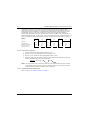
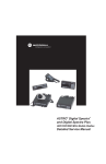
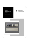
ASTRO Digital Spectra
and Digital Spectra Plus
UHF/VHF/800 MHz Mobile Radios
Detailed Service Manual
Foreword
This manual provides sufficient information to enable qualified service technicians to troubleshoot and repair ASTRO®
Digital Spectra® and ASTRO Digital Spectra Plus mobile radios (models W3, W4, W5, W7, and W9) to the component level.
For the most part, the information in this manual pertains to both ASTRO Digital Spectra and ASTRO Digital Spectra Plus
radios. Exceptions are clearly noted where they occur.
For details on radio operation or basic troubleshooting, refer to the applicable manuals available separately. A list of related
publications is provided in the section, “Related Publications,” on page xiv.
Product Safety and RF Exposure Compliance
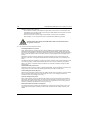
!
Caution
Before using this product, read the operating instructions
for safe usage contained in the Product Safety and RF
Exposure booklet enclosed with your radio.
ATTENTION!
This radio is restricted to occupational use only to satisfy FCC RF energy exposure requirements.
Before using this product, read the RF energy awareness information and operating instructions in the
Product Safety and RF Exposure booklet enclosed with your radio (Motorola Publication part number
68P81095C99) to ensure compliance with RF energy exposure limits.
Manual Revisions
Changes which occur after this manual is printed are described in FMRs (Florida Manual Revisions). These FMRs provide
complete replacement pages for all added, changed, and deleted items, including pertinent parts list data, schematics, and
component layout diagrams.
Computer Software Copyrights
The Motorola products described in this manual may include copyrighted Motorola computer programs stored in
semiconductor memories or other media. Laws in the United States and other countries preserve for Motorola certain
exclusive rights for copyrighted computer programs, including, but not limited to, the exclusive right to copy or reproduce in
any form the copyrighted computer program. Accordingly, any copyrighted Motorola computer programs contained in the
Motorola products described in this manual may not be copied, reproduced, modified, reverse-engineered, or distributed in
any manner without the express written permission of Motorola. Furthermore, the purchase of Motorola products shall not
be deemed to grant either directly or by implication, estoppel, or otherwise, any license under the copyrights, patents or
patent applications of Motorola, except for the normal non-exclusive license to use that arises by operation of law in the
sale of a product.
Document Copyrights
No duplication or distribution of this document or any portion thereof shall take place without the express written permission
of Motorola. No part of this manual may be reproduced, distributed, or transmitted in any form or by any means, electronic
or mechanical, for any purpose without the express written permission of Motorola.
Disclaimer
The information in this document is carefully examined, and is believed to be entirely reliable. However, no responsibility is
assumed for inaccuracies. Furthermore, Motorola reserves the right to make changes to any products herein to improve
readability, function, or design. Motorola does not assume any liability arising out of the applications or use of any product
or circuit described herein; nor does it cover any license under its patent rights nor the rights of others.
Trademarks
MOTOROLA, the Stylized M logo, ASTRO, and Spectra are registered in the US Patent & Trademark Office. All other
products or service names are the property of their respective owners.
© Motorola, Inc. 2002.
ii
Table of Contents
Foreword .........................................................................................................ii
Product Safety and RF Exposure Compliance ............................................................................................ii
Manual Revisions ........................................................................................................................................ii
Computer Software Copyrights ...................................................................................................................ii
Document Copyrights ..................................................................................................................................ii
Disclaimer....................................................................................................................................................ii
Trademarks .................................................................................................................................................ii
Commercial Warranty ..................................................................................xv
Limited Warranty .......................................................................................................................................xv
MOTOROLA COMMUNICATION PRODUCTS ...............................................................................xv
I. What This Warranty Covers And For How Long ....................................................................xv
II. General Provisions ................................................................................................................xv
III. State Law Rights ................................................................................................................. xvi
IV. How To Get Warranty Service ............................................................................................ xvi
V. What This Warranty Does Not Cover................................................................................... xvi
VI. Patent And Software Provisions ........................................................................................ xvii
VII. Governing Law.................................................................................................................. xvii
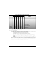
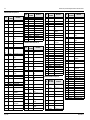
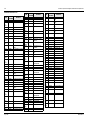
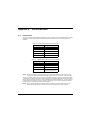
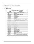
Model Numbering, Charts, and Specifications.........................................xix
Mobile Radio Model Numbering Scheme ................................................................................................. xix
ASTRO Digital Spectra Motorcycle 15 Watt (Ranges 1 and 2) Model Chart.............................................xx
ASTRO Digital Spectra Motorcycle 15 Watt (Ranges 3 and 3.5) Model Chart......................................... xxi
ASTRO Digital Spectra VHF 10–25 Watt Model Chart............................................................................ xxii
ASTRO Digital Spectra VHF 10–25 and 50–110 Watt Model Chart....................................................... xxiii
ASTRO Digital Spectra UHF 10–25 Watt Model Chart ........................................................................... xxv
ASTRO Digital Spectra UHF 20–40 Watt Model Chart .......................................................................... xxvi
ASTRO Digital Spectra UHF 50–110 Watt Model Chart .......................................................................xxviii
ASTRO Digital Spectra 800 MHz Model Chart........................................................................................ xxx
ASTRO Digital Spectra Plus VHF 25–50 and 50–110 Watt Model Chart............................................... xxxi
ASTRO Digital Spectra Plus 800 MHz Model Chart..............................................................................xxxiii
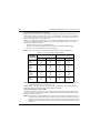
VHF Radio Specifications...................................................................................................................... xxxv
UHF Radio Specifications..................................................................................................................... xxxvi
800 MHz Radio Specifications..............................................................................................................xxxvii
Chapter 1
1.1
1.2
Introduction ......................................................................... 1-1
General .......................................................................................................................................... 1-1
Notations Used in This Manual...................................................................................................... 1-2
iv
Table of Contents
Chapter 2
General Overview................................................................ 2-1
2.1
2.2
2.3
2.4
Introduction .................................................................................................................................... 2-1
Analog Mode of Operation ............................................................................................................. 2-2
ASTRO Mode of Operation............................................................................................................ 2-2
Control Head Assembly ................................................................................................................. 2-2
2.4.1 Display (W3 Model)........................................................................................................... 2-2
2.4.2 Display (W4, W5, and W7 Models) ................................................................................... 2-2
2.4.3 Display (W9 Model)........................................................................................................... 2-3
2.4.4 Vacuum Fluorescent Display Driver.................................................................................. 2-3
2.4.5 Vacuum Fluorescent Voltage Source (W9 Model) ............................................................ 2-3
2.4.6 Controls and Indicators ..................................................................................................... 2-3
2.4.7 Status LEDs ...................................................................................................................... 2-3
2.4.8 Backlight LEDs.................................................................................................................. 2-3
2.4.9 Vehicle Interface Ports...................................................................................................... 2-4
2.4.10 Power Supplies ................................................................................................................. 2-4
2.4.11 Ignition Sense Circuits ...................................................................................................... 2-4
2.5 Power Amplifier.............................................................................................................................. 2-5
2.5.1 Gain Stages ...................................................................................................................... 2-5
2.5.2 Power Control ................................................................................................................... 2-5
2.5.3 Circuit Protection............................................................................................................... 2-5
2.5.4 DC Interconnect ................................................................................................................ 2-5
2.6 Front-End Receiver Assembly ....................................................................................................... 2-6
2.7 RF Board Basic.............................................................................................................................. 2-6
2.8 Voltage-Controlled Oscillator ......................................................................................................... 2-6
2.8.1 VHF Radios....................................................................................................................... 2-6
2.8.2 UHF and 800 MHz Radios ................................................................................................ 2-7
2.9 Command Board............................................................................................................................ 2-7
2.10 ASTRO Spectra Vocoder/Controller Board.................................................................................... 2-7
2.11 Radio Power .................................................................................................................................. 2-8
2.11.1 General ............................................................................................................................. 2-8
2.11.2 B+ Routing for ASTRO Spectra VOCON Board ............................................................... 2-9
Chapter 3
3.1
3.2
Theory of Operation............................................................ 3-1
RF Board........................................................................................................................................ 3-1
3.1.1 General ............................................................................................................................. 3-1
3.1.2 Synthesizer ....................................................................................................................... 3-3
3.1.2.1 Reference Frequency Generation............................................................................ 3-3
3.1.2.2 First VCO Frequency Generation ............................................................................ 3-3
3.1.2.3 Programmable Reference Divider............................................................................ 3-4
3.1.2.4 Phase Modulator...................................................................................................... 3-5
3.1.2.5 Loop Filter ................................................................................................................ 3-5
3.1.2.6 Auxiliary Control Bits................................................................................................ 3-5
3.1.2.7 Second VCO ............................................................................................................ 3-6
3.1.2.8 Power Distribution.................................................................................................... 3-6
3.1.3 Receiver Back-End ........................................................................................................... 3-6
3.1.3.1 First IF...................................................................................................................... 3-6
3.1.3.2 ABACUS II IC........................................................................................................... 3-7
Command Board............................................................................................................................ 3-8
3.2.1 Microcontroller and Support ICs ....................................................................................... 3-8
3.2.2 Serial Input/Output IC ....................................................................................................... 3-8
3.2.3 Power-Up/-Down Sequence ............................................................................................. 3-9
July 1, 2002
68P81076C25-C
Table of Contents
3.3
3.4
3.5
v
3.2.4 Regulators ...................................................................................................................... 3-10
3.2.5 Reset Circuits ................................................................................................................. 3-10
3.2.6 Serial Communications on the External Bus .................................................................. 3-11
3.2.7 Synchronous Serial Bus (MOSI) ..................................................................................... 3-12
3.2.8 Received Audio............................................................................................................... 3-12
3.2.9 Microphone Audio ........................................................................................................... 3-12
3.2.10 Transmit Deviation .......................................................................................................... 3-13
3.2.11 RS-232 Line Driver ......................................................................................................... 3-13
3.2.12 Flash Programming ........................................................................................................ 3-13
3.2.13 Encryption Voltages ........................................................................................................ 3-13
3.2.14 Regulator and Power-Control IC..................................................................................... 3-14
ASTRO Spectra VOCON Board .................................................................................................. 3-15
3.3.1 General ........................................................................................................................... 3-15
3.3.2 Controller Section ........................................................................................................... 3-15
3.3.3 Vocoder Section ............................................................................................................. 3-17
3.3.4 RX Signal Path ............................................................................................................... 3-18
3.3.5 TX Signal Path ................................................................................................................ 3-21
3.3.6 Controller Bootstrap and Asynchronous Buses .............................................................. 3-22
3.3.7 Vocoder Bootstrap .......................................................................................................... 3-24
3.3.8 Serial Peripheral Interface (SPI) Bus .............................................................................. 3-24
3.3.9 Controller Memory Map .................................................................................................. 3-24
3.3.10 Vocoder Memory Map .................................................................................................... 3-26
3.3.11 MCU System Clock......................................................................................................... 3-28
3.3.12 DSP System Clock ......................................................................................................... 3-28
3.3.13 Radio Power-Up/Power-Down Sequence....................................................................... 3-28
3.3.14 VOCON BOARD Signals ................................................................................................ 3-29
ASTRO Spectra Plus VOCON Board .......................................................................................... 3-38
3.4.1 General ........................................................................................................................... 3-38
3.4.2 ASTRO Spectra Plus Controller Section ........................................................................ 3-38
3.4.3 ASTRO Spectra Plus Vocoder Section........................................................................... 3-39
3.4.4 ASTRO Spectra Plus RX Signal Path............................................................................. 3-41
3.4.5 ASTRO Spectra Plus TX Signal Path ............................................................................. 3-42
3.4.6 ASTRO Spectra Plus Controller Bootstrap and Asynchronous Busses ......................... 3-43
3.4.7 ASTRO Spectra Plus Serial Peripheral Interface Bus .................................................... 3-44
3.4.8 ASTRO Spectra Plus MCU and DSP System Clocks..................................................... 3-44
3.4.9 ASTRO Spectra Plus Voltage Regulators ...................................................................... 3-45
3.4.10 ASTRO Spectra Plus Radio Power-Up/Power-Down Sequence .................................... 3-46
Voltage Control Oscillator ............................................................................................................ 3-47
3.5.1 VHF Band ....................................................................................................................... 3-47
3.5.1.1 General .................................................................................................................. 3-47
3.5.1.2 DC Voltage Supplies.............................................................................................. 3-47
3.5.1.3 VCO ....................................................................................................................... 3-47
3.5.1.4 Synthesizer Feedback ........................................................................................... 3-48
3.5.1.5 RX Buffer Circuitry ................................................................................................. 3-48
3.5.1.6 Frequency Divider and TX Buffer Circuitry ............................................................ 3-48
3.5.2 UHF Band ....................................................................................................................... 3-48
3.5.2.1 General .................................................................................................................. 3-48
3.5.2.2 Super Filter 8.6 V................................................................................................... 3-49
3.5.2.3 VCO ....................................................................................................................... 3-49
3.5.2.4 Receive Mode (AUX2* Low) .................................................................................. 3-49
3.5.2.5 Transmit Mode (AUX2* High) ................................................................................ 3-49
3.5.2.6 Bandshift Circuit..................................................................................................... 3-49
3.5.2.7 Output Buffer ......................................................................................................... 3-49
3.5.2.8 First Buffer ............................................................................................................. 3-49
68P81076C25-C
July 1, 2002
vi
Table of Contents
3.6
3.7
3.5.2.9 Doubler .................................................................................................................. 3-50
3.5.2.10 Synthesizer Feedback ........................................................................................... 3-50
3.5.2.11 Second Buffer ........................................................................................................ 3-50
3.5.2.12 Receive/Transmit Switch ....................................................................................... 3-50
3.5.3 800 MHz Band ................................................................................................................ 3-50
3.5.3.1 General .................................................................................................................. 3-50
3.5.3.2 Super Filter 8.6 V ................................................................................................... 3-50
3.5.3.3 VCO ....................................................................................................................... 3-50
3.5.3.4 Receive Mode-AUX 1* and AUX 2* High............................................................... 3-51
3.5.3.5 Transmit Mode-AUX 1* High; AUX 2* Low ............................................................ 3-51
3.5.3.6 TalkAround Mode-AUX 1* Low; AUX 2* Low......................................................... 3-51
3.5.3.7 VCO Buffer............................................................................................................. 3-51
3.5.3.8 First Buffer Circuit .................................................................................................. 3-51
3.5.3.9 Doubler .................................................................................................................. 3-51
3.5.3.10 Second Buffer ........................................................................................................ 3-52
3.5.3.11 K9.4 V Switch......................................................................................................... 3-52
Receiver Front-End...................................................................................................................... 3-53
3.6.1 VHF Band ....................................................................................................................... 3-53
3.6.1.1 General .................................................................................................................. 3-53
3.6.1.2 Theory of Operation ............................................................................................... 3-53
3.6.2 UHF Band ....................................................................................................................... 3-53
3.6.2.1 General .................................................................................................................. 3-53
3.6.2.2 Theory of Operation ............................................................................................... 3-54
3.6.3 800 MHz Band ................................................................................................................ 3-54
3.6.3.1 General .................................................................................................................. 3-54
3.6.3.2 Theory of Operation ............................................................................................... 3-54
Power Amplifiers .......................................................................................................................... 3-55
3.7.1 VHF Band Power Amplifiers ........................................................................................... 3-55
3.7.1.1 High-Power Amplifier ............................................................................................. 3-55
3.7.1.1.1 Transmitter...................................................................................................... 3-55
3.7.1.1.2 Antenna Switch and Harmonic Filter............................................................... 3-56
3.7.1.1.3 Power Control Circuitry ................................................................................... 3-57
3.7.1.2 25/10-Watt Power Amplifier ................................................................................... 3-59
3.7.1.2.1 Antenna Switch and Harmonic Filter............................................................... 3-60
3.7.1.2.2 Power Control Circuitry ................................................................................... 3-60
3.7.1.3 50-Watt Power Amplifiers ...................................................................................... 3-63
3.7.1.3.1 Transmitter...................................................................................................... 3-63
3.7.1.3.2 Antenna Switch and Harmonic Filter............................................................... 3-64
3.7.1.3.3 Power Control Circuitry ................................................................................... 3-65
3.7.2 UHF Band Power Amplifiers ........................................................................................... 3-68
3.7.2.1 High-Power Amplifier ............................................................................................. 3-68
3.7.2.1.1 Transmitter...................................................................................................... 3-68
3.7.2.1.2 Antenna Switch and Harmonic Filter............................................................... 3-69
3.7.2.1.3 Power Control Circuitry ................................................................................... 3-69
3.7.2.2 40-Watt Power Amplifier ........................................................................................ 3-72
3.7.2.2.1 Transmitter...................................................................................................... 3-72
3.7.2.2.2 Antenna Switch and Harmonic Filter............................................................... 3-73
3.7.2.2.3 Power Control Circuitry ................................................................................... 3-74
3.7.3 800 MHz Band Power Amplifiers .................................................................................... 3-77
3.7.3.1 15- and 35-Watt Amplifiers .................................................................................... 3-77
3.7.3.1.1 Transmitter...................................................................................................... 3-77
3.7.3.1.2 Antenna Switch and Harmonic Filter............................................................... 3-78
3.7.3.1.3 Power Control Circuitry ................................................................................... 3-79
3.7.3.1.4 Temperature Sensing ..................................................................................... 3-81
July 1, 2002
68P81076C25-C
Table of Contents
Chapter 4
4.1
4.2
4.3
4.4
4.5
vii
Troubleshooting Procedures ............................................. 4-1
ASTRO Spectra Procedures.......................................................................................................... 4-1
4.1.1 Handling Precautions........................................................................................................ 4-1
4.1.2 Voltage Measurement and Signal Tracing........................................................................ 4-2
4.1.3 Power-Up Self-Check Errors ............................................................................................ 4-2
4.1.3.1 Power-Up Sequence................................................................................................ 4-3
4.1.4 RF Board Troubleshooting................................................................................................ 4-5
4.1.4.1 Display Flashes “FAIL 001” ..................................................................................... 4-5
4.1.4.1.1 Incorrect Values at U602, Pin 19 ...................................................................... 4-6
4.1.4.1.2 Incorrect Values at U602 Pin 25 (MODULUS CONTROL) ............................... 4-7
4.1.4.1.3 Incorrect Voltage at Positive Steering Line....................................................... 4-7
4.1.4.1.4 Incorrect Values at U602, pin 27 ...................................................................... 4-7
4.1.4.2 Review of Synthesizer Fundamentals ..................................................................... 4-7
4.1.4.3 Second VCO Checks............................................................................................... 4-8
4.1.4.4 Troubleshooting the Back-End ................................................................................ 4-8
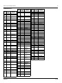
4.1.5 Standard Bias Table ......................................................................................................... 4-9
ASTRO Spectra Plus Procedures................................................................................................ 4-10
4.2.1 ASTRO Spectra Plus Power-Up Self-Check Errors........................................................ 4-10
4.2.2 ASTRO Spectra Plus Power-Up Self-Check Diagnostics and Repair ............................ 4-11
4.2.3 ASTRO Spectra Plus Standard Bias Table .................................................................... 4-12
VCO Procedures.......................................................................................................................... 4-13
4.3.1 VHF Band ....................................................................................................................... 4-13
4.3.1.1 VCO Hybrid Assembly ........................................................................................... 4-13
4.3.1.2 Out-of-Lock Condition............................................................................................ 4-13
4.3.1.3 No or Low Output Power (TX or RX Injection)....................................................... 4-15
4.3.1.4 No or Low Modulation............................................................................................ 4-15
4.3.2 UHF Band ....................................................................................................................... 4-15
4.3.2.1 VCO Hybrid Assembly ........................................................................................... 4-15
4.3.2.2 Out-of-Lock Condition............................................................................................ 4-16
4.3.2.3 No or Low Output Power (TX or RX Injection)....................................................... 4-16
4.3.2.4 No or Low Modulation............................................................................................ 4-17
4.3.3 800 MHz Band ................................................................................................................ 4-18
4.3.3.1 VCO Hybrid Assembly ........................................................................................... 4-18
4.3.3.2 Out-of-Lock Condition............................................................................................ 4-18
4.3.3.3 No or Low Output Power (TX or RX Injection)....................................................... 4-19
4.3.3.4 No or Low Modulation............................................................................................ 4-19
Receiver Front-End (RXFE)......................................................................................................... 4-20
4.4.1 VHF Band ....................................................................................................................... 4-20
4.4.2 UHF Band ....................................................................................................................... 4-20
4.4.3 800 MHz Band ................................................................................................................ 4-20
Power Amplifier Procedures ........................................................................................................ 4-21
4.5.1 VHF Band ....................................................................................................................... 4-21
4.5.1.1 High-Power Amplifier ............................................................................................. 4-21
4.5.1.1.1 General Troubleshooting and Repair Notes ................................................... 4-21
4.5.1.1.2 PA Functional Testing..................................................................................... 4-25
4.5.1.1.3 Power Control and Protection Circuitry........................................................... 4-28
4.5.1.2 25/10 Watt Power Amplifier ................................................................................... 4-29
4.5.1.2.1 General Troubleshooting and Repair Notes ................................................... 4-29
4.5.1.2.2 PA Functional Testing..................................................................................... 4-30
4.5.1.2.3 Localizing Problems........................................................................................ 4-34
4.5.1.2.4 Isolating Failures............................................................................................. 4-35
4.5.1.2.5 Power Control and Protection Circuitry........................................................... 4-37
4.5.1.3 50 Watt Power Amplifiers ...................................................................................... 4-38
68P81076C25-C
July 1, 2002
viii
Table of Contents
4.5.1.3.1 General Troubleshooting and Repair Notes ................................................... 4-38
4.5.1.3.2 PA Functional Testing..................................................................................... 4-39
4.5.1.3.3 Localizing Problems........................................................................................ 4-42
4.5.1.3.4 Isolating Failures............................................................................................. 4-43
4.5.1.3.5 Power Control and Protection Circuitry........................................................... 4-45
4.5.2 UHF Band ....................................................................................................................... 4-47
4.5.2.1 High-Power Amplifier ............................................................................................. 4-47
4.5.2.1.1 General Troubleshooting and Repair Notes ................................................... 4-47
4.5.2.1.2 PA Functional Testing..................................................................................... 4-51
4.5.2.1.3 Power Control and Protection Circuitry........................................................... 4-54
4.5.2.2 40 Watt Power Amplifiers....................................................................................... 4-56
4.5.2.2.1 General Troubleshooting and Repair Notes ................................................... 4-56
4.5.2.2.2 PA Functional Testing..................................................................................... 4-57
4.5.2.2.3 Localizing Problems........................................................................................ 4-61
4.5.2.2.4 Isolating Failures............................................................................................. 4-62
4.5.2.2.5 Power Control and Protection Circuitry........................................................... 4-64
4.5.3 800 MHz Band ................................................................................................................ 4-66
4.5.3.1 15 Watt and 35 Watt Power Amplifiers .................................................................. 4-66
4.5.3.1.1 General Troubleshooting and Repair Notes ................................................... 4-66
4.5.3.1.2 PA Functional Testing..................................................................................... 4-67
4.5.3.1.3 Localizing Problems........................................................................................ 4-71
4.5.3.1.4 Isolating Failures............................................................................................. 4-72
4.5.3.1.5 Power Control and Protection Circuitry........................................................... 4-74
Chapter 5
5.1
5.2
Troubleshooting Charts ..................................................... 5-1
Introduction .................................................................................................................................... 5-1
List of Troubleshooting Charts ....................................................................................................... 5-1
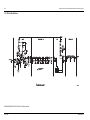
RF Board Back-End................................................................................................................. 5-3
Command Board ..................................................................................................................... 5-4
Radio Power-Up Fail ............................................................................................................... 5-5
Bootstrap Fail .......................................................................................................................... 5-6
01/90, General Hardware Failure ............................................................................................ 5-7
01/81, Host ROM Checksum Failure....................................................................................... 5-7
01/82 or 002, External EEPROM Checksum Failure............................................................... 5-8
01/84, SLIC Initialization Failure.............................................................................................. 5-8
01/88, MCU (Host mC) External SRAM Failure ...................................................................... 5-9
01/92, Internal EEPROM Checksum Failure ........................................................................... 5-9
02/A0, ADSIC Checksum Failure .......................................................................................... 5-10
02/81, DSP ROM Checksum Failure..................................................................................... 5-10
02/88, DSP External SRAM Failure U414 ............................................................................. 5-11
02/84, DSP External SRAM Failure U403 ............................................................................. 5-11
02/82, DSP External SRAM Failure U402 ............................................................................. 5-12
02/90, General DSP Hardware Failure.................................................................................. 5-12
09/10, Secure Hardware Failure............................................................................................ 5-13
09/90, Secure Hardware Failure............................................................................................ 5-13
No RX Audio.......................................................................................................................... 5-14
No TX Modulation.................................................................................................................. 5-15
Key Load Fail......................................................................................................................... 5-16
800 MHz Receiver Front-End Hybrid..................................................................................... 5-17
UHF Receiver Front-End Hybrid............................................................................................ 5-17
VHF Receiver Front-End Hybrid............................................................................................ 5-18
ASTRO Spectra Plus VOCON Power-Up Failure.................................................................. 5-19
July 1, 2002
68P81076C25-C
Table of Contents
ix
ASTRO Spectra Plus VOCON DC Supply Failure ................................................................ 5-20
ASTRO Spectra Plus VOCON TX Modulation Failure Sheet 1 of 4...................................... 5-21
ASTRO Spectra Plus VOCON TX Modulation Failure Sheet 2 of 4 ...................................... 5-22
ASTRO Spectra Plus VOCON TX Modulation Failure Sheet 3 of 4...................................... 5-23
ASTRO Spectra Plus VOCON TX Modulation Failure Sheet 4 of 4 ...................................... 5-24
ASTRO Spectra Plus VOCON RX Audio Failure .................................................................. 5-24
ASTRO Spectra Plus VOCON Secure Hardware Failure ..................................................... 5-25
ASTRO Spectra Plus VOCON Key Load Fail........................................................................ 5-26
Chapter 6
6.1
6.2
6.3
Introduction .................................................................................................................................... 6-1
ASTRO Spectra Waveforms.......................................................................................................... 6-1
Waveform W1: Power-On Reset Timing........................................................................................ 6-1
Waveform W2: DSP SSI Port RX Mode ........................................................................................ 6-2
Waveform W3: DSP SSI Port TX Mode CSQ................................................................................ 6-2
Waveform W4: ABACUS Programming at Mode Change ............................................................. 6-3
Waveform W5: ABACUS/ADSIC Interface .................................................................................... 6-3
Waveform W6: SPI Bus Programming ADSIC .............................................................................. 6-4
Waveform W7: Receive Audio....................................................................................................... 6-4
Waveform W8: Transmit Audio...................................................................................................... 6-5
Waveform W9: Power-Down Reset ............................................................................................... 6-5
Waveform W10: ADSIC 2.4 MHz Reference ................................................................................. 6-6
ASTRO Spectra Digital Plus VOCON Board Waveforms .............................................................. 6-7
32 kHz Clock Waveform ................................................................................................................ 6-7
16.8 MHz Clock Waveform ............................................................................................................ 6-8
TX Modulation Out Waveform ....................................................................................................... 6-8
Differential ADDAG Output Waveform........................................................................................... 6-9
TX SSI Waveform .......................................................................................................................... 6-9
SPI Bus Waveform ...................................................................................................................... 6-10
TX 1 kHz Tone Waveform ........................................................................................................... 6-10
Serial Audio Port Waveform ........................................................................................................ 6-11
RX Audio Waveform .................................................................................................................... 6-11
RX BBP Waveform ...................................................................................................................... 6-12
Secure Interface Waveform ......................................................................................................... 6-12
8 kHz Frame Sync for Security Circuitry Waveform .................................................................... 6-13
Chapter 7
Parts Lists
7.1
Troubleshooting Waveforms ............................................. 6-1
Schematics, Component Location Diagrams, and
.............................................................................................. 7-1
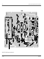
RF Section .................................................................................................................................... 7-2
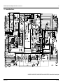
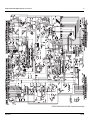
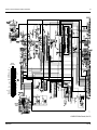
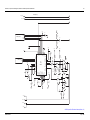
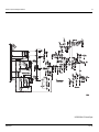
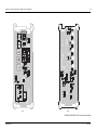
ASTRO Spectra Radio Interconnection................................................................................... 7-4
HRN4009B/HRN6014A VHF RF Board; HRN4010B/HRN6020A UHF RF Board; and
HRN6019A 800 MHz RF Board Schematic............................................................................. 7-5
HRN4009B/HRN6014A VHF RF Board, HRN4010B/HRN6020A UHF RF Board, and
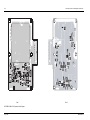
HRN6019A 800 MHz RF Board Component Location Diagrams............................................ 7-6
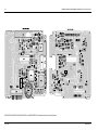
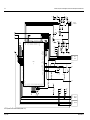
HRN4009C/HRN6014C VHF RF Board Schematic Diagram.................................................. 7-9
HRN4009C/HRN6014C VHF RF Board Component Location Diagrams ............................. 7-10
HRN4009E and HRN6014D VHF RF Board; HRN4010D and HRN6020C UHF RF Board; and
HRN6019C 800 MHz RF Board Schematic Diagram (Sheet 1 of 2) ..................................... 7-12
HRN4009E and HRN6014D VHF RF Board; HRN4010D and HRN6020C UHF RF Board; and
HRN6019C 800 MHz RF Board Schematic Diagram (Sheet 2 of 2) ..................................... 7-13
68P81076C25-C
July 1, 2002
x
Table of Contents
7.2
7.3
7.4
7.5
HRN4009E and HRN6014D VHF RF Board; HRN4010D and HRN6020C UHF RF Board; and
HRN6019C 800 MHz RF Component Location Diagram ...................................................... 7-14
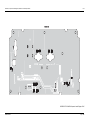
Command Board Section............................................................................................................. 7-17
HLN5558E/F/G, HLN6529C/D/E/F/G, HLN6560C/D/E/F/G/H and HLN6562C/D/E/F/G/H
Command Board Schematic Diagram ................................................................................... 7-17
HLN5558E/F/G, HLN6529C/D/E, HLN6560C/D/E/F/G/H, and HLN6562C/D/E/F/G/H Command
Board Component Location Diagrams .................................................................................. 7-18
HLN5558H/J, HLN6529H, HLN6560J and HLN6562J Command Board Schematic
Diagram ................................................................................................................................. 7-21
HLN5558H/J, HLN6529H, HLN6560J and HLN6562J Component Location Diagram ......... 7-22
VOCON Section........................................................................................................................... 7-26
HLN6458D VOCON Board Schematic (Sheet 1 of 2) ........................................................... 7-26
HLN6458D VOCON Board Schematic (Sheet 2 of 2) ........................................................... 7-27
HLN6458D VOCON Board Component Location Diagrams (Sheet 1 of 2)........................... 7-28
HLN6458D VOCON Board Component Location Diagrams (Sheet 2 of 2)........................... 7-29
HLN6458E VOCON Board Schematic (Sheet 1 of 2)............................................................ 7-32
HLN6458E VOCON Board Schematic (Sheet 2 of 2)............................................................ 7-33
HLN6458E VOCON Board Component Location Diagrams (Sheet 1 of 2)........................... 7-34
HLN6458E VOCON Board Component Location Diagrams (Sheet 2 of 2)........................... 7-35
HLN6458F/G VOCON Board Schematic (Sheet 1 of 2) ........................................................ 7-38
HLN6458F/G VOCON Board Schematic (Sheet 2 of 2) ........................................................ 7-39
HLN6458F/G VOCON Board Component Location Diagrams (Sheet 1 of 2) ....................... 7-40
HLN6458F/G VOCON Board Component Location Diagrams (Sheet 2 of 2) ....................... 7-41
HLN6458H VOCON Board Schematic (Sheet 1 of 2) ........................................................... 7-44
HLN6458H VOCON Board Schematic (Sheet 2 of 2) ........................................................... 7-45
HLN6458H VOCON Board Component Location Diagrams ................................................. 7-46
ASTRO Spectra Plus VOCON Section ........................................................................................ 7-49
ASTRO Spectra Plus Top Level Schematic (Sheet 1 of 2) ................................................... 7-49
ASTRO Spectra Plus Top Level Schematic (Sheet 2 of 2) .................................................... 7-50
ASTRO Spectra Plus RF Interface Schematic (Sheet 1 of 2) ............................................... 7-51
ASTRO Spectra Plus RF Interface Schematic (Sheet 2 of 2)................................................ 7-52
ASTRO Spectra Plus Digital/USB Schematic (Sheet 1 of 2)................................................. 7-53
ASTRO Spectra Plus Digital/USB Schematic (Sheet 2 of 2) ................................................. 7-54
ASTRO Spectra Plus Audio/DC Schematic........................................................................... 7-55
ASTRO Spectra Plus Voltage Conversion Schematic ........................................................... 7-56
ASTRO Spectra Plus Secure Interface Schematic................................................................ 7-57
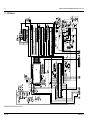
ASTRO Spectra Plus VOCON Component Location Diagram, Top View ............................. 7-58
ASTRO Spectra Plus VOCON Component Location Diagram, Bottom View........................ 7-59
VCO Section ................................................................................................................................ 7-62
HLD6061D and HLD6062D VHF VCO Hybrid Schematic..................................................... 7-62
HLD6061D and HLD6062D VHF VCO Hybrid Component Location Diagram...................... 7-63
HLD4342B and HLD4343B VHF VCO Carrier Schematic Diagram ...................................... 7-64
HLD4342D and HLD4343D VHF VCO Carrier Schematic Diagram...................................... 7-65
HLD4342B/HLD4343B VHF VCO Carrier Component Location Diagram............................. 7-66
HLD4342D/HLD4343D VHF VCO Carrier Component Location Diagram ............................ 7-67
UHF VCO Ranges 1, 2, 3, and 4 Hybrid Schematic.............................................................. 7-70
HLE6101A UHF VCO Range 1 Hybrid and HLE6102A Range 2 Hybrid Component Location
Diagram ................................................................................................................................. 7-71
HLE6103B UHF VCO Range 3 Hybrid and HLE6104B Range 4 Hybrid Component Location
Diagram ................................................................................................................................. 7-73
UHF VCO Ranges 1, 2, 3, and 4 Schematic Diagram........................................................... 7-75
HLE6045B Range 1 and HLE6046B Range 2 UHF VCO Component Location Diagram..... 7-76
HLE6000D Range 3 and HLE6041D Range 4 UHF VCO Component Location Diagrams .. 7-77
HLF6080B 800 MHz VCO Schematic Diagram..................................................................... 7-79
July 1, 2002
68P81076C25-C
Table of Contents
7.6
7.7
xi
HLF6080B 800 MHz VCO Component Location Diagram .................................................... 7-80
RX Front-End Section.................................................................................................................. 7-82
HRD6001E/6002E/6011E/6012E VHF Receiver Front-End Schematic ................................ 7-82
HRD6001E/6002E/6011E/6012E VHF Component Location Diagram ................................. 7-83
HRD6001G/6002G/6011G/6012G VHF Receiver Front-End Schematic .............................. 7-87
HRD6001G/6002G/6011G/6012G VHF Receiver Front-End Component Location Diagram 7-88
HRE6001B/6002C/6003B/6004B/6011B/6012B/6014B UHF Receiver Front-End Preamp and
Standard Schematics ............................................................................................................ 7-90
HRE6001B/6002C/6003B/6004B/6011B/6012B/6014B UHF Receiver Front-End Hybrid
Component Location Diagram............................................................................................... 7-91
HRF6004B/C 800 MHz Receiver Front-End Schematic Diagram ......................................... 7-94
HRF6004B/C 800 MHz Receiver Front-End Component Location Diagram......................... 7-95
Power Amplifier Section............................................................................................................... 7-97
HLD6022C VHF 50 Watt PA Schematic ............................................................................... 7-97
HLD6022C VHF 50-Watt PA Component Location Diagram, Side 1 .................................... 7-98
HLD6022C VHF 50-Watt PA Component Location Diagram, Side 2 .................................... 7-99
HLD6064C VHF 100-Watt PA Schematic ........................................................................... 7-101
HLD6064C VHF 100-Watt PA Component Location Diagram, Side 1 ................................ 7-102
HLD6064C VHF 100-Watt PA Component Location Diagram, Side 2 ................................ 7-103
HLD6032B/HLD6066B VHF 25-Watt PA Schematic........................................................... 7-105
HLD6032B/HLD6066B VHF 25-Watt PA Component Location Diagram, Side 1 ................ 7-106
HLD6032B/HLD6066B VHF 25-Watt PA Component Location Diagram, Side 2................ 7-107
HLE6062B and HLE6071B UHF 25-Watt PA Schematic .................................................... 7-110
HLE6062B UHF 25-Watt PA Component Location Diagram, Side 1 .................................. 7-111
HLE6062B UHF 25-Watt PA Component Location Diagram, Side 2.................................. 7-112
HLE6043C, HLE6044C, and HLE6049B UHF 40-Watt PA Schematic................................ 7-114
HLE6043C, HLE6044C, and HLE6049B UHF 40-Watt PA Component Location Diagram,
Side 1 .................................................................................................................................. 7-115
HLE6043C, HLE6044C, and HLE6049B UHF 40-Watt PA Component Location Diagram,
Side 2 .................................................................................................................................. 7-116
HLE6039C, HLE6040C, and HLE6051C UHF 100-Watt PA Schematic ............................. 7-120
HLE6039C, HLE6040C, and HLE6051C UHF 100-Watt PA Component Location Diagram,
Side 1 .................................................................................................................................. 7-121
HLE6039C, HLE6040C, and HLE6051C UHF 100-Watt PA Component Location Diagram,
Side 2 .................................................................................................................................. 7-122
HLF6078B 800 MHz 15-Watt PA Schematic....................................................................... 7-127
HLF6078B 800 MHz 15-Watt PA Component Location Diagram, Side 1............................ 7-128
HLF6078B 800 MHz 15-Watt PA Component Location Diagram, Side 2 ........................... 7-129
HLF6077D 800 MHz 35-Watt PA Schematic ...................................................................... 7-131
HLF6077D 800 MHz 35-Watt PA Component Location Diagram, Side 1............................ 7-132
HLF6077D 800 MHz 35-Watt PA Component Location Diagram, Side 2 ........................... 7-133
Appendix A Secure Modules...................................................................A-1
A.1
A.2
A.3
Introduction ....................................................................................................................................A-1
Circuit Description..........................................................................................................................A-2
Troubleshooting Secure Operations ..............................................................................................A-2
A.3.1 Error 09/10, Error 09/90 ....................................................................................................A-2
A.3.2 Keyload .............................................................................................................................A-2
68P81076C25-C
July 1, 2002
xii
Table of Contents
Appendix B Replacement Parts Ordering..............................................B-1
B.1
B.2
B.3
B.4
B.5
B.6
B.7
B.8
Basic Ordering Information ............................................................................................................B-1
Transceiver Board and VOCON Board Ordering Information........................................................B-1
Motorola Online..............................................................................................................................B-1
Mail Orders ....................................................................................................................................B-1
Telephone Orders ..........................................................................................................................B-2
Fax Orders .....................................................................................................................................B-2
Parts Identification .........................................................................................................................B-2
Product Customer Service .............................................................................................................B-2
Glossary ......................................................................................... Glossary-1
July 1, 2002
68P81076C25-C
List of Figures
xiii
List of Figures
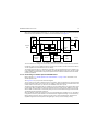
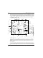
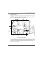
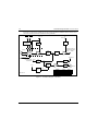
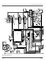
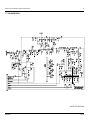
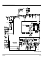
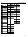
Figure 2-1. DC Voltage Routing Block Diagram ...................................................................................... 2-9
Figure 2-2. ASTRO Spectra B+ Routing for Vocoder/Controller (VOCON) Board ................................ 2-10
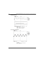
Figure 3-1. Prescaler IC Block Diagram.................................................................................................. 3-2
Figure 3-2. Synthesizer IC Block Diagram .............................................................................................. 3-2
Figure 3-3. Loop Divider Waveforms....................................................................................................... 3-4
Figure 3-4. Loop Filter Schematic ........................................................................................................... 3-5
Figure 3-5. Power-on Reset .................................................................................................................. 3-11
Figure 3-6. Transmitter Attack Time ...................................................................................................... 3-14
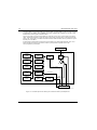
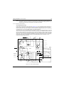
Figure 3-7. VOCON Board - Controller Section .................................................................................... 3-16
Figure 3-8. VOCON Board - Vocoder Section....................................................................................... 3-18
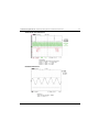
Figure 3-9. DSP RSSI Port - RX Mode ................................................................................................. 3-19
Figure 3-10. DSP RSSI Port - TX Mode.................................................................................................. 3-21
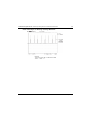
Figure 3-11. Host SB9600 and RS232 Ports .......................................................................................... 3-23
Figure 3-12. Controller Memory Mapping................................................................................................ 3-25
Figure 3-13. Vocoder Memory Mapping .................................................................................................. 3-27
Figure 3-14. ASTRO Spectra Plus VOCON Board - Controller Section.................................................. 3-39
Figure 3-15. ASTRO Spectra Plus VOCON Board - Vocoder Section .................................................... 3-40
Figure 3-16. ASTRO Spectra Plus RX Mode .......................................................................................... 3-41
Figure 3-17. ASTRO Spectra Plus TX Mode........................................................................................... 3-42
Figure 3-18. ASTRO Spectra Plus Host SB9600 and RS232 Ports........................................................ 3-44
Figure 3-19. ASTRO Spectra Plus VOCON DC Distribution ................................................................... 3-45
Figure 3-20. RPCIC Block Diagram ........................................................................................................ 3-57
Figure 3-21. Regulator/Power Control IC Block Diagram........................................................................ 3-61
Figure 3-22. 50-Watt Power Amplifier Block Diagram ............................................................................. 3-63
Figure 3-23. Regulator/Power Control IC Block Diagram........................................................................ 3-65
Figure 3-24. UHF High-Power, Power Amplifier Block Diagram ............................................................. 3-68
Figure 3-25. RPCIC Block Diagram ........................................................................................................ 3-70
Figure 3-26. RPCIC Block Diagram ........................................................................................................ 3-74
Figure 3-27. RPCIC Block Diagram ........................................................................................................ 3-79
Figure 4-1. VCO Block Diagram - VHF Band ........................................................................................ 4-14
Figure 4-2. VCO Block Diagram - UHF Band........................................................................................ 4-17
Figure 4-3. VCO Block Diagram - 800 MHz Band................................................................................. 4-18
Figure 4-4. Connector Pin-Out - High-Power Amplifier ......................................................................... 4-22
Figure 4-5. PA Test Adapter, 25/10 Watt Power Amplifier ..................................................................... 4-31
Figure 4-6. PA Test Adapter, 50 Watt Power Amplifier .......................................................................... 4-40
Figure 4-7. Connector Pin-Out - High-Power Amplifier ......................................................................... 4-48
Figure 4-8. Block Diagram for Spectra High-Power Power Amplifier .................................................... 4-56
Figure 4-9. PA Test Adapter, 40 Watt Power Amplifier .......................................................................... 4-58
Figure 4-10. PA Test Adapter, 15 and 35 Watt Power Amplifier .............................................................. 4-67
Go to Chapter 7 on page 7-1 for a listing of schematics and component location diagrams.
68P81076C25-C
July 1, 2002
xiv
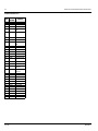
List of Tables
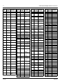
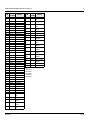
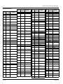
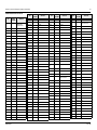
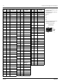
List of Tables
Table 3-1.
Table 3-2.
Table 3-3.
Table 3-4.
Table 3-5.
Table 3-6.
Table 3-7.
Table 3-8.
Table 3-9.
Table 4-1.
Table 4-2.
Table 4-3.
Table 4-4.
Table 4-5.
Table 4-6.
Table 4-7.
Table 4-8.
Table 4-9.
Table 4-10.
Table 4-11.
Table 4-12.
Table 4-13.
Table 4-14.
Table 4-15.
Table 4-16.
Table 4-17.
Table 4-18.
Table 4-19.
Table 4-20.
Table 4-21.
Table 4-22.
Table 4-23.
Table 4-24.
Table 4-25.
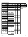
Table 5-1.
Table A-1.
Table A-2.
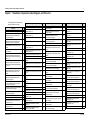
Integrated Circuits Voltages ................................................................................................ 3-10
VOCON Board Address Bus (A) Pinouts ............................................................................ 3-29
VOCON Board Address Bus (HA) Pinouts.......................................................................... 3-30
VOCON Board Data Bus (D) Pinouts.................................................................................. 3-30
VOCON Board Data Bus (HD) Pinouts ............................................................................... 3-31
U204 (MCU) ........................................................................................................................ 3-32
U206 (SLIC) ........................................................................................................................ 3-33
VOCON U405 (DSP) .......................................................................................................... 3-35
VOCON U406 (ADSIC) ....................................................................................................... 3-36
Power-Up Self-Check Error Codes ....................................................................................... 4-2
Voltage by Location............................................................................................................... 4-5
Feedback Frequency Ranges ............................................................................................... 4-7
Standard Operating Bias ....................................................................................................... 4-9
ASTRO Spectra Plus Power-Up Self-Check Error Codes .................................................. 4-10
ASTRO Spectra Plus Standard Operating Bias .................................................................. 4-12
VCO Frequency .................................................................................................................. 4-15
Power Control DC Voltage Chart ........................................................................................ 4-23
LLA and 2nd Stage Typical Voltages................................................................................... 4-26
DC Voltages and Input Power Chart ................................................................................... 4-30
Power Control DC Voltage Chart ........................................................................................ 4-31
Antenna Switch DC Voltage Chart ...................................................................................... 4-34
LLA and Driver Typical Voltages ......................................................................................... 4-35
DC Voltages and Input Power Chart ................................................................................... 4-39
Power Control DC Voltage Chart ........................................................................................ 4-40
LLA and Pre-Driver Typical Voltages .................................................................................. 4-43
Power Control DC Voltage Chart ........................................................................................ 4-49
LLA and 2nd Stage Typical Voltages................................................................................... 4-52
DC Voltages and Input Power Chart ................................................................................... 4-58
Power Control DC Voltage Chart ........................................................................................ 4-59
Antenna Switch DC Voltage Chart ...................................................................................... 4-61
LLA and Pre-Driver Typical Voltages .................................................................................. 4-62
DC Voltages and Input Power Chart ................................................................................... 4-68
Power Control DC Voltage Chart ........................................................................................ 4-68
Antenna Switch DC Voltage Chart ...................................................................................... 4-71
List of Troubleshooting Charts .............................................................................................. 5-1
ASTRO Digital Spectra Secure Modules...............................................................................A-1
ASTRO Digital Spectra Plus Secure Modules.......................................................................A-1
Related Publications
ASTRO Digital Spectra and Digital Spectra Plus Model W3 User’s Guide .................................. 68P81090C61
ASTRO Digital Spectra and Digital Spectra Plus Models W4, W5, W7, and W9 User’s Guide ... 68P81090C62
ASTRO Digital Spectra Hand-Held Control Head User’s Guide (Model W3)............................... 68P81073C25
ASTRO Digital Spectra (Model W4, W5, W7, and W9) User’s Guide .......................................... 68P81074C80
ASTRO Digital Spectra and Digital Spectra Plus Mobile Radios Basic Service Manual .............. 68P81076C20
ASTRO Digital Spectra Mobile Radios Dual Control Head Radio System Service Manual ......... 68P81091C78
ASTRO Spectra and Digital Spectra FM Two-Way Mobile Radios Installation Manual................ 68P81070C85
ASTRO Spectra Motorcycle Radios Supplemental Installation Manual ...................................... 68P80103W01
KVL 3000 User’s Manual ..............................................................................................................68P81131E16
Spectra VHF VCO Section Detailed Service Manual Supplement............................................... 68P81074C48
Spectra High-Power Power Amplifier Detailed Service Manual Supplement ............................... 68P81077C25
Spectra Systems 9000 Control Unit Detailed Service Manual Supplement ................................. 68P81077C30
Spectra A5 and A7 Control Head Instruction Manual....................................................................68P81109C33
Spectra A4 Control Head Instruction Manual ...............................................................................68P81109C34
July 1, 2002
68P81076C25-C
Commercial Warranty
Limited Warranty
MOTOROLA COMMUNICATION PRODUCTS
I. What This Warranty Covers And For How Long
MOTOROLA INC. (“MOTOROLA”) warrants the MOTOROLA manufactured Communication
Products listed below (“Product”) against defects in material and workmanship under normal use and
service for a period of time from the date of purchase as scheduled below:
ASTRO Digital Spectra and Digital Spectra
Plus Units
One (1) Year
Product Accessories
One (1) Year
Motorola, at its option, will at no charge either repair the Product (with new or reconditioned parts),
replace it (with a new or reconditioned Product), or refund the purchase price of the Product during
the warranty period provided it is returned in accordance with the terms of this warranty. Replaced
parts or boards are warranted for the balance of the original applicable warranty period. All replaced
parts of Product shall become the property of MOTOROLA.
This express limited warranty is extended by MOTOROLA to the original end user purchaser only
and is not assignable or transferable to any other party. This is the complete warranty for the Product
manufactured by MOTOROLA. MOTOROLA assumes no obligations or liability for additions or
modifications to this warranty unless made in writing and signed by an officer of MOTOROLA.
Unless made in a separate agreement between MOTOROLA and the original end user purchaser,
MOTOROLA does not warrant the installation, maintenance or service of the Product.
MOTOROLA cannot be responsible in any way for any ancillary equipment not furnished by
MOTOROLA which is attached to or used in connection with the Product, or for operation of the
Product with any ancillary equipment, and all such equipment is expressly excluded from this
warranty. Because each system which may use the Product is unique, MOTOROLA disclaims
liability for range, coverage, or operation of the system as a whole under this warranty.
II. General Provisions
This warranty sets forth the full extent of MOTOROLA'S responsibilities regarding the Product.
Repair, replacement or refund of the purchase price, at MOTOROLA's option, is the exclusive
remedy. THIS WARRANTY IS GIVEN IN LIEU OF ALL OTHER EXPRESS WARRANTIES. IMPLIED
WARRANTIES, INCLUDING WITHOUT LIMITATION, IMPLIED WARRANTIES OF
MERCHANTABILITY AND FITNESS FOR A PARTICULAR PURPOSE, ARE LIMITED TO THE
DURATION OF THIS LIMITED WARRANTY. IN NO EVENT SHALL MOTOROLA BE LIABLE FOR
DAMAGES IN EXCESS OF THE PURCHASE PRICE OF THE PRODUCT, FOR ANY LOSS OF
USE, LOSS OF TIME, INCONVENIENCE, COMMERCIAL LOSS, LOST PROFITS OR SAVINGS
OR OTHER INCIDENTAL, SPECIAL OR CONSEQUENTIAL DAMAGES ARISING OUT OF THE
USE OR INABILITY TO USE SUCH PRODUCT, TO THE FULL EXTENT SUCH MAY BE
DISCLAIMED BY LAW.
xvi
Commercial Warranty
III. State Law Rights
SOME STATES DO NOT ALLOW THE EXCLUSION OR LIMITATION OF INCIDENTAL OR
CONSEQUENTIAL DAMAGES OR LIMITATION ON HOW LONG AN IMPLIED WARRANTY
LASTS, SO THE ABOVE LIMITATION OR EXCLUSIONS MAY NOT APPLY.
This warranty gives specific legal rights, and there may be other rights which may vary from state to
state.
IV. How To Get Warranty Service
You must provide proof of purchase (bearing the date of purchase and Product item serial number)
in order to receive warranty service and, also, deliver or send the Product item, transportation and
insurance prepaid, to an authorized warranty service location. Warranty service will be provided by
Motorola through one of its authorized warranty service locations. If you first contact the company
which sold you the Product, it can facilitate your obtaining warranty service. You can also call
Motorola at 1-888-567-7347 US/Canada.
V. What This Warranty Does Not Cover
A. Defects or damage resulting from use of the Product in other than its normal and customary
manner.
B. Defects or damage from misuse, accident, water, or neglect.
C. Defects or damage from improper testing, operation, maintenance, installation, alteration,
modification, or adjustment.
D. Breakage or damage to antennas unless caused directly by defects in material workmanship.
E. A Product subjected to unauthorized Product modifications, disassemblies or repairs (including, without limitation, the addition to the Product of non-Motorola supplied equipment) which
adversely affect performance of the Product or interfere with Motorola's normal warranty
inspection and testing of the Product to verify any warranty claim.
F.
Product which has had the serial number removed or made illegible.
G. Rechargeable batteries if:
H. any of the seals on the battery enclosure of cells are broken or show evidence of tampering.
I.
the damage or defect is caused by charging or using the battery in equipment or service other
than the Product for which it is specified.
J.
Freight costs to the repair depot.
K. A Product which, due to illegal or unauthorized alteration of the software/firmware in the Product, does not function in accordance with MOTOROLA's published specifications or the FCC
type acceptance labeling in effect for the Product at the time the Product was initially distributed from MOTOROLA.
L. Scratches or other cosmetic damage to Product surfaces that does not affect the operation of
the Product.
M. Normal and customary wear and tear.
June 28, 2002
68P81076C25-C
Commercial Warranty
xvii
VI. Patent And Software Provisions
MOTOROLA will defend, at its own expense, any suit brought against the end user purchaser to the
extent that it is based on a claim that the Product or parts infringe a United States patent, and
MOTOROLA will pay those costs and damages finally awarded against the end user purchaser in
any such suit which are attributable to any such claim, but such defense and payments are
conditioned on the following:
A. that MOTOROLA will be notified promptly in writing by such purchaser of any notice of such
claim;
B. that MOTOROLA will have sole control of the defense of such suit and all negotiations for its
settlement or compromise; and
C. should the Product or parts become, or in MOTOROLA's opinion be likely to become, the
subject of a claim of infringement of a United States patent, that such purchaser will permit
MOTOROLA, at its option and expense, either to procure for such purchaser the right to continue using the Product or parts or to replace or modify the same so that it becomes noninfringing or to grant such purchaser a credit for the Product or parts as depreciated and accept
its return. The depreciation will be an equal amount per year over the lifetime of the Product
or parts as established by MOTOROLA.
MOTOROLA will have no liability with respect to any claim of patent infringement which is based
upon the combination of the Product or parts furnished hereunder with software, apparatus or
devices not furnished by MOTOROLA, nor will MOTOROLA have any liability for the use of ancillary
equipment or software not furnished by MOTOROLA which is attached to or used in connection with
the Product. The foregoing states the entire liability of MOTOROLA with respect to infringement of
patents by the Product or any parts thereof.
Laws in the United States and other countries preserve for MOTOROLA certain exclusive rights for
copyrighted MOTOROLA software such as the exclusive rights to reproduce in copies and distribute
copies of such Motorola software. MOTOROLA software may be used in only the Product in which
the software was originally embodied and such software in such Product may not be replaced,
copied, distributed, modified in any way, or used to produce any derivative thereof. No other use
including, without limitation, alteration, modification, reproduction, distribution, or reverse
engineering of such MOTOROLA software or exercise of rights in such MOTOROLA software is
permitted. No license is granted by implication, estoppel or otherwise under MOTOROLA patent
rights or copyrights.
VII. Governing Law
This Warranty is governed by the laws of the State of Illinois, USA.
68P81076C25-C
June 28, 2002
xviii
Commercial Warranty
This Page Intentionally Left Blank
June 28, 2002
68P81076C25-C
Model Numbering, Charts, and Specifications
xix
Model Numbering, Charts, and Specifications
Mobile Radio Model Numbering Scheme
Typical Model Number: T
Position: 1
0
2
4
3
S
4
L
5
Position 1 - Type of Unit
D = Dash-Mounted Mobile Radio
M = Motorcycle Mobile Radio
T = Trunk-Mounted Mobile Radio
9
7
P
8
W
9
7
10
A
11
N
12
S
13
P
14
0
15
1
16
Positions 13 - 16
SP Model Suffix
Position 12 Unique Model Variations
C = Cenelec
N = Standard Package
Positions 2 & 3 - Model Series
04 = ASTRO
Position 4 - Frequency Band
A = Less than 29.7MHz
P =
B = 29.7 to 35.99MHz
Q=
C = 36 to 41.99MHz
R=
D = 42 to 50MHz
S =
F = 66 to 80MHz
T =
G = 74 to 90MHz
U=
H = Product Specific
V =
J = 136 to 162MHz
W=
K = 146 to 178MHz
Y =
L = 174 to 210MHz
Z =
M = 190 to 235MHz
F
6
336 to 410MHz
403 to 437MHz
438 to 482MHz
470 to 520MHz
Product Specific
806 to 870MHz
825 to 870MHz
896 to 941MHz
1.0 to 1.6GHz
1.5 to 2.0GHz
Values given represent range only; they are
not absolute.
Position 5 - Power Level
A = 0 to 0.7 Watts
G = 10.1 to 15 Watts
B = 0.7 to 0.9 Watts H = 16 to 25 Watts
C = 1.0 to 3.9 Watts J = 26 to 35 Watts
D = 4.0 to 5.0 Watts K = 36 to 60 Watts
E = 5.1 to 6.0 Watts L = 61 to 110 Watts
F = 6.1 to 10 Watts
Position 6 - Physical Packages
A = RF Modem Operation
B = Receiver Only
C = Standard Control; No Display
D = Standard Control; With Display
E = Limited Keypad; No Display
F = Limited Keypad; With Display
G = Full Keypad; No Display
H = Full Keypad; With Display
J = Limited Controls; No Display
K = Limited Controls; Basic Display
L = Limited Controls; Limited Display
M = Rotary Controls; Standard Display
N = Enhanced Controls; Enhanced Display
P = Low Profile; No Display
Q = Low Profile; Basic Display
R = Low Profile; Basic Display, Full Keypad
Position 7 - Channel Spacing
1 = 5kHz
5 = 15kHz
2 = 6.25kHz 6 = 20/25kHz
3 = 10kHz
7 = 30kHz
4 = 12.5kHz 9 = Variable/Programmable
Position 11 - Version
Version Letter (Alpha) - Major Change
Position 10 - Feature Level
1 = Basic
6 = Standard Plus
2 = Limited Package 7 = Expanded Package
3 = Limited Plus
8 = Expanded Plus
4 = Intermediate
9 = Full Feature/
5 = Standard Package
Programmable
Position 9 - Primary System Type
A = Conventional
B = Privacy Plus
C = Clear SMARTNET
D = Advanced Conventional Stat-Alert
E = Enhanced Privacy Plus
F = Nauganet 888 Series
G = Japan Specialized Mobile Radio (JSMR)
H = Multi-Channel Access (MCA)
J = CoveragePLUS
K = MPT1327* - Public
L = MPT1327* - Private
M = Radiocom
N = Tone Signalling
P = Binary Signalling
Q = Phonenet
W = Programmable
X = Secure Conventional
Y = Secure SMARTNET
* MPT = Ministry of Posts and Telecommunications
Position 8 - Primary Operation
A = Conventinal/Simplex
B = Conventional/Duplex
C = Trunked Twin Type
D = Dual Mode Trunked
E = Dual Mode Trunked/Duplex
F = Trunked Type I
G = Trunked Type II
H = FDMA* Digital Dual Mode
J = TDMA** Digital Dual Mode
K = Single Sideband
L = Global Positioning Satellite Capable
M = Amplitude Companded Sideband (ACSB)
P = Programmable
S = Integrated Voice and Data
* FDMA = Frequency Division Multiple Access
** TDMA = Time Division Multiple Access
MAEPF-27247-O
68P81076C25-C
July 1, 2002
xx
Model Numbering, Charts, and Specifications
ASTRO Digital Spectra Motorcycle 15 Watt (Ranges 1 and 2) Model Chart
Model Number
Description
M04JGF9PW4AN
M04JGF9PW5AN
M04JGH9PW7AN
M04KGF9PW4AN
M04KGF9PW5AN
M04KGH9PW7AN
M04RGF9PW4AN
M04RGF9PW5AN
M04RGH9PW7AN
M04UGF9PW4AN
M04UGF9PW5AN
M04UGH9PW7AN
Model W4 (136-162 MHz), Range 1, 15 Watt, 128 Channels
Model W5 (136-162 MHz), Range 1, 15 Watt, 128 Channels
Model W7 (136-162 MHz), Range 1, 15 Watt, 128 Channels
Model W4 (146-174 MHz), Range 2, 15 Watt, 128 Channels
Model W5 (146-174 MHz), Range 2, 15 Watt, 128 Channels
Model W7 (146-174 MHz), Range 2, 15 Watt, 128 Channels
Model W4 (438-470 MHz), Range 2, 15 Watt, 128 Channels
Model W5 (438-470 MHz), Range 2, 15 Watt, 128 Channels
Model W7 (438-470 MHz), Range 2, 15 Watt, 128 Channels
Model W4 (800 MHz), 15 Watt, 128 Channels
Model W5 (800 MHz), 15 Watt, 128 Channels
Model W7 (800 MHz), 15 Watt, 128 Channels
Item No.
X
X
X
X
X
X
X
X
X
X
X
X
X
X
X
X
X
X
X
X
X
X
X
X
X
X
X
X
X
X
X
X
X
X
X
X
X
X
X
X
X
X
X
X
X
X
X
X
X
X
X
X
X
X
X
X
X
X
X
X
X
X
X
X
X
X
X
X
X
X
X
X
X
X
X
X
X
X
X
X
X
X
X
X
X
X
X
X
X
X
X
X
X
X
X
X
X
X
X
X
X
X
X
X
X
X
X
X
X
X
X
X
X
X
X
X
X
X
X
X
X
X
X
X
X
X
X
X
X
X
X
X
X
X
X
X
X
X
X
X
X
X
X
X
X
X
X
X
X
X
X
X
X
X
X
X
X
X
X
X
X
X
X
X
X
X
X
X
X
X
X
X
X
X
X
X
X
X
X
X
X
X
X
X
X
X
X
X
X
X
X
X
X
X
X
X
X
X
X
X
X
X
X
X
X
X
X
X
X
X
X
X
X
X
X
X
X
X
X
X
X
X
X
X
X
X
X
X
X
X
X
HLD6066_
HKN6062_
HLD4342_
HLD4343_
HLD6032_
HLD6061_
HLD6062_
HLE6046_
HLE6062_
HLE6102_
HLF6078_
HLF6079_
HLF6080_
HLN1368_
HLN6127_*
HLN6193_
HLN6342_*
HLN6365_
HLN6418_*
HLN6444_*
HLN6445_*
HLN6454_
HLN6458_
HLN6459_
HLN6523_*
HLN6548_*
HLN6549_*
HLN6562_
HLN6563_
HLN6571_
HMN1079_
HRD6001_
HRD6002_
HRE6002_
HRF6004_
HRN4009_
HRN4010_
HRN6014_
HRN6019_
HSN6003_
PMLN4019_
RAE4024_
RAF4011_
Description
VHF Power Amplifier Board, 25-Watt
Cable, Control Head to Radio
VHF VCO Carrier
VHF VCO Carrier, CEPT
VHF Power Amplifier Board, Range 2, 25-Watt
VHF VCO, Range 1, 136-162 MHz
VHF VCO Board, Range 2, 146-174 MHz
UHF VCO Carrier, Range 2
UHF RF Power Amplifier Board, Range 2, 25-Watt
UHF VCO Board, Range 2
800 MHz RF Power Amplifier Board, 15-Watt
800 MHz VCO Board
800 MHz VCO Carrier Board
White Motorcycle Enclosure and Hardware
Low-Power Dash Hardware
MPL Button Kit
Motorcycle Hardware
Interface Board Kit
Transceiver Hardware
W5 Motorcycle Control Head Hardware
W7 Motorcycle Control Head Hardware
Motorcycle Control Head Board Kit
Vocoder Controller
Interface Board
W7 Button Kit
W5 Button Kit
W4 Button Kit
Motorcycle Command Board Kit
Motorcycle Control Head
Spare Button Kit
Weatherproof Microphone
VHF Receiver Board, Range 1, Standard
VHF Receiver Board, Range 2, Standard
UHF Receiver Board, Range 2, Standard
800 MHz FX Front-End
VHF RF Board
UHF RF Board
VHF RF Board, ASTRO
800 MHz RF Board, ASTRO
Weatherproof Speaker
W4 Motorcycle Control Head
UHF Antenna, Quarterwave
800 MHz Antenna, 3 dB Gain
X = Item Included
_ = the latest version kit. When ordering a kit, refer to your specific kit for the suffix number.
* = kit not available. Order piece parts from the Accessories and Aftermarket Division.
July 1, 2002
68P81076C25-C
Model Numbering, Charts, and Specifications
xxi
ASTRO Digital Spectra Motorcycle 15 Watt (Ranges 3 and 3.5) Model
Chart
Model Number
M04RGF9PW4ANSP02
M04RGF9PW5ANSP02
M04RGF9PW4ANSP01
M04RGF9PW5ANSP01
M04RGH9PW7ANSP01
Item No.
X
X
X
X
X
X
X
X
X
X
X
X
X
X
X
X
X
X
X
X
X
X
X
X
X
X
X
X
X
X
X
X
X
X
X
X
X
X
X
X
X
X
X
X
X
X
X
X
X
X
X
X
X
X
X
X
X
X
X
X
X
X
X
X
X
X
X
X
X
X
X
X
X
X
X
X
X
X
X
X
X
X
X
X
X
X
X
X
X
X
X
X
X
X
X
X
X
X
X
X
X
HKN6062_
HLE6000_
HLE6000DSP01
HLE6043_
HLE6043CSP01
HLE6103_
HLE6103BSP01
HLN1368_
HLN6127_*
HLN6193_
HLN6342_*
HLN6365_
HLN6418_*
HLN6444_*
HLN6445_*
HLN6458_
HLN6523_*
HLN6548_*
HLN6549_*
HLN6562_
HLN6563_
HLN6571_
HMN1079_
HRE6003_
HRE6003BSP01
HRN6020_
HSN6003_
PMLN4019_
RAE4024_
Description
Model W4 (450-482 MHz), Range 3, 15 Watt, 128 Channels
Model W5 (450-482 MHz), Range 3, 15 Watt, 128 Channels
Model W4 (453-488 MHz), Range 3.5, 15 Watt, 128 Channels
Model W5 (453-488 MHz), Range 3.5, 15 Watt, 128 Channels
Model W7 (453-488 MHz), Range 3.5, 15 Watt, 128 Channels
Description
Cable, Control Head to Radio
UHF VCO Carrier, Range 3
UHF VCO Carrier, Range 3.5
UHF RF Power Amplifier Board, Range 3, 40-Watt
UHF RF Power Amplifier Board, Range 3.5, 40-Watt
UHF VCO Hybrid, Range 3
UHF VCO Hybrid, Range 3.5
White Motorcycle Enclosure and Hardware
Low-Power Dash Hardware
MPL Button Kit
Motorcycle Hardware
Interface Board Kit
Transceiver Hardware
W5 Motorcycle Control Head Hardware
W7 Motorcycle Control Head Hardware
Vocoder Controller
W7 Button Kit
W5 Button Kit
W4 Button Kit
Motorcycle Command Board Kit
Motorcycle Control Head
Spare Button Kit
Weatherproof Microphone
UHF Receiver Board, Range 3, Standard
UHF Receiver Board, Range 3.5, Standard
UHF RF Board, ASTRO
Weatherproof Speaker
W4 Motorcycle Control Head
UHF Antenna, Quarterwave
X = Item Included
_ = the latest version kit. When ordering a kit, refer to your specific kit for the suffix number.
* = kit not available. Order piece parts from the Accessories and Aftermarket Division.
68P81076C25-C
July 1, 2002
xxii
Model Numbering, Charts, and Specifications
ASTRO Digital Spectra VHF 10–25 Watt Model Chart
Model Number
Description
D04JHH9PW3AN
D04JHF9PW4AN
D04JHF9PW5AN
D04JHH9PW7AN
T04JHH9PW9AN
D04KHH9PW3AN
D04KHF9PW4AN
D04KHF9PW5AN
D04KHH9PW7AN
T04KHH9PW9AN
Model W3 (136-145.9 MHz), 10-25 Watt, 255 Channels
Model W4 (136-162 MHz), 10-25 Watt, 128 Channels
Model W5 (136-162 MHz); 10-25 Watt, 128 Channels
Model W7 (136-162 MHz), 10-25 Watt, 255 Channels
Model W9 (136-162 MHz), 10-25 Watt, 255 Channels
Model W3 (146-145.9 MHz), 10-25 Watt, 255 Channels
Model W4 (146-174 MHz), 10-25 Watt, 128 Channels
Model W5 (146-174 MHz), 10-25 Watt, 128 Channels
Model W7 (146-174 MHz), 10-25 Watt, 255 Channels
Model W9 (146-174 MHz), 10-25 Watt, 255 Channels
Item No.
X
X
X
X
X
X
X
X
X
X
X
X
X
X
X
X
X
X
X
X
X
X
X
X
X
X
X
X
X
X
X
X
X
X
X
X
X
X
X
X
X
X
X
X
X
X
X
X
X
X
X
X
X
X
X
X
X
X
X
X
X
X
X
X
X
X
X
X
X
X
X
X
X
X
X
X
X
X
X
X
X
X
X
X
X
X
X
X
X
X
X
X
X
X
X
X
X
X
X
X
X
X
X
X
X
X
X
X
X
X
X
X
X
X
X
X
X
X
X
X
X
X
X
X
X
X
X
X
X
X
X
X
X
X
X
X
X
X
X
X
X
X
X
X
X
X
X
X
X
X
X
X
X
X
X
X
X
X
X
X
X
X
X
X
X
X
X
X
X
X
X
X
X
X
X
HRD6001_
HRD6002_
HRN6014_
HLD4342_
HLD6061_
HLD6062_
HLN5558_
HLN6458_
HLD6066_
HLN6344_
HLN6401_
AAHN4045_
HLN6396_
HCN1078_
HMN1080_
HMN1061_
HSN4018_
HLN4921_
HLN5488_
HLN6015_
HLN6060_
HLN6185_*
HLN6418_*
HLN6440_*
HLN6441_*
HLN6493_*
HLN4952_
HKN4356_
HKN4191_
HKN4192_
HLN6481_*
HLN6549_*
HLN6105_
HLN6193_
HLN6548_*
HLN6523_*
HLN6167_
HLD4343_
HLD6032_
HLN6127_
HLN6459_
HMN4044_
HRN4009_
Description
Front-End Receiver Board Kit (Range 1, 136-162 MHz)
Front-End Receiver Board Kit (Range 2, 146-174 MHz)
RF Board Kit
VCO Board Kit
VCO Hybrid Kit (Range 1, 136-162 MHz)
VCO Hybrid Kit (Range 2, 146-174 MHz)
Command Board Kit
VOCON Board Kit
Power Amplifier Board
Interface Board
Control Head Interconnect Board
W4 Control Head
W5,W7 Control Head Board
W9 Control Head
Microphone
Microphone
Speaker
Control Head (W9) Trunnion
Radio Microphone Installation Hardware (W9 Trunnion)
Trunnion/Hardware (Dash Mount)
Dash-Mount Hardware
Remote-Mount, SECURENET Control-Head Hardware
Transceiver Hardware
Control Head without Keypad Hardware
Control Head with Keypad Hardware
Plug Kit
Fuse Kit
Radio Cable (Length -17 Feet)
Power Cable (Length - 20 Feet)
Power Cable (Length - 20 Feet)
Systems 9000 E9 Clear Button Kit
C4 Button Kit
Emergency/Secure/MPL Button Kit
Emergency/MPL Field Option Button Kit
SMARTNET Button Kit
SMARTNET Button Kit
Option Button Kit
VCO Board Kit; VHF CEPT
Power Amplifier Board Kit
Hardware, Radio Dash Low-Power
W3 Interface Board
ASTRO Handheld Control Head (W3)
RF Board Kit
X = Item Included
_ = the latest version kit. When ordering a kit, refer to your specific kit for the suffix number.
* = kit not available. Order piece parts from the Accessories and Aftermarket Division.
July 1, 2002
68P81076C25-C
Model Numbering, Charts, and Specifications
xxiii
ASTRO Digital Spectra VHF 10–25 and 50–110 Watt Model Chart
Model Number
Description
D04JKH9PW3AN
D04JKF9PW4AN
D04JKF9PW5AN
D04JKH9PW7AN
T04JKH9PW9AN
D04KKF9PW3AN
D04KKF9PW4AN
D04KKF9PW5AN
D04KKH9PW7AN
T04KKH9PW9AN
T04JLH9PW3AN
T04JLF9PW4AN
T04JLF9PW5AN
T04JLH9PW7AN
T04JLH9PW9AN
T04KLH9PW3AN
T04KLF9PW4AN
T04KLF9PW5AN
T04KLH9PW7AN
T04KLH9PW9AN
Model W3 (136-145.9 MHz), 25-50 Watt, 128 Channels
Model W4 (136-162 MHz), 25-50 Watt, 128 Channels
Model W5 (136-162 MHz); 25-50 Watt, 128 Channels
Model W7 (136-162 MHz), 25-50 Watt, 255 Channels
Model W9 (136-162 MHz), 25-50 Watt, 255 Channels
Model W3 (146-174 MHz), 25-50 Watt, 128 Channels
Model W4 (146-174 MHz), 25-50 Watt, 128 Channels
Model W5 (146-174 MHz), 25-50 Watt, 128 Channels
Model W7 (146-174 MHz), 25-50 Watt, 255 Channels
Model W9 (146-174 MHz), 25-50 Watt, 255 Channels
Model W3 (136-145.9 MHz), 50-110 Watt, 128 Channels
Model W4 (136-162 MHz), 50-110 Watt, 128 Channels
Model W5 (136-162 MHz), 50-110 Watt, 128 Channels
Model W7 (136-162 MHz), 50-110 Watt, 255 Channels
Model W9 (136-162 MHz), 50-110 Watt, 255 Channels
Model W3 (146-174 MHz), 50-110 Watt, 255 Channels
Model W4 (146-174 MHz), 50-110 Watt, 128 Channels
Model W5 (146-174 MHz), 50-110 Watt, 128 Channels
Model W7 (146-174 MHz), 50-110 Watt, 255 Channels
Model W9 (146-174 MHz), 50-110 Watt, 255 Channels
Item No.
X X X X X
X X X X X
X
X X X X X X
X X X X X X
X X X X X
X
X X X X X X
X X X X X X
X X X X
X X X X X X
X X X X X X
X X
X X X X
X X X X X X
X X X X X X
X X
X X
X X X X X
X X X X X
X X X
X X
X X X X X
X X X X X
X X X
X X X
X X X
X X X
X X X
X X X
X X X
X X X X X X X X X X
HRD6001_
HRD6002_
HRN6014_
HLD4342_
HLD6061_
HLD6062_
HLN5558_
HLN6458_
HLD6064_
HLD6022_
X X X X X HLD6063_
X
X X X
X
X
X
X
X X
X X
X X
X
X X X
X
X
X X
X
X
X X X X X X X X X X
X
X
X
X X
X
X
X
X
X X X X
X X X
X X
X
X X X
X
X
X X X X
X X X
X X
X
X X X
X
X X X X X X X X X X
X
X
X X X
X X X
X X X X X X X X X X
HLN6344_
HLN6401_
AAHN4045_
HLN6486_
HLN6432_
HLN6396_
HCN1078_
HMN1080_
HMN1061_
HSN4018_
HSN6001_
HLN4921_
HLN5488_
HLN6185_*
HLN6231_
HLN6233_*
Description
Front-End Rcvr Board Kit (Range 1, 136-162 MHz)
Front-End Rcvr Board Kit (Range 2, 146-174 MHz)
RF Board Kit
VCO Board Kit
VCO Hybrid Kit (Range 1, 136-162 MHz)
VCO Hybrid Kit (Range 2, 146-174 MHz)
Command Board Kit
VOCON Board Kit
Power Amplifier Board
(50-110W, Range 1, 136-162 MHz)
Power Amplifier Board
(25-50W, Range 1, 136-174 MHz)
Power Amplifier Board
(50-110W, Range 2, 146-174 MHz)
Interface Board
Control Head Interconnect Board
W4 Control Head
High-Power Interconnect Board
Control Head Back Housing
W5,W7 Control Head Board
W9 Control Head
Microphone
Microphone
Speaker
Speaker
Control Head (W9) Trunnion
Radio Microphone Installation Hardware (W9 Trunnion)
Rem-Mount, SECURENET Control-Head Hardware
Remote W4, W5, W7 Control-Head Trunnion
Option Connector Hardware
X = Item Included
_ = the latest version kit. When ordering a kit, refer to your specific kit for the suffix number.
* = kit not available. Order piece parts from the Accessories and Aftermarket Division.
68P81076C25-C
July 1, 2002
xxiv
Model Numbering, Charts, and Specifications
ASTRO Digital Spectra VHF 10–25 and 50–110 Watt Model Chart (cont.)
Model Number
Description
D04JKH9PW3AN
D04JKF9PW4AN
D04JKF9PW5AN
D04JKH9PW7AN
T04JKH9PW9AN
D04KKF9PW3AN
D04KKF9PW4AN
D04KKF9PW5AN
D04KKH9PW7AN
T04KKH9PW9AN
T04JLH9PW3AN
T04JLF9PW4AN
T04JLF9PW5AN
T04JLH9PW7AN
T04JLH9PW9AN
T04KLH9PW3AN
T04KLF9PW4AN
T04KLF9PW5AN
T04KLH9PW7AN
T04KLH9PW9AN
Model W3 (136-145.9 MHz), 25-50 Watt, 128 Channels
Model W4 (136-162 MHz), 25-50 Watt, 128 Channels
Model W5 (136-162 MHz); 25-50 Watt, 128 Channels
Model W7 (136-162 MHz), 25-50 Watt, 255 Channels
Model W9 (136-162 MHz), 25-50 Watt, 255 Channels
Model W3 (146-174 MHz), 25-50 Watt, 128 Channels
Model W4 (146-174 MHz), 25-50 Watt, 128 Channels
Model W5 (146-174 MHz), 25-50 Watt, 128 Channels
Model W7 (146-174 MHz), 25-50 Watt, 255 Channels
Model W9 (146-174 MHz), 25-50 Watt, 255 Channels
Model W3 (136-145.9 MHz), 50-110 Watt, 128 Channels
Model W4 (136-162 MHz), 50-110 Watt, 128 Channels
Model W5 (136-162 MHz), 50-110 Watt, 128 Channels
Model W7 (136-162 MHz), 50-110 Watt, 255 Channels
Model W9 (136-162 MHz), 50-110 Watt, 255 Channels
Model W3 (146-174 MHz), 50-110 Watt, 255 Channels
Model W4 (146-174 MHz), 50-110 Watt, 128 Channels
Model W5 (146-174 MHz), 50-110 Watt, 128 Channels
Model W7 (146-174 MHz), 50-110 Watt, 255 Channels
Model W9 (146-174 MHz), 50-110 Watt, 255 Channels
Item No.
X X X X
X X X X
X X X X
X X X X
X X X X X X X X X X
X
X
X
X
X
X
X
X X X X
X
X
X X X X
X
X
X
X
X
X
X
X
X X
X
X
X X
X
X
X
X
X
X
X
X
X
X
X X X X X X X X X X HLN6132_*
HLN6015_
HLN6060_
X X X X X X X X X X HLN6121_*
HLN6418_*
X
X
HLN6440_*
X
X
HLN6441_*
X X X X X X X X X X HLN6525_*
X
X
X
X X HLN6493_*
X X X X X
X X X X HLN4952_
X X X X
X X X X HKN4356_
X X X X X X X X X X HKN6039_
X X X X X X X X X X HKN4051_
HKN4191_
HKN4192_
X
X HLN6481_*
X
X
HLN6549_*
X
X
HLN6105_
X X
X X
HLN6193_
X
X
HLN6548_*
X
X
HLN6523_*
X
X HLN6167_
HLN6459_
X
X
HMN4044_
X
X
TLN5277_
X
X
HKN6096_
X
X
HLN6291_
X
X
HLN6574_
Description
High-Power Installation Hardware
Trunnion/Hardware (Dash Mount)
Dash-Mount Hardware
High-Power Radio Hardware
Transceiver Hardware
Control Head without Keypad Hardware
Control Head with Keypad Hardware
High-Power Transceiver Hardware
Plug Kit
Fuse Kit
Radio Cable (Length -17 Feet)
Cable (Length - 17 Feet)
Cable and Fuse
Power Cable (Length - 20 Feet)
Power Cable (Length - 20 Feet)
Systems 9000 E9 Clear Button Kit
C4 Button Kit
Emergency/Secure/MPL Button Kit
Emergency/MPL Field Option Button Kit
SMARTNET Button Kit
SMARTNET Button Kit
Option Button Kit
W3 Interface Board Kit
ASTRO Handheld Control Head (W3)
Filter Kit
Handheld Control Head ”Y” Cable Kit
Installation Hardware Kit
W3 Interconnect Board Kit
X = Item Included
_ = the latest version kit. When ordering a kit, refer to your specific kit for the suffix number.
* = kit not available. Order piece parts from the Accessories and Aftermarket Division.
July 1, 2002
68P81076C25-C
Model Numbering, Charts, and Specifications
xxv
ASTRO Digital Spectra UHF 10–25 Watt Model Chart
Model Number
D04RHH9PW3AN
D04RHF9PW4AN
D04RHF9PW5AN
D04RHH9PW7AN
T04RHH9PW9AN
Item No.
X
X
X
X
X
X
X
X
X
X
X
X
X
X
X
X
X
X
X
X
X
X
X
X
X
X
X
X
X
X
X
X
X
X
X
X
X
X
X
X
X
X
X
X
X
X
X
X
X
X
X
X
X
X
X
X
X
X
X
X
X
X
X
X
X
X
X
X
X
X
X
X
X
X
X
X
X
X
X
X
X
X
X
X
X
X
X
X
X
X
X
X
X
X
X
X
AAHN4045_
HAE4003_
HKN4191_
HLE6046_
HLE6062_
HLE6102_
HLN5558_
HLN6015_
HLN6073_
HLN6105_
HLN6549_*
HLN6401_
HLN6418_*
HLN6458_
HMN1080_
HRE6002_
HRN6020_
HSN4018_
HLN6548_*
HLN6193_
HLN6396_
HLN6440_*
HLN6441_*
HLN6523_*
HCN1078_
HKN4192_
HKN4356_
HLN4921_
HLN4952_
HLN5488_
HLN6162_*
HLN6167_
HSN6185_
HLN6344_
HLN6481_*
HLN6493_*
HMN1061_
HLN6127_
HLN6459_
HMN4044_
HRN4010_
TLN5277_
Description
Model W3 (438-470 MHz), 10-25 Watt, 255 Channels
Model W4 (438-470 MHz), 10-25 Watt, 128 Channels
Model W5 (438-470 MHz), 10-25 Watt, 128 Channels
Model W7 (438-470 MHz), 10-25 Watt, 255 Channels
Model W9 (438-470 MHz), 10-25 Watt, 255 Channels
Description
Front Housing
Antenna
Power Cable (Length-20 Feet)
VCO Carrier, Range 2
Power Amplifier, 25W, Range 2
VCO Hybrid Kit, Range 2
Command Board Kit
Trunnion
Dash-Mount Hardware
Emergency/Secure/MPL Button Kit
C4 Button Kit
Control Head Interconnect Board
Transceiver Hardware
VOCODER Controller
Microphone
Receiver, Range 2
RF Board Kit
Speaker
SMARTNET Button Kit
Emergency/MPL Field Option Button Kit
DEK Compatible Control Head
Control Head without Keypad Hardware
Control Head with Keypad Hardware
SMARTNET Button Kit
W9 Control Head
Power Cable (Length-20 Feet)
Radio Cable
Trunnion
Fuse Kit
Installation Hardware
Remote Hardware
Option Button Kit
Remote-Mount, SECURENET Control-Head Hardware
Interface Board
Systems 9000 E9 Clear Button Kit
Plug Kit
Microphone
Dash Hardware, Low-Power Kit
W3 Interface Board Kit
ASTRO Handheld Control Head (W3)
Low-Power RF Board Kit
Filter Kit
X = Item Included
_ = the latest version kit. When ordering a kit, refer to your specific kit for the suffix number.
* = kit not available. Order piece parts from the Accessories and Aftermarket Division.
68P81076C25-C
July 1, 2002
xxvi
Model Numbering, Charts, and Specifications
ASTRO Digital Spectra UHF 20–40 Watt Model Chart
Model Number
Description
D04QKH9PW3AN
D04QKF9PW4AN
D04QKF9PW5AN
D04QKH9PW7AN
T04QKH9PW9AN
D04RKH9PW3ANSP01
D04RKF9PW4AN
D04RKF9PW5AN
D04RKH9PW7AN
T04RKH9PW9AN
D04SKH9PW3AN
D04SKF9PW4AN
D04SKF9PW5AN
D04SKH9PW7AN
T04SKH9PW9AN
Model W3 (403-433 MHz), 20-40 Watt, 128 Channels
Model W4 (403-433 MHz), 20-40 Watt, 128 Channels
Model W5 (403-433 MHz), 20-40 Watt, 128 Channels
Model W7 (403-433 MHz), 20-40 Watt, 255 Channels
Model W9 (403-433 MHz), 20-40 Watt, 255 Channels
Model W3 (450-482 MHz), 20-40 Watt, 128 Channels
Model W4 (450-482 MHz), 20-40 Watt, 128 Channels
Model W5 (450-482 MHz), 20-40 Watt, 128 Channels
Model W7 (450-482 MHz), 20-40 Watt, 255 Channels
Model W9 (450-482 MHz), 20-40 Watt, 255 Channels
Model W3 (482-512 MHz), 20-40 Watt, 128 Channels
Model W4 (482-512 MHz), 20-40 Watt, 128 Channels
Model W5 (482-512 MHz), 20-40 Watt, 128 Channels
Model W7 (482-512 MHz), 20-40 Watt, 255 Channels
Model W9 (482-512 MHz), 20-40 Watt, 255 Channels
Item No.
X
X
X
X
X
X
X
X
X
X
X
X
X
X
X
X
X
X
X
X
X
X
X
X
X
X
X
X
X
X
X
X
X
X
X
X
X
X
X
X
X
X
X
X
X
X
X
X
X
X
X
X
X
X
X
X
X
X
X
X
X
X
X
X
X
X
X
X
X
X
X
X
X
X
X
X
X
X
X
X
X
X
X
X
X
X
X
X
X
X
X
X
X
X
X
X
X
X
X
X
X
X
X
X
X
X
X
X
X
X
X
X
X
X
X
X
X
X
X
X
X
X
X
X
X
X
X
X
X
X
X
X
X
X
X
X
X
X
X
X
X
X
X
X
X
X
X
X
X
X
X
X
X
X
X
X
X
X
X
X
X
X
X
X
X
X
X
X
X
X
X
X
X
X
X
X
X
X
X
X
X
X
X
X
X
X
X
X
X
X
X
X
X
X
X
X
X
X
X
X
X
X
X
X
X
X
X
X
AAHN4045_
HAE4002_
HKN4191_
HKN4192_
HKN4356_
HLE6045_
HLE6049_
HLE6101_
HLN4921_
HLN4952_
HLN5488_
HLN5558_
HLN6015_
HLN6073_
HLN6548_*
HLN6162_*
HLN6167_
HLN6185_*
HLN6193_
HLN6396_
HLN6105_
HLN6549_*
HLN6344_
HLN6401_
HLN6418_*
HLN6440_*
HLN6441_*
HLN6458_
HLN6481_*
HLN6493_*
HLN6523_*
HMN1080_
HRE6001_
HRN6020_
HMN1061_
Description
Front Housing
Antenna, Roof Top
Power Cable (Length-20 Feet)
Power Cable (Length-20 Feet)
Radio Cable (Length-17 Feet)
VCO Carrier, Range 1
Power Amplifier, 40W, Range 1
VCO Hybrid Kit, Range 1
Trunnion
Fuse Kit
Installation Hardware
Command Board Kit
Trunnion/Hardware (Dash Mount)
Dash-Mount Hardware
SMARTNET Button Kit
Remote-Mount Hardware
Option Button Kit
Remote-Mount, SECURENET Control-Head Hardware
Emergency/MPL Field Option Button Kit
Control Head Deck Compatible
Emergency/Secure/MPL Button Kit
C4 Button Kit
Interface Board
Control Head Interconnect Board
Transceiver Hardware
Control Head without Keypad Hardware
Control Head with Keypad Hardware
VOCODER Controller
Systems 9000 E9 Clear Button Kit
Plug Kit
SMARTNET Button Kit
Microphone
Receiver R/E, Range 1
RF Board
Microphone
X = Item Included
_ = the latest version kit. When ordering a kit, refer to your specific kit for the suffix number.
* = kit not available. Order piece parts from the Accessories and Aftermarket Division.
July 1, 2002
68P81076C25-C
Model Numbering, Charts, and Specifications
xxvii
ASTRO Digital Spectra UHF 20–40 Watt Model Chart (cont.)
Model Number
Description
D04QKH9PW3AN
D04QKF9PW4AN
D04QKF9PW5AN
D04QKH9PW7AN
T04QKH9PW9AN
D04RKH9PW3ANSP01
D04RKF9PW4AN
D04RKF9PW5AN
D04RKH9PW7AN
T04RKH9PW9AN
D04SKH9PW3AN
D04SKF9PW4AN
D04SKF9PW5AN
D04SKH9PW7AN
T04SKH9PW9AN
Model W3 (403-433 MHz), 20-40 Watt, 128 Channels
Model W4 (403-433 MHz), 20-40 Watt, 128 Channels
Model W5 (403-433 MHz), 20-40 Watt, 128 Channels
Model W7 (403-433 MHz), 20-40 Watt, 255 Channels
Model W9 (403-433 MHz), 20-40 Watt, 255 Channels
Model W3 (450-482 MHz), 20-40 Watt, 128 Channels
Model W4 (450-482 MHz), 20-40 Watt, 128 Channels
Model W5 (450-482 MHz), 20-40 Watt, 128 Channels
Model W7 (450-482 MHz), 20-40 Watt, 255 Channels
Model W9 (450-482 MHz), 20-40 Watt, 255 Channels
Model W3 (482-512 MHz), 20-40 Watt, 128 Channels
Model W4 (482-512 MHz), 20-40 Watt, 128 Channels
Model W5 (482-512 MHz), 20-40 Watt, 128 Channels
Model W7 (482-512 MHz), 20-40 Watt, 255 Channels
Model W9 (482-512 MHz), 20-40 Watt, 255 Channels
Item No.
X
X
X
X
X
X
X
X
X
X
X
X
X
X
X
X
X
X
X
X
X
X
X
X
X
X
X
X
X
X
X
X
X
X
X
X
X
X
X
X
X
X
X
X
X
X
X
X
X
X
X
X
X
X
X
X
X
X
X
X
X
X
X
X
X
X
X
X
X
X
HAE4003_
HLE6000_
HLE6043_
HLE6103_
HRE6003_
HSN4018_
HCN1078_
HAE4004_
HLE6041_
HLE6044_
HLE6104_
HRE6004_
HLN6459_
HMN4044_
Description
Antenna, Quarterwave
VCO Carrier, Range 3
Power Amplifier, 40W, range 3
VCO Hybrid Kit, range 3
Receiver R/E, Range 3
Speaker
W9 Control Head
Antenna, Roof Top
VCO Carrier, Range 4
Power Amplifier, 40W, Range 4
VCO Hybrid Kit, Range 4
Receiver R/E, Range 4
W3 Interface Board
ASTRO Handheld Control Head (W3)
X = Item Included
_ = the latest version kit. When ordering a kit, refer to your specific kit for the suffix number.
* = kit not available. Order piece parts from the Accessories and Aftermarket Division.
68P81076C25-C
July 1, 2002
xxviii
Model Numbering, Charts, and Specifications
ASTRO Digital Spectra UHF 50–110 Watt Model Chart
Model Number
Description
T04QLF9PW4AN
T04QLF9PW5AN
T04QLH9PW7AN
T04QLH9PW9AN
T04RLF9PW4AN
T04RLF9PW5AN
T04RLH9PW7AN
T04RLH9PW9AN
T04SLF9PW4AN
T04SLF9PW5AN
T04SLHPW7AN
T04SLHPW9AN
Item No.
X
X
X
X
X
X
X
X
X
X
X
X
X
X
X
X
X
X
X
X
X
X
X
X
X
X
X
X
X
X
X
X
X
X
X
X
X
X
X
X
X
X
X
X
X
X
X
X
X
X
X
X
X
X
X
X
X
X
X
X
X
X
X
X
X
X
X
X
X
X
X
X
X
X
X
X
X
X
X
X
X
X
X
X
X
X
X
X
X
X
X
X
X
X
X
X
X
X
X
X
X
X
X
X
X
X
X
X
X
X
X
X
X
X
X
X
X
X
X
X
X
X
X
X
X
X
X
X
X
X
X
X
X
X
X
X
X
X
X
X
X
X
X
X
X
X
X
X
X
X
X
X
X
X
X
X
X
X
X
X
X
X
X
X
X
X
X
X
X
X
X
X
X
X
X
X
X
X
X
X
X
X
X
X
X
X
X
X
X
X
X
X
X
X
X
X
X
X
X
X
X
X
X
X
X
X
X
X
X
X
X
X
X
X
X
X
X
X
X
X
X
X
X
X
X
X
X
X
X
X
X
X
X
X
X
X
X
X
X
X
X
X
X
X
X
X
X
X
X
X
X
X
X
X
X
X
X
X
X
X
X
X
X
X
X
X
X
X
X
X
X
AAHN4045_
HAE4002_
HAE4003_
HAE4004_
HKN4051_
HKN4356_
HKN6039_
HLE6039_
HLE6040_
HLE6041_
HLE6045_
HLE6051_
HLE6101_
HLE6103_
HLE6104_
HLN4952_
HLN5558_
HLN6105_
HLN6121_*
HLN6132_*
HLN6231_
HLN6233_*
HLN6549_*
HLN6432_
HLN6458_
HLN6486_
HLN6493_*
HLN6525_*
HMN1080_
HMN1061_
HRE6001_
HRE6003_
HRE6004_
HRN6020_
HSN6001_
HLN6548_*
HLN6193_
HLN6396_
Model W4 (403-433 MHz), 50-110 Watt, 128 Channels
Model W5 (403-433 MHz), 50-110 Watt, 255 Channels
Model W7 (403-433 MHz), 50-110 Watt, 255 Channels
Model W9 (403-433 MHz), 50-110 Watt, 255 Channels
Model W4 (450-482 MHz), 50-110 Watt, 128 Channels
Model W5 (450-482 MHz), 50-110 Watt, 128 Channels
Model W7 (450-482 MHz), 50-110 Watt, 255 Channels
Model W9 (450-482 MHz), 50-110 Watt, 255 Channels
Model W4 (482-512 MHz), 50-110 Watt, 128 Channels
Model W5 (482-512 MHz), 50-110 Watt, 128 Channels
Model W7 (482-512 MHz), 50-110 Watt, 128 Channels
Model W9 (482-512 MHz), 50-110 Watt, 128 Channels
Description
Front Housing
Antenna, Roof Top
Antenna, Quarterwave
Antenna, Roof Top
Cable and Fuse
Radio Cable (Length-17 Feet)
Cable (Length-17 Feet)
VCO Carrier, Range 3
Power Amplifier Board, Range 4
VCO Carrier, Range 4
VCO Carrier, Range 1
Power Amplifier Board, 100W, Range 1
VCO Hybrid Kit, Range 1
VCO Hybrid Kit, Range 3
VCO Hybrid Kit, Range 4
Fuse Kit
Command Board Kit
Emergency/Secure/MPL Button Kit
High-Power Radio Hardware
Installation Hardware, High-Power
Remote W4, W5, W7 Control-Head Trunnion
Option Connector Hardware
C4 Button Kit
Back Housing, Control Head
VOCON Board Kit
Interconnect Board
Plug Kit
High-Power Transceiver Hardware
Microphone
Microphone
Receiver Board Kit, Range 1
Receiver Board Kit, Range 3
Receiver Board Kit, Range 4
RF Board
Speaker
SMARTNET Button Kit
Emergency/MPL Field Option Button Kit
W5, W7 Control Head Board
X = Item Included
_ = the latest version kit. When ordering a kit, refer to your specific kit for the suffix number.
* = kit not available. Order piece parts from the Accessories and Aftermarket Division.
July 1, 2002
68P81076C25-C
Model Numbering, Charts, and Specifications
xxix
ASTRO Digital Spectra UHF 50–110 Watt Model Chart (cont.)
Model Number
Description
T04QLF9PW4AN
T04QLF9PW5AN
T04QLH9PW7AN
T04QLH9PW9AN
T04RLF9PW4AN
T04RLF9PW5AN
T04RLH9PW7AN
T04RLH9PW9AN
T04SLF9PW4AN
T04SLF9PW5AN
T04SLHPW7AN
T04SLHPW9AN
Item No.
X
X
X
X
X
X
X
X
X
X
X
X
X
X
X
X
X
X
X
X
X
HLN6440_*
HLN6441_*
HLN6523_*
HCN1078_
HLN4921_
HLN6167_
HLN6481_*
Model W4 (403-433 MHz), 50-110 Watt, 128 Channels
Model W5 (403-433 MHz), 50-110 Watt, 255 Channels
Model W7 (403-433 MHz), 50-110 Watt, 255 Channels
Model W9 (403-433 MHz), 50-110 Watt, 255 Channels
Model W4 (450-482 MHz), 50-110 Watt, 128 Channels
Model W5 (450-482 MHz), 50-110 Watt, 128 Channels
Model W7 (450-482 MHz), 50-110 Watt, 255 Channels
Model W9 (450-482 MHz), 50-110 Watt, 255 Channels
Model W4 (482-512 MHz), 50-110 Watt, 128 Channels
Model W5 (482-512 MHz), 50-110 Watt, 128 Channels
Model W7 (482-512 MHz), 50-110 Watt, 128 Channels
Model W9 (482-512 MHz), 50-110 Watt, 128 Channels
Description
Control Head without Keypad Hardware
Control Head with Keypad Hardware
SMARTNET Button Kit
W9 Control Head
Trunnion
Option Button Kit
Systems 9000 E9 Clear Button Kit
X = Item Included
_ = the latest version kit. When ordering a kit, refer to your specific kit for the suffix number.
* = kit not available. Order piece parts from the Accessories and Aftermarket Division.
68P81076C25-C
July 1, 2002
xxx
Model Numbering, Charts, and Specifications
ASTRO Digital Spectra 800 MHz Model Chart
Model Number
D04UJF9PW3AN
D04UJF9PW4AN
D04UJF9PW5AN
D04UJF9PW7AN
T04UJF9PW9AN
Item No.
X
X
X
X
X
X
X
X
X
X
X
X
X
X
X
X
X
X
X
X
X
X
X
X
X
X
X
X
X
X
X
X
X
X
X
X
X
X
X
X
X
X
X
X
X
X
X
X
X
X
X
X
X
X
X
X
X
X
X
X
X
X
X
X
X
X
X
X
X
X
X
X
X
X
X
X
X
X
X
X
X
X
X
X
X
X
X
X
X
X
X
X
AAHN4045_
HKN4191_
HLF6077_
HLF6079_
HLF6080_
HLN6015_
HLN6040_
HLN6126_*
HLN6193_
HLN6549_*
HLN6401_
HLN6418_*
HMN1080_
HRF6004_
HRN6019_
HSN4018_
RRA4914_
HLN5558_
HLN6548_*
HLN6396_
HLN6440_*
HLN6458_
HLN6441_*
HLN6523_*
HCN1078_
HKN4192_
HKN4356_
HLN4921_
HLN4952_
HLN5488_
HLN6167_
HLN6185_*
HLN6344_
HLN6481_*
HLN6493_*
HMN1061_
Description
Model W3 (800 MHz), 35 Watt, 128 Channels
Model W4 (800 MHz), 35 Watt, 128 Channels
Model W5 (800 MHz), 35 Watt, 128 Channels
Model W7 (800 MHz), 35 Watt, 255 Channels
Model W9 (800 MHz), 35 Watt, 255 Channels
Description
Front Housing
Power Cable (Length-20 Feet)
Power Amplifier
VCO Hybrid
VCO Carrier
Trunnion/Hardware
Phon/Page/Emer/MPL Button
Mid-Power Dash Mount Radio Hardware
Emergency/MPL Field Option Button Kit
C4 Button Kit
Control Head Interconnect Board
Transceiver Hardware
Microphone
Front-End Receiver Kit
RF Board Kit
Speaker
Antenna
Command Board Kit
SMARTNET Button Kit
Control Head Deck Compatible
Control Head without Keypad Hardware
VOCODER Controller
Control Head with Keypad Hardware
SMARTNET Button Kit
W9 Control Head
Power Cable (Length-20 Feet)
Radio Cable (Length-17 Feet)
Trunnion, Control Head w9
Fuse Kit
Installation Hardware (W9 Trunnion) Radio Microphone
Option Button Kit
Remote-Mount, SECURENET Control Head Hardware
Interface Board
Systems 9000 E9 Clear Button Kit
Plug Kit
Microphone
X = Item Included
_ = the latest version kit. When ordering a kit, refer to your specific kit for the suffix number.
* = kit not available. Order piece parts from the Accessories and Aftermarket Division.
July 1, 2002
68P81076C25-C
Model Numbering, Charts, and Specifications
xxxi
ASTRO Digital Spectra Plus VHF 25–50 and 50–110 Watt Model Chart
Model Number
Description
D04KKH9SW3AN
D04KKF9SW4AN
D04KKF9SW5AN
D04KKH9SW7AN
T04KKH9SW9AN
T04KLH9SW3AN
T04KLF9SW4AN
T04KLF9SW5AN
T04KLH9SW7AN
T04KLH9SW9AN
Model W3 (146-174 MHz), 25-50 Watt, 512 Channels
Model W4 (146-174 MHz), 25-50 Watt, 128 Channels
Model W5 (146-174 MHz); 25-50 Watt, 128 Channels
Model W7 (146-174 MHz),25-50 Watt, 512 Channels
Model W9 (146-174 MHz), 25-50 Watt, 512 Channels
Model W3 (146-174 MHz), 50-110 Watt, 512 Channels
Model W4 (146-174 MHz), 50-110 Watt, 128 Channels
Model W5 (146-174 MHz), 50-110 Watt, 128 Channels
Model W7 (146-174 MHz), 50-110 Watt, 512 Channels
Model W9 (146-174 MHz), 50-110 Watt, 512 Channels
Item No.
X
X
X
X
X
X
X
X
X
X
X
X
X
X
X
X
X
X
X
X
X
X
X
X
X
X
X
X
X
X
X
X
X
X
X
X
X
X
X
X
X
X
X
X
X
X
X
X
X
X
X
X
X
X
X
X
X
X
X
X
X
X
X
X
X
HRD6002_
HRN6014_
HLD4342_
HLD6062_
HLN5558_
HLN6837_
HLD6022_
X
X
X
X
X
HLD6063_
X
X
X
X
X
X
X
X
X
X
O
O
X
O
X
O
X
X
X
X
X
X
O
O
O
X
X
X
X
X
X
X
O
X
O
X
X
X
X
X
X
X
X
X
X
X
X
X
X
X
X
X
O
X
X
X
X
X
X
X
X
X
X
X
X
X
X
X
X
X
X
X
X
X
X
X
X
X
X
X
X
X
X
X
X
X
X
X
X
X
X
X
X
X
X
X
X
X
X
X
X
X
X
X
X
X
X
X
X
X
X
X
X
X
X
HLN6344_
HLN6401_
AAHN4045_
HLN6486_
HLN6432_
HLN6396_
HCN1078_
NTN9801_
HMN1080_
HMN1061_
HSN4018_
HSN6001_
HLN4921_
HLN5488_
HLN6185_*
HLN6231_
HLN6233_*
HLN6132_*
HLN6015_
HLN6060_
HLN6121_*
HLN6866_*
HLN6440_*
HLN6441_*
HLN6525_*
HLN6493_*
HLN4952_
HKN4356_
HKN6039_
HKN4051_
Description
Front-End Rcvr Board Kit (Range 2, 146-174 MHz)
RF Board Kit
VCO Board Kit
VCO Hybrid Kit (Range 2, 146-174 MHz)
Command Board Kit
VOCON Board Kit
Power Amplifier Board
(25-50W, Range 2, 146-174 MHz)
Power Amplifier Board
(50-110W, Range 2, 146-174 MHz)
Interface Board
Control Head Interconnect Board
W4 Control Head
High-Power Interconnect Board
Control Head Back Housing
W5,W7 Control Head Board
W9 Control Head
ASTRO Spectra Plus UCM
Microphone
Microphone
Speaker
Speaker
Control Head (W9) Trunnion
Radio Microphone Installation Hardware (W9 Trunnion)
Rem-Mount, SECURENET Control-Head Hardware
Remote W4, W5, W7 Control-Head Trunnion
Option Connector Hardware
High-Power Installation Hardware
Trunnion/Hardware (Dash Mount)
Dash-Mount Hardware
High-Power Radio Hardware
Transceiver Hardware
Control Head without Keypad Hardware
Control Head with Keypad Hardware
High-Power Transceiver Hardware
Plug Kit
Fuse Kit
Radio Cable (Length -17 Feet)
Cable (Length - 17 Feet)
Cable and Fuse
X = Item Included
O = Optional item
_ = the latest version kit. When ordering a kit, refer to your specific kit for the suffix number.
* = kit not available. Order piece parts from the Accessories and Aftermarket Division.
68P81076C25-C
July 1, 2002
xxxii
Model Numbering, Charts, and Specifications
ASTRO Digital Spectra Plus VHF 25–50 and 50–110 Watt Model Chart
(cont.)
Model Number
Description
D04KKH9SW3AN
D04KKF9SW4AN
D04KKF9SW5AN
D04KKH9SW7AN
T04KKH9SW9AN
T04KLH9SW3AN
T04KLF9SW4AN
T04KLF9SW5AN
T04KLH9SW7AN
T04KLH9SW9AN
Model W3 (146-174 MHz), 25-50 Watt, 512 Channels
Model W4 (146-174 MHz), 25-50 Watt, 128 Channels
Model W5 (146-174 MHz); 25-50 Watt, 128 Channels
Model W7 (146-174 MHz),25-50 Watt, 512 Channels
Model W9 (146-174 MHz), 25-50 Watt, 512 Channels
Model W3 (146-174 MHz), 50-110 Watt, 512 Channels
Model W4 (146-174 MHz), 50-110 Watt, 128 Channels
Model W5 (146-174 MHz), 50-110 Watt, 128 Channels
Model W7 (146-174 MHz), 50-110 Watt, 512 Channels
Model W9 (146-174 MHz), 50-110 Watt, 512 Channels
Item No.
X
X
X
X
X
X
X
X
X
X
X
X
X
X
X
X
X
X
X
X
X
X
X
X
X
X
X
X
X
X
X
HKN4191_
HKN4192_
HLN6481_*
HLN6549_*
HLN6105_
HLN6548_*
HLN6523_*
HLN6167_
HLN6459_
HMN4044_
TLN5277_
HKN6096_
HLN6291_
HLN6574_
Description
Power Cable (Length - 20 Feet)
Power Cable (Length - 20 Feet)
Systems 9000 E9 Clear Button Kit
C4 Button Kit
Emergency/Secure/MPL Button Kit
SMARTNET Button Kit
SMARTNET Button Kit
Option Button Kit
W3 Interface Board Kit
ASTRO Handheld Control Head (W3)
Filter Kit
Handheld Control Head ”Y” Cable Kit
Installation Hardware Kit
W3 Interconnect Board Kit
X = Item Included
O = Optional item
_ = the latest version kit. When ordering a kit, refer to your specific kit for the suffix number.
* = kit not available. Order piece parts from the Accessories and Aftermarket Division.
July 1, 2002
68P81076C25-C
Model Numbering, Charts, and Specifications
xxxiii
ASTRO Digital Spectra Plus 800 MHz Model Chart
Model Number
Description
M04UGF9SW4AN
M04UGF9SW5AN
M04UGH9SW7AN
D04UJH9SW3AN
D04UJF9SW4AN
D04UJF9SW5AN
D04UJH9SW7AN
T04UJH9SW9AN
Item No.
X
X
X
X
X
X
X
X
X
X
X
X
X
X
X
X
X
X
X
X
X
X
X
X
X
X
X
X
X
X
X
X
X
X
X
X
X
X
X
X
X
X
X
X
X
X
X
X
X
X
X
X
X
X
X
X
X
X
X
X
X
X
X
X
X
X
X
X
X
X
X
X
X
X
X
X
X
X
X
X
X
X
X
X
X
X
X
X
X
X
X
X
X
X
X
X
X
X
X
X
X
X
X
X
X
X
X
X
X
X
X
X
X
X
X
X
X
O
O
O
O
O
O
O
X
O
O
O
O
O
O
X
X
X
X
X
X
X
X
X
X
X
AAHN4045_
HKN4191_
HLF6077_
HLF6078_
HLF6079_
HLF6080_
HLN6015_
HLN6688A_
HLN6126_
HLN6645A_
HLN6549_*
HLN6401_
HLN6365_
HLN6418_*
HMN1080_
HRF6004_
HRN6019_
HSN4018_
RRA4914_
HLN5558_
HLN6562_
HLN6548_*
HLN6396_
HLN6440_*
PMLN4019_
HLN6563_
HLN6445_*
HLN6208_
HLN6441_*
HLN6523_*
HCN1078_
HKN4192_
HKN4356_
HLN4921_
HLN4952_
HLN5488_
HLN6167_
HLN6185_*
HLN6344_
HLN6481_*
HMN1061_
Model W4 (800 MHz), 15 Watt, 128 Channels
Model W5 (800 MHz), 15 Watt, 128 Channels
Model W7 (800 MHz), 15 Watt, 512 Channels
Model W3 (800 MHz), 35 Watt, 512 Channels
Model W4 (800 MHz), 35 Watt, 128 Channels
Model W5 (800 MHz), 35 Watt, 128 Channels
Model W7 (800 MHz), 35 Watt, 512 Channels
Model W9 (800 MHz), 35 Watt, 512 Channels
Description
Front Housing, W4 Control Head
Power Cable (Length-20 Feet)
Power Amplifier
15W. 800 MHz Power Amplifier
VCO Hybrid
VCO Carrier
Trunnion/Hardware
Phon/Page/Emer/MPL Button
Mid-Power Dash Mount Radio Hardware
Emergency/MPL Field Option Button Kit
W4 Button Kit
Control Head Interconnect Board
Interface Board, Motorcycle
Transceiver Hardware
Microphone, Modified Standard
Front-End Receiver Kit
RF Board Kit
Speaker
Antenna
Command Board Kit
Command Board, Motorcycle
SMARTNET Button Kit
Control Head Deck Compatible
W5 Control Head without Keypad Hardware
W4 ASTRO Motorcycle Control Head
Motorcycle Control Head
Hardware, Control Head, Motorcycle
Button, Spectra SecureNET
W7 Control Head with Keypad Hardware
SMARTNET Button Kit
W9 Control Head
Power Cable (Length-20 Feet)
Remote Mount Radio Cable (Length-17 Feet)
Trunnion, Control Head w9
Fuse Kit
Installation Hardware (W9 Trunnion)
Option Button Kit
Remote-Mount, SECURENET Control Head Hardware
Interface Board, Remote Mount
Systems 9000 E9 Clear Button Kit
Microphone
X = Item Included
O = Optional
_ = the latest version kit. When ordering a kit, refer to your specific kit for the suffix number.
* = kit not available. Order piece parts from the Accessories and Aftermarket Division.
68P81076C25-C
July 1, 2002
xxxiv
Model Numbering, Charts, and Specifications
ASTRO Digital Spectra Plus 800 MHz Model Chart (cont.)
Model Number
Description
M04UGF9SW4AN
M04UGF9SW5AN
M04UGH9SW7AN
D04UJH9SW3AN
D04UJF9SW4AN
D04UJF9SW5AN
D04UJH9SW7AN
T04UJH9SW9AN
Item No.
X
X
X
X
X
X
X
X
X
X
X
X
X
X
X
X
X
X
X
X
X
X
X
X
X
X
X
X
X
X
X
X
X
X
X
X
X
X
X
X
X
X
X
X
X
X
X
X
X
X
O
O
X
O
O
X
O
O
X
X
X
X
X
HLN6638_
HLN6837_
HLN6073_
HLN6459_
HMN4044_
HLN6613_
HLN6493_*
HLN6105_
HLN6675_*
HLN6639_*
HKN6062_
HLN6179_
HKN6032_
HLN6180_
HLN6342_*
HLN6249_*
RAF4011_
HSN6003_
HMN1079_
HLN6524_
HKN6432_
HLN6231_
HLN6444_*
Model W4 (800 MHz), 15 Watt, 128 Channels
Model W5 (800 MHz), 15 Watt, 128 Channels
Model W7 (800 MHz), 15 Watt, 512 Channels
Model W3 (800 MHz), 35 Watt, 512 Channels
Model W4 (800 MHz), 35 Watt, 128 Channels
Model W5 (800 MHz), 35 Watt, 128 Channels
Model W7 (800 MHz), 35 Watt, 512 Channels
Model W9 (800 MHz), 35 Watt, 512 Channels
Description
Radio Hardware
Vocoder/Controller
Radio Hardware
Interface Board
Handheld Control Head
Transceiver Hardware
Large Black Plug Kit
Spare Button Kit
System 9000 Button Kit Secure
Radio Hardware
Cable, Control Head to Radio
Motorcycle Adapter Control Head Speaker
Motorcycle Power Cable
Motorcycle Mounting Hardware
Motorcycle Hardware Secure
Button, Secure
800 MHz Antenna, 3 dB Gain
Motorcycle Waterproof Speaker
Modified Motorcycle Waterproof Microphone
Button, Conventional
Back Housing Kit
Hardware, Remote-Mount Dash
Hardware, Control Head, Motorcycle
X = Item Included
O = Optional
_ = the latest version kit. When ordering a kit, refer to your specific kit for the suffix number.
* = kit not available. Order piece parts from the Accessories and Aftermarket Division.
July 1, 2002
68P81076C25-C
Model Numbering, Charts, and Specifications
xxxv
VHF Radio Specifications
GENERAL
FCC Designations:
RECEIVER
AZ492FT3772
AZ492FT3773
Frequency Range:
Range 1:
Range 2:
TRANSMITTER
136–162 MHz
146–174 MHz
Frequency Range:
Range 1:
Range 2:
136–162 MHz
146–174 MHz
Temperature Range:
Operating:
Storage:
–30°C to +60°C
–40°C to +85°C
Power Supply:
Channel Spacing:
12.5 kHz, 25 kHz
Input Impedance:
50 Ohm
Mid-Power Radio:
High-Power Radio:
25–50 Watt Variable
50–110 Watt Variable
26 MHz
28 MHz
Channel Spacing:
12.5 kHz, 25 kHz
12 Vdc Negative Ground Only
Rated Output Power:
Low-Power Radio:
10–25 Watt Variable
Frequency Separation:
Battery Drain: (Maximum)
10–25 Watt Variable:
Range 1:
Range 2:
Standby @ 13.8 V:
0.8 A
Receive at Rated Audio @ 13.8 V:
3.0 A
Sensitivity: (per EIA spec. RS204C)
Transmit @ Rated Power:
25–50 Watt Variable:
7.0 A
0.8 A
3.0 A
13.5 A
Standby @ 13.8 V:
Receive at Rated Audio @ 13.8 V:
Transmit @ Rated Power:
50–110 Watt Variable:
Standby @ 13.8 V:
Channel Increment Step:
2.5 kHz
20 dB Quieting: (25/30 kHz Channel Spacing)
With Optional Preamp:
0.30 µV
Output Impedance:
50 Ohm
Without Optional Preamp:
0.50 µV
12 dB SINAD (25/30 kHz Channel Spacing)
With Optional Preamp:
0.20 µV
Without Optional Preamp:
0.35 µV
Frequency Separation:
Range 1:
Range 2:
26 MHz
28 MHz
0.9 A
Receive at Rated Audio @ 13.8 V:
Transmit @ Rated Power:
4.0 A
27.5 A
(–30 to +60°C; 25°C Ref.):
25/30 kHz Channel Spacing:
12.5 kHz Channel Spacing:
Dimensions (H x W x D)
W4, W5, and W7 Models:
Remote-Mount Control Head:
Frequency Stability:
Selectivity: (per EIA Specifications)
(Measured in the Analog Mode)
2.0" x 7.1"x 2.2"
(50.8 mm x 180.3 mm x 55.9 mm)
Dash-Mount Radio:
2.0" x 7.1"x 8.6"
(50.8 mm x 180.3 mm x 218.4 mm)
–80 dB
–70 dB
±0.00025%
Modulation Limiting:
25 kHz/30 kHz Channel Spacing:
12.5 kHz Channel Spacing:
±5.0 kHz
±2.5 kHz
Intermodulation: (per EIA Specifications)
(Measured in the Analog Mode)
With Optional Preamp:
Without Optional Preamp:
–70 dB
–80 dB
W9 Model:
FM Hum and Noise:
(Measured in the Analog Mode):
–45 dB
Emission (Conducted and Radiated): –75 dB
Remote-Mount Control Head:
3.4" x 6.5"x 1.7"
(86.4 mm x 165.1 mm x 43.2 mm)
Speaker: (excluding mounting bracket)
5.5" x 5.5"x 2.5"
(139.7 mm x 139. 7mm x 63.5 mm)
Spurious Rejection:
With Optional Preamp:
Without Optional Preamp:
Frequency Stability:
(–30° to +60°C; 25°C Reference):
–80 dB
–83 dB
±0.00025%
Weight:
Mid-Power Radio:
High-Power Radio:
Speaker:
6.1 lbs (2.8 kg)
11.2 lbs (5.1 kg)
1.5 lbs (0.7 kg)
Audio Sensitivity:
(For 60% Max. Deviation at 1 kHz): 0.08V ±3 dB
Audio Response:
(Measured in the Analog Mode)
(6 dB/Octave Pre-Emphasis 300 to 3000 Hz):
Audio Output: (per EIA Specifications)
(Measured in the Analog Mode):
5 Watts at Less Than 3% Distortion
10 Watts Optional with Reduced Duty Cycle
12 Watts for High-Power Radios
+1, –3 dB
Emissions Designators:
8K10F1E, 11K0F3E, 15K0F2D, 16K0F3E,
20K0F1E, and 15K0F1D
AZ492FT3771: 11K0F1D, 11K0F2D
AZ492FT3772: 10K0F1D, 10K0F2D
AZ492FT3773: 11K0F1D, 11K0F2D
Specifications subject to change without notice.
All measurements are taken in the test mode at 25 kHz channel spacing except where indicated.
68P81076C25-C
July 1, 2002
xxxvi
Model Numbering, Charts, and Specifications
UHF Radio Specifications
GENERAL
FCC Designations:
AZ492FT4786
AZ492FT4787
Temperature Range:
Operating:
Storage:
Power Supply:
RECEIVER
–30°C to +60°C
–40°C to +85°C
Frequency Range:
Range 1:
Range 2:
Range 3:
Range 4:
TRANSMITTER
403–433 MHz
438–470 MHz
450–482 MHz
482–512 MHz
Channel Spacing:
12.5 kHz or 25 kHz
Input Impedance:
50 Ohm
12 Vdc Negative Ground Only
Frequency Range:
Range 1:
Range 2:
Range 3:
Range 4:
403–433 MHz
438–470 MHz
450–482 MHz
482–512 MHz
Rated Output Power:
Low-Power Radio:
1–6 Watt Variable
Mid-Power Radio:
10–25 Watt Variable
Battery Drain: (Maximum)
20–40 Watt Variable
1–6 Watt Variable:
Standby @ 13.8 V:
0.7 A
Receive at Rated Audio @ 13.8 V:
Transmit @ Rated Power:
3.0 A
4.0 A
10–25 Watt Variable:
Standby @ 13.8 V:
0.7 A
Frequency Separation:
Range 1 and 4:
30 MHz
Range 2 and 3:
32 MHz
High-Power Radio:
50–110* Watt Variable
Channel Spacing:
12.5 kHz or 25 kHz
Sensitivity: (per EIA spec. RS204C)
20 dB Quieting: (25 kHz Channel Spacing)
Output Impedance:
50 Ohm
30 MHz
32 MHz
Receive at Rated Audio @ 13.8 V:
Transmit @ Rated Power:
20–40 Watt Variable:
(30 W Max. in Talk-Around Mode)
3.0 A
7.0 A
With Optional Preamp:
0.30 µV
Without Optional Preamp:
0.50 µV
12 dB SINAD (25 kHz Channel Spacing)
With Optional Preamp:
0.20 µV
Frequency Separation:
Range 1 and 4:
Range 2 and 3:
Standby @ 13.8 V:
Receive at Rated Audio @ 13.8 V:
0.7 A
3.0 A
Without Optional Preamp:
Frequency Stability:
(–30° to +60°C; 25°C Ref.):
±0.00025%
Modulation Limiting:
25 kHz Channel Spacing:
12.5 kHz Channel Spacing:
±5.0 kHz
±2.5 kHz
Transmit @ Rated Power:
13.0 A
78 Watt (Range 3 & 4)/110 W (Range 1 & 3):
Standby @ 13.8 V:
0.8 A
Receive at Rated Audio @ 13.8 V:
4.0 A
Transmit @ Rated Power:
31.5 A
0.35 µV
Selectivity: (per EIA Specifications)
(Measured in the Analog Mode)
25 kHz Channel Spacing:
12.5 kHz Channel Spacing:
–75 dB
–70 dB
Intermodulation: (per EIA Specifications)
(Measured in the Analog Mode)
With Optional Preamp:
–70 dB
FM Hum and Noise:
(Measured in the Analog Mode):
Remote-Mount Control Head: 2.0" x 7.1"x 2.2"
(50.8 mm x 180.3 mm x 55.9 mm)
Without Optional Preamp:
–75 dB
Emission (Conducted and Radiated): –70 dB
Dash-Mount Radio:
2.0" x 7.1"x 8.6"
(50.8 mm x 180.3 mm x 218.4 mm)
W9 Model:
Spurious Rejection:
With Optional Preamp:
Without Optional Preamp:
–80 dB
–83 dB
Dimensions (H x W x D)
W4, W5, and W7 Models:
Remote-Mount Control Head:
3.4" x 6.5"x 1.7"
(86.4 mm x 165.1 mm x 43.2 mm)
Speaker: (excluding mounting bracket)
5.5" x 5.5"x 2.5"
(139.7 mm x 139.7 mm x 63.5 mm)
Weight:
Mid-Power Radio:
High-Power Radio:
Speaker:
6.1 lbs (2.8 kg)
11.2 lbs (5.1 kg)
–45 dB
Audio Sensitivity:
(For 60% Max. Deviation at 1 kHz): 0.08V ±3 dB
Audio Response:
Frequency Stability:
(–30° to +60°C; 25°C Reference):
±0.00025%
(Measured in the Analog Mode)
(6 dB/Octave Pre-Emphasis 300 to 3000Hz):
+1,–3 dB
Audio Output: (per EIA Specifications)
(Measured in the Analog Mode):
5 Watts at Less Than 3% Distortion
10 Watts Optional with Reduced Duty Cycle
12 Watts for High-Power Radios
Emissions Designators:
8K10F1E, 11K0F3E, 15K0F2D, 16K0F3E,
20K0F1E, 15K0F1D, 11K0F1D, and 11K0F2D
1.5 lbs (0.7 kg)
Specifications subject to change without notice.
All measurements are taken in the test mode at 25 kHz channel spacing except where indicated.
* Maximum power 78 Watts above 470 MHz.
July 1, 2002
68P81076C25-C
Model Numbering, Charts, and Specifications
xxxvii
800 MHz Radio Specifications
GENERAL
FCC Designations:
RECEIVER
AZ492FT5759
AZ492FT5751
Frequency Range:
TRANSMITTER
851–869 MHz
Frequency Range:
Repeater Mode:
Talk-Around Mode:
806–824 MHz
851–869 MHz
Channel Spacing:
12.5 kHz/20 kHz/25 kHz
Input Impedance:
50 Ohm
Rated Output Power:
Mid-Power Radio:
15 Watt
Frequency Separation:
18 MHz
High-Power Radio:
35 Watt
Sensitivity: (per EIA spec. RS204C)
20 dB Quieting: (25 kHz Channel Spacing):
Channel Spacing:
12.5 kHz/20 kHz/25 kHz
0.50µV
12 dB SINAD: (25 kHz Channel Spacing):
Output Impedance:
50 Ohm
0.35µV
Frequency Separation:
18 MHz
Digital Sensitivity:
1% BER (12.5 kHz channel):
0.30µV
Frequency Stability:
(–30° to +60°C; 25°C Ref.):
5% BER (12.5 kHz channel):
0.25µV
Temperature Range:
Operating:
Storage:
–30°C to +60°C
–40°C to +85°C
Power Supply:
12 Vdc Negative Ground Only
Battery Drain: (Maximum)
15 Watt:
Standby @ 13.8 V:
0.7 A
Receive at Rated Audio @ 13.8 V:
Transmit @ Rated Power:
3.0 A
6.5 A
35 Watt: (30 W max. in Talk-Around mode)
Standby @ 13.8 V:
0.7 A
Receive at Rated Audio @ 13.8 V:
3.0 A
Transmit @ Rated Power:
14.0 A
Selectivity: (per EIA Specifications)
(Measured in the Analog Mode)
Dimensions (H x W x D)
W4, W5, and W7 Models:
Remote-Mount Control Head:
25 kHz Channel Spacing:
–75 dB
2.0" x 7.1"x 2.2"
(50.8 mm x 180.3 mm x 55.9 mm)
(Measured in the Analog Mode):
–75 dB
W9 Model:
Spurious Rejection:
–90 dB
3.4" x 6.5"x 1.7"
(86.4 mm x 165.1 mm x 43.2 mm)
Speaker: (excluding mounting bracket)
5.5" x 5.5"x 2.5"
(139.7 mm x 139.7 mm x 63.5 mm)
Weight:
Mid-Power Radio:
High-Power Radio:
Speaker:
6.1 lbs (2.8 kg)
11.2 lbs (5.1 kg)
1.5 lbs (0.7 kg)
Modulation Limiting:
25 kHz Channel Spacing:
±5.0 kHz
Modulation Fidelity (C4FM):
12.5 kHz Digital Channel:
±2.8 kHz
Intermodulation: (per EIA Specifications)
Dash-Mount Radio:
2.0" x 7.1"x 8.6"
(50.8 mm x 180.3 mm x 218.4 mm)
Remote-Mount Control Head:
±0.00015%
FM Hum and Noise:
(Measured in the Analog Mode):
–40 dB
Emission (Conducted and Radiated): –60 dBc
Frequency Stability:
(–30° to +60°C; 25°C Reference):
±0.00015%
Audio Output: (per EIA Specifications)
(Measured in the Analog Mode):
5 Watts at Less Than 3% Distortion
10 Watts Optional with Reduced Duty Cycle
12 Watts for High-Power Radios
Audio Sensitivity:
(For 60% Max. Deviation at 1 kHz): 0.08V ±3 dB
Audio Response:
(Measured in the Analog Mode)
(6 dB/Octave Pre-Emphasis 300 to 3000Hz):
+1,–3 dB
Emissions Designators:
8K10F1E, 15K0F1D, 10K0F2D, 11K0F3E,
15K0F2D, 10K0F1D, 16K0F3E, and 20K0F1E
Specifications subject to change without notice.
All measurements are taken in the test mode at 25 kHz channel spacing except where indicated.
68P81076C25-C
July 1, 2002
xxxviii
This Page Intentionally Left Blank
July 1, 2002
68P81076C25-C
Chapter 1 Introduction
1.1
General
This manual includes all the information necessary to maintain peak product performance and
maximum working time. This detailed level of service (component-level) is typical of some service
centers, self-maintained customers, and distributors.
Use this manual in conjunction with the ASTRO Digital Spectra and Digital Spectra Plus Mobile
Radios Basic Service Manual (Motorola part number 68P81076C20), which helps in troubleshooting
a problem to a particular board.
Conduct the basic performance checks first to verify the need to analyze the radio and help pinpoint
the functional problem area. In addition, you will become familiar with the radio test mode of
operation which is a helpful tool. If any basic receiver or transmitter parameters fail to be met, the
radio should be aligned using the radio alignment procedure described in the ASTRO Digital Spectra
and Digital Spectra Plus Mobile Radios Basic Service Manual.
Included in other areas of this manual are functional block diagrams, detailed Theory of Operation,
troubleshooting charts and waveforms, schematics, and parts list. You should be familiar with these
sections to aid in deducing the problem circuit. Also included are component location diagrams to aid
in locating individual circuit components, as well as IC diagrams, which identify some convenient
probe points.
The Theory of Operation section of this manual contains detailed descriptions of operations of many
circuits. Once you locate the problem area, review the Troubleshooting Chart for that circuit to fix the
problem.
1-2
1.2
Introduction: Notations Used in This Manual
Notations Used in This Manual
Throughout the text in this publication, you will notice the use of warnings, cautions, and notes.
These notations are used to emphasize that safety hazards exist, and care must be taken and
observed.
NOTE: An operational procedure, practice, or condition that is essential to emphasize.
!
CAUTION indicates a potentially hazardous
situation which, if not avoided, may result in
equipment damage.
Caution
!
WARNING indicates a potentially hazardous
situation which, if not avoided, could result in
death or injury.
WARNING
!
DANGER
DANGER indicates an imminently
hazardous situation which, if not avoided,
will result in death or injury.
You will also find in this publication the use of the asterisk symbol (*) to indicate a negative or NOT
logic true signal.
June 28, 2002
68P81076C25-C
Chapter 2 General Overview
2.1
Introduction
The ASTRO Digital Spectra radio is a dual-mode (trunked/conventional), microcontroller-based
transceiver incorporating a Digital Signal Processor (DSP). The microcontroller handles the general
radio control, monitors status, and processes commands input from the keypad or other user
controls. The DSP processes the typical analog signals and generates the standard signaling
digitally to provide compatibility with existing analog systems. In addition it provides for digital
modulation techniques utilizing voice encoding techniques with error correction schemes to provide
the user with enhanced range and audio quality all in a reduced bandwidth channel requirement. It
allows embedded signaling which can mix system information and data with digital voice to add the
capability of supporting a multitude of system features.
The ASTRO Digital Spectra radio comes in five models and are available in the following bands; VHF
(136-174 MHz), UHF (403-470 MHz or 450-512 MHz), and 800 MHz (806-870 MHz).
The ASTRO Digital Spectra radio comprises seven major assemblies, six of which are in the main
radio housing. They are:
• Control-Head Assembly (Dash- or Remote-Mount) — is connected, directly or remotely, to the
front of the transceiver by the interconnect board or remote interconnect board and control
cable. This assembly contains a vacuum fluorescent (VF) display, VF driver, microprocessor
and serial bus interface.
• Power Amplifier (PA) — contains antenna switch, directional coupler/detector, and amplifier(s).
• Front-End Receiver Assembly — contains pre-amplifier, preselector, mixer, and injection filter.
• RF Board — contains receiver I-F amplifier, demodulator, synthesizer logic and filtering
circuitry, and digital receiver back-end integrated circuit (IC).
• VCO/Buffer/Divider Board — contains voltage controlled oscillator (VCO), divider, receive and
transmit buffers.
• Command Board — contains power control/regulator, digital-to-analog (D/A) IC, serial bus
interface, and audio power amplifier (PA).
• VOCON (Vocoder/Controller) Board — contains the microcomputer unit (MCU), its associated
memory and memory management integrated circuit, and the digital signal processor (DSP)
and its associated memories and support IC.
• VOCON Plus (Vocoder/Controller) Board — the architecture is based on a Dual-Core
processor, which contains a DSP Core, an MCORE 210 Microcontroller Core, and custom
peripherals. The board also contains memory ICs and DSP support ICs.
2-2
2.2
General Overview: Analog Mode of Operation
Analog Mode of Operation
When the radio is receiving, the signal comes from the antenna/antenna-switch on the power
amplifier board to the front-end receiver assembly. The signal is then filtered, amplified, and mixed
with the first local-oscillator signal generated by the voltage-controlled oscillator (VCO). The resulting
intermediate frequency (IF) signal is fed to the IF circuitry on the RF board, where it is again filtered
and amplified. This amplified signal is passed to the digital back-end IC, where it is mixed with the
second local oscillator to create the second IF at 450 kHz. The analog IF is processed by an analogto-digital (A/D) converter, where it is converted to a digital bit stream and divided down to a baseband
signal, producing digital samples. These samples are converted to current signals and sent to the
DSP support IC. The digital-signal-processor-support IC digitally filters and discriminates the signal,
and passes it to the digital-signal processor (DSP). The DSP decodes the information in the signal
and identifies the appropriate destination for it. For a voice signal, the DSP will route the digital voice
data to the DSP-support IC for conversion to an analog signal. The DSP-support IC will then present
the signal to the audio power amplifier on the command board, which drives the speaker. For
signalling information, the DSP will decode the message and pass it to the microcomputer.
When the radio is transmitting, microphone audio is passed to the command board limiter then to the
DSP-support IC, where the signal is digitized. The DSP-support IC passes digital data to the DSP,
where pre-emphasis and low-pass (splatter) filtering are done. The DSP returns this signal to the
DSP-support IC, where it is reconverted into an analog signal and scaled for application to the
voltage-controlled oscillator as a modulation signal. Transmitted signalling information is accepted by
the DSP from the microcomputer, coded appropriately, and passed to the DSP-support IC, which
handles it the same as a voice signal. Modulation information is passed to the synthesizer along the
modulation line. A modulated carrier is provided to the power amplifier (PA) board, which transmits
the signal under dynamic power control.
2.3
ASTRO Mode of Operation
In the ASTRO mode (digital mode) of operation, the transmitted or received signal is limited to a
discrete set of deviation levels, instead of continuously varying. The receiver handles an ASTROmode signal identically to an analog-mode signal up to the point where the DSP decodes the
received data. In the ASTRO receive mode, the DSP uses a specifically defined algorithm to recover
information. In the ASTRO transmit mode, microphone audio is processed identically to an analog
mode with the exception of the algorithm the DSP uses to encode the information. This algorithm will
result in deviation levels that are limited to discrete levels.
2.4
Control Head Assembly
This section discusses the basic operation and components of each control head assembly.
2.4.1
Display (W3 Model)
The control head assembly for a W3 model has a two-line, 14-character liquid-crystal display (LCD)
with eight Status annunciators.
2.4.2
Display (W4, W5, and W7 Models)
The control head assembly for W4, W5, and W7 models has an 8-character, alphanumeric, vacuum
fluorescent display. The anodes and the grids operate at approximately 34 Vdc when on and 0 Vdc
when off. The filament operates at approximately 2.4 Vac. The voltage for the display is generated by
a fixed-frequency, variable duty-cycle controlled “flyback” voltage converter. The switching frequency
is approximately 210 kHz. The internal microprocessor controls the voltage converter, which
provides approximately 37 Vdc to the vacuum fluorescent (VF) driver and approximately 2.4 Vrms to
the VF display.
July 1, 2002
68P81076C25-C
General Overview: Control Head Assembly
2.4.3
2-3
Display (W9 Model)
The control-head assembly for a W9 model has an 11-character, alphanumeric, vacuum fluorescent
display. It needs three separate voltages to operate; the cathode needs 35 V to accelerate electrons
to the anode; the grid needs 40 V to totally shut off current flow; the filament needs 3.8 Vac at 80mA.
These voltages are obtained from the transformer on the display controller board.
2.4.4
Vacuum Fluorescent Display Driver
This Vacuum Fluorescent (VF) display driver receives ASCII data from the VOCON board, decodes
it into display data, and then scans the display with the data. Once properly loaded into the display,
data is refreshed without any further processor action. The display driver is periodically reset by the
actions of transistors that watch the clock line from the microprocessor to the display driver. When
the clock line is held low for more than 600 ms, the display driver resets and new display data
follows.
2.4.5
Vacuum Fluorescent Voltage Source (W9 Model)
Voltage for the VF display is generated by a fixed frequency, variable-duty cycle driven, flyback
voltage converter. An emitter-coupled stable multi vibrator runs at approximately 150 kHz. The
square wave output from this circuit is integrated to form a triangle that is applied to the non-inverting
input of half an integrated circuit (IC).
During start up, the inverting input is biased at 3.7 V. A transistor is on while the non-inverting input
voltage is below 3.7 V. This allows current to flow in a transformer, building a magnetic field. When
the triangle wave exceeds 3.7 V, the transistor turns off and the magnetic field collapses, inducing
negative current in the transformer.
This current flow charges two capacitors. As the voltage on one of the capacitor increases beyond
35 V, a diode begins to conduct, pulling the integrated circuit’s inverting input below 3.7 V. This
decreases the cycle time to produce the 35 V. The 41 V supply is not regulated, but it tracks the
35 V supply.
Similarly, the ac supply for VF filament is not regulated, but is controlled to within one volt by an
inductor on the display board.
2.4.6
Controls and Indicators
The control-head assembly processes all the keypad (button) inputs and visual indicators through
the microprocessor. Some of the buttons double as function keys for radio options. All buttons are
backlit to allow operation in low-light conditions.
2.4.7
Status LEDs
These LEDs are driven by the display driver as though they were decimal points on the VF display.
Level shifting transistors are required for this since the display driver uses 39 V for control signals.
2.4.8
Backlight LEDs
The microprocessor operates the backlight LEDs. A transistor supplies base current to the individual
LED driver transistors. The driver transistors act as constant current sources to the LEDs. Some
backlight LEDs are connected to a thermistor. This circuit allows more current to flow through these
LEDs at room temperature and reduces current as the temperature rises.
68P81076C25-C
July 1, 2002
2-4
2.4.9
General Overview: Control Head Assembly
Vehicle Interface Ports
The Vehicle Interface Ports (VIPs) allow the control head to activate external circuits and receive
inputs from the outside world. In general, VIP outputs are used for relay control and VIP inputs
accept inputs from external switches. See the cable kit section for typical connections of VIP input
switches and VIP output relays.
The VIP outputs are driven by logic within the control head for both the Dash and Remote Mount
configuration. Field programming of the radio can define the functions of these pins. The output
transistors that drive the VIP outputs can sink 300 mA of current. Primarily, they are used to control
external relays. These relays should be connected between the respective VIP output pin and
switched B+. Typical applications for VIP outputs are controlling the external horn/lights alarm and
activating the horn-ring transfer relay function.
Remote Mount Configuration:
The VIP pins are located on the back of the control head below the area labeled “VIP”. For Remote
Mount radios, all three VIP inputs and outputs are available at the rear of the control head. The VIP
inputs are connected to ground with either normally-open or normally-closed switches.
Dash Mount Configuration:
For the Dash Mount configuration, only two VIP output pins are available and they are located at the
15-pin accessory connector. VIP input lines are not available in this configuration.
2.4.10 Power Supplies
The +5-V supply is a three-terminal regulator IC to regulate the 12 V SWB+ down for the digital logic
hardware.
2.4.11 Ignition Sense Circuits
A transistor senses the vehicle ignition’s state, disabling the radio when the ignition is off. For
negative-ground systems, the orange lead is typically connected to the fuse box (+12 V).
NOTE: Refer to the ASTRO Spectra and Digital Spectra FM Two-Way Mobile Radios Installation
Manual (68P81070C85) for more information on operating the radio independent of the
ignition switch.
July 1, 2002
68P81076C25-C
General Overview: Power Amplifier
2.5
2-5
Power Amplifier
The power amplifier (PA) is a multi-stage, discrete-transistor RF amplifier consisting of the following:
• Low-level power controlling stage
• Drivers
• Final amplifier
• Directional coupler
• Antenna switch
• Harmonic filter
2.5.1
Gain Stages
The first stage buffers the RF signal, filters harmonics, and acts as a variable amplifier. All of the
amplifying stages are matched using transmission lines, capacitors, and inductors and are supplied
with DC from either A+, keyed 9.4-V, or 9.6-V sources. Following the last gain stage, PIN diodes
switch the signal flow either from the antenna to the receiver, or from the last gain stage to the
antenna.
2.5.2
Power Control
A directional coupler and detector network controls power. It senses the forward power from the last
gain stage and feeds the detected voltage back to the command board control circuitry where it is
compared to a reference voltage set during power-set procedures. The DC feed voltage is corrected
and supplied to the “controlled” stage of the power amplifier. Circuitry on the power amplifier board
controls the gain of the first stage and is proportional to the DC control voltage.
2.5.3
Circuit Protection
Current and temperature sensing circuitry on the power amplifier board feed sensed voltages to the
command board for comparison. If the command board suspects a fault condition, it overrides the
power control function and cuts the power back to a level that is safe for the conditions. In addition,
some high-power amplifier boards include circuitry that monitors the power supply line. If the battery
voltage exceeds or drops below a pre-determined level, the power output of the amplifier is adjusted
to ensure proper operation of the transmitter.
2.5.4
DC Interconnect
The ribbon cable connector carries sensed voltages for power and protection to the command board.
It also carries A+ feed to the command board for distribution throughout the internal transceiver
housing and carries control voltage from the command board to the power amplifier board.
The rear battery connector carries A+ from the battery to the power amplifier board. The red lead
goes directly to the A+ terminal on the PA board. The black lead from the battery connector ties to
the chassis, and connection to the power amplifier board is made through the board mounting
screws.
A+ ground connection for the internal transceiver housing is through the RF coax ground connectors
and through the mechanical connection of the power amplifier heatsink to the rest of the radio.
During test conditions in which the power amplifier assembly (board and heatsink) is physically
disconnected from the rest of the radio, it is acceptable to rely on the coax cable connections to carry
ground to the internal housing.
68P81076C25-C
July 1, 2002
2-6
2.6
General Overview: Front-End Receiver Assembly
Front-End Receiver Assembly
The receiver front-end consists of a preselector, a mixer circuit, and an injection filter. The receiver
injection (1st local oscillator) comes from the VCO assembly through a coax cable. The injection filter
is either fixed-tuned or tuned at the factory depending upon the bandsplit. The output of the filter is
connected to the mixer.
The preselector is a fixed-tuned filter. The receiver signal is fed to the preselector from the antenna
switch in the PA for the 800 MHz and UHF radios, or the preamp output for VHF. The signal is then
sent to the mixer integrated circuit where it is connected to the mixer transistor. The receiver injection
is also fed to this point. The mixer output is at the 1st IF center frequency of 109.65 MHz. This signal
is sent to the 1st IF amplifier stage on the RF board through a coaxial cable.
2.7
RF Board Basic
The RF board contains the common synthesizer circuits, dual IF receiver and demodulation circuits.
A 4-pole crystal filter at 109.65 MHz provides first IF selectivity. (For HRN6014D, HRN6020C,
HRN6019C, HRN4009D, HRN4010C and later RF board kits, two 2-pole crystal filters provide first IF
selectivity at 109.65 MHz.) The output of the filter circuit is fed directly to the custom digital back-end
circuit module. An amplification circuit at 109.65 MHz, the second mixer, the second IF amplifiers (at
450 kHz), the IF digital-to-analog converter, and the baseband down-converter comprise the digital
back-end circuit module.
Synthesizing for the first and second VCO is performed by the prescaler and synthesizer ICs. These
ICs are programmed through a serial data bus from signals generated on the VOCON board. A DC
voltage generated on the command board, sets the synthesizer’s reference oscillator frequency of
16.8 MHz. This voltage is controlled by the digital-to-analog converter (D/A), and is the only element
of the RF board requiring alignment.
The second local oscillator runs at 109.2 MHz (low-side injection), or 110.1 MHz (high-side injection)
and consists of a VCO which is frequency-locked to the reference oscillator. Part of the local
oscillator’s circuitry is in the prescaler IC.
A clamp and rectifier circuit on the RF board generates a negative DC voltage of -4 V (nominal) for
increasing the total voltage available to the first VCO and second local oscillator’s VCO. The circuit
receives a 300 kHz square wave output from the prescaler IC, then clamps, rectifies, and filters the
signal for use as the negative steering line for the two VCOs.
2.8
Voltage-Controlled Oscillator
This section discusses the voltage-controlled oscillator components and basic operation for each
band.
2.8.1
VHF Radios
The voltage-controlled oscillator (VCO) assembly utilizes a common-gate Field Effect Transistor
(FET) in a Colpitts configuration as the gain device. The LC tank circuit’s capacitive portion consists
of a varactor bank and a laser-trimmed stub capacitor. The inductive portion consists of microstrip
transmission line resonators. The stub capacitor serves to tune out build variations. Tuning is
performed at the factory and is not field adjustable. The varactor network changes the oscillator
frequency when the DC voltage of the steering line changes. The microstrip transmission lines are
shifted in and out of the tank by PIN diodes for coarse frequency jumps. A third varactor is used in a
modulation circuit to modulate the oscillator during transmit.
July 1, 2002
68P81076C25-C
General Overview: Command Board
2-7
The VCO output is coupled to a transistor for amplification and for impedance buffering. The output
of this stage passes through a low-pass filter where the signal is split into three paths. One path
feeds back to the synthesizer prescaler; the other two provide injection for the RX and TX
amplification strings. The receive injection signal is further amplified and passed to the RX front-end
injection filter. The transmit signal goes to an analog divider, which divides the signal by two. The
signal is amplified and buffered and then injected into the transmitter’s low-level amplifier.
All transmit circuitry operates from keyed 9.4 V to conserve current drain while the radio is receiving.
A transistor/resistor network drives the PIN diodes in the VCO tank. These driver networks provide
forward bias current to turn diodes on and reverse the bias voltage to turn the diodes off. AUX 1 AND
AUX 2 lines control the PIN diode driver networks.
2.8.2
UHF and 800 MHz Radios
The voltage-controlled oscillator (VCO) assembly generates variable frequency output signals
controlled by the two steering lines. The negative steering line increases the tuning range of the
VCO, while the positive steering line affects the synthesizer control loop to incrementally change the
frequency.
The VCO generates a signal in the required frequency range. For UHF and 800 MHz radios, this
signal is fed to the doubler/buffer circuit which, in turn, doubles the VCO output frequency and
amplifies it to the power level required by the TX buffer and RX mixer. A PIN diode switch routes the
signal to the TX port when the keyed 9.4 V is high. Otherwise, the signal is routed to the RX port. The
synthesizer feedback is provided from the output of the doubler stage.
2.9
Command Board
The serial input/output IC provides command board functions including buffers for PTT, channel
active, squelch mute, busy, and data transmission, and logic functions for switched B+, emergency,
reset, and power control.
The regulator and power control circuits include an unswitched +5 V discrete circuit and the
regulator/power control IC, which produces both switched +5 V and 9.6 V. The unswitched +5 V
source is used as a reference for its switched +5 V source. Filtered unswitched +5 V is used for the
microcontrol circuits. Switched +5 V and 9.6 V are controlled by a digital transistor from the serial
input/output IC.The power control circuitry receives power set and limit inputs from the digital-toanalog IC, and feedback from the RF power amplifier. Based on those inputs, the power control
circuitry produces a control voltage to maintain a constant RF power level to the antenna.
The reset circuits consist of the power-on reset, high/low battery voltage reset, and the external bus
system reset. The reset circuits allow the microcomputer to recover from an unstable situation; for
example, no battery on the radio, battery voltage too high or too low, and remote devices on the
external bus not communicating. Communication in RS-232 protocol is provided by an IC which
interfaces to the rear accessory connector (J2).
2.10 ASTRO Spectra Vocoder/Controller Board
The Vocoder/Controller (VOCON) board, located on the top side of the radio housing, contains a
microcontrol unit (MCU) with its flash memory, DSP, and DSP support ICs. The VOCON board
controls receive/transmit frequencies, the display, and various radio functions, using either direct
logic control or serial communication to external devices. The connector J801 provides interface
between the encryption module and the VOCON board for encrypting voice messages.
The VOCON board executes a stored program located in the FLASH ROM. Data is transferred to
and from memory by the microcontrol unit data bus. The memory location from which data is read, or
to which data is written, is selected by the address lines.
68P81076C25-C
July 1, 2002
2-8
General Overview: Radio Power
The support-logic IC acts as an extension of the microcontrol unit by providing logic functions such
as lower address latch, reset, memory address decoding, and additional control lines for the radio.
The VOCON board controls a crystal-pull circuit to adjust the crystal oscillator frequency on the
microcontrol unit, so that the E-clock harmonics do not cause interference with the receive channel.
The vocoder circuitry on the VOCON board is powered by a switched +5-V regulator located on the
command board. This voltage is removed from the board when the radio is turned off by the control
head switch.
The DSP (digital-signal processing) IC performs signaling, voice encoding/decoding, audio filtering,
and volume control functions. This IC performs Private-Line/Digital Private Line (PL/DPL) encode
and alert-tone generation. The DSP IC transmits pre-emphasized analog signals and applies a lowpass (splatter) filter to all transmitted signals. It requires a 33 MHz crystal to function. An 8 kHz
interrupt signal generated by the DSP-support IC is also required for functionality. This device is
programmed using parallel programming from the microcontrol unit and the DSP-support IC.
The DSP-support IC performs analog-to-digital and digital-to-analog conversions on audio signals. It
contains attenuators for volume, squelch, deviation, and compensation, and it executes receiver
filtering and discrimination. The IC requires a 2.4 MHz clock to function (generated by the digital
back-end IC) and is programmed by the microcontrol unit’s Serial Peripheral Interface (SPI) bus.
2.11 Radio Power
This section provides information on DC power distribution in ASTRO radios.
2.11.1 General
In the ASTRO radio, power is distributed to seven boards: command, VOCON, control head,
synthesizer, receiver front end, RF, and RF power amplifier.
Power for the radio is supplied by the vehicle’s 12-V battery. When using a desktop adapter unit, an
external DC power supply can be connected to replace the vehicle’s battery source.
A+ (referred to as incoming unswitched battery voltage) enters the radio through the rear RF power
amplifier connector (P1) and is the main entry for DC power. The second path, through P2, pin 5,
provides ignition sense to inhibit the RF transmitter when the ignition switch is off.
July 1, 2002
68P81076C25-C
General Overview: Radio Power
2-9
When the command board regulators are “on,” the 9.6-V output sources the command board and RF
board circuits. The switched +5 V is routed to the VOCON board. See Figure 2-1.
Control
Head
RF
Power Amp
Command Board
A+
9.6V
UNSW
+5V
SW
+5V
SW
9.4V
Keyed
9.4V
9.6V
VOCON
Board
Battery
12V
P1
SWB+
On/Off
5W
A+
Synth
9.6V
J2-5
A+
RF
Board
IGN
9.6V
RF
Filter
Figure 2-1. DC Voltage Routing Block Diagram
The 9.6 V and the A+ voltage are the main DC power for the RF board. Outputs from the RF board
provide DC power to the synthesizer and the receiver front-end filter. The RF board has an internal
+5-Vdc regulator that is sourced from the A+ voltage.
The voltage to power the 9.4-V regulator is produced by the command board’s 9.6-V regulator. The
9.4 V (referred to as “keyed 9.4 V”) is controlled by the VOCON board through P501, pin 45. This DC
voltage enables the transmitter’s RF power amplifier when the VOCON board senses a lock detect
from the synthesizer.
2.11.2 B+ Routing for ASTRO Spectra VOCON Board
Refer to Section 3.4, "ASTRO Spectra Plus VOCON Board," on page 3-38 for information on the
ASTRO Spectra Plus.
See Figure 2-2 and your specific schematic diagram.
The A+ power for the radio is derived from the 12-V battery, which is applied to the command board
through connector P503, pins 5 and 9. This A+ voltage is routed through the command board to the
control head connector, P502, pin 30 and to the VOCON board, J501, pin 38.
The interconnect board couples the A+ voltage from the command board to the control head, where
a power FET (Q51) provides the means of controlling the main power source (SWB+) by the on/off
switch. SWB+ is routed back to the SIO/IC (U522) on the command board through connector P502.
The SIO/ICcontrols the RPCIC enable line.
When the RPCIC enable line toggles low, the 9.6-V and the SW+5-V regulators turn on. The SW+5V regulator is the main power source for the VOCON board. Digital and analog +5 V are derived by
filtering SW+5 V through .005 µH chokes L511 and L510 on the command board. These two 5-V
regulated supplies are used to partition the digital logic circuitry from the analog circuitry.
68P81076C25-C
July 1, 2002
2-10
General Overview: Radio Power
Transistor Q206 controls solid-state power switch Q207, providing SWB+ to the encryption module
(if equipped). The "SWB+" and "UNSWB+" encryption voltages both originate from pin 38 of J501
and are fed to the encryption module via J801.
Port PL3 (5-V EN) on the SLIC and Q207 are under the control of the microcontroller unit (MCU),
U204. This allows the MCU to follow an orderly power-down sequence when it senses that the B+
sense is off. This sense is provided via resistor network R222 and R223, which provides an input to
the A/D port to the MCU.
It should also be noted that a system reset is provided by the undervoltage detector, U407. This
device brings the system out of reset on power-up, and provides a system reset to the
microcomputer on power-down.
J801
8Kx24
SRAM
U402
DSP56001
U405
8Kx24
SRAM
U403
256Kx8
FLASH
U404
SW B+
ADSIC
U406
Switch
Q207
B+_Sense
8Kx24
SRAM
U414
SRAMPage
This
U202
256Kx8
FLASH
U205
EEPROM
U201
256Kx8
FLASH
U210
HC11F1
MCU
U204
Intentionally Left Blank
5V Analog
5V Digital
SLIC IV
U206
B+_CNTL
5V EN
Vocoder/Controller
B+_
Sense
UNSW_B+
J501
MAEPF-25104-O
Figure 2-2. ASTRO Spectra B+ Routing for Vocoder/Controller (VOCON) Board
July 1, 2002
68P81076C25-C
Chapter 3 Theory of Operation
3.1
RF Board
This section provides a detailed circuit description of the ASTRO RF board for VHF, UHF and
800 MHz models. This board contains the common synthesizer circuits (synthesizer section) and
dual IF receiver and demodulation circuits (receiver back-end). When reading the theory of
operation, refer to your appropriate schematic and component location diagrams located in “Chapter
7. Schematics, Component Location Diagrams, and Parts Lists”. This detailed Theory of Operation
will help isolate the problem. However, first use the ASTRO Digital Spectra and Digital Spectra Plus
Mobile Radios Basic Service Manual (68P81076C20) to troubleshoot the problem to a particular
board.
3.1.1
General
The synthesizer section includes the prescaler IC (U601), the synthesizer IC (U602), and the
reference oscillator (U600). The prescaler and the synthesizer chips are completely controlled by the
serial data bus.
The prescaler IC (see Figure 3-1) provides the following:
• Multi-dual modulus prescaler
• 5-V regulator
• Super filter 8.6-V regulator
• Fixed divide-by-8 circuit for the reference oscillator
• Programmable divide-by-N and charge pump phase detector to support the second injection
VCO
The synthesizer IC (see Figure 3-2) provides:
• Reference divider
• Phase modulator
• Dual-bandwidth adaptive filter
• Ramp generator
• Sample-and-hold phase detector
• Programmable loop divider
• Auxiliary output bits for system control
3-2
Theory of Operation: RF Board
6
5
4
3
2
NC
7
8
9
10
11
12
13
14
15
16
PNP BASE
5V OUT
43
42
PRE
BC1
VREF
41
BC2
40
MOD PRE
CONT OUT
VCC
MULTI - MODULUS
PRESCALER
BS
AUX
5V
REG
5V
REG
GND
44
PRE
IN
AUX AUX
5V
PNP
BASE OUT
B+
IN
LATCH
u
P
S.F. VIN
U601
MOSAIC
PRESCALER
S
U
P
E
R
S.F. BASE
2ND L.O. CHARGE - PUMP
PHASE DETECTOR
S.F. OUT
F
I
L
T
E
R
S.F. CAP
2ND L.O.
CE
I
N
T
E
R
F
A
C
E
300KHz
GND
DATA
CLOCK
0 DET REF IN
NC
DATA OUT
0 DET OUT
8
2ND L.O. VCO (NOT USED)
18
8
BIAS
19
8
8
VREF IN
20
21
VCO
VCC
22
VCO
BIAS
23
VCO
GND
24
VCO
BYP.
25
38
37
36
34
33
32
31
30
N OUT 29
NC
8
OUT
39
NC 35
S
R
L
N
S.F. GND
REF
17
1
NC
VCO VCO
TANK OUT NC
26
27
28
MAEPF-25181-O
Figure 3-1. Prescaler IC Block Diagram
8
43
42
41
40
BUF
PNP
BASE
BUF
OUT
FILT
GB
44
STEER AF3
LING
TX FIL
OUT
AF2
AF1
1
MAIN AF4
CAP
2
AF5
3
RX FIL
OUT
S2
4
FIL IN
S1
TX FIL AF6
IN
7
5
FILT
GB
6
LIN
GND
LIN
39
GND
OUTPUT
BUFFER
BUF
BIAS 38
ADAPTIVE FILTER
(300KHz)
12
13
ENR
PHASE
MODULATOR
CLOCK
DATA
LIN VDD 37
RAMP GENERATOR
11
U602
CMOS
SYNTHESIZER
SAMPLE & HOLD
10
EN3
uP
INTERFACE
9
3/
RAMP CONTROL
STEERING, &
SAMPLE LOGIC
SEL
+1
BUF
RAMP
36
VDD
RAMP
35
RES
RAMP PNP
34
BASE
RAMP
RAMP
33
CAP
GB
3/
18
19
20
21
22
23
24
25
26
DIG 30
VDD
FIN
0 MOD IN
AOS
MOD
CNT
AUX3
STEER
(LOCK)
AUX2
BUF
REF
31
RAMP GB
AUX CONTROL
BIT LATCHES
REF IN
AUX1
17
REF
DIV
DATA
SYNC
16
NC
LOOP
DIVIDER
&
PRESCALER
CONTROL
FR
15
32
DIG GND
TEST
14
27
0 MOD 29
RAMP
28
MAEPF-25182-O
Figure 3-2. Synthesizer IC Block Diagram
July 1, 2002
68P81076C25-C
Theory of Operation: RF Board
3-3
The reference oscillator generates the 16.8 MHz signal that serves as the reference for all radio
frequency accuracy. It uses a proprietary temperature compensation circuit to keep the radio within
its specified frequency tolerance.
The receiver back-end uses the ABACUS II IC (U301) to demodulate all the way to baseband,
starting from the first IF.
3.1.2
Synthesizer
This section discusses the synthesizer components and detailed theory of operation.
3.1.2.1 Reference Frequency Generation
The reference oscillator (U600) generates a 16.8 MHz reference signal that is tuned onto frequency
via a DC-fed varactor input. The digital/analog IC (U502), which is on the command board and is
under the control of the serial data bus, generates the DC voltage to the varactor. The reference
signal from U600-3 is capacitively coupled into the prescaler (U601-21), where it is divided by 8. The
resulting 2.1 MHz signal is routed to the synthesizer IC (U602).
The 2.1 MHz signal is divided by 7, with the result, a 300 kHz signal, serving the following purposes:
• Input to the prescaler IC for second VCO reference
• A source for the negative voltage generator
• Input to the programmable reference divider
3.1.2.2 First VCO Frequency Generation
For reasons of clarity and simplicity, 800 MHz is used as the example product in all synthesizer text.
In the 800 MHz models, the feedback is taken before the doubler circuit of the VCO. Band-to-band
and kit-to-kit variations are noted in the text as required.
The first VCO in ASTRO radios is a thick-film hybrid transmission line resonator. Its frequency is
controlled by a DC-fed varactor bank.
A transmission line feedback path from J601-1 to C604 couples the output frequency back to the
prescaler. The signal from the prescaler output (U601, pin 40) is routed to the synthesizer input
(U602, pin 27), where it is divided by the A&B counters of the loop divider. The loop equations
required for calculating the counter values are as follows:
NOTE: These are examples — the prescaler modulus and the reference frequency are
programmable and vary from band-to-band. The examples that follow are for 800 MHz and
assume:
P / P + 1= 255 / 256 and Fr = 6.25 kHz. For UHF and VHF, P / P + 1= 127 / 128 and Fr = 5 kHz.
EQUATION: N = Fvco / Fr
EXAMPLE: N = (Fvco / Fr) = (403 MHz / 6.25 kHz) or N = 64,480
EQUATION: A = (fractional remainder of N / P) (P)
EXAMPLE: A = N / P = (72,000 / 255) = 252.8627; .8627 x 255
or A = 220
EQUATlON: B = [N - {A x (P + 1)}] / P
EXAMPLE: B = [64,480 - {220 x (255+1)}] / 255 or B = 32
Plug in the calculated numbers to test the value of N with the following equation:
EQUATION: N = B (P) + A (P + 1)
EXAMPLE: N = (32) (255) + (220) (256) or N = 64,480
68P81076C25-C
July 1, 2002
3-4
Theory of Operation: RF Board
The synthesizer generates a modulus control output which instructs the prescaler to divide by either
P or P + 1 (that is, 255 or 256). When modulus control is low, the prescaler is dividing by P + l (256)
and the A counter is running; when modulus control is high, the prescaler is dividing by P (255) and
the B counter is running. One complete cycle of loop division is repeated for each reference period.
Assume that the VCO is operating correctly at 403 MHz, and the reference frequency is 6.25 kHz.
The prescaler and loop divider work in tandem to divide the VCO frequency down to the reference
frequency. The waveforms in Figure 3-3 depict what happens in a locked system. Notice in the
waveforms that the leading edge of Fr goes high to turn on the constant current source Q607. The
ramp capacitor (C634) begins to charge through Q607 and R627, charging at a constant rate, while
the prescaler and loop divider are dividing the VCO frequency by N (64,480 in the example). At this
point, the loop divider generates a loop pulse (Fv) which turns off the current source.
FR
REFERENCE
FREQUENCY
FV
SAMPLE
AND HOLD
RAMP DISCHARGE
LOOP
DIVIDER
RAMP
CAPACITOR
MAEPF-25183-O
Figure 3-3. Loop Divider Waveforms
The voltage that was on C634 is sampled and held by the phase detector. This voltage is amplified
approximately 1.8 times and applied to the VCO varactors via the adaptive loop filter and the
steering line. This event is repeated at the reference rate so that frequency errors will always be
corrected.
NOTE: In VHF receive mode, for frequencies divisible only by 2.5 kHz (for example, 146.0025 MHz),
capacitor C670 will be switched in parallel with C634 by Q670. The reference frequency will
be 2.5 kHz instead of 5.0 kHz or 6.25 kHz. In transmit mode, the 2.5 kHz reference is not
used.
Assume that the VCO frequency tends to drift low. If this happens, the loop pulse will occur at some
later time. The current source still begins at the rising edge of Fr but it stays on longer because the
leading edge of Fv has been time delayed. Thus, C634 charges to a higher value and the steering
line drives the VCO to a higher frequency. The opposite case also applies.
3.1.2.3 Programmable Reference Divider
The reference frequency for 800 MHz is 6.25 kHz; for VHF and UHF, the typical reference frequency
is 5.0 kHz. In VHF radios, the reference frequency is 2.5 kHz for receive frequencies not evenly
divisible by 5.0 kHz or 6.25 kHz.
July 1, 2002
68P81076C25-C
Theory of Operation: RF Board
3-5
3.1.2.4 Phase Modulator
ASTRO radios use a dual-port modulation scheme. The nature of the synthesizer loop is to track out
low-frequency errors. In order to enable low-frequency modulation, such as DPL, the reference
signal is modulated with the same signal as the VCO. Effectively, this prevents the low-frequency
error in the loop (DPL) from tracking out because the same error is on the reference signal. The net
effect is that the leading edge of the reference pulse is time-varying at the same rate as the loop
pulse; therefore, there is no phase error between the two signals and low-frequency modulation is
allowed to pass.
The phase modulation comparator has two inputs: U602, pins 28 and 29. R625 and C630 form an
exponential ramp into the plus side of the comparator on U602, pin 29. This ramp is tickled at the
reference rate. R626 and C631 form an integrator through which modulation is applied to the minus
side of the comparator. The comparator trips when the ramp voltage reaches the voltage on U602,
pin 28. The output of the comparator is the time-shifted leading edge of Fr .
3.1.2.5 Loop Filter
ASTRO radios use a switchable, dual-bandwidth loop filter. They also use adaptive filter switching to
achieve fast lock. The output of the phase detector is routed to an external device (Q608), the output
of which is routed back into the IC for proper filter path selection.
In normal operation, the high drive buffer output is routed through the appropriate transmission gates
into the selected filter. A simplified schematic is shown in Figure 3-4.
IN
R615
OUT
R613
C625
IN
R616
C626
R617
C654
OUT
C625
C623
C623
NARROW BAND
R614
WIDE BAND
MAEPF-25184-O
Figure 3-4. Loop Filter Schematic
The loop filters greatly minimize voltage transients that contribute to system hum and noise but, due
to their lowpass nature, it takes considerable time to change the average charge in the filters.
Therefore, the adapt scheme was implemented. When the radio is changing frequency, the loop
goes into the adapt mode. Selected transmission gates in the IC effectively place a short across the
resistors in the filter (eliminating associated RC time constants) and quickly charge the loop filter
capacitors to the correct steering line voltage for the new frequency. At the end of the adapt
sequence, the appropriate filter is reconnected via internal transmission gates.
3.1.2.6 Auxiliary Control Bits
The auxiliary control bits are system control outputs whose states are controlled by the
microprocessor via the serial data bus. AUX 1 and AUX 2 are sent to the first VCO to control pin shift
states. AUX 3 controls the state of the negative steering line.
68P81076C25-C
July 1, 2002
3-6
Theory of Operation: RF Board
3.1.2.7 Second VCO
The second VCO is a grounded-gate, FET Colpitts oscillator. The resonator consists of a fixed
inductor and a varactor. A potentiometer, R634, adjusts the negative voltage to the varactor. This
adjustment is performed at board test to bring the phase detector output to the center of its linear
region; that is approximately 2.25 V. (For HRN6014D, HRN6020C, HRN6019C, HRN4009D,
HRN4010C and later RF board kits, a voltage divider consisting of R633 and R635 brings the phase
voltage detector output to the center of its linear region (2.25 V), eliminating the adjustment at board
test.) The negative voltage is filtered by R611 and C612. The oscillator output is coupled into the IF
IC (U301) as a second injection source. It is also fed back to the prescaler (U601, pin 26) for phase
locking.
The prescaler contains a programmable, single modulus, divide-by-N circuit, and a charge pump
phase detector. The reference frequency (Fr) is 300 kHz and comes in on U601, pin 31. The low-side
injection oscillator runs at 109.2 MHz and is divided by 364 inside the IC. The phase detector in the
chip compares the divided signal to Fr and either sources or sinks current, as necessary, in order to
maintain frequency control.
The phase detector output is routed to the varactor via decoupling choke L604. A divide-by-N test
point is also provided from U601, pin 29.
3.1.2.8 Power Distribution
The command board provides all power to the synthesizer in the form of 9.6 Vdc. The prescaler has
onboard voltage regulators for 5 V and super filter 8.6 V. The 5-V regulator drives the external series
pass device Q602; the super filter’s pass device is Q603.
3.1.3
Receiver Back-End
This section discusses the receiver back-end components and detailed theory of operation.
3.1.3.1 First IF
The 109.65 MHz IF signal reaches the RF board via a connector J350. Transistor Q350 amplifies the
signal approximately 9dB and supplies the proper impedance for crystal filter Y350. (For HRN6014D,
HRN6020C, HRN6019C, HRN4009D, HRN4010C and later RF board kits, amplification circuitry
consisting of transistors Q350 and Q354 amplifies the signal approximately 9dB and supplies the
proper impedance for crystal filters FL350 and FL351.)
Transistor Q351 supplies filtered A+ for powering Q350 and the receiver front-end. Transistor Q352
switches the filtered A+ supply by reducing the base current from Q351.
NOTE: Since there is 12.5 Vdc on J350, it is important to use a DC block when connecting J350 to
an external source.
Y350 is a 4-pole crystal filter, consisting of two independent 2-pole crystal filters contained in a single
package. The filter package has a polarization mark located on the top to ensure proper installation.
Y350 supplies the 109.65 MHz IF selectivity and its output passes through a matching network and
then goes to ABACUS II IC (U301) pin 30.
(For HRN6014D, HRN6020C, HRN6019C, HRN4009D, HRN4010C and later RF board kits, FL350
and FL351 are 2-pole crystal filters which supply the 109.65 IF selectivity. The output passes through
a matching network and goes to the ABACUS II IC (U301), pin 30.)
July 1, 2002
68P81076C25-C
Theory of Operation: RF Board
3-7
3.1.3.2 ABACUS II IC
Once in the ABACUS II IC (U301), the first IF frequency is amplified and then down converted to
450 kHz, the second IF frequency. At this point, the analog signal is converted into two digital bit
streams by a sigma-delta A/D converter. The bit streams are then digitally filtered and mixed down to
baseband and filtered again. The differential output data stream is then sent to the VOCON board
where it is decoded to produce the recovered audio.
The ABACUS II IC is electronically programmable, and the amount of filtering, which is dependent
on the radio channel spacing and signal type, is controlled by the microcomputer. Additional filtering,
which used to be provided externally by a conventional ceramic filter, is replaced by internal digital
filters in the ABACUS II IC.
The ABACUS II IC contains a feedback AGC circuit to expand the dynamic range of the sigma-delta
converter. The differential output data contains the quadrature (I and Q) information in 16-bit words,
the AGC information in a 9-bit word, imbedded word sync information and fill bits dependent on
sampling speed. A fractional-n synthesizer is also incorporated in the ABACUS II IC for the 2nd LO
generation.
The second LO/VCO is a Colpitts oscillator (see Section 3.1.2.7, "Second VCO," on page 3-6). Its
output feeds into the ABACUS II IC on pin 35, providing injection to the second mixer for converting
the IF frequency to 450 kHz.
68P81076C25-C
July 1, 2002
3-8
3.2
Theory of Operation: Command Board
Command Board
This section of the theory of operation provides a detailed circuit description of the ASTRO Digital
Spectra Command Board. When reading the Theory of Operation, refer to your appropriate
schematic and component location diagrams located in “Chapter 7. Schematics, Component
Location Diagrams, and Parts Lists”. This detailed Theory of Operation will help isolate the problem
to a particular component. However, first use the ASTRO Digital Spectra and Digital Spectra Plus
Mobile Radios Basic Service Manual to troubleshoot the problem to a particular board.
The command board includes the following integrated circuits:
• U401, U402 — Differential Amplifiers
• U450 — Audio Amplifier
• U500 — Regulator/Power Control IC (RPCIC)
• U501 — 555 Timer
• U502 — D/A Converter
• U503 — Precision Voltage Regulator
• U522 — Serial Input/Output IC (SIOIC)
• U523, U524 — Analog Switch
• U526 — RS232 Level Shifter
• U530 — 8-Bit Shift Register
3.2.1
Microcontroller and Support ICs
The microcontroller and support ICs are located on the VOCON board, and are interconnected to the
command board via connector P501. The control lines linking the boards are either drivers or
receivers, depending upon their application. The VOCON board is responsible for decoding or
encoding ASTRO and analog data, and producing receive audio and transmit deviation.
3.2.2
Serial Input/Output IC
The serial input/output IC (SIOIC), U522, is a special-function logic/linear integrated circuit. In the
ASTRO mobile application, the device provides power-on reset, power control, and bipolar driver/
receivers for serial communication. The SIOIC supports the following functions:
1. A buffer for push-to-talk (PTT) to SLIC (U522, pins 37 and 38). Normally a contact closure for
PTT is detected by the control head, which sends a command to the VOCON board via the
external serial bus protocol. However, some applications require direct PTT control. To
generate PTT via the buffer inverter (pin 37), a contact closure to ground at J502, pin 24, or
from the accessory connector P503, pin 17, will generate a logic high to the SLIC device
(U206, port PH6) on the VOCON board.
2. A buffer for the Busy signal from the VOCON board to the external bus (Busy Out) and the
return path back to the VOCON board (Busy RTS). This function is described in Section
3.2.6, "Serial Communications on the External Bus," on page 3-11.
3. A buffer for Data Transmission from the VOCON board to the External Bus and a received
data return to the VOCON board. This function is described in Section 3.2.6, "Serial
Communications on the External Bus," on page 3-11.
4. Inputs to sense Switched B+ or Emergency enabling the Power Regulators and provide the
switched +5-V regulated supply. This function is described in Section 3.2.3, "Power-Up/Down Sequence," on page 3-9.
5. Power-on reset (POR*) circuits provide reset to the Host processor (U204). This function is
described in Section 3.2.5, "Reset Circuits," on page 3-10.
July 1, 2002
68P81076C25-C
Theory of Operation: Command Board
3.2.3
3-9
Power-Up/-Down Sequence
Normally, switched B+ (SWB+) enters the command board from P502, pin 31. This voltage is derived
from the battery A+ voltage which enters the control head through P502, pin 30. A power FET
transistor, located in the control head (W5 and W7 models), provides the means of controlling the
main power source via the control head’s on/off switch.
When SWB+ or EMERG become active, the RPCIC EN output (U522, pin 15) goes to a logic low,
enabling the Switched +5-V and +9.6-V regulators of the RPCIC (U500). Approximately 220 ms after
the B+ is active (see Waveform W1), the power-on-reset (POR*) from U522, pin 40 switches to a
logic 1 state, enabling the microprocessor on the VOCON board. The microprocessor then
completes an initialization sequence and sets Row 5/5-V enable input to a logic low at P501, pin 15.
The input provides a low to the SIOIC to hold the 9.6-V enable on. Therefore, if SWB+ or EMERG go
inactive, the regulators will remain enabled until the microcontroller turns them off by returning the
9.6/5-V EN state to a logic high. (This is especially true with emergency, since the foot switch is
usually momentary.)
The emergency input is provided to enable the radio transceiver to be activated, regardless of the
state of the control head’s on/off power switch. The emergency input (EMERG) is activated by
opening the normally grounded foot switch connected to either P502, pin3 or P503, pin 24. This input
is routed to the SIOIC (U522, pin 31) and is internally connected to a pull-up resistor within the IC to
provide the logic 1 state change.
This change is inverted through an exclusive OR gate within the IC, outputting a logic 0 at pin 30 and
the NOR gate input (internal to the IC) to enable the 9.6-V regulator. The logic low at pin 30 is
connected to a time-out timer, which latches the 9.6-V enable output for 100 ms. This delay is
required to allow the VOCON microprocessor to initiate its start-up vectors and poll the emergency
interrupt input from P501, pin 16. The microprocessor takes control of the 9.6 V (P501, pin 15),
holding it active low regardless of the states of other inputs.
The emergency active state depends on the emergency polarity (EMERG POL) input to the SIOIC
(U522, pin 32). When the jumper JU502 is installed, emergency is active with the foot switch open.
Removing JU502 causes the emergency to go active with the switch closed.
To turn off the radio, SWB+ is taken inactive (- Vdc) by pressing the on/off switch on the control head.
The microcontroller periodically audits the SWB+ at its input port (pin 20) to determine if it has
returned to a logic high. When it sees the logic high condition (caused by an inactive switch), the
microcontroller initiates the power-down sequence, turning the voltage regulators and the radio off.
68P81076C25-C
July 1, 2002
3-10
3.2.4
Theory of Operation: Command Board
Regulators
The regulator circuits include an unswitched +5 V (UNSW5V) discrete circuit, and the regulator/
power-control IC (RPCIC) that produces switched +5 V (U500, pin 14) and 9.6 V (U500, pin 17). The
UNSW+5-V source is used by the RPCIC as a reference (U500, pin 20) for its switched + 5-V
source. This regulated voltage is produced from the A+ voltage and is present when the battery is
connected. The regulators within the RPCIC are controlled by the input to pin 24 via a digital
transistor, Q538. This device is controlled from an output (9.6/5-V enable) of the SIOIC (U522, pin
15).
The various voltages used by the ICs on the command board are shown in Table 3-1.
Table 3-1. Integrated Circuits Voltages
Integrated Circuit
Serial Input/ Output (SIOIC)
Regulator/ Power Control
(RPCIC)
Digital/ Analog IC (DAIC)
UNSW5V
SW +5V
SW +9.6V
U522-6, -24
U522-3, -12
U522-14
U500-20
U500-14
U500-17
U502-1, -28
U523-16, U524-14
Analog Switch
RS232 Driver (IC)
555 Timer (IC)
8-Bit Shift Register
Differential Amplifiers
3.2.5
U526-19
U501-8
U530-16
U401-4, U402-4
Reset Circuits
The reset circuits consist of the power-on reset (POR), high-/low- battery voltage reset, and the
external bus system reset. The reset circuits allow the microcontroller to recover from an unstable
condition, such as no battery on the radio, battery voltage too high or too low, and remote devices on
the external bus not communicating.
When the battery (A+) is first applied to the radio, the unregulated voltage source powers the
unswitched +5-V regulator and the SIOIC internal regulator. The voltage is also sent to the control
head, where it is switched on/off by a series FET transistor. The transistor returns the voltage to the
command board, via connector P502-31, as switched B+. The switched B+ voltage is sensed by the
SIOIC on pin 28, and changes the state of the 9.6-V enable output gate (RPCIC_EN*) to an active
“low.” The low state turns on the 9.6-V regulator (U500-24), and its regulated output is fed back to the
input of the voltage comparator on the SIOIC (U522-14). The comparator output switches to a logic
low upon exceeding the 5.6-V threshold (see Figure 3-5).
July 1, 2002
68P81076C25-C
Theory of Operation: Command Board
3-11
The three inputs to the NOR gate (SW9.6-V, RPCIC EN, and RPCIC_EN delayed) must be at a logic
low to enable the power-on reset (POR*) to a high logic state. During this power-up sequence, this
reset is delayed approximately 170 ms after the B+ voltage is sensed. This delay is needed to allow
the supply voltages and oscillators to stabilize before releasing the VOCON board’s microprocessor.
Figure 3-5 illustrates the internal function of the POR* within the SIOIC device.
SIOIC
(Internal)
RPCIC EN
UNSW+5V
SW9.6V
P501-27
POR
15
R524 25
R526
5.6V Reference
14
C511
MAEPF-25185-O
Figure 3-5. Power-on Reset
3.2.6
Serial Communications on the External Bus
Serial communications on the external bus use the BUS+ (J502-25), BUS- (J502-22), and BUSY
(J502-9) lines.
These three lines are bidirectional; therefore, numerous devices can be in parallel on the bus. All
devices monitor the bus while data is being transmitted at a 9600-baud rate. The transmitted data
includes the address of the device for which the data is intended. Examples of the different types of
data are: control head display data and button closure data.
Data bus drivers for the BUS+ and BUS- lines are differentially driven, having BUS- inverted from the
state of BUS+. The idle states are: BUS+, a logic high; and BUS-, a logic low. The drivers are so
designed that any of the devices on the bus can drive these lines to their non-idle state without
loading problems.
In a typical transmission, the microcontroller examines the BUSY line. If the BUSY line is in the idle
state, the microcontroller sets the BUSY line and then transmits. At the end of transmission, the
microcontroller returns the BUSY line to idle. The microcontroller sets the BUSY line via
microcontroller pin 30, SIOIC pins 10 and 13, and J502-9.
Data transmission is sent onto the bus asynchronously. When the microcontroller sends data onto
the bus, the microcontroller also monitors the transmitted data as a collision detection measure. If a
collision is detected as a result of receiving a different data pattern, the microcontroller will stop
transmission and try again. The microcontroller monitors and receives data via the BUS+ line (J50225) to the SIOIC (U522, pin 17) and the BUS- line (J502-22) to the SIOIC (U522, pins 18 and 20),
and pin 20 of the microcontroller. Data is transmitted from microcontroller pin 19 to the SIOIC to
BUS+ (J501, pin 25), and the SIOIC to BUS- (J501, pin 22).
In the remote version of the radio, option cards can be installed. If data transmission is required, data
is transmitted from J502-20 to SIOIC pin 19, then from the SIOIC to BUS+ (J501, pin 25), and the
SIOIC to BUS- (J501, pin 22).
68P81076C25-C
July 1, 2002
3-12
3.2.7
Theory of Operation: Command Board
Synchronous Serial Bus (MOSI)
The synchronous serial bus is an internal bus used by the microcontroller for communicating with
various ICs. The serial bus, called MOSI (master out/ slave in), is used to program the digital-toanalog (D/A) converter IC (U526), the serial-to-parallel shift register (U530) on the command board,
and the ABACUS II IC (U301) on the RF board. The MOSI data is sent from the VOCON board’s
microprocessor (U204) through the ADSIC input/output IC (U406) and enters the command board
through P501, pin 9. This serial bus has an associated clock and individual select lines for steering
the data to one of the three possible devices.
The clock and data are routed in parallel to all serially programmed ICs. The ICs are programmed
one-at-a-time by the microcontroller, with each IC ignoring activity on its clock and data lines unless
it has been selected.
3.2.8
Received Audio
The received audio is sent from the ADSIC D/A converter as the SDO signal. The audio enters the
command board at P501, pin 40, and is routed to the analog multiplex gate (U524, pin 1). The gate’s
output (U524, pin 2) is paralleled with the output of a second multiplex gate (U524, pin 9) and sent to
voltage divider R455 and R456. The voltage divider provides the required attenuation for minimum/
maximum volume control settings. Capacitor C454 provides a DC block and couples the audio into
U450, pin 2 for amplification.
The two multiplex gates provide control of either receive audio or vehicular repeater audio. These
gates are controlled by the inputs to U524, pin 13 and U524, pin 6 from the serial shift register, U530.
The independent inputs are software selected by the VOCON’s microcontroller.
The audio power amplifier (PA), U450, is a DC-coupled-output bridge-type amplifier. The gain is
internally fixed at 36 dB. Speaker audio leaves U450 on pins 11 and 13. For dash-mount models, the
audio is routed to the speaker via P503, pins14 and 16. The amplifier is biased to one half of the A+
voltage and connected directly to the speaker from the rear accessory connector (J2, pins 6 and 7).
The speaker outputs must NOT be grounded in any way. An audio isolation transformer must be
used if grounded test equipment (such as a service monitor) is to be connected to the speaker
outputs.
When the radio is squelched, the audio PA is disabled by the VOCON board’s controller, providing a
low output state to P501, pin 44 (speaker-enable input). The low input turns off Q401 and Q400,
removing SWB+ voltage to the audio PA, U450. When U450, pin 10 does not have SW+B applied,
the speaker is totally muted and the audio PA current drain is greatly reduced. Diode CR402 (not
normally installed) is used when a vehicular repeater is installed and audio muting is required.
A second output for filtered receive audio is provided to drive accessory hardware. The output of
P501, pin 49 (MOD IN/DISC AUDIO) is primarily used for transmitter modulation. In the receive
mode, the digital signal processor (DSP), via ADSIC, outputs audio at a fixed level (approximately
800 mV pp). This output can be connected to the accessory connector (P503, pin 21) by selecting
the appropriate jumper settings.
3.2.9
Microphone Audio
The mobile microphone connects to the front of the control head through connector P104.
Microphone high audio enters the command board via P502, pin 6 and is routed to differential
amplifier buffer U402. Resistors R414 and R415 provide 9.6-V bias voltage for the microphone’s
internal circuitry. Amplifier U402 pre-emphasizes and limits the incoming microphone audio through
components C462, R407, C463, and R408, which perform an active filter function. Components
R441, R442, C467, C465, R443, C466, and C568 provide de-emphasis, developing the required
clamped microphone audio, referred to as “mic audio in” (MAI).
July 1, 2002
68P81076C25-C
Theory of Operation: Command Board
3-13
3.2.10 Transmit Deviation
The analog transmit deviation (MAI) enters the VOCON board through P501, pin 39, and is
converted to a digital format. The digital representation is processed and pre-emphasized by the
DSP processor. The pre-emphasized digital bit stream is converted back to analog by the ADSIC
device.
The modulation enters the command board through P501, pin 49 (MOD IN) and P501, pin 48 (REF
MOD). The two audio signals are required to compensate for low-frequency non-linearities caused
by the loop filter in the VCO. The two transmit modulation signals enter a buffer (U401, pin 5 and
U401, pin 3). The outputs are sent to a multiplex gate (U523), used to disable the outputs during the
receive mode. The multiplex gate is controlled by the serial shift register (U530), and the control lines
(U530, pins 10 and 11) are pulled low in the transmit mode.
The modulation is sent out on U530, pins 14 (MOD IN) and 15 (REF MOD). Modulation from U530,
pin 14, is coupled through R400 to a non-inverting amplifier, U401. Resistors R403 and R437 fix the
closed-loop output gain to 4. Modulation from U530, pin 15 is coupled through R420 to the second
non-inverting amplifier, U401. Resistors R422 and R438 fix the closed-loop output gain to 6. The
amplified modulation leaves the command board through J500, pins 11 and 17, and is routed to the
RF board to provide the transmit modulation.
3.2.11 RS-232 Line Driver
The U526 device is a driver/receiver IC, capable of interfacing with external hardware that utilizes
the RS-232 protocol. The device includes an internal oscillator, a voltage doubler, a voltage inverter,
and a level shifter. The IC is sourced by +5 V and outputs digital signals at voltage levels of
±10 Vdc.
The device accepts incoming RS-232 data and converts it to a 5-V logic level. The command board
jumper default settings are arranged to have the RS-232 driver normally connected to the accessory
outputs, except when ordered as Motorcycle models.
3.2.12 Flash Programming
The command board provides multiplexing of the receive and transmit data inputs from the control
head’s microphone connector (P104). The microphone connector is used (during certain conditions)
as a Flash programming input port. When the special programming cable is inserted into P104, the
“microphone high” line (normally 9.6 V) increases to 13 V, due to internal connections made within
the radio interface box (RIB). Zener diode VR401 (and resistor R519), connected to the “Mic Hi”
input (P502, pin 6), is forward-biased beyond its breakdown voltage of 11 Vdc. The voltage drop
across R516 forward-biases Q401, turning on the transistor. The collector of Q401 pulls the voltage
provided by R521 to ground. The change in state causes the multiplex control line (U525, pins 9, 10,
11) to change the gate inputs. The change allows the receive and transmit data paths to be
multiplexed to P502, pin 23 (Key Fail), P502, pin 15 (P_RX data), and P502, pin 2 (PTT*/P reset).
3.2.13 Encryption Voltages
The command board produces two voltages that are used by the encryption module: 10-V (9-V on G
and earlier boards) constant and 5-V key storage. The constant 10 V is generated using components
U604, R608, R609, and C605 (R420, VR403, C457, and Q508 on G and earlier boards) and is fed to
pin 38 of P501. On the VOCON board, the 10 V provides continuous unswitched voltage when the
vehicular battery is connected to the radio and is also switched via VOCON transistors Q206 and
Q207 to provide SWB+ to the encryption module. A 5-V storage circuit comprised of components
R532, R533, and C571 (0.47 farad capacitor) provides +5 Vdc to the encryption module via P501 pin
36 to hold encryption keys for a period of three days with no A+ voltage present. Provision is made
for a battery holder to replace capacitor C571. The addition of the battery will increase encryption
key hold time to approximately one year.
68P81076C25-C
July 1, 2002
3-14
Theory of Operation: Command Board
3.2.14 Regulator and Power-Control IC
The regulator and power-control IC (RPCIC), U500, contains internal circuitry for the 9.6-V regulator
and the switched +5-V regulator. Refer to Section 3.2.4, "Regulators," on page 3-10 for detailed
theory of operation.
The power-control section of the device is responsible for maintaining a constant RF output power. A
directional coupler and detector network, located within the RF power amplifier circuit, rectifies the
sensed forward power from the last RF gain stage. The detected voltage is routed back to the
command board control circuitry (U500) via P503, pin 8. The voltage is then coupled through a buffer
amplifier and summed, through a resistor network (R509, R508, and R507), with the transmit power
set voltage (U500, pin 6) and the temperature sense voltage. The resulting voltage is applied to the
control amplifier’s inverting port (U502, pin 2) for automatic RF gain control.
The U500 current-sense inputs, pin 37 (sense +) and pin 38 (sense -), are sourced from the currentsensing resistor on the RF power amplifier. The two inputs are applied to a differential amplifier
internal to the RPCIC. The current limit is set by a software-programmable D/A device (U502) that
causes a cut back in RF output power when the set limit is exceeded.
The transmitter attack and off times are software programmable to meet domestic and international
specifications. Transistors Q514 and Q515 are controlled by a serial shift register (U530). The
transistors, when turned on (logic 1 input) cause the output of Q504 (the PA control line) to ramp up
slowly to prevent an abrupt RF PA turn-on. The slower rate is required to meet international spurious
requirements. When the transistors are turned off, the attack times return to a standard domestic
response with fast rise times. Refer to Figure 3-6 for attack time diagrams.
Trigger
Standard spec.
European spec.
1.87 mS
T1
T2
MAEPF-25186-O
Figure 3-6. Transmitter Attack Time
July 1, 2002
68P81076C25-C
Theory of Operation: ASTRO Spectra VOCON Board
3.3
3-15
ASTRO Spectra VOCON Board
This section of the theory of operation provides a detailed circuit description of an ASTRO Digital
Spectra Vocoder/Controller (VOCON) Board. When reading the Theory of Operation, refer to your
appropriate schematic and component location diagrams located in “Chapter 7. Schematics,
Component Location Diagrams, and Parts Lists”. This detailed Theory of Operation will help isolate
the problem to a particular component. However, first use the ASTRO Digital Spectra and Digital
Spectra Plus Mobile Radios Basic Service Manual to troubleshoot the problem to a particular board.
NOTE: The information in this subsection applies to the non Plus VOCON Board. Refer to Section
3.4, "ASTRO Spectra Plus VOCON Board," on page 3-38 for information on the ASTRO
Spectra Plus VOCON board.
3.3.1
General
The VOCON board consists of two subsystems; the vocoder and the controller. Although these two
subsystems share the same printed circuit board and work closely together, it helps to keep their
individual functionality separate in describing the operation of the radio.
The controller section is the central interface between the various subsystems of the radio. It is very
similar to the digital logic portion of the controllers on many existing Motorola radios. Its main task is
to interpret user input, provide user feedback, and schedule events in the radio operation, which
includes programming ICs, steering the activities of the DSP, and sending messages to the display
through the control head.
The vocoder section performs all tone signaling, trunking signalling, conventional analog voice, etc.
All analog signal processing is done digitally utilizing a DSP56001. In addition it provides a digital
voice plus data capability utilizing VSELP or IMBE voice compression algorithms. Vocoder is a
general term used to refer to these DSP based systems and is short for voice encoder.
In addition, the VOCON board provides the interconnection between the microcontroller unit (MCU),
digital-signal processor (DSP), command board, and encryption board on secure-equipped radios.
3.3.2
Controller Section
Refer to Figure 3-7 and your specific schematic diagram.
The controller section of the VOCON board consists entirely of digital logic comprised of a
microcontrol unit (MCU-U204), a custom support logic IC (SLIC-U206), and memory consisting of:
SRAM (U202), EEPROM (U201), and FLASH ROM (U205).
The MCU (U204) memory system is comprised of a 32k x 8 SRAM (U202), 32k x 8 EEPROM
(U201), and 512k x 8 FLASH ROMs (U205). The MCU also contains 1024 bytes of internal SRAM
and 512 bytes of internal EEPROM. The EEPROM memory is used to store customer specific
information and radio personality features. The FLASH ROM contains the programs which the
HC11F1 executes. The FLASH ROM allows the controller firmware to be reprogrammed for future
software upgrades or feature enhancements. The SRAM is used for scratchpad memory during
program execution.
68P81076C25-C
July 1, 2002
3-16
Theory of Operation: ASTRO Spectra VOCON Board
The SLIC (U206) performs many functions as a companion IC for the MCU. Among these are
expanded input/output (I/O), memory decoding and management, and interrupt control. It also
contains the universal asynchronous receiver transmitter (UART) used for the RS232 data
communications. The SLIC control registers are mapped into the MCU (U204) memory space.
SCI
U201
32Kx8
EEPROM
U202
32Kx8
SRAM
U205
256Kx8
FLASH
U210
256Kx8
FLASH
HC11/DSP
Interface
1024 Bytes
SRAM
512 Bytes
EEPROM
Command Board
Command Board
SPI
ADSIC
Encryption Board
Address/Data/
Control
U204
MC68HC11F1
General
Purpose I/O
Clocks
A/D
Clocks
Resets
U206
SLIC IV
Address/Data/
Control
Chip Selects/
Bank Control
Controls
General
Purpose I/O
RS232
Command Board
MAEPF-25105-O
Figure 3-7. VOCON Board - Controller Section
The controller performs the programming of all peripheral ICs. This is done via a serial peripheral
interface (SPI) bus. ICs programmed through this bus include the synthesizer prescaler, DAIC, and
ADSIC. On secure-equipped model, the encryption board is also controlled through the SPI bus.
In addition to the SPI bus, the controller also maintains two asynchronous serial buses; the SB9600
bus and an RS232 serial bus. The SB9600 bus is for interfacing the controller section to different
hardware option boards, some of which may be external to the radio. The RS232 is used as common
data interface for external devices.
User input from the control head is sent to the controller via the SB9600 bus. Feedback to the user is
provided by the display on the control head. The display is 2 line 14 characters on the W3 model, 8
characters on W4, W5, and W7 models, and 11 characters on the W9 model.
The controller schedules the activities of the DSP through the host port interface. This includes
setting the operational modes and parameters of the DSP. The controlling of the DSP is analogous to
programming analog signaling ICs on standard analog radios.
July 1, 2002
68P81076C25-C
Theory of Operation: ASTRO Spectra VOCON Board
3.3.3
3-17
Vocoder Section
Refer to Figure 3-8 and your specific schematic diagram.
The vocoder section of the VOCON board is made up of a digital signal processor (DSP) (U405),
24k x24 static-RAM (SRAM) (U414, U403, and U402), 256kB FLASH ROM (U404), and
ABACUS II/DSP support IC (ADSIC) (U406).
The FLASH ROM (U404) contains the program code executed by the DSP. As with the FLASH ROM
used in the controller section, the FLASH ROM is reprogrammable so new features and algorithms
can be updated in the field as they become available. Depending on the mode and operation of the
DSP, corresponding program code is moved from the FLASH ROM into the faster SRAM, where it is
executed at full bus rate.
The ADSIC (U406) is basically a support IC for the DSP. It provides among other things, the interface
from the digital world of the DSP to the analog world. The ADSIC also provides some memory
management and provides interrupt control for the DSP processing algorithms. The configuration
programming of the ADSIC is performed by the MCU. However some components of the ADSIC are
controlled through a parallel memory mapped register bank by the DSP.
In the receive mode, The ADSIC (U406) acts as an interface to the ABACUS II IC, which can provide
digital output of I (In phase) and Q (Quadrature) data words directly to the DSP for processing. Or
the data can be filtered and discriminated by the ADSIC and data provided to the DSP as raw
discriminator sample data. The latter mode, with the ADSIC performing the filtering and
discrimination, is the typical mode of operation.
In the transmit mode, the ADSIC (U406) provides a serial digital-to-analog (D/A) converter. The data
generated by the DSP is filtered and reconstructed as an analog signal to present to the VCO and
Synthesizer as a modulation signal. Both the transmit and receive data paths between the DSP and
ADSIC are through the DSP SSI port.
68P81076C25-C
July 1, 2002
3-18
Theory of Operation: ASTRO Spectra VOCON Board
When transmitting, the microphone audio is passed from the command board to the ADSIC, which
incorporates an analog-to-digital (A/D) converter to translate the analog waveform to a series of
data. The data is available to the DSP through the ADSIC parallel registers. In the converse way, the
DSP writes speaker data samples to a D/A in the ADSIC, which provides an analog speaker audio
signal to the audio power amplifier on the command board.
U402
8Kx24
SRAM
A0-A15
U403
8Kx24
SRAM
D0-D23
U414
8Kx24
SRAM
U405
DSP56001
MODA
EXTAL
MODB
BUS
CONTROL
U404
256Kx8
FLASH
HC11/DSP
Interface
Host
Port
SCI
SERIAL
Encryption
Interface
SSI
SERIAL
Gata Array
Logic
System
Clock
Tx D/A
General
Purpose I/O
U406
ADSIC
ABACUS Rx
Interface
Speaker
D/A
Microphone
A/D
Serial
Config.
Modulation
Out
ABACUS
Interface
HC11
SPI
Command
Board
MAEPF-25106-O
Figure 3-8. VOCON Board - Vocoder Section
3.3.4
RX Signal Path
The vocoder processes all received signals digitally. This requires a unique back end from a
standard analog radio. This unique functionality is provided by the ABACUS II IC with the ADSIC
(U406) acting as the interface to the DSP. The ABACUS II IC located on the RF board provides a
digital back-end for the receiver section. It provides a digital output of I (In phase) and Q
(Quadrature) data words at 20 kHz sampling rate through the ADSIC interface to the DSP. Refer to
the appropriate transceiver section for details on ABACUS II operation.
The ADSIC interface to the ABACUS II is comprised of the four signals SBI, DIN, DIN*, and ODC
(refer to Figure 3-9).
July 1, 2002
68P81076C25-C
Theory of Operation: ASTRO Spectra VOCON Board
IRQB
8KHz
3-19
IRQB
D8-D23
DSP56001
U405
SC0
SC1
SSI
SERIAL
SC2
SCK
SRD
STD
SDO
ADSIC
U406
A0-A2,A13-A15,RD*,WR*
2.4 MHz Receive Data Clock
20 KHz RX Data Interrupt
48KHz TX Data Interrupt
1.2 MHz Tx Data Serial Clock
Serial Receive Data
Serial Transmit Data
Command Board
Interface
J501-40
ABACUS II
Interface
SCKR
RFS
TFS
SBI
DIN
SCKT
RXD
TXD
DINIDC
SBI
J501-6
Data In
Data In*
ODC
J501-2
J501-1
J501-7
MAEPF-25107-O
Figure 3-9. DSP RSSI Port - RX Mode
NOTE: An asterisk symbol (*) next to a signal name indicates a negative or NOT logic true signal.
ODC is a clock ABACUS II provides to the ADSIC. Most internal ADSIC functions are clocked by this
ODC signal at a rate of 2.4 MHz and is available as soon as power is supplied to the circuitry. This
signal may initially be 2.4 or 4.8 MHz after power-up. It is programmed by the ADSIC through the SBI
signal to 2.4 MHz when the ADSIC is initialized by the MCU through the SPI bus. For any
functionality of the ADSIC to exist, including initial programming, this reference clock must be
present. SBI is a programming data line for the ABACUS II. This line is used to configure the
operation of the ABACUS II and is driven by the ADSIC. The MCU programs many of the ADSIC
operational features through the SPI interface. There are 36 configuration registers in the ADSIC of
which four contain configuration data for the ABACUS II. When these particular registers are
programmed by the MCU, the ADSIC in turn sends this data to the ABACUS II through the SBI.
DIN and DIN* are the data lines on which the I and Q data words are transferred from the ABACUS
II. These signals make up a differentially encoded current loop. Instead of sending TTL type voltage
signals, the data is transferred by flowing current one way or the other through the loop. This helps to
reduce internally generated spurious emissions on the RF board. The ADSIC contains an internal
current loop decoder which translates these signals back to TTL logic and stores the data in internal
registers.
In the fundamental mode of operation, the ADSIC transfers raw baseband data to the DSP. The DSP
can perform IF filtering and discriminator functions on this data to obtain a baseband demodulated
signal. However, the ADSIC contains a digital filter and discriminator function and can provide this
baseband demodulated signal directly to the DSP, this being the typical mode of operation. The
internal digital IF filter is programmable up to 24 taps. These taps are programmed by the MCU
through the SPI interface.
68P81076C25-C
July 1, 2002
3-20
Theory of Operation: ASTRO Spectra VOCON Board
The DSP accesses this data through its SSI port. This is a 6 port synchronous serial bus. It is used
by the DSP for both transmit and receive data transferal, but only the receive functions will be
discussed here. The ADSIC transfers the data to the DSP on the SRD line at a rate of 2.4 MHz. This
is clocked synchronously by the ADSIC which provides a 2.4 MHz clock on SC0. In addition,
a 20 kHz interrupt is provided on SC1 signaling the arrival of a data packet. This means a new I and
Q sample data packet is available to the DSP at a 20 kHz rate which represents the sampling rate of
the received data. The DSP then processes this data to extract audio, signaling, etc. based on the
20 kHz interrupt.
In addition to the SPI programming bus, the ADSIC also contains a parallel configuration bus
consisting of D8-D23, A0-A2, A13-A15, RD*, and WR*, This bus is used to access registers mapped
into the DSP memory starting at Y:FFF0. Some of these registers are used for additional ADSIC
configuration controlled directly by the DSP. Some of the registers are data registers for the speaker
D/A. Analog speaker audio is processed through this parallel bus where the DSP outputs the
speaker audio digital data words to this speaker D/A and an analog waveform is generated which is
output on SDO (Speaker Data Out). In conjunction with the speaker D/A, the ADSIC contains a
programmable attenuator to set the rough signal attenuation. However, the fine levels and
differences between signal types is adjusted through the DSP software algorithms. The speaker D/A
attenuator setting is programmed by the MCU through the SPI bus.
The ADSIC provides an 8 kHz interrupt to the DSP on IRQB for processing the speaker data
samples. IRQB is also one of the DSP mode configuration pins at start up. This 8 kHz signal must be
enabled through the SPI programming bus by the MCU and is necessary for any audio processing to
occur.
For secure messages, the digital signal data must be passed to the secure module for decryption
prior to processing speaker data. The DSP transfers the data to and from the secure module through
it's SCI port consisting of TXD and RXD. The SCI port is a two wire duplex asynchronous serial port.
Configuration and mode control of the secure module is performed by the MCU through the SPI bus.
The ADSIC presents the analog speaker audio to the command board’s audio power amplifier.,
which drives an external speaker. For more information on this subject, refer to Section
3.2, "Command Board," on page 3-8.
Since all of the audio and signaling is processed in DSP software algorithms, all types of audio and
signalling follow this same path. There is, however, one exception. Low-speed trunking data is
processed by the host µC through the SCLK port of the DSP. This port is connected to port PA0 on
the host µC. The DSP extracts the low-speed data from the received signal and relays it to the host
µC for processing.
July 1, 2002
68P81076C25-C
Theory of Operation: ASTRO Spectra VOCON Board
3.3.5
3-21
TX Signal Path
The transmit signal path follows some of the same design structure as the receive signal path
described in Section 3.3.4, "RX Signal Path," on page 3-18 (refer to Figure 3-10). It is advisable to
read through the section on RX Signal Path that precedes this section.
IRQB
8KHz
IRQB
D8-D23
DSP56001
U405
SC0
SC1
SSI
SERIAL
SC2
SCK
SRD
STD
VVO
ADSIC
U406
A0-A2,A13-A15,RD*,WR*
2.4 MHz Receive Data Clock
20 KHz RX Data Interrupt
48KHz TX Data Interrupt
1.2 MHz Tx Data Serial Clock
Serial Receive Data
Serial Transmit Data
MAI
VRO
J501-39
MODIN
REF MOD
TFS
SBI
DIN
SCKT
RXD
TXD
J501-48
ABACUS II
Interface
SCKR
RFS
J501-49
DINIDC
SBI
Data In
Data In*
ODC
J501-6
J501-2
J501-1
J501-7
MAEPF-25108-O
Figure 3-10. DSP RSSI Port - TX Mode
The ADSIC contains a microphone A/D with a programmable attenuator for coarse level adjustment.
As with the speaker D/A attenuator, the microphone attenuator value is programmed by the MCU
through the SPI bus. The analog microphone signal from the command board is input to the A/D on
MAI (Mic Audio In). The microphone A/D converts the analog signal to a digital data stream and
stores it in internal registers. The DSP accesses this data through the parallel configuration bus
consisting of D8-D23, A0-A2, A13-A15, RD*, and WR*. As with the speaker data samples, the DSP
reads the microphone samples from registers mapped into it's memory space starting at Y:FFF0.
The ADSIC provides an 8 kHz interrupt to the DSP on IRQB for processing these microphone data
samples.
As with the received trunking low-speed data, low speed Tx data is processed by the MCU and
returned to the DSP at the DSP SCLK port connected to the MCU port PA0.
For secure messages, the digital signal may be passed to the secure module for encryption prior to
further processing. The DSP transfers the data to and from the secure module through its SCI port,
consisting of TXD and RXD. Configuration and mode control of the secure module is performed by
the MCU via the SPI bus.
The DSP processes these converted microphone samples, generates and mixes the appropriate
signalling, and filters the resultant data. This data is then transferred to the ADSIC IC on the DSP
SSI port. The transmit side of the SSI port consists of SC2, SCK, and STD. The DSP SSI port is a
synchronous serial port. SCK is the 1.2 MHz clock input derived from the ADSIC, which makes it
synchronous. The data is clocked over to the ADSIC on STD at a 1.2 MHz rate. The ADSIC
generates a 48 kHz interrupt on SC2 so that a new sample data packet is transferred at a 48 kHz
rate which sets the transmit data sampling rate at 48Ksp.
68P81076C25-C
July 1, 2002
3-22
Theory of Operation: ASTRO Spectra VOCON Board
These samples are then input to a transmit D/A, which converts the data to an analog waveform.
This waveform is the modulation out signal from the ADSIC ports, VVO and VRO. These signals are
both sent to the command board, where they go through a gain stage and then to the VCO and
Synthesizer. VVO is used primarily for audio frequency modulation; VRO is used to compensate for
low-frequency response to pass Digital Private Line (DPL) modulated signals.The transmit side of
the transceiver is virtually identical to a standard analog FM radio.
Also required is the 2.4 MHz ODC signal from the ABACUS II IC. Although the ABACUS II IC
provides receiver functions, it is important to note that this 2.4 MHz reference is required for all of the
ADSIC operations.
3.3.6
Controller Bootstrap and Asynchronous Buses
The SB9600 bus (see Figure 3-11) is an asynchronous serial communication bus, utilizing a
Motorola proprietary protocol. It provides a means for the MCU to communicate with other hardware
devices. In the ASTRO Digital Spectra radio, it communicates with hardware accessories connected
to the accessory connector and the remote interface board.
The SB9600 bus utilizes the UART internal to the MCU, operating at 9600 baud. The SB9600 bus
consists of LH/TX_Data (J501-18), LH/RX_Data (J501-17), and Busy_RTS (J501-20) signals.
LH/TX_Data and LH/RX_Data are the SCI TXD and RXD ports (U204-PD0 and PD1), respectively.
Busy_RTS (U204-PA3) is an active-low signal, which is pulled low when a device wants control of
the bus.
July 1, 2002
68P81076C25-C
Theory of Operation: ASTRO Spectra VOCON Board
3-23
The same UART internal to the MCU is used in the controller bootstrap mode of operation. This
mode is used primarily in downloading new program code to the FLASH ROMs on the VOCON
board. In this mode, the MCU accepts special code downloaded at 7200 baud through the SCI bus
instead of operating from program code resident in its ROMs.
J501-20
SB9600_BUSY
PA3
HC11F1
U204
J501-18
LH_DATA/BOOT_DATA_OUT
J501-17
BOOT_DATA_IN
BOOT_DATA_OUT
BOOT_DATA_IN
J501-43
RS232_DATA_OUT
J501-50
RS232_DATA_IN
PD1 (TXD)
PD0 (RXD)
PJ2
SLIC IV
U206
RXDIN
J501-5
CTSOUT*
PJ3
J501-42
RTS_IN*
RTSBIN
MAEPF-25109-O
Figure 3-11. Host SB9600 and RS232 Ports
A voltage greater than 10 Vdc applied to J501-31 (Vpp) will trip the circuit comprising Q203, Q204,
and VR207. This circuit sets the MODA and MODB pins of the MCU to bootstrap mode (logic 0,0). If
the Vpp voltage is raised to 12 Vdc required on the FLASH devices for programming, the circuit
comprising VR208, Q211, and Q208 will trip, supplying Vpp to the FLASH devices, U205 and U404.
The ASTRO Digital Spectra radio has an additional asynchronous serial bus which utilizes RS232
bus protocol. This bus utilizes the UART in the SLIC IC (U206). It consists of TX/RS232 (J501-43),
RX/RS232 (J501-50), CTS/RS232 (J501-5), and RTS/RS232 (J501-42). It is a four-wire duplex bus
used to connect to external data devices.
68P81076C25-C
July 1, 2002
3-24
3.3.7
Theory of Operation: ASTRO Spectra VOCON Board
Vocoder Bootstrap
The DSP has two modes of bootstrap: from program code stored in the FLASH ROM U404, or
retrieving code from the host port.
During normal modes of operation, the DSP executes program code stored in the FLASH ROM,
U404. Unlike the MCU, however, the DSP moves the code from the FLASH ROM into the three
SRAMs, U402, U403, and U414, where it is executed from. Since, at initial start-up, the DSP must
execute this process before it can begin to execute system code, it is considered a bootstrap
process. In this process, the DSP fetches 512 words, 1536 bytes, of code from the FLASH ROM,
starting at physical address $C000, and moves it into internal P memory. This code contains the
system vectors, including the reset vector. It then executes this piece of bootstrap code, which
basically in turn moves additional code into the external SRAMs.
A second mode of bootstrap allows the DSP to load this initial 512 words of data from the host port,
being supplied by the MCU. This mode is used for FLASH programming the DSP ROM when the
ROM may initially be blank. In addition, this mode may be used for downloading some diagnostic
software for evaluating that portion of the board.
The bootstrap mode for the DSP is controlled by three signals; MODA/IRQA*, MODB/IRQB*, and
D23. All three of these signals are on the DSP (U405). MODA and MODB configure the memory
map of the DSP when the DSP reset become active. These two signals are controlled by the ADSIC
(U406) during power-up, which sets MODA low and MODB high for proper configuration. Later these
lines become interrupts for analog signal processing. D23 controls whether the DSP will look for
code from the MCU or will retrieve code from the FLASH ROM. D23 by default is pulled high through
R404 which will cause the DSP to seek code from the FLASH ROM (U404) if this line is read high out
of reset. This line is also connected to an I/O port on the MCU which can configure it for the second,
host port, mode of bootstrap.
3.3.8
Serial Peripheral Interface (SPI) Bus
This bus is a synchronous serial bus made up of a data, a clock, and an individual IC unique select
line. It's primary purpose is to configure the operating state of each IC. ICs programmed by this
include; ADSIC, Synthesizer, Prescaler, DAIC, and, if equipped, the secure module.
The MCU (U204) is configured as the master of the bus. It provides the synchronous clock
(SPI_SCK), a select line, and data (MOSI [Master Out Slave In]). In general the appropriate select
line is pulled low to enable the target IC and the data is clocked in. The SPI bus is a duplex bus with
the return data being clocked in on MISO (Master In Slave Out). The only place this is used is when
communicating with the secure module. In this case, the return data is clocked back to the MCU on
MISO (master in slave out).
3.3.9
Controller Memory Map
Figure 3-12 depicts the controller section memory map for the parallel data bus as used in normal
modes of operation. There are three maps available for normal operation, but map 2 is the only one
used. In bootstrap mode, the mapping is slightly different and will be addressed later.
The external bus for the host controller (U204)) consists of one 32Kx8 SRAM (U202), one 32Kx8
EEPROM (U201), one IMEG FLASH ROM U205, and SLIC (U206) configuration registers. In
addition the DSP host port is mapped into this bus through the SLIC address space. The purpose of
this bus is to interface the MCU (U204) to these devices
July 1, 2002
68P81076C25-C
Theory of Operation: ASTRO Spectra VOCON Board
3-25
MAP 2
$0000
NON-MUX 32K COMMON
$0000
External
RAM
$1000
$2000
Int EE
F1 REGS
$1060
$3000
$4000
$5000
*
F1
INT RAM
SLIC REG
HOST PORT
*
$6000
$0E00
$1000
Ext RAM
$1400
$1500
$1600
$1800
$7000
$8000
External
RAM
$9000
$A000
$B000
$C000
$3fff
$D000
$E000
$F000
$FFFF
SLIC III REGISTER
$1400 - $14FF
F1 REGISTERS
AND MEMORY:
*
*
COMMON ROM
RAM
BANKED ROM/EEPROM
CONTROLLED BY SLIC
EXTERNAL EEPROM
CONTROLLED BY F1
INT RAM: $1060-$13FF
INT EE: $0E00-$0FFF
REGISTERS: $1000-$105F
MAEPF-24346-O
Figure 3-12. Controller Memory Mapping
68P81076C25-C
July 1, 2002
3-26
Theory of Operation: ASTRO Spectra VOCON Board
The MCU executes program code stored in the FLASH ROMs. On a power-up reset, it fetches a
vector from $FFFE, $FFFF in the ROMs and begins to execute code stored at this location. The
external SRAM along with the internal 1Kx8 SRAM is used for temporary variable storage and stack
space. The internal 512 bytes of EEPROM along with the external EEPROM are used for non
volatile storage of customer-specific information. More specifically the internal EEPROM space
contains transceiver board tuning information and on power-down some radio state information is
stored in the external EEPROM.
The SLIC is controlled through sixteen registers mapped into the MCU memory at $1400-$14FF.
This mapping is achieved by the following signals from the MCU: R/W*, CSIO1*, HA0-HA4,HA8,
HA9. Upon power-up, the MCU configures the SLIC including the memory map by writing to these
registers.
The SLIC memory management functions in conjunction with the chip selects provided by the MCU
provide the decoding logic for the memory map which is dependent upon the “map” selected in the
SLIC. The MCU provides a chip select, CSGEN*, which decodes the valid range for the external
SRAM. In addition CSI01* and CSPROG* are provided to the SLIC decoding logic for the external
EEPROM and FLASH ROM respectively. The SLIC provides a chip select and banking scheme for
the EEPROM and FLASH ROM. The FLASH ROM is banked into the map in 16KB blocks with one
32KB common ROM block. The external EEPROM may be swapped into one of the banked ROM
areas. This is all controlled by EE1CS*, ROM1CS*, ROM2CS*, HA14_OUT, HA15_OUT, HA16, and
HA17 from the SLIC (U206) and D0-D8 and A0-16 from the MCU (U204).
The SLIC provides three peripheral chip selects; XTSC1B, XTCS2B, and XTCS3B. These can be
configured to drive an external chip select when its range of memory is addressed. XTSC1B is used
to address the host port interface to the DSP. XTSC2B is used to address a small portion of external
SRAM through the gate U211. XTSCB3 is used as general purpose I/O for interrupting the secure
module.
In bootstrap mode the memory map is slightly different. Internal EEPROM is mapped at $FE00$FFFF and F1 internal SRAM starts at $0000-$03FF. In addition, a special bootstrap ROM appears
in the ROM space from $B600-$BFFF. For additional information on bootstrap mode, refer to Section
3.3.6, "Controller Bootstrap and Asynchronous Buses," on page 3-22.
3.3.10 Vocoder Memory Map
The vocoder (DSP) external bus consists of three 32k x 8 SRAMs (U401, U402, and U403), one
256k x 8 FLASH ROM (U404), and ADSIC (U406) configuration registers. Refer to Figure 3-13.
The DSP56001A (U405) has a 24 bit wide data bus (D0-D23) and a 16 bit wide address bus
(A0 - A15). The DSP can address three 64k x 24 memory spaces: P (Program), Dx (Data X), and Dy
(Data Y). These additional RAM spaces are decoded using PS* (Program Strobe), DS* (Data
Strobe), and X/Y*. RD* and WR* are separate read and write strobes.
The ADSIC provides memory decoding for the FLASH ROM (U404). EPS* provides the logic:
A15 x (A14 ⊕ A13)
and is used as a select for the ROM. The ADSIC provide three bank lines for selecting 16k byte
banks from the ROM. This provides decoding for 128k bytes from the ROM in the P: memory space.
PS* is used to select A17 to provide an additional 128k bytes of space in Dx: memory space for the
ROM.
July 1, 2002
68P81076C25-C
Theory of Operation: ASTRO Spectra VOCON Board
P
Dx
3-27
Dy
$FFFF
ADSIC
Registers
$E000
$DFFF
ADS Vectors
External ROM
16KB Physical
Banks
$00000-1FFFF
External ROM
16KB Physical
Banks
$20000-3FFFF
$A000
$9FFF
Not Used
$8000
$7FFF
External
RAM
External
RAM
External
RAM
U401
U402
U403
ADS P Ram
Internal P Ram
ADS Dx Ram
Internal X Rom
Internal Dx Ram
ADS Dy Ram
Internal Y Rom
Internal Dy Ram
$2000
$1FFF
$1000
$0FFF
$0200
$01FF
$0000
MAEPF-26007-A
Figure 3-13. Vocoder Memory Mapping
The ADSIC internal registers are decoded internally and start at $E000 in Dy:. These registers are
decoded using A0-A2, A13-A15, and PS* from the DSP. The ADSIC internal registers are 16 bits
wide, so only D8-D23 are used.
68P81076C25-C
July 1, 2002
3-28
Theory of Operation: ASTRO Spectra VOCON Board
The DSP program code is stored in the FLASH ROM, U404. During normal modes of operation, the
DSP moves the appropriate program code into the three SRAMs (U401, U402, and U403) and
internal RAM for execution. The DSP never executes program code from the FLASH ROM itself. At
power-up after reset, the DSP downloads 512 words (1536 bytes) from the ROM, starting at $C000,
and puts it into the internal RAM, starting at $0000, where it is executed. This segment of program
code contains the interrupt vectors and the reset vector, and is basically an expanded bootstrap
code. When the MCU messages the DSP that the ADSIC has been configured, the DSP overlays
more code from the ROM into external SRAM and begins to execute it. Overlays occur at different
times when the DSP moves code from the ROM into external SRAM, depending on immediate mode
of operation, such as changing from transmit to receive.
3.3.11 MCU System Clock
The MCU (U701) system clock is provided by circuitry internal to the MCU and is based on the
crystal reference, Y100. The nominal operating frequency is 7.3728 MHz. This signal is available as
a clock at 4XECLK on U701 and is provided to the SLIC (U702) for internal clock timing. The MCU
actually operates at a clock rate of 1/4 the crystal reference frequency or 1.8432 MHz. This clock is
available at ECLK on U701.
The MCU clock contains a crystal warp circuit comprised of L120, Q102, and C162. This circuit is
controlled by an I/O port (PA6) on the MCU. This circuit moves the operating frequency of the
oscillator about 250ppM on certain receive channels to prevent interference from the MCU bus
noise.
3.3.12 DSP System Clock
The DSP (U405) system clock, DCLK, is provided by the ADSIC (U406). It is based off the crystal
reference, Y401, with a nominal operating frequency of 33.0000 MHz. The ADSIC contains an
internal clock-divider circuit that can divide the system clock from 33 MHz to 16.5 MHz or 8.25 MHz
operation. The DSP controls this divider by writing to the ADSIC parallel registers. The frequency is
determined by the processes the DSP is running and, to reduce system power consumption, is
generally configured to the slowest operating speed possible.
The additional circuitry of CR402, L401, C416, C417, C419, and C422 make up a crystal warp
circuit. This circuit is controlled by the OSCw signal from ADSIC, which is configured by the host
through the SPI bus. The crystal warp circuit moves the operating frequency of the oscillator about
400ppM on certain receive channels to prevent interference from the DSP bus noise.
3.3.13 Radio Power-Up/Power-Down Sequence
Radio power-up begins when the user closes the radio on/off switch on the control top, placing 7.5
Vdc on the B+_SENSE line. This signal enables the pass element Q106 through Q105, enabling
SW_B+ to the controller board and the transceiver board. B+_SENSE also enables the +5 Vdc
regulator, U709. When +5 Vdc has been established, it is sensed by the supervisory IC, U726, which
disables the system reset through the delay circuit R208 and C214.
When the MCU comes out of reset, it fetches the reset vector in ROM at $FFFE, $FFFF and begins
to execute the code this vector points to. It configures the SLIC through the parallel bus registers.
Among other things it enables the correct memory map for the MCU. It configures all the transceiver
devices on the SPI bus. The MCU then pulls the ADSIC out of reset and, after a minimal delay, the
DSP also. It then configures the ADSIC via the SPI bus, configuring, among other things, the DSP
memory map. While this is happening, the DSP is fetching code from ROM U404 into internal RAM
and beginning to execute it. It then waits for a message from the MCU that the ADSIC has been
configured, before going on.
July 1, 2002
68P81076C25-C
Theory of Operation: ASTRO Spectra VOCON Board
3-29
During this process, the MCU does power diagnostics. These diagnostics include verifying the MCU
system RAM, and verifying the data stored in the internal EEPROM, external EEPROM, and FLASH
ROMs. The MCU queries the DSP for proper status and the results of DSP self tests. The DSP self
tests include testing the system RAM, verifying the program code in ROM U404, and returning the
ADSIC configuration register checksum. Any failures cause the appropriate error codes to be sent to
the display. If everything is OK, the appropriate radio state is configured and the unit waits for user
input.
On power-down, the user opens the radio on/off switch, removing the B+_SENSE signal from the
controller board. This does not immediately remove power, as the MCU holds this line active through
B+_CNTL. The MCU then saves pertinent radio status data to the external EEPROM. Once this is
done, B+_CNTL is released, shutting off SW_B+ at Q106 and shutting down the 5-Vdc regulator
U709. When the regulator slumps to about 4.7 Vdc, supervisory IC U726 activates a system reset to
the SLIC, which in turn resets the MCU.
3.3.14 VOCON BOARD Signals
Due to the nature of the schematic-generating program, signal names must be different when they
are not directly connected to the same point. The following tables provide a cross-reference to the
various pinouts for the same functional signal.
Table 3-2. VOCON Board Address Bus (A) Pinouts
Bus
68P81076C25-C
U402
U403
U404
U405
U406
U414
U415
A0
A4
A4
20
C2
E9
A4
--
A1
B4
B4
19
D3
E10
B4
--
A2
A3
A3
18
D2
E8
A3
--
A3
B3
B3
17
E2
--
B3
--
A4
A2
A2
16
D4
--
A2
--
A5
B2
B2
15
B1
--
B2
--
A6
J6
J6
14
E3
--
J6
--
A7
K7
K7
13
F1
--
K7
--
A8
J7
J7
3
F2
--
J7
--
A9
K8
K8
2
F3
--
K8
--
A10
B8
B8
31
G1
--
B8
--
A11
A8
A8
1
J2
--
A8
--
A12
B7
B7
12
K1
--
B7
--
A13
J3
--
4
H3
D9
--
2
A14
--
--
5
G2
B9
--
1
A15
K3
K3
11
H2
D10
J3
--
July 1, 2002
3-30
Theory of Operation: ASTRO Spectra VOCON Board
Table 3-3. VOCON Board Address Bus (HA) Pinouts
Bus
U201
U202
U204
U205
HA0
13
10
D2
20
HA1
11
9
C2
HA2
10
8
HA3
8
HA4
U206
U210
U405
D7
20
E9
19
C7
19
F8
C1
18
C8
18
F9
7
D1
17
D8
17
--
2
6
E3
16
E6
16
--
HA5
7
5
E2
15
--
15
--
HA6
6
4
E1
14
--
14
--
HA7
5
3
E4
13
--
13
--
HA8
27
25
F1
3
F6
3
--
HA9
12
24
F3
2
F7
2
--
HA10
24
21
F2
31
--
31
--
HA11
26
23
G1
1
--
1
--
HA12
4
2
F4
12
--
12
--
HA13
28
26
G2
4
--
4
--
HA14
3
1
H1-In
5
H8-In
H4-Out
5
--
HA15
--
--
H2-In
11
H7-In
K3-Out
11
--
HA16
--
--
--
10
K6
10
--
HA17
--
--
--
6
G5
6
--
Table 3-4. VOCON Board Data Bus (D) Pinouts
Bus
July 1, 2002
U402
U403
U404
U405
U406
U414
D0
B9
B9
21
G3
--
B9
D1
C8
C8
22
J1
--
C8
D2
C9
C9
23
K3
--
C9
D3
D9
D9
25
L3
--
D9
D4
E8
E8
26
J3
--
E8
D5
E9
E9
27
K4
--
E9
D6
F9
F9
28
H4
--
F9
D7
G9
G9
29
L2
--
G9
D8
G8
G8
--
K2
H10
G8
68P81076C25-C
Theory of Operation: ASTRO Spectra VOCON Board
3-31
Table 3-4. VOCON Board Data Bus (D) Pinouts (Continued)
Bus
U402
U403
U404
U405
U406
U414
D9
H8
H8
--
J4
H9
H8
D10
J9
J9
--
K5
H8
J9
D11
J8
J8
--
L5
J8
J8
D12
J2
J2
--
J5
L9
J2
D13
J1
J1
--
K6
K8
J1
D14
H2
H2
--
J6
L8
H2
D15
G2
G2
--
H7
J7
G2
D16
G1
G1
--
L9
K7
G1
D17
F1
F1
--
K8
L7
F1
D18
E1
E1
--
K7
J6
E1
D19
E2
E2
--
J7
K6
E2
D20
D1
D1
--
L8
J5
D1
D21
C1
C1
--
K10
L6
C1
D22
C2
C2
--
J9
L5
C2
D23
B1
B1
--
J10
K5
B1
Table 3-5. VOCON Board Data Bus (HD) Pinouts
Bus
68P81076C25-C
U201
U202
U204
U205
U206
U210
U405
HD0
14
1
C6
21
C3
21
C7
HD1
15
12
B8
22
B1
22
B8
HD2
16
13
C7
23
C2
23
D7
HD3
18
15
D5
25
D4
25
A9
HD4
19
16
C8
26
C1
26
C9
HD5
20
17
D7
27
D2
27
C10
HD6
21
18
D6
28
D3
28
D8
HD7
23
19
D8
29
D1
29
C8
July 1, 2002
3-32
Theory of Operation: ASTRO Spectra VOCON Board
Table 3-6. U204 (MCU)
U204
Pin #
July 1, 2002
Description
To/From
B1
PE0
R260
B2
PE1 B SENSE/LBAT/PWR DWN
VR214
C3
PE2
N/C
A3
PE3 EMERG
J901-4
D3
PE4
N/C
A2
PE5
N/C
B3
PE6 SPKR COMMON
R263
C4
PE7 EXT SPKR
R261
B7
4XECLK (7.3726 MHz)
U206-A3
J7
PD0 BOOT DATA IN (RXD)
J501-17 U206
G6
PD1 BOOT DATA OUT (TXD)
J501-18 U208
H6
PD2 MISO
J801-7
J6
PD3 MOSI
J501-9 J801-8
G5
PD4 SPI SCK
J501-8 J801-9
H5
PD5 DA SEL*
J501-13
C5
MOD A
Q204C
B5
MOD B
Q204C
G3
PA0 SCLK
U405-C6
U406-C9
J2
PA1 BOOT MODE
U405
H3
PA2 HREQ*
U405-B10
J3
PA3 SB9600 BUSY
J501-20
G4
PA4 IRQA*
U406-F10
U405-H10
H4
PA5 BOOTSTRAP*
U206-E5
J4
PA6 ECLK SHIFT
Q205B
F5
PA7
N/C
E5
RESET/RESET*
U201-31
U206-E4
E6
PG7 CSPROG*
U206-E3
F8
PG6 CSGEN*
U211-1
G8
PG5 CS101*
U206-G1
68P81076C25-C
Theory of Operation: ASTRO Spectra VOCON Board
3-33
Table 3-6. U204 (MCU) (Continued)
U204
Pin #
Description
To/From
G7
PG4 ADSIC RST*
U406-A8
F7
PG3 ADSIC SEL*
U406-B8
H8
PG2 DSP RST*
U405-G9
F6
PG1 ROSC/PSC CE*
J501-12
H7
PG0 SYN SEL*
J501-11
B6
R/W*
U405-D9
U206-B3
A5
ECLK (1.8432 MHz)
U206-A4
E8
XIRQ*
R233
E7
IRQ*
U206-E2
A6
EXTAL 7.3728 MHz
Y201
A7
XTAL
Q205C
Table 3-7. U206 (SLIC)
U206
Pin #
68P81076C25-C
Description
To/From
F3
PH0
N/C
F4
PH1
N/C
F2
PH2
N/C
H1
PH3
N/C
G3
PH4
N/C
H2
PH5 INT PTT*
J501-30
U206-H2
H3
PH6 EMC REQ
J801-11
K2
PH7 LOCK DET*
J501-10
U302-41
CR502
B4
PJ0 MOB IRQ*
J501-26
D5
PJ1 VIP IN2
J501-25
A5
RS232 DATA OUT
J501-43
B6
PJ3 CTSOUT*
J501-5
July 1, 2002
3-34
Theory of Operation: ASTRO Spectra VOCON Board
Table 3-7. U206 (SLIC) (Continued)
U206
Pin #
July 1, 2002
Description
To/From
A6
PJ4
R268
C6
PJ5 OPT SEL2 (KEYLOAD*)
R237
A7
PJ6 VIP IN1
J501-24
D6
PJ7 EMC EN*
J801-10
C9
POR*
U409-2
E4
HC11RST*/RESET*
U204-E5
U201-31
C4
OE*
U201-25
U202-22
U205-32
U210-32
B3
R/W*
U405-D9
U204-B6
E5
BOOTSTRAP*
U204-H4
A2
MEM R/W*
U201-29
U202-27
E3
AV*/CSPROG*
U204-E6
G1
CE*/CS101*
U204-G8
G2
SCNSLB
R252
K5
ROM1CS*
U205-30
F5
ROM2CS*
U210-30
J4
EE1CS*
U201-22
J8
KEYFAIL*
J801-15
J501-21
B2
RS232 DATA IN
J501-50
J2
BOOT DATA IN
J501-17 U204J7
A3
4XECLK
U204-B7
A4
ECLK
U204-A5
J3
VIP OUT2
J501-23
G4
SPKREN*
J501-44
K8
BUSY OUT*
J501-19
G9
TXPA EN*
J501-14
F8
5V EN*
J501-15
68P81076C25-C
Theory of Operation: ASTRO Spectra VOCON Board
3-35
Table 3-7. U206 (SLIC) (Continued)
U206
Pin #
Description
To/From
G7
MICEN
J501-45
J9
B+ CNTL
U409-2
Q206B
E7
VIP OUT1
J501-22
K7
CS3B EMC MAKEUP*
J801-12
G6
CS2B RAM SEL*
U211-2
J7
CS1B HEN*
U405-E8
G8
DISP EN*/LATCH SEL*
J601-4
H9
RED LED
N/C
E8
GRN LED
N/C
E2
IRQ*
U204-E7
Table 3-8. VOCON U405 (DSP)
U405
Pin #
68P81076C25-C
Description
To/From
C1
PS*
U404-6 U406-D8
C3
DS*
A3
RD*
U404-32 U406-F8
C4
WR*
U404-7 U406-G10
B3
X/Y*
A4
BR*
R411
B4
BG*/BS*
R432
H10
MODA/IRQA*
U204-G4 U406-F10
H9
MODB/IRQB*
U406-F9
J8
XTAL
R415
K9
EXTAL
U406-G9 (DCLK)
A2
STO
U406-H1
C5
SRO
U406-L3
B6
SCK
U406-G3
B2
SC2
U406-H2
July 1, 2002
3-36
Theory of Operation: ASTRO Spectra VOCON Board
Table 3-8. VOCON U405 (DSP) (Continued)
U405
Pin #
Description
To/From
B5
SC1
U406-J4
B9
SC0
U406-K4
C6
SCLK
U204-G3
U406-C9
A7
TXD/EMC RXD
J801-3
B7
RXD/EMC TXD
J801-4
G9
RESET/DSP RST*
U204-H8
E10
HACK*
R409
B19
HREQ*
U204-H3
E8
HEN*
U206-J7
D9
HR/W*
U204-B6
Table 3-9. VOCON U406 (ADSIC)
U406
Pin #
July 1, 2002
Description
To/From
D8
PS*
U404-6
U405-C1
G10
WR*
U405-C4
U404-7
U402/3/14-K2
F8
RD*
U405-A3
U404-32
U402/3/14-K6
J9
RSEL
U403-J3
U414-K3
G2
TP1
R407
G1
TP2
N/C
A4
AB1
R402
B8
SEL*/ADSIC SEL*
U204-F7
A8
RST*/ADSIC RST*
U204-G7
F10
IRQA/IRQA*
U204-G4
U405-H10
F9
IRQB/IRQB* 8 kHz
U405-H9
68P81076C25-C
Theory of Operation: ASTRO Spectra VOCON Board
3-37
Table 3-9. VOCON U406 (ADSIC) (Continued)
U406
Pin #
68P81076C25-C
Description
To/From
F2
SSW/EPS*
U404-30
C9
SCLK/SPI SCK
U204-G5
J501-8
J801-9
C10
SPO/MOSI
J501-9
J801-8
C1
MA1
U501-39
B5
SDO
U501-40
B1
VRO REFMOD
J501-48
B2
MODIN
J501-49
L3
RXD SRO 2.4 MHz
U405-C5
J4
RFS SC1
U405-B5
K4
SCKR SCO
U405-B9
H1
TXD STO
U405-A2
H2
TFS SC2 48 kHz
U405-B2
G3
SCKT SCK 1.2 MHz
U405-B6
C8
DA4 BNK2
U404-10
C3
DA7B BNK1
U404-11
B6
DA7A BNK0
U404-5
J1
N/C
J2
N/C
K1
N/C
K2
N/C
H3
DIN*/DOUT*
J501-1
K3
DIN/DOUT
J501-2
F3
IDC ODC 2.4 MHz
J501-7
J3
SBI
J501-6
C7
XTL 33 MHz
Y401
C6
EXTL
Y401
K9
OSC*
CR402
G9
DCLK
U405-K9
July 1, 2002
3-38
3.4
Theory of Operation: ASTRO Spectra Plus VOCON Board
ASTRO Spectra Plus VOCON Board
This section of the theory of operation provides a detailed circuit description of an ASTRO Digital
Spectra Plus Vocoder/Controller (VOCON) Board. When reading the Theory of Operation, refer to
your appropriate schematic and component location diagrams located in “Chapter 7. Schematics,
Component Location Diagrams, and Parts Lists” of this manual. This detailed Theory of Operation
will help isolate the problem to a particular component. However, first use the ASTRO Digital Spectra
and Digital Spectra Plus Mobile Radios Basic Service Manual to troubleshoot the problem to a
particular board.
NOTE: The information in this subsection applies to the Plus VOCON Board. Refer to Section
3.3, "ASTRO Spectra VOCON Board," on page 3-15 for information on the ASTRO Spectra
VOCON (non Plus) board.
3.4.1
General
The ASTRO Spectra Plus VOCON board consists of two subsystems; the vocoder and the controller.
Although these two subsystems share the same printed circuit board and work closely together, it
helps to keep their individual functionality separate in describing the operation of the radio. The
controller section is the central interface between the various subsystems of the radio. It is very
similar to the digital logic portion of the controllers on many existing Motorola radios. Its main task is
to interpret user input, provide user feedback, and schedule events in the radio operation, which
includes programming ICs (Integrated Circuits), steering the activities of the DSP (Digital Signal
Processor), and sending messages to the display through the control head. The vocoder section
performs functions previously performed by analog circuitry. This includes all tone signaling, trunking
signaling, and conventional analog voice, etc. All analog signal processing is done digitally utilizing a
DSP56600. In addition it provides a digital voice plus data capability utilizing IMBE voice
compression algorithms. Vocoder is a general term used to refer to these DSP based systems and is
short for voice encoder. In addition, the ASTRO Spectra Plus VOCON board provides the
interconnection between the MCU (microcontroller unit), DSP, command board, and UCM (Universal
Encryption Module) on secure-equipped radios.
3.4.2
ASTRO Spectra Plus Controller Section
Refer to Figure 3-14 and your specific schematic diagram located in Chapter 7.
The controller section of the ASTRO Spectra Plus VOCON board consists entirely of digital logic
comprised of a microcontroller unit core (Patriot IC-U300), and memory consisting of: SRAM (U302),
and FLASH ROM (U301). The Patriot IC is a dual-core processor that contains a DSP56600 core, a
MCore 210 microcontroller core and custom peripherals. Note: When the Controller Section
references the MCU, it will be referencing the Mcore 210 inside the Patriot IC (U300).
The MCU (U300) memory system is comprised of a 256k x 16 SRAM (U302) and a 2M x 16 FLASH
ROM (U301). The MCU also contains 22.5k x 32 of internal SRAM. The FLASH ROM contains the
programs that the Patriot IC executes, and is used to store customer specific information and radio
personality features (i.e. codeplug information). The FLASH ROM allows the controller firmware to
be reprogrammed for future software upgrades or feature enhancements. The SRAM is used for
scratchpad memory during program execution.
The controller performs the programming of all peripheral ICs. This is done via a serial peripheral
interface (SPI) bus, and through General Purpose Input/Outputs (GPIO) from the Patriot IC. ICs
programmed through these interfaces include the Synthesizer, Prescaler, DAIC, and KRSIC (U200)
and ADDAG (U201).
July 1, 2002
68P81076C25-C
Theory of Operation: ASTRO Spectra Plus VOCON Board
3-39
In addition to the SPI bus, the controller also maintains two asynchronous serial busses; the SB9600
bus and an RS232 serial bus. The SB9600 bus is for interfacing the controller section to different
hardware option boards, some of which may be external to the radio. The RS232 is used as a
common data interface for external devices.
User input from the control head is sent to the controller through SB9600 bus messages. Feedback
to the user is provided by the display on the control head. The display is 2-line 14 characters on the
W3 model, 8 characters on W4, W5, and W7 models; and 11 characters on the W9 model.
The controller schedules the activities of the DSP through the host port interface, which is internal to
the Patriot IC (the MCU and DSP are both contained within the Patriot IC). This includes setting the
operational modes and parameters of the DSP. The controlling of the DSP is similar to programming
analog signaling ICs on standard analog radios.
Command Board
SPI
PATRIOT
U300
Address/Data/
Control
ADDAG
Encryption Board
SSI
22.5k x 32
SRAM
DSP 56600
KRSIC
FLASH
U301
2M x 16
SRAM
U302
256k x 16
GPIO
Figure 3-14. ASTRO Spectra Plus VOCON Board - Controller Section
3.4.3
ASTRO Spectra Plus Vocoder Section
Refer to Figure 3-15 and your specific schematic diagram in Chapter 7.
The vocoder section of the ASTRO Spectra Plus VOCON board is made up of a digital signal
processor (DSP) core, 84Kx24 Program RAM, 2Kx24 Program ROM, and 62Kx16 Data RAM, which
are all integrated into the Patriot IC (U300). The vocoder also contains the KRSIC (U200) and
ADDAG (U201).
The FLASH ROM (U301) contains both the program code executed by the DSP and the controller
firmware. As with the FLASH ROM used in the controller section, the FLASH ROM is
reprogrammable so new features and algorithms can be updated in the field as they become
available. Depending on the mode and operation of the DSP, corresponding program code is moved
from the FLASH ROM into the faster SRAM, where it is executed at the full bus rate.
The KRSIC and ADDAG IC's are the support IC's for the DSP. In the receive mode, the KRSIC
(U200) acts as an interface to the ABACUS IC, which can provide data samples directly to the DSP
for processing. In the transmit mode, the ADDAG (U201) provides a serial digital-to-analog (D/A)
converter. The ADDAG (U201) also has a function in receive mode for special applications. The data
generated by the DSP is filtered and reconstructed as an analog signal to present a modulation
signal to the VCO (voltage-controlled oscillator). Both the transmit and receive data paths between
the DSP and ADDAG are through the DSP SSI port.
68P81076C25-C
July 1, 2002
3-40
Theory of Operation: ASTRO Spectra Plus VOCON Board
When transmitting, the microphone audio is passed from the command board to the MC145483
CODEC (U402), which incorporates an analog-to-digital (A/D) converter to translate the analog
waveform to a data stream. The data is made available to the DSP through the Serial Audio Port
(SAP) of the Patriot IC. In the converse way, the DSP writes speaker data samples to a D/A in the
CODEC (U402) through the SAP. The CODEC (U402) provides an analog speaker audio signal to
the audio power amplifier on the command board.
PATRIOT
U300
Command Board
SPI
FLASH
U301
2M x 16
Address/Data/
Control
22.5k x 32
SRAM
SSI - BBP
SRAM
U302
256k x 16
DSP 56600
GPIO
SSI - SAP
Mic
A/D
Encryption
Board
KRSIC
ADDAG
ABACUS
Interface
Modulation
Out
Speaker
D/A
CODEC
Command
Board
Figure 3-15. ASTRO Spectra Plus VOCON Board - Vocoder Section
July 1, 2002
68P81076C25-C
Theory of Operation: ASTRO Spectra Plus VOCON Board
3.4.4
3-41
ASTRO Spectra Plus RX Signal Path
The vocoder processes all received signals digitally. This requires a unique back end from a
standard analog radio. This unique functionality is provided by the ABACUS IC with the KRSIC
(U200) acting as the interface to the DSP. The ABACUS IC located on the transceiver board
provides a digital back-end for the receiver section. It provides a digital output of I (In phase) and Q
(Quadrature) data words at a 20 kHz sampling rate (refer to the Receiver Back-End section for more
details on ABACUS operation). This data is passed to the DSP through an interface with the KRSIC
(U200) for appropriate processing. The KRSIC interface to the ABACUS is comprised of the four
signals SBI, DIN, DIN*, and ODC (refer to Figure 3-16).
PATRIOT
KRSIC
U300
U200
DSP 56600
SAP
GPIO
BBP
SCKA
SC0B
STDA
SRDB
SC2A
SC1B
512 kHz
Data
8 kHz
D0-D7,
RS0-RS4
RXSBI
800 KHz
ABA_CLK
RXData_HI
Serial Receive Data ABA_RXD RXData_LO
20 kHz
ABA_FSYNC
RXODC
ABACUS II
Interface
SBI
Data In
Data In*
ODC
J501-6
J501-2
J501-1
J501-7
CODEC
MCLK
DR
FSR
U402
RO_NEG
SDO
Command
Board
J501-40
Figure 3-16. ASTRO Spectra Plus RX Mode
NOTE: An asterisk symbol (*) next to a signal name indicates a negative or NOT logic true signal.
ODC is a clock ABACUS provides to the KRSIC. Most internal KRSIC functions are clocked by this
ODC signal at a rate of 2.4 MHz and is available as soon as power is supplied to the circuitry. This
signal may initially be 2.4 or 4.8 MHz after power-up. It is programmed by the KRSIC through the SBI
signal to 2.4 MHz when the KRSIC is initialized by the MCU (in the Patriot IC) through GPIO. SBI is
a programming data line for the ABACUS. This line is used to configure the operation of the
ABACUS and is driven by the KRSIC. The MCU programs many of the KRSIC operational features
through the GPIO interface. When the KRSIC is programmed properly by the MCU, the KRSIC in
turn sends this data to the ABACUS through the SBI.
DIN and DIN* are the data lines on which the I and Q data words are transferred from the ABACUS.
These signals make up a differentially encoded current loop. Instead of sending TTL type voltage
signals, the data is transferred by flowing current one way or the other through the loop. This helps to
reduce internally generated spurious emissions on the RF board. There are single-ended driver
circuits between the ABACUS and the KRSIC, which are used to convert the differential current
driven by the ABACUS. After the driver circuits, the I and Q samples are detected and transferred to
a serial transmitter.
68P81076C25-C
July 1, 2002
3-42
Theory of Operation: ASTRO Spectra Plus VOCON Board
The DSP accesses this data through its SSI port. The SSI port is used by the DSP for both transmit
and receive data transferal, but only the receive functions will be discussed in this section. The
KRSIC transfers the data to the DSP on the SRDB line at a rate of 1.2 MHz. This is clocked
synchronously by the KRSIC which provides a 1.2 MHz clock on SC0B. In addition, a 20 kHz
interrupt is provided on SC1B, signaling the arrival of a data packet. This means the I and Q sample
data packets are available to the DSP at a 20 kHz rate which represents the sampling rate of the
received data. The DSP then processes this data to extract audio, signaling, etc. based on the 20
kHz interrupt.
Speaker audio is processed by the DSP (in the Patriot IC), which outputs the audio data words to the
speaker D/A inside the CODEC (U402), and an analog waveform is generated on the SDO (Speaker
Data Out) line. In conjunction with the speaker D/A, the CODEC (U402) has the ability to attenuate
the receive analog output, using three data bits which provide programmable attenuation to set the
rough signal attenuation.
For secure messages, the digital signal data must be passed to the secure module for decryption
prior to DSP processing of the speaker data. The DSP transfers the data to and from the secure
module through it's SSI port consisting of TXD and RXD. The secure module communicates with the
DSP through its SPI bus, therefore a SSI to SPI conversion circuit is on the ASTRO Spectra Plus
VOCON board to ensure communication between the DSP and the secure module. Configuration
and mode control of the secure module is performed by the MCU through the SSI/SPI bus.
The CODEC presents the analog speaker audio to the command board's audio power amplifier,
which drives the external speaker. For more information on this subject, refer to Section
3.2, "Command Board," on page 3-8.
Since all of the audio and signaling is processed in DSP software algorithms, all types of audio and
signaling follow this same path. There is, however, one exception. Low-speed trunking data is
processed by the host uP through the SCLK port of the DSP. The DSP extracts the low-speed data
from the received signal and relays it to the host uP for processing.
3.4.5
ASTRO Spectra Plus TX Signal Path
The transmit signal path (refer to Figure 3-17) follows some of the same design structure as the
receive signal path described in Section 3.4.4, "ASTRO Spectra Plus RX Signal Path," on page 3-41.
PATRIOT
ADDAG
U300
MOD OUT
J501-49
U201
DSP 56600
SAP
REF MOD
J501-48
BBP
SCKA
SCKB
SRDA
STDB
SC2A
SC2B
512 kHz
Data
8 kHz
2.4 MHz
Serial TX Data
48 kHz
SCK
STD
SFS
D/A
Conv.
OUTQB
OUTQ
U202
FMOUT
CODEC
MCLK
DT
FSR
U402
TG
Gain / Attenuation
Stages
U400,401,404
MAI
J501-39
Figure 3-17. ASTRO Spectra Plus TX Mode
July 1, 2002
68P81076C25-C
Theory of Operation: ASTRO Spectra Plus VOCON Board
3-43
The analog microphone signal from the command board is passed to the ASTRO Spectra Plus
VOCON on MAI (Mic Audio In). This signal passes through gain and attenuation stages so that the
correct amplitude level of the audio is presented to the CODEC input. The CODEC contains a
microphone A/D. The microphone A/D converts the analog signal to a digital data stream and
transmits them to the SAP of the Patriot IC. The DSP accesses this data through this port. As with
the speaker data samples, the DSP reads the microphone samples from registers mapped into its
memory space.
As with the received trunking low-speed data, low speed transmit data is processed by the MCU and
returned to the DSP. For secure messages, the digital signal data may be passed to the secure
module prior to DSP processing before the ADDAG IC. The DSP transfers the data to and from the
secure module through it's SSI port consisting of TXD and RXD. The secure module communicates
with the DSP through its SPI bus, therefore a SSI to SPI conversion circuit is on the ASTRO Spectra
Plus VOCON board to ensure communication between the DSP and the secure module.
Configuration and mode control of the secure module is performed by the MCU through the SSI / SPI
bus.
The DSP processes these microphone samples, generates and mixes the appropriate signaling, and
filters the resultant data. This data is then transferred to the ADDAG IC on the DSP BBP (Baseband
Port) - SSI port. The transmit side of the SSI port consists of SC2B, SCKB, and STDB. The DSP
BBP-SSI port is a synchronous serial port. SCKB is the 2.4 MHz clock input derived from the
ADDAG, which makes it synchronous. The data is clocked over to the ADDAG on STDB at a
2.4 MHz rate. The ADDAG generates a 48 kHz interrupt on SC2B so that a new sample data packet
is transferred at a 48 kHz rate, which sets the transmit data sampling rate at 48Ksp.
Within the ADDAG IC, these samples are then input to a transmit D/A, which converts the data to an
analog waveform. This waveform is the modulation out signal from the ADDAG ports, FMOUT,
OUTQ, and OUTQB. FMOUT is single-ended, while OUTQ and OUTQB form a differential pair. This
pair is then sent to an Op-Amp (U202), which outputs a single-ended waveform. FMOUT is passed
through an Op-Amp (U202) for attenuation. These signals are both sent to the command board,
where they go through a gain stage and then to the VCO and Synthesizer. MODOUT is used
primarily for audio frequency modulation; REFMOD is used to compensate for low-frequency
response to pass subaudible modulated signals (such as PL).
3.4.6
ASTRO Spectra Plus Controller Bootstrap and Asynchronous Busses
The SB9600 bus (see Figure 3-18) is an asynchronous serial communication bus, utilizing a
Motorola proprietary protocol. It provides a means for the MCU to communicate with other hardware
devices. In the ASTRO Digital Spectra Plus radio, it communicates with hardware accessories
connected to the accessory connector and the remote interface board.
The SB9600 bus utilizes the UART internal to the MCU, operating at 9600 baud. The SB9600 bus
consists of LH / TX_Data (J501-18), LH / RX_Data (J501-17), and BUSY_RTS (J501-20) signals.
LH / TX_Data and LH / RX_Data are the UTXD1 (K11) and URXD1 (K12) ports of the Patriot IC
(U300), respectively. BUSY_RTS (U300-URTS1- L16) is an active-low signal, which is pulled low
when a device wants control of the bus.
The same UART internal to the MCU is used in the controller bootstrap mode of operation. This
mode is used primarily in downloading new program code to the FLASH ROM (U301) on the
VOCON board. In this mode, the MCU accepts special code downloaded at 115k baud through the
UART instead of operating from program code resident in its ROMs.
A voltage greater than 11 Vdc applied to J501-31 (Vpp) will trip the circuit comprising VR304, Q300,
and U307. This circuit sets the MOD pin (J1) of the MCU to bootstrap mode (logic 1). A voltage
greater than 7 Vdc applied to J501-31 (Vpp) will trip the circuit comprising VR305 and Q302. This will
not put the MCU in Bootstrap mode, but the software will detect this using pin PA7 (G11), which will
allow the user to interface with the Customer Programming Software, Tuner, and Flashport.
68P81076C25-C
July 1, 2002
3-44
Theory of Operation: ASTRO Spectra Plus VOCON Board
The ASTRO Digital Spectra Plus radio has an additional asynchronous serial bus, which utilizes the
RS232 bus protocol. This bus utilizes the secondary UART in the Patriot IC (U300). It consists of TX
/ RS232 (J501-43), RX / RS232 (J501-50), CTS / RS232 (J501-5), and RTS / RS232 (J501-42). It is
a four-wire duplex bus used to connect to external data devices.
PATRIOT
U300
Busy_RTS J501-20
URTS1
LH / TX_Data J501-18
UTXD1
LH / RX_Data J501-17
URXD1
TX / RS232 J501-43
UTXD2
RX / RS232 J501-50
URXD2
CTS / RS232J501-5
UCTS2
RTS / RS232 J501-42
URTS2
Primary
UART
Secondary
UART
Figure 3-18. ASTRO Spectra Plus Host SB9600 and RS232 Ports
3.4.7
ASTRO Spectra Plus Serial Peripheral Interface Bus
This bus is a synchronous serial bus made up of a data, a clock, and an individual IC unique select
line. Its primary purpose is to configure the operating state of each IC. ICs programmed by this
include: ADDAG, Synthesizer, Prescaler, and the DAIC.
The MCU within the Patriot IC (U300) is configured as the master of the bus. It provides the
synchronous clock (SPI_SCK), a select line, and data (MOSI [Master Out Slave In]). In general the
appropriate select line is pulled low to enable the target IC and the data is clocked in. The SPI bus is
a duplex bus with the return data being clocked in on MISO (Master In Slave Out). The only place
this is used is when communicating with the ADDAG. In this case, the return data is clocked back to
the MCU on MISO (master in slave out).
3.4.8
ASTRO Spectra Plus MCU and DSP System Clocks
The MCU within the Patriot IC (U300) needs two clocks for proper operation. A 16.8 MHz sine-wave
reference is provided at the CKIH (A6) pin of the Patriot IC (U300). The source of this clock is a
16.8 MHz oscillator (Y400), and its associated filtering circuitry. This clock is also provided to the
KRSIC (U200), and the ADDAG IC (U201). The MCU has the capability of running at higher clock
rates, which are programmable and based on this 16.8 MHz reference. The DSP within the Patriot IC
(U300) also uses the 16.8 MHz provided at the CKIH (A6) pin as a reference.
The Patriot IC (U300) also requires a 32 kHz square-wave clock, provided at the CKIL (J7) pin. This
clock is generated by a 32 kHz crystal (Y401), with supporting circuitry for oscillation. This clock is
utilized only for the Patriot IC (U300), and is used for reset capability and other Patriot IC (U300)
functions.
July 1, 2002
68P81076C25-C
Theory of Operation: ASTRO Spectra Plus VOCON Board
3.4.9
3-45
ASTRO Spectra Plus Voltage Regulators
The ASTRO Spectra Plus VOCON board contains two voltage regulators, a 3-V regulator (U411) and
a 1.8-V regulator (U410). SW+5-V, which is routed to the ASTRO Spectra Plus VOCON board from
the command board, drives the two regulators. Figure 3-19 shows the DC distribution for the ASTRO
Spectra Plus VOCON Board.
ON
Semiconductor
LP2951
ON
Semiconductor
LP2951
V = 1.8V
2M x 16
FLASH
PATRIOT
Core, EIM
256 x 16
SRAM
PATRIOT
Buses
SSI,SPI,UART
Clock Gen
buffers
16.8 MHz
Ref Osc
MC145483
CODEC
EEPOTs
MAX5160
ADDAG
V = 3.0 V
Voltage
Conversion
block
Secure
SSI to SPI
conversion
circuitry
KRSIC
USB
5V
SW_5V
(from RPCIC
on command
board)
5V
Audio/
Modulation
OP amps
Voltage
Conversion
block
USB/RS232
quad mux
Figure 3-19. ASTRO Spectra Plus VOCON DC Distribution
U410 and U411 are on Semiconductor LP2951CD adjustable regulators. The output voltage of these
regulators is determined by the resistive divider network between the regulator output and the error
amplifier feedback input. The LP2951 has error output lines which are open collector and requires a
pull up resistor (R332). The error line is high when the output voltage is high and low otherwise.
U412 is a 4.2-V detect circuit for the SW_5-V line. The output of this detector is tied to the error
outputs of the LP2951 regulators as a low voltage detect (LV_detect ) circuit. C438 provides delay on
the LV_detect line during startup. This is to allow all regulators to settle prior to Patriot U300 coming
out of reset.
68P81076C25-C
July 1, 2002
3-46
Theory of Operation: ASTRO Spectra Plus VOCON Board
3.4.10 ASTRO Spectra Plus Radio Power-Up/Power-Down Sequence
The radio power-up sequence begins when the user actuates the control head's on/off switch. The
control head then produces the switched B+ (SWB+) output voltage which is routed to the command
board. Upon sensing the SWB+ voltage, the command board circuitry powers on the 9.6V and the
SW +5-V regulated supplies. The ASTRO Spectra Plus VOCON board contains two voltage
regulators, a 3-V regulator (U411) and a 1.8-V regulator (U410). The SW+5-V from the command
board is routed to the ASTRO Spectra Plus VOCON board via connector P501, and drives the two
regulators. When SW+5-V increases above 4.2 V and after a delay time chosen by C438, the voltage
detector (U412) disables the power-on reset to the Patriot IC (U300), enabling the device.
When the MCU comes out of reset, it fetches the reset vector in ROM at $FFFE, $FFFF and begins
to execute the code this vector points to. Among other things it enables the correct memory map for
the MCU. It configures all the transceiver devices on the SPI bus. The MCU then pulls the ADDAG
and KRSIC out of reset. It then configures the ADDAG through the SPI bus configuring among other
things, the DSP memory map. While this is happening, the DSP is fetching code from the FLASH
(U301) into internal RAM and beginning to execute it. It then waits for a message from the MCU that
the ADDAG has been configured, before going on.
During this process, the MCU does power diagnostics. These diagnostics include verifying the MCU
system RAM and verifying the data stored in the FLASH ROM. The MCU queries the DSP for proper
status and the results of DSP self tests. The DSP self tests include testing the system RAM and
verifying the program code. Any failures cause the appropriate error codes to be sent to the display.
If everything is OK, the appropriate radio state is configured and the unit waits for user input.
On power-down, the user actuates the radio's on/off switch, removing the SW_B+ signal from the
ASTRO Spectra Plus VOCON board. The host processor, after polling ROW3 (G2) and
acknowledging the signal loss, begins the power-down sequence. Since the host holds the 9.6-V/
5V_EN (enable) line active by controlling the state of the ROW5 / 5_EN line at P501, pin 15, this
does not immediately remove power. The host then saves pertinent radio status data to the external
FLASH (U301). Once this is done, the ROW5 / 5V_EN line is released (brought to logical 1), turning
off 9.6-V and the SW+5-V regulators on the command board. When the SW_+5-V slumps to about
4.2 Vdc, the voltage detector (U412) on the ASTRO Spectra Plus VOCON board activates the
system reset to the Patriot IC (U300). This turns off the host processor.
July 1, 2002
68P81076C25-C
Theory of Operation: Voltage Control Oscillator
3.5
3-47
Voltage Control Oscillator
This section of the theory of operation provides a detailed circuit description of voltage control
oscillator (VCO). When reading the Theory of Operation, refer to your appropriate schematic and
component location diagrams located in “Chapter 7. Schematics, Component Location Diagrams,
and Parts Lists”. This detailed Theory of Operation will help isolate the problem to a particular
component. However, first use the ASTRO Digital Spectra and Digital Spectra Plus Mobile Radios
Basic Service Manual to troubleshoot the problem to a particular board.
3.5.1
VHF Band
3.5.1.1 General
The frequency injection string consists of a voltage-controlled oscillator (VCO) constructed on a
ceramic substrate and amplifier and divider stages located on the PC board. The components
associated with the PC board may be repaired by conventional methods while the VCO substrate
should be replaced as a unit.
3.5.1.2 DC Voltage Supplies
The 9.6-V supply enters the VCO carrier board at P601-2. It powers the receiver amplifier (Q675)
and its associated biasing components. The keyed 9.4-V supply enters the carrier board at J601-5,
but only during the transmit mode. K9.4 powers the divider (Q681), and the buffer amplifiers (Q682,
Q683). The 8.6-V supply enters through P601-12 and passes to MP652, MP653, and MP654 on the
VCO substrate. The 8.6 V supplies the output buffer on the VCO substrate, and supplies Q642 and
0643, the PIN diode drivers.
3.5.1.3 VCO
The VCO utilizes a common-gate FET in a Colpitts configuration as the gain device. The LC tank
circuit's capacitive portion consists of a varactor bank and a laser-trimmed stub capacitor. The
inductive portion consists of microstrip transmission-line resonators. The stub capacitor serves to
tune out build variations. Tuning is performed at the factory and is not field adjustable. The varactor
network changes the oscillator frequency when the DC voltage of the steering line changes. The
microstrip transmission lines are shifted in and out of the tank by PIN diodes for coarse frequency
jumps. The varactor bank consists of CR644 CR645 and L648. The positive steering line connects to
the cathodes of both varactors through L3647, an RF choke. This line is normally between 0.5 and
8.5 Vdc, depending on the frequency programmed in the synthesizer. The negative steering line
connects to the anodes of the varactors through L646 and is normally 3.9 (±0.3) Vdc.
Diode CR643, a third varactor tapped into the main transmission line resonator, modulates the
oscillator during transmit. The 8.6 Vdc supplies bias to the cathode. Modulation is coupled to the
anode through C639, R636, C636, and R3637, which also provide filtering and attenuation to the
modulation path.
Components CR646, C668, and R655 provide automatic gain control for the FET. A hot carrier
diode, CR3646, detects the peak RF voltage swings on the source of the FET. A negative voltage,
proportional to the magnitude of the RF voltage swing, is applied to the gate of the FET, thereby
lowering its gain and accomplishing automatic gain control. Typical DC value of the gate bias is -0.8
to -1.7 V, depending on the state of the oscillator.
PIN diodes, CR640, CR641, and CR642, serve to couple secondary transmission lines into and out
of the main oscillator tank, depending on which range the VCO is operating. AUX 1* controls CR642
and CR643; AUX 2* controls CR3640. When AUX 1* goes high, Q643 turns off and a reverse-bias
voltage of about 8.6 Vdc is applied to the PIN diodes to turn them off. When AUX1* goes low, Q643
turns on and a forward-bias current of about 15mA is supplied to the PIN diodes to turn them on. The
other PIN diode driver network operates similarly.
68P81076C25-C
July 1, 2002
3-48
Theory of Operation: Voltage Control Oscillator
The VCO output is coupled through C672 to Q645 to amplify the signal and provide load isolation for
the VCO. The collector voltage of Q645 is normally about 5 Vdc.
3.5.1.4 Synthesizer Feedback
The synthesizer locks the VCO on frequency by the VCO feedback to the prescaler IC on the RF
board. The output of the VCO goes into a low-pass filter consisting of C685, L676, and C687. After it
is filtered, the signal splits into three directions - the majority of which passes to the RX buffer
through a 2db attenuator. A smaller portion of the signal passes through C679 to the divider. Finally,
another small portion of the signal is fed back to the RF board through C676 to P601 -1. Although on
a DC connector, P601 -1 is an RF-sensitive node. To measure the synthesizer feedback power, use
a high-impedance probe, or operate the VCO in an external fixture.
3.5.1.5 RX Buffer Circuitry
After the low-pass filtering state, VCO power is attenuated 2dB by R678, R680, and R679. The RX
buffer is a 50-ohm in-and-out stage that uses L681 and C689 for the input match and C691, L678,
C692, and R699 for the output match. The 9.6 Vdc supplies the RX buffer for a gain of about 10db.
Components R677 and C686 help to filter out some of the 9.6-V supply's noise from the RX buffer.
Transistors Q677, Q678, and associated resistors set the bias level of the RX buffer device, Q675.
The collector voltage and current should be near 6.6 V and 29 mA, respectively. Resistor R682 feeds
the base of 0675 while L677 is used as the collector choke; R681, C690, and C688 are added to
increase stability. The cable from the RX frontend is plugged into J642.
3.5.1.6 Frequency Divider and TX Buffer Circuitry
During transmit, the VCO oscillates at twice the transmit frequency. A frequency-divider circuit
following the VCO buffer divides the VCO's output frequency by two. The circuit is known as a
"regenerative frequency divider" in which a mixer and a feedback amplifier are used to divide the
frequency of the input signal. The divider circuit consists of transformers T601 and T602, diodes
CR601, CR602, amplifier Q681, and the associated bias circuitry. The divider action of this circuit
can be understood by tracing the signal through the circuit as follows: The 300 MHz range signal
from the VCO buffer is fed into the primary of T602. Note that T602, T601, and diodes CR601 and
CR602 form a balanced mixer. (CR601 and CR602 are actually two diodes in one SOT-23 package.)
To analyze the frequency division action of the circuit, it must be assumed that the divided output
frequency of 150 MHz already exists at the secondary of T601. This 150 MHz signal passes through
the low-pass filter consisting of L661, L662, and C651. The 150 MHz signal is now at the input of the
amplifier device, Q681. The amplified 150 MHz signal is now applied back into the balanced mixer by
the center tap of T601. The difference frequency of the two applied signals (300 MHz and 150 MHz)
is 150 MHz, which is half the VCO's frequency. The difference frequency is output through the
secondary of T601 where it had been previously assumed to exist. This completes the feedback
loop.
The 150 MHz signal is tapped off of the emitter resistor of Q681 and is amplified by the buffer stage,
Q682. Transistor Q683 amplifies the signal to 10dBm, which is the level required by the power
amplifier. The signal passes through a low-pass filter before exiting the board through J641.
3.5.2
UHF Band
3.5.2.1 General
The VCO is located on an alumina substrate with a metallic cover. The buffer-doubler-buffer section
is located on the PC board and may be repaired using normal repair methods.
July 1, 2002
68P81076C25-C
Theory of Operation: Voltage Control Oscillator
3-49
3.5.2.2 Super Filter 8.6 V
Super-filtered 8.6 V enters the carrier board at J601-12, through an R-C filter, then on to the drain of
Q9610 and the collector of Q9635.
3.5.2.3 VCO
The oscillator consists of Q9610, the main transmission line (T-line), varactor bank (CR9616-9617,
C9616-9617, L9616) and feedback capacitors (C9611-9613). Components CR9610, C9614, and
R9613 form an AGC circuit to prevent breakdown of the FET. Components CR9626 and C9626 form
a bandshift circuit to shift the oscillator frequency up 50 MHz; C9630-9631 and CR9630 form the
Receive shift circuit which shifts the VCO up 50 MHz. The main modulation circuit consists of C9621
and CR9621 in conjunction with the deviation compensating capacitors (C9622 and C9623). Finally,
transistor (Q9635), resistors (R9635-9639), and capacitors (C9635-9636, C9638) form the output
buffer.
This VCO utilizes both a positive and negative steering line. The SL- should be -4.O V (±.3 V) at all
times. The SL+ will range from 1 to 8 V, depending on frequency and AUX bits.
3.5.2.4 Receive Mode (AUX2* Low)
When AUX2* input is low, the receive pin diode, CR9630, is forward biased by 8.6-V supply thru
Q5650 and R5652. This current is then sunk into the RF board thru R5654. At this time the voltage
divider output of R5649, R5651, and R5653 will keep Q5651 turned off.
3.5.2.5 Transmit Mode (AUX2* High)
When AUX2* is high (8.4 V), Q5650 will be off and Q5651 will be on. This puts -8 V on the anode of
CR9630 and +8.4 V on its cathode. With approximately 16-V reverse bias on the diode, the receive
bandshift T-line is removed from the circuit.
3.5.2.6 Bandshift Circuit
R9625, C9625, L9628, and C9628 form a bandshift circuit which shifts the frequency of the oscillator
slightly. There is one bandshift in receive and one in transmit. The circuitry works similar to the
receive pin circuitry but with the cathode of CR9626 returned to ground. This results in a maximum of
8-V reverse bias on this diode.
3.5.2.7 Output Buffer
Transistor (Q9635), resistors (R9635-9639), and capacitors (C9635-9636, C9638) form a simple
common-emitter buffer to provide isolation to the VCO and an output power of +10 dBm.
3.5.2.8 First Buffer
The VCO output is coupled to the first buffer via blocking capacitor (C5661), resistive pads (R5661
and R5662), and a high-pass filter (L5660 and C5662). Q5660 is a self-biased, common-emitter
amplifier which provides approximately + 10 dBm drive to the doubler as well as reverse isolation to
the VC0.
68P81076C25-C
July 1, 2002
3-50
Theory of Operation: Voltage Control Oscillator
3.5.2.9 Doubler
The first buffer output is coupled to the input of the doubler by C5663. Q5660 doubles the drive
frequency and increases power by approximately 3 dB as a result of the high and low impedances
presented to its collector at the doubled frequency and drive frequency, respectively. The collector
impedances are presented by an elliptical high-pass filter (C5670-C5674, L5670, and L5671). The
filter is terminated in a resistive pad (R5676-R5678) which also serves to terminate one end of the
elliptical low-pass filter (C5675, C5677, and L5672-L5674). In addition to filtering, the low-pass filter
provides part of the impedance match required between the resistive pad and the second buffer. The
remaining impedance match is accomplished with L5680 and C5680, configured to provide
additional high-pass selectivity.
3.5.2.10 Synthesizer Feedback
The base of Q5680 provides the tap location for the synthesizer feedback buffer. C5685-C5686 and
L5681 provide low-pass filtering. R5630, R5631 and R5632 is a resistive pad. Q5630 provides
approximately -5 dBm to the RF board.
3.5.2.11 Second Buffer
The second buffer, Q5680, is a common-emitter amplifier with approximately 12 dB gain. It is biased
to 40 mA. with an active current source, Q5681 and R5580-R5587, which ensures saturated
operation.
3.5.2.12 Receive/Transmit Switch
In the receive mode where K9.4-V is off, Q5640 conducts current to turn on the part of CR5690 (a
dual-common cathode pin diode) that is in series with the receive path, and the part of CR5691 that
is in shunt with the transmit path. The output of Q5680 is then coupled to a resistive pad
R5697-R5699 which sets the power out of J5642 to approximately +12 dBm.
In the transmit mode, K9.4-V applies 9.4 V to the anode of CR5640, thus turning off Q5640. K9.4-V
is also applied to resistors R5688 and R5694 which turn on the parts of CR5690 and CR5691 that
are in series with the transmit path. The output of Q5680 is then coupled to a resistive pad
(R5689-R5691) which sets the power out of J5641 to approximately +16 dBm.
3.5.3
800 MHz Band
3.5.3.1 General
The VCO is located on an alumina substrate with a metal cover. The buffer-doubler-buffer section is
located on the PC board and may be repaired using normal repair methods.
3.5.3.2 Super Filter 8.6 V
Super filter 8.6 V is applied to the VCO carrier board at J601-12. From there, SF8.6 passes to the
drain of Q9641, to the emitters of Q9643 and Q9644, and to the collector of Q9642.
3.5.3.3 VCO
Q9641, the main and transmit/TalkAround transmission lines, and the varactors CR9641 through
CR9644 form the major circuitry of the oscillator. CR9645, C9648, C9647, and R9641 make up an
automatic gain control (AGC) circuit.
July 1, 2002
68P81076C25-C
Theory of Operation: Voltage Control Oscillator
3-51
The positive steering line connects to the cathodes of the four varactors and the negative steering
line connects to the anodes. The negative line should be -4.0 ±0.3 V and the positive line can go as
high as 9 V, allowing a difference of 15 to 16 V between the two. Normally, at room temperature, the
positive steering line will be between 1.5 and 5.5 V and will fluctuate with temperature change in the
radio. Modulation is connected to the negative steering line via R9651 and C9651.
When the radio is transmitting, the oscillator's frequency will be in the 403 to 412 MHz range. When
receiving, the frequency will be between 370.675 and 379.675 MHz. If the radio is in the TalkAround
mode, the frequency will be between 425.5 and 434.5 MHz. The transmit and TalkAround ranges are
produced by coupling an additional length of transmission line to the main transmission line and is
done by a high or low on the AUX 1* or AUX 2* input lines.
3.5.3.4 Receive Mode-AUX 1* and AUX 2* High
When AUX 1* is HIGH, 8.6 V is applied to the cathode of CR9646. Q9643 is turned off and Q9647 is
turned on placing approximately -6.2 V at the anode of CR9646 reverse biasing it. Likewise with AUX
2* high the same occurs except CR9647 is reversed biased with Q9644 off and Q9646 on. This
isolates the TRANSMIT/TALKAROUND transmission line from the MAIN transmission line.
3.5.3.5 Transmit Mode-AUX 1* High; AUX 2* Low
When AUX 1* is high, the same occurs as mentioned above, however, with AUX 2* low, CR9647 is
forward-biased, connecting the TRANSMIT/TALKAROUND transmission line through C9658 and
C9657 to the MAIN transmission line.
3.5.3.6 TalkAround Mode-AUX 1* Low; AUX 2* Low
With AUX 1* and AUX 2* low, CR9647 and CR9646 are forward-biased, connecting the TRANSMIT/
TALKAROUND transmission line through C9656, C9655, C9657, and C9658 to the MAIN
transmission line.
3.5.3.7 VCO Buffer
Q9642 amplifies and provides reverse isolation to the oscillator. The frequency is then applied to the
buffer-doubler-buffer section of the VCO carrier board.
3.5.3.8 First Buffer Circuit
The VCO output is coupled to the first buffer section through C9677. Q9660 amplifies and provides
additional isolation between the doubler and the VCO.
3.5.3.9 Doubler
The first buffer output is coupled to the doubler section through C9662 and a lowpass input match
circuitry (C9675, L9675, C9676, and L9676), which serves two purposes: it matches the input of the
doubler to 50 ohms, and improves isolation between the VCO and doubler. It also keeps the desired
doubler output frequency from getting to the synthesizer. The synthesizer feedback frequency is via
C9674 and R9669.
Q9675 doubles the frequency applied to its base. The components on the collector are built so that a
400 MHz signal is effectively shorted to ground, while the 800 MHz signal sees high impedance to
ground. The doubler is coupled to the buffer through C9681, and into a 50-ohm matching network
made up of C9683 and L9680.
68P81076C25-C
July 1, 2002
3-52
Theory of Operation: Voltage Control Oscillator
Doubler-biasing differs between receive mode and transmit mode. For receive, R9677, R9678, and
R9676 (in parallel to dissipate power) plus R9679 and R9680 bias the base of Q9675 to 0.7-V
potential, if NO input RF power is applied to the base. For transmit mode, keyed 9.4 V is fed through
CR9694 and another parallel resistor network R9674 and R9675. This raises the current to the
collector of Q9675 via L9678, producing more power out.
3.5.3.10 Second Buffer
The second buffer circuit is Q9676 with a 460 MHz trap, made up of L9682 and C9686, on the
collector. The signal is coupled by series LC network of L9683 and C9687. For the receive mode,
Q9676's gain is approximately 1 to 4 dB; in transmit, its gain is approximately 7 dB.
In receive mode, K9.4-volts is off so that the base voltage of Q9692 is controlled by voltage divider,
R9694 an R9695. With temperature changes, the emitter-base junction of Q9691 tracks that of
Q9692's, stabilizing the collector current and collector voltage of Q9676. R9690, R9691, and R9692
set the current level to the collector of Q9676 in receive.
In transmit mode, K9.4-volts is applied to CR9693 and through R9697, R9699, and R9693,
increasing the current flow to Q9676. K9.4-volts on the anode of CR9690 increases the voltage on
the base of Q9692. This increases voltage at Q9692's emitter and Q9676's collector. In the transmit
mode, the buffer draws approximately 60 mA.
3.5.3.11 K9.4 V Switch
In the receive mode, K9.4-volts is off. CR9691 is reverse-biased, CR9692 is forward-biased;
therefore Q9693 conducts to produce 9.4 V on the collector. This forward-biases CR9678 and
CR9677, allowing RF to pass through C9688. R9687, R9688, and R9689 drop the 12 dBm signal on
the anode of CR9678 down to 0 to 5 dBm. This is the receiver injection signal which is applied to the
first mixer in the front end of the radio.
In the transmit mode, K9.4-volts is on. Q9693 turns off, reverse biasing CR9678 and CR9677.
However, CR9675 and CR9676 are forward-biased, allowing the RF signal to pass through C9689.
The signal (approximately 20 dBm) at the junction of CR9675 and CR9677, is attenuated about 1 dB
across the diodes. The transmit signal, at approximately 18 to 23 dBm, is applied to the power
amplifier via C9689.
July 1, 2002
68P81076C25-C
Theory of Operation: Receiver Front-End
3.6
3-53
Receiver Front-End
This section of the theory of operation provides a detailed circuit description of receiver front-end
(RXFE). When reading the Theory of Operation, refer to your appropriate schematic and component
location diagrams located in “Chapter 7. Schematics, Component Location Diagrams, and Parts
Lists”. This detailed Theory of Operation will help isolate the problem to a particular component.
However, first use the ASTRO Digital Spectra and Digital Spectra Plus Mobile Radios Basic Service
Manual to troubleshoot the problem to a particular board.
3.6.1
VHF Band
3.6.1.1 General
The Receiver Front-End (RXFE) performs the first conversion of the received signal. The inbound
signal is mixed with the high side injection signal, to produce the 109.65 MHz first IF. The pre-amp/
mixer configuration of the RXFE includes a preamplifier, a factory-tuned, 5-pole L.C. preselector
unique for two ranges, a fixed injection filter, and a double balanced mixer.
3.6.1.2 Theory of Operation
The RF input from the PA first enters the high pass filter consisting of components L3200, L3201,
L3202, C3200, C3201, C3209, and C3210. The high pass filter attenuates signals below the receiver
passband for both RF frequency ranges.
A pair of Schottky diodes (CR3200) located before the high pass filter and after the 5-pole L.C.
preselector, limit the signal amplitude going into the preamplifier. A second pair of Schottky diodes
(CR3201) located after the 5-pole L.C. preselector, further provide signal protection to the mixer.
The RF board supplies DC voltage to the pre-amp. Transistors Q3200 and Q3201 stabilize the bias
for pre-amp device Q3202 through temperature changes. R3206, R3200, R3210, R3208, and R3209
are adjusted to meet radio performance specifications for High or Low sensitivity.
The factory-tuned preselector filter accepts RF input frequencies ranging from 136-162 MHz (Range
1) or 146-174 MHz (Range 2). L3100, L3101, L3102, L3103, L3104 comprise the set of inductors
which are tuned by the factory.
The double-balanced mixer has an injection level of +20 dBm, common for both ranges; at its output,
a diplexer helps terminate the IF port at all frequencies of interest, and forms the bandpass filter.
From the pre-amp input to the IF output, there should be a conversion gain of -1.5 to +3.5 dB for high
sensitivity, and +7.0 to +10 dB for low sensitivity specifications.
3.6.2
UHF Band
3.6.2.1 General
The receiver ceramic filter has a typical insertion loss of about 0.5 to 1.5 dB; it should not have a loss
greater than 2.0 dB. If any soldering must be done on the filter, be very careful not to get any solder
on the filter tuning pads.
The injection filter is a printed pattern on the substrate which is laser-tuned at the factory. The
insertion loss of this filter is about 3 dB.
68P81076C25-C
July 1, 2002
3-54
Theory of Operation: Receiver Front-End
3.6.2.2 Theory of Operation
The factory-tuned ceramic preselector filter accommodates RF input frequencies ranging from 438 to
470 MHz (Range 2), 450 to 482 MHz (Range 3), or 482 to 512 MHz (Range 4). The injection filter is
tuned to pass frequencies from 549 to 580 MHz for Range 2, 559 to 592 MHz for Range 3, or 592 to
622 MHz for Range 4. Each frequency is connected at a node just before C9138 via a transmission
line which acts as a high impedance input to the other frequency.
The RF board supplies DC voltage to bias the mixer Q125. Transistor Q126 controls the voltage to
the base of Q125. The voltage at the collector of Q125 should be approximately 10 V.
3.6.3
800 MHz Band
3.6.3.1 General
The receiver ceramic filter has a typical insertion loss of about 1.6 to 1.7 dB; it should not have a loss
greater than 2.5 dB. If any soldering must be done on the filter, be very careful not to get any solder
on the filter tuning pads.
The injection filter is a printed pattern on the substrate which is laser-tuned at the factory. The
insertion loss of this filter is about 3 dB.
3.6.3.2 Theory of Operation
The factory-tuned ceramic prescaler filter accommodates RF input frequencies ranging from 851 to
870 MHz. The injection filter is tuned to pass frequencies from 741 to 760 MHz. Each frequency is
connected at a node just before C8126 via a transmission line which acts as a high impedance input
to the other frequency.
DC voltage, supplied from the RF board, biases the mixer Q8126. Transistors Q8127 and Q8128
control the voltage to the base of Q8126. Q8128 acts as a diode to maintain a voltage on the base of
Q8127, which keeps the bias of Q8126 stable through temperature changes. The voltage for the
collector of Q8126, which passes through R8128, L8131, and L8130 should be approximately 8
volts.
C8129, L8129, C8131, and L8130 form the output network for the mixer. C8131 is a large capacitor
that appears as a short to all frequencies of interest. The remaining components form a bandpass
filter centered at the IF frequency.
R8130, R8129, and R8131 form an attenuator on the output path to stabilize both the mixer output
impedance and the source impedance for the IF amplifier.
From the input to the ceramic filter to the IF output, there should be an 8 dB power gain presented to
the IF. If the beta of Q8126 falls below 60, the mixer (Q8126) is probably bad and must be replaced.
July 1, 2002
68P81076C25-C
Theory of Operation: Power Amplifiers
3.7
3-55
Power Amplifiers
This section of the theory of operation provides a detailed circuit description of the power amolifiers.
When reading the Theory of Operation, refer to your appropriate schematic and component location
diagrams located in “Chapter 7. Schematics, Component Location Diagrams, and Parts Lists”. This
detailed Theory of Operation will help isolate the problem to a particular component. However, first
use the ASTRO Digital Spectra and Digital Spectra Plus Mobile Radios Basic Service Manual to
troubleshoot the problem to a particular board.
3.7.1
VHF Band Power Amplifiers
3.7.1.1 High-Power Amplifier
3.7.1.1.1 Transmitter
The high-power ASTRO Spectra amplifier is discussed in the following text. A block diagram of the
circuit is shown on the foldout drawing.
Transmit Low Level Amplifier (LLA)
The LLA is the first stage of the PA and provides a gain that is a function of the control voltage. This
control voltage comes from the Regulator Power Control IC (RPCIC) on the command board. The
magnitude of the control voltage depends on PA output power, temperature, and final amplifier
current drain. See Section 3.7.1.1.3, "Power Control Circuitry," on page 3-57 for a detailed
explanation of the power control circuitry.
The LLA, Q3801, is unique in that its gain is controlled by varying the collector's current rather than
its voltage. Q3801 and associated circuitry (Q3806 Q3802, R3804, and R3818) are best described
as a voltage-controlled current source. This means that the collector current of Q3801 is controlled
by the magnitude of the control voltage.
Second Amplifier Stage
The second stage of the PA, Q3804, amplifies the output of the LLA to a level sufficient to drive the
third stage device, Q3805. Q3804 amplifies the LLA output from approximately 300 mW to 3.0 Watts.
Driver Stage (Q3805)
The third stage uses a 3.0-Watt input to 30-Watt output device. It is driven by the second stage
through a matching circuit that consists of C3824, L3808, C3819, and C3820. L3812 and L3809 give
the device a zero-Vdc base bias (required for Class-C operation). The network of L3811, L3810,
R3819, and C3821 provide A+ to the collector.
Final Stage (Q3870 AND Q3871)
The final amplifier stage is the parallel combination of two 15-Watt input to 75-Watt output RF
transistors. The matching network, from the collector of the driver device Q3805 to the bases of the
final devices Q3870 and Q3871, utilizes transmission lines as part of a combination matching
network and power splitter. The capacitors C3860, C3861, C3862, and C3863 are on the bottom
side of the PC board underneath the base leads of Q3870 and Q3871.
The DC bias path for the base of Q3870 is via L3930 and L3931. Q3871 has a similar network.
R4007, R4008, and R3859 improve division of driver power between the final devices Q3870 and
Q3871.
A feedback network consisting of C3870, R3870, and L3870 suppresses parasitic oscillations in
Q3870. Q3871 has a similar network.
68P81076C25-C
July 1, 2002
3-56
Theory of Operation: Power Amplifiers
The final stage output network serves the dual purpose of impedance matching and power
combining of the two final devices. R3872 and R3873 help balance the load impedances presented
to the collectors of the final devices. Filtered A+ is routed to the final amplifier devices via the current
sense resistor R3841, the ferrite bead L3881, and the coil L3880. The final stage output network
terminates at C3889, which is the input to the antenna switch. The circuit impedance is 50 ohms at
this point.
3.7.1.1.2 Antenna Switch and Harmonic Filter
Antenna Switch
The antenna switch utilizes PIN diodes to form a low loss, high isolation RF relay. During transmit,
PIN diodes CR3901, CR3902, and CR3903 are forward biased during transmit via the K9.4 supply
and resistors R3900, R3901, R3902, and R3903. In this state, a low loss path exists from the final
amplifier through PIN diode CR3901 and into the harmonic filter. PIN diodes CR3902, and CR3903
effectively shunt the path to the receiver front-end which protects the preamp or mixer device from
excessive RF levels. A properly functioning switch will pass less than 10 mW of transmit power to the
receiver front-end.
During receive, all three PIN diodes remain unbiased. This opens a low loss path from the harmonic
filter to the receiver.
Harmonic Filter
The harmonic filter is a 7-pole low-pass filter consisting of screened plate capacitors and air-wound
coils on a 0.035 inch thick ceramic substrate. The filter's primary function is to.attenuate harmonic
energy generated by the amplifier stages. The filter also adds some selectivity for the receiver.
July 1, 2002
68P81076C25-C
Theory of Operation: Power Amplifiers
3-57
3.7.1.1.3 Power Control Circuitry
Command Board Circuitry
N.C.
N.C.
25
24
23
22
21
N.C.
26
N.C.
N.C.
27
20
18
19
PACKAGE
GROUND
29
17
30
31
A+
N.C.
N.C.
28
9.6V DRIVE
Q538
RPCIC ENABLE
UNSW 5V REF
Inside U500, the Regulator Power Control IC (see Figure 3-20) is an operational amplifier that has
four inverting inputs, and one non-inverting input (at pin 44) which is the reference input for the entire
power control loop of the power amplifier. The 3.2-V reference voltage at U500-44 is produced by
dividing SW +5-V with the voltage-divider circuit, R514 and R515.
32
16
15
REGULATOR
GROUND
+
13.8V
33
+
PA ENABLE
LOCK
THERMISTER
BUFFER
U500
34
5V FEEDBACK
13
TEMPERATURE SENSE
INPUT
RESISTIVE
SUMMING
NETWORK
TEMPERATURE SENSE R508
OUTPUT TO 500-2
68K
11
WIDE-BAND
ENABLE
CONTROL AMP
+
DIRECTIONAL
COUPLER BUFFER
36
37
5V CURRENT SENSE
14
12
35
ONESHOT Q
CURRENT SENSE +
FROM R9875
5V DRIVE TO Q502
+
9.6 VOLT
REGULATOR
5V REGULATOR
TX P.A. ENABLE
9.6V SENSE INPUT
CURRENT SENSE
+ AMP
10
+
9
POWER SET FROM
U502 1.5V
5 VOLTS
R516
100K
FORWARD DET.
VOLTAGE
+
8
CURRENT
LIMIT SET
BUFFER
+
7
POWER CONTROL
GROUND
42
43
44
1
5V
2
3
4
5
POWER SET OUT TO
PIN 2 VIA R507
R507
47K
6
POWER
SET
41
FORWARD BUFFERED R509
OUT
68K
POWER SET
BUFFER
VOLTAGE
CONTROL
LIMIT
TX CURRENT
LIMIT FROM
U502-15
40
PACKAGE FLAG
GROUND
CONT.
AMP IN
39
REF.
3.2V
KEYED 9.4V INPUT
38
CONT.
AMP
OUT
CURRENT SENSE
FROM R9875
REGULATOR/POWER CONTROL IC U500
TO PIN 10
U502 DAIC
MAEPF-22034-O
Figure 3-20. RPCIC Block Diagram
The power control loop is controlled by the microprocessor U204 on the VOCON board. Through the
SLIC IC U206, the microprocessor enables the RPCIC by pulling TX PA ENABLE (U500 pin 33) low
while the radio synthesizer is locked (U500 pin 35). U520 writes data to a digital-to-analog converter,
U502, to change and control the power-set voltage from pin 10 of U502 to pin 6 of U500. The voltage
on this line, 1.5 to 5 V, will be inversely proportional to the power out of the PA, with 5 V producing
the lowest power output. This voltage may be set with RSS (Radio Service Software) or CPS
(Customer Programming Software). On U500, the voltage at pin 6 is buffered internally and exits on
pin 7. Through R507, it is connected to pin 2 of U500. Note that pin 2 of U500 is the summing point
of three voltages: forward detect voltage, power set voltage, and temp-sense.
68P81076C25-C
July 1, 2002
3-58
Theory of Operation: Power Amplifiers
Control Voltage Limiter
R3807 and R3808 form a voltage divider that connects to control voltage drive. The output of this
voltage divider is connected to the control-voltage-limit input (pin 4) of the RPCIC. If the voltage at
this input reaches 3.2 V, then the control voltage will be clamped to a maximum value. For the
high-power VHF PA, this maximum value is 9 V. This voltage control limit is set by the values of
R3807 and R3808.
Current Limiter
U204, the processor on the VOCON board, sends data to U502, the digital-to-analog converter, to
properly set the voltage on U502, pin 15, which is the TX CURRENT LIMIT control line to the RPCIC
(U500, pin 40). Sixteen different voltages, ranging from 1.5 to 4.5 V, can be programmed from U502.
The collector current of the 110-Watt amplifier is monitored by sensing the voltage across R3849.
CURRENT SENSE + connects to one end of R3849; CURRENT SENSE - connects to the other end.
These lines connect to the command board on U500 pins 37 and 38, respectively. If the TX
CURRENT LIMIT is set for 1.5 V, then the voltage difference between U500 pins 37 and 38 must be
0.1 V before the current through R3849 is reduced. If U500 pin 40 is programmed for 4.5 V, then the
difference of potential between pins 37 and 38 must exceed 0.3 V before current limiting begins. The
voltage across R3849, where current sense occurs, can be determined by multiplying the voltage on
U500 pin 40, by 0.067. When current is being limited, the output of the op-amp (U500, pin 42) begins
shutting down the conduction of Q503 and Q504, reducing PA control voltage, and reducing drive to
the final amplifier to, effectively, control the final amplifier's maximum current.
Forward Power Limiter
After the harmonic filter a parallel pair of microstrip lines form a forward power sensing directional
coupler and detector. The output of this directional coupler/detector is a DC voltage that is
proportional to the forward RF power from the final amplifier. During normal transmission, the DC
voltage from the forward detect line to the RPCIC ranges from 2 to 5.0 V. This voltage connects to
U500 pin 9, the directional coupler buffer input.
The directional coupler's buffered output, U500 pin 8, is summed to pin 2 with the digital/analog
buffer's output through R509 and R507, respectively. In typical operation, the closed loop operation
of the circuit attempts to keep the voltage at U500 pin 2 a constant value of 3.2 V. The control amp
will maintain this condition by increasing or decreasing the control amp output voltage. This control
amp output voltage is routed to the LLA via transistors Q503 and Q504. The output of Q504 is
designated "control voltage drive" and is routed to J1 pin 2 of the PA board.
Since control voltage drive controls the gain of the LLA, it determines the drive level to the following
stages and thus the output power of the final amplifier. The output power of the final stage is
detected by the directional coupler and is routed back to U500 pin 2 via the buffer and R507. Thus
the loop is complete and forward power is maintained a constant value. The voltage at pin 2 will drop
below 3.2 V during low line voltage conditions where the PA cannot produce rated power. Current
limit and voltage control limit circuits will also affect the voltage at pin 2 as described in the following.
July 1, 2002
68P81076C25-C
Theory of Operation: Power Amplifiers
3-59
Temperature Sensing
The temperature-sensing circuit of the PA works with the RPCIC to protect the PA devices from
excessively high temperatures. On the PA board, this circuit (formed by resistors R3916, R3841, and
thermistor RT3842), provides a temperature dependent voltage to the RPCIC via J1 pin 6. As the PA
temperature increases, the resistance of RT3842 decreases, causing the voltage at pin 6 to
increase. This voltage is routed to the RPCIC, U500 pin 13, which is the input to the thermistor
buffer. The buffer's output on pin 12 is connected to pin 2 via resistor R508. Note that pin 2 is the
control amp input and is a summing point for temperature, forward-power detect, and power set
signals. If the PA temperature becomes high enough so that the voltage at pin 7 exceeds 3.2 V, the
thermistor buffer starts supplying current to the node at pin 2. Due to the fixed output current of the
power-set buffer, the control loop can maintain 3.2 V at pin 2 only by reducing the forward-power
detect voltage and, therefore, reducing the PA output power. Since power output is reduced, the
generated heat is reduced to a safe level. If temperature decreases, the power output of the PA
gradually increases to its nominal value.
NOTE: Under severe environmental conditions, more than one circuit may be attempting to reduce
power output at the same time (i.e., during high VSWR conditions, the current limiter may
initially reduce power, but eventual heat buildup will cause further power reduction by the
thermal cut-back circuit).
The temperature sense circuitry can easily be tested by placing an ordinary leaded 4.7k ohm
resistor across RT3842. PA output power should drop significantly if this circuit is working
properly.
3.7.1.2 25/10-Watt Power Amplifier
Transmitter
The 25/10-Watt Spectra power amplifier is discussed in the following text.
Transmit Low Level Amplifier (LLA)
NOTE: The minimum input drive level to the PA into J3850 is 10 mW. Refer to the synthesizer section
if input drive is less than 10 mW.
The Low Level Amplifier, the first stage of the PA, provides a gain that is a function of a control
voltage. This control voltage comes from the Regulator Power Control IC (RPCIC) on the command
board. The magnitude of the control voltage depends on PA output power, temperature, and final
amplifier current drain.
The LLA, Q3801, is unique in that its gain is controlled by varying the collector's current rather than
its voltage. Q3801 and associated circuitry (Q3806, Q3802, R3804, and R3818) are best described
as a voltage-controlled current source. This means that the collector current of Q3801 is controlled
by the magnitude of the control voltage. Proper operation of the LLA can be checked by monitoring
the voltage across the resistor R3804. The voltage should measure in the range of 0.1 V to
1.0 V, depending on the value of control voltage. A 0.1-V reading corresponds to a low control
voltage (1 to 5 V) and a 1.0 V reading corresponds to a high control voltage (up to control voltage
limit).
Driver Stage
The second stage of the PA, Q3804, is the driver. The purpose of this stage is to amplify the output of
the LLA to a level sufficient to drive the final device, Q3850. Input power to this stage is
approximately 100 mw; output power from this stage is 3.5 Watts.
68P81076C25-C
July 1, 2002
3-60
Theory of Operation: Power Amplifiers
Final Stage
The final device is a 3- to 33-Watt device and is driven by the driver through a low-pass matching
circuit that consists of C3815, C3816, C3817, L3811, C3819, C3821, C3822, C3823 and associated
transmission lines. Base network, L3852, L3851, and R3815, R3819 provide the zero-DC bias
required by the final device's Class-C operation. L3852 and L3851 provide the DC path from base to
ground. R3815 and R3819 help lower the network's Q at low frequencies. The collector DC network
consists of L3875, L3876, R3876, R3877, C3880, C3885, C3881, C3882, and CR3875. This network
provides the A+ voltage to the final while blocking RF from getting up the DC line. L3875 and L3876
provide the DC path and block RF. R3876 and R3877 resistively load down the final's collector at low
frequencies and prevent unwanted oscillations. C3881, C3882, C3880, and C3885 are all bypass
capacitors ranging from very low frequencies up to VHF frequencies. R3875 is the current-sense
resistor. CR3875 protects against reverse polarity. Finally, the RF signal goes through a low-pass
matching network (C3875, C3877, C3878, C3879, L3877, and associated transmission lines) to the
rest of the output network (Directional Coupler, Antenna Switch, and Harmonic Filter).
3.7.1.2.1 Antenna Switch and Harmonic Filter
Antenna Switch
The antenna switch's impedance inverter circuit, made up of C3920 and L3920, takes the place of a
quarter-wave microstrip line. During transmission, Keyed 9.4 V forward-biases CR3921, producing
low impedance on CR3921's anode and high impedance on the C3920/L3920 node. Effectively, this
isolates the transmitted power from the receiver. C3910 couples the power to the harmonic filter and
on to the antenna.
Total TX to RX isolation exceeds 50 dB from 136-174 MHz. The impedance inverter contributes
approximately 30 db to transmit isolation. A second shunt switch, made up of CR3922, L3921,
C3922, and C3921, provide additional isolation. C3926 and C3923 block DC.
During RX, CR3920 has an OFF capacitance of approximately 1 pF. CR3921 and CR3922,
incorporated in the RX match, have similar OFF capacitance.
Harmonic Filter
The 25/10-Watt harmonic filter is a 7-pole, low-pass filter, consisting of high-Q chip capacitors
(C3911, C3913, C3912, and C3914) and discrete inductors (L3911, L3912, and L3913). The filter's
primary function is to attenuate harmonic spurs generated by the transmitter. It also adds low-pass
selectivity for the receiver. L3914 protects the PA from static discharge.
3.7.1.2.2 Power Control Circuitry
Command Board Circuitry
Inside U500, the Regulator Power Control IC (see Figure 3-21), is an operational amplifier that has
four inverting inputs, and one non-inverting input (at pin 44) which is the reference input for the entire
power control loop of the power amplifier. The 3.2-V reference voltage at U500-44 is produced by
dividing SW +5-V with the voltage-divider circuit, R514 and R515.
July 1, 2002
68P81076C25-C
Theory of Operation: Power Amplifiers
3-61
N.C.
N.C.
25
24
23
22
21
N.C.
26
N.C.
N.C.
27
20
18
19
PACKAGE
GROUND
29
17
30
31
A+
N.C.
N.C.
28
9.6V DRIVE
Q538
RPCIC ENABLE
UNSW 5V REF
The power control loop is controlled by the microprocessor U204 on the VOCON board. Through the
SLIC IC U206, the microprocessor enables the RPCIC by pulling TX PA ENABLE (U500 pin 33) low
while the radio synthesizer is locked (U500 pin 35). U520 writes data to a digital-to-analog converter,
U502, to change and control the power-set voltage from pin 10 of U502 to pin 6 of U500. The voltage
on this line, 1.5 to 5 V, will be inversely proportional to the power out of the PA, with 5 V producing
the lowest power output. This voltage may be set with RSS (Radio Service Software) or CPS
(Customer Programming Software).
32
16
15
REGULATOR
GROUND
+
13.8V
33
+
PA ENABLE
LOCK
THERMISTER
BUFFER
U500
34
5V FEEDBACK
13
TEMPERATURE SENSE
INPUT
RESISTIVE
SUMMING
NETWORK
TEMPERATURE SENSE R508
OUTPUT TO 500-2
68K
11
WIDE-BAND
ENABLE
CONTROL AMP
+
DIRECTIONAL
COUPLER BUFFER
36
37
5V CURRENT SENSE
14
12
35
ONESHOT Q
CURRENT SENSE +
FROM R9875
5V DRIVE TO Q502
+
9.6 VOLT
REGULATOR
5V REGULATOR
TX P.A. ENABLE
9.6V SENSE INPUT
CURRENT SENSE
+ AMP
10
+
9
POWER SET FROM
U502 1.5V
5 VOLTS
R516
100K
FORWARD DET.
VOLTAGE
+
8
CURRENT
LIMIT SET
BUFFER
+
7
POWER CONTROL
GROUND
42
43
44
1
5V
2
3
4
5
POWER SET OUT TO
PIN 2 VIA R507
R507
47K
6
POWER
SET
41
FORWARD BUFFERED R509
OUT
68K
POWER SET
BUFFER
VOLTAGE
CONTROL
LIMIT
TX CURRENT
LIMIT FROM
U502-15
40
PACKAGE FLAG
GROUND
CONT.
AMP IN
39
REF.
3.2V
KEYED 9.4V INPUT
38
CONT.
AMP
OUT
CURRENT SENSE
FROM R9875
TO PIN 10
U502 DAIC
REGULATOR/POWER CONTROL IC U500
MAEPF-22034-O
Figure 3-21. Regulator/Power Control IC Block Diagram
Control Voltage Limiter
R3813 and R3814 form a voltage divider that connects to control voltage drive. The output of this
voltage divider is connected to the control-voltage-limit input ( pin 4) of the RPCIC. If the voltage at
this input reaches 3.2 V, then the control voltage will be clamped to a maximum value. For the
25/10-Watt VHF PA, this maximum value is 9.2 V. This voltage-control limit is set by the values of
R3813 and R3814.
Current Limiter
U204, the processor on the VOCON board, sends data to U502, the digital-to-analog converter, to
properly set the voltage on U502, pin 15, which is the TX CURRENT LIMIT control line to the RPCIC
(U500, pin 40). Sixteen different voltages, ranging from 1.5 to 4.5 V, can be programmed from U502.
68P81076C25-C
July 1, 2002
3-62
Theory of Operation: Power Amplifiers
The collector currents of the 25/10-Watt amplifier is monitored by sensing the voltage across R3875.
CURRENT SENSE + connects to one end of R3875; CURRENT SENSE - connects to the other end.
These lines connect to the command board on U500, Pins 37 and 38, respectively. If the TX
CURRENT LIMIT is set for 1.5 V, then the voltage difference between U500, Pins 37 and 38 must be
0. 1 V before the current through R3875 is reduced. If U500, pin 40 is programmed for
4.5 V, then the difference of potential between Pins 37 and 38 must exceed 0.3 V before current
limiting begins. The voltage across R3875, where current sense occurs, can be determined by
multiplying the voltage on U500, pin 40, by 0.067. When current is being limited, the output of the
op-amp (U500, pin 42) begins shutting down the conduction of Q503 and Q504, reducing PA control
voltage, and reducing drive to the final amplifier to control the final amplifier's maximum current.
Forward Power Limiter
After the final amplifier, a parallel pair of non-symmetrical microstrip lines form a forward
power-sensing directional coupler. Because of increased coupling with frequency, C3902 is used to
compensate and filter out harmonics. R3905, R3906, C3903, and L3903 provide DC bias to
CR3900, which rectifies the signal. During normal transmission, the DC voltage from the
forward-detect line to the RPCIC ranges from 1.5 to 5.0 V. This voltage connects to U500, pin 9, the
directional coupler buffer input.
The directional coupler's output, U500 pin 8, is summed to pin 2 with the digital/analog buffer's
output through R509 and R507, respectively.
Closed loop operation reduces the control amp's output ( pin 42), reduces the power amplifier's gain,
and reduces power output to maintain the coupler buffer output (U500, pin 2) at 3.2 V regardless of
the D/A voltage level. If the D/A voltage is high (4.5 V), little detected voltage is needed to keep pin 2
at 3.2 V, and the power, consequently, is low. If the D/A voltage is low (1.5 V), a large forward
detected voltage is needed to keep pin 2 at 3.2 V and power, consequently, is at maximum value.
The voltage at pin 2 drops below 3.2 V under proper operation during low line voltage conditions
where the PA cannot produce rated power, or if, under any conditions, the control voltage, or the final
device current exceeds safe levels.
Temperature Sensing
The temperature-sensing circuit of the PA works with the RPCIC to protect the PA devices from
excessively high temperatures. On the PA board, this circuit, formed by resistors R3878, R3879, and
thermistor RT3876, provides a temperature-dependent voltage to the RPCIC via P0853, pin 7. As
the PA temperature increases, the resistance of RT3876 decreases, causing the voltage at pin 7 to
increase. This voltage is routed to the RPCIC, U500, pin 13, which is the input to the thermistor
buffer. The buffer's output on pin 12 is connected to pin 2 via resistor R508. Note that pin 2 is the
control amp input and is a summing point for temperature, forward-power detect, and power set
signals. If the PA temperature becomes high enough so that the voltage at pin 7 exceeds 3.2 V, the
thermistor buffer starts supplying current to the node at pin 2. Due to the fixed output current of the
power-set buffer, the control loop can maintain 3.2 V at pin 2 only by reducing the forward-power
detect voltage and, therefore, reducing the PA output power. Since power output is reduced, the
generated heat is reduced to a safe level. If temperature decreases, the power output of the PA
gradually increases to its nominal value. Temperature cutback should occur at about 140°F (60°C).
The temperature sense circuitry can easily be tested by placing an ordinary leaded 4.7k ohm resistor
across RT3876. PA output power should drop significantly if this circuit is working properly.
NOTE: Under severe environmental conditions, more than one circuit may he attempting to reduce
power output at the same time (i.e., during high VSWR conditions, the current limiter may
initially reduce power, but eventual heat buildup will cause further power reduction by the
thermal cut-back circuit).
July 1, 2002
68P81076C25-C
Theory of Operation: Power Amplifiers
3-63
3.7.1.3 50-Watt Power Amplifiers
3.7.1.3.1 Transmitter
The 50-Watt ASTRO Spectra power amplifiers (PA's) are discussed in the following text. A block
diagram of the circuit is shown in Figure 3-22.
CONTROLLED
TX BUFFER
TX INJECTION
E3850
PREDRIVER
FINAL
AMPLIFIER
DRIVER
DIRECTIONAL
COUPLER
P.I.N. SWITCH
10 mW Q3801
82D50
MALE SMB/
TAIKO DENKI
100 mW Q3804
M9859
CONTROL
VOLTS K9.4
9.6V
1W
Q3850
25C28
A+
12 W
Q3875
11L04
65 W
55 W
ANTENNA
E3852
RECEIVE
A+
TEMP
SENSE
CURRENT
SENSE
E3851
MINI UHF
HARMONIC FILTER
DET
VOLTAGE
K9.4
MALE SMB/
TAIKO DENKI
Figure 3-22. 50-Watt Power Amplifier Block Diagram
Transmit Low Level Amplifier (LLA)
NOTE: The minimum input drive level to the PA into J3850 is 10 mW. Refer to the synthesizer section
if input drive is less than 10 mW.
The LLA, the first stage of the of the PA, provides a gain that is a function of a control voltage. This
control voltage comes from the Regulator Power Control IC (RPCIC) on the command board. The
magnitude of the control voltage depends on PA output power, temperature, and final amplifier
current drain.
The LLA, Q3801, is unique in that its gain is controlled by varying the collector's current rather than
its voltage. Transistor Q3801 and associated circuitry (Q3806, Q3802, R3804, and R3818) are best
described as a voltage-controlled current source. This means that the collector current of Q3801 is
controlled by the magnitude of the control voltage. Proper operation of the LLA can be checked by
monitoring the voltage across the resistor R3804. The voltage should measure in the range of
0.1 V to 1.0 V, depending on the value of control voltage. A 0.1-V reading corresponds to a low
control voltage (1 to 5 V) and a 1.0-V reading corresponds to a high control voltage (up to control
voltage limit).
Predriver Stage
The second stage of the PA, Q3804, is the predriver. The purpose of this stage is to amplify the
output of the LLA to a level sufficient to drive the driver device, Q3850. Input power to this stage is
approximately 100 mW; output power from this stage is 1.0 Watt.
Driver Stage
The driver is a 1.2- to 15-Watt device. It is driven by the predriver device through a matching circuit
that consists of C3815, C3816, C3817, C3818, and L3811. A ferrite bead L3810, and a parallel
resistor, R3815, give the driver a zero-DC bias required for the driver's Class C operation, and
provides a low Q network to prevent unwanted oscillations. The network of L3851, L3854, C3858,
C3856, C3855, and R3850 provide A+ to the collector. L3851 and L3854 provide the DC path and
block RF from coming up the DC line. R3850 resistively loads down the collector at low frequencies,
preventing unwanted oscillations. C3856, C3855, C3858, and C3855 are bypass capacitors.
68P81076C25-C
July 1, 2002
3-64
Theory of Operation: Power Amplifiers
Final Stage
The final device is a 12- to 75-Watt device and is driven by the driver through a low pass matching
circuit that consists of C3850 through C3854 and associated transmission lines. Base network,
L3852, L3853, and R3851, provide the zero-DC bias required by the final device's Class C operation.
L3852 and L3851 provide the DC path from base to ground. R3851 helps lower the network's Q at
low frequencies. The collector DC network consists of L3875, L3876, R3876, C3880, C3885, C3881,
C3882, and CR3875. This network provides the A+ voltage to the final stage while blocking RF from
getting up the DC line. L3875 and L3876 provide the DC path and block RF. R3850 resistively loads
down the final stage's collector at low frequencies and prevents unwanted oscillations. C3881,
C3882, C3880, and C3885 are all bypass capacitors ranging from very low frequencies up to VHF
frequencies. R3875 is the current sense resistor. CR3875 protects against reverse polarity. Finally,
the RF signal goes through a low pass matching network (C3875, C3876, C3877, C3878, C3879,
L3877, and associated transmission lines) to the rest of the output network (directional coupler,
antennal switch, and harmonic filter).
3.7.1.3.2 Antenna Switch and Harmonic Filter
Antenna Switch
The antenna switches impedance inverter circuit, made up of C3920 and L3920, takes the place of a
quarter-wave microstrip line. During transmission, keyed 9.4 V forward biases CR3921, producing a
low impedance on CR3921's anode and a high impedance on the C3920/L3920 node. Effectively,
this isolates the transmitted power from the receiver. C3910 couples the power to the harmonic filter
and on to the antenna.
Total TX to RX isolation exceeds 55dB from 136-174MHz. The impedance inverter contributes
approximately 35dB to transmit isolation. A second shunt switch made up of CR3922, L3921 and
C3921, provide additional isolation. Capacitors C3922 and C3923 block DC.
During RX, CR3920 has an OFF capacitance of approximately 1 pF. CR3921 and CR3922
incorporated in the RX match have a similar OFF capacitance.
Harmonic Filter
The 50-Watt harmonic filter is a 7-pole, low-pass filter, consisting of high Q chip capacitors (C3911
thru C3914) and discrete inductors (L3911 thru L3913). The filter's primary function is to attenuate
harmonic spurs generated by the transmitter, It also adds low-pass selectivity for the receiver. L3914
protects the PA from static discharge.
July 1, 2002
68P81076C25-C
Theory of Operation: Power Amplifiers
3-65
3.7.1.3.3 Power Control Circuitry
Command Board Circuitry
N.C.
N.C.
25
24
23
22
21
N.C.
26
N.C.
N.C.
27
20
18
19
PACKAGE
GROUND
29
17
30
31
A+
N.C.
N.C.
28
9.6V DRIVE
Q538
RPCIC ENABLE
UNSW 5V REF
Inside U500, the Regulator Power Control IC (Figure 3-23), is an operational amplifier that has four
inverting inputs, and non-inverting input at pin 44 which is the reference input for the entire power
control loop of the power amplifier. The 3.2-V reference voltage at U500-44 is produced by dividing
SW +5-V with the voltage-divider circuit, R514 and R515.
32
16
15
REGULATOR
GROUND
+
13.8V
33
+
PA ENABLE
LOCK
THERMISTER
BUFFER
U500
34
5V FEEDBACK
13
TEMPERATURE SENSE
INPUT
RESISTIVE
SUMMING
NETWORK
TEMPERATURE SENSE R508
OUTPUT TO 500-2
68K
11
WIDE-BAND
ENABLE
CONTROL AMP
+
DIRECTIONAL
COUPLER BUFFER
36
37
5V CURRENT SENSE
14
12
35
ONESHOT Q
CURRENT SENSE +
FROM R9875
5V DRIVE TO Q502
+
9.6 VOLT
REGULATOR
5V REGULATOR
TX P.A. ENABLE
9.6V SENSE INPUT
CURRENT SENSE
+ AMP
10
+
9
POWER SET FROM
U502 1.5V
5 VOLTS
R516
100K
FORWARD DET.
VOLTAGE
+
8
CURRENT
LIMIT SET
BUFFER
+
7
POWER CONTROL
GROUND
42
43
44
1
5V
2
3
4
5
POWER SET OUT TO
PIN 2 VIA R507
R507
47K
6
POWER
SET
41
FORWARD BUFFERED R509
OUT
68K
POWER SET
BUFFER
VOLTAGE
CONTROL
LIMIT
TX CURRENT
LIMIT FROM
U502-15
40
PACKAGE FLAG
GROUND
CONT.
AMP IN
39
REF.
3.2V
KEYED 9.4V INPUT
38
CONT.
AMP
OUT
CURRENT SENSE
FROM R9875
TO PIN 10
U502 DAIC
REGULATOR/POWER CONTROL IC U500
MAEPF-22034-O
Figure 3-23. Regulator/Power Control IC Block Diagram
The power control loop is controlled by the microprocessor U204 on the VOCON board. Through the
SLIC IC U206, the microprocessor enables the RPCIC by pulling TX PA ENABLE (U500 pin 33) low
while the radio synthesizer is locked (U500 pin 35). U520 writes data to a digital-to-analog converter,
U502, to change and control the power-set voltage from pin 10 of U502 to pin 6 of U500. The voltage
on this line, 1.5 to 5 V, will be inversely proportional to the power out of the PA, with 5 V producing
the lowest power output. This voltage may be set with RSS (Radio Service Software) or CPS
(Customer Programming Software).
68P81076C25-C
July 1, 2002
3-66
Theory of Operation: Power Amplifiers
Control Voltage Limiter
R3807 and R3808 form a voltage divider that connects to control voltage drive. The output of this
voltage divider is connected to the control-voltage-limit input, pin 4 of the RPCIC. If the voltage at this
input reaches 3.2 V, then the control voltage will be clamped to a maximum value. For the 50-Watt
VHF PA, this maximum value is 8 V. This voltage control limit is set by the values of R3807 and
R3808.
Current Limiter
U204, the processor on the VOCON board, sends data to U502, the digital-to-analog converter, to
properly set the voltage on U502, pin 15, which is the TX CURRENT LIMIT control line to the RPCIC,
U500, pin 40. Sixteen different voltages, ranging from 1.5 to 4.5 V, can be programmed from U502.
The collector current of the amplifier is monitored by sensing the voltage across R3875; CURRENT
SENSE + connects to one end of R3875; CURRENT SENSE - connects to the other end. These
lines connect to the command board on U500, pins 37 and 38 respectively. If the TX CURRENT
LIMIT is set for 1.5 V, then the voltage difference between U500, pins 37 and 38 must be
0.1 V before the current through R3875 is reduced. If U500, pin 40 is programmed for 4.5 V, then the
difference of potential between pins 37 and 38 must exceed 0.3 V before current limiting begins, The
voltage across R3875, where current sense occurs, can be determined by multiplying the voltage on
U500, pin 40, by 0.067 V. When current is being limited, the output of the operational amplifier, U500,
pin 42 begins shutting down the conduction of Q503 and Q504, reducing PA control voltage, and
reducing drive to the final amplifier to effectively control the final amplifier's maximum current.
Forward Power Limiter
After the final amplifier, a parallel pair of non-symmetrical microstrip lines form a forward
power-sensing directional coupler. Because of increased coupling with frequency, C3902 is used to
compensate and filter out harmonics. R3905, R3906, C3902, and L3903 provide DC bias to
CR3900, which rectifies the signal. During normal transmission, the DC voltage from the
forward-detect line to the RPCIC ranges from 2 to 4.5 V. This voltage connects to U500, pin 9, the
directional coupler buffer input.
The directional coupler's output, U500 pin 8, is summed to pin 2 with the digital/analog buffer's
output through R509 and R507 respectively.
Closed loop operation reduces the control amplifier's output pin 42, reduces the power module's
gain, and reduces power output to maintain the coupler buffer output U500, pin 2 at 3.2 V regardless
of the D/A voltage level. If the D/A voltage is high (4.5 V), little detected voltage is needed to keep pin
2 at 3.2 V, and the power, consequently, is low. If the D/A voltage is low (1.5 V), a large forward
detected voltage is needed to keep pin 2 at 3.2 V and power, consequently, is at maximum value.
The voltage at pin 2 drops below 3.2 V under proper operation during low line voltage conditions
where the PA cannot produce rated power, or if, under any conditions, the control voltage, or the final
device current exceeds safe levels.
July 1, 2002
68P81076C25-C
Theory of Operation: Power Amplifiers
3-67
Temperature Sensing
The temperature-sensing circuit of the PA works with the RPCIC to protect the PA devices from
exclusively high temperatures. On the PA board, this circuit, formed by resistors R3878 thru R3880
and thermistor RT3877, provides a temperature-dependent voltage to the RPCIC via P0853, pin 7.
As the PA temperature increases, the resistance of RT3875 decreases, causing the voltage at pin 7
to increase. This voltage is routed to the RPCIC, U500, pin 13, which is the input to the thermistor
buffer. The buffer's output on pin 12 is connected to pin 2 via resistor R508. Note that pin 2 is the
control amplifier input and is a summing point for temperature, forward-power detect, and power set
signals. If the PA temperature becomes high enough so that the voltage at pin 7 exceeds 3.2 V, the
thermistor buffer starts supplying current to the node at pin 2. Due to the fixed output current of the
power-set buffer, the control loop can maintain 3.2 V at pin 2 only by reducing the forward-power
detect voltage and therefore, reducing the PA output power. Since power output is reduced, the
generated heat is reduced to a safe level, If temperature decreases, the power output of the PA
gradually increases to its nominal value. Temperature cutback should occur at about 140 degrees F
(60 degrees C).
The temperature sense circuitry can easily be tested by placing an ordinary leaded 4.7k ohm across
RT3875, PA output power should drop significantly if this circuit is working properly.
NOTE: Under severe environmental conditions, more than one circuit may be attempting to reduce
power output at the same time (i.e. during high VSWR conditions). The current limiter may
initially reduce power, but eventual heat buildup will cause further power reduction by the
thermal cut-back circuit.
68P81076C25-C
July 1, 2002
3-68
Theory of Operation: Power Amplifiers
3.7.2
UHF Band Power Amplifiers
3.7.2.1 High-Power Amplifier
3.7.2.1.1 Transmitter
The high-power Spectra amplifier is discussed in the following text. A block diagram of the circuit is
shown in.
FINAL AMPLIFIER
Q5875
25C29
J5901
INJECTION
LLA
30mW Q5801
82D50
CONTROL
VOLTAGE
2ND STAGE
250mW Q5803
25C09
K9.4
3RD STAGE
2W
9.6V
Q5850
25C27
FILTERED
A+
PIN
ANTENNA
SWITCH
HARMONIC
FILTER
DRIVER
15W
Q5851
25C30
FILTERED
A+
50W
FILTERED
A+
DIRECTIONAL
COUPLER AND
DETECTOR
125W
J3853
ANTENNA
CONNECTOR
MINI UHF
110W
Q5876
25C29
K9.4
TO
RECEIVER
E5802
FORWARD
POWER
DETECT
MAEPF-22045-O
Figure 3-24. UHF High-Power, Power Amplifier Block Diagram
Transmit Low Level Amplifier (LLA)
The LLA is the first stage of the PA and provides a gain that is a function of a control voltage. This
control voltage comes from the Regulator Power Control IC (RPCIC) on the command board. The
magnitude of the control voltage depends on PA output power, temperature, and final amplifier
current drain.
The LLA, Q5801, is unique in that its gain is controlled by varying the collectors current rather than
its voltage. Q5801 and associated circuitry (Q5806, Q5800, R5805, and R5818) are best described
as a voltage-controlled current source. This means that the collector current of Q5801 is controlled
by the magnitude of the control voltage.
Second Amplifier Stage
The second stage of the PA, Q5803, amplifies the output of the LLA to a level sufficient to drive the
third stage device, Q5850. Q5803 amplifies the LLA output from approximately 250 mW to 2.5 Watts.
Third Amplifier Stage
The third stage uses a 2.5-Watt input to 16-Watt output device. It is driven by the second stage
through a matching circuit that consists of C5851, C5852 C5850, C5858, and L5850. L5851 and
L5852 give the device a zero-Vdc base bias (required for Class-C operation). The network of L5853,
L5854, C5856, C5857, and R5850 provide A+ to the collector.
Driver Stage
The driver stage uses a 15-Watt input to 50-Watt output device. It is driven by the third stage through
the matching network consisting of C5853, C5854, C5855, C5861, C5862, and associated
transmission lines. The DC bias path for the base is provided by L5855 and L5857. C5859, R5851,
and C5860 are for the purpose of suppressing parasitic oscillations. Note that the capacitors C5861,
C5862, C5863, and C5864 are placed on the bottom side of the PC board.
July 1, 2002
68P81076C25-C
Theory of Operation: Power Amplifiers
3-69
Final Stage
The final amplifier stage is the parallel combination of two 25-Watt input to 75-Watt output RF
transistors. The matching network from the collector of the driver device Q5851 to the bases of the
final devices Q5875 and Q5876 utilizes transmission lines as part of a combination matching
network and power splitter. The capacitors C5885, C5886, C5887, and C5888 are on the bottom
side of the PC board underneath the base leads of Q5875 and Q5876.
The DC bias path for the base of Q5875 is via L5877 and L5879. Q5876 has a similar network.
R5878 improves division of driver power between the final devices Q5875 and Q5876.
A feedback network consisting of C5890, R5879, and L5881 suppresses parasitic oscillations in
Q5875. Q5876 has a similar network.
The final stage output network serves the dual purpose of impedance matching and power
combining of the two final devices. C5891, C5892, C5893, and C5894 are on the bottom side of the
PC board underneath the collectors of the final devices. These capacitors are especially critical in
terms of their exact physical placement.
R5881 and R5882 help balance the load impedances presented to the collectors of the final devices.
Filtered A+ is routed to the final amplifier devices via the current sense resistor R5875, the ferrite
bead L5884, and the coil L5882. The final stage output network terminates at C5900 which is the
input to the antenna switch. The circuit impedance is 50 ohms at this point.
3.7.2.1.2 Antenna Switch and Harmonic Filter
Antenna Switch
The antenna switch utilizes PIN diodes to form a low loss, high isolation RF relay. During transmit,
PIN diodes CR5900, CR5902, CR5904, and CR5905,are forward biased during transmit via the K9.4
supply and resistors R5901, R5900, R5908, and R5909. In this state, a low loss path exists from the
final amplifier through PIN diode CR5900 and into the harmonic filter. PIN diodes CR5902, CR5904,
and CR5905 effectively shunt the path to the receiver front-end, which protects the preamp or mixer
device from excessive RF levels. A properly functioning switch will pass less than 10 mW of transmit
power to the receiver front-end.
During receive, all four PIN diodes remain unbiased. This opens a low loss path from the harmonic
filter to the receiver
Harmonic Filter
The harmonic filter is a 9-pole low-pass filter consisting of screened plate capacitors and air-wound
coils on a 0.035 inch thick ceramic substrate. The filter's primary function is to attenuate harmonic
energy generated by the amplifier stages. The filter also adds some selectivity for the receiver.
3.7.2.1.3 Power Control Circuitry
Command Board Circuitry
Inside U500, the Regulator Power Control IC (Figure 3-25) is an operational amplifier that has four
inverting inputs, and one non-inverting input (at pin 44) which is the reference input for the entire
power control loop of the power amplifier. The 3.2-V reference voltage at U500-44 is produced by
dividing SW +5-V with the voltage-divider circuit, R514 and R515.
68P81076C25-C
July 1, 2002
3-70
Theory of Operation: Power Amplifiers
N.C.
N.C.
25
24
23
22
21
N.C.
26
N.C.
N.C.
27
20
18
19
PACKAGE
GROUND
29
17
30
31
A+
N.C.
N.C.
28
9.6V DRIVE
Q538
RPCIC ENABLE
UNSW 5V REF
The power control loop is controlled by the microprocessor U204 on the VOCON board. Through the
SLIC IC U206, the microprocessor enables the RPCIC by pulling TX PA ENABLE (U500 pin 33) low
while the radio synthesizer is locked (U500 pin 35). U520 writes data to a digital-to-analog converter,
U502, to change and control the power-set voltage from pin 10 of U502 to pin 6 of U500. The voltage
on this line, 1.5 to 5 V, will be inversely proportional to the power out of the PA, with 5 V producing
the lowest power output. This voltage may be set with RSS (Radio Service Software) or CPS
(Customer Programming Software).
32
16
15
REGULATOR
GROUND
+
13.8V
33
+
PA ENABLE
LOCK
THERMISTER
BUFFER
U500
34
5V FEEDBACK
13
TEMPERATURE SENSE
INPUT
RESISTIVE
SUMMING
NETWORK
TEMPERATURE SENSE R508
OUTPUT TO 500-2
68K
11
WIDE-BAND
ENABLE
CONTROL AMP
+
DIRECTIONAL
COUPLER BUFFER
36
37
5V CURRENT SENSE
14
12
35
ONESHOT Q
CURRENT SENSE +
FROM R9875
5V DRIVE TO Q502
+
9.6 VOLT
REGULATOR
5V REGULATOR
TX P.A. ENABLE
9.6V SENSE INPUT
CURRENT SENSE
+ AMP
10
+
9
POWER SET FROM
U502 1.5V
5 VOLTS
R516
100K
FORWARD DET.
VOLTAGE
+
8
CURRENT
LIMIT SET
BUFFER
+
7
POWER CONTROL
GROUND
42
43
44
1
5V
2
3
4
5
POWER SET OUT TO
PIN 2 VIA R507
R507
47K
6
POWER
SET
41
FORWARD BUFFERED R509
OUT
68K
POWER SET
BUFFER
VOLTAGE
CONTROL
LIMIT
TX CURRENT
LIMIT FROM
U502-15
40
PACKAGE FLAG
GROUND
CONT.
AMP IN
39
REF.
3.2V
KEYED 9.4V INPUT
38
CONT.
AMP
OUT
CURRENT SENSE
FROM R9875
REGULATOR/POWER CONTROL IC U500
TO PIN 10
U502 DAIC
MAEPF-22034-O
Figure 3-25. RPCIC Block Diagram
Control Voltage Limiter
R5807 and R5808 form a voltage divider that connects to control voltage drive. The output of this
voltage divider is connected to the control-voltage-limit input (pin 4) of the RPCIC. If the voltage at
this input reaches 3.2 V, then the control voltage will be clamped to a maximum value. For the
high-power UHF PA, this maximum value is 10 V. This voltage control limit is set by the values of
R5807 and R5808.
Current Limiter
U204, the processor on the VOCON board, sends data to U502, the digital-to-analog converter, to
properly set the voltage on U502, pin 15, which is the TX CURRENT LIMIT control line to the RPCIC
(U500, pin 40). Sixteen different voltages, ranging from 1.5 to 4.5 V, can be programmed from U502.
July 1, 2002
68P81076C25-C
Theory of Operation: Power Amplifiers
3-71
The collector current of the high-power amplifier is monitored by sensing the voltage across R5875.
CURRENT SENSE + connects to one end of R5875; CURRENT SENSE - connects to the other end.
These lines connect to the command board on U500 pins 37 and 38, respectively. If the TX
CURRENT LIMIT is set for 1.5 V, then the voltage difference between U500 pins 37 and 38 must be
0.1 V before the current through R5875 is reduced. If U500 pin 40 is programmed for 4.5 V, then the
difference of potential between pins 37 and 38 must exceed 0.3 V before current limiting begins. The
voltage across R5875, where current sense occurs, can be determined by multiplying the voltage on
U500, pin 40 by 0.067. When current is being limited, the output of the op-amp (U500, pin 42) begins
shutting down the conduction of Q503 and Q504, reducing PA control voltage, and reducing drive to
the final amplifier to, effectively, control the final amplifier's maximum current.
Forward Power Limiter
After the harmonic filter a parallel pair of microstrip lines form a forward power sensing directional
coupler and detector. The output of this directional coupler/detector is a DC voltage that is
proportional to the forward RF power from the final amplifier. During normal transmission, the DC
voltage from the forward detect line to the RPCIC ranges from 2 to 5.0 V.
This voltage connects to U500 pin 9, the directional coupler buffer input.
The directional coupler's buffered output, U500 pin 8, is summed to pin 2 with the digital/analog
buffer's output through R509 and R507, respectively. In typical operation, the closed loop operation
of the circuit attempts to keep the voltage at U500 pin 2 a constant value of 3.2 V. The control amp
will maintain this condition by increasing or decreasing the control amp output voltage. This control
amp output voltage is routed to the LLA via transistors Q503 and Q504. The output of Q504 is
designated "control voltage drive" and is routed to J1 pin 2 of the PA board.
Since control voltage drive controls the gain of the LLA, it determines the drive level to the following
stages and thus the output power of the final amplifier. The output power of the final stage is
detected by the directional coupler and is routed back to U500 pin 2 via the buffer and R507. Thus
the loop is complete and forward power is maintained a constant value. The voltage at pin 2 will drop
below 3.2 V during low line voltage conditions where the PA cannot produce rated power. Current
limit and voltage control limit circuits will also affect the voltage at pin 2 as described in the following
discussion on temperature sensing.
Temperature Sensing
The temperature-sensing circuit of the PA works with the RPCIC to protect the PA devices from
excessively high temperatures. On the PA board, this circuit, (formed by resistors R5857, R5843,
R5858, and thermistor RT5875), provides a temperature dependent voltage to the RPCIC via J1 pin
6. As the PA temperature increases, the resistance of RT5875 decreases, causing the voltage at pin
6 to increase. This voltage is routed to the RPCIC, U500 pin 13, which is the input to the thermistor
buffer. The buffer's output on pin 12 is connected to pin 2 via resistor R508. Note that pin 2 is the
control amp input and is a summing point for temperature, forward-power detect, and power set
signals. If the PA temperature becomes high enough so that the voltage at pin 7 exceeds 3.2 V, the
thermistor buffer starts supplying current to the node at pin 2. Due to the fixed output current of the
power-set buffer, the control loop can maintain 3.2 V at pin 2 only by reducing the forward-power
detect voltage and, therefore, reducing the PA output power. Since power output is reduced, the
generated heat is reduced to a safe level. If temperature decreases, the power output of the PA
gradually increases to its nominal value.
NOTE: Under severe environmental conditions, more than one circuit may be attempting to reduce
power output at the same time (i.e., during high VSWR conditions, the current limiter may
initially reduce power, but eventual heat buildup will cause further power reduction by the
thermal cut-back circuit).
68P81076C25-C
July 1, 2002
3-72
Theory of Operation: Power Amplifiers
3.7.2.2 40-Watt Power Amplifier
3.7.2.2.1 Transmitter
The 40-Watt ASTRO Spectra power amplifier is discussed in the following text.
Transmit Low Level Amplifier (LLA)
NOTE: The minimum input drive level to the PA into P5850 is 30 mW. Refer to the synthesizer section
if input drive is less than 30 mW.
The Low Level Amplifier, the first stage of the PA, provides a gain that is a function of a control
voltage. This control voltage comes from the Regulator Power Control IC (RPCIC) on the command
board. The magnitude of the control voltage depends on PA output power, temperature, and final
amplifier current drain.
The LLA, Q5801, is unique in that its gain is controlled by varying the collector's current rather than
its voltage. Q5801 and associated circuitry (Q5806, Q5800, R5805, and R5818) are best described
as a voltage-controlled current source. This means that the collector current of Q5801 is controlled
by the magnitude of the control voltage. Proper operation of the LLA can be checked by monitoring
the voltage across the resistor R5805 The voltage should measure in the range of 0.1 to 1.0 V,
depending on the value of control voltage. A 0.1-V reading corresponds to a low control voltage
(1 to 5 V) and a 1.0-V reading corresponds to a high control voltage (up to control voltage limit).
Predriver Stage
The second stage of the PA, Q5803, is the predriver which amplifies the output of the LLA to a level
sufficient to operate the driver device, Q5850. This stage amplifies the LLA output from,
approximately, 250 mW in to 2.0 Watts out.
Driver Stage
The driver is a six-leaded 2.5- to 16-Watt device. It is driven by the predriver device through a
matching circuit that consists of C5851, C5852, C5850, C5858, and L5850. L5851 and L5852 give
the driver a zero-DC bias (required for the driver's Class-C operation). L5852, a ferrite bead, helps
lower the driver base Q and prevent unwanted oscillations. The network of L5853, L5854, C5856,
C5857, and R5850 provide A+ to the collector. L5853 and L5854 provide the DC path and block RF
from coming up the DC line. R5850 resistively loads down the collector at low frequencies,
preventing unwanted oscillations. C5856 and C5857 are bypass capacitors.
Final Stage
The final device is a six-leaded 15- to 50-Watt device and is driven by the driver through a quasi-low
pass matching circuit that consists of C5853, C5854, C5855, C5875, C5876, and associated
transmission lines. Base network, L5875, L5876, L5883, C5891, R5881, and R5882, provide the
zero-DC bias required by the final device's Class-C operation. L5875, L5876, and L5883 provide the
DC path from base to ground. C5891, in parallel with L5875, presents a high impedance at UHF
frequencies, thus minimizing RF losses in the base network. R5881, R5882, and L5883 resistively
load down the base at low frequencies, thus preventing unwanted oscillations. The collector DC
network consists of L5878, L5879 R5879, R5880, R5883, R5884, R5875, C5881, C5883 C5884,
C5885, C5886, C5893, and CR5875. This network provides the A+ voltage to the final while blocking
RF from getting up the DC line. L5878 and L5879 provide the DC path and block RF. R5879, R5880,
R5883, and R5884 resistively load down the final's collector at low frequencies and prevent
unwanted oscillations. C5881, C5883, C5884, C3885, C5886 and C5893 are all bypass capacitors
ranging from very low frequencies up to UHF frequencies. R5875 is the current-sense resistor.
CR5875 protects against reverse polarity. Finally, the power goes through a low-pass matching
network (C5877, C5878, C5887, C5892, C5880, and associated transmission lines) to the rest of the
output network (Directional Coupler, Antenna Switch, and Harmonic Filter).
July 1, 2002
68P81076C25-C
Theory of Operation: Power Amplifiers
3-73
3.7.2.2.2 Antenna Switch and Harmonic Filter
Antenna Switch
The antenna switch's impedance inverter circuit, made up of C5923 and L5921, takes the place of a
quarter-wave microstrip line. During transmission, Keyed 9.4 V forward-biases CR5921, producing
low impedance on CR5921's anode and high impedance on the C5923/L5921 node. Effectively, this
isolates the transmitted power from the receiver, C5922 couples the power to the harmonic filter and
on to the antenna.
Total TX to RX isolation exceeds 45 dB from 450-512 MHz. The impedance inverter contributes
approximately 35 dB to transmit isolation. A second shunt switch, made up of CR5922, L5922, and
C5924, provides additional isolation. C5926 and C5927 block DC.
During RX, CR5920 has an OFF capacitance of approximately 1 pF, which is tuned out by L5904.
CR5921 and CR5922, incorporated in the RX match, have similar OFF capacitances.
Harmonic Filter
The 40-Watt harmonic filter is a 7-pole, low-pass filter, consisting of screened plate capacitors and
discrete inductors (1,5924, L5925, and L5926) on a 35-mil alumina substrate. The filter's ground
plane is attached to the PA printed circuit board with solder, while input and output connections are
made via MP5901 and MP5902. The filter's primary function is to attenuate harmonic spurs
generated by the transmitter. It also adds low-pass selectivity for the receiver. L5910, grounded
through MP5903, protects the PA from static discharge.
NOTE: When removing any of the discrete coils, take care to avoid leaching the plate capacitor
metallization. Removal of the entire hybrid is best accomplished by heating the hybrid/PC
board assembly with a heat gun or heat blower until the solder joint reflows.
68P81076C25-C
July 1, 2002
3-74
Theory of Operation: Power Amplifiers
3.7.2.2.3 Power Control Circuitry
Command Board Circuitry
N.C.
N.C.
25
24
23
22
21
N.C.
26
N.C.
N.C.
27
20
18
19
PACKAGE
GROUND
29
17
30
31
A+
N.C.
N.C.
28
9.6V DRIVE
Q538
RPCIC ENABLE
UNSW 5V REF
Inside U500, the Regulator Power Control IC (Figure 3-26), is an operational amplifier that has four
inverting inputs, and one non-inverting input (at pin 44) which is the reference input for the entire
power control loop of the power amplifier. The 3.2-V reference voltage at U500-44 is produced by
dividing SW +5-V with the voltage-divider circuit, R514 and R515.
32
16
15
REGULATOR
GROUND
+
13.8V
33
+
PA ENABLE
LOCK
THERMISTER
BUFFER
U500
34
5V FEEDBACK
13
TEMPERATURE SENSE
INPUT
RESISTIVE
SUMMING
NETWORK
TEMPERATURE SENSE R508
OUTPUT TO 500-2
68K
11
WIDE-BAND
ENABLE
CONTROL AMP
+
DIRECTIONAL
COUPLER BUFFER
36
37
5V CURRENT SENSE
14
12
35
ONESHOT Q
CURRENT SENSE +
FROM R9875
5V DRIVE TO Q502
+
9.6 VOLT
REGULATOR
5V REGULATOR
TX P.A. ENABLE
9.6V SENSE INPUT
CURRENT SENSE
+ AMP
10
+
9
POWER SET FROM
U502 1.5V
5 VOLTS
R516
100K
FORWARD DET.
VOLTAGE
+
8
CURRENT
LIMIT SET
BUFFER
+
7
POWER CONTROL
GROUND
42
43
44
1
5V
2
3
4
5
POWER SET OUT TO
PIN 2 VIA R507
R507
47K
6
POWER
SET
41
FORWARD BUFFERED R509
OUT
68K
POWER SET
BUFFER
VOLTAGE
CONTROL
LIMIT
TX CURRENT
LIMIT FROM
U502-15
40
PACKAGE FLAG
GROUND
CONT.
AMP IN
39
REF.
3.2V
KEYED 9.4V INPUT
38
CONT.
AMP
OUT
CURRENT SENSE
FROM R9875
REGULATOR/POWER CONTROL IC U500
TO PIN 10
U502 DAIC
MAEPF-22034-O
Figure 3-26. RPCIC Block Diagram
The power control loop is controlled by the microprocessor U204 on the VOCON board. Through the
SLIC IC U206, the microprocessor enables the RPCIC by pulling TX PA ENABLE (U500 pin 33) low
while the radio synthesizer is locked (U500 pin 35). U520 writes data to a digital-to-analog converter,
U502, to change and control the power-set voltage from pin 10 of U502 to pin 6 of U500. The voltage
on this line, 1.5 to 5 V, will be inversely proportional to the power out of the PA, with 5 V producing
the lowest power output. This voltage may be set with RSS (Radio Service Software) or CPS
(Customer Programming Software).
July 1, 2002
68P81076C25-C
Theory of Operation: Power Amplifiers
3-75
Control Voltage Limiter
R5807 and R5808 form a voltage divider that connects to control voltage drive. The output of this
voltage divider is connected to the control-voltage-limit input ( pin 4) of the RPCIC. If the voltage at
this input reaches 3.2 V, then the control voltage will be clamped to a maximum value. For the
40-Watt UHF PA, this maximum value is 10 V. This voltage-control limit is set by the values of R5807
and R5808.
Current Limiter
U204, the processor on the VOCON board, sends data to U502, the digital-to-analog converter, to
properly set the voltage on U502, pin 15, which is the TX CURRENT LIMIT control line to the RPCIC
(U500, pin 40). Sixteen different voltages, ranging from 1.5 to 4.5 V, can be programmed from U502.
The collector current of the 40-Watt amplifier is monitored by sensing the voltage across R5875.
CURRENT SENSE + connects to one end of R5875; CURRENT SENSE - connects to the other end.
These lines connect to the command board on U500, Pins 37 and 38, respectively. If the TX
CURRENT LIMIT is set for 1.5 V, then the voltage difference between U500, Pins 37 and 38 must be
0. 1 V before the current through R5875 is reduced. If U500, pin 40 is programmed for 4.5 V, then the
difference of potential between Pins 37 and 38 must exceed 0.3 V before current limiting begins. The
voltage across R5875, where current sense occurs, can be determined by multiplying the voltage on
U500, pin 40, by 0.067. When current is being limited, the output of the op-amp (U500, pin 42)
begins shutting down the conduction of Q503 and Q504, reducing PA control voltage, and reducing
drive to the final amplifier to, effectively, control the final amplifier's maximum current.
Forward Power Limiter
After the final amplifier, a parallel pair of microstrip lines form a forward power-sensing directional
coupler. Because of increased coupling with frequency, C5903, L5902, C5904, L5903, and C5905
are used to compensate and filter out harmonics. CR5900 rectifies the signal. R5904, R5905, and
RT5904 provide thermal compensation. During normal transmission, the DC voltage from the
forward-detect line to the RPCIC ranges from 2 to 4.5 V. This voltage connects to U500, pin 9, the
directional coupler buffer input.
The directional coupler's output, U500 pin 8, is summed to pin 2 with the digital/analog buffer's
output through R509 and R507, respectively. Closed loop operation reduces the control amp's output
( pin 42), reduces the power module's gain, and reduces power output to maintain the coupler buffer
output (U500, pin 2) at 3.2 V regardless of the D/A voltage level. If the D/A voltage is high
(4.5 V), little detected voltage is needed to keep pin 2 at 3.2 V, and the power, consequently, is low. If
the D/A voltage is low (1.5 V), a large forward detected voltage is needed to keep pin 2 at 3.2 V and
power, consequently, is at maximum value. The voltage at pin 2 drops below 3.2 V under proper
operation during low line voltage conditions where the PA cannot produce rated power, or if, under
any conditions, the control voltage or the final device current exceeds safe levels.
68P81076C25-C
July 1, 2002
3-76
Theory of Operation: Power Amplifiers
Temperature Sensing
The temperature-sensing circuit of the PA works with the RPCIC to protect the PA devices from
excessively high temperatures. On the PA board, this circuit, formed by resistors R5878, R5876,
R5877, and thermistor RT5875, provides a temperature-dependent voltage to the RPCIC via P0853,
pin 7. As the PA temperature increases, the resistance of RT5875 decreases, causing the voltage at
pin 7 to increase. This voltage is routed to the RPCIC, U500, pin 13, which is the input to the
thermistor buffer. The buffer's output on pin 12 is connected to pin 2 via resistor R508. Note that pin
2 is the control amp input and is a summing point for temperature, forward-power detect, and power
set signals. If the PA temperature becomes high enough so that the voltage at pin 7 exceeds
3.2 V, the thermistor buffer starts supplying current to the node at pin 2. Due to the fixed output
current of the power-set buffer, the control loop can maintain 3.2 V at pin 2 only by reducing the
forward-power detect voltage and, therefore, reducing the PA output power. Since power output is
reduced, the generated heat is reduced to a safe level. If temperature decreases, the power output
of the PA gradually increases to its nominal value. Temperature cutback should occur at about 140 F
(60 C).
The temperature sense circuitry can easily be tested by placing an ordinary leaded 6.8k ohm resistor
across RT5875. PA output power should drop significantly if this circuit is working properly.
NOTE: Under severe environmental conditions, more than one circuit may be attempting to reduce
power output at the same time (i.e., during high VSWR conditions, the current limiter may
initially reduce power, but eventual heat buildup will cause further power reduction by the
thermal cut-back circuit).
July 1, 2002
68P81076C25-C
Theory of Operation: Power Amplifiers
3.7.3
3-77
800 MHz Band Power Amplifiers
3.7.3.1 15- and 35-Watt Amplifiers
3.7.3.1.1 Transmitter
The 15-Watt and 35-Watt ASTRO Spectra power amplifiers are discussed in the following text.
Transmit Buffer
The PA receives 18 to 23 dBm (60 to 200 mW) at the transmit injection (TX INJ) coax. The first
stage, TX BUFFER, uses adaptive biasing which varies the base voltage inversely proportional to
the input drive level. With Keyed 9.4 V (K9.4) ON and NO DRIVE, Q9800 base voltage should equal
the voltage drop across CR9800. R9801 sets the diode current, and R9802 sets the base voltage
referenced from CR9800. At the input, L9804, C9801, and C9800 are for matching while C9808 and
R9806 prevent interfacing instability. L9800 is the base feed choke and L9801 is the collector choke.
R9800 parallels L9800 for added stability. L9805, and C9803 are on the buffer's supply (K9.4) for
stability. C9802 and L9802 are for output matching. L9803 and C9804 are added as a "suckout" for
half carrier. Like the input, C9807 and R9805 were added at the output to help prevent interfacing
instability. The power output of this stage should be greater than 325 mW (25 dBm).
The TX Buffer applies the modulated RF signal to pin 1 of U9850, the Power Amplifier Module, which
is a 5-pin, 20-Watt, three-stage amplifier. The control voltage from the power control series-pass
transistor, Q9500, controls the gain of the first two amplifier stages of U9850, through pin 2 and pin 3.
Battery voltage (A +), connected to pin 4, powers the third stage.
Power Module
The power module (U9850) is the major gain block for both the 15- and 35-Watt amplifiers. The
50-ohm input and output impedances connect to adjacent power stages via 50-ohm microstrip lines.
The parallel resistor, R9805, and capacitor C9807, on the input, reduce circuit response at lower
frequencies and improve stability. The 350 mW (typical) input power is increased to approximately
15 Watts. The amplifier power is monitored by the power control IC on the command board and
adjusted by controlling the voltage on U9850, Pins 2 and 3. A+ is applied directly to the final stage
inside the power module via pin 4. No repairs can be made to the module; damaged or failed units
must be replaced.
!
The power module leads will not tolerate undue stress; handle carefully when repairing.
Caution
68P81076C25-C
July 1, 2002
3-78
Theory of Operation: Power Amplifiers
Final Stage (35-Watt Only)
On the 15-Watt radio, the transmit RF signal from U9850, pin 5, is applied to the 50-ohm microstrip
directional coupler. On the 35-Watt radio, the transmit RF signal is applied to the emitter of the final
power amplifier Q9880 through the coupling capacitor C9856, the 50-ohm quarter-wave matching
transmission line, and the matching capacitors C9875 and C9876. The 100-ohm coupling line,
L9930, R9930, R9931, CR9930, and C9930 form an interstage power detector between U9850 and
Q9880 to limit the drive into Q9880 to about 17 Watts. L9875, the emitter choke, is also the emitter
DC return. The final power amplifier, Q9880, is a 45-Watt, 800 MHz, common-base NPN devise. The
Q9880 output match consists of C9877, C9878, a section of the 50-ohm microstrip line, C9879 and
the DC blocking capacitor, C9883. L9876 isolates the RF signal from A+. C9880 and C9884 are
signal frequency bypass capacitors. L9877 presents a high impedance at low RF frequencies;
therefore the collector of Q9880 is resistively loaded by R9876 at low frequencies where the gain is
much greater. C9881 and C9882 are low frequency bypass capacitors.
3.7.3.1.2 Antenna Switch and Harmonic Filter
Antenna Switch
35-Watt Power Amplifier:
The antenna switch's impedance inverter circuit, made up of C9922 and L9921, takes the place of a
quarter-wave microstrip line. During transmission, K9.4-V forward-biases CR9921, producing a low
impedance at its anode end, and a high impedance at the node of C9922 and L9921, to effectively
isolate the transmitted power from the receiver. C9921 couples the power to the harmonic filter and
on to the antenna.
The impedance inverter contributes approximately 30 dB to transmit isolation. Additional isolation is
obtained by the series switch made up of CR9922, L9923, and associated DC bias components.
During transmit, CR9922 is reverse-biased, thus creating a small series capacitor that is tuned out
by L9923. C9925 is a DC blocking capacitor. The high impedance of the series arm works against
the low impedance of the shunt arm (CR9921) to provide approximately 10 to 15 dB additional
isolation. Total TX to RX isolation is in excess of 45 dB from 851-870 MHz. The preselector provides
over 50 dB isolation from 806-824 MHz.
When receiving, CR9920 has an off capacitance of approximately 1 pF, which is tuned out by L9926.
CR9921, with similar off capacitance, is incorporated in the RX match. CR9922 is forward-biased
with an ON resistance of approximately 1 ohm. The signal passes CR9922 and through L9922, a
series inductor used to complete the RX match. Capacitor C9929 blocks DC.
L9910, at the node of the antenna and harmonic filter, protects the PA from static discharge.
15-Watt Power Amplifier:
The theory for the 15-Watt antenna switch is exactly the same as the 35-Watt except that some of
the components are labeled with different numbers. C9921, in the 15-Watt PA, is located after the
harmonic filter.
L9922, at the node of the antenna and capacitor C9921, protects the PA from static discharge.
Harmonic Filter
The 15- and 35-Watt harmonic filters are 7-pole, low-pass filters implemented with screened plate
capacitors and discrete inductors (L9911, L9912, and L9913) on a 35 mil (0.035") alumina substrate.
The filter's ground plane is attached to the PA printed circuit board with solder, while input and output
connections are made via "J"-straps MP9856 and MP9857. The filter's primary function is to
attenuate harmonic spurs generated by the transmitter and to provide additional low-pass selectivity
for the receiver.
July 1, 2002
68P81076C25-C
Theory of Operation: Power Amplifiers
3-79
NOTE: When removing any of the discrete coils, take care to avoid leaching the plate capacitor
metallization. Removal of the entire hybrid is best accomplished by heating hybrid/PC board
assembly with a heat gun or heat blower until solder joint reflows.
3.7.3.1.3 Power Control Circuitry
Command Board Circuitry
Inside U500, the Regulator Power Control IC (Figure 3-27), is an operational amplifier that has four
inverting inputs, and one non-inverting input (at pin 44) which is the reference input for the entire
power control loop of the power amplifier. The 3.2-V reference voltage at U500, pin 44, is produced
by dividing SW + 5-V with the voltage-divider circuit, R514 and R515.
N.C.
N.C.
25
24
23
22
21
N.C.
26
N.C.
N.C.
27
20
18
19
PACKAGE
GROUND
29
17
30
31
A+
N.C.
N.C.
28
9.6V DRIVE
Q538
RPCIC ENABLE
UNSW 5V REF
The power control loop is controlled by the microprocessor U204 on the VOCON board. Through the
SLIC IC U206, the microprocessor enables the RPCIC by pulling TX PA ENABLE (U500 pin 33) low
while the radio synthesizer is locked (U500 pin 35). U520 writes data to a digital-to-analog converter,
U502, to change and control the power-set voltage from pin 10 of U502 to pin 6 of U500. The voltage
on this line, 1.5 to 5 V, will be inversely proportional to the power out of the PA, with 5 V producing
the lowest power output. This voltage may be set with RSS (Radio Service Software) or CPS
(Customer Programming Software).
32
16
15
REGULATOR
GROUND
+
13.8V
33
+
PA ENABLE
LOCK
THERMISTER
BUFFER
U500
34
5V FEEDBACK
13
TEMPERATURE SENSE
INPUT
CONTROL AMP
+
DIRECTIONAL
COUPLER BUFFER
36
CURRENT SENSE
FROM R9875
38
RESISTIVE
SUMMING
NETWORK
TEMPERATURE SENSE R508
OUTPUT TO 500-2
68K
11
WIDE-BAND
ENABLE
ONESHOT Q
37
5V CURRENT SENSE
14
12
35
CURRENT SENSE +
FROM R9875
5V DRIVE TO Q502
+
9.6 VOLT
REGULATOR
5V REGULATOR
TX P.A. ENABLE
9.6V SENSE INPUT
CURRENT SENSE
+ AMP
10
+
9
POWER SET FROM
U502 1.5V
5 VOLTS
R516
100K
FORWARD DET.
VOLTAGE
+
+
7
POWER CONTROL
GROUND
43
44
1
5V
2
3
4
5
POWER SET OUT TO
PIN 2 VIA R507
R507
47K
REGULATOR/POWER CONTROL IC U500
6
POWER
SET
42
FORWARD BUFFERED R509
OUT
68K
POWER SET
BUFFER
VOLTAGE
CONTROL
LIMIT
41
REF.
3.2V
TX CURRENT
LIMIT FROM
U502-15
40
PACKAGE FLAG
GROUND
CONT.
AMP IN
39
CONT.
AMP
OUT
KEYED 9.4V INPUT
8
CURRENT
LIMIT SET
BUFFER
TO PIN 10
U502 DAIC
MAEPF-22034-O
Figure 3-27. RPCIC Block Diagram
68P81076C25-C
July 1, 2002
3-80
Theory of Operation: Power Amplifiers
Power Module Control Voltage Limiter
R9562 and R9563 connect in series to the emitter of Q9500. The ratio of R9563 and R9562 feed a
portion of the control voltage (U9850, Pins 2 and 3) to U500, pin 4. When pin 4 exceeds 3.2 V, the
output of the control op-amp (U500, pin 42) is reduced. Eventually, this reduces the control voltage
available to the power module (U9850).
The input RF power to the 45-Watt amplifier Q9880) must stay below 17 Watts. Power is coupled
from the inter-stage 50-ohm transmission line to a 100 ohm transmission line and rectified by
CR9930 on the PA, producing a DC voltage on U500, pin 4. IF this voltage exceeds 3.2 V, the output
voltage on U500, pin 42, is reduced, lowering the control voltage and reducing U9850's gain until its
RF output power is approximately 17 Watts.
Current Limiter
U204, the processor on the VOCON board, sends data to U502, the digital to analog converter, to
properly set the voltage on U502, pin 15, which is the TX CURRENT LIMIT control line to the RPCIC
(U500, pin 40). Sixteen different voltages, ranging from 1.5 to 4.5 V, can be programmed from U502.
The collector current of the 45-Watt final amplifier (in the 35-Watt PA only) is monitored by sensing
the voltage across R9875. CURRENT SENSE + connects to one end of R9875 and CURRENT
SENSE - connects to the other end. These lines connect to the command board on U500, Pins 37
and 38, respectively. If the TX CURRENT LIMIT is set for 1.5 V, then the voltage difference between
U500, Pins 37 and 38 must be 0.1 V before the current through R9785 is reduced. If U500, pin 40 is
programmed for 4.5 V, then the difference of potential between Pins 37 and 38 must exceed 3 V
before current limiting begins. The voltage across R9875, where current sense occurs, can be
determined by multiplying the voltage on U500, pin 40, by 0.067. When current is being limited, the
output of the op-amp (U500, pin 42), begins shutting down the conduction of Q503 and Q504,
reducing base drive to Q9500, reducing drive to the final amplifier to, effectively, control the final
amplifier's maximum current.
Forward Power Limiter
The parallel pair of microstrip lines after the final amplifier, form a forward power sensing directional
coupler. Because the coupling increases with frequency, the compensation network of L9806 and
C9901 is used. CR9900 rectifies the signal, C9900 filters it, and R9905 and R9904 form a voltage
divider. During normal transmission, the DC voltage from the forward detect line to the RPCIC
ranges from 2 to 4.5 V. This voltage connects to U500, pin 9, the input to the directional coupler
buffer.
The directional coupler's output, U500, pin 8, is summed to pin 2 with the digital/analog buffer's
output through R509 and R507, respectively. Closed loop operation reduces the control amp's output
( pin 42), reduces the power module's gain, and reduces power output to maintain the coupler buffer
output U500, pin 2) at 3.2 V regardless of the D/A voltage level. If the D/A voltage is high
(4.5 V), little detected voltage is needed to keep pin 2 at 3.2 V, and the power, consequently, is low. If
the D/A voltage is low (1.5 V), a large forward detected voltage is needed to keep pin 2 at 3.2 V and
power, consequently, is at maximum value. The voltage at pin 2 drops below 3.2 V under proper
operation during low line voltage conditions where the PA cannot produce rated power, or if, under
any conditions, either the inter-stage power (in 35-Watt models only), the control voltage, or the final
device current exceeds safe levels.
July 1, 2002
68P81076C25-C
Theory of Operation: Power Amplifiers
3-81
3.7.3.1.4 Temperature Sensing
When the radio is keyed, K9.4-V is applied to pin 5 of the PA connector and on one side of thermistor
RT9560. As the temperature increases, the resistance of RT9560 decreases, creating more voltage
across R9561. This temperature voltage is routed via PA connector pin 7 back to U500, pin 13, which
is the input to a thermistor buffer. The thermistor buffer's output on pin 12 is summed to U500, pin 2,
and passes through its scaling resistor, R508. When the temperature of the RT9560 causes its value
to change enough that the voltage exceeds 3.2 V, the thermister buffer starts supplying current to the
node at pin 2. Due to the fixed output of the D/A, the control loop can maintain 3.2 V at pin 2 only by
reducing power out and reducing the forward detected voltage. Since output is reduced, the
generated heat is held to a safe level. As temp decreases, the power output of the PA gradually
increases to its nominal value.
Q9515 and Q9510 switch A+ to one side of R9513. R9513 sums the A+ voltage into the same node
as TEMPSENSE. Together with temp-sense the circuitry protects the power amplifier from unsafe
operating conditions of high line and high temp.
NOTE: Under severe environmental conditions more than one circuit may be attempting to reduce
power output at the same time (i.e., during high VSWR conditions, the inter-stage power limit
may initially reduce power, but eventual heat build-up will cause further power reduction by
the thermal cut-back circuit).
68P81076C25-C
July 1, 2002
3-82
Theory of Operation: Power Amplifiers
This Page Intentionally Left Blank
July 1, 2002
68P81076C25-C
Chapter 4 Troubleshooting Procedures
4.1
ASTRO Spectra Procedures
This section will aid you in troubleshooting a malfunctioning ASTRO Digital Spectra radio. It is
intended to be detailed enough to localize the malfunctioning circuit and isolate the defective
component.
NOTE: Refer to “4.2 ASTRO Spectra Plus Procedures” on page 4-10 for troubleshooting information
specific to the ASTRO Spectra Plus radio.
!
Caution
4.1.1
Most of the ICs are static-sensitive devices. Do not
attempt to troubleshoot or disassemble a board
without first referring to the following Handling
Precautions section.
Handling Precautions
Complementary metal-oxide semiconductor (CMOS) devices and other high-technology devices, are
used in this family of radios. While the attributes of these devices are many, their characteristics
make them susceptible to damage by electrostatic discharge (ESD) or high-voltage charges.
Damage can be latent, resulting in failures occurring weeks or months later. Therefore, special
precautions must be taken to prevent device damage during disassembly, troubleshooting, and
repair. Handling precautions are mandatory for this radio, and are especially important in lowhumidity conditions. DO NOT attempt to disassemble the radio without observing the following
handling precautions.
1. Eliminate static generators (plastics, Styrofoam, etc.) in the work area.
2. Remove nylon or double-knit polyester jackets, roll up long sleeves, and remove or tie back
loose hanging neckties.
3. Store and transport all static-sensitive devices in ESD-protective containers.
4. Disconnect all power from the unit before ESD-sensitive components are removed or inserted
unless otherwise noted.
5. Use a static-safeguarded workstation, which can be accomplished through the use of an antistatic kit (Motorola part number 01-80386A82). This kit includes a wrist strap, two ground
cords, a static-control table mat and a static-control floor mat.
6. Always wear a conductive wrist strap when servicing this equipment. The Motorola part
number for a replacement wrist strap that connects to the table mat is 42-80385A59.
4-2
4.1.2
Troubleshooting Procedures: ASTRO Spectra Procedures
Voltage Measurement and Signal Tracing
In most situations, the problem circuit may be identified using a dc voltmeter, RF millivoltmeter, and
oscilloscope (preferably with 100 MHz bandwidth or more). The “Recommended Test Equipment,
Service Aids, and Tools” section in the ASTRO Digital Spectra and Digital Spectra Plus Mobile
Radios Basic Service Manual (68P81076C20) outlines the recommended tools and service aids
which would be useful. Of special note are:
• 30-80370E06 Extender Cable which provides an extension cable for VOCON board connector
J501 and command board connector P501.
• RPX-4725A Command and Control Service Cable Kit which provides extension cables for
servicing digital and analog circuits.
• RPX-4724A RF Service Cable Kit which provides interface cables needed to service the RF
boards.
In some cases dc voltages at probe points are shown in red on the schematics. In other areas
diagrams are included to show time-varying signals, which should be present under the indicated
circumstances. It is recommended that a thorough check be made prior to replacement of any IC or
part. If the probe point does not have a signal reasonably close to the indicated one, a check of the
surrounding components should be made prior to replacing any parts.
When checking a transistor or module, either in or
out of circuit, do not use an ohmmeter having more
than 1.5 Vdc appearing across test leads or use an
ohms scale of less than x100.
!
Caution
4.1.3
Power-Up Self-Check Errors
Each time the radio is turned on the MCU and DSP perform some internal diagnostics. These
diagnostics consist of checking the programmable devices such as the FLASH ROMs, internal and
external EEPROMs, SRAM devices, and ADSIC configuration bus checksum. At the end of the
power-up self-check routines, if an error exists, the appropriate error code is shown on the display.
Self-test errors are classified as either “fatal” or “non-fatal.” Fatal errors will inhibit user operation;
non-fatal errors will not. For non-display radios, the error codes may be read using the Radio Service
Software (RSS) from the SB9600 bus on the universal connector. Table 4-1 lists self-check error
codes, describes the codes, and recommends troubleshooting charts for investigating the cause of
the failure.
Table 4-1. Power-Up Self-Check Error Codes
Error
Code
July 1, 2002
Description
Troubleshooting Chart
01/02
External EEPROM checksum non-fatal error
Chart C.2 (p. 4), C.7 (p. 8)
01/81
ROM checksum failure
Chart C.6 (p. 7)
01/82
External EEPROM checksum failure
Chart C.2 (p. 4), C.7 (p. 8)
01/84
EEPROM is blank
Chart C.2 (p. 4), C.8 (p. 8)
01/88
RAM failure - Note: Not a checksum failure
Chart C.2 (p. 4), C.9 (p. 9)
01/90
General hardware failure
Chart C.2 (p. 4), C.5 (p. 7)
68P81076C25-C
Troubleshooting Procedures: ASTRO Spectra Procedures
4-3
Table 4-1. Power-Up Self-Check Error Codes (Continued)
Error
Code
Description
Troubleshooting Chart
01/92
Internal EEPROM checksum failure
Chart C.10 (p. 9)
02/81
DSP ROM checksum failure
Chart C.12 (p. 10)
02/82
DSP RAM 1 failure
Chart C.15 (p. 12)
02/84
DSP RAM 2 failure
Chart C.14 (p. 11)
02/88
DSP RAM failure - Note: Not a checksum failure
Chart C.13 (p. 11)
02/90
General DSP hardware failure (DSP start-up
message not received correctly)
Chart C.16 (p. 12)
02/A0
ADSIC checksum failure
Chart C.11 (p. 10)
09/10
Secure option not communicating with radio
Chart C.17 (p. 13)
09/90
Secure hardware failure
Chart C.18 (p. 13)
In the case of multiple errors, the codes are logically OR’d and the results displayed. As an example,
in the case of an ADSIC checksum failure and a DSP ROM checksum failure, the resultant code
would be 02/A1. Following is a series of troubleshooting flowcharts which relate to each of these
failure codes.
4.1.3.1 Power-Up Sequence
Upon RESET* going active, the MCU begins to execute code which is pointed to by the vector stored
at $FFFE, $FFFF in the FLASH ROM. The execution of this code is as follows:
1. Initialize the MCU (U204).
2. The control head’s MCU turns on the:
- Green LED for the W3 model.
- TX and Busy LEDs for the W4, W5, W7 and W9 models.
3. Initialize the SLIC (U206).
4. CONFIG register check. If the CONFIG register is not correct, the MCU will repair it and loop.
5. Start ADSIC/DSP:
- Bring the ADSIC reset line high.
- Wait 2ms.
- Bring the DSP reset line high.
6. Start EMC:
- Set the EMC wake-up line low (emc irq line).
- Wait 5ms.
- Set the EMC wake-up line high.
- Wait 10ms.
- Set the EMC wake-up line low (emc irq line).
- Wait 5ms.
68P81076C25-C
July 1, 2002
4-4
Troubleshooting Procedures: ASTRO Spectra Procedures
- Set the EMC wake-up line high.
7. Begin power-up self-tests.
8. Begin RAM tests:
- External RAM ($1800-3FFF).
- Internal RAM ($1060-$1300).
- External RAM ($0000-$0DFF).
- Display 01/88 if failure.
The radio will get stuck here if the internal RAM is defective. The radio uses the internal RAM for
stack. The RAM routines use subroutines. Thus, if the internal RAM is defective, the radio will get
lost testing the external RAM.
9. Begin MCU (host µC) ROM checksum test.
- Fail 01/81 if this routine fails.
10. Begin DSP power-up tests. The MCU will try this five times before it fails the DSP test.
- Check for HF2.
- Fail 02/90 if 100ms.
- Program the ADSIC.
- Wait for the DSP power-up message.
- Fail 02/A0 if 300ms.
- Fail 02/A0 if wrong message from the DSP.
- Wait for the DSP status information.
- Fail 02/90 if 100ms.
- Fail 02/88 if DSP RAM (U414) fails.
- Fail 02/84 if DSP RAM U403 fails.
- Fail 02/82 if DSP RAM U402 fails.
- Fail 02/81 if DSP RAM fails.
- Wait for the ADSIC checksum.
- Fail 02/A0 if 100ms.
- Fail 02/A0 if failure.
- Wait for the first part of the DSP version number.
- Fail 02/90 if 100ms.
- Wait for the second part of the DSP version number.
- Fail 02/90 if 100ms.
11. Checksum the codeplug.
- Test internal codeplug checksums.
- Fail 01/92 if failure.
- Test external codeplug checksums.
- Error 01/02 if non-fatal error; fail 01/82 if fatal error.
July 1, 2002
68P81076C25-C
Troubleshooting Procedures: ASTRO Spectra Procedures
4-5
12. Power-up the EMC (if it is enabled in the codeplug).
13. Turn off the green LED.
14. Start up operating system.
15. Display for one second:
- “SELF TEST” for the W3, model.
- “SELF CHK” for the W4, W5, and W7 models.
- “SELF CHECK” for the W9 models.
16. Turn off the green LED in the W3 model, or the TX and Busy LEDs in the W4, W5, W7, and
W9 models.
Display errors if a fatal error exists at this time.
4.1.4
RF Board Troubleshooting
This information will help you troubleshoot the ASTRO Spectra Radio RF board. Use this
information, along with the Theory of Operation, to diagnose and isolate the cause of failures. The
principal tools needed to troubleshoot a circuit to the component level are the schematic and the
Theory of Operation.
In addition to the schematic and theory, the following troubleshooting information identifies tests and
checks designed to help isolate problems.
Prior to troubleshooting, it is important to review the Theory of Operation, including specific
precautions and troubleshooting methods. Because much of the radio’s circuitry operates at high
frequencies, measurements must be taken very carefully. Notes and cautions are added to the text
to alert the reader to this need in areas of greatest sensitivity. However, the need for extreme care
does exist in all measurements and tests.
4.1.4.1 Display Flashes “FAIL 001”
This display indicates a synthesizer “out-of-lock” condition. Check the dc power supplies for the
correct voltages at the following locations:
Table 4-2. Voltage by Location
VOLTAGE
1.
LOCATION
+5 Vdc
Q602 Collector
+8.6 Vdc
Q603 Collector
+5 Vdc
+3.25 Vdc
J500 pin 1
J500 pin 2
REMARKS
Power from command board to
reference oscillator
If any of the dc voltages are not correct, troubleshoot the source of the supplied power and
correct the problem. If the voltages are correct, continue with the following checks.
2. Check U602, pin 19 for reference frequency, 0- to 9-V, square wave. If not correct, go to
“Incorrect Values at U602, pin 19”; otherwise, continue with the following checks.
3. Check U602, pin 25 for reference frequency, 0- to 9-V, square wave. If not correct, go to
“Incorrect Values at U602, pin 25 (MODULUS CONTROL)”; otherwise, continue with the
following checks.
68P81076C25-C
July 1, 2002
4-6
Troubleshooting Procedures: ASTRO Spectra Procedures
4. Check the negative steering line, J601, pin 4. If correct, continue with the following checks.
5. Check the positive steering line, J601, pin 1 or 2 for positive voltage between 1.0 and 8.0 V. If
not correct, go to “Incorrect Voltage at Positive Steering Line”; otherwise, continue with the
following checks.
NOTE: It is common for both steps 3 and 5 to be incorrect in an “out-of-lock” condition.
6. Check U602, pin 27 for a 1.5 Vp-p square wave whose frequency is determined in the
following equation. If the values are not correct, go to “Incorrect Values at U602, pin 27.”
Freq into U601-1 / Prescaler Modulus;
for example, Fin / P = 455 MHz / 255 = 1.77 MHz, or
Fin / (P+1) = 455 MHz / 256 = 1.76 MHz.
NOTE: The frequency at U601, pin 40, is seldom exactly equal to “Fin” divided by “P” or “P+
1” because the prescaler is continuously changing from one division to the other. In
the above example, P is 255 and P+ 1 is 256.
4.1.4.1.1 Incorrect Values at U602, Pin 19
1. If the reference frequency is not equal to 6.25 kHz (800/900 MHz) or 5.0 kHz (VHF/UHF),
check U602-7 for 300 kHz, 0- to 9-V square wave. Then:
a. If 300 kHz is good, check the power to U602, pins 30 and 37. Also, check the serial data
programming by pressing and holding the mode select button and probing pins 11, 12,
and 13. The 0- to 5-V logic waveforms should appear similar to the following:
PIN 13 (Chip Select)
PIN 12 (Data)
PIN 11 (Clock)
NOTE: The above waveforms are crude representations.
b. If the programming appears normal and the power supplies have all checked out correctly,
the out-of-lock condition is caused by a defective synthesizer IC (U602).
2. If 300 kHz is not present, check U602, pin 16, for 2.1 MHz, 1.5 Vp-p square wave.
a. If the signal is present and the power to the chip is normal, the condition is caused by a
defective synthesizer IC (U602).
b. If the signal is not present, check for the same signal at U601, pin 18. If not on pin 18,
check the reference oscillator output signal at U601, pin 21; it should be 16.8 MHz,
300 mVp-p. If the reference oscillator signal is present and the prescaler power supply
voltages are normal, the prescaler IC(U601)is defective.
c. If the reference oscillator signal (16.8 MHz) is not present on U601, pin 21, check U600,
pin 1 for 3.25 Vdc, pin 2 for ground, pin 3 for 16.8 MHz at 300 mVp-p, and pin 4 for
5 Vdc.
NOTE: Before concluding that the reference oscillator is defective, remove it from the
board, power it up externally, and test it as an independent circuit.
July 1, 2002
68P81076C25-C
Troubleshooting Procedures: ASTRO Spectra Procedures
4-7
4.1.4.1.2 Incorrect Values at U602 Pin 25 (MODULUS CONTROL)
If the frequency is not 6.25 kHz (or 5.0 kHz for VHF), verify the proper VCO pin-shift logic. See VCO
block diagram (Figure 4-1) for pin-shift logic. Also, check the VCO feedback for approximately -10 to
5 dBm at proper VCO frequency. Use the following table:
Table 4-3. Feedback Frequency Ranges
Band
VCO Feedback Frequency
VHF
TX Freq x 2 or
RX Freq + 109.65 MHz
UHF
TX Freq or
RX Freq + 109.65 MHz
800 MHz
TX Freq / 2 or
(RX Freq - 109.65 MHz) / 2
If the VCO is running at approximately the correct level and frequency, proceed to “Incorrect Values
at U602, pin 27.”
4.1.4.1.3 Incorrect Voltage at Positive Steering Line
Verify that the VCO is running; check VCO feedback for -10 to 0 dBm. Verify that the feedback buffer
(if used) is working check U601-1.
4.1.4.1.4 Incorrect Values at U602, pin 27
Check prescaler (U601) operation; U601-40 should be:
EQUATION: F = Fvco /(P or P+1)
4.1.4.2 Review of Synthesizer Fundamentals
1. The synthesizer is a phase-locked loop system with a sample-and-hold phase detector.
2. In a locked system, the prescaler, in conjunction with the counters in the synthesizer chip,
counts the VCO frequency down to the reference frequency. Think of this division process as
a time domain function rather than frequency domain.
3. For each reference period (if using 6.25 kHz reference), you have 160 microseconds in which
the VCO frequency is divided by N. Recall the equations:
EQUATION: N = Fvco / Fr
EXAMPLE: N = Fvco / Fr = 450 MHz / 6.25 kHz or 72,000
EQUATION: A = (fractional remainder of N/P) (P)
EXAMPLE: A = N/P = 72,000 / 255 = 282.3529; .3529 x 255 Or A=90
EQUATlON: B = [N - {A x (P + 1)}] / P
EXAMPLE: B = [72,000 - {90 x (255 +1)}] or 192
68P81076C25-C
July 1, 2002
4-8
Troubleshooting Procedures: ASTRO Spectra Procedures
At 450 MHz, there are 72,000 counts of 2.22 nanoseconds each per reference period. When
modulus control (MCT) is high, the VCO output is prescaled by 255 (see the diagram below). The
output frequency of the prescaler is 1.765 MHz which corresponds to a period, per-cycle, of 567
nanoseconds. The “A” counter runs long enough to count down 90 cycles which equals 51
microseconds. When MCT is low, the prescaled output equals 1.758 MHz which corresponds to a
period of 569 nanoseconds. The “B” counter counts 192 cycles which takes 109 microseconds. The
total time required for proper loop division is thus 160 microseconds (the reciprocal of 6.25 kHz).
HI
MODULUS
CONTROL:
HI
HI
LOW
LOW
LOW
COUNTER:
A
B
A
B
A
B
COUNTER RESET:
90
192
90
192
90
192
PRESCALER DIVIDES BY:
255
256
255
256
255
256
TIME (Microseconds):
51
109
51
109
51
160
LOOP DIV. TIME ( Sec):
160
109
160
4.1.4.3 Second VCO Checks
1. Check for 300 kHz reference frequency at U601, pin 31.
2. Check for 0.5 to 4.0-V phase detector output at U601, pin 30.
3. Check for -12 to -16 dBm at 109.2 MHz feedback (U601, pin 26).
4. Check the divide-by-N test point for a 700-mV p-p waveform at 300 kHz (the second VCO
frequency divided by 364). See the example below.
109.2 MHz
= 300 kHz
364
NOTE: The second VCO circuit is external to U601 and, while it does depend on U601 for proper
phase-locking, it should free-run, open-loop, at some frequency, if U601 fails. If the 8.8-V
super filter and the oscillator are “dead,” U601 is defective.
4.1.4.4 Troubleshooting the Back-End
Refer to "Chart C.1 RF Board Back-End," on page 5-3.
July 1, 2002
68P81076C25-C
Troubleshooting Procedures: ASTRO Spectra Procedures
4.1.5
4-9
Standard Bias Table
Table 4-4, below, outlines some standard supply voltages and system clocks which should be
present under normal operation. These should be checked as a first step to any troubleshooting
procedure.
Table 4-4. Standard Operating Bias
Signal Name
Nominal Value
Tolerance
Source
UNSW_B+
13.8 Vdc
11.0-16.6 Vdc
J501
SW_B+
13.8 Vdc
11.0-16.6 Vdc
J501
+5V
5.0 Vdc
±10%
J501
+5VA
5.0 Vdc
±10%
J501
RESET
5.0 Vdc
+0.7, - 1.0 Vdc
J501
POR*
5.0 Vdc
+0.7, - 1.0 Vdc
J501
DSP_RST*
5.0 Vdc
+0.7, -1.0 Vdc
U204
ADSIC_RST*
5.0 Vdc
+0.7, -1.0 Vdc
U204
±500 ppM
U406
a
DCLK
33.0000 MHz
ODC
2.4 MHz
±30 ppM
ABACUS
ECLK
1.8432 MHz
±500 ppM
U204
b
IRQB*
8 kHz
±500 ppM
U406
+5V
5.0 Vdc
±10%
U202
RX_5Vc
5.0 Vdc
±10%
U106
a. This number may vary due to the operating mode of the radio
when it is measured. The ADSIC contains a divider which may
divide the clock by a modulus of 2. Therefore, the actual
frequency measured may be clock/2n. The most common
frequency will be 16.5000 MHz nominal.
b. This 8 kHz clock will be present only after the MCU has
successfully programmed the ADSIC after power-up. This is a
good indication that the ADSIC is at least marginally
operational.
c. Receive mode only.
68P81076C25-C
July 1, 2002
4-10
4.2
Troubleshooting Procedures: ASTRO Spectra Plus Procedures
ASTRO Spectra Plus Procedures
This section will aid you in troubleshooting a malfunctioning ASTRO Digital Spectra Plus radio. It is
intended to be detailed enough to localize the malfunctioning circuit and isolate the defective
component.
!
Caution
Most of the ICs are static-sensitive devices. Do not
attempt to troubleshoot or disassemble a board
without first referring to the following Handling
Precautions section.
Please review sections 4.1.1 Handling Precautions on page 4-1 and 4.1.2 Voltage Measurement and
Signal Tracing on page 4-2 before continuing. Also, for information on troubleshooting the RF board,
refer to Section 4.1.4 RF Board Troubleshooting on page 4-5.
4.2.1
ASTRO Spectra Plus Power-Up Self-Check Errors
Each time the radio is turned on the MCU and DSP perform some internal diagnostics. These
diagnostics consist of checking the programmable devices such as the FLASH ROMs and SRAM
devices. At the end of the power-up self-check routines any errors produced are recorded. If an error
exists, use the Customer Programming Software (CPS) from the RS232 bus on front and rear of the
radio to read the error code. Table 4-5 lists self-check error codes, describes the codes, and gives
the recommended corrective action.
Table 4-5. ASTRO Spectra Plus Power-Up Self-Check Error Codes
Error Code
July 1, 2002
Description
Corrective Action
01/02
FLASH ROM codeplug Checksum Non-Fatal
Error
Reprogram the codeplug
01/12
Security Partition Checksum Non-Fatal Error
Send radio to depot
01/20
ABACUS Tune Failure Non-Fatal Error
Turn radio off, then on
01/22
Tuning Codeplug Checksum Non-Fatal Error
Send radio to depot
01/81
Host ROM Checksum Fatal Error
Send radio to depot
01/82
FLASH ROM codeplug Checksum Fatal Error
Reprogram the codeplug
01/88
External RAM Fatal Error --Note: Not a checksum
error
Send radio to depot
01/90
General Hardware Failure Fatal Error
Turn radio off, then on
01/92
Security Partition Checksum Fatal Error
Send radio to depot
01/93
FLASHport Authentication Code Failure
Send radio to depot
01/98
Internal RAM Fail Fatal Error
Send radio to depot
01/A2
Tuning Codeplug Checksum Fatal Error
Send radio to depot
02/81
DSP ROM Checksum Fatal Error
Send radio to depot
68P81076C25-C
Troubleshooting Procedures: ASTRO Spectra Plus Procedures
4-11
Table 4-5. ASTRO Spectra Plus Power-Up Self-Check Error Codes (Continued)
Error Code
Description
Corrective Action
02/88
DSP RAM Fatal Error --Note: Not a checksum
error
Turn radio off, then on
02/90
General DSP Hardware Failure (DSP startup
message not received correctly)
Turn radio off, then on
09/10
Secure Hardware Failure
Turn radio off, then on
09/90
Secure Hardware Fatal Error
Turn radio off, then on
NOTE: In cases of multiple errors, the codes are logically OR’d and the results displayed.
4.2.2
ASTRO Spectra Plus Power-Up Self-Check Diagnostics and Repair
The following are additional action items to be utilized for the diagnosis and resolution of the error
codes shown in Table 4-5:
Error Code 01/02
This non fatal error will likely recover if the radio's power is cycled. In the event that
this does not resolve the issue, the radio should be reflashed. As a last resort, the
FLASH ROM U301 should be replaced.
Error Code 01/12
The radio should be sent to the depot for reflahing of the security codeplug.
Error Code 01/20
Cycling radio power should resolve this issue.
Error Code 01/22
The radio should be sent to the depot for reflash of the tuning codeplug followed by
re-tuning of the radio.
Error Code 01/81
The radio should be sent to the depot for reflashing of the host code.
Error Code 01/82
The radio should be sent to the depot for reflashing of the radio codeplug.
Error Code 01/88
Reflashing of the radio should first be performed. If this fails to resolve the issue,
then replacement of the SRAM U302 is necessary.
Error Code 01/90
Cycle power to radio. Continued failure indicates a likely IC failure. In this event,
radio should be sent to the depot for isolation and repair of the problem IC.
Error Code 01/92
The radio should be sent to the depot for reporgramming of the security codeplug.
Error Code 01/93
The radio should be sent to the depot for reflashing of the host code.
Error Code 01/98
Send radio to the depot for replacement of the SRAM U302.
Error Code 01/A2
The radio should be sent to the depot for reflashing of the tuning codeplug followed
by re-tuning of the radio.
Error Code 02/81
The radio should be sent to the depot for examination and/or replacement of either
the FLASH U301, or the PATRIOT MCU/DSP U300.
Error Code 02/88
Cycle power to the radio. If this does not fix the problem, then the radio should be
sent to the depot for reflashing of the DSP code. Continued failure requires
examination and/or replacement of the SRAM U302.
Error Code 02/90
Cycle power to the radio. If this fails to fix the problem, then the radio should be
sent to the depot for reflashing of the DSP code. Continued failure may require
replacement of U300, the PATRIOT MCU/DSP.
68P81076C25-C
July 1, 2002
4-12
4.2.3
Troubleshooting Procedures: ASTRO Spectra Plus Procedures
Error Code 09/10
Cycle power to the radio. If this fails then follow instructions as per troubleshooting
chart C.32
Error Code 09/90
Cycle power to the radio. If this fails then follow instructions as per troubleshooting
chart C.32
ASTRO Spectra Plus Standard Bias Table
Table 4-6 outlines some standard supply voltages and system clocks which should be present under
normal operation. These should be checked as a first step to any troubleshooting procedure.
Table 4-6. ASTRO Spectra Plus Standard Operating Bias
Signal Name
July 1, 2002
Nominal
Value
Tolerance
+/- 400 ppm
Probe Point
SINE32K
32.768 kHz
R428
CKIH
16.8 MHz
C326
16_8MHz
16.8 MHz
TP401
POR
3.0 V
+/- 5%
J501-29
RESET_OUT
3.0 V
+/- 5%
J501
VCC1.8
1.80 Vdc
+/- 5%
R419
VCC3.0
3.0 Vdc
+/- 5%
R420
SW_B+
13.8 Vdc
11.0-16.6 Vdc
J501-35
VCC5
5.0 V
+/- 10%
J501-34
68P81076C25-C
Troubleshooting Procedures: VCO Procedures
4.3
4-13
VCO Procedures
This section provides band-specific troubleshooting procedures for the VCO.
4.3.1
VHF Band
Use these instructions along with the Theory of Operation, the block diagram, and the schematic to
help isolate failures: first, to the individual circuits, and finally, to the failing piece part.
4.3.1.1 VCO Hybrid Assembly
The VCO hybrid substrate is glued to the carrier board. The hybrid is not a field-repairable assembly.
If a failure is indicated in this assembly, replace the complete hybrid. You will need a hot-air source to
heat and soften the glue to separate the hybrid from the carrier board. If no hot-air source is
available, replace the entire carrier board.
4.3.1.2 Out-of-Lock Condition
The probable cause of an out-of-lock condition is a failure in the synthesizer circuit. (See Section
4.1.4.2 Review of Synthesizer Fundamentals on page 4-7.) If the voltages on the AUX 1* and AUX
2* lines do not conform to Table 4-7, troubleshoot the synthesizer.
If the AUX 1* and AUX 2* voltages are correct but the synthesizer feedback level is not within the
range indicated, troubleshoot the first buffer on the VCO carrier board. If no problem is found with the
first buffer and the level out of the VCO is below that indicated on the block diagram, then replace the
VCO assembly.
68P81076C25-C
July 1, 2002
4-14
Troubleshooting Procedures: VCO Procedures
If the AUX 1* and AUX 2* voltages are correct and the synthesizer feedback level is correct but an
out-of-lock condition persists, troubleshoot the synthesizer.
AUX 1
J601-11
AUX 2
J601-9
SF 8.6
J601-12
9.6
J601-2
PIN DIODE
DRIVERS
BIAS
BIAS
RX INJECTION TO
RECEIVER FRONT
END > + 19dBm
J601-3
+SL
-SL
J601-4
LOW
PASS
FILTER
Q3645
VCO
PAD
Q3675
J3642
VCO SUBSTRATE
J601-10
MOD
K9.4
J601-5
SYNTHESIZER J601-1
FEEDBACK
PAD
BIAS
_.. 2
U3676
K9.4
5V
REG.
U3675
GPW-5867-O
J3641
Q3676
PAD
TX INJECTION TO
PA > +9dBm
5V
RANGE
RX1
RX2, TX1
TX2
TX3
AUX1
>8Vdc
<1Vdc
>8Vdc
<1Vdc
AUX2
>8Vdc
>8Vdc
<1Vdc
<1Vdc
Figure 4-1. VCO Block Diagram - VHF Band
July 1, 2002
68P81076C25-C
Troubleshooting Procedures: VCO Procedures
4-15
Table 4-7. VCO Frequency
Mode
AUX 1
AUX 2
Radio Freq (MHz)
VCO Freq (MHz)
Port Freq (MHz)
Port
HIGH
HIGH
HIGH
LOW
LOW
136.00 - 158.35
158.35 - 162.00
136.00 - 145.20
145.20 - 157.00
157.00 - 162.00
245.65 - 268.00
268.00 - 271.65
272.00 - 290.40
290.40 - 314.00
314.00 - 324.00
245.65 - 268.00
268.00 - 271.65
136.00 - 145.20
145.20 - 157.00
157.00 - 162.00
(RX)
(RX)
(TX)
(TX)
(TX)
HIGH
HIGH
HIGH
LOW
LOW
146.00 - 166.15
166.15 - 174.00
146.00 - 150.00
150.00 - 162.00
162.00 - 174.00
255.65 - 275.80
275.80 - 283.65
292.00 - 300.00
300.00 - 324.00
324.00 - 348.00
255.65 - 275.80
275.80 - 283.65
146.00 - 150.00
150.00 - 162.00
162.00- 174.00
(RX)
(RX)
(TX)
(TX)
(TX)
VHF RANGE 1
RX
RX
TX
TX
TX
HIGH
LOW
LOW
HIGH
LOW
VHF RANGE 2
RX
RX
TX
TX
TX
HIGH
LOW
LOW
HIGH
LOW
4.3.1.3 No or Low Output Power (TX or RX Injection)
Use the test cables listed in the Service Aids section in the ASTRO Digital Spectra and Digital
Spectra Plus Mobile Radios Basic Service Manual (68P81076C20). Measure the power at the
synthesizer feedback port - if it is not within the range specified in the block diagram, troubleshoot
the first buffer. If failure is found in the first buffer, replace the defective component. If no failure is
found in the first buffer and the level out of the VCO (measured with an RF millivoltmeter) is below
that indicated in the block diagram, then replace the VCO assembly.
If the level at the synthesizer feedback port is within the indicated range, then troubleshoot the
divider, RX, and TX buffer.
4.3.1.4 No or Low Modulation
Under standard test conditions with a 1 kHz tone injected and 4.5 kHz (±50OHz) deviation, there
should be at least 0.8-V peak-to-peak present on J601, pin 10 (modulation input). (See the circuit
board overlay for location.) If this level is not present, troubleshoot the audio circuitry, if it is present,
check the VCO modulation circuitry.
4.3.2
UHF Band
Use these instructions along with the Theory of Operation, the VCO block diagram, and the
schematic to help isolate failures, first to the individual circuits, and finally to the failing piece part.
4.3.2.1 VCO Hybrid Assembly
The VCO hybrid substrate is glued to the carrier board. The hybrid is not a field-repairable assembly.
If a failure is indicated in this assembly, replace the complete hybrid. You will need a hot air source
for heating and softening the glue to separate the hybrid from the carrier board. If no hot air source is
available, replace the entire carrier board.
68P81076C25-C
July 1, 2002
4-16
Troubleshooting Procedures: VCO Procedures
4.3.2.2 Out-of-Lock Condition
The probable cause of an out-of-lock condition is a failure in the synthesizer circuit. (See Section
4.1.4.2 Review of Synthesizer Fundamentals on page 4-7.) If the voltages on the AUX 1*, AUX 2*, or
-8V lines at P0601 do not conform to the values shown in Figure 4-2, check the pin shift circuitry on
the carrier board for proper operation. If no trouble is found, troubleshoot the synthesizer.
If the AUX1*, AUX2*, and -8-V voltages are correct at P0601, check the pin shift circuitry on the
carrier board for proper operation. If no problem is found, probe the level of the synthesizer feed
back at P0601-1 using an RF millivoltmeter. The meter should indicate greater than -15 dBm. If it
does not, troubleshoot the synthesizer feedback circuitry; then troubleshoot the first buffer on the
VCO carrier board. If no trouble is found and the level out of the VCO is below that indicated on the
block diagram, then replace the VCO assembly.
If the AUX 1*, AUX2*, and -8-V voltages are correct and the synthesizer feedback level is correct but
an out-of-lock condition persists, troubleshoot the synthesizer.
4.3.2.3 No or Low Output Power (TX or RX Injection)
Using an RF millivoltmeter, probe the synthesizer feedback level at P0601-1. If the meter indication
is not greater than -15 dBm, troubleshoot the first buffer. If no failure is found and the level out of the
VCO (measured into 50 ohms at the RF output of the hybrid) is below that indicated in the block
diagram, then replace the VCO assembly.
If the level of synthesizer feedback at P0601-1 is correct, troubleshoot the doubler, second buffer,
and then the RX/TX pin diode switch.
July 1, 2002
68P81076C25-C
Troubleshooting Procedures: VCO Procedures
4-17
4.3.2.4 No or Low Modulation
Under standard test conditions with a 1 kHz tone injected and 4.5 kHz deviation, there should be 700
mV (RMS) ±20% present on P0601-10. If this level is not present, troubleshoot the modulation circuit
on the carrier board and then troubleshoot the audio circuitry. If the proper level is present,
troubleshoot the modulation circuitry on the VCO kit. If no failure exists, replace the VCO.
TX
INJECTION
(16 dBm TYPICAL)
-SL
+SL
P0601
4
9.6
8.6
3
K9.4
2
12
5
ACTIVE
BIAS
BUFFER
OSC
1ST
BUFFER
8 dBm Typical*
6
11
9
1
10
AUX2
-8V
AUX1
FEEDBACK
BUFFER
SYNTH
MODULATION
CIRCUITRY
PINSHIFT
CIRCUITRY
P0601
2ND
BUFFER
X2
DOUBLER
SYNTHESIZER
FEEDBACK
MODULATION
* MEASURED WITH VCO OUTPUT
TERMINATED INTO 50 OHMS.
RX
INJECTION
(12 dBm TYPICAL)
_8V
AUX1, AUX2 HIGH>
_
AUX1, AUX2 LOW <
1V
GPW-5861-A
Figure 4-2. VCO Block Diagram - UHF Band
68P81076C25-C
July 1, 2002
4-18
4.3.3
Troubleshooting Procedures: VCO Procedures
800 MHz Band
Use these instructions along with the Theory of Operation, the block diagram, and the schematic to
help isolate failures, first, to the individual circuits, and finally to the failing piece part.
4.3.3.1 VCO Hybrid Assembly
The VCO hybrid substrate is glued to the carrier board. The hybrid is not a field-repairable assembly.
If a failure is indicated in this assembly, replace the entire carrier board.
4.3.3.2 Out-of-Lock Condition
The probable cause of an out-of-lock condition is a failure in the synthesizer circuit. (See Section
4.1.4.2 Review of Synthesizer Fundamentals on page 4-7.) If the voltages on the AUX 1* and AUX
2* lines do not conform to the table in Figure 4-3, troubleshoot the synthesizer.
If the AUX 1* and AUX 2* voltages are correct but the synthesizer feedback level is not within the
range indicated, troubleshoot the first buffer on the VCO carrier board. If no problem is found with the
first buffer and the level out of the VCO is below that indicated on the block diagram, check J straps
MP9656-MP9668. If no problem is found with these, replace the entire carrier board.
MOD
9.6
K9.4
-SL
AUX2
8.6
+SL
AUX1
If the AUX 1* and AUX 2* voltages are correct and the synthesizer feedback level is correct but an
out-of-lock condition persists, troubleshoot the synthesizer.
TX/RX
SWITCH
TX
INJ
TX = 806 - 824
TA = 851 - 869
OSC
VCO HYBRID
2ND
BUFFER
+1.0 dBm 1ST
DOUBLER
Min BUFFER
PAD
PAD
CARRIER BOARD
SYNTH FEEDBACK
741.35 - 759.35
RX INJ
RX = 370.675 - 379.675
TX = 403.000 - 412.000
TA = 425.500 - 434.500
6.0 dBm + 7 dBm
-
-
FREQUENCY
RANGE
RX
TX
TA
AUX1
AUX2
OUTPUT FREQUENCY
HI
HI
LOW
HI
LOW
LOW
741.35 - 759.35
806.00 - 824.00
851.00 - 869.00
GPW-6395-O
Figure 4-3. VCO Block Diagram - 800 MHz Band
July 1, 2002
68P81076C25-C
Troubleshooting Procedures: VCO Procedures
4-19
4.3.3.3 No or Low Output Power (TX or RX Injection)
Use the test cables listed in the “Service Aids” in the ASTRO Digital Spectra and Digital Spectra Plus
Mobile Radios Basic Service Manual (68P81076C20). Measure the power at the synthesizer
feedback port-if it is not within the range specified in the block diagram, troubleshoot the first buffer.
If failure is found in the first buffer, replace the defective component. If no failure is found in the first
buffer and the level out of the VCO (measured with an RF millivoltmeter) is below that indicated in
the block diagram check J straps MP9656-MP9668. If no problem is found with these, replace the
entire carrier board.
If the level at the synthesizer feedback port is within the indicated range, then troubleshoot the
doubler, second buffer, and PIN diode switch.
4.3.3.4 No or Low Modulation
Under standard test conditions with a 1 kHz tone injected and 4.6 kHz (±250 Hz) deviation, there
should be between 500 and 1000 mV present on J601, pin 10 (modulation input). (See the circuit
board overlay for location.) If this level is not present, troubleshoot the audio circuitry. If it is present,
check J601, pin 4 (NEG S.L.). The negative steering line should be -4.0 V (±0.3 V). If this is not
correct, check the negative steering line circuitry on the RF board and/or check R9651 and C9651 on
the carrier board. If no problem is found, check J straps MP9656-MP9668. If no problem is found
with these, replace the entire carrier board.
68P81076C25-C
July 1, 2002
4-20
4.4
Troubleshooting Procedures: Receiver Front-End (RXFE)
Receiver Front-End (RXFE)
This section provides band-specific troubleshooting procedures for the receiver front-end.
4.4.1
VHF Band
This information will help you troubleshoot the Spectra radio. Use this information, along with the
Theory of Operation, to diagnose and isolate the cause of failures. The principle tools needed to
troubleshoot a circuit to the component level are the schematic and the Theory of Operation.
In addition to the schematic and theory, this section includes a troubleshooting chart that will guide
you through a sequence of tests and checks designed to isolate problems.
Prior to troubleshooting, it is important to review the Theory of Operation including specific
precautions and troubleshooting methods.
4.4.2
UHF Band
This information will help you troubleshoot the Spectra radio. Use this information, along with the
Theory of Operation, to diagnose and isolate the cause of failures. The principle tools needed to
troubleshoot a circuit to the component level are the schematic and the Theory of Operation.
In addition to the schematic and theory, this section includes a troubleshooting chart that will guide
you through a sequence of tests and checks designed to isolate problems.
Prior to troubleshooting, it is important to review the Theory of Operation including specific
precautions and troubleshooting methods. Because much of the radio’s circuitry operates at
500 MHz, measurements must be taken carefully.
4.4.3
800 MHz Band
This information will help you troubleshoot the Spectra radio. Use this information, along with the
Theory of Operation, to diagnose and isolate the cause of failures. The principle tools needed to
troubleshoot a circuit to the component level are the schematic and the Theory of Operation.
In addition to the schematic and theory, this section includes a troubleshooting chart that will guide
you through a sequence of tests and checks designed to isolate problems.
Prior to troubleshooting, it is important to review the Theory of Operation including specific
precautions and troubleshooting methods. Because much of the radio’s circuitry operates at 800
MHz, measurements must be taken carefully.
July 1, 2002
68P81076C25-C
Troubleshooting Procedures: Power Amplifier Procedures
4.5
4-21
Power Amplifier Procedures
This section provides band-specific troubleshooting procedures for the power amplifier.
4.5.1
VHF Band
4.5.1.1 High-Power Amplifier
This information will help you troubleshoot the Spectra radio. Use this information, along with the
Theory of Operation, to diagnose and isolate the cause of failures. This section includes
troubleshooting information that will help you test and check the circuits to localize and isolate
problems.
Prior to troubleshooting, it is important to review the Theory of Operation, including specific
precautions and troubleshooting methods. Because much of the radio's circuitry operates at VHF
frequencies, measurements must be taken very carefully. Notes and cautions are added to the text
to alert the reader to this need in areas of greatest sensitivity. However, the need for extreme care
does exist in all measurements and tests at VHF frequencies.
4.5.1.1.1 General Troubleshooting and Repair Notes
Most of the common transmitter symptoms are not necessarily caused by failure of circuits on the PA
board. Failure of command board or synthesizer circuits can disable the transmitter. The initial
troubleshooting effort should be toward isolating the problem to one of these areas. If either the
control voltage or keyed 9.4 V are zero, then the problem is likely to be in the control circuit or
synthesizer. If those voltages are present, then the problem is more likely in the power amplifier
circuit.
If, for diagnostic reasons, a chip component needs to be removed to facilitate testing, such as a
series capacitor removed to allow for signal insertion, then the component(s) returned to the circuit
should be new parts. The application of a soldering iron to many chip components will tend to cause
leaching which could lead to failure.
If the harmonic filter is damaged and needs to be replaced, then removal and replacement requires
the use of a hot-air source capable of reflowing the solder beneath the filter hybrid. When replacing
it, add small amounts of fresh solder paste to the silver regions beneath the ceramic to assure
adequate electrical ground contact. Save the original input and output connectors (J-straps); these
are not included with the replacement kit. No tuning is required. The harmonic filter may be ordered
separately, but if the PA kit is ordered a filter kit comes with the PA kit.
After a PA board is replaced, or if any power control circuitry components are replaced, readjust the
power according to instructions in the ASTRO Digital Spectra and Digital Spectra Plus Mobile Radios
Basic Service Manual (68P81076C20).
Due to high operating frequencies, you must use specified Motorola parts when component
replacement is necessary. Substitute components may not work. It is also critical that you use great
care when replacing parts. Excessive solder or flux, longer than original leads on coax connectors,
misorientation of parts and other commonly benign imperfections, may cause the radio's
performance to degrade.
Bench testing the high-power Spectra PA is most easily accomplished if a Spectra control head,
control cable, and power cable are available on the test bench. This greatly simplifies the
troubleshooting as several supply voltages are provided by the command board. Proper operation of
the command board circuitry can be simultaneously verified.
68P81076C25-C
July 1, 2002
4-22
Troubleshooting Procedures: Power Amplifier Procedures
Begin troubleshooting by connecting an RF power meter and appropriate power load to the antenna
connector. Connect the control cable and the power cable. Make sure the ignition sense lead is also
connected to the positive lead of the power supply. Note that a regulated DC power supply capable
of at least 30 A. is necessary to power a high-powered Spectra transmitter. Remove the radio bottom
cover. Remove the PA shield by pulling straight up on the plastic handle. This must be done carefully,
as the edge of the PA shield can damage components on the PA board if it is removed unevenly. Set
the power supply to 13.4 V. The radio may now be turned on. All critical voltages may be measured
at connector J1 from the top side of the PA board. A diagram of the connector pin-out, as viewed
from the top side of the PA board, is shown below.
Pin Configuration of J1
As Viewed From Top of PA Board
12
10
8
6
4
2
11
9
7
5
3
1
1
2
3
4
5
6
7
8
9
10
11
Control Voltage Limit
Control Voltage Drive
Current Sense +
Key 9.4V
Filtered A+
Temp-Sense
Not Connected
Forward Power Detect
9.6V
Current Sense –
Not Connected
Figure 4-4. Connector Pin-Out - High-Power Amplifier
Key the transmitter. The RF power meter should read at least 100 Watts if it is calibrated. If power is
low, the power set must be checked first before suspecting a defective PA or command board. This
may be checked using a PC and RSS software. Alternatively, front panel programming may be used.
Please refer to the ASTRO Digital Spectra and Digital Spectra Plus Mobile Radios Basic Service
Manual (68P81076C20) for programming instructions.
If correct power output can not be obtained by following the power set procedure outlined in the
ASTRO Digital Spectra and Digital Spectra Plus Mobile Radios Basic Service Manual
(68P81076C20), it is possible that current limit may be improperly set. This can not be adjusted
using front panel programming. A PC with RSS must be used. A simple way to check for current limit
engagement is to temporarily short out the current sense resistor R3849 with a piece of 12- or 14gauge wire. If full power is restored, then RSS must be used to properly set current limit.
July 1, 2002
68P81076C25-C
Troubleshooting Procedures: Power Amplifier Procedures
4-23
If it is verified that both power set and current limit are not related to the power problem, then the
synthesizer output must be checked. A milliwatt meter connected to the TX injection cable should
indicate at least 10 mW of injection power during key-up. If this is not the case, refer to the RF board
and VCO sections of this manual for troubleshooting procedures.
Table 4-8. Power Control DC Voltage Chart
RX MODE
TX MODE
LOCATION
LOW
TYP
HI
LOW
TYP
HI
COMMENTS
J1
1
0
0
2.0
3.2
2
0
2.0
7.0
10.0
Drive Voltage
Current Sense +
3
10.8
13.6
16.5
10.0
13.0
16.0
4
0
0
0
9.2
9.4
9.8
5
10.8
13.6
16.5
10.0
13.0
16.0
6
7
0
-
8
-
1.2
-
0
Control Voltage Limit
Keyed 9.4
A+ to Command Board
Temp Sense (cutback begins at 3.3-V)
-
-
-
13.0
9.3
5.0
Forward Detect Voltage
Key (no pin)
9
10.8
13.6
16.5
10.0
13.0
16.0
A+ to Command Board
10
11
9.4
10.8
9.6
13.6
9.9
16.5
9.4
9.8
9.6
12.8
9.9
15.8
9.6-V Supply from Command Board
Current Sense - (voltage delta 150 mV)
12
-
-
-
-
-
-
Key (no pin or wire)
0
0
0
0
0
0
Ground
U500
1
2
3
0
0
0
4
0
5
9
6
1.5
3.0
3.2
0
Control AMP Input
0
0
0
0
2
3.2
0
4.5
Control AMP Input (not used)
Control Voltage Limit (cutback at 3.3 V)
N.C.
1.5
3.0
4.5
Power Set from D-A (max power at 1.5 V)
7
0
1.5
3.0
4.5
Power Set Buffer Out
8
0
1.3
3.5
6.0
Coupler Buffer Out
9
0
1.3
3.5
6.0
Forward Detect Volt
10
0
11
0
1.3
3.5
6.0
Same as pin 8 (not used)
12
0
0
1.2
6.0
Thermister Buffer out (increases as PA gets hot)
68P81076C25-C
0
Reflected Power Detect (not used)
July 1, 2002
4-24
Troubleshooting Procedures: Power Amplifier Procedures
Table 4-8. Power Control DC Voltage Chart (Continued)
RX MODE
TX MODE
LOCATION
LOW
TYP
HI
LOW
TYP
HI
0
1.2
6.0
COMMENTS
J1
13
0
14
5.0
5.0
Thermister Buffer in
5-V Sense Input (follows pin 20 ±0.1 V)
15
4.9
5.0
5.7
4.9
5.0
5.7
5-V Current Limit (limits at 5.7 V)
16
5.0
5.7
6.4
5.0
5.7
6.4
5-V Series Pass Drive (6.4 at max current)
17
9.5
9.6
9.9
9.5
9.6
9.9
9.6-V Sense Input
18
7
7
19
5.7
5.7
20
4.9
5.0
5.1
4.9
5.0
21
1.2
1.2
22
0
0
23
0.9
24
2.9
25
-
-
9.6
1.2
5-V Reg. Compensation Capacitor
N.C.
5.1
9.6-V Reg. Compensation Capacitor
N.C.
9.6
3.3
-
-
-
5-V Reference Input (UNSW5V)
9.6-V Series Pass Drive
Regulator Enable/Compensation
-
9.6-V Programming (N.C.)
26
0
0
N.C.
27
13.6
13.6
N.C.
28
-
-
-
-
-
-
9.6-V Programming (N.C.)
29
-
-
-
-
-
-
9.6-V Programming (N.C.)
30
-
-
-
-
-
-
9.6-V Programming (N.C.)
31
0
0
0
0
0
0
Ground
32
10.8
13.6
16.5
10.0
13.0
16.0
33
4.0
5.0
0
0.2
34
0
1.3
35
0
0
36
0
0.8
Decoupled A+
TX PA Enable (from U520-25)
Control AMP one-shot
Lock (5 V of Synth Out of Lock)
Control AMP one-shot
37
10.8
13.6
16.3
10.0
13.0
16.0
A+ (Current Sense +)
38
10.8
13.6
16.3
10.0
13.0
16.0
Current Sense - Voltage Delta 150 mV
9.2
9.4
9.8
Keyed 9.4-V in
1.5
3.0
4.5
Current Limit D-A (max current at 4.5 V)
39
40
July 1, 2002
0
1.5
3.0
4.5
68P81076C25-C
Troubleshooting Procedures: Power Amplifier Procedures
4-25
Table 4-8. Power Control DC Voltage Chart (Continued)
RX MODE
TX MODE
LOCATION
LOW
TYP
HI
LOW
TYP
HI
0
0
0
0
0
0
9.6
COMMENTS
J1
41
Ground
42
0
2.2
43
1.3
7.0
Loop Integrator Capacitor
44
2.1
3.2
Control AMP Reference
Q0500E
13.0
13.0
A+ - CR0500 Drop
Q0501C
12.3
12.3
VQ0500E - B/E Drop
Q0501E
0.2
0.2
V pin 23 - B/E Drop
Q0503E
0
1.5
V pin 42 - B/E Drop (TX)
Q0503C
13.6
9.0
Q0504B
13.6
12.9
Control AMP Output (Approx 1/2-V Control)
A+ - B/E Drop (TX)
If the command board and synthesizer are functioning properly, the PA must be defective. Details on
troubleshooting each circuit of the PA follow.
4.5.1.1.2 PA Functional Testing
NOTE: When setting or measuring RF power at VHF follow these guidelines to avoid measurement
errors due to cable losses or non-50-ohm connector VSWR:
- All coaxial cables should be low loss and as short as possible.
- Attenuators and 50-ohm loads should have at least 25 dB return loss.
- Mini UHF to 'N' adapter, P/N 58803671321, should be used at the antenna connector. All
other connectors should be 'N' type. No other adapters, barrel connectors, etc. should be
used.
Maximum input level to the PA is 20 mW. Too much input power could result in damage to the
LLA stage.
Methods of analyzing individual stages of the power amplifiers are detailed below. Most of the stages
are Class-C and must be analyzed under relatively high RF power levels. The following information
should help in isolation and repair of the majority of transmitter failures.
68P81076C25-C
July 1, 2002
4-26
Troubleshooting Procedures: Power Amplifier Procedures
Testing Low-Level Amplifier (LLA) Circuitry
Proper operation of the LLA can be checked by monitoring the voltage across resistor R3804. The
voltage should measure in the range of 0.4 V to 1.0 V, depending on the value of control voltage. A
0.4-V reading corresponds to a low control voltage (4 to 5 V) and a 1.0-V reading corresponds to a
high control voltage (up to control voltage limit).
Measure LLA voltages according to Table 4-9. If the DC bias conditions are correct, check to see if
the LLA is providing drive power to Q3804. Do so by checking Q3804's collector current under
normal drive conditions, as follows:
• Remove L3806 (be sure to reinstall after testing).
• Solder wires to the remaining pads. Place an ammeter in series with Q3804 collector.
• Check for 0.2 to 0.5 A. (depending on control voltage).
NOTE: With no RF drive to the input of the PA, Q3804 collector current should be zero.
Table 4-9. LLA and 2nd Stage Typical Voltages
CONTROL
VOLTAGE
RF DRIVE OFF
RF DRIVE ON
8.0 V
6.0 V
8.0 V
6.0 V
Q3801
Base
Collector
—
0.7
8.3
—
0.7
9.0
—
0.7
8.0
—
0.5
8.8
Q3802
Base
Collector
Emitter
—
7.7
2.0
8.3
—
8.4
1.4
9.0
—
7.5
2.3
8.0
—
8.2
1.2
8.8
Q3806
Base
Collector
Emitter
—
5.1
7.7
4.5
—
4.1
8.4
3.4
—
5.1
7.5
4.5
—
4.1
8.2
3.4
Q3804
Base
Collector
—
0.5
9.6
—
0.5
9.6
—
0.0
9.5
—
0.2
9.5
NOTE: The LLA voltages change with different control voltages. An example of LLA voltages with
control voltage equal to 8.0 V and 6 V is shown.
If Q3804 draws no current under normal conditions, then check for short or open input cable, or for
defective parts in the matching circuitry between Q3801 and Q3804.
Testing Second Stage Circuitry Q3804
The second stage is a typical Class-C stage, except the base is biased with resistors R3809 and
R3810. The necessary conditions for proper operation of this stage are input drive power, and bias
conditions as shown in Table 4-9.
NOTE: If it is necessary to replace Q3804, use a hot-air blower to remove and replace the part. It is
important that the replacement device's case be properly soldered to its heatsink. Do so by
flowing a small bead of solder around the rim of the device while it is clamped in the hot-air
soldering device. The base and collector leads must be hand-soldered on the bottom side of
the board.
July 1, 2002
68P81076C25-C
Troubleshooting Procedures: Power Amplifier Procedures
4-27
Troubleshooting the Driver Stage (Q3805)
• Make sure A+ is at the collector.
• Check for shorts and/or opens in the matching circuitry. Also look for faulty components
(cracked parts or parts not properly soldered).
• Measure the DC resistance from base to emitter. It should be less than 1-ohm. If not, check
L3812 and L3809 for proper soldering, and replace if faulty.
• Check the current drain of Q3805. Remove L3811 and R3819 and solder wires to the pads.
With an ammeter connected to these wires, check the collector current drain during transmit. It
should be around 2.0 to 4.0 A. If current drain is low, go to next step.
• Desolder the base of Q3805 and bend its lead slightly so it does not contact the PC board.
Check the base-emitter and base-collector junction diode voltages using the diode check
function of a multimeter. Normal voltage drop should be near 0.6 V. If either junction is open or
short circuited replace the device.
Analysis of the Final Amplifier Stage (Q3870 and Q3871)
Extreme care must be taken when troubleshooting the final amplifier due to the high RF currents and
voltages present.
A visual inspection of the matching networks should be done first. Check for defective solder joints or
burned components. Good soldering of the transistor device leads is essential. Make sure A+
voltage is reaching the collector of each final device.
Check the base-emitter and base-collector junctions of the final devices by removing L3930, L3933,
R3859, and R4007. Using the diode check function of a multimeter, the junctions should have a
forward voltage drop close to 0.6 V. Replace a final device if it has an open or shorted junction.
Capacitors C3860, C3861, C3862, and C3863 are placed on the bottom side of the PA board
underneath the base leads of the final devices. Extreme care should be used when replacing these
parts. Exact positioning is critical. Inspect for solder shorts on these capacitors before installing the
PA board in the radio chassis.
Installation of the PA board into the radio chassis must be done carefully. The PC board’s screws use
a T-15 Torx bit and should be torqued to 12 to 14 inch-pounds. The device screws use a T-8 Torx bit
and should be torqued to 12 to 14 inch-pounds. Always apply thermal compound to the area under
the device flanges before installing the PA board.
Current drain of the final amplifier may be checked by measuring the voltage across R3849 during
transmit. A voltage drop of 0.10 V to 0.15 V indicates the finals are drawing 10 to 15 A., which is
within the acceptable range.
Testing the Antenna Switch and Harmonic Filter
Use care when replacing the harmonic filter. Removal of the filter is best accomplished by heating
the filter/PC board assembly with a heat gun or heat blower until the solder joint reflows.
Verify that the receive path of the antenna switch and the harmonic filter are functioning by testing
the receiver insertion loss as follows:
• Apply a low-level signal source at the antenna connector.
• Verify the conditions indicated in Table 4-8 for RX tests.
• Measure the power at the receive coax.
• If the difference between the input and output (insertion loss) is less than 1 db, then the circuitry
is functioning properly.
68P81076C25-C
July 1, 2002
4-28
Troubleshooting Procedures: Power Amplifier Procedures
Additional antenna switch tests are:
• Check CR3901, CR3902, and CR3903 using the diode check function of a multimeter. Note
that CR3903 is on the bottom side of the board. This diode affects the receive path only and is
unrelated to transmitter problems.
• Check for proper DC current through the PIN diodes; correct current is indicated if
approximately 1.5 V is present at the junction of R3900 and L3900 during transmit.
!
DO NOT measure bias directly at the PIN diodes while in transmit mode unless
TX injection is removed.
WARNING
4.5.1.1.3 Power Control and Protection Circuitry
Localizing Problems to a Circuit
Power leveling and current limiting are set to values detailed in the ASTRO Digital Spectra and
Digital Spectra Plus Mobile Radios Basic Service Manual (68P81076C20). These values will vary
from unit to unit, depending on the unique variations of each unit. If symptoms indicate that either of
these circuits have failed, verify that the radio has been properly aligned before investigating the
circuitry.
Temperature sense and control voltage limit are fixed by design and are not influenced by the
alignment of the radio. If symptoms indicate that these circuits have failed, then troubleshoot the
circuit.
The tests that follow are intended to provide a convenient means of verifying that a particular circuit
is functioning properly. These tests will isolate the failure to a minimum number of components.
Refer to the Theory of Operation and the schematic for information needed to identify the failed
component(s).
Temperature Sense Circuit Test
Temporarily install a 2.2k ohm resistor in parallel with RT3842. Key the transmitter and monitor the
output power. The power meter should read approximately one-half the rated power.
Control-Voltage-Limit Circuitry Test
Disconnect the transmitter injection cable from J3850. With all other connections in normal condition,
key the transmitter and monitor the control voltage at J1 pin 2. If the voltage exceeds 9.0 V,
troubleshoot the control voltage limit circuitry.
Current-Limiting Circuitry Test
When ready to adjust current limit, decrease the relative current limit value with the keyboard per
instructions. After several decrements, the current limit should begin to reduce power in 0.5 to 1.0
Watt increments. After this test, reset the current limit to its original value. If the circuitry does not
perform as indicated, troubleshoot the current limit circuitry.
Directional Coupler and Power-Leveling Test
The directional coupler combined with the RPCIC form a closed-loop power leveling circuit. This
circuit keeps forward power essentially constant under variations of line voltage, frequency, and
VSWR.
July 1, 2002
68P81076C25-C
Troubleshooting Procedures: Power Amplifier Procedures
4-29
The directional coupler samples a small amount of forward power during transmit. This power is
rectified by a detector diode CR3904. This rectified DC voltage is fed back to the RPCIC where it is
compared to a reference voltage. An error voltage is generated which is ultimately translated into the
control voltage via RPCIC circuitry and amplifiers Q503 and Q504 on the command board. Control
voltage is routed to the LLA stage, thereby completing the feedback loop. In operation, the control
loop tends to maintain the forward detected voltage constant versus frequency and line voltage
variations. Proper operation can be observed by monitoring the forward detected voltage while
varying the supply voltage from 13.4 to 16.1 V. Forward detected voltage should not change more
than a few hundreths of a volt. Note that the forward power may not necessarily be level if one of the
other protection circuits such as temp-sense or current limit is engaged.
NOTE: If any part of the power leveling circuitry is replaced, perform the power set procedure. See
the ASTRO Digital Spectra and Digital Spectra Plus Mobile Radios Basic Service Manual
(68P81076C20) for details.
Miscellaneous Circuits and Notes
Diode CR3840 acts as a reverse protect diode. This diode also protects from over-voltage
conditions, as it has a Zener breakdown voltage of approximately 28 V. When replacing this diode,
care must be taken to place the diode with the cathode marking ring down (towards the PC board)
NOTE: The control voltage drive and K9.4 supplies from the command board are not current limited.
A momentary short on either of these supplies will cause damage to transistors on the
command board. Use caution when troubleshooting circuits that use these.
4.5.1.2 25/10 Watt Power Amplifier
This information will help you troubleshoot the Spectra radio. Use this information, along with the
Theory of Operation, to diagnose and isolate the cause of failures. The principle tools needed to
troubleshoot a circuit to the component level are the schematic and the Theory of Operation.
In addition to the schematic and theory, this section includes troubleshooting information that will
help you test and check the circuits to localize and isolate problems.
Prior to troubleshooting, it is important to review the Theory of Operation, including specific
precautions and troubleshooting methods. Because much of the radio's circuitry operates at high
frequency, measurements must be taken very carefully. Notes and cautions are added to the text to
alert the reader to this need in areas of greatest sensitivity
However, the need for extreme care does exist in all measurements and tests at high frequency.
4.5.1.2.1 General Troubleshooting and Repair Notes
Most of the common transmitter symptoms are caused by either failure of the power amplifier or a
failure in the control circuitry. The initial troubleshooting effort should be toward isolating the problem
to one of those two areas. If either the control voltage or keyed 9.4 V are zero, then the problem is
likely to be in the control circuit. If those voltages are present, then the problem is more likely in the
power amplifier circuit.
If, for diagnostic reasons, a chip component needs to be removed to facilitate testing, such as a
series capacitor removed to allow for signal insertion, then the component(s) returned to the circuit
should be new parts. The application of a soldering iron to many chip components will tend to cause
leaching which could lead to failure.
68P81076C25-C
July 1, 2002
4-30
Troubleshooting Procedures: Power Amplifier Procedures
After a PA board is replaced, or if any power control circuitry components are replaced, readjust the
power according to instructions in the ASTRO Digital Spectra and Digital Spectra Plus Mobile Radios
Basic Service Manual (68P81076C20).
NOTE: Due to high operating frequencies, you must use specified Motorola parts when component
replacement is necessary. Substitute components may not work. It is also critical that you use
great care when replacing parts. Excessive solder or flux, longer than original leads on coax
connectors, misorientation of parts, and other commonly benign imperfections may cause the
radio's performance to degrade.
4.5.1.2.2 PA Functional Testing
To test the PA assembly for proper operation, perform the following steps:
1. Disassemble the PA assembly from the radio, leaving the power cable connected to the rear
connector. Replace the PA shield and cover. Disconnect the coax connectors and the ribbon
cable. Connect a power meter to the antenna port using minimum cable length.
a. When setting or measuring RF power, follow these guidelines to avoid measurement
errors due to cable losses or non 25/10-ohm connector VSVVR:
- All cables should be very short and have Teflon dielectric.
- Attenuators and 25/10-ohm loads should have at least 25 dB return loss.
- Mini UHF to 'N' adapter, P/N 58-80367B21, should be used at the antenna connector. All
other connectors should be 'N' type. No other adapters, barrel connectors, etc. should be
used.
b. Maximum input level to the PA is 20 mW. Too much input power could result in damage to
the LLA stage.
2. Apply the input power and DC voltages indicated in Table 4-10 to the power amplifier
assembly. To make the DC connections, use small spring-clips or make a test adapter similar
to that shown in Figure 4-5.
Table 4-10. DC Voltages and Input Power Chart
Test
Keyed 9.4 V
CONTROL
VOLTAGE
DRIVE
POWER IN
(mW)
A+ .V
Transmit
9.4
See notea
10
13.4
Receive
0
0
0
13.4
a. Set initially to zero. Increase value until power equals 28 Watts or 9.2 V maximum.
Do NOT exceed 9.2 V.
July 1, 2002
68P81076C25-C
Troubleshooting Procedures: Power Amplifier Procedures
4-31
3. Apply the required input power via an adapter cable. For this application, non 'N' type
connectors are acceptable.
A+ TO COMMAND
BOARD
A+ TO COMMAND BOARD
CURRENT SENSE +
CURRENT SENSE CONTROL VOLTAGE LIMIT
2
1
4
3
8
6
5
7
10
9
12
11
FEMALE RECEPTACLE
CONNECTOR W 100 MIL
SPACING MATES TO P853
REGULATED 9.6V
CONTROL VOLTAGE DRIVE
V DETECT
K9.4
TEMP SENSE
Figure 4-5. PA Test Adapter, 25/10 Watt Power Amplifier
4. With the applied control voltage drive initially at 0 V, slowly increase the voltage until power
out equals 28 Watts. Power should rise smoothly with control voltage once the turn-on
threshold is reached. Control voltage drive should not exceed 9.2 V.
5. If 9.2 V does not produce 28 Watts, then a failure exists in the power amplifier circuit.
6. Refer to the voltage chart (see Table 4-11). Measure the indicated voltages. If they are not
within the limits shown in the chart, then a failure exists in the PA assembly.
7. If the voltages in the chart are correct, verify that the injection is at least 10 mW. (See the
VCO troubleshooting section.)
8. If no failure is located from the previous checks, troubleshoot the power control circuitry.
Table 4-11. Power Control DC Voltage Chart
RX MODE
TX MODE
LOCATION
COMMENTS
LOW
TYP
HI
LOW
TYP
HI
P0853
1
—
—
—
—
—
—
Key (no pin or wire)
2
0
0
2.0
3.2
Control Voltage Limit
3
0
2.0
7.0
9.2
Control Drive Voltage
4
10.8
13.8
16.6
10.4
13.4
16.2
5
0
0
0
9.2
9.4
9.8
6
10.8
13.8
16.6
10.4
13.4
16.2
7
8
9
68P81076C25-C
0
—
—
0
1.2
—
Current Sense +
Keyed 9.4
A+ to Command Board
Temp Sense (cutback begins at 3.3 V)
—
—
—
Key (no pin)
1.5
3.5
5.0
Forward Detect Volt
July 1, 2002
4-32
Troubleshooting Procedures: Power Amplifier Procedures
Table 4-11. Power Control DC Voltage Chart (Continued)
RX MODE
TX MODE
LOCATION
COMMENTS
LOW
TYP
HI
LOW
TYP
HI
10
10.8
13.8
16.6
10.4
13.4
16.2
11
9.4
9.6
9.9
9.4
9.6
9.9
12
10.8
9.8
13.1
15.9
A+ to Command Board
9.6-V Supply from Command Board
Current Sense - (voltage delta 150 mV)
U0500
1
0
2
3
0
0
0
0
0
4
0
5
0
6
0
1.5
0
0
3.2
0
Ground
Control AMP Input
0
0
0
0
2
3.2
0
Control AMP Input (not used)
Control Voltage Limit (cutback at 3.3 V)
N.C.
3.0
4.5
1.5
3.0
4.5
Power Set from D-A (max power at 1.5 V)
7
0
0
1.5
3.0
4.5
Power Set Buffer Out
8
0
1.3
3.5
6.0
Coupler Buffer Out
9
0
1.3
3.5
6.0
Forward Detect Voltage
10
0
11
0
1.3
3.5
6.0
Same as pin 8 (not used)
12
0
0
1.2
6.0
Thermister Buffer out (increases as PA gets hot)
13
0
0
1.2
6.0
Thermister Buffer in
14
5.0
0
Reflected Power Detect (not used)
5.0
5-V Sense Input (follows pin 20 ±0.1 V)
15
4.9
5.0
5.7
4.9
5.0
5.7
5-V Current Limit (limits at 5.7 V)
16
5.0
5.7
6.4
5.0
5.7
6.4
5-V Series Pass Drive (6.4 at max current)
17
9.5
9.6
9.9
9.5
9.6
9.9
9.6-V Sense Input
18
7
7
19
5.7
5.7
20
4.9
5.0
5.1
4.9
5.0
21
1.2
1.2
22
0
0
23
0.9
24
2.9
25
July 1, 2002
—
—
9.6
1.2
5-V Reg. Compensation Capacitor
N.C.
5.1
9.6-V Reg. Compensation Capacitor
N.C.
9.6
3.3
—
—
—
5-V Reference Input (UNSW5-V)
9.6-V Series Pass Drive
Regulator Enable/Compensation
—
9.6-V Programming (N.C.)
68P81076C25-C
Troubleshooting Procedures: Power Amplifier Procedures
4-33
Table 4-11. Power Control DC Voltage Chart (Continued)
RX MODE
TX MODE
LOCATION
COMMENTS
LOW
TYP
HI
LOW
TYP
HI
26
0
0
N.C.
27
13.6
13.6
N.C.
28
—
—
—
—
—
—
9.6-V Programming (N.C.)
29
—
—
—
—
—
—
9.6-V Programming (N.C.)
30
—
—
—
—
—
—
9.6-V Programming (N.C.)
31
0
0
0
0
0
0
Ground
32
10.8
13.6
16.5
10.0
13.0
16.0
33
4.0
5.0
0
0.2
34
0
1.3
35
0
0
36
0
0.8
Decoupled A+
TX PA Enable (from U520-25)
Control AMP one-shot
Lock (5-V of Synth Out of Lock)
Control AMP one-shot
37
10.8
13.6
16.3
10.0
13.0
16.0
A+ (Current Sense +)
38
10.8
13.6
16.3
10.0
13.0
16.0
Current Sense - Voltage Delta 150 mV (30 Watt
only)
9.2
9.4
9.8
Keyed 9.4-V in
Current Limit D-A (max current at 4.5 V)
39
0
40
1.5
3.0
4.5
1.5
3.0
4.5
41
0
0
0
0
0
0
9.6
Ground
42
0
2.2
43
1.3
7.0
Loop Integrator Capacitor
44
2.1
3.2
Control AMP Reference
Q0500E
13.0
13.0
A+ - CR0500 Drop
Q0501C
12.3
12.3
VQ0500E - B/E Drop
Q0501E
0.2
0.2
V pin 23 - B/E Drop
Q0503E
0
1.5
V pin 42 - B/E Drop (TX)
Q0503C
13.6
9.0
Q0504B
13.6
12.9
Control AMP Output (Approx 1/2-V Control)
A+ - B/E Drop (TX)
NOTE: For antenna switch transmit bias conditions, RF drive must be removed from PA.
68P81076C25-C
July 1, 2002
4-34
Troubleshooting Procedures: Power Amplifier Procedures
Table 4-12. Antenna Switch DC Voltage Chart
TYPICAL RX
TYPICAL TX
NO PREDRIVE
ANODE
0
1.6
CATHODE
0
0.8
ANODE
0
0.8
CATHODE
—
—
ANODE
0
<0.8
CATHODE
—
—
LOCATION
CR3920
CR3921
CR3922
COMMENTS
4.5.1.2.3 Localizing Problems
Failure locations often can be determined by externally measured symptoms. Basic symptoms are
noted below with probable failure locations.
1. Low Power and High Current
- Check for improper load conditions caused by high VSWR external to the radio.
- Check output coax and mini-UHF connector.
- Check harmonic filter.
- Check output impedance-matching circuitry from the final device to the harmonic filter.
2. Low Power and Low Current
- If control voltage drive is equal to 9.2 V, then check per the above.
- If control voltage drive is less than 9.2 V, then check the control circuitry.
3. Power Intermittently Low (or Zero) and Current Less than 1 A. When Power Drops
- Check LLA stage.
4. Power Zero and Current Greater Than 3 A.
- Check harmonic filter, antenna switch, and matching circuits beyond final stage.
5. Power Zero and Current Between 1 and 3 A.
- Check driver and/or final stages.
6. Power Zero and Current Less Than 1 A.
- Check LLA/driver circuitry.
July 1, 2002
68P81076C25-C
Troubleshooting Procedures: Power Amplifier Procedures
4-35
4.5.1.2.4 Isolating Failures
Methods of analyzing individual stages of the Power Amplifiers are detailed below. Most of the
stages are Class C and must be analyzed under relatively high RF power levels. Generators capable
of such levels may not be available in all service shops, therefore the tests below are arranged in
order of ascending power. This tends to allow the preceding stage to be the source of RF power for
testing the next stage.
Testing Low-Level Amplifier (LLA) Circuitry
The required DC and RF conditions are defined in Table 4-10. Measure LLA voltages according to
Table 4-13.
If the above DC bias conditions are correct, check to see if the LLA is providing drive power to the
pre-driver, Q3804. Do so by checking Q3804's collector current under normal drive conditions, as
follows:
• Remove R3810 and L3806 (Be sure to reinstall after testing.)
• Solder wires to the remaining pads.
• Place an ammeter in series with Q3804 collector.
• Check for 0.1 to 0.5 A. (depending on control voltage).
NOTE: With no RF drive to the input of the PA, Q3804's collector current should be zero.
Table 4-13. LLA and Driver Typical Voltages
CONTROL
VOLTAGE
RF DRIVE OFF
RF DRIVE ON
9.2 V
6.0 V
9.2 V
6.0 V
Q3801
Base
Collector
—
0.7
8.3
—
0.7
9.0
—
0.7
8.0
—
0.5
8.8
Q3802
Base
Collector
Emitter
—
7.7
2.0
8.3
—
8.4
1.4
9.0
—
7.5
2.3
8.0
—
8.2
1.2
8.8
Q3806
Base
Collector
Emitter
—
5.1
7.7
4.5
—
4.1
8.4
3.4
—
5.1
7.5
4.5
—
4.1
8.2
3.4
Q3804
Base
Collector
—
0.5
13.8
—
0.5
13.8
—
0.0
13.3
—
0.2
13.4
If Q3804 draws no current under normal conditions, then check for shorted or open input cable, or for
defective parts in the input network or matching circuitry between Q3801 and Q3804. If all of the
above check out OK, then replace Q3801.
68P81076C25-C
July 1, 2002
4-36
Troubleshooting Procedures: Power Amplifier Procedures
Testing Driver Circuitry
The driver is a typical Class-C stage, except the base is biased with resistors R3809 and R3810. The
necessary conditions for proper operation of this stage are input drive power, and bias conditions as
shown in Table 4-13.
NOTE: If it is necessary to replace Q3804, use a hot-air blower to remove and replace the part. It is
important that the replacement device's case be properly soldered to its heatsink. Do so by
flowing a small bead of solder around the rim of the device while it is clamped in the hot-air
soldering device. The base and collector leads must be hand-soldered on the bottom side of
the board.
Troubleshooting the Final Device
• Make sure A+ is at the final's collector; if not, check for shorts and/or opens.
• Check the matching circuitry for shorts and/or opens. Also, check for faulty components.
• Measure the resistance from base to emitter; it should be less than 1 ohm. If not, check for
proper soldering on L3852 and L3851; replace faulty component(s).
• Current drain on the final device should be >3.5 A. for 25-Watt operation. If low current, go on to
the next step.
• Remove L3851 from the board and check the base-emitter and base-collector junction diode
drops. Normal voltage drop should be between 0.4 and 1.0 V. If either junction is outside this
range, replace the final device.
NOTE: When replacing either the driver or final device, apply thermal compound on the heatsink
surface. Torque the screws to the correct value; see the ASTRO Digital Spectra and Digital
Spectra Plus Mobile Radios Basic Service Manual (68P81076C20).
Testing the Antenna Switch and Harmonic Filter
Verify that most of this circuit is functioning properly by testing the receiver insertion loss as follows:
• Apply a low-level signal source at the antenna connector.
• Apply the conditions indicated in Table 4-10 for RX tests.
• Measure the power at the receive coax.
• If the difference between the input and output (insertion loss) is less than 1 dB, then the circuitry
is functioning properly.
• Additional antenna switch tests are:
- Check CR3920, CR3921, and CR3922 with an ohmmeter for forward and reverse
continuity.
- In the transmit mode, adjust control voltage for 28 Watts at the antenna connector. Check
for less than 10 mW at the end of the receive input cable. If power exceeds 10 mW, then
check CR3922 and associated circuitry. Receiver sensitivity can degrade if power at this
port exceeds 10 mW.
July 1, 2002
68P81076C25-C
Troubleshooting Procedures: Power Amplifier Procedures
4-37
- Check for proper DC current through the PIN diodes; correct current is indicated if
approximately 1.5 V is present at the junction of C3900 and L3900 during transmit mode.
!
DO NOT measure bias directly at the PIN diodes while in transmit mode unless
TX injection is removed.
WARNING
4.5.1.2.5 Power Control and Protection Circuitry
Localizing Problems to a Circuit
Power leveling and current limiting are set to values detailed in the ASTRO Digital Spectra and
Digital Spectra Plus Mobile Radios Basic Service Manual (68P81076C20). These values will vary
from unit to unit, depending on the unique variations of each unit. If symptoms indicate that either of
these circuits have failed, verify that the radio has been properly aligned before investigating the
circuitry.
Temperature sense and control voltage limit are fixed by design and are not influenced by the
alignment of the radio. If symptoms indicate that these circuits have failed, then troubleshoot the
circuit.
The tests that follow are intended to provide a convenient means of verifying that a particular circuit
is functioning properly. These tests will isolate the failure to a minimum number of components.
Refer to the Theory of Operation and the schematic for information needed to identify the failed
component(s).
Temperature Sense Circuit Test
Temporarily install a 6.8k ohm resistor in parallel with RT3876. Key the transmitter and monitor the
output power. The power meter should read approximately one-half the rated power (12 Watts).
Control-Voltage-Limit Circuitry Test
Disconnect the transmitter injection from the internal transceiver chassis. This will require removal of
the power amplifier assembly. With all other connections in normal condition, key the transmitter and
monitor the control voltage. If the voltage exceeds 9.2 V, troubleshoot the control voltage limit
circuitry.
Current-Limiting Circuitry Test
Refer to Chapter 6 of the ASTRO Digital Spectra and Digital Spectra Plus Mobile Radios Basic
Service Manual (68P81076C20) for current limit setting instructions. When ready to adjust current
limit, decrease the relative current limit value with the keyboard per instructions. After several
decrements, the current limit should begin to reduce power. After this test, reset the current limit to its
original value. If the circuitry does not perform as indicated, troubleshoot the current limit circuitry.
68P81076C25-C
July 1, 2002
4-38
Troubleshooting Procedures: Power Amplifier Procedures
Power-Leveling Circuitry Test
With the radio connected for power measurements, vary the line voltage from 12.5 to 16 V. The
power should not vary more than 2 Watts. At a line voltage of 13.8 V, vary the frequency using the
three test modes. If power varies more than 2 Watts, measure the detected voltage on P0853, pin 9.
If this voltage varies more than 0.2 V over line and frequency variations, the power control circuitry
(most of which is located on the command board) may be malfunctioning. If the detected voltage
varies less than 0.2 V, the problem is likely in diode CR3900, the harmonic filter, the antenna switch,
or the output coax. Check continuity through the 12-pin DC connector P0853 on the PA board; check
digital/analog circuitry, and check 5-V regulator operation. See Table 4-12, DC Voltage Chart, for
typical values.
With the radio connected for power measurements and a disconnected TX injection coax, the
detected voltage at P0853, pin 9, should measure approximately 1.3 V.
NOTE: If any part of the power leveling circuitry is replaced, perform the power set procedure. See
the ASTRO Digital Spectra and Digital Spectra Plus Mobile Radios Basic Service Manual
(68P81076C20) for details.
4.5.1.3 50 Watt Power Amplifiers
This information will help you troubleshoot the ASTRO Spectra radio. Use this information, along
with the Theory of Operation, to diagnose and isolate the cause of failures. The principle tools
needed to troubleshoot a circuit to the component level are the schematic and the Theory of
Operation.
In addition to the schematic and theory, this section includes troubleshooting information that will
help you test and check the circuits to localize and isolate problems.
Prior to troubleshooting, it is important to review the Theory of Operation, including specific
precautions and troubleshooting methods. Because much of the radio's circuitry operates at high
frequency, measurements must be taken very carefully. Notes and cautions are added to the text to
alert the reader to this need in areas of greatest sensitivity. However, the need for extreme care does
exist in all measurements and tests at high frequency.
4.5.1.3.1 General Troubleshooting and Repair Notes
Most of the common transmitter symptoms are caused by either failure of the power amplifier or a
failure in the control circuitry. The initial troubleshooting effort should be toward isolating the problem
to one of those two areas. If either the control voltage or keyed 9.4 V are zero, then the problem is
likely to be in the control circuit. If those voltages are present, then the problem is more likely in the
power amplifier circuit.
If, for diagnostic reasons, a chip component needs to be removed to facilitate testing, such as a
series capacitor removed to allow for signal insertion, then the components (s) returned to the circuit
should be new parts. The application of a soldering iron to many chip components will tend to cause
leaching which could lead to failure.
After a PA board is replaced, or if any power control circuitry components are replaced, readjust the
power according to instructions in the ASTRO Digital Spectra and Digital Spectra Plus Mobile Radios
Basic Service Manual (68P81076C20).
NOTE: Due to high operating frequencies, you must use specified Motorola parts when component
replacement is necessary. Substitute components may not work. It is also critical that you use
great care when replacing parts. Excessive solder or flux, longer than original leads on coax
connectors, misorientation of parts, and other commonly benign imperfections may cause the
radio's performance to degrade.
July 1, 2002
68P81076C25-C
Troubleshooting Procedures: Power Amplifier Procedures
4-39
4.5.1.3.2 PA Functional Testing
To test the PA assembly for proper operation, perform the following steps:
1. Disassemble the PA assembly from the radio, leaving the power cable connected to the rear
connector. Replace the PA shield and cover. Disconnect the coax connectors and the ribbon
cable. Connect a power meter to the antenna port using minimum cable length.
a. When setting or measuring RF power, follow these guidelines to avoid measurement
errors due to cable losses or non-50-ohm connector VSWR:
- All cables should be very short and have Teflon dielectric.
- Attenuators and 50 ohm loads should have at least 25dB return loss.
- Mini UHF to 'N' adapter, P/N 58-803671321, should be used at the antenna connector. All
other connectors should be 'N' type. No other adapters, barrel connectors, etc. should be
used.
b. Maximum input level to the PA is 20 mW. Too much input power could result in damage to
the LLA stage.
2. Apply the input power and DC voltages indicated in Table 4-14 to the power amplifier
assembly. To make the DC connections, use small spring clips or make a test adapter similar
to that shown in Figure 4-6.
Table 4-14. DC Voltages and Input Power Chart
Test
Keyed 9.4 V
CONTROL
VOLTAGE
DRIVE
POWER IN
(mW)
A+ .V
Transmit
9.4
See notea
10
13.4
Receive
0
0
0
13.4
a. Set initially to zero. Increase value until power equals 28 wafts or 9.2 V maximum.
Do NOT exceed 9.2 V.
3. Apply the required input power via an adapter cable. For this application, non 'N' type
connectors are acceptable.
4. With the applied control voltage initially at 0 V, slowly increase the voltage until power out
equals 55 Watts. Power should rise smoothly with control voltage once the turn-on threshold
is reached. Control voltage should not exceed 8.0 V.
5. If 8.0 V does not produce 55 Watts, then a failure exists in the power amplifier circuit.
6. Refer to the voltage chart (see Table 4-15). Measure the indicated voltages. If they are not
within the limits shown on chart, then a failure exists in the PA assembly.
7. If the voltages in the chart are correct, verify that the injection is at least 10 mW (see the VCO
Troubleshooting Section).
68P81076C25-C
July 1, 2002
4-40
Troubleshooting Procedures: Power Amplifier Procedures
8. If no failure is located from the previous checks, troubleshoot the power control circuitry.
A+ TO COMMAND
BOARD
A+ TO COMMAND BOARD
CURRENT SENSE +
CURRENT SENSE CONTROL VOLTAGE LIMIT
2
1
4
3
8
6
5
7
10
9
12
11
FEMALE RECEPTACLE
CONNECTOR W 100 MIL
SPACING MATES TO P853
REGULATED 9.6V
CONTROL VOLTAGE DRIVE
V DETECT
K9.4
TEMP SENSE
Figure 4-6. PA Test Adapter, 50 Watt Power Amplifier
Table 4-15. Power Control DC Voltage Chart
RX MODE
TX MODE
LOCATION
COMMENTS
LOW
TYP
HI
LOW
TYP
HI
P0853
1
—
—
—
—
—
—
Key (no pin or wire)
2
0
0
2.0
3.2
Control Voltage Limit
3
0
2.0
7.0
9.2
Control Drive Voltage
4
10.8
13.8
16.6
10.4
13.4
16.2
5
0
0
0
9.2
9.4
9.8
6
10.8
13.8
16.6
10.4
13.4
16.2
7
8
0
—
9
—
1.2
—
0
Current Sense +
Keyed 9.4
A+ to Command Board
Temp Sense (cutback begins at 3.3 V)
—
—
v
1.5
3.5
5.0
10
10.8
13.8
16.6
10.4
13.4
16.2
11
9.4
9.6
9.9
9.4
9.6
9.9
12
10.8
9.8
13.1
15.9
Key (no pin)
Forward Detect Volt
A+ to Command Board
9.6-V Supply from Command Board
Current Sense - (voltage delta 150 mV)
U0500
1
2
July 1, 2002
0
0
0
0
0
0
3.2
0
Ground
Control AMP Input
68P81076C25-C
Troubleshooting Procedures: Power Amplifier Procedures
4-41
Table 4-15. Power Control DC Voltage Chart (Continued)
RX MODE
TX MODE
LOCATION
3
COMMENTS
LOW
TYP
HI
LOW
TYP
HI
0
0
0
0
0
0
0
2
3.2
4
0
5
0
6
1.5
0
Control AMP Input (not used)
Control Voltage Limit (cutback at 3.3 V)
N.C.
3.0
4.5
1.5
3.0
4.5
Power Set from D-A (max power at 1.5 V)
7
0
0
1.5
3.0
4.5
Power Set Buffer Out
8
0
1.3
3.5
6.0
Coupler Buffer Out
9
0
1.3
3.5
6.0
Forward Detect Voltage
10
0
11
0
1.3
3.5
6.0
Same as pin 8 (not used)
12
0
0
1.2
6.0
Thermister Buffer out (increases as PA gets hot)
13
0
0
1.2
6.0
Thermister Buffer in
14
5.0
0
Reflected Power Detect (not used)
5.0
5-V Sense Input (follows pin 20 ±0.1 V)
15
4.9
5.0
5.7
4.9
5.0
5.7
5-V Current Limit (limits at 5.7 V)
16
5.0
5.7
6.4
5.0
5.7
6.4
5-V Series Pass Drive (6.4 at max current)
17
9.5
9.6
9.9
9.5
9.6
9.9
9.6-V Sense Input
18
7
7
19
5.7
5.7
20
4.9
5.0
5.1
4.9
5.0
21
1.2
1.2
22
0
0
23
0.9
24
2.9
25
—
—
9.6
1.2
5-V Reg. Compensation Capacitor
N.C.
5.1
9.6-V Reg. Compensation Capacitor
N.C.
9.6
3.3
—
—
—
5-V Reference Input (UNSW5-V)
9.6-V Series Pass Drive
Regulator Enable/Compensation
—
9.6-V Programming (N.C.)
26
0
0
N.C.
27
13.6
13.6
N.C.
28
—
—
—
—
—
—
9.6-V Programming (N.C.)
29
—
—
—
—
—
—
9.6-V Programming (N.C.)
30
—
—
—
—
v
—
9.6-V Programming (N.C.)
31
0
0
0
0
0
0
Ground
68P81076C25-C
July 1, 2002
4-42
Troubleshooting Procedures: Power Amplifier Procedures
Table 4-15. Power Control DC Voltage Chart (Continued)
RX MODE
TX MODE
LOCATION
COMMENTS
LOW
TYP
HI
LOW
TYP
HI
32
10.8
13.6
16.5
10.0
13.0
16.0
33
4.0
5.0
0
0.2
34
0
1.3
35
0
0
36
0
0.8
Decoupled A+
TX PA Enable (from U520-25)
Control AMP one-shot
Lock (5-V of Synth Out of Lock)
Control AMP one-shot
37
10.8
13.6
16.3
10.0
13.0
16.0
A+ (Current Sense +)
38
10.8
13.6
16.3
10.0
13.0
16.0
Current Sense - Voltage Delta 150 mV (30 Watt
only)
9.2
9.4
9.8
Keyed 9.4-V in
Current Limit D-A (max current at 4.5 V)
39
0
40
1.5
3.0
4.5
1.5
3.0
4.5
41
0
0
0
0
0
0
9.6
Ground
42
0
2.2
43
1.3
7.0
Loop Integrator Capacitor
44
2.1
3.2
Control AMP Reference
Q0500E
13.0
13.0
A+ - CR0500 Drop
Q0501C
12.3
12.3
VQ0500E - B/E Drop
Q0501E
0.2
0.2
V pin 23 - B/E Drop
Q0503E
0
1.5
V pin 42 - B/E Drop (TX)
Q0503C
13.6
9.0
Q0504B
13.6
12.9
Control AMP Output (Approx 1/2-V Control)
A+ - B/E Drop (TX)
4.5.1.3.3 Localizing Problems
Failure locations often can be determined by externally measured symptoms. Basic symptoms are
noted below with probable failure locations.
1. Low Power and High Current
- Check for improper load conditions caused by high VSWR external to the radio.
- Check output coax and mini UHF connector.
- Check harmonic filter.
- Check output impedance-matching circuitry from the final device to the harmonic filter.
2. Low Power and Low Current
- If control voltage drive is equal to 8.0 V, then check per the above.
- It control voltage drive is less than 8.0 V, then check the control circuitry.
July 1, 2002
68P81076C25-C
Troubleshooting Procedures: Power Amplifier Procedures
4-43
3. Power Intermittently Low (or Zero) and Current Less than 1 A. When Power Drops
- Check LLA stage.
4. Power Zero and Current Greater Than 5 A.
- Check harmonic filter, antenna switch, and matching circuits beyond final stage.
5. Power Zero and Current Between 2 and 5 A.
- Check driver and/or final stages.
6. Power Zero and Current Less Than 1 A.
- Check LLA/driver circuitry.
4.5.1.3.4 Isolating Failures
Methods of analyzing individual stages of the power amplifiers are detailed below. Most of the stages
are Class C and must be analyzed under relatively high RF power levels. Generators capable of
such levels may not be available in all service shops, therefore the tests below are arranged in order
of ascending power. This tends to allow the preceding stage to be the source of RF power for testing
the next stage.
Testing Low-Level Amplifier (LLA) Circuitry
The required DC and RF conditions are defined in Table 4-15. Measure LLA voltages according to
Table 4-16.
If the above DC bias conditions are correct, check to see if the LLA is providing drive power to the
driver Q3804. Do so by checking Q3804's collector current under normal drive conditions, as follows:
• Remove R3810 and L3806 (Be sure to reinstall after testing).
• Solder wires to the remaining pads.
• Place an ammeter in series with the collector of Q3804.
• Check for 0.1 to 0.5 A. depending on the control voltage.
NOTE: With no RF drive to the input of the PA, the collector current of Q3804 should be zero.
Table 4-16. LLA and Pre-Driver Typical Voltages
CONTROL
VOLTAGE
68P81076C25-C
RF DRIVE OFF
RF DRIVE ON
9.2 V
6.0 V
9.2 V
6.0 V
Q3801
Base
Collector
—
0.7
8.3
—
0.7
9.0
—
0.7
8.0
—
0.5
8.8
Q3802
Base
Collector
Emitter
—
7.7
2.0
8.3
—
8.4
1.4
9.0
—
7.5
2.3
8.0
—
8.2
1.2
8.8
Q3806
Base
Collector
Emitter
—
5.1
7.7
4.5
—
4.1
8.4
3.4
—
5.1
7.5
4.5
—
4.1
8.2
3.4
Q3804
Base
Collector
—
0.5
13.8
—
0.5
13.8
—
0.0
13.3
—
0.2
13.4
July 1, 2002
4-44
Troubleshooting Procedures: Power Amplifier Procedures
If the above DC bias conditions are correct, check to see if the LLA is providing drive power to the
pre-driver, Q3804. Do so by checking Q3804's collector current under normal drive conditions, as
follows:
• Remove R3810 and L3806 (Be sure to reinstall after testing).
• Solder wires to the remaining pads.
• Place an ammeter in series with the collector of Q3804. Check for 0.1 to 0.5 A. depending the
control voltage.
NOTE: With no RF drive to the input of the PA, Q3804's collector current should be zero.
If Q3804 draws no current under normal conditions, then check for a shorted or open input cable, or
for defective parts in the input network or matching circuitry between Q3801 and Q3804. If all the
above check out OK, then replace Q3801.
Testing Pre-Driver Circuitry
The pre-driver is a typical Class C stage, except the base is biased with resistors R3809 and R3806.
The necessary conditions for proper operation of this stage are input drive power, and bias
conditions as shown in Table 4-16 above.
NOTE: If it is necessary to replace Q3804, use a hot-air blower to remove and replace the part. It is
important that the replacement device's case be properly soldered to its heatsink. Do so by
flowing a small bead of solder around the rim of the device while it is clamped in the hot-air
soldering device. The base and collector leads must be hand-soldered on the bottom of the
board.
Troubleshooting the Driver Stage
• Make sure A+ is at the collector.
• Check for shorts and/or opens in the matching circuitry. Also look for faulty components.
• Measure the DC resistance from base to emitter. It should be less than 1 ohm. If not, check
L3810 for proper soldering and replace if faulty.
• Check the current drain of the driver. It should be around 0.5 to 2.5 A. for 50-Watt operation. If
current drain is low, go to next step.
• Unsolder the base lead. Making sure the lead is not touching the PC board, check the
base-emitter and base-collector junction diode drops. Normal voltage drop should be between
0.4 and 1.0 V. If either junction reads outside this range, replace the driver device.
• Unsolder either L3854, R3875, or L3851 to isolate the driver and final stages. Measure the
collector emitter DC resistance. If the resistance is below 5k ohms, then replace the driver
device.
Troubleshooting the Final Device
• Make sure A+ is at the final's collector; if not, check for shorts and/or opens.
• Check the matching circuitry for shorts and/or opens. Also, check for faulty components.
• Measure the resistance from base to emitter; it should be less than 1 ohm. If not, check for
proper soldering on L3852 and L3853; replace faulty component (s).
• Current drain on the final device should be >6 A. for 50-Watt operation. If low current, go on to
the next step.
• Remove L3853 from the board and check the base-emitter and base-collector junction diode
drops. Normal voltage drop should be between 0.4 and 1.0 V. If either junction is outside the
range, replace the final device.
July 1, 2002
68P81076C25-C
Troubleshooting Procedures: Power Amplifier Procedures
4-45
• Unsolder either L3859, R3875, or L3851 to isolate the driver and final stages. Measure the
collector emitter DC resistances. If the resistance is below 5k ohms, then replace the driver
device.
NOTE: The position of capacitors C3853 and C3854 is critical to the performance of the circuit. If they
are removed for any reason, they must be re-installed as close to the cap of the final device
as possible.When replacing either the driver or final device, apply thermal compound on the
heatsink surface. Torque the screws to the correct value; see the ASTRO Digital Spectra and
Digital Spectra Plus Mobile Radios Basic Service Manual (68P81076C20).
Testing the Antenna Switch and Harmonic Filter
Verify that most of this circuit is functioning properly by testing the receiver insertion loss as follows:
• Apply a low-level signal source at the antenna connector.
• Apply the conditions indicated in Table 4-14 for RX tests.
• If the difference between the input and output (insertion loss) is less than 1 dB, then the circuitry
is functioning properly.
Additional antenna switch tests are:
• Check CR3920, CR3921, and CR3922 with an ohm meter for forward and reverse continuity.
• In the transmit mode, adjust the control voltage for 55 Watts at the antenna connector. Check
for less than 10 mW at the end of the receive input cable. If power exceeds 10 mW, then check
CR3922 and associated circuitry. Receiver sensitivity can degrade if power at this port exceeds
10 mW.
• Check for proper DC current through the PIN diodes; correct current is indicated if
approximately 1.5 V is present at the junction of C3900 an L3900 during the transmit mode.
!
DO NOT measure bias directly at the PIN diodes while in transmit mode unless
TX injection is removed.
WARNING
4.5.1.3.5 Power Control and Protection Circuitry
Localizing Problems to a Circuit
Power leveling and current limiting are set to values detailed in the ASTRO Digital Spectra and
Digital Spectra Plus Mobile Radios Basic Service Manual (68P81076C20). These values will vary
from unit to unit, depending on the unique variations of each unit. If symptoms indicate that either of
these circuits have failed, verify that the radio has been properly aligned before investigating the
circuitry.
Temperature sense and control voltage limit are fixed by design and are not influenced by the
alignment of the radio. If symptoms indicate that these circuits have failed, then troubleshoot the
circuit.
The tests that follow are intended to provide a convenient means of verifying that a particular circuit
is functioning properly. These tests will isolate the failure to a minimum number of components.
Refer to the Theory of Operation and the schematic for information needed to identify the failed
component(s).
68P81076C25-C
July 1, 2002
4-46
Troubleshooting Procedures: Power Amplifier Procedures
Temperature Sense Circuit Test
Temporarily place a leaded 6.8k ohm resistor in parallel with RT3875. Key the transmitter and
monitor the output power. The power meter should read approximately 1/2 the rated power
(25 Watts).
Control-Voltage-Limit Circuitry Test
Disconnect the transmitter injection from the internal transceiver chassis. This will require removal of
the power amplifier assembly. With all other connections in normal condition, key the transmitter and
monitor the control voltage. It the voltage exceeds 9.0 V, troubleshoot the control voltage limit
circuitry.
Current-Limiting Circuitry Test
When ready to adjust current limit, decrease the relative current limit value with the keyboard per
instructions. After several decrements, the current limit should begin to reduce power. After this test,
reset the current limit to its original value. If the circuitry does not perform as indicated, troubleshoot
the current limit circuitry.
Power-Leveling Circuitry Test
With the radio connected for power measurements, vary the line voltage from 12.5 to 16 V. The
power should not vary more than 12.5 to 16 V. The power should not vary more than 2 Watts. At a
line voltage of 13.6 V, vary the frequency using the three test modes.
If power varies more than 2 Watts, measure the detected voltage on P0853, pin 9. If this voltage
varies more than 0.2 V over line and frequency variations, the power control circuitry (most of which
is located on the command board) may be malfunctioning. If the detected voltage varies less than
0.2 V, the problem is probably in diode CR3900, the harmonic filter, the antenna switch, or the output
coax. Check continuity through the 12-pin connector P0853 on the PA board; check digital/analog
circuitry, and check 5-V regulator operation. See Table 4-15 for typical values.
With the radio connected for power measurements and a disconnected TX injection coax, the
detected voltage at P0853, pin 9, should measure approximately 1.3 V.
NOTE: If any part of the power leveling circuitry is replaced, perform the power set procedure. See
the ASTRO Digital Spectra and Digital Spectra Plus Mobile Radios Basic Service Manual
(68P81076C20) for details.
July 1, 2002
68P81076C25-C
Troubleshooting Procedures: Power Amplifier Procedures
4.5.2
4-47
UHF Band
4.5.2.1 High-Power Amplifier
This information will help you troubleshoot the Spectra radio. Use this information, along with the
Theory of Operation, to diagnose and isolate the cause of failures. This section includes
troubleshooting information that will help you test and check the circuits to localize and isolate
problems.
Prior to troubleshooting, it is important to review the Theory of Operation, including specific
precautions and troubleshooting methods. Because much of the radio's circuitry operates at UHF
frequencies, measurements must be taken very carefully. Notes and cautions are added to the text
to alert the reader to this need in areas of greatest sensitivity. However, the need for extreme care
does exist in all measurements and tests at UHF frequencies.
4.5.2.1.1 General Troubleshooting and Repair Notes
Most of the common transmitter symptoms are not necessarily caused by failure of circuits on the PA
board. Failure of command board or synthesizer circuits can disable the transmitter. The initial
troubleshooting effort should be toward isolating the problem to one of these areas. If either the
control voltage or keyed 9.4 V are zero, then the problem is likely to be in the control circuit or
synthesizer. If those voltages are present, then the problem is more likely in the power amplifier
circuit.
If, for diagnostic reasons, a chip component needs to be removed to facilitate testing, such as a
series capacitor removed to allow for signal insertion, then the component(s) returned to the circuit
should be new parts. The application of a soldering iron to many chip components will tend to cause
leaching which could lead to failure.
If the harmonic filter is damaged and needs to be replaced, then removal and replacement requires
the use of a hot-air source capable of reflowing the solder beneath the filter hybrid. When replacing
it, add small amounts of fresh solder paste to the silver regions beneath the ceramic to assure
adequate electrical ground contact. Save the original input and output connectors (J-straps); these
are not included with the replacement kit. No tuning is required. The harmonic filter may be ordered
separately, but if the PA kit is ordered a filter kit comes with the PA kit.
After a PA board is replaced, or if any power control circuitry components are replaced, readjust the
power according to instructions in the ASTRO Digital Spectra and Digital Spectra Plus Mobile Radios
Basic Service Manual (68P81076C20).
NOTE: Due to high operating frequencies, you must use specified Motorola parts when component
replacement is necessary. Substitute components may not work. It is also critical that you use
great care when replacing parts. Excessive solder or flux, Longer than original leads on coax
connectors, misorientation of parts, and other commonly benign imperfections, may cause
the radio's performance to degrade.
Bench testing the high-power Spectra PA is most easily accomplished if a Spectra control head,
control cable, and power cable are available on the test bench. This greatly simplifies the
troubleshooting as several supply voltages are provided by the command board. Proper operation of
the command board circuitry can be simultaneously verified.
68P81076C25-C
July 1, 2002
4-48
Troubleshooting Procedures: Power Amplifier Procedures
Begin troubleshooting by connecting an RF power meter and appropriate power load to the antenna
connector. Connect the control cable and the power cable. Make sure the ignition sense lead is also
connected to the positive lead of the power supply. Note that a regulated DC power supply capable
of at least 30 A. is necessary to power a high-power Spectra transmitter. Remove the radio bottom
cover. Remove the PA shield by pulling straight up on the plastic handle. This must be done carefully,
as the edge of the PA shield can damage components on the PA board if it is removed unevenly. Set
the power supply to 13.4 V. The radio may now be turned on. All critical voltages may be measured
at connector J1 from the top side of the PA board. A diagram of the connector pin-out as viewed from
the top side of the PA board is shown below.
Pin Configuration of J1
As Viewed From Top of PA Board
12
10
8
6
4
2
11
9
7
5
3
1
1
2
3
4
5
6
7
8
9
10
11
Control Voltage Limit
Control Voltage Drive
Current Sense +
Key 9.4V
Filtered A+
Temp-Sense
Not Connected
Forward Power Detect
9.6V
Current Sense –
Not Connected
Figure 4-7. Connector Pin-Out - High-Power Amplifier
July 1, 2002
68P81076C25-C
Troubleshooting Procedures: Power Amplifier Procedures
4-49
Table 4-17. Power Control DC Voltage Chart
RX MODE
TX MODE
LOCATION
LOW
TYP
HI
LOW
TYP
HI
COMMENTS
J1
1
0
0
2.0
3.2
2
0
2.0
7.0
10.0
Drive Voltage
Current Sense +
3
10.8
13.6
16.5
10.0
13.0
16.0
4
0
0
0
9.2
9.4
9.8
5
10.8
13.6
16.5
10.0
13.0
16.0
6
7
0
—
8
—
1.2
—
0
Control Voltage Limit
Keyed 9.4
A+ to Command Board
Temp Sense (cutback begins at 3.3 V)
—
—
—
Key (no pin)
13.0
9.3
5.0
Forward Detect Voltage
9
10.8
13.6
16.5
10.0
13.0
16.0
A+ to Command Board
10
11
9.4
10.8
9.6
13.6
9.9
16.5
9.4
9.8
9.6
12.8
9.9
15.8
9.6-V Supply from Command Board
Current Sense - (voltage delta 150 mV)
12
—
—
—
—
—
—
Key (no pin or wire)
0
0
0
0
0
0
Ground
U0500
1
2
3
0
0
0
4
0
5
9
6
1.5
3.0
3.2
0
Control AMP Input
0
0
0
0
2
3.2
0
4.5
Control AMP Input (not used)
Control Voltage Limit (cutback at 3.3 V)
N.C.
1.5
3.0
4.5
Power Set from D-A (max power at 1.5 V)
7
0
1.5
3.0
4.5
Power Set Buffer Out
8
0
1.3
3.5
6.0
Coupler Buffer Out
9
0
1.3
3.5
6.0
Forward Detect Volt
10
0
11
0
1.3
3.5
6.0
Same as pin 8 (not used)
12
0
0
1.2
6.0
Thermister Buffer out (increases as PA gets hot)
13
0
0
1.2
6.0
Thermister Buffer in
14
5.0
15
68P81076C25-C
4.9
5.0
0
Reflected Power Detect (not used)
5.0
5.7
4.9
5.0
5-V Sense Input (follows pin 20 ±0.1 V)
5.7
5-V Current Limit (limits at 5.7 V)
July 1, 2002
4-50
Troubleshooting Procedures: Power Amplifier Procedures
Table 4-17. Power Control DC Voltage Chart (Continued)
RX MODE
TX MODE
LOCATION
COMMENTS
LOW
TYP
HI
LOW
TYP
HI
16
5.0
5.7
6.4
5.0
5.7
6.4
5-V Series Pass Drive (6.4 at max current)
17
9.5
9.6
9.9
9.5
9.6
9.9
9.6-V Sense Input
J1
18
7
7
19
5.7
5.7
20
4.9
5.0
5.1
4.9
5.0
21
1.2
1.2
22
0
0
23
0.9
24
2.9
25
v
—
9.6
1.2
5-V Reg. Compensation Capacitor
N.C.
5.1
9.6-V Reg. Compensation Capacitor
N.C.
9.6
3.3
—
—
—
5-V Reference Input (UNSW5-V)
9.6-V Series Pass Drive
Regulator Enable/Compensation
—
9.6-V Programming (N.C.)
26
0
0
N.C.
27
13.6
13.6
N.C.
28
—
—
—
—
—
—
9.6-V Programming (N.C.)
29
—
—
—
—
—
—
9.6-V Programming (N.C.)
30
—
—
—
—
—
—
9.6-V Programming (N.C.)
31
0
0
0
0
0
0
Ground
32
10.8
13.6
16.5
10.0
13.0
16.0
33
4.0
5.0
0
0.2
34
0
1.3
35
0
0
36
0
0.8
Decoupled A+
TX PA Enable (from U520-25)
Control AMP one-shot
Lock (5-V of Synth Out of Lock)
Control AMP one-shot
37
10.8
13.6
16.3
10.0
13.0
16.0
A+ (Current Sense +)
38
10.8
13.6
16.3
10.0
13.0
16.0
Current Sense - Voltage Delta 150 mV
9.2
9.4
9.8
Keyed 9.4-V in
Current Limit D-A (max current at 4.5 V)
39
0
40
1.5
3.0
4.5
1.5
3.0
4.5
41
0
0
0
0
0
0
9.6
42
0
2.2
43
1.3
7.0
July 1, 2002
Ground
Control AMP Output (Approx 1/2-V Control)
Loop Integrator Capacitor
68P81076C25-C
Troubleshooting Procedures: Power Amplifier Procedures
4-51
Table 4-17. Power Control DC Voltage Chart (Continued)
RX MODE
TX MODE
LOCATION
LOW
TYP
HI
LOW
TYP
HI
COMMENTS
J1
44
2.1
3.2
Q0500E
13.0
13.0
A+ - CR0500 Drop
Q0501C
12.3
12.3
VQ0500E - B/E Drop
Q0501E
0.2
0.2
V pin 23 - B/E Drop
Q0503E
0
1.5
V pin 42 - B/E Drop (TX)
Q0503C
13.6
9.0
Q0504B
13.6
12.9
Control AMP Reference
A+ - B/E Drop (TX)
Key the transmitter. The RF power meter should read at least 100 Watts if it is calibrated. Range 3
UHF radios will have power set to 78 Watts at modes above 470 MHz. R4 UHF radios will be set to
78 Watts on all modes. If power is low, the power set must be checked first before suspecting a
defective PA or command board. This may be checked using a PC and RSS software. Alternatively,
front panel programming may be used. Please refer to the ASTRO Digital Spectra and Digital
Spectra Plus Mobile Radios Basic Service Manual (68P81076C20) for programming instructions.
If correct power output can not be obtained by following the power set procedure outlined in the
ASTRO Digital Spectra and Digital Spectra Plus Mobile Radios Basic Service Manual
(68P81076C20), it is possible that current limit may be improperly set. This can not be adjusted
using front panel programming. A PC with RSS must be used. A simple way to check for current limit
engagement is to temporarily short out the current sense resistor R5875 with a piece of 12- or 14gauge wire. If full power is restored, then RSS must be used to properly set current limit.
If it is verified that both power set and current limit are not related to the power problem, then the
synthesizer output must be checked. A milliwatt meter connected to the TX injection cable should
indicate at least 30 mW of injection power during key-up. If this is not the case, refer to the RF Board
and VCO troubleshooting procedures in this chapter.
If the command board and synthesizer are functioning properly, the PA must be defective. Details on
troubleshooting each circuit of the PA follow.
4.5.2.1.2 PA Functional Testing
NOTE: When setting or measuring RF power at UHF, follow these guidelines to avoid measurement
errors due to cable losses or non-50-ohm connector VSWR:
- All coaxial cables should be low loss and as short as possible.
- Attenuators and 50-ohm loads should have at least 25 dB return loss.
- Mini UHF to 'N' adapter, P/N 58803671321, should be used at the antenna connector. All
other connectors should be 'N' type. No other adapters, barrel connectors, etc. should be
used.
Maximum input level to the PA is 50 mW. Too much input power could result in damage to the
LLA stage.
68P81076C25-C
July 1, 2002
4-52
Troubleshooting Procedures: Power Amplifier Procedures
Methods of analyzing individual stages of the power amplifiers are detailed below. Most of the stages
are Class-C and must be analyzed under relatively high RF power levels. The following information
should help in isolation and repair of the majority of transmitter failures.
Testing Low-Level Amplifier (LLA) Circuitry
Proper operation of the LLA can be checked by monitoring the voltage across resistor R5805. The
voltage should measure in the range of 0.4 to 1.2 V, depending on the value of control voltage. A 0.4V reading corresponds to a low control voltage (4 to 5 V) and a 1.2-V reading corresponds to a high
control voltage (up to control voltage limit).
Measure LLA voltages according to Table 4-18. If the DC bias conditions are correct, check to see if
the LLA is providing drive power to Q5803. Do so by checking Q5803 collector current under normal
drive conditions, as follows:
• Remove R5810 and L5806 (Be sure to reinstall after testing).
• Solder wires to the remaining pads.
• Place an ammeter in series with Q5803 collector.
• Check for 0.2 to 0.5 A. (depending on control voltage).
NOTE: With no RF drive to the input of the PA, Q5803 collector current should be zero.
Table 4-18. LLA and 2nd Stage Typical Voltages
CONTROL
VOLTAGE
RF DRIVE OFF
RF DRIVE ON
10.0 V
6.0 V
10.0 V
6.0 V
Q5801
Base
Collector
—
0.7
8.1
—
0.7
9.1
—
0.7
8.0
—
0.3
8.8
Q5800
Base
Collector
Emitter
—
7.6
2.3
8.1
—
8.5
1.4
9.1
—
7.4
2.8
8.0
—
8.3
1.1
8.8
Q5806
Base
Collector
Emitter
—
6.4
7.6
5.7
—
3.8
8.5
3.2
—
6.4
7.4
5.7
—
3.9
8.3
3.2
Q5803
Base
Collector
—
0.6
9.6
—
0.6
9.6
—
0.0
9.5
—
0.3
9.5
NOTE: The LLA voltages change with different control voltages. An example of LLA voltages with
control voltage equal to 10.0 V and 6 V is shown.
If Q5803 draws no current under normal conditions, then check for short or open input cable, or for
defective parts in the transmit injection filter or matching circuitry between Q5801 and Q5803.
Testing Second Stage Circuitry Q5803
The second stage is a typical class-C stage, except the base is biased with resistors R5809 and
R5806. The necessary conditions for proper operation of this stage are input drive power, and bias
conditions as shown in Table 4-18.
July 1, 2002
68P81076C25-C
Troubleshooting Procedures: Power Amplifier Procedures
4-53
NOTE: If it is necessary to replace Q5803, use a hot-air blower to remove and replace the part. It is
important that the replacement device's case be properly soldered to its heatsink. Do so by
flowing a small bead of solder around the rim of the device while it is clamped in the hot-air
soldering device. The base and collector leads must be hand-soldered on the bottom side of
the board.
Troubleshooting the Third Stage Q5850
• Make sure A+ is at the collector.
• Check for shorts and/or opens in the matching circuitry. Also look for faulty components
(cracked parts or parts not properly soldered).
• Measure the DC resistance from base to emitter. It should be less than 1-ohm. If not, check
L5851 and L5852 for proper soldering, and replace if faulty.
• Check the current drain of Q5850. Remove L5854 and R5850 and solder wires to the pads.
With an ammeter connected to these wires, check the collector current drain during transmit. It
should be around 1.5 to 2.0 A. If current drain is low, go to next step.
• Remove L5851 from the board and check the base-emitter and base-collector junction diode
voltages using the diode check function of a multimeter. Normal voltage drop should be near
0.6 V. If either junction is open or short circuited replace the device.
Troubleshooting the Driver Stage Q5851
• Make sure A+ is at the driver's collector. Check for shorts and or opens.
• Check the matching circuitry for shorts and/or opens. Also, check for faulty components.
(Cracked parts or parts not properly soldered.)
• Measure the resistance from base to emitter; it should be less than 1 ohm. If not, check for
proper soldering on L5855 and L5857. Replace faulty component(s).
• Current drain for this stage should be close to 5 A. If low current, go to the next step.
• Remove L5857 from the board and check the base-emitter and base-collector junction diode
drops. Normal voltage drops should be near 0.6 V. If either junction is open or shorted, replace
the device.
NOTE: The position of capacitors C5861, C5862, C5863 and C5864 is critical to the performance of
the circuit. If they are removed for any reason, they must be re-installed in the exact same
physical location from which they were removed.
Analysis of the Final Amplifier Stage (Q5875 and Q5876)
Extreme care must be taken when troubleshooting the final amplifier due to the high RF currents and
voltages present.
A visual inspection of the matching networks should be done first. Check for defective solder joints or
burned components. Good soldering of the transistor device leads is essential. Make sure A+
voltage is reaching the collector of each final device.
Check the base-emitter and base-collector junctions of the final devices by removing L5877, L5876,
and R5878. Using the diode check function of a multimeter, the junctions should have a forward
voltage drop close to 0.6 V. Replace a final device if it has an open or shorted junction.
Capacitors C5885, C5886, C5887, and C5888 are placed on the bottom side of the PA board
underneath the leads of the final devices. Extreme care should be used when replacing these parts.
Exact positioning is critical. Inspect for solder shorts on these capacitors before installing the PA
board in the radio chassis.
68P81076C25-C
July 1, 2002
4-54
Troubleshooting Procedures: Power Amplifier Procedures
Installation of the PA board into the radio chassis must be done carefully. The PC board screws use
a T-15 Torx bit and should be torqued to 6 to 8 inch-pounds. The device screws use a T-8 Torx bit
and should be torqued to 6 to 8 inch-pounds. Always apply thermal compound to the area under the
device flanges before installing the PA board.
Current drain of the final amplifier may be checked by measuring the voltage across R5875 during
transmit. A voltage drop of 0.10 to 0.15 V indicates the finals are drawing 10 to 15 A., which is within
the acceptable range.
Testing the Antenna Switch and Harmonic Filter
Use care when replacing the harmonic filter. Removal of the filter is best accomplished by heating
the filter/PC board assembly with a heat gun or heat blower until the solder joint reflows.
Verify that the receive path of the antenna switch and the harmonic filter are functioning by testing
the receiver insertion loss as follows:
• Apply a low-level signal source at the antenna connector.
• Verify the conditions indicated in Table 4-17 for RX tests.
• Measure the power at the receive coax.
• If the difference between the input and output (insertion loss) is less than 1 dB, then the circuitry
is functioning properly. Additional antenna switch tests are:
- Check CR5900, CR5902, CR5904, and CR5905 using the diode-check function of a
multimeter. Note that CR5904 and CR5905 are on the bottom side of the board. These two
diodes affect the receive path only and are unrelated to transmitter problems.
- Check for proper DC current through the PIN diodes; correct current is indicated if
approximately 1.5 V is present at the junction of R5900 and L5900 during transmit.
!
DO NOT measure bias directly at the PIN diodes while in transmit mode unless
TX injection is removed.
WARNING
4.5.2.1.3 Power Control and Protection Circuitry
Localizing Problems to a Circuit
Power leveling and current limiting are set to values detailed in the ASTRO Digital Spectra and
Digital Spectra Plus Mobile Radios Basic Service Manual (68P81076C20). These values will vary
from unit to unit, depending on the unique variations of each unit. If symptoms indicate that either of
these circuits have failed, verify that the radio has been properly aligned before investigating the
circuitry.
Temperature sense and control voltage limit are fixed by design and are not influenced by the
alignment of the radio. If symptoms indicate that these circuits have failed, then troubleshoot the
circuit.
The tests that follow are intended to provide a convenient means of verifying that a particular circuit
is functioning properly. These tests will isolate the failure to a minimum number of components.
Refer to the Theory of Operation and the schematic for information needed to identify the failed
component(s).
Temperature Sense Circuit Test
Temporarily install a 2.2k ohm resistor in parallel with RT5875. Key the transmitter and monitor the
output power. The power meter should read approximately one-half the rated power.
July 1, 2002
68P81076C25-C
Troubleshooting Procedures: Power Amplifier Procedures
4-55
Control-Voltage-Limit Circuitry Test
Disconnect J5901 (transmitter injection) from the PA input. With all other connections in normal
condition, key the transmitter and monitor the control voltage at J1 pin 2. If the voltage exceeds
10.0 V, troubleshoot the control voltage limit circuitry.
Current-Limiting Circuitry Test
When ready to adjust current limit, decrease the relative current limit value with the keyboard per
instructions. After several decrements, the current limit should begin to reduce power in 0.5 to 1.0
Watt increments. After this test, reset the current limit to its original value. If the circuitry does not
perform as indicated, troubleshoot the current limit circuitry.
Directional Coupler and Power-Leveling Test
The directional coupler combined with the RPCIC form a closed-loop power leveling circuit. This
circuit keeps forward power essentially constant under variations of line voltage, frequency, and
VSWR.
The directional coupler samples a small amount of forward power during transmit. This power is
rectified by a detector diode CR5906. This rectified DC voltage is fed back to the RPCIC where it is
compared to a reference voltage. An error voltage is generated which is ultimately translated into the
control voltage via RPCIC circuitry and amplifiers Q503 and Q504 on the command board. Control
voltage is routed to the LLA stage, thereby completing the feedback loop. In operation, the control
loop tends to maintain the forward detected voltage constant versus frequency and line voltage
variations. Proper operation can be observed by monitoring the forward detected voltage while
varying the supply voltage from 13.4 to 16.1 V. Forward-detected voltage should not change more
than a few hundreths of a volt. Note that the forward power may not necessarily be level if one of the
other protection circuits such as temp-sense or current limit are engaged.
PA Voltage Protection Circuit
Some versions of the PA board may include a voltage protection circuit. This circuit is intended to
prevent premature failure of a transmitter operated in extreme conditions. An example of an extreme
condition would be operation at above normal battery voltages (greater than 15 V) combined with
high temperatures (greater than 500°C or 122°F).
The circuit monitors the A+ voltage from the battery, and it is activated if the A+ voltage exceeds
approximately 15 V. R5825 and R5823 form a voltage divider connected to A+. The divided A+
voltage is connected to the base of Q5805. The emitter of Q5805 is connected to Zener diode Z1.
This 5-V Zener diode, combined with the voltage divider action of R5825 and R5823, sets the
voltage “trip point" at which 05805 turns on (A+ near 15 V). When Q5805 turns on, this provides a
path for current to flow through the base-emitter junction of Q5802. Q5802 then acts as a switch to
connect the K9.4 voltage supply to R5826 and the directional coupler circuit composed of C5924,
R5916, R5905, and R5904. A fixed DC bias voltage is applied to the forward power detector.
This fixed DC bias voltage is summed with the rectified RF signal that is coupled from the output of
the transmitter. Since the PA power control requires that the detected voltage is a constant value, the
output power of the power amplifier must be reduced by an amount proportional to the applied DC
bias. The values of R5916, R5905, and R5904 are chosen such that power is cut in half. The
reduced output power decreases the current drain of the transmitter, and therefore reduces the
internal temperature of the amplifier devices which increases their lifetime. The circuit disengages
and full rated power is restored if the over-voltage condition is corrected.
68P81076C25-C
July 1, 2002
4-56
Troubleshooting Procedures: Power Amplifier Procedures
Low-Voltage Current Drain Cutback
An additional circuit associated with the over-voltage protection circuit is the low-voltage current
drain circuit. This circuit acts to reduce the transmitter current drain under conditions of low supply
voltage. This action extends the available transmit time when, for example, the transmitter in a
vehicular installation must be used when the engine is not running. Operation of this circuit is similar
to the over-voltage circuit. R5819 and R5820 form a voltage divider which is connected to the base
of transistor Q5804. If the A+ voltage drops below approximately 12 V, Q5804 will begin to conduct.
This turns on Q5802, which supplies a DC bias voltage to the forward power detector as explained in
the Theory of Operation for the over-voltage protection circuit. The transmitter output power is
reduced by the power control, which results in reduced current drain and extended battery life.
NOTE: If any part of the power leveling circuitry is replaced, perform the power set procedure. See
the ASTRO Digital Spectra and Digital Spectra Plus Mobile Radios Basic Service Manual
(68P81076C20) for details.
Miscellaneous Circuits and Notes
Diode CR5875 acts as a reverse-protect diode. This diode also protects from over-voltage
conditions, as it has a Zener breakdown voltage of approximately 28 V. When replacing this diode,
care must be taken to place the diode with the cathode marking ring down (towards the PC board).
FINAL AMPLIFIER
Q5875
25C29
J5901
INJECTION
LLA
30mW Q5801
82D50
CONTROL
VOLTAGE
2ND STAGE
250mW Q5803
25C09
K9.4
9.6V
3RD STAGE
2W
Q5850
25C27
PIN
ANTENNA
SWITCH
HARMONIC
FILTER
DIRECTIONAL
COUPLER AND
DETECTOR
DRIVER
15W
FILTERED
A+
Q5851
25C30
50W
FILTERED
A+
FILTERED
A+
125W
J3853
ANTENNA
CONNECTOR
MINI UHF
110W
Q5876
25C29
K9.4
TO
RECEIVER
E5802
FORWARD
POWER
DETECT
MAEPF-22045-O
Figure 4-8. Block Diagram for Spectra High-Power Power Amplifier
4.5.2.2 40 Watt Power Amplifiers
This information will help you troubleshoot the Spectra radio. Use this information, along with the
Theory of Operation, to diagnose and isolate the cause of failures. The principle tools needed to
troubleshoot a circuit to the component level are the schematic and the Theory of Operation.
In addition to the schematic and theory, this section includes troubleshooting information that will
help you test and check the circuits to localize and isolate problems.
Prior to troubleshooting, it is important to review the Theory of Operation, including specific
precautions and troubleshooting methods. Because much of the radio's circuitry operates at UHF
frequencies, measurements must be taken very carefully. Notes and cautions are added to the text
to alert the reader to this need in areas of greatest sensitivity. However, the need for extreme care
does exist in all measurements and tests at UHF frequencies.
4.5.2.2.1 General Troubleshooting and Repair Notes
Most of the common transmitter symptoms are caused by either failure of the power amplifier or a
failure in the control circuitry. The initial troubleshooting effort should be toward isolating the problem
to one of those two areas. If either the control voltage or keyed 9.4 V are zero, then the problem is
likely to be in the control circuit. If those voltages are present, then the problem is more likely in the
power amplifier circuit.
July 1, 2002
68P81076C25-C
Troubleshooting Procedures: Power Amplifier Procedures
4-57
If, for diagnostic reasons, a chip component needs to be removed to facilitate testing, such as a
series capacitor removed to allow for signal insertion, then the component(s) returned to the circuit
should be new parts. The application of a soldering iron to many chip components will tend to cause
leaching which could lead to failure.
If the harmonic filter is damaged and needs to be replaced, then removal and replacement requires
the use of a hot-air source capable of reflowing the solder beneath the filter hybrid. When replacing
it, add small amounts of fresh solder paste to the silver regions beneath the ceramic to assure
adequate electrical ground contact. Save the original input and output connectors (J-straps); these
are not included with the replacement kit. No tuning is required. The harmonic filter may be ordered
separately, but if the PA kit is ordered, a filter kit comes with the PA kit.
After a PA board is replaced, or if any power control circuitry components are replaced, readjust the
power according to instructions in the ASTRO Digital Spectra and Digital Spectra Plus Mobile Radios
Basic Service Manual (68P81076C20).
NOTE: Due to high operating frequencies, you must use specified Motorola parts when component
replacement is necessary. Substitute components may not work. It is also critical that you use
great care when replacing parts. Excessive solder or flux, longer than original leads on coax
connectors, misorientation of parts, and other commonly benign imperfections may cause the
radio's performance to degrade.
4.5.2.2.2 PA Functional Testing
Test the PA assembly for proper operation as follows:
1. Disassemble the PA assembly from the radio, leaving the power cable connected to the rear
connector. Replace the PA shield and cover. Disconnect the coax connectors and the ribbon
cable. Connect a power meter to the antenna port using minimum cable length.
- When setting or measuring RF power at UHF, follow these guidelines to avoid
measurement errors due to cable losses or non-50-ohm connector VSWR:
- All cables should be very short and have Teflon dielectric.
- Attenuators and 50-ohm loads should have at least 25 dB return loss.
- Mini UHF to 'N' adapter, P/N 5880367B21, should be used at the antenna connector. All
other connectors should be 'N' type. No other adapters, barrel connectors, etc. should be
used.
- Maximum input level to the PA is 50 mW. Too much input power could result in damage to
the LLA stage.
2. Apply the input power and DC voltages indicated in Table 4-19 to the power amplifier
assembly. To make the DC connections, use small spring--clips or make a test adapter similar
to that shown in "Figure 4-9. PA Test Adapter, 40 Watt Power Amplifier".
3. Apply the required input power via an adapter cable. For this application, non N-type
connectors are acceptable.
4. With the applied control voltage initially at 0 V, slowly increase the voltage until power out
equals 46 Watts. Power should rise smoothly with control voltage once the tum-on threshold
is reached. Control voltage should not exceed 10.0 V.
5. If 10.0 V does not produce 46 Watts, then a failure exists in the power amplifier circuit.
6. Refer to the voltage chart (Table 4-20). Measure the indicated voltages. If they are not within
the limits shown in the chart, then a failure exists in the PA assembly.
7. If the voltages in the chart are correct, verify that the injection is at least 30 mW. (See the
VCO troubleshooting section.)
68P81076C25-C
July 1, 2002
4-58
Troubleshooting Procedures: Power Amplifier Procedures
8. If no failure is located from the previous checks, troubleshoot the power control circuitry.
Table 4-19. DC Voltages and Input Power Chart
Test
Keyed 9.4 V
9.6 V
CONTROL
VOLTAGE
DRIVE
POWER IN
(mW)
A+ .V
Transmit
9.4
9.6
See notea
30
13.0
Receive
0
9.6
0
0
13.0
a. Set initially to zero. Increase value until power equals 46 Wafts or 10.0 V maximum.
Do NOT exceed 10.0 V.
A+ TO COMMAND
BOARD
A+ TO COMMAND BOARD
CURRENT SENSE +
CURRENT SENSE CONTROL VOLTAGE LIMIT
2
1
3
4
5
8
6
7
10
9
12
11
FEMALE RECEPTACLE
CONNECTOR W 100 MIL
SPACING MATES TO P853
REGULATED 9.6V
CONTROL VOLTAGE DRIVE
V DETECT
K9.4
TEMP SENSE
Figure 4-9. PA Test Adapter, 40 Watt Power Amplifier
July 1, 2002
68P81076C25-C
Troubleshooting Procedures: Power Amplifier Procedures
4-59
Table 4-20. Power Control DC Voltage Chart
RX MODE
TX MODE
LOCATION
COMMENTS
LOW
TYP
HI
LOW
TYP
HI
P0853
1
—
—
—
—
—
—
Key (no pin or wire)
Control Voltage Limit
2
0
0
2.0
3.2
3
0
2.0
7.0
10.0
Drive Voltage
Current Sense +
4
10.8
13.6
16.5
10.0
13.0
16.0
5
0
0
0
9.2
9.4
9.8
6
10.8
13.6
16.5
10.0
13.0
16.0
7
8
0
—
9
—
1.2
—
0
Keyed 9.4
A+ to Command Board
Temp Sense (cutback begins at 3.3 V)
—
—
—
Key (no pin)
13.0
9.3
5.0
Forward Detect Voltage
A+ to Command Board
10
10.8
13.8
16.6
10.4
13.4
16.2
11
9.4
9.6
9.9
9.4
9.6
9.9
12
10.8
13.6
16.5
9.8
12.8
15.8
9.6-V Supply from Command Board
Current Sense - (voltage delta 150 mV)
U0500
1
0
2
3
0
0
0
0
0
4
0
5
0
6
0
1.5
3.0
0
0
3.2
0
Control AMP Input
0
0
0
0
2
3.2
0
4.5
Ground
Control AMP Input (not used)
Control Voltage Limit (cutback at 3.3 V)
N.C.
1.5
3.0
4.5
Power Set from D-A (max power at 1.5 V)
7
0
1.5
3.0
4.5
Power Set Buffer Out
8
0
1.3
3.5
6.0
Coupler Buffer Out
9
0
1.3
3.5
6.0
Forward Detect Voltage
10
0
11
0
1.3
3.5
6.0
Same as pin 8 (not used)
12
0
0
1.2
6.0
Thermister Buffer out (increases as PA gets hot)
13
0
0
1.2
6.0
Thermister Buffer in
14
5.0
68P81076C25-C
0
5.0
Reflected Power Detect (not used)
5-V Sense Input (follows pin 20 ±0.1 V)
July 1, 2002
4-60
Troubleshooting Procedures: Power Amplifier Procedures
Table 4-20. Power Control DC Voltage Chart (Continued)
RX MODE
TX MODE
LOCATION
COMMENTS
LOW
TYP
HI
LOW
TYP
HI
15
4.9
5.0
5.7
4.9
5.0
5.7
5-V Current Limit (limits at 5.7 V)
16
5.0
5.7
6.4
5.0
5.7
6.4
5-V Series Pass Drive (6.4 at max current)
17
9.5
9.6
9.9
9.5
9.6
9.9
9.6-V Sense Input
18
7
7
19
5.7
5.7
20
4.9
5.0
5.1
4.9
5.0
21
1.2
1.2
22
0
0
23
0.9
24
2.9
25
—
—
9.6
1.2
5-V Reg. Compensation Capacitor
N.C.
5.1
9.6-V Reg. Compensation Capacitor
N.C.
9.6
3.3
—
—
—
5-V Reference Input (UNSW5-V)
9.6-V Series Pass Drive
Regulator Enable/Compensation
—
9.6-V Programming (N.C.)
26
0
0
N.C.
27
13.6
13.6
N.C.
28
—
—
—
—
—
—
9.6-V Programming (N.C.)
29
—
—
—
—
—
—
9.6-V Programming (N.C.)
30
—
—
—
—
—
—
9.6-V Programming (N.C.)
31
0
0
0
0
0
0
Ground
32
10.8
13.6
16.5
10.0
13.0
16.0
33
4.0
5.0
0
0.2
34
0
1.3
35
0
0
36
0
0.8
Decoupled A+
TX PA Enable (from U520-25)
Control AMP one-shot
Lock (5-V of Synth Out of Lock)
Control AMP one-shot
37
10.8
13.6
16.3
10.0
13.0
16.0
A+ (Current Sense +)
38
10.8
13.6
16.3
10.0
13.0
16.0
Current Sense - Voltage Delta 150 mV (30 Watt
only)
9.2
9.4
9.8
Keyed 9.4-V in
Current Limit D-A (max current at 4.5 V)
39
0
40
1.5
3.0
4.5
1.5
3.0
4.5
41
0
0
0
0
0
0
2.2
9.6
42
July 1, 2002
0
Ground
Control AMP Output (Approx 1/2-V Control)
68P81076C25-C
Troubleshooting Procedures: Power Amplifier Procedures
4-61
Table 4-20. Power Control DC Voltage Chart (Continued)
RX MODE
TX MODE
LOCATION
COMMENTS
LOW
TYP
HI
LOW
TYP
HI
43
1.3
7.0
Loop Integrator Capacitor
44
2.1
3.2
Control AMP Reference
Q0500E
13.0
13.0
A+ - CR0500 Drop
Q0501C
12.3
12.3
VQ0500E - B/E Drop
Q0501E
0.2
0.2
V pin 23 - B/E Drop
Q0503E
0
1.5
V pin 42 - B/E Drop (TX)
Q0503C
13.6
9.0
Q0504B
13.6
12.9
A+ - B/E Drop (TX)
NOTE: For antenna switch transmit bias conditions, RF drive must be removed from PA.
Table 4-21. Antenna Switch DC Voltage Chart
TYPICAL RX
TYPICAL TX
NO PREDRIVE
ANODE
0
1.6
CATHODE
0
0.8
ANODE
0
0.8
CATHODE
—
—
ANODE
0
<0.8
CATHODE
—
—
LOCATION
CR5920
CR5921
CR5922
COMMENTS
4.5.2.2.3 Localizing Problems
Failure locations often can be determined by externally measured symptoms. Basic symptoms are
noted below with probable failure locations.
1. Low Power and High Current
- Check for improper load conditions caused by high VSWR external to the radio.
- Check output coax and mini-UHF connector.
- Check harmonic filter and J-straps for opens and/or shorts.
- Check output impedance-matching circuitry from the final device to the harmonic filter.
2. Low Power and Low Current
- If control voltage is equal to 10.0 V, then check per the above.
- If control voltage is less than 10.0 V, then check the control circuitry.
68P81076C25-C
July 1, 2002
4-62
Troubleshooting Procedures: Power Amplifier Procedures
3. Power Intermittently Low (or Zero) and Current Less than 1 A. When Power Drops
- Check LLA stage.
4. Power Zero and Current Greater Than 2 A.
- Check harmonic filter, antenna switch, matching circuits between driver and final stages,
and matching circuits beyond final stage.
5. Power Zero and Current Less Than 1 A.
- Check LLA/pre-driver circuitry.
4.5.2.2.4 Isolating Failures
Methods of analyzing individual stages of the power amplifiers are detailed below. Most of the stages
are Class C and must be analyzed under relatively high RF power levels. Generators capable of
such levels may not be available in all service shops, therefore the tests below are arranged in order
of ascending power. This tends to allow the preceding stage to be the source of RF power for testing
the next stage.
1. Testing Low-Level Amplifier (LLA) Circuitry
The required DC and RF conditions are defined in Table 4-19. Measure LLA voltages
according to Table 4-22.
If the above DC bias conditions are correct, check to see if the LLA is providing drive power to
the pre-driver, Q5803. Do so by checking Q5803 collector current under normal drive
conditions, as follows:
- Remove R5810 and L5806 (Be sure to reinstall after testing.)
- Solder wires to the remaining pads.
- Place an ammeter in series with Q5803 collector.
- Check for 0.2 to 0.5 A. (depending on control voltage).
NOTE: With no RFdrive to the input of the PA, Q5803 collector current should be zero.
Table 4-22. LLA and Pre-Driver Typical Voltages
CONTROL
VOLTAGE
July 1, 2002
RF DRIVE OFF
RF DRIVE ON
10.0 V
6.0 V
10.0 V
6.0 V
Q5801
Base
Collector
—
0.7
8.1
—
0.7
9.1
—
0.7
8.0
—
0.3
8.8
Q5800
Base
Collector
Emitter
—
7.6
2.3
8.1
—
8.5
1.4
9.1
—
7.4
2.8
8.0
—
8.3
1.1
8.8
Q5806
Base
Collector
Emitter
—
6.4
7.6
5.7
—
3.8
8.5
3.2
—
6.4
7.4
5.7
—
3.9
8.3
3.2
Q5803
Base
Collector
—
0.6
9.6
—
0.6
9.6
—
0.0
9.5
—
0.3
9.5
68P81076C25-C
Troubleshooting Procedures: Power Amplifier Procedures
4-63
NOTE: The LLA voltages change with different control voltages. An example of LLA voltages with
control voltage equal to 10.0 V and 6 V is shown.
If Q5803 draws no current under normal conditions, then check for short or open input cable, or for
defective parts in the transmit injection filter or matching circuitry between Q5801 and Q5803. If all of
the above check out OK, then replace Q5803.
2. Testing Pre-Driver Circuitry.
The pre-driver is a typical class-C stage, except the base is biased with resistors R5809 and
R5806. The necessary conditions for proper operation of this stage are input drive power, and
bias conditions as shown in Table 4-22, above.
NOTE: If it is necessary to replace Q5803, use a hot-air blower to remove and replace the part. It is
important that the replacement device's case be properly soldered to its heatsink. Do so by
flowing a small bead of solder around the rim of the device while it is clamped in the hot-air
soldering device. The base and collector leads must be hand-soldered on the bottom side of
the board.
3. Troubleshooting the Driver Stage
- Make sure A+ is at the collector.
- Check for shorts and/or opens in the matching circuitry. Also look for faulty components.
(Cracked parts or parts not properly soldered).
- Measure the DC resistance from base to emitter. It should be less than 1-ohm. If not,
check L5851 and L5852 for proper soldering, and replace if faulty.
- Check the current drain of the driver. It should be around 1.5 to 2.0 A. for 40-Watt
operation. If current drain is low, go to next step.
- Remove L5851 from the board and check the base-emitter and base-collector junction
diode drops. Normal voltage drop should be between 0.4 and 1.0 V. If either junction
reads outside this range, replace the driver device.
4. Troubleshooting the Final Device
- Make sure A+ is at the final's collector; if not, check for shorts and/or opens. If A+ is
shorted, check C5877 and C5878 first for shorts, by lifting L5878 and measuring the
resistance from collector to ground.
- Check the matching circuitry for shorts and/or opens. Also, check for faulty components.
(Cracked parts or parts not properly soldered.)
- Measure the resistance from base to emitter; it should be less than 1 ohm. If not, check
for proper soldering on L5875, L5876, and L5883; replace faulty component(s).
- Current drain on the final device should be >5 A. for 40-Watt operation. If low current, go
on to the next step.
- Remove L5875 from the board and check the base-emitter and base-collector junction
diode drops. Normal voltage drop should be between 0.4 and 1.0 V. If either junction is
outside this range, replace the final device.
NOTE: The position of capacitors C5875, C5876, C5877, and C5878 is critical to the performance of
the circuit. If they are removed for any reason, they must be re-installed as close to the cap
of the final device as possible.
When replacing either the driver or final device, apply thermal compound on the heatsink
surface. Torque the screws to the correct value; see the ASTRO Digital Spectra and Digital
Spectra Plus Mobile Radios Basic Service Manual (68P81076C20).
68P81076C25-C
July 1, 2002
4-64
Troubleshooting Procedures: Power Amplifier Procedures
5. Testing the Antenna Switch and Harmonic Filter
Verify that most of this circuit is functioning properly by testing the receiver insertion loss as
follows:
- Apply a low-level signal source at the antenna connector.
- Apply the conditions indicated in Table 4-19 for RX tests.
- Measure the power at the receive coax.
- If the difference between the input and output (insertion loss) is less than 1 dB, then the
circuitry is functioning properly.
Additional antenna switch tests are:
- Check CR5920, CR5921, and CR5922 with an ohmmeter for forward and reverse
continuity.
- In the transmit mode, adjust control voltage for 44 Watts at the antenna connector. Check
for less than 10 mW at the end of the receive input cable. If power exceeds 10 mW, then
check CR5922 and associated circuitry. Receiver sensitivity can degrade if power at this
port exceeds 10 mW.
- Check for proper DC current through the PIN diodes; correct current is indicated if
approximately 1.5 V is present at the junction of C5920 and L5920 during transmit mode.
DO NOT measure bias directly at the PIN diodes while in transmit mode unless
TX injection is removed.
!
WARNING
4.5.2.2.5 Power Control and Protection Circuitry
1. Localizing Problems to a Circuit
Power leveling and current limiting are set to values detailed in the ASTRO Digital Spectra
and Digital Spectra Plus Mobile Radios Basic Service Manual (68P81076C20). These values
will vary from unit to unit, depending on the unique variations of each unit. If symptoms
indicate that either of these circuits have failed, verify that the radio has been properly aligned
before investigating the circuitry.
Temperature sense and control voltage limit are fixed by design and are not influenced by the
alignment of the radio. If symptoms indicate that these circuits have failed, then troubleshoot
the circuit.
The tests that follow are intended to provide a convenient means of verifying that a particular
circuit is functioning properly. These tests will isolate the failure to a minimum number of
components. Refer to the Theory of Operation and the schematic for information needed to
identify the failed component(s).
2. Temperature Sense Circuit Test
Temporarily install a 6.8k ohm resistor in parallel with RT5875. Key the transmitter and
monitor the output power. The power meter should read approximately one-half the rated
power (25 Watts).
July 1, 2002
68P81076C25-C
Troubleshooting Procedures: Power Amplifier Procedures
4-65
3. Control-Voltage-Limit Circuitry Test
Disconnect J5901 (transmitter injection) from the internal transceiver chassis. This will
require removal of the power amplifier assembly. With all other connections in normal
condition, key the transmitter and monitor the control voltage at the node of R5811,
C5814,L5808, and R5808. If the voltage exceeds 10.0 V, troubleshoot the control voltage limit
circuitry.
4.
Current-Limiting Circuitry Test
When ready to adjust current limit, decrease the relative current limit value with the keyboard
per instructions. After several decrements, the current limit should begin to reduce power in 0.
1- to 0.5-Watt increments. After this test, reset the current limit to its original value. If the
circuitry does not perform as indicated, troubleshoot the current limit circuitry.
5. Power-Leveling Circuitry Test
With the radio connected for power measurements, vary the line voltage from 12.5 to
16 V. The power should not vary more than 2 Watts. At a line voltage of 13.6 V, vary the
frequency using the three test modes. If power varies more than 2 Watts, measure the
detected voltage on P0853, pin 9. 1 this voltage varies more than 0.2 V over line and
frequency variations, the power control circuitry (most of which is located on the command
board) may be malfunctioning. If the detected voltage varies less than 0.2 V, the problem is
likely in diode CR5900, the harmonic filter, the antenna switch, or the output coax. Check
continuity through the 12-pin DC connector P0853 on the PA board; check digital/analog
circuitry, and check 5-V regulator operation. See Table 4-20 for typical values.
With the radio connected for power measurements and, disconnected TX injection coax, the
detected voltage a P0853, pin 9, should measure approximately 1.3 V.
NOTE: If any part of the power leveling circuitry is replaced, perform the power set procedure. See
the ASTRO Digital Spectra and Digital Spectra Plus Mobile Radios Basic Service Manual
(68P81076C20) for details.
68P81076C25-C
July 1, 2002
4-66
4.5.3
Troubleshooting Procedures: Power Amplifier Procedures
800 MHz Band
4.5.3.1 15 Watt and 35 Watt Power Amplifiers
This information will help you troubleshoot the Spectra radio. Use this information, along with the
Theory of Operation, to diagnose and isolate the cause of failures. The principle tools needed to
troubleshoot a circuit to the component level are the schematic and the Theory of Operation.
In addition to the schematic and theory, this section includes troubleshooting information that will
help you test and check the circuits to localize and isolate problems.
Prior to troubleshooting, it is important to review the Theory of Operation, including specific
precautions and troubleshooting methods. Because much of the radio's circuitry operates at 800
MHz, measurements must be taken very carefully. Notes and cautions are added to the text to alert
the reader to this need in areas of greatest sensitivity. However the need to extreme care does exist
in all measurements and tests at 800 MHz.
4.5.3.1.1 General Troubleshooting and Repair Notes
Most of the common transmitter symptoms are caused by either failure of the power amplifier or a
failure in the control circuitry. The initial troubleshooting effort should be toward isolating the problem
to one of those two areas. If either the control voltage or keyed 9.4 V are zero, then the problem is
likely to be in the control circuit. If those voltages are present, then the problem is more likely in the
power amplifier circuit.
If for diagnostic reasons, a chip component needs to be removed to facilitate testing, such as a
series capacitor removed to allow for signal insertion, then the component(s) returned to the circuit
should be new parts. The application of a soldering iron to many chip components will tend to cause
leaching which could lead to failure.
If the harmonic filter is damaged and needs to be replaced, then removal and replacement requires
the use of a hot air source capable of reflowing the solder beneath the filter hybrid. When replacing it,
add small amounts of fresh solder paste to the silver regions beneath the ceramic to assure
adequate electrical ground contact. Save the original input and output connectors ('J' straps); these
are not included with the replacement kit. No turning is required. The harmonic filter may be ordered
separately, but if the PA kit is ordered, a filter kit comes with the PA kit.
The pass device may be ordered separately or may be received as part of the hardware kit-it is not
part of the PA kit. The PA kit comes with all surface-mount components, including the harmonic filter
hybrid, but the harmonic filter cover is not included. Neither does the PA kit include the Power
Module, nor, on 35-Watt models, the final device and associated matching capacitors.
After a PA board is replaced, or if any power control circuitry components are replaced, readjust the
power according to instructions in the ASTRO Digital Spectra and Digital Spectra Plus Mobile Radios
Basic Service Manual (68P81076C20).
NOTE: Due to the high frequency of operation, it is imperative that you use specified Motorola parts
when component replacement is necessary. At these frequencies, second and third order
properties of the components are very important and are part of the circuit's design. Substitute
components may not work. It is also critical that you use great care when replacing parts.
Excessive solder or flux, longer than original leads on coax connectors, misorientation of
parts, and other commonly benign imperfections may cause the radio's performance to
degrade.
July 1, 2002
68P81076C25-C
Troubleshooting Procedures: Power Amplifier Procedures
4-67
4.5.3.1.2 PA Functional Testing
To test the PA assembly for proper operation, perform the following steps:
NOTE: The following instructions pertain to both the 15 Watt and 35 Watt power amplifiers. A
distinction between the two PA’s is given only where necessary.
1. Disassemble the PA assembly from the radio, leaving the power cable connected to the rear
connector. Replace the 15-Watt PA shield (or the 35-Watt PA shield and cover). Disconnect
the coax connectors and the ribbon cable. Connect a power meter to the antenna port using
minimum cable length.
When setting or measuring RF power at 800 MHz, follow these guidelines to avoid
measurement errors due to cable losses or non-50-ohm connector VSWR:
- All cables should be very short and have Teflon dielectric.
- Attenuators and 50-ohm loads should have at least 25 dB return loss.
- Mini UHF to 'N' adapter P/N 5880367B21, should be used at the antenna connector. All
other connectors should be 'N' type. No other adapters, barrel connectors, etc. should be
used.
Maximum input level to the PA is 200 mW. Over driving the buffer could result in damage to
the PA buffer stage.
2. Apply the input power and DC voltages indicated in Table 4-23 to the power amplifier
assembly. To make the DC connections, use small spring-clips or make a test adapter similar
to that shown in Figure 4-10.
A+ TO COMMAND
BOARD
A+ TO COMMAND BOARD
CURRENT SENSE +
CURRENT SENSE CONTROL VOLTAGE LIMIT
2
1
3
4
5
8
6
7
10
9
11
12
FEMALE RECEPTACLE
CONNECTOR W 100 MIL
SPACING MATES TO P853
REGULATED 9.6V
CONTROL VOLTAGE DRIVE
K9.4
V DETECT
TEMP SENSE
Figure 4-10. PA Test Adapter, 15 and 35 Watt Power Amplifier
68P81076C25-C
July 1, 2002
4-68
Troubleshooting Procedures: Power Amplifier Procedures
Table 4-23. DC Voltages and Input Power Chart
Test
Keyed 9.4 V
9.6 V
CONTROL
VOLTAGE
DRIVE
POWER IN
(mW)
A+ .V
Transmit
9.4
9.6
See notea
0.1
13.0
Receive
0
9.6
0
0
13.0
a. Set initially to zero. Increase value until power equals 17 wafts(15-Watt radio) or 38 Watts
(35-Watt radio) or 11.0 V maximum.
3. Apply the required input power via adapter cable 30-80373B27 or equivalent. For this
application, non N-type connectors are acceptable.
4. With the applied control voltage initially at 0 V slowly increase the voltage until power out
equals 17 Watts (15-Watt radio) or 38 Watts (38-Watt radio) Power should rise smoothly with
control voltage once the turn-on threshold is reached. Control voltage should no exceed
11.0 V.
5. If 11.0 V does not produce 17 (or 38) Watts, then a failure exists in the power amplifier circuit.
6. Refer to the voltage chart (see Table 4-24). Measure the indicated voltages. If they are not
within the limits shown in the chart, then a failure exists in the PA assembly.
7. If the voltages in the chart are correct, verify that the injection is at least 75 mW. (See the
VCO troubleshooting section.)
8. If no failure is located from the previous checks troubleshoot the power control circuitry.
Table 4-24. Power Control DC Voltage Chart
RX MODE
TX MODE
LOCATION
COMMENTS
LOW
TYP
HI
LOW
TYP
HI
P0853
1
—
—
—
—
—
—
Key (no pin or wire)
Control Voltage Limit
2
0
0
2.0
3.2
3
0
2.0
7.0
13.0
Drive Voltage
Current Sense +
4
10.8
13.6
16.5
10.0
13.0
16.0
5
0
0
0
9.2
9.4
9.8
6
10.8
13.6
16.5
10.8
13.6
16.5
7
8
0
—
9
—
1.2
—
0
A+ to Command Board
Temp Sense (cutback begins at 3.3 V)
—
—
—
Key (no pin)
1.3
3.5
6.0
Forward Detect Voltage
A+ to Command Board
10
10.8
13.8
16.5
10.8
13.6
16.5
11
9.4
9.6
9.9
9.4
9.6
9.9
12
20.8
13.6
16.5
10.0
13.0
16.0
July 1, 2002
Keyed 9.4
9.6-V Supply from Command Board
Current Sense - (voltage delta 150 mV)
68P81076C25-C
Troubleshooting Procedures: Power Amplifier Procedures
4-69
Table 4-24. Power Control DC Voltage Chart (Continued)
RX MODE
TX MODE
LOCATION
COMMENTS
LOW
TYP
HI
LOW
TYP
HI
U0500
1
0
2
3
0
0
0
0
0
4
0
5
0
6
0
1.5
0
0
3.2
0
Ground
Control AMP Input
0
0
0
0
2
3.2
0
Control AMP Input (not used)
Control Voltage Limit (cutback at 3.3 V)
N.C.
3.0
4.5
1.5
3.0
4.5
Power Set from D-A (max power at 1.5 V)
7
0
0
1.5
3.0
4.5
Power Set Buffer Out
8
0
1.3
3.5
6.0
Coupler Buffer Out
9
0
1.3
3.5
6.0
Forward Detect Voltage
10
0
11
0
1.3
3.5
6.0
Same as pin 8 (not used)
12
0
0
1.2
6.0
Thermister Buffer out (increases as PA gets hot)
13
0
0
1.2
6.0
Thermister Buffer in
14
5.0
0
Reflected Power Detect (not used)
5.0
5-V Sense Input (follows pin 20 ±0.1 V)
15
4.9
5.0
5.7
4.9
5.0
5.7
5-V Current Limit (limits at 5.7 V)
16
5.0
5.7
6.4
5.0
5.7
6.4
5-V Series Pass Drive (6.4 at max current)
17
9.5
9.6
9.9
9.5
9.6
9.9
9.6-V Sense Input
18
7
7
19
5.7
5.7
20
4.9
5.0
5.1
4.9
5.0
21
1.2
1.2
22
0
0
23
0.9
24
2.9
25
—
—
9.6
1.2
5-V Reg. Compensation Capacitor
N.C.
5.1
9.6-V Reg. Compensation Capacitor
N.C.
9.6
3.3
—
—
—
5-V Reference Input (UNSW5-V)
9.6V Series Pass Drive
Regulator Enable/Compensation
—
9.6-V Programming (N.C.)
26
0
0
N.C.
27
13.6
13.6
N.C.
28
68P81076C25-C
—
—
—
—
—
—
9.6-V Programming (N.C.)
July 1, 2002
4-70
Troubleshooting Procedures: Power Amplifier Procedures
Table 4-24. Power Control DC Voltage Chart (Continued)
RX MODE
TX MODE
LOCATION
COMMENTS
LOW
TYP
HI
LOW
TYP
HI
29
—
—
—
—
—
—
9.6-V Programming (N.C.)
30
—
—
—
—
—
—
9.6-V Programming (N.C.)
31
0
0
0
0
0
0
Ground
32
10.8
13.6
16.5
10.0
13.0
16.0
33
4.0
5.0
0
0.2
34
0
1.3
35
0
0
36
0
0.8
Decoupled A+
TX PA Enable (from U520-25)
Control AMP one-shot
Lock (5-V of Synth Out of Lock)
Control AMP one-shot
37
10.8
13.6
16.3
10.0
13.0
16.0
A+ (Current Sense +)
38
10.8
13.6
16.3
10.0
13.0
16.0
Current Sense - Voltage Delta 150 mV (35 Watt
only)
9.2
9.4
9.8
Keyed 9.4-V in
Current Limit D-A (max current at 4.5 V)
39
0
40
1.5
3.0
4.5
1.5
3.0
4.5
41
0
0
0
0
0
0
9.6
Ground
42
0
2.2
43
1.3
7.0
Loop Integrator Capacitor
44
2.1
3.2
Control AMP Reference
Q0500E
13.0
13.0
A+ - CR0500 Drop
Q0501C
12.3
12.3
VQ0500E - B/E Drop
Q0501E
0.2
0.2
V pin 23 - B/E Drop
Q0503E
0
1.5
V pin 42 - B/E Drop (TX)
Q0503C
13.6
9.0
Q0504B
13.6
12.9
Control AMP Output (Approx 1/2-V Control)
A+ - B/E Drop (TX)
NOTE: For antenna switch transmit bias conditions, RF drive must be removed from PA.
July 1, 2002
68P81076C25-C
Troubleshooting Procedures: Power Amplifier Procedures
4-71
Table 4-25. Antenna Switch DC Voltage Chart
TYPICAL RX
TYPICAL TX
NO PREDRIVE
ANODE
0
1.6
TX Series P.I.N. diode
CATHODE
0
0.8
(on in TX mode)
ANODE
0
0.8
TX Shunt P.I.N. diode
CATHODE
—
—
(on in TX mode)
ANODE
5.15V
<0.2
CATHODE
4.45V
8.7
COLLEC
5.15V
<0.2
LOCATION
CR9920
CR9921
CR9922
Q9920
COMMENTS
RX Series P.I.N. diode
(off in TX mode)
4.5.3.1.3 Localizing Problems
Failure locations often can be determined by externally measured symptoms. Basic symptoms are
noted below with probable failure locations.
1. Low Power and High Current
- Check for improper load conditions caused by high VSWR external to the radio.
- Check output coax and mini-UHF connector.
- Check harmonic filter and J-straps.
- Check output impedance-matching circuitry from the final device to the harmonic filter.
2. Low Power and Low Current
- If control voltage is greater than 10 V, then check per the above.
- If control voltage is less than 10 V, then check the control circuitry.
3. Power Intermittently Low (or zero) and Current less than 1 A. when Power Drops
- Check Buffer Stage.
4. Power Zero and Current greater than 5 A.
- Check harmonic filter, antenna switch, and matching circuits beyond final stage.
5. Power Zero and Current between 2 and 5 A.
- Check Power Module.
6. Power Zero and Current less than 1 A.
- Check input coax.
- Check Buffer Stage.
68P81076C25-C
July 1, 2002
4-72
Troubleshooting Procedures: Power Amplifier Procedures
4.5.3.1.4 Isolating Failures
Methods of analyzing individual stages of the Power Amplifiers are detailed below. Most of the
stages are Class C and must he analyzed under relatively high RF power levels. Generators capable
of such levels may not be available in all service shops, therefore the tests below are arranged in
order of increasing power. This tends to allow the preceding stage to be the source of RF power for
testing the next stage. If adequate power sources are available, then any stage may be tested with
external signal injection.
1. Testing Buffer Circuitry
The required DC and RF conditions are defined in Table 4-23. With no RF input applied, the
collector voltage of Q9800 should be 9.4V. If not, check L9805, L9801, and the feed runners.
The base voltage should be 0.6-V (0.7-V without RF). If not, check R9801, CR9800, and
related adaptive bias circuitry.
To check for power out, remove R9805 and lift the output end of C9807. Solder the center
conductor of a small-diameter 50-ohm, coax to the vacated pad on the buffer side. Solder the
coax's shield to ground. Under the conditions specified in Table 4-23, the measured power
should be at least 350 mW. After output power has been tested, replace the resistor and
capacitor with new parts.
An alternate method of testing the buffer's power out is to carefully lift the input lead of the
power module ( pin 1) from the circuit board and replace it with the center conductor of a
small-diameter coax. Solder the shield of the coax. Solder the shield of the coax to the
adjacent ground pad.
To test the input VSWR of the circuit, apply 70 mW to the input. Using a directional coupler,
verify that the reflected power is less than 20 mW.
2. Testing the Power Module (U9850)
The power module is a packaged gain block with 50-ohm input and output impedances. It has
three gain stages, the first two of which have controlled voltage applied (for regulating power)
and the final stage has A+ applied.
If the buffer stage has not been confirmed in "working order," an external 400 mW must be
injected. Do this by carefully lifting pin 1 of the power module and soldering the center
conductor of a small diameter coax to the pin. Solder the shield to the ground pad adjacent to
pin 1. To this cable, inject 400 mW. (This application is not so critical to require an 'N'
connector on the loose end of the coax.)
If the buffer stage is confirmed in "working order," then provide 100 mW drive to the buffer
(K9.4-V must be applied) to drive the module.
To measure the output power from the module, remove the series DC blocking capacitor
C9879 (15W) or C9856 (35W), then connect a 39 pF blocking capacitor from the center
conductor of a small diameter coax to the vacated pad, and finally, ground the shield of the
output coax. Use this coax to measure output power.
Control voltage (Pins 2 and 3) should be 10 V; A+ ( pin 4) should be 13.0 V. Apply voltages
through the DC connector on the PA board.
With either 100 mW applied to the buffer or 400 mW applied to the module input, the output
power should be at least 15 Watts. If power out is less than 15 Watts, the module is defective
and must be replaced.
NOTE: When replacing the module, apply thermal compound on the heatsink surface.
Torque the screws to the correct value; see the ASTRO Digital Spectra and Digital
Spectra Plus Mobile Radios Basic Service Manual (68P81076C20).
July 1, 2002
68P81076C25-C
Troubleshooting Procedures: Power Amplifier Procedures
4-73
When testing is complete, replace any capacitors or resistors that were removed for testing
with new parts.
3. Testing the Final Stage (35-Watt Models Only)
The final stage is capable of producing over 50 Watts. Be sure to protect power measuring
equipment with series attenuation. 30 dB is usually adequate.
15 Watts are needed to drive the final stage. Because this may exceed the power available at
800 MHz in many repair facilities, these tests consider the module stage as the drive source
for the final stage. Therefore, check out the module first to ensure that it operates properly.
In the course of testing the final stage with the module as the power source, begin with
control voltage at zero and increase control voltage smoothly until output of the final stage
reaches 40 Watts. If control voltage reaches 10 V, but the power out does not reach 40 Watts,
the final stage is defective. Under normal conditions, the protection circuitry limits the power
to the final stage to approximately 17 Watts maximum, protecting it from overdrive and
damage. Under test conditions, however, the protection circuitry is disabled. Observe the
above caution; the power module can produce in excess of 25 Watts.
Measure the output power by lifting the output side of C9856 and connecting to the center
conductor of a small-diameter coax which has its shield grounded. If the output stage does
not produce 40 Watts (at 10-V control voltage), then remove the RF drive and perform the
following tests:
- Check continuity from the collector lead to the A+ connector on the back of the radio.
- Examine the solder connections on all leads of the device (Q9880) and the clamped mica
capacitors.
NOTE: The position of the clamped capacitors adjacent to the device is critical to the
performance of the circuit. If they are removed for any reason, they must be
re-installed with their leads approximately 70 mil s (0.070 inches) from the final
device cap.
4. Testing the Antenna Switch and Harmonic Filter
Verify that most of this circuit is functioning properly by testing the receiver insertion loss as
follows:
- Apply a low-level signal source at the antenna connector.
- Apply the conditions indicated in Table 4-23 for RX tests.
- Measure the power at the receive coax.
- If the difference between the input and output (insertion loss) is less than 2 dB, then the
circuitry is functioning properly.
68P81076C25-C
July 1, 2002
4-74
Troubleshooting Procedures: Power Amplifier Procedures
Additional antenna switch tests are:
- Check CR9922 with an ohmmeter for forward and reverse continuity.
- In the transmit mode, adjust control voltage for 38 Watts at the antenna connector. Check
for less than 10 mW at the end of the receive input cable. If power exceeds 10 mW, then
check CR9922 and associated circuitry. Receiver sensitivity can degrade if power at this
port exceeds 10 mW.
- Check for proper DC current through the PIN diodes; correct current is indicated if
approximately 1.5 V is present at the junction of C9920 and L9920 during transmit mode.
!
DO NOT measure bias directly at the PIN diodes while in transmit mode unless
TX injection is removed.
WARNING
4.5.3.1.5 Power Control and Protection Circuitry
1. Localizing Problems to a Circuit
Power leveling and current limiting (35-Watt models only) are set to values detailed in the
ASTRO Digital Spectra and Digital Spectra Plus Mobile Radios Basic Service Manual
(68P81076C20). These values will vary from unit to unit, depending on the unique variations
of each unit. If symptoms indicate that either of these circuits have failed, verify that the radio
has been properly aligned before investigating the circuitry.
Temperature sense, voltage control limit, and interstage drive limit (on 35-Watt models only)
are fixed by design and are not influenced by the alignment of the radio. If symptoms indicate
that these circuits have failed, then troubleshoot the circuit.
The tests that follow are intended to provide a convenient means of verifying that a particular
circuit is functioning properly. These tests will isolate the failure to a minimum number of
components. Refer to the Theory of Operation and the schematic for information needed to
identify the failed component(s).
2. Temperature Sense Circuit Test
Temporarily install a 6.8k ohm resistor in parallel with RT9650. Key the transmitter and
monitor the output power. The power meter should read approximately 1/2 the rated power
(7.5 Watts or 17.5 Watts).
3. Control-Voltage-Limit Circuitry Test
Disconnect P9641 (Transmitter injection) from the internal transceiver chassis. This will
require removal of the power amplifier assembly. With all other connections in normal
condition, key the transmitter and monitor the control voltage on pin 2 of the power module. If
the voltage exceeds 12.5 V, troubleshoot the control voltage limit circuitry.
4. Interstage Drive Limiter Circuitry Test (35-Watt models)
Check this circuit only when the final device Q9880) has failed. With the radio off, check
CR9930 and associated components.
5.
Current-Limiting Circuitry Test (35-Watt models)
When ready to adjust current limit, decrease the relative current limit value with the keyboard
per instructions. After several decrements, the current limit should reduce power from 0.1
Watt to 0.5 Watt. After this test, reset the current limit. If the circuitry does not perform as
indicated, troubleshoot the current limit circuitry.
July 1, 2002
68P81076C25-C
Troubleshooting Procedures: Power Amplifier Procedures
4-75
6. Power-Leveling Circuitry Test
With the radio connected for power measurements, vary the line voltage from 12.5 to 16 V.
The power should not vary more than 3 Watts. At a line voltage of 13.6 V, vary the frequency
using the three test modes. If power varies more than 3 Watts, measure the detected voltage
on P0853, pin 9. If this voltage varies more than 0.2 V over line and frequency variations, the
power control circuitry (most of which is located on the command board) may be
malfunctioning. If the detected voltage varies less than 0.2 V, the problem is likely in CR9900,
the harmonic filter, the antenna switch, or the output coax. Check continuity through 12 pin
DC connector P0853 on the PA board; check digital/analog circuitry, and check 5-V regulator
operation. See Table 4-24 for typical values.
NOTE: If any part of the power leveling circuitry is replaced, perform the power set procedure. See
the ASTRO Digital Spectra and Digital Spectra Plus Mobile Radios Basic Service Manual
(68P81076C20) for details.
68P81076C25-C
July 1, 2002
4-76
Troubleshooting Procedures: Power Amplifier Procedures
This Page Intentionally Left Blank
July 1, 2002
68P81076C25-C
Chapter 5 Troubleshooting Charts
5.1
Introduction
This chapter contains detailed troubleshooting flowcharts. These charts should be used as a guide in
determining the problem areas. They are not a substitute for knowledge of circuit operation and
astute troubleshooting techniques. It is advisable to refer to the related detailed circuit descriptions in
the theory section prior to troubleshooting a radio.
5.2
List of Troubleshooting Charts
Most troubleshooting charts (see Table 5-1) end up by pointing to an IC to replace. It is not always
noted, but is good practice, to verify supplies and grounds to the affected IC, and trace
continuity to the malfunctioning signal and related circuitry before replacing any IC. For
instance, if a clock signal is not available at a destination IC, continuity from the source IC should be
checked before replacing the source IC.
Table 5-1. List of Troubleshooting Charts
Chart
Number
Description
Page
Number
Chart C.1
RF Board Back-End
5-3
Chart C.2
Command Board
5-4
Chart C.3
Radio Power-Up Fail
5-5
Chart C.4
Bootstrap Fail
5-6
Chart C.5
01/90, General Hardware Failure
5-7
Chart C.6
01/81, Host ROM Checksum Failure
5-7
Chart C.7
01/82, or 002, External EEPROM Checksum Failure
5-8
Chart C.8
01/84, SLIC Initialization Failure
5-8
Chart C.9
01/88, MCU (Host µC) External SRAM Failure
5-9
Chart C.10
01/92, Internal EEPROM Checksum Failure
5-9
Chart C.11
02/A0, ADSIC Checksum Failure
5-10
Chart C.12
02/81, DSP ROM Checksum Failure
5-10
Chart C.13
02/88, DSP External SRAM Failure U414
5-11
Chart C.14
02/84, DSP External SRAM Failure U403
5-11
Chart C.15
02/82, DSP External SRAM Failure U402
5-12
Chart C.16
02/90, General DSP Hardware Failure
5-12
Chart C.17
09/10, Secure Hardware Failure
5-13
Chart C.18
09/90, Secure Hardware Failure
5-13
5-2
Troubleshooting Charts: List of Troubleshooting Charts
Table 5-1. List of Troubleshooting Charts (Continued)
Chart
Number
Description
Page
Number
Chart C.19
No RX Audio
5-14
Chart C.20
No TX Modulation
5-15
Chart C.21
Key Load Fail
5-16
Chart C.22
800 MHz Receiver Front-End Hybrid
5-17
Chart C.23
UHF Receiver Front-End Hybrid
5-17
Chart C.24
VHF Receiver Front-End Hybrid
5-18
Chart C.25
ASTRO Spectra Plus VOCON Power-Up Failure
5-19
Chart C.26
ASTRO Spectra Plus VOCON DC Supply Failure
5-20
Chart C.27
ASTRO Spectra Plus VOCON TX Modulation Failure Sheet 1 of 4
5-21
Chart C.28
ASTRO Spectra Plus VOCON TX Modulation Failure Sheet 2 of 4
5-22
Chart C.29
ASTRO Spectra Plus VOCON TX Modulation Failure Sheet 3 of 4
5-23
Chart C.30
ASTRO Spectra Plus VOCON TX Modulation Failure Sheet 4 of 4
5-24
Chart C.31
ASTRO Spectra Plus VOCON RX Audio Failure
5-24
Chart C.32
ASTRO Spectra Plus VOCON Secure Hardware Failure
5-25
Chart C.33
ASTRO Spectra Plus VOCON Key Load Fail
5-26
NOTE: The term µC is used in several of the following troubleshooting charts;
µC = MCU.
July 1, 2002
68P81076C25-C
Troubleshooting Charts
5-3
Bad SINAD.
Bad 20Db Quieting.
No Recovered Audio.
Note: Inject Modulated On
Carrier Frequency
Signal As Required.
Inject 1st IF
into Johnson connector
on RF board IF Freqs:
109.65MHz
Check RX
Front End.
Yes
Audio
Heard?
No
Check 2nd VCO
"Second VCO Checks"
Yes
VCO
Locked?
No
2.1MHz
Check At
Pin 19
U301?
No
"Display Flashes
"FAIL 001""
Yes
14.4MHz
at ABACUS
U301 Pin
15?
No
Check U301 Voltages,
Programming, &
14.4MHz VCO
Components.
Yes
Change
Mode
Activity
On U301
Sel Pin?
No
Check VOCON
Board.
Yes
Before Replacing
U301, Check 2nd
VCO.
"Second VCO Checks"
MAEPF-25192-A
Chart C.1 RF Board Back-End
68P81076C25-C
July 1, 2002
5-4
Troubleshooting Charts
Control Head Display: "FAIL 01/82"
"FAIL 01/84"
"FAIL 01/88"
"FAIL 01/02"
START
Note 1: See Control Head Troubleshooting Chart In Spectra Detailed Service Manual.
Note 2: See VOCON Board Troubleshooting Chart.
Control Head Display: "FAIL 01/90" or Blank
START
Replace and/or
Reprogram
VOCON Board.
(See Note 2)
Check Busy In
P501-20
(Press Control
Head Button).
Check Voltages UNSW +5V, SW +5V,
+9.6V.
Check U522-13
(Press Control
Head Button).
Problem Is
With Vocon Board
(See Note 2).
No
Is
Problem
Corrected?
No
Check
RPCIC Enable
At U522-15.
External EE Memory
or VOCN Board
Faulty.
No
Voltages
OK?
Yes
Yes
Reprogram or
Replace VOCON
Board (See Note 2).
Problem Is
RPCIC
Regulators.
Yes
Check VOCON Board
Address/Data
Activity.
Logic
Low?
Replace
RF Board.
Activity?
No
No
Ok?
Yes
Check RX Data
U501-17
(Press Control
Head Button).
Yes
See Note 1.
Activity?
No
Check
P501-19.
Activity?
Yes
Yes
Check Busy Out
P501-19
(Press Control
Head Button).
Check P502-9
(Press Control
Head Button).
Problem Is
With R579 or
SIOIC.
No
Control Head Display:
"FAIL 01/81"
Check Res
SWB+
U522-28.
Error In
VOCON Board.
Replace Board
(See Note 2).
Activity?
Yes
Check "ODC"
Output (2.4MHz)
P501-7.
Activity?
No
Problem Is
SIOIC
Circuits.
Yes
No
Activity?
Yes
Activity?
No
Problem Is
With U522.
Yes
Problem Is
With R578.
Yes
No
Check TX Data
P501-18
(Press Control
Head Button).
Check POR
Reset
P501-29.
Logic
High?
Yes
Check U522-11
(Press Control
Head Button).
Problem Is In
VOCON Board.
(See Note 2)
No
LEGEND
U522 - Serial Input/ Output IC
Problem Is
With SWB+
Circuit.
U500 - Regulator Power Control IC (RPCIC)
HLN6458- VOCON Board
Logic
High?
Yes
Check +5VDC
P501-33, 34.
and 37.
Activity?
No
No
Problem Is
With U522.
Activity?
U525 - MUX Gate
Check Reset
U522-40.
Clear
Failed Area.
Yes
Check 9.6V
Input
U522-14.
No
Shorted?
+5V
Correct?
No
Check R526
or C511.
Yes
Problem
In U522.
Yes
Check U522-19
(Press Control
Head Button).
Yes
Activity?
No
Check Q403
For Shorts.
No
Logic
High?
Problem Is
L510, L511, or
L512
Replace
VOCON Board
(See Note 2).
Check U525-14
(Press Control
Head Button).
Yes
Activity?
Problem Is
C585 or
JU524.
No
Activity?
Yes
Check BUS+/P502-25, 22
(Press Control
Head Button).
Check U525-11
For +5 Volts.
No
Yes
Volume
High?
No
Yes
No
Problem Is In
VOCON Board
(See Note 2).
Problem Is
C584 or JU523.
Activity?
No
Problem Is
U522, C821, C822,
C870, or C861.
Yes
Check U522-20
(Press Control
Head Button).
Logic
High?
Yes
Problem Is
U525.
No
Problem Is
Q509 or VR401.
MBEPF-25191-O
Chart C.2 Command Board
July 1, 2002
68P81076C25-C
Troubleshooting Charts
5-5
1
Radio Power-Up
Failure.
Synopsis
This failure assumes the radio
fails to power up correctly and
does not send any Power up
failure messages via the
display or serial bus. Some
basic failure modes:
1) Radio is inhibited.
2) Battery voltage is low.
3) A problem exists with a
supply or system clock.
4) Host C code is corrupted.
5) Host FLASH or RAM is
faulty.
6) Corrupted host C
configuration register.
7) Host C or SLIC is faulty.
Verify standard
bias per table
Table 3 pertaining
to host C.
Isolate and
repair problem.
See Chart C.5
No
Standard
bias OK?.
Verify Host Port:
Use ohmmeter to
electrically verify
following signal connections
to source IC:
Signal @ U202 Source
HA0-HA13
U206
HD0-HD7
U204
MEMR/W*
U206
OE*
U206
CS*
U211
Signal @ U211
IN_B
IN_A
Source
U204
U206
Signal @ U206 Source
OE*
U204
WE*
U204
HD0-HD7
U204
4XECLK
U204
HA0-HA4,
HA14_IN, HA15_IN,
HA16,HA17
U204
CSIO1*
U204
CSPROG*
U204
Yes
Using RSS,
verify radio is
not inhibited.
Use RSS to
clear radio
inhibit.
No
Radio is
not inhibited or
unable to
check?
End.
Using RSS,
reinitialize host
C
configuration
register and
reverify initial
problem. Note:
if this requires
writing the
internal EE, the
radio must be
realigned.
Yes
During radio power-up
Self-Test, verify
activity (transitions
from high to low) on
U202 OE* and WE*.
Yes
Yes
Connections
good?
No
Repair
connections.
Power up
failure fixed?
Yes
No
Replace U206.
Signals
verified?
No
During radio power-up
Self-Test, verify
activity (transitions
from high to low) on
U202 CS*.
ReFLASH host
C code.
Refer to host C
ROM checksum
error (FAIL 01/81).
Chart C.6
No
Error in
Bootstrapping
host C?
Yes
Error
ReFLASHING
host C code?
No
Verify operation of
U211 and logic AND
gate. During radio power
up Self-Test, verify
activity (transitions
from high to low) on
U211 IN_B.
Reverify initial
problem.
No
Signals
verified?
Yes
Replace U202.
Yes
When reFLASHing
host code, there
are two
fundamental modes
of failure: 1) The
host C fails to
respond or 2)
reports an error
in programming.
Yes
Refer to section
on Failure to
Bootstrap.
Chart C.4
Initial
problem
persists?
Replace U204.
Signals
verified?
Replace U211.
MAEPF-24419-A
No
1
End.
Chart C.3 Radio Power-Up Fail
68P81076C25-C
July 1, 2002
5-6
Troubleshooting Charts
Host C
Bootstrap Failure.
Synopsis
The host C bootstrap mode is
used during reprogramming of
the host C and DSP FLASH
ROMs. Refer to appropriate
Theory of Operation section for
description of bootstrap
operation. Since the operating
code is downloaded through the
serial bus instead of from the
ROM and is initially executed in
the C internal RAM, this is a
good method of verifying
operation of the C. Basic
failure modes:
1) Necessary supplies,
grounds, system clocks not
present.
2) Vpp voltage not set to
correct voltage for bootstrap
mode select or FLASH
programming.
3) Improper configuration of
mode select pins.
4) Improper operation of RESET
to the host C.
5) Improper
configuration/operation of the
host C serial bus.
Verify standard
bias per table
Table 3.
Isolate and
repair problem.
See Chart C.5.
No
Standard
bias OK?
Yes
Verify voltage at VR207
(OPTB+/BOOT_SEL/VPP)
is: 10VDC†VPP†12.7VDC.
Isolate open
and repair or
adjust VPP as
required.
No
VPP is
correct?
Yes
Verify MODA and MODB of
U204 are pulled to a logic
low state (< .8VDC).
Repair inverter
circuit consisting
of VR207 and
Q204.
No
MODA and
MODB are
correct?
Yes
Verify
BOOT_DATA_IN and
BOOT_DATA_OUT
are isolated by
MUX U208.
With the host C out of
reset and prior to any
downloading through the
serial bus:
Verify U204-PD1
(BOOT_DATA_OUT) is logic
low and U204-PD0 is logic
high (BOOT_DATA_IN).
No
PD0 and PD1
are correct?
Note: This
configuration
indicates the
C is in
Bootstrap
mode waiting
for data.
2
1
Verify MUX
control on Pin
4 of U208 is
low.
Initiate download
and verify the
No
Signals are
isolated?
Yes
data on
BOOT_DATA_IN is
echoed out on
BOOT_DATA_OUT
.
Control
voltage
correct?
Yes
No
Replace U208.
Data echoed?
No
Verify continuity
of BOOT_DATA_IN
from J201-15 to
U204-PD0.
Yes
Repair inverter
circuit
composed of
VR207 and
Q203.
No
Verify U204 ECLK
is 1.8432 MHZ
–200ppM.
Signal good?
Isolate and
repair open.
Yes
Replace Y201.
No
ECLK frequency
correct?
In some
circumstances
additional code is
downloaded and
placed in external
RAM. In this
case, a failure of
the external RAM
could look like a
bootstrap failure.
Yes
Verify download
baud rate is 7200.
Fix baud rate.
No
Baud rate
correct?
Yes
Replace U204.
Yes
MAEPF-24420-A
1
2
Chart C.4 Bootstrap Fail
July 1, 2002
68P81076C25-C
Troubleshooting Charts
5-7
Fail 01/81
Host ROM Checksum
Failure
Visually inspect all
leads to U205 and
U210 with a 5x glass.
Fail 01/90
General Hardware Failure
No
Repair opens.
Check
Command Board for
9.6 V and 5.0 VDC.
No
Yes
Replace
Command
Board.
Use ohmmeter to electrically
verify following signal
connections to source IC:
Signal @ U205/U210
Source
HD0-HD7
U204
HA0-HA13
U204
HA14OUT,HA15OUT
U206
HA16,HA17
U206
ROMCS1*,ROMCS2*
U206
OE*,MEMR/W*
U206
VCC
+5V
VSS
GND
Yes
Replace
VOCON
Board.
Problem
corrected?
Yes
Go to
troubleshooting
for VOCON.
Connections
good?
Repair opens.
No
Synopsis
This failure indicates the Host
ROM program code is incorrect.
It is implied that the host
processor found and executed
enough valid code at power up
to get to the point of verifying
the rest. Basic failure modes
are as follows:
1) The contents of U205/U210
have been corrupted.
2) The decoding logic comprised
of U204 and U206 is not
working properly due possibly
to circuit opens or shorts or
that a failure of one or more of
these ICs has occurred.
3) U205 or U210 has failed.
Due to the fact that the Host C
successfully initialized, a
failure in one of the ICs is not
likely.
Connections
good?
No
Yes
Is there
activity on BUSY, RX DATA,
and TX DATA lines?
No
Replace
Command
Board.
Host ROM
ReFLASH
passed?
Yes
Replace
Control
Head.
Yes
MAEPF-25209-O
Replace
U205/U210.
ReFLASH Host
ROM
End
No
Check for operation of
U204 and U206 as
follows: During radio
power up Self-Test,
verify activity
(transitions from high
to low) on U205/U210 ROM1CS*/ROM2CS*,
and OE*.
Yes
Initial
operation
checks
Good?
No
Refer to section on
Power-up Failure C.3
and/or Fails to
Bootstrap C.4.
MAEPF-24421-A
Chart C.5 01/90, General Hardware Failure
68P81076C25-C
Chart C.6 01/81, Host ROM Checksum Failure
July 1, 2002
5-8
Troubleshooting Charts
Fail 01/82 or 002
External EEPROM
Checksum Failure
Use ohmmeter to electrically
verify following signal
connections to source IC:
Signal @ U201
Source
HD0-HD7
U204
HA0-HA13
U204
HA14OUT
U206
EE1CS*
U206
OE*,MEMR/W*
U206
RESET*
U407
VCC
+5V
VSS
GND
No
Repair opens.
Fail 01/84
SLIC Init Failure
Synopsis
This failure indicates the
External EEPROM data
containing mostly customer
specific channel/mode
information is incorrect.
Basic failure modes are as
follows:
1) The contents of U201 has
been corrupted. A possible
cause of this failure would be
the improper operation of the
RESET circuit during a radio
power down sequence.
2) The decoding logic comprised
of U204 and U206 is not
working properly due possibly
to circuit opens or shorts or
that a failure of one or more of
these ICs has occurred.
3) U201 has failed.
Verify standard
bias per table
Table 3 pertaining
to SLIC.
Standard
bias OK?.
Yes
Verify Host/SLIC connections:
Use ohmmeter to electrically
verify following signal
connections to source IC:
Signal @ U206 Source
OE*
U204
WE*
U204
HD0-HD7
U204
4XECLK
U204
HA0-HA4,
HA14_IN, HA15_IN,
HA16,HA17
U204
CSIO1*
U204
CSPROG*
U204
Connections
good?
Verify operation of
Power-Down Reset Per
Fig. W9.
No
No
Isolate and
repair problem.
Yes
Replace U407.
Synopsis
This failure indicates a failure
in verification of the data in the
SLIC parallel programming
registers Some basic failure
modes:
1) Missing supply or ground to
SLIC.
2) Open in parallel address bus,
data bus or associated select
lines between the host C and
the SLIC.
3) 4xECLK missing to the SLIC.
4) SLIC is faulty.
Reset
Functional?
Verify 4xECLK on SLIC;
nominal 1.8432MHz
square wave, 0-5V.
Yes
Replace
U201.
Reprogram
external EEPROM.
External
EEPROM
reprogrammed?
Yes
No
Check for operation of
U204 and U206 as
follows: During radio
power up Self-Test,
verify activity
(transitions from high
to low) on U201 EE1CS*, and OE*.
End
Yes
Connections
good?
No
Repair
connections.
MAEPF-24664-A
Yes
Initial
operation
checks
Good?
Signals
verified?
No
Replace U204.
No
Yes
Refer to section on
Power-up Failure C.3
and/or Fails to
Bootstrap C.4.
Replace U206.
MAEPF-24415-A
Chart C.7 01/82 or 002, External EEPROM Checksum Failure
July 1, 2002
Chart C.8 01/84, SLIC Initialization Failure
68P81076C25-C
Troubleshooting Charts
5-9
Fail 01/88
Host C External RAM
Failure.
Synopsis
This failure indicates a failure
in the C external SRAM at
power up test. Some basic
failure modes:
1) Missing supply or ground to
SLIC.
2) Open in parallel address bus,
data bus or associated select
lines between the host C and
the SLIC and the SRAM.
3) 4xECLK missing to the SLIC.
4) SLIC is faulty.
5) Improper decoding logic due
to open or failure of U211 AND
logic gate.
6) SRAM is faulty.
Verify standard
bias per table
Table 3 pertaining
to host C.
Isolate and
repair problem.
No
Standard
bias OK?.
Fail 01/92
Internal EEPROM
Checksum Failure
Verify operation of
Power Down Reset Per
Fig. W9.
Yes
Verify Host RAM:
Use ohmmeter to
electrically verify
following signal connections
to source IC:
Signal @ U202 Source
HA0-HA13
U206
HD0-HD7
U204
MEMR/W*
U206
OE*
U206
CS*
U211
Signal @ U211
IN_B
IN_A
Source
U204
U206
Reset
Functional?
Signal @ U206 Source
OE*
U204
WE*
U204
HD0-HD7
U204
4XECLK
U204
HA0-HA4,
HA14_IN, HA15_IN,
HA16,HA17
U204
CSIO1*
U204
CSPROG*
U204
No
Replace U407.
Yes
Reprogram Internal
EEPROM.
During radio power up
Self-Test, verify
activity (transitions
from high to low) on
U202 OE* and WE*.
Connections
good?
Yes
No
Repair
connections.
Replace U204.
Replace U206.
No
Signals
verified?
Yes
During radio power up
Self-Test, verify
activity (transitions
from high to low) on
U202 CS*.
No
Internal
EEPROM
reprogrammed?
Yes
Verify operation of
U204 and U211 logic AND
gate. During radio power
up Self-Test, verify
activity (transitions
from high to low) on
U211 IN_B.
No
Signals
verified?
Yes
Realign radio.
Replace U202.
End
Synopsis
This failure indicates the Host
C internal EEPROM is incorrect.
This data contains, among other
things, radio tuning parameters.
Basic failure modes are as
follows:
1) The contents of the internal
EEPROM have been corrupted.
A possible cause of corrupted
data may be improper operation
of the power down RESET
circuit U407.
2) An internal failure of U204
has occurred.
MAEPF-24407-B
Replace U204.
No
Signals
verified?
Yes
Replace U211.
MAEPF-24665-B
Chart C.9 01/88, MCU (Host mC) External SRAM Failure
68P81076C25-C
Chart C.10 01/92, Internal EEPROM Checksum Failure
July 1, 2002
5-10
Troubleshooting Charts
Fail 02/A0
ADSIC Checksum
Failure
Use ohmmeter to electrically
verify following signal
connections to source IC:
Signal @ U406
Source
D8-D23
U405
A0-A2,A13-A15
U405
PS*,RD*,WR*
U405
SELx,RSTx
U204
SPD,SCLK
U204
1 VDDD,VDD1,VDD2,
VDD3
VDDAb,VDDA
VSSD,VSS1,VSS2,
VSS3
2 VSSA,VSSAb
+5V
+5VA
GND
AGND
R402
ABI
1 Note: Finding an open at VDDx
may be difficult because of low
isolation between supply pins.
2 Also measure continuity
between GND and AGND through
jumper JU407.
No
Repair opens.
Connections
good?
Yes
Fail 02/81
DSP ROM Checksum
Failure
Synopsis
The ADSIC calculates a checksum of the
configuration bus data programmed
through the Host C SPI interface. This
failure indicates some problem with the
data. It should be noted that this is a
non-fatal error as it happened. As the
ADSIC controls some of the functions of
the DSP memory mapping and
interrupts, some aspects of ADSIC
programming problems may cause a
general DSP hardware failure. Some
operation of the ADSIC can be
determined by looking for the 8KHz @
IRQB. This signal is present only after
the host C has programmed the IC.
Partial operation of the device may point
to a missing supply connection. Basic
failure modes are as follows:
1) An open or short in the DSP address
or data bus and select lines may cause
an error in reading the checksum.
2) Missing or improper 2.4 MHz clock
reference.
3) Missing signal in the Host C SPI
programming interface.
4) Open or missing analog or digital
supply at one or more IC pads.
5) General IC failure.
Verify 2.4MHz
reference clock at
U406 IDC per Fig.
W10
Clock
Present?
No
Synopsis
This failure indicates the DSP
ROM program code is incorrect.
It is implied that the DSP found
and executed enough valid code
at power up to get to the point
of verifying the rest. Basic
failure modes are as follows:
1) The contents of U404 has
been corrupted.
2) The decoding logic comprised
of U405 and U406 is not
working properly due possibly
to circuit opens or shorts or
that a failure of one or more of
these ICs has occurred.
3) U405 has failed.
Due to the fact that the DSP
successfully initialized, a
failure in one of the ICs is not
likely.
Visually inspect all
leads to U404 with
a 5x glass.
No
Repair opens.
Connections
good?
Yes
Use ohmmeter to
electrically verify
following signal
connections to source IC:
Signal @ U404 Source
D0-D7
U405
A0-A13,A17
U405
A14-A16
U406
CE*
U406
OE*,WE*
U405
VCC
+5V
VSS
GND
Verify clock at
ABACUS
source and/or
fix connection.
Repair opens.
No
Replace U404
Connections
good?
Yes
Yes
No
Verify SPI operation
by verifying
programming of
synthesizer IC
initiated by a channel
change. If pass find
connection problems to
U406. A failure
indicates a software
problem or hardware
fault with U204.
No
Programming
signals
verified?
Yes
Verify SPI
programming
signals per Fig.
W6. initiated by
mode change.
ADSIC
Good?
Replace U406
ReFLASH DSP
ROM
No
At radio power up,
verify U404
A14,A15,A16
transisiton to a high
logic state. Verify
activity(transitions
from high to low)
on U404 - CE*.
Yes
Verify U406RSTx goes high on
initial power up.
No
Reset high?
Replace U204.
Yes
DSP ROM
ReFLASH
passed?
No
Go to section
on ADSIC
Checksum
Failure (02/A0).
Chart C.11
Yes
ADSIC
Good?
Yes
MAEPF-24417-O
TECHNICAL PUBLICATIONS DEPT.
ASTRO SABER C.11
FAIL 02/A0 ADSIC CHECKSUM
FAILURE TROUBLESHOOTING
ILLUSTRATOR
DATE
ENGINEER
DATE
Replace U406.
DWG. NO.
MAEPF-24416
PROGRAM
Chart C.11 02/A0, ADSIC Checksum Failure
July 1, 2002
End
DISK
CHECK
MAEPF-24416-O
TECHNICAL PUBLICATIONS DEPT.
ASTRO SABER C.12
FAIL 02/81 DSP ROM CHECKSUM
FAILURE TROUBLESHOOTING
ILLUSTRATOR
DATE
ENGINEER
DATE
DWG. NO.
MAEPF-24417
PROGRAM
DISK
CHECK
Chart C.12 02/81, DSP ROM Checksum Failure
68P81076C25-C
Troubleshooting Charts
5-11
Fail 02/88
DSP SRAM U414
Failure
Synopsis
On power-up the DSP writes
data to the device and then
verifies the data. This failure
indicates the DSP SRAM failed
this pattern/checksum test.
U414 is selected by the DSP
(U405) address bus with the
addition of the OR logic gate
U415. Basic failure modes
are as follows:
1) Some problem exists
(open/shorts) with the
external address/data bus.
2) Possible failure of the DSP
address/data bus or
RD*/WR*/PS*/DS* signals
used in selecting this part.
Since the other two DSP
SRAMs share this bus as well
as other ICs, this is not a likely
failure.
3) Operational failure of the OR
logic of gate U415.
4) Open in supply or ground to
the IC.
5) Failure of the IC.
Use ohmmeter to
electrically verify
following signal connections
to source IC:
Signal @ U414 Source
D0-D23
U405
A0-A12
U405
WR*,RD*
U405
E1*
U415-OUT
E2
U406-A15
X/Y*,V/S*
GND
VCC
+5V
VSS
GND
Signal @ U415 Source
IN_A
U405-A14
IN_B
U405-A13
No
Repair opens.
Connections
good?
Refer to
section on
FAIL 02/A0.
Chart C.11
Yes
Check for
ADSIC
programming
checksum
error.
ADSIC
checksum
error?
Yes
Fail 02/84
DSP SRAM U403
Failure
Use ohmmeter to
electrically verify
following signal connections
to source IC:
Signal @ U403 Source
D0-D23
U405
A0-A12
U405
WR*,RD*
U405
E1*
U405-A15
E2
U406-RSEL
X/Y*,V/S*
GND
VCC
+5V
VSS
GND
Repair opens.
No
Connections
good?
Yes
Check for
ADSIC
programming
checksum
error.
No
During power
up Self-Test
verify E1~ on
U414 is enabled
by high to low
transitions of
R3SEL*.
Replace U414.
Refer to
section on
FAIL 02/A0.
Chart C.11
Yes
ADSIC
checksum
error?
No
No
Replace U415.
Yes
Inputs to
U415
functional?
During power-up
verify operation
of U415 by
looking for
transitions on
inputs IN_B and
IN_A.
No
Synopsis
On power-up the DSP writes
data to the device and then
verifies the data. This failure
indicates the DSP SRAM failed
this pattern/checksum test.
Besides utilizing decoding logic
from the DSP (U405), U403
has additional logic in the form
of RSEL from the ADSIC
(U406). A problem with the
ADSIC in the form of a
programming or hardware fault
will cause a problem with the
operation of this part. Basic
failure modes are as follows:
1) Some problem exists
(open/shorts) with the
external address/data bus.
2) Some problem exists with
the ADSIC memory select
(RSEL) which may include an
ADSIC programming problem
(SPI bus) or possibly a failed
ADSIC.
3) Possible failure of the DSP
address/data bus or
RD*/WR*/PS*/DS* signals
used in selecting this part.
Since the other two DSP
SRAMs share this bus as well
as other ICs, this is not a likely
failure.
4) Open in supply or ground to
the IC.
5) Failure of the IC.
No
R3SEL*
appears
functional?
Yes
Do all three
SRAMs
exhibit a
fault?
Replace
U406.
No
During power
up Self-Test
verify E2 on
U403 is enabled
by low to high
transitions of
RSEL.
RSEL
appears
functional?
Yes
Do all three
SRAMs
exhibit a
fault?
No
Replace U403.
Yes
Yes
Replace U405.
Replace U405.
Replace U405.
MAEPF-24410-B
MAEPF-24409-B
Chart C.13 02/88, DSP External SRAM Failure U414
68P81076C25-C
Chart C.14 02/84, DSP External SRAM Failure U403
July 1, 2002
5-12
Troubleshooting Charts
Fail 02/82
DSP SRAM U402
Failure
Use ohmmeter to
electrically verify
following signal connections
to source IC:
Signal @ U402 Source
D0-D23
U405
A0-A12
U405
WR*,RD*
U405
E1*
U405-A15
E2
U405-A13
X/Y*,V/S*
GND
VCC
+5V
VSS
GND
Repair opens.
No
Connections
good?
Yes
Check for
ADSIC
programming
checksum
error.
Refer to
section on
Fail 02/A0.
Chart C.11
Yes
ADSIC
checksum
error?
Refer to a
Fail 02/84.
No
Yes
Fail 02/90
DSP Hardware
Failure
Synopsis
On power up the DSP writes
data to the device and then
verifies the data. This failure
indicates the DSP SRAM failed
this pattern/checksum test.
U402 decoding logic consists
entirely of address lines from
the DSP (U405). A failure in
this part would point to the
part itself or with the DSP.
However the possibility exists
for a decoding logic problem to
cause one of the other SRAMs
to overwrite U402. This is
particularly the case with
U403 which is selected with
the RSEL signal from ADSIC
(U406). This problem should
be investigated before
replacing any parts. Basic
failure modes are as follows:
1) Some problem exists
(open/shorts) with the
external address/data bus.
2) Possible failure of the DSP
address/data bus or
RD*/WR*/PS*/DS* signals
used in selecting this part.
Since the other two DSP
SRAMs share this bus as well
as other ICs, this is not a likely
failure.
3) Open in supply or ground to
the IC.
4) Failure of the IC.
Verify standard
bias per table
Table 3.
Isolate and
repair problem.
See Chart C.5
No
Standard
bias OK?.
Yes
Reflash DSP
code.
No
End.
Fail
02/90
persists?
No
Unable to
Reflash
DSP code?
Yes
Verify D23 is
pulled high
through R404
at power up.
Yes
FLASH
programming
error
generated?
No
Yes
Repair problem
with R404.
No
D23 is
high?
Refer to
section on DSP
ROM failure
(Fail 02/81).
Chart C.12
MOD pins
correct?
Yes
Verify Host Port:
Use ohmmeter to
electrically verify
following signal connections
to source IC:
Signal @ U405 Source
H0-H7
U204
HA0-HA2
U204
HR/W*
U204
HEN*
U204
RESET
U204
On power up, verify
transitions on HEN* from
high to low indicating DSP
is being selected.
No
Do all three
SRAMs
exhibit a
fault?
At power up
verify state of
MOD select
pins on DSP
when RESET
goes high:
MODA High
MODB Low.
Yes
Replace U405.
Due to the
possibility of a
failure causing
a RAM overlap,
U403 should be
verified.
Does a fault
exist with
U403?
Synopsis
On power-up the host C sends
several handshake commands
through the host interface to
the DSP system to coordinate
the power up programming of
the ADSIC and detect any DSP
power up status messages..
This error indicates the host
never received a response
from the DSP. The power up
code is downloaded from U404
and executed internally in the
DSP. This is a wide ranging
problem which may be difficult
to isolate without special tools.
Some basic failure modes:
1) Some fundamental system
clocks or supplies are not
operational.
2) Improper operation of the
ADSIC memory mapping
functions.
3) Corrupted DSP FLASH
program code.
4) Hardware problem with host
C/DSP interface.
5) Improper configuration of
MODA and MODB by ADSIC.
6) DSP_RST* not operating
correctly.
7) ADSIC not functional due to
missing 2.4MHz reference.
No
Replace U402.
Repair opens
as necessary.
No activity
exists on
pins when
measured on
U204 at power
up may
indicate a bad
C. If this is
the case
replace U204.
No
No
Verify
operation and
continuity of
RSTx on U406.
On power up,
signal should
transition
from low to
high.
ADSIC RESET
functional?
No
Replace U204.
Yes
Verify 2.4
MHz reference
on U406-IDC
per Fig W10.
*Note
frequency may
be off, if
sequence was
aborted before
ABACUS was
programmed.
Host port
operation
verified?
Yes
Reference
present?
Yes
Replace U406.
Replace U405.
No
Yes
Replace U405.
MAEPF-24408-B
Verify
operation of
ABACUS IC
and repair as
necessary.
MAEPF-24414-B
Chart C.15 02/82, DSP External SRAM Failure U402
July 1, 2002
Chart C.16 02/90, General DSP Hardware Failure
68P81076C25-C
Troubleshooting Charts
5-13
Fail 09/10
Secure Hardware
Failure
Synopsis
This failure relates only to
secure equipped radios and
indicates a power up self-test
failure for the secure module.
More specifically this failure
indicates a failure in
communications between the
Host C and secure module.
The secure module is not
considered field repairable so
troubleshooting is limited to
verifying a problem with the
module and replacing. Typical
failure modes would be:
1) Open between secure module
and vocon board at J801.
2) The host C communicates
with the secure module via the
SPI bus (Refer to Fig. S1). A
failure of this bus.
3) Failure to get proper
supplies and grounds to J801.
Verify connections
to secure module
through J801.
No
Connections
good?
Repair opens.
Yes
Replace module
with known
good one and
retest.
Is known
good module
available?
Yes
Fail 09/90
Secure Hardware
Failure
Verify connections
to secure module
through J801.
No
Repair opens.
Replace module
with known
good one and
retest.
Yes
Replace secure
module.
No
Use ohmmeter to electrically
verify following signal
connections to source IC:
Signal @ J801
Source
MOSI,MISO,SPI_SCK
U204
EMC_WAKEUP*
U206
EMC_EN*
U206
EMC_REQ
U206
Pins 6,21,22
GND
Replace
respective
source IC or
VOCON board.
TECHNICAL PUBLICATIONS DEPT.
ASTRO SABER C.17
DWG. NO.
Chart C.17 09/10, Secure Hardware Failure
68P81076C25-C
Yes
Is known
good module
available?
No
Connections
good?
No
Repair
connections.
Yes
Verify bias of following signals
Signal@J801
Nominal Bias
UNSW_B+ 7.5VDC–1.0VDC
SW_B+
7.5VDC–1.0VDC
GND
GND
Connections
good?
Yes
No
Radio
functions
with known
good
module?
Synopsis
This failure relates only to
secure equipped radios and
indicates a power up self-test
failure for the secure module.
More specifically this failure
indicates a failure in
communications between the
DSP and secure module. The
secure module is not considered
field repairable so
troubleshooting is limited to
verifying a problem with the
module and replacing. Typical
failure modes would be:
1) Open between secure module
and vocon board at J801.
2) The DSP communicates with
the secure module via the
SCI/SSI bus (Refer to Fig. S1).
A failure of this bus.
3) Failure to get proper
supplies and grounds to J801.
Replace secure
module.
Yes
Signals
good?
No
Use ohmmeter to electrically
verify following signal
connections to source IC:
Signal @ J801
Source
EMC_RXD
U405
EMC_TXD
U405
Pins 6,21,22
GND
Connections
good?
No
Repair
connections.
Yes
Verify electrical activity at the
following signals at power up:
Signal @ J801
Source
MOSI,MISO,SPI_SCK
U204
EMC_WAKEUP*
U206
EMC_EN*
U206
EMC_REQ
U206
No
Radio
functions
with known
good
module?
Replace secure
module.
MAEPF-24411-O
Verify bias of following signals
Signal@J801
Nominal Bias
UNSW_B+ 7.5VDC–1.0VDC
SW_B+
7.5VDC–1.0VDC
GND
GND
Replace
respective
source IC or
VOCON board.
Yes
Verify electrical activity at the
following signals at power up:
Signal @ J801
Source
EMC_RXD
U405
No
Yes
Signals
good?
Replace secure
module.
MAEPF-24412-O
Chart C.18 09/90, Secure Hardware Failure
July 1, 2002
5-14
Troubleshooting Charts
No Receive Audio
Verify signal
at output of
U524 pin 2.
Verify signals per
Fig. W2 at points
indicated.
Set radio to test mode CSQ.
Inject a 1KHz modulated
signal at the carrier.
Frequency at -60dBm level
with 3KHz deviation.
No
Signals
present?
Replace U406.
Yes
Verify standard
bias per Table 6.
No
No
Verify signal
at input of
U524 pin 1.
Yes
Signal
present?
Verify signal
present at
U450 pin 2.
Check for continuity between
U405 and U406 of the
signals depicted in Fig. W2
and the 8KHz IRQB.
Isolate and
repair problems,
See Chart C.5.
Signal
present?
Yes
Verify control
lines to U524.
No
Standard
bias OK?
Repair connection
from C412 to U524.
Yes
Verify signals present at
ADSIC (U406) per Fig. W10
and Fig. W5. Note DOUT
and DOUT* are low-level
voltage signals.
Perform radio functions,
which causes an alert
tone to be generated.
Yes
Connections
good?
Signal
present?
No
Check for
continuity from
U524 to U450.
Signals
present?
Troubleshoot
control or
supply lines.
No
Yes
Replace U524.
No
Yes
Repair connections.
Yes
During a mode change,
verify an ABACUS
programming sequence
occurs per Fig. W4,
probing on the
ABACUS carrier.
Replace U406.
No
Signals
present?
No
ABACUS is
programmed?
No
Replace U405.
Fig. W7Trace 2
present?
Verify signals per
Fig. W7 at points
indicated.
Yes
Fig. W7Trace 3 or 4
present or in
phase?
No
Yes
Yes
Fault lies with RF
board. Refer to
appropriate section,
Chart C.1.
Signals
present?
Yes
Verify signals
present at U450
pins 11 and 13.
Synopsis
No
Yes
Verify SBI signal
connection between
ADSIC and ABACUS
ICs; repair as necessary.
If connection is good
replace U406.
Alert tone
audible?
No
Fig. W7Trace 1
present?
No
Replace U406.
Check for continuity
from U406 to C412.
Check for shorts and
check C412.
Signals
present?
Yes
Repair connection
from U450 to
speaker terminals.
Yes
No
Verify control
and supply
for U450.
Signals
present?
Yes
This failure indicates a lack of
received audio with the fault lying
with the VOCON or Command
board. It assumes a functional
transceiver and no power
up fail codes were displayed.
Since all received signal modes
occur through this same path,
this failure applies to digital/
PL,DPL, etc. Failure modes are
as follows:
1) Missing DSP IRQB interrupt.
2) Lack of 2.4 REF clock and/or
data from ABACUS.
3) Missing clock or data on SSI
port from ADSIC.
4) Non-functional control of or
faulty Audio PA.
5) Faulty ADSIC.
Replace U450.
No
Troubleshoot
control or
supply lines.
MAEPF-26075-O
Chart C.19 No RX Audio
July 1, 2002
68P81076C25-C
Troubleshooting Charts
5-15
1
No Tx Modulation
2
Verify 1KHz signal
present at U401.
Verify standard
bias per Table 6.
Isolate and
repair problems,
See Chart C.5.
No
Standard
bias OK?
Signal
present?
Synopsis
This failure indicates a lack of
transmit modulation with the
fault lying with the VOCON or
Command board. It assumes no
power up codes were displayed.
Since all modulation modes
occur through the same path,
this failure applies to digital/
PL,DPL, etc. Failure modes are
as follows:
1) Error with host C in which
PTT is not detected.
2) Missing DSP IRQB interrupt.
3) Missing clock or data on SSI
port from/to ADSIC.
4) Damaged microphone.
5) Faulty ADSIC IC.
Yes
Inject a 80 mV
1KHz mic. signal
into the microphone
connector.
PTT radio using
microphone.
No
Verify control
signals at U524.
Ext Mic
Hi
VRX TX audio Low
Check for continuity
between U406
and U401.
No
Fig. W8
Trace 4
present?
Yes
Yes
Verify audio at
input to U524
pin 4.
Verify 1KHz signal
present at U523.
Yes
Control
signals
correct?
Fig. W8
Trace 2
present?
No
Replace U524.
Check for continuity
between U401
and U523.
No
Signal
present?
1
No
No
Signal
present?
Yes
Verify that Q541 and
Q554 are good.
Verify signals per
Waveform W3 at
indicated points.
Functional?
Fig. W3
Trace 1 and 3
present?
Yes
Yes
Replace U402.
Verify TX LED is
on in display of
control head.
Continuity?
Verify 1KHz signal
present at output
of U523.
No
Repair connection.
No
Replace part.
Yes
No
Replace U406.
Yes
Yes
Replace U401.
Trace PTT line from
PTT switch to U522
and on to U206.
Correct problems.
No
Verify 1KHz signal
present at J500-1.
LED on?
Yes
Yes
Signal
present?
Verify that data is
getting to U530.
No
Troubleshoot
RF board.
Verify signal per
Figs. W8
and W10.
Yes
Signal
present?
1
Signal
present?
No
Fig. W8
Trace 1
present?
No
Verify 1KHz signal
present at input
of U402.
Replace U406.
Troubleshoot VOCON
board data lines.
Repair connection
or replace Q542.
Verify
control lines.
No
Signals
present?
No
Replace U405.
Yes
No
Yes
Fig. W3
Trace 2
present?
No
Verify pin 1 of
U530 goes Hi
on PTT.
Signals
present?
Replace U406.
Yes
Signal
present?
Yes
No
Replace U530.
Yes
Yes
Repair connection.
Trace Mic Hi line back
to the microphone
connector and
correct problem.
No
Fig. W8
Trace 3
present?
No
Replace U523.
Yes
Yes
Replace U402.
˚2
Verify data
goes into U530.
Signal
present?
Repair connection.
No
Signals
present?
Yes
Replace U530.
MAEPF-26076-O
Chart C.20 No TX Modulation
68P81076C25-C
July 1, 2002
5-16
Troubleshooting Charts
Keyload
Failure
Kit
NTN1146
NTN1152
NTN1153
NTN1158
NTN1147
NTN1367
NTN1368
NTN1369
NTN1370
NTN1371
NTN1562
NTN1563
NTN1564
NTN1565
NTN1566
Verify the use of the correct keyloader per the following table:
Secure Board Kit(s) KVL Kit(s)
Encryption
NTN7770
T3010DX
DVP
NTN7771
T3011DX
DES
NTN7772
T3011DX
DES-XL
NTN7773
T3012DX
DVI-XL
NTN7774
T3014DX
DVP-XL
NTN7329
T3012DX & T3010DX
DVI-XL & DVP
NTN7332
T3011DX & T3010DX
DES-XL & DVP
NTN7331
T3011DX & T3014DX
DES-XL & DVP-XL
NTN7330
T3014DX & T3010DX
DVP-XL & DVP
T3014DX & T3012DX
DVP-XL & DVI-XL
NTN7370
T3011DX
NTN8408
DES-OFB
T3011DX
NTN8409
DES-OFB & DES
T3011DX
NTN8410
DES-OFB & DES-XL
T3011DX & T3014DX
NTN8411
DES-OFB & DVP-XL
T3011DX & T3012DX
DES-OFB & DVI-XL
NTN8412
Synopsis
This failure relates only to
secure equipped radios and
indicates a failure to load key
with the KVL indicated by the
message "x FAIL" and key fail
tone. Typical failure modes
would be:
1) Open between Pin 10 of the
universal connector C which
places radio in Keyload mode.
2) Use of wrong KVL or KVL
cable for ASTRO Digital Spectra
radio.
3) Failure of secure module.
Verify the use of the correct KVL cable as a TKN8506.
Obtain correct
KVL and cable.
No
Correct
equipment?
Yes
With KVL attached to
radio and radio on,
verify display
message "KEYLOAD"
Verify and repair
connection of
OPT_SEL2/KEYLOAD*
from KVL to Universal
connector to J206.
No
"KEYLOAD"
message
displayed?
With KVL attached to
radio and radio on,
inititate a keyload by
pressing P-T-T on the
keyloader and look for
activity on J801-15.
Yes
Replace
secure module.
Replace U206.
Yes
Yes
Good
connection?
No
Repair
connection.
Verify connection of
RTSIN*/KEYFAIL*
from the universal
connector pin 9
and from J206 to
J801-15.
No
Activity?
Yes
Verify
connection
across J801.
Good
connection?
No
Repair
connection.
˚MAEPF-24413-B
Chart C.21 Key Load Fail
July 1, 2002
68P81076C25-C
Troubleshooting Charts
5-17
START
START
Check Module Gain: Inject
On-Channel Signal
(851-870 MHz) of -20dBm
at J9127: Measure Level 109.65
MHz Out at IF Output Pad
Measure Transceiver
Sinad by Injecting
Signal at J9127
Yes
Sinad
<- 119
?
-10 dBm
to -14 dBm
?
No Problem with
RX Front End or
RF Board
Yes
Check Module Gain: Inject
Signal -20dBm at J9127
Measure at IF Output Pad
Measure Transceiver
Sinad by Injecting
Signal at J9127
Check Beta
of Q8126
Yes
Sinad
<- 120
?
No
No Problem with
RX Front End or
RF Board
-20 dBm
to -17 dBm
?
Yes
No
No
Measure RF Board
Sinad: Inject
109.65MHz into RF
Board at J350
B = <60
?
No
Replace Q8126
No
Measure RF Board
Sinad: Inject
109.65MHz into RF
Board at J350
B = >60
?
Yes
Sinad
<- 119
?
No
Sinad
<- 120
?
Recheck RF BD
and Transceiver
Sinad
Measure RF Level
at Base of Q8126
Troubleshoot
RF Board
Replace Q9125
No
Troubleshoot
RF Board
Recheck RF BD
and Transceiver
Sinad
Measure RF Level
at Base of Q9125
Yes
Check DC
Voltage at IF
Output Pad
_ -1 dBm
~
?
Yes
Check DC
Voltage at IF
Output Pad
Measure Level of
On-Channel Signal
at Preselector
Input Pad
_ -10 dBm
~
?
No
_
~ 9.6V
?
No
Troubleshoot
DC Feed from
RF Board
Check Inject Level
at Injection Input Pad
-20 to -23 dBm
?
No
Check Biasing
on Q8126:
_ 8.0V
Vcollector ~
Vbase = 0.4 to 0.8V
_
> + 3 dBm
?
Yes
Replace
RXFE Board
Yes
Check Components
in Output Network
C8129, 30, 31, 36:
L8129, 30, 31:
R8129, 30, 31:
Replace as
Necessary
_
~ 12V
?
No
Troubleshoot
DC Feed from
RF Board
Check Bias Circuit
and Associated
Components
Yes
Chart C.22 800 MHz Receiver Front-End Hybrid
Troubleshoot
RF Injection or
Carrier Board
Check Injection Level
at Injection Input Pad
Measure Level
at Preselector
Input Pad
~
~ -20 dBm
?
Yes
Check Components
in Output Network
Replace as
Necessary
No
Yes
Check Biasing
on Q9125:
_ 10V
Vcollector ~
Vbase = 0.4 to 0.8V
_
> + 10dBm
?
No
No
Yes
No
Yes
68P81076C25-C
No
Yes
Yes
OK
?
Check Beta
of Q9125
Yes
Replace
RXFE Board
No
OK
?
No
Check Bias Circuit
and Associated
Components
Troubleshoot
RF Injection or
Carrier Board
Yes
Chart C.23 UHF Receiver Front-End Hybrid
July 1, 2002
5-18
Troubleshooting Charts
START
Check Module Gain: Inject
160MHz -20dBm at J9127
Measure at IF Output
Measure Transceiver
Sinad by Injecting
Signal at J9127
Is
Sinad
Yes
<-120 with Preamp
<-117 nonPreamp
?
No Problem with
RX Front End or
RF Board
Is
>-13 with
Yes
Preamp; >-22 NonPreamp
?
Recheck RF Board and
Transceiver Sinad
No
No
Measure Sinad
Inject 106.5 MHz
into RF Board
at J350
Sinad
<- 120
?
No
Troubleshoot
RF Board
Measure RF Level
at Input of 1st
Mixer
Yes
Is
>-7dBm with
No
Preamp; >-17 dBm
Non-Preamp
?
Check DC
Voltage at IF
Output Pad
Check the Preselector
and its Components
Replace as Necessary
Yes
Is
Voltage
_ 9.6V
~
?
No
Troubleshoot
DC Feed from
RF Board
Check Inject Level
at Injection Input Pad
Yes
Is
Level
_ + 20dBm
>
?
Check Biasing
on Q3202:
_ 7.5V
Vcollector ~
_ 0.9 to 1.6V
Vbase ~
No
Troubleshoot
RF Injection or
Carrier Board
Yes
Is
Voltage At
Q3202 OK
?
No
Check Bias Circuit
and Associated
Components
Check 1st Mixer and
Associated Components
Replace as Necessary
Yes
Chart C.24 VHF Receiver Front-End Hybrid
July 1, 2002
68P81076C25-C
Troubleshooting Charts
5-19
Verify Standard Bias per
Table (xref to standard operating bias table)
Standard Bias
OK?
No
See Chart C.26
Yes
Measure waveform at R428,
should match Figure 6-11
Waveform
OK?
No
Make sure the following
components are placed
and soldered correctly:
U408, Y401, R427, R425, R426,
C423, C424, C422
OK?
Yes
Replace Y401
No
Fixed?
No
Replace U408
Fixed?
No
Refer board to
Service Depot
Yes
Yes
Yes
Repair proper
components
END
END
Measure waveform at TP401,
should match Figure 6-12
Waveform
OK?
No
Yes
Measure waveform at C326,
should match Figure 6-12
Waveform
OK?
Yes
Refer board to
Service Depot
Make sure the following
components are placed
and soldered correctly:
Y400, U409, R456, R441, R442,
R435, R436, C420, R421, R430,
R443, C439, L400, C427
Note: Amplitude
may be lower
than Figure
No
Make sure C326 is placed
and soldered correctly
OK?
Yes
Repair Y400
No
Yes
Repair proper
components
END
Yes
OK?
Fixed?
No
Replace U409
Fixed?
No
Refer board to
Service Depot
Yes
END
Refer board to
Service Depot
No
Repair C326
Chart C.25 ASTRO Spectra Plus VOCON Power-Up Failure
68P81076C25-C
July 1, 2002
5-20
Troubleshooting Charts
Check for 1.8V at R419
Present?
No
Make sure the following
components are placed
and soldered correctly:
U410, C430 R431, R451, R452,
C433, C415, R419
Replace U410
Fixed?
No
Yes
Make sure the following
components are placed
and soldered correctly:
U411, C434, C435, C436, C437,
R420
OK?
Yes
Replace U411
Inspect placement and
soldering of J501
Yes
No trouble found
No
Repair connector
No
Refer board to
Service Depot
END
Yes
OK?
Fixed?
Yes
Repair proper
components
No
Refer board to
Service Depot
END
No
Check for 13.8 V at J501-35
No
Yes
Repair proper
components
Check for 3.0 V at R420
Present?
Yes
No
Yes
Present?
OK?
Recycle radio
power
Fixed?
No
Refer board to
Service Depot
Yes
END
Chart C.26 ASTRO Spectra Plus VOCON DC Supply Failure
July 1, 2002
68P81076C25-C
Troubleshooting Charts
5-21
Inspect and Repair
Repair proper
components
U202
Inject a 1kHz tone into MIC
with sufficient amplitude to
produce 3kHz of deviation,
PTT radio
No
Check 5V supply of U202-8
and GND U202-4
Amplitude of
Waveform
may vary
Measure waveform at
TP208, should match
Figure 6-13
No
Yes
OK?
Make sure the following components
are placed and soldered correctly:
U202, R207, R208, C216, R209, R226,
C223, C217
Yes
Measure waveform at R208
(left) should match Figure 6-13
No
Waveform
Correct?
Yes
Measure waveform at
TP209, should match
Figure 6-13
Amplitude of
Waveform
may vary
Yes
OK?
Replace U202
Yes
Waveform
Correct?
No
Measure waveform at U201-9
should match Figure 6-13
Waveform
Correct?
No
Check that 3V is present at
U201-45, 31, 27, 3. Check
GND at U201-30, 28, 4
OK?
Amplitude of
Waveform
may vary
Amplitude of
Waveform
may vary
Continued on
next page
Repair U201
Repair proper
components
No
No
Check 5V supply of U202-8
and GND U202-4
A
No
Inspect and repair
U202
Waveform
Correct?
Yes
OK?
Make sure the following components
are placed and soldered correctly:
U202, R202, R231, and C215
Yes
Yes
OK?
Replace U202
No
Yes
Yes
Measure waveform at J501-49
should match Figure 6-13
Measure waveform at C203
and C204, should match
Figure 6-14 Traces 1 and 2
Waveform
Correct?
Check that 3V is present at
U201-45, 31, 27, 3. Check GND
at U201-30, 28, 4
No
OK?
Amplitude of
Waveform
may vary
Waveform
Correct?
No
No
Repair U201
Inspect and repair
J501
Repair J501
Yes
B
Yes
Inspect J501
connections
No
No
Yes
OK?
Present?
Yes
Check for GND
at J501-14
Present?
Replace proper
components
Replace proper
components
No
No
No
Keyed 9.4V
Check for 5V at
J501-45
Continued on
next page
No
Amplitude of
Measure waveform at J501-48 Waveform
should match Figure 6-13
may vary
Inspect and repair
J501
Waveform
Correct?
Yes
Yes
Make sure the following parts
are the correct value: R207,
R208, R209, R226, R202,
R231, C216, C215
Yes
Correct?
Make sure the following parts
are the correct value: R401,
R408, R405, C405, C403,
R400, R407, C402, R438,
R437, R406, C404
Correct?
Yes
No trouble
found
Chart C.27 ASTRO Spectra Plus VOCON TX Modulation Failure Sheet 1 of 4
68P81076C25-C
July 1, 2002
5-22
Troubleshooting Charts
A
Inspect U201
OK?
No
Repair component
Yes
Check Patriot clocks
C326 - T1 - 16.8MHz
R428 - T2 - 32kHz
Measure waveform at U201-39
should match Figure 6-12
16.8MHz
Clock
Repair regulator
circuit
Repair components
No
Yes
No
Waveform
correct?
No
Inspect R200,
R201, and C201
OK?
Yes
Yes
OK?
Inspect and repair
Patriot IC - U300
Repair oscillator
circuit
OK?
No
Yes
Repair U201
Check SSI connections per
Figure 5. U201-35 = STD - T1
U201-34 = FS -T2
U201-33 = SCK - T3
Repair proper clock
circuit
No
No
OK?
Check Patriot supplies
L300 - T1 -3.0V
L301 - T2 - 1.8V
Yes
OK?
Inspect U20135, 34, 33
No
No
Repair U201
Yes
Check SPI connections per
Figure 6. U201-44 = ADDAG_SEL
-T1
U201-43 = QSCKA - T2
U201-42 = MOSIA - T3
U201-41 = MISOA - T4
Inspect U20141, 42, 43, 44
OK?
Yes
Yes
Check SAP connections per
Figure 8. U402-7 = FS -T1
U402-11 = DCLK - T2
U402-13 = TXD - T3
U402-10 = PWRD - T4
Yes
OK?
Replace U201
No
OK?
Yes
Measure wavefoorm at U402-17,
should match Figure 6-17
OK?
No
C
Continued on
next page
Chart C.28 ASTRO Spectra Plus VOCON TX Modulation Failure Sheet 2 of 4
July 1, 2002
68P81076C25-C
Troubleshooting Charts
5-23
C
B
Inspect U402, also check 3V
at pin6 and GND at pin 15
Inspect U501
No
OK?
Repair U402
No
OK?
Repair U501
Yes
Yes
Is problem with
Keyed9.4_EN or
TXPA_EN
Inspect U404, also check 5V
at pin8 and GND at pin 4
TXPA_EN
Check for GND
at J501-14
Yes
Present?
Defective PCB
Keyed9.4_EN
No
OK?
No
Repair U404
Yes
Check for 5V at
U501-5
Present?
Check for GND
at U501-11
Yes
Defective PCB
Present?
Inspect U400, U401, also
check 3V at pin8 and GND
at pin 4
Yes
Replace U501
No
Repair proper clock
circuit
Check for 3V at
U501-15
Present?
Yes
OK?
Amplitude of
waveform
may vary
Inspect and repair
Patriot IC - U300
OK?
Replace U501
No
Measure waveform at TP404,
should match Figure 6-17
Yes
Repair regular
circuit
Repair U400, U401
Yes
No
No
No
OK?
Yes
No
Check Patriot supplies
L300 - T1 - 3.0V
L301 - T2 - 1.8V
OK?
Yes
Check Patriot clocks
C326 - T1 - 16.8 MHz
R428 - T2 32 kHz
Make sure that R401, R408
are placed and values are
correct
No
D
Continued on
next page
Chart C.29 ASTRO Spectra Plus VOCON TX Modulation Failure Sheet 3 of 4
68P81076C25-C
July 1, 2002
5-24
Troubleshooting Charts
Put the radio into Test mode (CSQ 1).
Connect RF Signal Generator to the RF
input of the radio. Use Dev=3kHz,
Amplitude=-47dBm and
Freq=851.025MHz
D
Amplitude of
waveform
may vary
Measure waveform at TP403,
should match Figure 6-17
Make sure that R407, R400,
C405 are placed and values
are correct
Yes
OK?
Measure waveform at the Vocon
Connector, J501 pin 40. Should
match Figure 6-19
OK?
No
Microphone
input
Make sure that R406, R437,
R438, C429, C402 are
placed and values are
correct
Yes
OK?
Measure waveform at U402, pin 2.
Should look similar to Figure 6-19
but lower in amplitude.
No
Waveform
correct?
Yes
Repair proper
components
Yes
Make sure that R406, and
C404 are placed and values
are correct
Make sure the following components
are placed and soldered correctly:
R404, R405, R416
Refer board to
Service Depot
No
Waveforms
correct?
Measure waveforms at U402,
pins 8, 7, 11. Should look similar
to Figure 6-18
Yes
Replace U404
Waveforms
correct?
OK?
No trouble
found
No
Yes
Amplitude of
waveform
may vary
Yes
Waveform
correct?
No
Replace U404
No
Measure waveform at J501-39,
should match Figure 6-17
Repair proper
components
Yes
Amplitude of
Measure waveform at R406 (left), waveform
should match Figure 6-17
may vary
OK?
No
Repair proper
components
No
Inspect placement
and soldering of
U402
Yes
Make sure the following components are
placed and soldered correctly and recheck
BBP waveforms: U200, Q202, Q201,
L200, Q200
No
No
BBP
waveforms
correct?
Inspect placement and
soldering of U402
Inspect and repair
J501
Yes
Waveform
correct?
Yes
Inspect placement
and soldering of
Patriot IC - U300
Check BBP waveforms at TP219,
TP221, and TP223. Should look
similar to Figure 6-20
No
Chart C.30 ASTRO Spectra Plus VOCON TX Modulation Failure Sheet 4 of 4
July 1, 2002
Chart C.31 ASTRO Spectra Plus VOCON RX Audio Failure
68P81076C25-C
Troubleshooting Charts
5-25
Make sure the Secure Module
is connected to the Plus VOCON
board and the radio is ON
Measure the voltage at pins 1, 2
and 20 on the secure connector.
The voltage reading should be
between 10V and 13V
No
Voltages
correct?
Measure voltage on Q600,
pin 5. Voltage should read
between 10V and 13V
Yes
Voltage
correct?
No
Verify placement, soldering
of J501 connector
Yes
Measure waveforms on P1
(secure connector) at pins
7, 8, 9, and 10. They should
look similar to Figure 6-21
Waveforms
correct?
Measure voltage on Q600
pin 4. It should measure 0V
Yes
No trouble
found
Voltage
correct?
No
Measure waveforms on U502 (pins 11, 13, and
15) and U504 (pin 9). They should look similar to
Figure 11 but with an amplitude of approximately
3V
No
Yes
Verify placement,
soldering of Patriot
IC- U300
Verify placement, soldering
of Q600. Otherwise replace
part
Waveforms
correct?
Yes
Verify placement
and soldering of
U502 and U504
No
Refer board
to Service Depot
Measure waveform on U601
pin 5. It should look like
Figure 6-22
No
Waveforms
correct?
No
Yes
Verify placement and soldering
of the following components:
U307, U601, U600, and U602
Waveforms
correct?
Yes
Verify placement,
soldering of Patriot
IC- U300
Chart C.32 ASTRO Spectra Plus VOCON Secure Hardware Failure
68P81076C25-C
July 1, 2002
5-26
Troubleshooting Charts
Make sure the Secure Module is connected
to the Plus VOCON board and the radio is ON
Synopsis
This failure relates only to secure equipped
radios and indicates a failure to load a key
with the KVL indicated by the message
“xFail” and keyfail tone. Typical failure modes
would be:
1) Keyload line not connected properly.
2) Use of wrong KVL or KVL cable.
3) Failure of Secure Module.
Replace Secure
Module
Connect the Key Loader and download
the appropriate secure key. Reset radio.
Note: Use only supported KVL kits and
encryption types
Yes
Good
connection?
Correct
equipment?
No
No
Repair connection
Obtain correct KVL
and cable
Yes
Verify connection
across J801
With KVL attached to radio,
verify display message
“KEYLOAD”
Yes
KEYLOAD
message
displayed?
Yes
With the KVL attached to the
radio and radio on, initiate a
keyload by pressing PTT on
the keyloader and look for
activity on P1-15
Activity?
No
Verify and repair connection
of OPT_SEL2/KEYLOAD*
from KVL to Universal
connector to J206
Verify and repair connection
of KEYLOAD* from J501-21
to P1-15
Chart C.33 ASTRO Spectra Plus VOCON Key Load Fail
July 1, 2002
68P81076C25-C
Chapter 6 Troubleshooting Waveforms
6.1
Introduction
This chapter contains images of waveforms that might be useful in verifying operation of certain parts
of the circuitry. These waveforms are for reference only; the actual data depicted will vary depending
upon the operating conditions.
6.2
ASTRO Spectra Waveforms
Waveform W1: Power-On Reset Timing
SWB+
POR
to
217mS
MAEPF-25187-O
6-2
Troubleshooting Waveforms: ASTRO Spectra Waveforms
Waveform W2: DSP SSI Port RX Mode
2893 Acquisitions
T
Tek stopped:
Ch1 Freq
19.991kHz
Low signal
amplitude
1
2
T
3
5.00V
5.00V
Ch1
Ch3
Ch2
5.00V
M 20.0us Ch1
2.2 V
MAEPF-24377-O
W2: DSP SSI Port RX mode.
Receiving
1KHz tone @ 3KHz deviation, -60dBm.
Trace 1 - RFS
Trace 2 - RXD 1
Trace 3 - SCKR (2.4/0.600MHz)
Note 1: Typically SCKR is a 2.4 MHz clock. In low power
modes, as shown here, SCKR is 600KHz.
Waveform W3: DSP SSI Port TX Mode CSQ
Tek stopped:
2836 Acquisitions
T
1
Ch1 Freq
47.856kHz
Low signal
amplitude
T
T
2
3
Ch1
Ch3
5.00V
5.00V
Ch2
5.00V
M 5.00us Ch1
2.2 V
MAEPF-24378-O
W3: DSP SSI Port TX mode CSQ.
Trace 1 - SC2
Trace 2 - STD
Trace 3 - SCK (1.2MHz)
July 1, 2002
68P81076C25-C
Troubleshooting Waveforms: ASTRO Spectra Waveforms
6-3
Waveform W4: ABACUS Programming at Mode Change
13 Acquisitions
T
Tek stopped:
Ch1 Freq
74.610kHz
T
1
Ch1
2.00V
M 10.0us Ch1
W4: ABACUS programming
captured during mode change.
Trace 1 - (ADSIC) SBI
2.2 V
MAEPF-24379-O
Waveform W5: ABACUS/ADSIC Interface
Tek stopped:
34513 Acquisitions
T
T
Ch1 Freq
2.251920 MHz
Low resolution
1
2
3
Ch1
Ch3
2.00V Ch2 500mV
500mV
M 5.00us Ch1
W5: ABACUS/ADSIC Interface.
Receiving 1KHz tone @ 3KHz deviation,
-60dbm.
Trace 1 -IDC (2.4MHz)
Trace 2 - DOUT 2
TRACE 3 - DOUT*
2.2 V
MAEPF-24380-O
Note 2: Since these signals are a differential
current loop these voltages are very low.
68P81076C25-C
July 1, 2002
6-4
Troubleshooting Waveforms: ASTRO Spectra Waveforms
Waveform W6: SPI Bus Programming ADSIC
18 Acquisitions
T
Tek stopped:
T
Ch1 Freq
= Hz
No period
found
T
1
T
21
T
T
31
Ch1
Ch3
5.00V
5.00V
Ch2 5.00V
Ch1
M 50ns Ch1
W6: SPI Bus Programming ADSIC.
Trace 1 - ADSIC_SEL*
Trace 2 - SPI_SCK
Trace 3 - MOSI
Note: These waveforms are typical to
any device on the SPI bus.
2.2 V
MAEPF-24381-O
Waveform W7: Receive Audio
Tek stopped:
103 Acquisitions
T
T
1
Ch1 Freq
7.9118kHz
Low signal
amplitude
2
T
3
4
T
Ch1
Ch3
5.00V
10.00V
Ch2 500mV
Ch4 10.00V
M 200us Ch1
2.20 V
W7: Receive audio: Receiving
1KHz tone @ 3KHz deviation, -60dBm. Volume set to rated audio.
Trace 1 - IRQB @ DSP (8KHz)
Trace 2 - SD0 @ C412 on Command Board
Trace 3 - SPKR_LOW Out of U450
Trace 4 - SPKR_HI Out of U450 3
Note 3: Actual level is dependent upon volume setting.
MAEPF-26077-O
July 1, 2002
68P81076C25-C
Troubleshooting Waveforms: ASTRO Spectra Waveforms
6-5
Waveform W8: Transmit Audio
Tek stopped:
507 Acquisitions
T
T
1
Ch1 Freq
7.9872kHz
Low signal
amplitude
T
2
3
4
T
5.00V
300mV
Ch1
Ch3
Ch2 500mV
Ch4 100mV
M 200us Ch1
1.5 V
W8: Transmit Audio. 1KHz Tone
which provides 3KHz deviation.
Trace 1 - IRQB @ DSP (8KHz)
Trace 2 - MODIN
Trace 3 - MIC @ node P502/R415
Trace 4 - MAI @ U406
MAEPF-26078-O
Waveform W9: Power-Down Reset
Tek stopped:
1 Acquisitions
T
T
1
T
2
Ch1
2.00V
Ch2
2.00V
M1.00ms Ch1
W9: Power Down Reset.
Trace 1 - +5V @ U407 (VDD)
Trace 2 - Reset @ U407 (OUT)
68P81076C25-C
4.52 V
MAEPF-24384-O
July 1, 2002
6-6
Troubleshooting Waveforms: ASTRO Spectra Waveforms
Waveform W10: ADSIC 2.4 MHz Reference
493 Acquisitions
Tek stopped:
T
Ch1 Freq
2.4038MHz
T
1
Ch1
2.00V
M 200ns
Ch1
1.64 V
W10 ADSIC 2.4 MHz Reference
Trace 1 - IDC @ U406
MAEPF-24385-O
July 1, 2002
68P81076C25-C
Troubleshooting Waveforms: ASTRO Spectra Digital Plus VOCON Board Waveforms
6.3
6-7
ASTRO Spectra Digital Plus VOCON Board Waveforms
This section contains images of waveforms specific to the ASTRO Spectra Digital Plus VOCON
board. These waveforms might be useful in verifying operation of certain parts of the circuitry. These
waveforms are for reference only; the actual data depicted will vary depending upon the operating
conditions.
32 kHz Clock Waveform
Trace 1 — R428 — 32 kHz Clock
68P81076C25-C
July 1, 2002
6-8
Troubleshooting Waveforms: ASTRO Spectra Digital Plus VOCON Board Waveforms
16.8 MHz Clock Waveform
Trace 1 — TP401 — 16.8 MHz Clock
TX Modulation Out Waveform
Transmitting
1 kHz tone at 85mVrms into microphone
Trace 1 — U201 — 9
July 1, 2002
68P81076C25-C
Troubleshooting Waveforms: ASTRO Spectra Digital Plus VOCON Board Waveforms
6-9
Differential ADDAG Output Waveform
Transmitting
1 kHz tone at 85mVrms into microphone
Trace 1 — U201 — 4
Trace 2 — U201 — 5
TX SSI Waveform
Transmitting
1 kHz tone at 85mVrms into microphone
Trace 1 — U201 — 33 - Data
Trace 2 — U201 — 35 - Frame Sync
Trace 3 — U201 — 34 - Clock
68P81076C25-C
July 1, 2002
6-10
Troubleshooting Waveforms: ASTRO Spectra Digital Plus VOCON Board Waveforms
SPI Bus Waveform
Radio Power Up
Trace 1 — U201 — 41 - Data
Trace 2 — U201 — 43 - Chip Select
Trace 3 — U201 — 42 - Clock
TX 1 kHz Tone Waveform
Transmitting
1 kHz tone at 85mVrms into microphone
Trace 1 — U402 — 17
July 1, 2002
68P81076C25-C
Troubleshooting Waveforms: ASTRO Spectra Digital Plus VOCON Board Waveforms
6-11
Serial Audio Port Waveform
Transmitting
1 kHz tone at 85mVrms into microphone
Trace 1 — U402 — 7 - Frame Sync
Trace 2 — U402 — 11 - Clock
Trace 3 — U402 — 13 - Data
RX Audio Waveform
Receiving
1 kHz tone at 3 kHz Dev, -47dBm
Trace 1 — U402 — 2
68P81076C25-C
July 1, 2002
6-12
Troubleshooting Waveforms: ASTRO Spectra Digital Plus VOCON Board Waveforms
RX BBP Waveform
Receiving
1 kHz tone at 3 kHz Dev, -47dBm
Trace 1 — TP221 — Frame Sync
Trace 2 — TP223 — Data
Trace 3 — TP219 — Clock
Secure Interface Waveform
Receiving
1 kHz tone at 3 kHz Dev, -47dBm Secure Mode
Trace 1 — P1 — 8 - Data
Trace 2 — P1 — 10 - SS
Trace 3 — P1 — 9 - Clock
July 1, 2002
68P81076C25-C
Troubleshooting Waveforms: ASTRO Spectra Digital Plus VOCON Board Waveforms
6-13
8 kHz Frame Sync for Security Circuitry Waveform
Receiving
1 kHz tone at 3 kHz Dev, -47dBm Secure Mode
Trace 1 — U601 — 5
68P81076C25-C
July 1, 2002
6-14
Troubleshooting Waveforms: ASTRO Spectra Digital Plus VOCON Board Waveforms
This Page Intentionally Left Blank
July 1, 2002
68P81076C25-C
Schematics, Component Location Diagrams, and Parts Lists:
7-1
Chapter 7 Schematics, Component Location Diagrams, and Parts Lists
The following table lists the schematics and
diagrams contained in this chapter.
Figure Title
Page
Figure Title
Page
HLN6458E VOCON Board Schematic (Sheet 2 of 2)
7-33
HLN6458E VOCON Board Component Location
Diagrams (Sheet 1 of 2)
7-34
HLN6458E VOCON Board Component Location
Diagrams (Sheet 2 of 2)
7-35
HLN6458F/G VOCON Board Schematic (Sheet 1 of
2)
7-38
HLN6458F/G VOCON Board Schematic (Sheet 2 of
2)
7-39
Figure Title
Page
Figure Title
Page
HLD4342B and HLD4343B VHF VCO Carrier
Schematic Diagram
7-64
HLD6022C VHF 50 Watt PA Schematic
7-97
7-65
HLD6022C VHF 50-Watt PA Component Location
Diagram, Side 1
7-98
HLD4342D and HLD4343D VHF VCO Carrier
Schematic Diagram
7-66
HLD6022C VHF 50-Watt PA Component Location
Diagram, Side 2
7-99
HLD4342B/HLD4343B VHF VCO Carrier
Component Location Diagram
HLD6064C VHF 100-Watt PA Schematic
7-101
HLD4342D/HLD4343D VHF VCO Carrier
Component Location Diagram
7-67
HLD6064C VHF 100-Watt PA Component Location
Diagram, Side 1
7-102
UHF VCO Ranges 1, 2, 3, and 4 Hybrid Schematic
7-70
7-71
HLD6064C VHF 100-Watt PA Component Location
Diagram, Side 2
7-103
HLE6101A UHF VCO Range 1 Hybrid and
HLE6102A Range 2 Hybrid Component Location
Diagram
HLD6032B/HLD6066B VHF 25-Watt PA Schematic
7-105
HLE6103B UHF VCO Range 3 Hybrid and
HLE6104B Range 4 Hybrid Component Location
Diagram
7-73
HLD6032B/HLD6066B VHF 25-Watt PA Component
Location Diagram, Side 1
7-106
7-107
UHF VCO Ranges 1, 2, 3, and 4 Schematic Diagram
7-75
HLD6032B/HLD6066B VHF 25-Watt PA Component
Location Diagram, Side 2
HLE6045B Range 1 and HLE6046B Range 2 UHF
VCO Component Location Diagram
7-76
HLE6062B and HLE6071B UHF 25-Watt PA
Schematic
7-110
HLE6000D Range 3 and HLE6041D Range 4 UHF
VCO Component Location Diagrams
7-77
HLE6062B UHF 25-Watt PA Component Location
Diagram, Side 1
7-111
HLF6080B 800 MHz VCO Schematic Diagram
7-79
HLE6062B UHF 25-Watt PA Component Location
Diagram, Side 2
7-112
HLE6043C, HLE6044C, and HLE6049B UHF 40Watt PA Schematic
7-114
HLE6043C, HLE6044C, and HLE6049B UHF 40Watt PA Component Location Diagram, Side 1
7-115
HLE6043C, HLE6044C, and HLE6049B UHF 40Watt PA Component Location Diagram, Side 2
7-116
HLE6039C, HLE6040C, and HLE6051C UHF 100Watt PA Schematic
7-120
HLE6039C, HLE6040C, and HLE6051C UHF 100Watt PA Component Location Diagram, Side 1
7-121
HLE6039C, HLE6040C, and HLE6051C UHF 100Watt PA Component Location Diagram, Side 2
7-122
HLF6078B 800 MHz 15-Watt PA Schematic
7-127
HLF6078B 800 MHz 15-Watt PA Component
Location Diagram, Side 1
7-128
ASTRO Spectra Radio Interconnection
7-4
HRN4009B/HRN6014A VHF RF Board; HRN4010B/
HRN6020A UHF RF Board; and HRN6019A 800
MHz RF Board Schematic
7-5
HRN4009B/HRN6014A VHF RF Board, HRN4010B/
HRN6020A UHF RF Board, and HRN6019A 800
MHz RF Board Component Location Diagrams
7-6
HRN4009C/HRN6014C VHF RF Board Schematic
Diagram
7-9
HLN6458F/G VOCON Board Component Location
Diagrams (Sheet 1 of 2)
7-40
HRN4009C/HRN6014C VHF RF Board Component
Location Diagrams
7-10
HLN6458F/G VOCON Board Component Location
Diagrams (Sheet 2 of 2)
7-41
HRN4009E and HRN6014D VHF RF Board;
HRN4010D and HRN6020C UHF RF Board; and
HRN6019C 800 MHz RF Board Schematic Diagram
(Sheet 1 of 2)
7-12
HLN6458H VOCON Board Schematic (Sheet 1 of 2)
7-44
HLN6458H VOCON Board Schematic (Sheet 2 of 2)
7-45
HLN6458H VOCON Board Component Location
Diagrams
7-46
ASTRO Spectra Plus Top Level Schematic (Sheet 1
of 2)
7-49
ASTRO Spectra Plus Top Level Schematic (Sheet 2
of 2)
7-50
ASTRO Spectra Plus RF Interface Schematic (Sheet
1 of 2)
7-51
HLF6080B 800 MHz VCO Component Location
Diagram
7-80
ASTRO Spectra Plus RF Interface Schematic (Sheet
2 of 2)
7-52
HRD6001E/6002E/6011E/6012E VHF Receiver
Front-End Schematic
7-82
ASTRO Spectra Plus Digital/USB Schematic (Sheet
1 of 2)
7-53
HRD6001E/6002E/6011E/6012E VHF Component
Location Diagram
7-83
ASTRO Spectra Plus Digital/USB Schematic (Sheet
2 of 2)
7-54
HRD6001G/6002G/6011G/6012G VHF Receiver
Front-End Schematic
7-87
ASTRO Spectra Plus Audio/DC Schematic
7-55
HRD6001G/6002G/6011G/6012G VHF Receiver
Front-End Component Location Diagram
7-88
ASTRO Spectra Plus Voltage Conversion Schematic
7-56
7-57
ASTRO Spectra Plus VOCON Component Location
Diagram, Top View
7-58
HRE6001B/6002C/6003B/6004B/6011B/6012B/
6014B UHF Receiver Front-End Preamp and
Standard Schematics
7-90
ASTRO Spectra Plus Secure Interface Schematic
7-91
7-59
HRE6001B/6002C/6003B/6004B/6011B/6012B/
6014B UHF Receiver Front-End Hybrid Component
Location Diagram
HRN4009E and HRN6014D VHF RF Board;
HRN4010D and HRN6020C UHF RF Board; and
HRN6019C 800 MHz RF Board Schematic Diagram
(Sheet 2 of 2)
7-13
HRN4009E and HRN6014D VHF RF Board;
HRN4010D and HRN6020C UHF RF Board; and
HRN6019C 800 MHz RF Component Location
Diagram
7-14
HLN5558E/F/G, HLN6529C/D/E/F/G, HLN6560C/D/
E/F/G/H and HLN6562C/D/E/F/G/H Command
Board Schematic Diagram
7-17
HLN5558E/F/G, HLN6529C/D/E, HLN6560C/D/E/F/
G/H, and HLN6562C/D/E/F/G/H Command Board
Component Location Diagrams
7-18
HLN5558H/J, HLN6529H, HLN6560J and HLN6562J
Command Board Schematic Diagram
7-21
HLN5558H/J, HLN6529H, HLN6560J and HLN6562J
Component Location Diagram
7-22
HLN6458D VOCON Board Schematic (Sheet 1 of 2)
7-26
HLN6458D VOCON Board Schematic (Sheet 2 of 2)
7-27
HLN6458D VOCON Board Component Location
Diagrams (Sheet 1 of 2)
7-28
ASTRO Spectra Plus VOCON Component Location
Diagram, Bottom View
HRF6004B/C 800 MHz Receiver Front-End
Schematic Diagram
7-94
HLF6078B 800 MHz 15-Watt PA Component
Location Diagram, Side 2
7-129
7-29
HLD6061D and HLD6062D VHF VCO Hybrid
Schematic
7-62
HLN6458D VOCON Board Component Location
Diagrams (Sheet 2 of 2)
HRF6004B/C 800 MHz Receiver Front-End
Component Location Diagram
7-95
HLF6077D 800 MHz 35-Watt PA Schematic
7-131
7-32
HLD6061D and HLD6062D VHF VCO Hybrid
Component Location Diagram
7-63
HLN6458E VOCON Board Schematic (Sheet 1 of 2)
68P81076C25-C
July 1, 2002
7-2
Schematics, Component Location Diagrams, and Parts Lists: RF Section
Figure Title
Page
HLF6077D 800 MHz 35-Watt PA Component
Location Diagram, Side 1
7-132
HLF6077D 800 MHz 35-Watt PA Component
Location Diagram, Side 2
7-133
7.1
RF Section
Table 7-1: J500 Command Board to RF Board
J500
Pin #
Description
To
RF Board
Table 7-2: P502 Command Board to Control Head
Interconnect Board
P502
Pin #
Description
Table 7-2: P502 Command Board to Control Head
Interconnect Board
To
Intcon Board
2
PTT*/P RESET
N/C
3
EMERGENCY
N/C
4
SPARE 2
N/C
5
DISC AUDIO 2
N/C
6
N/C
J103-27
7
GND
J103-3
P502
Pin #
38
Description
VIP IN 2
To
Intcon Board
P503
Pin #
Description
8
VRS RX AUDIO
N/C
2
REF TUNE
J500B-2
9
BUSY
J103-25
1
CONT VOLT LIMIT
P853-2
3
DOUT*
J500B-3
10
GND
N/C
2
CONT VOLT DRIVE
P853-3
4
DOUT
J500B-4
11
LH RESET
J103-23
3
CURRENT SENSE +
P853-4
5
SBI
J500B-5
12
VRS TX AUDIO
N/C
4
KEYED +9.4V
P853-5
6
N/C
J500B-6
13
DISC AUDIO
N/C
5
A+
P853-6
7
ODC
J500B-7
14
VIP OUT 1
J103-8
6
TEMP SENSE
P853-7
8
GND
J500B-8
15
P RS DATA
J103-21
7
KEYED SLOT
P853-8
9
GND
J500B-9
16
BOOT/VPP
J103-20
8
FWD DET VOLT
P853-9
10
SW +9.6V
J500B-10
17
VO 2
J103-19
9
A+
P853-10
11
MOD OUT
J500B-11
18
VO 1
J103-18
10
SW +9.6V
P853-11
12
A+
J500B-12
19
RX/RS232
N/C
11
CURRENT SENSE-
P853-12
13
GND
J500B-13
20
TX/RS232
N/C
12
GND
J2-8
14
LOCK DET*
J500B-14
21
IGN SW B+
J103-11
13
J2-15
15
KEYED +9.4V
J500B-15
22
BUS-
J103-10
MIC HI/RESET/
RTS RS232
16
ROSC/PSC_CE*
J500B-16
23
KEYFAIL*/TX
J103-9
14
SPEAKER LOW
J2-7
17
REF MOD
J500B-17
24
PTTB/VIP IN 1
N/C
15
BUS+
J2-14
18
MOSI
J500B-18
25
BUS+
J103-22
16
SPEAKER HIGH
J2-6
19
SCLK
J500B-19
26
CTS/RS232
N/C
17
PTT*/TX RS232
J2-13
20
SYN SEL*
J500B-20
27
VIP OUT 2
J103-7
18
IGN/SW B+
J2-5
21
N/C
J500B-21
28
GND
J103-6
19
V_OUT 1
J2-12
22
GND
J500B-22
29
HUB/BUSY
N/C
20
SW B+
J2-4
23
GND
J500B-23
30
A+
J103-5
21
DISC AUD/RX RS232
J2-11
24
GND
J500B-24
31
SW B+
J103-4
22
V_OUT 2
J2-3
32
KEYED SLOT
—
23
BUS-
J2-10
33
RTS/RS232
N/C
24
EMERGENCY
J2-2
34
SPEAKER LOW
N/C
25
BUSY
J2-9
35
SPEAKER HIGH
N/C
36
UNSW +5V
N/C
37
SW +5V
N/C
1
July 1, 2002
SW +9.6V
To
Intcon Board
N/C
PTT
DISC
AUD
JU519
OUT
OUT
JU521
OUT
JU513
IN
JU500
JU528
JU515
VRS
TX
OUT
JU520
To
RF PA
Board
J500B-1
Description
MIC
HI
JU518
Table 7-3: P503 Command Board to RF Power Amplifier
Board
SW +5V
P502
Pin #
Function
Jumper
N/C
1
Table 7-2: P502 Command Board to Control Head
Interconnect Board
Table 7-4: Configuring Command Board Jumpers for NonRS232 Operation
IN
IN
IN
68P81076C25-C
Schematics, Component Location Diagrams, and Parts Lists: RF Section
7-3
Table 7-5: J501 Command Board to VOCON Board
Table 7-6: J801 VOCON Board to Encryption Board
Table 7-5: J501 Command Board to VOCON Board
J501
Pin
#
Description
Command
Board
VOCON
Board
J501
Pin
#
Description
Command
Board
34
+5V
Q502
+5V
1
DOUT*
J500-3
U406-H3
35
B+ SENSE
P502-31
B+ SENSE
2
DOUT
J500-4
U406-K3
36
KG BACKUP
JU527
J801-23
3
GROUND
P503-12
GROUND
37
+5VA
U500-14
+5VA
4
GROUND
P503-12
GROUND
38
UNSW B+
Q508
UNSW B+
5
CTSOUT*
U526-13
CTSOUT*
39
MAI
U524
U406-C1
6
SBI
J500-5
U406-J3
40
SDO
U524-1
U406-B5
7
DOC
J500-7
U406-F3
41
LATCH SEL*
U530-12
U206-G8
8
SPI SCK
J500-19
U204-G5
42
RTSIN*
U526-14
U206-J8
9
MOSI
J500-18
U204-J6
43
RS232 DATA OUT
U526-15
U206-A5
10
LOCK DET*
J500-14
U206-K2
44
SPKREN
Q401
U206-G4
11
SYN SEL*
J500-20
U204-H7
45
MICEN
Q404
U206-G7
12
ROSC/PSC CE*
J500-16
U204-F6
46
GROUND
P503-12
GROUND
13
DA SEL*
U502-25
U204-H5
47
GROUND DIGITAL
P503-12
GRD DIGITAL
14
TXPA EN*
U500-33
U206-G9
48
REFMOD
U401-5
U406-B1
15
5V EN*
CR401
U206-F8
49
MODIN
EMERG
Q507
U204-A3
U401-3/
JU530
U406-B2
16
17
BOOT DATA IN
U525-14
U206-J2/
U204-J7
50
RS232 DATA IN
U526-16
U206-B2
18
BOOT DATA OUT
U522-19
U204-G6
19
BUSY OUT
U522-13
U206-K8
20
SB9600 BUSY
U522-11
U204-J3
21
KEYFAIL*
U525-1
U206-J8/J80115
22
VIP OUT1
P502-14
U206-E7
23
VIP OUT2
P502-27
U206-J3
24
VIP IN1
Q512
U206-A7
25
VIP IN2
A513
U206-D5
26
MOB IRQ*
U522-24
U206-B4
27
LHRST0*
U522-8
U206-B7
28
LHRST1
Q511
U206-A8
29
POR*
U522-40
U206-C9/
U409-2
30
INT PTT*
U522-38
U206-H2
31
OPTB+/BOOT SEL/
VPP
P502-16
CR201
32
TAMPER
GND
J801-6
33
+5V
Q502
+5V
68P81076C25-C
Table 7-6: J801 VOCON Board to Encryption Board
J801
Pin #
Description
J801
Pin #
VOCON
Board
To Encryption
Board
1
SW B+
J401-17
2
SW B+
J401-17
3
EMC RXO
U405-B7
4
EMC TXO
U405-A7
5
N/C
6
GROUND
7
MISO
U204-H6
8
MOSI
U204-J6
J601-1
9
SPI SCK
U204-G5 J601-2
10
EMC EN*
U206-D6
11
EMC REQ*
U206-H3
12
EMC MAKEUP*
U206-K7
13
N/C
To Encryption
Board
Description
14
N/C
15
KEYFAIL*/RTSIN*
16
N/C
17
N/C
18
N/C
19
N/C
20
UNSW B+
21
GROUND
22
GROUND
23
N/C
24
N/C
25
N/C
U206-J8
J401-19
Table 7-7: J601 RF Board to VCO Board
J601
Pin #
Description
To
VCO Board
1
SYNTH-FDBK
P601-1
2
+9.6V
P601-2
3
POS-S.L.
P601-3
4
NEG-S.L.
P601-4
5
KEYED-9.4V
P601-5
6
DATA
P601-6
7
CLOCK
P601-7
8
SEL
P601-8
9
AUX-2
P601-9
10
VCO-MOD
P601-10
11
AUX-1
P601-11
12
S.F.8.6V
P601-12
July 1, 2002
7-4
Schematics, Component Location Diagrams, and Parts Lists: RF Section
MID/LOW-POWER PA
HIGH-POWER PA
ANTENNA
CONNNECTOR
ANTENNA
CONNNECTOR
TX
RX
TX
DIRECTIONAL
COUPLER/
DETECTOR
TX
LPF/
ANTENNA SW
RX
LPF/
ANTENNA SW
RX
RX
COAXIAL
CABLE
TO
FRONT-END
RECEIVER
BOARD
RX
TX
TO
FRONT-END
RECEIVER
BOARD
FRONT-END RECEIVER BOARD
DIRECTIONAL
COUPLER/
DETECTOR
LOW-POWER
MIXER
FROM
POWER
PA
PREAMP
PRESELECTOR
COAXIAL
CABLE
MIXER
IF AMP
4 POLE
XTAL
109.2MHz
D OUT
D OUT
MIDPOWER
COAXIAL
CABLE
RIBBON
CABLE
RX
(COAXIAL CABLE)
FROM
VCO
BOARD
RIBBON
CABLE
FROM
COMMAND
BOARD
J2
L/C
FROM
COMMAND
BOARD
TO
POWER
PA
TX
TX BUFFER
16.8MHz
XTAL
SYNTHESIZER
VCO
FUSE
MOSI
REF
TUNE
INPUT
VCO BOARD
IGNITION
CABLE
CHASSIS
GND
TO
COMMAND
BOARD
DASH MOUNT MODELS
REMOTE
INTERCONNECT
BOARD
IGN. CABLE (ORG)
VF VOLTAGE
SOURCE
VACUUM
FLUORESCENT
11-CHARACTER
D/A
IC
TO
INTERCONNECT
BOARD OR
DIRECTLY
TO W9
CONTROL
HEAD
AUDIO
PA
COMMAND BOARD
HANDHELD
INTERCONNECT
BOARD
RF BOARD
MOSI
INPUT
SERIAL
BUS
INTERFACE
FUSE
FUSE
FROM
INTERCONNECT
BOARD
MICROPHONE
SPEAKER
TO POSITIVE
TERMINAL OF
VEHICLE
BATTERY
DASH
INTERCONNECT
BOARD
POWER
CONTROL/
REGULATOR
TO
POWER
PA
TO POSITIVE
TERMINAL OF
VEHICLE
BATTERY
CHASSIS
GND
PRESCALER
REF
TUNE
DC POWER
CABLE
BATT CABLE (GRN)
LO
RX BUFFER
DIVIDER
DC POWER
CABLE
ODC
REF
2.1MHz
FUSE
FUSE
ABACUS
IC
L/C
REAR ACCESSORY
CONNECTION
P2
SBI
450Khz
FILTER
FROM
VCO
BOARD
TX
BUFFER
VIP
IN/OUT
INJECTION
FILTER
MOSI
MODULATION OUT
VIP IN/OUT
REMOTE MOUNT MODELS
DSP
SUPPORT
CIRCUIT
MODULE
MICROCONTROL
UNIT
(MCU)
AND
SUPPORT LOGIC IC
(SLIC)
REMOTE
INTERCONNECT
BOARD
SERIAL BUS
INTERFACE
2.4MHz REF
DIGITAL RX IN
SBI
DATA IN
HIGH VOLTAGE
VF DRIVER
MICROPROCESSOR
VACUUM
FLOURESCENT
8 CHARACTER
SERIAL BUS
INTERFACE
EEPROM
HIGH VOLTAGE
VF DRIVER
MICROPROCESSOR
SERIAL BUS
INTERFACE
8-CHARACTER
VACUUM
FLOURESCENT
DISPLAY
MICROPROCESSOR
HIGH VOLTAGE
VF DRIVER
DIGITAL SIGNAL
PROCESSOR
(DSP)
DISPLAY
DRIVER
DATA OUT
ENCRYPTION
BOARD
(OPTIONAL)
DISPLAY
RAM
SWITCHES
RAM
ROM
ROM
EEPROM
VOCON BOARD
CONTROL HEAD (REMOTE MOUNT)
(W9 PUSHBUTTON MODEL)
CONTROL HEAD (REMOTE MOUNT)
(W5/W7 PUSHBUTTON AND W4 ROTARY MODELS)
CONTROL HEAD (DASH MOUNT)
(W5/W7 PUSHBUTTON AND W4 ROTARY MODELS)
W3 HANDHELD CONTROL HEAD
MBEPF-23553-B
ASTRO Spectra Radio Interconnection
July 1, 2002
68P81076C25-C
Schematics, Component Location Diagrams, and Parts Lists: RF Section
7-5
EDITOR
DATE
BW
LETTERING SIZE:
REQUIRES:
CHECKER
DATE
O.K. AS IS
CORRECTED
AS
MARKED
ISS.
REVISION
RLSE.
O
MAEPF-27086-O
HRN4009B/HRN6014A VHF RF Board; HRN4010B/HRN6020A UHF RF Board; and HRN6019A 800 MHz RF Board Schematic
68P81076C25-C
(
O.K. AS MARKED (
July 1, 2002
R
7-6
Schematics, Component Location Diagrams, and Parts Lists: RF Section
MAEPF-27088-O
MAEPF-27087-O
HRN4009B/HRN6014A VHF RF Board, HRN4010B/HRN6020A UHF RF Board, and HRN6019A 800 MHz RF Board Component Location Diagrams
July 1, 2002
68P81076C25-C
Schematics, Component Location Diagrams, and Parts Lists: RF Section
HRN4009B, HRN6014A VHF RF Board
HRN4010B, HRN6020A UHF RF Board
HRN6019A 800 MHz RF Board
Electrical Parts List
ITEM
MOTOROLA
PART NUMBER
DESCRIPTION
ITEM
7-7
MOTOROLA
PART NUMBER
DESCRIPTION
ITEM
or 2113740B13 3.3pF (UHF and 800 MHz Bds)
MOTOROLA
PART NUMBER
or - - - - -
C358
2113741N69
0.1µF (Placed on VHF Bd Only)
C600
2113740B49
100pF
C656
2113741N69
C601
2113740B34
24pF
C657
2113740B27
DESCRIPTION
Not Placed (UHF Bd)
ITEM
MOTOROLA
PART NUMBER
DESCRIPTION
JU611
-----
JU612
0611077A01
0.1µF
JU613
0611077A01
0W (Placed on UHF Bd Only)
12pF
JU614
0611077A01
0W (Placed on 800MHz Bd Only)
or 2113741N45 .01µF (800MHz Bd)
C604
2113741N21
1000pF
C658
2113741N45
.01µF
JU615, 616
CAPACITOR, Fixed:
unless otherwise stated
C605
2380090M06
10pF
C659
2113740B27
12pF
JU617
0611077A01
-----
Not Placed
0W (Placed on VHF Bd Only)
Not Placed
0W (Placed on VHF Bd Only)
C606, 607
2311049J26
10pF
C660
2113741N69
0.1µF
JU618
0611077A01
0W (Placed on UHF Bd Only)
C300
2113740B65
470pF
C608
2380090M06
10pF
C664
2113741N45
.01µF
JU619
0611077A01
0W (Placed on 800MHz Bd Only)
C301, 302
2113741N45
.01µF
C609
2113741N69
0.1µF
C665
2113740B27
12pF
JU620
-----
Not Placed
C610
2113741N45
.01µF
Varactor
C303
-----
C304
2311049J26
10pF
C611
-----
C305
2113741B41
6800pF
C612
2113741N69
0.1µF
CR301
4880006E09
C613
2113741N45
.01µF
CR350
-----
Not Placed
C306
2113740B69
680pF
C307
2113741N45
.01µF
C614
2113740B31
18pF
C308
2311049J26
10pF
C615
2113740B39
39pF
C309
2113741N57
.033µF
C310
2113741N69
0.1µF
C311
2311049J26
10pF
C312, 313
-----
Not Placed
C314
2113741N69
0.1µF
C315
2113740B73
1000pF
C316
2113743G21
1.0µF (VHF Bd)
or 2311049A37 1.0µF (UHF and 800MHz Bds)
C317
2311049J26
10pF
C318
2113740B31
18pF
C319
2113741N45
.01µF
C320
2113741N61
.047µF
C321
2113741N21
1000pF
C322
2113741N69
0.1µF (Placed on UHF Bd Only)
C323
-----
C324
2113741N69
0.1µF
C325, 326
2113741N45
.01µF
C327
2311049J26
10pF
C328
-----
C329
2113741N69
Not Placed
Not Placed
0.1µF
C330
2113740B49
100pF
C332 thru 334
2113740B49
100pF
C336, 337
2113740B49
100pF
C339
2113740B49
100pF
C341
2113740B49
100pF (Placed on VHF Bd Only)
C343
2113740B27
12pF
C345
2113741N69
0.1µF
C350
2113741N45
.01µF
C351
2113741N69
0.1µF (Placed on UHF Bd Only)
C352
2113741N45
.01µF
C353
2113740B15
3.9pF (VHF Bd)
or 2113740B13 3.3pF (UHF Bd)
or 2113740B19 5.6pF (800MHz Bd)
C354
C355
2113741N69
0.1µF
2113741N69
0.1µF (VHF and 800MHz Bds)
or 2311049J04 2.2µF (UHF Bd)
C357
2113740B17
68P81076C25-C
4.7pF (VHF Bd))
C616
2113741N45
2113741N69
0.1µF
C620
2113741N45
.01µF
C621
2113740B25
10pF
C622
2113741N21
1000pF
C623
0880027B09
100pF
C624
2113741N45
.01µF
C625
2113741D28
0.22µF
C626
2113740B76
1500pF (VHF and UHF Bds)
or 2113741N45 .01µF (800MHz Bd)
C627 thru 629
2113741N45
.01µF
C630
2113740B73
1000pF (VHF Bd)
4882958R39
C631
2311049J07
3.3pF
C632
2380090M06
10pF
C633
2311049J26
10pF
C634
2113740B76
1500pF
C635
2380090M06
10pF
C636
2380090M07
C637
C638
C639
(VHF and 800MHz Bds)
or 4882958R78 (UHF Bd)
CR352
4880154K03
or - - - - -
CR601
4880006E09
CR602, 603
4811058B11
CR605
-----
CR606
4813830A28
COIL, RF:
unless otherwise stated
L302
2411087A11
.056µH (Placed on UHF Bd Only)
L303
2411087A32
3.3µH
L304
2480140E16
10µH
L351
2480140E11
360nH (VHF and UHF Bds)
or 2405452C78 295nH (800MHz Bd)
Dual; Shottky (VHF Bd)
Not Placed (UHF and 800MHz Bds)
L352
2405452C78
295nH (VHF Bd)
or 2480140E15 275nH (UHF and 800MHz Bds)
Varactor
L353
2405452C78
295nH (VHF Bd)
or 2405452C90 400nH (UHF and 800MHz Bds)
Not Placed
L354
2480140E16
10µH
L600
2480140E06
130nH
CORE:
L603
----2480140E01
Not Placed
E301
2680003M03
Ferrite Bead
L604
E302
2680004M03
Ferrite Bead
L605
-----
Ferrite Bead
L608
2480140E16
10µH
L610, 611
2480140E01
1.2µH
Q350
4802000P02
NPN
Q351
4880052M01
NPN; Darlington (Placed on UHF
Bd Only)
Q352
4884235R02
SOT (Placed on UHF Bd Only)
Q353
4880048M01
NPN (Placed on UHF Bd Only)
E602
2680006M02
Not Placed (UHF Bd)
or 2113740B76 1500pF (800MHz Bd)
Not Placed (VHF and 800MHz Bds)
or 4813830A28 (UHF Bd)
CR351
.01µF
C617 thru 619
or - - - - -
DIODE: See Note 1.
Not Placed
1.2µH
Not Placed
FILTER: See Note 2.
FL300, 301
9185128U02
TRANSISTOR: See Note 1.
LC; 450kHz
JACK:
J350
0980110M01
Receptacle, Coaxial
J500
0980104M02
Receptacle, Bottom-Entry
47pF
J601
0980103N02
Sockets, 12-Position
Q602, 603
4805128M27
SOT89
2113741N69
0.1µF
J602
-----
Not Placed
Q606
4884235R02
SOT
2113741N45
.01µF
Q607
4880182D48
PNP
2113741N69
0.1µF
JUMPER:
Q608
4880141L01
PNP; SOT23
C641
2113740B01
1.0pF
JU300, 301
0611077A01
0W
Q609, 610
4880141L02
NPN; SOT23
C642
2113741N69
0.1µF
JU351
0611077A01
C644
2113741N69
0.1µF
0W (Placed on UHF and 800MHz
Bds Only)
C645
2113740B49
100pF (VHF and UHF Bds)
JU352
0611077A01
0W (Placed on UHF Bd Only)
JU601
0611077A01
0W
R300
0611077A98
10k
JU604
-----
Not Placed
R301
0611077A19
5.1
JU605
0611077A01
0W (Placed on VHF and 800MHz
Bds Only)
R302
0611077A36
27
R303
0611077B33
270k
R307, 308
0611077A46
68
R311, R312
0611077A01
0
R313
0611077A38
33
R314
0611077B09
27k
R315
0611077A98
10k
or 2113741N45 .01µF (800MHz Bd)
C646
2113743G21
1.0µF (VHF Bd)
or 2311049A37 1.0µF (UHF and 800MHz Bds)
C647
C648 thru 650
2113741N69
-----
0.1µF
Not Placed
JU606
0611077A01
0W (Placed on UHF Bd Only)
JU607
0611077A01
0W (Placed on VHF and 800MHz
Bds Only)
C651
2113740B49
100pF
C652
2113740B49
100pF (Placed on UHF Bd Only)
JU608
0611077A01
0W (Placed on UHF Bd Only)
C653
2113740B49
100pF
JU609
0611077A01
C654
2113740B76
1500pF (VHF Bd)
0W (Placed on VHF and 800MHz
Bds Only)
RESISTOR: Ohms ±5%;
1/8W unless otherwise stated
July 1, 2002
7-8
Schematics, Component Location Diagrams, and Parts Lists: RF Section
ITEM
MOTOROLA
PART NUMBER
DESCRIPTION
R316
0611077A94
6.8k
R317
0611077A43
51
R318
0611077A01
0
R319
-----
R320
0611077A26
R325
-----
R350
0611077A58
Not Placed
10
Not Placed
220 (VHF and 800MHz Bds)
or 0611077A58 120 (UHF Bd)
R351
0611077A26
10 (VHF and 800MHz Bds)
or 0611077A36 27 (UHF Bd)
R353
0611077A78
R354
0611077A28
1.5k
12
R355
0611077A01
0 (VHF and 800MHz Bds)
or 0611077A98 10k (UHF Bd)
R356
0611077A38
33 (VHF and 800MHz Bds)
or 0611077A52 120 (UHF Bd)
R357
0611077A98
10k
R358
0611077A10
2.2 (Placed on VHF and 800MHz
Bds Only)
R602
0611077A43
51
R607
0611077A74
1k
R608
0611077A98
10k
R609
0611077A62
330
R610
0611077A43
51
R611
0611077B31
220k
R612
0611077B31
220k (Placed on UHF Bd only)
R613
0611077B11
R614
R615
R616
R637
MOTOROLA
PART NUMBER
0611077B31
220k (VHF and UHF Bds)
or 0611077B47 1M (800MHz Bd)
R638, 639
0611077A98
10k
R640
0611077B31
220k (VHF and UHF Bds)
or 0611077B47 1M (800MHz Bd)
R641
0611077A43
51
R642
0611077A98
10k
R645
0611077B47
1M
R646, 647
0611077A98
10k
R648
-----
R653
0611077B11
Not Placed
33k
INTEGRATED CIRCUIT
MODULE: See Note 1.
U301
5105835U90
Hybrid, ABACUS (800MHz Bd)
U302
5105469E90
5V Regulator
U600
5180291B09
Reference Oscillator; 16.8MHz
(VHF and UHF Bds)
or 5180291B11 Reference Oscillator; 16.8MHz
(800MHz Bd)
5180057S09
Prescaler
U602
5180057S10
Synthesizer
Y350
9180084M01
109.65MHz
33k
2605256X01
Shield, Filter
0611077A90
4.7k
7580094M06
Pad, VF Shock
0611077B47
1M
8405884V02
Circuit Board
0611077B07
22k (VHF Bd)
or 0611077A98 10k (800MHz Bd)
R617
0611077B11
33k
R618
0611077A28
12
R620
0611077A74
1k
R622
0611077A74
1k
R623
0611077A26
10
R624
0611077A98
10k (VHF Bd)
or 0611077A90 4.7k (UHF and 800MHz Bds)
0611077B07
22k (VHF Bd)
or 0611077A96 8.2k (UHF Bd)
or 0611077A78 1.5k (800MHz Bd)
R626
0611077B23
100k
R627
0611077A90
4.7k (VHF Bd)
CRYSTAL: See Note 1.
MISCELLANEOUS:
Notes:
1.
For optimum performance, order replacement diodes, transistors, and circuit
modules by Motorola part number only.
2.
When ordering crystals, specify carrier frequency, crystal frequency, crystal
type number, and Motorola part number.
3.
Part value notations:
p=10-12
n=10-9
µ=10-6
m=10-3
k=103
M=106
4.
ITEM refers to the component reference designator.
5.
The RF Board Kits use a 6-layer printed circuit board.
6-LAYER CIRCUIT BOARD DETAIL VIEWING
COPPER STEPS IN PROPER LAYER SEQUENCE
SIDE 1
LAYER 1 (L1)
LAYER 2 (L2)
LAYER 3 (L3)
or 0611077A82 2.2k (UHF Bd)
LAYER 4 (L4)
R628 thru 630
0611077A78
1.5k
R631
0611077B47
1M
R633
0611077B21
82k
R634
1880273N01
Potentiometer
R635
0611077B23
100k
INNER LAYERS
LAYER 5 (L5)
or 0611077A80 1.8k (800MHz Bd)
July 1, 2002
DESCRIPTION
U601
or 0611077B01 12k (UHF Bd)
R625
ITEM
LAYER 6 (L6)
SIDE 2
MAEPF-18827-A
68P81076C25-C
Schematics, Component Location Diagrams, and Parts Lists: RF Section
7-9
MAEPF-27089-O
HRN4009C/HRN6014C VHF RF Board Schematic Diagram
68P81076C25-C
July 1, 2002
7-10
Schematics, Component Location Diagrams, and Parts Lists: RF Section
MAEPF-27090-O
MAEPF-27091-O
HRN4009C/HRN6014C VHF RF Board Component Location Diagrams
July 1, 2002
68P81076C25-C
Schematics, Component Location Diagrams, and Parts Lists: RF Section
HRN4009C/HRN6014C VHF RF Board Electrical Parts List
ITEM
C300
C301, 302
C303
C304
C305
C306
C307
C308
C309
C310
C311
C312
C313
C314
C315
C316
C317
C318
C319
C320
C321
C322, 323
C324
C325, 326
C327
C329
C330
C332 thru 334
C336, 337
C339
C341
C343
C345
C350
C351
C352
C353
C354, 355
C357
C358
C600
C601
C604
C605
C606, 607
C608
C609
C610
C611
C612
C613
C614
C615
C616
C617 thru 619
C620
C621
C622
MOTOROLA
PART NUMBER
2113740B65
2113741N45
----2311049J26
2113741B41
2113740B69
2113741N45
2311049J26
2113741N57
2113741N69
2311049J26
----2113740B65
2113741N69
2113740B73
2113743G21
2311049J26
2113740B31
2113741N45
2113741N61
2113741N21
----2113741N69
2113741N45
2311049J26
2113741N69
2113740B49
2113740B49
2113740B49
2113740B49
2113740B49
2113740B27
2113741N69
2113741N45
----2113741N45
2113740B15
2113741N69
2113740B17
2113741N69
2113740B49
2113740B34
2113741N21
2380090M06
2311049J26
2380090M06
2113741N69
2113741N45
----2113741N69
2113741N45
2113740B31
2113740B39
2113741N45
2113741N69
2113741N45
2113740B25
2113741N21
68P81076C25-C
ITEM
DESCRIPTION
CAPACITOR, Fixed:
unless otherwise stated
470pF
.01µF
Not Placed
10pF
6800pF
680pF
.01µF
10pF
.033µF
0.1µF
10pF
Not Placed
470pF
0.1µF
1000pF
1.0µF
10pF
18pF
.01µF
.047µF
1000pF
Not Placed
0.1µF
.01µF
10pF
0.1µF
100pF
100pF
100pF
100pF
100pF
12pF
0.1µF
.01µF
Not Placed
.01µF
3.9pF
0.1µF
4.7pF
0.1µF
100pF
24pF
1000pF
10pF
10pF
10pF
0.1µF
.01µF
Not Placed
0.1µF
.01µF
18pF
39pF
.01µF
0.1µF
.01µF
10pF
1000pF
7-11
MOTOROLA
PART NUMBER
DESCRIPTION
C623
C624
C625
C626
C627 thru 629
0880027B09
2113741N45
2113741D28
2113740B76
2113741N45
100pF
.01µF
0.22µF
1500pF
.01µF
C630
C631
C632
C633
C634
C635
C636
C637
C638
C639
C641
C642
C644
C645
C646
C647
C648 thru 650
C651
C652
C653
C654
C656
C657
C658
C659
C660
C664
C665
C670
211374 0B73
2311049J07
2380090M06
2311049J26
2113740B76
2380090M06
2380090M07
2113741N69
2113741N45
2113741N69
2113740B01
2113741N69
2113741N69
2113740B49
2113743G21
2113741N69
----2113740B49
----2113740B49
2113740B76
2113741N69
2113740B27
2113741N45
2113740B27
2113741N69
2113741N45
2113740B27
2113740B79
CR301
CR350
CR351
CR352
CR601
CR602, 603
CR605
CR606
4880006E09
----4882958R39
4880154K03
4880006E09
4811058B11
----4813830A28
1000pF
3.3pF
10pF
10pF
1500pF
10pF
47pF
0.1µF
.01µF
0.1µF
1.0pF
0.1µF
0.1µF
100pF
1.0µF
0.1µF
Not Placed
100pF
Not Placed
100pF
1500pF
0.1µF
12pF
.01µF
12pF
0.1µF
.01µF
12pF
2000pF
DIODE: See Note 1.
Varactor
Not Placed
3.3V
Dual; Shottky
Varactor
E301
E302
E602
2680003M03
2680004M03
2680006M02
CORE:
Ferrite Bead
Ferrite Bead
Ferrite Bead
FL300, 301
9185128U02
FILTER: See Note 2.
LC; 450kHz
J350
J500
J601
J602
0980110M01
0980104M02
0980103N02
-----
JU300, 301
JU351
JU352
JU601
0611077A01
0611077A01
----0611077A01
Not Placed
JACK:
Receptacle, Coaxial
Receptacle, Bottom-Entry
Sockets, 12-Position
Not Placed
JUMPER:
0W
0W
Not Placed
0W
ITEM
MOTOROLA
PART NUMBER
JU604 thru 606
JU607
JU608
JU609
JU611
JU612
JU613 thru 615
JU617
JU618 thru 620
----0611077A01
----0611077A01
----0611077A01
----0611077A01
-----
L302
L303
L304
L351
L352, 353
L354
L600
L603
L604
L605
L608
L610, 611
----2411087A32
2480140E16
2480140E11
2405452C78
2480140E16
2480140E06
----2480140E01
----2480140E16
2480140E01
Q350
Q351 thru 353
Q602, 603
Q606
Q607
Q608
Q609, 610
Q670
4802000P02
----4805128M27
4884235R02
4880182D48
4880141L01
4880141L02
4805218N11
R300
R301
R302
R303
R307, 308
R311, R312
R313
R314
R315
R316
R317
R318
R319
R320
R325
R350
R351
R353
R354
R355
R356
R357
R358
R602
R607
R608
R609
R610
0611077A98
0611077A19
0611077A36
0611077B33
0611077A46
0611077A01
0611077A38
0611077B09
0611077A98
0611077A94
0611077A43
0611077A01
----0611077A26
----0611077A52
0611077A26
0611077A78
0611077A28
0611077A01
0611077A38
0611077A98
0611077A10
0611077A43
0611077A74
0611077A98
0611077A62
0611077A43
DESCRIPTION
Not Placed
0W
Not Placed
0W
Not Placed
0W
Not Placed
0W
Not Placed
COIL, RF:
unless otherwise stated
Not Placed
3.3µH
10µH
360nH
295nH
10µH
130nH
Not Placed
1.2µH
Not Placed
10µH
1.2µH
TRANSISTOR: See Note 1.
NPN
Not Placed
SOT89
SOT
PNP
PNP; SOT23
NPN; SOT23
SOT
RESISTOR: Ohms ±5%;
1/8W unless otherwise stated
10k
5.1
27
270k
68
0
33
27k
10k
6.8k
51
0
Not Placed
10
Not Placed
120
10
1.5k
12
0
33
10k
2.2
51
1k
10k
330
51
ITEM
MOTOROLA
PART NUMBER
DESCRIPTION
R611
R612
R613
R614
R615
R616
R617
R618
R620
R622
R623
R624
R625
R626
0611077B31
----0611077B11
0611077A90
0611077B47
0611077B07
0611077B11
0611077A28
0611077A74
0611077A74
0611077A26
0611077A98
0611077B07
0611077B23
220k
Not Placed
33k
4.7k
1M
22k
33k
12
1k
1k
10
10k
22k
100k
R627
R628 thru 630
R631
R633
R634
R635
R637
R638, 639
R640
R641
R642
R645
R646, 647
R653
R670
0611077A90
0611077A78
0611077B47
0611077B21
1880273N01
0611077B23
0611077B31
0611077A98
0611077B31
0611077A43
0611077A98
0611077B47
0611077A98
0611077B11
0611077A90
U301
U302
U600
U601
U602
5105835U90
5105469E90
5180291B09
5180057S09
5180057S10
4.7k
1.5k
1M
82k
Potentiometer
100k
220k
10k
220k
51
10k
1M
10k
33k
4.7k
INTEGRATED CIRCUIT
MODULE: See Note 1.
Hybrid, ABACUS
5V Regulator
Reference Oscillator
Prescaler
Synthesizer
Y350
9180084M01
CRYSTAL: See Note 2.
109.65MHz
2605256X01
7580094M06
8485865B01
MISCELLANEOUS:
Shield, Filter
Pad, VF Shock
Circuit Board
1.
2.
3.
4.
5.
For optimum performance, order replacement diodes, transistors, and circuit
modules by Motorola part number only.
When ordering crystals, specify carrier frequency, crystal frequency, crystal
type number, and Motorola part number.
Part value notations:
p=10-12
m=10-3
-9
n=10
k=103
µ=10-6
M=106
ITEM refers to the component reference designator.
The RF Board Kits use a 6-layer printed circuit board.
6-LAYER CIRCUIT BOARD DETAIL VIEWING
COPPER STEPS IN PROPER LAYER SEQUENCE
SIDE 1
LAYER 1 (L1)
LAYER 2 (L2)
LAYER 3 (L3)
LAYER 4 (L4)
INNER LAYERS
LAYER 5 (L5)
LAYER 6 (L6)
SIDE 2
MAEPF-18827-A
July 1, 2002
7-12
Schematics, Component Location Diagrams, and Parts Lists: RF Section
A+
9.6V
A+
3
J500-12
5
C322
0.1uF
JU352
JU351
*
3
*R355*
0
47K
47K
Q351
*
-8V
Q353
*
2.2
*R350*
220
68
C351
0.1uF
R312
0
*
C307
.01uF
CR352
*L353*
400nH
Q350
CR353
E302
SHIELD
2.7pF
R366
27
C358
0.1uF
1
2
*L352*
400nH
C366
E301
SHIELD
R351
27
R325
J500-9
+5V-FIL
R356
220
0
J500-4
J500-7
61
60
59
52
R300
10K
N.C.
FLAG13
FLAG12
FLAG11
FLAG10
FLAG9
FLAG8
FLAG7
FLAG6
FLAG5
FLAG4
FLAG3
FLAG2
FLAG1
FLAG
1
2
0.1uF
75
74
73
72
69
68
67
65
64
63
45
44
43
42
41
38
MO
37
MOX
GNDO3
GNDO2
GNDO1
GNDO
GNDI1
GNDI
OGND3
OGND2
OGND1
OGND
BYP2
BYP1
DAFG
DAF2
DAF
SSL
OB
VDD
ODC
DOUT
DOUTX
IOUT
U301
SC380018
T1C2
T1C
VCCP2
VCCP
OVCC
VDDH
LVCC
VCC
NLS
REF1
OT
OTBY
SBI
71
66
58
36
53
31
70
62
57
13
T2
T2X
T2C
T1
TIX
2
IFIN2
IFIN
*
*C362*
0.1uF
OUT
*C350*
*R361*
27
IF-IC-CONTROL
C326
27
28
25
22
.01uF
R315
10K
C320
.047uF
24
17
14
10
7
5
4
1
C311
IF-DATA
C305
6800pF
C309
.033uF
R316
6.8K
3
2
CR301
1
10uF
+5V-REG
+5V-REG
R301
5.1
39
40
29
33
12
8
3
20
R302
+5V-FIL
C315
1000pF
27
R317
51
C302
C310
C304
10uF
0.1uF
.01uF
C301
R303
C308
10uF
270K
JU300
C306
680pF
R314
27K
.01uF
L303
3.3uH
JU301
IF-DATA-X
0
.01uF
C300
470pF
0
IF-DATA-CLOCK
C319
.01uF
+5V-REG
C316
1uF
IN
2
3
6
7
8
J500-10
1
OUT
4
NC1
5
NC2
GND1
GND2
GND3
GND4
U302
78L05
9.6V
C324
0.1uF
*
C325
23
19
16
15
6
*L351*
400nH
R353
1.5K
0.1uF
5.6pF
3.3pF
IN
30
32
Q354
1
12
3.3V
*C364*
5.6pF
C360
R354
C357
3.3pF
LO
LOX
1
2
*FL351*
HFF101A
109.65MHz
*C359*
*C353*
35
34
*
VR350
47
CAP
46
CAPX
*L350*
400nH
R349
10K
BASE
COL
2
50
OUT
EMIT
IN
*C313*
470pF
C352
0.1uF
51
49
J350
1
C314
0.1uF
R308
GND3
GND
GND
GND
3.3V
R363
1.5K
S
R612
220K
*
C312
470pF
68
FLTR
FL301
56
55
54
21
5.6pF
*
R307
1
48
26
18
11
9
2
12
*Q352*
3
0
4
*FL350*
HFF101A
109.65MHz
*
*C363*
D
*
2
R364
CASE2 CASE1
VPP
IFI
SUB
VSSR
DGND
LGND
VR351
1
2
0.1uF
1
*CR350*
15V
3
GND
4
GND1
5
GND2
6
GND3
L354
9.107uH
C354
0.1uF
*R360*
120
3
GND
4
GND1
5
GND2
6
GND3
C365
0.1uF
C355
*
5
2
R358
J500-5
R313
33
R311
J500-22
J500-23
J500-24
J500-3
+5V-REG
FLTR
FL300
K9.4V
J500-6
4
1
2
0
0
CASE2 CASE1
*
C321
1000uF
+5V-FIL
L304
9.107uH
C317
10uF
R320
C303
1000uF
L302
0.056uH
10
REF1
PART
DESC.
800
VALUE
JU605
IN (0)
R318
0
LO
JU619
0
JU615
0
PIN1
PIN1
PIN1
PIN1
JU620
0
R319
0
MH5
BMH_NP_5_08X3_988
MH6
BMH_NP_5_08X3_988
SIDE1
SIDE2
INNER1
INNER2
INNER3
INNER4
INNER5
INNER6
JU618
0
JU614
0
MH4
BMH_P_5_08X3_988
1
2
3
4
5
6
7
8
JU617
0
JU613
0
MH3
BMH_P_5_08X3_988
1
2
3
4
5
6
7
8
JU612
0
MH2
BMH_P_5_08X3_988
SIDE1
SIDE2
INNER1
INNER2
INNER3
INNER4
INNER5
INNER6
JU611
0
MH1
BMH_P_5_08X3_988
UHF
VALUE
OUT
IN (0)
OUT
IN (0)
JU606
OUT
JU607
IN (0)
IN (0)
OUT
JU608
JU609
OUT
IN
OUT
IN (0)
IN (0)
OUT
10K
5.6K
R624
C327
10uF
VHF
VALUE
3.3K
R625
1.5K
12K
4.7K
R627
1.8K
6.8K
2.2K
R616
1.5K
22K
12K
C654
JU301
IN
IN
IN
UNUSED
JU351
IN
IN
IN
IN
IN
JU352
OUT
OUT
OUT
R350
220
220
220
R351
27
27
27
R355
OUT
0
10K
R356
220
220
220
R358
CR350
2.2
2.2
IN
IN
15V
0.1
C351
C355
R612
Q351
IN
220K
NPN
Q352
IN
Q353
NPN
MAEPF-27122-O
SHEET 1
HRN4009E and HRN6014D VHF RF Board; HRN4010D and HRN6020C UHF RF Board; and HRN6019C 800 MHz RF Board Schematic Diagram (Sheet 1 of 2)
July 1, 2002
68P81076C25-C
Schematics, Component Location Diagrams, and Parts Lists: RF Section
7-13
+5V
J500-1
NOTE 3
+5V
J602
R641
T-LINE 2
51
C330
100pF
J500-2
C618
0.1uF
R642
REF-TUNE
U600
91B11
16.8MHz
R602
51
VDC
14
SPARE
J500-13
C610
1 WARP
8
RF_OUT
+5V
.01uF
7
C619
0.1uF
C329
0.1uF
SYNTH-FDBK
GND
10K
T-LINE 1
*JU601*
R670
4.7K
J500-18
DATA
J500-16
PRESCALAR-SELECT
J500-19
CLOCK
J500-20
SYNTH-SELECT
J500-21
2.1MHz
J500-14
LOCK
TP604
C628
.01uF
REF-MOD
C345
0.1uF
C332
100pF
C333
100pF
C334
100pF
C631
3.3uF
C336
100pF
R620
1K
K9.4V
TP601
R622
Not placed
(See
parts list)
REF1
-8V
1K
C601
24pF
JU604 * JU605*
K9.4V
VCO-MOD
PRESCALAR-SELECT
DATA.
CLOCK
0
0
S.F.8.6V
*
C652
100pF
*
C650
100pF
C647
0.1uF
*
C648
100pF
+5V-VCC
*
C649
100pF
C665
R645
12pF
1MEG
POS-S.L.
C620
.01uF
J601-4
*R637*
NEG-S.L.
*
1MEG
SYNTH-FDBK
C646
1uF
*R640*
1MEG
*
7
8
9
10
11
12
13
14
15
16
17
-8V
CR603
R629
C638
1.5K
.01uF
C656
0.1uF
*C639*
0.1uF
CR602
R630
1.5K
C645
.01uF
C625
0.22uF
*
S.F.8.6V
*C654*
.01uF
J601-2
1MEG
*C626*
.01uF
*
R617
33K
*
*R616*
R638
10K
12K
*R639*
10K
AUX-1
TP603
AUX-2
10K
9..6V.
Q610
9.6V
C644
0.1uF
L608
C653
100pF
C651
100pF
6
5
4
3
2
1
44
43
42
41
40
FGB1
TF1
RF1
RF2
TF2
VAS
FAS
FGB2
BPC
BPB
LVS1
U602
SC42920
TST
FR
STR
SYN
AX1
AX2
AX3
MCT
AOS
FIN
MIN
29
30
31
32
33
34
35
36
37
38
39
DBNOUT
IOUT
REF_IN
CLK
DATA
GND5
NC5
EN_CE
LATCH
BS
VCC2
1
2
C623 C627
1.0uF .01uF
U601
SC77777
C629
S.F.8.6V
L611
1.165uH
Q603
NC3
DATAOUT
NC2
GND3
SUPCAP
SUPVOUT
SUP_BASE
SUP_VIN
GND2
VCC1
REG5_BASE
C614
18pF
R610
51
17
16
15
14
13
12
11
10
9
8
7
C658
.01uF
C607
10uF
D
*C621*
Q606
S
*C641*
1pF
C608
R607
1K
CR606
15V
C659
12pF
12pF
10uF
*C615*
18pF
*L600*
120nH
*
C611
100pF
*CR601*
R608
10K
*C616*
*
CR605
.01uF
*C318*
JU621
0
L610
1.165uH C343
12pF
C613
.01uF
C617
0.1uF
*
L605
1.165uH
*C612*
0.1uF
RT612
100K
R611
220K
*R609*
330
+5V-VCC
L604
1.165uH
2
18pF
*C657*
E602
SHIELD
C622
1000uF
.01uF
1
3
10pF
9.6V
Q602
18
19
20
21
22
23
24
25
26
27
28
C606
10uF
TP602
+5V-VCC
JU606
*
0
JU609
0
Q670
*
9.6V
JU607
*
0
C605
10uF
C660
0.1uF
*
JU608
0
C634
1500pF
3
*
2
*R627*
1.8K
C636
47uF
Q607
1
C635
10uF
R631
1MEG
R635
180K
R628
1.5K
R623
10
R653
33K
C637
0.1uF
R633
75K
C670
2000pF
Q609
R646
J601-9
R614
S.F.8.6V
C642
0.1uF
J601-11
R615
4.7K
J601-1
J601-12
R613
33K
9.6V
28
27
26
25
24
23
22
21
20
19
18
C337
100pF
1
2
100pF
NC4
VCO_OUT
TANK
BP1
GND4
BIAS
BP2
DB8_IN
DB8REF
DB8BC
DB8OUT
*
PRE_OUT
MOD_CNTL
BC2
BC1
PREREF
PREIN
NC1
CMOS_VOUT
CMOS_BASE
VIN
GND1
C339
*
C341
100pF
40
41
42
43
44
1
2
3
4
5
6
VCO-MOD
0.1uF
J601-3
C664
.01uF
C609
0.1uF
100K
K9.4V
C323
J601-5
J601-10
J601-8
J601-6
J601-7
LO
R626
S1
S2
EN3
ENR
CLK
DAT
SEL
DVS
NC
RIN
BRF
J500-11
.01uF
LVS2
BBS
LVD
RVD
RRE
RPB
RGB1
RCP
RGB2
DVD
MRP
J500-15
C604
1000uF
C624
39
38
37
36
35
34
33
32
31
30
29
J500-17
0
+5V-VCC
*
*
*R625*
*R624*
1.5K
4.7K
R618
C630
1500pF
C633
10uF
C632
10uF
Q608
12
R647
10K
9.107uH
MAEPF-27122-O
SHEET 2
HRN4009E and HRN6014D VHF RF Board; HRN4010D and HRN6020C UHF RF Board; and HRN6019C 800 MHz RF Board Schematic Diagram (Sheet 2 of 2)
68P81076C25-C
July 1, 2002
7-14
J601
1
C645
C646
C647
C648
C649
C650
C651
C652
C653
C642
2
C644
1
J350
3
C623
R623
R614
R617
C339
TP603
C337
C627
R620
C334
C601
C333
R622
C637
R613
6
40
1
7
39
Q607
R627
C329
C332
C635
C636
J500
L608
C336
Q608
R615
R616
R628
C341
C625
R653
C324
C654
C626
C345
C359
C353
C364
C323
C362
L352
L351
C352
R354
R349
R353
C350
5
Q351
C
66
VR350
C322
12
R350
R358
13
C355
L354
L350
C363
Q350
Side 1
U602
C634
24
1
C358
C357
L353
C330
C670
17
CR352
3
4
JU615
FL301
1
JU609
2
JU608
1
JU607
C620
3
C604
40
1
L611
Q606
CR605
CR601
C612
L600
JU621
R607
C624
C659
C664
C343
TP604
C618
C615
C613
C610
L604
C609
R642
C619
RT612
C657
7
R611
R61
TP601
C608
C607
1
29
28
18
C614
C318
17
CR606
C641
8
U600
C621
R609
U601
Q603
R641
C606
L610
C611
C61
39
Q602
C320
C309
C326
R610
R315
R314
C306
6
7
C658
L605
5
2
C319
FL300
R316
C302
R317
C605
R319
R635
R633
R602
C325
14
R625
C631
5
JU614
C633
TP602
C632
JU606
3
JU613
Q670
R624
R670
J602
4
JU612
R318
L302
C308
2
1
4 2 52 50 48 46
5 3 1 51 49 47 45
7
44
8
43
9
75 74 73 72 71
10
42
41
11
70 69 68 67 66
12
40
13
65 64 63
39
38
14
37
15
62 61 60 59 58
16
36
35
17
57 56 55 54 53
34
18
U301
19 21 23 25
27 29 31 33
20 22 24 26 28 30 32
29
28
18
JU611
JU61
6
C304
C311
C31
C628
C310
C315
5
1
U302
JU601
R626
8
C316
C630
C656
FL351
C303
5
CR603 CR602
2
R645
6
R618
CR350
C365
JU352
R363
VR351
C360
R325
JU351
R355
R364
Q353
C354
R360
Q352
6
R356
R351
5
C639
2
FL350
1
R629
4
3
R637
JU605
Q609
R639
JU604
R638
Q610
CR353
C366
R366
R361
68P81076C25-C
Q354
R646
R640
JU617
JU618
R647
JU619
JU620
R612
C351
8485219C03
C638
R630
C321
4
3
1
Schematics, Component Location Diagrams, and Parts Lists: RF Section
R300
4
R631
C629
C327
Side 2
R307
L304
R320
JU300
R308
C307
C317
R312
R311
JU301
C622
R313
C314
L303
C313
C312
C301
C300
C660
C617
R303
R608
R302
C616
R301
CR301
C305
HRN4009E and HRN6014D VHF RF Board; HRN4010D and HRN6020C UHF RF Board; and HRN6019C 800 MHz RF Component Location Diagram
July 1, 2002
12
Schematics, Component Location Diagrams, and Parts Lists: RF Section
HRN4009E and HRN6014D VHF RF Board, HRN6010D
and HRN6020C UHF RF Board, and HRN6019C 800
MHz RF Board Parts Lists
ITEM
C300
C301, 302
C303
C304
C305
C306
C307
C308
C309
C310
C311
C312, 313
C314
C315
C316
C317
C318
C319
C320
C321
C322, 323
C324
C325, 326
C327
C329
C330
C332, 333
C334
C336, 337
C339
C341
C343
C345
C350
C351
C352
C353
C354, 355
C357
C358
C359
C360
C361, 362
C363
C364
C365, 366
C600
C601
C604
C605
C606, 607
C608
C609
MOTOROLA
PART NUMBER
DESCRIPTION
CAPACITOR, Fixed:
unless otherwise stated
2113740B65 470pF
2113741N45 .01µF
----Not Placed
2311049J26
10pF
2113741B41 6800pF
2113740B69 680pF
2113741N45 .01µF
2311049J26
10pF
2113741N57 .033µF
2113741N69 0.1µF
2311049J26
10pF
----Not Placed
2113741N69 0.1µF
2113740B73 1000pF
2311049A37 1.0µF
2311049J26
10pF
2113740B31 18pF
2113741N45 .01µF
2113741N61 .047µF
2113741N21 1000pF
2113741N69 0.1µF (Placed on UHF Bd Only)
2113741N69 0.1µF
2113741N45 .01µF
2311049J26
10pF
2113741N69 0.1µF
2113740B49 100pF
2113740B49 100pF
2113740B49 100pF/Not Placed (see Note 6)
2113740B49 100pF
2113740B49 100pF
2113740B49 100pF (Placed on VHF Bd Only)
2113740B27 12pF
2113741N69 0.1µF
2113740B09 2.2pF
2113741N69 0.1µF (Placed on UHF Bd Only)
2113741N69 0.1µF
2113740B13 3.3pF
2113741N69 0.1µF
2113740B13 3.3pF
2113741N69 0.1µF
2113740B19 5.6pF
2113741N69 0.1µF
----Not Placed
2113740B07 1.8pF (Placed on VHF and
800MHz Bds Only)
2113740B11 2.7pF (VHF Bd)
or 2113740B19 5.6pF (UHF and 800MHz Bds)
2113741N69 0.1µF
2113740B49 100pF
2113740B34 24pF
2113741N21 1000pF
2380090M06 10pF
2311049J26
10pF
2380090M06 10pF
2113741N69 0.1µF
68P81076C25-C
ITEM
7-15
MOTOROLA
PART NUMBER
DESCRIPTION
C610
C611
C612
C613
C614
C615
C616
2113741N45
----2113741N69
2113741N45
2113740B31
2113740B39
2113741N45
.01µF
Not Placed
0.1µF
.01µF
18pF
39pF
.01µF
C617 thru 619
C620
C621
C622
C623
C624
C625
C626
C627 thru 629
C630
C631
C632
C633
C634
C635
C636
C637
C638
C639
C641
C642
C644
C645
C646
C647
C648 thru 650
C651
C652
C653
C654
C656
C657
C658
C659
C660
C664
C665
C670
2113741N69
2113741N45
2113740B25
2113741N21
0880027B09
2113741N45
2113741D28
2113741N45
2113741N45
2113740B76
2311049J07
2380090M06
2311049J26
2113740B76
2380090M06
2380090M07
2113741N69
2113741N45
2113741N69
2113740B01
2113741N69
2113741N69
2113741N45
2311049A37
2113741N69
----2113740B49
2113740B49
2113740B49
2113741N45
or - - - - 2113741N69
2113740B27
2113741N45
2113740B27
2113741N69
2113741N45
2113740B27
2113740B79
0.1µF
.01µF
10pF
1000pF
100pF
.01µF
0.22µF
.01µF (Placed on UHF Bd Only)
.01µF
1500pF
3.3pF
10pF
10pF
1500pF
10pF
47pF
0.1µF
.01µF
0.1µF
1.0pF
0.1µF
0.1µF
.01µF
1.0µF
0.1µF
Not Placed
100pF
100pF (Placed on UHF Bd Only)
100pF
.01µF (VHF and 800MHz Bds)
Not Placed (UHF Bd)
0.1µF
12pF
.01µF
12pF
0.1µF
.01µF
12pF
2000pF (Placed on VHF Bd Only)
CR301
CR350
CR352
4880006E09
4880140L20
4880154K03
CR353
CR601
CR602, 603
CR605
CR606
4880154K03
4880006E09
4811058B11
----4813830A28
E301
E302
2680006M02
2680004M03
DIODE: See Note 1.
Varactor
(Placed on UHF Bd Only)
Dual; Shottky (Placed on VHF Bd
Only)
Dual; Shottky
Varactor
Not Placed
CORE:
Ferrite Bead
Ferrite Bead
ITEM
MOTOROLA
PART NUMBER
E303
2605261V01
E602
2680006M02
FL300, 301
FL350, 351
0980110M01
0980104M02
0980103N02
-----
JU300, 301
JU351
0611077A01
0611077A01
JU352
JU601
JU604
JU605
0611077A01
0611077A01
----0611077A01
JU606
JU607
0611077A01
0611077A01
JU608
JU609
0611077A01
0611077A01
JU611
JU612
JU613
JU614
JU615
JU617
JU618
JU619
JU620
----0611077A01
0611077A01
0611077A01
----0611077A01
0611077A01
0611077A01
-----
L352
L353
L354
L600
L603
L604
L605
L608
L610, 611
Q350
Ferrite Bead (Placed on 800MHz
Bd Only)
Ferrite Bead
FILTER: See Note 2.
9185128U02 LC; 450kHz
4885230C01 109.65MHz (VHF Bd)
or 4805736Y03 Crystal; 109.65MHz (UHF and
800MHz Bds)
J350
J500
J601
J602
L302
L303
L304
L350
L351
DESCRIPTION
JACK:
Receptacle, Coaxial
Receptacle, Bottom-Entry
Sockets, 12-Position
Not Placed
JUMPER:
0Ω
0Ω (Placed on VHF and 800MHz
Bds Only)
0Ω (Placed on UHF Bd Only)
0Ω
Not Placed
0Ω (Placed on UHF and 800MHz
Bds Only)
0Ω (Placed on UHF Bd Only)
0Ω (Placed on VHF and 800MHz
Bds Only)
0Ω (Placed on UHF Bd Only)
0Ω (Placed on VHF and 800MHz
Bds Only)
Not Placed
0Ω (Placed on VHF Bd Only)
0Ω (Placed on UHF Bd Only)
0Ω (Placed on 800MHz Bd Only)
Not Placed
0Ω (Placed on VHF Bd Only)
0Ω (Placed on UHF Bd Only)
0Ω (Placed on 800MHz Bd Only)
Not Placed
COIL, RF:
unless otherwise stated
----Not Placed
2411087A32 3.3µH
2480140E16 10µH
2405423A12 470nH
2405423A11 390nH (VHF and UHF Bds)
or 2405452C90 400nH (800MHz Bd)
2405423A12 470nH
2405423A11 390nH (VHF Bd)
or 2405423A12 470nH (UHF and 800MHz Bds)
2480140E16 10µH
2480140E06 130nH
----Not Placed
2480140E01 1.2µH
----Not Placed
2480140E16 10µH
2480140E01 1.2µH
4802000P02
TRANSISTOR: See Note 1.
NPN
ITEM
MOTOROLA
PART NUMBER
Q351
4880052M01
Q352
Q353
Q354
Q602, 603
Q606
Q607
Q608
Q609, 610
Q670
4884235R02
4880048M01
4802000P02
4805128M27
4884235R02
4880182D48
4880141L01
4880141L02
4805218N11
R300
R301
R302
R303
R307, 308
R311
R312
R313
R314
R315
R316
R317
R318
R319
R320
R325
R350
R351
R353
R354
R355
R356
R357
R358
R360
R361
R363
R364
R366
R602
R607
R608
R609
R610
R611
R612
R613
R614
R615
R616
R617
0611077A98
0611077A19
0611077A36
0611077B33
0611077A46
0611077A01
0611077A01
DESCRIPTION
NPN; Darlington (Placed on UHF
Bd Only)
SOT (Placed on UHF Bd Only)
NPN (Placed on UHF Bd Only)
NPN
SOT89
SOT
PNP
PNP; SOT23
NPN; SOT23
SOT (Placed on VHF Bd Only)
RESISTOR: Ohms ±5%;
1/8W unless otherwise stated
10k
5.1
27
270k
68
0
0 (Placed on UHF and 800MHz
Bds Only)
0611077A38
or 0611077A74
0611077B09
0611077A98
0611077A94
0611077A43
0611077A01
----0611077A26
----0611077A58
0611077A36
0611077A78
0611077A28
0611077A01
or 0611077A98
0611077A58
0611077A98
0611077A10
33 (VHF Bd)
1k (UHF and 800MHz Bds)
27k
10k
6.8k
51
0
Not Placed
10
Not Placed
220
27
1.5k
12
0 (VHF and 800MHz Bds)
10k (UHF Bd)
220
10k (Placed on VHF Bd Only)
2.2 (Placed on VHF and 800MHz
Bds Only)
0611077A58 220 (VHF Bd)
or 0611077A52 120 (UHF and 800MHz Bds)
0611077A32 18 (VHF Bd)
or 0611077A36 27 (UHF and 800MHz Bds)
0611077A78 1.5k
0611077A28 12
0611077A36 27
0611077A43 51
0611077A74 1k
0611077A98 10k
0611077A62 330
0611077A43 51
0611077B31 220k
0611077B31 220k (Placed on UHF Bd only)
0611077B11 33k
0611077A90 4.7k
0611077B47 1M
0611077B07 22k (VHF Bd)
or 0611077A98 10k (UHF and 800MHz Bds)
0611077B11 33k
July 1, 2002
7-16
Schematics, Component Location Diagrams, and Parts Lists: RF Section
ITEM
MOTOROLA
PART NUMBER
R618
R620
R622
R623
R624
0611077A28
0611077A74
0611077A74
0611077A26
0611077A98
or 0611077A90
R625
0611077B01
or 0611077A78
R626
0611077B23
R627
0611077A94
or 0611077A80
R628 thru 630 0611077A78
R631
0611077B47
R633
0611077B21
R634
1880273N01
R635
0611077B23
R637
0611077B47
R638, 639
0611077A98
R640
0611077B47
R641
R642
R645
R646, 647
R653
R670
0611077A43
0611077A98
0611077B47
0611077A98
0611077B11
0611077A90
DESCRIPTION
12
1k
1k
10
10k (VHF Bd)
4.7k (UHF and 800MHz Bds)
12k (VHF Bd)
1.5k (UHF and 800MHz Bds)
100k
6.8k (VHF Bd)
1.8 (UHF and 800MHz Bds
1.5k
1M
82k
Potentiometer
100k
1M
10k
1M (Placed on VHF and 800MHz
Bds Only)
51
10k
1M
10k
33k
4.7k (Placed on VHF Bd Only)
:
Notes:
1.
For optimum performance, order replacement diodes, transistors, and circuit
modules by Motorola part number only.
2.
When ordering crystals, specify carrier frequency, crystal frequency, crystal
type number, and Motorola part number.
3.
Part value notations:
p=10-12
m=10-3
n=10-9
k=103
µ=10-6
M=106
4.
ITEM refers to the component reference designator.
5.
The RF Board Kits use a 6-layer printed circuit board.
6-LAYER CIRCUIT BOARD DETAIL VIEWING
COPPER STEPS IN PROPER LAYER SEQUENCE
SIDE 1
LAYER 1 (L1)
LAYER 2 (L2)
LAYER 3 (L3)
LAYER 4 (L4)
INNER LAYERS
LAYER 5 (L5)
LAYER 6 (L6)
SIDE 2
6.
MAEPF-18827-A
C334 is Not Placed in the following kits. Earlier kits contain the 100pF
capacitor.
HRN4009F,G
HRN6014E-G
HRN4010E,F
HRN6020D-F
HRN6019D-F.
:
RT612
0680149M02
THERMISTOR:
100k (Placed on UHF and 800MHz
Bds Only)
INTEGRATED CIRCUIT
MODULE: See Note 1.
Hybrid, ABACUS (VHF and 800MHz
Bds)
5V Regulator
Reference Oscillator; 16.8MHz
Prescaler
Synthesizer (Placed on VHF and
800MHz Bds Only)
U301
5105835U90
U302
U600
U601
U602
5105469E90
5180291B11
5180057S09
5180057S10
VR350, 351
4882958R39
DIODE:
Zener, 3.3V
Y350
9180084M01
CRYSTAL: See Note 2.
109.65MHz
2605256X01
7580094M06
8485219C02
MISCELLANEOUS:
Shield, Filter
Pad, VF Shock
Circuit Board
July 1, 2002
68P81076C25-C
Schematics, Component Location Diagrams, and Parts Lists: Command Board Section
7.2
7-17
Command Board Section
HLN5558E/F/G, HLN6529C/D/E/F/G, HLN6560C/D/E/F/G/H and HLN6562C/D/E/F/G/H Command Board Schematic Diagram
68P81076C25-C
July 1, 2002
7-18
Schematics, Component Location Diagrams, and Parts Lists: Command Board Section
MEDIA & COMMUNICATIONS DEPT.
Astro Mobile Command Board
HLN5558DSP01/8405885V05
ILLUSTRATOR
JP
EDITOR
DATE
7/17/96
DATE
BW
LETTERING SIZE:
REQUIRES:
ENGINEER
DATE
AC
CHECKER
DWG. NO.
MAEPF-25699
PROGRAM
DISK
CHECK
ONE
Illustrator
DATE
ISS.
(
)
O.K. AS MARKED (
)
O.K. AS IS
CORRECTED
AS
MARKED
REVISION
RLSE.
RLSE.
O
MAEPF-25699-O
MAEPF-25700-O
HLN5558E/F/G, HLN6529C/D/E, HLN6560C/D/E/F/G/H, and HLN6562C/D/E/F/G/H Command Board Component Location Diagrams
July 1, 2002
68P81076C25-C
Schematics, Component Location Diagrams, and Parts Lists: Command Board Section
7-19
Command Boards Reference Designator and Part
Number Comparison Chart
The following table lists those reference designators
common to the various command board kits and the part
numbers assigned to those designators for each kit and
version.
Ref Des
HLN5558G
Part Number
HLN6529G
Part Number
HLN6560H
Part Number
HLN6562H
Part Number
C512
2311049A40
2311049A40
2311049A54
2311049A40
C562
2113740B65
2113740B65
NOTPLACED
NOTPLACED
C571
2105285X01
NOTPLACED
2105285X01
2105285X01
JU500
NOTPLACED
NOTPLACED
0611077A01
0611077A01
JU513
NOTPLACED
NOTPLACED
0611077A01
0611077A01
JU518
0611077A01
0611077A01
NOTPLACED
NOTPLACED
JU519
0611077A01
0611077A01
NOTPLACED
0611077A01
JU521
0611077A01
0611077A01
NOTPLACED
NOTPLACED
JU528
NOTPLACED
NOTPLACED
0611077A01
NOTPLACED
JU532
NOTPLACED
NOTPLACED
NOTPLACED
0611077A01
R561
0611077B29
NOTPLACED
0611077B29
NOTPLACED
HLN5558E/F/G, HLN6529C/D/E, HLN6560C/D/E/F/G/H,
and HLN6562C/D/E/F/G/H Parts List
ITEM
C401, 402
C404
C405
C406
C408
C412
C413
C416
C418
C420, 421
C434
C436
C437
C438
C451, 452
C453, 454
C455
C456
C457, 458
C459 thru 461
C462
C463
MOTOROLA
PART NUMBER
DESCRIPTION
CAPACITOR, Fixed: unless
otherwise stated
2113741N69 0.1µF
2113741N45 .01µF
2113743G21 1µF
2113743G24 2.2µF
2113741N45 .01µF
2113741N69 0.1µF
2113740B57
220pF
2113743G24 2.2µF
2113741N69 0.1µF
2113743G24 2.2µF
2113741N69 0.1µF
2311049J09
3.3µF
2311049J26
10µF
2311049J09
3.3µF
2113743G21 1µF
2113741N69 0.1µF
2113740B57
220pF
2380090M24 10µF
2113741N69 0.1µF
2113743G24 2.2µF
2113741B51
.018µF (HLN5558F/G and
HLN6529D/E)
or 2113741N45 .01µF (HLN5558E and
HLN6529C)
2113740B49
100pF (HLN5558E and
HLN6529C)
68P81076C25-C
ITEM
C464
C465
C466
C467
C468
C476
C478
C480
C481
C482
C500, 501
C502
C503
C504
C505
C506, 507
C508
C509
C510
C511
C512
C513
C524
C527
C535
C548
MOTOROLA
PART NUMBER
DESCRIPTION
or 2113740B59 270pF (HLN5558F/G and
HLN6529D/E
2113741N45 .01µF
2113741B61
.047µF (not placed on
HLN5558F/G and HLN6529D/E)
2113743F14
0.47µF
2113741B61
.047µF (Not placed on
HLN5558F/G and HLN6529D/E)
2113743F08
0.22µF
2113740B65
470pF
2113740B65
470pF
2113740B65
470pF
2113741N21 1000pF
2311049C07 100µF
2113743G24 2.2µF
2113740B36
30pF
2113743G21 1µF (Not placed on
HLN5558F/G and HLN6529E)
2113741N21 1000pF
2311049A40
3.3µF
2113743G24 2.2µF
2113743G21 1µF
2113743G24 2.2µF
2113741N69 0.1µF
2113743F16
1µF
2311049A40
3.3µF
2311049A03
0.22µF
2113741N45 .01µF
2113741N69 0.1µF
2113741N45 .01µF
2113743G21 1µF
ITEM
MOTOROLA
PART NUMBER
DESCRIPTION
C549
C554
C560
C561 thru 565
C569, 570
C571
2113741N69
2113740B65
2311049A40
2113740B65
2113740B65
2105285X01
0.1µF
470pF
2.2µF
470pF
470pF
0.47F (Not placed on
HLN6529C/D/E)
C572
C575 thru 577
C580
C581 thru 583
C584
C585
C586 thru 589
C591
C592
C801
C802 thru 804
C805
C806
C807
C808, 809
C811
C813
C814
C815
C816, 817
C818
C819
C820 thru 822
C860 thru 877
2113740B65
2113740B65
2113741N69
2113740B65
--------2113740B65
2113743G24
2113740B36
2113740B65
2113741N69
2113740B65
2113741N69
2113740B65
2113741N69
2113740B65
2113740B65
2113741N69
2113740B65
2113741N69
2113740B65
2113741N69
2113743G21
2113740B65
2113740B65
470pF
470pF
0.1µF
470pF
Not Placed
470pF
2.2µF
30pF
470pF
0.1µF
470pF
0.1µF
470pF
0.1µF
470pF
470pF
0.1µF
470pF
0.1µF
470pF
0.1µF
1µF
470pF
470pF
ITEM
MOTOROLA
PART NUMBER
DESCRIPTION
DIODE: See Note 1.
CR400
CR401
CR402
CR403
CR500, 501
CR502
CR503
CR504
4813833C10
4813833C03
--------4813833C10
4813833C10
--------4813833C10
---------
F500
6505663R06
FUSE:
7A
J500
0980104M02
JACK:
Receptacle, Bottom Entry
JU500, 501
JU505
JU508 thru 511
JU512
JU513
JU514
JU515 thru 517
JU518 thru 521
JU523 thru 527
JU528
JU529 thru 531
JU532
JU533
------------------------0611077A01
--------0611077A01
--------0611077A01
0611077A01
--------0611077A01
--------0611077A01
JUMPER:
Not Placed
Not Placed
Not Placed
0Ω
Not Placed
0Ω
Not Placed
0Ω
0Ω
Not Placed
0Ω
Not Placed
0Ω
Dual
Not Placed
Not Placed
Not Placed
July 1, 2002
7-20
Schematics, Component Location Diagrams, and Parts Lists: Command Board Section
ITEM
JU534, 535
JU536
MOTOROLA
PART NUMBER
DESCRIPTION
--------0611077A01
Not Placed
0Ω
2480067M01
2480067M01
2413924A13
2480067M01
COIL, RF:
unless otherwise stated
Bead
Bead
10µH
Bead
P501
P502
P503
2805515W01
0980103M02
2880267M01
PLUG:
Connector
Receptacle, Right Angle
Header, Right Angle
Q400
Q401
Q402
Q403, 404
Q500
Q501
Q502
Q503
Q504
Q506
Q507
Q508, 509
Q510
Q511
Q512
Q513 thru 515
Q516, 517
Q520
Q521
Q538
Q540 thru 543
Q554
Q555
4880141L01
4880048M01
4880141L01
4880048M01
4813822D39
4880053M02
4880182D46
4880141L02
4805128M27
4805128M27
4880048M01
4805128M12
4880048M01
4880141L01
--------4880048M01
--------4880048M01
4880182D46
4880048M01
4880048M01
4880048M01
4805218N11
TRANSISTOR: See Note 1.
PNP
NPN
PNP
NPN
PNP
PNP
NPN
NPN
SOT89
SOT89
NPN
SOT
NPN
NPN
Not Placed
NPN
Not Placed
NPN
NPN
NPN
NPN
NPN
SOT
L500
L506
L511
L528
R400
R401, 402
R403, 404
R405, 406
R407
R408
R409, 410
R411, 412
R413
R414
R415
R416
R417, 418
R419
R420
R421
July 1, 2002
RESISTOR, Fixed: Ω≠5%
15k
120k
47k
2.2k
3.3k (HLN5558E and
HLN6529C)
or 0611077B15 47k (HLN5558F/G and
HLN6529D/E)
0611077B15
47k (HLN5558F/G and
HLN6529D/E)
or 0611077B29 180k (HLN5558E and
HLN6529C)
0611077B11
33k
0611077B15
47k
0611077B23
100k
0611077A74
1k
0611077A68
560
0611077B15
47k
0611077A98
10k
0611077B23
100k
0611077B03
15k
0611077B07
22k
0611077B03
0611077B25
0611077B15
0611077A82
0611077A86
ITEM
R422
R423
R424, 425
R426, 427
R428, 429
R437
R438, 439
R440
R441
R442
R443
R454
R455
R456
R457, 458
R459
R500
R501
R502
R503
R504
R505, 506
R507
R508, 509
R510
R511
R512
R513
R514
R515
R516
R517
R518
R519
R520
R521
R522
R523
R524
R525
R526
R527 thru 531
R532, 533
R534
R535
R536
R537
R543
R544
R545
R546, 547
MOTOROLA
PART NUMBER
DESCRIPTION
0611077B20
0611077A68
0611077A74
0611077A98
0611077A74
0611077B15
0611077B03
0611077B23
0611077A90
75k
560
1k
10k
1k
47k
15k
100k
4.7k (HLN5558F/G and
HLN6529D/E)
or 0611077B12 36k (HLN5558E and
HLN6529C)
0611077A95
7.5k (HLN5558E and
HLN6529C)
or 0611077A98 10k (HLN5558F/G and
HLN6529D/E)
0611077A95
7.5k (HLN5558F/G and
HLN6529D/E)
or 0611077B01 12k (HLN5558E and
HLN6529C)
0611077B23
100k
0611077A98
10k
0611077B11
0611077A10
--------0611077A46
0611077A58
0611077A10
0611077A98
0611077A74
0611077A58
0611077B15
0611077B19
0611077A98
0611077A74
0611077A58
0611077A50
0611077A68
0611077A74
0611077B23
0611077A10
0611077A74
0611077B15
0611077A74
or 0611077A98
0611077A74
0611077A78
0611077A82
0611077A98
0611077A50
0611077B07
0611077B15
0611077A62
--------0611077A98
--------0611077A82
0611077A74
0611077A98
0611077A74
0611077A98
33k
2.2
Not Placed
68
220
2.2
10k
1k
220
47k
68k
10k
1k
220
100
560
1k
100k
2.2
1k
47k
1k (HLN5558G and HLN6529E)
10k (HLN5558E/F and
HLN6529C/D)
1k
1.5k
2.2k
10k
100
22k
47k
330
Not Placed
10k
Not Placed
2.2k
1k
10k
1k
10k
ITEM
MOTOROLA
PART NUMBER
DESCRIPTION
R550, 551
R552
R553
R554
R555
R557
R560
R561
0611077A98
0611077B15
0611077A90
0611077A80
0611077A98
0611077A98
0611077A74
0611077B29
R562
R565
R571 thru 573
R575, 576
R577
R578, 579
R584, 585
R590
R591
R592
R745
0611077A50
0611077A50
0611077A74
0611077A50
0611077A98
0611077A74
0611077A50
0611077A01
0611077A74
0611077A90
0611077A98
10k
47k
4.7k
1.8k
10k
10k
1k
180k (Not placed on
HLN6529C/D/E)
100
100
1k
100
10k
1k
100
0
1k
4.7k
10k
5183222M49
5180065C19
5180057S01
5113815G02
5180057S02
5180056M02
5180057S04
5113806A20
5182400T11
5113806A20
5113811A11
5105492X76
INTEGRATED CIRCUIT
MODULE: See Note 1.
Differential Amp
Audio Amplifier
Regulator/Power Control
555 Timer
D/A Converter
Voltage Regulator
Serial I/O
MUX/DEMUX, Triple 2-Ch
Analog Switch, Quad
MUX/DEMUX, Triple 2-Ch
RS232-C Driver
8-Bit Shift Register
U401, 402
U450
U500
U501
U502
U503
U522
U523
U524
U525
U526
U530
VR400
VR401
VR402
VR403
VR404 thru 406
VR407
Notes:
1.
For optimum performance, order replacement diodes, transistors, and circuit
modules by Motorola part number only.
2.
Part value notations:
m=10-3
p=10-12
n=10-9
k=103
µ=10-6
M=106
3.
ITEM refers to the component reference designator. SIDE refers to the location of the component on the board; S1=Side 1, S2=Side 2.
4.
Command boards use a 6-layer printed circuit board.
6-LAYER CIRCUIT BOARD DETAIL VIEWING
COPPER STEPS IN PROPER LAYER SEQUENCE
SIDE 1
LAYER 1 (L1)
LAYER 2 (L2)
LAYER 3 (L3)
LAYER 4 (L4)
INNER LAYERS
LAYER 5 (L5)
LAYER 6 (L6)
SIDE 2
MAEPF-18827-A
DIODE: See Note 1.
Zener; 15V
Zener; 11V
Zener 15V
Zener; 9.1V (HLN5558E/F and
HLN6529C/D)
or 4813830A26 Zener; 13V (HLN5558G and
HLN6529E)
4813830A28
Zener 15V
4805129M27
4813830A28
4813830A24
4813830A28
4813830A22
8405885V05
MISCELLANEOUS:
Command Board
68P81076C25-C
Schematics, Component Location Diagrams, and Parts Lists: Command Board Section
7-21
HLN5558H/J, HLN6529H, HLN6560J and HLN6562J Command Board Schematic Diagram
68P81076C25-C
July 1, 2002
7-22
Schematics, Component Location Diagrams, and Parts Lists: Command Board Section
C571
E C
B
E C
17
B
E C
B
2
26
1
25
20
18
7
6
40
39
6
7
10
28
40
39
29
11
8
Q517
R536
4
R552
Q516
5
29
28
17
18
15
14
24
13
1
12
2
1
50 48
18
12
49
19
30 28 26 24 22 2018 16 14 12 10 8 6
2
45 43 41 39 37 36 33 3129 27 25 23 21 18 17 15 13 11 9 7 5
44 42 40 38 36 34
1
11
5
25
26
9
1
4
8
38
20
1
19
16
side 1
side 2
HLN5558H/J, HLN6529H, HLN6560J and HLN6562J Component Location Diagram
July 1, 2002
68P81076C25-C
Schematics, Component Location Diagrams, and Parts Lists: Command Board Section
7-23
Command Boards Reference Designator and Part
Number Comparison Chart
The following table lists those reference designators
common to the various command board kits and the part
numbers assigned to those designators for each kit and
version.
Ref Des
HLN5558J
Part Number
HLN6529H
Part Number
HLN6560J
Part Number
HLN6562J
Part Number
C571
2105285X01
NOTPLACED
2105285X01
2105285X01
JU500
NOTPLACED
NOTPLACED
0611077A01
0611077A01
JU513
NOTPLACED
NOTPLACED
0611077A01
0611077A01
JU518
0611077A01
0611077A01
NOTPLACED
NOTPLACED
JU519
0611077A01
0611077A01
NOTPLACED
0611077A01
JU521
0611077A01
0611077A01
NOTPLACED
NOTPLACED
JU528
NOTPLACED
NOTPLACED
0611077A01
NOTPLACED
JU532
NOTPLACED
NOTPLACED
NOTPLACED
0611077A01
HLN5558H/J, HLN6529H, HLN6560J and HLN6562J
Parts List
ITEM
MOTOROLA
PART NUMBER
BT001
C401
--------2113741N69
C402
2113741N69
C404
2113741N45
C405
C406
2113743G21
2113743G24
C408
2113741N45
C412
2113741N69
C413
2113740B57
C416
2113743G24
C418
2113741N69
C420
2113743G24
C421
2113743G24
C434
2113741N69
C436
C437
2311049J09
2311049J26
68P81076C25-C
DESCRIPTION
NOTPLACED
CAP CHIP CL2 X7R 10%
100000
CAP CHIP CL2 X7R 10%
100000
CAP CHIP CL2 X7R 10%
10000
CER CHIP CAP 1.0 UF
CAP CHIP 2.2 UF 16V +8020%
CAP CHIP CL2 X7R 10%
10000
CAP CHIP CL2 X7R 10%
100000
CAP CHIP REEL CL1 +/-30
220
CAP CHIP 2.2 UF 16V +8020%
CAP CHIP CL2 X7R 10%
100000
CAP CHIP 2.2 UF 16V +8020%
CAP CHIP 2.2 UF 16V +8020%
CAP CHIP CL2 X7R 10%
100000
CAP TANT CHIP 3.3 10 35
CAP TANT CHIP 10 20 16
ITEM
MOTOROLA
PART NUMBER
C438
2311049J09
C451 & C452 2113743G21
C453
2113741N69
C454
2113741N69
C455
2113740B57
C456
2380090M24
C458
2113741N69
C459 thru
C461
C462
2113743G24
C463
2113741B51
2113740B59
C464
2113741N45
C465
C466
--------2113743F14
C467
C468
C476, C478
& C480
C481
--------2113743F08
2113740B65
C482
2311049A28
2113741N21
DESCRIPTION
CAP TANT CHIP 3.3 10 35
CER CHIP CAP 1.0 UF
CAP CHIP CL2 X7R 10%
100000
CAP CHIP CL2 X7R 10%
100000
CAP CHIP REEL CL1 +/-30
220
CAP ALU 10 20 50V SURF
MT
CAP CHIP CL2 X7R 10%
100000
CAP CHIP 2.2 UF 16V +8020%
CAP CHIP CL2 X7R REEL
18000
CAP CHIP REEL CL1 +/-30
270
CAP CHIP CL2 X7R 10%
10000
NOTPLACED
CAP CHIP .470UF +80 20% Y5V
NOTPLACED
CER CHIP CAP .220UF
CAP CHIP REEL CL1 +/-30
470
CAP CHIP CL2 X7R 10%
1000
CAP TANT CHIP 100UF 6V
ITEM
MOTOROLA
PART NUMBER
C500 & C501 2113743G24
C502
2113740B36
C503
C504
--------2113741N21
C505
2311049A40
C506 & C507 2113743G24
C508
C509
2113743G21
2113743G24
C510
2113741N69
C511
2113743F16
C512
C513
2311049A40
2311049A03
C524
2113741N45
C527
2113741N69
C535
2113741N45
C548
C549
2113743G21
2113741N69
DESCRIPTION
CAP CHIP 2.2 UF 16V +8020%
CAP CHIP REEL CL1 +/-30
30
NOTPLACED
CAP CHIP CL2 X7R 10%
1000
CAP TANT CHIP 2.2 10 10
CAP CHIP 2.2 UF 16V +8020%
CER CHIP CAP 1.0 UF
CAP CHIP 2.2 UF 16V +8020%
CAP CHIP CL2 X7R 10%
100000
CAP CHIP 1.0 UF 16V +8020%
CAP TANT CHIP 2.2 10 10
CAP TANT CHIP A/P .22 10
35
CAP CHIP CL2 X7R 10%
10000
CAP CHIP CL2 X7R 10%
100000
CAP CHIP CL2 X7R 10%
10000
CER CHIP CAP 1.0 UF
CAP CHIP CL2 X7R 10%
100000
ITEM
MOTOROLA
PART NUMBER
C554
2113740B65
C560
C561
2311049A40
2113740B65
C562
2113740B65
C563
---------2113740B65
C564
2113740B65
C565
2113740B65
C569
2113740B65
C570
2113740B65
C571
2105285X01
C572
--------2113740B65
C575
2113740B65
C576
2113740B65
C577
2113740B65
C580
2113741N69
DESCRIPTION
CAP CHIP REEL CL1 +/-30
470
CAP TANT CHIP 2.2 10 10
CAP CHIP REEL CL1 +/-30
470
CAP CHIP REEL CL1 +/-30
470 1 and 5
NOTPLACED 2, 3, and 4
CAP CHIP REEL CL1 +/-30
470
CAP CHIP REEL CL1 +/-30
470
CAP CHIP REEL CL1 +/-30
470
CAP CHIP REEL CL1 +/-30
470
CAP CHIP REEL CL1 +/-30
470
CAP GOLD F SERIES (.47
FARAD) 1, 2, 4, and 5
NOT PLACED 3
CAP CHIP REEL CL1 +/-30
470
CAP CHIP REEL CL1 +/-30
470
CAP CHIP REEL CL1 +/-30
470
CAP CHIP REEL CL1 +/-30
470
CAP CHIP CL2 X7R 10%
100000
July 1, 2002
7-24
Schematics, Component Location Diagrams, and Parts Lists: Command Board Section
ITEM
MOTOROLA
PART NUMBER
C581
2113740B65
C582
2113740B65
C583
2113740B65
C584
C585
--------2113740B65
C586 thru
C589
C591
2113743G24
2113740B36
C592
2113740B65
C601
2311049J26
C602
2113740B65
C604
2113741N69
C605
2311049J26
DESCRIPTION
CAP CHIP REEL CL1 +/-30
470
CAP CHIP REEL CL1 +/-30
470
CAP CHIP REEL CL1 +/-30
470
NOTPLACED
CAP CHIP REEL CL1 +/-30
470
CAP CHIP 2.2 UF 16V +8020%
CAP CHIP REEL CL1 +/-30
30
CAP CHIP REEL CL1 +/-30
470
CAP TANT CHIP 10 20 16
2, 3, 4, and 5
CAP CHIP REEL CL1 +/-30
470
CAP CHIP CL2 X7R 10%
100000
CAP TANT CHIP 10 20 16
2, 3, 4, and 5
C801
2113741N69
C802 thru
C804
C805
2113740B65
C806
2113740B65
C807
2113741N69
2113741N69
C808, C809
& C811
C813
2113740B65
C814
2113740B65
C815
2113741N69
2113741N69
C816 & C817 2113740B65
C818
2113741N69
C819
C820 thru
C822
C860 thru
C877
CR400
2113743G21
2113740B65
July 1, 2002
2113740B65
4813833C10
CAP CHIP CL2 X7R 10%
100000
CAP CHIP REEL CL1 +/-30
470
CAP CHIP CL2 X7R 10%
100000
CAP CHIP REEL CL1 +/-30
470
CAP CHIP CL2 X7R 10%
100000
CAP CHIP REEL CL1 +/-30
470
CAP CHIP CL2 X7R 10%
100000
CAP CHIP REEL CL1 +/-30
470
CAP CHIP CL2 X7R 10%
100000
CAP CHIP REEL CL1 +/-30
470
CAP CHIP CL2 X7R 10%
100000
CER CHIP CAP 1.0 UF
CAP CHIP REEL CL1 +/-30
470
CAP CHIP REEL CL1 +/-30
470
DIODE GEN PUR 70V
MMBD6050
ITEM
MOTOROLA
PART NUMBER
CR401
4813833C03
CR402
CR403,
CR500 &
CR501
CR502
CR503
--------4813833C10
--------4813833C10
CR504
CR600
--------4813833C10
F500
F501
J500
6505663R06
6505663R03
0980104M02
JU500
JU501
JU502
JU505
JU507
JU508 thru
JU511
JU512
JU513
JU514
JU515 thru
JU517
JU518
JU519
JU520
JU521
JU523 thru
JU527
JU528
JU529 thru
JU531
JU532
JU533
JU534,
JU535
JU536
JU537
JU538
DESCRIPTION
ITEM
MOTOROLA
PART NUMBER
DESCRIPTION
ITEM
NOTPLACED
CHK RF CHIP BEAD
INDUCTOR 28MZ
IND CHIP 10.0 UH 10%
CHK RF CHIP BEAD
INDUCTOR 28MZ
CONN PLUG
RECEPTACLE RIGHT
ANGLE
PLUG RIGHT ANGLE HDR
26 POS
TSTR PNP SOT23 LO
PROFILE TAPE
TSTR NPN DIG 47K/47K
TSTR PNP SOT23 LO
PROFILE TAPE
TSTR NPN DIG 47K/47K
R409 & R410
R411 & R412
R413
R414
R415
R416
R417 & R418
R419
R420
R421
R422
R423
R424 & R425
R426 & R427
R428 & R429
R437
R438 & R439
R440
R441
R442
R443
R454
R455
R456
R457 & R458
R459
R500
R501
R502
R503
R504
R505 & R506
R507
R508 & R509
R510
R511
R512
R513
R514
R515
R516
R517
R518
R519
R521
R522
R523
R524
R525
R526
R527
DIODE DUAL 70V 'A1X'
BAW56LT1
NOTPLACED
DIODE GEN PUR 70V
MMBD6050
JU601
--------L500 & L506 2480067M01
L511
L528
2413924A13
2480067M01
P501
P502
2805515W01
0980103M02
P503
2880267M01
Q400
4880141L01
Q401
Q402
4880048M01
4880141L01
--------0611077A01
--------0611077A01
--------0611077A01
---------
NOTPLACED
DIODE GEN PUR 70V
MMBD6050
NOTPLACED
DIODE GEN PUR 70V
MMBD6050
FUSE 7 AMP
FUSE 5 AMP
RECEPTACLE BOTTOM
ENTRY
NOTPLACED 1, 2, and 3
RES CHIP JUMPER 4 and 5
NOTPLACED
RES CHIP JUMPER
NOTPLACED
RES CHIP JUMPER
NOTPLACED
Q403 &
Q404
Q500
Q501
Q502
Q503
4880048M01
RES CHIP JUMPER
NOTPLACED 1, 2, and 3
RES CHIP JUMPER 4 and 5
RES CHIP JUMPER
NOTPLACED
Q504 &
Q506
Q507
Q508
Q509
Q510
Q511
4805128M27
0611077A01
--------0611077A01
0611077A01
--------0611077A01
---------
RES CHIP JUMPER 1, 2,
Q512
Q513 thru
Q515
Q516 &
Q517
Q520
Q521
Q538
Q540 thru
Q543
Q554
Q555
Q601 &
Q602
Q603
--------4880048M01
TSTR NPN DIG 47K/47K
TSTR SOT BCW 60B (RH)
TSTR SOT BCW 60B (RH)
TSTR NPN DIG 47K/47K
TSTR PNP SOT23 LO
PROFILE TAPE
NOTPLACED
TSTR NPN DIG 47K/47K
---------
NOTPLACED
4880048M01
4880182D46
4880048M01
4880048M01
TSTR NPN DIG 47K/47K
TSTR NPN 2N5190
TSTR NPN DIG 47K/47K
TSTR NPN DIG 47K/47K
4880048M01
4805218N11
4880141L01
TSTR NPN DIG 47K/47K
XISTOR SOT RH BST82
TSTR PNP SOT23 LO
PROFILE TAPE
TSTR SOT BCW 60B (RH)
0611077A01
--------0611077A01
0611077A01
---------
and 3
NOTPLACED 4 and 5
RES CHIP JUMPER 1, 2, 3,
and 5
NOTPLACED 4
RES CHIP JUMPER
RES CHIP JUMPER 1, 2,
and 3
0611077A01
NOTPLACED 4 and 5
RES CHIP JUMPER
--------0611077A01
0611077A01
NOTPLACED 1, 2, 3, and 5
RES CHIP JUMPER 4
RES CHIP JUMPER
--------0611077A01
---------
NOTPLACED
RES CHIP JUMPER
NOTPLACED
0611077A01
--------0611077A01
RES CHIP JUMPER
NOTPLACED
RES CHIP JUMPER
4813822D39
4880053M02
4880182D46
4880141L02
4880048M01
4805218N50
4805128M12
4880048M01
4880141L01
4805128M12
TSTR PNP 60V 7A 2N5194
TSTR NPN MXT2222A
TSTR NPN 2N5190
TSTR NPN SOT23 LO
PROFILE TAPE
TSTR SOT89 BSR33 LH
2, 3, 4, and 5
R400
R401 & R402
R403 & R404
R405 & R406
R407 & R408
0611077B03
0611077B25
0611077B15
0611077A82
0611077B15
RES CHIP 15K 5 1/8W
RES CHIP 120K 5 1/8W
RES CHIP 47K 5 1/8W
RES CHIP 2200 5 1/8
RES CHIP 47K 5 1/8W
MOTOROLA
PART NUMBER
0611077B11
0611077B15
0611077B23
0611077A74
0611077A68
0611077B15
0611077A98
0611077B23
0611077B03
0611077B07
0611077B20
0611077A68
0611077A74
0611077A98
0611077A74
0611077B15
0611077B03
0611077B23
0611077A90
0611077A98
0611077A95
0611077B23
0611077A98
0611077B11
0611077A10
--------0611077A46
0611077A58
0611077A10
0611077A98
0611077A74
0611077A58
0611077B15
0611077B19
0611077A98
0611077A74
0611077A58
0611077A50
0611077A68
0611077A74
0611077B23
0611077A10
0611077A74
0611077B15
0611077A74
0611077A78
0611077A82
0611077A98
0611077A50
0611077B07
0611077B15
DESCRIPTION
RES CHIP 33K 5 1/8W
RES CHIP 47K 5 1/8W
RES CHIP 100K 5 1/8W
RES CHIP 1000 5 1/8
RES CHIP 560 5 1/8W
RES CHIP 47K 5 1/8W
RES CHIP 10K 5 1/8W
RES CHIP 100K 5 1/8W
RES CHIP 15K 5 1/8W
RES CHIP 22K 5 1/8W
RES CHIP 75K 5 1/8W
RES CHIP 560 5 1/8W
RES CHIP 1000 5 1/8
RES CHIP 10K 5 1/8W
RES CHIP 1000 5 1/8
RES CHIP 47K 5 1/8W
RES CHIP 15K 5 1/8W
RES CHIP 100K 5 1/8W
RES CHIP 4700 5 1/8
RES CHIP 10K 5 1/8W
RES CHIP 7500 5 1/8
RES CHIP 100K 5 1/8W
RES CHIP 10K 5 1/8W
RES CHIP 33K 5 1/8W
RES CHIP 2.2 5 1/8W
NOTPLACED
RES CHIP 68 5 1/8W
RES CHIP 220 5 1/8W
RES CHIP 2.2 5 1/8W
RES CHIP 10K 5 1/8W
RES CHIP 1000 5 1/8
RES CHIP 220 5 1/8W
RES CHIP 47K 5 1/8W
RES CHIP 68K 5 1/8W
RES CHIP 10K 5 1/8W
RES CHIP 1000 5 1/8
RES CHIP 220 5 1/8W
RES CHIP 100 5 1/8W
RES CHIP 560 5 1/8W
RES CHIP 1000 5 1/8
RES CHIP 100K 5 1/8W
RES CHIP 2.2 5 1/8W
RES CHIP 1000 5 1/8
RES CHIP 47K 5 1/8W
RES CHIP 1000 5 1/8
RES CHIP 1500 5 1/8
RES CHIP 2200 5 1/8
RES CHIP 10K 5 1/8W
RES CHIP 100 5 1/8W
RES CHIP 22K 5 1/8W
RES CHIP 47K 5 1/8W
68P81076C25-C
Schematics, Component Location Diagrams, and Parts Lists: Command Board Section
ITEM
MOTOROLA
PART NUMBER
DESCRIPTION
ITEM
MOTOROLA
PART NUMBER
0611077B15
RES CHIP 47K 5 1/8W
U523
5113806A20
0611077A62
--------0611077A98
--------0611077A82
0611077A74
0611077A98
0611077A74
0611077A98
0611077A98
0611077B15
0611077A90
0611077A80
0611077A98
0611077A74
0611077B29
0611077A50
0611077A74
RES CHIP 330 5 1/8W
NOTPLACED
RES CHIP 10K 5 1/8W
NOTPLACED
RES CHIP 2200 5 1/8
RES CHIP 1000 5 1/8
RES CHIP 10K 5 1/8W
RES CHIP 1000 5 1/8
RES CHIP 10K 5 1/8W
RES CHIP 10K 5 1/8W
RES CHIP 47K 5 1/8W
RES CHIP 4700 5 1/8
RES CHIP 1800 5 1/8
RES CHIP 10K 5 1/8W
RES CHIP 1000 5 1/8
RES CHIP 180K 5 1/8W
RES CHIP 100 5 1/8W
RES CHIP 1000 5 1/8
U524
5182400T11
U525
5113806A20
U526
5113811A11
U530
U601
U602
U603
5105492X76
5113806A05
5105625U41
5113806A37
U604
5113816A19
VR400
4813830A28
VR401
4813830A24
VR402
4813830A28
0611077A50
0611077A98
0611077A74
0611077A50
0611077A01
0611077A74
0611077A90
0611077B23
0611077B29
0611077A98
0611077A90
0611077A98
0611077A78
0611077A98
--------0611077A01
0611077B07
0611077A10
0611077A98
5183222M49
5180065C19
5180057S01
RES CHIP 100 5 1/8W
RES CHIP 10K 5 1/8W
RES CHIP 1000 5 1/8
RES CHIP 100 5 1/8W
RES CHIP JUMPER
RES CHIP 1000 5 1/8
RES CHIP 4700 5 1/8
RES CHIP 100K 5 1/8W
RES CHIP 180K 5 1/8W
RES CHIP 10K 5 1/8W
RES CHIP 4700 5 1/8
RES CHIP 10K 5 1/8W
RES CHIP 1500 5 1/8
RES CHIP 10K 5 1/8W
NOTPLACED
RES CHIP JUMPER
RES CHIP 22K 5 1/8W
RES CHIP 2.2 5 1/8W
RES CHIP 10K 5 1/8W
IC AMP __3403_
IC AUDIO PA 4.5 AMP 22W
IC REG/PWR CONT 13"
REEL
IC TIMER 555 1455
IC CMOS CUST DA CONV
13" REEL
IC 2.5V PRGMBLE PREC
REF SO 8
IC CUST SER I/O 13"
REEL
VR404 thru
VR406
VR407
VR601
4813830A28
R528 thru
R531
R532 & R533
R534
R535
R536
R537
R543
R544
R545
R546 & R547
R550 & R551
R552
R553
R554
R555 & R557
R560
R561
R562 & R565
R571 thru
R573
R575 & R576
R577
R578 & R579
R584 & R585
R590
R591
R592
R601 & R602
R603
R604
R605
R606
R608
R609
R610
R611
R612
R613 & R614
R745
U401 & U402
U450
U500
U501
U502
5113815G02
5180057S02
U503
5180056M02
U522
5180057S04
68P81076C25-C
VR603
4805129M27
4813830A14
--------8485758A04
7-25
DESCRIPTION
IC MUX/DEMUX,TRIPLE 2CHNL
IC HCMOS 04M52 QUAD
SW
IC MUX/DEMUX,TRIPLE 2CHNL
IC RS-232-C DVR/RCVR
SNGL SUP
IC 8 BIT SHIFT REGISTER
IC FLIP-FLOP,DUAL D
IC +5V REGULATOR
IC SCHMITT
TRIGGER,HEX
IC ADJ LO DROPOUT POS
REG .8A
DIODE 15V 5% 225MW
MMBZ5245B_
DIODE 11V 5% 225MW
MMBZ5241B_
DIODE 15V 5% 225MW
MMBZ5245B_
DIODE 15V 5% 225MW
MMBZ5245B_
DIODE MMBZ5226 RH
DIODE 5.1V 5% 225MW
MMBZ5231B_
NOTPLACED
BD CKT COMMAND
Notes:
1. Valid in HLN6558H
2. Valid in HLN5558J
3. Valid in HLN6529J
4. Valid in HLN6560J
5. Valid in HLN6562J
July 1, 2002
7-26
7.3
Schematics, Component Location Diagrams, and Parts Lists: VOCON Section
VOCON Section
63B81087C40-O
HLN6458D VOCON Board Schematic (Sheet 1 of 2)
July 1, 2002
68P81076C25-C
Schematics, Component Location Diagrams, and Parts Lists: VOCON Section
7-27
VOCON Section
J501 VOCON
Universal Connector
DOUT*
CTS/RS232
ODC
MOS1
SYN SEL*
DA SEL*
ROW5/5V EN
LH/RX DATA
BUSY OUT
KEY FAIL*
VIP OUT2
VIP IN2
LHRST0
POR*
VOC +5
B+ SENSE
MAI
DISP EN*/LATCH*
TX/RS232
K9-4V EN
DISC AUDIO1
1
3
5
7
9
11
13
15
17
19
21
23
25
27
29
31
33
35
37
39
41
43
45
47
49
J501
2
4
6
8
10
12
14
16
18
20
22
24
26
28
30
32
34
36
38
40
42
44
46
48
50
DOUT
SB1
SCLK)
LOCK DET6
ROSC/PSC CE*)
ROW4/TXPA EN*
EMERG
LH/TX DATA
BUSY RTS
VIP OUT1
VIP IN1
IRQ B
LH RESET1
INT PTT B
TAMPER LOOP
KG BACKUP
UNSW +9V
SDO
RTS/RS232
SPKR EN
REF MOD
RX/RS232
63B81087C39-O
HLN6458D VOCON Board Schematic (Sheet 2 of 2)
68P81076C25-C
July 1, 2002
A15
A14
A13
A12
A0
A1
A2
A3
A4
A5
VCC
N/C
A12
X/Y
V/S
A10
A11
LHRSTI
LHRSTOB
PJ7
PJ6
PJ5
PJ4
PJ3
BOOTSTRB
PJ2
VDD4
VSS4
ECLK
PJ1 PJ0
OEB
4XECLK
D3
RWBIN
D0
MEMRWB
PG0
PD0
PD1
MOSI
MISO
VDD
PD5
PD4
PA7
PA4
PA5
PA6
PA3
PA2
PA1
Schematics, Component Location Diagrams, and Parts Lists: VOCON Section
4XECLK
7-28
PG1
D3
D2
D1
PE0
PE4
DESCRIPTION
DATE
A15IN
PL5
XTAL
4XOUT
R/W*
EXTAL
PE7
VRL
VRH
VSS
MODB
MODA
ECLK
PE3
PE6
PE1
PE5
PE2
D21
VSS
D20
D19
D18
D17
D16
D15
VSS
D14
D13
MAEPF-24366-O
Figure TP2: U402, U403, U414 - DSP SRAM
U402, U403, U414 - DSP SRAM
EDITOR
JP
DATE
2/4/94
PR
CHECKER
DWG. NO.
DISK
DATE
O
ISS.
)
CHECK
ONE
)
RLSE.
CORRECTED
AS
MARKED
RLSE.
(
O.K. AS IS
O.K. AS MARKED (
)
CHECK
ONE
)
RLSE.
MAEPF-24370
PROGRAM
Illustrator
REVISION
RLSE.
(
O.K. AS IS
O.K. AS MARKED (
TECHNICAL PUBLICATIONS DEPT.
DATE
DATE
LETTERING SIZE:
REQUIRES:
ENGINEER
CHECKER
CORRECTED
AS
MARKED
O
ISS.
DWG. NO.
DISK
REVISION
MAEPF-24369
PROGRAM
Illustrator
CORRECTED
AS
MARKED
O
ISS.
TECHNICAL PUBLICATIONS DEPT.
DATE
DATE
ASTRO SABER TP6
U206 - SLIC
DATE
2/1/94
ILLUSTRATOR
JP
ENGINEER
CHECKER
EDITOR
PR
U206 - SLIC
JAPAN
D10
MAEPF-24370-O
LETTERING SIZE:
REQUIRES:
DESCRIPTION
DATE
DATE
1/31/94
Figure TP6: U206 - SLIC
ASTRO SABER TP5
U206 - HC11F1 uC
JP
ILLUSTRATOR
EDITOR
PR
U204 - MCU
LETTERING SIZE:
REQUIRES:
Figure TP5: U204 - HC11F1˚uC
MAEPF-24369-O
D7
D8
VSS
D9
PH1
PH2
PH3
RTSBOUT
BOOTRX
PH5
RTSBIN
A14IN
D0
CEB
SCNSLB
PH4
PK7
A0
PL3
PK1
PL1
PK2
PL2
D6
MCM56824ZP25
DSPRAM
29V12
WAUDWL9201
VSS
VSS
E1
E2
W
D12
PK3
D6
D5
D4
D3
D4
D5
VCC
D7
PM2
PM1
PM0
VSS2
VDD2
ROM1CSB
ROM2CSB
EE1CSB
EE2CSB
A14OUT
A15OUT
PL6
PL7
PH7
PH6
A2
A1
VDD1
PK4
PL4
RESET
PM3
A3
SLIC
57W06 0
TXPG028NP06
ATWLYYWWW
PK5
A6
A5
A4
PK6
SC415012ZP
62U52 X
ATWLYYWW
JAPAN
A7
PG7
IRQ
XIRQ
D23
D22
D1
D2
VSS
D11
A9
A8
PG6
A8
D2
RXDIN
D6
D5
D1
D4
IRQB
HC11RST
D7
AVB
VDD3
VSS3
PH0
A7
A6
G
DECIN
PG3
PG4
PG5
A11
A10
A9
D0
A1
A2
A0
A3
OVERRIDE
POR
PK0
A4
SCNEN
PL0
VSS1
PG2
REVISION
RLSE.
)
)
RLSE.
(
O.K. AS IS
O.K. AS MARKED (
HLN6458D VOCON Board Component Location Diagrams (Sheet 1 of 2)
July 1, 2002
68P81076C25-C
7-29
TXD
SCLK
SCK
GND
VCC
SC1
SRD
BG*
BR*
WR*
RD*
X/Y*
DS*
STD
SC2
RXD
SC0
H3
H2
H1
GND
H0
Schematics, Component Location Diagrams, and Parts Lists: VOCON Section
HREQ*
H7
H4
H5
H6
VCC
HR/W*
HEN*
A5
A4
PS*
A0
A1
GND
A2
A3
VCC
A6
A7
A8
A9
A10
GND
A14
A15
D0
D1
A13
A12
A11
DSP56001ZP33
DSP
HACK*
HA0
HA1
HA2
GND
VCC
RST*
IRQA
IRQB
D23
D22
D21
XTAL
EXTAL
29V08
WAUDWL9201
JAPAN
MEDIA & COMMUNICATIONS DEPT.
ASTRO Spectra VOCON
8405160Y01.O (HLN6458D)
JP
D6
D7
EDITOR
D8
D4
D3
D2
D5
D11
D10
D9
GND
VCC
D12
D13
D18
D15
D16
D17
D20
D19
GND
D14
ILLUSTRATOR
DATE
DATE
7/21/97
DATE
BW
MAEPF-24365-O
ENGINEER
LETTERING SIZE:
REQUIRES:
CHECKER
DWG. NO.
MAEPF-26122
PROGRAM
DISK
Illustrator
DATE
O.K. AS IS
CORRECTED
AS
MARKED
ISS.
CHECK
ONE
( )
O.K. AS MARKED (
REVISION
RLSE.
)
RLSE.
O
MAEPF-26121-O
V3B
VDDD
VSSD
DA7A
DA7Am
SDO
ABI
VAG0s
V20s
VSSA
V20m
VAG0m
VDDA
DA7B
XTL
EXTL
SELx
RSTx
VDD1
D22
D23
VDD3
VSS3
SCKR
RFS
RXD
DIN
DINx
SBI
)
CHECK
ONE
)
RLSE.
D19
D20
D21
DISK
RLSE.
(
O.K. AS IS
O.K. AS MARKED (
MAEPF-24365
DWG. NO.
PROGRAM
Illustrator
REVISION
D18
DATE
CORRECTED
AS
MARKED
TECHNICAL PUBLICATIONS DEPT.
ENGINEER
DATE
D11
D12
D13
D14
D15
D16
D17
DATE
CHECKER
ASTRO SABER TP1
U405 - DSP56001
2/4/94
DESCRIPTION
JP
ILLUSTRATOR
DATE
PR
JAPAN
OSCW
Die Paddle
EDITOR
SC380017ZP
ADSIC
57W19
WAUDWL9201
V2B
VAGB
VAG0b
VDDAb
GDRN
EPSb
IDC
TP2
TP1
TXD
TFS
SCKT
GCB3
GCB2
GCB1
GCB0
Fiducial
O
Fiducial
VRO
VVO
MAI
VSSAb
V20b
ISS.
Fiducial
VSS1
DA4
A14
SCLK
SPD
PSx
A15
A13
A2
A1
A0
RDx
IRQB
IRQA
WRx
DCLK
D8
D9
D10
VDD2
VSS2
RSEL
LETTERING SIZE:
REQUIRES:
U405
- DSP
Figure TP1: U405 - DSP56001
MAEPF-24367-O
MAEPF-26122-O
HLN6458D VOCON Board Component Location Diagrams (Sheet 2 of 2)
68P81076C25-C
July 1, 2002
7-30
Schematics, Component Location Diagrams, and Parts Lists: VOCON Section
HLN6458D VOCON Board Parts List
ITEM
ITEM
MOTOROLA PART
NUMBER
C201
C202
C203 &
C204
C205 thru
C213
C214
------------------2113930F39
C215
2113930F39
---------2113931F17
C216
C217
---------2113932K15
C218
C219
---------2113931F17
C220 &
C221
C222 &
C223
C224 thru
C226
C227
----------
C228
C229
---------2113930F36
C230 &
C231
C235 &
C236
C237
2113932K15
C238
2113932K15
2113931F17
2113932K15
2113930F36
2113932K15
2113931F17
C241
2113931F17
C245 thru
C247
C248
2113932K15
C249 thru
C257
C258
----------
2113931F17
2113930F39
C261
2113932K15
C262 &
C263
C264
----------
July 1, 2002
2113931F17
DESCRIPTION
NOTPLACED
NOTPLACED
CAP CER CHP 33 PF 50V
5%
NOTPLACED
CAP CER CHP 470 PF 5%
50V
CAP CER CHP 33 PF 50V
5%
NOTPLACED
CAP CER .100 UF +80/-20%
16V
NOTPLACED
CAP CER CHP 470 PF 5%
50V
NOTPLACED
CAP CER CHP 470 PF 5%
50V
CAP CER .100 UF +80/-20%
16V
CAP CER CHP 24 PF 50V
5%
NOTPLACED
CAP CER CHP 24 PF 50V
5%
CAP CER .100 UF +80/-20%
16V
CAP CER .100 UF +80/-20%
16V
CAP CER CHP 470 PF 5%
50V
CAP CER .100 UF +80/-20%
16V
CAP CER CHP 470 PF 5%
50V
CAP CER .100 UF +80/-20%
16V
CAP CER CHP 470 PF 5%
50V
NOTPLACED
CAP CER CHP 33 PF 50V
5%
CAP CER .100 UF +80/-20%
16V
NOTPLACED
CAP CER CHP 470 PF 5%
50V
C265 thru
C267
C268
MOTOROLA PART
NUMBER
DESCRIPTION
----------
NOTPLACED
2113931F17
CAP CER CHP 470 PF 5%
50V
CAP CER CHP 470 PF 5%
50V
NOTPLACED
C269 &
C270
C271 &
C272
C273
2113931F17
C274 thru
C279
C281 &
C282
C284 thru
C287
C402 thru
C406
C407 thru
C414
C415
C416 thru
C422
C423 thru
C434
C435
----------
C436 &
C437
C438
----------
C439
C440
---------2113932K15
C441
C442 &
C443
C444 thru
C448
C456 thru
C458
C459
---------2113930F09
C460
C461 &
C462
C463 thru
C465
C466
---------2113932K15
C467
2113930F24
C468
2113743A23
---------2113931F17
2113930F39
CAP CER CHP 470 PF 5%
50V
NOTPLACED
----------
CAP CER CHP 33 PF 50V
5%
NOTPLACED
----------
NOTPLACED
2113932K15
CAP CER .100 UF +80/-20%
16V
CAP CHIP .220 UF 10% X7R
CAP CER .100 UF +80/-20%
16V
NOTPLACED
2113743A23
2113932K15
---------2113932K15
2113930F34
2113932K15
2113932K15
2113930F03
---------2113932K15
CAP CER .100 UF +80/-20%
16V
NOTPLACED
CAP CER CHP 20 PF 50V
5%
NOTPLACED
CAP CER .100 UF +80/-20%
16V
NOTPLACED
CAP 1.8 PF 50V +/-0.1 PF
50V
CAP CER .100 UF +80/-20%
16V
CAP CER .100 UF +80/-20%
16V
CAP 1.0 PF 50V +/-0.1 PF
50V
NOTPLACED
CAP CER .100 UF +80/-20%
16V
NOTPLACED
CAP CER .100 UF +80/-20%
16V
C~P 7.5 PF 50V +/-.25 PF
50V
CAP CHIP .220 UF 10% X7R
ITEM
MOTOROLA PART
NUMBER
DESCRIPTION
C469
C470
---------2311049C07
C471 thru
C475
C476
----------
C478 &
C479
C480
----------
C481
C482
---------2311049A05
C483
2113930F46
C484 thru
C489
C490
----------
C491
2113931F17
CR201
CR202
CR203 &
CR204
CR401
CR402
CR403
J201 &
J401
J501
J601 &
J701
J801
J901
JU201 &
JU401
JU402 thru
JU404
JU405
JU407
---------4884939C35
----------
CAP CER CHP 470 PF 5%
50V
CAP CER CHP 470 PF 5%
50V
NOTPLACED
DIODE HOT CAR 39C35 4V
NOTPLACED
4884939C35
4813825A06
-------------------
DIODE HOT CAR 39C35 4V
PIN DIODE 35V
NOTPLACED
NOTPLACED
0905516W02
- - - - - - - - - --
CONN RECEPTACLE
NOTPLACED
0913915A11
-------------------
RECP SMT LOPRO 25 POS
NOTPLACED
NOTPLACED
0662057B47
L201
2460578C43
L203 thru
L206
L208 thru
L223
L401 &
L402
L403
----------
CHIP RES 0 OHMS +-.050
OHMS
NOTPLACED
CHIP RES 0 OHMS +-.050
OHMS
INDUCTOR CHIP 33.0UH
10%
NOTPLACED
----------
NOTPLACED
----------
NOTPLACED
2462587E71
CHIPINDUCTOR 1800 NH
5%
2113932K15
2113930F46
2113931F17
---------0662057B47
NOTPLACED
CAP TANT CHIP 100UF 10V
10%
NOTPLACED
CAP CER .100 UF +80/-20%
16V
NOTPLACED
CAP CER CHP 62 PF 50V
5%
NOTPLACED
CAP TANT CHIP A/P .47 10
25
CAP CER CHP 62 PF 50V
5%
NOTPLACED
ITEM
Q201 thru
Q203
Q204 thru
Q206
Q207
Q208
Q210
Q211
Q401 &
Q402
R201 thru
R203
R205
R206
R207
R208 thru
R210
R212
R213 thru
R217
R218
R219
R220
R221
R222
R223
R224
R225
MOTOROLA PART
NUMBER
DESCRIPTION
----------
NOTPLACED
4805128M12
TSTR SOT BCW 60B (RH)
4805718V01
4805128M12
---------4805128M40
----------
XSTR IC PKG
TSTR SOT BCW 60B (RH)
NOTPLACED
TSTR BCW61BB LH 48G26
NOTPLACED
0662057A97
CHIP RES 100K OHMS 5%
0662057A97
---------0662057A73
----------
CHIP RES 100K OHMS 5%
NOTPLACED
CHIP RES 10K OHMS 5%
NOTPLACED
0662057A73
----------
CHIP RES 10K OHMS 5%
NOTPLACED
0662057A65
0662057A97
---------0662057A73
0662057G08
0662057R92
0662057A85
0662057B47
CHIP RES 4700 OHMS 5%
CHIP RES 100K OHMS 5%
NOTPLACED
CHIP RES 10K OHMS 5%
CHIP RES 82.5 K OHMS 1%
RES CHIP 47.5K .1W 1%
CHIP RES 33K OHMS 5%
CHIP RES 0 OHMS +-.050
OHMS
CHIP RES 100K OHMS 5%
R226 &
R227
R228
R230
R231
0662057A97
R232
R233
R234 &
R235
R237
R238
R239
R240 thru
R242
R243 thru
R246
R249
R251
0662057A65
0662057A85
0662057A73
NOTPLACED
CHIP RES 4700 OHMS 5%
CHIP RES 1.0 MEG OHMS
5%
CHIP RES 4700 OHMS 5%
CHIP RES 33K OHMS 5%
CHIP RES 10K OHMS 5%
0662057A73
0662057A97
0662057A65
----------
CHIP RES 10K OHMS 5%
CHIP RES 100K OHMS 5%
CHIP RES 4700 OHMS 5%
NOTPLACED
0662057A97
CHIP RES 100K OHMS 5%
---------0662057B47
R252
R253 thru
R256
0662057A97
----------
NOTPLACED
CHIP RES 0 OHMS +-.050
OHMS
CHIP RES 100K OHMS 5%
NOTPLACED
---------0662057A65
0662057B22
68P81076C25-C
Schematics, Component Location Diagrams, and Parts Lists: VOCON Section
ITEM
MOTOROLA PART
NUMBER
DESCRIPTION
R259 &
R260
R261
R262
R263
R263
R264
R265 &
R266
R267
R268
R269
R272
R273
R274 thru
R282
R283
R284
R285 thru
R287
R289 thru
R307
R402
R403
R404
R405
0662057A97
CHIP RES 100K OHMS 5%
0662057A73
0662057A89
0662057A73
---------0662057A82
0662057A97
CHIP RES 10K OHMS 5%
CHIP RES 47K OHMS 5%
CHIP RES 10K OHMS 5%
NOTPLACED
CHIP RES 24K OHMS 5%
CHIP RES 100K OHMS 5%
0662057A73
0662057A97
0662057A85
0662057A73
0662057A97
0662057A85
R406
R407
R408
R409 thru
R414
R415
R416
R417
R418
R419
R420
R421 &
R423
R424
R425
R426 thru
R430
R432
R433
R434
R435
R436 thru
R438
R477 thru
R480
ITEM
7-31
MOTOROLA PART
NUMBER
DESCRIPTION
R481
R482
0662057A97
0662057B47
R483 thru
R485
R490 thru
R492
U201
0662057A97
CHIP RES 100K OHMS 5%
CHIP RES 0 OHMS +-.050
OHMS
CHIP RES 100K OHMS 5%
----------
NOTPLACED
5105625U33
CHIP RES 10K OHMS 5%
CHIP RES 100K OHMS 5%
CHIP RES 33K OHMS 5%
CHIP RES 10K OHMS 5%
CHIP RES 100K OHMS 5%
CHIP RES 33K OHMS 5%
U202
5105662U54
U204
U205
5105662U52
5105625U73
U206
5105835U80
---------0662057A97
----------
NOTPLACED
CHIP RES 100K OHMS 5%
NOTPLACED
U208
U210
---------5105625U73
----------
NOTPLACED
5105279V65
---------5105329V12
0662057B12
---------0662057A73
0662057B22
U405
U406
5105457W70
5105457W19
---------0662057A97
---------0662057A73
CHIP RES 390K OHMS 5%
NOTPLACED
CHIP RES 10K OHMS 5%
CHIP RES 1.0 MEG OHMS
5%
NOTPLACED
CHIP RES 100K OHMS 5%
NOTPLACED
CHIP RES 10K OHMS 5%
U211
U401
U402 &
U403
U404
U407
5105492X73
----------
0662057A97
---------0662057A97
0662057A49
0662057A73
0662057A97
----------
CHIP RES 100K OHMS 5%
NOTPLACED
CHIP RES 100K OHMS 5%
CHIP RES 1000 OHMS 5%
CHIP RES 10K OHMS 5%
CHIP RES 100K OHMS 5%
NOTPLACED
U408 thru
U412
U414
IC 32KX8 EE EPROM 28
PIN TSOP
HYBRID 32K X 8 SRAM
TESTED
HYBRID CC HC11F1
IC 256K X8 FLS ROM NIN
TSOP SD
CC SLIC5 GLOBTOP DIE
91W30 86P
NOTPLACED
IC 256K X8 FLS ROM NIN
TSOP SD
IC
NOTPLACED
HYBRID CC BUMPED TEST
5596E99
IC 256K X8 FLS ROM NIN
TSOP SD
CC OMPAC DSP56001A
CC ADSIC ABACUS/DSP
SUP/OMPAC
IC 4.2V VOLTAGE
DETECTOR
NOTPLACED
U415
5105492X05
0662057A63
0662057A69
----------
CHIP RES 3900 OHMS 5%
CHIP RES 6800 OHMS 5%
NOTPLACED
0662057A73
0662057A57
---------0662057A73
----------
CHIP RES 10K OHMS 5%
CHIP RES 2200 OHMS 5%
NOTPLACED
CHIP RES 10K OHMS 5%
NOTPLACED
----------
NOTPLACED
68P81076C25-C
5105625U73
5105329V12
VR201 thru 4813830A15
VR203
VR204 &
---------VR205
VR206
4813830A31
VR207
4813830A22
VR208
4813830A24
VR209
4813830A15
VR210
---------VR211 thru 4813830A15
VR214
VR215 thru - - - - - - - - - VR223
ITEM
MOTOROLA PART
NUMBER
Y201
4805574W01
Y401
4805573W01
DESCRIPTION
XTAL PRL RESONANCE
7.3728 MHZ
CRYSTAL SERIAL
RESONANCE
HYBRID CC BUMPED TEST
5596E99
IC SNG HI SPD L-MOS OR
GATE
DIODE 5.6V 5% 225MW
MMBZ5232B_
NOTPLACED
DIODE 18V 5% 225MW
MMBZ5248B_
DIODE 9.1V 5% 225MW
MMBZ5239B_
DIODE 11V 5% 225MW
MMBZ5241B_
DIODE 5.6V 5% 225MW
MMBZ5232B_
NOTPLACED
DIODE 5.6V 5% 225MW
MMBZ5232B_
NOTPLACED
July 1, 2002
7-32
Schematics, Component Location Diagrams, and Parts Lists: VOCON Section
63B81087C42-O
HLN6458E VOCON Board Schematic (Sheet 1 of 2)
July 1, 2002
68P81076C25-C
Schematics, Component Location Diagrams, and Parts Lists: VOCON Section
7-33
J501 VOCON
Universal Connector
DOUT*
CTS/RS232
ODC
MOS1
SYN SEL*
DA SEL*
ROW5/5V EN
LH/RX DATA
BUSY OUT
KEY FAIL*
VIP OUT2
VIP IN2
LHRST0
POR*
VOC +5
B+ SENSE
MAI
DISP EN*/LATCH*
TX/RS232
K9-4V EN
DISC AUDIO1
1
3
5
7
9
11
13
15
17
19
21
23
25
27
29
31
33
35
37
39
41
43
45
47
49
J501
2
4
6
8
10
12
14
16
18
20
22
24
26
28
30
32
34
36
38
40
42
44
46
48
50
DOUT
SB1
SCLK)
LOCK DET6
ROSC/PSC CE*)
ROW4/TXPA EN*
EMERG
LH/TX DATA
BUSY RTS
VIP OUT1
VIP IN1
IRQ B
LH RESET1
INT PTT B
TAMPER LOOP
KG BACKUP
UNSW +9V
SDO
RTS/RS232
SPKR EN
REF MOD
RX/RS232
63B81087C41-O
HLN6458E VOCON Board Schematic (Sheet 2 of 2)
68P81076C25-C
July 1, 2002
A0
A1
A2
A3
A4
A5
VCC
N/C
A12
X/Y
V/S
V3B
VDDD
VSSD
DA7A
DA7Am
SDO
ABI
VAG0s
V20s
VSSA
V20m
VAG0m
VDDA
DA7B
XTL
EXTL
VDD1
57W19
WAUDWL9201
JAPAN
D22
D23
VDD3
VSS3
SCKR
RFS
RXD
DIN
DINx
SBI
D18
D19
D20
D21
D11
D12
D13
D14
D15
D16
D17
D6
D7
D8
D4
D3
D2
D5
D11
D10
D9
GND
SELx
RSTx
H0
RXD
D18
PK7
PM3
PM2
PM1
PM0
VSS2
VDD2
ROM1CSB
ROM2CSB
EE1CSB
EE2CSB
A14OUT
A15OUT
PL6
PL7
PH7
PH6
PK5
PK6
A15IN
PL5
SC380017ZP
ADSIC
V2B
VAGB
VAG0b
VDDAb
GDRN
EPSb
IDC
TP2
TP1
TXD
TFS
SCKT
GCB3
GCB2
GCB1
GCB0
Fiducial
MAEPF-24367-O
U406 - ADSIC
DATE
1/31/94
DATE
JP
ENGINEER
CHECKER
DATE
DATE
DWG. NO.
DISK
DISK
REVISION
RLSE.
)
)
CHECK
ONE
RLSE.
PR
JP
11/28/94 11/28/94
(
O.K. AS IS
O.K. AS MARKED (
)
)
CHECK
ONE
RLSE.
MAEPF-24367
PROGRAM
Illustrator
CORRECTED
AS
MARKED
O
ISS.
RLSE.
(
O.K. AS IS
O.K. AS MARKED (
MAEPF-24365
PROGRAM
Illustrator
REVISION
)
)
CHECK
ONE
RLSE.
TECHNICAL PUBLICATIONS DEPT.
DATE
DATE
ASTRO SABER TP3
U406 - ADSIC
EDITOR
PR
ENGINEER
ILLUSTRATOR
Figure TP3: U406 - ADSIC
LETTERING SIZE:
REQUIRES:
DATE
ASTRO SABER TP1
U405 - DSP56001
2/4/94
DESCRIPTION
ILLUSTRATOR
JP
CHECKER
CORRECTED
AS
MARKED
O
ISS.
DISK
RLSE.
(
O.K. AS IS
O.K. AS MARKED (
MAEPF-24370
DWG. NO.
PROGRAM
Illustrator
REVISION
VSS
D14
DATE
DATE
CORRECTED
AS
MARKED
D16
D15
EDITOR
ENGINEER
DATE
D17
MAEPF-24365-O
PR
U405 - DSP
Fiducial
VRO
VVO
MAI
VSSAb
V20b
OSCW
Die Paddle
LETTERING SIZE:
REQUIRES:
A10
A11
JAPAN
Figure TP1: U405 - DSP56001
TECHNICAL PUBLICATIONS DEPT.
CHECKER
ASTRO SABER TP6
U206 - SLIC
DATE
2/1/94
DESCRIPTION
JP
ILLUSTRATOR
DATE
JAPAN
PR
MCM56824ZP25
DSPRAM
29V12
WAUDWL9201
D21
VSS
D20
D19
D18
EDITOR
O
D23
D22
D1
D2
VSS
ISS.
D0
MAEPF-24370-O
LETTERING SIZE:
REQUIRES:
Figure TP6: U206 - SLIC
D7
D8
VSS
D9
SC0
H3
H2
H1
GND
BOOTRX
PH5
U206 - SLIC
D6
PH1
PH2
PH3
RTSBOUT
SCNSLB
PH4
RTSBIN
A14IN
D3
D4
D5
CEB
D12
PL3
PK1
PL1
PK2
PL2
A0
A1
GND
A2
A3
VCC
A6
A7
A8
A9
A10
GND
A14
A15
D0
D1
A13
A12
A11
DSP56001ZP33
DSP
29V08
WAUDWL9201
D15
D16
D17
D20
D19
PK3
Fiducial
VSS1
DA4
A14
SCLK
SPD
PSx
A15
A13
A2
A1
A0
RDx
IRQB
IRQA
WRx
DCLK
D8
D9
D10
VDD2
VSS2
RSEL
PS*
VCC
VDD1
PK4
PL4
HACK*
HA0
HA1
HA2
GND
VCC
RST*
IRQA
IRQB
D23
D22
D21
XTAL
EXTAL
A5
A4
D13
SLIC
57W06 0
TXPG028NP06
ATWLYYWWW
HREQ*
H7
H4
H5
H6
VCC
HR/W*
HEN*
D2
RXDIN
D6
D5
D1
D4
IRQB
HC11RST
D7
AVB
VDD3
VSS3
PH0
GND
D14
A1
A2
A0
A3
OVERRIDE
POR
PK0
A4
SCNEN
PL0
VSS1
DECIN
TXD
SCLK
SCK
GND
VCC
SC1
SRD
BG*
BR*
WR*
RD*
X/Y*
DS*
STD
SC2
Schematics, Component Location Diagrams, and Parts Lists: VOCON Section
LHRSTI
LHRSTOB
PJ7
PJ6
PJ5
PJ4
PJ3
BOOTSTRB
PJ2
VDD4
VSS4
ECLK
PJ1 PJ0
OEB
4XECLK
D3
RWBIN
D0
MEMRWB
7-34
D13
VSS
VSS
E1
E2
W
D12
VCC
A7
A6
G
D11
A9
A8
D10
MAEPF-24366-O
U402, U403, U414 - DSP SRAM
HLN6458E VOCON Board Component Location Diagrams (Sheet 1 of 2)
July 1, 2002
68P81076C25-C
Schematics, Component Location Diagrams, and Parts Lists: VOCON Section
7-35
MEDIA & COMMUNICATIONS DEPT.
ASTRO Spectra VOCON
8405160Y02.B (HLN6458E)
ILLUSTRATOR
JP
EDITOR
DATE
ENGINEER
DATE
7/21/97
DATE
BW
LETTERING SIZE:
REQUIRES:
CHECKER
DWG. NO.
MAEPF-26124
PROGRAM
DISK
CHECK
ONE
Illustrator
DATE
CORRECTED
AS
MARKED
ISS.
(
)
O.K. AS MARKED (
)
O.K. AS IS
REVISION
RLSE.
RLSE.
O
MAEPF-26123-O
MAEPF-26124-O
HLN6458E VOCON Board Component Location Diagrams (Sheet 2 of 2)
68P81076C25-C
July 1, 2002
7-36
Schematics, Component Location Diagrams, and Parts Lists: VOCON Section
HLN6458E VOCON Board Electrical Parts List
ITEM
ITEM
MOTOROLA
PART NUMBER
C201, 202
-----
C203, 204
2113930F39
C205 thru 213
-----
DESCRIPTION
MOTOROLA
PART NUMBER
2113930F24
7.5pF
Q208
4805128M12
2113743A23
0.22µF
Q210
-----
Not Placed
Q211
4805128M40
100µF
Q401, 402
CAPACITOR, Fixed:
unless otherwise stated
C469
-----
C470
2311049C07
Not Placed
C471 thru 475
33pF
C476
----2113932K15
Not Placed
C478, 479
470pF
C480
2113930F46
C215
2113930F39
33pF
C481
-----
C216
-----
C217
2113932K15
C218
-----
C219
2113931F17
R402
0662057A73
10k
R403
-----
Not Placed
R404
0662057A73
10k
1M
-----
0662057A97
470pF
C238
2113932K15
0.1µF
C241
2113931F17
470pF
C245 thru 247
2113932K15
0.1µF
C248
2113931F17
470pF
Not Placed
Not Placed
C258
2113930F39
33pF
C261
2113932K15
0.1µF
Not Placed
470pF
C495
2113931F17
-----
R213 thru 217
DIODE: See Note 1.
CR201
-----
CR202
4884939C35
CR203, 204
33pF
-----
Not Placed
C402 thru 406
-----
Not Placed
C407 thru 414
2113932K15
0.1µF
C415
2113743A23
0.22µF
C416 thru 422
2113932K15
0.1µF
C423 thru 434
-----
Not Placed
0.1µF
Not Placed
0.1µF
Not Placed
C442, 443
2113930F09
1.8pF
C444 thru 448
2113932K15
0.1µF
C456 thru 458
2113932K15
0.1µF
C459
2113930F03
1pF
C460
-----
Not Placed
0.1µF
Not Placed
Hot Carrier, 4V
Not Placed
CR205
4805212N57
Dual Diode
CR402
4813825A06
PIN, 35V
CR403
-----
Not Placed
JACK:
J201
-----
Not Placed
J401
-----
Not Placed
J501
0905516W02
J601
-----
Not Placed
J701
-----
Not Placed
J801
0913915A11
J901
-----
-----
-----
R218
0662057A65
4.7k
R408
R219
0662057A97
100k
R409 thru 411
0662057B12
----0662057A73
100k
Not Placed
390k
Not Placed
Not Placed
100k
Not Placed
10k
R220
-----
Not Placed
R413, 414
0662057A73
10k
R221
0662057A73
10k
R412
0662057A65
4.7k
R222
0662057G08
82.5k
R415
0662057A97
100k
R223
0662057R92
47.5k
R416
-----
R224
0662057A85
33k
R417
0662057A97
100k
R225
0662057B47
0
R418
0662057A49
1k
R226, 227
0662057A97
100k
R419
0662057A73
10k
Not Placed
R420
0662057A97
100k
Not Placed
R228
-----
R229
0662057A97
100k
R421 thru 423
R230
0662057A65
4.7k
R424
0662057A63
3.9k
R231
0662057B22
1M
R425
0662057A69
6.8k
R232
0662057A65
4.7k
R426 thru 431
R233
0662057A85
33k
R432
0662057A73
10k
R234, 235
0662057A73
10k
R433
0662057A57
2.2k
JUMPER:
R236
0662057A97
100k
R434
-----
0662057A73
10k
R435
0662057A73
Connector, Receptacle
Connector, 25-Position
Not Placed
-----
-----
Not Placed
Not Placed
Not Placed
10k
JU201
-----
Not Placed
R237
JU401
-----
Not Placed
R238
0662057A97
100k
R436 thru 438
-----
Not Placed
0 Ohm
R239
0662057A65
4.7k
R444, 445
-----
Not Placed
Not Placed
R240 thru 242
-----
0 Ohm
R243 thru 248
0662057A97
Not Placed
R249
-----
Not Placed
R250
0662057A73
R251
0662057B47
COIL, RF: unless otherwise stated
R252
0662057A97
33µH
R253 thru 256
----0662057A97
100k
JU402 thru 404
JU405
JU407, 408
JU409
JU410, 411
0662057B47
----0662057B47
---------
Not Placed
20pF
Not Placed
-----
Not Placed
C284 thru 287
July 1, 2002
R289 thru 307
Not Placed
R407
2113931F17
-----
100k
-----
Not Placed
C237
C463 thru 466
0662057A97
-----
0.1µF
2113932K15
R201 thru 205
0662057B22
2113932K15
C461, 462
Not Placed
0662057A97
R406
C236
-----
R288
R405
0.1µF
C441
4.7k
10k
Not Placed
-----
Not Placed
0662057A65
Not Placed
2113932K15
2113932K15
-----
R200
100k
C230, 231
C440
R285 thru 287
Not Placed
100k
62pF
0662057A73
24pF
-----
0662057A97
0662057A97
2113930F36
C439
R284
R212
C229
2113930F34
RESISTOR: W±5%; 1/8W
unless otherwise stated
R211
C490, 491
-----
C438
-----
470pF
470pF
C228
-----
33k
R283
Not Placed
C484 thru 489
24pF
C436, 437
100k
0662057A85
R208 thru 210
2113930F36
2113932K15
0662057A97
R274 thru 282
R207
C227
C435
R273
Not Placed
33pF
0.1µF
2113930F39
PNP
2113930F39
2113932K15
C281, 282
10k
C483
C224 thru 226
-----
100k
0662057A73
0.1µF
470pF
C271 thru 279
0662057A97
R272
0.47µF
2113931F17
2113931F17
R270, 271
2311049A05
Not Placed
DESCRIPTION
Not Placed
C482
C222, 223
C270
Not Placed
MOTOROLA
PART NUMBER
NPN
Not Placed
0.1µF
ITEM
R206
-----
-----
-----
-----
DESCRIPTION
Not Placed
C220, 221
C262 thru 269
MOTOROLA
PART NUMBER
C468
2113931F17
-----
ITEM
C467
C214
C249 thru 257
DESCRIPTION
L201
2460578C43
Not Placed
R448, 449
100k
R450
-----
Not Placed
R477 thru 480
10k
R481
0662057A97
100k
0
R482
0662057B47
0
100k
R483 thru 485
0662057A97
100k
Not Placed
R490 thru 492
-----
0662057A89
-----
Not Placed
47k
Not Placed
Not Placed
INTEGRATED CIRCUIT
MODULE: See Note 1.
L203 thru 206
-----
Not Placed
R257 thru 260
L208 thru 223
-----
Not Placed
R261
0662057A73
10k
Not Placed
R262
0662057A89
47k
1.8µH
R263
0662057A73
10k
R264
0662057A82
24k
TRANSISTOR: See Note 1.
R265, 266
0662057A97
100k
Not Placed
R267
0662057A73
10k
U205
5105109Z15
FLASH (TSOP)
0662057A97
100k
U206
5105835U80
SLIC (Support-Logic IC)
0662057A85
33k
U208
-----
L401, 402
L403
Q201 thru 203
----2462587E71
-----
Q204 thru 206
4805128M12
NPN
R268
Q207
4805718V01
PNP
R269
U201
5105625U33
32k x 8 EEPROM
U202
5105662U54
SRAM (Static RAM)
U204
5113802A33
MCU (Microcontrol Unit – Type
MC68HC11)
Not Placed
68P81076C25-C
Schematics, Component Location Diagrams, and Parts Lists: VOCON Section
MOTOROLA
PART NUMBER
ITEM
DESCRIPTION
U211
5105279V65
AND Gate
U214
5105279V65
AND Gate
-----
Not Placed
U401
U402, 403
5105329V12
8k x 24 DSPRAM
U404
5105625U73
FLASH (TSOP)
U405
5105457W70
Digital Signal Processor
U406
5105457W19
ADSIC (ABACUS/DSP Support IC)
U407
5105492X73
Voltage Detector XSX
U408 thru 412
-----
7-37
Not Placed
U414
5105329V12
8k x 24 DSPRAM
U415
5105492X05
OR Gate
U416
-----
Not Placed
DIODE: See Note 1.
VR201 thru 203
4813830A15
VR204, 205
Zener, 5.6V
-----
Not Placed
VR206
4813830A31
Zener, 18V
VR207
4813830A22
Zener, 9.1V
VR208
4813830A24
Zener, 11V
VR209
4813830A15
Zener, 5.6V
VR210
-----
Not Placed
VR211 thru 214
4813830A15
Zener, 5.6V
VR215 thru 223
-----
Not Placed
Y201
4805574W01
7.3728MHz
Y401
4805573W01
33MHz
8405160Y02
Printed Circuit Board
CRYSTAL: See Note 2.
MISCELLANEOUS:
Notes:
1.
For optimum performance, order replacement diodes, transistors, and circuit
modules by Motorola part number only.
2.
When ordering crystals, specify carrier frequency, crystal frequency, crystal
type number, and Motorola part number.
3.
Part value notations:
p=10-12
n=10-9
µ=10-6
m=10-3
k=103
M=106
4.
ITEM refers to the component reference designator. SIDE refers to the location of the component on the board; S1=Side 1, S2=Side 2.
5.
The VOCON Board Kit uses a 6-layer printed circuit board.
6-LAYER CIRCUIT BOARD DETAIL VIEWING
COPPER STEPS IN PROPER LAYER SEQUENCE
SIDE 1
LAYER 1 (L1)
LAYER 2 (L2)
LAYER 3 (L3)
LAYER 4 (L4)
INNER LAYERS
LAYER 5 (L5)
LAYER 6 (L6)
SIDE 2
68P81076C25-C
MAEPF-18827-A
July 1, 2002
7-38
Schematics, Component Location Diagrams, and Parts Lists: VOCON Section
MAEPF-27097-O
SHEET 1
HLN6458F/G VOCON Board Schematic (Sheet 1 of 2)
July 1, 2002
68P81076C25-C
Schematics, Component Location Diagrams, and Parts Lists: VOCON Section
7-39
J501 VOCON
Universal Connector
DOUT*
CTS/RS232
ODC
MOS1
SYN SEL*
DA SEL*
ROW5/5V EN
LH/RX DATA
BUSY OUT
KEY FAIL*
VIP OUT2
VIP IN2
LHRST0
POR*
VOC +5
B+ SENSE
MAI
DISP EN*/LATCH*
TX/RS232
K9-4V EN
DISC AUDIO1
1
3
5
7
9
11
13
15
17
19
21
23
25
27
29
31
33
35
37
39
41
43
45
47
49
J501
2
4
6
8
10
12
14
16
18
20
22
24
26
28
30
32
34
36
38
40
42
44
46
48
50
DOUT
SB1
SCLK)
LOCK DET6
ROSC/PSC CE*)
ROW4/TXPA EN*
EMERG
LH/TX DATA
BUSY RTS
VIP OUT1
VIP IN1
IRQ B
LH RESET1
INT PTT B
TAMPER LOOP
KG BACKUP
UNSW +9V
SDO
RTS/RS232
SPKR EN
REF MOD
RX/RS232
HLN6458F/G VOCON Board Schematic (Sheet 2 of 2)
68P81076C25-C
July 1, 2002
V3B
VDDD
VSSD
DA7A
DA7Am
SDO
ABI
VAG0s
V20s
VSSA
V20m
VAG0m
VDDA
DA7B
XTL
EXTL
SELx
RSTx
VDD1
D22
D23
VDD3
VSS3
SCKR
RFS
RXD
DIN
DINx
SBI
D19
D20
D21
D18
D8
D6
D7
D4
D3
D2
D5
D18
PK7
PM3
PM2
PM1
PM0
VSS2
VDD2
ROM1CSB
ROM2CSB
EE1CSB
EE2CSB
A14OUT
A15OUT
PL6
PL7
PH7
PH6
PK5
PK6
A15IN
PL5
JAPAN
MAEPF-24365-O
DESCRIPTION
V2B
VAGB
VAG0b
VDDAb
GDRN
EPSb
IDC
TP2
TP1
TXD
TFS
SCKT
GCB3
GCB2
GCB1
GCB0
Fiducial
MAEPF-24367-O
U406 - ADSIC
Figure TP3: U406 - ADSIC
JP
DATE
1/31/94
PR
CHECKER
DWG. NO.
DATE
DISK
Illustrator
ISS.
CORRECTED
AS
MARKED
O
RLSE.
REVISION
)
CHECK
ONE
)
RLSE.
(
O.K. AS IS
O.K. AS MARKED (
)
RLSE.
CHECK
ONE
)
MAEPF-24365
PROGRAM
Illustrator
REVISION
RLSE.
(
O.K. AS IS
O.K. AS MARKED (
TECHNICAL PUBLICATIONS DEPT.
DATE
DATE
CORRECTED
AS
MARKED
O
ISS.
DWG. NO.
DISK
REVISION
MAEPF-24370
PROGRAM
Illustrator
CORRECTED
AS
MARKED
O
ISS.
TECHNICAL PUBLICATIONS DEPT.
DATE
DATE
EDITOR
ENGINEER
CHECKER
LETTERING SIZE:
REQUIRES:
DATE
DATE
2/4/94
ENGINEER
CHECKER
ASTRO SABER TP1
U405 - DSP56001
JP
ILLUSTRATOR
EDITOR
PR
DATE
Figure TP1: U405 - DSP56001
SC380017ZP
ADSIC
57W19
WAUDWL9201
OSCW
Die Paddle
LETTERING SIZE:
REQUIRES:
ILLUSTRATOR
DATE
2/1/94
U405 - DSP
U405 - DSP
DESCRIPTION
JP
ASTRO SABER TP6
U206 - SLIC
EDITOR
PR
LETTERING SIZE:
REQUIRES:
TP6: U206 - SLIC
U206Figure
- SLIC
MAEPF-24370-O
D11
D10
D9
GND
BOOTRX
PH5
JAPAN
Fiducial
VRO
VVO
MAI
VSSAb
V20b
D11
D12
D13
D14
D15
D16
D17
H0
PH1
PH2
PH3
RTSBOUT
SCNSLB
PH4
RTSBIN
A14IN
RXD
SC0
H3
H2
H1
GND
CEB
D12
PL3
PK1
PL1
PK2
PL2
D15
D16
D17
D20
D19
PK3
PS*
A0
A1
GND
A2
A3
VCC
A6
A7
A8
A9
A10
GND
A14
A15
D0
D1
A13
A12
A11
DSP56001ZP33
DSP
29V08
WAUDWL9201
VCC
VDD1
PK4
PL4
HACK*
HA0
HA1
HA2
GND
VCC
RST*
IRQA
IRQB
D23
D22
D21
XTAL
EXTAL
Fiducial
VSS1
DA4
A14
SCLK
SPD
PSx
A15
A13
A2
A1
A0
RDx
IRQB
IRQA
WRx
DCLK
D8
D9
D10
VDD2
VSS2
RSEL
A5
A4
D13
SLIC
57W06 0
TXPG028NP06
ATWLYYWWW
HREQ*
H7
H4
H5
H6
VCC
HR/W*
HEN*
D2
RXDIN
D6
D5
D1
D4
IRQB
HC11RST
D7
AVB
VDD3
VSS3
PH0
GND
D14
A1
A2
DECIN
A0
A3
OVERRIDE
POR
PK0
A4
SCNEN
PL0
VSS1
TXD
SCLK
SCK
GND
VCC
SC1
SRD
BG*
BR*
WR*
RD*
X/Y*
DS*
STD
SC2
Schematics, Component Location Diagrams, and Parts Lists: VOCON Section
LHRSTI
LHRSTOB
PJ7
PJ6
PJ5
PJ4
PJ3
BOOTSTRB
PJ2
VDD4
VSS4
ECLK
PJ1 PJ0
OEB
4XECLK
D3
RWBIN
D0
MEMRWB
7-40
RLSE.
)
)
July 1, 2002
68P81076C25-C
ONE
RLSE.
(
O.K. AS IS
O.K. AS MARKED (
PR
JP
11/28/94 11/28/94
HLN6458F/G VOCON Board Component Location Diagrams (Sheet 1 of 2)
Schematics, Component Location Diagrams, and Parts Lists: VOCON Section
7-41
MEDIA & COMMUNICATIONS DEPT.
Astro Saber Vocon
PCB - 8405160Y03
ILLUSTRATOR
JP
DATE
ENGINEER
DWG. NO.
MAEPF-27096
DATE
6/30/99
EDITOR
DATE
CHECKER
BW
PROGRAM
DATE
O.K. AS IS
CORRECTED
AS
MARKED
ISS.
HLN6458F/G
DISK
Illustrator
CHECK
ONE
( )
O.K. AS MARKED (
REVISION
RLSE.
)
RLSE.
O
MAEPF-27095-O
MAEPF-27096-O
HLN6458F/G VOCON Board Component Location Diagrams (Sheet 2 of 2)
68P81076C25-C
July 1, 2002
7-42
Schematics, Component Location Diagrams, and Parts Lists: VOCON Section
HLN6458F/G VOCON Board Parts List
ITEM
ITEM
MOTOROLA
PART NUMBER
C201 &
C202
C203 &
C204
C205 thru
C213
C214
----------
C215
C216
C217
2113930F39
---------2113932K15
C218
C219
---------2113931F17
C220 &
C222
C222 &
C223
C224 thru
C226
C227
C228
C229
C230 &
C231
C236
----------
C237
2113931F17
C238
2113932K15
C241
2113931F17
C245 thru
C247
C248
2113932K15
C249 thru
C257
C258
C261
2113930F39
NOTPLACED
CAP CER CHP 33 PF 50V 5%
----------
NOTPLACED
2113931F17
CAP CER CHP 470 PF 5%
50V
CAP CER CHP 33 PF 50V 5%
NOTPLACED
CAP CER .100 UF +80/-20%
16V
NOTPLACED
CAP CER CHP 470 PF 5%
50V
NOTPLACED
2113931F17
2113932K15
2113930F36
---------2113930F36
2113932K15
2113932K15
2113931F17
---------2113930F39
2113932K15
C262 thru
C264
C264
----------
C265 thru
C268
C268
----------
July 1, 2002
DESCRIPTION
2113931F17
2113931F17
CAP CER CHP 470 PF 5%
50V
CAP CER .100 UF +80/-20%
16V
CAP CER CHP 24 PF 50V 5%
NOTPLACED
CAP CER CHP 24 PF 50V 5%
CAP CER .100 UF +80/-20%
16V
CAP CER .100 UF +80/-20%
16V
CAP CER CHP 470 PF 5%
50V
CAP CER .100 UF +80/-20%
16V
CAP CER CHP 470 PF 5%
50V
CAP CER .100 UF +80/-20%
16V
CAP CER CHP 470 PF 5%
50V
NOTPLACED
CAP CER CHP 33 PF 50V 5%
CAP CER .100 UF +80/-20%
16V
NOTPLACED
CAP CER CHP 470 PF 5%
50V
NOTPLACED
CAP CER CHP 470 PF 5%
50V
C269
C269 &
C270
C271 thru
C273
C273
MOTOROLA
PART NUMBER
---------2113931F17
---------2113931F17
DESCRIPTION
NOTPLACED
CAP CER CHP 470 PF 5%
50V
NOTPLACED
C274 thru
C279
C281 &
C282
C284 thru
C287
C402 thru
C406
C407 thru
C414
C415
C416 thru
C420
C422 thru
C434
C435
----------
CAP CER CHP 470 PF 5%
50V
NOTPLACED
2113930F39
CAP CER CHP 33 PF 50V 5%
C436 &
C437
C438
C439
C440
----------
C441
C442 &
C443
C444 thru
C448
C457
---------2113930F09
C458
2113932K15
C459
2113930F03
C460
C461 &
C462
C463 thru
C465
C467
---------2113932K15
C468
C469
C470
2113743A23
---------2311049C07
----------
NOTPLACED
----------
NOTPLACED
2113932K15
CAP CER .100 UF +80/-20%
16V
CAP CHIP .220 UF 10% X7R
CAP CER .100 UF +80/-20%
16V
NOTPLACED
2113743A23
2113932K15
---------2113932K15
2113930F34
---------2113932K15
2113932K15
2113931F13
---------2113930F24
CAP CER .100 UF +80/-20%
16V
NOTPLACED
CAP CER CHP 20 PF 50V 5%
NOTPLACED
CAP CER .100 UF +80/-20%
16V
NOTPLACED
CAP 1.8 PF 50V +/-0.1 PF
50V
CAP CER .100 UF +80/-20%
16V
CAP CER CHP 330 PF 5%
50V
CAP CER .100 UF +80/-20%
16V
CAP 1.0 PF 50V +/-0.1 PF
50V
NOTPLACED
CAP CER .100 UF +80/-20%
16V
NOTPLACED
C~P 7.5 PF 50V +/-.25 PF
50V
CAP CHIP .220 UF 10% X7R
NOTPLACED
CAP TANT CHIP 100UF 10V
10%
ITEM
MOTOROLA
PART NUMBER
DESCRIPTION
C471 thru
C475
C476
----------
NOTPLACED
2113932K15
C478 &
C479
C480
C481
C482
----------
CAP CER .100 UF +80/-20%
16V
NOTPLACED
C483
C484 thru
C489
C490 &
C491
CR201
CR202
CR203 &
CR204
CR205
CR402
CR403
J201 & J401
J501
J601 & J701
J801
J901
JU201
JU202
2113930F39
----------
4805218N57
4813825A06
------------------0905516W02
---------0913915A11
------------------0662057B47
JU203
JU204
---------0662057B47
JU401
JU402 thru
JU404
JU405
JU407
---------0662057B47
---------0662057B47
L201
2460578C43
L203 thru
L206
L208 thru
L223
L401 & L402
L403
---------
DIODE DUAL
PIN DIODE 35V
NOTPLACED
NOTPLACED
CONN RECEPTACLE
NOTPLACED
RECP SMT LOPRO 25 POS
NOTPLACED
NOTPLACED
CHIP RES 0 OHMS +-.050
OHMS
NOTPLACED
CHIP RES 0 OHMS +-.050
OHMS
NOTPLACED
CHIP RES 0 OHMS +-.050
OHMS
NOTPLACED
CHIP RES 0 OHMS +-.050
OHMS
INDUCTOR CHIP 33.0UH
10%
NOTPLACED
----------
NOTPLACED
---------2462587E71
Q201 thru
Q203
Q204 thru
Q206
Q207
----------
NOTPLACED
CHIPINDUCTOR 1800 NH
5%
NOTPLACED
4805128M12
TSTR SOT BCW 60B (RH)
4805718V01
XSTR IC PKG
2113930F46
---------2311049A05
2113931F17
---------4884939C35
----------
CAP CER CHP 62 PF 50V 5%
NOTPLACED
CAP TANT CHIP A/P .47 10
25
CAP CER CHP 33 PF 50V 5%
NOTPLACED
CAP CER CHP 470 PF 5%
50V
NOTPLACED
DIODE HOT CAR 39C35 4V
NOTPLACED
ITEM
MOTOROLA
PART NUMBER
DESCRIPTION
Q208
Q210
Q211
Q401 &
Q402
R199
R200
R201 thru
R205
R206
R207
R208 thru
R210
R211
R212
R213 thru
R217
R218
R219
R220
R221
R222
R223
R224
R225
4805128M12
---------4805128M40
----------
TSTR SOT BCW 60B (RH)
NOTPLACED
TSTR BCW61BB LH 48G26
NOTPLACED
---------0662057A65
0662057A97
NOTPLACED
CHIP RES 4700 OHMS 5%
CHIP RES 100K OHMS 5%
---------0662057A73
----------
NOTPLACED
CHIP RES 10K OHMS 5%
NOTPLACED
0662057A97
0662057A73
----------
CHIP RES 100K OHMS 5%
CHIP RES 10K OHMS 5%
NOTPLACED
0662057A65
0662057A97
---------0662057A73
0662057G08
0662057R92
0662057A85
0662057B47
R226
R227
R228
R229
R230
R231
0662057A97
0662057A97
---------0662057A97
0662057A65
0662057B22
R232
R233
R234 &
R235
R236
R237
R238
R239
R240 thru
R242
R243 thru
R248
R249
R250
R251
0662057A65
0662057A85
0662057A73
CHIP RES 4700 OHMS 5%
CHIP RES 100K OHMS 5%
NOTPLACED
CHIP RES 10K OHMS 5%
CHIP RES 82.5 K OHMS 1%
RES CHIP 47.5K .1W 1%
CHIP RES 33K OHMS 5%
CHIP RES 0 OHMS +-.050
OHMS
CHIP RES 100K OHMS 5%
CHIP RES 100K OHMS 5%
NOTPLACED
CHIP RES 100K OHMS 5%
CHIP RES 4700 OHMS 5%
CHIP RES 1.0 MEG OHMS
5%
CHIP RES 4700 OHMS 5%
CHIP RES 33K OHMS 5%
CHIP RES 10K OHMS 5%
0662057A97
0662057A73
0662057A97
0662057A65
----------
CHIP RES 100K OHMS 5%
CHIP RES 10K OHMS 5%
CHIP RES 100K OHMS 5%
CHIP RES 4700 OHMS 5%
NOTPLACED
0662057A97
CHIP RES 100K OHMS 5%
---------0662057A73
0662057B47
R252
R253 thru
R256
0662057A97
----------
NOTPLACED
CHIP RES 10K OHMS 5%
CHIP RES 0 OHMS +-.050
OHMS
CHIP RES 100K OHMS 5%
NOTPLACED
68P81076C25-C
Schematics, Component Location Diagrams, and Parts Lists: VOCON Section
ITEM
R257 thru
R260
R261
R262
R263
R264
R265 &
R266
R267
R268
R269
R270
R271
R272
R273
R274
R275
R276
R277
R278
R279
R280
R281
R282
R283
MOTOROLA
PART NUMBER
MOTOROLA
PART NUMBER
DESCRIPTION
CHIP RES 100K OHMS 5%
R308
0662057B47
0662057A73
0662057A89
0662057A73
---------0662057A82
0662057A97
CHIP RES 10K OHMS 5%
CHIP RES 47K OHMS 5%
CHIP RES 10K OHMS 5% 1
NOTPLACED 2
CHIP RES 24K OHMS 5%
CHIP RES 100K OHMS 5%
R402
R403
R404
R405
0662057B12
---------0662057A73
0662057B22
0662057A73
0662057A97
0662057A85
0662057A97
0662057A97
0662057A73
0662057A97
0662057A85
---------0662057A85
0662057A85
0662057A85
0662057A85
0662057A85
0662057A85
0662057A85
0662057A85
NOTPLACED
CHIP RES 10K OHMS 5%
CHIP RES 100K OHMS 5%
CHIP RES 33K OHMS 5%
CHIP RES 100K OHMS 5%
CHIP RES 100K OHMS 5%
CHIP RES 10K OHMS 5%
CHIP RES 100K OHMS 5%
CHIP RES 33K OHMS 5% 1
NOTPLACED 2
CHIP RES 33K OHMS 5%
CHIP RES 33K OHMS 5%
CHIP RES 33K OHMS 5%
CHIP RES 33K OHMS 5%
CHIP RES 33K OHMS 5%
CHIP RES 33K OHMS 5%
CHIP RES 33K OHMS 5%
CHIP RES 33K OHMS 5%
64AM DUMMY PART
NUMBER
CHIP RES 100K OHMS 5%
64AM DUMMY PART
NUMBER
64AM DUMMY PART
NUMBER
64AM DUMMY PART
NUMBER
CHIP RES 100K OHMS 5%
64AM DUMMY PART
NUMBER
64AM DUMMY PART
NUMBER
64AM DUMMY PART
NUMBER
64AM DUMMY PART
NUMBER
64AM DUMMY PART
NUMBER
64AM DUMMY PART
NUMBER
64AM DUMMY PART
NUMBER
NOTPLACED
R406
R407
R408
R409 thru
R411
R412
R413 &
R414
R415
R416
R417
R418
R419
R420
R421 thru
R423
R424
R425
R426 thru
R431
R432
R433
R434
R435
R436 thru
R438
R450
R459 &
R460
R477 thru
R480
R481
R482
---------0662057A97
---------0662057A73
CHIP RES 0 OHMS +-.050
OHMS
CHIP RES 390K OHMS 5%
NOTPLACED
CHIP RES 10K OHMS 5%
CHIP RES 1.0 MEG OHMS
5%
NOTPLACED
CHIP RES 100K OHMS 5%
NOTPLACED
CHIP RES 10K OHMS 5%
0662057A65
0662057A73
CHIP RES 4700 OHMS 5%
CHIP RES 10K OHMS 5%
0662057A97
---------0662057A97
0662057A49
0662057A73
0662057A97
----------
CHIP RES 100K OHMS 5%
NOTPLACED
CHIP RES 100K OHMS 5%
CHIP RES 1000 OHMS 5%
CHIP RES 10K OHMS 5%
CHIP RES 100K OHMS 5%
NOTPLACED
0662057A63
0662057A69
----------
CHIP RES 3900 OHMS 5%
CHIP RES 6800 OHMS 5%
NOTPLACED
0662057A73
0662057A57
---------0662057A73
----------
CHIP RES 10K OHMS 5%
CHIP RES 2200 OHMS 5%
NOTPLACED
CHIP RES 10K OHMS 5%
NOTPLACED
0662057A89
0662057A73
CHIP RES 47K OHMS 5%
CHIP RES 10K OHMS 5%
----------
NOTPLACED
0662057A97
0662057B47
R483 thru
R485
R490 thru
R492
U201
0662057A97
CHIP RES 100K OHMS 5%
CHIP RES 0 OHMS +-.050
OHMS
CHIP RES 100K OHMS 5%
----------
NOTPLACED
5105109Z72
U202
5185963A21
5185748L01
IC 32X8 EEPROM 28 PIN
TSOP
IC, 32K X 8 SRAM 1
32K X 8 SRAM 28 PIN TSOP
0662057A97
NOTPLACED
R286
NOTPLACED
R287
NOTPLACED
R288
R289
0662057A97
NOTPLACED
R290
NOTPLACED
R291
NOTPLACED
R292
NOTPLACED
R293
NOTPLACED
R294
NOTPLACED
R296 thru
R307
ITEM
0662057A97
R284
R285
R295
DESCRIPTION
7-43
NOTPLACED
----------
68P81076C25-C
2
U204
5113802A75
HC11F1
MICROPROCESSOR (TAPE/
REEL)
ITEM
MOTOROLA
PART NUMBER
DESCRIPTION
U205
5185963A84
U206
5105835U80
U208
U211 &
U214
U215 &
U216
U401
U402
---------5105279V65
IC 512K X 16/1M X 8 SMART
VLTG
CC SLIC5 GLOBTOP DIE
91W30 86P
NOTPLACED
IC
----------
NOTPLACED
---------5105462G87
NOTPLACED
IC 32K X 8 LW PWR SRAM
TSOP 1
IC 32K X 8 LW PWR SRAM
TSOP 2
IC 32K X 8 LW PWR SRAM
TSOP 1
IC 32K X 8 LW PWR SRAM
TSOP 2
IC 256K X8 FLS ROM NIN
TSOP SD
CC OMPAC DSP56001A
CC ADSIC ABACUS/DSP
SUP/OMPAC
IC 4.2V VOLTAGE
DETECTOR
NOTPLACED
5185963A18
U403
5105462G87
5185963A18
U404
5105625U73
U405
U406
5105457W70
5105457W19
U407
5105492X73
U408 thru
U412
U414
---------5105462G87
518963A18
U417
VR201 thru
VR203
VR204 &
VR205
VR206
---------4813830A15
4813830A31
VR207
4813830A22
VR208
4813830A24
VR209
4813830A15
VR210
VR211
---------4813830A15
VR212 thru
VR214
VR215 thru
VR223
Y201
4813830A15
----------
---------4805574W01
ITEM
Y401
MOTOROLA
PART NUMBER
4805573W01
8405160Y03
DESCRIPTION
CRYSTAL SERIAL
RESONANCE
BD CKT VOCON CTRL
Notes:
1. Valid in HLN6458F only.
2. Valid in HLN6458G only.
IC 32K X 8 LW PWR SRAM
TSOP 1
IC 32K X 8 LW PWR SRAM
TSOP 2
NOTPLACED
DIODE 5.6V 5% 225MW
MMBZ5232B_
NOTPLACED
DIODE 18V 5% 225MW
MMBZ5248B_
DIODE 9.1V 5% 225MW
MMBZ5239B_
DIODE 11V 5% 225MW
MMBZ5241B_
DIODE 5.6V 5% 225MW
MMBZ5232B_
NOTPLACED
DIODE 5.6V 5% 225MW
MMBZ5232B_
DIODE 5.6V 5% 225MW
MMBZ5232B_
NOTPLACED
XTAL PRL RESONANCE
7.3728 MHZ
July 1, 2002
7-44
Schematics, Component Location Diagrams, and Parts Lists: VOCON Section
MAEPF-27100
-O
SHEET 1
HLN6458H VOCON Board Schematic (Sheet 1 of 2)
July 1, 2002
68P81076C25-C
Schematics, Component Location Diagrams, and Parts Lists: VOCON Section
7-45
J501 VOCON
Universal Connector
DOUT*
CTS/RS232
ODC
MOS1
SYN SEL*
DA SEL*
ROW5/5V EN
LH/RX DATA
BUSY OUT
KEY FAIL*
VIP OUT2
VIP IN2
LHRST0
POR*
VOC +5
B+ SENSE
MAI
DISP EN*/LATCH*
TX/RS232
K9-4V EN
DISC AUDIO1
1
3
5
7
9
11
13
15
17
19
21
23
25
27
29
31
33
35
37
39
41
43
45
47
49
J501
2
4
6
8
10
12
14
16
18
20
22
24
26
28
30
32
34
36
38
40
42
44
46
48
50
DOUT
SB1
SCLK)
LOCK DET6
ROSC/PSC CE*)
ROW4/TXPA EN*
EMERG
LH/TX DATA
BUSY RTS
VIP OUT1
VIP IN1
IRQ B
LH RESET1
INT PTT B
TAMPER LOOP
KG BACKUP
UNSW +9V
SDO
RTS/RS232
SPKR EN
REF MOD
RX/RS232
MAEPF-27100-O
SHEET 2
HLN6458H VOCON Board Schematic (Sheet 2 of 2)
68P81076C25-C
July 1, 2002
7-46
Schematics, Component Location Diagrams, and Parts Lists: VOCON Section
LHRSTI
LHRSTOB
PJ7
PJ6
PJ5
PJ4
PJ3
BOOTSTRB
PJ2
VDD4
VSS4
ECLK
PJ1 PJ0
OEB
4XECLK
D3
RWBIN
D0
MEMRWB
VIEWED FROM SIDE 1
A1
A2
A0
A3
OVERRIDE
POR
PK0
A4
SCNEN
PL0
VSS1
D2
RXDIN
D6
D5
D1
D4
IRQB
HC11RST
D7
AVB
VDD3
VSS3
PH0
DECIN
SLIC
57W06 0
TXPG028NP06
ATWLYYWWW
VDD1
PK4
PL4
PK3
PL3
PK1
PL1
PK2
PL2
CEB
PH1
PH2
PH3
RTSBOUT
MEDIA & COMMUNICATIONS DEPT
Astro Saber Vocon
PCB - 8405160Y04
SCNSLB
PH4
ILLUSTRATOR
JP
EDITOR
DATE
ENGINEER
DWG. NO.
MAEPF-270
DATE
12/12/00
DATE
CHECKER
BW
PROGRAM
DATE
BOOTRX
PH5
RTSBIN
A14IN
O.K. AS IS
CORRECTED
AS
MARKED
ISS.
HLN6458H
DISK
Illustrator
O.K. AS MARK
REVISION
RLSE
O
PM2
PM1
PM0
VSS2
VDD2
ROM1CSB
ROM2CSB
EE1CSB
EE2CSB
A14OUT
A15OUT
PL6
PL7
PH7
PH6
PK7
PM3
PK5
PK6
A15IN
PL5
MAEPF-27098-O
VIEWED FROM SIDE 2
MAEPF-24370-O
DESCRIPTION
DATE
ENGINEER
CHECKER
ASTRO SABER TP6
U206 - SLIC
2/1/94
ILLUSTRATOR
JP
DATE
PR
EDITOR
LETTERING SIZE:
REQUIRES:
U206
- SLIC
Figure TP6: U206 - SLIC
DWG. NO.
DISK
REVISION
RLSE.
)
CHECK
ONE
)
RLSE.
(
O.K. AS IS
O.K. AS MARKED (
MAEPF-24370
PROGRAM
Illustrator
CORRECTED
AS
MARKED
TECHNICAL PUBLICATIONS DEPT.
DATE
DATE
O
ISS.
MAEPF-27099-O
HLN6458H VOCON Board Component Location Diagrams
July 1, 2002
68P81076C25-C
Schematics, Component Location Diagrams, and Parts Lists: VOCON Section
HLN6458H VOCON Board Electrical Parts List
ITEM
MOTOROLA
PART NUMBER
DESCRIPTION
CAPACITOR, Fixed:
unless otherwise stated
C201, 202
-----
C203, 204
2113930F39
C205 thru 213
-----
Not Placed
33pF
Not Placed
C214
2113931F17
470pF
C215
2113930F39
33pF
C216
-----
C217
2113932K15
C218
-----
C219
2113931F17
Not Placed
0.1µF
Not Placed
470pF
C220, 221
-----
C222, 223
2113931F17
470pF
C224 thru 226
2113932K15
0.1µF
C227
2113930F36
24pF
C228
-----
C229
2113930F36
24pF
C230, 231
2113932K15
0.1µF
C236
2113932K15
0.1µF
C237
2113931F17
470pF
C238
2113932K15
0.1µF
C241
2113931F17
470pF
C245 thru 247
2113932K15
0.1µF
C248
2113931F17
470pF
C249 thru 257
-----
Not Placed
Not Placed
C281, 282
C284 thru 287
2113930F39
-----
470pF
CR402
4813825A06
PIN, 35V
Not Placed
CR403
-----
C422 thru 434
C435
C436, 437
----2113932K15
-----
C438
2113930F34
C439
-----
C440
2113732K15
C441
-----
MOTOROLA
PART NUMBER
J201
-----
Not Placed
Not Placed
J401
-----
Not Placed
0.1µF
J501
0905516W02
Not Placed
J601
-----
Not Placed
Not Placed
2113930F09
1.8pF
J701
-----
C444 thru 456
2113932K15
0.1µF
J801
0913915A11
C457
2113931F13
330pF
J901
-----
C458
2113932K15
0.1µF
C459
2113930F03
1pF
C460
-----
C463 thru 465
2113932K15
-----
0.1µF
JU210, 211
-----
Not Placed
Not Placed
JU401
-----
Not Placed
JU402 thru
404
2113930F21
5.6pF
C468
2113743A23
0.22µF
C469
-----
C470
2311049C07
2113932K15
C478, 479
-----
Not Placed
Not Placed
62pF
L208 thru 223
-----
Not Placed
Not Placed
L401, 402
-----
Not Placed
L403
Not Placed
C493
2113932K15
CR202
4884939C35
2113743A23
0.22µF
CR203, 204
-----
COIL, RF:
unless otherwise stated
-----
-----
0.1µF
0 Ohm
L203 thru 206
C492
2113932K15
0662057B47
Not Placed
33pF
-----
JU407
Not Placed
L201
C490, 491
CR201
-----
0 Ohm
0.1µF
Not Placed
Not Placed
JU405
Not Placed
C484 thru 489
2113931F17
0662057B47
100µF
470pF
-----
JUMPER:
Not Placed
C467
C476, 477
Not Placed
-----
0.1µF
-----
Connector, 25-Position
JU201
2113932K15
C471 thru 475
Connector, Receptacle
Not Placed
C466
2460578C43
2462587E71
33µH
1.8µH
TRANSISTOR: See Note 1.
Not Placed
470pF
Q201 thru 203
-----
Not Placed
Q204 thru 206
4805128M12
NPN
0.1µF
Q207
4805718V01
PNP
Q208
4805128M12
NPN
DIODE: See Note 1.
Q210
-----
Not Placed
Q211
4805128M40
Hot Carrier, 4V
Q401, 402
Not Placed
Q403
----4805128M12
ITEM
MOTOROLA
PART NUMBER
Not Placed
Not Placed
PNP
Not Placed
NPN
DESCRIPTION
RESISTOR: W±5%; 1/8W
unless otherwise stated
Not Placed
20pF
C442, 443
C461, 462
DESCRIPTION
JACK:
Not Placed
33pF
470pF
ITEM
0.1µF
2113930F39
2113931F17
68P81076C25-C
2113931F17
C483
C401
C415
C421
Not Placed
0.1µF
C407 thru 414
Dual Diode
0.47µF
2113932K15
-----
4805212N57
2311049A05
C400
C402 thru 406
CR205
C482
0.1µF
-----
0.1µF
-----
2113932K15
C271 thru 279
2113932K15
C481
C261
2113931F17
C416 thru 420
DESCRIPTION
2113930F46
33pF
C270
MOTOROLA
PART NUMBER
C480
2113930F39
-----
ITEM
Not Placed
C258
C262 thru 269
7-47
R199
-----
R200
0662057A65
4.7k
R201, 202
0662057A97
100k
R203
-----
R204
0662057A97
R205, 206
R207
R208 thru 210
----0662057A73
-----
Not Placed
Not Placed
100k
Not Placed
10k
Not Placed
R211
0662057A97
100k
R212
0662057A73
10k
R213 thru 217
-----
Not Placed
R218
0662057A65
4.7k
R219
0662057A97
100k
R220
-----
R221
0662057A73
10k
R222
0662057G08
82.5k
R223
0662057R92
47.5k
R224
0662057A85
33k
R225
0662057B47
0
R226, 227
0662057A97
100k
Not Placed
R228
-----
R229
0662057A97
100k
R230
0662057A65
4.7k
R231
0662057B22
1M
R232
0662057A65
4.7k
R233
0662057A85
33k
R234, 235
0662057A73
10k
R236
0662057A97
100k
R237
0662057A73
10k
R238
0662057A97
100k
R239
0662057A65
4.7k
R240 thru 242
-----
R243 thru 248
0662057A97
R249
-----
R250
0662057A73
Not Placed
Not Placed
100k
Not Placed
10k
July 1, 2002
7-48
Schematics, Component Location Diagrams, and Parts Lists: VOCON Section
Notes:
ITEM
MOTOROLA
PART NUMBER
DESCRIPTION
ITEM
MOTOROLA
PART NUMBER
DESCRIPTION
ITEM
MOTOROLA
PART NUMBER
DESCRIPTION
R251
0662057B47
0
R419
0662057A73
10k
U214
5105279V65
AND Gate
R252
0662057A97
100k
R420
0662057A97
100k
U215, 216
5105750U28
Switch, Bilateral CMOS
Not Placed
R421 thru 423
Not Placed
U401
-----
-----
1.
For optimum performance, order replacement diodes, transistors, and circuit
modules by Motorola part number only.
2.
When ordering crystals, specify carrier frequency, crystal frequency, crystal
type number, and Motorola part number.
3.
Part value notations:
p=10-12
n=10-9
µ=10-6
m=10-3
k=103
M=106
Not Placed
R253 thru 256
-----
R257 thru 260
0662057A97
100k
R424
0662057A63
3.9k
U402, 403
5185963A18
8k x 24 DSPRAM
R261
0662057A73
10k
R425
0662057A69
6.8k
U404
5105130C54
FLASH ROM, 256k x 8
R262
0662057A89
47k
R426 thru 431
Not Placed
U405
5105457W66
DSP (Digital Signal Processor)
4.
R263
-----
Not Placed
R432
0662057A73
10k
U406
5185963A10
ITEM refers to the component reference designator. SIDE refers to the location of the component on the board; S1=Side 1, S2=Side 2.
5.
The VOCON Board Kit uses a 6-layer printed circuit board.
R264
0662057A82
24k
R433
0662057A57
2.2k
ADSIC (ABACUS/DSP Support
IC)
R265, 266
0662057A97
100k
R434
-----
U407
5105492X73
Voltage DetectorXSX
R267
0662057A73
10k
R435
0662057A73
R268
R269
0662057A97
0662057A85
100k
33k
R270, 271
0662057A97
100k
R272
0662057A73
10k
R273
0662057A97
100k
R274
-----
R275 thru 282
0662057A85
R283
-----
R284
0662057A97
R285 thru 287
R288
R289 thru 307
----0662057A97
-----
Not Placed
33k
Not Placed
100k
Not Placed
100k
Not Placed
R308
0662057B47
0
R400, 401
0662057A73
10k
R402
0662057B12
390k
R403
-----
R404
0662057A73
10k
R405
0662057B22
1M
R406
-----
R407
0662057A97
R408
-----
Not Placed
R436 thru 438
R436 thru 438
-----
---------
Not Placed
10k
Not Placed
Not Placed
-----
U414
5185963A18
U417
-----
Not Placed
SIDE 1
LAYER 1 (L1)
LAYER 2 (L2)
8k x 24 DSPRAM
LAYER 3 (L3)
LAYER 4 (L4)
Not Placed
R439
0662057A73
R440
-----
LAYER 6 (L6)
R441
0662057A73
R442, 443
-----
10k
Not Placed
VR201 thru
203
4813830A15
Zener, 5.6V
Not Placed
VR204, 205
-----
Not Placed
10k
VR206
4813830A31
Zener, 18V
Not Placed
VR207
4813830A22
Zener, 9.1V
R444
0662057A73
R445
-----
R450
0662057A89
47k
VR208
4813830A24
Zener, 11V
R459, 460
0662057A73
10k
VR209
4813830A15
Zener, 5.6V
-----
Not Placed
R467
-----
Not Placed
VR210
R477 thru 480
-----
Not Placed
VR211 thru
214
4813830A15
Zener, 5.6V
VR215 thru
223
-----
Not Placed
0662057A97
100k
R482
0662057B47
0
R483 thru 485
0662057A97
100k
R486
-----
Not Placed
R490 thru 492
-----
Not Placed
Y201
4805574W01
7.3728MHz
10k
Y401
4805573W01
33MHz
R499
0662057A73
MAEPF-18827-A
DIODE: See Note 1.
10k
R481
INNER LAYERS
LAYER 5 (L5)
SIDE 2
CRYSTAL: See Note 2.
Not Placed
100k
INTEGRATED CIRCUIT
MODULE: See Note 1.
Not Placed
R409 thru 411
0662057A73
10k
U201
5105109Z72
32k x 8 EEPROM
R412
0662057A65
4.7k
U202
5185748L01
SRAM (Static RAM), 32k x 8
R413, 414
0662057A73
10k
U204
5113802A75
Microprocessor
R415
0662057A97
100k
U205
5185963A84
FLASH
R416
-----
Not Placed
U206
5185765B19
SLIC (Support-Logic IC)
R417
0662057A97
100k
U208
-----
Not Placed
R418
0662057A49
1k
U211
5105279V65
AND Gate
July 1, 2002
U408 thru 412
6-LAYER CIRCUIT BOARD DETAIL VIEWING
COPPER STEPS IN PROPER LAYER SEQUENCE
MISCELLANEOUS:
8405160Y04
Printed Circuit Board
68P81076C25-C
Schematics, Component Location Diagrams, and Parts Lists: ASTRO Spectra Plus VOCON Section
7.4
7-49
ASTRO Spectra Plus VOCON Section
USB CONNECTOR
USB_D+
TP100
SECURE_CNT(12:0)
A
1
USB_D-
TP101
USB_PWR
TP102
GND
TP103
USB_CONTROL
TP104
USB_BOOT
TP105
USB_VPP
TP106
USB_MOD
TP107
1
1
1
1
CODEC_PWR_DOWN
1
0
1
USB_BOOT
MOD_OUT
REFMOD
VOCON BOARD CONNECTOR
ODC
KRSIC_SEL
MISOB
MOSIB
QSCKB
ODC
DOUT*
DOUT
SBI
1
ABA_CLK
ABA_FSYNC
ABA_RXD
J501-1
DOUT
J501-2
ABA_CLK
ABA_FSYNC
ABA_RXD
KRSIC_CS
KRSIC_WR
KRSIC_RD
J501-7
DOUT*
MISOB
MOSIB
QSCKB
KRSIC_CS
KRSIC_WR
KRSIC_RD
DCLK
TX
RX
SAP_FSYNC
EEPOT_U_D*
EEPOT_INC*
EEPOT_CS*
EEPOT_CS_2
32KHz
CLIH
WARP
2
1
3
DCLK
TX
RX
FSYNC
EEPOT_U_D*
EEPOT_INC*
EEPOT_CS
EEPOT_CS_2
32k_CLK
CLIH
MAI
SDO
WARP
LV_DETECT
SBI
J501-6
DISC_AUDIOI
J501-49
REF_MOD
J501-48
ADDAG_SEL
MISOA
MOSIA
QSCKA
J501-13
2
ROSC/PSC_CE*
SFS
SCK
STD
SFS
SCK
STD
TXE
1
DA_SEL*
MISOA
MOSIA
QSCKA
J501-12
CODEC_PWR_DWN
LV_DETECT
TX-RS232
CTS-RS232
RX-RS232
RTS-RS232
B
C
LH-TX_DATA
BUSY_OUT
LH-RX_DATA
BUSY_RTS
LH_RESETO
LH_RESETI
F
G
D
E
0
LOCK_DET
J501-10
SYN_SEL*
J501-11
MOSI
J501-9
KRSIC_AB(4:0)
KRSIC_DB(7:0)
3
KRSIC_AB(4:0)
KRSIC_DB(7:0)
4
8Khz_DSP
SCLK
USB_PWR
USB_D+
USB_DUSB_CONTROL
USB_VPP
USB_MOD
16.8MHz
RESET_OUT
5
J501-8
4
5
10 11
5
4
2
KRSIC_SEL
ADDAG_SEL
DA_SEL*
SYN_SEL
1
H
I
J
K
L
M
VIPOUT1-BL_EN
VIPOUT2
VIP_IN2
VIP_IN1
N
O
P
POR
RESET_OUT
Q
3
3
SS#_3
ONOFF_SWB
KEYFAIL
7
SSI_CLK_5
MOSI_5
SS#_5
12
8
SSI_CLK_3IN
9
SSI_FS
0
0
KG_BCKUP
WAKEUP*
MISO_5
SWB
VCC10_13V
ROSC-PSC_EN
LOCK_DET
TXPA_EN*
TXE_ADDAG
COLUMN0
COLUMN1
COLUMN2
COLUMN3
COLUMN4
COLUMN5
COLUMN6
COLUMN7
UNSWB
TAMPER
R
OPTB+_BOOT_VPP-CABLE
INT_PTT
USB_BOOT
EMER
S
T
U
V
DISP_EN-LATCH*
SPKR_EN
K9_4EN-MIC_EN
5V_EN*
W
X
8Khz_DSP_int
Y
Z
EMC_REQUEST
AA
RF_INT_3(5:0)
BB
RF_INT_5(5:0)
CC
ASTRO Spectra Plus Top Level Schematic (Sheet 1 of 2)
68P81076C25-C
July 1, 2002
7-50
Schematics, Component Location Diagrams, and Parts Lists: ASTRO Spectra Plus VOCON Section
7
1
4
0
2
A
TX-RS232_3
CTS-RS232_3
LH-TX_DATA_3
BUSY_OUT_3
LH_RESETO_3
DISP_EN-LATCH_3
SPKR_EN_3
TXPA_EN*_3
TX-RS232_5
CTS-RS232_5
LH-TX_DATA_5
BUSY_OUT_5
LH_RESETO_5
DISP_EN-LATCH*_5
SPKR_EN_5
TXPA_EN*_5
K9_4EN-MIC_EN_3
5V_EN*_3
K9_4EN-MIC_EN_5
5V_EN*_5
VIPOUT1-BL_EN_3
VIPOUT2_3
RESET_OUT_3
VIPOUT1-BL_EN_5
VIPOUT2_5
RESET_OUT_5
RX-RS232_3
RTS-RS232_3
LH-RX_DATA_3
BUSY_RTS_3
LH_RESETI_3
B
C
5
8
9
12 10
11
VOCON BOARD CONNECTOR
VIP_IN2_5
VIP_IN1_5
EMER_3
INT_PTT_3
EMER_5
INT_PTT_5
TX/RS232
J501-5
CTS/RS232
J501-18
RX-RS232_5
RTS-RS232_5
LH-RX_DATA_5
BUSY_RTS_5
LH_RESETI_5
VIP_IN2_3
VIP_IN1_3
J501-43
B+_SENSE
LH/TX_DATA
J501-19
BUSY_OUT
J501-27
LH_RSTO
J501-41
DISP_EN*/LATCH*
J501-44
SPKR_EN
J501-14
ROW4/TXPA_EN*
J501-29
POR*
J501-45
K9-4V_EN
J501-15
ROW5/5V_EN
J501-35
B+SENSE
J501-22
VIP_OUT1
J501-23
VIP_OUT2
J501-50
RX/RS232
J501-42
RTS/RS232
D
E
MISO_SEC_3
MOSI_SEC_3
SSI_SEC_CLK_3V
F
G
H
I
J
K
L
M
N
SS#_3
0
LOCK_DET_3
MISO_SEC_5
MOSI_SEC_5
SSI_SEC_CLK_5V
P
Q
2
3
4
5
MOSIA_3
QSCKA_3
ROSC-PSC_EN_3
SYN_SEL_3
DA_SEL*_3
LH/RX_DATA
J501-20
BUSY_RTS
J501-28
LH_RESETI
J501-25
VIP_IN2
SS#_5
LOCK_DET_5
0
O
1
J501-17
DA_SEL*_5
ROSC-PSC_EN_5
SYN_SEL_5
MOSIA_5
QSCKA_5
1
J501-24
VIP_IN1
J501-31
OPTB+/BOOT/VPP/CABLE
J501-16
EMERG
J501-30
INT_PTT
J501-26
IRQ_B
2
3
J501-32
TAMPER_LOOP
J501-21
KEYFAIL*
J501-36
KG_BACKUP
4
5
R
J501-39
MAI
J501-40
SDO
J501-38
UNSW_10-13V
S
VCC10_13V
T
VCC5.0
U
V
J501-33
SW5.0
J501-34
VOC+5V
W
X
J501-37
SW 5
J501-47
Y
Z
AA
J501-46
J501-3
J501-4
BB
CC
ASTRO Spectra Plus Top Level Schematic (Sheet 2 of 2)
July 1, 2002
68P81076C25-C
Schematics, Component Location Diagrams, and Parts Lists: ASTRO Spectra Plus VOCON Section
7-51
KRSIC_DB(7:0)
KRSIC_DB(7:0)
KRSIC_AB(4:0)
A
KRSIC_AB(4:0)
B
I
C
VCC3.0
VCC3.0
C200
ADDAG_SEL
I
QSCKA
I
MOSIA
I
ADDAG QSPIA
MISOA
R200
100K
0.1uF
C201
O
D
4.3pF
R201
100K
VCC3.0
VCC5.0
48
46
47
TSLOT
TSLOTB
44
43
45
VSSR
DVDD3
42
41
SPI
SPCK
39
38
40
SPO
ICLKR
CSB
OUTIB
DVDD1
OUTI
AGND1
FMOUT
AVDD1
ASW
1
2
*C204*
4.7uF
3
R203
120K
R204
120K
DNP
DNP
MC33202
4
5
3
R231
U202-1
4
6
1
7
*C203*
8
2
30K
VCC5.0
4.7uF
9
10
11
C222
0.1uF
12
DNP
VCC3.0
C215
1000pF
C221
0.1uF
R205
120K
8
R206
120K
DNP
R202
13K
DNP
DNP
C216
220pF
13
CPP
14
15
16
17
VBLIN
VCNTF
CPM
AGC
CPBYP
VCNTO
IREF
AGCB
24
VCC3.0
OUTQ
ADDAG
DGND
INQB
C205
0.1uF
OUTQB
18
25
C214
0.1uF
DVDD2
TCAPP
27
26
U201
57W85
SRD
TCAPPM
28
AGND2
20
29
STD
19
30
AVDD2
CREF
31
VCC3.0
TCLK
SCK
21
32
SFS
INI
33
I
C202
0.1uF
TCLKB
22
STD
34
CLKIN
37
O
DSPCLK
INIB
O
RSTB
TXE
SFS
SCK
35
INQ
36
ADDAG SSI
VCC5.0
I
23
TXE
R207
R208
C206
0.1uF
C218
0.1uF
VCC5.0
30K
C207
1000pF
*R224*
100K
C208
0.1uF
VCC5.0
30K
C217
0.1uF
U202-2
6
5
8
MC33202
7
4
R209
30K
R226
30K
TP208
MOD_OUT
O
REFMOD
O
C223
0.1uF
TP209
ASTRO Spectra Plus RF Interface Schematic (Sheet 1 of 2)
68P81076C25-C
July 1, 2002
7-52
Schematics, Component Location Diagrams, and Parts Lists: ASTRO Spectra Plus VOCON Section
R242
R241
VCC3.0
R240
5.6K
R245
DNP
3.3K
390
DNP 15K
VCC5.0
R250
Q200
R243
560
DNP
R234
100
SBI
O
4.7K
L200
ABACUSII
I
ODC
I
DOUT*
I
DOUT
I
KRSIC_SEL
I
MOSIB
KRSIC
MISOB
QSPIB
INTERFACE
270nH
VCC3.0
R213
270
VCC3.0
Q201
A
R214
B
270
R215
33
CLK_RSTX
NC16
NC17
ENC_RXD
NC18
ENC_TXD
NC19
ENC_CLK
NC20
NC1
NC21
NC2
NC22
NC3
NC23
NC4
ABA_CLK
NC6
ABA_FSYNC
NC7
ABA_RXD
NC8
C219
0.1uF
NC44
NC9
NC10
TP227
B5
0
A4
1
VCC3.0
VCC3.0
R246
33
2
5.6K
C4
3
R247
B4
4
C3
C1
6
D1
7
DNP 18K
TP214
5
C2
R248
5.6K
R249
Q203
DNP 18K
Q204
TP215
E5
C5
B6
TP216
R219
R220
TP217
330
330
TP231
TP230
C12
TP229
D12
TP228
A5
O
D9
E12
G12
I
QSCKB
I
RESET_OUT
I
16.8MHz
C210
F10
E10
10pF
*R221*
18K
H8
C211
.01uF
H12
G8
R222
100K
F12
L4
VCC3.0
R230
100K
M3
VCC3.0
VCC3.0
C9
B10
C212
0.1uF
A10
E9
R229
100K
R232
10K
F9
G9
H9
J8
J7
J6
J5
H4
R223
10K
O
8Khz_DSP
O
ABA_RXD
O
ABA_FSYNC
O
ABA_CLK
VCC3.0
G4
L1
NC43
NC42
NC41
J2
M1
M2
NC40
F2
NC39
NC38
A1
VDD6
A2
VDD5
F5
A3
VDD4
K6
VDD3
VDD2
VDD1
J9
B7
D10
VSS9
K1
VSS8
B2
L12
M12
VSS7
NC5
C220
0.1uF
TP226
TP224
K2
NC37
M10
K10
L10
SCLK
MISO
J10
SCS
MOSI
F8
E11
CODEC_CLK
CODEC_FSYNC
L9
M9
K7
K8
HC12GPIO7
HC12GPIO6
HC12GPIO5
H7
HC12GPIO3
HC12GPIO4
H6
M8
L8
HC12GPIO2
HC12GPIO1
HC12GPIO0
G11
J12
K12
H11
H10
J11
G10
DSPGPIO7
DSPGPIO6
DSPGPIO5
DSPGPIO4
DSPGPIO3
DSPGPIO2
DSPGPIO1
DSPGPIO0
J4
K11
K4
OUT_DIS
TEST_MODE
L2
L3
SCAN_EN
BD_CTRLX
M7
K5
L7
RXDATA_LO
RXDATA_HI
RXSBI
RESETX
NC15
NC24
M6
NC14
VSS6
L5
HC12_CLK
D4
M5
DSP_CLK
NC13
VSS5
B8
NC12
E6
D11
MSTR_CLK_HI
MSTR_CLK_LO
M4
C10
CS1X
NC11
VSS4
A11
C11
INTX
NC46
K9
B12
WRX
VSS3
A12
EIGHTKHZ_INTX
U200
VSS2
D8
AUX_INTX
KRSIC
L11
D7
RS4
RDX
VSS1
D6
SSI_FSYNC
RS3
F11
E4
D5
SSI_CLK
RS2
B11
F4
RS1
NC36
B1
SSI_DI
NC35
G3
SSI_DO
RS0
F3
J1
A14
NC34
K3
G2
A13
D3
J3
PRAM_CSX
NC33
H3
3
4
DATA_RAM_CSX
A12
NC32
2
PRAM_A13
A11
F6
H5
A10
B3
1
FLASH_CSX
G6
H2
A9
NC31
E3
H1
0
D7
A8
NC30
E2
F1
D4
NC45
F7
VCC3.0
D3
D6
NC29
G5
D1
D2
PG0
E7
D
D0
D5
NC28
E1
R216
PG1
E8
D2
PG2
G7
G1
PG3
NC27
A6
PG4
C8
C7
A7
PG5
RXODC
L6
C6
NC26
A8
PG6
NC25
B9
M11
TP234
TP233
TP232
TP236
TP235
A9
TP225
Q202
C
C209
0.1uF
TP218
TP219
TP220
TP221
TP222
TP223
I
KRSIC_CS
I
KRSIC_WR
I
KRSIC_RD
KRSIC SSI
BBP-ABAII
KRSIC R/W*
ASTRO Spectra Plus RF Interface Schematic (Sheet 2 of 2)
July 1, 2002
68P81076C25-C
Schematics, Component Location Diagrams, and Parts Lists: ASTRO Spectra Plus VOCON Section
7-53
EIM MODULE
12V_VPP
USB_VPP
VR302
15V
VCC1.8
TP312
TP313
TP314
VCC1.8
TP336
R301
TP337
0
TP338
C302
0.1uF
TP318
R10
10
P9
11
L10
12
13
T10
R9
14
L9
15
K9
16
J9
17
L8
18
M8
19
N8
20
K8
21
L7
22
T7
23
R7
N11
CS0
A8
A9
A10
D0
*U300-1*
EIM_BLOCK
D1
D2
A11
D3
A12
D4
A13
D5
A14
D6
A15
D7
A16
D8
A17
D9
A18
D10
A19
D11
A20
D12
A21
D13
A22_PA1_DSP_DBG_XDW
D14
A23_PA0_DSP_DBG_YDW
D15
P7
N7
0
2
T6
3
F8
EB1
C5
D6
0
C4
RESET_OUT
B5
4
T5
5
R5
6
P5
7
N5
E7
OE
1
M7
R6
R303
B4
8
T4
9
J8
10
R4
11
P4
12
N4
13
T3
14
R3
15
VCC1.8
1
E8
2
D8
3
R322
4
5
6
100K
7
8
D304
9
10
11
12
13
14
15
16
17
18
19
20
21
22
C8
B8
A8
B7
A7
C7
A2
B2
C2
A1
B1
C1
D2
D1
D4
B6
A6
C6
B3
C3
G6
A5
VPP
VCCQ2
E1
VCCQ1
VCC2
1
EN_CE
2
EN_OE
3
EN_WE
4
WP
ADV
RESET
A0
A1
D0
FLASH
A2
A3
D1
2Meg x 16
A4
D2
D3
A5
D4
A6
D5
A7
D6
A8
D7
A9
D8
A10
D9
A11
D10
A12
D11
A13
D12
A14
D13
A15
D14
A16
D15
G5
A3
A4
A5
B3
B4
C3
C4
D4
9
H2
F7
0
10
H3
E6
1
11
H4
2
12
H5
G5
3
13
G3
E4
4
14
G4
E5
G3
5
15
F3
E3
6
16
F4
G1
7
17
E4
D3
G7
8
18
F6
9
19
F5
10
F4
11
D5
12
F3
13
F2
14
E2
15
EN_OE
E1
VCC2
R/W*
6
8
*U301*
B5
5
7
D3
WAIT
IO0
IO1
EN_BHE
IO2
EN_CE
IO3
EN_WE
IO4
IO5
A0
A1
SRAM
IO6
256K x 16
IO7
A2
IO8
A3
IO9
A4
IO10
A5
IO11
A6
IO12
A7
IO13
A8
IO14
A9
IO15
A10
A11
NC1
A12
NC2
A13
NC3
A14
NC4
A15
NC5
A16
A17
0
C5
1
C6
2
D5
3
E5
4
F5
5
F6
6
G6
7
B1
8
C1
9
C2
10
D2
11
E2
12
F2
13
F1
14
G1
15
A6
CS
E3
G2
H1
A18
H6
VCC3.0
POR
R332
10K
A
A17
B
A18
DataBus(15:0)
A19
A20
A21
A22
F1
A3
GND1
D7
CLK
B2
CS2
VCC1
D6
BURSTCLK
A6
A7
G4
A4
OE
M13
EB1
R13
EB0
T16
N14
P14
N13
P16
T11
EB0
EN_BLE
GND2
9
R_W*
R14
A2
GND1
N9
CS5
N12
OE
D1
8
A5
CS4
T14
EB1
U302
CY62147V
B6
GND4
P12
CS3
28F320
R11
GND3
P10
CS2
R15
A1
G8
M9
6
7
A4
CS1
GND2
5
A3
CS0
G2
P13
A2
D300
VCC1
T12
4
A1
SEB_PA5
T13
M10
3
ECB_PA4_CCM_MCU_CLK
1
2
A0
SQE
R12
LBA
0
BURSTCLK
T15
0.1uF
E6
TP317
TP315
C303
AddressBus(23:0)
C
ASTRO Spectra Plus Digital/USB Schematic (Sheet 1 of 2)
68P81076C25-C
July 1, 2002
7-54
Schematics, Component Location Diagrams, and Parts Lists: ASTRO Spectra Plus VOCON Section
0
1
O
D7
MISOA
D3
MISOB
E6
F7
D6
C5
12
8
0
13
14
15
10
1
VCC3.0
C326
I
32KHz
TP322
220pF
I
6
3
5
BRD_ID4
E16
D11
CLKSEL_PD15
L13
RAMBKUP
C4
ANALOG_TEST
TP323
Force_Fail
O
SYN_SEL
DA_SEL*
DISP_EN-LATCH*
O
KRSIC_SEL
5
12
0
R344
11
C307
0.1uF
3
Patriot Core (1.8V)
UART, GPIO (3.0)
BBP (3.0)
Layer 1 Timer,
QSPI (3.0)
Layer 1 Timer,
QSPI (3.0)
USB_CONTROL
U306-3
MC74LCX125
8
1
4
6
TCK
DSP_DE
P3-2
P3-4
P3-6
P3-8
P3-9
P3-11
P3-13
P3-10
P3-12
P3-14
VR301
TRST
R314
0
PC0_USB_EOP
0.1uF
C331
470pF
VR305
5.6V
PC1_USB_TXEN
C308
SN74CBT3257
DNP
U307-3
MC74LCX02
8
10
0 R309
0
DNP
R347
47K
R348
1
4
3
UTXD1/USB_VOUT
4
0
URXD1/USB_SEO
7
9
MOD
R323
0
R307
47K
I OPTB+_BOOT_VPP-CABLE
R318
0
VR304
C309
470pF
R308
47K
9.1V
BOOTSTRAP
R345
1K
UCTS1/USB_FSEN
9
4
1
R331
0
URTS1/USB_XRXDX 12
YA
YB
YC
YD
2
U303 I0A
3
I1A
5
I0B
6
I1B
11
I0C
10
I1C
14
I0D
13
I1D
I USB_BOOT
U304
PDIUSBP11A
1
MODE
RCV
2
OE
VP
12
VM
VPO
13
VMO
DPOS
6
SUSPND DNEG
9
SPEED
8
15
EN_OE
1
SELECT
CABLE DETECT
Q300
2
R311
10K
RIA_USB_SUSP
VCC5.0
VCC3.0
3
5 MCU_DE R306
USB_PWR
9
C306
7
0 DNP
RMS
10
VCC3.0
Force Fail
C330
470pF
P3-1
P3-3
P3-5
P3-7
VCC5.0
4 3 2
Q303
VCC3.0
TDI
TDO
GND
VCC3.0
R346
47K
Q302
0
C305
0.1uF
USB_VP
3.9V
R349
47K
U306-5
PWR_GND
VCC
USB INTERFACE
MC74LCX125
U306-4
13
U307-5
PWR_GND
VCC
GND
0.1uF
SPKR_EN
R320
0
DNP
C304
0.1uF
R310
47K
QSPI CSÕs
VCC3.0
VCC3.0
*U300-5*
IC_PWR_GND
B+_SENSE
VCC3.0
RESET_OUT
R325
0
O
0
DNP
C
ADDAG_SEL
ROSC-PSC_EN
O
O
O
0.1uF
47K
VR303
5.6V
TP332
JTAG / ONCE CONN.
JTAG RESET
O
O
GND
USB_INIT
R315
B+ SENSE
Q301
R321
T2 DSP_AT
TP321
U306-2
MC74LCX125
QSPI B
1 0
B+_SENSE
K7
KV1_2VDD
N2 K3VDD
L5
K1VSS
L6
KV2_3VSS
4
6
MOSIB
QSCKB
I MISOB
MORTABLE
STBY_PD14
T1
PAGE0
R2
PAGE1
5
M6 PGAD0_PF0_MD16
R1 PGAD1_PF1_MD17
N3
PGAD2_PF2_MD18
M5
PGAD3_PF3_MD19
P2 PGAD4_PF4_MD20
P1
PGAD5_PF5_MD21
N1
PGAD6_PF6_MD22
M4
PGAD7_PF7_MD23
M3 PGAD8_PF8_MD24
M2
PGAD9_PF9_MD25
M1
PGAD10_PF10_MD26
L4
PGAD11_PF11_MD27
L3 PGAD12_PF12_MD28
L1
PGAD13_PF13_MD29
L2
PGAD14_PF14_MD30
K2
PGAD15_PF15_MD31
TP320
QSPI A
USB(4:0)
TP319
R333
47K
QSCKA
I MISOA
C325
0.1uF
14
E12
TDI
A14
TDO
E11
TRST
C13
TMS
D12
TCK
F10
MCU_DE
E10
DSP_DE
J7
CKIL
G13
MUX_CTL
J1
MOD
A13
TEST
MOSIA
C324
0.1uF
VCC
CLIH
C328
0.1uF
O
O
C323
NC1
GND
I
VIPOUT1-BL_EN
VIPOUT2
16
LV_DETECT
CTS-RS232
O
O
O
O
14
15
2
11
QSPI(15:0)
USB_VP
F16
RESET_OUT
H8
PWM_PE13
K5
PWM_PE14
F15
CKOH_SCC_CLK
RESET_IN
F9
WDOG
J2
OC3_PC13_FRAME_TICK
A6
CKIH
RS 232
O
I RTS-RS232
9
VCC3.0
K4
I RX-RS232
VCC
O
WARP
A
URTS2
TX-RS232
O
C327
0.1uF
R313
1.5K
3
2
NC7SZ125
U305-1
4
5
11
10
R316
22
USB_D+
USB_DUSB_MOD
R317
22
USB_VM
O
GND
I
UCTS2
1
9
10
11
12
*U300-3*
MISC_BLOCK
H13
PC8_UTXD1_UTXD2
H12
PC9_URXD1_URXD2
K6
PA2
K14
PC0_USB_EOP
K13
PC1_USB_TXENB
D5
PC12_STO
H14
PC11_OC1_USBCLK
3
VCC
BBP
8
0
PSTAT1
M14
PSTAT2
L11
PSTAT3
P15
STROBE
L14
MLB_TSCA
M16
MLB_TSCD
M15
N15
M12
B
8Khz_DSP_int
L12
N16
SIZ0
SIZ1
CKO_PA3
PSTAT0
R304
URXD2
7
8
JTAG(6:0)
I
UTXD2
0
U305-2
PWR_GND
14
7
C6
MOSIA
C7
QSCKA
F5
MOSIB
E4
QSCKB
B1
SPICS0_PE10
F4
SDI_D_C_PE5_SPICS1
E3
SPICS2_PE4
D2
SPICS3_PE6
E2
SPICS4_PE11
2 3 4 5 6
0 1 2 3 4 5 6
2
VCC3.0
ADDAG SSI
STDA
B6 SPICS5_PE11
TXPA_EN*
6
7
J11
G16
SC1A_PC6
G10
SC0A_PC7
SRDA
J15
SCKA
K16
SC2A
DCLK I
SAP_FSYNC I
RX
O
CODEC_PWR_DWN O
I SCK
2
3
POWER / GND
C316
0.1uF
STD
I SFS
5
R329
0
UART, SIM (3.0)
SCKB
O
C315
1uF
SIM, SAP, Bottom
Conn. (3.0)
1
C314
33pF
I ABA_RXD
0.1uF
SC2B
3
7
J10
I
TP325
TP326
4
2
MC74LCX02
U307-4
14
TX
CODEC_INT
*U300-2*
SERIAL_PORTS_BLOCK
13
11
0.1uF
7
4
KRSIC R/W*
I COLUMN5
I COLUMN4
TP328
6
7
E9
STDB
A11
SC0B_PC2
A12
SC1B
0.1uF
1
7
LH_RESETO
B12
SRDB
C11
SCKB
B10
SRDB2_PC4_OC2
D10
SCKB2_PC5_OC3
B11
SC2B_PC3
0.1uF
MC74LCX125
U306-1
VCC3.0
12
C312
E15
C1VDD
A16
C2VDD
K10
D1VDD
C12
E1VDD
D8
H1VDD
B7
H2VDD
A4
I1VDD
A1
I2VDD
H2
Q1_2VDD
K3
Q3VDD
R8
Q4VDD
G15
Q5VDD
C10
Q6VDD
KRSIC_CS
KRSIC_RD
KRSIC_WR
LH_RESETI
I COLUMN7
I COLUMN6
3 4
STDB
3
F12
UTXD2_PB0
C15
UCTS2_PB2
B16
URXD2_PB1
D14
URTS2_PB3
1
2
3
I LOCK_DET
TOUT10
O
TOUT12
O
TOUT13
O
TOUT14
I
TOUT15
O
SRDB
5
BBP-ABAII
Clock Amplifier
0
1
KRSIC ADDRESS
BUS
0
TOUT9
0
4
5
O
KRSIC_AB(4:0)
O
0.1uF
C311
L301
KRSIC SSI
A7
VCCA
P3
A1VDD
P6
A2VDD
T9
A3VDD
N10
A4VDD
R16
A5VDD
H9
B1VDD
G9
B2VDD_B3VDD
1
2
3
4
2
C313
A5
GNDA
N6
A1VSS
P8
A2VSS
P11
A3VSS
M11
A4VSS
L15
A5VSS
H16
B1VSS
F14
B2VSS
G14
B2VSSA
E13
C1VSS
B13
C2VSS
K15
D1VSS
D9
E1VSS
C8
H1VSS
B5
H2VSS
C2
I1VSS
C1
I2VSS
H3
Q1VSS
K1
Q2VSS
T8
Q4VSS
H15
Q5VSS
C9
Q6VSS
TXE_ADDAG
0
URXD1_PA15_USB_SE0_IRXD_TDI
L16
URTS1_PA13_USBXRXD_IPWR_RESET_IN_IC2A
F13
DTRA_PA11_IPMODEIN_TMS_INT7_SRDA
I ABA_CLK
0.1uF
TP324
K11
UTXD1_PA14_USB_VOUT_ITXD_TDO
G12
UCTS1_PA12_USB_FSEN_IOE_MCU_DE
D16
DSRA_PA10_IRE_TRST_INT6_STDA
E14
DCDA_PA18_IPMODEOTHI_DSP_DE_SC2A
D15
RIA_PA9_USBSUSP_IPMODEOTLO+TCK_DSCEN_SCKA
K12
I ABA_FSYNC
C322
0
1
2
SC1B
SC0B
0.1uF
6
O
I COLUMN3
1
KRSIC DATA
BUS
3
K9_4EN-MIC_EN
A10
TOUT0
B9
TOUT1
B8
TOUT2
A9
TOUT3
B4
TOUT4_PD0
B3
TOUT5_PD1
A3
TOUT6_PD2
B2
TOUT7_PD3
A2
TOUT8_PD4
D4
TOUT9_PD12
C3
TOUT10_PD13
G8
TOUT11_PD7
E8
TOUT12_PD8
F8
TOUT13_PD9
A8
TOUT14_PD10
E7
TOUT15_PD11
TP330
TP331
2
7
5 6
2
C310
VCC1.8
G6
COLUMN0 I
COLUMN1 I
COLUMN2 I
TP329
0
KRSIC_DB(7:0)
SPICS9_PE3
SPICS8_PE2
SPICS7_PE1
SPICS6_PE0
B+_SENSE
USB_INIT
USB_SB9600
EMER I
VIP_IN2 I
VIP_IN1 I
PRIMARY_UART(7:0)
6
BRD_ID2
C321
5V_EN* O
D1
COLUMN0
G5
COLUMN1
F3
COLUMN2
G4
COLUMN3
F2
COLUMN4_PE12_IC2B
E1
COLUMN5
H5
COLUMN6
G3
COLUMN7
F1
ROW0
H4
ROW1
H6
ROW2
G2
ROW3
G1
ROW4
G7
ROW5
H7
ROW6
H1
ROW7
33pF
DNP
R342
0
USB_SB9600
Force_Fail
BBP(7:0)
SECONDARY_UART(3:0)
1 2
C320
R343 0
CONTROL
C319
J6
INT0_PE8
J5
INT1_PE9
J4
INT2_PC14
J3
INT3_PC15
C16
INT4_PA6_IC1A
G11
INT5_PA7_IC1B
INT0
INT_PTT I
BRD_ID3
USB_PWR
FSYNC
INT5
DSC_TX_PD5
EEPOT_CS_2
2
4
5
C300
1uF
C301
0.1uF
F6
OWIRE_DAT_PC10
E5
DSC_RX_PD6
O
BRD_ID1
0.1uF
TP340
0
spare parts
L300
R341
0
EEPOT
0.1uF
H10
J14
C14
B14
EEPOT_INC*
EEPOT_CS*
EEPOT_U_D*
C318
1
3
7
SIM_D0TX_PB4
J12
SIM_RST0_PB6
SIM_D0RX_PB5
J16
SIM_CLK0_PB7
SIM_PD0_PB9
J13
SIM_SVEN0_PB8
B15
SIM_D1RX_PB11
SIM_D1TX_PB10
SIM_RST1_PB12_TIO0 F11
SIM_PD1_PB15_DSP_DBG_PAW
A15
SIM_CLK1_PB13_TIO1_DSP_DBG_YDW
D13
SIM_SVEN1_PB14_TIO2_DSP_DBG_XDW
O
O
O
BRD_ID0
C317
H11
VCC3.0
R340
0
EIM (3.0)
SIM_INT_TOUT_BLOCK
TP302
*U300-4*
TP301
KRSIC_DB(7:0)
LH-TX_DATA
I LH-RX_DATA
O
BUSY_OUT
SB9600
I BUSY_RTS
ASTRO Spectra Plus Digital/USB Schematic (Sheet 2 of 2)
July 1, 2002
68P81076C25-C
Schematics, Component Location Diagrams, and Parts Lists: ASTRO Spectra Plus VOCON Section
7-55
AUDIO DC BLOCK
VCC3.0
VCC3.0
VCC3.0
C441
0.1uF
R403
0
U_D
W
INC
2
6
1
W
INC
L
R402
3
100K
5
6
7
10
R400
14
3
C403
3.3K
TP403
19
C428
0.1uF
150pF
R409
100K
C402
R406
2
1uF
8
C405
4 U404-2
MC33202
FSR
PDI
5.1K
U402
MC145483
4
PO_NEG
PI
TI_NEG
TG
TI_POS
DT
R405
2.2K
5
PO_POS
17
Ana / Dig Ground Conn.
R429
0
DNP
13
1
HB
VAGREF
VAG
I1
I2
2
R416
20
SIGNAL_CONVERT
SC400
0
R410
18K
0.1uF
R404
2
RO_NEG
FST
0.1uF
5
4 U404-1
DR
R408
7
10K
BCLKT
C406
R407
6
3
C404
33pF
16
1
8
1
100K
BCLKR
MCLK
15
1
18
VCC3.0
VCC5.0
MAI
9
12
11
8
R401
3.3K
R438
22K
6
8
H
U_D
VCC5.0
C429
150pF
R437
22K
CS
4.7uF
VDD
5
VDD
7
4
EEPOT_CS_2
L
3
VCC3.0
VSS
1
H
C425
C401
0.1uF
GND
EEPOT_INC*
CS
U401
MAX5160
4
2
VDD
7
EEPOT_U_D*
GND
EEPOT_CS
C400
0.1uF
8
U400
MAX5160
10K
MC33202
C407
1
1
TP404
TP400
.01uF
SDO
1
TP407
CLIH
32k_CLK
VCC3.0
1.8V and 3.0V Regulators
5V voltage detect
32kHz TO PATRIOT
DCLK
.01uF
R451
39K
VCC5.0
2
U410
LP2951CD
1
CODEC_PWR_DOWN
8
TP401
7
TX
3
0
100pF
2
R421
GND
0
5
R456
R441
470K
3
SHUTDOWN
SENSE
VTAP
0
R435
C440
12pF
1K
R419
1
0
2
C433
0.1uF
4
C415
4.7uF
R428
100
LV_DETECT
4
VCC5.0
L400
R442
470K
NC
1
1uH
TC7SH04F
R454
33K
C427
100pF
R455
VCC3.0
47K
NC
U408
TC7SU04F
3
R425
10MEG
2
C424
R427
10MEG
1
12pF
Y401
CC4V
C434
4.7uF
C435
0.1uF
OUTPUT
ERROR
SHUTDOWN
SENSE
VTAP
R420
1
5
0
2
6
C437
0.1uF
C417
4.7uF
4
GND
VCC
3
R426
470K
1
INPUT
FEEDBACK
GND
8
7
VCC3.0
5
Reset out
4
6
U411
LP2951CD
C422
0.1uF
1
.01uF
DNP
CLOCK GEN
NC
C436
2
4
OUTPUT
C438
.01uF
5
U409
VCC
C444
OUT
R436
0
GND
4
VCON
ERROR
INPUT
CD
15pF
VCC3.0
3
1
FEEDBACK
C439
VCC3.0
Y400
XTAL
16.80MHz
VCC
R430
WARP
OUTPUT
R443
10MEG
C420
0.1uF
C431
0.1uF
INPUT
GND
C430
4.7uF
VCC3.0
5
VCC1.8
20K
RX
FSYNC
U412
53D46
R452
3
R434
2K
GND
16.8Mhz TO PATRIOT
C432
VCC5.0
2
32.768KHz
C423
12pF
ASTRO Spectra Plus Audio/DC Schematic
68P81076C25-C
July 1, 2002
7-56
Schematics, Component Location Diagrams, and Parts Lists: ASTRO Spectra Plus VOCON Section
VCC5.0
TO CONNECTOR
20
VCC3.0
I
I
I
13
17
Y4
Y5
Y6
SYN_SEL_3
I
A7
Y7
I
1
I
I
I
11
I
15
I
VCC5.0
Y4
Y5
Y6
20
ENCRYPTION 3V FROM/TO PATRIOT
MOSI_SEC_3
I
MISO_SEC_3
19
O
I
13
A7
Y7
C502
0.1uF
O
DISP_EN-LATCH*_5
O
SPKR_EN_5
O
TXPA_EN*_5
O
K9_4EN-MIC_EN_5
O
5V_EN*_5
O
VIPOUT1-BL_EN_5
O
RESET_OUT_5
A4
Y4
A5
Y5
A6
Y6
A7
Y7
1
EN_OE1
19
EN_OE2
U503
18
2
MC74LCX244
Y0
A0
16
4
Y1
A1
14
6
Y2
A2
12
8
Y3
A3
9
7
5
9
3
7
5
Y4
A4
Y5
A5
Y6
Y7
A6
10
3
COMMAND TO VOCON
O
O
BUSY_RTS_3
O
LH_RESETI_3
O
O
O
C504
0.1uF
1
EN_OE1
19
EN_OE2
U504
18
2
MC74LCX244
Y0
A0
16
4
Y1
A1
14
6
Y2
A2
12
8
Y3
A3
9
7
O
SSI_SEC_CLK_5V
SS#_5
MISO_SEC_5
A7
11
FROM CONNECTOR
I
RX-RS232_5
I
RTS-RS232_5
I
LH-RX_DATA_5
I
BUSY_RTS_5
13
15
17
I
LH_RESETI_5
I
LOCK_DET_5
I
VIP_IN2_5
I
VIP_IN1_5
20
RTS-RS232_3
O
O
VCC
O
5
A4
A5
Y6
Y7
A6
A7
I
EMER_5
I
INT_PTT_5
11
13
15
17
10
3
Y4
Y5
GND
RX-RS232_3
MOSI_SEC_5
O
I
C503
0.1uF
EN_OE1
VCC3.0
VIP_IN1_3
DA_SEL*_5
VIPOUT2_5
10
17
VIP_IN2_3
O
7
EN_OE2
U502
MC74VHCT244A 18
A0
Y0
4
16
A1
Y1
6
14
A2
Y2
8
12
A3
Y3
15
LOCK_DET_3
ROSC-PSC_EN_5
SYN_SEL_5
5
2
11
LH-RX_DATA_3
O
O
20
I
I
MOSIA_5
QSCKA_5
3
I
SSI_SEC_CLK_3V
O
O
ENCRYPTION 5V TO/FROM SECURE
1
SS#_3
A4
A5
A6
9
VCC3.0
VCC
RESET_OUT_3
LH_RESETO_5
EN_OE1
I
GND
VIPOUT2_3
O
10
17
VIPOUT1-BL_EN_3
C501
0.1uF
EN_OE2
U501
2 MC74VHCT244A
18
A0
Y0
4
16
A1
Y1
6
14
A2
Y2
8
12
A3
Y3
13
5V_EN*_3
BUSY_OUT_5
VCC
K9_4EN-MIC_EN_3
LH-TX_DATA_5
O
VCC5.0
GND
SPKR_EN_3
O
7
5
19
TXPA_EN*_3
CTS-RS232_5
3
20
I
DA_SEL*_3
A4
A5
A6
I
ROSC-PSC_EN_3
DISP_EN-LATCH_3
15
I
9
VCC
QSCKA_3
11
10
MOSIA_3
I
TX-RS232_5
O
EN_OE1
EN_OE2
U500
2
MC74VHCT244A 18
A0
Y0
4
16
A1
Y1
6
14
A2
Y2
8
12
A3
Y3
GND
CTS-RS232_3
LH_RESETO_3
1
19
LH-TX_DATA_3
BUSY_OUT_3
R500
2K
I
GND
TX-RS232_3
VCC
VOCON TO COMMAND
C500
0.1uF
O
EMER_3
INT_PTT_3
O
O
ASTRO Spectra Plus Voltage Conversion Schematic
July 1, 2002
68P81076C25-C
Schematics, Component Location Diagrams, and Parts Lists: ASTRO Spectra Plus VOCON Section
7-57
IC Power/GND Supply
Q*
2
13
Q3
Q4
CLK
Q1
U600-2
MC74HC393
12
Q2
RESET
RESET
Q2
Q3
Q4
4
2
3
1
5
6
4
C600
C601
VCC
GND
C602
GND
U602-3
MC74HC32A
U602-4
MC74HC32A
VCC
12
9
13
10
8
11
0.1uF
0.1uF
0.1uF
6
2
5
3
VCC
14
U602-2
MC74HC32A
14
1
14
U307-1
MC74LCX02
GND
11
10
9
8
10
D
6
5
2
3
11
5V IN
I
MOSI_5
I
SS#_5
Secure Connector
SWB
SWB
I
R603 DNP
KG_BCKUP
I
0
TAMPER
MISO
POWER
UNSWB
I
SWB
I
ONOFF_SWB
I
MOSI
SSI_CLK
SS#
EMC_REQ
EMC_WAKEUP*
P1-1
P1-15
P1-2
P1-16
P1-3
P1-17
P1-4
P1-18
P1-5
P1-19
P1-6
P1-20
P1-7
P1-21
P1-8
P1-22
P1-9
P1-23
P1-10
P1-24
P1-11
P1-25
3V OUT
KEYFAIL
O
SS#_3
CLK
Q
13
U601-2
MC14013B
9
D
Q*
12
8
SSI_CLK_5
RESET
U600-1
MC74HC393
U601-1
MC14013B
Q1
Spare Parts
U602-5
PWR_GND
SET
Q
CLK
U601-3
PWR_GND
7
CLK
6
1
1
U600-3
PWR_GND
7
I
3
4
7
SSI_FS
5
RESET
I
SET
SSI_CLK_3IN
4
U307-2
MC74LCX02
3V IN
VCC3.0
VCC3.0
VCC3.0
U602-1
MC74HC32A
UNSWB
GND
5V OUT/IN
GND
O
MISO_5
O
KEYFAIL
O
TAMPER
O
EMC_REQUEST
KG_BCKUP
P1-12
P1-13
P1-14
Q600
WAKEUP*
TP601
R600
0
R606
TP603
TP602
100K
Q601
ASTRO Spectra Plus Secure Interface Schematic
68P81076C25-C
July 1, 2002
7-58
Schematics, Component Location Diagrams, and Parts Lists: ASTRO Spectra Plus VOCON Section
R307
4
8
C305
R419
8
9
U306
R304
C415
7
R329
R310
C322
C315
U301
G1
L400
C437
R332
R436
C427
R456
C439
C313
TP340
R435
C436
R455
8
5
C420
3
4
C444
2
T1
A1
TP329
C307
C435
TP208
TP331
Q301
R315
VR301
VR303
8
4 5
C302
TP326
20
C501
1
TP215
R320
C422
Q302
Q303
C219
TP234
TP221
8
14
TP236
TP227
U600
TP228
C220
TP232
7
TP226
TP224
TP222
TP235
TP229
TP230
TP233
TP218 TP220 TP231
TP214
TP332
U602
C602
TP217
C423
C424
C504
11
Y401
C500
11
20
U504
10
U408
TP603
U503
U501
R232
TP225
TP330
20
10
C600
TP216
H6
H1
R606
C503
11
7
TP318
C321
C325
R321
C434
U412
A6
A1
R421 R430
R454
U601
R322
U302
TP328
8
14
C303
TP403
Y400
C601
TP223
Q600
C438
1
VR302
C317
Q601
U411
R348
C319
C326 C312
U409
4
U300
C331
G8
TP315
C316
R443
R331
R349
R303
C311
TP219
C417
A8
A1
T16
C328
R420
R345
R325
R301
C308 TP312
C324
R323
R318
1
16
L301
C310
R311
A16
8
C304
R314
U303
C314
L300
14
1
C432
R452 C433
R451
C430
C306
C327
C301
U410
C431
C300
R308
R347
R346
VR305
5
R309
C309
D304
R306
R333
U307
U304
R313
TP106 TP105 TP103 TP101
U305
2
14
Q300
P3
C330
D300
R316
R317
VR304
TP107 TP104 TP102 TP100
13
1
11
20
U500
10
10
11
R425
R500
10
U502
R426
R428
R427
20
TP407
C502
ASTRO Spectra Plus VOCON Component Location Diagram, Top View
July 1, 2002
68P81076C25-C
Schematics, Component Location Diagrams, and Parts Lists: ASTRO Spectra Plus VOCON Section
7-59
R603
25
27
1
P1
24
R403
26
TP321
TP313
R342
2
TP601
TP602
R246
R247
R219
R229
C211
R221
C210
R216
R230
R340
M12
R343
A1
Q200
R241
R240
C212 R242
R243
R234
R222
M1
R250
R409
C401
4
5
U400
8
C400
TP324
C320
R249
R248
R401
5
4
U401
8
R400
R402
R213
U200
11
10
R215
R410
20
U402
R405
Q204
Q201
C209
R223
R341
R220
R214
C407
C441
1
R404
TP322
TP338
Q202
A12
R434
TP323
TP337 TP336
Q203
TP401
R600
C425
C406
C323
TP320 TP319
R438
C318
R344
TP314
C429 R429 R416
C428
R437
4
C218
R408
C405
C206
R441
R442
U201
L200
2
C222
C404
SC400
C203
R202
C215
R231
49
C204
R224
R208
C202
C201
J501
TP301
R201
TP209
C402
50
1
13
1
R200
TP400
C207
C200
5
TP325
R245
C208
25
37
C440
C403
R407
U404
R406
TP317
8
1
C205
C214
TP404
C221
R205
R206
R203 R204
1
8
U202
4
C217
C216
5
R209
R207
C223
R226
TP302
ASTRO Spectra Plus VOCON Component Location Diagram, Bottom View
68P81076C25-C
July 1, 2002
7-60
Schematics, Component Location Diagrams, and Parts Lists: ASTRO Spectra Plus VOCON Section
HLN6837A ASTRO Spectra Plus VOCON Electrical
Parts List
ITEM
C200
MOTOROLA
PART NUMBER
2113743M24
DESCRIPTION
CAP CHIP 100000 PF +80-20%
Y5V
C201
2113930F18
CAP 4.3 PF 50V +/-.25 PF 50V
C202
2113743M24
CAP CHIP 100000 PF +80-20%
Y5V
C203
0662057C01
CHIP RES 0 OHMS +.050 OHMS
C204
0662057C01
CHIP RES 0 OHMS +.050 OHMS
C205
2113743M24
CAP CHIP 100000 PF +80-20%
Y5V
C206
2113743M24
CAP CHIP 100000 PF +80-20%
Y5V
C207
2113743L17
CAP CHIP 1000 PF 10% X7R
C208
2113743M24
CAP CHIP 100000 PF +80-20%
Y5V
C209
2113743M24
CAP CHIP 100000 PF +80-20%
Y5V
ITEM
MOTOROLA
PART NUMBER
DESCRIPTION
CAP CHIP 100000 PF +80-20%
Y5V
C600
2113743M24
CAP CHIP 100000 PF +80-20%
Y5V
C306
2113743M24
CAP CHIP 100000 PF +80-20%
Y5V
C402
2113928E01
CAP CER CHIP 1.0 UF 10 % 10V
C601
2113743M24
C403
2113743N54
CAP CHIP 150 PF 5% COG
CAP CHIP 100000 PF +80-20%
Y5V
C307
2113743M24
CAP CHIP 100000 PF +80-20%
Y5V
C404
2113743N38
CAP CHIP 33.0 PF 5% COG
C602
2113743M24
C308
2113743M24
CAP CHIP 100000 PF +80-20%
Y5V
C405
2113743M24
CAP CHIP 100000 PF +80-20%
Y5V
CAP CHIP 100000 PF +80-20%
Y5V
D300
4805129M90
DIODE SOT PKGD
4805129M90
DIODE SOT PKGD
C406
2113743M24
CAP CHIP 100000 PF +80-20%
Y5V
D304
J501
0905516W02
CONN RECEPTACLE
CAP CHIP 100000 PF +80-20%
Y5V
C407
2113743L41
CAP CHIP 10000 PF 10% X7R
L200
2462587N58
CHIP IND 270 NH 5%
2113743M24
CAP CHIP 100000 PF +80-20%
Y5V
C415
2185802B01
CAP 10V 4.7UF
L300
2480067M02
CHK RF CHIP BEAD INDUCTOR
C417
2185802B01
CAP 10V 4.7UF
L301
2480067M02
CHK RF CHIP BEAD INDUCTOR
2113743M24
CAP CHIP 100000 PF +80-20%
Y5V
C420
2113743M24
CAP CHIP 100000 PF +80-20%
Y5V
L400
2462587N68
CHIP IND 1000 NH 5%
P1
0913915A11
RECP SMT LOPRO 25 POS
CAP CHIP 100000 PF +80-20%
Y5V
P3
C309
2113743L09
CAP CHIP 470 PF 10% X7R
C310
2113743M24
C311
C312
C313
2113743M24
CAP CHIP 100000 PF +80-20%
Y5V
C314
2113743N38
CAP CHIP 33.0 PF 5% COG
C315
2113928E01
CAP CER CHIP 1.0 UF 10 % 10V
CAP CHIP 12.0 PF 5% COG
Q200
4813824A10
TSTR NPN 40V .2A GEN PURP
Q201
4805128M12
TSTR SOT BCW 60B (RH)
C427
2113743N50
CAP CHIP 100 PF 5% COG
Q202
4805128M12
TSTR SOT BCW 60B (RH)
CAP CHIP 100000 PF +80-20%
Y5V
C428
2113743M24
CAP CHIP 100000 PF +80-20%
Y5V
Q203
4805128M12
TSTR SOT BCW 60B (RH)
2113743M24
CAP CHIP 100000 PF +80-20%
Y5V
C429
2113743N54
CAP CHIP 150 PF 5% COG
C430
2185802B01
CAP 10V 4.7UF
2113743M24
CAP CHIP 100000 PF +80-20%
Y5V
C431
2113932E20
CAP CER CHP .10 UF 10% 16V
C432
2113743L41
CAP CHIP 10000 PF 10% X7R
CAP CHIP 100000 PF +80-20%
Y5V
C433
2113932E20
CAP CER CHP .10 UF 10% 16V
CAP CHIP 100000 PF +80-20%
Y5V
C434
2185802B01
CAP 10V 4.7UF
C435
2113932E20
CAP CHIP 100000 PF +80-20%
Y5V
C436
2113743L41
C437
2113932E20
CAP CER CHP .10 UF 10% 16V
CAP CHIP 100000 PF +80-20%
Y5V
C438
2113743L41
CAP CHIP 10000 PF 10% X7R
R202
C439
2113743N30
CAP CHIP 15.0 PF 5% COG
NOTPLACED
R203 R206
2113743M24
C214
2113743M24
CAP CHIP 100000 PF +80-20%
Y5V
C318
C215
2113743L33
CAP CHIP 4700 PF 10% X7R
C319
C217
2113743M24
CAP CHIP 100000 PF +80-20%
Y5V
C320
CAP CHIP 100000 PF +80-20%
Y5V
C321
CAP CHIP 100000 PF +80-20%
Y5V
C322
CAP CHIP 100000 PF +80-20%
Y5V
C323
PCB, ASTRO/SPECTRA PLUS
VOCON
CAP 10V 4.7UF
C317
CAP CHIP 470 PF 10% X7R
CAP CHIP 12.0 PF 5% COG
NOTPLACED
8485146D01
2113743N28
CAP CHIP 100000 PF +80-20%
Y5V
2113743L09
2113743N28
PCB
2185802B01
2113743M24
C216
C423
2113743M24
C425
C212
C316
C422
C424
CAP CHIP 10000 PF 10% X7R
2113743M24
MOTOROLA
PART NUMBER
2113743M24
2113743L41
C220
ITEM
C401
C211
2113743M24
DESCRIPTION
CAP CHIP 100000 PF +80-20%
Y5V
CAP CHIP 10.0 PF 5% COG
C219
MOTOROLA
PART NUMBER
2113743M24
2113743N26
2113743M24
ITEM
C305
C210
C218
DESCRIPTION
2113743M24
2113743M24
2113743M24
2113743M24
2113743M24
CAP CHIP 100000 PF +80-20%
Y5V
Q204
4805128M12
TSTR SOT BCW 60B (RH)
Q300
4880048M01
TSTR NPN DIG 47K/47K
Q301
4880048M01
TSTR NPN DIG 47K/47K
Q302
4880048M01
TSTR NPN DIG 47K/47K
Q303
4880048M01
TSTR NPN DIG 47K/47K
Q600
4885844C02
XSTR P-CH MOSFET 30V
[email protected]
CAP CER CHP .10 UF 10% 16V
Q601
4880048M01
TSTR NPN DIG 47K/47K
CAP CHIP 10000 PF 10% X7R
R200
0662057N23
RES. CHIP 100K 5% 20X40
R201
0662057N23
RES. CHIP 100K 5% 20X40
0662057M81
-----------
RES. CHIP 2000 5% 20X40
NOTPLACED
C221 C222
----------
NOTPLACED
C324
2113743M24
CAP CHIP 100000 PF +80-20%
Y5V
C440
C441
2113932E20
CAP CER CHP .10 UF 10% 16V
R207
0662057N05
RES. CHIP 18K 5% 20X40
C223
2113743M24
CAP CHIP 100000 PF +80-20%
Y5V
C325
2113743M24
CAP CHIP 100000 PF +80-20%
Y5V
C444
2113743N50
CAP CHIP 100 PF 5% COG
R208
0662057N10
RES. CHIP 30K 5% 20X40
C300
2113928E01
CAP CER CHIP 1.0 UF 10 % 10V
C326
2113930F59
CAP CER CHP 220 PF 50V 5%
C500
2113743M24
CAP CHIP 100000 PF +80-20%
Y5V
R209
0662057N10
RES. CHIP 30K 5% 20X40
C327
2113743M24
CAP CHIP 100000 PF +80-20%
Y5V
R213
0662057A35
CHIP RES 270 OHMS 5%
CAP CHIP 100000 PF +80-20%
Y5V
R214
0662057A35
CHIP RES 270 OHMS 5%
CAP CHIP 100000 PF +80-20%
Y5V
R215
0662057A13
CHIP RES 33 OHMS 5%
R216
0662057A13
CHIP RES 33 OHMS 5%
R219
0662057A37
CHIP RES 330 OHMS 5%
R220
0662057A37
CHIP RES 330 OHMS 5%
R221
0662057N05
RES. CHIP 18K 5% 20X40
R222
0662057N23
RES. CHIP 100K 5% 20X40
C301
2113743N38
CAP CHIP 33.0 PF 5% COG
C302
2113743M24
CAP CHIP 100000 PF +80-20%
Y5V
C328
2113743M24
CAP CHIP 100000 PF +80-20%
Y5V
CAP CHIP 100000 PF +80-20%
Y5V
C330
2113743L09
CAP CHIP 470 PF 10% X7R
C303
C304
2113743M24
2113743M24
July 1, 2002
CAP CHIP 100000 PF +80-20%
Y5V
C331
2113743L09
CAP CHIP 470 PF 10% X7R
C400
2113743M24
CAP CHIP 100000 PF +80-20%
Y5V
C501
C502
C503
C504
2113743M24
2113743M24
2113743M24
2113743M24
CAP CHIP 100000 PF +80-20%
Y5V
CAP CHIP 100000 PF +80-20%
Y5V
68P81076C25-C
Schematics, Component Location Diagrams, and Parts Lists: ASTRO Spectra Plus VOCON Section
ITEM
MOTOROLA
PART NUMBER
DESCRIPTION
ITEM
MOTOROLA
PART NUMBER
7-61
DESCRIPTION
R223
0662057M98
RES. CHIP 10K 5% 20X40
R332
0662057M98
R224
0662057N23
RES. CHIP 100K 5% 20X40
R333
0662057N15
RES. CHIP 47K 5% 20X40
R226
0662057N10
RES. CHIP 30K 5% 20X40
R340
0662057B47
R229
0662057N23
RES. CHIP 100K 5% 20X40
R230
0662057N23
RES. CHIP 100K 5% 20X40
R231
0662057N10
RES. CHIP 30K 5% 20X40
R232
0662057M98
RES. CHIP 10K 5% 20X40
R234
0662057M50
RES. CHIP 100 5% 20X40
R240
0662057M86
R241
---------
R242
0662057M64
R243
R245 R249
RES. CHIP 3300 5X 20X40
RES. CHIP 10K 5% 20X40
ITEM
MOTOROLA
PART NUMBER
DESCRIPTION
CHIP RES 0 OHMS +-.050
OHMS
U412
5185353D46
IF 4.3V VOLTAGE DETECTOR
U500
5113805C01
IC LN DRVR/RCVR 3V
CHIP RES 0 OHMS +-.050
OHMS
R437
0662057N07
RES. CHIP 22K 5% 20X40
U501
5113805C01
IC LN DRVR/RCVR 3V
R438
0662057N07
RES. CHIP 22K 5% 20X40
U502
5113805C01
IC LN DRVR/RCVR 3V
U503
5113837A07
IC LINE DRVR OCT3
MC74LCX244DT
U504
5113837A07
IC LINE DRVR OCT3
MC74LCX244DT
U600
5113805B16
IC CNTR DL 4 STAGE BIN
HC393D
U601
5113806A05
IC FLIP-FLOP,DUAL D
U602
5113805B44
IC OR QUAD 2-IN
VR301
4813830A11
DIODE 3.9V 5% 225MW
MMBZ5228B_
VR302
4813830A28
DIODE 15V 5% 225MW
MMBZ5245B_
VR303
4813830A15
DIODE 5.6V 5% 225MW
MMBZ5232B_
VR304
4813830A22
DIODE 9.1V 5% 225MW
MMBZ5239B_
VR305
4813830A15
DIODE 5.6V 5% 225MW
MMBZ5232B_
Y400
4885071E01
MODULE REFERENCE
OSCILLATOR 16.8 MHZ 5X3.2
MM
Y401
4809995L05
XTAL QUARTZ 32.768KHZ
CC4V-T1
CHIP RES 0 OHMS +-.050
OHMS
R441
0662057N39
RES. CHIP 470K 5% 20X40
R442
0662057N39
RES. CHIP 470K 5% 20X40
R342
----------
NOTPLACED
R443
0662057B46
CHIP RES 10.0 MEG OHMS 5%
R343
0662057B47
CHIP RES 0 OHMS +-.050
OHMS
R451
0662057N13
RES. CHIP 39K 5% 20X40
CHIP RES 0 OHMS +-.050
OHMS
R452
0662057N06
RES. CHIP 20K 5% 20X40
R454
0662057N11
RES. CHIP 33K 5% 20X40
R455
0662057N15
RES. CHIP 47K 5% 20X40
R456
0662057B47
CHIP RES 0 OHMS +-.050
OHMS
R500
0662057M81
RES. CHIP 2000 5% 20X40
R600
0662057B47
CHIP RES 0 OHMS +-.050
OHMS
NOTPLACED
RES. CHIP 390 5% 20X40
R345
0662057M74
RES. CHIP 1000 5% 20X40
---------
NOTPLACED
R346
0662057N15
RES. CHIP 47K 5% 20X40
---------
NOTPLACED
R347
0662057N15
RES. CHIP 47K 5% 20X40
R348
-----------
NOTPLACED
R250
0662057M90
RES. CHIP 4700 5% 20X40
R349
0662057N15
RES. CHIP 47K 5% 20X40
R301
0662057B47
CHIP RES 0 OHMS +-.050
OHMS
R400
0662057M86
RES. CHIP 3300 5X 20X40
R603
---------
NOTPLACED
R303
0662057B47
CHIP RES 0 OHMS +-.050
OHMS
R401
0662057M86
RES. CHIP 3300 5X 20X40
R606
0662057N23
RES. CHIP 100K 5% 20X40
R402
0662057N23
RES. CHIP 100K 5% 20X40
SC400
----------
NOTPLACED
CHIP RES 0 OHMS +-.050
OHMS
R403
0662057B47
CHIP RES 0 OHMS +-.050
OHMS
U200
5185963A50
IC CMOS KRSIC
0662057M91
RES CHIP 5100 5% 20X40
5105457W85
CC ADDAG IC
NOTPLACED
R404
U201
0662057M82
RES. CHIP 2200 5% 20X40
U202
5113818A14
IC DL OP AMP RAIL TO RAIL
U300
5109841C69
IC 256 BGA 17X17 PACKAGE
PATRIOT
R304
R306
0662057B47
-----------
R307
0662057N15
RES. CHIP 47K 5% 20X40
R405
R308
0662057N15
RES. CHIP 47K 5% 20X40
R406
0662057N23
RES. CHIP 100K 5% 20X40
NOTPLACED
R407
0662057M98
RES. CHIP 10K 5% 20X40
U301
5185368C95
IC BURST FLASH 32MB
RES. CHIP 47K 5% 20X40
R408
0662057N05
RES. CHIP 18K 5% 20X40
U302
5185130C38
IC SRAM 4MG
RES. CHIP 10K 5% 20X40
R409
0662057N23
RES. CHIP 100K 5% 20X40
U303
5105109Z31
IC QUAD 2:1 MUX/DEMUX
0662057M98
RES. CHIP 10K 5% 20X40
R309
R310
R311
0662057N15
0662057M98
R313
0662057M78
RES. CHIP 1500 5% 20X40
R410
U304
5185368C53
R314
0662057B47
CHIP RES 0 OHMS +-.050
OHMS
R416
0662057B47
CHIP RES 0 OHMS +-.050
OHMS
IC USB TRANSCEIVER 14 PIN
TSSOP14
U305
5109522E53
R315
0662057N15
RES. CHIP 47K 5% 20X40
R419
0662057B47
IC SNGL BUF NC7S125P5X
SC70
R316
0662057M34
RES. CHIP 22 5% 20X40
CHIP RES 0 OHMS +-.050
OHMS
U306
5113837A15
IC 3.3V QUAD BUFFER
R317
0662057M34
RES. CHIP 22 5% 20X40
R420
0662057B47
CHIP RES 0 OHMS +-.050
OHMS
U307
5113837A02
R318
0662057B47
CHIP RES 0 OHMS +-.050
OHMS
IC NOR QUAD 2 IN MC
74LCX02DTR
R421
0662057B47
CHIP RES 0 OHMS +-.050
OHMS
U400
5185368C55
ICDIGITAL EEPOT 8 PIN S08
U401
5185368C55
ICDIGITAL EEPOT 8 PIN S08
U402
5105109Z38
3 VOLT LINEAR PCM CODEC
FILTER
5113818A14
IC DL OP AMP RAIL TO RAIL
R320 R321
----------
NOTPLACED
R322
0662057N23
RES. CHIP 100K 5% 20X40
R323
0662057B47
CHIP RES 0 OHMS +-.050
OHMS
R325
0662057B47
CHIP RES 0 OHMS +-.050
OHMS
R329
0662057B47
CHIP RES 0 OHMS +-.050
OHMS
R331
0662057B47
68P81076C25-C
CHIP RES 0 OHMS +-.050
OHMS
DESCRIPTION
0662057B47
0662057B47
0662057B47
MOTOROLA
PART NUMBER
R436
R341
R344
ITEM
R425
0662057B46
CHIP RES 10.0 MEG OHMS 5%
R426
0662057N39
RES. CHIP 470K 5% 20X40
R427
0662057B46
CHIP RES 10.0 MEG OHMS 5%
U404
R428
0662057M50
RES. CHIP 100 5% 20X40
U408
5185623B01
HIGH SPEED CMOS INVERTER
R429
-----------
NOTPLACED
U409
5185353D93
R430
0662057B47
CHIP RES 0 OHMS +-.050
OHMS
IC AHCMOS SINGER GATE
BUFFERED INVERTER
U410
5185353D55
R434
0662057M81
RES. CHIP 2000 5% 20X40
IC VOLTAGE REGULATOR
100MZ ADJ
R435
0662057M74
RES. CHIP 1000 5% 20X40
U411
5185353D55
IC VOLTAGE REGULATOR
100MZ ADJ
July 1, 2002
7-62
7.5
Schematics, Component Location Diagrams, and Parts Lists: ASTRO Spectra Plus VOCON Section
VCO Section
C3649
HLD6061D and HLD6062D VHF VCO Hybrid Schematic
July 1, 2002
68P81076C25-C
Schematics, Component Location Diagrams, and Parts Lists ASTRO Spectra Plus VOCON Section
7-63
HLD6061D and HLD6062D Parts List
ITEM
ITEM
MOTOROLA
PART NUMBER
MP652
MP650
MP649
MP651
MP653
C3647 thru 2113740B65
C3652
C3653
2113740B73
2113740B65
C3654
2111078B59
C3671
R3655
L3647
L3648
K
K
CR3644
A
R3651
C3667
D
S
C3659
C3670
C3656
NC
A
2113740B09
A
CR3646
C
RT640
C3659
L3642
MP648
K
L3643
CR3641
NC
C3654
R656
L3644
C3672
E
B
C3662 &
C3663
C3664
2113740B65
C3665
2111078B59
2113741N45
MP641
MP642
MP643
C3652
MP644
2111078B31
R3650
L3640
MP645
C3648
L3641
C3657
MP646
2113740B19
Q3645
C
C3651
MP640
CR3642
JU3601
K
C3647
C3661
JU3602
A
A
2113740B11
R3657
C3653
C3650
C3649
L3645
C3660
L3649
CR3643
K
MP647
2113740B11
C3669
C3655
NC
2111078B59
2113740B65
Q3644
C3666
L3652
C3658
C3668
CR3643
C
2111078B59
G
A
A
A
2111078B59
2113740B65
L3650
R3652
C3368
CR3645
C3660
C3655 &
C3656
C3657
A
A
C3680
L3646
C3682
C3664
R3654
C3681
C3665
C3663
R3653
C3662
A
2113740B69
C3666
2111078B23
C3667
2111078B31
C3668
2113741N45
C3669
2111078B05
C3670
2111078B11
C3671
2113740B65
C3672
2113740B05
DESCRIPTION
CAP CHIP REEL CL1 +/-30
470
CAP CHIP REEL CL1 +/-30
1000 1
CAP CHIP REEL CL1 +/-30
470 2
CAP CHIP REEL CL1 +/-30
680 1
CAP CHIP RF 470 5 NPO
100V 2
CAP CHIP RF 470 5 NPO
100V
CAP CHIP RF 470 5 NPO
100V 1
CAP CHIP REEL CL1 +/-30
470 2
CAP CHIP RF 470 5 NPO
100V 1
CAP CHIP REEL CL1 +/-30
470 2
CAP CHIP REEL CL1 +/-30
2.7 1
CAP CHIP REEL CL1 +/-30
2.2 2
CAP CHIP REEL CL1 +/-30
2.7
CAP CHIP REEL CL1 +/-30
5.6
CAP CHIP REEL CL1 +/-30
470
CAP CHIP CL2 X7R 10%
10000
CAP CHIP RF 470 5 NPO
100V 1
CAP CHIP RF 36 5 NPO
100V 2
CAP CHIP RF 24 5 NPO
100V
CAP CHIP RF 36 5 NPO
100V
CAP CHIP CL2 X7R 10%
10000
CAP CHIP RF 4.7 .25 NPO
100V
CAP CHIP RF 8.2 .5 NPO
100V
CAP CHIP REEL CL1 +/-30
470
CAP CHIP REEL CL1 +/-30
1.5
MOTOROLA
PART NUMBER
DESCRIPTION
C3680
2113740B01
C3681
---------2113740B65
C3682
2113741N45
CR3640
CR3641 &
CR3642
CR3643
4805656W04
4880142L01
CR3644 &
CR3645
CR3646
4880006E13
JU3601
---------0611077A01
0611077A01
---------2480140E01
CAP CHIP REEL CL1 +/-30
1.0 1
NOTPLACED 2
CAP CHIP REEL CL1 +/-30
470
CAP CHIP CL2 X7R 10%
10000
DIODE SOT 23 PIN
DIODE PIN SOT 23 MMBV
3401
DIODE VARACTOR
MMBV109 350MW
DIODE VAR SI SMBV1050
350MW
DIODE 30V HOT CARRIER
MMBD301L
NOTPLACED 1
RES CHIP JUMPER 2
RES CHIP JUMPER 1
NOTPLACED 2
INDUCTOR CHIP 1.2 UH
2405452C87
2480140E01
COIL CHIP INDUCTOR 39 5
INDUCTOR CHIP 1.2 UH
JU3602
4880006E09
4813825A05
L3640 thru
L3647
L3648
L3649 &
L3650
L3652
MP3640
thru
MP3653
Q3644
2405452C87
0780299L01
COIL CHIP INDUCTOR 39 5
FRAME LEAD J STRAP
4880141L06
Q3645
4813827A03
R3650
R3651 &
R3652
R3653
R3654
0611077A26
0611077B07
TSTR NC MOS FET SOT23
TGR MMBF
TSTR NPN SML SIG
MMBR901LT1 7X
RES CHIP 10 5 1/8W
RES CHIP 22K 5 1/8W
R3655
R3656
R3657
RT3640
0611077B03
0611077B23
---------0611077B07
0611077A50
0611077A66
0680149M01
1280954T43
RES CHIP 15K 5 1/8W
RES CHIP 100K 5 1/8W 1
NOTPLACED 2
RES CHIP 22K 5 1/8W
RES CHIP 100 5 1/8W
RES CHIP 470 5 1/8W
THERMISTOR CHIP 470
OHMS
SPECTRA VHF VCO
ASSEMBLY
Notes:
1. Valid in HLD6061D only.
2. Valid in HLD6062D only.
HLD6061D and HLD6062D VHF VCO Hybrid Component Location Diagram
July 1, 2002
68P81076C25-C
7-64
Schematics, Component Location Diagrams, and Parts Lists: ASTRO Spectra Plus VOCON Section
HLD4342B and HLD4343B VHF VCO Carrier Schematic Diagram
July 1, 2002
68P81076C25-C
Schematics, Component Location Diagrams, and Parts Lists:
7-65
HLD4342D and HLD4343D VHF VCO Carrier Schematic Diagram
68P81076C25-C
July 1, 2002
MP652
MP650
MP649
MP651
Schematics, Component Location Diagrams, and Parts Lists:
MP654
7-66
C703
L685
C639
C672
R637
R636
L667
L684
R639
C665
C636
C638
C673
C671
C637
C702
C664
L672
JU670
JU671
12
L671
R650
C3645
R700
C668
MP648
L668
L674
L661
Q681
R674
C690
R683
R656
R655
L662
R670
C661
R653
Q677
L670
R651
CR601
L660
C649
C651
R685
C648
P602
C679
L669
R654
R652
R647
R648
L673
C670
R644
L683
C669
R645
R646
L682
C701
R675
C686
R684
C654
C647
T601
C700
R677
Q678
C650
R657
CR602
R659
R662
R661
R660
C653
R658
R667
C655
L666
R643
C652
C677
R678
R679
C688
R682
R681
L663
R664
Q682
R669
Q683
C687
L676
T602
C656
L664
C657
C659
C658
C660
L665
L681
L677
R668
L679
J3641
R665
R666
R
67
2
R
67
3
9
69
R
L678
C692
Q675
C685
Q643
L675
C674
R680
C689
R663
C691
J642
C675
R642
1
C646
R671
C662
C676
MP640
MP641
MP642
MP643
MP644
MP645
MP646
R641
C666
Q642
C663
MP647
R649
Side 1
Side 2
HLD4342B/HLD4343B VHF VCO Carrier Component Location Diagram
July 1, 2002
68P81076C25-C
MP652
MP650
7-67
MP649
MP651
MP654
Schematics, Component Location Diagrams, and Parts Lists:
12
MP648
MP640
MP641
MP642
MP643
MP644
MP645
MP646
MP647
1
Side 1
C679
CR602
CR601
R657
C647
R659
R661
R660
T602
T601
P602
L676
C687
R652
C650
R678
C685
C688
R682
C653
R658
R667
Q682
L663
C655
R663
Q683
R669
C657
L664
C658
C660
C659
L665
R664
R668
L679
J3641
L677
R665
R666
R681
2
L678
C656
69
C
L686
R679
L681
C677
R680
C689
Q675
R662
9
69
C691
R
C705
J642
C704
C646
Side 2
HLD4342D/HLD4343D VHF VCO Carrier Component Location Diagram
68P81076C25-C
July 1, 2002
7-68
Schematics, Component Location Diagrams, and Parts Lists:
HLD4342B and HLD4343B VHF VCO Parts List
ITEM
MOTOROLA
PART NUMBER
ITEM
C3645
2113741N45
C3655
C3656
2113740B65
2113741N45
C3657
C3658
C3659
C3660
C636
C637 &
C638
C639
C646 &
C647
C648
2113740B28
2113740B36
2113740B39
2113740B65
2113741N21
2113740B76
2311049A37
2113741N45
2113741N69
C649
2113741N45
C650
C651
C652
C653
C654
C661
2113740B65
2113740B21
---------2113740B65
2160521H41
2113741N45
C662
2113741N69
C663 &
C664
C665
---------2113741N69
C666
C668 thru
C672
C673
2160521H41
2113740B76
C674
---------2113740B65
2113741N69
DESCRIPTION
C688
2113741N45
CAP CHIP CL2 X7R 10%
10000
CAP CHIP REEL CL1 +/-30 470
CAP CHIP CL2 X7R 10%
10000
CAP CHIP REEL CL1 +/-30 13
CAP CHIP REEL CL1 +/-30 30
CAP CHIP REEL CL1 +/-30 39
CAP CHIP REEL CL1 +/-30 470
CAP CHIP CL2 X7R 10% 1000
CAP CHIP REEL CL1 +/-30
1500
CAP TANT CHIP 1 20 20
CAP CHIP CL2 X7R 10%
10000
CAP CHIP CL2 X7R 10%
100000
CAP CHIP CL2 X7R 10%
10000
CAP CHIP REEL CL1 +/-30 470
CAP CHIP REEL CL1 +/-30 6.8
NOTPLACED
CAP CHIP REEL CL1 +/-30 470
CAP CHIP 220K 80 20 25V Y5V
CAP CHIP CL2 X7R 10%
10000
CAP CHIP CL2 X7R 10%
100000
NOTPLACED
C689
C690
2113740B44
2113741N45
C691
C692
C700
C701
2113740B11
2113740B65
---------2113741N69
C702 &
C703
CR601 &
CR602
J3641
J642
JU670 &
JU671
L3663
L3664 &
L3665
L660
L661 &
L662
L666 thru
L674
L675
L676
L677
L678
L679
L681
L682 thru
L685
P0601
P0602
2113740B76
CAP CHIP CL2 X7R 10%
100000
CAP CHIP 220K 80 20 25V Y5V
CAP CHIP REEL CL1 +/-30
1500
CAP CHIP CL2 X7R 10%
100000
NOTPLACED 1
CAP CHIP REEL CL1 +/-30 470
2
C675
2113741N45
C676
2113740B65
----------
C677 &
C679
C685
C686
C687
2113740B65
2113740B21
2311049J07
2113740B21
July 1, 2002
MOTOROLA
PART NUMBER
CAP CHIP CL2 X7R 10%
10000
CAP CHIP REEL CL1 +/-30 470
1
NOTPLACED 2
CAP CHIP REEL CL1 +/-30 470
CAP CHIP REEL CL1 +/-30 6.8
CAP TANT CHIP 3.3 10 20
CAP CHIP REEL CL1 +/-30 6.8
Q3683
DESCRIPTION
0980110M01
0980212N03
----------
CAP CHIP CL2 X7R 10%
10000
CAP CHIP REEL CL1 +/-30 62
CAP CHIP CL2 X7R 10%
10000
CAP CHIP REEL CL1 +/-30 2.7
CAP CHIP REEL CL1 +/-30 470
NOTPLACED
CAP CHIP CL2 X7R 10%
100000
CAP CHIP REEL CL1 +/-30
1500
DIODE DUAL SCHOTTKY
MIXER
RECP COAX PCBMOUNT
RECP COAX PCB MOUNT
NOTPLACED
2480140E01
2480140E04
INDUCTOR CHIP 1.2 UH
INDUCTOR CHIP 65 NH
2480140E01
2480140E03
INDUCTOR CHIP 1.2 UH
INDUCTOR CHIP 50 NH
2480067M01
CHK RF CHIP BEAD
INDUCTOR 28MZ
INDUCTOR CHIP 1.2 UH
COIL CHIP INDUCTOR 39 5
INDUCTOR CHIP 1.2 UH
INDUCTOR CHIP 50 NH
COIL CHIP INDUCTOR 39 5
INDUCTOR CHIP 50 NH
CHK RF CHIP BEAD
INDUCTOR 28MZ
PLUG VERTICAL
NOTPLACED 1
CLIP COAX 2
TSTR NPN SML SIG
MMBR901LT1 7X
TSTR PNP SOT23 LO
PROFILE TAPE
NEC SILICON TR 2SC3357 RE
TSTR PNP SOT23 LO
PROFILE TAPE
TSTR NPN SML SIG
MMBR901LT1 7X
TSTR NPN SML SIG
MMBR901LT1 7X
RES CHIP 330 5 1/8W
RES CHIP 2200 5 1/8
NOTPLACED
RES CHIP 15 5 1/8W
RES CHIP 470 5 1/8W
4880154K03
2480140E01
2405452C87
2480140E01
2480140E03
2405452C87
2480140E03
2480067M01
2880099M02
---------4280088P01
4813827A03
Q642 &
Q643
Q675
Q677 &
Q678
Q681
4880141L01
4802000P02
4880141L01
Q682
4813827A03
R3663
R3664
R3665
R3666
R3667
0611077A62
0611077A82
---------0611077A30
0611077A66
4813827A03
ITEM
R3668
R3669
R636
R637
R639
R641
R642
R643
R644
R645
R646 &
R647
R648 &
R649
R650
R651
R652
R652
R653
R654
R655
R656
R657
R658
R659
R660
R661
R662
R670
R671
R672
R673
R674 &
R675
R677
R678 &
R679
R680
R681 &
R682
R683
R684
R685
R699
R700
T601 &
T602
MOTOROLA
PART NUMBER
DESCRIPTION
0611077A90
---------0611077A94
0611077B07
0611077B15
0611077A58
0611077A90
0611077A74
0611077A98
0611077A58
0611077A98
RES CHIP 4700 5 1/8
NOTPLACED
RES CHIP 6800 5 1/8
RES CHIP 22K 5 1/8W
RES CHIP 47K 5 1/8W
RES CHIP 220 5 1/8W
RES CHIP 4700 5 1/8
RES CHIP 1000 5 1/8
RES CHIP 10K 5 1/8W
RES CHIP 220 5 1/8W
RES CHIP 10K 5 1/8W
0611077A70
RES CHIP 680 5 1/8W
0611077A98
0611077A54
0611077A86
---------0611077A62
0611077A98
0611077A32
0611077A50
0611077A30
---------0611077A78
0611077A90
0611077A30
---------0611077A50
------------------0611077A58
---------0611077A58
0611077A50
RES CHIP 10K 5 1/8W
RES CHIP 150 5 1/8W
RES CHIP 3300 5 1/8
NOTPLACED
RES CHIP 330 5 1/8W
RES CHIP 10K 5 1/8W
RES CHIP 18 5 1/8W
RES CHIP 100 5 1/8W
RES CHIP 15 5 1/8W
NOTPLACED
RES CHIP 1500 5 1/8
RES CHIP 4700 5 1/8
RES CHIP 15 5 1/8W
NOTPLACED
RES CHIP 100 5 1/8W
NOTPLACED
NOTPLACED 1
RES CHIP 220 5 1/8W 2
NOTPLACED 1
RES CHIP 220 5 1/8W 2
RES CHIP 100 5 1/8W
0611077A36
0611077A62
RES CHIP 27 5 1/8W
RES CHIP 330 5 1/8W
0611077A26
0611077A74
RES CHIP 10 5 1/8W
RES CHIP 1000 5 1/8
0611077A50
0611077A86
0611077A98
0611077A38
0611077A62
2405548Q06
RES CHIP 100 5 1/8W
RES CHIP 3300 5 1/8
RES CHIP 10K 5 1/8W
RES CHIP 33 5 1/8W
RES CHIP 330 5 1/8W
TRANSFORMER, RF
1280954T43
SPECTRA VHF VCO
ASSEMBLY
Notes:
1. Valid in HLD4342B
2. Valid in HLD4343B
HLD4342D and HLD4343D VHF VCO Parts List
ITEM
MOTOROLA PART
NUMBER
C3645
2113741N45
C3655
2113740B65
C3656
2113741N45
C3657
2113740B28
C3658
2113740B36
C3659
2113740B39
C3660
2113740B65
C636
2113740B76
C637 & C638 2113740B76
C639
2311049A37
C646 & C647 2113741N45
C648
2113741N69
C649
2113741N45
C650
2113740B65
C651
2113740B21
C652
C653
---------2113740B65
C654
2113741N69
C661
2113741N45
C662
2113741N69
C663
---------C664
---------C665 & C666 2113741N69
C668 & C669 2113740B76
C670 thru
C672
C673
2113740B76
2113741N69
DESCRIPTION
CAP CHIP CL2 X7R 10%
10000
CAP CHIP REEL CL1 +/-30
470
CAP CHIP CL2 X7R 10%
10000
CAP CHIP REEL CL1 +/-30
13
CAP CHIP REEL CL1 +/-30
30
CAP CHIP REEL CL1 +/-30
39
CAP CHIP REEL CL1 +/-30
470
CAP CHIP REEL CL1 +/-30
1500 1
CAP CHIP REEL CL1 +/-30
1500
CAP TANT CHIP 1 20 20
CAP CHIP CL2 X7R 10%
10000
CAP CHIP CL2 X7R 10%
100000
CAP CHIP CL2 X7R 10%
10000
CAP CHIP REEL CL1 +/-30
470
CAP CHIP REEL CL1 +/-30
6.8
NOTPLACED
CAP CHIP REEL CL1 +/-30
470
CAP CHIP CL2 X7R 10%
100000 1
CAP CHIP CL2 X7R 10%
10000
CAP CHIP CL2 X7R 10%
100000
NOTPLACED 2
NOTPLACED
CAP CHIP CL2 X7R 10%
100000
000CAP CHIP REEL CL1
+/-30 1500
CAP CHIP REEL CL1 +/-30
1500
CAP CHIP CL2 X7R 10%
100000
68P81076C25-C
Schematics, Component Location Diagrams, and Parts Lists:
ITEM
MOTOROLA PART
NUMBER
DESCRIPTION
0980110M01
0980212N03
----------
NOTPLACED 1
CAP CHIP REEL CL1 +/-30
470 2
CAP CHIP CL2 X7R 10%
10000
CAP CHIP REEL CL1 +/-30
470 1
NOTPLACED 2
CAP CHIP REEL CL1 +/-30
470
CAP CHIP REEL CL1 +/-30
6.8
CAP TANT CHIP 3.3 10 20
CAP CHIP REEL CL1 +/-30
6.8
CAP CHIP CL2 X7R 10%
10000
CAP CHIP REEL CL1 +/-30
62
CAP CHIP CL2 X7R 10%
10000
CAP CHIP REEL CL1 +/-30
2.7
CAP CHIP REEL CL1 +/-30
470
NOTPLACED 2
CAP CHIP CL2 X7R 10%
100000
CAP CHIP REEL CL1 +/-30
1500
CAP CHIP REEL CL1 +/-30
16
CAP CHIP REEL CL1 +/-30
15
DIODE DUAL SCHOTTKY
MIXER
RECP COAX PCBMOUNT
RECP COAX PCB MOUNT
NOTPLACED
2480140E01
2480140E04
INDUCTOR CHIP 1.2 UH
INDUCTOR CHIP 65 NH
2480140E01
2480140E03
2480067M01
INDUCTOR CHIP 1.2 UH
INDUCTOR CHIP 50 NH
CHK RF CHIP BEAD
INDUCTOR 28MZ
000INDUCTOR CHIP 1.2
UH
COIL CHIP INDUCTOR 39
5
INDUCTOR CHIP 1.2 UH
INDUCTOR CHIP 50 NH
C674
---------2113740B65
C675
2113741N45
C676
2113740B65
---------C677 & C679 2113740B65
C685
2113740B21
C686
C687
2311049J07
2113740B21
C688
2113741N45
C689
2113740B44
C690
2113741N45
C691
2113740B11
C692
2113740B65
C700
C701
---------2113741N69
C702 & C703 2113740B76
C704
2113740B30
C705
2113740B29
CR601 &
CR602
J3641
J642
JU670 &
JU671
L3663
L3664 &
L3665
L660
L661 & L662
L666 thru
L674
L675
4880154K03
2480140E01
L676
2405452C87
L677
L678
2480140E01
2480140E03
68P81076C25-C
7-69
ITEM
MOTOROLA PART
NUMBER
L679
2405452C87
L681
L682 thru
L685
L686
2480140E03
2480067M01
P0601
P0602
2880099M02
---------4280088P01
4813827A03
Q3683
2405452C87
Q642 &
Q643
Q644
4880141L01
Q675
4802000P02
Q677 &
Q678
Q681 &
Q682
R3663
R3664
R3665
R3666
R3667
R3668
R3669
R636
R637
R639
R641
R642
R643
R644
R645
R646 & R647
R648 & R649
R650
R651
R652
4880141L01
R653
R654
R655
R656
R657
R658
R659
R660
R661
4880141L01
4813827A03
0611077A62
0611077A82
---------0611077A30
0611077A66
0611077A90
---------0611077A94
0611077B07
0611077B15
0611077A58
0611077A90
0611077A74
0611077A98
0611077A58
0611077A98
0611077A70
0611077A98
0611077A54
0611077A86
---------0611077A62
0611077A98
0611077A32
0611077A50
0611077A30
---------0611077A78
0611077A90
0611077A30
DESCRIPTION
ITEM
COIL CHIP INDUCTOR 39
5
INDUCTOR CHIP 50 NH
CHK RF CHIP BEAD
INDUCTOR 28MZ
COIL CHIP INDUCTOR 39
51
PLUG VERTICAL
NOTPLACED 1
CLIP COAX 2
TSTR NPN SML SIG
MMBR901LT1 7X
TSTR PNP SOT23 LO
PROFILE TAPE
TSTR PNP SOT23 LO
PROFILE TAPE 1
NEC SILICON TR
2SC3357 RE
TSTR PNP SOT23 LO
PROFILE TAPE
TSTR NPN SML SIG
MMBR901LT1 7X
RES CHIP 330 5 1/8W
RES CHIP 2200 5 1/8
NOTPLACED
RES CHIP 15 5 1/8W
RES CHIP 470 5 1/8W
RES CHIP 4700 5 1/8
NOTPLACED
RES CHIP 6800 5 1/8
RES CHIP 22K 5 1/8W
RES CHIP 47K 5 1/8W
RES CHIP 220 5 1/8W
RES CHIP 4700 5 1/8
RES CHIP 1000 5 1/8
RES CHIP 10K 5 1/8W
RES CHIP 220 5 1/8W
RES CHIP 10K 5 1/8W
RES CHIP 680 5 1/8W
RES CHIP 10K 5 1/8W
RES CHIP 150 5 1/8W
RES CHIP 3300 5 1/8 1
NOTPLACED 2
RES CHIP 330 5 1/8W
RES CHIP 10K 5 1/8W
RES CHIP 18 5 1/8W
RES CHIP 100 5 1/8W
RES CHIP 15 5 1/8W
NOTPLACED
RES CHIP 1500 5 1/8
RES CHIP 4700 5 1/8
RES CHIP 15 5 1/8W
R662
R670
R671
R672 & R673
R674
R675
R677
R678 & R679
R680
R681
R682
R683
R684
R685
R699
R700
R701
R702
T601
T602
MOTOROLA PART
NUMBER
---------0611077A50
---------0611077A58
0611077A48
0611077A50
0611077A26
0611077A62
0611077A26
0611077A74
0611077A74
0611077A48
0611077A86
0611077A98
0611077A43
0611077A62
0611077A26
0611077A98
2405548Q06
2405548Q06
1280954T43
DESCRIPTION
NOTPLACED
RES CHIP 100 5 1/8W
NOTPLACED
RES CHIP 220 5 1/8W 2
RES CHIP 82 5 1/8W
RES CHIP 100 5 1/8W
RES CHIP 10 5 1/8W
RES CHIP 330 5 1/8W
RES CHIP 10 5 1/8W
RES CHIP 1000 5 1/8
RES CHIP 1000 5 1/8
RES CHIP 82 5 1/8W
RES CHIP 3300 5 1/8
RES CHIP 10K 5 1/8W
RES CHIP 10 5 1/8W
RES CHIP 330 5 1/8W
RES CHIP 10 5 1/8W
RES CHIP 10K 5 1/8W 1
TRANSFORMER, RF
TRANSFORMER, RF
SPECTRA VHF VCO
ASSEMBLY
Notes:
1. Valid in HLD4342D only.
2. Valid in HLD4343D only.
July 1, 2002
7-70
Schematics, Component Location Diagrams, and Parts Lists:
C
A
L9621
C
C
B
A
C9615
A
E
C
UHF VCO Ranges 1, 2, 3, and 4 Hybrid Schematic
July 1, 2002
68P81076C25-C
RF OUT
GND
PIN2C
PIN2A
GND
MP37
MP38
MP33
MP32
MP39
FID1
C36
C33
C32
R39
C38
R36
Q35
R38
R37
73 + / - E
R35
C35
R11
MP28
L32
C30
PIN1A
C21
CR12
R12
R25
C15
E - / + 06
CR30
C13
CR21
Q10
C28
MP13
L28
L33
C12
R24
C14
R13
C23
C10
L16
CR16
CR17
L19
FID2
MP14
C26
C22
C16
CR23
C31
C11
L10
L18
C24
C17
GND
C18
C25
MP11
MP15
MP12
MP1E
MP24
MP25
+8.6VDC
+5LV
GND
-5LV
MDD
+8.6VDC
BIAS
RF OUT
GND
PIN2C
PIN2A
GND
MP36
MP37
MP38
MP33
MP32
MP39
C36
FID1
C33
R39
GND
Note: These components are shown for reference only. Hybrid assemblies are not considered repairable.
RT11
L11
July 1, 2002
HLE6101A UHF VCO Range 1 Hybrid and HLE6102A Range 2 Hybrid Component Location Diagram
7-71
BIAS
MP36
C32
C38
R36
Q35
1 - 7 + 85
R38
L32
R37
R35
C30
CR30
L33
C31
RT11
C35
L11
MP28
PIN1A
C21
L21
CR10
R12
R25
C15
E - / + 06
C13
C28
CR21
L28
MP13
GND
C12
C10
C23
C11
L10
C26
CR25
R24
C14
C22
C16
R13
C10
L16
CR16
L19
CR17
MP14
C24
L18
C17
GND
C25
C13
C18
MP11
MP15
MP12
MP18
MP24
MP25
+8.6VDC
+5LV
GND
-5LV
MDD
+8.6VDC
68P81076C25-C
Schematics, Component Location Diagrams, and Parts Lists:
R11
7-72
Schematics, Component Location Diagrams, and Parts Lists:
HLE6101A UHF VCO Range 1 Hybrid and HLE6102A
UHF VCO Range 2 Hybrid Parts List
ITEM
C9610
C9611
MOTOROLA PART
NUMBER
2111059B11
2111078B29
2111078B27
C9612
2111078B14
C9613
2111078B20
C9614
2111078B59
C9615
2113740B65
C9616
2111078B14
2111078B15
C9617
2111078B59
C9618
C9619
2111059B11
2113740B65
C9621
2113740B07
2113740B11
C9622
2113740B29
2113740B27
C9623
2113740B05
C9624
2113740B76
C9625
C9626
2111059B11
2111078B59
C9628
2113740B65
C9630 &
C9631
C9632 &
C9633
C9635
2111078B59
2113740B65
2113740B11
C9636 &
C9638
CR9610
2111059B11
CR9616 &
CR9617
4880006E13
July 1, 2002
4813825A05
ITEM
MOTOROLA PART
NUMBER
CR9621
4880006E13
2480140E01
DIODE VAR SI SMBV1050
350MW
DIODE PIN SOT 23 MMBV
3401
INDUCTOR CHIP 1.2 UH
CR9626 &
CR9630
L9610 &
L9611
L9616
L9618 &
L9619
L9621
L9628,
L9632, &
L9633
MP9611
thru
MP9614,
MP9618 &
M9619
MP9624 &
M9625
MP9628
MP9632 &
M9633
MP9636
thru M9639
Q9610
4880142L01
2480140E04
2480140E01
INDUCTOR CHIP 65 NH
INDUCTOR CHIP 1.2 UH
2480140E03
2480140E01
INDUCTOR CHIP 50 NH 1
INDUCTOR CHIP 1.2 UH
0780299L01
FRAME LEAD J STRAP
0780299L01
FRAME LEAD J STRAP
0780299L01
FRAME LEAD J STRAP
0780299L01
0780299L01
FRAME LEAD J STRAP
FRAME LEAD J STRAP
0780299L01
FRAME LEAD J STRAP
4880141L06
0611077A46
0611077A32
0611077B07
0611077B07
TSTR NC MOS FET SOT23
TGR MMBF
TSTR NPN SML SIG
MMBR901LT1 7X
RES CHIP 68 5 1/8W
RES CHIP 18 5 1/8W
RES CHIP 22K 5 1/8W
RES CHIP 22K 5 1/8W
Q9635
4813827A03
R9611
R9612
R9613
R9624 &
R9625
R9635
R9636
R9637
R9638 &
R9639
RT9611
0611077A01
0611077A82
0611077A74
0611077A50
RES CHIP JUMPER
RES CHIP 2200 5 1/8
RES CHIP 1000 5 1/8
RES CHIP 100 5 1/8W
0680149M01
THERMISTOR CHIP 470
OHMS
HYBRID CKT BD UHF VCO
R1
DESCRIPTION
CAP CHIP 21D84547A11 A/I
CAP CHIP RF 33 5 NPO
100V 1
CAP CHIP RF 30 5 NPO
100V 2
CAP CHIP RF 11 5 NPO
100V
CAP CHIP RF 18 5 NPO
100V
CAP CHIP RF 470 5 NPO
100V
CAP CHIP REEL CL1 +/-30
470
CAP CHIP RF 11 5 NPO
100V 1
CAP CHIP RF 12 5 NPO
100V 2
CAP CHIP RF 470 5 NPO
100V
CAP CHIP 21D84547A11 A/I
CAP CHIP REEL CL1 +/-30
470
CAP CHIP REEL CL1 +/-30
1.8 1
CAP CHIP REEL CL1 +/-30
2.7 2
CAP CHIP REEL CL1 +/-30
15 1
CAP CHIP REEL CL1 +/-30
12 2
CAP CHIP REEL CL1 +/-30
1.5
CAP CHIP REEL CL1 +/-30
1500
CAP CHIP 21D84547A11 A/I
CAP CHIP RF 470 5 NPO
100V
CAP CHIP REEL CL1 +/-30
470
CAP CHIP RF 470 5 NPO
100V
CAP CHIP REEL CL1 +/-30
470
CAP CHIP REEL CL1 +/-30
2.7
CAP CHIP 21D84547A11 A/I
DESCRIPTION
8480034P02
Notes:
1. Valid in HLE6101A only.
2. Valid in HLE6102A only.
DIODE 30V HOT CARRIER
MMBD301L
DIODE VAR SI SMBV1050
350MW
68P81076C25-C
C325
MP339
C333
C336
C318
MP332
MP333
MP338
MP337
MP336
MP311
MP319
MP312
7-73
MP318
MP325
MP324
Schematics, Component Location Diagrams, and Parts Lists:
L319
R313
R337
C314
R335
C312
RT311
L311
Q310
C335
L310
C313
R311
CR310
R312
CR310
C15
RT311
C313
L11
Q310
R337
L310
C316
C311
Q335
L316
L319
C319
R339
C333
Range 3
MP319
C318
MP311
MP336
MP337
MP338
MP333
MP332
MP339
C336
C317
R312
R312
MP324
C332
L322
CR317
MP314
MP312
R338
R336
C310
C326
C323
CR316
R338
L332
MP313
CR326
R324
L318
CR330
C328
L328
MP325
R335
R313
C330
L333
C314
C331
L333
MP328
R325
CR321
C335
MP313
C330
CR330
C312
C321
R312
R311
C315
CR321
R325
MP328
C321
L332
MP318
C323
R324
C322
C326
C311
L328
ZC328
R338
C316
L316
C310
CR316
CR326
Q335
C331
CR317
C332
R339
MP314
C338
L318
R336
C324
C317
L319
Range 4
HLE6103B UHF VCO Range 3 Hybrid and HLE6104B Range 4 Hybrid Component Location Diagram
68P81076C25-C
July 1, 2002
7-74
Schematics, Component Location Diagrams, and Parts Lists:
HLE6103B UHF VCO Range 3 Hybrid and HLE6104B
UHF VCO Range 4 Hybrid Parts List
ITEM
C9610
C9611
C9612 &
C9613
C9614
C9615
C9616
C9617
C9618
C9619
C9621
C9622
C9623
C9624
C9625
C9626
C9628
C9630 &
C9631
C9632
C9633
C9635
C9636 &
C9638
CR9610
CR9616
CR9617
&
CR9621
CR9626
&
CR9630
L9610 &
L9611
L9616
L9618 &
L8619
L9628
L9632 &
L9633
MP9611
thru
MP9614
MP9618
&
MP9619
MOTOROLA
PART NUMBER
DESCRIPTION
2111059B11
2111078B22
2111078B15
CAP CHIP 21D84547A11 A/I
CAP CHIP RF 22 5 NPO 100V
CAP CHIP RF 12 5 NPO 100V
2111078B59
2113740B65
2111078B18
2111078B14
2111078B59
2111059B11
2113740B65
2113740B11
2113740B15
2113740B31
2113740B05
2113740B76
2111059B11
2111078B59
2113740B65
2111078B59
CAP CHIP RF 470 5 NPO 100V
CAP CHIP REEL CL1 +/-30 470 2
CAP CHIP RF 15 5 NPO 100V 1
CAP CHIP RF 11 5 NPO 100V 2
CAP CHIP RF 470 5 NPO 100V
CAP CHIP 21D84547A11 A/I
CAP CHIP REEL CL1 +/-30 470
CAP CHIP REEL CL1 +/-30 2.7
CAP CHIP REEL CL1 +/-30 3.9 1
CAP CHIP REEL CL1 +/-30 18 2
CAP CHIP REEL CL1 +/-30 1.5
CAP CHIP REEL CL1 +/-30 1500
CAP CHIP 21D84547A11 A/I
CAP CHIP RF 470 5 NPO 100V
CAP CHIP REEL CL1 +/-30 470
CAP CHIP RF 470 5 NPO 100V
2113740B65
2113740B65
2113740B11
2111059B11
CAP CHIP REEL CL1 +/-30 470
CAP CHIP REEL CL1 +/-30 470
CAP CHIP REEL CL1 +/-30 2.7
CAP CHIP 21D84547A11 A/I
4813825A05
4880006E13
4880006E13
MOTOROLA
PART NUMBER
MP9624
&
MP9625
MP9628
MP9632
&
MP9633
MP9636
thru
MP9639
Q9610
Q9635
4813827A03
R9611
R9612
R9613
R9624 &
R9625
R9635
R9636
R9637
R9638
R9639
RT9611
DESCRIPTION
0780299L01
FRAME LEAD J STRAP
0780299L01
0780299L01
FRAME LEAD J STRAP
FRAME LEAD J STRAP
0780299L01
FRAME LEAD J STRAP
4880141L06
0611077A32
0611077A43
0611077A46
0611077A43
0611077B07
0611077B07
TSTR NC MOS FET SOT23 TGR
MMBF
TSTR NPN SML SIG
MMBR901LT1 7X
RES CHIP 18 5 1/8W 1
RES CHIP 51 5 1/8W 2
RES CHIP 68 5 1/8W 1
RES CHIP 51 5 1/8W 2
RES CHIP 22K 5 1/8W
RES CHIP 22K 5 1/8W
0611077A01
0611077A82
0611077A74
0611077A50
0611077A50
0680149M01
8480036P02
RES CHIP JUMPER
RES CHIP 2200 5 1/8
RES CHIP 1000 5 1/8
RES CHIP 100 5 1/8W
RES CHIP 100 5 1/8W
THERMISTOR CHIP 470 OHMS
BD CKT HYBRID
Notes:
DIODE 30V HOT CARRIER
1. Valid in HLE6103B only.
MMBD301L
2. Valid in HLE6104B only.
DIODE VAR SI SMBV1050 350MW
DIODE VAR SI SMBV1050 350MW
4880154K05
DIODE CMN CATH DUAL PIN
SOT23
2480140E01
INDUCTOR CHIP 1.2 UH
2480140E06
2480140E04
2480140E01
INDUCTOR CHIP 130 NH 1
INDUCTOR CHIP 65 NH 2
INDUCTOR CHIP 1.2 UH
2480140E01
2480140E01
INDUCTOR CHIP 1.2 UH
INDUCTOR CHIP 1.2 UH
0780299L01
FRAME LEAD J STRAP
0780299L01
FRAME LEAD J STRAP
July 1, 2002
ITEM
68P81076C25-C
Schematics, Component Location Diagrams, and Parts Lists:
7-75
UHF VCO Ranges 1, 2, 3, and 4 Schematic Diagram
68P81076C25-C
July 1, 2002
MP9611
MP9619
MP9612
MP9624
MP9618
Schematics, Component Location Diagrams, and Parts Lists:
MP9625
7-76
C5640
MP9614
MP9613
12
MP9628
C5686
MP9636
MP9637
MP9638
MP9633
MP9632
MP9639
P601
1
C5652
C5663
8
C5682
L5673
P602
4
R5670
R5672
R5674
1
R5676
R5630
5
Q5670
R5632
C5666
R5665
C5673
Q5660
R5666
R5662
C5682
R5664
L5671
R5678 L5672
C5694
C5689
J5641
5
C5677
CR5691
L5660
R5631
C5661
C5662
C5687
L5680
C5693
L5690
8
C5680
4
R5693
C5697
R5694
Q5680
C5676
R5695
1
C5690
R5661
R5680
R5687
C5691
R5696
R5697
R5699
L5682
CR5690
L5681
L5674
R5691
R5698
8
68
R5 692
C5
R5690
R5689
J5642
R5686
C5671
R5677
L5670
Side 1
Side 2
HLE6045B Range 1 and HLE6046B Range 2 UHF VCO Component Location Diagram
July 1, 2002
68P81076C25-C
L5682
1
R5686
Q5680
8
5
C5662
L5660
R5661
C5687
C5661
8
5
R5664
Q5660
Q5670
4
L5683
R5666
12
R5632
C5688
JU
56
JU5682
81
Q
R
0
56
C5683
34
R5682
R5684
R5683
R5635
C5648
Q5650
R5646
R5647
C5641
Q5651
Q5653
R5657
Q5640
R5655
JU5669
C5699
C5684
R5681
Q5681
R5660
Q5652
CR5641
R5643
R5649
R5639
R5654
MP9614
MP9615
P601
1
R5631
R5630
C5685
56
3
R5674
R5652
C5640
L5681
JU5668
R5671
R5650
MP9613
MP9628
R5698
CR5690
MP9625
C5690
MP9611
L5671
1
C5671
Side 2
JU5641
JU5642
JU5643
56
91
JU5644
R
R5640
C5695
R5656
C5698
CR5640
R5653
R5641
JU680
R5692
C563
R5651
C5696
MP9618
L5680
R
56
88
R5677
R5667
R5659
R5642
MP9624
4
L5673
R5636
MP9636
L5670
R5670
C5642
R5656
7-77
July 1, 2002
HLE6000D Range 3 and HLE6041D Range 4 UHF VCO Component Location Diagrams
C5665
C5643
R5633
R5672
C5657
C5686
C5654
C5656
C5658
C5646
C5653
C5651
C5652
C5655
R5645
JU5683
R5679
C5630
C5676
R5675
R5694
CR5691
R5689
Side 1
C5666
MP9640
Schematics, Component Location Diagrams, and Parts Lists:
J5642
J5641
68P81076C25-C
C5664
R5662
R5665
R5676
C5663
R5670
MP9633
C5673
MP9637
R5672
MP9632
R5678 L5672
MP9638
R5674
MP9619
C5682
C5677
MP9639
R5680
C5680
R5696
R5693
MP9612
C5676
C5691
C5697
R5687
L5674
R5699
R5690
R5695
C5693
R5697
C5692
7-78
Schematics, Component Location Diagrams, and Parts Lists:
HLE6000D and HLE6041D UHF VCO Parts List
ITEM
ITEM
C5630 &
C5631
C5640
C5641
C5642 &
C5643
C5646
MOTOROLA PART
NUMBER
2113741N45
2311049J26
2311049A35
2113740B76
2113740B49
C5650
C5651 thru
C5658
C5661
2311049A37
2113740B49
C5662
2113740B28
C5663 thru
C5665
C5666
C5670
2113741N45
C5671
2113740B39
C5672
2113740B17
C5673
2113740B27
C5674
2113740B29
C5675
2113740B25
C5676
2113741N45
C5677
2113740B09
C5680
2113740B27
C5682 thru
C5684
C5685 &
C5686
C5687 &
C5688
C5690 thru
C5693
C5695 thru
C5699
CR5640 &
CR5641
CR5690 &
CR5691
J5641
2113741N45
July 1, 2002
2113741N45
2311049J26
2113740B34
2113740B19
2113741N45
2113741N45
2113741N45
4880066M01
4880154K05
0980110M01
DESCRIPTION
CAP CHIP CL2 X7R 10%
10000
CAP TANT CHIP 10 20 16
CAP TANT CHIP 0.47 20 25
CAP CHIP REEL CL1 +/-30
1500
CAP CHIP REEL CL1 +/-30
100
CAP TANT CHIP 1 20 20
CAP CHIP REEL CL1 +/-30
100
CAP CHIP CL2 X7R 10%
10000
CAP CHIP REEL CL1 +/-30
13
CAP CHIP CL2 X7R 10%
10000
CAP TANT CHIP 10 20 16
CAP CHIP REEL CL1 +/-30
24
CAP CHIP REEL CL1 +/-30
39
CAP CHIP REEL CL1 +/-30
4.7
CAP CHIP REEL CL1 +/-30
12
CAP CHIP REEL CL1 +/-30
15
CAP CHIP REEL CL1 +/-30
10
CAP CHIP CL2 X7R 10%
10000
CAP CHIP REEL CL1 +/-30
2.2
CAP CHIP REEL CL1 +/-30
12
CAP CHIP CL2 X7R 10%
10000
CAP CHIP REEL CL1 +/-30
5.6
CAP CHIP CL2 X7R 10%
10000
CAP CHIP CL2 X7R 10%
10000
CAP CHIP CL2 X7R 10%
10000
DIODE SIGNAL RLS4148
DIODE CMN CATH DUAL
PIN SOT23
RECP COAX PCBMOUNT
J5642
JU5641 &
JU5642
JU5643
MOTOROLA PART
NUMBER
0980212N03
----------
0611077A01
---------JU5644
---------0611077A01
JU5668
0611077A01
JU5669
---------JU5680 thru 0611077A01
Ju5683
L5660
2480140E04
L5670
2480091G21
L5671
2480091G24
L5672 &
2480091G21
L5673
L5674
2480091G06
L5680
2480091G20
L5681
2480091G24
L5682
2480091G32
L5683
---------MP5655
1180117M01
MP5676
P0601
Q5630
1580223N02
2880099M02
4813827A03
Q5640 &
Q5650
Q5651
4880141L01
4880141L02
Q5652
4880141L01
Q5653
4880141L02
Q5660
4813827A03
Q5670 &
Q5680
Q5681
4880182D50
R5630
R5631
R5632
R5633
R5634
R5635
R5636
R5639
R5640
R5641
4880141L01
0611077A32
0611077A46
0611077A32
0611077A50
0611077A50
0611077A82
0611077A74
0611077A01
0611077A94
0611077A98
0611077A90
DESCRIPTION
ITEM
RECP COAX PCB MOUNT
NOTPLACED
R5642
R5643
RES CHIP JUMPER 1
NOTPLACED 2
NOTPLACED 1
RES CHIP JUMPER 2
RES CHIP JUMPER
NOTPLACED
RES CHIP JUMPER
R5645
R5646
R5647
R5648
R5649
R5650
R5651
R5652
R5653
R5654
R5655
R5656
R5657
R5658
R5659
R5660
R5661 &
R5662
R5664
R5665
R5666 &
R5667
R5670
R5671 &
R5672
R5674
R5675
R5676
R5677
R5678
R5679 &
R5680
R5681
R5682
R5683
R5684
R5686
R5687
R5688
R5689
R5690
R5691
R5692 thru
R5696
R5697
R5698
R5699
INDUCTOR CHIP 65 NH
COIL AIRWOUND
COIL AIRWOUND
COIL AIRWOUND
COIL AIRWOUND
COIL AIRWOUND
COIL AIRWOUND
COIL AIRWOUND
NOTPLACED
ADHESIVE PREFORM
VCO
COVER SHIELD
PLUG VERTICAL
TSTR NPN SML SIG
MMBR901LT1 7X
TSTR PNP SOT23 LO
PROFILE TAPE
TSTR NPN SOT23 LO
PROFILE TAPE
TSTR PNP SOT23 LO
PROFILE TAPE
TSTR NPN SOT23 LO
PROFILE TAPE
TSTR NPN SML SIG
MMBR901LT1 7X
TSTR SI SORF 4V 750MW
960MHZ
TSTR PNP SOT23 LO
PROFILE TAPE
RES CHIP 18 5 1/8W
RES CHIP 68 5 1/8W
RES CHIP 18 5 1/8W
RES CHIP 100 5 1/8W
RES CHIP 100 5 1/8W
RES CHIP 2200 5 1/8
RES CHIP 1000 5 1/8
RES CHIP JUMPER 1
RES CHIP 6800 5 1/8 2
RES CHIP 10K 5 1/8W
RES CHIP 4700 5 1/8
MOTOROLA PART
NUMBER
DESCRIPTION
0611077A98
0611077B07
0611077A90
0611077A32
0611077B19
0611077A90
0611077B31
0611077B47
0611077A98
0611077B47
0611077A60
0611077B23
0611077A60
0611077B47
0611077A68
0611077B23
0611077A98
0611077B23
0611077B47
0611077A46
RES CHIP 10K 5 1/8W
RES CHIP 22K 5 1/8W 1
RES CHIP 4700 5 1/8 2
RES CHIP 18 5 1/8W
RES CHIP 68K 5 1/8W
RES CHIP 4700 5 1/8
RES CHIP 220K 5 1/8W
RES CHIP 1 MEG 5 1/8W
RES CHIP 10K 5 1/8W
RES CHIP 1 MEG 5 1/8W
RES CHIP 270 5 1/8W
RES CHIP 100K 5 1/8W
RES CHIP 270 5 1/8W
RES CHIP 1 MEG 5 1/8W
RES CHIP 560 5 1/8W
RES CHIP 100K 5 1/8W
RES CHIP 10K 5 1/8W
RES CHIP 100K 5 1/8W
RES CHIP 1 MEG 5 1/8W
RES CHIP 68 5 1/8W
0611077A82
0611077A74
0611077A50
RES CHIP 2200 5 1/8
RES CHIP 1000 5 1/8
RES CHIP 100 5 1/8W
0611077A90
0611077A74
RES CHIP 4700 5 1/8
RES CHIP 1000 5 1/8
0611077A36
0611077A74
0611077A68
0611077A30
0611077A68
0611077A74
RES CHIP 27 5 1/8W
RES CHIP 1000 5 1/8
RES CHIP 560 5 1/8W
RES CHIP 15 5 1/8W
RES CHIP 560 5 1/8W
RES CHIP 1000 5 1/8
0611077A82
0611077A74
0611077A46
0611077A50
0611077A46
0611077A50
0611077A74
0611077A68
0611077A26
0611077A68
0611077A74
RES CHIP 2200 5 1/8
RES CHIP 1000 5 1/8
RES CHIP 68 5 1/8W
RES CHIP 100 5 1/8W
RES CHIP 68 5 1/8W
RES CHIP 100 5 1/8W
RES CHIP 1000 5 1/8
RES CHIP 560 5 1/8W
RES CHIP 10 5 1/8W
RES CHIP 560 5 1/8W
RES CHIP 1000 5 1/8
0611077A58
0611077A40
0611077A58
3280247N01
RES CHIP 220 5 1/8W
RES CHIP 39 5 1/8W
RES CHIP 220 5 1/8W
GASKET VCO
ITEM
MOTOROLA PART
NUMBER
8480208N37
8480208N07
DESCRIPTION
BD CKT UHF VCO CAR
BFRPNL
BD CKT UHF VCO CAR
BFR
Notes:
1. Valid in HLE6000D only.
2. Valid in HLE6041D only.
68P81076C25-C
Schematics, Component Location Diagrams, and Parts Lists:
7-79
(Not Used)
HLF6080B 800 MHz VCO Schematic Diagram
68P81076C25-C
July 1, 2002
7-80
Schematics, Component Location Diagrams, and Parts Lists:
Side 1
Side 2
HLF6080B 800 MHz VCO Component Location Diagram
July 1, 2002
68P81076C25-C
Schematics, Component Location Diagrams, and Parts Lists:
7-81
HLF6080B 800 MHz VCO Parts List
ITEM
ITEM
MOTOROLA
PART NUMBER
DESCRIPTION
C635 thru
C637
C638 &
C639
C640
C649
2113740B49
CAP CHIP REEL CL1 +/-30 100
2113741N45
C650
C651
C660
C661 thru
C663
C665
C666
C667 &
C668
C669
C670
---------2113740B69
---------2113741N69
C671 thru
C674
C675
C676
C677
2113740B49
CAP CHIP CL2 X7R 10%
10000
CAP CHIP REEL CL1 +/-30 100
CAP CHIP CL2 X7R 10%
100000
NOTPLACED
CAP CHIP REEL CL1 +/-30 680
NOTPLACED
CAP CHIP CL2 X7R 10%
100000
CAP CHIP REEL CL1 +/-30 100
NOTPLACED
CAP CHIP REEL CL1 +/-30
1500
CAP CHIP REEL CL1 +/-30 100
CAP CHIP CL2 X7R 10%
100000
CAP CHIP REEL CL1 +/-30 100
C678
C679
2113740B05
2113741N45
C680
C681
C682
C683
C684
2113740B49
2113740B15
2113740B28
2113740B11
2113741N45
C685
C686
C687 &
C688
C689
C690 &
C691
C692 thru
C695
C696
2111078B27
2113740B15
2113740B36
CAP CHIP REEL CL1 +/-30 16
CAP CHIP REEL CL1 +/-30 30
CAP CHIP CL2 X7R 10%
100000
CAP CHIP REEL CL1 +/-30 1.5
CAP CHIP CL2 X7R 10%
10000
CAP CHIP REEL CL1 +/-30 100
CAP CHIP REEL CL1 +/-30 3.9
CAP CHIP REEL CL1 +/-30 13
CAP CHIP REEL CL1 +/-30 2.7
CAP CHIP CL2 X7R 10%
10000
CAP CHIP RF 30 5 NPO 100V
CAP CHIP REEL CL1 +/-30 3.9
CAP CHIP REEL CL1 +/-30 30
2113740B25
2111078B27
CAP CHIP REEL CL1 +/-30 10
CAP CHIP RF 30 5 NPO 100V
2113741N45
C697
C698 &
C699
CR675
thru
CR678
2311049A37
2113741N45
CAP CHIP CL2 X7R 10%
10000
CAP CHIP CL2 X7R 10%
100000
CAP TANT CHIP 1 20 20
CAP CHIP CL2 X7R 10%
10000
DIODE PIN SOT 23 MMBV
3401
2113740B49
2113741N69
2113740B49
---------2113740B76
2113740B49
2113741N69
2113740B30
2113740B36
2113741N69
2113741N69
4880142L01
68P81076C25-C
MOTOROLA
PART NUMBER
DESCRIPTION
CR690
thru
CR694
E9677
E9677
4880066M01
DIODE SIGNAL RLS4148
8480154P01
8480154P31
J641
J642
JU645
JU646
JU647
JU648
L675
L676
L677
L678
L679
L680
L681
L682
L683
L684
L685
L686
MP9655
MP9676
P601
Q643
0980110M01
0980212N03
0611077A01
---------0611077A01
---------2480091G20
2480091G06
2480091G06
2480140E04
2480091G20
2480091G06
2480140E06
2480091G01
2480091G20
2480140E06
2480091G01
---------1180117M01
1580223N02
2880099M02
4880141L01
Q644
4880141L01
Q645
Q646
---------4880141L02
Q647
4880141L02
Q660
4813827A03
Q675
4880182D50
Q676
Q691 thru
Q693
R621
R622
R643
R644 &
R649
R650
R651
R656 &
R657
4802000P02
4880141L01
0611077B47
0611077B23
0611077B23
0611077A90
BD CKT 800 VCO CARRIER
BD CKT 800 VCO CARRIER
PNL
RECP COAX PCBMOUNT
RECP COAX PCB MOUNT
RES CHIP JUMPER
NOTPLACED
RES CHIP JUMPER
NOTPLACED
COIL AIRWOUND
COIL AIRWOUND
COIL AIRWOUND
INDUCTOR CHIP 65 NH
COIL AIRWOUND
COIL AIRWOUND
INDUCTOR CHIP 130 NH
COIL AIRWOUND
COIL AIRWOUND
INDUCTOR CHIP 130 NH
COIL AIRWOUND
NOTPLACED
ADHESIVE PREFORM VCO
COVER SHIELD
PLUG VERTICAL
TSTR PNP SOT23 LO
PROFILE TAPE
TSTR PNP SOT23 LO
PROFILE TAPE
NOTPLACED
TSTR NPN SOT23 LO
PROFILE TAPE
TSTR NPN SOT23 LO
PROFILE TAPE
TSTR NPN SML SIG
MMBR901LT1 7X
TSTR SI SORF 4V 750MW
960MHZ
NEC SILICON TR 2SC3357 RE
TSTR PNP SOT23 LO
PROFILE TAPE
RES CHIP 1 MEG 5 1/8W
RES CHIP 100K 5 1/8W
RES CHIP 100K 5 1/8W
RES CHIP 4700 5 1/8
NOTPLACED
0611077A94
0611077B47
64AM DUMMY PART NUMBER
RES CHIP 6800 5 1/8
RES CHIP 1 MEG 5 1/8W
ITEM
R662
R663
R664
R665 &
R666
R668
R669
R670
R671
R672
R673
R674
R675
R676
R677
R678
R679
R680
R681
R682
R683
R684
R685
R686
R687
R688
R689
R690
R691 &
R692
R693
R694
R695
R696 &
R697
R698
R699
MOTOROLA
PART NUMBER
DESCRIPTION
---------0611077A82
0611077A74
0611077A50
NOTPLACED
RES CHIP 2200 5 1/8
RES CHIP 1000 5 1/8
RES CHIP 100 5 1/8W
0611077B23
0611077A54
0611077A50
0611077A98
0611077A90
0611077A98
0611077A70
0611077A78
0611077A74
0611077A70
0611077A74
0611077A94
0611077A74
0611077A82
0611077B47
0611077A74
0611077A82
0611077A74
0611077A82
0611077A50
0611077A46
0611077A50
0611077A70
0611077A70
RES CHIP 100K 5 1/8W
RES CHIP 150 5 1/8W
RES CHIP 100 5 1/8W
RES CHIP 10K 5 1/8W
RES CHIP 4700 5 1/8
RES CHIP 10K 5 1/8W
RES CHIP 680 5 1/8W
RES CHIP 1500 5 1/8
RES CHIP 1000 5 1/8
RES CHIP 680 5 1/8W
RES CHIP 1000 5 1/8
RES CHIP 6800 5 1/8
RES CHIP 1000 5 1/8
RES CHIP 2200 5 1/8
RES CHIP 1 MEG 5 1/8W
RES CHIP 1000 5 1/8
RES CHIP 2200 5 1/8
RES CHIP 1000 5 1/8
RES CHIP 2200 5 1/8
RES CHIP 100 5 1/8W
RES CHIP 68 5 1/8W
RES CHIP 100 5 1/8W
RES CHIP 680 5 1/8W
RES CHIP 680 5 1/8W
0611077A58
0611077A90
0611077A74
0611077A70
RES CHIP 220 5 1/8W
RES CHIP 4700 5 1/8
RES CHIP 1000 5 1/8
RES CHIP 680 5 1/8W
0611077A36
0611077A50
3280247N01
RES CHIP 27 5 1/8W
RES CHIP 100 5 1/8W
GASKET VCO
July 1, 2002
7-82
7.6
Schematics, Component Location Diagrams, and Parts Lists: RX Front-End Section
RX Front-End Section
TP8
TP7
TP5
TP2
TP1
TP3
TP4
TP6
C3211
CR3201
C3209
C3210
CR3126
CR3127
CR3200
HRD6001E/6002E/6011E/6012E VHF Receiver Front-End Schematic
July 1, 2002
68P81076C25-C
Schematics, Component Location Diagrams, and Parts Lists: RX Front-End Section
7-83
RX Front-End Section
C3103
C3102
2
3
R3101
1
R3100
2
4
C3110
1
C3106
CR3127
4
2
IF
OUT
5
C3126
L3102
L3204
T3126
C3109
1
C3125
R3130
R3127
L3125
C3108
C3104
2
L3100
3
R3126
C3152
L3101
1
2
R3125
2
R3128
1
1
C3105
L3126
C3153
C3154
C3101
L3151
R3203
C3208
C3205
R3200
C3207
R3202
Q3202
C3202
C3210
Side 1
R3209
C3201
C3211
C3200
RF IN
2
JU3170 JU3180
C3209 L3200
JU3181 JU3182
L3202
1
R3208
R3205
C3206
L3201
C3100
C3203
Q3201
R3201
R3204
L3203
LO
IN
Q3200
C3151
C3150
JU3176 JU3178
JU3175 JU3177
2
L3150
1
CR3201
2
1
R3206
1
5
2
CR3126
1
L3103
C3107
T3125
CR3200
2
L3104
3
Side 2
HRD6001E/6002E/6011E/6012E VHF Component Location Diagram
68P81076C25-C
July 1, 2002
7-84
Schematics, Component Location Diagrams, and Parts Lists: RX Front-End Section
HRD6001E VHF RXFE Parts List
ITEM
ITEM
MOTOROLA PART
NUMBER
DESCRIPTION
C3100 &
C3101
C3102
C3103
C3104
2113740B34
CAP CHIP REEL CL1 +/-30 24
2113740B30
2113740B34
2113740B11
C3105 &
C3106
C3107
2113740B09
C3108 thru
C3110
C3125
C3126
C3150 thru
C3153
C3154
C3200
C3201
2111078B15
CAP CHIP REEL CL1 +/-30 16
CAP CHIP REEL CL1 +/-30 24
CAP CHIP REEL CL1 +/-30
2.7
CAP CHIP REEL CL1 +/-30
2.2
CAP CHIP REEL CL1 +/-30
2.7
CAP CHIP RF 12 5 NPO 100V
2113740B29
2113740B35
2113740B27
CAP CHIP REEL CL1 +/-30 15
CAP CHIP REEL CL1 +/-30 27
CAP CHIP REEL CL1 +/-30 12
C3202 &
C3203
C3205 thru
C3208
C3209 &
C3210
CR3125
CR3200 &
CR3201
E3103 &
E3104
E3105 &
E3106
E3107
2113740B49
J3102
JU3175 &
JU3178
JU3180 &
JU3181
L3100 thru
L3104
L3125 &
L3126
L3150 &
L3151
L3200
L3201
L3202
L3203
L3204
July 1, 2002
2113740B11
2111078B25
2113740B30
2113740B24
2113741N45
0611077A01
4880236E17
4880154K03
CAP CHIP RF 27 5 NPO 100V
CAP CHIP REEL CL1 +/-30 16
CAP CHIP REEL CL1 +/-30
9.1
CAP CHIP REEL CL1 +/-30
100
CAP CHIP CL2 X7R 10%
10000
RES CHIP JUMPER
2980014A03
DIODE QUAD RING
DIODE DUAL SCHOTTKY
MIXER
CLIP COAX TERMINAL
2680003M03
SHLD HI IF TIN PLATED
2680004M03
0980110M01
0611077A01
SHLD OUTPUT MATCH TIN
PLATED
RECP COAX PCBMOUNT
RES CHIP JUMPER
0611077A01
RES CHIP JUMPER
2480148M07
2480140E06
IND 4 1/2 TURNS FER CORE
82NH
INDUCTOR CHIP 130 NH
2480091G23
COIL AIRWOUND
2480140E04
2480140E03
2480140E04
2480140E07
2480140E01
INDUCTOR CHIP 65 NH
INDUCTOR CHIP 50 NH
INDUCTOR CHIP 65 NH
INDUCTOR CHIP 680 NH
INDUCTOR CHIP 1.2 UH
Q3200 &
Q3201
Q3202
R3100
R3101 &
R3125
R3126
R3127
R3128
R3130
R3200
R3201
R3202
R3203
R3204
R3205
R3206
R3208
R3209
T3125
T3126
W3101
W3103
MOTOROLA PART
NUMBER
4880141L01
4802000P02
0611077A26
0611077A70
0611077A26
0611077A70
0611077A43
0611077A01
0611077A43
0611077A98
0611077B15
0611077A43
0611077A01
0611077A98
0611077A46
0611077A26
0611077A72
2405548Q06
2405548Q06
3080037R05
3080152M07
1280954T42
MXW7635
8480067S32
5480072G01
HRD6002E Parts List
DESCRIPTION
TSTR PNP SOT23 LO
PROFILE TAPE
NEC SILICON TR 2SC3357
RE
RES CHIP 10 5 1/8W
RES CHIP 680 5 1/8W
RES CHIP 10 5 1/8W
RES CHIP 680 5 1/8W
RES CHIP 51 5 1/8W
RES CHIP JUMPER
RES CHIP 51 5 1/8W
RES CHIP 10K 5 1/8W
RES CHIP 47K 5 1/8W
RES CHIP 51 5 1/8W
RES CHIP JUMPER
RES CHIP 10K 5 1/8W
RES CHIP 68 5 1/8W
RES CHIP 10 5 1/8W
RES CHIP 820 5 1/8W
TRANSFORMER, RF
TRANSFORMER, RF
CABLE ASSEMBLY
CBL COAX ASSEMBLY
SPECTRA VHF FRONT END
ASSEM
HRD6001B/6011B PL
PCB VHF RX PNL
LABEL BD CKT PRTD
ITEM
ITEM
C3100
C3101
C3102
C3103
C3104
MOTOROLA
PART NUMBER
2113740B31
2113740B35
2113740B31
2113740B35
211374B009
2113740B11
C3105 thru 2113740B11
C3106
C3107
2113740B13
C3108
2111078B16
DESCRIPTION
CAP CHIP REEL CL1 +/-30 18
CAP CHIP REEL CL1 +/-30 27
CAP CHIP REEL CL1 +/-30 18
CAP CHIP REEL CL1 +/-30 27
CAP CHIP REEL CL1 +/-30
2.2 3
CAP CHIP REEL CL1 +/-30
2.7
CAP CHIP REEL CL1 +/-30
2.7
CAP CHIP REEL CL1 +/-30
3.3
CAP CHIP RF 13 5 NPO 100V
3
C3109 &
C3110
C3125
C3126
C3150 thru
C3153
C3154
C3200
2111078B19
2111078B16
CAP CHIP RF 16 5 NPO 100V
CAP CHIP RF 13 5 NPO 100V
2113740B29
2113740B35
2113740B27
CAP CHIP REEL CL1 +/-30 15
CAP CHIP REEL CL1 +/-30 27
CAP CHIP REEL CL1 +/-30 12
2111078B25
2113740B25
CAP CHIP RF 27 5 NPO 100V
CAP CHIP REEL CL1 +/-30 10
3
C3201
2113740B30
2113740B23
2113740B24
C3202
2113740B49
2113740B65
C3203
2113740B49
C3205 thru 2113741N45
C3208
C3209
2113740B31
C3210
2113740B32
CAP CHIP REEL CL1 +/-30 16
CAP CHIP REEL CL1 +/-30
8.2 3
CAP CHIP REEL CL1 +/-30
9.1
CAP CHIP REEL CL1 +/-30
100
CAP CHIP REEL CL1 +/-30
470 3
CAP CHIP REEL CL1 +/-30
100
CAP CHIP CL2 X7R 10%
10000
CAP CHIP REEL CL1 +/-30
183
CAP CHIP REEL CL1 +/-30 20
J3102
JU3175
JU3177 &
JU3178
JU3176,
JU3179, &
JU3181 3
JU3180 &
JU3181
JU3182
JU3209 &
JU3210
L3100 thru
L3104
L3125 &
L3126
L3150 &
L3151
L3200
2980014A03
DIODE QUAD RING 1
DIODE DUAL SCHOTTKY
MIXER 4
DIODE DUAL SCHOTTKY
MIXER 4
CLIP COAX TERMINAL 6
2680003M03
SHLD HI IF TIN PLATED 6
2680004M03
SHLD OUTPUT MATCH TIN
PLATED 6
4880236E17
4880154K03
4880154K03
DESCRIPTION
0980110M01
0611077A01
----------
RECP COAX PCBMOUNT
RES CHIP JUMPER 3
NOTPLACED
0611077A01
RES CHIP JUMPER
----------
NOTPLACED 3
0611077A01
0611077A01
RES CHIP JUMPER 3
RES CHIP JUMPER 2
2480148M04
2480140E06
IND 3 1/2 TURNS FER CORE
62NH
INDUCTOR CHIP 130 NH
2480091G23
COIL AIRWOUND
L3204
M3000 &
M3001
Q3200
2480140E04
2480140E06
2480140E03
2480140E04
2480140E06
2480140E07
2480140E06
2480140E01
2980014A03
INDUCTOR CHIP 65 NH
INDUCTOR CHIP 130 NH 3
INDUCTOR CHIP 50 NH
INDUCTOR CHIP 65 NH
INDUCTOR CHIP 130 NH 3
INDUCTOR CHIP 680 NH
INDUCTOR CHIP 130 NH 3
INDUCTOR CHIP 1.2 UH
CLIP COAX TERMINAL 3
4880141L01
Q3201
4880141L01
Q3202
4882971R01
4802000P02
R3100
R3101
R3125
0611077A26
0611077A70
0611077A70
0611077A68
0611077A26
0611077A70
0611077A68
0611077A43
0611077A01
----------
TSTR PNP SOT23 LO
PROFILE TAPE
TSTR PNP SOT23 LO
PROFILE TAPE
TSTR NPN 71R01 RF
NEC SILICON TR 2SC3357
RE 7
RES CHIP 10 5 1/8W
RES CHIP 680 5 1/8W
RES CHIP 680 5 1/8W
RES CHIP 560 5 1/8W 3
RES CHIP 10 5 1/8W
RES CHIP 680 5 1/8W
RES CHIP 560 5 1/8W 3
RES CHIP 51 5 1/8W
RES CHIP JUMPER
NOTPLACED 3
0611077A43
0611077A98
0611077B15
0611077A43
0611077A01
0611077A98
0611077A36
RES CHIP 51 5 1/8W
RES CHIP 10K 5 1/8W
RES CHIP 47K 5 1/8W
RES CHIP 51 5 1/8W
RES CHIP JUMPER
RES CHIP 10K 5 1/8W
RES CHIP 27 5 1/8W 5
L3201
L3202
L3203
R3126
R3127
3
CR3125
CR3126 &
C3127
CR3200 &
CR3201
E3103 &
E3104
E3105 &
E3106
E3107
MOTOROLA
PART NUMBER
R3128
R3130
R3131 &
R3132
R3200
R3201
R3202
R3203
R3204
R3205
R3206
68P81076C25-C
Schematics, Component Location Diagrams, and Parts Lists: RX Front-End Section
ITEM
R3208
R3209
R3210
SH1
SH2
SH3
T3125
T3126
T3127
W3101
W3103
MOTOROLA
PART NUMBER
0611077A26
0611077A32
0611077A68
0611077A72
0611077A68
0611077A72
2680003M03
2680004M03
2680003M03
2405548Q06
2405548Q06
2405548Q06
3080037R05
3080152M07
1280954T42
DESCRIPTION
RES CHIP 10 5 1/8W
RES CHIP 18 5 1/8W 1
RES CHIP 560 5 1/8W
RES CHIP 820 5 1/8W 4
RES CHIP 560 5 1/8W 4
RES CHIP 820 5 1/8W 3
SHLD HI IF TIN PLATED 3
SHLD OUTPUT MATCH TIN
PLATED 3
SHLD HI IF TIN PLATED 3
TRANSFORMER, RF 6
TRANSFORMER, RF
TRANSFORMER, RF 3
CABLE ASSEMBLY 6
CBL COAX ASSEMBLY 6
SPECTRA VHF FRONT END
ASSEM
Notes:
1. Valid in HRD6002C only.
2. Valid in HRD6002E only.
3. Valid in HRD6002G only.
4. Not valid in HRD6002C.
5. Not valid in HRD6002E
6. Not valid in HRD6002G
7. Valid in HRD6002E and HRD6002G only.
HRD6011E Parts List
ITEM
C3100 &
C3101
C3102
C3103
C3104
MOTOROLA
PART NUBER
DESCRIPTION
2113740B34
CAP CHIP REEL CL1 +/-30 24
2113740B30
2113740B34
2113740B11
CAP CHIP REEL CL1 +/-30 16
CAP CHIP REEL CL1 +/-30 24
CAP CHIP REEL CL1 +/-30
2.7
CAP CHIP REEL CL1 +/-30
2.2
CAP CHIP REEL CL1 +/-30
2.7
CAP CHIP RF 13 5 NPO 100V
CAP CHIP RF 12 5 NPO 100V
CAP CHIP RF 13 5 NPO 100V
CAP CHIP REEL CL1 +/-30 15
CAP CHIP REEL CL1 +/-30 27
CAP CHIP REEL CL1 +/-30 12
C3105 &
C3106
C3107
2113740B09
C3108
C3109
C3110
C3125
C3126
C3150
thru
C3153
C3154
C3200
C3201
2111078B16
2111078B15
2111078B16
2113740B29
2113740B35
2113740B27
2113740B11
2111078B25
2113740B30
2113740B24
68P81076C25-C
CAP CHIP RF 27 5 NPO 100V
CAP CHIP REEL CL1 +/-30 16
CAP CHIP REEL CL1 +/-30
9.1
ITEM
MOTOROLA
PART NUBER
C3202 &
C3203
C3205
thru
C3208
C3209 &
C3210
CR3125
CR3200
2113740B49
CR3201
4880154K03
E3103 &
E3104
E3105 &
E3106
E3107
J3102
JU3177 &
JU3178
JU3180 &
JU3182
L3100 thru
L3104
L3125 &
L3126
L3150 &
L3151
L3200
L3201
L3202
L3203
L3204
Q3200 &
Q3201
Q3202
R3100 &
R3126
R3128
R3130
R3201
R3202
R3203
R3204
R3205
R3206 &
R3208
R3209
R3210
T3125
T3126
W3101
2113741N45
7-85
DESCRIPTION
CAP CHIP REEL CL1 +/-30
100
CAP CHIP CL2 X7R 10%
10000
ITEM
W3103
MOTOROLA
PART NUBER
3080152M07
1280954T42
RES CHIP JUMPER 1
4880236E17
4880154K03
2980014A03
DIODE QUAD RING
DIODE DUAL SCHOTTKY
MIXER 1
DIODE DUAL SCHOTTKY
MIXER 1
CLIP COAX TERMINAL
2680003M03
SHLD HI IF TIN PLATED
2680004M03
0980110M01
0611077A01
SHLD OUTPUT MATCH TIN
PLATED
RECP COAX PCBMOUNT
RES CHIP JUMPER
0611077A01
RES CHIP JUMPER
C3105 thru 2113740B11
C3106
C3107
2113740B13
2480148M07
IND 4 1/2 TURNS FER CORE
82NH
INDUCTOR CHIP 130 NH
C3108
2480091G23
COIL AIRWOUND
2480140E04
2480140E03
2480140E04
2480140E07
2480140E01
4880141L01
4882971R01
0611077A01
INDUCTOR CHIP 65 NH
INDUCTOR CHIP 50 NH
INDUCTOR CHIP 65 NH
INDUCTOR CHIP 680 NH
INDUCTOR CHIP 1.2 UH
TSTR PNP SOT23 LO
PROFILE TAPE
TSTR NPN 71R01 RF
RES CHIP JUMPER
0611077A43
0611077A01
0611077A98
0611077B15
0611077A43
0611077A01
0611077A98
0611077A26
RES CHIP 51 5 1/8W
RES CHIP JUMPER
RES CHIP 10K 5 1/8W
RES CHIP 47K 5 1/8W
RES CHIP 51 5 1/8W
RES CHIP JUMPER
RES CHIP 10K 5 1/8W
RES CHIP 10 5 1/8W
0611077A72
0611077A72
2405548Q06
2405548Q06
3080037R05
RES CHIP 820 5 1/8W
RES CHIP 820 5 1/8W 2
TRANSFORMER, RF
TRANSFORMER, RF
CABLE ASSEMBLY
CBL COAX ASSEMBLY
SPECTRA VHF FRONT END
ASSEM
Notes:
1. Valid in HRD6011D only.
2. Valid in HRD6011C only.
0611077A01
2480140E06
DESCRIPTION
HRD6012E Parts List
ITEM
C3100
C3101
C3102
C3103
C3104
MOTOROLA
PART NUMBER
2113740B31
2113740B35
2113740B31
2113740B35
2113740B09
2113740B11
2111078B16
DESCRIPTION
CAP CHIP REEL CL1 +/-30 18
CAP CHIP REEL CL1 +/-30 27
CAP CHIP REEL CL1 +/-30 18
CAP CHIP REEL CL1 +/-30 27
CAP CHIP REEL CL1 +/-30
2.2 3
CAP CHIP REEL CL1 +/-30
2.7
CAP CHIP REEL CL1 +/-30
2.7
CAP CHIP REEL CL1 +/-30
3.3
CAP CHIP RF 13 5 NPO 100V
3
2111078B19
2111078B16
CAP CHIP RF 16 5 NPO 100V
CAP CHIP RF 13 5 NPO 100V
C3109 &
C3110
C3125
C3126
C3150 thru
C3153
C3154
C3200
2113740B29
2113740B35
2113740B27
CAP CHIP REEL CL1 +/-30 15
CAP CHIP REEL CL1 +/-30 27
CAP CHIP REEL CL1 +/-30 12
2111078B25
2113740B25
CAP CHIP RF 27 5 NPO 100V
CAP CHIP REEL CL1 +/-30 10
C3201
2113740B30
2113740B24
3
2113740B25
CAP CHIP REEL CL1 +/-30 16
CAP CHIP REEL CL1 +/-30
9.1
CAP CHIP REEL CL1 +/-30 10
3
C3202
2113740B49
2113740B65
C3203
2113740B49
C3205 thru 2113741N45
C3208
C3209
0611077A01
2113740B31
CAP CHIP REEL CL1 +/-30
100
CAP CHIP REEL CL1 +/-30
470 3
CAP CHIP REEL CL1 +/-30
100
CAP CHIP CL2 X7R 10%
10000
RES CHIP JUMPER
CAP CHIP REEL CL1 +/-30 18
3
ITEM
C3210
MOTOROLA
PART NUMBER
0611077A01
2113740B32
DESCRIPTION
RES CHIP JUMPER
CAP CHIP REEL CL1 +/-30 20
3
CR3125
CR3126 &
CR3127
CR3200 &
CR3201
E3103 &
E3104
E3105 &
E3106
E3107
J3102
JU3175
JU3176 &
JU3177
JU3178
JU3179
JU3180
JU3181
JU3182
2980014A03
DIODE QUAD RING 1
DIODE DUAL SCHOTTKY
MIXER 4
DIODE DUAL SCHOTTKY
MIXER
CLIP COAX TERMINAL 5
2680003M03
SHLD HI IF TIN PLATED 5
2680004M03
SHLD OUTPUT MATCH TIN
PLATED 5
RECP COAX PCBMOUNT
NOTPLACED 3
RES CHIP JUMPER
4880236E17
4880154K03
4880154K03
0980110M01
---------0611077A01
---------0611077A01
---------0611077A01
0611077A01
---------L3100 thru 2480148M04
L3104
L3125 &
2480140E06
L3126
L3150 &
2480091G23
L3151
L3200
2480140E04
2480140E06
L3201
2480140E03
L3202
2480140E04
2480140E06
L3203
2480140E06
2480140E07
L3204
2480140E01
M3000 & 2980014A03
M3001
Q3200 & 4880141L01
Q3201
Q3202
4880141L01
COIL AIRWOUND
INDUCTOR CHIP 65 NH
INDUCTOR CHIP 130 NH 3
INDUCTOR CHIP 50 NH
INDUCTOR CHIP 65 NH
INDUCTOR CHIP 130 NH 3
INDUCTOR CHIP 130 NH 3
INDUCTOR CHIP 680 NH
INDUCTOR CHIP 1.2 UH
CLIP COAX TERMINAL 3
4882971R01
----------
TSTR PNP SOT23 LO
PROFILE TAPE
TSTR PNP SOT23 LO
PROFILE TAPE 2
NEC SILICON TR 2SC3357
RE 3
TSTR NPN 71R01 RF 1
NOTPLACED 3
0611077A01
RES CHIP JUMPER
0611077A43
RES CHIP 51 5 1/8W
4802000P02
R3101,
R31127 &
R3125
R3100 &
R3126
R3128
NOTPLACED 3
RES CHIP JUMPER
NOTPLACED 3
RES CHIP JUMPER 3
RES CHIP JUMPER
NOTPLACED 3
IND 3 1/2 TURNS FER CORE
62NH
INDUCTOR CHIP 130 NH
July 1, 2002
7-86
Schematics, Component Location Diagrams, and Parts Lists: RX Front-End Section
MOTOROLA
PART NUMBER
ITEM
R3130
R3131 &
R3132
R3200
R3201
R3202
R3203
R3204
R3205
R3206
R3208
R3209
R3210
SH1
SH2
SH3
T3125
T3126
T3127
W3101
W3103
DESCRIPTION
0611077A01
----------
RES CHIP JUMPER
NOTPLACED 3
---------0611077A98
0611077B15
0611077A43
0611077A01
0611077A98
0611077A10
0611077A26
0611077A26
0611077A72
---------2680003M03
2680004M03
NOTPLACED 3
RES CHIP 10K 5 1/8W
RES CHIP 47K 5 1/8W
RES CHIP 51 5 1/8W
RES CHIP JUMPER
RES CHIP 10K 5 1/8W
RES CHIP 2.2 5 1/8W 3
RES CHIP 10 5 1/8W
RES CHIP 10 5 1/8W
RES CHIP 820 5 1/8W
NOTPLACED 3
SHLD HI IF TIN PLATED 3
SHLD OUTPUT MATCH TIN
PLATED 3
SHLD HI IF TIN PLATED 3
TRANSFORMER, RF 5
TRANSFORMER, RF
TRANSFORMER, RF 3
CABLE ASSEMBLY 5
CBL COAX ASSEMBLY 5
PCB VHF RX 1
PCB VHF RX PNL 2
SPECTRA VHF FRONT END
ASSEM
2680003M03
2405548Q06
2405548Q06
2405548Q06
3080037R05
3080152M07
8480067S02
8480067S32
1280954T42
Notes:
1. Valid in HRD6012D only.
2. Valid in HRD6012E only.
3. Valid in HRD6012G only.
4. Not valid in HRD6012D.
5. Noy valid in HRD6012G.
July 1, 2002
68P81076C25-C
Schematics, Component Location Diagrams, and Parts Lists: RX Front-End Section
7-87
TP10
1
JU3175
0
JU3176
0
JU3177
0
L3204
1.165uH
JU3178
0
TP9
C3205
.01uF
R3203
51
1
1
Q3200
JU3180
0
JU3181
0
TP8
JU3182
0
1
J3102
1
L3200
0.117uH
CR3200
*C3201*
8.2pF
R3202
47K
*C3207*
.01uF
L3202
0.117uH
1
TP2
470pF
TP11
SH3
SHIELD
R3205 1
10K
TP4
1
560
*R3126*
10
4
*R3125*
C3203
Q3202
1
C3152
12pF
2
1
XFMR
*T3127*
1
3
*R3127* 15pF
*L3203*
0.117uH
1
TP13
C3125
51
C3208
.01uF
TP12
L3125
0.117uH
R3128
2
C3202
L3201
.04uH
C3209
18pF
TP5
*R3132
1MEG
R3130
0
L3126
0.117uH
Q3201
TP1
*C3200* 1
12pF
1
1
C3206
.01uF
TP26
1
R3204
0
R3201
10K
TP7
1
TP6
*R3131
1MEG
C3126
27pF
M3001
JU3179
0
J3101
C3153
12pF
1
L3151
TBD
J3100
TP15
1
L3150
TBD
1
C3151
12pF
C3154
27pF
TP16
C3150
12pF
5
2
1
560
100pF
TP14
M3000
2
CR3126
TP3
R3200
51
C3210
20pF
*R3206*
39
CR3127
TP18
1
SH1
SHIELD
*R3209*
820
1 2
1
*R3208*
10
5
TP17
4
2
SH2
SHIELD
XFMR
*T3126*
2
1
1
3
*R3210*
820
TP24
*C3101*
27pF
TP19
1
*C3104*
3.3pF
TP20
1
*C3105*
2.7pF
TP21
1
*C3106*
2.7pF
TP22
1
*C3107*
3.3pF
TP23 *C3102*
18pF
1
TP25
1
R3100
1
10
CR3201
*C3100*
18pF
*L3100*
62nH
*L3101*
62nH
*C3110*
16pF
*C3109*
13pF
*C3108*
16pF
*L3102*
62nH
*L3103*
62nH
*C3103*
27pF
*R3101*
680
*L3104*
62nH
HRD6001G/6002G/6011G/6012G VHF Receiver Front-End Schematic
68P81076C25-C
July 1, 2002
7-88
Schematics, Component Location Diagrams, and Parts Lists: RX Front-End Section
C3103
1
4
3
3
L3104
5
2
T3126
CR3201
4
R3100
4
3
C3110
C3106
L3103
CR3127
CR3126
M3001
1
C3107
R3101
2
2
C3126
R3125
R3126
C3125
R3127
L3125
*R3132
3
L3101
4
C3109
C3105
SH3
2
1
L3204
L3126
R3130
3
L3102
5
T3127
2
3
*R3131
4
R3128
1
4
C3102
C3108
C3152
C3153
C3104
2
C3205
1
L3150
C3101
L3203
C3100
R3208
C3203
R3204
R3201
M3000
R3200
R3209
R3210
C3208
C3150
R3203
C3154
JU3176 JU3178
JU3175 JU3177
2
Q3200
3
L3100
C3151
4
L3151
Q3202
R3205
C3206
L3202
L3200
J3102
2
C3200
C3209
JU3182 JU3181
1
JU3179 JU3180
L3201
CR3200
C3201
C3210
C3207
R3206
R3202
C3202
Q3201
3
Side 1
Side 2
HRD6001G/6002G/6011G/6012G VHF Receiver Front-End Component Location Diagram
July 1, 2002
68P81076C25-C
Schematics, Component Location Diagrams, and Parts Lists: RX Front-End Section
HRD6001G/HRD6002G/HRD6011G/HRD6012G VHF RXFE
ITEM
Parts List
ITEM
C3100
C3101
C3102
C3103
C3104
C3105 &
C3106
C3107
MOTOROLA
PART NUMBER
2113740B35 1
2113740B31 2
2113740B35 3
2113740B31 4
2113740B32 1
2113740B35 2
2113740B32 3
2113740B35 4
2113740B32 1
2113740B31 2
2113740B34 3
2113740B31 4
2113740B31 1
2113740B35 2
2113740B31 3
2113740B35 4
2113740B13 1
2113740B09 2
2113740B13 3
2113740B09 4
2113740B11
C3125
2113740B11 1
2113740B13 2
2113740B11 3
2113740B13 4
2111078B15 1
2111078B16 2
2111078B15 3
2111078B16 4
2111078B15 1
2111078B16 2
2111078B15 3
2111078B16 4
2113740B29
C3126
2113740B35
C3108 &
C3109
C3110
C3150 thru 2113740B27
C3153
C3154
2111078B25
C3200
C3201
C3202
1
2113740B27
2113740B25 2
2113740B27 3
2113740B25 4
2113740B23 1
2113740B23 2
2113740B23 3
2113740B25 4
2113740B65
68P81076C25-C
7-89
MOTOROLA
PART NUMBER
C3203
2113740B49
C3205
2113741N45
C3206
2113741N45
C3207
2113741N45
C3208
2113741N45
C3209
2113740B31
C3210
2113740B32
DESCRIPTION
CAP CHIP REEL CL1
+/-30 27
CAP CHIP REEL CL1
+/-30 20
CAP CHIP REEL CL1
+/-30 20
CAP CHIP REEL CL1
+/-30 18
CAP CHIP REEL CL1
+/-30 3.3
CAP CHIP REEL CL1
+/-30 2.7
CAP CHIP REEL CL1
+/-30 2.7
CR3126 &
CR3127
CR3200 &
CR3201
J3102
JU3175
JU3176
JU3177
CAP CHIP RF 12 5 NPO
100V
JU3178
CAP CHIP RF 12 5 NPO
100V
JU3179
CAP CHIP REEL CL1
+/-30 15
CAP CHIP REEL CL1
+/-30 27
CAP CHIP REEL CL1
+/-30 12
CAP CHIP RF 27 5 NPO
100V
CAP CHIP REEL CL1
+/-30 12
JU3180
JU3181
JU3182
CAP CHIP REEL CL1
+/-30 8.2
CAP CHIP REEL CL1
+/-30 470
L3100 thru
L3104
4880154K03
4880154K03
0980110M01
0611077A01 1
0611077A01 2
NOTPLACED 3
NOTPLACED 4
NOTPLACED 1
0611077A01 2
NOTPLACED 3
0611077A01 4
NOTPLACED 1
NOTPLACED 2
0611077A01 3
0611077A01 4
0611077A01 1
NOTPLACED 2
0611077A01 3
NOTPLACED 4
NOTPLACED 1
0611077A01 2
NOTPLACED 3
0611077A01 4
0611077A01 1
NOTPLACED 2
0611077A01 3
NOTPLACED 4
NOTPLACED 1
NOTPLACED 2
0611077A01 3
0611077A01 4
0611077A01 1
0611077A01 2
NOTPLACED 3
NOTPLACED 4
2480148M04
DESCRIPTION
CAP CHIP REEL CL1
+/-30 100
CAP CHIP CL2 X7R 10%
10000
CAP CHIP CL2 X7R 10%
10000
CAP CHIP CL2 X7R 10%
10000
CAP CHIP CL2 X7R 10%
10000
CAP CHIP REEL CL1
+/-30 18
CAP CHIP REEL CL1
+/-30 20
DIODE DUAL SCHOTTKY
MIXER
DIODE DUAL SCHOTTKY
MIXER
RECP COAX PCBMOUNT
RES CHIP JUMPER
ITEM
2480140E06
INDUCTOR CHIP 130 NH
2480091G23
COIL AIRWOUND
2480140E06
2480140E03
2480140E06
INDUCTOR CHIP 130 NH
INDUCTOR CHIP 50 NH
INDUCTOR CHIP 130 NH
2480140E01
2980014A03
2980014A03
4880141L01
Q3201
4880141L01
Q3202
4802000P02
R3100
0611077A26 1
0611077A26 2
0611077A01 3
0611077A01 4
0611077A70 1
0611077A70 2
NOTPLACED 3
NOTPLACED 4
0611077A68 1
0611077A68 2
NOTPLACED 3
NOTPLACED 4
0611077A26 1
0611077A26 2
0611077A01 3
0611077A01 4
0611077A68 1
0611077A68 2
NOTPLACED 3
NOTPLACED 4
0611077A43
0611077A01
NOTPLACED
INDUCTOR CHIP 1.2 UH
CLIP COAX TERMINAL
CLIP COAX TERMINAL
TSTR PNP SOT23 LO
PROFILE TAPE
TSTR PNP SOT23 LO
PROFILE TAPE
NEC SILICON TR 2SC3357
RE
RES CHIP 10 5 1/8W
RES CHIP JUMPER
R3125
RES CHIP JUMPER
R3126
RES CHIP JUMPER
R3127
RES CHIP JUMPER
R3128
R3130
R3131 &
R3132
R3200
RES CHIP JUMPER
RES CHIP JUMPER
IND 3 1/2 TURNS FER
CORE 62NH
DESCRIPTION
L3125 &
L3126
L3150 &
L3151
L3200
L3201
L3202 &
L3203
L3204
M3000
M3001
Q3200
R3101
RES CHIP JUMPER
MOTOROLA
PART NUMBER
R3201
R3202
R3203
R3204
R3205
R3206
0611077A43 1
0611077A43 2
NOTPLACED 3
NOTPLACED 4
0611077A98
0611077B15
0611077A43
0611077A01
0611077A98
0611077A36 1
0611077A36 2
0611077A10 3
0611077A10 4
ITEM
R3208
R3209
R3210
SH1
SH2
SH3
T3126 &
T3127
MOTOROLA
PART NUMBER
0611077A26
0611077A72
0611077A72 1
0611077A72 2
NOTPLACED 3
NOTPLACED 4
2680003M03
2680004M03
2680003M03
2405548Q06
DESCRIPTION
RES CHIP 10 5 1/8W
RES CHIP 820 5 1/8W
RES CHIP 820 5 1/8W
SHLD HI IF TIN PLATED
SHLD OUTPUT MATCH TIN
PLATED
SHLD HI IF TIN PLATED
TRANSFORMER, RF
Notes:
1. Valid in HRD6001G.
2. Valid in HRD6002G.
3. Valid in HRD6011G.
4. Valid in HRD6012G.
RES CHIP 680 5 1/8W
RES CHIP 560 5 1/8W
RES CHIP 10 5 1/8W
RES CHIP 560 5 1/8W
RES CHIP 51 5 1/8W
RES CHIP JUMPER
---------RES CHIP 51 5 1/8W
RES CHIP 10K 5 1/8W
RES CHIP 47K 5 1/8W
RES CHIP 51 5 1/8W
RES CHIP JUMPER
RES CHIP 10K 5 1/8W
RES CHIP 27 5 1/8W
July 1, 2002
7-90
Schematics, Component Location Diagrams, and Parts Lists: RX Front-End Section
Front-End-Preamp
Front-End-Standard
HRE6001B/6002C/6003B/6004B/6011B/6012B/6014B UHF Receiver Front-End Preamp and Standard Schematics
July 1, 2002
68P81076C25-C
7-91
R131
R130
C133
R104
C100
C102
L129
C127
L128
C136
R129
L127
R126
C126
C135
Q126
C133
R128
Q125
C128
R132
L125
C134
C130
R127
C132
C129
L126
Schematics, Component Location Diagrams, and Parts Lists: RX Front-End Section
R103
C125
CR100
C138
C103
R100
C101
R102
Q100
R101
HRE6001B/6002C/6003B/6004B/6011B/6012B/6014B UHF Receiver Front-End Hybrid Component Location Diagram
68P81076C25-C
July 1, 2002
7-92
Schematics, Component Location Diagrams, and Parts Lists: RX Front-End Section
HRE6011B UHF RXFE Pre-Amp Parts List
ITEM
ITEM
MOTOROLA
PART NUMBER
C100
2113740B76
C101
2113740B19
C102
2113740B76
C103
C126
2113740B48
2113740B11
C127
thru
C129
C130
C131
2113741N45
C132
C133
thru
C135
C136
C137
2113740B34
2113740B17
C138
2113740B34
2113740B76
2113740B46
2113741N45
2113740B17
CR100
4882958R78
E125
2680015P02
E126
HY126
2680002M02
9180209N01
JU5125
L125
L126 &
L127
L128
L129
MP126
MP127
---------2480140E10
2480140E01
2480091G21
2480091G33
0780091P01
0780214N01
MP128
4280191N01
DESCRIPTION
CAP CHIP REEL CL1 +/-30
1500
CAP CHIP REEL CL1 +/-30
5.6
CAP CHIP REEL CL1 +/-30
1500
CAP CHIP REEL CL1 +/-30 91
CAP CHIP REEL CL1 +/-30
2.7
CAP CHIP CL2 X7R 10%
10000
CAP CHIP REEL CL1 +/-30 24
CAP CHIP REEL CL1 +/-30
1500
CAP CHIP REEL CL1 +/-30 24
CAP CHIP REEL CL1 +/-30
4.7
CAP CHIP REEL CL1 +/-30 75
CAP CHIP CL2 X7R 10%
10000
CAP CHIP REEL CL1 +/-30
4.7
DIODE 48R82958R01 A/P
5.6V
SHLD RXFE UHF TIN
PLATED
SHLD INJ FLTR TIN PLATED
FLTR BANDPASS CERAMIC
417 MHZ
PART NOT USED
INDUCTOR CHIP 100NH
INDUCTOR CHIP 1.2 UH
MP129
MP130
Q100 &
Q125
Q126
4280013P01
4380025P01
4802000P02
R100 &
R101
R102
0611077A26
COIL AIRWOUND
COIL AIRWOUND
BRACKET RX FE UHF
FRAME PRESELECTOR
LEAD
CLIP RECEIVER
GROUNDING
RETAINER WIRE
SPACER WIRE
NEC SILICON TR 2SC3357
RE
TSTR PNP SOT23 LO
PROFILE TAPE
RES CHIP 10 5 1/8W
0611077A70
RES CHIP 680 5 1/8W
4880141L01
July 1, 2002
R103
R104
R126
R127
R128
R129
R130
R131
R132
W128
W642
MOTOROLA
PART NUMBER
0611077A62
0611077A43
0611077A74
0611077A36
0611077A52
0611077A80
0611077A94
0611077A50
0611077A43
3080152M07
3080037R05
8480241N02
0980212N02
DESCRIPTION
RES CHIP 330 5 1/8W
RES CHIP 51 5 1/8W
RES CHIP 1000 5 1/8
RES CHIP 27 5 1/8W
RES CHIP 120 5 1/8W
RES CHIP 1800 5 1/8
RES CHIP 6800 5 1/8
RES CHIP 100 5 1/8W
RES CHIP 51 5 1/8W
CBL COAX ASSEMBLY
CABLE ASSEMBLY
HYBRID CKT BD UHF F/E
RECP COAX PCB MOUNT
ITEM
MOTOROLA
PART NUMBER
L126 &
L127
L128
L129
MP126
MP127
2480140E01
INDUCTOR CHIP 1.2 UH
2480091G21
2480091G33
0780091P01
0780214N01
MP128
4280191N01
MP129
MP130
Q100 &
Q125
Q126
4280013P01
4380025P01
4802000P02
R100 &
R101
R102
R103
R104
R126
R127
R128
R129
R130
R131
R132
W128
0611077A26
COIL AIRWOUND
COIL AIRWOUND
BRACKET RX FE UHF
FRAME PRESELECTOR
LEAD
CLIP RECEIVER
GROUNDING
RETAINER WIRE
SPACER WIRE
NEC SILICON TR 2SC3357
RE
TSTR PNP SOT23 LO
PROFILE TAPE
RES CHIP 10 5 1/8W
0611077A70
0611077A62
0611077A43
0611077A74
0611077A36
0611077A52
0611077A80
0611077A94
0611077A50
0611077A43
3080152M07
0980212N02
3080037R05
0180757T43
8480241N02
RES CHIP 680 5 1/8W
RES CHIP 330 5 1/8W
RES CHIP 51 5 1/8W
RES CHIP 1000 5 1/8
RES CHIP 27 5 1/8W
RES CHIP 120 5 1/8W
RES CHIP 1800 5 1/8
RES CHIP 6800 5 1/8
RES CHIP 100 5 1/8W
RES CHIP 51 5 1/8W
CBL COAX ASSEMBLY
RECP COAX PCB MOUNT
CABLE ASSEMBLY
SHLD W/CONTACT
HYBRID CKT BD UHF F/E
4880141L01
HRE6012B UHF RXFE Pre-Amp Parts List
ITEM
MOTOROLA
PART NUMBER
C100
2113740B76
C101
2113740B19
C102
2113740B76
C103
C126
2113740B48
2113740B09
C127 thru 2113741N45
C129
C130
2113740B34
C131
2113740B76
C132
C132
2113740B34
2113740B76
C133 &
C134
C135
2113740B13
C136
C137
2113740B46
2113741N45
C138
2113740B09
CR100
4882958R78
E125
2680015P02
E126
HY126
2680002M02
9180209N02
L125
2480140E10
2113740B13
DESCRIPTION
CAP CHIP REEL CL1 +/-30
1500
CAP CHIP REEL CL1 +/-30
5.6
CAP CHIP REEL CL1 +/-30
1500
CAP CHIP REEL CL1 +/-30 91
CAP CHIP REEL CL1 +/-30
2.2
CAP CHIP CL2 X7R 10%
10000
CAP CHIP REEL CL1 +/-30 24
CAP CHIP REEL CL1 +/-30
1500
CAP CHIP REEL CL1 +/-30 24
CAP CHIP REEL CL1 +/-30
1500
CAP CHIP REEL CL1 +/-30
3.3
CAP CHIP REEL CL1 +/-30
3.3
CAP CHIP REEL CL1 +/-30 75
CAP CHIP CL2 X7R 10%
10000
CAP CHIP REEL CL1 +/-30
2.2
DIODE 48R82958R01 A/P
5.6V
SHLD RXFE UHF TIN
PLATED
SHLD INJ FLTR TIN PLATED
FLTR BANDPASS CERAMIC
455 MHZ
INDUCTOR CHIP 100NH
DESCRIPTION
HRE6014B UHF RXFE Pre-Amp Parts List
ITEM
MOTOROLA
PART NUMBER
C100
2113740B76
C101
2113740B19
C102
2113740B76
C103
C126
2113740B48
2113740B09
C127 thru 2113741N45
C129
C130
2113740B34
C131
2113740B76
C132
2113740B34
DESCRIPTION
CAP CHIP REEL CL1 +/-30
1500
CAP CHIP REEL CL1 +/-30
5.6
CAP CHIP REEL CL1 +/-30
1500
CAP CHIP REEL CL1 +/-30 91
CAP CHIP REEL CL1 +/-30
2.2
CAP CHIP CL2 X7R 10%
10000
CAP CHIP REEL CL1 +/-30 24
CAP CHIP REEL CL1 +/-30
1500
CAP CHIP REEL CL1 +/-30 24
ITEM
MOTOROLA
PART NUMBER
C133 thru 2113740B13
C135
C136
2113740B46
C137
2113741N45
C138
2113740B09
CR100
4882958R78
E125
2680015P02
E126
HY126
2680002M02
9180209N04
L125
L126 &
L127
L128
L129
MP126
MP127
2480140E10
2480140E01
2480091G21
2480091G33
0780091P01
0780214N01
MP128
4280191N01
MP129
MP130
Q100 &
Q125
Q126
4280013P01
4380025P01
4802000P02
R100
R101
R102
R103
R104
R126
R127
R128
R129
R130
R131
R132
W128
W642
0611077A26
0611077A26
0611077A70
0611077A62
0611077A43
0611077A74
0611077A36
0611077A52
0611077A80
0611077A94
0611077A50
0611077A43
3080152M07
3080037R05
0980212N02
8480241N02
4880141L01
DESCRIPTION
CAP CHIP REEL CL1 +/-30
3.3
CAP CHIP REEL CL1 +/-30 75
CAP CHIP CL2 X7R 10%
10000
CAP CHIP REEL CL1 +/-30
2.2
DIODE 48R82958R01 A/P
5.6V
SHLD RXFE UHF TIN
PLATED
SHLD INJ FLTR TIN PLATED
FLTR BANDPASS CERAMIC
497 MHZ
INDUCTOR CHIP 100NH
INDUCTOR CHIP 1.2 UH
COIL AIRWOUND
COIL AIRWOUND
BRACKET RX FE UHF
FRAME PRESELECTOR
LEAD
CLIP RECEIVER
GROUNDING
RETAINER WIRE
SPACER WIRE
NEC SILICON TR 2SC3357
RE
TSTR PNP SOT23 LO
PROFILE TAPE
RES CHIP 10 5 1/8W
RES CHIP 10 5 1/8W
RES CHIP 680 5 1/8W
RES CHIP 330 5 1/8W
RES CHIP 51 5 1/8W
RES CHIP 1000 5 1/8
RES CHIP 27 5 1/8W
RES CHIP 120 5 1/8W
RES CHIP 1800 5 1/8
RES CHIP 6800 5 1/8
RES CHIP 100 5 1/8W
RES CHIP 51 5 1/8W
CBL COAX ASSEMBLY
CABLE ASSEMBLY
RECP COAX PCB MOUNT
HYBRID CKT BD UHF F/E
68P81076C25-C
Schematics, Component Location Diagrams, and Parts Lists: RX Front-End Section
HRE6001B and HRE6002C UHF RXFE Standard Parts
List
ITEM
MOTOROLA
PART NUMBER
C125
2113740B76
C126
2113740B09
2113740B11
C127
2113741N45
C128 &
C129
C130
C131
2113741N45
2113740B34
2113740B76
C132
2113740B34
C133 thru 2113740B13
C135
2113740B17
C136
C137
2113740B46
2113741N45
C138
2113740B09
2113740B17
E125
2680015P02
E126
HY126
2680002M02
9180209N02
HY5126
9180209N01
JU125
JU5125
L125
L126 &
L127
L128
L129
MP127
0611077A01
---------2480140E10
2480140E01
2480091G21
2480091G33
0780214N01
MP128
4280191N01
MP129
MP130
MP156
Q125
4280013P01
4380025P01
0780091P01
4802000P02
Q126
4880141L01
68P81076C25-C
DESCRIPTION
CAP CHIP REEL CL1 +/-30
1500
CAP CHIP REEL CL1 +/-30
2.7 2
CAP CHIP REEL CL1 +/-30
2.7 1
CAP CHIP CL2 X7R 10%
10000 1
CAP CHIP CL2 X7R 10%
10000
CAP CHIP REEL CL1 +/-30 24
CAP CHIP REEL CL1 +/-30
1500
CAP CHIP REEL CL1 +/-30 24
CAP CHIP REEL CL1 +/-30
3.3 2
CAP CHIP REEL CL1 +/-30
4.7 1
CAP CHIP REEL CL1 +/-30 75
CAP CHIP CL2 X7R 10%
10000
CAP CHIP REEL CL1 +/-30
2.2 2
CAP CHIP REEL CL1 +/-30
4.7 1
SHLD RXFE UHF TIN
PLATED
SHLD INJ FLTR TIN PLATED
FLTR BANDPASS CERAMIC
455 MHZ 2
FLTR BANDPASS CERAMIC
417 MHZ 1
RES CHIP JUMPER 1
PART NOT USED 1
INDUCTOR CHIP 100NH
INDUCTOR CHIP 1.2 UH
COIL AIRWOUND
COIL AIRWOUND
FRAME PRESELECTOR
LEAD
CLIP RECEIVER
GROUNDING
RETAINER WIRE
SPACER WIRE
BRACKET RX FE UHF
NEC SILICON TR 2SC3357
RE
TSTR PNP SOT23 LO
PROFILE TAPE
ITEM
R126
R127
R128
R129
R130
R131
R132
W128
W642
MOTOROLA
PART NUMBER
0611077A74
0611077A36
0611077A52
0611077A80
0611077A90
0611077A94
0611077A46
0611077A50
0611077A43
3080152M07
3080037R05
8480241N02
7-93
DESCRIPTION
RES CHIP 1000 5 1/8
RES CHIP 27 5 1/8W 1
RES CHIP 120 5 1/8W
RES CHIP 1800 5 1/8
RES CHIP 4700 5 1/8 1
RES CHIP 6800 5 1/8 2
RES CHIP 68 5 1/8W 1
RES CHIP 100 5 1/8W 2
RES CHIP 51 5 1/8W
CBL COAX ASSEMBLY
CABLE ASSEMBLY
HYBRID CKT BD UHF F/E
Notes:
1. Valid in HRE6001B only.
2. Valid in HRE6002C only.
HRE6003B and HRE6004B UHF RXFE Standard Parts
List
ITEM
MOTOROLA
PART NUMBER
DESCRIPTION
C100,
C101 &
C103
C125
----------
NOTPLACED
2113740B76
C126
2113740B09
C127 thru
C129
C130
C131
2113741N45
C132
C133 thru
C135
C136
C137
2113740B34
2113740B13
C138
2113740B09
CR100
E125
---------2680015P02
E126
HY126
2680002M02
9180209N03
CAP CHIP REEL CL1 +/-30
1500
CAP CHIP REEL CL1 +/-30
2.2
CAP CHIP CL2 X7R 10%
10000
CAP CHIP REEL CL1 +/-30 24
CAP CHIP REEL CL1 +/-30
1500
CAP CHIP REEL CL1 +/-30 24
CAP CHIP REEL CL1 +/-30
3.3
CAP CHIP REEL CL1 +/-30 75
CAP CHIP CL2 X7R 10%
10000
CAP CHIP REEL CL1 +/-30
2.2
NOTPLACED
SHLD RXFE UHF TIN
PLATED
SHLD INJ FLTR TIN PLATED
FLTR BANDPASS CERAMIC
465 MHZ 1
FLTR BANDPASS CERAMIC
497 MHZ 2
INDUCTOR CHIP 100NH
INDUCTOR CHIP 1.2 UH
INDUCTOR CHIP 1.2 UH
2113740B34
2113740B76
2113740B46
2113741N45
9180209N04
L125
L126
L127
2480140E10
2480140E01
2480140E01
ITEM
MOTOROLA
PART NUMBER
DESCRIPTION
L128
L129
MP126
MP127
2480091G21
2480091G33
0780091P01
0780214N01
MP128
4280191N01
MP129
MP130
Q100
Q125
4280013P01
4380025P01
---------4802000P02
Q126
4880141L01
R100 thru
R104
R126
R127
R128
R129
R130
R131
R132
----------
COIL AIRWOUND
COIL AIRWOUND
BRACKET RX FE UHF
FRAME PRESELECTOR
LEAD
CLIP RECEIVER
GROUNDING
RETAINER WIRE
SPACER WIRE
NOTPLACED
NEC SILICON TR 2SC3357
RE
TSTR PNP SOT23 LO
PROFILE TAPE
NOTPLACED
0611077A74
0611077A36
0611077A52
0611077A80
0611077A94
0611077A50
0611077A26
0611077A43
3080152M07
3080037R05
0980212N02
0980110M01
8480241N02
RES CHIP 1000 5 1/8
RES CHIP 27 5 1/8W
RES CHIP 120 5 1/8W
RES CHIP 1800 5 1/8
RES CHIP 6800 5 1/8
RES CHIP 100 5 1/8W
RES CHIP 10 5 1/8W 2
RES CHIP 51 5 1/8W 1
CBL COAX ASSEMBLY
CABLE ASSEMBLY
RECP COAX PCB MOUNT
RECP COAX PCBMOUNT
HYBRID CKT BD UHF F/E
W128
W642
Notes:
1. Valid in HRE6003B only.
2. Valid in HRE6004B only.
July 1, 2002
7-94
Schematics, Component Location Diagrams, and Parts Lists: RX Front-End Section
T-line
T-line
T-line
HRF6004B/C 800 MHz Receiver Front-End Schematic Diagram
July 1, 2002
68P81076C25-C
R8135
R8128
J8350
R8132
IF OUTPUT
& DC INPUT
R8131
R8129
C8130
C8136
L8129
R8130
R8127
L8132
C8130
Q8128
C8133
C8132
RF INPUT FROM
DOUBLE/BUFFER
C8135
7-95
R8126
Schematics, Component Location Diagrams, and Parts Lists: RX Front-End Section
R8134
Q8127
L8131
L8130
Q8126
C8126
C8134
C8129
RF INPUT FROM
PRESELECTOR
HRF6004B/C 800 MHz Receiver Front-End Component Location Diagram
68P81076C25-C
July 1, 2002
7-96
Schematics, Component Location Diagrams, and Parts Lists: RX Front-End Section
HRF6004B/C 800 MHz RXFE Parts List
MOTOROLA
PART NUMBER
ITEM
C8126
C8129
C8130
C8131
2111078B42
2111059D57
2111059B11
2113741N69
C8132
thru
C8136
E8126
E8127
E8130
2111059B11
9180087M02
2680002M02
2680010N02
J9127
L8129
L8130
L8131
L8132
MP8126
MP8127
0980110M01
2480140E06
2480140E10
2480140E01
2480140E01
0780259M02
6480100P01
MP8128
Q8126
Q8127
0780031P01
4802000P02
4880141L01
Q8128
4880141L01
R8126
R8127
R8128
R8129
R8130
R8131
R8132
R8134
R8135
W8127
W8128
0611077B15
0611077A98
0611077A50
0611077A54
0611077A38
0611077A54
0611077A01
0611077A98
0611077A64
3080037R05
3080152M07
4285615C01
8480106P02
July 1, 2002
DESCRIPTION
CAP CHIP RF 100 5 NPO 100V
CAP CHIP 21D84873H57 A/I
CAP CHIP 21D84547A11 A/I
CAP CHIP CL2 X7R 10%
100000
CAP CHIP 21D84547A11 A/I
FILTER CER 6 P 938MHZ
SHLD INJ FLTR TIN PLATED
SHLD RCVR FNT END TIN
PLATED
RECP COAX PCBMOUNT
INDUCTOR CHIP 130 NH
INDUCTOR CHIP 100NH
INDUCTOR CHIP 1.2 UH
INDUCTOR CHIP 1.2 UH
FRAME TIN PLATED
SBSTR RECEIVER FRONT
END
BRKT RCVR FRONT END
NEC SILICON TR 2SC3357 RE
TSTR PNP SOT23 LO
PROFILE TAPE
TSTR PNP SOT23 LO
PROFILE TAPE
RES CHIP 47K 5 1/8W
RES CHIP 10K 5 1/8W
RES CHIP 100 5 1/8W
RES CHIP 150 5 1/8W
RES CHIP 33 5 1/8W
RES CHIP 150 5 1/8W
RES CHIP JUMPER
RES CHIP 10K 5 1/8W
RES CHIP 390 5 1/8W
CABLE ASSEMBLY
CBL COAX ASSEMBLY
CLIP, GROUND
BD THK FLM MIXER
68P81076C25-C
Schematics, Component Location Diagrams, and Parts Lists: Power Amplifier Section
7.7
7-97
Power Amplifier Section
63D81085C15-O
HLD6022C VHF 50 Watt PA Schematic
68P81076C25-C
July 1, 2002
7-98
Schematics, Component Location Diagrams, and Parts Lists: Power Amplifier Section
Power Amplifier Section
HLD6022C VHF 50-Watt PA Component Location Diagram, Side 1
July 1, 2002
68P81076C25-C
Schematics, Component Location Diagrams, and Parts Lists: Power Amplifier Section
7-99
HLD6022C VHF 50-Watt PA Component Location Diagram, Side 2
68P81076C25-C
July 1, 2002
7-100
Schematics, Component Location Diagrams, and Parts Lists: Power Amplifier Section
HLD6022C VHF 50-Watt PA Parts List
ITEM
ITEM
MOTOROLA
PART NUMBER
C3801
C3802
thru
C3805
C3806
C3807
C3808
C3810 &
C3811
C3812
C3813 &
C3815
C3816 &
C3817
C3818
2113741N21
2113741N45
C3819
C3831 &
C3832
C3834
C3835 &
C3836
C3850
thru
C3852
C3855
C3856
C3857
C3858
C3859
C3875 &
C3876
C3877
C3878
C3879
C3880
C3881
2111078B49
C3882
C3883
thru
C3885
C3890
thru
C3901
C3902
C3903 &
C3904
C3910
C3911
2113741N45
2113740B65
DESCRIPTION
CAP CHIP CL2 X7R 10% 1000
CAP CHIP CL2 X7R 10% 10000
2113740B65
2113740B41
2113740B48
2113740B65
CAP CHIP REEL CL1 +/-30 470
CAP CHIP REEL CL1 +/-30 47
CAP CHIP REEL CL1 +/-30 91
CAP CHIP REEL CL1 +/-30 470
2113741N45
2113740B65
CAP CHIP CL2 X7R 10% 10000
CAP CHIP REEL CL1 +/-30 470
2113740B44
CAP CHIP REEL CL1 +/-30 62
2113741N69
2113740B44
----------
CAP CHIP CL2 X7R 10%
100000
CAP CHIP REEL CL1 +/-30 62
NOTPLACED
2113743G24
----------
CAP CHIP 2.2 UF 16V +80-20%
NOTPLACED
2111078B49
CAP CHIP RF 180 5 NPO 100V
2113740B65
2380090M24
2113741N45
2113740B65
2113741N69
2111078B42
2111078B27
2111078B59
2113740B65
2113741N69
CAP CHIP REEL CL1 +/-30 470
CAP ALU 10 20 50V SURF MT
CAP CHIP CL2 X7R 10% 10000
CAP CHIP REEL CL1 +/-30 470
CAP CHIP CL2 X7R 10%
100000
CAP CHIP RF 180 5 NPO 100V
CAP CHIP RF 100 5 NPO 100V
CAP CHIP RF 30 5 NPO 100V
CAP CHIP RF 470 5 NPO 100V
CAP CHIP REEL CL1 +/-30 470
CAP CHIP CL2 X7R 10%
100000
CAP CHIP CL2 X7R 10% 10000
CAP CHIP REEL CL1 +/-30 470
2113740B65
CAP CHIP REEL CL1 +/-30 470
2113740B36
2113740B65
CAP CHIP REEL CL1 +/-30 30
CAP CHIP REEL CL1 +/-30 470
2111078B59
2111078B19
CAP CHIP RF 470 5 NPO 100V
CAP CHIP RF 16 5 NPO 100V
July 1, 2002
C3912
C3913
C3914
C3920 &
C3921
C3922
thru
C3924
C3925
C3926 &
C3927
CR3875
CR3900
MOTOROLA
PART NUMBER
DESCRIPTION
2111078B19
2111078B31
2111078B23
2111078B22
CAP CHIP RF 16 5 NPO 100V
CAP CHIP RF 36 5 NPO 100V
CAP CHIP RF 24 5 NPO 100V
CAP CHIP RF 22 5 NPO 100V
2113740B65
CAP CHIP REEL CL1 +/-30 470
2111078B19
2113740B65
CAP CHIP RF 16 5 NPO 100V
CAP CHIP REEL CL1 +/-30 470
4880236E07
4813825A05
DIODE TRANSIENT SUP
DIODE 30V HOT CARRIER
MMBD301L
DIODE PIN
CR3920 & 4880236E24
CR3921
CR3922
4805119G18
DIODE SMBD1023 STEP
RECOVERY
HEATSINK, TO39
SHLD HAR FILTER FENCE TIN
PLAT
BD CK 50W PA PNL
CLIP COAX TERMINAL
E3800
E3801
2680187N02
2680188N02
E3803
E3850
thru
E3852
L3801
8480176N34
2980014A03
L3802
L3806
L3807
L3810
2480091G23
2484657R01
2480091G23
2480067M01
L3811 &
L3851
L3852
L3853
L3854
L3875
L3876
L3877
L3890
L3900 &
L3903
L3904
2480091G24
CHK RF CHIP BEAD
INDUCTOR 28MZ
COIL AIRWOUND
INDUCTOR BEAD CHIP
COIL AIRWOUND
CHK RF CHIP BEAD
INDUCTOR 28MZ
COIL AIRWOUND
2484657R01
2480091G23
2484657R01
2480090G03
2484657R01
2480090G03
2484657R01
2480140E01
INDUCTOR BEAD CHIP
COIL AIRWOUND
INDUCTOR BEAD CHIP
COIL AIRWOUND
INDUCTOR BEAD CHIP
COIL AIRWOUND
INDUCTOR BEAD CHIP
INDUCTOR CHIP 1.2 UH
2480067M01
L3911
L3912
L3913
L3914
L3920 &
L3921
L3922
P0850
2480090G15
2480090G10
2480090G15
2480090G13
2480090G14
CHK RF CHIP BEAD
INDUCTOR 28MZ
COIL AIRWOUND
COIL AIRWOUND
COIL AIRWOUND
COIL AIRWOUND
COIL AIRWOUND
2480140E01
2880102M06
INDUCTOR CHIP 1.2 UH
PLUG VERTICAL 12 POSITION
2480067M01
ITEM
MOTOROLA
PART NUMBER
DESCRIPTION
P0853
0980103M04
Q3801
4880182D50
Q3802
4880141L01
Q3804
Q3806
4800869859
4880141L02
Q3850
4880225C28
Q3875
R3801
R3802
R3803
R3804
R3805
R3806
R3807
R3808
R3809
R3810
R3811
R3812
R3813
R3815
R3816
R3817
R3818
R3850
R3851
R3875
R3876
R3878
R3879
R3880
R3900 &
R3901
R3903
R3904
R3905 &
R3906
R3907
R3910
thru
R3912
R3920 &
R3921
RT3877 &
RT3905
4884411L04
0611077A26
0611077A54
0611077A43
0611077A26
0611077A82
0611077A26
0611077A86
0611077A82
0611077A74
0611077A43
---------0611077A74
0611077A50
0611077A26
0611077A80
0611077A74
0611077A62
0611077A26
0611077A26
1780228N02
0680195M01
0611077A70
---------0611077A90
0680194M18
RECEPTICAL RIGHT ANGLE
12 POS
TSTR SI SORF 4V 750MW
960MHZ
TSTR PNP SOT23 LO PROFILE
TAPE
TSTR NPN 69859
TSTR NPN SOT23 LO PROFILE
TAPE
TSTR RF MRF2628 IN FLANGE
PKG
TSTR M1104
RES CHIP 10 5 1/8W
RES CHIP 150 5 1/8W
RES CHIP 51 5 1/8W
RES CHIP 10 5 1/8W
RES CHIP 2200 5 1/8
RES CHIP 10 5 1/8W
RES CHIP 3300 5 1/8
RES CHIP 2200 5 1/8
RES CHIP 1000 5 1/8
RES CHIP 51 5 1/8W
NOTPLACED
RES CHIP 1000 5 1/8
RES CHIP 100 5 1/8W
RES CHIP 10 5 1/8W
RES CHIP 1800 5 1/8
RES CHIP 1000 5 1/8
RES CHIP 330 5 1/8W
RES CHIP 10 5 1/8W
RES CHIP 10 5 1/8W
RESISTOR SHUNT
RES CHIP 10 OHMS 5% .5W
RES CHIP 680 5 1/8W
NOTPLACED
RES CHIP 4700 5 1/8
RES 51 OHMS 5% 1W
0680195M25
0611077B11
0611077A74
RES CHIP 100 OHMS 5% .5W
RES CHIP 33K 5 1/8W
RES CHIP 1000 5 1/8
0611077A78
0611077A50
RES CHIP 1500 5 1/8
RES CHIP 100 5 1/8W
0611077A72
RES CHIP 820 5 1/8W
0680149M02
THERMISTOR CHIP 100K OHM
68P81076C25-C
Schematics, Component Location Diagrams, and Parts Lists: Power Amplifier Section
7-101
4C
8
9
R3844
63D81085C19-O
HLD6064C VHF 100-Watt PA Schematic
68P81076C25-C
July 1, 2002
7-102
Schematics, Component Location Diagrams, and Parts Lists: Power Amplifier Section
HLD6064C VHF 100-Watt PA Component Location Diagram, Side 1
July 1, 2002
68P81076C25-C
Schematics, Component Location Diagrams, and Parts Lists: Power Amplifier Section
7-103
HLD6064C VHF 100-Watt PA Component Location Diagram, Side 2
68P81076C25-C
July 1, 2002
7-104
Schematics, Component Location Diagrams, and Parts Lists: Power Amplifier Section
HLD6064C VHF R1 100-Watt PA Parts List
ITEM
ITEM
C3801 &
C3802
C3804
C3807
C3808
C3809
C3810
C3812
C3816
C3818
C3819
C3820
C3821 &
C3824
C3835
C3836
C3840
thru
C3844
C3846
thru
C3849
C3851
C3852
C3853
C3856
C3857
C3858
thru
C3860
C3861 &
C3862
C3863
C3870 &
C3871
C3872
thru
C3875
C3878
C3880
C3881
C3882
C3886 &
C3887
C3888
C3889
C3900
C3901
C3902
C3903
MOTOROLA
PART NUMBER
2113741N45
DESCRIPTION
CAP CHIP CL2 X7R 10% 10000
2113741N45
2113740B36
2113740B48
2113741N69
2113740B76
2113741N45
2113740B65
2113740B39
2113740B35
2111078B49
2113740B65
CAP CHIP CL2 X7R 10% 10000
CAP CHIP REEL CL1 +/-30 30
CAP CHIP REEL CL1 +/-30 91
CAP CHIP CL2 X7R 10% 100000
CAP CHIP REEL CL1 +/-30 1500
CAP CHIP CL2 X7R 10% 10000
CAP CHIP REEL CL1 +/-30 470
CAP CHIP REEL CL1 +/-30 39
CAP CHIP REEL CL1 +/-30 27
CAP CHIP RF 180 5 NPO 100V
CAP CHIP REEL CL1 +/-30 470
2113741N69
2113741N45
2113741N45
CAP CHIP CL2 X7R 10% 100000
CAP CHIP CL2 X7R 10% 10000
CAP CHIP CL2 X7R 10% 10000
2113741N45
CAP CHIP CL2 X7R 10% 10000
2111078B44
2111078B40
2111078B44
2111078B59
2111078B47
2111078B49
CAP CHIP RF 120 5 NPO 100V
CAP CHIP RF 82 5 NPO 100V
CAP CHIP RF 120 5 NPO 100V
CAP CHIP RF 470 5 NPO 100V
CAP CHIP RF 150 5 NPO 100V
CAP CHIP RF 180 5 NPO 100V
2111078B51
CAP CHIP RF 220 5 NPO 100V
2111078B49
2113741N69
CAP CHIP RF 180 5 NPO 100V
CAP CHIP CL2 X7R 10% 100000
2111078B49
CAP CHIP RF 180 5 NPO 100V
2111078B40
2113741N69
2111078B59
2111078B40
2111078B40
CAP CHIP RF 82 5 NPO 100V
CAP CHIP CL2 X7R 10% 100000
CAP CHIP RF 470 5 NPO 100V
CAP CHIP RF 82 5 NPO 100V
CAP CHIP RF 82 5 NPO 100V
2111078B27
2111078B59
2113740B65
2113740B30
2113740B65
2113740B09
CAP CHIP RF 30 5 NPO 100V
CAP CHIP RF 470 5 NPO 100V
CAP CHIP REEL CL1 +/-30 470
CAP CHIP REEL CL1 +/-30 16
CAP CHIP REEL CL1 +/-30 470
CAP CHIP REEL CL1 +/-30 2.2
July 1, 2002
C3904 &
C3905
C3907
C3908
C3913
C3914
C3917
C3919
C3920
C3931 &
C3932
C3933
C3935
C3936
C3937
CR3840
MOTOROLA
PART NUMBER
DESCRIPTION
2113740B65
CAP CHIP REEL CL1 +/-30 470
2113740B65
2111078B59
2111078B19
2113740B65
2113740B36
2113740B65
2113740B36
2380090M32
CAP CHIP REEL CL1 +/-30 470
CAP CHIP RF 470 5 NPO 100V
CAP CHIP RF 16 5 NPO 100V
CAP CHIP REEL CL1 +/-30 470
CAP CHIP REEL CL1 +/-30 30
CAP CHIP REEL CL1 +/-30 470
CAP CHIP REEL CL1 +/-30 30
CAP ALU 220 20 35V
2111078B44
2113741N69
2111078B59
2380090M24
4880222R01
CAP CHIP RF 120 5 NPO 100V
CAP CHIP CL2 X7R 10% 100000
CAP CHIP RF 470 5 NPO 100V
CAP ALU 10 20 50V SURF MT
DIODE REVERSE POLARITY
SPECTRA
PWR PIN DIODE SMD TAPE &
REEL
CR3901
&
CR3902
CR3903
CR3904
4880121R01
J0001
J3850
J3851
J3852 &
J3853
L3802
L3806
L3807
L3808
L3809
L3810
L3811 &
L3812
L3840
L3860
L3870 &
L3871
L3881
L3900
L3901
L3902
L3903
L3909
L3910
L3911
L3920
L3930
L3931
L3933
2880102M11
4280088P01
2980119R01
4280088P01
DIODE PIN SOT 23 MMBV 3401
DIODE 30V HOT CARRIER
MMBD301L
PLUG VERTICAL 12 POS
CLIP COAX
TERMINAL POWER
CLIP COAX
2480091G23
2484657R01
2480091G23
2480091G24
2480091G23
2480090G16
2484657R01
COIL AIRWOUND
INDUCTOR BEAD CHIP
COIL AIRWOUND
COIL AIRWOUND
COIL AIRWOUND
COIL AIRWOUND RF 000.000
INDUCTOR BEAD CHIP
2484657R01
2480090G19
2480091G23
INDUCTOR BEAD CHIP
COIL AIRWOUND
COIL AIRWOUND
2484657R01
2480140E01
2480090G16
2480090G20
2480140E01
2480091G21
2480140E11
2480090G16
2480090G13
2480091G23
2484657R01
2480091G23
INDUCTOR BEAD CHIP
INDUCTOR CHIP 1.2 UH
COIL AIRWOUND RF 000.000
COIL AIRWOUND
INDUCTOR CHIP 1.2 UH
COIL AIRWOUND
INDUCTOR CHIP 360 NH
COIL AIRWOUND RF 000.000
COIL AIRWOUND
COIL AIRWOUND
INDUCTOR BEAD CHIP
COIL AIRWOUND
4880142L01
4813825A05
ITEM
MOTOROLA
PART NUMBER
DESCRIPTION
L3934
L3950 &
L3951
MP3801
MP3802
MP3803
MP3804
Q3801
2484657R01
2480090G10
INDUCTOR BEAD CHIP
COIL AIRWOUND
4280202R02
2680139P02
2680201R02
2680187N02
4880182D50
Q3802
4880141L01
Q3804
Q3805
4800869859
4880225C22
Q3806
4880141L02
Q3870 &
Q3871
R3802 &
R3803
R3804
R3805
R3806
R3807
R3808
R3809
R3810
R3811
R3816
R3817
R3818
R3819
R3822
R3840
R3841
R3843
R3849
R3859
R3870 &
R3871
R3872 &
R3873
R3879
R3900 &
R3901
R3902 &
R3903
R3904
R3906
R3908
R3909
R3910
4884411L04
CLIP COAX TIN PLATED
SHLD HAR FLTR TIN PLATED
HEATSINK DIODE TIN PLATED
HEATSINK, TO39
TSTR SI SORF 4V 750MW
960MHZ
TSTR PNP SOT23 LO PROFILE
TAPE
TSTR NPN 69859
TSTR NPN 174MHZ 3/30W
MRF1946
TSTR NPN SOT23 LO PROFILE
TAPE
TSTR M1104
0611077A46
RES CHIP 68 5 1/8W
0611077A26
0611077A82
0611077A74
0611077A86
0611077A80
0611077A74
0611077A43
0611077A74
0611077A80
0611077A74
0611077A62
0680195M01
0611077A26
0611077A50
0611077A80
0611077A50
1780165C02
0680194M01
0680194M18
RES CHIP 10 5 1/8W
RES CHIP 2200 5 1/8
RES CHIP 1000 5 1/8
RES CHIP 3300 5 1/8
RES CHIP 1800 5 1/8
RES CHIP 1000 5 1/8
RES CHIP 51 5 1/8W
RES CHIP 1000 5 1/8
RES CHIP 1800 5 1/8
RES CHIP 1000 5 1/8
RES CHIP 330 5 1/8W
RES CHIP 10 OHMS 5% .5W
RES CHIP 10 5 1/8W
RES CHIP 100 5 1/8W
RES CHIP 1800 5 1/8
RES CHIP 100 5 1/8W
RES SHUNT
RES 10 OHMS 5% 1W
RES 51 OHMS 5% 1W
0680194M13
RES 33 OHMS 5% 1W
0680195M01
0680194M18
RES CHIP 10 OHMS 5% .5W
RES 51 OHMS 5% 1W
0611077A54
RES CHIP 150 5 1/8W
0611077A52
0611077A78
0611077B11
0611077B15
0611077A66
RES CHIP 120 5 1/8W
RES CHIP 1500 5 1/8
RES CHIP 33K 5 1/8W
RES CHIP 47K 5 1/8W
RES CHIP 470 5 1/8W
ITEM
R3913 &
R3914
R3916
R3920
R4005 &
R4006
R4007
R4008
R5001
R6001
RT3842
&
RT3907
MOTOROLA
PART NUMBER
DESCRIPTION
0611077B47
RES CHIP 1 MEG 5 1/8W
0611077B07
0680195M01
0611077A32
RES CHIP 22K 5 1/8W
RES CHIP 10 OHMS 5% .5W
RES CHIP 18 5 1/8W
0680194M01
0680194M18
0611077A26
0611077A01
0680149M02
RES 10 OHMS 5% 1W
RES 51 OHMS 5% 1W
RES CHIP 10 5 1/8W
RES CHIP JUMPER
THERMISTOR CHIP 100K OHM
8480112P05
0180756T06
BD CKT VHF
HYBRID BD HAR FLTR VHF
SPECTRA
68P81076C25-C
Schematics, Component Location Diagrams, and Parts Lists: Power Amplifier Section
7-105
HLD6032B/HLD6066B VHF 25-Watt PA Schematic
68P81076C25-C
July 1, 2002
7-106
Schematics, Component Location Diagrams, and Parts Lists: Power Amplifier Section
HLD6032B/HLD6066B VHF 25-Watt PA Component Location Diagram, Side 1
July 1, 2002
68P81076C25-C
Schematics, Component Location Diagrams, and Parts Lists: Power Amplifier Section
7-107
HLD6032B/HLD6066B VHF 25-Watt PA Component Location Diagram, Side 2
68P81076C25-C
July 1, 2002
7-108
Schematics, Component Location Diagrams, and Parts Lists: Power Amplifier Section
HLD6032B VHF R2 25-Watt PA Parts List
ITEM
ITEM
C3800
C3801
C3802
C3803
C3804
C3805 &
C3806
C3807
C3809
C3810
C3811
C3812
C3813
C3815
C3816
C3817
C3819
C3820
C3821
C3822
C3823
C3856
C3874
C3875
C3877
C3879
C3880
C3881
C3882
C3883
thru
C3885
C3889 &
C3890
C3891
C3892
thru
C3895
C3900 &
C3901
C3902
C3903
C3904
C3910
C3911
C3912
C3913
C3914 &
C3920
MOTOROLA
PART NUMBER
DESCRIPTION
2113740B39
2113741N45
2113740B65
2113741N69
2113741N45
2113740B65
CAP CHIP REEL CL1 +/-30 39
CAP CHIP CL2 X7R 10% 10000
CAP CHIP REEL CL1 +/-30 470
CAP CHIP CL2 X7R 10% 100000
CAP CHIP CL2 X7R 10% 10000
CAP CHIP REEL CL1 +/-30 470
2113740B39
2113740B49
2113741N45
2113740B65
2113741N69
2113740B65
2113740B49
2113740B21
2113740B34
2113740B44
2113740B65
2113740B41
2113740B49
2113740B44
2380090M24
2113741N69
2111078B49
2111078B42
2111078B59
2113740B65
2113741N45
2113741N45
2113740B65
CAP CHIP REEL CL1 +/-30 39
CAP CHIP REEL CL1 +/-30 100
CAP CHIP CL2 X7R 10% 10000
CAP CHIP REEL CL1 +/-30 470
CAP CHIP CL2 X7R 10% 100000
CAP CHIP REEL CL1 +/-30 470
CAP CHIP REEL CL1 +/-30 100
CAP CHIP REEL CL1 +/-30 6.8
CAP CHIP REEL CL1 +/-30 24
CAP CHIP REEL CL1 +/-30 62
CAP CHIP REEL CL1 +/-30 470
CAP CHIP REEL CL1 +/-30 47
CAP CHIP REEL CL1 +/-30 100
CAP CHIP REEL CL1 +/-30 62
CAP ALU 10 20 50V SURF MT
CAP CHIP CL2 X7R 10% 100000
CAP CHIP RF 180 5 NPO 100V
CAP CHIP RF 100 5 NPO 100V
CAP CHIP RF 470 5 NPO 100V
CAP CHIP REEL CL1 +/-30 470
CAP CHIP CL2 X7R 10% 10000
CAP CHIP CL2 X7R 10% 10000
CAP CHIP REEL CL1 +/-30 470
2113740B65
CAP CHIP REEL CL1 +/-30 470
2113741N69
2113740B65
CAP CHIP CL2 X7R 10% 100000
CAP CHIP REEL CL1 +/-30 470
2113740B65
CAP CHIP REEL CL1 +/-30 470
2113740B23
2113740B65
2113740B65
2111078B59
2111078B19
2111078B31
2111078B27
2111078B22
CAP CHIP REEL CL1 +/-30 8.2
CAP CHIP REEL CL1 +/-30 470
CAP CHIP REEL CL1 +/-30 470
CAP CHIP RF 470 5 NPO 100V
CAP CHIP RF 16 5 NPO 100V
CAP CHIP RF 36 5 NPO 100V
CAP CHIP RF 30 5 NPO 100V
CAP CHIP RF 22 5 NPO 100V
July 1, 2002
MOTOROLA
PART NUMBER
C3921 &
C3922
C3923
C3925
C3926
thru
C3928
CR3875
CR3900
CR3922
4805119G18
E3800
E3803
E3804
E3850
E3851
E3852
E3854
L3800
L3801
2680187N02
8480259N33
8480259N03
2980014A03
3080152M10
2980014A03
3080152M02
2480091G24
2480067M01
L3802
L3807
L3808
2480091G23
2480091G07
2480067M01
L3811
L3851
L3852
2480091G24
2480091G23
2480067M01
L3875
L3877
L3900 &
L3903
L3904
2480090G16
2480090G03
2480140E01
L3911
L3912
L3913
L3914
L3920
L3921
L3922
P0853
2480090G15
2480090G10
2480090G15
2480090G13
2480090G14
2480090G03
2480140E01
6480262N01
Q3801
4880182D50
Q3802
4880141L01
Q3804
Q3806
4800869859
4880141L02
DESCRIPTION
ITEM
MOTOROLA
PART NUMBER
HLD6066B VHF R1 25-Watt PA Parts List
DESCRIPTION
2113740B21
CAP CHIP REEL CL1 +/-30 6.8
Q3850
4880225C22
2113740B65
2113740B17
2113740B65
CAP CHIP REEL CL1 +/-30 470
CAP CHIP REEL CL1 +/-30 4.7
CAP CHIP REEL CL1 +/-30 470
4880236E07
4813825A05
DIODE TRANSIENT SUP
DIODE 30V HOT CARRIER
MMBD301L
DIODE SMBD1023 STEP
RECOVERY
HEATSINK, TO39
CKT BD VHF 25W PANEL
CKT BD VHF 25W PA
CLIP COAX TERMINAL
CBL COAX ASSEMBLY
CLIP COAX TERMINAL
CABLE COAX ASSEMBLY
COIL AIRWOUND
CHK RF CHIP BEAD INDUCTOR
28MZ
COIL AIRWOUND
COIL AIRWOUND
CHK RF CHIP BEAD INDUCTOR
28MZ
COIL AIRWOUND
COIL AIRWOUND
CHK RF CHIP BEAD INDUCTOR
28MZ
COIL AIRWOUND RF 000.000
COIL AIRWOUND
INDUCTOR CHIP 1.2 UH
R3800
R3801
R3802
R3803
R3804
R3805
R3806
R3807
R3809
R3810
R3811
R3812
R3813
R3814
R3815
R3816
R3817
R3818
R3819
R3820
R3821
R3875
R3876 &
R3877
R3878
R3879
R3881
R3900 &
R3901
R3903
R3904
R3905
R3906 &
R3907
R3908
R3920 &
R3921
RM0002
RT3876 &
RT3905
0611077A01
0611077A26
0611077A54
0611077A36
0611077A26
0611077A82
0611077A54
0611077A10
0611077A74
0611077A43
0611077A50
0611077A74
0611077A86
0611077A82
0611077A26
0611077A80
0611077A74
0611077A62
0611077A32
0611077A50
0611077A58
1780228N01
0611077A26
TSTR NPN 174MHZ 3/30W
MRF1946
RES CHIP JUMPER
RES CHIP 10 5 1/8W
RES CHIP 150 5 1/8W
RES CHIP 27 5 1/8W
RES CHIP 10 5 1/8W
RES CHIP 2200 5 1/8
RES CHIP 150 5 1/8W
RES CHIP 2.2 5 1/8W
RES CHIP 1000 5 1/8
RES CHIP 51 5 1/8W
RES CHIP 100 5 1/8W
RES CHIP 1000 5 1/8
RES CHIP 3300 5 1/8
RES CHIP 2200 5 1/8
RES CHIP 10 5 1/8W
RES CHIP 1800 5 1/8
RES CHIP 1000 5 1/8
RES CHIP 330 5 1/8W
RES CHIP 18 5 1/8W
RES CHIP 100 5 1/8W
RES CHIP 220 5 1/8W
RESISTOR SHUNT
RES CHIP 10 5 1/8W
0611077A94
0611077B23
0611077A50
0680194M18
RES CHIP 6800 5 1/8
RES CHIP 100K 5 1/8W
RES CHIP 100 5 1/8W
RES 51 OHMS 5% 1W
0680195M25
0611077B11
0611077A74
0611077A78
RES CHIP 100 OHMS 5% .5W
RES CHIP 33K 5 1/8W
RES CHIP 1000 5 1/8
RES CHIP 1500 5 1/8
0611077A50
0611077A72
RES CHIP 100 5 1/8W
RES CHIP 820 5 1/8W
0611077A01
0680149M02
RES CHIP JUMPER
THERMISTOR CHIP 100K OHM
2484657R01
4880236E24
2111078B32
INDUCTOR BEAD CHIP
DIODE PIN
CAP CHIP RF 39 5 NPO 100V
2480067M01
CHK RF CHIP BEAD INDUCTOR
28MZ
COIL AIRWOUND
COIL AIRWOUND
COIL AIRWOUND
COIL AIRWOUND
COIL AIRWOUND
COIL AIRWOUND
INDUCTOR CHIP 1.2 UH
PLATE LP FEEDTHRU
ASSEMBLY
TSTR SI SORF 4V 750MW
960MHZ
TSTR PNP SOT23 LO PROFILE
TAPE
TSTR NPN 69859
TSTR NPN SOT23 LO PROFILE
TAPE
ITEM
C3801
C3802
C3803
C3804
C3805 &
C3806
C3807
C3809
C3810
C3811
C3812
C3813
C3815
C3816
C3817
C3819
C3820
C3821 &
C3822
C3823
C3856
C3874
C3875
C3877
C3878
C3879
C3880
C3881 &
C3882
C3883
thru
C3885 &
C3889,
C3890
C3891
C3892
thru
C3895
C3900 &
C3901
C3902
C3903 &
C3904
C3910
C3911
C3912
C3913
C3914 &
C3920
C3921 &
C3922
MOTOROLA
PART NUMBER
DESCRIPTION
2113741N45
2113740B65
2113741N69
2113741N45
2113740B65
CAP CHIP CL2 X7R 10% 10000
CAP CHIP REEL CL1 +/-30 470
CAP CHIP CL2 X7R 10% 100000
CAP CHIP CL2 X7R 10% 10000
CAP CHIP REEL CL1 +/-30 470
2113740B39
2113740B49
2113741N45
2113740B65
2113741N69
2113740B65
2113740B49
2113740B21
2113740B34
2113740B47
2113740B65
2113740B44
CAP CHIP REEL CL1 +/-30 39
CAP CHIP REEL CL1 +/-30 100
CAP CHIP CL2 X7R 10% 10000
CAP CHIP REEL CL1 +/-30 470
CAP CHIP CL2 X7R 10% 100000
CAP CHIP REEL CL1 +/-30 470
CAP CHIP REEL CL1 +/-30 100
CAP CHIP REEL CL1 +/-30 6.8
CAP CHIP REEL CL1 +/-30 24
CAP CHIP REEL CL1 +/-30 82
CAP CHIP REEL CL1 +/-30 470
CAP CHIP REEL CL1 +/-30 62
2113740B47
2380090M24
2113741N69
2111078B49
2111078B42
2111078B32
2111078B59
2113740B65
2113741N45
CAP CHIP REEL CL1 +/-30 82
CAP ALU 10 20 50V SURF MT
CAP CHIP CL2 X7R 10% 100000
CAP CHIP RF 180 5 NPO 100V
CAP CHIP RF 100 5 NPO 100V
CAP CHIP RF 39 5 NPO 100V
CAP CHIP RF 470 5 NPO 100V
CAP CHIP REEL CL1 +/-30 470
CAP CHIP CL2 X7R 10% 10000
2113740B65
CAP CHIP REEL CL1 +/-30 470
2113741N69
2113740B65
CAP CHIP CL2 X7R 10% 100000
CAP CHIP REEL CL1 +/-30 470
2113740B65
CAP CHIP REEL CL1 +/-30 470
2113740B21
2113740B65
CAP CHIP REEL CL1 +/-30 6.8
CAP CHIP REEL CL1 +/-30 470
2111078B59
2111078B19
2111078B31
2111078B27
2111078B22
CAP CHIP RF 470 5 NPO 100V
CAP CHIP RF 16 5 NPO 100V
CAP CHIP RF 36 5 NPO 100V
CAP CHIP RF 30 5 NPO 100V
CAP CHIP RF 22 5 NPO 100V
2113740B21
CAP CHIP REEL CL1 +/-30 6.8
68P81076C25-C
Schematics, Component Location Diagrams, and Parts Lists: Power Amplifier Section
ITEM
C3923
C3925
C3926
thru
C3928
CR3875
CR3900
MOTOROLA
PART NUMBER
DESCRIPTION
2113740B65
2113740B17
2113740B65
CAP CHIP REEL CL1 +/-30 470
CAP CHIP REEL CL1 +/-30 4.7
CAP CHIP REEL CL1 +/-30 470
4880236E07
4813825A05
DIODE TRANSIENT SUP
DIODE 30V HOT CARRIER
MMBD301L
DIODE PIN
CR3920
4880236E24
& CR3921
CR3922
4805119G18
E3800
E3803
E3804
E3850 &
E3852
L3801
2680187N02
8480259N33
8480259N03
2980014A03
L3802
L3806
L3807
L3808
2480091G23
2484657R01
2480091G36
2480067M01
L3811
L3851
L3852
2480091G24
2480091G23
2480067M01
L3875
L3876
L3877
L3890
L3900 &
L3903
L3904
2480090G16
2484657R01
2480090G03
2484657R01
2480140E01
L3911
L3912
L3913
L3914
L3920
L3921
L3922
P0853
2480090G15
2480090G10
2480090G15
2480090G13
2480090G14
2480090G04
2480140E01
6480262N01
Q3801
4880182D50
Q3802
4880141L01
Q3804
Q3806
4800869859
4880141L02
2480067M01
2480067M01
68P81076C25-C
DIODE SMBD1023 STEP
RECOVERY
HEATSINK, TO39
CKT BD VHF 25W PANEL
CKT BD VHF 25W PA
CLIP COAX TERMINAL
CHK RF CHIP BEAD INDUCTOR
28MZ
COIL AIRWOUND
INDUCTOR BEAD CHIP
COIL AIRWOUND
CHK RF CHIP BEAD INDUCTOR
28MZ
COIL AIRWOUND
COIL AIRWOUND
CHK RF CHIP BEAD INDUCTOR
28MZ
COIL AIRWOUND RF 000.000
INDUCTOR BEAD CHIP
COIL AIRWOUND
INDUCTOR BEAD CHIP
INDUCTOR CHIP 1.2 UH
CHK RF CHIP BEAD INDUCTOR
28MZ
COIL AIRWOUND
COIL AIRWOUND
COIL AIRWOUND
COIL AIRWOUND
COIL AIRWOUND
COIL AIRWOUND
INDUCTOR CHIP 1.2 UH
PLATE LP FEEDTHRU
ASSEMBLY
TSTR SI SORF 4V 750MW
960MHZ
TSTR PNP SOT23 LO PROFILE
TAPE
TSTR NPN 69859
TSTR NPN SOT23 LO PROFILE
TAPE
ITEM
MOTOROLA
PART NUMBER
7-109
DESCRIPTION
Q3850
4880225C22
R3800
R3801
R3802
R3803
R3804
R3805
R3806
R3807
R3809
R3810
R3811
R3812
R3813
R3814
R3815
R3816
R3817
R3818
R3819
R3820
R3821
R3875
R3876 &
R3877
R3878
R3879
R3881
R3900 &
R3901
R3903
R3904
R3905
thru
R3907
R3908
R3920 &
R3921
RM01
RT3876 &
RT3905
0611077A01
0611077A26
0611077A54
0611077A40
0611077A26
0611077A82
0611077A54
0611077A10
0611077A74
0611077A43
0611077A50
0611077A74
0611077A86
0611077A80
0611077A26
0611077A80
0611077A74
0611077A62
0611077A32
0611077A50
0611077A58
1780228N01
0611077A26
TSTR NPN 174MHZ3/30W
MRF1946
RES CHIP JUMPER
RES CHIP 10 5 1/8W
RES CHIP 150 5 1/8W
RES CHIP 39 5 1/8W
RES CHIP 10 5 1/8W
RES CHIP 2200 5 1/8
RES CHIP 150 5 1/8W
RES CHIP 2.2 5 1/8W
RES CHIP 1000 5 1/8
RES CHIP 51 5 1/8W
RES CHIP 100 5 1/8W
RES CHIP 1000 5 1/8
RES CHIP 3300 5 1/8
RES CHIP 1800 5 1/8
RES CHIP 10 5 1/8W
RES CHIP 1800 5 1/8
RES CHIP 1000 5 1/8
RES CHIP 330 5 1/8W
RES CHIP 18 5 1/8W
RES CHIP 100 5 1/8W
RES CHIP 220 5 1/8W
RESISTOR SHUNT
RES CHIP 10 5 1/8W
0611077A94
0611077B23
0611077A50
0680194M18
RES CHIP 6800 5 1/8
RES CHIP 100K 5 1/8W
RES CHIP 100 5 1/8W
RES 51 OHMS 5% 1W
0680195M25
0611077B11
0611077A78
RES CHIP 100 OHMS 5% .5W
RES CHIP 33K 5 1/8W
RES CHIP 1500 5 1/8
0611077A50
0611077A66
RES CHIP 100 5 1/8W
RES CHIP 470 5 1/8W
0611077A01
0680149M02
RES CHIP JUMPER
THERMISTOR CHIP 100K OHM
July 1, 2002
7-110
Schematics, Component Location Diagrams, and Parts Lists: Power Amplifier Section
63D81085C13-O
HLE6062B and HLE6071B UHF 25-Watt PA Schematic
July 1, 2002
68P81076C25-C
Schematics, Component Location Diagrams, and Parts Lists: Power Amplifier Section
7-111
HLE6062B UHF 25-Watt PA Component Location Diagram, Side 1
68P81076C25-C
July 1, 2002
7-112
Schematics, Component Location Diagrams, and Parts Lists: Power Amplifier Section
HLE6062B UHF 25-Watt PA Component Location Diagram, Side 2
July 1, 2002
68P81076C25-C
Schematics, Component Location Diagrams, and Parts Lists: Power Amplifier Section
HLE6062B VHF R2 25-Watt PA Parts List
ITEM
ITEM
C5801 &
C5804
C5805
C5806
C5807 &
C5808
C5810
C5811 &
C5812
C5813
C5814 thru
C5816
C5820
C5821
C5822
C5823
C5824
C5825
C5850
C5851
C5852
C5854
C5855
C5858
C5860
C5875 &
C5876
C5877 &
C5878
C5879
C5880
C5881
C5882
C5883
C5884
C5885
C5886
C5887
C5888
C5889
C5890
C5892 &
C5893
C5900
C5901
C5903 &
C5904
C5906 &
C5920
C5922
MOTOROLA
PART NUMBER
DESCRIPTION
2113741N45
CAP CHIP CL2 X7R 10% 10000
2113740B21
2113740B34
2113740B49
CAP CHIP REEL CL1 +/-30 6.8
CAP CHIP REEL CL1 +/-30 24
CAP CHIP REEL CL1 +/-30 100
2113741N69
2113740B49
CAP CHIP CL2 X7R 10% 100000
CAP CHIP REEL CL1 +/-30 100
2113741N69
2113740B49
CAP CHIP CL2 X7R 10% 100000
CAP CHIP REEL CL1 +/-30 100
2113740B24
2113740B25
2113740B05
2113740B21
2113740B30
2113741N45
2113740B25
2113740B36
2113740B35
2111078B05
2111078B42
2113740B49
2113741N21
2111078B29
CAP CHIP REEL CL1 +/-30 9.1
CAP CHIP REEL CL1 +/-30 10
CAP CHIP REEL CL1 +/-30 1.5
CAP CHIP REEL CL1 +/-30 6.8
CAP CHIP REEL CL1 +/-30 16
CAP CHIP CL2 X7R 10% 10000
CAP CHIP REEL CL1 +/-30 10
CAP CHIP REEL CL1 +/-30 30
CAP CHIP REEL CL1 +/-30 27
CAP CHIP RF 4.7 .25 NPO 100V
CAP CHIP RF 100 5 NPO 100V
CAP CHIP REEL CL1 +/-30 100
CAP CHIP CL2 X7R 10% 1000
CAP CHIP RF 33 5 NPO 100V
2111078B21
CAP CHIP RF 20 5 NPO 100V
2111078B08
2111078B42
2113740B49
2380090M24
2113741N45
2113741N69
---------2113741N21
2111078B15
2113740B49
---------2113740B49
----------
CAP CHIP RF 6.2 .25 NPO 100V
CAP CHIP RF 100 5 NPO 100V
CAP CHIP REEL CL1 +/-30 100
CAP ALU 10 20 50V SURF MT
CAP CHIP CL2 X7R 10% 10000
CAP CHIP CL2 X7R 10% 100000
NOTPLACED
CAP CHIP CL2 X7R 10% 1000
CAP CHIP RF 12 5 NPO 100V
CAP CHIP REEL CL1 +/-30 100
NOTPLACED
CAP CHIP REEL CL1 +/-30 100
NOTPLACED
2113740B39
2113740B49
2113740B17
CAP CHIP REEL CL1 +/-30 39
CAP CHIP REEL CL1 +/-30 100
CAP CHIP REEL CL1 +/-30 4.7
2113740B49
CAP CHIP REEL CL1 +/-30 100
2111078B42
CAP CHIP RF 100 5 NPO 100V
68P81076C25-C
C5923
C5924
C5926 thru
C5928 &
C5930
CR5875
CR5900
MOTOROLA
PART NUMBER
7-113
DESCRIPTION
2111078B01
2113740B13
2113740B49
CAP CHIP RF 3.3 .25 NPO 100V
CAP CHIP REEL CL1 +/-30 3.3
CAP CHIP REEL CL1 +/-30 100
4880236E07
4813825A05
DIODE TRANSIENT SUP
DIODE 30V HOT CARRIER
MMBD301L
DIODE PIN
CR5920 & 4880236E24
CR5921
CR5922
4805119G18
E5803
E5920
J5852 &
J5853
L5801
2680187N02
2680084N02
2980014A03
L5802
L5804
2480091G21
2480067M01
L5805
L5806
2480091G23
2480067M01
L5808 &
L5809
L5820 &
L5821
L5850
L5851
L5852
L5853
L5854
L5875
L5876
L5878
L5879
L5882
2480067M01
2480067M01
2480091G21
2480091G20
2480091G21
2484657R01
2480091G21
2484657R01
2480091G21
2484657R01
2480090G03
2484657R01
2480067M01
L5901
L5902 &
L5903
L5904
L5910
L5920
L5921
L5922
L5923
L5930
---------2480091G01
P0853
6480262N01
2480140E06
2480091G36
2480140E06
2480090G03
2480091G21
2480091G36
2480067M01
DIODE SMBD1023 STEP
RECOVERY
HEATSINK, TO39
SHLD HAR FLTR TIN PLATED
CLIP COAX TERMINAL
CHK RF CHIP BEAD INDUCTOR
28MZ
COIL AIRWOUND
CHK RF CHIP BEAD INDUCTOR
28MZ
COIL AIRWOUND
CHK RF CHIP BEAD INDUCTOR
28MZ
CHK RF CHIP BEAD INDUCTOR
28MZ
COIL AIRWOUND
COIL AIRWOUND
COIL AIRWOUND
INDUCTOR BEAD CHIP
COIL AIRWOUND
INDUCTOR BEAD CHIP
COIL AIRWOUND
INDUCTOR BEAD CHIP
COIL AIRWOUND
INDUCTOR BEAD CHIP
CHK RF CHIP BEAD INDUCTOR
28MZ
NOTPLACED
COIL AIRWOUND
INDUCTOR CHIP 130 NH
COIL AIRWOUND
INDUCTOR CHIP 130 NH
COIL AIRWOUND
COIL AIRWOUND
COIL AIRWOUND
CHK RF CHIP BEAD INDUCTOR
28MZ
PLATE LP FEEDTHRU
ASSEMBLY
ITEM
MOTOROLA
PART NUMBER
DESCRIPTION
Q5800
4880141L01
Q5801
4880182D50
Q5803
Q5806
4880225C09
4880141L02
Q5850
R5801
R5803
R5805
R5806
R5807
R5808
R5809
R5810
R5811
R5812
R5813
R5816
R5817
R5818
R5850
R5851
R5875
R5876
R5877
R5880
R5881
R5882
R5883
R5900 &
R5901
R5904
R5905
R5920 &
R5921
R5922 &
R5923
R5930
R5931
RT5875
RT5876
RT5901
4880225C27
0611077A26
0611077A82
0611077A26
0611077A43
0611077A82
0611077A86
0611077A74
0611077A26
0611077A74
---------0611077A01
0611077A80
0611077A74
0611077A62
0611077A10
0611077A26
1780228N01
0611077B11
0611077A94
0611077A32
0611077A01
0680195M01
0611077A32
0680195M25
TSTR PNP SOT23 LO PROFILE
TAPE
TSTR SI SORF 4V 750MW
960MHZ
TSTR M25C09
TSTR NPN SOT23 LO PROFILE
TAPE
TSTR RF MRF654F IN CS12 PKG
RES CHIP 10 5 1/8W
RES CHIP 2200 5 1/8
RES CHIP 10 5 1/8W
RES CHIP 51 5 1/8W
RES CHIP 2200 5 1/8
RES CHIP 3300 5 1/8
RES CHIP 1000 5 1/8
RES CHIP 10 5 1/8W
RES CHIP 1000 5 1/8
NOTPLACED
RES CHIP JUMPER
RES CHIP 1800 5 1/8
RES CHIP 1000 5 1/8
RES CHIP 330 5 1/8W
RES CHIP 2.2 5 1/8W
RES CHIP 10 5 1/8W
RESISTOR SHUNT
RES CHIP 33K 5 1/8W
RES CHIP 6800 5 1/8
RES CHIP 18 5 1/8W
RES CHIP JUMPER
RES CHIP 10 OHMS 5% .5W
RES CHIP 18 5 1/8W
RES CHIP 100 OHMS 5% .5W
0611077A82
0611077B11
0680194M18
RES CHIP 2200 5 1/8
RES CHIP 33K 5 1/8W
RES 51 OHMS 5% 1W
0611077A72
RES CHIP 820 5 1/8W
0611077A01
---------0680149M02
---------0680149M02
8480233N32
2280128P01
8480233N02
RES CHIP JUMPER
NOTPLACED
THERMISTOR CHIP 100K OHM
NOTPLACED
THERMISTOR CHIP 100K OHM
BD CKT 25W PA UHF PNL
PIN POLARIZING
BD CKT 25W PA UHF
July 1, 2002
7-114
Schematics, Component Location Diagrams, and Parts Lists: Power Amplifier Section
63D81085C14-O
HLE6043C, HLE6044C, and HLE6049B UHF 40-Watt PA Schematic
July 1, 2002
68P81076C25-C
Schematics, Component Location Diagrams, and Parts Lists: Power Amplifier Section
7-115
HLE6043C, HLE6044C, and HLE6049B UHF 40-Watt PA Component Location Diagram, Side 1
68P81076C25-C
July 1, 2002
7-116
Schematics, Component Location Diagrams, and Parts Lists: Power Amplifier Section
HLE6043C, HLE6044C, and HLE6049B UHF 40-Watt PA Component Location Diagram, Side 2
July 1, 2002
68P81076C25-C
Schematics, Component Location Diagrams, and Parts Lists: Power Amplifier Section
HLE6043C UHF R3 40-Watt Parts List
ITEM
ITEM
C5801 &
C5804
C5805
C5806
C5807 &
C5808
C5810
C5811
C5813
C5815
C5816
C5820 &
C5821
C5822
C5823
C5824
C5826
C5850
C5851 &
C5852
C5853
C5854
C5855
C5856
C5857
C5858
C5860
thru
C5862
C5863
C5864
thru
C5869
C5875 &
C5876
C5877 &
C5878
C5879
C5880
C5881
C5883
C5884
C5885
C5886
C5887
C5888
thru
C5890
C5891
C5892
C5893
MOTOROLA
PART NUMBER
DESCRIPTION
2113741N45
CAP CHIP CL2 X7R 10% 10000
2113740B21
2113740B31
2113740B49
CAP CHIP REEL CL1 +/-30 6.8
CAP CHIP REEL CL1 +/-30 18
CAP CHIP REEL CL1 +/-30 100
2113741N69
2113740B49
2113741N45
2113740B49
2113743G24
2113740B25
CAP CHIP CL2 X7R 10% 100000
CAP CHIP REEL CL1 +/-30 100
CAP CHIP CL2 X7R 10% 10000
CAP CHIP REEL CL1 +/-30 100
CAP CHIP 2.2 UF 16V +80-20%
CAP CHIP REEL CL1 +/-30 10
2113740B05
2113740B21
2113740B27
2113741N45
2113740B01
2113740B34
CAP CHIP REEL CL1 +/-30 1.5
CAP CHIP REEL CL1 +/-30 6.8
CAP CHIP REEL CL1 +/-30 12
CAP CHIP CL2 X7R 10% 10000
CAP CHIP REEL CL1 +/-30 1.0
CAP CHIP REEL CL1 +/-30 24
---------2111078B42
2111078B23
2113740B49
2113741N45
2113740B17
2113740B49
NOTPLACED
CAP CHIP RF 100 5 NPO 100V
CAP CHIP RF 24 5 NPO 100V
CAP CHIP REEL CL1 +/-30 100
CAP CHIP CL2 X7R 10% 10000
CAP CHIP REEL CL1 +/-30 4.7
CAP CHIP REEL CL1 +/-30 100
2113743G24
2113740B49
CAP CHIP 2.2 UF 16V +80-20%
CAP CHIP REEL CL1 +/-30 100
2111078B32
CAP CHIP RF 39 5 NPO 100V
2184366F08
CAP MICA 40 5 250V
---------2111078B15
2113740B49
2113741N45
2113741N69
2380090M24
2113741N21
2111078B19
2113740B49
2113740B17
2111078B13
2113741N45
68P81076C25-C
NOTPLACED
CAP CHIP RF 12 5 NPO 100V
CAP CHIP REEL CL1 +/-30 100
CAP CHIP CL2 X7R 10% 10000
CAP CHIP CL2 X7R 10% 100000
CAP ALU 10 20 50V SURF MT
CAP CHIP CL2 X7R 10% 1000
CAP CHIP RF 16 5 NPO 100V
CAP CHIP REEL CL1 +/-30 100
CAP CHIP REEL CL1 +/-30 4.7
CAP CHIP RF 10 .5 NPO 100V
CAP CHIP CL2 X7R 10% 10000
MOTOROLA
PART NUMBER
7-117
DESCRIPTION
C5894
C5895
C5900
C5901 &
C5902
C5903
C5904
C5905
C5906
C5907
C5920
C5922
C5923
C5924
C5926 &
C5927
C5928
C5930 &
C5931
CR5875
CR5900
CR5920
&
CR5921
CR5922
---------2113741N21
---------2113740B49
NOTPLACED
CAP CHIP CL2 X7R 10% 1000
NOTPLACED
CAP CHIP REEL CL1 +/-30 100
2113740B17
2113740B27
2113740B21
2113740B49
---------2113743G24
2111078B42
2111078B05
2111078B08
2111078B42
CAP CHIP REEL CL1 +/-30 4.7
CAP CHIP REEL CL1 +/-30 12
CAP CHIP REEL CL1 +/-30 6.8
CAP CHIP REEL CL1 +/-30 100
NOTPLACED
CAP CHIP 2.2 UF 16V +80-20%
CAP CHIP RF 100 5 NPO 100V
CAP CHIP RF 4.7 .25 NPO 100V
CAP CHIP RF 6.2 .25 NPO 100V
CAP CHIP RF 100 5 NPO 100V
J0853
L5801
2880102M06
2480067M01
L5802
L5805
L5806
2480091G21
2480091G23
2480067M01
L5809
2480067M01
L5810
L5820 &
L5821
L5850
L5851
L5852
L5853
L5854
L5875
L5876
L5878
L5879
L5883
L5900
L5901
L5902 &
L5903
2113740B34
2113740B49
CAP CHIP REEL CL1 +/-30 24
CAP CHIP REEL CL1 +/-30 100
4880236E07
4880236E05
4880236E24
DIODE TRANSIENT SUP
DIODE HOT CAR SOT 23
DIODE PIN
4805119G18
2484657R01
2480091G21
DIODE SMBD1023 STEP
RECOVERY
PLUG VERTICAL 12 POSITION
CHK RF CHIP BEAD INDUCTOR
28MZ
COIL AIRWOUND
COIL AIRWOUND
CHK RF CHIP BEAD INDUCTOR
28MZ
CHK RF CHIP BEAD INDUCTOR
28MZ
INDUCTOR BEAD CHIP
COIL AIRWOUND
2480091G21
2480091G23
2484657R01
2480091G21
2484657R01
2480091G21
2480091G36
2480090G03
2480090G05
2484657R01
2480091G06
---------2480091G24
COIL AIRWOUND
COIL AIRWOUND
INDUCTOR BEAD CHIP
COIL AIRWOUND
INDUCTOR BEAD CHIP
COIL AIRWOUND
COIL AIRWOUND
COIL AIRWOUND
COIL AIRWOUND
INDUCTOR BEAD CHIP
COIL AIRWOUND
NOTPLACED
COIL AIRWOUND
ITEM
MOTOROLA
PART NUMBER
DESCRIPTION
L5904 &
L5920
L5921 &
L5922
L5923
P0853
2480091G36
COIL AIRWOUND
2480090G03
COIL AIRWOUND
2480091G36
0980103M04
Q5800
4880141L01
Q5801
4880182D50
Q5803
Q5803
Q5806
4880225C09
2680187N02
4880141L02
Q5850
Q5875
R5801
R5802
R5803
R5805
R5806
R5807
R5808
R5809
R5810
R5811
R5812
R5813
R5816
R5817
R5818
R5850
R5872
R5873
R5875
R5876
R5877
R5878
R5879 &
R5880
R5881 &
R5882
R5883 &
R5884
R5900 &
R5901
R5902 &
R5903
R5904
R5905
R5906
4880225C27
4880225C30
0611077A26
0611077A50
0611077A82
0611077A26
0611077A50
0611077A82
0611077A90
0611077A78
0611077A26
0611077A74
0611077A01
---------0611077A80
0611077A74
0611077A62
0611077A10
0611077A50
0611077A50
1780228N01
0611077B11
0611077A94
0611077A86
0611077A10
COIL AIRWOUND
RECEPTICAL RIGHT ANGLE 12
POS
TSTR PNP SOT23 LO PROFILE
TAPE
TSTR SI SORF 4V 750MW
960MHZ
TSTR M25C09
HEATSINK, TO39
TSTR NPN SOT23 LO PROFILE
TAPE
TSTR RF MRF654F IN CS12 PKG
TSTR RF 14W/50W UHF .5 CQ
RES CHIP 10 5 1/8W
RES CHIP 100 5 1/8W
RES CHIP 2200 5 1/8
RES CHIP 10 5 1/8W
RES CHIP 100 5 1/8W
RES CHIP 2200 5 1/8
RES CHIP 4700 5 1/8
RES CHIP 1500 5 1/8
RES CHIP 10 5 1/8W
RES CHIP 1000 5 1/8
RES CHIP JUMPER
NOTPLACED
RES CHIP 1800 5 1/8
RES CHIP 1000 5 1/8
RES CHIP 330 5 1/8W
RES CHIP 2.2 5 1/8W
RES CHIP 100 5 1/8W
RES CHIP 100 5 1/8W
RESISTOR SHUNT
RES CHIP 33K 5 1/8W
RES CHIP 6800 5 1/8
RES CHIP 3300 5 1/8
RES CHIP 2.2 5 1/8W
0611077A19
RES CHIP 5.1 5 1/8W
0611077A10
RES CHIP 2.2 5 1/8W
0680194M18
RES 51 OHMS 5% 1W
----------
NOTPLACED
0611077A80
0611077B11
0611077A50
RES CHIP 1800 5 1/8
RES CHIP 33K 5 1/8W
RES CHIP 100 5 1/8W
ITEM
R5920 &
R5921
R5922 &
R5923
R5931
thru
R5933
R5934
RT5875
&
RT5904
MOTOROLA
PART NUMBER
DESCRIPTION
0680194M18
RES 51 OHMS 5% 1W
0611077A78
RES CHIP 1500 5 1/8
0611077A01
RES CHIP JUMPER
---------0680149M02
NOTPLACED
THERMISTOR CHIP 100K OHM
8480198N34
BD CKT 40W UHF PA PNL
HLE6044C UHF R4 40-Watt PA Parts List
ITEM
C5801 &
C5804
C5805
C5806
C5807 &
C5808
C5810
C5811
C5813
C5815 &
C5816
C5820 &
C5821
C5822
C5823
C5824
C5826
C5850
C5851 &
C5852
C5853
C5854
C5855
C5856
C5857
C5858
C5860
thru
C5869
C5875 &
C5876
C5877 &
C5878
C5879
C5880
MOTOROLA
PART NUMBER
DESCRIPTION
2113741N45
CAP CHIP CL2 X7R 10% 10000
2113740B21
2113740B31
2113740B49
CAP CHIP REEL CL1 +/-30 6.8
CAP CHIP REEL CL1 +/-30 18
CAP CHIP REEL CL1 +/-30 100
2113741N69
2113740B49
2113741N45
2113740B49
CAP CHIP CL2 X7R 10% 100000
CAP CHIP REEL CL1 +/-30 100
CAP CHIP CL2 X7R 10% 10000
CAP CHIP REEL CL1 +/-30 100
2113740B24
CAP CHIP REEL CL1 +/-30 9.1
2113740B05
2113740B21
2113740B27
2113741N45
---------2113740B34
CAP CHIP REEL CL1 +/-30 1.5
CAP CHIP REEL CL1 +/-30 6.8
CAP CHIP REEL CL1 +/-30 12
CAP CHIP CL2 X7R 10% 10000
NOTPLACED
CAP CHIP REEL CL1 +/-30 24
2111078B19
2111078B42
2111078B22
2113740B49
2113741N45
2113740B17
2113740B49
CAP CHIP RF 16 5 NPO 100V
CAP CHIP RF 100 5 NPO 100V
CAP CHIP RF 22 5 NPO 100V
CAP CHIP REEL CL1 +/-30 100
CAP CHIP CL2 X7R 10% 10000
CAP CHIP REEL CL1 +/-30 4.7
CAP CHIP REEL CL1 +/-30 100
2111078B32
CAP CHIP RF 39 5 NPO 100V
2184366F08
CAP MICA 40 5 250V
---------2111078B08
NOTPLACED
CAP CHIP RF 6.2 .25 NPO 100V
July 1, 2002
7-118
ITEM
Schematics, Component Location Diagrams, and Parts Lists: Power Amplifier Section
MOTOROLA
PART NUMBER
DESCRIPTION
C5881
C5883
C5884
C5885
C5886
C5887
C5888 &
C5889
C5890
C5891
C5892
C5893
C5894
C5895
C5900
C5901 &
C5902
C5903
C5904
C5905
C5906
C5907
C5920
C5922
C5923
C5924
C5926 &
C5927
C5928
C5930 &
C5931
CR5875
CR5900
2113740B49
2113741N45
2113741N69
2380090M24
2113741N21
---------2113740B49
CAP CHIP REEL CL1 +/-30 100
CAP CHIP CL2 X7R 10% 10000
CAP CHIP CL2 X7R 10% 100000
CAP ALU 10 20 50V SURF MT
CAP CHIP CL2 X7R 10% 1000
NOTPLACED
CAP CHIP REEL CL1 +/-30 100
2113740B49
2113740B17
2111078B08
2113741N45
---------2113741N21
---------2113740B49
CAP CHIP REEL CL1 +/-30 100
CAP CHIP REEL CL1 +/-30 4.7
CAP CHIP RF 6.2 .25 NPO 100V
CAP CHIP CL2 X7R 10% 10000
NOTPLACED
CAP CHIP CL2 X7R 10% 1000
NOTPLACED
CAP CHIP REEL CL1 +/-30 100
2113740B17
2113740B25
2113740B21
2113740B49
---------2113743G24
2111078B42
2111078B01
2111078B05
2111078B42
CAP CHIP REEL CL1 +/-30 4.7
CAP CHIP REEL CL1 +/-30 10
CAP CHIP REEL CL1 +/-30 6.8
CAP CHIP REEL CL1 +/-30 100
NOTPLACED
CAP CHIP 2.2 UF 16V +80-20%
CAP CHIP RF 100 5 NPO 100V
CAP CHIP RF 3.3 .25 NPO 100V
CAP CHIP RF 4.7 .25 NPO 100V
CAP CHIP RF 100 5 NPO 100V
2113740B34
2113740B49
CAP CHIP REEL CL1 +/-30 24
CAP CHIP REEL CL1 +/-30 100
4880236E07
4813825A05
CR5920
&
CR5921
CR5922
4880236E24
DIODE TRANSIENT SUP
DIODE 30V HOT CARRIER
MMBD301L
DIODE PIN
J0853
L5801
2880102M06
2480067M01
L5802
L5805
L5806 &
L5809
L5810
L5820,
L5821 &
L5850
L5851
L5852
2480091G21
2480091G23
2480067M01
4805119G18
2484657R01
2480091G21
2480091G23
2484657R01
July 1, 2002
DIODE SMBD1023 STEP
RECOVERY
PLUG VERTICAL 12 POSITION
CHK RF CHIP BEAD INDUCTOR
28MZ
COIL AIRWOUND
COIL AIRWOUND
CHK RF CHIP BEAD INDUCTOR
28MZ
INDUCTOR BEAD CHIP
COIL AIRWOUND
COIL AIRWOUND
INDUCTOR BEAD CHIP
ITEM
MOTOROLA
PART NUMBER
DESCRIPTION
L5853
L5854
L5875
L5876
L5878
L5879
L5883
L5900
L5901
L5902 &
L5903
L5904 &
L5920
L5921 &
L5922
L5923
MP5801
thru
MP5803
P0853
2480091G21
2484657R01
2480091G21
2480091G36
2480090G03
2480090G05
2484657R01
2480091G06
---------2480091G24
COIL AIRWOUND
INDUCTOR BEAD CHIP
COIL AIRWOUND
COIL AIRWOUND
COIL AIRWOUND
COIL AIRWOUND
INDUCTOR BEAD CHIP
COIL AIRWOUND
NOTPLACED
COIL AIRWOUND
2480091G36
COIL AIRWOUND
2480090G03
COIL AIRWOUND
2480091G36
2980014A03
COIL AIRWOUND
CLIP COAX TERMINAL
0980103M04
Q5800
4880141L01
Q5801
4880182D50
Q5803
Q5806
4880225C09
4880141L02
Q5850
Q5875
R5801
R5802
R5803
R5805
R5806
R5807
R5808
R5809
R5810
R5811
R5812
R5813
R5816
R5817
R5818
R5850
R5872 &
R5873
R5875
R5876
R5877
R5878
4880225C27
4880225C30
0611077A30
0611077A50
0611077A82
0611077A26
0611077A50
0611077A82
0611077A90
0611077A78
0611077A26
0611077A74
0611077A01
---------0611077A80
0611077A74
0611077A62
0611077A10
0611077A50
RECEPTICAL RIGHT ANGLE 12
POS
TSTR PNP SOT23 LO PROFILE
TAPE
TSTR SI SORF 4V 750MW
960MHZ
TSTR M25C09
TSTR NPN SOT23 LO PROFILE
TAPE
TSTR RF MRF654F IN CS12 PKG
TSTR RF 14W/50W UHF .5 CQ
RES CHIP 15 5 1/8W
RES CHIP 100 5 1/8W
RES CHIP 2200 5 1/8
RES CHIP 10 5 1/8W
RES CHIP 100 5 1/8W
RES CHIP 2200 5 1/8
RES CHIP 4700 5 1/8
RES CHIP 1500 5 1/8
RES CHIP 10 5 1/8W
RES CHIP 1000 5 1/8
RES CHIP JUMPER
NOTPLACED
RES CHIP 1800 5 1/8
RES CHIP 1000 5 1/8
RES CHIP 330 5 1/8W
RES CHIP 2.2 5 1/8W
RES CHIP 100 5 1/8W
1780228N01
0611077B11
0611077A94
0611077A86
RESISTOR SHUNT
RES CHIP 33K 5 1/8W
RES CHIP 6800 5 1/8
RES CHIP 3300 5 1/8
ITEM
R5879
R5880
R5881
R5882
R5883 &
R5884
R5900 &
R5901
R5902 &
R5903
R5904
R5905
R5906
R5920 &
R5921
R5922 &
R5923
R5931 &
R5932
R5933
R5934
RT5875
&
RT5904
MOTOROLA
PART NUMBER
DESCRIPTION
0611077A10
0611077A10
0611077A19
0611077A19
0611077A10
RES CHIP 2.2 5 1/8W
RES CHIP 2.2 5 1/8W
RES CHIP 5.1 5 1/8W
RES CHIP 5.1 5 1/8W
RES CHIP 2.2 5 1/8W
0680194M18
RES 51 OHMS 5% 1W
----------
NOTPLACED
0611077A80
0611077B11
0611077A50
0680194M18
RES CHIP 1800 5 1/8
RES CHIP 33K 5 1/8W
RES CHIP 100 5 1/8W
RES 51 OHMS 5% 1W
0611077A78
RES CHIP 1500 5 1/8
0611077A01
RES CHIP JUMPER
---------0611077A01
0680149M02
NOTPLACED
RES CHIP JUMPER
THERMISTOR CHIP 100K OHM
8480198N34
BD CKT 40W UHF PA PNL
HLE6049B UHF R1 40-Watt PA Parts List
ITEM
C5801 &
C5804
C5805
C5806
C5807 &
C5808
C5810
C5811
C5813
C5815
C5816
C5820
C5821
C5822
C5823
C5824
C5826
C5850
C5851
C5852
C5853
C5854
MOTOROLA
PART NUMBER
DESCRIPTION
2113741N45
CAP CHIP CL2 X7R 10% 10000
2113740B24
2113740B34
2113740B49
CAP CHIP REEL CL1 +/-30 9.1
CAP CHIP REEL CL1 +/-30 24
CAP CHIP REEL CL1 +/-30 100
2113741N69
2113740B49
2113741N45
2113740B49
2113743G24
2113740B27
2113740B28
2113740B07
2113740B24
2113740B28
2113741N45
2113740B11
2113740B39
2113740B35
---------2111078B42
CAP CHIP CL2 X7R 10% 100000
CAP CHIP REEL CL1 +/-30 100
CAP CHIP CL2 X7R 10% 10000
CAP CHIP REEL CL1 +/-30 100
CAP CHIP 2.2 UF 16V +80-20%
CAP CHIP REEL CL1 +/-30 12
CAP CHIP REEL CL1 +/-30 13
CAP CHIP REEL CL1 +/-30 1.8
CAP CHIP REEL CL1 +/-30 9.1
CAP CHIP REEL CL1 +/-30 13
CAP CHIP CL2 X7R 10% 10000
CAP CHIP REEL CL1 +/-30 2.7
CAP CHIP REEL CL1 +/-30 39
CAP CHIP REEL CL1 +/-30 27
NOTPLACED
CAP CHIP RF 100 5 NPO 100V
ITEM
C5855
C5856
C5857
C5858
C5860 &
C5861
C5862
C5863
C5864
thru
C5869
C5875 &
C5876
C5877 &
C5878
C5879
C5880
C5881
C5883
C5884
C5885
C5886
C5887
C5888 &
C5889
C5890
C5891
C5892
C5893
C5894
C5895
C5900
C5901
C5902
C5903
C5904
C5905
C5906
C5920
C5922
C5923
C5924
C5926 &
C5927
C5928
C5930 &
C5931
CR5875
CR5900
MOTOROLA
PART NUMBER
DESCRIPTION
2111078B27
2113740B49
2113741N45
2113740B17
2113740B49
CAP CHIP RF 30 5 NPO 100V
CAP CHIP REEL CL1 +/-30 100
CAP CHIP CL2 X7R 10% 10000
CAP CHIP REEL CL1 +/-30 4.7
CAP CHIP REEL CL1 +/-30 100
2113740B49
2113743G24
2113740B49
CAP CHIP REEL CL1 +/-30 100
CAP CHIP 2.2 UF 16V +80-20%
CAP CHIP REEL CL1 +/-30 100
2111078B32
CAP CHIP RF 39 5 NPO 100V
2184366F08
CAP MICA 40 5 250V
---------2111078B22
2113740B49
2113741N45
2113741N69
2380090M24
2113741N21
2111078B22
2113740B49
NOTPLACED
CAP CHIP RF 22 5 NPO 100V
CAP CHIP REEL CL1 +/-30 100
CAP CHIP CL2 X7R 10% 10000
CAP CHIP CL2 X7R 10% 100000
CAP ALU 10 20 50V SURF MT
CAP CHIP CL2 X7R 10% 1000
CAP CHIP RF 22 5 NPO 100V
CAP CHIP REEL CL1 +/-30 100
2113740B49
2113740B24
2111078B15
2113741N45
---------2113741N21
---------2113740B49
---------2113740B17
2113740B28
2113740B21
2113740B49
2113743G24
2111078B42
2111078B01
2111078B08
2111078B42
CAP CHIP REEL CL1 +/-30 100
CAP CHIP REEL CL1 +/-30 9.1
CAP CHIP RF 12 5 NPO 100V
CAP CHIP CL2 X7R 10% 10000
NOTPLACED
CAP CHIP CL2 X7R 10% 1000
NOTPLACED
CAP CHIP REEL CL1 +/-30 100
NOTPLACED
CAP CHIP REEL CL1 +/-30 4.7
CAP CHIP REEL CL1 +/-30 13
CAP CHIP REEL CL1 +/-30 6.8
CAP CHIP REEL CL1 +/-30 100
CAP CHIP 2.2 UF 16V +80-20%
CAP CHIP RF 100 5 NPO 100V
CAP CHIP RF 3.3 .25 NPO 100V
CAP CHIP RF 6.2 .25 NPO 100V
CAP CHIP RF 100 5 NPO 100V
2113740B34
2113740B49
CAP CHIP REEL CL1 +/-30 24
CAP CHIP REEL CL1 +/-30 100
4880236E07
4813825A05
DIODE TRANSIENT SUP
DIODE 30V HOT CARRIER
MMBD301L
DIODE PIN
CR5920 & 4880236E24
CR5921
68P81076C25-C
Schematics, Component Location Diagrams, and Parts Lists: Power Amplifier Section
ITEM
MOTOROLA
PART NUMBER
CR5922
4805119G18
E5803
E5920
2680187N02
2680188N02
E5922
L5801
2880102M06
2480067M01
L5802
L5805
L5806 &
L5809
L5810
L5820,
L5821 &
L5850
L5851
L5852
L5853
L5854
L5875
L5876
L5878
L5879
L5883
L5900 &
L5901
L5902 &
L5903
L5904 &
L5920
L5921
L5922
L5923
MP5801
thru
MP5803
P0853
2480091G21
2480091G23
2480067M01
Q5800
4880141L01
Q5801
4880182D50
Q5803
Q5806
4880225C09
4880141L02
Q5850
4880225C27
Q5875
R5801
R5802
R5803
R5805
4880225C30
0611077A30
0611077A50
0611077A82
0611077A26
2484657R01
2480091G21
DESCRIPTION
DIODE SMBD1023 STEP
RECOVERY
HEATSINK, TO39
SHLD HAR FILTER FENCE TIN
PLAT
PLUG VERTICAL 12 POSITION
CHK RF CHIP BEAD INDUCTOR
28MZ
COIL AIRWOUND
COIL AIRWOUND
CHK RF CHIP BEAD INDUCTOR
28MZ
INDUCTOR BEAD CHIP
COIL AIRWOUND
2480091G23
2484657R01
2480091G21
2484657R01
2480091G21
2480091G36
2480090G03
2480090G05
2484657R01
----------
COIL AIRWOUND
INDUCTOR BEAD CHIP
COIL AIRWOUND
INDUCTOR BEAD CHIP
COIL AIRWOUND
COIL AIRWOUND
COIL AIRWOUND
COIL AIRWOUND
INDUCTOR BEAD CHIP
NOTPLACED
2480091G24
COIL AIRWOUND
2480091G36
COIL AIRWOUND
2480090G04
2480090G18
2480091G36
2980014A03
COIL AIRWOUND
COIL AIRWOUND
COIL AIRWOUND
CLIP COAX TERMINAL
0980103M04
RECEPTICAL RIGHT ANGLE 12
POS
TSTR PNP SOT23 LO PROFILE
TAPE
TSTR SI SORF 4V 750MW
960MHZ
TSTR M25C09
TSTR NPN SOT23 LO PROFILE
TAPE
TSTR RF MRF654F IN CS12
PKG
TSTR RF 14W/50W UHF .5 CQ
RES CHIP 15 5 1/8W
RES CHIP 100 5 1/8W
RES CHIP 2200 5 1/8
RES CHIP 10 5 1/8W
68P81076C25-C
ITEM
R5806
R5807
R5808
R5809
R5810
R5811
R5812
R5813
R5816
R5817
R5818
R5850
R5872 &
R5873
R5875
R5876
R5877
R5878
R5879 &
R5880
R5881 &
R5882
R5883 &
R5884
R5900 &
R5901
R5902 &
R5903
R5904
R5905
R5906
R5907
R5920 &
R5921
R5922 &
R5923
R5931
R5932
R5933 &
R5934
RT5875
RT5904
MOTOROLA
PART NUMBER
7-119
DESCRIPTION
0611077A50
0611077A82
0611077A90
0611077A78
0611077A26
0611077A74
0611077A01
---------0611077A80
0611077A74
0611077A62
0611077A10
0611077A50
RES CHIP 100 5 1/8W
RES CHIP 2200 5 1/8
RES CHIP 4700 5 1/8
RES CHIP 1500 5 1/8
RES CHIP 10 5 1/8W
RES CHIP 1000 5 1/8
RES CHIP JUMPER
NOTPLACED
RES CHIP 1800 5 1/8
RES CHIP 1000 5 1/8
RES CHIP 330 5 1/8W
RES CHIP 2.2 5 1/8W
RES CHIP 100 5 1/8W
1780228N01
0611077B11
0611077A94
0611077A86
0611077A10
RESISTOR SHUNT
RES CHIP 33K 5 1/8W
RES CHIP 6800 5 1/8
RES CHIP 3300 5 1/8
RES CHIP 2.2 5 1/8W
0611077A19
RES CHIP 5.1 5 1/8W
0611077A10
RES CHIP 2.2 5 1/8W
0680194M18
RES 51 OHMS 5% 1W
----------
NOTPLACED
0611077A80
0611077B11
0611077A50
0611077A36
0680194M18
RES CHIP 1800 5 1/8
RES CHIP 33K 5 1/8W
RES CHIP 100 5 1/8W
RES CHIP 27 5 1/8W
RES 51 OHMS 5% 1W
0611077A78
RES CHIP 1500 5 1/8
0611077A01
---------0611077A01
RES CHIP JUMPER
NOTPLACED
RES CHIP JUMPER
0680149M02
0680149M02
4280120P01
8480198N34
THERMISTOR CHIP 100K OHM
THERMISTOR CHIP 100K OHM
CLIP RECEIVE GROUND
BD CKT 40W UHF PA PNL
July 1, 2002
7-120
Schematics, Component Location Diagrams, and Parts Lists: Power Amplifier Section
63D81085C18-O
HLE6039C, HLE6040C, and HLE6051C UHF 100-Watt PA Schematic
July 1, 2002
68P81076C25-C
Schematics, Component Location Diagrams, and Parts Lists: Power Amplifier Section
7-121
HLE6039C, HLE6040C, and HLE6051C UHF 100-Watt PA Component Location Diagram, Side 1
68P81076C25-C
July 1, 2002
7-122
Schematics, Component Location Diagrams, and Parts Lists: Power Amplifier Section
HLE6039C, HLE6040C, and HLE6051C UHF 100-Watt PA Component Location Diagram, Side 2
July 1, 2002
68P81076C25-C
Schematics, Component Location Diagrams, and Parts Lists: Power Amplifier Section
HLE6039C UHF R3 100-Watt PA Parts List
ITEM
ITEM
C5801
C5804
C5805
C5806
C5807
C5808
C5810
C5811
C5813
C5815
thru
C5818
C5820
C5821
C5822
C5823
C5824
C5826
C5830 &
C5831
C5838
C5839
C5840
thru
C5844
C5846
C5848 &
C5849
C5851 &
C5852
C5853
C5854
C5855
C5856
C5858
C5859
C5860
C5861 &
C5862
C5863 &
C5864
C5865
C5867
C5868
C5870
C5872
C5873
C5874
C5875
C5876
MOTOROLA
PART NUMBER
DESCRIPTION
2113741N69
2113741N45
2113740B25
2113740B30
2113740B49
2113741N45
2113741N69
2113740B49
2113741N45
2113740B49
CAP CHIP CL2 X7R 10% 100000
CAP CHIP CL2 X7R 10% 10000
CAP CHIP REEL CL1 +/-30 10
CAP CHIP REEL CL1 +/-30 16
CAP CHIP REEL CL1 +/-30 100
CAP CHIP CL2 X7R 10% 10000
CAP CHIP CL2 X7R 10% 100000
CAP CHIP REEL CL1 +/-30 100
CAP CHIP CL2 X7R 10% 10000
CAP CHIP REEL CL1 +/-30 100
2113740B27
2113740B23
2113740B05
2113740B21
2113740B27
2113741N45
2380090M32
CAP CHIP REEL CL1 +/-30 12
CAP CHIP REEL CL1 +/-30 8.2
CAP CHIP REEL CL1 +/-30 1.5
CAP CHIP REEL CL1 +/-30 6.8
CAP CHIP REEL CL1 +/-30 12
CAP CHIP CL2 X7R 10% 10000
CAP ALU 220 20 35V
2113740B73
2113740B25
2113740B73
CAP CHIP REEL CL1 +/-30 1000
CAP CHIP REEL CL1 +/-30 10
CAP CHIP REEL CL1 +/-30 1000
2113740B73
2113740B73
CAP CHIP REEL CL1 +/-30 1000
CAP CHIP REEL CL1 +/-30 1000
2113740B34
CAP CHIP REEL CL1 +/-30 24
2111078B19
2111078B40
2111078B19
2113740B49
2113740B21
2113740B17
2113740B49
2111078B29
CAP CHIP RF 16 5 NPO 100V
CAP CHIP RF 82 5 NPO 100V
CAP CHIP RF 16 5 NPO 100V
CAP CHIP REEL CL1 +/-30 100
CAP CHIP REEL CL1 +/-30 6.8
CAP CHIP REEL CL1 +/-30 4.7
CAP CHIP REEL CL1 +/-30 100
CAP CHIP RF 33 5 NPO 100V
2184366F43
CAP MICA 30 5 250V
2111078B07
2111078B42
2113740B49
2113741N69
2113740B49
2113741N69
2380090M24
2111078B08
2111078B22
68P81076C25-C
CAP CHIP RF 5.6 .25 NPO 100V
CAP CHIP RF 100 5 NPO 100V
CAP CHIP REEL CL1 +/-30 100
CAP CHIP CL2 X7R 10% 100000
CAP CHIP REEL CL1 +/-30 100
CAP CHIP CL2 X7R 10% 100000
CAP ALU 10 20 50V SURF MT
CAP CHIP RF 6.2 .25 NPO 100V
CAP CHIP RF 22 5 NPO 100V
C5877 &
C5878
C5879 &
C5880
C5883 &
C5884
C5885
thru
C5888
C5889 &
C5890
C5891
thru
C5894
C5897
C5898
C5899
C5900
C5901
C5904
C5905
C5906
C5908
C5909
C5910
C5912
C5915
C5917
C5918
C5919 &
C5921
C5923
C5924
C5926
C5928
C5965
C5997
CR5875
MOTOROLA
PART NUMBER
7-123
DESCRIPTION
2111078B13
CAP CHIP RF 10 .5 NPO 100V
2111078B27
CAP CHIP RF 30 5 NPO 100V
2113740B73
CAP CHIP REEL CL1 +/-30 1000
2184366F43
CAP MICA 30 5 250V
2113741N69
CAP CHIP CL2 X7R 10% 100000
2184366F43
CAP MICA 30 5 250V
2113741N69
---------2113742B18
2111078B27
2111078B42
2113740B01
2113740B49
2113740B29
2113740B49
2113740B49
2113740B13
2111078B42
2113740B49
2111078B01
2113740B13
2113740B49
CAP CHIP CL2 X7R 10% 100000
NOTPLACED
CAP CER 4.7 PF +- .25PF
CAP CHIP RF 30 5 NPO 100V
CAP CHIP RF 100 5 NPO 100V
CAP CHIP REEL CL1 +/-30 1.0
CAP CHIP REEL CL1 +/-30 100
CAP CHIP REEL CL1 +/-30 15
CAP CHIP REEL CL1 +/-30 100
CAP CHIP REEL CL1 +/-30 100
CAP CHIP REEL CL1 +/-30 3.3
CAP CHIP RF 100 5 NPO 100V
CAP CHIP REEL CL1 +/-30 100
CAP CHIP RF 3.3 .25 NPO 100V
CAP CHIP REEL CL1 +/-30 3.3
CAP CHIP REEL CL1 +/-30 100
2113741N45
2113740B49
2111078B09
2113741N69
2111078B09
2113742B22
4880222R01
CAP CHIP CL2 X7R 10% 10000
CAP CHIP REEL CL1 +/-30 100
CAP CHIP RF 6.8 .25 NPO 100V
CAP CHIP CL2 X7R 10% 100000
CAP CHIP RF 6.8 .25 NPO 100V
CAP CER 10.0 PF .50 PF
DIODE REVERSE POLARITY
SPECTRA
PWR PIN DIODE SMD TAPE &
REEL
CR5900
&
CR5902
CR5904
&
CR5905
CR5906
4880121R01
E5800 &
E5802
E5803
E5804
E5806
E5807
ITEM
MOTOROLA
PART NUMBER
DESCRIPTION
ITEM
Q5805 &
Q5806
Q5850
Q5851
Q5875 &
Q5876
R5801
R5802
R5803
R5805
R5806
R5807
R5808
R5809
R5810
R5811
R5812
R5816
R5817
R5818
R5819
R5820
R5821
R5822
R5823
R5824
R5825
R5826
R5827
R5828
R5843
R5850 &
R5851
R5853 &
R5854
R5855
R5857
R5858
R5859
R5875
R5876 &
R5877
R5878
R5879 &
R5880
R5881 &
R5882
R5900
R5901
R5904
R5905
R5906
E5808
J0001
J5901
L5801
4280202R02
2880102M11
4280088P01
2480067M01
L5802
L5805
L5806
2480091G21
2480091G23
2480067M01
L5810 &
L5811
L5820,
L5821 &
L5850
L5851
L5852
L5853
L5854
L5855
L5857
L5858
L5859
L5875
L5876 &
L5877
L5878 &
L5879
L5880 &
L5881
L5882
L5884
L5900
L5901
L5902
L5903
L5904
L5905
2484657R01
CLIP COAX TIN PLATED
PLUG VERTICAL 12 POS
CLIP COAX
CHK RF CHIP BEAD INDUCTOR
28MZ
COIL AIRWOUND
COIL AIRWOUND
CHK RF CHIP BEAD INDUCTOR
28MZ
INDUCTOR BEAD CHIP
2480091G21
COIL AIRWOUND
2480091G23
2484657R01
2480090G03
2484657R01
2480091G21
2484657R01
2480090G03
2484657R01
2480090G03
2480091G21
COIL AIRWOUND
INDUCTOR BEAD CHIP
COIL AIRWOUND
INDUCTOR BEAD CHIP
COIL AIRWOUND
INDUCTOR BEAD CHIP
COIL AIRWOUND
INDUCTOR BEAD CHIP
COIL AIRWOUND
COIL AIRWOUND
2484657R01
INDUCTOR BEAD CHIP
2480091G36
COIL AIRWOUND
2480090G10
2484657R01
2480090G13
2480090G16
2480090G19
2480090G03
2480140E11
2480067M01
L5906
thru
L5910
L5927
MP0002
Q5800
2480067M01
COIL AIRWOUND
INDUCTOR BEAD CHIP
COIL AIRWOUND
COIL AIRWOUND RF 000.000
COIL AIRWOUND
COIL AIRWOUND
INDUCTOR CHIP 360 NH
CHK RF CHIP BEAD INDUCTOR
28MZ
CHK RF CHIP BEAD INDUCTOR
28MZ
2480091G24
2680139P02
4880141L01
4805656W04
DIODE SOT 23 PIN
4813825A05
Q5801
4880182D50
4280088P01
DIODE 30V HOT CARRIER
MMBD301L
CLIP COAX
Q5802
4880141L01
2680187N02
2680201R02
4280088P01
4280088P01
HEATSINK, TO39
HEATSINK DIODE TIN PLATED
CLIP COAX
CLIP COAX
Q5803
Q5804
4880225C09
4880141L01
COIL AIRWOUND
SHLD HAR FLTR TIN PLATED
TSTR PNP SOT23 LO PROFILE
TAPE
TSTR SI SORF 4V 750MW
960MHZ
TSTR PNP SOT23 LO PROFILE
TAPE
TSTR M25C09
TSTR PNP SOT23 LO PROFILE
TAPE
MOTOROLA
PART NUMBER
4880141L02
DESCRIPTION
0611077A30
0611077A74
0611077A82
0611077A26
0611077A50
0611077A82
0611077A90
0611077A78
0611077A26
0611077A74
0611077A01
0611077A80
0611077A74
0611077A62
0611077A86
0611077B01
0611077A90
0611077A74
0611077A98
0611077A90
0611077B05
0611077A68
0611077A50
0611077B15
0611077B07
0611077A10
TSTR NPN SOT23 LO PROFILE
TAPE
TSTR RF MRF654F IN CS12 PKG
TSTR RF 14W/50W UHF .5 CQ
TSTR RF MRF658 IN FLANGE
PKG
RES CHIP 15 5 1/8W
RES CHIP 1000 5 1/8
RES CHIP 2200 5 1/8
RES CHIP 10 5 1/8W
RES CHIP 100 5 1/8W
RES CHIP 2200 5 1/8
RES CHIP 4700 5 1/8
RES CHIP 1500 5 1/8
RES CHIP 10 5 1/8W
RES CHIP 1000 5 1/8
RES CHIP JUMPER
RES CHIP 1800 5 1/8
RES CHIP 1000 5 1/8
RES CHIP 330 5 1/8W
RES CHIP 3300 5 1/8
RES CHIP 12K 5 1/8W
RES CHIP 4700 5 1/8
RES CHIP 1000 5 1/8
RES CHIP 10K 5 1/8W
RES CHIP 4700 5 1/8
RES CHIP 18K 5 1/8W
RES CHIP 560 5 1/8W
RES CHIP 100 5 1/8W
RES CHIP 47K 5 1/8W
RES CHIP 22K 5 1/8W
RES CHIP 2.2 5 1/8W
0611077A10
RES CHIP 2.2 5 1/8W
0611077A74
0611077A82
0611077A74
0611077A50
1780165C02
0611077A10
RES CHIP 1000 5 1/8
RES CHIP 2200 5 1/8
RES CHIP 1000 5 1/8
RES CHIP 100 5 1/8W
RES SHUNT
RES CHIP 2.2 5 1/8W
0680194M01
0680194M13
RES 10 OHMS 5% 1W
RES 33 OHMS 5% 1W
0680194M01
RES 10 OHMS 5% 1W
0680194M18
0680194M01
0611077A50
0611077A60
0611077A01
RES 51 OHMS 5% 1W
RES 10 OHMS 5% 1W
RES CHIP 100 5 1/8W
RES CHIP 270 5 1/8W
RES CHIP JUMPER
4880225C27
4880225C30
4880225C29
July 1, 2002
7-124
ITEM
R5907
R5908 &
R5909
R5910
R5911
R5912 &
R5913
R5914
R5915
R5916
RT5875
& RT5904
Z1
Schematics, Component Location Diagrams, and Parts Lists: Power Amplifier Section
MOTOROLA
PART NUMBER
DESCRIPTION
0611077B11
0611077A54
RES CHIP 33K 5 1/8W
RES CHIP 150 5 1/8W
0611077B23
0611077A74
0611077B47
RES CHIP 100K 5 1/8W
RES CHIP 1000 5 1/8
RES CHIP 1 MEG 5 1/8W
0611077A90
0611077A26
0611077A66
0680149M02
RES CHIP 4700 5 1/8
RES CHIP 10 5 1/8W
RES CHIP 470 5 1/8W
THERMISTOR CHIP 100K OHM
4813830A14
DIODE 5.1V 5% 225MW
MMBZ5231B_
HLE6040C UHF R4 100-Watt PA Parts List
ITEM
C5801
C5804
C5805
C5806
C5807
C5808
C5810
C5811
C5813
C5815
thru
C5818
C5820
C5820
C5821
C5822
C5823
C5824
C5826
C5830 &
C5831
C5838
C5839
C5840
thru
C5844
C5846
C5848 &
C5849
C5851
C5852
C5853
C5854
MOTOROLA
PART NUMBER
DESCRIPTION
2113741N69
2113741N45
2113740B25
2113740B27
2113740B49
2113741N45
2113741N69
2113740B49
2113741N45
2113740B49
CAP CHIP CL2 X7R 10% 100000
CAP CHIP CL2 X7R 10% 10000
CAP CHIP REEL CL1 +/-30 10
CAP CHIP REEL CL1 +/-30 12
CAP CHIP REEL CL1 +/-30 100
CAP CHIP CL2 X7R 10% 10000
CAP CHIP CL2 X7R 10% 100000
CAP CHIP REEL CL1 +/-30 100
CAP CHIP CL2 X7R 10% 10000
CAP CHIP REEL CL1 +/-30 100
2113740B24
2113740B21
2113740B23
2113740B17
2113740B23
2113740B21
2113741N45
2380090M32
CAP CHIP REEL CL1 +/-30 9.1
CAP CHIP REEL CL1 +/-30 6.8
CAP CHIP REEL CL1 +/-30 8.2
CAP CHIP REEL CL1 +/-30 4.7
CAP CHIP REEL CL1 +/-30 8.2
CAP CHIP REEL CL1 +/-30 6.8
CAP CHIP CL2 X7R 10% 10000
CAP ALU 220 20 35V
2113740B73
2113740B24
2113740B73
CAP CHIP REEL CL1 +/-30 1000
CAP CHIP REEL CL1 +/-30 9.1
CAP CHIP REEL CL1 +/-30 1000
2113740B73
2113740B73
CAP CHIP REEL CL1 +/-30 1000
CAP CHIP REEL CL1 +/-30 1000
2113740B34
2113740B34
2111078B21
2111078B42
CAP CHIP REEL CL1 +/-30 24
CAP CHIP REEL CL1 +/-30 24
CAP CHIP RF 20 5 NPO 100V
CAP CHIP RF 100 5 NPO 100V
July 1, 2002
ITEM
C5855
C5856
C5858
C5859
C5860
C5861 &
C5862
C5863 &
C5864
C5865
C5866
C5867
C5868
C5870
C5872
C5873
C5874
C5875
C5876
C5877
C5878
C5879 &
C5880
C5883 &
C5884
C5885
thru
C5888
C5889
C5890
C5891
thru
C5894
C5897
C5898
C5898
C5900
C5901
C5904
C5905
C5906
C5908 &
C5909
C5910
C5912
C5915
C5917
C5918
C5919 &
C5921
C5923
C5924
MOTOROLA
PART NUMBER
DESCRIPTION
2111078B22
2113740B49
2113740B21
2113740B17
2113740B49
2111078B23
CAP CHIP RF 22 5 NPO 100V
CAP CHIP REEL CL1 +/-30 100
CAP CHIP REEL CL1 +/-30 6.8
CAP CHIP REEL CL1 +/-30 4.7
CAP CHIP REEL CL1 +/-30 100
CAP CHIP RF 24 5 NPO 100V
2113742B27
CAP CER 27.0 PF 5% PF
2111078B05
2111078B15
2111078B42
2113740B49
2113741N69
2113740B49
2113741N69
2380090M24
2111078B08
2111078B22
2111078B13
2111078B15
2111078B27
CAP CHIP RF 4.7 .25 NPO 100V
CAP CHIP RF 12 5 NPO 100V
CAP CHIP RF 100 5 NPO 100V
CAP CHIP REEL CL1 +/-30 100
CAP CHIP CL2 X7R 10% 100000
CAP CHIP REEL CL1 +/-30 100
CAP CHIP CL2 X7R 10% 100000
CAP ALU 10 20 50V SURF MT
CAP CHIP RF 6.2 .25 NPO 100V
CAP CHIP RF 22 5 NPO 100V
CAP CHIP RF 10 .5 NPO 100V
CAP CHIP RF 12 5 NPO 100V
CAP CHIP RF 30 5 NPO 100V
2113740B73
CAP CHIP REEL CL1 +/-30 1000
2113742B27
CAP CER 27.0 PF 5% PF
2113741N69
2113741N69
2113742B27
CAP CHIP CL2 X7R 10% 100000
CAP CHIP CL2 X7R 10% 100000
CAP CER 27.0 PF 5% PF
2113741N69
2113742B17
2113742B18
2111078B27
2111078B42
2113740B01
2113740B49
2113740B29
2113740B49
CAP CHIP CL2 X7R 10% 100000
CAP CER 3.9 PF +- .25PF
CAP CER 4.7 PF +- .25PF
CAP CHIP RF 30 5 NPO 100V
CAP CHIP RF 100 5 NPO 100V
CAP CHIP REEL CL1 +/-30 1.0
CAP CHIP REEL CL1 +/-30 100
CAP CHIP REEL CL1 +/-30 15
CAP CHIP REEL CL1 +/-30 100
2113740B11
2111078B42
2113740B49
2111078B01
2113740B11
2113740B49
CAP CHIP REEL CL1 +/-30 2.7
CAP CHIP RF 100 5 NPO 100V
CAP CHIP REEL CL1 +/-30 100
CAP CHIP RF 3.3 .25 NPO 100V
CAP CHIP REEL CL1 +/-30 2.7
CAP CHIP REEL CL1 +/-30 100
2113741N45
2113740B49
CAP CHIP CL2 X7R 10% 10000
CAP CHIP REEL CL1 +/-30 100
ITEM
MOTOROLA
PART NUMBER
C5925
C5926
C5928
C5965
C5997
C5998
C5999
CR5875
2113740B73
2111078B08
2113741N69
2111078B19
2113742B17
2113740B47
2113742B20
4880222R01
CR5900
&
CR5902
CR5904
&
CR5905
CR5906
4880121R01
DESCRIPTION
CAP CHIP REEL CL1 +/-30 1000
CAP CHIP RF 6.2 .25 NPO 100V
CAP CHIP CL2 X7R 10% 100000
CAP CHIP RF 16 5 NPO 100V
CAP CER 3.9 PF +- .25PF
CAP CHIP REEL CL1 +/-30 82
CAP CER 6.8 PF .25 PF
DIODE REVERSE POLARITY
SPECTRA
PWR PIN DIODE SMD TAPE &
REEL
4880142L01
DIODE PIN SOT 23 MMBV 3401
4813825A05
DIODE 30V HOT CARRIER
MMBD301L
CLIP COAX
E5800 &
E5802
E5803
E5804
E5804
E5806
thru
E5808
E5808
J0001
L5801
4280088P01
L5802
L5805
L5806
2480091G21
2480091G23
2480067M01
L5820 &
L5821
L5850
L5851
L5853
L5855
L5858 &
L5875
L5876 &
L5877
L5880 &
L5881
L5882
L5882
L5900
L5901
L5902
L5903
L5904
2480091G21
CLIP COAX TIN PLATED
PLUG VERTICAL 12 POS
CHK RF CHIP BEAD INDUCTOR
28MZ
COIL AIRWOUND
COIL AIRWOUND
CHK RF CHIP BEAD INDUCTOR
28MZ
COIL AIRWOUND
2480091G21
2480090G16
2480090G03
2480091G21
2480090G03
COIL AIRWOUND
COIL AIRWOUND RF 000.000
COIL AIRWOUND
COIL AIRWOUND
COIL AIRWOUND
2480091G20
COIL AIRWOUND
2480091G36
COIL AIRWOUND
2480090G19
2480090G10
2480090G13
2480090G16
2480090G19
2480090G03
2480140E11
COIL AIRWOUND
COIL AIRWOUND
COIL AIRWOUND
COIL AIRWOUND RF 000.000
COIL AIRWOUND
COIL AIRWOUND
INDUCTOR CHIP 360 NH
2680187N02
8480110P05
2680201R02
4280088P01
4280202R02
2880102M11
2480067M01
HEATSINK, TO39
BD CKT PA UHF
HEATSINK DIODE TIN PLATED
CLIP COAX
ITEM
MOTOROLA
PART NUMBER
DESCRIPTION
L5905
thru
L5910
L5927
MP0002
Q5800
2480067M01
CHK RF CHIP BEAD INDUCTOR
28MZ
2480091G24
2680139P02
4880141L01
Q5801
4880182D50
Q5802
4880141L01
Q5803
Q5804
4880225C09
4880141L01
Q5851
Q5875
4880225C30
4880225C29
Q5876
4880225C29
R5801
R5802
R5803
R5805
R5806
R5807
R5808
R5809
R5810
R5811
R5812
R5816
R5817
R5818
R5819
R5820
R5821
R5822
R5823
R5824
R5825
R5826
R5827
R5828
R5843
R5850 &
R5851
R5853 &
R5854
0611077A30
0611077A74
0611077A82
0611077A26
0611077A50
0611077A82
0611077A90
0611077A78
0611077A26
0611077A74
0611077A01
0611077A80
0611077A74
0611077A62
0611077A86
0611077B01
0611077A90
0611077A74
0611077A98
0611077A90
0611077B05
0611077A68
0611077A50
0611077B15
0611077B07
0611077A10
COIL AIRWOUND
SHLD HAR FLTR TIN PLATED
TSTR PNP SOT23 LO PROFILE
TAPE
TSTR SI SORF 4V 750MW
960MHZ
TSTR PNP SOT23 LO PROFILE
TAPE
TSTR M25C09
TSTR PNP SOT23 LO PROFILE
TAPE
TSTR NPN SOT23 LO PROFILE
TAPE
TSTR RF MRF654F IN CS12
PKG
TSTR RF 14W/50W UHF .5 CQ
TSTR RF MRF658 IN FLANGE
PKG
TSTR RF MRF658 IN FLANGE
PKG
RES CHIP 15 5 1/8W
RES CHIP 1000 5 1/8
RES CHIP 2200 5 1/8
RES CHIP 10 5 1/8W
RES CHIP 100 5 1/8W
RES CHIP 2200 5 1/8
RES CHIP 4700 5 1/8
RES CHIP 1500 5 1/8
RES CHIP 10 5 1/8W
RES CHIP 1000 5 1/8
RES CHIP JUMPER
RES CHIP 1800 5 1/8
RES CHIP 1000 5 1/8
RES CHIP 330 5 1/8W
RES CHIP 3300 5 1/8
RES CHIP 12K 5 1/8W
RES CHIP 4700 5 1/8
RES CHIP 1000 5 1/8
RES CHIP 10K 5 1/8W
RES CHIP 4700 5 1/8
RES CHIP 18K 5 1/8W
RES CHIP 560 5 1/8W
RES CHIP 100 5 1/8W
RES CHIP 47K 5 1/8W
RES CHIP 22K 5 1/8W
RES CHIP 2.2 5 1/8W
0611077A10
RES CHIP 2.2 5 1/8W
Q5805 & 4880141L02
Q5806
Q5850
4880225C27
68P81076C25-C
Schematics, Component Location Diagrams, and Parts Lists: Power Amplifier Section
ITEM
R5855
R5857
R5858
R5859
R5875
R5876 &
R5877
R5878
R5879 &
R5880
R5881
R5882
R5900
R5901
R5904
R5905
R5906
R5907
R5908 &
R5909
R5910
R5911
R5912 &
R5913
R5915
R5916
R5917
RT5875
&
RT5904
MOTOROLA
PART NUMBER
DESCRIPTION
0611077A50
0611077A82
0611077A74
0611077A50
1780165C02
0611077A10
RES CHIP 100 5 1/8W
RES CHIP 2200 5 1/8
RES CHIP 1000 5 1/8
RES CHIP 100 5 1/8W
RES SHUNT
RES CHIP 2.2 5 1/8W
0680194M01
0680194M13
RES 10 OHMS 5% 1W
RES 33 OHMS 5% 1W
0680194M01
0680194M01
0680194M18
0680194M01
0611077A52
0611077A60
0611077A74
0611077B11
0611077A54
RES 10 OHMS 5% 1W
RES 10 OHMS 5% 1W
RES 51 OHMS 5% 1W
RES 10 OHMS 5% 1W
RES CHIP 120 5 1/8W
RES CHIP 270 5 1/8W
RES CHIP 1000 5 1/8
RES CHIP 33K 5 1/8W
RES CHIP 150 5 1/8W
0611077B23
0611077A01
0611077B47
RES CHIP 100K 5 1/8W
RES CHIP JUMPER
RES CHIP 1 MEG 5 1/8W
0611077A26
0611077A74
0680194M01
0680149M02
RES CHIP 10 5 1/8W
RES CHIP 1000 5 1/8
RES 10 OHMS 5% 1W
THERMISTOR CHIP 100K OHM
HLE6051 UHF R1 100-Watt PA Parts List
ITEM
C5801
C5802 &
C5803
C5804
C5805
C5806
C5807
C5808
C5810
C5811
C5813
C5815
thru
C5818
C5820
C5821
C5822
MOTOROLA
PART NUMBER
DESCRIPTION
2113741N69
----------
CAP CHIP CL2 X7R 10% 100000
NOTPLACED
2113741N45
2113740B30
2113740B34
2113740B49
2113741N45
2113741N69
2113740B49
2113741N45
2113740B49
CAP CHIP CL2 X7R 10% 10000
CAP CHIP REEL CL1 +/-30 16
CAP CHIP REEL CL1 +/-30 24
CAP CHIP REEL CL1 +/-30 100
CAP CHIP CL2 X7R 10% 10000
CAP CHIP CL2 X7R 10% 100000
CAP CHIP REEL CL1 +/-30 100
CAP CHIP CL2 X7R 10% 10000
CAP CHIP REEL CL1 +/-30 100
2113740B25
2113740B29
2113740B09
68P81076C25-C
CAP CHIP REEL CL1 +/-30 10
CAP CHIP REEL CL1 +/-30 15
CAP CHIP REEL CL1 +/-30 2.2
ITEM
C5823
C5824
C5826
C5830 &
C5831
C5838
C5839
C5840
thru
C5844
C5846,
C5848 &
C5849
C5851
C5852
C5853
C5854
C5855
C5856
C5856 &
C5857
C5858
C5859
C5860
C5861 &
C5862
C5863 &
C5864
C5865
C5866
C5867
C5868
C5869
C5870
C5871
C5872
C5873
C5874
C5875
C5876
C5877
C5878
C5879 &
C5880
C5881 &
C5882
C5883 &
C5884
C5885
thru
C5888
MOTOROLA
PART NUMBER
7-125
DESCRIPTION
2113740B24
2113740B28
2113741N45
2380090M32
CAP CHIP REEL CL1 +/-30 9.1
CAP CHIP REEL CL1 +/-30 13
CAP CHIP CL2 X7R 10% 10000
CAP ALU 220 20 35V
2113741N21
---------2113741N21
CAP CHIP CL2 X7R 10% 1000
NOTPLACED
CAP CHIP CL2 X7R 10% 1000
2113741N21
CAP CHIP CL2 X7R 10% 1000
2113740B36
2113740B36
---------2111078B42
2111078B29
2113740B49
----------
CAP CHIP REEL CL1 +/-30 30
CAP CHIP REEL CL1 +/-30 30
NOTPLACED
CAP CHIP RF 100 5 NPO 100V
CAP CHIP RF 33 5 NPO 100V
CAP CHIP REEL CL1 +/-30 100
NOTPLACED
2113740B21
2113740B17
2113740B49
2111078B31
CAP CHIP REEL CL1 +/-30 6.8
CAP CHIP REEL CL1 +/-30 4.7
CAP CHIP REEL CL1 +/-30 100
CAP CHIP RF 36 5 NPO 100V
2113742B28
CAP CER 33.0 PF 5% PF
2111078B07
---------2111078B25
2113740B49
---------2113741N69
---------2113740B49
2113741N69
2380090M24
2111078B15
2111078B27
2111078B15
2111078B19
2111078B27
CAP CHIP RF 5.6 .25 NPO 100V
NOTPLACED
CAP CHIP RF 27 5 NPO 100V
CAP CHIP REEL CL1 +/-30 100
NOTPLACED
CAP CHIP CL2 X7R 10% 100000
NOTPLACED
CAP CHIP REEL CL1 +/-30 100
CAP CHIP CL2 X7R 10% 100000
CAP ALU 10 20 50V SURF MT
CAP CHIP RF 12 5 NPO 100V
CAP CHIP RF 30 5 NPO 100V
CAP CHIP RF 12 5 NPO 100V
CAP CHIP RF 16 5 NPO 100V
CAP CHIP RF 30 5 NPO 100V
2111078B07
CAP CHIP RF 5.6 .25 NPO 100V
2113741N21
CAP CHIP CL2 X7R 10% 1000
2184366F44
ITEM
C5889 &
C5890
C5891
thru
C5894
C5895 &
C5896
C5897
C5898
C5899
C5900
C5901
C5904
C5905
C5906
C5908 &
C5909
C5910
C5912
C5915
C5917
C5918
C5919
C5920
C5921
C5922
C5923
C5924
C5925
C5926
C5927
C5928
C5965
C5997
C5998
thru
C6003
C6004
C6005
CR5875
MOTOROLA
PART NUMBER
DESCRIPTION
2113741N69
CAP CHIP CL2 X7R 10% 100000
2184366F44
CAP MICA 40 5 250V
----------
NOTPLACED
2113741N69
2113742B21
---------2111078B19
2111078B42
2113740B21
2113740B49
2113740B23
2113740B49
CAP CHIP CL2 X7R 10% 100000
CAP CER 8.2 PF .50 PF
NOTPLACED
CAP CHIP RF 16 5 NPO 100V
CAP CHIP RF 100 5 NPO 100V
CAP CHIP REEL CL1 +/-30 6.8
CAP CHIP REEL CL1 +/-30 100
CAP CHIP REEL CL1 +/-30 8.2
CAP CHIP REEL CL1 +/-30 100
2113740B01
2111078B42
2113740B49
2111078B01
2113740B09
2113740B49
---------2113740B49
---------2113741N45
2113740B49
---------2111078B13
2113742B31
2113741N69
2111078B22
2113742B23
----------
CAP CHIP REEL CL1 +/-30 1.0
CAP CHIP RF 100 5 NPO 100V
CAP CHIP REEL CL1 +/-30 100
CAP CHIP RF 3.3 .25 NPO 100V
CAP CHIP REEL CL1 +/-30 2.2
CAP CHIP REEL CL1 +/-30 100
NOTPLACED
CAP CHIP REEL CL1 +/-30 100
NOTPLACED
CAP CHIP CL2 X7R 10% 10000
CAP CHIP REEL CL1 +/-30 100
NOTPLACED
CAP CHIP RF 10 .5 NPO 100V
CAP CER 6.2PF +-.25PF
CAP CHIP CL2 X7R 10% 100000
CAP CHIP RF 22 5 NPO 100V
CAP CHIP 12PF
NOTPLACED
2111078B03
0780255R01
4880222R01
CAP CHIP RF 3.9 .25 NPO 100V
BRKT FLTR
DIODE REVERSE POLARITY
SPECTRA
PWR PIN DIODE SMD TAPE &
REEL
CR5900
&
CR5902
CR5904
&
CR5905
CR5906
4880121R01
4880142L01
DIODE PIN SOT 23 MMBV 3401
4813825A05
E5800
E5801
E5802
4280088P01
2680201R02
4280088P01
DIODE 30V HOT CARRIER
MMBD301L
CLIP COAX
HEATSINK DIODE TIN PLATED
CLIP COAX
CAP MICA 40 5 250V
ITEM
MOTOROLA
PART NUMBER
DESCRIPTION
E5803
E5806 &
E5807
E5808
J1103
J5901
L5801
2680187N02
4280088P01
HEATSINK, TO39
CLIP COAX
4280202R02
2880102M11
4280088P01
2480067M01
L5802
L5805
L5806
2480091G21
2480091G23
2480067M01
L5810 &
L5811
L5820 &
L5821
L5850
L5851
L5852
L5853
L5854
L5855
L5857
L5858
L5859
L5875
L5876 &
L5877
L5878 &
L5879
L5880 &
L5881
L5882
L5884
L5900
L5901
L5902
L5903
L5904
L5905
thru
L5910
L5927
MP0002
Q5800
2484657R01
CLIP COAX TIN PLATED
PLUG VERTICAL 12 POS
CLIP COAX
CHK RF CHIP BEAD INDUCTOR
28MZ
COIL AIRWOUND
COIL AIRWOUND
CHK RF CHIP BEAD INDUCTOR
28MZ
INDUCTOR BEAD CHIP
2480091G21
COIL AIRWOUND
2480091G21
2480091G23
2484657R01
2480090G03
2484657R01
2480091G21
2484657R01
2480090G03
2484657R01
2480090G03
2480091G21
COIL AIRWOUND
COIL AIRWOUND
INDUCTOR BEAD CHIP
COIL AIRWOUND
INDUCTOR BEAD CHIP
COIL AIRWOUND
INDUCTOR BEAD CHIP
COIL AIRWOUND
INDUCTOR BEAD CHIP
COIL AIRWOUND
COIL AIRWOUND
2484657R01
INDUCTOR BEAD CHIP
2480091G36
COIL AIRWOUND
2480090G16
2484657R01
2480090G13
2480090G16
2480090G19
2480090G03
2480140E11
2480067M01
COIL AIRWOUND RF 000.000
INDUCTOR BEAD CHIP
COIL AIRWOUND
COIL AIRWOUND RF 000.000
COIL AIRWOUND
COIL AIRWOUND
INDUCTOR CHIP 360 NH
CHK RF CHIP BEAD INDUCTOR
28MZ
2480091G24
2680139P02
4880141L01
Q5801
4880182D50
Q5802
4880141L01
Q5803
4880225C09
COIL AIRWOUND
SHLD HAR FLTR TIN PLATED
TSTR PNP SOT23 LO PROFILE
TAPE
TSTR SI SORF 4V 750MW
960MHZ
TSTR PNP SOT23 LO PROFILE
TAPE
TSTR M25C09
July 1, 2002
7-126
ITEM
Schematics, Component Location Diagrams, and Parts Lists: Power Amplifier Section
MOTOROLA
PART NUMBER
DESCRIPTION
ITEM
R5881 &
R5882
R5900
R5901
R5904
R5905
R5906
R5907
R5908 &
R5909
R5910
R5911
R5912 &
R5913
R5914
R5915
R5916
R5917
RT5875
&
RT5904
Z1
Z2
Q5804
4880141L01
Q5805 &
Q5806
Q5850
Q5851
Q5875
4880141L02
Q5876
4880225C29
R5801
R5802
R5803
R5805
R5806
R5807
R5808
R5809
R5810
R5811
R5812
R5813 &
R5814
R5816
R5817
R5818
R5819
R5820
R5821
R5822
R5823
R5824
R5825
R5826
R5827
R5828
R5843
R5850 &
R5851
R5853 &
R5854
R5855
R5857
R5858
R5859
R5875
R5876 &
R5877
R5878
R5879 &
R5880
0611077A30
0611077A74
0611077A82
0611077A26
0611077A50
0611077A82
0611077A90
0611077A78
0611077A26
0611077A74
0611077A01
----------
TSTR PNP SOT23 LO PROFILE
TAPE
TSTR NPN SOT23 LO PROFILE
TAPE
TSTR RF MRF654F IN CS12 PKG
TSTR RF 14W/50W UHF .5 CQ
TSTR RF MRF658 IN FLANGE
PKG
TSTR RF MRF658 IN FLANGE
PKG
RES CHIP 15 5 1/8W
RES CHIP 1000 5 1/8
RES CHIP 2200 5 1/8
RES CHIP 10 5 1/8W
RES CHIP 100 5 1/8W
RES CHIP 2200 5 1/8
RES CHIP 4700 5 1/8
RES CHIP 1500 5 1/8
RES CHIP 10 5 1/8W
RES CHIP 1000 5 1/8
RES CHIP JUMPER
NOTPLACED
0611077A80
0611077A74
0611077A62
0611077A86
0611077B01
0611077A90
0611077A74
0611077A98
0611077A90
0611077B05
0611077A68
0611077A50
0611077B15
0611077B07
0611077A10
RES CHIP 1800 5 1/8
RES CHIP 1000 5 1/8
RES CHIP 330 5 1/8W
RES CHIP 3300 5 1/8
RES CHIP 12K 5 1/8W
RES CHIP 4700 5 1/8
RES CHIP 1000 5 1/8
RES CHIP 10K 5 1/8W
RES CHIP 4700 5 1/8
RES CHIP 18K 5 1/8W
RES CHIP 560 5 1/8W
RES CHIP 100 5 1/8W
RES CHIP 47K 5 1/8W
RES CHIP 22K 5 1/8W
RES CHIP 2.2 5 1/8W
0611077A10
RES CHIP 2.2 5 1/8W
0611077A74
0611077A82
0611077A74
0611077A50
1780165C02
0611077A10
RES CHIP 1000 5 1/8
RES CHIP 2200 5 1/8
RES CHIP 1000 5 1/8
RES CHIP 100 5 1/8W
RES SHUNT
RES CHIP 2.2 5 1/8W
0680194M01
0680194M13
RES 10 OHMS 5% 1W
RES 33 OHMS 5% 1W
4880225C27
4880225C30
4880225C29
July 1, 2002
MOTOROLA
PART NUMBER
DESCRIPTION
0680194M01
RES 10 OHMS 5% 1W
0680194M18
0680194M01
0611077A50
0611077A60
0611077A74
0611077B11
0611077A54
RES 51 OHMS 5% 1W
RES 10 OHMS 5% 1W
RES CHIP 100 5 1/8W
RES CHIP 270 5 1/8W
RES CHIP 1000 5 1/8
RES CHIP 33K 5 1/8W
RES CHIP 150 5 1/8W
0611077B23
0611077A74
0611077B47
RES CHIP 100K 5 1/8W
RES CHIP 1000 5 1/8
RES CHIP 1 MEG 5 1/8W
0611077A90
0611077A26
0611077A66
0680194M01
0680149M02
RES CHIP 4700 5 1/8
RES CHIP 10 5 1/8W
RES CHIP 470 5 1/8W
RES 10 OHMS 5% 1W
THERMISTOR CHIP 100K OHM
4813830A14
DIODE 5.1V 5% 225MW
MMBZ5231B_
NOTPLACED
PIN POLARIZING
BD CKT PA UHF
---------2280128P01
8480110P05
68P81076C25-C
Schematics, Component Location Diagrams, and Parts Lists: Power Amplifier Section
7-127
63D81085C16-O
HLF6078B 800 MHz 15-Watt PA Schematic
68P81076C25-C
July 1, 2002
7-128
Schematics, Component Location Diagrams, and Parts Lists: Power Amplifier Section
U9850
HLF6078B 800 MHz 15-Watt PA Component Location Diagram, Side 1
July 1, 2002
68P81076C25-C
Schematics, Component Location Diagrams, and Parts Lists: Power Amplifier Section
7-129
HLF6078B 800 MHz 15-Watt PA Component Location Diagram, Side 2
68P81076C25-C
July 1, 2002
7-130
Schematics, Component Location Diagrams, and Parts Lists: Power Amplifier Section
HLF6078C 800MHz 15-Watt PA Parts List
ITEM
ITEM
MOTOROLA
PARTS NUMBER
DESCRIPTION
C9500
C9800 &
C9801
C9802
C9803
C9804
C9805
C9806
thru
C9808
C9851
C9852
2311049A37
2113740B13
CAP TANT CHIP 1 20 20
CAP CHIP REEL CL1 +/-30 3.3
2113740B25
2113740B39
2113740B11
2113741N45
2113740B39
CAP CHIP REEL CL1 +/-30 10
CAP CHIP REEL CL1 +/-30 39
CAP CHIP REEL CL1 +/-30 2.7
CAP CHIP CL2 X7R 10% 10000
CAP CHIP REEL CL1 +/-30 39
2113740B39
2113741N69
C9854
2113741N69
C9855
C9857
C9858
C9859
2113740B39
2380090M24
2111078B29
2113741N69
C9879
C9900
C9902
C9920
C9921
C9922
C9923
C9924
thru
C9928
C9932
C9933 &
C9934
C9940
thru
C9944
CR9800
CR9850
CR9900
2111078B32
2113740B39
2113740B25
2113740B39
2111078B32
2113740B01
2113740B07
2113740B39
CAP CHIP REEL CL1 +/-30 39
CAP CHIP CL2 X7R 10%
100000
CAP CHIP CL2 X7R 10%
100000
CAP CHIP REEL CL1 +/-30 39
CAP ALU 10 20 50V SURF MT
CAP CHIP RF 33 5 NPO 100V
CAP CHIP CL2 X7R 10%
100000
CAP CHIP RF 39 5 NPO 100V
CAP CHIP REEL CL1 +/-30 39
CAP CHIP REEL CL1 +/-30 10
CAP CHIP REEL CL1 +/-30 39
CAP CHIP RF 39 5 NPO 100V
CAP CHIP REEL CL1 +/-30 1.0
CAP CHIP REEL CL1 +/-30 1.8
CAP CHIP REEL CL1 +/-30 39
2311049A37
2113740B39
CAP TANT CHIP 1 20 20
CAP CHIP REEL CL1 +/-30 39
2113740B39
CAP CHIP REEL CL1 +/-30 39
CR9920
thru
CR9922
CR9923
J9860
L9800
L9801
L9803
L9804
L9805
4880236E24
DIODE 48S11058A11 A/P
DIODE TRANSIENT SUP
DIODE 30V HOT CARRIER
MMBD301L
DIODE PIN
4811058B11
2980014A03
2480091G23
2480091G24
2480091G23
2480091G06
2480091G23
DIODE 48S11058A11 A/P
CLIP COAX TERMINAL
COIL AIRWOUND
COIL AIRWOUND
COIL AIRWOUND
COIL AIRWOUND
COIL AIRWOUND
4811058B11
4880236E07
4813825A05
July 1, 2002
L9900 &
L9920
L9921
L9922
L9923
L9924
L9925 &
L9926
L9927
P9853
MOTOROLA
PARTS NUMBER
2480091G32
COIL AIRWOUND
2480091G40
2480091G32
2480091G23
2480091G01
2480091G24
COIL AIRWOUND
COIL AIRWOUND
COIL AIRWOUND
COIL AIRWOUND
COIL AIRWOUND
2480091G06
6480262N01
COIL AIRWOUND
PLATE LP FEEDTHRU
ASSEMBLY
CLIP COAX TERMINAL
P9950 & 2980014A03
P9951
Q9800
4880182D50
Q9500
Q9920
R9500
R9501
R9560
R9561
R9562
R9563
R9800
R9801
R9802 &
R9805
R9806
R9807
R9875
R9900
R9901 &
R9902
R9905
R9920 &
R9921
R9922
thru
R9927
R9990
thru
R9995
RT9560
U9850
DESCRIPTION
4813822D56
4880048M01
0611077A74
0611077A28
0611077B23
0611077A94
0611077A86
0611077A98
0611077A54
0611077A74
0611077A50
TSTR SI SORF 4V 750MW
960MHZ
TSTR NPN 100V 6A
TSTR NPN DIG 47K/47K
RES CHIP 1000 5 1/8
RES CHIP 12 5 1/8W
RES CHIP 100K 5 1/8W
RES CHIP 6800 5 1/8
RES CHIP 3300 5 1/8
RES CHIP 10K 5 1/8W
RES CHIP 150 5 1/8W
RES CHIP 1000 5 1/8
RES CHIP 100 5 1/8W
0611077A50
0611077A26
1780228N03
0611077A43
0680194M18
RES CHIP 100 5 1/8W
RES CHIP 10 5 1/8W
RESISTOR SHUNT
RES CHIP 51 5 1/8W
RES 51 OHMS 5% 1W
0611077B23
0680194M18
RES CHIP 100K 5 1/8W
RES 51 OHMS 5% 1W
0611077A74
RES CHIP 1000 5 1/8
0611077A01
RES CHIP JUMPER
0680149M02
5180110E01
2280128P01
8480130P05
THERMISTOR CHIP 100K OHM
MODE RF PWR 800MH 20W
PIN POLARIZING
BD CKT 1.5/15W PA
68P81076C25-C
Schematics, Component Location Diagrams, and Parts Lists: Power Amplifier Section
7-131
63D81085C17-O
SPECTRA 30W - KITS: HLF6075B AND
HLF6087B - PCB:8480156P04
HLF6077D 800 MHz 35-Watt PA Schematic
68P81076C25-C
July 1, 2002
7-132
Schematics, Component Location Diagrams, and Parts Lists: Power Amplifier Section
Spectra
8480156p04.A
HLF6077D 800 MHz 35-Watt PA Component Location Diagram, Side 1
July 1, 2002
68P81076C25-C
Schematics, Component Location Diagrams, and Parts Lists: Power Amplifier Section
7-133
HLF6077D 800 MHz 35-Watt PA Component Location Diagram, Side 2
68P81076C25-C
July 1, 2002
7-134
Schematics, Component Location Diagrams, and Parts Lists: Power Amplifier Section
HLF6077D 800MHz 35-Watt PA Parts List
ITEM
ITEM
C9500
C9560
C9800 &
C9801
C9802
C9803
C9804
C9806
thru
C9808
C9809
C9851
C9852
C9853
C9854
C9855
C9856
C9857
C9858
C9859
C9879
C9880
C9881
C9882
C9883
C9884
C9885 &
C9890
C9900
C9901
C9902
C9903 &
C9920
C9921
C9922
C9923
C9924
thru
C9929
C9930
C9931
C9932
C9933
thru
C9941
C9942 &
C9943
C9945
C9946
C9947
MOTOROLA
PART NUMBER
DESCRIPTION
2311049A37
2113740B39
2113740B13
CAP TANT CHIP 1 20 20
CAP CHIP REEL CL1 +/-30 39
CAP CHIP REEL CL1 +/-30 3.3
2113740B15
2113740B39
2113740B21
2113740B39
CAP CHIP REEL CL1 +/-30 3.9
CAP CHIP REEL CL1 +/-30 39
CAP CHIP REEL CL1 +/-30 6.8
CAP CHIP REEL CL1 +/-30 39
---------2113740B39
2113741N69
2311049A37
2113741N69
2113740B39
2111078B42
2380090M24
2111078B29
---------2180240G69
2113740B39
2113741N69
2113741N45
2111078B32
2113740B39
----------
NOTPLACED
CAP CHIP REEL CL1 +/-30 39
CAP CHIP CL2 X7R 10% 100000
CAP TANT CHIP 1 20 20
CAP CHIP CL2 X7R 10% 100000
CAP CHIP REEL CL1 +/-30 39
CAP CHIP RF 100 5 NPO 100V
CAP ALU 10 20 50V SURF MT
CAP CHIP RF 33 5 NPO 100V
NOTPLACED
CAP MTL CLAD MICA PF
CAP CHIP REEL CL1 +/-30 39
CAP CHIP CL2 X7R 10% 100000
CAP CHIP CL2 X7R 10% 10000
CAP CHIP RF 39 5 NPO 100V
CAP CHIP REEL CL1 +/-30 39
NOTPLACED
2113740B39
2113740B13
2113740B25
2113740B39
CAP CHIP REEL CL1 +/-30 39
CAP CHIP REEL CL1 +/-30 3.3
CAP CHIP REEL CL1 +/-30 10
CAP CHIP REEL CL1 +/-30 39
2111078B32
2113740B01
2113740B05
2113740B39
CAP CHIP RF 39 5 NPO 100V
CAP CHIP REEL CL1 +/-30 1.0
CAP CHIP REEL CL1 +/-30 1.5
CAP CHIP REEL CL1 +/-30 39
2113740B25
2113740B39
2311049A37
2113740B39
CAP CHIP REEL CL1 +/-30 10
CAP CHIP REEL CL1 +/-30 39
CAP TANT CHIP 1 20 20
CAP CHIP REEL CL1 +/-30 39
----------
NOTPLACED
2113740B39
---------2113740B39
CAP CHIP REEL CL1 +/-30 39
NOTPLACED
CAP CHIP REEL CL1 +/-30 39
July 1, 2002
MOTOROLA
PART NUMBER
DESCRIPTION
CR9800
CR9850
CR9900
4880066M01
4880236E07
4813825A05
CR9920
thru
CR9922
CR9923
CR9930
4880236E24
J9001
L9800
L9801
L9802
L9803
L9804
L9805
L9806
L9876
L9877
L9910 &
L9920
L9921
L9922
L9923
thru
L9926
L9930
MP0001
2980014A03
2480091G23
2480091G24
2480091G13
2480091G24
2480091G06
2480091G23
2480091G06
2480091G21
2480090G05
2480091G32
DIODE SIGNAL RLS4148
DIODE 30V HOT CARRIER
MMBD301L
CLIP COAX TERMINAL
COIL AIRWOUND
COIL AIRWOUND
COIL AIRWOUND
COIL AIRWOUND
COIL AIRWOUND
COIL AIRWOUND
COIL AIRWOUND
COIL AIRWOUND
COIL AIRWOUND
COIL AIRWOUND
2480091G40
2480091G06
2480091G24
COIL AIRWOUND
COIL AIRWOUND
COIL AIRWOUND
2480091G21
2680090N02
P0853
0980103M04
P9227 &
P9741
Q9500
Q9510
Q9515
2980014A03
4813822D56
4880048M01
4880141L01
Q9800
4880182D50
Q9920
R9500
R9501
R9510
R9511
R9512
R9513
R9560
R9561
R9562
R9563
R9800
4880048M01
0611077A74
0611077A28
0611077B11
0611077A98
0611077A01
0611077B07
---------0611077A90
0611077B11
0611077B21
0611077A54
4880066M01
4813825A05
DIODE SIGNAL RLS4148
DIODE TRANSIENT SUP
DIODE 30V HOT CARRIER
MMBD301L
DIODE PIN
COIL AIRWOUND
SHLD MID PWR FENCE TIN
PLATED
RECEPTICAL RIGHT ANGLE 12
POS
CLIP COAX TERMINAL
ITEM
R9801
R9802
R9803
R9805 &
R9806
R9807 &
R9809
R9870 &
R9871
R9872 &
R9873
R9874
R9875
R9876
R9877 &
R9878
R9901 &
R9902
R9904
R9905
R9906
R9920 &
R9921
R9922
thru
R9927
R9928 &
R9929
R9930
R9931
RT9560
U9850
MOTOROLA
PART NUMBER
DESCRIPTION
0611077A74
0611077A50
---------0611077A50
RES CHIP 1000 5 1/8
RES CHIP 100 5 1/8W
NOTPLACED
RES CHIP 100 5 1/8W
----------
NOTPLACED
0611077A01
RES CHIP JUMPER
----------
NOTPLACED
0611077A01
1780228N01
---------0611077A26
RES CHIP JUMPER
RESISTOR SHUNT
NOTPLACED
RES CHIP 10 5 1/8W
0680194M18
RES 51 OHMS 5% 1W
0611077B07
0611077B11
---------0680194M18
RES CHIP 22K 5 1/8W
RES CHIP 33K 5 1/8W
NOTPLACED
RES 51 OHMS 5% 1W
0611077A74
RES CHIP 1000 5 1/8
0611077A01
RES CHIP JUMPER
0611077A52
0611077A50
0680149M02
5180110E01
2280128P01
8480156P04
RES CHIP 120 5 1/8W
RES CHIP 100 5 1/8W
THERMISTOR CHIP 100K OHM
MODE RF PWR 800MH 20W
PIN POLARIZING
BD CKT PA
TSTR NPN 100V 6A
TSTR NPN DIG 47K/47K
TSTR PNP SOT23 LO PROFILE
TAPE
TSTR SI SORF 4V 750MW
960MHZ
TSTR NPN DIG 47K/47K
RES CHIP 1000 5 1/8
RES CHIP 12 5 1/8W
RES CHIP 33K 5 1/8W
RES CHIP 10K 5 1/8W
RES CHIP JUMPER
RES CHIP 22K 5 1/8W
NOTPLACED
RES CHIP 4700 5 1/8
RES CHIP 33K 5 1/8W
RES CHIP 82K 5 1/8W
RES CHIP 150 5 1/8W
68P81076C25-C
Appendix A
A.1
Secure Modules
Introduction
The secure modules are designed to digitally encrypt and decrypt voice and ASTRO data in ASTRO
Digital Spectra and Digital Spectra Plus mobile radios. This section covers the following secure
modules:
Table A-1. ASTRO Digital Spectra Secure Modules
KIT NO.
:
ENCRYPTION TYPE
HLN1441
DES, DES-XL, DES-OFB
NTN1158
DVI-XL
NTN1147
DVP-XL
NTN1369
DES-XL , DVP-XL
NTN1565
DES-OFB, DVP-XL
Table A-2. ASTRO Digital Spectra Plus Secure Modules
KIT NO.
ENCRYPTION TYPE
NNTN4024A
DES, DES-XL, DES-OFB
NNTN4025A
DVI-XL
NNTN4026A
DVP-XL
NNTN4027A
DES, DES-XL , DES-OFB
with DVP-XL Encryption Kit
NOTE: The secure module is NOT serviceable. The information contained in this section is only
meant to help determine whether a problem is due to the secure module or the radio itself.
The secure module uses a custom encryption integrated circuit (IC) and an encryption key variable
to perform its encode/decode function. The encryption key variable is loaded into the secure module,
via the radio’s microphone connector, from a hand-held key-variable loader (KVL). The encryption IC
corresponds to the particular encryption algorithm purchased. The encryption algorithms and their
corresponding kit numbers are listed in the above table.
NOTE: When ordering replacement modules, make sure that the kit and board numbers of the
module that is ordered are the same as those of the module that is being replaced.
A-2
A.2
Secure Modules: Circuit Description
Circuit Description
The secure module operates from three power supplies (UNSW_B+, SW_B+, and KG_BACKUP).
The SW_B+ is turned on and off by the radio’s on/off switch. The UNSW_B+ provides power to the
secure module as long as the radio battery is in place.
Key variables are loaded into the secure module through connector P1, pin 15. Up to 16 keys
(depending on the type of encryption module) can be stored in the module at a time. The key can be
infinite key retention or 3 day key retention, depending on how the code plug is setup.
The radio’s host processor communicates with the secure module on the Serial Peripheral Interface
(SPI) bus. The host processor is the master on this bus, while the secure module is a slave on the
bus. The SPI bus consists of five signal lines. Refer to Table A-1 for signal information. A
communications failure between the host processor and the secure module will be indicated as an
“ERROR 09/10” message on the radio display.
A.3
Troubleshooting Secure Operations
Refer to the ASTRO Digital Spectra and Digital Spectra Plus Mobile Radios Basic Service Manual
(68P81076C20) for disassembly and reassembly information. A key-variable loader (KVL) and
oscilloscope are needed to troubleshoot the secure module.
NOTE: The secure module itself is not serviceable. If the secure module is found to be defective, it
must be replaced.
A.3.1 Error 09/10, Error 09/90
The ASTRO Digital Spectra Mobile Radio automatically performs a self test on every power-up.
Should the radio fail the self tests, the display will show “ERROR 09/10” or “ERROR 09/90”
accompanied by a short beep. If the display shows “ERROR 09/10” or “ERROR 09/90,” the radio
failed the secure power-up tests and the host microcontroller was unable to communicate with the
secure module via the SPI bus. Turn the radio off and back on. If the radio still does not pass the self
tests, then a problem exists with the secure operations of the radio.
Troubleshooting information for “ERROR 09/10” is found in Troubleshooting Chart C.17, "09/10,
Secure Hardware Failure," on page 5-13. For “ERROR 09/90,” see Troubleshooting Chart C.18,
"09/90, Secure Hardware Failure," on page 5-13.
A.3.2 Keyload
When the keyloading cable is attached to the ASTRO Digital Spectra Mobile Radio and
“KEYLOADING” is not displayed on the ASTRO Digital Spectra Mobile Radio display, then the radio
has not gone into KEYLOAD mode. For troubleshooting a “KEYLOAD” failure, refer to
Troubleshooting Chart C.21, "Key Load Fail," on page 5-16.
NOTE: ASTRO Digital Spectra Mobile Radios need a keyloader that has the ability to keyload a
ASTRO Digital Spectra Mobile Radio. The keyloader must be either a KVL-3000 or later
model key-variable loader.
July 1, 2002
68P81076C25-C
Appendix B
B.1
Replacement Parts Ordering
Basic Ordering Information
When ordering replacement parts or equipment information, the complete identification number
should be included. This applies to all components, kits, and chassis. If the component part number
is not known, the order should include the number of the chassis or kit of which it is a part, and
sufficient description of the desired component to identify it.
Crystal orders should specify the crystal type number, crystal and carrier frequency, and the model
number in which the part is used.
B.2
Transceiver Board and VOCON Board Ordering Information
When ordering a replacement Transceiver Board or VOCON Board, refer to the applicable Model
Chart in the front of this manual, read the Transceiver Board or VOCON Board note, and include the
proper information with your order.
B.3
Motorola Online
Motorola Online users can access our online catalog at
https://www.motorola.com/businessonline
To register for online access, please call 800-814-0601.
B.4
Mail Orders
Send written orders to the following addresses:
Replacement Parts/
Test Equipment/Manuals/
Crystal Service Items:
Federal Government Orders:
International Orders:
Motorola Inc.
Customer Care and Services
Division
(United States and Canada)
Attention: Order Processing
1307 E. Algonquin Road
Schaumburg, IL 60196
Motorola Inc.
U.S. Federal Government
Markets Division
Attention: Order Processing
7230 Parkway Drive
Landover, MD 21076
Motorola Inc.
Customer Care and Services
Division
(United States and Canada)
Attention: Order Processing
1307 E. Algonquin Road
Schaumburg, IL 60196
B-2
B.5
Replacement Parts Ordering Telephone Orders
Telephone Orders
Customer Care and Services Division
(United States and Canada)
7:00 AM to 7:00 PM (Central Standard Time)
Monday through Friday (Chicago, U.S.A.)
1-800-422-4210
1-847-538-8023 (International Orders)
U.S. Federal Government Markets Division (USFGMD)
1-800-826-1913 Federal Government Parts - Credit Cards Only
8:30 AM to 5:00 PM (Eastern Standard Time)
B.6
Fax Orders
Customer Care and Services Division
(United States and Canada)
1-800-622-6210
847-576-3023 (International)
USFGMD
(Federal Government Orders)
1-800-526-8641 (For Parts and Equipment Purchase Orders)
B.7
Parts Identification
Customer Care and Services Division
(United States and Canada)
1-800-422-4210, menu 3
B.8
Product Customer Service
Customer Response Center
(Non-technical Issues)
1-800-247-2346
FAX:1-800-247-2347
July 1, 2002
68P81076C25-C
Glossary
Glossary
This glossary contains an alphabetical listing of terms and their definitions that are applicable to
ASTRO portable and mobile subscriber radio products.
Term
Definition
A/D
See analog-to-digital conversion.
Abacus IC
A custom integrated circuit providing a digital receiver intermediate
frequency (IF) backend.
ADC
See analog-to-digital converter.
ADDAG
See Analog-to-Digital, Digital-to-Analog and Glue.
ALC
See automatic level control.
analog
Refers to a continuously variable signal or a circuit or device designed
to handle such signals. See also digital.
Analog-to-Digital,
Digital-to-Analog
and Glue
An integrated circuit designed to be an interface between the radio’s
DSP, which is digital, and the analog transmitter and receiver ICs.
analog-to-digital
conversion
Conversion of an instantaneous dc voltage level to a corresponding
digital value. See also D/A.
analog-to-digital
converter
A device that converts analog signals into digital data. See also DAC.
automatic level
control
A circuit in the transmit RF path that controls RF power amplifier output,
provides leveling over frequency and voltage, and protects against high
VSWR.
band
Frequencies allowed for a specific purpose.
BBP
See baseband interface port.
baseband interface
port
Synchronous serial interface to the transceiver board used to transfer
transmit and receive audio data.
BGA
See ball grid array.
ball grid array
A type of IC package characterized by solder balls arranged in a grid
that are located on the underside of the package.
CODEC
See coder/decoder.
coder/decoder
A device that encodes or decodes a signal.
Glossary-2
Term
Definition
CPS
See Customer Programming Software.
Customer
Programming
Software
Software with a graphical user interface containing the feature set of an
ASTRO radio. See also RSS.
D/A
See digital-to-analog conversion.
DAC
See digital-to-analog converter.
default
A pre-defined set of parameters.
digital
Refers to data that is stored or transmitted as a sequence of discrete
symbols from a finite set; most commonly this means binary data
represented using electronic or electromagnetic signals. See also
analog.
digital-to-analog
conversion
Conversion of a digital signal to a voltage that is proportional to the input
value. See also A/D.
digital-to-analog
converter
A device that converts digital data into analog signals. See also ADC.
Digital Private Line
A type of digital communications that utilizes privacy call, as well as
memory channel and busy channel lock out to enhance communication
efficiency.
digital signal
processor
A microcontroller specifically designed for performing the mathematics
involved in manipulating analog information, such as sound, that has
been converted into a digital form. DSP also implies the use of a data
compression technique.
digital signal
processor code
Object code executed by the Digital Signal Processor in an ASTRO
subscriber radio. The DSP is responsible for computation-intensive
tasks, such as decoding ASTRO signaling.
DPL
See Digital Private Line. See also PL.
DSP
See digital signal processor.
DSP code
See digital signal processor code.
DTMF
See dual tone multi-frequency.
dual tone multifrequency
The system used by touch-tone telephones. DTMF assigns a specific
frequency, or tone, to each key so that it can easily be identified by a
microprocessor.
EEPOT
Electrically Programmable Digital Potentiometer.
EEPROM
See Electrically Erasable Programmable Read-Only Memory.
July 1, 2002
68P81076C25-C
Glossary-3
Term
Definition
Electrically Erasable
Programmable
Read-Only Memory
A special type of PROM that can be erased by exposing it to an
electrical charge. An EEPROM retains its contents even when the
power is turned off.
FCC
Federal Communications Commission.
firmware
Code executed by an embedded processor such as the Host or DSP in
a subscriber radio. This type of code is typically resident in non-volatile
memory and as such is more difficult to change than code executed
from RAM.
FGU
See frequency generation unit.
flash
A non-volatile memory device similar to an EEPROM. Flash memory
can be erased and reprogrammed in blocks instead of one byte at a
time.
FLASHcode
A 13-digit code which uniquely identifies the System Software Package
and Software Revenue Options that are enabled in a particular
subscriber radio. FLASHcodes are only applicable for radios which are
upgradeable through the FLASHport process.
FLASHport
A Motorola term that describes the ability of a radio to change memory.
Every FLASHport radio contains a FLASHport EEPROM memory chip
that can be software written and rewritten to, again and again.
FMR
See Florida Manual Revision.
Florida Manual
Revision
A publication that provides supplemental information for its parent
publication before it is revised and reissued.
frequency
Number of times a complete electromagnetic-wave cycle occurs in a
fixed unit of time (usually one second).
frequency
generation unit
This unit generates ultra-stable, low-phase noise master clock and other
derived synchronization clocks that are distributed throughout the
communication network.
General-Purpose
Input/Output
Pins whose function is programmable.
GPIO
See General-Purpose Input/Output.
host code
Object code executed by the host processor in an ASTRO subscriber
radio. The host is responsible for control-oriented tasks such as
decoding and responding to user inputs.
IC
See integrated circuit.
IF
Intermediate Frequency.
IMBE
A sub-band, voice-encoding algorithm used in ASTRO digital voice.
68P81076C25-C
July 1, 2002
Glossary-4
Term
Definition
inbound signaling
word
Data transmitted on the control channel from a subscriber unit to the
central control unit.
integrated circuit
An assembly of interconnected components on a small semiconductor
chip, usually made of silicon. One chip can contain millions of
microscopic components and perform many functions.
ISW
See inbound signaling word.
key-variable loader
A device used to load encryption keys into a radio.
kHz
See kilohertz.
kilohertz
One thousand cycles per second. Used especially as a radio-frequency
unit.
KVL
See key-variable loader.
LCD
See liquid-crystal display.
LED
See LED.
light emitting diode
An electronic device that lights up when electricity is passed through it.
liquid-crystal display
An LCD uses two sheets of polarizing material with a liquid-crystal
solution between them. An electric current passed through the liquid
causes the crystals to align so that light cannot pass through them.
LO
Local oscillator.
low-speed
handshake
150-baud digital data sent to the radio during trunked operation while
receiving audio.
LSH
See low-speed handshake.
Master In Slave Out
SPI data line from a peripheral to the MCU.
Master Out Slave In
SPI data line from the MCU to a peripheral.
MCU
See microcontroller unit.
MDC
Motorola Digital Communications.
MDI
MCU/DSP Interface internal to the Patriot IC.
MHz
See Megahertz.
Megahertz
One million cycles per second. Used especially as a radio-frequency
unit.
microcontroller unit
Also written as µC. A microprocessor that contains RAM and ROM
components, as well as communications and programming components
and peripherals.
MISO
See Master In Slave Out.
July 1, 2002
68P81076C25-C
Glossary-5
Term
Definition
MOSI
See Master Out Slave In.
multiplexer
An electronic device that combines several signals for transmission on
some shared medium (e.g., a telephone wire).
MUX
See multiplexer.
NiCd
Nickel-cadmium.
NiMH
Nickel-metal-hydride.
OMPAC
See over-molded pad-array carrier.
open architecture
A controller configuration that utilizes a microprocessor with extended
ROM, RAM, and EEPROM.
oscillator
An electronic device that produces alternating electric current and
commonly employs tuned circuits and amplifying components.
OSW
See outbound signaling word.
OTAR
See over-the-air rekeying.
outbound signaling
word
Data transmitted on the control channel from the central controller to the
subscriber unit.
over-molded padarray carrier
A Motorola custom IC package, distinguished by the presence of solder
balls on the bottom pads.
over-the-air rekeying
Allows the dispatcher to remotely reprogram the encryption keys in the
radio.
PA
Power amplifier.
paging
One-way communication that alerts the receiver to retrieve a message.
Patriot IC
A dual-core processor that contains an MCU and a DSP in one IC
package.
PC Board
Printed Circuit Board. Also referred to as a PCB.
phase-locked loop
A circuit in which an oscillator is kept in phase with a reference, usually
after passing through a frequency divider.
PL
See private-line tone squelch.
PLL
See phase-locked loop.
private-line tone
squelch
A continuous sub-audible tone that is transmitted along with the carrier.
See also DPL.
Programmable
Read-Only Memory
A memory chip on which data can be written only once. Once data has
been written onto a PROM, it remains there forever.
PROM
See Programmable Read-Only Memory.
68P81076C25-C
July 1, 2002
Glossary-6
Term
Definition
PTT
See Push-to-Talk.
Push-to-Talk
The switch or button usually located on the left side of the radio which,
when pressed, causes the radio to transmit. When the PTT is released,
the unit returns to receive operation.
radio frequency
The portion of the electromagnetic spectrum between audio sound and
infrared light (approximately 10 kHz to 10 GHz).
radio frequency
power amplifier
Amplifier having one or more active devices to amplify radio signals.
Radio Interface Box
A service aid used to enable communications between a radio and the
programming software.
Radio Service
Software
DOS-based software containing the feature set of an ASTRO radio. See
also CPS.
random access
memory
A type of computer memory that can be accessed randomly; that is, any
byte of memory can be accessed without touching the preceding bytes.
RAM
See random access memory.
read-only memory
A type of computer memory on which data has been prerecorded. Once
data has been written onto a ROM chip, it cannot be removed and can
only be read.
real-time clock
A module that keeps track of elapsed time even when a computer is
turned off.
receiver
Electronic device that amplifies RF signals. A receiver separates the
audio signal from the RF carrier, amplifies it, and converts it back to the
original sound waves.
registers
Short-term data-storage circuits within the microcontroller unit or
programmable logic IC.
repeater
Remote transmit/receive facility that re-transmits received signals in
order to improve communications range and coverage (conventional
operation).
repeater/talkaround
A conventional radio feature that permits communication through a
receive/transmit facility, which re-transmits received signals in order to
improve communication range and coverage.
RESET
Reset line: an input to the microcontroller that restarts execution.
RF
See radio frequency.
RF PA
See radio frequency power amplifier.
RIB
See Radio Interface Box.
ROM
See read-only memory.
July 1, 2002
68P81076C25-C
Glossary-7
Term
Definition
RPCIC
Regulator/power control IC.
RPT/TA
See repeater/talkaround.
RSS
See Radio Service Software.
RTC
See real-time clock.
RX
Receive.
RX DATA
Recovered digital data line.
SAP
See Serial Audio CODEC Port.
SCI IN
Serial Communications Interface Input line.
Serial Audio CODEC
Port
SSI to and from the GCAP II IC CODEC used to transfer transmit and
receive audio data.
Serial
Communication
Interface Input Line
A full-duplex (receiver/transmitter) asynchronous serial interface.
SCI IN
See Serial Communication Interface Input Line.
Serial Peripheral
Interface
How the microcontroller communicates to modules and ICs through the
CLOCK and DATA lines.
signal
An electrically transmitted electromagnetic wave.
Signal Qualifier
mode
An operating mode in which the radio is muted, but still continues to
analyze receive data to determine RX signal type.
softpot
See software potentiometer.
software
Computer programs, procedures, rules, documentation, and data
pertaining to the operation of a system.
software
potentiometer
A computer-adjustable electronic attenuator.
spectrum
Frequency range within which radiation has specific characteristics.
SPI
See Serial Peripheral Interface.
squelch
Muting of audio circuits when received signal levels fall below a predetermined value. With carrier squelch, all channel activity that exceeds
the radio’s preset squelch level can be heard.
SRAM
See static RAM.
SRIB
Smart Radio Interface Box. See RIB.
SSI
See Synchronous Serial Interface.
68P81076C25-C
July 1, 2002
Glossary-8
Term
Definition
Standby mode
An operating mode in which the radio is muted but still continues to
monitor data.
static RAM
A type of memory used for volatile, program/data memory that does not
need to be refreshed.
Synchronous Serial
Interface
DSP interface to peripherals that consists of a clock signal line, a frame
synchronization signal line, and a data line.
system central
controllers
Main control unit of the trunked dispatch system; handles ISW and
OSW messages to and from subscriber units (See ISW and OSW).
system select
The act of selecting the desired operating system with the system-select
switch (also, the name given to this switch).
thin small-outline
package
A type of dynamic random-access memory (DRAM) package that is
commonly used in memory applications.
time-out timer
A timer that limits the length of a transmission.
TOT
See time-out timer.
transceiver
Transmitter-receiver. A device that both transmits and receives analog
or digital signals. Also abbreviated as XCVR.
transmitter
Electronic equipment that generates and amplifies an RF carrier signal,
modulates the signal, and then radiates it into space.
TSOP
See thin small-outline package.
TX
Transmit.
UART
See also Universal Asynchronous Receiver Transmitter.
UHF
Ultra-High Frequency.
Universal
Asynchronous
Receiver Transmitter
A microchip with programming that controls a computer's interface to its
attached serial devices.
Universal Serial Bus
An external bus standard that supports data transfer rates of 12 Mbps.
USB
See Universal Serial Bus.
VCO
See voltage-controlled oscillator.
vector sum excited
linear predictive
coding
A voice-encoding technique used in ASTRO digital voice.
VHF
Very-High Frequency.
VIP
Vehicle Interface Port.
VOCON
See vocoder/controller.
July 1, 2002
68P81076C25-C
Glossary-9
Term
Definition
vocoder
An electronic device for synthesizing speech by implementing a
compression algorithm particular to voice. See also voice encoder.
vocoder/controller
A PC board that contains an ASTRO radio’s microcontroller, DSP,
memory, audio and power functions, and interface support circuitry.
voice encoder
The DSP-based system for digitally processing analog signals, and
includes the capabilities of performing voice compression algorithms or
voice encoding. See also vocoder.
voltage-controlled
oscillator
An oscillator in which the frequency of oscillation can be varied by
changing a control voltage.
68P81076C25-C
July 1, 2002
Glossary-10
This Page Intentionally Left Blank
July 1, 2002
68P81076C25-C
Motorola, Inc.
8000 West Sunrise Boulevard
Ft. Lauderdale, FL 33322
MOTOROLA, the Stylized M Logo, ASTRO, and Spectra are
registered in the U.S. Patent and Trademark Office. All other
product or service names are the property of their respective owners.
© Motorola, Inc. 2002
All rights reserved. Printed in U.S.A.
*6881076C25*
68P81076C25-C