1
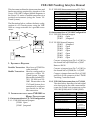
Vehicular
Cross-band Repeater
VERTEX STANDARD CO., LTD.
VXR-1000 (VHF)
YAESU UK LTD.
4-8-8 Nakameguro, Meguro-Ku, Tokyo 153-8644, Japan
VERTEX STANDARD
US Headquarters
10900 Walker Street, Cypress, CA 90630, U.S.A.
Unit 12, Sun Valley Business Park, Winnall Close
Winchester, Hampshire, SO23 0LB, U.K.
VERTEX STANDARD HK LTD.
Service Manual
©2009 VERTEX STANDARD CO., LTD.
Unit 5, 20/F., Seaview Centre, 139-141 Hoi Bun Road,
Kwun Tong, Kowloon, Hong Kong
VERTEX STANDARD (AUSTRALIA) PTY., LTD.
Normanby Business Park, Unit 14/45 Normanby Road
Notting Hill 3168, Victoria, Australia
E137190B
The VXR-1000 Series is designed to provide extended handheld coverage by repeating transmissions
in both directions through an existing high power mobile radio.
Reliability is assured by a highly integrated surface mount circuit design and a aluminum extrusion
chassis. Important channel frequency data is stored in EEPROM, and is easily programmable by
dealers using a personal computer and the Vertex VPL-1 Programming Cable and CE-22 Software.
Please take a few minutes to read this manual carefully. The information presented here will allow
you to derive maximum performance from your VXR-1000. After reading it, keep the manual handy
for quick reference, in case questions arise later on.
We’re glad you joined the Vertex team. Call on us any time, because our business is communications.
Let us help you get your message across.
Contents
Operating Manual Reprint ........................ 2
Specifications ............................................... 4
Installations .................................................. 5
Interconnection with
Vertex VX- Series Transceiver ........ 7
VXR-1000 Trunking Interface Manual ....... 11
CE-22 Programming Software .................. 14
Exploded View & Miscellaneous Parts ........ 25
Block Diagram .............................................. 26
Circuit Description ...................................... 27
Alignment ...................................................... 29
Repeater Cloning.......................................... 32
Board Unit (Schematics, Layouts & Parts)
Main Unit ............................................................... 33
1
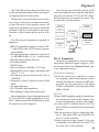
Operating Manual Reprint
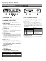
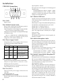
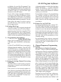
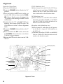
CONTROLS & CONNECTORS
Front Panel
Rear Panel
Microphone Jack
EXT SP (External Speaker)
Connect the microphone plug to this jack.
CHANNEL Selector Knob
This knob selects the operating channel.
PRI Indicator
When on, “PRI” indicates that the unit is at
priority count zero and will repeat all transmissions.
TX Indicator
When on, “TX” indicates that the repeater is
transmitting to the handheld.
COR Indicator
DSUB 9-Pin Accessory Connector
External TX audio line-input, PTT, external
RX audio line-output, and other signals may
be obtained from this connector for use with
accessories.
Pin Assignments
Pin 1 GND
Pin 2 Mobile Transmit Audio Pin 3 Power Supply Control
Pin 4 Mobile PTT Output
Pin 5 Vcc (13.8V DC)
Pin 6 Mobile Receive Audio
Pin 8
This lamp blinks red when the VXR-1000 is
receiving a signal from a handheld, and glows
red while the VXR-1000 is receiving a subaudible tone from the handheld.
MBL Indicator
This lamp blinks red when the Mobile is receiving signal from repeater or base, and
glows red while the Mobile is transmitting
to the repeater or base.
PWR Indicator
This is the main “POWER ON” indicator for the
VXR-1000.
VOLUME Knob
This knob adjusts the receiver volume.
Error Message
2
An external loudspeaker may be connected
to this 2-contact, 3.5-mm mini-phone jack.
No Channel Data
(Operating Channel is Vacant)
TX, COR, and PWR Indicators
Blink
ARTS Out of Range
PWR Indicator Blinks
Mobile Microphone
Audio
Antenna Socket
Pin 7 Mobile COR Detect
Mobile TX
Pin 9 Detect/Mobile
Microphone PTT
The Antenna socket is a standard 50 Ω BNC
antenna connector.
Operating Manual Reprint
HARDWARE SETTINGS
TRUNKING OPERATION
JP1004: Controls the output impedance of the
transmit audio line to the mobile radio.
Short: low-Z (600 Ω); open: high-Z (4.7
kΩ) *
JP1005: Controls the maximum drive level of
the transmit audio output to the mobile.
Short: low level output (0-100 mV)*;
open: high level output (0-5 V).
JP1001/1002/1003:
Polarity of Power supply control. Default setting: active high (JP1003: short).
VR1001: Mobile Microphone level
VR1002: Mobile RX Audio (External Modulation level)
VR1007:Mobile TX Audio (output level)
* default setting
When the radio is connected to a trunking mobile you wish to access the system from your
handheld radio, key the handheld briefly then
release the PTT key. The radio will attempt to
acquire a voice channel on the trunking system
by keying the mobile for 200 mS and monitoring the “on-air detect” line from the mobile. If
the VXR-1000 does not see the radio transmit at
all (system is busy), it will send a low tone to the
handheld to alert you that the system is busy.
The radio will automatically retry every 5 seconds and send a “busy” tone to the handheld
with each unsuccessful attempt, to indicate
progress of the call attempt. If unsuccessful after 30 seconds, the radio will transmit an “intercept” tone to alert the handheld that the call attempt failed.
The VXR-1000 has a fixed 3 minute time-out timer for base to handheld transmissions. If the
mobile COR is active for more than 3 minutes it
will send a error blip and cease transmission
until the mobile COR is inactive.
When the VXR-1000 detects that the mobile is
transmitting, it will continue to monitor the “onair detect” line until the transmitter remains
keyed for at least 250 mS to determine if the radio is merely handshaking or retrying. After
successful acquisition of a voice channel, it will
continue to hold the mobile’s PTT active for 2
seconds and transmit a “go-ahead” blip to the
handheld. You may then key their handheld to
speak on the voice channel. If you do not key
up within the 2-second period, the radio will unkey the mobile and send the “intercept” tone, as
before.
FUNCTIONAL DESCRIPTION
When the user leaves the vehicle, they activate
their mobile radio via its front panel or a separate switch. When the mobile radio is receiving
a signal, the VXR-1000 will begin transmitting
on the hand-held’s receive frequency. The user
is able to hear and respond to all radio traffic,
including other hand-helds on the same frequency. The repeater jumpers and potentiometers are
custom-configured for use with the particular
mobile radio to which it will be connected. The
CE-22 software is used to program the repeater
for the required operating parameters.
3
Specifications
GENERAL
Frequency Range:
MHz)
Number of Channels:
Channel Spacing:
Supply Voltage:
Ambient Temperature Range:
Frequency Stability:
RF Input-Output Impedance:
Audio Output Impedance:
Case Size (WHD):
Weight:
150 - 174 MHz
(Receive frequencies within a ±5 MHz spread over the range 150 - 174
16 Channels
12.5/25 kHz
13.8V DC, negative ground
−30 °C to +60 °C
±2.5 ppm
50 Ω
8Ω
111 × 25.4 × 136 mm (4.4” × 1” × 5.4”)
400 g (0.9 lb.)
RECEIVER
Circuit Type:
Sensitivity:
20 dB Quieting:
Squelch Threshold:
Adjacent Channel Selectivity:
Intermodulation Rejection:
Spurious and Image Rejection:
Conducted Spurious Emissions:
Audio Output:
Hum and Noise:
Double Conversion Superheterodyne
EIA 12dB SINAD 0.30 µV
0.40 µV
0.2 µV to 2 µV
60 dB
60 dB
60 dB
−57 dBm
1 W into 8 Ω w/<5% THD
−40 dB
TRANSMITTER
Power Output:
Modulation:
Maximum Deviation:
Conducted Spurious Emissions:
FM Hum and Noise:
5.0/2.5/1.0/0.5 W
16K0F3E /11K0F3E
±5 kHz/2.5 kHz
−60 dBc
−40 dB
Specifications may be subject to change without notice or obligation.
4
Installations
The VXR-1000 must only be installed in vehicles having a negative ground electrical system.
Mount the transceiver where the Indicators, controls, and microphone are easily accessible, using the supplied mounting bracket. The VXR1000 may be installed in any position, but should
not be positioned near a heating vent nor anywhere where it might interfere with driving (either visually or mechanically).
VXR-1000 Connections
The VXR-1000 provides a convenient rear-panel Accessory Connector for easy connections to
your transceiver. The connections to this jack are
in accordance with a standard adopted by many
commercial radio. However, we recommend
that you verify the connections to any cable you
already own by comparison to the pictorial below.
VXR-1000 Installation
Choose a mounting location with sufficient
clearance for the VXR-1000, plus space for
ventilation around the cooling fan and above
and below the VXR-1000. Using the mounting bracket as a template for the mounting
holes, use a 4.8 mm (3/16") bit to drill the
mounting holes, and secure the mounting
bracket with the supplied screws, washers,
and nuts (see diagram).
Position the VXR-1000 in the bracket so that
the holes in the side are aligned with those in
the bracket, and bolt the VXR-1000 into place
using the supplied short screws and flat
washers.
5
Installations
VXR-1000 Connections
Input impedance: 100 kΩ
The input level can be changed via CE-22 (range) and
VR1002 (value).
CE-22 EXT MOD level “HIGH”: –18 dBm ~ –2 dBm
CE-22 EXT MOD level “LOW”: –36 dBm ~ –18 dBm
Frequency response (de-emphasis on/off) can be
changed via CE-22 (default: off).
Pin 7: Mobile COR Detect
Pin 1: GND
Signal Ground
Pin 2: Mobile Transmit Audio
Receive audio output from the VXR-1000, passed to
the MIC jack of the mobile transceiver.
Output impedance can be changed via jumper JP1004.
open: 4.7 kΩ, short: 600 Ω (default: open).
Output level can be changed via jumper JP1005 (range)
and VR1007 (value).
open: -15 ~ +7 dBm, short: -40 ~ -15 dBm (default: short).
Frequency response (pre-emphasis on/off) can be
changed via CE-22 software (default: off).
Pin 3: Power Supply Control
The polarity of the “Power Supply Control” line can
be changed via jumpers JP1001/1002/1003.
high: 3 ~ 16 V
JP1001
J1002
J1003
short
short
open
short
open
short
open
short
open
open
open
short
Function
VXR-1000 turns on when
this pin connects to ground.
VXR-1000 turns off when
this pin connects to ground.
VXR-1000 turns off when
this pin is “high” level.
VXR-1000 turn on when this
pin is “high” level.
Pin 4: Mobile PTT Output
This pin controls the mobile transceiver’s TX/RX status.
This pin is an open-collector, “active-low” circuit.
When this pin closes to ground,
the mobile transceiver is switched into the TRANSMIT
mode. Maximum current: <20 mA.
Pin 5: Vcc (13.8 V)
This pin is the DC power supply connection for the
VXR-1000.
Maximum current: 2A.
Pin 6: Mobile Receive Audio
Receiver audio input to the VXR-1000 from the mobile
transceiver.
6
Squelch control input (including the effect of a CTCSS
or DCS detected tone) or audio mute line, also known
as a “BUSY” line.
When this pin is at “high” level (mobile radio Squelch open),
the VXR-1000 is commanded into the TRANSMIT mode.
Squelch open: 3 V, Squelch closed: 0 V.
Squelch open: >3 V, Squelch closed: 0 V.
This input level can be switched between “Squelch
open” and “Squelch closed” when this pin is at “high”
level via CE-22.
Impedance: 1 MΩ.
The Squelch Threshold level can be changed by adjustment of VR1003.
Pin 8: Mobile Microphone Audio
Mobile microphone audio input. This is the same audio which is being sent to the mobile radio’s Mic Amp
circuit (i.e. the microphone’s audio is “split” between
the mobile radio and the VXR-1000)
Input impedance: 100 kΩ
The input level to the mobile transceiver can be
changed via CE-22 (range) and VR1001 (value).
CE-22 EXT MIC level “HIGH”: –18 dBm ~ 0 dBm
CE-22 EXT MIC level “LOW”: –44 dBm ~ –18 dBm
Pin 9: Mobile TX detect/Mobile Microphone PTT
Mobile Tx/Rx control input.
This input function can be switched between “Mobile MIC
PTT” input and “Mobile Tx Detect” line input via CE-22.
This input level can be switched between “Tx” and
“Rx” when this pin is at “high” level via CE-22.
Input impedance: 10 kΩ.
Note:, When the VXR-1000 is used in a Trunking system, the “Mobile TX Detect” input signal must be received from the mobile transceiver when connected to
the Trunking system (the VXR-1000 checks this pin’s
level to confirm successful connection to the trunking
system). When this pin is at “high” level (>3 V), the
VXR-1000 is commanded into the TRANSMIT mode.
When a successful “handshake” occurs with the Trunking system, this line goes “low” and the VXR-1000 is
released into the RECEIVE mode.
Interconnection with Vertex VX- Series Transceivers
This document outlines the interconnections and hardware settings required for interface of the Vertex VXR-1000 Compact Mobile Repeater to the Vertex VX- series of mobile transceivers.
1. Interconnections to Mobile Transceivers
The chart below shows the interconnections between J1004 on the VXR-1000 and the corresponding interface jacks on the compatible mobile transceivers.
VXR-1000 DSUP 9-pin Accessory Connector
Pin 1 GND
FTL-7011
Pin 8 of J2006
VX-2000
VX-3000
GND
Pin 5 of J1003
GND
Pin 5 of J1004
GND
Pin 2 Mobile Transmit Audio
Pin 4 of J2006
MIC IN
Pin 3 of J1003
MOD IN
Pin 3 of J1004
EXM
Pin 3 Power Supply Control
Pin 12 of J2006
13.8V SWED
Pin 8 of J1003
+5V
Pin 8 of J1004
13 SWD
Pin 4 Mobile PTT Output
Pin 1 of J2006
PTT
Pin 7 of J1003
PTT
Pin 7 of J1004
PTT
Pin 5 Vcc (13.8 V)
Pin 9 of J2006
13.8V
TP1003
13.8V
13.8 V IN
13.8V
Pin 6 Mobile Receive Audio
Pin 3 of J2001
DET IN
Pin 2 of J1003
DISC OUT
Pin 2 of J1004
LINE
(or Base of Q2005)
Pin 1 of J2001
SQ SIG
(AF MUTE)
(or Base of Q1008)
Pin 1 of J1003
SQ
(AF MUTE)
Pin 1 of J1004
SQ
Pin 8 Mobile Microphone Audio
No Connection
−
No Connection
−
No Connection
−
Pin 9 Mobile TX detect/Mobile Mic. PTT (Note 2)
Pin 5 of J2005
RX/TX
TP1013
TX 9V
No Connection
−
GND
−
GND
−
GND
−
Pin 7 Mobile COR Detect (Note 1)
Shield GND
Note 1: The Mobile COR Detect line may be
connected, inside the mobile transceiver, to either pointshown (e.g. for
the VX-2000, either to Pin 1 of J1003
(SQ) or to the Base of Q1008 )AF
MUTE). See Section 6 of this document
for information regarding the Mobile
COR Detect connection in the VX3000.
Note 2: When the mobile transceiver is not
used in a trunking environment, the
“Mobile TX Detect” function is not
used.
7
Interconnection with Vertex VX- Series Transceivers
2. FTL-7011
(HARDWARE/SOFTWARE SETTINGS FOR VXR-1000)
2-1: VXR-1000 Internal Jumpers
POWER SUPPLY CONTROL: JP1001
JP1002
JP1003
VXR-1000 OUTPUT:
JP1004
JP1005
Open
Open
Jumper
Open
Jumper
2-2: CE-22 “Common Data” (F2) Settings
Use the “CE22 /P” option when starting the
CE-22 Software.
PTT1 State: High (set to “Low” if connecting to the MUTE
connection at the base
of Q2005)
PTT2 State: Low (if no connection is
made to Pin 9 of J1004,
set to “High”)
Pre-Emphasis: Off
De-Emphasis: On
EXT MOD Level: Low
EXT MOD Level: Low
3. VX-2000
(HARDWARE/SOFTWARE SETTINGS FOR VXR-1000)
3-1: VX-2000 Internal Jumpers
These jumpers configure the interconnections made via the D-sub 9-pin connector
on the rear of the VX-2000.
JP1002 Open
JP1003 Jumper
JP1004 Jumper
JP1005 Open
3-2: VXR-1000 Internal Jumpers
POWER SUPPLY CONTROL: JP1001
JP1002
JP1003
VXR-1000 OUTPUT:
JP1004
JP1005
8
Open
Open
Jumper
Open
Jumper
3-3: CE-22 “Common Data” (F2) Settings
Use the “CE22 /P” option when starting the
CE-22 Software.
PTT1 State: High
PTT2 State: High
Pre-emphasis: Off
De-Emphasis: On
EXT MIC Level: Low
EXT MOD Level: Low
4. VX-3000
(HARDWARE/SOFTWARE SETTINGS FOR VXR-1000)
4-1: VX-3000 Internal Jumpers
These jumpers configure the interconnections made via the D-sub 9-pin connector
on the rear of the VX-3000.
Note that the connections for the VX-3000L
(Low-Band) are different from those for the
VX-3000U.
VX-3000L JP1002 Open
JP1003 Jumper
JP1004 Open
JP1005 Jumper
JP1009 Open
JP1010 Jumper
VX-3000U JP1003 Open (RXD)
JP1004 Jumper (EXRA)
JP1005 Open (TXD)
JP1006 Jumper (EXM)
JP1009 Open
JP1010 Jumper
Connect a 10 kΩ resistor between Pin 1 and
Pin 8 at J1004 of the VX-3000; this is a pullup resistor for the Squelch line.
4-2: VX-3000 Software Settings in CE-19 for
PTT and MIC
These settings must be set appropriately
within CE19 in order for the VXR-1000 to
work correctly with the VX-3000.
Interconnection with Vertex VX- Series Transceivers
[COMMON]
[ MISCELLANEOUS]
[ EXTERNAL PTT]
Set to (Mic & Option)
[GROUP]
[CHANNEL ALLOCATIONS]
[GROUP]
[EXTERNAL MIC]
Set to (Enabled)
4-3: VXR-1000 Internal Jumpers
POWER SUPPLY CONTROL: JP1001
JP1002
JP1003
VXR-1000 OUTPUT:
JP1004
JP1005
Open
Open
Jumper
Open
Jumper
4-4: CE-22 “Common Data” (F2) Settings
Use the “CE22 /P” option when starting the
CE-22 Software.
PTT1 State:
Low
PTT2 State:
Low
(set to “High” when connecting to Pin 9 of J1004)
Pre-emphasis: Off
De-emphasis: On
EXT MIC Level: Low
EXT MOD Level: Low
5.Alignment
5-1: VXR-1000 Deviation Setting
On the connected mobile transceiver, receive a signal from an external signal source
with 1 kHz modulation frequency and deviation level of ±3.0 kHz (±1.5 kHz for the
“Narrow” mode).
This signal, when passed from the connected mobile transceiver to the VXR-1000,
should produced a transmitted signal from
the VXR-1000 with 1 kHz deviation at not
less than ±3.0 kHz (±1.5 kHz for the “Narrow” mode).
If the deviation level from the VXR-1000 is
not correct, adjust VR1002 (inside the VXR-
1000) for an output deviation of ±3.0 kHz
(±1.5 kHz in the “Narrow” mode).
5-2: VXR-1000 Receiver Output Level Setting
When the VXR-1000 receives a signal from
an external signal source (on the uplink frequency used by the portable transceiver)
modulated at 1 kHz at a level of ±3.0 kHz
(±1.5 kHz in the “Narrow” mode”), the output passed to the connected mobile transceiver should produce a transmitted output
signal from the mobile at a level of ±3.0 kHz
(±1.5 kHz in the “Narrow” mode”).
If the output level to the mobile does not
produce correct deviation from the mobile,
adjust VR1007 (inside the VXR-1000) so that
the transmitted output from the mobile is
modulated at a level of ±3.0 kHz (±1.5 kHz
in the “Narrow” mode”).
6. Trunking System configuration
All trunking parameters depend on the configuration of the individual trunking system
in which the connected mobile transceiver
is used. Please consult the CE22 programming instructions, and the separate “VX1000R Trunking Interface Manual,” for information about the software and other settings for the VXR-1000 when integrated into
a trunking environment.
7. Miscellaneous
In order to improve the audio muting performance of the VX-3000, a minor circuit
change was adopted from Production Lot
#03 (VX-3000L/U) and 04 (VX-3000V), and
this change was reflected in CE-19 software
version 1.16. This change affects the connection point for the Squelch (Mobile COR Detect) line, and the connection point is identified as “AF MUTE• in the various documentation for the VX-3000.
The configuration version can be identified
by looking for the presence of a jumper connection at jumper pad JP1002 in the VX3000U, or JP1016 in the VX-3000L. The connections for the Mobile COR Detect line
should be made as follows:
9
Interconnection with Vertex VX- Series Transceivers
VX-3000U
If JP1002 is not jumpered, connect this
line to Pin 8 of Q1043.
If JP1002 is jumpered, connect the
Mobile COR Detect line to JP1002.
10
VX-3000L
If JP1016 is not jumpered, connect this
line to Pin 8 of Q1043.
If JP1016 is jumpered, connect the
Mobile COR Detect line to JP1016.
VXR-1000 Trunking Interface Manual
This document outlines the interconnections and
hardware settings required for interface of the
Vertex VXR-1000 Compact Mobile Repeater to
the Vertex VX- series of mobile transceivers in a
trunked environment (using the Vertex VXTrunk System).
The illustration below outlines the basic configuration of a VX-Trunk system, using the VXR1000 as a range extender for a portable transceiver.
2-1-2: VXR-1000 Interconnections to FTL-7011
VXR-1000 DSUB 9-pin
Accessory Connector
Pin 1: GND
Pin 2: Mobile Transmit Audio
Pin 3: Power Supply Control
Pin 4: Mobile PTT Output
Pin 5: Vcc (13.8 V)
Pin 6: Mobile Receive Audio
Pin 7: Mobile COR Detect
Pin 8: Mobile Microphone Audio
Pin 9: Mobile TX detect/Mobile Mic. PTT
FTL-7011
Pin 8 of J2006
Pin 4 of J2006
Pin 12 of J2006
Pin 1 of J2006
Pin 9 of J2006
Pin 3 of J2001
Pin 1 of J2001
No Connection
No Connection
2-2: Interconnections to VX-2000/Configuration
2-2-1: VXR-1000 Internal Jumpers
JP1004
Open
JP1005
Jumpered
2-2-2: VX-2000 Internal Jumpers
JP1002
Jumpered
JP1003
Open
JP1004
Open
JP1005
Open
JP1007
Open
JP1008
Open
JP1009
Open
1. EQUIPMENT REQUIRED
Portable Transceiver: Must have a DTMF Encoder installed.
Mobile Transceiver: Must be configured for
operation within VXTrunk System. Compatible models include FTL7011, VX-2000, and VX3000. Please refer to the
VX-Trunk System documentation for configuration details for the mobile transceiver.
2. INTERCONNECTIONS FROM VXR-1000 TO
MOBILE TRANSCEIVERS
2-1: Interconnections to FTL-7011/Configuration
2-1-1: VXR-1000 Internal Jumpers
JP1004 Open
JP1005 Jumpered
Connect a jumper from Pin 3 of J1003 to
the shared side ofJP1009/Pin 4 of J1007.
Remove R1010
Connect a jumper from Pin 7 of J1003 to
the shared side of JP1008/Pin 1 of J1007.
Connect a jumper between Pin 4 of J1003
and Pin 6 of the connector of the VTM-20
Trunking Controller board.
2-2-3: VXR-1000 Interconnections to VX-2000
The chart below describes the individual
wire functions for the cable connected between the D-Sub 9-pin connectors on the
VXR-1000 (J1004) and VX-2000 (J1003).
VXR-1000 DSUB 9-pin
Accessory Connector
Pin 1: GND
Pin 2: Mobile Transmit Audio
Pin 3: Power Supply Control
Pin 4: Mobile PTT Output
Pin 5: Vcc (13.8 V)
Pin 6: Mobile Receive Audio
Pin 7: Mobile COR Detect
Pin 8: Mobile Microphone Audio
Pin 9: Mobile TX detect/Mobile Mic. PTT
VX-2000
Pin 5 of J1003
Pin 3 of 1003
Pin 8 of J1003
Pin 7 of J1003
Switched
13.8VDC
output from the
Power Switch
Pin 2 of J1003
Pin 4 of J1003
No Connection
No Connection
11
VXR-1000 Trunking Interface Manual
2-3: Interconnections to VX-3000/Configuration
2-3-1: VXR-1000 Internal Jumpers
*JP1004 Open
*JP1005 Jumpered
4. VX-TRUNK SYSTEM OPERATING
2-3-2: VX-3000 Internal Jumpers
*JP1003 Open
*JP1004 Jumpered
*JP1005 Open
*JP1006 Open
*JP1007 Open
*JP1008 Open
1. Press the portable's PTT key for longer than
the "Sampling Time" of the VXR-1000, so as
to ensure that the VXR-1000 receives the portable's signal, then press "3 *" while transmitting to connect to the VX-Trunk II system.
2. When the "3 *" is completed, immediately release the portable's PTT key, so as to return
the portable to the receive mode.
3. If the VX-Trunk system receives the connection command, a double "beep" will be heard
from the portable's speaker.
4. Press the portable's PTT key for longer than
the "Sampling Time" of the VXR-1000, so as
to ensure that the VXR-1000 receives the portable's signal, and enter the other unit's 5-digit
subscriber number via the portable's DTMF
pad. Now release the portable's PTT key to
return the portable to the receive mode.
5. When the subscriber number is successfully
received by the VX-Trunk II system, and a
connection thereby initiated, the VX-Trunk II
system will respond, and a double "beep" will
be heard from the speaker of the portable.
* Connect a jumper between the shared side
of JP1006/JP1006 and Pin 7 of J1003.
* Connect a jumper between the shared side
of JP1007/JP1008 and Pin 2 of J1005.
2-3-3: VXR-1000 Interconnections to VX-3000
The chart below describes the individual
wire functions for the cable connected between the D-Sub 9-pin connectors on the
VXR-1000 (J1004) and VX-3000 (J1004).
VXR-1000 DSUB 9-pin
Accessory Connector
Pin 1: GND
Pin 2: Mobile Transmit Audio
Pin 3: Power Supply Control
Pin 4: Mobile PTT Output
Pin 5: Vcc (13.8 V)
Pin 6: Mobile Receive Audio
Pin 7: Mobile COR Detect
Pin 8: Mobile Microphone Audio
Pin 9: Mobile TX detect/Mobile Mic. PTT
VX-3000
Pin 5 of J1004
Pin 3 of 1004
Pin 8 of J1004
Pin 7 of J1004
Switched
13.8VDC
output from the
Power Switch
Pin 2 of J1004
Pin 4 of J1004
No Connection
No Connection
3. VXR-1000 CONFIGURATION
For operation in a VX-Trunk II environment,
note the following setup tips regarding the
VXR-1000 (set via the CE-22 software):
The VXR-1000's "Pri Timer" option must be
set to a non-zero value by CE-22).
In CE-22, set the TRUNKING mode to OFF (for
VX-Trunk II only; for other Trunking systems
like LTR, this parameter must be set to ON).
Set PTT1 to HIGH.
Other parameters such as Master/Slave and
Sub_Audio may be set via CE-22 per the customer's operating requirements.
12
EXAMPLE
4-1: Making a Call from the Portable
4-2: Receiving a Call at the Portable
1. When the mobile connected to the VXR-1000
receives a connection request from the VXTrunk II system, it relays a "connection tone"
to the portable. When this happens, press the
PTT key on the portable.
2. Hold in the PTT key on the portable longer
than the "Sampling Time" programmed for
the VXR-1000, then press the DTMF "*" key.
After pressing the "*" key, release the PTT key
on the portable.
3. When the VX-Trunk II system receives the "*"
response from the portable, it will respond,
and a double "beep" will be heard from the
speaker of the portable.
4-3: Terminating a Call from the Portable
1. Press the portable's PTT key.
2. Hold the portable's PTT key for longer than the
"Sampling Time" of the VXR-1000, then press
the "#" key. The call will now be terminated, and
you may release the portable's PTT key.
VXR-1000 Trunking Interface Manual
5. NOTES RE TRUNKING OPERATION
5-1:
The VX-Trunk II system operates in a full duplex mode.
In this environment, while a call is in progress,
the connected mobile passes the received audio through to the VXR-1000 for re-transmission to the portable. In order for the portable
to be able to "capture" the VXR-1000 to make
a transmission back to the other party, the
VXR-1000 must be set, via the CE-22 software,
for a "Priority Timer" setting (Pri Timer) which
is not zero. A very short time will allow quick
interruption, but the incoming message from
the VXR-1000 to the portable may sound
"choppy" due to the frequent interrupts.
When the portable transmits longer than the
"Priority Timer" setting, the VXR-1000 will interrupt its transmission, and the VXR-1000
will instantly switch to the "receive" mode on
the portable's transmitting frequency.
5-2: VXR-1000 Local Microphone
In order to facilitate the above sampling feature, it is not possible to use a "Local" mic (a
DTMF microphone attached to the VXR-1000)
for access to the VX-Trunk II system.
13
CE-22 Program Software
The Vertex CE-22 program is a software package which controls the VXR-1000's "Clone Edit" feature.
This manual outlines the installation and use of the CE-22 software when used with the VXR-1000.
1. CE-22 Installation
and Operating Modes
The Vertex CE-22 program is an integrated
software package designed to work with
IBM PC, XT, AT, or compatible computers.
In order for CE-22 to run properly, your
computer must run DOS v3.0 (or a later version).
1-1: CE-22 Installation
There is no installation software included
with your distribution diskette.
Use standard DOS procedures to install the
software on your hard drive.
For example, let us create a directory named
"Vertex" into which we shall install the CE22 software. First, make a copy of the distribution diskette, then use the archive copy
for the installation from (floppy) Drive A:
c:\ mkdir vertex [ENTER]
c:\ cd\vertex [ENTER]
c:\vertex copy a:*.* [ENTER]
The files on the archive floppy disk will now
be copied to your hard drive into the new
"vertex" directory.
1-2: Starting CE-22
Before starting the CE-22 program, connect
the VPL-1 Cloning Cable between your
computer's COM port and the VXR-1000's
MIC jack.
Connecting the VPL-1 cable automatically
initiates the "CLONE" (programming)
mode, and the PWR LED will blink while
the CLONE mode is active.
14
The CE-22 program will now start. After five
seconds in an initial Program Identification
screen, the software will automatically
switch to the main Channel Editing Screen.
1-3: Startup Options
Two mode options for CE-22 are available.
The standard ce22 command allows all normally-required channel data entry parameters to be entered and/or edited. Additionally, the COM port line in the "Common
Data" window may also be changed. However, other "Common Data" parameters cannot be changed, although they are visible in
the window.
The alternative ce22 /p option allows editing of the other parameters in the "Common
Data" window. While changes to these parameters are not normally required, major
system changes may necessitate modification of one or more "Common Data" items.
If this is the case, type ce22 /p [ENTER] instead of (only) ce22 [ENTER] when starting
the program.
2. Sending/Downloading Data
from the VXR-1000
2-1: Reading Data from VXR-1000
When you start up CE-22, it is often useful to
download the current channel information
from the VXR-1000 for archive purposes.
To do this, press F5. The current data will
be read by the computer, and the data will
appear on the screen. If you wish to save
this data to disk, press F4 and assign a file
name into which the archive data will be
saved.
If your computer has more than one COM
port, you may select the COM port to be
used via the "Common Data" window (accessed by pressing F2 after CE-22 is started). Either COM1 or COM2 may be utilized.
2-2: Loading Data to VXR-1000
When all channel data has been successfully set up, press F6 to send the channel data
to the VXR-1000.
To start CE-22, be sure your computer
screen is displaying the DOS prompt. The
procedure thereafter is: c:\ ce22 [ENTER]
2-3: Saving Data to Disk
Channel programming data may be saved
to your computer's hard drive, or to a flop-
CE-22 Program Software
py diskette, by use of the F4 command. You
will be prompted to define a file name to be
used. Standard DOS file name specifications
should be used (e.g. no more than eight
characters in the file name).
A channel number on which data has been
hidden will display "-- --" in place of the field
entries. On the VXR-1000, if you select a
"hidden" channel, three indicators will blink
to alert you to this fact.
If you wish to create a separate sub-directory (so as to store files for different customers in different sub-directories, for example),
press [Tab], then press [F3], to activate the
[Mk Dir] (Make Directory) function. You can
then type in the name you wish to use for
this sub-directory, then continue with the
file storage process.
If you make a change to the programming
of a "hidden" channel at a later time, the
channel will automatically be re-activated
(removed from "hidden" status). You will
need to return to the Rx Freq field in order
to re-hide it.
2-4: Printing Hard Copy
To print a copy of the currently-displayed
channel data file, press [F7] when all programming steps have been completed. This
allows you to attach a copy of the programming information to the programming work
order, for the convenience of the customer.
3. Programming Navigation/
Use of SPACE Key
When CE-22 is initially started with a new
VXR-1000, only CHANNEL 1 will be showing.
Use the UP and DOWN keys to navigate to
different channel numbers. Use the LEFT
and RIGHT keys to navigate between the
various columns of a particular channel programming line. Beginning in Section 4 of this
manual, we will only discuss a single line
of channel programming data, as each line
of channel programming data is identical
(except for the fact that CHANNEL 1's data
cannot be hidden).
3-1: Hiding/Un-hiding Channel Data using
SPACE Bar
The SPACE bar is used in many programming steps to activate or de-activate a particular function.
If the cursor is on the channel number column, however, pressing the SPACE bar will
toggle between hiding of that channel number's data and re-activating that channel
number's data. CHANNEL 1's data, however, cannot be hidden.
3-2: Primary Use for SPACE Bar
In many programming steps, such as CTCSS or DCS tone/code entry, an initial press
of the SPACE bar will activate the parameter (turn it on) or de-activate the parameter
(turn it off). In each such step, you will be
prompted in the upper-right-hand window
as to additional steps to be taken to secure
the final value for the parameter you are
currently setting.
In programming steps where a numerical
value is required, press the [Space] bar to
increase the value, or [Back Space] to decrease the value.
4. Channel Frequency Programming
4-1: Rx Freq.
(Edit Receive (or Simplex) Frequency)
Use the 0 - 9 keys to enter the desired channel frequency directly, and press [ENTER].
The frequency entered will be adjusted automatically if it does not conform to the
"CHANNEL STEP" parameter, and will be
adjusted to the nearest "valid" step; the frequency will also appear in the Tx Freq. field
(next step) automatically, to simplify entry
if the current channel is to be used on Simplex. You do not need to enter all eight digits of the frequency; empty digits to the right
will be set to "0" when you press [ENTER].
Pressing [.] ("period") after several digits
forces those digits to be "MHz" digits. If you
press [.] before entering any digits, only the
"kHz" digits will be changed.
Pressing only the SPACE bar, without entering any frequency digits, toggles the data
for the entire channel between "hidden" and
15
CE-22 Program Software
"active" status (except for CHANNEL 1,
which cannot be hidden).
Hidden channels will show "-- --" in place
of the various field entries, and they are not
available for operation. However, they are
still stored in "hidden" form for possible recall later.
Note: Any entries or changes made to the
Rx Freq. field will also be applied to the Tx
Freq. field, so you may need to edit that field
after making any changes here.
4-2: Tx Freq. (Edit Transmit Frequency)
Use the 0 - 9 keys to enter the desired channel frequency directly, and press [ENTER].
The frequency entered will be adjusted automatically if it does not conform to the
"CHANNEL STEP" parameter, and will be
adjusted to the nearest "valid" step. You do
not need to enter all eight digits of the frequency; empty digits to the right will be set
to "0" when you press [ENTER]. Pressing [.]
("period") after several digits forces those
digits to be "MHz" digits. If you press [.]
before entering any digits, only the "kHz"
digits will be changed.
Note: The Transmit Frequency is automatically copied from the Receive Frequency's
column, so any changes you have made to
the Tx Freq. field will be LOST if the Rx Freq.
field is modified. Therefore, you should set
the Rx Freq. field data first, then edit the Tx
Freq. field.
5. CTCSS/DCS Decoders and Encoders
5-1: CTCSS Decoder
(Toggles CTCSS Decoder ON/OFF, Sets CTCSS Freq.)
Press the SPACE bar to toggle the CTCSS
Decoder ON or OFF, or press [ENTER] to
display the TONE SELECT window, from
which you may select a CTCSS frequency
using the Arrow keys; press [ENTER] again
to accept the selected tone, or press [ESC]
to cancel.
If you know the CTCSS frequency you want
(the precise value), you can enter it directly
using the 0 - 9 keys and the [.] ("period") key.
When the desired CTCSS frequency is dis16
played, press [ENTER] to accept this value.
If you keyed in an invalid frequency (not
among the "standard" CTCSS tone list), the
TONE SELECT window will appear, with
the nearest valid CTCSS frequency pre-selected.
Turning CTCSS ON turns DCS OFF (since
both cannot be ON). CTCSS cannot be selected for use if ARTS is enabled (ARTS uses
DCS only).
5-2: DCS Decoder
(Toggles DCS Decoder ON/OFF, Sets DCS Code #)
Press the SPACE bar to toggle the DCS Decoder ON or OFF, or press [ENTER] to display the CODE SELECT window, from
which you may select a DCS code using the
Arrow keys; press [ENTER] again to accept
the selected code, or press [ESC] to cancel.
If you know the three-digit DCS code you
want, you can enter it directly using the 0 9 keys. When the desired DCS code is displayed, press [ENTER] to accept this value.
If you keyed in an invalid code number (not
among the "standard" DCS code list), the
CODE SELECT window will appear, with
the nearest valid DCS code number pre-selected.
Turning the DCS Decoder ON turns CTCSS OFF (since both cannot be ON). DCS Encode and Decode are both required for
ARTS operation.
5-3: CTCSS Encoder
(Toggles CTCSS Encoder ON/OFF, Sets CTCSS Freq.)
Press the SPACE bar to toggle the CTCSS
Encoder ON or OFF, or press [ENTER] to
display the TONE SELECT window, from
which you may select a CTCSS frequency
using the Arrow keys; press [ENTER] again
to accept the selected tone, or press [ESC]
to cancel.
If you know the CTCSS frequency you want
(the precise value), you can enter it directly
using the 0 - 9 keys and the [.] ("period") key.
When the desired CTCSS frequency is displayed, press [ENTER] to accept this value.
If you keyed in an invalid frequency (not
CE-22 Program Software
among the "standard" CTCSS tone list), the
TONE SELECT window will appear, with
the nearest valid CTCSS frequency pre-selected.
Turning CTCSS ON turns DCS OFF (since
both cannot be ON). CTCSS cannot be selected for use if ARTS is enabled (ARTS uses
DCS only).
Note: Turning on the CTCSS Encoder automatically turns off the DCS Encoder, if it was
on.
5-4: DCS Encoder
(Toggles DCS Encoder ON/OFF, Sets DCS Code #)
Press the SPACE bar to toggle the DCS Encoder ON or OFF, or press [ENTER] to display the CODE SELECT window, if you are
not viewing it already); press [ENTER] again
to accept the selected code, or press [ESC]
to cancel.
If you know the three-digit DCS code you
want, you can enter it directly using the 0 9 keys. When the desired DCS code is displayed, press [ENTER] to accept this value.
If you keyed in an invalid code number (not
among the "standard" DCS code list), the
CODE SELECT window will appear, with
the nearest valid DCS code number pre-selected.
Turning the DCS Encoder ON turns CTCSS
OFF (since both cannot be ON). DCS Encode
and Decode are both required for ARTS
operation.
6. ARTS (Automatic Range Transponder System) Operation
The ARTS feature causes the VXR-1000 to
"shake hands" electronically with the user's
ARTS-compatible portable transceiver. If
the portable fails to shake hands with the
VXR-1000 in two successive handshake cycles, the PWR lamp will begin blinking, so
as to indicate "Out of Range" status for the
portable.
ARTS operation requires that DCS Encode
and Decode be engaged. It will not function
using CTCSS nor carrier-only squelch. The
portable radio's ARTS Mode must be in
complement in order for ARTS to function
correctly.
6-1: ARTS Mode
ARTS operates in one of four modes, described below:
OFF: ARTS is not active on this channel. No
handshaking is performed.
RX: The VXR-1000 receives handshake signals from the portable, but does not
send handshake signals itself. If an outof-range condition occurs, the VXR1000 will indicate "Out-of-Range" locally, but the portable user will not
receive an "Out-of-Range" warning.
TX: The VXR-1000 sends out handshake
signals, but does not act on handshake
signals received. If an out-of-range
condition occurs, the portable user will
receive an "Out-of-Range" warning (if
the portable is properly programmed),
but the VXR-1000 will not indicate an
out-of-range condition locally.
TRX:Both the TX and RX functions described above are active.
Press the SPACE bar to select the desired
ARTS Mode.
6-2: ARTS Int (Interval)
The ARTS Interval is the amount of time between ARTS handshake transmissions issued by the VXR-1000. Two selections are
available: 25 seconds or 55 seconds. The
portable radio's ARTS Interval setting must
match that of the VXR-1000 in order for
ARTS to function correctly.
Press the SPACE bar to select the desired
ARTS Interval.
7. DCS Type (Normal/Inverted)
7-1: DCS Type
This command is effective only when DCS
is chosen for squelch control.
A = "Normal" DCS
B = "Inverted" (complement) DCS
Press the SPACE bar to select the desired
DCS Type.
17
CE-22 Program Software
7-2: DDec Type (DCS Decoder Type)
This command selects the manner in which
DCS is to be decoded.
Fixed = Decodes the type selected in 7-1
only (Normal or Inverted).
Auto = Decodes both types (Normal and
Inverted)
Press the SPACE bar to select the desired
DCS Decoder Mode.
8. Squelch
8-1: Sql Ofst (Squelch Offset)
The Squelch Offset function provides a
means to fine-tune the VXR-1000 squelch
level on a channel-by-channel basis, without having to perform a full alignment.
The available values are an arbitrary scale
of 0 to 255. Use the Space bar and the Backspace key to increment/decrement the
Squelch Offset level.
Note: Although the Squelch Offset range is
between 0 and 255, the squelch threshold
will be close to saturation if the value is set
to about 100 or above. Therefore, you will
observe no significant difference in squelch
threshold between the values of 100 and 255.
9. Encryption
9-1: Encryption
When ON, the VXR-1000 operates in the
"Encrypted' mode on this channel. The encryption type is compatible with the encryption system used in the Vertex VX-10 (FTT15 module), VX-200 (FSU-1083), VX-400
(FVP-25), and the VX-500/510 (FVP-22)
models.
Press the SPACE bar to toggle Encryption
ON and OFF.
10. Channel Spacing
10-1: W/N (Wide/Narrow Channel Spacing)
This function selects the channel spacing environment in which the VXR-1000 operates.
Wide =
25 kHz Channel Spacing, ±5 kHz
Deviation
Narrow = 12.5 kHz Channel Spacing, ±2.5
kHz Deviation
18
Press the SPACE bar to select the desired
channel spacing environment.
11. Input Modulation
11-1: Mod In (Input Modulation Selection)
This function selects how the VXR-1000 will
utilize and apply audio signals which are to
be transmitted to the associated portable
radio.
Mix:
Any audio being transmitted by the
microphone on the mobile radio
connected to the VXR-1000 will also
be transmitted to the portable on the
other band. If a second microphone
is connected directly to the VXR1000 and is also keyed simultaneously with the microphone of the
mobile, the audio from both microphones will be mixed and transmitted to the portable.
Mono: The VXR-1000 will only select audio
from the microphone which first had
its PTT key pushed. Audio from the
other microphone, if its PTT key is
pushed while the first microphone
remains keyed, will be ignored.
12. Mobile Monitoring
12-1: MBL Moni (Mobile Audio Monitoring)
This command determines whether or not
the receive audio from the connected mobile radio will be routed to the VXR-1000's
EXTERNAL SPEAKER jack.
Press the SPACE bar to toggle the audio between ON and OFF.
13. Transmitter Power
13-1: Tx Pwr
(Transmitter Power Output Selection)
This command selects the desired power
output from the VXR-1000 on the current
channel. The available values are 0.5, 1.0, 2.5,
and 5.0 Watts.
Press the SPACE bar and the Backspace key
to increment/decrement the Transmit Power Level.
CE-22 Program Software
14. Trunking Operation
14-1: Trunking
This command activates or de-activates the
intercommunication protocol for Trunking
operation with the connected mobile radio.
mit in tandem with the mobile radio when
the mobile microphone's PTT switch is
pressed. If this command is set to OFF, the
VXR-1000 will not transmit when the mobile microphone's PTT switch is pressed.
If the mobile radio is a conventional twoway radio, this function must be set to OFF.
Press the Space bar to toggle this setting to
ON or OFF, as needed.
If the mobile radio is a trunked radio (SmarTrunk, LTR, etc.), this function should be set
ON. Also, set the Trunking Data parameters in the "Common Data" window as appropriate for operation with the mobile radio. Consult the Service Manuals for the
VXR-1000 and the trunked mobile radio to
determine the proper settings.
16-2: Trunking Mode
If the VXR-1000 is used in a Trunking environment (with the Trunking command in
section 14 set to ON), please set the MBL
MIC command to ON. This setting allows
the "Mobile TX Detect" line to signal the
VXR-1000 when the mobile radio is transmitting, whether by local microphone command or by trunking system handshake
command.
Press the SPACE bar to toggle Trunking operation ON or OFF.
15. Courtesy Blip
15-1: Cour Blip (Courtesy Blip)
When ON, this function causes the VXR1000 to send out a "blip" on the portable radio frequency each time the portable radio
is unkeyed. This provides audible confirmation to the user that the VXR-1000 was able
to receive the transmission from the portable.
This "blip" is not transmitted by the connected mobile radio.
Press the SPACE bar to toggle the Courtesy
Blip ON and OFF.
16. MBL MIC
(Mobile Microphone Configuration)
This command affects the way in which Pin
9 of J1004 (DSUB 9-pin Jack on rear of VXR1000) responds to PTT commands.
16-1: Conventional Mode
If the VXR-1000 and mobile radio are used
in a "conventional" two-way radio environment (the Trunking command in section 14
set to OFF), the MBL MIC command selects
whether or not the VXR-1000 will transmit
together with the mobile radio when the
mobile's PTT switch is keyed. If this command is set to ON, the VXR-1000 will trans-
Press the Space bar to toggle this setting to
ON.
17. Microphone Control
17-1: MIC Cntl
(VXR-1000 Microphone Utilization)
This function selects which radio (VXR-1000
and/or mobile) will transmit audio from the
microphone connected to the VXR-1000.
Int:
The VXR-1000 microphone will only
cause transmission on the VXR-1000
to the portable radio. It will not cause
transmission on the connected mobile
radio.
Ext: The VXR-1000 microphone will only
cause transmission on the connected
mobile radio. It will not cause transmission on the VXR-1000 to the portable. Pin 4 of J1004 (on the VXR-1000)
will go "Active Low" to provide a PTT
output to the mobile radio.
Both: The microphone connected to the
VXR-1000 will cause transmission on
both the VXR-1000 and the mobile.
Pin 4 of J1004 (on the VXR-1000) will go
"Active Low" to provide a PTT output to the
mobile radio.
Press the Space bar to select the desired
mode of operation.
19
CE-22 Program Software
18. External Radio Control
18-1: EXT.R Cntl
This command selects the manner in which
the VXR-1000 will control (and be controlled
by) the connected mobile radio.
On: Signals received by the mobile radio
will be re-transmitted to the portable
radio AND signals received from the
portable radio will be re-transmitted
by the mobile radio.
RX: Signals received by the mobile radio
will be re-transmitted to the portable
radio, but signals from the portable
radio WILL NOT be re-transmitted by
the mobile radio.
Off: Signals will not be re-transmitted by
the VXR-1000 or mobile radio in either
direction.
Press the Space bar to toggle this command
function to ON, RX, or OFF.
19. Priority Timer
19-1: Pri Timer (Priority Timer Polling Interval)
The function sets the interval which separates the momentary polling (by the VXR1000) of the portable radio; the VXR-1000
will unkey its transmitter, listening for a
possible transmission from the portable, and
if a transmission is detected, the VXR-1000
will cease its transmission. The VXR-1000
will instantly key up the connected mobile
radio to transmit to the "base." Therefore,
this feature allows the portable radio user
to override an incoming transmission from
the "base," if desired.
The available settings are 0.25 second
through 3.00 seconds. A setting of "0.00" seconds turns the interval timer off.
Use the Space bar or Backspace key to increment or decrement this setting, respectively.
20. Master/Slave Operation Parameters
20-1: Master Tone
When LkTn ("Lock Tone") is chosen as the
Master/Slave Mode, the user has the option
of using either 847.5 Hz or 832.5 Hz as the
Master Tone.
20
Press the Space bar to select the desired
Master Tone.
Note: If the Master/Slave Mode setting is not
set to LkTn, the Master Tone command will
not be available.
20-2: Master/Slave Mode
This command determines how the VXR1000 will behave when it is within the range
of other VXR-1000s operating on the same
frequency, such as when several mobile
units are at a common location. One (and
only one) VXR-1000 must act as the "Master" to provide portable-to-base relay for all
portable units at the scene.
All other VXR-1000s that are present must
revert to a "Slaved" (inactive) status, so as
to avoid interference to each other.
Ordinarily, the first VXR-1000 arriving at a
location will establish itself as the "Master"
by periodically transmitting a Master Tone
signal. Any other VXR-1000 coming within
range will receive this tone (which is transmitted on the same frequency as that used
by the portable for uplinking to the VXR1000); these VXR-1000s, upon receiving the
Master Tone, will switch themselves to the
"Slaved" status.
If the original Master leaves the location, the
first "Slave" VXR-1000 to detect the absence
of the Master Tone will then transmit its own
Master Tone. If not challenged by any other VXR-1000 within range, this Slave will
then become the new Master for this location.
All of these transactions occur automatically, without interruption of voice communications occurring through the VXR-1000
system.
Use the Space bar to choose between the following selections:
YAESU: This is a Yaesu/Vertex exclusive
system, based on subaudible DCS
signalling.
LkTn: The Lock Tone system employs
audible tone bursts for signalling.
CE-22 Program Software
Note: If the Yaesu system is used, you must
program only CTCSS or Carrier Squelch to
be used for the main coded squelch signal
(for communication between the portable
and the VXR-1000. The CE-22 will not allow the use of DCS if the Yaesu system is
selected, because the Yaesu system needs to
use DCS for coding for the Master Tone signal.
20-3: Master/Slave DCS
This function sets the DCS code to be employed by the Master VXR-1000. This DCS
code is sent to other arriving VXR-1000s,
whereby the first VXR-1000 on the scene
announces itself as the Master.
Press [ENTER] to display the CODE SELECT window, from which you may select
a DCS code using the Arrow keys; press
[ENTER] again to accept the selected code,
or press [ESC] to cancel.
If you know the three-digit DCS code you
want, you can enter it directly using the 0 9 keys. When the desired DCS code is displayed, press [ENTER] to accept this value.
If you keyed in an invalid code number (not
among the "standard" DCS code list), the
CODE SELECT window will appear, with
the nearest valid DCS code number pre-selected.
21. Modification of
"Common Data" Parameters
The following command parameters are
found in the "Edit Common Data" window.
These parameters are common to all channels in the VXR-1000 being programmed,
unlike the previous command parameters
(which can be set on a channel-by-channel
basis).
21-1: PTT1 State
This command allows customization of the
"Mobile COR Detect" signal at Pin 7 of J1004
(on the VXR-1000). This permits the VXR1000 to work with either "Active High" or
"Active Low" COR Detection signals from
the mobile.
High: If the connected mobile radio uses an
"Active High" system, set the PTT1
State parameter to High.
Low: If the connected mobile radio uses an
"Active Low" system, set the PTT1
State parameter to Low.
For control purposes, High is defined as 33.5
Volts, while "Low" is defined as ≤2.5 Volts.
There is no "pull up" facility provided on
this connector pin.
21-2: PTT2 State
This command allows customization of the
status of the "Mobile TX Detect" line applied
to Pin 9 of J1004 on the VXR-1000. This allows either "Active High" or "Active Low"
TX Detect signals from the connected mobile to be used.
High: If the connected mobile radio's "TX
Detect" line goes "High" during mobile transmission, set this parameter
to High.
Low: If the connected mobile radio's "TX
Detect" line goes "Low" during mobile transmission, set this parameter
to Low.
Levels used for this command are identical
to those in section 21-1, and there likewise
is no "pull-up" facility provided on this line.
21-3: Pre-Emphasis
When the VXR-1000 is receiving a signal
from the portable radio, the received audio
is fed to the connected mobile radio via Pin
2 of J1004 (on the VXR-1000). This parameter allows this audio signal to have either a
flat response, or to have 6 dB/Octave preemphasis applied.
Off: No pre-emphasis will be applied.
On: Pre-emphasis will be applied to the
signal applied to the connected mobile
radio's modulator circuit.
If the connected mobile injects this audio
signal to its modulator prior to the mobile's
internal pre-emphasis network, please set
this parameter to Off. If the audio input is
applied downstream from the internal pre21
CE-22 Program Software
emphasis network, please set this parameter to On.
21-4: De-Emphasis
The audio signal received by the connected
mobile (received from the base station) is
applied to the VXR-1000 via Pin 6 of J1004.
This command allows de-emphasis to be
applied (or not applied) to this audio signal, depending on the condition of the audio signal as it left the mobile radio's receiver
section.
On: De-emphasis of -6 dB/Octave will be
applied to the incoming audio signal.
Off: No de-emphasis will be applied to the
incoming audio signal.
If the connected mobile applies de-emphasis to the audio prior to routing the audio to
the VXR-1000, please set this parameter to
Off. If the audio exits the mobile radio before de-emphasis is applied at the mobile
radio side, please set this parameter to On.
21-5: EXT MIC Level
When audio from the connected mobile radio's microphone is routed to the VXR-1000
(via Pin 8 of J1004) for simultaneous transmission by the mobile and the VXR-1000,
using the mobile's microphone as the audio
source, this command allows configuration
of the VXR-1000 so as to be compatible with
the expected microphone audio level.
High: The input level is between -18 dBm
and 0 dBm.
Low: The input level is between -44 dBm
and -18 dBm.
21-6: EXT MOD Level
When receiver audio from the connected
mobile radio is routed to the VXR-1000 (via
Pin 6 of J1004), this command allows configuration of the VXR-1000 so as to be compatible with the expected receiver audio level.
High: The receiver audio level is between 18 dBm and -2 dBm.
Low: The receiver audio level is between36 dBm and -18 dBm.
22
21-7: Band
This parameter must be set for the band on
which the VXR-1000 is transmitting.
21-8: COM Port
Set this parameter for the COM port you will
use for data uploading and downloading.
Either COM1 or COM2 may be used.
21-9: Trunking Data
When the connected mobile radio is configured as a trunked radio, the VXR-1000's timing parameters must be compatible with
those used in the trunking system in use.
The default values are:
E-TX Time:
PTT2 Detector Time:
Connect Wait Time:
Waiting Time:
200 ms.
200 ms.
4800 ms.
2000 ms.
These parameters may be modified, if necessary, per the information presented below.
E-TX Time:
This is the length of the PTT signal sent to
the trunked mobile in response to a connection request from the portable radio.
PTT2 Detect Time:
This is the length of the Mobile TX Detect
response signal sent to the VXR-1000 from
the trunked mobile in response to a successful trunking request.
Connect Wait Time:
This is the length of time which the trunked
mobile will wait between connection requests to the trunking system.
Waiting Time:
When the trunking system has successfully
initiated a connection with the connected
mobile radio, the connection acknowledgment tone will be sent from the trunked
mobile, via the VXR-1000, to the portable.
The portable must then respond with its initial transmission within the time window set
via this parameter, or else the connection to
the trunking system will be terminated (to
avoid tying up the system).
Try Counter:
CE-22 Program Software
This parameter sets the number of times that
a connection attempt will be made by the
mobile radio, after which the trunking connection attempt will terminate.
current data as an archive before performing service work, etc., or to check a VXR1000's data for possible programming errors.
21-10:Master Interval
In the Master/Slave mode of operation, the
interval between Master Tone polling transmissions can be set via this parameter.
[F6] Write ROM
When you have completed the programming steps for the VXR-1000 to be programmed, the Write ROM command is used
to send the data from the computer to the
radio.
Intervals between 120 seconds and 300 seconds may be selected.
Use the Space bar or Backspace key to increment or decrement this setting, respectively.
APPENDIX: Function Key Summaries
A: Channel Editing Window Function Keys
[F1] Help
A comprehensive Help file provides stepby-step instructions for the field on which
the cursor is currently located.
[F2] Common
Pressing [F2] allows viewing and/or editing
of the COMMON DATA parameters. These
are parameters shared by all channels.
[F3] Disk Load
This option allows you to load a previously-stored channel data file from your computer's hard drive (or from a floppy diskette). When loading from a floppy diskette,
be sure to remember to include the drive
name (either a:\ or b:\).
[F4] Disk Save
This option allows you to save the current
screen's data to your hard drive or floppy
diskette. You will be asked to define a file
name and file path, just as you would if you
were saving a word processing file, for example. When saving to a floppy diskette, be
sure to remember to include the drive name
(either a:\ or b:\).
[F5] Read ROM
This option is used to allow you to load currently-installed data from a VXR-1000 to
your computer. This allows you to store the
Note that this command does not automatically save the data to your computer's hard
drive (use the [F4] command for that purpose).
[F7] PrintOut
This command allows you to print the currently-displayed channel data, for paper-file
or customer-copy purposes.
[F8] Quit
This command is used to exit from CE-22.
As with many programs, you will be asked
"Are You Sure?" before the "Quit" command
is actually executed.
B: Function Keys within Each Function Key
Group
This section will describe the features and
capabilities of the [F] keys which appear
when each of the function keys (described
in section A above) is pressed.
B-1: Sub-Functions within [F2] (Common)
[F1] Help
This command provides a Help file for each
available setting.
[F2] Enviro (Hardware Environment)
This window allows viewing of, but no
modifications to, the "Hardware Environment" window. Included in the "Hardware
Environment" category are such items as frequency range, etc., which are fundamental
hardware conditions.
[F7] Data Dump
This is a hexadecimal data map for the current data of the VXR-1000, and this function
is only used at the factory.
23
CE-22 Program Software
[F8] Ch Edit
This optional causes you to exit the [F2]
(Common) window and return to the Channel Editing screen.
B-2: Sub-Functions within [F3] (Disk Load) and
[F4] (Disk Save)
[F1] Help
This command provides a Help file for each
available setting.
[F3] Mk Dir
This command allows you to create a new
directory in which to store channel data for
archive purposes.
[F4] Delete
This command allows you to delete a chan-
24
nel data file, when it is no longer needed
for archive purposes.
[F8] Ch Edit
This optional causes you to exit the [F3]
(Disk Load) or [F4] (Disk Save) window and
return to the Channel Editing screen.
B-3: Sub-Functions within [F5] (Read ROM)
and [F6] (Write ROM)
[F1] Help
This command provides a Help file for each
available setting.
[F8] Ch Edit
This optional causes you to exit the [F5]
(Read ROM) or [F6] (Write ROM) window
and return to the Channel Editing screen.
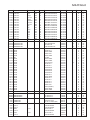
Exploded View & Miscellaneous Parts
Accessories
Description
CT CABLE
FOOT
BRACKET
SCREW-KIT
PAN HEAD TAPPING 5X20 #1
PAN HEAD SCREW M5X20
HEX NUT N5
TOOTHED LOCK WASHER OW5
PLAIN WASHER FW5
DOUBLE FACE
BRACKET SEAL
No.
VXSTD P/N Qty.
T9101496A
1
S4000046
4
RA0116500
1
U40520101
U00520001
U60500301
U72005001
U70005001
R7069960
R8069970
4
4
4
4
8
2
1
YAESU P/N
U04204001
U24306007
U20206001
U20210007
U20205007
U51308007
Description
×4
SEMS SCREW HSM 2.6×
×6B
TAPTITE SCREW M3×
×6
BINDING HEAD SCREW M2.6×
×10B
BINDING HEAD SCREW M2.6×
×5B
BINDING HEAD SCREW M2.6×
×8B
HEX SOCKET BOLT M3×
Qty.
5
4
2
3
9
4
RA0117000
TOP CASE
P1090376
CONNECTOR
Non-designated parts are available
only as part of a designated assembly.
RA0099900
REAR PANEL
R6054387B
SPECIAL NUT
RA0116900
FRONT PANEL
RA0116100
HEATSINK PLATE
R0144090
PLATE NUT
RA0116300
SPACER (7pcs)
RA0116700
RUBBER KNOB ASS'Y
RA0115900
RUBBER CAP
RA0117100
BOTTOM CASE
25
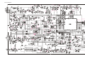
Block Diagram
26
Circuit Description
Reception and transmission are switched by
"RX5V" and "TX5V" lines from the microprocessor unit (MPU). The receiver uses double-conversion superheterodyne circuitry, with a 21.4 MHz
1st IF and 455 kHz 2nd IF. The 1st LO, produced
by a PLL synthesizer, yields the 21.4 MHz 1st IF.
The 2nd LO uses a 20.945 MHz (21.4 MHz455 kHz) signal generated by a crystal oscillator. The 2nd mixer and other circuits use a custom IC to convert and amplify the 2nd IF, and
detect FM to obtain demodulated signals. During transmit, the PLL synthesizer oscillates at the
desired frequency directly, for amplification to
obtain RF power output. During transmit, voice
modulation and CTCSS (or DCS) modulation are
applied to this synthesizer. Transceiver functions, such as tx/rx control, PLL synthesizer settings, and channel programming, are controlled
using the MPU.
Receiver
Incoming RF signals from the antenna connector are delivered to the MAIN Unit, and pass
through a low-pass filter (LPF) consisting of coils
L2001, L2002, L2004, and L2024, capacitors
C2002, C2004, C2009, C2111, C2112, C2113, and
C2114, and antenna switching diodes D2001,
D2002, and D2013 for delivery to the receiver
front end.
The signals are then band-pass filtered and
amplified by Q2001 (2C3356). The signals are
then fed to the input of the 1st mixer, Q2004
(SGM2016AM), where they are mixed with the
1st local signal from the PLL. The 21.4 MHz 1st
mixer product then passes through monolithic
crystal filters XF2001 and XF2002, and is amplified by Q2010 (2SC2714Y) and delivered to the
input of the FM subsystem IC Q2013
(MC3372ML). This IC contains the 2nd mixer, a
local oscillator, limiter amplifier, FM detector,
and audio amplifier. The 2nd LO in the IF-IC is
produced from crystal X2002 (20.945 MHz), and
the 1st IF is converted to 455 kHz by the 2nd
mixer and stripped of unwanted components by
ceramic filters CF2001 and CF2002. After passing through a limiter amplifier, the signal is demodulated by the FM detector.
Demodulated receive audio from the IF-IC is
amplified by Q1005 (NJM2902M). After volume
adjustment by the AF power amplifier Q1003
(LA4425A), the audio signal is passed to the
speaker jack.
PLL synthesizer
The 1st LO maintains stability from the PLL
synthesizer by using a 12.8 MHz reference signal from crystal X2001. PLL synthesizer IC
Q2009 (MC145191F) consists of a prescaler, reference counter, swallow counter, programmable counter, a serial data input port to set these
counters based on the external data, a phase
comparator, and charge pump.
The PLL-IC divides the 12.8 MHz reference
signal by 1,280 using the reference counter (10.0
kHz comparison frequency). The VCO output
is divided by the prescaler, swallow counter and
programmable counter. These two signals are
compared by the phase comparator and applied
to the charge pump. A voltage proportional to
their phase difference is delivered to the lowpass filter circuit, then fed back to the VCO as
an error-correcting voltage, controlling and stabilizing the oscillating frequency.
The VCO is comprised of Q2008 (2SC3356)
and D2003 (HVU350), and oscillates at 21.4 MHz
during receive, and at the fundamental frequency during transmit, with direct frequency-modulation using varactor diode D2004 (HVU350).
The VCO output passes through buffer amplifier Q2011 (2SC3356), and a portion is fed to the
PLL IC, and at the same time amplified by Q2016
(2SC3356) to obtain stable output. The VCO DC
supply is regulated by Q2017 (2SC2812). Synthesizer output is fed to the 1st mixer by diode
switch D2010 (1SS184) during receive, and to
drive amplifier Q2015 (µPC2710) for transmit.
The reference oscillator feeds the PLL synthe27
Circuit Description
sizer, and is composed of crystal X2001 (12.8
MHz), the temperature compensation circuit
which includes D2007 (1SS353) and thermostats
TH2001 and TH2002, and the transmit (DCS)
modulation circuit D2005/ D2006 (HVU350×2).
Transmitter
Voice audio from the microphone or external
inputs passes through a low-pass filter Q1005
(NJM2902M), and a limiter amplifier and lowpass filter at Q1006 (NJM2902M), then is adjusted for optimum deviation level and delivered
to the next stage.
Voice input from the microphone, or external
inputs and CTCSS, are frequency-modulated at
the VCO of the synthesizer, while DCS audio is
modulated by the reference frequency oscillator
of the synthesizer. Synthesizer output, after passing through diode switch D2010 (1SS184), is
amplified by driver Q2015 (µPC2710) and power module Q2003 (M68739M) to obtain full RF
output. The RF energy then passes through antenna switch D2001/ D2002 and a low-pass filter
circuit and finally to the antenna connector.
RF output power from the final amplifier is
sampled by C2117 and C2118 and is rectified by
D2017 (1SS321). The resulting DC is fed through
Automatic Power Controller Q2018 (TA75S01F)
to transmitter power module Q2003.
Generation of spurious products by the transmitter is minimized by the fundamental carrier
28
frequency being equal to the final transmitting
frequency, modulated directly in the transmit
VCO. Additional harmonic suppression is provided by a low-pass filter consisting of L2001,
L2002, and L2024 and C2002, C2004, C2009,
C2111, C2112, C2113, and C2114, resulting in
more than 60 dB of harmonic suppression prior
to delivery to the RF energy to the antenna.
DCS Demodulator
DCS signals are demodulated on the RFUNIT, and are applied to low-pass filter in sections 3 and 4 of Q1040 (NJM2902M), as well as
the limiter comparator in section 1 of Q1040.
CTCSS encoder/decoder
Generation, demodulation, and detection of
the CTCSS tones are carried out by IC Q1014
(MX165C).
MPU
Operation is controlled by 8-bit MPU IC
Q1039 (HD64F3334YTF). The system clock uses
a 9.8304 MHz crystal for a time base. IC Q1015
(RH5VL45AA) resets the MPU when the power
is on, and monitors the voltage of the regulated
5V power supply line.
EEPROM
The EEPROM retains Tx and Rx data for all
16 channels, CTCSS data, DCS data, prescaler
dividing, IF frequency, local oscillator injection
side (upper/lower), and REF oscillator data (internal/external).
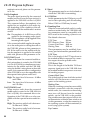
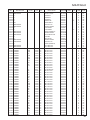
Alignment
The VXR-1000 has been aligned at the factory
for the specified performance across the frequency range specified for each version.
Realignment should therefore not be necessary except in the event of a component failure,
or after alteration of the repeater version. All
component replacement and service should be
performed only by an authorized Vertex representative, or the warranty policy may be voided.
The following test equipment is required for
alignment:
H IBM PC/compatible computer w/Vertex VPL-
1 cable, FRB-4, and CE-22 channel programming diskette.
H RF signal generator: calibrated output level
at 1000 MHz (0 dBµ = 1.0 µV - closed circuit)
H Deviation meter (linear detector)
H AF millivoltmeter
H SINAD meter
H Inline wattmeter: 1000 MHz, 10 W scale
H Regulated DC power supply: adjustable from
10 to 17 V, 3 A
H 50-Ohm non-reactive dummy load: 10 W at
1000 MHz
H Frequency counter: 0.2 ppm accuracy at 1000
MHz
H AF signal generator
H DC Voltmeter: high impedance
H RF Sampling Coupler (attenuation pad)
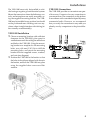
Before beginning, connect the transceiver and
PC using the VPL-1 cable and FRB-4 as shown
below, and download the EEPROM data from
the transceiver to the computer.
Store this data in a disk file so that it can be
saved and retrieved later. Using the table below,
program the channel, CTCSS, and DCS alignment settings for your transceiver version. Upload this file to the transceiver.
RF Signal
Generator
50-Ohm
Dummy Load
Inline Wattmeter
RF Sampling
Coupler
Transceiver
FRB-4
Deviation Meter
VPL-1 Connection
Cable
Power Supply
13.8V DC
Frequency
Counter
COM port
PLL & Transmitter
Set up the test equipment as shown for Alignment Setup. Adjust the supply voltage to 13.8 V
for all steps. Refer to the "Alignment Points" photo for alignment locations.
PLL Reference Frequency
Ë Tune the transceiver to channel #3, connect
the sampling coupler and frequency counter
between the antenna connector and RF dummy load, key the transmitter, and adjust
TC2001 on the MAIN Unit for precisely 162.00
MHz (±100 Hz).
PLL VCV
Ë Leave the RF sampling coupler in-line between
the antenna jack and the RF dummy load.
Connect the frequency counter to the coupler.
Ë Connect the DC voltmeter between VCV test
point TP2006 on the MAIN Unit and chassis
ground.
Ë Set the transceiver to the low band edge channel #1. And adjust T2001 on the MAIN Unit
for 0.5 V on the voltmeter.
Ë Select high band edge channel #2. Key the
transmitter, and confirm the low-end VCV is
less than 4.4 V on the voltmeter.
29
Alignment
Transmitter Output Power
Ë Turn the VXR-1000 off.
Ë Rotate the CHANNEL Selector Knob to the "16"
position.
Ë Press and hold in the PTT switch while you
turn the VXR-1000 on, then rotate the CHANNEL Selector Knob counter-clockwise to the
"12" position while holding in the PTT switch
continuously.
Ë Confirm that the "TX" and "PWR" LEDs are
blinking, then release the PTT switch. The
VXR-1000 now is in the Tx Power Alignment
Mode.
Ë Rotate the CHANNEL Selector Knob to the "3"
position.
Ë Press and hold in the PTT switch, and rotate
the CHANNEL Selector Knob so as to achieve
5.0 Watts on the wattmeter.
Ë Release the PTT switch, then turn the VXR1000 off.
CTCSS Modulation Level
Ë Select channel #4, with 151.4 Hz CTCSS encode. Transmit, and adjust VR1006 on the
MAIN Unit for 0.75 kHz (±0.05 kHz) deviation as indicated on the deviation meter.
DCS Modulation Level.
Ë Select channel #5, with DCS 023 enabled.
Transmit, and adjust VR1009 on the MAIN
Unit for 0.75 kHz (±0.1 kHz) deviation as indicated on the deviation meter.
Microphone Audio Modulation Level
Ë Select channel #3, and adjust the AF generator for 30 mVrms output at 1 kHz injection to
the MIC jack.
Ë Transmit, and adjust VR1005 on the MAIN
Unit for 4.2 kHz (±0.1 kHz) deviation as indicated on the deviation meter.
TP2006 (Chip Side)
VR1009
VR1005
T2005
VR1006
T2003
TC2001
T2002
T2001
T2004
Alignment Points
30
Alignment
Receiver
Ë With the transceiver set to (band center) chan-
Ë Rotate the CHANNEL Selector Knob to the "2"
nel #3, and the RF signal generator tuned to
the same frequency, set the generator for 3.0
kHz deviation (for 25 kHz steps) with 1 kHz
tone modulation, and set the output level for
100 µV at the antenna jack.
Ë Adjust T2002, T2003, T2004, and T2005 on the
Main Unit for optimum SINAD, reducing the
signal generator output level as necessary for
proper meter deflection.
Ë After the previous step, the final signal generator level should be less than 0.3 µV for 12
dB SINAD.
position, and adjust the Signal Generator level
for 0 dBµ (1.0 µV).
Ë Press and hold in the PTT switch, and rotate
the CHANNEL Selector Knob so that the "RX"
LED turns off (Squelch just closes).
Ë Release the PTT switch, then turn the VXR1000 off.
Squelch Threshold I
PC Alignment
Ë Select channel #3, and adjust the signal generator level for 0 dBµ (1.0 µV).
Ë Adjust the squelch threshold level by the PC
so that it just closes (RX LED turns off).
Manual Alignment
Ë Turn the VXR-1000 off.
Ë Rotate the CHANNEL Selector Knob to the "16"
position.
Ë Press and hold in the PTT switch while you
turn the VXR-1000 on, then rotate the CHANNEL Selector Knob counter-clockwise to the
"13" position while holding in the PTT switch
continuously.
Ë Confirm that the "PRI," "COR," and "PWR"
LEDs are blinking, then release the PTT
switch. The VXR-1000 now is in the Squelch
Threshold Alignment Mode.
Squelch Threshold II
You can now adjust the Squelch Threshold
for each channel.
Ë Turn
the VXR-1000 off.
Ë Rotate the CHANNEL Selector Knob to the "16"
position.
Ë Press and hold in the PTT switch while you
turn the VXR-1000 on, then rotate the CHANNEL Selector Knob counter-clockwise to the
"14" position while holding in the PTT switch
continuously.
Ë Confirm the "MBL," "COR," and "PWR" LEDs
are blinking, then release the PTT switch. The
VXR-1000 now is in the Squelch Threshold
Alignment (for each channel) Mode.
Ë Rotate the CHANNEL Selector Knob to the
channel position where you wish adjust the
squelch threshold level.
Ë Press and hold in the PTT switch, and rotate
the CHANNEL Selector Knob so that the "RX"
LED turns off (Squelch just closes).
Ë Release the PTT switch, then turn the VXR1000 off.
31
Repeater Cloning
You can transfer data stored in one VXR-1000 to another VXR-1000 by utilizing the handy
“Cloning” feature. This requires the optional T9101411 Cable and FRB-4 Alignment Interface
Box, so as to connect the Microphone jacks on the two repeaters as shown below.
To clone from one repeater to another, use the following procedure:
Ë Turn both repeaters off, and connect the T9101411 Cable between the FRB-4 modular jack
and the “Source” repeater’s Microphone jack. Turn the “Source” repeater On.
Ë Connect the FRB-4 modular connector to the “Target” repeater’s Microphone jack.
Ë Turn the “Target” repeater On, and set the FRB-4’s PTT switch to On. The “Source” repeater will now send its frequency data to the “Target” repeater.
Ë Wait two seconds, then turn the “Target” repeater off. Now turn the “Source” repeater off.
Ë Remove the T9101411 Cable and the FRB-4. All frequency data for the two repeaters are
now identical. They both may be turned on now for normal operation.
“Source” Repeater
“Target” Repeater
Optional Cable
(T9101411)
FRB-4
32
Main Unit
Circuit Diagram
10.5V
12.6V
5.0V(0.2V)
5.0V
0.2V(5.0V)
2.2V
13.8V
2.2V
2.2V
5.0V(4.3V)
2.2V
13.8V
2.2V
9.0V
13.7V
5.0V
4.3V(5.0V)
5.0V
13.1V
0V(5.0V)
5.0V
2.9V(0V)
0.7V
5.0V
0V(5.0V)
3.7V
3.7V
3.7V
3.2V
5.0V
0V
0V
3.7V
4.9V
0V
LED ON: 0V
LED OFF: 5.0V
0V
3.7V
3.7V
0V
3.7V
3.7V
3.7V
0V
0V
3.7V
3.6V
4.9V
0V
4.9V
4.9V(0V)
0V 0V(9.0V)
4.9V
4.9V
LED ON: 3.0V
LED OFF: 5.0V
2.8V
4.9V
3.6V
3.7V
0V
4.9V
2.5V
2.5V
0V
2.5V
5.0V
0V
2.5V
3.7V
3.7V
3.7V
3.7V
2.2V
3.7V
2.2V
2.5V
2.3V
3.6V
2.3V
2.3V
2.5V
3.7V
0.6V
2.2V
2.0V
2.3V
0 ~ 3.8V
0 ~ 2.6V
12.4V
5.9V
1.8V
1.1V
1.8V
1.8V
1.8V
2.3V
1.8V
1.8V
2.3V
RX (TX)
33
Main Unit
3.8V
3.7V
4.3V
(0.8V)
0.7V
0.6V
0.7V
0.7V
3.8V
4.3V
0.3V
2.7V
5.0V
(4.7V)
2.0V
(1.7V)
(2.0V)
0.6V
1.8V
2.0V
0.6V
1.1V
(4.3V)
1.4V
(4.9V)
3.4V
3.7V 4.4V
4.4V
12.6V
0V
4.0V
4.1V
4.8V
3.3V
0V
2.6V
2.0V
0.7V
0.8V
4.0V
1.4V
0V
4.8V
4.0V
5.0V
1.4V
0V
1.9V
5.0V
2.3V
0V
4.9V
2.2V
5.0V
0V
5.0V
5.0V
1.5V
2.7V
2.3V
5.0V
3.9V
4.0V
5.0V
5.0V
2.7V
5.0V
4.9V
RX (TX)
34
Main Unit
Parts Layout
A
B
C
D
E
F
G
HD64F3334YTF16
(Q1039)
MC145191FR(Lot.1-)
MC145193FR2(Lot.10-)
(Q2009)
M68739M-01(Lot.1-)
M68739M-21(Lot.3-)
RA08N1317M(Lot.29-)
(Q2003)
1
MX165CDW
(Q1016)
MC14053BFR
(Q1019)
MC3372ML
(Q2013)
BR93LC66RF (Lot.1-)
BR93L66RF-WE2 (Lot.13-)
(Q1051)
LA4425A
(Q1003)
2
NJM2902M
(Q1005, 1037, 1040)
3
4
2SD1667R
(Q1010)
µPC2710T (C1F)
(Q2015)
IMH11 (H11)
(Q1028, 1032, 1036)
2SJ125D (JD)
(Q1058)
DTC114EK (24)
(Q1056, 1057, 1060)
2SC3356 (R25)
(Q2008, 2011, 2016)
1SS181 (A3) (Lot.1-)
MA721WA-(TX) (Lot.10-)
(D1013)
1SS184 (B3)
(D1006)
DA204K (K)
(D1005, 2016)
5
1SS193 (F3)
(D1012)
Side A
35
Main Unit
a
b
c
d
e
f
g
M64026FP
(Q1059)
1
µPD74HC4066G (Lot.1-)
74HC4066D (Lot.30-)
(Q1001)
NJM2902M
(Q1002, 1006)
L78M05T
(Q1023)
TA75S01F (SA)
(Q2018)
RH5VL45AA (D5)
(Q1022)
NJM78L09UA (8H)
(Q1055)
2SD1767Q (DC)
(Q2002)
SGM2016AM (M-)
(Q2004)
IMH11 (H11)
(Q1009, 1027, 1053, 1054)
DTC114EK (24)
(Q1004, 1007, 1012, 1024,
1061, 2020, 2021)
2SD1368CB (CB)
(Q1017)
2SB1132R (BA)
(Q1015, 1033, 1034)
2SC2714Y (QY)
(Q2010)
2SC2812 (L6)
(Q1008, 1013, 2006, 2017)
2SC3356 (R24)
(Q2001)
2SA1179 (M6)
(Q2012)
1SS184 (B3)
(D1004, 2010, 2018, 2019)
1SS321 (F9)
(D2017)
2
3
4
5
Side B
36
MAIN Unit
Parts List
REF.
DESCRIPTION
VALUE
V/W
TOL.
MFR’S DESIG
YAESU P/N
VERS.
LOT.
SIDE
LAY ADR
A
A
B
A
B
A
A
A
B
A
A
A
A
A
B
B
B
B
B
A
A
A
A
B
A
B
A
B
B
A
B
A
A
A
B
B
B
A
B
B
B
A
A
A
A
B
B
A
A
B
B
A
B
B
A
A
A
B2
B1
f1
B1
f2
F5
B1
B1
f2
B2
A2
B2
B1
C2
g2
f1
e2
g1
e2
C2
C1
C1
C1
f1
C1
d2
D2
b1
f2
D1
f2
D1
D1
D1
d1
d1
f2
D1
d1
d1
f2
B2
D1
B1
F5
d1
c2
E2
F3
d1
b1
C1
c2
e1
F3
F3
F3
*** MAIN UNIT ***
PCB with Components (w/ Q1010 2SD1667R)
Printed Circuit Board
C 1001 CHIP CAP.
0.1uF
25V
C 1002 CHIP CAP.
0.1uF
25V
C 1003 CHIP CAP.
100pF
50V
C 1004 AL.ELECTRO.CAP.
220uF
16V
C 1005 CHIP CAP.
0.1uF
25V
C 1006 CHIP TA.CAP.
4.7uF
6.3V
C 1007 AL.ELECTRO.CAP.
470uF
25V
C 1008 CHIP CAP.
0.001uF
50V
C 1009 CHIP CAP.
0.1uF
25V
C 1010 CHIP CAP.
0.1uF
25V
C 1011 AL.ELECTRO.CAP.
470uF
25V
C 1012 CHIP CAP.
0.1uF
25V
C 1013 CHIP CAP.
0.1uF
25V
C 1014 CHIP TA.CAP.
4.7uF
6.3V
C 1015 CHIP CAP.
0.1uF
25V
C 1016 CHIP TA.CAP.
4.7uF
16V
C 1017 CHIP CAP.
0.1uF
25V
C 1018 CHIP CAP.
0.01uF
50V
C 1019 CHIP CAP.
0.1uF
25V
C 1020 CHIP CAP.
47pF
50V
C 1021 CHIP CAP.
47pF
50V
2.2uF
6.3V
C 1022 CHIP TA.CAP.
C 1023 CHIP TA.CAP.
0.47uF
16V
C 1024 CHIP TA.CAP.
4.7uF
16V
C 1025 CHIP CAP.
100pF
50V
C 1026 CHIP CAP.
0.1uF
25V
C 1027 CHIP CAP.
0.1uF
25V
C 1028 CHIP CAP.
0.0022uF
50V
C 1029 CHIP CAP.
0.1uF
25V
C 1030 CHIP CAP.
0.01uF
50V
C 1031 CHIP CAP.
0.0082uF
50V
C 1032 CHIP CAP.
0.1uF
25V
C 1033 CHIP TA.CAP.
4.7uF
6.3V
C 1034 CHIP CAP.
0.1uF
25V
C 1035 CHIP CAP.
68pF
50V
C 1035 CHIP CAP.
220pF
50V
C 1036 CHIP CAP.
0.033uF
25V
C 1037 CHIP TA.CAP.
0.47uF
16V
C 1038 CHIP CAP.
68pF
50V
C 1038 CHIP CAP.
220pF
50V
C 1039 CHIP CAP.
470pF
50V
C 1040 AL.ELECTRO.CAP.
47uF
25V
C 1041 CHIP CAP.
0.1uF
25V
C 1042 AL.ELECTRO.CAP.
470uF
25V
C 1043 AL.ELECTRO.CAP.
100uF
10V
C 1044 CHIP TA.CAP.
4.7uF
16V
C 1045 CHIP CAP.
0.1uF
25V
C 1046 CHIP CAP.
0.001uF
50V
C 1047 CHIP CAP.
0.001uF
50V
C 1048 CHIP CAP.
0.1uF
25V
C 1049 CHIP CAP.
0.1uF
25V
C 1050 CHIP CAP.
0.1uF
25V
C 1051 CHIP CAP.
33pF
50V
C 1052 CHIP CAP.
0.1uF
25V
C 1053 CHIP CAP.
0.0022uF
50V
C 1054 CHIP TA.CAP.
1uF
6.3V
C 1054 CHIP CAP.
0.047uF
50V
B
B
CH
B
B
B
B
B
B
B
B
B
B
CH
CH
CH
B
B
B
B
B
B
B
B
CH
CH
B
CH
CH
B
B
B
B
B
B
B
B
CH
B
B
B
GRM21BB11E104KA01L
GRM21BB11E104KA01L
GRM2162C1H101JA01D
RE2-16V221MG3#
GRM21BB11E104KA01L
TEESVA0J475M8R
RE3-25V471MH3#
GRM216B11H102KA01D
GRM21BB11E104KA01L
GRM21BB11E104KA01L
RE3-25V471MH3#
GRM21BB11E104KA01L
GRM21BB11E104KA01L
TEESVA0J475M8R
GRM21BB11E104KA01L
TEESVA1C475M8R
GRM21BB11E104KA01L
GRM40B103M50PT
GRM21BB11E104KA01L
GRM2162C1H470JZ01D
GRM2162C1H470JZ01D
TEESVA0J225M8R
TEESVSP1C474M8R
TEESVA1C475M8R
GRM2162C1H101JA01D
GRM21BB11E104KA01L
GRM21BB11E104KA01L
GRM216B11H222KA01D
GRM21BB11E104KA01L
GRM40B103M50PT
GRM40B822M50PT
GRM21BB11E104KA01L
TEESVA0J475M8R
GRM21BB11E104KA01L
GRM2162C1H680JZ01D
GRM2162C1H221JZ01D
GRM40B333M25PT
TEESVSP1C474M8R
GRM2162C1H680JZ01D
GRM2162C1H221JZ01D
GRM216B11H471KA01D
RC2-25V470MF1#
GRM21BB11E104KA01L
RE3-25V471MH3#
RE2-10V101ME3#
TEESVA1C475M8R
GRM21BB11E104KA01L
GRM216B11H102KA01D
GRM216B11H102KA01D
GRM21BB11E104KA01L
GRM21BB11E104KA01L
GRM21BB11E104KA01L
GRM2162C1H330JZ01D
GRM21BB11E104KA01L
GRM216B11H222KA01D
TEESVP0J105M8R
GRM21BB11H473KA01L
CS1630001
FR003310B
K22140811
K22140811
K22170235
K40129048
K22140811
K78080017
K40149044
K22170805
K22140811
K22140811
K40149044
K22140811
K22140811
K78080017
K22140811
K78120031
K22140811
K22170817
K22140811
K22170227
K22170227
K78080009
K78120035
K78120031
K22170235
K22140811
K22140811
K22170809
K22140811
K22170817
K22170816
K22140811
K78080017
K22140811
K22170231
K22170243
K22140810
K78120035
K22170231
K22170243
K22170801
K40149023
K22140811
K40149044
K40109024
K78120031
K22140811
K22170805
K22170805
K22140811
K22140811
K22140811
K22170223
K22140811
K22170809
K78080028
K22170823
111111111111111111111111111111111111101111011111111111111113-
37
MAIN Unit
REF.
C 1055
C 1056
C 1057
C 1058
C 1059
C 1060
C 1061
C 1062
C 1063
C 1064
C 1065
C 1066
C 1067
C 1068
C 1069
C 1070
C 1071
C 1072
C 1073
C 1074
C 1075
C 1076
C 1077
C 1078
C 1079
C 1081
C 1082
C 1083
C 1084
C 1085
C 1086
C 1087
C 1088
C 1089
C 1090
C 1091
C 1092
C 1093
C 1094
C 1095
C 1096
C 1097
C 1098
C 1099
C 1100
C 1101
C 1102
C 1103
C 1104
C 1105
C 1106
C 1107
C 1108
C 1109
C 1110
C 1111
C 1112
C 1113
C 1114
C 1115
38
DESCRIPTION
CHIP CAP.
CHIP CAP.
CHIP CAP.
CHIP CAP.
CHIP CAP.
CHIP TA.CAP.
CHIP TA.CAP.
CHIP CAP.
CHIP CAP.
CHIP CAP.
CHIP CAP.
CHIP TA.CAP.
CHIP TA.CAP.
CHIP CAP.
CHIP CAP.
CHIP CAP.
CHIP CAP.
CHIP CAP.
CHIP CAP.
CHIP TA.CAP.
CHIP TA.CAP.
CHIP TA.CAP.
CHIP TA.CAP.
CHIP TA.CAP.
CHIP TA.CAP.
CHIP CAP.
CHIP CAP.
CHIP CAP.
CHIP TA.CAP.
CHIP CAP.
CHIP TA.CAP.
CHIP CAP.
CHIP CAP.
CHIP CAP.
CHIP CAP.
CHIP CAP.
CHIP CAP.
CHIP TA.CAP.
CHIP CAP.
CHIP TA.CAP.
AL.ELECTRO.CAP.
CHIP CAP.
CHIP CAP.
CHIP CAP.
CHIP CAP.
CHIP CAP.
CHIP CAP.
CHIP CAP.
CHIP CAP.
CHIP CAP.
CHIP TA.CAP.
CHIP CAP.
CHIP CAP.
CHIP CAP.
CHIP CAP.
CHIP CAP.
CHIP CAP.
CHIP CAP.
CHIP CAP.
CHIP CAP.
VALUE
470pF
47pF
100pF
0.0047uF
0.0056uF
0.47uF
3.3uF
0.022uF
0.1uF
0.033uF
0.0082uF
10uF
0.47uF
0.01uF
0.0022uF
22pF
22pF
0.022uF
0.001uF
1uF
1uF
0.47uF
0.47uF
0.47uF
0.47uF
0.0012uF
0.01uF
0.0012uF
4.7uF
0.022uF
0.47uF
0.1uF
0.1uF
0.001uF
0.001uF
0.001uF
0.1uF
4.7uF
0.1uF
4.7uF
47uF
0.1uF
0.1uF
10pF
10pF
0.1uF
0.1uF
0.1uF
100pF
0.001uF
4.7uF
0.001uF
8pF
0.033uF
0.001uF
150pF
0.047uF
0.022uF
0.047uF
0.001uF
V/W
50V
50V
50V
50V
50V
16V
6.3V
50V
25V
25V
50V
16V
16V
50V
50V
50V
50V
50V
50V
6.3V
6.3V
16V
16V
16V
16V
50V
50V
50V
16V
50V
16V
25V
25V
50V
50V
50V
25V
16V
25V
16V
16V
25V
25V
50V
50V
25V
25V
25V
50V
50V
6.3V
50V
50V
25V
50V
50V
50V
50V
50V
50V
TOL.
B
CH
CH
B
B
B
B
B
B
B
B
CH
CH
B
B
B
B
B
B
B
B
B
B
B
B
B
B
B
CH
CH
B
B
B
CH
B
B
CH
B
B
CH
B
B
B
B
MFR’S DESIG
GRM216B11H471KA01D
GRM2162C1H470JZ01D
GRM2162C1H101JA01D
GRM216B11H472KA01D
GRM40B562M50PT
TEESVSP1C474M8R
TEESVA0J335M8R
GRM216B11H223KA01D
GRM21BB11E104KA01L
GRM40B333M25PT
GRM40B822M50PT
TEESVC1C106M12R
TEESVSP1C474M8R
GRM40B103M50PT
GRM216B11H222KA01D
GRM2162C1H220JZ01D
GRM2162C1H220JZ01D
GRM216B11H223KA01D
GRM216B11H102KA01D
TEESVP0J105M8R
TEESVP0J105M8R
TEESVSP1C474M8R
TEESVSP1C474M8R
TEESVSP1C474M8R
TEESVSP1C474M8R
GRM216B11H122KA01D
GRM40B103M50PT
GRM216B11H122KA01D
TEESVA1C475M8R
GRM216B11H223KA01D
TEESVSP1C474M8R
GRM21BB11E104KA01L
GRM21BB11E104KA01L
GRM216B11H102KA01D
GRM216B11H102KA01D
GRM216B11H102KA01D
GRM21BB11E104KA01L
TEESVA1C475M8R
GRM21BB11E104KA01L
TEESVA1C475M8R
RC2-16V470ME1#
GRM21BB11E104KA01L
GRM21BB11E104KA01L
GRM2162C1H100JZ01D
GRM2162C1H100JZ01D
GRM21BB11E104KA01L
GRM21BB11E104KA01L
GRM21BB11E104KA01L
GRM2162C1H101JA01D
GRM216B11H102KA01D
TEESVA0J475M8R
GRM216B11H102KA01D
GRM2162C1H8R0DZ01D
GRM40B333M25PT
GRM216B11H102KA01D
GRM2162C1H151JA01D
GRM21BB11H473KA01L
GRM216B11H223KA01D
GRM21BB11H473KA01L
GRM216B11H102KA01D
YAESU P/N
K22170801
K22170227
K22170235
K22170813
K22170814
K78120035
K78080021
K22170821
K22140811
K22140810
K22170816
K78120011
K78120035
K22170817
K22170809
K22170219
K22170219
K22170821
K22170805
K78080028
K78080028
K78120035
K78120035
K78120035
K78120035
K22170806
K22170817
K22170806
K78120031
K22170821
K78120035
K22140811
K22140811
K22170805
K22170805
K22170805
K22140811
K78120031
K22140811
K78120031
K40129058
K22140811
K22140811
K22170211
K22170211
K22140811
K22140811
K22140811
K22170235
K22170805
K78080017
K22170805
K22170209
K22140810
K22170805
K22170239
K22170823
K22170821
K22170823
K22170805
VERS.
LOT.
111111111111111111111111111111111111111111111111111111111111-
SIDE
LAY ADR
B
B
B
A
A
B
A
B
A
A
B
A
B
B
B
A
A
B
B
B
A
B
B
B
B
A
A
A
B
A
A
A
A
B
A
B
A
B
B
B
A
A
A
B
B
B
A
B
B
A
A
B
A
A
A
A
B
B
B
B
f1
e1
b2
C2
F3
c5
F2
f1
C2
F2
b2
E3
c5
b3
b3
E1
E1
c3
c3
c3
F4
c4
c4
c3
c3
E5
E5
F5
b4
F5
F5
F4
B1
d1
F4
c3
F3
c1
c2
c2
B1
F3
D2
d2
d2
d1
E4
e1
e2
D1
F2
e2
F4
F4
F3
E3
c2
d3
d3
c2
MAIN Unit
REF.
C 1116
C 1117
C 1118
C 1119
C 1120
C 1121
C 1122
C 1125
C 2002
C 2003
C 2004
C 2005
C 2007
C 2009
C 2010
C 2012
C 2012
C 2013
C 2014
C 2015
C 2016
C 2017
C 2018
C 2019
C 2019
C 2020
C 2021
C 2023
C 2023
C 2024
C 2024
C 2025
C 2026
C 2026
C 2027
C 2028
C 2029
C 2031
C 2032
C 2033
C 2034
C 2035
C 2036
C 2037
C 2038
C 2040
C 2041
C 2041
C 2042
C 2043
C 2044
C 2045
C 2045
C 2046
C 2047
C 2048
C 2049
C 2050
C 2051
C 2052
DESCRIPTION
CHIP CAP.
CHIP CAP.
CHIP CAP.
CHIP CAP.
CHIP CAP.
CHIP CAP.
CHIP CAP.
CHIP CAP.
CHIP CAP.
CHIP CAP.
CHIP CAP.
CHIP CAP.
CHIP CAP.
CHIP CAP.
CHIP CAP.
FILM CAP.
FILM CAP.
CHIP CAP.
CHIP CAP.
CHIP CAP.
CHIP CAP.
CHIP CAP.
CHIP CAP.
FILM CAP.
FILM CAP.
CHIP CAP.
CHIP CAP.
TANTALUM CAP.
TANTALUM CAP.
CHIP CAP.
CHIP CAP.
CHIP CAP.
CHIP TA.CAP.
CHIP TA.CAP.
CHIP CAP.
CHIP CAP.
CHIP CAP.
CHIP CAP.
CHIP CAP.
CHIP TA.CAP.
CHIP CAP.
CHIP CAP.
CHIP CAP.
CHIP CAP.
CHIP CAP.
CHIP CAP.
CHIP CAP.
CHIP CAP.
CHIP CAP.
CHIP CAP.
CHIP CAP.
CHIP CAP.
CHIP CAP.
CHIP CAP.
CHIP TA.CAP.
CHIP CAP.
CHIP CAP.
CHIP CAP.
CHIP CAP.
CHIP TA.CAP.
VALUE
0.0022uF
150pF
0.1uF
0.001uF
0.001uF
0.1uF
0.1uF
0.1uF
8pF
18pF
39pF
18pF
10pF
47pF
0.001uF
0.022uF
0.022uF
0.01uF
0.001uF
0.5pF
0.1uF
0.1uF
0.1uF
0.022uF
0.022uF
100pF
0.01uF
47uF
47uF
0.1uF
0.33uF
0.01uF
2.2uF
1.5uF
330pF
0.01uF
5pF
0.01uF
15pF
10uF
0.01uF
100pF
100pF
0.1uF
82pF
0.001uF
5pF
2pF
68pF
22pF
0.001uF
0.047uF
0.15uF
0.1uF
10uF
3pF
0.1uF
0.001uF
15pF
10uF
V/W
50V
50V
25V
50V
50V
25V
25V
25V
50V
50V
50V
50V
50V
50V
50V
16V
16V
50V
50V
50V
25V
25V
25V
16V
16V
50V
50V
16V
16V
25V
16V
50V
10V
10V
50V
50V
50V
50V
50V
6.3V
50V
50V
50V
25V
50V
50V
50V
50V
50V
50V
50V
50V
25V
25V
6.3V
50V
25V
50V
50V
6.3V
TOL.
B
CH
B
B
B
B
B
B
CH
CH
CH
CH
CH
CH
B
B
B
CK
B
B
B
CH
B
B
B
B
CH
B
CH
B
CH
B
CH
CH
B
CH
B
UJ
UJ
CH
CH
B
B
B
B
CJ
B
B
CH
MFR’S DESIG
GRM216B11H222KA01D
GRM2162C1H151JA01D
GRM21BB11E104KA01L
GRM216B11H102KA01D
GRM216B11H102KA01D
GRM21BB11E104KA01L
GRM21BB11E104KA01L
GRM21BB11E104KA01L
GRM2162C1H8R0DZ01D
GRM2162C1H180JZ01D
GRM2162C1H390JZ01D
GRM2162C1H180JZ01D
GRM2162C1H100JZ01D
GRM2162C1H470JZ01D
GRM216B11H102KA01D
ECHU1C223JB5
ECHU1C223JX5
GRM40B103M50PT
GRM216B11H102KA01D
GRM2164C1HR50CD01D
GRM21BB11E104KA01L
GRM21BB11E104KA01L
GRM21BB11E104KA01L
ECHU1C223JB5
ECHU1C223JX5
GRM2162C1H101JA01D
GRM40B103M50PT
SS2-1C476M
204M-1602-476M4F
GRM21BB11E104KA01L
GRM21BB11C334KA01L
GRM40B103M50PT
TEESVA1A225M8R
TEESVA1A155M8R
GRM2162C1H331JA01D
GRM40B103M50PT
GRM2162C1H5R0CD01D
GRM40B103M50PT
GRM2162C1H150JZ01D
TEESVA0J106M8R
GRM40B103M50PT
GRM2162C1H101JA01D
GRM2162C1H101JA01D
GRM21BB11E104KA01L
GRM2162C1H820JZ01D
GRM216B11H102KA01D
GRM40UJ050C50PT
GRM40UJ020C50PT
GRM2162C1H680JZ01D
GRM2162C1H220JZ01D
GRM216B11H102KA01D
GRM21BB11H473KA01L
GRM21BB11E154KA01L
GRM21BB11E104KA01L
TEESVA0J106M8R
GRM2163C1H3R0CD01D
GRM21BB11E104KA01L
GRM216B11H102KA01D
GRM2162C1H150JZ01D
TEESVA0J106M8R
YAESU P/N
K22170809
K22170239
K22140811
K22170805
K22170805
K22140811
K22140811
K22140811
K22170209
K22170217
K22170225
K22170217
K22170211
K22170227
K22170805
K57120011
K57120034
K22170817
K22170805
K22170201
K22140811
K22140811
K22140811
K57120011
K57120034
K22170235
K22170817
K70120020
K70120021
K22140811
K22120807
K22170817
K78100021
K78100009
K22170247
K22170817
K22170206
K22170817
K22170215
K78080027
K22170817
K22170235
K22170235
K22140811
K22170233
K22170805
K22170306
K22170303
K22170231
K22170219
K22170805
K22170823
K22140823
K22140811
K78080027
K22170204
K22140811
K22170805
K22170215
K78080027
VERS.
LOT.
1111111111111111321111111241113613113111111111111110111131111111-
SIDE
B
A
B
A
B
B
B
A
B
A
B
B
A
B
A
B
B
A
B
B
A
A
B
A
A
A
B
A
A
B
B
B
A
A
A
B
A
B
B
B
B
B
B
B
B
B
B
B
A
A
A
A
A
B
A
A
B
A
A
A
LAY ADR
d2
E4
g2
E2
b1
g1
b5
E3
g5
B4
g5
g4
B4
g5
C4
e3
e3
B4
g4
g3
D4
B4
d3
D3
D3
D3
f4
B4
B4
d4
d4
e4
D3
D3
D3
d3
D3
f4
e4
d4
d4
d3
d3
e4
e4
e4
d3
d3
C3
C3
D4
D4
D4
d3
D3
D3
f4
D3
D4
D4
39
MAIN Unit
REF.
C 2053
C 2055
C 2056
C 2058
C 2059
C 2060
C 2061
C 2062
C 2063
C 2064
C 2065
C 2066
C 2067
C 2068
C 2069
C 2070
C 2072
C 2073
C 2074
C 2075
C 2076
C 2077
C 2078
C 2079
C 2080
C 2081
C 2083
C 2086
C 2086
C 2088
C 2089
C 2090
C 2091
C 2094
C 2095
C 2097
C 2098
C 2100
C 2101
C 2102
C 2103
C 2104
C 2105
C 2106
C 2107
C 2109
C 2111
C 2112
C 2113
C 2114
C 2115
C 2116
C 2117
C 2118
C 2119
C 2120
C 2121
C 2122
C 2123
C 2124
40
DESCRIPTION
CHIP CAP.
CHIP CAP.
CHIP CAP.
CHIP CAP.
CHIP CAP.
CHIP CAP.
CHIP CAP.
CHIP CAP.
CHIP CAP.
CHIP CAP.
CHIP CAP.
CHIP CAP.
CHIP TA.CAP.
CHIP CAP.
CHIP CAP.
CHIP CAP.
CHIP CAP.
CHIP CAP.
CHIP CAP.
CHIP CAP.
CHIP CAP.
CHIP CAP.
CHIP CAP.
CHIP CAP.
CHIP CAP.
CHIP CAP.
CHIP TA.CAP.
CHIP CAP.
CHIP CAP.
CHIP CAP.
CHIP CAP.
CHIP CAP.
CHIP CAP.
CHIP CAP.
CHIP TA.CAP.
CHIP TA.CAP.
CHIP CAP.
CHIP CAP.
CHIP CAP.
CHIP CAP.
CHIP CAP.
CHIP CAP.
CHIP CAP.
CHIP TA.CAP.
CHIP CAP.
CHIP CAP.
CHIP CAP.
CHIP CAP.
CHIP CAP.
CHIP CAP.
CHIP CAP.
CHIP CAP.
CHIP CAP.
CHIP CAP.
CHIP CAP.
CHIP CAP.
CHIP CAP.
CHIP CAP.
CHIP CAP.
CHIP CAP.
VALUE
5pF
10pF
0.01uF
0.1uF
15pF
0.1uF
47pF
0.001uF
0.001uF
0.1uF
100pF
33pF
10uF
0.1uF
560pF
560pF
68pF
100pF
0.01uF
15pF
0.001uF
100pF
0.0022uF
15pF
0.001uF
0.001uF
10uF
3pF
1pF
47pF
0.001uF
6pF
1pF
0.01uF
10uF
10uF
0.001uF
0.001uF
22pF
2pF
8pF
0.0022uF
0.001uF
10uF
0.001uF
0.001uF
5pF
4pF
12pF
18pF
100pF
8pF
2pF
2pF
680pF
0.22uF
0.001uF
0.01uF
0.001uF
0.001uF
V/W
50V
50V
50V
25V
50V
25V
50V
50V
50V
25V
50V
50V
6.3V
25V
50V
50V
50V
50V
50V
50V
50V
50V
50V
50V
50V
50V
6.3V
50V
50V
50V
50V
50V
50V
50V
6.3V
6.3V
50V
50V
50V
50V
50V
50V
50V
6.3V
50V
50V
50V
50V
50V
50V
50V
50V
50V
50V
50V
16V
50V
50V
50V
50V
TOL.
CH
CH
B
B
CH
B
CH
B
B
B
CH
CH
B
B
B
CH
CH
B
CH
B
CH
B
CH
B
B
UJ
UJ
CH
B
CH
CK
B
B
B
CH
CK
CH
B
B
B
B
CH
CH
CH
CH
CH
CH
CK
CK
B
B
B
B
B
B
MFR’S DESIG
GRM2162C1H5R0CD01D
GRM2162C1H100JZ01D
GRM40B103M50PT
GRM21BB11E104KA01L
GRM2162C1H150JZ01D
GRM21BB11E104KA01L
GRM2162C1H470JZ01D
GRM216B11H102KA01D
GRM216B11H102KA01D
GRM21BB11E104KA01L
GRM2162C1H101JA01D
GRM2162C1H330JZ01D
TEESVA0J106M8R
GRM21BB11E104KA01L
GRM216B11H561KA01D
GRM216B11H561KA01D
GRM2162C1H680JZ01D
GRM2162C1H101JA01D
GRM40B103M50PT
GRM2162C1H150JZ01D
GRM216B11H102KA01D
GRM2162C1H101JA01D
GRM216B11H222KA01D
GRM2162C1H150JZ01D
GRM216B11H102KA01D
GRM216B11H102KA01D
TEESVA0J106M8R
GRM40UJ030C50PT
GRM40UJ010C50PT
GRM2162C1H470JZ01D
GRM216B11H102KA01D
GRM2162C1H6R0DD01D
GRM2164C1H1R0CD01D
GRM40B103M50PT
TEESVA0J106M8R
TEESVA0J106M8R
GRM216B11H102KA01D
GRM216B11H102KA01D
GRM2162C1H220JZ01D
GRM2164C1H2R0CD01D
GRM2162C1H8R0DZ01D
GRM216B11H222KA01D
GRM216B11H102KA01D
TEESVA0J106M8R
GRM216B11H102KA01D
GRM216B11H102KA01D
GRM2162C1H5R0CD01D
GRM2162C1H4R0CD01D
GRM2162C1H120JZ01D
GRM2162C1H180JZ01D
GRM2162C1H101JA01D
GRM2162C1H8R0DZ01D
GRM2164C1H2R0CD01D
GRM2164C1H2R0CD01D
GRM216B11H681KA01D
GRM219B11C224KC01D
GRM216B11H102KA01D
GRM40B103M50PT
GRM216B11H102KA01D
GRM216B11H102KA01D
YAESU P/N
K22170206
K22170211
K22170817
K22140811
K22170215
K22140811
K22170227
K22170805
K22170805
K22140811
K22170235
K22170223
K78080027
K22140811
K22170802
K22170802
K22170231
K22170235
K22170817
K22170215
K22170805
K22170235
K22170809
K22170215
K22170805
K22170805
K78080027
K22170304
K22170302
K22170227
K22170805
K22170207
K22170202
K22170817
K78080027
K78080027
K22170805
K22170805
K22170219
K22170203
K22170209
K22170809
K22170805
K78080027
K22170805
K22170805
K22170206
K22170205
K22170213
K22170217
K22170235
K22170209
K22170203
K22170203
K22170803
K22120806
K22170805
K22170817
K22170805
K22170805
VERS.
LOT.
1111111111111111111111111111371111111111111111111111111111111-
SIDE
LAY ADR
B
A
A
A
B
B
B
A
A
B
A
A
B
B
A
A
B
A
B
A
A
A
B
B
A
B
B
A
A
B
B
A
A
A
B
A
A
A
B
A
B
B
A
A
B
A
B
B
B
B
B
B
B
B
B
B
B
B
B
A
f3
D4
D4
C3
e4
f3
e3
C3
D4
f3
E3
D4
f3
f3
B3
B3
f3
E3
d4
D4
C4
E4
e4
e4
C4
g3
d4
D3
D3
f4
d4
C4
D3
D4
e4
D3
D3
B4
f4
D3
d3
d3
D3
E5
d4
C4
g5
g5
g5
g5
f3
e3
g5
g4
f4
d5
d5
d5
d5
C4
MAIN Unit
REF.
C 2126
C 2128
C 2129
C 2130
C 2131
C 2132
C 2133
C 2134
C 2135
C 2136
C 2137
C 2138
C 2139
C 2141
C 2143
C 2145
CD2001
CF2001
CF2001
CF2002
CF2002
D 1001
D 1003
D 1004
D 1005
D 1006
D 1007
D 1012
D 1013
D 1013
D 2001
D 2002
D 2003
D 2004
D 2005
D 2006
D 2007
D 2010
D 2012
D 2013
D 2014
D 2015
D 2016
D 2017
D 2018
D 2019
F 1001
FB2001
FB2003
FB2004
J 1002
J 1003
J 1004
L 2001
L 2002
L 2004
L 2005
L 2006
L 2007
L 2008
DESCRIPTION
CHIP CAP.
CHIP CAP.
CHIP CAP.
CHIP CAP.
CHIP CAP.
CHIP CAP.
CHIP CAP.
CHIP CAP.
CHIP CAP.
CHIP CAP.
CHIP CAP.
CHIP CAP.
CHIP CAP.
CHIP CAP.
CHIP CAP.
CHIP CAP.
CERAMIC DISC
CERAMIC FILTER
CERAMIC FILTER
CERAMIC FILTER
CERAMIC FILTER
SURGE ABSORBER
DIODE
DIODE
DIODE
DIODE
LED
DIODE
DIODE
DIODE
DIODE
DIODE
DIODE
DIODE
DIODE
DIODE
DIODE
DIODE
DIODE
DIODE
DIODE
DIODE
DIODE
DIODE
DIODE
DIODE
CHIPFUSE
FERRITE BEADS
FERRITE BEADS
FERRITE BEADS
CONNECTOR
CONNECTOR
CONNECTOR
COIL A1
COIL A1
COIL A1
M.RFC
COIL A1
M.RFC
COIL A1
VALUE
0.001uF
22pF
220pF
0.001uF
220pF
0.0047uF
0.047uF
0.047uF
7pF
7pF
0.5pF
33pF
15pF
15pF
6pF
6pF
3A
0.1uH
0.1uH
V/W
50V
50V
50V
50V
50V
50V
50V
50V
50V
50V
50V
50V
50V
50V
50V
50V
TOL.
B
CH
CH
B
CH
B
B
B
CH
CH
CK
CH
CH
CH
CH
CH
MFR’S DESIG
GRM216B11H102KA01D
GRM2162C1H220JZ01D
GRM2162C1H221JZ01D
GRM216B11H102KA01D
GRM2162C1H221JZ01D
GRM216B11H472KA01D
GRM21BB11H473KA01L
GRM21BB11H473KA01L
GRM2162C1H7R0DZ01D
GRM2162C1H7R0DZ01D
GRM2164C1HR50CD01D
GRM2162C1H330JZ01D
GRM2162C1H150JZ01D
GRM2162C1H150JZ01D
GRM2162C1H6R0DD01D
GRM2162C1H6R0DD01D
CDBLA455KCAY07-B0
KBF-455R-15A
CFWLA455KEFA-B0
KBF-455R-10A
CFWLA455KGFA-B0
P6KA18A-E3
1SS355 TE-17
1SS184 TE85R
DA204K T146
1SS184 TE85R
GL105R8
1SS193 TE85R
1SS181 TE85R
MA721WA-(TX)
RLS135 TE-11
RLS135 TE-11
HVU350 TRF-E
HVU350 TRF-E
HVU350 TRF-E
HVU350 TRF-E
1SS355 TE-17
1SS184 TE85R
1SS355 TE-17
RLS135 TE-11
1SS355 TE-17
1SS355 TE-17
DA204K T146
1SS321(TE85R.F)
1SS184 TE85R
1SS184 TE85R
0451003MRL 3A
BK2125HS101-T
BK2125HS101-T
BK2125HS101-T
SG8035#01
290A-88-30-335-F
JEY-9P-1A1A90(LF)(SN)
4.5T2.5D0.5UEW R
4.5T2.5D0.5UEW R
3.5T3.5D0.6UEW R
LK2125 R10K-T
3.5T3.5D0.6UEW R
LK2125 R10K-T
2.5T3.0D0.6UEW R
YAESU P/N
K22170805
K22170219
K22170243
K22170805
K22170243
K22170813
K22170823
K22170823
K22170208
K22170208
K22170201
K22170223
K22170215
K22170215
K22170207
K22170207
H7900180
H3900394
H3900505
H3900490
H3900507
Q9000721
G2070470
G2070009
G2070388
G2070009
G2090725
G2070052
G2070001
G2070288
G2070128
G2070128
G2070380
G2070380
G2070380
G2070380
G2070470
G2070009
G2070470
G2070128
G2070470
G2070470
G2070388
G2070076
G2070009
G2070009
Q0000052
L9190087
L9190087
L9190087
P1090350
P1091047
P0091227
L0021649A
L0021649A
L0020678A
L1690307
L0020678A
L1690307
L0021811A
VERS.
LOT.
111111111111111111451331111111110111111111111111111111111111111-
SIDE
B
B
A
B
B
A
B
B
B
B
B
B
B
B
B
A
A
A
A
A
A
A
A
B
A
A
A
A
A
A
B
B
A
A
B
B
B
B
B
B
B
B
B
B
B
B
A
A
B
B
A
A
A
A
A
A
B
A
B
A
LAY ADR
e3
f4
B4
d5
f4
C4
g2
g3
f4
f4
f3
e4
e4
e4
g4
A4
B3
B3
B3
B3
B3
A2
C1
d1
F4
E3
G2
E1
E1
E1
g5
g5
D3
D3
d3
d3
d3
e4
g4
g4
g4
g4
f3
g4
f3
g3
A2
C4
d4
c4
A1
G5
A2
A4
A5
B5
e4
B4
e4
C4
41
MAIN Unit
REF.
L 2010
L 2011
L 2012
L 2013
L 2015
L 2017
L 2020
L 2021
L 2024
L 2025
L 2026
L 2027
Q 1001
Q 1001
Q 1002
Q 1002
Q 1003
Q 1004
Q 1005
Q 1005
Q 1006
Q 1006
Q 1007
Q 1008
Q 1009
Q 1010
Q 1012
Q 1013
Q 1015
Q 1016
Q 1017
Q 1019
Q 1022
Q 1022
Q 1023
Q 1024
Q 1027
Q 1028
Q 1032
Q 1033
Q 1034
Q 1036
Q 1037
Q 1037
Q 1039
Q 1039
Q 1039
Q 1040
Q 1040
Q 1051
Q 1051
Q 1053
Q 1054
Q 1055
Q 1056
Q 1057
Q 1058
Q 1059
Q 1060
Q 1061
42
DESCRIPTION
COIL A1
M.RFC
M.RFC
M.RFC
M.RFC
M.RFC
M.RFC
M.RFC
COIL
COIL A1
COIL A1
M.RFC
IC
IC
IC
IC
IC
TRANSISTOR
IC
IC
IC
IC
TRANSISTOR
TRANSISTOR
TRANSISTOR
TRANSISTOR
TRANSISTOR
TRANSISTOR
TRANSISTOR
IC
TRANSISTOR
IC
IC
IC
IC
TRANSISTOR
TRANSISTOR
TRANSISTOR
TRANSISTOR
TRANSISTOR
TRANSISTOR
TRANSISTOR
IC
IC
IC
IC
IC
IC
IC
IC
IC
TRANSISTOR
TRANSISTOR
IC
TRANSISTOR
TRANSISTOR
FET
IC
TRANSISTOR
TRANSISTOR
VALUE
0.68uH
1uH
0.56uH
0.1uH
0.082uH
0.082uH
10uH
10uH
V/W
TOL.
MFR’S DESIG
YAESU P/N
2.5T2.0D0.5UEW R
LK2125 R68K-T
LK2125 1R0K-T
LK2125 R56K-T
LK2125 R10K-T
HK2125 82NJ-T
LL2012¥F82N
LK2125 100K-T
E2 0.28-1.0-10TR
4.5T2.5D0.5UEW R
4.5T2.5D0.5UEW R
LK2125 100K-T
UPD74HC4066G-T2
74HC4066D
NJM2902M-T2
NJM2902M-TE1
LA4425A
DTC114EK T146
NJM2902M-T2
NJM2902M-TE1
NJM2902M-T2
NJM2902M-TE1
DTC114EK T146
2SC2812L6-TA
IMH11A T110
2SD1667R
DTC114EK T146
2SC2812L6-TA
2SB1132 T100 R
MX165CDW-TR
2SD1368CB TL
MC14053BFR1
RH5VL45AA-T1
RH5VT45AA-T1
L78M05T-TL
DTC114EK T146
IMH11A T110
IMH11A T110
IMH11A T110
2SB1132 T100 R
2SB1132 T100 R
IMH11A T110
NJM2902M-T2
NJM2902M-TE1
HD64F3334YTF16
HD64F3334YTFLH16
HD64F3334YTF16
NJM2902M-T2
NJM2902M-TE1
BR93LC66RF-E2
BR93L66RF-WE2
IMH11A T110
IMH11A T110
NJM78L09UA-TE2
DTC114EK T146
DTC114EK T146
2SJ125D-T12-1D
M64026FP-650C
DTC114EK T146
DTC114EK T146
L0021799A
L1690317
L1690319
L1690316
L1690307
L1690388
L1690346
L1690331
L0022425
L0021649A
L0021649A
L1690331
G1091050
G1094287
G1090908
G1093092
G1092241
G3070002
G1090908
G1093092
G1090908
G1093092
G3070002
G3328127F
G3070070
G3416670R
G3070002
G3328127F
G3211327R
G1092775
G3413688B
G1091524
G1090966
G1093215
G1091731
G3070002
G3070070
G3070070
G3070070
G3211327R
G3211327R
G3070070
G1090908
G1093092
Ú
Ú
Ú
G1090908
G1093092
G1092006
G1093912
G3070070
G3070070
G1091305
G3070002
G3070002
G3701257D
G1092754
G3070002
G3070002
VERS.
LOT.
111111111111130131113131111111111171111111113171013113111111111-
SIDE
LAY ADR
A
B
A
A
B
A
A
B
B
A
A
A
B
B
B
B
A
B
A
A
B
B
B
B
B
A
B
B
B
A
B
A
B
B
B
B
B
A
A
B
B
A
A
A
A
A
A
A
A
A
A
B
B
B
A
A
A
B
A
B
C4
f4
D4
C3
e4
D4
E4
d4
g5
B5
A5
D3
c4
c4
f2
f2
B1
f1
C2
C2
c3
c3
e2
g2
e1
A4
f1
h2
h2
D1
g2
D2
c1
c1
c5
e1
c1
D2
D2
c5
c5
E1
F4
F4
E1
E1
E1
F5
F5
E2
E2
f2
c3
g1
B1
B2
D2
e2
F3
d2
Ú: Please contact Vertex Standard
MAIN Unit
REF.
Q 2001
Q 2002
Q 2003
Q 2003
Q 2003
Q 2003
Q 2004
Q 2006
Q 2008
Q 2009
Q 2009
Q 2010
Q 2011
Q 2012
Q 2013
Q 2015
Q 2016
Q 2017
Q 2018
Q 2020
Q 2021
R 1001
R 1002
R 1003
R 1004
R 1005
R 1006
R 1007
R 1008
R 1009
R 1010
R 1011
R 1012
R 1013
R 1014
R 1015
R 1016
R 1017
R 1018
R 1019
R 1020
R 1021
R 1022
R 1023
R 1024
R 1025
R 1026
R 1027
R 1028
R 1029
R 1030
R 1031
R 1032
R 1033
R 1034
R 1035
R 1036
R 1037
R 1038
R 1039
DESCRIPTION
TRANSISTOR
TRANSISTOR
IC
IC
IC
IC
FET
TRANSISTOR
TRANSISTOR
IC
IC
TRANSISTOR
TRANSISTOR
TRANSISTOR
IC
IC
TRANSISTOR
TRANSISTOR
IC
TRANSISTOR
TRANSISTOR
CHIP RES.
CHIP RES.
CHIP RES.
CHIP RES.
CHIP RES.
CHIP RES.
CHIP RES.
CHIP RES.
CHIP RES.
CHIP RES.
CHIP RES.
CHIP RES.
CHIP RES.
CHIP RES.
CHIP RES.
CHIP RES.
CHIP RES.
CHIP RES.
CHIP RES.
CHIP RES.
CHIP RES.
CHIP RES.
CHIP RES.
CHIP RES.
CHIP RES.
CHIP RES.
CHIP RES.
CHIP RES.
CHIP RES.
CHIP RES.
CHIP RES.
CHIP RES.
CHIP RES.
CHIP RES.
CHIP RES.
CHIP RES.
CHIP RES.
CHIP RES.
CHIP RES.
VALUE
120k
100k
100k
10k
2.2M
6.8k
150k
4.7k
680
10k
4.7k
0
2.2
10k
10k
10k
3.3k
10k
10k
22k
150k
470k
470k
10k
10k
22k
10k
4.7k
150k
47k
2.7k
22k
10k
100k
22k
150k
1.5k
4.7k
6.8k
V/W
1/10W
1/10W
1/10W
1/10W
1/10W
1/10W
1/10W
1/10W
1/10W
1/10W
1/10W
1/10W
1/2W
1/10W
1/10W
1/10W
1/10W
1/10W
1/10W
1/10W
1/10W
1/10W
1/10W
1/10W
1/10W
1/10W
1/10W
1/10W
1/10W
1/10W
1/10W
1/10W
1/10W
1/10W
1/10W
1/10W
1/10W
1/10W
1/10W
TOL.
5%
5%
5%
5%
5%
5%
5%
5%
5%
5%
5%
5%
5%
5%
5%
5%
5%
5%
5%
5%
5%
5%
5%
5%
5%
5%
5%
5%
5%
5%
5%
5%
5%
5%
5%
5%
5%
5%
5%
MFR’S DESIG
YAESU P/N
2SC3356-T2B R24
2SD1767 T100 Q
M68739M-01
M68739M-01
M68739M-21
RA08N1317M
SGM2016AM-T7
2SC2812L6-TA
2SC3356-T2B R25
MC145191FR2
MC145193FR2
2SC2714Y(TE85R.F)
2SC3356-T2B R25
2SA1179N6-CPA-TB
MC3372ML
UPC2710T-E3
2SC3356-T2B R25
2SC2812L6-TA
TA75S01F(TE85R.F)
DTC114EK T146
DTC114EK T146
RMC1/10T 124J
RMC1/10T 104J
RMC1/10T 104J
RMC1/10T 103J
RMC1/10T 225J
RMC1/10T 682J
RMC1/10T 154J
RMC1/10T 472J
RMC1/10T 681J
RMC1/10T 103J
RMC1/10T 472J
RMC1/10T 000J
RMC1/2 2R2JCTP
RMC1/10T 103J
RMC1/10T 103J
RMC1/10T 103J
RMC1/10T 332J
RMC1/10T 103J
RMC1/10T 103J
RMC1/10T 223J
RMC1/10T 154J
RMC1/10T 474J
RMC1/10T 474J
RMC1/10T 103J
RMC1/10T 103J
RMC1/10T 223J
RMC1/10T 103J
RMC1/10T 472J
RMC1/10T 154J
RMC1/10T 473J
RMC1/10T 272J
RMC1/10T 223J
RMC1/10T 103J
RMC1/10T 104J
RMC1/10T 223J
RMC1/10T 154J
RMC1/10T 152J
RMC1/10T 472J
RMC1/10T 682J
G3333567D
G3417677Q
G1092902
G1092902
G1092922
G1094268
G4070012
G3328127F
G3333567E
G1091868
G1093424
G3327147Y
G3333567E
G3111797F
G1091108
G1091844
G3333567E
G3328127F
G1091593
G3070002
G3070002
J24205124
J24205104
J24205104
J24205103
J24205225
J24205682
J24205154
J24205472
J24205681
J24205103
J24205472
J24205000
J24275229
J24205103
J24205103
J24205103
J24205332
J24205103
J24205103
J24205223
J24205154
J24205474
J24205474
J24205103
J24205103
J24205223
J24205103
J24205472
J24205154
J24205473
J24205272
J24205223
J24205103
J24205104
J24205223
J24205154
J24205152
J24205472
J24205682
VERS.
LOT.
111
2
3291111101111111111111111111111111111111111111111111111111-
SIDE
LAY ADR
B
B
A
A
A
A
B
B
A
A
A
B
A
B
A
A
B
B
B
B
B
B
A
A
B
B
A
B
A
A
B
A
B
B
B
A
B
A
B
A
B
A
A
A
B
B
B
A
B
A
A
A
A
B
A
B
A
A
A
A
g4
f4
D5
D5
D5
D5
f4
d4
D3
E4
E4
f3
C4
d4
B3
D4
e4
d4
d5
f2
g3
f2
B2
B1
f1
e2
B2
f2
C2
E2
d1
C1
g2
f1
e2
C1
e2
C2
f1
C2
g2
B2
C2
C1
g2
c2
g2
C2
g2
C1
C1
C1
C2
h2
B2
h2
C1
B2
B1
B2
43
MAIN Unit
REF.
R 1040
R 1041
R 1042
R 1043
R 1044
R 1045
R 1046
R 1047
R 1048
R 1049
R 1050
R 1051
R 1052
R 1053
R 1054
R 1055
R 1056
R 1057
R 1058
R 1059
R 1060
R 1061
R 1062
R 1063
R 1064
R 1065
R 1066
R 1067
R 1068
R 1069
R 1070
R 1071
R 1072
R 1073
R 1074
R 1075
R 1076
R 1077
R 1078
R 1079
R 1080
R 1081
R 1082
R 1083
R 1084
R 1085
R 1086
R 1087
R 1088
R 1089
R 1090
R 1091
R 1092
R 1093
R 1094
R 1095
R 1096
R 1097
R 1098
R 1099
44
DESCRIPTION
CHIP RES.
CHIP RES.
CHIP RES.
CHIP RES.
CHIP RES.
CHIP RES.
CHIP RES.
CHIP RES.
CHIP RES.
CHIP RES.
CHIP RES.
CHIP RES.
CHIP RES.
CHIP RES.
CHIP RES.
CHIP RES.
CHIP RES.
CHIP RES.
CHIP RES.
CHIP RES.
CHIP RES.
CHIP RES.
CHIP RES.
CHIP RES.
CHIP RES.
CHIP RES.
CHIP RES.
CHIP RES.
CHIP RES.
CHIP RES.
CHIP RES.
CHIP RES.
CHIP RES.
CHIP RES.
CHIP RES.
CHIP RES.
CHIP RES.
CHIP RES.
CHIP RES.
CHIP RES.
CHIP RES.
CHIP RES.
CHIP RES.
CHIP RES.
CHIP RES.
CHIP RES.
CHIP RES.
CHIP RES.
CHIP RES.
CHIP RES.
CHIP RES.
CHIP RES.
CHIP RES.
CHIP RES.
CHIP RES.
CHIP RES.
CHIP RES.
CHIP RES.
CHIP RES.
CHIP RES.
VALUE
4.7k
100k
22k
100k
10k
680
4.7k
4.7k
220
4.7k
10k
10k
47k
4.7k
10k
4.7k
1M
100k
330k
15k
10k
10k
10k
6.8k
10k
10k
390k
10k
10k
10k
10k
100k
220k
470k
10
10k
10k
68k
10k
10k
150k
10k
10k
330k
47k
8.2k
47k
10k
2.2k
12k
1k
100k
47k
12k
2.2k
10k
10k
47k
47k
47k
V/W
1/10W
1/10W
1/10W
1/10W
1/10W
1/10W
1/10W
1/10W
1/4W
1/10W
1/10W
1/10W
1/10W
1/10W
1/10W
1/10W
1/10W
1/10W
1/10W
1/10W
1/10W
1/10W
1/10W
1/10W
1/10W
1/10W
1/10W
1/10W
1/10W
1/10W
1/10W
1/10W
1/10W
1/10W
1/10W
1/10W
1/10W
1/10W
1/10W
1/10W
1/10W
1/10W
1/10W
1/10W
1/10W
1/10W
1/10W
1/10W
1/10W
1/10W
1/10W
1/10W
1/10W
1/10W
1/10W
1/10W
1/10W
1/10W
1/10W
1/10W
TOL.
5%
5%
5%
5%
5%
5%
5%
5%
5%
5%
5%
5%
5%
5%
5%
5%
5%
5%
5%
5%
5%
5%
5%
5%
5%
5%
5%
5%
5%
5%
5%
5%
5%
5%
5%
5%
5%
5%
5%
5%
5%
5%
5%
5%
5%
5%
5%
5%
5%
5%
5%
5%
5%
5%
5%
5%
5%
5%
5%
5%
MFR’S DESIG
RMC1/10T 472J
RMC1/10T 104J
RMC1/10T 223J
RMC1/10T 104J
RMC1/10T 103J
RMC1/10T 681J
RMC1/10T 472J
RMC1/10T 472J
RMC1/4 221JATP
RMC1/10T 472J
RMC1/10T 103J
RMC1/10T 103J
RMC1/10T 473J
RMC1/10T 472J
RMC1/10T 103J
RMC1/10T 472J
RMC1/10T 105J
RMC1/10T 104J
RMC1/10T 334J
RMC1/10T 153J
RMC1/10T 103J
RMC1/10T 103J
RMC1/10T 103J
RMC1/10T 682J
RMC1/10T 103J
RMC1/10T 103J
RMC1/10T 394J
RMC1/10T 103J
RMC1/10T 103J
RMC1/10T 103J
RMC1/10T 103J
RMC1/10T 104J
RMC1/10T 224J
RMC1/10T 474J
RMC1/10T 100J
RMC1/10T 103J
RMC1/10T 103J
RMC1/10T 683J
RMC1/10T 103J
RMC1/10T 103J
RMC1/10T 154J
RMC1/10T 103J
RMC1/10T 103J
RMC1/10T 334J
RMC1/10T 473J
RMC1/10T 822J
RMC1/10T 473J
RMC1/10T 103J
RMC1/10T 222J
RMC1/10T 123J
RMC1/10T 102J
RMC1/10T 104J
RMC1/10T 473J
RMC1/10T 123J
RMC1/10T 222J
RMC1/10T 103J
RMC1/10T 103J
RMC1/10T 473J
RMC1/10T 473J
RMC1/10T 473J
YAESU P/N
J24205472
J24205104
J24205223
J24205104
J24205103
J24205681
J24205472
J24205472
J24245221
J24205472
J24205103
J24205103
J24205473
J24205472
J24205103
J24205472
J24205105
J24205104
J24205334
J24205153
J24205103
J24205103
J24205103
J24205682
J24205103
J24205103
J24205394
J24205103
J24205103
J24205103
J24205103
J24205104
J24205224
J24205474
J24205100
J24205103
J24205103
J24205683
J24205103
J24205103
J24205154
J24205103
J24205103
J24205334
J24205473
J24205822
J24205473
J24205103
J24205222
J24205123
J24205102
J24205104
J24205473
J24205123
J24205222
J24205103
J24205103
J24205473
J24205473
J24205473
VERS.
LOT.
111111111111111111111111111111111111111111111111111111111111-
SIDE
LAY ADR
B
B
B
B
B
B
B
A
B
B
B
B
B
B
B
A
A
B
A
B
B
A
A
B
A
A
B
A
A
B
B
A
A
B
A
A
A
B
A
A
B
A
A
A
B
B
A
B
B
B
B
A
B
B
B
A
B
A
B
B
h2
h3
b1
f2
f2
f1
f1
C2
h2
f2
f2
f2
g2
e1
d1
C2
C1
e1
C1
c2
b2
D2
D2
d1
D2
B1
c2
D2
E3
f1
e1
F3
F3
e1
D1
E2
E1
f1
E2
E2
b2
F3
E2
C2
c5
f1
C2
b2
c5
b2
f1
E2
c5
b3
c5
E1
c3
E1
c1
c1
MAIN Unit
REF.
R 1100
R 1101
R 1102
R 1103
R 1104
R 1105
R 1106
R 1107
R 1108
R 1109
R 1110
R 1111
R 1112
R 1113
R 1114
R 1115
R 1116
R 1117
R 1118
R 1119
R 1120
R 1121
R 1122
R 1123
R 1124
R 1125
R 1126
R 1127
R 1128
R 1129
R 1130
R 1131
R 1132
R 1133
R 1134
R 1135
R 1136
R 1137
R 1138
R 1139
R 1140
R 1141
R 1142
R 1143
R 1144
R 1145
R 1146
R 1147
R 1148
R 1149
R 1150
R 1151
R 1152
R 1153
R 1154
R 1156
R 1157
R 1158
R 1159
R 1160
DESCRIPTION
CHIP RES.
CHIP RES.
CHIP RES.
CHIP RES.
CHIP RES.
CHIP RES.
CHIP RES.
CHIP RES.
CHIP RES.
CHIP RES.
CHIP RES.
CHIP RES.
CHIP RES.
CHIP RES.
CHIP RES.
CHIP RES.
CHIP RES.
CHIP RES.
CHIP RES.
CHIP RES.
CHIP RES.
CHIP RES.
CHIP RES.
CHIP RES.
CHIP RES.
CHIP RES.
CHIP RES.
CHIP RES.
CHIP RES.
CHIP RES.
CHIP RES.
CHIP RES.
CHIP RES.
CHIP RES.
CHIP RES.
CHIP RES.
CHIP RES.
CHIP RES.
CHIP RES.
CHIP RES.
CHIP RES.
CHIP RES.
CHIP RES.
CHIP RES.
CHIP RES.
CHIP RES.
CHIP RES.
CHIP RES.
CHIP RES.
CHIP RES.
CHIP RES.
CHIP RES.
CHIP RES.
CHIP RES.
CHIP RES.
CHIP RES.
CHIP RES.
CHIP RES.
CHIP RES.
CHIP RES.
VALUE
47k
12k
270k
1k
1M
470k
10k
100k
10k
150k
150k
220k
1M
220k
100k
100k
100k
10k
470k
220k
2.2M
22k
220k
10k
1k
10k
4.7k
3.9k
47k
10k
390
390
390
390
390
10k
150k
10k
100k
10k
10k
2.2
10k
10k
10k
100k
3.3k
5.6k
10k
10k
10k
10k
4.7k
15
10k
10k
47k
2.2M
10k
150k
V/W
1/10W
1/10W
1/10W
1/10W
1/10W
1/10W
1/10W
1/10W
1/10W
1/10W
1/10W
1/10W
1/10W
1/10W
1/10W
1/10W
1/10W
1/10W
1/10W
1/10W
1/10W
1/10W
1/10W
1/10W
1/10W
1/10W
1/10W
1/10W
1/10W
1/10W
1/10W
1/10W
1/10W
1/10W
1/10W
1/10W
1/10W
1/10W
1/10W
1/10W
1/10W
1/2W
1/10W
1/10W
1/10W
1/10W
1/10W
1/10W
1/10W
1/10W
1/10W
1/10W
1/10W
1W
1/10W
1/10W
1/10W
1/10W
1/10W
1/10W
TOL.
5%
5%
5%
5%
5%
5%
5%
5%
5%
5%
5%
5%
5%
5%
5%
5%
5%
5%
5%
5%
5%
5%
5%
5%
5%
5%
5%
5%
5%
5%
5%
5%
5%
5%
5%
5%
5%
5%
5%
5%
5%
5%
5%
5%
5%
5%
5%
5%
5%
5%
5%
5%
5%
5%
5%
5%
5%
5%
5%
5%
MFR’S DESIG
RMC1/10T 473J
RMC1/10T 123J
RMC1/10T 274J
RMC1/10T 102J
RMC1/10T 105J
RMC1/10T 474J
RMC1/10T 103J
RMC1/10T 104J
RMC1/10T 103J
RMC1/10T 154J
RMC1/10T 154J
RMC1/10T 224J
RMC1/10T 105J
RMC1/10T 224J
RMC1/10T 104J
RMC1/10T 104J
RMC1/10T 104J
RMC1/10T 103J
RMC1/10T 474J
RMC1/10T 224J
RMC1/10T 225J
RMC1/10T 223J
RMC1/10T 224J
RMC1/10T 103J
RMC1/10T 102J
RMC1/10T 103J
RMC1/10T 472J
RMC1/10T 392J
RMC1/10T 473J
RMC1/10T 103J
RMC1/10T 391J
RMC1/10T 391J
RMC1/10T 391J
RMC1/10T 391J
RMC1/10T 391J
RMC1/10T 103J
RMC1/10T 154J
RMC1/10T 103J
RMC1/10T 104J
RMC1/10T 103J
RMC1/10T 103J
RMC1/2 2R2JCTP
RMC1/10T 103J
RMC1/10T 103J
RMC1/10T 103J
RMC1/10T 104J
RMC1/10T 332J
RMC1/10T 562J
RMC1/10T 103J
RMC1/10T 103J
RMC1/10T 103J
RMC1/10T 103J
RMC1/10T 472J
RMC1 150JTE
RMC1/10T 103J
RMC1/10T 103J
RMC1/10T 473J
RMC1/10T 225J
RMC1/10T 103J
RMC1/10T 154J
YAESU P/N
J24205473
J24205123
J24205274
J24205102
J24205105
J24205474
J24205103
J24205104
J24205103
J24205154
J24205154
J24205224
J24205105
J24205224
J24205104
J24205104
J24205104
J24205103
J24205474
J24205224
J24205225
J24205223
J24205224
J24205103
J24205102
J24205103
J24205472
J24205392
J24205473
J24205103
J24205391
J24205391
J24205391
J24205391
J24205391
J24205103
J24205154
J24205103
J24205104
J24205103
J24205103
J24275229
J24205103
J24205103
J24205103
J24205104
J24205332
J24205562
J24205103
J24205103
J24205103
J24205103
J24205472
J24305150
J24205103
J24205103
J24205473
J24205225
J24205103
J24205154
VERS.
LOT.
111111111111111111111111111111111111111111111111111111111111-
SIDE
LAY ADR
A
B
A
A
A
B
B
A
B
A
A
A
A
A
B
A
A
A
A
A
A
A
A
A
B
A
B
B
A
B
A
A
A
A
A
A
B
B
A
B
A
B
B
A
B
B
B
B
A
B
B
A
B
B
B
A
B
B
B
B
E1
c3
F3
F4
F3
c3
b2
F4
c3
E4
E3
E5
E5
E5
e1
E4
E4
E4
F5
F5
F4
F4
F5
E4
c4
E4
b5
b5
F4
e1
G3
G3
F2
F2
F2
F4
f2
b3
B2
b4
F4
b4
c2
D2
d3
d2
c2
c2
E1
c4
c4
E1
c2
b5
f2
D2
d2
d2
e2
e2
45
MAIN Unit
REF.
R 1163
R 1164
R 1165
R 1166
R 1167
R 1168
R 1169
R 1170
R 1171
R 1173
R 1174
R 2002
R 2003
R 2004
R 2006
R 2007
R 2008
R 2009
R 2010
R 2011
R 2011
R 2012
R 2013
R 2015
R 2016
R 2018
R 2019
R 2020
R 2022
R 2024
R 2025
R 2027
R 2030
R 2030
R 2031
R 2033
R 2034
R 2035
R 2036
R 2037
R 2038
R 2039
R 2040
R 2041
R 2042
R 2043
R 2044
R 2045
R 2046
R 2047
R 2047
R 2048
R 2049
R 2050
R 2051
R 2052
R 2053
R 2054
R 2055
R 2056
46
DESCRIPTION
CHIP RES.
CHIP RES.
CHIP RES.
CHIP RES.
CHIP RES.
CHIP RES.
CHIP RES.
CHIP RES.
CHIP RES.
CHIP RES.
CHIP RES.
CHIP RES.
CHIP RES.
CHIP RES.
CHIP RES.
CHIP RES.
CHIP RES.
CHIP RES.
CHIP RES.
CHIP RES.
CHIP RES.
CHIP RES.
CHIP RES.
CHIP RES.
CHIP RES.
CHIP RES.
CHIP RES.
CHIP RES.
CHIP RES.
CHIP RES.
CHIP RES.
CHIP RES.
CHIP RES.
CHIP RES.
CHIP RES.
CHIP RES.
CHIP RES.
CHIP RES.
CHIP RES.
CHIP RES.
CHIP RES.
CHIP RES.
CHIP RES.
CHIP RES.
CHIP RES.
CHIP RES.
CHIP RES.
CHIP RES.
CHIP RES.
CHIP RES.
CHIP RES.
CHIP RES.
CHIP RES.
CHIP RES.
CHIP RES.
CHIP RES.
CHIP RES.
CHIP RES.
CHIP RES.
CHIP RES.
VALUE
10k
10k
3.9k
3.3k
10k
47k
47k
0
68k
0
1M
39k
10k
150
2.2k
4.7k
4.7k
68k
4.7k
1.5k
1.8k
10k
10k
10
470
10k
47
47k
10k
47k
100
2.2M
22k
4.7k
2.2k
1.5k
330
100
100
330k
100k
82
10
10k
22
1k
1k
100
10k
10k
100k
22k
4.7k
47k
1.8k
47k
470k
10
1.8k
56
V/W
1/10W
1/10W
1/10W
1/10W
1/10W
1/10W
1/10W
1/10W
1/10W
1/10W
1/16W
1/10W
1/10W
1/10W
1/10W
1/10W
1/10W
1/10W
1/10W
1/10W
1/10W
1/10W
1/10W
1/10W
1/10W
1/10W
1/10W
1/10W
1/10W
1/10W
1/10W
1/10W
1/10W
1/10W
1/10W
1/10W
1/10W
1/10W
1/10W
1/10W
1/10W
1/10W
1/10W
1/10W
1/10W
1/10W
1/10W
1/10W
1/10W
1/10W
1/10W
1/10W
1/10W
1/10W
1/10W
1/10W
1/10W
1/10W
1/10W
1/10W
TOL.
5%
5%
5%
5%
5%
5%
5%
5%
5%
5%
5%
5%
5%
5%
5%
5%
5%
5%
5%
5%
5%
5%
5%
5%
5%
5%
5%
5%
5%
5%
5%
5%
5%
5%
5%
5%
5%
5%
5%
5%
5%
5%
5%
5%
5%
5%
5%
5%
5%
5%
5%
5%
5%
5%
5%
5%
5%
5%
5%
5%
MFR’S DESIG
RMC1/10T 103J
RMC1/10T 103J
RMC1/10T 392J
RMC1/10T 332J
RMC1/10T 103J
RMC1/10T 473J
RMC1/10T 473J
RMC1/10T 000J
RMC1/10T 683J
RMC1/10T 000J
RMC1/16S 105JTH
RMC1/10T 393J
RMC1/10T 103J
RMC1/10T 151J
RMC1/10T 222J
RMC1/10T 472J
RMC1/10T 472J
RMC1/10T 683J
RMC1/10T 472J
RMC1/10T 152J
RMC1/10T 182J
RMC1/10T 103J
RMC1/10T 103J
RMC1/10T 100J
RMC1/10T 471J
RMC1/10T 103J
RMC1/10T 470J
RMC1/10T 473J
RMC1/10T 103J
RMC1/10T 473J
RMC1/10T 101J
RMC1/10T 225J
RMC1/10T 223J
RMC1/10T 472J
RMC1/10T 222J
RMC1/10T 152J
RMC1/10T 331J
RMC1/10T 101J
RMC1/10T 101J
RMC1/10T 334J
RMC1/10T 104J
RMC1/10T 820J
RMC1/10T 100J
RMC1/10T 103J
RMC1/10T 220J
RMC1/10T 102J
RMC1/10T 102J
RMC1/10T 101J
RMC1/10T 103J
RMC1/10T 103J
RMC1/10T 104J
RMC1/10T 223J
RMC1/10T 472J
RMC1/10T 473J
RMC1/10T 182J
RMC1/10T 473J
RMC1/10T 474J
RMC1/10T 100J
RMC1/10T 182J
RMC1/10T 560J
YAESU P/N
J24205103
J24205103
J24205392
J24205332
J24205103
J24205473
J24205473
J24205000
J24205683
J24205000
J24189061
J24205393
J24205103
J24205151
J24205222
J24205472
J24205472
J24205683
J24205472
J24205152
J24205182
J24205103
J24205103
J24205100
J24205471
J24205103
J24205470
J24205473
J24205103
J24205473
J24205101
J24205225
J24205223
J24205472
J24205222
J24205152
J24205331
J24205101
J24205101
J24205334
J24205104
J24205820
J24205100
J24205103
J24205220
J24205102
J24205102
J24205101
J24205103
J24205103
J24205104
J24205223
J24205472
J24205473
J24205182
J24205473
J24205474
J24205100
J24205182
J24205560
VERS.
LOT.
11111111111011111111131111111111111011111111111111113111111111-
SIDE
LAY ADR
A
B
B
B
B
B
B
B
B
B
F3
d3
c2
d2
c2
d2
d2
d3
b5
d1
B
A
A
B
B
A
B
A
A
A
B
A
A
B
B
B
B
A
B
B
B
A
A
A
B
A
A
A
B
A
A
B
B
A
A
A
A
B
B
B
B
B
B
B
B
A
B
B
A
g4
D3
B4
d3
d3
D3
d3
D3
D3
D3
d3
E3
D4
f4
f4
f4
d3
C3
d3
e4
d3
D4
D4
D3
e3
C3
D3
C3
f3
D4
D3
e4
d3
D4
C4
C3
E4
d4
d4
d4
f3
d4
d4
f3
f3
B3
e4
g3
D4
MAIN Unit
REF.
R 2057
R 2058
R 2059
R 2060
R 2061
R 2062
R 2063
R 2064
R 2069
R 2070
R 2071
R 2072
R 2073
R 2074
R 2076
R 2079
R 2080
R 2081
R 2082
R 2083
R 2084
R 2086
R 2087
R 2088
R 2089
R 2090
R 2091
R 2092
R 2093
R 2094
R 2095
R 2096
R 2098
R 2099
R 2100
R 2101
R 2102
R 2103
S 1001
T 2001
T 2002
T 2003
T 2004
T 2005
TC2001
TH2001
TH2002
VR1001
VR1002
VR1003
VR1005
VR1006
VR1006
VR1007
VR1007
VR1009
VR1009
VR1010
X 1001
X 1001
DESCRIPTION
CHIP RES.
CHIP RES.
CHIP RES.
CHIP RES.
CHIP RES.
CHIP RES.
CHIP RES.
CHIP RES.
CHIP RES.
CHIP RES.
CHIP RES.
CHIP RES.
CHIP RES.
CHIP RES.
CHIP RES.
CHIP RES.
CHIP RES.
CHIP RES.
CHIP RES.
CHIP RES.
CHIP RES.
CHIP RES.
CHIP RES.
CHIP RES.
CHIP RES.
CHIP RES.
CHIP RES.
CHIP RES.
CHIP RES.
CHIP RES.
CHIP RES.
CHIP RES.
CHIP RES.
CHIP RES.
CHIP RES.
CHIP RES.
CHIP RES.
CHIP RES.
ROTARY SWITCH
COIL 05RF
COIL 05RF
COIL 05RF
COIL 05RF
COIL 05RF
TRIMMER CAP.
THERMISTOR
THERMISTOR
POT.
POT.
POT.
POT.
POT.
POT.
POT.
POT.
POT.
POT.
POT.
CERAMIC OSC
CERAMIC OSC
VALUE
220
560
56
10k
1k
8.2k
2.2k
1k
1M
22
0
100k
15k
22k
0
10k
33k
33k
10k
5.6k
100
47k
1.8k
12k
5.6k
12k
12k
12k
12k
1.2k
1k
2.2M
0
0
1k
0
150
470
150MHz
20pF
100k
100k
10k
10k
47k
47k
47k
47k
47k
47k
1MHz
1MHz
V/W
1/10W
1/10W
1/10W
1/10W
1/10W
1/10W
1/10W
1/10W
1/10W
1/10W
1/10W
1/10W
1/10W
1/10W
1/10W
1/10W
1/10W
1/10W
1/10W
1/10W
1/10W
1/10W
1/10W
1/10W
1/10W
1/10W
1/10W
1/10W
1/10W
1/10W
1/10W
1/10W
1/10W
1/10W
1/10W
1/10W
1/10W
1/10W
TOL.
5%
5%
5%
5%
5%
5%
5%
5%
5%
5%
5%
5%
5%
5%
5%
5%
5%
5%
5%
5%
5%
5%
5%
5%
5%
5%
5%
5%
5%
5%
5%
5%
5%
5%
5%
5%
5%
5%
MFR’S DESIG
RMC1/10T 221J
RMC1/10T 561J
RMC1/10T 560J
RMC1/10T 103J
RMC1/10T 102J
RMC1/10T 822J
RMC1/10T 222J
RMC1/10T 102J
RMC1/10T 105J
RMC1/10T 220J
RMC1/10T 000J
RMC1/10T 104J
RMC1/10T 153J
RMC1/10T 223J
RMC1/10T 000J
RMC1/10T 103J
RMC1/10T 333J
RMC1/10T 333J
RMC1/10T 103J
RMC1/10T 562J
RMC1/10T 101J
RMC1/10T 473J
RMC1/10T 182J
RMC1/10T 123J
RMC1/10T 562J
RMC1/10T 123J
RMC1/10T 123J
RMC1/10T 123J
RMC1/10T 123J
RMC1/10T 122J
RMC1/10T 102J
RMC1/10T 225J
RMC1/10T 000J
RMC1/10T 000J
RMC1/10T 102J
RMC1/10T 000J
RMC1/10T 151J
RMC1/10T 471J
SRZW0L010K
CS-4N 5203-JPS-045
5KM 150M
5KM 150M
5KM 150M
5KM 150M
ECR-JA020E11X
NT732ATD2.0K K
NT732ATD2.0K K
EVN-5ESX50B15
EVN-5ESX50B15
EVN-5ESX50B14
EVN-5ESX50B14
EVM-7JS-X30-BQ4
EVM3YSX50BQ4
EVM-7JS-X30-BQ4
EVM3YSX50BQ4
EVM-7JS-X30-BQ4
EVM3YSX50BQ4
RK09L1120 L=15 10KA
KBR-1000YTR17
CSBLA1M00J2BT21-B0
YAESU P/N
J24205221
J24205561
J24205560
J24205103
J24205102
J24205822
J24205222
J24205102
J24205105
J24205220
J24205000
J24205104
J24205153
J24205223
J24205000
J24205103
J24205333
J24205333
J24205103
J24205562
J24205101
J24205473
J24205182
J24205123
J24205562
J24205123
J24205123
J24205123
J24205123
J24205122
J24205102
J24205225
J24205000
J24205000
J24205102
J24205000
J24205151
J24205471
N0190177
L0022347
L0022344
L0022344
L0022344
L0022344
K91000228
G9090079
G9090079
J51811104
J51811104
J51811103
J51811103
J51788473
J51833473
J51788473
J51833473
J51788473
J51833473
J60800237
H7900840
H7900550
VERS.
LOT.
1111111111111111111111111111111111111111111111111111251251251110-
SIDE
LAY ADR
A
A
A
B
A
B
B
B
A
A
A
A
B
B
B
B
A
B
B
A
B
B
B
B
B
B
B
B
B
B
A
B
B
B
B
B
D4
B3
D4
f3
C4
g3
d4
e4
C3
D3
E4
D3
e3
d3
g4
d4
B5
g4
g4
B4
d5
d3
d3
f2
g3
f3
g3
g3
g2
f3
B3
d3
e3
f4
g3
d3
A
A
A
A
A
A
A
B
B
A
A
A
A
A
A
A
A
A
A
A
B
B
G4
D3
B4
A4
B4
B4
E3
d3
d3
B2
B1
C2
F2
F3
F3
B2
B2
F2
F2
G1
d1
d1
47
REF.
X 1002
X 1003
X 1003
X 2001
X 2001
X 2001
X 2001
X 2002
XF2001
XF2002
DESCRIPTION
XTAL CSA-309
XTAL SX-1315
XTAL SL-MG
XTAL UM-5
XTAL UM-5
XTAL UM-5
XTAL UM-5
XTAL CSA-309
XTAL FILTER
XTAL FILTER
C 0001 CERAMIC CAP.
J 0001 CONNECTOR
48
VALUE
V/W
TOL.
9.8304MHz
3.6263MHz
3.6263MHz
12.8MHz
12.8MHz
12.8MHz
12.8MHz
20.945MHz
22pF
50V
SL
MFR’S DESIG
9.8304MHZ-10
3.6263MHZ
3.6263MHZ
12.8MHZ
12.8MHZ
12.8MHZ
12.8MHZ
20.945MHZ
21S152F
21S152F
*** MAIN ASSY ***
UP050SL220J-A-B
BNC-R (050-1400)
YAESU P/N
VERS.
LOT.
H0103050A
H0103183
H0103343
H0103109
H0103313
H0103329
H0103346
H0103045
H1102256
H1102256
114212641
42111-
K28179070
P1090376
11-
SIDE
LAY ADR
A
B
B
A
A
A
A
A
A
A
E1
d2
d2
E3
E3
E3
E3
C3
C3
C3
49
Copyright © 2009
VERTEX STANDARD CO., LTD.
All rights reserved
50
No portion of this manual may be
reproduced without the permission
of VERTEX STANDARD CO., LTD.