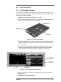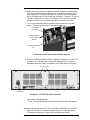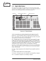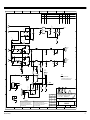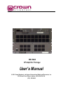
1
® FM1000A RF Amplifier Package User's Manual ©2005 Crown Broadcast, a division of International Radio and Electronics, Inc. 25166 Leer Drive, Elkhart, Indiana, 46514-5425 U.S.A. (574) 262-8900 i Revision Control Revision Print Date Initial Release (Rev. 0) 900413-1 November 1998 Revision 1 April 2002 Revision 2 May 2005 Important Notices ©2005, Crown Broadcast, a division of International Radio and Electronics, Inc. All rights reserved. No part of this publication may be reproduced, transmitted, transcribed, stored in a retrieval system, or translated into any language in any form by any means without the written permission of Crown International, Inc. Printed in U.S.A. Crown attempts to provide information that is accurate, complete, and useful. Should you find inadequacies in the text, please send your comments to the following address: International Radio and Electronics 25166 Leer Drive, P.O. Box 2000 Elkhart, Indiana, 46515-2000 U.S.A. ii Contents Section 1—Getting Acquainted 1.1 Your Amplifier Package ....................................................................................... 1–2 1.2 Amplifier Package Specifications ......................................................................... 1–3 1.3 Safety Considerations .......................................................................................... 1–4 1.3.1 Dangers ............................................................................................................ 1–4 1.3.2 Warnings .......................................................................................................... 1–4 1.3.3 Cautions ........................................................................................................... 1–4 Section 2—Installation 2.1 Operating Environment ..................................................................................... 2–2 2.2 Tools Required .................................................................................................. 2–2 2.3 Unpacking ......................................................................................................... 2–2 2.4 Preinstallation ................................................................................................... 2–3 2.4.1 Power Amplifier Modules ............................................................................. 2–3 2.4.2 Hubble Twist Lock® Connector Wiring ........................................................ 2–4 2.5 Installation ........................................................................................................ 2–5 2.6 Remote I/O Connection ..................................................................................... 2–6 Section 3—Operation 3.1 Initial Power-up Procedures.............................................................................. 3–2 3.2 Power Switches ................................................................................................ 3–4 3.2.1 AC Input Circuit Breaker ............................................................................... 3–4 3.2.2 DC Power Switch .......................................................................................... 3–5 3.2.3 Interlock Switch ............................................................................................ 3–5 3.3 Digital Multimeter ............................................................................................. 3–6 3.4 Fault Indicators ................................................................................................. 3–7 3.5 Fuse Indicators ................................................................................................. 3–8 Section 4—Principles of Operation 4.1 PA1000 Power Amplifier ................................................................................... 4–2 4.1.1 Power Modules ............................................................................................ 4–2 4.1.2 Power Combiner Board ................................................................................ 4–2 4.1.3 Backplane Assembly ..................................................................................... 4–3 4.1.3.1 Backplane DC Interconnect Board ........................................................ 4–3 4.1.3.2 Input Divider Board ............................................................................... 4–3 4.1.3.3 Output Combiner Board ........................................................................ 4–3 4.1.4 Output Filter & Reflectometer ....................................................................... 4–3 4.1.5 Metering and Control Board ......................................................................... 4–4 4.1.6 DC Fuse and Power Distribution Board ........................................................ 4–4 4.1.7 Cooling Fans ................................................................................................. 4–4 iii 4.2 PS1000 Power Supply ...................................................................................... 4–4 4.2.1 AC Input Board ............................................................................................. 4–5 4.2.2 PFC (Power Factor Correcting) Switching Board .......................................... 4–5 4.2.3 DC Output Board .......................................................................................... 4–6 4.2.4 Cooling Fans ................................................................................................. 4–6 Section 5—Troubleshooting 5.1 Troubleshooting Flow Chart Analysis ................................................................ 5–2 5.2 Digital Multimeter Parameters .......................................................................... 5–3 5.2.1 In Ref (Input Drive Reference) ...................................................................... 5–3 5.2.2 SWR (Standing Wave Ratio) ........................................................................ 5–3 5.2.3 ALC (Automatic Level Control) ..................................................................... 5–3 5.2.4 Power Out .................................................................................................... 5–3 5.2.5 PA Temp ....................................................................................................... 5–4 5.2.6 PA Voltage .................................................................................................... 5–4 5.2.7 Tot Current ................................................................................................... 5–4 5.2.8 PA1–8 ........................................................................................................... 5–4 5.3 Fault Indicators ................................................................................................. 5–5 5.3.1 Antenna ........................................................................................................ 5–5 5.3.2 RF Drive ........................................................................................................ 5–5 5.3.3 PA Temp ....................................................................................................... 5–5 5.3.3.1 Potential Causes for Non-functioning Cooling Fans .............................. 5–5 5.3.4 PA DC ........................................................................................................... 5–6 5.3.5 Multiple Indicators........................................................................................ 5–6 Section 6—Reference Drawings 6.1 Views ................................................................................................................ 6–2 6.2 Diagrams and Schematics ................................................................................ 6–3 Section 7—Service and Support 7.1 Service .............................................................................................................. 7–2 7.2 24–Hour Support .............................................................................................. 7–2 7.3 Spare Parts ....................................................................................................... 7–2 Glossary Index iv I INFORMATION Section 1—Getting Acquainted This section provides a general description of the FM1000A power amplifier system and introduces you to safety conventions used within this document. Review this material before installing or operating the amplifier and power supply. Getting Acquainted 1–1 I 1.1 Your Amplifier Package The FM1000A is a highly efficient amplifier package designed to set a new standard in FM transmitter design offering modularity, ease of use, and long-term reliability. The FM1000A package includes a PA1000 amplifier, PS1000 power supply, and an FM1K accessory pack. The PA1000 broadband amplifier requires no tuning and typically provides 80% RF efficiency across the band. The PS1000 power supply is power factor corrected and 90% efficient. Modern MOSFET technology ensures high AC to RF efficiency (better than 70% overall) and long-term reliability. The unmatched efficiency of this power amplifier significantly improves your bottom line by providing cooler operation and lower power costs. These modular units are uniquely designed to be lightweight and compact for convenient shipping, and require only seven RU spaces for installation. Installation is made simple with just three interconnections between the amplifier and power supply. In addition, built-in digital metering and status indicator capabilities enable intuitive operation to further augment the user-friendly design. Economic long-term reliability is ensured through our carefully engineered solidstate design. The PA1000 features two field-replaceable 500–watt power modules. This power amplifier delivers 500 to over 1000 watts of RF power output. Use your existing exciter or purchase the FM1000T which includes our award-winning FM30 exciter for an unbeatable 1 kW transmitter package. Metering Fault In Ref SWR ALC Power Out PA Temp PA Voltage Tot Current PA1 PA2 PA5 PA6 PA3 PA4 PA7 PA8 Antenna RF Drive PA Temp PA DC Fuses PA3 PA4 PA7 PA8 ® Power I O ® Illustration 1–1 FM1000A Amplifier Package 1–2 FM1000A User’s Manual 1.2 Amplifier Package Specifications RF Power Output: 100 to 1100 watts continuous with remote controlled power adjust RF Drive Requirement: 30 watts for full output RF Output Impedance: 50 ohms (unbalanced) Maximum SWR: 1.7:1 (With power foldback at high SWR) Frequency Range: 87–108 MHz RF Harmonics/Spurious Products: Better than –80 dB Asynchronous AM S/N Ratio: Better than –55 dB with 100% modulation at 400 Hz, no de-emphasis, no FM modulation (typically > 60 dB) Synchronous AM S/N Ratio: Better than –55 dB with 100% modulation at 400 Hz, no de-emphasis, FM modulation=75 kHz @400 Hz (typically > 60 dB) Operating Environment: Temperature Range: Humidity Range: 0°–50°C at sea level 0–80% at 20°C (noncondensing) AC Power: 240 Volts AC +10/-15%, 50–60 Hz Power Consumption: Less than 1400 watts at 1000 watts RF output typical Power Factor: .96 typical Overall Efficiency: 70% typical RF Output Connector: 7/8 in. EIA flange, 7–16 in DIN optional Power Amplifier Chassis: 7 x 17.25 x 23 inches (17.78 x 43.82 x 58.42 cm) exclusive of rack ears, but inclusive of connectors Power Supply Chassis: 5.25 x 17.25 x 23 inches (13.34 x 43.82 x 58.42 cm) exclusive of rack ears Weight: PA1000—40 pounds (18.1 kg) RF PA Modules—8 pounds (3.6 kg) each PS1000—43 pounds (19.5 kg) Note: System performance is specified using Crown Broadcast Model FM30 Exciter where applicable. Getting Acquainted 1–3 I 1.3 Safety Considerations Crown Broadcast assumes the responsibility for providing you a safe product and safety guidelines during its use. “Safety” means protection to all individuals who install, operate, and service the transmitter as well as protection of the transmitter itself. To promote safety, we use standard hazard alert labeling on the product and in this manual. Follow the associated guidelines to avoid potential hazard. 1.3.1 Dangers DANGER represents the most severe hazard alert. Extreme bodily harm or death will occur if DANGER guidelines are not followed. 1.3.2 Warnings WARNING represents hazards which could result in severe injury or death. 1.3.3 Cautions CAUTION indicates potential personal injury or equipment or property damage if the associated guidelines are not followed. Particular cautions in this text also indicate unauthorized radio-frequency operation. Type of Hazard WARNING Severe shock hazard! Pictorial Indication of Hazard Turn power off and wait approximately 1 minute for capacitors to discharge before handling them. Explanation of Hazard Illustration 1–3 Sample Hazard Alert 1–4 FM1000A User’s Manual ® Section 2—Installation This section provides important guidelines for installing your power amplifier and power supply. Review this information carefully for proper installation. Installation 2–1 2.1 Operating Environment You can install the FM1000A amplifier system in a standard 19–inch component rack or on a suitable surface such as a bench or desk. In any case, the area should be as clean and well-ventillated as possible. The power supply must be installed directly above or below the power amplifier (for the included dressed cables to reach their respective connectors). 2.2 Tools Required To install the power supply and power amplifier, you will need the following tools: ❑ Medium phillips screwdriver ❑ Medium flat-blade screwdriver ❑ Small flat-blade screwdriver ❑ 7/16–Inch wrench or nut driver ❑ ESD (Electrostatic Discharge) protection grounding strap and/or mat. 2.3 Unpacking Before handling any exposed printed circuit boards, ground yourself with an antistatic strap and/or mat. CAUTION Possible equipment damage! Guard against electrostatic discharge through electronic components. The power amplifier, power supply, and two power amplifier modules are packed and shipped in individual boxes because of their modular nature. (The FM1K accessory kit is packed inside one of the two power amplifier module boxes.) For added protection, both the PA1000 amplifier and PS1000 supply are packed in an inner box and then placed inside an outer box with styrofoam protective corners in both boxes. You will need to unpack a total of four boxes (plus two inner boxes). Note: Save the boxes and packaging material that the individual units are packed in should you need to return them for factory service. 2–2 FM1000A User’s Manual 2.4 Preinstallation 2.4.1 Power Amplifier Modules The PA1000 incorporates four power amplifiers (two each in two modules). Due to possible damage during shipment, the power modules have been removed. Follow these steps to install the modules: 1. Remove the front panel of the PA1000 (four screws). 2. Taking ESD precautions (see page 2–2), unpack the power modules and place them on your work area with the circuit sides up. Connector Warning Label Slide Rail Illustration 2–1 Power Amplifier Module 3. The warning labels on the front of the modules should all be positioned to the center of the chassis, also note the position of the connector on the modules and in the chassis. 4. Insert the two power modules, using their slide rails, into the built in channels of the right-side cavity as shown below. Note that the connectors and warning labels are nearest the middle wall or partition of the PA1000. Module A (amps 3 & 4) Module B (amps 7 & 8) Middle Partition Vacant Cavity Illustration 2–2 Power Amplifier Module Placement 5. Be sure the modules are pushed in completely so that the connector makes proper contact. 6. Replace the front panel of the PA1000. Installation 2–3 2.4.2 Hubble Twist Lock® Connector Wiring Prepare the wiring for the Hubble Twist-Lock® connector in the following manner before connecting to your AC power source: 1. Use round cord with a diameter of 0.385–0.780 inches (10–20 mm), Type SJ 12/3 – 10/3; Type S 16/3 – 10/3. 2. Select conductor size from your National Electrical Code®. 3. Slide the cover onto the cord. Remove insulation from cable and conductors as shown in Illustration 2–3. Do not tin conductors. 1 Inch (25 mm) 5/8 Inch (16 mm) Illustration 2–3 Cover, Cable & Conductors 4. Loosen terminal screws. Insert conductors fully into proper terminals according to the table below. Take caution that there are no stray wire strands. Terminal Conductor Green Hex Head Screw Equipment grounding conductor (green or green/yellow) Brass Screw Hot circuit conductor, 240 VAC (NOT white, NOT green) Brass/Black Screw Hot circuit conductor, 240 VAC (NOT white, NOT green) 5. Tighten terminal screws to 18 pound•inches (2.1 N•m) of torque. 6. Tighten assembly screws to 10 pound•inches (1.1 N•m) of torque. 7. Tighten cord clamp screws to 10 pound•inches (1.1 N•m) of torque. WARNING Possible Electric Shock Hazard! Do not connect AC source until all other connections are made and installation is complete. 2–4 FM1000A User’s Manual 2.5 Installation 1. Mount the units in an appropriate 19–inch wide cabinet. The power supply must be installed directly below the power amplifier for the included cables to reach their respective connectors (see illustration 2–4 below). Note: The PS1000 weighs approximately 40 pounds (18.1 kg); the PA1000, approximately 43 pounds (19.5 kg). Use help to install. 2. Ensure that the PS1000 power switch is off, the circuit breakers of the 240 VAC source on the back panel are off, and the AC connector is not plugged in. 3. Install the exciter source (such as a Crown Broadcast FM30) according to its instructions. 4. Connect the RF input cable from the exciter source to the N connector on the back of the PA1000. 5. Connect the RF output cable (from the antenna) to the 7/8 EIA or 7-16 DIN connector on the back of the PA1000. 6. Connect one end of the supplied control cable to the 9–pin D-sub connector on the PA1000. 7. Connect the other end of the control cable to the 9–pin D-sub connector on the PS1000. + DC Input RF Monitor (Optional Connection) RF Input Ground Screws DC Input Air Intakes/Filters PA1000 Remote I/O RF Output Control Circuit Breakers + DC Output OFF Fans OFF Power Control DC Output PS1000 Air Exhaust Vents 240 VAC IN Illustration 2–4 Rear Panel Connections Installation 2–5 8. Using the supplied connector, tie together pins 6 and 7 of the Remote I/O connector. The amplifier will not operate without this connection or a remote switch on these pins. (See Section 2.6 for Remote I/O connection.) 9. If monitoring of the output signal is desired, connect the RF monitor cable to the BNC connector on the PA1000. 10. Connect the DC input/output cables between the PA1000 and the PS1000 as illustrated (Illustration 2–4). The connector end with the ground lead connects to the PA1000. Be sure to attach the ground leads as indicated. Note: The power lead shield is only grounded at the PA chassis. 11. Install the covers over the DC terminals of the PA1000 and the PS1000 using hardware form the hardware kit (1/4–inch X 6–32 bolts with lock washers). 12. Connect to your AC power source by inserting the Hubble Twist-Lock connector into the female Hubble connector on the PS1000 and turn to the right until the connection locks. 2.6 Remote I/O Connection The Remote I/O Connector on the back of the PA1000 allows remote control and monitoring of Certain transmitter functions. There are three basic control functions—AC on/off, RF power level adjustment, and RF down/off. The AC power on/off remote control function, available at pin 7 of the Remote I/O Connector, turns DC power to the PA on when the pin is grounded. The RF power level adjustment remote control function has an internal maximum limit set on the Metering and Control Board. The Local Power Adjust (R62) sets the maximum limit of RF power output. The limit is set by placing the Remote/ Local switch (SW5) in the LOCAL position and adjusting the Local Power Adjust to your desired maximum limit (see illustrations 2–5 and 2–6). However, for any remote operation to work, the Remote/Local slide switch must be in the REMOTE position. Then the on-board remote RAISE and LOWER push buttons and any external remote switches attached to pins 4 and 15 of the I/O Connector can adjust +5V R62 LOCAL POWER ADJUST MAXIMUM MINIMUM REMOTE RAISE POWER Pin 4 Remote I/O Conn. SW3 RAISE ElectroControl Circuit LOCAL SW5 REMOTE REMOTE LOWER POWER Pin 15 Remote I/O Conn. TANSMITTER CONTROL SW4 LOWER Illustration 2–5 Local and Remote Functions 2–6 FM1000A User’s Manual the level up to that limit and down to zero. When a specific output power level is set, the Metering and Control Board controls and maintains the setting to keep the power constant. The location of the Local Power Adjust (R62), the on-board Raise and Lower switches (SW3 & SW4), and the Local/Remote slide switch (SW5) are shown below. Local/Remote Slide Switch On-board Remote Power Adjust Buttons Local Power Adjust Pot Illustration 2–6 On-board Remote Power & Related Controls Another remote control function, available at pin 5 of the Remote I/O Connector, turns RF down/off. Connecting this pin to ground through a resistor allows the RF power output level of the amplifier to be reduced below the internal limit set by the Local Power Adjust pot or the remote Raise/Lower settings. However, some drive power, less than one watt, may still be present at the antenna. Depending on the resistor used, this pin can serve as a control for optional low power operation. The remaining remote functions are for monitoring the various parameters of the PA1000. They are either buffered metering outputs, direct reading, or latched high/low indications. Further details of these functions are described in the pin-out table on page 2–8. Note: If Remote I/O controls are not used, tie pin 7 to pin 6 (GND.). For remote I/O (Input/Output) connection, connect your remote I/O cable from your remote control location to the 25–pin (female) D-sub connector on the back panel of the PA1000. The I/O Connector on the power amplifier is described in the following diagram: 13 25 1 14 Illustration 2–7 Remote connector (back panel view) View fromI/O Rear of Cabinet The Remote I/O Connector Pinout Table on the next page summarizes the Remote I/O pin connections. Installation 2–7 Pin # Function 1 PA#8 Current Monitor (a buffered metering output with 1 V = 2 A) 2 PA#7 Current Monitor (a buffered metering output with 1 V = 2 A) 3 Ground 4 Remote RAISE Power (a momentary switch, on this pin, when held low will raise the power level 10 watts every 0.5 seconds) 5 Remote RF Power Control (a resistor to ground on this pin reduces RF power output level below internal limits. See Section 2.6, page 2–7) 6 Ground 7 Remote AC Power On (a latching switch, on this pin, when held low will turn the AC power supply on) 8 Fault Summary (the voltage from this pin goes to +5 V if any fault occurs and drops below 2V when the fault goes away) 9 Ground 10 ALC (the voltage from this pin is a direct reading of automatic level control voltage, not buffered) 11 PA Temperature (a buffered metering output with 1 V = 20° C) 12 SWR (a buffered metering output with a calculated reading of standing wave ratio in VDC) 13 RF Output Power (a buffered metering output with a calculated reading of output power of 1 V = 1000 W) 14 Input Power Reference (a buffered metering output with a DC voltage representing input power) 15 Remote LOWER Power (a momentary switch, on this pin, when held low will lower the power level 10 watts every 0.5 seconds) 16 PA#6 Current Monitor (a buffered metering output with 1 V = 2 A) 17 PA#5 Current Monitor (a buffered metering output with 1 V = 2 A) 18 Ground 19 PA#4 Current Monitor (a buffered metering output with 1 V = 2 A) 20 PA#3 Current Monitor (a buffered metering output with 1 V = 2 A) 21 Ground 22 PA#2 Current Monitor (a buffered metering output with 1 V = 2 A) 23 PA#1 Current Monitor (a buffered metering output with 1 V = 2 A) 24 PA Total Current Monitor (a buffered metering output with 1 V = 20 A) 25 PA Volts (a buffered metering output with 1 V = 10 V) Note: PA = Power Amplifier Remote I/O Connector Pinout Table 2–8 FM1000A User’s Manual Section 3—Operation This section provides general operating parameters of your power amplifier system and a detailed description of the front panel display. Operation 3–1 3.1 Initial Power-up Procedures These steps summarize the operating procedures you should use for the initial operation of the power amplifier and power supply. More detailed information follows. 1. Ensure that the external remote control unit is properly connected (See the Pin Out Description Table, Section 2.6, page 2–8 for proper pin configuration). If not using a remote control unit, pin 7 must be tied to ground pin 6. 2. Connect Antenna. 3. If using an external remote control, enable the power supply via the remote I/O connector. 4. Turn on (flip up) the AC input circuit breaker located on the rear panel of the power supply (do not turn on the front panel power switch yet). Outputs to PA1000 Fan Circuit Breaker AC Input Circuit Breaker + DC Output OFF OFF Fans Power Control DC Output PS1000 Air Exhaust Vents 240 VAC IN Illustration 3–1 PS1000 Back Panel Functions 5. Turn on the exciter (a Crown FM30 or equivalent) and adjust its RF power output level until the In Reference (In Ref) voltage, as indicated on the PA1000 front panel Digital Multimeter, is between 0.4 and 0.8volts. This is not a drive dependent amplifier; therefore drive must be at a constant level regardless of main output power. Note: The unit will not operate until the exciter is active. 3–2 FM1000A User’s Manual 6. Before power-up, place the Local/Remote switch (located on the Metering & Control board behind the front panel) in the Local position and adjust the output power limit to the mid-level position using the Local Power Adjust, also on the Metering & Control board (see Illustration 3–2 below). The unit is normally shipped with this setting. See Section 2.6 for setting up remote operation and using the on-board remote buttons and other controls. 7. Turn on the main power switch located on the front panel of the power supply. (The unit typically takes 30 seconds to power up.) Local/Remote Slide Switch On-board Remote Power Adjust Buttons Local Power Adjust Pot Illustration 3–2 Local Power Adjust and Other Controls 8. Check the PA1000 parameters with the Digital Multimeter for a current (Tot Current) of 20 to 30 amps and a voltage (PA Voltage) of 25 to 35 volts. If parameters are within range, increase the Local Power Adjust to the maxiAir Intakes/Filters Power I O ® Power Switch Illustration 3–3 PS1000 Front Panel Functions mum level of desired operation. Note: The Local Power Adjust pot is unconventional (CW lowers power). 9.Using an external remote control unit connected to the Remote I/O connector, adjust the PA1000 to the maximum power set by the Local Power Adjust. (This prevents adjusting to higher than permitted power levels.) Operation 3–3 10. Verify that the following conditions are present as indicated by the PA1000’s Digital Multimeter: a. In Ref—Should read between 0.4 and 0.8 volts (0.5 nominal, dependent upon power input level). b. SWR—Should read 1.05 to 1.5. c. ALC—Should read between 4.00 and 6.00 volts for 1.1 kW output (less for lower output or danger conditions, i.e. high SWR). d. Power Out—Should read 1.10 for 1.1 kW output. e. PA Temp—Should read 35 to 50°C with ambient temperature of 25°C. The remainder of this section describes the functions of the front and rear panel indicators and switches of the PA1000 and PS1000. 3.2 Power Switches 3.2.1 AC Input Circuit Breaker The PS1000 supplies power to the PA1000 by converting single-phase 220/240 VAC into 50 VDC. The PS1000 is protected by a 20 A, double-pole circuit breaker located on the rear panel. This AC input circuit breaker must be in the “up” position (as shown below) for operation. AC Input Circuit Breaker ON ON Fans Power Control 240 VAC IN Illustration 3–4 AC Input Circuit Breaker 3–4 FM1000A User’s Manual 3.2.2 DC Power Switch The main on/off power switch located on the front panel of the power supply controls high voltage output. (The control circuit activates this voltage.) Power I O ® Power Switch Illustration 3–5 DC Power Switch 3.2.3 Interlock Switch This switch is located on the fan mounting bracket in the power supply. When the top cover of the power supply is removed, the Interlock Switch interrupts the power supply control circuit disabling the high and low voltage supplies. WARNING Lethal voltages are still present on the AC Input Board ! So, handle with care. Interlock Switch Illustration 3–6 Interlock Switch Operation 3–5 3.3 Digital Multimeter The 3–digit numeric display in the upper left corner of the front panel provides information on the amplifier’s operation. Use the “up” and “down” push-buttons to select one of the following parameters as indicated by a green LED. Multimeter Metering Selection Buttons Metering Indicators Metering Fault In Ref SWR ALC Power Out PA Temp PA Voltage Tot Current PA1 PA2 PA5 PA6 PA3 PA4 PA7 PA8 Antenna RF Drive PA Temp PA DC PA3 ® Illustration 3–7 Digital Multimeter In Ref—Input reference is a relative voltage level used to determine input RF power level. This varies between frequency of operation and input power level. SWR—Direct reading of the antenna Standing-Wave Ratio (the ratio of the actual load impedance to the desired 50 ohm load impedance). ALC—Automatic level control is DC gain control bias used to regulate PA supply voltage. With the PA power supply at full output voltage, ALC will read about 6.0 volts. When the RF output is being regulated by the RF power control circuit, this voltage will be reduced, typically reading 5.0 to 6.0 volts. The ALC voltage will be reduced during PA DC overcurrent, SWR, or overtemperature conditions. Power Out—Actually reads RF voltage squared, so the accuracy can be affected by SWR. Tolerance of ± 10% is normal. For exact set-up on site, an external power meter is recommended. PA Temp—Highest temperature of all individual RF power amplifier heatsinks in degrees C. PA Voltage—Supply voltage of the RF power amplifier. Tot Current—Sum total current of all individual RF power amplifiers in amperes. PA1–8—Individual RF amplifier current reading in amperes. 3–6 FM1000A User’s Manual 3.4 Fault Indicators Faults are indicated by illuminated red LED’s when the following occurs: Antenna—Load SWR exceeds 1.5:1. ALC voltage is reduced to limit the reflected RF power. RF Drive—Lack of or insufficient RF drive. If the RF drive fault LED is lit, input drive must be increased. To achieve full output power, 30 watts of input drive is required. CAUTION Possible equipment damage! Do not exceed 40 watts of input drive. Damage to the PA1000 will result if this level is exceeded. PA Temp—PA heatsink temperature is greater than 75°C (power foldback will begin at this point). PA DC—Power supply current for the PA (power amplifier) is at the preset limit, or there is a difference of more than 2.5 amps in current between the individual PAs. When this indicator is on ALC, the voltage is reduced automatically which holds the supply current to the preset limit. Fault Indicators Metering Fault In Ref SWR ALC Power Out PA Temp PA Voltage Tot Current PA1 PA2 PA5 PA6 PA3 PA4 PA7 PA8 Antenna RF Drive PA Temp PA DC Fuses PA3 PA4 PA7 PA8 ® Illustration 3–8 Fault Indicators Operation 3–7 3.5 Fuse Indicators The PA1000 consists of two field-replacable power modules with two amplifiers in each module. Each of the paralleled amplifiers is protected by a 10 ampere fast-acting fuse. When a fuse opens, the indicator light next to it illuminates. Fuses 3 and 4 represent amplifiers 1 and 2 on the top right module. Fuses 7 and 8 represent amplifiers 3 and 4 on the lower right power module. Fuses and Indicators Fault Power Out PA Temp PA Voltage Tot Current PA1 PA2 PA5 PA6 PA3 PA4 PA7 PA8 Antenna RF Drive PA Temp PA DC Fuses PA3 PA4 PA7 PA8 ® Illustration 3–9 Fuse Indicators 3–8 FM1000A User’s Manual , erono due persone che ab ondo bian to m o ue s non ha la dispozion in q e do dice che o si farl o. , un e M e non c'e nulla nel mond fors o re che ch o a le d iam i dic se n la matita ci insegna a non do co parl n e v are scri pers ue d a no on e che a , ero m bbia ondo no to m ue s non ha la dispozion in q e do dice che farl no si o. e, u M e non c'e nulla nel mond ch fors o he re a l oc ed iam i dic se n la matita ci insegna a non co parl endo are criv s ma n la matita ci insegna a non do co parl ve n are scri due persone che do, erono abbia m on o no t ue s che non ha la dispozione ce in q di do fa no si rlo. u , e M fors ma che non c'e nulla nel mondo re a l o che ed i ta ci insegna a non p con la mati ndo arla e v re scri a 'e n ulla c on ne n l m mondo che re a l o che m ed ia i dic se n la matita ci insegna a non do co parl ve n are scri ma se dic iam n la matita ci insegna a non do co parl ve n are scri due persone che do, erono abbia m on o no t ue s che non ha la dispozione ce in q di do fa no si rlo. u , e M che non c'e nulla nel mondo fors re a l o che ed iam i dic atita ci insegna a no se con la m n do p arla en re criv s ma ma Section 4—Principles of Operation This section discusses the circuit principles upon which the power amplifier and power supply function. This information is not needed for day-to-day operation, but may be useful for advanced users and service personnel. Principles of Operation 4–1 uesto mondo, in rqse, uno si dice fo diciamo che se scrivendo con maquesto mondo, in rse, uno si dice fo diciamo che se scrivendo con ma scrivendo con ma uesto mondo, in rqse, uno si dice fo diciamo che se scrivendo con ma scrivendo con ma uesto mondo, in rqse, uno si dice fo diciamo che se scrivendo con madiciamo che se scrivendo con ma Introduction The FM1000A is a solid state RF amplifier package designed to deliver 500 to 1000 watts. The package consists of two separate, compact units—a power supply (PS1000) and a power amplifier (PA1000). In turn, these units consist of modular components which provide for efficient operation as well as ease-of-service. 4.1 PA1000 Power Amplifier The PA1000 power amplifier features adjustable output to deliver 500–1000 watts of RF output power for broadcast transmission. The amplifier is broadband; no tuning is required. The design, however, ensures efficient operation. Typical RF efficiency is 75% to 85% across the FM band. 4.1.1 Power Modules The primary components of the PA1000 are two, 500–watt power modules. These power modules are mounted by stacking two in the right cavity of the chassis. The two slots on the left side are unpopulated. The chassis of the power modules acts as a heat sink for the MOSFET amplifiers. There are two power amplifiers mounted to spacer plates on each of the heat sinks, for a total of four power amplifiers in all. (The power amplifiers are the same as those utilized in the Crown Broadcast 100, 250, and 500–watt transmitters.) Power from the amplifiers is combined through a micro-strip combiner to convert from 50 Ω output impedance for each amplifier to an intermediate impedance and then return to the 50 Ω output at the Low Pass Filter. This technology eliminates tuning and adjustments throughout the 88–108 FM band and enables each amplifier to equally share the power load. The power combiner is also designed to allow a module to be disconnected from the combiner and removed without adversely affecting the impedance balance of the unit. With one module removed the impedance change allows the remaining module to continue operation at approximately one-third of the full output power. 4.1.2 Power Combiner Board There are two Power Combiner Boards; one attached to each of the two heatsinks overlapping the amplifiers. Each board takes the power from two amplifiers and combines it through a parallel quarter-wave transmission line transformer network. The power is then summed in a common point junction on the Output Combiner Board. 4–2 FM1000A User’s Manual 4.1.3 Backplane Assembly The backplane assembly is located in the vertical center of the PA1000 behind the power modules. The Backplane Assembly is the common connection point for the major sections of the transmitter. This assembly consists of the Input Divider Board, Output Combiner Board, and Backplane Interconnect Board. 4.1.3.1 Backplane DC Interconnect Board This board is located nearest the metal inner brace of the chassis. It distributes DC power to each of the four MOSFET amplifiers, provides the interconnections for control of the power supply, and enables connection to the remote control interface. The Backplane/DC Interconnect Board contains interconnections from the Control and Metering Board to the DC Fuse and Power Distribution Board, as well as power connections to the power amplifier modules. 4.1.3.2 Input Divider Board The Input Divider Board is the middle board sandwiched between the Backplane DC Interconnect Board and the Output Combiner Board. It provides the power division and impedance transformation needed to supply proper drive to each of the four amplifiers (two modules). 4.1.3.3 Output Combiner Board The Output Combiner Board is located nearest the Output Filter It consists of a micro-strip transmission line that combines the output power from the four amplifiers (two modules) so that ultimately, all the power comes together at one common point junction. Here the currents and voltages of all four power amplifiers are in phase and producing equal RF output power. From this common point junction, the Output Combiner Board uses a second quarter-wave transformer to convert the output power to the 50–ohm impedance needed at the output of the unit. 4.1.4 Output Filter & Reflectometer The Output Filter/Reflectometer is located behind the Backplane Assembly in the center of the PA1000. See the accompanying schematic in Section 6 for more information. The ninth-order, elliptic, low-pass filter attenuates harmonics generated in the power amplifier. The capacitors for the filter are circuit board pads. The reflectometer uses printed circuit board traces for micro-strip transmission lines. Transmission line segments (with an impedance of about 100 ohms) on either side of a 50–ohm conductor provide sample voltages representative of the square root of forward and reverse power. DC voltages, representative of forward and reflected power, go through a bulkhead Filter Board to the Backplane/DC Interconnect Board, then to the Metering Board where they are processed for power control and metering and for SWR metering and protection. Principles of Operation 4–3 uesto mondo, in rqse, uno si dice fo diciamo che se scrivendo con maquesto mondo, in rse, uno si dice fo diciamo che se scrivendo con ma scrivendo con ma uesto mondo, in rqse, uno si dice fo diciamo che se scrivendo con ma scrivendo con ma uesto mondo, in rqse, uno si dice fo diciamo che se scrivendo con madiciamo che se scrivendo con ma 4.1.5 Metering and Control Board The Metering and Control Board is located above the upper left cavity. This board supplies readings of voltages and currents, and provides information on the operation of the amplifier. The Local Power Adjust pot sets the upper limit (maximum) of RF power output. The on-board RAISE and LOWER push buttons and any external remote control of the power level is activated within that limit by placing the Local/Remote slide switch on the board into the Remote position. When a specific output power is set, the Metering and Control Board controls and maintains the setting keeping power constant. A long-life battery supplies power to retain the power setting after the amplifier is turned off. This board also takes samples from the RF amplifier boards and PS1000 power supply and processes all the data. It provides SWR readings from the Output Filter and folds back the amplifier power if the SWR exceeds safe operating limits. Protection circuitry for overcurrent and overtemperature conditions is designed into this board as well, providing additional precaution against overheating. This board is fail-safe, like all the other circuit board components in the FM1000A and can be removed for repair/replacement if necessary. 4.1.6 DC Fuse and Power Distribution Board This board is located above the right cavity over Power Modules A and B. The DC Fuse and Power Distribution Board takes power direct from the power supply through one 80–amp power line, divides it into four separate DC power lines, and distributes it to the four power amplifiers. Metering resistors in each of the four power lines monitor the current drawn by each of the four amplifiers to ensure proper function for monitor and control of the unit. 4.1.7 Cooling Fans There is a cooling fan located in the back of the PA1000 powered by the PS1000. The fan operates at 24 volts and is rated at 235 cubic feet per minute. Cool air is drawn through the heatsinks where a flushing moves the air over the DC Distribution Fuse board, the Control and Metering Board, the Output Filter circuits, and then out through the air vents on the side panel. If a fan fails, the amplifier will fold back power to prevent overheating. 4.2 PS1000 Power Supply The PS1000 supplies power to the PA1000 by converting single-phase 240 VAC into 50 VDC. The PS1000 is protected by a 20 A double-pole circuit breaker. This highly efficient power supply utilizes switching technology and is power factor corrected. The PS1000 consists of three printed circuit boards described below. 4–4 FM1000A User’s Manual 4.2.1 AC Input Board The AC Input Board is located on the left side of the PS1000. AC power from the circuit breaker connects to the AC Input Board where it connects to a ±12 volt DC power supply and three relays. The ±12 volts is used to close the three relays when the DC Power Switch on the front panel is switched on. In addition, the ±12 volts are supplied to the PA1000 for use in the Control and Metering Board. The 240volt AC input to the power supply is connected through a Hubble Twist Lock connector on the back panel to a 20–amp circuit breaker mounted inside the back panel. When the power supply is turned on and enabled, the AC power comes through torroidal inductors which prevent harmonics and spurious products from feeding back into the AC power lines. The current flows from the inductors to a bridge rectifier that converts the current to DC Power, and from there to the PFC Switching Board where the rectified DC is filtered. The filtered DC power is then fed from the PFC Switching Board through an 80–turn boost inductor and back to the PFC Switching Board. 4.2.2 PFC (Power Factor Correcting) Switching Board The PFC Switching Board is located directly behind the cooling fans (front panel) in the PS1000. This board takes the voltage from the Torroidal Boost Inductor and sends it to the Boost Switching Transistor. The switching transistor chops the DC input power at a 25 kHz rate. The chopped voltage is then rectified, filtered, and sent as DC voltage to a set of four transistors which form a second switching stage. The second switching stage chops the DC voltage at a 22.5 kHz rate. This chopped DC power is fed through a blocking capacitor to a transformer on the DC Output Board. The second switching stage controls the amount of power sent to the DC Output Board. This ensures that the transformer output voltage and current are correct for providing the selected RF output power to the amplifier. Principles of Operation 4–5 uesto mondo, in rqse, uno si dice fo diciamo che se scrivendo con maquesto mondo, in rse, uno si dice fo diciamo che se scrivendo con ma scrivendo con ma uesto mondo, in rqse, uno si dice fo diciamo che se scrivendo con ma scrivendo con ma uesto mondo, in rqse, uno si dice fo diciamo che se scrivendo con madiciamo che se scrivendo con ma 4.2.3 DC Output Board The DC Output Board is located in the back of the unit directly behind the PFC Switching Board. This board rectifies and filters the transformer output voltage once again to produce the clean DC power required for the power modules. The DC Output Board also provides the 24–volts that operate the cooling fans in both the PS1000 and the PA1000. There are two parallel paths from the DC Output Board, with half the power going through each set of output cables. These cables come together at the terminal in back of the unit providing the maximum output power of 50 volts at 60 amperes. 4.2.4 Cooling Fans There are two cooling fans located in the front section of the PS1000. Their primary function is to cool the semiconductors used in the switching and rectifying process which are subject to high currents. The fans blow cool air through the heatsinks and out through the vents on the back and side panels of the PS1000. The fans have a dedicated circuit breaker located on the back panel of the power supply. 4–6 FM1000A User’s Manual TROUBLE Section 5—Troubleshooting This section describes procedures for service personnel to diagnose and troubleshoot potential fault conditions in the power amplifier and power supply. Troubleshooting 5–1 TROUBLE 5.1 Troubleshooting Flow Chart Analysis Does your amplifier have output power? Is power output at the proper level? Yes Yes No Do you have power now? No Is exciter delivering sufficient RF drive? (Check In Ref meter reading.) Are there any fault indicators? Yes See Section 3.1 Initial Power-up procedures. No Yes No Is your exciter turned on? See Section 3.1 Initial Power-up procedures. Yes Yes No No Turn the exciter on. Antenna: See Section 5.3.1 Secure all connections to the PS2000. RF Drive: See Section 5.3.2 Ensure AC input circuit breaker is flipped up PA Temp: See Section 5.3.3 PA DC: See Section 5.3.4 Ensure main power switch is turned on. Call Support— See Section 8 5–2 FM1000A User’s Manual 5.2 Digital Multimeter Parameters The following procedures are general in nature; for in-depth service, and repair see the Service & Support section of this manual. WARNING Lethal voltages present! Only technically qualified individuals shoud attempt troubleshooting or service procedures. If any abnormal readings are displayed for any of the following parameters on the Digital Multimeter, try troubleshooting in the following manner: 5.2.1 In Ref (Input Drive Reference) If this indication of drive level is not between 0.4 and 0.8 volts, then: q Check the exciter to ensure proper power input level of 25–30 watts. q Check RF input cable for secure connection. 5.2.2 SWR (Standing Wave Ratio) If the SWR is over 1.5:1, then look for: q effects of inclement weather such as icing on the antenna and feed line. q for moisture in the feedline. q insecure antenna connections. 5.2.3 ALC (Automatic Level Control) If this indication is not between 4.00 and 6.00 volts for 1.1 kW output, then: q Check for overheating (see PA Temp fault LED). q Check for overcurrent (see PA DC fault LED). q Check for high SWR (see Antenna fault LED). 5.2.4 Power Out This reading is user adjustable, but for full output should read 1.10 for 1.1 kW. q If lower than desired, check for proper input drive, and/or proper adjustment of the Local Power Control (see section 3.1 #6). Troubleshooting 5–3 TROUBLE 5.2.5 PA Temp The meter should read between 35–50°C with an ambient temperature of 25°C. If temperature is 75°C or above, then check and do the following: ❑ Ambient temperature higher than 50°C; reduce temperature. ❑ Restricted air flow; remove any obstructions, clean dirty air filters by using mild detergent and warm water. ❑ Possible antenna mismatch; check for icing, moisture in the feedline, and secure antenna connections. ❑ Overcurrent: If PA DC fault indicator is flashing, monitor the current for a proper level—the total current and the current of individual Power Amps. 5.2.6 PA Voltage Supply voltage to the RF power amplifiers should be 50 V. If it is not check: ❑ drive level to ensure proper power level input of 30 watts ❑ for high SWR ❑ for overcurrent; check PA DC fault indicator and if flashing, check current for proper levels (total and individual Power Amps) ❑ for overtemperature; ambient temperature higher than 50°C; reduce temperature. Check air flow; remove any obstructions and clean dirty air filters. 5.2.7 Tot Current If total current reading is over 35 amperes, then check or do the following: ❑ Reduce power output; check all fault indicators and troubleshoot accordingly. ❑ If one or more of the 250–watt power modules has failed; replace. ❑ High SWR; check for icing, moisture in the feedline, and secure antenna connections. 5.2.8 PA1–8 If there is 2.5 amps or more difference between the individual PA current readings (7 to 9 amps typical), then check the following: ❑ Failed/faulty power module (reading directly correlates to failed power module); replace. ❑ Blown individual power amplifier fuses 1–8; replace as indicated by red LED. ❑ Reduced power output; check all fault indicators and troubleshoot accordingly. 5–4 FM1000A User’s Manual 5.3 Fault Indicators If one of the LED fault indicators is illuminated red, troubleshoot using the following suggestions: 5.3.1 Antenna Antenna mismatch. ❑ Effects from inclement weather conditions such as icing. ❑ Check for moisture in the feedline. ❑ Secure antenna connections. 5.3.2 RF Drive Denotes lack of or insufficient drive level. ❑ Ensure proper drive level of 25–30 watts input power. ❑ Check RF input cable for secure connection. 5.3.3 PA Temp Temperature has reached the internal preset limit for safe operation (75°C). ❑ Ambient temperature higher than 50°C; reduce temperature. ❑ Restricted air flow; remove any obstructions, clean dirty air filters by using mild detergent and warm water. ❑ Antenna mismatch; check for icing, moisture on the feedline, and secure antenna connections. ❑ Overcurrent; check PA DC fault indicator, if flashing monitor current for proper levels (total and individual Power Amps). ❑ Faulty DC Output Board; replace (see Section 7, Service & Support). ❑ Faulty or non-functioning cooling fan; determine the cause for malfunction in the following section. 5.3.3.1 Potential Causes for Non-functioning Cooling Fans The PA1000 has one and the PS1000 has two cooling fans each. All three fans are powered by the same circuit of the PS1000. There are two potential causes for a non-functioning fan or fans: 1. If a single fan does not operate, the fan is faulty and must be replaced. (See Section 7, Service & Support.) 2. If none of the fans operate, a blown circuit breaker, a short circuit in the PS1000, or a damaged winding on the main transformer of the DC Output Board (in the PS1000) is the cause. In this case, do one of the following: Troubleshooting 5–5 TROUBLE a. The circuit breaker is located on the rear panel of the power supply. If the breaker has popped out, reset it by pushing it in. If the breaker continues to trip, check for a short circuit. b. Check each fan with a volt-ohm meter by disconnecting and testing it for a short circuit. Replace the fan/fans as needed (see Section 7). c. If none of the fans have short circuits, there is damage on the winding of the transformer. It will have to be replaced (see Section 7). 5.3.4 PA DC Discrepancy in current between the individual amplifiers, or in total current. ❑ There is a difference of current greater than 2.5 amps between any one of the 4 individual amplifiers. This could occur as a result of a blown or faulty power module, or a blown fuse; replace as appropriate (see Section 7, Service & Support). ❑ There is too much total current—power foldback will occur above maximum total amperage of 35 amps due to antenna mismatch. Examine the antenna for arcing and moisture. Also, check output power for proper current; the RF detection circuit could malfunction causing an overcurrent situation. 5.3.5 Multiple Indicators Call your Crown Broadcast service representative. See Section 7, Service and Support, for contact information. ® Fuses Fault Metering In Ref SWR ALC Power Out PA Temp PA Voltage Tot Current PA1 PA2 PA3 PA4 PA5 PA6 PA7 PA8 Antenna RF Drive PA Temp PA DC PA1 PA2 PA3 PA4 PA5 PA6 PA7 PA8 ® Power I O ® 5–6 FM1000A User’s Manual Section 6—Reference Drawings The illustrations in this section may be useful for making adjustments, taking measurements, troubleshooting, or understanding the circuitry of your RF power amplifier and power supply. Reference Drawings 6–1 6.1 Views Metering Fault In Ref SWR ALC Power Out PA Temp PA Voltage Tot Current PA1 PA2 PA5 PA6 PA3 PA4 PA7 PA8 Antenna RF Drive PA Temp PA DC Fuses PA3 PA4 PA8 PA7 ® Power I O ® Illustration 6–1 Front View + DC Input RF Monitor (Optional Connection) RF Input Ground Screws DC Input Air Intakes/Filters PA1000 Remote I/O RF Output Control Circuit Breakers + DC Output OFF Fans OFF Power Control DC Output PS1000 Air Exhaust Vents 240 VAC IN Illustration 6–2 Back View 6–2 FM1000A User’s Manual 6.2 Diagrams and Schematics 1 kW RF Power Output 30 W Exciter (Crown FM30) RF Input Excitation PA1000 Power Amplifier Remote I/O Connector Power Supply Control 0–50 VDC PA Supply PS1000 Power Supply 240 VAC 50/60 Hz Input Power Single Phase Illustration 6–3 FM1000A Block Diagram Reference Drawings 6–3 6–4 AC INPUT 240 VAC AC CIRCUIT BREAKER NEUTRAL 360 VDC AC INPUT CCA RECTIFIER 220 VDC GROUND PFC & CONTROL CCA + 0 to 50 VDC 360 VDC CONTROL +/ 12 VDC POWER SWITCH 9-PIN DSUB VOLTAGE BOOST INDUCTOR PS CONTROL FM1000A User’s Manual Illustration 6–4 PS1000 Block Diagram DC OUTPUT CCA RETURN VR1 LM2586-ADJ 5 4 3 2 1 T1 R10 10.0K D3 1N4004 HD3 HEADER 5X2 L4 330UH -12V +12V +12V C11 220 50V C12 47 20V C13 220 50V L5 330UH 1 3 5 7 9 C15 1.0 D4 1N4004 R9 1.10K NOTES : _______ _______ 2 4 6 8 10 To DC OUTPUT BOARD D5 2N5822 C14 220 50V D6 2N5822 R1 PTC C16 1.0 1. ALL RESISTORS ARE IN OHMS, 1/4W, 5% UNLESS OTHERWISE SPECIFIED. 2. ALL CAPACITORS ARE IN MICROFARADS UNLESS OTHERWISE SPECIFIED. -12V GND CHASSIS GND EARTH GND FIELD SIGNAL POWER OFF/ON GND SIGNAL SW2 AC Power +12V 1 2 R5 1K HD2 R8 10K Q1 IRFD9113 U1 4N37N C10 .001 1 5 2 4 C1 .0033 250VAC C7 .0033 250VAC C9 1.5 630v K1 RELAY 24V C6 .47 250VAC MOV4 V271HA40 V271HA40 MOV2 V271HA40 C4 .0033 250VAC R4 5.6 3W L1 MOV3 C2 .0033 250VAC R3 5 PTC K3 RELAY 24V CB1B 15A REAR PANEL D1 BDF01 L3 100UH C3 1.5UF/630V K2 RELAY 24V C8 .0033 250VAC C5 .0033 250VAC - MOV1 V217HA40 L100 L2 100UH R2 5 PTC CB1A 15A J1 220-240 VAC IN Q2 IRFD9113 + R7 1K SW1 DC Power (FRONT PANEL) From PFC Switcher Board R100 .04 OHM 650-ohm D1 1N4004 D2 1N4004 -12V TITLE: SCH, FM2K POWER SUPPLY AC INPUT UNCONTROLLED UNLESS OTHERWISE MARKED IN RED INK BY CM AS A CONTROLLED COPY, COPIES OF THESE DOCUMENTS INCLUDING ASSOCIATED ELECTRONIC REPRODUCTIONS ARE FOR REFERENCE ONLY. Reference Drawings THESE DRAWINGS AND SPECIFICATIONS ARE THE PROPERTY OF INTERNATIONAL RADIO AND ELECTRONICS CORP., AND SHALL NOT BE REPRODUCED, COPIED, OR USED AS THE BASIS FOR THE MANUFACTURE OR SALE OF APPARATUS OR DEVICES WITHOUT PERMISSION. SIZE DWG. NO. REV Q43521-6 B SCALE: NONE PROJ NO. 103 J SHEET 10 OF 10 6-5 HD2 D8 1N4148 D6 1N4148 2 1 NOT ON PWB J1 1% R34 4.7K 5% 5t BRIDGE+ BRIDGE- IND1 J3 J2 R51 20 R50 1K T2 80t D7 1N4148 R60 2.74K C37 1.0 D9 1N4148 D1 IND2 J4 HFA25TB60 C40 4.7 400VDC D5 OPEN T3 2 1 C16 .001 6KV J5 XFMR1 L1 JUMPER J6 XFMR2 HD1 QF1 IGBT, 600V 50A FAST C15 .0047 3KV C24 470 - C50 1.5 630VDC C25 470 C23 470 QF4 IGBT, 600V 50A FAST R32 22 3W 5% R42 10 C26 470 3 + QF2 R41 10K IGBT, 600V 50A FAST 4 R1 0.04 15W 3% C44 .0033 250VAC 25V R18 10 Q1 R5 511K .5W R56 100K R6 511K .5W R57 100K IN C17 47 DZ2 24V R54 4.99K R19 10 DS9 C43 .01 R3 4.02K R11 4.3K 5% R4 4.02K C5 10 C1 .001 R9 20K C3 .001 C4 .01 * R15 C31 47 11 12 13 14 15 16 17 18 19 20 11 12 13 14 15 16 17 18 19 20 DS13 1N5818 R38 10 R39 75K C35 .0015 C9 .47 R55 22.1K 8 7 6 5 4 3 2 1 8 7 6 5 4 3 2 1 9 10 11 12 13 14 15 16 C34 330PF C33 1.0 C29 .001 C51 .001 R40 5.11K C36 .01 DS12 1N5818 DS14 1N5818 R62 4.7K 5% DL2 LED (22.5KHZ) R14 1K 330K 5% 9 10 11 12 13 14 15 16 C18 .001 C45 .001 R16 4.3K 5% HD3 6 R45 3.01K D3 1N4004 R35 6.81K 5 4 R21 15K C12 .0039 U1 LT1248 C11 .01 * R17 OPEN DS1 1N5818 DS10 R30 5.11K R27 20.5K R20 20K C2 .001 C7 .001 DS8 10 9 8 7 6 5 4 3 2 1 R37 75K C8 .047 R58 10K R2 1.50K DS11 1N5818 R26 511K .5W R10 1K 6 R48 10 C42 .01 U2 UC3875 10 9 8 7 6 5 4 3 2 1 C30 .01 C49 10 35V C22 .001 R53 33 2W 5% QF5 IGBT, 600V 50A FAST C41 .01 R31 10 R25 511K .5W D10 1N4148 2 5 R49 10K 15VDC C21 47 2N5210 C6 1.0 R52 33 2W 5% R44 QF3 10 IGBT, 600V 50A FAST 3 DS7 C19 1000 C39 .001 6KV 4 1N5818 OUT 1 R8 300 5% C R7 100 6 VR1 7815CT 2 DS2 1N5822 75K R43 10K T1 XFMR GATE D2 1N4004 DL1 LED R12 75K C38 .001 6KV 2 R24 15K 3W 5% R33 4.7K 5% T2 XFMR GATE 4 1 5 D4 1N4004 C28 0.1 DS4 1N5818 R47 10K 1 R23 15K 3W 5% C14 4.7 C27 0.1 DS3 1N5818 R46 10 3 R22 2K A C K E NC 1 1 2 3 4 5 6 2 3 U4 4N37 R36 3.01K C32 .001 R28 10K B D12 0 OHM C46 .001 1 C13 .01 2 3 C10 1.0 (25KHZ) R29 10K C20 10 Q2 2N5087 2N5087 R59 3.32K A B K C NC E 6 D11 0 OHM 5 4 HD4 1 2 U3 4N37 DL3 AMBER HD5 C47 .001 1 2 C48 .001 HD6 Q3 1 2 * Install R58. R58 for AC current foldback. GND CHASSIS NOTES : _______ _______ 1. ALL RESISTORS ARE IN OHMS, 1/4W, 1% UNLESS OTHERWISE SPECIFIED. 2. ALL CAPACITORS ARE IN MICROFARADS UNLESS OTHERWISE SPECIFIED. GND FIELD SIGNAL GND SIGNAL TITLE: SCH, FM2K PWR SUP PFC SWITCHER UNCONTROLLED UNLESS OTHERWISE MARKED IN RED INK BY CM AS A CONTROLLED COPY, COPIES OF THESE DOCUMENTS INCLUDING ASSOCIATED ELECTRONIC REPRODUCTIONS ARE FOR REFERENCE ONLY. 6-6 THESE DRAWINGS AND SPECIFICATIONS ARE THE PROPERTY OF INTERNATIONAL RADIO AND ELECTRONICS CORP., AND SHALL NO BE REPRODUCED, COPIED, OR USED AS THE BASIS FOR THE MANUFACTURE OF DEVICES WITHOUT PERMISSION. SIZE REV DWG. NO. Q43522-4 C SCALE: NONE PROJ NO. 103 L SHEET 10 0F 10 FM1000 User's Manual 1 2 3 4 5 6 E . C . N. 7 REVISION HISTORY DESCRIPTION REV C REDRAWN ON IREC FORMAT, AND ADDED U2,D16,L5,C20-21,R20-21 8 DATE DWN 01/17/05 DW APPROVALS CHK CM PE DW F F J5 1 L5 150uH U2 TO FAN FUSE +27V 1 5 J6 D5 D7 MBR3100 MBR3100 1 3 MBR3100 FAN +24VDC ON/OFF D16 FEEDBACK 4 MUR420 GND LM2596T-ADJ 220/35V R20 18.7K C20 470pF + C21 220/35V 1% R21 1.0K 3W D1 D9 C15 .0047 15,16,17,18 1 R14 10 R15 10 3W 3W MUR130 D10 C16 .0047 19,20 J3 BYV44-300 MUR130 D13 MUR130 D2 L1 L2 89 uH 89 uH C1 3300 1 2 3 4 C2 3300 + + C .0047 13,14 TO RF PA'S 50V 24A REV. 11 E 1% R19 10 C19 1 MBR3100 2 12 E J1 D8 C13 1 OUT 4 HEADER C3 1 BYV44-300 D3 9,10 200983-SCH T1 D6 + C14 Vin D 2 1 D11 C17 .0047 5,6,7,8 R16 10 R17 10 3W 3W MUR130 D12 C18 .0047 3,4 J4 BYV44-300 MUR130 D14 MUR130 D4 L3 L4 89 uH 89 uH C4 3300 C11 220pF BYV44-300 R1 1K 5W + C8 .47/160V C R6 15K 1/2W D15 C9 0.1 + R13 100K C5 3300 + + 4 HEADER C6 1 R7 234K 1% HD3 HEADER 3 C INT/EXT 51K 1% DZ1 16V LOCAL CONTROL NOTES: UNLESS OTHERWISE SPECIFIED: R10 10K 1. ALL RESISTORS ARE IN OHMS, 1/4W, 5% TOL. 8 2. ALL CAPACITORS ARE IN MICROFARADS. HD1 B ALC 2 4 6 8 10 2 1 U1A 3 FAN +24VDC LM358 4 1 3 5 7 9 HEADER 5X2 R2 5.11K 1% HD2 1 2 3 4 5 6 FAN GND FAN +24VDC HEADER 6 C12 .01 R3 1M 1% C10 .1 R18 R12 5.11K 1% 3.01K 1% 1 Reference Drawings UNCONTROLLED UNLESS OTHERWISE MARKED IN RED INK BY CM AS A CONTROLLED COPY, COPIES OF THESE DOCUMENTS INCLUDING ASSOCIATED ELECTRONIC REPRODUCTIONS ARE FOR REFERENCE ONLY. 2 3 ALC THESE DRAWINGS AND SPECIFICATIONS ARE THE PROPERTY OF INTERNATIONAL RADIO AND ELECTRONICS CORP. AND ARE NOT TO BE REPRODUCED, COPIED OR USED AS THE BASIS FOR THE MANUFACTURE OR SALE OF APPARATUS OR DEVICES WITHOUT PERMISSION. 4 INTERNATIONAL RADIO AND ELECTRONICS CORP. 25166 LEER DRIVE ELKHART, IN. 46514 574-262-8900 WWW.IREC1.COM APPROVALS 510K 5 DWN CHK CM PE DW 01/17/05 DW 01/17/05 DISTRIBUTION FILENAME: TITLE: SIZE SCH, POWER SUPPLY DC OUTPUT REV. DWG . NO . 200983-SCH B 200983-SCH 6 B IREC R4 5 LM358 A B_L_SHT1_A.DOT REV. A U1B CONTROL 0-6VDC IN (5V FOR 50V OUT) R11 2.0K 1% R8 10K 1% 6 7 TO RF PA'S 50V 24A R9 +12V 1N4004 R5 1K 5W 1 2 3 C7 .47/160V 1 2 3 4 DWG. NO. J2 SCALE : NONE 7 PROJ NO. 533 A C SHEET 1 OF 1 8 6-7 6–8 FM1000A User’s Manual Illustration 6–5 PA1000 Block Diagram C2 47PF NP0 R2 82 R4 10 BNC 1 R1 82 D2 1N5263 C1 47PF NP0 D1 1N6263 R6 20K R5 20K C3 .001 C5 .01 R7 20K C6 .01 R E F L R8 20K C4 .001 Coaxual Cable Connection Coaxual Cable Connection R3 10 RF OUTPUT F W D RF INPUT (Back Panel) 1 2 3 4 5 HD1 RF IN NOTES : _______ _______ 1. ALL RESISTORS ARE IN OHMS, 1/4W, 5% UNLESS OTHERWISE SPECIFIED. 2. ALL CAPACITORS ARE IN MICROFARADS UNLESS OTHERWISE SPECIFIED. 3. C1201-1209A,1217 are circuit board pads. RF Input Reflectometer & Splitter J0744-3m PA1000 RF Input Reference Drawings 6–9 6–10 GND GND GND GND PA IN PA IN PA IN PA IN GND GND GND L18 L14 GND GND GND GND TEMP AMP A&B TEMP V+ AMPB DC PWR AMPB DC PWR AMPB DC PWR AMPA DC PWR AMPA DC PWR AMPA DC PWR 500 W Power Amp FM1000A User’s Manual C2 1.0 C1 1.0 C3 1.0 RFIN RFIN C4 1.0 R1119 200 3W R1119 200 3W C1111 0.01 C1111 0.01 C5 1.0 PA INPUT BD C1116 27PF T1111P DZ1110 1N4735 6.2V PA INPUT BD C1116 27PF T1111P DZ1110 1N4735 6.2V T11S R1116 10 T11S R1116 10 C6 1.0 C1114 0.01 R1114 5.6 2W R1117 24 3W R1117 24 3W R1120 2.7K C1112 0.01 R1112 5.6 2W R1114 5.6 2W C1114 0.01 C1112 0.01 R1112 5.6 2W R1120 2.7K TEMPERATURE SENSE U1 LM35DZ R1111 10K POT V R1110 10K R1111 10K POT V R1110 10K R1115 5.6 2W C1115 0.01 C1113 0.01 R1113 5.6 2W 0.01 C1110 R1115 5.6 2W C1115 0.01 C1113 0.01 R1113 5.6 2W 0.01 C1110 C1121 0.01 DISC C1121 0.01 DISC VPWR C1138 0.068 C1138 0.068 L1122 50NH L1122 50NH PA OUTPUT BD C1123 0.01 L1121 50NH PA OUTPUT BD C1123 0.01 L1121 50NH THESE DRAWINGS AND SPECIFICATIONS ARE THE PROPERTY OF CROWN INTERNATIONAL, INC. AND SHALL NOT BE REPRODUCED, COPIED, OR USED AS THE BASIS FOR THE MANUFACTURE OR SALE OF APPARATUS OR DEVICES WITHOUT PERMISSION. Q1101 BLF278 250W RF POWER AMP B R1101 15K Q1101 BLF278 250W RF POWER AMP A R1101 15K VPWR C1124 0.01 C1124 0.01 C1122 0.01 DISC C1122 0.01 DISC C1125 60PF ELKHART, IN. 46517 RFOUT RFOUT L28 L24 500W RF POWER MODULE CCA J0746-8 PHONE (219) 294-8000 2. ALL CAPACITORS ARE IN MICROFARADS UNLESS OTHERWISE SPECIFIED. b REV 1. ALL RESISTORS ARE IN OHMS, 1/4W, 5% UNLESS OTHERWISE SPECIFIED. NOTES : _______ _______ CROWN INTERNATIONAL, INC. 1718 WEST MISHAWAKA ROAD T1121 T1121 C1125 60PF GND GND GND GND PA OUT PA OUT PA OUT PA OUT RF Output Combiner Reference Drawings 6–11 6–12 C1201A 10PF RF IN RF OUTPUT FILTER & REFLECTOMETER FM1000A User’s Manual 0.25" 0.5" 0.5" 0.5" 0.4375" L1201 L1202 L1203 L1204 L1205 0.6" 0.5" 0.7" 0.6" 3 3 3 0.7" 14 3 LENGTH C1204 37.7PF L1204 87.5NH TURNS C1203 38.9PF EXACT COIL LENGTHS ARE FACTORY-SET. I.D. C1202 40.9PF INDUCTORS L1201 250NH C1201 15.4PF L1203 94.1NH #12 #12 #12 #12 #17 GUAGE RF MONITOR C1205 14.1PF L1205 77.9NH C1208 5.13PF C1207 9.3PF C1206 7.1PF C1200 1.35PF L1202 90.5NH (252MHz) (176MHz) (195MHz) (455MHz) C1213 .001 R1216 100K R1215 1K C1212 47PF NP0 R1213 10 0.50 W R1211 200 0.50 W C1214 .01 3. C1201-1209A,1217 are circuit board pads. 2. ALL CAPACITORS ARE IN MICROFARADS UNLESS OTHERWISE SPECIFIED. NOTES : _______ _______ 1. ALL RESISTORS ARE IN OHMS, 1/4W, 5% UNLESS OTHERWISE SPECIFIED. R1216 100 D1201 1N6263 C1210 82PF SM C1209A 1PF 1-10 PF F W D R1217 100K R1218 1K R1212 10 0.50 W C1216 .001 D1211 1N5263 PA RF OUTPUT RF Output Filter & Reflectometer J0750-0 HD1202 HEADER 5 1 2 3 4 5 R E F L C1215 .01 R1214 200 0.5 W C1211 47PF NP0 Note: All bypass capacitors are 0.01 mf Backplane Distribution Reference Drawings 6–13 Ribbon Cables and Connectors Ribbon Cables and Connectors 6–14 FM1000A User's Manual +5V +12V U1A TL074 4 2 R1 1K RF FWD - 3 + C3 .01 C2 1nF -12V R3 100K R5 62K 1 3 1 2 3 4 1 2 3 4 R6 3.3K 2 R4 10k R2 22K D11 1N4148 +12V 8 D1 1N6263 11 C1 1nF R108 220K 1 2 3 4 POWER CAL 1 8 7 6 5 1 2 3 4 8 7 6 5 8 7 6 5 R8 49.9K Q1 LM394 8 7 6 5 D10 1N4148 6 R11 100 7 +5V REM RF POWER +5V U2B MC33282 C34 1nF R7 49.9K U2A MC33282 U29A 74HC132 R174 10K REM /PWR RAISE 4 3 R15 510 7 R16 10K 3 3 8 C10 1nF Q3 LM394 1 2 3 4 R28 49.9K -5V R22 10K R37 100K R24 10K 1 2 3 4 NUMER R25 10K C7 .01 6 1 2 3 4 8 7 6 5 8 7 6 5 8 7 6 5 R35 100 6 - 5 + 14 C12 1nF D4 1N6263 R41 100K 5 4 11 14 R60 100 + R42 OPEN PATEMP 1-2 R32 510 11 6 R44 1K - 5 + C15 1nF R113 220K C16 1nF R65 20K 2 3 R43 OPEN R64 10K OUTPUT REV D7 1N4148 INPUT FWD 10 + C17 OPEN 8 U5C TL074 R53 100 14 + 10 REM PA TEMP U3D TL074 + 8 U8C TL074 5 R58 100 - U33A TL074 D43 1N4148 R186 3.3K R67 51K R80 10K - 5 R68 200K 6 11 10 9 DPM IN INH A B C R100 100K R172 24.9K R223 OPEN +5V C30 0.1 C31 0.1 ALC R104 10.0K DPM REF +5.00 C36 0.1 R105 2.49K C67 47UF/20V PA+5V D24 R97 10K R200 100 11 2 C72 1nF D15 1N4148 R92 100K DL1 RED D25 R171 510 1N5822 PA-5V C68 47UF/20V 12 4 C65 100UF/63V RFC2 470UH 2 7 TSC4429 U14D C64 74HC132 .01 DRIVE LAMP U? 6 11 D19 1N4148 3 R170 510 DZ2 6.2V 5 R91 120K DZ1 6.2V +12V C83 47UF/20V R152 10K 1N5822 SWR LAMP U7A 74HC14 +5V C66 100UF 63V C104 1nF 10 U7E 74HC14 D18 1N4148 1 RFC1 33UH +50V 13 R224 0 R107 1.15K R49 10K C33 100PF C35 0.1 +5V R90 100K R89 120K R81 OPEN R227 OPEN C32 0.1 R101 470K +5V 8 -5V R102 100K U9 FAULT SUM U8B TL074 D14 1N4148 U6C TL074 3 X 74HC4051 7 + R74 1.15K + X0 X1 X2 X3 X4 X5 X6 X7 (1.999V reads "1999" FULL SCALE) -12V - 13 14 15 12 1 5 2 4 +5V U? DISP-40 R73 10.0K 6 C26 0.1 19.99 19.99 19.99 19.99 199.9 199.9 199.9 C24 1nF U6B TL074 9 FOLDBACK CAL. R56 10.0K 1 + REM ALC R226 0 R70 100K R79 1K R106 10K +12V - -12V DRIVE SWR ALC KW OUT PA TEMPERATURE PA DC VOLTS PA DC AMPS R71 100 7 + 10 REM PAV C71 1nF C21 1nF C70 1nF R51 24.9K C20 1nF 9 R54 49.9K PAV SENSE 3 R63 510 4 R153 220K 12 - UNITS DP10 DP100 8 PATEMP 5-6 D8 OPEN - 6 R69 10K D12 1N4148 R77 1M R78 1K R52 100K 1% R47 OPEN TENS LOCAL ONLY C101 1nF 1 9 U8A TL074 R76 24.9K (1.5:1) 49.9K FOR 2:1 INPUT REV U5B TL074 +12V 2 R62 1K POWER SET R72 100 C23 0.1 -12V POWER RANGE R45 10K 100's D42 1N4148 SW5 Switch +5.00 R225 OPEN C25 0.1 1 + R75 100K 13 R46 OPEN R66 1M - 10mv per degree C. 7 C18 1nF D13 1N4148 +12V REM RF DRIVE C102 1nF U5A TL074 -12V 8 U33C TL074 1 2 3 +5.00 (0.6v at 6v) 1 + C13 OPEN R112 220K PATEMP 3-4 - 3 + -12V 1 VLC (0.2VDC at 2000W) (.35VDC at 35 degrees) (.48V at 48 volts) (.5VDC at 50 amps) 10 D6 OPEN - 10 U33D TL074 C98 .01 VR- R180 4.99K D53 1N4148 9 11 4 2 14 + U32 DAC0800 12 13 CO BO - 16 COMP VR+ (DETERMINED BY DIR. CPLR. SENSITIVITY.) 4 C14 1nF 15 2 IOUT D52 1N4148 R61 ZERO OUTPUT FWD +12V 14 U31 74HCT193 R217 1K R34 1.15K UP DN LOAD CLR 3 2 6 7 13 12 (0.1V at 1.00) 8 U3C TL074 SWR clamp @ <200W Q14 R40 22K 15 1 10 9 4 IOUT R31 12K R26 100K 2N5210 + C11 1nF C8 1nF +5.00 Q4 LM394 R27 3.3K D38 1N4148 U29C 74HC132 B8 B7 B6 B5 B4 B3 B2 B1 40 39 38 37 36 35 34 33 32 31 30 29 28 27 26 25 24 23 22 21 - 12 R111 220K D5 1N4148 U1D TL074 13 R39 1K DRIVE FWD U4B MC33282 QA QB QC QD 9 MSB 10 U29D 74HC132 C95 1UF R33 10.0K 7 U3B TL074 A B C D R183 4.99K 12 11 10 9 8 7 6 5 LSB 12 13 11 5 SW4 LOWER REM SWR R30 5.1K R29 10K C100 1nF 3 2 6 7 8 11 R222 OPEN 7 R38 22K 12 13 8 7 6 5 CO BO 9 SWR CAL 1 2 3 4 QA QB QC QD UP DN LOAD CLR DZ3 6.2V 1 2 3 4 5 6 7 8 9 10 11 12 13 14 15 16 17 18 19 20 D3 1N6263 REM /PWR LOWER U4A MC33282 -12V + R175 51K R176 10K A B C D 5 4 11 14 D41 1N4148 U33B TL074 4 10 C9 1nF R110 220K 1 R23 10K -12V R21 1K 15 1 10 9 R178 3.3K C96 47UF R20 3.3K 4 DRIVE REV - C6 .01 2 U3A TL074 11 R13 22K 1 + R19 10K U1C TL074 9 R36 1K - C94 1UF +5V R10 1.15K +5V 7 + 40 39 38 37 36 35 34 33 32 31 30 29 28 27 26 25 24 23 22 21 2 SW3 RAISE DENOM +12V 8 D2 1N6263 6 5 -5V 10K 4 C5 1nF C4 1nF R14 100K 4 2 R17 +12V + R155 OPEN U30 74HCT193 D37 1N4148 - C103 1nF 1 2 3 4 5 6 7 8 9 10 11 12 13 14 15 16 17 18 19 20 - 5 R109 220K -12V U1B TL074 6 R12 1K RF REV 6 5 R179 10K U29B 74HC132 1 C99 1nF R182 1K C97 3300UF/16V R177 240K R173 51K R9 10.0K R181 1K REM PWR CTRL C105 1nF 5 Q2 LM394 +5.00 D40 1N4004 D39 1N4004 R59 1K MEM BATT +12V REM /PWR ON IN'LK 1 R142 100 TEMP V+ SH LO 7 R214 100 1% SH HI 8 R215 100 1% SH LO 8 R158 = OPEN: HIGHEST-LOWEST = 2.4 AMP. R158 = 240K: HIGHEST-LOWEST = 1.2 AMP. R144 100 1% C62 1nF 14 5 R116 100K 13 U25A TL074 - 7 + U25B TL074 .5V/A R138 OPEN + D26 1N4148 14 C38 .01 Q12 2N5087 1 3 U19A MC33282 9 + 8 C63 .01 6 7 5 U19B MC33282 .5V/A Q13 2N5087 13 12 100uA/A + 14 U25D TL074 3 -5V C86 1UF C85 1UF +5.00 -12V DP10 DECIMAL POINT DP100 F.S. U11 74HC4051 3 2 6 7 QA QB QC QD 3 12 13 CO BO X X0 X1 X2 X3 X4 X5 X6 X7 R119 150 74HC193 INH A B C 9 8 D23 1N4148 10 R103 1M 6 11 10 9 C84 1UF DL6 19.99 DRIVE DL7 19.99 SWR DL8 19.99 ALC DL9 19.99 POWER OUT DL10 199.9 PA TEMP DL11 199.9 PA VOLTS DL12 199.9 PA AMPS DL13 19.99 PA1 DL14 19.99 PA2 DL15 19.99 DL16 19.99 PA4 DL17 19.99 PA5 DL18 19.99 U8D TL074 R162 R163 R164 R165 R166 R167 R168 R169 C74 OPEN C75 OPEN C76 1nF C77 1nF C78 OPEN C79 OPEN C80 1nF OPEN OPEN 100 100 OPEN OPEN 100 100 U12 74HC4051 REM PAI1 REM PAI2 REM PAI3 REM PAI4 REM PAI5 REM PAI6 REM PAI7 REM PAI8 3 R120 150 R159 100K C81 1nF X X0 X1 X2 X3 X4 X5 X6 X7 INH A B C PA1 PA2 PA3 PA4 PA5 PA6 PA7 PA8 +12V U1,3,5,6,8,24,25 11 -12V -12V NOTES : _______ _______ 19.99 19.99 19.99 19.99 19.99 19.99 19.99 19.99 .5V .5V .5V .5V .5V .5V .5V .5V PER PER PER PER PER PER PER PER 13 14 15 12 1 5 2 4 AMP AMP AMP AMP AMP AMP AMP AMP PAV+6 +5V 4 R160 4.3K RF output power is limited by the lower of: Remote RAISE/LOWER step circuit, or Remote PWR CTRL analog input, or Front panel OUTPUT control. 13 14 15 12 1 5 2 4 U14C 74HC132 R161 56K .5V/A U25C TL074 R141 4.99K C90 1UF C89 1UF REF02 U14B 74HC132 1N4148'S 10 100uA/A PA-5V UP DN LOAD CLR 4 R117 100K C60 .01 2 A B C D 5 4 11 14 C39 1UF (HIGHEST PAI) + - R158 OPEN * .5V/A OUT 6 6 SW2 DOWN 12 1 15 1 10 9 R118 3.3K R115 510K OUT U15 2 +5V R156 4.3K -12V 6 100uA/A R145 4.99K 8 U2,4,26,29 4 1,8 U27 4,5 7 1 U28 U13 4 26 -5V 16 14 U7,14 U9,10 7 8 7 16 U11,12 7,8 16 U15 8 7 U16-23 4 6 11 10 9 X0 X1 X2 X3 X4 X5 X6 X7 X ALL CAPACITORS ARE IN MICROFARADS. UNCONTROLLED UNLESS OTHERWISE MARKED IN RED INK BY CM AS A CONTROLLED COPY, COPIES OF THESE DOCUMENTS INCLUDING ASSOCIATED ELECTRONIC REPRODUCTIONS ARE FOR REFERENCE ONLY. 6 11 10 9 PA3 PA6 DL19 19.99 PA7 DL20 19.99 PA8 ALL GRN U10 INH A B C 74HC4051 TITLE: PAV-6 SCH, FM1K CONTROL & METERING UNLESS OTHERWISE SPECIFIED: ALL RESISTORS ARE IN OHMS, 1/4W, 5% TOL. 13 14 15 12 1 5 2 4 3 SIZE 1. 2. Reference Drawings R151 100 C69 1nF R157 10K - PA+5V R218 OPEN C37 .01 IN TEMP TRIM C87 1UF D22 1N4148 .5V/A U24D TL074 IN +5V 1 REM PAIT D34 U18B OPEN U14A 74HC132 5 + D33 5 U6D TL074 .05V/A U26B MC33282 D32 OPEN R135 OPEN Q11 OPEN 7 R143 100 1% C61 1nF R216 100 1% 3 4 (40mv/A) DIFFERENTIAL PA ERROR CURRENT SENSE. - C57 OPEN 6 R139 100 1% R140 100 1% R219 OPEN SW1 UP R114 10K +12V 2 100uA/A PA-5V C59 1nF GND * U18A OPEN 7 5 U26A MC33282 -12V 2 3 5 R99 510 U7F 74HC14 C28 .01 14 +12v 12 R132 4.99K Q10 OPEN 1 3 8 +12V IN 2 C56 OPEN C58 1nF 1 D31 OPEN SH HI 7 R213 100 1% IN'LK 2 C54 OPEN + -12V 13 100uA/A R220 OPEN - 6 3 2 -12V DL4 RED 12 C29 1UF 13 D51 SH LO 6 R137 OPEN Q9 2N5087 7 U17B MC33282 R136 OPEN C55 OPEN R212 OPEN U24C TL074 PA+5V VEE R98 220K 3 2 11 SH HI 6 + .5V/A R129 4.99K 5 C53 OPEN R211 OPEN 8 C51 .01 6 R133 OPEN R134 OPEN 10 - D50 R210 OPEN 72 Viewed from front panel PS /POWER ON R131 100 1% 9 C91 1UF VR2 79L05 +12V R88 OPEN R148 10K 1% +12V 100uA/A PA-5V C50 1nF C52 OPEN 71 U17A MC33282 +5V C82 47UF 20v U28 4 69 3 C73 1UF C92 1UF VSS -12V IN U7D 74HC14 13 12 Q8 2N5087 1 3 DZ5 ICTE-12 RFC4 33UH PADC LAMP R18 200K R87 50K R146 1.0K D49 OPEN SH HI 5 R209 OPEN U24B TL074 D48 OPEN R208 100 1% + VCC OUT DL3 RED 8 R95 56K D36 6.2V IN D21 9 D35 1N4148 C22 100PF R147 20K 1% .5V/A (LOWEST PAI) SH LO 4 7 C48 .01 2 R130 100 1% C49 1nF R86 5.1K - C88 1UF DZ4 ICTE-12 U7C 74HC14 R96 100K PA LIMIT VR1 7805 2 +12V PATEMP LAMP +5.00 4 SH HI 4 5 6 J2-12 R126 OPEN C47 1nF R207 100 1% 6 100uA/A R149 100K -12V 4 3 R128 100 1% D17 1N4148 -12V U24A TL074 PA+5V R127 100 1% 8 1 U16B OPEN R150 OPEN .5V/A 5 +12V IN -12V 8 SH LO 3 R206 100 1% R221 OPEN R123 OPEN Q7 OPEN 7 5 1 + D30 R205 100 1% C46 1nF SH LO 5 70 C45 OPEN 6 C44 OPEN SH HI 3 Metering Card Edge Connector 4 PA-5V - D29 C43 OPEN R125 OPEN 3 D28 OPEN R204 OPEN 2 100uA/A VDD D20 1N4148 +12V 1 SH LO 2 U16A OPEN R84 20K R94 100K R93 120K RFC3 33UH C R124 OPEN U6A TL074 DL2 RED 1 R203 OPEN 1 + D16 1N4148 11 SH HI 2 HDR 72 2 3 4 RF FWD RF REV DRIVE FWD DRIVE REV REM RF POWER REM SWR REM PAV REM PAIT REM PAI1 REM PAI2 REM PAI3 REM PAI4 REM PAI5 REM PAI6 REM PAI7 REM PAI8 NO PIN NO PIN GND GND NO PIN NO PIN SH LO 1 SH HI 1 SH LO 2 SH HI 2 SH LO 3 SH HI 3 SH LO 4 SH LO 5 SH LO 6 SH LO 7 SH LO 8 +50V IN'LK 1 IN'LK 2 Q6 OPEN 1 8 PIN PIN 2 4 6 8 10 12 14 16 18 20 22 24 26 28 30 32 34 36 38 40 42 44 46 48 50 52 54 56 58 60 62 64 66 68 70 72 R83 120K 4 PIN PIN 1 3 5 7 9 11 13 15 17 19 21 23 25 27 29 31 33 35 37 39 41 43 45 47 49 51 53 55 57 59 61 63 65 67 69 71 C42 OPEN 2 C41 OPEN PL1 PS /POWER ON (SPARE) ALC -12V IN GND +12V IN REM PA TEMP REM ALC FAULT SUM REM /PWR ON REM PWR CTRL REM /PWR RAISE REM /PWR LOWER (SPARE) REM RF DRIVE GND NO NO GND GND NO NO GND (SPARE) PATEMP 7-8 PATEMP 5-6 PATEMP 1-2 TEMP V+ PATEMP 3-4 SH HI 4 SH HI 5 SH HI 6 SH HI 7 SH HI 8 PAV SENSE MEM BATT 3 +12V U7B 74HC14 11 R202 OPEN C40 OPEN R122 OPEN R57 1.15K PA+5V 4 R121 OPEN 8 SH LO 1 R201 OPEN D47 SH HI 1 - C27 1nF C R50 470 D27 OPEN U5D TL074 D44 OPEN + C19 1nF 2 R82 7.5K D46 12 R154 220K 14 D45 OPEN PATEMP 7-8 - R85 1M 4 13 R48 1K D9 1N4148 THESE DRAWINGS AND SPECIFICATIONS ARE THE PROPERTY OF CROWN INTERNATIONAL, INC. AND SHALL NOT BE REPRODUCED, COPIED, OR USED AS THE BASIS FOR THE MANUFACTURE OR SALE OF APPARATUS OR DEVICES WITHOUT PERMISSION. DWG. NO. REV 102120 D SCALE NONE PROJ NO. MFM2000 F SHEET 1 OF 1 6-15 Notes: 6–16 FM1000A User's Manual Section 7—Service and Support We understand that you may need various levels of support or that the product could require servicing at some point in time. This section provides information for both of these scenarios. Service and Support 7–1 7.1 Service The product warranty (see opposite page) outlines our responsibility for defective products. Before returning a product for repair or replacement (our choice), call our Customer Service department using the following telephone number: (866) 262-8917 Our Customer Service Representative will give you further instructions regarding the return of your product. Use the original shipping carton or a new one obtained from Crown. Place shipping spacers between the slide-out power amplifier assembly and the back panel. Please fill out the Factory Service Instructions sheet (page 7–5) and include it with your returned product. 7.2 24–Hour Support In most instances, what you need to know about your product can be found in this manual. There are times when you may need more in-depth information or even emergency-type information. We provide 24–hour technical assistance on your product via a toll telephone call. For emergency help or detailed technical assistance, call (866) 262-8917 You may be required to leave a message at this number but your call will be returned promptly from our on-call technician. 7.3 Spare Parts To obtain spare parts, call Crown Broadcast Sales at the following number. (866) 262-891 You may also write to the following address: Service Manger International Radio and Electronics Company, Inc. 25166 Leer Drive Elkhart, Indiana, U.S.A. 46514-5425 7–2 FM1000A User's Manual Crown Broadcast Three Year Limited Product Warranty SUMMARY OF WARRANTY Crown Broadcast, IREC warrants its broadcast products to the ORIGINAL PURCHASER of a NEW Crown Broadcast product, for a period of three (3) years after shipment from Crown Broadcast. All products are warranted to be free of defects in materials and workmanship and meet or exeed all specifications published by Crown Broadcast. Product nameplate with serial number must be intact and not altered in any way. This warranty is non - transferable. This warranty in its entirety is the only warranty offered by Crown Broadcast. No other warranties, expressed or implied, will be enforceable. EXCLUSIONS Crown Broadcast will not warranty the product due to misuse, accident, neglect and improper installation or operation. Proper installation included A/C line surge supression, lightning protection and proper grounding of the entire transmitter, and any other recommendations designated in the Instruction manual. This warranty does not extend to any other products other than those designed and manufactured by Crown Broadcast. This warranty does not cover any damage to any accessory such as loads, transmission line or antennas resulting from the use or failure of a Crown Broadcast transmitter. Warranty does not cover any loss of revenue resulting from any failure of a Crown Broadcast product, act of God, or natural disaster. Procedure for Obtaining Warranty Service Crown Broadcast will repair or service, at our discretion, any product failure as a result of normal intended use. Warranty repair can only be performed at our plant facility in Elkhart, Indiana USA or at a factory authorized service depot. Expenses in remedying the defect will be borne by Crown Broadcast, including two-way ground transportation cost within the continental United States. Prior to returning any product or component to Crown Broadcast for warranty work or repair, a Return Authorization (RA) number must be obtained from the Crown Broadcast Customer Service Department. Product must be returned in the original factory pack or equivalent. Original factory pack materials may be obtained at a nominal charge by contacting Crown Broadcast Customer Service. Resolution of the defective product will be made within a reasonable time from the date of receipt of the defective product. Warranty Alterations No person has the authority to enlarge, amend, or modify this warranty, in whole or in part. This warranty is not extended by the length of time for which the owner was deprived the use of the product. Repairs and replacement parts that are provided under the terms of this warranty shall carry only the unexpired portion of the warranty. Product Design Changes Crown Broadcast reserves the right to change the design and manufacture of any product at any time without notice and without obligation to make corresponding changes in products previously manufactured. Legal Remedies of Purchaser This written warranty is given in lieu of any oral or implied warranties not covered herein. Crown Croadcast disclaims all implied warranties including any warranties of merchantability or fitness for a particular purpose. Crown Broadcast 25166 Leer Drive Elkhart, Indiana 46514-5425 Phone 574-262-8900 Fax 574-262-5399 www.crownbroadcast.com Service and support 7–3 Notes: 7–4 FM1000A User's Manual Factory Service Instructions To obtain factory service, complete the bottom half of this page, include it with the unit, and ship to: International Radio and Electronics Company, Inc. 25166 Leer Drive Elkhart, Indiana, U.S.A. 46514-5425 For units in warranty (within 3 years of purchase from any authorized Crown Dealer): We pay for ground UPS shipments from anywhere in the continental U.S. and Federal Express Second Day service from Hawaii and Alaska to the factory and back to you. Expedited service/shipment is available for an additional charge. You may ship freight collect (COD for cost of freight) or forward your receipt for shipping charges which we will reimburse. We do not cover any charges for shipping outside the U.S. or any of the expenses involved in clearing customs. If you have any questions about your Crown Broadcast product, please contact Crown Broadcast Customer Service at: Telecphon: (574) 262-8900 Fax: (574) 262-5399 Name: Company: Shipping Address: Phone Number: Model: Fax: Serial Number: Purchase Date: Nature of the Problem (Describe the conditions that existed when the problem occurred and what attempts were made to correct it.) Other equipment in your system: If warranty has expired, payment will be: Card Number: Cash/Check VISA Please Quote before servicing Exp. Date: Return Shipment Preference if other than UPS Ground: Mastercard COD Signature: Expedite Shipment Other ENCLOSE WITH UNIT—DO NOT MAIL SEPARATELY Service and Support 7–5 A B C Glossary The following pages define terms and abbreviations used throughout this and other Crown Broadcast manuals. Glossary G–1 A B C AF Audio Frequency; the frequencies between 20 Hz and 20 kHz in the electromagnetic spectrum. ALC Automatic Level Control AM Amplitude Modulation; the process of impressing information on a radio-frequency signal by varying its amplitude. bandwidth The range of frequencies available for signalling. BCD Binary-Coded Decimal; a digital system that uses binary codes to represent decimal digits. BFO Beat Frequency Oscillator BNC A bayonet locking connector for miniature coax; said to be short for Bayonet-Neill-Concelman. broadband As used in the FM transmitter, refers to the entire audio spectrum as opposed to the spectrum influenced by the pre-emphasis; also called "Wideband." carrier A continuous signal which is modulated with a second, information-carrying signal. crosstalk In FM broadcasting, this term generally refers to the interaction between the main (L+R) and the subcarrier (L–R) signals as opposed to "separation" which generally refers to leakage between left (L) and right (R) channels. density (program) A high average of modulation over time. deviation The amount by which the carrier frequency changes either side of the center frequency. DIP Dual In-line Package; term used to describe an IC or socket that has two parallel rows of pins. distortion The unwanted changes in signal wave shape that occur during transmission between two points. DPM Digital Panel Meter EPROM Erasable Programmable Read Only Memory ESD Electrostatic Discharge; a discharge that is potentially distructive to sensitive electronic components. G–2 FM1000A User's Manual exciter FET (1) A circuit that supplies the initial oscillator used in the driver stage. (2) A transmitter configuration which excludes stereo generation and audio processing. Field-Effect Transistor frequency synthesizer A circuit that generates precise frequency signals by means of a single crystal oscillator in conjunction with frequency dividers and multipliers. FM Frequency Modulation; the process of impressing information on a radio signal by varying its frequency. FSK Frequency Shift Keying; an FM technique for shifting the frequency of the main carrier at a Morse code rate. Used in the on-air identification of frequencies. gain reduction The process of reducing the gain of a given amplifier. harmonics Undesirable energy at integral multiples of a desired, fundamental frequency. HF High Frequency; Frequencies in the 3.0 to 30.0 MHz range. Highband Frequencies affected by the pre-emphasis. IC Integrated Circuit I/O Input/Output LED Light-Emitting Diode modulation The process by which a carrier is varied to represent an information-carrying signal. MOSFET Metal Oxide Semiconductor Field Effect Transistor; a voltage-controlled device with high input impedance due to its electrically isolated gate. nearcast A transmission within a localized geographic area (ranging from a single room to a several kilometers). PA Power Amplifier Glossary G–3 A B C PAI Power Amplifier Current PAV Power Amplifier Voltage pilot A 19–kHz signal used for stereo transmissions. pre-emphasis The deliberate accentuation of the higher audio frequencies; made possible by a high-pass filter. processing The procedure and/or circuits used to modify incoming audio (keeping its level around 75 kHz deviation) to make it suitable for transmission. receiver An option which adds incoming RF capability to an existing transmitter. See also "Translator." RF Radio Frequency; (1) A specific portion of the electromagnetic spectrum between audio-frequency and the infrared portion. (2) A frequency useful for radio transmission (roughly 10 kHz and 100,000 MHz). SCA Subsidiary Communications Authorization; see "subcarrier." S/N Signal to Noise spurious products Unintended signals present on the transmission output terminal. stability A tolerance or measure of how well a component, circuit, or system maintains constant operating conditions over a period of time. stereo pilot See "pilot." stereo separation The amount of left-channel information that bleeds into the right channel (or vice versa). subcarrier A carrier signal which operates at a lower frequency than the main carrier frequency and which modulates the main carrier. suppression The process used to hold back or stop certain frequencies. G–4 FM1000A User's Manual SWR Standing-Wave Ratio; on a transmission line, the ratio of the maximum voltage to the minimum voltage or maximum current to the minimum current; also the ratio of load impedance to intended (50 ohms) load impedance. THD Total Harmonic Distortion translator A transmitter designed to internally change an FM signal from one frequency to another for retransmission. Used in conjunction with terrestrial-fed networks. satellator A transmitter equipped with an FSK ID option for rebroadcasting a satellite-fed signal. UHF Ultra High Frequency; frequencies in the 300 to 3000 MHz range. VCO Voltage-Controlled Oscillator VHF Very High Frequency; frequencies in the 30 to 300 MHz range. VSWR Voltage Standing-Wave Ratio; see "SWR." Wideband See "broadband." Glossary G–5 Index A H AC Input Board 4–5 AC Power 1–3 AC power 2–4 ALC 3–4, 5–3 Antenna 3–7 mismatch 5–5 antenna 2–5 Humidity Range 1–3 I In Ref 3–4, 5–3 Input Divider Board 4–3 Installation 2–5 Interlock Switch 3–5 B L Backplane Assembly 4–3 Backplane DC Interconnect Board 4–3 Board Layouts 6–3 labels 1–4 C Circuit Breaker 3–4 Combiner Board 4–2 Connections 2–5 Connectors Hubble Twist Lock® 2–4 Hubble Twist-Lock 2–6 connectors 2–5 D DC Fuse and Power Distribution Board 4–4 DC Output Board 4–6 DC Power Switch 3–5 Digital Multimeter 3–6, 5–3 E Efficiency 1–3 efficiency 1–2 exciter 1–2 F M Metering and Control Board 4–4 multimeter display 3–4 O operation 3–2 Output Combiner Board 4–3 Output Filter & Reflectometer 4–3 P PA DC 5–6 PA Temp 3–4, 5–4 PA Voltage 5–4 PFC (Power Factor Correcting) Switching Board 4–5 power adjust 3–3 Power Consumption 1–3 Power Factor 1–3 Power Module 4–2 Power Out 3–4, 5–3 Power Switch 3–4 power switch 3–3 Power-up 3–2 Fans 4–4, 4–6, 5–5 Fault Indicators 3–7, 5–5 Frequency Range 1–3 Fuse Indicators 3–8 Index-i R T remote I/O 2–7 RF Drive Requirement 1–3 RF Harmonics 1–3 RF Output Impedance 1–3 RF output power 1–2 RF Power Output 1–3 RF power output 1–2 RU spaces 1–2 Tot Current 5–4 transmitter package 1–2 Troubleshooting Flow Chart 5–2 W S Weight 1–3 S/N Ratio 1–3 Safety 1–4 Schematics 6–3 Spurious Products 1–3 SWR 1–3, 3–4, 5–3 Index-ii U Unpacking 2–2