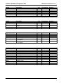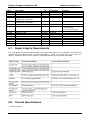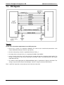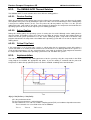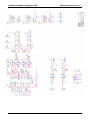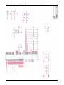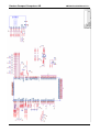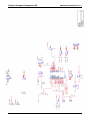
1
Detailed USER MANUAL FOR: SmartModule Express SMX945 / SMX945B Including Specifications for: COMexpress SMX945 Nordstrasse 11/F CH - 4542 Luterbach Tel.: ++41 (0)32 681 58 00 Fax: ++41 (0)32 681 58 01 Homepage: http://www.digitallogic.com Support: http://support.kcc-ag.ch Kontron Compact Computers AG SMX945 Detailed Manual V1.1 For internal use only: File: Path: SMX945_Detailed_V1.1.doc R:\HANDBUCH\smart\SMX945\SMX945_Detailed_V1.1.doc COPYRIGHT 2011 BY KONTRON COMPACT COMPUTERS AG This publication is protected by copyright and all rights are reserved. No part of this document may be reproduced, transmitted, transcribed or stored in a retrieval system, in any form or by any means, electronic, mechanical, optical, manual, or otherwise, without the prior written permission of KONTRON AG. The software described herein, together with this document, are furnished under a license agreement and may be used or copied only in accordance with the terms of that agreement. About this Manual and How to Use It This manual is written for the original equipment manufacturer (OEM) who plans to build computer systems based on the single board MICROSPACE-PC. It is for integrators and programmers of systems based on the MICROSPACE-Computer family. This manual provides instructions for installing and configuring the board, and describes the system and setup requirements. This document contains information on hardware requirements, interconnections, and details of how to program the system. Please check the Product CD for further information and manuals. REVISION HISTORY: Document Version V1.0 V1.0A Date/Initials: 05.2007 KUF 07.2007 KUF/WAS V1.0B V1.0C V1.0D V1.0E V1.0F V1.0G v1.1 09.2007 DAR/WAS 10.2007 DAR 01.2008 WAS 02.2008 DAR 05.2008 KUF 02.2009 WAS/SEP 05.2011 WAS Modification: Remarks, News, Attention: Initial Version Added: Schematics / Assembly-Disassembly Section / Updated Block Diagram / General corrections Attaching non-KCC heat sink (Sections 6.1 / 6.2.1 ) Chapter 6.1.7 Sections 1.12 / 1.13 added Chapter 6 Various additions / SMX945B spec. & picture LVDS channels Features & Flat Panel Interface Specs corrected Kontron logo & conversion to Kontron CI info added to title page. Attention! 1. All information in this manual, and the product, are subject to change without prior notice. 2. Read this manual prior to installation of the product. 3. Read the security information carefully prior to installation of the product. 2 Kontron Compact Computers AG SMX945 Detailed Manual V1.1 Table of Contents 1. PREFACE .....................................................................................................................................................5 1.1. Trademarks ..................................................................................................................................... 5 1.2. Disclaimer ....................................................................................................................................... 5 1.3. Environmental Protection Statement ........................................................................................... 5 1.4. Who should use this Product ....................................................................................................... 5 1.5. Recycling Information.................................................................................................................... 6 1.6. Technical Support .......................................................................................................................... 6 1.7. Limited Two Year Warranty ........................................................................................................... 6 1.8. Explanation of Symbols................................................................................................................. 7 1.9. Applicable Documents and Standards ........................................................................................ 8 1.10. For Your Safety............................................................................................................................... 9 1.11. RoHS Commitment......................................................................................................................... 9 1.11.1. RoHS Compatible Product Design ........................................................................................ 10 1.11.2. RoHS Compliant Production Process ................................................................................... 10 1.11.3. WEEE Application.................................................................................................................. 10 1.12. Swiss Quality ................................................................................................................................ 11 1.13. The Swiss Association for Quality and Management Systems............................................... 11 2. OVERVIEW .................................................................................................................................................12 2.1. Standard Features........................................................................................................................ 12 2.2. Unique Features ........................................................................................................................... 13 2.3. Standards ...................................................................................................................................... 13 2.4. Block Diagram .............................................................................................................................. 14 2.5. Specifications ............................................................................................................................... 15 2.6. Examples of Ordering Codes ...................................................................................................... 17 2.7. Product Pictures: ......................................................................................................................... 18 2.7.1. SMX945: ................................................................................................................................ 18 2.7.2. SMX945B............................................................................................................................... 18 2.8. Thermoscan .................................................................................................................................. 19 2.8.1. SMX945 – CPUs.................................................................................................................... 19 2.8.2. SMX945-L2400 (mounted on EBX-Board) ............................................................................ 19 3. PC FUNCTIONAL DESCRIPTION ...................................................................................................................20 3.1. Power Input ................................................................................................................................... 20 3.1.1. Power Supply Sequencing .................................................................................................... 20 3.1.2. Battery Backed Clock (RTC) ................................................................................................. 21 3.1.3. Watchdog............................................................................................................................... 21 3.2. Watchdog Control ........................................................................................................................ 21 3.3. BIOS............................................................................................................................................... 22 3.3.1. ROM-BIOS............................................................................................................................. 22 3.3.2. EEPROM Memory for Setup ................................................................................................. 22 3.4. CMOS RAM Map ........................................................................................................................... 23 3.5. System Memory Map.................................................................................................................... 23 3.6. Graphics Controller...................................................................................................................... 24 3.6.1. Analog Display Port ............................................................................................................... 24 3.6.2. Integrated LVDS Port ............................................................................................................ 24 3.6.3. Integrated DVO Ports ............................................................................................................ 24 4. DESCRIPTION OF THE JUMPERS ..................................................................................................................24 5. LED CRITERIA: ..........................................................................................................................................25 6. DESIGN-IN WITH THE SMARTMODULE ..........................................................................................................26 6.1. Mechanical Assembly .................................................................................................................. 26 6.1.1. Dimensions of the SMX945 Computer on Module ................................................................ 27 6.1.2. Connector Placement & Pin Definition on the Carrier Board ................................................ 29 6.1.3. Connector Placement on the Carrier Board .......................................................................... 30 6.1.4. Height of the Module Stack ................................................................................................... 30 6.1.5. Mechanical Dimensions......................................................................................................... 31 6.1.6. Dimensions of the Carrier Board Connector ......................................................................... 32 6.1.7. Component Heights between Module and Carrier Board ..................................................... 32 6.2. Assembly / Disassembly ............................................................................................................. 33 3 Kontron Compact Computers AG SMX945 Detailed Manual V1.1 6.2.1. Passive/Active Heat Sink....................................................................................................... 33 6.2.2. SODIMM-DDR2 RAM ............................................................................................................ 34 6.3. COMexpress Connector Description ......................................................................................... 36 6.3.1. Signal Terminology Descriptions ........................................................................................... 36 6.3.2. COMexpress Connector Pinout............................................................................................. 37 6.3.3. COMexpress Connector Specifications................................................................................. 41 6.3.4. SDVO / PEG Multiplexed Signals.......................................................................................... 42 6.4. Signal Loss ................................................................................................................................... 43 6.5. Layout of High Speed Signals: ................................................................................................... 44 6.5.1. Design Rules for PCIexpress ................................................................................................ 44 6.5.2. Layout Rules.......................................................................................................................... 45 6.5.3. Eye Diagram with 6GHz/20GS Digital Scope........................................................................ 46 6.6. Signal Descriptions...................................................................................................................... 47 6.7. Signal Integrity Requirements .................................................................................................... 55 6.8. Thermal Specifications ................................................................................................................ 55 7. DESIGN RULES FOR THE INTEGRATION ........................................................................................................56 7.1. Video Signals ................................................................................................................................ 56 7.2. IDE Signals.................................................................................................................................... 57 7.3. AC97 Audio Signals ..................................................................................................................... 58 7.4. USB2 Signal .................................................................................................................................. 59 7.5. LAN Signals .................................................................................................................................. 60 7.6. Power Planes ................................................................................................................................ 61 8. DETAILED SPECIFICATIONS .........................................................................................................................62 8.1. Intel Core Duo Processors .......................................................................................................... 62 8.2. Thermal Monitor and Catastrophic Thermal Protection........................................................... 63 8.2.1. Thermal Management ........................................................................................................... 63 8.2.2. The SMX945 ACPI Thermal Solution .................................................................................... 64 8.2.3. Implementation ...................................................................................................................... 64 8.3. ACPI Suspend Modes and Resume Events............................................................................... 65 8.4. PCI Resources .............................................................................................................................. 66 9. CORE BIOS...............................................................................................................................................67 10. SCHEMATICS .........................................................................................................................................67 11. INDEX ....................................................................................................................................................85 4 Kontron Compact Computers AG SMX945 Detailed Manual V1.1 1. PREFACE The information contained in this manual has been carefully checked and is believed to be accurate; it is subject to change without notice. Product advances mean that some specifications may have changed. Kontron AG assumes no responsibility for any inaccuracies, or the consequences thereof, that may appear in this manual. Furthermore, Kontron AG does not accept any liability arising from the use or application of any circuit or product described herein. 1.1. Trademarks ® ® ® ® MICROSPACE , smartModule , smartCore Express and DIGITAL-LOGIC are trademarks or registered trademarks of Kontron Compact Computers AG. Kontron is a trademark or registered trademark of Kontron AG. In addition, this document may include names, company logos, and registered trademarks which are, therefore, proprietary to their respective owners. 1.2. Disclaimer Kontron Compact Computers (KCC) makes no representations or warranties with respect to the contents of this manual, and specifically disclaims any implied warranty of merchantability or fitness, for any particular purpose. KCC shall, under no circumstances, be liable for incidental or consequential damages or related expenses resulting from the use of this product, even if it has been notified of the possibility of such damage. 1.3. Environmental Protection Statement This product has been manufactured to satisfy environmental protection requirements wherever possible. Many of the components used (structural parts, printed circuit boards, connectors, batteries, etc.) are capable of being recycled. Final disposal of this product after its service life must be accomplished in accordance with applicable country, state, or local laws or regulations. 1.4. Who should use this Product Electrical engineers with know-how in PC-technology. Because of the complexity and the variability of PC-technology, we cannot guarantee that the product will work in any particular situation or set-up. Our technical support will try to help you find a solution. Pay attention to electrostatic discharges; use a CMOS protected workplace. Power supply must be OFF when working on the board or connecting any cables or devices. 5 Kontron Compact Computers AG 1.5. SMX945 Detailed Manual V1.1 Recycling Information All components within this product fulfill the requirements of the RoHS (Restriction of Hazardous Substances Directive). The product is soldered with a lead free process. 1.6. Technical Support 1. Contact your local Kontron Technical Support, in your country. 2. Use the Internet Support Request form at http://support.kcc-ag.ch/ embedded products New Support Request Support requests are only accepted with detailed information about the product (i.e., BIOS-, Boardversion)! 1.7. Limited Two Year Warranty Kontron Compact Computers (KCC) guarantees the hardware and software products it manufactures and produces to be free from defects in materials and workmanship for two years following the date of shipment from Kontron Compact Computers, Switzerland. This warranty is limited to the original purchaser of the product and is not transferable. During the two year warranty period, Kontron Compact Computers will repair or replace, at its discretion, any defective product or part at no additional charge, provided that the product is returned, shipping prepaid, to KCC. All replaced parts and products become property of KCC. Before returning any product for repair, direct customers of Kontron Compact Computers AG Switzerland are required to register a RMA (Return Material Authorization) number in the Support Center at http://support.kcc-ag.ch/ All other customers must contact their local distributors for returning defective materials. This limited warranty does not extend to any product which has been damaged as a result of accident, misuse, abuse (such as use of incorrect input voltages, wrong cabling, wrong polarity, improper or insufficient ventilation, failure to follow the operating instructions that are provided by Kontron Compact Computers or other contingencies beyond the control of KCC), wrong connection, wrong information or as a result of service or modification by anyone other than Kontron Compact Computers. Nor if the user has insufficient knowledge of these technologies or has not consulted the product manuals or the technical support of KCC and therefore the product has been damaged. Empty batteries (external and onboard), as well as all other battery failures, are not covered by this manufacturer’s limited warranty. Except, as directly set forth above, no other warranties are expressed or implied, including, but not limited to, any implied warranty of merchantability and fitness for a particular purpose, and Kontron Compact Computers expressly disclaims all warranties not stated herein. Under no circumstances will KCC be liable to the purchaser or any user for any damage, including any incidental or consequential damage, expenses, lost profits, lost savings, or other damages arising out of the use or inability to use the product. 6 Kontron Compact Computers AG 1.8. SMX945 Detailed Manual V1.1 Explanation of Symbols CE Conformity This symbol indicates that the product described in this manual is in compliance with all applied CE standards. Caution, Electric Shock! This symbol and title warn of hazards due to electrical shocks (> 60V) when touching products or parts of them. Failure to observe the precautions indicated and/or prescribed by the law may endanger your life/health and/or result in damage to your equipment. Caution, Electric Shock! This symbol and title warn of hazards due to electrical shocks (> 32V) when touching products or parts of them. Failure to observe the precautions indicated and/or prescribed by the law may endanger your life/health and/or result in damage to your equipment Warning, ESD Sensitive Device! This symbol and title inform that electronic boards and their components are sensitive to Electro Static Discharge (ESD). In order to ensure product integrity at all times, care must always be taken while handling and examining this product. Attention! This symbol and title emphasize points which, if not fully understood and taken into consideration by the reader, may endanger your health and/or result in damage to your equipment. Note... This symbol and title emphasize aspects the user should read through carefully for his, or her, own advantage. Warning, Heat Sensitive Device! This symbol indicates a heat sensitive component. Safety Instructions This symbol shows safety instructions for the operator to follow. This symbol warns of general hazards from mechanical, electrical, and/or chemical failure. This may endanger your life/health and/or result in damage to your equipment. 7 Kontron Compact Computers AG 1.9. SMX945 Detailed Manual V1.1 Applicable Documents and Standards The following publications are used in conjunction with this manual. When any of the referenced specifications are superseded by an approved revision, that revision shall apply. All documents may be obtained from their respective organizations. Advanced Configuration and Power Interface Specification Revision 2.0c, August 25, 2003 Copyright © 1996-2003 Compaq Computer Corporation, Intel Corporation, Microsoft Corporation, Phoenix Technologies Ltd., Toshiba Corporation. All rights reserved. http://www.acpi.info/ ANSI/TIA/EIA-644-A-2001: Electrical Characteristics of Low Voltage Differential Signaling (LVDS) Interface Circuits, January 1, 2001. http://www.ansi.org/ ANSI INCITS 361-2002: AT Attachment with Packet Interface - 6 (ATA/ATAPI-6), November 1, 2002. http://www.ansi.org/ ANSI INCITS 376-2003: American National Standard for Information Technology – Serial Attached SCSI (SAS), October 30, 2003. http://www.ansi.org/ Audio Codec ’97 Revision 2.3 Revision 1.0, April 2002 Copyright © 2002 Intel Corporation. All rights reserved. http://www.intel.com/labs/media/audio/ Display Data Channel Command Interface (DDC/CI) Standard (formerly DDC2Bi) Version 1, August 14, 1998 Copyright © 1998 Video Electronics Standards Association. All rights reserved. http://www.vesa.org/summary/sumddcci.htm ExpressCard Standard Release 1.0, December 2003 Copyright © 2003 PCMCIA. All rights reserved. http://www.expresscard.org/ IEEE 802.3-2002, IEEE Standard for Information technology, Telecommunications and information exchange between systems–Local and metropolitan area networks–Specific requirements – Part 3: Carrier Sense Multiple Access with Collision Detection (CSMA/CD) Access Method and Physical Layer Specifications. http://www.ieee.org IEEE 802.3ae (Amendment to IEEE 802.3-2002), Part 3: Carrier Sense Multiple Access with Collision Detection (CSMA/CD) Access Method and Physical Layer Specifications, Amendment: Media Access Control (MAC) Parameters, Physical Layers, and Management Parameters for 10 GB/s Operation. http://www.ieee.org Intel Low Pin Count (LPC) Interface Specification Revision 1.1, August 2002 Copyright © 2002 Intel Corporation. All rights reserved. http://developer.intel.com/design/chipsets/industry/lpc.htm PCI Express Base Specification Revision 1.1, March 28, 2005, Copyright © 2002-2005 PCI Special Interest Group. All rights reserved. http://www.pcisig.com/ PCI Express Card Electromechanical Specification Revision 1.1, March 28, 2005, Copyright © 20022005 PCI Special Interest Group. All rights reserved. http://www.pcisig.com/ PCI Local Bus Specification Revision 2.3, March 29, 2002 Copyright © 1992, 1993, 1995, 1998, 2002 PCI Special Interest Group. All rights reserved. http://www.pcisig.com/ PCI-104 Specification, Version V1.0, November 2003. All rights reserved. http://www.pc104.org PICMG® Policies and Procedures for Specification Development, Revision 2.0, September 14, 2004, PCI Industrial Computer Manufacturers Group (PICMG®), 401 Edgewater Place, Suite 500, Wakefield, MA 01880, USA, Tel: 781.224.1100, Fax: 781.224.1239. http://www.picmg.org/ Serial ATA: High Speed Serialized AT Attachment Revision 1.0a January 7, 2003 Copyright © 20002003, APT Technologies, Inc, Dell Computer Corporation, Intel Corporation, Maxtor Corporation, Seagate Technology LLC. All rights reserved. http://www.sata-io.org/ 8 Kontron Compact Computers AG SMX945 Detailed Manual V1.1 Smart Battery Data Specification Revision 1.1, December 11, 1998. www.sbs-forum.org System Management Bus (SMBus) Specification Version 2.0, August 3, 2000 Copyright © 1994, 1995, 1998, 2000 Duracell, Inc., Energizer Power Systems, Inc., Fujitsu, Ltd., Intel Corporation, Linear Technology Inc., Maxim Integrated Products, Mitsubishi Electric Semiconductor Company, PowerSmart, Inc., Toshiba Battery Co. Ltd., Unitrode Corporation, USAR Systems, Inc. All rights reserved. http://www.smbus.org/ Universal Serial Bus Specification Revision 2.0, April 27, 2000 Copyright © 2000 Compaq Computer Corporation, Hewlett-Packard Company, Intel Corporation, Lucent Technologies Inc., Microsoft Corporation, NEC Corporation, Koninklijke Philips Electronics N.V. All rights reserved. http://www.usb.org/ 1.10. For Your Safety Your new Kontron Compact Computers (KCC) product was developed and tested carefully to provide all features necessary to ensure its compliance with electrical safety requirements. It was also designed for a long, fault-free life. However, this life expectancy can be drastically reduced by improper treatment during unpacking and installation. Therefore, in the interest of your own safety and for the correct operation of your new KCC product, please comply with the following guidelines. Attention! All work on this device must only be carried out by sufficiently skilled personnel. Caution, Electric Shock! Before installing your new KCC product, always ensure that your mains power is switched off. This applies also to the installation of piggybacks or peripherals. Serious electrical shock hazards can exist during all installation, repair and maintenance operations with this product. Therefore, always unplug the power cable and any other cables which provide external voltage before performing work. Warning, ESD Sensitive Device! Electronic boards and their components are sensitive to static electricity. In order to ensure product integrity at all times, be careful during all handling and examinations of this product. 1.11. RoHS Commitment Kontron Compact Computers is committed to develop and produce environmentally friendly products according to the Restriction of Hazardous Substances (RoHS) Directive (2002/95/EC) and the Waste Electrical and Electronic Equipment (WEEE) Directive (2002/96/EC) established by the European Union. The RoHS directive was adopted in February 2003 by the European Union and came into effect on July 1, 2006. It is not a law but a directive, which restricts the use of six hazardous materials in the manufacturing of various types of electronic and electrical equipment. It is closely linked with the Waste Electrical and Electronic Equipment Directive (WEEE) 2002/96/EC, which has set targets for collection, recycling and recovery of electrical goods and is part of a legislative initiative to solve the problem of huge amounts of toxic e-waste. Each European Union member state is adopting its own enforcement and implementation policies using the directive as a guide. Therefore, there could be as many different versions of the law as there are states in the EU. Additionally, non-EU countries like China, Japan, or states in the U.S. such as California may have their own regulations for green products, which are similar, but not identical, to the RoHS directive. 9 Kontron Compact Computers AG SMX945 Detailed Manual V1.1 RoHS is often referred to as the "lead-free" directive but it restricts the use of the following substances: Lead Mercury Cadmium Chromium VI PBB and PBDE The maximum allowable concentration of any of the above mentioned substances is 0.1% (except for Cadmium, which is limited to 0.01%) by weight of homogeneous material. This means that the limits do not apply to the weight of the finished product, or even to a component but to any single substance that could (theoretically) be separated mechanically. 1.11.1. RoHS Compatible Product Design All Kontron Compact Computers (KCC) standard products comply with RoHS legislation. Since July 1, 2006, there has been a strict adherence to the use of RoHS compliant electronic and mechanical components during the design-in phase of all KCC standard products. 1.11.2. RoHS Compliant Production Process Kontron Compact Computers selects external suppliers that are capable of producing RoHS compliant devices. These capabilities are verified by: 1. A confirmation from the supplier indicating that their production processes and resulting devices are RoHS compliant. 2. If there is any doubt of the RoHS compliancy, the concentration of the previously mentioned substances in a produced device will be measured. These measurements are carried out by an accredited laboratory. 1.11.3. WEEE Application The WEEE directive is closely related to the RoHS directive and applies to the following devices: Large and small household appliances IT equipment Telecommunications equipment (although infrastructure equipment is exempt in some countries) Consumer equipment Lighting equipment – including light bulbs Electronic and electrical tools Toys, leisure and sports equipment Automatic dispensers It does not apply to fixed industrial plants and tools. The compliance is the responsibility of the company that brings the product to market, as defined in the directive. Components and sub-assemblies are not subject to product compliance. In other words, since Kontron Compact Computers does not deliver ready-made products to end users the WEEE directive is not applicable for KCC. Users are nevertheless encouraged to properly recycle all electronic products that have reached the end of their life cycle. 10 Kontron Compact Computers AG SMX945 Detailed Manual V1.1 1.12. Swiss Quality 100% Made in Switzerland This product was not manufactured by employees earning piecework wages This product was manufactured in humane work conditions All employees who worked on this product are paid customary Swiss market wages and are insured ISO 9000:2001 (quality management system) 1.13. The Swiss Association for Quality and Management Systems The Swiss Association for Quality and Management Systems (SQS) provides certification and assessment services for all types of industries and services. SQS certificates are accepted worldwide thanks to accreditation by the Swiss Accreditation Service (SAS), active membership in the International Certification Network, IQNet, and co-operation contracts/agreements with accredited partners. www.sqs.ch The SQS Certificate ISO 9001:2000 has been issued to Kontron Compact Computers AG, the entire company, in the field of development, manufacturing and sales of embedded computer boards, embedded computer modules and computer systems. The certification is valid for three years at which time an audit is performed for recertification. 11 Kontron Compact Computers AG SMX945 Detailed Manual V1.1 2. OVERVIEW 2.1. Standard Features The smartModuleExpress945 is a miniaturized PC system on chip unit incorporating the major elements of a PC/AT compatible computer. It includes standard PC/AT compatible elements, such as: Powerful Core Duo, Core 2 Duo, Core Solo CPU DDR2 SODIMM socket for 256MByte to 2GByte (SMX945), RAM-Module 1GB DDR2 RAM soldered onboard, only SMX945B DDR2 SODIMM socket for 256MByte to 2GByte RAM-Module (SMX945B max. 3GB RAM) st nd Dual 220pin connectors (1 Connector: Rows A-B and 2 Connector: Rows C-D, 440pins total) COMexpress Bus Type 2 32bit PCI interface IDE port (to support legacy ATA devices as CD-ROM and CompactFlash) Up to 6 PCI Express general purpose lanes One, 1x16 PCI Express Graphics (PEG) slot SDVO option (pins shared with PCI Express Graphics) Maximum module input power capability extended to 80W Maximum Thermal Design Power up to 40W Up to 8 USB 2.0 ports; 4 shared over-current lines Up to 2 Serial ATA ports Dual 24bit LVDS channels Analog VGA Powerful internal Graphic controller GMA950 Intel High Definition Audio (Azalia) and AC '97 digital audio interface (external CODEC) Single Ethernet interface 100/10Mbit/s with integrated PHY AMI BIOS LPC Bus for SuperIO (COM1/2, LPT, FD), diagnostics, BIOS device 12 Kontron Compact Computers AG 2.2. SMX945 Detailed Manual V1.1 Unique Features EEPROM for setup and configuration UL approved parts Remote Function Thermal Interface with a very low thermal resistance (copper core) Very ruggedized, withstands highest mechanical vibration and shock Very low power consumption no active cooling required Extended wide range power input for single 5Volt supply applications Power Management Microcontroller 2.3. Standards 13 Kontron Compact Computers AG 2.4. SMX945 Detailed Manual V1.1 Block Diagram * This function is disabled. A Macrovision license is required to enable it. (only with GM chipset / GME chipset does not support Macrovision) 14 Kontron Compact Computers AG 2.5. SMX945 Detailed Manual V1.1 Specifications CPU CoreDuo / Celeron M Clock st 1 Level Cache nd 2 Level Cache Technology VCCCore @ 1.6GHz VCCCore @ 0.6GHz VCCCore @ deep sleep CPU-Bus AGTL+ Termination FSB Specification Intel Core Duo L2400 LV 2x 1.66GHz with 2MB L2-cache Intel Core 2 Duo L7400 LV 2x 1.66GHz with 4MB L2-cache 1GHz up to 1.86GHz 2x 32kByte 1, 2, 4 MByte (on die) 65nm 1.308V 0.844V 0.748V AGTL+ Integrated 533/666MHz quad-pumped synchronous bus Mathematics Coprocessor Available on the PENTIUM CPU Intel 945GME Graphics Memory Controller Hub Memory Controller Specification Supports PC1600 / PC2100 / PC2700 Socket DDR2 SODIMM 200pin (SMX945B 1GB soldered on board) Technologies DDR2-667 Capacity 256MByte up to 2GByte (3GByte with SMX945B) Voltage 2.5V Termination 1.25V Width 64bit ECC-Support No Intel 945GME Graphics Memory Controller Hub Graphic Controller Specification Alternative to the PEG Interface Max. Video memory 224MByte with Intel GMA950 Graphic Core Frequency 400MHz 3D Graphic Engine 3D-setup and rendering engine Zone rendering Texture engine Direct-X Compatibility Direct-X9 Analog CRT 400MHz RAMDAC with 24bit Resolution up to 2048 x 1536 @ 70Hz (QXGA) Hardware cursor support I2C and DDC channels Dual independent display SDVO Port 2 channels (multiplexed with the PEG signals) 2x 200 Mpixel/sec Support for up to 2x DVI, 1x TV and 2x LVDS Dotclock = 165MHz Compliant with DVI Spec.1.5 Flat Panel Interface 2 channel LVDS interface 1x 18, 2x 18, 1x24, 2x24bpp TFT Dotclock = up to 2x 112 MHz Resolutions 640 x 480 up to 1600 x 1200 (UXGA) Automatic panel detection via VESA EDID 1.3 TV Out Disabled. A Macrovision license is required. 15 Kontron Compact Computers AG Intel 945GME Graphics PEG PEG Controller Alternative to the internal graphic controller multiplexed with the SDVO signals Support Mode Voltage Signals Intel 82801DBM (ICH7DH) PCI-Bus EIDE-Bus SATA-Bus USB V2.0 APIC SMB FWH LPC SMX945 Detailed Manual V1.1 Specification PEG 16 lanes 1.5Volt Differential 2.5Gbit/sec Sound IRQ Controller Timers Power Management Specification Supports PCI 2.2 with 6 resources 1x Ultra P-ATA 100 2 channels 150MByte/sec 8 channels USB INTEL I/O APIC V2.0 SMBus controller Firm Ware Hub for BIOS devices Serialized BUS (no ISA) used for external SuperIO (COM1/2, MS, KB, FD and LPT) AC97 2.3 HDA Interface with 192kHz sampling rate and 8 channels 8259 compatible 8254 compatible Integrated Reset & Power Management Controller Power Modes ACPI Specification PIC 16C870 S5, S4, S3, S1 V3.0 BUS PCI LPC PCIexpress Specification PCI 2.2 33MHz 32bit 8bit 33MHz 6x 1 lane, PEG Power Supply DC Input Specification 5.0V up to maximum 18V, max. 200mV ripple up to 30 Watts peak for VCCCore, 2.5V and 1.25V generation 5.0V up to 10Amp for 100µs 18.0V up to 30Amp for 20µs 0.1Amp (VCC5ALW) VCC-Core, 1.05V, 1.2V, 1.25V, 1.3V, 1.5V, 1.8V, 2.5V, 3.3V 800MHz: approx. 6Watts @ 512MByte DDR2-RAM, Desktop load 1.6GHz: approx. 24Watts @ 512MByte DDR2-RAM, 100% workload Inrush current 5.0Volt Onboard Voltages Power Consumption Use inductors in series to reduce the maximum inrush current! 16 Kontron Compact Computers AG Physical Characteristics Dimensions Weight PCB Thickness PCB Layer Operating Environment Relative Humidity Vibration Shock Operating Temperature Maximum Copper Temperature Storage Temperature Specification Length: 117 mm +/- 0.1mm Depth: 70 mm +/- 0.1mm Height: 15 mm +/- 0.2mm (with 5mm bus connectors) 18 mm +/- 0.2mm (with 8mm bus connectors) The connector height is selected by the connector on the carrier board. 120 grams / 12 ounces 1.6 mm / 0.0625 inches nominal Multilayer Specification 5-90% non-condensing 5 to 2000 Hz 10 G Standard: T.B.D. (depends on the CPU and the cooling concept) Extended Range: T.B.D. 90°C -55°C to +85°C EMI / EMC (IEC1131-2 refer MIL 461/462) ESD Electro Static Discharge REF Radiated Electromagnetic Field EFT Electric Fast Transient (Burst) SIR Surge Immunity Requirements High-Frequency Radiation SMX945 Detailed Manual V1.1 Specification IEC 801-2, EN55101-2, VDE 0843/0847 Part 2 Metallic protection needed Separate Ground Layer included 15 kV single peak IEC 801-3, VDE 0843 Part 3, IEC770 6.2.9. Not tested IEC 801-4, EN50082-1, VDE 0843 Part 4 250V - 4kV, 50 ohms, Ts=5ns Grade 2: 1KV Supply, 500 I/O, 5Khz IEC 801-5, IEEE587, VDE 0843 Part 5 Supply: 2kV, 6 pulse/minute I/O: 500V, 2 pulse/minute FD, CRT: None EN55022 All information is subject to change without notice. 2.6. Examples of Ordering Codes Product Name SMX945-L2400 SMX945-L7400 Part Number 805350 805352 Description smartModuleExpress945, Core Duo L2400, 0MB RAM smartModuleExpress945, Core 2 Duo L7400, 0MB RAM These are only examples; for current ordering codes, please see the current price list. 17 Kontron Compact Computers AG 2.7. SMX945 Detailed Manual V1.1 Product Pictures: 2.7.1. SMX945: 2.7.2. SMX945B 18 Kontron Compact Computers AG 2.8. SMX945 Detailed Manual V1.1 Thermoscan 2.8.1. SMX945 – CPUs CPU with 512MB-RAM Core Duo L7400 Core Duo L2400 Celeron M 423 Celeron M 440 2.8.2. Desktop WIN-XP 1.2A / 6W 1.2A / 6W 1.4A / 7W 1.9A / 10W 100% workload 4.4A / 22W 4.8A / 24W 2.5A / 13W 4.6A / 23W Standby 1.4A / 7W 1.4A / 7W 1.4A 7 7W 1.4A / 7W SMX945-L2400 (mounted on EBX-Board) Product MSEBX945 SMX945-L2400 SODIMM DDR2 512MB Software: Part Number Serial Number Version After INT 19 (before starting OS) MSEBX945 passive cooled – Top View t [min] 60 fCPU [MHz] 2000 I [mA] 2500 R11[°C] 66.8 VCC[V] 12 MSEBX945 active cooled – Top View t [min] 60 fCPU [MHz] 2000 I [mA] 2500 R11[°C] 45.9 19 P01[°C] 51.7 VCC [V] 12 Kontron Compact Computers AG SMX945 Detailed Manual V1.1 3. PC FUNCTIONAL DESCRIPTION 3.1. Power Input The SMX945 module uses a single main power rail with a nominal value of +12V. Kontron Compact Computers has expanded the 12Volt input to a wide-range input, working between 5Volt and 18Volt. Main supply: 5.0Volt (-0.1V) to 18Volt ( +0V) with 20-30Watt depending on the processor. The sources of the main supply may be: 12Volt supply as the COMexpress Specs define Single 5Volt systems such as PC/104express Battery supplied systems (Li-ion with 14.4Volt nominal) Vehicle supply, nominal with 12V Two additional voltage inputs are specified: +5V Always (0.1Amp) = VCC_5V_SBY = VCC5ALWAYS +3V-3.6V battery input to power the module Real-time Clock (RTC) circuit 3.1.1. Power Supply Sequencing 20 Kontron Compact Computers AG 3.1.2. SMX945 Detailed Manual V1.1 Battery Backed Clock (RTC) An AT compatible date/time clock is located within the chipset. The device also contains a CMOS static RAM, compatible with that in standard ATs. System configuration data is normally stored in the clock chip's CMOS RAM in a manner consistent with the convention used in other AT compatible computers. Connect an external Lithium battery of 3.0V-3.6V to the RTC pin. The battery-backed clock can be set by using the Kontron Compact Computers SETUP at boot-time. Addresses: 70h 71h RTC-Address MAP: 00-0F 10-3F 40-7F = = Index register Data transfer register Real time clock BIOS setup (Standard) Extended BIOS Voltage range: 2.0-3.6V DC With an external Lithium 3.6V / 400mAh battery, the board will work for over 10 years without needing a replacement battery. The chipset consumes the following currents: Typical battery current at 25°C: 3.1.3. 2.4uA @ typ. 3V DC Watchdog The watchdog timer detects a system crash and performs a hardware reset. After power up, the watchdog is always disabled as the BIOS does not send strobes to the watchdog. In case that the user wants to take advantage of the watchdog, the application must produce a strobe at least every 800 ms. If no strobe occurs within the 800 ms, the watchdog resets the system. For more information, please refer to the driver/software/BIOS manual SMX945_BIOS on the Product CD. The watchdog feature is integrated in the INT15 function. There are some programming examples available: Product CD-Rom or customer download area: \tools\SMX945\int15dl\... 3.2. Watchdog Control Interface/Function External WatchDOG Control On the smartModule Standard – automatically strobed with 32kHz 21 Circuits needed on the OEM board Kontron Compact Computers AG 3.3. 3.3.1. SMX945 Detailed Manual V1.1 BIOS ROM-BIOS An EPROM with 8bit wide data access normally contains the board's AT compatible ROM-BIOS. The BIOS takes an E82802AC8 EPROM (or equivalent) device on the LPC-Bus. The board's wait-state control logic automatically inserts four memory wait states in all CPU accesses to this (socket). The ROM-BIOS occupies the memory area from C0000H through FFFFFh; however, the board's ASIC logic reserves the entire area from C0000h through FFFFFh for onboard devices, so that this area is already usable for ROM-DOS and BIOS expansion modules. Consult the appropriate address map for the MICROSPACE SMX945 ROM-BIOS. Standard BIOS ROM DEVICE: Intel E82802AC8 onboard soldered MAP: 3.3.2. E0000 - FFFFFh C0000 - CFFFFh Core BIOS, 1024kB VGA BIOS, 64kB EEPROM Memory for Setup The EEPROM is used for setup and configuration data, stored as an alternative to the CMOS-RTC. Optionally, the EEPROM setup driver may update the CMOS RTC, if the battery is running down and the checksum error would appear and stop the system. The capacity of the EEPROM is 2 kByte. Organization of the 2048Byte EEPROMs: Address MAP 0000h 0001h 0003h 0010h-007Fh 0080h-00FFh 0100h-010Fh 0110h-0113h 0114h-0117h 0118h-011Bh 011Ch-011Fh 0120h-0122h 0123h-0125h 0126h-0128h 0129h-012Bh 0130h 0131h 0132h/0133h 0134h/0135h 0136h Function CMOS-Setup valid (01=valid) Reserved Flag for DLAG-Message (FF=no message) Copy of CMOS-Setup data Reserved for AUX-CMOS-Setup Serial Number Production Date (year/day/month) st 1 Service Date (year/day/month) nd 2 Service Date (year/day/month) rd 3 Service Date (year/day/month) Boot errors (Auto incremented if any boot error occurs) Setup Entries (Auto incremented on every setup entry) Low Battery (Auto incremented every time the battery is low, EEPROMCMOS) Startup (Auto incremented on every power-on start) Reserved Reserved BIOS Version (V1.4 => [0132h]:= 4, [0133h]:=1) BOARD Version (V1.5 => [0124h]:=5, [0125h]:=1) BOARD TYPE: 0137h CPU TYPE: 0200h-03FFh 0200h-027Fh 0400h-07FFh Reserved Reserved Free for Customer’s use (‘M’=PC/104, ‘E’=Euro, ‘W’=MSWS, ‘S’=Slot, ‘C’=Custom, ‘X’= smartCore or smartModule) (01h=ELAN300/310, 02h=ELAN400, 05h=P5, 08h=P3, 09h=Elan520, 10h=P-M) 22 Kontron Compact Computers AG 3.4. SMX945 Detailed Manual V1.1 CMOS RAM Map Systems based on the industry-standard specification include a battery backed Real Time Clock chip. This clock contains at least 64Bytes of non-volatile RAM. The system BIOS uses this area to store information including system configuration and initialization parameters, system diagnostics, and the time and date. This information remains intact even when the system is powered down. The BIOS supports 128Bytes of CMOS RAM. This information is accessible through I/O ports 70h and 71h. CMOS RAM can be divided into several segments: Locations 00h - 0Fh contain real time clock (RTC) and status information Locations 10h - 2Fh contain system configuration data Locations 30h - 3Fh contain System BIOS-specific configuration data as well as chipset-specific information Locations 40h - 7Fh contain chipset-specific information as well as power management configuration parameters 3.5. System Memory Map The PENTIUM CPU, used as a central processing unit on the MICROSPACE, has a memory address space which is defined by 32 address bits. Therefore, it can address 4GBytes of memory. The memory address map is as follows: CPU Pentium Address 000000 - 09FFFFh 0C0000 - 0CBFFFh 0CC000 - 0CFFFFh 0D0000 - 0D4000h 0D4000 - 0D8000h 0D8000 - 0DFFFFh 0E0000 - 0FFFFFh 100000 - 1FFFFFh 200000 - FFFFFFh Size 640kBytes 48kBytes 16kBytes 16kBytes 16kBytes 32kBytes 1024kBytes 1MByte 14MBytes Function / Comments Onboard DRAM for DOS applications VGA BIOS, selected by the hardware BIOS extensions, selected by the hardware Free for user Free for user Free for user Core BIOS, selected by the 945GM chipset DRAM for extended onboard memory DRAM for extended onboard memory 23 Kontron Compact Computers AG 3.6. SMX945 Detailed Manual V1.1 Graphics Controller The Intel 945GM Express Chipset The GMCH IGD provides a highly integrated graphics accelerator delivering high performance 2D, 3D and video capabilities. With its interfaces to UMA using a DVMT configuration, an analog display, a LVDS port and two digital display ports (e.g. flat panel), the GMCH can provide a complete graphics solution. The GMCH also provides 2D hardware acceleration for block transfers of data (BLTs). The BLT engine provides the ability to copy a source block of data to a destination and perform raster operations (e.g., ROP1, ROP2 and ROP3) on the data using a pattern, and/or another destination. Performing these common tasks with the hardware reduces the CPU load and thus improves performance. High bandwidth access to data is provided through the system memory interface. The GMCH uses tiling architecture to increase the system memory efficiency and thus maximize effective rendering bandwidth. The Intel 945GME GMCH also improves 3D performance and quality with 3D Zone Rendering technology. The GMCH has four display ports, one analog and three digital. These provide support for a progressive scan analog monitor, a dedicated dual channel LVDS LCD panel, and two DVO devices. Each port can transmit data according to one or more protocols. The DVO ports are connected to an external device that converts one protocol to another. Examples of this are TV-out encoders, external DACs, LVDS transmitters and TMDS transmitters. Each display port has control signals that may be used to control, configure and/or determine the capabilities of an external device. The data that is sent out of the display port is selected from one of two possible sources, Pipe A or Pipe B. 3.6.1. Analog Display Port The Intel 945GM GMCH has an integrated 400MHz, 24bit RAMDAC that can directly drive a progressive scan analog monitor pixel resolution of up to 1600x1200 at 85Hz refresh and up to 2048x1536 at 72Hz refresh. The analog display port can be driven by Pipe A or Pipe B. 3.6.2. Integrated LVDS Port The Intel 945GM GMCH has an integrated dual channel LFP transmitter interface to support LVDS LCD panel resolutions up to UXGA with center and down spread SSC support of 0.5%, 1%, and 2.5% utilizing an external SSC clock. The display pipe provides panel up-scaling to fit a smaller source image onto a specific native panel size, as well as provides panning and centering support. The LVDS port is only supported on Pipe B. The LVDS port can only be driven by Pipe B, either independently or simultaneously with the Analog Display port. 3.6.3. Integrated DVO Ports The DVO B/C interface is compliant with the DVI Specification 1.0. When combined with a DVI compliant external device (e.g. TMDS Flat Panel Transmitter, TV-out encoder, etc.), the GMCH provides a high-speed interface to a digital or analog display (e.g. flat panel, TV monitor, etc.). The GMCH provides two DVO ports that are each capable of driving a 165MHz pixel clock at the DVO B or DVO C interface. When DVO B and DVO C are combined into a single DVO port, then an effective pixel rate of 330MHz can be achieved. The DVO B/C ports can be driven by Pipe A or Pipe B. If driven on Pipe B, then the LVDS port must be disabled. 4. DESCRIPTION OF THE JUMPERS Note… There are no jumpers on this product! 24 Kontron Compact Computers AG SMX945 Detailed Manual V1.1 5. LED CRITERIA: LED D26 D31 Color Green Green Function Run OK 3.3Volt OK The Power & Control LEDs on the SMX945PC There are 2 LEDs located on the top side of the smartModule: 1. The green Power LED a. Indicates that the 3.3V core supply for the CPU is OK. b. This LED must light as soon as the external 5V power supply is available. 2. The green Reset/Run LED OFF: The module is in the Reset state which means there is no operation. Either the Watchdog, the power supervisor or an active external reset signal holds the module in the Reset state. ON: The module is running normally. After power up, this LED must come ON after 1-2 seconds. After a successful boot sequence, both green LEDs are on! 25 Kontron Compact Computers AG SMX945 Detailed Manual V1.1 6. DESIGN-IN WITH THE SMARTMODULE 6.1. Mechanical Assembly 26 Kontron Compact Computers AG SMX945 Detailed Manual V1.1 Attention! When using an active/passive heatsink that is not from KCC, be very careful! The maximum depth the screws can go into the product is 3mm or the smartModule will be destroyed! 6.1.1. Dimensions of the SMX945 Computer on Module 27 Kontron Compact Computers AG SMX945 Detailed Manual V1.1 28 Kontron Compact Computers AG 6.1.2. SMX945 Detailed Manual V1.1 Connector Placement & Pin Definition on the Carrier Board Top View of the PCB: Remarks: 1. All dimensions in millimeters. 2. For the carrier board, use the Pin Definition A1/B1/C1/D1 for the plug. 3. The receptacle is mounted on the SMX945/915. Top View, Pin Definition for the Carrier Board PCB: 29 Kontron Compact Computers AG SMX945 Detailed Manual V1.1 6.1.3. Connector Placement on the Carrier Board 6.1.4. Height of the Module Stack 30 Kontron Compact Computers AG 6.1.5. SMX945 Detailed Manual V1.1 Mechanical Dimensions 31 Kontron Compact Computers AG 6.1.6. SMX945 Detailed Manual V1.1 Dimensions of the Carrier Board Connector SMX-CON8: Standard height: KCC part number: AMP/Tyco: 8.0mm 807138 8-6318491-6 (components placed below the smartModule total a maximum 2.0mm) 6.1.7. Component Heights between Module and Carrier Board Parts mounted on the back side of the module (in the space between the bottom surface of the module PCB and the carrier board) should have a maximum height of 8.0mm. 8mm stack height standard for SMX945: If the carrier board uses the 8mm stack option, then the carrier board topside components within the module envelope are limited to a height of 1.6mm, with the exception of the mating connectors. Using carrier board topside components up to 1.6mm allows a gap of 0.4mm between the carrier board topside components and the module’s bottom side components. 32 Kontron Compact Computers AG 6.2. 6.2.1. SMX945 Detailed Manual V1.1 Assembly / Disassembly Passive/Active Heat Sink Attention! When using an active/passive heatsink that is not from KCC, be very careful! The maximum depth the screws can go into the product is 3mm or the smartModule will be destroyed! The photo on the left shows the basic SMX945 with active heat sink. The photo below shows a passive heat sink. Assembly is the same except Step 3 is not required for a passive heat sink. The passive heat sink has no electric connection. Step 1: Put the active heat sink onto the SMX945. Step 2: Affix the heat sink with 3 screws. Screw type: Cylinder hexagon socket type screw M2x6mm / BN7 DIN 912 ISO 4762 Tool: Hexagon head socket wrench no. 1.5 33 Kontron Compact Computers AG SMX945 Detailed Manual V1.1 Step 3: Plug the fan into the electric connection on the host board. For example: On the MSEBX945 V1.0: Connector X207 Pin1 (GND) and Pin2 (FAN1_PWR) or Connector X208 Pin1 (GND) and Pin2 (FAN2_PWR) On the MSM945: Connector X205 Pictured: electric connection on the MSEBX945. 6.2.2. SODIMM-DDR2 RAM Step 1: In the case of an active heat sink, remove the electric fan connector. This step is not required for a passive heat sink. (The photo shows the basic MSEBX945 board with active heat sink.) Step 2: Remove the 3 screws from the heat sink and dismantle the heat sink. Screw Type: Cylinder hexagon socket type screw M2x6mm / BN7 DIN912 ISO 4762 Tool: Hexagon head socket wrench no. 1.5. 34 Kontron Compact Computers AG SMX945 Detailed Manual V1.1 Step 3: Remove the 2 screws from the SODIMM cover and dismantle the cover very carefully. Slide the cover to the side and gently lift it away from the casing. Screw Type: Cylinder hexagon socket type screw M2x4mm / BN11 DIN912 ISO 4762 Tool: Hexagon head socket wrench no. 1.5 Step 4: Using your thumbnails, gently push the clips holding the RAM module in place toward the outside. There will be a slight "click" and the RAM will flip up at an angle. Remove the original RAM. With the new RAM, carefully place the side with the connectors into the slot. There is only one correct way to place the RAM in the slot due to a notch between the connectors which matches up to a tab in the slot. Do not force the RAM into the slot, it should fit very easily. Slowly push the RAM down until the clips "click" into place. Step 5: To reassemble the smartModule and heat sink, follow Steps 1-4 backwards. In the case of an active heat sink, do not forget to connect it. The photo shows the completely dismantled parts. 35 Kontron Compact Computers AG 6.3. SMX945 Detailed Manual V1.1 COMexpress Connector Description 6.3.1. Signal PU PD I/O 3.3V I/O 5V I 3V I 5V I/O 3.3VSB O 3V O 5V P D DDC PCIE SATA LVDS LAN TPM Signal Terminology Descriptions Description Internally implemented Pull up resistor Internally implemented Pull down resistor Bi-directional signal 3.3V tolerant Bi-directional signal 5V tolerant Input 3.3V tolerant Input 5V tolerant Input 3.3V tolerant, active in standby state Output 3.3V signal level Output 5V signal level Power Input/Output Differential signal pair Display Data Channel In compliance with PCI Express Base Specification, Revision 1.0a In compliance with Serial ATA specification, Revision 1.0a Low Voltage Differential Signal-350mV nominal; 450mV maximum differential signal 100/10Mbit/s LAN signals coming from the PHY Trusted Platform Module 36 Kontron Compact Computers AG 6.3.2. SMX945 Detailed Manual V1.1 COMexpress Connector Pinout COMexpress type 2 (BUS on the smartModuleExpress 945) Connectors A / B: Pins 1-55 Pin A1 A2 A3 A4 A5 A6 A7 A8 A9 A10 A11 A12 A13 A14 A15 A16 A17 A18 A19 A20 A21 A22 A23 A24 A25 A26 A27 A28 A29 A30 A31 A32 A33 A34 A35 A36 A37 A38 A39 A40 A41 A42 A43 A44 A45 A46 A47 A48 A49 A50 A51 A52 A53 A54 A55 Group Volt LAN LAN LAN LAN LAN LAN LAN LAN LAN D D 3.3V 3.3V D D 3.3V D D LAN LAN LAN PM SATA0 SATA0 PM SATA0 SATA0 SATA2 SATA2 PM SATA2 SATA2 PM IDE AC97 AC97 Length Signal D D 3.3V D D 3.3V D D D D 3.3V D D AC97 AC97 BIOS PM USB6 USB6 USB67OC USB4 USB4 USB2 USB2 USB23OC USB0 USB0 Supply PCIEX PCIEX LPC 3.3V 3.3V 3.3V 3.3V 3.3V 3.3V 3.3V 3.3V D D 3.3V D D D D 3.3V D D 3.3V 3.3V 3.3V PCIEX5 PCIEX5 D D 3.3V PCIEX4 D GND MDI3MDI3+ SPEED100# SPEED1000# MD2IMD2+ LAN_LINK# MDI1MDI1+ GND MD0MD0+ CT-Ref SUS_S3# SATA0-TX+ SATA0-TXSUS_S4# SATA0-RX+ SATA0-RX0GND NC NC SUS_S5# NC NC BATLOW# ATA_ACTIVITY# AC_SYNCH AC_RST# GND AC_BITCLK AC_SDOUT BIOS_DISABLE# THRMTRIP# USB6USB6+ USB_6_7_OC# USB4USB4+ GND USB2USB2+ USB_2_3_OC# USB0USB0+ VCC_RTC EXCD0_PERST# EXCD0_CPPE# LPC_SERIRQ GND PCIe_TX5+ PCIe_TX5GPI 0 PCIe_TX4+ Pin B1 B2 B3 B4 B5 B6 B7 B8 B9 B10 B11 B12 B13 B14 B15 B16 B17 B18 B19 B20 B21 B22 B23 B24 B25 B26 B27 B28 B29 B30 B31 B32 B33 B34 B35 B36 B37 B38 B39 B40 B41 B42 B43 B44 B45 B46 B47 B48 B49 B50 B51 B52 B53 B54 B55 Group Volt LAN LPC LPC LPC LPC LPC LPC LPC LPC 3.3V 3.3V 3.3V 3.3V 3.3V 3.3V 3.3V 3.3V 3.3V PM SMB SMB SMB SATA1 SATA1 PM SATA1 SATA1 3.3V 3.3V 3.3V 3.3V SATA3 SATA3 PM SATA3 SATA3 PM AC97 AC97 AC97 Length Input D D 3.3V D D D D 3.3V D D Legacy Not used Not used PM USB7 USB7 USB45OC USB5 USB5 USB3 USB3 USB01OC USB1 USB1 PCIEX PCIEX Reset_In Reset_Out 3.3V 3.3V 3.3V 3.3V 3.3V 3.3V 3.3V 3.3V D D 3.3V D D D D 3.3V D D 3.3V 3.3V 3.3V 3.3V PCIEX5 PCIEX5 D D 3.3V PCIEX4 D Signal GND LAN_ACTIVITY# LPC_FRAME# LPC_AD0 LPC_AD1 LPC_AD2 LPC_AD3 LPC_DRQ0# LPC_DRQ1# LPC_CLK GND PWRBTN# SMB_CLK SMB_DAT SMB_ALERT# SATA1-TX+ SATA1-TXSUS_STAT# SATA1-RX+ SATA1-RXGND NC NC PWR_OK NC NC WDT AC_SDIN2 AC_SDIN1 AC_SDIN0 GND Speaker Out I2C-CK I2C-DAT THRM# USB7USB7+ USB_4_5_OC# USB5USB5+ GND USB3USB3+ USB_0_1_OC# USB1USB1+ EXCD1_PERST# EXCD1_CPPE# MAIN_IN_RESET# CB_RESET# GND PCIe_RX5+ PCIe_RX5GPO 1 PCIe_RX4+ The CB_Reset# is used to start the external Supply and works as Power_Enable. The SATA3/3 are not connected on the SMX945 because the 945GM has only 2 SATA ports! Use only SATA0 and SATA1 with the SMX945 series Version 1.0. 37 Kontron Compact Computers AG SMX945 Detailed Manual V1.1 COMexpress type 2 (Bus on smartModuleExpress 945) Connectors A / B: Pins 56-110 Pin Group A56 A57 A58 A59 A60 A61 A62 A63 A64 A65 A66 A67 A68 A69 A70 A71 A72 A73 A74 A75 A76 A77 A78 A79 A80 A81 A82 A83 A84 A85 A86 A87 A88 A89 A90 A91 A92 A93 A94 A95 A96 A97 A98 A99 A100 A101 A102 A103 A104 A105 A106 A107 A108 A109 A110 PCIEX4 D PCIEX3 PCIEX3 D D PCIEX2 PCIEX2 D D PCIEX1 PCIEX1 D D Volt Length Signal 3.3V PCIEX0 PCIEX0 D D LVDS-A LVDS-A LVDS-A LVDS-A LVDS-A LVDS-A LVDS Clock Out Clock Out D D D D D D LVDS-A LVDS-A LVDS LVDS KB Legacy PCIEX0 PCIEX0 3.3V 3.3V 3.3V D D 3.3V 3.3V 3.3V 3.3V D D Power Out Power Out 3.3V Power Out Power Out Power-In Power-In Power-In Power-In Power-In Power-In Power-In Power-In Power-In Power-In Power-In Power-In PCIe_TX4GND PCIe_TX3+ PCIe_TX3GND PCIe_TX2+ PCIe_TX2GPI 1 PCIe_TX1+ PCIe_TX1GND GPI 2 PCIe_TX0+ PCIe_TX0GND LVDS_A0+ LVDS_A0LVDS_A1+ LVDS_A1LVDS_A2+ LVDS_A2LVDS_VDD_EN 48MHz CLKSIO_33MHz GND LVDS_A_CLK+ LVDS_A_CLKLVDS_I2C_CK LVDS_I2C_DAT GPI 3 KBD_RST# KBD_A20Gate PCIe0_CK_REF+ PCIe0_CK_REFGND VCC3.3V Out VCC3.3V Out GPO 0 3.3V Alw Out 3.3V Alw Out GND +12Volt +12Volt +12Volt GND +12Volt +12Volt +12Volt +12Volt +12Volt +12Volt +12Volt +12Volt +12Volt GND Pin Group B56 B57 B58 B59 B60 B61 B62 B63 B64 B65 B66 B67 B68 B69 B70 B71 B72 B73 B74 B75 B76 B77 B78 B79 B80 B81 B82 B83 B84 B85 B86 B87 B88 B89 B90 B91 B92 B93 B94 B95 B96 B97 B98 B99 B100 B101 B102 B103 B104 B105 B106 B107 B108 B109 B110 PCIEX4 D PCIEX3 PCIEX3 D D PCIEX2 PCIEX2 D D PCIEX1 PCIEX1 PM PM PCIEX0 PCIEX0 D D LVDS-B LVDS-B LVDS-B LVDS-B LVDS-B LVDS-B Clock Out Clock Out LVDS Volt Length Signal 3.3V 3.3V D D D D D D D D 3.3V 3.3V 3.3V LVDS-B LVDS-B LVDS POWER-In POWER-In POWER-In POWER-In Power Out VGA 3.3V 5.0V 5.0V 5.0V 5.0V 5.0V A VGA VGA VGA VGA VGA VGA TV-Out TV-Out TV-Out A A 5.0V 5.0V 3.3V 3.3V A A A Power-In Power-In Power-In Power-In Power-In Power-In Power-In Power-In Power-In D D PCIe_RX4GPO 2 PCIe_RX3+ PCIe_RX3GND PCIe_RX2+ PCIe_RX2GP0 3 PCIe_RX1+ PCIe_RX1WAKE0# WAKE1# PCIe_RX0+ PCIe_RX0GND LVDS_B0+ LVDS_B0LVDS_B1+ LVDS_B1LVDS_B2+ LVDS_B2PCI_CLK4 14MHz LVDS_BKLT_EN GND LVDS_B_CLK+ LVDS_B_CLKLVDS_BKLT_CTRL VCC5V_ALW In VCC5V_ALW In VCC5V_ALW In VCC5V_ALW In VCC5 output VGA-RED GND VGA – GREEN VGA – BLUE VGA - HSYNCH VGA - VSYNCH VGA_I2C_CLK VGA_I2C_DAT TV_DAC_A TV_DAC_B TV_DAC_C GND +12Volt Input +12Volt Input +12Volt Input +12Volt Input +12Volt Input +12Volt Input +12Volt Input +12Volt Input +12Volt Input GND These voltages are generated in the smartModule and are only connected for monitoring. Do not supply external circuits with these voltages. 38 Kontron Compact Computers AG SMX945 Detailed Manual V1.1 COMexpress type 2 (BUS on the smartModuleExpress 945) Connectors C / D: Pins 1-55 Pin Group C1 C2 C3 C4 C5 C6 C7 C8 C9 C10 C11 C12 C13 C14 C15 C16 C17 C18 C19 C20 C21 C22 C23 C24 C25 C26 C27 C28 C29 C30 C31 C32 C33 C34 C35 C36 C37 C38 C39 C40 C41 C42 C43 C44 C45 C46 C47 C48 C49 C50 C51 C52 C53 C54 C55 Volt IDE IDE IDE IDE IDE IDE IDE IDE IDE 3.3V 3.3V 3.3V 3.3V 3.3V 3.3V 3.3V 3.3V 3.3V IDE IDE IDE PCI PCI PCI PCI PCI PCI 3.3V 3.3V 3.3V 3.3V 3.3V 3.3V 3.3V 3.3V 3.3V PCI PCI PCI PCI PCI PCI PCI PCI PCI 3.3V 3.3V 3.3V 3.3V 3.3V 3.3V 3.3V 3.3V 3.3V PCI PCI PCI PCI PCI PCI PCI PCI PCI 3.3V 3.3V 3.3V 3.3V 3.3V 3.3V 3.3V 3.3V 3.3V PCI PCI PCI PCI PCI PCI PCI PCI PCI 3.3V 3.3V 3.3V 3.3V 3.3V 3.3V 3.3V 3.3V 3.3V PEG PEG BIOS / Type-In PEG Length Signal Out D D OC D Pin GND IDE-D7 IDE-D6 IDE-D3 IDE-D15 IDE-D8 IDE-D9 IDE-D2 IDE-D13 IDE-D1 GND IDE-D14 IDE-IORDY IDE-IOR# PCI_PME# PCI_GNT2# PCI_REQ2# PCI_GNT1# PCI_REQ1# PCI_GNT0# GND PCI_REQ0# PCI_RESET#_Out PCI_AD0 PCI_AD2 PCI_AD4 PCI_AD6 PCI_AD8 PCI_AD10 PCI_AD12 GND PCI_AD14 PCI_C/BE1# PCI_PERR# PCI_LOCK# PCI_DEVSEL# PCI_IRDY# PCI_C/BE2# PCI_AD17 PCI_AD19 GND PCI_AD21 PCI_AD23 PCI_C/BE3# PCI_AD25 PCI_AD27 PCI_AD29 PCI_AD31 PCI_IRQA# PCI_IRQB# GND PEG_RX0+ PEG_RX0FWH_TBL / TYPE0 PEG_RX1+ D1 D2 D3 D4 D5 D6 D7 D8 D9 D10 D11 D12 D13 D14 D15 D16 D17 D18 D19 D20 D21 D22 D23 D24 D25 D26 D27 D28 D29 D30 D31 D32 D33 D34 D35 D36 D37 D38 D39 D40 D41 D42 D43 D44 D45 D46 D47 D48 D49 D50 D51 D52 D53 D54 D55 Group Volt IDE IDE IDE IDE IDE IDE IDE IDE IDE 3.3V 3.3V 3.3V 3.3V 3.3V 3.3V 3.3V 3.3V 3.3V IDE IDE IDE IDE IDE IDE IDE PCI PCI 3.3V 3.3V 3.3V 3.3V 3.3V 3.3V 3.3V 3.3V 3.3V PCI PCI PCI PCI PCI PCI PCI PCI PCI 3.3V 3.3V 3.3V 3.3V 3.3V 3.3V 3.3V 3.3V 3.3V PCI PCI PCI PCI PCI PCI PCI PCI PCI 3.3V 3.3V 3.3V 3.3V 3.3V 3.3V 3.3V 3.3V 3.3V PCI PCI PCI PCI PCI PCI PCI PCI PCI 3.3V 3.3V 3.3V 3.3V 3.3V 3.3V 3.3V 3.3V 3.3V PEG PEG PEG PEG Length Signal D D D GND IDE-D5 IDE-D10 IDE-D11 IDE-D12 IDE-D4 IDE-D0 IDE-REQ IDE-IOW# IDE-ACK GND IDE-IRQ IDE-A0 IDE-A1 IDE_A2 IDE_CS1# IDE_CS3# IDE_RESET# PCI_GNT3# PCI_REQ3# GND PCI_AD1 PCI_AD3 PCI_AD5 PCI_AD7 PCI_C/BE0# PCI_AD9 PCI_AD11 PCI_AD13 PCI_AD15 GND PCI_PAR PCI_SERR# PCI_STOP# PCI_TRDY# PCI_FRAME# PCI_AD16 PCI_AD18 PCI_AD20 PCI_AD22 GND PCI_AD24 PCI_AD26 PCI_AD28 PCI_AD30 PCI_IRQC# PCI_IRQD# PCI_CLKRUN# PCI_M66EN PCI_CLK GND PEG_TX0+ PEG_TX0PEG_LANE_RV# PEG_TX1+ PCI_Reset# [C23] is used as a reset for all LPC, PCI and PCIexpress devices. Use a 74HC08 supplied with 3.3V as a buffer to generate different reset groups (Reset_PCI#, Reset_PCIex#, Reset_LPC# , etc.). 39 Kontron Compact Computers AG SMX945 Detailed Manual V1.1 COMexpress type 2 (Bus on smartModuleExpress 945) Connectors C / D: Pins 56-110 Pin Group C56 C57 C58 C59 C60 C61 C62 C63 C64 C65 C66 C67 C68 C69 C70 C71 C72 C73 C74 C75 C76 C77 C78 C79 C80 C81 C82 C83 C84 C85 C86 C87 C88 C89 C90 C91 C92 C93 C94 C95 C96 C97 C98 C99 C100 C101 C102 C103 C104 C105 C106 C107 C108 C109 C110 PEG Type-In PEG PEG Volt Length Signal D OC D D PEG PEG PCI PCI PEG PEG D D PEG PEG D D PEG PEG SDVO PEG PEG D D PCI PEG PEG D D D D 3.3V D D PEG PEG D D PEG PEG D D PEG PEG D D PEG PEG D D PEG PEG D D BIOS PEG PEG 3.3V D D PEG PEG Power In Power In Power In Power In Power In Power In D D 12V 12V 12V 12V 12V 12V PEG_RX1TYPE1# PEG_RX2+ PEG_RX2GND PEG_RX3+ PEG_RX3P-IRQ-E# P-IRQ-F# PEG_RX4+ PEG_RX4Reserved / NC PEG_RX5+ PEG_RX5GND PEG_RX6+ PEG_RX6SDVO_DATA PEG_RX7+ PEG_RX7GND REQ4# PEG_RX8+ PEG_RX8GND PEG_RX9+ PEG_RX9REQ5# GND PEG_RX10+ PEG_RX10GND PEG_RX11+ PEG_RX11GND PEG_RX12+ PEG_RX12GND PEG_RX13+ PEG_RX13GND FWH_INIT# PEG_RX14+ PEG_RX14GND PEG_RX15+ PEG_RX15GND +12Volt +12Volt +12Volt +12Volt +12Volt +12Volt GND Pin D56 D57 D58 D59 D60 D61 D62 D63 D64 D65 D66 D67 D68 D69 D70 D71 D72 D73 D74 D75 D76 D77 D78 D79 D80 D81 D82 D83 D84 D85 D86 D87 D88 D89 D90 D91 D92 D93 D94 D95 D96 D97 D98 D99 D100 D101 D102 D103 D104 D105 D106 D107 D108 D109 D110 40 Group PEG PCI PEG PEG Volt Length Signal D 3.3V D D PEG PEG PCI PCI PEG PEG D D PEG PEG D D PEG PEG SDVO PEG PEG D D IDE PEG PEG D D D D 3.3V D D PEG PEG D D PEG PEG D D PEG PEG D D PEG PEG D D PEG PEG D D PEG PEG PEG 3.3V D D PEG PEG Power In Power In Power In Power In Power In Power In D D 12V 12V 12V 12V 12V 12V PEG_TX1GNT4# PEG_TX2+ PEG_TX2GND PEG_TX3+ PEG_TX3P-IRQ-G# P-IRQ-H# PEG_TX4+ PEG_TX4GND PEG_TX5+ PEG_TX5GND PEG_TX6+ PEG_TX6SDVO_CLK PEG_TX7+ PEG_TX7GND PATA_Detect# PEG_TX8+ PEG_TX8GND PEG_TX9+ PEG_TX9GNT5# GND PEG_TX10+ PEG_TX10GND PEG_TX11+ PEG_TX11GND PEG_TX12+ PEG_TX12GND PEG_TX13+ PEG_TX13GND PEG_ENABLE# PEG_TX14+ PEG_TX14GND PEG_TX15+ PEG_TX15GND +12Volt +12Volt +12Volt +12Volt +12Volt +12Volt GND Kontron Compact Computers AG 6.3.3. SMX945 Detailed Manual V1.1 COMexpress Connector Specifications The Kontron Compact Computers smartModuleX945 module connectors are surface-mounted, 0.5mm pitch, 220pin connectors. Parameter Material Electrical Mechanical Condition: Contact: Housing: Current: Voltage: Termination Resistance: Insulation Resistance: Mating Cycles: Connector Mating Force: Connector Unmating Force: Pitch: Number of pins: Temperature rating: Specification Copper Alloy Thermoplastic Molded Compound L.C.P 0.5 Amp 50 VAC 55mΩ max. ∆R = 20mΩ max. 500MΩ 30 0.9N per contact 0.1N per contact 0.5mm 220 -40°C to 85°C The manufacturer of the connector is: Source on smartBusX945 module * Carrier Board Connector TYCO / AMP SMX945/915 COMexpress Connector TYCO / AMP Part Name H = 8mm H = 5mm Part Number Standard Alternative Mating connector 8-6318491-6 3-1827253-6 8-1318490-6 The stack height may be defined on the carrier board as either 5 or 8mm using the two different connector types available. 41 Kontron Compact Computers AG 6.3.4. SMX945 Detailed Manual V1.1 SDVO / PEG Multiplexed Signals The Kontron Compact Computers (KCC) smartModuleX945 uses the upper PEG signals to multiplex the two SDVO channels. If the SDVO is in use, the PEG function is not available. Intel allows, with the P45CM, multiplexing the SDVO on the lower or, alternatively, on the upper PEG lines. KCC's implementation for multiplexing the upper PEG lines are defined in the table below. Pin D78 D79 D81 D82 D85 D86 D88 D89 C85 C86 PEG Function PEG_TX8+ PEG_TX8PEG_TX9+ PEG_TX9PEG_TX10+ PEG_TX10PEG_TX11+ PEG_TX11PEG_RX10+ PEG_RX10- SDVO Function SDVO_Channel_C_CLK+ SDVO_Channel_C_CLKSDVO_Channel_C_Blue+ SDVO_Channel_C_BlueSDVO_Channel_C_Green+ SDVO_Channel_C_GreenSDVO_Channel_C_Red+ SDVO_Channel_C_RedSDVO_Channel_C_INT+ SDVO_Channel_C_INT- D91 D92 D94 D95 D98 D99 D101 D102 C98 C99 PEG_TX12+ PEG_TX12PEG_TX13+ PEG_TX13PEG_TX14+ PEG_TX14PEG_TX15+ PEG_TX15PEG_RX14+ PEG_RX14- SDVO_Channel_B_CLK+ SDVO_Channel_B_CLKSDVO_Channel_B_Blue+ SDVO_Channel_B_BlueSDVO_Channel_B_Green+ SDVO_Channel_B_GreenSDVO_Channel_B_Red+ SDVO_Channel_B_RedSDVO_Channel_B_INT+ SDVO_Channel_B_INT- C101 C102 PEG_TX15+ PEG_TX15- SDVO_TVCLK_Input+ SDVO_TVCLK_Input- C94 C95 D97 PEG-Enable C73 D73 PEG_RX13+ PEG_RX130Volt Not used Not used SDVO_STALL+ SDVO_STALLOpen SDVO_DATA SDVO_CLK Buffered with (74HC08) from the PCI-Reset# Pin C23 PEG_RESET SDVO_Reset 42 Kontron Compact Computers AG 6.4. SMX945 Detailed Manual V1.1 Signal Loss COM Express™ module and carrier board insertion-loss budgets for the PCI Express, SATA, USB and GBE interfaces are presented in the following sections. These budgets were formulated to be compatible with the relevant source specifications. The source specifications vary in their treatment of insertion-loss parameters. For example, the PCI Express Card Electromechanical Specification factors cross-talk losses into the insertion-loss budgets, but the SATA, USB and GBE source specifications do not. There is no explicit COM Express™ jitter budget for the high speed differential interfaces. Designers should refer to the relevant source specifications (PCIE, SATA, USB and GBE) for system jitter budgets. For frequency-dependent material losses, a rule-of-thumb insertion-loss value of 0.28 dB per inch per GHz is used in all cases, representative of commonly used FR4 PCB laminates. This value is consistent with the PCI Express Card Electromechanical Specification usage (which calls out a 1.4 dB material loss for 4 inches ® of trace at 1.25 GHz). It is also consistent with other PICMG specifications that use values slightly above and below this value. Module and carrier board vendors may elect to use PCB laminates with better characteristics than common FR4. If this is done, then the trace lengths referenced in the following sections may be extended as long as the net insertion-loss budgets are met. Loss budgets for future generations of PCI Express (Gen 2), Ethernet (10 Gb/s) and SATA (Gen 3) will be addressed in future revisions to this document. 43 Kontron Compact Computers AG 6.5. 6.5.1. SMX945 Detailed Manual V1.1 Layout of High Speed Signals: Design Rules for PCIexpress Point-to-point, match per data pair only TX must be AC coupled up to 12" long, 0.3dB loss per inch max. 13.2 dB loss and 300ps jitter between TX - RX! 44 Kontron Compact Computers AG 6.5.2. SMX945 Detailed Manual V1.1 Layout Rules 45 Kontron Compact Computers AG 6.5.3. SMX945 Detailed Manual V1.1 Eye Diagram with 6GHz/20GS Digital Scope 46 Kontron Compact Computers AG 6.6. SMX945 Detailed Manual V1.1 Signal Descriptions Signal VCC Description Power Supply +5VDC ±5% I/O P GND 3.3V Power Ground Power Supply +3.3VDC P P NC SERIRQ PCICLK1-4 REQ0-3# Not Connected Serial Interrupt request Clock output Bus request N.A. I 3.3V O 3.3V I 3.3V PU 8k2 3.3V GNT0-3# AD0-31 CBE0-3# PAR SERR# PERR# PME# Bus grant Address/Data bus lines Bus command/byte enables Bus parity Bus system error Bus grant parity error Bus power management event Bus lock Bus device select Bus target ready Bus initiator ready Bus stop Bus frame Bus reset Bus interrupt A Bus interrupt B Bus interrupt C Bus interrupt D Bus Reset# O 3.3V I/O 3.3V I/O 3.3V I/O 3.3V I/O 3.3V I/O 3.3V I/O 3.3VSB PU 8k2 3.3V PU 8k2 3.3V PU 8k2 3.3V SB LOCK# DEVSEL# TRDY# IRDY# STOP# FRAME# PCIRST# INTA# INTB# INTC# INTD# PCI_Reset# Termination Remarks External supply for external peripheral External supply External supply for external peripheral Do not connect PU 10K 3.3V I/O 3.3V I/O 3.3V I/O 3.3V I/O 3.3V I/O 3.3V I/O 3.3V O 3.3V I 3.3V I 3.3V I 3.3V I 3.3V O 3.3V PU 8k2 3.3V PU 8k2 3.3V PU 8k2 3.3V PU 8k2 3.3V PU 8k2 3.3V PU 8k2 3.3V PU 8k2 3.3V PU 8k2 3.3V PU 8k2 3.3V PU 8k2 3.3V REQ1-3# is a boot strap signal, 5V Tolerant GNT2/3# is a boot strap signal 5V Tolerant 5V Tolerant 5V Tolerant 5V Tolerant 5V Tolerant 5V Tolerant 5V Tolerant 5V Tolerant 5V Tolerant 5V Tolerant 5V Tolerant Asserted during system reset 5V Tolerant 5V Tolerant 5V Tolerant 5V Tolerant Generated out of Pin C23 with a 74HC08 buffer (3.3V) COM Express™ specifies only a single copy of the PCI clock for off-module use. If only one carrier board PCI device is implemented, then that single clock may be routed to the device. If more than one carrier board PCI device is implemented, then the carrier board should replicate the PCI clock using a zero delay buffer. COM Express™ carrier board implementations should allow 1.6 ns +/- 0.1 ns for the PCI clock propagation delay from the COM Express™ module connector pin to the destination device pin. Propagation delay varies with construction details such as trace geometry, PCB stack up, and PCB material dielectric constant. Propagation delay values of 140ps/inch to 180ps/inch are common for outer layer traces. A propagation delay value of 180ps/inch is common for inner layer traces/carrier boards. Using 180ps/inch as the propagation delay value for an inner layer carrier board PCI clock, then the COM Express™ carrier board delay of 1.6 ns works out to 8.88 inches of trace. If the destination device is on an add-on card, then the propagation delay associated with the 2.5 inches of add-on card trace are deducted from the 1.6 ns. Using 160ps/inch as a typical value for an outer layer slot card clock trace, the 2.5 inches of slot card clock trace length work out to a propagation delay of 0.4 ns. The carrier board PCI clock delay in this example would be 1.6 ns - 0.4 ns or 1.2 ns. 47 Kontron Compact Computers AG SMX945 Detailed Manual V1.1 The PCI Local Bus Specification requires that: PCI clocks be synchronous within a 2 ns window at the destination devices the maximum propagation delay for the clock be 10 ns PCI slot-based add-on cards implement a PCI clock trace length of 2.5 inches TMD Propagation delay: module PCI clock source to on-module PCI device TMC Propagation delay: module PCI clock source to module connector PCI clock pin TCD Propagation delay: module connector to carrier board device Fixed by COM Express TM Specification at 1.6 ns TCS Propagation delay: module connector to slot connector pin PSD Inverse propagation speed: slot card connector pin to slot card device TMD = TMC + TCD TMD = TMC + TCS + LSD * PSD TCS = TCD – LSD*PSD The parameters TMD and TMC apply to module designs. Module designers should minimize TMC, and then arrange that TMD satisfies the relation TMD = TMC + TCD. Carrier board located PCI device Slot board located PCI device LSD Length: slot card connector pin to slot card device. The following definitions and equations apply: Fixed by PCI Local Bus Specification at 2.5 inches (units of time/length) Determined by slot card PCB design; typical value is 160ps/inch. 48 Kontron Compact Computers AG Signal USB0 USB0# SMX945 Detailed Manual V1.1 Description USB Port 0, data + or D+ USB Port 0, data - or D- I/O Termination I/O 3.3V I/O 3.3V Remarks USB 2.0 compliant USB 2.0 compliant USB Port 7, data + or D+ USB Port 7, data - or D- I/O 3.3V I/O 3.3V USB 2.0 compliant USB 2.0 compliant to USB7 USB7 Signal LPC_AD[0-3] LPC_FRAME# Description Multiplexed Command, Address and Data Frame: Indicates the start of a new cycle or termination of a broken cycle LPC_DRQ[0-1]# Encoded DMA/Bus Master Request. I 3.3V LPC_Reset# Reset# I/O Termination Remarks I/O 3.3V O 3.3V I 3.3V O 3.3V PU 10k 3.3V Generated from the PCI_Reset# Signal. Carrier Board LPC devices should be clocked with the LPC clock provided by the module interface. LPC clock length guidelines are the same as those for the PCI clock. Carrier Board LPC devices should be reset with signal CB_RESET#. 49 Kontron Compact Computers AG Signal SATA0_RX+ SATA0_RXSATA0_TX+ SATA0_TX- Description Serial ATA channel 0 Receive Input differential pair Serial ATA channel 0 Transmitter Output differential pair SATA1_RX+ SATA1_RXSATA1_TX+ SATA1_TX- Serial ATA channel 1 Receive Input differential pair Serial ATA channel 1 Transmitter Output differential pair SMX945 Detailed Manual V1.1 I/O I SATA Termination Remarks SATA-Spec. 1.0a O SATA SATA-Spec. 1.0a I SATA SATA-Spec. 1.0a O SATA SATA-Spec. 1.0a The COM Express™ SATA insertion-loss budgets, presented below, represent the material losses and do not include cross-talk losses. The COM Express™ SATA insertion-loss budgets are a guideline: module and carrier board vendors should not exceed the values shown in the tables below. The Serial ATA source specification provides insertion-loss figures only for the SATA cable. There are several cable types defined with insertion-losses ranging from 6 dB up to 16 dB. Cross-talk losses are separate from material losses in the SATA specification. 50 Kontron Compact Computers AG Signal PCIE0_RX+ PCIE0_RXPCIE0_TX+ PCIE0_TX- Description PCI Express channel 0 Receive Input differential pair PCI Express channel 0 Transmit Output differential pair PCIE1_RX+ PCIE1_RXPCIE1_TX+ PCIE1_TX- PCI Express channel 1 Receive Input differential pair PCI Express channel 1 Transmit Output differential pair PCIE2_RX+ PCIE2_RXPCIE2_TX+ PCIE2_TX- PCI Express channel 2 Receive Input differential pair PCI Express channel 2 Transmit Output differential pair PCIE3_RX+ PCIE3_RXPCIE3_TX+ PCIE3_TX- PCI Express channel 3 Receive Input differential pair PCI Express channel 3 Transmit Output differential pair PCIE_CLK_REF+ PCIE_CLK_REFPCE_WAKE# PCI Express Reference Clock or Lanes 0 to 3 PCI Express Wake Event PCIE_Reset# Reset# SMX945 Detailed Manual V1.1 I/O Termination Remarks I PCIE Spec. 1.0A O PCIE Spec. 1.0A I PCIE Spec. 1.0A O PCIE Spec. 1.0A I PCIE Spec. 1.0A O PCIE Spec. 1.0A I PCIE Spec. 1.0A O PCIE Spec. 1.0A 0 PCIE PD 50Ohm Spec 1.0a I 3.3VSB PU 1K 3.3VSB Sideband wake signal asserted by components requesting wakeup O 3.3V Generated from the PCI_Reset#, coming from Pin C23, buffered with a 74HC08 (3.3V). The insertion losses previously allowed for the slot card and slot card connector are re-allocated for use on the carrier board, allowing longer carrier board trace lengths and more carrier board design flexibility. The module and COM Express™ connector-loss budgets remain the same. 51 Kontron Compact Computers AG SMX945 Detailed Manual V1.1 The module's transmit and receive insertion-loss budgets are different due to the presence of the coupling caps in the module transmit path. The module transmit path insertion-loss budget shall be 4.65 dB (3.46 dB + 1.19 dB). The module receive-path insertion-loss budget shall be 3.46 dB. COM Express™ connector loss is accounted for separately. The carrier board's transmit and receive insertion-loss budgets are different due to the presence of the coupling caps in the carrier board transmit path. The carrier board transmit path insertion-loss budget shall be 9.49 dB (8.30 dB + 1.19 dB). The carrier board receive path insertion-loss shall be 8.30 dB. COM Express™ connector loss is accounted for separately. Signal AC_RST# AC_SYN Description CODEC Reset Serial Bus Synchronization I/O Termination O 3.3V O 3.3V AC_BIT_CLK 12.228MHz Serial Bit Clock from CODEC Audio Serial Data Output to CODEC O 3.3V O 3.3V AC_SDOUT is a boot strap signal (see note below) Audio Serial Data Input from CODEC0-CODEC2 I 3.3V Only AC_SDIN2 is PD 10k AC_SDOUT AC_SDIN[0-2] Remarks AC_SYNC is a boot strap AC_SYNC is a boot strap Note... Not available: CODECDISABLE Disable onboard Audio Codec 52 I 3.3V PD 10k Kontron Compact Computers AG Signal MD0+ MD0MD1+ MD1MD2+ MD2MD3+ MD3ACTLED# LILED# SPEEDLED# Description LAN channel 0 Differential pair LAN channel 1 Differential pair LAN channel 2 Differential pair LAN channel 3 Differential pair Ethernet activity LED Ethernet link LED Ethernet speed LED, (ON at 100M) SMX945 Detailed Manual V1.1 I/O Termination Remarks D Intel LAN PHY D Intel LAN PHY D Intel LAN PHY D O 3.3V O 3.3V O 3.3V Intel LAN PHY 53 Kontron Compact Computers AG SMX945 Detailed Manual V1.1 Signal HSYNCH VSYNCH R G B DDCK DDDA Description Horizontal Synchronization Pulse Vertical Synchronization Pulse Red-channel RGB Analog Video Green-channel RGB Analog Video Blue-channel RGB Analog Video Display Data Channel Clock Display Data Channel Data Signal SYNC Y C Description Composite sync Luminance for S-Video or Red for SCART Chrominance for S-Video or Green for SCART Composite Video or Blue for SCART COMP Signal DIGON BLON# LCDDO0-19 DETECT# FPDDC_CLK FPDDC_DAT DDC Signal IDE_D0-15 IDE_A0-2 IDE_CS1# IDE_CS3# IDE_DRQ IDE_DACK# IDE_RDY IDE_IOR# IDE_IOW# IDE_INTRQ DASP PDIAG IDE_RST# Description Controls display Power ON Controls display Backlight ON LVDS channel data 0-19 Panel hot-plug detection DDC lines used for flat panel detection and control Lines used for flat panel detection and control Description Primary IDE Data bus Primary IDE Address bus Primary IDE chip select channel 0 Primary IDE chip select channel 1 Primary IDE DMA request Primary IDE DMA acknowledge Primary IDE ready Primary IDE IO read Primary IDE IO write Primary IDE interrupt request IDE Drive active IDE Master/Slave negotiation Hard Drive reset 54 I/O O 3.3V O 3.3V O O O I/O 5V I/O 5V Termination Remarks PD 150R PD 150R PD 150R PU 2k2 5V PU 2k2 5V Analog output Analog output Analog output Termination I/O NC O O PD 150R PD 150R Remarks Not supported Analog output Analog output O PD 150R Analog output I/O Termination O 5V PD 10k O 5V O LVDS NC O 3.3V PU 2k2 3.3V Remarks Not supported I/O 3.3V PU 2k2 3.3V I/O Termination I/O 3.3V O 3.3V O 3.3V O 3.3V I 3.3V O 3.3V I 3.3V PU 4k7 3.3V O 3.3V O 3.3V I 3.3V PU 8k2 3.3V NC O 5V Remarks 5V tolerant 5V tolerant 5V tolerant 5V tolerant NC Kontron Compact Computers AG Signal RSMRST# SMBALRT# BATLOW# GPE1# SMX945 Detailed Manual V1.1 I/O I 3.3VSB I 3.3VSB I 3.3VSB I 3.3VSB Termination PU 100k 3.3VSB PU 100k 3.3VSB PU 100k 3.3VSB PU 100k 3.3VSB I 3.3VSB PU 100k 3.3VSB EXTSMI# PWGIN Description Resume / reset input System management bus alert in Battery low input General purpose power management event input 1 General purpose power management event input 2 System management interrupt input Power good input I 3.3VSB I PU 100k 3.3VSB 5V_ALW PS_ON# PWRBTN# Supply of internal suspend circuit Power Save ON Power Button Power-In O 5VSB 10k 5VSB I 5VSB 10k 5VSB I2CLK I2DAT SMBCLK SMBDATA I2C Bus clock I2C Bus Data SM Bus clock SM Bus Data I/O 5V I/O 5V I/O 3.3V I/O 3.3V GPE2# 6.7. Remarks Also usable as a reset input; make low with O.C. to cause reset Input voltage of the SMX PU 10k 5V PU 10k 5V PU 2k2 3.3V PU 2k2 3.3V Signal Integrity Requirements The signal groups listed in the following table have signal-integrity concerns that should be accounted for in module and carrier board designs. A general description is shown in the table for reference only. The designer should consult the relevant interface specification documents for complete information. 6.8. Thermal Specifications ** To be determined. 55 Kontron Compact Computers AG SMX945 Detailed Manual V1.1 7. DESIGN RULES FOR THE INTEGRATION On this product, there are many very fast interfaces. Some of these interfaces work differentially and must be routed in twisted pair with equal flight times. All power signals must be designed as power planes including all decoupling capacitors. The power planes and their vias must be capable of transporting the maximum energy. 7.1. Video Signals The DAC channel (red, green, blue) outputs should be routed as single-ended shielded routes. An analog switch should be used in order to provide the proper termination that is required for high-performance video signal integrity. The analog switch should exhibit a low “on” resistance (< 8) and low parasitic capacitance (<10 pF). The output routing from the analog switch should be routed as single-ended 37.5- impedance to the 75- termination resistors that are located near the VGA connector on the motherboard and the VGA connector on the docking station. The single- ended routing after these 75- termination resistors to the pifilter and then to the VGA connector should ideally be 75. HSYNC and VSYNC signals are connected to the analog display attached to the VGA connector. These are 3.3-V outputs from the GMCH. A 39 Ohm series resistor is required before routing to the VGA connector. Also, capacitors (28 pF - 33 pF) before and after the series resistor may be needed to meet the VESA rise/fall time specification. Unidirectional buffers (high impedance buffers) are required on both HSYNC and VSYNC to prevent potential electrical overstress and illegal operation of the GMCH, since some display monitors may attempt to drive HSYNC and VSYNC signals back to GMCH. DDCADATA and DDCACLK are 3.3-V IO buffers connecting the GMCH to the monitor. If higher signaling voltage (5 V) is required by the monitor, level shifting devices may be used. Pull-up resistors of 2.2-k (or the appropriate value derived from simulation) are required on each of these signals. LVDS Signals: Signal Group Topology Referred plane Impedance Trace with / pair spacing Number of allowed vias Maximal length Length matching Remarks: LVDS Differential Ground 100 Ohm +/-15% 4mil / 7mil 2 20cm +/- 1mm - DVO Signals: Signal Group Topology Referred plane Impedance Trace with / pair spacing Number of allowed vias Maximal length Clock length matching Remarks: DVO Data: single Clocks: differential Ground 55 Ohm +/-15% 4mil / 8mil 2 10cm Data: +/- 10mm Clocks: +/- 1mm - 56 Kontron Compact Computers AG 7.2. SMX945 Detailed Manual V1.1 IDE Signals Signals: Follow these connection requirements for an IDE connector: 22-47 series resistors are required on RESET#. The correct value should be determined for each unique motherboard design, based on signal quality. An 8.2 to 10 k pull-up resistor is required on IRQ14 to VCC3_3. A 4.7kΩ pull-up resistor to VCC3_3 is required on PIORDY and SIORDY. Series resistors of 10 Ohms can be placed on the control and data lines to improve signal quality. The resistors are placed as close to the connector as possible. Values are determined for each unique motherboard design. The 10kΩ resistor to ground on the PDIAG#/CBLID# signal is required on the Primary Connector. This change is to prevent the GPI pin from floating if a device is not present on the IDE interface. Place a 22uF/10V capacitor at each power pin of the interface connector. 57 Kontron Compact Computers AG 7.3. SMX945 Detailed Manual V1.1 AC97 Audio Signals To ensure the maximum performance of the codec, proper component placement and routing techniques are required. These techniques include properly isolating the codec, associated audio circuitry, analog power supplies, and analog ground plane, from the rest of the motherboard. This includes plane splits and proper routing of signals not associated with the audio section. Contact your vendor for device specific recommendations. The basic recommendations are as follows: Special consideration must be given for the ground return paths for the analog signals. Digital signals routed in the vicinity of the analog audio signals must not cross the power plane split lines. Analog and digital signals should be located as far as possible from each other. Partition the board with all analog components grouped together in one area and all digital components in another. Separate analog and digital ground planes should be provided, with the digital components over the digital ground plane and the analog components, including the analog power regulators, over the analog ground plane. The split between planes must be a minimum of 0.05 inches wide. Keep digital signal traces, especially the clock, as far as possible from the analog input and voltage reference pins. Do not completely isolate the analog/audio ground plane from the rest of the board ground plane. There should be a single point (0.25 inches to 0.5 inches wide) where the analog/isolated ground plane connects to the main ground plane. The split between planes must be a minimum of 0.05 inches wide. Any signals entering or leaving the analog area must cross the ground split in the area where the analog ground is attached to the main motherboard ground. This means that no signal should cross the EMI emissions thus degrading the analog and digital signal quality. Analog power and signal traces should be routed over the analog ground plane. Digital power and signal traces should be routed over the digital ground plane. Bypassing and decoupling capacitors should be close to the IC pins, or positioned for the shortest connections to pins, with wide traces to reduce impedance. All resistors in the signal path or on the voltage reference should be metal film. Carbon resistors can be used for DC voltages and the power supply path, where the voltage coefficient, temperature coefficient, and noise are not factors. Regions between analog signal traces should be filled with copper, which should be electrically attached to the analog ground plane. Regions between digital signal traces should be filled with copper, which should be electrically attached to the digital ground plane. Locate the crystal or oscillator close to the codec. 58 Kontron Compact Computers AG 7.4. SMX945 Detailed Manual V1.1 USB2 Signal Use the following general routing and placement guidelines when laying out a new design. These guidelines will help to minimize signal quality and EMI problems. The USB 2.0 validation efforts focused on a four-layer motherboard where the first layer is a signal layer, the second plane is power, the third plane is ground and the fourth is a signal layer. This results in the placement of most of the routing on the fourth plane (closest to the ground plane), allowing a higher component density on the first plane. 1. Place the ICH7-M and major components on the un-routed board first. With minimum trace lengths, route high-speed clock, periodic signals, and USB 2.0 differential pairs first. Maintain maximum possible distance between high-speed clocks/periodic signals to USB 2.0 differential pairs and any connector leaving the PCB (i.e., I/O connectors, control and signal headers, or power connectors). 2. USB 2.0 signals should be ground referenced. 3. Route USB 2.0 signals using a minimum of vias and corners. 4. When it becomes necessary to turn 90°, use two 45° turns or an arc instead of making a single 90° turn. This reduces reflections on the signal by minimizing impedance discontinuities. 5. Do not route USB 2.0 traces under crystals, oscillators, clock synthesizers, magnetic devices or ICs that use and/or duplicate clocks. 6. Stubs on high speed USB signals should be avoided, as stubs will cause signal reflections and affect signal quality. If a stub is unavoidable in the design, the sum of all stubs for a particular line should not be greater than 200 mils. 7. Route all traces over continuous planes (VCC or GND), with no interruptions. If at all possible, avoid crossing over anti-etch. 8. Separate signal traces into similar categories and route similar signal traces together (such as routing differential pairs together). 9. Keep USB 2.0 USB signals clear of the core logic set. High current transients are produced during internal state transitions and can be very difficult to filter out. 10. Place a 10uF/10V tantalum capacitor and a 100nF capacitor directly at the power pin of each USB2 connector. USB Signals: Signal Group Topology Referred plane Impedance Trace with / pair spacing Number of allowed vias Maximal length Length matching Remarks: USB2 Differential Ground 90 Ohm +/-15% 4mil / 4.5mil 2 20cm +/- 0.5mm - 59 Kontron Compact Computers AG 7.5. SMX945 Detailed Manual V1.1 LAN Signals Component placement can affect signal quality, emissions, and temperature of a board design. Decrease potential problems directly related to electromagnetic interference (EMI), which could cause failure to meet FCC. Simplify the task of routing traces. To some extent, component orientation will affect complexity of trace routing. The overall objective is to minimize turns and crossovers. Minimizing the amount of space needed for the Ethernet LAN interface is important because all other interfaces will compete for physical space on a motherboard near the connector edge. As with most subsystems, the Ethernet LAN circuits need to be as close as possible to the connector. To minimize the effects of EMI, clock sources should not be placed near I/O ports or board edges. Radiation from these devices may be coupled onto the I/O ports or out of the system chassis. Crystals should also be kept away from the Ethernet magnetics module to prevent interference of communication. The retaining straps of the crystal, if they exist, should be grounded to prevent possible radiation from the crystal case. The crystal should lay flat against the PC board to provide better coupling of the electromagnetic fields to the board. For a noise free and stable operation, place the crystal and associated discrete components as close as possible to the Intel 82562ET/EM, keeping the trace length as short as possible and do not route any noise signals in this area. The 100 Ohms ± 1% resistor used to terminate the differential transmit pairs (TDP/TDN) and the 121 Ohms ± 1% receive differential pairs (RDP/RDN) and should be placed as close to the platform LAN connect component (Intel 82562ET or Intel 82562EM) as possible. This is due to the fact that these resistors are terminating the entire impedance that is seen at the termination source (i.e. Intel 82562ET). LAN Signals: Signal Group Topology Referred plane Impedance Trace with / pair spacing Number of allowed vias Maximal length Length matching Remarks: LAN Differential Ground 55 Ohm +/-1% 4mil / 7mil 2 20cm +/- 1mm - 60 Kontron Compact Computers AG 7.6. SMX945 Detailed Manual V1.1 Power Planes Use a plane for all power signals. Place decoupling capacitors on each power plane as referred to in the following table: Power Plane for Power Input Voltage Current Voltage Decoupling Capacitors to the SMX945 (Volt) (Amp) Tolerance DCIN 12V 12V 30Watt 10x 22uF/35V CER LowESR For generating the processor core voltage (5V-18V) (internal reg) 5x 1uF/35V CERCAP 2x 2200uF/35V VCC5ALW 5.0V 0.1A +/- 5% 5x 100nF The VCC3, VCC3ALW and VCC5 are generated internally on the SMX945 module. Attention! The minimum input voltage is 4.9Volt under full load. Be careful that the power plane is able to support 8Amp peaks with a voltage loss of not more than 100mV. Power Output from the SMX945 Power Plane from the SMX945 to supply circuits on the motherboard VCC3ALW VCC3 Voltage (Volt) 3.3V 3.3V 61 Current (Amp) 0.05 0.1 Voltage Decoupling Capacitors Tolerance +/-5% Only for test purposes +/-5% Only for test purposes Kontron Compact Computers AG SMX945 Detailed Manual V1.1 8. DETAILED SPECIFICATIONS Note... On the following pages are design-in recommendations taken from various Intel manuals. 8.1. Intel Core Duo Processors ® Intel Core™ Duo processors run at different voltage/frequency states (performance states), which is ® ® referred to as Enhanced Intel SpeedStep technology (EIST). Operating systems that support performance control take advantage of microprocessors that use several different performance states in order to efficiently operate the processor when it is not being fully utilized. The operating system will determine the necessary performance state that the processor should run at so that the optimal balance between performance and power consumption can be achieved during runtime. The Windows family of operating systems links its processor performance control policy to the power scheme setting found in the control panel option applet. If the “Home/Office” or “Always On” power scheme is selected when using Windows operating systems, then the processor will always run at the highest performance state. For more information about this subject see Chapter 8 of the ACPI Specification Revision 2.0c, which can be found at www.acpi.info . Also, visit Microsoft's website and search for the document called “Windows Native Processor Performance Control”. The BIOS allows you to limit the maximum processor frequency. This can be useful if the maximum performance is not required or if the maximum processor performance state dissipates too much power and heat. In the “CPU Configuration” submenu of the “BIOS Setup Program” you'll find the node for “Max. Frequency” ® limitation. For each Intel Core™ Duo processor, the BIOS lists the supported frequencies. If a lower frequency than the maximum one is selected, the processor will never run at frequencies above this setting. ® ® Celeron M processors do not support Enhanced Intel SpeedStep technology; they always run at a fixed frequency. In order to limit the performance and power consumption of Celeron M processors, the BIOS offers “On-Demand Clock Modulation” support in the “CPU Configuration” submenu of the “BIOS Setup Program”. When “On-Demand Clock Modulation” is enabled, the processor clock is throttled using the duty cycle determined in setup. Keep in mind that the “On-Demand” clock modulation duty cycle indicates the clock-on to clock-off interval ratio. This means that when set to 75% the clock is running 75% of the overall time and leads to a performance decrease of approximately 25%. With the Celeron M 440 (1.86GHz CPU), the power consumption decreases approximately 3W when set to 75% duty cycle and 6W when set to 50% duty cycle. 62 Kontron Compact Computers AG 8.2. SMX945 Detailed Manual V1.1 Thermal Monitor and Catastrophic Thermal Protection ® Intel Core™ Duo processors have a thermal monitor feature that helps to control the processor temperature. The integrated TCC (Thermal Control Circuit) activates if the processor silicon reaches its maximum operating temperature. The activation temperature that the Intel Thermal Monitor uses to activate the TCC cannot be configured by the user nor is its software visible. The Thermal Monitor can control the processor temperature through the use of two different methods defined as TM1 and TM2. The TM1 method consists of the modulation (starting and stopping) of the processor clocks at a 50% duty cycle. The TM2 ® ® method initiates an Enhanced Intel SpeedStep transition to the lowest performance state once the processor silicon reaches the maximum operating temperature. ® The maximum operating temperature for Intel Core™ Duo processors is 100°C. TM2 mode is used for ® Intel Core™ Duo processors. Two modes are supported by the Thermal Monitor to activate the TCC. They are called Automatic and On-Demand. No additional hardware, software, or handling routines are necessary when using Automatic Mode. To ensure that the TCC is active for only short periods of time, thus reducing the impact on processor ® performance to a minimum, it is necessary to have a properly designed thermal solution. The Intel Core™ Duo processor's datasheet can provide you with more information about this subject. ® The THERMTRIP# signal is used by the Intel Core™ Duo processors for catastrophic thermal protection. If the processor's silicon reaches a temperature of approximately 125°C then the processor signal THERMTRIP# will go active and the system will automatically shut down to prevent any damage to the processor as a result of overheating. The THERMTRIP# signal activation is completely independent from processor activity and therefore does not produce any bus cycles. In order for THERMTRIP# to be able to automatically switch off the system it is necessary to use an ATXstyle power supply. 8.2.1. Thermal Management ACPI is responsible for allowing the operating system to play an important part in the system's thermal management. This results in the operating system having the ability to take control of the operating environment by implementing cooling decisions according to the demands put on the CPU by the application. 63 Kontron Compact Computers AG 8.2.2. SMX945 Detailed Manual V1.1 The SMX945 ACPI Thermal Solution The SMX945 ACPI Thermal Solution offers three different cooling policies: 8.2.2.1. Passive Cooling When the temperature in the thermal zone must be reduced, the operating system can decrease the power consumption of the processor by throttling the processor clock. One of the advantages of this cooling policy is that passive cooling devices (in this case the processor) do not produce any noise. Use the “passive cooling trip point” setup node in the BIOS setup program to determine the temperature threshold that the operating system will use to start or stop the passive cooling procedure. 8.2.2.2. Active Cooling During this cooling policy the operating system is turning the fan on/off. Although active cooling devices consume power and produce noise, they also have the ability to cool the thermal zone without having to reduce the overall system performance. Use the “active cooling trip point” setup node in the BIOS setup program to determine the temperature threshold that the operating system will use to start or stop the active cooling device. 8.2.2.3. Critical Trip Point If the temperature in the thermal zone reaches a critical point then the operating system will perform a system shut down in an orderly fashion in order to ensure that there is no damage done to the system as a result of high temperatures. Use the “critical trip point” setup node in the BIOS setup program to determine the temperature threshold that the operating system will use to shut down the system. 8.2.3. Implementation The end user must determine the cooling preferences for the system by using the setup nodes in the BIOS setup program to establish the appropriate trip points. If passive cooling is activated and the processor temperature is above the trip point the processor clock is throttled according to the formula below. ∆P[%] = TC1(Tn-Tn-1) + TC2(Tn-Tt) ∆P is the performance delta. Tt is the target temperature = critical trip point. The two coefficients, TC1 and TC2, and the sampling period (TSP) are hardware-dependent constants. These constants are set to fixed values for the SMX945: TC1 = 1 TC2 = 5 TSP = 5sec. 64 Kontron Compact Computers AG 8.3. SMX945 Detailed Manual V1.1 ACPI Suspend Modes and Resume Events The SMX945 supports the S1 (POS = Power On Suspend) and S3 (STR = Save to RAM) states. S4 (Save to Disk) is not supported by the BIOS (S4_BIOS) but is supported by the following operating systems (S4_OS = Hibernate): Win2K WinXP The following table lists the “Wake Events” that resume the system from both S1 or S3 unless otherwise stated in the “Conditions/Remarks” column. Wake Event Power Button GPE1# GPE2# Onboard LAN Event Conditions/Remarks Wakes unconditionally from S1-S5 Only if configured as Lid Switch in the ACPI setup menu. Additionally the lid button has to be activated using the Windows Power Options. The best way to use it is to go to Standby on lid button, press and wake from Standby on lid button release. Set GPE2 Function node to Sleep Button in the ACPI setup menu or set Resume On Ring to Enabled in the Power setup menu. Device driver must be configured for Wake On LAN support. For configuration go to Device Manager, Network Adapters, Intel(R) PRO/100 VE Network Connection and launch properties. Power Management: Allow this device to bring the computer out of standby. Advanced Wake on LAN Options Properties: Enable PME:Enabled Wake On Link Settings: Forced Wake On Settings: Wake on Magic & Directed SMBALERT# PCI Express WAKE# PME# USB Mouse/Keyboard Event RTC Alarm Watchdog Power Button Event PS/2 Mouse/Keyboard Event Using this configuration the system will wake from Standby in case a magic packet or a directed packet is sent. Directed packet: e.g. ping to last IP / MAC address. If there is no network cable connected to the system when it goes to Standby mode, the system will wake from Standby as soon as a cable is connected. Wakes unconditionally from S1-S5 Wakes unconditionally from S1-S3 Activate the wake up capabilities of a PCI device using Windows Device Manager configuration options for this device or set Resume On PME# to Enabled in the Power setup menu. When Standby mode is set to S1, no special action must be taken for a USB Mouse/Keyboard Event to be used as a Wake Event. When Standby mode is set to S3, the following must be done for a USB Mouse/Keyboard Event to be used as a Wake Event: USB Hardware must be powered by standby power source. Set USB Device Wakeup from S3/S4 to ENABLED in the ACPI setup menu. Under Windows XP add following registry entries: Add this key: HKEY_LOCAL_MACHINE\SYSTEM\CurrentControlSet\Services\usb Under this key add the following value: “USBBIOSx“=DWORD:00000000 Activate and configure Resume On RTC Alarm in the Power setup menu Wakes unconditionally from S1-S5 Only can be used as a Wake Event when in S1 mode Note... Windows XP disables USB wakeup from S3, so this entry has to be added to re-enable it. 65 Kontron Compact Computers AG SMX945 Detailed Manual V1.1 Configure USB keyboard/mouse to be able to wake up the system: In Device Manager look for the keyboard/mouse devices. Go to the Power Management tab and check “Allow this device to bring the computer out of standby”. Note… When the standby state is set to S3 in the ACPI setup menu, the power management tab for USB keyboard /mouse devices only becomes available after adding the registry entry (see the table on previous page) and rebooting to allow the registry changes to take affect. 8.4. PCI Resources Addressing PCI devices on the SMX945: DEVICE IDSEL PIRQ Internal Chipset PCI devices and resources GMCH internal PEG Controller internal Graphics Controller internal ICH7_USB Controller Internal ICH7_HUB Controller internal ICH7_LPC Controller ICH7_AZALIA Controller ICH7_PCIE Controller internal internal Network internal AD24 External PCI slots PC/104+ Slot 1 PC/104+ Slot 2 PC/104+ Slot 3 PC/104+ Slot 4 AD20 AD21 AD22 AD23 E/F/G/H F/G/H/E G/H/E/F H/E/F/G #REG #GNT Remarks --------- --------- --- --- --- --- --- --- --- --- 0-4 0-4 0-4 0-4 0-4 0-4 0-4 0-4 66 PCI Bus 0 PCI Bus 0 PCI Bus 0 PCI Bus 0 Func 0 = USB0 mapped to PIRQH Func 1 = USB1 mapped to PIRQD Func 2 = USB2 mapped to PIRQC Func 3 = USB3 mapped to PIRQA Func 7 = USB2.0 mapped to PIRQH PCI Bus 0 AC97 Audio mapped to PIRQB AC97 Modem mapped to PIRQE PCI Bus 0 IDE mapped to PIRQC SATA mapped to PIRQD SMBUS mapped to PIRQD CHAP mapped to PIRQA PCI Bus 0 PCI Express Ports 1-4 Slot1 mapped to PIRQB Slot2 mapped to PIRQA Slot3 mapped to PIRQC Slot4 mapped to PIRQD PCI Bus 6 Internal chipset onboard device PCI Bus 6 PCI Bus 6 PCI Bus 6 PCI Bus 6 Kontron Compact Computers AG SMX945 Detailed Manual V1.1 9. CORE BIOS For BIOS specific information, please refer to the driver/software/BIOS manual “SMX945_BIOS” on the Product CD. Examples of BIOS specific information: Core BIOS Download, BIOS History, The Special Function Interface (SFI), Console Redirection, etc. 10.SCHEMATICS You will find the schematics of the MSEBX945 on the SMX945 Product CD. 67 Kontron Compact Computers AG SMX945 Detailed Manual V1.1 68 Kontron Compact Computers AG SMX945 Detailed Manual V1.1 69 Kontron Compact Computers AG SMX945 Detailed Manual V1.1 70 Kontron Compact Computers AG SMX945 Detailed Manual V1.1 71 Kontron Compact Computers AG SMX945 Detailed Manual V1.1 72 Kontron Compact Computers AG SMX945 Detailed Manual V1.1 73 Kontron Compact Computers AG SMX945 Detailed Manual V1.1 74 Kontron Compact Computers AG SMX945 Detailed Manual V1.1 75 Kontron Compact Computers AG SMX945 Detailed Manual V1.1 76 Kontron Compact Computers AG SMX945 Detailed Manual V1.1 77 Kontron Compact Computers AG SMX945 Detailed Manual V1.1 78 Kontron Compact Computers AG SMX945 Detailed Manual V1.1 79 Kontron Compact Computers AG SMX945 Detailed Manual V1.1 80 Kontron Compact Computers AG SMX945 Detailed Manual V1.1 81 Kontron Compact Computers AG SMX945 Detailed Manual V1.1 82 Kontron Compact Computers AG SMX945 Detailed Manual V1.1 83 Kontron Compact Computers AG SMX945 Detailed Manual V1.1 84 Kontron Compact Computers AG SMX945 Detailed Manual V1.1 11.INDEX A I AC97 Audio Signals ................................................... 58 ACPI Suspend Modes ................................................ 65 Analog Display ........................................................... 24 Assembly / Disassembly ............................................ 33 IDE Signals................................................................. 57 Integrated DVO .......................................................... 24 Integrated LVDS......................................................... 24 Intel 945GM Express .................................................. 24 ISO 9001:2000 ........................................................... 11 B J Battery Current........................................................... 21 BIOS..................................................................... 22, 67 BIOS ROM ................................................................. 22 Block Diagram............................................................ 14 BUS............................................................................ 16 Jumpers...................................................................... 24 L LAN Signals................................................................ 60 LED Criteria................................................................ 25 C Catastrophic Thermal Protection................................ 63 CMOS RAM Map ....................................................... 23 COMexpress Connector Description.......................... 36 COMexpress Connector Pinout.................................. 37 COMexpress Connector Specifications...................... 41 Component Heights ................................................... 32 Connector Placement........................................... 29, 30 Coprocessor......................................................... 15, 16 Core Duo.................................................................... 62 Manual, How to Use It .................................................. 2 Mechanical Assembly................................................. 26 Mechanical Dimensions.............................................. 31 Memory Address Map ................................................ 23 D Ordering Codes .......................................................... 17 M O Design-In.................................................................... 26 Detailed Specifications ............................................... 62 Dimensions ................................................................ 27 Dimensions of the Carrier Board Connector............... 32 Disclaimer .................................................................... 5 Dog ............................................................................ 16 P PCI Resources ........................................................... 66 Pin Definition .............................................................. 29 Power Input ................................................................ 20 Power Management ................................................... 16 Power Planes ............................................................. 61 Power Supply ............................................................. 16 Power Supply Sequencing ......................................... 20 E EEPROM Memory for Setup ...................................... 22 EMI / EMC.................................................................. 17 Environmental Protection Statement............................ 5 R Real Time Clock ......................................................... 21 Recycling Information ................................................... 6 RoHS Commitment....................................................... 9 ROM-BIOS ................................................................. 22 RTC ............................................................................ 21 RTC-Address Map...................................................... 21 F Features, Standard .................................................... 12 Features, Unique........................................................ 13 G S Graphics Controller .................................................... 24 Safety Precautions ....................................................... 9 Schematics................................................................. 67 SDVO / PEG Multiplexed Signals............................... 42 Signal Descriptions..................................................... 47 Signal Integrity Requirements .................................... 55 Signal Loss................................................................. 43 Signal Terminology Descriptions ................................ 36 SODIMM-DDR2 RAM................................................. 34 Specifications ............................................................. 15 H Heat Sink.................................................................... 33 Height of the Module Stack ........................................ 30 85 Kontron Compact Computers AG SMX945 Detailed Manual V1.1 SQS............................................................................ 11 Standards............................................................... 8, 13 Swiss Association for Quality and Management Systems................................................................. 11 Swiss Quality.............................................................. 11 Symbols ....................................................................... 7 System Memory Map ................................................. 23 U USB2 Signal ............................................................... 59 V Video Signals ............................................................. 56 T W Technical Support ........................................................ 6 Thermal Management ................................................ 63 Thermal Monitor ......................................................... 63 Thermal Solution ........................................................ 64 Thermal Specifications ............................................... 55 Thermoscan ............................................................... 19 Trademarks .................................................................. 5 Warranty....................................................................... 6 Watchdog ................................................................... 21 Watchdog Control....................................................... 21 86