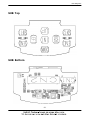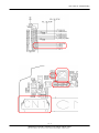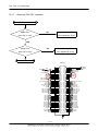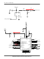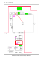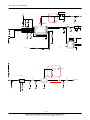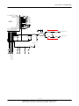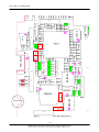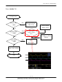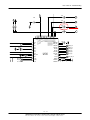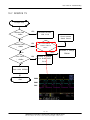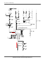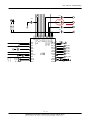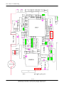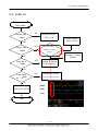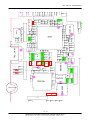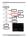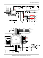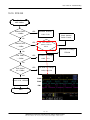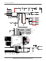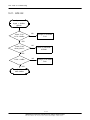
1
GSM TELEPHONE
SGH-G810
GSM TELEPHONE
CONTENTS
1.
Safety Precautions
2.
Specification
3.
Product Function
4.
Array course control
5.
Exploded View and Parts list
6.
MAIN Electrical Parts List
7.
Disassembly and Assembly
Instructions
8.
Block Diagrams
9.
PCB Diagrams
10. Chart of Troubleshooting
11. Reference data
GSPN (Global Service Partner Network)
Country
Web Site
North America
service.samsungportal.com
Latin America
latin.samsungportal.com
CIS
cis.samsungportal.com
Europe
europe.samsungportal.com
China
china.samsungportal.com
Asia
asia.samsungportal.com
Mideast & Africa
mea.samsungportal.com
This Service Manual is a property of Samsung Electronics Co.,Ltd.
Any unauthorized use of Manual can be punished under applicable
International and/or domestic law.
ⓒ Samsung Electronics Co.,Ltd.
2008. 04. Rev.1.0
1. Safety Precautions
1-1. Repair Precaution
● Repair in Shield Box, during detailed tuning.
Take specially care of tuning or test,
because specipicty of cellular phone is sensitive for surrounding interference(RF noise).
● Be careful to use a kind of magnetic object or tool,
because performance of parts is damaged by the influence of manetic force.
● Surely use a standard screwdriver when you disassemble this product,
otherwise screw will be worn away.
● Use a thicken twisted wire when you measure level.
A thicken twisted wire has low resistance, therefore error of measurement is few.
● Repair after separate Test Pack and Set because for short danger (for example an
overcurrent and furious flames of parts etc) when you repair board in condition of
connecting Test Pack and tuning on.
● Take specially care of soldering, because Land of PCB is small and weak in heat.
● Surely tune on/off while using AC power plug, because a repair of battery charger is
dangerous when tuning ON/OFF PBA and Connector after disassembing charger.
● Don't use as you pleases after change other material than replacement registered on SEC
System.
Otherwise engineer in charge isn't charged with problem that you don't keep this rules.
1-1
SAMSUNG Proprietary-Contents may change without notice
This Document can not be used without Samsung's authorization
Safety Precautions
1-2. ESD(Electrostatically Sensitive Devices) Precaution
Several semiconductor may be damaged easilly by static electricity. Such parts are called by
ESD(Electrostatically Sensitive Devices), for example IC,BGA chip etc. Read Precaution below.
You can prevent from ESD damage by static electricity.
● Remove static electricity remained your body before you touch semiconductor or parts with
semiconductor. There are ways that you touch an earthed place or wear static electricity
prevention string on wrist.
● Use earthed soldering steel when you connect or disconnect ESD.
● Use soldering removing tool to break static electricity. , otherwise ESD will be damaged by
static electricity.
● Don't unpack until you set up ESD on product. Because most of ESD are packed by box
and aluminum plate to have conductive power,they are prevented from static electricity.
● You must maintain electric contact between ESD and place due to be set up until ESD is
connected completely to the proper place or a circuit board.
1-2
SAMSUNG Proprietary-Contents may change without notice
This Document can not be used without Samsung's authorization
2. Specification
2-1. GSM General Specification
EGSM 900
DCS 18 00
PCS 190 0
WCDMA 2100
Fre q. Band[MHz]
Uplink/Downlink
880~91 5
925~96 0
1 710~17 85
1 805~18 80
1 850~19 10
1 930~19 90
1 920~19 80
2 110~21 70
ARFCN r ange
0~124 &
9 75~102 3
512~88 5
512~81 0
UL:9 612~98 88
DL:10 562~10 838
Tx/Rx spa cing
10MHz
20MHz
20MHz
130MHz
Mod. Bit rat e/
Bit Period
27 0.833 kbps
3.692 us
27 0.833 kbps
3.692 us
27 0.833 kbps
3.692 us
3. 84Mcps
(chip ra te)
T ime Slot Per iod/
Fra me Per iod
576.9 us
4. 615ms
576.9 us
4. 615ms
576.9 us
4. 615ms
F rame l ength : 10ms
Slot lengt h : 0. 667ms
Modulation
0.3G M SK
0.3G MSK
0.3G M SK
QPSK
HPSK
MS Powe r
33 dBm~5d Bm
30 dBm~0d Bm
30 dBm~0d Bm
2 4dBm~- 50dBm
4
(max +33dBm)
1
(max +30dBm)
1
(max +30dBm)
Power Class
Sensit ivit y
-1 02dBm
-1 00dBm
-1 00dBm
T DM A Mu x
8
8
8
Cell Radius
35Km
2Km
2Km
2-1
SAMSUNG Proprietary-Contents may change without notice
This Document can not be used without Samsung's authorization
3
(max +24dBm)
- 106.7 dBm
2Km
Specification
2-2. GSM TX power class
TX Power
TX Power
TX Power
control level
GSM850
GSM900
control level
5
33±2 dBm
0
30±3 dBm
0
30±3 dBm
6
31±2 dBm
1
28±3 dBm
1
28±3 dBm
7
29±2 dBm
2
26±3 dBm
2
26±3 dBm
8
27±2 dBm
3
24±3 dBm
3
24±3 dBm
9
25±2 dBm
4
22±3 dBm
4
22±3 dBm
10
23±2 dBm
5
20±3 dBm
5
20±3 dBm
11
21±2 dBm
6
18±3 dBm
6
18±3 dBm
12
19±2 dBm
7
16±3 dBm
7
16±3 dBm
13
17±2 dBm
8
14±3 dBm
8
14±3 dBm
14
15±2 dBm
9
12±4 dBm
9
12±4 dBm
15
13±2 dBm
10
10±4 dBm
10
10±4 dBm
16
11±3 dBm
11
8±4 dBm
11
8±4 dBm
17
9±3 dBm
12
6±4 dBm
12
6±4 dBm
18
7±3 dBm
13
4±4 dBm
13
4±4 dBm
19
5±3 dBm
14
2±5 dBm
14
2±5 dBm
15
0±5 dBm
15
0±5 dBm
DCS1800
control level
2-2
SAMSUNG Proprietary-Contents may change without notice
This Document can not be used without Samsung's authorization
PCS1900
3. Product Function
Main Function
• HSDPA/UMTS, EDGE, GPRS
• WLAN 802.11 b/g
• Bluetooth v2.0 + EDR
• USB v2.0 HS compatible
• Camera 5 Mega x 3 Optical Zooming and camcorder
• FM Radio
• Instant Messaging capability
• E-mail
• Featured applications provide alarms, calendar, calculator, record audio, converter, timer, stopwatch,
and world time.
• File viewer (MS office, PDF)
• Multimedia Message Service (MMS)
• Multimedia capability (with included Media player)
• Photo caller ID
• Speakerphone capability
• WEB/WAP browser (HTMS, xHTML, WML)
3-1
SAMSUNG Proprietary-Contents may change without notice
This Document can not be used without Samsung's authorization
4. Array course control
4-1. Software Adjustments
- There is 2 set to download the binary image into your device.
[First set]
3
1.
2.
3.
4.
5.
6.
7.
JIG BOX (UMTS TEST JIG; GH80-03308A)
USB Cable : JIG to PC
Test Cable : JIG to BENU (0.4M:GH39-01091A, 1.5M: GH39-01093A)
Power Cable : JIG to power supply
Serial Cable : JIG to PC
Power Supply
Rf Cable : Scotch to Agilent 8960 or CMU200 (GH39-00397A)
4-1
SAMSUNG Proprietary-Contents may change without notice
This Document can not be used without Samsung's authorization
Array course control
[Second Set]
1
USB Data Link Cable : BENU to PC (GH39-00922A)
Standard Battery for BENU (GH43-02986A)
4-2
SAMSUNG Proprietary-Contents may change without notice
This Document can not be used without Samsung's authorization
Array course control
4-2. Software Download
4-2-1. Pre-requisite for Download
SGH - G810 Mobile Device
Apollo v4.3.exe : Downloader Application for SGH-G810
USB Download Driver : SS60_Downloader_Driver.zip
Rom Image : PDA(*.IMG), MODEM(*.BIN) images
Equipment set for Download.
4-3
SAMSUNG Proprietary-Contents may change without notice
This Document can not be used without Samsung's authorization
Array course control
4-2-2. Concupts & cautions.
You can download PDA or MODEM separately. But We are always recommended to
download both at the same time using same version of rom image.
To download an image, the phone need to be set to a proper download mode.
There are 3 download modes.
PDA download : Hold 1, 4 keys and power on -> Blue screen with some information.
MODEM download : Hold 7, * keys and power on -> Blinking "MODEM DOWNLOAD"
on blue screen
All download : Hold 4, 7 keys and power on -> Blinking "ALL DOWNLOAD" on blue screen
For PDA image download, the phone shows download progress on the screen
For MODEM image download, the phone shows RGBW/B Screen.
For All download mode, MODEM image is downloaded first and then PDA
downloading starts.
After downloading PDA, the phone will be reboot.
Do NOT interrupt downloading process or the phone will be damaged. You would be
unable to boot up the phone or to re-flash the phone. Let it finish downloading
process even though you are flashing wrong images.
4-4
SAMSUNG Proprietary-Contents may change without notice
This Document can not be used without Samsung's authorization
Array course control
4-2-3. USB Driver installation for PDA
Execution Apollo.exe.
SGH-G810 connect to the Host computer using download equipment set.
Hold “1+4” key and insert power supplied test cable when use equipment set 1
or Hold “1+4” key and press power on key when use equipment set 2.
Install PDA side driver.
Follow New H/W Installation Manager.
Select ‘IBootHostUSB.inf’file under ‘i550_Apollo_Drivers\PDA_driver’ folder when
Windows asks for new h/w driver. It is safe to choose “Yes” for the waring window.
Confirm “SAMSUNG BlueFin USB Downloader” Installed.
Refer to Next Page.
** If Windows doesn’t ask for USB driver, it means USB driver installation was
failed before. Open Hardware Manager then delete devices with ? or ! mark then
try again. If it doesn’t work, you need to right click on the device then try Driver
Update.
After installing PDA driver, Apollo shows the connection status if it is installed
properly.
4-5
SAMSUNG Proprietary-Contents may change without notice
This Document can not be used without Samsung's authorization
Array course control
4-6
SAMSUNG Proprietary-Contents may change without notice
This Document can not be used without Samsung's authorization
Array course control
4-2-4. USB Driver installation for MODEM
Hold “7 + *” key and insert power supplied test cable when use equipment set 1 or
Hold “7+ *” key and press power on key when use equipment set 2.
Install Modem side driver.
Execute ‘Setup.exe’file under ‘i450_Apollo_Drivers\PHONE_driver’ folder when
Windows asks for new h/w driver.
Confirm “SAMSUNG USB Composite Device” Installed.
4-7
SAMSUNG Proprietary-Contents may change without notice
This Document can not be used without Samsung's authorization
Array course control
4-2-5. USB Driver installation
4-8
SAMSUNG Proprietary-Contents may change without notice
This Document can not be used without Samsung's authorization
Array course control
4-2-6. Download the image using APOLLO
Execution Apollo.exe.
Select a Rom Image to download
Check this field : 1. SGH-i550 (above GG2^)
4-9
SAMSUNG Proprietary-Contents may change without notice
This Document can not be used without Samsung's authorization
Array course control
Select the proper check option .
PDA stasus
- Bootloader : Update PDA Bootloader section.
- NV Clear : IMEI section erase.
You can see following message when you click this option
MODEM Status
- Boot Update : Update Modem Bootloader section.
4-10
SAMSUNG Proprietary-Contents may change without notice
This Document can not be used without Samsung's authorization
Array course control
Make sure that phone and host computer connection, click proper download
button.
PDA download : Hold 1, 4 keys and power on -> Blue screen with some information.
MODEM download : Hold 7, * keys and power on -> Blinking "MODEM DOWNLOAD"
on blue screen
All download : Hold 4, 7 keys and power on -> Blinking "ALL DOWNLOAD" on blue screen
4-11
SAMSUNG Proprietary-Contents may change without notice
This Document can not be used without Samsung's authorization
Array course control
Do NOT interrupt downloading process.
- Pda download time: About 1 min.
- Modem download time : About 2 min.
- All download time: About 3 min.
Confirm Download Complete.
- SGH-G810 will be reboot when PDA download complete.
4-12
SAMSUNG Proprietary-Contents may change without notice
This Document can not be used without Samsung's authorization
Array course control
4-2-7. Troubleshooting
Unable to install USB driver.
Try another Download equipment
Try another SGH-G810.
Consult to R&D team.
Download stops in the middle.
Close and launch Apollo again then try again.
Check the battery is charged enough.
Download doesn’t start
Check the connection between Apollo and a SGH-G810.
Check the image that is not damaged.
Select an image and download again.
Phone doesn’t boot up after downloading.
Check the release version of PDA and MODEM. They should be same.
Make sure that rom image, and then try to download.
4-13
SAMSUNG Proprietary-Contents may change without notice
This Document can not be used without Samsung's authorization
Array course control
4-14
SAMSUNG Proprietary-Contents may change without notice
This Document can not be used without Samsung's authorization
5. Exploded View and Parts List
5-1. Cellular phone Exploded View
QMW02
QKP01
QFU01
QME01
QKP02
QSH01
QMP01
QME02
QAN06
QCK02
QMI03
QVO01
QLC01
QSH02
QCA01
QCA02
QCK01
QSP01
QCR87
QMO01
QAN02
QAN03
QCR49
QPC01
QCR85
QSD01
QFL01
QRF03
QRE01
QSC02
QRF07
QCR05
QHI02
QFL00
QRF01
QCR04
QSC01
QFR01
QCH04
QHI01
QBA01
QBA00
QCR85
5-1
SAMSUNG Proprietary-Contents may change without notice
This Document can not be used without Samsung's authorization
Exploded View and Parts List
5-2. Cellular phone Parts list
Design LOC
QAN02
QAN03
QAN06
QBA00
QBA01
QCA01
QCA02
QCH04
QCK01
QCK02
QCR04
QCR05
QCR49
QCR85
QCR85
QCR87
QFL00
QFL01
QFR01
QFU01
QHI01
QHI02
QKP01
QKP02
QLC01
QME01
QME02
QMI01
QMI03
QMO01
QMP01
QMW02
QPC01
QRE01
QRF01
QRF03
QRF07
QSC01
QSC02
QSD01
QSH01
QSH02
QSP01
QVO01
Description
INTENNA-SGHG810
INTENNA-SGHG810 BT & GPS
ASSY RUBBER-ANTENNA
PMO COVER-BATT V5
INNER BATTERY PACK-1200MAH,BLK
CAMERA MODULE-SGHG810(CIF)
CAMERA MODULE-SGHG810(5M)
ASSY COVER-CAMERA
PMO KEY-CAMERA
PMO KEY-POWER
SCREW-MACHINE
SCREW-MACHINE
SCREW-MACHINE
SCREW-MACHINE
SCREW-MACHINE
SCREW-TAPPING
ASSY CASE-LOWER/FRONT
ASSY CASE-LOWER
ASSY CASE-FRONT
ASSY CASE-UPPER
ASSY HINGE-SLIDE BASE
ASSY HINGE-PUSH ROD
ASSY KEYPAD-MAIN(EU/T_SIL)
ASSY KEYPAD-SUB(EU/T_SIL)
LCD-MAIN LCD MODULE
KEY FPCB-M/DOME SHEET 15KEY
KEY FPCB-S/DOME SHEET 9KEY
MICROPHONE-ASSY-SGHG810(SMD TY
RMO RUBBER-MIC HOLDER V2
MOTOR DC-SPH-B5000
PBA MAIN-SGHG810
PMO WINDOW-MAIN
FPC-CON TO CON(G810)
ASSY CASE-REAR
TAPE-COVER RF
PMO COVER-EAR
PMO COVER-MINI USB V2
PMO COVER-SCREW CAP
TAPE-SCREW CAP LOWER
PMO COVER-SD
ASSY COVER-SHIELDCAN TOP
ASSY COVER-BTM
SPEAKER
PMO KEY-VOLUME
SEC CODE
GH42-01377A
GH42-01378A
GH98-07824A
GH72-47985H
GH43-02986A
GH59-05244A
GH59-05248A
GH98-06886H
GH72-45003H
GH72-45004H
6001-001479
6001-001478
6001-001823
6001-002097
6001-002097
6002-001412
GH98-06715H
GH98-06712H
GH98-06713H
GH98-06711H
GH98-07242A
GH98-08089A
GH98-07244H
GH98-07245H
GH07-01232A
GH59-05125A
GH59-05351A
GH30-00450A
GH73-11597A
GH31-00255B
GH92-04240A
GH72-45011H
GH41-02002A
GH98-06714H
GH74-36681H
GH72-46031H
GH72-46762H
GH72-45916H
GH74-36693H
GH72-43221H
GH98-08431A
GH98-08433A
3001-002299
GH72-45005H
5-2
SAMSUNG Proprietary-Contents may change without notice
This Document can not be used without Samsung's authorization
6. MAIN Electrical Parts List
SEC CODE
Design LOC
Discription
0403-001547
D700
DIODE-ZENER
0406-001150
ZD906
DIODE-TVS
0406-001201
ZD700
DIODE-TVS
0406-001254
ZD703
DIODE-TVS
0406-001254
ZD706
DIODE-TVS
0406-001254
ZD707
DIODE-TVS
0406-001254
ZD708
DIODE-TVS
0406-001254
ZD710
DIODE-TVS
0406-001254
ZD711
DIODE-TVS
0406-001256
ZD701
DIODE-TVS
0406-001256
ZD702
DIODE-TVS
0406-001256
ZD704
DIODE-TVS
0406-001267
ZD601
DIODE-TVS
0406-001267
ZD602
DIODE-TVS
0406-001267
ZD603
DIODE-TVS
0406-001267
ZD604
DIODE-TVS
0407-001002
D400
DIODE-ARRAY
0407-001002
D901
DIODE-ARRAY
0407-001007
D903
DIODE-ARRAY
0504-000168
TR901
TR-DIGITAL
0504-001113
TR400
TR-DIGITAL
0504-001113
TR402
TR-DIGITAL
0505-001165
TR900
FET-SILICON
0505-001570
TR611
FET-SILICON
0601-002268
LED700
LED
0601-002268
LED702
LED
0801-002294
U303
IC-CMOS LOGIC
0801-002294
U901
IC-CMOS LOGIC
0801-002294
U917
IC-CMOS LOGIC
0801-002321
U900
IC-CMOS LOGIC
0801-003012
U902
IC-CMOS LOGIC
0801-003013
U301
IC-CMOS LOGIC
0801-003052
U302
IC-CMOS LOGIC
0801-003065
U409
IC-CMOS LOGIC
0801-003124
U408
IC-CMOS LOGIC
0801-003205
U909
IC-CMOS LOGIC
6-1
SAMSUNG Proprietary-Contents may change without notice
This Document can not be used without Samsung's authorization
Main Electrical Parts List
SEC CODE
Design LOC
Discription
0904-002227
UCP800
IC-DSP
1001-001336
U906
IC-ANALOG SWITCH
1001-001394
U609
IC-ANALOG SWITCH
1001-001461
U501
IC-ANALOG SWITCH
1001-001461
U502
IC-ANALOG SWITCH
1001-001483
U700
IC-ANALOG SWITCH
1001-001483
U701
IC-ANALOG SWITCH
1001-001483
U702
IC-ANALOG SWITCH
1001-001483
U703
IC-ANALOG SWITCH
1001-001483
U704
IC-ANALOG SWITCH
1001-001483
U705
IC-ANALOG SWITCH
1001-001489
U907
IC-ANALOG SWITCH
1009-001024
U903
IC-HALL EFFECT S/W
1106-001511
UME900
IC-SRAM
1108-000127
UME300
IC-MCP
1108-000135
UME800
IC-MCP
1201-002531
PAM200
IC-POWER AMP
1201-002570
FEM100
IC-POWER AMP
1201-002581
F104
IC-RF AMP
1201-002610
U504
IC-AUDIO AMP
1202-001079
U610
IC-VOLTAGE COMP.
1202-001079
U912
IC-VOLTAGE COMP.
1203-002716
U910
IC-VOL. DETECTOR
1203-003432
U607
IC-POSI.FIXED REG.
1203-003737
U706
IC-POSI.FIXED REG.
1203-004330
U601
IC-MULTI REG.
1203-004330
U608
IC-MULTI REG.
1203-004339
U602
IC-MULTI REG.
1203-004340
U606
IC-MULTI REG.
1203-004430
U404
IC-VOL. DETECTOR
1203-004524
U605
IC-MULTI REG.
1203-004548
U603
IC-DC/DC CONVERTER
1203-004607
U604
IC-MULTI REG.
1203-004621
U500
IC-POWER SUPERVISOR
1203-004728
U612
IC-POSI.FIXED REG.
1203-004763
U911
IC-VOL. DETECTOR
6-2
SAMSUNG Proprietary-Contents may change without notice
This Document can not be used without Samsung's authorization
Main Electrical Parts List
SEC CODE
Design LOC
Discription
1203-004778
U400
IC-POWER SUPERVISOR
1203-004838
U401
IC-BATTERY
1204-002746
U101
IC-TUNER
1205-003281
UCP300
IC-MODEM
1205-003297
U100
IC-TRANSCEIVER
1205-003467
U908
IC-SWITCH
1404-001221
VR100
THERMISTOR-NTC
2007-000070
R222
R-CHIP
2007-000070
R619
R-CHIP
2007-000070
R803
R-CHIP
2007-000070
R804
R-CHIP
2007-000070
R805
R-CHIP
2007-000137
R321
R-CHIP
2007-000138
R109
R-CHIP
2007-000138
R110
R-CHIP
2007-000138
R132
R-CHIP
2007-000138
R524
R-CHIP
2007-000138
R525
R-CHIP
2007-000138
R601
R-CHIP
2007-000138
R734
R-CHIP
2007-000138
R923
R-CHIP
2007-000138
R924
R-CHIP
2007-000140
R115
R-CHIP
2007-000141
R434
R-CHIP
2007-000143
R502
R-CHIP
2007-000143
R504
R-CHIP
2007-000148
R218
R-CHIP
2007-000148
R311
R-CHIP
2007-000148
R313
R-CHIP
2007-000148
R316
R-CHIP
2007-000148
R319
R-CHIP
2007-000148
R410
R-CHIP
2007-000148
R643
R-CHIP
2007-000148
R725
R-CHIP
2007-000157
R412
R-CHIP
2007-000157
R721
R-CHIP
6-3
SAMSUNG Proprietary-Contents may change without notice
This Document can not be used without Samsung's authorization
Main Electrical Parts List
SEC CODE
Design LOC
Discription
2007-000157
R722
R-CHIP
2007-000157
R723
R-CHIP
2007-000157
R724
R-CHIP
2007-000159
R917
R-CHIP
2007-000162
R129
R-CHIP
2007-000162
R130
R-CHIP
2007-000162
R131
R-CHIP
2007-000162
R325
R-CHIP
2007-000162
R326
R-CHIP
2007-000162
R413
R-CHIP
2007-000162
R414
R-CHIP
2007-000162
R503
R-CHIP
2007-000162
R507
R-CHIP
2007-000162
R511
R-CHIP
2007-000162
R523
R-CHIP
2007-000162
R529
R-CHIP
2007-000162
R621
R-CHIP
2007-000162
R628
R-CHIP
2007-000162
R629
R-CHIP
2007-000162
R630
R-CHIP
2007-000162
R631
R-CHIP
2007-000162
R648
R-CHIP
2007-000162
R719
R-CHIP
2007-000162
R726
R-CHIP
2007-000162
R905
R-CHIP
2007-000162
R909
R-CHIP
2007-000162
R910
R-CHIP
2007-000162
R911
R-CHIP
2007-000162
R912
R-CHIP
2007-000162
R913
R-CHIP
2007-000162
R914
R-CHIP
2007-000162
R915
R-CHIP
2007-000162
R922
R-CHIP
2007-000162
U916
R-CHIP
2007-000164
R908
R-CHIP
2007-000165
R401
R-CHIP
6-4
SAMSUNG Proprietary-Contents may change without notice
This Document can not be used without Samsung's authorization
Main Electrical Parts List
SEC CODE
Design LOC
Discription
2007-000169
R602
R-CHIP
2007-000169
U913
R-CHIP
2007-000170
R302
R-CHIP
2007-000170
R636
R-CHIP
2007-000170
R639
R-CHIP
2007-000170
R903
R-CHIP
2007-000170
R925
R-CHIP
2007-000171
R102
R-CHIP
2007-000171
R120
R-CHIP
2007-000171
R135
R-CHIP
2007-000171
R221
R-CHIP
2007-000171
R318
R-CHIP
2007-000171
R404
R-CHIP
2007-000171
R526
R-CHIP
2007-000171
R618
R-CHIP
2007-000171
R642
R-CHIP
2007-000171
R702
R-CHIP
2007-000171
R703
R-CHIP
2007-000171
R718
R-CHIP
2007-000171
R802
R-CHIP
2007-000171
R821
R-CHIP
2007-000171
R822
R-CHIP
2007-000171
R825
R-CHIP
2007-000171
R826
R-CHIP
2007-000171
R902
R-CHIP
2007-000171
R918
R-CHIP
2007-000171
U915
R-CHIP
2007-000171
U918
R-CHIP
2007-001119
R417
R-CHIP
2007-001119
R528
R-CHIP
2007-001285
R116
R-CHIP
2007-001285
R119
R-CHIP
2007-001290
R322
R-CHIP
2007-001292
R304
R-CHIP
2007-001298
R113
R-CHIP
2007-001298
R328
R-CHIP
6-5
SAMSUNG Proprietary-Contents may change without notice
This Document can not be used without Samsung's authorization
Main Electrical Parts List
SEC CODE
Design LOC
Discription
2007-001298
R407
R-CHIP
2007-001298
R510
R-CHIP
2007-001305
R117
R-CHIP
2007-001305
R118
R-CHIP
2007-002965
R728
R-CHIP
2007-002965
R729
R-CHIP
2007-007009
R201
R-CHIP
2007-007014
R406
R-CHIP
2007-007014
R408
R-CHIP
2007-007107
R125
R-CHIP
2007-007107
R126
R-CHIP
2007-007137
R204
R-CHIP
2007-007306
R202
R-CHIP
2007-007306
R203
R-CHIP
2007-007306
R710
R-CHIP
2007-007306
R711
R-CHIP
2007-007306
R712
R-CHIP
2007-007306
R713
R-CHIP
2007-007306
R824
R-CHIP
2007-007309
R104
R-CHIP
2007-007309
R735
R-CHIP
2007-007315
R814
R-CHIP
2007-007316
R305
R-CHIP
2007-007317
R800
R-CHIP
2007-007317
R801
R-CHIP
2007-007318
R815
R-CHIP
2007-007318
R820
R-CHIP
2007-007321
R108
R-CHIP
2007-007468
R403
R-CHIP
2007-007528
R515
R-CHIP
2007-007698
R411
R-CHIP
2007-007698
R416
R-CHIP
2007-007741
R141
R-CHIP
2007-008015
R646
R-CHIP
2007-008015
R647
R-CHIP
2007-008015
R819
R-CHIP
6-6
SAMSUNG Proprietary-Contents may change without notice
This Document can not be used without Samsung's authorization
Main Electrical Parts List
SEC CODE
Design LOC
Discription
2007-008052
R809
R-CHIP
2007-008052
R810
R-CHIP
2007-008052
R811
R-CHIP
2007-008052
R813
R-CHIP
2007-008055
R432
R-CHIP
2007-008117
R415
R-CHIP
2007-008516
R114
R-CHIP
2007-008588
R122
R-CHIP
2007-008806
R200
R-CHIP
2007-009084
R640
R-CHIP
2203-000233
C115
C-CER,CHIP
2203-000233
C134
C-CER,CHIP
2203-000233
C175
C-CER,CHIP
2203-000233
C419
C-CER,CHIP
2203-000233
C422
C-CER,CHIP
2203-000233
C427
C-CER,CHIP
2203-000233
C431
C-CER,CHIP
2203-000254
C177
C-CER,CHIP
2203-000254
C182
C-CER,CHIP
2203-000254
C304
C-CER,CHIP
2203-000254
C305
C-CER,CHIP
2203-000254
C307
C-CER,CHIP
2203-000254
C311
C-CER,CHIP
2203-000254
C312
C-CER,CHIP
2203-000254
C313
C-CER,CHIP
2203-000254
C706
C-CER,CHIP
2203-000254
C826
C-CER,CHIP
2203-000278
C191
C-CER,CHIP
2203-000278
C531
C-CER,CHIP
2203-000278
C544
C-CER,CHIP
2203-000278
C629
C-CER,CHIP
2203-000278
C630
C-CER,CHIP
2203-000330
C185
C-CER,CHIP
2203-000330
C186
C-CER,CHIP
2203-000330
C425
C-CER,CHIP
2203-000330
C545
C-CER,CHIP
6-7
SAMSUNG Proprietary-Contents may change without notice
This Document can not be used without Samsung's authorization
Main Electrical Parts List
SEC CODE
Design LOC
Discription
2203-000386
C426
C-CER,CHIP
2203-000386
C700
C-CER,CHIP
2203-000386
C701
C-CER,CHIP
2203-000386
C702
C-CER,CHIP
2203-000386
C703
C-CER,CHIP
2203-000386
C725
C-CER,CHIP
2203-000386
C726
C-CER,CHIP
2203-000386
C727
C-CER,CHIP
2203-000425
C120
C-CER,CHIP
2203-000438
C130
C-CER,CHIP
2203-000438
C181
C-CER,CHIP
2203-000489
C338
C-CER,CHIP
2203-000627
C113
C-CER,CHIP
2203-000627
C114
C-CER,CHIP
2203-000627
C170
C-CER,CHIP
2203-000812
C119
C-CER,CHIP
2203-000812
C187
C-CER,CHIP
2203-000812
C200
C-CER,CHIP
2203-000812
C202
C-CER,CHIP
2203-000812
C219
C-CER,CHIP
2203-000812
C343
C-CER,CHIP
2203-000812
C412
C-CER,CHIP
2203-000812
C424
C-CER,CHIP
2203-000812
C533
C-CER,CHIP
2203-000812
C707
C-CER,CHIP
2203-000812
C708
C-CER,CHIP
2203-000812
C709
C-CER,CHIP
2203-000812
C713
C-CER,CHIP
2203-000812
C714
C-CER,CHIP
2203-000812
C715
C-CER,CHIP
2203-000812
C716
C-CER,CHIP
2203-000812
C827
C-CER,CHIP
2203-000812
C828
C-CER,CHIP
2203-000995
C128
C-CER,CHIP
2203-000995
C346
C-CER,CHIP
2203-000995
C537
C-CER,CHIP
6-8
SAMSUNG Proprietary-Contents may change without notice
This Document can not be used without Samsung's authorization
Main Electrical Parts List
SEC CODE
Design LOC
Discription
2203-001017
C103
C-CER,CHIP
2203-001072
C146
C-CER,CHIP
2203-001124
C211
C-CER,CHIP
2203-001153
C162
C-CER,CHIP
2203-001153
C205
C-CER,CHIP
2203-001153
C217
C-CER,CHIP
2203-001383
C216
C-CER,CHIP
2203-001383
L214
C-CER,CHIP
2203-002709
C209
C-CER,CHIP
2203-002709
C525
C-CER,CHIP
2203-005050
C125
C-CER,CHIP
2203-005288
C247
C-CER,CHIP
2203-005444
C144
C-CER,CHIP
2203-005444
C149
C-CER,CHIP
2203-005444
C201
C-CER,CHIP
2203-005444
C646
C-CER,CHIP
2203-005444
L117
C-CER,CHIP
2203-005446
C174
C-CER,CHIP
2203-005446
R103
C-CER,CHIP
2203-005480
C341
C-CER,CHIP
2203-005482
C104
C-CER,CHIP
2203-005482
C127
C-CER,CHIP
2203-005482
C154
C-CER,CHIP
2203-005482
C168
C-CER,CHIP
2203-005482
C176
C-CER,CHIP
2203-005482
C178
C-CER,CHIP
2203-005482
C193
C-CER,CHIP
2203-005482
C194
C-CER,CHIP
2203-005482
C197
C-CER,CHIP
2203-005482
C218
C-CER,CHIP
2203-005482
C303
C-CER,CHIP
2203-005482
C306
C-CER,CHIP
2203-005482
C308
C-CER,CHIP
2203-005482
C314
C-CER,CHIP
2203-005482
C315
C-CER,CHIP
2203-005482
C331
C-CER,CHIP
6-9
SAMSUNG Proprietary-Contents may change without notice
This Document can not be used without Samsung's authorization
Main Electrical Parts List
SEC CODE
Design LOC
Discription
2203-005482
C332
C-CER,CHIP
2203-005482
C335
C-CER,CHIP
2203-005482
C339
C-CER,CHIP
2203-005482
C340
C-CER,CHIP
2203-005482
C342
C-CER,CHIP
2203-005482
C345
C-CER,CHIP
2203-005482
C404
C-CER,CHIP
2203-005482
C406
C-CER,CHIP
2203-005482
C411
C-CER,CHIP
2203-005482
C414
C-CER,CHIP
2203-005482
C501
C-CER,CHIP
2203-005482
C510
C-CER,CHIP
2203-005482
C527
C-CER,CHIP
2203-005482
C563
C-CER,CHIP
2203-005482
C564
C-CER,CHIP
2203-005482
C565
C-CER,CHIP
2203-005482
C635
C-CER,CHIP
2203-005482
C640
C-CER,CHIP
2203-005482
C711
C-CER,CHIP
2203-005482
C801
C-CER,CHIP
2203-005482
C802
C-CER,CHIP
2203-005482
C812
C-CER,CHIP
2203-005482
C813
C-CER,CHIP
2203-005482
C822
C-CER,CHIP
2203-005482
C823
C-CER,CHIP
2203-005482
C824
C-CER,CHIP
2203-005482
C825
C-CER,CHIP
2203-005482
C831
C-CER,CHIP
2203-005482
C832
C-CER,CHIP
2203-005482
C841
C-CER,CHIP
2203-005482
C847
C-CER,CHIP
2203-005482
C849
C-CER,CHIP
2203-005482
C856
C-CER,CHIP
2203-005482
C902
C-CER,CHIP
2203-005482
C904
C-CER,CHIP
2203-005482
C905
C-CER,CHIP
6-10
SAMSUNG Proprietary-Contents may change without notice
This Document can not be used without Samsung's authorization
Main Electrical Parts List
SEC CODE
Design LOC
Discription
2203-005482
C907
C-CER,CHIP
2203-005482
C908
C-CER,CHIP
2203-005482
C909
C-CER,CHIP
2203-005482
C910
C-CER,CHIP
2203-005482
C911
C-CER,CHIP
2203-005482
C914
C-CER,CHIP
2203-005682
C147
C-CER,CHIP
2203-005682
C148
C-CER,CHIP
2203-005682
C195
C-CER,CHIP
2203-005682
C198
C-CER,CHIP
2203-005725
C101
C-CER,CHIP
2203-005725
C106
C-CER,CHIP
2203-005725
C108
C-CER,CHIP
2203-005725
C110
C-CER,CHIP
2203-005725
C112
C-CER,CHIP
2203-005725
C117
C-CER,CHIP
2203-005725
C122
C-CER,CHIP
2203-005725
C132
C-CER,CHIP
2203-005725
C133
C-CER,CHIP
2203-005725
C138
C-CER,CHIP
2203-005725
C141
C-CER,CHIP
2203-005725
C143
C-CER,CHIP
2203-005725
C152
C-CER,CHIP
2203-005725
C153
C-CER,CHIP
2203-005725
C155
C-CER,CHIP
2203-005725
C165
C-CER,CHIP
2203-005725
C213
C-CER,CHIP
2203-005725
C214
C-CER,CHIP
2203-005727
C183
C-CER,CHIP
2203-005732
C100
C-CER,CHIP
2203-005732
C102
C-CER,CHIP
2203-005736
C123
C-CER,CHIP
2203-005736
C135
C-CER,CHIP
2203-005736
C137
C-CER,CHIP
2203-005736
C157
C-CER,CHIP
2203-005736
C159
C-CER,CHIP
6-11
SAMSUNG Proprietary-Contents may change without notice
This Document can not be used without Samsung's authorization
Main Electrical Parts List
SEC CODE
Design LOC
Discription
2203-005736
C161
C-CER,CHIP
2203-005736
C166
C-CER,CHIP
2203-005736
C215
C-CER,CHIP
2203-006048
C705
C-CER,CHIP
2203-006137
C407
C-CER,CHIP
2203-006208
C613
C-CER,CHIP
2203-006208
C634
C-CER,CHIP
2203-006208
C710
C-CER,CHIP
2203-006260
C636
C-CER,CHIP
2203-006324
C251
C-CER,CHIP
2203-006324
C405
C-CER,CHIP
2203-006324
C429
C-CER,CHIP
2203-006324
C611
C-CER,CHIP
2203-006324
C637
C-CER,CHIP
2203-006348
C921
C-CER,CHIP
2203-006399
C845
C-CER,CHIP
2203-006423
C105
C-CER,CHIP
2203-006423
C107
C-CER,CHIP
2203-006423
C109
C-CER,CHIP
2203-006423
C111
C-CER,CHIP
2203-006423
C116
C-CER,CHIP
2203-006423
C129
C-CER,CHIP
2203-006423
C136
C-CER,CHIP
2203-006423
C158
C-CER,CHIP
2203-006423
C160
C-CER,CHIP
2203-006423
C167
C-CER,CHIP
2203-006474
C220
C-CER,CHIP
2203-006562
C184
C-CER,CHIP
2203-006562
C302
C-CER,CHIP
2203-006562
C309
C-CER,CHIP
2203-006562
C310
C-CER,CHIP
2203-006562
C316
C-CER,CHIP
2203-006562
C320
C-CER,CHIP
2203-006562
C321
C-CER,CHIP
2203-006562
C322
C-CER,CHIP
2203-006562
C324
C-CER,CHIP
6-12
SAMSUNG Proprietary-Contents may change without notice
This Document can not be used without Samsung's authorization
Main Electrical Parts List
SEC CODE
Design LOC
Discription
2203-006562
C325
C-CER,CHIP
2203-006562
C326
C-CER,CHIP
2203-006562
C327
C-CER,CHIP
2203-006562
C328
C-CER,CHIP
2203-006562
C336
C-CER,CHIP
2203-006562
C430
C-CER,CHIP
2203-006562
C432
C-CER,CHIP
2203-006562
C435
C-CER,CHIP
2203-006562
C504
C-CER,CHIP
2203-006562
C509
C-CER,CHIP
2203-006562
C513
C-CER,CHIP
2203-006562
C515
C-CER,CHIP
2203-006562
C516
C-CER,CHIP
2203-006562
C519
C-CER,CHIP
2203-006562
C520
C-CER,CHIP
2203-006562
C521
C-CER,CHIP
2203-006562
C522
C-CER,CHIP
2203-006562
C523
C-CER,CHIP
2203-006562
C524
C-CER,CHIP
2203-006562
C528
C-CER,CHIP
2203-006562
C529
C-CER,CHIP
2203-006562
C530
C-CER,CHIP
2203-006562
C535
C-CER,CHIP
2203-006562
C539
C-CER,CHIP
2203-006562
C543
C-CER,CHIP
2203-006562
C547
C-CER,CHIP
2203-006562
C549
C-CER,CHIP
2203-006562
C551
C-CER,CHIP
2203-006562
C555
C-CER,CHIP
2203-006562
C557
C-CER,CHIP
2203-006562
C558
C-CER,CHIP
2203-006562
C559
C-CER,CHIP
2203-006562
C560
C-CER,CHIP
2203-006562
C561
C-CER,CHIP
2203-006562
C570
C-CER,CHIP
2203-006562
C606
C-CER,CHIP
6-13
SAMSUNG Proprietary-Contents may change without notice
This Document can not be used without Samsung's authorization
Main Electrical Parts List
SEC CODE
Design LOC
Discription
2203-006562
C607
C-CER,CHIP
2203-006562
C608
C-CER,CHIP
2203-006562
C609
C-CER,CHIP
2203-006562
C612
C-CER,CHIP
2203-006562
C617
C-CER,CHIP
2203-006562
C618
C-CER,CHIP
2203-006562
C619
C-CER,CHIP
2203-006562
C620
C-CER,CHIP
2203-006562
C621
C-CER,CHIP
2203-006562
C622
C-CER,CHIP
2203-006562
C623
C-CER,CHIP
2203-006562
C624
C-CER,CHIP
2203-006562
C625
C-CER,CHIP
2203-006562
C626
C-CER,CHIP
2203-006562
C631
C-CER,CHIP
2203-006562
C632
C-CER,CHIP
2203-006562
C633
C-CER,CHIP
2203-006562
C639
C-CER,CHIP
2203-006562
C641
C-CER,CHIP
2203-006562
C712
C-CER,CHIP
2203-006562
C723
C-CER,CHIP
2203-006562
C724
C-CER,CHIP
2203-006562
C800
C-CER,CHIP
2203-006562
C803
C-CER,CHIP
2203-006562
C811
C-CER,CHIP
2203-006562
C820
C-CER,CHIP
2203-006562
C821
C-CER,CHIP
2203-006562
C830
C-CER,CHIP
2203-006562
C843
C-CER,CHIP
2203-006562
C846
C-CER,CHIP
2203-006562
C848
C-CER,CHIP
2203-006562
C858
C-CER,CHIP
2203-006562
C915
C-CER,CHIP
2203-006562
C916
C-CER,CHIP
2203-006562
C917
C-CER,CHIP
2203-006562
C918
C-CER,CHIP
6-14
SAMSUNG Proprietary-Contents may change without notice
This Document can not be used without Samsung's authorization
Main Electrical Parts List
SEC CODE
Design LOC
Discription
2203-006562
C920
C-CER,CHIP
2203-006681
C507
C-CER,CHIP
2203-006681
C518
C-CER,CHIP
2203-006681
C534
C-CER,CHIP
2203-006681
C540
C-CER,CHIP
2203-006824
C124
C-CER,CHIP
2203-006824
C156
C-CER,CHIP
2203-006824
C301
C-CER,CHIP
2203-006824
C400
C-CER,CHIP
2203-006824
C401
C-CER,CHIP
2203-006824
C415
C-CER,CHIP
2203-006824
C417
C-CER,CHIP
2203-006824
C418
C-CER,CHIP
2203-006824
C638
C-CER,CHIP
2203-006838
C252
C-CER,CHIP
2203-006838
C416
C-CER,CHIP
2203-006838
C420
C-CER,CHIP
2203-006838
C423
C-CER,CHIP
2203-006838
C548
C-CER,CHIP
2203-006838
C614
C-CER,CHIP
2203-006838
C615
C-CER,CHIP
2203-006838
C819
C-CER,CHIP
2203-006838
C850
C-CER,CHIP
2203-006839
C121
C-CER,CHIP
2203-006839
C140
C-CER,CHIP
2203-006839
C142
C-CER,CHIP
2203-006839
C318
C-CER,CHIP
2203-006839
C319
C-CER,CHIP
2203-006872
C317
C-CER,CHIP
2203-006890
C300
C-CER,CHIP
2203-006890
C421
C-CER,CHIP
2203-006890
C434
C-CER,CHIP
2203-006890
C436
C-CER,CHIP
2203-006890
C566
C-CER,CHIP
2203-006890
C567
C-CER,CHIP
2203-006979
C126
C-CER,CHIP
6-15
SAMSUNG Proprietary-Contents may change without notice
This Document can not be used without Samsung's authorization
Main Electrical Parts List
SEC CODE
Design LOC
Discription
2203-006979
C164
C-CER,CHIP
2203-006979
C196
C-CER,CHIP
2203-007195
C508
C-CER,CHIP
2203-007195
C511
C-CER,CHIP
2404-001225
TA566
C-TA,CHIP
2404-001339
TA913
C-TA,CHIP
2404-001381
TA200
C-TA,CHIP
2404-001381
TA501
C-TA,CHIP
2404-001381
TA505
C-TA,CHIP
2404-001381
TA506
C-TA,CHIP
2404-001381
TA567
C-TA,CHIP
2404-001381
TA704
C-TA,CHIP
2404-001381
TA900
C-TA,CHIP
2404-001381
TA901
C-TA,CHIP
2404-001484
TA504
C-TA,CHIP
2404-001506
TA129
C-TA,CHIP
2703-002170
L121
INDUCTOR-SMD
2703-002199
L110
INDUCTOR-SMD
2703-002202
L205
INDUCTOR-SMD
2703-002204
L111
INDUCTOR-SMD
2703-002204
L114
INDUCTOR-SMD
2703-002204
L124
INDUCTOR-SMD
2703-002205
C118
INDUCTOR-SMD
2703-002205
L100
INDUCTOR-SMD
2703-002206
L113
INDUCTOR-SMD
2703-002208
L101
INDUCTOR-SMD
2703-002208
L109
INDUCTOR-SMD
2703-002208
L126
INDUCTOR-SMD
2703-002208
L204
INDUCTOR-SMD
2703-002308
L607
INDUCTOR-SMD
2703-002308
L608
INDUCTOR-SMD
2703-002314
L102
INDUCTOR-SMD
2703-002314
R700
INDUCTOR-SMD
2703-002314
R701
INDUCTOR-SMD
2703-002367
C207
INDUCTOR-SMD
2703-002367
L105
INDUCTOR-SMD
6-16
SAMSUNG Proprietary-Contents may change without notice
This Document can not be used without Samsung's authorization
Main Electrical Parts List
SEC CODE
Design LOC
Discription
2703-002367
L108
INDUCTOR-SMD
2703-002608
L128
INDUCTOR-SMD
2703-002608
L129
INDUCTOR-SMD
2703-002608
L131
INDUCTOR-SMD
2703-002608
L132
INDUCTOR-SMD
2703-002612
L103
INDUCTOR-SMD
2703-002612
L106
INDUCTOR-SMD
2703-002782
L215
INDUCTOR-SMD
2703-002866
L605
INDUCTOR-SMD
2703-002872
L400
INDUCTOR-SMD
2703-002872
L401
INDUCTOR-SMD
2703-002872
L402
INDUCTOR-SMD
2703-003347
L500
INDUCTOR-SMD
2703-003347
L503
INDUCTOR-SMD
2703-003347
L609
INDUCTOR-SMD
2801-004339
OSC400
CRYSTAL-SMD
2801-004466
OSC501
CRYSTAL-SMD
2804-001748
TCX500
OSCILLATOR-CLOCK
2804-001762
TCX200
OSCILLATOR-CLOCK
2809-001324
TCX100
OSCILLATOR-VCTCXO
2901-001324
F700
FILTER-EMI/ESD
2901-001324
F701
FILTER-EMI/ESD
2901-001324
F703
FILTER-EMI/ESD
2901-001324
F704
FILTER-EMI/ESD
2901-001324
F705
FILTER-EMI/ESD
2904-001628
F103
FILTER-SAW
2904-001658
F204
FILTER-SAW
2904-001702
F109
FILTER-SAW
2904-001703
F105
FILTER-SAW
2904-001716
F101
FILTER-SAW
2904-001759
F110
FILTER-SAW
2910-000027
DUF201
DUPLEXER-SAW
3301-001120
L604
BEAD-SMD
3301-001342
L900
BEAD-SMD
3301-001756
L125
BEAD-SMD
3301-001885
L505
BEAD-SMD
6-17
SAMSUNG Proprietary-Contents may change without notice
This Document can not be used without Samsung's authorization
Main Electrical Parts List
SEC CODE
Design LOC
Discription
3301-001885
L506
BEAD-SMD
3301-001885
L610
BEAD-SMD
3301-001885
L611
BEAD-SMD
3301-001917
L600
BEAD-SMD
3301-001917
L601
BEAD-SMD
3301-001917
L602
BEAD-SMD
3404-001303
TAC_DOWN
SWITCH-TACT
3404-001303
TAC_ON
SWITCH-TACT
3404-001303
TAC_UP
SWITCH-TACT
3404-001320
TAC_CAM
SWITCH-TACT
3705-001421
RFS100
CONNECTOR-COAXIAL
3709-001384
SIM700
CONNECTOR-CARD EDGE
3709-001464
CD700
CONNECTOR-CARD EDGE
3711-006023
HDC700
HEADER-BOARD TO BOARD
3711-006141
HDC701
HEADER-BOARD TO BOARD
3711-006228
BTC700
HEADER-BATTERY
3722-002643
IFC700
JACK-USB
3722-002658
EAR600
JACK-EAR PHONE
4302-001130
BAT400
BATTERY-LI(2ND)
4709-001399
CPL200
COUPLER-DIRECTION
4709-001559
U202
W-LAN MODULE
GH30-00450A
MIC500
MICROPHONE-ASSY-SGHG810(SMD TYPE)
GH41-01937A
PCB-SGHG810 MAIN
GH70-02640A
SC100
ICT SHIELD-CAN CLIP
GH70-02640A
SC102
ICT SHIELD-CAN CLIP
GH70-02640A
SC104
ICT SHIELD-CAN CLIP
GH70-02640A
SC105
ICT SHIELD-CAN CLIP
GH70-02640A
SC106
ICT SHIELD-CAN CLIP
GH70-02640A
SC301
ICT SHIELD-CAN CLIP
GH70-02640A
SC302
ICT SHIELD-CAN CLIP
GH70-02640A
SC303
ICT SHIELD-CAN CLIP
GH70-02640A
SC304
ICT SHIELD-CAN CLIP
GH71-07624A
ANT100
NPR CONTACT-ANTENNA
GH71-07624A
ANT_GND1
NPR CONTACT-ANTENNA
GH71-07624A
ANT_GPS
NPR CONTACT-ANTENNA
Please consult the GSPN website (Samsung Portal) for the most recent version of the product's
part list.
6-18
SAMSUNG Proprietary-Contents may change without notice
This Document can not be used without Samsung's authorization
7. Disassembly and Assembly Instructions
7-1. Disassembly
1
1) Be careful not to make scratch and molding damage!
3
2
1) Remove 4 screw caps
1) Be careful not to make scratch and molding damage!
1) Remove 2 screw caps. (Red)
1) Be careful not to make scratch and molding damage!
1) Make the space between rear cover and front
cover using assembly stick.
2) And then widen space with hand and separate 2
parts
4
1)Separate BT module. (Red)
1) Be careful not to make scratch and molding damage!
7-1
SAMSUNG Proprietary-Contents may change without notice
This Document can not be used without Samsung's authorization
Exploded View and Parts List
5
1) Open the Camera module connector
6
1) Be careful not to make scratch and molding damage!
2) FPCB 손상에 주의한다.
1) Be careful not to make scratch and molding damage!
8
1)Separate keypad and front ass'y
1) Be careful not to make scratch and molding damage!
1) Separate PBA and Front ass'y
1)Remove 4 screws (red)
1) Be careful not to make scratch and molding damage!
7-2
SAMSUNG Proprietary-Contents may change without notice
This Document can not be used without Samsung's authorization
Exploded View and Parts List
9
10
1)Make the space between slide upper and
1)Remove the insulation tape.
slide lower using assembly stick.
2) And then widen space with hand and
separate 2 parts.
1) Be careful not to make scratch and molding damage!
2) Be careful not to make any scratch to the FPCB
11
1) Be careful not to make scratch and molding damage!
12
1)Remove EMI tape (red)
1) Be careful not to make scratch and molding damage!
1)Remove insulation tape (red)
1) Be careful not to make scratch and molding damage!
7-3
SAMSUNG Proprietary-Contents may change without notice
This Document can not be used without Samsung's authorization
Exploded View and Parts List
13
1)Separate LCD ass'y from slide upper
1) Be careful not to make scratch and molding damage!
2) Be careful not to make any scratch to the FPCB
7-4
SAMSUNG Proprietary-Contents may change without notice
This Document can not be used without Samsung's authorization
Exploded View and Parts List
7-2. Assembly
1
2
1) Combine FPCB to sub-PBA
1) Combine CIF camera to the connector
1) Be careful not to make scratch and molding damage!
1) Be careful not to make scratch and molding damage!
2) Be careful not to make any scratch to the FPCB
2) Please insert FPCB based on the silk guide line
3
4
1) Put insulation tape on the pointed part
1) Be careful not to make scratch and molding damage!
2) Be careful not to make any scratch to the FPCB
1) Put EMI tape on the pointed part (red)
1) Be careful not to make scratch and molding damage!
7-5
SAMSUNG Proprietary-Contents may change without notice
This Document can not be used without Samsung's authorization
Exploded View and Parts List
5
6
1) Put SUB KEYPAD on the upper case (red)
1) Put the sub PBA considering sub hook
and put LCD to main window
2) Attach insulation tape (red)
1) Be careful not to make scratch and molding damage!
2) Be careful not to make any scratch to the FPCB
7
1)Attach the tape based on the besel guide line
8
1) Combine slide upper and lower case.
1) Fasten a screw at 4 points with driver
after slide up
1) Be careful not to make scratch and molding damage!
2) Put the lower part of lower case to the upper's hook,
first. (red)
1) Be careful not to make scratch and molding damage!
2) Check the screw TORQUE (1.0~ 1.2 Kgf.Cm)
7-6
SAMSUNG Proprietary-Contents may change without notice
This Document can not be used without Samsung's authorization
Exploded View and Parts List
9
10
1) Put main keypad to the pointed area
1) Be careful not to make scratch and molding damage!
2) Check the screw torque (1.0~ 1.2 Kgf.Cm)
11
1) Combine slide FPCB and main PBA
1) Be careful not to make scratch and molding damage!
12
1) Put the main-PBA on 4 screw hole
1) Combine camera connetor
2) Put the camera module to the front case
1) Be careful not to make scratch and molding damage!
2) Be careful to make sure that FPCB doesn't be
1) Be careful not to make scratch and molding damage!
separated from the main PBA
7-7
SAMSUNG Proprietary-Contents may change without notice
This Document can not be used without Samsung's authorization
Exploded View and Parts List
13
1) Attach BT antenna to the camera
14
1) Fasten a screw at 2 points
module
1) Be careful not to make scratch and molding damage!. 1) Be careful not to make scratch and molding damage!
15
1) Put rear cover on the front ass'y
2) Fasten a screw at 4 points
1) Be careful not to make scratch and molding damage!
7-8
SAMSUNG Proprietary-Contents may change without notice
This Document can not be used without Samsung's authorization
8. Block Diagrams
8-1. Base Band Solution Block Diagram
8-1
SAMSUNG Proprietary-Contents may change without notice
This Document can not be used without Samsung's authorization
Block Diagrams
8-2. RF Solution Block Diagram
8-2
SAMSUNG Proprietary-Contents may change without notice
This Document can not be used without Samsung's authorization
9. PCB Diagrams
MAIN Top
ANT_WIFI
L214
C207
C203
C251
C253
TP_UARTTP_ WAKE UP
TP_WLAN_PM EN
R2 22 C 252
U2 02
R 221
TP_nSHU T D OWN
TP_WLAN_IR Q
TP_RS_R X
TP_R S_TX
T P_ NAND_RETP_N AND _C LE
TP_N AND _ALET P_ NA ND_CS T P_NAND _WE
TP_PS_HO LD
_F
RESOUT_N
T P_TX_AGC _ADJT P_SLEEP_CLK_OUT
T P_A UX_PCM_DOUT
TP _AUX_PCM_SYNCT
T P_S D_CS 1
S C302
TP_D1(15 )
UME300
T P_S D_CS 0
TP_KHAIN3
C319
C318
TP_MODE0
TP_KHAIN5
C300
F705
R321C341
D40 0
C407R401
F703
U302
TP_D PRA M_nIN T_OMAP
OMAP_TSRT
SEND
END
OMAP_TDI
CLEAR
OMAP_TCK
OMAP_TMS
OMAP_TDO
D IG IT 1
TP403
DIGIT2
DIGIT3
OMAP_GND
VREG_MSMP_2 .6V
MSM_TRST_N
DIGIT6
MSM_TDI
MSM_TCK
DIGIT5
MSM_TMS
MSM_TDO
DIGIT7
MSM_RTCK
MSM_GND
DIGIT8
DIGIT9
MSM_RESET_IN
SHARP
DIGIT0
STAR
9-1
R9 04
R9 02
U909
C909
LED700
U910
F704
D901
F700
R728
R729
L 608
L 607
C636
C635
LED702
TR901
D90 3
HDC 700
C918
C701
R712
C700
R713 U901
R711
C702
OMAP_JTAG_1.8V
DIGIT4
R910
R912
R909
R911
R914
C917
UME900
TP_G PM C _N OE
T P_GPM C_nWE
TP_GPMC _A13
T P_GP MC_D1
n DP RA M _CS
C559 R701
OMAP_RTCK
R90 8 C905
ZD906
U301
R432
C342C324
R434
C327
C904
L900
C908C907R913C910
U408
R700
U601
C557
TA506
C902R431
TR402
R710
F701
C703
U504
R529
C176C178
C175R131C194
C 571
C 1 93
C1 97
R 1 30
R 1 29
L506C560
L505C558
C 561
C632
C631
C633
U303
U404
TP_U AR T_SEL30
R304
C634
U9 17
R918
T P_PD A_AC TIVE
R511
U900
T P_USB_SEL30
U902
U409
R 905
C 916
C915
T P_P DA_ACTI VE30
C184
U903
SC301
TA913
C640
C641
TP_MODE1
C340C337
T A 5 04
C529R515C531
R528C537
C5 21
C534C533
C547C540C525
C51 3
C50 9
R92 9
C51 0
R930R503
TP_D2(1)
T P_P HO NE _ACTIV E
U101
TP_MODE2
T P_GP IO10 5
TP_SD_ WE
U908
U612
T P_A UX_PCM_DIN30
UCP300
T P_S D_CA S
TP_PHONE_A CTI VE30
C639R648
TP_AUX_PCM_CLK 30
TP_A1(1)
T P_S D_RA S
TP_nCS_D PR AM
TCX500
TP_SLEEP _C LK
S C 304
C535C522
U500
L500
C566 TA566
C519
C516
C520
C570
R523
C563
C564
C518
C503
C507
R504
R502
C528
C530
R318C336C335C328C331C325C309C322C304C316C315C338R320C343C305 C301
C317C307C306C302R302C320
R510C545C544
TP_WLAN_SPI _DI N TP_W LA N_SPI_CLK TP _W LAN_SPI_CSXTP_WLA N_SPI _DOUT
SC303
C 3 11
C 3 39
R 3 16
R 3 12
R 3 11
R 3 15
C 3 21
R 3 19
C 3 12
R 3 05
C 3 03
C313C314C310C308R322R313R317C332C326
C 551
C 504
C 548
C 523
OSC501
L503
TA567 C543
C 555
C 567
R928 C539
C134
L205
BAT400
L126
C113
C115 C114
R117 R109
R108
R118 R110
C120
C119 L102
SC100
L100C103C125L101
ANT100
9-2
U604
C615
ANT_GPS
ZD704
TP_VF
TP_GND
TP_DM
TP_DP
TP_VBUS
TP_NC2
T P_IF_CON_SE NS E
R803
C830
C803
UCP800
C811
C813
C812
R631
U608
C710
C819
ZD602
TR400
R415
R416C432U916
U401
SIM700
BTC700
C821
R805
R601C628
R 92 5
ZD703
L60 1
U 702
U 704
C 51 1
C 50 8 R 5 07
C 5 15
TA501
U912
U 6 09
C630
L610
TA505
R629
R628U915
I F C 70 0
TP_UART_RX
C 64 6
TP_UART_TX
R640
TP_VBAT
U 705
U 703
R 7 34
TP_HSYNC
TP_VSYNC
R 9 23
C 9 14 U 90 6
R125
C 841 C 8 56
U 6 05
R 802
L6 00
R 6 46
C606 C609
C607 C625
C608 C626
C824C828 C832C831C850C845R825C823
L605
U 6 02
TP_M_SCL
C 50 6
R 52 6
R132
C 7 23
R 40 5
R 40 4
R 41 0
C 42 3
TA900 R903
R 630
C 6 21
C 6 20
R703C728R702
C 5 49
C565C524
TP_ CAM _R ESET
U610
R 636
R 602
H D C 701
L2 15
C254
TAC_ON
R524C501
C 418
C 4 24
C 4 19
R412 C435
M I C 50 0
C196
U700
U 91 1
SC102
U701
C 9 21
C800
C801
C802
C825
C826
C822
C820
C827
R619
C 84 9
C 84 8
U 603
R621 TR611
C 6 37
C724
C613
R642
C709R813 C614
R811
C 7 08
R 7 35
C 7 11
R 4 06
L40 0
C416 ZD711
U606
D 70 0
DUF201
U706
R810
R126
R719
R 3 28 R 804
C346R812
R 326
C843R826
R 325
R815R814
C 345
R820R824
R 618
R819C858
C 612
82 1
R
R809
C 6 22 R 82 2
C 85 7
C 6 23 R 800
C 6 24 R 801
R 4 14 R 917
R413 R922C846
R 4 17
C 8 47
R 9 15
VR100
TP_S TA NDBYTP_M_SD AT P_ CA M _D7
TA704
PAM200
C638
C 7 05
C 7 07
C205
R122
C128C127C162 C247
L604
C 1 70
L 12 7
C102
C619
C 7 06
C153C152
TA901
F 11 0
U100
T C X 100
C183
C100
ZD700
TA129
C611
C 10 4
C 17 7
C155
C164
R 11 3
C117C180
C116C182
C140
C141C181
R 10 4
C405 R643
R201 F105 F204
R203
TA200
L125R119
C108C106
C107C105
C110
C109
C121
C135
C136
C137
TR900
S C 10 6
L129
L128
L132
L131
L114
L111
C 4 14
PM_INT
C111
C112
R407
R 40 3
R4 0 8
C400
L 11 9
R 1 02
L 11 7
BOTHHOLE703
C401
C218C217
L105
L108
C 41 5
C434
C101
R120
R116
C154
C165
C166C142
C167C143
C404
C411
C406
C412
C 2 04
C 2 19
OSC400
R 2 02
C436
C126 C122
C425C426
C 41 7
U 40 0
C422
C215
C213
C214
C D 700
L 401
C 4 20
L402
C 13 0
R 71 8
R 72 1
C 71 3
C 71 4
R 72 2
R 72 6
C 71 2
R 72 5
C 71 5
R 72 3
R 72 4
C 71 6
C4 2 7
C429
L202 R200
C 20 1
C 20 0
CPL200C212
L 201
C 20 2
C123
U501
L 113 L 10 3 L10 6
R135
C 16 8
C129
Z D 7 01
Z D 7 02
C421
TP_P CM _SE L
C161
L112 L104 L107CC113680
C133
C132
C157
C158
C159
C 12 4 C 15 6
S C 10 4
C527
R525 U502
R F S 10 0
ZD707C725
C147
C148
F103
C 1 44
C187C185C186
C 1 49 C 1 50
L124L122L123 C146R115
L1 10 L10 9
F101
TAC_DOWN
C 2 09
C 2 11
R 2 18
R 2 04
ZD710
T A C_ UP
U607
L204C216
ZD708C726
F 109
BOTHHOLE701
FEM100
R114C195
C727
S C 10 5
R 1 03
C 1 18
F104
C174C191L121 R141
C220
ANT_GND1
T A C _C A M
PCB Diagrams
MAIN Bottom
C618
C617
TCX200
U918
ZD706
BOTHHOLE700
U913R639
ZD601
EAR600
ZD604C629L611L602ZD603
R647
L609
R924
C911
C920
U907
C198
R411
C430
C431
BOTHHOLE702
PCB Diagrams
SUB Top
SUB Bottom
9-3
10. Flow Chart of TroubleShooting
10-1. Logic Section
10-1-1 : No Power
Press PWR KEY
Check pin #1 and #2
NO
U901 pin4
if One of them is low,
output high?
replace board
YES
Check TR900, TR901,
NO
TR900 pin1
and neighboring circuits
output higher 3.5V?
Replace board if required
YES
END
V_BAT
VREG_MSMP_2.6V
TR900
D901
VBUS
2
R902
TA900
3
1
ALARM_BOOT
10V
D903
5
1
4
SYSEN
3
2
2
ON_SW
3
U901
IF_CON_SENSE
R903 G
3
TA901
10V
R904
1
6
5
2
1
4
VIO_1.8V
PS_HOLD_PU
VBAT
1
3
TR901
4
2
5
10-1
SAMSUNG Proprietary-Contents may change without notice
This Document can not be used without Samsung's authorization
Flow Chart of Troubleshooting
07R401
F705
L900
R321C341
R432
C342C324
R4 3 4
D400
0 8 C905
Z D9 0 6
4 08
U301
U302
T P_G PM C_NOE
T P_GPM C_nWE
TP_GPM C_A13
T P_GP M C_D1
n DP RA M _CS
TP _DP RA M_nINT_OMA P
C91 8
C701
R712
C700
R713 U901
R711
C702
D9 0 1
D90 3
R904
R902
U910
R72 8
U909
R
700
TR901
C909
R910
R912
R909
R911
R914
C917
UME900
L604
C 6 21
C 6 20
U706
C724
C613
R642
R7 3 4
R6 3 0
U700
TP_M_S
R619
L605
U6 0 2
R4 0 6
C4 1 4
R4 0 3
R4 0 8
R407
C 41 5
C 41 7
0
C611
U701
U606
C638
C405 R643
PM_INT
C619
C7 2 3
C400
6
TA901
C 637
C401
TR900
U 603
T A9 0 0 R 9 0 3
C404
C411
C406
C412
R 6 2 1 T R 6 11
U4 0 0
R 40 5
R 40 4
R 41 0
C 42 3
C435
R125
TP_VBAT
VR100
TP_UART_TX
TP_UART_RX
10-2
SAMSUNG Proprietary-Contents may change without notice
This Document can not be used without Samsung's authorization
TP_VF
TP
Flow Chart of Troubleshooting
10-1-2 : Abnormal initial operation (Normal +4.0V voltage source)
Press PWR KEY
C566 voltage
NO
level=1.1~1.3V?
Check L500 and
neighboring circuits
YES
C567 voltage level
NO
= 1.8V?
Check L503 and
neighboring circuits
YES
NO
U409 pin 4
Check U409 and
output is asserted?
neighboring circuits
YES
NO
U303 pin 4
Check U303
output is asserted?
and neighboring circuits
YES
END
10-3
SAMSUNG Proprietary-Contents may change without notice
This Document can not be used without Samsung's authorization
Flow Chart of Troubleshooting
32K_XOUT
32K_XIN
C544
2
1
C545
VDD1_OUT
VDD1_L
VDD1_GND
OSC501
VDD1
TA566
C566
6.3V
6.3V
L500
10-4
SAMSUNG Proprietary-Contents may change without notice
This Document can not be used without Samsung's authorization
TA567
C567
10V
6.3V
TESTV2
A16
TEST
T1
A1
TESTV1
JTAG_TMS|GPIO_1|CD2
N12
JTAG_TCK|BERCLK
JTAG_TDI|BERDATA
A15
VIO_OUT
B16
N3
VIO_IN
VIO_L
VIO_L
L503
P3
R2
VIO_1.8V
R3
VIO_GND
Flow Chart of Troubleshooting
VIO_L
VIO_1.8V
VIO_IN
R510C545C544
C535C522
T P_S D_CS1
T
R51
C5 2 9
R52
C5 2 1
C53
C547C54
C5 1 3
C5 0 9
R9 2 9
C5 1 0
R930R50
C520
C570
R523
C563
C564
C518
C503
C507
R504
R502
C528
C530
R318C33
S C302
U500
L 50 0
C 5 6 6 TA 5 6 6
C519
C516
TA 5 6 7 C 5 4 3
C 555
C 551
C 504
C 548
C 523
OSC501
L503
C567
R928 C539
10-5
SAMSUNG Proprietary-Contents may change without notice
This Document can not be used without Samsung's authorization
TP_D1 (15)
TP_S D_RAS
TP_S D_CAS
T P_S D_CS0
TP_SD_WE
TP_D2(1)
Flow Chart of Troubleshooting
V_BAT
U409
1 INA
FONE_ON30
5
VCC
2 GND
3 NC
OUTY 4
PHONE_ON
V2DD6
C327
5
1
PONE_RESET_N
R304
4
FONE_RST
2
nMSM_RST
U303
3
16
12
11
15
21
19
12
05
03
26
504
531
537
533
SC301
T P_PHO NE_ACTI VE30
TR402
C327
R710
F701
C703
C407R401
F703
F705
10-6
SAMSUNG Proprietary-Contents may change without notice
This Document can not be used without Samsung's authorization
U302
C701
R712
C700
R713 U
C9 1 8
HD C 7 0 0
U504
R321C341
U6 0 1
R7 0 0
L506C560
L505C558
C 561
C 571
40
C632
C631
C633
U303
R432
U301
C342C324
R4 3 4
TP_UART _SEL30
R 30 4
C634
U408
T P_PDA_AC TIVE
T P_PDA_ACTI VE30
C902R431
U404
TA913
R918
D4 0 0
U900
T P_USB_SEL30
U917
T P_P HONE_ACTI V E
R511
U409
U9 0 2
C915
R 905
C 916
U908
Flow Chart of Troubleshooting
10-1-3 : Abnormal Sound operation
1) No Sound on Playing MP3
No sound on playing MP3
IC9 enable pin
NO
level is high?
Check
UCP800(OMAP2430)
neighboring circuit
YES
BD7 voltage level
NO
= 3.5 ~ 4.2V
Re-solder BD7
YES
NO
R35
input exist?
Check C35, R35
and neighboring circuit,
changed IC9
YES
BD10 & BD11
NO
Re-solder BD10, BD11
and check IC9
output exist?
YES
U1 pin 5, pin 10
NO
Check U1 and neighboring
circuit, changed Speaker
output exist?
module assay
YES
END
10-7
SAMSUNG Proprietary-Contents may change without notice
This Document can not be used without Samsung's authorization
Flow Chart of Troubleshooting
10-8
SAMSUNG Proprietary-Contents may change without notice
This Document can not be used without Samsung's authorization
Flow Chart of Troubleshooting
10-9
SAMSUNG Proprietary-Contents may change without notice
This Document can not be used without Samsung's authorization
Flow Chart of Troubleshooting
2) No Sound on Calling
No sound on calling
Check U500, MIC500
NO
C518, C503
and neighboring circuit
output exist?
YES
NO
PCM_CLK(TP)
Check U900
and neighboring circuit
output=exist?
YES
Check U1
NO
U1 pin5, pin 10
and neighboring circuit,
output is differential?
change cif fpcb assay
YES
END
MICBIAS1
MMIC-
C518
R526
MIC500
1
POWER
2
GND1 GND
3
GND2 GND
4
OUT
C507
MMIC+
C506
C503
10-10
SAMSUNG Proprietary-Contents may change without notice
This Document can not be used without Samsung's authorization
Flow Chart of Troubleshooting
GPIO_77
GPIO_78
GPIO_79
GPIO_80
GPIO_81
GPIO_82
GPIO 83
W4
T5
V1
L19
H25
J22
H24
TP_AUX_PCM_CLK30
SD_CS1
SD_DQM2
A1(0)
AUX_PCM_CLK30
10-11
SAMSUNG Proprietary-Contents may change without notice
This Document can not be used without Samsung's authorization
Flow Chart of Troubleshooting
TA 5 0 4
5C531
8C537
4C533
0C525
C430
C431
T P_P HO NE _A CTI VE30
T P_P HO NE _ACTI VE
U900
TA913
R918
TP_USB_SEL30
TP_PDA_AC TIVE
U6 0 1
C640
R7 0 0
L506C560
L505C558
C 56 1
C 571
12
R7
C70
U504
C 55 1
C 50 4
C 54 8
C 52 3
OSC501
R510C545C544
C535C522
L50 0
T P_S D_CS 1
TP_D1 (15)
TP_S D_RAS
TP_S D_CAS
T P_S D_CS 0
TP_SD_WE
TP_D2(1)
TA 50
R515C53
C52 9
R528C53
C52 1
C534C53
C547C540C52
C513
C509
R929
C510
R930R503
C520
C570
R523
C563
C564
C518
C503
C507
R504
R502
C528
C530
R318C
S C302
U500
TCX500
T A56 7 C 54 3
C 55 5
L503
C56 7
R928 C539
C519
C516
U3
MIC500
C632
C631
C633
TP_UART _SE L30
R3 0 4
C634
T P_P DA_ ACTI VE30
648
C5 0 6
R5 2 6
U409
R 9 05
C 9 16
C915
U908
10-12
SAMSUNG Proprietary-Contents may change without notice
This Document can not be used without Samsung's authorization
BOTHHOLE702
Flow Chart of Troubleshooting
10-1-4 : Abnormal Vibrator operation
Drive vibrator
U601 pin1
Check
NO
output = high?
U601, C634, C635, C636, L607
YES
NO
CN1 pin 1
Check
output=high?
CN1, C66, AD1, C65
YES
Check motor
END
V_BAT
VDD_3.3V_VIB
VDD_3.3V_SUBKEY
U601
1
2
SUB_KEY_EN
3
CE1
VOUT1
GND
VDD
CE2
VOUT2
4
NC
GND
MOTOR_EN
NC
8
7
6
5
9
C631
C632
10-13
SAMSUNG Proprietary-Contents may change without notice
This Document can not be used without Samsung's authorization
C633
Flow Chart of Troubleshooting
VDD_3.3V_VIB
L607
MOT_P
C634
C635
L608
C636
MOT_N
10-14
SAMSUNG Proprietary-Contents may change without notice
This Document can not be used without Samsung's authorization
Flow Chart of Troubleshooting
T P_PHONE _ACTI VE30
U409
T P_PHONE_ACTIV E
U900
TA913
R918
TP_USB_SEL30
TP_PDA_AC TIVE
C632
C631
C633
TP_UART_SEL30
R700
L506C560
L505C558
C 561
U60 1
R304
C634
T P_P DA_ACTI VE30
U303
R710
F7
C703
HDC 700
L 608
L 607
C6 36
C6 35
LED702
R7 29
R529
C559 R701
TR
C3
U504
57
6
U902
C915
R 9 05
C 9 16
U908
F700
10-15
SAMSUNG Proprietary-Contents may change without notice
This Document can not be used without Samsung's authorization
Flow Chart of Troubleshooting
10-1-5 : Abnormal Camera operation
Drive Camera
TR611 pin2, 3
Check TR611, U602,
U602 pin6, 8
U603 pin1, 3
NO
U603, U605, U606
U605 pin6, 8
EN#(high?)
U606 pin6, 8
and neighboring circuit
output Exist?
YES
HDC701
pin7 output = 24MHz
NO
Check UCP800
pin8 output = 48Mhz?
YES
HDC701 pin30,31
NO
output = exist?
Check UCP800
YES
E N D
10-16
SAMSUNG Proprietary-Contents may change without notice
This Document can not be used without Samsung's authorization
Flow Chart of Troubleshooting
U602
1
CAM_PWR_EN2
2
3
CE1
VOUT1
GND
VDD
CE2
8
VM_2.8V
5
NC
GND
NC
V_BAT
6
VOUT2
4
VDD_3.3V_CAM_AF
7
C606
C607
C608
10V
10V
10V
9
VDD_1.2V_CAM_CORE
V_BAT
U603
L604
L605
6
IN
5
GND
4
CAM_PWR_EN1
R621
2
GND
OUT
_SHDN
R619
1
LX
3
C611
C613
10V
6.3V
VDD_2.8V_CAM_AVDD
V_BAT
VDD_2.8V_STBR
U605
1
CAM_PWR_EN3
2
3
CAM_PWR_EN4
CE1
VOUT1
GND
VDD
CE2
VOUT2
4
R629
GND
NC
R628
NC
8
7
6
5
9
C626
C625
C609
10V
10V
10V
VDD_2.8V_CAM
VDD_1.8V_CAM_CORE
V_BAT
U606
1
CAM_PWR_EN2
2
3
CE1
VOUT1
GND
VDD
CE2
VOUT2
4
GND
NC
R630
NC
8
7
6
5
9
C620
C621
10V
10V
C619
10V
10-17
SAMSUNG Proprietary-Contents may change without notice
This Document can not be used without Samsung's authorization
Flow Chart of Troubleshooting
V_BAT
V_IN_4.2V
TR611
R642
1 R2
2
D2
R643
R1,C1 6
ON/OFF
3 D2
S2
5
CAM_FLASH_EN
4
C637
C638
10V
10V
VDD_2.8V_STBR
HDC701
CAM_MCLK
V_IN_4.2V
V_IN_4.2V
VDD_2.8V_CAM
VDD_2.8V_CAM
VM_2.8V
CAM_RST
CAM_D3
CAM_D5
CAM_D1
CAM_D7
V3DD0
CAM_SDA1
5M_STBY
VDD_1.8V_CAM_CORE
VDD_1.8V_CAM_CORE
VDD_1.8V_CAM_CORE
R702
TP_CAM_RESET
TP_CAM_D7
TP_M_SDA
TP_STANDBY
1
3
5
7
9
11
13
15
17
19
21
23
25
27
29
31
33
35
37
39
41
43
1
3
5
7
9
11
13
15
17
19
21
23
25
27
29
31
33
35
37
39
41
43
2
4
6
8
10
12
14
16
18
20
22
24
26
28
30
32
34
36
38
40
42
44
2
4
6
8
10
12
14
16
18
20
22
24
26
28
30
32
34
36
38
40
42
44
R703
CAM_PCLK
VDD_3.3V_CAM_AF
VDD_3.3V_CAM_AF
VDD_2.8V_CAM_AVDD
CAM_D2
CAM_D4
CAM_D0
CAM_D6
CAM_VSYNC
CAM_HSYNC
CAM_SCL1
VDD_1.2V_CAM_CORE
VDD_1.2V_CAM_CORE
CAM_HALL_30
TP_VSYNC
TP_HSYNC
TP_M_SCL
C728
10-18
SAMSUNG Proprietary-Contents may change without notice
This Document can not be used without Samsung's authorization
C 5 49
H D C 7 01
C630
L610
R125
10-19
SAMSUNG Proprietary-Contents may change without notice
This Document can not be used without Samsung's authorization
T A 50 5
U 7 02
R629
R628U915
R 64 6
C606 C609
C607 C625
C608 C626
R703C728R702
U 7 04
C 621
C 620
L605
U 7 03
R619
TP_H SYNC
TP_VSYNC
U 7 05
R7 3 4
C7 2 3
TP_M_SCL
U 6 05
L604
C724
C613
R642
TP_CAM _RESE T
C 85 6
C611
U700
U 6 02
R 4 06
C 4 14
R4 0 3
R 4 08
C 415
C405 R643
U701
U606
U706
C638
U 60 3
C400
TP_S TA NDB YTP_M_SDAT P_ CA M_D7
C619
R 63 0
TA901
C 63 7
C401
TR900
R6 2 1 TR6 1 1
C404
C411
C406
C412
T A9 0 0 R 90 3
C 42 3
Flow Chart of Troubleshooting
U912
U
Flow Chart of Troubleshooting
10-1-7 : Abnormal 3X4 KEY operation
Press the key
NO
KBR# level
goes high to low?
Check idle state level
and neighboring circuit
YES
NO
KBC# level
goes low to high?
Check idle state level
and neighboring circuit
END
HDC700
RCVM
R701
CAM_PWR_EN3
BL_CONT
CAM_PWR_EN2
KBR(1)
KBR(2)
KBR(0)
CAM_VGA_PCLK
CAM_VGA_MCLK
CAM_VGA_HSYNC
V_BAT
MOT_P
CAM_PWR_EN1
CAM_SCL1
MOT_N
CAM_VGA_D0
CAM_VGA_D2
CAM_VGA_D4
CAM_VGA_D6
LCD_D1F
LCD_D3F
LCD_D5F
LCD_D7F
LCD_D9F
LCD_D11F
LCD_D13F
LCD_D15F
LCD_D17F
LCD_VSYNCF
LCD_ON
LCD_SCL
LCD_RST
1
3
5
7
9
11
13
15
17
19
21
23
25
27
29
31
33
35
37
39
41
43
45
47
49
51
53
55
57
59
61
63
65
67
69
1
3
5
7
9
11
13
15
17
19
21
23
25
27
29
31
33
35
37
39
41
43
45
47
49
51
53
55
57
59
61
63
65
67
69
2
4
6
8
10
12
14
16
18
20
22
24
26
28
30
32
34
36
38
40
42
44
46
48
50
52
54
56
58
60
62
64
66
68
70
2
4
6
8
10
12
14
16
18
20
22
24
26
28
30
32
34
36
38
40
42
44
46
48
50
52
54
56
58
60
62
64
66
68
70
10-20
SAMSUNG Proprietary-Contents may change without notice
This Document can not be used without Samsung's authorization
RSPK
RCVP
R700
VDD_3.3V_SUBKEY
RCVSPK_SEL
D_AMP_ON
KBC(1)
KBC(2)
KBC(0)
CAM_VGA_VSYNC
V_BAT
V_BAT
CAM_SDA1
CAM_RST
CAM_VGA_D1
CAM_VGA_D3
CAM_VGA_D5
CAM_VGA_D7
VGA_STBY
LCD_ENF
LCD_D0F
LCD_D2F
LCD_D4F
LCD_D6F
LCD_D8F
LCD_D10F
LCD_D12F
LCD_D14F
LCD_D16F
LCD_HSYNCF
LCD_MCLKF
LCD_SI
LCD_CS
Flow Chart of Troubleshooting
10-1-8 : Abnormal micro-SD operation
Insert the card
R719 level
NO
low?
card insertion retry
and check neighboring circuit
YES
C712 level
NO
is 3.0V?
Check UCP800
and neighboring circuit
YES
Check
NO Problem
R721~R726 Value.
Check UCP800
and neighboring circuit
END
10-21
SAMSUNG Proprietary-Contents may change without notice
This Document can not be used without Samsung's authorization
Flow Chart of Troubleshooting
VTF30_S
R718
VIO_1.8V
CD700
R726
R724
R725
R723
R721
R722
R719
1
2
3
4
5
6
7
8
9
10
11
12
13
14
TF_DAT2
TF_DAT3
TF_CMD
TF_CLK
C715
C716
C714
C713
C712
7
5V
NC
3 IO
IO 4
GND
6
5
IO
ZD702
2
1
IO
7
OSC400
C436
R
C
L604
R4 0 3
R4 0 8
C421
C
C4 2 7
C
ZD701
C
5V
NC
6
IO
IO
3 IO
IO 4
GND
2
1
5
TF_DAT0
TF_DAT1
TF_DETECT
1
2
3
4
5
6
7
8
SW-B
NC
NC
SW-A
NC
NC
R407
R125
VR100
R126
R719
R803
C D7 0 0
C800
C801
C802
C825
C826
C822
C820
C827
C811
C813
C812
R718
R721
C713
C714
R722
R726
C712
R725
C715
R723
R724
C716
Z D7 0 1
Z D7 0 2
C830
C803
C121
C135
C117C180
C116C182
C122
C165
C166C142
30
168
R135
29
156
SC102
10-22
SAMSUNG Proprietary-Contents may change without notice
This Document can not be used without Samsung's authorization
T
T
Flow Chart of Troubleshooting
10-1-9 : Abnormal LCD operation
Press Power key
Check LCD
abnormal
connector
Reconnect LCD Connector
Normal
IC8 pin5,6
NO
is high?
Check IC8 pin 3
and neighboring circuit
YES
HDC700 pin66
NO
signal = 8MHz
Check UCP800
and neighboring circuit
YES
Change LCD
Module
END
10-23
SAMSUNG Proprietary-Contents may change without notice
This Document can not be used without Samsung's authorization
Flow Chart of Troubleshooting
10-24
SAMSUNG Proprietary-Contents may change without notice
This Document can not be used without Samsung's authorization
Flow Chart of Troubleshooting
10-2. BT TX/RX
Operate BT
Check
NO
TP_nSHUTDOWN
Check UCP800
level = 1.8V?
Normal
Check TCX200
Change the TCX200
NO
Output = 26MHz?
YES
Check RF line
and neighboring circuit
NO
Check neighboring circuit
YES
END
10-25
SAMSUNG Proprietary-Contents may change without notice
This Document can not be used without Samsung's authorization
Flow Chart of Troubleshooting
WLAN_1.8V
C211
R204
C209
WLAN_CLK_IN
4
3
VDD
OUT
SW
GND
1
2
R218
TCX200
WLAN_CLK_REQ
V_BAT
R222
ANT_WIFI
C251
SGHG810-BT
WLAN_1.8V
1
C207
C203
C252
L214
6.3V
C253
TP_RS_TX
12
TP_UART
36
BT_CTS
BT_RTS
BT_RXD
BT_TXD
TP_WAKEUP
BT_nSHUTDOWN
WLAN_SPI_CSX
WLAN_SPI_CLK
TP_nSHUTDOWN
TP_WLAN_SPI_DIN
TP_WLAN_SPI_DOUT
TP_WLAN_SPI_CSX
TP_WLAN_SPI_CLK
15
18
13
14
17
16
UART_TX
44
3
4
RS232_RX
HCI_RTS|BTSDIO_IRQ|BTSPI_IRQ
HCI_CTS|BTSPI_CS
HCI_TX|BTSDIO_DATA|BTSPI_DO
HCI_RX|BTSDIO_CMD_BTSPI_DI
BT_WAKEUP|BTSDIO_CLK|BTSPI_CLK
BT_SHUTDOWN
SPI_DIN|SDIO_CMD
SPI_DOUT|SDIO_D0
SDIO_D1
SDIO_D2
SPI_CSX|SDIO_D3
SPI_CLK|SDIO_CLK
AUD_IN
AUD_OUT
AUD_FSYNC
AUD_CLK
IO15
CLK_IP
SLEEP_CLK
EXT_CLK_REQ
VSW
VFB
PMEN
WLAN_IRQ
HOSTIF_LVL_SEL
10
BT_PCM_OUT
BT_PCM_IN
BT_PCM_SYNC
BT_PCM_CLK
34
6
7
19
1
2
43
8
9
10-26
SAMSUNG Proprietary-Contents may change without notice
This Document can not be used without Samsung's authorization
TP_RS_RX
21
22
23
24
G ND
G ND
G ND
G ND
G ND
G ND
G ND
G ND
G ND
G ND
G ND
G ND
G ND
G ND
G ND
G ND
WLAN_SPI_DIN
WLAN_SPI_DOUT
25
26
27
28
35
29
RS232_TX
VB A T
VDDIO
VDDHOSTIF
A NT
40
U202
5
11
20
30
31
32
33
37
38
39
41
42
45
46
47
48
2
10V
WLAN_CLK_IN
32KCLKOUT
WLAN_CLK_REQ
R221
L215
C220
6.3V
TP_WLAN_PMEN
TP_WLAN_IRQ
C254
WLAN_PMEN
WLAN_IRQ
Flow Chart of Troubleshooting
ANT_WIFI
T P_ W A K EU P
C253
TP_ UART
L2 1 4
TP_WLAN_PMEN
C2 0 7
C2 0 3
C251
R2 2 2
C2 5 2
U2 0 2
R2 2 1
TP_nSHUTDOWN
TP_WLAN_IRQ
TP_ W L A N_ SPI _ DO U T
TP_W LAN _SPI_ CSX
TP_RS_TX
TP_ WLAN _SPI _CLK
TP_ WLAN _SPI _D I N
TP_RS_RX
C618
U607
C617
R2 0 4
R2 1 8
C2 1 1
C2 0 9
TCX200
C254
U501
C4 1 9
C4 2 4
C4 1 8
R412
C435
C404
TA9
C411
10-27
SAMSUNG Proprietary-Contents may change without notice
This Document can not be used without Samsung's authorization
C6 2 1
R9 0 3
C4 2 3
R4 1 0
R4 0 4
R4 0 5
L4 0 0
C429
R5 2 4
U502
TR900
TP_ PCM_S EL
5
C5 0 1
7
Flow Chart of Troubleshooting
10-3. WLAN TX/RX
Operate WLAN
Check
NO
TP_WLAN_PMEN
Check UCP800
level = 1.8V?
Normal
Check TCX200
NO
Output = 26MHz?
Change the TCX200
and neighboring circuit
YES
Check RF line
NO
Check neighboring circuit
YES
END
10-28
SAMSUNG Proprietary-Contents may change without notice
This Document can not be used without Samsung's authorization
Flow Chart of Troubleshooting
WLAN_1.8V
C211
R204
C209
WLAN_CLK_IN
4
3
VDD
OUT
SW
GND
1
2
R218
TCX200
WLAN_CLK_REQ
V_BAT
R222
ANT_WIFI
C251
SGHG810-BT
WLAN_1.8V
1
C207
C203
C252
L214
6.3V
C253
TP_RS_TX
12
TP_UART
36
BT_CTS
BT_RTS
BT_RXD
BT_TXD
TP_WAKEUP
BT_nSHUTDOWN
WLAN_SPI_CSX
WLAN_SPI_CLK
TP_nSHUTDOWN
TP_WLAN_SPI_DIN
TP_WLAN_SPI_DOUT
TP_WLAN_SPI_CSX
TP_WLAN_SPI_CLK
15
18
13
14
17
16
UART_TX
44
3
4
RS232_RX
HCI_RTS|BTSDIO_IRQ|BTSPI_IRQ
HCI_CTS|BTSPI_CS
HCI_TX|BTSDIO_DATA|BTSPI_DO
HCI_RX|BTSDIO_CMD_BTSPI_DI
BT_WAKEUP|BTSDIO_CLK|BTSPI_CLK
BT_SHUTDOWN
SPI_DIN|SDIO_CMD
SPI_DOUT|SDIO_D0
SDIO_D1
SDIO_D2
SPI_CSX|SDIO_D3
SPI_CLK|SDIO_CLK
AUD_IN
AUD_OUT
AUD_FSYNC
AUD_CLK
IO15
CLK_IP
SLEEP_CLK
EXT_CLK_REQ
VSW
VFB
PMEN
WLAN_IRQ
HOSTIF_LVL_SEL
10
BT_PCM_OUT
BT_PCM_IN
BT_PCM_SYNC
BT_PCM_CLK
34
6
7
19
1
2
43
8
9
10-29
SAMSUNG Proprietary-Contents may change without notice
This Document can not be used without Samsung's authorization
TP_RS_RX
21
22
23
24
G ND
G ND
G ND
G ND
G ND
G ND
G ND
G ND
G ND
G ND
G ND
G ND
G ND
G ND
G ND
G ND
WLAN_SPI_DIN
WLAN_SPI_DOUT
25
26
27
28
35
29
RS232_TX
VB A T
VDDIO
VDDHOSTIF
A NT
40
U202
5
11
20
30
31
32
33
37
38
39
41
42
45
46
47
48
2
10V
WLAN_CLK_IN
32KCLKOUT
WLAN_CLK_REQ
R221
L215
C220
6.3V
TP_WLAN_PMEN
TP_WLAN_IRQ
C254
WLAN_PMEN
WLAN_IRQ
Flow Chart of Troubleshooting
ANT_WIFI
T P_ W A K EU P
C253
TP_ UART
TP_WLAN_PMEN
L2 1 4
C2 0 7
C2 0 3
C251
R2 2 2
C2 5 2
U2 0 2
R2 2 1
TP_WLAN_IRQ
TP_ W L A N_ SPI _ DO U T
TP_W LAN _SPI _ CSX
TP_RS_TX
TP_ WLAN _SPI _CLK
TP_ WLAN _SPI _D I N
TP_RS_RX
C618
U607
C617
R2 0 4
R2 1 8
C2 1 1
C2 0 9
TCX200
C254
C5 0 1
TP_ PCM_S EL
U501
C4 1 9
C4 2 4
C4 1 8
R412
R5 2 4
U502
C435
10-30
SAMSUNG Proprietary-Contents may change without notice
This Document can not be used without Samsung's authorization
TP_nSHUTDOWN
Flow Chart of Troubleshooting
10-4. WCDMA TX
TX ON
Target PWR=23dBm
Check
TX Module Output
FEM100 PIN8
YES
≥ 10dBm
Check
TX Module Input
C119, L102
Switch Control
YES
Check FEM100
PIN28=H, PIN27=L
≥ 8dBm
PIN1=L
NO
YES
Re-solder or Change
FEM100
DUF201 PIN1
YES
≥ 5dBm
Check
Coupler Input
Check Antenna
NO
FEM100 PIN10
Check
Duplexer Input
Re-solder RFS100,
Re-solder DUF201,
L204, C216
NO
CPL200 PIN2
YES
≥ 5dBm
Re-solder or change CPL200,
C200, R200, R201,
R202, R203
NO
Check
PAM Input
PAM200 PIN8
YES
PAM200, C201
≥ -15dBm
Check
Transceiver Input
Re-solder or Change
NO
U100 PIN59
≥ -20dBm
YES
Re-solder or Change
C113, C219, C201, F204
NO
Check U101, UCP300
END
10-31
SAMSUNG Proprietary-Contents may change without notice
This Document can not be used without Samsung's authorization
G
1
A
C
3
4
V_BAT
2
G
Flow Chart of Troubleshooting
C119
L101
C103
L102
C128
TA129
10V
50V
10V
FEM100
29
C147
OUT
MODE
RSVD
_TXEN
BS2
BS1
VAPC
27
28
GSM_ANT_SEL1
GSM_ANT_SEL0
WCDMA1
DCS|PCS_IN
GSM_IN
GND
GND
22
GND
24 GND
R110
RX4
RX3
RX2
RX1
4
5
6
7
1
C185
OUT
IN
L124
G
OUT
G
2
5
L122
2
3
1
25
20
10
21
23
UMTS_ANT
VBATT
ANT
9 GND
GND
11
GND
12
GND
13
GND
14
GND
15
GND
16
GND
17
GND
18
GND
19
26
F103
C187
8
C127
C125
C148
F101
R114
4
G
2 3 510
GG G G
OUT2 6
IN2
4
BAL2 7
1 IN1
R122
OUT1 8
BAL1 9
C186
GSM_PA_PWR_CTL
C113
C183
C114
C 117
71
70
69
68
67
66
65
64
63
62
61
60
59
58
57
56
55
54
53
52
C198
RTR6285_TCXO
C126
C130
RX_Q_P
RX_Q_N
RX I N
1
2
3
4
5
6
7
8
9
10
11
12
13
NC
NC
G ND_SLUG
T X _ R B IA S
D A C _ IR E F
TX_QP
TX_Q N
T X _ IP
T X _ IN
VDDA2
VDDA2
VDDA2
H B _R F_O U T3
H B _R F_O U T2
L B _R F_O U T2
H B _R F_O U T1
L B _R F_O U T1
VDDA2
VDDA1
P D E T _ IN
C 116
C115
VDDA2
TCXO
VDDA1
VDDA1
VTUNE1
VDDA1
VDDA2
VDDA2
VTUNE_GPS
VDDA1
PRX_QP
PRX_QN
PRX IN
U100
GCELL_INN
GCELL_INP
EGSM_INN
EGSM_INP
DCS_INN
DCS_INP
GPCS_INN
GPCS_INP
VDDA2
GPS_IN
WDRXLB
WDRXHB1
WDRXHB2
51
C101
50
49
48
47
46
45
44
43
42
41 C132
40
C133
39
10-32
SAMSUNG Proprietary-Contents may change without notice
This Document can not be used without Samsung's authorization
GSM_RX_N
GSM_RX_P
DCS_RX_N
DCS_RX_P
PCS_RX_N
PCS_RX_P
GPS_PLNA_IN
3
4
PA_ON
PA_RANGE1
PA_RANGE0
UMTS_TX
C215
C213
OUT 4
C214
2 35
GGG
1 IN
F204
C219
C204
VBATT
GND9
VCC10
11
GND
5 VENA
GND6
4 VMODE1GND7
3 VMODE2
8
RFOUT
2 RFIN
1
PAM200
L205
C217 C218
C201
10V
TA200
V_BAT
C212
1
4
3
R200
2
IN
OUT
COUP
50OHM
CPL200
L201
R202
C200
R203
R201
L202
TX
2
4
RX
3
DUF201
PWR_DET
GND
ANT
1
C216
L204
C202
C247
UMTS_ANT
C205
UMTS_RX
Flow Chart of Troubleshooting
10-33
This Document can not be used without Samsung's authorization
SAMSUNG Proprietary-Contents may change without notice
C2 1 2
C2 0 1
R2 0 0
CPL2 0 0
S C1 0 6
C2 1 8
TA2 0 0
C2 1 7
C2 1 9
C2 0 4
L2 0 1
C2 0 0
C2 1 6
L2 0 2
F105
R1 1 4
L2 0 4
RFS1 0 0
F204
U100
F1 0 9
C3 4 6
C1 1 1
R1 1 3
C1 1 2
S C1 0 5
R8 1 2
C1 7 7
C1 0 4
C1 1 0
C1 0 8
C1 0 7
L205
PAM2 0 0
C2 0 2
C1 9 5
SAMSUNG Proprietary-Contents may change without notice
C1 0 9
C1 0 6
C1 0 5
C2 1 3
C2 1 4
C1 4 8
C1 4 7
This Document can not be used without Samsung's authorization
TCX1 0 0
R3 2 8
R1 0 4
C1 0 1
C2 1 5
L1 1 3
L1 1 2
R2 0 2
L1 0 3
L1 0 4
L1 2 4
10-34
R8 0 4
C1 2 6
L1 0 6
L1 0 7
L1 2 2
C1 8 7
F1 0 1
C1 8 5
L101
C125
C7 1 6
R7 2 4
C1 2 2
C1 3 3
C1 3 2
C1 3 8
C1 6 1
C1 6 0
L1 1 0
L1 2 3
C1 8 6
L102
C119
R7 2 3
L1 0 9
C1 4 6
DUF201
R108
R1 1 5
FEM100
R109
C1 4 9
C205
C114
R117
C1 4 4
L114
C7 1 5
C1 5 9
C1 5 0
L132
R7 2 5
C1 3 0
C1 6 8
C1 2 4
S C1 0 4
C1 7 4
SC100
C1 1 8
L111
R203
R110
R118
R132
C1 9 1
C113
L108
R1 0 3
L131
R201
L128
C103
L10 0
C134
C7 1 2
R7 2 6
R7 2 2
C7 1 4
C7 1 3
R7 2 1
R7 1 8
C1 2 9
C1 5 6
R120
C812
D7 0 1
C183
L1 2 1
R116
C154
R1 4 1
L105
C181
C141
C137
C813
D7 0 2
F1 0 4
C725
C143
C247
ZD707
C167
C198
L129
F103
C162
C127
C726
C142
C123
R122
TA129
C727
C128
ZD708
C152
C153
C102
C164
C158
C180
C140
C136
C166
C196
R119
L125
C100
C155
C157
C182
C116
C135
C117
C121
C165
R135
C115
TAC_ CAM
Flow Chart of Troubleshooting
SC102
BOTHHOLE703
Flow Chart of Troubleshooting
10-5. WCDMA RX
RX ON
AMP=-50dBm
YES
FEM100 PIN8
Re-solder RFS100,
L102, C119
≥ -65dBm
Check Antenna
Switch Control
NO
YES
FEM100 PIN10
Check FEM100
PIN28=H, PIN27=L
≥ -70dBm
PIN1=L
YES
NO
YES
DUF200 PIN3
Re-solder or Change
FEM100
Re-solder DUF200,
L204, C216
≥ -75dBm
NO
YES
U100 PIN36
Re-solder or change
C202, C205, C247
≥ -75dBm
NO
YES
U100 PIN34
Re-solder or Change
U100
≥ -75dBm
NO
F109 PIN3,4
YES
≥ -75dBm
Re-solder or Change
F103, C146, C144, L110, L105,
C149, L108
NO
Check U101, UCP300
END
10-35
SAMSUNG Proprietary-Contents may change without notice
This Document can not be used without Samsung's authorization
1
A
G
C
3
4
V_BAT
2
G
Flow Chart of Troubleshooting
C119
L101
C103
L102
C128
TA129
10V
50V
10V
FEM100
10
21
23
UMTS_ANT
R110
VBATT
RX4
RX3
RX2
RX1
WCDMA1
DCS|PCS_IN
GSM_IN
27
28
MODE
RSVD
_TXEN
BS2
BS1
9 GND
GND
11
GND
12
GND
13
GND
14
GND
15
GND
16
GND
17
GND
18
GND
19
GND
20
GND
22
GND
24 GND
GSM_ANT_SEL1
GSM_ANT_SEL0
ANT
29
C147
OUT
VAPC
26
F103
C187
8
C127
C125
4
5
6
7
1
C185
L124
OUT
IN
G
OUT
G
2
5
L122
2
3
1
25
C148
F101
R114
4
G
2 3 510
GG G G
OUT2 6
4 IN2
BAL2 7
1 IN1
R122
OUT1 8
BAL1 9
C186
GSM_PA_PWR_CTL
BAT
L204
UMTS_ANT
C216
TA200
CPL200
10V
DUF201
C200
C201
C212
1 IN
OUT 2
COUP 50OHM
4
3
2
TX
L201
L202
1
ANT
GND
C202
C205
3
UMTS_RX
RX
4
C247
R200
10-36
SAMSUNG Proprietary-Contents may change without notice
This Document can not be used without Samsung's authorization
3
4
_Q
TX_Q
TX_I
TX_I
VDDA
VDDA
VDDA
HB _RF_OUT
HB _RF_OUT
L B _RF_OUT
HB _RF_OUT
L B _RF_OUT
VDDA
VDDA
PDET_I
Flow Chart of Troubleshooting
A
VDDM
VTUNE2
VDDA 2
RF_ON
VDDA 2
WB _MX_INP
WB _MX_INM
WPRXL B P
WPRXL B M
WPRXHB P
WPRXHB M
WPRXSE2_OUT
U100
GCELL_INN
GCELL_INP
EGSM_INN
EGSM_INP
DCS_INN
DCS_INP
GPCS_INN
GPCS_INP
VDDA2
GPS_IN
WDRXLB
WDRXHB1
WDRXHB2
WPRXSE1
VDDA2
WPRXSE2
WPRXSE1_OUT
51
50
49
48
47
46
45
44
43
42
41
40
39
38
37
36
35
C101
GSM_RX_N
GSM_RX_P
DCS_RX_N
DCS_RX_P
PCS_RX_N
PCS_RX_P
GPS_PLNA_IN
C132
C133
C138
UMTS_RX
L105
G
C146
1
G OUT
IN
OUT
F109
C153
25V
25V
L109
4
3
C149
L108
R115
L 110
C152
WCDMA_HB_MIX_IN_P
5
C 1 50
23
24
25
26
27
28
29
30
31
32
33
34
C144
2
VREG_MSMP_2.6V
RF_ON_TX_ON
C168
C167
C166
WCDMA _HB _MIX_IN_P
WCDMA _HB _MIX_IN_N
C164
C165
R135
10-37
SAMSUNG Proprietary-Contents may change without notice
This Document can not be used without Samsung's authorization
WCDMA_HB_MIX_IN_N
C2 1 2
C2 0 1
R2 0 0
CPL2 0 0
SC1 0 6
C2 1 8
TA2 0 0
C2 1 7
C2 1 9
C2 0 4
C2 0 2
F105
C1 9 5
L2 0 1
C2 0 0
C2 1 6
L2 0 2
R1 1 4
L2 0 4
RFS1 0 0
C1 1 1
R1 1 3
C1 1 2
U100
F1 0 9
C1 0 7
PAM2 0 0
C1 4 8
C1 4 7
S C1 0 5
C3 4 6
C1 7 7
C1 0 4
C1 0 9
C1 0 8
C1 1 0
C1 0 6
C1 0 5
C2 1 4
C2 1 3
C2 1 5
L205
R8 1 2
TCX1 0 0
R3 2 8
R1 0 4
C1 0 1
R2 0 2
L1 1 3
L1 1 2
L1 0 3
L1 0 4
L1 0 6
L1 0 7
F1 0 1
L1 2 4
SAMSUNG Proprietary-Contents may change without notice
R8 0 4
C1 2 6
C1 3 3
C1 3 2
C1 3 8
C1 6 1
C1 6 0
L1 1 0
L1 2 2
This Document can not be used without Samsung's authorization
R110
R118
F204
C7 1 6
R7 2 4
C1 2 2
L1 0 9
L1 2 3
C1 8 7
10-38
R108
C1 4 6
C1 8 5
L101
C125
R109
R1 1 5
C1 8 6
DUF201
R117
C1 4 9
C205
C114
C1 4 4
L102
C119
R7 2 3
C1 5 9
C1 5 0
C1 7 4
FEM100
C7 1 5
R7 2 5
C1 3 0
C1 6 8
C1 2 9
C183
C1 2 4
C154
R132
C1 9 1
L111
R203
L114
C103
L10 0
C134
C7 1 2
R7 2 6
R7 2 2
C7 1 4
C7 1 3
R7 2 1
R7 1 8
C1 5 6
S C1 0 4
L1 2 1
SC100
C1 1 8
L131
C198
L132
C812
D70 1
R116
R1 4 1
C113
L108
R1 0 3
C725
L128
C181
C137
R120
C813
D70 2
F1 0 4
ZD707
L105
C247
C162
C127
C726
C143
R201
L129
F103
C167
C123
R122
TA129
C727
C128
ZD708
C152
C153
C102
C164
C158
C142
C196
R119
L125
C100
C155
C157
C182
C166
C141
C180
C140
C136
C116
C135
C117
C121
C165
R135
C115
TAC_ CAM
Flow Chart of Troubleshooting
SC102
BOTHHOLE703
Flow Chart of Troubleshooting
10-6. EGSM TX
TX ON(5 level)
YES
FEM100 PIN8
Re-solder RFS100,
≥ -5dBm
L102, C119
Check Antenna
Switch Control
NO
YES
FEM100 PIN23
Check FEM100
PIN28=H, PIN27=L
≥ -15dBm
PIN1=L
NO
YES
YES
U100 PIN55
Re-solder or Change
FEM100
Re-solder F105, R113,
R117
≥ -15dBm
R118, C115
NO
Check U100, UCP300
END
PIN28
PIN27
PIN1
10-39
SAMSUNG Proprietary-Contents may change without notice
This Document can not be used without Samsung's authorization
R118
1
23 5
GGG
IN
4
OUT
F105
C147
C148
GSM_PA_PWR_CTL
GSM_ANT_SEL0
GSM_ANT_SEL1
10
29
28
27
23
21
ANT
BS1
BS2
GSM_IN
DCS|PCS_IN
WCDMA1
8
R117
R113
R110
UMTS_ANT
VBATT
C162
CPAV
DNG 42
DNG
22
DNG
02
DNG
91
DNG
81
DNG
71
DNG
61
DNG
51
DNG
41
DNG
31
DNG
21
DNG
11
DNG
DNG 9
R122
7
6
5
4
2
MODE
3
RSVD
1
_TXEN
25
RX1
RX2
RX3
RX4
R114
1
L122
L123
C186
C185
3
R109
R108
26
2
GSM900_TX
DCS1800_PCS1900_TX
10V
FEM100
C
50V
G
L102
G
10V
C119
A
C127C128 TA129
V_BAT
RFS100
L124
1
IN1
1
IN2
4
2
G
IN
BAL2
7
C195
BAL1
9
OUT1
8
C103
5
4
OUT
G
3
OUT
C125
F103
OUT2
6
GGGG
2 3510
F101
C187
L101
L107
L104
L112
L129
L128
L132
L131
L114
L111
L100
1
2
3
4
4
10-40
This Document can not be used without Samsung's authorization
SAMSUNG Proprietary-Contents may change without notice
1
2
3
PCS_RX_P
PCS_RX_N
DCS_RX_P
DCS_RX_N
GSM_RX_P
GSM_ANT_SEL2
L106
L103
1
1
4
GSM_RX_N
2
L113
3
3
4
ANT_GND1
2
4
ANT100
ANT_J
C134
Flow Chart of Troubleshooting
Flow Chart of Troubleshooting
C113
C183
C114
C 117
71
70
69
68
67
66
65
64
63
62
61
60
59
58
57
56
55
54
53
52
C198
RTR6285_TCXO
C126
C130
RX_Q_P
RX_Q_N
RX I N
1
2
3
4
5
6
7
8
9
10
11
12
13
NC
NC
G ND_SLUG
T X _ R B IA S
D A C _ IR E F
TX_QP
TX_Q N
T X _ IP
T X _ IN
VDDA2
VDDA2
VDDA2
H B _R F_O U T3
H B _R F_O U T2
L B _R F_O U T2
H B _R F_O U T1
L B _R F_O U T1
VDDA2
VDDA1
P D E T _ IN
C 116
C115
VDDA2
TCXO
VDDA1
VDDA1
VTUNE1
VDDA1
VDDA2
VDDA2
VTUNE_GPS
VDDA1
PRX_QP
PRX_QN
PRX IN
U100
GCELL_INN
GCELL_INP
EGSM_INN
EGSM_INP
DCS_INN
DCS_INP
GPCS_INN
GPCS_INP
VDDA2
GPS_IN
WDRXLB
WDRXHB1
WDRXHB2
51
C101
50
49
48
47
46
45
44
43
42
41 C132
40
C133
39
10-41
SAMSUNG Proprietary-Contents may change without notice
This Document can not be used without Samsung's authorization
GSM_RX_N
GSM_RX_P
DCS_RX_N
DCS_RX_P
PCS_RX_N
PCS_RX_P
GPS_PLNA_IN
C2 1 2
C2 0 1
R2 0 0
CPL2 0 0
SC1 0 6
C2 1 8
TA2 0 0
C2 1 7
C2 1 9
C2 0 4
C2 0 2
F105
C1 9 5
L2 0 1
C2 0 0
C2 1 6
L2 0 2
R1 1 4
L2 0 4
RFS1 0 0
R1 1 3
C1 1 2
C1 1 1
PAM2 0 0
F1 0 9
U100
C1 4 8
C1 4 7
SC1 0 5
C3 4 6
C1 7 7
C1 0 4
C1 0 9
C1 0 8
C1 0 7
C1 1 0
C1 0 6
C1 0 5
C2 1 4
C2 1 5
C2 1 3
L205
R8 1 2
TCX1 0 0
R3 2 8
R1 0 4
C1 0 1
R2 0 2
L1 1 3
L1 1 2
L1 0 3
L1 0 4
L1 0 6
L1 0 7
F1 0 1
L1 2 4
SAMSUNG Proprietary-Contents may change without notice
R8 0 4
C1 2 6
C1 3 3
C1 3 2
C1 3 8
C1 6 1
C1 6 0
L1 1 0
L1 2 2
This Document can not be used without Samsung's authorization
F204
C7 1 6
R7 2 4
C1 2 2
L1 0 9
L1 2 3
C1 8 7
10-42
R110
R118
C1 4 6
C1 8 5
L101
C125
R108
R1 1 5
C1 8 6
DUF201
R109
C1 4 9
C205
C114
R117
C1 4 4
L102
C119
R7 2 3
C1 3 0
C1 5 9
C1 5 0
C1 7 4
FEM100
C7 1 5
R7 2 5
C1 6 8
C1 2 9
C183
C1 2 4
C154
R132
C1 9 1
L114
C103
L100
C134
C7 1 2
R7 2 6
R7 2 2
C7 1 4
C7 1 3
R7 2 1
R7 1 8
C1 5 6
S C1 0 4
L1 2 1
L111
R203
L132
C812
D70 1
R116
R1 4 1
SC100
C1 1 8
C725
C113
L108
R1 0 3
ZD707
L131
R201
L128
C181
C137
R120
C813
D70 2
F1 0 4
C726
L105
C247
C162
C127
C128
ZD708
C143
C198
L129
F103
C167
C123
R122
TA129
C727
C152
C153
C102
C164
C158
C142
C196
R119
L125
C100
C155
C157
C182
C166
C141
C180
C140
C136
C116
C135
C117
C121
C165
R135
C115
TAC_ CAM
Flow Chart of Troubleshooting
SC102
BOTHHOLE703
Flow Chart of Troubleshooting
10-7. DCS/PCS TX
TX ON(0 level)
YES
FEM100 PIN8
Re-solder RFS100,
≥ 0dBm
L102, C119
Check Antenna
Switch Control
NO
YES
FEM100 PIN21
Check FEM100
PIN28=H, PIN27=H
≥ -15dBm
PIN1=L
NO
YES
YES
U100 PIN56
Re-solder or Change
FEM100
Re-solder or Change
C114, R108, R109,
≥ -15dBm
R110
NO
Check U100, UCP300
END
PIN28
PIN27
PIN1
10-43
SAMSUNG Proprietary-Contents may change without notice
This Document can not be used without Samsung's authorization
R118
1
23 5
GGG
IN
4
OUT
F105
C147
C148
GSM_PA_PWR_CTL
GSM_ANT_SEL0
GSM_ANT_SEL1
10
29
28
27
23
21
ANT
BS1
BS2
GSM_IN
DCS|PCS_IN
WCDMA1
8
R117
R113
R110
UMTS_ANT
VBATT
C162
CPAV
DNG 42
DNG
22
DNG
02
DNG
91
DNG
81
DNG
71
DNG
61
DNG
51
DNG
41
DNG
31
DNG
21
DNG
11
DNG
DNG 9
R122
7
6
5
4
2
MODE
3
RSVD
1
_TXEN
25
RX1
RX2
RX3
RX4
R114
1
L122
L123
C186
C185
3
R109
R108
26
2
GSM900_TX
DCS1800_PCS1900_TX
10V
FEM100
C
50V
G
L102
G
10V
C119
A
C127C128 TA129
V_BAT
RFS100
L124
1
IN1
1
IN2
4
2
G
IN
BAL2
7
C195
BAL1
9
OUT1
8
C103
5
4
OUT
G
3
OUT
C125
F103
OUT2
6
GGGG
2 3510
F101
C187
L101
L107
L104
L112
L129
L128
L132
L131
L114
L111
L100
1
2
3
4
4
10-44
This Document can not be used without Samsung's authorization
SAMSUNG Proprietary-Contents may change without notice
1
2
3
PCS_RX_P
PCS_RX_N
DCS_RX_P
DCS_RX_N
GSM_RX_P
GSM_ANT_SEL2
L106
L103
1
1
4
GSM_RX_N
2
L113
3
3
4
ANT_GND1
2
4
ANT100
ANT_J
C134
Flow Chart of Troubleshooting
Flow Chart of Troubleshooting
C113
C183
C114
C 117
71
70
69
68
67
66
65
64
63
62
61
60
59
58
57
56
55
54
53
52
C198
RTR6285_TCXO
C126
C130
RX_Q_P
RX_Q_N
RX I N
1
2
3
4
5
6
7
8
9
10
11
12
13
NC
NC
G ND_SLUG
T X _ R B IA S
D A C _ IR E F
TX_QP
TX_Q N
T X _ IP
T X _ IN
VDDA2
VDDA2
VDDA2
H B _R F_O U T3
H B _R F_O U T2
L B _R F_O U T2
H B _R F_O U T1
L B _R F_O U T1
VDDA2
VDDA1
P D E T _ IN
C 116
C115
VDDA2
TCXO
VDDA1
VDDA1
VTUNE1
VDDA1
VDDA2
VDDA2
VTUNE_GPS
VDDA1
PRX_QP
PRX_QN
PRX IN
U100
GCELL_INN
GCELL_INP
EGSM_INN
EGSM_INP
DCS_INN
DCS_INP
GPCS_INN
GPCS_INP
VDDA2
GPS_IN
WDRXLB
WDRXHB1
WDRXHB2
51
C101
50
49
48
47
46
45
44
43
42
41 C132
40
C133
39
10-45
SAMSUNG Proprietary-Contents may change without notice
This Document can not be used without Samsung's authorization
GSM_RX_N
GSM_RX_P
DCS_RX_N
DCS_RX_P
PCS_RX_N
PCS_RX_P
GPS_PLNA_IN
C2 1 2
C2 0 1
R2 0 0
CPL2 0 0
SC1 0 6
C2 1 8
TA2 0 0
C2 1 7
C2 1 9
C2 0 4
C2 0 2
F105
C1 9 5
L2 0 1
C2 0 0
C2 1 6
L2 0 2
R1 1 4
L2 0 4
RFS1 0 0
C1 1 1
R1 1 3
C1 1 2
PAM2 0 0
F1 0 9
U100
C1 4 8
C1 4 7
S C1 0 5
C3 4 6
C1 7 7
C1 0 4
C1 0 9
C1 0 8
C1 0 7
C1 1 0
C1 0 6
C1 0 5
C2 1 4
C2 1 5
C2 1 3
L205
R8 1 2
TCX1 0 0
R3 2 8
R1 0 4
C1 0 1
R2 0 2
L1 1 3
L1 1 2
L1 0 3
L1 0 4
L1 0 6
L1 0 7
F1 0 1
L1 2 4
SAMSUNG Proprietary-Contents may change without notice
R8 0 4
C1 2 6
C1 3 3
C1 3 2
C1 3 8
C1 6 1
C1 6 0
L1 1 0
L1 2 2
This Document can not be used without Samsung's authorization
R110
R118
F204
C7 1 6
R7 2 4
C1 2 2
L1 0 9
L1 2 3
C1 8 7
10-46
R108
C1 4 6
C1 8 5
L101
C125
R109
R1 1 5
C1 8 6
DUF201
R117
C1 4 9
C205
C114
C1 4 4
L102
C119
R7 2 3
C1 3 0
C1 5 9
C1 5 0
C1 7 4
FEM100
C7 1 5
R7 2 5
C1 6 8
C1 2 9
C183
C1 2 4
C154
R132
C1 9 1
L111
R203
L114
C103
L10 0
C134
C7 1 2
R7 2 6
R7 2 2
C7 1 4
C7 1 3
R7 2 1
R7 1 8
C1 5 6
S C1 0 4
L1 2 1
SC100
C1 1 8
L131
C198
L132
C812
D7 0 1
R116
R1 4 1
C113
L108
R1 0 3
C725
L128
C181
C137
R120
C813
D7 0 2
F1 0 4
ZD707
L105
C247
C162
C127
C726
C143
R201
L129
F103
C167
C123
R122
TA129
C727
C128
ZD708
C152
C153
C102
C164
C158
C142
C196
R119
L125
C100
C155
C157
C182
C166
C141
C180
C140
C136
C116
C135
C117
C121
C165
R135
C115
TAC_ CAM
Flow Chart of Troubleshooting
SC102
BOTHHOLE703
Flow Chart of Troubleshooting
10-8. EGSM RX
RX ON
AMP--50dBm
YES
FEM100 PIN8
Re-solder RFS100,
≥ -60dBm
L102, C119
Check Antenna
Switch Control
NO
YES
FEM100 PIN4
Check FEM100
PIN28=H, PIN27=L
≥ -70dBm
PIN1=H
NO
YES
YES
U100 PIN3,4
Re-solder or Change
FEM100
Re-solder or Change
F103,C119,C187
≥ -75dBm
NO
YES
U100 PIN48,
Re-solder or Change
L111,L112,L113, L114
49 ≥ -75dBm
NO
PIN28
Check U100, UCP300
PIN27
PIN1
END
10-47
SAMSUNG Proprietary-Contents may change without notice
This Document can not be used without Samsung's authorization
Flow Chart of Troubleshooting
C119
L101
C103
L102
C128
TA129
10V
50V
10V
L100
4
4
3 3
2
2
1
1
C134
FEM100
F103
C187
8
C127
C125
4
4
3 3
2
2
1
1
26
ANT
VBATT
10
WCDMA1
21
DCS|PCS_IN
23
GSM_IN
UMTS_ANT
MODE
RSVD
_TXEN
C185
L124
OUT
IN
G
GOUT
2
5
L111
3
4
L113
L112
L122
2
3
1
25
GSM_RX_N
L114
GSM_RX_P
9
11
12
13
14
15
16
17
18
19
20
22
24
29
1
GND
GND
GND
GND
GND
GND
GND
GND
GND
GND
GND
GND
G
GN
ND
D
VA PC
27
BS2
28
BS1
GSM_ANT_SEL1
GSM_ANT_SEL0
RX4
RX3
RX2
RX1
4
5
6
7
C147
C148
F101
R114
L131
DCS_RX_N
L103
L104
2 3 510
GG G G
OUT2 6
IN2
4
BAL2 7
L132
DCS_RX_P
OUT1 8
C113
UMTS_TX
C183
C114
DCS1800_PCS1900_TX
C115
GSM900_TX
C198
_Q_P
_Q_N
X_I_N
X_I_P
_Q_P
_Q_N
X_I_P
X_I_N
U100
51
50
49
48
47
46
45
44
43
42
41
40
39
38
37
36
35
GCELL_INN
GCELL_INP
EGSM_INN
EGSM_INP
DCS_INN
DCS_INP
GPCS_INN
GPCS_INP
VDDA2
GPS_IN
WDRXLB
WDRXHB1
WDRXHB2
WPRXSE1
VDDA2
WPRXSE2
WPRXSE1_OUT
C101
GSM_RX_N
GSM_RX_P
DCS_RX_N
DCS_RX_P
PCS_RX_N
PCS_RX_P
GPS_PLNA_IN
C132
C133
C138
UMTS_RX
C144
2
G
C146
1
5
G OUT
IN
OUT
F109
C152
C153
25V
25V
L109
R115
L 110
C130
VDDA2
TCXO
VDDA1
VDDA1
VTUNE1
VDDA1
VDDA2
VDDA2
VTUNE_GPS
VDDA1
PRX_QP
PRX_QN
PRX_IN
PRX_IP
DRX_QP
DRX_QN
DRX_IP
D R X _ IN
N |C
S B DT
V DD A 2
V DD A 1
V DD M
V TU NE 2
V DD A 2
R F_ O N
V DD A 2
W B _M X _ IN P
W B _ M X _ IN M
W P RXL B P
W P RXL B M
W P RXH B P
W P RXH B M
W P R X S E2 _ O U T
C126
1
2
3
4
5
6
7
8
9
10
11
12
13
14
15
16
17
18
19
20
21
22
23
24
25
26
27
28
29
30
31
32
33
34
CXO
NC
NC
G N D _ SL U G
T X _ R B IA S
D A C _IR E F
T X _ QP
TX _Q N
TX _I P
T X _ IN
VD D A 2
VD D A 2
VD D A 2
H B _ R F _O U T 3
H B _ R F _O U T 2
L B _ R F _O U T 2
H B _ R F _O U T 1
L B _ R F _O U T 1
VD D A 2
VD D A 1
P D ET _ I N
71
70
69
68
67
66
65
64
63
62
61
60
59
58
57
56
55
54
53
52
PWR_DET
VREG_MSMP_2.6V
10-48
SAMSUNG Proprietary-Contents may change without notice
This Document can not be used without Samsung's authorization
4
3
C149
C2 1 2
C2 0 1
R2 0 0
CPL2 0 0
S C1 0 6
C2 1 8
TA2 0 0
C2 1 7
C2 1 9
C2 0 4
C2 0 2
F105
C1 9 5
L2 0 1
C2 0 0
C2 1 6
L2 0 2
R1 1 4
L2 0 4
RFS1 0 0
R1 1 3
C1 1 2
C1 1 1
U100
F1 0 9
C1 0 8
C1 0 7
PAM2 0 0
L1 1 3
L1 1 2
C1 4 8
C1 4 7
SC1 0 5
C3 4 6
C1 7 7
C1 0 4
C1 0 9
C1 0 5
C1 1 0
C1 0 6
C2 1 4
L205
R8 1 2
TCX1 0 0
R3 2 8
R1 0 4
C1 0 1
C2 1 5
C2 1 3
L1 0 3
L1 0 4
R2 0 2
L1 0 6
L1 0 7
F1 0 1
L1 2 4
SAMSUNG Proprietary-Contents may change without notice
R8 0 4
C1 2 6
C1 3 2
C1 3 3
C1 3 8
C1 6 0
C1 6 1
L1 1 0
L1 2 2
This Document can not be used without Samsung's authorization
R110
R118
F204
C7 1 6
R7 2 4
C1 2 2
L1 0 9
L1 2 3
C1 8 7
10-49
R108
C1 4 6
C1 8 5
L101
C125
R109
R1 1 5
C1 8 6
DUF201
R117
C1 4 9
C205
C114
C1 4 4
L102
C119
R7 2 3
C1 5 9
C1 5 0
FEM100
C7 1 5
C1 3 0
C1 6 8
C1 2 9
C1 2 4
S C1 0 4
C1 7 4
L111
R203
L114
R7 2 5
C7 1 2
R7 2 6
R7 2 2
C7 1 4
C7 1 3
R7 2 1
R7 1 8
C1 5 6
C183
R132
C1 9 1
L131
C198
L132
C813
D7 0 1
C154
SC100
L1 2 1
R116
R1 4 1
C1 1 8
L128
C103
L10 0
C134
C113
L108
R1 0 3
C725
L105
C181
C141
C137
R120
C812
D7 0 2
F1 0 4
ZD707
C143
C247
C162
C127
C726
C167
R201
L129
F103
C142
C123
R122
TA129
C727
C128
ZD708
C152
C153
C102
C164
C158
C180
C140
C136
C166
C196
R119
L125
C100
C155
C157
C182
C116
C135
C117
C121
C165
R135
C115
TAC_ CAM
Flow Chart of Troubleshooting
SC102
BOTHHOLE703
Flow Chart of Troubleshooting
10-9. DCS RX
RX ON
AMP--50dBm
YES
FEM100 PIN8
Re-solder RFS100,
≥ -65dBm
L102, C119
Check Antenna
Switch Control
NO
YES
FEM100 PIN5
Check FEM100
PIN28=H, PIN27=H
≥ -70dBm
PIN1=H
YES
NO
YES
U100 PIN6,7
Re-solder or Change
FEM100
Re-solder or Change
C185,F101
≥ -75dBm
NO
YES
U100 PIN46,
Re-solder or Change
L131,L132,L103
47≥-75dBm
NO
PIN28
Check U100, UCP300
PIN27
PIN1
END
10-50
SAMSUNG Proprietary-Contents may change without notice
This Document can not be used without Samsung's authorization
Flow Chart of Troubleshooting
C119
L101
C103
L102
C128
TA129
10V
50V
10V
4
4
3 3
2
2
1
1
L100
4
4
3 3
2
2
1
1
C134
FEM100
26
10
21
23
UMTS_ANT
MODE
RSVD
_TXEN
GND
GND
GND
GND
GND
GND
GND
GND
GND
GND
GND
GND
GND
GND
VAPC
BS2
BS1
4
5
6
7
1
C185
L124
OUT
IN
G
GOUT
2
5
L111
3
4
L122
2
3
1
25
GSM_RX_N
L113
L112
L114
GSM_RX_P
9
11
12
13
14
15
16
17
18
19
20
22
24
29
RX4
RX3
RX2
RX1
WCDMA1
DCS|PCS_IN
GSM_IN
27
28
GSM_ANT_SEL1
GSM_ANT_SEL0
ANT
VBATT
F103
C187
8
C127
C125
C147
C148
F101
R114
L131
2 3 510
GG G G
OUT2 6
4 IN2
BAL2 7
L132
OUT1 8
1 IN1
R122
DCS_RX_P
L128
PCS_RX_N
BAL1 9
C186
GSM_PA_PWR_CTL
DCS_RX_N
L103
L104
L106
L107
C162
L129
PCS_RX_P
L123
GSM ANT SEL2
C113
UMTS_TX
C183
C114
DCS1800_PCS1900_TX
C115
GSM900_TX
C198
_Q_P
_Q_N
X_I_N
X_I_P
_Q_P
_Q_N
X_I_P
X_I_N
U100
GCELL_INN
GCELL_INP
EGSM_INN
EGSM_INP
DCS_INN
DCS_INP
GPCS_INN
GPCS_INP
VDDA2
GPS_IN
WDRXLB
WDRXHB1
WDRXHB2
WPRXSE1
VDDA2
WPRXSE2
WPRXSE1_OUT
51
50
49
48
47
46
45
44
43
42
41
40
39
38
37
36
35
C101
GSM_RX_N
GSM_RX_P
DCS_RX_N
DCS_RX_P
PCS_RX_N
PCS_RX_P
GPS_PLNA_IN
C132
C133
C138
UMTS_RX
C144
2
G
C146
1
5
G OUT
IN
OUT
F109
C152
C153
25V
25V
L109
R115
L 110
C130
VDDA2
TCXO
VDDA1
VDDA1
VTUNE1
VDDA1
VDDA2
VDDA2
VTUNE_GPS
VDDA1
PRX_QP
PRX_QN
PRX_IN
PRX_IP
DRX_QP
DRX_QN
DRX_IP
D R X _ IN
N |C
S B DT
V DD A 2
V DD A 1
V DD M
V TU NE 2
V DD A 2
R F_ O N
V DD A 2
W B _M X _ IN P
W B _ M X _ IN M
W P RXL B P
W P RXL B M
W P RXH B P
W P RXH B M
W P R X S E2 _ O U T
C126
1
2
3
4
5
6
7
8
9
10
11
12
13
14
15
16
17
18
19
20
21
22
23
24
25
26
27
28
29
30
31
32
33
34
CXO
NC
NC
G N D _ SL U G
T X _ R B IA S
D A C _IR E F
T X _ QP
TX _Q N
TX _I P
T X _ IN
VD D A 2
VD D A 2
VD D A 2
H B _ R F _O U T 3
H B _ R F _O U T 2
L B _ R F _O U T 2
H B _ R F _O U T 1
L B _ R F _O U T 1
VD D A 2
VD D A 1
P D ET _ I N
71
70
69
68
67
66
65
64
63
62
61
60
59
58
57
56
55
54
53
52
PWR_DET
VREG_MSMP_2.6V
10-51
SAMSUNG Proprietary-Contents may change without notice
This Document can not be used without Samsung's authorization
4
3
C149
C2 1 2
C2 0 1
R2 0 0
CPL2 0 0
SC1 0 6
C2 1 8
TA2 0 0
C2 1 7
C2 1 9
C2 0 4
C2 0 2
F105
C1 9 5
L2 0 1
C2 0 0
C2 1 6
L2 0 2
R1 1 4
L2 0 4
RFS1 0 0
R1 1 3
C1 1 2
C1 1 1
F1 0 9
U100
C1 4 8
C1 4 7
S C1 0 5
C3 4 6
C1 0 7
L1 1 3
PAM2 0 0
L205
R8 1 2
C1 7 7
C1 0 4
C1 0 9
C1 0 8
C1 1 0
C1 0 6
C1 0 5
C2 1 4
C2 1 5
C2 1 3
L1 0 3
L1 1 2
L1 2 4
SAMSUNG Proprietary-Contents may change without notice
TCX1 0 0
R3 2 8
R1 0 4
C1 0 1
L1 0 6
L1 0 4
L1 2 2
F1 0 1
L1 0 7
R2 0 2
C1 3 2
C1 3 3
C1 3 8
C1 6 1
C1 6 0
L1 1 0
L1 2 3
C1 8 7
This Document can not be used without Samsung's authorization
R8 0 4
C1 2 6
L1 0 9
C1 4 6
C1 8 5
10-52
R108
R1 1 5
C1 8 6
L101
C125
R109
C1 4 9
DUF201
C114
R117
C1 4 4
C205
R110
R118
F204
C7 1 6
R7 2 4
C1 2 2
C1 5 9
C1 5 0
C1 7 4
L102
C119
R7 2 3
C1 3 0
C1 6 8
C1 2 9
C183
C1 2 4
C154
R132
C1 9 1
FEM100
C7 1 5
R7 2 5
C7 1 2
R7 2 6
R7 2 2
C7 1 4
C7 1 3
R7 2 1
R7 1 8
C1 5 6
S C1 0 4
SC100
L1 2 1
L114
C813
D7 0 1
R116
R1 4 1
C1 1 8
L111
R203
L132
C103
L10 0
C134
C113
L108
R1 0 3
C725
L131
R201
L128
C181
C137
R120
C812
D7 0 2
F1 0 4
ZD707
L105
C247
C162
C127
C726
C143
C198
L129
F103
C167
C123
R122
TA129
C727
C128
ZD708
C152
C153
C102
C164
C158
C142
C196
R119
L125
C100
C155
C157
C182
C166
C141
C180
C140
C136
C116
C135
C117
C121
C165
R135
C115
TAC_ CAM
Flow Chart of Troubleshooting
SC102
BOTHHOLE703
Flow Chart of Troubleshooting
10-10. PCS RX
RX ON
AMP--50dBm
YES
FEM100 PIN8
Re-solder RFS100,
≥ -65dBm
L102, C119
Check Antenna
Switch Control
NO
Check FEM100
YES
FEM100 PIN6
PIN28=L, PIN27=H
≥ -70dBm
PIN1=H
YES
NO
YES
U100 PIN8,9
Re-solder or Change
FEM100
Re-solder or Change
C186, F101
≥ -75dBm
NO
YES
U100 PIN44,
Re-solder or Change
L106,L128,L129
45≥-75dBm
NO
PIN28
Check U100, UCP300
PIN27
PIN1
END
10-53
SAMSUNG Proprietary-Contents may change without notice
This Document can not be used without Samsung's authorization
Flow Chart of Troubleshooting
C119
L101
C103
L102
C128
TA129
10V
50V
10V
4
4
3 3
2
2
1
1
L100
4
4
3 3
2
2
1
1
C134
FEM100
26
VBATT
10
21
23
UMTS_ANT
MODE
RSVD
_TXEN
BS2
BS1
4
5
6
7
1
C185
L124
OUT
IN
G
GOUT
2
5
L111
3
4
L122
2
3
1
25
GSM_RX_N
L113
L112
L114
GSM_RX_P
9
11
12
13
14
15
16
17
18
19
20
22
24
29
RX4
RX3
RX2
RX1
GND
GND
GND
GND
GND
GND
GND
GND
GND
GND
GND
GND
GND
GND
VAPC
GSM_ANT_SEL1
GSM_ANT_SEL0
ANT
WCDMA1
DCS|PCS_IN
GSM_IN
27
28
F103
C187
8
C127
C125
C147
C148
F101
R114
L131
2 3 510
GG G G
OUT2 6
4 IN2
BAL2 7
1 IN1
R122
L132
OUT1 8
DCS_RX_P
L128
PCS_RX_N
BAL1 9
C186
GSM_PA_PWR_CTL
DCS_RX_N
L103
L104
L106
L107
C162
L129
PCS_RX_P
L123
GSM ANT SEL2
C113
UMTS_TX
C183
C114
DCS1800_PCS1900_TX
C115
GSM900_TX
C198
_Q_P
_Q_N
X_I_N
X_I_P
_Q_P
_Q_N
X_I_P
X_I_N
U100
51
50
49
48
47
46
45
44
43
42
41
40
39
38
37
36
35
GCELL_INN
GCELL_INP
EGSM_INN
EGSM_INP
DCS_INN
DCS_INP
GPCS_INN
GPCS_INP
VDDA2
GPS_IN
WDRXLB
WDRXHB1
WDRXHB2
WPRXSE1
VDDA2
WPRXSE2
WPRXSE1_OUT
C101
GSM_RX_N
GSM_RX_P
DCS_RX_N
DCS_RX_P
PCS_RX_N
PCS_RX_P
GPS_PLNA_IN
C132
C133
C138
UMTS_RX
C144
2
G
C146
1
5
G OUT
IN
OUT
F109
C152
C153
25V
25V
L109
R115
L 110
C130
VDDA2
TCXO
VDDA1
VDDA1
VTUNE1
VDDA1
VDDA2
VDDA2
VTUNE_GPS
VDDA1
PRX_QP
PRX_QN
PRX_IN
PRX_IP
DRX_QP
DRX_QN
DRX_IP
D R X _ IN
N |C
S B DT
V DD A 2
V DD A 1
V DD M
V TU NE 2
V DD A 2
R F_ O N
V DD A 2
W B _M X _ IN P
W B _ M X _ IN M
W P RXL B P
W P RXL B M
W P RXH B P
W P RXH B M
W P R X S E2 _ O U T
C126
1
2
3
4
5
6
7
8
9
10
11
12
13
14
15
16
17
18
19
20
21
22
23
24
25
26
27
28
29
30
31
32
33
34
CXO
NC
NC
G N D _ SL U G
T X _ R B IA S
D A C _IR E F
T X _ QP
TX _Q N
TX _I P
T X _ IN
VD D A 2
VD D A 2
VD D A 2
H B _ R F _O U T 3
H B _ R F _O U T 2
L B _ R F _O U T 2
H B _ R F _O U T 1
L B _ R F _O U T 1
VD D A 2
VD D A 1
P D ET _ I N
71
70
69
68
67
66
65
64
63
62
61
60
59
58
57
56
55
54
53
52
PWR_DET
VREG_MSMP_2.6V
10-54
SAMSUNG Proprietary-Contents may change without notice
This Document can not be used without Samsung's authorization
4
3
C149
C2 1 8
TA2 0 0
C2 1 7
C2 1 9
C2 0 4
C2 1 2
C2 0 1
F105
C1 9 5
C2 0 2
R2 0 0
CPL2 0 0
S C1 0 6
R1 1 3
C1 1 2
C1 1 1
PAM2 0 0
L1 1 3
U100
C1 4 8
C1 4 7
L2 0 1
C2 0 0
C2 1 6
L2 0 2
R1 1 4
L2 0 4
RFS1 0 0
C1 0 8
C1 0 7
F1 0 9
C1 7 7
C1 0 4
C1 0 9
C1 0 5
C1 1 0
C1 0 6
C2 1 4
C2 1 5
C2 1 3
L1 0 3
L1 1 2
L1 2 4
S C1 0 5
C3 4 6
TCX1 0 0
R3 2 8
R1 0 4
C1 0 1
L1 0 6
L1 0 4
L1 2 2
F1 0 1
L1 0 7
R2 0 2
C1 3 3
C1 3 2
C1 3 8
C1 6 0
C1 6 1
L1 1 0
L205
R8 1 2
R8 0 4
C1 2 6
L1 0 9
L1 2 3
C1 8 7
SAMSUNG Proprietary-Contents may change without notice
R108
C1 4 6
C1 8 5
This Document can not be used without Samsung's authorization
R109
R1 1 5
C1 8 6
10-55
R117
C1 4 9
L101
C125
C114
C1 4 4
DUF201
R110
R118
F204
C7 1 6
R7 2 4
C1 2 2
C1 5 9
C1 5 0
C1 7 4
L102
C119
R7 2 3
C1 3 0
C1 6 8
C1 2 9
C183
C1 2 4
C154
R132
C1 9 1
FEM100
C7 1 5
R7 2 5
C7 1 2
R7 2 6
R7 2 2
C7 1 4
C7 1 3
R7 2 1
R7 1 8
C1 5 6
S C1 0 4
SC100
L1 2 1
C205
C812
D70 1
R116
R1 4 1
C1 1 8
L111
R203
L114
C103
L10 0
C134
C113
L108
R1 0 3
C725
L131
C813
D70 2
F1 0 4
ZD707
L105
C181
C137
R120
R201
L128
L132
C247
C162
C127
C726
C143
C198
L129
F103
C167
C123
R122
TA129
C727
C128
ZD708
C152
C153
C102
C164
C158
C142
C196
R119
L125
C100
C155
C157
C182
C166
C141
C180
C140
C136
C116
C135
C117
C121
C165
R135
C115
TAC_ CAM
Flow Chart of Troubleshooting
SC102
BOTHHOLE703
Flow Chart of Troubleshooting
10-11. GPS RX
Operate
Signal = -50dBm
@C120
Check F110
NO
C170≥-52dBm
Change or Re-solder
F110
YES
Check F104
NO
Check or Re-solder
GLNA_ON=2.7
UCP300
YES
R103≥-53dBm
NO
Change or Re-solder
F104
YES
RX ON
AMP--50dBm
10-56
SAMSUNG Proprietary-Contents may change without notice
This Document can not be used without Samsung's authorization
R8 1 0
R8 1 1
R8 1 3
C7 0 9
C7 0 8
R7 3 5
C7 1 1
C9 2 1
F1 1 0
C6 1 4
U6 0 4
C2 1 2
C2 0 1
F204
F105
C1 4 7
C1 4 8
C1 9 5
C2 0 2
R2 0 0
CPL2 0 0
SC1 0 6
R4 1 4
C6 2 2
R8 0 9
R6 1 8
C6 1 2
L1 2 7
F1 0 9
R9 1 7
C6 2 4
R8 1 9
C3 4 5
C
C1 7 0
C2 1 8
TA2 0 0
C2 1 7
C2 0 4
C2 1 9
L205
PAM2 0 0
L1 2 4
SC1 0 5
R8 0 1
C6 2 3
R8 2 0
R3 2 5
C1 1 1
R1 1 3
C1 1 2
C2 1 3
C2 1 4
L1 1 3
L1 2 2
C1 8 7
L2
L2
C2
R1 1 4
SAMSUNG Proprietary-Contents may change without notice
R8 0 0
C8 5 8
R8 1 5
R3 2 6
C1 7 7
C1 0 4
C1 1 0
C1 0 9
C1 0 8
C1 0 7
C1 0 1
C2 1 5
L1 0 3
L1 1 2
L1 0 6
L1 0 4
L1 2 3
C1 8 5
F1 0 1
L1 0 7
R2 0 2
C1 3 2
C1 3 3
C1 3 8
C1 6 0
C1 6 1
L1 1 0
C1 4 6
C1 8 6
This Document can not be used without Samsung's authorization
C8 5 7
R8 2 4
C8 4 3
C1 0 6
C1 0 5
L1 0 9
R1 1 5
C1 4 9
C1 4 4
10-57
R8 2 2
R8 1 4
C3 4 6
TCX1 0 0
R1 0 4
C1 5 9
C1 5 0
C1 7 4
R110
R8 2 1
R8 2 6
R3 2 8
R8 1 2
C1 2 6
C1 2 4
C1 9 1
DUF201
R8 0 4
C1 2 2
C1 3 0
C1 6 8
C1 2 9
C1 5 6
S C1 0 4
L1 2 1
U100
R7 1 8
R7 2 1
C7 1 3
C7 1 4
R7 2 2
R7 2 6
C7 1 2
R7 2 5
C7 1 5
R7 2 3
R7 2 4
C7 1 6
C812
D7 0 1
R1 4 1
L114
C813
D7 0 2
L111
R203
L132
ZD704
R108
L126
R132
C710
R109
C120
R118
C114
C115
R415
C1 1 8
C725
C183
R416
C113
L108
R1 0 3
ZD707
C154
U608
F1 0 4
C726
L131
R201
L128
C247
C162
C127
C128
ZD708
R116
R631
L105
C181
C137
R120
C205
R122
TA129
C727
C143
C198
L129
F103
C167
C123
C118
3
6
GND
GND
C174
S| D
VDD
R103
SIM700
G GG
C615
C152
C153
C102
C164
C158
C142
C196
R119
L125
C100
C155
C157
C182
C166
C141
C180
C140
C136
C116
C135
C117
C121
C165
R135
L127
2 3 5
L119
2
5
C191
Signal generator -50 dBm
TR400
L117
L121
R141
GPS_PLNA_IN
4
FILT_OUT
RF_IN
1
4
OUT
IN
1
L126
C170
C120
R102
4
4
3
3
2
2
1 1
F104
F110
ANT_GPS
R117
TA C_ CAM
Flow Chart of Troubleshooting
VREG_RF_S3_2.7V
BLM15HG102SN1D
L125
GPS_LNA_ON
SC102
11. Reference data
11-1. Reference Abbreviate
AAC: Advanced Audio Coding.
AVC : Advanced Video Coding.
BER : Bit Error Rate
BPSK: Binary Phase Shift Keying
CA : Conditional Access
CDM : Code Division Multiplexing
C/I : Carrier to Interference
DMB : Digital Multimedia Broadcasting
EN : European Standard
ES : Elementary Stream
ETSI: European Telecommunications Standards Institute
MPEG: Moving Picture Experts Group
PN : Pseudo-random Noise
PS : Pilot Symbol
QPSK: Quadrature Phase Shift Keying
RS : Reed-Solomon
SI : Service Information
TDM : Time Division Multiplexing
TS : Transport Stream
11-1
SAMSUNG Proprietary-Contents may change without notice
This Document can not be used without Samsung's authorization