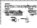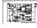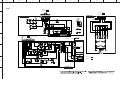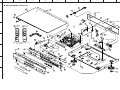
1
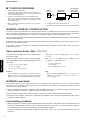
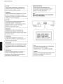
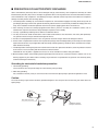
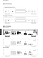
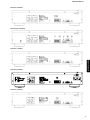
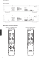
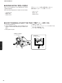
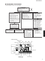
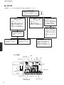
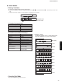
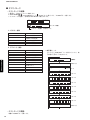
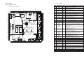
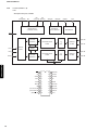
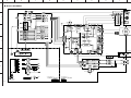
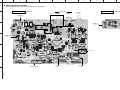
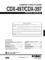
COMPACT DISC PLAYER CDX-497/CDX-397 SERVICE MANUAL IMPORTANT NOTICE This manual has been provided for the use of authorized YAMAHA Retailers and their service personnel. It has been assumed that basic service procedures inherent to the industry, and more specifically YAMAHA Products, are already known and understood by the users, and have therefore not been restated. WARNING: The data provided is believed to be accurate and applicable to the unit(s) indicated on the cover. The research, engineering, and service departments of YAMAHA are continually striving to improve YAMAHA products. Modifications are, therefore, inevitable and specifications are subject to change without notice or obligation to retrofit. Should any discrepancy appear to exist, please contact the distributor's Service Division. WARNING: Static discharges can destroy expensive components. Discharge any static electricity your body may have accumulated by grounding yourself to the ground buss in the unit (heavy gauge black wires connect to this buss). IMPORTANT: Turn the unit OFF during disassembly and part replacement. Recheck all work before you apply power to the unit. ■ CONTENTS TO SERVICE PERSONNEL ...................................... 2–4 PREVENTION OF ELECTROSTATIC DISCHARGE .... 5 FRONT PANELS ............................................................ 6 REAR PANELS .......................................................... 6–8 REMOTE CONTROL PANELS ...................................... 8 SPECIFICATIONS / 参考仕様 ........................................ 9 INTERNAL VIEW ........................................................... 9 REPAIR NOTES / 修理上の留意点 .............................. 10 HOW TO MANUALLY EJECT THE TRAY / 手動でトレーを開く方法 ........................................... 10 101016 DISASSEMBLY PROCEDURES / 分解手順 .......... 11–12 TEST MODE / テストモード .................................. 13–14 IC DATA ................................................................. 15–19 BLOCK DIAGRAM ....................................................... 20 WIRING DIAGRAM ...................................................... 21 PRINTED CIRCUIT BOARDS ................................ 22–24 SCHEMATIC DIAGRAMS ...................................... 25–26 REPLACEMENT PARTS LIST .............................. 28–29 REMOTE CONTROL .................................................... 30 2006 All rights reserved. This manual is copyrighted by YAMAHA and may not be copied or redistributed either in print or electronically without permission. P.O.Box 1, Hamamatsu, Japan '06.07 CDX-497/CDX-397 Failure to follow appropriate service and safety procedures when servicing this product may result in personal injury, destruction of expensive components, and failure of the product to perform as specified. For these reasons, we advise all YAMAHA product owners that any service required should be performed by an authorized YAMAHA Retailer or the appointed service representative. IMPORTANT: The presentation or sale of this manual to any individual or firm does not constitute authorization, certification or recognition of any applicable technical capabilities, or establish a principle-agent relationship of any form. CDX-497/CDX-397 ■ TO SERVICE PERSONNEL WALL OUTLET 1. Critical Components Information Components having special characteristics are marked s and must be replaced with parts having specifications equal to those originally installed. 2. Leakage Current Measurement (For 120V Models Only) When service has been completed, it is imperative to verify that all exposed conductive surfaces are properly insulated from supply circuits. ● Meter impedance should be equivalent to 1500 ohms shunted by 0.15µF. EQUIPMENT UNDER TEST AC LEAKAGE TESTER OR EQUIVALENT INSULATING TABLE ● Leakage current must not exceed 0.5mA. ● Be sure to test for leakage with the AC plug in both polarities. WARNING: CHEMICAL CONTENT NOTICE! The solder used in the production of this product contains LEAD. In addition, other electrical/electronic and/or plastic (where applicable) components may also contain traces of chemicals found by the California Health and Welfare Agency (and possibly other entities) to cause cancer and/or birth defects or other reproductive harm. DO NOT PLACE SOLDER, ELECTRICAL/ELECTRONIC OR PLASTIC COMPONENTS IN YOUR MOUTH FOR ANY REASON WHATSOEVER! Avoid prolonged, unprotected contact between solder and your skin! When soldering, do not inhale solder fumes or expose eyes to solder/flux vapor! If you come in contact with solder or components located inside the enclosure of this product, wash your hands before handling food. CDX-497/CDX-397 About Lead Free Solder / 無鉛ハンダについて All of the P.C.B.s installed in this unit are soldered using the lead free solder. 本機に搭載されているすべての基板は無鉛ハンダでハンダ付けさ れています。 Among some types of lead free solder currently available, it is recommended to use one of the following types for the repair work. 無鉛ハンダにはいくつかの種類がありますが、修理時には下記の ような無鉛ハンダの使用を推奨します。 • Sn + Ag + Cu (tin + silver + copper) • Sn + Cu (tin + copper) • Sn + Zn + Bi (tin + zinc + bismuth) Caution: As the melting point temperature of the lead free solder is about 30°C to 40°C (50°F to 70°F) higher than that of the lead solder, be sure to use a soldering iron suitable to each solder. ・Sn+Ag+Cu(錫+銀+銅) ・Sn+Cu(錫+銅) ・Sn+Zn+Bi(錫+亜鉛+ビスマス) 注意: 無鉛ハンダの融点温度は通常の鉛入りハンダに比べ30∼40 ℃程度高くなっていますので、それぞれのハンダに合ったハン ダごてをご使用ください。 WARNING: Laser Safety This product contains a laser beam component. This component may emit invisible, as well as visible radiation, which may cause eye damage. To protect your eyes and skin from laser radiation, the following precautions must be used during servicing of the unit. 1) When testing and/or repairing any component within the product, keep your eyes and skin more than 30 cm away from the laser pick-up unit at all times. Do not stare at the laser beam at any time. 2) Do not attempt to readjust, disassemble or repair the laser pick-up, unless noted elsewhere in this manual. 3) CAUTION: Use of controls, adjustments or performance of procedures other than those specified herein may result in hazardous radiation exposure. Laser Emitting conditions: 1) When the top cover is removed, and the “STANDBY/ON” SW is turned to the “ON” position, the laser component will emit a beam for several seconds to detect if a disc is present. During this time (5-10 sec.) the laser may radiate through the lens of the laser pick-up unit. Do not attempt any servicing during this period! If no disc is detected, the laser will stop emitting the beam. When a disc is set, you will not be exposed to any laser emissions. 2 CDX-497/CDX-397 2) The laser power level can be adjusted with the VR on the pick-up PWB. However, this level has been set by the factory prior to shipping from the factory. Do not adjust this laser level control unless instruction is provided elsewhere in this manual. Adjustment of this control can increase the laser emission level from the device. Laser Diode Properties Material: Wavelength: Emission duration: Laser output: GaAlAs 780 nm continuous max. 44.6 µW * * This output is the value measured at a distance of about 200 mm from the objective lens surface on the Optical Pick-up Block. Optical Pick-up WARNING CDX-497/CDX-397 3 CDX-497/CDX-397 CDX-497/CDX-397 4 CDX-497/CDX-397 ■ PREVENTION OF ELECTROSTATIC DISCHARGE Some semiconductor (solid state) devices can be damaged easily by static electricity. Such components commonly are called Electrostatically Sensitive (ES) Devices. Examples of typical ES devices are integrated circuits and some field-effect transistors and semiconductor “chip” components. The following techniques should be used to help reduce the incidence of component damage caused by electro static discharge (ESD). 1. Immediately before handling any semiconductor component or semiconductor-equipped assembly, drain off any ESD on your body by touching a known earth ground. Alternatively, obtain and wear a commercially available discharging ESD wrist strap, which should be removed for potential shock reasons prior to applying power to the unit under test. 2. After removing an electrical assembly equipped with ES devices, place the assembly on a conductive surface such as aluminum foil, to prevent electrostatic charge buildup or exposure of the assembly. 3. Use only a grounded-tip soldering iron to solder or unsolder ES devices. 4. Use only an anti-static solder removal device. Some solder removal devices not classified as “anti-static (ESD protected)” can generate electrical charge sufficient to damage ES devices. 5. Do not use freon-propelled chemicals. These can generate electrical charges sufficient to damage ES devices. 6. Do not remove a replacement ES device from its protective package until immediately before you are ready to install it. (Most replacement ES devices are packaged with leads electrically shorted together by conductive foam, aluminum foil or comparable conductive material). 7. Immediately before removing the protective material from the leads of a replacement ES divice, touch the protective material to the chassis or circuit assembly into which the device will be installed. CAUTION: Be sure no power is applied to the chassis or circuit, and observe all other safety precautions. 8. Minimize bodily motions when handling unpackaged replacement ES devices. (Otherwise harmless motion such as the brushing together of your clothes fabric or the lifting of your foot from a carpeted floor can generate static electricity (ESD) sufficient to damage an ES device). Grounding for electrostatic breakdown prevention CDX-497/CDX-397 1. Human body grounding. Use the antistatic wrist strap to discharge the static electricity from your body. 2. Work table grounding. Put a conductive material (sheet) or steel sheet on the area where the optical pickup is placed and ground the sheet. Caution: The static electricity of your clothes will not be grounded through the wrist strap. So take care not to let your clothes touch the optical pickup. Anti-static wrist strap 1M-ohms Conductive material (sheet) or steel sheet 5 CDX-497/CDX-397 ■ FRONT PANELS CDX-497 (R, T, K, A, B, G, J models) CDX-397 (R, T, A, B, G models) ■ REAR PANELS CDX-497/CDX-397 CDX-497 (R model) CDX-497 (T model) CDX-497 (K model) 6 CDX-497/CDX-397 CDX-497 (A model) CDX-497 (B, G models) CDX-497 (J model) CDX-497/CDX-397 CDX-397 (R model) CDX-397 (T model) 7 CDX-497/CDX-397 CDX-397 (A model) CDX-397 (B, G models) ■ REMOTE CONTROL PANELS CDX-497/CDX-397 CDX-497 (R, T, K, A, B, G, J models) 8 CDX-397 (R, T, A, B, G models) CDX-497/CDX-397 ■ SPECIFICATIONS / 参考仕様 ■ Audio Section / オーディオ部 Frequency Response / 周波数特性 . . . . . . . . . . . . . . . . . . . . . . . . . . . . . . . . 2 Hz to 20 kHz, ± 0.5 dB Total Harmonic Distortion + Noise (1 kHz) / 高調波歪率(1 kHz) . . . . . . . . . . . . . . . . . . . . . . . . . . . . . . . . . . . . . . . 0.003 % or less Signal to Noise Ratio / 信号対雑音比 . . . . . . . . . . . . . . . . . . . . . . . . . . . . . . . . . . . . . . . 105 dB or more Dynamic Range / ダイナミックレンジ . . . . . . . . . . . . . . . . . . . . . . . . . . . . . . . . . . . . . . . . 95 dB or more Output Voltage (1 kHz, 0 dB) / 出力電圧(1 kHz、0 dB) . . . . . . . . . . . . . . . . . . . . . . . . . . . . . . . . . . . . . . . . . . . 2.0 ± 0.5 V Headphone Output (-20 dB) / ヘッドフォン出力電圧(-20 dB) [CDX-497 model] . . . . . . . . . . . . . . . . . . . . . . . . . . . . . . . . . 750 ± 100 mV/32 ohms Accessories / 付属品 Remote control x 1, Batteries x 2, Audio pin cable (1.5 m) x 1 * Specifications are subject to change without notice due to product improvements. ※ 参考仕様および外観は予告なく変更されることがあります。 R .......... General model T ....... Chinese model K .......... Korean model A ...... Australian model B .......... British model G ...... European model J ........... Japanese model 287 (11-5/16") 87 (3-7/16") 276 (10-7/8") 70 4 (2-3/4") (3/16") 17 (11/16") 435 (17-1/8") CDX-497/CDX-397 Power Supply / 電源電圧 R model ..................................... AC 110-120/220-240 V, 50/60 Hz T model ................................................................. AC 220 V, 50 Hz K model ................................................................. AC 220 V, 60 Hz A model ................................................................. AC 240 V, 50 Hz B, G models .................................................. AC 220-240 V, 50 Hz J model ............................................................ AC 100V, 50/60 Hz Power Consumption / 消費電力 . . . . . . . . . . . . . . . . . . . . . . . . . . . . . . . . . . . . . . . . . . . . . . . 13 W Dimensions (W x H x D) / 寸法(幅×高さ×奥行き) . . . . . . . . . . . . 435 x 87 x 287 mm (17-1/8" x 3-7/16" x 11-5/16") Weight / 質量 . . . . . . . . . . . . . . . . . . . . . . . . . . . . . . . . . . . 3.5 kg (7 lbs. 11 oz) Finish / 仕上げ [CDX-497] Gold color ................................................................ T, K, J models Black color .............................................................. R, A, G models Titanium color ......................................................... R, B, G models [CDX-397] Gold color ........................................................................... T model Black color .......................................................... R, T, A, G models Titanium color ......................................................... R, B, G models 7 (1/4") • DIMENSIONS ■ General / 総合 Unit: mm (inch) 単位:mm(インチ) ■ INTERNAL VIEW 1 2 3 4 5 1 FRONT (5) P.C.B. (R model) 2 FRONT (2) P.C.B. 3 CD Mechanism 4 MAIN (2) P.C.B. 5 MAIN (1) P.C.B. 6 FRONT (4) P.C.B. 7 FRONT (3) P.C.B. (CDX-497 model) 8 FRONT (1) P.C.B. 6 7 8 9 CDX-497/CDX-397 ■ REPAIR NOTES / 修理上の留意点 None of the components of the following unit can be supplied separately. Each unit must be replaced as a whole in case of a failure. 下記のユニットは、小部品の部品供給はできません。 故障の場合は、各ユニットを交換してください。 ・ CDメカニズム ・ MAIN P.C.B. ・ FRONT P.C.B. • CD Mechanism • MAIN P.C.B. • FRONT P.C.B. ■ HOW TO MANUALLY EJECT THE TRAY / 手動でトレーを開く方法 a. Turn the unit bottom up. b. Using a flatblade screwdriver, turn the loading cam 90 degrees in the direction indicated by an arrow in the figure. c. Gently pull the tray out. CDX-497/CDX-397 Flatblade screwdriver マイナスドライバー Tray トレー 10 a. 本機を上下反転します。 b. マイナスドライバーでローディングカムを図に示す矢 印の方向に90度回転します。 c. トレーをそっと引き出します。 Loading cam ローディングカム Tray トレー CDX-497/CDX-397 ■ DISASSEMBLY PROCEDURES See REPLACEMENT PARTS LIST for item numbers. Top Cabinet [25] Mounting → Remove 2 screws. [61] (2 on side) → Remove 4 screws. [60] (4 on rear side) → Lift top cabinet from rear side to remove. Dismounting Front Panel Ass'y → Open tray. (See "HOW TO MANUALLY EJECT THE TRAY") → Unlock tray lid and close tray. → Remove CN42, CN52 and CN71. → Remove 2 screws. [52] (Front panel ass'y to side frame) → Remove 4 screws. [51] (Front panel ass'y to bottom frame) → Unlock front panel ass'y from frame by releasing successively 2 snaps. (2 on the side) → Remove front panel ass'y. CD Mechanism [38] → Open tray. (See "HOW TO MANUALLY EJECT THE TRAY") → Unlock tray lid and close tray. → Remove CN21-23. → Remove 4 screws. [57] (CD mechanism to bottom frame) → Remove CD mechanism. MAIN (1) P.C.B. [35 (1)] → Remove CN21-23, CN41 (MAIN (1) P.C.B.) and CN44. → Remove 2 screws. [56] (P.C.B. to bottom frame) → Remove 1 screw. [59] (P.C.B. to rear panel) → Remove 3 screws (CDX-497), 2 screws (CDX-397). [58] (P.C.B. to rear panel) → Remove MAIN (1) P.C.B.. FRONT (3) P.C.B. [31 (3)] (CDX-497 model) → Remove 1 screws. [54] (P.C.B. to front panel ass'y) → Remove FRONT(3) P.C.B.. FRONT (4) P.C.B. [31 (4)] → Remove 2 screws. [53] (P.C.B. to front panel ass'y) → Remove FRONT (4) P.C.B.. FRONT (2) P.C.B. [31 (2)] → Remove CN41 (FRONT (2) P.C.B.), CN41(MAIN P.C.B.) and CN44. → Remove CN43. (R model) (P.C.B. to rear panel) → Remove 1 screws. [56] (P.C.B. to bottom frame) → Remove 3 screws. [55] (P.C.B. to bottom frame) FRONT (5) P.C.B. [31 (5)] (R model) → Remove CN43. → Remove 2 screws. [53] (P.C.B. to rear panel) → Remove FRONT (5) P.C.B.. CDX-497/CDX-397 FRONT (1) P.C.B. [31 (1)] → Remove 1 screws. [53] (P.C.B. to front panel ass'y) → Remove FRONT (1) P.C.B.. MAIN (2) P.C.B. [35 (2)] → Remove 1 screw. [59] (P.C.B. to rear panel) → Remove MAIN (2) P.C.B. which is connected directly to the lower P.C.B. with connectors. • Cable Connections FRONT (5) P.C.B. (R model) CN44 CN23 CN71 CN41 (MAIN (1) P.C.B.) CN21 CN22 FRONT (2) P.C.B. CN43 (R model) CN52 FRONT (2) P.C.B. A CN42 CD Mechanism CN41 (FRONT (2) P.C.B.) View A FRONT (4) P.C.B. FRONT (1) P.C.B. FRONT (3) P.C.B. (CDX-497 model) Front Panel A'ssy 11 CDX-497/CDX-397 ■ 分解手順 項目番号については、REPLACEMENT PARTS LISTを参照してください。 トップカバー[25] → 側面のネジ[61]2本を外します。 → リア面のネジ[60]4本を外します。 → トップカバーを後ろ側から上げて取り 外します。 フロントパネルASS'Y → トレーを開きます。(“手動で トレーを開く方法”参照) → トレーリッドを外し、トレーを 閉じます。 → CN42、CN52、CN71を外します。 → 側面のネジ[52]2本を外します。 → 底面のネジ[51]4本を外します。 → 側面のスナップ2ヶ所を外して、 フロントパネルASS'Yを取り外し ます。 Mounting Dismounting CDメカニズム[38] → トレーを開きます。(“手動で トレーを開く方法”参照) → トレーリッドを外し、トレーを 閉じます。 → CN21-23を外します。 → 底面のネジ[57]4本を外します。 → CDメカニズムを取り外します。 MAIN(1)P.C.B.[35(1)] → CN21-23、CN41(MAIN(1) P.C.B.)、CN44を外します。 → リア面のネジ[59]1本を外 します。 → リア面のネジ[58]3本を外 します。 → MAIN(1)P.C.B.を取り外し ます。 FRONT(3)P.C.B.[31(3)] → ネジ[54]1本を外します。 → FRONT(3)P.C.B.を取り外 します。 CDX-497/CDX-397 FRONT(1)P.C.B.[31(1)] → ネジ[53]1本を外します。 → FRONT(1)P.C.B.を取り 外します。 MAIN(2)P.C.B.[35(2)] → リア面のネジ[59]1本を外 します。 → MAIN(2)P.C.B.を取り外しま す。但し、MAIN(2)P.C.B.は 下方のP.C.B.と直接コネク ター接続されています。 FRONT(2)P.C.B.[31(2)] → CN41(FRONT(2)P.C.B.)、CN41 (MAIN P.C.B.)CN44を外します。 → 底面のネジ[56]1本を外します。 → 底面のネジ[55]3本を外します。 → FRONT(2)P.C.B.を取り外します。 FRONT(4)P.C.B.[31(4)] → ネジ[53]1本を外します。 → FRONT(4)P.C.B.を取り 外します。 ・ コネクタ配置図 CN44 CN41 (MAIN (1) P. C. B.) CN23 CN21 FRONT (2) P. C. B. CN71 CN22 CN43 (R model) CN52 FRONT (2) P. C. B. A CN42 CD Mechanism CN41 (FRONT (2) P. C. B.) View A FRONT (4) P. C. B. FRONT (1) P. C. B. FRONT (3) P. C. B. (CDX-497 model) 12 Front Panel A'ssy CDX-497/CDX-397 ■ TEST MODE • Starting Test Mode a. Connect the power cable to the AC power outlet. W / D ” (PLAY/PAUSE) and “A A ” (STOP) keys of the main b. Press the “POWER” key while simultaneously pressing “W unit. c. When in the TEST mode, the “TEST MODE” is displayed for 2 seconds. 2 seconds Starting TEST mode This part is always displayed when in the TEST mode. 1. Function list of panel keys. Panel key F (OPEN/CLOSE) W / D (PLAY/PAUSE) A (STOP) T / E (SKIP-/SEARCH-) R / Y (SKIP+/SEARCH+) Function Tray open/close. Playback/Pause. Stop. Move traverse reverse. Move traverse forward. 2. Function list of remote control keys. Panel key TIME/INFO SPACE RANDOM OUTPUT LEVEL + OUTPUT LEVEL - Function Tray open/close. Playback. Pause. Stop. Move traverse reverse. Move traverse forward. Check FL display. (*1) EEPROM write/read test. Spindle servo on/off. Output level up. (CDX-497 model) Output level down. (CDX-497 model) *1 Check FL display The display condition varies as shown below according to the “TIME/INFO” key of the remote control. Initial display CDX-497/CDX-397 F (OPEN/CLOSE) W (PLAY) D (PAUSE) A (STOP) T (SKIP-) Y (SKIP+) Icon (left) Icon (right) Pattern 1 Pattern 2 Pattern 3 Pattern 4 Pattern 5 Pattern 6 Pattern 7 Icon (left) • Canceling Test Mode Press the “POWER” key of the main unit. 13 CDX-497/CDX-397 ■ テストモード ・ テストモードの起動 a. 電源コードをACコンセントに接続します。 W / D” b. 同時に本機の“W (PLAY/PAUSE)キーと“A (STOP)キーを押しながら、“POWER”キーを押します。 A” c. テストモードが起動し、約2秒間“TEST MODE”が表示されます。 2秒後 テストモード起動 テストモード起動中、常時表示します。 1. パネルキー操作 パネルキー 機能 トレイ オープン/クローズ 再生(DISC挿入時)/ W / D(PLAY/PAUSE) 一時停止(DISC再生時) A(STOP) 停止(DISC再生時) T / E(SKIP-/SEARCH-) トラバース内周移動 R / Y(SKIP+/SEARCH+) トラバース外周移動 F(OPEN/CLOSE) 2. リモコンキー操作 パネルキー CDX-497/CDX-397 F(OPEN/CLOSE) W(PLAY) D(PAUSE) A(STOP) T(SKIP-) Y(SKIP+) TIME/INFO SPACE RANDOM OUTPUT LEVEL + OUTPUT LEVEL - 機能 トレイ オープン・クローズ 再生(DISC挿入時) 一時停止(DISC再生時) 停止(DISC再生時) トラバース内周移動 トラバース外周移動 表示器チェック(*1) EEPROM書き込み/ 読み取りテスト スピンドルサーボオン/オフ 出力レベルを上げる 出力レベルを下げる *1 表示器チェック リモコンの“TIME/INFO”キーを押すことにより、表 示状態が下記のように変わります。 初期表示 DISCタイプ モード パターン1 パターン2 パターン3 パターン4 パターン5 パターン6 パターン7 DISCタイプ ・ テストモードの解除 本機の“POWER”キーを押します。 14 CDX-497/CDX-397 ■ IC DATA IC21 IC21 : TC94A54 (MAIN P.C.B) DSP : TC94A54 (MAIN P.C.B) DSP Pin No. 1 Pin name RFZI 2 3 AVSS3 RFRP 4 FEI 5 SBAD/RFDC 6 TEI 7 TEZI 8 9 AVDD3 FOO 10 TRO 11 VREF 12 FMO 13 DMO 14 SBSY (SPCK) 15 SBOK (FOK) (CLCK) (MBOV) O 3I/F IPF (SPDA) O 3I/F 17 SFSY (EMPH) (LOCK) (MONIT) O 3I/F 18 O 3I/F 19 ZDET (DATA) (COFS) GPIN 20 21 22 23 VSS1 VDD1 XVSS3 XI 24 XO 25 26 27 XVDD3 DVSS3 RO 28 DVDD3 I/O 3I/F – – – I 3AI/F O 3AI/F – – O 3AI/F – 29 DVR O 30 LO 31 32 33 DVSS3 VSS3 VDD3 O 3AI/F – – – DVSS3 26 RO 27 DVDD3 28 DVR 29 LO 30 DVSS3 31 VSS3 32 VDD3 33 XVDD3 XO XI XVSS3 VDD1 VSS1S GPIN ZDET SFSY IPF SBOK SBSY DMO PMO VREF TRO FOO AVDD3 TEZI TEI SBAD/RFDC FEI RFRP AVSS3 RFZI * No replacement part available. 25 24 23 22 21 20 19 18 17 16 15 14 13 12 11 10 9 8 7 6 5 4 3 2 1 CLOCK GEN ANA LPF SUBCODE DEMOCULA TION CDRCUIT 1-bit DAC 10-bit SAR ADC 5-bit R-2R DAC PWM 100 FTE 99 TNI 98 TPI 97 FPI1 96 FPI2 95 PNI1 94 PNI2 93 RVSS3 TE FE 34 VSS1S 35 BUS0 36 BUS1 37 BUS2 38 BUS3 39 BUCK 40 /CCE 41 /RST 42 ROM 43 VDDT 44 FGIN 45 MDI DIGITAL EQ AUTO ADJ 91 LDO RF BLOCK 90 RVDD3 89 CPU I/F ADRRESS CIRCUIT RF PULL-UP STBY 92 APC RAN CORRECTION CIRCUIT VDDM SERVO CONTROL CAV SERVO CLV SERVO PNSEL 87 RFO 86 RFDC 16k RAM 88 AGC 46 IO1 47 TESTD 48 VSSP 49 83 82 SYNC SIGNAL PROTECTION EFM DEMODULATION O 3AI/F O 3AI/F O 3I/F Speed error/feed equalizer output pin. 81 80 79 RFEQ 78 RFRP 77 EFM SLICE 67 68 69 70 71 72 73 74 75 PVSS3 66 VCOREF AOUT 65 VCOF DOUT 64 LPFO PIO3 63 LPPN PIO2 62 TMAX PIO1 61 PDO PIO0 60 PVDD3 TESTC 59 AWRC 58 VSS1S 57 VDD1S 56 LRCKI 55 BCKI 54 AIN 53 BCKO 52 76 VCO LRCKO 51 PLL TMAX AWRC PVREF DIGITAL AUDIO OUT OUT 50 VDDP VCOI Description Input pin for the RF ripple zero-cross signal. 84 VRO IO0 16 85 I/O I 3AI/F – O 3AI/F O 3AI/F O 3AI/F O 3AI/F I 3AI/F – O 3AI/F O 3AI/F O 3AI/F Grounding pin for 3.3V analog circuits. RF ripple signal output pin. Remark To be connected to the RFRP via 0.033 uF. – – Focus error signal input pin. Subbeam addition signal input pin. Monitor pin for various signals. Tracking error signal input pin. Input pin for tracking error signal zero-cross. Supply voltage pin for 3.3V analog circuit. Forcus equalizer output pin. Tracking equalizer output pin. Analog reference supply voltage pin. Disc equalizer output pin. Pin for outputting the subcode block sync signal. It is “H” at position S1 when the subcode sync signal is detected. (CD Processor Status Read Clock (176.4 kHz) output) Pin for outputting the CRCC check result of a subcode Q data check. It is “H” when the check result is OK. (Focus OK signal) (Input/output pin for the clock used in reading the subcode P to W data.) (CD Buffer memory overflow output) Correction flag output pin. “H” if the AOUT pin outputs an uncorrectable symbol in C2 correction. (CD Processor Status signal output) Pin for outputting the playback frame sync signal. (Emphasis fiag output pin. ENPH on: “H”. EMPH off: “L”. The output polarity can be switched, using a command.) (LOCk signal) (Pin for monitoring signals in the DSP.) Output pin for zero detection flag for the 1-bit DAC. (Pin for outputting subcode P to W data) (Error Correstion Frame Clock 7.35 kHz output) General-purpose I/O (DSP) To be connected to the TEI via 0.033 uF. – – – Connected to the VRO and PVREF within the IC. To be connected 0.1 uF. PWM ternary output (AVDD3, GND, and VREF). “H” at S1 when Subcode Sync is detected. – – 7.35kHz (At this pin, flags in the DSP and PLL-circuit clock can be monitored, using microcontroller commands. The pin also outputs text data serially.) Valid also for 1-bit DAC external inputs. 1.5V grounding pin dedicated to the Digital circuit. 1.5V supply voltage pin dedicated to the Digital circuit. Grounding pin for the system clock oscillation circuit. Input pin for the system clock oscillation circuit. General-purpose I/O (input after a reset). – – – – Output pin for the system clock oscillation circuit. Input to the internal MCK. – 3.3V supply voltage pin for the system clock oscillation circuit. – Grounding pin for the 1-bit DAC. No capacitor is required at the Output pin for normal R-channel data for the 1-bit DAC. DVR pin unless the built-in 1-bit DAC is used. 3.3V supply voltage pin for the 1-bit DAC. 3.3V must be applied across the DVDD3 and DVSS3 pins, howReference voltage pin for the 1-bit DAC. ever. – Output pin for normal L-channel data for the 1-bit DAC. Grounding pin for the 1-bit DAC. 3.3V grounding pin dedicated to the I/F circuit 3.3V supply voltage pin dedicated to the I/F circuit. – – 15 CDX-497/CDX-397 IC21 16 : TC94A54 (MAIN P.C.B) DSP Pin No. 34 Pin name VDDM 35 36 VSS1 BUS0 37 BUS1 38 BUS2 39 BUS3 40 BUCK 41 /CCE 42 /RST 43 STBY 44 45 VDDT FGIN 46 IO0A (/HSO) IC21 Pin name Function 1.5V supply voltage pin dedicated to the DSP/1Mbit SRAM – circuit. 1.5V groundind pin dedicated to the DSP/1Mbit SRAM circuit. – I/O 3I/F I/O Data input/output pin for the microcontroller interface. 3I/F I/O 3I/F I/O 3I/F Clock input pin for the microcontroller interface. I 3I/F Chip enable signal input pin for the microcontroller interface. I BUS3 to BUS0 are active if this pin is “L”. 3I/F Reset signal input pin. The internal registers and servo section I registers are reset, respectively, when the reset signal is “L” 3I/F and on the positive-going edge of the reset signal. STANDBY control pin dedicated to the DSP/1Mbit SRAM I circuit. 3I/F 3.3V supply voltage pin dedicated to the Digital I/O circuit. – FG signal input pin for CAV. I CLV: “L”. CAV: FG input. 3AI/F Genelal-purpose input/output pins. I/O (Pin for outputting the playback speed mode flag.) 3I/F 47 IO1A (/UHSO) I/O 3I/F 48 TESTD 49 50 VSSP VCOI 51 52 VDDP TESTC 53 PIO0 54 PIO1 55 PIO2 56 PIO3 57 DOUT 58 AOUT 59 BCK 60 LRCK I 3I/F – O 1.5AI/F – I 3I/F I/O 3I/F I/O 3I/F I/O 3I/F I/O 3I/F O 3I/F O 3I/F O 3I/F O 3I/F 61 AIN 62 BCKI 63 LRCKI 64 65 66 VDD1 VSS1 AWRC 67 68 PVDD3 PDO 69 TMAX I 3I/F I 3I/F I 3I/F – – O 3AI/F – O 3AI/F O 3AI/F : TC94A54 (MAIN P.C.B) DSP Remark – Pin No. 70 Pin name LPFN – 71 LPFO 72 PVREF 73 VCOF 74 VCOREF 75 76 PVSS3 SLCO 77 RFI 78 RFRPI 79 RFEQO 80 RESIN 81 VRO 82 83 VMDIR TESTR 84 INVSEL 85 AGCI 86 AGCI 87 RFO 88 PNSEL General-purpose I/O (DSP) 89 EQSET Digital-out output pin. Digital data for up to double speed can As per CP-1201 be output when a frequency of 16.9344 MHz is used. – Audio data output pin. Which bit is first (MSB first or LSB first) can be selected, using a command. Bit clock output pin. 32fs, 48fs, and 64fs can be selected, Normal speed: 32fs = 1.4112 MHz using a command. LR channel clock output pin. L for the L-channel and “H” for the R-channel. The output polarity can be inverted, using a Normal speed: 44.1kHz command. 1-bit DAC external input: AIN 90 91 RVDD3 LDO 92 MDI 93 94 RVSS3 FNI2 95 FNI1 96 FPI2 97 FPI1 98 TPI 99 TNI 100 FTE To be fixed at “H” or “L” when communication is not in progress, so that the pin will not become HiZ. To be fixed at “H” when communication is not in progress, so that the pin will not become HiZ. To be connected to 0.1 uF. – – – Genelal-purpose I/O (input after a reset). The playback speed mode flag output can be switched, using command bits. DSP/Test input pin. Usually fixed at “L”. – 1.5V grounding pin dedicated to the DSP/VCO circuit. PD output pin dedicated to the DSP/VCO circuit. – – 1.5V supply voltage pin dedicated to the DSP/VCO circuit. CD/Test input pin. Usually fixed at “L”. – – General-purpose I/O (CD/DSP) I/O I 3AI/F O 3AI/F – O 3AI/F I 3AI/F – O 3AI/F I 3AI/F I 3AI/F O 3AI/F Description Remark Pin for receiving an inverted output of the PLL-circuit low-pass The resistance side is connected. filter amp. See an applicable circuit diagram. Pin for the PLL-circuit low-pass filter amp output. The capacitor side is connected. See an spplicable circuit diagram. 1.65V reference supply voltage pin dedicated to the PLL Connected to the VREF and PVREF circuit. within the IC. A 0.1 uF capacitor is connected. VCO filter pin. – Input pin for the VCO center frequency reference level. To be connected to the PVREF if the AWRC is not used. 3.3V grounding pin dedicated to the PLL circit. – EFM slice level output pin. A capacitor to be connected is seFor both analog and digital slice modes, the output impedance lected according to the servo op= 2.5 k-ohms. eration band. RF signal input pin. Zin: 20 k-ohms, 10 k-ohms, 5 kThe input resistance can be selected, using a command. ohms RF ripple signal input pin. – RF equalizer circuit output pin. I 3AI/F O 3AI/F Pin for connecting a reference current generating resistance. – O 3AI/F I 3AI/F I 3AI/F I 3AI/F O 3AI/F Reference voltage poutput pin for the APC circuit. LPF pin for RFEQO offset correction. I 3AI/F O 3AI/F – O 3AI/F I 3AI/F – I 3AI/F I 3AI/F I 3AI/F I 3AI/F I 3AI/F I 3AI/F O 3AI/F Test pin, usually fixed at “H”. 1.65V reference voltage output pin. Test pin, usually fixed at “L”. Pin for RF signal amplitude adjustment amp input. – RF signal peak detsction input pin. – RF signal generation amp output pin. General-purpose I/O (CD/DSP) General-purpose I/O (DSP) 1-bit DAC external input: BCKI General-purpose I/O (input after a reset). 1-bit DAC external input 1-bit DAC external input: LRCKI 1.5V supply voltage pin dedicated to the DSP circuit. 1.5V grounding pin dedicated to the DSP circuit. VCO control pin for active wide range. Controllable in CLV/CAV. – 3.3V supply voltage pin dedicated to the PLL circuit. Pin for outputting a phase difference signal between the EFM Quaternary output (PVDD3, HiZ, VSS, and PVREF). signal and PLCK signal. Ternary output (PVDD3, VSS, and Pin for outputting the result of TMAX detection. Hiz). The TMAX pin output the same signal. To be connected to the RFRPI via 0.1 uF and to the RFI via 4700 pF or higher. To be connected to 22 k-ohms and 680 pF in parallel. Connected to the VREF and PVREF within the IC To be connected to 0.1uF anf 100 uF. To be connected to 0.1uF. To be connected to 0.015 uF or higher. – External connection pin for the RF signal equalizer. 3.3V supply voltage pin for the Rfamp core section. Laser diode amp output pin. Monitor photodiode amp input pin. 3.3V grounding pin for the RF amp core section. Main beam input pin. Connected to PIN diode C. Main beam input pin. Connected to PIN diode A. Main beam input pin. Connected to PIN diode D. Main beam input pin. Connected to PIN diode B. Subbeam input pin. Connected to PIN diode F. Subbeam input pin. Connected to PIN diode E. Focus /tracking signal output. (Test pin for servo characteristic measurement.) Note: “3AI/F : 3V circuit analog input/output pin.” “3I/F : 3V circuit digital input/output pin.” “1.5AI/F : 1.5V circuit analog input/output pin.” To be connected directly to the RFDCI. To ne connected to the AGCI via 0.1 uF. To be kept open when the RFEQ is used. – Reference to 178 mV (typ.) – – – – – – – Switchable using a command. CDX-497/CDX-397 IC22 : TA2125 (MAIN P.C.B) Motor driver * No replacement part available. VR RIN 4ch Driver FIN STB IN3 VCC REG IN4 STB RL4 RL3 REG OUT N.C. 36 35 34 Control Logic 33 32 31 STBY 30 29 28 FIN 27 26 25 24 23 22 STBY 21 20 19 x3 x3 x3 x3 x3 x3 x3 + x3 + lref TSD + 1 2 3 4 5 6 7 N.C. N.C. RL5 Symbol OUT5A VM OUT5B VCIN IN1 N.C. N.C. N.C. N.C. N.C. IN2 N.C. N.C. VCC1 OUT2M OUT2P OUT1M OUT1P OUT3P OUT3M OUT4P OUT4M VCC2 N.C. REG OUT REG OUT N.C. N.C. N.C. REG STBY IN4 IN3 STBY FIN RIN VR 9 FIN 10 11 GND VCIN IN1 12 13 14 15 16 17 18 N.C. N.C. IN2 RL2 RL1 Function Output terminal Supply voltage terminal for Logic Output terminal Input reference voltage Input for ch1 Open Open 8, 9, 10, 27, 28, 29 are connected to PW 8, 9, 10, 27, 28, 29 are connected to PW 8, 9, 10, 27, 28, 29 are connected to PW Input for ch2 Open Open Supply voltage terminal for ch 1/ch2 Inverted output for ch2 Non-inverted output for ch2 Inverted output for ch1 Non-inverted output for ch1 Non-inverted output for ch3 Inverted output for ch3 Non-inverted output for ch4 Inverted output for ch4 Supply voltage terminal for ch3/ch4 Open Connection with BASE of PNP Tr Output for regulator (5V) 8, 9, 10, 27, 28, 29 are connected to PW 8, 9, 10, 27, 28, 29 are connected to PW 8, 9, 10, 27, 28, 29 are connected to PW Standby control for regulator Input for ch4 Input for ch3 Standby control for 4ch BTL Logic control input Logic control input Supply voltage terminal for motor driver GND (FIN) GND (FIN) GND (FIN) GND (FIN) GND (FIN) GND (FIN) CDX-497/CDX-397 No. 1 2 3 4 5 6 7 8 9 10 11 12 13 14 15 16 17 18 19 20 21 22 23 24 25 26 27 28 29 30 31 32 33 34 35 36 8 H-bridge H-bridge H-bridge 4ch BTL 4ch BTL – – – – – 4ch BTL – – 4ch BTL 4ch BTL 4ch BTL 4ch BTL 4ch BTL 4ch BTL 4ch BTL 4ch BTL 4ch BTL 4ch BTL – Regulator Regulator – – – Regulator 4ch BTL 4ch BTL 4ch BTL H-bridge H-bridge H-bridge 17 CDX-497/CDX-397 IC71 : CS4392 (MAIN P.C.B) DAC * No replacement part available. M1 (SDA/CDIN) M3 M2 M0 (CL/CCLK) (AD0/CS) AMUTEC MODE SELECT (CONTROL PORT) BMUTEC EXTERNAL MUTE CONTROL CMOUT FILT+ REFERENCE RST VOLUME CONTROL SCLK SERIAL PORT AOUTA+ INTERPOLATION FILTER ∆∑ DAC ANALOG FILTER INTERPOLATION FILTER ∆∑ DAC ANALOG FILTER MIXER LRCK SDATA AOUTBVOLUME CONTROL CDX-497/CDX-397 MCLK RST 1 20 AMUTEC VL 2 19 AOUTA- SDATA 3 18 AOUTA+ SCLK 4 17 VA LRCK 5 16 AGND MCLK 6 15 AOUTB+ M3 7 14 AOUTB- (SCL/CCLK) M2 8 13 BMUTEC (SDA/CDIN) M1 9 12 CMOUT 10 11 FILT+ (AD0/CS) M0 18 AOUTA- AOUTB- CDX-497/CDX-397 IC71 : CS4392 (MAIN P.C.B) DAC No. 1 2 3 4 5 Symbol RST VL SDATA SCLK LRCK 6 11 12 20 13 14 15 18 19 16 17 MCLK FILT+ CMOUT AMUTEC BMUTEC AOUTBAOUTB+ AOUTA+ AOUTA AGND VA Function Reset (Input) - Powers down device and resets all intemal registers to their default settings. Logic Power (Input) - Positive power for the digital input/output. Serial Audio Data (Input) - Input for two’s complement serical audio data. Serial Clock (input/output) - Serial clock for the serial audio interface. Left Right Clock (Input/output) - Determines which channel, Left or Right, is currently active on the serial audio data line. Master Clock (Input) -Clock source for the delta-sigma moudukafor and digital filters. Positive Voltage Reference (Output) - Positive reference voltage for the intemal sampling circuits. Common Mode Voltage (Output) - Filter connection for internal quiescent voltage. Mute Control (output) - The Mute Confrol pin goes high during power-up initialization, reset, muting, power-down or if the master clock to left/right clock frequency ratio is incorrect. Differential Analog Output (Outputs) - The full scale differential analog output level is specified in the Analog Characteristics specification table. Ground (Input) Analog Power (Input) - Positive power for the analog section. Control Port mode Definitions No. 7 8 9 Symbol M3 SCL/CCLK SDA/CDIN 10 AD0/CS Function Mode Selection (Input) -This pins should be tied to GND level during control port mode. Serial Control Port Clock (input) - Serial clock for the serial control port. Serial Control Data (input/output) - SDA is a data l/O line in l2C mode.CDIN is the input data line for the control port interface in SPI mode. Address Bit 0 (I2C) / Control Port Chip Select (SPI) (Input/Output) - AD0 is a chip address pin in I2C mode, CS is the chip select signal for SPI format. Stand-Alone Mode Definitions No. 7 8 9 10 Symbol M3 M2 M1 M0 Function Mode Selection (Input) - Determines the operational mode of the device. 19 A B C D E F G H I J CDX-497/CDX-397 1 ■ BLOCK DIAGRAM X501 IC22 IC51 2 X201 IC21 CD Mechanism 3 4 COAXIAL 5 IC75 JK75 RS51 OPTICAL IC41 D401, 403 JK52 IC71 T401 IC74 IC42 JK73 D402, 404 R 6 IC43 IC44 D405, 406 IC72 IC45 Q401 7 AC IN POWER ON/OFF 20 • See page 26 → SCHEMATIC DIAGRAM FRONT • See page 25 → SCHEMATIC DIAGRAM MAIN LINE OUT IC73 L SW41 DIGITAL OUT CDX-497 model FL51 A B C D E F G H I J CDX-497/CDX-397 1 ■ WIRING DIAGRAM R model CDX-497 model FRONT (5) MAIN (2) VOLTAGE/SELECTOR MAIN (1) 1 2 13 +9V 1 AGND -9V P_MUTE PWR_ON +8V MGND VDD ST+5V FL+ FLVP FLT_ON 13 +9V AGND -9V P_MUTE PWR_ON +8V MGND VDD ST+5V FL+ FLVP FLT_ON (VP_ON) -9V 6 +9V -9V AGND +9V PWR_ON 1 CDX-497 model FRONT (2) Power Control FRONT (3) 1 ST+5V RX_CLK TX_CLK DATA_OUT DATA_IN RESET DGND 6 PH71 7 STBY–LED KEY2 KEY1 DGND DGND ST+5V VFD–DI VFD–CLK VFD–CE VFD–RST REMO FLVP FL+ VDD 1 -9V +9V AGND HP-R AGND HP-L AGND CD–LIMIT–SW MGND SLED+ 1 SLED- 5 SPINDLE- CD–CLOSE–SW 15 SPINDLE+ 1 CD–OPEN–SW 16 LOADING+ 2 MGND 3 LOADING- FCSTRKTRK+ FCS+ LD PD LD VR LD LD PDIC GND PDIC F PDIC C PDIC B PDIC A PDIC D PDIC E PDIC VCC PDIC VC Phones 1 2 15 1 14 GND HP-L GND HP-R GND V+ VMUTE_L MUTE_R 9 1 7 PHONES 4 AC IN 5 CD Machanism FRONT (4) FL51 RS51 2 15 1 14 NC KEY2 KEY1 GND GND ST+5V VFD–DI VFD–CLK VFD–CE VFD–RST REMO FLVP FL+ NC 6 FRONT (1) Display and key's 7 POWER ON/OFF 21 A B C D E F G H I J CDX-497/CDX-397 1 ■ PRINTED CIRCUIT BOARDS FOR INFORMATION ONLY (NO SERVICE PARTS WILL BE AVAILABLE) MAIN (1) P.C.B. DIGITAL OUT (Top view) CDX-497 model COAXIAL MAIN (2) P.C.B. OPTICAL LINE OUT L/R MAIN (2) 2 (CN43) MAIN (1) (CN42) 3 FRONT (2) (CN41) 4 5 CDX-497 model 6 CDX-497 model CD Mechanism 7 22 FRONT (3) FRONT (1) (BN71) (BN52) (Top view) A B C D E F G H I J CDX-497/CDX-397 1 MAIN (1) P.C.B. (Bottom view) MAIN (2) P.C.B. (Bottom view) 2 3 4 5 6 CDX-497 model 7 23 A B C D E F G H I CDX-497/CDX-397 1 FRONT (1) P.C.B. (Top view) MAIN (1) (CN52) 2 3 FRONT (2) P.C.B. FRONT (3) P.C.B. (Top view) CDX-497 model FRONT (4) (BN42) R PHONES L MAIN (1) FRONT (5) (BN43) 4 (CN41) (R model) T, K, A, B, G, J models 5 R model MAIN (1) POWER ON/OFF (CN71) FRONT (5) P.C.B. (Top view) R model FRONT (4) P.C.B. 6 220-240 VOLTS FRONT (2) (CN43) (Top view) VOLTAGE SELECTOR 110-120 VOLTS FRONT (2) (CN42) 7 24 (Top view) J A B C D E F G H I J CDX-497/CDX-397 1 ■ SCHEMATIC DIAGRAMS FOR INFORMATION ONLY (NO SERVICE PARTS WILL BE AVAILABLE) MAIN To CD Machanism MAIN (1) MAIN (2) 2 To CD Machanism 3 To CD Machanism OPTICAL DIGITAL OUT CDX-497 model 4 COAXIAL 5 L R AUDIO OUT CDX-497 model 6 Page 26 H2 to FRONT (3)_BN71 Page 26 D2 to FRONT (1)_CN52 Page 26 B4 to FRONT (2)_CN41 7 25 A B C D E F G H I CDX-497/CDX-397 1 FRONT Page 25 B7 to MAIN (1)_CN52 Page 25 H6 to MAIN (1)_CN71 2 FRONT (3) FRONT (1) CDX-497 model 3 Page 25 C7 to MAIN (1)_CB41 AC IN 4 T, K, A, B, G, J models FRONT (4) POWER ON/OFF 5 FRONT (5) PHONES R model 220-240 VOLTS VOLTAGE SELECTOR 110-120 VOLTS R model 6 FRONT (2) 7 26 J CDX-497/CDX-397 MEMO MEMO MEMO MEMO 27 A B C D E F G H I J CDX-497/CDX-397 1 ■ REPLACEMENT PARTS LIST 39 25 60 9 53 R model 61 2 24 59 58 CDX-497 model 31 (5) 3 200 CDX-497 201 CDX-397 model model 55 56 R model 58 57 202 38 57 35 (2) 38-1 31 (2) 53 4 31 (4) 61 72 56 CDX-497 model 54 Note) The replacement battery cover is not available. 31 (3) 51 5 CDX-497 model 52 3 35 (1) 53 71 31 (1) 6 6 51 7 55 6 52 2 7 4 21 1 28 5 7 CDX-497/CDX-397 WARNING ● Components having special characteristics are marked s and must be replaced with parts having specifications equal to those originally installed. ● s印のある部分は、安全確保部品を示しています。部品の交換が必要な場合、パーツリストに記載されている部品を使用してください。 ● 部品価格ランクは、予告なく変更することがあります。 Ref. No. Part No. * * * * * * * * * * * * * * * * * * * * * * * * * * * * * * * * * * * * * * * * s s s s s s s * s s * s s * * * * * * * * * * 1 2 3 3 3 4 4 4 5 5 5 6 6 7 9 21 21 21 21 21 21 24 24 24 24 24 24 24 24 24 24 25 25 25 31 31 31 31 35 35 38 38-1 39 39 39 39 39 39 39 51 51 52 53 54 55 56 57 58 59 AAX78150 AAX78160 AAX78350 AAX78360 AAX78340 AAX78270 AAX78250 AAX78260 AAX78300 AAX78280 AAX78290 AAX78660 AAX78650 AAX76760 AAX73380 AAX78470 AAX78480 AAX78490 AAX78440 AAX78450 AAX78460 AAX78590 AAX78620 AAX78580 AAX78570 AAX78600 AAX78610 AAX78560 AAX78530 AAX78540 AAX78550 AAX78320 AAX78320 AAX78330 AAX78170 AAX78180 AAX78190 AAX78200 AAX78210 AAX78220 AAX78140 AAX78500 AAX74330 AAX74340 AAX74350 AAX78680 AAX74360 AAX78690 AAX74310 AAX78510 AAX78520 AAX78670 AAX78410 AAX78240 AAX78430 AAX78390 AAX78420 AAX78400 AAX78370 Description FL WINDOW FL SHEET TRAY LID (DOOR ORNAMENT) TRAY LID (DOOR ORNAMENT) TRAY LID (DOOR ORNAMENT) ESCUTCHEON (BUSHING) ESCUTCHEON (BUSHING) ESCUTCHEON (BUSHING) SUB PANEL SUB PANEL SUB PANEL FOOT FOOT CUSHION FOOT CABLE STOPPER FRONT PANEL FRONT PANEL FRONT PANEL FRONT PANEL FRONT PANEL FRONT PANEL REAR PANEL REAR PANEL REAR PANEL REAR PANEL REAR PANEL REAR PANEL REAR PANEL REAR PANEL REAR PANEL REAR PANEL TOP CABINET TOP CABINET TOP CABINET P.C.B. ASS'Y P.C.B. ASS'Y P.C.B. ASS'Y P.C.B. ASS'Y P.C.B. ASS'Y P.C.B. ASS'Y CD MECHANISM BELT POWER CABLE POWER CABLE POWER CABLE POWER CABLE POWER CABLE POWER CABLE POWER CABLE BIND HEAD BONDING SCREW BIND HEAD BONDING SCREW FLAT HEAD B-TIGHT SCREW BIND HEAD P-TIGHT SCREW PW HEAD P-TIGHT SCREW BIND HEAD SCREW BIND HEAD B-TIGHT SCREW BIND HEAD SCREW BIND HEAD P-TIGHT SCREW BIND HEAD B-TIGHT SCREW ✻ New Parts * 新規部品 GD BL TI GD BL TI GD BL TI GD BL, TI 497GD 497BL 497TI 397GD 397BL 397TI 497 497 497 497 497 497 397 397 397 397 GD BL TI 497 FRONT 497 FRONT 397 FRONT 397 FRONT 497 MAIN 397 MAIN 2m 2m 2m 2m 2m 2m 2m GD,TI 3x6 MFZN2W3 BL 3x6 MFZN2B3 3x6 MFZN2Y 3x10 MFZN2Y 3x10 MFZN2Y 4x6 MFZN2Y 3x8 MFZN2Y 3x6 MFZN2Y 3x10 MFZN2B3 3x6 MFZN2B3 Remarks CGU1A393Z CMZ1A117Z CGR1A400M9XH54 CGR1A400ZH53 CGR1A400M7YH55 CGR1A399M9D6 CGR1A399K128 CGR1A399M7G41 CGW1A422M9D6 CGW1A422K128 CGW1A422M7G41 CKL1A192H57 CKL1A192H56 CHG1A329 KHR1A028 CKM2A176ZC55 CKM2A176ZC59 CKM2A176ZC60 CKM1A176ZC55 CKM1A176ZC59 CKM1A176ZC60 CKF3A312T CKF4A312S CKF3A312R CKF3A312Q CKF3A312U CKF3A312V CKF2A312X CKF1A312W CKF1A312Y CKF1A312Z CKC1A173B11 CKC1A173B11 CKC1A173G40 COP11891B COP11891D COP11891F COP11891E COP11855B COP11855C CJDKSL2130CCMZ 9A07980900 CJA2J049ZA CJA2L072ZA CJA2N047ZA CJA2D073Y CJA2S048ZA CJA2E086ZA CJA2B043ZA CTBD3+6FFC CTBD3+6FFZR CTS3+6JR CTB3+10GR CTWS3+10GR CTB4+6FR CTB3+8JR CTB3+6FR CTB3+10GFZR CTB3+6JFZR Markets J R T K A BG R T A BG JTKABG R R TABG J R T K A B G 部 品 名 FLウィンドウ FLシート トレイLID トレイLID トレイLID エスカッション エスカッション エスカッション サブパネル サブパネル サブパネル 脚 脚 クッション 脚 コードストッパー フロントパネル フロントパネル フロントパネル フロントパネル フロントパネル フロントパネル リアパネル リアパネル リアパネル リアパネル リアパネル リアパネル リアパネル リアパネル リアパネル リアパネル トップカバー トップカバー トップカバー PCB フロント PCB フロント PCB フロント PCB フロント PCB メイン PCB メイン CDメカニズム ベルト 電源コード 電源コード 電源コード 電源コード 電源コード 電源コード 電源コード ボンディング小ネジ ボンディング小ネジ 皿Bタイトネジ バインドPタイトネジ PWヘッドPタイトネジ バインド小ネジ バインドBタイトネジ バインド小ネジ バインドPタイトネジ バインドBタイトネジ Rank Ref. No. Part No. Description Remarks * * * 60 60 61 61 71 72 AAX73500 AAX78380 AAX73930 AAX78230 AAX79920 AAX79910 BIND HEAD B-TIGHT SCREW BIND HEAD B-TIGHT SCREW PW HEAD B-TIGHT SCREW PW HEAD B-TIGHT SCREW FLEXIBLE FLAT CABLE FLEXIBLE FLAT CABLE GD,TI 3x8 BL 3x8 GD,TI 3x8 BL 3x8 15P 220mm 16P 140mm * * * 200 201 202 AAX78640 AAX78630 AAX78310 ACCESSORY REMOTE CONTROL REMOTE CONTROL AUDIO PIN CABLE BATTERY 497 397 2P 1.5m 1pc R03 2pcs * MFZN2W3 MFZN2B3 MFZN2W3 MFZN2B3 P=1mm P=1mm Markets 部 品 名 Rank CTB3+8JFC CTB3+8JFZR CTW3+8JFC CTW3+8JFZR CWC4F4A15A220A CWC4F2A16A140B バインドBタイトネジ バインドBタイトネジ PWヘッドBタイトネジ PWヘッドBタイトネジ カード電線 カード電線 01 CARTCDX497 CARTCDX397 CJS4N001Y 付属品 リモコン リモコン ステレオピンケーブル 単4乾電池 01 01 04 ✻ New Parts * 新規部品 29 CDX-497/CDX-397 ■ REMOTE CONTROL • PANELS CDX-497 (R, T, K, A, B, G, J models) • KEY CODE CDX-397 (R, T, A, B, G models) CDX-497 model 30 Key label Code OPEN/CLOSE 79-01 1 79-11 2 79-12 3 79-13 4 79-14 5 79-15 6 79-16 7 79-17 8 79-18 9 79-19 0 79-10 INDEX 79-0B DIMMER 79-1E RANDOM 79-1B REPEAT 79-08 REPEAT A-B 79-09 PROGRAM 79-0C CLEAR 79-0D SYNCHRO 79-58 TAPE 79-57 PEAK 79-5D SPACE 79-0F E SEARCH SEARCH R 79-05 PLAY 79-02 T SKIP SKIP Y 79-04 79-06 79-07 STOP 79-56 TIME/INFO 79-0A PAUSE 79-55 H FOLDER + 79-69 OUTPUT LEVEL + 79-1D Q FILE - 79-6C ENTER 79-3F W FILE + G FOLDER - 79-6B OUTPUT LEVEL - 79-1C 79-6A CDX-497/CDX-397