1
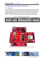
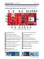
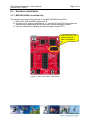
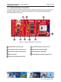
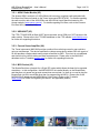
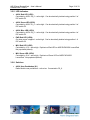
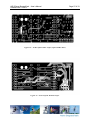
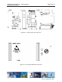
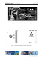
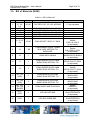
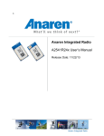
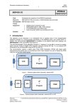
Anaren Integrated Radio AIR B-Smart BoosterPack User’s Manual A2541R24A-ADB1 A2541E24A-ADB1 Release Date 11/04/13 ii THIS PAGE LEFT INTENTIONALLY BLANK iii USER’S MANUAL AIR B-Smart BoosterPack Contents 1. AIR B-Smart BoosterPack Overview ............................................................................................................5 1.1. Overview ....................................................................................................................................................5 1.2. Kit Contents ...............................................................................................................................................6 2. Getting Started with the AIR B-Smart BoosterPack ...................................................................................7 2.1. Hardware Installation ............................................................................................................................... 8 2.1.1. MSP-EXP430G2 LaunchPad Only ....................................................................................................8 2.1.2. All LaunchPads ...................................................................................................................................9 2.1.3. Optional Hardware Components ...................................................................................................... 10 2.2. Emmoco Em-Ware Wiki ......................................................................................................................... 11 3. AIR B-Smart BoosterPack Hardware .......................................................................................................... 12 3.1. Electrical Characteristics ........................................................................................................................ 12 3.1.1. Absolute Maximum Ratings ............................................................................................................. 12 3.1.2. Recommended Operating Conditions ................................................................................................ 12 3.2. Functional Description ........................................................................................................................... 13 3.2.1. A2541 Radio Module (U2) ................................................................................................................ 14 3.2.2. USB-UART (U3) .............................................................................................................................. 14 3.2.3. Current Sense Amplifier (U4)........................................................................................................... 14 3.2.4. MCU Socket (X1).............................................................................................................................. 14 3.2.5. LED Indicators .................................................................................................................................. 15 3.2.6. Switches............................................................................................................................................. 15 3.2.7. Jumpers.............................................................................................................................................. 18 3.2.8. Connectors ......................................................................................................................................... 20 3.3. Schematics ................................................................................................................................................ 24 3.4. PCB Layout .............................................................................................................................................. 26 3.5. Bill of Materials (BOM) ........................................................................................................................... 30 iv THIS PAGE LEFT INTENTIONALLY BLANK AIR B-Smart BoosterPack – User’s Manual Release Date 11/04/13 Page 5 of 33 1. AIR B-Smart BoosterPack Overview 1.1. Overview The AIR B-Smart BoosterPack is a low-power wireless transceiver extension module compliant with the Texas Instruments BoosterPack Pinout Standard and compatible with 20-pin and 40-pin LaunchPad development kits. Refer to the Emmoco Em-Ware Wiki (see section 2.2) for more information regarding firmware availability for the various LaunchPad kits. The BoosterPack is available in two configurations, each of which contains an AIR radio module with integrated antenna. See Table 1 for a listing of the supported BoosterPacks and their operating bands. Table 1 - AIR B-Smart BoosterPack Models Model Module Operating Band Range Extender A2541R24A-ADB1 A2541R24A20 2402-2480MHz ISM Band No A2541E24A-ADB1 A2541E24A20 2402-2480MHz ISM Band Yes Figure 1 - AIR B-Smart BoosterPack with MSP-EXP430G2 LaunchPad AIR B-Smart BoosterPack – User’s Manual Release Date 11/04/13 Page 6 of 33 AIR B-Smart BoosterPack Hardware Features: 2.4GHz radio incorporating Bluetooth® Smart technology 2.0V to 3.6 V operation Low power consumption UART interface to Radio Module Analog Current Monitor Accessible Test Points for many of the Radio Module port pins 8 DIP Switches for isolating nonessential circuitry during low-power operation Option for installing 20-pin DIP socket + MSP430 microcontroller for standalone operation ROHS compliant See AIR Module Users Manual for radio specific features 1.2. Kit Contents The AIR B-Smart BoosterPack kit includes the following: One AIR B-Smart BoosterPack One USB 2.0 cable (A to Mini-B) One 6-wire B-Smart cable for connecting an external MCU Quick Start Guide Regulatory Guide AIR B-Smart BoosterPack – User’s Manual Release Date 11/04/13 Page 7 of 33 2. Getting Started with the AIR B-Smart BoosterPack The following sections describe the necessary steps to get the AIR B-Smart BoosterPack hardware and software up and running with the LaunchPad. 13 12 14 16 15 17 18 19 20 21 11 10 1 9 8 7 6 5 4 3 2 Figure 2 – AIR B-Smart BoosterPack Overview 1 AIR Radio Module (U2) 12 LaunchPad Interface Connector (J1) 2 External MCU Connector (J8) 13 Mini-B USB Connector (J6) 3 USB UART Disconnect DIP Switch (S3) 14 Power LED (LED4) 4 Radio Module Reset Pushbutton Switch (S6) 15 LED Disconnect DIP Switch (S2) 5 MCU UART RTS Selection Jumper (JP4) 16 LaunchPad Interface Connector (J2) 6 MCU UART CTS Selection Jumper (JP3) 17 Radio Module User Pushbutton Switch (S1) 7 Current Monitor Jumper (JP2) 18 DC-DC Conv ON/BYP Override Jumper (JP1) 8 Current Sense Amplifier Connector (J7) 19 Red Status LED (LED1) 9 Current Sense Amplifier (U4) 20 Green Status LED (LED2) 10 USB-UART Device (U3) 11 USB ESD Protection Device (U1) 21 Blue Status LED (LED3) AIR B-Smart BoosterPack – User’s Manual Release Date 11/04/13 Page 8 of 33 2.1. Hardware Installation 2.1.1. MSP-EXP430G2 LaunchPad Only The following steps need to be performed on the MSP-EXP430G2 LaunchPad: 1) Remove the TXD and RXD jumpers from J3. 2) Ensure the VCC jumper is populated on J3. Jumpers RST and TEST also need to be installed when programming the microcontroller or when debugging firmware. 3) Continue installation by following the steps provided in Section 2.1.2. UART RXD and TXD jumpers removed from LaunchPad J3. Figure 3 –MSP-EXP430G2 LaunchPad AIR B-Smart BoosterPack – User’s Manual Release Date 11/04/13 Page 9 of 33 2.1.2. All LaunchPads The following steps need to be performed on the LaunchPad/BoosterPack: 1) Install the AIR B-Smart BoosterPack onto the LaunchPad board. Ensure the BoosterPack is oriented correctly. With the LaunchPad emulator section at the top, the BoosterPack radio module should overhang at the right. Figure 4 shows an example of a BoosterPack installed on a MSP-EXP430G2 LaunchPad, but the orientation is the same for all LaunchPads. 2) Ensure the jumper is installed on BoosterPack JP1. See section 3.2.7 and Table 6 for more information regarding this jumper. 3) Ensure the jumper is installed on BoosterPack JP2, unless an ammeter is connected for taking current measurements. See section 3.2.7 and Table 7 for more information regarding this jumper. 4) Install jumpers on BoosterPack JP3 and JP4 to select the desired UART CTS/RTS pin mapping. See section 3.2.7, Table 8, and Table 9 for details. Also refer to the Emmoco Em-Ware Wiki (see section 2.2) for information regarding the required jumper settings when the BoosterPack is used with a specific LaunchPad. Jumper must be on BoosterPack JP1. Jumper installed on BoosterPack JP2. Select desired RTS/CTS pin mapping using BoosterPack JP3 and JP4. Figure 4 – AIR B-Smart BoosterPack Installed On MSP-EXP430G2 LaunchPad AIR B-Smart BoosterPack – User’s Manual Release Date 11/04/13 Page 10 of 33 2.1.3. Optional Hardware Components The AIR B-Smart BoosterPack supports additional hardware features which are not populated by default. Refer to section 3.2 and its sub-sections for more information regarding these optional hardware components. 7 8 9 1 6 5 4 2 3 Figure 5 - Optional Hardware Components 1 Radio Module Test Points (J8) 6 LaunchPad Interface Connector (J3) 2 LaunchPad Interface Connector (J4) 7 MCU Green Status LED (LED6) 3 MCU Reset Pushbutton Switch (S5) 8 MCU Red Status LED (LED5) 4 MCU Socket (X1) 9 Radio Module Programming Header (J5) 5 MCU User Pushbutton Switch (S4) AIR B-Smart BoosterPack – User’s Manual Release Date 11/04/13 Page 11 of 33 2.2. Emmoco Em-Ware Wiki Please visit the Emmoco Em-Ware Wiki (wiki.em-hub.com) for information regarding how to get started developing applications for the AIR B-Smart BoosterPack and your mobile device. In order to download the firmware examples or develop your own applications, an account will need to be created on Emmoco’s Em-Hub (www.em-hub.com). Follow the instructions provided in the Wiki, and when prompted enter the Access Code found on the label located on the side of J1 (see Figure 6). When trying to establish a connection between your handheld device and the AIR B-Smart BoosterPack, the list of available devices displayed on the handheld device should include the Board ID which is also identified on the label. Board ID Access Code Figure 6 – AIR B-Smart BoosterPack ID Label AIR B-Smart BoosterPack – User’s Manual Release Date 11/04/13 Page 12 of 33 3. AIR B-Smart BoosterPack Hardware 3.1. Electrical Characteristics 3.1.1. Absolute Maximum Ratings Under no circumstances shall the absolute maximum ratings given in Table 2 be violated. Stress exceeding one or more of the limiting values may cause permanent damage to the device. Caution! ESD sensitive device. Precaution should be used when handling the device in order to prevent permanent damage. Table 2 - Absolute Maximum Ratings Parameter Supply Voltage Voltage On Any Digital Pin Input RF Level Storage Temperature Range Min Max Unit -0.3 3.9 V -0.3 VDD + 0.3 max 3.9 V +10 dBm 125 °C 2000 V 500 V -40 ESD Condition According to JEDEC STD 22, method A114, Human Body Model (HBM) According to JEDEC STD 22, C101C,Charged Device Model (CDM) 3.1.2. Recommended Operating Conditions Table 3 – Recommended Operating Conditions Parameter Operating Supply Voltage Min 2.0 Max 3.6 Unit V Operating Temperature -40 +85 °C Condition AIR B-Smart BoosterPack – User’s Manual Release Date 11/04/13 Page 13 of 33 3.2. Functional Description Current Monitor Header VDD Debug Header 2 VDD_IN VDD_RADIO A2541x24A Module DEBUG Current Sense Amplifier LP_VDD LEDs (Red, Red, Grn, Blu) RESETn 4 VDD VDD_OUT Pushbuttons GPIO (User,Reset) GPIO 4 UART UART DIP Switch (4x SPST) 6 GPIO Header 4 Ext MCU Header LP_VDD LaunchPad Connectors (J1,J2) LP_VDD VDD 4 DIP Switch (4x SPST) GPIO 3 VDD USB-UART UART Mini-B USB Connector MCU Socket VDD LEDs (Red, Green) Pushbuttons (User,Reset) 2 4 GPIO LaunchPad Connectors (J3,J4) GPIO No Connection On Board, Pass-Thru Only RESETn Figure 7 – Hardware Block Diagram AIR B-Smart BoosterPack – User’s Manual Release Date 11/04/13 Page 14 of 33 3.2.1. A2541 Radio Module (U2) The Anaren A2541 module is a 2.4GHz Bluetooth low energy compliant radio preloaded with Em-Ware from Emmoco (based on the Texas Instruments BLE-STACK). For details regarding the radio module, refer to the A2541E24x and A2541R24x User’s Manuals located on the Anaren website (www.anaren.com/air). For details regarding Em-Ware, refer to the Emmoco Em-Ware Wiki (see section 2.2). 3.2.2. USB-UART (U3) The FTDI FT234XD USB to Basic UART device provides virtual COM port (VCP) access to the radio module. Please refer to the FT234XD datasheet on the FTDI website (www.ftdichip.com) for further info regarding this device. 3.2.3. Current Sense Amplifier (U4) The Texas Instruments INA216A2 provides a method for monitoring current in near real-time using an oscilloscope. The device amplifies the voltage across shunt resistor R23 with a gain of 50 and provides a single-ended analog output referenced to GND. This circuit is not calibrated and should not be used for taking accurate measurements. Please refer to the INA216A2 datasheet on the TI website (www.ti.com) for further info regarding this device. 3.2.4. MCU Socket (X1) The BoosterPack has a footprint for a 20-pin DIP socket which allows the board to be operated standalone. In this configuration, the MSP430G2553 is installed directly on the BoosterPack and therefore only power and ground connections are required (i.e. there is no need to plug the BoosterPack into the LaunchPad other than for programming the MCU). Please refer to the MSP430G2x53 datasheet and MSP430x2xx Family User’s Guide on the TI website (www.ti.com) for further info regarding this device. Not populated (default). AIR B-Smart BoosterPack – User’s Manual Release Date 11/04/13 Page 15 of 33 3.2.5. LED Indicators A2541 Red LED (LED1) Controlled by A2541 P0_6 – active high. Can be electrically isolated using position 2 of DIP switch S2. A2541 Green LED (LED2) Controlled by A2541 P1_0 – active high. Can be electrically isolated using position 3 of DIP switch S2. A2541 Blue LED (LED3) Controlled by A2541 P2_0 – active high. Can be electrically isolated using position 4 of DIP switch S2. PWR Red LED (LED4) On when power is applied – active high. Can be electrically isolated using position 1 of DIP switch S2. MCU Red LED (LED5) Controlled by J1-2 – active high. Duplicate of Red LED on MSP-EXP430G2 LaunchPad. Not populated (default). MCU Green LED (LED6) Controlled by J2-4 – active high. Duplicate of Green LED on MSP-EXP430G2 LaunchPad. Not populated (default). 3.2.6. Switches A2541 User Pushbutton (S1) Radio Module user pushbutton – active low. Connected to P0_0. AIR B-Smart BoosterPack – User’s Manual Release Date 11/04/13 Page 16 of 33 LED Disconnect DIP Switch (S2) These DIP switches are used to electrically isolate the LEDs from the A2541 GPIO signals for applications that require low-power operation. Position 1 also controls power to the USB-UART Vccio pin. The default state of all DIP switches is ON (closed). Table 4 – LED DIP Switch Settings (S2) Switch Position Signal Name Description PWR Red LED & USB-UART Vccio connect/disconnect. ON (closed): Red LED is ON when power is applied to the BoosterPack. Power is applied to the USB-UART device’s Vccio pin. 1 VDD OFF (open): Red LED is disabled and cannot be turned on, regardless of the voltage level supplied to the BoosterPack. The USB-UART device I/O is powered down. Note that a USB cable should not be plugged into J6 while this switch is OFF and the S3 switches are ON. A2541 Red LED connect/disconnect. S2 2 P0_6 ON (closed): Red LED is enabled and may be turned on by driving its control signal high. OFF (open): Red LED is disabled and cannot be turned on, regardless of the state of its control signal. A2541 Green LED connect/disconnect. 3 P1_0 ON (closed): Green LED is enabled and may be turned on by driving its control signal high. OFF (open): Green LED is disabled and cannot be turned on, regardless of the state of its control signal. A2541 Blue LED connect/disconnect. 4 P2_0 ON (closed): Blue LED is enabled and may be turned on by driving its control signal high. OFF (open): Blue LED is disabled and cannot be turned on, regardless of the state of its control signal. AIR B-Smart BoosterPack – User’s Manual Release Date 11/04/13 Page 17 of 33 USB UART Disconnect DIP Switch (S3) These DIP switches are used to electrically isolate the USB-UART signals from the A2541 for applications that require low-power operation. All switch positions should be set to the same setting (i.e. all ON or all OFF). The default state of all DIP switches is ON (closed). Table 5 – UART DIP Switch Settings (S3) Switch Position 1 Signal Name P1_7/RXD Description RXD connect/disconnect. ON (closed): The radio module RXD pin is connected to the USB-UART device TXD pin. OFF (open): The radio module RXD pin is isolated from the USB-UART device. CTS connect/disconnect. 2 P1_4/CTS ON (closed): The radio module CTS pin is connected to the USB-UART device RTS pin. OFF (open): The radio module CTS pin is isolated from the USB-UART device. TXD connect/disconnect. S3 3 P1_6/TXD ON (closed): The radio module TXD pin is connected to the USB-UART device RXD pin. OFF (open): The radio module TXD pin is isolated from the USB-UART device. RTS connect/disconnect. 4 P1_5/RTS ON (closed): The radio module RTS pin is connected to the USB-UART device CTS pin. OFF (open): The radio module RTS pin is isolated from the USB-UART device. MCU User Pushbutton (S4) Onboard MCU user pushbutton – active low. Duplicate of S2 user pushbutton on MSPEXP430G2 LaunchPad. Not populated (default). MCU Reset (S5) Onboard MCU hardware reset – active low. Duplicate of S1 reset pushbutton on MSPEXP430G2 LaunchPad. Not populated (default). A2541 Reset (S6) Radio Module hardware reset – active low. AIR B-Smart BoosterPack – User’s Manual Release Date 11/04/13 Page 18 of 33 3.2.7. Jumpers Radio Module DC-DC Converter ON/BYP Control The A2541R24A’s internal TPS62730 DC-DC Converter can be controlled via firmware or by an external signal on module pin 16. When controlled by firmware the converter is placed into Bypass mode whenever the CC2541 is in a low-power state, otherwise the converter is ON (i.e. switching). This helps reduce overall power consumption for systems operating above 2.1V since the CC2541 device is powered by the output of the TPS62730 instead of the radio module’s supply pin. That equates to about 30% reduction in current draw while the radio is in a higher power active state when operating at 3.0V and about 40% reduction in current when operating at 3.6V (current reduction is at module input). When the converter is ON the radio module’s I/O signals will be at 2.1V logic levels, whereas in Bypass mode the I/O will be at logic levels equal to the module’s supply voltage. This is an important consideration when deciding whether to force the DC-DC converter into Bypass mode or allow firmware to cycle between ON and Bypass. In the latter scenario, all devices that interface to the A2541R24A must be compatible with the changing logic levels. When the BoosterPack is plugged into a MSP-EXP430G2 LaunchPad, for example, the radio module supply voltage is near 3.6 Volts. Likewise, the MSP430 on the LaunchPad is also powered by 3.6V but its supply is fixed (i.e. it doesn’t change when the DC-DC converter mode is changed). Therefore in this example the converter must be forced into Bypass mode to maintain logic level compatibility between the two devices. For applications where all devices interfacing to the A2541R24A are powered by the radio module’s VDD_OUT pin (i.e. pin 4), the converter is allowed to change modes under firmware control since in this case all devices share the same supply. When using the BoosterPack on a LaunchPad, the DC-DC Converter MUST be forced into Bypass mode by placing a shunt on JP1. Table 6 - JP1 Jumper Settings (DC-DC Converter ON/BYP Override) Jumper Position Description Closed DC-DC Converter is forced to Bypass mode (default) JP1 Open DC-DC Converter mode is controlled by firmware Current Measurement JP2 allows for measuring radio module current draw using an ammeter. This jumper is in series between J1-1 (LP_VDD) and U2.33 (VDD_RADIO). Table 7 – JP2 Jumper Settings (Current Measurement) Jumper Position Description Closed Current measurement not available (default) JP2 Connect ammeter across pins to establish power connection and measure Open current AIR B-Smart BoosterPack – User’s Manual Release Date 11/04/13 Page 19 of 33 MCU UART Pin Mapping The BoosterPack board provides the ability to remap the MCU UART hardware flow control signals to support different LaunchPads. JP3 selects whether the P0_4/CTS signal is connected to J1-8 or J2-8. Similarly, JP4 selects whether the P0_5/RTS signal is connected to J1-9 or J2-9. Refer to the Emmoco Em-Ware Wiki (see section 2.2) for details regarding the required jumper settings for the specific LaunchPad used. Table 8 – JP3 Jumper Settings (CTS Select) Jumper Position Description 1-2 P0_4/CTS is connected to J1-8 (default) JP3 2-3 P0_4/CTS is connected to J2-8 Table 9 – JP4 Jumper Settings (RTS Select) Jumper Position Description 1-2 P0_5/RTS is connected to J1-9 (default) JP4 2-3 P0_5/RTS is connected to J2-9 AIR B-Smart BoosterPack – User’s Manual Release Date 11/04/13 Page 20 of 33 3.2.8. Connectors J1 – LaunchPad Interface Table 10 – J1 BoosterPack Connector Pinout Pin Signal Name I/O J1-1 LP_VDD I Supply voltage J1-2 LP_J1.2 - Not Used I J1-3 LP_J1.3/RXD O J1-4 LP_J1.4/TXD - Description UART Receive Data (LaunchPad MCU) Not Used (onboard MSP430 or ext MCU connected to J8) UART Transmit Data (LaunchPad MCU) Not Used (onboard MSP430 or ext MCU connected to J8) J1-5 LP_J1.5 - Not Used J1-6 LP_J1.6 - Not Used J1-7 LP_J1.7 - Not Used O J1-8 LP_J1.8/RTS_A I J1-9 LP_J1.9/CTS_A - J1-10 LP_J1.10 - UART Request To Send (LaunchPad MCU) Not Used (onboard MSP430 or ext MCU connected to J8) UART Clear To Send (LaunchPad MCU) Not Used (onboard MSP430 or ext MCU connected to J8) Not Used AIR B-Smart BoosterPack – User’s Manual Release Date 11/04/13 Page 21 of 33 J2 – LaunchPad Interface Table 11 - J2 BoosterPack Connector Pinout Pin Signal Name I/O J2-1 GND - Ground reference J2-2 LP_J2.2 - Not Used J2-3 LP_J2.3 - Not Used J2-4 LP_J2.4 - Not Used J2-5 LP_J2.5 - Not Used J2-6 LP_J2.6 - Not Used J2-7 LP_J2.7 - Not Used O J2-8 LP_J2.8/RTS_B I J2-9 LP_J2.9/CTS_B - J2-10 LP_J2.10 - Description UART Request To Send (LaunchPad MCU) Not Used (onboard MSP430 or ext MCU connected to J8) UART Clear To Send (LaunchPad MCU) Not Used (onboard MSP430 or ext MCU connected to J8) Not Used J3 – LaunchPad Interface 0.1” pitch thru-hole footprint for adding 10-pin socket. The signals on this connector are not used by the BoosterPack and the connector is therefore intended to be used as a pass-thru only. Not populated (default). J4 – LaunchPad Interface 0.1” pitch thru-hole footprint for adding 10-pin socket. The signals on this connector are not used by the BoosterPack and the connector is therefore intended to be used as a pass-thru only. Not populated (default). AIR B-Smart BoosterPack – User’s Manual Release Date 11/04/13 Page 22 of 33 J5 – Radio Module Programming/Debugging Interface 0.05” pitch footprint for A2541 programming/debugging using a CC Debugger. Not populated (default). Please note that if a header is added and the radio module is erased/reprogrammed, there is no way to reload the factory firmware image (i.e. the factory image will not be provided). Table 12 – J5 A2541 Program/Debug Connector Pinout Pin J5-1 J5-2 J5-3 J5-4 J5-5 J5-6 J5-7 J5-8 J5-9 J5-10 Signal Name GND VDD DEBUG_DC DEBUG_DD RESET - I/O O I I/O I - Description Ground reference Supply voltage to debugger Radio Module Debug Clock Radio Module Debug Data Radio Module Hardware Reset – active low J6 – USB Interface Mini-B USB connector. Provides Virtual COM Port access to the radio module. Table 13 – J6 Mini-B USB Connector Pinout Pin Signal Name I/O J6-1 +VBUS I J6-2 USB_D- I/O USB D- data signal J6-3 USB_D+ I/O USB D+ data signal J6-4 - - J6-5 GND - Description +5V USB supply Ground reference J7 – Current Sense Amplifier Interface 0.1” pitch header for measuring current via the current sense amplifier. Table 14 – J7 Current Sense Amplifier Connector Pinout Pin J7-1 Signal Name GND I/O - J7-2 ISENSE O Description Ground reference Analog current measurement I = V/(50 * R23) = V/50 AIR B-Smart BoosterPack – User’s Manual Release Date 11/04/13 Page 23 of 33 J8 – Radio Module Test Points/External MCU Interface 0.1” pitch header for connecting an external MCU to the BoosterPack via UART and or GPIO interface. Power may be provided to the external device by the BoosterPack assuming J1-1 is connected to a suitable power supply. Alternatively, an external power source may be used to provide power to the BoosterPack via this interface. Even row not populated (default). Table 15 – J8 A2541 Test Points & External MCU Connector Pinout Pin J8-1 J8-2 Signal Name GND P2_0 J8-3 P0_5/RTS J8-4 P1_0 I/O O I J8-5 LP_VDD O J8-6 P0_7 J8-7 P0_2/RXD J8-8 P0_6 J8-9 P0_3/TXD J8-10 P0_1 J8-11 P0_4/CTS J8-12 P0_0 I O I - Description Ground reference Test point UART Request To Send Not Used (LaunchPad MCU or onboard MSP430) Test point Supply input from external source. External supply powers BoosterPack and external MCU. A2541 DC-DC converter must be in Bypass mode. Supply output to external MCU. BoosterPack powered by J1-1 and provides supply voltage to external MCU. A2541 DC-DC converter must be in Bypass mode. Not Used (LaunchPad MCU or onboard MSP430) Test point UART Receive Data Not Used (LaunchPad MCU or onboard MSP430) Test point UART Transmit Data Not Used (LaunchPad MCU or onboard MSP430) Test point UART Clear To Send Not Used (LaunchPad MCU or onboard MSP430) Test point AIR B-Smart BoosterPack – User’s Manual Release Date 11/04/13 3.3. Schematics Figure 8 – Schematic Sheet 1 Page 24 of 33 AIR B-Smart BoosterPack – User’s Manual Release Date 11/04/13 Figure 9 – Schematic Sheet 2 Page 25 of 33 AIR B-Smart BoosterPack – User’s Manual Release Date 11/04/13 3.4. PCB Layout Figure 10 - PCB Layout Top Layer Figure 11 - PCB Layout Inner Layer (GND Plane) Page 26 of 33 AIR B-Smart BoosterPack – User’s Manual Release Date 11/04/13 Figure 12 - PCB Layout Inner Layer (Split PWR Plane) Figure 13 - PCB Layout Bottom Layer Page 27 of 33 AIR B-Smart BoosterPack – User’s Manual Release Date 11/04/13 Figure 14 - PCB Layout Top Silkscreen Figure 15 - PCB Layout Bottom Silkscreen Page 28 of 33 AIR B-Smart BoosterPack – User’s Manual Release Date 11/04/13 Figure 16 - PCB Layout Bottom Layer Mirror Image Figure 17 - PCB Layout Bottom Silkscreen Mirror Image Page 29 of 33 AIR B-Smart BoosterPack – User’s Manual Release Date 11/04/13 Page 30 of 33 3.5. Bill of Materials (BOM) Table 16 - Bill of Material Item 1 2 3 4 5 6 Ref Des C1, C6, C7, C8, C11 C2 C3, C4 C5 C9, C12 C10 Qty Description Comment 4/1 NP CAP CER 0.1UF 10V 10% X5R 0402 C1 not populated 1 2 1 NP 2 1 CAP CER 0.01UF 50V 10% X7R 0402 CAP CER 47PF 50V 5% NPO 0402 CAP CER 1000PF 50V 10% X7R 0603 CAP CER 4.7UF 6.3V 10% X5R 0402 CAP CER 1000PF 50V 5% NP0 0402 Not populated 7 J1, J2, J3, J4 2/2 NP CONN SOCKET 10POS 0.1" SNGL 8 J5 1 NP CONN HEADER 10POS 1.27MM DUAL ROW VERTICAL T/H SHROUDED 9 J6 1 CONN USB 2.0 MINI-B 10 J7 1 CONN HEADER 2POS 2.54MM SINGLE ROW VERTICAL T/H 11 J8 1 CONN HEADER 6POS 2.54MM SINGLE ROW VERTICAL T/H 12 JP1, JP2 (HDR) 2 CONN HEADER 2POS 2MM SINGLE ROW VERTICAL T/H 13 JP3, JP4 (HDR) 2 CONN HEADER 3POS 2MM SINGLE ROW VERTICAL T/H 14 JP1, JP2, JP3, JP4 (SHUNT) 4 CONN SHUNT 2MM 2POS GOLD 15 LED1, LED4 2 LED 0402 RED SMD 16 LED2 1 LED 0402 GREEN SMD J3, J4 not populated Samtec ESQ-110-13-S-S (or equivalent) Not populated Samtec SHF-105-01-L-D-TH (or equivalent) Samtec MUSBR-05-S-O-B-SM-A (or equivalent) Samtec MTLW-102-07-T-S-230 (or equivalent) Even row not populated Samtec MTLW-106-07-T-S-230 (or equivalent) Harwin M22-2510205 (or equivalent) Harwin M22-2510305 (or equivalent) Samtec 2SN-BK-G (or equivalent) Kingbright APHHS1005SURCK (or equivalent) Kingbright APHHS1005CGCK (or equivalent) AIR B-Smart BoosterPack – User’s Manual Release Date 11/04/13 Page 31 of 33 Item Ref Des Qty Description 17 LED3 1 LED 0402 BLUE SMD 18 19 20 LED5 LED6 Q1 R1, R3, R4 R2, R6, R18, R22 R5 1 NP 1 NP 1 NP LED 0603 RED SMD LED 0603 GREEN SMD 3 RES 270 OHM 1/10W 5% 0402 SMD 4 RES 10K OHM 1/10W 5% 0402 SMD 1 RES 680 OHM 1/10W 5% 0402 SMD 21 22 23 Comment Kingbright APHHS1005QBC/D (or equivalent) Not populated Not populated Not populated R8, R10 not populated 24 25 26 27 28 29 30 31 32 R7, R8, R10, R16, R24 R9, R21 R11, R17, R25 R12, R20 R13, R14 R15 R19 R23 R26 RES 0.0 OHM 1/10W 0402 SMD R24 not populated for A2541R24 version 2 NP RES 270 OHM 1/10W 5% 0603 SMD R7 not populated for A2541E24 version Not populated 3 RES 47K OHM 1/10W 5% 0402 SMD 2NP 2 1 NP 1 NP 1 1 RES 27 OHM 1/10W 5% 0402 SMD RES 2K OHM 1/10W 5% 0603 SMD RES 47K OHM 1/10W 5% 0603 SMD RES 1 OHM 1/10W 1% 0402 SMD RES 2K OHM 1/10W 5% 0402 SMD 2/3 NP Not populated 33 S1, S4, S5, S6 2/2 NP SWITCH TACT SPST NO SMD 34 S2, S3 2 SWITCH DIP 4POS 1.27MM SMD 35 U1 1 IC ESD-PROT ARRAY 4CH SOT563 36 U2 1 RADIO MODULE A2541 11x19 SMD 37 U3 1 38 U4 1 39 X1 1 NP IC USB SERIAL BASIC UART 12DFN IC CURRENT SHUNT MONITOR 4DSBGA IC SOCKET 20PIN Not populated Not populated S4, S5 not populated Omron B3U-1000P (or equivalent) CTS 218-4LPSTJ (or equivalent) Texas Instruments TPD4E001DRL Anaren A2541E24A20 or A2541R24A20 FTDI FT234XD-R Texas Instruments INA216A2YFFR Not populated AIR B-Smart BoosterPack – User’s Manual Release Date 11/04/13 HISTORY Date 10/11/13 11/04/13 Author Change Note No./Notes Initial Draft Initial Release Page 32 of 33 Attach distributor contact information here If you have additional questions, need samples, or would like a quote – please email the AIR team at [email protected] . For a full list of our franchised distributors, please visit our website: http://www.anaren.com/air/ Anaren Microwave, Inc. 6635 Kirkville Road East Syracuse, NY 13057 Tel: +1 315 432 8909 +1 800 411 6596 Fax: +1 315 432 8970 Anaren Microwave (Europe), Inc. 12 Somerset House, Suite 16 & 17 Hussar Court, Waterlooville Hampshire, England P07-7SG Tel: +44 2392 232392 Fax: +44 2392 251369 Anaren Communication Suzhou Co. Ltd. No. 1 Long Hui Street Weiting, Suzhou Industrial Park Suzhou 215122, P.R. China Tel: +86 512 6274 9282 Fax: +86 512 6274 9283