1
APR20/D
Application
Optimization
for the
DSP56300/DSP56600
Digital Signal
Processors
M o t o r o l a ’ s
H i g h - P e r f o r m a n c e
D S P
T e c h n o l o g y
TABLE OF CONTENTS
SECTION 1
INTRODUCTION . . . . . . . . . . . . . . .
1.1
DSP56300 CORE FAMILY . . . . . . . . . . . . . .
1.2
DSP56600 CORE FAMILY . . . . . . . . . . . . . .
1.3
ENHANCEMENTS OVER THE DSP56000 . .
1.3.1
Instruction Set Enhancements. . . . . . . . . .
1.3.2
Architectural Enhancements . . . . . . . . . . .
1.4
APPLICATION NOTE STRUCTURE . . . . . . .
1.4.1
DSP56300 and DSP56600 Features
Description and Use . . . . . . . . . . . . . . . . .
1.4.2
Optimizing the Code for Best Performance
1.4.3
Appendixes . . . . . . . . . . . . . . . . . . . . . . . .
1-1
1-1
1-2
1-3
1-3
1-5
1-6
1-6
1-7
1-8
SECTION 2
DATA OPERATIONS. . . . . . . . . . . . 2-1
2.1
USING THE DUAL DATA PATHS . . . . . . . . . 2-1
2.2
16-BIT ARITHMETIC MODE
(DSP56300 ONLY). . . . . . . . . . . . . . . . . . . . . 2-6
2.3
THE MAX INSTRUCTION . . . . . . . . . . . . . . . 2-7
2.4
USING THE BARREL SHIFTER . . . . . . . . . . 2-8
2.5
BIT MANIPULATION INSTRUCTIONS . . . . 2-10
2.6
DOUBLE PRECISION ARITHMETIC. . . . . . 2-11
2.7
USING LESS STRAIGHT-FORWARD
INSTRUCTIONS . . . . . . . . . . . . . . . . . . . . . 2-13
SECTION 3
PROGRAM CONTROL . . . . . . . . . . 3-1
3.1
HARDWARE LOOPS. . . . . . . . . . . . . . . . . . . 3-1
3.2
THE HARDWARE STACK . . . . . . . . . . . . . . . 3-3
3.3
USING THE STACK EXTENSION. . . . . . . . . 3-7
3.4
TASK SWITCHING WITH THE STACK
EXTENSION . . . . . . . . . . . . . . . . . . . . . . . . 3-10
3.5
CONDITIONAL DALU INSTRUCTIONS . . . 3-11
3.6
PC RELATIVE INSTRUCTIONS . . . . . . . . . 3-13
3.7
USING FAST INTERRUPTS . . . . . . . . . . . . 3-17
MOTOROLA
Optimizing DSP56300/DSP56600 Applications
iii
SECTION 4
USING THE DMA . . . . . . . . . . . . . . .4-1
4.1
INTRODUCTION . . . . . . . . . . . . . . . . . . . . . . .4-1
4.2
CONSERVING CORE MIPS BY WORKING IN
PARALLEL. . . . . . . . . . . . . . . . . . . . . . . . . . . .4-1
4.3
USING SLOW, LOW-COST MEMORIES . . . .4-4
4.4
SERVICING A PERIPHERAL . . . . . . . . . . . . .4-6
4.5
DATA TRANSFER OPTIMIZATION HINTS. .4-12
SECTION
5.1
5.1.1
5.1.2
5.1.3
5.2
5.3
5
INSTRUCTION CACHE AND
MEMORY FEATURES . . . . . . . . . . .5-1
THE INSTRUCTION CACHE. . . . . . . . . . . . . .5-1
Cache Sectors. . . . . . . . . . . . . . . . . . . . . . .5-3
Control of Sector Allocation. . . . . . . . . . . . .5-4
Cache Burst Mode. . . . . . . . . . . . . . . . . . . .5-6
MEMORY SWITCH . . . . . . . . . . . . . . . . . . . . .5-9
USING THE BOOTSTRAP ROM. . . . . . . . . .5-11
SECTION 6
PIPELINE INTERLOCKS . . . . . . . . .6-1
6.1
DATA ALU PIPELINE INTERLOCKS . . . . . . .6-1
6.1.1
What are the Data ALU Pipeline
Interlocks? . . . . . . . . . . . . . . . . . . . . . . . . . .6-2
6.1.2
Avoiding Data ALU Pipeline Interlocks . . . .6-3
6.1.2.1
Code Reorder . . . . . . . . . . . . . . . . . . . . .6-3
6.1.2.2
Loop Unrolling. . . . . . . . . . . . . . . . . . . . .6-4
6.1.2.2.1
Loop Unrolling in N Array Scale
Routine. . . . . . . . . . . . . . . . . . . . . . . .6-4
6.1.2.2.2
Unrolling in Memory Array Copy
Routine. . . . . . . . . . . . . . . . . . . . . . . .6-5
6.1.2.3
Saving Interlocks by Using the TFR
Instruction. . . . . . . . . . . . . . . . . . . . . . . .6-6
6.2
ADDRESS GENERATION PIPELINE
INTERLOCKS . . . . . . . . . . . . . . . . . . . . . . . . .6-7
6.2.1
What are the Address Generation Pipeline
Interlocks . . . . . . . . . . . . . . . . . . . . . . . . . . .6-7
6.2.2
Avoiding Address Generation Pipeline
Interlocks . . . . . . . . . . . . . . . . . . . . . . . . . . .6-8
iv
Optimizing DSP56300/DSP56600 Applications
MOTOROLA
6.3
6.3.1
6.3.2
6.4
6.4.1
6.4.1.1
6.4.1.2
6.4.1.3
6.4.1.4
6.4.1.5
6.4.1.6
6.4.2
STACK EXTENSION DELAYS . . . . . . . . . . . 6-8
Stack Extension Full/Empty Cases . . . . . . 6-9
Avoiding Stack Extension Delays . . . . . . . 6-9
PROGRAM FLOW-CONTROL PIPELINE
INTERLOCKS . . . . . . . . . . . . . . . . . . . . . . . . 6-9
What are the Program Flow-Control Pipeline
Interlocks? . . . . . . . . . . . . . . . . . . . . . . . . 6-10
MOVE to the Status Register (SR) . . . 6-10
MOVE to the System Stack High/Low
(SSH/SSL) . . . . . . . . . . . . . . . . . . . . . 6-11
JMP to Last Addresses of a Do-Loop
(LA or LA-1) . . . . . . . . . . . . . . . . . . . . 6-11
RTI to Last Addresses of a Do-Loop
(LA or LA-1) . . . . . . . . . . . . . . . . . . . . 6-11
MOVE from the System Stack High
(SSH) . . . . . . . . . . . . . . . . . . . . . . . . . 6-11
Conditional Instructions. . . . . . . . . . . . 6-11
Avoiding Program Flow-Control Pipeline
Interlocks . . . . . . . . . . . . . . . . . . . . . . . . . 6-11
SECTION 7
COMPACT OPCODE USE . . . . . . . 7-1
7.1
CYCLE COUNT OF AN INSTRUCTION . . . . 7-1
7.1.1
Opening small REP and DO Loops . . . . . . 7-1
7.1.2
Replacing Jumps with Conditional Execution
Instructions . . . . . . . . . . . . . . . . . . . . . . . . 7-2
7.1.3
Inverting Condition in Conditional Jump
Instructions . . . . . . . . . . . . . . . . . . . . . . . . 7-3
7.2
ADDRESSING MODES . . . . . . . . . . . . . . . . . 7-5
7.2.1
Single Cycle Addressing Modes . . . . . . . . 7-5
7.2.2
Short Addressing Mode . . . . . . . . . . . . . . . 7-5
7.2.3
Short Immediate Mode . . . . . . . . . . . . . . . 7-6
7.2.4
Short Immediate Operands . . . . . . . . . . . . 7-6
7.2.5
Register Addressing . . . . . . . . . . . . . . . . . 7-6
7.2.6
Word Count . . . . . . . . . . . . . . . . . . . . . . . . 7-7
7.3
PERIPHERAL ADDRESSING . . . . . . . . . . . . 7-7
7.4
SPECIAL INSTRUCTIONS . . . . . . . . . . . . . . 7-7
MOTOROLA
Optimizing DSP56300/DSP56600 Applications
v
7.4.1
7.4.2
7.4.3
vi
Dual Data Spaces . . . . . . . . . . . . . . . . . . . .7-7
Using the TFR instructions . . . . . . . . . . . . .7-8
Clearing Registers. . . . . . . . . . . . . . . . . . . .7-8
APPENDIX A SAVING POWER. . . . . . . . . . . . . . .
A.1
LOW POWER MODES . . . . . . . . . . . . . . . . .
A.1.1
Wait Standby Mode . . . . . . . . . . . . . . . . . .
A.1.2
Stop Standby Mode. . . . . . . . . . . . . . . . . .
A.1.3
Low-Power Clock Divider . . . . . . . . . . . . .
A.2
DISABLING FUNCTIONAL BLOCKS . . . . . .
A-1
A-1
A-1
A-2
A-2
A-3
APPENDIX B DEBUG AND TEST SUPPORT. . . .
B.1
ONCE PORT FEATURES . . . . . . . . . . . . . . .
B.2
JTAG PORT FEATURES. . . . . . . . . . . . . . . .
B.3
ADDRESS TRACING . . . . . . . . . . . . . . . . . .
B-1
B-1
B-2
B-3
APPENDIX C USING THE PROFILER . . . . . . . . .
C.1
SCOPE . . . . . . . . . . . . . . . . . . . . . . . . . . . . .
C.2
CREATING A PROFILER . . . . . . . . . . . . . . .
C.3
THE PROFILING REPORT . . . . . . . . . . . . . .
C.3.1
Basic Report . . . . . . . . . . . . . . . . . . . . . . .
C.3.2
Symbol Report. . . . . . . . . . . . . . . . . . . . . .
C.3.3
Instruction Set Usage Report . . . . . . . . . .
C.3.4
Code Coverage Report . . . . . . . . . . . . . . .
C.3.5
Basic Subroutine Report . . . . . . . . . . . . . .
C.3.6
Subroutine Call Graph Report . . . . . . . . . .
C.3.7
Subroutine Dependency Report . . . . . . . .
C.3.8
Subroutine Call Report . . . . . . . . . . . . . . .
C.4
USING THE PROFILE REPORT . . . . . . . . . .
C-1
C-1
C-1
C-2
C-2
C-3
C-3
C-5
C-6
C-6
C-7
C-8
C-8
Optimizing DSP56300/DSP56600 Applications
MOTOROLA
LIST OF FIGURES
Figure 2-1
The Fast Normalization Operation for the
DSP56300 . . . . . . . . . . . . . . . . . . . . . . . . . . . . 2-9
Figure 2-2
48 × 48-bit Multiplication with 48 Bits of the Result
Kept. . . . . . . . . . . . . . . . . . . . . . . . . . . . . . . . . 2-12
Figure 3-1
State of the Stack When IRQA Is Serviced. . . . 3-5
Figure 4-1
DMA Addressing Modes for SCI
Transmitters . . . . . . . . . . . . . . . . . . . . . . . . . . 4-10
Figure 5-1
DSP56302 Memory Maps . . . . . . . . . . . . . . . . 5-10
MOTOROLA
Optimizing DSP56300/DSP56600 Applications
vii
LIST OF TABLES
viii
Table 1-1
New Instructions in DSP56300 and
DSP56600 . . . . . . . . . . . . . . . . . . . . . . . . . . . . . 1-3
Table 2-1
Parallel Move Instructions . . . . . . . . . . . . . . . . . 2-2
Table 2-2
Registers Used in Parallel XY Moves . . . . . . . . 2-4
Table 2-3
Registers used in Long Addressing . . . . . . . . . . 2-5
Table 2-4
Data Operations Using Multi-shift . . . . . . . . . . . 2-8
Table 2-5
Bit manipulation instructions . . . . . . . . . . . . . . 2-10
Table 3-1
Implicit Stack Activity . . . . . . . . . . . . . . . . . . . . . 3-4
Table 3-2
Registers Involved in Stack Extension
Operation . . . . . . . . . . . . . . . . . . . . . . . . . . . . . . 3-7
Table 3-3
Stack Status Information . . . . . . . . . . . . . . . . . . 3-9
Table 3-4
Options for Parallel Moves and Conditional
Execution . . . . . . . . . . . . . . . . . . . . . . . . . . . . . 3-12
Table 3-5
Instructions with Program Memory
Arguments . . . . . . . . . . . . . . . . . . . . . . . . . . . . 3-14
Table 5-1
Example for Cycle Count with Cache
Enabled Versus Disabled. . . . . . . . . . . . . . . . . . 5-2
Table 5-2
Cycle Count Example With and Without
Burst Mode. . . . . . . . . . . . . . . . . . . . . . . . . . . . . 5-7
Optimizing DSP56300/DSP56600 Applications
MOTOROLA
Section 1
INTRODUCTION
The DSP56300 and DSP56600 are the new high-performance 24-bit
and 16-bit cores in Motorola’s family of Digital Signal Processors.
They are based on the same pipeline structure. This structure is
capable of executing an instruction on every clock cycle. At the
same time these cores maintain a Harvard architecture and
programming model similar to the older 24-bit DSP56000 core.
Code written for the DSP56300 or the DSP56600 may be based on
previously developed code written for the DSP56000, or it may be
new code that was developed initially for these new DSP cores. The
intent of this document is to describe the new and the
DSP56000-based features of the DSP56300 and DSP56600 cores in
order to help the DSP software engineer to fully utilize the
processor resources and generate an optimized application.
This application
note describes how
to optimize an
application for the
DSP56300 and
DSP56600 new
DSP cores
The document is a supplement to the detailed DSP56300 and
DSP56600 Family Manuals.
1.1
DSP56300 CORE FAMILY
The DSP56300 core consists of the Expansion Port and DRAM
Controller, Data ALU, Address Generation Unit, Instruction Cache
Controller, Program Control Unit, DMA Controller, PLL Clock
Oscillator, On-Chip Emulation (OnCE™) module, JTAG Test Access
Port (TAP), and the Peripheral and Memory Expansion Busses. The
main features of this high performance CPU include:
• Object code compatibility with the DSP56000 core
• Harvard Architecture with 24-bit instruction width and
24-bit data width
• Fully pipelined 24 × 24-bit parallel Multiplier-Accumulator
(MAC)
• 56-bit parallel barrel shifter
• 16-bit Arithmetic mode of operation
• Highly parallel instruction set
MOTOROLA
Optimizing DSP56300/DSP56600 Applications
1-1
Introduction
DSP56600 Core Family
• Position Independent Code (PIC) instruction-set support
• Unique DSP addressing modes
• On-chip memory-expandable hardware stack
• Nested hardware DO loops
• Fast auto-return interrupts
• On-chip instruction cache
• On-chip concurrent six-channel DMA controller
• On-chip Phase Lock Loop (PLL)
• On-Chip Emulation (OnCE) module
• Program address tracing support
• JTAG port compatible with the IEEE 1149.1 Standard
The first members of DSP chips that use the DSP56300 core are the
DSP56301, DSP56302, DSP56303, and DSP56305. The main
differences between these derivatives are the size of the on-chip
memory and the types of on-chip peripherals and hardware
accelerators.
1.2
DSP56600 CORE FAMILY
The DSP56600 core consists of the External Memory Interface port,
Data ALU, Address Generation Unit, Program Control Unit, PLL
Clock Oscillator, On-Chip Emulation module, and the Peripheral
and Memory Expansion Busses. The main differences between the
DSP56300 and the DSP56600 cores are:
• The DSP56600 uses a 16-bit data bus, while the DSP56300
uses a 24-bit data bus.
• The Multiplier-Accumulator in the DSP56600 is 16 × 16 bit
while the DSP56300 is 24 × 24 bit.
• The DSP56600’s barrel shifter is 40 bits wide, while the
DSP56300’s barrel shifter is 56 bits wide.
• The DSP56600 does not include an instruction cache
controller.
• The DSP56600 does not include a six-channel DMA
controller.
1-2
Optimizing DSP56300/DSP56600 Applications
MOTOROLA
Introduction
Enhancements over the DSP56000
The first members of DSP chips that use the DSP56600 core are the
DSP56602 and the DSP56603. The main differences between these
derivatives are the size of the on-chip memory and the types of
on-chip peripherals.
1.3
ENHANCEMENTS OVER THE DSP56000
The DSP56300 and the DSP56600 include many architectural
enhancements over the older generation 24-bit DSP family, the
DSP56000. The following tables shortly describe these
enhancements.
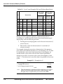
1.3.1
Instruction Set Enhancements
Many instructions were added in order to support the target
applications of the new DSP cores:
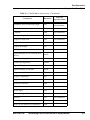
Table 1-1 New Instructions in DSP56300 and DSP56600
Opcodes
Opcodes
Exist in
DSP56300?
Exist in
DSP56600?
MAX
Transfer by Signed Value
√
√
MAXM
Transfer by Magnitude
√
√
INSERT
INSERT Bit Field
√
√
EXTRACT
Extract Bit Field
√
√
EXTRACTU
Extract Unsigned Bit Field
√
√
MERGE
Merge Two Half Words
√
√
CLB
Count Leading Bits
√
√
NORMF
Fast Accumulator
Normalize
√
√
CMPU
Compare Unsigned
√
√
Multibit
Shifts
Arithmetic and Logical
Shifts
√
√
MOTOROLA
Optimizing DSP56300/DSP56600 Applications
1-3
Introduction
Enhancements over the DSP56000
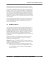
Table 1-1 New Instructions in DSP56300 and DSP56600
Opcodes
1-4
Opcodes
Exist in
DSP56300?
Exist in
DSP56600?
MAC (uu)
Unsigned MAC
√
√
DMAC
Double-Precision MAC
√
√
PLOCK
Lock Cache Sector
√
PUNLOCK
Unlock Cache Sector
√
PFLUSH
Flush Cache Sectors
√
PFLUSHUN
Flush Unlocked Cache
Sectors
√
PFREE
free all locked sectors
√
LRA
Load Relative Address
√
√
BSR / BScc
Branch Subroutine
always/conditionally
√
√
BRA / Bcc
Branch Target
always/conditionally
√
√
BSset / BSclr
Branch Subroutine on Bit
Set/Clear
√
BRset /
BRclr
Branch Target on Bit
Set/Clear
√
DO Forever
DO-Loop Forever
√
DOR Forever
DO-Loop Forever Relative
√
BRKcc
Break Loop Conditionally
√
√
TRAPcc
TRAP Conditionally
√
√
IFcc
Execute Instruction
Conditionally
√
√
VSL
Viterbi Shift Left
√
√
Optimizing DSP56300/DSP56600 Applications
√
MOTOROLA
Introduction
Enhancements over the DSP56000
1.3.2
Architectural Enhancements
The programmer’s model of the new DSP cores were also enhanced
by the following:
• An instruction cache controller was added to the DSP56300.
A Burst mode can be used to lower the off-chip traffic if
external DRAMs are used.
• A six-channel DMA controller was added to the DSP56300.
• A true barrel shifter (56-bit in DSP56300 and 40-bit in
DSP56600) was added to support multibit operations.
• The address and offset registers of the DSP56300 (R0–R7,
N0–N7) were extended to 24-bit wide to support larger
memory sizes.
• The DSP56300 has a 16-bit Arithmetic operating mode such
that 16-bit exact algorithms can be implemented without any
overhead.
• The DSP56300 and the DSP56600 have an on-chip Hardware
Stack Extension mechanism that makes the Stack depth
practically unlimited.
• Rounding and Saturation modes were added to the
Arithmetic Unit of the DSP56300 and DSP56600.
• New addressing modes were added to the DSP56300 and
DSP56600:
–
Short/Long address displacement
–
PC-Relative for Position Independent Code
–
Short/Long Immediate operands to Arithmetic and
Logical operations
MOTOROLA
Optimizing DSP56300/DSP56600 Applications
1-5
Introduction
Application Note Structure
1.4
APPLICATION NOTE STRUCTURE
This document has three main component parts:
• DSP56300 and DSP56600 features description and use
• Optimizing the code for best performance
• Appendices
1.4.1
DSP56300 and DSP56600 Features
Description and Use
The first five sections in this application note describe all the
architectural and instruction set enhancements in the new DSP
cores and how they can be used to optimize applications.
• Section 1—Introduction
–
DSP56300 core family
–
DSP56600 core family
–
Enhancements over the DSP56000
• Section 2—Data Operations
–
How to organize data in memory to use parallel moves
–
How to use the barrel shifter in various applications
–
The benefit and use of the 16-bit Arithmetic support
–
Some examples that show the benefit of few of the new
arithmetic and logical instructions
• Section 3—Program Control
1-6
–
How to use the on-chip hardware stack
–
Benefit and usage of the Stack Extension
–
Usage of the conditional arithmetic and logical
instructions
–
How to use the PC relative instructions for code
relocation and saving of program words
–
Using fast interrupts
Optimizing DSP56300/DSP56600 Applications
MOTOROLA
Introduction
Application Note Structure
• Section 4—Using the DMA
–
How to reduce core MIPS by using the DMA
–
How to service peripherals using the DMA
–
How to use slow, inexpensive memory chips without
loosing performance
–
How to handle complex data structures by using the
DMA
• Section 5—Instruction Cache and Other Memory Features
–
Basic instruction cache tutorial
–
Data organization for efficient sector allocation
–
Sector locking for critical loops
–
Flushing the cache after task switching.
–
Burst mode for DRAMs
–
Memory banks between program and data
–
Using the bootstrap ROM
1.4.2
Optimizing the Code for Best Performance
The next two sections include general explanation of the various
pipeline stall conditions and how they can be avoided in order to
get faster execution times. In addition, some observations on the
instruction set are included along with recommended usage for
optimization purposes.
• Section 6—Pipeline Interlocks
–
Description of the various types of interlocks
–
Ways to avoid each type of interlock
–
Program flow and control
–
Understanding timing of conditional change of flow
–
How to reorder code at the end of DO loops
–
When to use the repeat instruction
• Section 7—Compact Opcode Use
MOTOROLA
Optimizing DSP56300/DSP56600 Applications
1-7
Introduction
Application Note Structure
1.4.3
–
Cycle count of an instruction
–
Addressing modes
–
Word count of an instruction
–
Peripheral addressing
Appendixes
There are three appendices providing supplementary information
about application design guidelines:
• Appendix A—Saving Power
• Appendix B—Debug and Test Support
• Appendix C—Using the Profiler
1-8
Optimizing DSP56300/DSP56600 Applications
MOTOROLA
Section 2
DATA OPERATIONS
2.1
USING THE DUAL DATA PATHS
The DSP56300/DSP56600 core can execute a new instruction every
clock cycle. This performance can be used efficiently only if data can
be fed to the core and its results moved out of it at a sufficient rate.
The DSP56300/DSP56600 core’s highly parallel architecture was
designed to allow performing the following operations in parallel:
• Data ALU instruction execution
• Up to two parallel moves of data operands or results to/from
the Data ALU
• Up to two address calculations for the next instruction
This section
discusses
important features
and new additions
to the DSP56000
core Data
Arithmetic Unit
• Fetch of next instruction
The two data paths (the X bus and Y bus) connect two data memory
sections (the X memory and the Y memory) with the Data ALU.
This parallelism allows the DSP56300/DSP56600 core to execute
more effectively, for example, executing a FIR tap in one clock cycle:
Opcode + operands
Data for next
iteration via the X
data bus +
increment pointer
Data for next
iteration via the Y
data bus +
increment pointer
____________________________________________
___________________________________
____________________________________
mac
x:(r0)+,x0
y:(r4)+,y0
x0,y0,a
Data that is moved in parallel into a register is ready for use in the
next instruction, and does not interfere with the current value of the
operands in execution. In the above example, the values of X0 and
Y0 are updated only after the “MAC” instruction uses its operands.
Similarly, data moved from a register will hold the data before it was
updated as a result of execution. For example:
mac
x0,y0,a
a,x:(r0)+
The value of the accumulator A that is moved to the memory is the
value before its update by the “MAC” instruction.
MOTOROLA
Optimizing DSP56300/DSP56600 Applications
2-1
Data Operations
Using the Dual Data Paths
There are two ways to generate the operand addresses for parallel
moves:
• XY addressing—Two address registers are used
independently, one generating an operand address for the X
memory and the other for the Y memory. The FIR example
above is of this kind. The address registers must be of
different “banks”, meaning that if an address register R0–3 is
used for one data field, an address register R4–7 should be
used for the other data field. No absolute addresses are
allowed in this mode.
• Long addressing—One address register or absolute address
is used to generate the address for both the X memory and
the Y memory. For example:
mac
x0,x1,a
l:(r0)+,X
The syntax L:(R0)+,X is equivalent to moving X:(R0) to X0 and
Y:(R0) to X1, then incrementing R0. The name “long addressing”
refers to the fact that such addressing enables to access two data
registers as if they were one 48-bit long register.
Not all the DSP56300/DSP56600 instructions support parallel
moves. In general, the instructions that do are a subset of the
arithmetic instructions. The full list of these instructions appears in
Table 2-1.
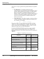
Table 2-1 Parallel Move Instructions
Instruction
2-2
Mnemonic
Relevant
Opcode variants
Absolute Value
ABS
Add Long with Carry
ADC
Add
ADD
Shift Left and Add Accumulators
ADDL
Shift Right and Add Accumulators
ADDR
Logical AND
AND
Non-immediate
Arithmetic Shift Accumulator Left
ASL
Single bit,
non-immediate
Optimizing DSP56300/DSP56600 Applications
Non-immediate
MOTOROLA
Data Operations
Using the Dual Data Paths
Table 2-1 Parallel Move Instructions (Continued)
Mnemonic
Relevant
Opcode variants
Arithmetic Shift Accumulator Right
ASR
Single bit,
non-immediate
Clear Accumulator
CLR
Compare
CMP
Compare Magnitude
CMPM
Logical Exclusive OR
EOR
Logical Shift Left
LSR
Logical Shift Right
LSR
Multiply and Accumulate
MAC
Signed Multiply and Accumulate and
Round
MACR
Transfer by Signed Value
MAX
Transfer by Magnitude
MAXM
Signed Multiply
MPY
Signed Multiply and Round
MPYR
Negate Accumulator
NEG
Logical Complement
NOT
Logical Inclusive OR
OR
Round Accumulator
RND
Rotate Left
ROL
Rotate Right
ROR
Subtract Long with Carry
SBC
Subtract
SUB
Shift Right and Subtract Accumulators
SUBR
Shift Left and Subtract Accumulators
SUBL
Instruction
MOTOROLA
Non-immediate
Non-immediate
Signed operands
Non-immediate
Non-immediate
Optimizing DSP56300/DSP56600 Applications
2-3
Data Operations
Using the Dual Data Paths
Table 2-1 Parallel Move Instructions (Continued)
Instruction
Mnemonic
Transfer Data ALU Register
TFR
Test Accumulators
TST
Relevant
Opcode variants
Parallel moves are also restricted in their use of registers as source
and destination to a part of the Data ALU registers. The register
options available for XY Addressing are listed in Table 2-2. Any
register in the X field column can appear with any register in the Y
column, with the obvious exception of updating the same
accumulator from both the X and Y fields.
Table 2-2 Registers Used in Parallel XY Moves
X Field
Y Field
X0
Y0
X1
Y1
A
B
A
B
Comments
As source: undergoes shifting and
limiting
As destination: A2/B2 sign
extended, A0/B0 zero filled
The register options available for long addressing are listed in
Table 2-3.
Note: Some syntax combinations of the accumulators differ only in
shifting/limiting (if the register is the source) or implicit
register updates (if they are destination). For example,
compare “A10” with “A”. In the “AB” and “BA”
combinations, each accumulator has same behavior as a
regular move, such as:
move a, x:(r0)+.
2-4
Optimizing DSP56300/DSP56600 Applications
MOTOROLA
Data Operations
Using the Dual Data Paths
Table 2-3 Registers used in Long Addressing
Assembler
Syntax
X
Field
Y
Field
Shifting/
Limiting if
source
Sign
extension
if
destination
Zero fill if
destination
A10
A1
A0
no
no
no
B10
B1
B0
no
no
no
X
X1
X0
no
no
no
Y
Y1
Y0
no
no
no
A
A1
A0
yes
A2
no
B
B1
B0
yes
B2
no
AB
A1
B1
yes
A2,B2
A0,B0
BA
B1
A1
yes
A2,B2
A0,B0
Keeping those restrictions in mind, writing a critical data processing
loop efficiently should be done after careful planning of register use
and the data allocations in the memory space according to the
parallelism possible in the calculation at hand. For example, in the
FIR tap calculation given above, the coefficients occupy the X
memory with pointer R0, and the data buffer occupies the Y
memory with pointer R4 (or vice versa). In other cases, the division
may not be so straight forward. For example, in many algorithms
involving complex numbers, the efficient solution uses one memory
space for the real part of the numbers, while the other memory
space is used for the imaginary part. In those examples, there is a
logical separating criterion between the data placed in the X and Y
memories. In many applications, however, variables may be split up
between the X and Y memories based on no other criterion than the
ability to transfer them in parallel to the core at the time they are
called for by the algorithm.
MOTOROLA
Optimizing DSP56300/DSP56600 Applications
2-5
Data Operations
16-bit Arithmetic Mode (DSP56300 Only)
2.2
16-BIT ARITHMETIC MODE (DSP56300 ONLY)
The 16-bit Arithmetic mode causes the Data ALU to use only 16 bits
of the 24-bit data in transfers and calculations, allowing use of the
DSP56300 as a 16-bit data processor. The 16-bit data is right aligned
in the memory, but left aligned in data registers (in order to comply
with the fractional numerical representation convention). The
hardware makes the proper alignments and shifts in data transfers
and operations, so the user does not have any overhead when using
this mode. This includes the accumulators, which in the 16-bit mode
are 40-bits wide (in accumulator A, for example, A0 and A1 are 16
bits each, and the extension A2 remains 8 bits wide). All data
operations are properly defined to give correct 16-bit arithmetic
results. For more information on the 16-bit Arithmetic mode, see
Section 3.4 in the DSP56300 Family Manual for a general
description, and Appendix A in the same manual (Instruction set)
for a detailed description on the functionality of each instruction
affected by this mode.
Using the 16-bit Arithmetic mode may give many advantages from
a general system point of view:
• Ability to implement a 16-bit exact algorithms. The DSP56300
also supports saturation arithmetic and flexible rounding
modes required by some standards.
• 16-bit exact algorithms exact algorithms could be integrated
easily into a software system that also includes 24-bit exact
routines. Changing of the arithmetic mode can be done “on
the fly”.
The 16-bit Arithmetic mode is activated by setting the SA bit in the
Status Register (SR).
Note: This is not the same as the 16-bit Compatibility mode
(activated by setting the SC bit in the Status Register). The
16-bit Compatibility mode affects address registers and
address calculations and enables object code compatibility
with the DSP56000 family (which uses 16-bit wide
addresses).
2-6
Optimizing DSP56300/DSP56600 Applications
MOTOROLA
Data Operations
The Max instruction
2.3
THE MAX INSTRUCTION
MAX is a new instruction in the DSP56300 and DSP56600
instruction set that can used to enhance performance in critical data
operation loops. For example,
max
a,b
compares the two accumulators, and places the bigger value in the
destination accumulator (accumulator B). The MAXM instruction
does the same thing, only it transfers the bigger absolute value to
the destination .
Like other data operations, this instruction is effectively executed in
one clock cycle. Previously such functionality was achieved in two
cycles, for example:
cmp
tlt
a,b
a,b
Note: This example differs from the MAX functionality only in the
status update.
The MAXM instruction can be used to find the largest number in an
array of values, in N + 10 clock cycles:
move
clr
rep
maxm
#DATA_POINTER,r0
b
x:(r0)+,a
#n
a,b
x:(r0)+,a
cycles
1
1+3 interlock
5
N
The initialization of R0 takes 4 cycles due to an address register
interlock. The three cycle stall could be used for other useful
instructions (see Section 6.2.1 on page 6-7).
Note: The MAX and MAXM instructions can only be used with
fixed operands (A as first source, B as destination). There is
no opcode for MAX B,A.
MOTOROLA
Optimizing DSP56300/DSP56600 Applications
2-7
Data Operations
Using the barrel shifter
2.4
USING THE BARREL SHIFTER
The DSP56300/DSP56600 includes a true barrel shifter that can be
used for multi-bit data shifts. The instructions that use the barrel
shifter are listed in Table 2-4.
Table 2-4 Data Operations Using Multi-shift
Mnemonic
Function
Operands
ASL
Arithmetic C,S,D
Shift Left
C: number of shift bits
ASR
Arithmetic S: source of shift
Shift Right D: destination
LSL
Logical
Shift Left
LSR
NORMF
C,D
S: number of shift bits
6-bit immediate, or
X0,X1,Y0,Y1,A1,B1
A,B
A,B
Logical
Shift Right D: source & destination
5 -bit immediate, or
X0,X1,Y0,Y1,A1,B1
A,B
Fast
C,D
Normalizat C: control of shift
ion
D: destination
X0,X1,Y0,Y1,A1,B1
A,B
The logical shifts operate on the most significant register (A1/B1) of
the accumulator destination (the accumulator extension and LS
register are not affected). The arithmetic shifts operate on the full
length of the source and destination accumulators, sign extending
when applicable. In addition to the multi-bit shifts, there are also
four respective single bit shift instructions that allow parallel moves
(the multi-bit shifts do not allow them).
The NORMF instruction deserves special attention, as it can
effectively replace several instructions in many common
algorithms. The NORMF instruction arithmetically shifts the data
from the destination accumulator (D) in the direction and amount
specified by the first operand (C). If C > 0, then D is arithmetically
shifted to the left by C bits. If C < 0, then D is arithmetically shifted
to the right by C bits. The operand C should normally be prepared
by the CLB instruction (Count Leading Bits). The instruction pair:
clb
normf
2-8
a,b
b1,a
Optimizing DSP56300/DSP56600 Applications
MOTOROLA
Data Operations
Using the barrel shifter
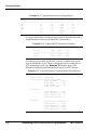
will normalize A, so that in the DSP56300 it’s leading one or zero
will be shifted to Bit 46 in the accumulator. If |A| > 1 (meaning that
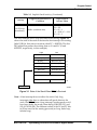
it spilled to the extension A2), then CLB returns a positive number
(between 1 and 8). If |A| < 1, CLB returns a zero or a negative
number (between –47 and 0). The two cases in Figure 2-1 exemplify
the normalization operation for the DSP56300. The NORMF at the
56600 core operates similarly, with adjustments to the different
accumulator length.
55
A
A,B
B
B1,A
A
0
47
23
47
23
00 601000 008000
55
A
0
00 000005 000000
55
NORMF
23
0c 020000 100000
55
CLB
47
0
47
ff
55
A
23
0
00 00c000 003000
55
B
47
fffff9
47
23
0
000000
23
0
00 600000 180000
AA0831
Figure 2-1 The Fast Normalization Operation for the DSP56300:
The NORMF instruction can be used to keep data dynamically
bounded (maximizing calculation accuracy), implement floating
point routines, normalizing data blocks, and more. For example,
consider the following routine for efficiently normalizing a data
block. The first pass finds the normalization factor (using MAXM
and CLB) and the second pass performed the normalization itself.
;NORMALIZING A DATA BLOCK
;=========================
;X:base - base address of un-normalized data.
;Y:base - base address of normalized data.
;N: data block size
;cycle count
move
#base,r0
; 1
move
#base,r1
; 1
clr b x:(r0)+,a
; 1 + 2 pointer interlock
rep
#N
; 5
maxm
a,b
x:(r0)+,a
; 1 x N
move
r1,r0
; 1
clb
b,a
; 1
MOTOROLA
Optimizing DSP56300/DSP56600 Applications
2-9
Data Operations
BIt manipulation instructions
move
move
move
do
move
normf
normf
move
_ENDLOOP
move
2.5
#base-1,r4
; 1
a1,x1
; 1
x:(r0)+,a
; 1
#N/2,_ENDLOOP
; 5
x:(r0)+,b b,y:(r4)+; 1 x N/2
x1,a
; 1 x N/2
x1,b
; 1 x N/2
x:(r0)+,a a,y:(r4)+; 1 x N/2
b,y:(r4)+
; 1
;Total: 3N + 22
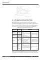
BIT MANIPULATION INSTRUCTIONS
The data ALU has a special Bit Field Unit (BFU) that supports
powerful bit-manipulation instructions that enable an application to
insert/ extract a bit field of varying width and position to/from an
accumulator. These instructions are summarized in Table 2-5.
Table 2-5 Bit manipulation instructions
Mnemonic
EXTRACT
Function
Extract a
bit field
Extract an
EXTRACTU unsigned
bit field
Operands
C,S,D
C: Source field position
& width
S: Data source
D: Data Destination
INSERT
C,S,D
C: Destination field
Insert a bit
position & width
field
S: Data source
D: Data Destination
MERGE
Merge
field &
width
data to
one
register
S,D
S: Width Data Source.
D: Position data source
& merging destination
6-bit immediate, or:
X0,X1,Y0,Y1,A1,B1
A,B
A,B
6-bit immediate, or:
X0,X1,Y0,Y1,A1,B1
X0,X1,Y0,Y1,A1,B1
A,B
X0,X1,Y0,Y1,A1,B1
A,B
The EXTRACT(U) and INSERT instruction use a control operand
(C) that specifies the bit field to be extracted or inserted. The bit field
2-10
Optimizing DSP56300/DSP56600 Applications
MOTOROLA
Data Operations
Double precision arithmetic
is specified by its width (in bits) and its starting position (in bits,
relative to the LSB of the accumulator). The width and position
values could be prepared using the MERGE instruction, which
merges data from two data registers in the appropriate positions for
future use as a control operand for EXTRACT and INSERT.
The EXTRACT instruction extracts the specified field, right-aligns it,
and sign-extends it in the destination accumulator. The EXTRACTU
instruction does the same, but does not sign-extend the result. The
INSERT instruction takes a right-aligned field of the specified width
from the source register and places it in the specified position in the
destination accumulator.
Detailed examples of the use of these instructions for parsing and
creating a data stream, and parsing Hoffman code data stream can
be found in Appendix C of the DSP56300 and DSP56600 Family
Manuals.
2.6
DOUBLE PRECISION ARITHMETIC
The DSP56300/DSP56600 has instructions to help the programmer
implement arithmetic operations if the operands are longer than
standard accumulator size. Using these instructions can help
achieve enhanced precision with minimum software overhead. The
examples below relate to the DSP56300 core register size (24 bits for
data registers, 56 bits for an accumulator), but can be adapted for
the DSP56600 core by changing the register size accordingly.
The normal ADD and SUB instructions can add a 48-bit operand
(X1:X0, for example) to an accumulator, and, of course, can add a
56-bit accumulator to another. Furthermore, the user may use ADC
(Add long with Carry) or SBC (Subtract long with Carry), which
adds (subtracts) a 48-bit operand to (from) an accumulator with a
carry (borrow) bit from a previous calculation.
The normal MPY (multiply) or MAC (multiply-accumulate)
instructions multiply two 24-bit operands to give a 48-bit result.
Implementing 32 × 32-bit or 48 × 48-bit multiplication requires four
24 × 24 multiplications, and some shifting and addition operations.
The DSP56300 and DSP56600 specialized instructions can help
reducing these extra operations to a minimum. Consider for
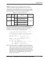
example 48 × 48 multiplication, where only the forty-eight Most
Significant Bits are needed, and the forty-eight Least Significant Bits
discarded. Figure 2-2 on page 2-12 illustrates the required
operations.
MOTOROLA
Optimizing DSP56300/DSP56600 Applications
2-11
Data Operations
Double precision arithmetic
23
×
0
23
0
X1
23
X0
0
23
0
Y1
Y0
47
0
X0(u) • Y0(u)
47
0
Y1(s) • X0(u)
+
47
0
X1(s) • Y0(u)
47
0
X1(s) • Y1(s)
47
0
Result accumulator
AA0832
Figure 2-2 48 × 48-bit Multiplication with 48 Bits of the Result Kept.
The (U) means an unsigned operand, and the (S) a signed operand.
The following four instructions perform the operation in full:
;48x48 bit multiplication with 48 bit result.
;============================================
;first operand - X1:X0
;second operand -Y1:y0
;result is in accumulator A.
mpyuu
dmacsu
macsu
dmacss
2-12
x0,y0,a
y1,x0,a
x1,y0,a
x1,y1,a
;
;a>>24
;a +
;a>>24
x0(u) * y0 (u) -> a
+y1(s) * x0 (u) -> a
x1(s) * y0 (u) -> a
+x1(s) * y1 (s) -> a
Optimizing DSP56300/DSP56600 Applications
MOTOROLA
Data Operations
Using Less Straight-Forward Instructions
The features that help in this case are:
• The ability to specify combinations of signed and unsigned
operands
• The 24-bit right arithmetic shifting inherent in the DMAC
instruction
Using these instruction combinations, and others, enables the
programmer to build other multi-register arithmetic operations. The
user is referred to Appendix A of the DSP56300 and DSP56600
Family Manuals for the full documentation of the various
instruction options.
2.7
USING LESS STRAIGHT-FORWARD
INSTRUCTIONS
The rich instruction set includes many instructions that are in fact
combinations of smaller atomic operations. Among these
instructions are ADDL, ADDR, MAX, EXTRACT, INSERT, MACR,
and MPYR.
A good example of using some of these less straight-forward
instructions is the SQROOT routine. The following is a straight
forward implementation of that routine:
sqroot
;determine 2nd term and add contribution
asr
a
sub
#$4000,a
;a = L_Temp1
move
a1,x0
;x0 = swTemp
sub
#$8000,a
;a = L_Temp1
;determine 3rd term and add contribution
mpy
-x0,x0,b
;b = swTemp ^ 2
move
b1,x1
;x1 = swTemp2
asr
b
add
b,a
;a = L_Temp0
;determine 4th term and add contribution
mpy
-x0,x1,b
;b = swTemp x swTemp2
move
b1,y0
;y0 = swTemp3
asr
b
b,a
;a = L_Temp1
;determine partial 5th term
mpyr
x0,y0,b
move
b,y1
;y1=swTemp4
add
MOTOROLA
Optimizing DSP56300/DSP56600 Applications
2-13
Data Operations
Using Less Straight-Forward Instructions
;determine partial 6th term
mpy
-x1,y0,b
rnd
b
move
b,x1
;determine 5th term and add its contribution
mpy
-#$5000,y1,b ;b = 0 - (swTemp4 x
;TERMS_MULTIPLIER)
add
b,a
;determine 6th term and add its contribution
macr
#$7000,x1,a
;swSqrtOut is contained in a
rts
In this example, the ADDR and MPYR instructions replace a few
instructions in the original code causing some reduction in total
cycle count:
sqroot
;determine 2nd term and add contribution
asr
a
#<$40,y1
sub
y1,a
#<$80,x1;a = L_Temp1
sub
x1,a
a1,x0 ;a = L_Temp1,x0 = swTemp
;determine 3rd term and add contribution
mpy
-x0,x0,b
;b = swTemp ^ 2
addr
a,b
b1,x1 ;x1 = swTemp2, b = L_Temp0
;determine 4th term and add contribution
mpy
-x0,x1,a#<$70,y1;a = swTemp x swTemp2
addr
b,a
a1,y0 ;y0 = swTemp3, a = L_Temp1
;determine partial 5th term
mpyr
x0,y0,b#<$50,x0
;determine partial 6th term
mpyr
-x1,y0,bb,x1
;y1=swTemp4
;determine 5th term and add its contribution
mac
-x0,x1,ab,x1 ;b = -(swTemp4 x
;TERMS_MULTIPLIER)
;determine 6th term and add its contribution
macr
x1,y1,a
;swSqrtOut is contained in a
rts
2-14
Optimizing DSP56300/DSP56600 Applications
MOTOROLA
Section 3
PROGRAM CONTROL
3.1
HARDWARE LOOPS
Hardware looping is one of the strongest features of the
DSP56300/DSP56600 core families. Loop counter management and
end-of-loop testing is done by hardware in parallel to instruction
execution, thus saving execution time of otherwise needed control
software. This enables the user to muster more performance in
critical loops, and also makes program writing more close to
high-level languages. Consider the following C code example:
for (i = 0; i < 100; i++){
a = a + data[i];
}
This section
discusses
important program
control features
and new additions.
A straight forward assembly implementation of the main loop of the
code may look like this:
move
clr
move
_LOOP_TOP
add
sub
tst
jne
#MEMORY_AREA,r0
a
#100,b
x:(r0)+,x0
x0,a
x:(r0)+,x0
#1,b
b
_LOOP_TOP
Using hardware looping, this code looks like:
move
clr
do
add
_LOOP_END
#MEMORY_AREA,r0
a
x:(r0)+,x0
#100,_LOOP_END
x0,a
x:(r0)+,x0
There is more to hardware loops than easy programming. The loop
control hardware is optimized for maximum pipeline efficiency.
There is no stall between loop iterations; all comparisons and loop
counter arithmetic are done in parallel to instruction execution. It is
important to know that after the loop is initialized (execution of the
DO instruction), the instructions in the loop are fetched and
executed in sequence. From the pipeline’s point of view, there is no
difference between the code in the last example and the “ADD”
instruction written 100 times in sequence.
MOTOROLA
Optimizing DSP56300/DSP56600 Applications
3-1
Program Control
Hardware Loops
A common programming technique is known as “loop unrolling”,
in which a high-level loop is replaced by the inner loop code,
repeated N times, thus saving the time needed to decrement the
counter, test for the end of the loop, and jumping back to the top.
From the above explanation, it follows that this technique is less
efficient in the DSP56300/DSP56600 family—the hardware executes
loops normally at the same speed as unrolled code (except for the
initializing DO instruction itself, which takes 5 cycles). Loops
should be unrolled only when the 5-cycle initialization is
meaningful in comparison to the total loop length, especially if this
loop is nested in another loop and the 5-cycle delay is multiplied.
See the example in Section 7.1.1 on page 7-1.
High-level “for” loops are normally implemented in assembly with
the DO instruction. The instructions DO FOREVER and BRKcc
(break on condition) may be used to implement high-level “while”
or “repeat” loops efficiently. The following example is a wave
generator that sends data to a peripheral (Host Interface HI08 in this
example) until a hardware interrupt (IRQA) sets a flag, signalling
the end of the loop. The core drives the HI08 transmitter by polling
the HTDE (Host Transmitter Data Empty) bit in the HI08 status
register. The C high-level code may look like:
while (!flag){
a1 = next_wave_value();
wait_until_transmitter_empty();
send_data(a1);
}
and in Assembler:
org
bset
p:I_IRQA
#0,x:<FLAG
org
...
move
move
bclr
p:MAIN_PROGRAM
#0,x0
x0,x:FLAG
#0,sr
;IRQA_ interrupt vector
;occupies 2 words
;clear FLAG register
;clear carry bit
do forever,_END_LOOP
brkcs
;break loop if carry bit set
jsr
NEXT_WAVE_VALUE;new value returned in a1
_WAIT
jclr
btst
movep
_END_LOOP
3-2
#0,x:M_SSR,_WAIT;wait until transmitter empty
#0,x:FLAG
;set carry by flag value
a1,x:M_HTX
;transmit data to host.
Optimizing DSP56300/DSP56600 Applications
MOTOROLA
Program Control
The Hardware Stack
Note: The BRKcc instruction has the same functionality as the C
language “break”, (i.e., terminating the loop and resuming
execution after the end of the loop). A similar instruction is
the ENDDO instruction, which exits the loop after finishing
the current loop iteration. ENDDO is not a conditional
instruction, therefore normal use generally includes testing a
condition and skipping the ENDDO instruction accordingly.
The following example counts the number of bits in A1, terminating
if the register turns 0 before the full 24 iterations.
clr
b
#0,x0
do
tst
jne
enddo
#24,_END_LOOP
a
_CONT
_CONT
lsr
addc
_END_LOOP
a
x0,b
Bit 0 of the result (B1) could be used as the parity of the original
operand (A1).
Note: Both ENDDO and BRKcc have sequence restrictions, as
shown in the DSP56300 and DSP56600 Family Manuals,
Appendix B.
3.2
THE HARDWARE STACK
The DSP56300/DSP56600 hardware stack enables the user to nest
DO loops and subroutines (called by software or interrupts) with no
software overhead. With the Stack Extension enabled, the hardware
stack can accommodate an unlimited nesting level of DO loops,
JSRs, or a combination of them. The only overhead of a very deep
nesting level is some additional cycles required to copy data to or
from the stack extension memory. Examples of stack extension use
are given in Section 3.3 on page 3-7.
The hardware stack mechanism works in parallel to opcode
execution, thus saving execution time, as well as software overhead
compared to conventional software stacks. These advantages make
the DSP56300/DSP56600 especially suitable for multi-tasking, and
running real-time operating systems and program code generated
from high-level languages.
MOTOROLA
Optimizing DSP56300/DSP56600 Applications
3-3
Program Control
The Hardware Stack
The current stack location is pointed by the SP register. A single
stack location can store two words, referred to as occupying the
“high” and “low” halves of the stack location. The current stack
locations pointed by SP (top of stack) are named SSH and SSL,
respectively. A single “push” or “pop” activity can access the SSH
and SSL concurrently. Stack activities are triggered implicitly at
execution of specialized instruction or fulfillment of certain
conditions. These activities are summarized in Table 3-1.
Note: The table only summarizes the effect of those instructions on
the stack. Some instructions update other registers as well.
For complete information on an instruction, refer to
Appendix A in the DSP56300 and DSP56600 Family
Manuals.
Table 3-1 Implicit Stack Activity
Triggered by Instruction or
Condition
Implicit Stack
Actions Taken
jump to
subroutine
JSR, BSR
JScc, BScc (condition true)
JSCLR, BSCLR (condition true)
JSSET, BSSET (condition true)
SP: = SP + 1;
SSH: = PC; SSL: = SR.
return from
subroutine
RTS
PC: = SSH
SP: = SP - 1
return from
long interrupt
RTI
PC: = SSH; SR: = SSL
SP: = SP – 1
move to SSH
MOVEC <source>,SSH
SP: = SP + 1
SSH: = <source>
Activity
move from SSH MOVEC SSH,<destination>
enter DO loop
DO
DOR
DO FOREVER
DOR FOREVER
(LF bit set and FV bit clear
exit DO loop at and fetched address = LA
last address
and LC = 0).
ENDDO
3-4
<destination>: = SSH
SP: = SP – 1
SP: = SP + 1
SSH: = LA, SSL: = LC
SP: = SP + 1
SSH: = PC, SSL: = SR
SR: = SSL
SP: = SP – 1
LA: = SSH, LC: = SSL
SP: = SP – 1
Optimizing DSP56300/DSP56600 Applications
MOTOROLA
Program Control
The Hardware Stack
Table 3-1 Implicit Stack Activity (Continued)
Activity
exit DO loop
immediately
Triggered by Instruction or
Condition
BRKcc (condition true)
Implicit Stack
Actions Taken
PC: = LA + 1;
SR: = SSL
SP: = SP – 1
LA: = SSH, LC: = SSL
SP: = SP – 1
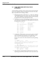
The next example shows loop and subroutine nesting. Figure 3-1
shows the state of the stack at the time the fast interrupt is executing
(label I_IRQA, that enters execution when PC = $000529). The first
DO instruction pushes the existing data on LA and LC (0 and
$FFFFFF, respectively, in this example).
High
Low
0
$109 (PC)
$C00300 (SR)
1
$0 (LA)
$FFFFFF (LC)
2
$520 (PC)
$C00300 (SR)
3
$530 (LA)
$6 (LC)
4
$525 (PC)
$C08300 (SR)
5
6
15
SP
AA0833
Figure 3-1 State of the Stack When IRQA Is Serviced
Note: A fast interrupt does not effect the stack. Only long
interrupts (that have a subroutine call) push data into the
stack. Had IRQA been a long interrupt, another push would
have been done, the saved values being SSH:$529 (PC) and
SSL: $C18300 (SR). The different values of the LF and FV bits
in SR are saved as the nesting proceeds (no loop, finite loop,
infinite loop).
MOTOROLA
Optimizing DSP56300/DSP56600 Applications
3-5
Program Control
The Hardware Stack
;example of loop and subroutine nesting.
;interrupt definitions: fast interrupt from IRQA_
org
p:I_IRQA
bset
#5,x:(r0)
nop
...
;program area
;after jsr execution, sp == 1,
;execution continues at _SUB1
jsr
_SUB1
...
...
...
_SUB1
do
...
do
btst
brkcs
move
move
move
_LOOP2
#6,_LOOP1
;after instruction, sp == 3
forever,_LOOP2 ;after instruction, sp == 5
#0,x:(r0)
;if condition true, resume at
;_LOOP2,and sp == 3.
a0,x:(r1)+
;<---- irqA occurs here.
a1,x:(r1)+
a2,x:(r1)+
;after loop is braked, sp == 3
nop
...
nop
_LOOP1
nop
rts
;after normal loop
;termination, sp == 1
;after execution, SP == 0,
;execution returns to main
Direct user access with the MOVEC instruction is possible to
SSL,SSH. Note that MOVEC to/from SSH implicitly increments or
decrements SP, while the same instruction on SSL has no effect on
SP. A manual “pop” operation will usually have the format:
movec
movec
ssl,<destination 1>
ssh,<destination 2>;implicit sp decrement
Explicit access to the stack registers is not recommended for the
general user. Such accesses have severe restrictions on them (see
Appendix B in the DSP56300 and DSP56600 Family Manuals). A
user who wishes to manually access the stack must take into
account pipeline effects that are usually transparent, and that long
interrupts may enter.
3-6
Optimizing DSP56300/DSP56600 Applications
MOTOROLA
Program Control
Using the Stack Extension
3.3
USING THE STACK EXTENSION
The hardware stack could be extended to the data memory (X or Y),
and it’s depth could be set by the user according to need. After
initialization, the stack extension works automatically without any
user overhead, giving the same functionality as the hardware stack.
The registers participating in stack extension operation are listed in
Table 3-2.
Table 3-2 Registers Involved in Stack Extension Operation
Register
OMR
Name
operating
mode register
Function
stack extension initialization (bits:SEN,XYS)
stack extension status (bits: WRP,EOV,EUN)
SZ
stack extension
maximum stack depth, in word pairs.
size
SP
stack pointer
current total stack depth, in word pairs
SC
stack counter
current hardware stack depth.
EP
stack extension pointer to the last address written in the
pointer
memory extension.
Stack extension initialization bits in the OMR include the XYS (X Y
Select) bit, by which the user selects the data space (X or Y) in which
the stack extension will reside, and the SEN (Stack Extension
Enable) bit, by which the user activates the stack extension after all
the relevant registers are initialized.
The SP register counts the number of entries in the stack. If the stack
extension is disabled, the values of SP are bounded to 0–15, and
selection of other values cause a stack error exception. When the
stack extension is enabled, SP may hold values from 0 up to the
value stored in SZ. A push increments SP by 1, a pop decrements it
by 1.
SZ stores the maximum stack depth. During stack extension
operation, if SP becomes greater than SZ, a stack overflow exception
occurs. SZ has no default value, and therefore, must be initialized
by the user before enabling the stack extension. Set the SZ value
according the amount of memory available to the user, using the
MOTOROLA
Optimizing DSP56300/DSP56600 Applications
3-7
Program Control
Using the Stack Extension
following formula, which takes into account that each increment in
SZ corresponds to two memory locations:
SZ = available memory extension size ⁄ 2 + 14
For example, if the memory extension space available is 1024 words,
SZ should be set to 1024/2 + 14 = 526. SZ should be set to an even
number since stack extension transfers are done in pairs.
SC is a 5-bit register that stores the number of entries in the
hardware stack. SC is related to the stack only when the stack
extension is enabled. A push increments SC by 1, until the value 14 is
reached. If SC equals 14 and a push occurs, the push is executed, and
the least recently used stack entry (2 words) is copied to the
extension, leaving SC with the same value of 14 (hardware stack-full
state). A pop decrements SC by 1, until the value 2 is reached. If SC
equals 2 and SP > SC, when a stack pop occurs, the pop is executed,
and the top entry of the extension (2 words) is copied from the
memory to the stack, replacing the entry just read, thus leaving SC
with the same value of 2 (hardware stack-empty state).
Note: In principle there is no forced connection between the values
of SP and SC.
EP holds the pointer to the data memory location where the
extension is stored. The address space (X or Y) is selected by setting
the XYS bit in the OMR. EP has no default value and should be
initialized by the user. Each push that activates the extension causes
two memory writes, after which EP is incremented by 2, since one
stack entry is composed of 2 words. Similarly, each pop that
activates the extension causes 2 memory reads, after which EP is
decremented by 2. There is no restriction on the value of EP
(internal or external memory space), however in the DSP56300
family, the user should be aware that setting EP to point to external
memory will generate external accesses with possible wait states,
depending on the external memory type. The DSP56600 family does
not support external data accesses.
When the stack extension is disabled, the stack status information
resides in Bits 4 and 5 of SP (named SE and UF, respectively).
Normally, the stack error routine should consult these bits. When
using the stack extension, however, all stack status information
resides in the OMR. The SP bits do not reflect stack status
information as they are now part of the stack pointer value. The
stack status bits are also functionality different, as summarized in
3-8
Optimizing DSP56300/DSP56600 Applications
MOTOROLA
Program Control
Using the Stack Extension
Table 3-3. The use of SP bits for stack status when the stack
extension is disabled, instead of OMR for both cases, is for code
compatibility with the 56K family. The user’s stack error interrupt
routine should test the SEN bit (Stack Extension Enable) in OMR to
know what register to consult for stack status information.
Table 3-3 Stack Status Information
Stack
Status
Bit
Extension Info. Name
disabled
SEN = 0
SP
enabled
SEN = 1
OMR
Function
SE
Stack Error flag
UF
Stack Underflow flag
WRP
Extended Stack Wrap flag
EOV
Extended Stack Overflow
EUN
Extended Stack Underflow
Comments
All these bits
are sticky
Following is a full example of stack extension initialization.The
memory area allocated is in addresses Y:1024–1536 (512 locations).
This space can accommodate 256 stack locations in the stack
extension + fourteen locations in the hardware stack.
;========== initializing the stack extension ====================
;recommended only before interrupts are enabled
;care should be taken in cases where the code is used after
;a stack error event so that part of the initialization routine
;will clear sticky bits and resume the engine state to the
;reset initial state
EXTEN_START
equ
1024
;start address of stack
;extension in data area
MEM_SIZE
equ
512
;stack ext. size in data area
;maximum stack size (hardware +;extension),
;in units of two 24-bit words.
STACK_LIMIT
equ
MEM_SIZE/2+14
move
#EXTEN_START,ep;set ext. pointer in data memory
move
#STACK_LIMIT,sz;set stack limit
bset
#M_XYS,omr
;select y space
bset
#M_SEN,omr
;enable stack extension
Note: The stack extension was designed to operate transparently,
with no user software overhead. The mechanism ensures that
within stack size limit, data that is pushed into the stack will
be popped from the top of the stack in the same order. The
actual split of stack data between the hardware stack and the
stack extension is not readily apparent. The user therefore is
advised to access stacked data directly by software only
through the top of the stack.
MOTOROLA
Optimizing DSP56300/DSP56600 Applications
3-9
Program Control
Task Switching with the Stack Extension
3.4
TASK SWITCHING WITH THE STACK
EXTENSION
A multi-tasking operating system using the stack extension should
ensure stack coherence when switching from one task to the other.
Here is a possible task switching scenario:
1. During the execution of the task “T1”, a “time-out” interrupt
occurs indicating the need to replace the active task with task
“T2”. The PC and SR of T1 task are pushed onto the stack by
the JSR instruction of the interrupt vector area.
2. The JSR gives control to the Operating System that must now
execute the task switching. First, all the registers are saved in
the register area of task T1:
movec
move
move
....
move
move
move
move
move
....
move
move
r7,x:OS_temp
;save r7 in order to
;use is later
#T1_task_reg_area,r7 ;Load pointer.
x0,x:(r7)+
;Save registers...
r6,x:(r7)+
x:OS_temp,r0
r0,x:(r7)+
n0,x:(r7)+
n1,x:(r7)+
;Save
;Pull
;Save
;Save
;Save
registers...
r7
r7
n0
n1
lc,x:(r7)+
la,x:(r7)+
3. At this point, all the registers were saved as a mirror of the T1
task, but the stack has some data in it that belongs to the T1
task, as well. This data should also be copied to some
memory area reserved for that information by the operating
system.
;Stack saving:
move
sc,x:(r7)+
;Save SC
;The next 14 pushes ensure that all the current entries in the
;hardware stack will be automatically saved in the
;stack extension memory:
rep
#14
move
#dummy,ssh
;After these moves are executed, all the hardware stack is stored
;in the memory extension stack area, and the pointers EP and SP
;are updated, so they should be saved:
move
sp,x:(r7)+
;Save SP
move
ep,x:(r7)+
;Save EP.
4. After all task T1 programming model have been saved, the
Operating System chooses the task T2 as the next task to run.
3-10
Optimizing DSP56300/DSP56600 Applications
MOTOROLA
Program Control
Conditional DALU Instructions
5. In order to activate the new task T2, the Operating System
dispatcher should first restore the task T2 programming
model:
move
move
....
move
move
move
move
move
move
....
move
move
#T2_task_reg_area,r7 ;Load pointer.
x:(r7)+,x0
;Restore registers...
r7,n0
x:(r7)+,r7
x:(r7)+,x:OS_r7_temp
n0,r7
x:(r7)+,n0
x:(r7)+,n1
;save pointer
;Restore r7 w/ T2 data
;Keep r7.
;restore pointer
;Restore n0
;Restore n1
x:(r7)+,lc
x:(r7)+,la
6. The second thing the Operating System dispatcher should do
is to restore the stack status:
move
move
move
move
move
rep
move
move
move
x:(r7)+,sc
sc,x:OS_SC_temp
x:-(r0),sp
x:-(r0),ep
#2,sc
#14
ssh,x:OS_dummy
x:OS_sc_temp,sc
x:OS_r7_temp,r7
;Restore SP.
;Restore EP.
;reset Stack Counter.
;Restore sc.
;Restore r7.
7. The last thing the Operating System dispatcher should do is
to execute an RTI instruction, which will give control back to
the new task T2:
;Activate T2:
rti
3.5
CONDITIONAL DALU INSTRUCTIONS
The DSP56300/600 instruction set has a group of arithmetic
instructions that could be executed conditionally, depending on the
value of bits in the CCR (Condition Code Register). For example, the
instruction:
add
x0,a
IFne
adds register X0 to the accumulator A only if the Zero bit in the CCR
is not set. Otherwise, the instruction is executed as a NOP. The
instruction in the above example does not update the CCR, thus
keeping the status unaltered for subsequent use. The user may
MOTOROLA
Optimizing DSP56300/DSP56600 Applications
3-11
Program Control
Conditional DALU Instructions
specify that the instruction will update the CCR (according to the
result and only if it is executed), by writing “.U” at the end of the
condition attribute. For example:
add
x0,a
IFne.U
The full set of condition mnemonics may be used, thus helping
program clarity and flexibility. The condition table could be found
on Appendix A of the DSP56300 and DSP56600 Family Manuals.
The full list of the arithmetic instructions that conditional execution
attributes could be added to them is given in Table 2-1 on page 2-2.
In general, these are all Data ALU operations that allow parallel
moves. The condition attributes use the same opcode fields that are
used to specify the parallel moves, so conditional execution and
parallel moves exclude each other. The options the user has to
modify these instructions are summarized in Table 3-4.
Table 3-4 Options for Parallel Moves and Conditional Execution
Attribute
Syntax
none
Example
add a,b
conditional execution
without status update
IFcc
add a,b IFge
conditional execution
with status update
IFcc.U
add a,b IFlt.U
parallel move
x:<ea>
or y:<ea>
or both
or l:<ea>
add a,b x:(r0)+,a y:(r4)-,b
Another data-changing instruction that could be executed
conditionally is Tcc (transfer on condition). This instruction could
also be used to transfer AGU registers conditionally. On the other
hand, it does not have a parallel move option—see Appendix A in
the DSP56300 and DSP56600 Family Manuals.
Conditional arithmetic instructions enable the user to replace short
jumps with fewer instructions, thus making the code more clear and
compact. For example, consider the following high-level code line:
if (A==Y0) then B=B+X0 else B=B+X1
Without conditional arithmetic instructions, the code may look like
this:
cmp
beq
3-12
y0,a
_TRUE
Optimizing DSP56300/DSP56600 Applications
MOTOROLA
Program Control
PC Relative Instructions
add
bra
b,x1
_CONT
add
b,x0
_TRUE
_CONT
.....
Using conditional instructions, the code can be written more
compactly, as listed below:
cmp
add
add
Y0,a
b,x0
b,x1
IFeq
IFne
The only difference between the two codes is that the Status
Register in the later option is not updated according to the
calculation result. Conditional execution with CCR update may in
some cases solve the problem, as in the following example:
btst
asr
#0,a0
a
IFcs.U
;CCR is updated according to the
;value of A if the instruction
;was executed.
Another example of using the CCR update is setting a complex
condition by accumulating simple comparison results. For example,
consider the high-level code line and its translation in assembly
listed below:
if (X0 < A && X1 < A) then {A=A+y0; b=b+y0}
cmp
X0,a
x:(r0),x1
;test for X0<a. parallel field
;used to set X1 for next cmp
cmp
X1,a
IFgt.U
;test for X1<a only if the last
;condition was true.
add
y0,a
IFgt
;A=A+y0,B=B+y0 only if both
;conditions were true.
add
y0,b
IFgt
3.6
PC RELATIVE INSTRUCTIONS
Many of the DSP56300 control instructions require a program
location as one of their arguments. The most obvious example is a
jump instruction, which needs the jump address. A strong feature of
the DSP56300 instruction set is the ability to reference program
locations relative to the Program Counter. Almost all instructions
that need program location arguments can be given both PC relative
and an absolute address. In the DSP56300 Family Manual, using
traditional mnemonic convention, jumps using PC relative
addressing are referred to as “branches”, while those using absolute
addressing are referred to as “jumps”.
MOTOROLA
Optimizing DSP56300/DSP56600 Applications
3-13
Program Control
PC Relative Instructions
In absolute addressing, the argument is the numerical value of the
address. In PC relative addressing, the argument is the
displacement of the address relative to the PC. For both absolute
and PC addressing, the address argument could be specified in one
of four ways:
1. explicit, as part of the 1-word opcode (restricted to short
arguments),
2. explicit, as a second program word ,
3. stored in a register , or,
4. indirect, stored in the memory and accessed by one of the
addressing modes <ea>.
A full list of instructions requiring a program location argument
and the possible addressing modes for each is summarized in
Table 3-5. The shaded sections in the table indicate instructions that
use PC relative arguments.
Note: The instructions LRA (load PC relative address) and LUA
(load effective address) can be used to calculate and load PC
relative address or an effective address, respectively. LRA is
a very efficient and common way for a program to monitor
directly the PC value during runtime.
Note: The DSP56600 does not include the complete set of
PC-Relative instructions like the DSP56300. There is also a
way to disable all the PC-Relative instructions on the
DSP56600 by setting a special mode bit, the PCD (PC relative
logic Disable) which is Bit 5 in the Operating Mode Register
(OMR). For details please see the DSP56600 Family Manual.
Table 3-5 Instructions with Program Memory Arguments
The Address Argument
Function
Address
Argument
unconditional
destination
jump
jump on CCR
destination
condition
3-14
Mnemonic
Encoded in the
opcode
(total 1 w)
JMP
addr < 4096
+
–
+
BRA
–257 <
disp < 256
+
+
–
Jcc
address <
4096
+
–
+
Bcc
–257 <
disp < 256
+
+
–
Optimizing DSP56300/DSP56600 Applications
2nd Register
Data
word
Memory
<ea>
MOTOROLA
Program Control
PC Relative Instructions
Table 3-5 Instructions with Program Memory Arguments
The Address Argument
Function
jump to
subroutine
Address
Argument
destination
jump to
subroutine on
destination
CCR
condition
jump if bit
clear/set
destination
jump to
subroutine if
bit clear/set
destination
DO loop
last
address
Mnemonic
Encoded in the
opcode
(total 1 w)
JSR
address <
4096
+
–
+
BSR
–257 <
disp < 256
+
+
–
JScc
address <
4096
+
–
+
BScc
–257 <
disp < 256
+
+
–
JCLR,JSET
–
+
–
–
BCLR, BSET
–
+
–
–
JSCLR,
JSSET
–
+
–
–
BSCLR,
BSSET
–
+
–
–
DO
–
+
–
–
DOR
–
+
–
–
PLOCK,
PUNLOCK
–
+
–
+
PLOCKR,
PUNLOCKR
–
+
–
–
LUA
–
+
–
+
2nd Register
Data
word
Memory
<ea>
lock/unlock
cache sector
address in
sector
calculate and
load absolute
address
effective
address
calculate and
load PC
relative
address
absolute
address1
or disp.
register
LRA
–
+
+
–
move
from/to
program
memory.
program
memory
source/
dest.
MOVEM
addr < 64
+
–
+
MOTOROLA
Optimizing DSP56300/DSP56600 Applications
3-15
Program Control
PC Relative Instructions
Table 3-5 Instructions with Program Memory Arguments
The Address Argument
Function
Note:
1.
Address
Argument
Mnemonic
Encoded in the
opcode
(total 1 w)
2nd Register
Data
word
Memory
<ea>
The LRA opcode can only add a displacement to the PC. The Assembler
translates the absolute address to displacement from the Location Counter, so
the two modes (absolute address/ displacement register) are the same from the
machine’s point of view.
There are two main advantages for using PC relative addressing
over absolute addressing:
1. Code Relocation—Code written with PC relative code could
be relocated, reused or imported to different program
addresses without the need to update the program labels.
2. Code Compactness—Most address references are generally
to locations not many memory words away in the program.
Therefore, the PC displacement will usually be a small
number, that may fit in the address field of a 1-word opcode.
Absolute addressing generally will not fit, and requires a
second word to specify it.
Compare the following 2 examples:
;first example: using absolute addressing
cmp
x0,a
jne
_CONT
inc
b
_CONT
rts
;second example: using PC relative addressing
cmp
x0,a
bne
<_CONT1
inc
b
_CONT1
rts
After assembly, the labels _CONT and _CONT1 have definite
values. In the first example, if _CONT > 4095, then the Assembler
must use the 2-word opcode, placing the value of _CONT as the
second word. _CONT1, however, has the value of 2, therefore fitting
into the 1-word opcode version of the instruction Bcc (Branch on
Condition). Furthermore, the value of _CONT1 remains the same
regardless of the location of the code in the program space. The
Short Addressing mode force operator (“<” in the Bne argument)
3-16
Optimizing DSP56300/DSP56600 Applications
MOTOROLA
Program Control
Using Fast Interrupts
instructs the assembler to try and compact the argument into a
1-word opcode. Without it, the assembler may use the 2-word
version.
Note: If a 2-word opcode is used, the value of _CONT1 is 3 (and not
2). This is because the extra word pushes the RTS instruction
address one position forward.
3.7
USING FAST INTERRUPTS
Once the PIC (Program Interrupt Controller) decides to pass an
interrupt request and interrupt the core, two instruction words are
fetched from the interrupt vector space and enter the pipeline for
execution. As explained in Section 7 of the DSP56300 and
DSP56600 Family Manuals, interrupt execution is of two types:
• Fast interrupts—None of the two interrupt words is a
“change of flow” instruction (JSR, JSCLR, etc.). The program
controller automatically continues to fetch instructions from
the address at which it was interrupted and execution
resumes with no software overhead. There is no pipeline
flush or stall— the pipeline behaves as if the two interrupt
words were originally part of the program sequence.
• Long interrupts—If one of the instructions is of a
change-of-flow type, execution cost is much higher.
Normally, the minimum activity includes a jump to a
subroutine, which is relatively a long instruction since it
pushes data to the stack. Normally at the subroutine end
there is a corresponding “RTI” instruction that pops data
from the stack and reconstructs the PC and the SR.
The pipeline is optimized for very high performance (minimum
stall) for fast interrupts, so the user is advised to try using them
whenever possible. Some specialized instructions were added to the
instruction set in order to help the user perform many operations
using fast interrupts. Also for this reason, many instructions have
1-opcode versions, generally at the expense of argument.
A frequently encountered interrupt activity is driving data to and
from a peripheral device triggered by an interrupt at the
peripheral's request. For example, a serial peripheral interrupts the
core when data is received, and expects it to be moved (generally to
a memory location), or the interrupt occurs when the serial device is
MOTOROLA
Optimizing DSP56300/DSP56600 Applications
3-17
Program Control
Using Fast Interrupts
ready to transmit another word and expects the core to move data
(generally from the memory) to the transmit register. Both these
actions include moving data from one memory-mapped register to
another, which in many processors can be done in 2 instructions
only through an intermediate core register that must be kept ready
continuously in anticipation of that event.
For this reason the MOVEP instruction (move to/from peripheral)
is included in the instruction set. In the MOVP instruction, the
peripheral address is encoded as part of the first word of the
opcode. The memory address can be specified using an address
register (with instruction length of 1 word), or an absolute address
(occupying the second word). This memory-to-memory transfer is
done without using an intermediate register of the programmer's
model.
In the following example, the DSP passes all data received from
ESSI0 to the Host Interface (HI08), thus serving as a relay. This
example assumes both the host and the DSP work much faster than
the ESSI.
org
movep
p:I_SI0RD
x:<<M_RX0,x:M_HTX
org
movep
p:I_SI0TD
x:M_HRX,x:<<M_TX0
;essi0 receive data interrupt
;from ESSI receive register
;to host interface transmit
;register.occupies 2 words
;essi0 transmit data interrupt
;from host interface receive
;register to ESSI transmit
;register. occupies 2 words
In a second example provided below, the MOVEP instruction is
used with a pointer. It is a 1-word instruction, and that leaves room
for another instruction in the fast interrupt. Two address registers
are used to point to the receive data buffer (R4) and the transmit
data buffer area (R5). M4 and M5 should be set to a Regular Modulo
mode so the pointer values remain bounded. In the DSP56300 core,
bits 16–22 of the modifier register Mx are not used in address
generation in regular modulo modes (see Section 4 of the
DSP56300 Family Manual). In this example, the second interrupt
instruction is used to set Bit 22 in the modifier register as a flag (for
the DSP56600, the flag should be placed elsewhere). This way the
main program may leave the buffers unattended for relatively a
long time, and then later or periodically, the program can study the
flag for a quick test to see if data was transmitted or received. After
a flag bit change is detected, the DSP can compute the exact number
of words received or transmitted from the values of the pointers.
3-18
Optimizing DSP56300/DSP56600 Applications
MOTOROLA
Program Control
Using Fast Interrupts
org
movep
p:I_SI0RD
x:<<M_RX0,x:(r4)+
bset
#22,m4
org
movep
p:I_SI0TD
x:(r5)+,x:<<M_TX0
bset
#22,m5
;essi0 receive data interrupt
;r4 - receive data buffer
;pointer
;flag for data process routine,
;using a don't care bit in the
;modifier register
;essi0 transmit data interrupt
;r5 - transmit data buffer
;pointer
;flag for data process routine
;using a don't care bit in the
;modifying register
....
<somewhere in the program>
org
move
move
bclr
move
move
bclr
p: INITIALIZE
#RECIEVE_DATA_BUF,r4
#(RECIEVE_DATA_BUF_SIZE-1),m4
#22,m4
#TRANSMIT_DATA_BUF,r5
#(TRANSMT_DATA_BUF_SIZE-1),m5
#22,m5
MOTOROLA
Optimizing DSP56300/DSP56600 Applications
3-19
Program Control
Using Fast Interrupts
3-20
Optimizing DSP56300/DSP56600 Applications
MOTOROLA
Section 4
USING THE DMA
4.1
INTRODUCTION
The DSP56300 DMA is a powerful functional block for moving data.
It has special registers and data paths that enable it to perform
various transfer tasks without stalling the core. It's main features
are:
• Parallel operation with the core
• Complex address calculation modes
• Transfer triggered by peripheral events, external interrupts
or software
This section
describes the main
DMA features and
how they can be
used to enhance
performance.
• Transfer end may trigger other transfers or interrupt the core
• Transfer modes support flexible triggering for “words”,
“lines” and “blocks”
This section provides some application examples for using the
DMA functions. It assumes basic familiarity with the DMA. For
detailed information about the DMA see Section 8 of the
DSP56300 Family Manual.
Note: Although may of the DMA registers can be used as general
purpose registers if not otherwise used, do not use the
control registers for general purpose data, otherwise an
accidental activation of a transfer may result.
4.2
CONSERVING CORE MIPS BY WORKING IN
PARALLEL
The DMA has data and address busses that are separate from the
core and independent address generation capability. This enables it
to work completely in parallel with the core, as long as the DMA
unit and the core do not contend for the same resource.
MOTOROLA
Optimizing DSP56300/DSP56600 Applications
4-1
Using the DMA
Conserving Core MIPS by Working In Parallel
The core may contend with the DMA in one of two cases only:
1. Accessing the same internal memory block (contiguous 256
RAM words or 3 K ROM words), in which case the DMA
stalls—otherwise simultaneous core and DMA access to the
internal memory is possible without any delays
2. Accessing an external address through Port A, in which case
either the core or the DMA stalls, depending upon the
programmed priority
These restrictions are not severe and allow high utility of the
parallel potential.
The following example demonstrates a double-buffering scheme.
The DMA loads one buffer from the external memory while the core
processes the data block loaded previously into a second buffer.
When the core finishes, the DMA fills the second area while the core
processes the data block that the DMA has just loaded. The DMA
reads the data from an external memory using DMA channel 0. The
block size is BLOCK_SIZE data words. The core uses R0 as the
pointer to the data area under work, and R1 to point to memory
locations where the top addresses of the two memory areas are
stored. Modulo 1 Addressing mode is used with R1 to quickly load
R0 with the block address and switch between the two memory
areas. In this application, it is up to the user to stop processing the
data in mid-block if the data transferred is not an exact multiple of
the block size.
;============ general definitions and initialization.
;initial address of the first data area
BASE_AREA1
equ
512
BASE_AREA2
equ
1024
;initial addr. of 2nd data area
BLOCK_SIZE
equ
512
;size of each data area
AREA_POINTER
equ
16
;two consecutive addresses where the
;values BASE_AREA1,2 will be stored for
;use every area switch.
;the base address of the external
;memory from which the DMA will load
EXTERNAL_BASE equ
32768
TOTAL_DATA_SIZEequ
;total size of the memory to be loaded
51200
;
;check if TOTAL_DATA_SIZE is divided exactly by BLOCK_SIZE
IF
((TOTAL_DATA_SIZE%BLOCK_SIZE)==0)
NUMBER_OF_TRANSequTOTAL_DATA_SIZE/BLOCK_SIZE
ELSE
NUMBER_OF_TRANSequ(TOTAL_DATA_SIZE/BLOCK_SIZE)+1
ENDIF
move
4-2
#AREA_POINTERS,r1
Optimizing DSP56300/DSP56600 Applications
MOTOROLA
Using the DMA
Conserving Core MIPS by Working In Parallel
move
move
move
;
;
;
;
;
;
;
;
;
;
;
;
#0,m1
;modulo 1. each increment, R1 will flip
;between two consecutive addresses.
#BASE_AREA1,x:(r1)+
#BASE_AREA2,x:(r1)+;R1 will now point to
;the address storing BASE_AREA1.
;until changed, x:(r1) stores the
;base address of the current core
;processing area;
;x:(r+1) stores the base address of the
;DMA area.
movep
;first address of external data for DMA
;transfers
#EXTERNAL_BASE,x:M_DSR0;
movep
;destination address for first
;DMA block transfer
#BASE_AREA2,x:M_DDR0
;DMA data transfer block size.
movep
#BLOCK_SIZE-1,x:M_DCO0
; DMA control word:% 1 0 011 11 0 00000 0 101 101 00 01
DE
1
software trigger
DIE
0
DMA interrupts disabled
DTM
011
block transfer, DE trigger
DPR
11
highest channel priority
DCON
0
continuous mode disabled
DRS
00000
DMA request source - don't care
(arbitrary value)
D3D
0
3 dimensional mode disabled
DAM[5:3]101
destination address post-increment
DAM[2:0]101
source address post-increment
DS[3:2] 00
transfer destination: x memory.
DS[1:0] 01
transfer source: y memory.
movep
jmp
#$9e02d1,x:M_DCR0;initialize DMA control reg.
;and initiate first transfer
MAIN_PROGRAM
...
;================================== main program area
MAIN_PROGRAM
do
#(NUMBER_OF_TRANS-1),_END_LOOP
jsr
_SWITCH_DATA
jsr
_PROCESS_DATA
nop
_END_LOOP
move
x:-(r1),r0
;switch base ptr for core data
jsr
_PROCESS_DATA ;last iteration, out of loop
...
;================================== subroutine area
_SWITCH_DATA
_WAIT
jclr
#M_DTD0,x:M_DSTR,_WAIT ;verify that the DMA finished,
;otherwise wait until it does.
movep
x:(r1)+,x:M_DDR0
;load new value for DMA
;destination (previous core
;processing area).
;after R1 increment, x:(r1)
;points to the prev. DMA area.
move
x:(r1),r0
;load new core area pointer
bset
#23,x:M_DCR0
;trigger DMA tran. to new buffer
rts
MOTOROLA
Optimizing DSP56300/DSP56600 Applications
4-3
Using the DMA
Using Slow, Low-Cost Memories
Another possible application of this kind is in a multi-tasking
operating system: the DMA can be periodically activated by the
timer, and load the program of the next process, while the core
executes another code segment.
4.3
USING SLOW, LOW-COST MEMORIES
In many systems, data that is stored in external memory is not
frequently used, and can be loaded at a relatively slow rate. In
principle, this permit the use of slow, low-cost memories.
Interfacing such memories, however, can sometime require glue
hardware and management software, thus cutting possible savings
and performance gain. The DSP56300 was designed specifically
with features to support the use of low-cost memories, thus
reducing the overall system cost and software development time.
The External Memory Interface (DSP56300 only) supports glueless
connection to various types of external memory devices (DRAMs,
SRAMs and SSRAMs), and has the following supporting features:
• Programmable number of wait states
• Specialized address attributes pins, which can be used as
programmable chip-selects, masking address ranges and
memory spaces (x, y or p); each may support a different
memory type
• On-chip DRAM controller with programmable in-page and
out-of-page wait states and refresh control
More detailed information on these and other features could be
found in Section 2 of the DSP56300 Family Manual.
The parallel operation of the DMA, as in the example above, is
especially suited to load data slowly from an external memory
device. The resulting wait states do not effect program execution at
the core, as long as the core does not also attempt to use the external
port. For applications in which such contentions may occur, the user
can assign priorities between the core and each DMA channel, and
change them dynamically. For details, see Section 8 of the
DSP56300 Family Manual.
The DMA and BIU have a specialized Packing mode to support
external 8-bit memory devices. In this mode, each external DMA
access is translated to three hardware accesses to consecutive
4-4
Optimizing DSP56300/DSP56600 Applications
MOTOROLA
Using the DMA
Using Slow, Low-Cost Memories
memory locations. In a read access, the 3 bytes are concatenated to
one 24-bit word that is written to the destination by the DMA. In a
write access, the 24-bit word is unpacked to 3 single-byte write
accesses. After initialization, all this activity is done automatically
without software overhead.
In the following example, the DMA is programmed to read data
from an 8-bit wide external memory and store it as 24-bit words in
the internal memory, using the Packing mode. After reading a
predefined number of 24-bits words, the core is interrupted. The
external 8-bit data module is mapped to 65 K addresses in the Y
data space in addresses: $80XXXX and the data is transferred to
internal Y memory space.
;================= general definitions
MSP_8_BITequ
$80
;MSP of address of
;the 8-bit memory (8 bits)
INT_ADDRequ
$200
;internal address of transfer
;destination
NUM_24_Wequ
$512
;number of 24-bit words to read.
;================= initialize BIU
AAR_WORDequ
(MSP_8_BIT<<16)+$8a1
;AAR0
;BAC
;BNC
;BPAC
;BYEN
;BAT
value
MSP_8_BIT
1000
1
1
01
movep
movep
(only relevant non-zero values
;listed)
8 bits for address compare bits
number of address bits to compare (8)
packing mode enabled
Y data space enabled
external access type - Synchronous RAM
#AAR_WORD,x:M_AAR0
#5,x:M_BCR
;program aar0 accesses
;for 5 wait states.
;================= initialize DMA
movep
#(MSP_8_BIT<<16),x:M_DSR0;first address of
;8-bit data as
;source address
movep
#INT_ADDR,x:M_DDR0
;base address of
;memory data buffer
;is tran. destination.
movep
#((NUM_24_W-1)<<12),x:M_DCO0;number of transfers
;before core is
;interrupted
;(2D counter)
movep
#3,x:M_DOR0
;offset of 3 added
;after every 24-bit
;word access.
;DMA control word:
% 0 1 011 00 0 00000 0 101 000 01 01
;DE
0
channel not armed (yet)
;DIE
1
DMA interrupts enabled
;DTM
011
word transfer triggered by SW.
;DPR
00
lowest channel priority
;DCON
0
continuous mode disabled
;DRS
00000
DMA request source - don't care (SW trig)
;D3D
0
3 dimensional mode disabled
MOTOROLA
Optimizing DSP56300/DSP56600 Applications
4-5
Using the DMA
Servicing a Peripheral
;DAM[5:3]101
;DAM[2:0]000
;DS[3:2]01
;DS[1:0]01
movep
destination address post-increment
source address: 2D with offset register 0
transfer destination: y memory.
transfer source: y memory.
#$580285,x:M_DCR0;load control register.
;============ main program
...
bset
#23,x:M_DCR0
...
;============ interrupt definition
org
p:I_DMA0
jsr
<USE_COMPACT_DATA
4.4
;trigger transfer
SERVICING A PERIPHERAL
DMA transfers can be triggered by peripherals and can transfer data
to and from them, thus giving the user a powerful alternative for
driving peripherals. Examples for interrupt-driven core handling
were given earlier in Section 3. Using the DMA to handle
peripheral requests has the following advantages:
1. Saves core MIPS because the DMA is triggered
independently and transfers the data in parallel to the core
2. Frees core address registers that previously had to be
reserved as pointers to the data buffers to keep them
available for processing a fast interrupt
3. Decreases the latency between peripheral triggering and
actual handling by using the DMA (under the same
circumstances, i.e., no other triggers/interrupts with higher
priorities)
4-6
Optimizing DSP56300/DSP56600 Applications
MOTOROLA
Using the DMA
Servicing a Peripheral
In the following example, the DMA receives data from the ESSI and
passes it to a memory buffer. Only after the buffer is filled the DMA
interrupts the core. Each ESSI request triggers a transfer of one
word. After N words are transferred, the DMA is disarmed and
interrupts the core. The core re-arms the DMA at the end of the
interrupt routine.
;================= initialize DMA
movep
#M_RX0,x:M_DSR0;address of ESSI receive
;register is transfer source
;address.
movep
#DATA_BUF,x:M_DDR0;base address of memory data
;buffer is transfer dest.
movep
#BUF_SIZE-1,x:M_DCO0;load number of transfers
;before core is interrupted.
;DMA control word:% 0 1 101 11 0 01010 0 101 100 00 00
;
DE
0
channel not armed (yet)
;
DIE
1
DMA interrupts enabled
;
DTM
101
word transfer triggered by request source
;
DE is not disarmed at end of word trans.
;
DPR
11
highest channel priority
;
DCON
0
continuous mode disabled
;
DRS
01010
DMA request source - ESSI0 receive data
;
D3D
0
3 dimensional mode disabled
;
DAM[5:3]101
destination address post-increment
;
DAM[2:0]100
source address no update
;
DS[3:2] 00
transfer destination: x memory.
;
DS[1:0] 00
transfer source: x memory.
movep
#$6e52c0,x:M_DCR0;load control register.
;============== initialize ESSI0
movep
#$3f,x:M_PCRC ;enable all ESSI0 pins
movep
#$180000,x:M_CRA0;24 bits per word, maximal
;frequency
movep
#$011130,x:M_CRB0;transmitter enabled, one bit
;sync (sc2 output) syn mode,
;internal clocks.
;============== initialize the core
bset
#13,x:M_IPRP
;give DMA channel 0 interrupt
;priority 1.
ori
#$3,mr
;enable interrupts
...
;============== interrupt vector area
org
p:I_DMA0
jsr
<_ESSI0_RX
...
;============== subroutine area
_ESSI0_RX
jsr
<_PROCESS_DATA
movep
#DATA_BUF,x:M_DDR0;reset destination register at
;beginning of memory buffer.
bset
#23,x:M_DCR0
;re-arm channel 0
rts
MOTOROLA
Optimizing DSP56300/DSP56600 Applications
4-7
Using the DMA
Servicing a Peripheral
Note: Before servicing the data processing interrupt after the buffer
was filled, the core does not allocate any resource (registers
or processing time) to service the data acquisition that is
going on in the background.
The DMA flexible addressing modes can also be used to support
special data structures and I/O mapped addresses. Consider the
SCI, which can only transmit and receive serial data that is 8-bit
long. When transmitting a 24-bit word, it should write to three
transmit registers, each of which loads and transmits one byte
(STXL,STXM,STXH).
The core operations needed to initiate one 24-bit transfer are:
movep
x:(r0),x:M_STXL;transmit low byte. r0 points
;to the data source
<wait until end of transfer>
movep
x:(r0),x:M_STXM;transmit middle byte.
<wait until end of transfer>
movep
x:(r0),x:M_STXH;transmit high byte.
Similarly, when receiving 24-bit data, the SCI should be read from
three receive registers (SRXL,SRXM,SRXH).The byte that is read is
positioned in the 24-bit data bus accordingly, the other two bytes
read as zeros. Therefore, the three words that were read must be
OR-ed to give the 24-bit data.
The basic DMA addressing scheme needed for transmitting one
24-bit word from the DSP56300 is a block of three transfers used to
write the three bytes of the original word. The source address is not
incremented, and the destination (SCI side) is defined as a 3-word
circular buffer, mapped on STXL,STXM,STXH.
There are a few options to define the next hierarchy—feeding
consecutive 24-bit words for transfer:
• A core interrupt that is triggered by the end of the 3-word
transfer—The interrupt writes the next data to the fixed
DMA source location. The core may define a circular data
buffer using AGU Modulo modes. The DMA can use the
mode that does not clear the DE bit at the end (Mode 100),
thus enabling the core to use a fast interrupt for that task (no
need to re-trigger the DMA channel). This is on condition
that interrupt service could be guaranteed in the time the SCI
is transferring the last byte. The “cost” of this option is one
DMA channel, one offset register, two AGU registers (Rx,
4-8
Optimizing DSP56300/DSP56600 Applications
MOTOROLA
Using the DMA
Servicing a Peripheral
Mx), and the MIPS required to process a fast interrupt for
every 24-bit word transfer.
• Using the DMA 3-D Addressing mode to increment the
source address after the basic 3-word transfer—The core is
interrupted only after N words are transmitted to fill the
buffer again. The “cost” is one DMA channel and four offset
registers.
• A second DMA transfer defined in another channel
triggered by the end of the basic 3-word transfer—The
second transfer copies data from a buffer to a fixed address
used by the first channel. This option basically splits the
previous option between two DMA channels, thus enabling
the use of simpler addressing modes and freeing common
offset registers. The “cost” is two DMA channels and one
offset register.
The choice of a solution depends on the availability of the relevant
resources in the specific application. This example implements the
second option (using one DMA channel), for feeding the SCI
transmitter. Words for transmission are arranged in a data buffer.
As shown in Figure 4-1 on page 4-10, each word in the buffer
should be written 3 times to the SCI transmit registers so that all 3
bytes are transmitted. After all the buffer is transmitted, the core is
interrupted. This addressing is defined in the 3-D Addressing
mode. The first dimension counter is null (DCOL value 0), so that an
offset 0 (from DOR0) is added after each transfer. The second
dimension is used to increment the address by 1 after 3 transfers
(DOR1). The third dimension is used to count the words in the
buffer.
Note: An offset register is needed for zero offset since the
no-update mode is only for linear counting. Transfer
destination (SCI side) is addressed as a circular 3-word
buffer—after three words, the address is decreased by 3.
Usually a two-dimensional addressing mode is enough for
such addressing, but this example should also be
implemented using 3-D addressing. The reason is the need to
align the offsets needed for the destination with the counter
value as was defined for the source.
MOTOROLA
Optimizing DSP56300/DSP56600 Applications
4-9
Using the DMA
Servicing a Peripheral
Destination
Source
TX_BUF
SRXL
TX_BUF + 1
SRXM
TX_BUF + 2
SRXH
.
.
.
TX_BUF + SIZE – 1
X I/O Space
Y Space
AA0834
Figure 4-1 DMA Addressing Modes for SCI Transmitters
The following assembler code is needed for this configuration.
;================= initialize DMA channel 0
TX_BUF equ
BUF_SIZEequ
COUNT0 equ
movep
movep
movep
movep
movep
4-10
$200
;base address of buffer with data to
;transmit
16
;number of words in TX_BUF
((BUF_SIZE-1)<<12)+(2<<6)+0
;set the counter value for 3D mode:
;BUFF_SIZE-1 in DCOH (bits 23:12),
;(3-1=2) in DCOM (bits 11:6),
;0 in DCOL (bits 5:0).
#M_STXL,x:M_DDR0;destination base address:
;SCI Transmit Low register.
#TX_BUF,x:M_DSR0;source base address:
;address of memory transmit
;data area.
#COUNT0,x:M_DCO0;load number of transfers
before core is interrupted.
#0,x:M_DOR0
;offset register 0,
;added every word
;(DCOL) to source address.
#1,x:M_DOR1
;offset register 1,
;added every 3 words
;(DCOM) to source address.
Optimizing DSP56300/DSP56600 Applications
MOTOROLA
Using the DMA
Servicing a Peripheral
movep
#0,x:M_DOR2
movep
#-2,x:M_DOR3
;offset register 2,
;added every word
;(DCOL) to destination address.
;offset register 3,
;added every 3 words
;(DCOM) to destination address
;DMA ch.0 control word:% 0 1 001 10 0 01111 1 111 0 00 01 00
;DE
0
channel not armed (yet)
;DIE
1
DMA interrupts enabled
;DTM
001
word transfer triggered by request source,
;
DE disarmed at end of count.
;DPR
10
chann. priority (lower than channel 1 - receive)
;DCON
0
continuous mode disabled
;DRS
01111
DMA request source - SCI transmit
;D3D
1
3 dimensional mode enabled
;DAM[5:3]111
dest. addressing - 3D, with offsets DOR2:DOR3
;DAM[2] 0
source address 3D (DOR0:DOR1).
;DAM[1:0]00
3D counter mode: DCOH 12 bits, DCOM 6 bits,
;
DCOL 6 bits.
;DS[3:2]01
transfer destination: y memory.
;DS[1:0]00
transfer source: x memory.
movep
#$4c7f84,x:M_DCR0;load control register,
;not triggered.
;============== initialize SCI
movep #$8200,x:M_SCR ;8 bits sync. mode, transmit
;enable, clock invert.
movep #$1,x:M_SCCR
;max freq/2, int. clock for TRx.
movep #$7,x:M_PCRE
;enable SCI pins
;============== initialize the core
bset
#13,x:M_IPRC
;DMA channel 0 interrupt
;priority 1.
andi
#$fc,mr
;enable interrupts
bset
#23,x:M_DCR0
;activate Tx DMA transfer.
...
;============== interrupt vectors and routines
org
p:I_DMA0
jsr
<_FILL_TX_BUF
...
MOTOROLA
Optimizing DSP56300/DSP56600 Applications
4-11
Using the DMA
Data Transfer Optimization Hints
4.5
DATA TRANSFER OPTIMIZATION HINTS
Some points should be bared in mind when optimizing the code for
performance:
• While transferring words between two data memory
locations takes approximately the same number of cycles if
done either by software or by DMA, the DMA has an
advantage when transferring to or from program memory.
This is due to the 6 cycles required for every software access
(MOVEM instruction) to program memory.
• The DSP56300 memory RAM is organized in 256-word
blocks (addresses in a block share the sixteen Most
Significant Bits of the address). A ROM block is 3 K words
long. If both the core and the DMA access addresses in the
same block, the DMA access stalls until the core stops its
access to that block. To avoid such stalls, the core and the
DMA should be made to work on separate memory blocks.
However, in case requirements for overall efficiency
outweigh possible stalls, the programmer should still be
aware of the possible DMA stall, and perhaps write the loops
so that the core will not access the same memory block in
every clock. The following loop generates an access to the
source memory block every clock, and will stall a parallel
DMA transfer to that block for as long as the loop lasts:
move
move
DO
move
x:(r0)+,a
x:(r0)+,b
#(N/2-1),_BE_NASTY_TO_DMA
x:(r0)+,aa,y:(r4)+
;r0 points to the
;memory block that is
;also used by the DMA
move
x:(r0)+,bb,y:(r4)+
;r4 points to other
;internal memory
_BE_NASTY_TO_DMA
move
a,y:(r4)+
move
b,y:(r4)+
• The following more considerate loop lasts longer, but enables
the DMA to access the memory block, too:
DO
move
move
#N,_IM_OK_DMA_OK
x:(r0)+,x0
;r0 points to memory block
;also used by the DMA
x0,y:(r4)+
;r4 points to other
;internal memory
_IM_OK_DMA_OK
4-12
Optimizing DSP56300/DSP56600 Applications
MOTOROLA
Section 5
INSTRUCTION CACHE AND MEMORY FEATURES
The DSP56300 supports running programs from the external
memory, but each fetch of a program word inserts wait states
(depending on the memory type, with a minimum of one wait state
per fetch). The performance of such a program may be severely
impaired, but the user is able to reduce his system cost by using
slower and cheaper memory devices, such as slow EPROMs and
Dynamic RAMs. The common way to maintain program speed with
these wait states is program overlays, which are handled by
software. The instruction cache allows an external code to execute
automatically at the highest speed of on-chip execution without the
need for program overlays, yet use slow memory devices. Detailed
information about the instruction cache can be found in Section 5
of the DSP56300 Family Manual.
5.1
This section
discusses the
instruction cache
and some other
memory features.
THE INSTRUCTION CACHE
The instruction cache includes a controller (part of the DSP56300
core) and a cacheable memory array (part of the on-chip Program
RAM) that may be used to store the cached instructions. When the
cache controller is disabled (the Cache Enable bit in the SR is
cleared), the cacheable memory behaves like regular Program RAM,
and is accessible to the user as part of the internal program memory
space. When the cache controller is enabled (the Cache Enable bit in
the SR is set), the cacheable memory is used by the cache controller
to store the cached instructions, and is not accessible to the user. The
address space onto which it was previously mapped is now
considered external. When the cache is enabled, the cache controller
checks each external program address before it is fetched. If it was
not fetched before, it is a cache “miss”. The address is fetched from
the external memory, and stored in the cache memory in parallel to
it's execution. If that address was fetched before, it is a cache “hit”,
meaning that a copy of the instruction was previously stored in the
cache. The cache controller blocks the external access and the
instruction is fetched from the cache. From the pipeline's point of
view, an external fetch with a cache “hit” is equivalent to an internal
fetch—no wait states are inserted.
MOTOROLA
Optimizing DSP56300/DSP56600 Applications
5-1
Instruction Cache and Memory Features
The Instruction Cache
Activating the cache requires only setting the CE bit in the SR. The
following instruction activates the cache:
bset
#19,SR
Because of pipelining, allow four instructions to execute before
assuming the cache is active. Disabling the cache is done by clearing
that bit.
Note: For obvious reasons, the user should not enable the cache
while running from the cacheable memory area itself.
To demonstrate the benefit of cache use, consider the example in
Table 5-1, taken from a benchmark for FIR lattice filter (the
DSP56300 Family Manual, Appendix C).
Table 5-1 Example for Cycle Count with Cache Enabled Versus
Disabled
Program Code
movep x:IN,b
Program
Words
Hit
Cycles
External
Miss
Cycles
1
1
4
move
x:(r0)+,x0 y:(r4)+,y0
1
1
4
move
b,a
1
1
4
do
#N,_END
2
5
11
1
1
4
1
1
4
1
1
4
1
1
4
1
1
4
Total:
3N+10
12N+31
macr x0,y0,b
b,y1
tfr x0,a
x:(r0)+
macr y1,y0,a
x:(r0),x0
y:(r4)+,y0
_END
movep b,x:OUT
move
a,x:(r0)+
y:(r4)-,y0
In the example, each external fetch inserts 3 wait states. Therefore,
the execute time needed for each instruction in the loop is 4 cycles: 1
cycle for execution, and 3 wait states for the instruction that is being
fetched in parallel. In other words, due to the pipelining, the wait
states of an instruction stalls the execution of the instruction
5-2
Optimizing DSP56300/DSP56600 Applications
MOTOROLA
Instruction Cache and Memory Features
The Instruction Cache
preceding it. The DO instruction, being a 2-word instruction, suffers
the wait states of two fetches
Instructions in a loop are re-fetched on each iteration, with the wait
states inserted each time. The column in Table 5-1 labeled “hit
cycles” is the number of cycles needed for the execution of the
instructions if they were run from internal memory or were cache
hits. The column “external miss cycles” is the number of cycles
needed if they were run from a 3-wait state memory with cache
disabled, or fetched with a “miss”.
If the same code is run with the cache enabled, the first loop
iteration will take the same number of cycles as with the cache
disabled, since the instructions are “misses” and should be fetched
from the external memory. From the second iteration onwards, the
instructions are “hits” and, therefore, execution time will be one
cycle per instruction. At the end of the loop there will be cache
misses once more. If this code section will be executed again (e.g., if
it was a part of a subroutine), then it will be all “hits” and run
according to the 3N + 10 formula—as if it were in the internal
memory.
There is no penalty for a cache miss, above the needed wait states
associated with the external access itself. All cache operations are
done in parallel to program execution, without any performance
cost.
5.1.1
Cache Sectors
A chip in the DSP56300 family may be factory-configured to
support a 1 K or 2 K cache, or none. See the user's manual for the
specific configuration of the chip you are using. In this section,
when data that depends on the size of the cache is given, the 1 K
cache data is written first followed by the data for 2 K cache written
in parentheses.
The 1 K (2 K) cache is logically divided into eight sectors, each 128
(256) words long. Accordingly, the cache views an instruction
address as comprised of two parts: bits 23:8 (23:9), labeled the “tag
field”, and bits 7:0 (8:0) labeled the “vbit field”. During cache
operation, a sector is allocated to store program words with the
same tag field in their address. This tag field is stored in a tag
register associated with each sector. It follows, therefore, that the
cache cannot store 1024 (2048) instructions originating from
MOTOROLA
Optimizing DSP56300/DSP56600 Applications
5-3
Instruction Cache and Memory Features
The Instruction Cache
independent addresses. The instruction addresses must have one of
the allocated tag fields, and only eight different tag fields can be
allocated at any given time.
An application that depends on the cache for efficient execution
should be designed taking into account the sector allocation. If
possible, important code segments that are planned to be cached
should be written to fit the smallest possible number of 128 (256)
word units, so that they occupy the minimum number of cache
sectors. Also, care should be taken to place segments that are
planned to be cached in addresses that are inside a sector and not
cross sector borders needlessly.
For example, a routine that is 100 words long should start at an
address whose seven (eight) LSBs are between 0 and $1b ($9b),
otherwise it will “spill over” and use two cache sectors instead of
the one into which it could fit. Small code segments could be packed
together to fit into a smaller number of sectors, keeping fragments
of unused sector space at a minimum.
5.1.2
Control of Sector Allocation
Allocation of sectors is done automatically—they are allocated as
instructions are fetched. If an instruction does not have a sector with
a fitting tag, it is a “sector miss”. If a sector is available, it's tag
register is written with the tag field of the instruction's address, and
the instruction from that address is written to the cache. There is no
wait penalty for a sector miss.
When all eight sectors are used, and a sector miss occurs, the cache
controller chooses a sector that will be written over. The controller
keeps track of the sector use, and uses the Least-Recently-Used
(LRU) sector for replacement.
The data that was in that sector is lost for hit detection even if that
sector will be allocated again later with the same tag. A newly
allocated sector should be filled with data fetched from the external
memory, with the resulting wait states.
The user has at his disposal a set of specialized cache control
instructions, for better management of sector allocation. The
following operations can be performed:
1. Lock a sector (PLOCK,PLOCKR)—A sector that is locked will
not be a part of the LRU arbitration for sectors to be replaced
5-4
Optimizing DSP56300/DSP56600 Applications
MOTOROLA
Instruction Cache and Memory Features
The Instruction Cache
and written over. Locking a sector is useful for time-critical
code sections, that should execute at maximum speed
whenever called. Locking them will prevent the need to
re-allocate a sector and re-load it by slow fetches.
2. Unlock a sector (PUNLOCK,PUNLOCKR)—Make the sector
available again for the LRU replacement algorithm. The
unlocked sector is considered “most-recently-used”, that is,
last in line for replacement.
3. Unlock all locked sectors (PFREE)
4. Flush the whole cache (PFLUSH), bringing all the sector tags
and LRU stack to their default values.
5. Flush only the unlocked sectors (PFLUSHUN).
The argument for the PLOCK and PUNLOCK instructions is an
address. The cache controller matches the tag field to the tag
registers, thus identifying the sector. This means that the 8 cache
sectors cannot be allocated by the user directly by using a sector
number or another designator. A sector can be accessed by
searching a match to its tag register. Selecting a sector for allocation
from one of the available (unlocked) sectors is always done by the
controller hardware using the LRU algorithm.
The PLOCK and PUNLOCK are given the address argument by
using one of the regular addressing modes (Absolute Address, or
Memory Indirect Using an Address Register). The PLOCKR and
PUNLOCKR use a PC relative displacement to calculate the address
argument.
Locking sectors enables the user to select actively what code
segments will be in the cache at any given moment. Unlocking
sectors enables changing the sector allocation map dynamically,
according to changing program needs. Software control over sector
allocation should normally be done by locking. It is possible to
allocate an available sector to a tag without locking it (using the
PUNLOCK/R commands on an unallocated address), but it has no
benefit over a regular sector miss during execution.
The multiple unlocking/flushing commands are useful for fast task
switching, in multi-tasking systems. For example, the routines from
the operating system's kernel could be in locked cache sectors, while
the unlocked sectors are for the use of the current task. The
PLFUSHUN instruction could be used at the beginning of a
context-switch.
MOTOROLA
Optimizing DSP56300/DSP56600 Applications
5-5
Instruction Cache and Memory Features
The Instruction Cache
Notes:
1. Disabling the cache controller and enabling it again
implicitly flushes the cache. Data stored in the cache prior to
its activation cannot be accessed as “hits”. A program section
cannot be copied into the cacheable array for use as cached
instructions.
2. The user should refrain from using old data from the
cacheable array after the cache is disabled.
5.1.3
Cache Burst Mode
A cache miss usually results in a single external memory read. The
fetched word is passed to execution and also written into the cache.
When the Burst mode is enabled (BE bit in the OMR is set), a cache
miss may initiate up to four consecutive external memory reads.
The instructions that are fetched are stored into the cache in their
appropriate locations. Only the instruction that caused the miss is
executed. The program continues to execute and normally fetches
the next instruction. This instruction may now be in the cache (as a
result of the previous burst), and therefore it will be a cache hit.
The instructions that were fetched during the burst cause the
regular wait states as defined for that type of access. The Burst
mode is intended for working with DRAM external memory, where
an out-of-page access causes more wait states than an in-page
access. In an application that uses the same DRAM for both data
and program memory, the program's serial flow of fetches will be
interleaved with data accesses. Usually the program fetch after a
data access will be out-of-page, even if it is in the same page as the
previous instruction. When using the Burst mode, instructions
fetched during a burst will all be in the same page, and so the total
program stall will be lower.
The number of program words that are brought in a burst depends
only on the value of the last two bits of the address that caused the
cache miss. If the value of those bits is “00”, then four consecutive
words will be fetched, with the last bits of the addresses being “11”,
“10”, “01” and “00” (the instruction that caused the miss). For a miss
on an address with “01” LS bits, three words will be fetched (“11”,
“10”, “01”). For “10” only two words will be fetched (“11” and
“10”), and for an address with “11” LS bits, only the word that
caused the miss will be fetched. This mechanism is basically not
5-6
Optimizing DSP56300/DSP56600 Applications
MOTOROLA
Instruction Cache and Memory Features
The Instruction Cache
controlled by the user. In a program segment that advances
consecutively (no change of flow), the fetches will be done in groups
of four, initiated by instructions with addresses ending with “00”.
The following example is of a program that uses the same DRAM
for the program and the data. The DRAM has 2 wait states for
in-page access and 8 wait states for out-of-page access. The data
pointers R0,R4,R1 all point to addresses in the same DRAM page,
but a different page than the one where the program instructions
are stored.
The code is a benchmark of [1x3][3x3] matrix multiplication, from
the DSP56300 Family Manual, Appendix C. Below are the general
initialization instructions:
move
move
move
move
move
move
#MAT_A,r0
#MAT_B,r4
#MAT_X,r1
#2,m0
#8,m4
m0,m1
;[1x3] matrix
;[3x3] matrix
;[1x3] output matrix
;Modulo 3
;Modulo 9
;Modulo 3
Table 5-2 shows the example program and the relevant cycle count.
In the external access columns, “po” and “pi” designate out-of-page
or in-page program fetches, while “do” and “di” designate
out-of-page or in-page data accesses, respectively.
Table 5-2 Cycle Count Example With and Without Burst Mode
Burst Mode
Disabled
No
Burst Mode
Enabled
Instruction
External
External
Cyc
Cyc
Accesses
Accesses
i0
nop
i1
move
i2
mpy
i3
1po
9
1po,3pi
15
x:(r0)+,x0
y:(r4)+,y0
1pi
3
-
x0,y0,a
x:(r0)+,x0
y:(r4)+,y0
1pi
3
-
mac
x0,y0,a
x:(r0)+,x0
y:(r4)+,y0
1pi
3
1do,1di
12
i4
macr
x0,y0,a
x:(r0)+,x0
y:(r4)+,y0
1do,1di,1po
21
2di,1po,3pi
24
i5
mpy
x0,y0,b
x:(r0)+,x0
y:(r4)+,y0
1do,1di,1po
21
1do,1di
12
i6
move
a,y:(r1)+
1do,1di,1po
21
2di
6
i7
mac
x0,y0,b
x:(r0)+,x0
y:(r4)+,y0
1do,1di,1po
21
2di
6
i8
macr
x0,y0,b
x:(r0)+,x0
y:(r4)+,y0
1do,1di,1po
21
2di,1po,3pi
24
i9
mpy
x0,y0,a
x:(r0)+,x0
y:(r4)+,y0
1do,1po
18
1do
9
i10
move
b,y:(r1)+
1do,1di,1po
21
2di
6
MOTOROLA
Optimizing DSP56300/DSP56600 Applications
5-7
Instruction Cache and Memory Features
The Instruction Cache
Table 5-2 Cycle Count Example With and Without Burst Mode
Burst Mode
Disabled
No
Burst Mode
Enabled
Instruction
External
External
Cyc
Cyc
Accesses
Accesses
i11
mac
x0,y0,a
i12
macr
x0,y0,a
i13
nop
i14
move
i15
1do,1di,1po
21
2di
6
1do,1di,1po
21
2di,1po,3pi
24
1do,1po
18
1do
9
1do,1di,1po
21
2di
6
nop
1pi
3
—
i16
nop
1pi
3
1po,3pi
18
i17
nop
1do
9
1do
9
TOTAL:
257
—
186
1po
9
1po,3pi
15
i0
x:(r0)+,x0
y:(r4)+,y0
a,y:(r1)+
nop
During non-burst pipeline operation, while an instruction is
executing (i.e., in the instruction latch), the external memory port
may be busy with the following accesses:
1. Fetching an external program word of the next instruction (1
access at most)
2. Data reads/writes for the instruction 3 words back (2
accesses at most)
For example, during the execution of instruction i4, the memory
port is busy with the data transfers of i1, and fetching of i5. In order
to calculate the cycle count of an instruction in the example, we
should add the cycle count of the accesses that are performed
during its execution. An access cycle count is the number of wait
states + 1. The instruction's execution time is in parallel to the access
cycles.
Example 5-1 Example for i5
1 out-of-page data access
1 in-page data access
1 out-of-page program access
total:
Note:
5-8
9 cycles
3 cycles
9 cycles
21 cycles
This information is specific for this example (in 2-word or
multi-cycle instructions the behavior may change), and
brought only to explain the cycle count in the table.
Optimizing DSP56300/DSP56600 Applications
MOTOROLA
Instruction Cache and Memory Features
Memory Switch
When the same code is run in Burst mode, every fourth external
fetch is replaced by four fetches, and the other fetches are cache hits.
In a hit state the internal fetch and instruction execution take (in this
example) 1 cycle. This cycle may be in parallel to an external data
access, so the total cycle count of such an instruction will be equal to
the cycle count of the external data access. If an instruction is a hit,
with no memory accesses that should be performed from previous
instructions, it may be executed in parallel to the accesses starting in
the previous instruction. This is why some entries in the cycle count
table are empty.
As could be seen from the table, in both cases, the total cycle count
in this example depends only on the external accesses. The cut in
external access time achieved by using the burst mode is a net
increase in performance.
5.2
MEMORY SWITCH
Each chip has a fixed amount of internal RAM, divided between x, y
and p spaces. This architecture allows fetching an instruction in
parallel to two data moves, but does not allow the use of data space
for program instructions and vice-versa. Some members of the
DSP56300/600 families support a Memory Switch mode, in which
the user may chose between two predefined internal memory
partitions, one with more Program RAM at the expense of the X and
Y data RAM.
Memory switching is not available for some chips and revisions.
Please refer to the user's manual of the chip you are using for
information on the memory map.
Figure 5-1 on page 5-10 depicts the DSP56302 memory map as an
example. The upper parts of the shaded memory areas are switched
between data and program spaces.
Note: In Memory Switch mode, the cacheable program memory
module changes its location in the program memory map, so
that it will always occupy the top-most internal program
memory addresses.
MOTOROLA
Optimizing DSP56300/DSP56600 Applications
5-9
Instruction Cache and Memory Features
Memory Switch
Default Mode
External
Memory
Memory Switch Mode
External
Memory
$6000
Icache
$5C00
$5000
$4C00
Icache
Internal
Memory
Internal
Memory
Program Memory
Program Memory
External
Memory
External
Memory
$1C00
$1400
$1400
Internal
Memory
Internal
Memory
Y Memory
Y Memory
External
Memory
External
Memory
$1C00
$1400
$1400
Internal
Memory
Internal
Memory
X Memory
X Memory
AA0835
Figure 5-1 DSP56302 Memory Maps
5-10
Optimizing DSP56300/DSP56600 Applications
MOTOROLA
Instruction Cache and Memory Features
Using the Bootstrap ROM
Possible advantages for using the Memory Switch mode:
1. A program may dynamically change it's internal memory
map according to need.
2. A system may be developed with the intention of using
Program and data ROM in the end product. Using a ROM
allows much more data to be placed on chip. Development is
done with a RAM-based emulation version, which can hold
much smaller internal memory. Using external memory is
not always an adequate solution due the different timing of
external accesses. Using a RAM-based chip with Memory
Switch mode may help solving the problem—large program
sections may be tested using more program memory, and
sections using large data tables could be tested separately
using more data memory.
The MS (Memory Switch) bit in the OMR selects between the two
alternate memory configurations. In chips without the Memory
Switch mode, this bit is reserved. Enabling or disabling the Memory
Switch mode should be done with care—the user may not use
memory addresses that change their locations while executing the
switch instruction at least six instructions afterwards. The cache
must also be disabled. A proper switching sequence should be run
from program memory addresses that do not change their physical
mapping during the switch, when the cache is disabled, and
without data accesses to the data areas that change their physical
mapping. In the example of the DSP56302, the switching routine
may be run from program memory addresses lower than $4C00, or
higher than $6000, with the cache disabled.
5.3
USING THE BOOTSTRAP ROM
Most DSP56300 family members have a short ROM program for
downloading a program from an external device to the program
RAM. This program is coded in the core, and is mapped to the
internal program memory space. At the user's choice, this program
may be executed immediately after a hardware reset. The program
chooses the device that is used for the download by studying the
operating mode bits in the OMR. The operating mode bits are
latched from the interrupt request pins during the hardware reset,
and thus are user-controlled. According to these bits, program data
may be downloaded from the SCI, Host Interface, the external
MOTOROLA
Optimizing DSP56300/DSP56600 Applications
5-11
Instruction Cache and Memory Features
Using the Bootstrap ROM
memory port, etc. The boot program initializes the relevant port,
then starts reading data in. The program generally interprets the
first two 24-bit words that are read as the number of words to be
read, and the internal program memory address destination,
respectively. That number of data words is read and written to the
internal memory starting at the given address. The boot program
then passes program control to that address.
Consult the user's manual of the chip you are using to see if the chip
has a boot ROM program, and if it does, what boot options are
available, and what is the expected data format. A full program
listing is also provided.
After the bootstrap program has finished, the mode bits in the OMR
may be modified by the user's program and serve as general
purpose flags. In case of a hardware reset, the value on the interrupt
request pins will be latched again regardless of their previous value.
With these bits written to at will, the user may chose to activate the
boot program by jumping to it's initial address. The program will
study the current value of the OMR and initialize accordingly.
5-12
Optimizing DSP56300/DSP56600 Applications
MOTOROLA
Section 6
PIPELINE INTERLOCKS
Due to the pipeline nature of the DSP56300 and DSP56600 Cores,
there are certain instruction sequences that cause a delay in
execution.
There are seven types of instruction sequence delays:
• External Bus Wait States
• External Bus Arbitration
• Instruction fetch delays
• Data ALU Pipeline Interlocks
This section
describes various
Pipeline Interlocks
and suggests ways
to avoid them.
• Address Generation Pipeline Interlocks
• Stack Extension delays
• Program flow Pipeline Interlocks
The first three types of instruction sequence delays can be avoided
by a better design of the overall memory system. If the main and
critical routines will be executed on-chip, both data movements and
instruction fetches, then the impact of these interlocks will be
negligible. However, it is very important for the user to be familiar
with and know ways to avoid those interlocks that are caused from
certain dependencies between instructions and operands.
Note: The DSP56300 and DSP56600 assemblers generate a
warnings for every occurrence of a pipeline interlock. These
warnings help to locate places in the code where
optimization should be exercised to avoid interlocks. Also,
the reader is advised to read the Appendix B of the
DSP56300 and DSP56600 Family Manuals for detailed
description and definition of the various interlock and
pipeline delays.
6.1
DATA ALU PIPELINE INTERLOCKS
There are sequences related to Data ALU operation that cause the
insertion of one or two pipeline interlock cycles. This section
describes what are these sequences and suggests a few ways to
avoid them in the application.
MOTOROLA
Optimizing DSP56300/DSP56600 Applications
6-1
Pipeline Interlocks
Data ALU Pipeline Interlocks
6.1.1
What are the Data ALU Pipeline Interlocks?
There are three types of Data ALU pipeline interlocks:
• Arithmetic Interlock—An arithmetic interlock causes a
single cycle delay in the execution of the MOVE instruction.
It is caused by moving the contents of (or one part of) an
accumulator that was the destination in the preceding
arithmetic instruction.
Example:
mpy
X0,Y0,A
move
A,X:(R0)+
;Arithmetic Instruction. A is
;destination
;Move the contents of A to
;memory
Note: The following code sequence does not generate an arithmetic
pipeline interlock:
mpy
X0,Y0,A
mac
X1,Y1,A
;Arithmetic Instruction. A is
;destination
;Add A contents from previous
;instruction with X1 × Y1
• Transfer Interlock—A transfer interlock causes a single cycle
delay in the execution of the second MOVE instruction (the
one that reads the accumulator or one of its parts). It is
caused by moving the contents of an (or parts of)
accumulator that was the destination of the preceding or
second preceding MOVE instruction.
Example:
move
move
X:(R0)+,A
A1,Y0
;Move memory to A
;Move A1 to register
• Status Interlock—A status interlock causes a double or
single cycle delay in the execution of the MOVE instruction
that reads SR. It is caused by a MOVE instruction that reads
the contents of the Status Register (SR) immediately or two
instructions after an arithmetic instruction.
Example:
mac
move
X1,Y1,B
SR,X:(R0)+
;Arithmetic Instruction
;Read SR by a MOVE instruction
Out of these three pipeline interlocks, only the Arithmetic Interlock
may occur more often in a typical application. Transfer Interlock
6-2
Optimizing DSP56300/DSP56600 Applications
MOTOROLA
Pipeline Interlocks
Data ALU Pipeline Interlocks
and Status Interlock may be avoided by adding some useful
instructions in between the instructions. The following paragraph
will demonstrate few ways to overcome the Arithmetic Interlock.
6.1.2
Avoiding Data ALU Pipeline Interlocks
There are few common ways to avoid the Arithmetic Interlock. The
first is to change the order of the instructions such that a sequence
that caused the interlocks will not be part of the re-ordered code.
The second is to unroll the loop and use two accumulators in an
interleaving manner.
6.1.2.1
Code Reorder
The following DSP56000 program code is part of Real input FFT
based on Glenn Bergland algorithm. It is taken from Appendix B of
the DSP56000 Family Manual (Figure B-5, sheet 7):
move
mpy
mac
sub
addl
mpy
mac
x:(r0)+,x1y:(r4)-,y1
x1,y0,B x:(r3)+,r7
x0,y1,B x:(r3)+,r1
B,A
A,B
A,x:(r1)
y1,y0,A B,x:(r7)
-x1,x0,Ay:(r4)+n4,B
sub
B,A
x:(r2)+,x0y:(r6)+,y0
addl
A,B
A,y:(r1)
move
move
x:(r0)+,AB,y:(r7)
y:(r4)+,B
;x1=b, y1=d, r4 ptr back to c
;A=bWr,
;B=bWr+dWi=T1, get first index
;A=a-T1=c’, get second index
;B=a+T1=a’, PUT c’ to x:b
;B=dWr, B=c PUT a’
;A=dWi-bWr=T2, B=c, r4 ptr to
;next c
;A=T2-c=d’,x0=next Wi,y0=next
;Wr
;B=T2+c=b’,update r4,A=next a,
;PUT d’
;PUT b’, A=next a
;B=next c
This code consists of four arithmetic stalls that are caused by the
accumulator read operation in the fifth, sixth, ninth, and tenth
instructions. By reordering the parallel moves we can write a similar
code that consists of no pipeline interlocks at all (notice that pointers
r4 and r0 were switched).
move
mpy
mac
sub
addl
mpy
mac
x:(r4)+,x1y:(r0)-,y1
x1,y0,B x:(r3)+,r7
x0,y1,B x:(r3)+,r1
B,A
A,B
y1,y0,A A,x:(r1)
-x1,x0,AB,x:(r7)y:(r0)+n0,B
sub
B,A
addl
A,B
MOTOROLA
x:(r2)+,x0y
;x1=b, y1=d, r0 ptr back to c
;A=bWr,
;B=bWr+dWi=T1, get first index
;A=a-T1=c’, get second index
;B=a+T1=a’, PUT c’ to x:b
;B=dWr, B=c PUT a’
;A=dWi-bWr=T2, B=c, r0 ptr to
;next c
:(r6)+,y0;A=T2-c=d’,x0=next Wi,
;y0=next Wr
;B=T2+c=b’,update r0,
Optimizing DSP56300/DSP56600 Applications
6-3
Pipeline Interlocks
Data ALU Pipeline Interlocks
move
move
move
x:(r4)+,AA,y:(r1)
B,y:(r7)
y:(r0)+,B
;A=next a,PUT d’
;PUT b’, A=next a
;B=next c
The parallel source moves that caused the pipeline interlocks were
shifted to the following instructions. This example illustrates the
importance of ordering the arithmetic instructions and the parallel
read operations. Taking this approach when writing a program can
shorten the execution time by preventing unnecessary pipeline
interlocks.
6.1.2.2
Loop Unrolling
The usage of two accumulators can avoid arithmetic pipeline when
combined in loop unrolling techniques. The following two
examples demonstrate possible applications for this method.
6.1.2.2.1
Loop Unrolling in N Array Scale routine
The following code segment is used for scaling an array of N
positive numbers:
clr
rep
max
clb
A
#N
B,A
A,B
x:(r0)+,B
move
do
normf
move
x:(r1)+,A
#N,_end
B1,A
x:(r1)+,AA,y:(r4)+
x:(r0)+,A
;Largest value of N numbers
;Count leading bits of the
;largest number
;Scaling block of N numbers
_end
The read operation of accumulator A in the eighth instruction
causes an arithmetic pipeline interlock in the critical loop, causing
the loop to execute 3N cycles instead of 2N. Using two accumulators
can avoid this to happen, as demonstrated in the modified code:
clr
rep
max
clb
A
#N
B,A
A,B
x:(r0)+,B
move
move
do
normf
normf
move
move
x:(r1)+,A
x:(r1)+,BB,y0
#N/2,_end
y0,A
y0,B
x:(r1)+,AA,y:(r4)+
x:(r1)+,BB,y:(r4)+
x:(r0)+,A
;Largest value of N numbers
;Count leading bits of the
;largest number
;Scaling block of N numbers
_end
6-4
Optimizing DSP56300/DSP56600 Applications
MOTOROLA
Pipeline Interlocks
Data ALU Pipeline Interlocks
The read operations in the tenth and eleventh instructions will not
cause arithmetic pipeline interlocks to happen. Although the loop
contains double the words of the original code, it is executed half
the time, resulting in 2N cycles performance as desired.
6.1.2.2.2
Unrolling in Memory Array Copy routine
The following code segment is used to copy data array (of N words)
from x-space memory to y-space memory:
move
#X-start,r0
move
#Y-start,r4
DO
move
move
#N,_end
x:(r0)+,x0
x0,y:(r4)+
;starting address of source
;array in x-memory
;starting address of
;destination array in y-memory
;read source array
;write destination memory
_end
The main loop in the above code will be executed in 2N cycles. The
first stage towards optimization of this task would be to unroll the
loop while using double parallel moves:
move
#X-start,r0
move
#Y-start,r4
move
x:(r0)+,a
DO
move
#(N/2-1),_end
x:(r0)+,aa,y:(r4)+
move
x:(r0)+,aa,y:(r4)+
;starting address of source
;array in x-memory
;starting address of
;destination array in y-memory
;read first word from source
;memory
;read source array, write
;previous data
;write destination memory,
;read next data
_end
move
a,y:(r4)+
;write last word to destination
;memory
Please note that a transfer pipeline interlock is introduced in this
optimized code, causing the main loop to execute in 1.5N – 1 cycles.
The next step in optimizing the task would be to use both A and B to
avoid the transfer pipeline interlock. Using the following
modification, the main loop will execute in N – 1 cycles.
move
#X-start,r0
move
#Y-start,r4
move
x:(r0)+,a
move
x:(r0)+,b
DO
move
#(N/2-1),_end
x:(r0)+,aa,y:(r4)+
MOTOROLA
;starting address of source
;array in x-memory
;starting address of
;destination array in y-memory
;read first word from source
;memory
;read second word from source
;memory
;read source array, write
Optimizing DSP56300/DSP56600 Applications
6-5
Pipeline Interlocks
Data ALU Pipeline Interlocks
move
x:(r0)+,bb,y:(r4)+
move
a,y:(r4)+
move
b,y:(r4)+
;previous data
;write destination memory,
;read next data
_end
6.1.2.3
;write last-1 word to
;destination memory
;write last word to destination
;memory
Saving Interlocks by Using the TFR Instruction.
The following C code adds a constant to two memory arrays, one in
X memory space and the other in Y memory space:
static int a[N],b[N];
int i;
for (i=0;i<N;i++)
{
b[i] = b[i]+c;}
for (i=0;i<N;i++)
{
a[i] = a[i]+c;}
The straightforward implementation of the code will execute in 8N
cycles:
move
move
move
do
move
add
move
var_a,r4
var_b,r0
var_c,x0
#N,_1Loop
y:(r4),a
x0,a
a,y:(r4)+
;a array in Y:memory space
;b array in X:memory space
;constant to add
;handle Y array
;read data word
;add constant
;store result and increment pointer
do
move
add
move
#N,_2Loop
x:(r0),a
x0,a
a,x:(r0)+
;handle X array
;read data word
;add constant
;store result and increment
;pointer
_1Loop
_2Loop
By combining the two loops into one and using the TFR instruction,
an optimized implementation takes only 1.5 cycles for main loop
iteration summing up to 3N cycles for the whole task:
move
move
lua
lua
move
move
add
do
add
add
tfr
var_a,r4
var_b,r0
(r4)+,r5
(r0)+,r1
var_c,x1
x:(r0),b
x1,b
x:(r1)+,x0
#N,_3Loop
x1,a
b,x:(r0)+
x1,b
y1,a
x:(r1)+,x0
;a array
;b array
;r5 = r4
;r1 = r0
in Y memory
in X memory
+ 1
+ 1
y:(r4),a
x0,b
y:(r5)+,y1
a,y:(r4)+
_3Loop
6-6
Optimizing DSP56300/DSP56600 Applications
MOTOROLA
Pipeline Interlocks
Address Generation Pipeline Interlocks
6.2
ADDRESS GENERATION PIPELINE
INTERLOCKS
There are sequences related to the Address Generation Unit that
cause the insertion of one, two or three pipeline interlock cycles.
These paragraphs describe what are these sequences and suggest
few ways to avoid them in the application.
6.2.1
What are the Address Generation Pipeline
Interlocks
There are two types of Address Generation pipeline interlock:
• Tcc Interlock is caused by a Transfer On-Condition (Tcc)
instruction that specified one of the address registers as its
destination. If the following instruction specifies the same
address registers as its source operand, than the execution of
this instruction will be delayed by one instruction cycle.
Example:
Tcc
move
A1,B
r0,r1
r1,x0
;Tcc instruction. R1 is
;conditional destination
;R1 is source operand
• Address Generation Interlock is caused by a MOVE
instruction that uses one of the AGU registers R0–R7 for
address generation, while one of the three preceding
instructions used one of the register-set (Ri, Ni or Mi)
members as a destination register.
Example:
move
move
move
#addr,R0
#offset,N0
X:(r0)+,y1
;R0 is destination
;N0 is destination
;Instruction uses R0
Up to three interlock cycles are added to the execution of the
instruction that caused the interlock, depending on the distance (in
instruction words) between this instruction and the preceding
instruction that used one of the register set members (Ri, Ni or Mi)
as a destination register. In the example above, the distance is 0,
thus three interlock cycles will be added. In the next example, only
one interlock cycle will be added to the execution of the first MPY
MOTOROLA
Optimizing DSP56300/DSP56600 Applications
6-7
Pipeline Interlocks
Stack Extension Delays
instruction and no interlock cycles will be added to the execution of
the second MPY instruction:
move
move
move
mpy
mpy
6.2.2
#addr,R0
;R0 is destination
#data,X0
#data,Y0
X0,Y0,A X:(R0)+,Y0;Instruction uses R0
X0,Y0,A X:(R0)+,Y0;Instruction uses R0
Avoiding Address Generation Pipeline
Interlocks
There are few common ways to avoid the Address Generation
pipeline Interlock. The first is to change the order to the instructions
such that a sequence that caused the interlocks will not be part of
the re-ordered code. The second is to put some useful instructions
inside the sequence such that the new sequence of instructions will
not generate interlock cycles.
An example of code reordering is described in the following
example:
move
move
move
move
move
#1,r1
#3,r2
#<$50,y0
#table,r0
x:(r0),x0
In the above example, 3 address generation pipeline interlock cycles
are added to the execution of the last instruction. By reordering the
instructions in that code however, the interlock cycles are avoided
completely:
move
move
move
move
move
6.3
#table,r0
#1,r1
#3,r2
#<$50,y0
x:(r0),x0
STACK EXTENSION DELAYS
Some instructions access the System Stack as part of their normal
activity. If the stack is full or empty, execution of instructions is
halted, and a stack extension on-chip hardware (if enabled) is
engaged. The stack extension hardware will move stack words from
the hardware stack to data memory or from data memory to the
6-8
Optimizing DSP56300/DSP56600 Applications
MOTOROLA
Pipeline Interlocks
Program Flow-Control Pipeline Interlocks
hardware stack so that it will not be full or empty and the execution
of instructions can continue. This activity of the stack extension
delays the execution phases by the number of cycles required to
move data to or from the stack, usually two cycles for each move.
6.3.1
Stack Extension Full/Empty Cases
The stack-full or stack-empty states are defined by the contents of
the SC (Stack Counter) register. When the stack counter equals 14, it
means that the on-chip hardware stack has fourteen words (a stack
word is a 48-bit long word combined from the low and the high
portions of the stack) inside. The stack is declared as stack-full, and
any additional push operation will activate the stack extension
mechanism. When the stack counter equals 2, it means that the
on-chip hardware stack has only two words inside. The stack is
declared as stack-empty, and any additional pop operation will
activate the stack extension mechanism.
6.3.2
Avoiding Stack Extension Delays
The best way to avoid stack extension delays is to make sure that
the number of stack levels used during execution of critical code
segments will not be larger than fourteen. If this is the case, and
upon entry to this piece of code, the stack was empty, absolutely no
stack extension delays will be added to the program flow. If
however, the stack was not empty, few stack extension delays will
be added until the code has reached its upper stack level.
6.4
PROGRAM FLOW-CONTROL PIPELINE
INTERLOCKS
During the execution of flow-control instructions, some boundary
non-frequent cases exist and introduce interlocks to the program
flow. These cases represent very unusual operations which
probably would never be used in a usual code. The generation of
interlock cycles in these cases is done in order to maintain object
code compatibility to the DSP56000 family of Digital Signal
Processors.
MOTOROLA
Optimizing DSP56300/DSP56600 Applications
6-9
Pipeline Interlocks
Program Flow-Control Pipeline Interlocks
6.4.1
What are the Program Flow-Control Pipeline
Interlocks?
Some of the flow-control interlocks may exist only in very unique
sequences and will not be described in this paragraph. The
interlocks that are not described here are:
• Write to or Read from a Control Register inside a do-loop
• Write to the Stack Pointer (SP) or Stack Counter (SC)
• Write to the Loop Address (LA) register after a write to the
Status Register (SR)
• A DO Loop with only one instruction in the loop.
• A nulled REP or DO loops.
The above sequences are described in detail in the Family Manual.
For the other cases, the following legend is used:
• I1—An address of an instruction, where I2, I3, I4 are used to
indicate the next instructions in the program flow
• MOVE—any type of MOVE, MOVEM, MOVEP, MOVEC,
BSET, BCHG, BCLR,BTST
• JMP—any type of JMP, Jcc, BRA, Bcc, JSR, JScc, BSR, BScc,
JSET, JCLR, JSSET, JSCLR, BRSET, BRCLR, BSSET, BSCLR.
• (LA)—the last address of a DO LOOP
• (LA-i)—the address of an instruction word located at LA-i
• CR—Control Register, every one of the registers LA, LC, SR,
SP, SC, SSH, SSL, OMR
6.4.1.1
MOVE to the Status Register (SR)
Whenever I1 is a MOVE to SR, then I2 will be delayed by 1 clock
cycle.
6.4.1.2
MOVE to the System Stack High/Low (SSH/SSL)
Whenever I1 is a MOVE to SSH or to SSL, and I3 is any one of the
instructions DO, DOR, RTI, RTS, ENDDO or BRKcc, then I3 will be
delayed by 3 clock cycles.
6-10
Optimizing DSP56300/DSP56600 Applications
MOTOROLA
Pipeline Interlocks
Program Flow-Control Pipeline Interlocks
6.4.1.3
JMP to Last Addresses of a Do-Loop (LA or LA–1)
Whenever I1 is any type of JMP with the target address equals to
(LA) or to (LA–1) then the instruction following the instruction at
(LA) will be delayed by 2 or 1 clock cycles, respectively.
6.4.1.4
RTI to Last Addresses of a Do-Loop (LA or LA–1)
Whenever I1 is an RTI instruction with the return address being
either (LA) or (LA–1), then the instruction at (LA) will be delayed by
2 or 1 clock cycles, respectively.
6.4.1.5
MOVE from the System Stack High (SSH)
Whenever I1 is a MOVE from SSH and it is located at (LA–2) then
the instruction following the instruction at (LA) will be delayed by 1
clock cycle.
6.4.1.6
Conditional Instructions
Whenever I1 is a conditional change of flow instruction e.g. Jcc and
the condition is false, then I2 will be delayed by 1 clock cycle.
6.4.2
Avoiding Program Flow-Control Pipeline
Interlocks
The common way to avoid a flow-control pipeline interlock is to
reorder the code or to use the locations near the end of a Do-Loop
for some other useful instructions.
Note: Some sequences are restricted to be used near the end of a
Do-Loop. Please consult Appendix B of the Family Manual
for details.
The following code is an example of code that was reordered to save
some interlock cycles.
The main loop in the code accumulates elements of an array. If an
element is greater than a threshold, than that value is substracted
from the sum and the number of substracted values is also
calculated.
;straightforward version - 2 interlock cycles in case jump taken (likely case).
;execution time of a single iteration (condition true): 9 clocks
DO
#N,LoopEnd
move
X:(r0)+,B;read tested data to B
MOTOROLA
Optimizing DSP56300/DSP56600 Applications
6-11
Pipeline Interlocks
Program Flow-Control Pipeline Interlocks
cmp
blt
move
sub
B,x0
cont
add
b,a
;compare to threshold
(r4)+
x0,b
;increment counter
;subtract threshold from sum
cont
LoopEnd
;efficient version - loop reordered.
;the main point - the CMP and subsequent branch are split between two
;iterations
;execution time of one iteration (condition true): 7 clocks
move
X:(r0)+,B
;read first data to B
cmp
B,x0
;first compare - before loop.
DO
#(N-1),LoopEnd1
blt
<cont
;SR updated in previous loop iteration
move
(r4)+
sub
x0,b
cont
add
b,a
move
X:(r0)+,B
;read next data to B
cmp
B,A
LoopEnd1
cmp
B,A
;after SR pop, new CMP is needed.
blt
contin1
move
(r4)+
sub
x0,b
cont1
add
b,a
6-12
Optimizing DSP56300/DSP56600 Applications
MOTOROLA
Section 7
COMPACT OPCODE USE
The rich instruction set of the DSP56300 and DSP56600 gives a great
amount of flexibility to the DSP software engineer when writing the
DSP code. However, careful selection of the right opcode will help
the user to generate an optimized application. There are few aspects
of the instruction set that should be considered when choosing the
opcode to be used:
• Cycle count of an instruction
• Addressing modes
• Word count of an instruction
• Peripheral addressing
This section
describes ways to
optimize the size
and speed of the
code by efficiently
using the
instruction set.
• Special instructions
The following paragraphs briefly describe important aspects of the
instruction set. Please consult with Appendix B of the DSP56300
and DSP56600 Family Manuals for details on the exact cycle count
and word count of each instruction.
7.1
CYCLE COUNT OF AN INSTRUCTION
Most of the instructions are executed in one clock cycle. Among
them are most of the arithmetic instructions and the move
instructions. But some instructions need more clock cycles to
execute. The following paragraph will describe ways to minimize
the effect of these multi-cycle instructions on total code
performance.
7.1.1
Opening Small REP and DO Loops
The REP and DO instructions are a multi-cycle instructions that
needs several cycles to decode before the actual loop is executed.
Hence, a loop that should be iterated a small number of times will
take a long time to execute if initiated by the REP or DO
instructions. In the following example, a DO loop contains an
internal REP loop that should iterate ten times:
MOTOROLA
Optimizing DSP56300/DSP56600 Applications
7-1
Compact Opcode Use
Cycle Count of an Instruction
move
move
do
...
move
rep
mac
move
move
move
...
r4,n4
r0,n0
#N,_loop
x:(r0)+,x0
#10
x:(r0)+,x0
x0,y0,a
n0,r0
n4,r4
x(r1)+,x1
y:(r4)+,y0
y:(r4)+,y0
_loop
The cycle count of this loop is increased by the number of cycles it
takes to decode the REP instruction, which is 5. The code may be
optimized by replacing the REP with in-line assembly and
restructuring some instructions to have parallel moves, saving 8N
cycles:
move
move
do
...
move
DUP
mac
ENDM
mac
mac
...
#-9,n0
#-9,n4
#N,_loop
x:(r0)+,x0
y:(r4)+,y0
8
x0,y0,a
x:(r0)+,x0
y:(r4)+,y0
x0,y0,a
x0,y0,a
x:(r0)+n0,x0
x(r1)+,x1
y:(r4)+n4,y0
_loop
7.1.2
Replacing Jumps with Conditional Execution
Instructions
The various JUMP and BRANCH instructions are a multi-cycle
instructions that needs several cycles to decode before actually
branching to the target. When a code needs to branch to certain
locations based upon various conditions, the Conditional Execution
Instructions can be used, thus reducing the number of cycles
required by the JUMP instructions. In the following example, the
IFcc instruction is used in parallel of arithmetic opcodes to replace a
conditional branch, saving 3 to 8 cycles.
7-2
Optimizing DSP56300/DSP56600 Applications
MOTOROLA
Compact Opcode Use
Cycle Count of an Instruction
Example 7-1 First Example—Original Code with Conditional
Branch
tst
bgt
add
bra
a
_else
x0,b
_endif
add
y0,b
_else
_endif
Example 7-2 First Example—Code with Conditional Branch
Replaced by Conditional Execution Opcodes (IFcc)
tst
add
add
a
x0,b
y0,b
ifgt
ifle
In the second example, the Tcc instruction is used in parallel with a
move instruction to replace a conditional branch, saving 6 cycles.
Example 7-3 Second Example—Original Code with Conditional
Branch
ble
move
move
_next
y0,b
r1,r2
_next
Example 7-4 Second Example—Code with Conditional Branch
Replaced by Conditional Execution Opcodes (Tcc)
tgt
7.1.3
y0,b
r1,r2
Inverting Condition in Conditional Jump
Instructions
The conditional JUMP and BRANCH instructions require
additional cycle when the condition is not true and the target is not
taken. It is advised to choose the exact condition of the JUMP such
that in most cases, the target will be taken.
MOTOROLA
Optimizing DSP56300/DSP56600 Applications
7-3
Compact Opcode Use
Cycle Count of an Instruction
Example:
tst
blt
frequent_code
...
rare_error
a
rare_error
...
By choosing the inverse of the condition, the code can be optimized
and some cycles can be saved:
tst
bge
a
frequent_code
rare_error
...
frequent_code
...
Another example is the implementation of a CASE structure or an
FSM (Finite State Machine) in code:
switch (a) {
case 0:
case 4:
case 9:
default:
}
a
a
a
a
+=2; break;
= b; break;
<<= a; break;
+= x0;
The straight forward implementation would be:
tst
beq
cmp
beq
cmp
beq
a
_case_0
#4,a
_case_4
#9,a
_case_9
add
bra
x0,a
_end_case
add
bra
#2,a
_end_case
tfr
bra
b,a
_end_case
asl
a
_default
_case_0
_case_4
_case_9
_end_case
7-4
Optimizing DSP56300/DSP56600 Applications
MOTOROLA
Compact Opcode Use
Addressing Modes
By choosing the conditions more carefully, the code can be
optimized:
tst
bne
add
bra
a
_case_4
#2,a
_end_case
_case_4
cmp
bne
tfr
bra
#4,a
_case_9
b,a
_end_case
_case_9
cmp
bne
asl
bra
#9,a
_default
a
_end_case
add
x0,a
_default
_end_case
7.2
ADDRESSING MODES
The cycle count of an instruction may depend upon the specific
addressing mode used with this instruction. It is essential that the
user will recognize these addressing modes in order to decrease the
cycle count of the entire application.
7.2.1
Single Cycle Addressing Modes
Many addressing modes, especially in the MOVE instructions, are
single cycle. Some addressing modes add an additional cycle to the
execution of the instruction, for example the instruction
move
X:(R0+N),X0
executes in 2 clock cycles, while the instruction
move
X:(R0)+N,X0
executes in a single clock cycle.
MOTOROLA
Optimizing DSP56300/DSP56600 Applications
7-5
Compact Opcode Use
Addressing Modes
7.2.2
Short Addressing Mode
The lower portion (first 64 locations 0–63) of data memory can be
accessed by special short addressing modes that can specify the
location as part of the opcode, contrary to other locations where a
second instruction word is required. Example:
move
X:5,x0
This instruction executes in 1 clock cycle. This makes it possible to
use the lower portion of the data memory as general purpose
registers without a significant increase in code length.
7.2.3
Short Immediate Mode
There are some MOVE instructions that permit the specification of
immediate data numbers in a small range so that a second word is
not required. Example:
move
#5,r0
This instruction executes in one clock cycle. This makes it possible
to initialize registers without executing 2-word, 2-cycle instructions.
7.2.4
Short Immediate Operands
There are also some arithmetic instructions that defines a short
immediate operand. Example:
move
move
xor
#>$8000,a
#>$0075,r0
#>$0003,a
;the “>” is the ‘force long’
;assembler directive
This example can be optimized by replacing all the instructions by
their short immediate operand versions:
move
move
xor
7-6
#<$80,a
#<$75,r0
#<$03,a
Optimizing DSP56300/DSP56600 Applications
MOTOROLA
Compact Opcode Use
Peripheral Addressing
7.2.5
Register Addressing
The register addressing can also be used to decrease the total cycle
count. The next example is an implementation of a jump table that
uses register addressing. The code is used when exiting reset to
jump to a location that corresponds to the specific mode that was
chosen at power up:
org
move
and
move
move
move
jmp
j_table
dc
dc
dc
dc
dc
dc
dc
dc
7.2.6
p:$400
omr,a
#<$7,a
#j_table,r0
a,n0
p:(r0+n0),r0
(r0)
;jump table starting address
1ST_R
;If MC:MB:MA=000, goto 1st routine
2ND_R
;If MC:MB:MA=001, goto 2nd routine
3RD_R
;If MC:MB:MA=010, goto 3rd routine
4TH_R
;If MC:MB:MA=011, goto 4th routine
5TH_R
;If MC:MB:MA=100, goto 5th routine
6TH_R
;If MC:MB:MA=101, goto 6th routine
7TH_R
;If MC:MB:MA=110, goto 7th routine
8TH_R
;If MC:MB:MA=111, goto 8th routine
Word Count
Some instructions have single word versions that should be used
when possible. It is advisable to consult the Family Manuals for
details on the word count of the various instructions.
7.3
PERIPHERAL ADDRESSING
The on-chip peripherals have special addressing modes. Moving
data to/from an on-chip peripheral can be done by a MOVEP
instruction, where the address of the peripheral is defined by very
few address bits as part of the opcode.
The use of MOVEP usually does not save execution time, but makes
it possible to put two MOVEP instructions in an interrupt vector,
instead of only one if a long absolute addressing mode is used.
MOTOROLA
Optimizing DSP56300/DSP56600 Applications
7-7
Compact Opcode Use
Special Instructions
7.4
7.4.1
SPECIAL INSTRUCTIONS
Dual Data Spaces
The Harvard architecture of the DSP56300/DSP56600 cores includes
two data memory spaces: X and Y. An efficient structure of the
application’s data segment can improve the code performance by
being able to use instructions that support this architecture. For
example, the following code:
move
move
x:(r0),x0
x:(r4),y0
In this code, two data arrays were put into the same memory space,
while the code had to access an item from each array one after the
other. Instead, if one of the arrays can be put into the other data
memory space (Y in this example) then the two items can be
accessed on the same instruction:
move
7.4.2
x:(r0),x0 y:(r4),y0
Using the TFR instructions
The TFR instruction is unique by giving the ability to combine two
move operations into a single instruction in a way that is not
supported by the usual parallel opcodes. Example:
move
move
x0,a
r1,r2
This example can be optimized by combining the two move
instructions into a single TFR instruction:
tfr
7-8
x0,a
r1,r2
Optimizing DSP56300/DSP56600 Applications
MOTOROLA
Compact Opcode Use
Special Instructions
7.4.3
Clearing Registers
It is often needed to clear a certain register or accumulator in the
code. Optimization can be accomplished in this area, also. Example:
move
move
move
r1,r0
#0,a
y0,a0
This example can be optimized by using the CLR instructions and
by combining a move instruction with the CLR to a parallel opcode:
clr
move
a
y0,a0
r1,r0
Another example:
add
clr
move
x0,a
b
y0,b0
This can be optimized by:
add
move
MOTOROLA
x0,a
y0,b0
#0,b
Optimizing DSP56300/DSP56600 Applications
7-9
Compact Opcode Use
Special Instructions
7-10
Optimizing DSP56300/DSP56600 Applications
MOTOROLA
Appendix
A
SAVING POWER
A very important attribute of the code efficiency is its power
requirements. The DSP programmer should use various power
saving techniques that will result in a minimal power requirement
by the application.
A.1
LOW POWER MODES
The DSP56300 and DSP56600 have several low power modes:
• Wait Standby Mode
This section
describes way to
optimize the
application for
minimal power
consumption.
• Stop Standby Mode
• Low-Power Clock Divider
A.1.1
Wait Standby Mode
The Wait Standby mode is entered by using the special WAIT
instruction. The WAIT instruction turns off most of the core and
chip logic until one of the following events occur:
• An Interrupt request from one of the following sources:
–
an external interrupt request pin
–
an interrupt request from an on-chip peripheral
Note: An interrupt request will terminate the Wait mode only if it
is enabled and given the appropriate interrupt priority by
programming the Interrupt Priority Register and the
applicable peripheral control register.
• A DMA transfer request to one of the DMA channels
(DSP56300 only; this is not supported by the DSP56600)
During the Wait mode, all the on-chip peripherals may work if
enabled. It is common to use the Wait mode to stop processing
while an on-chip peripheral continues to communicate with an
external device. When the core needs to read or write to that
MOTOROLA
Optimizing DSP56300/DSP56600 Applications
A-1
Saving Power
Low Power Modes
peripheral, an interrupt request is generated to take the core out of
the Wait mode.
Power consumption during a Wait Standby Mode is very low, in the
range of a few milliamperes. Please refer to the specific device data
sheet for more accurate numbers.
A.1.2
Stop Standby Mode
The Stop Standby mode is entered by using the special STOP
instruction. The STOP instruction turns off the entire chip logic until
one of the following events occur:
• Assertion of the IRQA (Interrupt Request A) pin
• Assertion of the DE (Debug Event) pin
• Transmission of a Debug Request command to the JTAG port
• Assertion of the RESET input signal
During Stop mode, the entire chip function is shut down. A
common use of the Stop mode is in systems that process data on
time intervals. When processing is complete for a specific interval,
the chip can enter Stop mode until the next time slot. This reduces
overall power consumption.
Power consumption during Stop Standby Mode is almost zero, in
the range of 10 µA. Please refer to the specific device data sheet for
more accurate numbers.
A.1.3
Low-Power Clock Divider
The on-chip clock generator includes a divider connected to the
output. This output divider can divide the operating frequency
without causing the PLL to lose lock. Thus, it can be easily used to
reduce the chip’s power consumption during time intervals in
which the application does not require the full MIPS capability of
DSP device.
A-2
Optimizing DSP56300/DSP56600 Applications
MOTOROLA
Saving Power
Disabling Functional Blocks
A.2
DISABLING FUNCTIONAL BLOCKS
The are few functional blocks that can be disabled during normal
operation if they are not required by the application. A special
control bit exist for each block that should be used to disable it and
by that reduce the total power consumption. The following
functions can be disabled:
• CLKOUT—If the user does not need this pin for external
devices, it can be shut off by setting the COD (Clock Out
Disable) bit in the PLL Control Register—Bit 19 in the PCTL
[X:$FFFFFD] register in the DSP56300 and Bit 7 in the PCTL1
[X:$FFFEC] register in the DSP56600.
• Instruction Cache—When the instruction cache is not
required to operate in the application, the instruction cache
controller should be disabled by clearing the CE (Cache
Enable) bit in the Status Register (SR)—Bit 19 (DSP56300
only).
• Direct Memory Access (DMA) Controller—Each DMA
channel has a special DMA Enable bit (DE) in its control
register. When all these bits are cleared, the DMA controller
is disabled and will not consume any power supply current
(DSP56300 only).
• External Bus—When the application does not require access
to external devices (I/O or Memories) through the External
Bus (Port A), then the External Bus Disable (EBD) bit should
be set—Bit 4 of the Operating Mode Register (OMR) in both
the DSP56300 and DSP56600.
• PC Relative—When the application does not use the PC
Relative subset of the instruction set, than the PCD (PC
Relative Disable) bit should be set—Bit 5 of the Operating
Mode Register (OMR) in the DSP56600. (DSP56600 only)
• Address Tracing—When the user is not debugging his
application and tracing of internal activity over the external
address bus is not required, it is advisable to turn off the
Address Tracing (AT) mode bit to reduce current drain.
MOTOROLA
Optimizing DSP56300/DSP56600 Applications
A-3
Saving Power
Disabling Functional Blocks
A-4
Optimizing DSP56300/DSP56600 Applications
MOTOROLA
Appendix
B
DEBUG AND TEST SUPPORT
The DSP56300 and DSP56600 families provide board and chip-level
testing capability through the On-Chip Emulation (OnCE) module
and the Test Access Port (TAP) commonly referred to as the JTAG
port. These two ports are both accessed through the JTAG port pins.
The DE pin is the only direct access to the OnCE module.
The presence of the JTAG interface allows the user to insert the DSP
chip into a target system while retaining debug control. This
capability is especially important for high speed devices, because it
eliminates the need for a costly cable to bring out the footprint of the
chip, as required by a traditional emulator system.
B.1
This section
describes way to
optimize the
application for
minimal power
consumption.
OnCE PORT FEATURES
The OnCE port is a Motorola-designed module used in DSP chips to
debug application software used with the chip. The port allows
non-intrusive interaction with the DSP and is accessible through the
pins of the JTAG interface. The OnCE module supports a special
debug environment that makes it possible to examine the contents
of registers, memory, or on-chip peripheral. This avoids sacrificing
other user-accessible on-chip resources to perform debugging. The
capabilities of the OnCE Port include:
• Generate Debug Event on a program memory address (fetch,
read, write or access)
• Generate Debug Event on a data memory address (read,
write, or access)
• Generate Debug Event on an on-chip peripheral register
access (read, write or access)
• Generate Debug Event using a special instruction
• Display/modify the contents of any DSP core register
• Display/modify the contents of any peripheral
memory-mapped registers
• Display/modify any desired sections of program or data
memory
MOTOROLA
Optimizing DSP56300/DSP56600 Applications
B-1
Debug and Test Support
JTAG Port Features
• Trace one (single stepping) or up to 256 instructions
• Save or restore the current pipeline state of the DSP core
• Display the contents of the real-time instruction trace buffer
• Return to user mode from Debug mode
• Set-up breakpoints without being in Debug mode
• All OnCE events can either force the chip into Debug mode
or force a vectored interrupt, based on the users needs
B.2
JTAG PORT FEATURES
The JTAG port conforms to the IEEE 1149.1a-1993 IEEE Standard
Test Access Port and Boundary Scan Architecture specification
defined by the Joint Test Action Group (JTAG). Five dedicated pins
interface to a Test Access Port (TAP). The TAP uses a boundary scan
technique to test the interconnections between integrated circuits
after they are assembled onto a printed circuit board. Boundary
scan allows a tester to observe and control signal levels at each
component pin through a shift register placed next to each pin. This
is important for testing continuity and determining if pins are stuck
at a one or zero level.
The JTAG port has the following capabilities:
• Perform boundary scan operations to test circuit-board
electrical continuity
• Bypass the DSP for a given circuit-board test by replacing the
boundary scan register with a single bit register
• Sample the DSP system pins during operation, and
transparently shift out the result in the boundary scan
register; pre-load values to output pins prior to invoking the
EXTEST instruction
• Disable the output drive to pins during circuit-board testing
• Provide a means of accessing the OnCE controller and
circuits to control a target system
• Query identification information (manufacturer, part
number, and version) from a DSP
B-2
Optimizing DSP56300/DSP56600 Applications
MOTOROLA
Debug and Test Support
Address Tracing
• Force test data onto the outputs of a DSP or DSPs, while
replacing its boundary scan register in the serial data path
with a single bit register
• Enable a weak pull-up current device on all input signals of a
DSP or DSPs; this helps to ensures deterministic test results
in the presence of a continuity fault during interconnect
testing
B.3
ADDRESS TRACING
The Address Tracing (AT) mode is a feature that helps the user in
software development by generation of the internal program
address on the external address bus.
When the AT mode is enabled by setting the ATE bit in OMR, the
DSP56300/DSP56600 core reflects the addresses of internal fetches
and program space moves (MOVEM) to the External Address Bus,
if the Address Bus is not needed by the DSP56300/DSP56600 Core
for external accesses. During an Address Trace (AT) cycle, the RD
and WR strobes and the chip select or address attribute signals are
deasserted. This guarantees that an external device (e.g., memory)
that is connected to the external port will not be erroneously
activated.
The BCLK signal on the DSP56300/DSP56600 or the AT signal on
the DSP56600 indicates a new address on the Address Bus, for either
an AT cycle or a regular external memory or I/O access. The user
may sample the Address Bus with the rising edge of BCLK (or AT)
and sort between the AT cycles and the external accesses.
MOTOROLA
Optimizing DSP56300/DSP56600 Applications
B-3
Debug and Test Support
Address Tracing
B-4
Optimizing DSP56300/DSP56600 Applications
MOTOROLA
Appendix
C
USING THE PROFILER
C.1
SCOPE
Profiling capabilities are built into the Motorola DSP Simulator. The
profiler provides dynamic and static analysis. The analysis results
are displayed in profiling report files.
Note: Acquaintance with Motorola DSP Simulator is required for
activating the profiler. Please refer to the Simulator’s user’s
manual for detailed description of the DSP Simulator.
C.2
This section
describes way to
optimize the
application for
minimal power
consumption
CREATING A PROFILER
Being an integral part of the Motorola DSP Simulator, the code that
is to be profiled is first loaded into the Simulator. The embedded
profiler is activated using the Simulator’s “log” command, by
specifying the ‘p’ command option. To invoke the profiler type the
command:
LOG P filename
Note: ‘filename’ is the name of the output file into which the profile
report will be written.
The DSP program should be assembled using the DSP Assembler’s
and Linker’s -g command line option. This option directs the
Assembler and Linker to place symbolic information in the
generated COFF file.
Profiling is terminated when the Simulator is exited, or when the
user issues the command ‘log off p’ or ‘log off’. Upon termination of
the profiling the profiler metrics report is written to file (see Section
C.3 on page C-2).
MOTOROLA
Optimizing DSP56300/DSP56600 Applications
C-1
Using the Profiler
C.3
THE PROFILING REPORT
The profiling report is provided in two formats: ASCII and
Postscript. Assuming the profiler was invoked using the command
‘log p filename’, the ASCII report in written into the file named
filename.log and the Postscript report is written into the file named
filename.ps. The profile report consists of several sections, each
pertaining to some metrics of the DSP program. The following
sections describe each of the report sections.
C.3.1
Basic Report
The basic section of the report consists of the static and dynamic
subsections. The static subsection describes how many data words
(initialized and uninitialized) and how many instruction words the
program occupies. The dynamic subsection describes how many
data and instruction words were moved between the DSP core and
memory during execution of the DSP program. It also describes the
number of instructions executed, the number of clock cycles
executed, and the number of clock cycles spent on stalls and
interlocks. Example C-1 depicts the basic report section (in ASCII
format).
Example C-1 Typical Basic Profiler Report
Basic Profile
Static
Initialized data size
Uninitialized data size
Code size
Instructions
:
:
:
:
Dynamic
Total cycle count
Stall cycle count
Code size
Instructions
Function calls
: 33375394 cycles
:
849568 cycles
: 27041412 words
: 25836700
:
132977
0 words
3111 words (X=1984, Y=1127, P=0)
15577 words
6708
Data memory references
Memory
Read
Write
----------------------------------Internal
22102025
3505689
External
1188007
17424
Internal ROM
0
-External ROM
0
--
C-2
Optimizing DSP56300/DSP56600 Applications
MOTOROLA
Using the Profiler
C.3.2
Symbol Report
The symbol report section provides a profile of the accesses made
during program execution to the memory objects defined by the
program symbols. This report can highlight the usage patterns of
memory objects. For each array in memory, the report specifies the
number of read and write accesses performed to each of the cells of
the array. When memory locations are aliased by several symbols,
accesses to the locations are reported under all aliasing symbols.
The total number of read and write accesses made to unlabeled
addresses is also reported in this section. Example C-2 depicts part
of the Symbol memory references report, in ASCII format.
Example C-2 Typical Symbol Report
Symbol memory references
symbol+offset
r
w
r
w
r
w
r
w
r
w
-------------------------------------------------------------------------------ComfortStaticStor+0
|
0
0|
0
0|
0
0|
0
0|
0
0|
*
ComfortStaticStor+125 |
0
0|
0
0|
0
0|
0
0|
0
0|
EncoderXStatic+0
| 25 101|
25 101|
25 101|
25 101|
25 101|
*
EncoderXStatic+10
| 125 101| 100 101| 100 101| 100 101| 100 101|
EncoderXStatic+15
| 100 101| 100 101| 100 101| 200 101| 200 101|
EncoderXStatic+20
| 200 101| 200 101| 200 101| 200 101| 200 101|
EncoderXStatic+25
| 200 101| 4100 401| 4100 401| 3700 401| 3300 401|
C.3.3
Instruction Set Usage Report
The instruction set usage report section provides a profile of how
the DSP program utilizes programming aspects of the DSP
instruction set architecture. For each assembly mnemonic the
number of occurrences and the percentage out of the total number
of instruction occurrences is given, both static and dynamic counts.
This information is displayed twice, once ordered alphabetically by
mnemonics, once ordered in descending percentage of dynamic
occurrence. Example C-3 on page C-4 depicts part of the
Instruction Occurrence Breakdown report, in ASCII format.
MOTOROLA
Optimizing DSP56300/DSP56600 Applications
C-3
Using the Profiler
Example C-3 Typical Instruction Set Usage Report
s t a t i c
d y n a m i c
mnemonic
# occur
% of 100
# occur
% of 100
--------------------------------------------------------------------------abs
15
0.22
21536
0.08
add
392
5.84
1327468
5.14
and
13
0.19
36372
0.14
andi
50
0.75
7357
0.03
asl
133
1.98
866526
3.35
asr
166
2.47
534554
2.07
For move instructions, statistics are provided to describe the level of
parallelization of moves with Data ALU instructions.
Example C-4 Typical MOVE Instruction Statistics
Parallel move instruction dynamic breakdown
move type
single
double
L space
-------------------------------------------------unpaired
5567175
2367038
930924
paired
4213351
8960271
379552
For mnemonics groups which have a variety of addressing mode
types a breakdown is provided of mnemonics and occurrences of
each addressing mode type. Example C-5 depicts part of the
Dynamic addressing mode breakdown report in ASCII format.
Example C-5 Typical Dynamic Addressing Mode Breakdown
Dynamic addressing mode breakdown
instruction group
operand modes
Control (jmp,jsr,jcc,jscc,bra,bsr,bcc,bscc)
opcode rel_indirect.....334506
opcode label.............10132
opcode indirect..............0
opcode relative_label........0
Loop (do,dor)
opcode
opcode
opcode
opcode
reg,label........330712
immediate,label...61269
s:indirect,label......0
s:absolute,label......0
opcode
opcode
opcode
opcode
opcode
s:indirect,dst.23632522
reg,dst.........8117003
immediate,dst....566929
s:(Rn+abs),dst...102490
s:absolute,dst....16200
Move source
C-4
Optimizing DSP56300/DSP56600 Applications
MOTOROLA
Using the Profiler
C.3.4
Code Coverage Report
The code coverage report juxtaposes the assembly source code with
dynamic profile information pertaining to the code generated for
that source. The report provides, for each source line that
corresponds to an assembly instruction, the number of times control
has passed through that instruction and the total number of
machine cycles spent in executing the instruction. For conditional
instruction, the number of times the condition has evaluated to
TRUE is also provided. For DO-type instructions (DO, DOR, DO
FOREVER) the cycle count provided is the total number of cycles
spent executing the corresponding loop, not just the DO instruction
itself. For each source line containing a macro invocation which
resulted in expansion into more than one instruction, the
instructions expanded by the macro invocation are displayed in
disassembly form. Example C-6 depicts part of the Code Coverage
Report, in ASCII format.
Example C-6 Code Coverage Report
#Cycles spent in
this loop
[0164]
[0165]
[0166]
[0167]
[0168]
[0169]
[0170]
[0171]
[0172]
[0173]
[0174]
00010D
00010E
00010F
000110
000111
000113
000114
000115
000116
000117
000118
000119
00011A
00011B
1700
#Cycles/stalls spent on this instruction
100
500
1700/100
100
300/100
100
100
100
483
166/83
100
100
100
100
100
100
1600
100
100
100
100
100
100/17
83
1
1
1
1
Line number Instr. address
# times instruction was executed /
# times condition evaluated to true
MOTOROLA
//
//
//
//
clr
B
A,y0
rep
#16
div
x0,A
move
a0,B
and
#>SW_MAX,B
move
b1,A
move
x1,B
cmp
y0,B
bne
<if2falseaFlatRcDp
neg
A
MV
#$0,x0
nop
move #$0,x0
nop
inc a
Disassembly of inlined macro
Source code
Optimizing DSP56300/DSP56600 Applications
C-5
Using the Profiler
C.3.5
Basic Subroutine Report
This section of the profile report lists the subroutines that have been
executed during the DSP program simulation. For each subroutine,
the report provides the number of times the subroutine has been
called, the number of different places from which the subroutine
was called, the number of entry points used for the subroutine, and
the total number of machine cycles spent executing the subroutine.
Example C-7 depicts part of the Basic subroutine report, in ASCII
format.
Example C-7 Typical Basic Subroutine Report
Basic Subroutine Profile
Routine
Type
#calls
------------------------------aflatRecursion inline 36800
lpcZsIir1
4120
v_srch
504
openLoopLagSearch
100
lpcZsIir
1687
getNextVec
inline 37100
flat
100
lpcFir
1200
sfrmAnalysis
400
fnBest_CG
1215
decorr
400
C.3.6
#call
-----1
2
2
1
4
2
1
3
2
2
2
#entry
points
-----0
1
1
1
1
0
1
1
1
1
1
Cycles
%Cycles Cumulativepoints
Cycles
--------------------------------4907200 14.7
4907200
4049960 12.1
8957160
3464400 10.4
12421560
2665640 8.0
15087200
1653260 5.0
16740460
1249900 3.7
17990360
1195900 3.6
19186260
1102800 3.3
20289060
988694 3.0
21277754
945577 2.8
22223331
760552 2.3
22983883
Subroutine Call Graph Report
This section of the profile report provides information on the
interaction between subroutines during DSP program simulation.
For each subroutine that has been executed the report lists the
subroutines from which it has been invoked and the subroutines
which it has invoked. For each pair of caller-callee relationship, the
report provides the number of times caller has called callee and the
number of cycles spent during those invocations. The format of the
Subroutine Call Graph report follows that of the Unix “gprof”
utility. Example C-8 on page C-7 depicts part of the Subroutine Call
Graph report, in ASCII format.
C-6
Optimizing DSP56300/DSP56600 Applications
MOTOROLA
Using the Profiler
Example C-8 Typical Subroutine Call Graph Report
Subroutine Call Graph report
----------------------------------------------------------------------------------------speechEncoder
calls - 100/100, cycles - 9189668
aflat
calls - 100, cycles - 15100/9174568
flat
calls - 100/100, cycles - 1676900
rcToCorrDpL
calls - 100/100, cycles - 188300
vad_algorithm
calls - 100/100, cycles - 323968
swComfortNoise
calls - 100/100, cycles - 4900
lpcCorrQntz
calls - 100/100, cycles - 6980500
----------------------------------------------------------------------------------------lpcCorrQntz
calls - 200/200, cycles - 233900
aflatNewBarRecursion
calls - 200, cycles - 233900/0
C.3.7
Subroutine Dependency Report
This section of the profile report presents graphically the
caller/callee relationships between the subroutines that have been
executed during the DSP program simulation. For each caller/callee
pair, the report contains an arrow leading from the caller to the
callee.
Example C-9 Typical Subroutine Dependency Report
Subroutine Dependency Graph
o resvec(M)
|
|-------o encoderReset
|
|
|
|-------o vad_reset
|
|
|
`-------o dtxResetTx
|
|-------o sim_x_in
|
Example C-9 depicts part of the Subroutine Dependency report, in
ASCII format. Subroutines that have not been invoked during the
program simulation will appear in this report as disconnected
nodes.
MOTOROLA
Optimizing DSP56300/DSP56600 Applications
C-7
Using the Profiler
C.3.8
Subroutine Call Report
This section exists only in the Postscript profile report. It illustrates
the relationships between the subroutines that have been active
during program simulation. Each such subroutine appears as a
node in a graph. Nodes are connected using directed edges, which
correspond to the caller/callee relationships. Subroutines that have
not been invoked during program simulation will not appear in this
graph.
C.4
USING THE PROFILE REPORT
The profile report aids the DSP software and system developer in
choosing where to concentrate the optimization efforts. It also can
help in debugging the DSP software. For profiling results to be
meaningful they must be based on simulation of the DSP program
using relevant input data. The first step is, therefore, to identify the
relevant input data sets, assemble the DSP program (using the -g
option) and execute the program on the simulator profiler. The
profile report that is generated can then serve as a powerful tool for
selecting the code sections to be optimized.
The profiler report provides a variety of metrics which can improve
the DSP programmer’s understanding of the program’s
characteristics. Several sections of the report can be of useful in
applying specific debug and optimization steps. The code coverage
report highlights the code sections that are most frequently
executed. Optimization efforts that are aimed to reduce cycle and
power consumption can best be concentrated on these code
sections. The code coverage report can also help in writing
conditional jumps so that the most frequently taken jump directions
take fewer clock cycles. The report section that correlates memory
accesses with program symbols can help catch strayed memory
accesses. Unused memory variables or variables set but not used
can also be found based on this report. The instruction set usage
report indicates the level of instruction-level parallelism that has
been achieved in the program code.
C-8
Optimizing DSP56300/DSP56600 Applications
MOTOROLA
Mfax and OnCE are trademarks of Motorola, Inc.
Motorola reserves the right to make changes without further notice to any products herein. Motorola makes no
warranty, representation or guarantee regarding the suitability of its products for any particular purpose, nor does
Motorola assume any liability arising out of the application or use of any product or circuit, and specifically
disclaims any and all liability, including without limitation consequential or incidental damages. “typical”
parameters which may be provided in Motorola data sheets and/or specifications can and do vary in different
applications and actual performance may vary over time. All operating parameters, including “Typicals” must be
validated for each customer application by customer’s technical experts. Motorola does not convey any license
under its patent rights nor the rights of others. Motorola products are not designed, intended, or authorized for use
as components in systems intended for surgical implant into the body, or other applications intended to support
life, or for any other application in which the failure of the Motorola product could create a situation where personal
injury or death may occur. Should Buyer purchase or use Motorola products for any such unintended or
unauthorized application, Buyer shall indemnify and hold Motorola and its officers, employees, subsidiaries,
affiliates, and distributors harmless against all claims, costs, damages, and expenses, and reasonable attorney
fees arising out of, directly or indirectly, any claim of personal injury or death associated with such unintended or
unauthorized use, even if such claim alleges that Motorola was negligent regarding the design or manufacture of
the part. Motorola and
are registered trademarks of Motorola, Inc. Motorola, Inc. is an Equal
Opportunity/Affirmative Action Employer.
How to reach us:
USA/Europe/Locations Not
Listed:
Motorola Literature Distribution
P.O. Box 20912
Phoenix, Arizona 85036
1 (800) 441-2447 or
1 (602) 303-5454
Mfax™:
[email protected]
TOUCHTONE (602) 244-6609
Asia/Pacific:
Motorola Semiconductors H.K. Ltd.
8B Tai Ping Industrial Park
51 Ting Kok Road
Tai Po, N.T., Hong Kong
852-2662928
Japan:
Nippon Motorola Ltd.
Tatsumi-SPD-JLDC
6F Seibu-Butsuryu-Center
3-14-2 Tatsumi Koto-Ku
Tokyo 135, Japan
03-3521-8315
Technical Resource Center:
1 (800) 521-6274
DSP Helpline
[email protected]
Internet:
http://www.motorola-dsp.com