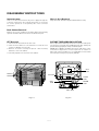
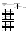
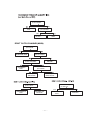
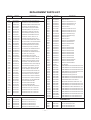
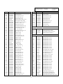
1
website:http://biz.LGservice.com
e-mail:http://www.LGEservice.com/techsup.html
COLOR TV
SERVICE MANUAL
CHASSIS : MC-021A
MODEL:RT-29FB20RB/RP
CAUTION
BEFORE SERVICING THE CHASSIS,
READ THE SAFETY PRECAUTIONS IN THIS MANUAL.
CONTENTS
Contents ................................................................................................................. 2
Safety Precautions ............................................................................................3
Specifications ..................................................................................................... 4
Control Descriptions ........................................................................................ 5
Disassembly Instructions ............................................................................. 8
Adjustment Instructions ............................................................................... 9
Trouble Shooting .............................................................................................. 14
Block Diagram .................................................................................................... 19
Exploded View .................................................................................................. 20
Exploded View Parts List ..............................................................................21
Replacement Parts List ............................................................................... 22
SVC. Sheet ................................................................................................................
- 2 -
SAFETY PRECAUTIONS
IMPORTANT SAFETY NOTICE
Many electrical and mechanical parts in this chassis have special safety-related characteristics. These parts are identified by
in
the Schematic Diagram and Replacement Parts List.
It is essential that these special safety parts should be replaced with the same components as recommended in this manual to
prevent X-RADIATION, Shock, Fire, or other Hazards.
Do not modify the original design without permission of manufacturer.
General Guidance
Before returning the receiver to the customer,
An lsolation Transformer should always be used during
the servicing of a receiver whose chassis is not isolated from
the AC power line. Use a transformer of adequate power rating
as this protects the technician from accidents resulting in
personal injury from electrical shocks.
always perform an AC leakage current check on the exposed
metallic parts of the cabinet, such as antennas, terminals, etc.,
to be sure the set is safe to operate without damage of
electrical shock.
Leakage Current Cold Check(Antenna Cold Check)
It will also protect the receiver and it's components from being
damaged by accidental shorts of the circuitary that may be
inadvertently introduced during the service operation.
If any fuse (or Fusible Resistor) in this TV receiver is blown,
replace it with the specified.
When replacing a high wattage resistor (Oxide Metal Film
Resistor, over 1W), keep the resistor 10mm away from PCB.
Keep wires away from high voltage or high temperature parts.
Due to high vacuum and large surface area of picture tube,
extreme care should be used in handling the Picture Tube.
Do not lift the Picture tube by it's Neck.
X-RAY Radiation
Warning:
The source of X-RAY RADIATION in this TV receiver is the
High Voltage Section and the Picture Tube.
For continued X-RAY RADIATION protection, the
replacement tube must be the same type tube as specified in
the Replacement Parts List.
To determine the presence of high voltage, use an accurate
high impedance HV meter.
With the instrument AC plug removed from AC source,
connect an electrical jumper across the two AC plug prongs.
Place the AC switch in the on positioin, connect one lead of
ohm-meter to the AC plug prongs tied together and touch other
ohm-meter lead in turn to each exposed metallic parts such as
antenna terminals, phone jacks, etc.
If the exposed metallic part has a return path to the chassis, the
measured resistance should be between 1MΩ and 5.2MΩ.
When the exposed metal has no return path to the chassis the
reading must be infinite.
An other abnormality exists that must be corrected before the
receiver is returned to the customer.
Leakage Current Hot Check (See below Figure)
Plug the AC cord directly into the AC outlet.
Do not use a line Isolation Transformer during this check.
Connect 1.5K/10watt resistor in parallel with a 0.15uF capacitor
between a known good earth ground (Water Pipe, Conduit, etc.)
and the exposed metallic parts.
Measure the AC voltage across the resistor using AC
voltmeter with 1000 ohms/volt or more sensitivity.
Reverse plug the AC cord into the AC outlet and repeat AC
voltage measurements for each esposed metallic part. Any
voltage measured must not exceed 0.75 volt RMS which is
corresponds to 0.5mA.
In case any measurement is out of the limits sepcified, there is
possibility of shock hazard and the set must be checked and
repaired before it is returned to the customer.
Leakage Current Hot Check circuit
Adjust brightness, color, contrast controls to minimum.
Measure the high voltage.
The meter reading should indicate
23.5 ¡ 1.5KV: 14-19 inch, 26 ¡ 1.5KV: 19-21 inch,
29.0 ¡ 1.5KV: 25-29 inch, 30.0 ¡ 1.5KV: 32 inch
If the meter indication is out of tolerance, immediate service
and correction is required to prevent the possibility of
premature component failure.
AC Volt-meter
To Instrument's
exposed
METALLIC PARTS
Good Earth Ground
such as WATER PIPE,
CONDUIT etc.
0.15uF
1.5 Kohm/10W
- 3 -
SPECIFICATIONS
Note : Specification and others are subject to change without notice for improvement.
SOUND IF :
O
Video input system:
PAL-B/G, D/K, I/I
SECAM-B/G, D/K/L/L’
NTSC M
O
Intermediate Frequency (Unit : MHz)
VISION IF : 38.9MHz,33.9MHz(SECAM-L’)
COLOR IF : 34.47MHz(4.43)
35.32MHz(3.58)
: NTSC-M
VIF-4.25000MHz
(
): SECAM
VIF-4.40625MHz
O
33.4MHz (B/G)
32.9MHz (I/I)
32.4MHz (D/K,L)
34.4MHz (M)
40.4MHz (L’)
O
Power requirement : 110~240V, 50/60Hz
O
Power consumption : Max 160W
O
CPT : Flat CPT
Tuning range
Band
For TV
B/G
D/K
VHF-Low
Ch2-4
Ch1-5
VHF-High
Ch5-12
Ch6-12
For CATV
I/I
NTSC
S1'-S3', S1
Ch2-13
Ch4-13
S11-S20
Hyper
UHF
S2-S10,
S21-S41
Ch21-69
Ch14-69
O
Tuning system :
FVS
100 Programme memory
200 Programme memory (W/O TXT)
O
Antenna input impedance : VHF/UHF 75 ohm, unbalanced
O
Voice coil impedance : 8 ohm
O
External connection :
AV Input: 4 (side or front:1,rear:2)
Component Input: 2 (rear)
PERI TV Connector: Full Scart:1(AV Input or Scart option)
R,G,B Input: 1(option)
O
External In/Output
Audio-In:0.5Vrms!3db,over 10Kohm
Audio-Out:0.5Vrms!3db,below 1Kohm
Video-In/Out:1Vp-p!3db,75ohm
R,G,B In:0.7Vp-p!3db
O
- 4 -
Feature : NICAM Stereo/Dual
2 Carrier Stereo/Dual
SSC mode(Split Screen)
Multi Picture Display mode(1:4:9 PIP)
Film mode
DBS(option)
Teletext (TOP/FLOF 128 page)
Noise Reduction
Progressive Scan
Motion Detection
Digital EYE
DESCRIPTION OF CONTROLS
All the functions can be controlled with the remote control handset.
Some functions can also be adjusted with the buttons on the front
panel of the set.
Remote control handset
POWER
TV/AV
1
2
3
1
2
3
4
5
6
7
8
9
PSM
0
SSM
I / II
DRP
PICTURE
4
MENU
SOUND
5
PR
6
VOL
VOL
OK
PR
PIP
MUTE
7
PIP PR
PIP PR
ARC
PIP INPUT
PIP SWAP
TEXT
8
POSITION
SCAN
STILL
SIZE
REVEAL
SLEEP
i
MIX
LIST
TIME
?
M
REW
PLAY
FF
P/STILL
STOP
REC
9
EYE/
10
T
U
R
B
O
Before you use the remote control handset, please install the batteries. See the next page.
11
1. TV/AV
selects TV or AV mode.
switches the set on from standby.
2. NUMBER BUTTONS
switches the set on from standby or directly select a number.
3. PSM (Picture Status Memory)
12
recalls your preferred picture setting.
4.
I/II
13
selects the language during dual language broadcast.
14
selects the sound output (option).
15
5. MENU
selects a menu.
6. D / E (Programme Up/Down)
selects a programme or a menu item.
switches the set on from standby.
F / G (Volume Down/Up)
16
adjusts the volume.
adjusts menu settings.
17
OK
accepts your selection or displays the current mode.
18
7. PIP BUTTONS
PIP
switches the sub picture on or off.
19
PIP PR +/selects a programme for the sub picture.
20
PIP SWAP
alternates between main and sub picture.
PIP INPUT
selects the input mode for the sub picture.
SIZE
adjusts the sub picture size.
STILL
freezes motion of the sub picture.
POSITION
relocates the sub picture in clockwise direction.
SCAN
switches on or off the programme scan mode through 12 sub
pictures.
8. PIP SWAP
returns to the previously viewed programme.
selects a favourite programme.
9. LIST
displays the programme table.
10. EYE/ (option)
switches the eye function on or off.
*
- 5 -
11. POWER
switches the set on from standby or off to standby.
12. SSM (Sound Status Memory)
recalls your preferred sound setting.
13. TURBO PICTURE BUTTON
selects Turbo picture.
POWER
TV/AV
11
1
14. DRP (Digital Reality Picture)
switches DRP Pro or 100.
2
15. TURBO SOUND BUTTON
selects Turbo sound.
3
16. MUTE
switches the sound on or off.
1
2
3
4
5
6
7
8
9
PSM
0
SSM
I / II
DRP
PICTURE
4
17. ARC (Aspect Ratio Control)
changes the picture format.
MENU
SOUND
5
18. TELETEXT BUTTONS (option)
These buttons are used for teletext.
For further details, see the ‘Teletext’ section.
12
T
U
R
B
O
13
14
15
PR
6
VOL
VOL
OK
PR
19. SLEEP
sets the sleep timer.
PIP
MUTE
16
7
20. VCR BUTTONS
control a LG video cassette recorder.
PIP PR
PIP PR
PIP INPUT
PIP SWAP
ARC
17
Note : In teletext mode, the PIP PR +/-, PIP SWAP and PIP INPUT 8
buttons are used for teletext function.
POSITION
SCAN
STILL
SIZE
SLEEP
19
LIST
Internal generator charge
REW
PLAY
FF
P/STILL
STOP
REC
9
EYE/
The remote control handset can be charged with the internal electric 10
generator. To charge the remote control handset do the followings;
1. In first use,
20 rotation of the handle in the arrow direction as picture below
-> waiting for one minute -> 20 rotation again -> waiting for one
minute again -> 20 rotation again -> beginning to use
2. In usual use
5 or 6 rotation -> resuming to use
Note : Do not rotate the handle too rapidly for the protection of the
remote control handset.
- 6 -
20
Front panel
RF/RT-29FB20 series
7
S-VIDEO
ON/OFF
MENU
VOL
OK
PR
VIDEO
1
2 3
4
5
6
AV4
PC INPUT
9
L/MONO AUDIO R
8
Side panel
1. MAIN POWER (ON/OFF)
switches the set on or off.
2. POWER/STANDBY INDICATOR
illuminates red when the set is in standby mode and green when the
set is switched on.
3. REMOTE CONTROL SENSOR
4. MENU
selects a menu.
5. OK
accepts your selection or displays the current mode.
F / G (Volume Down/Up)
adjusts the volume.
adjusts menu settings.
D / E (Programme Up/Down)
selects a programme or a menu item.
switches the set on from standby.
6. EYE (option)
adjusts picture according to the surrounding conditions.
7. HEADPHONE SOCKET
Connect the headphone plug to this socket.
8. AUDIO/VIDEO IN SOCKETS (AV4)
Connect the audio/video out sockets of external equipment to these
sockets.
S-VIDEO/AUDIO IN SOCKETS (S-AV)
Connect the video out socket of an S-VIDEO VCR to the S-VIDEO
socket.
Connect the audio out sockets of the S-VIDEO VCR to the audio
sockets as in AV4.
9. PC INPUT SOCKET
Connect the monitor output socket of the PERSONAL COMPUTER
to this socket.
Note : Set the resolution of PC to VGA 640x480 (60 Hz) video mode
to use this set as PC monitor.
- 7 -
DISASSEMBLY INSTRUCTIONS
Important note
Chassis Assy Removal
This set is disconnected from the power supply through the
converter transformer. An isolating transformer is necessary
for service operations on the primary side of the converter
transformer.
Grasp both side of Frame and pull it backward smoothly.
Back Cabinet Removal
Remove the screws residing on the back cabinet and carefully
separate the back cabinet from the front cabinet. (Fig. 2-1).
CPT Removal
PICTURE TUBE HANDLING CAUTION
1. Pull out the CPT board from the CPT neck.
2. Place the front cabinet on soft material not to mar the front
surface or damage control knobs.
3. Remove 4 screws securing the picture tube mounting
brackets to the front cabinet.
4. Carefully separate CPT from the front cabinet.
Due to high vacuum and large surface area of picture tube, great
care must be exercised when handling picture tube. Always lift
picture tube by grasping it firmly around faceplate.
NEVER LIFT TUBE BY ITS NECK! The picture tube must not be
scratched or subjected to excessive pressure as fracture of
glass may result in an implosion of considerable violence which
can cause personal injury or property damage.
CPT
PCB
Remove
Screws
A/V PCB
4
Control
PCB
VCD
PCB
MICOM
PCB
Main PCB
Fig. 2-1
Fig. 2-2
- 8 -
ADJUSTMENT INSTRUCTIONS
1.Safety Precautions
5. Purity & convergence Adjustment
1. It is safe to adjust after using insulating transformer between
the power supply line and chassis input to prevent the risk of
electric shock and protect the instrument.
2. Never disconnect leads while the TV receiver is on.
3. Don't short any portion of circuits while power is on.
4. The adjustment must be done by the correct appliances.
5. Unless otherwise noted, set the line voltage to 220Vac!10%,
50Hz.
5. The adjustment of TVshould be performed after warming up
for 15 minutes.
5-1. Preparation for Adjustment
Adjustment should be operated when using the CPT(without
ITC from CPT manufacturing place)
*This adjustment must follow the sequence as shown picture
below.
5-2. Purity Adjustment
1) Degauss the CPT and CABINET enough.
CPT Assembling
As preparatory operations before
assembling CPT, wind cotton Tape for
protecting to CPT NECK and DY, CPT
connection parts. At this moment, end of
tape should be over-lapped and wound in
direct route to the NECK.
Assembling DY to CPT
Fix the Magnet to the position as shown
picture below. Be careful not to make CPT
neck shadow while adjusting DY.
2.Test Equipment required
1.
2.
3.
4.
5.
RF signal generator (with pattern generator)
DC Power Supply
Multimeter (volt meter)
Oscilloscope
Color analyzer
3.DVCO Adjustment
1) This is for adjustment of VPC9407,crystal oscillator
frequency after receiving a company Digital
pattern.(PAL:EU05CH,NTSC:13CH)
2) When entering adjustment mode by pressing IN-START
button,DVCO adjustment is operating automatically.
(T/X doesn’t operating occassionally during DVCO
adjustment.)
HEAT RUN
Degaussing
6pole 4 2
STC Adjustment
2¡ 2mm
4. Focus Adjustment
PURITY Adjustment
4-1. Preparation for Adjustment
Tune the TV set to receive a digital pattern.
DY Fixing
4-2. Adjustment Method
1) Adjust the lower Focus volume of FBT for the best focus of
vertical line B.
2) Adjust the upper Focus volume of FBT for the best focus of
area A.
Let the screen Standard condition. Operate
Heat-Run at least 15 minutes.
SCREEN Voltage adj.
W/B Fixing
Torque is to be 9-11 kg f.cm when fixing
DY.
FOCUS not yet ADJ.
STC not yet ADJ.
A
B
DYC not yet ADJ.
Fig. 1
2) Receive red RASTER signal.(PG50ch)
3) Remove fixing screw of DY and stick DY to opening
part(CPT FUNNEL part)
4) Make crossing adjustment to the Magnet of CPT and make
the R-land is placed on center correctly. At this moment, 4
pole and 6 pole magnet should be at the position of no
magnetic field.
b
3) Repeat above step 1) and 2) for the best overall focus.
- 9 -
5) Move DY and make whole screen to be equal red, and fix
the DY with fixing SCREW after checking color pollution in
each single color and white RASTER of green/blue/red.(At
this time, be careful about inclination and DY should be fixed
keeping horizontality.)
6) Check the receiver in direction of East, West, South, North.
Adjust with supporting MAGNET when adjustment is not
operated.
coordinates of Low Light which is specified in "__clause".
e- Repeat the adjustment from 'a' to 'd' until the High, Low
color coordinates of "_clause" is satisfied.
f- Check the adjusted color coordinates with white balance
meter.
5-3. Convergence Adjustment
Color Tem.
X
Y
Memo
13000K
266!8
273!8
NON EU
9000K
288!8
295!8
EU
This adjustment should be operated at the best condition of
FOCUS after finishing the PURITY adjustment.
1) BACK RASTER receives black CROSS HATCH signal.
2) Adjust Brightness so that there are 9-12 dots.
3) Widen two tabs of 4pole Magnet with equal angles and
accord red, blue vertical lines at the center of screen.
4) With keeping angle of "c. clause", rotate tab and accord
red/blue, green vertical lines at the center of screen.
5) Widen two tabs of 6pole Magnet with equal angles and
accord red, blue vertical lines at the center of screen.
6) With keeping angle of "e. clause", repeat the adjustment from
c to e keeping in mind the movement of red, blue, green
when the horizontal lines are twisted.
7) Move DY up, down, left, right and make the convergence to
be optimal condition and stick rubber wedge to CPT so that
the DY not to move.
MENO
RC
001F
Low Light Adj
GC
0019
Low Light Adj
BC
001F
Low Light Adj
RD
001F
High Light Adj
GD
0019
High Light Adj
BD
001F
High Light Adj
8-1. Preparation for Adjustment
1) Deflection Data Adjustment should be performed with the
remote controller for handset.
2) Enter the Adjustment mode by pressing the INSTART button.
3) Select the DEFLECT to deflection Data Adjustment.
4) Press the Channel UP/DOWN button to select adjustment
items.
5) Press the Volume UP/DOWN button to adjust the data.
6) The TV set receives PAL-B/G Digital pattern.
6-1. Preparation for Adjustment
1) Connect power to TV Set and let POWER ON condition.
2) Operate screen more than 15 minutes before adjustment.
6-2. Adjustment Method
NOTE : If production line doesn’t the production line of LG
TV,receive available deflection adjustment pattern.
7. White balance Adjustment
7-1. Preparation for Adjustment
1) This adjustment should be performed after screen
adjustment.
2) Tune the TV set to receive an 100% white pattern.
LG 29” FLAT
8. Deflection Data Adjustment
6. Screen voltage Adjustment
1) Adjust in no RF signal condition.
2) Press ADJ KEY on the R/C for adjustment and make
horizontal line.
Turn the Screen Volume so that horizontal line not to be
shown and then change oppositely to finish the adjustment
at the showing place.
Menu
voltage
7-2. Adjustment Method
1) Enter the adjust mode by pressing the IN-START button.
2) Press Channel UP/DOWN button for desirous function
Adjustment.
3) Press Volume UP/DOWN button to adjust the data.
4) Adjustment Sequence
a- Change the "CONTRAST", "BRIGHT" and adjust to be 3.5
Ft_L.
b- Adjust "Y" value of High Light with GD(G-Drive) and adjust
"X" value with BD(B-Drive) and make color coordinates
of High Light which is specified in "__clause".
c- Change the "CONTRAST", "BRIGHT" and adjust to be 4.5
Ft_L.
d- Adjust "Y" value of Low Light with GC(G-Cutoff) and
adjust "X" value with BC(B-Cutoff) and make color
- 10 -
VL (Vertical Linearity)
Adjust so that the boundary line between upper and lower half
is in accord with geometric horizontal center of the CPT.
VA (Vertical Amplitude)
Adjust so that the circle of a digital circle pattern may be
located within the effective screen of the CPT.
SC (Vertical “S” Correction)
Adjust so that all distance between each horizontal lines are
to be the same.
VS--(Vertical Shift)
Adjust so that the horizontal center line of a digital circle pattern
is in accord with geometric horizontal center of the CPT.
HS (Horizontal Shift)
Adjust so that the vertical center line of a digital circle pattern
is in accord with geometric vertical center of the CPT.
EW (Horizontal Width)
Adjust to that a digital circle pattern looks like exact circle.
Fig. 2 <50HZ>
Menu
Range
PAL
100HZ
NTSC
60HZ
480P
1080I
VGA
VS
0 ~ 3F
1E
18
17
11
1D
VA
0 ~ 3F
1E
1F
1E
23
2B
HS
0 ~ 3F
1C
29
14
25
10
EW
0 ~ 3F
1D
1D
1F
2A
1C
EP
0 ~ 3F
A
C
B
E
7
EPP
0 ~ 3F
1E
1D
1B
14
22
A-ANG
0 ~ 3F
1F
1F
1D
1D
21
A-BOW
0 ~ 3F
1E
20
1E
1E
1E
UC
0 ~ 3F
1F
21
20
20
1C
LC
0 ~ 3F
1F
22
20
1F
15
U-VL
0 ~ 0F
02
2
2
2
2
L-VL
0 ~ 0F
06
7
7
7
6
VL
0 ~ 0F
05
5
5
5
5
SC
0 ~ 0F
05
4
4
4
4
V-SCR
0 ~ 3F
21
21
21
21
21
Fig. 2<60HZ>
* Adjust in PAL100Hz and PAL50Hz, NTSC60Hz, 480P, 1080I,
VGA Mode don't need to be adjusted because they are changed
into correction about adjustment value of PAL 100Hz.
EPP(East-West Pin Phase)
Adjust so that horizontal width of the uppermost part and
horizontal width of the lowermost part of received screen are
to be the same.
* But, If the inclination adjustment is not correct when checking
NTSC60Hz, 480P, 1080I, VGA Mode after finishing adjustment in
PAL100Hz, adjust each Mode again.
UC(Upper Coner Correction)
Adjust so that coner vertical line of upper-left and upper-right
to be straight line after finishing EP adjustment.
9. OPTION Adjustment
9-1. Preparation for Adjustment
LC(Lower Coner Correction)
Adjust so that coner vertical line of lower-left and lower-right
to be straight line after finishing EP adjustment.
A-BOW(AFC Bow)
In line adjustment, not to change default value is basic.
1) This decides funtion in accordance with model.
Press the SVC TX adjustment button(IN-START button) at
SVC mode,then adjust the option at OPTION 1,2,3,4 mode.
2) Mark the option adjustment data like [111,11,111,11] in
BOM.
[113,63,112,128]
A-ANG(AFC Angle)
In angle adjustment, adjust until inclination of left and right
screen should be precise.
V-SCR(V-Scroll)
Only adjust when V SHIFT is impossible.
O
D
D
D
D
OPTION 1
OPTION 2
OPTION 3
OPTION 4
Mark of BOM
LEVEL
PART NO.
1.
3141VMN382A
SPECIFICATION DESCRIPTION
JOB EXP.
MAIN[MC-022A] CHASSIS ASSY OP[113,63,112,128]
The OPTION 1 data is 113,OPTION 2 data is 63,the oOPTION 3 data is 112,the
OPTION 4 data is 128 in this model.
- 11 -
Table 3. OPTION 3 Function
9-2. Adjustment Method
1) Input data directly by the buttons corresponded with
OPTION1 ??(0~255), OPTION2 ??(0~255), OPTION3
???(0~250).
2) Option4???(0~116) controls correspondinglines directly
relate with OSD and TXT LANG.
3) Select each OPTION function by the CH Up/Down button and
then set up each OPTION by the VOL Up/Down button.
Option
WIDE
CH+AU
HDEV
Table 1. OPTION 1 Function
Option
200 PR
TSEAR
I/II SV
TOP
EYE
A2 ST
SYS
Code
Function
Remark
0
100 PROGRAM SAVE
1
200 PROGRAM SAVENICAM
0
Without Turbo Search function
WL/CL
1
With Turbo Search function
CT/CE/WT/WE
0
NO SAVE DUAL/SOUND Condition
EU(WE/WL/CE/CL
1
SAVE DUAL SOUND Condition
NON-EU(WT/CT)
0
FLOP TEXT
Without TOP TEXT
1
TOP TEXT
0
Without EYE
1
With EYE
0
NICAM
1
NICAM&FM STEREO/DUAL
0
B/G,I.D/K
1
B/G
2
B/G,I.D/K,M
3
RESERVED
Table 2. OPTION 2 CODE Data
Option
ACMS
VOL
H-PHON
DVD
Code
Function
0
Without ACMS funtion
1
With ACMS funtion
0
NORMAL VOLUME CURVE
1
RUSHED VOLUME CURVE
0
Without HEADPHONE
1
With HEADPHONE
0
Without DVD INPUT
1
With DVD INPUT
Remark
0
SAV3
WOOF
VGA
AV SV
1
AV3 Y&C
0
Without WOOFER
1
With WOOFER
0
Without VGA
1
With VGA
0
1
- 12 -
Code
Function
0
4 : 3 TV
1
16 : 9 TV
0
Without D/K CHINA or BB sys.
1
With D/K CHINA or BB sys.
0
NO SAVE DUAL/SOUND Condition
1
SAVE DUAL SOUND Condition
Remark
HIGH DEVIATION
Table 4. OPTION 4 Funtion
CODE
LANG
0
E Only
1
English+EU 5
2
English+Other EU
3
FARSI
4
ARAB URDU
5
E + HINDI
6
E+I+M+V
7
E + THAI
8
E + CHINA
0
West Europe
1
East Europe
2
Turkey EU1
3
EAST EU2
4
Cyrillic 1
5
Cyrillic 2
6
Cyrillic 3
7
Turkey/Greek 1
8
Turkey/Greek 2
9
Turkey/Greek 3
10
Arab/France
11
Arab/English
12
Arab/Hebrew 1
13
Arab/Hebrew 2
14
Farsi/English
15
Farsi/France
16
Farsi all
T LAN
Funciton
Language
OPTION
- 13 -
TROUBLE SHOOTING
Check pin 2 of P005A.
1V
Check / Replace
Q871,Q852,Q854,
IC803,IC851
Check the voltage at
pin 10 of P004A.
2Vp-p
Check the H-DRV voltage at
pin 5 of P214A.
5.5Vp-p
Check / Replace
IC001,Q002.
0V
Check / Replace
FR359,FR360,D339,D349,IC301.
0V
Check / Replace
IC1113.
Check the voltage of C404(+).
67V
Check / Replace
R407,D861,FB854.
Check the voltage at
pin 2 of FBT.
135V
Check / Replace
R865,R864,L853,D850,FB856.
Check / Replace
Q401, Q402, T401.
Check the voltage of C821.
Check / Replace
SW1101,F1101,T1101,
DB814,TH810.
Check the voltage at
pin 4 of STR.
17.8V
Check / Replace
R809,D802,R803,R810.
Check / Replace
IC801 and the
secondary part of
POWER circuit.
- 14 -
Check if heater element is lighting.
Check the heater voltage.
Increase the screen
voltage of FBT.
Check/Replace
FR442,R910.
Check/Replace
CPT.
Screen is black.
Retrace line is
visible.
Check the waveform
at pin 3 of ic901,902,903
Check FBT & CPT socket
& CPT.
YES
NO
Check the waveform
at pin 62,63,64 of IC501S.
(RGB out)
YES
Check the waveform
at pin 7 of IC901,902,903.
NO
NO
Check the waveform
at pin 20,21,22 of IC501S.
Check/Replace
Q503,504,505.
YES
YES
Check/Replace
IC901,902,903.
Check/Replace
IC101.
NO
Check the waveform
at pin 2,76,79 of IC101S.
Check/Replace
IC501S.
YES
NO
Check/Replace
IC401S,FL201S,202S,203S.
Check the waveform at
PIN52 of IC101S.(CVBS1)
YES
NO
Check/Replace
IC101S.
YES
Check/Replace
IC201S.
- 15 -
Check the waveform at
Pin2 of P213A.(Vmain)
NO
Check the waveform at
TU101,Q108.
Check the voltage at pin3,13
of IC652(SOUND AMP).
18V
D850,F851.
7
2.5V
0V
CHECK/REPLACE
IC601,Q650.
CHECK/REPLACE
Q651.
CHECK/REPLACE
TU101.
Check the waveform
at pin 11 of P901B.
NORMAL
Checkthe waveform at
pin10 of HIC951.
Check the Vcc at pin11(135V).
Check the Vcc at pin4(12V).
Q501,IC501S.
PIN CUSHION
47
IC501S.
IC501S.
IC302
R424.
IC302
Q404, Q405.
- 16 -
D402.
Check the waveform at
pin 21,22 of IC601.
YES
Check / Replace
IC601.
Check the waveform at
pin 1,3 of IC602.
YES
Check / Replace
H/P JACK.
Check / Replace
IC603.
DON'T CATCH CHANNEL(MAIN)
Check the voltage at
pin9 of TU101.
Check/Replace
R403,FB854,D861,ZD102.
Check the voltage at
pin13 of TU101(5V).
Check the waveform at
pin19 of TU101(Video).
Check/Replace
TU101.
Check/Replace
IC854,F856.
Check the waveform at
pin2 of P213A.
Check/Replace
IC201S,IC101S.
Check/Replace
Q108,C114,R119.
Check the voltage at
pin 14 of TU101.
Check the voltage at
pin 14 of T101.
2.5V
CHECK/REPLACE
TU101.
CHECK/REPLACE
IC001,IC007.
- 17 -
CHECK/REPLACE
TU101.
0V
CHECK/REPLACE
IC001,IC007.
Check the waveform
at pin 2 of P004A.
NO
YES
Check the waveform at
pin4 of P213A(CVBS)
Check the waveform at
pin21 of IC001(CVBS)
Check the voltage
at pin 1,6 of IC301.
Check / Replace
FR359,FR360,D339,D349.
Check the waveform
at pin 52,53 of IC501S.
Check / Replace
IC301, D301.
Check / Replace
IC501S,R540,R541.
NO DVD/COMPONENT PICTURE
Check Y,Cb,Cr signal
input from JA201.
YES
Check the waveform at pin46,47,48 of IC101S.
(From comp1,480i input)
Check the waveform at pin1,2,3 of IC401S.
(From comp1,480p/1080i input)
Check the waveform at pin7,8,9 of IC401S.
(From comp2,480p/1080i input)
YES
NO
Check/Replace
Q301,302,303,304,305,306.
Check the waveform at
pin25,26,27 of IC401S.
NO
YES
Check / Replace
IC401S.
Check the waveform at
pin 62,63,64 of IC501S.
NO
Check / Replace
IC501S
- 18 -
YES
Check / Replace
Q503,504,505,CPT Board.
- 19 -
R
L
RF OUT
WOOFER SPK
CENTER SPK
TDA7253
AUDIO AMP
TDA7297
AV4
AV3
AV2
CXA2069
SIF_M
V(pip)
MICOM
Board
2M
ROM
SDA
SCL
(Digital Processor)
1M
SRAM
V(main)
(CRT Driver)
CXA2150
100Hz Board
Y,U,V
(Video S/W)
CXA2151
SDA
SCL
MNT L,R
MSP3411
SOUND
Processor
PIP L,R
(A/V Switch)
IN4
480P/1080I
AV1
IN3
480P/1080I
L R
L R
480I
V(pip)
V(main)
IN1
IN2
VGA In
EEPROM
AT24C16
SCL,SDA
MICOM
SDA5550
SCREEN
480I/P
E/W
FBP
HDRIVE
ABL
VPROT
VD+,VD-
ABNORMAL
FBP
VFB
60V
24V(Sound)
18V(Sound)
6.5 V
HEATER
SCREEN
FBT FOCUS1.2
ANODE
AC IN
SMPS Trans
EE5555
STR- F6658
200V
¡ 14, 28V
FBP
POWER
DEG
ST- BY(13.5V)
B+
(135V)
B+
ABL
SCREEN
FOCUS1,2
CPT
HEATER
V- DY H- DY
G
B
200V
R
H- OUT
2SC5446
S.M.P.S/DEF
H- DRIVE
IRFIBC20G
V- OUT
LA7845
SANYO HIC
VM
TDA6111Q
RGB
IK
CPT Board
C
C
C
MNT OUT
SDA9407
Y,U,V,Hs,Vs
V IN (MAIN)
(Color decoder
&
Scan converter)
V/A
(PIP)
VM
IK
RGB
C
C
C
COMP2
COMP1
AV3
AV2
REAR A/V
AV1
E/P OUT
S- IN
AV4
SIDE A/V
TUNER2 (SUB)
SIF_M
C
C
C
TUNER1 (MAIN)
BLOCK DIAGRAM
D- COIL
EXPLODED VIEW
943
913
150
400
153
510
401
170
112
402
503
570
520
530
540
P801
550
501
123
121
126
120
125
124
310
560
600
330
320
700
- 20 -
The components identified by mark
critical for safety.
Replace only with part number specified.
EXPLODED VIEW PARTS LIST
LOCA. NO
112
PART NO
DESCRIPTIONS
2426VSF0011
CPT SET, 2426GF239AR A68QCU259X000MYF BARE LGESY LOCAL
6341V29004C
BARE CPT ASSEMBLY 2426GF239AR6150V-5006E
120
120-C77N
SPEAKER,FULLRANGE C122S01K1450 ESTEC MID-RANGE 8
121
120-C76G
SPEAKER,TWEETERC050TX-357K14 FOSTER 8 OHM 10/
123
6400VA0015C
124
6400VA3002C
SPEAKER,GENERALC123P01K1452 ESTEC 8 OHM 7/10W
125
3110V00200A
CASE DOME FRONT 29FB20 PP .
3110V00200B
CASE, DOME FRONT,CKD,RT-29FB20 - PP
126
SPEAKER,FULLRANGE C151P01K1451 ESTEC WOOFER 8OHM
3550V00226A
COVER,DOME PP 29FB20 .
3550V00226B
COVER, DOME,CKD,RT-29FB20 - PP
150
6140VC2005F
COIL,DEGAUSSING 29 FLAT ASSY(W) SELLA
153
6150V-5006E
DY 6150Z-1343B 29” LPD.
170
170-844K
300
3091V00A86A
CABINET ASSY 3090V00341 LG
5020V00657A
BUTTON,CONTROL
5020V00657B
BUTTON, CONTROL RT-29FB20RB ABS 6KEY NON
310
CPT EARTH 29” 98T 4LUG LEAD SET SPRING(5
320
320-062E
330
5020V00656A
BUTTON,POWER
5020V00656B
BUTTON, POWER RT-29FB20RB ABS NON NON
3809V00A44A
BACK COVER ASSY
3809V00A44W
BACK COVER ASSEMBLY, RT-29FB20RP(W/O PC)CKD NON LGESY
400
401
402
SPRING,KNOB
4811V00025A
BRACKET ASSY PS 29FB20(FOR LEFT SPK)
4811V00025B
BRACKET ASSEMBLY, COVER SPK(L),CKD,RT-29FB20 MC021A
4811V00026A
BRACKET ASSY PS 29FB20(FOR RIGHT SPK)
4811V00026B
BRACKET ASSEMBLY, COVER SPK(R),CKD,RT-29FB20 MC021A
501
4810V00379L
BRACKET,MAIN
503
4811V00024A
BRACKET ASSEMBLY,HIPS/ABS PHONO+PHONO
510
6871VSMD14A
PWB ASSY,SUB MC-021A LG29 CPT SET
6871VSMU32B
PWB(PCB) ASSEMBLY,SUB MC021A LG29”CPT SET,CKD
520
6871VMMB38A
PWB ASSY,MAIN (MC-021A) RT29FB20RB.ATLL
6871VMMP29D
PWB(PCB) ASSEMBLY,MAIN MC-021A RT-29FB20RP.KTLLSP8 MONGOL
6871VSMD13A
PWB ASSY,VCD MC-021A 100HZ,RT29FB20RB.A
530
540
550
560
570
600
6871VSMD13D
PWB(PCB) ASSEMBLY,SUB VCD MC021A 100HZ CHINA COMP+PH
6871VSMD15A
PWB ASSY,MC-021A MICOM RT29FB20RB.A
6871VSMD15V
PWB(PCB) ASSEMBLY,SUB MC021A RT-29FB20RP.KTLLSP8 MONGOL
6871VSMD47A
PWB ASSY,MC-021A CTRL FB20RB SET
6871VSMU33B
PWB(PCB) ASSEMBLY,SUB CONT MC021A CTRL FB20RP,CKD
6871VSMD18A
PWB ASSY,MC-021A CTRL FB20
6871VSMU36B
PWB(PCB) ASSEMBLY,SUB MC021A CTRL FB20,CHINA CKD”
6871VSMU34B
PWB(PCB) ASSEMBLY,SUB MC021A REACTOR,SUB”
6871VSMD17A
PWB ASSY,MC-021A SIDE A/V FB20
6871VSMU35B
PWB(PCB) ASSEMBLY,SUB A/V MC021A SIDE A/V FB20,CHINA CKD
700
0IGL120104A
913
332-229H
943
1PTF0403116
P801
174-322D
6411VCH001E
IC,CDS SENSOR MODULE(P1201-04)
SCREW ASSY HEXAGON HEAD (L:40,D:18)
SCREW,TAP TITE(P) D4.0 L16.0 MSWR3/FZB
POWER CORD W/FILTER L=300(179B)VDE
POWER CORD ASSEMBLY, YP-51 YUKITA CCEE 2400MM HOUSING LOCAL
- 21 -
is
REPLACEMENT PARTS LIST
LOCA. NO
PART NO
DESCRIPTION
IC
D850
0ISK100300A
IC,SLA1003 SIP12 BK DIODE MODULE(
HIC951
0IZZVF0018B
IC,STK396-120 11P ST SCAN VELOCIT
IC001
0ISM555000A
IC,SDA5550 MQFP100 BK MICOM TXT M
IC002
0IAL241600B
IC,AT24C16-10PC 8D EEPROM 16K
IC003
0ISS610082A
IC,K6T1008V2E-TB(F)70 [K6T1008BLT
IC004
0ISG272012A
IC,M27W201(2M BIT 3.3V) 32PLCC TP
IC005
0IFA752700A
IC,KA75270Z 3 TP RE-SET IC MC-007
IC006
0IFA754207A
IC,KA75420ZTA(KA7542ZTA) 3P,TO-92
IC007
0IMI623200B
IC,M62320FP,I/O EXPANDER 16P SOP
IC008
0IMCRUK002B
IC,S78DL33L AUK 3P, TO-92L TP 3.3
IC009
0IMCRUK003A
IC,S5225M AUK 5SOP, SOT-25 R/TP 1
IC101S
0IMCRMN015A
IC,VSP9407B MICRONAS 80QFP TRAY C
IC106S
0ISA721700C
IC,LA7217M MFP14 TP SYNC SEPARATO
IC190
0ISA164500B
IC,LB1645N 10SIP BK MOTOR DRIVE I
IC201S
0ISO206900A
IC,CXA2069Q QFP64 BK I2C BUS AV S
IC202S
0ISH323422A
IC,PQ3RF23 4P(TO-220) 3.3V REGUL
IC203S
0IMCRSG011A
IC,LD1086V18 SGS-THOMSON 3DIP,TO-
IC204S
0IMCRKE002A
IC,KIA78R09PI KEC 4PIN,TO220IS-4
IC205S
0IMCRSG011A
IC,LD1086V18 SGS-THOMSON 3DIP,TO-
IC301
0ISA784500A
IC,LA7845 7SIP V/OUT(1.5A)
IC401
0IKE455800E
IC,KIA4558 8DIP DUAL OP AMP
IC401S
0IMCRSO008A
IC,CXA2151Q SONY 48P QFP TRAY 60”
IC501S
0IMCRSO007A
IC,CXA2150Q SONY 64P QFP TRAY 60”
IC601
0IIT341120C
IC,MSP3411G VER B8 52P DIP ST ADD
IC602
0ISG725300A
IC,TDA7253 11P,SIP BK 8W AUDIO AM
IC603
0ISG282200A
IC,TDA2822M 8D DUAL AUDIO AMP(1W)
IC650
0IFA754207A
IC,KA75420ZTA(KA7542ZTA) 3P,TO-92
IC652
0ISG729700A
IC,TDA7297 15P,SIP BK 2CH 15W DUA
IC801
0ISK665813A
IC,STR-F6658B(LF1352) 5PIN SIP BK
IC802
0ILI817000G
IC,LTV817M-VB 4P,DIP BK PHOTO COU
IC803
0ILI817000G
IC,LTV817M-VB 4P,DIP BK PHOTO COU
IC851
0IKE780500Q
IC,KIA7805API 3P TO-220 ST REGULA
IC853
0ISS278120A
IC,KA278R12 4P,TO-220F BK LOW DRO
IC854
0ISS278050A
IC,KA278R05 4P,TO-220F BK LOW DRO
IC856
0ISK135000A
IC,SE135N(LF12) 3P 135V ERROR AMP
IC901
0IPH611190A
IC,TDA6111Q 9SIP RGB AMP
IC902
0IPH611190A
IC,TDA6111Q 9SIP RGB AMP
IC903
0IPH611190A
IC,TDA6111Q 9SIP RGB AMP
IC1251
0IRH707800A
IC,BA7078S 18P,SDIP BK SYNC DISCR
Q003
0IFA270000A
IC,2N7000TA TO-92, 3P TP LEVEL SH
Q004
0IFA270000A
IC,2N7000TA TO-92, 3P TP LEVEL SH
Q251
0IFA270000A
IC,2N7000TA TO-92, 3P TP LEVEL SH
Q252
0IFA270000A
IC,2N7000TA TO-92, 3P TP LEVEL SH
DIODE
D001
0DS113379BA
DIODE,SWITCHING 1SS133 T-72
D190
0DS113379BA
DIODE,SWITCHING 1SS133 T-72
D301
0DD200009AF
DIODE,RECTIFIERS RU2M V(1)
D339
0DD200009AF
DIODE,RECTIFIERS RU2M V(1)
D349
0DD200009AF
DIODE,RECTIFIERS RU2M V(1)
D402
0DD011150AA
DIODE,RECTIFIERS ESC011M-15 400V
LOCA. NO
PART NO
DESCRIPTION
D403
0DD100009AU
DIODE,RECTIFIERS EU1AV(1) T
D405
0DD414809ED
DIODE,1N4148 TA
D410
0DD150009CA
DIODE,RECTIFIERS RGP15J TP
D413
0DD150009CC
DIODE,RECTIFIERS RGP15G TP
D414
0DD100009AE
DIODE,RECTIFIERS RU1A V(1)
D425
0DD414809ED
DIODE,1N4148 TA
D502
0DS113379BA
DIODE,SWITCHING 1SS133 T-72
D503
0DS113379BA
DIODE,SWITCHING 1SS133 T-72
D504
0DS113379BA
DIODE,SWITCHING 1SS133 T-72
D802
0DD100009AM
DIODE,RECTIFIERS EU1ZV(1)
D803
0DD100009AM
DIODE,RECTIFIERS EU1ZV(1)
D804
0DD414809ED
DIODE,1N4148 TA
D857
0DD414809ED
DIODE,1N4148 TA
D858
0DD420000BB
DIODE,D4L20U SHINDENGEN
D859
0DD150009CA
DIODE,RECTIFIERS RGP15J
D861
0DD060009AC
DIODE,RECTIFIERS TVR06J
D866
0DD414809ED
DIODE,1N4148 TA
D900
0DD060009AC
DIODE,RECTIFIERS TVR06J
D901
0DD060009AC
DIODE,RECTIFIERS TVR06J
D902
0DD060009AC
DIODE,RECTIFIERS TVR06J
D903
0DD060009AC
DIODE,RECTIFIERS TVR06J
D904
0DD060009AC
DIODE,RECTIFIERS TVR06J
D908
0DD060009AC
DIODE,RECTIFIERS TVR06J
D909
0DD060009AC
DIODE,RECTIFIERS TVR06J
D910
0DR140059AC
DIODE,RECTIFIERS 1N4005GP
D950
0DD060009AC
DIODE,RECTIFIERS TVR06J
DB814
0DRGS00011A
DIODE,RECTIFIERS GSIB660
LD1101
162-002B
LED LED ASSY
ZD001
0DZ620009BB
DIODE,ZENERS MTZJ6.2B TP ROHM-K DO34 0.5W
ZD002
0DZ910009AJ
DIODE,ZENERS MTZJ9.1B TP ROHM-K DO34 0.5W
ZD003
0DZ620009BB
DIODE,ZENERS MTZJ6.2B TP ROHM-K DO34 0.5W
ZD004
0DZ620009BB
DIODE,ZENERS MTZJ6.2B TP ROHM-K DO34 0.5W
ZD101
0DZ330009BA
DIODE,ZENER HZT33(TP) HITACHI
ZD102
0DZ330009BA
DIODE,ZENER HZT33(TP) HITACHI
ZD201
0DZ620009BB
DIODE,ZENERS MTZJ6.2B TP ROHM-K DO34 0.5W
ZD351
0DZ750009AG
DIODE,ZENERS MTZJ7.5B TP ROHM-K DO34 0.5W
ZD403
0DZ510009AB
DIODE,ZENERS MTZ5.1B TP ROHM-K
ZD601
0DZ820009AH
DIODE,ZENERS MTZJ8.2B TP ROHM-K DO34 - 8.2V
ZD650
0DZ620009BB
DIODE,ZENERS MTZJ6.2B TP ROHM-K DO34 0.5W
ZD901
0DZ910009AJ
DIODE,ZENERS MTZJ9.1B TP ROHM-K DO34 0.5W
ZD930
0DZ180009AG
DIODE,ZENERS MTZJ18B TP ROHM-K DO34 - 18V
ZD1201
0DZ620009BB
DIODE,ZENERS MTZJ6.2B TP ROHM-K DO34 0.5W
ZD1202
0DZ620009BB
DIODE,ZENERS MTZJ6.2B TP ROHM-K DO34 0.5W
ZD1205
0DZ620009BB
DIODE,ZENERS MTZJ6.2B TP ROHM-K DO34 0.5W
ZD1206
0DZ620009BB
DIODE,ZENERS MTZJ6.2B TP ROHM-K DO34 0.5W
ZD1251
0DZ510009DB
DIODE,ZENERS MTZJ5.1B TP ROHM-K DO34 - 5
ZD1252
0DZ510009DB
DIODE,ZENERS MTZJ5.1B TP ROHM-K DO34 - 5
TRANSISTOR
Q001
0TR387500AA
TR,CHIP 2SC3875S(ALY) KEC
Q002
0TR387500AA
TR,CHIP 2SC3875S(ALY) KEC
Q006
0TR150400BA
TR,CHIP 2SA1504S(ASY) KEC
Q007
0TR150400BA
TR,CHIP 2SA1504S(ASY) KEC
- 22 -
For Capacitor & Resistors,
the charactors at 2nd and 3rd
digit in the P/No. means as
follows;
LOCA. NO
PART NO
CC, CX, CK, CN : Ceramic
CQ : Polyestor
CE : Electrolytic
RD : Carbon Film
RS : Metal Oxide Film
RN : Metal Film
RF : Fusible
DESCRIPTION
LOCA. NO
PART NO
DESCRIPTION
Q008
0TR150400BA
TR,CHIP 2SA1504S(ASY) KEC
Q605
0TR733009AA
TR,KSA733C-Y TP SAMSUNG TO-92
Q009
0TR387500AA
TR,CHIP 2SC3875S(ALY) KEC
Q651
0TR945009AA
TR,KSC945C-Y TP SAMSUNG
Q101
0TR387500AA
TR,CHIP 2SC3875S(ALY) KEC
Q854
0TR322709AA
TR,KTC3227-Y,TP(KTC1627A),KEC
Q101
0TR733009AA
TR,KSA733C-Y TP SAMSUNG TO-92
Q855
0TR421009AB
TR,BF421 TP TELEFUNKEN TO92 KEC
Q103
0TR945009AA
TR,KSC945C-Y TP SAMSUNG
Q856
0TR102009AB
TR,KRC102M,TP(KRC1202),KEC
Q104
0TR127009AA
TR,KTA1270-TP-Y (KTA562TM)KEC
Q857
0TR945009AA
TR,KSC945C-Y TP SAMSUNG
Q105
0TR945009AA
TR,KSC945C-Y TP SAMSUNG
Q858
0TR945009AA
TR,KSC945C-Y TP SAMSUNG
Q108
0TR945009AA
TR,KSC945C-Y TP SAMSUNG
Q871
0TR945009AA
TR,KSC945C-Y TP SAMSUNG
Q109
0TR945009AA
TR,KSC945C-Y TP SAMSUNG
Q900
0TR127109AA
TR,KTA1271 TP KEC - - -Y (KTA950)
Q111
0TR945009AA
TR,KSC945C-Y TP SAMSUNG
Q1101
0TR319809AA
TR,KTC3198 TP KEC - - -Y (KTC1815
Q171
0TR150400BA
TR,CHIP 2SA1504S(ASY) KEC
Q172
0TR150400BA
TR,CHIP 2SA1504S(ASY) KEC
Q173
0TR150400BA
TR,CHIP 2SA1504S(ASY) KEC
C001
0CE107DD618
100UF STD 10V M FL TP5
Q174
0TR150400BA
TR,CHIP 2SA1504S(ASY) KEC
C007
0CE107DD618
100UF STD 10V M FL TP5
Q175
0TR150400BA
TR,CHIP 2SA1504S(ASY) KEC
C009
181-007C
MPE ECQ-V1H104JL3(TR), 50V 0.1
Q176
0TR150400BA
TR,CHIP 2SA1504S(ASY) KEC
C011
0CE476DD618
47UF STD 10V 20% FL TP 5
Q190
0TR102009AB
TR,KRC102M,TP(KRC1202),KEC
C013
0CQ1831N509
0.018U 100V K POLY TP5
Q191
0TR945009AA
TR,KSC945C-Y TP SAMSUNG
C018
0CE476DD618
47UF STD 10V 20% FL TP 5
Q192
0TR945009AA
TR,KSC945C-Y TP SAMSUNG
C024
0CE226DF618
22UF STD 16V M FL TP5
Q193
0TR945009AA
TR,KSC945C-Y TP SAMSUNG
C025
0CE106DF618
10UF STD 16V M FL TP5
Q203
0TR387500AA
TR,CHIP 2SC3875S(ALY) KEC
C028
0CE107DD618
100UF STD 10V M FL TP5
Q207
0TR387500AA
TR,CHIP 2SC3875S(ALY) KEC
C030
0CE106DF618
10UF STD 16V M FL TP5
Q208
0TR387500AA
TR,CHIP 2SC3875S(ALY) KEC
C034
0CE476DD618
47UF STD 10V 20% FL TP 5
Q209
0TR387500AA
TR,CHIP 2SC3875S(ALY) KEC
C035
0CE476DD618
47UF STD 10V 20% FL TP 5
Q301
0TR387500AA
TR,CHIP 2SC3875S(ALY) KEC
C036
0CE476DD618
47UF STD 10V 20% FL TP 5
Q302
0TR387500AA
TR,CHIP 2SC3875S(ALY) KEC
C040
0CE107DD618
100UF STD 10V M FL TP5
Q303
0TR387500AA
TR,CHIP 2SC3875S(ALY) KEC
C042
0CE106DF618
10UF STD 16V M FL TP5
Q304
0TR387500AA
TR,CHIP 2SC3875S(ALY) KEC
C045
0CE107DD618
100UF STD 10V M FL TP5
Q305
0TR387500AA
TR,CHIP 2SC3875S(ALY) KEC
C047
0CE107DD618
100UF STD 10V M FL TP5
Q306
0TR387500AA
TR,CHIP 2SC3875S(ALY) KEC
C054
0CE106DF618
10UF STD 16V M FL TP5
Q307
0TR150400BA
TR,CHIP 2SA1504S(ASY) KEC
C059
0CE107DD618
100UF STD 10V M FL TP5
Q308
0TR945009AA
TR,KSC945C-Y TP SAMSUNG
C062
0CE107DD618
100UF STD 10V M FL TP5
Q401
0TF200000AA
TR,IRFIBC20G BK I.R 600V - -
C064
0CE107DD618
100UF STD 10V M FL TP5
Q402
0TR544600AA
TR,2SC5446(AS) BK TOSHIBA TO3P 17
C101
0CE106DF618
10UF STD 16V M FL TP5
Q403
0TR150400BA
TR,CHIP 2SA1504S(ASY) KEC
C102
0CE106DK618
10UF STD 50V M FL TP5
Q404
0TR127509AC
TR,KTA1275-Y TP(KTA1013),KEC
C103
0CN1030F679
10000P 16V M Y TA52
Q405
0TR205900AB
TR,KTD2059-Y TO-220IS KEC
C104
0CE476DD618
47UF STD 10V 20% FL TP 5
Q501
0TR387500AA
TR,CHIP 2SC3875S(ALY) KEC
C105
0CN1030F679
10000P 16V M Y TA52
Q502
0TR150400BA
TR,CHIP 2SA1504S(ASY) KEC
C106
0CN1030F679
10000P 16V M Y TA52
Q503
0TR387500AA
TR,CHIP 2SC3875S(ALY) KEC
C108
0CN1030F679
10000P 16V M Y TA52
Q504
0TR387500AA
TR,CHIP 2SC3875S(ALY) KEC
C109
0CE475DK618
4.7UF STD 50V 20% FL TP 5
Q505
0TR387500AA
TR,CHIP 2SC3875S(ALY) KEC
C114
0CE476DD618
47UF STD 10V 20% FL TP 5
Q506
0TR150400BA
TR,CHIP 2SA1504S(ASY) KEC
C117
0CE227DD618
220UF STD 10V M FL TP5
Q507
0TR387500AA
TR,CHIP 2SC3875S(ALY) KEC
C121
0CE105DK618
1UF STD 50V M FL TP5
Q508
0TR387500AA
TR,CHIP 2SC3875S(ALY) KEC
C123
0CN1030F679
10000P 16V M Y TA52
Q509
0TR387500AA
TR,CHIP 2SC3875S(ALY) KEC
C124
0CE106DF618
10UF STD 16V M FL TP5
Q510
0TR387500AA
TR,CHIP 2SC3875S(ALY) KEC
C125
0CE108DD618
1000UF STD 10V M FL TP5
Q511
0TR387500AA
TR,CHIP 2SC3875S(ALY) KEC
C126
0CE477DD618
470UF STD 10V M FL TP5
Q512
0TR387500AA
TR,CHIP 2SC3875S(ALY) KEC
C127
0CE476DD618
47UF STD 10V 20% FL TP 5
Q601
0TR733009AA
TR,KSA733C-Y TP SAMSUNG TO-92
C129
0CE106DK618
10UF STD 50V M FL TP5
Q602
0TR733009AA
TR,KSA733C-Y TP SAMSUNG TO-92
C141
0CE337DD618
330UF STD 10V M FL TP5
Q604
0TR733009AA
TR,KSA733C-Y TP SAMSUNG TO-92
C142
0CE476DK618
47UF STD 50V M FL TP5
CAPACITOR
- 23 -
For Capacitor & Resistors,
the charactors at 2nd and 3rd
digit in the P/No. means as
follows;
LOCA. NO
PART NO
DESCRIPTION
LOCA. NO
CC, CX, CK, CN : Ceramic
CQ : Polyestor
CE : Electrolytic
RD : Carbon Film
RS : Metal Oxide Film
RN : Metal Film
RF : Fusible
PART NO
DESCRIPTION
C145
0CE477DD618
470UF STD 10V M FL TP5
C316
0CE228DJ650
2200UF STD 35V M FM7.5 BULK
C146
0CE227DD618
220UF STD 10V M FL TP5
C317
0CE475DK618
4.7UF STD 50V 20% FL TP 5
C147
0CE227DD618
220UF STD 10V M FL TP5
C319
0CE226DF618
22UF STD 16V M FL TP5
C152
0CE227DD618
220UF STD 10V M FL TP5
C322
0CE105DK618
1UF STD 50V M FL TP5
C181
0CE105DK618
1UF STD 50V M FL TP5
C324
0CE105DK618
1UF STD 50V M FL TP5
C183
0CE105DK618
1UF STD 50V M FL TP5
C324
0CQ2231N509
0.022U 100V K POLY
C190
181-007C
MPE ECQ-V1H104JL3(TR), 50V 0.1
C325
0CE227DF618
220UF STD 16V M FL TP5
C192
0CE226DF618
22UF STD 16V M FL TP5
C327
0CE225DK618
2.2UF STD 50V 20% FL TP 5
C200
0CE105DK618
1UF STD 50V M FL TP5
C328
0CE105DK618
1UF STD 50V M FL TP5
C201
0CE105DK618
1UF STD 50V M FL TP5
C329
0CE105DK618
1UF STD 50V M FL TP5
C202
0CX4700K409
47P 50V J SL TA52
C332
0CE225DK618
2.2UF STD 50V 20% FL TP 5
C203
0CE227DD618
220UF STD 10V M FL TP5
C332
0CQ1021N519
0.001U 100V K POLY NI TP
C203
0CN1010K519
100P 50V K B TA52
C333
0CN3320F569
3300P 16V K X TA52
C204
0CE227DD618
220UF STD 10V M FL TP5
C338
0CE228DH610
2200UF STD 25V M FL BULK
C204
0CN1010K519
100P 50V K B TA52
C339
0CK56101515
560P 1KV K B TS
C206
0CE227DD618
220UF STD 10V M FL TP5
C340
181-014W
0.0033UF 2KV 5% FM MPP
C207
0CE226DF618
22UF STD 16V M FL TP5
C348
0CE228BH61A
2200UF KME 25V M FL TP7.5
C208
0CE226DF618
22UF STD 16V M FL TP5
C350
0CK56101515
560P 1KV K B TS
C212
0CN4710K519
470P 50V K B TA52
C401
181-091D
DEHR33A102KN2A 1000PF 1KV 10%,
C213
0CE476DF618
47UF STD 16V M FL TP5
C402
181-091D
DEHR33A102KN2A 1000PF 1KV 10%,
C213
0CN4710K519
470P 50V K B TA52
C403
0CK22101515
220P 1KV K B TP5
C214
0CN1030F679
10000P 16V M Y TA52
C404
181-010A
PP 400V 0.022UF J
C215
0CN1010K519
100P 50V K B TA52
C405
181-014Y
MPP 1.6KV 0.0015UF J
C216
0CE105DK618
1UF STD 50V M FL TP5
C406
0CK10201515
1000P 1KV K B TS
C216
0CN1010K519
100P 50V K B TA52
C408
181-015K
MPP/NI 0.0091UF 1.6KV 3% FM 20
C217
0CE107DF618
100UF STD 16V M FL TP5
C409
181-010A
PP 400V 0.022UF J
C219
0CE227DF618
220UF STD 16V M FL TP5
C411
181-013A
0.33UF 200V 5% FM MPP
C220
0CE225DK618
2.2UF STD 50V 20% FL TP 5
C412
0CE226DF618
22UF STD 16V M FL TP5
C220
0CE226DK618
22UF STD 50V M FL TP5
C413
181-038D
MPP 400V 0.24MF J
C221
0CE106DF618
10UF STD 16V M FL TP5
C414
0CE105DK618
1UF STD 50V M FL TP5
C221
0CN1030F679
10000P 16V M Y TA52
C414
181-010E
PP 400V 0.12UF J
C225
0CE225DK618
2.2UF STD 50V 20% FL TP 5
C415
181-013U
MPP 630V 0.1UF J
C239
0CE225DK618
2.2UF STD 50V 20% FL TP 5
C416
0CE107DK618
100UF STD 50V M FL TP5
C242
0CE225DK618
2.2UF STD 50V 20% FL TP 5
C417
0CE226DF618
22UF STD 16V M FL TP5
C244
0CE107DF618
100UF STD 16V M FL TP5
C417
0CK1030K945
0.01UF 50V Z F TR
C257
0CN1010K519
100P 50V K B TA52
C418
0CN6810K519
680P 50V K B TA52
C301
0CE337DF618
330UF STD 16V M FL TP5
C419
0CN1030F679
10000P 16V M Y TA52
C303
0CE106DK618
10UF STD 50V M FL TP5
C420
0CN1010K519
100P 50V K B TA52
C304
0CE106DK618
10UF STD 50V M FL TP5
C421
181-009V
PP 200V 0.047UF K
C305
0CE106DK618
10UF STD 50V M FL TP5
C423
0CE685BK652
6.8UF KME TYPE 50V 20% FM7.5 B
C306
0CE475DK618
4.7UF STD 50V 20% FL TP 5
C425
0CE226DF618
22UF STD 16V M FL TP5
C306
0CN1030F679
10000P 16V M Y TA52
C426
0CQ6831N509
0.068U 100V K POLY TP
C307
0CE475DK618
4.7UF STD 50V 20% FL TP 5
C436
0CN1040K949
0.1M 50V Z F TA52
C307
0CN1030F679
10000P 16V M Y TA52
C437
0CK56101515
560P 1KV K B TS
C308
0CE106DK618
10UF STD 50V M FL TP5
C438
0CE107DK618
100UF STD 50V M FL TP5
C308
0CF4741L438
0.47UF D 63V 5% TP 5 M/PE NI
C439
0CQ1021N519
0.001U 100V K POLY NI TP
C309
0CE106DK618
10UF STD 50V M FL TP5
C446
0CK56102515
560P 2KV K B TS
C310
0CE106DK618
10UF STD 50V M FL TP5
C447
0CE476DR618
47UF STD 250V 20% FL TP 5
C310
0CE107BJ618
100UF KME 35V M FL TP5
C502
0CE475DK618
4.7UF STD 50V 20% FL TP 5
C313
0CE475DK618
4.7UF STD 50V 20% FL TP 5
C503
181-007H
MPE ECQ-V1H474JL3(TR), 50V 0.4
C313
0CQ4731N509
0.047U 100V K POLY TP
C511
181-007H
MPE ECQ-V1H474JL3(TR), 50V 0.4
C314
0CE226DF618
22UF STD 16V M FL TP5
C516
0CE107DF618
100UF STD 16V M FL TP5
- 24 -
TP
For Capacitor & Resistors,
the charactors at 2nd and 3rd
digit in the P/No. means as
follows;
LOCA. NO
CC, CX, CK, CN : Ceramic
CQ : Polyestor
CE : Electrolytic
PART NO
RD : Carbon Film
RS : Metal Oxide Film
RN : Metal Film
RF : Fusible
DESCRIPTION
LOCA. NO
PART NO
DESCRIPTION
C519
0CE226DF618
22UF STD 16V M FL TP5
C641
0CN1020K519
1000P 50V K B TA52
C520
0CQ6831N509
0.068U 100V K POLY TP
C642
0CN1020K519
1000P 50V K B TA52
C522
0CE107DF618
100UF STD 16V M FL TP5
C643
0CE107DF618
100UF STD 16V M FL TP5
C524
0CE684DK618
0.68UF STD 50V 20% FL TP 5
C644
0CE107DF618
100UF STD 16V M FL TP5
C526
0CQ4721N519
0.0047U 100V K POLY NI TP
C645
0CE107DF618
100UF STD 16V M FL TP5
C529
0CQ1041N455
0.1000UF 100V J PP NI FM7.5
C646
0CE107DF618
100UF STD 16V M FL TP5
C530
0CQ1041N455
0.1000UF 100V J PP NI FM7.5
C648
0CN1040K949
0.1M 50V Z F TA52
C531
181-442Z
PE,ECQ-B1H104KF3(TR)
C649
0CN1040K949
0.1M 50V Z F TA52
C537
0CE107DF618
100UF STD 16V M FL TP5
C650
0CE108DH618
1000UF STD 25V M FL TP5
C538
0CE107DD618
100UF STD 10V M FL TP5
C651
0CN2230H949
22000P 25V Z FTA52
C553
0CE107DF618
100UF STD 16V M FL TP5
C652
0CQ2242K439
0.22UF S 50V 5% M/PE NI TP5
C555
0CE227DF618
220UF STD 16V M FL TP5
C653
0CN3320F569
3300P 16V K X TA52
C570
0CE107DF618
100UF STD 16V M FL TP5
C655
0CQ2242K439
0.22UF S 50V 5% M/PE NI TP5
C584
181-007H
MPE ECQ-V1H474JL3(TR), 50V 0.4
C656
0CN3320F569
3300P 16V K X TA52
C601
0CE475DK618
4.7UF STD 50V 20% FL TP 5
C657
0CE336DD618
33UF STD 10V 20% FL TP 5
C602
0CN3320F569
3300P 16V K X TA52
C660
0CE227DJ618
220UF STD 35V M FL TP5
C603
0CN3320F569
3300P 16V K X TA52
C661
0CK1030K945
0.01UF 50V Z F TR
C604
0CN2210K519
220P 50V K B TA52
C662
181-007G
MPE ECQ-V1H334JL3(TR), 50V 0.3
C605
0CN1520F569
1500P 16V K X TA52
C663
181-007G
MPE ECQ-V1H334JL3(TR), 50V 0.3
C606
0CE475DK618
4.7UF STD 50V 20% FL TP 5
C673
0CE336DD618
33UF STD 10V 20% FL TP 5
C607
0CE475DK618
4.7UF STD 50V 20% FL TP 5
C674
0CE106CF636
10UF SHL,SD 16V M FM5 BP(D) TP
C609
0CN1030F679
10000P 16V M Y TA52
C675
0CE476DF618
47UF STD 16V M FL TP5
C610
0CE106DF618
10UF STD 16V M FL TP5
C676
181-007C
MPE ECQ-V1H104JL3(TR), 50V 0.1
C611
0CN1030F679
10000P 16V M Y TA52
C677
0CE477DH618
470UF STD 25V M FL TP5
C612
0CN1030F679
10000P 16V M Y TA52
C679
0CQ6821N509
0.0068U 100V K POLY
C613
0CE107DD618
100UF STD 10V M FL TP5
C680
0CN1040K949
0.1M 50V Z F TA52
C614
0CN1030F679
10000P 16V M Y TA52
C681
0CN4710K519
470P 50V K B TA52
C615
0CX5600K409
56P 50V J SL TA52
C682
0CN4710K519
470P 50V K B TA52
C617
0CN1040K949
0.1M 50V Z F TA52
C803
181-091G
DEHR33D471KN3A 470PF 2KV 10%,-
C618
181-007G
MPE ECQ-V1H334JL3(TR), 50V 0.3
C806
181-014Y
MPP 1.6KV 0.0015UF J
C619
181-007G
MPE ECQ-V1H334JL3(TR), 50V 0.3
C807
181-091C
DEHR33A471KN2A 470PF 1KV 10%,-
C620
181-442Z
PE,ECQ-B1H104KF3(TR)
C808
0CE107BJ618
100UF KME 35V M FL TP5
C621
0CN1030F679
10000P 16V M Y TA52
C809
0CK1020K515
1000P 50V
C622
0CN1020K519
1000P 50V K B TA52
C811
181-120K
2200PF 4KV M E FMTW LEAD 4.5
C623
0CE106DF618
10UF STD 16V M FL TP5
C813
181-091D
DEHR33A102KN2A 1000PF 1KV 10%,
C624
0CX5600K409
56P 50V J SL TA52
C814
0CQZVBK002A
A.C 275V 0.1UF M (S=15)
C625
0CX5600K409
56P 50V J SL TA52
C815
181-091C
DEHR33A471KN2A 470PF 1KV 10%,-
C626
0CN4710K519
470P 50V K B TA52
C816
181-091D
DEHR33A102KN2A 1000PF 1KV 10%,
C627
0CX5600K409
56P 50V J SL TA52
C817
0CN1030F679
10000P 16V M Y TA52
C628
0CC0200K115
2P
50V
D NP0 TS
C818
0CN1040K949
0.1M 50V Z F TA52
C629
0CC0200K115
2P
50V
D NP0 TS
C821
181-001U
CE 450V 470UF M LUG(85)
C630
0CN1030F679
10000P 16V M Y TA52
C852
181-091C
DEHR33A471KN2A 470PF 1KV 10%,-
C631
0CE476DD618
47UF STD 10V 20% FL TP 5
C853
0CE108DF618
1000UF STD 16V M FL TP5
C632
0CE476DF618
47UF STD 16V M FL TP5
C855
0CE477DD618
470UF STD 10V M FL TP5
C633
0CN2720F569
2700P 16V K X TA52
C856
181-091C
DEHR33A471KN2A 470PF 1KV 10%,-
C634
0CN2720F569
2700P 16V K X TA52
C857
0CE228BF618
2200UF KME 16V M FL TP5
C635
0CN2720F569
2700P 16V K X TA52
C858
0CE108BF618
1000UF KME 16V M FL TP5
C636
0CN2720F569
2700P 16V K X TA52
C859
181-091C
DEHR33A471KN2A 470PF 1KV 10%,-
C637
0CN1030F679
10000P 16V M Y TA52
C860
0CE227DJ618
220UF STD 35V M FL TP5
C638
0CN1030F679
10000P 16V M Y TA52
C861
0CE108BF618
1000UF KME 16V M FL TP5
C639
181-442Z
PE,ECQ-B1H104KF3(TR)
C862
0CE475CK636
4.7UF SHL,SD 50V 20% FM5 BP(D)
C640
181-442Z
PE,ECQ-B1H104KF3(TR)
C863
181-091C
DEHR33A471KN2A 470PF 1KV 10%,-
- 25 -
KB
TP
TS
For Capacitor & Resistors,
the charactors at 2nd and 3rd
digit in the P/No. means as
follows;
LOCA. NO
PART NO
DESCRIPTION
LOCA. NO
CC, CX, CK, CN : Ceramic
CQ : Polyestor
CE : Electrolytic
PART NO
RD : Carbon Film
RS : Metal Oxide Film
RN : Metal Film
RF : Fusible
DESCRIPTION
C864
0CE108BH618
1000UF KME 25V M FL TP5
C1210
0CE475DK618
4.7UF STD 50V 20% FL TP 5
C866
0CK4710W515
470PF 500V K B TR
C1211
0CN2210K519
220P 50V K B TA52
C867
0CE107DN618
100UF STD 100V M FL TP5
C1212
0CE475DK618
4.7UF STD 50V 20% FL TP 5
C868
0CE227DD618
220UF STD 10V M FL TP5
C1213
0CE475DK618
4.7UF STD 50V 20% FL TP 5
C869
0CE106DH618
10UF STD 25V M FL TP5
C1251
0CE105DK618
1UF STD 50V M FL TP5
C870
181-091D
DEHR33A102KN2A 1000PF 1KV 10%,
C1252
0CE105DK618
1UF STD 50V M FL TP5
C871
0CE227DP650
220UF STD 160V M FM7.5 BULK
C1253
0CE684DK618
0.68UF STD 50V 20% FL TP 5
C872
0CE227BP650
220UF KME TYPE 160V 20% FM7.5
C1254
0CE225DK618
2.2UF STD 50V 20% FL TP 5
C873
0CQ1041N509
0.1U 100V
TP
C1255
0CE105DK618
1UF STD 50V M FL TP5
C875
0CE108BF618
1000UF KME 16V M FL TP5
C1256
0CN1010K519
100P 50V K B TA52
C900
0CE475BR618
4.7UF KME TYPE 250V 20% FL TP
C1257
0CN1030F679
10000P 16V M Y TA52
C901
0CE475BR618
4.7UF KME TYPE 250V 20% FL TP
C902
0CE475DR618
4.7UF STD 250V 20% FL TP 5
C903
0CC0500K115
5P
JA1
6613V00010A
JACK ASSY PMJ016A A/V 3P+S VHS
C904
0CE475BR618
4.7UF KME TYPE 250V 20% FL TP
JA201
6612VJH022B
JACK,RCA PPJ125B A/V 10P MON
C905
0CK5610W515
560P
JA203
6613V00013E
JACK ASSEMBLY PMJ021E A/V 9P WITH
C906
0CN1040K949
0.1M 50V Z F TA52
JA205
6612VJH011C
JACK,RCA PPJ109C A/V IN/OUT 6
C907
0CN1040K949
0.1M 50V Z F TA52
C908
0CE475DR618
4.7UF STD 250V 20% FL TP 5
C910
0CE225DK618
2.2UF STD 50V 20% FL TP 5
L101
0LA0102K139
INDUCTOR,10UH K 4*10.5 TP
C911
0CN1040K949
0.1M 50V Z F TA52
L204
0LA0102K119
INDUCTOR,10UH K 2.3*3.4 TP
C912
0CN1040K949
0.1M 50V Z F TA52
L205
0LA0102K119
INDUCTOR,10UH K 2.3*3.4 TP
C914
0CE228DF618
2200UF STD 16V M FL TP5
L206
0LA0102K119
INDUCTOR,10UH K 2.3*3.4 TP
C915
0CK5610W515
560P
L207
0LA0102K119
INDUCTOR,10UH K 2.3*3.4 TP
C916
181-033T
2KV B 222K TP7.5
L301
0LA0102K119
INDUCTOR,10UH K 2.3*3.4 TP
C917
0CN1040K949
0.1M 50V Z F TA52
L302
0LA0102K119
INDUCTOR,10UH K 2.3*3.4 TP
C918
0CC0500K115
5P
50V
L304
0LA0102K119
INDUCTOR,10UH K 2.3*3.4 TP
C919
0CK5610W515
560P
500V K B
L305
0LA0102K119
INDUCTOR,10UH K 2.3*3.4 TP
C925
0CN1040K949
0.1M 50V Z F TA52
L307
0LA0102K119
INDUCTOR,10UH K 2.3*3.4 TP
C950
0CN1030F679
10000P 16V M Y TA52
L309
0LA0102K119
INDUCTOR,10UH K 2.3*3.4 TP
C951
0CE107DF618
100UF STD 16V M FL TP5
L401
150-L02Q
COIL,LINEARITY 10UH PHY TURN
C952
0CN1510K519
150P 50V K B TA52
L402
150-C13B
COIL,CHOKE 52UH PHY TURN
C953
0CE107DJ618
100UF STD 35V M FL TP5
L403
150-C13B
COIL,CHOKE 52UH PHY TURN
C954
0CE107DF618
100UF STD 16V M FL TP5
L404
150-W01A
COIL,CHOKE WIDTH 24UH
C955
0CK1010W515
100P
L407
150-717K
COIL,CHOKE 1.1UH PHY TURN
C956
0CE106DP618
10UF STD 160V M FL TP5
L601
0LA0102K119
INDUCTOR,10UH K 2.3*3.4 TP
C957
0CK1030W510
0.01U 500V K B
L603
0LA0102K119
INDUCTOR,10UH K 2.3*3.4 TP
C958
0CE107DF618
100UF STD 16V M FL TP5
L604
0LA0102K119
INDUCTOR,10UH K 2.3*3.4 TP
C959
0CK1030W510
0.01U 500V K B
L605
0LA0102K119
INDUCTOR,10UH K 2.3*3.4 TP
C960
0CE106DP618
10UF STD 160V M FL TP5
L606
0LA0102K119
INDUCTOR,10UH K 2.3*3.4 TP
C1102
0CE107DD618
100UF STD 10V M FL TP5
L853
150-C02F
COIL,CHOKE 82UH PHY TURN
C1103
0CN1030F679
10000P 16V M Y TA52
L901
0LA0272K139
INDUCTOR,27UH K 4X10.5 TP
C1104
0CE476DD618
47UF STD 10V 20% FL TP 5
L1101
0LA0102K119
INDUCTOR,10UH K 2.3*3.4 TP
C1130
0CQZVBK002D
A.C 275V 0.47UF K (S=22.5)
L1201
0LA0472K119
INDUCTOR,47UH K 2.3*3.4 TP
C1203
0CN2210K519
220P 50V K B TA52
L1202
0LA0472K119
INDUCTOR,47UH K 2.3*3.4 TP
C1204
0CN1040K949
0.1M 50V Z F TA52
L1203
0LA0472K119
INDUCTOR,47UH K 2.3*3.4 TP
C1205
0CN2210K519
220P 50V K B TA52
L1204
0LA0472K119
INDUCTOR,47UH K 2.3*3.4 TP
C1206
0CN4710K519
470P 50V K B TA52
R334
150-C02V
COIL,CHOKE 10UH R 1318
C1207
0CN4710K519
470P 50V K B TA52
T401
6170VC0002A
TRANSFORMER,H-DRIVE EER-2619
C1208
0CN2210K519
220P 50V K B TA52
T402
6174V-6010A
FBT 6174Z-6005S 29” JEONGWOO 13V
C1209
0CE475DK618
4.7UF STD 50V 20% FL TP 5
T403
151-E06A
TRANSFORMER,POWER EER2834 0UH
C1210
0CE106DF618
10UF STD 16V M FL TP5
T802
6170VMCA16T
TRANSFORMER,SMPS EE5555 390UH 0.25PHY
50V
K POLY
D NP0 TS
500V K B
500V K B
TS
TS
D NP0 TS
500V K B
TS
TS
S
S
JACK
COIL & TRANSFORMER
- 26 -
For Capacitor & Resistors,
the charactors at 2nd and 3rd
digit in the P/No. means as
follows;
LOCA. NO
PART NO
CC, CX, CK, CN : Ceramic
CQ : Polyestor
CE : Electrolytic
RD : Carbon Film
RS : Metal Oxide Film
RN : Metal Film
RF : Fusible
DESCRIPTION
PA1101
6726VV0006J
REMOTE CONTROLLER RECEIVER 38KHZ
RL801
6920VB1001E
RELAY,SDT-S-105LMR OEG 5V 0.05A 250V
LOCA. NO
PART NO
DESCRIPTION
RESISTOR
CONNECTOR
AR001
0RRZVTA001A
MNR-14-E0A-J-101 R OHM 100 OH
AR002
0RRZVTA001A
MNR-14-E0A-J-101 R OHM 100 OH
P003B
366-173J
CONNECTOR,2.5MM 10*2P AEPH-254 A/K R/A
AR003
0RRZVTA001A
MNR-14-E0A-J-101 R OHM 100 OH
P004B
366-173J
CONNECTOR,2.5MM 10*2P AEPH-254 A/K R/A
AR004
0RRZVTA001A
MNR-14-E0A-J-101 R OHM 100 OH
P005B
366-173L
CONNECTOR,2.5MM 12*2P AEPH-254 A/K R/N
AR006
0RRZVTA001A
MNR-14-E0A-J-101 R OHM 100 OH
P007
366-922G
CONNECTOR,2.5MM 8P GIL-G LG CABLE R/A
AR007
0RRZVTA001A
MNR-14-E0A-J-101 R OHM 100 OH
P008
366-922B
CONNECTOR,2.5MM 3P GIL-G LG CABLE R/A
AR008
0RRZVTA001A
MNR-14-E0A-J-101 R OHM 100 OH
P009
366-922C
CONNECTOR,2.5MM 4P GIL-G LG CABLE R/A
AR009
0RRZVTA001A
MNR-14-E0A-J-101 R OHM 100 OH
P101A
366-922J
CONNECTOR,2.5MM 10P GIL-G LG CABLE R/A
AR011
0RRZVTA001A
MNR-14-E0A-J-101 R OHM 100 OH
P101
366-932E
CONNECTOR,2.5MM 6P GIL-G LG CABLE S
F851
0RP0020J809
0.02 OHM 1 W 20% TA52
P101B
387-B10J
CONNECTOR ASSY,10P(L=500) SHIELD
F853
0RP0050H709
0.05 OHM 1/2 W 10% TA52
P102
366-009D
CONNECTOR,2.36PAI 1P . K/M AUTO
F855
0RP0050H709
0.05 OHM 1/2 W 10% TA52
P190
6631V25A21A
CONNECTOR ASSY,3P 100MM H-B UL 1007 AWG 26 TW
F856
0RP0020J809
0.02 OHM 1 W 20% TA52
P211B
366-173J
CONNECTOR,2.5MM 10*2P AEPH-254 A/K R/A
FB854
0RF0470H609
0.47 OHM 1/2 W 5.00% TA52
P212B
366-173G
CONNECTOR,2.5MM 8*2P AEPH-254 A/K R/A
FR359
0RP0050H709
0.05 OHM 1/2 W 10% TA52
P213B
366-173G
CONNECTOR,2.5MM 8*2P AEPH-254 A/K R/A
FR360
0RP0050H709
0.05 OHM 1/2 W 10% TA52
P214B
366-173H
CONNECTOR,2.5MM 9*2P AEPH-254 A/K R/N
FR442
0RF0391K607
3.9 OHM 2 W 5.00% TA62
P215B
366-173N
CONNECTOR,AEPH254-D28R(14*2)
FR443
0RP0050H709
0.05 OHM 1/2 W 10% TA52
P401
366-043K
CONNECTOR,PLUG(4P)
FR448
0RP0050H709
0.05 OHM 1/2 W 10% TA52
P601B
366-921L
CONNECTOR,2.5MM 12P GIL-G LG CABLE .
J111
0RD3300A609
330 OHM 1/2 W(7.0) 5.00% TA52
P601A
366-922L
CONNECTOR,2.5MM 12P GIL-G LG CABLE R/A
J315
0RS0101J607
1 OHM 1 W 5.00% TA62
P601A
387-J12K
CONNECTOR ASSY,12P SHIELD(600)
J630
0RD1001F609
1K OHM 1/6 W 5.00% TA52
P602A
366-932C
CONNECTOR,2.5MM 4P GIL-G LG CABLE S
J926
0RD1000F609
100 OHM 1/6 W 5.00% TA52
P602B
387-B04M
CONNECTOR ASSY,4P SHIELD WIRE(L=800)
L602
0RD0822A609
82 OHM 1/2 W(7.0) 5.00% TA52
P604
366-932B
CONNECTOR,2.5MM 3P GIL-G LG CABLE S
R093
0RD2000F609
200 OHM 1/6 W 5.00% TA52
P650
366-932C
CONNECTOR,2.5MM 4P GIL-G LG CABLE S
R101
0RD0752F609
75 OHM 1/6 W 5.00% TA52
P651
366-932B
CONNECTOR,2.5MM 3P GIL-G LG CABLE S
R102
0RD0822F609
82 OHM 1/6 W 5.00% TA52
P803A
366-009D
CONNECTOR,2.36PAI 1P . K/M AUTO
R103
0RS1801H609
1.8K OHM 1/2 W 5.00% TA52
P803B
366-009D
CONNECTOR,2.36PAI 1P . K/M AUTO
R104
0RD0102F609
10 OHM 1/6 W 5.00% TA52
P822A
366-009D
CONNECTOR,2.36PAI 1P . K/M AUTO
R105
0RD2200F609
220 OHM 1/6 W 5.00% TA52
P822B
366-009D
CONNECTOR,2.36PAI 1P . K/M AUTO
R107
0RD1000F609
100 OHM 1/6 W 5.00% TA52
P823
366-009D
CONNECTOR,2.36PAI 1P . K/M AUTO
R108
0RD1000F609
100 OHM 1/6 W 5.00% TA52
P824
366-009D
CONNECTOR,2.36PAI 1P . K/M AUTO
R109
0RD1000F609
100 OHM 1/6 W 5.00% TA52
P901B
366-921L
CONNECTOR,2.5MM 12P GIL-G LG CABLE .
R110
0RD1000F609
100 OHM 1/6 W 5.00% TA52
P901A
366-922L
CONNECTOR,2.5MM 12P GIL-G LG CABLE R/A
R111
0RD8201F609
8.2K OHM 1/6 W 5.00% TA52
P902A
366-921J
CONNECTOR,2.5MM 10P GIL-G LG CABLE .
R112
0RD1002F609
10K OHM 1/6 W 5.00% TA52
P902B
387-A10G
CONNECTOR ASSY,10P (L=400)
R113
0RD0102F609
10 OHM 1/6 W 5.00% TA52
P905
366-009D
CONNECTOR,2.36PAI 1P
R116
0RD1002F609
10K OHM 1/6 W 5.00% TA52
P906
366-009D
CONNECTOR,2.36PAI 1P
R117
0RD2201F609
2.2K OHM 1/6 W 5.00% TA52
P950
366-932B
CONNECTOR,2.5MM 3P GIL-G LG CABLE S
R119
0RD0102F609
10 OHM 1/6 W 5.00% TA52
P1001B
366-932C
CONNECTOR,2.5MM 4P GIL-G LG CABLE S
R125
0RD1000F609
100 OHM 1/6 W 5.00% TA52
P1101A
366-009D
CONNECTOR,2.36PAI 1P
R126
0RD1000F609
100 OHM 1/6 W 5.00% TA52
P1101B
366-009D
CONNECTOR,2.36PAI 1P
R127
0RD1000F609
100 OHM 1/6 W 5.00% TA52
P1102
366-009D
CONNECTOR,2.36PAI 1P
R128
0RD0222F609
22 OHM 1/6 W 5.00% TA52
P1103A
366-009D
CONNECTOR,2.36PAI 1P
R129
0RD1000F609
100 OHM 1/6 W 5.00% TA52
P1103B
366-009D
CONNECTOR,2.36PAI 1P
R130
0RD1000F609
100 OHM 1/6 W 5.00% TA52
P1103
387-552M
CONNECTOR ASSY,2P
R131
0RD2200F609
220 OHM 1/6 W 5.00% TA52
VGA01
6630VGA001B
CONNECTOR,D-SUB 68114-1522 15PIN 2.2
R132
0RD2200F609
220 OHM 1/6 W 5.00% TA52
R133
0RD2400F609
240 OHM 1/6 W 5.00% TA52
R134
0RD1001F609
1K OHM 1/6 W 5.00% TA52
- 27 -
For Capacitor & Resistors,
the charactors at 2nd and 3rd
digit in the P/No. means as
follows;
LOCA. NO
PART NO
DESCRIPTION
LOCA. NO
PART NO
CC, CX, CK, CN : Ceramic
CQ : Polyestor
CE : Electrolytic
RD : Carbon Film
RS : Metal Oxide Film
RN : Metal Film
RF : Fusible
DESCRIPTION
R135
0RS1801H609
1.8K OHM 1/2 W 5.00% TA52
R420
0RD1001F609
1K OHM 1/6 W 5.00% TA52
R136
0RD1002F609
10K OHM 1/6 W 5.00% TA52
R421
0RD0221F609
2.2 OHM 1/6 W 5.00% TA52
R137
0RD1002F609
10K OHM 1/6 W 5.00% TA52
R422
0RD1001A609
1K OHM 1/2 W(7.0) 5.00% TA52
R138
0RD0102F609
10 OHM 1/6 W 5.00% TA52
R423
0RD2001A609
2K OHM 1/2 W(7.0) 5.00% TA52
R160
0RD0822F609
82 OHM 1/6 W 5.00% TA52
R424
0RS0561K607
5.6 OHM 2 W 5.00% TA62
R190
0RD1000F609
100 OHM 1/6 W 5.00% TA52
R425
0RD2400A609
240 OHM 1/2 W(7.0) 5.00% TA52
R191
0RD1002F609
10K OHM 1/6 W 5.00% TA52
R426
0RD1000A609
100 OHM 1/2 W(7.0) 5.00% TA52
R192
0RD1000F609
100 OHM 1/6 W 5.00% TA52
R430
0RS4701H609
4.7K OHM 1/2 W 5.00% TA52
R193
0RD1001F609
1K OHM 1/6 W 5.00% TA52
R431
0RS6802H609
68K OHM 1/2 W 5.00% TA52
R194
0RD5101F609
5.1K OHM 1/6 W 5.00% TA52
R434
0RS3901H609
3.9K OHM 1/2 W 5.00% TA52
R195
0RD1002F609
10K OHM 1/6 W 5.00% TA52
R450
0RD0221A609
2.2 OHM 1/2 W(7.0) 5.00% TA52
R196
0RD1001F609
1K OHM 1/6 W 5.00% TA52
R451
180-C02M
5.6K OHM 1/2 W 10% TA52 ERC12G
R197
0RD0272A609
27 OHM 1/2 W(7.0) 5.00% TA52
R490
180-B01E
RS RECT S 5W 15K J DOUBLE
R198
0RD4701F609
4.7K OHM 1/6 W 5.00% TA52
R514
0RN4701F409
4.7K OHM 1/6 W 1.00% TA52
R199
0RD4701F609
4.7K OHM 1/6 W 5.00% TA52
R536
0RN1002F409
10K OHM 1/6 W 1.00% TA52
R203
0RS0221K607
2.2 OHM 2 W 5.00% TA62
R601
0RD3602F609
36K OHM 1/6 W 5.00% TA52
R205
0RS0821K619
8.2 OHM 2 W 5% TR
R602
0RD3602F609
36K OHM 1/6 W 5.00% TA52
R206
0RS0221K607
2.2 OHM 2 W 5.00% TA62
R611
0RD0102F609
10 OHM 1/6 W 5.00% TA52
R211
0RD0752F609
75 OHM 1/6 W 5.00% TA52
R612
0RD1000F609
100 OHM 1/6 W 5.00% TA52
R217
0RD0752F609
75 OHM 1/6 W 5.00% TA52
R613
0RD1000F609
100 OHM 1/6 W 5.00% TA52
R219
0RD0752F609
75 OHM 1/6 W 5.00% TA52
R614
0RD3302F609
33K OHM 1/6 W 5.00% TA52
R311
0RD1002F609
10K OHM 1/6 W 5.00% TA52
R615
0RD3302F609
33K OHM 1/6 W 5.00% TA52
R312
0RD8202F609
82K OHM 1/6 W 5.00% TA52
R616
0RD3001F609
3K OHM 1/6 W 5.00% TA52
R313
0RD1802F609
18K OHM 1/6 W 5.00% TA52
R617
0RD3001F609
3K OHM 1/6 W 5.00% TA52
R314
0RD4701F609
4.7K OHM 1/6 W 5.00% TA52
R618
0RD0471F609
4.7 OHM 1/6 W 5.00% TA52
R318
0RS0331K619
3.3 OHM 2 W 5% TR
R619
0RD0471F609
4.7 OHM 1/6 W 5.00% TA52
R324
0RD0392F609
39 OHM 1/6 W 5.00% TA52
R620
0RD0271F609
2.7 OHM 1/6 W 5.00% TA52
R325
0RD3901F609
3.9K OHM 1/6 W 5.00% TA52
R621
0RD0271F609
2.7 OHM 1/6 W 5.00% TA52
R326
0RN5601F409
5.6K OHM 1/6 W 1.00% TA52
R623
0RD1000F609
100 OHM 1/6 W 5.00% TA52
R327
0RN5601F409
5.6K OHM 1/6 W 1.00% TA52
R624
0RD1000F609
100 OHM 1/6 W 5.00% TA52
R328
0RS3300K607
330 OHM 2 W 5.00% TA62
R628
0RD3301F609
3.3K OHM 1/6 W 5.00% TA52
R329
0RN0271J607
2.7 OHM 1 W 5.00% TA62
R629
0RD3901F609
3.9K OHM 1/6 W 5.00% TA52
R330
0RS0331J607
3.3 OHM 1 W 5.00% TA62
R630
0RD1000F609
100 OHM 1/6 W 5.00% TA52
R331
0RN1001F409
1K OHM 1/6 W 1.00% TA52
R632
0RD3901F609
3.9K OHM 1/6 W 5.00% TA52
R332
0RD3901F609
3.9K OHM 1/6 W 5.00% TA52
R633
0RD3301F609
3.3K OHM 1/6 W 5.00% TA52
R401
0RD1002F609
10K OHM 1/6 W 5.00% TA52
R634
0RD1000F609
100 OHM 1/6 W 5.00% TA52
R403
0RN1002F409
10K OHM 1/6 W 1.00% TA52
R651
0RD4701F609
4.7K OHM 1/6 W 5.00% TA52
R403
0RS1001K619
1K OHM 2 W 5% TR
R653
0RD4702F609
47K OHM 1/6 W 5.00% TA52
R404
0RS4701K619
4.7K OHM 2 W 5% TR
R654
0RD4702F609
47K OHM 1/6 W 5.00% TA52
R405
180-A01B
RW ROUND G 2W 0.11 K TA31(63)
R657
0RD1001F609
1K OHM 1/6 W 5.00% TA52
R406
0RS0561K619
5.6 OHM 2 W 5% TR
R658
0RD1001F609
1K OHM 1/6 W 5.00% TA52
R407
0RS1001K607
1K OHM 2 W 5.00% TA62
R659
0RD1001F609
1K OHM 1/6 W 5.00% TA52
R408
0RD3301A609
3.3K OHM 1/2 W(7.0) 5.00% TA52
R661
0RD4701F609
4.7K OHM 1/6 W 5.00% TA52
R410
0RD3301F609
3.3K OHM 1/6 W 5.00% TA52
R663
0RD1002F609
10K OHM 1/6 W 5.00% TA52
R412
0RD7503F609
750K OHM 1/6 W 5.00% TA52
R664
0RD2701F609
2.7K OHM 1/6 W 5.00% TA52
R413
0RN4701F409
4.7K OHM 1/6 W 1.00% TA52
R668
0RD1001F609
1K OHM 1/6 W 5.00% TA52
R414
0RD3602F609
36K OHM 1/6 W 5.00% TA52
R669
0RD1001F609
1K OHM 1/6 W 5.00% TA52
R415
0RD3301F609
3.3K OHM 1/6 W 5.00% TA52
R670
0RD3901F609
3.9K OHM 1/6 W 5.00% TA52
R416
0RN4702F409
47K OHM 1/6 W 1.00% TA52
R676
0RD4702F609
47K OHM 1/6 W 5.00% TA52
R417
0RD4700F609
470 OHM 1/6 W 5.00% TA52
R677
0RD1201F609
1.2K OHM 1/6 W 5.00% TA52
R418
0RD2701A609
2.7K OHM 1/2 W(7.0) 5.00% TA52
R678
0RD0471F609
4.7 OHM 1/6 W 5.00% TA52
R419
0RN1501F409
1.5K OHM 1/6 W 1.00% TA52
R679
0RD0472F609
47 OHM 1/6 W 5.00% TA52
- 28 -
For Capacitor & Resistors,
the charactors at 2nd and 3rd
digit in the P/No. means as
follows;
LOCA. NO
PART NO
CC, CX, CK, CN : Ceramic
CQ : Polyestor
CE : Electrolytic
RD : Carbon Film
RS : Metal Oxide Film
RN : Metal Film
RF : Fusible
DESCRIPTION
LOCA. NO
PART NO
DESCRIPTION
R680
0RD1300A609
130 OHM 1/2 W(7.0) 5.00% TA52
R946
0RD9100F609
910 OHM 1/6 W 5.00% TA52
R681
0RD1002F609
10K OHM 1/6 W 5.00% TA52
R947
0RD3001F609
3K OHM 1/6 W 5.00% TA52
R803
0RD0201A609
2 OHM 1/2 W(7.0) 5.00% TA52
R950
0RD1000F609
100 OHM 1/6 W 5.00% TA52
R804
0RD4701F609
4.7K OHM 1/6 W 5.00% TA52
R951
0RS0102J607
10 OHM 1 W 5.00% TA62
R805
0RD1001F609
1K OHM 1/6 W 5.00% TA52
R952
0RD0622F609
62 OHM 1/6 W 5.00% TA52
R806
180-A01Q
0.082 OHM 2W +/-10% PRW V-TYPE
R953
0RS4300J607
430 OHM 1 W 5.00% TA62
R807
0RKZVTA001C
8.2M OHM 1/2 W 5% TA52 UL PILK
R954
0RS3300J607
330 OHM 1 W 5.00% TA62
R808
0RD3001F609
3K OHM 1/6 W 5.00% TA52
R955
0RS3900K607
390 OHM 2 W 5.00% TA62
R809
0RS2402K607
24K OHM 2 W 5.00% TA62
R1101
0RD4702F609
47K OHM 1/6 W 5.00% TA52
R810
0RS2402K619
24K OHM 2 W 5% TR
R1102
0RD4701F609
4.7K OHM 1/6 W 5.00% TA52
R821
0RS6801K607
6.8K OHM 2 W 5.00% TA62
R1103
0RD3300F609
330 OHM 1/6 W 5.00% TA52
R832
0RD3000F609
300 OHM 1/6 W 5.00% TA52
R1104
0RD0102F609
10 OHM 1/6 W 5.00% TA52
R833
0RD2203A609
220K OHM 1/2 W(7.0) 5.00% TA52
R1130
0RKZVTA001K
0.47M OHM 1/2 W 5% TA52 PILKOR
R851
0RS0102K607
10 OHM 2 W 5.00% TA62
R1151
0RD1000F609
100 OHM 1/6 W 5.00% TA52
R852
0RS0821K607
8.2 OHM 2 W 5.00% TA62
R1152
0RD1000F609
100 OHM 1/6 W 5.00% TA52
R855
0RD4701F609
4.7K OHM 1/6 W 5.00% TA52
R1153
0RD1000F609
100 OHM 1/6 W 5.00% TA52
R856
0RD4702F609
47K OHM 1/6 W 5.00% TA52
R1155
0RD1000F609
100 OHM 1/6 W 5.00% TA52
R857
0RD2701F609
2.7K OHM 1/6 W 5.00% TA52
R1156
0RD1000F609
100 OHM 1/6 W 5.00% TA52
R859
0RD7501F609
7.5K OHM 1/6 W 5.00% TA52
R1204
0RD2403F609
240K OHM 1/6 W 5.00% TA52
R860
0RD4701F609
4.7K OHM 1/6 W 5.00% TA52
R1206
0RD0752F609
75 OHM 1/6 W 5.00% TA52
R862
0RD4702F609
47K OHM 1/6 W 5.00% TA52
R1208
0RD2403F609
240K OHM 1/6 W 5.00% TA52
R863
0RD2001F609
2K OHM 1/6 W 5.00% TA52
R1212
0RD0752F609
75 OHM 1/6 W 5.00% TA52
R864
0RF0161K607
1.6 OHM 2 W 5.00% TA62
R1254
0RD1001F609
1K OHM 1/6 W 5.00% TA52
R865
0RF0161K607
1.6 OHM 2 W 5.00% TA62
R1255
0RD1001F609
1K OHM 1/6 W 5.00% TA52
R866
0RS1002H609
10K OHM 1/2 W 5.00% TA52
R1292
0RD0752F609
75 OHM 1/6 W 5.00% TA52
R867
0RD7502H609
75K OHM 1/2 W 5.00% TA52
R2156
0RD0752F609
75 OHM 1/6 W 5.00% TA52
R868
0RD1002F609
10K OHM 1/6 W 5.00% TA52
R2157
0RD0752F609
75 OHM 1/6 W 5.00% TA52
R869
0RD4701F609
4.7K OHM 1/6 W 5.00% TA52
R2158
0RD0752F609
75 OHM 1/6 W 5.00% TA52
R870
0RD4702F609
47K OHM 1/6 W 5.00% TA52
ZD851
0RD8202F609
82K OHM 1/6 W 5.00% TA52
R873
0RD4701F609
4.7K OHM 1/6 W 5.00% TA52
R874
0RD4701F609
4.7K OHM 1/6 W 5.00% TA52
R876
0RN1501F409
1.5K OHM 1/6 W 1.00% TA52
SG904
6918VAX002D
SPARK GAP,WSP-301M 300V 20% AXIAL TY
R877
0RD4701F609
4.7K OHM 1/6 W 5.00% TA52
SG905
6918VAX002D
SPARK GAP,WSP-301M 300V 20% AXIAL TY
R902
0RD4702F609
47K OHM 1/6 W 5.00% TA52
SG906
6918VAX002D
SPARK GAP,WSP-301M 300V 20% AXIAL TY
R903
0RS5602K607
56K OHM 2 W 5.00% TA62
SG907
6918VAX002H
SPARK GAP,WSP-122N 1200V -100V,+300V
R905
0RD9100F609
910 OHM 1/6 W 5.00% TA52
SG908
6918VAX002D
SPARK GAP,WSP-301M 300V 20% AXIAL TY
R906
0RD1001F609
1K OHM 1/6 W 5.00% TA52
R907
0RS5602K607
56K OHM 2 W 5.00% TA62
R908
0RS4700H609
470 OHM 1/2 W 5.00% TA52
SW1101
6600VM2002A
SWITCH,PUSH SDKEA3 IEC 250V 8A HORIZO
R909
0RN3302F409
33K OHM 1/6 W 1.00% TA52
SW1151
140-313B
SWITCH,TACT 2LEAD 160G(TA) LG C&D NON
R910
0RF0101K607
1 OHM 2 W 5.00% TA62
SW1152
140-313B
SWITCH,TACT 2LEAD 160G(TA) LG C&D NON
R911
0RD1001F609
1K OHM 1/6 W 5.00% TA52
SW1153
140-313B
SWITCH,TACT 2LEAD 160G(TA) LG C&D NON
R912
0RN5601F409
5.6K OHM 1/6 W 1.00% TA52
SW1155
140-313B
SWITCH,TACT 2LEAD 160G(TA) LG C&D NON
R914
0RD3001F609
3K OHM 1/6 W 5.00% TA52
SW1156
140-313B
SWITCH,TACT 2LEAD 160G(TA) LG C&D NON
R915
0RD9100F609
910 OHM 1/6 W 5.00% TA52
SW1157
140-313B
SWITCH,TACT 2LEAD 160G(TA) LG C&D NON
R916
0RKZVTA001L
1.0M OHM 1/2 W 5% TA52 UL PILK
R917
0RD1803H609
180K OHM 1/2 W 5.00% TA52
R918
0RS5602K607
56K OHM 2 W 5.00% TA62
FB204
125-022K
FILTER,EMC FERRITE 1UH TAPING
R921
0RN3001F409
3K OHM 1/6 W 1.00% TA52
FB301
125-022K
FILTER,EMC FERRITE 1UH TAPING
R929
0RD3001F609
3K OHM 1/6 W 5.00% TA52
FB802
125-022K
FILTER,EMC FERRITE 1UH TAPING
R930
0RS4700H609
470 OHM 1/2 W 5.00% TA52
FB803
125-022K
FILTER,EMC FERRITE 1UH TAPING
R938
0RS4700H609
470 OHM 1/2 W 5.00% TA52
FB852
125-022K
FILTER,EMC FERRITE 1UH TAPING
SPARK GAP
SWITCH
FILTER & CRYSTAL
- 29 -
LOCA. NO
PART NO
DESCRIPTION
LOCA. NO
FB853
125-022K
FILTER,EMC FERRITE 1UH TAPING
FB855
125-022K
FILTER,EMC FERRITE 1UH TAPING
FB856
125-022K
FILTER,EMC FERRITE 1UH TAPING
FB901
125-123A
FILTER,EMC FERRITE BFD3565R2F
FB902
125-022K
FILTER,EMC FERRITE 1UH TAPING
FL201S
6200VKR001B
FILTER,BAND PASS 2EA SMD TH355LSK-K5214
FL202S
6200VKR001A
FILTER,BAND PASS 1EA SMD H354LAI-K5206
FL203S
6200VKR001A
FILTER,BAND PASS 1EA SMD H354LAI-K5206
FL301
125-022K
FILTER,EMC FERRITE 1UH TAPING
FL302
125-022K
FILTER,EMC FERRITE 1UH TAPING
J14
125-022K
FILTER,EMC FERRITE 1UH TAPING
J831
125-022K
FILTER,EMC FERRITE 1UH TAPING
L102
125-022K
FILTER,EMC FERRITE 1UH TAPING
L104
6210VC0006A
FILTER,EMC FBMH3216 HM501NT TAIYOYUDEN
L105
6210VC0006A
FILTER,EMC FBMH3216 HM501NT TAIYOYUDEN
L201
6210VC0006A
FILTER,EMC FBMH3216 HM501NT TAIYOYUDEN
L401
6210VC0006A
FILTER,EMC FBMH3216 HM501NT TAIYOYUDEN
L402
6210VC0006A
FILTER,EMC FBMH3216 HM501NT TAIYOYUDEN
T811
150-F06T
FILTER,EMC SQE3535 20MH PHY TURN
T1101
150-F06R
FILTER,EMC SQE3535 20MH PHY TURN
X001
156-A01L
RESONATOR,CRYSTAL SUNNY RADIAL 6.000MHZ
X101
6202VDB007B
RESONATOR,CRYSTAL SUNNY RADIAL 20.250MHZ
X102
166-E02F
FILTER,BAND PASS CSBLA500KECZF09-B0 CSB500F9
X401
156-A01E
RESONATOR,CRYSTAL SUNNY RADIAL 4.000MHZ 30
X501
6212BA2002C
RESONATOR,CERAMIC CSTCV50M0X51J-RO 2.69MH
X601
156-A02M
RESONATOR,CRYSTAL KJE RADIAL 18.432MHZ 30P
ACCESSORIES
A1
3828VA0350F
MANUAL,OWNERS MC021A NEU LG AR/EN/FR 089A TX
A2
6710V00089A
REMOTE CONTROLLER MC021A
A4
450-018C
ADAPTER,RF UGCOM 1.5KV 5mA .
MISCELLANEOUS
F1101
0FS4001B53C
FUSE,SLOW BLOW 4000MA 250 V 5.2X20 CY/CE SEMK
SK902
6620VBD002A
SOCKET (CIRC),CPT PCS029A 9PIN 14/360
TH801
163-058D
THERMISTOR,PTC 03-07MX 7 OHM 20% 80/60
TH810
163-048D
THERMISTOR,KL15L2R5 +/- 15% 125V
TU101
6700MF0001C
TUNER,TAUD-Z240D LG MULTI FS 4SYS,2I
TU102
6700MF0001D
TUNER,TAFD-Z241P LG MULTI FS 4SYS,2
ZN1101
164-003K
VARISTOR,SVC621D-14A 620V 0% UL/C
- 30 -
PART NO
DESCRIPTION
PRINTED CIRCUIT BOARD
MAIN
PROGRESSIVE(TOP)
POWER CONTROL
COMPONENT LOCATION GUIDE
C101 ........A2
C102 ........A2
C103 ........A2
C104 ........A2
C105 ........A4
C106 ........A5
C108 ........A3
C109 ........A3
C111 ........A3
C114 ........A4
C117 ........A5
C121 ........A5
C122 ........A5
C123 ........A5
C124 ........A5
C125 ........A3
C126 ........B2
C127 ........A4
C129 ........A5
C190 ........C3
C191 ........C2
C192 ........C3
C200 ........B5
C201 ........B5
C202 ........C5
C203 ........D5
C204 ........D5
C206 ........B5
C207 ........C5
C208 ........C5
C212 ........D5
C213 ........D5
C214 ........C5
C215 ........D5
C216 ........D5
C220 ........B5
C221 ........D5
C257 ........C5
C306 ........C4
C307 ........C4
C308 ........E4
C310 ........D4
C312 ........D4
C313.........F4
C316 ........D5
C324 ........D4
C332 ........D4
C333 ........D4
C338 ........E4
C339.........F4
C340 ........E5
C348 ........E4
C350.........F4
C401 ........E4
C402 ........D4
C403 ........G3
C404 ........G3
C405 ........G4
C406.........F3
C408.........F4
C409.........F3
C411.........F3
C413.........F3
C414 ........E3
C415 ........E3
C416 ........C4
C417 ........C4
C418 ........C3
C419 ........C4
C420 ........D4
C421 ........E5
C423 ........D3
C426 ........E5
C428 ........D5
C436 ........D5
C437 ........E5
C438 ........D5
C439.........F4
C446 ........E4
C447 ........E5
C601 ........B4
C602 ........B4
C603 ........B4
C604 ........B4
C605 ........C4
C606 ........C5
C607 ........B5
C608 ........B4
C609 ........A2
C610 ........B5
PROGRESSIVE(BOTTOM)
C611 ........C5
C612 ........B5
C613 ........C4
C614 ........C4
C615 ........C4
C617 ........C3
C618 ........C5
C619 ........C5
C620 ........C5
C621 ........C5
C622 ........C5
C623 ........C5
C624 ........C4
C625 ........C5
C626 ........C5
C627 ........C5
C628 ........C5
C629 ........C5
C630 ........C5
C631 ........C4
C632 ........B4
C633 ........B5
C634 ........B5
C635 ........B5
C636 ........B5
C637 ........B4
C638 ........B4
C639 ........B4
C640 ........B4
C641 ........B4
C642 ........C4
C643 ........C4
C644 ........B4
C645 ........C4
C646 ........B4
C648 ........B4
C649 ........C4
C650 ........B1
C651 ........B1
C652 ........A1
C653 ........A1
C654 ........B1
C655 ........A1
C656 ........A1
C657 ........B1
C660 ........C1
C661 ........C1
C662 ........B5
C663 ........B5
C673 ........C1
C674 ........C1
C675 ........C1
C676 ........D1
C677 ........D1
C679 ........C1
C680 ........C4
C681 ........C4
C682 ........C4
C801 ........D1
C803 ........E2
C806.........F2
C807 ........E2
C808 ........G2
C809 ........G2
C811 ........G3
C812 ........E1
C813.........F2
C814.........F1
C815 ........E2
C816 ........G1
C817 ........B2
C818 ........B2
C821.........F2
C824 ........G1
C851 ........D1
C852 ........D1
C853 ........D1
C855 ........D1
C856 ........C2
C857 ........C2
C858 ........C2
C859 ........D2
C860 ........D1
C861 ........C1
C862 ........D1
C863 ........D2
C864 ........C2
C865 ........C2
C866 ........E3
C867 ........E3
C868 ........D3
C869 ........C3
C870 ........C2
C871 ........D3
C872 ........E3
C873 ........D3
C875 ........C2
D190 ........C3
D301 ........D4
D339.........F4
D349.........F4
D402 ........G3
D403 ........D5
D405 ........D5
D410.........F3
D413 ........E5
D414.........F4
D425 ........D3
D802 ........E2
D803 ........E2
D804 ........E2
D850 ........D2
D851 ........D1
D852 ........D1
D853 ........D1
D854 ........D1
D855 ........D1
D856 ........D1
D857 ........D1
D858 ........C2
D859 ........D2
D861 ........E3
D866 ........B3
DB814 ......F2
E1 ............G1
E2 ............G1
E3 ............G3
E4 ............G3
E5.............F2
E6.............F2
E7.............E2
E8.............E2
E9.............E2
E10...........F5
E11 ..........G3
E12 ..........G3
E13 ..........G4
E14 ..........G4
E15 ..........G4
E16...........F4
E17...........E5
E18...........F5
E19 ..........G5
E20...........F5
E21...........F4
E22...........E4
E23...........E4
E24 ..........C4
E25 ..........C4
E26 ..........C1
E27 ..........D1
E28 ..........C1
E29 ..........G4
E30 ..........D1
E31...........F5
E32...........A1
E33...........B1
E34...........A1
E35...........B1
E36 ..........G5
E37...........F3
E38...........F3
F851.........D2
F853.........D2
F855.........D2
F856.........D2
FB204 ......D5
FB301 ......E4
FB302 ......E4
FB802.......F2
FB803.......F2
FB804.......F1
FB805.......F2
FB852 ......D2
FB853 ......D2
FB854 ......D3
FB855 ......D2
FB856 ......D2
FR359 ......F4
FR360 ......F4
FR442 ......D5
FR443 ......F4
FR448 ......F5
G1............G1
G2............G1
G3 ............F1
G4............G1
G5 ............F1
G6............G1
G7 ............F1
G8 ............F1
G9 ............F2
G10..........G2
G11 ..........E1
G12 ..........E1
G13 ..........E1
G14 ..........E1
G15 ..........F2
G16 ..........F2
G17..........G2
G18 ..........F2
G19 ..........F2
G21 ..........C3
G22 ..........D3
G23 ..........D3
G24 ..........D3
G25 ..........E3
G26 ..........D3
G27 ..........D3
G28 ..........D3
G29 ..........D3
G30 ..........E3
G31 ..........E3
G32 ..........E3
G33 ..........E3
G34 ..........F3
G35 ..........F3
G36 ..........F3
G37 ..........F3
G38 ..........F3
G39 ..........F3
G40 ..........F3
G41 ..........F4
G42 ..........F3
G43 ..........F4
G46..........G3
G47..........G4
G50 ..........F3
G51 ..........F3
G52..........G3
G53..........G3
G54..........G3
G55..........G3
G56..........G4
G57..........G4
G58..........G4
G59 ..........E5
G60 ..........E5
G61 ..........E5
G62 ..........E5
G63 ..........E5
G64 ..........E5
G65 ..........E4
G66 ..........E4
G67 ..........E4
G68 ..........E4
G69 ..........E4
G70 ..........E4
G71 ..........E5
G72 ..........E5
G73 ..........D4
G74 ..........D5
G75 ..........C5
G76 ..........D5
G77 ..........F3
G78 ..........E3
G79 ..........D2
G80 ..........D2
G81 ..........D2
G82 ..........D2
G83 ..........D2
G84 ..........D2
G85 ..........D2
G86 ..........D2
G87 ..........D2
G88 ..........D2
G89 ..........D2
G90 ..........D2
G91 ..........D2
G92 ..........D2
G93 ..........D2
G94 ..........D2
G95 ..........D2
G96 ..........D2
G98 ..........F1
G99 ..........D3
G100 ........F2
G101 ........F2
G102 ........D2
G103 ........C2
G104 ........C2
G105 ........C2
IC190 .......C2
IC301 .......E4
IC401 .......C4
IC601 .......C4
IC602 .......C1
IC603 .......C4
IC650 .......B1
IC652 .......B1
IC801 .......G2
IC802........F3
IC803 .......E3
IC851 .......D1
IC853 .......C2
IC856 .......D3
J11 ...........C2
J12 ...........B2
J13 ...........B2
J14 ...........B2
J15 ...........B3
J16 ...........B3
J17 ...........B3
J18 ...........B3
J19 ...........B3
J20 ...........B2
J21 ...........B2
J22 ...........B2
J68 ...........A3
J102 .........A4
J105 .........A5
J111 .........B3
J112 .........B2
J113 .........A2
J114 .........C3
J116 .........A4
J118 .........A4
J119 .........A2
J120 .........A2
J121 .........A3
J122 .........A3
J123 .........A4
J124 .........A5
J125 .........A4
J126 .........A2
J127 .........A2
J128 .........A5
J129 .........A2
J130 .........A2
J131 .........A3
J132 .........A3
J133 .........A5
J134 .........B3
J135 .........A2
J136 .........A2
J137 .........B4
J138 .........A4
J139 .........A2
J141 .........B4
J144 .........B3
J204 .........D5
J213 .........C5
J223 .........C5
J224 .........C5
J273 .........E4
J311 .........E4
J312 .........E4
J313 .........D4
J314 .........D4
J315 .........E4
J316 .........E4
J317 .........D4
J318 .........D4
J319 .........D3
J320 .........B3
J322 .........D5
J401 .........D4
J402 .........D5
J404 .........D5
J405 .........D5
J406 .........F4
J407 .........B3
J601 .........B3
J602 .........C4
J603 .........B3
J604 .........B3
J605 .........B3
J606 .........B3
J607 .........C5
J608 .........B4
J610 .........B4
J611 .........B4
J612 .........B4
J613 .........B4
J614 .........B4
J615 .........A5
J616 .........B3
J617 .........B4
J618 .........C1
J619 .........B3
J620 .........A3
J621 .........A3
J622 .........B2
J623 .........A3
J624 .........A2
J625 .........A2
J626 .........A2
J627 .........A2
J629 .........A1
J630 .........B1
J631 .........B1
J632 .........C1
J633 .........C1
J650 .........B1
J651 .........B1
J653 .........B1
J654 .........B1
J655 .........A2
J803 .........D3
J811 .........F2
J812 .........F2
J813.........G2
J814 .........F2
J815.........G2
J816.........G2
J817 .........F2
J818 .........B2
J819 .........B2
J820 .........C2
J821 .........D2
J822 .........D1
J823 .........D3
J824 .........F3
J825 .........D3
J826 .........C2
J827 .........B2
J828.........G1
J829 .........B3
J830.........G2
J831 .........D3
J832 .........D3
J833 .........C3
J834.........G1
J835.........G2
J836.........G2
J837.........G2
J838.........G2
J839 .........F1
J840 .........F1
J841 .........F1
J842 .........D1
J843 .........D1
J844 .........C2
J845 .........C2
J846 .........E1
J847 .........E1
J848 .........C3
J849 .........F1
J850 .........C2
J851 .........C2
J852 .........F1
JA205.......C5
JP1 ..........G4
JP2 ...........F4
JP3 ..........G1
JP4 ..........G1
JP5 ...........F1
JP6 ...........F1
JP7...........E2
JP8...........E2
JP9 ...........F3
JP10 .........F4
JP11.........E4
JP12 .........F4
JP13.........E4
JP14.........D5
JP15.........D5
JP16.........D5
JP17.........D5
JP18.........D5
JP19.........C5
JP20.........C5
JP21.........C5
JP22.........C5
JP23.........C4
JP24.........C4
JP25.........B4
JP26.........D3
JP27.........C2
JP28.........C2
JP29.........D1
JP30.........D1
JP31.........C1
JP32.........B1
JP33.........A1
JP34.........A1
JP35.........A1
JP36.........A1
JP37.........A1
JP38.........A1
JP39.........A1
JP40.........B1
JP41.........B1
L101 .........A2
L102 .........B5
L204.........D5
L205.........C5
L206.........D5
L207.........C5
L401 .........F3
L402 .........E3
L403.........D3
L404 .........F4
L407 .........E4
L601 .........B4
L602 .........B4
L603.........C4
L604.........C4
L605.........C4
L606 .........A2
L853.........D3
P101.........A4
P102.........A5
P190 ........C2
P410 ........G5
P604 ........D1
P605.........A1
P606.........B1
P650.........A1
P651.........A1
P823.........E1
P824.........E1
P004A ......B4
P211A ......B5
P401A ......F4
P401B ......F4
P401C ......F4
P401D ......F4
P602A ......C3
P803A ......F1
P803B ......F1
P822A......G1
P822B......G1
P902A ......D5
Q101 ........A2
Q102 ........A3
Q103 ........A4
Q104 ........A5
Q105 ........A4
Q107 ........A5
Q108 ........A4
Q109 ........A2
Q111 ........A4
Q190 ........C3
Q191 ........C3
Q192 ........C3
Q193 ........C3
Q308 ........D5
Q401........G3
Q402 ........E4
MICOM(TOP)
Q404 ........D4
Q601 ........B4
Q602 ........B4
Q604 ........A3
Q605 ........A3
Q650 ........B1
Q651 ........B1
Q852 ........D1
Q854 ........E3
Q855 ........D3
Q856 ........C3
Q857 ........D1
Q858 ........D3
Q871 ........C1
R101 ........A2
R102 ........A2
R103 ........A3
R104 ........A2
R105 ........A2
R106 ........A5
R107 ........A2
R108 ........A2
R109 ........A3
R110 ........A3
R111 ........A5
R112 ........A5
R113 ........A5
R114 ........A3
R115 ........A4
R116 ........A4
R117 ........A5
R119 ........A4
R125 ........A4
R126 ........A4
R127 ........A4
R128 ........A4
R129 ........A5
R130 ........A5
R131 ........A4
R132 ........A4
R133 ........A4
R134 ........A5
R135 ........A4
R136 ........A4
R137 ........A4
R138 ........A4
R160 ........A2
R190 ........C3
R191 ........B3
R192 ........C3
R193 ........C3
R194 ........C3
R195 ........C3
R196 ........C3
R197 ........C2
R198 ........C3
R199 ........C3
R211 ........C5
R217 ........C5
R219 ........C5
R311 ........D4
R312 ........D5
R313 ........D5
R314 ........D4
R318 ........E4
R324 ........D4
R325 ........C4
R326 ........D4
R327 ........D4
R328 ........E4
R329 ........D4
R330 ........D3
R331 ........D3
R332 ........C4
R333 ........E4
R334 ........E4
R401 ........G3
R402.........F3
R403 ........C3
R404 ........G3
R405 ........G4
R406 ........G4
R407.........F3
R408 ........D5
R410 ........D4
R412 ........C3
R413 ........C3
R414 ........C3
R415 ........C3
R416 ........C3
R417 ........D4
R418 ........C3
R419 ........C4
R420 ........C3
R421 ........C4
R422 ........C3
R423 ........D4
R424 ........D4
R425.........F3
R426 ........E4
R430 ........D5
R431 ........G4
R434 ........G4
R450 ........E5
R451 ........E5
R490.........F3
R601 ........B4
R602 ........B4
R603 ........B4
R604 ........B4
R611 ........B5
R612 ........B5
R613 ........C4
R614 ........B4
R615 ........B4
R616 ........B4
R617 ........C4
R618 ........C4
R619 ........C4
R620 ........C4
R621 ........C4
R623 ........C4
R624 ........C4
R625 ........A3
R628 ........A2
R629 ........A2
R630 ........A3
R632 ........A3
R633 ........A3
R634 ........A3
R650 ........B1
R651 ........A1
R652 ........A1
R653 ........B1
R654 ........B1
R655 ........B1
R656 ........A1
R657 ........B1
R658 ........B4
R659 ........B4
R660 ........B1
R661 ........A1
R662 ........A1
R663 ........A1
R664 ........B1
R668 ........B5
R669 ........B5
R670 ........C1
R676 ........C1
R677 ........C1
R678 ........C1
R679 ........C1
R680 ........B4
R681 ........B1
R802 ........D1
R803 ........E2
R804.........F2
R805 ........G2
R806 ........G2
R807 ........G3
R808 ........E2
R809.........F2
R810.........F2
R821 ........E3
R832 ........D3
R833 ........C3
R851 ........D1
R852 ........C2
R853 ........C1
R854 ........D1
R855 ........E3
R856 ........E3
R857 ........C1
R859 ........E3
R860 ........C2
R861 ........C3
R862 ........C2
R863.........F3
R864 ........D3
R865 ........D3
R866 ........D3
R867 ........C3
R868 ........C3
R869 ........B2
R870 ........D1
R873 ........B2
R874 ........C2
R876 ........D3
R877 ........D3
RL801 ......E1
RL802 ......E1
T401 ........G4
T402 .........F5
T403.........E5
T802.........E2
T803.........E1
T811 .........F1
TH801 ......F1
TH810 ......E1
TP1 ..........A4
TP2 ..........A4
TP3 ..........A1
TP4 ..........A3
TP5 ..........A2
TP6 ..........A2
TP7 ..........A3
TP8 ..........A2
TP9 ..........A2
TP10 ........A5
TP11 ........A4
TP12 ........A4
TP13 ........B3
TP14 ........B3
TP15 ........B1
TP16 ........B2
TP17 ........B2
TP18 ........B2
TP19 ........B2
TP20 ........B2
TP21 ........B3
TP22 ........B3
TP23 ........C4
TP24 ........C4
TP25 ........C5
TP26 ........C5
TP27 ........C4
TP28 ........C2
TP29 ........C4
TP30 ........C4
TP31 ........C2
TP32 ........C4
TP33 ........C4
TP34 ........C4
TP35 ........C4
TP36 ........C1
TP37 ........C1
TP38 ........C4
TP39 ........C4
TP40 ........C4
TP41 ........C1
TP42 ........C1
TP43 ........C1
TP44 ........E3
TP45.........F3
TP46 ........E3
TU101 ......A5
TU102 ......A3
VD801 ......F2
X601 ........C5
Z101.........A4
Z110.........A4
ZD101 ......A2
ZD102 ......A5
ZD351 ......D4
ZD403 ......D5
ZD601 ......B4
ZD650 ......B2
ZD851 ......C3
CPT
MICOM(BOTTOM)
FRONT CONTROL
P/N: 3854VA0104A-S1(2/2)
DATE: 2002.07.25
P/NO : 3854VA0104A-S1(1/2)
DATE : 2002.07.25
P/NO : 3854VA0104A-S2(1/2)
DATE : 2002.07.25
SVC. SHEET : 3854VA0104A-S1
SVC. SHEET : 3854VA0104A-S2
SVC. SHEET
P/NO : 3828VD0130A
Apr.,2004
Printed in Korea