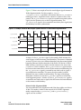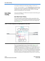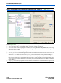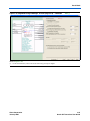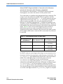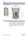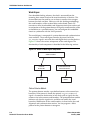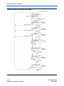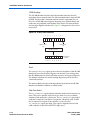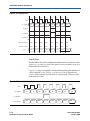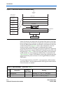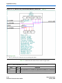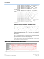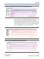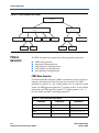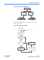
1
Stratix GX Transceiver User Guide
101 Innovation Drive
San Jose, CA 95134
(408) 544-7000
http://www.altera.com
UG-STXGX-3.0
P25-10021-02
Copyright © 2005 Altera Corporation. All rights reserved. Altera, The Programmable Solutions Company, the stylized Altera logo, specific device designations, and all other words and logos that are identified as trademarks and/or service marks are, unless noted otherwise, the trademarks and
service marks of Altera Corporation in the U.S. and other countries. All other product or service names are the property of their respective holders. Altera products are protected under numerous U.S. and foreign patents and pending applications, maskwork rights, and copyrights. Altera warrants
performance of its semiconductor products to current specifications in accordance with Altera's standard warranty, but reserves the right to make
changes to any products and services at any time without notice. Altera assumes no responsibility or liability arising out of the application or use of any information, product, or service described herein except as expressly agreed to in writing by Altera
Corporation. Altera customers are advised to obtain the latest version of device specifications before relying on any published information and before placing orders for products or services.
Printed on recycled paper
ii
Altera Corporation
Contents
About This User Guide ............................................................................ vii
How to Contact Altera ........................................................................................................................... vii
Typographic Conventions .................................................................................................................... viii
Chapter 1. Introduction
Gigabit Transceiver Block Highlights .................................................................................................
Transceiver Block Architecture ...........................................................................................................
Analog Section Overview ...............................................................................................................
Digital Overview ..............................................................................................................................
Modes of Operation ...............................................................................................................................
Basic Mode ........................................................................................................................................
SONET Mode ....................................................................................................................................
XAUI Mode .......................................................................................................................................
GigE Mode .........................................................................................................................................
Loopback ...........................................................................................................................................
Built-In Self Test ...............................................................................................................................
1–1
1–2
1–2
1–3
1–5
1–5
1–6
1–7
1–8
1–9
1–9
Chapter 2. Stratix GX Analog Description
Introduction ............................................................................................................................................ 2–1
Transmitter Analog ............................................................................................................................... 2–2
Transmitter Buffer ............................................................................................................................ 2–2
Transmitter PLL ................................................................................................................................ 2–5
Serializer (Parallel-to-Serial Converter) ........................................................................................ 2–8
Receiver Analog ..................................................................................................................................... 2–9
Receiver Input Buffer ....................................................................................................................... 2–9
Receiver PLL ................................................................................................................................... 2–12
Clock Recovery Unit ...................................................................................................................... 2–16
Deserializer (Serial-to-Parallel Converter) .................................................................................. 2–19
MegaWizard Analog Features ........................................................................................................... 2–20
MegaWizard Analog Feature Considerations ........................................................................... 2–20
Chapter 3. Basic Mode
Introduction ............................................................................................................................................ 3–1
Basic Mode Receiver Architecture ...................................................................................................... 3–2
Word Aligner .................................................................................................................................... 3–2
8B/10B Decoder ................................................................................................................................ 3–9
Byte Deserializer ............................................................................................................................. 3–13
Receiver Phase Compensation FIFO Buffer ............................................................................... 3–15
Basic Mode Transmitter Architecture ............................................................................................... 3–16
Transmitter Phase Compensation FIFO Buffer .......................................................................... 3–16
Altera Corporation
iii
Contents
Stratix GX Transceiver User Guide
Byte Serializer .................................................................................................................................
8B/10B Encoder ..............................................................................................................................
Basic Mode Clocking ...........................................................................................................................
Basic Mode Channel Clocking ......................................................................................................
Basic Mode Inter-Transceiver Block Clocking ...........................................................................
Basic Mode MegaWizard Plug-In .....................................................................................................
Basic Mode MegaWizard Plug-In Manager Considerations ...................................................
Basic Mode altgxb MegaWizard Options ...................................................................................
3–17
3–17
3–20
3–20
3–24
3–29
3–29
3–29
Chapter 4. SONET Mode
Introduction ............................................................................................................................................ 4–1
SONET Mode Receiver Architecture .................................................................................................. 4–2
Word Aligner .................................................................................................................................... 4–2
Byte Deserializer ............................................................................................................................... 4–8
Receiver Phase Compensation FIFO Module ............................................................................. 4–10
SONET Mode Transmitter Architecture .......................................................................................... 4–11
Transmitter Phase Compensation FIFO Buffer .......................................................................... 4–11
Byte Serializer ................................................................................................................................. 4–12
SONET Mode Clocking ...................................................................................................................... 4–12
SONET Mode Channel Clocking ................................................................................................. 4–12
SONET Mode Inter-Transceiver Block Clocking ....................................................................... 4–17
SONET Mode MegaWizard Plug-In Manager ................................................................................ 4–23
SONET Mode MegaWizard Considerations .............................................................................. 4–23
SONET Mode altgxb MegaWizard Options ............................................................................... 4–23
Chapter 5. XAUI Mode
Introduction ............................................................................................................................................ 5–1
XAUI Mode Receiver Architecture ..................................................................................................... 5–5
Word Aligner .................................................................................................................................... 5–6
Channel Aligner ............................................................................................................................... 5–9
Rate Matcher ................................................................................................................................... 5–11
8B/10B Decoder .............................................................................................................................. 5–11
PCS - XGMII Code Conversion .................................................................................................... 5–15
Byte Deserializer ............................................................................................................................. 5–15
Receiver Phase Compensation FIFO Module ............................................................................. 5–18
XAUI Mode Transmitter Architecture .............................................................................................. 5–18
Transmitter Phase Compensation FIFO Module ....................................................................... 5–18
Byte Serializer ................................................................................................................................. 5–19
XGMII Character to PCS Code-Group Mapping ....................................................................... 5–20
8B/10B Encoder .............................................................................................................................. 5–21
XAUI Mode Clocking .......................................................................................................................... 5–24
XAUI Mode Channel Clocking .................................................................................................... 5–24
XAUI Inter-Transceiver Block Clocking ..................................................................................... 5–28
XAUI Mode MegaWizard Plug-In Manager ................................................................................... 5–34
XAUI Mode MegaWizard Considerations ................................................................................. 5–34
XAUI Mode altgxb MegaWizard Options .................................................................................. 5–34
iv
Altera Corporation
Contents
Contents
Chapter 6. GigE Mode
Introduction ............................................................................................................................................ 6–1
Word Aligner .................................................................................................................................... 6–4
Rate Matcher ..................................................................................................................................... 6–9
8B/10B Decoder .............................................................................................................................. 6–11
Receiver Phase Compensation FIFO Buffer ............................................................................... 6–14
GigE Mode Transmitter Architecture ............................................................................................... 6–14
Transmitter Phase Compensation FIFO Buffer .......................................................................... 6–15
GigE Transmitter Synchronization .............................................................................................. 6–16
Idle Generation ............................................................................................................................... 6–16
8B/10B Encoder .............................................................................................................................. 6–17
GigE Mode Clocking ........................................................................................................................... 6–20
GigE Mode Channel Clocking ...................................................................................................... 6–20
GigE Mode Inter-Transceiver Clocking ...................................................................................... 6–25
GigE Mode MegaWizard Considerations ................................................................................... 6–31
GigE Mode altgxb MegaWizard Options ................................................................................... 6–31
Design Example ................................................................................................................................... 6–38
Design Description ......................................................................................................................... 6–38
Simulation Waveform & Hardware Verification Results ......................................................... 6–44
Chapter 7. Loopback Modes
Introduction ............................................................................................................................................
Serial Loopback ......................................................................................................................................
Parallel Loopback ..................................................................................................................................
Reverse Serial Loopback .......................................................................................................................
7–1
7–1
7–2
7–3
Chapter 8. Stratix GX Built-In Self Test (BIST)
Introduction ............................................................................................................................................ 8–1
Pattern Generator .................................................................................................................................. 8–2
PRBS Mode Generator ..................................................................................................................... 8–2
Incremental Mode Generator ......................................................................................................... 8–3
High-Frequency Mode Generator .................................................................................................. 8–3
Low-Frequency Mode Generator ................................................................................................... 8–4
Mix-Frequency Mode Generator .................................................................................................... 8–5
Pattern Verifier ....................................................................................................................................... 8–5
PRBS Mode Verifier ......................................................................................................................... 8–5
Incremental Mode Verifier .............................................................................................................. 8–6
Design Examples ................................................................................................................................... 8–7
Design 1: PRBS BIST Generator & Verification Design .............................................................. 8–7
Design 2: Incremental BIST Generator & Verification Design ................................................. 8–11
Design 3: High-Frequency Transmitter Generator Design ...................................................... 8–16
Design 4: Low-Frequency Transmitter Generator Design ....................................................... 8–18
Design 5: Mix-Frequency Transmitter Generator Design ........................................................ 8–20
Altera Corporation
v
Contents
Stratix GX Transceiver User Guide
Chapter 9. Reset Control &
Power Down
Introduction ............................................................................................................................................ 9–1
Power On Reset (POR) .......................................................................................................................... 9–1
USER Reset & Enable Signals .............................................................................................................. 9–1
Recommended Resets ........................................................................................................................... 9–4
Receiver & Transmitter Reset ......................................................................................................... 9–4
Receiver Reset ................................................................................................................................. 9–32
Transmitter Reset ........................................................................................................................... 9–52
Power Down ......................................................................................................................................... 9–57
Appendix A. Data & Control Codes
8B/10B Code ......................................................................................................................................... A–1
Code Notation .................................................................................................................................. A–1
Disparity Calculation ...................................................................................................................... A–1
Supported Codes ............................................................................................................................. A–3
Appendix B. Ports & Parameters
Input Ports ............................................................................................................................................. B–1
Output Ports .......................................................................................................................................... B–5
Parameter Descriptions ........................................................................................................................ B–9
Appendix C. REFCLKB Pin Constraints
Known Issues ........................................................................................................................................ C–1
Quartus II Software Messages ....................................................................................................... C–3
Recommendations ........................................................................................................................... C–5
vi
Altera Corporation
About This User Guide
How to Contact
Altera
Information Type
Technical support
Product literature
For the most up-to-date information about Altera® products, go to the
Altera world-wide web site at www.altera.com. For technical support on
this product, go to www.altera.com/mysupport. For additional
information about Altera products, consult the sources shown below.
USA & Canada
All Other Locations
www.altera.com/mysupport/
www.altera.com/mysupport/
(800) 800-EPLD (3753)
(7:00 a.m. to 5:00 p.m. Pacific Time)
+1 408-544-8767
7:00 a.m. to 5:00 p.m. (GMT -8:00)
Pacific Time
www.altera.com
www.altera.com
Altera literature services
[email protected]
[email protected]
Non-technical customer
service
(800) 767-3753
+ 1 408-544-7000
7:00 a.m. to 5:00 p.m. (GMT -8:00)
Pacific Time
FTP site
ftp.altera.com
ftp.altera.com
Altera Corporation
vii
Preliminary
Typographic Conventions
Typographic
Conventions
Visual Cue
Stratix GX Transceiver User Guide
This document uses the typographic conventions shown below.
Meaning
Bold Type with Initial
Capital Letters
Command names, dialog box titles, checkbox options, and dialog box options are
shown in bold, initial capital letters. Example: Save As dialog box.
bold type
External timing parameters, directory names, project names, disk drive names,
filenames, filename extensions, and software utility names are shown in bold
type. Examples: fMAX, \qdesigns directory, d: drive, chiptrip.gdf file.
Italic Type with Initial Capital
Letters
Document titles are shown in italic type with initial capital letters. Example: AN
75: High-Speed Board Design.
Italic type
Internal timing parameters and variables are shown in italic type.
Examples: tPIA, n + 1.
Variable names are enclosed in angle brackets (< >) and shown in italic type.
Example: <file name>, <project name>.pof file.
Initial Capital Letters
Keyboard keys and menu names are shown with initial capital letters. Examples:
Delete key, the Options menu.
“Subheading Title”
References to sections of a document and titles of on-line help topics are shown
in quotation marks. Example: “Typographic Conventions.”
Courier type
Signal and port names are shown in lowercase Courier type. Examples: data1,
tdi, input. Active-low signals are denoted by suffix n, e.g., resetn.
Anything that must be typed exactly as it appears is shown in Courier type. For
example: c:\qdesigns\tutorial\chiptrip.gdf. Also, sections of an
actual file, such as a Report File, references to parts of files (e.g., the AHDL
keyword SUBDESIGN), as well as logic function names (e.g., TRI) are shown in
Courier.
1., 2., 3., and
a., b., c., etc.
Numbered steps are used in a list of items when the sequence of the items is
important, such as the steps listed in a procedure.
■
Bullets are used in a list of items when the sequence of the items is not important.
●
•
v
The checkmark indicates a procedure that consists of one step only.
1
The hand points to information that requires special attention.
r
The angled arrow indicates you should press the Enter key.
f
The feet direct you to more information on a particular topic.
viii
Preliminary
Altera Corporation
1. Introduction
Introduction
Stratix® GX devices combine highly advanced 3.1875-gigabit-per-second
(Gbps) four-channel gigabit transceiver blocks with one of the industry’s
most advanced FPGA architectures. Stratix GX devices are manufactured
on a 1.5-V, 0.13-µm, all-layer copper CMOS process technology with 1.5V PCML I/O standard support.
Historically, designers have used high-speed transceivers in strictly
structured, line-side applications. Now, with the new gigabit transceiver
blocks embedded in FPGAs, you can use transceivers in a host of new
systems that require flexibility, increased time-to-market, high
performance, and top-of-the-line features.
Gigabit
Transceiver
Block Highlights
Stratix GX devices are organized into four-channel blocks with four
3.1875 Gbps full-duplex channels per block and up to 20 channels (in five
blocks) per device. Each self-contained Stratix GX gigabit transceiver
block supports a variety of embedded functions and does the following:
■
■
■
■
■
■
■
■
■
Altera Corporation
January 2005
Supports frequencies from 500 megabits per second (Mbps) to
3.1875 Gbps
Integrates serializer/deserializer (SERDES), clock data recovery
(CDR), word aligner, channel aligner, rate matcher, 8B/10B
encoder/decoder, byte serializer/deserializer, and phase
compensation first-in first-out (FIFO) modules
Supports flexible reference clock generation capabilities, including a
dedicated transmitter phase-locked loop (PLL) and four receiver
PLLs per gigabit transceiver block
Supports programmable pre-emphasis, equalization, and
programmable VOD settings in I/O buffers, and dynamic
reprogrammability for each of these features
Implements XAUI physical media attachment (PMA) and physical
coding sublayer (PCS) functionality for 10GBASE-X systems
Provides built-in Gigabit Ethernet (GigE) physical coding sublayer
functionality
Provides individual transmitter and receiver power-down capability
for reduced power consumption during non-operation
Includes built-in self test (BIST) capability, including embedded
Pseudo Random Binary Sequence (PRBS) pattern generation and
verification
Includes three independent loopback paths for system verification
1–1
Transceiver Block Architecture
Transceiver
Block
Architecture
Figure 1–1 shows a block diagram of the gigabit transceiver block (GXB).
You can bypass various modules if desired. Refer to“Modes of
Operation” on page 1–5 for a description of the supported features in
each mode. You can divide the transceiver block into an analog section
and a digital section, as shown in Figure 1–1.
Figure 1–1. Block Diagram of a Stratix GX Gigabit Transceiver Block
Analog Section
Digital Section
Deserializer
Word
Aligner
Channel
Aligner
Clock
Recovery
Unit
Reference
Clock
Receiver
PLL
Reference
Clock
Transmitter
PLL
Rate
Matcher
8B/10B
Decoder
Serializer
8B/10B
Encoder
Byte
Serializer
Byte
Deserializer
Phase
Compensation
FIFO Buffer
Phase
Compensation
FIFO Buffer
Receiver
Transmitter
Analog Section Overview
This section describes the various components within the analog section
of the transceiver block.
Transmitter Differential I/O Buffers
The gigabit transmitter block differential I/O buffers support the 1.5-V
PCML I/O standard, and contain features that improve system signal
integrity. These features include programmable pre-emphasis, which
helps compensate for high frequency losses, and a variety of
programmable VOD settings that support noise margin tuning.
Receiver Differential I/O Buffers
The gigabit transceiver block differential I/O buffers support the 1.5-V
PCML I/O standard, and contain a variety of features that improve
system signal integrity. Programmable equalization capabilities are used
to compensate for signal degradation across transmission mediums.
1–2
Stratix GX Transceiver User Guide
Altera Corporation
January 2005
Introduction
Transmitter & Receiver PLLs
Each gigabit transceiver block contains one dedicated transmitter PLL
and four dedicated receiver PLLs. These PLLs provide clocking flexibility
and support a range of incoming data streams. For data transmission and
recovery, these PLLs generate the required clock frequencies based upon
the synthesis of an input reference clock. Each transmitter PLL supports
multiplication factors of 2, 4, 5, 8, 10, 16, or 20. Either external reference
clocks or a variety of clock sources within the Stratix GX device drive the
PLLs.
Clock Recovery Unit
The gigabit transceiver block clock recovery unit (CRU) performs analog
Clock Data Recovery (CDR). The CRU uses an external reference clock to
extract a recovered clock that is frequency and phase aligned with the
incoming data, thereby eliminating any clock-to-data skew. This
recovered clock then clocks the data through the rest of the gigabit
transceiver block.
Serializer Deserializer (SERDES)
The transmitter serializer converts the incoming lower speed parallel
signal to a high-speed serial signal on the transmit side. The SERDES
supports a variety of conversion factors, ensuring implementation
flexibility. For example, the SERDES supports 10- and 20-bit serialization
factors, typically required for 8B/10B encoded data, as well as 8- and
16-bit factors.
The receiver deserializer converts the incoming data stream from a
high-speed serial signal to a lower-speed parallel signal that can be
processed in the FPGA logic array on the receive side. The SERDES
supports a variety of conversion factors, ensuring implementation
flexibility. For example, the SERDES supports both 10-bit and 8-bit
serialization and deserialization factors.
Digital Overview
This section describes the various components in the digital section of the
transceiver block.
Altera Corporation
January 2005
1–3
Stratix GX Transceiver User Guide
Transceiver Block Architecture
Transmitter & Receiver Phase Compensation FIFO Buffer
The transmitter and receiver data path has a dedicated phase
compensation FIFO buffer that decouples phase variations between the
FPGA and transceiver clock domains. These FIFO buffers ensure a
consistent, reliable interface to the logic array and simplify system design
and timing analysis.
Byte Serializer/Deserializer
The byte serializer converts a 16- or 20-bit data bus into two 8- or 10-bit
data buses, respectively, at double the data rate. The byte serializer
converts an 8- or 10-bit data bus into 16- or 20-bit data buses, allowing
maximum throughput of the transceiver without burdening the FPGA
logic array.
The byte deserializer converts an 8- or 10-bit data bus into 16- or 20-bit
data buses, allowing maximum throughput of the transceiver without
burdening the FPGA logic array.
8B/10B Encoder/Decoder
8B/10B encoding/decoding is the backbone of many transceiver
protocols, and it is often used in proprietary implementations. The
gigabit transceiver block has dedicated circuitry to perform 8B/10B
encoding in the transmitter and decoding in the receiver. This coding
technique ensures sufficient data transitions and a DC balanced stream in
the data signal for successful data recovery at the receiver.
Word Aligner
The word aligner module contains a fully programmable pattern detector
to identify specific patterns within the incoming data stream. The pattern
detector includes recognition support /K28.5/ comma characters for
8B/10B encoded data and A1 or A2 frame alignment patterns for
scrambled signals. Additionally, you can specify a custom alignment
pattern in lieu of the /K28.5/ comma.
The word aligner in the gigabit transceiver block also creates words from
the incoming serial data stream by realigning the data based on identified
byte boundaries. The realignment function uses a barrel shifter and
works with the pattern detector. Additionally, the word aligner has a
manual data realignment mode that lets you control the data realignment
in user mode without consistent alignment characters.
1–4
Stratix GX Transceiver User Guide
Altera Corporation
January 2005
Introduction
Channel Aligner
An embedded channel aligner aligns byte boundaries across multiple
channels and synchronizes the data entering the logic array from the
gigabit transceiver block’s four channels. The Stratix GX channel aligner
is optimized for a 10-Gigabit Ethernet XAUI 4-channel implementation.
The channel aligner includes the control circuitry and channel alignment
character detection defined by the XAUI protocol. The channel aligner is
only available in XAUI mode.
Rate Matcher
In multi-crystal environments, the clock frequencies of the transmitting
and receiving devices do not match. This mismatch can cause the data to
transmit at a rate slightly faster or slower than the receiving device can
interpret. The Stratix GX rate matcher resolves the frequency differences
between the recovered clock and the FPGA logic array clock by inserting
or deleting removable characters from the data stream, as defined by the
transmission protocol, without compromising transmitted data. If the
functional mode is XAUI, the rate matcher is based on the 10-Gigabit
Ethernet protocol. If the functional mode is GigE, the rate matcher is
based on the Gigabit Ethernet protocol.
Modes of
Operation
You can bypass various modules of the gigabit transceiver block based on
the configured mode of operation. Stratix GX transceivers currently
support basic mode, SONET mode, and XAUI mode. This section
provides an overview of each supported mode of operation.
Basic Mode
Basic mode enables a subset of the transceiver blocks so you can perform
customizable configuration. Channel aligner and the rate matcher
features are not available in this mode. Refer to the Basic Mode chapter for
more details on the configurability of this mode. Figure 1–2 shows a block
diagram of a duplex channel configured in basic mode.
Altera Corporation
January 2005
1–5
Stratix GX Transceiver User Guide
Modes of Operation
Figure 1–2. Block Diagram of a Duplex Channel Configured in Basic Mode
Analog Section
Digital Section
Deserializer
Word
Aligner
Channel
Aligner
Clock
Recovery
Unit
Reference
Clock
Receiver
PLL
Reference
Clock
Transmitter
PLL
Rate
Matcher
8B/10B
Decoder
Serializer
8B/10B
Encoder
Byte
Serializer
Byte
Deserializer
Phase
Compensation
FIFO Buffer
Phase
Compensation
FIFO Buffer
Receiver
Transmitter
SONET Mode
SONET mode lets you to select a subset of the transceiver blocks to
perform SONET-like configuration. SONET-like implies that the data
width can either be 8 or 16 bits and that the 8B/10B encoder/decoder,
channel aligner, and the rate matcher features are not available. Refer to
the SONET Mode chapter for more details on the configurability of this
mode. Figure 1–3 shows a block diagram of a duplex channel configured
in SONET mode.
1–6
Stratix GX Transceiver User Guide
Altera Corporation
January 2005
Introduction
Figure 1–3. Block Diagram of a Duplex Channel Configured in SONET Mode
Analog Section
Digital Section
Deserializer
Clock
Recovery
Unit
Reference
Clock
Receiver
PLL
Reference
Clock
Transmitter
PLL
Word
Aligner
Channel
Aligner
Rate
Matcher
8B/10B
Decoder
Byte
Deserializer
Serializer
8B/10B
Encoder
Byte
Serializer
Phase
Compensation
FIFO Buffer
Phase
Compensation
FIFO Buffer
Receiver
Transmitter
XAUI Mode
Stratix GX transceivers contain embedded macros dedicated to
supporting the XAUI protocol, specified in clause 47 of the IEEE 802.3ae
specification. These macros includes synchronization, channel deskew,
rate matching, XGXS to XGMII, and XGMII to XGXS code-group
conversion. Refer to the XAUI Mode chapter for more details on the
configurability of this mode. Figure 1–4 shows a block diagram of a
duplex channel configured in XAUI mode.
Altera Corporation
January 2005
1–7
Stratix GX Transceiver User Guide
Modes of Operation
Figure 1–4. Block Diagram of a Duplex Channel Configured in XAUI Mode
Analog Section
Digital Section
Deserializer
Word
Aligner
Channel
Aligner
Clock
Recovery
Unit
Reference
Clock
Receiver
PLL
Reference
Clock
Transmitter
PLL
Rate
Matcher
8B/10B
Decoder
Serializer
8B/10B
Encoder
Byte
Serializer
Byte
Deserializer
Phase
Compensation
FIFO Buffer
Phase
Compensation
FIFO Buffer
Receiver
Transmitter
GigE Mode
Stratix GX devices in GigE mode can use the 8B/10B encoder/decoder,
rate matcher, synchronizer, and byte serializer/deserializer built-in hard
macros. Refer to the GigE Mode chapter for more information about this
mode. The rate matcher and word aligner each have a dedicated state
machine governing their functions. These state machines are active only
in GigE mode. Figure 1–5 shows a block diagram of a duplex channel
configured in GigE mode.
1–8
Stratix GX Transceiver User Guide
Altera Corporation
January 2005
Introduction
Figure 1–5. Block Diagram of a Duplex Channel Configured in GigE Mode
Analog Section
Digital Section
Deserializer
Clock
Recovery
Unit
Reference
Clock
Receiver
PLL
Reference
Clock
Transmitter
PLL
Word
Aligner
Channel
Aligner
Rate
Matcher
8B/10B
Decoder
Byte
Deserializer
Serializer
8B/10B
Encoder
Byte
Serializer
Phase
Compensation
FIFO Buffer
Phase
Compensation
FIFO Buffer
Receiver
Transmitter
Loopback
There are three different loopback modes to use in the gigabit transceiver
block to allow for a complete method of in-system verification. The
loopback modes are versatile and robust enough to accommodate all
protocols and let you to choose whether to retime the data.
Built-In Self Test
The gigabit transceiver block contains several features that simplify
design verification. An embedded PRBS pattern generator provides a
bitstream pattern that you can use to test the device and board
connections. The PRBS pattern generator works with a PRBS receiver to
implement a full self-test path. Additionally, serial and parallel loopback
paths let you test the FPGA logic without monitoring external signals.
The reverse loopback path enables external system testing with minimal
device interaction.
Altera Corporation
January 2005
1–9
Stratix GX Transceiver User Guide
Modes of Operation
1–10
Stratix GX Transceiver User Guide
Altera Corporation
January 2005
2. Stratix GX Analog
Description
Introduction
This chapter describes how to serialize the parallel data for transmission
and convert received data into parallel data. Data transmission and
reception is performed by pseudo current mode logic (PCML) buffers.
These transceiver buffers support programmable pre-emphasis,
equalization, and programmable VOD settings in I/O buffers.
The programmable pre-emphasis setting is available on transmit buffers
to maximize the eye opening on the far-end receiver by boosting the
high-frequency component of the data signal. Similarly, programmable
equalization is available for receive buffers to reduce the high-frequency
losses and inter-symbol interference. These features are useful in lossy
transmission lines. Transceivers also support flexible reference clock
generation capabilities, including a dedicated transmitter phase-locked
loop (PLL) and four receiver PLLs per transceiver block.
The clock recovery unit (CRU) is the main part of each receive analog
section; it recovers the clock from the serial data stream (see Figure 2–1).
You can set the CRU to automatically or manually alter the receiver PLL
phase and frequency to match the bit transition on the incoming data
stream. This is to eliminate any clock-to-data skew or to keep the receiver
PLL locked to the reference clock (lock-to-data or lock-to-reference
mode).
During the clock recovery phase, the receiver PLL initially locks to the
reference clock and then attempts to lock on to the incoming data by first
recovering the clock from the incoming serial data.
Altera Corporation
January 2005
2–1
Transmitter Analog
Figure 2–1. Block Diagram Analog Components
Analog Section
Digital Section
Deserializer
Word
Aligner
Channel
Aligner
Clock
Recovery
Unit
Reference
Clock
Receiver
PLL
Reference
Clock
Transmitter
PLL
Rate
Matcher
8B/10B
Decoder
Serializer
8B/10B
Encoder
Byte
Serializer
Byte
Deserializer
Phase
Compensation
FIFO Buffer
Phase
Compensation
FIFO Buffer
Receiver
Transmitter
Transmitter
Analog
This section describes the transmitter buffer, the transmitter PLL, and the
serializer. Figure 2–2 shows the transmitter analog components.
Figure 2–2. Transmitter Analog Components
Analog Section
Reference
Clock
Digital Section
Transmitter
PLL
Serializer
8B/10B
Encoder
Byte
Serializer
Phase
Compensation
FIFO Buffer
Transmitter
Transmitter Buffer
The Stratix® GX transceiver buffers support the 1.5-V PCML standard at
speeds up to 3.1875 gigabits per second (Gbps) and are capable of driving
40 inches of FR4 trace across two connectors. In addition, the buffer
contains programmable output voltage, programmable pre-emphasis
circuitry, and internal termination circuitry.
2–2
Stratix GX Transceiver User Guide
Altera Corporation
January 2005
Stratix GX Analog Description
Programmable Voltage Output Differential (VOD)
Stratix GX transceivers let you customize the differential output voltage
(VOD) to handle different length, backplane, and receiver requirements
(see Figure 2–3). You can select the VOD (differential) from a range of 400
to 1,600 mV, as shown in Table 2–1.
Figure 2–3. VOD (Differential) Signal Level
Single-Ended Waveform
Positive Channel (p) = VOH
VOD
Negative Channel (n) = VOL
VCM
Ground
Differential Waveform
(VOD (Differential) = 2 x VOD (single-ended))
VOD
p−n=0V
VOD
Table 2–1 shows the differential output voltage (VOD) setting per current
level for each of the on-chip transmitter programmable termination
values.
Table 2–1. Programmable VO D (Differential)
100 Ω (mV)
120 Ω (mV)
150 Ω (mV)
400
480
600
800
960
1,200
1,000
1,200
1,500
1,200
1,440
1,400
1,600
Altera Corporation
January 2005
2–3
Stratix GX Transceiver User Guide
Transmitter Analog
You can set the differential VOD values statically during configuration or
dynamically adjust them in user mode. You select the static VOD value
through a list in the altgxb MegaWizard® Plug-In Manager, which sets
the appropriate VOD setting in the configuration file. The disadvantage of
the static mode setting is that the VOD is set on a per transceiver block
basis and cannot be changed unless you regenerate another
programming file.
Alternatively, if you enable dynamic adjustment in the altgxb
MegaWizard Plug-In, you can dynamically configure the VOD setting by
the device during user mode. This configuration is done by asserting
encoded values on the tx_vodctrl bus, which is instantiated in the
altgxb module when you select the dynamic adjustment option. This
option lets you make quick performance evaluations of the various
settings without having to recompile and regenerate multiple
configuration files. Another advantage of this option is that it allows the
VOD of each channel to be configured independently. Refer to the section
“MegaWizard Analog Features” on page 2–20 for further details.
Programmable Pre-Emphasis
The programmable pre-emphasis module in each transmit buffer boosts
the high frequencies in the transmit data signal, which may be attenuated
in the transmission media. This maximizes the data eye opening at the
far-end receiver. Pre-emphasis is particularly useful in lossy transmission
mediums.
The transfer function of a transmission line can be represented in the
frequency domain as a low-pass filter. Any frequency components below
the –3 dB frequency pass through with minimal losses. Frequency
components that are greater than the –3-dB frequency are attenuated.
This variation in frequency response yields data-dependant jitter and
other ISI effects. By applying pre-emphasis, the high frequency
components are boosted, or in other words, pre-emphasized. This
pre-emphasis equalizes the frequency response as seen at the receiver so
that the delta between the low-frequency and high-frequency
components is reduced, which in return minimizes the ISI effects from the
transmission medium.
In Stratix GX transceivers, the programmable pre-emphasis settings can
have one of six values (0 to 5). You should experiment with the
pre-emphasis values to determine the optimal setting based on your
system variables.
2–4
Stratix GX Transceiver User Guide
Altera Corporation
January 2005
Stratix GX Analog Description
As with the VOD settings, you can set the pre-emphasis settings statically
during configuration or adjust them dynamically in user mode. You can
set the static pre-emphasis value through a drop-down menu in the
altgxb MegaWizard Plug-In, which sets the appropriate pre-emphasis
setting in the configuration file. The disadvantage of the static mode
setting is that the pre-emphasis is set on a per-transceiver-block basis and
cannot be changed without regenerating another programming file.
On the other hand, if you select dynamic adjustment in the altgxb
MegaWizard Plug-In, the pre-emphasis setting can be configured
dynamically by the device during user mode. This configuration is done
by asserting encoded values on the tx_preemphasisctrl bus, which
is instantiated in the altgxb module when you select the dynamic
adjustment option. This option lets you make quick performance
evaluations of the various settings without having to recompile and
regenerate multiple configuration files. Another advantage of this option
is that it allows the pre-emphasis of each channel to be configured
independently. For further details, refer to “MegaWizard Analog
Features” on page 2–20.
Avoid pre-emphasis and VOD settings that yield a value greater than
1,600 mV. Settings beyond this value do not damage the buffer, but they
prevent accurate device operation. Verify that the combination of VOD
and pre-emphasis settings do not exceed the 1,600-mV limit.
Programmable Transmitter Termination
The Stratix GX transmitter buffer includes a 100-, 120-, or 150-Ω
programmable on-chip differential termination resistor. The Stratix GX
transmitter buffers are current-mode drivers, so the resultant VOD is a
function of the transmitter termination value. For more information on
resultant VOD values, see “Programmable Voltage Output Differential
(VOD)” on page 2–3.
Transmitter PLL
Each transceiver block contains a transmitter PLL and a slow-speed
reference clock. The transmitter PLL receives the reference clock and
generates the high-speed serial clock used by the serializer. The slowspeed reference clock is used for the transceiver logic. Figure 2–4 shows
the transmitter PLL’s block diagram. The pll_locked signal indicates
when the transmitter PLL is locked to the reference clock. A high signal
indicates that the PLL is locked to the reference clock; a low signal
indicates that the PLL is not locked to the reference clock.
Altera Corporation
January 2005
2–5
Stratix GX Transceiver User Guide
Transmitter Analog
Figure 2–4. Transmitter PLL Block Diagram
/4, 8, 10, 16, 20
/m
Clock
Driver
Up
Inter Quad Routing (IQ1)
Inter Quad Routing (IQ0)
INCLK
PFD
Down
CP+LF
High Speed
TX_PLL_CLK
Low Speed
TX_PLL_CLK
VCO
Global Clocks, I/O Bus, General Routing
Dedicated Local
REFCLKB
/2
Table 2–2 lists some of the transmitter PLL specifications.
Table 2–2. Transmitter PLL Specifications
Parameter
Specifications
Input reference frequency range
25 MHz to 650 MHz
Data rate support
500 Mbps to 3.1875 Gbps
Multiplication factor (W)
2, 4, 5, 8, 10, 16, or 20 (1)
Note to Table 2–2:
(1)
Multiplication factors 2 and 5 can only be achieved with the use of the pre-divider
on the REFCLKB.
Clock Synthesis
The maximum input frequency of the phase frequency detector (PFD) is
325 MHz. To achieve reference clock frequency above this limitation, the
/2 pre-divider on the dedicated local REFCLKB path can be enabled
automatically by the Quartus® II software. The /2 pre-divider divides the
reference clock frequency by a factor of 2 and then the /m factor
compensates the frequency difference. An example would be a data rate
of 2,488 Mbps with a 622-MHz reference clock. In this scenario, the
reference clock must be assigned to the REFCLKB port where the 622MHz reference clock is divided by 2, yielding a 311-MHz clock at the PFD.
This 311-MHz reference clock is then multiplied by a factor of 8 to achieve
the 2,488-MHz clock at the VCO.
2–6
Stratix GX Transceiver User Guide
Altera Corporation
January 2005
Stratix GX Analog Description
If the reference clock exceeds 325 MHz, the clock must be fed by the
dedicated local reference clock pin, REFCLKB. By default, the Quartus II
software assigns pins to be LVTTL, so you must assign the 1.5-V PCML
I/O standard to the I/O pins to select the REFCLKB port as the reference
source. The Quartus II software prompts a fitter error if the reference
clock exceeds 325 MHz and the reference clock source is not on the
REFCLKB port.
You can also use the pre-divider on the REFCLKB path to support
additional multiplication factors. The block diagram in Figure 2–4 shows
that /m can only support multiplication factors of 4, 8, 10, 16, and 20, but
Table 2–3 shows that the additional multiplication factors of 2 and 5 are
also achievable. You can achieve these multiplication factors by using the
pre-divider. A multiplication factor of 2 is achieved by pre-dividing the
reference clock by 2 and then multiplying the resultant frequency by 4,
which yields a multiplication factor of 2. A multiplication factor of 5 is
achieved in the same manner by pre-dividing the reference clock by 2 and
then multiplying the resultant frequency by 10, which yields a
multiplication factor of 5.
Table 2–3 lists the possible multiplication values as a function of the
source to the transmitter PLL. Table 2–3 assumes that the reference clock
is directly fed from the source listed and does not factor any pre-clock
synthesis (that is, the Stratix GX PLL driving a global clock that is used for
the transmitter PLL reference clock source).
Table 2–3. Multiplication Values as a Function of the Reference Clock
Source to the Transmitter PLL
Transmitter PLL Reference Clock
Source
Multiplication Factors
Global clock, I/O bus, general routing
4, 8, 10, 16, 20
Inter-transceiver routing
2, 4, 5, 8, 10, 16, 20
Dedicated local REFCLKB
2, 4, 5, 8, 10, 16, 20
You must specify the data rate of the channel and input clock period of
the reference clock. The data rate divided by the input clock period must
equal one of the multiplication factors listed in Table 2–3.
Transmitter PLL Bandwidth Setting
The Stratix GX transmitter PLL in the transceiver block offers a
programmable bandwidth setting. The PLL bandwidth is the measure of
its ability to track the input clock and jitter. The bandwidth is determined
by the –3-dB frequency of the closed-loop gain of the PLL.
Altera Corporation
January 2005
2–7
Stratix GX Transceiver User Guide
Transmitter Analog
A high-bandwidth setting provides a faster lock time and tracks more
jitter on the input clock source which passes it through the PLL. This
helps reject noise from the VCO and power supplies. A low-bandwidth
setting, on the other hand, filters out more high frequency input clock
jitter, but increases lock time.
You can set the bandwidth for Stratix GX devices to either low or high.
The –3-dB frequencies for these settings can vary due to the non-linear
nature and frequency dependencies of the circuit. As a result, you can
vary the bandwidth to customize the performance on specific systems.
Serializer (Parallel-to-Serial Converter)
The serializer converts parallel data to serial data at the transmitter
output buffer. The serializer can support 8- or 10-bit words when used
with the transmitter multiplexer. The 8-bit serializer drives the serial data
to the output buffer, as shown in Figure 2–5. The serializer can drive the
serial bit-stream at a data rate range of 500 Mbps to 3.1875 Gbps. The
serializer outputs the least significant bit (LSB) of the word first.
Figure 2–5. Example of 8-Bit Serialization
Serializer
Parallel Data
8
D7
D7
D8
D8
D6
D6
D4
D4
D3
D3
D2
D2
D1
D1
D0
D0
Serial Data Out
(I/O Output Buffer)
Low-Speed
Parallel Clock
High-Speed
Serial Clock
Figure 2–6 shows the serial bit order of the serializer output. In this
example, a constant 8’h6a (01010110) value is serialized.
1
2–8
Stratix GX Transceiver User Guide
The serial data is transmitted from LSB to most significant bit
(MSB).
Altera Corporation
January 2005
Stratix GX Analog Description
Figure 2–6. Serializer Bit Order
Parallel Clock
Serial Clock
Parallel Data (in Hex)
(x)
56
011 01 010
Serial Data Out
Receiver Analog
This section describes the receiver input buffer, the receiver PLL, the clock
recovery unit, and the deserializer. Figure 2–7 shows the receiver analog
components.
Figure 2–7. Highlighted Block Diagram of the Receiver Analog Components
Analog Section
Digital Section
Deserializer
Clock
Recovery
Unit
Reference
Clock
Word
Aligner
Channel
Aligner
Rate
Matcher
8B/10B
Decoder
Byte
Deserializer
Phase
Compensation
FIFO Buffer
Receiver
PLL
Receiver
Receiver Input Buffer
The receiver input buffer contains internal termination and internal
equalization. Figure 2–8 shows the structure of the input buffer. The input
buffer has programmable equalization that you can apply to increase the
signal integrity of the transmission line. The internal termination in the
receiver buffer can support AC and DC coupling with programmable
differential termination settings of 100, 120, or 150 Ω..
Altera Corporation
January 2005
2–9
Stratix GX Transceiver User Guide
Receiver Analog
Figure 2–8. Receiver Input Buffer
Input Buffer
Programmable
Termination
Programmable
Equalizer
Input Pins
To PLD
Internal Loopback
from Transmitter
Programmable Receiver Termination
The Stratix GX receiver buffer includes programmable on-chip
differential termination of 100, 120, or 150 Ω..
This assignment must be made per pin through the Assignment Editor in
the Quartus II software. Select Assignment Organizer > Options for
Individual Nodes Only > Stratix GX Termination Value (Assignments
menu).
1
The proper termination settings should be selected and verified
accordingly before compilation.
The transmitter PLL input signal (inclk) drives the termination
resistance calibration circuit. The Quartus II software allows
receiver-only configurations in Stratix GX devices. However, if you use
the Quartus II software to remove the transmitter PLL in a receiver-only
configuration, you will see an incorrect value or unpredictable behavior
with the receiver input pin termination. If the rx_cruclk signal is
globally routed, the Quartus II software handles this automatically. If the
rx_cruclk signal is not globally routed or routed using the interquadrant line (IQ2), the Quartus II software returns a no-fit. In this
situation, you must add a transmitter PLL to your design.
If the pll_areset (analog reset) signal goes high, the RX_Vcm value is
less than the 1.1 V. This value varies unpredictably because the circuit is
tristated. RX_Vcm is referenced from the Stratix GX receiver analog power
supply.
2–10
Stratix GX Transceiver User Guide
Altera Corporation
January 2005
Stratix GX Analog Description
If external termination is used, the receiver must be externally terminated
and biased to 1.1 V. Figure 2–9 shows an example of an external
termination and biasing circuit.
Figure 2–9. External Termination & Biasing Circuit
Receiver External Termination
and Biasing
50/60/75-Ω
Termination
Resistance
Stratix GX Device
VDD
R1
C1
Receiver
R1/R2 = 1K
VDD × {R2/(R1 + R 2)} = 1.1 V
RXIP
R2
RXIN
Receiver External Termination
and Biasing
Transmission
Line
Enable Stratix GX-to-Stratix GX Receiver DC Coupling
You can configure the Stratix GX receiver buffers so that DC-coupled
Stratix GX-to-Stratix GX communication is possible. The Stratix GX
transmitter’s common-mode is typically around 750 mV, while the
receiver common mode by default is approximately 1.1 V. However, by
enabling DC coupling, the receiver common mode is biased to allow
interoperability with the Stratix GX transmitter.
Equalizer Mode
Stratix GX transceivers offer an equalization circuit in each receiver
channel to increase noise margins and help reduce the effects of high
frequency losses. The programmable equalizer compensates for
inter-symbol interference (ISI) and high frequency losses that distort the
signal and reduce the noise margin of the transmission medium by
equalizing the frequency response.
The transfer function of a transmission line can be represented in the
frequency domain as a low-pass filter. Any frequency components below
the –3-dB frequency pass through with minimal losses. Frequency
components that are greater than the –3-dB frequency are attenuated.
Altera Corporation
January 2005
2–11
Stratix GX Transceiver User Guide
Receiver Analog
This variation in frequency response yields data-dependant jitter and
other ISI effects. By applying equalization, the low frequency components
are attenuated. This equalizes the frequency response so that the delta
between the low frequency and high frequency components are reduced,
which minimizes the ISI effects from the transmission medium.
In Stratix GX transceivers, the programmable equalizer settings can have
one of five values (0 through four). You should experiment with the
equalization values to determine the optimal setting based on your
system variables.
As with the VOD settings, you can set the equalization settings statically
during configuration or adjust them dynamically in user mode. You can
select the static equalization value through a drop-down menu in the
altgxb MegaWizard Plug-In. This action sets the appropriate
equalization setting in the configuration file. The disadvantage of this
mode is that the equalization is set on a per-transceiver block basis and
cannot be changed without regenerating another programming file.
On the other hand, if you select the dynamic adjustment in the altgxb
MegaWizard Plug-In, the equalization setting can be configured
dynamically by the device during user mode. This configuration is
accomplished by asserting encoded values on the rx_equalizerctrl
signal, which is instantiated in the altgxb module when this option is
selected. This feature lets you make quick performance evaluations of the
various settings without having to recompile and regenerate multiple
configuration files. Another advantage is that this option allows the
equalization of each channel to be configured independently. Refer to
“MegaWizard Analog Features” on page 2–20 for more details.
Receiver PLL
Each transceiver block contains four receiver PLLs and a slow-speed
reference clock. The receiver PLLs receive the reference clock and
generate the high-speed serial clock used by the CR. The slow-speed
reference clock is used for the transceiver logic. Figure 2–10 shows the
block diagram for the lock-to-reference portion of the receiver PLL.
This section focuses on the receiver PLL in Lock-to-Reference mode. The
lock-to-data circuit has been omitted. Refer to the “Lock-to-Reference
Mode & Lock-to-Data Mode” on page 2–16 for more information on the
operation between the two modes.
2–12
Stratix GX Transceiver User Guide
Altera Corporation
January 2005
Stratix GX Analog Description
The receiver PLL contains an optional loss-of-lock indicator signal
(rx_locked) that indicates when the receiver PLL is not locked to the
reference clock. The rx_locked signal is active low. A low signal
indicates that the PLL is locked to a reference clock; a high signal indicates
that the PLL is not locked to the reference clock.
Figure 2–10. Receiver PLL Block Diagram
÷m (1)
Low speed TX_PLL_CLK
Inter Transceiver Block Routing
Global Clks, I/O Bus, Gen Routing
RX_CRUCLK
Up
PFD
Down
CP+LF
VCO
Up
Dedicated Local
REFCLKB
Down
÷2
rx_rlv[ ]
rx_locktorefclk
rx_locktodata
High Speed RCVD_CLK
Clock Recovery Unit (CRU)
RX_IN
Low Speed RCVD_CLK
Note to Figure 2–10:
(1)
m = 8, 10, 16, or 20.
Table 2–4 lists some of the clock recovery unit specifications.
Table 2–4. Clock Recovery Unit Specifications
Parameter
Input reference frequency range
Specification
25 MHz to 650 MHz
Data rate support
500 Mbps to 3.1875 Gbps
Multiplication factor (W)
2, 4, 5, 8, 10, 16, or 20 (1)
Note to Table 2–4:
(1)
Multiplication factors 2, 4, and 5 can only be achieved with the use of the predivider on the REFCLKB port or if the CRU is trained with the low speed clock
from the transmitter PLL.
Clock Synthesis
The maximum input frequency of the PFD of the receiver PLL is
325 MHz. To achieve reference clock frequency above this limit, the
Quartus II software enables the divide by 2 pre-divider on the dedicated
local REFCLKB path. This divides the reference clock frequency by a factor
of 2 and then the /m factor compensates the frequency difference. For
example, given a data rate of 2,488 Mbps with a reference clock of
622 MHz, the reference clock must be assigned to the REFCLKB port,
Altera Corporation
January 2005
2–13
Stratix GX Transceiver User Guide
Receiver Analog
where the reference clock signal is divided by 2, yielding a 311 MHz clock
at the PFD. This 311-MHz reference clock is then multiplied by a factor of
8 to achieve the 2,488-MHz clock at the VCO.
If the reference clock (RX_CRUCLK) exceeds 325 MHz, the clock must be
fed by the dedicated local reference clock pin, REFCLKB. By default, the
Quartus II software assigns pins to be LVTTL, so a 1.5-V PCML I/O
standard assignment is required to select the REFCLKB port as the
reference source. The Quartus II software prompts a fitter error if the
reference clock exceeds 325 MHz and the reference clock source is not on
the REFCLKB port.
The pre-divider on the REFCLKB path is also used to support additional
multiplication factors. The block diagram in Figure 2–10 on page 2–13
shows that /m supports only multiplication factors of 8, 10, 16, and 20,
but Table 2–4 states that the additional multiplication factors of 2, 4, and
5 can also be achieved.
Without using the transmitter PLL, the pre-divider achieves the
multiplication factors of 4 and 5. A multiplication factor of 4 is achieved
by pre-dividing the reference clock by 2 and then multiplying the
resulting frequency by 8, which yields a multiplication factor of 4. A
multiplication factor of 5 is achieved in the same manner by pre-dividing
the reference clock by 2 and then multiplying the resulting frequency by
10, which yields a multiplication factor of 5.
The MegaWizard Plug-In altgxb option enables the transmitter PLL in
receiver mode. There is also an option to train the receiver CRU with the
output of the low-speed transmitter PLL clock. If you select this option,
all the multiplication factors that are supported in the transmitter PLL are
also supported in the receiver CRU PLL, including the multiplication
factor of 2. This option selects the low-speed transmitter PLL clock as the
reference source. The low speed transmitter PLL clock is either divided by
a SERDES factor of 8 or 10. The receiver PLL then multiplies this reference
clock by a factor of 8 or 10 to achieve the same multiplication factor as the
transmitter PLL.
For example, a multiplication factor of 2 is achieved on the transmitter
PLL by pre-dividing the reference clock by 2 and then multiplying the
resultant frequency by 4, which yields a multiplication factor of 2.
However, on the low-speed clock output, this frequency is divided by a
factor of 8 or 10, depending on the deserialization factor. The low-speed
clock feeds the reference of the receiver PLL where the clock is multiplied
back up by a factor of 8 or 10, which results in total multiplication factor
of 2.
2–14
Stratix GX Transceiver User Guide
Altera Corporation
January 2005
Stratix GX Analog Description
Table 2–5 lists the possible multiplication values as a function of the
reference clock source to the receiver PLL. Table 2–5 assumes that the
reference clock (RX_CRUCLK) is directly fed from the source listed and
does not factor any pre-clock synthesis (that is, a Stratix GX PLL driving
a global clock used for the receiver PLL reference clock source).
Table 2–5. Multiplication Values as a Function of the Reference Clock
Source to the Receiver PLL
Receiver PLL Reference Clock Source
Global clock, IO bus, general routing
Multiplication Factors
8, 10, 16, 20
Inter-transceiver routing
4, 5, 8, 10, 16, 20
Dedicated local REFCLKB
4, 5, 8, 10, 16, 20
Low-speed transmitter PLL clock
2, 4, 5, 8, 10, 16, 20
(train CRU with transmitter PLL option)
You specify the data rate of the channel and receiver CRU clock period of
the receiver reference clock. The data rate divided by the input clock
period must equal one of the multiplication factors listed in Table 2–5.
PPM Frequency Threshold Detector
The PPM frequency threshold detector senses whether the incoming
reference clock to the CRU and the PLL VCO of the CRU are within a
prescribed PPM tolerance range. Valid parameters are 125, 250, 500, or
1,000 PPM. The default parameter, if no assignments are made, is
1,000 PPM. The output of the PPM frequency threshold detector is one of
the variables that asserts the rx_freqlocked signal. Refer to “Clock
Recovery Unit” on page 2–16 for more detail regarding the
rx_freqlocked signal.
Receiver Bandwidth Type
The Stratix GX receiver PLL in the CRU offers a programmable
bandwidth setting. The bandwidth of a data recovery PLL is the measure
of its ability to track the input data and jitter. The bandwidth is
determined by the –3-dB frequency of the closed-loop gain of the PLL.
A higher bandwidth setting provides a faster lock time and tracks greater
jitter on the input data source, rx_in[], which passes it through the PLL.
This helps reject noise from the VCO and power supplies. A
low-bandwidth setting, on the other hand, filters out more
high-frequency data input jitter, but increases lock time.
Altera Corporation
January 2005
2–15
Stratix GX Transceiver User Guide
Receiver Analog
Valid receiver bandwidth settings are low, medium, and high. The –3-dB
frequencies for these settings vary due to the non-linear nature and data
dependencies of the circuit. You vary the bandwidth to customize the
performance on specific systems.
Clock Recovery Unit
The CRU in each Stratix GX receiver channel recovers the clock from the
serial data stream on RX_IN. You can set the CRU to automatically or
manually alter the receiver PLL phase and frequency to match the bit
transition on the incoming data stream. This is to eliminate any
clock-to-data skew or to keep the receiver PLL locked to the reference
clock (lock-to-data or lock-to-reference mode). The CRU generates two
clocks, a high-speed RCVD_CLK to feed the deserializer and a low-speed
RCVD_CLK to feed transceiver logic. You can set the CRU to optionally
detect run-length violations in the incoming data stream and generate an
error whenever the preset run length is exceeded (run-length violation
detection circuit).
Lock-to-Reference Mode & Lock-to-Data Mode
The Stratix GX device offers both automatic and manual locking options,
as described in the following sections.
Automatic Lock Mode
By default, the CRU initially locks to the CRU reference clock RX_CRUCLK
(lock-to-reference mode) until conditions warrant the switchover to the
incoming data (lock-to-data mode). The device switches to the
lock-to-data mode when the rx_freqlocked signal goes high. After
switching to lock-to-data mode, the CRU requires more time to lock to the
incoming serial data.
f
For information about the CRU to serial data lock time, which includes
frequency lock (during lock-to-reference mode) and phase lock (during
lock-to-data mode), refer to the Stratix GX FPGA Family data sheet. Also
refer to the Reset Control & Power Down chapter for the recommendations
on resets.
To automatically transition from the lock-to-reference mode to the
lock-to-data mode, the following conditions must be met:
■
■
The CRU PLL is within the prescribed PPM frequency threshold
setting (125, 250, 500, or 1,000 PPM) of the CRU reference clock.
Reference clock and CRU PLL output are phase matched (phases are
within 0.08 UI).
2–16
Stratix GX Transceiver User Guide
Altera Corporation
January 2005
Stratix GX Analog Description
During the lock-to-reference mode, the frequency detector determines
whether the reference clock to the receiver PLL and the VCO output are
within the prescribed PPM setting.
The phase lock happens when the phase-frequency detector up/down
transitions are relatively few and, the pulse widths are sufficiently
narrow. These conditions show that the PLL is close to absolute phase
lock to the reference clock. This ensures that when actual data signals are
sampled, the receiver PLL locks to the fundamental REFCLK frequency
and does not drift off to any sub-harmonic.
In lock-to-data mode, the PLL uses a phase detector to keep the recovered
clock aligned properly with the data. If the PLL does not stay locked to
data because of problems such as frequency drift or severe amplitude
attenuation, the receiver PLL locks back to the reference clock of the CRU
to train the VCO. When the device is in lock-to-data mode, the CRU tries
to align itself with incoming data and there is no phase relationship with
the reference clock.
In lock-to-data mode, the rx_freqlocked signal is asserted, and the
rx_locked signal looses its significance. The rx_locked signal
signifies that the CRU has locked to the reference clock. When the CRU is
in lock-to-data mode, the rx_locked signal behavior is not predictable.
In automatic lock mode, CRU is forced out of lock-to-data mode if the
CRU PLL is not within the recommended PPM frequency threshold
setting (125 PPM, 250 PPM, 500 PPM, 1000 PPM) of the CRU reference
clock.
When the CRU goes out of lock-to-data mode, the rx_freqlocked
signal goes low. The rx_freqlocked signal also goes low when either
the rx_analogreset or pll_areset signal goes high. The
rx_analogreset signal powers down the receiver and the
pll_areset signal powers down the entire transceiver block (four
channels).
Manual Lock Options
Two optional input pins, rx_locktorefclk[] and
rx_locktodata[], are available that let you control whether the CRU
PLL automatically or manually switches between lock-to-reference clock
and lock-to-data modes. This lets you bypass the default automatic
switchover circuitry if either the rx_locktorefclk[] or
rx_locktodata[] signal is instantiated.
When the rx_locktorefclk[] signal is asserted, it forces the CRU PLL
to lock to the reference clock (RX_CRUCLK). Asserting the
rx_locktodata[] signal forces the CRU PLL to lock to data, whether
Altera Corporation
January 2005
2–17
Stratix GX Transceiver User Guide
Receiver Analog
or not the CRU is ready. When both signals are asserted, the
rx_locktodata[] signal takes precedence over the
rx_locktorefclk[] signal.
You might want to have control over both rx_locktorefclk[] and
rx_locktodata[] signals to potentially reduce the CRU lock times.
The PPM threshold frequency detector and phase relationship detector
require additional latencies to ensure that the CRU is ready to lock to
data. These extra latencies are potentially reduced by manually
controlling the CRU train signals. You assert the rx_locktorefclk[]
signal to initially train the CRU and, after some delta time, assert the
rx_locktodata[] signal.
You configure the controller that controls the signals based on your
system. You do this by experimenting because many variables must be
considered, such as temperature, transition densities, and data rates.
However, by doing so, you are not subjected to the CRU lock times
required to verify if the two conditions to switch from lock-to-reference
mode to lock-to-data mode in the defaulted automatic mode are met.
When the rx_locktorefclk goes high, the rx_freqlocked signal is
ignored and does not toggle. The rx_freqlocked signal always goes
high if lock-to-data mode is asserted. If you want to transition from
lock-to-data mode to automatic mode, the transition should be followed
by rx_analogreset to send the rx_freqlocked signal low. The CRU
does not often transition from manual mode to automatic mode during
system operation.
1
The rx_analogreset signal functions like a power down
signal as opposed to a digital reset. For more information on
various reset signals, refer to the chapter Reset Control & Power
Down.
Run Length Violation Detection Circuit
The programmable run length violation (RLV) circuit is in the CRU and
detects consecutive ones or zeros in the data. If the data stream exceeds
the preset maximum number of consecutive ones or zeros, the violation is
signified by the assertion of the rx_rlv signal.
The rx_rlv signal is not synchronized to the parallel data, and as a result
appears in the logic array earlier than the run-length violation data. To
ensure that the FPGA latches this signal in systems where there are
frequency variations between the recovered clock and the PLD logic array
clock, the rx_rlv signal is asserted for more than two clock cycles in 8or 10-bit data modes and three clock cycles in 16- or 20-bit data modes.
2–18
Stratix GX Transceiver User Guide
Altera Corporation
January 2005
Stratix GX Analog Description
If the data width is 8 or 16, set the legal run length threshold values within
the range of 4 to 128 UI in multiples of four. If the data width is 10 or 20,
or if using 8b10b, set the legal run length threshold values within the
range of 5 to 160 UI in multiples of five.
1
See the Stratix GX FPGA Family data sheet to verify the
guaranteed maximum run length.
Deserializer (Serial-to-Parallel Converter)
The deserializer converts incoming high-speed serial data streams to
either 8- or 10-bit-wide parallel data synchronized to the recovered clock
of the CRU. The deserializer drives the parallel data to the pattern
detector and word aligner, as shown in Figure 2–11. The data rate of the
deserializer output bus is the input data rate divided by the width of the
output data bus. For example, for a 10-bit bus and a serial input data rate
of 2.5 Gbps, the parallel data rate is 2500/10 or 250 MHz. The first bit into
the deserializer is the LSB of the data bus out of the deserializer.
Figure 2–11. Deserializer Block Diagram
Deserializer
Serial Data In
(From CRU)
D7
D7
D6
D6
D5
D5
D4
D4
D3
D3
D2
D2
D1
D1
D0
D0
8
Parallel Data Out
(To Word Aligner)
High-speed
Serial Clock
Low-speed
Parallel Clock
Figure 2–12 shows the serial bit order of the deserializer input and the
parallel data out of the deserializer.
1
Altera Corporation
January 2005
The serial data is received LSB to MSB.
2–19
Stratix GX Transceiver User Guide
MegaWizard Analog Features
Figure 2–12. Deserializer Bit Order
Serial clock
Parallel clock
Serial data in
Parallel data
out (hex)
MegaWizard
Analog Features
0 11 0 1 0 1 0
00
56
This section describes the analog options for the instantiation of the
altgxb megafunction in the Quartus II MegaWizard® Plug-In Manager.
Altera® recommends that the Stratix GX transceiver block be instantiated
and parameterized through the MegaWizard Plug-In Manager. The
MegaWizard Plug-In Manager offers a graphical user interface (GUI) that
organizes the altgxb options in easy-to-use sections. The wizard also
sets the proper ports and parameters automatically, based on the options
and parameters you select. Invalid settings are automatically flagged to
avoid illegal configurations.
Although you can instantiate the Stratix GX block directly by calling out
the altgxb megafunction, Altera recommends using the MegaWizard
Plug-In Manager to instantiate your altgxb megafunction, reducing the
likelihood of invalid settings.
MegaWizard Analog Feature Considerations
Each altgxb MegaWizard Plug-In uses one or more transceiver blocks
based on the number of channels you select. There are four channels per
transceiver block. If a MegaWizard Plug-In Manager instantiation uses
fewer than four channels, the remaining channels in that transceiver
block are not available for use.
Each MegaWizard Plug-In Manager instantiation must have similar
functionality and data rates. If you want transceiver blocks that differ in
functionality and data rates, create a separate MegaWizard Plug-In
Manager instantiation for each transceiver block.
As mentioned in the clocking section, the MegaWizard Plug-In Manager
also displays the configuration of the altgxb megafunction.
Figures 2–13 through 2–19 change dynamically based on the selected
mode, options, and clocking schemes.
2–20
Stratix GX Transceiver User Guide
Altera Corporation
January 2005
Stratix GX Analog Description
Figure 2–13. MegaWizard Plug-In Manager - ALTGXB (Page 1 of 7) - General (1)
Notes (1)–(4)
Notes to Figure 2–13:
(1)
(2)
(3)
(4)
Option available in receiver-only mode: Supports use of the transmitter PLL even when the transmit channel is disabled.
Provides a non-recovered clock output for the logic array.
Enables the transmitter PLL to train the receiver PLL: Use this option to support additional multiplication factors for
the receiver PLL. This option also supports the separation of receiver and transmitter reference clocks. An additional
input receiver reference clock (rx_cruclk) is available when this option is turned off. The first option that is
enabled is needed for non-encoded 16-bit modes with a line rate of 2,600 Mbps or greater. For more details regarding
this feature, refer to “Clock Synthesis” on page 2–6.
Selectable High and Low: High bandwidth supports faster lock times. It also tracks higher frequency jitter (based on
the –3-db frequency of the PLL gain plot) on the input clock. Low bandwidth has a smaller pass band to filter out
more high-frequency jitter, but has a slower lock time.
Selectable PPM difference tolerance {125, 250, 500, 1000} between the Receiver PLL VCO and the CRU clock: This is one of
three parameters that affect the rx_freqlocked signal. If an out-of-tolerance event occurs, rx_freqlocked goes
low.
Altera Corporation
January 2005
2–21
Stratix GX Transceiver User Guide
MegaWizard Analog Features
Figure 2–14. MegaWizard Plug-In Manager - ALTGXB (Page 2 of 7) - General (2)
Notes (1), (2)
Notes to Figure 2–14:
(1)
(2)
For information, refer to the Loopback Modes chapter.
For more information, refer to the Stratix GX Built-In Self Test (BIST) chapter.
2–22
Stratix GX Transceiver User Guide
Altera Corporation
January 2005
Stratix GX Analog Description
Figure 2–15. MegaWizard Plug-In Manager - ALTGXB (Page 3 of 7) - Receiver (1)
Note (1)
Note to Figure 2–15:
(1)
Enable run length violation circuit. If enabled, the optional output pin rx_rlv pin is available and pulses high
when the specified run length is violated. In 8-bit or 16-bit mode, set the run length threshold from 4 to 124 in steps
of 4. In 10-bit and 20-bit mode, or if using 8b10b, set the run length threshold from 5 to 160 in steps of 5.
Altera Corporation
January 2005
2–23
Stratix GX Transceiver User Guide
MegaWizard Analog Features
Figure 2–16. MegaWizard Plug-In Manager - ALTGXB (Page 4 of 7) - Receiver (2)
Notes (1)–(3)
Notes to Figure 2–16:
(1)
(2)
(3)
Stratix GX to Stratix GX DC coupling only. Lets the receiver accept a 1.5-V PCML signal from a Stratix GX
transmitter buffer.
The Use equalizer control signal option enables dynamic equalization via the optional rx_equalizerctrl input
port. If this control signal is not used, you can set equalization in the MegaWizard Plug-In Manager via the Select
the equalizer control setting. The valid values are 0 through 4, with 0 being off and 4 being the largest gain setting.
Available settings are High, Medium, and Low. High bandwidth allows for faster lock times and tracks higher
frequency jitter (based on the -3 db frequency of the PLL gain plot) on the input clock. Low bandwidth contains a
smaller pass band to filter out more high-frequency jitter, but has slower lock times.
2–24
Stratix GX Transceiver User Guide
Altera Corporation
January 2005
Stratix GX Analog Description
Figure 2–17. MegaWizard Plug-In Manager - ALTGXB (Page 5 of 7) - Receiver (3)
Notes (1)–(3)
Notes to Figure 2–17:
(1)
(2)
(3)
Optional input signal that forces the CRU to lock to the reference clock. This disables the auto switch- over mode
that switches the CRU to lock-to-data mode. If both rx_locktorefclk and rx_locktodata are asserted, then
rx_locktodata takes precedence.
Optional input signal that forces the CRU to lock to the incoming data. If both rx_locktorefclk and
rx_locktodata are asserted, rx_locktodata takes precedence.
Optional output signal that indicates when the CRU is locked to the incoming data stream. The lock indication is
based on the following conditions:
a. The CRU PLL is within the prescribed PPM frequency threshold setting (125 PPM, 250 PPM, 500 PPM, 1,000 PPM)
of the CRU reference clock.
b. The reference clock and CRU PLL output are phase matched (~ phases are within 0.08 UI).
Altera Corporation
January 2005
2–25
Stratix GX Transceiver User Guide
MegaWizard Analog Features
Figure 2–18. MegaWizard Plug-In Manager - ALTGXB (Page 6 of 7) - Transmitter
Notes (1), (2)
Notes to Figure 2–18:
(1)
(2)
The Use VOD control signal option enables dynamic VOD adjustment via the optional tx_vodctrl input port. If
this control signal is not used, set the VOD in the MegaWizard Plug-In Manager via the Select the VOD control
setting option. The valid values are based on your transmitter termination value and range from 400 to 1,600 mV.
The Use Preemphasis control signal option enables dynamic pre-emphasis control using the optional
tx_preemphasisctrl input port. If this control signal is not used, set the pre-emphasis in the MegaWizard
Plug-In Manager using the Select the preemphasis control setting. The valid values are 1 through 5, where 1 is the
smallest pre-emphasis value and 5 is the largest. The amount of pre-emphasis is based on your VOD values.
2–26
Stratix GX Transceiver User Guide
Altera Corporation
January 2005
Stratix GX Analog Description
Figure 2–19. MegaWizard Plug-In Manager - ALTGXB (Page 7of 7) - Summary
Altera Corporation
January 2005
2–27
Stratix GX Transceiver User Guide
MegaWizard Analog Features
2–28
Stratix GX Transceiver User Guide
Altera Corporation
January 2005
3. Basic Mode
Introduction
The basic mode of the Stratix® GX device includes the following features:
■
■
■
■
■
Serial data rate range from 500 Mbps to 3.1875 Gbps
Input reference clock range from 25 to 650 MHz
Parallel interface width of 8, 10, 16, or 20-bit support
8B/10B encoder/decoder can be enabled or bypassed
Word aligner supports 7-bit, 10-bit, 16-bit, or bit slip mode
Applications like packet or streaming data applications, chip-to-chip
connectivity, backplanes, or board-to-board connectivity, which do not
have a defined protocol overhead or a custom protocol to transfer data
serially over a medium, can use the basic mode offered by Stratix GX
devices. The basic mode includes SERDES and parallel interconnect
functionality. In this mode, the transceiver performs serialization and deserialization with an optional 8B/10B coding scheme. Basic mode is not
aware of the system level protocol wrapped on top of it.
Basic mode enables a subset of the transceiver blocks for customizable
configuration. The channel aligner and the rate matcher features are not
available in basic mode.
This chapter details the supported digital architecture, clocking schemes,
and software implementation for basic mode. Figure 3–1 shows a block
diagram of a duplex channel configured in basic mode.
The digital section starts at the word aligner of the receiver channel and
propagates up to the device logic array.
Altera Corporation
January 2005
3–1
Basic Mode Receiver Architecture
Figure 3–1. Block Diagram of a Duplex Channel Configured in Basic Mode
Analog Section
Digital Section
Deserializer
Word
Aligner
Channel
Aligner
Clock
Recovery
Unit
Reference
Clock
Receiver
PLL
Reference
Clock
Transmitter
PLL
Rate
Matcher
8B/10B
Decoder
Byte
Deserializer
Serializer
Phase
Compensation
FIFO Buffer
Byte
Serializer
8B/10B
Encoder
Phase
Compensation
FIFO Buffer
Receiver
Transmitter
Basic Mode
Receiver
Architecture
Figure 3–2 shows a block diagram of the digital components of the
receiver in basic mode.
Figure 3–2. Block Diagram of the Receiver Digital Components in Basic Mode
Analog Section
Digital Section
Deserializer
Word
Aligner
Channel
Aligner
Clock
Recovery
Unit
Reference
Clock
Rate
Matcher
8B/10B
Decoder
Byte
Deserializer
Phase
Compensation
FIFO Buffer
Receiver
PLL
Receiver
Word Aligner
For embedded clocking schemes, the clock is recovered from the
incoming data stream based on transition density of the data. This feature
eliminates the need to factor in receiver skew margins between the clock
and data. However, with this clocking methodology, the word boundary
of the re-timed data can be altered. Stratix GX devices offer an embedded
3–2
Stratix GX Transceiver User Guide
Altera Corporation
January 2005
Basic Mode
word alignment circuit that is used in conjunction with the pattern
detector to align the word boundary of the re-timed data to a specified
comma. In basic mode, this embedded circuit is configured to manual
alignment mode, which consists of 10-bit, 16-bit, and bit-slip modes.
The word aligner is composed of a pattern detector, manual alignment
controller, bit-slipper circuitry, and synchronization state machines.
Depending on the configuration, these components work in conjunction
or independently of one another. The word aligner cannot be bypassed,
but if the rx_enacdet signal is not used, the word aligner does not alter
the data. Figure 3–3 shows the various components of the word aligner in
basic mode. The functionality is described in the following sections.
Figure 3–3. Components in the Stratix GX Word Aligner
Word Aligner
Manual
Alignment Mode
Pattern
Detector
10-Bit
Mode
Bit-Slip
Mode
16-Bit
Mode
10-Bit
Mode
16-Bit
Mode
7-Bit
Mode
A1A2
Mode
Pattern Detector Module
The pattern detector matches a predefined comma to the current byte
boundary. If the comma is found, the optional rx_patterndetect
signal is asserted for the duration of one clock cycle to signify that the
comma exists in the current word boundary. The pattern detector module
only indicates that the signal exists and does not modify the word
boundary. Modification of the word boundary is discussed in the word
alignment and synchronization sections.
Altera Corporation
January 2005
3–3
Stratix GX Transceiver User Guide
Basic Mode Receiver Architecture
A 10-bit pattern, 7-bit pattern, or 16-bit pattern can be programmed for
the pattern detector to recognize. Refer to the section “Basic Mode
MegaWizard Plug-In” on page 3–29 for more details.
10-Bit Pattern Mode
When the word alignment pattern length parameter in the MegaWizard®
Plug-In Manager is set to 10, the module matches the 10-bit comma with
the data and its complement in the current word boundary. Both positive
and negative disparities are checked in this mode. For example, if a
/K28.5/ (b'0011111010) pattern is specified as the comma, the
rx_patterndetect is asserted if b'0011111010 or b'1100000101 is
detected in the incoming data.
7-Bit Pattern Mode
When the word alignment pattern length parameter in the MegaWizard
Plug-In Manager is set to 7, the module matches the 7-bit comma
specified in the wizard field parameter with the seven least significant
bits (LSB) of the data and its complement in the current word boundary.
Both positive and negative disparities are also checked in this mode.
The 7-bit pattern mode is useful because it can mask out the three most
significant bits of the data. This lets the pattern detector recognize
multiple commas. For example, in the 8b/10b encoded data, a /K28.5/
(b'0011111010), /K28.1/ (b'0011111001), and /K28.7/
(b'0011111000) shares seven common LSBs, so masking the three
MSBs lets the pattern detector resolve all three commas.
16-Bit Pattern Mode
The two consecutive 8-bit characters (A1A2) are used as the comma in
16-bit pattern mode.
A1 represents the least significant byte, which consists of bits [7..0],
and A2 represents the most significant byte, consisting of bits [15..8].
Therefore, the comma must be specified as [A2,A1] in the MegaWizard
Plug-In Manager word alignment comma section. Only the positive
disparity of the comma is detected in the mode. The A1A1A2A2 mode is
only available when SONET is specified as the protocol.
Table 3–1. Pattern Detector Comma Patterns in Basic Mode
Pattern Detect Mode
10-bit
Data Width
Disparity
10-bits, 20-bits
±
7-bit
10-bits, 20-bits
±
Two consecutive 8-bit characters
8-bits, 16-bits
+
3–4
Stratix GX Transceiver User Guide
Altera Corporation
January 2005
Basic Mode
Manual Alignment Modes
The Stratix GX device supports manual alignment in 10-bit, 16-bit, and
bit-slipping modes.
Manual 10-Bit Alignment Mode
You can configure the word aligner to align to a 10-bit word boundary if
you use 8B/10B encoding or if you specify the data width to be either 10or 20-bits wide. In this mode, the internal word alignment circuitry barrel
shifts the correct word boundary if the comma specified in the pattern
detector is detected in the data stream.
When rx_enacdet[] is high, the word aligner detects the specified
comma and re-aligns the byte boundary, if needed. The
rx_syncstatus[] signal is asserted for one clock cycle to signify that
the word boundary has been synchronized. The rx_enacdet[] signal
can be held high if the comma is known to be unique and does not also
appear across the byte boundaries of other data. For example, if the
design uses an encoding scheme such as 8B/10B to guarantee that the
/K28.5/ code group is a unique pattern in the data stream, the
rx_enacdet is held high. In situations where the comma exists between
word boundaries, rx_enacdet must be controlled to avoid false word
alignment. For example, suppose that you use 8B/10B encoding and
specify a /+D19.1/ (b'110010 1001) character as the comma. In this case, a
false word boundary is detected if a /-D15.1/ (b'010111 1001) is followed
by a /+D18.1/ (b'010011 1001). (See Figure 3–4.)
Figure 3–4. False Word Boundary Alignment if the Comma Exists Across Word Boundaries
-D15.1
…..
..
0
1
0
1
1
1
+D18.1
1
0
0
1
0
1
0
0
1
1
1
0
0
1
…..
..
+D19.1
The rx_enacdet signal must be deasserted after the initial word
alignment is found, so as to prevent false word boundary alignment.
When rx_enacdet is deasserted, the current word boundary is locked
even if the comma is detected across different boundaries. In this case,
rx_syncstatus[] acts as a re-synchronization signal to signify that the
comma was detected, but the boundary is different than the current
boundary. For best results, monitor this signal and reassert
rx_enacdet[], if re-alignment is desired.
Altera Corporation
January 2005
3–5
Stratix GX Transceiver User Guide
Basic Mode Receiver Architecture
Figure 3–5 shows an example of how the word aligner signals interact in
10-bit alignment mode. For this example, a /K28.5/
(10'b0011111010) is specified as the comma. Because rx_enacdet is
held high at time n, alignment occurs whenever a comma exists in the
pattern. The rx_patterndetect signal is asserted for one clock cycle to
signify that the pattern exists on the re-aligned boundary. The
rx_syncstatus signal is also asserted for one clock cycle to signify that
the boundary has been synchronized.
Figure 3–5. Example of How the Word Aligner Symbols Interact in 10-Bit Manual Alignment Mode
n
n+1
n+2
n+3
n+4
n+5
111110000
0101111100
rx_recovclockout
rx_word_align_out
111110000
0101111100
111110000
1111001010
1000000101
rx_enacdet
rx_patterndetect
rx_syncstatus
At time n+1 the rx_enacdet signal is deasserted, which instructs the
word aligner to lock the current word boundary. The comma is detected
at time n+2, but it exists on a different boundary than the current locked
boundary. Because the bit orientation of the Stratix GX device is LSB to
MSB, it follows, from the waveform, that the comma exists across time
n+2 and n+3. In this condition, the rx_patterndetect signal remains
low because the comma does not exist on the current word boundary, but
the rx_syncstatus signal is asserted for one clock cycle to signify a
resynchronization condition. This means that the comma has been
detected, but across another word boundary. The logic of the design
determines whether to assert the rx_enacdet signal to re-initiate the
word alignment process. At time n+5 the rx_patterndetect signal is
asserted for one clock cycle to signify that the comma has been detected
on the current word boundary.
Manual 16-bit Alignment Mode
You can enable the 16-bit alignment mode if the data widths are 8-bits or
16-bits. This mode is similar to the manual A1A2 SONET alignment
mode, except that the rx_a1a2size[] and rx_a1a2sizeout[]
signals are not available.
3–6
Stratix GX Transceiver User Guide
Altera Corporation
January 2005
Basic Mode
The byte boundary is locked after the first comma is detected and aligned
after the rising edge of the rx_enacdet[] signal. If the byte boundary
changes, the rx_enacdet[] signal must be deasserted and reasserted
to reset the alignment circuit. On the rising edge of the rx_enacdet[],
the word aligner locks onto the first comma detected. In this scenario, the
rx_patterndetect[] signal is asserted to signify that the comma has
been aligned. Also, the rx_syncstatus[] signal is asserted for a clock
cycle to signify that the word boundary has been synchronized. After the
word boundary has been locked, regardless of whether the
rx_enacdet[] is high or low, the rx_syncstatus[] signal asserts
itself for one clock cycle whenever a comma is detected across a different
byte boundary. The rx_syncstatus[] signal operates in this resynchronization state until a rising edge is detected on rx_enacdet[].
Figure 3–6 shows how the word aligner signals interact in 16-bit
alignment mode for an A1A2 pattern.
Figure 3–6. Example of How the Word Aligner Signals Interact in SONET A1A2 Manual Alignment Mode
n
n+1
n+2
n+3
n+4
n+5
n+6
rx_recovclockout
rx_word_align_out
01101111
00010100
111110000
01000110
00000001
01101111
00010100
rx_enacdet
rx_patterndetect
rx_syncstatus
In Figure 3–6, the rx_enacdet signal is toggled high at time n, at which
point the aligner locks to the boundary of the next present comma. The
A1 comma also appears on the rx_word_align_out port during this
period. At time n+1 the A2 comma appears on the rx_word_align_out
port. Because the comma exists, the rx_patterndetect and
rx_syncstatus signals are asserted for one clock cycle to signify that
the A1A2 comma has been detected and the word boundary has been
locked. The A1A2 comma appears again across word boundaries during
periods n+2, n+3, and n+4. The rx_enacdet signal is held high, but the
word aligner does not re-align the byte boundary as it would in 10-bit
manual alignment mode. Instead, the rx_syncstatus signal is asserted
for one clock cycle to signify a re-synchronization condition. You must
deassert and reassert the rx_enacdet signal to retrigger the word
aligner. The next transition occurs at time n+5, where rx_enacdet is
Altera Corporation
January 2005
3–7
Stratix GX Transceiver User Guide
Basic Mode Receiver Architecture
deasserted and the A1 pattern is present on the rx_word_align_out
port. At time n+6, the A2 pattern is present on the rx_word_align_out
port. The word aligner then asserts the rx_patterndetect signal for
one clock cycle to flag the detection of the comma on the current word
boundary.
Manual Bit-Slipping Alignment Mode
You can also achieve word alignment by enabling the manual bit-slip
option. With this option enabled, the transceiver has the ability to shift the
word boundary one-bit every parallel clock cycle. Bits are shifted from the
MSB to LSB direction. Shifting occurs every time the bit-slipping circuitry
detects a rising edge of the rx_bitslip[] signal. Each time a bit is
slipped, the bit that arrived at the receiver earlier is skipped. When the
word boundary matches what is specified as the comma, the
rx_patterndetect[] signal is asserted for one clock cycle. For best
results, implement the logic in the device logic array to control the bit-slip
circuitry.
This scheme is useful if the comma changes dynamically when the
Stratix GX device is in user mode. Because the controller is implemented
in the logic array, a custom controller can be built to dynamically change
the comma without needing to reprogram the Stratix GX device.
Figure 3–7 shows an example of how the word aligner signals interact in
the manual bitslip alignment mode. For this example, 8'b00111100 is
specified as the comma, and an 8'b11110000 value is held at the rx_in
port. Every rising edge on the rx_bitslip port causes the
rx_word_align_out data to shift a bit from the MSB to the LSB. This
shifting is shown at time n+2, where the 8'b11110000 data is shifted to
a value of 8'b01111000. At this state, the rx_patterndetect is held
low, because the specified comma does not exist in the current word
boundary. The rx_bitslip is disabled at time n+3 and re-enabled at
time n+4. The output of the rx_word_align_out now matches the
specified comma, so the rx_patterndetect is asserted for one clock
cycle. At time n+5 the rx_patterndetect is still asserted since the
comma still exists in the current word boundary. Finally, at time n+6 the
rx_word_align_out boundary is shifted again, and the
rx_patterndetect signal is deasserted to signify that the word
boundary does not contain the comma.
3–8
Stratix GX Transceiver User Guide
Altera Corporation
January 2005
Basic Mode
Figure 3–7. Example of How the Word Aligner Symbols Interact in Manual Bitslip Mode
n
n+1
n+2
n+3
n+4
n+5
n+6
rx_recovclockout
11110000
rx_in
rx_word_align_out
11110000
01111000
00111100
00011110
rx_bitslip
rx_patterndetect
Table 3–2. Word Alignment Support for Basic Mode
Word Alignment Mode
Effective Mode
Control
Signals
Status Signals
Manual 10-bit alignment
Mode
Alignment to detected pattern when
allowed by the rx_enacdet signal
rx_enacdet rx_syncstatus
rx_patterndetect
Manual 16-bit alignment
Mode
Alignment to detected pattern when
allowed by the rx_enacdet signal
rx_enacdet rx_syncstatus
rx_patterndetect
Manual bit-slipping
alignment mode
Manual bit slip controlled by the device
logic array
rx_bitslip rx_patterndetect
8B/10B Decoder
The 8B/10B decoder is part of the Stratix GX transceiver block. The
8B/10B decoder restores the 8-bit data + 1-bit control identifier from the
10-bit code.
10-bit Decoding
The 8B/10B decoder translates the 10-bit encoded code into the 8-bit
equivalent data or control code. The 10-bit encoded code is received LSB
to MSB. The data received must come from the supported Dx.y or Kx.y
list. All 8B/10B control signals (Disparity error, control detect, and code
error) are pipelined with the data in the Stratix GX receiver block and are
edge-aligned with the data. Figure 3–8 diagrams the 10-bit to 8-bit
conversion.
Altera Corporation
January 2005
3–9
Stratix GX Transceiver User Guide
Basic Mode Receiver Architecture
Figure 3–8. 10-Bit to 8-Bit Conversion
j
h
g
f
i
e
d
c
b
a
9
8
7
6
5
4
3
2
1
0
LSB received
first
MSB received
last
8b-10b conversion
7
6
5
4
3
2
1
0
H
G
F
E
D
C
B
A
Parallel Data + CTRL
Reset
The rxdigitalreset signal governs the reset condition of the 8B/10B
decoder. In reset, the disparity registers are cleared. Upon exiting reset,
the 8B/10B decoder can start with either a positive or negative disparity.
The decoder calculates the initial running disparity based on the first
valid code received.
The receiver block must be word aligned after reset before the 8B/10B
decoder can decode valid data or control codes.
Code Error Detect
The rx_errdetect signal indicates when the code that is received
contains an error. This port is optional and if not in use, there is no way to
determine whether a code that is received is valid. The rx_errdetect
signal goes high if a code received is an invalid code or if it contains a
disparity error. If a code is received that is not part of the valid Dx.y or
Kx.y list, the rx_errdetect signal goes high. This signal is aligned with
the invalid code word that is received at the device logic array and/or the
code word that triggered the disparity error.
3–10
Stratix GX Transceiver User Guide
Altera Corporation
January 2005
Basic Mode
Disparity Error Detector
The 8B/10B decoder can detect disparity errors based on which 10-bit
code it received. The disparity error is indicated at the optional
rx_disperr port. The current running disparity is based on the
disparity calculation of the last code it received. The disparity calculation
is described in Appendix A, Data & Control Codes.
If negative disparity is calculated for the last 10-bit code, a neutral or
positive disparity 10-bit code is expected. If the decoder does not receive
a neutral or positive disparity 10-bit code as the next code word, the
rx_disperr signal goes high, indicating that the code that was received
contained a disparity error.
If a positive disparity is calculated, the next code-group must be a neutral
or negative disparity 10-bit code. The rx_disperr signal goes high if the
code that is received is not as expected. When the rx_disperr signal
transitions high, rx_errdetect also transitions high.
Figure 3–9 shows a case where the disparity is violated. A K28.5 code has
an 8-bit value of 8'hbc and a 10-bit value (jhgfiedcba). The 10-bit value
is 10'b0011111010 (10'h17c) for RD- or 10'b1100000101 (10'h283) for RD+.
Assume that the running disparity at time n-1 is negative, so the expected
code at time n is taken from the RD- column. Because a K28.5 does not
have a balanced 10-bit code (equal number of 1’s and 0’s), the expected
RD code toggles back and forth between RD- and RD+. At time n+3, the
8B/10B decoder received a RD+ K28.5 code (10'h283), which would make
the current running disparity negative. At time n+4, because the current
disparity is negative, a K28.5 from the RD- column is expected, but a
K28.5 code from the RD+ is received instead. This code prompts
rx_disperr to go high during time n+4 to indicate that this particular
K28.5 code contained a disparity error. The current running disparity at
the end of time n+4 is negative because a K28.5 from the RD+ column was
received. Based on the current running disparity at the end of time n+5, a
positive disparity K28.5 code (from the RD-) column is expected at time
n+5.
Altera Corporation
January 2005
3–11
Stratix GX Transceiver User Guide
Basic Mode Receiver Architecture
Figure 3–9. Disparity Error
n
n+1
BC
BC
Expected RD code
RD-
RD code received
n+2
n+3
n+4
BC
BC
xx
RD+
RD-
RD+
RD-
RD+
RD-
17C
283
n+5
n+6
n+7
BC
BC
BC
RD-
RD-
RD+
RD-
RD+
RD+
RD-
RD+
RD-
283
283
clock
rx_out[7:0 ]
rx_disperr
rx_errdetect
rx_ctrldetect
rx_in
17C
17C
283
17C
Control Detect
The 8B/10B can differentiate between data and control codes via the
rx_ctrldetect port. This port is optional, and if it is not in use, there
is no way of differentiating a Dx.y from a Kx.y.
Figure 3–10 shows an example waveform demonstrating the receipt of a
K28.5 code (BC + ctrl). The rx_ctrldetect=1'b1 is aligned with 8'hbc,
indicating that it is a control code.
Figure 3–10. Control Code Detection
clock
rx_out[7:0]
83
78
BC
BC
0F
00
BF
3C
D3.4
D24.3
D28.5
K28.5
D15.0
D0.0
D31.5
D28.1
rx_ctrldetect
Code Group
3–12
Stratix GX Transceiver User Guide
Altera Corporation
January 2005
Basic Mode
Byte Deserializer
The byte deserializer module further reduces the speed at which the
FPGA logic array must run in order to meet performance. If the input is
10 bits of data, the output to the FPGA logic array is deserialized to 20
bits. If the input is 8 bits of data, the output to the FPGA logic array is
deserialized to 16 bits. The byte deserializer does not process the data and
as such, the control signals that are fed to the module are only processed
to match the latency to the data.
The byte deserializer in the receiver block takes in a maximum of 13 bits.
It is possible to feed the following to the byte deserializer:
■
■
■
8 bits of data and up to three control signals (rx_patterndetect,
rx_syncstatus, and rx_a1a2sizeout)
8 bits of data and up to five control signals (rx_patterndetect,
rx_syncstatus, rx_disperr, rx_ctrldetect, and
rx_errdetect)
10 bits of data and up to two control signals (rx_patterndetect
and rx_syncstatus)
The byte deserializer outputs up to 26 bits, depending on the number of
bits that was passed to it. When the input includes data and control
signals, the data and the control signals are deserialized to include double
the data bits and two bits of each control signal, one for the MSB and one
for the LSB. The aggregate bandwidth does not change by using the byte
deserializer, because the logic array data width is doubled.
Figure 3–11 demonstrates input and output signals of the byte
deserializer when deserializing a 10-bit data input to 20 bits. In this case,
the alignment pattern A (1010100000) is located in the MSB of the 20-bit
output, and this is reflected with patterndetect [1] going high. The
output of the byte deserializer is AX, CB, ED, and so on.
Altera Corporation
January 2005
3–13
Stratix GX Transceiver User Guide
Basic Mode Receiver Architecture
Figure 3–11. Receiver Byte Deserialzer in 10/20-Bit Mode With Alignment Pattern in MSB
inclk
X
A
xxxxxxxxxx
1010100000
B
C
1111000111
1100011000
D
E
1010101010
1100110011
data_in[9..0]
AX
xxxxxxxxxxxxxxxxxxxx
CB
1010100000xxxxxxxxxx
1111000111 1100011000
data_out[19..0]
patterndetect[0]
patterndetect[1]
Figure 3–12 demonstrates the alternate case of the alignment pattern
found in the LSB of the 20-bit output. Correspondingly,
patterndetect[0] goes high. In this case, the output is BA, DC, FE,
and so on.
Figure 3–12. Receiver Byte Deserialzer in 10/20-Bit Mode With Alignment Pattern in LSB
inclk
data_in[9..0]
data_out[19..0]
A
B
C
D
E
F
1010100000
1100011000
1111000111
1010101010
1100110011
1111100000
xxxxxxxxxxxxxxxxxxxx
BA
DC
11000110001010100000
10101010101111000111
patterndetect[0]
patterndetect[1]
You must implement logic for byte position alignment, if necessary, once
data enters the logic array, as seen in Figure 3–13. In this example, the byte
position selection logic determines the proper byte position based on the
pattern detect signal.
3–14
Stratix GX Transceiver User Guide
Altera Corporation
January 2005
Basic Mode
Figure 3–13. Receiver Byte Deserialzer Data Recovery in Logic Array
Gigabit Transceiver Block
Logic Array
rx_out_post[19..10]
rx_out[19..10]
10
D
Q
10
10
Phase
Compensation
FIFO
Buffer
rx_out_post[19..0]
10
rx_out_align[19..0]
20
{rx_out[9..0], rx_out_post[19..10]}
rx_out_post[9..0]
rx_out[9..0]
10
D
Q
10
Byte Boundary
Selection Logic
Receiver Phase Compensation FIFO Buffer
The receiver phase compensation FIFO buffer is located at the FPGA logic
array interface in the receiver block and is four words deep. The buffer
compensates for the phase difference between the clock in the FPGA and
the operating clocks in the transceiver block.
In basic mode, the write port is clocked by the recovered clock from the
CRU. This clock is half the original rate if the byte deserializer is used. The
read clock is clocked by RX_CORECLK.
You can select RX_CORECLK as an optional receiver input port, and it can
also accept a clock supply. The clock that feeds the RX_CORECLK must be
derived from the RX_CLKOUT of its associated receiver channel. The
receiver phase compensation FIFO buffer can only account for phase
differences.
Altera Corporation
January 2005
3–15
Stratix GX Transceiver User Guide
Basic Mode Transmitter Architecture
In basic mode, if the RX_CLKOUT port is not selected for use, the read
clock is clocked by RX_CORECLK, which is fed by RX_CLKOUT. An FPGA
global clock, regional clock, or fast regional clock resource is required to
make the connection for the read clock. Refer to the section “Basic Mode
Channel Clocking” on page 3–20 or the block diagram in the MegaWizard
Plug-In Manager for more information on the clock structure in a
particular mode.
The receiver phase compensation FIFO buffer is always used and cannot
be bypassed.
Basic Mode
Transmitter
Architecture
Figure 3–14 shows the components of the transmitter block that are used
in the basic mode of operation.
Figure 3–14. Block diagram of the Transmitter Digital Components in Basic Mode
Analog Section
Reference
Clock
Digital Section
Transmitter
PLL
Serializer
8B/10B
Encoder
Byte
Serializer
Phase
Compensation
FIFO Buffer
Transmitter
Transmitter Phase Compensation FIFO Buffer
The transmitter phase compensation FIFO buffer is located at the FPGA
logic array interface in the transmitter block and is four words deep. The
phase compensation FIFO buffer compensates for the phase difference
between the clock in the FPGA and the operating clocks in the transceiver
block.
The read port of the phase compensation FIFO module is clocked by the
transmitter PLL clock. The write clock is clocked by TX_CORECLK. You
can select the TX_CORECLK as an optional transmitter input port in which
to supply a clock. In this case, you must ensure that there is no frequency
difference between the TX_CORECLK and the Transmitter PLL clock. The
transmitter phase compensation FIFO buffer can only account for phase
differences.
3–16
Stratix GX Transceiver User Guide
Altera Corporation
January 2005
Basic Mode
If the TX_CORECLK is not selected as an optional input transmitter port,
TX_CORECLK is fed by CORECLK_OUT. This connection occurs using the
logic array routing. In this situation, the software defaults to using an
FPGA global clock, a regional clock, or a fast regional clock resource.
The transmitter phase compensation FIFO buffer is always used and
cannot be bypassed. The input to the transmitter phase compensation
FIFO module is the data from the device logic array. If they are used, the
tx_ctrlenable and tx_forcedisparity signals are also passed
through the FIFO module to ensure that they are synchronized with the
data when they feed the 8B/10B encoder module.
Byte Serializer
The byte serializer in the transmitter block takes in a 20- or 16-bit input
from the phase compensation FIFO module and serializes it to 10 or 8 bits.
It transmits the least significant byte to the most significant byte. Altera®
recommends using the transmitter digital reset to reset the byte serializer
FIFO module pointers whenever an unknown state is encountered: for
example, periods when the transmitter PLL unlocks. Refer to the Reset
Control & Power Down chapter for further details on the reset sequence.
Figure 3–15 demonstrates input and output signals of the byte serializer
when serializing a 20-bit input to 10 bits. The tx_in[] signal is the input
from the FPGA logic array that has already passed through the
transmitter phase compensation FIFO buffer.
Figure 3–15. Transmitter Byte Serializer in 20- to 10-Bit Mode
D1
datain[19..0]
dataout[9..0]
D2
11111000001010100000
xxxxxxxxxx
xxxxxxxxxx
D3
11000110001111000111
1010100000
1111100000
LSB
MSB
D1
10101010101100110011
1111000111
1100011000
LSB
MSB
D2
The LSB is transmitted before the MSB in the Transmitter byte serializer.
For the input of D1, the output is D1LSB and then D1MSB.
8B/10B Encoder
The 8B/10B encoder is part of the Stratix GX transceiver block. The
purpose of the 8B/10B encoder is to translate 8-bit data and a 1-bit control
identifier (via tx_ctrlenable) into a 10-bit DC-balanced data stream.
Altera Corporation
January 2005
3–17
Stratix GX Transceiver User Guide
Basic Mode Transmitter Architecture
For additional information regarding the 8B/10B code itself, refer to
Appendix A, Data & Control Codes. The 8B/10B encoder translates the 8bit data or 8-bit control character to its 10-bit equivalent. The conversion
format is shown in Figure 3–16. The 10-bit resultant data is transmitted
LSB first by the serializer.
Figure 3–16. 8B/10B Conversion Format
7
6
5
4
3
2
1
0
H
G
F
E
D
C
B
A
+ CTRL
8b-10b conversion
j
h
g
f
i
e
d
c
b
a
9
8
7
6
5
4
3
2
1
0
MSB sent last
LSB sent first
8B/10B Reset Condition
The txdigitalreset controls the reset of the 8B/10B encoder. To reset
the 8B/10B encoder, txdigitalreset must be high. During reset, the
running disparity registers are cleared, as are the data registers. Also, the
8B/10B encoder outputs a K28.5 pattern from the RD- column
continuously until txdigitalreset is low. The tx_in[] and
tx_ctrlenable[] are ignored during the reset state. Once out of reset,
the 8B/10B encoder starts with a bias towards negative disparity (RD-)
and transmits three K28.5 code for synchronizing before it starts encoding
and transmitting the data on tx_in[].
If the reset for the 8B/10B encoder is asserted, the 8B/10B decoder
receiving the data might receive an invalid code error, sync error, control
detect, and/or disparity error while txdigitalreset is high.
3–18
Stratix GX Transceiver User Guide
Altera Corporation
January 2005
Basic Mode
Figure 3–17 shows the reset behavior of the 8B/10B encoder. When in
reset (txdigitalreset is high), a K28.5- (K28.5 10-bit code from the
RD- column) is sent continuously until txdigitalreset is low. Because
of the pipelining of the transmitter channel, there are some don't-care
values (10'hxxx) until the first of three K28.5 is sent (Figure 3–17 shows
three don't-cares). Normal user data follows the third K28.5.
Figure 3–17. Transmitter Output During Reset Conditions
clock
txdigitalreset
tx_out[9:0 ]
K28.5-
K28.5-
K28.5-
xxx
xxx
xxx
K28.5-
k28.5+
K28.5-
Dx.y+
Control Code Encoding
The tx_ctrlenable[] controls when a control code is to be inserted in
the encoded data flow. When tx_ctrlenable[] is low, the byte at
tx_in[] is encoded as data. When tx_ctrlenable[] is high,
tx_in[] is encoded as a control word. Figure 3–18 shows that the
second 0xBC is encoded as a control code. The others are encoded as data.
Figure 3–18. Control Word Identification Waveform
clock
tx_in[7:0]
83
78
BC
BC
0F
00
BF
3C
D3.4
D24.3
D28.5
K28.5
D15.0
D0.0
D31.5
D28.1
tx_ctrlenable
Code Group
The 8B/10B encoder does not check whether the control code word
entered is one of the 12 valid control code-groups. If an invalid control
code is entered, the resulting 10-bit code might also be invalid (might not
map to a valid Dx.y or Kx.y code), depending on the value entered.
Altera Corporation
January 2005
3–19
Stratix GX Transceiver User Guide
Basic Mode Clocking
An example would be the invalid code encoding of a K24.1 (data =
8'h38 + tx_ctrlenable = 1'b1). Depending on the current running
disparity, the K24.1 can be encoded to be 10'b0110001100 (0x18C), which
is equivalent to a D24.6+ (0xD8 from the RD+ column). An 8B/10B
decoder would decode this value incorrectly.
Basic Mode
Clocking
Two types of clocking are available in basic mode: channel clocking and
inter-transceiver clocking.
Basic Mode Channel Clocking
This section describes internal clocking and the external clocks of the
transceiver in basic mode. By default, the MegaWizard Plug-In Manager
parameterizes the altgxb megafunction with the clock configuration
shown in Figure 3–19.
Figure 3–19. Default Configuration of the altgxb Megafunction in Basic Mode
The altgxb megafunction (shown in basic mode in Figure 3–19) is
configured such that the train receiver PLL with transmitter PLL is
enabled. The transmitter PLL is fed from an inclk port, which itself can
be fed from a dedicated REFCLKB, global clock, regional clock, or fast
regional clock source. The receiver logic is clocked by the recovered clock
from the CRU, which is rx_clkout. This recovered clock is also fed into
the device so that in a multi-crystal environment, some level of clock
domain decoupling can be implemented to interface with a system clock.
3–20
Stratix GX Transceiver User Guide
Altera Corporation
January 2005
Basic Mode
On the transmitter channel the output of the transmitter PLL,
coreclk_out, is sent into the logic array and also loops back to clock the
write side of the transmit phase compensation FIFO buffer.
You can disable the trained receiver PLL CRU clock from the transmitter
PLL feature in the MegaWizard Plug-In Manager. Deselecting this option
adds an additional RX_CRUCLK input reference clock port for the receiver
PLL. This feature supports additional multiplication factors for the
receiver PLL and also supports the separation of receiver and transmitter
reference clocks. This separation is required if the output reference clock
frequency from the transmitter PLL exceeds the 325-MHz phase
frequency detector of the receiver PLL. For more information on this
feature, refer to the Stratix GX Analog Description chapter. This
configuration is shown in Figure 3–20.
If double width is used (16-bit bus) and the data rate is above 2,600 Mbps,
the train receiver PLL clock from the transmitter PLL must be turned off,
because the output clock from the transmitter PLL exceeds the 325-MHz
limit on the receiver PLL input clock, if the input clock is fed by any
non-REFCLKB pins. REFCLKB input pins have a 650-MHz limit.
Figure 3–20. altgxb Megafunction in Basic Mode With the Train Receiver CRU From Transmitter PLL
Disabled
Altera Corporation
January 2005
3–21
Stratix GX Transceiver User Guide
Basic Mode Clocking
This configuration has an independent rx_cruclk that feeds the
receiver PLL reference clock. This input clock port is only available when
the receiver PLL is not trained by the transmitter PLL. There is one
rx_cruclk associated with a channel. If four channels are active, there
are four rx_cruclk signals.
The RX_CLKOUT is the recovered clock from the associated receiver
channel. One rx_clkout is available for each receiver channel that is
used. You can use this clock to clock the rate-matching FIFO buffer write
port in the device. The read port of the FIFO buffer can be clocked by the
CORECLK_OUT signal or device clock.
The CORECLK_OUT port is the output from the transmitter PLL. A
CORECLK_OUT port is available for each transceiver block used. You
should use the CORECLK_OUT clock to clock the transmitter input.
The receiver phase compensation FIFO buffer read clock and the
transmitter phase compensation FIFO buffer write clock can be optionally
enabled to manually feed in a clock from the device buffer write block.
You can use these options to optimize the global clock usage. For
example, if all transmitter channels between transceiver blocks are from
a common clock domain, the transceiver instantiations use only one
global resource clock instead of one global per transceiver block, if the
TX_CORECLK option is disabled.
The situation is similar for the receiver channels in a single-crystal
synchronous system with RX_CORECLK. During initialization or long run
lengths, the recovered clock becomes asynchronous with the system
clock. As a result, the pointers of the receiver phase compensation FIFO
buffer might overlap and fail to function correctly. In these situations, the
receiver phase compensation FIFO buffers must be reset by the
rxdigitalreset signal.
In multi-crystal environments, individual recovered clocks must drive
the read clock of the phase compensation FIFO buffer. The Quartus® II
software does so by default and you do not need to manually make this
connection. The rx_coreclk and tx_coreclk must be frequency
matched with their respective read and write ports. Figure 3–21 shows
the clock configuration with these optional input ports enabled.
3–22
Stratix GX Transceiver User Guide
Altera Corporation
January 2005
Basic Mode
Figure 3–21. altgxb in Basic Mode With rx_coreclk & tx_coreclk Enabled
Table 3–3 displays a list of the input and output clock ports available in
basic mode.
Table 3–3. Input & Output Ports Available in Basic Mode (Part 1 of 2)
Clock
Port
Description
rx_cruclk
Input
Input to CRU available as a port when CRU is not
trained by the transmitter PLL.
inclk
Input
Input to transmitter PLL available as a port when the
transmitter PLL is instantiated.
coreclk_out Output Output clock from transmitter PLL equivalent to
TX_PLL_CLK. Available as port if transmitter PLL is
used.
rx_clkout
Altera Corporation
January 2005
Output Output clock from transceiver. In this mode,
RX_CLKOUT is the recovered clock of the respective
channel.
3–23
Stratix GX Transceiver User Guide
Basic Mode Clocking
Table 3–3. Input & Output Ports Available in Basic Mode (Part 2 of 2)
Clock
Port
Description
tx_coreclk
Input
Clocks write port of transmitter phase compensation
FIFO module. Available as optional port in the
Quartus II MegaWizard® Plug-In Manager. Must be
frequency matched to TX_PLL_CLK. If not available
as a port, this is fed by CORECLK_OUT through logic
array routing.
rx_coreclk
Input
Clocks read port of Receiver phase compensation
FIFO module. Available as optional port in the
Quartus II MegaWizard Plug-In Manager. If not
available as a port, this is fed by RX_CLKOUT
through logic array routing.
Basic Mode Inter-Transceiver Block Clocking
This section describes guidelines for using transceiver interface clocking
between the device logic array and transceiver channels when multiple
transceiver blocks are active. Depending on the mode supported by the
Stratix GX devices, each transceiver block has a different transceiver-todevice-interface clocking. Different input and output clocks are available
based on the options provided by the MegaWizard Plug-In Manager’s
built-in functions. Support for the number of channels offered varies
depending on which Stratix GX device is selected. Because of the various
configurations of input and output clocks, you must carefully consider
the clocking schemes between transceiver blocks to prevent pitfalls later
in the design cycle.
One of the clocking interfaces to consider while designing with Stratix GX
devices is the transceiver-to-FPGA interface. This clocking scheme is
further classified as the FPGA to transmitter channel and the receiver
channel to the FPGA.
In basic mode, the read port of the transmitter phase compensation FIFO
module is either clocked by the CORECLK_OUT or the TX_CORECLK
signal. The constraint on using TX_CORECLK is that the clock must be
frequency locked to the read clock of the transmitter phase compensation
FIFO module. Synchronous data transfers for a multi-transceiver block
configuration can be accomplished by using the TX_CORECLK port. The
TX_CORECLK of multi-transceiver blocks is connected to a common clock
domain either from a single CORECLK_OUT signal or from a device
system clock domain. This scheme is shown in Figure 3–22.
3–24
Stratix GX Transceiver User Guide
Altera Corporation
January 2005
Basic Mode
Figure 3–22. Example of a Multi-Transceiver Block Device to Transmitter Interface Clocking Scheme in Basic
Mode
Altera Gigabit Transceiver Block
PLD
coreclk_out[0]
Transceiver Block 0
tx_in_0[15..0]
tx_coreclk[0]
coreclk_out[1]
Transceiver Block 1
tx_in_1[15..0]
tx_coreclk[1]
PLD Transmit Data
Clock Domain
coreclk_out[2]
Transceiver Block 2
tx_in_2[15..0]
tx_coreclk[2]
coreclk_out[3]
Transceiver Block 3
tx_in_3[15..0]
tx_coreclk[3]
When TX_CORECLK is not enabled, the Quartus II software automatically
routes the CORECLK_OUT signal to the write clock of the phase
compensation FIFO module using a global, regional, or fast regional
resource. In a multi transceiver block configuration, this routing can lead
to timing violations because the coreclk_out per transceiver block
cannot guarantee phase relationship. Therefore, the TX_CORECLK with a
common clock is recommended for synchronous transmission.
Altera Corporation
January 2005
3–25
Stratix GX Transceiver User Guide
Basic Mode Clocking
Another inter-transceiver block consideration is the selection of the
dedicated REFCLKB pin. Stratix GX channels are arranged in banks of
four, or transceiver blocks. Each transceiver block is able to share a
common reference clock through the inter-transceiver lines. You can
reduce the Stratix GX logic array clock usage by using the intertransceiver lines. The inter-transceiver lines are used when a REFCLKB
input port from one transceiver block or channel drives any other
transceiver blocks or channels. The Quartus II software automatically
determines the inter-transceiver line usage.
When determining the location of REFCLKB pins, you should consider
what is fed by the chosen pin. Table 3–4 shows the available
inter-transceiver lines, along with the transceiver block that drives them.
This information is based on the number of transceiver channels in the
Stratix GX device.
Table 3–4. REFCLKB to IQ Line Connections
Channel Density
REFCLKB in
Channels in
IQ Line Driven by
Transceiver Block
Transceiver Block
REFCLKB
Number
8 channels
(EP1SGX10)
0
[3:0]
IQ2
1
[7:4]
IQ0
16 channels
(EP1SGX25)
0
[3:0]
N/A
1
[7:4]
IQ2
20 channels
(EP1SGX40)
2
[11:8]
IQ0
3
[15:12]
IQ1
0
[3:0]
N/A
1
[7:4]
IQ2
2
[11:8]
IQ0
3
[15:12]
IQ1
4
[19:16
N/A
Figure 3–23 shows the transceiver routing with respect to intertransceiver lines for the EP1SGX25 device. It is important to use this
information when placing REFCLKB pins. For example, if a REFCLKB pin
is used and is required to feed a transmitter PLL using an intertransceiver line, the REFCLKB pin cannot be in transceiver block 1,
because IQ2 feeds only the receiver PLLs.
3–26
Stratix GX Transceiver User Guide
Altera Corporation
January 2005
Basic Mode
Figure 3–23. Inter-Transceiver Line Connections for EP1SGX25 Device
Transceiver Block 0
IQ0
IQ1
Global Clocks, I/O Bus, General Routing
Transmitter
PLL
refclkb
/2
IQ0
IQ1
IQ2
IQ2
Global Clocks, I/O Bus, General Routing
4
Receiver
PLLs
4
Transceiver Block 1
IQ0
IQ1
Global Clocks, I/O Bus, General Routing
Transmitter
PLL
refclkb
/2
IQ2
Global Clocks, I/O Bus, General Routing
4
Receiver
PLLs
4
16
Transceiver Block 2
PLD Global Clocks
IQ0
IQ1
Global Clocks, I/O Bus, General Routing
Transmitter
PLL
refclkb
/2
IQ2
Global Clocks, I/O Bus, General Routing
4
Receiver
PLLs
4
Transceiver Block 3
IQ0
IQ1
Global Clocks, I/O Bus, General Routing
refclkb
/2
IQ2
Global Clocks, I/O Bus, General Routing
Altera Corporation
January 2005
Transmitter
PLL
4
Receiver
PLLs
4
3–27
Stratix GX Transceiver User Guide
Basic Mode Clocking
Figure 3–24 shows the transceiver routing with respect to intertransceiver lines for the EP1SGX40G Device. This device has an extra
transceiver block (4), which is in the middle of the row of transceiver
blocks. This information is important when placing REFCLKB pins. For
example, if a REFCLKB pin must feed a transmitter PLL using an intertransceiver line, the REFCLKB pin cannot be in transceiver block 1,
because IQ2 feeds only the receiver PLLs. REFCLKB is used for
transceiver block 2 and transceiver block 3.
Figure 3–24. Inter-Transceiver Line Connections for the EP1SGX40G Device
Transceiver Block 0
IQ0
IQ1
Global Clks, I/O Bus, Gen Routing
TX PLL
refclkb
/2
IQ2
Global Clks, I/O Bus, Gen Routing
4
Receiver
PLLs
4
Transceiver Block 1
IQ0
IQ1
IQ2
IQ0
IQ1
Global Clks, I/O Bus, Gen Routing
TX PLL
refclkb
/2
IQ2
Global Clks, I/O Bus, Gen Routing
4
Receiver
PLLs
4
PLD
Global
Clocks
Transceiver Block 4
IQ0
IQ1
Global Clks, I/O Bus, Gen Routing
TX PLL
16
refclkb
/2
IQ2
Global Clks, I/O Bus, Gen Routing
4
Receiver
PLLs
4
Transceiver Block 2
IQ0
IQ1
Global Clks, I/O Bus, Gen Routing
TX PLL
refclkb
/2
IQ2
Global Clks, I/O Bus, Gen Routing
4
Receiver
PLLs
4
Transceiver Block 3
IQ0
IQ1
Global Clks, I/O Bus, Gen Routing
TX PLL
refclkb
/2
IQ2
Global Clks, I/O Bus, Gen Routing
3–28
Stratix GX Transceiver User Guide
4
Receiver
PLLs
4
Altera Corporation
January 2005
Basic Mode
Basic Mode
MegaWizard
Plug-In
Altera recommends that the Stratix GX transceiver block be instantiated
and parameterized through the altgxb megafunction in the
MegaWizard Plug-In Manager. The MegaWizard Plug-In Manager offers
a graphical user interface (GUI) that organizes the altgxb options into
easy-to-use sections. The wizard also sets the proper ports and
parameters automatically, based on the options and parameters you
select. Invalid settings are automatically flagged in the wizard to help
prevent illegal configurations. The MegaWizard Plug-In Manager does
not provide access to any options that do not apply to basic mode.
Basic Mode MegaWizard Plug-In Manager Considerations
Each altgxb megafunction instantiation uses one or more transceiver
blocks, based on the number of channels that you select. There are four
channels per transceiver block. If a MegaWizard Plug-In Manager
instantiation uses fewer than four channels, the remaining channels in
that transceiver block are not available for use.
Each MegaWizard Plug-In Manager instantiation must have similar
functionality and data rates. If transceiver blocks that differ in
functionality and/or data rates are required, you can create separate
instantiations for each transceiver block.
As mentioned in the clocking section, the MegaWizard Plug-In Manager
displays the configuration of the altgxb megafunction. This diagram
changes dynamically based on the selected mode, options and clocking
schemes.
Basic Mode altgxb MegaWizard Options
Figure 3–25 through 3–31 show where you select the options for a basic
mode configuration in the MegaWizard Plug-In Manager pages.
Altera Corporation
January 2005
3–29
Stratix GX Transceiver User Guide
Basic Mode MegaWizard Plug-In
Figure 3–25. MegaWizard Plug-In Manager - ALTGXB (Page 3 of 9) - General (1)
Notes (1)–(5)
Notes to Figure 3–25:
(1)
(2)
(3)
(4)
(5)
(6)
Basic protocol mode supports duplex, receive- only, or transmitter-only operation modes.
This value can be from 1 to the maximum number of channels available on the device.
The correct channel width setting depends on whether you are using 8B/10B decoding. With 8B/10B, 8 bits is single
width, 16 bits is double width. Without 8B/10B, 8 bits is single width, 16 bits is double width, 10 bits is single width,
and 20 bits is double width.
Refer to the Stratix GX Analog Description chapter for more information.
The rxdigitalreset port resets the digital blocks in the receiver channel. Each active receiver channel has its own
digital reset. The txdigitalreset port resets the digital blocks of the transmitter channel. Each active transmitter
channel has its own digital reset. The rxanalogreset port resets the receiver’s analog circuits including the
receiver PLL. Each active receiver channel has its own analog reset. The pll_areset port resets the entire
transceiver block (all receiver and transmitter digital and analog circuits including receiver and transmitter PLLs).
The pllenable port enables the entire transceiver block; if deasserted, the entire transceiver block is held in the
reset condition.
The pll_locked active high signal that indicates that the transmitter PLL is locked to the reference input clock.
3–30
Stratix GX Transceiver User Guide
Altera Corporation
January 2005
Basic Mode
Figure 3–26. MegaWizard Plug-In Manager - ALTGXB (Page 4 of 9) - General (2)
Notes (1), (2)
Notes to Figure 3–26:
(1)
(2)
For more information, refer to the Loopback Modes chapter.
For more information, refer to the Stratix GX Built-In Self Test (BIST) chapter.
Altera Corporation
January 2005
3–31
Stratix GX Transceiver User Guide
Basic Mode MegaWizard Plug-In
Figure 3–27. MegaWizard Plug-In Manager - ALTGXB (Page 5 of 9) - Receiver (1)
Notes (1), (2)
Notes to Figure 3–27:
(1)
(2)
(3)
(4)
(5)
(6)
You can enable or disable 8B/10B. With 8B/10B active, data width must be 8-bits or 16-bits.
For more information, refer to the Stratix GX Analog Description chapter.
rx_enacdet: supports word aligner to byte align to the word alignment pattern. When rx_enacdet is held high,
the word aligner aligns to the byte boundary, if the comma is detected. If this option is de-selected, the word aligner
is not active, but the pattern detect signal is still functional. Refer to the word aligner section for further details.
Manual bit-slipping mode lets you control the word aligner’s shift register directly via the rx_bitslip port. A low
to high transition on the rx_bitslip port enables the word aligner’s shift register to slip one bit. For example, if
a 3-bit shift is required to align the incoming byte, then rx_bitslip must be toggled low, high, low, high, low, high.
The rx_bitslip port can be left in the high or low position after the above sequence.
The word alignment pattern size must be set to 16-bits if using 8-bits or 16-bits data bus size with 8B/10B off. With
8B/10B on and a data width of 8-bits or 16-bits, the pattern size must be 7-bits or 10-bits. The 7-bit mode is for the
pattern detect module. Word alignment is still done on the 10-bit pattern, even in a 7-bit mode.
Flips the word alignment bit order. If checked, the right-most bit is the MSB, otherwise the right-most bit is the LSB.
This option is used in conjunction with the receiver and transmitter bit-flip options to ensure that the MSB is
transmitted/received first in the serial stream. Not available if 8B/10B is used.
3–32
Stratix GX Transceiver User Guide
Altera Corporation
January 2005
Basic Mode
Figure 3–28. MegaWizard Plug-In Manager - ALTGXB (Page 6 of 9) - Receiver (2)
Notes (1), (2)
Notes to Figure 3–28:
(1)
(2)
For more information, refer to the Stratix GX Analog Description chapter.
Data rate versus input clock frequency must adhere to the set multiplication factor of 2, 4, 5, 8, 10, 16, 20 of the input
clock. Multiplication factors of 2, 4, 5 must use the dedicated refclkb pins. The multiplication factor of 2 also
requires that the receiver PLL be trained by the transmitter PLL.
Altera Corporation
January 2005
3–33
Stratix GX Transceiver User Guide
Basic Mode MegaWizard Plug-In
Figure 3–29. MegaWizard Plug-In Manager - ALTGXB (Page 7 of 9) - Receiver (3)
Notes (1)–(5)
Notes to Figure 3–29:
(1)
(2)
(3)
(4)
(5)
For more information, refer to the Stratix GX Analog Description chapter.
The rx_clkout signal is a recovered clock output from individual receiver channels. One rx_clkout signal is
available per channel.
The rx_locked signal is an active low signal that indicates that the receiver PLL is phase locked to the reference
clock. In data mode, this signal might be deasserted because the phase is being locked to the data and not the
reference clock.
The rx_syncstatus signal indicates the status of the word aligner. Refer to the section “Word Aligner” on
page 3–2 for more information.
The rx_patterndetect signal is an active high signal that signifies that the comma appears in the current byte
boundary of the incoming data stream.
3–34
Stratix GX Transceiver User Guide
Altera Corporation
January 2005
Basic Mode
Figure 3–30. MegaWizard Plug-In Manager - ALTGXB (Page 8 of 9) - Transmitter
Note (1)
Notes to Figure 3–30:
(1)
For more information, refer to the Stratix GX Analog Description chapter.
Altera Corporation
January 2005
3–35
Stratix GX Transceiver User Guide
Basic Mode MegaWizard Plug-In
Figure 3–31. MegaWizard Plug-In Manager - ALTGXB (Page 9 of 9) - Summary
3–36
Stratix GX Transceiver User Guide
Altera Corporation
January 2005
4. SONET Mode
Introduction
One of the most common serial backplanes in the communications or
telecom area is the SONET/SDH interface. For SONET/SDH
applications the synchronous transport signal STS-48 and Synchronous
Transport Module -16 (STM -16) are becoming popular SONET
backplanes.
Transceiver blocks provide an implementation of SONET/SDH
backplanes. The serial data range over 40'' of FR4 printed circuit board
support a STS-12/STS-48 and STS-192 standards data range. You can
implement many functions associated with SONET/SDH processing.
SONET/SDH backplanes are not designed to a specific standard because
different telecom manufacturers have developed their own proprietary
buses. The backplane transceiver in a SONET/SDH application requires
two types of features: protocol-specific functions and electrical features.
Transceiver blocks provide both of these features to a limited extent. One
example is the protocol feature using A1A2 or A1A1A2A2 for word
alignment.
SONET mode supports a subset of the transceiver blocks to allow for
customizable configuration. The channel aligner, rate matcher, and the
8B/10B encoder/decoder features are not available in this mode. This
chapter describes the supported digital architecture, clocking schemes,
and software implementation in SONET mode. Figure 4–1 shows a block
diagram of a transceiver channel configured in SONET mode.
Stratix® GX devices offer the following SONET/SDH features:
■
■
■
■
Altera Corporation
January 2005
Serial data rate range from 614 Mbps to 3.1875 Gbps (non-encoded)
Input reference clock range from 38.375 to 650 MHz
Supports parallel interface width of 8 or 16 bits
Word aligner supports 16-bit or bit-slip mode
4–1
SONET Mode Receiver Architecture
Figure 4–1. Block Diagram of Transceiver Channel Configured in SONET Mode
Analog Section
Digital Section
Deserializer
Word
Aligner
Channel
Aligner
Clock
Recovery
Unit
Reference
Clock
Receiver
PLL
Reference
Clock
Transmitter
PLL
Rate
Matcher
8B/10B
Decoder
Byte
Deserializer
Serializer
Phase
Compensation
FIFO Buffer
Byte
Serializer
8B/10B
Encoder
Phase
Compensation
FIFO Buffer
Receiver
Transmitter
SONET Mode
Receiver
Architecture
Figure 4–2 shows the digital components of the Stratix GX receiver that
are active in SONET mode.
Figure 4–2. Block Diagram of Receiver Digital Components in SONET Mode
Analog Section
Digital Section
Deserializer
Word
Aligner
Channel
Aligner
Clock
Recovery
Unit
Reference
Clock
Rate
Matcher
8B/10B
Decoder
Byte
Deserializer
Phase
Compensation
FIFO Buffer
Receiver
PLL
Receiver
Word Aligner
For embedded clocking schemes, the clock is recovered from the
incoming data stream based on transition density of the data. This feature
eliminates the need to factor in receiver skew margins between the clock
and data. However, with this clocking methodology, the word boundary
of the re-timed data can be altered. Stratix GX transceivers offer an
4–2
Stratix GX Transceiver User Guide
Altera Corporation
January 2005
SONET Mode
embedded word alignment circuit to use in conjunction with the pattern
detector to align the word boundary of the re-timed data to a specified
comma. In SONET mode, this embedded circuit is configured to manual
alignment mode consisting of 16-bit and bit-slip modes.
The word aligner is composed of a pattern detector, manual alignment
controller, bit-slipper circuitry, and synchronization state machines.
Depending on the configuration, these components work in conjunction
with or independently of one another. The word aligner cannot be
bypassed, but if the rx_enacdet signal is held low, the word aligner
does not alter the word boundary. Figure 4–3 shows the various
components of the word aligner in SONET mode. The functionality is
described in the following sections.
Figure 4–3. Stratix GX Word Aligner Components
Word Aligner
Pattern
Detector
Manual
Alignment Mode
SONET
Mode
A1A2
Mode
Bit-slip
Mode
A1A1A2A2
Mode
SONET
Mode
A1A2
Mode
A1A1A2A2
Mode
Pattern Detector Module
The pattern detector matches the comma to the current byte-boundary, as
specified in the MegaWizard® Plug-In Manager. If the comma is found,
the optional rx_patterndetect signal is asserted for the duration of
one clock cycle to signify that the comma exists in the current word
boundary. The pattern detector module only indicates that the signal
exists and does not modify the word boundary. Modification of the word
boundary is discussed later in the word alignment and synchronization
sections.
Altera Corporation
January 2005
4–3
Stratix GX Transceiver User Guide
SONET Mode Receiver Architecture
Manual SONET Alignment Mode (2 Consecutive 8-bit Characters
(A1A2) or 4 Consecutive 8-bit Characters (A1A1A2A2)
The 2 consecutive 8-bit characters, A1A2 SONET Section Overhead
Framing Bytes, are used as the comma in 16-bit pattern mode.
The 16-bit comma is specified in the MegaWizard Plug-In Manager. The
comma has the bit orientation of [MSB..LSB]. A1 represents the least
significant byte, which consist of bits [7..0], and A2 represents the most
significant byte consisting of bits [15..8]. The comma, or alignment
pattern, must be specified as [A2,A1] in the MegaWizard Plug-In
Manager. If “Flip Word Alignment bits” is selected, the ordering of the
alignment pattern is [LSB..MSB] for the bit ordering and [A1, A2] for the
byte ordering. Only the positive disparity of the comma is detected in the
mode. Table 4–1 shows several word alignment patterns based on
different bit transmission orders and whether the receiver word
alignment bit flip option is checked. The bit transmission order assumes
that if double width mode is used, the LSB is transmitted first, followed
by the MSB.
Table 4–1. Word Alignment Patterns for SONET Mode
Bit Transmission Order
(at the Source)
Word Alignment Bit Flip Word Alignment Pattern
MSB to LSB
On
1111011000101000
(hex F628)
MSB to LSB
Off
0001010001101111
(hex 146F)
LSB to MSB
Off
0010100011110110
(hex 28F6)
In SONET mode, the word aligner either aligns to two consecutive 8-bit
characters (A1A2) or four consecutive 8-bit characters (A1A1A2A2). The
rx_a1a2size[] signal differentiates between the 2 and 4 consecutive
modes. The word aligner aligns to the A1A2 pattern when the
rx_a1a2size[] is held low, or to the A1A1A2A2 when
rx_a1a2size[] is high. If the optional rx_a1a2size signal is not
selected, the word aligner defaults to the A1A2 mode. An optional signal,
rx_a1a2sizeout[], can also be enabled to send the state of the
rx_a1a2[] signal as seen by the word aligner into the device logic array.
The value of the signal is forwarded to the device, along with the byte that
was in the word aligner when the rx_a1a2size[] signal was sampled.
4–4
Stratix GX Transceiver User Guide
Altera Corporation
January 2005
SONET Mode
In SONET mode, the byte boundary is locked after the first comma is
detected, and the boundary is aligned after the rising edge of the
rx_enacdet[] signal. If the byte boundary changes the
rx_enacdet[] signal must be deasserted and reasserted to reset the
alignment circuit. This feature is valuable in SONET because the data is
scrambled and not encoded. The comma can exist across byte boundaries
and can trigger a false re-alignment. In SONET, the byte boundary must
be aligned and locked at the beginning of a SONET frame, because the
A1A2 comma resides in the framing section at the beginning of the
transport overhead.
Because the SONET frame is a set size, the occurrence of the A1A2
framing bytes is anticipated. The actual A1A2 framing bytes are checked
with a counter (A1A2 framing bytes occur every 125 µs based on an STS1 Frame and a rate of 51.84 Mbps).
As stated earlier, at the rising edge of the rx_enacdet[], the word
aligner locks onto the first comma detected. In this scenario, the
rx_patterndetect[] is asserted for one clock cycle to signify that the
comma has been aligned. Also, the rx_syncstatus[] signal is asserted
for a clock cycle to signify that the word boundary has been
synchronized. After the word boundary has been locked, regardless of
whether the rx_enacdet[] is held high or low, the rx_syncstatus[]
signal asserts itself for one clock cycle whenever the comma is detected
across a different byte boundary. The rx_syncstatus[] operates in this
re-synchronization state until a rising edge is detected on the
rx_enacdet[].
Figure 4–4 shows an example of how the word aligner signals interact in
SONET alignment mode for an A1A2 pattern. In this example, a SONET
A1A2 Framing pattern is used (16'b0001010001101111). In this case,
the A1 is represented by 8'b01101111, and A2 is represented by
8'b00010100.
Altera Corporation
January 2005
4–5
Stratix GX Transceiver User Guide
SONET Mode Receiver Architecture
Figure 4–4. Word Aligner Symbols Interacting in SONET A1A2 Manual Alignment Mode
n
n+1
n+2
n+3
n+4
n+5
n+6
rx_recovclockout
rx_word_align_out
01101111
00010100
11111111
01000110
00000001
01101111
00010100
rx_enacdet
rx_patterndetect
rx_syncstatus
rx_a1a2size
The rx_a1a2size signal is held low. This low signal sets the SONET
alignment mode to A1A2. Because rx_enacdet is toggled high at
time n, the aligner locks to the boundary of the next present comma.
Additionally, the A1 comma appears on the rx_word_align_out port
during this period. At time n+1, the A2 comma appears on the
rx_word_align_out port. Because the comma exists, the
rx_patterndetect and rx_syncstatus signals are asserted for one
clock cycle to signify that the A1A2 comma has been detected and that the
word boundary has been locked. The A1A2 comma appears again across
word boundaries during periods n+2, n+3, and n+4. The rx_enacdet
signal is held high, but the word aligner does not re-align the byte
boundary. Instead, the rx_syncstatus signal is asserted for one clock
cycle to signify a re-synchronization condition. You must deassert and
reassert the rx_enacdet signal to re-trigger the word aligner. The next
transition occurs at time n+5, where rx_enacdet is deasserted and the
A1 pattern is present on the rx_word_align_out port. At time n+6, the
A2 pattern is present on the rx_word_align_out port. The word
aligner then asserts the rx_patterndetect signal for one clock cycle to
flag the detection of the comma on the current word boundary.
Manual Bit-Slipping Alignment Mode
Word alignment is achieved by enabling the manual bit-slip option in the
MegaWizard Plug-In Manager. With this option enabled, the transceiver
can shift the word boundary by one bit in every parallel clock cycle. Bits
are shifted from the MSB to LSB direction. This shift occurs every time the
bit-slipping circuitry detects a rising edge of the rx_bitslip[] signal.
Each time a bit is slipped, the bit that arrived at the receiver earlier is
skipped. When the word boundary matches what is specified as the
4–6
Stratix GX Transceiver User Guide
Altera Corporation
January 2005
SONET Mode
comma, the rx_patterndetect[] signal is asserted for one clock
cycle. You must implement the logic in the device logic array to control
the bit-slip circuitry.
This scheme is useful if the comma changes dynamically when the
Stratix GX device is in user mode. Because the controller is implemented
in the logic array, a custom controller can be built to dynamically change
the comma without needing to reprogram the Stratix GX device. The
pattern detect circuitry matches only the pattern that is specified in the
MegaWizard Plug-In Manager and is not dynamically adjustable.
Figure 4–5 shows an example of how the word aligner signals interact in
the manual bit-slip alignment mode. In this example, 8'b00111100 is
specified as the comma, and an 8'b11110000 value is held at the rx_in
port. Every rising edge on the rx_bitslip port causes the
rx_word_align_out data to shift one bit from the MSB to the LSB. At
time n+2, the 8'b11110000 data is shifted to a value of 8'b01111000.
At this state the rx_patterndetect is held low, because the specified
comma does not exist in the current word boundary. The rx_bitslip is
disabled at time n+3 and re-enabled at time n+4. The output of the
rx_word_align_out now matches the specified comma, so the
rx_patterndetect is asserted for one clock cycle. At time n+5, the
rx_patterndetect is still asserted because the comma still exists in the
current word boundary. Finally, at time n+6, the rx_word_align_out
boundary is shifted again and the rx_patterndetect signal is
deasserted to signify that the word boundary does not contain the
comma.
Figure 4–5. Word Aligner Symbols Interacting in Manual Bit-Slip Mode
n
n+1
n+2
n+3
n+4
n+5
n+6
rx_recovclockout
11110000
rx_in
rx_word_align_out
11110000
01111000
00111100
00011110
rx_bitslip
rx_patterndetect
Altera Corporation
January 2005
4–7
Stratix GX Transceiver User Guide
SONET Mode Receiver Architecture
Byte Deserializer
The byte deserializer module further reduces the speed that the FPGA
logic array must achieve in order to meet performance. The possible
division factors are 8 and 16. This requirement results in a byte or double
byte data width in the PLD logic array.
In SONET mode, the maximum output bus width is 22 bits. If the input
includes data and control signals, the data and the control signals are
deserialized to include double the data bits and 2 bits of each control
signal, one for the MSB and one for the LSB. This case is shown when in
SONET mode where the inputs to the Byte Deserializer are
datain[7..0], rx_syncstatus, rx_patterndetect, and
rx_a1a2sizeout. These total 11 input signals feeding the byte
deserializer and 22 output signals are fed to the FPGA logic array. The
signals are sent into the logic array as two 11-bit buses. The aggregate
bandwidth does not change by use of the Byte Deserializer because the
logic array data width is doubled.
Figure 4–6 demonstrates input and output signals of the byte deserializer
when deserializing an 8-bit data input to 16-bits. In this case, the finishing
alignment pattern A2 (00010100) shown as 'B' is located in the MSB of the
16-bit output and this is reflected with patterndetect [1] going high.
The output of the byte deserializer is BA, DC, FE, and so on. This example
assumes that the word alignment bit-flip option is unchecked (OFF), and
that the transmitter and receiver bit-flip option is checked (ON) to adhere
to the MSB transmitted first option.
Figure 4–6. Receiver Byte Deserializer in 8/16-Bit Mode With Finishing Alignment Pattern in MSB
inclk
data_in[7..0]
data_out[15..0]
A
B
C
D
E
F
01101111
00010100
11000110
11110001
10101010
11001100
xxxxxxxxxxxxxxxxxxxx
BA
DC
0001010001101111
1111000111000110
patterndetect[0]
patterndetect[1]
4–8
Stratix GX Transceiver User Guide
Altera Corporation
January 2005
SONET Mode
Figure 4–7 demonstrates the alternate case of the finishing alignment
pattern found in the LSB of the 16-bit output. Correspondingly
patterndetect[0] goes high. In this case, the output is BA, DC, FE,
and so on.
Figure 4–7. Receiver Byte Deserializer in 8/16-Bit Mode with Finishing Alignment Pattern in LSB
inclk
data_in[7..0]
A
B
C
D
E
F
00010100
11000110
11110001
10101010
11001100
11111000
BA
data_out[15..0]
xxxxxxxx01101111
11000110
DC
00010100
10101010
11110001
patterndetect[0]
patterndetect[1]
If necessary, you might implement logic to perform byte position
alignment once data enters the logic array, as seen in Figure 4–8. In this
example, the byte position selection logic determines the proper byte
position based on the pattern detect signal.
Altera Corporation
January 2005
4–9
Stratix GX Transceiver User Guide
SONET Mode Receiver Architecture
Figure 4–8. Receiver Byte Deserializer Data Recovery in Logic Array
Gigabit Transceiver Block
Logic Array
rx_out_post[19..10]
rx_out[19..10]
10
D
Q
10
10
Phase
Compensation
FIFO
Buffer
rx_out_post[19..0]
10
rx_out_align[19..0]
20
{rx_out[9..0], rx_out_post[19..10]}
rx_out_post[9..0]
rx_out[9..0]
10
D
Q
10
Byte Boundary
Selection Logic
Receiver Phase Compensation FIFO Module
The receiver phase compensation FIFO module is located at the FPGA
logic array interface in the receiver block and is four words deep. The
FIFO module compensates for the phase difference between the clock in
the FPGA and the operating clocks in the transceiver block.
In SONET mode, the write port is clocked by the recovered clock from the
CRU. The rate of this clock is reduced by half if the byte deserializer is
used. The read clock is clocked by rx_coreclk.
You can select rx_coreclk as an optional receiver input port that can
also accept a clock supply. The clock that feeds the rx_coreclk must be
derived from the rx_clkout of its associated receiver channel. The
receiver phase compensation FIFO buffer can only account for phase
differences.
In SONET mode, if you do not select the rx_clkout port, the read clock
of the receiver phase compensation FIFO module, clocked by
rx_coreclk, is fed by rx_clkout. An FPGA global clock, regional
clock, or fast regional clock resource is required to make the connection
4–10
Stratix GX Transceiver User Guide
Altera Corporation
January 2005
SONET Mode
for the read clock. Refer to “SONET Mode Channel Clocking” on
page 4–12 or the block diagram in the MegaWizard Plug-In Manager for
more information on the clock structure in a particular mode.
The Receiver Phase Compensation FIFO module is always used and
cannot be bypassed.
SONET Mode
Transmitter
Architecture
Figure 4–9 shows a diagram of the digital components of the transmitter.
The rest of this section describes the active components of the transmitter,
which are the phase compensation FIFO buffer and the byte serializer.
The 8B/10B decoder is not active during SONET mode.
Figure 4–9. Block Diagram of the Transmitter Digital Components in SONET Mode
Analog Section
Reference
Clock
Digital Section
Transmitter
PLL
Serializer
8B/10B
Encoder
Byte
Serializer
Phase
Compensation
FIFO Buffer
Transmitter
Transmitter Phase Compensation FIFO Buffer
The transmitter phase compensation FIFO buffer is located at the FPGA
logic array interface in the transmitter block and is four words deep. The
phase compensation FIFO module compensates for the phase difference
between the clock in the FPGA and the operating clocks in the transceiver
block.
The read port of the phase compensation FIFO buffer is clocked by the
transmitter PLL clock. The write clock is clocked by tx_coreclk. You
can select the tx_coreclk as an optional transmitter input port to
supply a clock to. In this case, you must ensure that there is no frequency
difference between the tx_coreclk and the transmitter PLL clock. The
transmitter phase compensation FIFO module can only account for phase
differences.
If the tx_coreclk is not selected as an optional input transmitter port,
tx_coreclk is fed by coreclk_out. This connection occurs using the
logic array routing. In this case, the software defaults to using an FPGA
global clock, regional clock, or fast regional clock resource.
Altera Corporation
January 2005
4–11
Stratix GX Transceiver User Guide
SONET Mode Clocking
The Transmitter Phase Compensation FIFO module is always used and
cannot be bypassed. The input to the Transmitter Phase Compensation
FIFO module is the data from the FPGA logic array.
Byte Serializer
In SONET mode, the Byte Serializer in the transmitter block takes in a
16-bit input from the phase compensation FIFO module and serializes it
to 8 bits. It transmits the least significant byte to the most significant byte.
The transmitter digital reset must always be used to reset the Byte
Serializer FIFO module pointers whenever an unknown state is
encountered, for example, during periods when the transmitter PLL loses
lock. Refer to Chapter 8, Reset Control and Power Down, for further
details on the reset sequence.
Figure 4–10 demonstrates input and output signals of the byte serializer
when serializing a 16 bit input to 8 bits. The tx_in[] signal is the
input from the FPGA logic array that has already passed through the
Transmitter Phase Compensation FIFO module.
Figure 4–10. Transmitter Byte Serializer in 8- to 16-Bit Mode
datain[15..0]
dataout[7..0]
D1
D2
D3
0001010001101111
1100011011110001
1010101010110011
xxxxxxxx
xxxxxxxx
01101111
00010100
LSB
MSB
D1
11110001
11000110
LSB
MSB
D2
The LSB is transmitted before the MSB in the transmitter byte serializer.
Figure 4–10 shows the order of data transmitted. For the input of D1, the
output is D1LSB and then D1MSB. The byte serializer is selected in the
MegaWizard Plug-In Manager when a 16-bit channel width is selected.
SONET Mode
Clocking
SONET Mode Channel Clocking
This section covers describes the internal clocking and the external clocks
of the transceiver in SONET mode. By default, the MegaWizard Plug-In
Manager parameterizes the altgxb megafunction with the clock
configuration shown in Figure 4–11.
4–12
Stratix GX Transceiver User Guide
Altera Corporation
January 2005
SONET Mode
Figure 4–11. Default Configuration of altgxb in SONET Mode
In Figure 4–11, the altgxb megafunction is configured so that the train
receiver PLL with transmitter PLL is enabled. The transmitter PLL is fed
from an inclk port, which can be fed from a dedicated REFCLKB, Global
clock, Regional clock, or Fast Regional clock source. The receiver logic is
clocked by the recovered clock from the clock recovery unit, rx_clkout.
This recovered clock is also fed into the FPGA so that, in a multi-crystal
environment, some level of clock domain decoupling can be
implemented to interface with a system clock. On the transmitter channel,
the output of the transmitter PLL, coreclk_out, is sent into the logic
array and also loops back to clock the write side of the transmit phase
compensation FIFO module.
The train receiver PLL CRU clock from the transmitter PLL feature can be
disabled in the altgxb MegaWizard Plug-In. Deselecting this option
enables an additional rx_cruclk input reference clock port for the
receiver PLL. This feature supports additional multiplication factors for
the receiver PLL and allows for the separation of receiver and transmitter
reference clocks. This separation is required if the output reference clock
frequency from the transmitter PLL exceeds the 325 MHz phase
Altera Corporation
January 2005
4–13
Stratix GX Transceiver User Guide
SONET Mode Clocking
frequency detector of the receiver PLL. For more information on this
feature, refer to the Stratix GX Analog Description chapter. This
configuration is shown in Figure 4–12.
If double width is used (16-bit bus) and the data rate is above 2,600 Mbps,
the trained receiver PLL clock from the transmitter PLL must be turned
off, because the output clock from the transmitter PLL exceeds the 325MHz limit on the receiver PLL input clock, if the input clock is fed from
any non-REFCLKB pin. REFCLKB pins have a 650-MHz limit.
Figure 4–12. altgxb Megafunction in SONET Mode With Train Receiver CRU From Transmitter PLL Disabled
This configuration contains an independent rx_cruclk, which feeds the
receiver PLL reference clock. This input clock port is only available when
the receiver PLL is not trained by the transmitter PLL. One rx_cruclk
is associated with a channel. If four channels are active, there are four
rx_cruclks.
The rx_clkout is the recovered clock from the associated receiver
channel. An rx_clkout is available for each receiver channel that is
used. This clock is used to clock the write port of a rate matching FIFO
module. The read port of the FIFO module is clocked by the
coreclk_out or PLD clock.
4–14
Stratix GX Transceiver User Guide
Altera Corporation
January 2005
SONET Mode
The coreclk_out is the output from the transmitter PLL. A
coreclk_out is available for each transceiver block that is used. Altera®
recommends clocking the logic that is feeding the transmitter with this
clock.
The read clock of the receiver phase compensation FIFO module and the
write clock of the transmitter phase compensation FIFO module are
optionally enabled to manually feed in a clock from the FPGA logic array.
You use these options to optimize the global clock usage. For instance, if
all transmitter channels between transceiver blocks are from a common
clock domain, the transceiver instantiations use a total of one global
resource clock versus one global per transceiver block, if the
tx_coreclk option is not enabled.
The same situation can be optimized for the receiver channels in a single
crystal synchronous system with the rx_coreclk. Even in a system that
is based on a single crystal, the recovered clock can still become
asynchronous to the system clock during initialization or long run
lengths. As a result, the pointers of the Receiver Phase Compensation
FIFO module might overlap and fail to function correctly. In situations
where there are long run lengths or no data transmissions, these FIFO
modules must be reset by the rxdigitalreset signal.
In multi-crystal environments, individual recovered clocks must drive
the read clock of the phase compensation FIFO module. The Quartus® II
software does this by default, and you do have to manually make this
connection. The rx_coreclk and tx_coreclk must be frequency
matched with their respective read and write ports. The phase
compensation FIFO module can only correct for phase, not frequency
differences. Figure 4–13 shows the clock configuration with these
optional input ports enabled.
Altera Corporation
January 2005
4–15
Stratix GX Transceiver User Guide
SONET Mode Clocking
Figure 4–13. altgxb in SONET Mode With rx_coreclk & tx_coreclk Enabled
For reference, the various input and output clock ports are listed in
Table 4–2.
Table 4–2. List of Clocking Input & Output Ports Available in SONET Mode
(Part 1 of 2)
Clock
Port
Description
rx_cruclk
Input
Input to CRU available as
a port when CRU is not
trained by the transmitter
PLL.
inclk
Input
Input to the transmitter
PLL, available as a port
when the transmitter PLL
is instantiated.
coreclk_out
Output
Output clock from the
transmitter PLL
equivalent to
TX_PLL_CLK. Available
as a port if the transmitter
PLL is used.
4–16
Stratix GX Transceiver User Guide
Altera Corporation
January 2005
SONET Mode
Table 4–2. List of Clocking Input & Output Ports Available in SONET Mode
(Part 2 of 2)
Clock
Port
Description
rx_clkout
Output
Output clock from
transceiver. In this mode,
rx_clkout is the
recovered clock of the
respective channel.
tx_coreclk
Input
Clocks the write port of
transmitter phase
compensation FIFO
module. Available as an
optional port in the
Quartus II MegaWizard®
Plug-In Manager. Must
be frequency matched to
tx_pll_clk. If not
available as a port, this is
fed by coreclk_out
through logic array
routing.
rx_coreclk
Input
Clocks read port of
receiver phase
compensation FIFO
module. Available as an
optional port in the
Quartus II MegaWizard
Plug-In Manager. If not
available as a port, this is
fed by rx_clkout
through logic array
routing.
SONET Mode Inter-Transceiver Block Clocking
This section provides guidelines for using transceiver interface clocking
between the FPGA logic array and transceiver channels when multiple
transceiver blocks are active. Depending on each mode supported by
Stratix GX devices, each transceiver block contains different
transceiver-to-FPGA interface clocking. Different input and output clocks
are available based on the options provided by the Quartus II
MegaWizard Plug-In Manager’s built-in functions. The number of
supported channels varies based on which Stratix GX device you select.
Because of the various configurations of input and output clocks,
consider the clocking schemes between inter-transceiver blocks carefully
to prevent problems later in the design cycle.
Altera Corporation
January 2005
4–17
Stratix GX Transceiver User Guide
SONET Mode Clocking
One of the clocking interfaces to consider while designing with Stratix GX
devices is the transceiver-to-FPGA interface. This clocking scheme is
further classified as the FPGA-to-transmitter channel and the
FPGA-to-receiver channel to the PLD.
In SONET mode, the read port of the transmitter phase compensation
FIFO module is either clocked by the coreclk_out or by the
tx_coreclk signal. The constraint on using tx_coreclk is that the
clock must be frequency locked to the read clock of the transmitter phase
compensation FIFO module. Synchronous data transfers for a
multi-transceiver block configuration are accomplished by using the
tx_coreclk port. The tx_coreclk of multi-transceiver blocks are
connected to a common clock domain either from a single coreclk_out
signal or from an FPGA system clock domain. This scheme is shown in
Figure 4–14.
4–18
Stratix GX Transceiver User Guide
Altera Corporation
January 2005
SONET Mode
Figure 4–14. Example of a Multi-Transceiver Block FPGA to Transmitter Interface Clocking Scheme in SONET
Mode
Altera Gigabit Transceiver Block
PLD
coreclk_out[0]
Transceiver Block 0
tx_in_0[15..0]
tx_coreclk[0]
coreclk_out[1]
Transceiver Block 1
tx_in_1[15..0]
tx_coreclk[1]
PLD Transmit Data
Clock Domain
coreclk_out[2]
Transceiver Block 2
tx_in_2[15..0]
tx_coreclk[2]
coreclk_out[3]
Transceiver Block 3
tx_in_3[15..0]
tx_coreclk[3]
When tx_coreclk is not enabled, the Quartus II software automatically
routes the coreclk_out signal to the write clock of the phase
compensation FIFO module via a global, regional, or fast regional
resource. In multi-transceiver block configuration, this routing might
lead to timing violations because the coreclk_out per transceiver block
cannot guarantee phase relationship. For this reason, Altera recommends
clocking the tx_coreclk with a common clock for synchronous
transmission.
Another inter-transceiver block consideration is the selection of the
dedicated refclkb pin. Stratix GX channels are arranged in banks of
four, or transceiver blocks. Each transceiver block has the ability to share
a common reference clock through the inter-transceiver (IQ) lines. The
Altera Corporation
January 2005
4–19
Stratix GX Transceiver User Guide
SONET Mode Clocking
Stratix GX logic array clock usage can be reduced by using the IQ lines.
The IQ lines are used when a refclkb input port from one transceiver
block or channel drives any other transceiver blocks or channels. The
Quartus II software automatically determines the IQ line usage.
When determining the location of refclkb pins, be sure to take into
consideration what is fed by the pin you choose. Table 4–3 shows the
available IQ lines and which transceiver block refclkb drives them.
This capability is based on the number of transceiver channels in the
Stratix GX device.
Table 4–3. REFCLKB to Inter-Transceiver Line Connections
Channel Density
REFCLKB in
Channels in
IQ Line Driven by
Transceiver Block
Transceiver Block
REFCLKB
Number
8 channels
(EP1S10)
0
[3:0]
IQ2
1
[7:4]
IQ0
16 channels
(EP1S25)
0
[3:0]
N/A
1
[7:4]
IQ2
2
[11:8]
IQ0
3
[15:12]
IQ1
0
[3:0]
N/A
1
[7:4]
IQ2
2
[11:8]
IQ0
3
[15:12]
IQ1
4
[19:16]
N/A
20 channels
(EP1S40)
Figure 4–15 shows the transceiver routing with respect to intertransceiver lines. It is important to use this information when placing
REFCLKB pins. For example, if a REFCLKB pin is required to feed a
transmitter PLL using an IQ line, the REFCLKB pin cannot be in
transceiver block 1, because IQ2 only feeds the receiver PLLs.
4–20
Stratix GX Transceiver User Guide
Altera Corporation
January 2005
SONET Mode
Figure 4–15. Inter-Transceiver Line Connections for EP1SGX25 Device
Transceiver Block 0
IQ0
IQ1
Global Clocks, I/O Bus, General Routing
refclkb
IQ0
IQ1
IQ2
Transmitter
PLL
/2
IQ2
Global Clocks, I/O Bus, General Routing
4
Receiver
PLLs
4
Transceiver Block 1
IQ0
IQ1
Global Clocks, I/O Bus, General Routing
Transmitter
PLL
refclkb
/2
IQ2
Global Clocks, I/O Bus, General Routing
4
Receiver
PLLs
4
Transceiver Block 2
IQ0
IQ1
Global Clocks, I/O Bus, General Routing
16
PLD Global Clocks
Transmitter
PLL
refclkb
/2
IQ2
Global Clocks, I/O Bus, General Routing
4
Receiver
PLLs
4
Transceiver Block 3
IQ0
IQ1
Global Clocks, I/O Bus, General Routing
refclkb
/2
IQ2
Global Clocks, I/O Bus, General Routing
Altera Corporation
January 2005
Transmitter
PLL
4
Receiver
PLLs
4
4–21
Stratix GX Transceiver User Guide
SONET Mode Clocking
Figure 4–16 shows the transceiver routing with respect to IQ lines for the
EP1SGX40G device. This device has an extra transceiver block
(transceiver block 4), in the middle of the other transceiver blocks, as
shown. Again, this information is important when determining where to
place REFCLKB pins. For example, if a REFCLKB pin is needed to feed to
a transmitter PLL using an IQ line, the pin cannot be in transceiver block 1
because IQ2 feeds only the receiver PLLs.
Figure 4–16. IQ Line Connections for EP1SGX40G Device
Transceiver Block 0
IQ0
IQ1
Global Clks, I/O Bus, Gen Routing
refclkb
/2
IQ2
Global Clks, I/O Bus, Gen Routing
Transmitter
PLL
4
Receiver
PLLs
4
Transceiver Block 1
IQ0
IQ1
IQ2
IQ0
IQ1
Global Clks, I/O Bus, Gen Routing
refclkb
Transmitter
PLL
/2
IQ2
Global Clks, I/O Bus, Gen Routing
4
Receiver
PLLs
4
PLD
Global
Clocks
Transceiver Block 4
IQ0
IQ1
Global Clks, I/O Bus, Gen Routing
refclkb
Transmitter
PLL
16
/2
IQ2
Global Clks, I/O Bus, Gen Routing
4
Receiver
PLLs
4
Transceiver Block 2
IQ0
IQ1
Global Clks, I/O Bus, Gen Routing
refclkb
Transmitter
PLL
/2
IQ2
Global Clks, I/O Bus, Gen Routing
4
Receiver
PLLs
4
Transceiver Block 3
IQ0
IQ1
Global Clks, I/O Bus, Gen Routing
refclkb
Transmitter
PLL
/2
IQ2
Global Clks, I/O Bus, Gen Routing
4–22
Stratix GX Transceiver User Guide
4
Receiver
PLLs
4
Altera Corporation
January 2005
SONET Mode
SONET Mode
MegaWizard
Plug-In Manager
This section describes the altgxb megafunction options in the
MegaWizard Plug-In Manager for SONET mode. Altera recommends
that the Stratix GX transceiver block be instantiated and parameterized
through the altgxb megafunction in the MegaWizard Plug-In Manager.
The Quartus II MegaWizard Plug-In Manager offers a Graphical User
Interface (GUI) that organizes the altgxb options in easy to use sections.
The MegaWizard Plug-In Manager also sets the proper ports and
parameters automatically based on the selected options and parameters.
Invalid settings are automatically flagged in the MegaWizard Plug-In
Manager to help prevent illegal configurations. The MegaWizard Plug-In
Manager also grays out any options that do not apply to SONET mode.
Although you can instantiate the Stratix GX block directly by calling out
the altgxb megafunction, Altera recommends using the MegaWizard
Plug-In Manager to instantiate the altgxb megafunction to reduce the
chance of invalid settings.
SONET Mode MegaWizard Considerations
Each altgxb megafunction instantiation uses one or more transceiver
blocks based on the number of channels that you select. There are four
channels per transceiver block. If a MegaWizard Plug-In Manager
instantiation uses fewer than four channels, the remaining channels in
that transceiver block are not available for use.
Each MegaWizard Plug-In Manager instantiation must have similar
functionality and data rates. To have transceiver blocks that differ in
functionality and/or data rates, you can create a separate instantiation for
each transceiver block.
As mentioned in the clocking section, the MegaWizard Plug-In Manager
displays the configuration of the altgxb megafunction. This diagram
changes dynamically based on the selected mode, options, and clocking
schemes.
SONET Mode altgxb MegaWizard Options
Figures 4–17 through 4–22 show where you select the options for a
SONET mode configuration in the MegaWizard Plug-In Manager pages.
Altera Corporation
January 2005
4–23
Stratix GX Transceiver User Guide
SONET Mode MegaWizard Plug-In Manager
Figure 4–17. MegaWizard Plug-In Manager - ALTGXB (Page 3 of 9) - General (1)
Notes (1)–(5)
Notes to Figure 4–17:
(1)
(2)
(3)
(4)
(5)
(6)
SONET protocol mode supports duplex, receiver-only, or transmitter-only operation modes.
Valid numbers are 1 to Max Channels available on the device. The Quartus II software automatically assigns the
channels to a transceiver block unless input/output pin assignments are made to the channel’s HSSIO input and
output pins.
8 bits is single width and 16 bits is double width.
Refer to the Stratix GX Analog Description chapter for more information.
The rxdigitalreset port resets the digital blocks in the receiver channel. Each active receiver channel contains
its own digital reset. The txdigitalreset port resets the digital blocks of the transmitter channel. Each active
transmitter channel contains its own digital reset. The rxanalogreset port resets the receiver's analog circuits
including the receiver PLL. Each active receiver channel contains its own analog reset. The pll_areset port resets
the entire transceiver block (all receiver and transmitter digital and analog circuits including receiver and
transmitter PLLs). If you send the pllenable signal low, the entire transceiver block is held in reset conditions.
The pll_locked active high signal indicates that the transmitter PLL is locked to the reference input clock.
4–24
Stratix GX Transceiver User Guide
Altera Corporation
January 2005
SONET Mode
Figure 4–18. MegaWizard Plug-In Manager - ALTGXB (Page 4 of 9) - General (2)
Notes (1), (2)
Notes to Figure 4–18:
(1)
(2)
For more information, refer to the Loopback Modes chapter.
For more information, refer to the Stratix GX Built-In Self Test (BIST) chapter.
Altera Corporation
January 2005
4–25
Stratix GX Transceiver User Guide
SONET Mode MegaWizard Plug-In Manager
Figure 4–19. MegaWizard Plug-In Manager - ALTGXB (Page 5 of 9) - Receiver (1)
Notes (1)–(5)
Notes to Figure 4–19:
(1)
(2)
(3)
(4)
(5)
For more information, refer to the Stratix GX Analog Description chapter.
The rx_enacdet port lets the word aligner byte align to the word alignment pattern (active high synchronous
signal). The signal must go low then high to trigger word re-alignment. If this option is de-selected, the word aligner
is not active, but the pattern detect signal is still functional.
Manual bit-slipping mode lets you control the word aligner’s shift register directly via the rx_bitslip port. A
low-to-high transition on rx_bitslip port enables the word aligner’s shift register to slip one bit. For example, if
a 3-bit shift is required to align the incoming byte, rx_bitslip must be toggled low, high, low, high, low, and high.
The rx_bitslip can be left in the high or low position after the above sequence.
The word alignment pattern size in SONET mode is always set to 16-bits, and the pattern must be set to
1111011000101000 (F628) if “flip word alignment pattern bits” is set or 0001010001101111 (146F) otherwise, regardless
of whether the incoming pattern is an A1/A2 or A1/A1/A2/A2.
Flips the word alignment bit order. If checked, the rightmost bit is the MSB, otherwise the rightmost bit is the LSB.
Used in conjunction with receiver and transmitter bit flip options to ensure that the MSB is transmitted and received
first in the serial stream.
4–26
Stratix GX Transceiver User Guide
Altera Corporation
January 2005
SONET Mode
Figure 4–20. MegaWizard Plug-In Manager - ALTGXB (Page 6 of 9) - Receiver (2)
Notes (1)–(3)
Notes to Figure 4–20:
(1)
(2)
(3)
Flips the bit ordering at the receiver output to the FPGA. The bit flip operates on a by-byte mode only. The low byte
and high byte are flipped separately. The low byte is still transmitted first. This feature is used in conjunction with
transmitter and word aligner bit flip in SONET mode.
For more information, refer to the Stratix GX Analog Description chapter.
SONET data rate is set at 2488.32 Mbps by default. Other data rates are possible, but they must adhere to the set
multiplication factor of 2, 4, 5, 8, 10, 16, 20 of the input clock. Multiplication factors of 2, 4, 5 must use the refclkb
pins. A multiplication factor of 2 also requires that the receiver PLL be trained by the transmitter PLL.
Altera Corporation
January 2005
4–27
Stratix GX Transceiver User Guide
SONET Mode MegaWizard Plug-In Manager
Figure 4–21. MegaWizard Plug-In Manager - ALTGXB (Page 7 of 9) - Receiver (3)
Notes (1)–(7)
Notes to Figure 4–21:
(1)
(2)
(3)
(4)
(5)
(6)
(7)
Indicates to the word aligner to either align to an A1A2 or A1A1A2A2 pattern. Low = A1A2, High = A1A1A2A2.
For more information, refer to the Stratix GX Analog Description chapter.
Transmitter PLL and receiver PLL lock indicator. For pll_locked, High = transmitter PLL locked to reference
clock. For rx_locked, Low = receiver PLL locked to reference clock.
Receiver recovered clock output. There is one recovered clock available per receiver channel.
Indicates when the word aligner has aligned to the byte boundary. The rx_syncstatus signal goes high for
one rx_clkout period when the word aligner aligns to the new byte boundary. In 16-bit mode, each high and
low byte has a separate rx_syncstatus signal.
Rx_patterndetect is similar to rx_syncstatus, with the exception that the rx_patterndetect
asserts only when the word alignment pattern appears in the data stream within the synchronized byte boundary.
The rx_a1a2sizeout is a loopback of the rx_a1a2size signal that is synchronized with the current byte
from the word aligner.
4–28
Stratix GX Transceiver User Guide
Altera Corporation
January 2005
SONET Mode
Figure 4–22. MegaWizard Plug-In Manager - ALTGXB (Page 8 of 9) - Transmitter
Notes (1), (2)
Notes to Figure 4–22:
(1)
(2)
Flips the bit ordering from the FPGA to the transmitter input. Bit-flip operates on a by-byte mode only. The low byte
and high byte are flipped separately. The low byte is still transmitted first. This feature is used in conjunction with
receiver and word aligner bit-flip in SONET mode.
For more information, refer to the Stratix GX Analog Description chapter.
Altera Corporation
January 2005
4–29
Stratix GX Transceiver User Guide
SONET Mode MegaWizard Plug-In Manager
Figure 4–23. MegaWizard Plug-In Manager - ALTGXB (Page 9 of 9) - Summary
4–30
Stratix GX Transceiver User Guide
Altera Corporation
January 2005
5. XAUI Mode
Introduction
The 10 Gigabit Attachment Unit Interface (XAUI) is an optional,
self-managed interface that can be inserted between the reconciliation
sublayer and the PHY layer to transparently extend the physical reach of
the 10 Gigabit Media Independent Interface (XGMII).
XAUI addresses several physical limitations of the XGMII. XGMII
signaling is based on the HSTL class 1 single-ended I/O standard, which
has an electrical distance limitation of approximately 7 cm. Because XAUI
uses low voltage differential signaling method, the electrical limitation is
increased to approximately 50 cm. Another advantage of XAUI is
simplification of backplane and board trace routing. XGMII is composed
of 32 transmit channels, 32 receive channels, 1 transmit clock, 1 receive
clock, 4 transmitter control characters, and 4 receive control characters for
a 74-pin wide interface in total. XAUI, on the other hand, only consists of
4 differential transmitter channels and 4 differential receiver channels for
a 16-pin wide interface in total. This reduction in pin count significantly
simplifies the routing process in the layout design. Figure 5–1 shows the
relationships between the XGMII and XAUI layers.
Stratix® GX devices offer the following XAUI features:
■
■
■
■
■
■
■
■
■
■
Altera Corporation
January 2005
Serial data rate range from 500 Mbps to 3.1875 Gbps
Input reference clock range from 25 to 637.5 MHz
Parallel interface width of 16 bits
8B/10B encoder and decoder
Word aligner supports 10-bit code-group
Channel deskew
Rate compensation or elastic buffer
XGMII-to -PCS code conversion on transmit
PCS-to -XGMII code conversion on receive
Byte deserializer
5–1
Introduction
Figure 5–1. XGMII & XAUI Relationship to ISO/IEC Open Systems Interconnection (OSI) Reference Model &
IEEE 802.3 CSMA/CD LAN Model
LAN Carrier Sense Multiple
Access/Collision Detect (CSMA/CD)
Layers
OSI Reference
Model Layers
Higher Layers
Application
Logical Link Control (LLC)
Presentation
MAC Control (optional)
Session
Media Access Control (MAC)
Transport
Reconciliation
10 Gigabit Media Independent Interface
Network
XGMII Extender Sublayer
Data Link
Optional XGMII
Extender
10 Gigabit Attachment Unit Interface
XGMII Extender Sublayer
Physical
10 Gigabit Media Independent Interface
Physical Coding Sublayer
Physical Medium Attachment
Physical Layer Device
Physical Medium Dependent
Medium Dependent Interface
Medium
10 Gb/s
As noted earlier, the XGMII interface consists of 4 lanes of 8 bits. At the
transmit side of the XAUI interface, the data and control characters are
converted within the XGXS into an 8B/10B encoded data stream. Each
data stream is then transmitted across a single differential pair running at
3.125 Gbps. At the XAUI receiver, the incoming data is decoded and
mapped back to the 32 bit XGMII format. This process provides a
transparent extension of the physical reach of the XGMII and also reduces
the interface pin count.
5–2
Stratix GX Transceiver User Guide
Altera Corporation
January 2005
XAUI Mode
XAUI functions as a self-managed interface because code-group
synchronization, channel deskew, and clock domain decoupling are
handled with no upper layer support requirements. These features are
accomplished based on Physical Coding Sublayer (PCS) code-groups that
are used during the Inter-Packet Gap (IPG) time and during idle periods.
PCS code-groups are mapped by the XGMII Extender Sublayer (XGXS) to
XGMII characters, as specified in Table 5–1.
Table 5–1. XGMII Character to PCS Code-Group Mapping
Note (1)
XGMII TXC
XGMII TXD
PCD Code-Group
0
00 through FF
Dxx,y
1
07
K28.0 or K28.3 or
K28.5
Idle in ||I||
1
07
K28.5
Idle in ||T||
1
9C
K28.4
Sequence
1
FB
K27.7
Start
1
FD
K29.7
Terminate
1
FE
K30.7
Error
1
1
Description
Normal data
transmission
Reserved XGMII
character
Any other value
K30.7
Invalid XGMII
character
Note to Table 5–1:
(1)
Values in TXD column are in hexadecimal.
Figure 5–2 shows an example of the mapping between XGMII characters
to the PCS code-groups used in XAUI. The idle characters are mapped to
a pseudorandom sequence of ||A||, ||R||, and ||K|| code-groups.
Altera Corporation
January 2005
5–3
Stratix GX Transceiver User Guide
Introduction
Figure 5–2. Example of Mapping XGMII Characters to PCS Code-Groups
XGMII
T/RXD<7..0>
I
I
S
Dp
D
D
D
---
D
D
D
D
I
I
I
I
I
I
T/RXD<15..8>
I
I
Dp
Dp
D
D
D
---
D
D
D
T
I
I
I
I
I
I
T/RXD<23..16>
I
I
Dp
Dp
D
D
D
---
D
D
D
I
I
I
I
I
I
I
T/RXD<31..24>
I
I
Dp
Ds
D
D
D
---
D
D
D
I
I
I
I
I
I
I
PCS
Lane 0
K
R
S
Dp
D
D
D
---
D
D
D
D
A
R
R
K
K
R
Lane 1
K
R
Dp
Dp
D
D
D
---
D
D
D
T
A
R
R
K
K
R
Lane 2
K
R
Dp
Dp
D
D
D
---
D
D
D
K
A
R
R
K
K
R
Lane 3
K
R
Dp
Ds
D
D
D
---
D
D
D
K
A
R
R
K
K
R
The PCS code-groups are sent via PCS ordered sets. PCS ordered sets
consist of combinations of special and data code-groups defined as a
column of code-groups. These ordered sets are composed of four codegroups beginning in lane 0. Table 5–2 lists the defined idle ordered sets
(||I||) that are used for the self managed properties of XAUI.
Table 5–2. Defined Idle Ordered Set
Code
Ordered_Set
||I|
Idle
Number of
Code_Groups
Encoding
Substitute for XGMII Idle
||K||
Sync column
4
/K28.5/K28.5/K28.5/K28.5/
||R||
Skip column
4
/K28.0/K28.0/K28.0/K28.0/
||A||
Align column
4
/K28.3/K28.3/K28.3/K28.3/
This section briefly introduces XAUI, along with the code-groups and
ordered sets associated with this self-managed interface. For full details
on the XAUI standard, refer to clauses 47–48 in the 10 Gigabit Ethernet
standard (IEEE 802.3ae).
XAUI mode enables the configuring of transceiver blocks to support
XAUI synchronization, channel alignment, rate compensation, XGMII to
PCS code-group conversion, and PCS code-group-to-XGMII conversion.
This section describes the supported digital architecture, clocking
schemes, and software implementation of the XAUI mode. Figure 5–3
shows a block diagram of a duplex channel configured in XAUI mode.
5–4
Stratix GX Transceiver User Guide
Altera Corporation
January 2005
XAUI Mode
Figure 5–3. Block Diagram of a Duplex Channel Configured in XAUI Mode
Analog Section
Deserializer
Digital Section
Word
Aligner
Clock
Recovery Unit
Reference
Clock
Reference
Clock
Channel
Aligner
Rate
Matcher
8B/10B
Decoder
Byte
Serializer
Phase
Compensation
FIFO Buffer
Receiver
PLL
Transmitter
PLL
Byte
Serializer
8B/10B
Encoder
Serializer
Phase
Compensation
FIFO Buffer
Receiver
Transmitter
XAUI Mode
Receiver
Architecture
Figure 5–4 diagrams the digital components of the receiver in XAUI
mode.
Figure 5–4. Block diagram of Receiver Digital Components in XAUI Mode
Analog Section
Deserializer
Clock
Recovery Unit
Reference
Clock
Digital Section
Word
Aligner
Channel
Aligner
Rate
Matcher
8B/10B
Decoder
Byte
Serializer
Phase
Compensation
FIFO Buffer
Receiver
PLL
Receiver
Altera Corporation
January 2005
5–5
Stratix GX Transceiver User Guide
XAUI Mode Receiver Architecture
Word Aligner
For embedded clocking schemes, the clock is recovered from the
incoming data stream based on the transition density of the data. This
feature eliminates the need for you to factor in receiver skew margins
between the clock and data. However, with this clocking methodology,
the word boundary of the re-timed data can be altered. Stratix GX
transceivers offer an embedded word alignment circuit that can be used
in conjunction with the pattern detector to align the word boundary of the
re-timed data to a specified comma. You can configure this embedded
circuit to synchronize with the XAUI protocols.
The word aligner is composed of a pattern detector and synchronization
state machines. The word aligner cannot be bypassed, but if the
rx_enacdet signal is not used, the word aligner does not alter the data.
Figure 5–5 shows the various components of the word aligner. The
functionality of each component is described in the following sections.
Figure 5–5. Stratix GX Word Aligner Components
WORD ALIGNER
PATTERN
SYNCHRONIZATION
DETECTOR
STATE MACHINES
10-BIT
MODE
XAUI
MODE
Pattern Detector Module
The pattern detector matches a pre-defined comma to the current byte
boundary. If the comma is found, the optional rx_patterndetect
signal is asserted for the duration of one clock cycle to signify that the
comma exists in the current word boundary. The pattern detector module
indicates only that the signal exists and does not modify the word
boundary. Modification of the word boundary is discussed in the word
alignment and synchronization sections. You can program a 10-bit
pattern for the pattern detector to recognize.
5–6
Stratix GX Transceiver User Guide
Altera Corporation
January 2005
XAUI Mode
This module matches the 10-bit comma specified in the MegaWizard®
Plug-In Manager with the data and its complement in the current word
boundary. Both positive and negative disparities are checked in this
mode. For example, if a /K28.5/ (b'0011111010) pattern is specified as
the comma, the rx_patterndetect signal is asserted if
b'0011111010 or b'1100000101 is detected in the incoming data.
XAUI uses an embedded clocking scheme that re-times the data, which
can also alter the code-group boundary. The boundaries of the
code-groups are realigned through a synchronization process specified in
clause 48 of the IEEE 802.3ae standard, which states that synchronization
is achieved upon the reception of four /K28.5/ commas. Each comma can
be followed by any number of valid code-groups. Invalid code-groups are
not supported during the synchronization stage.
XAUI Synchronization Mode
When a Stratix GX transceiver is configured to the XAUI protocol, the
built-in pattern detector, word aligner, and XAUI state machines adhere
to the PCS synchronization specification. The code-group
synchronization is achieved upon the reception of four /K28.5/ commas.
Each comma is followed by any number of valid code-groups. Invalid
code-groups are not supported during the synchronization stage. When
code-group synchronization is achieved, the optional
rx_syncstatus[] signal is asserted. Refer to clause 47-48 of the IEEE
P802.3ae standard for more information regarding the operation of the
synchronization phase. If the rx_sigdet signal is valid and the reset is
deasserted, the synchronization state machine begins the synchronization
process. If either of the two signals are not valid, the state machine falls
out of the synchronization process and waits for the valid rx_sigdet
signal and reset.
For reference, the PCS synchronization state diagram specified in
clause 48 of the IEEE P802.3ae is shown in Figure 5–6.
Altera Corporation
January 2005
5–7
Stratix GX Transceiver User Guide
XAUI Mode Receiver Architecture
Figure 5–6. IEEE 802.3ae PCS Synchronization State Diagram
Note to Figure 5–6:
(1)
lane_sync_status<n>, signal_detect<n>, and signal_detectCHANGE<n> refer to the
number of the received lane n where n = 0 to 3.
5–8
Stratix GX Transceiver User Guide
Altera Corporation
January 2005
XAUI Mode
Channel Aligner
You use the channel aligner when implementing the XAUI protocol, to
ensure that the channels are aligned. The channel aligner uses a 16-worddeep FIFO module.
Ordered sets can be misaligned with respect to one another because of
board skew or differences between the independent clock recoveries per
serial lane. Channel alignment re-aligns the ordered sets. This process is
commonly referred to as deskew or channel bonding. Channel alignment
is accomplished by using the alignment code-group, referred to as /A/.
The /A/ code-group is transmitted simultaneously on all four lanes,
constituting an ||A|| ordered set, during idles or inter packet gaps
(IPG). XAUI receivers use these code-groups to resolve any lane to lane
skew. Skew between the lanes can be up to 40 UI (12.8ns) as specified in
the standard, which relaxes the board design constraints. Figure 5–7
shows lane skew at the receiver input, and how the deskew circuitry uses
the /A/ code-group to deskew the channels.
Figure 5–7. Example of Lane Skew at Receiver Input
Lane 0
K
K
R
A
K
R
R
K
K
R
K
R
K
K
R
A
K
R
R
K
K
R
K
K
R
A
K
R
R
K
K
R
K
R
Lane 1
Lane 2
K
Lane 3
K
K
R
A
K
R
R
K
K
R
K
Lane 0
K
K
R
A
K
R
R
K
K
R
K
R
Lane 1
K
K
R
A
K
R
R
K
K
R
K
R
Lane 2
K
K
R
A
K
R
R
K
K
R
K
R
Lane 3
K
K
R
A
K
R
R
K
K
R
K
R
Altera Corporation
January 2005
R
R
5–9
Stratix GX Transceiver User Guide
XAUI Mode Receiver Architecture
Figure 5–8. IEEE802.3ae PCS Deskew State Diagram
5–10
Stratix GX Transceiver User Guide
Altera Corporation
January 2005
XAUI Mode
Stratix GX transceivers handle XAUI channel alignment with a dedicated
deskew macro consisting of a 16-word-deep FIFO module that is
controlled by a XAUI deskew state machine. The XAUI deskew state
machine first looks for the /A/ code-group within each channel. When
/A/ is detected in each channel, the deskew FIFO module is enabled. The
deskew state machine then monitors the reception of /A/ code-groups.
When four aligned /A/ code-groups are received, the
rx_channelaligned[] signal is asserted. The deskew state machine
continues to monitor the reception of /A/ code-groups and deasserts the
rx_channelaligned[] signal if alignment conditions are lost. This
built-in deskew macro is only enabled for the XAUI protocol. For
reference, the PCS deskew state diagram specified in clause 48 of the
IEEE P802.3ae is shown in Figure 5–8.
Rate Matcher
XAUI can operate in multi-crystal environments, which can tolerate a
frequency variation of ±100 ppm between crystals. Stratix GX
transceivers have embedded circuitry to perform clock rate
compensation. This is achieved by the insertion or removal of the PCS
SKIP code-group (/R/) from the inter packet gap (IPG) or idle stream.
This process is called rate matching and is sometimes referred to as clock
rate compensation.
The rate matcher in Stratix GX transceivers consists of a 12-word-deep
FIFO module along with control logic. In XAUI mode, the controller
begins to write data into the FIFO module whenever the
rx_channelaligned signal is asserted. Within the control logic, there
is a FIFO module counter that keeps track of the read and write
executions. When the FIFO module is near an overflow condition, the
receivers delete the /R/ code-group simultaneously across all channels
during IPG or idle conditions. If the FIFO counter is near an underflow
condition, the receivers insert the /R/ code-group simultaneously across
all channels during IPG or idle conditions. This circuitry compensates for
±100 ppm frequency variations.
8B/10B Decoder
The 8B/10B decoder is part of the Stratix GX transceiver blocks. The
purpose of the 8B/10B decoder is to restore the 8-bit data + 1-bit control
identifier from the 10-bit code.
Altera Corporation
January 2005
5–11
Stratix GX Transceiver User Guide
XAUI Mode Receiver Architecture
10-Bit Decoding
The 8B/10B decoder translates the 10-bit encode code into the 8-bit
equivalent data or control code. The 10-bit encoded code is received LSB
to MSB. The data that is received must be from the supported Dx.y or
Kx.y list. All 8B/10B control signals (disparity error, control detect, and
code error) are pipelined with the data in the Stratix GX receiver block
and are edge-aligned with the data. Figure 5–9 diagrams the 10- to 8-bit
conversion.
Figure 5–9. 10-Bit to 8-Bit Conversion
j
h
g
f
i
e
d
c
b
a
9
8
7
6
5
4
3
2
1
0
LSB received
first
MSB received
last
8b-10b conversion
7
6
5
4
3
2
1
0
H
G
F
E
D
C
B
A
Parallel Data
+ CTRL
Reset
The rxdigitalreset signal governs the reset condition of the 8B/10B
decoder. In reset, the disparity registers are cleared. Upon exiting reset,
the 8B/10B decoder can start with either a positive or negative disparity.
The decoder calculates the initial running disparity based on the first
valid code received.
The receiver block must be word-aligned after reset before the 8B/10B
decoder can decode valid data or control codes.
Code Error Detect
The rx_errdetect signal indicates when the code received contains an
error. This port is optional and if not in use, there is no way to detect
whether a code received is valid or not. The rx_errdetect goes high if
code that is received is invalid or if it contains a disparity error. If code
that is received is not part of the valid Dx.y or Kx.y list, the
rx_errdetect signal goes high. This signal is aligned to the invalid
code word that is received at the FPGA logic array.
5–12
Stratix GX Transceiver User Guide
Altera Corporation
January 2005
XAUI Mode
Disparity Error Detector
The 8B/10B decoder detects disparity errors based on which 10-bit code
it received. The disparity error is indicated at the optional rx_disperr
port. The current running disparity is based on the disparity calculation
of the last code received. The disparity calculation is described in
Appendix A, Data & Control Codes.
If negative disparity is calculated for the last 10-bit code, a neutral or
positive disparity 10-bit code is expected. If the decoder does not receive
a neutral or positive disparity 10-bit code, the rx_disperr signal goes
high, which indicates that the code received had a disparity error.
If a positive disparity is calculated, a neutral or negative disparity 10-bit
code is expected. Rx_disperr goes high if the code received is not as
expected. When the rx_disperr signal is high, the rx_errdetect
signal also transitions high.
Figure 5–10 shows a case where the disparity is violated. A K28.5 code
has an 8-bit value of 8'hbc and a 10-bit value (jhgfiedcba). The 10-bit
value is 10'b0011111010 (10'h17c) for RD- or 10'b1100000101 (10'h283) for
RD+. Assume that the running disparity at time n-1 is negative, so the
expected code at time n is from the RD- column. Since a K28.5 does not
have a balanced 10-bit code (equal number of 1’s and 0’s), the expected
RD code toggles back and forth between RD- and RD+. At time n+3, the
8B/10B decoder received a RD+ K28.5 code (10'h283), which makes the
current running disparity negative. At time n+4, because the current
disparity is negative, a K28.5 from the RD- column is expected, but a
K28.5 code from the RD+ is received instead. This code prompts
rx_disperr to go high during time n+4 to indicate that the K28.5 code
had a disparity error. The current running disparity at the end of time n+4
is negative, because a K28.5 from the RD+ column was received. Based on
the current running disparity at the end of time n+5, a positive disparity
K28.5 code (from the RD-) column is expected at time n+5.
Altera Corporation
January 2005
5–13
Stratix GX Transceiver User Guide
XAUI Mode Receiver Architecture
Figure 5–10. Disparity Error
n
n+1
n+2
n+3
07
07
07
07
Expected RD code
RD-
RD+
RD-
RD code received
RD-
RD+
RD-
17C
283
n+4
n+5
n+6
n+7
FE
07
07
07
RD+
RD-
RD-
RD+
RD-
RD+
RD+
RD-
RD+
RD-
283
283
clock
rx_out[7:0 ]
rx_disperr
rx_errdetect
rx_ctrldetect
rx_in
17C
17C
283
17C
Control Detect
The 8B/10B has the ability to differentiate between data and control codes
via the rx_ctrldetect port. If this port is not in use, there is no way to
differentiate Dx.y from Kx.y.
Figure 5–11 shows an example waveform demonstrating the detection of
a K28.5 code (BC + ctrl). The rx_ctrldetect=1'b1 is aligned with
8'hbc, which indicates that this code is a control code. The reset of the
code received is data.
Figure 5–11. Control Code Detection
clock
rx_out[7:0]
83
78
BC
07
0F
00
BF
3C
D3.4
D24.3
D28.5
K28.5
D15.0
D0.0
D31.5
D28.1
rx_ctrldetect
Code Group
5–14
Stratix GX Transceiver User Guide
Altera Corporation
January 2005
XAUI Mode
PCS - XGMII Code Conversion
In XAUI mode, the 8b/10b decoder in Stratix GX transceivers is
controlled by a global receiver state machine that maps various PCS
code-groups into specific 8-bit XGMII codes. Table 5–3 lists the PCS code
group to XGMII character mapping.
Table 5–3. PCS Code-Group to XGMII Character Mapping
Note (1)
XGMII RXC
XGMII RXD
PCS Code Group
Description
0
00 through FF
Dxx.y
1
07
K28.0 or K28.3 or
K28.5
Idle in ||I||
Normal data
reception
1
07
K28.5
Idle in ||T||
1
9C
K28.4
Sequence
1
FB
K27.7
Start
1
FD
K29.7
Terminate
1
FE
K30.7
Error
1
FE
Invalid code-group Received codegroup
Note to Table 5–3:
(1)
Values in RXD column are in hexadecimal.
Byte Deserializer
The byte deserializer module reduces the speed at which the FPGA logic
array must run to meet performance specifications. It is possible to bring
the data rate down from the line rate by a factor of 20.
The input to this module is 8 bits of data; the output to the FPGA logic
array is deserialized to 16 bits. The byte deserializer does not process the
data, and therefore, the control signals fed to the module are simply
processed to match the latency to the data.
The byte deserializer in the receiver block takes in up to 13 bits. It is
possible to feed the following to the byte deserialzer:
■
■
Altera Corporation
January 2005
8 bits of data and up to 2 control signals (rx_patterndetect,
rx_syncstatus)
8 bits of data and up to 5 control signals (rx_patterndetect,
rx_syncstatus, rx_disperr, rx_ctrldetect, and
rx_errdetect)
5–15
Stratix GX Transceiver User Guide
XAUI Mode Receiver Architecture
The byte deserializer outputs up to 26 bits, depending on the number of
bits that was passed to it. When the input includes data and control
signals, the data and the control signals are deserialized to include double
the data bits and 2 bits of each control signal, one for the MSB and one for
the LSB. This case is shown in the XAUI mode where the inputs to the
Byte Deserializer are datain[7..0], patterndetect, syncstatus,
disperr, ctrldet, and errdet. These 13 input signals feeding the byte
deserializer and 26 output signals are fed to the FPGA logic array. The
signals are sent into the logic array as two 13-bit buses. The aggregate
bandwidth does not change by using the byte deserializer because the
logic array data width is doubled.
Figure 5–12 demonstrates input and output signals of the byte
deserializer when deserializing an 8-bit data input to 16 bits. In this case,
the alignment pattern A (10111100) is located in the MSB of the 16-bit
output, and this is reflected with patterndetect[1] going high. The
output of the byte deserializer is BA, DC, FE, and so on.
Figure 5–12. Receiver Byte Deserializer in 8/16-Bit Mode with Alignment Pattern in MSB
inclk
A
B
C
D
E
F
xxxxxxxxxx
1010100000
1100011000
1111000111
1010101010
1100110011
data_in[7..0]
BA
xxxxxxxxxxxxxxxxxxxx
1010100000xxxxxxxxxx
DC
1111000111 1100011000
data_out[15..0]
patterndetect[0]
patterndetect[1]
Figure 5–13 demonstrates the alternate case of the alignment pattern
found in the LSB of the 16-bit output. Correspondingly,
patterndetect[0] goes high. In this case, the output is BA, DC, FE,
and so on.
5–16
Stratix GX Transceiver User Guide
Altera Corporation
January 2005
XAUI Mode
Figure 5–13. Receiver Byte Deserializer in 8/16-Bit Mode With Alignment Pattern in LSB
inclk
A
B
C
D
E
F
10111100
11000110
11110001
10101010
11001100
11111000
data_in[7..0]
BA
xxxxxxxx01101111
11000110
DC
10111100
10101010
11110001
data_out[15..0]
patterndetect[0]
patterndetect[1]
The logic array must include logic to perform byte position alignment
when the data enters the logic array, as seen in Figure 5–14. In this
example, the byte position selection logic determines the proper byte
position based on the pattern detect signal.
Figure 5–14. Receiver Byte Deserializer Data Recovery in Logic Array
Gigabit Transceiver Block
Logic Array
rx_out_post[17..10]
rx_out[17..10]
D
8
Q
8
8
Phase
Compensation
FIFO
Buffer
rx_out_post[17..0]
8
rx_out_align[17..0]
16
{rx_out[7..0], rx_out_post[17..10]}
rx_out_post[7..0]
rx_out[7..0]
8
D
Q
8
Byte Boundary
Selection Logic
Altera Corporation
January 2005
5–17
Stratix GX Transceiver User Guide
XAUI Mode Transmitter Architecture
Receiver Phase Compensation FIFO Module
The receiver phase compensation FIFO module is located at the FPGA
logic array interface in the receiver block and is four words deep. The
FIFO module compensates for the phase difference between the clock in
the FPGA and the operating clocks in the transceiver block.
In XAUI mode, the write port is clocked by the refclk from the
transmitter PLL. This clock is half the rate if the byte deserializer is used.
The read clock is clocked by coreclk (output from the transmitter PLL).
The receiver phase compensation FIFO module only accounts for phase
differences.
The receiver phase compensation FIFO module is always used and
cannot be bypassed.
XAUI Mode
Transmitter
Architecture
Figure 5–15 diagrams the transmitter digital components in XAUI mode.
Figure 5–15. Block Diagram of Transmitter Digital Components in XAUI Mode
Analog Section
Reference
Clock
Digital Section
Transmitter
PLL
8B/10B
Encoder
Serializer
Byte
Serializer
Phase
Compensation
FIFO Buffer
Transmitter
Transmitter Phase Compensation FIFO Module
The Transmitter Phase Compensation FIFO module is located at the
FPGA logic array interface in the transmitter block and is four words
deep. The FIFO module compensates for the phase difference between
the clock in the FPGA and the operating clocks in the transceiver block.
The read port of the phase compensation FIFO module is clocked by the
transmitter PLL clock. The write clock is clocked by tx_coreclk. You
can select the tx_coreclk as an optional transmitter input port to
5–18
Stratix GX Transceiver User Guide
Altera Corporation
January 2005
XAUI Mode
receive a clock supply. In this case, there must be no frequency difference
between the tx_coreclk and the transmitter PLL clock. The transmitter
Phase Compensation FIFO module can only account for phase
differences.
If the tx_coreclk is not selected as an optional input transmitter port,
tx_coreclk is fed by coreclk_out. This connection occurs using the
logic array routing. As such, the software defaults to using an FPGA
global clock, regional clock, or fast regional clock resource.
The transmitter phase compensation FIFO module is always used and
cannot be bypassed. The input to this FIFO module is the data from the
FPGA logic array. If they are used, the tx_ctrlenable and
tx_forcedisparity signals are also passed through the FIFO module
to ensure that they are synchronized with the data when they feed to the
subsequent module.
Byte Serializer
The byte serializer in the transmitter block takes a 16-bit input from the
FPGA logic array and serializes it to 8 bits. It transmits from the least
significant byte to the most significant byte. The transmitter digital reset
must always be used to reset the FIFO module pointers whenever an
unknown state is encountered, such as when the transmitter PLL loses
lock. Refer to the chapter Reset Control & Power Down for further details
on the reset sequence.
Figure 5–16 demonstrates input and output signals of the byte serializer
when serializing a 20-bit input to 10 bits. The tx_in[] signal is the input
that has already passed from the FPGA logic array through the
transmitter phase compensation FIFO module.
Figure 5–16. Transmitter Byte Serializer in 16- to 8-Bit Mode
D1
datain[15:0]
D2
0001010001101111
1100011011110001
D1 LSB
dataout[7:0]
xxxxxxxx
xxxxxxxx
D3
01101111
D1 MSB
00010100
1010101010110011
D2 LSB
11110001
D2 MSB
11000110
The LSB is transmitted before the MSB in the transmitter byte serializer.
Figure 5–16 shows the order of data transmitted. For the input of D1, the
output is D1LSB and then D1MSB.
Altera Corporation
January 2005
5–19
Stratix GX Transceiver User Guide
XAUI Mode Transmitter Architecture
XGMII Character to PCS Code-Group Mapping
In XAUI mode, the 8b/10b encoder in the Stratix GX transceiver is
controlled by a global transmitter state machine that maps various 8-bit
XGMII codes to 10-bit PCS code-groups. This state machine complies
with the IEEE 802.3ae PCS transmit specification. For reference, the PCS
transmit source state diagram, specified in clause 48 of the IEEE P802.3ae
specification, is shown in Figure 5–17.
Figure 5–17. IEEE 802.3ae PCS Transmit Source State Diagram
!reset *
!(TX=||IDLE|| + TX=||Q||)
SEND_DATA
IF TX=||T|| THEN cvtx_terminate
tx_code-group<39:0>
ENCODE(TX)
PUDR
reset
(next_ifg=K + A_CNT 0)
next_ifg=A * A_CNT=0
SEND_K
SEND_A
tx_code-group<39:0>
next_ifg K
PUDR
tx_code-group<39:0>
next_ifg A
PUDR
||A||
||K||
UCT
Q_det
!Q_det
SEND_Q
tx_code-group(39:0>
Q_det false
PUDR
TQMSG
UCT
A_CNT 0 *
code_sel=1
SEND_RANDOM_R
tx_code-group<39:0>
PUDR
||R||
A_CNT 0 *
code_sel=0
A_CNT 0 *
code_sel=1
SEND_RANDOM_K
tx_code-group<39:0>
PUDR
||K||
A_CNT 0 *
code_sel=0
A_CNT=0
A_CNT=0
SEND_RANDOM_A
tx_code-group<39:0>
PUDR
||A||
!Q_det *
code_sel=1
Q_det
!Q_det *
code_sel=0
SEND_RANDOM_Q
tx_code-group<39:0>
Q_det false
PUDR
TQMSG
code_sel=0
code_sel=1
5–20
Stratix GX Transceiver User Guide
Altera Corporation
January 2005
XAUI Mode
Table 5–4 lists the XGMII character-to -PCS code-group mapping.
Table 5–4. XGMII Character to PCS Code-Group Mapping
Note (1)
XGMII
XGMII TXD
PCS Code-Group
Description
0
00 though FF
Dxx,y
1
07
K28.0 or K28.3 or
K28.5
Idle in ||I||
Normal data
transmission
1
07
K28.5
Idle in ||T||
1
9C
K28.4
Sequence
1
FB
K27.7
Start
1
FD
K29.7
Terminate
1
FE
K30.7
Error
1
Any other value
K30.7
Invalid XGMII
character
Note to Table 5–4:
(1)
Values in TXD column are in hexadecimal.
8B/10B Encoder
The 8B/10B encoder is part of the Stratix GX transceiver blocks. The
purpose of the 8B/10B encoder is to translate 8-bit data and a 1-bit control
identifier (via tx_ctrlenable) into a 10-bit DC balanced data stream.
For additional information about the 8B/10B code itself, refer to “8B/10B
Code” on page 10–1. The 8B/10B encoder translates the 8-bit data or 8-bit
control character to its 10-bit equivalent. The conversion format is shown
in Figure 5–18. The10-bit resultant data is transmitted LSB first by the
serializer.
Altera Corporation
January 2005
5–21
Stratix GX Transceiver User Guide
XAUI Mode Transmitter Architecture
Figure 5–18. 8B/10B Conversion Format
7
6
5
4
3
2
1
0
H
G
F
E
D
C
B
A
+ CTRL
8b-10b conversion
j
h
g
f
i
e
d
c
b
a
9
8
7
6
5
4
3
2
1
0
MSB sent last
LSB sent first
8B/10B Reset Condition
The txdigitalreset controls the reset of the 8B/10B encoder. To reset
the 8B/10B encoder, txdigitalreset must be high. During reset, the
running disparity registers are cleared, along with the data registers.
Also, the 8B/10B encoder outputs a K28.5 pattern from the RD- column
continuously until txdigitalreset goes low. The tx_in[] and
tx_ctrlenable[] are ignored during the reset state. Once out of reset,
the 8B/10B encoder starts with a bias towards negative disparity (RD-)
and transmits three K28.5 codes for synchronizing before it starts
encoding and transmitting the data on tx_in[].
If the reset for the 8B/10B encoder is asserted, the 8B/10B decoder
receiving the data may receive an invalid code error, sync error, control
detect, and/or disparity error while txdigitalreset is high.
Figure 5–19 shows the reset behavior of the 8B/10B encoder. When in
reset (txdigitalreset is high) a K28.5- (K28.5 10-bit code from the RDcolumn) is sent continuously until txdigitalreset goes low. Because
of pipelining of the transmitter channel, there are several don’t-care
values (10'hxxx) until the first of three K28.5 is sent (Figure 5–19 shows
three don’t-cares). Normal user data follows the third K28.5.
5–22
Stratix GX Transceiver User Guide
Altera Corporation
January 2005
XAUI Mode
Figure 5–19. Transmitter Output During Reset Conditions
clock
txdigitalreset
tx_out[9:0 ]
K28.5-
K28.5-
K28.5-
xxx
xxx
xxx
K28.5-
(1)
k28.5+
K28.5-
Dx.y+
Note to Figure 5–19:
(1)
K28.5 is an example, but an 07 control generates an idle sequence based on the 802.3 specification.
Control Code Encoding
The tx_ctrlenable[] signal dictates when a control code is to be
inserted in the encoded data flow. When tx_ctrlenable[] is low, the
byte at tx_in[] is encoded as data. When tx_ctrlenable[] is high,
tx_in[] is encoded as a control word. The waveform in Figure 5–20
shows that 0x07 is encoded as a control code. The other values of
tx_in[] are encoded as data.
Figure 5–20. Control Word Identification Waveform
clock
tx_in[7:0]
83
78
BC
07
0F
00
BF
3C
D3.4
D24.3
D28.5
K28.5
D15.0
D0.0
D31.5
D28.1
tx_ctrlenable
Code Group
The 8B/10B encoder does not check to see if the code word that is entered
is one of the 12 valid codes. If an invalid control code is entered, the
resulting 10-bit code might be encoded as an invalid code, which does not
map to a valid Dx.y or Kx.y code), or a valid Dx.y code, depending on the
value entered.
Altera Corporation
January 2005
5–23
Stratix GX Transceiver User Guide
XAUI Mode Clocking
An example is the invalid encoding of a K24.1 (data = 8'h38 +
tx_ctrlenable = 1'b1). Depending on the current running disparity,
you can encode the K24.1 to be 10'b0110001100 (0x18C), which is
equivalent to a D24.6+ (0xD8 from the RD+ column). An 8B/10B decoder
decodes this value incorrectly (based on the 8B/10B Fibre Channel
specification).
XAUI Mode
Clocking
This section describes the clocking supported by the Stratix GX device in
XAUI mode.
XAUI Mode Channel Clocking
This section describes clocking of the transceiver, internal clocking
details, and external clock ports in XAUI mode. Each block diagram
shows the input and output port clocks. Most of the settings are based on
per transceiver block (4 channels) basis. By default, the MegaWizard
Plug-In Manager selects a set of clocks for transmitters and receivers in a
transceiver block when XAUI mode is selected. The MegaWizard Plug-In
Manager also offers clock options other than the default selection, which
facilitates the clocking scheme.
Figure 5–21 shows that the altgxb megafunction is configured such that
the train receiver PLL with transmitter PLL is enabled. The transmitter
PLL is fed from an inclk port that can itself be fed from a dedicated
REFCLKB, global clock, regional clock, or fast regional clock source. The
receiver logic is clocked by the recovered clock from the clock recovery
unit up to a deskew FIFO module in the data path. Rate matching is done
between recovered clock of channel 0 and refclk from the transmitter
PLL. The data from the receive parallel interface, which is also from the
phase compensation FIFO module, is clocked by coreclk_out from the
transmitter PLL. On the transmitter channel, the output of the transmitter
PLL, coreclk_out, is sent out of the logic array as an output and also
loops back to clock the write side of the transmit phase compensation
FIFO module and the read side of the receive phase compensation FIFO
module.
5–24
Stratix GX Transceiver User Guide
Altera Corporation
January 2005
XAUI Mode
Figure 5–21. Default Configuration of altgxb Megafunction in XAUI Mode
You can disable the train receiver PLL CRU clock from transmitter PLL
feature in the altgxb MegaWizard Plug-In. Deselecting this option
enables an additional rx_cruclk input reference clock port for the
receiver PLL. You can use this feature to support additional
multiplication factors for the receiver PLL, because it supports the
separation of receiver and transmitter reference clocks. This separation is
necessary if the output reference clock frequency from the transmitter
PLL exceeds the 325 MHz phase frequency detector of the receiver PLL
(see Chapter 2, Stratix GX Analog Description for more information).
This configuration is shown in Figure 5–22.
f
Altera Corporation
January 2005
Refer to the Stratix GX FPGA Family data sheet for information on
parallel interface speeds for other device speed grades.
5–25
Stratix GX Transceiver User Guide
XAUI Mode Clocking
Figure 5–22. Train Receiver PLL CRU Clock From Transmitter PLL Feature Is Disabled With Added Port
RX_CRUCLK
If tx_coreclk is enabled, the train receiver CRU clock from transmitter
PLL is disabled, and if other default options are also enabled, this
configuration has an independent rx_cruclk that feeds the receiver
PLL reference clock. This input clock port is only available when the
receiver PLL is not trained by the transmitter PLL.
You can enable the write clock of the transmitter phase compensation
FIFO module to manually feed in a clock from the FPGA logic array. You
can use this option to optimize the global clock usage. For instance, if all
transmitter channels between transceiver blocks are from a common
clock domain, the transceiver instantiations use a total of one global
resource instead of one global per transceiver block if the tx_coreclk
option is not enabled. On the transmitter functionality screen under the
optional port of transmitter section, if tx_coreclk is selected as an input
port, the default clocking scheme changes by using tx_coreclk as the
write clock for the phase compensation FIFO module.
There are two ways to connect tx_coreclk. To use coreclk_out,
connect coreclk_out to tx_coreclk by using either
gclk/rclk/fclk or logic array routing. Alternatively, tx_coreclk
can be supplied from a crystal or any other clock source, as long as
tx_coreclk is frequency-locked to the read side of the phase
compensation FIFO module on the transmit side.
5–26
Stratix GX Transceiver User Guide
Altera Corporation
January 2005
XAUI Mode
The tx_coreclk must be frequency matched with its respective read
ports. The phase compensation FIFO module can only correct for phase,
not for frequency differences. The receiver parallel interface clocks the
data to the FPGA based on coreclk_out, which is the default option in
the MegaWizard Plug-In Manager.
Figure 5–23 shows the clock configuration with these optional input ports
enabled.
Figure 5–23. TX_CORECLK Enabled With RX_CRUCLK Port
Table 5–5 describes the input and output ports shown in Figure 5–23.
Table 5–5. List of Input & Output Ports Available in XAUI Mode
Clock
Port
Description
inclk
Input
Input to the transmitter PLL. Available as a port when the
transmitter PLL is instantiated.
rx_cruclk
Input
Input to CRU. Available as a port when CRU is not trained by the
transmitter PLL.
tx_coreclk
Input
Clocks write port of the transmitter phase compensation FIFO
module. Optional port in the Quartus® II software. Must be
frequency matched to tx_pll_clk. If not available as a port, is
fed by coreclk_out through logic array routing.
Output
Output clock from the transmitter PLL equivalent to tx_pll_clk.
Available as port if the transmitter PLL is used.
coreclk_out
Altera Corporation
January 2005
5–27
Stratix GX Transceiver User Guide
XAUI Mode Clocking
XAUI Inter-Transceiver Block Clocking
This section describes guidelines for the transceiver interface clocking
that is used inside the FPGA logic array when multiple transceiver blocks
are active. The transceiver blocks for each mode are supported by
transceiver-to-FPGA interface clocking, unique to the Stratix GX
transceiver. Different input and output clocks are available based on the
options provided by the Quartus II MegaWizard Plug-In Manager’s
built-in functions. The number of supported channels varies based on the
type of Stratix GX device you select (for example, EP1SGX40G,
EP1SGX25F, and so on). Consider the clocking schemes at a system level
with multiple lanes carefully to prevent pitfalls later in the design cycle.
XAUI mode is transceiver-block-based and can only support lanes in
multiples of four.
One of the clocking interfaces in the Stratix GX device is the interface
between the transceiver and the FPGA, which can be further divided into
FPGA-transmit of a transceiver and FPGA-receive of a transceiver. In
XAUI mode, depending on the options set in the MegaWizard Plug-In
Manager, you can use either the coreclk_out or tx_coreclk clock to
send the data into the transmit of the transceiver. However, the
tx_coreclk must be frequency locked with the transmit system clock of
each transceiver block. (In each transceiver block, one transmitter PLL is
shared among four transmitters.)
In a multi-transceiver block scenario, if there are synchronous data
transfers based on transmit clocks when tx_coreclk is enabled for each
channel, each enabled transceiver block must connect to one of the
coreclk_out outputs. When tx_coreclk is not enabled, the
Quartus II software automatically routes the coreclk_out signal to
write the clock of the phase compensation FIFO module using a global,
regional, or fast regional resource. In a multi-transceiver block
configuration, this feature can lead to timing violations because the
coreclk_out per transceiver block cannot guarantee a phase
relationship. For this reason, Altera recommends clocking the
tx_coreclk with a common clock for synchronous transmission.
In the multi-transceiver block case, use the transmit clock by enabling
tx_coreclk and connecting one of the coreclk_out clock signals
output from one of the transceiver blocks that is active. An illustration of
this scheme is shown in Figure 5–24.
5–28
Stratix GX Transceiver User Guide
Altera Corporation
January 2005
XAUI Mode
Figure 5–24. PLD to Transmit Interface Clocking Scheme in a Multi-Channel Application
ALTGXB (GX25f)
PLD
coreclk_out[0]
Transceiver Block 0
tx_in_0[15..0]
tx_coreclk[0]
coreclk_out[1]
Transceiver Block 1
tx_in_1[15..0]
tx_coreclk[1]
coreclk_out[2]
Transceiver Block 2
tx_coreclk[1]
PLD Transmit Data
Clock Domain
tx_in_2[15..0]
tx_coreclk[2]
coreclk_out[3]
Transceiver Block 3
tx_in_3[15..0]
tx_coreclk[3]
At the FPGA-receive interface, there is no receive parallel interface clock
option in the MegaWizard Plug-In Manager; the default is the transmitter
PLL output clock, which is a transceiver internal clock.
Altera recommends implementing channel bonding across the
transceiver blocks used in Stratix GX devices to ensure that there is no
skew between the transceiver blocks (if each transceiver is operating, no
channel bonding is required and the data can simply go to destination
registers, as shown in Figure 5–25). Also, all traces in your design should
match.
Altera Corporation
January 2005
5–29
Stratix GX Transceiver User Guide
XAUI Mode Clocking
Figure 5–25. Clocking Scheme in Multi-Channel, Only CORECLK_OUT Is Enabled
ALTGXB (GX25f)
PLD
rx_out[15..0]
Transceiver Block 0
coreclk_out[0]
Destination Register Logic
FIFO
Buffer
rx_out_1[15..0]
Transceiver Block 1
FIFO
Buffer
coreclk_out[1]
FIFO
Buffer
rx_out_2[15..0]
Transceiver Block 2
FIFO
Buffer
coreclk_out[2]
rx_out_3[15..0]
Transceiver Block 3
coreclk_out[3]
coreclk_out[3]
XAUI mode applications are typically transceiver block-based. The
previous recommendations are valid in a multi-transceiver block
situation. In a multi-transceiver block situation, data striping across the
channels is common. Skew introduced between transceiver blocks by
passive and active elements of the link must be de-skewed in the PLD
core (channel alignment) to ensure error-free data.
5–30
Stratix GX Transceiver User Guide
Altera Corporation
January 2005
XAUI Mode
Another multi-transceiver block issue is the selection of the dedicated
refclkb pin. Stratix GX channels are arranged in banks of four, which
are called transceiver blocks. Each transceiver block has the ability to
share a common reference clock through the Inter-Transceiver (IQ) lines.
You can reduce the Stratix GX logic array clock usage by using the IQ
lines. The IQ lines are used when a refclkb input port from one
transceiver block or channel drives any other transceiver blocks or
channels. The IQ line usage is determined automatically by the Quartus II
software.
When determining the location of refclkb pins, consider what is fed by
the pin you select. Table 5–6 shows the available IQ lines and which
transceiver blocks are driven by refclkb. This information is based on
the number of transceiver channels in the Stratix GX device.
Table 5–6. REFCLKB to Inter-Transceiver Line connections
Channel Density
REFCLKB in
Channels in
IQ Line Driven by
Transceiver Block
Transceiver Block
REFCLKB
Number
8 channels
(EP1SGX10)
0
[3:0]
IQ2
1
[7:4]
IQ0
16 channels
(EP1SGX25)
0
[3:0]
N/A
1
[7:4]
IQ2
20 channels
(EP1SGX40)
2
[11:8]
IQ0
3
[15:12]
IQ1
0
[3:0]
N/A
1
[7:4]
IQ2
2
[11:8]
IQ0
3
[15:12]
IQ1
4
[19:16]
N/A
Figure 5–26 shows the transceiver routing with respect to InterTransceiver lines. This information is vital when placing refclkb pins.
(When placing refclkb pins, see Appendix C, REFCLKB Pin
Constraints for information about analog reads and refclkb pin usage
constraints.) For example, if a refclkb pin is required to feed a
transmitter PLL using an IQ line, the refclkb pin cannot be in
transceiver block 1, because IQ2 only feeds the receiver PLLs.
Altera Corporation
January 2005
5–31
Stratix GX Transceiver User Guide
XAUI Mode Clocking
Figure 5–26. IQ Line Connections for EP1SGX25 Device
Transceiver Block 0
IQ0
IQ1
Global Clocks, I/O Bus, General Routing
refclkb
IQ0
IQ1
IQ2
Transmitter
PLL
/2
IQ2
Global Clocks, I/O Bus, General Routing
4
Receiver
PLLs
4
Transceiver Block 1
IQ0
IQ1
Global Clocks, I/O Bus, General Routing
Transmitter
PLL
refclkb
/2
IQ2
Global Clocks, I/O Bus, General Routing
4
Receiver
PLLs
4
Transceiver Block 2
16
PLD Global Clocks
IQ0
IQ1
Global Clocks, I/O Bus, General Routing
Transmitter
PLL
refclkb
/2
IQ2
Global Clocks, I/O Bus, General Routing
4
Receiver
PLLs
4
Transceiver Block 3
IQ0
IQ1
Global Clocks, I/O Bus, General Routing
refclkb
Transmitter
PLL
/2
IQ2
Global Clocks, I/O Bus, General Routing
4
Receiver
PLLs
4
Figure 5–27 shows the transceiver routing with respect to IQ lines for the
EP1SGX40G device. This device has an extra transceiver block
(transceiver block 4), which is in the middle of the other transceiver
blocks, as shown. It is important to use this information when placing
refclkb pins. (When placing refclkb pins, see Appendix C, REFCLKB
Pin Constraints for information about analog reads and refclkb pin
usage constraints.)
5–32
Stratix GX Transceiver User Guide
Altera Corporation
January 2005
XAUI Mode
For example, if a refclkb pin is required to feed a transmitter PLL using
an IQ line, the refclkb pin cannot be in transceiver block 1, because IQ2
only feeds the receiver PLLs.
Figure 5–27. IQ Line Connections for EP1SGX40G
Transceiver Block 0
IQ0
IQ1
Global Clks, I/O Bus, Gen Routing
TX PLL
refclkb
/2
IQ2
Global Clks, I/O Bus, Gen Routing
4
Receiver
PLLs
4
Transceiver Block 1
IQ0
IQ1
IQ2
IQ0
IQ1
Global Clks, I/O Bus, Gen Routing
TX PLL
refclkb
/2
IQ2
Global Clks, I/O Bus, Gen Routing
4
Receiver
PLLs
4
Transceiver Block 4
IQ0
IQ1
Global Clks, I/O Bus, Gen Routing
PLD
Global
Clocks
TX PLL
refclkb
16
/2
IQ2
Global Clks, I/O Bus, Gen Routing
4
Receiver
PLLs
4
Transceiver Block 2
IQ0
IQ1
Global Clks, I/O Bus, Gen Routing
TX PLL
refclkb
/2
IQ2
Global Clks, I/O Bus, Gen Routing
4
Receiver
PLLs
4
Transceiver Block 3
IQ0
IQ1
Global Clks, I/O Bus, Gen Routing
TX PLL
refclkb
/2
IQ2
Global Clks, I/O Bus, Gen Routing
Altera Corporation
January 2005
4
Receiver
PLLs
4
5–33
Stratix GX Transceiver User Guide
XAUI Mode MegaWizard Plug-In Manager
XAUI Mode
MegaWizard
Plug-In Manager
This section describes the altgxb megafunction MegaWizard® Plug-In
Manager options in XAUI mode. Altera recommends that the Stratix GX
transceiver block be instantiated and parameterized through the
MegaWizard Plug-In Manager in the Quartus II software. The Quartus II
MegaWizard Plug-In Manager offers a graphical user interface (GUI) that
organizes the altgxb options in easy-to-use sections. The MegaWizard
Plug-In Manager also sets the proper ports and parameters automatically,
based on the selected options and parameters. Invalid settings are
automatically flagged to help prevent illegal configurations. The
MegaWizard Plug-In Manager grays out any options that do not apply to
XAUI mode.
Although it is possible to instantiate the Stratix GX block directly by
calling out the altgxb megafunction, Altera recommends using the
MegaWizard Plug-In Manager to instantiate the altgxb megafunction to
reduce the chance of invalid settings.
XAUI Mode MegaWizard Considerations
Each altgxb MegaWizard instantiation can use one or more transceiver
blocks based on the number of channels you select. There are four
channels per transceiver block. In XAUI mode, the number of channels
are in multiples of four or transceiver block based.
Each MegaWizard instantiation must have similar functionality and data
rates. To use transceiver blocks that differ in functionality and/or data
rates, create a separate MegaWizard instantiation for each transceiver
block.
As mentioned in the clocking section, the MegaWizard Plug-In Manager
displays the configuration of the altgxb megafunction. This diagram
changes dynamically based on the selected mode, options, and clocking
schemes.
XAUI Mode altgxb MegaWizard Options
Figures 5–28 through 5–33 show the MegaWizard Plug-In Manager pages
where you select the options for a XAUI mode configuration.
5–34
Stratix GX Transceiver User Guide
Altera Corporation
January 2005
XAUI Mode
Figure 5–28. MegaWizard Plug-In Manager - ALTGXB (Page 3 of 9) - General (1)
Notes (1)–(7)
Notes to Figure 5–28:
(1)
(2)
(3)
(4)
(5)
(6)
(7)
Currently, only Stratix GX devices support the altgxb megafunction.
Select XAUI for XAUI protocol support.
XAUI protocol mode supports duplex only-operation mode.
You can select between 4 and the maximum number of channels available on the device in increments of 4.
16 bits is double width.
For more information, refer to the Stratix GX Analog Description chapter.
The rxdigitalreset port resets the digital blocks in the receiver channel. Each active receiver channel has its own
digital reset. The txdigitalreset port resets the digital blocks of the transmitter channel. Each active transmitter
channel has its own digital reset. The rxanalogreset signal resets the receiver's analog circuits including the
receiver PLL. Each active receiver channel has its own analog reset. The pll_areset port resets the entire
transceiver block (all receiver and transmitter digital and analog circuits including receiver and transmitter PLLs).
The pllenable port enables the entire transceiver block. If this signal goes low, the entire transceiver block is held
in reset conditions.
Altera Corporation
January 2005
5–35
Stratix GX Transceiver User Guide
XAUI Mode MegaWizard Plug-In Manager
Figure 5–29. MegaWizard Plug-In Manager - ALTGXB (Page 4 of 9) - General (2)
Notes (1), (2)
Notes to Figure 5–29:
(1)
(2)
For more information, refer to the Loopback Modes chapter.
For more information, refer to the Stratix GX Built-In Self Test (BIST) chapter.
5–36
Stratix GX Transceiver User Guide
Altera Corporation
January 2005
XAUI Mode
Figure 5–30. MegaWizard Plug-In Manager - ALTGXB (Page 5 of 9) - Receiver (1)
Notes (1), (2)
Notes to Figure 5–30:
(1)
(2)
For more information, refer to the Stratix GX Analog Description chapter.
Word aligner in XAUI mode is always set as a 10-bit K28.5 pattern. Both positive and negative disparities are
checked.
Altera Corporation
January 2005
5–37
Stratix GX Transceiver User Guide
XAUI Mode MegaWizard Plug-In Manager
Figure 5–31. MegaWizard Plug-In Manager - ALTGXB (Page 6 of 9) - Receiver (2)
Notes (1)–(3)
Notes to Figure 5–31:
(1)
(2)
(3)
For more information, refer to the Stratix GX Analog Description chapter.
For more information, refer to the Stratix GX Analog Description chapter. The Force Signal Detect option is always on
and cannot be turned off. Because the signal detect circuitry is always forced, the rx_signaldetect is always set
in XAUI mode.
XAUI Data Rate is set to 3125 Mbps by default. Other data rates are possible, but they must adhere to the set
multiplication factor of 2,4,5,8,10,16,20 of the input clock. Multiplication factors of 2,4,5 must use the refclkb
pins. Multiplication factor of 2 also requires that the receiver PLL be trained by the transmitter PLL.
5–38
Stratix GX Transceiver User Guide
Altera Corporation
January 2005
XAUI Mode
Figure 5–32. MegaWizard Plug-In Manager - ALTGXB (Page 7 of 9) - Receiver (3)
Notes (1)–(5)
Notes to Figure 5–32:
(1)
(2)
(3)
(4)
(5)
For more information, refer to the Stratix GX Analog Description chapter.
Receiver PLL lock indicator. For rx_locked, Low = receiver PLL locked to reference clock.
rx_signaldetect is only available in XAUI mode. Because the signal detect circuitry is always forced, the
rx_signaldetect signal is always set in XAUI and GIGE modes, supporting backward compatibility with
existing designs. See the Stratix GX Analog Description chapter for additional information.
Indicates when the word aligner has aligned to the byte boundary. The rx_syncstatus signal goes high for
one rx_clkout period when the word aligner aligns to the new byte boundary. If in 16-bit mode, each high and
low byte has a separate rx_syncstatus signal.
rx_patterndetect is similar to the rx_syncstatus, except that rx_patterndetect asserts only
when the word alignment pattern appears in the data stream within the synchronized byte boundary.
Altera Corporation
January 2005
5–39
Stratix GX Transceiver User Guide
XAUI Mode MegaWizard Plug-In Manager
Figure 5–33. MegaWizard Plug-In Manager - ALTGXB (Page 8 of 9) - Transmitter
Notes (1), (2)
Notes to Figure 5–33:
(1)
(2)
For more information, refer to the Stratix GX Analog Description chapter.
tx_coreclk: You can optionally choose the write clock of the transmitter phase comp FIFO buffer. This clock
should be frequency locked with the internal reference clock because the phase comp FIFO buffer cannot tolerate
frequency variations and contains no error flags.
5–40
Stratix GX Transceiver User Guide
Altera Corporation
January 2005
XAUI Mode
Figure 5–34. MegaWizard Plug-In Manager - ALTGXB (Page 9 of 9) - Summary
Altera Corporation
January 2005
5–41
Stratix GX Transceiver User Guide
XAUI Mode MegaWizard Plug-In Manager
5–42
Stratix GX Transceiver User Guide
Altera Corporation
January 2005
6. GigE Mode
Introduction
The Gigabit Ethernet (GigE) mode in Stratix® GX devices supports a
subset of the IEEE GigE standard. Stratix GX devices have Physical
Coding Sub-layer (PCS) functions and Physical Medium Attachment
(PMA) functions as Hard Intellectual Property (IP).
Stratix GX devices provide the following GigE features:
■
■
■
■
■
■
■
Serial data rate of 1.25 Gigabits per second
Input clock reference range of 62.5 to 625 MHz (these values are the
minimum and maximum for an input reference clock with a data rate
of 1.25 Gbps and an 8-bit data width)
Parallel interface width of 8 bits
8B/10B encoding decoder
Word aligner supports 10-bit code groups
Rate compensation or elastic buffer
Gigabit Media Independent Interface (GMII) to PCS code conversion
on transmit
The GMII is an intermediate or parallel interface that connects the PCS
sub-layer with the media access control (MAC) in a system that supports
GigE mode. The GigE physical layer is divided into three sub-layers: the
PCS, the PMA, and the physical medium dependent (PMD) layers. If you
implement a GMII-compliant interface, that interface offers data rates up
to 1,000 Mbps at either half- or full-duplex modes.
The PCS provides synchronization, encoding, decoding, and rate
matching services to the MAC. The PCS also provides autonegotiation to
the network to negotiate speeds, carrier-detect signals, and
collision-detect signals.
The PMA sublayer provides the PCS with a media-independent interface
that a variety of serial physical media can connect to. This sublayer
handles the serialization and deserialization of the data.
The PMD sublayer defines the physical attachments, such as connectors
for different media types.
Figure 6–1 shows the positioning of these layers.
Altera Corporation
January 2005
6–1
Introduction
Figure 6–1. GMII Position Relative to OSI Reference Model
LAN
CSMA/CD
Layers
OSI Reference
Model Layers
Higher Layers
LLC - Logical Link Control
Application
MAC Control (Optional)
Presentation
MAC - Media Access Control
Session
Reconciliation
Transport
GMII
Network
PCS
Data Link
1000BASE-X
PHY
PMA
PMD
Physical
Medium
Stratix GX devices are used for the PCS and the PMA layers of the GigE
physical layer. Stratix GX devices in GigE mode use built-in hard macros
for the 8B/10B encoder/decoder, rate matcher, synchronizer, or the byte
serializer/deserializer. Figure 6–2 shows these components. The rate
matcher and the word aligner contain a dedicated state machine
governing their functions, which is active only in GigE mode. GigE mode
enables transceivers to support GMII-to-PCS code group conversion and
idle generation. Table 6–1 shows the GigE code groups for the reference
of idle ordered sets and configuration ordered sets, as explained in the
“Idle Generation” section. For full details on the GigE standard and codegroup functionality, refer to clause 36 in the Gigabit Ethernet standard
(IEEE 802.3).
The remaining functions of the PCS—auto negotiation, collision detect,
and carrier detect—must be implemented in user logic or external circuits
if these functions are needed.
Table 6–1. GigE Code Groups
Code
/C/
(Part 1 of 2) Note (1)
Ordered Set
Number of
Code Groups
Configuration
/C1/ Configuration 1
6–2
Stratix GX Transceiver User Guide
Encoding
Alternating /C1/ and /C2/ code groups
4
/K28.5/D21.5/Config_Reg (1)
Altera Corporation
January 2005
GigE Mode
Table 6–1. GigE Code Groups
Code
Ordered Set
(Part 2 of 2) Note (1)
Number of
Code Groups
/C2/ Configuration 2
/I/
4
IDLE
Encoding
/K28.5/D2.2/Config_Reg (1)
/I1/ is correcting; /I2/ is preserving
/I1/ IDLE 1
2
/K28.5/D5.6/
/I2/ IDLE 2
2
/K28.5/D16.2/
Encapsulation
/R/
Carrier_Extend
1
/K23.7/
/S/
Start_of_Packet
1
/K27.7/
/T/
End_of_Packet
1
/K29.7/
/V/
Error_Propagation
1
/K30.7/
Note to Table 6–1:
(1)
Two data code groups represent the Config_Reg value.
Figure 6–2. Block Diagram of a Duplex Channel Configured in GigE Mode
Analog Section
Digital Section
Deserializer
Clock
Recovery
Unit
Reference
Clock
Receiver
PLL
Reference
Clock
Transmitter
PLL
Word
Aligner
Channel
Aligner
Rate
Matcher
8B/10B
Decoder
Byte
Deserializer
Serializer
8B/10B
Encoder
Byte
Serializer
Phase
Compensation
FIFO Buffer
Phase
Compensation
FIFO Buffer
Receiver
Transmitter
Altera Corporation
January 2005
6–3
Stratix GX Transceiver User Guide
GigE Mode Receiver Architecture
GigE Mode
Receiver
Architecture
Figure 6–3 shows the digital components of the Stratix GX receiver that
are active in GigE mode.
Figure 6–3. Block Diagram of the Stratix GX Receiver Digital Components in GigE Mode
Analog Section
Digital Section
Deserializer
Word
Aligner
Channel
Aligner
Clock
Recovery
Unit
Reference
Clock
Rate
Matcher
8B/10B
Decoder
Byte
Deserializer
Phase
Compensation
FIFO Buffer
Receiver
PLL
Receiver
The GigE mode receiver architecture includes:
■
■
■
■
Word aligner
Rate matcher
8B/10B decoder
Receiver phase compensation FIFO buffer
Word Aligner
The word aligner is composed of a pattern detector and synchronization
state machines. The word aligner cannot be bypassed, but if the
application is not using the rx_enacdet signal, the word aligner does
not alter the data. Figure 6–4 shows the various components of the word
aligner. The “Pattern Detector Module” and “Synchronization State
Machines” sections describe the functionality of the main components.
6–4
Stratix GX Transceiver User Guide
Altera Corporation
January 2005
GigE Mode
Figure 6–4. Components in Stratix GX Word Aligner
Word Aligner
Pattern
Synchronization
Detector
State Machines
10-Bit
Mode
GigE
Mode
For embedded clocking schemes, the clock is recovered from the
incoming data stream based on the data transition density. Therefore, you
do not need to factor in receiver skew margins between the clock and
data. However, with this clocking methodology, the word boundary of
the re-timed data might be altered. Stratix GX devices offer an embedded
word alignment circuit that uses synchronization state machines in
conjunction with the pattern detector to align the word boundary of the
re-timed data to a specified comma. This embedded circuit can be
configured to synchronize to the GigE protocols.
GigE mode requires synchronization to align the byte boundary of the
receiver after incoming serial data is de-serialized. This step is necessary
because the Stratix GX block uses a non-source-synchronous serial
stream. To correctly align the byte boundary at the receiver, the Stratix GX
device sends a unique synchronization pattern to the receiver that does
not occur between any Dx.y or Kx.y code combinations, namely, a
/K28.5/ 10-bit comma.
Pattern Detector Module
The pattern detector matches a predefined comma to the current byteboundary. If the comma is present, the optional rx_patterndetect
signal asserts for one clock cycle to signify that the comma exists in the
current word boundary. The pattern detector module only indicates that
the signal exists and does not modify the word boundary. A 10-bit pattern
can be programmed for the pattern detector to recognize.
Altera Corporation
January 2005
6–5
Stratix GX Transceiver User Guide
GigE Mode Receiver Architecture
In GigE mode, the MegaWizard® Plug-In Manager defaults to the 10-bit
/K28.5/ code as the comma character. The Quartus® II software
automatically sets the options related to the word aligner, and you cannot
change these options in GigE mode. This module matches the 10-bit
comma with the data and its complement in the current word boundary.
Both positive and negative disparities are checked in this mode. For
example, if you specify a /K28.5/ (b’0011111010) pattern as the
comma, the rx_patterndetect signal asserts if either the
b’0011111010 or b’1100000101 pattern is present in the incoming
data.
To use transceiver parameters to set the functional mode, you must
preconfigure the receiver with a K28.5 (10’b0101111100 or
10’b1010000011) word align pattern (ALIGN_PATTERN =
0101111100 or ALIGN_PATTERN = 1010000011). Set the
ALIGN_PATTERN_LENGTH to 10, even though a 7-bit comma string
(7’b0011111 as a comma- or 7’b1100000 as a comma+) is allowed, as
stated in the IEEE 802.3 specification. This 7-bit comma is part of the
/K28.1/, /K28.5/, and /K28.7/ code-groups. Use a 10-bit /K28.5/
code group to prevent a 7-bit comma from being detected across
boundaries when a /K28.7/ code is followed by a /K28.x/, /D3.x/,
/D11.x/, /D12.x/, /D19.x/, /D20.x/, or /D28.x/ code group,
where x is a value from 0 to 7. Figure 6–5 shows this situation.
Figure 6–5. A Cross-boundary 7-bit Comma When a /K28.7/ Code is Followed by a /K28.5/ Code
K28.7
0
0
1
1
1
1
K28.5
1
0
0
0
0
0
1
1
1
1
1
0
1
0
7-bit comma7-bit comma+
The receiver sends a K28.4 (8’h9c + rx_ctrldetect) code from the
rx_out[] port and deasserts the rx_syncstatus (1’b0) signal when
the receiver is not synchronized. When synchronized, the receiver asserts
the rx_syncstatus (1’b1) signal. This signal is aligned with the first
valid data received from the rx_out[] port.
Figure 6–6 shows the waveforms related to receiver synchronization. The
rx_syncstatus signal goes high when synchronization is complete,
indicating that the data is valid. In the example, D1 is the first valid data.
6–6
Stratix GX Transceiver User Guide
Altera Corporation
January 2005
GigE Mode
Figure 6–6. Example of Completed Synchronization
clock
rx_out[7:0]
K28.4
K28.4
K28.4
D1
D2
D3
D4
D5
rx_syncstatus
The receiver remains synchronized until it detects a series of bad code
groups or is reset. The IEEE 802.3 standard defines the bad code group as
four invalid code groups separated by fewer than three valid code
groups. If the receiver detects the bad code group or is reset, the
rx_syncstatus signal goes low, and a /K28.4/ code appears on the
rx_out[] port. GigE mode uses an embedded clocking scheme that
retimes all data that can potentially alter the code-group boundary. The
boundaries of the code-groups are re-aligned through a synchronization
process specified in the IEEE 802.3 standard.
Synchronization State Machines
Synchronization occurs when the receiver sees three consecutive ordered
sets. An ordered set defined for synchronization is a /K28.5/ comma
followed by any odd number of valid data code groups (/Dx.y/).
Although you can have a number of sync patterns based on the
synchronization rule, three sets of {/K28.5/ /Dx.y/} code groups are
the fastest way to achieve synchronization.
GigE mode requires a special synchronization sequence that follows the
IEEE 802.3 GMII PCS synchronization specification, as shown in
Figure 6–7.
Altera Corporation
January 2005
6–7
Stratix GX Transceiver User Guide
GigE Mode Receiver Architecture
Figure 6–7. Synchronization Diagram State Machine
6–8
Stratix GX Transceiver User Guide
Altera Corporation
January 2005
GigE Mode
Rate Matcher
The GigE mode operates in multi-crystal environments, which can
tolerate a frequency variation of ± 100 ppm between crystals. Stratix GX
devices have embedded circuitry to perform clock rate compensation by
inserting or removing the /I2/ code group from the interpacket gap
(IPG) or idle stream. This process is called “rate matching” or “clock rate
compensation.”
The IEEE 802.3 standard, clause 36, specifies two idle order sets (/I1/
and /I2/) for the transmitter. The /I1/ ordered set consists of a negative
disparity /K28.5/ (10’h283) followed by a /D5.6/ code group. (A
/D5.6/ has the same value, 10’h1A5, for the positive and negative
disparity versions and has a balanced 10-bit code.) The /I1/ ordered set
should be transmitted only once if the running disparity before the idle is
positive.
The /I2/ ordered set consists of a positive disparity /K28.5/
(10’h17C) followed by a negative disparity /D16.2/ (10’h289) code
group. The /I2/ ordered set can start the idle sequence if the disparity
before the idle sequence is negative. Otherwise, /I2/ follows an /I1/
ordered set and is continually transmitted, maintaining a negative
running disparity until the end of the IPG.
Figure 6–8 shows a case in which the idle stream starts with an /I1/
followed by /I2/ ordered sets. The running disparity before the idle state
is positive, as indicated by the positive disparity /D30.1/.
Figure 6–8. Idle Generation With /I1/ Ordered Set
clock
tx_out
Code Group
261h
283h
1A5h
17Ch
289h
17Ch
289h
17Ch
289h
D30.1+
K28.5-
D5.6
K28.5+
D16.2-
K28.5+
D16.2-
K28.5+
D16.2-
GMII Idle
/I1/
/I2/
/I2/
/I2/
Figure 6–9 shows cases in which only /I2/ ordered sets are generated.
The running disparity is negative before the start of the idle generation,
as indicated by the negative disparity /D30.1/. The /D30.1/ code
group in Figure 6–8 and Figure 6–9 is intended only for illustrating
disparity and is not intended to signify an end of frame (EOF), nor is it
required prior to idle generation.
Altera Corporation
January 2005
6–9
Stratix GX Transceiver User Guide
GigE Mode Receiver Architecture
Figure 6–9. Idle Generation Without /I1/ Ordered Set
clock
tx_out
25Eh
17Ch
289h
17Ch
289h
17Ch
289h
17Ch
289h
Code Group
D30.1-
K28.5+
D16.2-
K28.5+
D16.2-
K28.5+
D16.2-
K28.5+
D16.2-
GMII Idle
/I2/
/I2/
/I2/
/I2/
Stratix GX devices have a built-in rate matcher that is 12 words deep,
which is a FIFO buffer with control logic. Stratix GX devices implement
rate matching in GigE mode by adding or removing /I2/ ordered sets.
The /I1/ ordered set is not added or removed.
If the rate matching FIFO buffer encounters an almost full condition, an
/I2/ ordered set is deleted, as shown in Figure 6–10. If the rate matching
FIFO buffer encounters an almost empty condition, an /I2/ ordered set
will be added, as shown in Figure 6–11. The position of the /I2/ ordered
set that is added to or deleted from the idle stream varies, depending on
when the rate matcher encounters the almost full or almost empty
condition.
Figure 6–10. Detection of an /I2/ Ordered Set During an Almost Full Condition
/D/
/D/
from Rate Matcher
/D/ /D/
/D/
/D/ /D/
/S/
/D/
/I2/
/I2/
/I1/
/D/
/D/
/D/
to Rate Matcher
/S/
/I2/
/I1/
one /I2/ code removed
6–10
Stratix GX Transceiver User Guide
Altera Corporation
January 2005
GigE Mode
Figure 6–11. Addition of an /I2/ Ordered Set During an Almost Empty Condition
/D/
/D/
/D/ /D/
/D/
/S/
/I2/
/I2/
/I1/
/D/ /D/
/D/
/D/
/D/
/D/
/S/
from Rate Matcher
to Rate Matcher
/I2/
/I2/ /I2/ /I1/
one /I2/ code added
8B/10B Decoder
The 8B/10B decoder is part of the Stratix GX transceiver block. The
purpose of the 8B/10B Decoder is to restore the 8-bit data plus 1-bit
control identifier from the 10-bit code.
10-Bit Decoding
The 8B/10B decoder translates the 10-bit encoded data into the 8-bit
equivalent data or control code. The byte deserializer receives the least
significant bit (LSB) of the 10-bit encoded code first, and the most
significant bit (MSB) last. The data received must be from the supported
Dx.y or Kx.y list. All 8B/10B control signals (disparity error, control
detect, and code error) are pipelined with the data in the Stratix GX
receiver block and are edge-aligned with the data. Figure 6–12 is a
diagram of the 10-bit to 8-bit conversion.
Figure 6–12. 10-Bit to 8-Bit Conversion
j
h
g
f
i
e
d
c
b
a
9
8
7
6
5
4
3
2
1
0
LSB received
first
MSB received
last
10b-8b conversion
Altera Corporation
January 2005
7
6
5
4
3
2
1
0
H
G
F
E
D
C
B
A
Parallel Data
6–11
Stratix GX Transceiver User Guide
GigE Mode Receiver Architecture
Reset
The rxdigitalreset signal governs the reset condition of the 8B/10B
decoder. In reset, the disparity registers are cleared. Upon exiting reset,
the 8B/10B decoder starts with either a positive or negative disparity. The
decoder calculates the initial running disparity based on the first valid
code that is received.
The receiver block must be word-aligned after reset before the 8B/10B
decoder can decode valid data or control codes.
Code Error Detect
The rx_errdetect signal indicates when the code received contains an
error. This port is optional and, if not in use, there is no way to detect
whether a code received is valid. The rx_errdetect goes high if a code
received is an invalid code, or if it has a disparity error. If a code is
received that is not part of the valid Dx.y or Kx.y list, the
rx_errdetect signal goes high. This signal is aligned to the invalid
code word received at the PLD logic array.
Disparity Error Detector
The 8B/10B decoder detects disparity errors based on which 10-bit code
it received. The disparity error is indicated at the optional rx_disperr
port. The current running disparity is based on the disparity calculation
of the last code received. The disparity calculation is described in the
8B/10B code section in the Appendix.
If negative disparity is calculated for the last 10-bit code, a neutral or
positive disparity 10-bit code is expected. If the decoder does not receive
a neutral or positive disparity 10-bit code, the rx_disperr signal goes
high.
If a positive disparity is calculated, a neutral or negative disparity 10-bit
code is expected. In this situation, the rx_disperr signal goes high if the
code received is not as expected. When the rx_disperr signal is high,
the rx_errdetect signal also goes high.
Figure 6–13 shows a case where the disparity is violated. A K28.5 code
has an 8-bit value (8’hbc) and a 10-bit value (jhgfiedcba). The 10-bit
value is 10’b0011111010 (10’h17c) for RD- or 10’b1100000101
(10’h283) for RD+. If the running disparity at time n – 1 is negative the
expected code at time n must be from the RD- column. Because a K28.5
does not have a balanced 10-bit code (having an equal number of 1’s and
0’s), the expected RD code must toggle back and forth between RD- and
RD+. At time n + 3, the 8B/10B decoder received an RD+ K28.5 code
(10’h283), which would make the current running disparity negative.
6–12
Stratix GX Transceiver User Guide
Altera Corporation
January 2005
GigE Mode
At time n + 4, because the current disparity is negative, a K28.5 from the
RD- column is expected, but a K28.5 code from the RD+ is received
instead. This disparity prompts the rx_disperr signal to go high
during time n + 4 to indicate that this particular K28.5 code contained a
disparity error. The current running disparity at the end of time n + 4 is
negative because a K28.5 code from the RD+ column was received. Based
on the current running disparity at the end of time n + 5, a positive
disparity K28.5 code (from the RD-) column is expected at time n + 5.
Figure 6–13. Disparity Error
n
n+1
BC
BC
Expected RD code
RD-
RD code received
n+2
n+3
n+4
BC
BC
xx
RD+
RD-
RD+
RD-
RD+
RD-
17C
283
n+5
n+6
n+7
BC
BC
BC
RD-
RD-
RD+
RD-
RD+
RD+
RD-
RD+
RD-
283
283
clock
rx_out[7:0 ]
rx_disperr
rx_errdetect
rx_ctrldetect
rx_in
17C
17C
283
17C
Control Detect
The 8B/10B decoder differentiates between data and control codes using
the rx_ctrldetect port. Although this port is optional, there is no way
of differentiating a Dx.y code group from a Kx.y code group if the port
is unused.
Figure 6–14 shows an example waveform demonstrating the receipt of a
K28.5 code (BC + ctrl). The rx_ctrldetect=1’b1 port is aligned with
8’hbc, indicating that it is a control code. The rest of the code received is
data.
Altera Corporation
January 2005
6–13
Stratix GX Transceiver User Guide
GigE Mode Transmitter Architecture
Figure 6–14. Control Code Detection
clock
rx_out[7:0]
83
78
BC
07
0F
00
BF
3C
D3.4
D24.3
D28.5
K28.5
D15.0
D0.0
D31.5
D28.1
rx_ctrldetect
Code Group
Receiver Phase Compensation FIFO Buffer
The receiver phase compensation FIFO buffer is located at the FPGA logic
array interface in the receiver block and is four words deep. This FIFO
buffer compensates for the phase difference between the clock in the
FPGA and the operating clocks in the transceiver block.
In GigE mode, the write port is clocked by the refclk from the
transmitter phase-locked loop (PLL). The read clock is clocked by
CORECLK (output from the transmitter PLL). The receiver phase
compensation FIFO buffer can only account for phase differences and
must be derived from the recovered clock of its associated channel.
The receiver phase compensation FIFO buffer is always used, and you
cannot bypass it.
GigE Mode
Transmitter
Architecture
Figure 6–15 shows the digital components of the Stratix GX transmitter
that are active in GigE mode.
6–14
Stratix GX Transceiver User Guide
Altera Corporation
January 2005
GigE Mode
Figure 6–15. Block Diagram of Transmitter Components Configured in GigE Mode
Analog Section
Reference
Clock
Digital Section
Transmitter
PLL
8B/10B
Encoder
Serializer
Byte
Serializer
Phase
Compensation
FIFO Buffer
Transmitter
The transmitter architecture includes:
■
■
■
■
Transmitter phase compensation FIFO buffer
GigE transmitter synchronization
Idle generation
8B/10B encoder
Transmitter Phase Compensation FIFO Buffer
The transmitter phase compensation FIFO buffer is located at the FPGA
logic array interface in the transmitter block and is four words deep. The
phase compensation FIFO buffer compensates for the phase difference
between the clock in the FPGA and the operating clocks in the transceiver
block.
The transmitter PLL output clock (refclk) clocks the read port of the
phase compensation FIFO buffer. The TX_CORECLK port clocks the write
clock. You can select the TX_CORECLK port as an optional transmitter
input port to use as a write-side clock of the FIFO buffer. Make sure that
there is no frequency difference between the TX_CORECLK port and the
transmitter PLL clock. The transmitter phase compensation FIFO only
accounts for phase differences.
If you do not select the TX_CORECLK port as an optional input transmitter
port, the CORECLK_OUT port feeds the TX_CORECLK port. This
connection occurs using the logic array routing. As a result, the software
defaults to using an FPGA global clock, regional clock, or fast regional
clock resource.
Altera Corporation
January 2005
6–15
Stratix GX Transceiver User Guide
GigE Mode Transmitter Architecture
The transmitter phase compensation FIFO buffer is always used, and you
cannot bypass it. The input to the transmitter phase compensation FIFO
buffer is the data from the PLD logic array. The tx_ctrlenable and
tx_forcedisparity signals are also passed through the FIFO buffer to
ensure that they are synchronized with the data when they feed to the
subsequent module.
GigE Transmitter Synchronization
The transmitter must send out the GigE synchronization sequence to
synchronize the target receiver. Stratix GX devices do not have a built-in
macro that performs this function on power-up or txdigitalreset.
This function must be implemented in user logic to send out a /K28.5/,
/Dx.y/, /K28.5/, /Dx.y/, /K28.5/, /Dx.y/ sequence.
Figure 6–16 shows an example of the GigE synchronization pattern.
Although the example shows one D0.0 (8’h00) as the /Dx.y/ code, any
/Dx.y/ and any odd number of /Dx.y/ can be used.
Figure 6–16. Example of a GigE Synchronization Transmit Pattern
GigE Synchronization Pattern
clock
rx_out[7:0]
00
BC
00
BC
00
BC
00
8D
A4
tx_ctrlenable
Idle Generation
In GigE mode, the transmitter replaces any /Dx.y/ code group following
a /K28.5/ comma with either a /D5.6/ (8’hc5) or a /D16.2/ (8’h50),
depending on the current running disparity, except when the data
following the /K28.5/ is /D21.5/ (8’hb5) or /D2.2/ (8’h42). This
replacement is to ensure the generation of /I1/ (/K28.5/, /D5.6/) and
/I2/ (/K28.5/, /D16.2/) ordered sets and to let the configuration
ordered sets /C1/ (/K28.5/, /D21.5/) and /C2/ (/K28.5/, /D2.2/)
be received. If the running disparity before the idle ordered set is positive,
an /I1/ is chosen. If the running disparity is negative, an /I2/ is chosen.
The disparity at the end of an /I1/ is the opposite of the disparity at the
beginning of the /I1/. However, the disparity at the end of an /I2/ is
6–16
Stratix GX Transceiver User Guide
Altera Corporation
January 2005
GigE Mode
the same as the beginning running disparity (right before the idle code).
This rule ensures a negative running disparity at the end of an idle
ordered set. A /Kx.y/ following a /K28.5/ is not replaced.
Figure 6–17 shows the input data codes versus the output data codes. The
/D14.3/, /D24.0/, and /D15.8/ code groups were replaced by
/D5.6/ or /D16.2/ (for /I1/ and /I2/ ordered sets), and /D21.5/
(part of the /C2/ ordered set) was not replaced.
Figure 6–17. Input Data Codes vs. Output Data Codes
clock
tx_in[ ]
tx_out
K28.5
Dx.y
Order Set
D14.3
K28.5
D24.0
K28.5
D15.8
K28.5
K28.5
D5.6
K28.5
D16.2
K28.5
D16.2
/I1/
/I2/
/I2/
Dx.y
D21.5
D21.5
K28.5
/C2/
8B/10B Encoder
The 8B/10B encoder is part of the Stratix GX transceiver block. The
8B/10B encoder translates 8-bit data and a 1-bit control identifier (by
using the tx_ctrlenable signal) into a 10-bit, DC-balanced data
stream.
For more information about the 8B/10B code, refer to the 8B/10B Code
section in the Appendix. The 8B/10B encoder translates the 8-bit data or
8-bit control character to its 10-bit equivalent. Figure 6–18 shows the
conversion format. The serializer sends the 10-bit data in order from LSB
to MSB.
Altera Corporation
January 2005
6–17
Stratix GX Transceiver User Guide
GigE Mode Transmitter Architecture
Figure 6–18. 8B/10B Conversion Format
7
6
5
4
3
2
1
0
H
G
F
E
D
C
B
A
8b-10b conversion
j
h
g
f
i
e
d
c
b
a
9
8
7
6
5
4
3
2
1
0
MSB sent
last
LSB sent
first
Reset
After power up or reset, the 8B/10B encoder in GigE mode sends three
/K28.5/ commas before user data can be sent. These commas affect the
synchronization-ordered set transmission.
After reset (txdigitalreset), three /K28.5/ commas are sent
automatically by the 8B/10B encoder. Depending on when you start
outputting the synchronization sequence, there are an even or odd
number of /Dx.y/ code groups sent by the transmitter before the
synchronization sequence. The last of three automatically sent /K28.5/
commas and the first user-sent /Dx.y/ code groups are considered as
one idle ordered set. This fact can be a problem if there are even numbers
of /Dx.y/ code groups transmitted before the start of the
synchronization sequence.
Figure 6–19 shows an example of an even number of /Dx.y/ code groups
between the last automatically sent /K28.5/ comma and the first user
sent /K28.5/. The first user-sent ordered set is ignored, so three
additional ordered sets are required for proper synchronization.
Although one set of invalid data is shown between the
txdigitalreset signal going low and the first of three automatic
K28.5, there can be more than one invalid data set.
6–18
Stratix GX Transceiver User Guide
Altera Corporation
January 2005
GigE Mode
Figure 6–19. Even Number of /Dx.y/ Between Last Automatically Sent /K28.5/ & the First User-Sent /K28.5/
clock
txdigitalreset
tx_out[9:0 ]
K28.5
xxx
K28.5
K28.5
K28.5
Dx.y
Dx.y
K28.5
Dx.y
K28.5
Dx.y
K28.5
D.xy
K28.5
Dx.y
Three Ordered Sets for Syncrhonization
First Ordered Set
Invalid Ordered Set
Even Number of /Dx.y/
Control Code Encoding
The tx_ctrlenable[] signal determines when a control code must be
inserted in the encoded data flow. When the tx_ctrlenable[] signal
is low, the byte at tx_in[] is encoded as data. When the
tx_ctrlenable[] signal is high, tx_in[] is encoded as a control
word. The waveform in Figure 6–20 shows that the second 0xBC is
encoded as a control code. The rest are encoded as data.
Figure 6–20. Control Word Identification Waveform
clock
tx_in[7:0]
83
78
BC
BC
0F
00
BF
3C
D3.4
D24.3
D28.5
K28.5
D15.0
D0.0
D31.5
D28.1
tx_ctrlenable
Code Group
The 8B/10B encoder does not check that the code word you entered is one
of the 12 valid codes. If an invalid control code is entered, the resulting
10-bit code is encoded as either invalid code (that does not map to a valid
/Dx.y/ or /Kx.y/ code), or valid /Dx.y/ code, depending on the value
entered.
An example is the invalid encoding of a /K24.1/ (data = 8’h38 +
tx_ctrlenable = 1’b1). Depending on the current running disparity,
the /K24.1/ can be encoded to be 10’b0110001100 (0x18C), which is
equivalent to a /D24.6/+ (0xD8 from the RD+ column). An 8B/10B
decoder decodes this incorrectly (based on the 8B/10B Fibre Channel
specification).
Altera Corporation
January 2005
6–19
Stratix GX Transceiver User Guide
GigE Mode Clocking
GigE Mode
Clocking
GigE Mode Channel Clocking
This section describes the details of clocking the transceiver, the internal
clocking details, and the external clock ports in GigE mode. Each block
diagram shows the input and output port clocks. The MegaWizard
Plug-In Manager by default selects a set of clocks for transmitters and
receivers in a transceiver when GigE mode is selected. The wizard also
offers clock options, other than default, to facilitate your clocking
schemes.
Figure 6–21. Default Configuration of altgxb Megafunction in GigE Mode
6–20
Stratix GX Transceiver User Guide
Altera Corporation
January 2005
GigE Mode
Figure 6–21 shows the altgxb megafunction configured so that the
training receiver PLL with the transmitter PLL is enabled. The transmitter
PLL is fed from an inclk port that can, in turn, be fed from a dedicated
REFCLKB, global clock, regional clock, or fast regional clock source. The
receiver logic is clocked by the recovered clock from the clock recovery
unit up to the deskew FIFO buffer in the data path. Rate matching occurs
between the recovered clock of the channel and refclk from the
transmitter PLL. The data from the receiver’s parallel interface is clocked
by coreclk_out from the transmitter PLL. On the transmitter channel,
the output of the transmitter PLL, coreclk_out, is sent from the logic
array as an output and also loops back to clock the write side of the
transmit phase compensation FIFO buffer (in this case, software
automatically routes the connection) and the read side of the receive
phase compensation FIFO buffer.
The training receiver PLL clock recovery unit (CRU) clock from the
transmitter PLL can be disabled in the altgxb MegaWizard tool.
Deselecting this option adds an additional RX_CRUCLK input reference
clock port for the receiver PLL. This feature supports additional
multiplication factors for the receiver PLL and also enables the separation
of receiver and transmitter reference clocks. This configuration is shown
in Figure 6–22.
f
Altera Corporation
January 2005
For more information on parallel interface speeds, refer to the Stratix GX
FPGA Family data sheet.
6–21
Stratix GX Transceiver User Guide
GigE Mode Clocking
Figure 6–22. Receiver PLL CRU Clock From Transmitter PLL is Disabled by Adding RX_CRUCLK
If the TX_CORECLK is enabled, the training receiver CRU clock from
transmitter PLL is not enabled, and other default options are also
enabled, this configuration has an independent rx_cruclk port that
feeds the receiver PLL reference clock. This input clock port is available
only when the receiver PLL is not trained by the transmitter PLL.
6–22
Stratix GX Transceiver User Guide
Altera Corporation
January 2005
GigE Mode
You can optionally enable the write clock of the transmitter phase
compensation FIFO buffer to feed in a clock from the PLD logic array.
For example, if all the transmitter channels between transceiver blocks
are from a common clock domain, the transceiver instantiations can use a
total of one global resource versus one global per transceiver block if the
TX_CORECLK option is not enabled. On the transmitter functionality
screen and the “optional port of transmitter” section, if TX_CORECLK is
selected as an input port, the default clocking scheme changes by using
TX_CORECLK as the write clock for the phase compensation FIFO buffer.
The user needs to connect CORECLK_OUT to TX_CORECLK using either
gclk/rclk/fclk or logic array routing if CORECLK_OUT must be used.
Alternatively, TX_CORECLK is supplied from a crystal or any other clock
source, as long as it is frequency-locked to the read side of the phase
compensation FIFO buffer on the transmit side.
In multicrystal environments, individual recovered clocks need to drive
the read clock of the phase compensation FIFO. The Quartus® II software
does this by default; you are not required to manually make the
connection. tx_coreclk must be frequency matched with its respective
read ports. The phase compensation FIFO buffer can only correct for
phase, not for frequency differences. The receive parallel interface clocks
the data to PLD based on CORECLK_OUT (the default option in the
MegaWizard Plug-In Manager). RX_CORECLK is used as the read clock
for the rate matching FIFO buffer. Before you can enable this feature, you
must set the receiver to 8-bit mode.
Figure 6–23 shows the clock configuration with these optional input ports
enabled.
Altera Corporation
January 2005
6–23
Stratix GX Transceiver User Guide
GigE Mode Clocking
Figure 6–23. TX_CORECLK & RX_CORECLK Enabled With RX_CRUCLK Port
Note (1)
Note to Figure 6–23:
(1)
The RX_CORECLK port is enabled for the rate-matching FIFO buffer.
Table 6–2 summarizes the clocks that are used in GigE mode.
Table 6–2. Clocks in GigE Mode (Part 1 of 2)
Clock
Port
Description
INCLK
Input
Input to transmitter PLL. Available as a port when transmitter PLL is instantiated.
RX_CRUCLK
Input
Input to CRU. Available as a port when CRU is not trained by transmitter PLL.
6–24
Stratix GX Transceiver User Guide
Altera Corporation
January 2005
GigE Mode
Table 6–2. Clocks in GigE Mode (Part 2 of 2)
Clock
Port
Description
TX_CORECLK
Input
Clocks the write port of transmitter phase compensation FIFO buffer. Optional port
in Quartus II software. Must be frequency matched to TX_PLL_CLK. If not
available as a port, is fed by CORECLK_OUT through logic array routing.
RX_CORECLK
Input
Clocks the read port of receiver phase compensation FIFO buffer. Optional port in
Quartus II software. If not available as a port, is fed by CORECLK_OUT through
logic array routing.
CORECLK_OUT
Output Output clock from transmitter PLL equivalent to TX_PLL_CLK. Available as a port
if transmitter PLL is used.
GigE Mode Inter-Transceiver Clocking
This section provides guidelines for using transceiver interface clocking
between the PLD logic array and transceiver channels when multiple
transceiver blocks are active. Depending on which mode is supported by
Stratix GX devices, each transceiver block has different transceiver-toPLD interface clocking. Different input and output clocks are available
based on the options provided by Quartus II MegaWizard built-in
functions. The number of supported channels varies based on the type of
Stratix GX device you select. Because of the various configurations of the
input and output clocks, consider the clocking schemes between
transceiver blocks carefully to avoid future problems in the design cycle.
One of the clocking interfaces to consider while designing with Stratix GX
is the transceiver-to-PLD interface. This clocking scheme can be further
classified as the PLD-to-transmitter channel and receiver channel to the
PLD.
In GigE mode, the read port of the transmitter phase compensation FIFO
buffer can either be clocked by the CORECLK_OUT or the TX_CORECLK
port. The constraint on using TX_CORECLK port is that the clock must be
frequency locked to the read port of the transmitter phase compensation
FIFO buffer. Synchronous data transfers for a multi-transceiver
configuration are accomplished with the TX_CORECLK port. The
TX_CORECLK of multiple transceivers can be connected to a common
clock domain, either from a single CORECLK_OUT signal or from a PLD
system clock domain. This scheme is shown in Figure 6–24.
Altera Corporation
January 2005
6–25
Stratix GX Transceiver User Guide
GigE Mode Clocking
Figure 6–24. Example of a Multi-Transceiver PLD to Transmitter Interface Clocking Scheme
ALTGXB
PLD
coreclk_out[0]
Transceiver Block 0
tx_in_0[15..0]
tx_coreclk[0]
coreclk_out[1]
Transceiver Block 1
tx_in_1[15..0]
tx_coreclk[1]
coreclk_out[2]
Transceiver Block 2
tx_coreclk[1]
PLD Transmit Data
Clock Domain
tx_in_2[15..0]
tx_coreclk[2]
coreclk_out[3]
Transceiver Block 3
tx_in_3[15..0]
tx_coreclk[3]
When TX_CORECLK is not enabled, the Quartus II software automatically
routes the signal from the CORECLK_OUT port to the write clock of the
phase compensation FIFO buffer using a global, regional, or fast regional
resource. In a multi-transceiver configuration, this routing can lead to
timing violations because the coreclk_out per transceiver block cannot
guarantee a phase relationship. Therefore, clocking the TX_CORECLK
with a common clock is recommended for synchronous transmission.
Another inter-transceiver consideration is the selection of the dedicated
REFCLKB pin. Stratix GX channels are arranged in banks of four (called
transceiver blocks). Each transceiver block has the ability to share a
common reference clock through the inter-transceiver lines (IQ lines). The
Stratix GX logic array clock usage can be reduced by using the IQ lines.
The IQ lines are used when a REFCLKB input port from one transceiver
block or channel drives other transceiver blocks or channels. The
Quartus I software automatically determines the IQ line usage.
6–26
Stratix GX Transceiver User Guide
Altera Corporation
January 2005
GigE Mode
When determining the location of REFCLKB pins, consider what can be
fed by the pin you choose. Table 6–3 shows the available IQ lines and
which transceiver block REFCLKB drives the REFCLKB pin. This data is
based on the number of transceiver channels in the Stratix GX device.
Table 6–3. REFCLKB Pin to Inter-Transceiver Line Connections
Channel Density
8 channels
(EP1SGX10)
16 channels
(EP1SGX25)
20 channels
(EP1SGX40)
REFCLKB Pin in
Inter-Transceiver
Channels in
Transceiver Block
Line Driven by
Transceiver Block
Number
REFCLKB
0
[3:0]
IQ2
1
[7:4]
IQ0
0
[3:0]
—
1
[7:4]
IQ2
2
[11:8]
IQ0
3
[15:12]
IQ1
0
[3:0]
—
1
[7:4]
IQ2
2
[11:8]
IQ0
3
[15:12]
IQ1
4
[19:16]
—
Figure 6–25 shows the transceiver routing with respect to intertransceiver lines for the EP1SGX25F device. Be sure to use this
information when placing REFCLKB pins. (When placing refclkb pins,
see Appendix C, REFCLKB Pin Constraints for information about analog
reads and refclkb pin usage constraints.) For example, if a REFCLKB
pin is required to feed a transmitter PLL using an inter-transceiver line,
the REFCLKB pin cannot be in transceiver block 1, because IQ2 only feeds
the receiver PLLs.
Altera Corporation
January 2005
6–27
Stratix GX Transceiver User Guide
GigE Mode Clocking
Figure 6–25. Inter-transceiver Line Connections for EP1SGX25F Device
Transceiver Block 0
IQ0
IQ1
Global Clocks, I/O Bus, General Routing
refclkb
IQ0
IQ1
IQ2
Transmitter
PLL
/2
IQ2
Global Clocks, I/O Bus, General Routing
4
Receiver
PLLs
4
Transceiver Block 1
IQ0
IQ1
Global Clocks, I/O Bus, General Routing
Transmitter
PLL
refclkb
/2
IQ2
Global Clocks, I/O Bus, General Routing
4
Receiver
PLLs
4
Transceiver Block 2
16
PLD Global Clocks
IQ0
IQ1
Global Clocks, I/O Bus, General Routing
Transmitter
PLL
refclkb
/2
IQ2
Global Clocks, I/O Bus, General Routing
4
Receiver
PLLs
4
Transceiver Block 3
IQ0
IQ1
Global Clocks, I/O Bus, General Routing
refclkb
/2
IQ2
Global Clocks, I/O Bus, General Routing
6–28
Stratix GX Transceiver User Guide
Transmitter
PLL
4
Receiver
PLLs
4
Altera Corporation
January 2005
GigE Mode
Figure 6–26 shows the transceiver routing with respect to intertransceiver lines for the EP1SGX40G device. This device has an extra
transceiver block (number 4), which is in the middle of all the transceiver
blocks, as illustrated. Be sure to use this information when placing
REFCLKB pins. (When placing refclkb pins, see Appendix C, REFCLKB
Pin Constraints for information about analog reads and refclkb pin
usage constraints.) For example, if a REFCLKB pin is required to feed a
transmitter PLL using an inter-transceiver line, the REFCLKB pin cannot
be in transceiver block 1, because IQ2 only feeds the receiver PLLs.
Altera Corporation
January 2005
6–29
Stratix GX Transceiver User Guide
GigE Mode Clocking
Figure 6–26. Inter-transceiver Line Connections for EP1SGX40G Device
Transceiver Block 0
IQ0
IQ1
Global Clks, I/O Bus, Gen Routing
TX PLL
refclkb
/2
IQ2
Global Clks, I/O Bus, Gen Routing
4
Receiver
PLLs
4
Transceiver Block 1
IQ0
IQ1
IQ2
IQ0
IQ1
Global Clks, I/O Bus, Gen Routing
TX PLL
refclkb
/2
IQ2
Global Clks, I/O Bus, Gen Routing
4
Receiver
PLLs
4
Transceiver Block 4
IQ0
IQ1
Global Clks, I/O Bus, Gen Routing
PLD
Global
Clocks
TX PLL
refclkb
16
/2
IQ2
Global Clks, I/O Bus, Gen Routing
4
Receiver
PLLs
4
Transceiver Block 2
IQ0
IQ1
Global Clks, I/O Bus, Gen Routing
TX PLL
refclkb
/2
IQ2
Global Clks, I/O Bus, Gen Routing
4
Receiver
PLLs
4
Transceiver Block 3
IQ0
IQ1
Global Clks, I/O Bus, Gen Routing
TX PLL
refclkb
/2
IQ2
Global Clks, I/O Bus, Gen Routing
6–30
Stratix GX Transceiver User Guide
4
Receiver
PLLs
4
Altera Corporation
January 2005
GigE Mode
GigE Mode
MegaWizard
This section describes the altgxb megafunction options for GigE mode.
Altera® recommends that the Stratix GX transceiver block be instantiated
and parameterized through the altgxb MegaWizard Plug-In Manager in
the Quartus II software. The Quartus II MegaWizard Plug-In Manager
altgxb-In offers a graphical user interface (GUI) that organizes the
altgxb options in easy-to-use sections. The MegaWizard Plug-In
Manager also sets the correct ports and parameters automatically, based
on the options and parameters you select. Invalid settings are
automatically flagged in the wizard to avoid illegal configurations. The
MegaWizard Plug-In also disables any options that do not apply to GigE
mode.
Although you can instantiate the Stratix GX block directly by calling out
the altgxb megafunction, Altera recommends that you use the
MegaWizard Plug-In Manager to instantiate your altgxb megafunction
to reduce the chance of invalid settings.
GigE Mode MegaWizard Considerations
Each altgxb MegaWizard instantiation can use one or more transceiver
blocks, based on the number of channels you select. There are four
channels per transceiver block. If a MegaWizard instantiation uses fewer
than four channels, the remaining channels in that transceiver block are
no longer available for use.
Each MegaWizard instantiation must have similar functionality and data
rates. If you wish to have transceiver blocks that differ in functionality or
data rates, you can create a separate MegaWizard instantiation for each
transceiver block.
Also, as mentioned in the clocking section, the MegaWizard displays the
configuration of the altgxb megafunction. This diagram changes
dynamically based on the selected mode, options, and clocking schemes.
GigE Mode altgxb MegaWizard Options
Figures 6–27 through 6–33 show the MegaWizard Plug-In Manager pages
where you select the options for a GigE mode configuration.
Altera Corporation
January 2005
6–31
Stratix GX Transceiver User Guide
GigE Mode MegaWizard
Figure 6–27. MegaWizard Plug-In Manager - ALTGXB (Page 3 of 9) - General (1)
Notes (1)–(5)
Notes to Figure 6–27:
(1)
(2)
(3)
(4)
(5)
GigE protocol mode supports duplex, receiver-only, or transmitter-only operation modes.
Valid numbers: 1 to Max Channels available on the device. The Quartus II software automatically assigns the
channels to a transceiver block unless input/output pin assignments are made to the channel’s transceiver input
and output pins.
8 bits: single width
For more information, refer to the Stratix GX Analog Description chapter.
rxdigitalreset: resets the digital blocks in the receiver channel. Each active receiver channel has its own digital
reset.
txdigitalreset: resets the digital blocks of the transmitter channel. Each active transmitter channel has its own
digital reset.
rxanalogreset: Resets the receiver’s analog circuits and the receiver PLL. Each active receiver channel contains
its own analog reset.
pll_areset: Resets the entire transceiver block: all receiver and transmitter digital and analog circuits, including
receiver and transmitter PLLs.
6–32
Stratix GX Transceiver User Guide
Altera Corporation
January 2005
GigE Mode
Figure 6–28. MegaWizard Plug-In - ALTGXB (Page 4 of 9) - General (2)
Notes (1), (2)
Notes to Figure 6–28:
(1)
(2)
For more information, refer to the Loopback Modes chapter.
For more information, refer to the Stratix GX Built-In Self Test (BIST) chapter.
Altera Corporation
January 2005
6–33
Stratix GX Transceiver User Guide
GigE Mode MegaWizard
Figure 6–29. MegaWizard Plug-In Manager - ALTGXB (Page 5 of 9) - Receiver (1)
Notes (1)–(3)
Notes to Figure 6–29:
(1)
(2)
(3)
Enable this if the device is an engineering sample device.
For more information, refer to the Stratix GX Analog Description chapter.
The word aligner in GigE mode is always set as a 10-bit K28.5 pattern. Both positive and negative disparities are
checked.
6–34
Stratix GX Transceiver User Guide
Altera Corporation
January 2005
GigE Mode
Figure 6–30. MegaWizard Plug-In Manager - ALTGXB (Page 6 of 9) - Receiver (2)
Notes (1)–(3)
Notes to Figure 6–30:
(1)
(2)
(3)
For more information, refer to the Stratix GX Analog Description chapter.
The GigE data rate is set to 1250 Mbps by default. Possible multiplication factors of the input clock are 2, 4, 5, 8, 10,
16, and 20. Multiplication factors of 2, 4, and 5 must use the refclkb pins. A multiplication factor of 2 also requires
that the receiver PLL be trained by the transmitter PLL.
The force signal detection option is always on; you cannot turn it off. Because the signal detect circuitry is always
forced, the rx_signaldetect signal is always set in GigE mode.
Altera Corporation
January 2005
6–35
Stratix GX Transceiver User Guide
GigE Mode MegaWizard
Figure 6–31. MegaWizard Plug-In Manager - ALTGXB (Page 7 of 9) - Receiver (3)
Notes (1)–(5)
Notes to Figure 6–31:
(1)
(2)
(3)
(4)
(5)
For more information, refer to the Stratix GX Analog Description chapter.
Receiver PLL lock indicator. For rx_locked, Low = receiver PLL locked to reference clock.
The rx_signaldetect is only available in XAUI or GigE mode. Refer to the Stratix GX Analog Description chapter
for additional information.
Indicates when the word aligner has aligned to the byte boundary. The rx_syncstatus signal goes high for one
rx_clkout period when the word aligner aligns to the new byte boundary.
The rx_patterndetect is similar to the rx_syncstatus, with the exception that the rx_patterndetect
asserts only when the Word Alignment pattern appears in the data stream within the synchronized byte boundary.
6–36
Stratix GX Transceiver User Guide
Altera Corporation
January 2005
GigE Mode
Figure 6–32. MegaWizard Plug-In Manager - ALTGXB (Page 8 of 9) - Transmitter
Notes (1), (2)
Notes to Figure 6–32:
(1)
(2)
For more information, refer to the Stratix GX Analog Description chapter.
tx_coreclk. You can optionally choose the write clock of the transmitter phase comp FIFO buffer. This clock
should be frequency locked with the internal reference clock because the phase comp FIFO buffer cannot tolerate
frequency variations and contains no error flags.
Altera Corporation
January 2005
6–37
Stratix GX Transceiver User Guide
Design Example
Figure 6–33. MegaWizard Plug-In Manager - ALTGXB (Page 9 of 9) - Summary
Design Example
The design example shows the GigE synchronization sequence and
illustrates what happens when the receiver loses synchronization, as
described in clause 36 of the IEEE 802.3 specification. To simplify the
documentation process, the design is implemented in Verilog hardware
description language (HDL).
Design Description
When the protocol is specified as GigE, synchronization is achieved on
receiving three (/K28.5/, /Dx.y/) ordered sets. Each /K28.5/ is
separated by any odd number of /Dx.y/ code groups. Invalid code
groups are not supported during the synchronization stage. If at any time
four invalid code groups are received separated by fewer than three valid
code groups, synchronization is lost. This design example shows both the
transmission of the synchronization sequence and the transmission of the
invalid error codes that cause the loss of synchronization.
`define
`define
`define
`define
6–38
Stratix GX Transceiver User Guide
reset 3'd0
donothing 3'd1
sync 3'd2
tx_err 3'd3
Altera Corporation
January 2005
GigE Mode
`define count 3'd4
`define txk 3'd5
module gige8b10btest(
clk,
rx_in,
patterndetect,
ctrldetect,
errdetect,
syncstatus,
disperr,
rxout,
txout);
input clk, rx_in;
output patterndetect, ctrldetect,
errdetect,syncstatus,disperr;
output [7:0] rxout;
output txout;
reg [3:0] curst,nextst;
reg reset, txctrl;
reg [6:0] globalcntr;
reg [3:0] kcntr;
reg [7:0] datacntr, kdata,txdata;
reg tff;
wire [7:0] rxout;
wire coreclk, rxclk, rx_in;
wire patterndetect, ctrldetect,
errdetect,syncstatus,disperr;
//GXB instantiation
gige8b10bgxb gige8b10bgxb_inst(
.pll_areset(1'b0),
.pllenable(1'b1),
.inclk(clk),
.rx_in(rx_in),
.rx_slpbk(1'b1),
.rxanalogreset(1'b0),
.tx_in(txdata),
.tx_ctrlenable(txctrl),
.rxdigitalreset(reset),
.txdigitalreset(1'b0),
.rx_disperr(disperr),
.rx_patterndetect(patterndetect),
.rx_ctrldetect(ctrldetect),
.tx_out(txout),
.rx_errdetect(errdetect),
.coreclk_out(coreclk),
.rx_out(rxout),
.rx_syncstatus(syncstatus));
//governing counter
always@(posedge clk)
globalcntr <= globalcntr +1;
//control character counter
always@(posedge clk)
Altera Corporation
January 2005
6–39
Stratix GX Transceiver User Guide
Design Example
if(kcntr==4'd11 || reset==1'b1)
kcntr<=4'b0;
else
kcntr<=kcntr+1;
//data counter
always@(posedge clk or posedge reset)
if(reset==1'b1)
datacntr<=1'b0;
else
datacntr<=datacntr+1;
//control character decode
always@(kcntr)
case (kcntr)
0: kdata=8'h1c; //k28.0
1: kdata=8'h3c; //k28.1
2: kdata=8'h5c; //k28.2
3: kdata=8'h7c; //k28.3
4: kdata=8'h9c; //k28.4
5: kdata=8'hbc; //k28.5
6: kdata=8'hdc; //k28.6
7: kdata=8'hfc; //k28.7
8: kdata=8'hf7; //k23.7
9: kdata=8'hfb; //k27.7
10: kdata=8'hfd; //k29.7
11: kdata=8'hfe; //k30.7
// 12: kdata=8'hff; //invalid code
default:kdata=8'hbc;
endcase
always@(globalcntr or curst)
case(globalcntr)
0:
nextst=`reset;//resets receiver
1:
nextst=`sync; //sends out 3 idle ordered sets
8:
nextst=`count; //sending counter values
40:
nextst=`txk; //sending control characters
52:
nextst=`count; //sending counter values
60:
nextst=`tx_err; //sending 4 illegal codes
64:
nextst=`donothing; //do nothing until resync
default:
nextst= curst;
endcase
always @(posedge clk)
curst<=nextst;
always@(posedge clk)
case(curst)
`reset: //resets receiver
6–40
Stratix GX Transceiver User Guide
Altera Corporation
January 2005
GigE Mode
begin
reset<=1;
txctrl<=0;
txdata<=datacntr;
end
`donothing: //sends out /D0.0/
begin
reset<=0;
txctrl<=0;
txdata<=8'h00;
end
`sync: //sends alternating /K28.5/ and /D31.7/
begin
reset<=0;
if (globalcntr[0]==1)
begin
txdata<=8'hbc;
txctrl<=1;
end
else
begin
txdata<=8'hff;
txctrl<=0;
end
end
`tx_err: //sends an out of bounds control code
/K31.7/
begin
reset<=0;
txctrl<=1;
txdata<=8'hff;
end
`count: //sends out value of a counter
begin
reset<=0;
txctrl<=0;
txdata<=datacntr;
end
`txk: //sends out all 12 K codes
begin
reset<=0;
txctrl<=1;
txdata<=kdata;
end
default:
begin
reset<=0;
txctrl<=0;
txdata<=datacntr;
end
endcase
endmodule
Altera Corporation
January 2005
6–41
Stratix GX Transceiver User Guide
Design Example
ALTGXB
module gige8b10bgxb (
pll_areset,
pllenable,
inclk,
rx_in,
rx_slpbk,
rxanalogreset,
tx_in,
tx_ctrlenable,
rxdigitalreset,
tx_forcedisparity,
txdigitalreset,
rx_disperr,
rx_patterndetect,
rx_ctrldetect,
tx_out,
rx_errdetect,
coreclk_out,
rx_out,
rx_syncstatus);
input[0:0] pll_areset;
input[0:0] pllenable;
input[0:0] inclk;
input[0:0] rx_in;
input[0:0] rx_slpbk;
input[0:0] rxanalogreset;
input[7:0] tx_in;
input[0:0] tx_ctrlenable;
input[0:0] rxdigitalreset;
input[0:0] tx_forcedisparity;
input[0:0] txdigitalreset;
output[0:0] rx_disperr;
output[0:0] rx_patterndetect;
output[0:0] rx_ctrldetect;
output[0:0] tx_out;
output[0:0] rx_errdetect;
output[0:0] coreclk_out;
output[7:0] rx_out;
output[0:0] rx_syncstatus;
wire [0:0] sub_wire0;
wire [0:0] sub_wire1;
wire [0:0] sub_wire2;
wire [0:0] sub_wire3;
wire [7:0] sub_wire4;
wire [0:0] sub_wire5;
wire [0:0] sub_wire6;
wire [0:0] sub_wire7;
wire [0:0] rx_disperr = sub_wire0[0:0];
wire [0:0] rx_patterndetect = sub_wire1[0:0];
6–42
Stratix GX Transceiver User Guide
Altera Corporation
January 2005
GigE Mode
wire [0:0] tx_out = sub_wire2[0:0];
wire [0:0] rx_ctrldetect = sub_wire3[0:0];
wire [7:0] rx_out = sub_wire4[7:0];
wire [0:0] rx_errdetect = sub_wire5[0:0];
wire [0:0] coreclk_out = sub_wire6[0:0];
wire [0:0] rx_syncstatus = sub_wire7[0:0];
altgxbaltgxb_component (
.pll_areset (pll_areset),
.pllenable (pllenable),
.inclk (inclk),
.rx_in (rx_in),
.rx_slpbk (rx_slpbk),
.tx_in (tx_in),
.rxanalogreset (rxanalogreset),
.tx_ctrlenable (tx_ctrlenable),
.rxdigitalreset (rxdigitalreset),
.tx_forcedisparity (tx_forcedisparity),
.txdigitalreset (txdigitalreset),
.rx_disperr (sub_wire0),
.rx_patterndetect (sub_wire1),
.tx_out (sub_wire2),
.rx_ctrldetect (sub_wire3),
.rx_out (sub_wire4),
.rx_errdetect (sub_wire5),
.coreclk_out (sub_wire6),
.rx_syncstatus (sub_wire7));
defparam
altgxb_component.force_disparity_mode = "ON",
altgxb_component.channel_width = 8,
altgxb_component.pll_inclock_period = 7812,
altgxb_component.use_symbol_align = "ON",
altgxb_component.rx_ppm_setting = 1000,
altgxb_component.pll_bandwidth_type = "LOW",
altgxb_component.dwidth_factor = 1,
altgxb_component.number_of_channels = 1,
altgxb_component.vod_ctrl_setting = 1000,
altgxb_component.align_pattern_length = 10,
altgxb_component.use_self_test_mode = "OFF",
altgxb_component.lpm_type = "altgxb",
altgxb_component.use_fifo_mode = "ON",
altgxb_component.use_vod_ctrl_signal = "OFF",
altgxb_component.equalizer_ctrl_setting = 0,
altgxb_component.use_auto_bit_slip = "ON",
altgxb_component.use_rate_match_fifo = "ON",
altgxb_component.signal_threshold_select = 80,
altgxb_component.use_double_data_mode = "OFF",
altgxb_component.use_preemphasis_ctrl_signal =
"OFF",
altgxb_component.protocol = "GIGE",
altgxb_component.clk_out_mode_reference = "ON",
altgxb_component.rx_bandwidth_type = "LOW",
altgxb_component.disparity_mode = "ON",
Altera Corporation
January 2005
6–43
Stratix GX Transceiver User Guide
Design Example
altgxb_component.preemphasis_ctrl_setting = 0,
altgxb_component.loopback_mode = "SLB",
altgxb_component.use_channel_align = "OFF",
altgxb_component.intended_device_family =
"Stratix GX",
altgxb_component.use_equalizer_ctrl_signal =
"OFF",
altgxb_component.rx_enable_dc_coupling = "OFF",
altgxb_component.run_length_enable = "OFF",
altgxb_component.pll_use_dc_coupling = "OFF",
altgxb_component.operation_mode = "DUPLEX",
altgxb_component.use_8b_10b_mode = "ON",
altgxb_component.use_rx_clkout = "OFF",
altgxb_component.data_rate_remainder = 0,
altgxb_component.data_rate = 1280,
altgxb_component.align_pattern = "P0101111100",
altgxb_component.use_rx_cruclk = "OFF",
altgxb_component.number_of_quads = 1;
endmodule
Simulation Waveform & Hardware Verification Results
Figures 6–34 and 6–35 show the complete synchronization sequence from
the transmitter to the receiver for the SignalTap® II logic analyzer and the
Quartus II software, respectively. The GigE duplex channel is configured
in a serial loopback mode. The synchronization pattern is sent by the
transmitter. The receiver sends a K28.4 character (8’ b9C + ctrl) until
synchronization is achieved. Although any odd number of valid /Dx.y/
codes is supported between each /K28.5/ code, one /Dx.y/ is shown in
this example.
The 8’h00 shown on the rx_out bus results from the reset pulse when
the pipelined registers are reset in the receiver block.
There is good correlation between the SignalTap II logic analyzer results
and the Quartus II software simulation.
Figure 6–34. GigE Synchronization Sequence SignalTap II Results
6–44
Stratix GX Transceiver User Guide
Altera Corporation
January 2005
GigE Mode
Figure 6–35. GigE Synchronization Sequence Quartus II Software Simulation Results
Figures 6–36 and 6–37 show the loss of GigE synchronization on receiving
invalid code groups from the SignalTap II logic analyzer and the
Quartus II software, respectively. On receiving four invalid codes that are
separated by fewer than three valid codes, the receiver signals a loss of
synchronization by deasserting the rx_syncstatus signal and sending
a /K28.4/ code group (8’h9C + ctrl). In the example, four invalid
codes are transmitted with zero valid codes in between.
Figure 6–36. Loss of Synchronization SignalTap II Logic Analyzer Results
Figure 6–37. Loss of Synchronization Quartus II Simulation Results
Altera Corporation
January 2005
6–45
Stratix GX Transceiver User Guide
Design Example
6–46
Stratix GX Transceiver User Guide
Altera Corporation
January 2005
7. Loopback Modes
Introduction
You can apply several loopback modes to the Stratix® GX block. The main
forms of loopback are as follows:
■
■
■
Serial loopback
Parallel loopback
Reverse serial loopback
Loopback refers to feeding the data from the transmitter directly to the
receiver. Reverse loopback refers to feeding the data from the receiver
directly to the transmitter. Serial loopback and parallel loopback feed
data from the transmitter block to the receiver. Reverse serial loopback
feeds the data from the receiver to the transmitter.
Serial Loopback
Figure 7–1 shows the data path for serial loopback. A data stream is fed
to the transmitter from the FPGA logic array and has the option of using
all the blocks in the transmitter. The data then traverses from the
transmitter in serial form to the receiver. The serial data is the data that is
transmitted from the Stratix GX device. Once the data enters the receiver
in serial form, it can use any of the receiver blocks and is then fed into the
FPGA logic array. The PRBS block generates data when using serial
loopback.
Serial loopback is dynamically enabled on a channel-by-channel basis
using the rx_slpbk port. When rx_slpbk is high, all blocks that are
active when the signal is low are still active. The serial loopback is
enabled but output is still seeing data on the tx_out[] port.
Serial loopback is often used to check the analog portion of the
transceiver. The data is retimed through different clock domains and an
alignment pattern is still necessary for the word aligner.
Altera Corporation
January 2005
7–1
Parallel Loopback
Figure 7–1. Stratix GX Block in Serial Loopback Mode
BIST PRBS
Verifier
Word
Aligner
Deserializer
BIST
Incremental
Verifier
Channel
Aligner
Rate
Matcher
Clock
Recovery
Unit
Serializer
8B/10B
Encoder
Active Path
Byte
Serializer
Byte
Deserializer
Phase
Compensation
FIFO
Phase
Compensation
FIFO
BIST
Generator
BIST PRBS
Generator
Non-Active Path
Parallel
Loopback
8B/10B
Decoder
Figure 7–2 shows the data path for parallel loopback. A data stream is fed
to the transmitter from the FPGA logic array and has the option of using
blocks in the transmitter block. The data then exits the transmitter into the
receiver in parallel form before entering the serializer. The data enters the
receiver block after the deserializer and has the option of using any of the
subsequent receiver blocks before being output by the receiver into the
FPGA logic array. The PRBS block generates data. When using parallel
loopback, the tx_out ports are active, and the differential output voltage
on the tx_out ports is based on the current setting in the Quartus® II
software or on the user setting.
7–2
Stratix GX Transceiver User Guide
Altera Corporation
January 2005
Loopback Modes
Figure 7–2. Stratix GX Block in Parallel Loopback Mode
BIST PRBS
Verifier
Word
Aligner
Deserializer
BIST
Incremental
Verifier
Channel
Aligner
Rate
Matcher
Clock
Recovery
Unit
Serializer
Active Path
Non-Active Path
Reverse Serial
Loopback
8B/10B
Encoder
8B/10B
Decoder
Byte
Serializer
Byte
Deserializer
Phase
Compensation
FIFO
Phase
Compensation
FIFO
BIST
Generator
BIST PRBS
Generator
Figure 7–3 shows the data path for reverse serial loopback. Data comes in
from the rx_in ports in the receiver. The data is then fed through the
CDR block in serial form directly to the tx_out ports in the transmitter
block.
Reverse serial loopback is enabled for all channels through the software
or is dynamically enabled on a channel-by-channel basis using the
tx_srlpbk port. When using reverse serial loopback, the VOD must be
400mV.
When tx_srlpbk is high, all blocks that are active when the signal is low
are still active. The reverse serial loopback is enabled but the logic array
is still seeing data.
Reverse serial loopback is often implemented when using a Bit Error Rate
Tester (BERT).
Altera Corporation
January 2005
7–3
Stratix GX Transceiver User Guide
Reverse Serial Loopback
Figure 7–3. Stratix GX Block in Reverse Serial Loopback Mode
BIST PRBS
Verifier
Deserializer
Word
Aligner
Channel
Aligner
BIST
Incremental
Verifier
Rate
Matcher
Clock
Recovery
Unit
Serializer
Active Path
Non-Active Path
7–4
Stratix GX Transceiver User Guide
8B/10B
Encoder
8B/10B
Decoder
Byte
Serializer
Byte
Deserializer
Phase
Compensation
FIFO
Phase
Compensation
FIFO
BIST
Generator
BIST PRBS
Generator
Altera Corporation
January 2005
8. Stratix GX Built-In Self Test
(BIST)
Introduction
Each Stratix® GX channel in the gigabit transceiver block contains
embedded built-in self test (BIST) circuitry, which is available for quick
device verification. The BIST circuitry consists of a data generator that
resides in the transmitter channel and a verifier that resides in the receiver
channel. Figure 8–1 shows a simplified block diagram of the BIST
circuitry.
Figure 8–1. Image of Stratix GX Built-In Self Test
txdigitalreset[]
rxdigitalreset[]
rx_slpbk[]1
Built-In Self Test
tx_out[]
rx_bisterr[]2
(BIST)
rx_bistdone[]2
inclk[]
Notes to Figure 8–1:
(1)
(2)
rx_slpbk[] is required in PRBS and incremental BIST modes.
rx_bisterr[] and rx_bistdone[] are only available in PRBS and incremental
BIST modes.
The BIST data generator is configured to generate pseudo-random binary
sequence (PRBS), incremental, high-frequency, low-frequency, or mixedfrequency patterns. The BIST verifier supports only the PRBS and
Incremental modes. The remaining BIST modes are intended for quick
evaluations of the transmitters. The Quartus® II software simulation
models do not support the PRBS patterns generated in the BIST circuit.
Figure 8–2 shows the BIST modes.
Altera Corporation
January 2005
8–1
Pattern Generator
Figure 8–2. Block Diagram of BIST Modes
BIST MODES
PATTERN GENERATOR
PATTERN VERIFIER
(Transmitter)
INCREMENTAL
PRBS
10^ 8 -1
Pattern
Generator
HIGH
PRBS
Frequency
(Receiver)
LOW
MIX
Frequency
PRBS
Frequency
PRBS
10^ 10-1
PRBS
10^ 8-1
INCREMENTAL
PRBS
10^ 10-1
The BIST data generator supports the following pattern generators:
■
■
■
■
■
PRBS mode generator
Incremental mode generator
High-frequency mode generator
Low-frequency mode generator
Mix-frequency mode generator
PRBS Mode Generator
Pseudo-Random Bit Sequences (PRBS) are commonly used to verify the
integrity and robustness of the data transmission paths. The PRBS
generator is used in 8-, 16-, 10-, or 20-bit modes. In 8- or 16-bit data width
modes, the PRBS generator generates 28-1 unique patterns. In 10- or 20-bit
data modes, the PRBS generator yields 210-1 unique patterns. Table 8–1
lists the modes and their associated polynomials.
Table 8–1. BIST Generator PRBS Modes
Data Width
PRBS Mode
Polynomials
8-bit
28-1
X8
10-bit
210-1
X10 + X7 + 1
16-bit
28-1
X8 + X 7 + X5 + X 3 + 1
20-bit
210-1
X10 + X7 + 1
8–2
Stratix GX Transceiver User Guide
+ X 7 + X5 + X 3 + 1
Altera Corporation
January 2005
Stratix GX Built-In Self Test (BIST)
PRBS mode is enabled when the PRBS option is enabled in the Quartus II
software. The 8b-10b encoder/decoder is bypassed automatically in this
mode.
You can use PRBS generation to test the functionality of both the
transmitter and receiver, to test if the BIST verifier is enabled, or to
measure the quality of the transmission medium. The advantage of using
a PRBS data stream is that the randomness yields an environment that
stresses the transmission medium. In the data stream both random jitter
and deterministic jitter are observed either by a time interval analyzer
(TIA), a bit error rate tester, or an oscilloscope.
Incremental Mode Generator
In the incremental mode, the data generator sweeps through all the valid
8b/10b data and control characters. You can also enable the incremental
BIST verifier to perform a quick verification of the 8B/10B
encoder/decoder paths. Refer to “Pattern Verifier” on page 8–5 for more
information.
Incremental mode is enabled when option 1 is selected under the what
self test mode do you want to use? option in the Quartus II software. In
this mode, the BIST generator sends out the data pattern in the following
sequence: K28.5 (comma), K27.7 (Start of Frame, SOF), Data (00-FF
incremental), K28.0, K28.1, K28.2, K28.3, K28.4, K28.6, K28.7, K23.7, K30.7,
K29.7 (End of Frame, EOF) and repeat. The 8b/10b encoder must be
enabled for proper operation.
Because the 8/b10b encoder is enabled, the data stream is DC balanced.
8b/10b encoding guarantees a run length less than 5 UI, which yields a
less stressful pattern than the PRBS data. However, because the PRBS
generator bypasses the 8b/10b paths, you can use the incremental BIST to
test this path.
High-Frequency Mode Generator
In high-frequency mode, the BIST generator transmits a D21.5
±(8'b10110101) character into the 8b/10b encoder to generate a
10'b1010101010 high-frequency character. This toggling data is the
highest frequency that the data stream can transmit.
This pattern is DC balanced; the number of ones is equal to number of
zeros. This fact is important when trying to perform a first-order random
jitter measurement. You can measure this jitter using an oscilloscope with
a histogram defined at the zero crossing point. This method is crude, but
still yields a first-order estimated value, because the majority of the
Altera Corporation
January 2005
8–3
Stratix GX Transceiver User Guide
Pattern Generator
deterministic data dependant components are masked out. However, for
more accurate measurements, use a TIA or some type of jitter separation
software to break down the random and deterministic components.
High-frequency mode is also useful when trying to characterize the
high-frequency losses in the time domain. The delta amplitude difference
between the high-frequency pattern and the low-frequency pattern can
give you a first-order approximation of the high-frequency losses due to
the skin effect and dielectric losses. This method is useful only for a
first-order approximation; use extractions of RLGC values with 2D and
3D field solvers to determine more accurate loss coefficients.
High-frequency mode is enabled when option 2 is selected in the
Quartus II software under what self test mode do you want to use?
Enable the 8b/10b encoder to generate the high-frequency pattern. If it is
disabled, an 8'b10110101 character is sent instead of the
10'b1010101010 character.
Low-Frequency Mode Generator
In low-frequency mode, the BIST generator transmits a K28.7 -/+
character (8'b11111100) into the 8b/10b encoder to generate a
10'b0011111000 or 10'b1100000111 low-frequency character. The
low-frequency data transition toggles at one-tenth the data rate of the
high-frequency pattern.
Like the high-frequency pattern, the low-frequency pattern is DC
balanced with the number of ones equal to the number of zeros. This fact
is important when trying to perform a first order random jitter
measurement. You can measure this jitter using an oscilloscope with a
histogram defined at the zero crossing point. This method is crude, but
still yields a first-order estimated value, because the majority of the
deterministic data-dependant components are masked out. However, for
more accurate measurements, use a TIA or some type of jitter separation
software to break down the random and deterministic components.
Because the data transitions in a slower frequency, the signal is less prone
to high-frequency losses. As a result, the signal is able to rise to a higher
amplitude than the high-frequency components. Therefore, the delta
between the two measurements yields a first order approximation of the
high-frequency losses in the time domain. Once again, this approach is
useful only for a first-order approximation. Use extractions of RLGC
values with 2D and 3D field solvers to determine more accurate loss
coefficients.
8–4
Stratix GX Transceiver User Guide
Altera Corporation
January 2005
Stratix GX Built-In Self Test (BIST)
Low-frequency mode is enabled when you select the SELF_ option 3 in
the Quartus II software under what self test mode do you want to use?
You must enable the 8b/10b encoder to generate the high-frequency
pattern. If it is disabled, an 8'b11111100 character is sent instead of the
10'b0011111000 or 10'b1100000111 characters.
Mix-Frequency Mode Generator
In mix-frequency mode, the BIST generator transmits a K28.5 -/+
character (8'b10111100) character into the 8b/10b encoder to generate
a 10'b0011111010 or 10'b1100000101 mixed-frequency character.
The mixed frequency pattern contains both high-frequency and
low-frequency components. This approach is useful for first-order
approximation of the frequency response of the transmission medium. If
captured with an oscilloscope, these frequency responses are
approximated in time domain.
Mix-frequency mode is enabled when you select option 4 in the
Quartus II software under what self test mode do you want to use? As in
the high-frequency and low-frequency modes, you must enable the
8b/10b encoder in order to generate the mixed-frequency pattern.
Pattern Verifier
The BIST verifier supports the PRBS and incremental modes.
PRBS Mode Verifier
The PRBS verifier provides a quick check through the non-8b/10b path of
the transceiver block. You must select the internal or external loopback
mode to loop the generated data back into the verifier in the receiver.
Select either a serial or parallel loopback to provide this path. A parallel
loopback tests the digital portion of the transceiver while a serial
loopback also tests the analog clock recovery unit (CRU) and the
serializer and deserializer.
The PRBS verifier is active when the receiver channel is synchronized.
The alignment pattern must be set to 16'b1000000011111111 for the
8- and 16-bit modes and to 10'b111111111 for the 10- and 20-bit modes.
The data is synchronized automatically with a built in state machine, so
the rx_enacdet signal is not required.
The verifier stops checking the patterns after receiving all the PRBS
patterns (255 patterns for 8-bit mode and 1023 patterns for 10-bit mode).
The rx_bistdone signal goes high, indicating that the verifier has
completed. If the verifier detects an error before it is finished,
rx_bisterr goes high and the value will be latched until it is reset. The
rxdigitalreset signal must be used to re-start the PRBS verification.
Altera Corporation
January 2005
8–5
Stratix GX Transceiver User Guide
Pattern Verifier
Be sure you do not use the rx_apllreset signal because the re-training
process of the CRU might cause false errors. A reference design is
included in “Design Examples” on page 8–7.
Incremental Mode Verifier
In the incremental mode, the BIST generator transmits the data pattern in
the following sequence: K28.5 (comma), K27.7 (SOF), Data (00-FF
incremental), K28.0, K28.1, K28.2, K28.3, K28.4, K28.6, K28.7, K23.7, K30.7,
K29.7 (EOF), and repeat.
The sync pattern on the receiver word aligner must be set to a K28.5
pattern (10'b0011111010) for proper synchronization between the
generator and verifier. As in the PRBS verification mode, the
synchronization is handled by a built-in state machine, so control of the
rx_enacdet signal is not required.
The BIST verifier waits for the word aligner to synchronize. After
synchronization, the BIST verifier checks for the following sequence:
K27.7 (SOF), Data (00-FF incremental), K28.0, K28.1, K28.2, K28.3, K28.4,
K28.6, K28.7, K23.7, K30.7, and K29.7 (EOF). If it does not see a K27.7
(SOF) within 31 patterns, the rx_errdetect and rx_bistdone signals
go high, and the verifier stops. The verifier checks for this sequence twice
before setting the rx_bistdone signal high. If any errors are detected
before the verifier finishes, the rx_errdetect and rx_bistdone
signals go high. Use the rxdigitalreset signal to restart the
incremental verification. Do not use the rx_apllreset signal because
the retraining process of the CRU might cause false errors. A reference
design is included in “Design Examples” on page 8–7.
Table 8–2 shows which loopback modes are supported for each
verification mode.
Table 8–2. Verification Modes
Verification Mode
Comma
Loopback Modes
28-1
16'b1000000011111111
(A1A2 mode)
Serial or parallel
210-1
10'b111111111
(10-bit mode)
Serial or parallel
Incremental
10'b0011111010
(10-bit mode)
Serial or parallel or post
8B/10B parallel
8–6
Stratix GX Transceiver User Guide
Altera Corporation
January 2005
Stratix GX Built-In Self Test (BIST)
Design
Examples
The purpose of these design examples are to show how to instantiate and
operate the various BIST modes in Stratix GX devices. The following
reference designs cover:
■
■
■
■
■
PRBS BIST generator and verification design
Incremental BIST generator and verification design
High-frequency transmitter generation design
Low-frequency transmitter generation design
Mixed-frequency transmitter generation design
Design 1: PRBS BIST Generator & Verification Design
This design shows how to use the BIST in PRBS 210-1 mode. You can also
apply this design principle to the 28-1 by changing the data-width mode,
comma, and word-alignment mode as listed in Table 8–2 on page 8–6.
A useful circuit to include in the PRBS verifier is a self-timed reset
controller. This controller prevents bounce conditions that might occur
when an external switch is used. This design consists of a reset module
(reset.v) that periodically toggles the rxdigitalreset signal of the
altgxb instantiation (PRBS_BIST.v). Figure 8–3 shows a block diagram
of this design.
Figure 8–3. Block Diagram of the PRBS BIST Design
rx_in
PRBS_BIST
inclk[0]
rx_in[0]
inclk
reset_mod
clk reset
reset_mod_inst
tx_out[0]
coreclk_out[0]
rx_slpbk[0]
rx_clkout[0]
rxdigitalreset[0] rx_bistdone[0]
rx_bisterr[0]
tx_out
coreclk_out
rx_clkout
rx_bistdone
rx_bisterr
PRBS_BIST_inst
reset
Top-Level Design (PRBS.v)
module PRBS(
inclk,
rx_in,
coreclk_out,
tx_out,
rx_bisterr,
rx_bistdone,
rx_clkout,
reset
);
Altera Corporation
January 2005
8–7
Stratix GX Transceiver User Guide
Design Examples
input
input
output
output
output
output
output
output
inclk;
rx_in;
coreclk_out;
tx_out;
rx_bisterr;
rx_bistdone;
rx_clkout;
reset;
wire
wire
assign
assign
reset_wire;
VCC;
reset = reset_wire;
VCC = 1;
//Altgxb Instantiation////////////////////////////
PRBS_BIST PRBS_BIST_inst(
.inclk(inclk),
.rx_in(rx_in),
.rx_slpbk(VCC),
.rxdigitalreset(reset_wire),
.coreclk_out(coreclk_out),
.rx_bistdone(rx_bistdone),
.rx_bisterr(rx_bisterr),
.rx_clkout(rx_clkout),
.tx_out(tx_out));
//Reset Module Instantiation//////////////////
reset_mod
.clk(inclk),
.reset(reset_wire));
endmodule
reset_mod_inst(
Reset Module Design (reset_mod.v)
module reset_mod(clk, reset);
input clk;
output reset;
reg [19:0] counter;
reg reset;
always @ (posedge clk)
counter = counter +1;
always @ (counter) begin
if ((counter >= 20'b11111111111111100000) &&
(counter <= 20'b11111111111111111111))
reset = 1'b1;
else
reset = 1'b0;
end
8–8
Stratix GX Transceiver User Guide
Altera Corporation
January 2005
Stratix GX Built-In Self Test (BIST)
endmodule
altgxb Instantiation (PRBS_BIST.v)
module PRBS_BIST (
inclk,
rx_in,
rx_slpbk,
rxdigitalreset,
tx_out,
coreclk_out,
rx_clkout,
rx_bistdone,
rx_bisterr);
input[
input[
input
input
output
output
output
output
output
wire
wire
wire
wire
wire
wire
wire
wire
wire
wire
0:0] inclk;
0:0] rx_in;
[0:0] rx_slpbk;
[0:0] rxdigitalreset;
[0:0] tx_out;
[0:0] coreclk_out;
[0:0] rx_clkout;
[0:0] rx_bistdone;
[0:0] rx_bisterr;
[0:0]
[0:0]
[0:0]
[0:0]
[0:0]
[0:0]
[0:0]
[0:0]
[0:0]
[0:0]
sub_wire0;
sub_wire1;
sub_wire2;
sub_wire3;
sub_wire4;
tx_out = sub_wire0[0:0];
coreclk_out = sub_wire1[0:0];
rx_clkout = sub_wire2[0:0];
rx_bistdone = sub_wire3[0:0];
rx_bisterr = sub_wire4[0:0];
altgxbaltgxb_component (
.inclk (inclk),
.rx_in (rx_in),
.rx_slpbk (rx_slpbk),
.rxdigitalreset (rxdigitalreset),
Altera Corporation
January 2005
8–9
Stratix GX Transceiver User Guide
Design Examples
.tx_out (sub_wire0),
.coreclk_out (sub_wire1),
.rx_clkout (sub_wire2),
.rx_bistdone (sub_wire3),
.rx_bisterr (sub_wire4));
defparam
altgxb_component.force_disparity_mode = "OFF",
altgxb_component.channel_width = 20,
altgxb_component.pll_inclock_period = 6400,
altgxb_component.use_symbol_align = "ON",
altgxb_component.rx_ppm_setting = 1000,
altgxb_component.pll_bandwidth_type = "LOW",
altgxb_component.dwidth_factor = 2,
altgxb_component.number_of_channels = 1,
altgxb_component.vod_ctrl_setting = 1000,
altgxb_component.align_pattern_length = 10,
altgxb_component.use_self_test_mode = "ON",
altgxb_component.lpm_type = "altgxb",
altgxb_component.use_fifo_mode = "ON",
altgxb_component.use_vod_ctrl_signal = "OFF",
altgxb_component.equalizer_ctrl_setting = 0,
altgxb_component.use_auto_bit_slip = "ON",
altgxb_component.use_rate_match_fifo = "OFF",
altgxb_component.signal_threshold_select = 80,
altgxb_component.self_test_mode = 0,
altgxb_component.use_double_data_mode = "ON",
altgxb_component.use_preemphasis_ctrl_signal =
"OFF",
altgxb_component.protocol = "CUSTOM",
altgxb_component.clk_out_mode_reference = "ON",
altgxb_component.rx_bandwidth_type = "LOW",
altgxb_component.disparity_mode = "ON",
altgxb_component.preemphasis_ctrl_setting = 0,
altgxb_component.loopback_mode = "SLB",
altgxb_component.use_channel_align = "OFF",
altgxb_component.intended_device_family =
"Stratix GX",
altgxb_component.use_equalizer_ctrl_signal =
"OFF",
altgxb_component.rx_enable_dc_coupling = "OFF",
altgxb_component.run_length_enable = "OFF",
altgxb_component.pll_use_dc_coupling = "OFF",
altgxb_component.operation_mode = "DUPLEX",
altgxb_component.use_8b_10b_mode = "OFF",
altgxb_component.use_rx_clkout = "ON",
altgxb_component.data_rate_remainder = 0,
8–10
Stratix GX Transceiver User Guide
Altera Corporation
January 2005
Stratix GX Built-In Self Test (BIST)
altgxb_component.data_rate = 3125,
altgxb_component.align_pattern = "P1111111111",
altgxb_component.use_rx_cruclk = "OFF",
altgxb_component.number_of_quads = 1;
endmodule
Results
A quick method for verifying whether the BIST verification passes or fails
is to use the SignalTap® II logic analyzer in the Quartus® II software. Refer
to Application Note 280: Design Verification Using the SignalTap II Logic
Analyzer for more information on using the SignalTap II logic analyzer.
The SignalTap II logic analyzer trigger is set to the falling edge of the reset
output signal. Figure 8–4 is a screen shot of the SignalTap II logic analyzer
results for this PRBS BIST test.
Figure 8–4. SignalTap II Logic Analyzer Results for PRBS BIST Test Design
(2)
(3)
(1)
Resets the Verifier
rx_bistdone signifies that
the verification cycle is complete
rx_bisterr remains low, signifying
no bit errors
Design 2: Incremental BIST Generator & Verification Design
This design is similar to the PRBS BIST generator and verification design,
except the altgxb megafunction is configured to the incremental BIST
mode. Refer to the design for information on the ports and parameters
required for altgxb in this mode.
As in the PRBS design, a useful circuit to include in the PRBS verifier is a
self-timed reset controller. This controller prevents bounce conditions
that might occur when an external switch is used. This design consists of
a reset module (reset.v) that periodically toggles the
rxdigitalreset signal of the altgxb instantiation
(Incremental_BIST.v). Figure 8–5 shows a block diagram of this
design.
Altera Corporation
January 2005
8–11
Stratix GX Transceiver User Guide
Design Examples
Figure 8–5. Block Diagram of the Incremental BIST Design
rx_in
Incr_BIST
inclk[0]
rx_in[0]
inclk
reset_mod
clk reset
reset_mod_inst
rx_slpbk[0]
tx_out[0]
coreclk_out[0]
rx_clkout[0]
rxdigitalreset[0] rx_bistdone[0]
rx_bisterr[0]
tx_out
coreclk_out
rx_clkout
rx_bistdone
rx_bisterr
Incr_BIST_inst
reset
Top-Level Design (Incremental)
module incremental(
inclk,
rx_in,
coreclk_out,
tx_out,
rx_bisterr,
rx_bistdone,
rx_clkout,
reset
);
input inclk;
input rx_in;
outputcoreclk_out;
output tx_out;
outputrx_bisterr;
output rx_bistdone;
output rx_clkout;
output reset;
wire
wire
reset_wire;
VCC;
assign reset = reset_wire;
assign VCC = 1;
Incr_BIST
.inclk(inclk),
.rx_in(rx_in),
.rx_slpbk(VCC),
.rxdigitalreset(reset_wire),
8–12
Stratix GX Transceiver User Guide
Incr_BIST_inst(
Altera Corporation
January 2005
Stratix GX Built-In Self Test (BIST)
.coreclk_out(coreclk_out),
.rx_bistdone(rx_bistdone),
.rx_bisterr(rx_bisterr),
.rx_clkout(rx_clkout),
.tx_out(tx_out));
reset_mod reset_mod_inst(
.clk(inclk),
.reset(reset_wire));
endmodule
Reset Module Design (reset_mod.v)
module reset_mod(clk, reset);
input clk;
output reset;
reg [19:0] counter;
reg reset;
always @ (posedge clk)
counter = counter +1;
always @ (counter) begin
if ((counter >= 20'b11111111111111100000) &&
(counter <= 20'b11111111111111111111))
reset = 1'b1;
else
reset = 1'b0;
end
endmodule
altgxb Instantiation (Incr_BIST.v)
module Incr_BIST (
inclk,
rx_in,
rx_slpbk,
rxdigitalreset,
tx_out,
coreclk_out,
rx_clkout,
rx_bistdone,
rx_bisterr);
Altera Corporation
January 2005
8–13
Stratix GX Transceiver User Guide
Design Examples
input
input
input
input
output
output
output
output
output
[0:0]
[0:0]
[0:0]
[0:0]
[0:0]
[0:0]
[0:0]
[0:0]
[0:0]
inclk;
rx_in;
rx_slpbk;
rxdigitalreset;
tx_out;
coreclk_out;
rx_clkout;
rx_bistdone;
rx_bisterr;
wire [0:0] sub_wire0;
wire [0:0] sub_wire1;
wire [0:0] sub_wire2;
wire
wire
wire
wire
wire
wire
wire
[0:0] sub_wire3;
[0:0] sub_wire4;
[0:0] tx_out = sub_wire0[0:0];
[0:0] coreclk_out = sub_wire1[0:0];
[0:0] rx_clkout = sub_wire2[0:0];
[0:0] rx_bistdone = sub_wire3[0:0];
[0:0] rx_bisterr = sub_wire4[0:0];
altgxb
altgxb_component
(
.inclk (inclk),
rx_in (rx_in),
.rx_slpbk (rx_slpbk),
.rxdigitalreset (rxdigitalreset),
.tx_out (sub_wire0),
.coreclk_out (sub_wire1),
.rx_clkout (sub_wire2),
.rx_bistdone (sub_wire3),
.rx_bisterr (sub_wire4));
defparam
altgxb_component.force_disparity_mode = "OFF",
altgxb_component.channel_width = 16,
altgxb_component.pll_inclock_period = 6250,
altgxb_component.use_symbol_align = "ON",
altgxb_component.rx_ppm_setting = 1000,
altgxb_component.pll_bandwidth_type = "LOW",
altgxb_component.dwidth_factor = 2,
altgxb_component.number_of_channels = 1,
altgxb_component.vod_ctrl_setting = 1000,
altgxb_component.align_pattern_length = 10,
altgxb_component.use_self_test_mode = "ON",
8–14
Stratix GX Transceiver User Guide
Altera Corporation
January 2005
Stratix GX Built-In Self Test (BIST)
altgxb_component.lpm_type = "altgxb",
altgxb_component.use_fifo_mode = "ON",
altgxb_component.use_vod_ctrl_signal = "OFF",
altgxb_component.equalizer_ctrl_setting = 0,
altgxb_component.use_auto_bit_slip = "ON",
altgxb_component.use_rate_match_fifo = "OFF",
altgxb_component.signal_threshold_select = 80,
altgxb_component.self_test_mode = 1,
altgxb_component.use_double_data_mode = "ON",
altgxb_component.use_preemphasis_ctrl_signal =
"OFF",
altgxb_component.protocol = "CUSTOM",
altgxb_component.clk_out_mode_reference = "ON",
altgxb_component.rx_bandwidth_type = "LOW",
altgxb_component.disparity_mode = "ON",
altgxb_component.preemphasis_ctrl_setting = 0,
altgxb_component.loopback_mode = "SLB",
altgxb_component.use_channel_align = "OFF",
altgxb_component.intended_device_family =
"Stratix GX",
altgxb_component.use_equalizer_ctrl_signal =
"OFF",
altgxb_component.rx_enable_dc_coupling = "OFF",
altgxb_component.run_length_enable = "OFF",
altgxb_component.pll_use_dc_coupling = "OFF",
altgxb_component.operation_mode = "DUPLEX",
altgxb_component.use_8b_10b_mode = "ON",
altgxb_component.use_rx_clkout = "ON",
altgxb_component.data_rate_remainder = 0,
altgxb_component.data_rate = 2560,
altgxb_component.align_pattern = "P0011111010",
altgxb_component.use_rx_cruclk = "OFF",
altgxb_component.number_of_quads = 1;
endmodule
Results
A quick method for verifying whether the BIST verification passes or fails
is to use the SignalTap II embedded logic analyzer in the Quartus II
software. Refer to Application Note 280: Design Verification Using the
SignalTap II Logic Analyzer for more information. The SignalTap II trigger
is set to the falling edge of the reset output signal. Figure 8–6 is a screen
shot of the SignalTap II results for the incremental BIST results.
Altera Corporation
January 2005
8–15
Stratix GX Transceiver User Guide
Design Examples
Figure 8–6. SignalTap II Results for PRBS BIST Test Design (Resets the Verifier)
(2)
(3)
(1)
rx_bistdone signifies that the
verification cycle is complete
resets the verifier
rx_bisterr remains low,
signifying no bit errors
Design 3: High-Frequency Transmitter Generator Design
This design shows how to instantiate the altgxb megafunction in the
high-frequency BIST mode. Because this design consists only of a single
transmitter design, only the altgxb instantiation is shown. The top level
simply consists of calling the megafunction instance.
altgxb Instantiation (High_Freq_BIST.v)
module high_freq_BIST (
inclk,
tx_out,
coreclk_out);
input [ 0:0] inclk;
output [0:0] tx_out;
output [0:0] coreclk_out;
wire
wire
wire
wire
[0:0]
[0:0]
[0:0]
[0:0]
altgxb
sub_wire0;
sub_wire1;
tx_out = sub_wire0[0:0];
coreclk_out = sub_wire1[0:0];
altgxb_component
(
.inclk (inclk),
.tx_out (sub_wire0),
.coreclk_out (sub_wire1));
defparam
altgxb_component.force_disparity_mode = "OFF",
altgxb_component.channel_width = 16,
8–16
Stratix GX Transceiver User Guide
Altera Corporation
January 2005
Stratix GX Built-In Self Test (BIST)
,
,
= 1000,
altgxb_component.pll_inclock_period = 6250,
altgxb_component.pll_bandwidth_type = "LOW"
altgxb_component.dwidth_factor = 2,
altgxb_component.number_of_channels = 1
altgxb_component.vod_ctrl_setting
altgxb_component.use_self_test_mode = "ON",
altgxb_component.lpm_type = "altgxb",
altgxb_component.use_fifo_mode = "ON",
altgxb_component.use_vod_ctrl_signal =
"OFF",
altgxb_component.self_test_mode = 2,
altgxb_component.use_double_data_mode =
"ON",
altgxb_component.use_preemphasis_ctrl_signal =
"OFF",
altgxb_component.protocol = "CUSTOM",
altgxb_component.clk_out_mode_reference =
"ON",
altgxb_component.preemphasis_ctrl_setting =
0,
altgxb_component.use_channel_align = "OFF",
altgxb_component.intended_device_family =
"Stratix GX",
altgxb_component.pll_use_dc_coupling =
"OFF",
altgxb_component.operation_mode = "TX",
altgxb_component.use_8b_10b_mode = "ON",
altgxb_component.use_rx_clkout = "OFF",
altgxb_component.data_rate_remainder = 0,
altgxb_component.data_rate = 2560,
altgxb_component.use_rx_cruclk = "OFF",
altgxb_component.number_of_quads = 1;
endmodule
Results
Figure 8–7 shows a screen shot of the high-frequency BIST mode. The
signal was captured using a sampling oscilloscope.
Altera Corporation
January 2005
8–17
Stratix GX Transceiver User Guide
Design Examples
Figure 8–7. High-Frequency BIST Measured on tx_out[]
Design 4: Low-Frequency Transmitter Generator Design
This design shows how to instantiate the altgxb megafunction in the
low-frequency BIST mode. Because this design consists only of a single
transmitter design, only the altgxb instantiation is shown. The top level
simply consists of calling the megafunction instance.
altgxb Instantiation (low_freq_BIST.v)
module low_freq_BIST (
inclk,
tx_out,
coreclk_out);
input
[0:0]
output
output [0:0]
wire
wire
wire
wire
8–18
Stratix GX Transceiver User Guide
[0:0]
[0:0]
[0:0]
[0:0]
inclk;
[0:0] tx_out;
coreclk_out;
sub_wire0;
sub_wire1;
tx_out = sub_wire0[0:0];
coreclk_out = sub_wire1[0:0];
Altera Corporation
January 2005
Stratix GX Built-In Self Test (BIST)
altgxb altgxb_component (
inclk (inclk),
.tx_out (sub_wire0),
.coreclk_out (sub_wire1));
defparam
altgxb_component.force_disparity_mode = "OFF",
altgxb_component.channel_width = 16,
altgxb_component.pll_inclock_period = 6250,
altgxb_component.pll_bandwidth_type = "LOW",
altgxb_component.dwidth_factor = 2,
altgxb_component.number_of_channels = 1,
altgxb_component.vod_ctrl_setting = 1000,
altgxb_component.use_self_test_mode = "ON",
altgxb_component.lpm_type = "altgxb",
altgxb_component.use_fifo_mode = "ON",
altgxb_component.use_vod_ctrl_signal = "OFF",
altgxb_component.self_test_mode = 3,
altgxb_component.use_double_data_mode = "ON",
altgxb_component.use_preemphasis_ctrl_signal =
"OFF",
altgxb_component.protocol = "CUSTOM",
altgxb_component.clk_out_mode_reference = "ON",
altgxb_component.preemphasis_ctrl_setting = 0,
altgxb_component.use_channel_align = "OFF",
altgxb_component.intended_device_family =
"Stratix GX",
altgxb_component.pll_use_dc_coupling = "OFF",
altgxb_component.operation_mode = "TX",
altgxb_component.use_8b_10b_mode = "ON",
altgxb_component.use_rx_clkout = "OFF",
altgxb_component.data_rate_remainder = 0,
altgxb_component.data_rate = 2560,
altgxb_component.use_rx_cruclk = "OFF",
altgxb_component.number_of_quads = 1;
endmodule
Results
The low-frequency BIST mode is shown in Figure 8–8. The signal was
captured using a sampling oscilloscope.
Altera Corporation
January 2005
8–19
Stratix GX Transceiver User Guide
Design Examples
Figure 8–8. Low-Frequency BIST Measured on tx_out[]
Design 5: Mix-Frequency Transmitter Generator Design
The mix-frequency transmitter generator design shows how to instantiate
the altgxb megafunction in the mix-frequency BIST mode. Because this
design consists only of a single transmitter design, only the altgxb
instantiation is shown. The top level simply consists of calling the
megafunction instance.
altgxb Instantiation (mix_freq_BIST.v)
module mix_freq_BIST (
inclk,
tx_out,
coreclk_out);
input
output[0:0]
output[0:0]
wire
wire
wire
wire
8–20
Stratix GX Transceiver User Guide
[0:0]
[0:0]
[0:0]
[0:0]
[0:0]
inclk;
tx_out;
coreclk_out;
sub_wire0;
sub_wire1;
tx_out = sub_wire0[0:0];
coreclk_out = sub_wire1[0:0];
Altera Corporation
January 2005
Stratix GX Built-In Self Test (BIST)
altgxb altgxb_component (
inclk (inclk),
.tx_out (sub_wire0),
.coreclk_out (sub_wire1));
defparam
altgxb_component.force_disparity_mode = "OFF",
altgxb_component.channel_width = 16,
altgxb_component.pll_inclock_period = 6250,
altgxb_component.pll_bandwidth_type = "LOW",
altgxb_component.dwidth_factor = 2,
altgxb_component.number_of_channels = 1,
altgxb_component.vod_ctrl_setting = 1000,
altgxb_component.use_self_test_mode = "ON",
altgxb_component.lpm_type = "altgxb",
altgxb_component.use_fifo_mode = "ON",
altgxb_component.use_vod_ctrl_signal = "OFF",
altgxb_component.self_test_mode = 4,
altgxb_component.use_double_data_mode = "ON",
altgxb_component.use_preemphasis_ctrl_signal =
"OFF",
altgxb_component.protocol = "CUSTOM",
altgxb_component.clk_out_mode_reference = "ON",
altgxb_component.preemphasis_ctrl_setting = 0,
altgxb_component.use_channel_align = "OFF",
altgxb_component.intended_device_family =
"Stratix GX",
altgxb_component.pll_use_dc_coupling = "OFF",
altgxb_component.operation_mode = "TX",
altgxb_component.use_8b_10b_mode = "ON",
altgxb_component.use_rx_clkout = "OFF",
altgxb_component.data_rate_remainder = 0,
altgxb_component.data_rate = 2560,
altgxb_component.use_rx_cruclk = "OFF",
altgxb_component.number_of_quads = 1;
endmodule
Results
Figure 8–9 shows a screen shot of the mix-frequency BIST mode. The
signal was captured using a sampling oscilloscope.
Altera Corporation
January 2005
8–21
Stratix GX Transceiver User Guide
Design Examples
Figure 8–9. Mix-Frequency BIST Measured on tx_out[]
8–22
Stratix GX Transceiver User Guide
Altera Corporation
January 2005
9. Reset Control &
Power Down
Introduction
Stratix® GX transceivers offer multiple reset signals to control separate
ports of the transceiver channels and transceiver blocks, as shown in
Figure 9–1. The Quartus® II software sets each unused channel to a
power-down mode to reduce power consumption.
Figure 9–1. Reset Control Diagram
txdigitalreset
rxdigitalreset
Reset
rxanalogreset
Control
pll_areset
pllenable
Power On Reset
(POR)
At power on, the Stratix GX transceiver uses built-in circuits that handle
the reset of the digital and analog circuits. After power on reset (POR), the
Stratix GX block is guaranteed to be in a known state.
USER Reset &
Enable Signals
Each transceiver block and channel in the Stratix GX transceiver block has
individual reset signals to reset the digital and analog portions of the
channel. The txdigitalreset, rxdigitalreset, and
rxanalogreset signals affect the channels individually. The
pll_areset and pllenable signals affect the entire transceiver block.
The pll_areset signal is a power-down signal and powers down the
entire transceiver block. The analog circuitry is powered down when the
pll_areset signal goes high. Although there is no specific requirement
on the duration of the pll_areset signal, Altera® lab experiments have
shown that 1 ms is a safe value. If you use the pll_areset signal to
power down the analog circuitry, Altera recommends that you use the
pll_locked and rx_freqlocked signals from the transceiver block to
implement your reset logic.
Altera Corporation
January 2005
9–1
USER Reset & Enable Signals
The rxanalogreset signal is a power-down signal and only powers
down the receiver. The analog circuitry is powered down when the
rxanalogreset signal goes high. Although there is no specific
requirement on the duration of the rxanalogreset signal, Altera lab
experiments have shown that 1 ms is a safe value. If you use the
rxanalogreset signal to power down the analog circuitry, Altera
recommends that you use the rx_freqlocked signal from the receiver
block to implement your reset logic.
The rxdigitalreset signal resets the digital logic in the receiver
section of the transceiver block. This signal is synchronized within the
transceiver block. The minimum duration required on the
rxdigitalreset signal is four parallel clock cycles.
The txdigitalreset signal resets the digital logic in the transmitter
section of the transceiver block. This signal is synchronized within the
transceiver block. The minimum duration required on the
txdigitalreset signal is four parallel clock cycles.
f
If you use REFCLKB pins in your design, refer to Appendix C, REFCLKB
Pin Constraints for analog reset (pll_areset, rxanalogreset,
pll_enable) refclkb usage constraints.
You do not have to use all of the reset and enable signals. If the reset and
power-down signals are not used, they default to their inactive levels.
Under normal operating conditions, you do not have to power down the
transmitter PLL. The PLLs should only be powered down as the last
option because there is a significant delay to recover from a power down
state and return to normal operation.
If the read and write pointers in the phase compensation FIFO buffers
point to the same location, the buffer outputs incorrect data. This can
occur during system initialization. If this occurs, use the digital reset
signals (rxdigitalreset and txdigitalreset) to reset the digital
logic of that channel.
Table 9–1 shows the reset and enable signals that are required for the
transceiver blocks.
9–2
Stratix GX Transceiver User Guide
Altera Corporation
January 2005
Reset Control & Power Down
In 16-bit or 20-bit mode, asserting rxdigitalreset causes the
recovered clock or the slow clock to reset. The slow clock is divided down
by the deserialization factor from rx_clkout. Altera recommends
synchronizing rxdigitalreset to the FPGA or the logic array clock.
v
rxdigitalreset
v
v v
v
rxanalogreset
txdigitalreset v v
v
Receiver Analog Circuits
BIST Verifiers
Receiver PLL / CRU
v
Receiver XAUI State Machine
Receiver Phase Compensation FIFO Module/ Byte Deserializer
Receiver 8B/10B Decoder
Receiver Rate Matcher
Receiver Deskew FIFO Module
Receiver Word Aligner
Receiver Deserializer
BIST Generators
Transmitter Analog Circuits
Transmitter PLL
Transmitter XAUI State Machine
Transmitter Analog Circuits
Transmitter Serializer
Transmitter 8B/10B Encoder
Transmitter Phase Compensation FIFO Module/ Byte Serializer
Table 9–1. Reset Signal Map to Stratix GX Blocks
v v
v
v
v
pll_areset
v v v v v v
v
v
v
v
v
v v
v
v v v
v
pllenable
v v v v v v
v
v
v
v
v
v v
v
v v v
v
Link initialization must be performed after any reset condition. You must
determine when the data is valid after reset (for example, by using the
rx_syncstatus signal in XAUI mode).
Altera Corporation
January 2005
9–3
Stratix GX Transceiver User Guide
Recommended Resets
Recommended
Resets
The following reset recommendations help guard against potential
initialization issues during the training of the transmitter PLL and
receiver PLLs. The counters that you specify in the recommendations
filter out any high frequency effects to ensure that the lock signals are
stable before releasing the subsequent reset signals. This action adds to
the robustness of the reset sequence.
Receiver & Transmitter Reset
The configurations and design examples in this section describe how to
implement a reset sequence for both the receiver and transmitter
channels. The designs in this section demonstrate the reset sequence only.
Each design example lists the constraints specific to the example to help
you understand the design parameters and limitations. You may want to
add additional escape states and other system-specific features in your
design. If your design requirements and GXB configurations are different
(for example, usage for multiple transceivers) from the design example,
you can make necessary changes using the flow chart and waveform
figures in each section as guidelines.
Train Receive CRU With Transmit PLL Output Clock
This section contains RTL examples that show some scenarios where a
transceiver is programmed to duplex and the transmitter PLL output
clock trains the receiver clock recovery unit (CRU).
Figure 9–2 shows the possible options on clocking the transmit and
receive parallel interface for a selected data path width.
Figure 9–2. Receiver & Transmitter Clock Options
Transmit & Receive (Duplex)
with Train RX CRU with TXPLL
Output Clock
Data Path Width
Double Width
(16/20)
Single Width
(8/10)
Receive
Parallel Clock
rx_clkout
rx_coreclk
Transmit
Parallel Clock
tx_coreclk
9–4
Stratix GX Transceiver User Guide
inclk
Receive
Parallel Clock
rx_clkout
Transmit
Parallel Clock
tx_coreclk
inclk
Altera Corporation
January 2005
Reset Control & Power Down
Figure 9–3 shows a situation in which you must reset both the transmitter
and receiver channels.
Figure 9–3. Receiver & Transmitter Reset Sequence
async_reset or sync_reset
Start
pll_areset = low
rxanalogreset = low
txdigitalreset = low
rxdigitalreset = high
wait_state
pll_areset = high
rxanalogreset = high
txdigitalreset = high
rxdigitalreset = high
pll_areset = low
rxanalogreset = high
txdigitalreset = high
rxdigitalreset = high
NO
waitstate_timer
= 0?
YES
pll_locked
= high?
NO
pll_areset = low
rxanalogreset = low
txdigitalreset = low
rxdigitalreset = low
YES
NO
pll_areset = low
rxanalogreset = low
txdigitalreset = low
rxdigitalreset = high
transmit_digitalreset
= high
YES
NO
Altera Corporation
January 2005
rx_freqlocked =
high?
YES
txdigitalreset
= high
receive_digitalreset
= high
YES
rxdigitalreset
= high
9–5
Stratix GX Transceiver User Guide
Recommended Resets
The waveform in Figure 9–4 shows the functionality of the receiver and
transmitter reset sequence shown in Figure 9–3. The pll_areset signal
resets the entire transceiver block, including both the analog and digital
portions of the transmitter and receiver (see Table 9–1). After the
pll_areset signal goes low, the controller waits until the transmitter
PLL is stable (pll_locked = 1’b1) before sending the tx_digitalreset
and rx_analogreset low. This ensures that the output of the
transmitter PLL is stable before releasing any of the logic that it feeds. The
transmitter PLL clock in this case also trains the receiver PLL. After the
CRU has transitioned to locking to data from locking to the reference
clock, the rx_freqlocked signal goes high, which allows the CRU to
transition into the wait state where a timer is loaded a certain amount of
time. See the Stratix GX FPGA Family data sheet for the amount of time
loaded into the timer. When the timer counts down, rx_clkout is stable.
The reset controller then sends rx_digital low, completing the reset
sequence. You will be able to monitor the BER (for example, a
synchronization state machine based on the Stratix GX transceiver data)
to determine whether the system is initialized and working properly.
Figure 9–4. Receiver & Transmitter Reset Sequence Waveforms
Reset Signals
pll_areset
tx_digitalreset
rx_analogreset
rx_digitalreset
Stable Transmit
Pll Clock
Output Status Signals
Stable Recovered Clock
pll_locked
rx_freqlocked
Trx_freqlock2phaselock
9–6
Stratix GX Transceiver User Guide
Altera Corporation
January 2005
Reset Control & Power Down
Design Example 1
This design example shows inclk as the input reference clock and the
transmit parallel clock and rx_coreclk as the receive parallel clock. The
design example has the following constraints:
■
■
■
■
■
■
If your design requirements are different from the examples, use the
flow charts and waveforms for each configuration as design
guidelines.
The design example requires a reset controller that generates a
sync_reset (synchronous reset) for the entire system.
The design example has an async_reset (a power down in GXB
terms) and digital resets for transmit and receive. All user input
digital resets must be at least four cycles long.
This design example does not cover all the digital reset scenarios in
a system that resets the digital logic of the GXB.
In this example, whenever the rx_freqlocked signal toggles the
rxdigitalreset, the receiver’s digital circuit is reset. However,
you can make changes to the design to avoid this if, for example, you
want to debug your design without the core being reset.
If you plan to use REFCLKB pins in your design, see Appendix C,
REFCLKB Pin Constraints for information about the effects of analog
resets (pll_arest, rx_analogreset).
/*
Copyright (c) Altera Corporation, 2004.
This file may contain proprietary and confidential information
of Altera Corporation
=================
We have made every effort to ensure that this design example works
correctly. If you have a question or problem that is not answered
by the information then please contact Altera Support.
****************************************************************
Reset Sequence for the ALTGXB. The configuration of GXB for which
the following reset sequence is valid is:
Transmit and Receive : Both used
Datapath
: Single Width(8/10 bits)
receive parallel clock: rx_coreclk
Functional Mode :'Any'
RX PLL CRU
: Train RX PLL CRU with TX PLL ouput clock
***************************************************************/
`timescale 1ns/10ps
module reset_seq_tx_train_rx_rx_coreclk (
rx_coreclk,
inclk,
sync_reset,
async_reset,
transmit_digitalreset,
Altera Corporation
January 2005
9–7
Stratix GX Transceiver User Guide
Recommended Resets
receive_digitalreset,
pll_locked,
rx_freqlocked,
pll_areset,
txdigitalreset,
rxanalogreset,
rxdigitalreset
);
input inclk; //GXB input reference clock
input rx_coreclk;//Receive recovered clock
input sync_reset;
//Input: synchronous reset from the system
input async_reset;
//Input: async reset from system
input transmit_digitalreset; //Input: Reset only the transmit
digital section
input receive_digitalreset; //Input : Reset the receiver section
input rx_freqlocked;
//rx_freqlocked signal from receive;
Transition from 'lock to reference clock mode' to 'lock to data
mode'
input pll_locked;
// Transmit PLL of GXB locked
output
output
output
output
rxdigitalreset;//GXB Receive digital reset
rxanalogreset;//Receive power down signal
txdigitalreset; //GXB transmit digital reset
pll_areset;//GXB power down signal
reg rxdigitalreset;
wire rxanalogreset;
reg txdigitalreset;
reg pll_areset;
reg [2:0] state;
reg rxdigitalreset_inclk;
reg rxanalogreset_inclk;
reg rxdigitalreset_rx_coreclk_Q;
reg rxanalogreset_rx_coreclk_Q;
parameter
parameter
parameter
parameter
IDLE = 3'b000;
STROBE_TXPLL_LOCKED = 3'b001;
STABLE_TX_PLL = 3'b010;
WAIT_STATE = 3'b011;
//Parameter value of T (2ms)based on the fastest clock (or 3.1875
Gbps)
parameter WAITSTATE_TIMER_VALUE = 1000000;
reg [19:0]waitstate_timer;
stratix data sheet
//timer - for actual value, refer
assign rxanalogreset = rxanalogreset_inclk;
9–8
Stratix GX Transceiver User Guide
Altera Corporation
January 2005
Reset Control & Power Down
always @ (posedge inclk or posedge async_reset) begin
if (async_reset)
begin
rxdigitalreset_inclk <= 1'b1;
rxanalogreset_inclk <= 1'b1;
txdigitalreset <= 1'b1;
pll_areset <= 1'b1;
waitstate_timer <= WAITSTATE_TIMER_VALUE;
state
<= STROBE_TXPLL_LOCKED;
end
else
case (state)
IDLE:
if (sync_reset)
//Synchronous Reset can be
asserted in IDLE state (After reset seq has finished)
begin
rxdigitalreset_inclk <= 1'b1;
rxanalogreset_inclk <= 1'b1;
txdigitalreset <= 1'b1;
pll_areset <= 1'b1;
waitstate_timer <=
WAITSTATE_TIMER_VALUE;
state
<= STROBE_TXPLL_LOCKED;
end
else
begin
rxdigitalreset_inclk <= 1'b0;
rxanalogreset_inclk <= 1'b0;
pll_areset <= 1'b0;
state
<= IDLE;
if(transmit_digitalreset)
txdigitalreset <= 1'b1;
else
txdigitalreset <= 1'b0;
end
STROBE_TXPLL_LOCKED: if (sync_reset)
//Synchronous Reset
can be asserted in IDLE state (After reset seq has finished)
begin
rxdigitalreset_inclk <= 1'b1;
rxanalogreset_inclk <= 1'b1;
txdigitalreset <= 1'b1;
pll_areset <= 1'b1;
state <= STROBE_TXPLL_LOCKED;
end
//Wait untill the TXPLL is locked to inclk and TX PLL has a
stable output clock which is also fed to RX CRU
else if (pll_locked)
begin
state <= STABLE_TX_PLL;
rxdigitalreset_inclk<= 1'b1;
rxanalogreset_inclk <= 1'b0;
txdigitalreset<= 1'b0;
pll_areset <= 1'b0;
end
else
begin
Altera Corporation
January 2005
9–9
Stratix GX Transceiver User Guide
Recommended Resets
state <= STROBE_TXPLL_LOCKED;
rxdigitalreset_inclk <= 1'b1;
rxanalogreset_inclk <= 1'b1;
txdigitalreset <= 1'b1;
pll_areset <= 1'b0;
end
STABLE_TX_PLL: if (sync_reset)
//Synchronous Reset can
be asserted in IDLE state (After reset seq has finished)
begin
rxdigitalreset_inclk <= 1'b1;
rxanalogreset_inclk <= 1'b1;
txdigitalreset <= 1'b1;
pll_areset <= 1'b1;
state <= STROBE_TXPLL_LOCKED;
end
else if (rx_freqlocked)
begin
state <= WAIT_STATE;
waitstate_timer <= waitstate_timer 1'b1 ;
rxdigitalreset_inclk<= 1'b1;
rxanalogreset_inclk <= 1'b0;
txdigitalreset<= 1'b0;
pll_areset <= 1'b0;
end
else
begin
state
<= STABLE_TX_PLL;
rxdigitalreset_inclk<= 1'b1;
rxanalogreset_inclk <= 1'b0;
txdigitalreset<= 1'b0;
pll_areset <= 1'b0;
end
WAIT_STATE: if (sync_reset)
//Synchronous Reset can be
asserted in IDLE state (After reset seq has finished)
begin
rxdigitalreset_inclk <= 1'b1;
rxanalogreset_inclk <= 1'b1;
txdigitalreset <= 1'b1;
pll_areset <= 1'b1;
state <= STROBE_TXPLL_LOCKED;
end
else if(rx_freqlocked)
//Condition to have
rx_freqlocked signal a stable high and should not bounce around
begin
//Decrement a Timer of 2ms (Refer
Stratix GX Datasheet for accurate value)after rx_freqlocked is
asserted
//This time is given to ensure the
recovered clock to be stable (No freq variations) and is locked
to incomming data
if(waitstate_timer == 0)
begin
state <= IDLE;
rxdigitalreset_inclk<= 1'b0;
rxanalogreset_inclk <=
1'b0;
txdigitalreset<= 1'b0;
9–10
Stratix GX Transceiver User Guide
Altera Corporation
January 2005
Reset Control & Power Down
pll_areset <= 1'b0;
end
else
begin
waitstate_timer <=
waitstate_timer - 1'b1;
rxdigitalreset_inclk<= 1'b1;
rxanalogreset_inclk <=
1'b0;
txdigitalreset<= 1'b0;
pll_areset <= 1'b0;
state <= WAIT_STATE;
end
end
else
begin
rxdigitalreset_inclk<= 1'b1;
rxanalogreset_inclk <= 1'b0;
txdigitalreset<= 1'b0;
pll_areset <= 1'b0;
waitstate_timer <=
WAITSTATE_TIMER_VALUE;
state <= STABLE_TX_PLL;
end
default: state = IDLE;
endcase
end
/*synchronizing the rxdigitalreset to recovered clock domain
If rxdigitalreset is only used for Receive GXB, then
synchronization is needed because
internally the rxdigitalreset is only synchronized to recovered
clock (rx_clkout). In the above description
of the module, a typical user likes to operate on the system clock
or PLD clock domain.
To reset the rx_coreclk domain logic in PLD fabric following reset
is useful
*/
/* rxanalogreset is optional because it is a power down signal.
The longer the duration of assertion of power down
signal, the circuit will go into a true power down state
*/
always @(posedge rx_coreclk or posedge async_reset)
if(async_reset)
begin
rxdigitalreset_rx_coreclk_Q <= 1'b1;
rxdigitalreset <= 1'b1;
end
else
begin
if(receive_digitalreset)
begin
rxdigitalreset_rx_coreclk_Q <= 1'b1;
rxdigitalreset <= 1'b1;
end
Altera Corporation
January 2005
9–11
Stratix GX Transceiver User Guide
Recommended Resets
else
begin
rxdigitalreset_rx_coreclk_Q <=
rxdigitalreset_inclk;
rxdigitalreset
<=
rxdigitalreset_rx_coreclk_Q;
end
end
endmodule
Design Example 2
The following design example shows inclk as the input reference clock
and the transmit parallel clock and rx_clkout as the receive parallel
clock.
This design example has the following constraints:
■
■
■
■
■
■
If your design requirements are different from the examples, use the
flow charts and waveforms for each configuration as design
guidelines.
The design example requires a reset controller that generates a
sync_reset (synchronous reset) for the entire system.
The design example contains an async_reset (a power down in
GXB terms) and digital resets for transmit and receive. All user input
digital resets must be at least four cycles long.
This design example does not cover all the digital reset scenarios in
a system that resets the digital logic of the GXB.
In this example, whenever the rx_freqlocked signal toggles the
rxdigitalreset, the receiver’s digital circuit is reset. However,
you can make changes to the design to avoid this if, for example, you
want to debug your design without the core being reset.
If you plan to use REFCLKB pins in your design, see Appendix C,
REFCLKB Pin Constraints for information about the effects of analog
resets (pll_arest, rx_analogreset).
/*
Copyright (c) Altera Corporation, 2004.
This file may contain proprietary and confidential information of
Altera Corporation
Contacting Altera
=================
We have made every effort to ensure that this design example works
correctly. If you have a question or problem that is not answered
by the information then please contact Altera Support.
****************************************************************
Reset Sequence for the ALTGXB. The configuration of GXB for which
the following
reset sequence is valid is:
9–12
Stratix GX Transceiver User Guide
Altera Corporation
January 2005
Reset Control & Power Down
Transmit and Receive : Both used
Datapath
: Single Width(8/10 bits) or Double Width (16/20
bits)
receive parallel clock: rx_clkout
Functional Mode :'Any'
RX PLL CRU : Train RX PLL CRU with TX PLL ouput clock
***************************************************************/
`timescale 1ns/10ps
module reset_seq_tx_train_rx_rx_clkout (
rx_clkout,
inclk,
sync_reset,
async_reset,
transmit_digitalreset,
receive_digitalreset,
pll_locked,
rx_freqlocked,
pll_areset,
txdigitalreset,
rxanalogreset,
rxdigitalreset
);
input inclk; //GXB input reference clock
input rx_clkout;//Receive recovered clock
input sync_reset;
//Input: synchronous reset from the system
input async_reset;
//Input: async reset from system
input transmit_digitalreset; //Input: Reset only the transmit
digital section
input receive_digitalreset; //Input : Reset the receiver section
input rx_freqlocked;
//rx_freqlocked signal from receive;
Transition from 'lock to reference clock mode' to 'lock to data
mode'
input pll_locked;
// Transmit PLL of GXB locked
output
output
output
output
rxdigitalreset;//GXB Receive digital reset
rxanalogreset;//Receive power down signal
txdigitalreset; //GXB transmit digital reset
pll_areset;//GXB power down signal
reg rxdigitalreset;
wire rxanalogreset;
reg txdigitalreset;
reg pll_areset;
reg [2:0] state;
reg rxdigitalreset_inclk;
reg rxanalogreset_inclk;
Altera Corporation
January 2005
9–13
Stratix GX Transceiver User Guide
Recommended Resets
reg rxdigitalreset_rx_clkout_Q;
reg rxanalogreset_rx_clkout_Q;
parameter
parameter
parameter
parameter
IDLE = 3'b000;
STROBE_TXPLL_LOCKED = 3'b001;
STABLE_TX_PLL = 3'b010;
WAIT_STATE = 3'b011;
//Parameter value of T (2ms)based on the fastest clock (or 3.1875
Gbps)
parameter WAITSTATE_TIMER_VALUE = 1000000;
reg [19:0]waitstate_timer;
stratix data sheet
//timer - for actual value, refer
assign rxanalogreset = rxanalogreset_inclk;
always @ (posedge inclk or posedge async_reset) begin
if (async_reset)
begin
rxdigitalreset_inclk <= 1'b1;
rxanalogreset_inclk <= 1'b1;
txdigitalreset <= 1'b1;
pll_areset <= 1'b1;
waitstate_timer <= WAITSTATE_TIMER_VALUE;
state
<= STROBE_TXPLL_LOCKED;
end
else
case (state)
IDLE:
if (sync_reset)
//Synchronous Reset can be
asserted in IDLE state (After reset seq has finished)
begin
rxdigitalreset_inclk <= 1'b1;
rxanalogreset_inclk <= 1'b1;
txdigitalreset <= 1'b1;
pll_areset <= 1'b1;
waitstate_timer <=
WAITSTATE_TIMER_VALUE;
state<= STROBE_TXPLL_LOCKED;
end
else
begin
rxdigitalreset_inclk <= 1'b0;
rxanalogreset_inclk <= 1'b0;
pll_areset <= 1'b0;
state
<= IDLE;
if(transmit_digitalreset)
txdigitalreset <= 1'b1;
else
txdigitalreset <= 1'b0;
end
STROBE_TXPLL_LOCKED: if (sync_reset)
//Synchronous Reset
can be asserted in IDLE state (After reset seq has finished)
9–14
Stratix GX Transceiver User Guide
Altera Corporation
January 2005
Reset Control & Power Down
begin
rxdigitalreset_inclk <= 1'b1;
rxanalogreset_inclk <= 1'b1;
txdigitalreset <= 1'b1;
pll_areset <= 1'b1;
state <= STROBE_TXPLL_LOCKED;
end
//Wait untill the TXPLL is locked to inclk and TX PLL has a
stable output clock which is also fed to RX CRU
else if (pll_locked)
begin
state <= STABLE_TX_PLL;
rxdigitalreset_inclk<= 1'b1;
rxanalogreset_inclk <= 1'b0;
txdigitalreset<= 1'b0;
pll_areset <= 1'b0;
end
else
begin
state <= STROBE_TXPLL_LOCKED;
rxdigitalreset_inclk <= 1'b1;
rxanalogreset_inclk <= 1'b1;
txdigitalreset <= 1'b1;
pll_areset <= 1'b0;
end
STABLE_TX_PLL: if (sync_reset)
//Synchronous Reset can
be asserted in IDLE state (After reset seq has finished)
begin
rxdigitalreset_inclk <= 1'b1;
rxanalogreset_inclk <= 1'b1;
txdigitalreset <= 1'b1;
pll_areset <= 1'b1;
state <= STROBE_TXPLL_LOCKED;
end
else if (rx_freqlocked)
begin
state <= WAIT_STATE;
waitstate_timer <= waitstate_timer 1'b1 ;
rxdigitalreset_inclk<= 1'b1;
rxanalogreset_inclk <= 1'b0;
txdigitalreset<= 1'b0;
pll_areset <= 1'b0;
end
else
begin
state <= STABLE_TX_PLL;
rxdigitalreset_inclk<= 1'b1;
rxanalogreset_inclk <= 1'b0;
txdigitalreset<= 1'b0;
pll_areset <= 1'b0;
end
WAIT_STATE: if (sync_reset)
//Synchronous Reset can be
asserted in IDLE state (After reset seq has finished)
begin
rxdigitalreset_inclk <= 1'b1;
rxanalogreset_inclk <= 1'b1;
txdigitalreset <= 1'b1;
Altera Corporation
January 2005
9–15
Stratix GX Transceiver User Guide
Recommended Resets
pll_areset <= 1'b1;
state <= STROBE_TXPLL_LOCKED;
end
else if(rx_freqlocked)
//Condition to have
rx_freqlocked signal a stable high and should not bounce around
begin
//Decrement a Timer of 2ms (Refer
Stratix GX Datasheet for accurate value)after rx_freqlocked is
asserted
//This time is given to ensure the
recovered clock to be stable (No freq variations) and is locked
to incomming data
if(waitstate_timer == 0)
begin
state <= IDLE;
rxdigitalreset_inclk<= 1'b0;
rxanalogreset_inclk <=
1'b0;
txdigitalreset<= 1'b0;
pll_areset <= 1'b0;
end
else
begin
waitstate_timer <=
waitstate_timer - 1'b1;
rxdigitalreset_inclk<= 1'b1;
rxanalogreset_inclk <=
1'b0;
txdigitalreset<= 1'b0;
pll_areset <= 1'b0;
state<= WAIT_STATE;
end
end
else
begin
rxdigitalreset_inclk<= 1'b1;
rxanalogreset_inclk <= 1'b0;
txdigitalreset<= 1'b0;
pll_areset <= 1'b0;
waitstate_timer <=
WAITSTATE_TIMER_VALUE;
state <= STABLE_TX_PLL;
end
default: state = IDLE;
endcase
end
/*synchronizing the rxdigitalreset to recovered clock domain
If rxdigitalreset is only used for Receive GXB, then this
synchronization is redundant because
internally the rxdigitalreset is synchronized to recovered clock
(rx_clkout). In the above description
of the module, a typical designer likes to operate on the system
clock
or PLD clock domain where one would like to have a FIFO with
rx_clkout domain being write clock and
9–16
Stratix GX Transceiver User Guide
Altera Corporation
January 2005
Reset Control & Power Down
pld clock domain(Generic name, can be any clock name) as read
clock. To reset the rx_clkout domain logic in
PLD fabric following reset is useful
*/
always @(posedge rx_clkout or posedge async_reset)
if(async_reset)
begin
rxdigitalreset_rx_clkout_Q <= 1'b1;
rxdigitalreset <= 1'b1;
end
else
begin
if(receive_digitalreset)
begin
rxdigitalreset_rx_clkout_Q <= 1'b1;
rxdigitalreset <= 1'b1;
end
else
begin
rxdigitalreset_rx_clkout_Q <=
rxdigitalreset_inclk;
rxdigitalreset
<=
rxdigitalreset_rx_clkout_Q;
end
end
endmodule
Train Receive CRU With Transmit PLL Output Clock Option Disabled
The configuration in this section is similar to having two independent
transmit and receive PLLs with their respective input reference clocks
(inclk and rx_cruclk). In this configuration, both the transmit and
receive parts of the transceiver are used. Figure 9–5 shows the possible
clock options for the selected transceiver configuration.
Altera Corporation
January 2005
9–17
Stratix GX Transceiver User Guide
Recommended Resets
Figure 9–5. Receiver & Transmitter With No Train Receiver CRU Option
Transmit and Receive (Duplex)
with Train RX CRU with TXPLL
output clock option disabled
data path width
Receive
Parallel
Clock
Single Width
(8/10)
Transmit
Parallel
Clock
rx_clkout
rx_coreclk
tx_coreclk
Double Width
(16/20)
Transmit
Parallel
Clock
Receive
Parallel
Clock
inclk
rx_clkout
tx_coreclk
inclk
Figure 9–6 shows the transmitter reset sequence.
9–18
Stratix GX Transceiver User Guide
Altera Corporation
January 2005
Reset Control & Power Down
Figure 9–6. Transmitter Reset Sequence
Start
async_reset or sync_reset
pll_areset = high
txdigitalreset = high
pll_areset = low
txdigitalreset = high
pll_locked = high
NO
pll_areset = low
txdigitalreset = high
YES
YES
pll_areset = low
txdigitalreset = low
transmit_digitalreset = high
NO
The waveform in Figure 9–7 shows the functionality of the transmitter
reset sequence shown in Figure 9–6. As described in Table 9–1 on
page 9–3, the pll_areset resets the entire transceiver block, including
both the analog and digital portions of the transmitter and receiver. After
this signal is deasserted, the controller waits until the transmitter PLL is
stable (pll_locked = 1'b1) before deasserting tx_digitalreset.
This ensures that the output of the transmitter PLL is stable before
releasing any of the logic that it feeds.
Altera Corporation
January 2005
9–19
Stratix GX Transceiver User Guide
Recommended Resets
Figure 9–7. Transmitter Reset Sequence Waveform
Reset Signals
1
2
pll_areset
4
tx_digitalreset
Stable TXPLL Clock
Output Status
3
pll_locked
Figure 9–8 shows the receiver reset sequence.
9–20
Stratix GX Transceiver User Guide
Altera Corporation
January 2005
Reset Control & Power Down
Figure 9–8. Receiver Reset Sequence
Start
pll_areset or sync_reset
rxanologreset = high
rxdigitalreset = high
rxanalogreset = low
rxdigitalreset = low
rxanalogreset = low
rxdigitalreset = high
NO
receive_digitalreset = high
rxfreqlocked = high
NO
YES
rxanalogreset = low
rxdigitalreset = high
YES
rxanalogreset = low
rxdigitalreset = high
NO
waitstate_timer = 0
YES
The waveform in Figure 9–9 shows the functionality of the receiver reset
sequence shown in Figure 9–8. The rx_analogreset signal is pulsed.
After the CRU has transitioned to locking to data from locking to the
reference clock, the rx_freqlocked signal is asserted, which allows the
reset sequence to transition into a wait state, where a timer is loaded with
T ms. When the timer counts down the value, it signifies that rx_clkout
is stable. The reset controller then deasserts the rx_digital reset, which
completes the reset sequence. You should be able to monitor the BER (for
example, a synchronization state machine based on the Stratix GX
transceiver data) to determine whether the system is initialized and
working properly.
f
Altera Corporation
January 2005
See the Stratix GX FPGA Family data sheet for the value of
Trx_freqlock2phaselock.
9–21
Stratix GX Transceiver User Guide
Recommended Resets
Figure 9–9. Receiver Reset Sequence Waveform
Reset Signals
1
2
rx_analogreset
4
rx_digitalreset
Stable Recovered Clock
Output Status
3
rx_freqlocked
Trx_freqlock2phaselock
Design Example 1
This design example shows inclk as the transmit PLL input reference
clock and the transmit parallel clock, rx_cruclk as the receive CRU
input reference clock, and rx_coreclk as the receive parallel clock.
This design example has following constraints:
■
■
■
■
■
■
If your design requirements are different from the examples, use the
flow charts and waveforms for each configuration as design
guidelines.
The design example requires a reset controller that generates a
sync_reset (synchronous reset) for the entire system.
The design example has an async_reset (a power down in GXB
terms) and digital resets for transmit and receive. All user input
digital resets must be at least four cycles long.
This design example does not cover all the digital reset scenarios in
a system that resets the digital logic of the GXB.
In this example, whenever the rx_freqlocked signal toggles the
rxdigitalreset, the receiver’s digital circuit is reset. However,
you can make changes to the design to avoid this if, for example, you
want to debug your design without the core being reset.
If you plan to use REFCLKB pins in your design, see Appendix C,
REFCLKB Pin Constraints for information about the effects of analog
resets (pll_arest, rx_analogreset).
/*
Copyright (c) Altera Corporation, 2004.
This file may contain proprietary and confidential information of
Altera Corporation
9–22
Stratix GX Transceiver User Guide
Altera Corporation
January 2005
Reset Control & Power Down
Contacting Altera
=================
We have made every effort to ensure that this design example works
correctly. If you have a question that is not answered by the
information, please contact Altera Support.
****************************************************************
Reset Sequence for the ALTGXB. The configuration of GXB for which
the following
reset sequence is valid is:
Transmit and Receive : Both used
Datapath
: Single Width(8/10 bits)
receive parallel clock: rx_coreclk
Functional Mode :'Any'
RX PLL CRU
: rx_cruclk
***************************************************************/
`timescale 1ns/10ps
module reset_seq_tx_rx_rx_cruclk_rx_coreclk (
rx_coreclk,
inclk,
rx_cruclk,
sync_reset,
async_reset,
transmit_digitalreset,
receive_digitalreset,
pll_locked,
rx_freqlocked,
pll_areset,
txdigitalreset,
rxanalogreset,
rxdigitalreset
);
input inclk; //GXB input reference clock
input rx_cruclk;
//Receive GXB input reference clock
input rx_coreclk;//Receive recovered clock
input sync_reset;
//Input: synchronous reset from the system
input async_reset;
//Input: async reset from system
input transmit_digitalreset; //Input: Reset only the transmit
digital section
input receive_digitalreset; //Input : Reset the receiver section
input rx_freqlocked;
//rx_freqlocked signal from receive;
Transition from 'lock to reference clock mode' to 'lock to data
mode'
input pll_locked;
// Transmit PLL of GXB locked
Altera Corporation
January 2005
9–23
Stratix GX Transceiver User Guide
Recommended Resets
output
output
output
output
reg
reg
reg
reg
reg
rxdigitalreset;//GXB Receive digital reset
rxanalogreset;//Receive power down signal
txdigitalreset; //GXB transmit digital reset
pll_areset;//GXB power down signal
rxdigitalreset;
txdigitalreset;
pll_areset;
[2:0] state;
rxdigitalreset_rx_cruclk;
reg rxdigitalreset_rx_coreclk_Q;
reg rxanalogreset;
parameter IDLE = 3'b000;
parameter STROBE_TXPLL_LOCKED = 3'b001;
parameter STABLE_TX_PLL = 3'b010;
//Parameter value of T (2ms)based on the fastest clock (or 3.1875
Gbps)
parameter WAITSTATE_TIMER_VALUE = 1000000;
reg [19:0]waitstate_timer;
stratix data sheet
//timer - for actual value, refer
//Transmit Reset Sequence
always @ (posedge inclk or posedge async_reset) begin
if (async_reset)
begin
txdigitalreset <= 1'b1;
pll_areset <= 1'b1;
state <= STROBE_TXPLL_LOCKED;
end
else
case (state)
IDLE:
if (sync_reset)
//Synchronous Reset can be
asserted in IDLE state (After reset seq has finished)
begin
txdigitalreset <= 1'b1;
pll_areset <= 1'b1;
state<= STROBE_TXPLL_LOCKED;
end
else
begin
pll_areset <= 1'b0;
state <= IDLE;
if(transmit_digitalreset)
txdigitalreset <= 1'b1;
else
txdigitalreset <= 1'b0;
end
9–24
Stratix GX Transceiver User Guide
Altera Corporation
January 2005
Reset Control & Power Down
STROBE_TXPLL_LOCKED: if (sync_reset)
//Synchronous Reset
can be asserted in IDLE state (After reset seq has finished)
begin
txdigitalreset <= 1'b1;
pll_areset <= 1'b1;
state <= STROBE_TXPLL_LOCKED;
end
//Wait untill the TXPLL is locked to inclk and TX PLL has a
stable output clock which is also fed to RX CRU
else if (pll_locked)
begin
state <= STABLE_TX_PLL;
txdigitalreset<= 1'b0;
pll_areset <= 1'b0;
end
else
begin
state <= STROBE_TXPLL_LOCKED;
txdigitalreset <= 1'b1;
pll_areset <= 1'b0;
end
STABLE_TX_PLL: if (sync_reset)
//Synchronous Reset can
be asserted in IDLE state (After reset seq has finished)
begin
txdigitalreset <= 1'b1;
pll_areset <= 1'b1;
state <= STROBE_TXPLL_LOCKED;
end
else
state <= IDLE;
default: state = IDLE;
endcase
end
//Receive Reset Sequence
always @(posedge rx_cruclk or posedge pll_areset)
if(pll_areset)
begin
rxanalogreset <= 1'b1;
rxdigitalreset_rx_cruclk <= 1'b1;
waitstate_timer <=
WAITSTATE_TIMER_VALUE;
end
else
begin
if(sync_reset)
begin
rxanalogreset <= 1'b1;
rxdigitalreset_rx_cruclk<= 1'b1;
waitstate_timer <=
WAITSTATE_TIMER_VALUE;
end
else
begin
rxanalogreset <= 1'b0;
if (rx_freqlocked)
begin
if(waitstate_timer == 0)
Altera Corporation
January 2005
9–25
Stratix GX Transceiver User Guide
Recommended Resets
begin
waitstate_timer <= waitstate_timer;
if(receive_digitalreset)
rxdigitalreset_rx_cruclk <= 1'b1;
else
rxdigitalreset_rx_cruclk <= 1'b0;
end
else
begin
waitstate_timer <= waitstate_timer - 1'b1;
rxdigitalreset_rx_cruclk <= 1'b1;
end
end
else
begin
rxdigitalreset_rx_cruclk <= 1'b1;
waitstate_timer <=
WAITSTATE_TIMER_VALUE;
end
end
end
/*synchronizing the rxdigitalreset to
If rxdigitalreset is used for Receive
synchronization is needed because
internally the rxdigitalreset is only
clock (rx_clkout).
To reset the rx_coreclk domain logic in
is useful
*/
recovered clock domain
GXB, then this
synchronized to recovered
PLD fabric following reset
always @(posedge rx_coreclk or posedge async_reset)
if(async_reset)
begin
rxdigitalreset_rx_coreclk_Q <= 1'b1;
rxdigitalreset <= 1'b1;
end
else
begin
if(receive_digitalreset)
begin
rxdigitalreset_rx_coreclk_Q <= 1'b1;
rxdigitalreset <= 1'b1;
end
else
begin
rxdigitalreset_rx_coreclk_Q <=
rxdigitalreset_rx_cruclk;
rxdigitalreset
<=
rxdigitalreset_rx_coreclk_Q;
9–26
Stratix GX Transceiver User Guide
Altera Corporation
January 2005
Reset Control & Power Down
end
end
endmodule
Design Example 2
This design example shows inclk as the transmit PLL input reference
clock and transmit parallel clock, rx_cruclk as the receive CRU input
reference clock, and rx_clkout as the receive parallel clock.
This design example has the following constraints:
■
■
■
■
■
■
If your design requirements are different from the examples, use the
flow charts and waveforms for each configuration as design
guidelines.
The design example requires a reset controller that generates a
sync_reset (synchronous reset) for the entire system.
The design example has an async_reset (a power down in GXB
terms) and digital resets for transmit and receive. All user input
digital resets must be at least four cycles long.
This design example does not cover all the digital reset scenarios in
a system that resets the digital logic of the GXB.
In this example, whenever the rx_freqlocked signal toggles the
rxdigitalreset, the receiver’s digital circuit is reset. However,
you can make changes to the design to avoid this if, for example, you
want to debug your design without the core being reset.
If you plan to use REFCLKB pins in your design, see Appendix C,
REFCLKB Pin Constraints for information about the effects of analog
resets (pll_arest, rx_analogreset).
/*
Copyright (c) Altera Corporation, 2004.
This file may contain proprietary and confidential information of
Altera Corporation
Contacting Altera
=================
We have made every effort to ensure that this design example works
correctly. If you have a question that is not answered by the
information, please contact Altera Support.
****************************************************************
Reset Sequence for the ALTGXB. The configuration of GXB for which
the following
reset sequence is valid is:
Transmit and Receive : Both used
Datapath
: Single Width(8/10 bits) or Double Width(16/20
bits)
receive parallel clock: rx_clkout
Functional Mode :'Any'
RX PLL CRU : rx_cruclk
Altera Corporation
January 2005
9–27
Stratix GX Transceiver User Guide
Recommended Resets
***************************************************************/
`timescale 1ns/10ps
module reset_seq_tx_rx_rx_cruclk_rx_clkout (
rx_clkout,
inclk,
rx_cruclk,
sync_reset,
async_reset,
transmit_digitalreset,
receive_digitalreset,
pll_locked,
rx_freqlocked,
pll_areset,
txdigitalreset,
rxanalogreset,
rxdigitalreset
);
input inclk; //GXB input reference clock
input rx_cruclk;
//Receive GXB input reference clock
input rx_clkout;//Receive recovered clock
input sync_reset;
//Input: synchronous reset from the system
input async_reset;
//Input: async reset from system
input transmit_digitalreset; //Input: Reset only the transmit
digital section
input receive_digitalreset; //Input : Reset the receiver section
input rx_freqlocked;
//rx_freqlocked signal from receive;
Transition from 'lock to reference clock mode' to 'lock to data
mode'
input pll_locked;
// Transmit PLL of GXB locked
output
output
output
output
reg
reg
reg
reg
reg
rxdigitalreset;//GXB Receive digital reset
rxanalogreset;//Receive power down signal
txdigitalreset; //GXB transmit digital reset
pll_areset;//GXB power down signal
rxdigitalreset;
txdigitalreset;
pll_areset;
[2:0] state;
rxdigitalreset_rx_cruclk;
reg rxdigitalreset_rx_clkout_Q;
reg rxanalogreset;
parameter IDLE
= 3'b000;
parameter STROBE_TXPLL_LOCKED = 3'b001;
9–28
Stratix GX Transceiver User Guide
Altera Corporation
January 2005
Reset Control & Power Down
parameter STABLE_TX_PLL = 3'b010;
//Parameter value of T (2ms)based on the fastest clock (or 3.1875
Gbps)
parameter WAITSTATE_TIMER_VALUE = 1000000;
reg [19:0]waitstate_timer;
stratix data sheet
//timer - for actual value, refer
//Transmit Reset Sequence
always @ (posedge inclk or posedge async_reset) begin
if (async_reset)
begin
txdigitalreset <= 1'b1;
pll_areset <= 1'b1;
state
<= STROBE_TXPLL_LOCKED;
end
else
case (state)
IDLE:
if (sync_reset)
//Synchronous Reset can be
asserted in IDLE state (After reset seq has finished)
begin
txdigitalreset <= 1'b1;
pll_areset <= 1'b1;
state
<= STROBE_TXPLL_LOCKED;
end
else
begin
pll_areset <= 1'b0;
state
<= IDLE;
if(transmit_digitalreset)
txdigitalreset <= 1'b1;
else
txdigitalreset <= 1'b0;
end
STROBE_TXPLL_LOCKED: if (sync_reset)
//Synchronous Reset
can be asserted in IDLE state (After reset seq has finished)
begin
txdigitalreset <= 1'b1;
pll_areset <= 1'b1;
state <= STROBE_TXPLL_LOCKED;
end
//Wait untill the TXPLL is locked to inclk and TX PLL has a
stable output clock which is also fed to RX CRU
else if (pll_locked)
begin
state <= STABLE_TX_PLL;
txdigitalreset<= 1'b0;
pll_areset <= 1'b0;
end
else
Altera Corporation
January 2005
9–29
Stratix GX Transceiver User Guide
Recommended Resets
begin
state <= STROBE_TXPLL_LOCKED;
txdigitalreset <= 1'b1;
pll_areset <= 1'b0;
end
STABLE_TX_PLL: if (sync_reset)
//Synchronous Reset can
be asserted in IDLE state (After reset seq has finished)
begin
txdigitalreset <= 1'b1;
pll_areset <= 1'b1;
state
<=
STROBE_TXPLL_LOCKED;
end
else
state <= IDLE;
default: state = IDLE;
endcase
end
//Receive Reset Sequence
always @(posedge rx_cruclk or posedge pll_areset)
if(pll_areset)
begin
rxanalogreset <= 1'b1;
rxdigitalreset_rx_cruclk <= 1'b1;
waitstate_timer <=
WAITSTATE_TIMER_VALUE;
end
else
begin
if(sync_reset)
begin
rxanalogreset <= 1'b1;
rxdigitalreset_rx_cruclk<= 1'b1;
waitstate_timer <=
WAITSTATE_TIMER_VALUE;
end
else
begin
rxanalogreset <= 1'b0;
if (rx_freqlocked)
begin
if(waitstate_timer == 0)
begin
waitstate_timer
<= waitstate_timer;
if(receive_digitalreset)
rxdigitalreset_rx_cruclk <= 1'b1;
else
rxdigitalreset_rx_cruclk <= 1'b0;
end
else
begin
waitstate_timer
<= waitstate_timer - 1'b1;
9–30
Stratix GX Transceiver User Guide
Altera Corporation
January 2005
Reset Control & Power Down
rxdigitalreset_rx_cruclk <= 1'b1;
end
end
else
begin
rxdigitalreset_rx_cruclk <= 1'b1;
waitstate_timer <=
WAITSTATE_TIMER_VALUE;
end
end
end
/*synchronizing the rxdigitalreset to recovered clock domain
If rxdigitalreset is only used for Receive GXB, then the following
synchronization is not needed because
internally the rxdigitalreset is synchronized to recovered clock
(rx_clkout). In the above description
of the module, a typical designer likes to operate on the system
clock
or PLD clock domain where one would like to have a FIFO with
rx_clkout domain being write clock and
may have pld clock domain(Generic name, can be any clock name) as
read clock. pld clock is optional.
To reset the rx_clkout domain logic in PLD fabric following reset
is useful
*/
always @(posedge rx_clkout or posedge async_reset)
if(async_reset)
begin
rxdigitalreset_rx_clkout_Q <= 1'b1;
rxdigitalreset <= 1'b1;
end
else
begin
if(receive_digitalreset)
begin
rxdigitalreset_rx_clkout_Q <= 1'b1;
rxdigitalreset <= 1'b1;
end
else
begin
rxdigitalreset_rx_clkout_Q <=
rxdigitalreset_rx_cruclk;
rxdigitalreset <=
rxdigitalreset_rx_clkout_Q;
end
end
endmodule
Altera Corporation
January 2005
9–31
Stratix GX Transceiver User Guide
Recommended Resets
Receiver Reset
The configurations and design examples in this section describe how to
implement a reset sequence for the receiver channels. This section
describes the reset sequence only. Each design example lists the
constraints specific to the example to help you understand the design
parameters and limitations. You may want to add additional escape states
and other system-specific features in your design. If your design
requirements are different from the design example, you can make
necessary changes using the flow chart and waveform figures in each
section as guidelines.
Receive CRU With Transmit PLL Output Clock Option Enabled
This section provides some design examples that show a receive-only
configuration with train receive CRU and the transmit PLL output clock
enabled.
Figure 9–10 shows the receive-only clock options.
Figure 9–10. Receiver Only With Clock Options Enabled
Receive Only with Train RX
CRU with TXPLL output clock
option enabled
data path width
Single Width
(8/10)
Double Width
(16/20)
Receive Parallel Clock
Receive Parallel Clock
rx_clkout
rx_coreclk
rx_clkout
The flow chart in Figure 9–11 shows a situation where only the receive
channel requires a reset sequence.
9–32
Stratix GX Transceiver User Guide
Altera Corporation
January 2005
Reset Control & Power Down
Figure 9–11. Receiver Reset Sequence
Start
async_reset or sync_reset
pll_areset = high
rxanologreset = high
rxdigitalreset = high
pll_areset = low
rxanalogreset = low
rxdigitalreset = high
pll_areset = low
rxanalogreset = low
rxdigitalreset = low
NO
receive_digitalreset = high
rxfreqlocked = high
NO
YES
pll_areset = low
rxanalogreset = low
rxdigitalreset = high
YES
pll_areset = low
rxanalogreset = low
rxdigitalreset = high
NO
waitstate_timer = 0
YES
The waveform in Figure 9–12 shows the functionality of the receiver reset
sequence shown in Figure 9–11. The rx_analogreset signal is pulsed.
After the CRU has transitioned to locking-to-data from locking to the
reference clock, the rx_freqlocked signal is asserted, which allows a
reset sequence to transition into a wait state, where a timer is loaded with
T ms. When the timer counts down the value, it signifies that rx_clkout
is stable. The reset controller then deasserts the rx_digital reset, which
completes the reset sequence.
Altera Corporation
January 2005
9–33
Stratix GX Transceiver User Guide
Recommended Resets
f
See the Stratix GX FPGA Family data sheet for the value of
Trx_freqlock2phaselock.
Figure 9–12. Receiver Reset Sequence Waveform
Reset Signals
1
2
rx_analogreset
4
rx_digitalreset
Stable Recovered Clock
Output Status
3
rx_freqlocked
Trx_freqlock2phaselock
Design Example 1
This design example shows a receive only configuration where inclk is
the transmit PLL input reference clock, the output of transmit PLL trains
receive CRU, and rx_coreclk is the receive parallel interface clock.
This design example has following constraints:
■
■
■
■
■
■
If your design requirements are different from the examples, use the
flow charts and waveforms for each configuration as design
guidelines.
The design example requires a reset controller that generates a
sync_reset (synchronous reset) for the entire system.
The design example has an async_reset (a power down in GXB
terms) and digital resets for transmit and receive. All user input
digital resets must be at least four cycles long.
This design example does not cover all the digital reset scenarios in
a system that resets the digital logic of the GXB.
In this example, whenever the rx_freqlocked signal toggles the
rxdigitalreset, the receiver’s digital circuit is reset. However,
you can make changes to the design to avoid this if, for example, you
want to debug your design without the core being reset.
If you plan to use REFCLKB pins in your design, see Appendix C,
REFCLKB Pin Constraints for information about the effects of analog
resets (pll_arest, rx_analogreset).
9–34
Stratix GX Transceiver User Guide
Altera Corporation
January 2005
Reset Control & Power Down
/*
Copyright (c) Altera Corporation, 2004.
This file may contain proprietary and confidential information of
Altera Corporation
Contacting Altera
=================
We have made every effort to ensure that this design example works
correctly. If you have a question that is not answered by the
information, please contact Altera Support.
****************************************************************
Reset Sequence for the ALTGXB. The configuration of GXB for which
the following
reset sequence is valid is:
Transmit and Receive : Receiver ONLY
Datapath
: Single Width(8/10 bits) or Double Width
(16/20 bits)
receive parallel clock: rx_coreclk
Functional Mode :'Any'
RX PLL CRU
: Train RX PLL CRU with TX PLL ouput clock
(refClk as shown in Mega Wizard)
***************************************************************/
`timescale 1ns/10ps
module reset_seq_rx_ONLY_TXPLL_rx_coreclk (
rx_coreclk,
inclk,
sync_reset,
async_reset,
receive_digitalreset,
pll_locked,
rx_freqlocked,
pll_areset,
rxanalogreset,
rxdigitalreset
);
input inclk; //GXB input reference clock
input rx_coreclk;//Receive recovered clock
input sync_reset;
input async_reset;
//Input: synchronous reset from the system
//Input: async reset from system
input receive_digitalreset; //Input : Reset the receiver section
input rx_freqlocked;
//rx_freqlocked signal from receive;
Transition from 'lock to reference clock mode' to 'lock to data
mode'
input pll_locked;
// Transmit PLL of GXB locked
Altera Corporation
January 2005
9–35
Stratix GX Transceiver User Guide
Recommended Resets
output rxdigitalreset;//GXB Receive digital reset
output rxanalogreset;//Receive power down signal
output pll_areset;//GXB power down signal
reg rxdigitalreset;
wire rxanalogreset;
reg
reg
reg
reg
pll_areset;
[2:0] state;
rxdigitalreset_inclk;
rxanalogreset_inclk;
reg rxdigitalreset_rx_coreclk_Q;
reg rxanalogreset_rx_coreclk_Q;
parameter
parameter
parameter
parameter
IDLE = 3'b000;
STROBE_TXPLL_LOCKED = 3'b001;
STABLE_TX_PLL = 3'b010;
WAIT_STATE = 3'b011;
//Parameter value of T (2ms)based on the fastest clock (or 3.1875
Gbps)
parameter WAITSTATE_TIMER_VALUE = 1000000;
reg [19:0]waitstate_timer;
stratix data sheet
//timer - for actual value, refer
assign rxanalogreset = rxanalogreset_inclk;
always @ (posedge inclk or posedge async_reset) begin
if (async_reset)
begin
rxdigitalreset_inclk <= 1'b1;
rxanalogreset_inclk <= 1'b1;
pll_areset <= 1'b1;
waitstate_timer <= WAITSTATE_TIMER_VALUE;
state <= STROBE_TXPLL_LOCKED;
end
else
case (state)
IDLE:
if (sync_reset)
//Synchronous Reset can be
asserted in IDLE state (After reset seq has finished)
begin
rxdigitalreset_inclk <= 1'b1;
rxanalogreset_inclk <= 1'b1;
pll_areset <= 1'b1;
waitstate_timer <=
WAITSTATE_TIMER_VALUE;
state<= STROBE_TXPLL_LOCKED;
end
else
9–36
Stratix GX Transceiver User Guide
Altera Corporation
January 2005
Reset Control & Power Down
begin
rxdigitalreset_inclk <= 1'b0;
rxanalogreset_inclk <= 1'b0;
pll_areset <= 1'b0;
state <= IDLE;
end
STROBE_TXPLL_LOCKED: if (sync_reset)
//Synchronous Reset
can be asserted in IDLE state (After reset seq has finished)
begin
rxdigitalreset_inclk <= 1'b1;
rxanalogreset_inclk <= 1'b1;
pll_areset <= 1'b1;
state <= STROBE_TXPLL_LOCKED;
end
//Wait untill the TXPLL is locked to inclk and TX PLL has a
stable output clock which is also fed to RX CRU
else if (pll_locked)
begin
state <= STABLE_TX_PLL;
rxdigitalreset_inclk<= 1'b1;
rxanalogreset_inclk <= 1'b0;
pll_areset <= 1'b0;
end
else
begin
state <= STROBE_TXPLL_LOCKED;
rxdigitalreset_inclk <= 1'b1;
rxanalogreset_inclk <= 1'b1;
pll_areset <= 1'b0;
end
STABLE_TX_PLL: if (sync_reset)
//Synchronous Reset can
be asserted in IDLE state (After reset seq has finished)
begin
rxdigitalreset_inclk <= 1'b1;
rxanalogreset_inclk <= 1'b1;
pll_areset <= 1'b1;
state <= STROBE_TXPLL_LOCKED;
end
else if (rx_freqlocked)
begin
state <= WAIT_STATE;
waitstate_timer <= waitstate_timer 1'b1 ;
rxdigitalreset_inclk<= 1'b1;
rxanalogreset_inclk <= 1'b0;
pll_areset <= 1'b0;
end
else
begin
state <= STABLE_TX_PLL;
rxdigitalreset_inclk<= 1'b1;
Altera Corporation
January 2005
9–37
Stratix GX Transceiver User Guide
Recommended Resets
rxanalogreset_inclk <= 1'b0;
pll_areset <= 1'b0;
end
WAIT_STATE: if (sync_reset)
//Synchronous Reset can be
asserted in IDLE state (After reset seq has finished)
begin
rxdigitalreset_inclk <= 1'b1;
rxanalogreset_inclk <= 1'b1;
pll_areset <= 1'b1;
state <= STROBE_TXPLL_LOCKED;
end
else if(rx_freqlocked)
//Condition to have
rx_freqlocked signal a stable high and should not bounce around
begin
//Decrement a Timer of 2ms (Refer
Stratix GX Datasheet for accurate value)after rx_freqlocked is
asserted
//This time is given to ensure the
recovered clock to be stable (Cannot have any freq variations) and
is locked to incomming data
if(waitstate_timer == 0)
begin
state <= IDLE;
rxdigitalreset_inclk<= 1'b0;
rxanalogreset_inclk <=
1'b0;
pll_areset <= 1'b0;
end
else
begin
waitstate_timer <=
waitstate_timer - 1'b1;
rxdigitalreset_inclk<= 1'b1;
rxanalogreset_inclk <=
1'b0;
pll_areset <= 1'b0;
state <= WAIT_STATE;
end
end
else
begin
rxdigitalreset_inclk<= 1'b1;
rxanalogreset_inclk <= 1'b0;
pll_areset <= 1'b0;
waitstate_timer <=
WAITSTATE_TIMER_VALUE;
state
<= STABLE_TX_PLL;
end
default: state = IDLE;
endcase
end
9–38
Stratix GX Transceiver User Guide
Altera Corporation
January 2005
Reset Control & Power Down
/*synchronizing the rxdigitalreset to recovered clock domain
If rxdigitalreset is used for Receive GXB, then this
synchronization is needed because
internally the rxdigitalreset is synchronized to recovered clock
(rx_clkout).To reset the rx_coreclk domain logic in
PLD fabric following reset is useful
*/
always @(posedge rx_coreclk or posedge async_reset)
if(async_reset)
begin
rxdigitalreset_rx_coreclk_Q <= 1'b1;
rxdigitalreset <= 1'b1;
end
else
begin
if(receive_digitalreset)
begin
rxdigitalreset_rx_coreclk_Q <= 1'b1;
rxdigitalreset <= 1'b1;
end
else
begin
rxdigitalreset_rx_coreclk_Q <=
rxdigitalreset_inclk;
rxdigitalreset
<=
rxdigitalreset_rx_coreclk_Q;
end
end
endmodule
Design Example 2
This design example shows a receive-only configuration where inclk is
the transmit PLL input reference clock, the output of transmit PLL trains
receive CRU, and rx_clkout is the receive parallel interface clock.
This design example has the following constraints:
■
■
■
■
Altera Corporation
January 2005
If your design requirements are different from the examples, use the
flow charts and waveforms for each configuration as design
guidelines.
The design example requires a reset controller that generates a
sync_reset (synchronous reset) for the entire system.
The design example has an async_reset (a power down in GXB
terms) and digital resets for transmit and receive. All user input
digital resets must be at least four cycles long.
This design example does not cover all the digital reset scenarios in
a system that resets the digital logic of the GXB.
9–39
Stratix GX Transceiver User Guide
Recommended Resets
■
■
In this example, whenever the rx_freqlocked signal toggles the
rxdigitalreset, the receiver’s digital circuit is reset. However,
you can make changes to the design to avoid this if, for example, you
want to debug your design without the core being reset.
If you plan to use REFCLKB pins in your design, see Appendix C,
REFCLKB Pin Constraints for information about the effects of analog
resets (pll_arest, rx_analogreset).
/*
Copyright (c) Altera Corporation, 2004.
This file may contain proprietary and confidential information of
Altera Corporation
Contacting Altera
=================
We have made every effort to ensure that this design example works
correctly. If you have a question that is not answered by the
information then please contact Altera Support.
****************************************************************
Reset Sequence for the ALTGXB. The configuration of GXB for which
the following
reset sequence is valid is:
Transmit and Receive : Receiver ONLY
Datapath
: Single Width(8/10 bits) or Double Width (16/20
bits)
receive parallel clock: rx_clkout
Functional Mode :'Any'
RX PLL CRU : Train RX PLL CRU with TX PLL ouput clock (refClk
as shown in Mega Wizard)
***************************************************************/
`timescale 1ns/10ps
module reset_seq_rx_ONLY_TXPLL_rx_clkout (
rx_clkout,
inclk,
sync_reset,
async_reset,
receive_digitalreset,
pll_locked,
rx_freqlocked,
pll_areset,
rxanalogreset,
rxdigitalreset
);
input inclk; //GXB input reference clock
input rx_clkout;//Receive recovered clock
9–40
Stratix GX Transceiver User Guide
Altera Corporation
January 2005
Reset Control & Power Down
input sync_reset;
input async_reset;
//Input: synchronous reset from the system
//Input: async reset from system
input receive_digitalreset; //Input : Reset the receiver section
input rx_freqlocked;
//rx_freqlocked signal from receive;
Transition from 'lock to reference clock mode' to 'lock to data
mode'
input pll_locked;
// Transmit PLL of GXB locked
output rxdigitalreset;//GXB Receive digital reset
output rxanalogreset;//Receive power down signal
output pll_areset;//GXB power down signal
reg rxdigitalreset;
wire rxanalogreset;
reg
reg
reg
reg
pll_areset;
[2:0] state;
rxdigitalreset_inclk;
rxanalogreset_inclk;
reg rxdigitalreset_rx_clkout_Q;
reg rxanalogreset_rx_clkout_Q;
parameter
parameter
parameter
parameter
IDLE
= 3'b000;
STROBE_TXPLL_LOCKED = 3'b001;
STABLE_TX_PLL = 3'b010;
WAIT_STATE = 3'b011;
//Parameter value of T (2ms)based on the fastest clock (or 3.1875
Gbps)
parameter WAITSTATE_TIMER_VALUE = 1000000;
reg [19:0]waitstate_timer;
stratix data sheet
//timer - for actual value, refer
assign rxanalogreset = rxanalogreset_inclk;
always @ (posedge inclk or posedge async_reset) begin
if (async_reset)
begin
rxdigitalreset_inclk <= 1'b1;
rxanalogreset_inclk <= 1'b1;
pll_areset <= 1'b1;
waitstate_timer <= WAITSTATE_TIMER_VALUE;
state
<= STROBE_TXPLL_LOCKED;
end
else
case (state)
IDLE:
if (sync_reset)
//Synchronous Reset can be
asserted in IDLE state (After reset seq has finished)
begin
rxdigitalreset_inclk <= 1'b1;
Altera Corporation
January 2005
9–41
Stratix GX Transceiver User Guide
Recommended Resets
rxanalogreset_inclk <= 1'b1;
pll_areset <= 1'b1;
waitstate_timer <=
WAITSTATE_TIMER_VALUE;
state<= STROBE_TXPLL_LOCKED;
end
else
begin
rxdigitalreset_inclk <= 1'b0;
rxanalogreset_inclk <= 1'b0;
pll_areset <= 1'b0;
state
<= IDLE;
end
STROBE_TXPLL_LOCKED: if (sync_reset)
//Synchronous Reset
can be asserted in IDLE state (After reset seq has finished)
begin
rxdigitalreset_inclk <= 1'b1;
rxanalogreset_inclk <= 1'b1;
pll_areset <= 1'b1;
state
<=
STROBE_TXPLL_LOCKED;
end
//Wait untill the TXPLL is locked to inclk and TX PLL has a
stable output clock which is also fed to RX CRU
else if (pll_locked)
begin
state <= STABLE_TX_PLL;
rxdigitalreset_inclk<= 1'b1;
rxanalogreset_inclk <= 1'b0;
pll_areset <= 1'b0;
end
else
begin
state <= STROBE_TXPLL_LOCKED;
rxdigitalreset_inclk <= 1'b1;
rxanalogreset_inclk <= 1'b1;
pll_areset <= 1'b0;
end
STABLE_TX_PLL: if (sync_reset)
//Synchronous Reset can
be asserted in IDLE state (After reset seq has finished)
begin
rxdigitalreset_inclk <= 1'b1;
rxanalogreset_inclk <= 1'b1;
pll_areset <= 1'b1;
state <= STROBE_TXPLL_LOCKED;
end
else if (rx_freqlocked)
begin
state <= WAIT_STATE;
9–42
Stratix GX Transceiver User Guide
Altera Corporation
January 2005
Reset Control & Power Down
waitstate_timer <= waitstate_timer 1'b1 ;
rxdigitalreset_inclk<= 1'b1;
rxanalogreset_inclk <= 1'b0;
pll_areset <= 1'b0;
end
else
begin
state <= STABLE_TX_PLL;
rxdigitalreset_inclk<= 1'b1;
rxanalogreset_inclk <= 1'b0;
pll_areset <= 1'b0;
end
WAIT_STATE: if (sync_reset)
//Synchronous Reset can be
asserted in IDLE state (After reset seq has finished)
begin
rxdigitalreset_inclk <= 1'b1;
rxanalogreset_inclk <= 1'b1;
pll_areset <= 1'b1;
state <= STROBE_TXPLL_LOCKED;
end
else if(rx_freqlocked)
//Condition to have
rx_freqlocked signal a stable high and should not bounce around
begin
//Decrement a Timer of 2ms (Refer
Stratix GX Datasheet for accurate value)after rx_freqlocked is
asserted
//This time is given to ensure the
recovered clock to be stable (Cannot have any freq variations) and
is locked to incomming data
if(waitstate_timer == 0)
begin
state <= IDLE;
rxdigitalreset_inclk<= 1'b0;
rxanalogreset_inclk <=
1'b0;
pll_areset <= 1'b0;
end
else
begin
waitstate_timer <=
waitstate_timer - 1'b1;
rxdigitalreset_inclk<= 1'b1;
rxanalogreset_inclk <=
1'b0;
pll_areset <= 1'b0;
state <= WAIT_STATE;
end
end
else
begin
rxdigitalreset_inclk<= 1'b1;
rxanalogreset_inclk <= 1'b0;
Altera Corporation
January 2005
9–43
Stratix GX Transceiver User Guide
Recommended Resets
pll_areset <= 1'b0;
waitstate_timer <=
WAITSTATE_TIMER_VALUE;
state <= STABLE_TX_PLL;
end
default: state = IDLE;
endcase
end
/*synchronizing the rxdigitalreset to recovered clock domain
If rxdigitalreset is only used for receive GXB, synchronization
is redundant because internally the rxdigitalreset is
synchronized to the recovered clock (rx_clkout). In the above
description of the module, User likes to operate on the system
clock or PLD clock domain where one would like to have a FIFO with
rx_clkout domain being write clock and pld clock domain (generic
name, can be any clock name) as read clock.
To reset the rx_clkout domain logic in PLD fabric following reset
is useful
*/
always @(posedge rx_clkout or posedge async_reset)
if(async_reset)
begin
rxdigitalreset_rx_clkout_Q <= 1'b1;
rxdigitalreset <= 1'b1;
end
else
begin
if(receive_digitalreset)
begin
rxdigitalreset_rx_clkout_Q <= 1'b1;
rxdigitalreset <= 1'b1;
end
else
begin
rxdigitalreset_rx_clkout_Q <=
rxdigitalreset_inclk;
rxdigitalreset
<=
rxdigitalreset_rx_clkout_Q;
end
end
endmodule
Receive CRU With Transmit PLL Output Clock Option Disabled
This section provides examples that show a receive-only configuration
with a train receive CRU and the transmitter PLL output clock option
disabled. The flow chart in Figure 9–11 on page 9–33 and the waveform
shown in Figure 9–12 on page 9–34 are valid for this configuration also.
9–44
Stratix GX Transceiver User Guide
Altera Corporation
January 2005
Reset Control & Power Down
The difference in this configuration from the configuration in “Receive
CRU With Transmit PLL Output Clock Option Enabled” on page 9–32 is
that receive CRU is trained by the input pin rx_cruclk.
Figure 9–13 shows the receive-only configuration with clock options
disabled.
Figure 9–13. Receive Clock Only With Clock Options Disabled
Receive Only with Train RX
CRU with TXPLL Output Clock
Option Disabled
data path width
Single Width
(8/10)
Double Width
(16/20)
Receive Parallel Clock
Receive Parallel Clock
rx_clkout
rx_coreclk
rx_clkout
Design Example 1
This design example shows a receive only configuration with
rx_cruclk as the receive CRU input reference clock and rx_coreclk
as the receive parallel interface clock.
This design example has the following constraints:
■
■
■
■
■
Altera Corporation
January 2005
If your design requirements are different from the examples, use the
flow charts and waveforms for each configuration as design
guidelines.
The design example requires a reset controller that generates a
sync_reset (synchronous reset) for the entire system.
The design example has an async_reset (a power down in GXB
terms) and digital resets for transmit and receive. All user input
digital resets must be at least four cycles long.
This design example does not cover all the digital reset scenarios in
a system that resets the digital logic of the GXB.
In this example, whenever the rx_freqlocked signal toggles the
rxdigitalreset, the receiver’s digital circuit is reset. However,
you can make changes to the design to avoid this if, for example, you
want to debug your design without the core being reset.
9–45
Stratix GX Transceiver User Guide
Recommended Resets
■
If you plan to use REFCLKB pins in your design, see Appendix C,
REFCLKB Pin Constraints for information about the effects of analog
resets (pll_arest, rx_analogreset).
/*
Copyright (c) Altera Corporation, 2004.
This file may contain proprietary and confidential information of
Altera Corporation
Contacting Altera
=================
We have made every effort to ensure that this design example works
correctly. If you have a question that is not answered by the
information, please contact Altera Support.
****************************************************************
Reset Sequence for the ALTGXB. The configuration of GXB for which
the following
reset sequence is valid is:
Transmit and Receive : Receive Only
Datapath : Single Width(8/10 bits)
receive parallel clock: rx_coreclk
Functional Mode :'Any'
RX PLL CRU : rx_cruclk
***************************************************************/
`timescale 1ns/10ps
module reset_seq_rx_rx_cruclk_rx_coreclk (
rx_coreclk,
rx_cruclk,
sync_reset,
async_reset,
receive_digitalreset,
rx_freqlocked,
rxanalogreset,
rxdigitalreset
);
input rx_cruclk;
//Receive GXB input reference clock
input rx_coreclk;//Receive recovered clock
input sync_reset;
//Input: synchronous reset from the system
input async_reset;
//Input: async reset from system
input receive_digitalreset; //Input : Reset the receiver section
input rx_freqlocked;
//rx_freqlocked signal from receive;
Transition from 'lock to reference clock mode' to 'lock to data
mode'
9–46
Stratix GX Transceiver User Guide
Altera Corporation
January 2005
Reset Control & Power Down
output rxdigitalreset;//GXB Receive digital reset
output rxanalogreset;//Receive power down signal
reg rxdigitalreset;
reg rxdigitalreset_rx_cruclk;
reg rxdigitalreset_rx_coreclk_Q;
reg rxanalogreset;
//Parameter value of T (2ms)based on the fastest clock (or 3.1875
Gbps)
parameter WAITSTATE_TIMER_VALUE = 1000000;
reg [19:0]waitstate_timer;
stratix data sheet
//timer - for actual value, refer
//Receive Reset Sequence
always @(posedge rx_cruclk or posedge async_reset)
if(async_reset)
begin
rxanalogreset <= 1'b1;
rxdigitalreset_rx_cruclk <= 1'b1;
waitstate_timer <=
WAITSTATE_TIMER_VALUE;
end
else
begin
if(sync_reset)
begin
rxanalogreset <= 1'b1;
rxdigitalreset_rx_cruclk<= 1'b1;
waitstate_timer <=
WAITSTATE_TIMER_VALUE;
end
else
begin
rxanalogreset <= 1'b0;
if (rx_freqlocked)
begin
if(waitstate_timer == 0)
begin
waitstate_timer
<= waitstate_timer;
if(receive_digitalreset)
rxdigitalreset_rx_cruclk <= 1'b1;
else
rxdigitalreset_rx_cruclk <= 1'b0;
end
else
Altera Corporation
January 2005
9–47
Stratix GX Transceiver User Guide
Recommended Resets
begin
waitstate_timer
<= waitstate_timer - 1'b1;
rxdigitalreset_rx_cruclk <= 1'b1;
end
end
else
begin
rxdigitalreset_rx_cruclk <= 1'b1;
waitstate_timer <=
WAITSTATE_TIMER_VALUE;
end
end
end
/*synchronizing the rxdigitalreset to
If rxdigitalreset is used for Receive
synchronization is needed because
internally the rxdigitalreset is only
clock (rx_clkout).
To reset the rx_coreclk domain logic in
is useful
*/
recovered clock domain
GXB, then this
synchronized to recovered
PLD fabric following reset
always @(posedge rx_coreclk or posedge async_reset)
if(async_reset)
begin
rxdigitalreset_rx_coreclk_Q <= 1'b1;
rxdigitalreset <= 1'b1;
end
else
begin
if(receive_digitalreset)
begin
rxdigitalreset_rx_coreclk_Q <= 1'b1;
rxdigitalreset <= 1'b1;
end
else
begin
rxdigitalreset_rx_coreclk_Q <=
rxdigitalreset_rx_cruclk;
rxdigitalreset
<=
rxdigitalreset_rx_coreclk_Q;
end
end
endmodule
9–48
Stratix GX Transceiver User Guide
Altera Corporation
January 2005
Reset Control & Power Down
Design Example 2
This design example shows a receive-only configuration with
rx_cruclk as the receive CRU input reference clock and rx_clkout as
the receive parallel interface clock.
This design example has the following constraints:
■
■
■
■
■
■
If your design requirements are different from the examples, use the
flow charts and waveforms for each configuration as design
guidelines.
The design example requires a reset controller that generates a
sync_reset (synchronous reset) for the entire system.
The design example has an async_reset (a power down in GXB
terms) and digital resets for transmit and receive. All user input
digital resets must be at least four cycles long.
This design example does not cover all the digital reset scenarios in
a system that resets the digital logic of the GXB.
In this example, whenever the rx_freqlocked signal toggles the
rxdigitalreset, the receiver’s digital circuit is reset. However,
you can make changes to the design to avoid this if, for example, you
want to debug your design without the core being reset.
If you plan to use REFCLKB pins in your design, see Appendix C,
REFCLKB Pin Constraints for information about the effects of analog
resets (pll_arest, rx_analogreset).
/*
Copyright (c) Altera Corporation, 2004.
This file may contain proprietary and confidential information of
Altera Corporation
Contacting Altera
=================
we have made every effort to ensure that this design example works
correctly. If you have a question that is not answered by the
information, please contact Altera Support.
****************************************************************
Reset Sequence for the ALTGXB. The configuration of GXB for which
the following
reset sequence is valid is:
Transmit and Receive : Receive Only
Datapath
: Single Width(8/10 bits) or Double Width(16/20
bits)
receive parallel clock: rx_clkout
Functional Mode :'Any'
RX PLL CRU : rx_cruclk
***************************************************************/
Altera Corporation
January 2005
9–49
Stratix GX Transceiver User Guide
Recommended Resets
`timescale 1ns/10ps
module reset_seq_rx_rx_cruclk_rx_clkout (
rx_clkout,
rx_cruclk,
sync_reset,
async_reset,
receive_digitalreset,
rx_freqlocked,
rxanalogreset,
rxdigitalreset
);
input rx_cruclk;
//Receive GXB input reference clock
input rx_clkout;//Receive recovered clock
input sync_reset;
//Input: synchronous reset from the system
input async_reset;
//Input: async reset from system
input receive_digitalreset; //Input : Reset the receiver section
input rx_freqlocked;
//rx_freqlocked signal from receive;
Transition from 'lock to reference clock mode' to 'lock to data
mode'
output rxdigitalreset;//GXB Receive digital reset
output rxanalogreset;//Receive power down signal
reg rxdigitalreset;
reg rxdigitalreset_rx_cruclk;
reg rxdigitalreset_rx_clkout_Q;
reg rxanalogreset;
//Parameter value of T (2ms)based on the fastest clock (or 3.1875
Gbps)
parameter WAITSTATE_TIMER_VALUE = 1000000;
reg [19:0]waitstate_timer;
stratix data sheet
//timer - for actual value, refer
//Receive Reset Sequence
always @(posedge rx_cruclk or posedge async_reset)
if(async_reset)
begin
rxanalogreset <= 1'b1;
rxdigitalreset_rx_cruclk <= 1'b1;
waitstate_timer <=
WAITSTATE_TIMER_VALUE;
9–50
Stratix GX Transceiver User Guide
Altera Corporation
January 2005
Reset Control & Power Down
end
else
begin
if(sync_reset)
begin
rxanalogreset <= 1'b1;
rxdigitalreset_rx_cruclk<= 1'b1;
waitstate_timer <=
WAITSTATE_TIMER_VALUE;
end
else
begin
rxanalogreset <= 1'b0;
if (rx_freqlocked)
begin
if(waitstate_timer == 0)
begin
waitstate_timer
<= waitstate_timer;
if(receive_digitalreset)
rxdigitalreset_rx_cruclk <= 1'b1;
else
rxdigitalreset_rx_cruclk <= 1'b0;
end
else
begin
waitstate_timer
<= waitstate_timer - 1'b1;
rxdigitalreset_rx_cruclk <= 1'b1;
end
end
else
begin
rxdigitalreset_rx_cruclk <= 1'b1;
waitstate_timer <=
WAITSTATE_TIMER_VALUE;
end
end
end
/*synchronizing the rxdigitalreset to recovered clock domain
If rxdigitalreset is only used for Receive GXB, then this
synchronization is not needed because internally the
rxdigitalreset is only synchronized to recovered clock
(rx_clkout). In the above description of the module, a designer
likes to operate on the system clock or PLD clock domain where one
would like to have a FIFO with rx_clkout domain being write clock
and may have pld clock domain(Generic name, can be any clock name)
as read clock. pld clock is optional. To reset the rx_clkout
domain logic in PLD fabric following reset is useful*/
Altera Corporation
January 2005
9–51
Stratix GX Transceiver User Guide
Recommended Resets
always @(posedge rx_clkout or posedge async_reset)
if(async_reset)
begin
rxdigitalreset_rx_clkout_Q <= 1'b1;
rxdigitalreset <= 1'b1;
end
else
begin
if(receive_digitalreset)
begin
rxdigitalreset_rx_clkout_Q <= 1'b1;
rxdigitalreset <= 1'b1;
end
else
begin
rxdigitalreset_rx_clkout_Q <=
rxdigitalreset_rx_cruclk;
rxdigitalreset
<=
rxdigitalreset_rx_clkout_Q;
end
end
endmodule
Transmitter Reset
The configurations and design examples in this section show how to
implement a reset sequence for the transmitter channels. In this
configuration, GXB is configured only as a transmitter. In the design
examples, the tx_coreclk option is not shown because the reset signals
(txdigitalreset) based on tx_coreclk are synchronized internally
by the reset controller in the Stratix GX hard IP. This configuration only
demonstrates the reset sequence. You might want to add additional
escape states and other system-specific features in your design. If your
design requirements are different from the design example, you can make
necessary changes, using the flow chart and waveform figures in each
section as guidelines.
9–52
Stratix GX Transceiver User Guide
Altera Corporation
January 2005
Reset Control & Power Down
Figure 9–14. Transmitter Only Clock Options
Transmit ONLY
data path width
Single Width
(8/10)
Double Width
(16/20)
Transmit Parallel Clock
tx_coreclk
inclk
tx_coreclk
inclk
Figure 9–15 shows a situation where only the transmitter channel
requires a reset sequence.
Figure 9–15. Transmitter Reset Sequence
Start
async_reset or sync_reset
pll_areset = high
txdigitalreset = high
pll_areset = low
txdigitalreset = high
pll_locked = high
NO
pll_areset = low
txdigitalreset = high
YES
YES
pll_areset = low
txdigitalreset = low
Altera Corporation
January 2005
transmit_digitalreset = high
NO
9–53
Stratix GX Transceiver User Guide
Recommended Resets
The waveform in Figure 9–16 shows the functionality of the transmitter
reset sequence shown in Figure 9–15. As described in Table 9–1 on
page 9–3, the pll_areset resets the entire transceiver block, including
both the analog and digital portions of the transmitter and receiver. After
this signal is deasserted, the controller waits until the transmitter PLL is
stable (pll_locked = 1'b1) before deasserting tx_digitalreset.
This ensures that the output of the transmitter PLL is stable before
releasing any of the logic that it feeds.
Figure 9–16. Transmitter Reset Sequence Waveform
Reset Signals
1
2
pll_areset
4
tx_digitalreset
Stable TXPLL Clock
Output Status
3
pll_locked
Design Example 1
This design example shows a transmit-only configuration with inclk as
both the transmit PLL input reference clock and the transmit parallel
interface clock.
This design example has the following constraints:
■
■
■
■
■
If your design requirements are different from the examples, use the
flow charts and waveforms for each configuration as design
guidelines.
The design example requires a reset controller that generates a
sync_reset (synchronous reset) for the entire system.
The design example has an async_reset (a power down in GXB
terms) and digital resets for transmit and receive. All user input
digital resets must be at least four cycles long.
This design example does not cover all the digital reset scenarios in
a system that resets the digital logic of the GXB.
In this example, whenever the rx_freqlocked signal toggles the
rxdigitalreset, the receiver’s digital circuit is reset. However,
you can make changes to the design to avoid this if, for example, you
want to debug your design without the core being reset.
9–54
Stratix GX Transceiver User Guide
Altera Corporation
January 2005
Reset Control & Power Down
■
If you plan to use REFCLKB pins in your design, see Appendix C,
REFCLKB Pin Constraints for information about the effects of analog
resets (pll_arest, rx_analogreset).
/*
Copyright (c) Altera Corporation, 2004.
This file may contain proprietary and confidential information of
Altera Corporation
Contacting Altera
=================
We have made every effort to ensure that this design example works
correctly. If you have a question that is not answered by the
information, please contact Altera Support.
****************************************************************
Reset Sequence for the ALTGXB. The configuration of GXB for which
the following
reset sequence is valid is:
Transmit and Receive : Transmit ONLY
Datapath
: Single Width(8/10 bits) or Double Width (16/20
bits)
Transmit parallel clock: '-'
Functional Mode :'Any'
***************************************************************/
`timescale 1ns/10ps
module reset_seq_tx_ONLY (
inclk,
sync_reset,
async_reset,
transmit_digitalreset,
pll_locked,
pll_areset,
txdigitalreset
);
input inclk; //GXB input reference clock
input sync_reset;
//Input: synchronous reset from the system
input async_reset;
//Input: async reset from system
input transmit_digitalreset; //Input: Reset only the transmit
digital section
input pll_locked;
Altera Corporation
January 2005
// Transmit PLL of GXB locked
9–55
Stratix GX Transceiver User Guide
Recommended Resets
output txdigitalreset; //GXB transmit digital reset
output pll_areset;//GXB power down signal
reg txdigitalreset;
reg pll_areset;
reg [1:0] state;
parameter IDLE
= 2'b00;
parameter STROBE_TXPLL_LOCKED = 2'b01;
always @ (posedge inclk or posedge async_reset) begin
if (async_reset)
begin
txdigitalreset <= 1'b1;
pll_areset <= 1'b1;
state <= STROBE_TXPLL_LOCKED;
end
else
case (state)
IDLE:
if (sync_reset)
//Synchronous Reset can be
asserted in IDLE state (After reset seq has finished)
begin
txdigitalreset <= 1'b1;
pll_areset <= 1'b1;
state
<= STROBE_TXPLL_LOCKED;
end
else
begin
pll_areset <= 1'b0;
state
<= IDLE;
if(transmit_digitalreset)
txdigitalreset <= 1'b1;
else
txdigitalreset <= 1'b0;
end
STROBE_TXPLL_LOCKED: if (sync_reset)
//Synchronous Reset
can be asserted in IDLE state (After reset seq has finished)
begin
txdigitalreset <= 1'b1;
pll_areset <= 1'b1;
state <= STROBE_TXPLL_LOCKED;
end
//Wait untill the TXPLL is locked to inclk and TX PLL has a
stable output clock which is also fed to RX CRU
9–56
Stratix GX Transceiver User Guide
Altera Corporation
January 2005
Reset Control & Power Down
else if (pll_locked)
begin
state <= IDLE;
txdigitalreset <= 1'b0;
pll_areset <= 1'b0;
end
else
begin
state <= STROBE_TXPLL_LOCKED;
txdigitalreset <= 1'b1;
pll_areset <= 1'b0;
end
default: state = IDLE;
endcase
end
endmodule
Power Down
The Quartus II software automatically selects the power-down feature
when you configure the Stratix GX device. All unused transceiver
channels and transceiver blocks in a design are powered down to reduce
the overall power consumption. The power-down feature cannot be used
on the fly to turn the transceiver channels/transceiver blocks on/off
without reconfiguration.
Table 9–2 details the state of the transceiver I/O pins during powerdown.
Table 9–2. I/O Pin States During Power-Down (Part 1 of 2)
Operation
Transmitter Pins
Receiver Pins
REFCLKB Pins
Rref Pin
Normal operation
Transmitter
Receiver
Clk input
Ext. reference R
Power down
Tri-state (1)
Tri-state (1)
Tri-state (2)
Low (3)
Altera Corporation
January 2005
9–57
Stratix GX Transceiver User Guide
Power Down
Table 9–2. I/O Pin States During Power-Down (Part 2 of 2)
Operation
PMA loop
back
Transmitter Pins
Receiver Pins
REFCLKB Pins
Rref Pin
Serial loop
back
Tri-state (4)
toggle
Low (5)
—
—
Reverse
serial loop
back
Transmitter (6)
Receiver
—
—
Notes to Table 9–2:
(1)
(2)
(3)
(4)
(5)
(6)
Either leave these pins floating or connect n_leg to GXB_GND through a 10-kΩ resistor and connect p_leg to
GXB_VCC through a 10-kΩ resistor to improve the device’s immunity to noise.
Either leave these pins floating or connect refclkb(+) to GXB_GND through a 10-kΩ resistor and connect
refclkb(-) to GXB_VCC through a 10-kΩ resistor to improve the device’s immunity to noise.
Altera recommends driving the reference resistor pin low for the powered down transceiver block.
Transmitter output is tri-stated at the lowest VOD setting and is toggling at any other setting. However, the VO D is
80% of the selected VO D setting.
Receiver pin is pulled low internally. It must be either left floating or pulled low externally.
Only the 4-mA setting is supported for reverse serial loopback.
9–58
Stratix GX Transceiver User Guide
Altera Corporation
January 2005
Appendix A. Data & Control
Codes
8B/10B Code
This appendix provides information about the data and control codes for
the Stratix® GX device.
Code Notation
The 8B/10B data and control codes are referred to as Dx.y and Kx.y,
respectively. The 8-bit byte (H G F E D C B A, where H is the MSB and A
is the LSB) is broken up into 2 groups, x and y, where x is the 5 lower bits
(E D C B A) and y is the upper 3 bits (H G F). Figure A–1 shows the
notation for 3C hexadecimal.
Figure A–1. Sample Notation for 3C Hexadecimal
x=28
y=1
D28.1
=
(3C hex)
0
0
1
1
1
1
0
0
H
G
F
E
D
C
B
A
There are 256 Dx.y and 12 Kx.y valid 8-bit codes. These codes have two
10-bit equivalent codes associated with each 8-bit code. The 10-bit codes
can have either a neutral disparity or a non-neutral disparity. In the case
of a neutral disparity, 2 neutral disparity 10-bit codes are associated with
an 8-bit code. In the case of a non-neutral disparity 10-bit code, a positive
and a negative disparity code are associated with the 8-bit code.
The positive disparity 10-bit code is associated with the RD- column, and
the negative disparity 10-bit code is associated with the RD+ column.
Disparity Calculation
The running disparity is calculated based on the sub-blocks of the 10-bit
code. The 10-bit code is divided into 2 sub blocks, a 6-bit sub-block
(abcdei) and a 4-bit sub-block (fghj), as shown in Figure A–2.
Altera Corporation
January 2005
A–1
8B/10B Code
Figure A–2. 10-Bit Grouping of 6-Bit & 4-Bit Sub-Blocks
10-Bit Code
j
h
g
f
i
e
d
c
b
a
9
8
7
6
5
4
3
2
1
0
4-Bit Block
6-Bit Block
The running disparity at the beginning of the 6-bit sub-block is the
running disparity at the end of the previous 10-bit code. The running
disparity of the 4-bit sub-block is the running disparity of the end of the
6-bit sub-block. The running disparity of the end of the 4-bit sub-block is
the running disparity of the 10-bit code, as shown in Figure A–3.
Figure A–3. Running Disparity Between Sub-Blocks
10-Bit Code
RD- 0
1
0
0
RD+
0
1
4-Bit Block
10-Bit Code
1
1
6-Bit Block
0
0 RD+ 1
1
0
4-Bit Block
0 RD+ 1
1
0
1
0
1
6-Bit Block
Last Bit
Received
1st Bit
Received
The running disparity calculation rules are as follows (if the conditions
are not met, then the running disparity at the end of the sub-blocks are the
same as the beginning of the sub-block):
■
The current running disparity at the end of a sub-block is positive if
any of the following are true:
●
●
●
■
The sub-block contains more ones than zeros.
The 6-bit sub-block is 6'b000111.
The 4-bit sub-block is 4'b0011.
The current running disparity at the end of a sub-block is negative if
any of the following are true:
●
●
●
A–2
Stratix GX Transceiver User Guide
The sub-block contains more zeros than ones.
The 6-bit sub-block is 6'b111000.
The 4-bit sub-block is 4'b1100.
Altera Corporation
January 2005
Supported Codes
The 8B/10B scheme defines the 12 control codes listed in Table A–1 for
synchronization, alignment, and general application purposes.
Table A–1. Supported K Codes
K Code
Octal Value
8-Bit Code
HGF_EDCBA
10-Bit Code RDabcdei_fghj
10-Bit Code RD+
abcdei_fghj
K28.0
1C
8'b000_11100
10'b001111_0100
10'b110000_1011
K28.1
3C
8'b001_11100
10'b001111_1001
10'b110000_0110
K28.2
5C
8'b010_11100
10'b001111_0101
10'b110000_1010
K28.3
7C
8'b011_11100
10'b001111_0011
10'b110000_1100
K28.4
9C
8'b100_11100
10'b001111_0010
10'b110000_1101
K28.5 (1)
BC
8'b101_11100
10'b001111_1010
10'b110000_0101
K28.6
DC
8'b110_11100
10'b001111_0110
10'b110000_1001
K28.7
FC
8'b111_11100
10'b001111_1000
10'b110000_0111
K23.7
F7
8'b111_10111
10'b111010_1000
10'b000101_0111
K27.7
FB
8'b111_11011
10'b110110_1000
10'b001001_0111
K29.7
FD
8'b111_11101
10'b101110_1000
10'b010001_0111
K30.7
FE
8'b111_11110
10'b011110_1000
10'b100001_0111
Note to Table A–1:
(1)
K28.5 is a comma code used for word alignment and indicates an IDLE state.
Table A–2 shows the valid data code-groups.
Table A–2. Valid Data Code-Groups (Part 1 of 9)
Code-group Name
Octet Value
Octet Bits
HGF EDCBA
Current RD-
Current RD+
abcdei fghj
abcdei fghj
D0.0
00
000 00000
100111 0100
011000 1011
D1.0
01
000 00001
011101 0100
100010 1011
D2.0
02
000 00010
101101 0100
010010 1011
D3.0
03
000 00011
110001 1011
110001 0100
D4.0
04
000 00100
110101 0100
001010 1011
D5.0
05
000 00101
101001 1011
101001 0100
D6.0
06
000 00110
011001 1011
011001 0100
D7.0
07
000 00111
111000 1011
000111 0100
D8.0
08
000 01000
111001 0100
000110 1011
Altera Corporation
January 2005
A–3
Stratix GX Transceiver User Guide
8B/10B Code
Table A–2. Valid Data Code-Groups (Part 2 of 9)
Code-group Name
Octet Value
Octet Bits
HGF EDCBA
Current RD-
Current RD+
abcdei fghj
abcdei fghj
D9.0
09
000 01001
100101 1011
100101 0100
D10.0
0A
000 01010
010101 1011
010101 0100
D11.0
0B
000 01011
110100 1011
110100 0100
D12.0
0C
000 01100
001101 1011
001101 0100
D13.0
0D
000 01101
101100 1011
101100 0100
D14.0
0E
000 01110
011100 1011
011100 0100
D15.0
0F
000 01111
010111 0100
101000 1011
D16.0
10
000 10000
011011 0100
100100 1011
D17.0
11
000 10001
100011 1011
100011 0100
D18.0
12
000 10010
010011 1011
010011 0100
D19.0
13
000 10011
110010 1011
110010 0100
D20.0
14
000 10100
001011 1011
001011 0100
D21.0
15
000 10101
101010 1011
101010 0100
D22.0
16
000 10110
011010 1011
011010 0100
D23.0
17
000 10111
111010 0100
000101 1011
D24.0
18
000 11000
110011 0100
001100 1011
D25.0
19
000 11001
100110 1011
100110 0100
D26.0
1A
000 11010
010110 1011
010110 0100
D27.0
1B
000 11011
110110 0100
001001 1011
D28.0
1C
000 11100
001110 1011
001110 0100
D29.0
1D
000 11101
101110 0100
010001 1011
D30.0
1E
000 11110
011110 0100
100001 1011
D31.0
1F
000 11111
101011 0100
010100 1011
D0.1
20
001 00000
100111 1001
011000 1001
D1.1
21
001 00001
011101 1001
100010 1001
D2.1
22
001 00010
101101 1001
010010 1001
D3.1
23
001 00011
110001 1001
110001 1001
D4.1
24
001 00100
110101 1001
001010 1001
D5.1
25
001 00101
101001 1001
101001 1001
D6.1
26
001 00110
011001 1001
011001 1001
D7.1
27
001 00111
111000 1001
000111 1001
D8.1
28
001 01000
111001 1001
000110 1001
D9.1
29
001 01001
100101 1001
100101 1001
A–4
Stratix GX Transceiver User Guide
Altera Corporation
January 2005
Table A–2. Valid Data Code-Groups (Part 3 of 9)
Code-group Name
Octet Value
Octet Bits
HGF EDCBA
Current RD-
Current RD+
abcdei fghj
abcdei fghj
D10.1
2A
001 01010
010101 1001
010101 1001
D11.1
2B
001 01011
110100 1001
110100 1001
D12.1
2C
001 01100
001101 1001
001101 1001
D13.1
2D
001 01101
101100 1001
101100 1001
D14.1
2E
001 01110
011100 1001
011100 1001
D15.1
2F
001 01111
010111 1001
101000 1001
D16.1
30
001 10000
011011 1001
100100 1001
D17.1
31
001 10001
100011 1001
100011 1001
D18.1
32
001 10010
010011 1001
010011 1001
D19.1
33
001 10011
110010 1001
110010 1001
D20.1
34
001 10100
001011 1001
001011 1001
D21.1
35
001 10101
101010 1001
101010 1001
D22.1
36
001 10110
011010 1001
011010 1001
D23.1
37
001 10111
111010 1001
000101 1001
D24.1
38
001 11000
110011 1001
001100 1001
D25.1
39
001 11001
100110 1001
100110 1001
D26.1
3A
001 11010
010110 1001
010110 1001
D27.1
3B
001 11011
110110 1001
001001 1001
D28.1
3C
001 11100
001110 1001
001110 1001
D29.1
3D
001 11101
101110 1001
010001 1001
D30.1
3E
001 11110
011110 1001
100001 1001
D31.1
3F
001 11111
101011 1001
010100 1001
D0.2
40
010 00000
100111 0101
011000 0101
D1.2
41
010 00001
011101 0101
100010 0101
D2.2
42
010 00010
101101 0101
010010 0101
D3.2
43
010 00011
110001 0101
110001 0101
D4.2
44
010 00100
110101 0101
001010 0101
D5.2
45
010 00101
101001 0101
101001 0101
D6.2
46
010 00110
011001 0101
011001 0101
D7.2
47
010 00111
111000 0101
000111 0101
D8.2
48
010 01000
111001 0101
000110 0101
D9.2
49
010 01001
100101 0101
100101 0101
D10.2
4A
010 01010
010101 0101
010101 0101
Altera Corporation
January 2005
A–5
Stratix GX Transceiver User Guide
8B/10B Code
Table A–2. Valid Data Code-Groups (Part 4 of 9)
Code-group Name
Octet Value
Octet Bits
HGF EDCBA
Current RD-
Current RD+
abcdei fghj
abcdei fghj
D11.2
4B
010 01011
110100 0101
110100 0101
D12.2
4C
010 01100
001101 0101
001101 0101
D13.2
4D
010 01101
101100 0101
101100 0101
D14.2
4E
010 01110
011100 0101
011100 0101
D15.2
4F
010 01111
010111 0101
101000 0101
D16.2
50
010 10000
011011 0101
100100 0101
D17.2
51
010 10001
100011 0101
100011 0101
D18.2
52
010 10010
010011 0101
010011 0101
D19.2
53
010 10011
110010 0101
110010 0101
D20.2
54
010 10100
001011 0101
001011 0101
D21.2
55
010 10101
101010 0101
101010 0101
D22.2
56
010 10110
011010 0101
011010 0101
D23.2
57
010 10111
111010 0101
000101 0101
D24.2
58
010 11000
110011 0101
001100 0101
D25.2
59
010 11001
100110 0101
100110 0101
D26.2
5A
010 11010
010110 0101
010110 0101
D27.2
5B
010 11011
110110 0101
001001 0101
D28.2
5C
010 11100
001110 0101
001110 0101
D29.2
5D
010 11101
101110 0101
010001 0101
D30.2
5E
010 11110
011110 0101
100001 0101
D31.2
5F
010 11111
101011 0101
010100 0101
D0.3
60
011 00000
100111 0011
011000 1100
D1.3
61
011 00001
011101 0011
100010 1100
D2.3
62
011 00010
101101 0011
010010 1100
D3.3
63
011 00011
110001 1100
110001 0011
D4.3
64
011 00100
110101 0011
001010 1100
D5.3
65
011 00101
101001 1100
101001 0011
D6.3
66
011 00110
011001 1100
011001 0011
D7.3
67
011 00111
111000 1100
000111 0011
D8.3
68
011 01000
111001 0011
000110 1100
D9.3
69
011 01001
100101 1100
100101 0011
D10.3
6A
011 01010
010101 1100
010101 0011
D11.3
6B
011 01011
110100 1100
110100 0011
A–6
Stratix GX Transceiver User Guide
Altera Corporation
January 2005
Table A–2. Valid Data Code-Groups (Part 5 of 9)
Code-group Name
Octet Value
Octet Bits
HGF EDCBA
Current RD-
Current RD+
abcdei fghj
abcdei fghj
D12.3
6C
011 01100
001101 1100
001101 0011
D13.3
6D
011 01101
101100 1100
101100 0011
D14.3
6E
011 01110
011100 1100
011100 0011
D15.3
6F
011 01111
010111 0011
101000 1100
D16.3
70
011 10000
011011 0011
100100 1100
D17.3
71
011 10001
100011 1100
100011 0011
D18.3
72
011 10010
010011 1100
010011 0011
D19.3
73
011 10011
110010 1100
110010 0011
D20.3
74
011 10100
001011 1100
001011 0011
D21.3
75
011 10101
101010 1100
101010 0011
D22.3
76
011 10110
011010 1100
011010 0011
D23.3
77
011 10111
111010 0011
000101 1100
D24.3
78
011 11000
110011 0011
001100 1100
D25.3
79
011 11001
100110 1100
100110 0011
D26.3
7A
011 11010
010110 1100
010110 0011
D27.3
7B
011 11011
110110 0011
001001 1100
D28.3
7C
011 11100
001110 1100
001110 0011
D29.3
7D
011 11101
101110 0011
010001 1100
D30.3
7E
011 11110
011110 0011
100001 1100
D31.3
7F
011 11111
101011 0011
010100 1100
D0.4
80
100 00000
100111 0010
011000 1101
D1.4
81
100 00001
011101 0010
100010 1101
D2.4
82
100 00010
101101 0010
010010 1101
D3.4
83
100 00011
110001 1101
110001 0010
D4.4
84
100 00100
110101 0010
001010 1101
D5.4
85
100 00101
101001 1101
101001 0010
D6.4
86
100 00110
011001 1101
011001 0010
D7.4
87
100 00111
111000 1101
000111 0010
D8.4
88
100 01000
111001 0010
000110 1101
D9.4
89
100 01001
100101 1101
100101 0010
D10.4
8A
100 01010
010101 1101
010101 0010
D11.4
8B
100 01011
110100 1101
110100 0010
D12.4
8C
100 01100
001101 1101
001101 0010
Altera Corporation
January 2005
A–7
Stratix GX Transceiver User Guide
8B/10B Code
Table A–2. Valid Data Code-Groups (Part 6 of 9)
Code-group Name
Octet Value
Octet Bits
HGF EDCBA
Current RD-
Current RD+
abcdei fghj
abcdei fghj
D13.4
8D
100 01101
101100 1101
101100 0010
D14.4
8E
100 01110
011100 1101
011100 0010
D15.4
8F
100 01111
010111 0010
101000 1101
D16.4
90
100 10000
011011 0010
100100 1101
D17.4
91
100 10001
100011 1101
100011 0010
D18.4
92
100 10010
010011 1101
010011 0010
D19.4
93
100 10011
110010 1101
110010 0010
D20.4
94
100 10100
001011 1101
001011 0010
D21.4
95
100 10101
101010 1101
101010 0010
D22.4
96
100 10110
011010 1101
011010 0010
D23.4
97
100 10111
111010 0010
000101 1101
D24.4
98
100 11000
110011 0010
001100 1101
D25.4
99
100 11001
100110 1101
100110 0010
D26.4
9A
100 11010
010110 1101
010110 0010
D27.4
9B
100 11011
110110 0010
001001 1101
D28.4
9C
100 11100
001110 1101
001110 0010
D29.4
9D
100 11101
101110 0010
010001 1101
D30.4
9E
100 11110
011110 0010
100001 1101
D31.4
9F
100 11111
101011 0010
010100 1101
D0.5
A0
101 00000
100111 1010
011000 1010
D1.5
A1
101 00001
011101 1010
100010 1010
D2.5
A2
101 00010
101101 1010
010010 1010
D3.5
A3
101 00011
110001 1010
110001 1010
D4.5
A4
101 00100
110101 1010
001010 1010
D5.5
A5
101 00101
101001 1010
101001 1010
D6.5
A6
101 00110
011001 1010
011001 1010
D7.5
A7
101 00111
111000 1010
000111 1010
D8.5
A8
101 01000
111001 1010
000110 1010
D9.5
A9
101 01001
100101 1010
100101 1010
D10.5
AA
101 01010
010101 1010
010101 1010
D11.5
AB
101 01011
110100 1010
110100 1010
D12.5
AC
101 01100
001101 1010
001101 1010
D13.5
AD
101 01101
101100 1010
101100 1010
A–8
Stratix GX Transceiver User Guide
Altera Corporation
January 2005
Table A–2. Valid Data Code-Groups (Part 7 of 9)
Code-group Name
Octet Value
Octet Bits
HGF EDCBA
Current RD-
Current RD+
abcdei fghj
abcdei fghj
D14.5
AE
101 01110
011100 1010
011100 1010
D15.5
AF
101 01111
010111 1010
101000 1010
D16.5
B0
101 10000
011011 1010
100100 1010
D17.5
B1
101 10001
100011 1010
100011 1010
D18.5
B2
101 10010
010011 1010
010011 1010
D19.5
B3
101 10011
110010 1010
110010 1010
D20.5
B4
101 10100
001011 1010
001011 1010
D21.5
B5
101 10101
101010 1010
101010 1010
D22.5
B6
101 10110
011010 1010
011010 1010
D23.5
B7
101 10111
111010 1010
000101 1010
D24.5
B8
101 11000
110011 1010
001100 1010
D25.5
B9
101 11001
100110 1010
100110 1010
D26.5
BA
101 11010
010110 1010
010110 1010
D27.5
BB
101 11011
110110 1010
001001 1010
D28.5
BC
101 11100
001110 1010
001110 1010
D29.5
BD
101 11101
101110 1010
010001 1010
D30.5
BE
101 11110
011110 1010
100001 1010
D31.5
BF
101 11111
101011 1010
010100 1010
D0.6
C0
110 00000
100111 0110
011000 0110
D1.6
C1
110 00001
011101 0110
100010 0110
D2.6
C2
110 00010
101101 0110
010010 0110
D3.6
C3
110 00011
110001 0110
110001 0110
D4.6
C4
110 00100
110101 0110
001010 0110
D5.6
C5
110 00101
101001 0110
101001 0110
D6.6
C6
110 00110
011001 0110
011001 0110
D7.6
C7
110 00111
111000 0110
000111 0110
D8.6
C8
110 01000
111001 0110
000110 0110
D9.6
C9
110 01001
100101 0110
100101 0110
D10.6
CA
110 01010
010101 0110
010101 0110
D11.6
CB
110 01011
110100 0110
110100 0110
D12.6
CC
110 01100
001101 0110
001101 0110
D13.6
CD
110 01101
101100 0110
101100 0110
D14.6
CE
110 01110
011100 0110
011100 0110
Altera Corporation
January 2005
A–9
Stratix GX Transceiver User Guide
8B/10B Code
Table A–2. Valid Data Code-Groups (Part 8 of 9)
Code-group Name
Octet Value
Octet Bits
HGF EDCBA
Current RD-
Current RD+
abcdei fghj
abcdei fghj
D15.6
CF
110 01111
010111 0110
101000 0110
D16.6
D0
110 10000
011011 0110
100100 0110
D17.6
D1
110 10001
100011 0110
100011 0110
D18.6
D2
110 10010
010011 0110
010011 0110
D19.6
D3
110 10011
110010 0110
110010 0110
D20.6
D4
110 10100
001011 0110
001011 0110
D21.6
D5
110 10101
101010 0110
101010 0110
D22.6
D6
110 10110
011010 0110
011010 0110
D23.6
D7
110 10111
111010 0110
000101 0110
D24.6
D8
110 11000
110011 0110
001100 0110
D25.6
D9
110 11001
100110 0110
100110 0110
D26.6
DA
110 11010
010110 0110
010110 0110
D27.6
DB
110 11011
110110 0110
001001 0110
D28.6
DC
110 11100
001110 0110
001110 0110
D29.6
DD
110 11101
101110 0110
010001 0110
D30.6
DE
110 11110
011110 0110
100001 0110
D31.6
DF
110 11111
101011 0110
010100 0110
D0.7
E0
111 00000
100111 0001
011000 1110
D1.7
E1
111 00001
011101 0001
100010 1110
D2.7
E2
111 00010
101101 0001
010010 1110
D3.7
E3
111 00011
110001 1110
110001 0001
D4.7
E4
111 00100
110101 0001
001010 1110
D5.7
E5
111 00101
101001 1110
101001 0001
D6.7
E6
111 00110
011001 1110
011001 0001
D7.7
E7
111 00111
111000 1110
000111 0001
D8.7
E8
111 01000
111001 0001
000110 1110
D9.7
E9
111 01001
100101 1110
100101 0001
D10.7
EA
111 01010
010101 1110
010101 0001
D11.7
EB
111 01011
110100 1110
110100 1000
D12.7
EC
111 01100
001101 1110
001101 0001
D13.7
ED
111 01101
101100 1110
101100 1000
D14.7
EE
111 01110
011100 1110
011100 1000
D15.7
EF
111 01111
010111 0001
101000 1110
A–10
Stratix GX Transceiver User Guide
Altera Corporation
January 2005
Table A–2. Valid Data Code-Groups (Part 9 of 9)
Code-group Name
Octet Value
Octet Bits
HGF EDCBA
Current RD-
Current RD+
abcdei fghj
abcdei fghj
D16.7
F0
111 10000
011011 0001
100100 1110
D17.7
F1
111 10001
100011 0111
100011 0001
D18.7
F2
111 10010
010011 0111
010011 0001
D19.7
F3
111 10011
110010 1110
110010 0001
D20.7
F4
111 10100
001011 0111
001011 0001
D21.7
F5
111 10101
101010 1110
101010 0001
D22.7
F6
111 10110
011010 1110
011010 0001
D23.7
F7
111 10111
111010 0001
000101 1110
D24.7
F8
111 11000
110011 0001
001100 1110
D25.7
F9
111 11001
100110 1110
100110 0001
D26.7
FA
111 11010
010110 1110
010110 0001
D27.7
FB
111 11011
110110 0001
001001 1110
D28.7
FC
111 11100
001110 1110
001110 0001
D29.7
FD
111 11101
101110 0001
010001 1110
D30.7
FE
111 11110
011110 0001
100001 1110
D31.7
FF
111 11111
101011 0001
010100 1110
Altera Corporation
January 2005
A–11
Stratix GX Transceiver User Guide
8B/10B Code
A–12
Stratix GX Transceiver User Guide
Altera Corporation
January 2005
Appendix B. Ports &
Parameters
Input Ports
Table B–1 lists the input ports of the Stratix® GX device.
Table B–1. Input Ports (Part 1 of 4)
Port Name
Required
Description
Comments
Input port [NUMBER_OF_QUADS - 1..0]
wide. If you use the transmitter PLL, the
inclk[] port is required. If you set the
OPERATION_MODE parameter to TX or
DUPLEX, the inclk[] port is required.
inclk[]
See
Transceiver block
comments transmitter PLL
reference input
clock.
pll_areset[]
No
Asynchronous reset Input port [NUMBER_OF_QUADS - 1..0]
wide.
for the transceiver
block transmitter
PLL. This signal
powers down the
entire transceiver
block. When placing
refclkb pins, see
Appendix C,
REFCLKB Pin
Constraints for
information about
analog reads and
refclkb pin usage
constraints.
rx_in[]
Yes
Transceiver block
receiver channel
data input port.
Input port [NUMBER_OF_CHANNELS 1..0] wide.
rx_cruclk[]
No
Clock recovery unit
(CRU) for the
transceiver block
receiver PLL
reference input
clock.
Input port [NUMBER_OF_QUADS - 1..0]
wide. When you set the
OPERATION_MODE parameter to TX or
DUPLEX, the rx_cruclk[] port cannot
be used. If you use this parameter, the
transceiver block transmitter PLL cannot be
instantiated.
rx_bitslip[]
No
Controls bit slipping
circuitry in the word
aligner.
Input port [NUMBER_OF_CHANNELS 1..0] wide. If you enable the rx_bitslip
port, the rx_enacdet[] port cannot be
connected and the
USE_AUTO_BIT_SLIP parameter must
be set to OFF.
Altera Corporation
January 2005
B–1
Input Ports
Table B–1. Input Ports (Part 2 of 4)
Port Name
Required
Description
Comments
rx_enacdet[]
No
Enables alignment
to the programmed
pattern.
Input port [NUMBER_OF_CHANNELS 1..0] wide. If you enable the rx_enacdet
port, the rx_bitslip[] port cannot be
connected, and the
USE_AUTO_BIT_SLIP parameter must
be set to ON.
rx_slpbk[]
No
Serial loopback
input. Dynamically
enables serial
loopback from the
transceiver block
transmitter to the
transceiver block
receiver in the same
channel.
Input port [NUMBER_OF_CHANNELS 1..0] wide. If you enable the rx_slpbk[]
input port, the OPERATION_MODE
parameter must be set to DUPLEX, and the
serialfdbk port of the transceiver block
receiver channel must be connected.
rx_a1a2size[]
No
Detects A1A2 or
A1A1A2A2 input
patterns. If the
signal is low (0),
A1A2 patterns are
detected. If the
signal is high (1),
A1A1A2A2 patterns
are detected.
Input port [NUMBER_OF_CHANNELS 1..0] wide. If you enable the
rx_a1a2size[] port, the PROTOCOL
parameter must be set to SONET.
rx_equalizerctrl[]
No
Specifies the
equalizer control
setting.
Input port [NUMBER_OF_CHANNELS *
3..0] wide. Use the following settings:
Incoming Signal
000
001
010
011
100
101
110
111
rx_locktorefclk[]
No
B–2
Stratix GX Transceiver User Guide
Control signal for
transceiver block
receiver PLL to lock
to the reference
clock.
Equalizer
Control Setting
0
Reserved
1
Reserved
2
3
Reserved
4
Input port [NUMBER_OF_CHANNELS 1..0] wide.
Altera Corporation
January 2005
Table B–1. Input Ports (Part 3 of 4)
Port Name
Required
Description
Comments
rx_locktodata[]
No
Control signal for
transceiver block
receiver PLL to lock
the received data.
Input port [NUMBER_OF_CHANNELS 1..0] wide. The rx_locktodata[] port
can overwrite the rx_locktorefclk[]
port.
tx_in[]
Yes
Transceiver block
transmitter channel
data input port.
Input port [CHANNEL_WIDTH *
NUMBER_OF_CHANNELS - 1..0] wide. If
you set the USE_8B_10B_MODE
parameter to OFF and the
USE_DOUBLE_DATA_MODE parameter is
set to OFF, the deserialization factor is
CHANNEL_WIDTH.
If you set the USE_8B_10B_MODE
parameter to OFF and the
USE_DOUBLE_DATA_MODE parameter is
set to ON, the deserialization factor is
CHANNEL_WIDTH / 2.
If you set the USE_8B_10B_MODE
parameter to ON, the deserialization factor
is 10.
tx_ctrlenable[]
No
Control character
enable. Enables the
8B/10B encoder to
identify control
characters. Labels
an input character
as a control code.
Input port [NUMBER_OF_CHANNELS *
DWIDTH_FACTOR - 1..0] wide. If
tx_ctrlenable[] port is high, the sent
word is a control character.
tx_srlpbk[]
No
Reverse serial
Input port [NUMBER_OF_CHANNELS loopback input.
1..0] wide.
Dynamically
enables reverse
serial loopback from
the rx_in[] port
to the tx_out[]
port
Altera Corporation
January 2005
B–3
Stratix GX Transceiver User Guide
Input Ports
Table B–1. Input Ports (Part 4 of 4)
Port Name
tx_vodctrl[]
Required
No
tx_preemphasisctrl[] No
Description
3-bit control signal
that dynamically
specifies the
Voltage Output
Differential (VOD)
control settings.
3-bit control signal
that dynamically
specifies the preemphasis settings.
Comments
Input port [NUMBER_OF_CHANNELS * 3 1..0] wide. Use the following settings:
VOD Control
Setting
Incoming Signal
000
001
010
011
100
101
110
111
400 mV
800 mV
1,000 mV
1,200 mV
1,400 mV
1,600 mV
1,600 mV
1,600 mV
Input port [NUMBER_OF_CHANNELS * 3 1..0] wide. Use the following settings:
Pre-emphasis
Setting
Incoming
Signal
000
001
010
011
100
101
110
111
0
1
2
3
4
5
5
5
txdigitalreset[]
No
Sends a reset signal Input port [NUMBER_OF_QUADS * 4 to the digital portion 1..0] wide.
of the transmitter.
rxdigitalreset[]
No
Sends a reset signal Input port [NUMBER_OF_QUADS * 4 to the digital portion 1..0] wide.
of the receiver.
rxanalogreset[]
No
Input port [NUMBER_OF_QUADS * 4 Sends a power
1..0] wide.
down signal to the
analog portion of the
receiver.
pllenable[]
No
Sends an enable
signal to the
transceiver block
transmitter PLL.
Input port [NUMBER_OF_QUADS - 1..0]
wide.
pll_areset[]
No
Sends a power
down signal to the
transceiver block
transmitter PLL.
Input port [NUMBER_OF_QUADS - 1..0]
wide.
B–4
Stratix GX Transceiver User Guide
Altera Corporation
January 2005
Output Ports
Table B–2 lists the output ports of the Stratix GX device.
Table B–2. Output Ports (Part 1 of 4)
Port Name
Required
Description
Comments
pll_locked[]
No
Gives the status of the
transceiver block
transmitter PLL.
Output port [NUMBER_OF_QUADS - 1..0]
wide. The pll_locked port is available
only when the transceiver block transmitter
PLL is used. The signal achieves lock
status within several clock cycles in
simulation. This does not necessarily reflect
the real lock time in the hardware, which
can take thousands of cycles for some
settings.
coreclk_out[]
No
Output clock fed by the
clk2 port of the
transceiver block
transmitter PLL.
Output port [NUMBER_OF_QUADS - 1..0]
wide. If a transceiver block transmitter PLL
is used, the coreclk_out port must be
enabled.
rx_out[]
Yes
Transceiver block
receiver PLL output
data.
Output port [CHANNEL_WIDTH *
NUMBER_OF_CHANNELS - 1..0] wide. If
you set the USE_8B_10B_MODE
parameter to OFF and the
USE_DOUBLE_DATA_MODE parameter is
set to OFF, the deserialization factor is
CHANNEL_WIDTH. If you set the
USE_8B_10B_MODE parameter to OFF
and the USE_DOUBLE_DATA_MODE
parameter is set to ON, the deserialization
factor is CHANNEL_WIDTH / 2. If you set
the USE_8B_10B_MODE parameter to ON,
the deserialization factor is 10.
Altera Corporation
January 2005
B–5
Stratix GX Transceiver User Guide
Output Ports
Table B–2. Output Ports (Part 2 of 4)
Port Name
Required
Description
Comments
rx_clkout[]
No
Output clock from the
transceiver block
receiver channel.
Output port [NUMBER_OF_CHANNELS 1..0] wide. If you set the
USE_RATE_MATCH_FIFO parameter to
ON and the CLK_OUT_MODE_REFERENCE
parameter is set to ON, the rx_clkout[]
port is the PLL reference clock with the
period PLL_INCLOCK_PERIOD /
DATA_RATE) * CHANNEL_WIDTH. If you
set the USE_RATE_MATCH_FIFO
parameter to ON and the
CLK_OUT_MODE_REFERENCE parameter
is set to OFF, the rx_clkout[] port is the
clock output of the PLL. If you set the
USE_RATE_MATCH_FIFO parameter is
OFF, the value of the rx_clkout[] port
is the same as the value of the
rx_recovclockout[] port. If you set
the USE_DOUBLE_DATA_MODE
parameter OFF, the clock period must be
doubled, or the clock frequency must be
halved.
rx_locked[]
No
Gives the status of the
transceiver block
receiver channel atom.
Output port [NUMBER_OF_CHANNELS 1..0] wide. Indicates that the transceiver
block receiver PLL is locked to the
reference input clock (active low). When the
transceiver block receiver PLL is locked,
this signal is GND. When the transceiver
block receiver PLL is out of lock, this signal
is VCC. The signal achieves lock status
within several clock cycles in simulation.
This does not necessarily reflect the real
lock time in hardware, which can take
thousands of cycles for some settings.
Channel alignment
status for the
transceiver block
receiver channels.
Output port [NUMBER_OF_QUADS - 1..0]
wide. If the PROTOCOL parameter is set to
XAUI, the rx_channelaligned[] port
must be connected.
rx_channelaligned[] Yes
B–6
Stratix GX Transceiver User Guide
Altera Corporation
January 2005
Table B–2. Output Ports (Part 3 of 4)
Port Name
Required
Description
Comments
rx_freqlocked[]
No
Indicates whether
transceiver block
receiver channel is
locked to the data mode
in the rx_in[] port.
Output port [NUMBER_OF_CHANNELS 1..0] wide. This port is asserted when the
GXB receiver PLL moves to lock to the
received data mode. At that time, the clock
recovery unit (CRU) for the GXB receiver
PLL is frequency and phase-locked to the
reference clock and starts using the phase
detector to lock onto the incoming data, but
it is not yet locked to the data. It takes a
finite time before the CRU for the GXB
receiver PLL is locked onto the data. The
signal achieves lock status within several
clock cycles in simulation. This does not
necessarily reflect the real lock time in
hardware, which can take thousands of
cycles for some settings.
rx_rlv[]
No
Indicates whether the
transceiver block
receiver channel
violated the value
specified for the
Output port [NUMBER_OF_CHANNELS 1..0] wide.
RUN_LENGTH
parameter.
No
Provides the status of
the pattern detector
and word aligner.
Output port [NUMBER_OF_CHANNELS *
DWIDTH_FACTOR - 1..0] wide. If you set
the PROTOCOL parameter to XAUI or
GigE, the rx_syncstatus[] port is
connected to the synchronization state
machine and indicates that the channel
completed synchronization. If you set the
PROTOCOL parameter to anything other
than XAUI or GigE, the
rx_syncstatus[] port becomes a
resync signal for manual synchronization of
the alignment system.
rx_patterndetect[] No
Indicates whether the
pattern detector
detected the
programmed pattern.
Output port [NUMBER_OF_CHANNELS *
DWIDTH_FACTOR - 1..0] wide.
Indicates whether the
8B/10B decoder
detects a control code.
Output port [NUMBER_OF_CHANNELS *
DWIDTH_FACTOR - 1..0] wide. If you set
the USE_8B_10B_MODE parameter to
OFF, the rx_ctrldetect port is not
available.
rx_syncstatus[]
rx_ctrldetect[]
Altera Corporation
January 2005
No
B–7
Stratix GX Transceiver User Guide
Output Ports
Table B–2. Output Ports (Part 4 of 4)
Port Name
Required
Description
Comments
rx_errdetect[]
No
Indicates whether the
8B/10B decoder
detects an error code.
Output port [NUMBER_OF_CHANNELS *
DWIDTH_FACTOR - 1..0] wide. If you set
the USE_8B_10B_MODE parameter to
OFF, the rx_errdetect port is not
available.
rx_disperr[]
No
Indicates whether the
8B/10B decoder
detects a disparity
error.
Output port [NUMBER_OF_CHANNELS *
DWIDTH_FACTOR - 1..0] wide.
rx_signaldetect[]
No
Indicates whether there Output port [NUMBER_OF_CHANNELS is a legal voltage level 1..0] wide. This port is available only if the
on the input buffer.
PROTOCOL parameter is set to XAUI or
GigE. This signal is always set in the
modes in which it is enabled. It is still
enabled even after the signal is a forced
HIGH for backward compatibility with
existing designs.
rx_bisterr[]
No
Error status signal for
the self test.
Output port [NUMBER_OF_CHANNELS 1..0] wide. This port is available only if the
USE_SELF_TEST_MODE parameter is
turned on.
rx_bistdone[]
No
Indicates whether the
self test is complete.
Output port [NUMBER_OF_CHANNELS 1..0] wide. This port is available only if the
USE_SELF_TEST_MODE parameter is
turned on.
rx_a1a2sizeout[]
No
Reports the
Output port [NUMBER_OF_CHANNELS *
DWIDTH_FACTOR - 1..0] wide.
a1a2size signal as
seen by the word
aligner.
tx_out[]
Yes
B–8
Stratix GX Transceiver User Guide
Serialized transceiver
block transmitter
channel data signal.
Output port [NUMBER_OF_CHANNELS 1..0] wide.
Altera Corporation
January 2005
Parameter
Descriptions
Table B–3 describes the Stratix GX device parameters.
Table B–3. Parameter Descriptions (Part 1 of 6)
Parameter
Type
Required
Comments
OPERATION_MODE
String
Yes
Specifies the operation of the transceiver block
transmitter PLL and transceiver block receiver PLL.
Values are RX, TX, and DUPLEX. If the PROTOCOL
parameter is set to XAUI, then you must set the
OPERATION_MODE parameter to DUPLEX.
LOOPBACK_MODE
String
No
Specifies the operation of the loopback. Values are
NONE, SLB, and PLB. If omitted, the default is NONE.
Values other than NONE are available only when the
OPERATION_MODE parameter is set to DUPLEX.
REVERSE_LOOPBACK
_MODE
String
No
Specifies the operation of the reverse loopback.
Values are NONE, and RSLB. If omitted, the default is
NONE. Values other than NONE are available only
when the OPERATION_MODE parameter is set to
DUPLEX.
PROTOCOL
String
Yes
Specifies the protocol. Values are XAUI, SONET,
GigE, and Basic.
NUMBER_OF_CHANNELS
Integer
Yes
Specifies the number of transceiver block receiver or
transmitter channels. Values are 1 through 20.
NUMBER_OF_QUADS
Integer
Yes
Specifies the number of transceiver blocks.
CHANNEL_WIDTH
Integer
Yes
Specifies the width of the dataout signal from the
transceiver block receiver or transmitter channel atom.
Use the following settings:
Setting of
PROTOCOL
Parameter
XAUI
SONET
GigE
Basic
Channel Width
Values
16
8 and 16
8
8, 10, 16, and
20
For more information, see the table in the comments
for the DATA_RATE parameter.
Altera Corporation
January 2005
B–9
Stratix GX Transceiver User Guide
Parameter Descriptions
Table B–3. Parameter Descriptions (Part 2 of 6)
Parameter
Type
Required
Comments
PLL_INCLOCK_PERIOD
Integer
Yes
Specifies, in picoseconds (ps), the period or frequency
of the transceiver block transmitter PLL. If omitted, the
default is 0. The value of this parameter is used to
compute the input clock frequency in MHz; (1 /
PLL_INCLOCK_PERIOD) * 1,000,000. When you
specify PLL_INCLOCK_PERIOD, the
CRU_INCLOCK_PERIOD parameter cannot be used.
For more information, see the table in the comments
for the DATA_RATE parameter.
DATA_RATE
Integer
Yes
Specifies, in Mbps, the rate of data from the transceiver
block transmitter channel and the transceiver block
receiver channel. If omitted, the default is 0.
DATA_RATE_REMAINDER
Integer
No
Specifies, in bits per second (bps), the remainder of the
DATA_RATE parameter; DATA_RATE * 1,000,000.
This parameter helps to specify non-integral data
rates. If omitted, the default is 0.
USE_DOUBLE_DATA_MODE
String
No
Specifies whether to use double data width mode. If
you enable this parameter, the CHANNEL_WIDTH
parameter value is 16 or 20. When the
CHANNEL_WIDTH parameter value is 8 or 10, the
transceiver block receiver channel is not in double data
width mode. Values are ON and OFF. If omitted, the
default is OFF.
USE_8B_10B_MODE
String
No
Specifies whether to use the 8B/10B decoder. If this
parameter is turned on, the deserialization factor is 10,
and the CHANNEL_WIDTH parameter value is 8 or 16.
Values are ON and OFF. If omitted, the default is OFF.
DWIDTH_FACTOR
Integer
No
Specifies the width of the double data factor. Values
are 1 and 2. If omitted, the default is 1. A value of 1
means that value of the USE_DOUBLE_DATA_MODE
parameter is OFF, and a value of 2 means that value
of the USE_DOUBLE_DATA_MODE parameter is ON.
CRU_INCLOCK_PERIOD
Integer
No
Specifies, in picoseconds (ps), the period or frequency
of the transceiver block receiver PLL. If omitted, the
default is 0. The value of this parameter computes the
input clock frequency in MHz; (1 /
CRU_INCLOCK_PERIOD) * 1,000,000. When you
specify the CRU_INCLOCK_PERIOD, the
PLL_INCLOCK_PERIOD parameter cannot be used.
For more information, see the table in the comments
for the DATA_RATE parameter.
B–10
Stratix GX Transceiver User Guide
Altera Corporation
January 2005
Table B–3. Parameter Descriptions (Part 3 of 6)
Parameter
Type
Required
Comments
RUN_LENGTH
Integer
No
Specifies the maximum run length supported for the
incoming data signal. This parameter is ignored if the
RUN_LENGTH_ENABLE parameter is turned off. If the
deserialization factor is 8, legal values are 4–128, in
multiples of four. If the deserialization factor is 10, legal
values are 5–160, in multiples of five. If omitted, the
default is 0.
RUN_LENGTH_ENABLE
String
No
Specifies whether to use run length detection. Values
are ON and OFF. If omitted, the default is OFF.
USE_CHANNEL_ALIGN
String
No
Specifies whether to use the channel aligner and
enable the deskew system. The
USE_CHANNEL_ALIGN parameter can only be used
when the PROTOCOL parameter is set to XAUI. Values
are ON and OFF. If omitted, the default is OFF.
USE_AUTO_BIT_SLIP
String
No
Specifies whether to use internal bit slipping circuitry. If
you enable this parameter, the bitslip transceiver block
receiver channel is ignored, and an internal register
controls the byte alignment functions. If this parameter
is turned off, the bit slipping operation is controlled by
the rx_bitslip[] signal. Values are ON and OFF.
If omitted, the default is OFF.
USE_SYMBOL_ALIGN
String
No
Specifies whether to use the word aligner. Values are
ON and OFF. If omitted, the default is ON.
ALIGN_PATTERN
String
No
Specifies the pattern of 7, 10, or 16 bits used by the
word aligner for the USE_SYMBOL_ALIGN parameter.
If the USE_SYMBOL_ALIGN parameter is turned off,
this parameter is ignored. If the PROTOCOL parameter
is set to XAUI or GigE, the only legal pattern is
0101111100.
ALIGN_PATTERN_LENGTH
Integer
No
Specifies the length of the ALIGN_PATTERN
parameter. Values are 7, 10, or 16. If omitted, the
default is 0.
CLK_OUT_MODE_
REFERENCE
String
No
Specifies whether to use the clock that operates the
post rate matching FIFO module of the transceiver
block receiver channel. This parameter is ignored if the
USE_RATE_MATCH_FIFO parameter is turned off.
Values are ON and OFF. If omitted, the default is OFF.
USE_SELF_TEST_MODE
String
No
Indicates whether to use the built-in self test mode.
Values are ON and OFF. If omitted, the default is OFF.
Altera Corporation
January 2005
B–11
Stratix GX Transceiver User Guide
Parameter Descriptions
Table B–3. Parameter Descriptions (Part 4 of 6)
Parameter
SELF_TEST_MODE
Type
Integer
Required
No
Comments
Indicates which self test mode to use. Values are 0, 1,
2, 3, or 4. If omitted, the default is 0. This parameter is
ignored if the USE_SELF_TEST_MODE parameter is
turned off. Use the following settings:
Value
0
1
2
3
4
Test
PRBS
00-FF, followed by 5
K28.5+ and repeat
High frequency pattern,
repeat of D21.5- D21.5+
Low frequency pattern,
repeat of K28.7- K28.7+
Mixed frequency pattern,
repeat of K28.5- K28.5+
USE_EQUALIZER_
CTRL_SIGNAL
String
No
Specifies whether to use the equalizer control signal.
Values are ON and OFF. If omitted, the default is OFF.
EQUALIZER_CTRL_
SETTING
Integer
No
Specifies the magnitude of the equalizer control
settings. Refer to the Quartus® II help menu for more
information regarding the variable values. This
parameter should be specified if the
USE_EQUALIZER_CTRL_SIGNAL parameter is
turned off.
SIGNAL_LOSS_
THRESHOLD_SELECT
Integer
No
Specifies the signal loss threshold. Refer to the
Quartus II software Help menu for more information
about the variable values.
PLL_BANDWIDTH_TYPE
String
No
Specifies the transceiver block receiver PLL or the
transceiver block transmitter bandwidth type. Values
are LOW and HIGH. If omitted, the default is HIGH.
RX_BANDWIDTH_TYPE
String
No
Specifies the transceiver block receiver PLL bandwidth
type. Values are LOW and HIGH. If omitted, the default
is HIGH.
PLL_ENABLE_DC_
COUPLING
String
No
Specifies whether to enable DC coupling on the
transceiver block transmitter PLL clock input. Values
are ON and OFF. If omitted, the default is OFF.
RX_ENABLE_DC_
COUPLING
String
No
Specifies whether to enable DC coupling on the
transceiver block receiver PLL data input. Values are
ON and OFF. If omitted, the default is OFF.
USE_VOD_CTRL_SIGNAL
String
No
Specifies whether the VOD control signal is used. If
this parameter is turned on, the tx_vodctrl port is
used and the VOD_CTRL_SETTING parameter is
ignored. Values are ON and OFF. If omitted, the default
is OFF.
B–12
Stratix GX Transceiver User Guide
Altera Corporation
January 2005
Table B–3. Parameter Descriptions (Part 5 of 6)
Parameter
Type
Required
Comments
VOD_CTRL_SETTING
Integer
No
Specifies, in mV, the value of the VO D control signal.
Values are 400, 800, 1000, 1200, 1400, 1600. If
omitted, the default is 1000.
USE_PREEMPHASIS_
CTRL_SIGNAL
String
No
Specifies whether the pre-emphasis control signal is
used. If you enable this parameter, the
tx_preemphasisctrl port is used and the
PREEMPHASIS_CTRL_SETTING parameter is
ignored. Values are ON and OFF. If omitted, the default
is OFF.
PREEMPHASIS_CTRL_
SETTING
Integer
No
Specifies, as a percentage of the VO D control setting,
the value of the pre-emphasis control signal. Values
are 0, 1, 2, 3, 4, or 5. If omitted, the default is 0.
USE_RX_CLKOUT
String
No
Specifies whether the output clock from the transceiver
block receiver channel is used. Values are ON and
OFF. If omitted, the default is OFF. If you enable this
parameter, the rx_clkout port must be used.
USE_RX_CRUCLK
String
No
Specifies whether the clock recovery unit (CRU) is
used for the transceiver block receiver PLL reference
input clock. Values are ON and OFF. If omitted, the
default is OFF. If you enable this parameter, the
rx_cruclk port must be used.
RX_PPM_SETTING
Integer
No
Specifies the value of the PPM threshold between the
transceiver block receiver PLL VCO and the clock
recovery unit (CRU). Values are 125, 250, 500, or
1000. If omitted, the default is 1000.
RX_FORCE_SIGNAL_
DETECT
String
No
Specifies whether the rx_signaldetect[] port is
used. Values are ON and OFF. If omitted, the default is
ON.
USE_RX_CORECLK
String
No
Specifies whether the rx_coreclk[] port is used.
Values are ON and OFF. If omitted, the default is OFF.
USE_TX_CORECLK
String
No
Specifies whether the tx_coreclk[] port is used.
Values are ON and OFF. If omitted, the default is OFF.
FLIP_RX_OUT
String
No
Specifies whether the transceiver block receiver
channel output data bits are flipped. Values are ON and
OFF. If omitted, the default is OFF.
FLIP_TX_IN
String
No
Specifies whether the transceiver block transmitter
channel input data bits are flipped. Values are ON and
OFF. If omitted, the default is OFF.
INSTANTIATE_
TRANSMITTER_PLL
String
No
Specifies whether the transceiver block transmitter
PLL is instantiated. Values are ON and OFF. If omitted,
the default is OFF.
Altera Corporation
January 2005
B–13
Stratix GX Transceiver User Guide
Parameter Descriptions
Table B–3. Parameter Descriptions (Part 6 of 6)
Parameter
Type
CONSIDER_INSTANTIATE
_TRANSMITTER_PLL
String
TX_TERMINATION
Integer
Required
No
Comments
Specifies whether the
INSTANTIATE_TRANSMITTER_PLL parameter is
turned on. Values are ON and OFF. If omitted, the
default is OFF.
No
Specifies the termination setting on the pin fed by the
transceiver block transmitter channel tx_out[] port.
Values are 0, 1, 2, or 3. If omitted, the default is 2. Use
the following settings:
Value
0
1
2
3
Integer
No
RX_DATA_RATE_REMAINDER Integer
No
RX_DATA_RATE
Termination Setting
150 Ω
120 Ω
100 Ω
External termination
Specifies, in Mbps, the rate of data from the GXB
receiver channel. If omitted, the default is 0.
Specifies, in bits per second (bps), the remainder of the
RX_DATA_RATE parameter; RX_DATA_RATE *
1000000. This parameter helps to specify non-integral
data rates. If omitted, the default is 0.
INTENDED_DEVICE_FAMILY String
B–14
Stratix GX Transceiver User Guide
No
Use this parameter for modeling and behavioral
simulation purposes. Create the altgxb megafunction
with the MegaWizard® Plug-in Manager to calculate
the value for this parameter.
Altera Corporation
January 2005
Appendix C. REFCLKB Pin
Constraints
Known Issues
This document discusses issues you might encounter in certain
configurations of the Stratix® GX device. These issues are a result of a
combination of resource utilization (REFCLKB pins that use Inter Quad
(IQ) lines, signals (pllenable, pll_areset, and rxanalogreset),
and software modeling.
The potential issues for certain configurations are described below:
1.
The pll_areset and pllenable signals in a transceiver block
reset its dedicated clock (REFCLKB) pad.
If the design uses the REFCLKB pin of the active transceiver block to
feed core logic, there is no clock to the core logic if the pll_areset
or pllenable signal is asserted. This problem could be severe if the
clock from the REFCLKB pin is also feeding the reset controller/logic
in the core logic. The system may never come out of reset in this
configuration.
Modeling in the Quartus® II software simulation does not reveal this
issue. This issue also exists for multiple transceiver block
applications that use the REFCLKB pin for clocking.
2.
Asserting the rxanalogreset signal of all four channels in a
transceiver block resets its dedicated clock pad.
This might happen if, in the design, only the receive portions of the
channels are used and the REFCLKB pin of the transceiver block is
used to feed the clock to the core logic. This can affect any logic using
the clock from this pad. This behavior is not modeled in the
Quartus II software simulation.
If the reference clock to the receiver (rx_cruclk) is routed globally,
the clock pad is not in use and will not flat-line the reference clock.
3.
Altera Corporation
January 2005
When the rxanalogreset signal of all four channels in a
transceiver block is asserted, it also resets the transmitter PLL.
C–1
Known Issues
If the design is using the transmitter PLL output to drive any clock
into the core (any part of the device), asserting the rxanalogreset
signal of all four channels also resets the transmitter PLL and affects
the clock that feeds the core logic. This behavior is not modeled in the
Quartus II software simulation.
Figure C–1 shows an example of a problem configuration using the
Stratix GX 25F device. This configuration is also applicable to all devices
in the Stratix GX device family.
Figure C–1. Example Configuration
Stratix GX25F Device
GX Transceivers
PLD
reset block
TX PLL
reset block
TX PLL
Reset
Controller
reset block
TX PLL
IQ1
pll_areset
C–2
Stratix GX Transceiver User Guide
reset block
TX PLL
Altera Corporation
January 2005
Quartus II Software Messages
The following sections provide details on the feedback provided by the
various versions of the Quartus II software when the design contains
configurations 1, 2, or 3, described previously.
Quartus II Software to Version 3.0 SP2
This version of the Quartus II software allows configurations 1, 2, and 3,
and provides no warnings. Because the behavior of the configuration is
not modeled, differences in functionality exist between simulations and
actual silicon.
Altera® recommends that you do not run the reset controller off the clock
from the REFCLKB pin. This might result in the signals to the GXB being
deasserted asynchronously (with respect to the clocks from the GXB).
However, a serial link usually goes through an initialization phase.
Therefore, metastability issues might not be critical because the logic has
enough time to recover during initialization.
Quartus II Software Version 4.0
For configurations 1 and 2, the Quartus II software version 4.0 prevents
the .sof file from being generated.
■
f
The assembler (ASM) will have an internal error (IE). Here are some
of the messages from the Quartus II software log:
●
Internal Error: Sub-system: ASM, File: asm_cdr.cpp, Line: 839,
Illegal Clock Placement. Problem between Quad PLL and the
Quad Clock Pad. PLL has Enable connected
●
Internal Error: Sub-system: ASM, File: asm_cdr.cpp, Line: 840,
Illegal Clock Placement. Problem between Quad PLL and the
Quad Clock Pad. PLL has Reset connected
●
Internal Error: Sub-system: ASM, File: asm_cdr.cpp, Line: 863,
Illegal Clock Placement. Problem between RX Channel Resets
and the Quad Clock Pad. All RXs in Quad have Resets
connected
Please refer to recommendation n in “Recommendations” on page C–5 if
you have an existing design (including the board) and cannot make
changes.
The Quartus II software version 4.0 supports configuration 3. There are
no warnings and results vary from simulation to actual silicon.
Altera Corporation
January 2005
C–3
Stratix GX Transceiver User Guide
Known Issues
Quartus II Software Versions 4.0 SP1 & 4.1
For configurations 1, 2, and 3, the Quartus II software versions 4.0 SP1
and 4.1 provide an error message if the resets are used as described in
those configurations. Unconstrained flows create a fit that does not have
the clock pin reset problem or a no-fit if such a fit cannot be found.
Quartus II software versions 4.0 SP1 and 4.1 provide an error message.
■
User assignments that force the previously discussed issues with
clock configuration yield a user error during fitter operation.
Examples of the error messages from the Quartus II software log are
shown below. These are generated for configurations 1 and 2.
■
Error: Can’t place GXB pin HSDI_CLK1_IN_I at location AM7
because of incompatible location or I/O standard assignments
Error: Can’t place input clock HSDI_CLK1_IN_I at pin AM7 which
is in the same quad as XGMII
■
Error: Can’t place GXB transmitter or receiver channels and/or their
associated I/O pins due to illegal location or I/O standard
assignments or inappropriate device
Error: Can’t fit design in device
Figure C–2 shows an example of an error message.
Figure C–2. Error Messages
The following error messages are generated in the Quartus II software
fitter for configuration 3.
■
Error: XGMII
GXB_RX:GXB_RX_b|CUSTOM_RX:CUSTOM_RX_inst|altgxb:altg
xb_component|xgm_machine[0] exists in a Quad that has no GXB
Transmitters and has GXB Transmitter PLL
GXB_RX:GXB_RX_b|CUSTOM_RX:CUSTOM_RX_inst|altgxb:altg
xb_component|pll[0], but all the RXANALOGRESET signals are
connected. This is not allowed.
C–4
Stratix GX Transceiver User Guide
Altera Corporation
January 2005
■
f
Error: XGMII
GXB_RX:GXB_RX_a|CUSTOM_RX:CUSTOM_RX_inst|altgxb:altg
xb_component|xgm_machine[0] exists in a Quad that has no GXB
Transmitters and has GXB Transmitter PLL
GXB_RX:GXB_RX_a|CUSTOM_RX:CUSTOM_RX_inst|altgxb:altg
xb_component|pll[0], but all the RXANALOGRESET signals are
connected. This is not allowed.
Refer to recommendation n in the section “Recommendations” on
page C–5 if you have an existing design (including the board) and wish
to keep the design.
Recommendations
The reset sequences described here are only recommendations. These
recommendations are to guard against potential initialization issues.
However, the transmitter PLLs within the transceivers are robust and
should track the reference clock during a loss of lock conditions without
requiring a reset. This reset signal must be used only if the PLLs fall into
an unrecoverable state. During lab testing at the factory, the Stratix GX
device did not require that the PLLs be reset. The PLLs have a wide pull
in range and were able to relock to their respective reference clocks.
There might be situations where the read and write pointers in the phase
compensation FIFO overlap. This will manifest as incorrect transmit data
and in some cases, receive data. A digital reset should correct this error.
Here are the reset and clocking recommendations:
■
Do not run the reset controller off the clock from the REFCLKB pin.
This might result in the signals to the GXB being deasserted
asynchronously (with respect to the clocks from the GXB). However,
a serial link usually goes through an initialization phase. Hence, any
concerns of meta-stability issues may not be critical as the logic has
enough time to recover during initialization.
To issue a pll_areset or pllenable or rxanalogreset (receive
only) with configurations 1 or 2 using the Quartus II software
version 4.0, use the following INI variable:
asm_skip_gxb_clock_fanout_restriction=on
For the Quartus II software version 4.0 SP1 (for configurations 1, 2,
and 3), the setting in the Quartus II Settings File (.qsf) must be
set_global_assignment -name
STRATIXGX_ALLOW_CLOCK_FANOUT_WITH_ANALOG_RESET ON
Altera Corporation
January 2005
C–5
Stratix GX Transceiver User Guide
Known Issues
The equivalent INI setting is
asm_skip_gxb_clock_fanout_restriction = on
If you use the INI variable, you are not required to make any changes
to the QSF. When you use the QSF setting, the Quartus II software
issues a critical warning if you implement any of the configurations
(1, 2, or 3). This critical warning message warns that these clock and
reset configurations are not modeled in simulation and there will be
differences in behavior between functional simulations and actual
silicon.
Figure C–3 shows an example of a critical warning.
Figure C–3. Critical Warning
The critical warning in this case warns you that the pll_areset signal
will power-down the clock pad.
■
Do not use the pll_areset, pllenable, or rxanalogreset
signals in receive-only configurations. The Stratix GX device is used
in various systems and configurations. Based on the feedback and
tests performed in the lab, assertion of any or all of these reset signals
is not required for the PLLs to recover if they lose lock.
The pll_areset and pllenable signals are power-down signals
Assertion of these signals powers down the entire transceiver block.
rxanalogreset is also power-down signal. Assertion of this signal
powers down the receiver. For more information about these signals,
see the chapter Reset Control & Power Down.
C–6
Stratix GX Transceiver User Guide
Altera Corporation
January 2005
■
You can use the REFCLKB pin on an unused transceiver block to
bring in the clock. Altera recommends that you study the IQ routing
to ensure that the transceiver block to be used can be reached from
the selected REFCLKB pin. It might be possible to use the global clock
pin for lower input clock frequencies. If the design requires using
more than one transceiver block, there might be some restrictions
because of the limited global clock resources. Please refer to the
Stratix GX FPGA Family data sheet for more information on clocking
resources available for each device in the family.
■
For designs that have receive-only configurations, try these
solutions:
●
●
While asserting rxanalogreset, ensure (if possible) that all
four channels are not being reset at the same time.
Do not use the transmitter PLL, train receive PLL from the
receiver input reference clock (rx_cruclk).
You must carefully evaluate your design based on the recommendations
in this appendix. Because you can configure the Stratix GX device in
many different ways, there might be some configurations that are not
covered by this document. Please contact ALTERA Applications for
resolution on issues that are not addressed in this document.
Altera Corporation
January 2005
C–7
Stratix GX Transceiver User Guide
Known Issues
C–8
Stratix GX Transceiver User Guide
Altera Corporation
January 2005