1
S i 3 2 2 0/25
S i 3 2 0 0/02
D U A L P RO S L I C ® P ROGRAMMABLE CMOS SLIC/C ODEC
Features
Performs all BORSCHT functions
Ideal for applications up to 18 kft
Internal balanced and unbalanced ringing
(Si3220)
External bulk ringer support (Si3225)
Software-programmable parameters:
Ringing frequency, amplitude, cadence,
and waveshape (Si3220)
Two-wire ac impedance
Transhybrid balance
DC current loop feed
Loop closure and ring trip thresholds
Ground key detect threshold
Automatic switching of up to three battery
supplies
On-hook transmission
Loop or ground start operation with
smooth/abrupt polarity reversal
Modem/fax tone detection
DTMF generation/decoding
Dual tone generators
A-Law/µ-Law, linear PCM
companding
PCM and SPI bus digital interfaces
with programmable interrupts
GCI mode support
3.3 or 5 V operation
GR-909 loop diagnostics
Audio diagnostics with loopback
12 kHz/16 kHz pulse metering
(Si3220)
FSK caller ID generation
Lead-free/RoHS-compliant
Applications
T
be his
en p
r
di od
sc u
o n ct
tin ha
ue s
d.
Digital loop carriers
Central Office telephony
Pair gain remote terminals
Wireless local loop
Description
Private Branch Exchange (PBX) systems
Cable telephony
Voice over IP/voice over DSL
ISDN terminal adapters
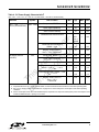
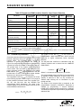
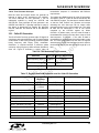
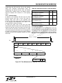
Part Number
Ringing
Method
Si3220
Internal
Si3225
External
Ringer
Ordering Information
See “Dual ProSLIC Selection
Guide” on page 110.
U.S. Patent #6,567,521
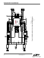
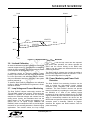
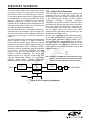
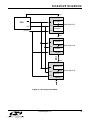
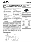
The Dual ProSLIC® is a series of low-voltage CMOS devices that integrate both
SLIC and codec functionality into a single IC to provide a complete dual-channel
analog telephone interface in accordance with all relevant LSSGR, ITU, and ETSI
specifications. The Si3220 includes internal ringing generation to eliminate
centralized ringers and ringing relays, and the Si3225 supports centralized ringing
for long loop and legacy applications. On-chip subscriber loop and audio testing
allows remote diagnostics and fault detection with no external test equipment or
relays. The Si3220 and Si3225 operate from a single 3.3 or 5 V supply and
interface to standard PCM/SPI or GCI bus digital interfaces. The Si3200/2 linefeed
ICs perform all high-voltage functions and operate from a 3.3 or 5 V supply as well
as single or dual battery supplies up to 100 V (Si3200) or 125 V (Si3202). The
Si3220 and Si3225 are available in a 64-pin thin quad flat package (TQFP), and the
Si3200/2 is available in a thermally-enhanced 16-pin small outline (SOIC) package.
U.S. Patent #6,812,744
Other patents pending
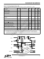
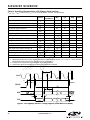
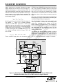
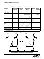
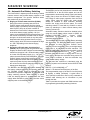
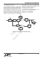
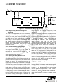
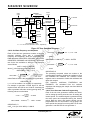
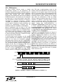
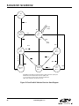
Functional Block Diagram
INT RESET
Si3220/25
CS
SCLK
SDO
SPI
Control
Interface
SDI
DTX
DRX
FSYNC
PCLK
PCM /
GCI
Interface
PLL
2-Wire AC
Impedance
Pulse Metering
Subscriber Line
Diagnostics
Ringing
Generator
& Ring Trip
Sense
DSP
ADC
SLIC A
Linefeed
Control
Codec B
Gain Adjust
Loop Closure,
& Ground Key
Detection
Programmable
Audio Filters
Relay Drivers
DAC
ADC
Si3200/2
TIP
Linefeed
Interface
Linefeed
Monitor
FSK
text ID
Caller
Modem Tone
Detection
Preliminary Rev. 1.3 2/05
DAC
Hybrid Balance
DTMF Decode
Dual Tone
Generators
Codec A
SLIC B
Linefeed
Control
Linefeed
Monitor
Channel A
RING
Si3200/2
TIP
Linefeed
Interface
Channel B
RING
Copyright © 2005 by Silicon Laboratories
Si3220/25 Si3200/02
This information applies to a product under development. Its characteristics and specifications are subject to change without notice.
T
be his
en p
r
di od
sc u
o n ct
tin ha
ue s
d.
Si3220/25 Si3200/02
2
Preliminary Rev. 1.3
Si3220/25 Si3200/02
TABLE O F C ONTENTS
Section
Page
T
be his
en p
r
di od
sc u
o n ct
tin ha
ue s
d.
1. Electrical Specifications . . . . . . . . . . . . . . . . . . . . . . . . . . . . . . . . . . . . . . . . . . . . . . . . . . .4
2. Bill of Materials . . . . . . . . . . . . . . . . . . . . . . . . . . . . . . . . . . . . . . . . . . . . . . . . . . . . . . . . . . 28
3. Functional Description . . . . . . . . . . . . . . . . . . . . . . . . . . . . . . . . . . . . . . . . . . . . . . . . . . . 30
3.1. Dual ProSLIC Architecture . . . . . . . . . . . . . . . . . . . . . . . . . . . . . . . . . . . . . . . . . . . . 30
3.2. Power Supply Sequencing . . . . . . . . . . . . . . . . . . . . . . . . . . . . . . . . . . . . . . . . . . . . 31
3.3. DC Feed Characteristics . . . . . . . . . . . . . . . . . . . . . . . . . . . . . . . . . . . . . . . . . . . . . . 31
3.4. Adaptive Linefeed . . . . . . . . . . . . . . . . . . . . . . . . . . . . . . . . . . . . . . . . . . . . . . . . . . . 34
3.5. Ground Start Operation . . . . . . . . . . . . . . . . . . . . . . . . . . . . . . . . . . . . . . . . . . . . . . . 36
3.6. Linefeed Calibration . . . . . . . . . . . . . . . . . . . . . . . . . . . . . . . . . . . . . . . . . . . . . . . . . 37
3.7. Loop Voltage and Current Monitoring . . . . . . . . . . . . . . . . . . . . . . . . . . . . . . . . . . . . 37
3.8. Power Monitoring and Power Fault Detection . . . . . . . . . . . . . . . . . . . . . . . . . . . . . . 37
3.9. Automatic Dual Battery Switching . . . . . . . . . . . . . . . . . . . . . . . . . . . . . . . . . . . . . . . 42
3.10. Loop Closure Detection . . . . . . . . . . . . . . . . . . . . . . . . . . . . . . . . . . . . . . . . . . . . . . 45
3.11. Ground Key Detection . . . . . . . . . . . . . . . . . . . . . . . . . . . . . . . . . . . . . . . . . . . . . . . 46
3.12. Ringing Generation . . . . . . . . . . . . . . . . . . . . . . . . . . . . . . . . . . . . . . . . . . . . . . . . .50
3.13. Internal Unbalanced Ringing . . . . . . . . . . . . . . . . . . . . . . . . . . . . . . . . . . . . . . . . . .52
3.14. Ringing Coefficients . . . . . . . . . . . . . . . . . . . . . . . . . . . . . . . . . . . . . . . . . . . . . . . . 53
3.15. Ring Trip Detection . . . . . . . . . . . . . . . . . . . . . . . . . . . . . . . . . . . . . . . . . . . . . . . . .54
3.16. Relay Driver Considerations . . . . . . . . . . . . . . . . . . . . . . . . . . . . . . . . . . . . . . . . . .57
3.17. Polarity Reversal . . . . . . . . . . . . . . . . . . . . . . . . . . . . . . . . . . . . . . . . . . . . . . . . . . . 60
3.18. Two-Wire Impedance Synthesis . . . . . . . . . . . . . . . . . . . . . . . . . . . . . . . . . . . . . . . 62
3.19. Transhybrid Balance Filter . . . . . . . . . . . . . . . . . . . . . . . . . . . . . . . . . . . . . . . . . . . 63
3.20. Tone Generators . . . . . . . . . . . . . . . . . . . . . . . . . . . . . . . . . . . . . . . . . . . . . . . . . . . 63
3.21. Caller ID Generation . . . . . . . . . . . . . . . . . . . . . . . . . . . . . . . . . . . . . . . . . . . . . . . . 67
3.22. Pulse Metering Generation . . . . . . . . . . . . . . . . . . . . . . . . . . . . . . . . . . . . . . . . . . . 68
3.23. DTMF Detection . . . . . . . . . . . . . . . . . . . . . . . . . . . . . . . . . . . . . . . . . . . . . . . . . . . 69
3.24. Modem Tone Detection . . . . . . . . . . . . . . . . . . . . . . . . . . . . . . . . . . . . . . . . . . . . . . 70
3.25. Audio Path Processing . . . . . . . . . . . . . . . . . . . . . . . . . . . . . . . . . . . . . . . . . . . . . . 70
3.26. System Clock Generation . . . . . . . . . . . . . . . . . . . . . . . . . . . . . . . . . . . . . . . . . . . . 72
3.27. Interrupt Logic . . . . . . . . . . . . . . . . . . . . . . . . . . . . . . . . . . . . . . . . . . . . . . . . . . . . .73
3.28. SPI Control Interface . . . . . . . . . . . . . . . . . . . . . . . . . . . . . . . . . . . . . . . . . . . . . . . . 73
3.29. PCM Interface . . . . . . . . . . . . . . . . . . . . . . . . . . . . . . . . . . . . . . . . . . . . . . . . . . . . . 79
3.30. PCM Companding . . . . . . . . . . . . . . . . . . . . . . . . . . . . . . . . . . . . . . . . . . . . . . . . . . 80
3.31. General Circuit Interface . . . . . . . . . . . . . . . . . . . . . . . . . . . . . . . . . . . . . . . . . . . . . 84
3.32. System Testing . . . . . . . . . . . . . . . . . . . . . . . . . . . . . . . . . . . . . . . . . . . . . . . . . . . . 96
4. Pin Descriptions: Si3220/25 . . . . . . . . . . . . . . . . . . . . . . . . . . . . . . . . . . . . . . . . . . . . . . 101
5. Pin Descriptions: Si3200/2 . . . . . . . . . . . . . . . . . . . . . . . . . . . . . . . . . . . . . . . . . . . . . . . 105
6. Package Outline: 64-Pin TQFP . . . . . . . . . . . . . . . . . . . . . . . . . . . . . . . . . . . . . . . . . . . .107
7. Package Outline: 16-Pin ESOIC . . . . . . . . . . . . . . . . . . . . . . . . . . . . . . . . . . . . . . . . . . . 108
8. Silicon Labs Si3220/25 Support Documentation . . . . . . . . . . . . . . . . . . . . . . . . . . . . . . 109
9. Dual ProSLIC Selection Guide . . . . . . . . . . . . . . . . . . . . . . . . . . . . . . . . . . . . . . . . . . . .110
Document Change List . . . . . . . . . . . . . . . . . . . . . . . . . . . . . . . . . . . . . . . . . . . . . . . . . . . . 111
Contact Information . . . . . . . . . . . . . . . . . . . . . . . . . . . . . . . . . . . . . . . . . . . . . . . . . . . . . . .112
Preliminary Rev. 1.3
3
Si3220/25 Si3200/02
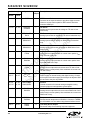
1. Electrical Specifications
Table 1. Absolute Maximum Ratings and Thermal Information1
Parameter
Symbol
Test Condition
Min
Max
Unit
–0.5
6.0
V
–20
+20
mA
Si3220/Si3225
Supply Voltage
VDD1VDD4
STIPAC, STIPDC, SRINGAC, SRINGDC Current
IIN
–10
+10
mA
Input Voltage, Digital Pins
VIND
–0.3
VDDD+0.3
V
T
be his
en p
r
di od
sc u
o n ct
tin ha
ue s
d.
Input Current, Digital Pins
Analog Ground Differential Voltage
(GND1 to ePad, GND2 to ePad or GND1 to GND2)2
VGNDA
–50
+50
mV
Digital Ground Differential Voltage
(GND3 to GND4)2
VGNDD
–50
+50
mV
–0.5
6.0
V
Continuous
–104
0.4
V
10 ms
–109
0.4
V
Si3200
Supply Voltage
High Battery Supply Voltage3
VDD
VBATH
Low Battery Supply Voltage
VBAT,
VBATL
Continuous
VBATH
0.4
V
TIP or RING Voltage
VTIP,
VRING
Continuous
–104
0.4
V
Pulse < 10 us
VBATH–15
0.4
V
Pulse < 4 us
VBATH–35
0.4
V
ITIP, IRING
–100
+100
mA
VDD
–0.5
6.0
V
TIP or RING Current
Si3202
Supply Voltage
Notes:
1. Permanent device damage may occur if the absolute maximum ratings are exceeded, and exposure to absolute
maximum rating conditions for extended periods may affect device reliability. Functional operation should be restricted
to the conditions as specified in the operational sections of this data sheet.
2. The PCB pad placed under the device package must be connected with multiple vias to the PCB ground layer and to
the GND1-GND4 pins via short traces. The TQFP-64 e-Pad must be properly soldered to the PCB pad during PCB
assembly. This type of low-impedance grounding arrangement is necessary to ensure that maximum differentials are
not exceeded under any operating condition in addition to providing thermal dissipation.
3. On Si3200 revision E, the dv/dt of the voltage applied to the VBAT, VBATH, and VBATL pins must be limited to 10 V/µs.
4. Operation of the Si3220/Si3225 above 125 C junction temperature may degrade device reliability. The Si3200/Si3202
should be operated at a junction temperature below 140 C for optimal reliability.
5. The thermal resistance of an exposed pad package is assured when the recommended printed circuit board layout
guidelines are followed correctly. The specified performance requires that the exposed pad be soldered to an exposed
copper surface of equal size and that multiple vias are added to enable heat transfer between the top-side copper
surface and a large internal copper ground plane. Refer to “AN55: Dual ProSLIC® User Guide” or to the Si3220/3225
evaluation board data sheet for specific layout examples.
4
Preliminary Rev. 1.3
Si3220/25 Si3200/02
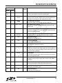
Table 1. Absolute Maximum Ratings and Thermal Information1 (Continued)
Parameter
High Battery Supply Voltage
Symbol
Test Condition
Min
Max
Unit
VBATH
Continuous
–130
0.4
V
10 ms
–135
0.4
V
VBAT,
VBATL
Continuous
VBATH
0.4
V
TIP or RING Voltage
VTIP,
VRING
Continuous
–130
0.4
V
Pulse < 10 us
VBATH–15
0.4
V
Pulse < 4 us
VBATH–35
0.4
V
T
be his
en p
r
di od
sc u
o n ct
tin ha
ue s
d.
Low Battery Supply Voltage
TIP or RING Current
ITIP, IRING
–100
+100
mA
Operating temperature (All devices)4
–40
+100
C
Storage temperature (All devices)
–40
+150
C
Thermal Information
Thermal Resistance (Si3220/Si3225)5
JA
TQFP-64 ePad
25 (typical)
C/W
5
JA
SOIC-16 ePad
55 (typical)
C/W
Thermal Resistance (Si3200/Si3202)
Notes:
1. Permanent device damage may occur if the absolute maximum ratings are exceeded, and exposure to absolute
maximum rating conditions for extended periods may affect device reliability. Functional operation should be restricted
to the conditions as specified in the operational sections of this data sheet.
2. The PCB pad placed under the device package must be connected with multiple vias to the PCB ground layer and to
the GND1-GND4 pins via short traces. The TQFP-64 e-Pad must be properly soldered to the PCB pad during PCB
assembly. This type of low-impedance grounding arrangement is necessary to ensure that maximum differentials are
not exceeded under any operating condition in addition to providing thermal dissipation.
3. On Si3200 revision E, the dv/dt of the voltage applied to the VBAT, VBATH, and VBATL pins must be limited to 10 V/µs.
4. Operation of the Si3220/Si3225 above 125 C junction temperature may degrade device reliability. The Si3200/Si3202
should be operated at a junction temperature below 140 C for optimal reliability.
5. The thermal resistance of an exposed pad package is assured when the recommended printed circuit board layout
guidelines are followed correctly. The specified performance requires that the exposed pad be soldered to an exposed
copper surface of equal size and that multiple vias are added to enable heat transfer between the top-side copper
surface and a large internal copper ground plane. Refer to “AN55: Dual ProSLIC® User Guide” or to the Si3220/3225
evaluation board data sheet for specific layout examples.
Preliminary Rev. 1.3
5
Si3220/25 Si3200/02
Table 2. Recommended Operating Conditions
Parameter
Symbol
Test
Condition
Min*
Typ
Max*
Unit
Ambient Temperature
TA
K/F-Grade
0
25
70
oC
Ambient Temperature
TA
B/G-Grade
–40
25
85
oC
VDD1–VDD4
3.13
3.3/5.0
5.25
V
Supply Voltage, Si3200/Si3202
VDD
3.13
3.3/5.0
5.25
V
High Battery Supply Voltage, Si3200
VBATH
–15
—
–99
V
Low Battery Supply Voltage, Si3200
VBATL
–15
—
VBATH
V
High Battery Supply Voltage, Si3202
VBATH
–15
—
–125
V
Low Battery Supply Voltage, Si3202
VBATL
–15
—
VBATH
V
T
be his
en p
r
di od
sc u
o n ct
tin ha
ue s
d.
Supply Voltage, Si3220/Si3225
*Note: All minimum and maximum specifications are guaranteed and apply across the recommended operating conditions.
Typical values apply at nominal supply voltages and an operating temperature of 25 °C unless otherwise stated.
Table 3. 3.3 V Power Supply Characteristics1
(VDD, VDD1 – VDD4 = 3.3 V, TA = 0 to 70 °C for K/F-Grade, –40 to 85 °C for B/G-Grade)
Parameter
VDD1–VDD4 Supply
Current (Si3220/
Si3225)
Symbol
Test Condition
Min
Typ
Max
Unit
IVDD1–IVDD4
Sleep mode, RESET = 0
—
200
—
µA
Open (high-impedance)
—
17
—
mA
Active on-hook standby
—
16
—
mA
—
45 + ILIM
+ ABIAS
—
mA
—
47
—
mA
—
26
—
mA
Forward/reverse active off-hook
Forward/reverse active OHT
OBIAS = 4 mA, VBAT = –70 V
Ringing, VRING = 45 Vrms, VBAT = –70 V,
Sine Wave, 1 REN load2
Notes:
1. All specifications are for a single channel based on measurements with both channels in the same operating state.
2. See "3.14.4. Ringing Power Considerations" on page 54 for current and power consumption under other operating
conditions.
3. Power consumption does not include additional power required for dc loop feed. Total system power consumption must
include an additional (VDD + |VBAT|) x ILOOP term.
6
Preliminary Rev. 1.3
Si3220/25 Si3200/02
Table 3. 3.3 V Power Supply Characteristics1 (Continued)
(VDD, VDD1 – VDD4 = 3.3 V, TA = 0 to 70 °C for K/F-Grade, –40 to 85 °C for B/G-Grade)
Parameter
Test Condition
Min
Typ
Max
Unit
IVDD
Sleep mode, RESET = 0
—
110
—
µA
Open (high-impedance)
—
110
—
µA
Active on-hook standby
—
110
—
µA
Forward/reverse active off-hook,
ABIAS = 4 mA, VBAT = –24 V
—
110
—
µA
Forward/reverse OHT, OBIAS = 4 mA,
VBAT = –70 V
—
110
—
µA
Ringing, VRING = 45 Vrms,
VBAT = –70 V,
Sine Wave, 1 REN load
—
110
—
µA
Sleep mode, RESET=0,
VBAT = –70 V
—
100
—
µA
Open (high-impedance),
VBAT = –70 V
—
189
—
µA
Active on-hook standby,
VBAT = –70 V
—
517
—
µA
Forward/reverse active off-hook,
ABIAS = 4 mA, VBAT = –24 V
—
4.5 +
ILIM
—
mA
—
8.6
—
mA
—
6.5
—
mA
T
be his
en p
r
di od
sc u
o n ct
tin ha
ue s
d.
VDD Supply Current
(Si3200/2)
Symbol
VBAT Supply Current
(Si3200/2)
IVBAT
Forward/reverse OHT, OBIAS = 4 mA,
VBAT = –70 V
Ringing, VRING = 45 Vrms,
VBAT = –70 V,
Sine Wave, 1 REN load2
Notes:
1. All specifications are for a single channel based on measurements with both channels in the same operating state.
2. See "3.14.4. Ringing Power Considerations" on page 54 for current and power consumption under other operating
conditions.
3. Power consumption does not include additional power required for dc loop feed. Total system power consumption must
include an additional (VDD + |VBAT|) x ILOOP term.
Preliminary Rev. 1.3
7
Si3220/25 Si3200/02
Table 3. 3.3 V Power Supply Characteristics1 (Continued)
(VDD, VDD1 – VDD4 = 3.3 V, TA = 0 to 70 °C for K/F-Grade, –40 to 85 °C for B/G-Grade)
Symbol
Test Condition
Min
Typ
Max
Unit
Chipset Power
Consumption
PSLEEP
Sleep mode, RESET = 0,
VBAT = –70 V
—
8
—
mW
POPEN
Open (high-impedance), VBAT = –70 V
—
69
—
mW
PSTBY
Active on-hook standby, VBAT = –70 V
—
89
—
mW
PACTIVE3
Forward/reverse active off-hook,
ABIAS = 4 mA, VBAT = –24 V
—
267
—
mW
POHT
Forward/reverse OHT, OBIAS = 4 mA,
VBAT = –70 V
—
757
—
mW
PRING
Ringing, VRING = 45 vrms,
VBAT = –70 V, 1 REN load2
—
541
—
mW
T
be his
en p
r
di od
sc u
o n ct
tin ha
ue s
d.
Parameter
Notes:
1. All specifications are for a single channel based on measurements with both channels in the same operating state.
2. See "3.14.4. Ringing Power Considerations" on page 54 for current and power consumption under other operating
conditions.
3. Power consumption does not include additional power required for dc loop feed. Total system power consumption must
include an additional (VDD + |VBAT|) x ILOOP term.
8
Preliminary Rev. 1.3
Si3220/25 Si3200/02
Table 4. 5 V Power Supply Characteristics1
(VDD, VDD1 – VDD4 = 5 V, TA = 0 to 70 °C for K/F-Grade, –40 to 85 °C for B/G-Grade)
Parameter
VDD1 – VDD4 Supply
Current (Si3220/Si3225)
Symbol
Test Condition
Min
Typ
Max
Unit
IVDD1–IVDD4
Sleep mode, RESET = 0
—
1
—
mA
Open (high-impedance)
—
22
—
mA
Active on-hook standby
—
21
—
mA
—
62 +
ILIM +
ABIAS
—
mA
—
65
—
mA
Ringing, VRING = 45 Vrms,
VBAT = –70 V, 1 REN load2
—
31
—
mA
Sleep mode, RESET = 0
—
110
—
µA
Open (high-impedance)
—
110
—
µA
Active on-hook standby
—
110
—
µA
Forward/reverse active off-hook,
ABIAS = 4 mA, VBAT = –24 V
—
110
—
µA
Forward/reverse OHT, OBIAS = 4 mA,
VBAT = –70 V
—
110
—
µA
—
110
—
µA
T
be his
en p
r
di od
sc u
o n ct
tin ha
ue s
d.
Forward/reverse active off-hook
Forward/reverse active OHT
OBIAS = 4 mA
VDD Supply Current
(Si3200/2)
IVDD
Ringing, VRING = 45 Vrms,
VBAT = –70 V,
1 REN load
Notes:
1. All specifications are for a single channel based on measurements with both channels in the same operating state.
2. See "3.14.4. Ringing Power Considerations" on page 54 for current and power consumption under other operating
conditions.
3. Power consumption does not include additional power required for dc loop feed. Total system power consumption must
include an additional (VDD + |VBAT|) x ILOOP term.
Preliminary Rev. 1.3
9
Si3220/25 Si3200/02
Table 4. 5 V Power Supply Characteristics1 (Continued)
(VDD, VDD1 – VDD4 = 5 V, TA = 0 to 70 °C for K/F-Grade, –40 to 85 °C for B/G-Grade)
Parameter
Test Condition
Min
Typ
Max
Unit
IVBAT
Sleep mode, RESET = 0,
VBAT = –70 V
—
125
—
µA
Open (high-impedance), VBAT = –70 V
—
190
—
µA
Active on-hook standby, VBAT = –70 V
—
700
—
µA
Forward/reverse active off-hook,
ABIAS = 4 mA, VBAT = –24 V
—
4.7 +
ILIM
—
mA
—
8.8
—
mA
Ringing, VRING = 45 Vrms,
VBAT = –70 V,
1 REN load2
—
6.5
—
mA
PSLEEP
Sleep mode, RESET = 0,
VBAT = –70 V
—
13.8
—
mW
POPEN
Open (high-impedance), VBAT = –70 V
—
123
—
mW
PSTBY
Active on-hook standby, VBAT = –70 V
—
154
—
mW
PACTIVE3
Forward/reverse active off-hook,
ABIAS = 4 mA, VBAT = –24 V
—
436
—
mW
POHT
Forward/reverse OHT, OBIAS = 4 mA,
VBAT = –70 V
—
941
—
mW
PRING
Ringing, VRING = 45 Vrms,
VBAT = –70 V, 1 REN load2
—
610
—
mW
T
be his
en p
r
di od
sc u
o n ct
tin ha
ue s
d.
VBAT Supply Current
(Si3200/2)
Symbol
Forward/reverse OHT, OBIAS = 4 mA,
VBAT = –70 V
Chipset Power
Consumption
Notes:
1. All specifications are for a single channel based on measurements with both channels in the same operating state.
2. See "3.14.4. Ringing Power Considerations" on page 54 for current and power consumption under other operating
conditions.
3. Power consumption does not include additional power required for dc loop feed. Total system power consumption must
include an additional (VDD + |VBAT|) x ILOOP term.
10
Preliminary Rev. 1.3
Si3220/25 Si3200/02
Table 5. AC Characteristics
(VDD, VDD1 – VDD4 = 3.13 to 5.25 V, TA = 0 to 70 °C for K/F-Grade, –40 to 85 °C for B/G-Grade)
Parameter
Test Condition
Min
Typ
Max
Unit
2.5
Figure 6
—
—
—
–85
—
—
–65
VPK
—
–87
–65
dB
TX/RX Performance
Overload Level
Overload Compression
Signal-to-(Noise + Distortion)
Ratio2
Audio Tone Generator Signal-toDistortion Ratio2
Intermodulation Distortion
Gain Accuracy
2
Attenuation Distortion vs. Freq.
Group Delay vs. Frequency
Gain Tracking3
2-Wire – PCM
2-Wire – PCM or PCM – 2-Wire:
200 Hz to 3.4 kHz
PCM – 2-Wire – PCM:
200 Hz – 3.4 kHz,
16-bit Linear mode
200 Hz to 3.4 kHz
D/A or A/D 8-bit
Active off-hook, and OHT, any ZT
0 dBm0, Active off-hook, and
OHT, any ZT
T
be his
en p
r
di od
sc u
o n ct
tin ha
ue s
d.
Single Frequency Distortion
1
Round-Trip Group Delay
Crosstalk between Channels
TX or RX to TX
TX or RX to RX
Gain Step Increment4
2-Wire Return Loss5
Transhybrid Balance
5
dB
Figure 5
—
—
46
—
—
dB
–41
+0.25
dB
dB
—
—
—
—
—
—
± 0.25
± 0.5
± 1.0
700
dB
dB
dB
µs
–75
–75
—
dB
dB
dB
—
—
2-Wire to PCM or PCM to 2-Wire
–0.25
—
1014 Hz, Any gain setting
0 dBm 0
Figure 7,8
—
Figure 9
—
1014 Hz sine wave,
—
—
reference level –10 dBm
Signal level:
3 dB to –37 dB
—
—
–37 dB to –50 dB
—
—
–50 dB to –60 dB
—
—
1014 Hz, Within same time-slot
—
600
0 dBm0,
300 Hz to 3.4 kHz
—
–108
300 Hz to 3.4 kHz
—
–108
Step size around 0 dB
—
±0.0005
200 Hz to 3.4 kHz
26
30
—
dB
300 Hz to 3.4 kHz
34
40
—
dB
Notes:
1. The input signal level should be 0 dBm0 for frequencies greater than 100 Hz. For 100 Hz and below, the level should
be –10 dBm0. The output signal magnitude at any other frequency will be smaller than the maximum value specified.
2. Analog signal measured as VTIP – VRING. Assumes ideal line impedance matching.
3. The quantization errors inherent in the µ/A-law companding process can generate slightly worse gain tracking
performance in the signal range of 3 to –37 dB for signal frequencies that are integer divisors of the 8 kHz PCM
sampling rate.
4. The digital gain block is a linear multiplier that is programmable from – to +6 dB. The step size in dB varies over the
complete range. See "3.25. Audio Path Processing" on page 70.
5. VDD1 – VDD4 = 3.3 V, VBAT = –52 V, no fuse resistors, RL = 600 , ZS = 600 synthesized using RS register
coefficients.
6. The level of any unwanted tones within the bandwidth of 0 to 4 kHz does not exceed –55 dBm.
7. The OBIAS and ABIAS registers program the dc bias current through the SLIC in the on-hook transmission and offhook active conditions, respectively. This per-pin total current setting should be selected so it can accommodate the
sum of the metallic and longitudinal currents through each of the TIP and RING leads for a given application.
Preliminary Rev. 1.3
11
Si3220/25 Si3200/02
Table 5. AC Characteristics (Continued)
(VDD, VDD1 – VDD4 = 3.13 to 5.25 V, TA = 0 to 70 °C for K/F-Grade, –40 to 85 °C for B/G-Grade)
Parameter
Test Condition
Idle Channel Noise6
PSRR from VDD1 – VDD4
PSRR from VBAT
Typ
Max
Unit
—
12
15
dBrnC
Psophometric weighted
3 kHz flat
RX and TX, dc to 3.4 kHz
RX and TX, dc to 3.4 kHz
Longitudinal Performance
200 Hz to 1 kHz
1 kHz to 3.4 kHz
200 Hz to 3.4 kHz
—
—
40
60
–78
—
—
—
–75
18
—
—
dBmP
dBrn
dB
dB
58
53
40
70
58
—
—
—
—
dB
dB
dB
200 Hz to 3.4 kHz at TIP or RING
Register-dependent
OBIAS/ABIAS
00 = 4 mA
01 = 8 mA
10 = 12 mA
11 = 16 mA
—
—
—
—
50
25
25
20
—
—
—
—
Active off-hook
200 Hz to 3.4 kHz
Register-dependent
OBIAS/ABIAS
00 = 4 mA
01 = 8 mA
10 = 12 mA
11 = 16 mA
—
—
—
—
4
8
8
10
—
—
—
—
mA
mA
mA
mA
T
be his
en p
r
di od
sc u
o n ct
tin ha
ue s
d.
Longitudinal to Metallic/PCM
Balance (forward or reverse)
Noise Performance
C-Message weighted
Min
Metallic/PCM to Longitudinal
Balance
Longitudinal Impedance7
Longitudinal Current per Pin7
Notes:
1. The input signal level should be 0 dBm0 for frequencies greater than 100 Hz. For 100 Hz and below, the level should
be –10 dBm0. The output signal magnitude at any other frequency will be smaller than the maximum value specified.
2. Analog signal measured as VTIP – VRING. Assumes ideal line impedance matching.
3. The quantization errors inherent in the µ/A-law companding process can generate slightly worse gain tracking
performance in the signal range of 3 to –37 dB for signal frequencies that are integer divisors of the 8 kHz PCM
sampling rate.
4. The digital gain block is a linear multiplier that is programmable from – to +6 dB. The step size in dB varies over the
complete range. See "3.25. Audio Path Processing" on page 70.
5. VDD1 – VDD4 = 3.3 V, VBAT = –52 V, no fuse resistors, RL = 600 , ZS = 600 synthesized using RS register
coefficients.
6. The level of any unwanted tones within the bandwidth of 0 to 4 kHz does not exceed –55 dBm.
7. The OBIAS and ABIAS registers program the dc bias current through the SLIC in the on-hook transmission and offhook active conditions, respectively. This per-pin total current setting should be selected so it can accommodate the
sum of the metallic and longitudinal currents through each of the TIP and RING leads for a given application.
12
Preliminary Rev. 1.3
Si3220/25 Si3200/02
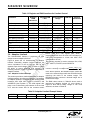
Table 6. Linefeed Characteristics
(VDD, VDD1 – VDD4 = 3.13 to 5.25 V, TA = 0 to 70 °C for K/F-Grade, –40 to 85 °C for B/G-Grade)
Parameter
Symbol
Test Condition
Min
Typ
Max
Unit
Maximum Loop Resistance (adaptive
linefeed disabled1)
RLOOP
2
RDC,MAX = 430 ,
ILOOP = 18 mA, VBAT = –52 V,
ABIAS = 8 mA
VOCDELTA = 0
1870
—
—
Maximum Loop Resistance (adaptive
linefeed enabled1)
RLOOP
RDC,MAX2 = 430 ,
ILOOP = 18 mA, VBAT = –52 V,
ABIAS = 8 mA
VOCDELTA 0
2030
—
—
ILIM = 18 mA
—
—
±10
%
Active Mode; VOC = 48 V,
VTIP – VRING
—
—
±4
V
RDO
ILOOP < ILIM
—
320
—
DC On-Hook Voltage Accuracy—Ground
Start
VOHTO
IRING<ILIM; VRING wrt ground,
VRING = –51 V
—
—
±4
V
DC Output Resistance—Ground Start
RROTO
IRING<ILIM; RING to ground
—
320
—
DC Output Resistance—Ground Start
RTOTO
TIP to ground
300
—
—
k
Loop Closure Detect Threshold Accuracy
ITHR = 13 mA
—
±10
±15
%
Ground Key Detect Threshold Accuracy
ITHR = 13 mA
—
±10
±15
%
Si3220, ac detection,
VRING = 70 Vpk, no offset,
ITH = 80 mA
—
±4
±5
mA
Si3220, dc detection,
20 V dc offset, ITH = 13 mA
—
±1.5
±2
mA
Si3225, dc detection,
48 V dc offset, Rloop = 1500
—
—
±4.5
mA
Open circuit, VBATH = 100 V
93
—
—
VPK
5 REN load, RLOOP = 0
VBATH = 100 V
82
—
—
VPK
—
2
—
%
f = 16 Hz to 100 Hz
—
—
±1
%
Accuracy of ON/OFF times
—
—
±50
ms
CAL to CAL bit
—
—
600
ms
T
be his
en p
r
di od
sc u
o n ct
tin ha
ue s
d.
DC Loop Current Accuracy
DC Open Circuit Voltage Accuracy
DC Differential Output Resistance
Ring Trip Threshold Accuracy
Ringing Amplitude, Si32203
Sinusoidal Ringing Total
Harmonic Distortion
Ringing Frequency Accuracy
Ringing Cadence Accuracy
Calibration Time
VRING
RTHD
Notes:
1. Adaptive linefeed is enabled when the VOCDELTA RAM address is set to a non-zero value and is disabled when
VOCDELTA is set to 0.
2. RDC,MAX is the maximum dc resistance of the CPE; hence the specified total loop resistance is RLOOP + RDC,MAX.
3. Ringing amplitude is set for 93 V peak using the RINGAMP RAM address and measured at TIP-RING using no series
protection resistance.
Preliminary Rev. 1.3
13
Si3220/25 Si3200/02
Table 6. Linefeed Characteristics (Continued)
(VDD, VDD1 – VDD4 = 3.13 to 5.25 V, TA = 0 to 70 °C for K/F-Grade, –40 to 85 °C for B/G-Grade)
Parameter
Symbol
Test Condition
Min
Typ
Max
Unit
Loop Voltage Sense Accuracy
Accuracy of boundaries for
each output code;
VTIP – VRING = 48 V
—
±2
±4
%
Loop Current Sense Accuracy
Accuracy of boundaries for
each output code;
ILOOP = 18 mA
—
±7
±10
%
Power Alarm Threshold Accuracy
Power Threshold = 300 mW
—
—
±25
%
T
be his
en p
r
di od
sc u
o n ct
tin ha
ue s
d.
Notes:
1. Adaptive linefeed is enabled when the VOCDELTA RAM address is set to a non-zero value and is disabled when
VOCDELTA is set to 0.
2. RDC,MAX is the maximum dc resistance of the CPE; hence the specified total loop resistance is RLOOP + RDC,MAX.
3. Ringing amplitude is set for 93 V peak using the RINGAMP RAM address and measured at TIP-RING using no series
protection resistance.
Table 7. Monitor ADC Characteristics
(VDD, VDD1–VDD4 = 3.13 to 5.25 V, TA = 0 to 70 °C for K/F-Grade, –40 to 85 °C for B/G-Grade)
Parameter
Resolution
Symbol
Test Condition
Min
Typ
Max
Unit
—
8
—
Bits
Differential Nonlinearity
DNL
–1.0
±0.75
+1.5
LSB
LSB
Integral Nonlinearity
INL
—
±0.6
±1.5
LSB
—
±0.1
±0.25
LSB
Gain Error
14
Preliminary Rev. 1.3
Si3220/25 Si3200/02
Table 8. Si3200/2 Characteristics
(VDD = 3.13 to 5.25 V, TA = 0 to 70 °C for K/F-Grade, –40 to 85 °C for B/G-Grade)
Parameter
TIP/RING Pulldown Transistor Saturation Voltage
Test Condition
VOV
VRING – VBAT (Forward)
VTIP – VBAT (Reverse)
ILIM = 22 mA, IABIAS = 4 mA1
ILIM = 45 mA,
IABIAS = 16 mA1
VCM
Min
Typ
Max
Unit
3
—
V
V
GND – VTIP (Forward)
GND – VRING (Reverse)
ILIM = 22 mA1
ILIM = 45 mA1
3
—
V
V
T
be his
en p
r
di od
sc u
o n ct
tin ha
ue s
d.
TIP/RING Pullup Transistor
Saturation Voltage
Symbol
Battery Switch Saturation
Impedance
RSAT
(VBAT – VBATH)/IOUT (Note 2)
15
OPEN State TIP/RING Leakage Current
ILKG
RL = 0
100
µA
Internal Blocking Diode Forward Voltage
VF
VBAT – VBATL (Note 2)
0.8
V
Notes:
1. VAC = 2.5 VPK, RLOAD = 600 .
2. IOUT = 60 mA.
Table 9. DC Characteristics (VDD, VDD1–VDD4 = 5 V)
(VDD, VDD1 – VDD4 = 4.75 to 5.25 V, TA = 0 to 70 °C for K/F-Grade, –40 to 85 °C for B/G-Grade)
Parameter
High Level Input
Voltage
Low Level Input
Voltage
Symbol
Test Condition
Min
Typ
Max
Unit
VIH
0.7 x VDD
—
5.25
V
VIL
—
—
0.3 x VDD
V
High Level Output
Voltage
VOH
IO = 8 mA
VDD – 0.6
—
—
V
Low Level Output
Voltage
VOL
DTX, SDO, INT, SDITHRU:
IO = –8 mA
—
—
0.4
V
BATSELa/b, RRDa/b,
GPOa/b, TRD1a/b,TRD2a/b:
IO = –40 mA
—
—
0.72
V
20
30
—
k
SDITHRU Internal
Pullup Resistance
Relay Driver Source
Impedance
Relay Driver Sink
Impedance
Input Leakage Current
ROUT
VDD1–VDD4 = 4.75 V
IO < 28 mA
—
63
—
RIN
VDD1–VDD4 = 4.75 V
IO < 85 mA
—
11
—
—
—
±10
µA
IL
Preliminary Rev. 1.3
15
Si3220/25 Si3200/02
Table 10. DC Characteristics (VDD, VDD1–VDD4 = 3.3 V)
(VDD, VDD1 – VDD4 = 3.13 to 3.47 V, TA = 0 to 70 °C for K/F-Grade, –40 to 85 °C for B/G-Grade)
Parameter
Symbol
Test Condition
Min
Typ
Max
Unit
VIH
0.7 x VDD
—
5.25
V
Low Level Input Voltage
VIL
—
—
0.3 x VDD
V
High Level Output
Voltage
VOH
IO = 4 mA
VDD – 0.6
—
—
V
Low Level Output
Voltage
VOL
DTX, SDO, INT,
SDITHRU:
IO = –4 mA
—
—
0.4
V
BATSELa/b, RRDa/b,
GPOa/b, TRD1a/b, TRD2a/b:
IO = –40 mA
—
—
0.72
35
50
—
k
T
be his
en p
r
di od
sc u
o n ct
tin ha
ue s
d.
High Level Input Voltage
SDITHRU internal pullup
resistance
Relay Driver Source Impedance
ROUT
VDD1–VDD4 = 3.13 V
IO < 28 mA
—
63
—
Relay Driver Sink Impedance
RIN
VDD1–VDD4 = 3.13 V
IO < 85 mA
—
11
—
—
—
±10
µA
Input Leakage Current
IL
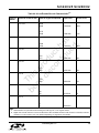
Table 11. Switching Characteristics—General Inputs1
(VDD, VDD1 – VDD4 = 3.13 to 5.25 V, TA = 0 to 70 °C for K/F-Grade, –40 to 85 °C for B/G-Grade, CL = 20 pF)
Parameter
Symbol
Min
Typ
Max
Unit
Rise Time, RESET
tr
—
—
5
ns
RESET Pulse Width, GCI Mode2
trl
500
—
—
ns
RESET Pulse Width, SPI Daisy Chain Mode
trl
6
—
—
µs
Notes:
1. All timing (except Rise and Fall time) is referenced to the 50% level of the waveform. Input test levels are VIH = VDD –
0.4 V, VIL = 0.4 V. Rise and Fall times are referenced to the 20% and 80% levels of the waveform.
2. The minimum RESET pulse width assumes the SDITHRU pin is tied to ground via a pulldown resistor no greater than
10 k per device.
16
Preliminary Rev. 1.3
Si3220/25 Si3200/02
Table 12. Switching Characteristics—SPI
(VDD, VDD1 – VDD4 = 3.13 to 5.25 V, TA = 0 to 70 °C for K/F-Grade, –40 to 85 °C for B/G-Grade, CL = 20 pF)
Parameter1
Symbol
Test Conditions
Min
Typ
Max
Unit
tc
62
—
—
ns
Rise Time, SCLK
tr
—
—
25
ns
Fall Time, SCLK
tf
—
—
25
ns
Delay Time, SCLK Fall to SDO Active
td1
—
—
20
ns
Delay Time, SCLK Fall to SDO
Transition
td2
—
—
20
ns
Delay Time, CS Rise to SDO Tri-state
td3
—
—
20
ns
Setup Time, CS to SCLK Fall
tsu1
25
—
—
ns
Hold Time, CS to SCLK Rise
th1
20
—
—
ns
Setup Time, SDI to SCLK Rise
tsu2
25
—
—
ns
Hold Time, SDI to SCLK Rise
th2
20
—
—
ns
Delay Time between Chip Selects
tcs
220
—
—
ns
SDI to SDITHRU Propagation Delay
td4
—
4
10
ns
T
be his
en p
r
di od
sc u
o n ct
tin ha
ue s
d.
Cycle Time SCLK2
Notes:
1. All timing is referenced to the 50% level of the waveform. Input test levels are VIH = VDDD –0.4 V, VIL = 0.4 V
2. The minimum SCLK cycle time is based on a single Si3220 connected to the SPI bus. If multiple Si3220s are
connected to the same SPI bus, please contact a Silicon Laboratories representative for the recommended minimum
SCLK cycle time for your application.
tr
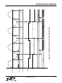
tc
tf
SCLK
tsu1
th1
CS
tcs
tsu2
th2
SDI
td1
td3
td2
SDO
td4
SDITHRU
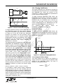
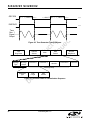
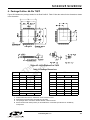
Figure 1. SPI Timing Diagram
Preliminary Rev. 1.3
17
Si3220/25 Si3200/02
Table 13. Switching Characteristics—PCM Highway Interface
(VDD, VDD1 – VDD4 = 3.13 to 5.25 V, TA = 0 to 70 °C for K/F-Grade, –40 to 85 °C for B/G-Grade, CL = 20 pF)
Parameter
Symbol
PCLK Period
Test
Conditions
tp
Typ1
Max1
Units
122
—
3906
ns
—
—
—
—
—
—
—
—
—
256
512
768
1.024
1.536
1.544
2.048
4.096
8.192
—
—
—
—
—
—
—
—
—
kHz
kHz
kHz
MHz
MHz
MHz
MHz
MHz
MHz
T
be his
en p
r
di od
sc u
o n ct
tin ha
ue s
d.
Valid PCLK Inputs
Min1
FSYNC Period2
tfs
—
125
—
µs
PCLK Duty Cycle Tolerance
tdty
40
50
60
%
PCLK Period Jitter Tolerance
tjitter
—
—
±120
ns
Rise Time, PCLK
tr
—
—
25
ns
Fall Time, PCLK
tf
—
—
25
ns
Delay Time, PCLK Rise to DTX Active
td1
—
—
20
ns
Delay Time, PCLK Rise to DTX
Transition
td2
—
—
20
ns
Delay Time, PCLK Rise to DTX Tristate3
td3
—
—
20
ns
Setup Time, FSYNC to PCLK Fall
tsu1
25
—
—
ns
Hold Time, FSYNC to PCLK Fall
th1
20
—
—
ns
Setup Time, DRX to PCLK Fall
tsu2
25
—
—
ns
Hold Time, DRX to PCLK Fall
th2
20
—
—
ns
FSYNC Pulse Width
twfs
tp/2
—
125 µs–tp
Notes:
1. All timing is referenced to the 50% level of the waveform. Input test levels are VIH – VI/O –0.4 V, VIL = 0.4 V.
2. FSYNC source is assumed to be 8 kHz under all operating conditions.
3. Specification applies to PCLK fall to DTX tristate when that mode is selected.
18
Preliminary Rev. 1.3
Si3220/25 Si3200/02
tr
tp
tf
PCLK
th1
twfs
tsu1
FSYNC
tfs
tsu2
th2
T
be his
en p
r
di od
sc u
o n ct
tin ha
ue s
d.
DRX
td1
td2
td3
DTX
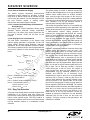
Figure 2. PCM Highway Interface Timing Diagram
Preliminary Rev. 1.3
19
Si3220/25 Si3200/02
Table 14. Switching Characteristics—GCI Highway Serial Interface
(VDD, VDD1 – VDD4 = 3.13 to 5.25 V, TA = 0 to 70 °C for K/F-Grade, –40 to 85 °C for B/G-Grade)
Parameter1
Symbol
Test
Conditions
Min
Typ
Max
Units
PCLK Period (2.048 MHz PCLK Mode)
tp
—
488
—
ns
PCLK Period (4.096 MHz PCLK Mode)
tp
—
244
—
ns
tfs
—
125
—
µs
PCLK Duty Cycle Tolerance
tdty
40
50
60
%
FSYNC Jitter Tolerance
tjitter
—
—
±120
ns
Rise Time, PCLK
tr
—
—
25
ns
Fall Time, PCLK
tf
—
—
25
ns
Delay Time, PCLK Rise to DTX Active
td1
—
—
20
ns
Delay Time, PCLK Rise to DTX Transition
td2
—
—
20
ns
Delay Time, PCLK Rise to DTX Tristate3
td3
—
—
20
ns
Setup Time, FSYNC Rise to PCLK Fall
tsu1
25
—
—
ns
Hold Time, PCLK Fall to FSYNC Fall
th1
20
—
—
ns
Setup Time, DRX Transition to PCLK Fall
tsu2
25
—
—
ns
Hold Time, PCLK Falling to DRX Transition
th2
20
—
—
ns
FSYNC Pulse Width
twfs
tp/2
—
—
ns
T
be his
en p
r
di od
sc u
o n ct
tin ha
ue s
d.
FSYNC Period
2
Notes:
1. All timing is referenced to the 50% level of the waveform. Input test levels are VIH = VO – 0.4 V, VIL = 0.4 V, rise and
fall times are referenced to the 20% and 80% levels of the waveform.
2. FSYNC source is assumed to be 8 kHz under all operating conditions.
3. Specification applies to PCLK fall to DTX tristate when that mode is selected.
tr
tp
tf
PCLK
th1
tsu1
tfs
FSYNC
tsu2
DRX
td1
DTX
th2
Frame 0,
Bit 0
td2
td3
Frame 0,
Bit 0
Figure 3. GCI Highway Interface Timing Diagram (2.048 MHz PCLK Mode)
20
Preliminary Rev. 1.3
Si3220/25 Si3200/02
tr
tf
tc
PCLK
th1
tfs
tsu1
FSYNC
tsu2
T
be his
en p
r
di od
sc u
o n ct
tin ha
ue s
d.
DRX
th2
Frame 0,
Bit 0
td1
td2
td3
Frame 0,
Bit 0
DTX
Figure 4. GCI Highway Interface Timing Diagram (4.096 MHz PCLK Mode)
Acceptable Region
Figure 5. Transmit and Receive Path SNDR
Preliminary Rev. 1.3
21
Si3220/25 Si3200/02
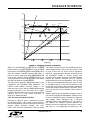
9
8
7
6
Fundamental
Output Power 5
(dBm0)
Acceptable
Region
4
3
2.6
2
T
be his
en p
r
di od
sc u
o n ct
tin ha
ue s
d.
1
0
1
2
3
4
5
6
7
8
9
Fundamental Input Power (dBm0)
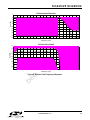
Figure 6. Overload Compression Performance
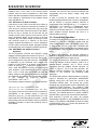
TX Attenuation Distortion
5
0
Gain (dB)
−5
−10
−15
−20
−25
−30
−35
−40
−45
0
250
500
750 1000 1250 1500 1750 2000 2250 2500 2750 3000 3250 3500 3750 4000 4250 4500 4750 5000
Frequency (Hz)
TX Pass−Band Detail
0.4
0.2
Gain (dB)
0
−0.2
−0.4
−0.6
−0.8
−1
−1.2
0
250
500
750 1000 1250 1500 1750 2000 2250 2500 2750 3000 3250 3500 3750 4000 4250 4500 4750 5000
Frequency (Hz)
Figure 7. Transmit Path Frequency Response
22
Preliminary Rev. 1.3
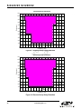
Si3220/25 Si3200/02
RX Attenuation Distortion
5
0
Gain (dB)
−5
−10
−15
−20
−25
−30
−40
−45
0
250
T
be his
en p
r
di od
sc u
o n ct
tin ha
ue s
d.
−35
500
750 1000 1250 1500 1750 2000 2250 2500 2750 3000 3250 3500 3750 4000 4250 4500 4750 5000
Frequency (Hz)
RX Pass−Band Detail
0.4
0.2
Gain (dB)
0
−0.2
−0.4
−0.6
−0.8
−1
−1.2
0
250
500
750 1000 1250 1500 1750 2000 2250 2500 2750 3000 3250 3500 3750 4000 4250 4500 4750 5000
Frequency (Hz)
Figure 8. Receive Path Frequency Response
Preliminary Rev. 1.3
23
Si3220/25 Si3200/02
TX Group Delay Distortion
1100
1000
900
Delay (us)
800
700
600
T
be his
en p
r
di od
sc u
o n ct
tin ha
ue s
d.
500
400
300
200
100
0
200
400
600
800 1000 1200 1400 1600 1800 2000 2200 2400 2600 2800 3000 3200 3400
Frequency (Hz)
Figure 9. Transmit Group Delay Distortion
RX Group Delay Distortion
1100
1000
900
Delay (us)
800
700
600
500
400
300
200
Typical Response
100
0
200
400
600
800 1000 1200 1400 1600 1800 2000 2200 2400 2600 2800 3000 3200 3400
Frequency (Hz)
Figure 10. Receive Group Delay Distortion
24
Preliminary Rev. 1.3
Ibuf
Off-chip
Gm
On-chip
ZA
Analog
Zsynth
Disable
ZSDIS
+
+
Decimation
Filter
THPF
TX EQ
TPGA
D/A
DLM3
Codec
Loopback
A/D
Preliminary Rev. 1.3
Interpolation
Filter
Receive Path
+
ZD
Decimation
Filter
H
Interpolation
Filter
DLM2
+
Modem
Tone
Detection
RPGA
Dual Tone
Generator
RX EQ
To Ringer
Circuit
RHPF
Hybrid
Loopback
+
/A-law
Expander
DLM1
PCM
Loopback
Figure 11. AC Signal Path Block Diagram for a Single Channel
From Billing
Tone DAC
+ Rx Mute
-
Tx Mute
/A-law
Compressor
DTMF
Decode
Diagnostics
Filter
T
be his
en p
r
di od
sc u
o n ct
tin ha
ue s
d.
Transmit Path
Modem Tone
Detection
Serial
Input
Serial
Output
Digital
RX
Digital
TX
Si3220/25 Si3200/02
25
Preliminary Rev. 1.3
RJ-11 SMD
6
5
4
3
2
1
J11
RJ-11 SMD
TP1
RINGa_ext
TIPa_ext
TP3
TP4
TIPa
RINGb_ext
TIPb_ext
VBATb
RINGb
TIPb
Protection
VBATa
RINGa
Protection
TP5 TP6 TP7 TP8
TP2
1
6
5
4
3
2
1
1
J1
1
1
1
1
1
RINGb
TIPb
C13
10n
100V
C3
10n
100V
RINGa
TIPa
C30
0.1u
100V
R22
0
C24
0.1u
10V
U2
Si3200
TIP
ITIPP
NC
ITIPN
RING
THERM
VBAT
IRINGP
VBATH IRINGN
VBATL
NC
GN D
NC
VDD
BATSEL
16
15
14
13
12
11
10
9
VBATH
R23
15
VBATH
VBLO
C31
0.1u
100V
VDD
VBLO
C23
0. 1u
10V
1
2
3
4
5
6
7
8
GN D
epad
16
15
14
13
12
11
10
9
C16
1u
6V
1u
6V
Si3200
1u
6V
C15
ITIPP
TIP
NC
ITIPN
RING
THERM
VBAT
IRINGP
VBATH IRINGN
VBATL
NC
GN D
NC
VDD
BATSEL
U3
C6
1u
6V
epad
C5
GN D
R2
402k
806k
BATSWa
R6
1
2
3
4
5
6
7
8
9
10
11
12
13
14
15
16
40.2k
BATSELa
R12
C12
C11
R11
R1
C1
C2
402k
182
806k
R18
R15
BATSWb
402k
0.1u
100V
X7R
0.1u
100V
X7R
182
R17
40.2k
182
R7
R10
182
R8
R5
402k
0.1u
100V
X7R
0.1u
100V
X7R
R4
R16
R14
R13
R3
4.7k
40.2k
4.7k
4.7k
SVBATa
RPOa
RPIa
RNIa
RNOa
CAPPa
CAPMa
QGND
IREF
CAPMb
CAPPb
RNOb
RNIb
RPIb
RPOb
SVBATb
U1
4.7k
Si3220
48
47
46
45
44
43
42
41
40
39
38
37
36
35
34
33
BATSELb
GPOa
/CS
SDITHRU
SDI
SDO
SCLK
VDD4
GND4
/INT
PCLK
GND3
VDD3
DTX
DRX
FSYNC
/RST
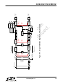
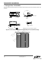
Figure 12. Si3220 Application Circuit Using Dual Battery Supply
C33
0.1u
100V
C14
10n
100V
C4
10 n
100V
R21
15
1
2
3
4
5
6
7
8
T
be his
en p
r
di od
sc u
o n ct
tin ha
ue s
d.
C32
0. 1u
100V
R20
0
64
63
62
61
60
59
58
57
56
55
54
53
52
51
50
49
STIPDCa
STIPACa
SRINGACa
SRINGDCa
ITIPNa
IRINGNa
ITIPPa
VDD1
GND1
IRINGPa
THERMa
NC
NC
TRD1a
TRD2a
BATSELa
STIPDCb
STIPACb
SRINGACb
SRINGDCb
ITIPNb
IRINGNb
ITIPPb
VDD2
GND2
IRINGPb
THERMb
NC
TRD1b
TRD2b
GPOb
BATSELb
17
18
19
20
21
22
23
24
25
26
27
28
29
30
31
32
26
1
VDD
VDD
GPOa
DTX
DRX
FSYNC
/RESET
/INT
PCLK
/CS
SDITHRU
SDI
SDO
SCLK
GPOb
R25
39k
R24
39k
GPOb
GPOa
1
2
J7
J7
1
2
J6
J6
1
2
J5
J5
1
2
J4
J4
1
2
J3
J3
1
2
J2
J2
TRD1b
TRD2b
GPOb
GPOa
TRD2a
TRD1a
Si3220/25 Si3200/02
RRDa
VDD
Ring B
TP4
RRDb
VDD
TP3
Tip B
Ring A
TP2
RJ-11 SMD
6
5
4
3
2
1
J11
RJ-11 SMD
1
TP1
Tip A
3
1
8
DPDT
K2
DPDT
10
10
1
8
3
K1
7
4
9
2
RINGa
TIPa
RINGb_ext
TIPb
C13
10n
100V
RINGb
Protection
TIPb_ext
C3
10n
100V
C30
R24
15
C32
0.1u
100V
C24
1
2
3
4
5
6
7
8
TIP
NC
RING
VBAT
VBATH
VBATL
GND
VDD
U2
ITIPP
ITIPN
THERM
IRINGP
IRINGN
NC
NC
BATSEL
16
15
14
13
12
11
10
9
C2
R6
1
2
3
4
5
6
7
8
9
10
11
12
13
14
15
16
40.2k
RNGNGa
806k
R9
RRDa
/CS
SDITHRU
SD I
SDO
SCLK
VDD4
GND4
/INT
PCLK
GND3
VDD3
DTX
D RX
FSYNC
/RST
510
R21
C31
0.1u
100V
C14
10n
100V
C4
10n
100V
0.1u
100V
VBHI
R26
15
VBHI
VBLO
C33
0.1u
100V
VBLO
VDD
C25
0.1u
6V
R25
0
0.1u
6V
1
2
3
4
5
6
7
8
1u
6V
GND
RNGNGb
Si3200
TIP
NC
RING
VBAT
VBATH
VBATL
GND
VDD
ITIPP
ITIPN
THERM
IRINGP
IRINGN
NC
NC
BATSEL
1u
6V
C15
U3
1u
6V
C16
1u
6V
C6
GND
C5
Si3200
epad
16
15
14
13
12
11
10
9
C12
C11
epad
R16
40.2k
402k
R12
4.7k
402k
SVBATa
RPOa
RPIa
RNIa
RNOa
CAPPa
CAPMa
QGND
IREF
CAPMb
CAPPb
RNOb
RNIb
RPIb
RPOb
SVBATb
U1
402k
4.7k
R1
4.7k
4.7k
402k
R14
R13
R11
806k
182
182
40.2k
0.1u
100V
<Material>
0.1u
100V
<Material>
R15
R18
R17
R10
182
182
R8
R7
806k
R5
C1
0.1u
100V R3
<Material>
0.1u
100V R4
<Material>
R2
Si3225
R19
5 10
R22
806k
48
47
46
45
44
43
42
41
40
39
38
37
36
35
34
33
806k
R20
VRNGSOURCE
T
be his
en p
r
di od
sc u
o n ct
tin ha
ue s
d.
TP5 TP6 TP7 TP8
GNDGNDGNDGND
RINGa_ext
TIPa_ext
Protection
R23
0
VDD
TRD1b
TRD2b
RRDb
R28
39k
RRDa
R27
39k
TRD2a
TRD1a
VRNGSOURCE
DTX
DRX
FSYNC
/RESET
/INT
PCLK
/ CS
SDITHRU
SDI
SDO
SCLK
Figure 13. Si3225 Application Circuit Using Centralized Ringer and Secondary Battery Supply
7
4
9
2
1
6
5
4
3
2
1
1
J1
1
64
63
62
61
60
59
58
57
56
55
54
53
52
51
50
49
STIPDCa
STIPACa
SRINGACa
SRINGDCa
ITIPNa
IRINGNa
ITIPPa
VDD1
GND1
IRINGPa
THERMa
BLKRNG
RTRPa
TRD1a
TRD2a
BATSELa
STIPDCb
STIPACb
SRINGACb
SRINGDCb
ITIPNb
IRINGNb
ITIPPb
VDD2
GND2
IRINGPb
THERMb
RTRPb
TRD1b
TRD2b
RRDb
BATSELb
17
18
19
20
21
22
23
24
25
26
27
28
29
30
31
32
1
1
Preliminary Rev. 1.3
1
1
VDD
1
2
J7
J7
1
2
J6
J6
1
2
J5
J5
1
2
J4
J4
1
2
J3
J3
1
2
J2
J2
TRD1b
TRD2b
RRDb
RRDa
TRD2a
TRD1a
Si3220/25 Si3200/02
27
Si3220/25 Si3200/02
2. Bill of Materials
Table 15. Si3220 + Si3200 External Component Values
Component
Value
Function
C1, C2, C11, C12
100 nF, 100 V, X7R, ±20% Filter capacitors for TIP, RING ac-sensing inputs.
C3, C4, C13, C14
10 nF, 100 V, X7R, ±20%
C5, C6, C15, C16
1 µF, 6.3 V, X7R, ±20%
TIP/RING compensation capacitors.
Low-pass filter capacitors to stabilize differential and
common-mode SLIC feedback loops.
C30–C33
0.1 µF, 100 V, Y5V
Decoupling for battery voltage supply pins.
C20–C25
0.1 µF, 10 V, Y5V
Decoupling for analog and digital chip supply pins.
402 k, 1/10 W, ±1%
Sense resistors for TIP, RING voltage-sensing nodes.
4.7 k, 1/10 W, ±1%
Current limiting resistors for TIP, RING ac-sensing inputs.
R5, R15
806 k, 1/10 W, ±1%
Sense resistor for battery dc-sensing nodes.
40.2 k, 1/10 W, ±5%
Sets bias current for battery-switching circuit.
R6, R16
T
be his
en p
r
di od
sc u
o n ct
tin ha
ue s
d.
R1, R2, R11, R12
R3, R4, R13, R14
R7, R8, R17, R18
182 , 1/10 W, ±1%
Reference resistors for internal transconductance amplifier.
40.2 k, 1/10 W, ±1%
R10
R20,
R221
R21,
R231
R24,
R252
Generates a high accuracy reference current.
0 , 1/10 W, ±5%
Protection against power supply transients.
15 , 1/8 W, ±5%
Protection against power supply transients.
39 k, 1/10 W, ±5%
Pulldown resistors.
Notes:
1. Required for Si3200 revision E only.
2. R24 and R25 must be populated for each Si3220 in the system.
Table 16. Si3220 + Si3202 External Component Values
Component
Value
Function
C1, C2, C11, C12
100 nF, 200 V, X7R, ±20% Filter capacitors for TIP, RING ac-sensing inputs.
C3, C4, C13, C14
10 nF, 200 V, X7R, ±20%
C5, C6, C15, C16
1 µF, 6.3 V, X7R, ±20%
C30–C33
C20–C25
TIP/RING compensation capacitors.
Low-pass filter capacitors to stabilize differential and
common-mode SLIC feedback loops.
0.1 µF, 200 V, Y5V
Decoupling for battery voltage supply pins.
0.1 µF, 10 V, Y5V
Decoupling for analog and digital chip supply pins.
R1, R2, R11, R12
402 k, 1/10 W, ±1%
Sense resistors for TIP, RING voltage-sensing nodes.
R3, R4, R13, R14
4.7 k, 1/10 W, ±1%
Current limiting resistors for TIP, RING ac-sensing inputs.
R5, R15
806 k, 1/10 W, ±1%
Sense resistor for battery dc-sensing nodes.
R6, R16
R7, R8, R17, R18
R10
40.2 k, 1/10 W, ±5%
182 , 1/10 W, ±1%
40.2 k, 1/10 W, ±1%
R20, R22
Not Required for Si3202
R21, R23
Not Required for Si3202
39 k, 1/10 W, ±5%
R24, R25*
Sets bias current for battery-switching circuit.
Reference resistors for internal transconductance amplifier.
Generates a high accuracy reference current.
Pulldown resistors.
*Note: R24 and R25 must be populated for each Si3220 in the system.
28
Preliminary Rev. 1.3
Si3220/25 Si3200/02
Table 17. Si3225 + Si3200 External Component Values
Component
Value
Function
C1, C2, C11, C12
100 nF, 100 V, X7R, ±20% Filter capacitors for TIP, RING ac sensing inputs.
C3, C4, C13, C14
10 nF, 100 V, X7R, ±20%
C5, C6, C15, C16
1 µF, 6.3 V, X7R, ±20%
TIP/RING compensation capacitors.
Low-pass filter capacitors to stabilize differential and common mode SLIC feedback loops.
C301, C311, C32, C33
0.1 µF, 100 V, Y5V
Decoupling for battery voltage supply pins.
C20–C25
0.1 µF, 10 V, Y5V
Decoupling for analog and digital chip supply pins.
402 k, 1/10 W, ±1%
Sense resistors for TIP, RING dc sensing nodes.
R5, R15
806 k, 1/10 W, ±1%
Sense resistors for battery voltage sensing nodes.
R3, R4, R13, R14
4.7 k, 1/10 W, ±1%
Current limiting resistors for TIP, RING ac sensing inputs.
R61, R161
40.2 k, 1/10 W, ±5%
Sets bias current for battery switching circuit.
T
be his
en p
r
di od
sc u
o n ct
tin ha
ue s
d.
R1, R2, R11, R12
R7, R8, R17, R18
182 , 1/10 W, ±1%
Reference resistors for internal transconductance amplifier.
R9, R19, R20
806 k, 1/10 W, ±1%
Sense registers for ringing generator feed.
40.2 k, 1/10 W, ±1%
Generates a high accuracy reference current.
R10
R21, R22
R23,
R253
R24, R263
R27,
R284
510 , 2W, ±2%2
Feed resistor for ringing generator source.
0 , 1/10 W, ±5%
Protection against power supply transients.
15 , 1/8 W, ±5%
Protection against power supply transients.
39 k, 1/10 W, ±5%
Pulldown resistors.
Notes:
1. Optional. Only required when using dual-battery architecture.
2. Example power rating.
3. Required for Si3200 revision E only.
4. R27 and R28 must be populated for each Si3225 in the system.
Preliminary Rev. 1.3
29
Si3220/25 Si3200/02
3. Functional Description
A complete audio transmit and receive path is
integrated, including DTMF generation and decoding,
tone
generation,
modem/fax
tone
detection,
programmable
ac
impedance
synthesis,
and
programmable transhybrid balance and programmable
gain attenuation. These features are softwareprogrammable providing a single hardware design to
meet international requirements. Digital voice data
transfer occurs over a standard PCM bus, and control
data is transferred using a standard 4-wire serial
peripheral interface (SPI). The Si3220 and Si3225 can
also be configured to support a 4-wire general circuit
interface (GCI). The Si3220 and Si3225 are available in
a 64-lead TQFP, and the Si3200/2 is available in a
thermally-enhanced 16-lead SOIC.
T
be his
en p
r
di od
sc u
o n ct
tin ha
ue s
d.
The Dual ProSLIC® chipset is a three-chip integrated
solution that provides all SLIC, codec, and DTMF
detection/decoding functions needed for a complete
dual-channel analog telephone interface. Intended for
multiple-channel long-loop (up to 18 kft) applications
requiring high-density line card designs, the Dual
ProSLIC chipset provides high integration and lowpower operation for applications, such as Central Office
(CO) and digital loop carrier (DLC) enclosures. The
Dual ProSLIC chipset is also ideal for short-loop
applications requiring a space-effective solution, such
as terminal adapters, integrated access devices (IADs),
PBX/key systems, and voice-over IP systems. The
chipset meets all relevant Bellcore LSSGR, ITU, and
ETSI standards.
comply with relevant LSSGR and ITU requirements for
line-fault detection and reporting, and measured values
are stored in registers for later use or further
calculations. The Si3220 and Si3225 also include two
relay drives per channel to support legacy systems
implementing centralized test equipment.
The Si3220/Si3225 ICs perform all battery, overvoltage,
ringing, supervision, codec, hybrid, and test
(BORSCHT) functions on-chip in a low-power, smallfootprint solution. DTMF decoding and generation,
phase continuous FSK (caller ID) signaling, and pulse
metering are also integrated. All high-voltage functions
are implemented using the Si3200/2 Linefeed Interface
IC allowing a highly-programmable integrated solution
that offers the lowest total system cost.
The internal linefeed circuitry provides programmable
on-hook voltage and off-hook loop current, reverse
battery operation, loop or ground-start operation, and
on-hook transmission. Loop current and voltage are
continuously monitored using an integrated 8-bit
monitor A/D converter. The Si3220 provides on-chip
balanced 5 REN ringing with or without a programmable
dc offset, eliminating the need for an external bulk ring
generator and per-channel ringing relay. Both sinusoidal
and trapezoidal ringing waveshapes are available.
Ringing parameters, such as frequency, waveshape,
cadence, and offset, are available in registers to reduce
external controller requirements. The Si3225 supports
external ringing generation with ring relay driver and
external ring trip sensing to address legacy systems
that implement a centralized ringing architecture. All
ringing options are software-programmable over a wide
range of parameters to address a wide variety of
application requirements.
The Si3220/Si3225 ICs also provide a variety of line
monitoring and subscriber loop testing functions. All
versions have the ability to generate specific dc and
audio signals and continuously monitor and store all line
voltage and current parameters. This combination of
signal generation and measurement tools allows remote
line card and loop diagnostics without requiring
additional test equipment. These diagnostic functions
30
3.1. Dual ProSLIC Architecture
The Dual ProSLIC chipset is comprised of a low-voltage
CMOS device that uses a low-cost integrated linefeed
interface IC to control the high voltages needed for
operating the terminal equipment connected to the
telephone line. Figure 15 presents a simplified diagram
of the linefeed control loop circuit for controlling the TIP
and RING leads. The diagram illustrates a single-ended
model for simplicity, showing either the TIP or the RING
lead.
The Dual ProSLIC chipset produces line voltages and
currents on the TIP/RING pair using registerprogrammable settings as well as direct ac and dc
voltage/current sensing from the line. The Si3200/2
LFIC provides a low-cost interface for bridging the lowvoltage CMOS devices to the high-voltage TIP/RING
pair. Sense resistors allow the voltage and current to be
measured on each lead or across T-R using the lowvoltage circuitry inside the Si3220 and Si3225
eliminating expensive analog sensing circuitry inside
the high-voltage Si3200/2. In addition, the total power
inside the Si3200/2 is constantly monitored and
controlled to provide optimal reliability under all
operating conditions. The sensing circuitry is calibrated
for environmental and process variations to guarantee
accuracy with standard external resistor tolerances.
Preliminary Rev. 1.3
Si3220/25 Si3200/02
3.2. Power Supply Sequencing
Note: This section applies to Si3200 revision E only.
To ensure proper operation, the following power
sequencing guidelines should be followed:
VDD should be allowed to reach its steady state
voltage at least 20 ms before VBATH is allowed to
begin to ramp to its desired voltage.
Transients and oscillations with a dv/dt above 10 V/
µs on the VDD and VBATH supplies should always be
avoided.
The ramp-up time for VDD should be in the range of
2 ms to 20 ms. The ramp-up time for VBATH should
be in the range of 10 ms to 150 ms. Slower ramp-up
times are not recommended.
VBATL rail must never be more negative than the
VBATH rail during any part of the power supply rampup.
The Si3200 revision E features an ESD clamp
protection circuit connected between the VDD and
VBATH rails. This clamp protects the Si3200 against
ESD damage when the device is being handled out-ofcircuit during manufacture. Precautions must be taken
in the VDD and VBATH system power supply design. At
power-up, the VDD and VBATH rails must ramp-up from
0 V to their respective target values in a linear fashion
and must not exhibit fast transients or oscillations which
could cause the ESD clamp to be activated for an
extended period of time resulting in damage to the
Si3200. The resistors shown as R20 through R23
together with capacitors C23, C24, C30 and C31 on
Figure 12 and R23 through R26 along with capacitors
C24, C25, C32 and C33 in Figure 13 provide some
measure of protection against in-circuit ESD clamp
activation by forming a filter time constant and by
providing current limiting action in case of momentary
clamp activation during power-up. These resistors and
capacitors must be included in the application circuit,
while ensuring that the VDD and VBATH system power
supplies are designed to exhibit start-up behavior that is
free of undesirable transients or oscillations. Once the
VDD and VBATH are in their steady state final values, the
ESD clamp has circuitry that prevents it from being
activated by transients slower than 10 V/µs. In the
steady powered-up state, the VDD and VBATH rails must
therefore not exhibit transients resulting in a voltage
slew rate greater than 10 V/µs.
The TIP-RING voltage (VOC) is offset from ground by a
programmable voltage (VCM) to provide sufficient
voltage headroom to the most positive terminal
(typically the TIP lead in normal polarity or the RING
lead in reverse polarity) for carrying audio signals. A
similar programmable voltage (VOV) is an offset
between the most negative terminal and the battery
supply rail for carrying audio signals. (See Figure 14.)
The user-supplied battery voltage must have sufficient
amplitude under all operating states to ensure sufficient
headroom. The Si3200/2 may be powered by a lower
secondary battery supply (VBATL) to reduce total power
dissipation when driving short-loop lengths.
T
be his
en p
r
di od
sc u
o n ct
tin ha
ue s
d.
(defined by the open-circuit voltage, VOC) is
programmable from 0 to 63.3 V in 1 V steps. The
constant current region (defined by the loop current
limit, ILIM) is programmable from 18 to 45 mA in
0.87 mA steps. The Si3220 and Si3225 exhibit a
characteristic dc impedance of 640 or 320 during
active mode. (See "3.4. Adaptive Linefeed" on page 34).
3.3. DC Feed Characteristics
The Si3220 and Si3225 offer programmable constantvoltage and constant-current operating regions as
illustrated in Figure 14. The constant voltage region
Loop Closure Threshold
Constant I Region
Constant V Region
RLOOP
VCM
VTIP
VOC
VOV
VBATL
V
Secondary VBAT
Selected
VOV
VRING
VBATH
Figure 14. DC Linefeed Overhead Voltages
(Forward State)
3.3.1. Calculating Overhead Voltages
The two programmable overhead voltages (VOV and
VCM) represent one portion of the total voltage between
VBAT and ground as illustrated in Figure 14. Under
normal operating conditions, these overhead voltages
are sufficiently low to maintain the desired TIP-RING
voltage (VOC). However, there are certain conditions
under which the user must exercise care in providing a
battery supply with enough amplitude to supply the
required TIP-RING voltage and enough margin to
accommodate these overhead voltages. The VCM
voltage is programmed for a given operating condition.
Therefore, the open-circuit voltage (VOC) varies
according to the required overhead voltage (VOV) and
the supplied battery voltage (VBAT). The user should
pay attention to the maximum VOV and VCM that might
be required for each operating state.
In the off-hook active state, sufficient VOC must be
maintained to correctly power the phone from the
Preliminary Rev. 1.3
31
Si3220/25 Si3200/02
battery supply that is provided. Because the battery
supply depends on the state of the input supply (i.e.,
charging, discharging, or battery backup mode), the
user must decide how much loop current is required and
determine the maximum loop impedance that can be
driven based on the battery supply provided. The
minimum battery supply required can be calculated with
the following equation:
V BAT V OC + V CM + V OV
See "3.14.3. Linefeed Overhead Voltage Considerations
During Ringing" on page 54 for details on calculating the
overhead voltage during the ringing state.
The Dual ProSLIC chipset uses both voltage and
current information to control TIP and RING. Sense
resistor RDC measures dc line voltages on TIP and
RING; Capacitor CAC couples the ac line voltages on
the TIP and RING leads to be measured. The Si3220
and Si3225 both use the Si3200/2 to drive TIP and
RING and isolate the high-voltage line from the lowvoltage CMOS devices.
T
be his
en p
r
di od
sc u
o n ct
tin ha
ue s
d.
where VCM and VOV are provided in Table 8 on page 15.
The default VCM value of 3 V provides sufficient
overhead for a 3.1 dBm signal into a 600 loop
impedance with an ILIM setting of 22 mA and an ABIAS
setting of 4 mA. A VOV value of 4 V provides sufficient
headroom to source a maximum ILOOP of 45 mA with a
3.1 dBm audio signal and an ABIAS setting of 16 mA.
For a typical operating condition of VBAT = –56 V and
ILIM = 22 mA:
(STIPDCa/b and SRINGDCa/b) are placed on the SLIC
side of any protection resistance placed in series with
the TIP and RING leads. If line-side sensing is desired,
both VOV and VCM must be increased by a voltage
equal to RPROT x ILIM where RPROT is the value of each
protection resistor. Other safety precautions may also
apply.
V OC MAX = 56 V – 3 V + 4 V = 49 V
These conditions apply when the dc-sensing inputs
Si3220/
Si3225
Low
Frequency
Diagnostic
Filters
Monitor A/D
Audio
Diagnostic
Filters
Audio
Codec
The Si3220 and Si3225 measure voltage at various
nodes to monitor the linefeed current. RDC and RBAT
provide these measuring points. The sense circuitry is
calibrated on-chip to guarantee measurement accuracy.
See "3.6. Linefeed Calibration" on page 37 for details.
A/D
A/D
DSP
D/A
D/A
SLIC DAC
Audio
Control
SLIC
Control
SVBAT
BATSEL
SLIC
Control
Loop
STIPDC/SRINGDC
ITIPP/IRINGP
Audio
Control
Loop
ITIPN/IRINGN
STIPAC/SRINGAC
VBAT Sense
RBAT
CAC
Si3200/2
RDC
TIP or
RING
Current
Mirror
Battery
Select
Control
VBATL
VBAT
VBATH
Figure 15. Simplified Dual ProSLIC Linefeed Architecture for TIP and RING Leads
(Diagram Illustrates either TIP or RING Lead of a Single Channel)
32
Preliminary Rev. 1.3
Si3220/25 Si3200/02
3.3.2. Linefeed Operation States
The linefeed interface includes eight different operating
states as shown in Table 18. The linefeed register
settings (LF[2:0], linefeed register) are also listed. The
open state is the default condition in the absence of any
pre-loaded register settings. The device may also
automatically enter the open state if excess power
consumption is detected in the Si3200/2. See "3.8.
Power Monitoring and Power Fault Detection" on page
37 for more details. The register and RAM locations
used for programming the linefeed parameters are
provided in Table 19. See “3.7. Loop Voltage and
Current Monitoring” and "3.8. Power Monitoring and
Power Fault Detection" on page 37, and "3.8.5. Power
Dissipation Considerations" on page 40 for detailed
descriptions and register/RAM locations for these
functions.
Table 18. Linefeed States
T
be his
en p
r
di od
sc u
o n ct
tin ha
ue s
d.
Open (LF[2:0] = 000).
The Si3200/2 output is high-impedance. This mode can be used in the presence of line fault conditions and to
generate open-switch intervals (OSIs). The device can also automatically enter the open state if excess power
consumption is detected in the Si3200/2 or in the discrete bipolar transistors.
Forward Active (LF[2:0] = 001).
Linefeed is active, but audio paths are powered down until an off-hook condition is detected. The Si3220 and
Si3225 automatically enter a low-power state to reduce power consumption during on-hook standby periods.
Forward On-Hook Transmission (LF[2:0] = 010).
Provides data transmission during an on-hook loop condition (e.g., transmitting FSK caller ID information
between ringing bursts).
Tip Open (LF[2:0] = 011).
Sets the portion of the linefeed interface connected to the TIP side of the subscriber loop to high-impedance
and provides an active linefeed on the RING side of the loop for ground-start operation.
Ringing (LF[2:0] = 100).
Drives programmable ringing waveforms onto the subscriber loop (Si3220) or switches in a centralized ringing
generator by driving an external relay (Si3225).
Reverse Active (LF[2:0] = 101).
Linefeed circuitry is active, but audio paths are powered down until an off-hook condition is detected. The
Si3220 and Si3225 automatically enter a low-power state to reduce power consumption during on-hook
standby periods.
Reverse On-Hook Transmission (LF[2:0] = 110).
Provide data transmission during an on-hook loop condition.
Ring Open (LF[2:0] = 111).
Sets the portion of the linefeed interface connected to the RING side of the subscriber loop to high impedance
and provides an active linefeed on the TIP side of the loop for ground start operation.
Preliminary Rev. 1.3
33
Si3220/25 Si3200/02
Table 19. Register and RAM Locations for Linefeed Control
Parameter
Register/
RAM
Mnemonic
Register/RAM
Bits
Programmable
Range
LSB Size
Effective
Resolution
Linefeed
LINEFEED
LF[2:0]
See Table 18
N/A
N/A
Linefeed Shadow
LINEFEED
LFS[2:0]
Monitor Only
N/A
N/A
RLYCON
BATSEL
VBATH/VBATL
N/A
N/A
Loop Current Limit
ILIM
ILIM[4:0]
18–45 mA
0.875 mA
0.875 mA
On-Hook Line Voltage
VOC
VOC[14:0]
0 to 63.3 V
4.907 mV
1.005 V
Common Mode Voltage
VCM
VCM[14:0]
0 to 63.3 V
4.907 mV
1.005 V
VOC Delta for Off-Hook
VOCDELTA
VOCDELTA[14:0]
0 to 63.3 V
4.907 mV
1.005 V
VOC Delta Threshold, Low
VOCLTH
VOCLTH[15:0]
0 to 63.3 V
4.907 mV
1.005 V
VOC Delta Threshold, High
VOCHTH
VOCHTH[15:0]
0 to 63.3 V
4.907 mV
1.005 V
VOV
VOV[14:0]
0 to 63.3 V
4.907 mV
1.005 V
VOVRING
VOVRING[14:0]
0 to 63.3 V
4.907 mV
1.005 V
VOCTRACK
VOCTRACK[15:0]
0 to 63.3 V
4.907 mV
1.005 V
T
be his
en p
r
di od
sc u
o n ct
tin ha
ue s
d.
Battery Feed Control
Overhead Voltage
Ringing Overhead Voltage
VOC During Battery Tracking
3.4. Adaptive Linefeed
The Si3220/Si3225 features a proprietary dc feed
design known as adaptive linefeed.
Figure 16 shows the V/I characteristics of adaptive
linefeed. Essentially, adaptive linefeed changes the
source impedance of the dc feed as well as the
apparent open-circuit voltage (VOC) in order to ensure
the ability to source extended loop lengths. The
following sections provide a detailed explanation of
adaptive linefeed.
3.4.1. Adaptive Linefeed Example
This section provides a detailed description of adaptive
linefeed operation by utilizing an example. The behavior
of adaptive linefeed is controlled by the following RAM
locations: VOV, VCM, VOC, VOCLTH, VOCHTH, and
VOCDELTA (see Equation 1). The ILIM register also
plays a role in determining the behavior of the dc feed
as it sets the current limit for the constant current
source. ILIM is a 5-bit register field, which is
programmable from 18 to 45 mA in 0.875 mA steps (i.e.,
ILIM = 0x0 corresponds to 18 mA, and ILIM= 0x1F
corresponds to 45 mA).
The following equation is used to calculate VOV, VCM,
VOC, VOCLTH, VOCHTH, and VOCDELTA.
desired _ voltage 512
RAMValue DEC2HEX 2 CEILING ROUND
1.005V
5
In the above equation, the ROUND function rounds the
result to the nearest integer while the CEILING function
rounds-up the result to the nearest integer. The
DEC2HEX function converts a decimal integer into a
hexadecimal integer.
The RAM values shown in Table 20 where used to
generate the adaptive linefeed V/I curve shown in
Figure 16. Note that a battery voltage of –56 V was
assumed, as shown in Table 20.
Table 20. Adaptive Linefeed Example Values
VBAT
–56 V
34
VOV
4V
VCM
3V
VOC
–48 V
ILIM
20 mA
Preliminary Rev. 1.3
VOCLTH
–7 V
VOCHTH
+2 V
VOCDELTA
+6 V
Si3220/25 Si3200/02
70
60
5
50
3
1
VOCHTH
4
VOCLTH
40
2
6
T
be his
en p
r
di od
sc u
o n ct
tin ha
ue s
d.
Vtip/ring (V)
320 Ohms
VOCDELTA
30
10 kOhms
2450 Ohms
1930 Ohms
1800 Ohms
20
10
0
0.005
0.01
0.015
0.02
0.025
Iloop (A)
Figure 16. Adaptive Linefeed V/I Behavior
When the Si3220/Si3225 is used with the Si3200/2
linefeed device, the source impedance of the dc feed is
640 before the adaptive linefeed transition and 320
after the adaptive linefeed transition, as shown in
Figure 16. On the other hand, when the Si3220/Si3225
is used with a discrete bipolar transistor linefeed, the
source impedance of the dc feed is 320 both before
and after the adaptive linefeed transition.
The loop closure thresholds are programmable via the
LCROFFHK and LCRONHK RAM addresses. The
LCRLPF RAM address provides filtering of the
measured loop current, and the LCRDBI RAM address
provides de-bouncing. The LCR status bit in register
LCRRTP indicates when a loop closure event has been
detected. See “3.10. Loop Closure Detection” on
page 45 for additional details.
3.4.2. On-Hook to Off-Hook Transition
Referring to Figure 16, point 1 represents the opencircuit voltage (VOC = –48 V) of the dc feed. At point 1,
the source impedance of the dc feed is 640 (320 for
discrete bipolar transistor linefeed) and VTIP/
RING = VOC, since no current flows in the loop. When
a dc load is connected across TIP and RING and as dc
current begins to flow in the dc loop, the product of the
dc loop current and the 640 source impedance
(320 for a discrete bipolar transistor linefeed) causes
the VTIP/RING voltage to decline linearly with
increasing loop current. When the VTIP/RING voltage
reaches the VOCLTH threshold (point 2), adaptive
linefeed switches the source impedance of the dc feed
to 320 and simultaneously boosts the value of VOC
by VOCDELTA (point 3). The source impedance of the
dc feed will now remain at 320 until the programmed
current limit (ILIM) is reached (point 4). At point 4, the dc
feed has entered into the constant current mode of
operation.
Adaptive linefeed can be disabled by writing a value of
zero into the VOCDELTA RAM address. Writing a value
of zero to VOCDELTA simply eliminates the apparent
VOC voltage boost associated with a non-zero
VOCDELTA value. With VOCDELTA = 0 in the case of
the Si3200/2, the adaptive linefeed transition still
changes the source impedance from 640 to 320 ,
and there is a corresponding discontinuity at the
Preliminary Rev. 1.3
35
Si3220/25 Si3200/02
transition point. In the case of the discrete bipolar
linefeed, since the source impedance is 320 both
before and after the adaptive linefeed transition, the V/I
curve exhibits no discontinuity at the transition points
when VOCDELTA = 0.
3.4.3. Off-Hook to On-Hook Transition
Load lines of 10 k, 1930 and 1800 are shown in
Figure 16. These load lines intercept the linefeed V/I
curve at the V/I point that would result if a load of that
resistance value were connected across TIP and RING.
In order to provide an adequate level of adaptive
linefeed hysteresis between the on-hook to off-transition
and the off-hook to on-hook transition, VOCLTH is
programmed below VOCTRACK (e.g., –7 V relative to
VOCTRACK), and VOCHTH is programmed above
VOCTRACK (e.g., +2 V above VOCTRACK). Also,
VOCHTH must be less than VOV – 1 V to ensure that a
proper adaptive linefeed transition will occur in a
reduced battery scenario.
3.5. Ground Start Operation
T
be his
en p
r
di od
sc u
o n ct
tin ha
ue s
d.
As the dc loop is opened, the dc feed will exit the
constant current region (point 4) and enter the 320
source impedance region. As the current in the loop
collapses, the VTIP/RING voltage will linearly increase
until VOCHTH (point 5) is reached. At this point,
adaptive linefeed will transition to a source impedance
of 640 (320 for discrete bipolar transistor linefeed)
and decrease the VOC voltage by VOCDELTA (point 6).
Therefore, the VOCLTH and VOCHTH thresholds will
automatically track the battery voltage along with
VOCTRACK.
3.4.4. VOCTRACK and Adaptive Linefeed
Hysteresis
The two thresholds, VOCLTH and VOCHTH, control
adaptive linefeed hysteresis as shown in Figure 16.
VOCTRACK is a RAM location and is the actual opencircuit voltage that is being fed to the line. VOCTRACK
is dependent on the measured VBAT voltage. The
behavior of VOCTRACK is as shown in the equation
below. As long as VBAT is sufficient to supply VOC +
VOV + VCM, VOCTRACK is equal to the programmed
VOC. However, if VBAT becomes too small to support
VOC + VOV + VCM, then VOCTRACK will track the
battery voltage so that the programmed VOV and VCM
are satisfied at the expense of a reduced VOC voltage.
In
the
example
of
Figure 16,
therefore,
VOCTRACK = VOC = 48 V.
The following equation describes VOCTRACK behavior:
| VBAT | VOC VOV VCM VOCTRACK VOC
| VBAT | VOC VOV VCM VOCTRACK| VBAT | (VOV VCM )
The values of VOCLTH and VOCHTH are set relative to
VOCTRACK. In the example shown in Figure 16,
VOCLTH is given as –7 V and VOCHTH as +2 V. This
implies that the VOCLTH threshold is located 7 V below
the prevailing value of VOCTRACK, while the VOCHTH
threshold is located 2 V above the prevailing value of
VOCTRACK.
36
To configure the dc feed for ground start operation, it is
necessary to write the LINEFEED register with the
value corresponding to either TIP-OPEN (LF[2:0] = 011)
or RING-OPEN (LF[2:0] = 111). The TIP-OPEN and
RING-OPEN linefeed modes place the indicated lead in
the OPEN state (>150 k) while the other lead remains
active.
In ground start operation, an off-hook condition is
signaled by the CPE (Customer Premise Equipment) by
connecting the active lead to earth ground.
The active lead presents a 640 source impedance
before the adaptive linefeed transition (320 for a
discrete bipolar linefeed), and a 320 source
impedance after the adaptive linefeed transition, as
shown in Figure 17. As for loop start operation, the
adaptive linefeed transitions are governed by the
contents of the VOCLTH and VOCHTH RAM
addresses.
The OPEN lead presents a high-impedance (>150 k).
Figure 17 illustrates the ground-start VRING/IRING
behavior using VOC = 48 V and ILIM = 24 mA in the
TIP-OPEN linefeed state. The ground key current
thresholds are programmable via the LONGLOTH and
LONGHITH RAM addresses. The LONGLPF RAM
address provides filtering of the measured longitudinal
currents, and the LONGDBI RAM address provides debouncing. The LONGHI status bit in register LCRRTP
indicates when a ground key event has been detected.
Upon detecting a ground key event, the linefeed
automatically transitions to the FORWARD ACTIVE (if
initially in TIP-OPEN) or REVERSE ACTIVE (if initially
in RING-OPEN). See “3.11. Ground Key Detection” on
page 46 for additional details.
Preliminary Rev. 1.3
Si3220/25 Si3200/02
0 mA
24 mA
IRING
-0 V
ILIM = 24 mA
-40 V
T
be his
en p
r
di od
sc u
o n ct
tin ha
ue s
d.
-20 V
VOCLTH
6 40
-48 V
VOC DELTA
-80 V
320
VOCHTH
V RING
Figure 17. Ground Start VRING/IRING Behavior
3.6. Linefeed Calibration
An internal calibration algorithm corrects for internal and
external component errors. The calibration is initiated by
setting the CAL register bit. This bit automatically resets
upon completion of the calibration cycle.
A calibration should be executed following system
powerup. Upon release of the chip reset, the chipset will
be in the open state, and calibration may be initiated.
Only one calibration should be necessary if the system
remains powered up.
To optimize Dual ProSLIC performance, the calibration
routine in “AN58: Si3220/Si3225 Programmer’s Guide”
should be followed.
3.7. Loop Voltage and Current Monitoring
The Dual ProSLIC chipset continuously monitors the
TIP and RING voltages and currents. These values are
available in registers. An internal 8-bit A/D converter
samples the measured voltages and currents from the
analog sense circuitry and translates them into the
digital domain. The A/D updates the samples at an
800 Hz rate for all inputs except VRNGNG and
IRNGNG, which are sampled at 8 kHz to provide higher
resolution for zero-crossing detection in external ringing
applications. Two derived values, the loop voltage
(VTIP – VRING) and the loop current are also reported.
For ground start operation, the values reported are
VRING and the current flowing in the RING lead.
Table 21 lists the register set associated with the loop
monitoring functions.
The Dual ProSLIC chipsets also include the ability to
perform loop diagnostic functions as outlined in "3.32.2.
Line Test and Diagnostics" on page 96.
3.8. Power Monitoring and Power Fault
Detection
The Dual ProSLIC line monitoring functions can be
used to protect the high-voltage circuitry against
excessive power dissipation and thermal overload
conditions. The Dual ProSLIC devices can prevent
thermal overloads by regulating the total power inside
the Si3200/2 or in each of the external bipolar
transistors (if using a discrete linefeed circuit). The DSP
engine performs all power calculations and provides the
ability to automatically transition the device into the
OPEN state and generate a power alarm interrupt when
excessive power is detected. Table 22 on page 41
describes the register and RAM locations used for
power monitoring.
Preliminary Rev. 1.3
37
Si3220/25 Si3200/02
Table 21. Register and RAM Locations Used for Loop Monitoring
Parameter
Register/RAM
Mnemonic
Register/RAM
Bits
Measurement
Range
LSB Size
Effective
Resolution
VLOOP
VLOOP[15:0]
0 to 64.07 V
64.07 to 160.173 V
4.907 mV
251 mV
628 mV
VTIP
VTIP[15:0]
0 to 64.07 V
64.07 to 160.173 V
4.907 mV
251 mV
628 mV
VRING
VRING[15:0]
0 to 64.07 V
64.07 to 160.173 V
4.907 mV
251 mV
628 mV
Loop Voltage Sense
(VTIP – VRING)
TIP Voltage Sense
T
be his
en p
r
di od
sc u
o n ct
tin ha
ue s
d.
RING Voltage Sense
Loop Current Sense
ILOOP
ILOOP[15:0]
0 to 101.09 mA
3.097 µA
500 A*
Battery Voltage Sense
VBAT
VBAT[15:0]
0 to 63.3 V
0 to 160.173 V
4.907 mV
251 mV
628 mV
Longitudinal Current
Sense
ILONG
ILONG[15:0]
0 to 101.09 mA
3.097 µA
500 µA*
External Ringing Generator Voltage Sense
VRNGNG
VRNGNG[15:0]
332.04 V
10.172 mV
1.302 V
External Ringing Generator Current Sense
IRNGNG
IRNGNG[15:0]
662.83 mA
20.3 µA
2.6 mA
*Note: ILOOP and ILONG are calculated values based on measured IQ1–IQ4 currents. The resulting effective resolution is
approximately 500 µA.
ITIPN
ITIPP
Q4
RBQ6
IRINGP
Q1
Q2
TIP
RBQ5
Q7
Q6
R6*gain
R6
1.74k
Q3
RING
Q8
Q10
IRINGN
82.5
Q5
Q9
R7
82.5
R7*gain
1.74k
VBAT
Figure 18. Discrete Linefeed Circuit for Power Monitoring
38
Preliminary Rev. 1.3
Si3220/25 Si3200/02
3.8.1. Transistor Power Equations
(Using Discrete Transistors)
3.8.3. Power Filter and Alarms
When using the Si3220 or Si3225 with discrete bipolar
transistors, it is possible to control the total power of the
solution by individually regulating the power in each
discrete transistor. Figure 18 illustrates the basic
transistor-based linefeed circuit for one channel. The
power dissipation of each external transistor is
estimated based on the A/D sample values. The
approximate power equations for each external BJT are
as follows:
PQ1 VCE1 x IQ1 (|VTIP| + 0.75 V) x (IQ1)
PQ2 VCE2 x IQ2 (|VRING| + 0.75 V) x (IQ2)
For Q1, Q2, Q3, and Q4 in SOT23 and Q5 and Q6 in
SOT223 packages, the settings for thermal low-pass
filter poles and power threshold settings are (for an
ambient temperature of 70 °C) calculated as follows: If
the thermal time constant of the package is thermal, the
decimal values of RAM locations PLPF12, PLPF34, and
PLPF56 are given by rounding to the next integer the
value given by the following equation:
T
be his
en p
r
di od
sc u
o n ct
tin ha
ue s
d.
PQ3 VCE3 x IQ3 (|VBAT| – R7 x IQ5) x (IQ3)
The power calculated during each A/D sample period
must be filtered before being compared to a userprogrammable maximum power threshold. A simple
digital low-pass filter is used to approximate the
transient thermal behavior of the package, with the
output of the filter representing the effective peak power
within the package or, equivalently, the peak junction
temperature.
PQ4 VCE4 x IQ4 (|VBAT| – R6 x IQ6) x (IQ4)
PQ5 VCE5 x IQ5 (|VBAT| – |VRING| – R7 x IQ5) x (IQ5)
PQ6 VCE6 x IQ6 (|VBAT| – |VTIP| – R6 x IQ6) x (IQ6)
The maximum power threshold for each device is
software-programmable and should be set based on the
characteristics of the transistor package, PCB design,
and available airflow. If the peak power exceeds the
programmed threshold for any device, the power-alarm
bit is set for that device. Each external bipolar has its
own register bit (PQ1S–PQ6S bits of the IRQVEC3
register), which goes high on a rising edge of the
comparator output and remains high until the user
clears it. Each transistor power alarm bit is also
maskable by setting the PQ1E–PQ6E bits in the
IRQEN3 register.
3.8.2. Si3200/2 Power Calculation
When using the Si3200/2, it is also possible to detect
the thermal conditions of the linefeed circuit by
calculating the total power dissipated within the Si3200/
2. This case is similar to the transistor power equations
case, with the exception that the total power from all
transistor devices is dissipated within the same package
enclosure, and the total power result is placed in the
PSUM RAM location. The power calculation is derived
using the following equations:
PQ1 (|VTIP| + 0.75 V) x IQ1
PQ2 (|VRING| + 0.75 V) x IQ2
PQ3 (|VBAT |+ 0.75 V) x IQ3
PQ4 (|VBAT| + 0.75 V) x IQ4
PQ5 (|VBAT| – |VRING|) x IQ5
PQ6 (|VBAT| – |VTIP|) x IQ6
3
4096
PLPFxx (decimal value) = ------------------------------------ 2
800 thermal
Where 4096 is the maximum value of the 12-bit plus
sign RAM locations PLPF12, PLPF34, and PLPF56,
and 800 is the power calculation clock rate in Hz. The
equation is an excellent approximation of the exact
equation for thermal = 1.25 ms … 5.12 s. With the
above equations in mind, example values of the RAM
locations, PTH12, PTH34, PTH56, PLPF12, PLPF34,
and PLPF56, are as follows:
PTH12 = power threshold for Q1, Q2 = 0.3 W (0x25A)
PTH34 = power
(0x1B5E)
threshold
for
Q3,
Q4 = 0.22 W
PTH56 = power threshold for Q5, Q6 = 1 W (0x7D8)
PLPF12 = Q1/Q2 thermal LPF pole = 0x0012
(for SOT–89 package)
PLPF34 = Q3/Q4 thermal LPF pole = 0x008C
(for SOT–23 package)
PLPF56 = Q5/Q6 thermal LPF pole = 0x000E
(for SOT–223 package)
In the case where the Si3200/2 is used, thermal filtering
needs to be performed only on the total power reflected
in the PSUM RAM location. When the filter output
exceeds the total power threshold, an interrupt is
issued. The PTH12 RAM location is used to preset the
total power threshold for the Si3200/2, and the PLPF12
RAM location is used to preset the thermal low-pass
filter pole.
PSUM = total dissipated power = PQ1 + PQ2 + PQ3 +
PQ4 + PQ5 + PQ6
Note: The Si3200/2 THERM pin must be connected to the
THERM a/b pin of the Si3220/Si3225 in order for the
Si3200/2 power calculation method to work correctly.
Preliminary Rev. 1.3
39
Si3220/25 Si3200/02
When the THERM pin is connected from the Si3220 or
Si3225 to the Si3200/2 (indicating the presence of an
Si3200/2), the resolution of the PTH12 and PSUM RAM
locations is modified from 498 µW/LSB to 1059.6 µW/
LSB. Additionally, the THERMAL value must be modified
to accommodate the Si3200/2. For the Si3200/2,
THERMAL is typically 0.7 s, assuming the exposed pad
is connected to the recommended ground plane as
stated in Table 1 on page 4. THERMAL decreases if the
PCB layout does not provide sufficient thermal
conduction. See “AN58: Si3220/Si3225 Programmer’s
Guide” for details.
T
be his
en p
r
di od
sc u
o n ct
tin ha
ue s
d.
Example calculations for PTH12 and PLPF12 in Si3200
mode are shown below:
PTH12 = Si3200/2 power threshold = 1 W (0x3B0)
PLPF12 = Si3200/2 thermal LPF pole = 2 (0x0010)
3.8.4. Automatic State Change Based on Power
Alarm
If either of the following situations occurs, the device
automatically transitions to the OPEN state:
Any of the transistor power alarm thresholds is
exceeded in the case of the discrete transistor
circuit.
The total power threshold is exceeded when using
the Si3200/2.
To provide optimal reliability, the device automatically
transitions into the open state until the user changes the
state manually, independent of whether or not the power
alarm interrupt has been masked. The PQ1E–PQ6E
bits of the IRQEN3 register enable the interrupts for
each transistor power alarm, and the PQ1S to PQ6S
bits of the IRQVEC3 register are set when a power
alarm is triggered in the respective transistor. When
using the Si3200/2, the PQ1E bit enables the power
alarm interrupt, and the PQ1S bit is set when a Si3200
power alarm is triggered.
3.8.5. Power Dissipation Considerations
The Dual ProSLIC devices rely on the Si3200/2 to
power the line from the battery supply. The PCB layout
and enclosure conditions should be designed to allow
sufficient thermal dissipation out of the Si3200/2, and a
programmable power alarm threshold ensures product
safety under all operating conditions. See "3.8. Power
Monitoring and Power Fault Detection" on page 37 for
more details on power alarm considerations.
40
The Si3200/2’s thermally-enhanced SOIC-16 package
offers an exposed pad that improves thermal dissipation
out of the package when soldered to a topside PCB pad
connected to inner power planes. Using appropriate
layout practices, the Si3200/2 can provide thermal
performance of 55 °C/W. The exposed path should be
connected to a low-impedance ground plane via a
topside PCB pad directly under the part. See package
outlines for PCB pad dimensions. In addition, an
opposite-side PCB pad with multiple vias connecting it
to the topside pad directly under the exposed pad will
further improve the overall thermal performance of the
system. Refer to “AN55: Dual ProSLIC User Guide” for
optimal thermal dissipation layout guidelines.
The Dual ProSLIC chipset is designed with the ability to
source long loop lengths in excess of 18 kft but can also
accommodate short loop configurations. For example,
the Si3220 can operate from one of two battery supplies
depending on the operating state. When in the on-hook
state, the on-hook loop feed is generated from the
ringing battery supply, generally –70 V or more. Once
the SLIC transitions to the off-hook state, a lower offhook battery supply (typically –24 V) supplies the
required current to power the loop if the loop length is
sufficiently short to accommodate the lower battery
supply. This battery switching method allows the SLIC
chipset to dissipate less power than when operating
from a –70 V battery supply. See “3.9. Automatic Dual
Battery Switching” for more details.
In long loop applications, there is generally a single
battery supply (e.g., –48 V) available for powering the
loop in the off-hook state. When sourcing loop lengths
similar to the maximum specified service distance (e.g.,
18 kft.), most of the power is dissipated in the
impedance of the line. SLICs used in long-loop
applications must also be able to provide phone service
to customers who are located much closer to the line
card than the maximum loop length specified for the
system. This situation may cause substantial power to
be dissipated inside the SLIC chipset. A special power
offload circuit is recommended for single-battery
extended-loop applications. Refer to “AN91: Si3200
Power Off-load Circuit” for power offload circuit usage
guidelines.
Preliminary Rev. 1.3
Si3220/25 Si3200/02
Table 22. Register and RAM Locations Used for Power Monitoring and Power Fault Detection
Register/
RAM
Mnemonic
Register/RAM
Bits
Measurement
Range
Resolution
PSUM
PSUM[15:0]
0 to 34.72 W
1059.6 µW
Si3200/2 Power Alarm Interrupt Pending
IRQVEC3
PQ1S
N/A
N/A
Si3200/2 Power Alarm Interrupt Enable
IRQEN3
PQ1E
N/A
N/A
Q1/Q2 Power Alarm Threshold (discrete)
Q1/Q2 Power Alarm Threshold (Si3200/2)
PTH12
PTH12[15:0]
0 to 16.319 W
0 to 34.72 W
498 µW
1059.6 µW
Q3/Q4 Power Alarm Threshold
PTH34
PTH34[15:0]
0 to 1.03 W
31.4 µW
Q5/Q6 Power Alarm Threshold
PTH56
PTH56[15:0]
0 to 16.319 W
498 µW
Q1/Q2 Thermal LPF Pole
PLPF12
PLPF12[15:3]
See “3.8.3. Power Filter and
Alarms”
Q3/Q4 Thermal LPF Pole
PLPF34
PLPF34[15:3]
See “3.8.3. Power Filter and
Alarms”
Q5/Q6 Thermal LPF Pole
PLPF56
PLPF56[15:3]
See “3.8.3. Power Filter and
Alarms”
Q1–Q6 Power Alarm Interrupt Pending
IRQVEC3
PQ1S–PQ6S
N/A
N/A
Q1–Q6 Power Alarm Interrupt Enable
IRQEN3
PQ1E–PQ6E
N/A
N/A
Parameter
T
be his
en p
r
di od
sc u
o n ct
tin ha
ue s
d.
Si3200/2 Total Power Output Monitor
Preliminary Rev. 1.3
41
Si3220/25 Si3200/02
3.9. Automatic Dual Battery Switching
The Dual ProSLIC chipsets provide the ability to switch
between several user-provided battery supplies to aid
thermal management. Two specific scenarios where
this method may be required follow:
Ringing to off-hook state transition (Si3220):
During the on-hook operating state, the Dual
ProSLIC chipset must operate from the ringing
battery supply to provide the desired ringing signal
when required. Once an off-hook condition is
detected, the Dual ProSLIC chipset must transition
to the lower battery supply (typically –24 V) to
reduce power dissipation during the active state. The
low current consumed by the Dual ProSLIC chipset
during the on-hook state results in very little power
dissipation while being powered from the ringing
battery supply, which can have an amplitude as high
as –100 V depending on the desired ringing
amplitude.
On-hook to off-hook state, short loop feed
(Si3225): When sourcing both long and short loop
lengths, the Dual ProSLIC chipset can automatically
switch from the typical –48 V off-hook battery supply
to a lower off-hook battery supply (e.g., –24 V) to
reduce the total off-hook power dissipation. The Dual
ProSLIC chipset continuously monitors the TIPRING voltage and selects the lowest battery voltage
required to power the loop when transitioning from
the on-hook to the off-hook state, thus assuring the
lowest power dissipation.
The BATSELa and BATSELb pins switch between the
two battery voltages based on the operating state and
the TIP-RING voltage. Figure 19 illustrates the chip
connections required to implement an automatic dual
battery switching scheme. When BATSEL is pulled
LOW, the desired channel is powered from the VBLO
supply. When BATSEL is pulled HIGH, the VBHI source
supplies power to the desired channel.
Automatic battery selection should be disabled before
using the manual battery select control bit (BSEL bit,
Register 5—RLYCON,
bit 5).
Contact
Silicon
Laboratories for information on how to disable
automatic battery selection.
T
be his
en p
r
di od
sc u
o n ct
tin ha
ue s
d.
The BATSEL pins for both channels are controlled using
the BATSEL bit of the RLYCON register and can be
programmed to automatically switch to the lower battery
supply (VBLO) when the off-hook TIP-RING voltage is
low enough to allow proper operation from the lower
supply. When using the Si3220, this mode should
always be enabled to allow seamless switching
between the ringing and off-hook states. The same
switching scheme is used with the Si3225 to reduce
power by switching to a lower off-hook battery when
sourcing a short loop.
42
Two thresholds are provided to enable battery switching
with hysteresis. The BATHTH RAM location specifies
the threshold at which the Dual ProSLIC device
switches from the low battery (VBLO) to the high battery
(VBHI) due to an off-hook-to-on-hook transition. The
BATLTH RAM location specifies the threshold at which
the Si3220/Si3225 switches from VBHI to VBLO due to a
transition from the on-hook or ringing state to the offhook state or because the overhead during active OffHook mode is sufficient to feed the subscriber loop
using a lower battery voltage.
The low-pass filter coefficient is calculated using the
following equation and is entered into the BATLPF RAM
location:
BATLPF = [(2f x 4096)/800] x 23
Where f = the desired cutoff frequency of the filter
The programmable range of the filter is from 0h (blocks
all signals) to 4000h (unfiltered). A typical value of
10 Hz (0A10h) is sufficient to filter out any unwanted ac
artifacts while allowing the dc information to pass
through the filter.
Table 23 provides the register and RAM locations used
for programming the battery switching functions.
Preliminary Rev. 1.3
Si3220/25 Si3200/02
Table 23. Register and RAM Locations Used for Battery Switching
Register/RAM
Mnemonic
Register/RAM
Bits
Programmable
Range
Resolution
(LSB Size)
High Battery Detect Threshold
BATHTH
BATHTH[14:7]
0 to 160.173 V*
628 mV
(4.907 mV)
Low Battery Detect Threshold
BATLTH
BATLTH[14:7]
0 to 160.173 V*
628 mV
(4.907 mV)
Ringing Battery Switch (Si3220 only)
RLYCON
GPO
Toggle
N/A
Battery Select Indicator
RLYCON
BSEL
Toggle
N/A
Battery Switching LPF
BATLPF
BATLPF[15:3]
0 to 4000h
N/A
T
be his
en p
r
di od
sc u
o n ct
tin ha
ue s
d.
Parameter
*Note: Usable range for BATHTH and BATLTH is limited to the VBHI voltage.
Si3220
Si3225
SVBAT
Battery
Control
Logic
Battery
Sense
Circuit
BATSEL
40.2 k
806 k
Si3200/2
Linefeed
Circuitry
VBLO
BATSEL
Battery
Select
Control
VBATL
VBAT
VBHI
VBATH
Figure 19. External Battery Switching Using the Si3220/Si3225
Preliminary Rev. 1.3
43
Si3220/25 Si3200/02
When generating a high-voltage ringing amplitude using
the Si3220, the power dissipated during the OHT state
typically increases due to operating from the ringing
battery supply in this mode. To reduce power, the
chipset provides the ability to accommodate up to three
separate battery supplies by implementing a secondary
battery switch using a few low-cost external
components as illustrated in Figure 20.
using the switch internal to the Si3200/2. The Si3220’s
GPO pin is used along with the external transistor circuit
to switch the VBRING rail (the ringing voltage battery rail)
onto the Si3200/2’s VBAT pin when ringing is enabled.
The GPO signal is driven automatically by the ringing
cadence provided that the RRAIL bit of the RLYCON
register is set to 1 (signifying that a third battery rail is
present).
The Si3220’s BATSEL pin is used to switch between the
VBHI (typically –48 V) and VBLO (typically –24 V) rails
Si3220
T
be his
en p
r
di od
sc u
o n ct
tin ha
ue s
d.
806 k
GPO
BATSEL
SVBAT
0.1 F
Si3200/2
VBRING
Q1
VBATH
0.1 F
VBLO
R101
R9
40.2 k
VBAT
VBATL
R102
BATSEL
CXT5401
10 k
Q2
D1
IN4003
402 k
R103
CXT5551
VBHI
Figure 20. 3-Battery Switching with Si3220/Si3200/Si3202
Table 24. Three-Battery Switching Components
44
Component
Value
Comments
D1
200 V, 200 mA
1N4003 or similar
Q1
100 V PNP
CXT5401 or
similar
Q2
100 V NPN
CXT5551 or
similar
R101
1/10 W, ± 5%
2.4 k for VDD=3.3 V
3.9 k for VDD=5 V
R102
10 k,1/10 W, ± 5%
R103
402 k,1/10 W,± 1%
Preliminary Rev. 1.3
Si3220/25 Si3200/02
3.10. Loop Closure Detection
Loop closure detection is required to accurately signal a
terminal device going off-hook during the Active, OnHook Transmission (forward or reverse polarity), and
ringing linefeed states. The functional blocks required to
implement a loop closure detector are shown in
Figure 21, and the register set for detecting a loop
closure event is provided in Table 25. The primary input
to the system is the loop current sense value from the
voltage/current/power monitoring circuitry and is
reported in the ILOOP RAM address.
I loop = I Q1 – I Q6 + I Q5 – I Q2 in TIP-OPEN or RING-OPEN
I Q1 – I Q6 + I Q5 – I Q2
= ---------------------------------------------------- in all other states
2
If the CMHITH (RAM 36) threshold is exceeded, the
CMH bit is 1, and IQ1 is forced to zero in the
FORWARD-ACTIVE and TIP-OPEN states, or IQ2 is
forced to zero in the REVERSE-ACTIVE and RINGOPEN states. The other currents in the equation are
allowed to contribute normally to the ILOOP value.
The conditioning due to the CMH bit (LCRRTP Register)
IQ1
IQ2
IQ5
IQ6
IQ1 = 0 if (CMH = 1 AND (LFS = 1 OR LFS = 3))
IQ2 = 0 if (CMH = 1 AND (LFS = 5 OR LFS = 7))
The output of the ISP is the input to a programmable
digital low-pass filter that removes unwanted ac signal
components before threshold detection.
The low-pass filter coefficient is calculated using the
following equation and is entered into the LCRLPF RAM
location:
LCRLPF = [(2f x 4096)/800] x 23
Where f = the desired cutoff frequency of the filter.
The programmable range of the filter is from 0h (blocks
all signals) to 4000h (unfiltered). A typical value of 10
(0A10h) is sufficient to filter out any unwanted ac
artifacts while allowing the dc information to pass
through the filter.
T
be his
en p
r
di od
sc u
o n ct
tin ha
ue s
d.
The loop current (ILOOP) is computed by the input signal
processor (ISP) using the equations shown below.
Refer to Figure 18 on page 38 for the discrete bipolar
transistor references) used in the equation below (Q1,
Q2, Q5 and Q6 – note that the Si3200/2 has
corresponding MOS transistors). The same ILOOP
equation applies to the discrete bipolar linefeed as well
as the Si3200/2 linefeed device. The following equation
is conditioned by the CMH status bit in register LCRRTP
and by the linefeed state as indicated by the LFS field in
the LINEFEED register.
and LFS field (LINEFEED Register) states can be
summarized as follows:
Input
Signal
Processor
ILOOP
Digital
LPF
+
–
The output of the low-pass filter is compared to a
programmable threshold, LCROFFHK. Hysteresis is
enabled by programming a second threshold,
LCRONHK, to detect the loop going to an open or onhook state. The threshold comparator output feeds a
programmable debounce filter. The output of the
debounce filter remains in its present state unless the
input remains in the opposite state for the entire period
of time programmed by the loop closure debounce
interval, LCRDBI. There is also a loop closure mask
interval, LCRMASK, that is used to mask transients
caused when an internal ringing burst (with no offset)
ends in the presence of a high REN load. If the
debounce interval has been satisfied, the LCR bit is set
to indicate that a valid loop closure has occurred.
Loop
Closure
Mask
Debounce
Filter
LCRMASK
LCRDBI
LCR
LCRLPF
CMH LFS
Interrupt
Logic
LOOPS
Loop Closure
Threshold
LOOPE
LCROFFHK LCRONHK
Figure 21. Loop Closure Detection Circuitry
Preliminary Rev. 1.3
45
Si3220/25 Si3200/02
Table 25. Register and RAM Locations Used for Loop Closure Detection
Parameter
Register/RAM
Mnemonic
Register/RAM Bits
Programmable
Range
LSB Size
Effective
Resolution
IRQVEC2
LOOPS
Yes/No
N/A
N/A
IRQEN2
LOOPE
Yes/No
N/A
N/A
LINEFEED
LFS[2:0]
Monitor only
N/A
N/A
Loop Closure Detect Status
LCRRTP
LCR
Monitor only
N/A
N/A
Loop Closure Detect Debounce
Interval
LCRDBI
LCRDBI[15:0]
0 to 40.96 s
1.25 ms
1.25 ms
ILOOP
ILOOP[15:0]
50.54 to
101.09 mA
3.097 µA
500 µA1
Loop Closure Threshold
(on-hook to off-hook)
LCROFFHK
LCROFFHK[15:0]
0 to 101.09 mA2
3.097 µA
396.4 µA
Loop Closure Threshold
(off-hook to on-hook)
LCRONHK
LCRONHK[15:0]
0 to 101.09 mA2
3.097 µA
396.4 µA
LCRLPF
LCRLPF[15:3]
0 to 4000h
N/A
N/A
LCRMASK
LCRMASK[15:0]
0 to 40.96s
1.25 ms
1.25 ms
Loop Closure Interrupt
Pending
Loop Closure Interrupt Enable
Linefeed Shadow
T
be his
en p
r
di od
sc u
o n ct
tin ha
ue s
d.
Loop Current Sense
Loop Closure Filter Coefficient
Loop Closure Mask Interval
Notes:
1. The effective ILOOP resolution is approximately 500 A.
2. The usable range for LCRONHK and LCROFFHK is limited to 61 mA. Entering a value > 61 mA will disable threshold
detection.
3.11. Ground Key Detection
Ground key detection detects an alerting signal from the
terminal equipment during the tip open or ring open
linefeed states. The functional blocks required to
implement a ground key detector are shown in
Figure 22 on page 48, and the register set for detecting
a ground key event is provided in Table 28 on page 49.
The primary input to the system is the longitudinal
current sense value provided by the voltage/current/
power monitoring circuitry and reported in the ILONG
RAM address. The ILONG value is produced in the ISP
provided the LFS bits in the linefeed register indicate
the device is in the tip open or ring open state.
The longitudinal current (ILONG) is computed as shown
in the following equation. Refer to Figure 18 on page 38
for the transistor references used in the equation (Q1,
Q2, Q5, and Q6—note that the Si3200/2 has
corresponding MOS transistors). The same ILONG
equation applies to the discrete bipolar linefeed as well
as the Si3200/2 linefeed device.
I Q1 – I Q6 – I Q5 + I Q2
I LONG = ---------------------------------------------------2
46
The output of the ISP (ILONG) is the input to a
programmable, digital low-pass filter, which removes
unwanted ac signal components before threshold
detection.
The low-pass filter coefficient is calculated using the
following equation and is entered into the LONGLPF
RAM location:
2f 4096
3
LONGLPF = --------------------------------- 2
800
Where f = the desired cutoff frequency of the filter.
The programmable range of the filter is from 0h (blocks
all signals) to 4000h (unfiltered). A typical value of 10
(0A10h) is sufficient to filter out any unwanted ac
artifacts while allowing the dc information to pass
through the filter.
The output of the low-pass filter is compared to the
programmable threshold, LONGHITH. Hysteresis is
enabled by programming a second threshold,
LONGLOTH, to detect when the ground key is released.
The threshold comparator output feeds a programmable
debounce filter.
Preliminary Rev. 1.3
Si3220/25 Si3200/02
The output of the debounce filter remains in its present
state unless the input remains in the opposite state for
the entire period of time programmed by the loop
closure debounce interval, LONGDBI. If the debounce
interval is satisfied, the LONGHI bit is set to indicate
that a valid ground key event has occurred.
When the Si3220/25 detects a ground key event, the
linefeed automatically transitions from the TIP-OPEN
(or RING-OPEN) state to the FORWARD-ACTIVE (or
REVERSE-ACTIVE) state. However, this automatic
state transition is triggered by the LCR bit becoming
active (i.e., =1), and not by the LONGHI bit.
T
be his
en p
r
di od
sc u
o n ct
tin ha
ue s
d.
While ILONG is used to generate the LONGHI status bit,
a transition from TIP-OPEN to the FORWARD-ACTIVE
state (or from the RING-OPEN to the REVERSEACTIVE state) occurs when the RING terminal (or TIP
terminal) is grounded and is based on the LCR bit and
implicitly on exceeding the LCROFFHK threshold.
As an example of ground key detection, suppose that
the Si3220/25 has been programmed with the current
values shown in Table 26.
Table 26. Settings for Ground Key Example
ILIM
21 mA
LCROFFHK
14 mA
LCRONHK
10 mA
LONGHITH
7 mA
LONGLOTH
5 mA
With the settings of Table 26, the behavior of ILOOP,
ILONG, LCR, LONGHI, and CMHIGH is as shown in
Table 27. The entries under “Loop State” indicate the
condition of the loop, as determined by the equipment
terminating the loop. The entries under “LINEFEED
Setting” indicate the state initially selected by the host
CPU (e.g., TIP-OPEN) and the automatic transition to
the FORWARD-ACTIVE state due to a ground key
event (when RING is connected to GND). The transition
from state #2 to state #3 in Table 27 is the automatic
transition from TIP-OPEN to FWD-ACTIVE in response
to LCR = 1.
Preliminary Rev. 1.3
47
Si3220/25 Si3200/02
Table 27. State Transitions During Ground Key Detection
IQ2
IQ5
IQ6
Loop
State
LINEFEED
State
ILOOP
(mA)
ILONG
(mA)
LCR
LONGHI
CMHIGH
1
LOOP OPEN
LFS = 3
(TIP-OPEN)
0
0
0
0
0
2
RING-GND
LFS = 3
(TIP-OPEN)
22
–11
1
1
0
3
RING-GND
LFS = 1
(FWD-ACTIVE)
22
–11
1
1
1
4
LOOP CLOSURE
LFS = 1
(FWD-ACTIVE)
21
0
1
0
0
5
LOOP OPEN
LFS = 1
(FWD-ACTIVE)
0
T
be his
en p
r
di od
sc u
o n ct
tin ha
ue s
d.
IQ1
#
Input
Signal
Processor
ILONG
Digital
LPF
+
–
0
0
Debounce
Filter
0
0
LONGHI
LONGLPF
LONGDBI
LFS
Interrupt
Logic
Ground Key
Threshold
LONGE
LONGHITH LONGLOTH
Figure 22. Ground Key Detection Circuitry
48
Preliminary Rev. 1.3
LONGS
Si3220/25 Si3200/02
Table 28. Register and RAM Locations Used for Ground Key Detection
Register/
RAM
Mnemonics
Register/RAM
Bits
Programmable
Range
LSB
Size
Resolution
Ground Key Interrupt Pending
IRQVEC2
LONGS
Yes/No
N/A
N/A
Ground Key Interrupt Enable
IRQEN2
LONGE
Yes/No
N/A
N/A
Ground Key Linefeed Shadow
LINEFEED
LFS[2:0]
Monitor only
N/A
N/A
Ground Key Detect Status
LCRRTP
LONGHI
Monitor only
N/A
N/A
Ground Key Detect Debounce
Interval
LONGDBI
LONGDBI[15:0]
0 to 40.96 s
1.25 ms
1.25 ms
T
be his
en p
r
di od
sc u
o n ct
tin ha
ue s
d.
Parameter
Longitudinal Current Sense
ILONG
ILONG[15:0]
Monitor only
Ground Key Threshold
(enabled)
LONGHITH
LONGHITH[15:0]
0 to
101.09 mA*
3.097 µA
396.4 µA
Ground Key Threshold
(released)
LONGLOTH
LONGLOTH[15:0]
0 to
101.09 mA*
3.097 µA
396.4 µA
LONGLPF
LONGLPF[15:3]
0 to 4000h
N/A
N/A
Ground Key Filter Coefficient
See Table 21
*Note: The usable range for LONGHITH and LONGLOTH is limited to 16 mA. Setting a value >16 mA will disable threshold
detection.
Preliminary Rev. 1.3
49
Si3220/25 Si3200/02
3.12. Ringing Generation
The Si3220-based Dual ProSLIC® chipset provides a
balanced ringing waveform with or without dc offset.
The ringing frequency, cadence, waveshape, and dc
offset are register-programmable.
VRING
VTERM
–
Figure 24. Simplified Loop Circuit During
Ringing
VOFF
R LOAD
V TERM = V RING -------------------------------------------------------------------- R LOAD + R LOOP + R OUT
TIP
VTIP
GND
RLOAD
VRING
The following equation can be used to determine the
TIP-RING ringing amplitude required for a specific load
and loop condition:
RING
SLIC
+
ROUT
T
be his
en p
r
di od
sc u
o n ct
tin ha
ue s
d.
Using a balanced ringing scheme, the ringing signal is
applied to both the TIP and the RING lines using ringing
waveforms that are 180° out of phase with each other.
The resulting ringing signal seen across TIP-RING is
twice the amplitude of the ringing waveform on either
the TIP or the RING line, which allows the ringing
circuitry to withstand half the total ringing amplitude
seen across TIP-RING.
RLOOP
where
R LOOP = 0.09 per foot for 26AWG wire
VTIP
VCM
R OUT = 320
V PK
VOFF
and
7000
R LOAD = -------------------#REN
VRING
VBATH
VOV
Figure 23. Balanced Ringing
An internal ringing scheme provides >40 Vrms into a 5
REN load at the terminal equipment using a userprovided ringing battery supply. The specific ringing
supply voltage required depends on the desired ringing
voltage. The ringing amplitude at the terminal
equipment also depends on the loop impedance and
the load impedance in REN. The simplified circuit in
Figure 24 shows the relationship between loop
impedance and load impedance.
50
When ringing longer loop lengths, adding a dc offset
voltage is necessary to reliably detect a ring trip
condition (off-hook phone). Adding dc offset to the
ringing signal decreases the maximum possible ringing
amplitude. Adding significant dc offset also increases
the power dissipation in the Si3200/2 and may require
additional airflow or modified PCB layout to maintain
acceptable operating temperatures in the line feed
circuitry. The Dual ProSLIC chipset automatically
applies and removes the ringing signal during VOCcrossing periods to reduce noise and crosstalk to
adjacent lines. Table 29 provides a list of registers
required for internal ringing generation
Preliminary Rev. 1.3
Si3220/25 Si3200/02
Table 29. Register and RAM Locations Used for Ringing Generation
Parameter
Register/RAM Register/RAM Bits
Mnemonic
Programmable
Range
Resolution
(LSB Size)
RINGCON
TRAP
Sinusoid/Trapezoid
N/A
Ringing Active Timer Enable
RINGCON
TAEN
Enabled/Disabled
N/A
Ringing Inactive Timer
Enable
RINGCON
TIEN
Enabled/Disabled
N/A
Ringing Oscillator Enable
Monitor
RINGCON
RINGEN
Enabled/Disabled
N/A
Ringing Oscillator Active
Timer
RINGTALO/
RINGTAHI
RINGTA[15:0]
0 to 8.19 s
125 µs
Ringing Oscillator Inactive
Timer
RINGTILO/
RINGTIHI
RINGTI[15:0]
0 to 8.19 s
125 µs
Linefeed Control
(Initiates Ringing State)
LINEFEED
LF[2:0]
000 to 111
N/A
On-Hook Line Voltage
VOC
VOC[15:0]
0 to 63.3 V
1.005 V (4.907 mV)
Ringing Voltage Offset
RINGOF
RINGOF[15:0]
0 to 63.3 V
1.005 V (4.907 mV)
Ringing Frequency
RINGFRHI/
RINGFRLO
RINGFRHI[14:3]/
RINGFRLO[14:3]
4 to 100 Hz
Ringing Amplitude
RINGAMP
RINGAMP[15:0]
0 to 160.173 V
628 mV (4.907 mV)
External Ringing Generator
Voltage Sense
VRNGNG
VRNGNG[15:0]
332.04 V
1.302 V
(10.172 mV)
External Ringing Generator
Current Sense
IRNGNG
IRNGNG[15:0]
662.83 mA
2.6 mA (20.3 µA)
Ringing Initial Phase
Sinusoidal
Trapezoid
External Ringing
RINGPHAS
RINGPHAS[15:0]
N/A
0 to 1.024 s
0 to 662.83 mA
N/A
31.25 µs
2.6 mA (20.3 µA)
Ringing Relay Driver Enable
(Si3225 only)
RELAYCON
RDOE
Enabled/Disabled
N/A
VOVRING
VOVRING[15:0]
0 to 63.3 V
1.005 V (4.907 mV)
SPEEDUPR
SPEEDUPR[15:0]
0 to 40.96 s
1.25 ms
T
be his
en p
r
di od
sc u
o n ct
tin ha
ue s
d.
Ringing Waveform
Ringing Overhead Voltage
Ringing Speedup Timer
Preliminary Rev. 1.3
51
Si3220/25 Si3200/02
3.12.1. Internal Sinusoidal Ringing
3.12.2. Internal Trapezoidal Ringing
A sinusoidal ringing waveform is generated by the onchip digital tone generator. The tone generator used to
generate ringing tones is a two-pole resonator with a
programmable frequency and amplitude. Since ringing
frequencies are low compared to the audio band
signaling frequencies, the sinusoid is generated at a
1 kHz rate. The ringing generator is programmed via the
RINGFREQ, RINGAMP, and RINGPHAS registers. The
equations are as follows:
In addition to the traditional sinusoidal ringing
waveform, the Dual ProSLIC can generate a trapezoidal
ringing waveform similar to the one illustrated in
Figure 26.
The
RINGFREQ,
RINGAMP,
and
RINGPHAS RAM addresses are used for programming
the ringing wave shape as follows:
2f
coeff = cos ---------------------
1000Hz
23
RINGAMP = (Desired V/160.8 V) x (215)
RINGFREQ = (2 x RINGAMP)/(tRISE x 8000)
RINGFREQ is a value that is added or subtracted from
the waveform to ramp the signal up or down in a linear
fashion. This value is a function of rise time, period, and
amplitude, where rise time and period are related
through the following equation for the crest factor of a
trapezoidal waveform.
T
be his
en p
r
di od
sc u
o n ct
tin ha
ue s
d.
RINGFREQ = coeff 2
RINGPHAS = 4 x Period x 8000
DesiredV PK
15
1 1 – coeff
RINGAMP = --- ----------------------- 2 --------------------------------160.173V
4 1 + coeff
3
1
t RISE = --- T 1 – ----------2-
4
CF
RINGPHAS = 0
For example, to generate a 60 Vrms (87 VPK), 20 Hz
ringing signal, the equations are as follows:
where
1
T = Period = -------------f RING
220
coeff = cos --------------------- = 0.9921
1000Hz
CF = desired crest factor
23
RINGFREQ = 0.9921 2 = 8322461 =
0x7EFD9D
So, for a 90 VPK, 20 Hz trapezoidal waveform with a
crest factor of 1.3, the period is 0.05 s, and the rise time
requirement is 0.015 s.
15
1 00789
85
RINGAMP = --- -------------------- 2 --------------------- = 273 = 0x111
4 1.99211
160.173
In addition to the variable frequency and amplitude, a
selectable dc offset (VOFF), which can be added to the
waveform, is included. The dc offset is defined in the
RINGOF RAM location.
As with the tone generators, the ringing generator has
two timers which function as described above. They
allow on/off cadence settings up to 8 s on/8 s off. In
addition to controlling ringing cadence, these timers
control the transition into and out of the ringing state.
To initiate ringing, the user must program the
RINGFREQ, RINGAMP, and RINGPHAS RAM
addresses as well as the RINGTA and RINGTI registers
and select the ringing waveshape and dc offset. After
this is done, TAEN and TIEN bits are set as desired.
The ringing state is invoked by a write to the linefeed
register. At the expiration of RINGTA, the Dual
ProSLIC® turns off the ringing waveform and goes to
the on-hook transmission state. At the expiration of
RINGTI, ringing is initiated again. This process
continues as long as the two timers are enabled and the
linefeed register remains in the ringing state.
52
RINGPHAS = 4 x 0.05 x 8000 = 1600 (0x0640)
RINGAMP = 90/160.8 x (215) = 18340 (0x47A5)
RINGFREQ = (2 x RINGAMP)/(0.0153 x 8000) = 300
(0x012C)
The time registers and interrupts described in the
sinusoidal ring description also apply to the trapezoidal
ring waveform:
3.13. Internal Unbalanced Ringing
The Si3220 also provides the ability to generate a
traditional battery-backed unbalanced ringing waveform
for ringing terminating devices that require a high dc
content or for use in ground-start systems that cannot
tolerate a ringing waveform on both the TIP and RING
leads. The unbalanced ringing scheme applies the
ringing signal to the RING lead; the TIP lead remains at
the programmed VCM voltage that is very close to
ground. A programmable dc offset can be preset to
provide dc current for ring trip detection. Figure 25
illustrates the internal unbalanced ringing waveform.
Preliminary Rev. 1.3
Si3220/25 Si3200/02
3.14. Ringing Coefficients
VRING
The ringing coefficients are calculated in decimals for
sinusoidal and trapezoidal waveforms. The RINGPHAS
and RINGAMP hex values are decimal to hex
conversions in 16-bit 2’s complement representations
for their respective RAM locations.
RING
Si3220
DC Offset
TIP
GND
VTIP
To obtain sinusoidal RINGFREQ RAM values, the
RINGFREQ decimal number is converted to a 24-bit 2’s
complement value. The lower 12 bits are placed in
RINGFRLO bits 14:3. RINGFRLO bits 15 and 2:0 are
cleared to 0. The upper 12 bits are set in a similar
manner in RINGFRHI, bits 13:3. RINGFRHI bit 14 is the
sign bit, and RINGFRHI bits 2:0 are cleared to 0.
VCM
DC Offset
VOFF
VBATR
VRING
V OVRING
For
example,
the
register
values
RINGFREQ = 0x7EFD9D are as follows:
T
be his
en p
r
di od
sc u
o n ct
tin ha
ue s
d.
-80V
Figure 25. Internal Unbalanced Ringing
To enable unbalanced ringing, set the RINGUNB bit of
the RINGCON register. As with internal balanced
ringing, the unbalanced ringing waveform is generated
by using one of the two on-chip tone generators
provided in the Si3220. The tone generator used to
generate ringing tones is a two-pole resonator with
programmable frequency and amplitude. Since ringing
frequencies are low compared to the audio band
signaling frequencies, the ringing waveform is
generated at a 1 kHz rate.
The ringing generator is programmed via the RINGAMP,
RINGFREQ, and RINGPHAS registers. The RINGOF
register is used in to set the dc offset position around
which the RING lead will oscillate. Unbalanced ringing
is centered at –80 V instead of VBAT / 2. Use the ring
offset register (RINGOF, indirect Register 56) to position
the dc offset as desired. The dc offset is set at a dc point
equal to VCM – (–80 V + VOFF), where VOFF is the
value that is input into the RINGOF RAM location.
Positive VOFF values will cause the dc offset point to
move closer to ground (lower dc offset), and negative
VOFF values will have the opposite effect. The dc offset
can be set to any value; however, the ringing signal will
be clipped digitally if the dc offset is set to a value that is
less than half the ringing amplitude. In general, the
following equation must hold true to ensure the battery
voltage is sufficient to provide the desired ringing
amplitude:
for
RINGFRHI = 0x3F78
RINGFRLO = 0x6CE8
To obtain trapezoidal RINGFREQ RAM values, the
RINGFREQ decimal number is converted to an 8-bit, 2’s
complement value. This value is loaded into RINGFRHI.
RINGFRLO is not used.
VTIP-RING
VOFF
T = 1/freq
tRISE
time
Figure 26. Trapezoidal Ringing Waveform
3.14.1. Ringing DC Offset Voltage
A dc offset voltage can be added to the Si3220’s ac
ringing waveform by programming the RINGOF RAM
location to the appropriate setting. The value of
RINGOF is calculated as follows:
|VBATR| > |VRING,PK + (–80 V + VOFF) + VOVRING|
V OFF
15
RINGOF = --------------- 2
160.8
It is possible to create reverse polarity unbalanced
ringing waveforms (the TIP lead oscillates while the
RING lead stays constant) by setting the UNBPOLR bit
of the RINGCON register. In this mode, the polarity of
VOFF must also be reversed (in normal ringing polarity
VOFF is subtracted from –80 V, and in reverse polarity,
ringing VOFF is added to –80 V).
Preliminary Rev. 1.3
53
Si3220/25 Si3200/02
3.14.2. External Unbalanced Ringing
The Si3225 supports centralized, battery-backed
unbalanced ringing schemes by providing a ringing
relay driver as well as inputs from an external ring trip
circuit. Using this scheme, line-card designers can use
the Dual ProSLIC chipset in existing system
architectures with minimal system changes.
3.14.3. Linefeed Overhead Voltage Considerations
During Ringing
3.14.4. Ringing Power Considerations
The total power consumption of the chipset using
internal ringing generation is dependent on the VDD
supply voltage, desired ringing amplitude, total loop
impedance, and ac load impedance (number of REN).
The following equations can be used to approximate the
total current required for each channel during ringing
mode:
V RING,PK 2
I DD,AVE = ----------------------- --- + I DD,OH
Z LOOP
V RING,PK 2
I BAT,AVE = ----------------------- --Z LOOP
where:
V RING,PK = V RING,RMS 2
Z LOOP = R LOOP + R LOAD + R OUT
RLOAD = 7000/REN (for North America)
RLOOP = loop impedance
ROUT = ProSLIC output impedance = 320
IDD,OH = IDD overhead current
= 22 mA for VDD = 3.3 V
= 26 mA for VDD = 5 V
3.15. Ring Trip Detection
A ring trip event signals that the terminal equipment has
transitioned to an off-hook state after ringing has
commenced, ensuring that the ringing signal is removed
before normal speech begins. The Dual ProSLIC is
designed to implement either an ac or dc-based internal
ring trip detection scheme or a combination of both
schemes.
54
The Si3220 can implement either an ac or dc-based ring
trip detection scheme depending on the application. The
Si3225 allows external dc ring trip detection when using
a battery-backed external ringing generator by
monitoring the ringing feed path through two sensing
inputs on each channel. By monitoring this path, the
Dual ProSLIC detects a dc current flowing in the loop
once the end equipment has gone off-hook. Table 30
provides recommended register and RAM settings for
various applications, and Table 31 lists the register and
RAM addresses that must be written or monitored to
correctly detect a ring trip condition.
T
be his
en p
r
di od
sc u
o n ct
tin ha
ue s
d.
The ringing mode output impedance allows ringing
operation without overhead voltage modification
(VOVR = 0). If an offset of the ringing signal from the
ring lead is desired, VOVR can be used for this
purpose.
The system design is flexible to address varying loop
lengths of different applications. An ac ring trip detection
scheme cannot reliably detect an off-hook condition
when sourcing longer loop lengths, as the 20 Hz ac
impedance of an off-hook long loop is indistinguishable
from a heavily-loaded (5 REN) short loop in the on-hook
state. Therefore, a dc ring trip detection scheme is
required when sourcing longer loop lengths.
Figure 27 illustrates the internal functional blocks that
correctly detect and process a ring trip event. The
primary input to the system is the loop current sense
(ILOOP) value provided by the loop monitoring circuitry
and reported in the ILOOP RAM location register. The
ILOOP RAM location value is processed by the ISP
block when the LFS bits in the linefeed register indicate
the device is in the ringing state. The output of the ISP
then feeds into a pair of programmable, digital low-pass
filters, one for the ac ring trip detection path and one for
the dc path. The ac path also includes a full-wave
rectifier block prior to the LPF block. The outputs of
each low-pass filter block are then passed on to a
programmable ring trip threshold (RTACTH for ac
detection and RTDCTH for dc detection). Each
threshold block output is then fed to a programmable
debounce filter to ensure a valid ring trip event. The
output of each debounce filter remains constant unless
the input remains in the opposite state for the entire
period of time set using the ac and dc ring trip debounce
interval registers, RTACDB and RTDCDB. The outputs
of both debounce filter blocks are then ORed together. If
either the ac or the dc ring trip circuits indicate that a
valid ring trip event has occurred, the RTP bit is set.
Either the ac or dc ring trip detection circuits are
disabled by setting the respective ring trip threshold
sufficiently high so that it does not trip under any
condition. A ring trip interrupt is also generated if the
RTRIPE bit is enabled.
Preliminary Rev. 1.3
Si3220/25 Si3200/02
3.15.1. Ringtrip Timeout Counter
The Dual ProSLIC incorporates a ringtrip timeout
counter, RTCOUNT, that will monitor the status of the
ringing control. When exiting ringing, the Dual ProSLIC
will allow the ringtrip timeout counter a sufficient amount
of time (RTCOUNT x 1.25 ms/LSB) for the mode to
switch to On-hook Transmission or Active. The mode
that is being exited to is governed by whether the
command to exit ringing is a ringing active timer
expiration (on-hook transmission) or ringtrip/manual
mode change (active mode). The ringtrip timeout
counter ensures ringing is exited within its time setting
(RTCOUNT x 1.25 ms/LSB, typically 200 ms).
3.15.2. Ringtrip Debounce Interval
The ac and dc ring trip debounce intervals can be
calculated based on the following equations:
RTACDB = tdebounce (1600/RTPER)
RTDCDB = tdebounce (1600/RTPER)
RTACTH
AC Ring Trip
Threshold
T
be his
en p
r
di od
sc u
o n ct
tin ha
ue s
d.
LFS
_
ILOOP
Input
Signal
Processor
Full Wave
Rectifier
Digital
LPF
+
Debounce
Filter_AC
RTP
Interrupt
Logic
RTACDB
RTPER
Digital
LPF
+
_
DC Ring Trip
Threshold
RTRIPS
RTRIPE
Debounce
Filter_DC
RTDCDB
RTDCTH
Figure 27. Ring Trip Detect Processing Circuitry
Preliminary Rev. 1.3
55
Si3220/25 Si3200/02
Table 30. Recommended Values for Ring Trip Registers and RAM Addresses1
Ringing
Method
Ringing
Frequency
DC
Offset
Added?
RTPER
RTACTH
RTDCTH
Yes
No
800/fRING
800/fRING
2(800/
fRING)
2(800/
fRING)
800/fRING
2(800/
fRING)
221 x RTPER
1.59 x VRING,PK x RTPER
0.577(RTPER x VOFF)
32767
221 x RTPER
0.577(RTPER x VOFF)
1.59 x VRING,PK x RTPER
32767
32767
0.067 x RTPER x VOFF
32767
0.067 x RTPER x VOFF
16–32 Hz
Internal
(Si3220)
Yes
33–60 Hz
No
16–32 Hz
Yes
33–60 Hz
Yes
T
be his
en p
r
di od
sc u
o n ct
tin ha
ue s
d.
External
(Si3225)
RTACDB/
RTDCDB
See Note 2
Notes:
1. All calculated values should be rounded to the nearest integer.
2. Refer to Ring Trip Debounce Interval for RTACDB and RTDCDB equations.
Table 31. Register and RAM Locations Used for Ring Trip Detection
Register/RAM
Mnemonic
Register/RAM
Bits
Programmable
Range
Resolution
Ring Trip Interrupt Pending
IRQVEC2
RTRIPS
Yes/No
N/A
Ring Trip Interrupt Enable
IRQEN2
RTRIPE
Enabled/Disabled
N/A
AC Ring Trip Threshold
RTACTH
RTACTH[15:0]
See Table 30
DC Ring Trip Threshold
RTDCTA
RTDCTH[15:0]
See Table 30
Ring Trip Sample Period
RTPER
RTPER[15:0]
See Table 30
LINEFEED
LFS[2:0]
N/A
N/A
Ring Trip Detect Status
(monitor only)
LCRRTP
RTP
N/A
N/A
AC Ring Trip Detect Debounce
Interval
RTACDB
RTACDB[15:0]
0 to 40.96 s
1.25 ms
DC Ring Trip Detect Debounce
Interval
RTDCDB
RTDCDB[15:0]
0 to 40.96 s
1.25 ms
ILOOP
ILOOP[15:0]
0 to 101.09 mA
See
Table 21
Parameter
Linefeed Shadow (monitor only)
Loop Current Sense
(monitor only)
3.15.3. Loop Closure Mask
3.15.4. Si3220 Ring Trip Detection
The Dual ProSLIC implements a loop closure mask to
ensure mode change between ringing and active or onhook transmission without causing an erroneous loop
closure detection. The loop closure mask register,
LCRMASK, should be set such that loop closure
detection is ignored for the time (LCRMASK 1.25 ms/
LSB). The programmed time is set to mask detection of
transitional currents that occur when exiting the ringing
mode while driving a reactive load (i.e., 5 REN). A
typical setting is 80 ms (LCRMASK = 0x40).
The Si3220 provides the ability to process a ring trip
event using an ac-based detection scheme. Using this
scheme eliminates the need to add dc offset to the
ringing signal, which reduces the total power dissipation
during the ringing state and maximizes the available
ringing amplitude. This scheme is valid for shorter loop
lengths only since it cannot reliably detect a ring trip
event if the off-hook line impedance overlaps the onhook impedance at 20 Hz.
56
Preliminary Rev. 1.3
Si3220/25 Si3200/02
VDD
VCC
Si3220/
Si3225
3 V/5 V Relay
(polarized or
non-polarized)
Relay
Driver
Logic
RRDa/b
TRD1a/b
TRD2a/b
T
be his
en p
r
di od
sc u
o n ct
tin ha
ue s
d.
The Si3220 can also add a dc offset component to the
ringing signal and detect a ring trip event by monitoring
the dc loop current flowing once the terminal equipment
transitions to the off-hook state. Although adding dc
offset reduces the maximum available ringing amplitude
(using the same ringing supply), this method is required
to reliably detect a valid ring trip event when sourcing
longer loop lengths. The dc offset can be programmed
from 0 to 64.32 V in the RINGOF RAM address as
required to produce adequate dc loop current in the offhook state. Depending on the loop length and the ring
trip method, the ac or dc ring trip detection circuits are
disabled by setting their respective ring trip thresholds,
RTACTH or RTDCTH, sufficiently high so that they do
not trip under any condition.
3.15.5. Si3225 Ring Trip Detection
The Si3225 implements an external ring trip detection
scheme when using a standard battery-backed external
ringing generator. In this application, the centralized
ringing generator produces an unbalanced ringing
signal that is distributed to individual TIP/RING pairs. A
per-channel ringing relay is required to disconnect the
Si3225 from the TIP/RING pair and apply the ringing
signal. By monitoring the ringing feed path across a ring
feed sense resistor (RRING in Figure 31 on page 60) in
series with the ringing source, the Si3225 can detect the
dc current path created when the hook switch inside the
terminal equipment closes. The internal ring trip
detection circuitry is identical to that illustrated in
Figure 27. Figure 31 illustrates the typical external ring
trip circuitry required for the Si3225. Because of the
long loop nature of these applications, a dc ring trip
detection scheme is typically used. The user can
disable the ac ring trip detection circuitry by setting the
RTACTH threshold sufficiently high so it does not trip
under any condition.
3.16. Relay Driver Considerations
The Dual ProSLIC devices include up to three
dedicated relay drivers to drive external ringing and/or
test relays. Test relay drivers TRD1a, TRD1b, TRD2a,
and TRD2b are provided in all product versions, and
ringing relay drivers RRDa and RRDb are included for
the Si3225 only. In most applications, the relay can be
driven directly from the Dual ProSLIC with no external
relay drive circuitry required. Figure 28 illustrates the
internal relay driver circuitry using a 3 V or 5 V relay.
GDD
Figure 28. Dual ProSLIC Internal Relay Drive
Circuitry
The internal driver logic and drive circuitry are powered
by the same VDD supply as the chip’s main VDD supply
(VDD1–VDD4 pins). When operating external relays from
a VCC supply equal to the chip’s VDD supply, an internal
diode network provides protection against overvoltage
conditions from flyback spikes when the relay is
opened. Either 3 V or 5 V relays can be used in the
configuration shown in Figure 28, and either polarized
or non-polarized relays are acceptable if the VCC and
VDD supplies are identical. The input impedance, RIN, of
the relay driver pins is a constant 11 while sinking
less than the maximum rated 85 mA into the pin.
If the operating voltage of the relay (VCC) is higher than
the Dual ProSLIC VDD supply voltage, an external drive
circuit is required to eliminate leakage from VCC to VDD
through the internal protection diode. In this
configuration, a polarized relay will provide optimal
overvoltage
protection
and
minimal
external
components. Figure 29 illustrates the required external
drive circuit, and Table 32 provides recommended
values for RDRV for typical relay characteristics and VCC
supplies. The output impedance, ROUT, of the relay
driver pins is a constant 63 while sourcing less than
the maximum rated 28 mA out of the pin.
Preliminary Rev. 1.3
57
Si3220/25 Si3200/02
VCC
VDD
Si3220/
Si3225
Polarized
relay
IDRV
Q1
RDRV
T
be his
en p
r
di od
sc u
o n ct
tin ha
ue s
d.
RRDa/b
TRD1a/b
TRD2a/b
Figure 29. Driving Relays with VCC > VDD
The maximum allowable RDRV value can be calculated with the following equation:
V DD,MIN – 0.6 V R RELAY Q1,MIN
MaxR DRV = ------------------------------------------------------------------------------------------------- – R SOURCE
V CC,MAX – 0.3 V
Where Q1,MIN ~ 30 for a 2N2222.
Table 32. Recommended RDRV Values
58
ProSLIC VDD
Relay VCC
Relay RCOIL
Maximum RDRV
Recommended 5% Value
3.3 V ±5%
3.3 V ±5%
64
Not Required
—
5 V ±5%
5 V ±5%
178
Not Required
—
3.3 V ±5%
5 V ±5%
178
2718
2.7 k
3.3 V ±5%
12 V ±10%
1028
6037
5.6 k
3.3 V ±5%
24 V ±10%
2880
8364
8.2 k
3.3 V ±5%
48 V ±10%
7680
11092
11 k
5 V ±5%
12 V ±10%
1028
9910
9.1 k
5 V ±5%
24 V ±10%
2880
13727
13 k
5 V ±5%
48 V ±10%
7680
18202
18 k
Preliminary Rev. 1.3
Preliminary Rev. 1.3
LFS
LF
RRD
RINGEN
COUNTER1
COUNTER0
IRINGXSCAL
0
1
2
3
5
0
6
1
7
2
8
3
9
5
11
6
0
LFSDELAY
4
10
7
1
8
2
9
3
Off
10
4
OHT
11
5
0
6
2
8
Ringing
1
7
3
9
4
10
5
11
6
0
7
1
8
2
9
3
11
5
0
6
Ringing
On
10
4
T
be his
en p
r
di od
sc u
o n ct
tin ha
ue s
d.
D
Figure 30. Timing Characteristics for Ringing Relay Control
Ringing
On
4
ZERDELAY
1
7
2
8
3
9
5
11
6
0
LFSDELAY
4
10
8
2
Active
7
1
10
4
Active
Off
9
3
11
5
0
6
Si3220/25 Si3200/02
59
Si3220/25 Si3200/02
VOFF VRING
+
510
_
806 k
Relay
RTRP
BLkRING
806 k
Si3225
Phone
RING
Si3200
Hook
Switch
Protection
T
be his
en p
r
di od
sc u
o n ct
tin ha
ue s
d.
RRD
TIP
VDD
Figure 31. Si3225 External Ring Trip Circuitry
3.16.1. Ringing Relay Activation During Zero
Crossings
timing sequence for a typical ringing relay control
application.
The Si3225 is for applications that use a centralized
ringing generator and a per-channel ringing relay to
connect the ringing signal to the TIP/RING pair. The
Si3225 has one relay driver output per channel (RRDa
and RRDb) that can drive a mechanical or solid-state
DPDT relay. To reduce impulse noise that can couple
into adjacent lines, the relay should be closed when
there is zero voltage across the relay contacts and
opened during periods when there is zero current
through the contacts.
During a typical ringing sequence, the Si3225 monitors
both the ringing relay current (IRNGNG) and the
RINGEN bit of the RINGCON register. The RINGEN bit
toggles because of pre-programmed ringing cadence or
a change in operating state. COUNTER0 and
COUNTER1 are restarted at each alternating zero
current crossing event, and the delay period,
ZERDELAY, equal to the ringing frequency period less
the desired advance firing time, D, is entered by the
user. If either counter reaches the same value as
ZERDELAY, the relay control signal is enabled when the
RINGEN bit transition has already occurred. During
typical ringing bursts, the LFS bits of the linefeed
register toggle between the RINGING and OHT states
based on the pre-programmed ringing cadence. The
transition from OHT to RINGING is synchronized with
the RRD state transitions, so the ringing burst starts
immediately. The transition from RINGING to OHT is
gated by a user-programmed delay period, LFSDELAY,
which ensures the ringing burst has ceased before
going to the OHT state or to the ACTIVE state in
response to a linefeed state change.
3.16.2. Closing the Relay at Zero Voltage
Internal voltage monitoring circuitry closes the relay at
zero voltage with respect to the line voltage. By
observing the phase of the ringing signal and constantly
monitoring the open-circuit T-R voltage, VOC, the
Si3225 can detect the next time when there is zero
voltage across the relay contacts.
3.16.3. Opening the Relay at Zero Current
Opening the ringing relay at zero current also is
accomplished using the internal monitoring circuitry and
prevents arcing from excess current flow when the relay
contacts are opened. The current flowing through the
ringing relay is continuously monitored in the IRNGNG
RAM address, and two internal counters (COUNTER0
and COUNTER1) detect time elapsed since the last two
zero current crossings based on the ringing period and
predict when the next zero crossing occurs. The ringing
relay current and internal counters are both updated at
an 8 kHz rate. To account for the mechanical delay of
the relay, a programmable advance firing timer allows
the user to initiate relay opening up to 10 ms prior to the
zero current crossing event. Figure 30 illustrates the
60
3.17. Polarity Reversal
The Dual ProSLIC devices support polarity reversal for
message-waiting functionality and various signaling
modes. The ramp rate can be programmed for a smooth
transition or an abrupt transition to accommodate
different application requirements. A wink function is
provided for special equipment that responds to a
smooth ramp to VOC = 0 V. Table 33 illustrates the
register bits required to program the polarity reversal
modes.
Preliminary Rev. 1.3
Si3220/25 Si3200/02
Setting the linefeed register to the opposite polarity
immediately reverses (hard reversal) the line polarity.
For example, to transition from Forward Active mode to
Reverse Active mode changes LF[2:0] from 001 to 101.
Polarity reversal is accommodated in the OHT and
ground start modes. The POLREV bit is a read-only bit
that reflects if the device is in polarity reversal mode.
For smooth polarity reversal, set the PREN bit to 1 and
the RAMP bit to 0 or 1 depending on the desired ramp
rate (see Table 33). Polarity reversal is then
accomplished by toggling the linefeed register from
forward to reverse modes as desired.
A wink function slowly ramps down the TIP-RING
voltage (VOC) to 1 followed by a return to the original
VOC value (set in the VOC RAM location). This scheme
lights a message-waiting lamp in certain handsets. No
change to the linefeed register is necessary to enable
this function. Instead, the user sets the VOCZERO bit to
1 so that the TIP-RING voltage collapses to 0 V at the
rate programmed by the RAMP bit. Setting the
VOCZERO bit back to 0 returns the TIP-RING voltage
to its normal setting. With a software timer, the user can
automate the cadence of the wink function. Figure 32
illustrates the wink function.
T
be his
en p
r
di od
sc u
o n ct
tin ha
ue s
d.
Table 33. Register and RAM Locations used for Polarity Reversal
Parameter
Programmable Range
Linefeed
See Table 18
Polarity Reversal Status
Read only
Wink Function
(Smooth transition to Voc=0V)
1 = Ramp to 0 V
0 = Return to previous VOC
Smooth Polarity Reversal Enable
Smooth Polarity Reversal Ramp
Rate
LF[2:0]
LINEFEED
POLREV
POLREV
VOCZERO
POLREV
0 = Disabled
1 = Enabled
PREN
POLREV
0 = 1 V/125 µs
1 = 2 V/125 µs
RAMP
POLREV
Set VOCZERO bit to 1
0
10
20
Register/RAM Register/RAM
Bits
Mnemonic
Set VOCZERO bit to 0
30
40
50
0
60
70
Vcm
80
Time (ms)
VTIP
-10
-20
2 V/125 µs slope
set by RAMP bit
Voc
-30
-40
Vov
-50
V RING
V BAT
V TIP/RING (V)
Figure 32. Wink Function with Programmable Ramp Rate
Preliminary Rev. 1.3
61
Si3220/25 Si3200/02
3.18. Two-Wire Impedance Synthesis
Where:
Two-wire impedance synthesis is performed on-chip to
optimally match the output impedance of the Dual
ProSLIC to the impedance of the subscriber loop thus
minimizing the receive path signal reflected back onto
the transmit path. The Dual ProSLIC chipset provides
on-chip, digitally-programmable, two-wire impedance
synthesis to meet return loss requirements against
virtually any global two-wire impedance requirement.
Real and complex two-wire impedances are realized by
a programmable digital filter block. (See ZA and ZD
blocks in Figure 11 on page 25.)
ZT is the termination impedance presented to the
TIP/RING pair
RPROT is the series resistance caused by protection
devices
RS is the series portion of the synthesized
impedance
RP||CP is the parallel portion of the synthesized
impedance
The user must enter the value of RPROT into the
software so the equalizer block can compensate for
additional series impedance. (See Figure 11 on page
25.) Figure 34 illustrates the simplified two-wire
impedance circuit including external protection
resistors, where ZL is the actual line impedance for the
specific geographical region. The Dual ProSLIC devices
can accomodate up to 50 of series protection
impedance per leg.
T
be his
en p
r
di od
sc u
o n ct
tin ha
ue s
d.
RP
CP
Figure 33. Two-Wire Impedance Synthesis
Configuration
Table 34. Two-Wire Impedance
Synthesis Limitations
Desired
Configuration
RS + CP
RS + RP||CP
Programmable Limits
The ac impedance generation scheme is comprised of
analog and DSP-based coefficients. To turn off the
analog coefficients (RS, ZP, and ZZ bits in the ZRS and
ZZ registers), the user can simply set the ZSDIS bit of
the ZZ register to 0. To turn off the DSP coefficients
(ZA1H1 through ZB3LO registers), each register must
be loaded with 0x00.
100–1000
TIP
RS x CP > 0.5 ms
RS/(RS + RP) > 0.1
The two-wire impedance is programmed by loading the
desired real or complex impedance value into the
Si322X coefficient generator software in the format RS +
RP||CP, as shown in Figure 33. The software calculates
the appropriate hex coefficients and loads them into the
appropriate control registers (registers 33–52). The twowire impedance can be set to any real or complex value
within the boundaries set in Table 34. The actual
impedance presented to the subscriber loop varies with
series impedance from protection devices placed
between the Dual ProSLIC chipset outputs and the TIP/
RING pair according to the following equation:
Z T = 2R PROT + R S + R P C P
ZL
RPROT
Si3200/2
RS
RS only
ZT
RING
Dual
ProSLIC
RPROT
Figure 34. Two-Wire Impedance Simplified
Circuit
3.18.1. Impedance Synthesis Initialization
and Control
The Si322x utilizes a digital IIR filter to implement SLIC
impedance synthesis. Under normal operation, the
Si322x state machine controls the clocks to this filter
automatically such that the filter clocks are turned OFF
during those times when the filter is not required. During
pulse dialing, for example, the clocks are shut OFF
during the break period and turned back ON during the
make period.
When the clocks are shut OFF, the IIR filter holds the
last sample values in its storage elements. When the
62
Preliminary Rev. 1.3
Si3220/25 Si3200/02
clocks are turned back ON, the IIR filter experiences a
discontinuity in the input signal.
By writing power-down register 124 (decimal) with
0xC0, the clocks to the digital synthesis filter are forced
to be continuously ON at all times, and the TX audio
path is also kept ON so that the IIR filter continues to
run and receive continuous signal samples from the TX
channel no matter what state the SLIC is in.
Register 124 is a protected register, which must be
unlocked, then written, then locked again to prevent
unintended modification of its contents. The sequence
to write register 124 is as follows:
The Dual ProSLIC devices provide a transhybrid
balance function via a digitally-programmable balance
filter block. (See “H” block in Figure 11.) The Dual
ProSLIC devices implement an 8-tap FIR filter and a
second-order IIR filter, both running at a 16 kHz sample
rate. These two filters combine to form a digital replica
of the reflected signal (echo) from the transmit path
inputs. The user can filter settings on a per-line basis by
loading the desired impedance cancellation coefficients
into the appropriate registers. The Si322x Coefficient
Generator software interface is provided for calculating
the appropriate coefficients for the FIR and IIR filter
blocks.
T
be his
en p
r
di od
sc u
o n ct
tin ha
ue s
d.
1. 0x2, 0x6, 0xC, 0x0 -> Reg.87 (decimal)
\\unlock protected registers
3.19. Transhybrid Balance Filter
2. 0xC0 -> Reg.124 (decimal)
\\force HSP (high-speed processing) clocks to ON
3. 0x2, 0x6, 0xC, 0x0 -> Reg.87 (decimal)
\\lock protected registers
To ensure proper device operation, the digital
impedance synthesis coefficients (registers 33-52,
decimal) should be programmed while the LINEFEED
state is set to zero (OPEN) and register 124 is set to
0x80. After loading the digital impedance synthesis
coefficients, register 124 should be set to 0xC0. The
following sequence should always be used to program
the digital impedance synthesis coefficients:
The transhybrid balance filters can be disabled to
implement loopback diagnostic modes. To disable the
transhybrid balance filter (zero cancellation), set the
HYBDIS bit in the DIGCON register to 1.
Note: The user must enter values into each register location
to ensure correct operation when the hybrid balance
block is enabled.
3.20. Tone Generators
2. 0x80 Reg. 124 (decimal) ;disable clock
Dual ProSLIC devices have two digital tone generators
that allow a wide variety of single or dual tone frequency
and amplitude combinations that spare the user the
effort of generating the required POTS signaling tones
on the PCM highway. DTMF, FSK (caller ID), call
progress, and other tones can all be generated on-chip.
The tones are sent to the receive or transmit paths.
(See Figure 11 on page 25.)
Channel B
3.20.1. Tone Generator Architecture
Channel A
1. 0x2, 0x6, 0xC, 0x0 Reg. 87 (decimal) ;unlock
protected registers
3. 0x80 Reg. 124 (decimal) ;disable clock
Both channels
4. Write registers 331–52 with the digital impedance
synthesis coefficients
Channel A
5. 0xC0 Reg. 124 (decimal) ;enable clock
Channel B
A simplified diagram of the tone generator architecture
is shown in Figure 35. The oscillator, active/inactive
timers, interrupt block, and signal routing block are
connected for flexibility in creating audio signals.
Control and status register bits are placed in the figure
to indicate their association with the tone generator
architecture. The register set for tone generation is
summarized in Table 35.
6. 0xC0 Reg. 124 (decimal) ;enable clock
7. 0x2, 0x6, 0xC, 0x0 Reg. 87 (decimal) ;lock
protected registers
During device initialization, steps 1, 5, 6, and 7 should
always be performed even if the digital impedance
synthesis coefficients are not programmed.
Preliminary Rev. 1.3
63
Si3220/25 Si3200/02
8 kHz
Clock
8 kHz
Clock
ZEROENn
Zero Cross
OSCnEN
16-Bit
Modulo
Counter
OSCnTA
Expire
Zero
Cross
Logic
ENSYNCn
Two-Pole
Resonant
Register Oscillator
Load
Logic
OSCnTI
Expire
to TX Path
Enable
Load
Signal
Routing
to RX Path
OSCnTA
OSCnFREQ
OSCnTAEN
INT
Logic
OSnTIS
OSCnTI
REL*
ROUTn
OSCnAMP
T
be his
en p
r
di od
sc u
o n ct
tin ha
ue s
d.
OSnTIE
INT
Logic
OSCnTIEN
OSnTAS
OSCnPHAS
OSnTAE
*Tone Generator 1 Only
n = "1" or "2" for Tone Generator 1 and 2, respectively
Figure 35. Tone Generator Diagram
3.20.2. Oscillator Frequency and Amplitude
Each of the two tone generators contains a two-pole
resonant oscillator circuit with a programmable
frequency and amplitude, which are programmed via
RAM addresses OSC1FREQ, OSC1AMP, OSC1PHAS,
OSC2FREQ, OSC2AMP, and OSC2PHAS. The sample
rate for the two oscillators is 8000 Hz. The equations
are as follows:
coeffn = cos(2fn/8000 Hz),
OSCnFREQ = coeffn x (214);
where Desired Vrms is the amplitude to be generated;
OSCnPHAS = 0,
n = 1 or 2 for oscillator 1 or oscillator 2, respectively.
For example, to generate a DTMF digit of 8, the two
required tones are 852 Hz and 1336 Hz. Assuming we
want to generate half-scale values (ignoring twist), the
following values are calculated:
2852
coeff 1 = cos ----------------- = 0.78434
8000
OSC1FREQ = 0.78434 2 = 12851 = 0x3233
coeff2 = cos (21336 / 8000) = 0.49819
64
OSC2FREQ = 0.49819 (214) = 8162 = 0x1FE2
1
15
OSC2AMP = --- 0.50181
--------------------- 2 – 1 0.5 = 2370
4 1.49819
OSC2PHAS = 0
15
1 1 – coeff
Desired Vrms
OSCnAMP = --- ------------------------ 2 – 1 ---------------------------------------4 1 + coeff
1.11 Vrms
OSC1PHAS = 0
= 0x590
= 0x942
where fn is the frequency to be generated;
14
1
15
OSC1AMP = --- 0.21556
--------------------- 2 – 1 0.5 = 1424
4 1.78434
The preceding computed values are written to the
corresponding registers to initialize the oscillators. Once
the oscillators are initialized, the oscillator control
registers can be accessed to enable the oscillators and
direct their outputs.
FSK frequency coefficients, FSKFREQ0/1 and
FSKAMP0/1, are calculated from the oscillator
equations and changing the sample rate from 8000 Hz
to 24000 Hz.
3.20.3. Tone Generator Cadence Programming
Each of the two tone generators contains two timers,
one for setting the active period and one for setting the
inactive period. The oscillator signal is generated during
the active period and suspended during the inactive
period. Both the active and inactive periods can be
programmed from 0 to 8 seconds in 125 µs steps. The
active period time interval is set using OSC1TA for tone
generator 1 and OSC2TA for tone generator 2.
Preliminary Rev. 1.3
Si3220/25 Si3200/02
To enable automatic cadence for tone generator 1,
define the OSC1TA and OSC1TI registers and set the
OSC1TAEN and OSC1TIEN bits. This enables each of
the timers to control the state of the oscillator enable bit,
OSC1EN. The 16-bit counter counts until the active
timer expires, at which time the 16-bit counter resets to
zero and begins counting until the inactive timer
expires. The cadence continues until the user clears the
OSC1TA and OSC1TIEN control bits. Setting the
ZEROEN1 bit implements the zero crossing detect
feature. This ensures that each oscillator pulse ends
without a dc component. The timing diagram in
Figure 36 is an example of an output cadence that uses
the zero crossing feature.
One-shot oscillation is possible with OSC1EN and
OSC1TAEN. Direct control over the cadence is
achieved by setting the OSC1EN bit directly if
OSC1TAEN and OSC1TIEN are disabled.
The operation of tone generator 2 is identical to that of
tone generator 1 using its respective control registers.
Note: Tone Generator 2 should not be enabled simultaneously with the ringing oscillator because of resource
sharing within the hardware.
T
be his
en p
r
di od
sc u
o n ct
tin ha
ue s
d.
Table 35. Register and RAM Locations Used for Tone Generation
Tone Generator 1
Parameter
Register/RAM
Mnemonics
Register/RAM Bits
Description/Range
(LSB Size)
OSC1FREQ
OSC1FREQ[15:3]
Sets oscillator frequency
Oscillator 1 Amplitude Coefficient
OSC1AMP
OSC1AMP[15:0]
Sets oscillator amplitude
Oscillator 1 Initial Phase
Coefficient
OSC1PHAS
OSC1PHAS[15:0]
Sets initial phase
(default = 0)
Oscillator 1 Active Timer
O1TALO/O1TAHI
OSC1TA[15:0]
0 to 8.19 s (125 µs)
Oscillator 1 Inactive Timer
O1TILO/O1TIHI
OSC1TI[15:0]
0 to 8.19 s (125 µs)
Oscillator 1 Control
OMODE, OCON
FSKSSEN, OSC1FSK,
ZEROEN1, ROUT1,
ENSYNC1, OSC1TAEN,
OSC1TIEN, OSC1EN
Enables all Oscillator 1
parameters
IRQVEC1, IRQEN1
OS1TAS, OS1TIS, OS1TAE, OS1TIE
Interrupt enable/status
Oscillator 1 Frequency
Coefficient
Oscillator 1 Interrupts
Tone Generator 2
Parameter
Location
Register/RAM Address
Description/Range
OSC2FREQ
OSC2FREQ[15:3]
Sets oscillator frequency
Oscillator 2 Amplitude Coefficient
OSC2AMP
OSC2AMP[15:0]
Sets oscillator amplitude
Oscillator 2 Initial Phase
Coefficient
OSC2PHAS
OSC2PHAS[15:0]
Sets initial phase
(default = 0)
Oscillator 2 Active Timer
O2TALO/O2TAHI
OSC2TA[15:0]
0 to 8.19 s (125 µs)
Oscillator 2 Inactive Timer
O2TILO/O2TIHI
OSC2TI[15:0]
0 to 8.19 s (125 µs)
Oscillator 2 Control
OMODE, OCON
ZEROEN2, ROUT2,
ENSYNC2, OSC2TAEN,
OSC2TIEN, OSC2EN
Enables all Oscillator 2
parameters
IRQVEC1, IRQEN1
OS2TAS, OS2TIS, OS2TAE, OS2TIE
Interrupt enable/status
Oscillator 2 Frequency
Coefficient
Oscillator 2 Interrupts
Preliminary Rev. 1.3
65
Si3220/25 Si3200/02
OSC1EN
0,1 ...
..., OSC1TA 0,1 ...
...
..., OSC1TI 0,1 ... ..., OSC1TA 0,1 ...
...
Tone
Gen. 1
Signal
Output
T
be his
en p
r
di od
sc u
o n ct
tin ha
ue s
d.
ENSYNC1
Figure 36. Tone Generator Timing Diagram
First
Ring Burst
Message
Type
Channel
Seizure
Message
Length
Parameter 1
Message Header
Parameter
Type
Mark
Data
Packet
Parameter 2
Second
Ring Burst
Parameter n
Message Body
Data
Length
Data
Content
Figure 37. On-Hook Caller ID Transmission Sequence
66
Preliminary Rev. 1.3
Checksum
Si3220/25 Si3200/02
3.20.4. Tone Generator Interrupts
Both the active and inactive timers can generate an
interrupt to signal “on/off” transitions to the software.
The timer interrupts for tone generator 1 can be
individually enabled by setting the OS1TAE and
OS1TIE bits. Timer interrupts for tone generator 2 are
OS2TAE and OS2TIE. A pending interrupt for each of
the timers is determined by reading the OS1TAS,
OS1TIS, OS2TAS, and OS2TIS bits in the IRQVEC1
register.
3.21. Caller ID Generation
The register and RAM locations for caller ID generation
are listed in Table 37. Caller ID data is entered into the
8-bit FSKDAT register. The data byte is double buffered
so that the Dual ProSLIC can generate an interrupt
indicating the next data byte can be written when
processing begins on the current data byte. The caller
ID data can be transmitted in one of two modes
controlled by the O1FSK8 register bit. When
O1FSK8 = 0 (default case), the 8-bit caller ID data is
transmitted with a start bit and stop bit to create a 10-bit
data sequence. If O1FSK8 = 1, the caller ID data is
transmitted as a raw 8-bit sequence with no start or stop
bits. The value programmed into the OSC1TA register
determines the bit rate, and the interrupt rate is equal to
the bit rate divided by the data sequence length (8 or 10
bits).
T
be his
en p
r
di od
sc u
o n ct
tin ha
ue s
d.
The Dual ProSLIC devices generate caller ID signals in
compliance with various Bellcore and ITU specifications
as described in Table 36 by providing continuous phase
binary frequency shift keying (FSK) modulation.
Oscillator 1 is required because it preserves phase
continuity during frequency shifts whereas Oscillator 2
does not. Figure 37 illustrates a typical caller ID
transmission sequence in accordance with Bellcore
requirements.
Table 36. FSK Modulation Requirements
Parameter
ITU-T V.23 Bellcore GR-30-CORE
Mark Frequency (logic 1)
1300 Hz
1200 Hz
Space Frequency (logic 0)
2100 Hz
2200 Hz
Transmission Rate
1200 baud
Table 37. Register and RAM Locations used for Caller ID Generation
Parameter
Register/RAM
Mnemonic
Register/RAM Bits
Description/Range (LSB Size)
FSK Start & Stop Bit Enable
OMODE
O1FSK8
Enable/disable
Oscillator 1 Active Timer
O1TALO/
O1TAHI
OSC1TA[15:0]
0 to 2.73 s (41.66 µs)*
FSK Data Byte
FSKDAT
FSKDAT[7:0]
Caller ID data
FSK Frequency for Space
FSKFREQ0
FSKFREQ0[15:3]
Audio range
FSK Frequency for Mark
FSKFREQ1
FSKFREQ1[15:3]
Audio range
FSK Amplitude for Space
FSKAMP0
FSKAMP0[15:3]
FSK Amplitude for Mark
FSKAMP1
FSKAMP1[15:3]
FSK 0-1 Transition Freq, High
FSK01HI
FSK01HI[15:3]
FSK 0-1 Transition Freq, Low
FSK01LO
FSK01LO[15:3]
FSK 1-0 Transition Freq, High
FSK10HI
FSK10HI[15:3]
FSK 1-0 Transition Freq, Low
FSK10LO
FSK10LO[15:3]
*Note: Oscillator 1 active timer range and LSB stage valid only for FSK mode.
Preliminary Rev. 1.3
67
Si3220/25 Si3200/02
3.22. Pulse Metering Generation
The Si3220 offers an additional tone generator to
generate tones above the audio frequency band. This
oscillator generates billing tones that are typically
12 kHz or 16 kHz. The generator follows the same
algorithm as described in "3.20.1. Tone Generator
Architecture" on page 63 with the exception that the
sample rate for computation is 64 kHz instead of 8 kHz.
The equation is as follows:
2f
Coeff = cos --------------------------
64000 Hz
14
– 1
T
be his
en p
r
di od
sc u
o n ct
tin ha
ue s
d.
PMFREQ = coeff 2
The pulse metering oscillator has a volume envelope
(linear ramp) on the on/off transitions of the oscillator.
The ramp is controlled by the value in the PMRAMP
RAM address, and the sinusoidal generator output is
multiplied by this volume before it is sent to the pulse
metering DAC. The volume value is incremented by the
value in PMRAMP at an 8 kHz rate. The volume will
ramp from 0 to 7FFF in increments of PMRAMP to allow
the value of PMRAMP to set the slope of the ramp. The
clip detector stops the ramp once the signal seen at the
transmit path exceeds the amplitude threshold set by
PMAMPTH, which provides an automatic gain control
(AGC) function to prevent the audio signal from clipping.
When the pulse metering signal is turned off, the
volume ramps down to 0 by decrementing according to
the value of PMRAMP. Figure 38 illustrates the
functional blocks involved in pulse metering generation,
and Table 38 presents the required register and RAM
locations that must be set to generate pulse metering
signals.
Desired V PK
15
1 1 – coeff
PMAMPL = --- ----------------------- 2 – 1 ---------------------------------------FullScale V PK
4 1 + coeff
where Full Scale VPK = 0.5 V.
Table 38. Register and RAM Locations Used for Pulse Metering Generation
Register/RAM
Mnemonic
Register/RAM
Bits
Description/Range
(LSB Size)
Pulse Metering Frequency
Coefficient
PMFREQ
PMFREQ[15:3]
Sets oscillator frequency
Pulse Metering Amplitude
Coefficient
PMAMPL
PMAMPL[15:0]
Sets oscillator amplitude
Pulse Metering Attack/Decay
Ramp Rate
PMRAMP
PMRAMP[15:0]
0 to PMAMPL
(full amplitude)
Pulse Metering Active Timer
PMTALO/PMTAHI
PULSETA[15:0]
0 to 8.19 s (125 µs)
PMTILO/PMTIHI
PULSETI[15:0]
0 to 8.19 s (125 µs)
IRQVEC1, IRQEN1
PULSTAE,
PULSTIE,
PULSTAS,
PULSTIS
Interrupt Status and control
registers
PMAMPTH
PMAMPTH[15:0]
0 to 500 mV
PM Waveform Present
PMCON
ENSYNC
Indicates signal present
PM Active Timer Enable
PMCON
TAEN
Enable/disable
PM Inactive Timer Enable
PMCON
TIEN
Enable/disable
Pulse Metering Enable
PMCON
PULSE1
Enable/disable
Parameter
Pulse Metering Inactive Timer
Pulse Metering, Control
Interrupt
Pulse Metering AGC
Amplitude Threshold
68
Preliminary Rev. 1.3
Si3220/25 Si3200/02
Decimation
Filter
ADC
12/16 kHz
Bandpass
Peak Detector
PMAMPTH
–
IBUF
ZA
++
+
DAC
T
be his
en p
r
di od
sc u
o n ct
tin ha
ue s
d.
PMRAMP
Pulse
Metering
DAC
±+
x+
Pulse
Metering
Oscillator
Volume
Clip
Logic
7FFF
or 0
8 kHz
Figure 38. Pulse Metering Generation Block Diagram
3.23. DTMF Detection
On-chip DTMF detection, also known as touch tone, is
available in the Si3220 and Si3225.
It is an in-band signaling system that replaces the pulsedial signaling standard. In DTMF, two tones generate a
DTMF digit. One tone is chosen from the four possible
row tones, and one tone is chosen from the four
possible column tones. The sum of these tones
constitutes one of 16 possible DTMF digits. The row
and column tones and corresponding digits are shown
in Table 39.
DTMF detection is performed using a modified Goertzel
algorithm to compute the DFT for each of the eight
DTMF frequencies and their second harmonics. At the
end of the DFT computation, the squared magnitudes of
the DFT results for the 8 DTMF fundamental tones are
computed. The row results are sorted to determine the
strongest row frequency, and the column frequencies
are sorted as well. Upon completion of this process,
checks are made to determine if the strongest row and
column tones constitute a DTMF digit.
The detection process occurs twice within the 45 ms
minimum tone time. A digit must be detected on two
consecutive tests after a pause to be recognized as a
new digit. If all tests pass, an interrupt is generated, and
the DTMF digit value is loaded into the DTMF register
according to Table 39. If tones occur at the maximum
rate of 100 ms per digit, the interrupt must be serviced
within 85 ms so that the current digit is not overwritten
by a new one. There is no buffering of the digit
information.
Table 39. DTMF Row/Column Tones
697 Hz
1
2
3
A
770 Hz
4
5
6
B
852 Hz
7
8
9
C
941 Hz
*
0
#
D
1209 Hz
1336 Hz
1477 Hz
1633 Hz
Preliminary Rev. 1.3
69
Si3220/25 Si3200/02
Table 40 outlines the hex codes corresponding to the
detected DTMF digits.
Table 40. DTMF Hex Codes
Hex code
1
0x1
2
0x2
3
0x3
4
0x4
5
0x5
Table 41. 2100 Hz Level vs. RAM Hex Value
TIP and RING
Level
Across 600 W
(dBm)
TX Path: RAM 410 (154)
or
RX Path: RAM 413 (157)
(Hex)
+3
0x838
0
0x420
–3
0x20a
T
be his
en p
r
di od
sc u
o n ct
tin ha
ue s
d.
Digit
The threshold for declaring the presence or absence of
2100 Hz energy should be based on Table 41. A
suitable threshold for most applications is >0x20,
corresponding to a level of –15 dBm.
6
0x6
7
0x7
8
0x8
–6
0x107
9
0x9
–9
0x83
0
0xA
–12
0x41
*
0xB
–15
0x20
#
0xC
A
0xD
B
0xE
C
0xF
D
0x0
The following steps are used to access RAM address
410 and 413:
1. Write 0x02, 0x06, 0x0C, 0x00 to Reg. 87 (un-protect
test registers/bits)
2. Write 0x40 to Reg. 4 (access upper RAM space)
3. Write 0x02, 0x06, 0x0C, 0x00 to Reg. 87 (protect
test registers/bits)
3.24. Modem Tone Detection
The Dual ProSLIC devices are capable of detecting a
2100 Hz modem tone as described in ITU-T
Recommendation V.8. The detection scheme can be
implemented in both transmit and receive paths and is
enabled by programming the appropriate register bit.
The detection scheme should be disabled for power
conservation after the modem tone window has passed.
Once a valid modem tone is detected, a register bit is
set accordingly, and the user can check the results by
reading the register value. A programmable debounce
interval is provided to eliminate false detection and can
be programmed in increments of 67 ms by writing to the
appropriate register.
The outputs of the 2100 Hz modem tone detectors are
located at RAM addresses 410 and 413 for the TX and
RX paths, respectively.
The contents of registers 410 and 413 indicate the
presence or absence of 2100 Hz energy. Table 41
indicates the relationship between the contents of these
RAM addresses and the level of the 2100 Hz energy
present in the corresponding signal path (TX or RX).
70
4. For TX path use RAMAddress = 154 for the RX path
use RAMAddress = 157:
if (readRAM(RAMAddress) > 0x20)
Tone2100 Hz = 1;
else Tone2100 Hz = 0;
endif
3.25. Audio Path Processing
Unlike traditional SLICs, the Dual ProSLIC devices
integrate the codec function into the same IC. The onchip 16-bit codec offers programmable gain/attenuation
blocks and multiple loopback modes for self testing. The
signal path block diagram is shown in Figure 11 on page
25.
3.25.1. Transmit Path
In the transmit path, the analog signal fed by the
external ac coupling capacitors is passed through an
anti-aliasing filter before being processed by the A/D
converter. An analog mute function is provided directly
prior to the A/D converter input. The output of the A/D
converter is an 8 kHz, 16-bit wide, linear PCM data
stream. The standard requirements for transmit path
Preliminary Rev. 1.3
Si3220/25 Si3200/02
3.25.4. TXEQ/RXEQ Equalizer Blocks
The TXEQ and RXEQ blocks (see Figure 11 on page
25) represent 4-tap filters that can be used to equalize
the transmit and receive paths, respectively. The
transmit path equalizer is controlled by the TXEQCO0TXEQCO3 RAM locations, and the receive path
equalizer is controlled by the RXEQCO0-RXEQCO3
RAM locations. The Si322x Coefficient Generator
software uses these filters in calculating the ac
impedance coefficients for optimal ac performance.
Refer to “AN63: Si322x Coefficient Generator User’s
Guide” for detailed information regarding the calculation
of ac impedance coefficients.
T
be his
en p
r
di od
sc u
o n ct
tin ha
ue s
d.
attenuation for signals above 3.4 kHz are part of the
combined decimation filter characteristic of the A/D
converter. One more digital filter, THPF, is available in
the transmit path. THPF implements the high-pass
attenuation requirements for signals below 65 Hz. An
equalizer block then equalizes the transmit signal path
to compensate for series protection resistance, RPROT,
outside of the ac-sensing inputs. The linear PCM data
stream output from the equalizer block is amplified by
the transmit-path programmable gain amplifier, TPGA,
which can be programmed from – to 6 dB. The DTMF
decoder receives the linear PCM data stream and
performs the digit extraction if enabled by the user. The
final step in the transmit path signal processing is the
A-law or µ-law compression, which can reduce the data
stream word width to 8 bits. Depending on the PCM
mode select register selection, every 8-bit compressed
serial data word occupies one time slot on the PCM
highway, or every 16-bit uncompressed serial data
word occupies two time slots on the PCM highway.
TPGA or RPGA
PCM
In
3.25.2. Receive Path
In the receive path, the optionally-compressed 8-bit
data is first expanded to 16-bit words. The PCMF
register bit can bypass the expansion process so that
two 8-bit words are assembled into one 16-bit word.
RPGA is the receive path programmable gain amplifier,
which can be programmed from – dB to 6 dB. An
8 kHz, 16-bit signal is then provided to a D/A converter.
An analog mute function is provided directly after the
D/A converter. When not muted, the resulting analog
signal is applied at the input of the transconductance
amplifier, Gm, which drives the off-chip current buffer,
IBUF.
3.25.3. TPGA/RPGA Gain/Attenuation Blocks
The TPGA and RPGA blocks are essentially linear
multipliers with the structure illustrated in Figure 39.
Both blocks can be independently programmed from –
to +6 dB (0 to 2 linear scale). The TXGAIN and RXGAIN
RAM locations are used to program each block. A
setting of 0000h mutes all audio signals; a setting of
4000h passes the audio signal with no gain or
attenuation (0 dB), and a setting of 7FFFh provides the
maximum 6 dB of gain to the incoming audio signal. The
device signal scaling assumes that dBm is always
referenced to 600 . To compensate for this, the correct
RXGAIN and TXGAIN settings are given in the
coefficient generator software. The DTXMUTE and
DRXMUTE bits in the DIGCON register are also
available to allow muting of the transmit and receive
paths without requiring modifications to the TXGAIN or
RXGAIN settings.
X
PCM
Out
M
where M = {0, 1/16384, 2/16384,...32767/16384}
Figure 39. TPGA and RPGA structure
3.25.5. Audio Characteristics
The dominant source of distortion and noise in both the
transmit and receive paths is the quantization noise
introduced by the µ-law or the A-law compression
process. Figure 5 on page 21 specifies the minimum
Signal-to-Noise and Distortion Ratio for either path for a
sine wave input of 200 Hz to 3400 Hz.
Both the µ-law and the A-law speech encoding allow the
audio codec to transfer and process audio signals larger
than 0 dBm0 without clipping. The maximum PCM code
is generated for a µ-law encoded sine wave of
3.17 dBm0 or an A-law encoded sine wave of
3.14 dBm0. The device overload clipping limits are
driven by the PCM encoding process. Figure 6 on page
22 shows the acceptable limits for the analog-to-analog
fundamental power transfer-function, which bounds the
behavior of the device.
The transmit path gain distortion versus frequency is
shown in Figure 7 on page 22. The same figure also
presents the minimum required attenuation for out-ofband analog signals applied on the line. The presence
of a high-pass filter transfer function ensures at least
30 dB of attenuation for signals below 65 Hz. The lowpass filter transfer function attenuates signals above
3.4 kHz. It is implemented as part of the A-to-D
converter.
Preliminary Rev. 1.3
71
Si3220/25 Si3200/02
The receive path transfer function requirement, shown
in Figure 8 on page 23, is very similar to the transmit
path transfer function. The PCM data rate is 8 kHz; so,
no frequencies greater than 4 kHz are digitally-encoded
in the data stream. At frequencies greater than 4 kHz,
the plot in Figure 8 is interpreted as the maximum
allowable magnitude of spurious signals that are
generated when a PCM data stream representing a sine
wave signal in the range of 300 Hz to 3.4 kHz at a level
of 0 dBm0 is applied at the digital input.
The block diagram for the voice-band signal processing
paths is shown in Figure 11 on page 25. Both the
receive and the transmit paths employ the optimal
combination of analog and digital signal processing for
maximum performance while maintaining sufficient
flexibility for users to optimize their particular application
of the device. The two-wire (TIP/RING) voice-band
interface to the device is implemented with a small
number of external components. The receive path
interface consists of a unity-gain current buffer, IBUF,
while the transmit path interface is an ac coupling
capacitor. Signal paths, although implemented
differentially, are shown as single-ended for simplicity.
PCLK
The Dual ProSLIC devices generate the internal clock
frequencies from the PCLK input. PCLK must be
synchronous to the 8 kHz FSYNC clock and run at one
of the following rates: 256 kHz, 512 kHz, 786 kHz,
1.024 MHz, 1.536 MHz, 1.544 MHz, 2.048 MHz,
4.096 MHz, or 8.192 MHz. The ratio of the PCLK rate to
the FSYNC rate is determined by a counter clocked by
PCLK. The three-bit ratio information is transferred into
an internal register, PLL_MULT, after a device reset.
The PLL_MULT controls the internal PLL, which
multiplies PCLK to generate the rate required to run the
internal filters and other circuitry.
The PLL clock synthesizer settles quickly after powerup or update of the PLL-MULT register. The PLL lock
process begins immediately after the RESET pin is
pulled high and takes approximately 5 ms to achieve
lock after RESET is released with stable PCLK and
FSYNC. However, the settling time depends on the
PCLK frequency and can be predicted based on the
following equation:
T
be his
en p
r
di od
sc u
o n ct
tin ha
ue s
d.
The group delay distortion in either path is limited to no
more than the levels indicated in Figure 9 on page 24.
The reference in Figure 9 is the smallest group delay for
a sine wave in the range of 500 Hz to 2500 Hz at
0 dBm0.
3.26. System Clock Generation
64
T settle = --------------f PCLK
Note: Therefore, the RESET pin must be held low during
powerup and should only be released when both
PCLK and FSYNC signals are known to be stable.
VCO
PFD
÷2
DIV M
RESET
PLL_MULT
Figure 40. PLL Frequency Synthesizer
72
Preliminary Rev. 1.3
÷2
28.672 MHz
Si3220/25 Si3200/02
3.27. Interrupt Logic
3.28. SPI Control Interface
The Dual ProSLIC devices are capable of generating
interrupts for the following events:
The control interface to the Dual ProSLIC devices is a
4-wire SPI bus modeled after microcontroller and serial
peripheral devices. The interface consists of a clock,
SCLK, chip select, CS, serial data input, SDI, and serial
data output, SDO. In addition, the Dual ProSLIC devices
include a serial data through output (SDI_THRU) to
support daisy-chain operation of up to eight devices (up
to sixteen channels). Figure 41 illustrates the daisychain connections. Note that the SDITHRU pin of the
last device in the chain must not be connected to
ground (SDITHRU = 0 indicated GCI mode). The device
operates with both 8-bit and 16-bit SPI controllers.
Each SPI operation consists of a control byte, an
address byte (of which only the seven LSBs are used
internally), and either one or two data bytes depending
on the width of the controller and whether the access is
to an 8-bit register or 16-bit RAM address. Bytes are
always transmitted MSB first. The variations of usage
on this four-wire interface are as follows:
T
be his
en p
r
di od
sc u
o n ct
tin ha
ue s
d.
Loop current/ring ground detected
Ring trip detected
Ground Key detected
Power alarm
DTMF digit detected
Active timer 1 expired
Inactive timer 1 expired
Active timer 2 expired
Inactive timer 2 expired
Ringing active timer expired
Ringing inactive timer expired
Pulse metering active timer expired
Pulse metering inactive timer expired
RAM address access complete
Receive path modem tone detected
Transmit path modem tone detected
The interface to the interrupt logic consists of six
registers. Four interrupt status registers (IRQ0–IRQ3)
contain 1 bit for each of the above interrupt functions.
These bits are set when an interrupt is pending for the
associated resource. Three interrupt mask registers
(IRQEN1–IRQEN3) also contain 1 bit for each interrupt
function. For interrupt mask registers, the bits are active
high. Refer to the appropriate functional description text
for operational details of the interrupt functions.
When a resource reaches an interrupt condition, it
signals an interrupt to the interrupt control block. The
interrupt control block sets the associated bit in the
interrupt status register if the mask bit for that interrupt
is set. The INT pin is a NOR of the bits of the interrupt
status registers. Therefore, if a bit in the interrupt status
registers is asserted, IRQ asserts low. Upon receiving
the interrupt, the interrupt handler should read interrupt
status registers to determine which resource requests
service. All interrupt bits in the interrupt status registers
IRQ0–IRQ3 are cleared following a register read
operation. If the interrupt status registers are non-zero,
the INT pin remains asserted.
Continuous clocking. During continuous clocking,
the data transfers are controlled by the assertion of
the CS pin. CS must be asserted before the falling
edge of SCLK on which the first bit of data is
expected during a read cycle and must remain low
for the duration of the 8-bit transfer (command/
address or data), going high after the last rising of
SCLK after the transfer.
Clock during transfer only. In this mode, the clock
is cycling only during the actual byte transfers. Each
byte transfer consists of eight clock cycles in a return
to “1” format.
SDI/SDO wired operation. Independent of the
clocking options described, SDI and SDO can be
treated as two separate lines or wired together if the
master is capable of tri-stating its output during the
data byte transfer of a read operation.
Soft reset. The SPI state machine resets whenever
CS asserts during an operation on an SCLK cycle
that is not a multiple of eight. This is a mechanism
for the controller to force the state machine to a
known state when the controller and the device are
out of synchronization.
As shown in the application schematics in Figure 12 on
page 26 and Figure 13 on page 27, a pulldown resistor
is required on the SDO pin to ensure proper operation.
A pullup resistor is not allowed on the SDO pin.
Preliminary Rev. 1.3
73
Si3220/25 Si3200/02
The control byte has the following structure and is presented on the SDI pin MSB first:
7
6
5
4
3
2
1
0
BRDCST R/W REG/RAM Reserved CID[0] CID[1] CID[2] CID[3]
See Table 42 for bit definitions.
Table 42. SPI Control Interface
6
74
BRDCST Indicates a broadcast operation that is intended for all devices in the daisy chain. This is
only valid for write operations since it would cause contention on the SDO pin during a
read.
T
be his
en p
r
di od
sc u
o n ct
tin ha
ue s
d.
7
R/W
Read/Write Bit.
0 = Write operation.
1 = Read operation.
5
REG/RAM Register/RAM Access Bit.
0 = RAM access.
1 = Register access.
4
Reserved
3:0
CID[3:0]
Indicates the channel that is targeted by the operation. Note that the 4-bit channel value is
provided LSB first. The devices reside on the daisy chain such that device 0 is nearest to
the controller, and device 15 is furthest down the SDI/SDU_THRU chain. (See Figure 41.)
As the CID information propagates down the daisy chain, each channel decrements the
CID by 1. The SDI nodes between devices reflect a decrement of 2 per device since each
device contains two channels. The device receiving a value of 0 in the CID field responds
to the SPI transaction. (See Figure 42.) If a broadcast to all devices connected to the chain
is requested, the CID does not decrement. In this case, the same 8-bit or 16-bit data is presented to all channels regardless of the CID values.
Preliminary Rev. 1.3
Si3220/25 Si3200/02
SDI0
SDI
SDO
CPU
CS
CS
SDI
SDO
Channel 0
SDI1
Dual ProSLIC #1
Channel 1
SCLK
SDITHRU
SDI2
T
be his
en p
r
di od
sc u
o n ct
tin ha
ue s
d.
SPI Clock
SDI
CS
Channel 2
SDI3
SDO
Dual ProSLIC #2
Channel 3
SCLK
SDITHRU
SDI4
SDI14
SDI
CS
Channel 14
SDI15
SDO
Dual ProSLIC #8
Channel 15
SCLK
SDITHRU
Figure 41. SPI Daisy-Chain Mode
Preliminary Rev. 1.3
75
Si3220/25 Si3200/02
In Figure 42, the CID field is zero. As this field is
decremented (in LSB to MSB order), the value
decrements for each SDI down the line. The BRDCST,
R/W, and REG/RAM bits remain unchanged as the
control word passes through the entire chain. The odd
SDIs are internal to the device and represent the SDI to
SDI_THRU connection between channels of the same
device. A unique CID is presented to each channel, and
the channel receiving a CID value of zero is the target of
the operation (channel 0 in this case). The last line of
Figure 42 illustrates that in Broadcast mode, all bits
pass through the chain without permutation.
Figures 43 and 44 illustrate WRITE and READ
operations to register addresses via an 8-bit SPI
controller. These operations are performed as a 3-byte
transfer. CS is asserted between each byte, which is
required for CS to be asserted before the first falling
edge of SCLK after the DATA byte to indicate to the
state machine that one byte only should be transferred.
The state of SDI is a “don’t care” during the DATA byte
of a read operation.
SPI Control Word
R/W
REG/RAM
Reserved
CID[0]
CID[1]
CID[2]
CID[3]
0
A
B
C
0
0
0
0
SDI1 (Internal)
0
A
B
C
1
1
1
1
SDI2
0
A
B
C
0
1
1
1
SDI3 (Internal)
0
A
B
C
1
0
1
1
SDI 14
0
A
B
C
0
1
0
0
SDI15 (Internal)
0
A
B
C
1
0
0
0
SDI0-15
1
A
B
C
D
E
F
G
SDI0
T
be his
en p
r
di od
sc u
o n ct
tin ha
ue s
d.
BRDCST
Figure 42. Sample SPI Control Word to Address Channel 0
CS
SCLK
CONTROL
SDI
ADDRESS
DATA [7:0]
Hi-Z
SDO
Figure 43. Register Write Operation via an 8-Bit SPI Port
CS
SCLK
SDI
CONTROL
ADDRESS
XXXXXXXX
Data [7:0]
SDO
Figure 44. Register Read Operation via an 8-Bit SPI Port
76
Preliminary Rev. 1.3
Si3220/25 Si3200/02
Figures 45 and 46 illustrate WRITE and READ
operations to register addresses via a 16-bit SPI
controller. These operations require a 4-byte transfer
arranged as two 16-bit words. The absence of CS going
high after the eighth bit of data indicates to the SPI state
machine that eight more SCLK pulses follow to
complete the operation. For a WRITE operation, the last
eight bits are ignored. For a read operation, the 8-bit
data value repeats so that the data is captured during
the last half of a data transfer if required by the
controller.
Figures 47–50 illustrate the various cycles for accessing
RAM addresses. RAM addresses are 16-bit entities;
therefore, the accesses always require four bytes.
During RAM address accesses, the CONTROL,
ADDRESS, and DATA are captured in the SPI module.
At the completion of the ADDRESS byte of a READ
access, the contents of the channel-based data buffer
CS
SCLK
SDI
SDO
A RAM access interrupt in each channel indicates that
the pending RAM access request is serviced. For a
RAM access, the ADDRESS and DATA is transferred
from the SPI registers to the address and data buffers in
the appropriate channel. The RAM WRITE request is
logged. As for READ operations, the status of the
pending request is monitored by either polling the
RAMSTAT bit for the channel or enabling the RAM
access interrupt for the channel. By keeping the
address, data buffers, and RAMSTAT register on a perchannel basis, RAM address accesses can be
scheduled for both channels without interface.
T
be his
en p
r
di od
sc u
o n ct
tin ha
ue s
d.
During register accesses, the CONTROL, ADDRESS,
and DATA are captured in the SPI module. At the
completion of the ADDRESS byte of a READ access,
the contents of the addressed register move into the
data register of the SPI data register. At the completion
of the DATA byte of a WRITE access, the data is
transferred from the SPI to the addressed register.
move into the data register in the SPI for shifting out
during the DATA portion of the SPI transfer. This is the
data loaded into the data buffer in response to the
previous RAM address read request. Therefore, there is
a one-deep pipeline nature to RAM address READ
operations. At the completion of the DATA portion of the
READ cycle, the ADDRESS is transferred to the
channel-based address buffer register, and a RAM
address is logged for that channel. The RAMSTAT bit in
each channel is polled to monitor the status of RAM
address accesses that are serviced twice per sample
period at dedicated windows in the DSP algorithm.
CONTROL
ADDRESS
Data [7:0]
XXXXXXXX
Hi - Z
Figure 45. Register Write Operation via a 16-Bit SPI Port
CS
SCLK
SDI
CONTROL
ADDRESS
XXXXXXXX
Data [7:0]
SDO
XXXXXXXX
Data [7:0]
Same byte repeated twice.
Figure 46. Register Read Operation via a 16-Bit SPI Port
Preliminary Rev. 1.3
77
Si3220/25 Si3200/02
CS
SCLK
SDI
CONTROL
ADDRESS
DATA [15:8]
DATA [7:0]
SDO
Hi-Z
CS
SCLK
SDI
SDO
T
be his
en p
r
di od
sc u
o n ct
tin ha
ue s
d.
Figure 47. RAM Write Operation via an 8-Bit SPI Port
CONTROL
ADDRESS
xxxxxxxx
xxxxxxxx
DATA [15:8]
DATA [7:0]
Figure 48. RAM Read Operation via an 8-Bit SPI Port
CS
SCLK
SDI
SDO
CONTROL
ADDRESS
Data [15:8]
Data [7:0]
Figure 49. RAM Write Operation via a 16-Bit SPI Port
CS
SCLK
SDI
CONTROL
ADDRESS
Data [15:8]
SDO
Figure 50. RAM Read Operation via a 16-Bit SPI Port
78
Preliminary Rev. 1.3
Data [7:0]
Hi - Z
Si3220/25 Si3200/02
3.29. PCM Interface
slots. DTX data is high-impedance except for the
duration of the 8-bit PCM transmit. DTX returns to highimpedance on the negative edge of PCLK during the
LSB or on the positive edge of PCLK following the LSB.
This is based on the setting of the PCMTRI bit of the
PCM Mode Select register. Tristating on the negative
edge allows the transmission of data by multiple
sources in adjacent timeslots without the risk of driver
contention. In addition to 8-bit data modes, a 16-bit
mode is provided for testing. This mode can be
activated via the PCMF bits of the PCM Mode Select
register.
Setting
the
PCMTXHI/PCMTXLO
or
PCMRXHI/PCMRXLO register greater than the number
of PCLK cycles in a sample period stops data
transmission because neither PCMTXHI/PCMTXLO nor
PCMRXHI/PCMRXLO equal the PCLK count. Figures
51–54 illustrate the usage of the PCM highway interface
to adapt to common PCM standards.
T
be his
en p
r
di od
sc u
o n ct
tin ha
ue s
d.
The Dual ProSLIC devices contain a flexible
programmable interface for the transmission and
reception of digital PCM samples. PCM data transfer is
controlled by the PCLK and FSYNC inputs, PCM Mode
Select, PCM Transmit Start Count (PCMTXHI/
PCMTXLO), and PCM Receive Start Count (PCMRXHI/
PCMRXLO) registers. The interface can be configured
to support from 4 to 128 8-bit timeslots in each frame.
This corresponds to PCLK frequencies of 256 kHz to
8.192 MHz in power-of-2 increments. (768 kHz,
1.536 MHz, and 1.544 MHz are also available for T1
and E1 support.) Timeslots for data transmission and
reception are independently configured with the
PCMTXHI, PCMTXLO, PCMRXHI, and PCMRXLO.
Special consideration must be given to the PCM
Receive Start Count (PCMRXHI / PCMRXLO) registers.
Changing the PCMRXHI (Reg. 57), PCMRXLO (Reg.
56) on-the-fly while the Si3220/25 is actively passing
audio can cause the digital impedance synthesis block
to perform improperly producing an audible loud white
noise signal across TIP and RING.
As shown in the application schematics in Figures 12
and 13, a pulldown resistor is required on the DTX pin.
A pullup resistor is not allowed on the DTX pin.
Additionally, the PCLK frequency should be chosen
such that there is at least one empty timeslot (hi-Z
timeslot) per 8 kHz frame. If a PCLK is chosen such that
DTX has valid data during the entire frame, choose the
next higher valid PCLK frequency to ensure one or
more empty timeslots in each frame. If an application
requires heavy capacitive loading on the DTX pin, or
more than eight Si322x devices connected to the same
PCM bus, consult your local Silicon Laboratories sales
representative to determine what value of pulldown
resistor should be used.
To ensure proper device operation, the RX timeslot
registers (PCMRXHI and PCMRXLO, registers 56–57)
should be set during the initialization procedure
immediately after power-up and prior to both enabling
the PCM bus and setting the linefeed to the active state.
The TX timeslot registers (PCMTXHI and PCMTXLO,
registers 54–55) may be changed at any time to
establish audio connections on the PCM bus.
Setting the correct starting point of the data configures
the part to support long FSYNC and short FSYNC
variants, IDL2 8-bit, 10-bit, and B1 and B2 channel time
PCLK
FSYNC
0
PCLK_CNT
1
2
3
4
5
6
7
8
9
10
11
12
13
14
15
16
17
18
DRX
DTX
MSB
LSB
MSB
LSB
HI-Z
HI-Z
Figure 51. Example, Timeslot 1, Short FSYNC (TXS/RXS = 1)
Preliminary Rev. 1.3
79
Si3220/25 Si3200/02
PCLK
FSYNC
0
PCLK_CNT
1
2
3
4
5
6
7
8
9
10
11
12
13
14
15
16
17
18
DRX
MSB
T
be his
en p
r
di od
sc u
o n ct
tin ha
ue s
d.
DTX
LSB
HI-Z
HI-Z
MSB
LSB
Figure 52. Example, Timeslot 1, Long FSYNC (TXS/RXS = 0)
PCLK
FSYNC
0
PCLK_CNT
1
2
3
4
5
6
7
8
9
10
11
12
13
14
15
16
17
18
DRX
DTX
MSB
LSB
MSB
LSB
HI-Z
HI-Z
Figure 53. Example, IDL2 Long FSYNC, B2, 10-Bit Mode (TXS/RXS = 10)
3.30. PCM Companding
The Dual ProSLIC devices support both µ-255 Law (µLaw) and A-Law companding formats in addition to
Linear Data mode. The data format is selected via the
PCMF bits of the PCM Mode Select register. µ-Law
mode is more commonly used in North America and
Japan, and A-Law is primarily used in Europe and other
countries. These 8-bit companding schemes follow a
segmented curve formatted as a sign bit (MSB) followed
by three chord bits and four step bits. A-Law typically
uses a scheme of inverting all even bits while µ-Law
does not. Dual ProSLIC devices also support A-Law
with inversion of even bits, inversion of all bits, or no bit
inversion by programming the ALAW bits of the PCM
Mode Select register to the appropriate setting.
80
Table 43 on page 82 and Table 44 on page 83 define
the µ-Law and A-Law encoding formats.
The Dual ProSLIC devices also support a 16-bit linear
data format with no companding. This Linear mode is
typically used in systems that convert to another
companding format, such as adaptive differential PCM
(ADPCM) or systems that perform all companding in an
external DSP. The data format is 2s complement with
MSB first (sign bit). Transmitting and receiving data via
Linear mode requires two continuous time slots. An 8-bit
Linear mode enables 8-bit transmission without
companding.
Preliminary Rev. 1.3
Si3220/25 Si3200/02
PCLK
FSYNC
PCLK_CNT
0
1
2
3
4
5
6
7
8
9
10
11
12
13
14
15
16
17
18
DRX
MSB
HI-Z
HI-Z
T
be his
en p
r
di od
sc u
o n ct
tin ha
ue s
d.
DTX
LSB
MSB
LSB
Figure 54. 16-Bit Linear Mode Example, Timeslots 1 and 2, Long FSYNC
Preliminary Rev. 1.3
81
Si3220/25 Si3200/02
Table 43. µ-Law Encode-Decode Characteristics*
8
7
6
5
4
3
2
1
#Intervals X Interval Size
16 X 256
16 X 128
Value at Segment Endpoints
8159
.
.
.
4319
4063
Digital Code
16 X 64
16 X 32
16 X 16
16 X 8
16 X 4
15 X 2
__________________
1 X 1
10000000b
8031
10001111b
4191
.
.
.
2143
2015
10011111b
2079
.
.
.
1055
991
10101111b
1023
.
.
.
511
479
10111111b
495
.
.
.
239
223
11001111b
231
.
.
.
103
95
11011111b
99
.
.
.
35
31
11101111b
33
.
.
.
3
1
0
11111110b
11111111b
2
0
*Note: Characteristics are symmetrical about analog zero with sign bit = 0 for negative analog values.
82
Decode Level
T
be his
en p
r
di od
sc u
o n ct
tin ha
ue s
d.
Segment
Number
Preliminary Rev. 1.3
Si3220/25 Si3200/02
Table 44. A-Law Encode-Decode Characteristics1,2
Segment
Number
#intervals X interval size
Value at segment endpoints
7
16 X 128
4096
3968
.
.
2176
2048
5
4
3
2
1
16 X 64
Decode Level
10101010b
4032
10100101b
2112
.
.
.
1088
1024
10110101b
1056
.
.
.
544
512
10000101b
528
.
.
.
272
256
10010101b
264
.
.
.
136
128
11100101b
132
.
.
.
68
64
11110101b
66
.
.
.
2
0
11010101b
1
T
be his
en p
r
di od
sc u
o n ct
tin ha
ue s
d.
6
Digital Code
16 X 32
16 X 16
16 X 8
16 X 4
32 X 2
Notes:
1. Characteristics are symmetrical about analog zero with sign bit = 0 for negative values.
2. Digital code includes inversion of even-numbered bits. Other available formats include inversion of odd bits, inversion
of all bits, or no bit inversion. See "3.30. PCM Companding" on page 80 for more details.
Preliminary Rev. 1.3
83
Si3220/25 Si3200/02
3.31. General Circuit Interface
The Dual ProSLIC devices also contain an alternate
communication interface to the SPI and PCM control
and data interface. The general circuit interface (GCI) is
used for the transmission and reception of both control
and data information onto a GCI bus. The PCM and GCI
interfaces are both four-wire interfaces and share the
same pins. The SPI control interface is not used as a
communication interface in the GCI mode but rather as
hard-wired channel selector pins. The selection
between PCM and GCI modes is performed out of reset
using the SDITHRU pin. Tables 45 and 46 illustrate how
to select the communication mode and how the pins are
used in each mode.
If GCI mode is selected, the following pins must be tied
to the correct state to select one of eight subframe
timeslots in the GCI frame (described below). These
pins must remain in this state while the Dual ProSLIC is
operating. Selecting a particular subframe causes that
individual Dual ProSLIC device to transmit and receive
on the appropriate subframe in the GCI frame, which is
initiated by an FSYNC pulse. No further register settings
are needed to select which subframe a device uses,
and the subframe for a particular device cannot be
changed while in operation.
Table 47. GCI Mode Subframe Selection
SDO
CS
GCI Subframe 0 Selected
(Voice channels 1–2)
1
1
1
GCI Subframe 1 Selected
(Voice channels 3–4)
1
1
0
GCI Subframe 2 Selected
(Voice channels 5–6)
1
0
1
Note: Values shown are the states of the pins at the rising
edge of RESET.
GCI Subframe 3 Selected
(Voice channels 7–8)
1
0
0
Table 46. Pin Functionality in PCM or GCI Mode
GCI Subframe 4 Selected
(Voice channels 9–10)
0
1
1
Pin Name
GCI Subframe 5 Selected
(Voice channels 11–12)
0
1
0
GCI Subframe 6 Selected
(Voice channels 13–14)
0
0
1
GCI Subframe 7 Selected
(Voice channels 15–16)
0
0
0
T
be his
en p
r
di od
sc u
o n ct
tin ha
ue s
d.
SDI
Table 45. PCM or GCI Mode Selection
SDITHRU SCLK
Mode Selected
0
0
GCI Mode—1x PCLK (2.048 MHz)
0
1
GCI Mode—2x PCLK (4.096 MHz)
1
x
PCM Mode
PCM Mode
GCI Mode
CS
SPI Chip Select
Channel Selector,
bit 0
SCLK
SPI Clock Input
PCLK Rate
Selector
SDI
SPI Serial Data Input
Channel Selector,
bit 2
SDO
SPI Serial Data
Output
Channel Selector,
bit 1
SPI Data Throughput
pin for Daisy Chaining
Operation (Connects
to the SDI pin of the
subsequent device in
the daisy chain)
PCM/GCI Mode
Selector
FSYNC
PCM Frame Sync
Input
GCI Frame Sync
Input
PCLK
PCM Input Clock
GCI Input Clock
DTX
PCM Data Transmit
GCI Data Transmit
DRX
PCM Data Receive
GCI Data Receive
SDITHRU
Note: This table denotes pin functionality after the rising
edge of RESET and mode selection.
84
In GCI mode, the PCLK input requires either a
2.048 MHz or a 4.096 MHz clock signal, and the
FSYNC input requires an 8 kHz frame sync signal. The
overall unit of data used to communicate on the GCI
highway is a frame 125 µs in length. Each frame is
initiated by a pulse on the FSYNC pin whose rising
edge signifies the beginning of the next frame. In 2x
PCLK mode, the user sees twice as many PCLK cycles
during each 125 µs frame versus 1x PCLK mode. Each
frame consists of eight fixed timeslot subframes that are
assigned by the subframe select pins as described
above (SDI, SDO, and CS). Within each subframe are
four channels (bytes) of data including two voice data
channels, B1 and B2, one Monitor channel, M, used for
initialization and setup of the device, and one Signaling
and Control channel, SC, used for communicating the
status of the device and initiating commands. Within the
SC channel are six Command/Indicate (C/I) bits and two
Preliminary Rev. 1.3
Si3220/25 Si3200/02
handshaking bits, MR and MX. The C/I bits indicate
status and command communication while the
handshaking bits Monitor Receive, MR, and Monitor
Transmit, MX, exchange data in the Monitor channel.
Figure 55 illustrates the contents of a GCI highway
frame.
3.31.1. 16-Bit GCI Mode
In addition to the standard 8-bit GCI mode, the Dual
ProSLIC devices also offer a 16-bit GCI mode for
passing 16-bit voice data to the upstream host
processor. This mode can be used for testing purposes
or for passing non-companded voice data to an
upstream DSP for further processing.
SDI
SDO
GCI Subframe 0 Selected
(Voice channels 0–1)
1
1
GCI Subframe 1 Selected
(Voice channels 2–3)
1
0
GCI Subframe 2 Selected
(Voice channels 4–5)
0
1
GCI Subframe 3 Selected
(Voice channels 6–7)
0
0
T
be his
en p
r
di od
sc u
o n ct
tin ha
ue s
d.
In 16-bit GCI mode, both of the 8-bit voice data
channels (B1 and B2 in Figure 56) of each subframe are
required to pass the 16-bit voice data to the host. Each
125 µs frame can, therefore, accommodate up to eight
voice channels (the Dual ProSLIC can accommodate up
to sixteen voice channels in 8-bit GCI mode). Table 48
describes the GCI mode subframe selection for 16-bit
GCI mode.
Table 48. Subframe Selection 16-Bit GCI Mode
3.31.2. Monitor Channel
The Monitor channel is used for initialization and setup
of the Dual ProSLIC devices. It is also used for general
communication with the Dual ProSLIC by allowing read
and write access to the Dual ProSLIC devices registers.
Use of the monitor channel requires manipulation of the
125 s = 1 Frame
FS
SF0
SF1
SF2
SF3
SF4
SF5
SF6
SF7
Sub-Frame
8
8
8
B1
B2
M
SC
0
1
2
3
1
Channel
C/I
1
MR MX
Figure 55. Time-Multiplexed GCI Highway Frame Structure
Preliminary Rev. 1.3
85
Si3220/25 Si3200/02
125 s = 1 Frame
FS
CH0
CH1
CH2
CH3
Sub-Frame
16
6
1
1
16
16
T
be his
en p
r
di od
sc u
o n ct
tin ha
ue s
d.
8
B1
M
C/I
MR
MX
B2
Unused
Figure 56. GCI Highway Frame Structure for 16-Bit GCI Mode
1st Byte
2nd Byte
3rd Byte
MX
Transm itter
MX
MR
Receiver
MR
ACK
1st Byte
ACK
2nd Byte
ACK
3rd Byte
125 s
Figure 57. Monitor Handshake Timing
86
Preliminary Rev. 1.3
Si3220/25 Si3200/02
By correctly manipulating the MX and MR bits, a
transmission sequence can continue from the beginning
specified address until an invalid memory location is
reached. To end a transmission sequence, the host
processor must signal an End-of-Message (EOM) by
placing the downstream MX and MR bits inactive for two
consecutive frames. The transmission can also be
stopped by the Dual ProSLIC by signaling an abort. This
is signaled by placing the upstream MR bit inactive for
at least two consecutive cycles in response to the
downstream MX bit going active. An abort is signaled by
the Dual ProSLIC for the following reasons:
A read or write to an invalid memory address is
attempted.
An invalid command sequence is received.
A data byte was not received for at least two
consecutive frames.
A collision occurs on the Monitor data bytes while
the Dual ProSLIC is transmitting data.
Downstream monitor byte not $FF while upstream
monitor byte is transmitting.
MR/MX protocol violation.
Whenever the Dual ProSLIC aborts due to an invalid
command sequence, the state of the Dual ProSLIC
does not change. If a read or write to an invalid memory
address is attempted, all previous reads or writes in that
transmission sequence are valid up to the read or write
to the invalid memory address. If an end-of-message is
detected before a valid command sequence is
communicated, the Dual ProSLIC returns to the idle
state and remains unchanged.
T
be his
en p
r
di od
sc u
o n ct
tin ha
ue s
d.
The Idle state is achieved by the MX and MR bits being
held inactive for two or more frames. When a
transmission is initiated by a host device, an active state
is seen on the downstream MX bit. This signals the Dual
ProSLIC that a transmission has begun on the Monitor
channel and it should begin accepting data from it. After
reading the data on the monitor channel, the Dual
ProSLIC acknowledges the initial transmission by
placing the upstream MR bit in an active state. The data
is received, and the upstream MR becomes active in the
frame immediately following the downstream MX
activation. The upstream MR then remains active until
either the next byte is received or an end of message is
detected (signaled by the downstream MX being held
inactive for two or more consecutive frames). Upon
receiving acknowledgement from the Dual ProSLIC that
the initial data was received (signaled by the upstream
MR bit transitioning from an active to an inactive state),
the host device places the downstream MX bit in the
inactive state for one frame and then either transmits
another byte by placing the downstream MX bit in an
active state again or signals an end of message by
leaving the downstream MX bit inactive for a second
frame.
When the host is performing a write command, the host
only manipulates the downstream MX bit, and the Dual
ProSLIC only manipulates the upstream MR bit. If a
read command is performed, the host initially
manipulates the downstream MX bit to communicate
the command but then manipulates the downstream MR
bit in response to the Dual ProSLIC responding with the
requested data. Similarly, the Dual ProSLIC initially
manipulates its upstream MR bit to receive the read
command and then manipulates its upstream MX bit to
respond with the requested data. If the host is
transmitting data, the Dual ProSLIC always transmits a
$FF value on its Monitor data byte. While the Dual
ProSLIC is transmitting data, the host should always
transmit a $FF value on its Monitor byte. If the Dual
ProSLIC is transmitting data and detects a value other
than a $FF on the downstream Monitor byte, the Dual
ProSLIC signals an abort.
For read and write commands, an initial address must
be specified. The Dual ProSLIC responds to a read or a
write command at this address and then subsequently
increments this address after every register access. In
this manner, multiple consecutive registers can be read
or written in one transmission sequence.
The data presented to the Dual ProSLIC in the
downstream Monitor bits must be present for two
consecutive frames to be considered valid data. The
Dual ProSLIC is designed to ensure it has received the
same data in two consecutive frames. If it does not, it
does not acknowledge receipt of the data byte and waits
until it does receive two consecutive identical data bytes
before acknowledging to the transmitter that it has
received the data. If the transmitter attempts to signal
transmission of a subsequent data byte by placing the
downstream MX bit in an inactive state while the Dual
ProSLIC is still waiting to receive a valid data byte
transmission of two consecutive identical data bytes,
the Dual ProSLIC signals an abort and ends the
transmission. Figure 58 shows a state diagram for the
Receiver Monitor channel for the Dual ProSLIC.
Figure 59 shows a state diagram for the Transmitter
Monitor channel for the Dual ProSLIC.
Preliminary Rev. 1.3
87
Si3220/25 Si3200/02
Idle
MR = 1
M X * LL
Initial
S tate
T
be his
en p
r
di od
sc u
o n ct
tin ha
ue s
d.
MX
1s t By te
Rec eiv ed
MR = 0
MX
A bort
MR = 1
MX
MX
ABT
A ny
S tate
MX
MX
Wait
f or LL
MR = 0
M X * LL
M X * LL
By te
V alid
MR = 0
M X * LL
MX
M X * LL
MX
New By te
MR = 1
MX
nth by te
rec eiv ed
MR = 1
M X * LL
Wait
f or LL
MR = 0
MR : MR bit calcu lated and tran s m itted on d ata ups tream (D TX) line.
MX: MX b it received d ata dow n s trea m (D R X) lin e.
LL: Las t look of m onitor b yte received on D R X line.
ABT: Abort ind ication to in terna l s ource.
Figure 58. Dual ProSLIC Monitor Receiver State Diagram
88
Preliminary Rev. 1.3
MX
Si3220/25 Si3200/02
M R * M XR
M XR
Idle
MR = 1
M R * M XR
Wait
MX = 1
M R * M XR
A bort
MX = 1
M R * RQT
T
be his
en p
r
di od
sc u
o n ct
tin ha
ue s
d.
MR
1s t By te
MX = 0
M R * RQT
EOM
MX = 1
MR
M R * RQT
nth By te
ac k
MX = 1
MR
MR
M R * RQT
Wait f or
ac k
MX = 0
M R * RQT
CLS /A B T
A ny S tate
MR : MR bit received on D R X line.
MX: MX bit calculated and expected on D TX line.
MXR : MX bit s am pled on D TX line.
C LS: C ollis ion w ithin the m onitor data byte on D TX
line.
R QT: R eques t for trans m is s ion from internal s ource.
ABT: Abort reques t/indication.
Figure 59. Dual ProSLIC Monitor Transmitter State Diagram
Preliminary Rev. 1.3
89
90
125 s
1 Frame
$FF
$91
$91
$FF
$FF
Preliminary Rev. 1.3
$FF
$FF
$81
$FF
$FF
$10
$FF
$FF
$91
$FF
<product> s ends
addres s before
data
$91
$FF
$FF
$FF
$FF
$FF
$FF
$FF
EOM
Acknow ledge
C ontents of C ontents of C ontents of C ontents of C ontents of
R eg ister $10 R eg ister $10 R eg ister $11 R eg ister $11 R eg ister $12
(ig nored by
host)
EOM Signalled
$FF
Figure 60. Example Read of Registers $10 and $11 in Channel 0 of the Dual ProSLIC
$FF
$10
T
be his
en p
r
di od
sc u
o n ct
tin ha
ue s
d.
$81
= Acknow ledgem ent of data reception
M R Upstre a m Bit
M X Upstre a m Bit
$FF
M onitor Da ta Upstre a m
M R Dow nstre a m Bit
M X Dow nstre a m Bit
$FF
M onitor Da ta Dow nstre a m
Si3220/25 Si3200/02
Figures 60 and 61 are example timing diagrams of a register read and a register write to the Dual ProSLIC using
the GCI. As noted in Figure 59, the transmitter should always anticipate the acknowledgement of the receiver for
correct communication with the Dual ProSLIC. Devices that do not accept this “best case” timing scenario will
not be able to communicate with the Dual ProSLIC.
Si3220/25 Si3200/02
Monitor Data Downstream
$FF
$FF
$91
$91
$01
$01
$10
$10
125 s
1 Frame
Data to be
written to
$10
Data to be
written to
$10
Data to be
written to
$11
Data to be
written to
$11
$FF
$FF
T
be his
en p
r
di od
sc u
o n ct
tin ha
ue s
d.
MX Downstream Bit
MR Downstream Bit
EOM Signalled
Monitor Data Upstream
$FF
$FF
$FF
$FF
$FF
$FF
$FF
$FF
$FF
$FF
$FF
$FF
$FF
$FF
MX Upstream Bit
MR Upstream Bit
EOM
Acknowledge
= Acknowledgement of data reception
Figure 61. Example Write to Registers $10 and $11 in Channel 0 of the Dual ProSLIC
Preliminary Rev. 1.3
91
Si3220/25 Si3200/02
3.31.3. Programming the Dual ProSLIC Using the
Monitor Channel
The Dual ProSLIC devices use the monitor channel to
Transfer status or operating mode information to and
from the host processor. Communication with the Dual
ProSLIC should be in the following format:
Immediately after the last bit of the CID command is
received, the Dual ProSLIC responds with a fixed twobyte identification code as follows:
MSB
Bit
7
6 5 4 3 2 1
0
Address Byte
1
0 0 A 0 0 0
0
Command Byte
1
0 1 1 1 1 1
0
Byte 1: Device Address Byte
Byte 2: Command Byte
Byte 3: Register Address Byte
Bytes 4-n: Data Bytes
LSB
A = 1: Channel A is the source
3.31.4. Device Address Byte
A = 0: Channel B is the source
The device address byte identifies which device
receives the particular message. This address must be
the first byte sent to the Dual ProSLIC at the beginning
of each transmission sequence. The device address
byte has the following structure:
Upon sending the two-byte CID command, the Dual
ProSLIC sends an EOM signal (MR = MX = 1) for two
consecutive frames. When C = 0, B must be 0, or the
Dual ProSLIC signals an abort due to an invalid
command. In this mode, only bit C is programmable.
MSB
T
be his
en p
r
di od
sc u
o n ct
tin ha
ue s
d.
Bytes n+1, N+2: EOM
LSB
7
6
1
0
5
4
3
2
1
0
0
A
B
0
0
C
The command byte has the following structure:
MSB
RW
A = 1:
Channel A receives the command.
A = 0:
Channel A does not receive the command.
B = 1:
Channel B receives the command.
B = 0:
Channel B does not receive the command.
C = 1:
Normal command follows.
C = 0:
Channel identification command.
When C = 1, bits A and B are channel enable bits.
When these bits are set to 1, the corresponding
channels receive the command in the next command
byte. The channels with corresponding bits set to 0
ignore the subsequent command byte.
3.31.5. Channel Identification (CID) Command
The lowest programmable bit of the device address
byte, C, enables a special channel identification
command to identify itself by software. When C = 0, the
structure of this command is as follows:
A = 1: Channel A is the destination
LSB
CMD[6:0]
RW = 1: A Read operation is performed from the Dual
ProSLIC
RW = 0: A Write operation is performed to the Dual
ProSLIC
CMD[6:0] = 0000001: Read or Write from the Dual
ProSLIC
CMD[6:0] = 0000010-1111111: Reserved
3.31.7. Register Address Byte
The register address byte has the following structure:
MSB
LSB
ADDRESS[7:0]
This byte contains the actual 8-bit address of the
register to be read or written.
3.31.8. SC Channel
A = 0: Channel B is the destination
MSB
LSB
Bit
7
6 5 4 3 2 1
0
Address Byte
1
0 0 A 0 0 0
0
Command Byte
0
0 0 0 0 0 0
0
92
3.31.6. Command Byte
The downstream and upstream SC channels are
continuously carrying I/O information to and from the
Dual ProSLIC during every frame. The upstream
processor has immediate access to the receive
(downstream) and transmit (upstream) data present on
the Dual ProSLIC digital I/O port when used in GCI
mode. The SC channel consists of six C/I bits and two
handshaking bits as described in the tables below. The
functionality of the handshaking bits is defined in the
Preliminary Rev. 1.3
Si3220/25 Si3200/02
monitor channel section. This section defines the
functionality of the six C/I bits whether they are being
transmitted to the GCI bus via the DTX pin (upstream)
or received from the GCI bus via the DRX pin
(downstream). The structure of the SC channel is
shown in Figure 62.
LSB
MSB
7
6
5
4
3
2
1
0
CI2A
CI1A
CI0A
CI2B
CI1B
CI0B
MR
MX
The current state of the C/I bits is stored in a primary
register, P. If the received C/I bits are identical to the
current state, no action is taken. If the received C/I bits
differ from those in register P, the new set of C/I bits is
loaded into secondary register S, and a latch is set.
When the next set of C/I bits is received during the
frame that immediately follows, the following rules
apply:
T
be his
en p
r
di od
sc u
o n ct
tin ha
ue s
d.
Figure 62. SC Channel Structure
Figure 63 illustrates the transmission protocol for the C/I
bits within the downstream SC channel. New data
received by either channel must be present and match
for two consecutive frames to be considered valid.
When a new command is communicated via the
downstream C/I bits, this data must be sent for at least
two consecutive frames to be recognized by the Dual
ProSLIC.
3.31.9. Downstream (Receive) SC Channel Byte
The first six bits in the downstream SC channel control
both channels of the Dual ProSLIC where the C/I bits
are defined as follows:
CI2A, CI1A, CI0A
Used to select operating mode for
channel A
CI2B, CI1B, CI0B
Used to select operating mode for
channel B
MR, MX
Monitor channel handshake bits
Table 49. Programming Operating Modes Using
Downstream SC Channel C/I Bits
Channel Specific C/I bits
Dual ProSLIC Operating
Mode
CI2x
CI1x
CI0x
0
0
0
Open (high impedence,
no line monitoring)
0
0
1
Forward Active
0
1
0
Forward On-Hook Transmission
0
1
1
Ground Start (Tip Open)
1
0
0
Ringing
1
0
1
Reverse Active
1
1
0
Reverse On-Hook Transmission
1
1
1
Ground Start (Ring
Open)
If the received C/I bits are identical to the contents of
register S, the stored C/I bits are loaded into register
P, and a valid C/I bit transition is recognized. The
latch is reset, and the Dual ProSLIC responds
accordingly to the command represented by the new
C/I bits.
If the received C/I bits differ from both the contents of
register S and the contents of register P, the newlyreceived C/I bits are loaded into register S, and the
latch remains set. This cycle continues as long as
any new set of C/I bits differs from the contents of
registers S and P.
If the newly-received C/I bits are identical to the
contents of register P, the contents of register P
remain unchanged, and the latch is reset.
Note: x = A or B, corresponding to Channel A or
Channel B.
Preliminary Rev. 1.3
93
Si3220/25 Si3200/02
Receive New
C/I Code
= P?
Yes
No
P: C/I Primary Register Contents
Store in S
S: C/I Secondary Register Contents
T
be his
en p
r
di od
sc u
o n ct
tin ha
ue s
d.
Receive New
C/I Code
= S?
Load C/I Register
With New C/I Bits
Yes
No
= P?
Yes
No
Figure 63. Protocol for Receiving C/I Bits in the Dual ProSLIC
When the Dual ProSLIC is set to GCI mode at
initialization, the default setting ignores the downstream
SC channel byte and allows linefeed state commands to
be directed through the monitor channel. This default
configuration is enabled by initializing the GCILINE bit
of the PCMMODE register to 0, which prevents the Dual
ProSLIC from transitioning between linefeed operating
states due to invalid data that may exist within the
downstream SC channel byte. To transfer direct linefeed
control to the downstream SC channel, the user must
set the GCILINE bit to 1. Once the GCILINE bit has
been set, the Dual ProSLIC follows the commands that
are contained in the downstream SC channel byte as
described in Figure 62.
The Dual ProSLIC architecture also enables automatic
transitions between linefeed operating states to reduce
the amount of interaction required between the host
processor and the Dual ProSLIC. When a GCI bus is
implemented, the user must ensure that these
automatic linefeed state transitions are consistent with
the linefeed commands contained within the
downstream SC channel byte.
In normal operation, these automatic linefeed state
transitions are accompanied by the setting of a
threshold detection flag and an interrupt bit, if enabled.
To allow the Dual ProSLIC to automatically detect the
94
appropriate thresholds and control the linefeed
transitions, the downstream SC channel byte should be
updated accordingly once the interrupt bit is read from
the upstream SC channel byte. To disable the automatic
transitions, the user must set the GCILINE bit. Enabling
this manual mode requires the host processor to read
the upstream SC channel information and provide the
appropriate downstream SC channel byte command to
program the correct linefeed state.
Table 50 presents the automatic linefeed state
transitions and their associated registers that cause the
transition.
The transition to the OPEN state stemming from power
alarm detection is intended to protect the Dual ProSLIC
circuit in the event that too much power is dissipated in
the Si3200/2 LFIC. This alarm is typically due to a fault
in the application circuit or on the subscriber loop but
can be caused by intermittent power spikes depending
on the threshold to which the alarm is set. The user can
re-initialize the linefeed operating state that was in effect
just prior to the power alarm by toggling the downstream
SC channel byte to the OPEN state for two consecutive
cycles and then resetting the downstream SC channel
byte to the intended linefeed state for two consecutive
cycles. If the Dual ProSLIC continues to automatically
transition to the OPEN state, the power alarm threshold
Preliminary Rev. 1.3
Si3220/25 Si3200/02
might be set incorrectly. If this problem persists after the
power alarm settings are verified, a system fault is
probable, and the user should take measures to
diagnose the problem.
3.31.10. Upstream (Transmit) SC Channel Byte
The upstream SC channel byte looks similar to the
downstream SC channel byte except that the
information quickly transfers the most time-critical
information from the Dual ProSLIC to the GCI bus. Each
upstream SC channel byte transfer from the Dual
ProSLIC lasts for at least two consecutive frames to
represent a valid transfer. The upstream C/I bits are
defined as follows:
CI2A, CI1A, CI0A
Monitors status data for channel A
CI2B, CI1B, CI0B
Monitors status data for channel B
MR, MX
Monitor channel handshake bits
(see Monitor Channel section)
T
be his
en p
r
di od
sc u
o n ct
tin ha
ue s
d.
Table 50. Automatic Linefeed State Transitions
Initiating Action
Automatic Linefeed State
Transition
Detection/Control Bits
Interrupt Enable/Status
Bits
LCR (Register 9)
LOOPE, LOOPS
(Register 16/19)
Ringing off-hook active
RTP (Register 9)
RTRIPE, RTRIPS
(Register 16/19)
Ringing on-hook transmission
On-hook transmission ringing
T1EN, T2EN
(Register 23)
RINGT1E, RINGT2E,
RINGT1S, RINGT2S
(Register 15/18)
Any state open
PQ1DL (RAM 50)
PQ1E, PQ1S
(Registers 17/20)
Loop closure detected On-hook active off-hook active,
Off-hook active on-hook active
Ring trip detected
Ringing burst
cadence
Power alarm detected
Table 51. Monitored Data via Upstream SC Channel C/I Bits
C/I Bit
Information Provided
Mirrored Register Bits
CI2A
Interrupt information on
channel A
IRQ0[0]+
IRQ0[1]+
IRQ0[2]
CI1A
Hook status information
on channel A
LCRRTP[0]
(LCR bit)
CI0A
Ground key information
on channel A
LCRRTP[2]
(LONGHI bit)
CI2B
Interrupt information on
channel B
IRQ0[4]+
IRQ0[5]+
IRQ0[6]
CI1B
Hook status information
on channel B
LCRRTP[0]
(LCR bit)
CI0B
Ground key information
on channel B
LCRRTP[2]
(LONGHI bit)
Context
CI2A = 0: No interrupt on channel A
CI2A = 1: Interrupt present on channel A
CI1A = 0: Channel A is on-hook
CI1A = 1: Channel A is off-hook
CI0A = 0: No longitudinal current detected
CI0A = 1: Longitudinal current detected in channel A
CI2A = 0: No interrupt on channel B
CI2A = 1: Interrupt present on channel B
CI1A = 0: Channel B is on-hook
CI1A = 1: Channel B is off-hook
CI0A = 0: No longitudinal current detected
CI0A = 1: Longitudinal current detected in channel B
Preliminary Rev. 1.3
95
Si3220/25 Si3200/02
The interrupt information for channels A and B is a
single bit that indicates that one or more interrupts might
exist on the respective channel. Each of the individual
interrupt flags (see registers 18–20) can be individually
masked by writing the appropriate bit in registers 21–23
to ignore specific interrupts. When using the GCI mode,
the user should verify that each of the desired interrupt
bits are set so the upstream SC channel byte includes
the required interrupt functions.
3.32. System Testing
3.32.1. Loopback Modes
Three loopback test options are available for the Dual
ProSLIC devices:
The codec loopback path encompasses almost
entirely the electronics of both the transmit and
receive paths. The analog signal at the output of the
receive path is fed back to the input of the transmit
path through a feedback path on the analog side of
the audio codec. Both the impedance synthesis and
transhybrid balance functions are disabled in this
mode. (See DLM3 path in Figure 11 on page 25.)
The signal path starts with 8-bit PCM data input to
the receive path and ends with 8-bit PCM data at the
output of the transmit path. The user can bypass the
companding process and interface directly to the 16bit data.
A second digital loopback takes the receive path
digital stream and routes it back to the transmit path
via the transhybrid feedback path. (See DLM2 path
through block H in Figure 11.) This mode
characterizes the transhybrid filter response. The
transhybrid block can also be disabled (set to unity
gain) in this mode for diagnosing the digital gain
blocks and filter stages in both transmit and receive
paths. The signal path starts with 8-bit PCM data
input to the receive path and ends with 8-bit PCM
data at the output of the transmit path. The user can
bypass the companding process and interface
directly to the 16-bit data.
96
A third digital loopback takes the digital stream at the
output of the µ-Law/A-Law expander and feeds it
back to the input of the µ-Law/A-Law compressor.
(See DLM1 path in Figure 11.) This path verifies that
the host is connected correctly with the Dual
ProSLIC through the PCM interface and that the
PCLK and FSYNC signals are correctly set. This
mode also can test the µ-Law/A-Law companding
process. The signal path starts with 8-bit PCM data
input to the receive path and ends with 8-bit PCM
data at the output of the transmit path. The user can
also connect directly to the 16-bit data to eliminate
the µ-Law/A-Law companding process when testing
the PCM interface.
T
be his
en p
r
di od
sc u
o n ct
tin ha
ue s
d.
The Dual ProSLIC devices include a complete suite of
test tools to test the functionality of the line card and
detect fault conditions present on the TIP/RING pair.
Using one of the loopback test modes with the signal
generation and measurement tools eliminates the need
for per-line test relays and centralized test equipment.
3.32.2. Line Test and Diagnostics
The Dual ProSLIC devices provide a variety of signal
generation and measurement tools that facilitate fault
detection and parametric diagnostics on the TIP/RING
pair and line card functionality verification. The Dual
ProSLIC generates test signals, measures the
appropriate voltage/current/signal levels, and processes
the results to provide a meaningful result to the user.
Interaction is required from the host microprocessor to
load the test parameters into the appropriate registers,
initiate the test(s), and read the results from the
registers. In some cases, the host processor might also
be required to perform some simple mathematics to
achieve the results. Software modules are available to
simplify integration of the diagnostics functions into the
system. The need for test relays and a separate test
head is eliminated in most applications. To address
legacy applications, all versions of the Dual ProSLIC
include test-in and test-out relay drivers to switch in a
centralized test card.
The Dual ProSLIC line test and diagnostics capabilities
are categorized into three sections: signal generation
tools, measurement tools, and diagnostics capabilities.
Using these signal generation and measurement tools,
a variety of other diagnostic functions can be performed
to meet the unique requirements of specific
applications. Table 52 summarizes the ranges and
capabilities of the signal generation and measurement
tools.
Preliminary Rev. 1.3
Si3220/25 Si3200/02
Table 52. Summary of Signal Generation and Measurement Tools
Function
Range
Accuracy/Resolution
Comments
Signal Generation Tools
DC Current Generation
18 to 45 mA
0.875 mA
DC Voltage Generation
0 to 63.3 V
1.005 V
Audio Tone Generation
200 to 3400 Hz
—
4 to 15 Hz
16 to 100 Hz
±5%
±1%
T
be his
en p
r
di od
sc u
o n ct
tin ha
ue s
d.
Ringing Signal Generation
Measurement Tools
8-Bit dc/Low-Frequency
Monitor A/D Converter
High Range:
0 to 160.173 V
0 to 101.09 mA
628 mV
396.4 µA
Low Range: 0 to 64.07 V
0 to 50.54 mA
251 mV
198.2 µA
Programmable Timer
0 to 8.19 s
125 µs
AC Low-Pass Filter
3 to 400 Hz
—
16-Bit Audio A/D Converter
0 to 2.5 V
38 µV
Transmit Path Notch Filter
300 to 3400 Hz
—
Transmit Path Bandpass Filter
300 to 3400 Hz
—
3.32.3. Signal Generation Tools
TIP/RING dc signal generation. The Dual ProSLIC
line feed D/A converter can program a constant
current linefeed from 18–45 mA in 0.87 mA steps
with a ±10% total accuracy. In addition, the opencircuit TIP/RING voltage can be programmed from 0
to 63 V in 1 V steps. The linefeed circuitry can also
generate a controlled polarity reversal.
Tone generation. The Dual ProSLIC devices can
generate single or dual tones over the entire audio
band and can direct them into either the transmit or
receive path depending on the diagnostic
requirements. Ringing signals from 4–100 Hz can
also be generated.
800 Hz update rate
acrms, acPK, and dc
post-processing blocks
Single or dual notch,
90 dB attenuation
Diagnostics mode ringing generation. The Dual
ProSLIC devices can generate an internal low-level
ringing signal to test for the presence of REN without
causing the terminal equipment to ring audibly. This
ringing signal can be either balanced or unbalanced
depending on the state of the RINGUNB bit of the
RINGCON register. This feature is also available
with the Si3225 provided that sufficient battery
voltage is present.
Preliminary Rev. 1.3
97
Si3220/25 Si3200/02
PEAK
DETECT
DIAGPK
VTIP
VRING
DIAGDCCO
VLOOP
VLONG
DIAGDC
LPF
ILOOP
DIAGACCO
ILONG
VRING,EXT
FULL WAVE
RECTIFY
LPF
DIAGAC
T
be his
en p
r
di od
sc u
o n ct
tin ha
ue s
d.
IRING,EXT
Figure 64. SLIC Diagnostic Filter Structure
3.32.4. Measurement Tools
VLONG
8-Bit monitor A/D converter. This 8-bit A/D
converter monitors all dc and low-frequency voltage
and current data from TIP to ground and RING to
ground. Two additional values, TIP – RING and
TIP + RING, are calculated and stored in on-chip
registers to analyze metallic and longitudinal effects.
The A/D operates at an 800 Hz update rate to allow
measurement bandwidth from dc to 400 Hz. A dualrange capability allows high-voltage/high-current
measurement in the high range but can also
measure lower voltages and currents with a tighter
resolution.
Programmable bandpass filter. A bandpass filter
discriminates certain frequency ranges, such as
ringing frequencies and 50 Hz/60 Hz induction, from
nearby or crossed power leads.
SLIC diagnostics filter. Several post-processing
filter blocks monitor peak dc and ac characteristics of
the Monitor A/D converter outputs and values
derived from these outputs. Setting the SDIAG bit in
the DIAG register enables the filters. There are
separate filters for each channel, and their control is
independent. These filters require DSP processing,
which is available only when voice band processing
is not being performed. If an off-hook or ring trip
condition is detected while the SDIAG bit is set, the
bit is cleared, and the diagnostic information is not
processed.
The following parameters can be selected as inputs
to the diagnostic block by setting the SDIAG bits in
the DIAG register to values 0–7 corresponding to the
order below:
ILOOP
= ITIP-IRING = metallic (loop) current
ILONG
= (ITIP+IRING)/2 = longitudinal current
VTIP
VRI
= voltage on the TIP lead
NG
VLOOP
98
= (VTIP+VRING)/2 = longitudinal voltage
VRING,
EXT = ringing voltage when using an external
ringing source (Si3225 only)
IRING,EXT = ringing current when using an external
ringing source (Si3225 only)
The SLIC diagnostic capability consists of a peak detect
block and two filter blocks, one for dc and one for ac.
The topology is illustrated in Figure 64.
The peak detect filter block reports the magnitude of the
largest positive or negative value without sign. The dc
filter block consists of a single pole IIR low-pass filter
with a coefficient held in the DIAGDCCO RAM location.
The filter output is read from the DIAGDC RAM location.
The ac filter block consists of a full-wave rectifier
followed by a single-pole IIR low-pass filter with a
coefficient held in the DIAGACCO RAM location. The
peak value is read from the DIAGPK RAM location. The
peak value is cleared and the filters are flushed on the
0-1 transition of the SDIAG bit and when the input
source changes. The user can write 0 to the DIAGPK
RAM location to get peak information for a specific time
interval.
16-bit audio A/D converter. The A/D converter
portion of the audio codec is made available for
processing test data received back through the
transmit audio path. The audio path offers a 2.5 V
peak voltage measurement capability and a coarse
attenuation stage for scenarios where the incoming
signal amplitude must be attenuated by as much as
3 dB to bring it into the allowable input range without
clipping.
= voltage on the RING lead
= VTIP-VRING = metallic (loop) voltage
Preliminary Rev. 1.3
Si3220/25 Si3200/02
Programmable timer. The Dual ProSLIC devices
incorporate several digital oscillator circuits to
program the on and off times of the ringing and
pulse-metering signals. The tone generation
oscillator can be used to program a time period for
averaging specific measured test parameters.
Transmit audio path diagnostics filter. Transmit
path audio diagnostics are facilitated by
implementing a sixth-order IIR filter followed by peak
detection and power estimation blocks. This filter
can be programmed to eliminate or amplify specific
signals for the purpose of measuring the peak
amplitude and power content of individual
components in the audio spectrum. Figure 11 on
page 25 illustrates the location of the diagnostics
filter block.
The sixth order IIR filter operates at an 8 kHz sample
rate and is implemented as three second-order filter
stages in cascade. Each second-order filter offers
five fully-programmable coefficients (a1, a2, b0, b1,
and b2) with 25-bit precision by providing several
user-accessible registers. Each filter stage is
implemented with the following format:
The power averaging filter time constant is absolute
value programmable, and the average power result is
read from the TESTAVO RAM location.
3.32.5. Diagnostics Capabilities
–1
–2
b0 + b1z + b2z H z = ------------------------------------------------------–1
–2
1 – a1z – a2z
If any of the second-order filter stages are not
required, they can be programmed to H(z) = 1 by
setting a1 = 0, a2 = 0, b0 = 1, b1 = 0, and b2 = 0.
This flexible filter block can be programmed with the
following characteristics:
notch. Used for measuring noise/distortion in
the presence of a single tone. 90 dB attenuation is
provided at the notched frequency. Implemented by
placing two 0s on the unit circle at the notch frequency
and two poles inside the unit circle at the notch
frequency.
Dual notch. Used for measuring noise/distortion in the
presence of dual tones.
Single notch/single peak. Used for measuring a
particular harmonic in the presence of a single tone.
Dual notch/single peak. Used to measure a particular
intermodulation product in the presence of dual tones.
Single
Foreign voltages test. The Dual ProSLIC devices
can detect the presence of foreign voltages
according to GR-909 requirements of ac voltages >
10 V and dc voltages > 6 V from T-G or R-G. This
test is performed when it has been determined that a
hazardous voltage is not present on the line.
Resistive faults (leakage current) test. Resistive
fault conditions are measured from T-G, R-G, or T-R
for dc resistance per GR-909 specifications. If the dc
resistance is < 150 k, it is considered a resistive
fault. To perform this test, program the Dual ProSLIC
chipset to generate a constant open-circuit voltage,
and measure the resulting current. The resistance is
then calculated.
Receiver off-hook test. Uses a similar procedure
as described in the resistive faults test above but is
measured across T-R only. In addition, two
measurements must be performed at different opencircuit voltages to verify the resistive linearity. If the
calculated resistance has more than 15%
nonlinearity between the two calculated points and
the voltage/current origin, it is determined to be a
resistive fault.
Ringers (REN) test. Verifies the presence of REN at
the end of the TIP/RING pair per GR-909
specifications. It can be implemented by generating
a 20 Hz ringing signal between 7 Vrms and 17 Vrms
and measuring the 20 Hz ac current using the 8-bit
monitor ADC. The resistance (REN) can then be
calculated using the software module. The
acceptable REN range is >0.175 REN (<40 k) or
<5 REN (>1400 ). A returned value of <1400 is
determined to be a resistive fault from T-R, and a
returned value >40 k is determined to be a loop
with no handset attached.
AC line impedance measurement. Determines the
ac loop impedence across T-R. It can be
implemented by sending out multiple discrete tones,
one at a time, and measuring the returned amplitude
with the hybrid balance filter disabled. By calculating
the voltage difference between the initial amplitude
and the received amplitude and dividing the result by
the audio current, the line impedance can then be
calculated.
T
be his
en p
r
di od
sc u
o n ct
tin ha
ue s
d.
Because each second-order filter stage is fullyprogrammable, there are many other possible filter
implementations.
The IIR filter output is measured for power and peak
post-processing. The peak measurement window
duration is programmable by entering a value into the
TESTWLN RAM address. The peak value (TESTPKO)
is updated at the end of each window period. Power
measurement is performed by using a single-pole IIR
filter to average the output of the sixth-order IIR filter.
Preliminary Rev. 1.3
99
Si3220/25 Si3200/02
Line capacitance measurement. Implemented like
the ac line impedance measurement test above, but
the frequency band of interest is between 1 kHz and
3.4 kHz. Knowing the synthesized two-wire
impedance of the Dual ProSLIC, the roll-off effect
can be used to calculate the ac line capacitance.
Ringing voltage verification. Verifies that the
desired ringing signal is correctly applied to the TIP/
RING pair and can be measured in the 8-bit monitor
ADC, which senses low-frequency signals directly
across T-R.
Idle channel noise measurement. Given any
transmission mode with no tone generated and the
hybrid balance filter turned off, the voice band
energy can be measured through the normal audio
path and read through the appropriate register.
Harmonic distortion measurement. Detects the
power content of a particular harmonic. It can be
implemented by programming two of the IIR
diagnostics filter stages to provide a notch at the
fundamental frequency and a peak at the harmonic
of interest. Performing this procedure on all relevant
harmonics individually and summing the results
provides the total harmonic distortion.
Intermodulation distortion measurement (twotone method). Measures the intermodulation
distortion product in the presence of two tones. It can
be implemented by programming the three IIR
diagnostic filter stages to provide two notches at the
two tone frequencies and a peak at the frequency of
interest.
100
T
be his
en p
r
di od
sc u
o n ct
tin ha
ue s
d.
Preliminary Rev. 1.3
Si3220/25 Si3200/02
64 63 62 61 60 59 58 57 56 55 54 53 52 51 50 49
BATSELa
TRD2a
TRD1a
RTRPa
BLKRNG
THERMa
IRINGPa
GND1
VDD1
ITIPPa
IRINGNa
ITIPNa
SRINGDCa
SRINGACa
STIPACa
STIPDCa
BATSELa
TRD2a
TRD1a
NC
IRINGPa
THERM
a
NC
GND1
VDD1
ITIPPa
IRINGNa
ITIPNa
SRINGDCa
SRINGACa
STIPACa
STIPDCa
4. Pin Descriptions: Si3220/25
64 63 62 61 60 59 58 57 56 55 54 53 52 51 50 49
SVBATa
1
48
GPOa
RPOa
2
47
CS
RPIa
3
46
RNIa
4
RNOa
SVBATa
1
48
RRDa
RPOa
2
47
CS
SDITHRU
RPIa
3
46
SDITHRU
45
SDI
RNIa
4
45
SDI
5
44
SDO
RNOa
5
44
SDO
CAPPa
6
43
SCLK
CAPPa
6
43
SCLK
CAPMa
7
42
VDD4
CAPMa
7
42
VDD4
QGND
8
41
GND4
IREF
9
40
INT
CAPMb
10
39
PCLK
CAPPb
11
RNOb
12
RNIb
13
RPIb
14
RPOb
15
SVBATb
16
41
GND4
40
INT
39
QGND
8
IREF
9
PCLK
CAPMb
10
38
GND3
CAPPb
11
38
GND3
37
VDD3
RNOb
12
37
VDD3
36
DTX
RNIb
13
36
DTX
35
DRX
RPIb
14
35
DRX
34
FSYNC
RPOb
15
34
FSYNC
33
RESET
SVBATb
16
33
RESET
Pin Number(s)
Symbol
Input/
Output
BATSELb
RRDb
TRD2b
TRD1b
RTRPb
THERMb
IRINGPb
GND2
VDD2
ITIPPb
IRINGNb
ITIPNb
SRINGDCb
SRINGACb
STIPACb
17 18 19 20 21 22 23 24 25 26 27 28 29 30 31 32
STIPDCb
BATSELb
GPOb
TRD2b
NC
TRD1b
THERMb
IRINGPb
GND2
VDD2
ITIPPb
IRINGNb
ITIPNb
SRINGDCb
SRINGACb
STIPACb
17 18 19 20 21 22 23 24 25 26 27 28 29 30 31 32
STIPDCb
Si3225
64-Lead TQFP
(epad)
T
be his
en p
r
di od
sc u
o n ct
tin ha
ue s
d.
Si3220
64-Lead TQFP
(epad)
Description
Si3220
Si3225
1, 16
1, 16
SVBATa,
SVBATb
I
Battery Sensing Input.
Analog current input used to sense battery voltage.
2,15
2,15
RPOa, RPOb
O
Transconductance Amplifier External Resistor Connection.
3, 14
3, 14
RPIa,
RPIb
I
Transconductance Amplifier External Resistor Connection.
4, 13
4, 13
RNIa,
RNIb
I
Transconductance Amplifier Resistor Connection.
5, 12
5, 12
RNOa, RNOb
O
Transconductance Amplifier Resistor Connection.
6, 11
6, 11
CAPPa,
CAPPb
Differential Capacitor.
Capacitor used in low-pass filter to stabilize SLIC feedback
loops.
7, 10
7, 10
CAPMa,
CAPMb
Common Mode Capacitor.
Capacitor used in low-pass filter to stabilize SLIC feedback
loops.
8
8
QGND
Component Reference Ground.
Return path for differential and common-mode capacitors. Do
not connect to system ground.
Preliminary Rev. 1.3
101
Si3220/25 Si3200/02
Pin Number(s)
Symbol
Input/
Output
Description
Si3225
9
9
IREF
I
IREF Current Reference.
Connects to an external resistor to provide a highly-accurate
reference current. Return path for IREF resistor should be
routed to QGND pin.
17, 64
17, 64
STIPDCb,
STIPDCa
I
TIP Sense.
Analog current input senses dc voltage on TIP side of subscriber loop.
18, 63
18, 63
STIPACb, STIPACa
I
TIP Transmit Input.
Analog input senses ac voltage on TIP side of subscriber loop.
19, 62
19, 62
SRINGACb,
SRINGACa
I
RING Transmit Input.
Analog input senses ac voltage on RING side of subscriber
loop.
20, 61
20, 61
SRINGDCb,
SRINGDCa
I
RING Sense.
Analog current input senses dc voltage on RING side of subscriber loop.
21, 60
21, 60
ITIPNb,
ITIPNa
O
Negative TIP Current Control.
Analog current output provides dc current return path to VBAT
from TIP side of the loop.
22, 59
22, 59
IRINGNb,
IRINGNa
O
Negative RING Current Control.
Analog current output provides dc current return path to VBAT
from RING side of the loop.
23, 58
23, 58
ITIPPb,
ITIPPa
O
Positive TIP Current Control.
Analog current output drives dc current onto TIP side of subscriber loop in normal polarity. Also modulates ac current onto
TIP side of loop.
24, 37,
42, 57
24, 37,
42, 57
VDD2,VDD3,
VDD4,VDD1
25, 38,
41, 56
25, 38,
41, 56
GND2,GND3,
GND4,GND1
26, 55
26, 55
IRINGPb,
IRINGPa
O
Positive RING Current Control.
Analog current output drives dc current onto RING side of subscriber loop in reverse polarity. Also modulates ac current onto
RING side of loop.
27,54
27,54
THERMb,
THERMa
I
Temperature Sensor.
Senses Internal temperature of Si3200/2. Connect to THERM
pin of Si3200/2 or to VDD when using discrete linefeed circuit.
29, 51
29, 51
TRD1b,
TRD1a
O
Test Relay Driver Output.
Drives test relays for connecting loop test equipment.
102
T
be his
en p
r
di od
sc u
o n ct
tin ha
ue s
d.
Si3220
Supply Voltage.
Power supply for internal analog and digital circuitry. Connect
all VDD pins to the same supply and decouple to adjacent GND
pin as close to the pins as possible.
Ground.
Ground connection for internal analog and digital circuitry.
Connect all pins to low-impedance ground plane.
Preliminary Rev. 1.3
Si3220/25 Si3200/02
Pin Number(s)
Si3220
Description
NC
No Internal Connection.
Leave unconnected or connect to ground plane.
28, 52
RTRPb,
RTRPa
I
External Ring Trip Sensing Input.
Used to sense ring-trip condition when using centralized ring
generator. Connect to low side of ring sense resistor.
30, 50
TRD2b,
TRD2a
O
Test Relay Driver Output.
Drives test relays for connecting loop test equipment.
31, 48
RRDb, RRDa
O
Ring Relay Driver Output.
Connects an external centralized ring generator to the subscriber loop.
GPOb, GPOa
O
General Purpose Output Driver.
Used as a relay driver or as a second battery select pin when
using a third battery supply.
T
be his
en p
r
di od
sc u
o n ct
tin ha
ue s
d.
31, 48
Input/
Output
Si3225
28, 52,
53
30, 50
Symbol
32, 49
32, 49
BATSELb,
BATSELa
O
Battery Voltage Select Pin.
Switches between high and low external battery supplies.
35
35
DRX
I
Receive PCM Data.
Input data from PCM/GCI bus.
36
36
DTX
O
Transmit PCM Data.
Output data to PCM/GCI bus.
39
39
PCLK
I
PCM Bus Clock.
Clock input for PCM/GCI bus timing.
33
33
RESET
I
Reset.
Active low. Hardware reset used to place all control registers in
a known state. An internal pulldown resistor asserts this pin low
when not driven externally.
34
34
FSYNC
I
Frame Sync.
8 kHz frame synchronization signal for PCM/GCI bus. May be
short or long pulse format.
40
40
INT
O
Interrupt.
Maskable interrupt output. Open drain output for wire-ORed
operation.
43
43
SCLK
I
Serial Port Bit Clock Input.
Controls serial data on SDO and latches data on SDI.
44
44
SDO
O
Serial Port Data Out.
Serial port control data output.
45
45
SDI
I
Serial Port Data In.
Serial port control data input.
Preliminary Rev. 1.3
103
Si3220/25 Si3200/02
Pin Number(s)
Symbol
Input/
Output
Description
Si3225
46
46
SDITHRU
O
Serial Data Daisy Chain.
Enables multiple devices to use a single CS for serial port control. Connect SDITHRU pin from master device to SDI pin of
slave device. An internal pullup resistor holds this pin high
during idle periods.
47
47
CS
I
Chip Select.
Active low. When inactive, SCLK and SDI are ignored, and
SDO is high impedance. When active, serial port is operational.
53
BLKRNG
I
Ring Generator Sensing Input.
Senses ring-trip condition when using centralized ring generator. Connect to high side of ring sense resistor. Shared by
channels a and b.
epad
GND
epad
104
T
be his
en p
r
di od
sc u
o n ct
tin ha
ue s
d.
Si3220
Exposed Die Paddle Ground.
Connect to a low-impedance ground plane via top side PCB
pad directly under the part. See Package Outlines: 64-Pin
TQFP for PCB pad dimensions.
Preliminary Rev. 1.3
Si3220/25 Si3200/02
5. Pin Descriptions: Si3200/2
Si3200/2
16-Lead SOIC
(epad)
TIP
1
16
ITIPP
NC
2
15
RING
3
14
ITIPN
THERM
4
13
IRINGP
5
12
IRINGN
VBATL
6
11
GND
7
10
NC
NC
VDD
8
9
BATSEL
T
be his
en p
r
di od
sc u
o n ct
tin ha
ue s
d.
VBAT
VBATH
Pin #(s)
Symbol
Input/
Output
1
TIP
I/O
TIP Output.
Connect to the TIP lead of the subscriber loop.
NC
—
No Internal Connection.
Do not connect to any electrical signal.
RING
I/O
RING Output.
Connect to the RING lead of the subscriber loop.
VBAT
—
Operating Battery Voltage.
Si3200/2 internal system battery supply. Connect SVBATa/b pin from
Si3220/25 and decouple with a 0.1 µF/100 V filter capacitor.
VBATH
—
High Battery Voltage.
Connect to the system ringing battery supply. Decouple with a 0.1 µF/100 V
filter capacitor.
VBATL
—
Low Battery Voltage.
Connect to lowest system battery supply for off-hook operation driving short
loops. An internal diode prevents leakage current when operating from
VBATH.
7
GND
—
Ground.
Connect to a low-impedance ground plane.
8
VDD
—
Supply Voltage.
Main power supply for all internal circuitry. Connect to a 3.3 V or 5 V supply.
Decouple locally with a 0.1 µF/10 V capacitor.
9
BATSEL
I
2, 10, 11
3
4
5
6
Description
Battery Voltage Select.
Connect to the BATSEL pin of the Si3220 or Si3225 through an external
resistor to enable automatic battery switching. No connection is required
when used with the Si3225 in a single battery system configuration.
Preliminary Rev. 1.3
105
Si3220/25 Si3200/02
Symbol
Input/
Output
12
IRINGN
I
Negative RING Current Control.
Connect to the IRINGN lead of the Si3220 or Si3225.
13
IRINGP
I
Positive RING Current Drive.
Connect to the IRINGP lead of the Si3220 or Si3225.
14
THERM
O
Thermal Sensor.
Connect to THERM pin of Si3220 or Si3225.
15
ITIPN
I
Negative TIP Current Control.
Connect to the ITIPN lead of the Si3220 or Si3225.
16
epad
106
Description
T
be his
en p
r
di od
sc u
o n ct
tin ha
ue s
d.
Pin #(s)
ITIPP
GND
I
Positive TIP Current Control.
Connect to the ITIPP lead of the Si3220 or Si3225.
Exposed Die Paddle Ground.
For adequate thermal management, the exposed die paddle should be soldered to a PCB pad that is connected to low-impedance inner and/or backside ground planes using multiple vias. See “7. Package Outline: 16-Pin
ESOIC” for PCB pad dimensions.
Preliminary Rev. 1.3
Si3220/25 Si3200/02
6. Package Outline: 64-Pin TQFP
T
be his
en p
r
di od
sc u
o n ct
tin ha
ue s
d.
Figure 65 illustrates the package details for the Dual ProSLIC. Table 53 lists the values for the dimensions shown
in the illustration.
Figure 65. 64-Pin Exposed Pad TQFP
Table 53. Package Dimensions
Symbol
A
A1
A2
b
c
Millimeters
Symbol
Millimeters
Min
Nom
Max
Min
Nom
Max
—
—
1.20
e
0.05
—
0.15
L
0.45
0.60
0.75
0.95
1.00
1.05
aaa
—
—
0.20
0.17
0.22
0.27
bbb
—
—
0.20
0.09
—
0.20
ccc
—
—
0.08
0.50 BSC
D, E
12.00 BSC
ddd
—
—
0.08
D1, E1
10.00 BSC
0
3.5
7
D2, E2
5.85
6.00
6.15
Notes:
1. All dimensions are shown in millimeters unless otherwise noted.
2. Dimensioning and tolerancing per ANSI Y14.5M-1982.
3. This package outline conforms to JEDEC MS-026, variant ACD-HD.
4. Recommended card reflow profile is per the JEDEC/IPC J-STD-020C specification for Small Body
Components.
Preliminary Rev. 1.3
107
Si3220/25 Si3200/02
7. Package Outline: 16-Pin ESOIC
Figure 66 illustrates the package details for the Si3200/2. Table 54 lists the values for the dimensions shown in the
illustration.
16
9
h
E
H
0.010
1
8
B
GAUGE PLANE
L
T
be his
en p
r
di od
sc u
o n ct
tin ha
ue s
d.
Bottom Side
Exposed Pad
2.3 x 3.6 mm
Detail F
D
C
A
e
Seating Plane
See Detail F
A1
Weight: Approximate device weight is 0.15 grams.
Figure 66. 16-Pin Thermal Enhanced Small Outline Integrated Circuit (ESOIC) Package
Table 54. Package Diagram Dimensions
Symbol
A
A1
B
C
D
E
e
H
h
L
108
Millimeters
Min
Max
1.35
1.75
0
0.15
.33
.51
.19
.25
9.80
10.00
3.80
4.00
1.27 BSC
5.80
6.20
.25
.50
.40
1.27
—
0.10
0º
8º
Preliminary Rev. 1.3
Si3220/25 Si3200/02
8. Silicon Labs Si3220/25 Support Documentation
“AN39: Connecting the Si321x and Si322x ProSLIC to the W&G PCM-4”
“AN55: Dual ProSLIC User Guide”
“AN58: Si3220/Si3225 Programmer's Guide”
“AN63: Si322x Coefficient Generator User's Guide”
“AN64: Dual ProSLIC LINC User Guide”
“AN68: 8-Bit Microcontroller Board Hardware Reference Guide”
“AN73: Si3220/Si3225 System Demonstration Kit User's Guide”
“AN74: SiLINKPS-EVB User's Guide”
“AN75: Si322x Dual ProSLIC Demo PBX and GR-909 Testing Software Guide”
“AN86: Ringing / Ringtrip Operation and Architecture on the Si3220/Si3225”
“AN88: Dual ProSLIC Line Card Design”
“AN91: Si3200 Power Offload Circuit”
Si3220PPT0-EVB Data Sheet
Si3225PPT0-EVB Data Sheet
T
be his
en p
r
di od
sc u
o n ct
tin ha
ue s
d.
Note: Refer to www.silabs.com for a current list of support documents for this chipset.
Preliminary Rev. 1.3
109
Si3220/25 Si3200/02
9. Dual ProSLIC Selection Guide
Description
Si3200-X-FS
Lead-Free/
RoHS
Compliant
Temp Range
Package
100 V Linefeed IC
0 to 70 oC
SOIC-16
Si3200-X-GS
100 V Linefeed IC
–40 to 85 oC
SOIC-16
Si3202-X-FS
125 V Linefeed IC
0 to 70 oC
SOIC-16
Si3202-X-GS
125 V Linefeed IC
–40 to 85 oC
SOIC-16
Si3220-X-FQ
Dual ProSLIC
0 to 70 oC
TQFP-64
Dual ProSLIC
–40 to 85 oC
TQFP-64
Si3220-X-GQ
Si3225-X-FQ
Si3225-X-GQ
On-Chip
Ringing
External
Ringing
Support
Pulse
Metering
T
be his
en p
r
di od
sc u
o n ct
tin ha
ue s
d.
Part Number
Dual ProSLIC
0 to 70 oC
TQFP-64
Dual ProSLIC
–40 to 85 oC
TQFP-64
Notes:
1. “X” denotes product revision.
2. Add an “R” at the end of the device to denote tape and reel option; 2500 quantity per reel.
Table 55. Evaluation Kit Ordering Guide
110
Item
Supported Dual
ProSLIC
Description
Linefeed Interface
Si3220PPT0-EVB
Si3220
Eval Board, Daughter Card
Si3200
Si3220DC0-EVB
Si3220
Daughter Card Only
Si3200
Si3225PPT0-EVB
Si3225
Eval Board, Daughter Card
Si3200
Si3225DC0-EVB
Si3225
Daughter Card Only
Si3200
Preliminary Rev. 1.3
Si3220/25 Si3200/02
DOCUMENT CHANGE LIST
Revision 1.1 to Revision 1.2
Updated power supply characteristics in Table 3 and
Table 4.
Added note to Tables 15 and 17 to clarify SDO
and DTX pulldown requirements when multiple
Si3220/25s are connected to the same SPI or PCM
bus.
Updated "9. Dual ProSLIC Selection Guide" on page
110.
Revision 1.2 to Revision 1.3
Added Si3202 125 V linefeed IC.
T
be his
en p
r
di od
sc u
o n ct
tin ha
ue s
d.
Preliminary Rev. 1.3
111
Si3220/25 Si3200/02
CONTACT INFORMATION
Silicon Laboratories Inc.
4635 Boston Lane
Austin, TX 78735
Tel: 1+(512) 416-8500
Fax: 1+(512) 416-9669
Toll Free: 1+(877) 444-3032
T
be his
en p
r
di od
sc u
o n ct
tin ha
ue s
d.
Email: [email protected]
Internet: www.silabs.com
The information in this document is believed to be accurate in all respects at the time of publication but is subject to change without notice.
Silicon Laboratories assumes no responsibility for errors and omissions, and disclaims responsibility for any consequences resulting from
the use of information included herein. Additionally, Silicon Laboratories assumes no responsibility for the functioning of undescribed features
or parameters. Silicon Laboratories reserves the right to make changes without further notice. Silicon Laboratories makes no warranty, representation or guarantee regarding the suitability of its products for any particular purpose, nor does Silicon Laboratories assume any liability
arising out of the application or use of any product or circuit, and specifically disclaims any and all liability, including without limitation consequential or incidental damages. Silicon Laboratories products are not designed, intended, or authorized for use in applications intended to
support or sustain life, or for any other application in which the failure of the Silicon Laboratories product could create a situation where personal injury or death may occur. Should Buyer purchase or use Silicon Laboratories products for any such unintended or unauthorized application, Buyer shall indemnify and hold Silicon Laboratories harmless against all claims and damages.
Silicon Laboratories, Silicon Labs, and ProSLIC are trademarks of Silicon Laboratories Inc.
Other products or brandnames mentioned herein are trademarks or registered trademarks of their respective holders.
112
Preliminary Rev. 1.3