1
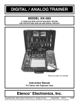
DIGITAL MULTIMETER KIT
MODEL M-2666K
WIDE RANGE DIGITAL MULTIMETER WITH
CAPACITANCE AND TRANSISTOR TESTING FEATURES
Assembly and Instruction Manual
Elenco Electronics, Inc.
®
Copyright © 2008 by Elenco® Electronics, Inc. All rights reserved.
Revised 2008
REV-A
No part of this book shall be reproduced by any means; electronic, photocopying, or otherwise without written permission from the publisher.
753128
INTRODUCTION
Assembly of your M-2666K Digital Multimeter Kit will
prove to be an exciting project and give much
satisfaction and personal achievement. If you have
experience in soldering and wiring technique, you
should have no problems. For the beginner, care
must be given to identifying the proper components
and in good soldering habits. Above all, take your
time and follow the easy step-by-step instructions.
Remember, “An ounce of prevention is worth a
pound of cure”.
The meter kit has been divided into a number of
sections to make the assembly easy and avoid
major problems with the meter operation.
Section A - Meter display circuit assembly.
Section B - DC voltage and current circuit
assembly.
Section C - AC voltage and current circuit
assembly.
Section D - Resistance & buzzer circuit assembly.
Section E - Capacitance and transistor testing
circuit assembly.
Section F - Final assembly.
THEORY OF OPERATION
A block diagram of the M-2666K is shown in Figure 1.
Operation centers around a custom LSI chip. This IC
contains a dual slope A/D converter, display, latches,
decoder and the display driver. A block diagram of
the IC functions is shown in Figure 6. The input
voltage, current or ohm signals are conditioned by the
function and selector switches to produce and output
DC voltage between 0 and +199mV. If the input signal
V
Ω
V/Ω
is 100VDC, it is reduced to 100mVDC by selecting a
1000:1 divider. Should the input be 100VAC, then
after the divider it is processed by the AC converter to
produce 100mVDC. If current is to be read, it is
converted to a DC voltage via internal shunt resistors.
For resistance measurements, an internal voltage
source supplies the necessary 0-199mV voltage to be
fed to the IC input.
Voltage
Divider
V
Ohms
Converter
Ω
DC
Analog
Data
VAC
COMM
Range
Switches
A/D
Converter
and
Display
Driver
Function
Switches
AC
VAC/mA AC
Converter
mA
Decimal
mA
mA
Current
Shunts
Point
Display
Figure 1 Simplified Block Diagram
The input of the 7106 IC is fed to an A/D (analog to
digital) converter. Here the DC voltage amplitude is
changed into a digital format. The resulting signals
are processed in the decoders to light the appropriate
LCD segment.
frequency is divided by four before it clocks the
decade counters. It is further divided to form the three
convert-cycle phases. The final readout is clocked at
about three readings per second.
Digitized measurements data is presented to the
display as four decoded digits (seven segments) plus
polarity. Decimal point position on the display is
determined by the selector switch setting.
Timing for the overall operation of the A/D converter
is derived from an external oscillator whose
frequency is selected to be 40kHz. In the IC, this
-1-
A/D CONVERTER
A simplified circuit diagram of the analog portion of
the A/D converter is shown in Figure 2. Each of the
switches shown represent analog gates which are
operated by the digital section of the A/D converter.
Basic timing for switch operation is keyed by an
external oscillator. The conversion process is
continuously repeated. A complete cycle is shown in
Figure 2.
converter can be divided into three consecutive time
periods: autozero (AZ), integrate (INTEG) and read.
Both autozero and integrate are fixed time periods.
A counter determines the length of both time
periods by providing an overflow at the end of every
1,000 clock pulses. The read period is a variable
time, which is proportional to the unknown input
voltage. The value of the voltage is determined by
counting the number of clock pulses that occur
during the read period.
Any given measurement cycle performed by the A/D
COMPARATOR
BUFFER
AMP
EXTERNAL
INPUTS
INTEGRATOR
AZ
AZ
READ
TO
DIGITAL
CONTROL
LOGIC
+REF
(FLYING
CAPACITOR)
INTEG
INTEG.
UNKNOWN
INPUT
VOLTAGE+
AZ
INTEG
AZ
READ
AZ
+.20
.15
.10
.05
0
COUNTER OUTPUT
0
10,000
166.7mS
500
1000
1500
2000
0
Figure 2 Dual Slope A/D Converter
capacitor at a fixed rate during the read period, and
counting the number of clock pulses that occur before
it returns to the original autozero level.
During autozero, a ground reference is applied as an
input to the A/D converter. Under ideal conditions the
output of the comparator would also go to zero.
However, input-offset-voltage errors accumulate in the
amplifier loop, and appear at the comparator output as
an error voltage. This error is impressed across the AZ
capacitor where it is stored for the remainder of the
measurement cycle. The stored level is used to provide
offset voltage correction during the integrate and read
periods.
As the read period begins, the INTEG switch opens
and the read switch closes. This applies a known
reference voltage to the input of the A/D converter. The
polarity of this voltage is automatically selected to be
opposite that of unknown input voltage, thus causing
the INTEG capacitor to discharge as fixed rate (slope).
When the charge is equal to the initial starting point
(autozero level), the read period is ended. Since the
discharge slope is fixed during the read period, the
time required is proportional to the unknown input
voltage.
The autozero period and thus a new measurement
cycle begins at the end of the read period. At the same
time, the counter is released for operation by
transferring its contents (previous measurement value)
to a series of latches. This stored stat is then decoded
and buffered before being used for driving the LCD
display.
The integrate period begins at the end of the autozero
period. As the period begins, the AZ switch opens and
the INTEG switch closes. This applies the unknown
input voltage to the input of the A/D converter. The
voltage is buffered and passed on to the input of the
A/D converter. The voltage is buffered and passed on
to the integrator to determine the charge rate (slope)
on the INTEG capacitor. At the end of the fixed
integrate period, the capacitor is charged to a level
proportional to the unknown input voltage. This voltage
is translated to a digital indication by discharging the
-2-
VOLTAGE MEASUREMENT
Figure 3 shows a simplified diagram of the voltage
measurement function.
The input divider resistors add up 10MΩ with each
step being a division of 10. The divider output
should be within –0.199 to +0.199V or the overload
indicator will function. If the AC function is selected,
the divider output is AC coupled to a full wave
rectifier and the DC output is calibrated to equal the
rms level of the AC input.
200mV
Volts
DC
9MΩ
900kΩ
2V
Low Pass
Filter
AC
20V
90kΩ
200V
AC to DC
Converter
9kΩ
100mV
Ref
7106
750V
9Ω
Common
Figure 3 Simplified Voltage Measurement Diagram
CURRENT MEASUREMENT
Figure 4 shows a simplified diagram of the current
measurement positions.
Internal shunt resistors convert the current to
between –0.199 to +0.199V which is then
processed in the 7106 IC to light the appropriate
LCD segments. If the current is AC in nature, the AC
converter changes it to the equivalent DC value.
200μA
DC
2mA
20mA
900Ω
Low Pass
Filter
90Ω
AC
A
200mA
20A
7106
9Ω
AC - DC
Converter
0.99Ω
100mV
Ref
20A
0.01Ω
COM
Figure 4 Simplified Current Measurement Diagram
-3-
RESISTANCE MEASUREMENTS
Figure 5 shows a simplified diagram of the resistance measurement function.
100Ω
900Ω
External
Resistor
9kΩ
Low Pass
Filter
20kΩ
2kΩ
90kΩ
900kΩ
9MΩ
200kΩ
200Ω
7106
100mV
Ref
2MΩ
20MΩ
Voltage
Source
Figure 5 Simplified Resistance Measurement Diagram
A simple series circuit is formed by the voltage
source, a reference resistor from the voltage divider
(selected by range switches), and the external
unknown resistor. The ratio of the two resistors is
equal to the ratio of their respective voltage drops.
Therefore, since the value of one resistor is known,
the value of the second can be determined by using
the voltage drop across the known resistor as a
reference. This determination is made directly by the
A/D converter.
Overall operation of the A/D converter during a
resistance measurement is basically as described
earlier in this section, with one exception. The
reference voltage present during a voltage
measurement is replaced by the voltage drop
across the reference resistor. This allows the voltage
across the unknown resistor to be read during the
read period. As before, the length of the read period
is a direct indication of the value of the unknown.
hFE MEASUREMENT
V+
Figure 6 shows a simplified diagram of the hFE
measurement function. Internal circuits in the 7106
IC maintain the COMMON line at 2.8 volts below
V+. When a PNP transistor is plugged into the
transistor socket, base to emitter current flows
through resistor R49. The voltage drop in resistor
R49 due to the collector current is fed to the 7106
and indicates the hFE of the transistor. For an NPN
transistor, the emitter current through R50 indicates
the hFE of the transistor.
PNP
NPN
E
C
R50
220kΩ
B
B
220kΩ
COM
100mV
Ref
E
C
10Ω
Figure 6
CAPACITANCE MEASUREMENT
The capacitor circuit consists of four opamps. IC3 D&A form an oscillator, which is
applied to the test-capacitor through the test
leads. The capacitor couples the oscillator to
pin 6 of IC3B. The amount of voltage
developed at pin 6 is indicative of the
capacitors ESR value. IC3B and C amplify
the signal which is seen at pin 8. The AC
signal is then converted to a DC voltage and
displayed on the meter.
Figure 7
-4-
Low Pass
Filter
7106
a
a
f
a
b
b
f
g
c
e
a
f
b
g
c
e
d
b
g
d
c
e
d
BACKPLANE
28
LCD PHASE DRIVER
7 Segment
Decode
7 Segment
Decode
TYPICAL SEGMENT OUTPUT
V+
7 Segment
Decode
200
0.5mA
LATCH
Segment
Output
2mA
Thousand
Tens
Hundreds
Units
Internal Digital Ground
To Switch Drivers
From Comparator Output
V+
CLOCK
6.2V
LOGIC CONTROL
-4
*
3
TEST
Internal Digital Ground
1V
500Ω
* Three inverters.
One inverter shown for clarity.
34
7
6
OSC 3
OSC 2
OSC 1
CREF
CREF+
REF HI
42
V+
A-Z &
Z1
43
41
A-Z &
Z1
CAZ
36
2.8V
Z1
8
37
6.2V
INT
INTEGRATOR
35
+
+
A-Z
COMPARATOR
ZERO
CROSSING
DETECTOR
TO
DIGITAL
SECTION
POLARITY
FLIP/FLOP
IN HI
DE (-)
DE (+)
A-Z
+
DE (+)
40
ANALOG SECTION of 7106
DE (-)
COMMON
IN LO
CINT
AUTO
ZERO
V+
+
10μA
INT
39
DIGITAL SECTION
RINT
REF LO CREF BUFFER
44
V
4
38
INT
A-Z & DE(+)
& Z1
34
V
Figure 8 7106 Functions
-5-
ASSEMBLY
IMPORTANT CONSTRUCTION NOTES
The meter kit has been divided into a number of
sections to make the assembly easy and avoid
major problems with the meter operation.
1. Wash your hands with soap and water before you
assemble this kit. The high impedance areas on
the circuit board can be contaminated by salt and
oil from your skin. If these areas become
contaminated, your completed multimeter may
not meet the listed specifications. Handle the
circuit board only by its edges.
ONLY OPEN COMPONENT BAGS THAT ARE
CALLED FOR IN YOUR ASSEMBLY PROCEDURE.
DO NOT OPEN ANY OTHER BAGS.
Do not build more than one section of your meter at
a time. Your instructor must approve the proper
operation of the section you have built before you
proceed to the next section. This procedure will
minimize the problems you may have at the
completion of the project.
2. Avoid any excessive accumulation of resin buildup whenever you solder a connection.
3. Take your time assembling the circuit board.
Work at a slow pace. Remember that accuracy is
far more important than speed.
Your kit program is divided into Sections “A – F”. The
small parts bags will be marked accordingly. The
sections are listed below.
4. When you perform the steps in assembly, identify
each respective component before you install it.
Then position it over its outline on the top legend
side of the PC•board, unless otherwise indicated.
Section A - Meter Display Circuit Assembly.
Section B - DC Voltage and Current Circuit
Assembly.
5. Check for the proper polarity of ICs, diodes,
electrolytic capacitors, battery snap and LCD.
Section C - AC Voltage and Current Circuit
Assembly.
Section D - Resistance & Buzzer Circuit Assembly.
Section E - Capacitance and Transistor Circuit
Assembly.
Section F - Final Assembly.
-6-
CONSTRUCTION
Introduction
The most important factor in assembling your M-2666K Digital Multimeter Kit is good soldering techniques.
Using the proper soldering iron is of prime importance. A small pencil type soldering iron of 25 - 40 watts is
recommended. The tip of the iron must be kept clean at all times and well-tinned.
Safety Procedures
•
•
•
•
Wear eye protection when soldering and during all phases of construction.
Locate soldering iron in an area where you do not have to go around it or reach over it.
Do not hold solder in your mouth. Wash your hands thoroughly after handling solder.
Be sure that there is adequate ventilation present.
Assemble Components
In all of the following assembly steps, the components must be installed on the top side of the PC board unless
otherwise indicated. The top legend shows where each component goes. The leads pass through the
corresponding holes in the board and are soldered on the foil side.
Use only rosin core solder.
DO NOT USE ACID CORE SOLDER!
What Good Soldering Looks Like
Types of Poor Soldering Connections
A good solder connection should be bright, shiny,
smooth, and uniformly flowed over all surfaces.
1.
Solder all components from
the copper foil side only.
Push the soldering iron tip
against both the lead and
the circuit board foil.
1. Insufficient heat - the
solder will not flow onto the
lead as shown.
Soldering Iron
Component Lead
Foil
Soldering iron positioned
incorrectly.
Circuit Board
2.
3.
4.
Apply a small amount of
solder to the iron tip. This
allows the heat to leave the
iron and onto the foil.
Immediately apply solder to
the opposite side of the
connection, away from the
iron. Allow the heated
component and the circuit
foil to melt the solder.
Allow the solder to flow
around the connection.
Then, remove the solder
and the iron and let the
connection cool. The solder
should
have
flowed
smoothly and not lump
around the wire lead.
Rosin
2. Insufficient solder - let the
solder flow over the
connection until it is
covered. Use just enough
solder
to
cover
the
connection.
Soldering Iron
Solder
Foil
Solder
Gap
Component Lead
Solder
3. Excessive solder - could
make connections that you
did not intend to between
adjacent foil areas or
terminals.
Soldering Iron
Solder
Foil
4. Solder bridges - occur
when solder runs between
circuit paths and creates a
short circuit. This is usually
caused by using too much
solder. To correct this,
simply drag your soldering
iron across the solder
bridge as shown.
Here is what a good solder
connection looks like.
-7-
Soldering Iron
Foil
Drag
IDENTIFYING CAPACITOR VALUES
Capacitors will be identified by their capacitance value in pF (picofarads), nF (nanofarads), or μF (microfarads). Most
capacitors will have their actual value printed on them. Some capacitors may have their value printed in the following
manner. The maximum operating voltage may also be printed on the capacitor.
Second Digit
103K
100V
Multiplier
For the No.
0
1
2
3
Multiply By
1
10
100
1k
Tolerance*
Maximum Working Voltage
4
5
8
10k 100k .01
9
0.1
Note: The letter “R” may be used at times to
signify a decimal point; as in 3R3 = 3.3
10μF 16V
First Digit
Multiplier
* The letter M indicates a tolerance of +20%
The value is 10 x 1,000 =
10,000pF or .01μF 100V
The letter K indicates a tolerance of +10%
The letter J indicates a tolerance of +5%
IDENTIFYING RESISTOR VALUES
Use the following information as a guide in properly identifying the value of resistors.
5 Bands
4 Bands
1 2
1
Multiplier
Tolerance
2 3 Multiplier
Tolerance
PART IDENTIFICATION CARDS
M-2666K
SECTION A
To help identify the resistors and diodes used in the construction of your digital
multimeter we have mounted the diodes and resistors of each section onto a card.
The card will help you find the diodes and resistors quickly. THE PARTS WILL NOT
NECESSARILY BE LISTED IN THE ORDER SHOWN IN THE PARTS LIST
SECTION OR IN THE ASSEMBLY PROCEDURE.
EXAMPLE
When you are ready to assemble the meter kit, follow the procedure shown. For
an example refer to page 11 for assembly of Section “A”. The first resistor called
for is R8, 470kΩ resistor (yellow-violet-yellow-gold). Locate it on the card ( ), verify
that it is the correct value. Some resistors may be mounted backwards on the card
so you must be certain that you are reading the resistors correctly. When the
correct value has been established, only then will you mount it into its correct
position on the PC board.
-8-
RESISTOR READING EXERCISE
Before starting assembly of your digital multimeter
project, you should be thoroughly familiar with the 5
band color code system. Many of the resistor values
will be identified by color bands and it is easy to
mistake their value if you read the colors incorrectly
or read the value from the wrong end. Do the
following exercise in resistor values. Place your
answer in the box beneath the resistor. Answers are
on the bottom of this page.
(1) yellow-black-black-black-brown
(2) white-black-black-red-green
(3) brown-red-violet-red-brown
(4) green-black-green-brown-green
(5) brown-black-black-black-brown
(6) brown-green-gray-orange-brown
(7) white-black-black-yellow-green
(8) white-black-black-silver-green
(9) brown-black-black-orange-green
(10) orange-white-red-red-brown
(11) gray-white-black-black-brown
(12) brown-brown-black-red-brown
Answers to Resistor Reading Exercise: 1) 400Ω+1%; 2) 90kΩ+.5%; 3) 12.7kΩ+1%; 4) 5.05kΩ+.5%; 5) 100Ω+1%;
6) 158kΩ+1%; 7) 9MΩ+.5%; 8) 9Ω+.5%; 9) 100kΩ+.5%; 10) 39.2kΩ+1%; 11) 890Ω+1%; 12) 11kΩ+1%;
-9-
SECTION A
Meter Display Circuit
PARTS LIST - SECTION A
If you are a student, and any parts are missing or damaged, please see instructor or bookstore.
If you purchased this kit from a distributor, catalog, etc., please contact Elenco® Electronics (address/phone/email is at the back of this manual) for additional assistance, if needed. DO NOT contact your place of purchase
as they will not be able to help you.
RESISTORS
Qty.
r2
r1
r1
r3
r2
Symbol
R4, R5
R3
R1
R7, R8, R9
R2, R6
Description
100kΩ 5% 1/4W
200kΩ 5% 1/4W
220kΩ 5% 1/4W
470kΩ 5% 1/4W
1MΩ 5% 1/4W
Qty.
r1
r1
r3
r1
Symbol
C5
C1
C2, C3, C4
C6
Value
100pF (101)
.1μF (104)
.1μF (104)
22μF
Color Code
brown-black-yellow-gold
red-black-yellow-gold
red-red-yellow-gold
yellow-violet-yellow-gold
brown-black-green-gold
Part #
161000
162000
162200
164700
171000
CAPACITORS
Description
Disc
Mylar (large brown)
Mylar (small yellow)
Electrolytic (Lytic)
Part #
221017
251017L
251017S
272244S
SEMICONDUCTORS
Qty.
r1
Symbol
T1
Value
9013
Description
Transistor 2SC9013
Part #
329013
MISCELLANEOUS
Qty.
r1
r1
r1
r1
r1
Description
LCD
Zebra
PC Board M2666K
Switch On/Off (SW1)
Battery 9V
Qty.
r1
r1
r1
r1
r2
Part #
351166
500007
512666
540004
590009
Description
Battery Snap (Batt)
LCD Housing
LCD Cover
Label Top
Solder
Part #
590098
629015
629016
723051
9LF99
PARTS IDENTIFICATION
Resistor
Diode
PC Board
Liquid Crystal Display (LCD)
Display
Cover
Capacitors
LCD
C1
Zebra
Transistor
Disc
Mylar
Display
Housing
Lytic
-10-
Label Top
ASSEMBLE THE FOLLOWING COMPONENTS TO THE PC BOARD
In all of the following steps the components must be installed either on the top or bottom legend sides of
the PC board as indicated. The board is turned to solder the component leads on the opposite side
(installed on Bottom, soldered on Top, installed on Top, soldered on Bottom).
Figure A
Figure B
Figure D
Figure C
Lay resistor flat against the
PC board.
Flat
Side
Negative (–)
marking on
capacitor
Negative (–)
marking on
PC board
White marking
on PC board
Marking
on PC board
Stand resistor on end as
shown. Solder and cut off
the excess leads.
Mount the capacitor with the negative (–)
lead in the negative hole and the positive
(+) lead in the positive hole marked on the
PC•board. Mount the capacitor flat against
the PC board as shown.
R8 - 470kΩ 5% 1/4W Res.
(yellow-violet-yellow-gold)
(see Figure A)
Mount the transistor
with the flat side in the
same direction as the
PC board marking.
Bottom Legend Side
R7 - 470kΩ 5% 1/4W Res.
(yellow-violet-yellow-gold)
(see Figure A)
C6 - 22μF Lytic Capacitor
(see Figure B)
T1 - 2SC9013 Transistor
(see Figure C)
R4 - 100kΩ 5% 1/4W Res.
(brown-black-yellow-gold)
(see Figure A)
R5 - 100kΩ 5% 1/4W Res.
(brown-black-yellow-gold)
(see Figure D)
C5 - 100pF (101) Discap
R6 - 1MΩ 5% 1/4W Res.
(brown-black-green-gold)
(see Figure A)
R3 - 200kΩ 5% 1/4W Res.
(red-black-yellow-gold)
(see Figure A)
R9 - 470kΩ 5% 1/4W Res.
(yellow-violet-yellow-gold)
(see Figure A)
C4 - .1μF (104) Mylar Cap.
(small yellow)
C1 - .1μF (104) Mylar Cap.
(large brown)
C3 - .1μF (104) Mylar Cap.
(small yellow)
R1 - 220kΩ 5% 1/4W Res.
(red-red-yellow-gold)
(see Figure A)
R2 - 1MΩ 5% 1/4W Res.
(brown-black-green-gold)
(see Figure A)
Mount switch in direction shown.
Assembled View
C2 - .1μF (104) Mylar Cap.
(small yellow)
Figure E
Insert the switch into the
PC board in the location
shown. Make sure that
the notch on the switch
is in the same direction
as the marking on the
PC board.
SW1 - Switch On/Off
(see Figure E)
BATT - 9V Battery Snap
(see Figure E)
Top Legend Side
-11-
Insert the 9V battery
wires through the hole of
the PC•board as shown.
Solder and cut off the
excess leads.
Notch
Red Wire
Black Wire
ASSEMBLE THE LCD
r Assemble the LCD into the housing with the parts
shown in Figure F. Note the top of the house is
curved.
Testing Procedure
The LCD housing will not be screwed to the PC
board for this test. Align the LCD housing holes with
those in the PC Board and hold in place. You can
also use a rubber band to hold the housing. You will
need to apply pressure so the zebra makes contact
to the copper pads.
r Wipe off zebra edges with a lint-free cloth and
then insert the zebra into the top slot of the
housing.
r The LCD must be put in with the notch in the
direction shown in Figure F. Peel off the clear
protective film on top of the LCD (see Figure F),
then place the LCD into the housing.
1. Place the top label over the knob. This will assist
in obtaining the correct knob position.
2. Connect the 9V battery to the battery snap
3. Turn the meter on by pressing the power switch
(down position).
r Place the display cover on top of the housing and
press down to snap into place.
4. Align the LCD housing holes with those in the PC
Board and hold in place. You can also use a
rubber band to hold the housing. You will need to
apply pressure so the zebra makes contact to the
copper pads.
r Place the LCD housing on top of the PC board as
shown.
5. Set the selector switch to the 200Ω position. The
first decimal point should light and show a 200
under it. Select the 20kΩ position and the second
decimal points lights with a 20 under it. Select the
2kΩ position and the second decimal points lights
with a 2 under it. Adjust the selector to other
ranges and check that correct decimal point
lights. The LCD may display random numbers.
Figure F
LCD Cover
Notch
If the tests are not working, check for cold solder
joints, part values and if the LCD is assembled
correctly. DO NOT PROCEED TO SECTION B
WITHOUT INSTRUCTOR’S APPROVAL.
LCD
Do not touch edge
Zebra
LCD Housing
Battery
Clear Protective Film
Tape
PC Board
Range Selector
Knob Assembly
Figure G
-12-
SECTION B
DC Voltage & Current Circuit
PARTS LIST - SECTION B
RESISTORS
Qty.
r1
r1
r1
r1
r1
r1
r1
r2
r1
r1
r1
r1
r1
r4
r1
Symbol
R23
R22
R21
R20
R18
R32
R31
R17, R19
R33
R16
R30
R15
R14
R10-R13
VR1
Description
.01Ω
0.99Ω 0.5% 1/4W
9Ω 0.5% 1/4W
90Ω 0.5% 1/4W
100Ω 0.5% 1/4W
390Ω 1% 1/4W
900Ω 1% 1/4W
900Ω 0.5% 1/4W
5.6kΩ 5% 1/4W
9kΩ 0.5% 1/4W
13kΩ 1% 1/4W
90kΩ 0.5% 1/4W
900kΩ 0.5% 1/4W
2.25MΩ 0.5% 1/4W
200Ω (201)
Color Code
Shunt wire
black-white-white-silver-green
white-black-black-silver-green
white-black-black-gold-green
brown-black-black-black-green
orange-white-black-black-brown
white-black-black-black-brown
white-black-black-black-green
green-blue-red-gold
white-black-black-brown-green
brown-orange-black-red-brown
white-black-black-red-green
white-black-black-orange-green
red-red-green-yellow-green
Pot (lay down)
Part #
100166
109950
119050
129050
131050
133930
139030
139050
145600
149050
151330
159050
169050
172250
191320
Note: Resistor tolerance (last band) of 5-band resistors may be blue instead of green.
SEMICONDUCTORS
Qty.
r2
r1
Symbol
D1, D2
T2
Value
1N4001
2SA9013
Description
Diode
Transistor
Qty.
r1
r2
r2
r4
Symbol
Description
Fuse 0.2A 250V 5 x 20mm
Screw 2.5 x 8mm
Fuse Clips
Input Socket (20A, μA/mA, COM, VΩCAP)
Part #
314001
329013
MISCELLANEOUS
Part #
530020
642239
663004
664066
PARTS IDENTIFICATION
Shunt Wire
Pot (lay down)
Fuse
-13-
Fuse Clip
Input Socket
ASSEMBLE THE FOLLOWING COMPONENTS TO THE PC BOARD
In all of the following steps the components must be installed either on the top or bottom legend sides of
the PC board as indicated. The board is turned to solder the component leads on the opposite side
(installed on Bottom, soldered on Top, installed on Top, soldered on Bottom).
Figure H
Figure I
Stand diode on end. Mount with band as
shown on the top legend.
Band
White marking
on PC board
Stand resistor on end as shown.
Solder and cut off the excess leads.
R14 - 900kΩ .5% 1/4W Res.
(white-blk-blk-orange-green)
(see Figure I)
D1 - 1N4001 Diode
D2 - 1N4001 Diode
(see Figure H)
R10 - 2.25MΩ .5% 1/4W Res.
R11 - 2.25MΩ .5% 1/4W Res.
R12 - 2.25MΩ .5% 1/4W Res.
R13 - 2.25MΩ .5% 1/4W Res.
(red-red-green-yellow-green)
(see Figure I)
R19 - 900Ω .5% 1/4W Res.
(white-blk-blk-blk-green)
(see Figure I)
R20 - 90Ω .5% 1/4W Res.
(white-blk-blk-gold-green)
(see Figure I)
R18 - 100Ω .5% 1/4W Res.
(brown-blk-blk-blk-green)
(see Figure I)
R21 - 9Ω .5% 1/4W Res.
(white-blk-blk-silver-green)
(see Figure I)
R17 - 900Ω .5% 1/4W Res.
(white-blk-blk-blk-green)
(see Figure I)
R22 - 0.99Ω .5% 1/4W Res.
(blk-wht-wht-silver-green)
(see Figure I)
T2 - 9013 Transistor
(see Figure C)
R33 - 5.6kΩ 5% 1/4W Res.
(green-blue-red-gold)
(see Figure I)
R16 - 9kΩ .5% 1/4W Res.
(white-blk-blk-brown-green)
(see Figure I)
R30 - 13kΩ 1% 1/4W Res.
(brn-orange-blk-red-brn)
(see Figure I)
R23 - Shunt Wire
1/4”
R31 - 900Ω 1% 1/4W Res.
(white-blk-blk-blk-brown)
(see Figure I)
VR1 - 200Ω Pot
(201)
R32 - 390Ω 1% 1/4W Res.
(orange-wht-blk-blk-brown)
(see Figure I)
R15 - 90kΩ .5% 1/4W Res.
(white-blk-blk-red-green)
(see Figure I)
Top Legend Side
See Page 21 for Assembled View
Fuse Holder Clips
Fuse 0.2A 250V
Mount holders with the tab
side as shown on the bottom
legend side, solder into place
and then insert fuse.
Tab
Tab
Bottom Legend Side
-14-
PC Board
r Insert the four input sockets into the PC board
holes and then solder the sockets in place.
Apply enough heat to allow the solder to flow
around the input sockets (see Figure J).
r Attach the LCD to the PC board using the two
2.5 x 8mm screws. Use the two top mounting
hole and lightly tighten the screws. The screws
will be removed to assemble the next section.
Figure K
Solder
Input Sockets
Socket
2.5 x 7.5
Screws
Bottom Legend Side
Figure J
Testing Procedure
Voltage Test
1. Place the top label over the knob and turn the
range selector knob to the 20V position.
Current Test
1. Turn the range selector knob to the 200μA
position.
2. Connect the 9V battery to the battery snap
2. Connect the test leads (red lead to μA/mA and
black to COM).
3. Connect the test leads (red lead to VΩCAP and
black to COM). Turn the meter on by pressing the
power switch.
3. Connect the kit meter and another meter of
known accuracy in series. Set the both meters in
the 200μA position. Construct a circuit for a DC
current (for example 9V and a 47kΩ resistor for
190μA) and measure the circuit. Both meters
should have close to the same readings. Check
the other DC current (2mA - 200mA) scales. The
20A scale requires a circuit of 1 - 20 amps.
4. Using another meter of known accuracy,
measure a DC voltage less than 20V (such as a
9 volt battery). You will calibrate the kit meter by
measuring the same voltage source and
adjusting VR1 until the kit meter reads the same
as the accurate meter. When the two meters
agree, the voltage circuit is calibrated. Turn the
meter off and continue to the Current Test.
If the meters do not agree, check the parts just
added. Do not readjust VR1 for this will change the
voltage reading set in step 1. If the tests are not
working, check for cold solder joints and part values.
If the tests are not working, check components
R10 – R24, R30 – R33, VR1, and the transistor
T2.
4. Turn the meter off and remove the battery, top
label, and test leads DO NOT PROCEED TO
SECTION C WITHOUT YOUR INSTRUCTOR’S
APPROVAL.
5. Remove two display mounting screws and
display by unscrewing the two mounting screws.
-15-
SECTION C
AC Voltage & Current Circuit
PARTS LIST - SECTION C
RESISTORS
Qty.
r1
r1
r1
r1
r2
r1
Note:
Symbol
Description
Color Code
R38
1.87kΩ 1% 1/4W
brown-gray-violet-brown-brown
R37
3kΩ 1% 1/4W
orange-black-black-brown-brown
R39
6.8kΩ 5% 1/4W
blue-gray-red-gold
R34
100kΩ 5% 1/4W
brown-black-yellow-brown
R35, R36 100kΩ 1% 1/4W
brown-black-black-orange-brown
VR2
200Ω
Trim Pot
Resistor tolerance (last band) of 5-band resistors may be blue instead of green.
Part #
141830
143030
146800
161000
161030
191320
CAPACITORS
Qty.
r1
r1
r2
r1
Symbol
C7
C10
C8, C9
C11
Value
470pF (471)
.33μF (334)
4.7μF
10μF
Description
Disc
Mylar (small yellow)
Electrolytic (Lytic)
Electrolytic (Lytic)
Qty.
r3
r1
Symbol
D3 - D5
IC2
Value
1N4148
LM324
Description
Diode (glass)
Op-Amp
Qty.
r1
Symbol
Value
Description
IC Socket 14-pin
Part #
224717
253318L
264747S
271015S
SEMICONDUCTORS
Part #
314148
330324
MISCELLANEOUS
Part #
664014
ASSEMBLE THE FOLLOWING COMPONENTS TO THE PC BOARD
Figure L
Stand diode on
end. Mount with
band as shown on
the top legend.
D5
D3
D4
R37 - 3kΩ 1% 1/4W Res.
(orange-blk-blk-brn-brn)
(see Figure I)
D4 - 1N4148 Diode
D5 - 1N4148 Diode
(see Figure L)
Assembled View
Bottom Legend Side
R38 - 1.87kΩ 1% 1/4W Res.
(brn-gray-violet-brn-brn)
(see Figure I)
C9 - 4.7μF Lytic Capacitor
(see Figure B)
C8 - 4.7μF Lytic Capacitor
(see Figure B)
R35 - 100kΩ 1% 1/4W Res.
(brown-blk-blk-orange-brown)
(see Figure I)
C10 - .33μF (334) Mylar Cap.
(may be marked 334)
D3 - 1N4148 Diode
(see Figure L)
R36 - 100kΩ 1% 1/4W Res.
(brown-blk-blk-orange-brown)
(see Figure I)
C7 - 470pF (471) Discap
-16-
ASSEMBLE THE FOLLOWING COMPONENTS TO THE PC BOARD
R39 - 6.8kΩ 5% 1/4W Res.
(blue-gray-red-gold)
(see Figure I)
Figure M
Insert the IC socket into the PC
board with the notch in the same
direction marked on the top legend.
Solder the IC socket into place.
Insert the IC into the socket with the
notch in the same direction as the
notch on the socket.
C11 - 10μF Lytic Capacitor
(see Figure B)
VR2 - 200Ω Pot (201)
R34 - 100kΩ 5% 1/4W Res.
(brown-black-yellow-brown)
(see Figure I)
IC
Socket
Notch
Top Legend Side
IC Socket 14-pin
IC2 - LM324 Op-Amp IC
(see Figure M)
PC•Board
Assembled View
r Attach the LCD to the PC board using the two 2.5 x 8mm screws. Use the top-mounting hole and lightly
tighten the screws. The screws will be removed to assemble the next section.
AC Voltage Test
AC Current Test
Caution do not handle the PC board during the
Voltage or Current test. If you do an AC source, set
VR2 to its middle position.
1. Turn the range selector knob to the 200mA AC
current position.
2. Connect the test leads (red lead to μA/mA and
black to COM) to the meter.
1. Placing the top label over the knob will assist in
obtaining the correct knob position when doing
tests.
3. Connect the kit meter and another meter of
known accuracy in series. Set the meters to the
200mA position. Construct a circuit for an AC
current (for example 12VAC and a 100Ω resistor
for 120mA) and connect the meters to the circuit.
2. Connect the 9V battery to the battery snap.
3. Connect the test leads (red lead to VΩ and black
to COM). Turn the meter on by pressing the power
switch.
4. Turn the meters on and both should have close to
the same readings. Check the other current scale
by changing the voltage or resistance values. The
20A scale requires a circuit of 1-20 amps. For the
20A shunt wire adjustment, refer to page 32.
4. Obtain an AC voltage and set the meter to the
appropriate range.
5. Using another meter of known accuracy, measure
the AC voltage. You will calibrate the kit meter by
measuring the same voltage source and
adjusting VR2 until the kit meter reads the same
as the accurate meter. When the two meters
agree, the AC voltage circuit is calibrated. Turn
the meter off and continue to the Current Test.
If the kit meter does not agree, check the parts just
added. Do not readjust VR2 for this will change the
AC voltage read. If the tests are not working, check
for cold solder joints and part values. Turn the meter
off and remove the battery and test leads. DO NOT
PROCEED TO SECTION D WITHOUT YOUR
INSTRUCTOR’S APPROVAL.
If the tests are not working, check components R34
– R39, VR2, C7-C11, and IC2.
Remove the two display mounting screws and
display by unscrewing the two mounting screws.
-17-
SECTION D
Resistance & Buzzer Circuit
PARTS LIST - SECTION D
RESISTORS
Qty.
r1
r1
r2
r4
r1
Symbol
R54
R52
R55, R57
R51,53,56,58
PTC
Description
10kΩ 5%
100kΩ 5%
330kΩ 5%
1MΩ 5%
1.5kΩ
Color Code
brown-black-orange-gold
brown-black-yellow-gold
orange-orange-yellow-gold
brown-black-green-gold
Thermister
Qty.
r2
Symbol
C16, C17
Value
.001μF (102)
Description
Discap
Qty.
r1
Symbol
Buz
Value
Description
Buzzer (20mm dia.)
Part #
151000
161000
163300
171000
190416
CAPACITORS
Part #
231036
MISCELLANEOUS
Part #
595220
ASSEMBLE THE FOLLOWING COMPONENTS TO THE PC BOARD
C17 - .001μF (102) Discap
C16 - .001μF (102) Discap
R58 - 1MΩ 5% 1/4W Res.
R51 - 1MΩ 5% 1/4W Res.
(brown-black-green-gold)
(see Figure I)
R57 - 330kΩ 5% 1/4W Res.
(orange-orange-yellow-gold)
(see Figure I)
R55 - 330kΩ 5% 1/4W Res.
(orange-orange-yellow-gold)
(see Figure I)
R53 - 1MΩ 5% 1/4W Res.
(brown-black-green-gold)
(see Figure I)
R52 - 100kΩ 5% 1/4W Res.
(brown-black-yellow-gold)
(see Figure I)
PTC - 1.5kΩ Thermister
R54 - 10kΩ 5% 1/4W Res.
(brown-black-orange-gold)
(see Figure I)
Top Legend Side
Figure N
Buzzer
Assembled View
Solder
Points
BUZ - Buzzer
(see Figure N)
R56 - 1MΩ 5% 1/4W Res.
(brown-black-green-gold)
(see Figure I)
Solder the buzzer to the PC board in the locations
shown. Then solder a discarded resistor lead to
the middle of the buzzer and to the point shown
on the PC board. Finally, solder the edge of the
buzzer to the other point shown on the PC•board.
Solder
Discarded
Resistor
Lead
Solder
Bottom Legend Side
-18-
PC Board
Solder
Points
r Attach the LCD to the PC board using the two 2.5
x 8mm screws. Use the top-mounting hole and
lightly tighten the screws. The screws will be
removed to assemble the next section.
with another meter of known accuracy. If the tests
are not working, check the solder of the PTC.
Buzzer - Set the selector knob to the Buzzer ( )
position. Short the red and black leads and the
buzzer should sound. If the buzzer does not sound,
check components R51-R58, PTC, C16, C17, and
the solder connections to the buzzer.
Testing Procedure
1. Place the top label over the knob and turn the
range selector knob to an OHM scale position.
Diode - Connect a diode to the test leads with the
correct polarity (see figure below). The meter will
range for 100 - 950.
2. Connect the 9V battery to the battery snap.
3. Connect the test leads (red lead to VΩ CAP and
black to COM). Turn the meter on by pressing the
power switch.
COM
4. Test the Ohms, Buzzer, and Diode functions
using the procedures below.
VΩ
5. Turn the meter off and remove the battery, top
label, and test leads.
OHMs - Using two or three different value resistors,
check each scale. Compare the kit meter readings
6. Remove two display mounting screws and
display by unscrewing the two mounting screws.
DO NOT PROCEED TO SECTION E WITHOUT INSTRUCTOR’S APPROVAL.
SECTION E
Capacitance and Transistor Testing Circuit
PARTS LIST - SECTION E
RESISTORS
Qty.
r1
r1
r1
r1
r1
r1
r1
r1
r1
r2
r1
r1
r1
r2
r1
r1
Symbol
R29
R28
R45
R27
R42
R43
R26
R44
R47
R40, R41
R46
R25
R48
R49, R50
R24
VR3
Description
10Ω 1% 1/4W
90Ω 1% 1/4W
150Ω 1% 1/4W
900Ω 1% 1/4W
1.91kΩ 1% 1/4W
4.3kΩ 1% 1/4W
9kΩ 1% 1/4W
10kΩ 1% 1/4W
11kΩ 1% 1/4W
39kΩ 1% 1/4W
76.8kΩ 1% 1/4W
90kΩ 1% 1/4W
160kΩ 1% 1/4W
220kΩ 5% 1/4W
900kΩ 1% 1/4W
200Ω (201)
Color Code
brown-black-black-gold-brown
white-black-black-gold-brown
brown-green-black-black-brown
white-black-black-black-brown
brown-white-brown-brown-brown
yellow-orange-black-brown-brown
white-black-black-brown-brown
brown-black-black-red-brown
brown-brown-black-red-brown
orange-white-black-red-brown
violet-blue-gray-red-brown
white-black-black-red-brown
brown-blue-black-orange-brown
red-red-yellow-gold
white-black-black-orange-brown
Trim Pot
Part #
121030
129030
131530
139030
141930
144330
149030
151030
151130
153930
157630
159030
161630
162200
169030
191320
Note: Resistor tolerance (last band) of 5-band resistors may be green instead of brown.
CAPACITORS
Qty.
r4
Symbol
C12 - C15
Value
.01μF (103)
Description
Mylar (large brown)
Qty.
r4
r1
Symbol
D6 - D9
IC3
Value
1N4001
LM324
Description
Diode
Op-Amp
Qty.
r1
r2
Symbol
Value
Description
IC Socket 14-pin
hFE Socket
Part #
241017L
SEMICONDUCTORS
Part #
314001
330324
MISCELLANEOUS
-19-
Part #
664014
664015
ASSEMBLE THE FOLLOWING COMPONENTS TO THE PC BOARD
IC Socket 14-pin
IC3 - LM324 Op-Amp IC
(see Figure M)
hFE - Sockets - Install
these with no more than
0.4” of height from the PC
board to the top of the
sockets. Otherwise, the top
case will not fit together
properly with the bottom
case.
R45 - 150Ω 1% 1/4W Res.
(brn-green-blk-blk-brn)
(see Figure I)
VR3 - 200Ω Pot
R47 - 11kΩ 1% 1/4W Res.
(brn-brn-blk-red-brn)
(see Figure I)
R46 - 76.8kΩ 1% 1/4W Res.
(violet-blue-gray-red-brn)
(see Figure I)
C14 - .01μF (103) Mylar Cap.
R48 - 160kΩ 1% 1/4W Res.
(brn-blue-black-orange-brn)
(see Figure I)
0.4”
C15 - .01μF (103) Mylar Cap.
D6 - 1N4001 Diode
D7 - 1N4001 Diode
(see Figure O)
R49 - 220kΩ 5% 1/4W Res.
R50 - 220kΩ 5% 1/4W Res.
(red-red-yellow-gold)
(see Figure I)
R29 - 10Ω 1% 1/4W Res.
(brn-blk-blk-gold-brn)
(see Figure I)
R24 - 900kΩ 1% 1/4W Res.
(white-black-black-org-brown)
(see Figure I)
D8 - 1N4001 Diode
D9 - 1N4001 Diode
(see Figure O)
R25 - 90kΩ 1% 1/4W Res.
(white-black-black-red-brown)
(see Figure I)
R26 - 9kΩ 1% 1/4W Res.
(white-black-black-brn-brn)
(see Figure I)
Figure O
Stand diode on end. Mount with
band as shown on the top legend.
D7
Top Legend Side
D6
D8
D9
R27 - 900Ω 1% 1/4W Res.
(white-blk-blk-blk-brown)
(see Figure I)
R28 - 90Ω 1% 1/4W Res.
(white-blk-blk-gold-brown)
(see Figure I)
Figure P
Lay resistor flat against the PC
board.
R43 - 4.3kΩ 1% 1/4W Res.
(yellow-orange-blk-brn-brn)
(see Figure I)
R42 - 1.91kΩ 1% 1/4W Res.
(brn-white-brn-brn-brn)
(see Figure I)
R40 - 39kΩ 1% 1/4W Res.
R41 - 39kΩ 1% 1/4W Res.
(orange-white-blk-red-brn)
(see Figure I)
R44 - 10kΩ 1% 1/4W Res.
(brn-blk-blk-red-brn)
(see Figure P)
Bottom Legend Side
C13 - .01μF (103) Mylar Cap.
C12 - .01μF (103) Mylar Cap.
-20-
Assembled View for Section B
r Attach the LCD to the PC board using the two 2.5
x 8mm screws. Use the top-mounting hole and
lightly tighten the screws.
Testing Procedure
Capacitance
1. Place the top label over the knob and turn the
range selector knob to a capacitance (C) scale
position.
Assembled Views for Section E
2. Connect the 9V battery to the battery snap.
3. Connect the short test leads (red lead to VΩ CAP
and black to COM). Turn the meter on by pressing
the power switch.
Transistor - Set the meter in the hFE scales. Place
an NPN transistor into the socket. Make sure that
the transistor is in correctly. Depending on the type
of transistor, the meter will range from 20 to 550.
Place a PNP transistor into the PNP socket; the
range will also be 20 to 550. If the tests are not
working, check components R49 - R50, and the
transistor sockets.
4. Capacitance - Measure a cap with another
meter and then connect the capacitor to the
meter leads. Adjust VR3 so that the meter reads
the same as the accurate one. This calibrates
capacitance circuit of meter. Using two or three
different value capacitors, check each scale. If
the test is not working check components R40 R48, VR3, C12 - C15, D6 - D9, and IC3.
5. Turn the meter off and remove the battery, top
label, and test leads.
DO NOT PROCEED TO SECTION F WITHOUT INSTRUCTOR’S APPROVAL.
-21-
SECTION F
Final Assembly
PARTS LIST - SECTION F
Qty.
r1
r3
r1
r1
r1
r1
r2
Description
Button (red)
Sleeve Input Socket (red)
Sleeve Input Socket (black)
Case Top
Case Bottom
Cover Battery
Screw LCD Housing 2.5 x 8mm
Qty.
r2
r1
r1
r1
r1
r1
r1
Part #
622027
622660
622661
623112
623203
623210
642239
Description
Screw Case 3 x 17.5mm
Spring
Label Bottom
Shield Label
Holster
Test Leads Alligator
Test Leads Red-Black
Part #
642240
680033
723052
780012
9C72
9TL13
9TL14
Note: The shield may be installed already.
FINAL ASSEMBLY
r Solder the spring to the PC board as shown in
Figure Q.
r Place the red power cap onto the switch SW1 as
shown in Figure T.
r Install the bottom two 2.5 x 8mm screws to the
LCD housing as shown in Figure R.
Spring
r Peel off the protective backing on the top label
(A) and bottom label (B) and stick them to the top
case as shown in Figure S.
Solder
r Place the PC board into the bottom case. Feed
the battery clip through the case as shown in
Figure T.
Figure Q
r Place the four colored sleeves over the input
sockets as shown in Figure T. Note that the black
sleeve goes on the COM socket.
Bottom Label (B)
Top Label (A)
2.5 x 8mm Screws
Figure R
Figure S
-22-
Figure T
Top Case
Red Power Cap
Black
Input Socket
Sleeves
Battery Snap
PC Board
Feed the
battery snap
through this
opening.
Shield Label
Bottom Case
-23-
FINAL ASSEMBLY (continued)
r Feed the battery snap wires through the slot on
the top case as shown in Figure U.
r Place the battery cover onto the case as shown
in Figure V. Hold the two sections together with
two M3 x 17.5 screws.
r Connect the battery and place it in the cavity of
the top case as shown in Figure V.
Battery Snap Wires
Slot
M3 x 17.5 Screws
Battery Cover
Battery
Figure U
Figure V
Assembled PC Board (Back View)
Assembled PC Board (Front View)
-24-
TROUBLESHOOTING GUIDE
If the meter is not working, perform the U1 (7106)
Voltage Test first. This test is to verify that the IC and
Reference Voltage are operational. Then perform
the tests that pertain to the Function that is not
working on your meter.
U1 (7106) Voltage Test
Voltage/OHM Section
1. Measure the voltage across pin 8 and pin 34 on
U1 (7106) for 9V.
1. Measure across VΩCAP terminal and COM
terminal for 10MΩ (set meter in 200mV) battery
installed.
A. Check the battery and SW1 connections.
A. Lower or higher than 10MΩ.
B. Check for a 9V and GND short.
1. Check resistors R10 - R18.
1. One of the ICs may be bad. Remove
one IC at a time and check voltage
again between pins 8 and 34.
2. LCD readings floating.
A. Measure from COM•terminal to pin 43 on
U1 (7106) for 220kΩ.
2. Measure the voltage from pin 8 to COM on U1 for
3V.
1. R3 open or defective.
A. U1 is defective.
AC Voltage Section
3. Check the Main Oscillator on U1 (7106) pins 6, 7,
and 4.
1. Apply 15VAC to meter and measure pin 14 of U2
(324) to COM terminal with a scope (meter on
20VAC scale).
Pin 6
Pin 14 to COM 2Vpp
Pin 7
Pin 4
A. Check IC2 and R34
4. Measure the voltage from pin 44 to COM on U1
(7106) = 0.1V.
2. Check junction R39 and C11 of U1 (7106) with a
scope.
A. Adjust VR1 so the the junction of R31,
R33 and VR1 equal to 100mV.
Waveform for junction R39 and C11.
.03Vpp
1. Can’t set to 100mV.
a. VR1 wrong value or defective.
b. R30 - R32 wrong value.
.16Vpp
0V
A. Check R35 - R39, C7 - C11, D3 - D5, and
VR2.
-25-
Amps Section
hFE Section
1. μA/mA scale not working:
1. Check for shorts on socket pins.
2. Measure across base (B) terminal to COM
terminal for 209kΩ to 231kΩ.
A. Check fuse.
B. Measure across (μA/mA) terminal and
(COM) terminal and check the following
settings:
200μ = 1kΩ
2m = 100Ω
20m = 10Ω
200m = 1Ω
A. Lower or higher than value; Check R49
(NPN) and R50 (PNP).
Decimal Point Section
1. Displays two decimal points.
1. Lower or higher check R19 - R23.
A. Shorted resistors R7 - R9.
2. 10A scale not working:
2. No decimal points displayed.
A. Check shunt.
A. Check R7 - R9.
Capacitance Section
Diode
1. Connect the .1μF cap to the meter and check pin
14 and pin 1 of U3 with a scope (meter set to 2N).
1. Measure voltage across V OHM and COM
terminal (set in diode mode) = 3V.
A. Low voltage, check R51, R53, and R54.
Pin 14 350Hz - 400Hz 5Vpp.
Buzzer
U2 Voltages
No Sound
Pin 1 350Hz - 400Hz .14Vpp.
Pin
Pin
Pin
Pin
Pin
Pin
Pin
A. No signal at pin 14.
1. Check R40 - R43, C12, C13, and IC3.
1
2
3
4
5
6
7
–5.5
–5.5
–5.5
3
0
3
–5.5
Sound
Pin
Pin
Pin
Pin
Pin
Pin
Pin
1
2
3
4
5
6
7
B. No signal at pin 1 but present at pin 14.
1. Check R44, R45, VR1, D6, and D7.
Pin 1 of IC2 - 1.5kHz.
Pin 8 350Hz - 400Hz .3Vpp.
1.6Vpp
6V
C. No signal at pin 8.
1. Check R46 - R48, D8, D9, C14, and
C15.
-26-
–1.87
–1.87
–1.87
3
0
0
1.87
REINSTALLATION OF THE RANGE SELECTOR KNOB
If you removed the rotary selector knob for
troubleshooting, then follow the instructions below to
reinstall it.
Place the PC board over the range selector knob and
fasten the knob to the PC board with a M2.3 x 8 screw.
CAUTION: Do not over-tighten the screw. The knob
should be snug, but not loose. Turn back the M2.3 x 8
screw 1/2 turn. Slip the two shims under the knob (see
Figure W). If they do not slip in, turn back the screw
another 1/4 turn. Tighten the screw just enough so that
the shims can be pulled out. You should now have the
proper tension to hold the knob and contacts in place and
rotate the knob to the desired positions.
Qty.
r1
r2
r6
r4
Figure W
Slide Contact
Spring
Ball Bearing
Bottom View of Selector Knob & Slide Contacts
Qty.
r4
r2
r2
Description
Part #
Selector Switch 2 psc.
622666
Selector Pin
622666A
Slide Contacts
622666B
Screws - Selector Switch M1.8 x 8mm 622666C
Description
Nut - Selector Switch M1.8
Ball Bearing
Spring - Selector
Part #
622666D
622666E
622666F
USING THE DIGITAL MULTIMETER
Familiarize yourself with your new digital meter by
taking readings of known resistances and voltages.
You will find that the readings will not be as accurate
on certain ranges for a given measurement. For
example, when measuring a low resistance on a
high range, the reading will show a short 0.00. When
measuring a high resistance on a low range, the
reading will show infinity 1. Likewise, it is important
MEASURED
RESISTANCE
SHORT
(LEADS TOUCHING)
RANGE SETTING
20kΩ 200kΩ
200Ω
2kΩ
* 00.1
.000
0.00
2MΩ
20MΩ
00.0
.000
0.00
INFINITY
1.
1.
1.
1 .
1.
1.
47Ω
52.1
.052
0.05
00.0
.000
0.00
270Ω
1.
.267
0.26
00.2
.000
0.00
10kΩ
1.
1.
10.18
10.2
.010
0.01
47kΩ
1.
1.
1.
52.7
.052
0.05
470kΩ
1.
1.
1.
1 .
.472
0.47
2.2MΩ
1.
1.
1.
1 .
1.
2.12
Table 1
* RESISTANCE OF TEST LEADS
Table 2
to use the correct range when measuring
voltages.Table 1 shows an example of the readouts
for different values of resistance. Table 2 shows an
example of the readouts for 117VAC and 100VDC.
The shaded area indicates the most accurate range.
It must be remembered that the readings will shift
slightly when switching to a different range.
MEASURED
VOLTAGE
200mV
2V
20V
200V
1000V
120VAC
1 .
1.
1.
120.0
120
100VDC
1 .
1.
1.
100.0
100
-27-
1. FEATURES
• Wide measuring ranges:
34 ranges for AC/DC Voltage and Current, Resistance, Capacitance, TR hFE,
Diode Test, and Continuity Buzzer.
• 10MΩ Input Impedance
• Big LCD for easy reading
• Tilt Stand
• Rubber Holster
2. SPECIFICATIONS
2-1 General Specifications
Display
3 1/2 LCD 0.9” height, maximum reading of 1999.
Polarity
Automatic “–” sign for negative polarity.
Overrange Indication
Highest digit of “1” or “–1” is displayed.
Low Battery Indication
“BAT” lettering on the LCD readout.
Operating Temperature
0OC to 50OC.
less than 80% relative humidity up to 35OC.
less than 70% relative humidity from 35OC to 50OC.
Storage Temperature
–15OC to 50OC
Temperature Coefficient
0OC to 18OC and 28OC to 50OC.
less than 0.1 x applicable accuracy specification per degree C.
Power
9V alkaline or carbon zinc battery (NEDA 1604).
Battery Life (typical)
100 hours with carbon zinc cells.
200 hours with alkaline cells.
Dimensions (w/o holster)
3.55” (90.2mm) (W) x 7.6” (193mm) (L) x 1.78” (45.2mm) (H).
Weight (w/o holster)
Approximately 10.4oz. (300g.)
Accessories
Safety Test Leads 1 pair
2-2 Measurement Ranges (Accuracy: 1 year 18OC to 28OC)
DC Voltage
Range
200mV
2V
20V
200V
1000V
Resolution
100μV
1mV
10mV
100mV
1V
Accuracy
+0.5% of rdg + 2dgt
+0.5% of rdg + 2dgt
+0.5% of rdg + 2dgt
+0.5% of rdg + 2dgt
+0.8% of rdg + 2dgt
Maximum Input
DC 1000V or peak AC
Normal Mode Rejection Ratio: Greater than 46dB at 50Hz 60Hz (1k unbalance)
-28-
AC Voltage
Range
200mV
2V
20V
200V
750V
Resolution
100μV
1mV
10mV
100mV
1V
Accuracy
+1.5% of rdg + 2dgt
+1% of rdg + 2dgt
+1% of rdg + 2dgt
+1% of rdg + 2dgt
+1.5% of rdg + 2dgt
Maximum Input
Resolution
0.1Ω
1Ω
10Ω
100Ω
1kΩ
10kΩ
Accuracy
+1% of rdg + 2dgt
+0.8% of rdg + 2dgt
+0.8% of rdg + 2dgt
+0.8% of rdg + 2dgt
+0.8% of rdg + 3dgt
+2.0% of rdg + 4dgt
Test Current
Input Protection
Approximately
1.2mA
Protected By
PTC
AC 750V maximum 50Hz - 400Hz
Resistance
Range
200Ω
2kΩ
20kΩ
200kΩ
2MΩ
20MΩ
Maximum open circuit voltage: 2.8V
DC Current
Range
200μA
2mA
20mA
200mA
20A
Resolution
100nA
1μA
10μA
100μA
10mA
Accuracy
+1.5% of rdg + 2dgt
+1.5% of rdg + 2dgt
+1.5% of rdg + 2dgt
+2% of rdg + 2dgt
+2.5% of rdg + 3dgt
Protection
Resolution
100nA
1μA
10μA
100μA
10mA
Accuracy
+1% of rdg + 3dgt
+1% of rdg + 3dgt
+1% of rdg + 3dgt
+1.5% of rdg + 3dgt
+2.0% of rdg + 3dgt
Protection
Resolution
1pF
10pF
100pF
1nF
10nF
100nF
Accuracy
+2.5% of rdg + 3dgt
+2.5% of rdg + 3dgt
+2.5% of rdg + 3dgt
+2.5% of rdg + 3dgt
+2.5% of rdg + 3dgt
+5% of rdg + 3dgt
Protection
Protected by
250V/2A Fuse
AC Current
Range
200μA
2mA
20mA
200mA
20A
Protected by
250V/2A Fuse
Capacitance
Range
2nF
2nF
200nF
2μF
20μF
200μF
-29-
Test frequency 400Hz
Transistor hFE
Range
NPN
PNP
Test Condition
2mA 3V
2mA 3V
Diode Test
Measures forward resistance of a semiconductor junction in k Ohm at max. test current of 1mA.
3. OPERATION
3-1 Preparation and caution before measurement
1. If the function must be switched during a
measurement, always remove the test leads
from the circuit being measured.
4. In order to prevent damage or injury to the unit,
never fail to keep the maximum tolerable voltage
and current, especially for the 20A current range.
2. If the unit is used near noise generating
equipment, be aware that the display may
become unstable or indicate large errors.
5. Carefully inspect the test lead. If damaged,
discard and replace.
3. Avoid using the unit in places with rapid
temperature variations.
3-2 Panel Description
LCD Display
On/Off Switch
hFE Input Socket
Range Selector Knob
Volt Ohm Cap Input Jack
20A Input Jack
(200mA Max) A input Jack
Common Input Jack
-30-
3-3 Method of Measurement
(A) DC/AC Voltage Measurement
(C) Resistance Measurement
1. Connect the red test lead to “VΩCAP” input jack
and the black one to the “COM” jack.
1. Connect red test lead to the “VΩCAP” input jack
and the black one to “COM”.
2. Turn the meter on by pressing the power switch.
2. Turn the meter on by pressing the power switch.
3. Set the range selector knob to the desired volt
position. If the magnitude of the voltage is not
known, set the range selector knob to the
highest range and reduce until a satisfactory
reading is obtained.
3. Set the range selector knob to desired “Ohm”
position.
4. If the resistance being measured is connected to
a circuit, turn off the power to the circuit being
tested and discharge all capacitors.
4. Connect the test leads to the device or circuit
being measured.
5. Connect the test leads to the circuit being
measured. When measuring high resistance, be
sure not to contact adjacent point even if
insulated, because some insulators have a
relatively low insulation resistance, causing the
measured resistance to be lower than the actual
resistance.
5. Turn on the power to the device or circuit being
measured. The voltage value will appear on the
digital display along with the voltage polarity.
6. Turn off the power to the device or circuit being
tested and discharge all of the capacitors prior to
disconnecting the test leads.
6. Read resistance value on digital display.
(B) DC/AC Current Measurement
(D) Diode Test
1. Connect the red test lead to the “A” input jack for
current measurement up to 200mA, and the
black one to “COM”.
1. Connect the red test lead to “VΩCAP” input jack
and the black one to the “COM” jack.
2. Turn the meter on by pressing the power switch.
2. Turn the meter on by pressing the power switch.
3. Set the range selector knob to the “
position.
3. Set the range selector knob to the desired “Amp”
current position.
”
4. If the semiconductor junction being measured is
connected to the circuit, turn off the power to the
circuit being tested and discharge all of the
capacitors.
If the magnitude of current is not known, set the
range selector knob to the highest range and
reduce until a satisfactory reading is obtained.
4. Open the circuit to be measured, and connect
the test leads in series with the load in which
current is to be measured.
5. Connect the test leads to the device and read
forward value on the digital display.
6. If the digital reads overrange (1), reverse the
lead connections.
5. Read the current value on the digital display.
6. Turn off all power to the circuit being tested and
discharge all of the capacitor prior to
disconnecting the test lead.
The placement of the test leads when the
forward reading is displayed indicates the
orientation of the diode.
7. To measure in the 20A range, use the “20A” jack
as the input jack. Be sure to measure within 10
seconds to avoid high-current hazard.
The red lead is positive and the black lead is
negative.
If overrange (1) is displayed with both lead
connections, the junction is open.
-31-
(E) Transistor hFE Measurement
(F) Capacitance Measurement
1. The transistor must be out of circuit. Set the
rotary selector knob to the hFE position.
1. Connect red test lead to the “VΩCAP” input jack
and the black one to “COM”.
2. Turn the meter on by pressing the power switch.
2. Turn the meter on by pressing the power switch.
3. Plug the emitter, base and collector leads of the
transistor into the correct holes in either the NPN
of the PNP transistor test socket, whichever is
appropriate for the transistor you are checking.
3. Set the rotary selector knob to the “FARAD”
position.
4. Set the rotary selector knob to the desired
capacitance position.
4. Read the hFE (beta or DC current gain) on the
display.
5. Short the leads of the capacitor to be tested
together to insure that there is no charge on the
capacitor.
6. Connect the leads to the capacitor and read the
capacitance value on the digital display.
SHUNT WIRE CALIBRATION
To calibrate the shunt wire, you will need a 5 amp current source such as a 5V power supply and a 1 ohm, 25
watt resistor. If a 5 amp source is not available, you can use a lower current (2 amps). If no supply is available,
it is not important to do this test. Set the range switch to the 20A position and connect the test leads.
If the meter reads higher than 5A, resolder the shunt wire so that there is less wire between the two mounting
holes.
If the meter reads low, resolder the shunt wire so that there is more wire between the two mounting holes.
4. OPERATION MAINTENANCE
4-1 Battery and Fuse Replacement
The fuse rarely needs replacement and blow almost
always as a result of operator error. To replace the
battery and fuse (200mA/250V), remove the two
screws in the bottom of the case. Simply remove the
old battery or fuse and replace with a new one.
CAUTION
BEFORE ATTEMPTING BATTERY REMOVAL OR
REPLACEMENT, DISCONNECT THE TEST
LEADS FROM ANY ENERGIZED CIRCUITS TO
AVOID SHOCK HAZARD.
-32-
5. SAFETY SYMBOLS
!
This marking adjacent to another marking or a terminal operating device indicates that the
operator must refer to an explanation in the operating instructions to avoid damage to the
equipment and/or to avoid personal injury.
WARNING
This WARNING sign denotes a hazard. It calls attention to a procedure, practice or the like, which
if not correctly performed or adhered to, could result in personal injury.
CAUTION
This CAUTION sign denotes a hazard. It calls attention to a procedure, practice or the like, which
if not correctly adhered to, could result in damage to or destruction of part or all of the instrument.
500V max.
This marking advises the user that the terminal(s) so marked must not be connected to a circuit
point at which the voltage, with respect to earth ground, exceeds (in this case) 500 volts.
This symbol adjacent to one or more terminals identifies them as being associated with ranges
that may in normal use be subjected to particularly hazardous voltages. For maximum safety, the
instrument and its test leads should not be handled when these terminals are energized.
QUIZ
6. Resistance measurements are made by . . .
r A. comparing voltage drops in the unknown
resistor and a reference resistor.
r B. measuring the current in the unknown resistor.
r C. measuring the current in the reference resistor.
r D. equalizing the voltage drop in the unknown
and reference resistor.
1. The function of the A/D converter is to . . .
r A. convert digital to analog.
r B. divide analog signal by 2.
r C. convert analog to digital.
r D. convert AC to DC.
2. What type of divider network is used for voltage
measurements?
r A. Divide by 20
r B. Capacitance
r C. Divide by 5
r D. Resistor
7. Measurement cycles performed by the A/D converter
can be divided into what types of time periods?
r A. Long, short
r B. Auto zero, integrate, read
r C. Zero, read, interphase
r D. Autozero, read, cycle phase
3. When the AC voltage is measured, it is first . . .
r A. divided down by 2.
r B. converted to DC.
r C. coupled to a halfwave rectifier.
r D. low voltage.
8. A resistor with band colors green-black-green-browngreen is what value?
r A. 50.5kΩ + 5%
r B. 5.15kΩ + 10%
r C. 5.05kΩ + .5%
r D. 5.05kΩ + 1%
4. When measuring current, the shunt resistors convert
the current to . . .
r A. +0.190 to –0.190.
r B. –1.199 to +1.199.
r C. –0.099 to +0.099.
r D. –199 to +0.199.
9. When checking a transistor, the selector knob should
be in the . . .
r A. farad position.
r B. ohm position.
r C. diode position.
r D. hFE position.
5. Which IC drives the LCD?
r A. 358
r B. LM324
r C. 7106
r D. 1N5232
10. Where do the leads need to be on the meter when
measuring 450mA?
r A. 10A, COM
r B. VΩCAP, COM
r C. μA/mA, 10A
r D. μA/mA, COM
Answers: 1. C, 2. D, 3. B, 4. B, 5. C, 6. A, 7. B, 8. C, 9. D, 10. A
-33-
SCHEMATIC DIAGRAM
-34-
Elenco® Electronics, Inc.
150 Carpenter Avenue
Wheeling, IL 60090
(847) 541-3800
Website: www.elenco.com
e-mail: [email protected]