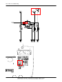
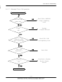
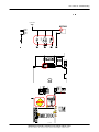
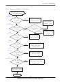
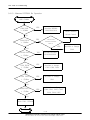
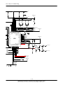
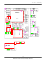
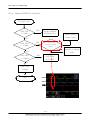
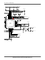
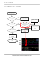
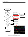
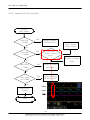
1
GSM TELEPHONE
SGH-i560V
GSM TELEPHONE
CONTENTS
1.
Safety Precautions
2.
Specification
3.
Product Function
4.
Array course control
5.
Exploded View and Parts List
6.
Main Electrical Parts List
7.
Block Diagrams
8.
PCB Diagrams
9.
Flow Chart of Troubleshooting
10.
Reference data
11.
Disassembly and Assembly
Instructions
GSPN (Global Service Partner Network)
Country
North America
Latin America
CIS
Europe
China
Asia
Mideast & Africa
Web Site
service.samsungportal.com
latin.samsungportal.com
cis.samsungportal.com
europe.samsungportal.com
china.samsungportal.com
asia.samsungportal.com
mea.samsungportal.com
This Service Manual is a property of Samsung Electronics Co.,Ltd.
Any unauthorized use of Manual can be punished under applicable
International and/or domestic law.
ⓒ Samsung Electronics Co.,Ltd.
2007. 11 Rev.1.0
1. Safety Precautions
1-1. Repair Precaution
● Repair in Shield Box, during detailed tuning.
Take specially care of tuning or test, because the specification of cellular phone is sensitive for
surrounding interference(RF noise).
● Be careful to use a kind of magnetic object or tool, because performance of parts is damaged by the
influence of magnetic force.
● Surely use a standard screwdriver when you disassemble this product, otherwise screw will be worn
away.
● Use a thicken twisted wire when you measure level.
A thicken twisted wire has low resistance, therefore error of measurement is few.
● Repair after separate Test Pack and Set because for short danger (for example an
overcurrent and furious flames of parts etc) when you repair board in condition of
connecting Test Pack and tuning on.
● Take specially care of soldering, because Land of PCB is small and weak in heat.
● Surely tune on/off while using AC power plug, because a repair of battery charger is
dangerous when tuning ON/OFF PBA and Connector after disassembling charger.
● Don't use as you pleases after change other material than replacement registered on SEC System.
Otherwise engineer in charge isn't charged with problem that you don't keep this rules.
1-1
SAMSUNG Proprietary-Contents may change without notice
This Document can not be used without Samsung's authorization
Safety Precautions
1-2. ESD(Electrostatically Sensitive Devices) Precaution
Several semiconductor may be damaged easily by static electricity. Such parts are called by ESD
(Electrostatically Sensitive Devices), for example IC,BGA chip etc. Read Precaution below.
You can prevent from ESD damage by static electricity.
● Remove static electricity remained your body before you touch semiconductor or parts with
semiconductor. There are ways that you touch an earthed place or wear static electricity
prevention string on wrist.
● Use earthed soldering steel when you connect or disconnect ESD.
● Use soldering removing tool to break static electricity. , otherwise ESD will be damaged by
static electricity.
● Don't unpack until you set up ESD on product. Because most of ESD are packed by box and
aluminum
plate to have conductive power,they are prevented from static electricity.
● You must maintain electric contact between ESD and place due to be set up until ESD is connected
completely to the proper place or a circuit board.
1-2
SAMSUNG Proprietary-Contents may change without notice
This Document can not be used without Samsung's authorization
2. Specification
2-1. GSM General Specification
EGSM 900
DCS 18 00
PCS 190 0
WCDMA 2100
Fre q. Band[MHz]
Uplink/Downlink
880~91 5
925~96 0
1 710~17 85
1 805~18 80
1 850~19 10
1 930~19 90
1 920~19 80
2 110~21 70
ARFCN r ange
0~124 &
9 75~102 3
512~88 5
512~81 0
UL:9 612~98 88
DL:10 562~10 838
Tx/Rx spa cing
10MHz
20MHz
20MHz
130MHz
Mod. Bit rat e/
Bit Period
27 0.833 kbps
3.692 us
27 0.833 kbps
3.692 us
27 0.833 kbps
3.692 us
3. 84Mcps
(chip ra te)
T ime Slot Per iod/
Fra me Per iod
576.9 us
4. 615ms
576.9 us
4. 615ms
576.9 us
4. 615ms
F rame l ength : 10ms
Slot lengt h : 0. 667ms
Modulation
0.3G M SK
0.3G MSK
0.3G M SK
QPSK
HPSK
MS Powe r
33 dBm~5d Bm
30 dBm~0d Bm
30 dBm~0d Bm
2 4dBm~- 50dBm
Power Class
4
(max +33dBm)
1
(max +30dBm)
1
(max +30dBm)
Sensit ivit y
-1 02dBm
-1 00dBm
-1 00dBm
T DM A Mu x
8
8
8
Cell Radius
35Km
2Km
2Km
2-1
SAMSUNG Proprietary-Contents may change without notice
This Document can not be used without Samsung's authorization
3
(max +24dBm)
- 106.7 dBm
2Km
Specification
2-2. GSM TX power class
TX Power
TX Power
TX Power
control level
GSM850
GSM900
control level
5
33±2 dBm
0
30±3 dBm
0
30±3 dBm
6
31±2 dBm
1
28±3 dBm
1
28±3 dBm
7
29±2 dBm
2
26±3 dBm
2
26±3 dBm
8
27±2 dBm
3
24±3 dBm
3
24±3 dBm
9
25±2 dBm
4
22±3 dBm
4
22±3 dBm
10
23±2 dBm
5
20±3 dBm
5
20±3 dBm
11
21±2 dBm
6
18±3 dBm
6
18±3 dBm
12
19±2 dBm
7
16±3 dBm
7
16±3 dBm
13
17±2 dBm
8
14±3 dBm
8
14±3 dBm
14
15±2 dBm
9
12±4 dBm
9
12±4 dBm
15
13±2 dBm
10
10±4 dBm
10
10±4 dBm
16
11±3 dBm
11
8±4 dBm
11
8±4 dBm
17
9±3 dBm
12
6±4 dBm
12
6±4 dBm
18
7±3 dBm
13
4±4 dBm
13
4±4 dBm
19
5±3 dBm
14
2±5 dBm
14
2±5 dBm
15
0±5 dBm
15
0±5 dBm
DCS1800
control level
2-2
SAMSUNG Proprietary-Contents may change without notice
This Document can not be used without Samsung's authorization
PCS1900
3. Product Function
Main Function
HSDPA/UMTS, EDGE, GPRS
Bluetooth v2.0 + EDR
USB v2.0 HS compatible
Camera 3Mega x 9 Digital Zooming and camcorder
FM Radio
Instant Messaging capability
E-mail
Featured applications provide alarms, calendar, calculator, record audio, converter, timer, stopwatch,
and world time.
File viewer (MS office, PDF)
Multimedia Message Service (MMS)
Multimedia capability (with included Media player)
Photo caller ID
Speakerphone capability
WEB/WAP browser (HTMS, xHTML, WML)
3-1
SAMSUNG Proprietary-Contents may change without notice
This Document can not be used without Samsung's authorization
Product Function
3-2
SAMSUNG Proprietary-Contents may change without notice
This Document can not be used without Samsung's authorization
4. Array course control
4-1. Software Adjustments
- There is 2 set to download the binary image into your device.
[First set]
8
1.
2.
3.
4.
5.
6.
7.
8.
JIG BOX (UMTS TEST JIG; GH80-03308A)
USB Cable : JIG to PC
Test Cable : JIG to SGH-i560 (GH39-00890A)
Power Cable : JIG to power supply
Serial Cable : SGH-i560 to PC
Power Supply
Rf Cable : SGH-i560 to Agilent 8960 or CMU200 (GH39-00397A)
Test Cable : JIG to SGH-i560 (GH39-00886A)
4-1
SAMSUNG Proprietary-Contents may change without notice
This Document can not be used without Samsung's authorization
Array course control
[Second Set]
USB Data Link Cable : SGH-i560 to PC (GH39-00922A)
Standard Battery for SGH-i560 (GH43-02992A)
4-2
SAMSUNG Proprietary-Contents may change without notice
This Document can not be used without Samsung's authorization
Array course control
4-2. Software Download
4-2-1. Pre-requisite for Download
SGH - i560 Mobile Device
Apollo v4.01.exe : Downloader Application for SGH-i560
USB Download Driver : SS60_Downloader_Driver.zip
Rom Image : PDA(*.IMG), MODEM(*.BIN) images
Equipment set for Download.
4-3
SAMSUNG Proprietary-Contents may change without notice
This Document can not be used without Samsung's authorization
Array course control
4-2-2. Concupts & cautions.
You can download PDA or MODEM separately. But We are always recommended to
download both at the same time using same version of rom image.
To download an image, the phone need to be set to a proper download mode.
There are 3 download modes.
PDA download : Hold 1, 4 keys and power on -> Blue screen with some information.
MODEM download : Hold 7, * keys and power on -> Blinking "MODEM DOWNLOAD"
on blue screen
All download : Hold 4, 7 keys and power on -> Blinking "ALL DOWNLOAD" on blue screen
For PDA image download, the phone shows download progress on the screen
For MODEM image download, the phone shows RGBW/B Screen.
For All download mode, MODEM image is downloaded first and then PDA
downloading starts.
After downloading PDA, the phone will be reboot.
Do NOT interrupt downloading process or the phone will be damaged. You would be
unable to boot up the phone or to re-flash the phone. Let it finish downloading
process even though you are flashing wrong images.
4-4
SAMSUNG Proprietary-Contents may change without notice
This Document can not be used without Samsung's authorization
Array course control
4-2-3. USB Driver installation for PDA
Execution Apollo.exe.
SGH-i560 connect to the Host computer using download equipment set.
Hold “1+4” key and insert power supplied test cable when use equipment set 1
or Hold “1+4” key and press power on key when use equipment set 2.
Install PDA side driver.
Follow New H/W Installation Manager.
Select ‘IBootHostUSB.inf’file under ‘i560_Apollo_Drivers\PDA_driver’ folder when
Windows asks for new h/w driver. It is safe to choose “Yes” for the waring window.
Confirm “SAMSUNG BlueFin USB Downloader” Installed.
Refer to Next Page.
** If Windows doesn’t ask for USB driver, it means USB driver installation was
failed before. Open Hardware Manager then delete devices with?or!mark then try
again. If it doesn’t work, you need to right click on the device then try Driver
Update.
After installing PDA driver, Apollo shows the connection status if it is installed
properly.
4-5
SAMSUNG Proprietary-Contents may change without notice
This Document can not be used without Samsung's authorization
Array course control
4-6
SAMSUNG Proprietary-Contents may change without notice
This Document can not be used without Samsung's authorization
Array course control
4-2-4. USB Driver installation for MODEM
Hold “7 + *” key and insert power supplied test cable when use equipment set 1 or
Hold “7+ *” key and press power on key when use equipment set 2.
Install Modem side driver.
Execute ‘Setup.exe’file under ‘i560_Apollo_Drivers\PHONE_driver’ folder when
Windows asks for new h/w driver.
Confirm “SAMSUNG USB Composite Device” Installed.
4-7
SAMSUNG Proprietary-Contents may change without notice
This Document can not be used without Samsung's authorization
Array course control
4-2-5. USB Driver installation
4-8
SAMSUNG Proprietary-Contents may change without notice
This Document can not be used without Samsung's authorization
Array course control
4-2-6. Download the image using APOLLO
Execution Apollo.exe.
Select a Rom Image to download
Check this field : 4. SGH-i560(Martini)
4-9
SAMSUNG Proprietary-Contents may change without notice
This Document can not be used without Samsung's authorization
Array course control
Select the proper check option .
PDA stasus
- Bootloader : Update PDA Bootloader section.
- NV Clear : IMEI section erase.
You can see following message when you click this option
MODEM Status
- Boot Update : Update Modem Bootloader section.
4-10
SAMSUNG Proprietary-Contents may change without notice
This Document can not be used without Samsung's authorization
Array course control
Make sure that phone and host computer connection, click proper download
button.
PDA download : Hold 1, 4 keys and power on -> Blue screen with some information.
MODEM download : Hold 7, * keys and power on -> Blinking "MODEM DOWNLOAD"
on blue screen
All download : Hold 4, 7 keys and power on -> Blinking "ALL DOWNLOAD" on blue screen
4-11
SAMSUNG Proprietary-Contents may change without notice
This Document can not be used without Samsung's authorization
Array course control
Do NOT interrupt downloading process.
- Pda download time: About 1 min.
- Modem download time : About 2 min.
- All download time: About 3 min.
Confirm Download Complete.
- SGH-i560 will be reboot when PDA download complete.
4-12
SAMSUNG Proprietary-Contents may change without notice
This Document can not be used without Samsung's authorization
Array course control
4-2-7. Troubleshooting
Unable to install USB driver.
Try another Download equipment
Try another SGH-i560.
Consult to R&D team.
Download stops in the middle.
Close and launch Apollo again then try again.
Check the battery is charged enough.
Download doesn’t start
Check the connection between Apollo and a SGH-i560.
Check the image that is not damaged.
Select an image and download again.
Phone doesn’t boot up after downloading.
Check the release version of PDA and MODEM. They should be same.
Make sure that rom image, and then try to download.
4-13
SAMSUNG Proprietary-Contents may change without notice
This Document can not be used without Samsung's authorization
Array course control
4-14
SAMSUNG Proprietary-Contents may change without notice
This Document can not be used without Samsung's authorization
5. Exploded View and Parts List
5-1. Cellular phone Exploded View
QRF03
QFR01
QMW02
QCR73
QSH01
QSH02
QSP05
QVO01
QCR12
QFU01
QCK01
QMP01
QAN11
QSC06
QCK02
QMI01
QAN03
QMO01
QCR72
QSC05
QCA01
QKP02
QAN02
QSP01
QAR01
QCR67
QCA10
QSD01
QLC01
QME02
QRE01
QPC01
QIF01
QFL02
QCR06
QCR12
QRF01
QCR06
QBA01
QFL01
QHI01
QBA00
5-1
SAMSUNG Proprietary-Contents may change without notice
This Document can not be used without Samsung's authorization
Exploded View and Parts List
5-2. Cellular phone Parts List
Design LOC
Description
SEC CODE
QAN02
INTENNA-SGHI560V
GH42-01423A
QAN03
INTENNA-SGHI560V BT FPCB
GH42-01451A
QAN11
ASSY-CUSHION-CUSHION RUBBER IN
GH98-01077A
QAR01
AUDIO-RECEIVER
3009-001300
QBA00
PMO COVER-BATT
GH72-44575A
QBA01
INNER BATTERY PACK-1200MAH , B
GH43-02992A
QCA01
CAMERA MODULE-1/4" 3.1M CMOS
GH59-05024A
QCA10
CAMERA MODULE-1/24" VT CMOS
GH59-05022A
QCK01
PMO KEY-CAMERA
GH72-44572A
QCK02
PMO KEY-POWER
GH72-44573A
QCR06
SCREW-MACHINE
6001-001155
QCR06
SCREW-MACHINE
6001-001155
QCR12
SCREW-MACHINE
6001-001530
QCR12
SCREW-MACHINE
6001-001530
QCR67
SCREW-MACHINE
6001-002083
QCR72
SCREW-MACHINE
6001-002051
QCR73
SCREW-MACHINE
6001-002102
QKP02
ASSY KEYPAD-SUB(VOD/BLK)
GH98-06756A
QLC01
LCD-SGHI560V
GH07-01211A
QME02
DOME SHEET-SGHI560V SUB 12KEY
GH59-05042A
QMI01
MICROPHONE-ASSY-SGHI560V
GH30-00438A
QMO01
MOTOR LINEAR VIBRATION-SGHI560
GH31-00384A
QMP01
PBA MAIN-SGHI560V
GH92-04151A
QMW02
PMO WINDOW-MAIN(VOD)
GH72-44581A
QPC01
MEA-FPCBKIT
GH97-08391A
QRF01
TAPE-RF
GH74-35878A
QSH01
ASSY BRACKET-SHIELD CAN
GH98-06755A
QSH02
ICT BRACKET-SHIELD COVER
GH70-03059A
QSP01
ASSY ETC-SPEAKER MODULE
GH59-05123A
5-2
SAMSUNG Proprietary-Contents may change without notice
This Document can not be used without Samsung's authorization
Exploded View and Parts List
Design LOC
Description
SEC CODE
QVO01
PMO KEY-VOLUME
GH72-44574A
QFL01
ASSY CASE-LOWER
GH98-06414A
QFL02
ASSY CASE-SLIDE LOWER
GH98-06754A
QHI01
ASSY HINGE-SLIDE
GH98-06412A
ASSY CASE-FRONT
GH98-06417A
PMO COVER-EAR
GH72-44576A
ASSY CASE-UPPER(AL)
GH98-07148A
QSC05
ASSY RUBBER-SLIDE UP L
GH98-06892A
QSC06
ASSY RUBBER-SLIDE UP R
GH98-06893A
QSP05
ASSY DECO-SPK
GH98-06757A
ASSY CASE-REAR
GH98-06416A
QIF01
PMO COVER-IF
GH72-44578A
QSD01
PMO COVER-SD
GH72-44579A
QFR01
QRF03
QFU01
QRE01
5-3
SAMSUNG Proprietary-Contents may change without notice
This Document can not be used without Samsung's authorization
Exploded View and Parts List
Description
SEC CODE
BAG PE
6902-000634
CBF INTERFACE-DLC APCBS10BBE(S
GH39-00922A
ADAPTOR-ATADS10EBE,BLK,EU
GH44-01702A
S/W CD-SGHI560V SAMSUNG PC 7.0
GH46-00550A
S/W CD-SGHI560V USER GUIDE 1.0
GH46-00560A
EARPHONE-SGHE210,AAEP405MBE,A
GH59-04535A
LABEL(P)-UNIT SEAL
GH68-00518B
LABEL(R)-WATER SOAK
GH68-09361A
MANUAL USERS-VODA SPANISH QRG
GH68-16620A
LABEL(R)-MAIN(EU)
GH68-16810A
CUSHION-CASEVODA)
GH69-06153A
BOX-UNIT(EU)
GH69-06183A
TAPE-PBA
GH74-35879A
TAPE GASK-LCD CON
GH74-36274A
SPONGE-SPK STRUCTURE
GH74-36280A
TAPE-BB ABSORBER
GH74-36305A
TAPE ELEC-FRONT BB
GH74-36306A
TAPE ELEC-FRONT
GH74-36307A
VINYL-BOHO UPPER
GH74-36310A
TAPE INSU-SIM SOKET
GH74-36385A
TAPE INSU-LCD CON
GH74-36393A
TAPE-CK
GH74-36394A
TAPE INSU-FLASH FPCB
GH74-36396A
SPONGE-SUB SLIDE
GH74-36491A
VINYL-BOHO MAIN WINDOW
GH74-36749A
5-4
SAMSUNG Proprietary-Contents may change without notice
This Document can not be used without Samsung's authorization
6. Main Electrical Parts List
SEC Code
Design LOC
Description
STATUS
0403-001547
0406-001150
0406-001197
0406-001208
0406-001208
0406-001208
0406-001231
0406-001231
0406-001231
0406-001231
0406-001254
0406-001254
0406-001254
0406-001254
0406-001254
0406-001254
0406-001254
0406-001254
0406-001254
0406-001254
0406-001254
0406-001254
0406-001256
0406-001256
0406-001267
0406-001267
0406-001267
0406-001267
0406-001267
0406-001267
0406-001267
0406-001267
0406-001267
0406-001267
0406-001267
0406-001267
0406-001267
0406-001267
0407-000115
0407-001002
0407-001002
0407-001007
0504-001113
0504-001113
0504-001113
0505-001165
0801-002294
0801-002294
0801-002294
0801-002321
0801-003012
0801-003013
0801-003052
0801-003124
D502
ZD700
ZD708
ZD802
ZD808
ZD811
ZD600
ZD601
ZD602
ZD603
ZD200
ZD500
ZD505
ZD604
ZD803
ZD804
ZD805
ZD806
ZD807
ZD809
ZD810
ZD812
ZD501
ZD502
ZD1000
ZD1001
ZD1003
ZD1005
ZD1006
ZD300
ZD301
ZD701
ZD702
ZD703
ZD704
ZD705
ZD706
ZD707
D800
D500
D501
D503
TR500
TR501
TR503
TR502
U401
U513
U514
U1000
U511
U402
U400
U512
DIODE-ZENER
DIODE-TVS
DIODE-TVS
DIODE-TVS
DIODE-TVS
DIODE-TVS
DIODE-TVS
DIODE-TVS
DIODE-TVS
DIODE-TVS
DIODE-TVS
DIODE-TVS
DIODE-TVS
DIODE-TVS
DIODE-TVS
DIODE-TVS
DIODE-TVS
DIODE-TVS
DIODE-TVS
DIODE-TVS
DIODE-TVS
DIODE-TVS
DIODE-TVS
DIODE-TVS
DIODE-TVS
DIODE-TVS
DIODE-TVS
DIODE-TVS
DIODE-TVS
DIODE-TVS
DIODE-TVS
DIODE-TVS
DIODE-TVS
DIODE-TVS
DIODE-TVS
DIODE-TVS
DIODE-TVS
DIODE-TVS
DIODE-ARRAY
DIODE-ARRAY
DIODE-ARRAY
DIODE-ARRAY
TR-DIGITAL
TR-DIGITAL
TR-DIGITAL
FET-SILICON
IC-CMOS LOGIC
IC-CMOS LOGIC
IC-CMOS LOGIC
IC-CMOS LOGIC
IC-CMOS LOGIC
IC-CMOS LOGIC
IC-CMOS LOGIC
IC-CMOS LOGIC
SA
SA
SA
SA
SA
SA
SA
SA
SA
SA
SA
SA
SA
SA
SA
SA
SA
SA
SA
SA
SA
SA
SA
SA
SA
SA
SA
SA
SA
SA
SA
SA
SA
SA
SA
SA
SA
SA
SA
SA
SA
SA
SA
SA
SA
SA
SA
SA
SA
SA
SA
SA
SA
SA
6-1
SAMSUNG Proprietary-Contents may change without notice
This Document can not be used without Samsung's authorization
Main Electrical Parts List
SEC Code
Design LOC
Description
STATUS
0801-003205
0904-002295
1001-001336
1001-001362
1001-001401
1001-001436
1001-001461
1001-001483
1001-001483
1001-001483
1001-001483
1001-001483
1001-001483
1009-001027
1106-001511
1108-000127
1108-000135
1201-002180
1201-002233
1201-002531
1201-002570
1201-002581
1202-001068
1203-002716
1203-003643
1203-003643
1203-003737
1203-003737
1203-003737
1203-003978
1203-004430
1203-004464
1203-004607
1203-004621
1203-004778
1203-004838
1204-002746
1205-002767
1205-003169
1205-003281
1205-003297
1404-001221
1405-001138
1405-001138
1405-001138
1405-001138
1405-001138
1405-001138
1405-001138
1405-001138
1405-001138
1405-001138
1405-001138
1405-001138
U509
UCP900
U706
U603
U1004
U1002
U601
U800
U801
U802
U803
U804
U805
U702
UME1000
UME400
UCP900UP
U1003
U605
U303
U202
F304
U1001
U510
U703
U705
U700
U704
U710
U707
U505
U515
U701
U602
U501
U500
U308
U504
MOD200
UCP400
U201
TH400
VR800
VR801
VR802
VR803
VR804
VR805
VR806
VR807
VR808
VR809
VR810
VR811
IC-CMOS LOGIC
IC-DSP
IC-ANALOG SWITCH
IC-ANALOG SWITCH
IC-ANALOG SWITCH
IC-ANALOG SWITCH
IC-ANALOG SWITCH
IC-ANALOG SWITCH
IC-ANALOG SWITCH
IC-ANALOG SWITCH
IC-ANALOG SWITCH
IC-ANALOG SWITCH
IC-ANALOG SWITCH
IC-HALL EFFECT S/W
IC-SRAM
IC-MCP
IC-MCP
IC-AUDIO AMP
IC-AUDIO AMP
IC-POWER AMP
IC-POWER AMP
IC-RF AMP
IC-VOLTAGE COMP.
IC-VOL. DETECTOR
IC-MULTI REG.
IC-MULTI REG.
IC-POSI.FIXED REG.
IC-POSI.FIXED REG.
IC-POSI.FIXED REG.
IC-DC/DC CONVERTER
IC-VOL. DETECTOR
IC-VOL. DETECTOR
IC-MULTI REG.
IC-POWER SUPERVISOR
IC-POWER SUPERVISOR
IC-BATTERY
IC-TUNER
IC-SWITCH
IC-DATA COMM./GEN.
IC-MODEM
IC-TRANSCEIVER
THERMISTOR-NTC
VARISTOR
VARISTOR
VARISTOR
VARISTOR
VARISTOR
VARISTOR
VARISTOR
VARISTOR
VARISTOR
VARISTOR
VARISTOR
VARISTOR
SA
SA
SA
SA
SA
SA
SA
SA
SA
SA
SA
SA
SA
SA
SA
SA
SA
SA
SA
SA
SA
SA
SA
SA
SA
SA
SA
SA
SA
SA
SA
SA
SA
SA
SA
SA
SA
SA
SA
SA
SA
SA
SA
SA
SA
SA
SA
SA
SA
SA
SA
SA
SA
SA
6-2
SAMSUNG Proprietary-Contents may change without notice
This Document can not be used without Samsung's authorization
Main Electrical Parts List
SEC Code
Design LOC
Description
STATUS
2007-000137
2007-000138
2007-000138
2007-000138
2007-000138
2007-000138
2007-000138
2007-000138
2007-000140
2007-000148
2007-000148
2007-000148
2007-000148
2007-000148
2007-000157
2007-000159
2007-000161
2007-000162
2007-000162
2007-000162
2007-000162
2007-000162
2007-000162
2007-000162
2007-000162
2007-000162
2007-000162
2007-000162
2007-000162
2007-000162
2007-000164
2007-000165
2007-000165
2007-000169
2007-000170
2007-000170
2007-000170
2007-000170
2007-000170
2007-000171
2007-000171
2007-000171
2007-000171
2007-000171
2007-000171
2007-000171
2007-000171
2007-000171
2007-000171
2007-000171
2007-000171
2007-000171
2007-000171
2007-000171
R419
R1040
R1043
R310
R642
R643
R720
R722
R1032
R210
R405
R407
R412
R523
R530
R909
R305
R1004
R1007
R1019
R1021
R500
R510
R511
R527
R537
R602
R701
R716
R903
R700
R518
R639
R1029
R1026
R1027
R1028
R422
R519
R1002
R205
R211
R214
R221
R300
R301
R304
R311
R312
R313
R317
R319
R538
R922
R-CHIP
R-CHIP
R-CHIP
R-CHIP
R-CHIP
R-CHIP
R-CHIP
R-CHIP
R-CHIP
R-CHIP
R-CHIP
R-CHIP
R-CHIP
R-CHIP
R-CHIP
R-CHIP
R-CHIP
R-CHIP
R-CHIP
R-CHIP
R-CHIP
R-CHIP
R-CHIP
R-CHIP
R-CHIP
R-CHIP
R-CHIP
R-CHIP
R-CHIP
R-CHIP
R-CHIP
R-CHIP
R-CHIP
R-CHIP
R-CHIP
R-CHIP
R-CHIP
R-CHIP
R-CHIP
R-CHIP
R-CHIP
R-CHIP
R-CHIP
R-CHIP
R-CHIP
R-CHIP
R-CHIP
R-CHIP
R-CHIP
R-CHIP
R-CHIP
R-CHIP
R-CHIP
R-CHIP
SA
SA
SA
SA
SA
SA
SA
SA
SA
SA
SA
SA
SA
SA
SA
SA
SA
SA
SA
SA
SA
SA
SA
SA
SA
SA
SA
SA
SA
SA
SA
SA
SA
SA
SA
SA
SA
SA
SA
SA
SA
SA
SA
SA
SA
SA
SA
SA
SA
SA
SA
SA
SA
SA
6-3
SAMSUNG Proprietary-Contents may change without notice
This Document can not be used without Samsung's authorization
Main Electrical Parts List
SEC Code
Design LOC
Description
STATUS
2007-001119
2007-001119
2007-001285
2007-001285
2007-001290
2007-001292
2007-001298
2007-001298
2007-001298
2007-001298
2007-001306
2007-001306
2007-001306
2007-001306
2007-001316
2007-001339
2007-001339
2007-007009
2007-007014
2007-007014
2007-007107
2007-007107
2007-007107
2007-007107
2007-007132
2007-007132
2007-007136
2007-007136
2007-007136
2007-007139
2007-007139
2007-007142
2007-007190
2007-007190
2007-007306
2007-007306
2007-007307
2007-007307
2007-007307
2007-007307
2007-007309
2007-007309
2007-007315
2007-007316
2007-007317
2007-007317
2007-007317
2007-007468
2007-007528
2007-007528
2007-007698
2007-007766
2007-007791
2007-008045
R603
R604
R207
R208
R418
R414
R209
R215
R303
R402
R212
R213
R216
R217
R517
R715
R806
R306
R506
R520
R220
R423
R425
R705
R1013
R1045
R625
R629
R923
R624
R626
R509
R902
R921
R302
R307
R1030
R1031
R721
R726
R202
R526
R516
R421
R539
R900
R901
R505
R610
R614
R508
R515
R704
R1044
R-CHIP
R-CHIP
R-CHIP
R-CHIP
R-CHIP
R-CHIP
R-CHIP
R-CHIP
R-CHIP
R-CHIP
R-CHIP
R-CHIP
R-CHIP
R-CHIP
R-CHIP
R-CHIP
R-CHIP
R-CHIP
R-CHIP
R-CHIP
R-CHIP
R-CHIP
R-CHIP
R-CHIP
R-CHIP
R-CHIP
R-CHIP
R-CHIP
R-CHIP
R-CHIP
R-CHIP
R-CHIP
R-CHIP
R-CHIP
R-CHIP
R-CHIP
R-CHIP
R-CHIP
R-CHIP
R-CHIP
R-CHIP
R-CHIP
R-CHIP
R-CHIP
R-CHIP
R-CHIP
R-CHIP
R-CHIP
R-CHIP
R-CHIP
R-CHIP
R-CHIP
R-CHIP
R-CHIP
SA
SA
SA
SA
SA
SA
SA
SA
SA
SA
SA
SA
SA
SA
SA
SA
SA
SA
SA
SA
SA
SA
SA
SA
SA
SA
SA
SA
SA
SA
SA
SA
SA
SA
SA
SA
SA
SA
SA
SA
SA
SA
SA
SA
SA
SA
SA
SA
SA
SA
SA
SA
SA
SA
6-4
SAMSUNG Proprietary-Contents may change without notice
This Document can not be used without Samsung's authorization
Main Electrical Parts List
SEC Code
Design LOC
Description
STATUS
2007-008045
2007-008052
2007-008052
2007-008052
2007-008052
2007-008055
2007-008055
2007-008419
2007-008419
2007-008419
2007-008483
2007-008483
2007-008483
2007-008483
2007-008516
2007-008516
2007-008516
2007-008542
2007-008542
2007-008542
2007-008588
2007-008806
2007-008806
2007-008806
2007-008806
2007-008806
2007-008806
2007-008806
2007-008806
2007-008806
2007-009157
2007-009157
2007-009157
2007-009157
2007-009157
2007-009793
2007-009793
2203-000233
2203-000233
2203-000233
2203-000233
2203-000233
2203-000233
2203-000233
2203-000233
2203-000233
2203-000233
2203-000233
2203-000233
2203-000233
2203-000233
2203-000254
2203-000254
2203-000254
R749
R904
R905
R906
R907
R514
R601
R733
R734
R737
R521
R522
R524
R525
R314
R640
R641
R634
R735
R736
R218
R507
R528
R529
R532
R533
R534
R535
R541
R605
R1005
R1006
R1009
R1010
R738
R1011
R1012
C1014
C207
C209
C218
C220
C234
C239
C247
C256
C279
C325
C512
C513
C520
C225
C253
C276
R-CHIP
R-CHIP
R-CHIP
R-CHIP
R-CHIP
R-CHIP
R-CHIP
R-CHIP
R-CHIP
R-CHIP
R-CHIP
R-CHIP
R-CHIP
R-CHIP
R-CHIP
R-CHIP
R-CHIP
R-CHIP
R-CHIP
R-CHIP
R-CHIP
R-CHIP
R-CHIP
R-CHIP
R-CHIP
R-CHIP
R-CHIP
R-CHIP
R-CHIP
R-CHIP
R-CHIP
R-CHIP
R-CHIP
R-CHIP
R-CHIP
R-CHIP
R-CHIP
C-CER,CHIP
C-CER,CHIP
C-CER,CHIP
C-CER,CHIP
C-CER,CHIP
C-CER,CHIP
C-CER,CHIP
C-CER,CHIP
C-CER,CHIP
C-CER,CHIP
C-CER,CHIP
C-CER,CHIP
C-CER,CHIP
C-CER,CHIP
C-CER,CHIP
C-CER,CHIP
C-CER,CHIP
SA
SA
SA
SA
SA
SA
SA
SA
SA
SA
SA
SA
SA
SA
SA
SA
SA
SA
SA
SA
SA
SA
SA
SA
SA
SA
SA
SA
SA
SA
SA
SA
SA
SA
SA
SA
SA
SA
SA
SA
SA
SA
SA
SA
SA
SA
SA
SA
SA
SA
SA
SA
SA
SA
6-5
SAMSUNG Proprietary-Contents may change without notice
This Document can not be used without Samsung's authorization
Main Electrical Parts List
SEC Code
Design LOC
Description
STATUS
2203-000254
2203-000254
2203-000254
2203-000254
2203-000254
2203-000254
2203-000278
2203-000278
2203-000278
2203-000278
2203-000311
2203-000311
2203-000311
2203-000311
2203-000330
2203-000330
2203-000330
2203-000330
2203-000330
2203-000386
2203-000386
2203-000386
2203-000386
2203-000386
2203-000438
2203-000438
2203-000438
2203-000489
2203-000627
2203-000627
2203-000627
2203-000627
2203-000627
2203-000627
2203-000627
2203-000627
2203-000627
2203-000679
2203-000679
2203-000812
2203-000812
2203-000812
2203-000812
2203-000812
2203-000812
2203-000812
2203-000812
2203-000812
2203-000812
2203-000812
2203-000812
2203-000812
2203-000812
2203-000812
C315
C317
C321
C443
C656
C658
C600
C626
C633
C642
C200
C202
C203
C205
C268
C273
C282
C283
C304
C264
C306
C680
C681
C682
C259
C316
C464
C402
C217
C222
C224
C228
C230
C232
C233
C254
C260
C238
C244
C1012
C1013
C214
C236
C237
C241
C243
C255
C262
C275
C305
C320
C328
C330
C332
C-CER,CHIP
C-CER,CHIP
C-CER,CHIP
C-CER,CHIP
C-CER,CHIP
C-CER,CHIP
C-CER,CHIP
C-CER,CHIP
C-CER,CHIP
C-CER,CHIP
C-CER,CHIP
C-CER,CHIP
C-CER,CHIP
C-CER,CHIP
C-CER,CHIP
C-CER,CHIP
C-CER,CHIP
C-CER,CHIP
C-CER,CHIP
C-CER,CHIP
C-CER,CHIP
C-CER,CHIP
C-CER,CHIP
C-CER,CHIP
C-CER,CHIP
C-CER,CHIP
C-CER,CHIP
C-CER,CHIP
C-CER,CHIP
C-CER,CHIP
C-CER,CHIP
C-CER,CHIP
C-CER,CHIP
C-CER,CHIP
C-CER,CHIP
C-CER,CHIP
C-CER,CHIP
C-CER,CHIP
C-CER,CHIP
C-CER,CHIP
C-CER,CHIP
C-CER,CHIP
C-CER,CHIP
C-CER,CHIP
C-CER,CHIP
C-CER,CHIP
C-CER,CHIP
C-CER,CHIP
C-CER,CHIP
C-CER,CHIP
C-CER,CHIP
C-CER,CHIP
C-CER,CHIP
C-CER,CHIP
SA
SA
SA
SA
SA
SA
SA
SA
SA
SA
SA
SA
SA
SA
SA
SA
SA
SA
SA
SA
SA
SA
SA
SA
SA
SA
SA
SA
SNA
SNA
SNA
SNA
SNA
SNA
SNA
SNA
SNA
SA
SA
SA
SA
SA
SA
SA
SA
SA
SA
SA
SA
SA
SA
SA
SA
SA
6-6
SAMSUNG Proprietary-Contents may change without notice
This Document can not be used without Samsung's authorization
Main Electrical Parts List
SEC Code
Design LOC
Description
STATUS
2203-000812
2203-000812
2203-000812
2203-000812
2203-000812
2203-000812
2203-000812
2203-000812
2203-000812
2203-000995
2203-000995
2203-000995
2203-000995
2203-000995
2203-000995
2203-000995
2203-000995
2203-000995
2203-000995
2203-001153
2203-001153
2203-001259
2203-002668
2203-002668
2203-002709
2203-002709
2203-002709
2203-002709
2203-002968
2203-003054
2203-003054
2203-005053
2203-005053
2203-005056
2203-005234
2203-005281
2203-005281
2203-005281
2203-005395
2203-005480
2203-005482
2203-005482
2203-005482
2203-005482
2203-005482
2203-005482
2203-005482
2203-005482
2203-005482
2203-005482
2203-005482
2203-005482
2203-005682
2203-005682
C527
C528
C531
C627
C635
C643
C652
C653
C720
C1008
C1009
C300
C401
C469
C663
C664
C678
C751
C752
C201
C204
C601
C303
C334
C503
C506
C515
C517
C250
C1006
C1007
C272
C274
C291
C280
C263
C265
C322
C271
C463
C301
C312
C326
C336
C406
C413
C420
C444
C450
C461
C462
C941
C231
C329
C-CER,CHIP
C-CER,CHIP
C-CER,CHIP
C-CER,CHIP
C-CER,CHIP
C-CER,CHIP
C-CER,CHIP
C-CER,CHIP
C-CER,CHIP
C-CER,CHIP
C-CER,CHIP
C-CER,CHIP
C-CER,CHIP
C-CER,CHIP
C-CER,CHIP
C-CER,CHIP
C-CER,CHIP
C-CER,CHIP
C-CER,CHIP
C-CER,CHIP
C-CER,CHIP
C-CER,CHIP
C-CER,CHIP
C-CER,CHIP
C-CER,CHIP
C-CER,CHIP
C-CER,CHIP
C-CER,CHIP
C-CER,CHIP
C-CER,CHIP
C-CER,CHIP
C-CER,CHIP
C-CER,CHIP
C-CER,CHIP
C-CER,CHIP
C-CER,CHIP
C-CER,CHIP
C-CER,CHIP
C-CER,CHIP
C-CER,CHIP
C-CER,CHIP
C-CER,CHIP
C-CER,CHIP
C-CER,CHIP
C-CER,CHIP
C-CER,CHIP
C-CER,CHIP
C-CER,CHIP
C-CER,CHIP
C-CER,CHIP
C-CER,CHIP
C-CER,CHIP
C-CER,CHIP
C-CER,CHIP
SA
SA
SA
SA
SA
SA
SA
SA
SA
SA
SA
SA
SA
SA
SA
SA
SA
SA
SA
SA
SA
SA
SA
SA
SA
SA
SA
SA
SA
SA
SA
SA
SA
SA
SA
SA
SA
SA
SA
SA
SA
SA
SA
SA
SA
SA
SA
SA
SA
SA
SA
SA
SA
SA
6-7
SAMSUNG Proprietary-Contents may change without notice
This Document can not be used without Samsung's authorization
Main Electrical Parts List
SEC Code
Design LOC
Description
STATUS
2203-005682
2203-005682
2203-005682
2203-005682
2203-005683
2203-005725
2203-005725
2203-005727
2203-005729
2203-005732
2203-005736
2203-005736
2203-005736
2203-005736
2203-005736
2203-005806
2203-006048
2203-006048
2203-006048
2203-006048
2203-006048
2203-006137
2203-006194
2203-006194
2203-006194
2203-006194
2203-006208
2203-006208
2203-006208
2203-006261
2203-006324
2203-006324
2203-006324
2203-006324
2203-006324
2203-006324
2203-006324
2203-006348
2203-006348
2203-006377
2203-006399
2203-006399
2203-006399
2203-006399
2203-006399
2203-006399
2203-006399
2203-006399
2203-006399
2203-006399
2203-006399
2203-006399
2203-006399
2203-006399
C611
C631
C637
C644
C1025
C211
C212
C510
C508
C266
C213
C816
C817
C818
C819
C226
C277
C278
C538
C700
C701
C313
C439
C447
C466
C468
C509
C516
C519
C339
C465
C500
C521
C650
C736
C737
C738
C535
C536
C719
C1017
C284
C285
C286
C287
C288
C407
C408
C409
C410
C418
C617
C623
C625
C-CER,CHIP
C-CER,CHIP
C-CER,CHIP
C-CER,CHIP
C-CER,CHIP
C-CER,CHIP
C-CER,CHIP
C-CER,CHIP
C-CER,CHIP
C-CER,CHIP
C-CER,CHIP
C-CER,CHIP
C-CER,CHIP
C-CER,CHIP
C-CER,CHIP
C-CER,CHIP
C-CER,CHIP
C-CER,CHIP
C-CER,CHIP
C-CER,CHIP
C-CER,CHIP
C-CER,CHIP
C-CER,CHIP
C-CER,CHIP
C-CER,CHIP
C-CER,CHIP
C-CER,CHIP
C-CER,CHIP
C-CER,CHIP
C-CER,CHIP
C-CER,CHIP
C-CER,CHIP
C-CER,CHIP
C-CER,CHIP
C-CER,CHIP
C-CER,CHIP
C-CER,CHIP
C-CER,CHIP
C-CER,CHIP
C-CER,CHIP
C-CER,CHIP
C-CER,CHIP
C-CER,CHIP
C-CER,CHIP
C-CER,CHIP
C-CER,CHIP
C-CER,CHIP
C-CER,CHIP
C-CER,CHIP
C-CER,CHIP
C-CER,CHIP
C-CER,CHIP
C-CER,CHIP
C-CER,CHIP
SA
SA
SA
SA
SA
SA
SA
SA
SA
SA
SA
SA
SA
SA
SA
SNA
SA
SA
SA
SA
SA
SA
SA
SA
SA
SA
SA
SA
SA
SA
SA
SA
SA
SA
SA
SA
SA
SA
SA
SA
SA
SA
SA
SA
SA
SA
SA
SA
SA
SA
SA
SA
SA
SA
6-8
SAMSUNG Proprietary-Contents may change without notice
This Document can not be used without Samsung's authorization
Main Electrical Parts List
SEC Code
Design LOC
Description
STATUS
2203-006399
2203-006399
2203-006399
2203-006399
2203-006423
2203-006423
2203-006423
2203-006423
2203-006423
2203-006423
2203-006423
2203-006423
2203-006423
2203-006423
2203-006423
2203-006423
2203-006423
2203-006423
2203-006423
2203-006423
2203-006423
2203-006423
2203-006423
2203-006423
2203-006423
2203-006423
2203-006423
2203-006423
2203-006423
2203-006423
2203-006423
2203-006423
2203-006423
2203-006423
2203-006423
2203-006423
2203-006423
2203-006423
2203-006423
2203-006423
2203-006423
2203-006423
2203-006474
2203-006474
2203-006562
2203-006562
2203-006562
2203-006562
2203-006562
2203-006562
2203-006562
2203-006562
2203-006562
2203-006562
C740
C805
C960
C963
C1002
C1003
C1004
C1005
C327
C417
C419
C436
C440
C451
C452
C539
C610
C612
C674
C741
C900
C901
C902
C903
C904
C905
C906
C907
C908
C909
C910
C919
C920
C921
C922
C923
C924
C925
C926
C955
C961
C962
C522
C541
C1000
C1001
C1011
C1018
C1019
C1020
C1021
C1022
C1023
C314
C-CER,CHIP
C-CER,CHIP
C-CER,CHIP
C-CER,CHIP
C-CER,CHIP
C-CER,CHIP
C-CER,CHIP
C-CER,CHIP
C-CER,CHIP
C-CER,CHIP
C-CER,CHIP
C-CER,CHIP
C-CER,CHIP
C-CER,CHIP
C-CER,CHIP
C-CER,CHIP
C-CER,CHIP
C-CER,CHIP
C-CER,CHIP
C-CER,CHIP
C-CER,CHIP
C-CER,CHIP
C-CER,CHIP
C-CER,CHIP
C-CER,CHIP
C-CER,CHIP
C-CER,CHIP
C-CER,CHIP
C-CER,CHIP
C-CER,CHIP
C-CER,CHIP
C-CER,CHIP
C-CER,CHIP
C-CER,CHIP
C-CER,CHIP
C-CER,CHIP
C-CER,CHIP
C-CER,CHIP
C-CER,CHIP
C-CER,CHIP
C-CER,CHIP
C-CER,CHIP
C-CER,CHIP
C-CER,CHIP
C-CER,CHIP
C-CER,CHIP
C-CER,CHIP
C-CER,CHIP
C-CER,CHIP
C-CER,CHIP
C-CER,CHIP
C-CER,CHIP
C-CER,CHIP
C-CER,CHIP
SA
SA
SA
SA
SA
SA
SA
SA
SA
SA
SA
SA
SA
SA
SA
SA
SA
SA
SA
SA
SA
SA
SA
SA
SA
SA
SA
SA
SA
SA
SA
SA
SA
SA
SA
SA
SA
SA
SA
SA
SA
SA
SA
SA
SA
SA
SA
SA
SA
SA
SA
SA
SA
SA
6-9
SAMSUNG Proprietary-Contents may change without notice
This Document can not be used without Samsung's authorization
Main Electrical Parts List
SEC Code
Design LOC
Description
STATUS
2203-006562
2203-006562
2203-006562
2203-006562
2203-006562
2203-006562
2203-006562
2203-006562
2203-006562
2203-006562
2203-006562
2203-006562
2203-006562
2203-006562
2203-006562
2203-006562
2203-006562
2203-006562
2203-006562
2203-006562
2203-006562
2203-006562
2203-006562
2203-006562
2203-006562
2203-006562
2203-006562
2203-006562
2203-006562
2203-006562
2203-006562
2203-006562
2203-006562
2203-006562
2203-006562
2203-006562
2203-006562
2203-006562
2203-006562
2203-006562
2203-006562
2203-006562
2203-006562
2203-006562
2203-006562
2203-006562
2203-006562
2203-006585
2203-006585
2203-006681
2203-006681
2203-006681
2203-006681
2203-006681
C400
C432
C433
C434
C435
C438
C442
C467
C507
C511
C540
C603
C604
C605
C606
C607
C608
C609
C613
C615
C616
C622
C647
C648
C649
C659
C662
C666
C667
C668
C702
C705
C706
C709
C715
C716
C729
C745
C750
C810
C812
C813
C814
C911
C912
C927
C928
C630
C636
C206
C208
C210
C215
C216
C-CER,CHIP
C-CER,CHIP
C-CER,CHIP
C-CER,CHIP
C-CER,CHIP
C-CER,CHIP
C-CER,CHIP
C-CER,CHIP
C-CER,CHIP
C-CER,CHIP
C-CER,CHIP
C-CER,CHIP
C-CER,CHIP
C-CER,CHIP
C-CER,CHIP
C-CER,CHIP
C-CER,CHIP
C-CER,CHIP
C-CER,CHIP
C-CER,CHIP
C-CER,CHIP
C-CER,CHIP
C-CER,CHIP
C-CER,CHIP
C-CER,CHIP
C-CER,CHIP
C-CER,CHIP
C-CER,CHIP
C-CER,CHIP
C-CER,CHIP
C-CER,CHIP
C-CER,CHIP
C-CER,CHIP
C-CER,CHIP
C-CER,CHIP
C-CER,CHIP
C-CER,CHIP
C-CER,CHIP
C-CER,CHIP
C-CER,CHIP
C-CER,CHIP
C-CER,CHIP
C-CER,CHIP
C-CER,CHIP
C-CER,CHIP
C-CER,CHIP
C-CER,CHIP
C-CER,CHIP
C-CER,CHIP
C-CER,CHIP
C-CER,CHIP
C-CER,CHIP
C-CER,CHIP
C-CER,CHIP
SA
SA
SA
SA
SA
SA
SA
SA
SA
SA
SA
SA
SA
SA
SA
SA
SA
SA
SA
SA
SA
SA
SA
SA
SA
SA
SA
SA
SA
SA
SA
SA
SA
SA
SA
SA
SA
SA
SA
SA
SA
SA
SA
SA
SA
SA
SA
SA
SA
SA
SA
SA
SA
SA
6-10
SAMSUNG Proprietary-Contents may change without notice
This Document can not be used without Samsung's authorization
Main Electrical Parts List
SEC Code
Design LOC
Description
STATUS
2203-006681
2203-006681
2203-006681
2203-006681
2203-006681
2203-006681
2203-006681
2203-006681
2203-006681
2203-006681
2203-006712
2203-006712
2203-006824
2203-006824
2203-006824
2203-006824
2203-006824
2203-006825
2203-006825
2203-006825
2203-006838
2203-006838
2203-006838
2203-006838
2203-006838
2203-006838
2203-006838
2203-006838
2203-006838
2203-006838
2203-006841
2203-006841
2203-006841
2203-006890
2203-006890
2203-006890
2203-006890
2404-001339
2404-001339
2404-001377
2404-001381
2404-001381
2404-001381
2404-001381
2404-001381
2404-001381
2404-001474
2404-001492
2404-001492
2404-001497
2703-001180
2703-001231
2703-001513
2703-001722
C223
C227
C229
C235
C240
C248
C257
C261
C318
C654
C657
C660
C504
C505
C524
C703
C704
C671
C672
C673
C1026
C514
C518
C523
C545
C746
C747
C748
C913
C929
C529
C530
C958
C707
C708
C710
C711
TA201
TA611
TA609
TA300
TA600
TA604
TA608
TA700
TA808
TA200
TA500
TA502
TA602
L205
L702
L1004
L208
C-CER,CHIP
C-CER,CHIP
C-CER,CHIP
C-CER,CHIP
C-CER,CHIP
C-CER,CHIP
C-CER,CHIP
C-CER,CHIP
C-CER,CHIP
C-CER,CHIP
C-CER,CHIP
C-CER,CHIP
C-CER,CHIP
C-CER,CHIP
C-CER,CHIP
C-CER,CHIP
C-CER,CHIP
C-CER,CHIP
C-CER,CHIP
C-CER,CHIP
C-CER,CHIP
C-CER,CHIP
C-CER,CHIP
C-CER,CHIP
C-CER,CHIP
C-CER,CHIP
C-CER,CHIP
C-CER,CHIP
C-CER,CHIP
C-CER,CHIP
C-CER,CHIP
C-CER,CHIP
C-CER,CHIP
C-CER,CHIP
C-CER,CHIP
C-CER,CHIP
C-CER,CHIP
C-TA,CHIP
C-TA,CHIP
C-TA,CHIP
C-TA,CHIP
C-TA,CHIP
C-TA,CHIP
C-TA,CHIP
C-TA,CHIP
C-TA,CHIP
C-TA,CHIP
C-TA,CHIP
C-TA,CHIP
C-TA,CHIP
INDUCTOR-SMD
INDUCTOR-SMD
INDUCTOR-SMD
INDUCTOR-SMD
SA
SA
SA
SA
SA
SA
SA
SA
SA
SA
SA
SA
SA
SA
SA
SA
SA
SA
SA
SA
SA
SA
SA
SA
SA
SA
SA
SA
SA
SA
SA
SA
SA
SA
SA
SA
SA
SA
SA
SA
SA
SA
SA
SA
SA
SA
SA
SA
SA
SA
SA
SNA
SA
SA
6-11
SAMSUNG Proprietary-Contents may change without notice
This Document can not be used without Samsung's authorization
Main Electrical Parts List
SEC Code
Design LOC
Description
STATUS
2703-001749
2703-001750
2703-002170
2703-002170
2703-002170
2703-002203
2703-002204
2703-002207
2703-002208
2703-002314
2703-002314
2703-002314
2703-002365
2703-002367
2703-002369
2703-002506
2703-002596
2703-002782
2703-002782
2703-002782
2703-002906
2703-002918
2703-003103
2703-003298
2703-003298
2801-004339
2801-004455
2801-004466
2804-001748
2809-001324
2901-001337
2901-001337
2901-001389
2901-001389
2901-001389
2904-001609
2904-001635
2904-001665
2904-001702
2904-001703
2904-001719
2904-001759
2910-000031
3301-001342
3301-001534
3301-001534
3301-001534
3301-001729
3301-001729
3301-001729
3301-001729
3301-001756
3301-001756
3301-001756
L218
L315
L220
L221
L308
L206
L201
L303
L312
L202
L203
L316
L304
L219
L215
L310
L210
L500
L501
L502
L200
L306
L212
L600
L608
OSC500
OSC200
OSC600
OSC601
OSC602
F801
F804
F800
F802
F803
F205
F206
F300
F200
F201
F202
F303
DUF300
L700
L607
L609
L610
L1000
L1001
L701
L703
L307
L601
L602
INDUCTOR-SMD
INDUCTOR-SMD
INDUCTOR-SMD
INDUCTOR-SMD
INDUCTOR-SMD
INDUCTOR-SMD
INDUCTOR-SMD
INDUCTOR-SMD
INDUCTOR-SMD
INDUCTOR-SMD
INDUCTOR-SMD
INDUCTOR-SMD
INDUCTOR-SMD
INDUCTOR-SMD
INDUCTOR-SMD
INDUCTOR-SMD
INDUCTOR-SMD
INDUCTOR-SMD
INDUCTOR-SMD
INDUCTOR-SMD
INDUCTOR-SMD
INDUCTOR-SMD
INDUCTOR-SMD
INDUCTOR-SMD
INDUCTOR-SMD
CRYSTAL-SMD
CRYSTAL-SMD
CRYSTAL-SMD
OSCILLATOR-CLOCK
OSCILLATOR-VCTCXO
FILTER-EMI/ESD
FILTER-EMI/ESD
FILTER-EMI/ESD
FILTER-EMI/ESD
FILTER-EMI/ESD
FILTER-SAW
FILTER-SAW
FILTER-SAW
FILTER-SAW
FILTER-SAW
FILTER-SAW
FILTER-SAW
DUPLEXER-SAW
BEAD-SMD
BEAD-SMD
BEAD-SMD
BEAD-SMD
BEAD-SMD
BEAD-SMD
BEAD-SMD
BEAD-SMD
BEAD-SMD
BEAD-SMD
BEAD-SMD
SA
SA
SA
SA
SA
SA
SA
SA
SA
SA
SA
SA
SA
SA
SA
SA
SA
SA
SA
SA
SA
SA
SA
SA
SA
SA
SA
SA
SA
SA
SA
SA
SA
SA
SA
SA
SA
SA
SA
SA
SA
SA
SA
SA
SA
SA
SA
SA
SA
SA
SA
SA
SA
SA
6-12
SAMSUNG Proprietary-Contents may change without notice
This Document can not be used without Samsung's authorization
Main Electrical Parts List
SEC Code
Design LOC
Description
STATUS
3301-001756
3301-001756
3404-001152
3404-001152
3404-001152
3404-001152
3705-001358
3709-001453
3710-002081
3710-002568
3711-005643
3711-005945
3711-005976
3711-006025
3722-002609
4302-001181
4709-001338
4709-001399
GH71-06262A
GH71-07941A
L603
L604
TAC500
TAC800
TAC801
TAC802
RFS200
CD500
SPK600
IFC700
HEA700
HEA801
HEA800
BTC500
EAR1000
BAT501
F204
F301
ANT301
SC300
BEAD-SMD
BEAD-SMD
SWITCH-TACT
SWITCH-TACT
SWITCH-TACT
SWITCH-TACT
CONNECTOR-COAXIAL
CONNECTOR-CARD EDGE
SOCKET-BOARD TO BOARD
SOCKET-INTERFACE
HEADER-BOARD TO BOARD
HEADER-BOARD TO BOARD
HEADER-BOARD TO BOARD
HEADER-BATTERY
JACK-EAR PHONE
BATTERY-LI(2ND)
BALUN
COUPLER-DIRECTION
NPR-ANTENNA CONTACT V2
NPR SHIELD-FRAME
SA
SA
SA
SA
SA
SA
SA
SA
SA
SA
SA
SA
SA
SA
SA
SA
SA
SA
SA
SA
Please consult the GSPN website (Samsung Portal) for the most recent version of the product's
part list.
6-13
SAMSUNG Proprietary-Contents may change without notice
This Document can not be used without Samsung's authorization
Main Electrical Parts List
6-14
SAMSUNG Proprietary-Contents may change without notice
This Document can not be used without Samsung's authorization
7. Block Diagrams
7-1. Main Block Diagram
7-1
Block Diagrams
7-2. RF Solution Block Diagram
7-2
8. PCB Diagrams
Main top view
8-1
PCB Diagrams
Main bottom view
8-2
9. Flow Chart of TroubleShooting
9-1. Logic Section
9-1-1 : No Power
Press PWR KEY
U514 pin4
NO
Check pin #1 and #2
if One of them is low,
output high?
replace board
YES
TR502 pin1
NO
output higher 3.5V?
Check TR502, TR503,
and neighboring circuits
Replace board if required
YES
END
9-1
SAMSUNG Proprietary-Contents may change without notice
This Document can not be used without Samsung's authorization
Flow Chart of Troubleshooting
V_BAT
V_EXT
VIO
VREG_TCXO_2.85V
TR502
D501
1
5
PS_HOLD_PU
1
3
3
ON_SW
3
D502
1
2
SYSEN
TA502
D503
U514
4
2
4
ZD500
2
IF_CON_SENSE
VBAT
1
3
4
TR503
2
5
9-2
SAMSUNG Proprietary-Contents may change without notice
This Document can not be used without Samsung's authorization
R519
G3
6
5
2
1
TA500
Flow Chart of Troubleshooting
9-1-2 : Abnormal initial operation (Normal +4.0V voltage source)
Press
PWR KEY
32KOUT is
NO
Check OSC600 and
neighboring circuits
exit?
YES
C671 voltage level
NO
Check L600 and
neighboring circuits
= 1.1~1.3V?
YES
NO
C673 voltage level
Check L608 and
= 1.8V?
neighboring circuits
YES
NO
TR501 pin3
Check TR501
output is aserted?
and neighboring circuits
YES
NO
U401 pin4
Check U401
output is aserted?
and neighboring circuits
YES
END
9-3
SAMSUNG Proprietary-Contents may change without notice
This Document can not be used without Samsung's authorization
Flow Chart of Troubleshooting
32KCLKOUT
VBAT
C600
2
1
C601
C650
OSC600
TA604
CLKEN
CLK256FS
P16
32KXIN
P15
32KXOUT
N10
32KCLKOUT
32KOUT
T6
T7
R6
R7
N7
P2
P6
P1
CP_CAPM
CP_CAPP
CP_GND
CP_IN
ICTLAC1
ICTLAC2
ICTLUSB1
ICTLUSB2
C6
CLKEN
D7
CLKEN2
G10
CLKREQ
D13
CLK256FS
9-4
SAMSUNG Proprietary-Contents may change without notice
This Document can not be used without Samsung's authorization
VHSMIC_OUT
VSIM_OUT
VMODE1
VMODE2|I2C_SR_SCL
VIO_L
VIO_IN
VIO_GND
K2
F8
D6
T4
R4
T3
VMODE
SYS_VMODE
VIO_IN
VBAT1
VDD1_L
Flow Chart of Troubleshooting
VDD1
VIO_L
D15
VDD1_L
E14
VDD1_IN
C15
VDD1_GND
C671
VDD1_L
DD2_L
DD2_I N
DD2_GND
C
C14
VDD1_L
D14
VDD1_IN
B15
VDD1_GND
VDD1_OUT
L600
9-5
SAMSUNG Proprietary-Contents may change without notice
This Document can not be used without Samsung's authorization
ZD604
Flow Chart of Troubleshooting
VIO
L608
V1DD8
C673
VIO_L
9-6
SAMSUNG Proprietary-Contents may change without notice
This Document can not be used without Samsung's authorization
Flow Chart of Troubleshooting
L4
C10
G10
F10
K9
TR501
PM_INT_N
PON_RESET_N
MSM_PSHOLD
SLEEP_CLK
D11
1
2
DNC
NC
NC
KPD_PWR_N
MSM_INT_N
PON_RESET_N
PS_HOLD
SLEEP_CLK
3
1
FONE_ON30
2
V2DD6
5
PON_RESET_N
U401
1
R414
4
nMSM_RST
FONE_RST
2
3
9-7
SAMSUNG Proprietary-Contents may change without notice
This Document can not be used without Samsung's authorization
Flow Chart of Troubleshooting
9-1-3 : Abnormal Camera operation
Drive Camera
U705 pin5, 6 &
NO
Check U705 and U703
U703 pin5, 6
EN#(high?)
output Exist?
and neighboring circuit
YES
NO
C731
Check UCP900
output=48MHz?
YES
R800, R801
NO
Check UCP900
I2C Clk, Data
output = exist?
END
9-8
SAMSUNG Proprietary-Contents may change without notice
This Document can not be used without Samsung's authorization
Flow Chart of Troubleshooting
VCAM_18IO
VCAM_28ISP
VCAM_18C
VBAT
U703
U705
3
6
2
VIN VOUT1 5
EN1
VSS
3
4
EN2 VOUT2
VIN VOUT1
EN1
GND
2
1
EN2 VOUT2
GND
1
VCAM_28A
VSS
6
5
4
7
7
C707
C708
C709
9-9
SAMSUNG Proprietary-Contents may change without notice
This Document can not be used without Samsung's authorization
C710
C711
Flow Chart of Troubleshooting
VCAM_18IO
HEA700
1
3
5
7
9
11
13
15
17
19
21
23
SCL1
PIXEL_VSYNC
PIXEL_MCLK
CAM_D7
CAM_D5
CAM_D3
CAM_D2
CAM_D0
FLASH_OUT
1
2
3
4
5
6
7
8
9
10
11
12
13
14
15
16
17
18
19
20
21
22
23
24
NC NC
2
4
6
8
10
12
14
16
18
20
22
24
25 26
ZD702
C731
C748
9-10
SAMSUNG Proprietary-Contents may change without notice
This Document can not be used without Samsung's authorization
C
Flow Chart of Troubleshooting
VIO
R901
CAM_D0
CAM_D1
R900
SCL1
LCD_D(0)
LCD_D(1)
LCD_D(2)
LCD_D(3)
LCD_D(4)
LCDD (5)
V8
W1
U8
U4
V3
AA4
CAM_D0|ETK_D2
CAM_D1|ETK_D3
CAM_D2|ETK_D4
CAM_D3|ETK_D5
CAM_D4|ETK_D6
CAM_D5|ETK_D7
T8
T4
R2
U3
U2
V1
T3
SDA1
DSS_DATA0|RFBI_DA0
DSS_DATA1|RFBI_DA1
DSS_DATA2|RFBI_DA2
DSS_DATA3|RFBI_DA3
DSS_DATA4|RFBI_DA4
DSS DATA5|RFBI DA5
9-11
SAMSUNG Proprietary-Contents may change without notice
This Document can not be used without Samsung's authorization
Flow Chart of Troubleshooting
9-12
SAMSUNG Proprietary-Contents may change without notice
This Document can not be used without Samsung's authorization
Flow Chart of Troubleshooting
9-1-4 : Abnormal 3X4 KEY operation
Press the key
KBR# level
Check idle state level
NO
goes high to low?
and neighboring circuit
YES
NO
KBC# level
Check idle state level
and neighboring circuit
goes low to high?
END
VCC_KEY_3.3V
HEA800
2
KBR0
KBR1
KBR2
KBR3
6
C819
C818
C817
C816
3
2
3
2
1
4
6
14
16
5
10
12
1
2
4
6
8
10
12
14
16
ZD802
4
5
ZD808
6
KBC0
KBC1
KBC2
17 NC
18 NC
1 1
34 3
5 5
78 7
9 9
11 11
13 13
15 15
9-13
SAMSUNG Proprietary-Contents may change without notice
This Document can not be used without Samsung's authorization
Flow Chart of Troubleshooting
9-14
SAMSUNG Proprietary-Contents may change without notice
This Document can not be used without Samsung's authorization
Flow Chart of Troubleshooting
9-1-5 : Abnormal LCD operation
Press Power key
abnormal
Check LCD
Reconnect LCD Connector
connector
Normal
NO
IC2(LCD PBA)
Check IC2(LCD) pin 1
pin5,6 is high?
and neighboring circuit
YES
NO
Check F802 pin3
signal = 8MHz
Check UCP900
YES
and neighboring circuit
YES
Change LCD
Module
END
9-15
SAMSUNG Proprietary-Contents may change without notice
This Document can not be used without Samsung's authorization
Flow Chart of Troubleshooting
9-16
SAMSUNG Proprietary-Contents may change without notice
This Document can not be used without Samsung's authorization
Flow Chart of Troubleshooting
F802
_D4
DISPLAY_VSYNC
1 IN1
OUT1
_D5
DISPLAY_MCLK
2 IN2
OUT2
_D6
LCD_D(0)
3 IN3
OUT3
_D7
LCD_D(1)
4 IN4
OUT4
_D8
LCD_D(2)
5 IN5
OUT5
_D9
LCD_D(3)
12
11
10
9
8
7
6 IN6
OUT6
GND GND
DISPLAY_VSYNC_F
DISPLAY_MCLK_F
LCD_D0
LCD_D1
LCD_D2
LCD_D3
13 14
9-17
SAMSUNG Proprietary-Contents may change without notice
This Document can not be used without Samsung's authorization
Flow Chart of Troubleshooting
9-1-6 : Abnormal Speaker operation
No sound on playing MP3, Key
Tone, Ring Tone
U605 enable pin
NO
level is high?
Check UCP900
neighboring circuit
YES
L610 voltage level
NO
= 3.5 ~ 4.2V
Change or Resolder
L610
YES
NO
R626
Check C658, R626
input exist?
and neighboring circuit
YES
L607 & L609
NO
Resolder L607, L609
and check U605
output exist?
YES
SPK600 1,2 pin
NO
output exist?
Check
Speker Conector
YES
Is Speaker
NO
Change Speaker
module assay
OK?
YES
END
9-18
SAMSUNG Proprietary-Contents may change without notice
This Document can not be used without Samsung's authorization
Flow Chart of Troubleshooting
9-19
SAMSUNG Proprietary-Contents may change without notice
This Document can not be used without Samsung's authorization
ZD60 3
C65 7
L60 7
L60 9
C66 0
ZD60 2
C732
C740
C731
C747
C746
C748
ZD706
R64 0
R64 1
L610
C65 6
ZD702
SPK600 R624
U70 7
C738C736
R704
R705
R639
HEA7
Flow Chart of Troubleshooting
U60 5
C65 9 R62 6
C65 4 C65 8
9-20
SAMSUNG Proprietary-Contents may change without notice
This Document can not be used without Samsung's authorization
Flow Chart of Troubleshooting
9-1-7 : Abnormal Voice Call operation
No sound on calling
C635 Both side
NO
Check U603 or MICBIAS
Voltage, neighboring
output exist?
circuit
YES
NO
Is MIC
Resolder
or Replace MIC Fpcb
OK?
YES
PCM CLK, SYNC,
NO
Check U601, U602
and neighboring circuit
DOUT output=exist?
YES
C652, C653
NO
Check U602
output=exist ?
YES
Is Receiver
NO
Check Fpcb or Resolder
Receiver, Replace
OK?
Receiver
YES
END
9-21
SAMSUNG Proprietary-Contents may change without notice
This Document can not be used without Samsung's authorization
Flow Chart of Troubleshooting
9-22
SAMSUNG Proprietary-Contents may change without notice
This Document can not be used without Samsung's authorization
Flow Chart of Troubleshooting
9-23
SAMSUNG Proprietary-Contents may change without notice
This Document can not be used without Samsung's authorization
Flow Chart of Troubleshooting
TA61 1
C672
L60 8
C635
VR801
C1026
C1022
U1003
C1021
PHONE_ACTIV
C1020
R1045
R643
U603
ZD701
C666
VR800
TA602
C673
U804
R603
C678
C604C662C664
TA609
C663R604C667
C643R614C668
C636
C630
C627 R610
C648
L702
TA604
C650
C649
C605
C1019
R1013
C524
E
PCM_DI N
PCM_DOU
T
PCM_SYNC
C1000
U504
R405
C406
PCM_CLK
R408
R
9-24
SAMSUNG Proprietary-Contents may change without notice
This Document can not be used without Samsung's authorization
Flow Chart of Troubleshooting
R1011 R1012
C651
C653
C652
U1002
L703 L70
C1007C1006
C1025
R1019C1017R1040
C633
C681
MI C600
C680 ZD600
L60 1
L60 3
C682 ZD601
C626
C642
9-25
SAMSUNG Proprietary-Contents may change without notice
This Document can not be used without Samsung's authorization
Flow Chart of Troubleshooting
9-1-8 : Abnormal micro-SD operation
Insert the card
NO
R527 level
card insertion retry
and check neighboring circuit
low?
YES
NO
C530 level
is 3.0V?
Check UCP900
and neighboring circuit
YES
Check
NO
R521~R525
Check UCP900
and neighboring circuit
END
9-26
SAMSUNG Proprietary-Contents may change without notice
This Document can not be used without Samsung's authorization
Flow Chart of Troubleshooting
VREG_USIM_2.85V
VTF_3.0V
VTF_3.0V
R525
R523
R522
R521
CD500
R524
R527
R526
R528
R529
R532
1
2
3
4
5
6
7
R534
R535
R541
TF_DAT2
TF_DAT3
TF_CMD
TF_CLK
TF_DAT0
TF_DAT1
TF_DETECT
SIM_RST
5V
IO 4
GND
5
IO
ZD501
NC
7
3I O
2
1
IO
7
3I OI
O4
GND
5
6
IO
5V
NC
IO
1
2
C528
C530
C544
C531
6
SIM_CLK
SIM_IO
C529
8
9
10
11
12
13
14
15
16
17
18
19
20
21
22
23
24
25
26
27
28
R533
C527
1
2
3
4
5
6
7
8
9
10
11
12
13
14
15
16
NC
NC
NC
NC
NC
NC
NC
NC
NC
NC
NC
NC
V1DD8
ZD502
9-27
SAMSUNG Proprietary-Contents may change without notice
This Document can not be used without Samsung's authorization
Flow Chart of Troubleshooting
9-1-9 : Abnormal Vibrator operation
Drive vibrator
U710 pin3
NO
Check
output = high?
U710,C805,D800,TA808
YES
NO
MOT800 Pin1
Check
output=high?
C805,D800,TA808
YES
NO
Replace
Check motor
Motor
END
V_BAT
V_MOTOR33
U710
MOTOR_EN
6
5
4
CE
VDD
GND GND
NC VOUT
1
2
3
C716
C750
9-28
SAMSUNG Proprietary-Contents may change without notice
This Document can not be used without Samsung's authorization
Flow Chart of Troubleshooting
V_MOTOR33
MOT800
11
KBR0
KBR1
KBR2
KBR3
TA808
1
2
D800
C805
3
2 2
9-29
SAMSUNG Proprietary-Contents may change without notice
This Document can not be used without Samsung's authorization
B
Flow Chart of Troubleshooting
9-2. RF Section
9-2-1. Abnormal Bluetooth Operation
Operate BT
NO
Check TP200
Check UCP900
level = 1.8V?
Normal
NO
Check OSC200
Change the OSC200
Output = 26MHz?
and neighboring circuit
YES
Check RF line
NO
(BT Ant & F204)
Check neighboring circuit
YES
END
9-30
SAMSUNG Proprietary-Contents may change without notice
This Document can not be used without Samsung's authorization
Flow Chart of Troubleshooting
V_BAT
VIO
ZD200
C277
C278
V_RFIO
TP200
BT_nSHUTDOWN
32KCLKOUT
C3
E6
L218
B5
D4
BT_RXD
BT_TXD
BT_RTS
BT_CTS
BT_RXD
BT_TXD
E5
E4
E8
E7
E2
E1
2
BTPCM_IN
C7
B6
H8
H6
B3
D6
G5
C2
D8
F1
A3
F5
H3
G7
MOD200
D7
C6
B7
D5
A6
C4
C8
B4
F7
A1
G4
F2
G3
D2
H5
A4
F8
1
2
F4
F3
G1
G2
D1
H4
A2
B8
G8
A5
B1
C283
H7
1
C1
4
A7
IO0|EXT_CLK_REQ_OUT
IO1
IO2
IO3|SDA
IO4
IO5
IO7|SDIO_CLK
IO14
IO15|EXT_CLK_REQ_IN
IO16
IO17|SCL
RFIO_LDO_OUT
OSC_LDO_OUT
ANA_OUT
FLDO_OUT
BB_LDO_OUT
BB_LDO_OUT
NC
NC
TX_DBG
PMTEST
ANATEST1
ANATEST2
BGAP_V|I
VSS
VSS
VSS
VSS
VSS
VSSA
VSSA
VSSA
VSSA
VSSA
VSS_HVM
C282
BTPCM_OUT C5
PCMOUT_BT
AUX_PCM_SYNC
PCMIN_BT
AUX_PCM_CLK
A8
OSC200
3
RFP
RFM
JTAG_TDI
JTAG_TDO
JTAG_TMS
JTAG_TCK
HCI_TX|SDIO_DATA
HCI_RX|SDIO_CMD
HCI_CTS
HCI_RTS|SDIO_IRQ
XTALP|FAST_CLK_IN
XTALM
AUD_IN
AUD_FSYNC
AUD_OUT
AUD_CLK
BT_TXDG
9-31
SAMSUNG Proprietary-Contents may change without notice
This Document can not be used without Samsung's authorization
C287
H2
C285
H1
C280
C286
BLANCE 4
DC G G
2 56
L217
F6
3
C284
BLANCE
B2
L202
1 IN
G6
C271
V_RFIO
L215
E3
F204
SLOW_CLK_IN
nSHUT_DOWN
VDD_IN_BB
VDD_IN_OSC
VDD_IN_RFIO
VDD_IO
VDD_IO
VDD_IO
VDD_DAC
PA_CTRL
CLK_MODE_SEL
NC
NC
NC
C279
C288
TP810 TP809
Flow Chart of Troubleshooting
SQ3D02600B2IBA
OSC200
C2 7 8
C2 8 8
C283
C282
C286
L2 1 8
BRF6300CZSLR
L2 1 5
TP200
C280
D BF7 1 B0 0 1 - T
3 2 K O UT
F2 0 4
MOD200
C2 8 4
C2 7 1
L2 1 7
C279
BT_RXD
BTPCM _ I N
L2 0 2
TP810
BT_TXD
C287
C285
ZD200
TP809
9-32
SAMSUNG Proprietary-Contents may change without notice
This Document can not be used without Samsung's authorization
C277
BTPCM_OUT
Flow Chart of Troubleshooting
9-2-2. Abnormal WCDMA Tx Operation
TX ON
Target PWR=23dBm
Check
TX Module Output
U202 PIN8
YES
L203,C236,L219
≥ 10dBm
Check
TX Module Input
Resolder RFS200,
Check Antenna
Switch Control
NO
U202 PIN10
YES
Check U202
PIN28=H, PIN27=L
≥ 8dBm
PIN1=L
YES
Check
Duplexer Input
DUF300 PIN1
U202
YES
Resolder DUF300,
L312, C303,C332
≥ 5dBm
Check
Coupler Input
Resolder or Change
NO
NO
F301 PIN2
YES
≥ 5dBm
Resolder or change F301,
R317, R302, R303,
R306, R307
NO
Check
PAM Input
U303 PIN8
YES
U303, L310, C339
≥ -15dBm
Check
Transceiver Input
Resolder or Change
NO
U201 PIN59
≥ -20dBm
YES
Resolder or Change
C211, L303, C322, F300,
R313, C304
NO
Check U201, UCP400
END
9-33
SAMSUNG Proprietary-Contents may change without notice
This Document can not be used without Samsung's authorization
Flow Chart of Troubleshooting
1
C
G
G
4
3
1
JTAG_ANT
A
RFS200
ANT102
TP
2
ANT101
TP
R205
C291
C236
L201
L219
L203
C289
R201
V_BAT
C250
TA200
U202
26
DCS1800_PCS1900_TX
R209
10
21
23
UMTS_TRX
27
28
R213
R211
C255
ANT
4
5
6
7
RX4
RX3
RX2
RX1
MODE
RSVD
_TXEN
VAPC
BS2
BS1
R210
2
3
1
25
29 GND
9
11
12
13
14
15
16
17
18
19
20
22
24
GSM_ANT_SEL1_N
8
WCDMA1
DCS|PCS_IN
GSM_IN
GND
GND
GND
GND
GND
GND
GND
GND
GND
GND
GND
GND
GND
R212
VBATT
F201
R215
1
GSM_TX
OUT
IN
4
GSM_ANT_SEL0_N
R214
C262
G GG
R216
GSM_PA_PWR_CTL
2 3 5
R217
R218
C266
F202
C264
1
OUT
IN
OUT
GG
L206
2
C263
L208
5
1
OUT
IN
GSM_ANT_SEL2_N
G
GOUT
L220
DCS_RXM
L210
3
4
DCS_RXP
L221
25
C273
R220
GSM_RXP
C265
F205
C268
R221
GSM_RXM
3
4
F206
C276
C275
L213
1
L214
OUT
IN
OUT
GG
2
3
C272
PCS_RXM
L212
4
5
PCS_RXP
C274
C332
UMTS_TRX
C333
V_BAT
C300
C301
TA300
U303
F300
L303
R313
1
UMTS_TX_2100
IN
3
OUT
GND1
C322
1
2
GND2
C304
L302
4
VBATT
C303
GND 9
2 RFIN
L312
VCC 10
3 VMODE2
RFOUT 8
4 VMODE1
GND 7
5 VENA
GND 6
F301
L310
R317
TX
2 OUT
IN 1
50OHM COUP
C307
34
C339
C309
GND
11
R300
1
ANT
3
C310
DUF300
RX
R303
PA_R0
R301
PA_R1
R304
R302
PA_ON_U2100
C306
C305
UMTS_RX_2100
2
GND
4
R306
C312
R307
PWR_DET
9-34
SAMSUNG Proprietary-Contents may change without notice
This Document can not be used without Samsung's authorization
L304
TA 3 0 0
U3 0 3
R3 0 7
R3 0 3
F201
F2 0 2
F2 0 5
F2 0 6
C3 1 7
C3 0 4
L3 0 2
AW T6 2 7 9 RM2 0 P8
R2 1 3
R2 0 1
L2 0 3
L2 0 1
SAMSUNG Proprietary-Contents may change without notice
F3 0 0
B9 0 3 1
R3 0 0
R3 0 1
R2 1 7
U2 0 2
C3 3 2
9-35
C3 1 6
C3 2 1
R3 1 2
R3 0 4
R2 2 1
C2 5 0
R306
SKY7 7 5 1 9 - 1 1
L3 1 2
C3 3 3
RTR6285
U201
C3 0 9
R3 1 7
RFS200
C3 1 8
C3 2 0
OSC6 0 2
C2 3 5
C3 1 2
C2 2 2
C2 3 4
L3 0 3
C2 0 6
C2 2 3
R2 2 0
L2 0 6
C2 6 4
L2 1 4
C2 6 8
C2 7 3
L2 1 3
C3 0 3
D UF3 0 0
SFXG5 0 PR5 0 1
This Document can not be used without Samsung's authorization
F301
C339
L310
C307
C300
C262
R302
R216
C3 3 8
C2 0 7
C2 0 9
C2 1 0
C2 0 8
C2 1 4
R2 1 0
C2 6 3
C2 6 5
L2 2 0
L2 2 1
C2 7 2
C3 0 6
C2 3 2
C2 7 4
C2 3 3
C2 4 6
C2 4 5
R212
R209
R211
C276
R215
C301
R214
R3 1 0
C2 0 1
L2 0 0
L2 0 4
R2 0 6
SC300
TG- 5 0 1 0 LH - 3 1 A
C2 0 4
C2 5 6
C2 5 7
C211
C3 1 5
C2 1 7
C2 2 7
C2 2 8
C2 2 5
C2 3 0
C2 2 9
C2 1 8
C2 2 0
C2 6 0
C2 2 6
R2 0 7
C2 5 9
C212
L2 0 5
C244
C255
R218
C266
TA200
C3 1 0
C291
C289
L219
C236
C275
C231
C305
C2 1 5
C2 4 8
C2 5 4
C2 4 3
L304
C239
C224
L208
L210
L212
C240
C203
C200
C2 6 1
R208
R311
C2 4 7
TA2 0 1
C237
R202
C322
C213
C238
C202
C205
C253
C216
R313
C241
F2 0 0
Flow Chart of Troubleshooting
Flow Chart of Troubleshooting
9-2-3. Abnormal WCDMA Rx Operation
RX ON
AMP=-50dBm
U202 PIN8
YES
Resolder RFS200,
L203,C236,L219
≥ -65dBm
Check Antenna
Switch Control
NO
U202 PIN10
YES
Check U202
PIN28=H, PIN27=L
≥ -70dBm
PIN1=L
YES
NO
DUF300 PIN3
U202
YES
Resolder DUF300,
L312,C303,C332
≥ -75dBm
NO
U201 PIN36
YES
≥ -75dBm
Resolder or change
C305, C306, L304
NO
U201 PIN34
YES
Resolder or Change
U201
≥ -75dBm
NO
F200 PIN3,4
≥ -75dBm
Resolder or Change
YES
Resolder or Change
F200, C241, C237, C243,
C238, C244, L205
NO
Check U201, UCP400
END
9-36
SAMSUNG Proprietary-Contents may change without notice
This Document can not be used without Samsung's authorization
Flow Chart of Troubleshooting
1
G
4
G
C
3
1
JTAG_ANT
A
RFS200
ANT102
TP
2
ANT101
TP
R205
C291
C236
L201
L219
L203
C289
R201
V_BAT
C250
TA200
U202
26
DCS1800_PCS1900_TX
R209
R212
VBATT
10
21
23
UMTS_TRX
R211
C255
4
5
6
7
RX4
RX3
RX2
RX1
MODE
RSVD
_TXEN
VAPC
BS2
BS1
29 GND
R210
2
3
1
25
9
11
12
13
14
15
16
17
18
19
20
22
24
GND
GND
GND
GND
GND
GND
GND
GND
GND
GND
GND
GND
GND
GSM_ANT_SEL1_N
ANT
WCDMA1
DCS|PCS_IN
GSM_IN
27
28
R213
8
F201
R215
1
GSM_TX
OUT 4
IN
GSM_ANT_SEL0_N
R214
C262
G GG
R216
GSM_PA_PWR_CTL
2 3 5
R217
R218
C266
F202
C264
1
OUT
IN
OUT
GG
L206
2
C263
L208
5
1
OUT
IN
GSM_ANT_SEL2_N
L220
G
DCS_RXM
L210
3
4
GOUT
DCS_RXP
L221
25
C273
R220
GSM_RXP
C265
F205
C268
R221
GSM_RXM
3
4
F206
C276
C275
L213
1
L214
OUT
IN
3
C272
PCS_RXM
L212
OUT 4
GG
2
5
PCS_RXP
C274
C332
UMTS_TRX
C333
V_BAT
C300
C301
TA300
U303
F300
L303
R313
1
UMTS_TX_2100
3
OUT
IN
GND1
C322
1
2
GND2
C304
L302
4
VBATT
C303
3 VMODE2
RFOUT 8
4 VMODE1
GND 7
5 VENA
L312
VCC 10
GND 9
2 RFIN
GND 6
F301
L310
R317
TX
2 OUT
IN 1
50OHM COUP
C307
34
C339
GND
11
R300
1
ANT
3
C309
C310
DUF300
RX
R303
PA_R0
R301
PA_R1
R304
R302
PA_ON_U2100
C306
C305
UMTS_RX_2100
2
GND
4
R306
C312
R307
PWR_DET
9-37
SAMSUNG Proprietary-Contents may change without notice
This Document can not be used without Samsung's authorization
L304
Flow Chart of Troubleshooting
TX_IP
C200
C201
C204
VREG_RFRX1_2.1V
C203
TX_IM
C206
C207
C208
C209
C210
C211
UMTS_TX_2100
DCS1800_PCS1900_TX
VREG_RFRX2_2.7V
GSM_TX
C212
C213
R202
C214
71
70
69
68
67
66
65
64
63
62
61
60
59
58
57
56
55
54
53
52
PWR_DET
P
M
M
P
P
M
P
M
VDDA2
TCXO
VDDA1
VDDA1
VTUNE1
VDDA1
VDDA2
VDDA2
VTUNE_GPS
VDDA1
PRX_QP
PRX_QN
PRX_IN
PRX_IP
DRX_QP
DRX_QN
DRX_IP
U201
C222
C224
C223
GSM_RXM
GSM_RXP
DCS_RXM
DCS_RXP
PCS_RXM
PCS_RXP
VREG_RFRX1_2.1V
RX_GPS
C234
C235
C232
C233
UMTS_RX_2100
C240
C239
L200
C238
UMTS_RXM_2100
F200
1
R207
OUT
IN
G
C241
C245
C237
R206
18
19
20
21
22
23
24
25
26
27
28
29
30
31
32
33
34
R
51
50
49
48
47
46
45
44
43
42
41
40 C231
39
38
37
36
35
WPRXSE1_OUT
GCELL_INN
GCELL_INP
EGSM_INN
EGSM_INP
DCS_INN
DCS_INP
GPCS_INN
GPCS_INP
VDDA2
GPS_IN
WDRXLB
WDRXHB1
WDRXHB2
WPRXSE1
VDDA2
WPRXSE2
DRX_IN
N|C
SBDT
VDDA2
VDDA1
VDDM
VTUNE2
VDDA2
RF_ON
VDDA2
WB_MX_INP
WB_MX_INM
WPRXLBP
WPRXLBM
WPRXHBP
WPRXHBM
WPRXSE2_OUT
1
2
3
4
5
6
7
8
9
10
11
12
13
14
15
16
17
NC
NC
GND_SLUG
TX_RBIAS
DAC_IREF
TX_QP
TX_QN
TX_IP
TX_IN
VDDA2
VDDA2
VDDA2
HB_RF_OUT3
HB_RF_OUT2
LB_RF_OUT2
HB_RF_OUT1
LB_RF_OUT1
VDDA2
VDDA1
PDET_IN
C246
25
L204
R208
GOUT
3
L205
4
C243
C244
UMTS_RXM_2100
UMTS_RXP_2100
RF_ON_TX_ON
C253
VREG_MSMP_2.6V
C254
59
C260
C256
C257
C261
9-38
SAMSUNG Proprietary-Contents may change without notice
This Document can not be used without Samsung's authorization
UMTS_RXP_2100
TA 3 0 0
U3 0 3
R3 0 7
R3 0 3
F201
F2 0 2
F2 0 5
F2 0 6
C3 1 7
C3 0 4
L3 0 2
AW T6 2 7 9 RM2 0 P8
R2 1 3
R2 0 1
L2 0 3
L2 0 1
SAMSUNG Proprietary-Contents may change without notice
F3 0 0
B9 0 3 1
R3 0 0
R3 0 1
R2 1 7
U2 0 2
C3 3 2
9-39
C3 1 6
C3 2 1
R3 1 2
R3 0 4
R2 2 1
C2 5 0
R306
SKY7 7 5 1 9 - 1 1
L3 1 2
C3 3 3
RTR6285
U201
C3 0 9
R3 1 7
RFS200
C3 1 8
C3 2 0
OSC6 0 2
C2 3 5
C3 1 2
C2 2 2
C2 3 4
L3 0 3
C2 0 6
C2 2 3
R2 2 0
L2 0 6
C2 6 4
L2 1 4
C2 6 8
C2 7 3
L2 1 3
C3 0 3
D UF3 0 0
SFXG5 0 PR5 0 1
This Document can not be used without Samsung's authorization
F301
C339
L310
C307
C300
C262
R302
R216
C3 3 8
C2 0 7
C2 0 9
C2 1 0
C2 0 8
C2 1 4
R2 1 0
C2 6 3
C2 6 5
L2 2 0
L2 2 1
C2 7 2
C3 0 6
C2 3 2
C2 7 4
C2 3 3
C2 4 6
C2 4 5
R212
R209
R211
C276
R215
C301
R214
R3 1 0
C2 0 1
L2 0 0
L2 0 4
R2 0 6
SC300
TG- 5 0 1 0 LH - 3 1 A
C2 0 4
C2 5 6
C2 5 7
C211
C3 1 5
C2 1 7
C2 2 7
C2 2 8
C2 2 5
C2 3 0
C2 2 9
C2 1 8
C2 2 0
C2 6 0
C2 2 6
R2 0 7
C2 5 9
C212
L2 0 5
C244
C255
R218
C266
TA200
C3 1 0
C291
C289
L219
C236
C275
C231
C305
C2 1 5
C2 4 8
C2 5 4
C2 4 3
L304
C239
C224
L208
L210
L212
C240
C203
C200
C2 6 1
R208
R311
C2 4 7
TA2 0 1
C237
R202
C322
C213
C238
C202
C205
C253
C216
R313
C241
F2 0 0
Flow Chart of Troubleshooting
Flow Chart of Troubleshooting
9-2-4. Abnormal EGSM Tx Operation
TX ON(5 level)
U202 PIN8
YES
≥ -5dBm
Resolder RFS200,
L203,C236,L219
Check Antenna
Switch Control
NO
F201 PIN4
YES
Check U202
PIN28=H, PIN27=L
≥ -15dBm
PIN1=L
YES
NO
U201 PIN55
U202
YES
Resolder F201,
R215, R216
≥ -15dBm
R217, C213
NO
Check U201,
UCP400
END
Resolder or Change
PIN28
PIN27
PIN1
9-40
SAMSUNG Proprietary-Contents may change without notice
This Document can not be used without Samsung's authorization
Flow Chart of Troubleshooting
1
G
4
G
1
JTAG_ANT
3 C
RFS200
ANT102
TP
2 A
ANT101
TP
R205
C291
L201
C236
L219
L203
C289
R201
V_BAT
C250
TA200
U202
26
DCS1800_PCS1900_TX
R209
R212
VBATT
10
WCDMA1
21
DCS|PCS_IN
23
GSM_IN
UMTS_TRX
27
BS2
28
BS1
R213
R211
C255
29 GND
ANT
RX4
RX3
RX2
RX1
4
5
6
7
R210
2
MODE
3
RSVD
1
_TXEN
25
VAPC
9
11
12
13
14
15
16
17
18
19
20
22
24
GND
GND
GND
GND
GND
GND
GND
GND
GND
GND
GND
GND
GND
GSM_ANT_SEL1_N
8
F201
R215
1
GSM_TX
OUT 4
IN
GSM_ANT_SEL0_N
R214
C262
G GG
R216
GSM_PA_PWR_CTL
R217
2 3 5
R218
C266
F202
C264
PIN28 : LOW
1
OUT
IN
OUT
GG
L206
2
PIN27 : HIGH
C263
GSM_RXM
3
L208
4
5
GSM_RXP
C265
PIN1 : LOW
L220
F205
C268
1
R221
OUT
IN
GSM_ANT_SEL2_N
G
R220
4
GOUT
DCS_RXP
L221
25
C273
DCS_RXM
L210
3
F206
C276
C275
L213
L214
1
OUT
IN
2
3
C272
5
C274
9-41
SAMSUNG Proprietary-Contents may change without notice
This Document can not be used without Samsung's authorization
PCS_RXM
L212
OUT 4
GG
PCS_RXP
Flow Chart of Troubleshooting
TX_IP
C200
C201
C204
VREG_RFRX1_2.1V
C203
TX_IM
C206
C207
C208
C209
C210
C211
UMTS_TX_2100
DCS1800_PCS1900_TX
VREG_RFRX2_2.7V
GSM_TX
C212
C213
R202
C214
P
M
M
P
P
M
P
M
VDDA2
TCXO
VDDA1
VDDA1
VTUNE1
VDDA1
VDDA2
VDDA2
VTUNE_GPS
VDDA1
PRX_QP
PRX_QN
PRX_IN
PRX_IP
DRX_QP
DRX_QN
DRX_IP
PDET_IN
51
GCELL_INN
50
GCELL_INP
49
EGSM_INN
48
EGSM_INP
47
DCS_INN
46
DCS_INP
45
GPCS_INN
44
GPCS_INP
43
VDDA2
42
GPS_IN
41
WDRXLB
40
WDRXHB1
39
WDRXHB2
38
WPRXSE1
37
VDDA2
36
WPRXSE2
35
WPRXSE1_OUT
U201
DRX_IN
N|C
SBDT
VDDA2
VDDA1
VDDM
VTUNE2
VDDA2
RF_ON
VDDA2
WB_MX_INP
WB_MX_INM
WPRXLBP
WPRXLBM
WPRXHBP
WPRXHBM
WPRXSE2_OUT
1
2
3
4
5
6
7
8
9
10
11
12
13
14
15
16
17
NC
NC
GND_SLUG
TX_RBIAS
DAC_IREF
TX_QP
TX_QN
TX_IP
TX_IN
VDDA2
VDDA2
VDDA2
HB_RF_OUT3
HB_RF_OUT2
LB_RF_OUT2
HB_RF_OUT1
LB_RF_OUT1
VDDA2
VDDA1
71
70
69
68
67
66
65
64
63
62
61
60
59
58
57
56
55
54
53
52
PWR_DET
GSM_RXM
GSM_RXP
DCS_RXM
DCS_RXP
PCS_RXM
PCS_RXP
VREG_RFRX1_2.1V
RX_GPS
C231
C234
C235
C232
C233
UMTS_RX_2100
C240
C239
L200
C238
UMTS_RXM_2100
F200
1
R207
OUT
IN
G
C241
C245
C237
R206
18
19
20
21
22
23
24
25
26
27
28
29
30
31
32
33
34
R
C223
C222
C224
C246
25
L204
R208
GOUT
3
L205
4
C243
C244
UMTS_RXM_2100
UMTS_RXP_2100
RF_ON_TX_ON
C253
VREG_MSMP_2.6V
C254
59
C260
C256
C257
C261
9-42
SAMSUNG Proprietary-Contents may change without notice
This Document can not be used without Samsung's authorization
UMTS_RXP_2100
TA 3 0 0
U3 0 3
R3 0 7
R3 0 3
F201
F2 0 2
F2 0 5
F2 0 6
C3 1 7
C3 0 4
L3 0 2
AW T6 2 7 9 RM2 0 P8
R2 1 3
R2 0 1
L2 0 3
L2 0 1
SAMSUNG Proprietary-Contents may change without notice
F3 0 0
B9 0 3 1
R3 0 0
R3 0 1
R2 1 7
U2 0 2
C3 3 2
9-43
C3 1 6
C3 2 1
R3 1 2
R3 0 4
R2 2 1
C2 5 0
R306
SKY7 7 5 1 9 - 1 1
L3 1 2
C3 3 3
RTR6285
U201
C3 0 9
R3 1 7
RFS200
C3 1 8
C3 2 0
OSC6 0 2
C2 3 5
C3 1 2
C2 2 2
C2 3 4
L3 0 3
C2 0 6
C2 2 3
R2 2 0
L2 0 6
C2 6 4
L2 1 4
C2 6 8
C2 7 3
L2 1 3
C3 0 3
D UF3 0 0
SFXG5 0 PR5 0 1
This Document can not be used without Samsung's authorization
F301
C339
L310
C307
C300
C262
R302
R216
C3 3 8
C2 0 7
C2 0 9
C2 1 0
C2 0 8
C2 1 4
R2 1 0
C2 6 3
C2 6 5
L2 2 0
L2 2 1
C2 7 2
C3 0 6
C2 3 2
C2 7 4
C2 3 3
C2 4 6
C2 4 5
R212
R209
R211
C276
R215
C301
R214
R3 1 0
C2 0 1
L2 0 0
L2 0 4
R2 0 6
SC300
TG- 5 0 1 0 LH - 3 1 A
C2 0 4
C2 5 6
C2 5 7
C211
C3 1 5
C2 1 7
C2 2 7
C2 2 8
C2 2 5
C2 3 0
C2 2 9
C2 1 8
C2 2 0
C2 6 0
C2 2 6
R2 0 7
C2 5 9
C212
L2 0 5
C244
C255
R218
C266
TA200
C3 1 0
C291
C289
L219
C236
C275
C231
C305
C2 1 5
C2 4 8
C2 5 4
C2 4 3
L304
C239
C224
L208
L210
L212
C240
C203
C200
C2 6 1
R208
R311
C2 4 7
TA2 0 1
C237
R202
C322
C213
C238
C202
C205
C253
C216
R313
C241
F2 0 0
Flow Chart of Troubleshooting
Flow Chart of Troubleshooting
9-2-5. Abnormal DCS/PCS Tx Operation
TX ON(0 level)
U202 PIN8
YES
Resolder RFS200,
≥ 0dBm
L203,C236,L219
Check Antenna
Switch Control
NO
U202 PIN21
YES
Check U202
PIN28=H, PIN27=H
≥ -15dBm
PIN1=L
YES
NO
U201 PIN56
U202
YES
Resolder or Change
C212, R209, R212,
≥ -15dBm
R213
NO
Check U201,
UCP400
END
Resolder or Change
PIN28
PIN27
PIN1
9-44
SAMSUNG Proprietary-Contents may change without notice
This Document can not be used without Samsung's authorization
Flow Chart of Troubleshooting
1
G
4
G
C
3
2
1
JTAG_ANT
A
RFS200
ANT102
TP
ANT101
TP
R205
C291
L201
C236
L219
L203
C289
R201
V_BAT
C250
TA200
U202
26
DCS1800_PCS1900_TX
R209
R212
VBATT
10
WCDMA1
21
DCS|PCS_IN
23
GSM_IN
UMTS_TRX
27
BS2
28
BS1
R213
R211
C255
29 GND
ANT
RX4
RX3
RX2
RX1
4
5
6
7
R210
2
MODE
3
RSVD
1
_TXEN
25
VAPC
9
11
12
13
14
15
16
17
18
19
20
22
24
GND
GND
GND
GND
GND
GND
GND
GND
GND
GND
GND
GND
GND
GSM_ANT_SEL1_N
8
F201
R215
1
GSM_TX
OUT 4
IN
GSM_ANT_SEL0_N
R214
C262
G GG
R216
GSM_PA_PWR_CTL
R217
2 3 5
R218
C266
PIN28 : HIGH
F202
C264
1
PIN27 : HIGH
OUT
IN
OUT
GG
L206
2
C263
L208
4
5
L220
F205
1
R221
OUT
IN
GSM_ANT_SEL2_N
G
R220
4
GOUT
DCS_RXM
L210
3
25
C273
GSM_RXP
C265
PIN1 : LOW
C268
GSM_RXM
3
DCS_RXP
L221
F206
C276
C275
L213
L214
1
OUT
IN
2
3
C272
5
C274
9-45
SAMSUNG Proprietary-Contents may change without notice
This Document can not be used without Samsung's authorization
PCS_RXM
L212
OUT 4
GG
PCS_RXP
Flow Chart of Troubleshooting
TX_IP
C200
C201
C204
VREG_RFRX1_2.1V
C203
TX_IM
C206
C207
C208
C209
C210
C211
UMTS_TX_2100
DCS1800_PCS1900_TX
VREG_RFRX2_2.7V
GSM_TX
C212
C213
R202
C214
P
M
M
P
P
M
P
M
VDDA2
TCXO
VDDA1
VDDA1
VTUNE1
VDDA1
VDDA2
VDDA2
VTUNE_GPS
VDDA1
PRX_QP
PRX_QN
PRX_IN
PRX_IP
DRX_QP
DRX_QN
DRX_IP
PDET_IN
51
GCELL_INN
50
GCELL_INP
49
EGSM_INN
48
EGSM_INP
47
DCS_INN
46
DCS_INP
45
GPCS_INN
44
GPCS_INP
43
VDDA2
42
GPS_IN
41
WDRXLB
40
WDRXHB1
39
WDRXHB2
38
WPRXSE1
37
VDDA2
36
WPRXSE2
35
WPRXSE1_OUT
U201
DRX_IN
N|C
SBDT
VDDA2
VDDA1
VDDM
VTUNE2
VDDA2
RF_ON
VDDA2
WB_MX_INP
WB_MX_INM
WPRXLBP
WPRXLBM
WPRXHBP
WPRXHBM
WPRXSE2_OUT
1
2
3
4
5
6
7
8
9
10
11
12
13
14
15
16
17
NC
NC
GND_SLUG
TX_RBIAS
DAC_IREF
TX_QP
TX_QN
TX_IP
TX_IN
VDDA2
VDDA2
VDDA2
HB_RF_OUT3
HB_RF_OUT2
LB_RF_OUT2
HB_RF_OUT1
LB_RF_OUT1
VDDA2
VDDA1
71
70
69
68
67
66
65
64
63
62
61
60
59
58
57
56
55
54
53
52
PWR_DET
GSM_RXM
GSM_RXP
DCS_RXM
DCS_RXP
PCS_RXM
PCS_RXP
VREG_RFRX1_2.1V
RX_GPS
C231
C234
C235
C232
C233
UMTS_RX_2100
C240
C239
L200
C238
UMTS_RXM_2100
F200
1
R207
OUT
IN
G
C241
C245
C237
R206
18
19
20
21
22
23
24
25
26
27
28
29
30
31
32
33
34
R
C223
C222
C224
C246
25
L204
R208
GOUT
3
L205
4
C243
C244
UMTS_RXM_2100
UMTS_RXP_2100
RF_ON_TX_ON
C253
VREG_MSMP_2.6V
C254
59
C260
C256
C257
C261
9-46
SAMSUNG Proprietary-Contents may change without notice
This Document can not be used without Samsung's authorization
UMTS_RXP_2100
TA 3 0 0
U3 0 3
R3 0 7
R3 0 3
F201
F2 0 2
F2 0 5
F2 0 6
C3 1 7
C3 0 4
L3 0 2
AW T6 2 7 9 RM2 0 P8
R2 1 3
R2 0 1
L2 0 3
L2 0 1
SAMSUNG Proprietary-Contents may change without notice
F3 0 0
B9 0 3 1
R3 0 0
R3 0 1
R2 1 7
U2 0 2
C3 3 2
9-47
C3 1 6
C3 2 1
R3 1 2
R3 0 4
R2 2 1
C2 5 0
R306
SKY7 7 5 1 9 - 1 1
L3 1 2
C3 3 3
RTR6285
U201
C3 0 9
R3 1 7
RFS200
C3 1 8
C3 2 0
OSC6 0 2
C2 3 5
C3 1 2
C2 2 2
C2 3 4
L3 0 3
C2 0 6
C2 2 3
R2 2 0
L2 0 6
C2 6 4
L2 1 4
C2 6 8
C2 7 3
L2 1 3
C3 0 3
D UF3 0 0
SFXG5 0 PR5 0 1
This Document can not be used without Samsung's authorization
F301
C339
L310
C307
C300
C262
R302
R216
C3 3 8
C2 0 7
C2 0 9
C2 1 0
C2 0 8
C2 1 4
R2 1 0
C2 6 3
C2 6 5
L2 2 0
L2 2 1
C2 7 2
C3 0 6
C2 3 2
C2 7 4
C2 3 3
C2 4 6
C2 4 5
R212
R209
R211
C276
R215
C301
R214
R3 1 0
C2 0 1
L2 0 0
L2 0 4
R2 0 6
SC300
TG- 5 0 1 0 LH - 3 1 A
C2 0 4
C2 5 6
C2 5 7
C211
C3 1 5
C2 1 7
C2 2 7
C2 2 8
C2 2 5
C2 3 0
C2 2 9
C2 1 8
C2 2 0
C2 6 0
C2 2 6
R2 0 7
C2 5 9
C212
L2 0 5
C244
C255
R218
C266
TA200
C3 1 0
C291
C289
L219
C236
C275
C231
C305
C2 1 5
C2 4 8
C2 5 4
C2 4 3
L304
C239
C224
L208
L210
L212
C240
C203
C200
C2 6 1
R208
R311
C2 4 7
TA2 0 1
C237
R202
C322
C213
C238
C202
C205
C253
C216
R313
C241
F2 0 0
Flow Chart of Troubleshooting
Flow Chart of Troubleshooting
9-2-6. Abnormal EGSM Rx Operation
RX ON
AMP--50dBm
U202 PIN8
YES
≥ -60dBm
Resolder RFS200,
L203,C236,L219
Check Antenna
Switch Control
NO
U202 PIN4
YES
Check U202
PIN28=H, PIN27=L
≥ -70dBm
PIN1=H
YES
NO
U202 PIN3,4
U202
YES
≥ -75dBm
Resolder or Change
F202,C264,L206
NO
U201 PIN48,
49 ≥ -75dBm
YES
Resolder or Change
C263,C265,L208
NO
Check U201,
UCP400
Resolder or Change
PIN28
PIN27
PIN1
END
9-48
SAMSUNG Proprietary-Contents may change without notice
This Document can not be used without Samsung's authorization
Flow Chart of Troubleshooting
1
G
4
G
C
3
2
1
JTAG_ANT
A
RFS200
ANT102
TP
ANT101
TP
R205
C291
L201
C236
L219
L203
C289
R201
V_BAT
C250
TA200
U202
26
DCS1800_PCS1900_TX
R209
R212
VBATT
10
WCDMA1
21
DCS|PCS_IN
23
GSM_IN
UMTS_TRX
27
BS2
28
BS1
R213
R211
C255
29 GND
ANT
RX4
RX3
RX2
RX1
4
5
6
7
R210
2
MODE
3
RSVD
1
_TXEN
25
VAPC
9
11
12
13
14
15
16
17
18
19
20
22
24
GND
GND
GND
GND
GND
GND
GND
GND
GND
GND
GND
GND
GND
GSM_ANT_SEL1_N
8
F201
R215
1
GSM_TX
OUT 4
IN
GSM_ANT_SEL0_N
R214
C262
G GG
R216
GSM_PA_PWR_CTL
R217
2 3 5
R218
C266
F202
C264
1
OUT
IN
OUT
GG
L206
2
C263
L208
4
5
1
R221
OUT
IN
GSM_ANT_SEL2_N
L220
G
R220
4
GOUT
DCS_RXM
L210
3
25
C273
GSM_RXP
C265
F205
C268
GSM_RXM
3
DCS_RXP
L221
F206
C276
C275
L213
L214
1
OUT
IN
2
3
C272
5
C274
9-49
SAMSUNG Proprietary-Contents may change without notice
This Document can not be used without Samsung's authorization
PCS_RXM
L212
OUT 4
GG
PCS_RXP
Flow Chart of Troubleshooting
TX_IP
C200
C201
C204
VREG_RFRX1_2.1V
C203
TX_IM
C206
C207
C208
C209
C210
C211
UMTS_TX_2100
DCS1800_PCS1900_TX
VREG_RFRX2_2.7V
GSM_TX
C212
C213
R202
C214
P
M
M
P
P
M
P
M
VDDA2
TCXO
VDDA1
VDDA1
VTUNE1
VDDA1
VDDA2
VDDA2
VTUNE_GPS
VDDA1
PRX_QP
PRX_QN
PRX_IN
PRX_IP
DRX_QP
DRX_QN
DRX_IP
PDET_IN
51
GCELL_INN
50
GCELL_INP
49
EGSM_INN
48
EGSM_INP
47
DCS_INN
46
DCS_INP
45
GPCS_INN
44
GPCS_INP
43
VDDA2
42
GPS_IN
41
WDRXLB
40
WDRXHB1
39
WDRXHB2
38
WPRXSE1
37
VDDA2
36
WPRXSE2
35
WPRXSE1_OUT
U201
DRX_IN
N|C
SBDT
VDDA2
VDDA1
VDDM
VTUNE2
VDDA2
RF_ON
VDDA2
WB_MX_INP
WB_MX_INM
WPRXLBP
WPRXLBM
WPRXHBP
WPRXHBM
WPRXSE2_OUT
1
2
3
4
5
6
7
8
9
10
11
12
13
14
15
16
17
NC
NC
GND_SLUG
TX_RBIAS
DAC_IREF
TX_QP
TX_QN
TX_IP
TX_IN
VDDA2
VDDA2
VDDA2
HB_RF_OUT3
HB_RF_OUT2
LB_RF_OUT2
HB_RF_OUT1
LB_RF_OUT1
VDDA2
VDDA1
71
70
69
68
67
66
65
64
63
62
61
60
59
58
57
56
55
54
53
52
PWR_DET
GSM_RXM
GSM_RXP
DCS_RXM
DCS_RXP
PCS_RXM
PCS_RXP
VREG_RFRX1_2.1V
RX_GPS
C231
C234
C235
C232
C233
UMTS_RX_2100
C240
C239
L200
C238
UMTS_RXM_2100
F200
1
R207
OUT
IN
G
C241
C245
C237
R206
18
19
20
21
22
23
24
25
26
27
28
29
30
31
32
33
34
R
C223
C222
C224
C246
25
L204
R208
GOUT
3
L205
4
C243
C244
UMTS_RXM_2100
UMTS_RXP_2100
RF_ON_TX_ON
C253
VREG_MSMP_2.6V
C254
59
C260
C256
C257
C261
9-50
SAMSUNG Proprietary-Contents may change without notice
This Document can not be used without Samsung's authorization
UMTS_RXP_2100
TA 3 0 0
U3 0 3
R3 0 7
R3 0 3
F201
F2 0 2
F2 0 5
F2 0 6
C3 1 7
C3 0 4
L3 0 2
AW T6 2 7 9 RM2 0 P8
R2 1 3
R2 0 1
L2 0 3
L2 0 1
SAMSUNG Proprietary-Contents may change without notice
F3 0 0
B9 0 3 1
R3 0 0
R3 0 1
R2 1 7
U2 0 2
C3 3 2
9-51
C3 1 6
C3 2 1
R3 1 2
R3 0 4
R2 2 1
C2 5 0
R306
SKY7 7 5 1 9 - 1 1
L3 1 2
C3 3 3
RTR6285
U201
C3 0 9
R3 1 7
RFS200
C3 1 8
C3 2 0
OSC6 0 2
C2 3 5
C3 1 2
C2 2 2
C2 3 4
L3 0 3
C2 0 6
C2 2 3
R2 2 0
L2 0 6
C2 6 4
L2 1 4
C2 6 8
C2 7 3
L2 1 3
C3 0 3
D UF3 0 0
SFXG5 0 PR5 0 1
This Document can not be used without Samsung's authorization
F301
C339
L310
C307
C300
C262
R302
R216
C3 3 8
C2 0 7
C2 0 9
C2 1 0
C2 0 8
C2 1 4
R2 1 0
C2 6 3
C2 6 5
L2 2 0
L2 2 1
C2 7 2
C3 0 6
C2 3 2
C2 7 4
C2 3 3
C2 4 6
C2 4 5
R212
R209
R211
C276
R215
C301
R214
R3 1 0
C2 0 1
L2 0 0
L2 0 4
R2 0 6
SC300
TG- 5 0 1 0 LH - 3 1 A
C2 0 4
C2 5 6
C2 5 7
C211
C3 1 5
C2 1 7
C2 2 7
C2 2 8
C2 2 5
C2 3 0
C2 2 9
C2 1 8
C2 2 0
C2 6 0
C2 2 6
R2 0 7
C2 5 9
C212
L2 0 5
C244
C255
R218
C266
TA200
C3 1 0
C291
C289
L219
C236
C275
C231
C305
C2 1 5
C2 4 8
C2 5 4
C2 4 3
L304
C239
C224
L208
L210
L212
C240
C203
C200
C2 6 1
R208
R311
C2 4 7
TA2 0 1
C237
R202
C322
C213
C238
C202
C205
C253
C216
R313
C241
F2 0 0
Flow Chart of Troubleshooting
Flow Chart of Troubleshooting
9-2-7. Abnormal DCS Rx Operation
RX ON
AMP--50dBm
U202 PIN8
YES
≥ -65dBm
Resolder RFS200,
L203,C236,L219
Check Antenna
Switch Control
NO
U202 PIN5
YES
Check U202
PIN28=H, PIN27=H
≥ -70dBm
PIN1=H
YES
NO
F205 PIN3,4
U202
YES
Resolder or Change
≥ -75dBm
C268,F205
NO
U201 PIN46,
47≥-75dBm
YES
Resolder or Change
L210,L220,L221
NO
Check U201,
UCP400
Resolder or Change
PIN28
PIN27
PIN1
END
9-52
SAMSUNG Proprietary-Contents may change without notice
This Document can not be used without Samsung's authorization
Flow Chart of Troubleshooting
1
G
4
G
C
3
2
1
JTAG_ANT
A
RFS200
ANT102
TP
ANT101
TP
R205
C291
L201
C236
L219
L203
C289
R201
V_BAT
C250
TA200
U202
26
DCS1800_PCS1900_TX
R209
R212
VBATT
10
WCDMA1
21
DCS|PCS_IN
23
GSM_IN
UMTS_TRX
27
BS2
28
BS1
R213
R211
C255
29 GND
ANT
RX4
RX3
RX2
RX1
4
5
6
7
R210
2
MODE
3
RSVD
1
_TXEN
25
VAPC
9
11
12
13
14
15
16
17
18
19
20
22
24
GND
GND
GND
GND
GND
GND
GND
GND
GND
GND
GND
GND
GND
GSM_ANT_SEL1_N
8
F201
R215
1
GSM_TX
OUT 4
IN
GSM_ANT_SEL0_N
R214
C262
G GG
R216
GSM_PA_PWR_CTL
R217
2 3 5
R218
C266
F202
C264
1
OUT
IN
OUT
GG
L206
2
C263
L208
4
5
1
R221
OUT
IN
GSM_ANT_SEL2_N
L220
G
R220
4
GOUT
DCS_RXM
L210
3
25
C273
GSM_RXP
C265
F205
C268
GSM_RXM
3
DCS_RXP
L221
F206
C276
C275
L213
L214
1
OUT
IN
2
3
C272
5
C274
9-53
SAMSUNG Proprietary-Contents may change without notice
This Document can not be used without Samsung's authorization
PCS_RXM
L212
OUT 4
GG
PCS_RXP
Flow Chart of Troubleshooting
TX_IP
C200
C201
C204
VREG_RFRX1_2.1V
C203
TX_IM
C206
C207
C208
C209
C210
C211
UMTS_TX_2100
DCS1800_PCS1900_TX
VREG_RFRX2_2.7V
GSM_TX
C212
C213
R202
C214
P
M
M
P
P
M
P
M
VDDA2
TCXO
VDDA1
VDDA1
VTUNE1
VDDA1
VDDA2
VDDA2
VTUNE_GPS
VDDA1
PRX_QP
PRX_QN
PRX_IN
PRX_IP
DRX_QP
DRX_QN
DRX_IP
PDET_IN
51
GCELL_INN
50
GCELL_INP
49
EGSM_INN
48
EGSM_INP
47
DCS_INN
46
DCS_INP
45
GPCS_INN
44
GPCS_INP
43
VDDA2
42
GPS_IN
41
WDRXLB
40
WDRXHB1
39
WDRXHB2
38
WPRXSE1
37
VDDA2
36
WPRXSE2
35
WPRXSE1_OUT
U201
DRX_IN
N|C
SBDT
VDDA2
VDDA1
VDDM
VTUNE2
VDDA2
RF_ON
VDDA2
WB_MX_INP
WB_MX_INM
WPRXLBP
WPRXLBM
WPRXHBP
WPRXHBM
WPRXSE2_OUT
1
2
3
4
5
6
7
8
9
10
11
12
13
14
15
16
17
NC
NC
GND_SLUG
TX_RBIAS
DAC_IREF
TX_QP
TX_QN
TX_IP
TX_IN
VDDA2
VDDA2
VDDA2
HB_RF_OUT3
HB_RF_OUT2
LB_RF_OUT2
HB_RF_OUT1
LB_RF_OUT1
VDDA2
VDDA1
71
70
69
68
67
66
65
64
63
62
61
60
59
58
57
56
55
54
53
52
PWR_DET
GSM_RXM
GSM_RXP
DCS_RXM
DCS_RXP
PCS_RXM
PCS_RXP
VREG_RFRX1_2.1V
RX_GPS
C231
C234
C235
C232
C233
UMTS_RX_2100
C240
C239
L200
C238
UMTS_RXM_2100
F200
1
R207
OUT
IN
G
C241
C245
C237
R206
18
19
20
21
22
23
24
25
26
27
28
29
30
31
32
33
34
R
C223
C222
C224
C246
25
L204
R208
GOUT
3
L205
4
C243
C244
UMTS_RXM_2100
UMTS_RXP_2100
RF_ON_TX_ON
C253
VREG_MSMP_2.6V
C254
59
C260
C256
C257
C261
9-54
SAMSUNG Proprietary-Contents may change without notice
This Document can not be used without Samsung's authorization
UMTS_RXP_2100
TA 3 0 0
U3 0 3
R3 0 7
R3 0 3
F201
F2 0 2
F2 0 5
F2 0 6
C3 1 7
C3 0 4
L3 0 2
AW T6 2 7 9 RM2 0 P8
R2 1 3
R2 0 1
L2 0 3
L2 0 1
SAMSUNG Proprietary-Contents may change without notice
F3 0 0
B9 0 3 1
R3 0 0
R3 0 1
R2 1 7
U2 0 2
C3 3 2
9-55
C3 1 6
C3 2 1
R3 1 2
R3 0 4
R2 2 1
C2 5 0
R306
SKY7 7 5 1 9 - 1 1
L3 1 2
C3 3 3
RTR6285
U201
C3 0 9
R3 1 7
RFS200
C3 1 8
C3 2 0
OSC6 0 2
C2 3 5
C3 1 2
C2 2 2
C2 3 4
L3 0 3
C2 0 6
C2 2 3
R2 2 0
L2 0 6
C2 6 4
L2 1 4
C2 6 8
C2 7 3
L2 1 3
C3 0 3
D UF3 0 0
SFXG5 0 PR5 0 1
This Document can not be used without Samsung's authorization
F301
C339
L310
C307
C300
C262
R302
R216
C3 3 8
C2 0 7
C2 0 9
C2 1 0
C2 0 8
C2 1 4
R2 1 0
C2 6 3
C2 6 5
L2 2 0
L2 2 1
C2 7 2
C3 0 6
C2 3 2
C2 7 4
C2 3 3
C2 4 6
C2 4 5
R212
R209
R211
C276
R215
C301
R214
R3 1 0
C2 0 1
L2 0 0
L2 0 4
R2 0 6
SC300
TG- 5 0 1 0 LH - 3 1 A
C2 0 4
C2 5 6
C2 5 7
C211
C3 1 5
C2 1 7
C2 2 7
C2 2 8
C2 2 5
C2 3 0
C2 2 9
C2 1 8
C2 2 0
C2 6 0
C2 2 6
R2 0 7
C2 5 9
C212
L2 0 5
C244
C255
R218
C266
TA200
C3 1 0
C291
C289
L219
C236
C275
C231
C305
C2 1 5
C2 4 8
C2 5 4
C2 4 3
L304
C239
C224
L208
L210
L212
C240
C203
C200
C2 6 1
R208
R311
C2 4 7
TA2 0 1
C237
R202
C322
C213
C238
C202
C205
C253
C216
R313
C241
F2 0 0
Flow Chart of Troubleshooting
Flow Chart of Troubleshooting
9-2-8. Abnormal PCS Rx Operation
RX ON
AMP--50dBm
U202 PIN8
YES
≥ -65dBm
Resolder RFS200,
L203,C236,L219
Check Antenna
Switch Control
NO
U202 PIN6
YES
Check U202
PIN28=L, PIN27=H
≥ -70dBm
PIN1=H
YES
NO
F206 PIN3,4
U202
YES
Resolder or Change
≥ -75dBm
C273,F206
NO
U201 PIN44,
45≥-75dBm
YES
Resolder or Change
C272,C274,L212
NO
Check U201,
UCP400
Resolder or Change
PIN28
PIN27
PIN1
END
9-56
SAMSUNG Proprietary-Contents may change without notice
This Document can not be used without Samsung's authorization
Flow Chart of Troubleshooting
1
G
4
G
C
3
2
1
JTAG_ANT
A
RFS200
ANT102
TP
ANT101
TP
R205
C291
L201
C236
L219
L203
C289
R201
V_BAT
C250
TA200
U202
26
DCS1800_PCS1900_TX
R209
R212
VBATT
10
WCDMA1
21
DCS|PCS_IN
23
GSM_IN
UMTS_TRX
27
BS2
28
BS1
R213
R211
C255
29 GND
ANT
RX4
RX3
RX2
RX1
4
5
6
7
R210
2
MODE
3
RSVD
1
_TXEN
25
VAPC
9
11
12
13
14
15
16
17
18
19
20
22
24
GND
GND
GND
GND
GND
GND
GND
GND
GND
GND
GND
GND
GND
GSM_ANT_SEL1_N
8
F201
R215
1
GSM_TX
OUT 4
IN
GSM_ANT_SEL0_N
R214
C262
G GG
R216
GSM_PA_PWR_CTL
R217
2 3 5
R218
C266
F202
C264
1
OUT
IN
OUT
GG
L206
2
C263
L208
4
5
1
R221
OUT
IN
GSM_ANT_SEL2_N
L220
G
R220
4
GOUT
DCS_RXM
L210
3
25
C273
GSM_RXP
C265
F205
C268
GSM_RXM
3
DCS_RXP
L221
F206
C276
C275
L213
L214
1
OUT
IN
2
3
C272
5
C274
9-57
SAMSUNG Proprietary-Contents may change without notice
This Document can not be used without Samsung's authorization
PCS_RXM
L212
OUT 4
GG
PCS_RXP
Flow Chart of Troubleshooting
TX_IP
C200
C201
C204
VREG_RFRX1_2.1V
C203
TX_IM
C206
C207
C208
C209
C210
C211
UMTS_TX_2100
DCS1800_PCS1900_TX
VREG_RFRX2_2.7V
GSM_TX
C212
C213
R202
C214
P
M
M
P
P
M
P
M
VDDA2
TCXO
VDDA1
VDDA1
VTUNE1
VDDA1
VDDA2
VDDA2
VTUNE_GPS
VDDA1
PRX_QP
PRX_QN
PRX_IN
PRX_IP
DRX_QP
DRX_QN
DRX_IP
PDET_IN
51
GCELL_INN
50
GCELL_INP
49
EGSM_INN
48
EGSM_INP
47
DCS_INN
46
DCS_INP
45
GPCS_INN
44
GPCS_INP
43
VDDA2
42
GPS_IN
41
WDRXLB
40
WDRXHB1
39
WDRXHB2
38
WPRXSE1
37
VDDA2
36
WPRXSE2
35
WPRXSE1_OUT
U201
DRX_IN
N|C
SBDT
VDDA2
VDDA1
VDDM
VTUNE2
VDDA2
RF_ON
VDDA2
WB_MX_INP
WB_MX_INM
WPRXLBP
WPRXLBM
WPRXHBP
WPRXHBM
WPRXSE2_OUT
1
2
3
4
5
6
7
8
9
10
11
12
13
14
15
16
17
NC
NC
GND_SLUG
TX_RBIAS
DAC_IREF
TX_QP
TX_QN
TX_IP
TX_IN
VDDA2
VDDA2
VDDA2
HB_RF_OUT3
HB_RF_OUT2
LB_RF_OUT2
HB_RF_OUT1
LB_RF_OUT1
VDDA2
VDDA1
71
70
69
68
67
66
65
64
63
62
61
60
59
58
57
56
55
54
53
52
PWR_DET
GSM_RXM
GSM_RXP
DCS_RXM
DCS_RXP
PCS_RXM
PCS_RXP
VREG_RFRX1_2.1V
RX_GPS
C231
C234
C235
C232
C233
UMTS_RX_2100
C240
C239
L200
C238
UMTS_RXM_2100
F200
1
R207
OUT
IN
G
C241
C245
C237
R206
18
19
20
21
22
23
24
25
26
27
28
29
30
31
32
33
34
R
C223
C222
C224
C246
25
L204
R208
GOUT
3
L205
4
C243
C244
UMTS_RXM_2100
UMTS_RXP_2100
RF_ON_TX_ON
C253
VREG_MSMP_2.6V
C254
59
C260
C256
C257
C261
9-58
SAMSUNG Proprietary-Contents may change without notice
This Document can not be used without Samsung's authorization
UMTS_RXP_2100
TA 3 0 0
U3 0 3
R3 0 7
R3 0 3
F201
F2 0 2
F2 0 5
F2 0 6
C3 1 7
C3 0 4
L3 0 2
AW T6 2 7 9 RM2 0 P8
R2 1 3
R2 0 1
L2 0 3
L2 0 1
SAMSUNG Proprietary-Contents may change without notice
F3 0 0
B9 0 3 1
R3 0 0
R3 0 1
R2 1 7
U2 0 2
C3 3 2
9-59
C3 1 6
C3 2 1
R3 1 2
R3 0 4
R2 2 1
C2 5 0
R306
SKY7 7 5 1 9 - 1 1
L3 1 2
C3 3 3
RTR6285
U201
C3 0 9
R3 1 7
RFS200
C3 1 8
C3 2 0
OSC6 0 2
C2 3 5
C3 1 2
C2 2 2
C2 3 4
L3 0 3
C2 0 6
C2 2 3
R2 2 0
L2 0 6
C2 6 4
L2 1 4
C2 6 8
C2 7 3
L2 1 3
C3 0 3
D UF3 0 0
SFXG5 0 PR5 0 1
This Document can not be used without Samsung's authorization
F301
C339
L310
C307
C300
C262
R302
R216
C3 3 8
C2 0 7
C2 0 9
C2 1 0
C2 0 8
C2 1 4
R2 1 0
C2 6 3
C2 6 5
L2 2 0
L2 2 1
C2 7 2
C3 0 6
C2 3 2
C2 7 4
C2 3 3
C2 4 6
C2 4 5
R212
R209
R211
C276
R215
C301
R214
R3 1 0
C2 0 1
L2 0 0
L2 0 4
R2 0 6
SC300
TG- 5 0 1 0 LH - 3 1 A
C2 0 4
C2 5 6
C2 5 7
C211
C3 1 5
C2 1 7
C2 2 7
C2 2 8
C2 2 5
C2 3 0
C2 2 9
C2 1 8
C2 2 0
C2 6 0
C2 2 6
R2 0 7
C2 5 9
C212
L2 0 5
C244
C255
R218
C266
TA200
C3 1 0
C291
C289
L219
C236
C275
C231
C305
C2 1 5
C2 4 8
C2 5 4
C2 4 3
L304
C239
C224
L208
L210
L212
C240
C203
C200
C2 6 1
R208
R311
C2 4 7
TA2 0 1
C237
R202
C322
C213
C238
C202
C205
C253
C216
R313
C241
F2 0 0
Flow Chart of Troubleshooting
Flow Chart of Troubleshooting
9-2-9. Abnormal GPS Rx Operation
Opreate
Signal = -50dBm
@C328
Check F303
NO
Change or Resolder
C329≥-52dBm
F303
YES
Check F304
NO
Check or Resolder
GLNA_ON=2.7
UCP400
YES
C330≥-
BO
Change or Resolder
53dBm
F304
RX ON
AMP--50dBm
9-60
SAMSUNG Proprietary-Contents may change without notice
This Document can not be used without Samsung's authorization
Flow Chart of Troubleshooting
ANT301
1 1
2
2
3
3
4
4 5
5 6
6
GLNA_ON
VREG_RFRX2_2.7V
L307
L306
C327
R314
1
C329
L308
1
OUT 4
IN
S|D
C328
RF_IN
5
VDD
2
F304
F303
FILT_OUT
C330
L315
4
RX_GPS
3
GND
C334
6
L316
L314
GND
G GG
2 3 5
L3 1 4
L3 0 8
F3 0 3
C329
F304
L3 1 5
L3 0 6
C3 2 7
R3 1 4
L307
C330
C334
C3 2 8
ANT301
L3 1 6
9-61
SAMSUNG Proprietary-Contents may change without notice
This Document can not be used without Samsung's authorization
Flow Chart of Troubleshooting
9-62
SAMSUNG Proprietary-Contents may change without notice
This Document can not be used without Samsung's authorization
10. Reference data
Reference Abbreviate
- AAC: Advanced Audio Coding.
- AVC : Advanced Video Coding.
- BER : Bit Error Rate
- BPSK: Binary Phase Shift Keying
- CA : Conditional Access
- CDM : Code Division Multiplexing
- C/I : Carrier to Interference
- DMB : Digital Multimedia Broadcasting
- EN : European Standard
- ES : Elementary Stream
- ETSI: European Telecommunications Standards Institute
- MPEG: Moving Picture Experts Group
- PN : Pseudo-random Noise
- PS : Pilot Symbol
- QPSK: Quadrature Phase Shift Keying
- RS : Reed-Solomon
- SI
: Service Information
- TDM : Time Division Multiplexing
- TS : Transport Stream
10-1
SAMSUNG Proprietary-Contents may change without notice
This Document can not be used without Samsung's authorization
Reference data
10-2
SAMSUNG Proprietary-Contents may change without notice
This Document can not be used without Samsung's authorization
11. Disassembly and Assembly Instructions
11-1. Disassembly Instructions
1
1) Unscrew at the four points and seperate
2
the rear frame and the upper parts.
1) Handle with care not to have scratches and
not to be damaged.
3
1) Handle with care not to have scratches and
not to damage the molds.
2) Watch out the rear frame not to have strains
when disassembled.
3) Use the disassembling tool by all means.
1) Detach BT antenna from the rib.
2) Detach Key FPCB and LCD Connector from
Upper slide parts.
1) Handle with care the FPCB not to be torn or
damaged.
1) Press the side parts using
disassembling tool and unlock the hook.
4
1) Unscrew at the four points.
2) Detach the speaker connector from the
header.
3) Take off the camera LED and seperate the
shieldCAN.
1) Do not damage the chip.
2) Do not damage the speaker connector.
3) Do not damage the camera LED FPCB.
11-1
SAMSUNG Proprietary-Contents may change without notice
This Document can not be used without Samsung's authorization
Disassembly and Assembly Instructions
1) Remove the absorber tape and detach the
5
6
motor from speaker.
1) Remove the three electric conduction
tape
2) Unscrew at one point then seperate the SPK
from the PBA.
1) Take care not to be torn of the tape
1) Do not damage the chip.
2) Handle with care the FPCB not to be torn or
damaged.
1) Unscrew at the six points and seperate
7
1) Unscrew at the four points and seperate
the Front frame from the upper parts.
1) Handle with care not to have scratches and
not to damage the molds.
2) Handle with care the FPCB not to be torn or
damaged.
8
the Lower frame from the upper parts.
1) Handle with care not to have scratches and
not to damage the molds.
2) Handle with care the FPCB not to be torn or
damaged.
11-2
SAMSUNG Proprietary-Contents may change without notice
This Document can not be used without Samsung's authorization
Disassembly and Assembly Instructions
11-2. Assembly Instructions
1
1) Fit the lower frame to the Upper parts.
2
2) Screw down the lower frame.
1) Handle with care not to have scratches and
not to damage the molds.
2) Handle with care the FPCB not to be torn or
damaged.
3
1) Handle with care not to have scratches and
not to damage the molds.
2) Handle with care the FPCB not to be torn or
damaged.
1) Attach the three electric conduction
4
tape as below.
1) Handle with care the FPCB not to be torn or
damaged.
1) Assemble the upper parts and the front
frame
2) Screw down the front frame at six
points.
1) Fit the Power key to be right part higher.
2) Assemble the SPK box the right hooker first.
3) Fit the motor to speaker box, and screw
down in one point.
4) Attach the absorber tape.
1) Assemble the SPK box fit firmly.
2) Before fitting the motor, twist the wire
twice.
3) The wire of the motor should not be above the
gold line.
4) Handle with care not to damage the camera
FPCB and the chip.
5) Attach the absorber tape as guided in the
picture.
11-3
SAMSUNG Proprietary-Contents may change without notice
This Document can not be used without Samsung's authorization
Disassembly and Assembly Instructions
Attach the camera LED at guide hole.
2) Attach the insulation tape and fit the
SPK Connector to header.
3) Put the SHIELDCAN at right position and
screw down at four points.
5
6
1) Slide up a little bit and connect the
LCD connector first,Key FPCB connector and
BT antenna between rib.
1) Watch out not to damage the chip and BT ant.
1) Watch out not to damage the chip.
2) Watch out the connectorto fit firmly.
3) Handle with care the FPCB not to be torn or
damaged.
1) Set the PBA on the slide upper parts.
7
8
2) Assemble the Rear frame from the top.
1) Handle with care not to have scratches and
not to damage the molds.
1) Screw down at four points.
1) Handle with care not to have scratches and
not to damage the molds.
11-4
SAMSUNG Proprietary-Contents may change without notice
This Document can not be used without Samsung's authorization