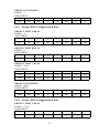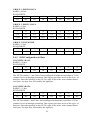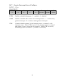
1
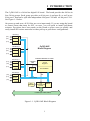
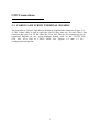
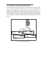
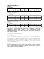
®
Digital I/O
CYDIO 96P
Multi-Channel Digital I/O Board
96-Channel, TTL-Level PCI Board
with 100-Pin Connection
USER’S MANUAL
VER. 2 • NOV 2000
&
No part of this manual may be reproduced without permission.
CyberResearch®, Inc.
www.cyberresearch.com
25 Business Park Dr., Branford, CT 06405 USA
203-483-8815 (9am to 5pm EST) FAX: 203-483-9024
©Copyright 2003
All Rights Reserved.
November 2000
The information in this document is subject to change without prior notice in order
to improve reliability, design, and function and does not represent a commitment
on the part of CyberResearch, Inc.
In no event will CyberResearch, Inc. be liable for direct, indirect, special,
incidental, or consequential damages arising out of the use of or inability to use
the product or documentation, even if advised of the possibility of such damages.
This document contains proprietary information protected by copyright. All rights
are reserved. No part of this manual may be reproduced by any mechanical,
electronic, or other means in any form without prior written permission of
CyberResearch, Inc.
TRADEMARKS
“CyberResearch,” and “CYDIO 96P,” are trademarks of CyberResearch, Inc. Other
product names mentioned herein are used for identification purposes only and
may be trademarks and/or registered trademarks of their respective companies.
• NOTICE •
CyberResearch, Inc. does not authorize any CyberResearch product for use in life
support systems, medical equipment, and/or medical devices without the written
approval of the President of CyberResearch, Inc. Life support devices and
systems are devices or systems which are intended for surgical implantation into
the body, or to support or sustain life and whose failure to perform can be
reasonably expected to result in injury. Other medical equipment includes devices
used for monitoring, data acquisition, modification, or notification purposes in
relation to life support, life sustaining, or vital statistic recording. CyberResearch
products are not designed with the components required, are not subject to
the testing required, and are not submitted to the certification required to ensure
a level of reliability appropriate for the treatment and diagnosis of humans.
TABLE OF CONTENTS
1 INTRODUCTION . . . . . . . . . . . . . . . . . . . . . . . . . . . . . . . . . . . . . . . . . . . . . . 1
2 INSTALLATION . . . . . . . . . . . . . . . . . . . . . . . . . . . . . . . . . . . . . . . . . . . . . . . 2
3 I/O CONNECTIONS . . . . . . . . . . . . . . . . . . . . . . . . . . . . . . . . . . . . . . . . . . . 3
3.1 CABLES AND SCREW TERMINAL BOARDS . . . . . . . . . . . . . 3
3.2 CONNECTOR DIAGRAM . . . . . . . . . . . . . . . . . . . . . . . . . . . . . . . . . . 4
3.3 SIGNAL CONNECTION CONSIDERATIONS . . . . . . . . . . . . . . 5
3.4 CYERB 24 & CYSSR 24 CONNECTIONS . . . . . . . . . . . . . .
8
4 SOFTWARE . . . . . . . . . . . . . . . . . . . . . . . . . . . . . . . . . . . . . . . . . . . . . . . . . . . . 9
4.1 UNIVERSAL LIBRARY . . . . . . . . . . . . . . . . . . . . . . . . . . . . . . . . . . . . 9
4.2 PACKAGED APPLICATION PROGRAMS . . . . . . . . . . . . . . . . . 9
5 REGISTER MAPS . . . . . . . . . . . . . . . . . . . . . . . . . . . . . . . . . . . . . . . . . . . . . 10
5.1 BADR0 . . . . . . . . . . . . . . . . . . . . . . . . . . . . . . . . . . . . . . . . . . . . . . . . . . . . 10
5.2 BADR1 . . . . . . . . . . . . . . . . . . . . . . . . . . . . . . . . . . . . . . . . . . . . . . . . . . . . 10
5.2.1 INTCSR Configure . . . . . . . . . . . . . . . . . . . . . . . . . . . . . . . . . . . . 10
5.3 BADR2 . . . . . . . . . . . . . . . . . . . . . . . . . . . . . . . . . . . . . . . . . . . . . . . . . . . . 11
5.4 BADR3 . . . . . . . . . . . . . . . . . . . . . . . . . . . . . . . . . . . . . . . . . . . . . . . . . . . . 12
5.4.1 Group 0 8255 Configuration & Data . . . . . . . . . . . . . . . . . . . 12
5.4.2 Group 1 8255 Configuration & Data . . . . . . . . . . . . . . . . . . . 14
5.4.3 Group 2 8255 Configuration & Data . . . . . . . . . . . . . . . . . . . 15
5.4.4 Group 3 8255 Configuration & Data . . . . . . . . . . . . . . . . . . . 15
5.4.5 8254 Configuration & Data . . . . . . . . . . . . . . . . . . . . . . . . . . . . 16
5.4.6 8255 Interrupt Source Configure . . . . . . . . . . . . . . . . . . . . . . . 17
5.4.7 Counter Interrupt Source Configure . . . . . . . . . . . . . . . . . . . . 18
6 SPECIFICATIONS . . . . . . . . . . . . . . . . . . . . . . . . . . . . . . . . . . . . . . . . . . . . 19
7 ELECTRONICS AND INTERFACING . . . . . . . . . . . . . . . . . . . . . . . 21
7.1 PULL UP & PULL DOWN RESISTORS . . . . . . . . . . . . . . . . . . . 21
7.2 TTL TO SOLID STATE RELAYS . . . . . . . . . . . . . . . . . . . . . . . . . . 22
7.3 VOLTAGE DIVIDERS . . . . . . . . . . . . . . . . . . . . . . . . . . . . . . . . . . . . . 23
This page is blank.
1 INTRODUCTION
The CyDIO 96P is a 96-bit line digital I/O board. The board provides the 96 bits in
four 24-bit groups. Each group provides an 8-bit port A and port B, as well as an
8-bit port C that can be split into independent 4-bit port C-HI and a 4-bit port C-LO.
See Figure 1-1 below.
On power up and reset, all I/O bits are set to input mode. If you are using the board
to control items that must be OFF on reset, you will need to install pull-down
resistors. Provisions have been made on the board to allow users to quickly and
easily install SIP resistor networks in either pull-up or pull-down configurations.
Port A
(7:0)
Port B
(7:0)
Port C
Control
DIO Group 3
(7:0)
82C55
CyDIO 96P
Block Diagram
(7:0)
Port A
(7:0)
Port B
(7:0)
Port C
Control
DIO Group 2
82C55
CONTROLLER FPGA and LOGIC
(7:0)
Port A
(7:0)
Port B
(7:0)
Port C
Control
DIO Group 1
CONTROL
BUS
COUNTERS
82C54
82C55
Control
Registers
Decode/Status
DIO Group 0
Port A
(7:0)
Port B
(7:0)
Port C
82C55
INT.
Control
(7:0)
LOCAL BUS
Boot
EEPROM
PCI
CONTROLLER BADR3
PLX-9052
PCI BUS (5V, 32-BIT, 33MHZ)
Figure 1-1. CyDIO 96P Block Diagram
1
This page is blank.
2 INSTALLATION
The CyDIO 96P boards are completely plug-and-play. There are no switches or
jumpers on the board. All board addresses are set by your computer’s plug-and-play
software.
InstaCal is the installation, calibration and test software supplied with your data
acquisition / IO hardware. Refer to the Extended Software Installation Manual to
install InstaCal.
If you need it, there is some on-line help in the InstaCal program.
Owners of the Universal Library should read the manual and examine the example
programs prior to attempting any programming tasks.
2
This page is blank.
3 I/O Connections
3.1 CABLES AND SCREW TERMINAL BOARDS
The board has a 100-pin, high-density Robinson-Nugent male connector (Figure 3-1).
A CBL 100xx cable is used to split the 100 I/O lines into two, 50-wire cables. One
connector has pins 1 to 50, the other has 51 to 100. The two I/O connectors can be
connected directly to two screw-terminal boards such as the CYSTP 50E,
STA 100, STA 50H or CYSTP 502E. See Figures 3-2 and 3-3 for
configuration and pin out.
3
3.2 CONNECTOR DIAGRAM
The CyDIO 96P I/O connector is a 100-pin type connector accessible from the rear of
the PC at the expansion backplate See Figure 3-1 below for the board pin out.
Port A7 B
Port A6 B
Port A5 B
Port A4 B
Port A3 B
Port A2 B
Port A1 B
Port A0 B
Port B7 B
Port B6 B
Port B5 B
Port B4 B
Port B3 B
DIO
Group 1 Port B2 B
Port B1 B
Port B0 B
Port C7 B
Port C6 B
Port C5 B
Port C4 B
Port C3 B
Port C2 B
Port C1 B
Port C0 B
Port A7 A
Port A6 A
Port A5 A
Port A4 A
Port A3 A
Port A2 A
Port A1 A
Port A0 A
Port B7 A
Port B6 A
Port B5 A
DIO
Group 0 Port B4 A
Port B3 A
Port B2 A
Port B1 A
Port B0 A
Port C7 A
Port C6 A
Port C5 A
Port C4 A
Port C3 A
Port C2 A
Port C1 A
Port C0 A
+5V
GND
51
52
53
54
55
56
57
58
59
60
61
62
63
64
65
66
67
68
69
70
71
72
73
74
75
76
77
78
79
80
81
82
83
84
85
86
87
88
89
90
91
92
93
94
95
96
97
98
99
100
1
2
3
4
5
6
7
8
9
10
11
12
13
14
15
16
17
18
19
20
21
22
23
24
25
26
27
28
29
30
31
32
33
34
35
36
37
38
39
40
41
42
43
44
45
46
47
48
49
50
Port A7 D
Port A6 D
Port A5 D
Port A4 D
Port A3 D
Port A2 D
Port A1 D
Port A0 D
Port B7 D
Port B6 D
Port B5 D
Port B4 D
Port B3 D
Port B2 D
Port B1 D
Port B0 D
Port C7 D
Port C6 D
Port C5 D
Port C4 D
Port C3 D
Port C2 D
Port C1 D
Port C0 D
Port A7 C
Port A6 C
Port A5 C
Port A4 C
Port A3 C
Port A2 C
Port A1 C
Port A0 C
Port B7 C
Port B6 C
Port B5 C
Port B4 C
Port B3 C
Port B2 C
Port B1 C
Port B0 C
Port C7 C
Port C6 C
Port C5 C
Port C4 C
Port C3 C
Port C2 C
Port C1 C
Port C0 C
+5V
GND
DIO
Group 3
DIO
Group 2
Figure 3-1. CyDIO 96P 100-Pin Connector Pin Out
4
BOARD’S
100-PIN I/O
CONNECTOR
CBL 100xx
CABLE
I/O PINS 1 TO 50
SIGNAL
CONDITIONING or
50-PIN SCREW
TERMINAL BOARD.
I/O PINS 51 TO 100
SIGNAL CONDITIONING OR
50-PIN SCREW TERMINAL BOARD
Figure 3-2. Cable CBL 100xx Configuration
5
DIO
Group 3
DIO
Group 2
Port A6 D
Port A4 D
Port A2 D
Port A0 D
Port B6 D
Port B4 D
Port B2 D
Port B0 D
Port C6 D
Port C4 D
Port C2 D
Port C0 D
Port A6 C
Port A4 C
Port A2 C
Port A0 C
Port B6 C
Port B4 C
Port B2 C
Port B0 C
Port C6 C
Port C4 C
Port C2 C
Port C0 C
Ground
2
4
6
8
10
12
14
16
18
20
22
24
26
28
30
32
34
36
38
40
42
44
46
48
50
1
3
5
7
9
11
13
15
17
19
21
23
25
27
29
31
33
35
37
39
41
43
45
47
49
Port A7 D
Port A5 D
Port A3 D
Port A1 D
Port B7 D
Port B5 D
Port B3 D
Port B1 D
Port C7 D
Port C5 D
Port C3 D
Port C1 D
Port A7 C
Port A5 C
Port A3 C
Port A1 C
Port B7 C
Port B5 C
Port B3 C
Port B1 C
Port C7 C
Port C5 C
Port C3 C
Port C1 C
+5V
DIO
Group 3
DIO
Group 2
2nd of 2
CBL 100xx
50-Pin Connectors
From board pins 51 to 100
(1st connector is pin 1 to 1, etc.,
DIO Groups 0 and 1)
51
52
53
54
55
56
57
58
59
60
61
62
63
64
65
66
67
68
69
70
71
72
73
74
75
76
77
78
79
80
81
82
83
84
85
86
87
88
89
90
91
92
93
94
95
96
97
98
99
100
Port A7 D
Port A6 D
Port A5 D
Port A4 D
Port A3 D
Port A2 D
Port A1 D
Port A0 D
Port B7 D
Port B6 D
Port B5 D
Port B4 D
Port B3 D
Port B2 D
Port B1 D
Port B0 D
Port C7 D
Port C6 D
Port C5 D
Port C4 D
Port C3 D
Port C2 D
Port C1 D
Port C0 D
Port A7 C
Port A6 C
Port A5 C
Port A4 C
Port A3 C
Port A2 C
Port A1 C
Port A0 C
Port B7 C
Port B6 C
Port B5 C
Port B4 C
Port B3 C
Port B2 C
Port B1 C
Port B0 C
Port C7 C
Port C6 C
Port C5 C
Port C4 C
Port C3 C
Port C2 C
Port C1 C
Port C0 C
+5V
GND
Pins 51- 100 of 100-Pin Conn.
Figure 3-3. Pin Translation - Pins 51 to 100 DI/O Signals
6
3.3 SIGNAL CONNECTION CONSIDERATIONS
All the digital inputs on the CyDIO 96P are 8255 CMOS TTL. The CyDIO 96P
output signals are 8255 CMOS.
CyberResearch, Inc. offers a wide variety of digital signal conditioning
products that provide an ideal interface between high voltage and/or high current
signals and the CyDIO 96P. If you need control or monitor non-TTL level signals
with your board, please refer to our catalog or our web site for the following
products:
CYERB series, electromechanical relay output boards
CYERB "S" series, 10A electromechanical relay output boards
CYSSR series solid state relay I/O module racks
A description of digital interfacing is in the Interface Electronics section.
IMPORTANT NOTE
The 82C55 digital I/O chip initializes all ports as inputs on powerup and reset. A TTL input is a high impedance input. If you
connect another TTL input device to the 82C55 it could be turned
ON or OFF every time the 82C55 is reset.
Remember, the 82C55 is reset to the INPUT mode.
There are positions for pull-up and pull-down resistor packs on your CyDIO 96P
board. To implement these, please refer to section 7.1.
7
3.4 CYERB 24 & CYSSR 24 CONNECTIONS
CyDIO 96P boards provide digital I/O in two major groups of 48 bits each (96 total,
but each side of the CBL 100xx cable provides 48 bits). However, many popular
relay and SSR boards provide only 24-bits of I/O. The CYERB 24 and
CYSSR 24 each implements a connector scheme where all 96 bits of the
CyDIO 96P board may be used to control relays and/or SSRs. This configuration is
shown in Figure 3-4 below. The 24-bits of digital I/O on CyDIO 96P connector pins
1-24 (base address +0 through +3) control the first relay board. The 24-bits on pins
25-50 will control the second relay/SSR board on the daisy chain and so on up to
100 pins.
CyDIO
96P
CBL 100xx
CYERB 24
or
CYSSR 24
IN
IN
or
CYSSR 24
CYERB 24
or
CYSSR 24
OUT
IN
CYERB 24
or
CYSSR 24
OUT
CYERB 24
Figure 3-4. Relay Rack Cabling
8
OUT
IN
OUT
4 SOFTWARE
We highly recommend that users take advantage of our Universal Library package's
easy-to-use programming interfaces. However, if you are an experienced
programmer, and wish to read and write directly to the board, we have provided a
detailed register map in the next chapter.
4.1 UNIVERSAL LIBRARY
The Universal Library provides complete access to the CyDIO 96P functions from a
range of programming languages. If you are planning to write programs, or would
like to run the example programs for Visual Basic or any other language, please turn
now to the Universal Library manual.
4.2 PACKAGED APPLICATION PROGRAMS
Most packaged application programs, such as SoftWIRE, DAS Wizard and HP-VEE
have drivers for the CyDIO 96P. If the package you own does not appear to have
drivers for the boards, please fax or e-mail the package name and the revision
number from the install disks. We will research the package for you and advise how
to utilize the CyDIO 96P boards with the driver available.
Some application drivers are included with the Universal Library package, but not
with the application package. If you have purchased an application package directly
from the software vendor, you may need to purchase our Universal Library and
drivers. Please contact us for more information on this topic.
9
This page is blank.
5 REGISTER MAPS
The PCI Controller, a PLX-9052, has four configuration, control, and status registers
(Table 5-1). They are described in the following section.
I/O Region
BADR0
BADR1
BADR2
BADR3
Table 5-1. I/O Region Register Operations
Function
Operations
PCI memory-mapped configuration
32-bit double word
registers
PCI I/O-mapped config. registers
32-bit double word
N/A
N/A
Digital I/O registers
8-bit byte
5.1 BADR0
BADR0 is reserved for the PLX-9052 configuration registers. There is no reason to
access this region of I/O space.
5.2 BADR1
BADR1 is a 32 bit register for control and configuration of interrupts.
5.2.1 INTCSR Configure
BADR1 +4C hex
32:15 14
13
X
X
X
READ/WRITE
7
6
X
PCINT
12
11
10
9
8
ISAMD
X
INTCLR
X
LEVEL/EDGE
5
4
3
2
1
0
X
X
X
INT
INTPOL
INTE
Note: For applications requiring edge triggered interrupts (LEVEL/EDGE bit 8 = 1),
the user must configure the INTPOL bit for active high polarity (bit 1=1).
The INTCSR (Interrupt Control/Status Register) controls the interrupt features of the
PLX-9052 controller. As with all of the PLX-9052 registers, it is 32-bits in length.
Since the rest of the register have specific control functions, those bits must be
masked off in order to access the specific interrupt control functions listed below.
10
INTE
Interrupt enable (local):
0 = disabled, 1 = enabled (default)
INTPOL
Interrupt polarity:
0 = active low (default), 1 = active high
INT
Interrupt status:
0 = interrupt not active, 1 = interrupt active
PCINT
PCI interrupt enable:
0 = disabled (default), 1 = enabled
LEVEL/EDGE
Interrupt trigger control:
0 = level triggered mode (default), 1 = edge triggered mode
INTCLR
Interrupt clear (edge triggered mode only):
0 = N/A, 1 = clear interrupt
ISAMD
ISA mode enable control (must be set to 1)
0 = ISA mode disabled, 1 = ISA mode enabled (default)
5.3 BADR2
BADR2 is not used.
11
5.4 BADR3
BADR3 is an 8-bit data bus for reading, writing and control of the individual 82C55
chips and the 82C54. Refer to Table 5-2 for register offsets.
REGISTER
BADR3 + 0
BADR3 + 1
BADR3 + 2
BADR3 + 3
BADR3 + 4
BADR3 + 5
BADR3 + 6
BADR3 + 7
BADR3 + 8
BADR3 + 9
BADR3 + A
BADR3 + B
BADR3 + C
BADR3 + D
BADR3 + E
BADR3 + F
BADR3 + 10h
BADR3 + 11h
BADR3 + 12h
BADR3 + 13h
BADR3 + 14h
BADR3 + 15h
Table 5-2. BADR3 Registers
READ FUNCTION
WRITE FUNCTION
Group 0 Port A Data
Group 0 Port A Data
Group 0 Port B Data
Group 0 Port B Data
Group 0 Port C Data
Group 0 Port Data
Group 0 Configure
Group 0 Configure
Group 1 Port A Data
Group 1 Port A Data
Group 1 Port B Data
Group 1 Port B Data
Group 1 Port C Data
Group 1 Port C Data
Group 1 Configure
Group 1 Configure
Group 2 Port A Data
Group 2 Port A Data
Group 2 Port B Data
Group 2 Port B Data
Group 2 Port C Data
Group 2 Port C Data
Group 2 Configure
Group 2 Configure
Group 3 Port A Data
Group 3 Port A Data
Group 3 Port B Data
Group 3 Port B Data
Group 3 Port C Data
Group 3 Port C Data
Group 3 Configure
Group 3 Configure
Counter 1
Counter 1
Counter 2
Counter 2
N/A
N/A
Counter Configuration
Counter Configure
Interrupt Control 1
Interrupt Control 1
Interrupt Control 2
Interrupt Control 2
The 82C55 may be programmed to operate in Input/Ouput (mode 0), Strobed
Input/Ouput (mode 1) or Bi-Directional Bus (mode 2). The following information
describes mode 0 operation. Users needing information regarding other modes of
operation should refer to an Intel or Intersil 82C55 data sheet.
Upon power-up, an 82C55 is reset and defaults to the input mode. No further
programming is needed to use the 24 lines of an 82C55 as TTL inputs.
5.4.1 Group 0 8255 Configuration & Data
GROUP 0, PORT A DATA
BADR3 + 0
READ/WRITE
7
6
5
D7
D6
D5
4
3
2
1
0
D4
D3
D2
D1
D0
12
GROUP 0, PORT B DATA
BADR3 + 1
READ/WRITE
7
6
5
D7
D6
D5
GROUP 0, PORT C DATA
BADR3 + 2
READ/WRITE
7
6
5
4
3
2
1
0
D4
D3
D2
D1
D0
4
3
2
1
0
C8
C7
C6
C5
C4
C3
C2
C1
CH4
CH3
CH2
CH1
CL4
CL3
CL2
CL1
4
3
2
1
0
A
CH
M1
B
CL
GROUP 0 CONFIGURE
BADR3 + 3
READ/WRITE
7
6
5
MS
M3
M2
This register is used to configure the Group 0 ports as either input or output, and
configures the operating mode to mode 0, 1 or 2. The following describes
configuration for mode 0. See the Intel or Harris 8255 data sheets for information on
other modes of operation
8255 MODE 0 CONFIGURATION
1. Output Ports
In mode 0 configuration, 82C55 ports can be configured as outputs, holding the data
written to them. For example, to set all three ports (A, B, & C) of Group 0 to output
mode, write the value 80 hex to BADR3 + 3 (refer to Table 5-3 below). The user is
then able to read the current state of the output port by simply reading the address
corresponding to that port.
2. Input Ports
In mode 0 configuration, the 82C55 ports can be configured as inputs, reading the
state of the inputs lines. For example, to set all of the ports of Group 0 to the input
mode, write the value 9B hex to BADR3 + 3.
13
D4
0
0
0
0
0
0
0
0
1
1
1
1
1
1
1
1
Table 5-3. DIO Port Configurations/Per Group
Programming Codes
Values
D3
D1
D0
Hex
Dec
A
B
CU
0
0
0
80
128
OUT OUT OUT
0
0
1
81
129
OUT OUT OUT
0
1
0
82
130
OUT
IN
OUT
0
1
1
83
131
OUT
IN
OUT
1
0
0
88
136
OUT OUT
IN
1
0
1
89
137
OUT OUT
IN
1
1
0
8A
138
OUT
IN
IN
1
1
1
8B
139
OUT
IN
IN
0
0
0
90
144
IN
OUT OUT
0
0
1
91
145
IN
OUT OUT
0
1
0
92
146
IN
IN
OUT
0
1
1
93
147
IN
IN
OUT
1
0
0
98
152
IN
OUT
IN
1
0
1
99
153
IN
OUT
IN
1
1
0
9A
154
IN
IN
IN
1
1
1
9B
155
IN
IN
IN
CL
OUT
IN
OUT
IN
OUT
IN
OUT
IN
OUT
IN
OUT
IN
OUT
IN
OUT
IN
Notes: ‘CU’ is PORT C upper nibble, ‘CL’ is PORT C lower nibble.
5.4.2 Group 1 8255 Configuration & Data
GROUP 1, PORT A DATA
BADR3 + 4
READ/WRITE
7
6
5
D7
D6
D5
GROUP 1, PORT B DATA
BADR3 + 5
READ/WRITE
7
6
5
D7
D6
D5
GROUP 1, PORT C DATA
BADR3 + 6
READ/WRITE
7
6
5
4
3
2
1
0
D4
D3
D2
D1
D0
4
3
2
1
0
D4
D3
D2
D1
D0
4
3
2
1
0
C8
C7
C6
C5
C4
C3
C2
C1
CH4
CH3
CH2
CH1
CL4
CL3
CL2
CL1
14
GROUP 1 CONFIGURE
BADR3 + 7
READ/WRITE
7
6
5
MS
M3
M2
4
3
2
1
0
A
CH
M1
B
CL
5.4.3 Group 2 8255 Configuration & Data
GROUP 2, PORT A DATA
BADR3 + 8
READ/WRITE
7
6
5
D7
D6
D5
GROUP 2, PORT B DATA
BADR3 + 9
READ/WRITE
7
6
5
D7
D6
D5
GROUP 2, PORT C DATA
BADR3 + A hex
READ/WRITE
7
6
5
4
3
2
1
0
D4
D3
D2
D1
D0
4
3
2
1
0
D4
D3
D2
D1
D0
4
3
2
1
0
C8
C7
C6
C5
C4
C3
C2
C1
CH4
CH3
CH2
CH1
CL4
CL3
CL2
CL1
4
3
2
1
0
A
CH
M1
B
CL
GROUP 2 CONFIGURE
BADR3 + B hex
READ/WRITE
7
6
5
MS
M3
M2
5.4.4 Group 3 8255 Configuration & Data
GROUP 3, PORT A DATA
BADR3 + C hex
READ/WRITE
7
6
5
D7
D6
D5
4
3
2
1
0
D4
D3
D2
D1
D0
15
GROUP 3, PORT B DATA
BADR3 + D hex
READ/WRITE
7
6
5
D7
D6
D5
GROUP 3, PORT C DATA
BADR3 + E hex
READ/WRITE
7
6
5
4
3
2
1
0
D4
D3
D2
D1
D0
4
3
2
1
0
C8
C7
C6
C5
C4
C3
C2
C1
CH4
CH3
CH2
CH1
CL4
CL3
CL2
CL1
4
3
2
1
0
A
CH
M1
B
CL
GROUP 3 CONFIGURE
BADR3 + F hex
READ/WRITE
7
6
5
MS
M3
M2
5.4.5 8254 Configuration & Data
COUNTER 1 DATA
BADR3 + 10 hex
READ/WRITE
7
6
D7
D6
5
4
3
2
1
0
D5
D4
D3
D2
D1
D0
The 82C54 counters 1 and 2 have been configured in hardware to produce a 32-bit
counter for use in interrupt generation. This register provides access to the lower 16
data bits. Since the interface to the 82C54 is only 8-bits wide, write counter data in
two bytes; low byte first, followed by the high byte.
COUNTER 2 DATA
BADR3 + 11 hex
READ/WRITE
7
6
D7
D6
5
4
3
2
1
0
D5
D4
D3
D2
D1
D0
The 82C54 counters 1 and 2 have been configured in hardware to produce a 32-bit
counter for use in interrupt generation. This register provides access to the upper 16
data bits. Since the interface to the 82C54 is only 8-bits wide, write counter data in
two bytes; low byte first, followed by the high byte.
16
COUNTER CONFIGURATION
BADR3 + 13 hex
READ/WRITE
7
6
5
D7
D6
D5
4
3
2
1
0
D4
D3
D2
D1
D0
This register is used to set the operating modes of each of the 82C54’s counters.
Configure the counters by writing mode information to the Configure register,
followed by the count information written to the specific counter (data) registers.
Refer to the Celeritous 82C54 data sheets for more detailed information.
5.4.6 8255 Interrupt Source Configure
BADR3 + 14 hex
READ/WRITE
7
6
DIRQ1
DIRQ0
5
4
3
2
1
0
CIRQ1
CIRQ0
BIRQ1
BIRQ0
AIRQ1
AIRQ0
DIRQ1
When this bit is set, the 8255 in Group 3 will generate an interrupt on
INTRB if INTEN in BASE +15 hex is also set.
DIRQ0
When this bit is set, the 8255 in Group 3 will generate an interrupt on
INTRA if INTEN in BASE +15 hex is also set.
CIRQ1
When this bit is set, the 8255 in Group 2 will generate an interrupt on
INTRB if INTEN in BASE +15 hex is also set.
CIRQ0
When this bit is set, the 8255 in Group 2 will generate an interrupt on
INTRA if INTEN in BASE +15 hex is also set.
BIRQ1
When this bit is set, the 8255 in Group 1 will generate an interrupt on
INTRB if INTEN in BASE +15 hex is also set.
BIRQ0
When this bit is set, the 8255 in Group 1 will generate an interrupt on
INTRA if INTEN in BASE +15 hex is also set.
AIRQ1
When this bit is set, the 8255 in Group 0 will generate an interrupt on
INTRB if INTEN in BASE +15 hex is also set.
AIRQ0
When this bit is set, the 8255 in Group 0 will generate an interrupt on
INTRA if INTEN in BASE +15 hex is also set.
17
5.4.7 Counter Interrupt Source Configure
BADR3 + 15 hex
READ/WRITE
7
6
X
X
5
4
3
2
1
0
X
X
X
INTEN
CTRIR
CTR1
INTEN
Enables or disabled interrupts. 1 = enabled, 0 = disabled
CTRIR
Enables or disables the counters as an interrupt source. 1 = counters may
generate interrupts. 0 = counters cannot generate interrupts.
CTR1
Controls whether counter 2 is the interrupt source, or counter 1 is the
interrupt source. When CTR1 is set to 1, the interrupt source is counter 2
and counter 1 acts as a prescaler for counter 2. When CTR1 is set to 0,
the interrupt source is counter 1. (Counter 3 is not used.)
18
This page is blank.
6 SPECIFICATIONS
Power Consumption
+5V
150 mA max
Digital Input / Output
Digital Type
Number of I/O
Configuration per 82C55
Output High
Output Low
Input High
Input Low
Power-up / reset state
Pull-Up/Pull-Down Resistors
Four 82C55
96
• 2 banks of 8 and 2 banks of 4, or
• 3 banks of 8, or
2 banks of 8 with handshake
3.0 volts min @ −2.5mA
0.4 volts max @ 2.5mA
2.0 volts min, 5.5 volts absolute max
0.8 volts max, −0.5 volts absolute min
Input mode (high impedance)
User installed. Dual footprint allows pull-up
or pull-down configuration
Counter Section
Counter type
Configuration
Counter 1
Counter 2
Counter 3 - Not used
82C54
3 counters, 16 bits each
Source: 2 MHz (crystal osc./8)
Gate:
Tied to +5V
Output: Selectable Interrupt source
Source: Counter 1 OUT
Gate:
Tied to +5V
Output: Selectable Interrupt source
Source:
Gate
Output:
19
Interrupts
The interrupt control registers function with the four 82C55 devices and the
82C54 counter timer to provide interrupt sources.
Interrupt
PCI Interrupt enable
Interrupt polarity
INTA# - mapped to IRQn via PCI BIOS at boot-time
Programmable through PLX9052 INTCSR
High or low level. Programmable through PLX9052
Rising / falling edge. Programmable through PLX-9052
1. 82C55 in Mode 1 or Mode 2 Interrupt configuration:
• First Port C0
• First Port C3
• Second Port C0
• Second Port C3
• Third Port C0
• Third Port C3
• Fourth Port C0
• Fourth Port C3
Note: Any interrupt source above can be individually
enabled.
2. 82C54 Counter
• Counter 1 OUT
• Counter 2 OUT
Note: Counters 1 and 2 interrupts are exclusive. Only
one counter can be enabled as an interrupt source at any
given time.
Interrupt sources
Crystal Oscillator
Oscillator type
Frequency
Frequency stability
AT-cut crystal
16 MHz
±100 ppm
Environmental
Operating temperature range
Storage temperature range
Humidity
0 to 70°C
−40 to 70°C
0 to 95% non-condensing
Mechanical
Card dimensions
PCI short card: 136.0mm(L) x 100.6mm(W) x11.00mm(H)
20
7 ELECTRONICS AND INTERFACING
This brief introduction to the electronics most often needed by digital I/O board users
covers a few key concepts.
IMPORTANT NOTE
WHENEVER AN 82C55 IS POWERED-ON OR RESET, ALL
PINS ARE SET TO HIGH-IMPEDANCE INPUT. FOLLOWING
STANDARD TTL FUNCTIONALITY, THESE INPUTS WILL
TYPICALLY FLOAT HIGH, AND MAY HAVE ENOUGH
DRIVE CURRENT TO TURN ON EXTERNAL DEVICES.
The implications of this is that if you have output devices such as solid state relays,
they may be switched on whenever the computer is powered on or reset. To prevent
unwanted switching and to drive all outputs to a known state after power on or reset,
pull all pins either high or low through a 2.2 K resistor.
7.1 PULL UP & PULL DOWN RESISTORS
Whenever the board is powered on or reset, the control register is set to a known
state. That state is all ports go to the input state.
The nature of the input means it will typically float high. However, depending on the
drive requirements of the device you are driving, they may float up or down. Which
way they float is dependent on the characteristics of the circuit and the electrical
environment; and may be unpredictable. This is why it often appears that the board
outputs have gone 'high' after power up. The result is that the controlled device gets
turned on. That is why you need pull up/down resistors.
Shown in Figure 7-1 is an 82C55 digital
output with a pull-up resistor attached.
The pull-up resistor provides a reference
to +5V. The value of 2.2K ohms requires
only 2.3 mA of drive current.
If the board is reset and enters high
impedance input, the line is pulled high.
At that point, both the board AND the
device being controlled will sense a high
signal
Figure 7-1. Pull-up Resistor
.
21
If the board is in output mode, the board has enough power to override the
pull-up/down resistor's high signal and drive the line to 0 volts. If the output circuit
asserts a high signal, the pull-up resistor guaranties that the line goes to +5 V.
Of course, a pull-down resistor accomplishes the same task except that the line is
pulled low when the board is reset. The board has enough power to drive the line
high.
The CyDIO 96P series boards are equipped with positions for pull-up/down resistors
Single Inline Packages (SIPs). The positions, marked PORT#A, B and C, are located
adjacent to the I/O connectors.
A 2.2K, 8-resistor SIP is made of eight 2.2K resistors all connected with one side to a
single common point, the other side of each to a pin protruding from the SIP. The
common line to which all resistors are connected also protrudes from the SIP. The
common line is marked with a dot and is at one end of the SIP.
The SIP may be installed as pull-up or pull-down. At each location, PORT#A, B &
C on the CyDIO 96P series boards, there are 10 holes in a line. One end of the line is
+5V, the other end is GND. They are marked HI and LO respectively. The eight
holes in the middle are connected to the eight lines of a port 1 through 4, A, B, or C.
A resistor value of 2.2K is recommended.
calculated the necessity of doing so.
Use other values only if you have
UNCONNECTED INPUTS FLOAT
Keep in mind that unconnected inputs float (typically, but not reliably, high). If you
are using the CyDIO 96P board for input, and have unconnected inputs, ignore the
data from those lines.
You do not have to tie input lines, and unconnected lines will not affect the
performance of connected lines. Just make sure that you mask out any unconnected
bits in software!
7.2 TTL TO SOLID STATE RELAYS
Many applications require digital outputs to switch AC and DC voltage motors on
and off, or to monitor AC and DC voltages. These AC and high DC voltages cannot
be controlled or read directly by the TTL digital lines of a CyDIO 96P.
Solid State Relays, such as those available from CyberResearch, Inc.
allow control and monitoring of AC and high DC voltages and provide up to
4000VAC isolation. Solid State Relays (SSRs) are the recommended method of
interfacing to AC and high DC signals.
22
The most convenient way to use solid state relays and a CyDIO 96P board is to use a
Solid State Relay Rack. An SSR Rack is a circuit board with input buffer amplifiers
that are powerful enough to switch the SSRs. The buffer amplifiers and SSRs are
socketed.
The standard buffer amplifiers are inverting types, meaning that a low input from a
DIO 82C55 outputs a high to the SSR which turns it on (“closes” the SSR output). If
desired, non-inverting amplifiers can be specified.
7.3 VOLTAGE DIVIDERS
If you wish to measure a signal that varies over a range greater than the input range
of a digital input, use a voltage divider to drop the voltage of the input signal to the
level the digital input can measure.
Ohm's law states:
Voltage = Current * Resistance
Thus, any variation in the voltage drop for the circuit as a whole will have a
proportional variation in all the voltage drops in the circuit.
Signal
High
In a voltage divider, the voltage
across one of the resistors in a
circuit is proportional to the
voltage across the total resistance
in the circuit (Figure 7-2).
R1
R2
Signal
Low
V2
Vout
Ground
SIMPLE VOLTAGE DIVIDER - Vin = R1+R2
Vout
R2
The formula for voltage attenuation is:
2 = 10K+10K
10K
Board
Input
Signal
Volts Vin
When designing a voltage divider,
choose two resistors with the
proper proportions relative to the
full scale of the digital input and
the maximum signal voltage.
Attenuation = R1+R2
R2
V1
Figure 7-2. Voltage Divider
The variable Attenuation is the
proportional difference between the
signal voltage max and the full scale of
the analog input.
For example, if the signal varies
between 0 and 10 volts, and you wish to
measure that with a CyDIO 96P board
23
with a full scale range of 0 to 5 volts,
the Attenuation is 2:1, or just 2.
R1=(A-1)*R2
For a given attenuation, pick a handy
resistor and call it R2, then use this
formula to calculate R1.
Digital inputs can readily use voltage dividers. For example, if you wish to measure a
digital signal that is at 0 volts when off and 24 volts when on, you cannot connect
that directly to the CyDIO 96P digital inputs. The voltage must be dropped to 5 volts
max when on. The Attenuation is 24:5 or 4.8. Use the equation above to find an
appropriate R1 if R2 is 1K. Remember that a TTL input is 'on' when the input
voltage is greater than 2.5 volts.
IMPORTANT NOTE
The resistors, R1 and R2, are going to dissipate all the power in
the divider circuit according to the equation Current = Voltage /
Resistance. The higher the value of the resistance (R1 + R2) the
less power dissipated by the divider circuit. Here is a simple rule:
For attenuation of 5:1 or less, no resistor should be < 10K.
For attenuation of greater than 5:1, no resistor should be < 1K.
24
EC Declaration of Conformity
We, the manufacturer, declare under sole responsibility that the
product:
CyDIO 96P
Part Number
Digital I/O board
Description
to which this declaration relates, meets the essential requirements, is in conformity
with, and CE marking has been applied according to the relevant EC Directives listed
below using the relevant section of the following EC standards and other normative
documents:
EU EMC Directive 89/336/EEC: Essential requirements relating to electromagnetic
compatibility.
EU 55022 Class B: Limits and methods of measurements of radio interference
characteristics of information technology equipment.
EN 50082-1: EC generic immunity requirements.
IEC 801-2: Electrostatic discharge requirements for industrial process measurement
and control equipment.
IEC 801-3: Radiated electromagnetic field requirements for industrial process
measurements and control equipment.
IEC 801-4: Electrically fast transients for industrial process measurement and control
equipment.
For Your Notes
Product Service
Diagnosis and Debug
CyberResearch, Inc. maintains technical support lines staffed by experienced
Applications Engineers and Technicians. There is no charge to call and we will
return your call promptly if it is received while our lines are busy. Most problems
encountered with data acquisition products can be solved over the phone. Signal
connections and programming are the two most common sources of difficulty.
CyberResearch support personnel can help you solve these problems, especially if
you are prepared for the call.
To ensure your call’s overall success and expediency:
1) Have the phone close to the PC so you can conveniently and quickly take action
that the Applications Engineer might suggest.
2) Be prepared to open your PC, remove boards, report back-switch or jumper
settings, and possibly change settings before reinstalling the modules.
3) Have a volt meter handy to take measurements of the signals you are trying to
measure as well as the signals on the board, module, or power supply.
4) Isolate problem areas that are not working as you expected.
5) Have the source code to the program you are having trouble with available so
that preceding and prerequisite modes can be referenced and discussed.
6) Have the manual at hand. Also have the product’s utility disks and any other
relevant disks nearby so programs and version numbers can be checked.
Preparation will facilitate the diagnosis procedure, save you time, and avoid repeated
calls. Here are a few preliminary actions you can take before you call which may
solve some of the more common problems:
1) Check the PC-bus power and any power supply signals.
2) Check the voltage level of the signal between SIGNAL HIGH and SIGNAL LOW,
or SIGNAL+ and SIGNAL– . It CANNOT exceed the full scale range of the board.
3) Check the other boards in your PC or modules on the network for address and
interrupt conflicts.
4) Refer to the example programs as a baseline for comparing code.
Warranty Notice
CyberResearch, Inc. warrants that this equipment as furnished will be free from
defects in material and workmanship for a period of one year from the confirmed
date of purchase by the original buyer and that upon written notice of any such
defect, CyberResearch, Inc. will, at its option, repair or replace the defective item
under the terms of this warranty, subject to the provisions and specific exclusions
listed herein.
This warranty shall not apply to equipment that has been previously repaired or
altered outside our plant in any way which may, in the judgment of the manufacturer,
affect its reliability. Nor will it apply if the equipment has been used in a manner
exceeding or inconsistent with its specifications or if the serial number has been
removed.
CyberResearch, Inc. does not assume any liability for consequential damages
as a result from our products uses, and in any event our liability shall not exceed
the original selling price of the equipment.
The equipment warranty shall constitute the sole and exclusive remedy of any Buyer
of Seller equipment and the sole and exclusive liability of the Seller, its successors
or assigns, in connection with equipment purchased and in lieu of all other warranties expressed implied or statutory, including, but not limited to, any implied
warranty of merchant ability or fitness and all other obligations or liabilities of seller,
its successors or assigns.
The equipment must be returned postage prepaid. Package it securely and insure it.
You will be charged for parts and labor if the warranty period has expired.
Returns and RMAs
If a CyberResearch product has been diagnosed as being non-functional, is visibly
damaged, or must be returned for any other reason, please call for an assigned
RMA number. The RMA number is a key piece of information that lets us track and
process returned merchandise with the fastest possible turnaround time.
PLEASE CALL FOR AN RMA NUMBER!
Packages returned without an RMA number will be refused!
In most cases, a returned package will be refused at the receiving dock if its
contents are not known. The RMA number allows us to reference the history of
returned products and determine if they are meeting your application’s requirements. When you call customer service for your RMA number, you will be asked to
provide information about the product you are returning, your address, and
a contact person at your organization.
Please make sure that the RMA number is
prominently displayed on the outside of the box.
• Thank You •