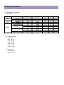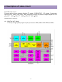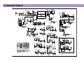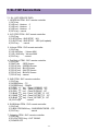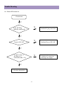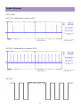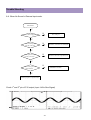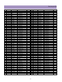
1
S/M NO. : DSL110PEF0
Service Manual
LCD Television
CHASSIS : SL-110P
Model :
D P-15D3SHS
DLP-17D3SHS
DLP-20D3AHS
Caution
: In this Manual, some parts can be changed for improving. their
performance without notice in the parts list. So, if you need the
latest parts information, please refer to PPL(Parts Price List)in
Service Information Center.
APR. 2005
Contents
I. Parts with the exception of MODULE
1. Safety Precaution
2. Product Specification
3. Block Diagram
3-1 PCB Structure
3-2 Power Tree
3-3 Signal Block Diagram
4. Description of video circuit
5. Schematic Diagram
6. PCB Data
6-1 DLP-15/17D3SHS
6-2 DLP-20D3SHS
7. SL-110P Service Data
8. Trouble Shooting
9. Service Part List
3
4
7
10
20
29
29
31
33
40
53
53
60
61
62
64
64
65
66
9-1 DLP-15D3SHS Service Part List
9-2 Difference List of SL-110P
10. Adapter
11. Inverter
12. Exploded View
12-1 DLP-15D3SHS
12-2 DLP-17D3SHS
12-3 DLP-20D3AHS
13. SOFTWARE INSTALL
14. SOFT UPGRADE
-2-
1. Safety Precautions
1. Safety Precautions
(1) When moving or laying down a LCD Set, at least two people must work together. Avoid any
impact towards the LCD Set.
(2) Do not leave a broken LCD Set on for a long time. To prevent any further damages, after
checking the condition of the broken Set, make sure to turn the power (AC) off.
(3) When opening the BACK COVER, you must turn off power (AC) to prevent any electric
shock.
(4) When loosening screws, check the position and type of the screw. Sort out the screws and
store them separately for reassembling. Because screws holding PCBs are working as
electric circuit grounding, make sure to check if any screw is missing when assembling /
reassembling. Do not leave any screws inside the set.
(5) A LCD Set contains different kinds of connector cables. When connecting or disconnecting
cables, check the direction and position of the cable beforehand.
(6) Connect/disconnect the connectors slowly with care especially FFC (film) cables and FPC
cables. Do not connect or disconnect
Picture 1-1. Panel Gas Exhaust Tube
connectors instantaneously with force, and
handle them carefully for reassembling.
(7) Connectors are designed so that if the number of pins or the direction does not match,
connectors will not fit. When having problem in plugging the connectors, check their kind,
position, and direction.
-3-
2. Product Specification
2-1. SPECIFICATION
Model
CHASSIS NO
DLP-15D3SHS
SL-110P
DLP-17D3SHS
SL110P
DLP-20D3AHS
SL-110P
Country
Remote controller
Europe
R-47B02
Europe
R-47B02
Europe
R-47B02
LCD Type
Screen Size
Aspect Ratio
Resolution
Pixel Pitch
Brightness
Contrast ratio
Viewing Angle (U/D/R/L)
Response Time
TN (Samaung)
15” (38 )
4:3
1024 768 (XGA)
0.297 0.297
400 cd/
400 : 1
60 / 65 / 70 / 70
25
TN (Samsung)
17” (43 )
15 : 9
1280 768 (WXGA)
0.2895 0.2895
400 cd/
450 : 1
50 / 60 / 70 / 70
25
TN (AIO)
20” (50.8 )
4:3
800 600 (SVGA)
0.51 0.51
500 cd/
500 : 1
60 / 60 / 80 / 80
16
Color System
Receiving System
PAL / SECAM
PAL B/G, I/I’, D/K, L-SECAM,
L’-SECAM
FVS
PATBF19D (PARTSNIC)
VHF :
BAND : CH2 ~ CH4
BAND : CH5 ~ CH12
CABLE BAND : S1’ ~ S3’,
S1 ~ S20
UHF :
HYPER BAND : S21 ~ S41
BAND , : CH21 ~ CH69
PIF :
38.9 (B/G, D/K, I/i’, L),
34.2 (L )
SIF :
33.4 (B/G), 32.4 (D/K, L),
32.9 (I/I’), 41.0 (L’)
S-subcarrier :
5.5 / 5.85 (NICAM) /
5.74 (2-Carrier)
Color-subcarrier :
4.43 (PAL), 4.25 /
4.40625 (SECAM)
Mono / Stereo / Dual
99 Channel, Auto Preset
PAL / SECAM
PAL B/G, I/I’, D/K, L-SECAM,
L’-SECAM
FVS
PATBF19D (PARTSNIC)
VHF :
BAND : CH2 ~ CH4
BAND : CH5 ~ CH12
CABLE BAND : S1’ ~ S3’,
S1 ~ S20
UHF :
HYPER BAND : S21 ~ S41
BAND , : CH21 ~ CH69
PIF :
38.9 (B/G, D/K, I/i’, L),
34.2 (L )
SIF :
33.4 (B/G), 32.4 (D/K, L),
32.9 (I/I’), 41.0 (L’)
S-subcarrier :
5.5 / 5.85 (NICAM) /
5.74 (2-Carrier)
Color-subcarrier :
4.43 (PAL), 4.25 /
4.40625 (SECAM)
Mono / Stereo / Dua
99 Channel, Auto Preset
PAL / SECAM
PAL B/G, I/I’, D/K, L-SECAM
L’-SECAM
FVS
PATBF19D (PARTSNIC)
VHF :
BAND : CH2 ~ CH4
BAND : CH5 ~ CH12
CABLE BAND : S1’ ~ S3’,
S1 ~ S20
UHF :
HYPER BAND : S21 ~ S41
BAND , : CH21 ~ CH69
PIF :
38.9 (B/G, D/K, I/i’, L),
34.2 (L )
SIF :
33.4 (B/G), 32.4 (D/K, L),
32.9 (I/I’), 41.0 (L’)
S-subcarrier :
5.5 / 5.85 (NICAM) /
5.74 (2-Carrier)
Color-subcarrier :
4.43 (PAL), 4.25 /
4.40625 (SECAM)
Mono / Stereo / Dua
99 Channel, Auto Preset
PC Audio Input
75 Ohm external input terminal
(DIN Standard)
Scart Jack 1
S-VHS (Y/C) 1
COMPOSITE
(NTSC, PAL, SECAM, NTSC4.43)
RCA Jack 1, Audio L/R 1
COMPONENT
(Y, Pb/Cb, Pr/Cr, 480i ~ 1080i)
RCA Jack 1
Audio L/R 1
VGA ~ XGA
15Pin D-SUB Jack 1
Stereo Jack 1
75 Ohm external input terminal
(DIN Standard)
Scart Jack 1
S-VHS (Y/C) 1
COMPOSITE
(NTSC, PAL, SECAM, NTSC4.43)
RCA Jack 1, Audio L/R 1
COMPONENT
(Y, Pb/Cb, Pr/Cr, 480i ~ 1080i)
RCA Jack 1
Audio L/R 1
VGA ~ WXGA
15Pin D-SUB Jack 1
Stereo Jack 1
75 Ohm external input terminal
(DIN Standard)
Scart Jack 1
S-VHS (Y/C) 1
COMPOSITE
(NTSC, PAL, SECAM, NTSC4.43)
RCA Jack 1, Audio L/R 1
COMPONENT
(Y, Pb/Cb, Pr/Cr, 480i ~ 1080i)
RCA Jack 1
Audio L/R 1
VGA ~ SVGA
15Pin D-SUB Jack 1
Stereo Jack 1
Video / Audio
Headphone
Scart Jack 1
3.5 Mini Stereo Jack
Scart Jack 1
3.5 Mini Stereo Jack
Scart Jack 1
3.5 Mini Stereo Jack
LCD Panel
TV System
Tuning Method
Tuner
Reception Channel
IF & SubCarier
Audio System
Channel Memory
Input
TV Input
A/V (R,G,B / COMPOSITE)
S-Video Input
Video / Audio
Component / Audio
PC Input
Output
1
-4-
1
1
Product Specification
Other Features
Comb Filter
CTI
LTI
OSD
TELETEXT
Audio Output
Speaker
Aspect ratio control
Auto Power off
Wake up
Sleep time
Wall mount hole
2D
2D
2D
17 Languages
10 Page memory TOP / FLOF
5W (2.5+2.5W)
(10%THD, 60%MOD at 1kHZ)
5
2
16 : 9 / ZOOM
17 Languages
10 Page memory TOP / FLOF
5W (2.5+2.5W)
(10%THD, 60%MOD at 1kHZ)
5
2
4 : 3 / ZOOM
17 Languages
10 Page memory TOP / FLOF
5W (2.5+2.5W)
(10%THD, 60%MOD at 1kHZ)
5
2
16 : 9 / ZOOM
15/30/45/60/90/120 min
VESA compatible
15/30/45/60/90/120 min
VESA compatible
15/30/45/60/90/120 min
VESA compatible
34 W
3W under
DC 12V
External Adaptor
AC 100-240V
50 / 60
40W
3W under
DC 12V
External Adaptor
AC 100-240V
50 / 60
50W
3W under
DC 15V
External Adaptor
AC 100-240V
50 / 60
(463 345
5” / 15”
6.25
(544 358
5” / 15”
7.2
(608 403
5” / 15”
10.95
Power Consumption
Max
Stand-by
Power supply
Power Source
Dimension (W
H
D)
Set dimension (with Stand)
Tilt (Front / Back)
Weight (with Stand)
215)
215)
215)
USER CONTROL & ACCESSORIES
Control Button (Set)
Remote Controller (32keys)
Accessories
POWER TV/VIDEO MENU
VOL. DOWN VOL. UP
PR. DOWN(On) PR. UP(On)
POWER MUTE PR. UP
PR. DOWN VOL. UP
VOL. DOWN MENU
NORMAL RED GREEN
YELLOW CYAN TELETEXT
SLEEP ASPECT PC
TV/AV S.MODE RECALL
TXT keys 0 ~ 9 Digit keys
Instruction AC Adapter
AC Power Remote Controller
Battery (AAA 2)
-5-
POWER TV/VIDEO MENU
VOL. DOWN VOL. UP
PR. DOWN(On) PR. UP(On)
POWER MUTE PR. UP
PR. DOWN VOL. UP
VOL. DOWN MENU
NORMAL RED GREEN
YELLOW CYAN TELETEXT
SLEEP ASPECT PC
TV/AV S.MODE RECALL
TXT keys 0 ~ 9 Digit keys
Instruction AC Adapter
AC Power Remote Controller
Battery (AAA 2)
POWER TV/VIDEO MENU
VOL. DOWN VOL. UP
PR. DOWN(On) PR. UP(On)
POWER MUTE PR. UP
PR. DOWN VOL. UP
VOL. DOWN MENU
NORMAL RED GREEN
YELLOW CYAN TELETEXT
SLEEP ASPECT PC
TV/AV S.MODE RECALL
TXT keys 0 ~ 9 Digit keys
Instruction AC Adapter
AC Power Remote Controller
Battery (AAA 2)
Product Specification
2-2. Available Input Signal
(1) PC input
Stamdard
MAC
Resolution (Mode)
640 480
832 624
V Frequency (Hz)
66
75
(2) Component input
- 480i/ 60 Hz
- 480p / 60 Hz
- 576i / 50 Hz
- 576p / 50 Hz
- 720p / 60 Hz
- 1080i / 50 Hz
- 1080i / 60 Hz
(3) Video input
- NTSC-M/4.43
- PAL / SECAM
-6-
H frequency (KHz)
35
49.73
15 inch
17 inch
20inch
7
8
3-3. SIGNAL BLOCK DIAGRAM
MAIN IC VCTI
(IC29)
SCL1 SDA1
SCL1
SDA1
FLASH
SST39VF800A
(IC11)
IR
TV
RF
IF
PROCESS
SAW
FILTER
TUNER
CVBS
Vide o In pu t
RCA (JP8 )
Y/C
S-VIDEO Input
S-VHS (JP5)
SW
A_SEL0
L
L
H
H
COMP2 (Y PbPr)
SCL1
SDA1
GCLK
MAIN (L,R)
GCOAST
SW IC
PI5V330
(IC9)
L : COMP2
H : COMP1
SW IC
PI5V330
(IC5)
G
P
O
R
T
SDA2
MODE
C OMP1
PC
COMP2
AV
L : PC
H : TV/COMP1,2
ADC
MST9883
(IC16)
SW IC
PI5V330
(IC34)
TV
(RGB),
COMP
(YPbPr),
24bit
GCLK
De-in terlace r
MDIN-150 (IC22)
Deint erlace
pro cesso r
C
S
C
SW
VVS
V
P
O
R
T
VCLK
GHS
SW
PC(HV)
SW
MAIN (L)
SOUND AMP
TDA1517 (IC30)
SPEAKER
MAIN (R)
SOUND AMP
TDA1517 (IC25)
SPEAKER
MODE
PC
X
X
AV
SCL2
SDA2
SDRAM
IS42S3200B-6T
(IC23)
SCL1
SDA1
H.P ( L,R)
SOUND AMP
KA45 58 (IC36)
D
P
O
R
T
DHS
DVS
CXA1315
(IC26)
LVDS
EL-LV385
(IC7)
RGB
DATA
8bit
CLK 2bit
COLOR
SPACE
EXPAND
-ER
LCD ON
Dimming
SCL2 SDA2
TV/C OMP ADC SEL
L
L
L
H
H
L
H
H
TO LCD
MODULE
INVERTER
SDRAM Int erface
SW IC
4052
(IC2)
15inch : XGA (S/S)
17inch : WXGA (S/S)
GVS
SW
PC ( RGB)
TV (HV)
SCL2
SDA2
DCLK
RGB
24bit
VHS
C
S
C
EEPROM
24LC16 (IC38)
RGB
24bit
SCAL ER
& CL T
& OSD
PC(RGB) 24bit
G COAST
SW
(5- Line)
PIXEL
PROCESSOR
SCL2
A_SEL1
L
H
L
H
L : COMP1,2
H : TV
MICOM
LOGIC IC
74LV273 (IC40)
GHS
GVS
TV (HV)
EEPROM
24LC16(IC31)
L, R
SW IC
4052
(IC33)
SCAL ER
PW113 (IC13)
TV (RGB)
L, R
PC AUDIO
COMP1 ( YPbPr)
TXD
RXD
H.P (L,R)
AV AUDIO
TV (RGB)
DISPLAY
DECODER
SOUND PROCESSOR
SCART
AUDIO
COMP2 AUDIO
VIDEO
BACK
END
RGB, CVBS
SCART(JP11)
(Only Europ e)
COMP1 AUDIO
TXD
RXD
TTX&
CAPTION
VIDEO
DECOD
-ER
KEY
MICOM
SOUND MUTE
H- PHONE
9
4-Lamp
cab le
(15"/ 17")
6- Lamp
cable (20" )
4. Description of video circuit
SL-110P video circuit :
Process various input signals <Analog-TV signal, CVBS(NTSC), Y/C signal, Component
signal(Y-Pb-Pr 1080i, 720P, 480P, 480i), Analog-PC signal> to produce Output Signal for LCD
panel(15” : 1024
768, 17” : 1280
768, 20” : 800
600).
Introduction for main IC
4-1. IC29 (The VCT 49xxI)
: IC family of high-quality single chip TV processors <DRX, MSP, VSP, DDP and SDA>
-10-
Description of video circuit
1) DRX
Overview of DRX
The Digital Receiver Front-end (DRX) performs the entire multi-standard Quasi Split Sound
(QSS) TV IF processing, AGC, video demodulation, and generation of the second sound IF
(SIF) requiring only one SAW filter.
All control functions and status registers are accessible via I2C bus interface. Therefore, it
simplifies the design of high-quality, highly standardized IF stages.
For pre-filtering, one 8-MHz channel SAW filter must be used.
TV signal Ë Tuner(TU1) Ë SAW-filter(S3) Ë 72 & 73 pin of VCTI(IC 29) Ë DRX of VCTI
Features
- Multi-standard QSS IF processing with a single SAW
- Programmable IF frequency (38.9 MHz, 45.75 MHz, 32.9 MHz, 36.125 MHz, 58.75 MHz.)
- Digital IF processing for the following standards: B/G, D/K, I, L/L’, and M/N
- Standard specific digital post filtering
- Standard specific digital video/audio splitting
- Standard-specific digital AGC and delayed tuner AGC with programmable tuner Take Over
Point
- Second SIF output with standard dependent pre-filtering and amplitude controlled output level
- Video demodulation
- Second SIF generation and AGC
Output of DRX : CVBS & SIF
-11-
Description of video circuit
2) MSP
Overview of MSP
The MSP receives the digital Sound IF signal from the DRX part.
The MSP is able to demodulate all TV sound standards worldwide including the digital NICAM
system.
INPUT :
SIF(DRX)
MSP of VCTI
Audio signal(External device)
of VCTI
OUTPUT :
84 & 85 of VCTI
CD4052(IC33, Switching)
TDA1517(IC25 & IC30)
Features
Sound Demodulator:
- worldwide FM/AM-mono demodulation
- FM carrier based demodulation (A2, EIA-J)
- FM stereo radio & RDS demodulation
- Nicam demodulation
- BTSC/SAP with MNR (DBX optional)
- automatic standard detection
- automatic sound select
Audio processing for loudspeaker channel:
- volume
- automatic volume correction (AVC)
- bass & treble or equalizer
- loudness
- balance
- spatial effect (e.g. pseudo stereo)
-12-
78&79 pin of VCTI(IC29)
MSP
Description of video circuit
3) VSP
Overview of VSP
INPUT :
VSP of VCTI
CVBS(DRX)
Video signal(External device)
51& 52 & 53 pin of VCTI(IC29)
VSP of VCTI
OUTPUT :
YUV(4:2:2 or 4:4:4)
Features
- multi-standard color decoder PAL/NTSC/SECAM including all substandards
- macro-vision compliant multi-standard sync processing
- macro-vision detection
- letterbox detector (auto-wide)
- 1H delay line (PAL compensation,NTSC combfilter)
- 4H adaptive comb filter (PAL/NTSC)
- vertical peaking (via comb filter)
- linear horizontal scaling (0.25 to 4)
- nonlinear horizontal scaling “panorama vision”
- peaking, contrast, brightness, color saturation and tint for all inputs (CVBS, S-VHS, YCrCb
and RGB)
- panorama scaler for all inputs (CVBS, S-VHS, YCrCb and RGB)
-13-
Description of video circuit
4) DDP
Overview of DDP
The DDP contains the entire digital video component and deflection processing, as well as all
analog interfaces to display the picture on a CRT
INPUT :
YUV(4:4:4 , VSP)
DDP of VCTI
OUTPUT :
16& 17 & 18 pin of VCTI(IC29)
TV_RGB signal
Features
Display processing
- dynamic contrast improvement (DCI)
- dynamic black level expander (BLE)
- luma sharpness enhancement (LSE)
- color transient improvement (CTI)
- brightness, contrast, saturation and tint
- programmable YCrCb to RGB matrix
- static black stretch, blue stretch, gamma correction by a programmable Non-linear Colorspace
Enhancer (NCE) on RGB
Deflection Processing
- vertical sawtooth (amplitude, linearity, s-correction, zoom)
- dynamic horizontal EHT (amplitude/phase compensation with Tc ~ 1line)
- vertical angle and bow correction
- horizontal and vertical protection circuit
- soft start/stop of H-drive
- supports horizontal and vertical dynamic focus
Backend Features
- internal analog OSD (RGB/FB/COR) input
- fast-blank priority & monitoring via I2C
-14-
Description of video circuit
5) TVT
Overview of TVT
TVT of VCTI
UART
PW113(IC13)
The TVT is a Teletext decoder for decoding World System Teletext data, as well as Video
Programming System (VPS), Program Delivery Control (PDC), and Wide-Screen Signalling
(WSS) data used for PALplus transmissions.
The device also supports Closed Caption acquisition and decoding.
The TVT provides an integrated general-purpose, fully 8051-compatible microcontroller with
television-specific hardware features.
The on-chip display unit for displaying Level 1.5 Teletext data can also be used for customerdefined onscreen displays.
Features
Controller Features
- 8-bit 8051 instruction set compatible CPU
- Watchdog timer
- UART
- Real time clock (RTC)
- I2C bus master/slave interface
OSD Features
- 24 kB on-chip character ROM
- Supports all East and West European languages
- National language support (Latin, Cyrillic, Greek, Arabic, Farsi, Hebrew)
- Mosaic graphic character Set
Teletext Features
- Multi-standard digital data slicer
- Full field and VBI data acquisition
- Simultaneous WST, PDC, VPS, and WSS acquisition
- Closed Caption and V-chip acquisition
-15-
Description of video circuit
4-2. IC25 and IC30 (TDA1517)
: Class-B dual audio amplifier
INPUT :
Audio signal (84 & 85 pin of VCTI)
TDA1517
OUTPUT :
Audio signal (TDA1517, amplify)
Speaker
4-3. IC16 (MST9883)
: Triple Video A/D Converter with Clamps & Pixel Clock Synthesizer
INPUT :
1-RF, 1-CVBS, 1-Y/C, 2-Component, 1-PC signal
54 pin of MST9883(IC16)
OUTPUT :
Gport ofPW113(IC13)
PC signal
Other signal
MDIN150(IC22)
PI5V330(IC5,9,34),Switching
FEATURES OVERVIEW
- Triple ADC with 12 - 140 MHz Sampling Rate
- Integrated line locked PLL generates pixel clock from HSYNC
- 4:2:2 Output Format Mode
-16-
43 & 48 &
Description of video circuit
4-4. IC22 (MDIN150)
: Single chip of de-interlacing and format conversion.
Interlace signal
MDIN150, Progressive signal
PW113(IC13)
Main Features
- Performs high quality deinterlacing for arbitrary format of interlaced video input up to 1080i
- Motion adaptive 3-D deinterlacing with pixel-by-pixel motion adaptive interpolation
- High quality edge preserving deinterlacing thru multiple directional edge detection and
interpolation
- Deinterlacing with fast motion detection and processing
- Deinterlacing with motion boundary preservation using previous 30 fields motion history
- Deinterlacing with film mode detection and processing for film source
- Deinterlacing with bad edit and subtitle detection and adaptation for film source
- Independent horizontal and vertical scaling
- Frame rate conversion with arbitrary conversion ratio
- Inter field noise reduction using previous 30 fields motion history
- Programmable high order peaking filter for horizontal edge enhancement
- Color enhancement filter for smooth color component output
- Programmable brightness, contrast, tint, saturation and gamma control
-17-
Description of video circuit
“rocess MDIN output signal to produce Signal for LCD panel(15”± : 1024*768, 17”± : 1280*768,
20”± : 800*600 ).
Control :
MST9883 and MDIN < I2C >
74LV273A(IC40) <Digital port>
Switching IC
Features
- ITU-R 656 Video Interface
- 2nd Generation Horizontal and Vertical Image Scaling
- Pixel Rate Conversion
- Multi-Region Non-Linear Scaling
- ITU-R 656 Video Interface
- Video Processing
- Advanced OSD Support
- On-Chip 80186 Microprocessor
-18-
Description of video circuit
4-6. IC17 (EL-LV385)
: LVDS Transmitter 24-Bit Flat Panel Display (FPD) Link-85 MHz
Output signal of PW113
LV385 (Converting LVDS signal)
LCD panel
EL-LV385 Transmitter converts parallel 28bits CMOS/TTL data to serial LVDS(Low Voltage
Differential Signaling)
4-7. IC9 and IC34 (PI5V330)
: Quad 2-channel Mux / DeMux, switching IC
4-8. IC2 and IC33 (4052)
: Dual 4-channel Analog Multiplexer, audio and sync signal switching IC
-19-
20
21
22
23
24
25
26
27
28
DLP-15D3SHS/DLP-17D3SHS(TOP)
29
DLP-15D3SHS/DLP-17D3SHS(BOTTOM)
30
DLP-20D3SHS(TOP)
31
DLP-20D3SHS(BOTTOM)
32
7. SL-110P Service Data
7-1. SL-110P SERVICE DATA
1. HEATRUN ITEM : SVC remote controller
1) SCV key
2) H/R key : Heatrun 0
3) H/R key : Heatrun 1
4) H/R key : Heatrun 0
5) SCV key : cancel
2. I2C STOP ITEM : SVC remote controller
1) SVC key
2) S.STOP key : BUS STOP NO
3) S.SOTP key : BUS STOP YES (soft update)
4) SVC key
: cancel
3. Volume ITEM : SVC remote controller
1) SVC key
2) VOL.MIN key : Volume MIN
3) VOL. MAX key : Volume MAX
4) SVC key
: cancel
4. Dot-Defect ITEM : SVC remote controller
1) SVC key
2) PART key : RED Screen
3) PR UP key : GREEN Screen
4) PR UP key : BLUE Screen
5) PR UP key : WHITE Screen
6) PR UP key : BLACK Screen
7) PR UP key : cancel
5. W/B ITEM : SVC remote controller
1) SVC key
2) SCREEN key : TV
3) SCREEN key : PANEL
4) R DRV
key : Panel_R DRIVE 127
5) G DRV
key : Panel_G DRIVE 127
6) B DRV
key : Panel_B DRIVE 127
7) R BIAS
key : Panel_OFFSET_R 127
8) G BIAS
key : Panel_OFFSET_G 127
9) B BIAS
key : Panel_OFFSET_B 127
10) SVC key
: cancel
6. SUB-Bright ITEM : SVC remote controller
1) SVC key
2) S-BRI UP/DOWN key : SUB BRIGHTNESS -172
3) SVC key
: cancel
7. Outgoing ITEM : SVC remote controller
1) SVC key
2) EX-FACTORY key : OUT GOING
3) POWER OFF
-33-
SL-110P Service Data
7-2. SL-110P USER_SVC DATA
1. CH MEMORY CONTENTS (Channel data after TV RESET) -- GUMI factory
PR. NO
SYS.
CH
Frequency
PATTERN
30
31
32
33
34
35
36
37
38
39
PAL-B
PAL-B
PAL-B
PAL-B
PAL-B
SCM-B
PAL-K
PAL-1
PAL-B
SCM-L
40CH
2CH
5CH
10CH
4CH
12CH
26CH
31CH
8CH
43CH
623.25 MHZ
48.25 MHZ
175.25 MHZ
210.25 MHZ
62.25 MHZ
224.25 MHZ
511.25 MHZ
551.25 MHZ
196.25 MHZ
647.25 MHZ
W/B
RETMA
CROSS HATCH
COLOR BAR
DEM
SCM COLOR BAR
RETMA
COLOR BAR
RED
FULL COLOR BAR
remark
2. ADJUSTMENT / OPTION DATA
USER_SVC Mode : PR91
ITEM
Vertical
Geometry
Tube
Settings
Additional
Settings
Audio
Options
DRX
CONTENTS
VERT. POSITION
VERT. AMPLITUDE
VERT. ZOOM
VERT.LINEARITY
VERT. S-CORRECTION
VERT. BLANKING START
VERT. BLANKING STOP
CUTOFF RED
CUTOFF GREEN
CUTOFF BLUE
WHITEDRV. RED
WHITEDRV. GREEN
WHITEDRV. BLUE
PWMV
DFHB
OSD H-SHIFT
OSD H-SHIFT
SPLIT SCREEN
OSD V- SHIFT
OSD PIXEL CLOCK
FULL AUDIO MENUS
SHOW VOLUME BAR
AUTOSTORE VOLUME
BBE
VOICE
SRS WOW
3D-PANORAMA
MUTE if no carrier
STANDARD SELECT
TOP SETTING
VIDEO PEAKING
SIF REFERENCE
Sharpness 0
DATA
+18
-120
+256
-30
+40
+343
+4
0
0
0
+470
+470
+470
+1
+1
+195
R
REMARK
+220
+36
+44
NO
YES
NO
NO
NO
NO
YES
NO
B
+8
0
+2
-34-
G
Y
ITEM
MENU
SLEEP (User remote controller)
CONTENTS
DATA
HOR. POSITION
+200
HOR. RGB POS
+2
PICTURE WIDTH
+30
TRAPEZE
+5
CUSHION
-5
Horizontal
ANGLE 0
Geometry
BOW 0
HOR. BLANKING START +1264
HOR. BLANKING STOP
+60
UPPER CORNER
0
LOWER CORNER
0
UPPER CORNER(SIXTH)
0
LOWER CORNER(SIXTH)
+9
FRONT AV(EXT3)
NO
YCrCb INPUT(EXT4)
NO
VGA INPUT
NO
DVB MODULE
NO
PICTURE TUBE 16 : 9
NO
BLUE SCREEN
YES
Optins
PICTURE MUTE
NO
SHOW I2C-OFF
YES
UHF ONLY
NO
ATS WITH L/L’ MODE
YES
SEARCH FOR BG, DK, I
YES
SEARCH FOR M
NO
STATION IDENT
YES
ATS DELAY TIME(ms)
50
M JAPAN
+36
BTSC
+36
DK DUAL
+36
Deviation
BG
+36
Settings
NICAM L
+36
NICAM I
+36
DK NICAM
+36
SAT
+36
FM RADIO
+36
NVM Edit
Reset TV-set
-
REMARK
SL-110P Service Data
3. USER_SVC Mode (NORMAL 1,2 MODE) :
USER_SVC Mode : PR91
Sharpness 0
R
G
Y
MENU
15
CONTRAST
BRIGHTNESS
COLOUR
SHARPNESS
BRIGHTNESS_PC
CONTRAST_PC
SHARPNESS_PC
NORMAL 1
48
40
32
32
45
38
32
NORMAL (User remote controller)
17
NORMAL 2
32
45
25
20
38
30
25
NORMAL 1
48
32
32
32
30
45
32
NORMAL 2
30
45
30
20
22
38
25
20
NORMAL 1 NORMAL 2
52
35
40
45
32
25
40
20
42
38
36
30
32
20
4. USER_SVC Mode (EXTERNAL OSD MODE) :
USER_SVC Mode : PR91
ITEM
EXTERNAL BRIGHTNESS
EXTERNAL CONTRAST
EXTERNAL OSD
BRIGHTNESS
CONTRAST+32
Inch option
ATS DISABLE
Tuner(1=Phil, 0=DW)
PC ENABLE
Fine Tuning
0=A, 1W, 2E, 3G, 4R, 5I
Sharpness 0
R
G
DATA
+40
+40
NO
+32
+32
15” / 17” / 20”
NO
+1
YES
0
0
Y
MENU
PC (User remote controller)
REMARK
15 / 17 / 20 INCH
TEXT SEL
W/B ITEM <PC, COMPNENT> : AUTO FIX
ITEM
W/B(PANEL)
CONTENTS
RED DRIVE
GREEN DRIVE
BLUE DRIVE
RED BIAS
GREEN BIAS
BLUE BIAS
DATA
12/128/128
125/123/124
118/98/112
128/128/128
126/126/125
122/126/120
-35-
REMARK
15/17/20 INCH
SL-110P Service Data
7-3. SL-110P MASTER IC EXCHANGING METHOD
1. After exchange EEPROM(IC31), Turn the SET on and wait for 20 sec.
2. Confirm LED Blinking and turn the SET on.
3. TV RESET
: Method (USER remote controller)
1) PR91
Sharpness 0
R
G
Y
MENU
SLEEP
2) Select the “Reset TV-set” on the MENU screen.
3) if push the “VOL up” key, MENU screen of “Reset TV-set” appear.
4) Push the “Green” key
5) Automatically Turn the SET OFF and ON.
4. W/B Adjustment
: Method (SCV remote controller)
1) SCV key
SCREEN key
R, G, B DRV & BIAS UP/DOWN key
ITME
W/B(PANEL)
CONTENTS
RED DRIVE
GREEN DRIVE
BLUE DRIVE
RED BIAS
GREEN BIAS
BLUE BIAS
DATA
139/138/137
128/128/128
112/109/107
129/130/130
128/128/128
130/127/127
REMARK
ITME
CONTENTS
CUTOFF RED
CUTOFF GREEN
15/17/20 INCH W/B(TV) CUTOFF BLUE
WHITEDRV. RED
WHITEDRV. GREEN
WHITEDRV. BLUE
DATA
REMARK
0/0/0
0/0/0
0/0/0
15/17/20 INCH
470/470/470
470/470/470
470/470/470
Enable to adjust W/B value Changing RED and BULE value of W/B(Panel)
2) SCV key : cancel
5. Inch Option
: Method (USER remote controller)
1) PR91
Sharpness
0
R
G
Y
MENU
2) Select the “Inch Option” on the MENU screen.
3) Select the proper inch using “VOV up” key.
4) MENU key : cancel
-36-
PC
SL-110P Service Data
7-4. Adjusting White Balance
1. More than 30 minutes, heat-run the set in full-white mode whit H/R button of SVC remote
controller.
2. Apply HIGH/LOW PATTERN of WHITE BALANCE TESTER (NITSUKI 2849) to Video input
terminal (CROMA : OFF, Reference : G)
100%
High
80%
60%
40%
Level
20%
Low
0%
Level
High/Low Pattern
3. Adjust Picture mode, “Normal1”.
4. Check initial data of User Menu.
SHARPNESS 0
R
G
Y
MENU
PC KEY
5. To enter Service Mode, Push PR91
of User remote controller.
6. Check initial data of Service Mode.
7. Attach a sensor of White Balance Meter (CA-100) to 80% / 20% of white level on the screen.
8. Push SVC KEY of SVC Remote controller to enter SVC Mode.
9. Push SCREEN KEY of Remote controller in SVC Mode. (PANEL /TV MODE Convert)
10. Adjust White Balance by adjusting R DRV, B DRV
- Coordinate of Color is x=280 +/- 3, y=290 +/- 3 and the Y is 150 / .
11. Attach a sensor of White Balance Meter (CA-100) to 20% of white level on the screen
12. Adjust White Balance by adjusting R Bias , G Bias
- Coordinate of Color is x=280 +/- 3, y=290 +/- 3 and the Y is 10 / .
13. Repeat No 7 to No 12 until getting that Coordinate of Color is x=280, y=290.
14. To exit from Service mode, press SVC button on the SVC remote controller.
-37-
SL-110P Service Data
7-5. COMPONENT and PC Test
(1) COMPONENT MODE
PCB LINE :
- Resolution : 480i or 720p - PATTERN : COLOR BAR
Finish LINE :
- Resolution : 1080i/60Hz
- PATTREN : COLOR BAR
(2) PC MODE
PCB LINE :
600 (SVGA VESA 72Hz)
- Resolution : 800
- PATTERN : FULL COLOR BAR
Finish LINE :
- 15 INCH (1024
768 70Hz : VESA XGA)
- 17 INCH (1280
768 60Hz : VESA WXGA)
- 20 INCH (600
800 72Hz : VESA SVGA)
- PATTERN : 16 GARY)
(3) Test screen condition
-38-
SL-110P Service Data
7-6. PANEL DEFECT Test
Visual Inspection
Bright Spot
Dark Spot
Bright Lines
Dark Lines
Polarizer Scratch
Polarizer dent/bubble
Max. Defects
Electrical Inspection
Bright Dot
Dark Dot
defect min distance
Max. Defects
condition
15” SS panel
diameter <= 0.8 .
Numberr <= 4.
diameter <= 0.8 .
Numberr <= 4.
Width <= 0.1 &
length <= 3.0 .
Number <= 4.
Width <= 0.1 &
length <= 3.0 .
Number <= 4.
Width <= 0.1 &
length <= 10.0 .
Number <= 3.
17” SS panel
diameter <= 0.8 .
Numberr <= 4.
diameter <= 0.8 .
Numberr <= 4.
Width <= 0.08 &
length <= 2.0 .
Numberr <= 4.
Width <= 0.08 &
length <= 2.0 .
Numberr <= 4.
Width <= 0.1 &
length <= 5.0 .
Numberr <= 3.
diameter <= 0.8 .
Numberr <= 3.
Numberr <= 7.
diameter <= 0.8 .
Numberr <= 6.
Numberr <= 10.
15” SS panel
random number <= 2.
2 neighboring dots <= 1.
3 neighboring dots <= 0.
random number <= 7.
2 neighboring dots <= 2.
3 neighboring dots <= 1.
neighboring dots<= 0.
distance between
bright sots >=15 .
distance between
dark dots >=5 .
number <= 7.
watching distance : 30 - 50
Iuminance : 300 - 700 Iux
(nominal 500 Iux)
temperature : 25+-3
angle : front
pattern : R, G, B, black, white
test : active area
20.1” AUO panel
diameter <= 0.5 .
Numberr <= 5.
diameter <= 0.5 .
Numberr <= 5.
Width <= 0.15 &
length <= 10.0 .
Numberr <= 5.
Width <= 0.15 &
length <= 10.0 .
Numberr <= 5.
Width <= 0.15 &
length <= 20.0 .
Numberr <= 5.
(circle scratch : diameter <= 20.0 .
Number <= 5.)
diameter <= 0.5 .
Numberr <= 5.
17” SS panel
random number <= 2.
2 neighboring dots <= 1.
3 neighboring dots <= 0.
20.1” AUO panel
random number <= 2.
2 neighboring dots <=0.
random number <= 6.
2 neighboring dots <= 2.
3 neighboring dots <= 0.
random number <= 5.
2 neighboring dots <= 0.
distance between
bright sots >=15 .
distance between
dark dots >=5 .
number <= 6.
distance between
bright sots >=15 .
distance between
dark dots >=5 .
number <= 5.
watching distance : 50 - 70
Iuminance : 300 - 700 Iux
(nominal 500 Iux)
temperature : 25+-5
angle : front
pattern : R, G, B, black, white
test : active area
watching distance : 60 +- 5
Iuminance : 300 - 700 Iux
temperature : 25+-25
angle : front
pattern : R, G, B, black, white
test : active area
(1) SVC KEY on the SVC remote controller => PART key => PR DOWN / UP KEY
TEST PATTERN : R, G, B, White, Black (Toggle : PR KEY)
PART KEY : Cancel
(2) Test method : In each pattern of R, G, B, White, Black, Check the DOT DEFECT number.
-39-
8. Trouble Shooting
8. Trouble Shooting
* Facts you must know at trouble diagnosis or repairing
(1) The trouble diagnosis and repairing of set means Module or Main IC Exchange.
In other words, find out which PCB modules or Main ICs are not working and replace them
with normal PCB modules or ICs.
(2) This TROUBLE SHOOTING list only contains representative and simple PCB or Main IC
trouble diagnosis and Module or Main IC Exchange method. Therefore, if you find Sets
that are difficult to diagnose or to repair, contact Daewoo Electronics.
(3) Basic TROUBLE SHOOTING procedure :
Detach Back Cover
Trouble Diagnosis
Replace broken
Check Trouble Symptoms
PCB module or Main IC
Heat-run (for at least 30 minutes, input Test pattern full white)
Adjust white balance
Function Check
Repair Complete.
(4) Required equipments for trouble diagnosis
- Digital Multi-meter (measure Dc voltage, measure Diode Voltage, Short-Open test)
- Screwdriver (or electric screwdriver), plastic adjusting tool
(5) Each block operation was explained including Digital Oscilloscope signal, but this is
reference only and applying them for repair is not necessary.
(6) Before assemble/disassemble PCBs, check to see if AC Switch is OFF.
(7) After Back cover is closed, redo Heat-run for at least one hour by inputting Full white using
test pattern of service mode. Check the screen conditions and basic functions.
Symptoms of adaptor, inverter, panel Trouble
<Symptom.1> Not even weak discharge (luminescence) shows on screen.
<Symptom.2> Discharge (luminescence) on screen is unstable
<Symptom.3> Set is producing unusual noise
Symptoms of VIDEO or JACK PCB Trouble
<Symptom.1> Only weak discharge (luminescence) shows on screen, but No Data is on
screen
<Symptom.2> Screen DATA is abnormal
<Symptom.3> Particular input signal (Video, PC or Component etc.) does not operate
<Symptom.4> No SOUND
<Symptom.5> Remote Control or KEY does not operate
-40-
Trouble Shooting
8-1. When LED doesn’t lit.
Ch eck start
Y
N
Is the DC Plug
correctly connected?
Confirm DC plug connection.
Y
N
Is power S/W ON?
Confirm Power S/W ON.
Y
Is output voltage of
DC Plug 12V?
(DLP-20D3AHS : 15V)
N
Y
Check the Main PCB.
-41-
Confirm AC connection.
Exchange the Adapter.
Trouble Shooting
8-2. When TV doesn’t turn on in red LED.
Ch eck start
Y
Does TV turn on
pushing the CH key?
Is output voltage of
DC Plug 12V?
(DLP-20D3AHS : 15V)
N
Y
N
Y
Check the connection to IR PCB.
Check the operation of Remote
Controller.
Confirm Power S/W ON.
8-3. When “white screen”.
Ch eck start
Y
N
Is P11 (15/17 inch) or
P8 (20 inch) correctly
connected?
Check the connection
of Panel
Y
Is DVS, DHS, DEN, DCLK
of the Main PCB normal?
Pin #2,3,4 of RP38, R54(15/17inch),
R58(20inch) Pin #1,2 of
P11(3.3V/15/17inch)
Y
Exchange the Cable or Panel.
-42-
N
Check the Main PCB.
Confirm AC connection.
Exchange the Adapter.
Trouble Shooting
DVS, DHS, DEN and DCLK signal
<Pin #2,3,4 of RP38, R54(15/17inch), R58(20inch)>
DCLK<R54(15/17inch), R58(20inch)> : CLOCK (output of PW113)
DEN(Pin#4 of RP38) : Data Enable(output of PW113)
DVS(Pin #2 of RP38): Vertical Sync(output of PW113)
DHS(Pin #3 of RP38): Horizontal Sync (output of PW113)
If DCLK, DHS, DEN and DCLK signal is not normal, Main PCB has a trouble.
-> Check the Main PCB.
-43-
Trouble Shooting
8-4. When “No picture” in TV mode.
Ch eck start
Y
N
Does LED turn on
in Green?
Go to chap 8-2
Y
N
Does raster
screen appear?
Is there a weak discharge
on the screen?
N
Confirm AC connection.
Confirm Power S/W ON.
Check the adapter,
inverter and panel.
Y
N
Does auto-tuning
function operate normally?
Y
Check the tuner
(TU1) or the VCTI.
Is output of TP normal?
(VCTI_VS,VCTI_HS,
R,G,B)
N
Check the VCTI.
Y
Y
Tune the channel.
Is GCLK(R63), GFBK(R62),
GVS(R66), GHS(R64), R, G, B
output of IC16(MST9883)
normal?
N
Check the MST9883(IC16)
and switching IC(2,9,34).
N
Check the 12C of MDIN150
(IC22) and PW113(IC13).
Y
Is DVS, DHS, DCLK,
DEN(#2,3,4 of RP38, R54), R, G, B
output of IC13(PW113)
normal?
Y
Is DVS, DHS, DCLK,
DEN(#2,3,4 of RP38, R54), R, G, B
output of IC13(PW113) normal?
Y
Check the LV385(IC17).
Check the cable to panel.
-44-
N
Check the PW113(IC13).
Trouble Shooting
VCTI <IC29>
VCTI_VS : Vertical Sync (output of VCTi)
VCTI_HS : Horizontal Sync (output of VCTi)
I2C (P13)
-45-
Trouble Shooting
MST9883 <IC16>
GCLK (R63) : CLOCK (output of MST9883)
GCLK (R63) : CLOCK (output of MST9883)
GCLK (R63) : CLOCK (output of MST9883)
GCLK (R63) : CLOCK (output of MST9883)
-46-
Trouble Shooting
MDIN <IC22>
VCLK(R330,T8) : CLOCK (output of MDIN150)
VVS(#1 of RP1, T15) : Vertical Sync (output of MDIN150)
VVS(#1 of RP1, T15) : Vertical Sync (output of MDIN150)
-47-
Trouble Shooting
8-5. When “No picture” in External input mode.
Ch eck start
Y
N
Does OSD menu
screen appear?
Is there a weak
discharge on the screen?
N
Confirm AC connection.
Confirm Power S/W ON.
Check the adapter,
inverter and panel
Y
Is the signal input
jack correctly connected?
N
Y
Check the
connection of Jack
Y
N
Does input source operate?
Is DVS, DHS, DEN, DCLK
of the Main PCB normal?
Pin #2,3,4 of RP38, r54
(15/17inch), R58(20inch)
Pin #1,2 of P11(3.3V/15/17inch)
Operate AV device.
Y
Is input selection
in used mode?
N
Confirm input
selection
Y
Check the Cable or Panel.
Y
Check the Main PCB
and Sub-Jack PCB.
-48-
N
Check the Main PCB.
Trouble Shooting
Input Video signal (color bar pattern) to COMPOSITE(AV2) and check 51th-pin signal of VCTI.
If no signal, sub-Jack PCB has a trouble.
Exchange sub-Jack PCB.
Input video signal (color bar pattern) to S-VIDEO and check 52th-pin signal and 53th-pin signal
of VCTI.
52th-pin signal : Y signal
53th-pin signal : C signal
If no signal, sub-Jack PCB has a trouble.
Exchange sub-Jack PCB.
-49-
Trouble Shooting
8-6. When No Sound in External input mode.
Ch eck start
Y
N
Does Screen appear?
Go to Chap 8-5.
Y
Is the Sound input Jack
correctly connected?
N
Check the connection of sound jack.
Y
Is the Speaker Jack (P12)
correctly connected?
N
Check the connection of Speaker (P12).
Y
Is 1st and 3rd pin of P12
output normal?
N
Check #84, 85pin output of VCTI.
CHECK IC25 and IC30.
Y
Exchange Speaker or Speaker Cable.
Check 1st and 3rd pin of P12 output (Input :1KHz Sine Signal)
-50-
Trouble Shooting
8-7. When Key does not operate.
Ch eck start
Y
Does Remote
Controller operate?
N
Check the VCTI.
Y
Is 3rd and 4th pin of P9A
otput normal?
N
Exchange the Key PCB.
Y
Check Key Cable and the VCTI.
Output of 3rd pin of P9A (Key1) : PCB for Key EX) Push “PR UP” key 3 times.
Output of 4th pin of P9A (Key2) : PCB for Key EX) Push “Menu” key 3 times.
-51-
Trouble Shooting
8-8. When Remote Controller does not operate.
Ch eck start
Y
N
Does input of key operate?
Check the VCTI.
Y
N
Does Remote
Controller operate?
Check the Battery of
Remote controller
Y
N
Whenever push the button of
remote controller, does 2nd pin
of P10A output normal?
Exchange the Key PCB.
Y
Check the IR Cable and VCTI.
Output of 2nd pin of P10A (IR) : PCB for Remote Control EX) Push “PR DOWN” button.
-52-
9. Service part list
9-1. DLP-15D3SHS Service part list
LOC
PART CODE
ADT1
M124
M125
M126
M127
M128
M150
M170
PA11
V901
V902
P601A
4859000840
485A101470
485A101470
485A101970
485A102070
485A102370
4850K02200
21500901SV
4859003060
485LD01156
4850M001NV
4850704S49
PART NAME
ADAPTER
SHIELDRON
SHIELDRON
SHIELDRON
SHIELDRON
SHIELDRON
CORE FERRITE
SHEET TAPE AL
CABLE LVDS AS
LCD PANEL
MODULE INVERTER
CONNECTOR
SP01
SP02
C0M1
IC12
IC25
IC29
IC30
IC31
J2
J2A
J2B
J7
J8
JP1
JP11
JP2
JP4
JP5
JP7
JP8
L46
L48
LED1
M100
M100A
M110
M110A
M123
P12
P13
P4
PA10
PA3
PA6
PA9
S3
SW1
SW2
loc
SW3
SW4
SW5
SW6
SW7
TU2
TU21A
X1
X4
X5
C103
C104
C106
C107
C109
C11
4858316610
4858316610
4859112750
1TS0P34838
1TDA1517PP
149531PYFP
1TDA1517PP
124LC16B1B
4859295420
4859295620
4859295620
85801065GY
85801065GY
4959200160
4859112950
4859113050
97P6316100
4859105340
4959102340
4859112850
58C0000116
58C0000116
DHL320CRGD
4857253700
485A100870
4857253800
485A100670
485A101170
4859236120
4859231620
485923172S
4850706S26
4850712S01
4850714S01
4850705S17
5PX6966D—
5S50101Z90
5S50101Z90
parts_code
5S50101Z90
5S50101Z90
5S40101009
5S50101Z90
5S50101Z90
4850A23840
485A101070
5XJ20R25AE
5XJ14R31AE
5XJ27R00AC
HCBK104KBA
HCBK104KBA
HCBK102KBA
HCQK120JBA
HCBK104KBA
HCQK120JBA
SPEAKER
SPEAKER
JACK PIN
IC PREAMP
IC
IC TV PROCESSORS
IC
IC MEMORY
CONN WAFER
CONN WAFER
CONN WAFER
WIRE COPPER
WIRE COPPER
CONN D-SUB
JACK SCART
JACK DC
JACK HEAD PHONE
JACK S-VHS
JACK PHONE
JACK PIN
COIL BEAD
COIL BEAD
LED
SHIELD COVER
SHIELDRON
SHIELD PLATE
SHIELDRON
SHIELDRON
CONN WAFER
CONN WAFER
CONN WAFER
CONNECTOR
CONNECTOR
CONNECTOR
CONNECTOR
FILTER SAW
SW TACT
SW TACT
parts_name
SW TACT
SW TACT
SW PUSH
SW TACT
SW TACT
ANT SHIELD BOX
SHIELDRON
CRYSTAL QUARTZ
CRYSTAL QUARTZ
CRYSTAL QUARTZ
C CHIP CERA
C CHIP CERA
C CHIP CERA
C CHIP CERA
C CHIP CERA
C CHIP CERA
DESCRIPTION
AP06312
30X140X7.5T
30X140X7.5T
8X170X22T
54X90X30T
30X70X7.5T
ZCAT1325-0530A
T0.06 AL-35 70X40
12507HS-20+1712LHS=140
LTM150XH-L06
DS-1015WDS
YH025-04+YRT205+YRT110+
ULW=800+200
SP-4872N03
SP-4872N03
DPSE-0375 5PIN STR
TSOP34838SJ
TDA1517P
VCT4953I-PY-F1
TDA1517P
24LC16B1B
4602-04MV2-60-1 PLUG 4P ST
4605-2FV2-1 JUMPER 2P 2.54
4605-2FV2-1 JUMPER 2P 2.54
AWG22 1/0.65 TIN COATING
AWG22 1/0.65 TIN COATING
SHF-015-B111-22/BR2-J0.6
DSSM-0378 STR
DDSE-9861R STR
DHSE-9959
DSW-10 (STRAIGHT)
YKB21-5157
DPSS-0173 3PIN STR
HC-3550R
HC-3550R
HI-L320CRGD
SPTH-C T0.3
40X60X16T
SPTH-C T0.3
40X60X4T
12X18X8T
YAW025-04
YW025-03
YW025-04 (STICK)
12505HS-06+12505HS-06+ULW=500
12505HS-12+12505HS-12+ULW=100
12505HS-14+12505HS-14+ULW=160
12505HS-05+12505HS-05+ULW=270
X6966D
THVV502GDA
THVV502GDA
parts_descr
THVV502GDA
THVV502GDA
PS-22E06
THVV502GDA
THVV502GDA
PAXBF01DA (PAL)
40X30X10T
HC-49/S 20.2500MHZ 16PF 30PPM
HC-49/S 14.31818MHZ 30PPM
HC-49/S 27.000MHZ 15PF 20PPM
50V X7R 0.1MF K 1608
50V X7R 0.1MF K 1608
50V X7R 1000PF K 1608
50V CH 12PF J 1608
50V X7R 0.1MF K 1608
50V CH 12PF J 1608
REMARK
LOC
C110
C111
C112
C117
C118
C12
C120
C121
C122
C123
C127
C128
C129
C13
C131
C134
C135
C139
C14
C142
C144
C147
C148
C154
C157
C158
C160
C161
C162
C163
C165
C166
C167
C169
loc
C17
C172
C174
C175
C176
C177
C183
C185
C189
C19
C190
C192
C193
C194
C195
C196
C197
C198
C199
C2
C20
C200
C201
C202
C207
C208
C21
C210
C211
C215
C218
C219
C221
-53-
PART CODE
HCFF334ZBA
HCBK104KBA
HCBK104KBA
HCBK104KBA
HCBK104KBA
HCBK104KBA
HCBK104KBA
HCBK104KBA
HCFF334ZBA
HCBK821KBA
HCBK104KBA
HCBK104KBA
HCBK821KBA
HCBK104KBA
HCBK104KBA
HCBK104KBA
HCQK120JBA
HCBK104KBA
HCBK104KBA
HCQK120JBA
HCBK104KBA
HCBK104KBA
HCBK152KBA
HCBK104KBA
HCBK822KBA
HCBK822KBA
HCBK104KBA
HCBK104KBA
HCBK104KBA
HCBK104KBA
HCBK104KBA
HCBK104KBA
HCBK104KBA
HCBK104KBA
parts_code
HCBK104KBA
HCBK104KBA
HCBK102KBA
HCBK102KBA
HCBK104KBA
HCBK104KBA
HCBK104KBA
HCBK104KBA
HCBK104KBA
HCBK104KBA
HCBK104KBA
HCQK180JBA
HCQK180JBA
HCBK104KBA
HCBK104KBA
HCBK104KBA
HCBK104KBA
HCBK104KBA
HCBK104KBA
HCBK104KBA
HCBK102KBA
HCBK104KBA
HCBK104KBA
HCBK104KBA
HCBK104KBA
HCBK104KBA
HCBK104KBA
HCQK331JBA
HCQK331JBA
HCBK104KBA
HCBK104KBA
HCBK104KBA
HCBK104KBA
PART NAME
C CHIP CERA
C CHIP CERA
C CHIP CERA
C CHIP CERA
C CHIP CERA
C CHIP CERA
C CHIP CERA
C CHIP CERA
C CHIP CERA
C CHIP CERA
C CHIP CERA
C CHIP CERA
C CHIP CERA
C CHIP CERA
C CHIP CERA
C CHIP CERA
C CHIP CERA
C CHIP CERA
C CHIP CERA
C CHIP CERA
C CHIP CERA
C CHIP CERA
C CHIP CERA
C CHIP CERA
C CHIP CERA
C CHIP CERA
C CHIP CERA
C CHIP CERA
C CHIP CERA
C CHIP CERA
C CHIP CERA
C CHIP CERA
C CHIP CERA
C CHIP CERA
parts_name
C CHIP CERA
C CHIP CERA
C CHIP CERA
C CHIP CERA
C CHIP CERA
C CHIP CERA
C CHIP CERA
C CHIP CERA
C CHIP CERA
C CHIP CERA
C CHIP CERA
C CHIP CERA
C CHIP CERA
C CHIP CERA
C CHIP CERA
C CHIP CERA
C CHIP CERA
C CHIP CERA
C CHIP CERA
C CHIP CERA
C CHIP CERA
C CHIP CERA
C CHIP CERA
C CHIP CERA
C CHIP CERA
C CHIP CERA
C CHIP CERA
C CHIP CERA
C CHIP CERA
C CHIP CERA
C CHIP CERA
C CHIP CERA
C CHIP CERA
DESCRIPTION
16V Y5V 0.33MF Z 1608
50V X7R 0.1MF K 1608
50V X7R 0.1MF K 1608
50V X7R 0.1MF K 1608
50V X7R 0.1MF K 1608
50V X7R 0.1MF K 1608
50V X7R 0.1MF K 1608
50V X7R 0.1MF K 1608
16V Y5V 0.33MF Z 1608
50V X7R 820PF K 1608
50V X7R 0.1MF K 1608
50V X7R 0.1MF K 1608
50V X7R 820PF K 1608
50V X7R 0.1MF K 1608
50V X7R 0.1MF K 1608
50V X7R 0.1MF K 1608
50V CH 12PF J 1608
50V X7R 0.1MF K 1608
50V X7R 0.1MF K 1608
50V CH 12PF J 1608
50V X7R 0.1MF K 1608
50V X7R 0.1MF K 1608
50V X7R 1500PF K 1608
50V X7R 0.1MF K 1608
50V X7R 8200PF K 1608
50V X7R 8200PF K 1608
50V X7R 0.1MF K 1608
50V X7R 0.1MF K 1608
50V X7R 0.1MF K 1608
50V X7R 0.1MF K 1608
50V X7R 0.1MF K 1608
50V X7R 0.1MF K 1608
50V X7R 0.1MF K 1608
50V X7R 0.1MF K 1608
parts_descr
50V X7R 0.1MF K 1608
50V X7R 0.1MF K 1608
50V X7R 1000PF K 1608
50V X7R 1000PF K 1608
50V X7R 0.1MF K 1608
50V X7R 0.1MF K 1608
50V X7R 0.1MF K 1608
50V X7R 0.1MF K 1608
50V X7R 0.1MF K 1608
50V X7R 0.1MF K 1608
50V X7R 0.1MF K 1608
50V CH 18PF J 1608
50V CH 18PF J 1608
50V X7R 0.1MF K 1608
50V X7R 0.1MF K 1608
50V X7R 0.1MF K 1608
50V X7R 0.1MF K 1608
50V X7R 0.1MF K 1608
50V X7R 0.1MF K 1608
50V X7R 0.1MF K 1608
50V X7R 1000PF K 1608
50V X7R 0.1MF K 1608
50V X7R 0.1MF K 1608
50V X7R 0.1MF K 1608
50V X7R 0.1MF K 1608
50V X7R 0.1MF K 1608
50V X7R 0.1MF K 1608
50V CH 330PF J 1608
50V CH 330PF J 1608
50V X7R 0.1MF K 1608
50V X7R 0.1MF K 1608
50V X7R 0.1MF K 1608
50V X7R 0.1MF K 1608
REMARK
Service part list
LOC
C223
C228
C229
C230
C233
C236
C237
C238
C24
C240
C241
C242
C243
C244
C245
C246
C247
loc
C248
C249
C251
C252
C254
C255
C257
C258
C259
C26
C262
C263
C264
C265
C266
C268
C269
C270
C271
C272
C274
C276
C278
C279
C28
C280
C284
C285
C286
C290
C292
C293
C295
C296
C297
C31
C311
C312
C313
C32
C324
C325
C326
C327
C328
C329
C33
C330
C333
C334
PART CODE
HCBK104KBA
HCBK102KBA
HCBK102KBA
HCQK100JBA
HCBK104KBA
HCQK100JBA
HCBK104KBA
HCBK104KBA
HCBK104KBA
HCBK104KBA
HCQK100JBA
HCQK150JBA
HCBK104KBA
HCBK104KBA
HCBK104KBA
HCBK104KBA
HCBK104KBA
parts_code
HCBK104KBA
HCBK104KBA
HCBK104KBA
HCBK104KBA
HCBK104KBA
HCBK104KBA
HCBK104KBA
HCBK104KBA
HCBK104KBA
HCBK104KBA
HCBK104KBA
HCBK104KBA
HCBK104KBA
HCBK104KBA
HCBK104KBA
HCBK104KBA
HCBK104KBA
HCBK104KBA
HCBK104KBA
HCBK104KBA
HCBK104KBA
HCBK104KBA
HCBK104KBA
HCBK104KBA
HCBK104KBA
HCBK104KBA
HCBK104KBA
HCBK104KBA
HCBK104KBA
HCBK104KBA
HCBK104KBA
HCBK104KBA
HCFF334ZBA
HCFF334ZBA
HCBK104KBA
HCBK103KBA
HCBK102KBA
HCBK102KBA
HCBK104KBA
HCBK104KBA
HCBK104KBA
HCBK104KBA
HCBK104KBA
HCBK104KBA
HCBK104KBA
HCBK104KBA
HCBK104KBA
HCBK104KBA
HCQK220JBA
HCQK220JBA
PART NAME
C CHIP CERA
C CHIP CERA
C CHIP CERA
C CHIP CERA
C CHIP CERA
C CHIP CERA
C CHIP CERA
C CHIP CERA
C CHIP CERA
C CHIP CERA
C CHIP CERA
C CHIP CERA
C CHIP CERA
C CHIP CERA
C CHIP CERA
C CHIP CERA
C CHIP CERA
parts_name
C CHIP CERA
C CHIP CERA
C CHIP CERA
C CHIP CERA
C CHIP CERA
C CHIP CERA
C CHIP CERA
C CHIP CERA
C CHIP CERA
C CHIP CERA
C CHIP CERA
C CHIP CERA
C CHIP CERA
C CHIP CERA
C CHIP CERA
C CHIP CERA
C CHIP CERA
C CHIP CERA
C CHIP CERA
C CHIP CERA
C CHIP CERA
C CHIP CERA
C CHIP CERA
C CHIP CERA
C CHIP CERA
C CHIP CERA
C CHIP CERA
C CHIP CERA
C CHIP CERA
C CHIP CERA
C CHIP CERA
C CHIP CERA
C CHIP CERA
C CHIP CERA
C CHIP CERA
C CHIP CERA
C CHIP CERA
C CHIP CERA
C CHIP CERA
C CHIP CERA
C CHIP CERA
C CHIP CERA
C CHIP CERA
C CHIP CERA
C CHIP CERA
C CHIP CERA
C CHIP CERA
C CHIP CERA
C CHIP CERA
C CHIP CERA
DESCRIPTION
50V X7R 0.1MF K 1608
50V X7R 1000PF K 1608
50V X7R 1000PF K 1608
50V CH 10PF J 1608
50V X7R 0.1MF K 1608
50V CH 10PF J 1608
50V X7R 0.1MF K 1608
50V X7R 0.1MF K 1608
50V X7R 0.1MF K 1608
50V X7R 0.1MF K 1608
50V CH 10PF J 1608
50V CH 15PF J 1608
50V X7R 0.1MF K 1608
50V X7R 0.1MF K 1608
50V X7R 0.1MF K 1608
50V X7R 0.1MF K 1608
50V X7R 0.1MF K 1608
parts_descr
50V X7R 0.1MF K 1608
50V X7R 0.1MF K 1608
50V X7R 0.1MF K 1608
50V X7R 0.1MF K 1608
50V X7R 0.1MF K 1608
50V X7R 0.1MF K 1608
50V X7R 0.1MF K 1608
50V X7R 0.1MF K 1608
50V X7R 0.1MF K 1608
50V X7R 0.1MF K 1608
50V X7R 0.1MF K 1608
50V X7R 0.1MF K 1608
50V X7R 0.1MF K 1608
50V X7R 0.1MF K 1608
50V X7R 0.1MF K 1608
50V X7R 0.1MF K 1608
50V X7R 0.1MF K 1608
50V X7R 0.1MF K 1608
50V X7R 0.1MF K 1608
50V X7R 0.1MF K 1608
50V X7R 0.1MF K 1608
50V X7R 0.1MF K 1608
50V X7R 0.1MF K 1608
50V X7R 0.1MF K 1608
50V X7R 0.1MF K 1608
50V X7R 0.1MF K 1608
50V X7R 0.1MF K 1608
50V X7R 0.1MF K 1608
50V X7R 0.1MF K 1608
50V X7R 0.1MF K 1608
50V X7R 0.1MF K 1608
50V X7R 0.1MF K 1608
16V Y5V 0.33MF Z 1608
16V Y5V 0.33MF Z 1608
50V X7R 0.1MF K 1608
50V X7R 0.01MF K 1608
50V X7R 1000PF K 1608
50V X7R 1000PF K 1608
50V X7R 0.1MF K 1608
50V X7R 0.1MF K 1608
50V X7R 0.1MF K 1608
50V X7R 0.1MF K 1608
50V X7R 0.1MF K 1608
50V X7R 0.1MF K 1608
50V X7R 0.1MF K 1608
50V X7R 0.1MF K 1608
50V X7R 0.1MF K 1608
50V X7R 0.1MF K 1608
50V CH 22PF J 1608
50V CH 22PF J 1608
REMARK
LOC
loc
C34
C35
C354
C355
C36
C383
C386
C387
C388
C42
C43
C44
C45
C46
C47
C49
C50
C53
C54
C55
C56
C57
C58
C59
C6
C60
C62
C63
C64
C67
C68
C7
C70
C72
C73
C74
C75
C76
C77
C78
C79
C80
C81
C82
C83
C84
C85
C86
C87
C88
loc
C89
C90
C91
C93
C94
C95
C97
C98
C99
D1
D13
D14
D17
D2
D21
D22
-54-
PART CODE
parts_code
HCBK104KBA
HCQK120JBA
HCQK100JBA
HCBK104KBA
HCBK104KBA
HCBK104KBA
HCBK104KBA
HCBK152KBA
HCBK152KBA
HCBK103KBA
HCBK104KBA
HCBK104KBA
HCBK104KBA
HCBK104KBA
HCBK104KBA
HCBK104KBA
HCBK104KBA
HCBK472KBA
HCBK472KBA
HCBK104KBA
HCBK104KBA
HCBK104KBA
HCBK104KBA
HCBK104KBA
HCQK120JBA
HCBK104KBA
HCBK104KBA
HCBK104KBA
HCBK104KBA
HCBK104KBA
HCBK104KBA
HCBK103KBA
HCBK104KBA
HCBK104KBA
HCBK392KBA
HCBK393KBA
HCBK104KBA
HCBK104KBA
HCBK104KBA
HCBK104KBA
HCBK104KBA
HCBK104KBA
HCBK104KBA
HCBK104KBA
HCBK104KBA
HCBK104KBA
HCBK104KBA
HCBK104KBA
HCBK104KBA
HCBK104KBA
parts_code
HCBK104KBA
HCBK104KBA
HCBK104KBA
HCBK104KBA
HCBK104KBA
HCBK152KBA
HCBK104KBA
HCBK104KBA
HCBK104KBA
DBAV70—-B
DZ02W5R6VA
DZ02W5R6VA
DBAV70—-B
DBAV70—-B
DZ02W5R6VA
DZ02W5R6VA
PART NAME
parts_name
C CHIP CERA
C CHIP CERA
C CHIP CERA
C CHIP CERA
C CHIP CERA
C CHIP CERA
C CHIP CERA
C CHIP CERA
C CHIP CERA
C CHIP CERA
C CHIP CERA
C CHIP CERA
C CHIP CERA
C CHIP CERA
C CHIP CERA
C CHIP CERA
C CHIP CERA
C CHIP CERA
C CHIP CERA
C CHIP CERA
C CHIP CERA
C CHIP CERA
C CHIP CERA
C CHIP CERA
C CHIP CERA
C CHIP CERA
C CHIP CERA
C CHIP CERA
C CHIP CERA
C CHIP CERA
C CHIP CERA
C CHIP CERA
C CHIP CERA
C CHIP CERA
C CHIP CERA
C CHIP CERA
C CHIP CERA
C CHIP CERA
C CHIP CERA
C CHIP CERA
C CHIP CERA
C CHIP CERA
C CHIP CERA
C CHIP CERA
C CHIP CERA
C CHIP CERA
C CHIP CERA
C CHIP CERA
C CHIP CERA
C CHIP CERA
parts_name
C CHIP CERA
C CHIP CERA
C CHIP CERA
C CHIP CERA
C CHIP CERA
C CHIP CERA
C CHIP CERA
C CHIP CERA
C CHIP CERA
DIODE CHIP
DIODE CHIP ZENER
DIODE CHIP ZENER
DIODE CHIP
DIODE CHIP
DIODE CHIP ZENER
DIODE CHIP ZENER
DESCRIPTION
parts_descr
50V X7R 0.1MF K 1608
50V CH 12PF J 1608
50V CH 10PF J 1608
50V X7R 0.1MF K 1608
50V X7R 0.1MF K 1608
50V X7R 0.1MF K 1608
50V X7R 0.1MF K 1608
50V X7R 1500PF K 1608
50V X7R 1500PF K 1608
50V X7R 0.01MF K 1608
50V X7R 0.1MF K 1608
50V X7R 0.1MF K 1608
50V X7R 0.1MF K 1608
50V X7R 0.1MF K 1608
50V X7R 0.1MF K 1608
50V X7R 0.1MF K 1608
50V X7R 0.1MF K 1608
50V X7R 4700PF K 1608
50V X7R 4700PF K 1608
50V X7R 0.1MF K 1608
50V X7R 0.1MF K 1608
50V X7R 0.1MF K 1608
50V X7R 0.1MF K 1608
50V X7R 0.1MF K 1608
50V CH 12PF J 1608
50V X7R 0.1MF K 1608
50V X7R 0.1MF K 1608
50V X7R 0.1MF K 1608
50V X7R 0.1MF K 1608
50V X7R 0.1MF K 1608
50V X7R 0.1MF K 1608
50V X7R 0.01MF K 1608
50V X7R 0.1MF K 1608
50V X7R 0.1MF K 1608
50V X7R 3900PF K 1608
50V X7R 0.039MF K 1608
50V X7R 0.1MF K 1608
50V X7R 0.1MF K 1608
50V X7R 0.1MF K 1608
50V X7R 0.1MF K 1608
50V X7R 0.1MF K 1608
50V X7R 0.1MF K 1608
50V X7R 0.1MF K 1608
50V X7R 0.1MF K 1608
50V X7R 0.1MF K 1608
50V X7R 0.1MF K 1608
50V X7R 0.1MF K 1608
50V X7R 0.1MF K 1608
50V X7R 0.1MF K 1608
50V X7R 0.1MF K 1608
parts_descr
50V X7R 0.1MF K 1608
50V X7R 0.1MF K 1608
50V X7R 0.1MF K 1608
50V X7R 0.1MF K 1608
50V X7R 0.1MF K 1608
50V X7R 1500PF K 1608
50V X7R 0.1MF K 1608
50V X7R 0.1MF K 1608
50V X7R 0.1MF K 1608
BAV70
Z02W5.6V
Z02W5.6V
BAV70
BAV70
Z02W5.6V
Z02W5.6V
REMARK
Service part list
LOC
D23
D32
D33
D36
D37
D38
D39
D40
D41
D42
D43
D45
L86
Q12
R1
R10
R100
R101
R102
R107
R108
R109
R110
R112
R121
R122
R123
R128
R130
R131
R14
R140
R141
R156
loc
R157
R158
R159
R161
R164
R166
R18
R185
R186
R189
R191
R196
R203
R204
R205
R206
R21
R210
R211
R212
R229
R230
R234
R235
R236
R237
R238
R239
R24
R243
R244
R245
R246
PART CODE
DZ02W5R6VA
DZ02W5R6VA
DZ02W5R6VA
DZ02W5R6VA
DZ02W5R6VA
DZ02W5R6VA
DZ02W5R6VA
DZ02W5R6VA
DZ02W5R6VA
DZ02W5R6VA
DZ02W5R6VA
DZ02W5R6VA
HLC479J00A
T2SC2412KB
HRFT155JBA
HRFT201JBA
HRFT750JBA
HRFT333JBA
HRFT223JBA
HRFT750JBA
HRFT224JBA
HRFT224JBA
HRFT000-BA
HRFT470JBA
HRFT241JBA
HRFT241JBA
HRFT103JBA
HRFT123JBA
HRFT242JBA
HRFT431JBA
HRFT472JBA
HRFT122JBA
HRFT122JBA
HRFT103JBA
parts_code
HRFT331JBA
HRFT101JBA
HRFT101JBA
HRFT472JBA
HRFT473JBA
HRFT331JBA
HRFT332JBA
HRFT106JBA
HRFT470JBA
HRFT103JBA
HRFT331JBA
HRFT102JBA
HRFT000-BA
HRFT750JBA
HRFT750JBA
HRFT750JBA
HRFT332JBA
HRFT101JBA
HRFT101JBA
HRFT000-BA
HRFT512JBA
HRFT682JBA
HRFT101JBA
HRFT101JBA
HRFT101JBA
HRFT101JBA
HRFT101JBA
HRFT101JBA
HRFT332JBA
HRFT000-BA
HRFT000-BA
HRFT101JBA
HRFT101JBA
PART NAME
DIODE CHIP ZENER
DIODE CHIP ZENER
DIODE CHIP ZENER
DIODE CHIP ZENER
DIODE CHIP ZENER
DIODE CHIP ZENER
DIODE CHIP ZENER
DIODE CHIP ZENER
DIODE CHIP ZENER
DIODE CHIP ZENER
DIODE CHIP ZENER
DIODE CHIP ZENER
L CHIP COIL
TR CHIP
R CHIP
R CHIP
R CHIP
R CHIP
R CHIP
R CHIP
R CHIP
R CHIP
R CHIP
R CHIP
R CHIP
R CHIP
R CHIP
R CHIP
R CHIP
R CHIP
R CHIP
R CHIP
R CHIP
R CHIP
parts_name
R CHIP
R CHIP
R CHIP
R CHIP
R CHIP
R CHIP
R CHIP
R CHIP
R CHIP
R CHIP
R CHIP
R CHIP
R CHIP
R CHIP
R CHIP
R CHIP
R CHIP
R CHIP
R CHIP
R CHIP
R CHIP
R CHIP
R CHIP
R CHIP
R CHIP
R CHIP
R CHIP
R CHIP
R CHIP
R CHIP
R CHIP
R CHIP
R CHIP
DESCRIPTION
Z02W5.6V
Z02W5.6V
Z02W5.6V
Z02W5.6V
Z02W5.6V
Z02W5.6V
Z02W5.6V
Z02W5.6V
Z02W5.6V
Z02W5.6V
Z02W5.6V
Z02W5.6V
4.7UH MLF2012
2SC2412K-T146-BR
1/10 1.5M OHM J 1608
1/10 200 OHM J 1608
1/10 75 OHM J 1608
1/10 33K OHM J 1608
1/10 22K OHM J 1608
1/10 75 OHM J 1608
1/10 220K OHM J 1608
1/10 220K OHM J 1608
1/10 0 OHM 1608
1/10 47 OHM J 1608
1/10 240 OHM J 1608
1/10 240 OHM J 1608
1/10 10K OHM J 1608
1/10 12K OHM J 1608
1/10 2.4K OHM J 1608
1/10 430 OHM J 1608
1/10 4.7K OHM J 1608
1/10 1.2K OHM J 1608
1/10 1.2K OHM J 1608
1/10 10K OHM J 1608
parts_descr
1/10 330 OHM J 1608
1/10 100 OHM J 1608
1/10 100 OHM J 1608
1/10 4.7K OHM J 1608
1/10 47K OHM J 1608
1/10 330 OHM J 1608
1/10 3.3K OHM J 1608
1/10 10M OHM J 1608
1/10 47 OHM J 1608
1/10 10K OHM J 1608
1/10 330 OHM J 1608
1/10 1K OHM J 1608
1/10 0 OHM 1608
1/10 75 OHM J 1608
1/10 75 OHM J 1608
1/10 75 OHM J 1608
1/10 3.3K OHM J 1608
1/10 100 OHM J 1608
1/10 100 OHM J 1608
1/10 0 OHM 1608
1/10 5.1K OHM J 1608
1/10 6.8K OHM J 1608
1/10 100 OHM J 1608
1/10 100 OHM J 1608
1/10 100 OHM J 1608
1/10 100 OHM J 1608
1/10 100 OHM J 1608
1/10 100 OHM J 1608
1/10 3.3K OHM J 1608
1/10 0 OHM 1608
1/10 0 OHM 1608
1/10 100 OHM J 1608
1/10 100 OHM J 1608
REMARK
LOC
R247
R248
R249
R25
R250
R254
R257
R258
R259
R261
R262
R263
R264
R27
R272
R273
R277
loc
R283
R284
R285
R288
R289
R291
R292
R293
R298
R304
R305
R308
R309
R31
R314
R315
R316
R317
R318
R33
R330
R332
R333
R335
R336
R34
R35
R36
R37
R38
R39
R4
R40
R41
R42
R53
R54
R55
R56
R59
R60
R61
R63
R65
R67
R69
R7
R71
R72
R79
-55-
PART CODE
HRFT152JBA
HRFT152JBA
HRFT101JBA
HRFT102JBA
HRFT101JBA
HRFT000-BA
HRFT102JBA
HRFT000-BA
HRFT000-BA
HRFT472JBA
HRFT562JBA
HRFT562JBA
HRFT472JBA
HRFT332JBA
HRFT103JBA
HRFT000-BA
HRFT102JBA
parts_code
HRFT473JBA
HRFT473JBA
HRFT473JBA
HRFT473JBA
HRFT473JBA
HRFT102JBA
HRFT000-BA
HRFT103JBA
HRFT332JBA
HRFT224JBA
HRFT224JBA
HRFT473JBA
HRFT473JBA
HRFT332JBA
HRFT332JBA
HRFT332JBA
HRFT332JBA
HRFT332JBA
HRFT332JBA
HRFT153JBA
HRFT000-BA
HRFT152JBA
HRFT000-BA
HRFT000-BA
HRFT000-BA
HRFT393JBA
HRFT750JBA
HRFT750JBA
HRFT750JBA
HRFT122JBA
HRFT750JBA
HRFT332JBA
HRFT332JBA
HRFT332JBA
HRFT103JBA
HRFT332JBA
HRFT560JBA
HRFT201JBA
HRFT201JBA
HRFT472JBA
HRFT392JBA
HRFT332JBA
HRFT470JBA
HRFT102JBA
HRFT332JBA
HRFT564JBA
HRFT103JBA
HRFT153JBA
HRFT332JBA
HRFT102JBA
PART NAME
R CHIP
R CHIP
R CHIP
R CHIP
R CHIP
R CHIP
R CHIP
R CHIP
R CHIP
R CHIP
R CHIP
R CHIP
R CHIP
R CHIP
R CHIP
R CHIP
R CHIP
parts_name
R CHIP
R CHIP
R CHIP
R CHIP
R CHIP
R CHIP
R CHIP
R CHIP
R CHIP
R CHIP
R CHIP
R CHIP
R CHIP
R CHIP
R CHIP
R CHIP
R CHIP
R CHIP
R CHIP
R CHIP
R CHIP
R CHIP
R CHIP
R CHIP
R CHIP
R CHIP
R CHIP
R CHIP
R CHIP
R CHIP
R CHIP
R CHIP
R CHIP
R CHIP
R CHIP
R CHIP
R CHIP
R CHIP
R CHIP
R CHIP
R CHIP
R CHIP
R CHIP
R CHIP
R CHIP
R CHIP
R CHIP
R CHIP
R CHIP
R CHIP
DESCRIPTION
1/10 1.5K OHM J 1608
1/10 1.5K OHM J 1608
1/10 100 OHM J 1608
1/10 1K OHM J 1608
1/10 100 OHM J 1608
1/10 0 OHM 1608
1/10 1K OHM J 1608
1/10 0 OHM 1608
1/10 0 OHM 1608
1/10 4.7K OHM J 1608
1/10 5.6K OHM J 1608
1/10 5.6K OHM J 1608
1/10 4.7K OHM J 1608
1/10 3.3K OHM J 1608
1/10 10K OHM J 1608
1/10 0 OHM 1608
1/10 1K OHM J 1608
parts_descr
1/10 47K OHM J 1608
1/10 47K OHM J 1608
1/10 47K OHM J 1608
1/10 47K OHM J 1608
1/10 47K OHM J 1608
1/10 1K OHM J 1608
1/10 0 OHM 1608
1/10 10K OHM J 1608
1/10 3.3K OHM J 1608
1/10 220K OHM J 1608
1/10 220K OHM J 1608
1/10 47K OHM J 1608
1/10 47K OHM J 1608
1/10 3.3K OHM J 1608
1/10 3.3K OHM J 1608
1/10 3.3K OHM J 1608
1/10 3.3K OHM J 1608
1/10 3.3K OHM J 1608
1/10 3.3K OHM J 1608
1/10 15K OHM J 1608
1/10 0 OHM 1608
1/10 1.5K OHM J 1608
1/10 0 OHM 1608
1/10 0 OHM 1608
1/10 0 OHM 1608
1/10 39K OHM J 1608
1/10 75 OHM J 1608
1/10 75 OHM J 1608
1/10 75 OHM J 1608
1/10 1.2K OHM J 1608
1/10 75 OHM J 1608
1/10 3.3K OHM J 1608
1/10 3.3K OHM J 1608
1/10 3.3K OHM J 1608
1/10 10K OHM J 1608
1/10 3.3K OHM J 1608
1/10 56 OHM J 1608
1/10 200 OHM J 1608
1/10 200 OHM J 1608
1/10 4.7K OHM J 1608
1/10 3.9K OHM J 1608
1/10 3.3K OHM J 1608
1/10 47 OHM J 1608
1/10 1K OHM J 1608
1/10 3.3K OHM J 1608
1/10 560K OHM J 1608
1/10 10K OHM J 1608
1/10 15K OHM J 1608
1/10 3.3K OHM J 1608
1/10 1K OHM J 1608
REMARK
Service part list
LOC
loc
R80
R82
R83
R90
R96
A001
C1
C10
C100
C101
C102
C105
C108
C114
C115
C116
C119
C124
C125
C130
C132
C133
C138
C140
C141
C145
C146
C15
C150
C155
C156
C16
C164
C168
C170
C173
C178
C179
C18
C180
C181
C182
C184
C186
C187
C188
C203
C204
C206
C209
loc
C212
C213
C214
C216
C217
C22
C220
C226
C227
C23
C231
C239
C25
C250
C253
C256
PART CODE
PART NAME
parts_code
HRFT750JBA
HRFT750JBA
HRFT750JBA
HRFT750JBA
HRFT750JBA
4859804996
HCELF471ME
HCBK104KBA
HCELF471ME
HCELF471ME
HCBK104KBA
HCBK104KBA
HCBK104KBA
HCELH100MC
HCBK104KBA
HCELF220MD
HCELH101MD
HCELF471ME
HCELC102ME
HCELF471ME
HCELK220MC
HCBK104KBA
HCELK479MC
HCELK479MC
HCELF220MD
HCELH101MD
HCBK103KBA
HCELF471ME
HCELH221ME
HCELC102ME
HCELC102ME
HCELH100MC
HCQK221JBA
HCBK103KBA
HCBK104KBA
HCELF470MC
HCBK104KBA
HCBK104KBA
HCELH100MC
HCBK102KBA
HCBK102KBA
HCELF220MD
HCELF220MD
HCQK221JBA
HCBK104KBA
HCBK104KBA
HCELK479MC
HCELF471ME
HCELH101MD
HCBK104KBA
parts_code
HCELH101MD
HCELF471ME
HCELF470MC
HCBK104KBA
HCBK104KBA
HCELC102ME
HCELF220MD
HCBK102KBA
HCBK102KBA
HCELC102ME
HCBK104KBA
HCELF220MD
HCELF220MD
HCELF220MD
HCELH101MD
HCELH101MD
parts_name
R CHIP
R CHIP
R CHIP
R CHIP
R CHIP
PCB MAIN
C CHIP ELECTRO
C CHIP CERA
C CHIP ELECTRO
C CHIP ELECTRO
C CHIP CERA
C CHIP CERA
C CHIP CERA
C CHIP ELECTRO
C CHIP CERA
C CHIP ELECTRO
C CHIP ELECTRO
C CHIP ELECTRO
C CHIP ELECTRO
C CHIP ELECTRO
C CHIP ELECTRO
C CHIP CERA
C CHIP ELECTRO
C CHIP ELECTRO
C CHIP ELECTRO
C CHIP ELECTRO
C CHIP CERA
C CHIP ELECTRO
C CHIP ELECTRO
C CHIP ELECTRO
C CHIP ELECTRO
C CHIP ELECTRO
C CHIP CERA
C CHIP CERA
C CHIP CERA
C CHIP ELECTRO
C CHIP CERA
C CHIP CERA
C CHIP ELECTRO
C CHIP CERA
C CHIP CERA
C CHIP ELECTRO
C CHIP ELECTRO
C CHIP CERA
C CHIP CERA
C CHIP CERA
C CHIP ELECTRO
C CHIP ELECTRO
C CHIP ELECTRO
C CHIP CERA
parts_name
C CHIP ELECTRO
C CHIP ELECTRO
C CHIP ELECTRO
C CHIP CERA
C CHIP CERA
C CHIP ELECTRO
C CHIP ELECTRO
C CHIP CERA
C CHIP CERA
C CHIP ELECTRO
C CHIP CERA
C CHIP ELECTRO
C CHIP ELECTRO
C CHIP ELECTRO
C CHIP ELECTRO
C CHIP ELECTRO
DESCRIPTION
parts_descr
1/10 75 OHM J 1608
1/10 75 OHM J 1608
1/10 75 OHM J 1608
1/10 75 OHM J 1608
1/10 75 OHM J 1608
260X234 G4V
16V 470MF CM 8010
50V X7R 0.1MF K 1608
16V 470MF CM 8010
16V 470MF CM 8010
50V X7R 0.1MF K 1608
50V X7R 0.1MF K 1608
50V X7R 0.1MF K 1608
25V 10MF CM 4052
50V X7R 0.1MF K 1608
16V 22MF CM 4052
25V 100MF CM 8063
16V 470MF CM 8010
6.3V 1000MF CM 8010
16V 470MF CM 8010
50V 22MF CM 6353
50V X7R 0.1MF K 1608
50V 4.7MF CM 4052
50V 4.7MF CM 4052
16V 22MF CM 4052
25V 100MF CM 8063
50V X7R 0.01MF K 1608
16V 470MF CM 8010
25V 220MF CM 8010
6.3V 1000MF CM 8010
6.3V 1000MF CM 8010
25V 10MF CM 4052
50V CH 220PF J 1608
50V X7R 0.01MF K 1608
50V X7R 0.1MF K 1608
16V 47MF CM 5053
50V X7R 0.1MF K 1608
50V X7R 0.1MF K 1608
25V 10MF CM 4052
50V X7R 1000PF K 1608
50V X7R 1000PF K 1608
16V 22MF CM 4052
16V 22MF CM 4052
50V CH 220PF J 1608
50V X7R 0.1MF K 1608
50V X7R 0.1MF K 1608
50V 4.7MF CM 4052
16V 470MF CM 8010
25V 100MF CM 8063
50V X7R 0.1MF K 1608
parts_descr
25V 100MF CM 8063
16V 470MF CM 8010
16V 47MF CM 5053
50V X7R 0.1MF K 1608
50V X7R 0.1MF K 1608
6.3V 1000MF CM 8010
16V 22MF CM 4052
50V X7R 1000PF K 1608
50V X7R 1000PF K 1608
6.3V 1000MF CM 8010
50V X7R 0.1MF K 1608
16V 22MF CM 4052
16V 22MF CM 4052
16V 22MF CM 4052
25V 100MF CM 8063
25V 100MF CM 8063
REMARK
LOC
C260
C261
C267
C27
C273
C275
C281
C282
C283
C287
C288
C289
C29
C291
C294
C298
C299
C3
C30
C300
C301
C303
C304
C305
C306
C307
C309
C314
C315
C316
C317
C319
C320
C321
loc
C322
C331
C332
C335
C336
C337
C338
C339
C340
C342
C343
C349
C353
C356
C357
C37
C38
C384
C385
C39
C4
C40
C41
C48
C51
C52
C61
C65
C66
C69
C71
C9
C92
-56-
PART CODE
PART NAME
HCELF470MC
HCBK104KBA
HCELF220MD
HCBK104KBA
HCELF220MD
HCELC102ME
HCBK104KBA
HCBK104KBA
HCBK104KBA
HCELF470MC
HCELF220MD
HCELH100MC
HCELH101MD
HCBK104KBA
HCELF220MD
HCELH221ME
HCELF471ME
HCELH100MC
HCBK104KBA
HCELF471ME
HCELF471ME
HCELH100MC
HCELH100MC
HCELH100MC
HCELH100MC
HCELH100MC
HCELH100MC
HCELK479MC
HCELH101MD
HCELH101MD
HCELF220MD
HCELF220MD
HCELH101MD
HCELF220MD
parts_code
HCELH101MD
HCELH100MC
HCELF470MC
HCELF471ME
HCELF220MD
HCELH101MD
HCELC102ME
HCELK220MC
HCELK479MC
HCELH100MC
HCELK479MC
HCELF470MC
HCELH100MC
HCELH100MC
HCELF220MD
HCBK473KBA
HCBK473KBA
HCELH100MC
HCELH101MD
HCQK331JBA
HCELH100MC
HCQK331JBA
HCELH101MD
HCBK104KBA
HCELH100MC
HCBK104KBA
HCQK221JBA
HCBK102KBA
HCBK473KBA
HCELH100MC
HCELC102ME
HCELH100MC
HCELH101MD
C CHIP ELECTRO
C CHIP CERA
C CHIP ELECTRO
C CHIP CERA
C CHIP ELECTRO
C CHIP ELECTRO
C CHIP CERA
C CHIP CERA
C CHIP CERA
C CHIP ELECTRO
C CHIP ELECTRO
C CHIP ELECTRO
C CHIP ELECTRO
C CHIP CERA
C CHIP ELECTRO
C CHIP ELECTRO
C CHIP ELECTRO
C CHIP ELECTRO
C CHIP CERA
C CHIP ELECTRO
C CHIP ELECTRO
C CHIP ELECTRO
C CHIP ELECTRO
C CHIP ELECTRO
C CHIP ELECTRO
C CHIP ELECTRO
C CHIP ELECTRO
C CHIP ELECTRO
C CHIP ELECTRO
C CHIP ELECTRO
C CHIP ELECTRO
C CHIP ELECTRO
C CHIP ELECTRO
C CHIP ELECTRO
parts_name
C CHIP ELECTRO
C CHIP ELECTRO
C CHIP ELECTRO
C CHIP ELECTRO
C CHIP ELECTRO
C CHIP ELECTRO
C CHIP ELECTRO
C CHIP ELECTRO
C CHIP ELECTRO
C CHIP ELECTRO
C CHIP ELECTRO
C CHIP ELECTRO
C CHIP ELECTRO
C CHIP ELECTRO
C CHIP ELECTRO
C CHIP CERA
C CHIP CERA
C CHIP ELECTRO
C CHIP ELECTRO
C CHIP CERA
C CHIP ELECTRO
C CHIP CERA
C CHIP ELECTRO
C CHIP CERA
C CHIP ELECTRO
C CHIP CERA
C CHIP CERA
C CHIP CERA
C CHIP CERA
C CHIP ELECTRO
C CHIP ELECTRO
C CHIP ELECTRO
C CHIP ELECTRO
DESCRIPTION
16V 47MF CM 5053
50V X7R 0.1MF K 1608
16V 22MF CM 4052
50V X7R 0.1MF K 1608
16V 22MF CM 4052
6.3V 1000MF CM 8010
50V X7R 0.1MF K 1608
50V X7R 0.1MF K 1608
50V X7R 0.1MF K 1608
16V 47MF CM 5053
16V 22MF CM 4052
25V 10MF CM 4052
25V 100MF CM 8063
50V X7R 0.1MF K 1608
16V 22MF CM 4052
25V 220MF CM 8010
16V 470MF CM 8010
25V 10MF CM 4052
50V X7R 0.1MF K 1608
16V 470MF CM 8010
16V 470MF CM 8010
25V 10MF CM 4052
25V 10MF CM 4052
25V 10MF CM 4052
25V 10MF CM 4052
25V 10MF CM 4052
25V 10MF CM 4052
50V 4.7MF CM 4052
25V 100MF CM 8063
25V 100MF CM 8063
16V 22MF CM 4052
16V 22MF CM 4052
25V 100MF CM 8063
16V 22MF CM 4052
parts_descr
25V 100MF CM 8063
25V 10MF CM 4052
16V 47MF CM 5053
16V 470MF CM 8010
16V 22MF CM 4052
25V 100MF CM 8063
6.3V 1000MF CM 8010
50V 22MF CM 6353
50V 4.7MF CM 4052
25V 10MF CM 4052
50V 4.7MF CM 4052
16V 47MF CM 5053
25V 10MF CM 4052
25V 10MF CM 4052
16V 22MF CM 4052
50V X7R 0.047MF K 1608
50V X7R 0.047MF K 1608
25V 10MF CM 4052
25V 100MF CM 8063
50V CH 330PF J 1608
25V 10MF CM 4052
50V CH 330PF J 1608
25V 100MF CM 8063
50V X7R 0.1MF K 1608
25V 10MF CM 4052
50V X7R 0.1MF K 1608
50V CH 220PF J 1608
50V X7R 1000PF K 1608
50V X7R 0.047MF K 1608
25V 10MF CM 4052
6.3V 1000MF CM 8010
25V 10MF CM 4052
25V 100MF CM 8063
REMARK
Service part list
LOC
C96
D10
D15
D16
D24
D25
D26
D27
D28
D29
D3
D30
D31
D34
D4
D5
D50
loc
D6
D7
D8
D9
IC1
IC10
IC11
IC13
IC14
IC15
IC16
IC17
IC18
IC19
IC2
IC20
IC21
IC22
IC23
IC24
IC26
IC3
IC33
IC34
IC35
IC36
IC38
IC39
IC4
IC40
IC5
IC6
IC7
IC8
IC9
L1
L10
L11
L12
L13
L14
L15
L16
L17
L18
L19
L2
L22
L23
L24
PART CODE
HCBK104KBA
DZ02W5R6VA
DM2FM3—-C
DBAV99L—B
DZ02W5R6VA
DBAV99L—B
DZ02W5R6VA
DZ02W5R6VA
DZ02W5R6VA
DZ02W5R6VA
DBAV99L—B
DZ02W5R6VA
DZ02W5R6VA
DBAV99L—B
DBAV99L—B
DBAV99L—B
DM2FM3—-C
parts_code
DBAV99L—B
DBAV99L—B
DBAV99L—B
DBAV99L—B
1A1117E33D
1A1117E33D
1VF800A70Q
1PW11310QQ
1S18033SDE
1A1117E18D
19883C110Q
1ELLV385-E
1A1117E33D
1A1117EA-D
1CD74HC52D
1S18050SDE
1A1117E18D
1MD1N150LQ
12S32200BQ
1PJ317CM-E
1CXA1315MD
124LC22A-C
1CD74HC52D
1P15V330-D
1BA6161F-C
1K1A4558FC
124LC16BTC
TFDS4953-C
1K1A358F-C
1V273APWRD
1P15V330-D
1A1117E33D
1K1A7027TB
TFDS4953-C
1P15V330-D
HLC569K00A
HLC100K02A
HFFMMZ400A
HFFMMZ400A
HFFMMZ400A
HFFMMZ400A
HLC472M01D
HLC569K00A
HLC569K00A
HLC109M02B
HFFMMZ400A
HLC101K01C
HLC569K00A
HLC569K00A
HLC100K02A
PART NAME
C CHIP CERA
DIODE CHIP ZENER
DIODE CHIP SCHOTTKY
DIODE CHIP
DIODE CHIP ZENER
DIODE CHIP
DIODE CHIP ZENER
DIODE CHIP ZENER
DIODE CHIP ZENER
DIODE CHIP ZENER
DIODE CHIP
DIODE CHIP ZENER
DIODE CHIP ZENER
DIODE CHIP
DIODE CHIP
DIODE CHIP
DIODE CHIP SCHOTTKY
parts_name
DIODE CHIP
DIODE CHIP
DIODE CHIP
DIODE CHIP
IC CHIP REGULATOR
IC CHIP REGULATOR
IC CHIP FLASH
IC CHIP IMAGE PROCESSOR
IC CHIP SW REG
IC CHIP REGULATOR
IC CHIP ADC
IC CHIP
IC CHIP REGULATOR
IC CHIP REGULATOR
IC CHIP LOGIC
IC CHIP SW REG
IC CHIP REGULATOR
IC CHIP HD DEINTERLACER
IC CHIP
IC CHIP REGULATOR
IC CHIP D/A
IC CHIP EEPROM
IC CHIP LOGIC
IC CHIP VIDEO SWITCH
IC CHIP SW REG
IC AMP
IC CHIP EEPROM
FET CHIP
IC CHIP OP AMP
IC CHIP LOGIC
IC CHIP VIDEO SWITCH
IC CHIP REGULATOR
IC CHIP RESET
FET CHIP
IC CHIP VIDEO SWITCH
L CHIP COIL
L CHIP COIL
F CHIP FERRITE BEAD
F CHIP FERRITE BEAD
F CHIP FERRITE BEAD
F CHIP FERRITE BEAD
L CHIP COIL
L CHIP COIL
L CHIP COIL
L CHIP COIL
F CHIP FERRITE BEAD
L CHIP COIL
L CHIP COIL
L CHIP COIL
L CHIP COIL
DESCRIPTION
50V X7R 0.1MF K 1608
Z02W5.6V
M2FM3 M2F TYPE
BAV99L
Z02W5.6V
BAV99L
Z02W5.6V
Z02W5.6V
Z02W5.6V
Z02W5.6V
BAV99L
Z02W5.6V
Z02W5.6V
BAV99L
BAV99L
BAV99L
M2FM3 M2F TYPE
parts_descr
BAV99L
BAV99L
BAV99L
BAV99L
AP1117E33A 3.3V 2% SOT-223
AP1117E33A 3.3V 2% SOT-223
SST39VF800A-70 4C-EK TRAY
PW113-10Q
SI-8033SD 3.0A 3.3V 60KHZ 5PIN
AP1117E18A 1.8V 2% SOT-223
MST9883CR-110 MSPS
EL-LV385
AP1117E33A 3.3V 2% SOT-223
AP1117EA ADJ 2% SOT-223
CD74HC4052M SOIC 16 REEL
SI-8050SD 3.0A 5.0V 60KHZ 5PIN
AP1117E18A 1.8V 2% SOT-223
MDIN-150L
IS42S32200B-6T
PJ317CM
CXA1315M
24LC22AT-ISN SOIC8 REEL
CD74HC4052M SOIC 16 REEL
PI5V330
BA6161F 30~35V 100KHZ SOP8 REEL
KIA4558F
24LC16BT-I/SN 16K 8 PIN SOIC REEL
FDS4953 SO-8 -30V -5A REEL
KIA358F DUAL OP AMP FLP-8
SN74LV273APWR
PI5V330
AP1117E33A 3.3V 2% SOT-223
KIA7027AT 2.7V TSM TYPE
FDS4953 SO-8 -30V -5A REEL
PI5V330
5.6UH MLF2012E
10UH MLF 2012
40 OHM MMZ 2012S
40 OHM MMZ 2012S
40 OHM MMZ 2012S
40 OHM MMZ 2012S
4.7MH M SLF7045
5.6UH MLF2012E
5.6UH MLF2012E
1UH M NLCV25T
40 OHM MMZ 2012S
100UH K NLC5650T
5.6UH MLF2012E
5.6UH MLF2012E
10UH MLF 2012
REMARK
LOC
loc
L25
L26
L27
L28
L3
L30
L31
L32
L33
L36
L37
L38
L39
L4
L40
L41
L42
L43
L44
L45
L49
L50
L51
L52
L53
L54
L55
L56
L57
L58
L6
L61
L62
L63
L64
L65
L66
L67
L68
L69
L7
L71
L72
L73
L74
L75
L76
L77
L82
L83
loc
L84
L85
L9
LP1
LP2
LP3
LP4
LP5
LP6
P10
P10A
P11
P3
P6
P6A
P9
-57-
PART CODE
parts_code
HLC569K00A
HLC479J00A
HLC151K01E
HLC100K02A
HLC100K03B
HLC100K03B
HLC479J00A
HLC189K00A
HLC100K03B
HFFMMZ400A
HFFMMZ400A
HFFMMZ400A
HFFMMZ400A
HLC109M02B
HFFMMZ400A
HFFMMZ400A
HFFMMZ400A
HFFMMZ400A
HFFMMZ400A
HLC569K00A
HFFMMZ400A
HFFMMZ301A
HFFMMZ301A
HFFMMZ301A
HFFMMZ301A
HLC151K01E
HFFMMZ400A
HFEACF470B
HFEACF470B
HFEACF470B
HFFMMZ400A
HFEACF470B
HFEACF470B
HFEACF470B
HFEACF470B
HFFMMZ400A
HFFMMZ400A
HFFMMZ400A
HFEACF470B
HFEACF470B
HFEACF470B
HLC479K03C
HLC189K00A
HLC100K03B
HLC479K03C
HFFMMZ400A
HFFMMZ400A
HLC479K03C
HLB300M04A
HLB300M04A
parts_code
HLC479J00A
HLC479J00A
HFFMMZ202A
HFRMZA600A
HFRMZA600A
HFRMZA600A
HFRMZA600A
HFRMZA600A
HFRMZA600A
49590001S0
49590001S0
4859294220
49590004S0
4859294420
4859294420
49590009S0
PART NAME
parts_name
L CHIP COIL
L CHIP COIL
L CHIP COIL
L CHIP COIL
L CHIP COIL
L CHIP COIL
L CHIP COIL
L CHIP COIL
L CHIP COIL
F CHIP FERRITE BEAD
F CHIP FERRITE BEAD
F CHIP FERRITE BEAD
F CHIP FERRITE BEAD
L CHIP COIL
F CHIP FERRITE BEAD
F CHIP FERRITE BEAD
F CHIP FERRITE BEAD
F CHIP FERRITE BEAD
F CHIP FERRITE BEAD
L CHIP COIL
F CHIP FERRITE BEAD
F CHIP FERRITE BEAD
F CHIP FERRITE BEAD
F CHIP FERRITE BEAD
F CHIP FERRITE BEAD
L CHIP COIL
F CHIP FERRITE BEAD
F CHIP EMI
F CHIP EMI
F CHIP EMI
F CHIP FERRITE BEAD
F CHIP EMI
F CHIP EMI
F CHIP EMI
F CHIP EMI
F CHIP FERRITE BEAD
F CHIP FERRITE BEAD
F CHIP FERRITE BEAD
F CHIP EMI
F CHIP EMI
F CHIP EMI
L CHIP COIL
L CHIP COIL
L CHIP COIL
L CHIP COIL
F CHIP FERRITE BEAD
F CHIP FERRITE BEAD
L CHIP COIL
L CHIP BEAD
L CHIP BEAD
parts_name
L CHIP COIL
L CHIP COIL
F CHIP FERRITE BEAD
F CHIP BEAD ARRARY
F CHIP BEAD ARRARY
F CHIP BEAD ARRARY
F CHIP BEAD ARRARY
F CHIP BEAD ARRARY
F CHIP BEAD ARRARY
CONN WAFER
CONN WAFER
CONN WAFER
CONN WAFER
CONN WAFER
CONN WAFER
CONN WAFER
DESCRIPTION
parts_descr
5.6UH MLF2012E
4.7UH MLF2012
150UH K 120120
10UH MLF 2012
10UH K NLCV25T-PF
10UH K NLCV25T-PF
4.7UH MLF2012
1.8UH K MLF 2012
10UH K NLCV25T-PF
40 OHM MMZ 2012S
40 OHM MMZ 2012S
40 OHM MMZ 2012S
40 OHM MMZ 2012S
1UH M NLCV25T
40 OHM MMZ 2012S
40 OHM MMZ 2012S
40 OHM MMZ 2012S
40 OHM MMZ 2012S
40 OHM MMZ 2012S
5.6UH MLF2012E
40 OHM MMZ 2012S
300 OHM MMZ 2012Y
300 OHM MMZ 2012Y
300 OHM MMZ 2012Y
300 OHM MMZ 2012Y
150UH K 120120
40 OHM MMZ 2012S
ACF321825 47P
ACF321825 47P
ACF321825 47P
40 OHM MMZ 2012S
ACF321825 47P
ACF321825 47P
ACF321825 47P
ACF321825 47P
40 OHM MMZ 2012S
40 OHM MMZ 2012S
40 OHM MMZ 2012S
ACF321825 47P
ACF321825 47P
ACF321825 47P
4.7UH K NLC5650T
1.8UH K MLF 2012
10UH K NLCV25T-PF
4.7UH K NLC5650T
40 OHM MMZ 2012S
40 OHM MMZ 2012S
4.7UH K NLC5650T
30 OHM MPZ 2012
30 OHM MPZ 2012
parts_descr
4.7UH MLF2012
4.7UH MLF2012
2000 OHM MMZ 2012Y
60 OHM MZA 3216Y
60 OHM MZA 3216Y
60 OHM MZA 3216Y
60 OHM MZA 3216Y
60 OHM MZA 3216Y
60 OHM MZA 3216Y
12505WR-06A00
12505WR-06A00
12507WR-20(SMD)
12505WR-12(SMD)
12505WR-14(SMD)
12505WR-14(SMD)
12505WR-05A00
REMARK
Service part list
LOC
P9A
Q1
Q10
Q11
Q13
Q14
Q15
Q16
Q17
Q18
Q19
Q2
Q20
Q21
Q22
Q23
Q24
Q25
Q26
Q27
Q3
Q31
Q32
Q33
Q34
Q35
Q36
Q37
Q38
Q39
Q4
Q40
Q41
Q5
loc
Q6
Q7
Q8
Q9
R103
R104
R106
R11
R111
R114
R115
R116
R117
R118
R119
R12
R124
R125
R126
R127
R129
R133
R134
R135
R136
R137
R138
R139
R143
R144
R145
R147
R149
PART CODE
PART NAME
49590009S0
T2N7002M-B
T2SA1037KB
T2SC2412KB
T2SC2412KB
T2SC2412KB
T2SC2412KB
T2SC2412KB
T2SC2412KB
T2SC2412KB
T2SC2412KB
T2N7002M-B
T2SA1037KB
T2SC2412KB
T2SA1037KB
T2SC2412KB
T2SC2412KB
T2SC2412KB
T2SC2412KB
T2SC2412KB
T2SC2412KB
T2SC2412KB
T2SC2412KB
T2SC2412KB
T2SC2412KB
T2SC2412KB
T2SC2412KB
T2SC2412KB
T2SC2412KB
T2SC2412KB
T2SA1037KB
T2SC2412KB
T2SC2412KB
T2SC2412KB
parts_code
T2SC2412KB
T2SC2412KB
T2SA1037KB
T2SA1037KB
HRFT101JBA
HRFT101JBA
HRFT332JBA
HRFT472JBA
HRFT470JBA
HRFT101JBA
HRFT332JBA
HRFT332JBA
HRFT000-BA
HRFT101JBA
HRFT101JBA
HRFT472JBA
HRFT750JBA
HRFT332JBA
HRFT101JBA
HRFT332JBA
HRFT303JBA
HRFT103JBA
HRFT103JBA
HRFT562JBA
HRFT512JBA
HRFT512JBA
HRFT332JBA
HRFT272JBA
HRFT470JBA
HRFT472JBA
HRFT331JBA
HRFT332JBA
HRFT331JBA
CONN WAFER
FET CHIP
TR CHIP
TR CHIP
TR CHIP
TR CHIP
TR CHIP
TR CHIP
TR CHIP
TR CHIP
TR CHIP
FET CHIP
TR CHIP
TR CHIP
TR CHIP
TR CHIP
TR CHIP
TR CHIP
TR CHIP
TR CHIP
TR CHIP
TR CHIP
TR CHIP
TR CHIP
TR CHIP
TR CHIP
TR CHIP
TR CHIP
TR CHIP
TR CHIP
TR CHIP
TR CHIP
TR CHIP
TR CHIP
parts_name
TR CHIP
TR CHIP
TR CHIP
TR CHIP
R CHIP
R CHIP
R CHIP
R CHIP
R CHIP
R CHIP
R CHIP
R CHIP
R CHIP
R CHIP
R CHIP
R CHIP
R CHIP
R CHIP
R CHIP
R CHIP
R CHIP
R CHIP
R CHIP
R CHIP
R CHIP
R CHIP
R CHIP
R CHIP
R CHIP
R CHIP
R CHIP
R CHIP
R CHIP
DESCRIPTION
12505WR-05A00
2N7002MTF SOT-23 60V 0.2A
2SA1037AKT146-R
2SC2412K-T146-BR
2SC2412K-T146-BR
2SC2412K-T146-BR
2SC2412K-T146-BR
2SC2412K-T146-BR
2SC2412K-T146-BR
2SC2412K-T146-BR
2SC2412K-T146-BR
2N7002MTF SOT-23 60V 0.2A
2SA1037AKT146-R
2SC2412K-T146-BR
2SA1037AKT146-R
2SC2412K-T146-BR
2SC2412K-T146-BR
2SC2412K-T146-BR
2SC2412K-T146-BR
2SC2412K-T146-BR
2SC2412K-T146-BR
2SC2412K-T146-BR
2SC2412K-T146-BR
2SC2412K-T146-BR
2SC2412K-T146-BR
2SC2412K-T146-BR
2SC2412K-T146-BR
2SC2412K-T146-BR
2SC2412K-T146-BR
2SC2412K-T146-BR
2SA1037AKT146-R
2SC2412K-T146-BR
2SC2412K-T146-BR
2SC2412K-T146-BR
parts_descr
2SC2412K-T146-BR
2SC2412K-T146-BR
2SA1037AKT146-R
2SA1037AKT146-R
1/10 100 OHM J 1608
1/10 100 OHM J 1608
1/10 3.3K OHM J 1608
1/10 4.7K OHM J 1608
1/10 47 OHM J 1608
1/10 100 OHM J 1608
1/10 3.3K OHM J 1608
1/10 3.3K OHM J 1608
1/10 0 OHM 1608
1/10 100 OHM J 1608
1/10 100 OHM J 1608
1/10 4.7K OHM J 1608
1/10 75 OHM J 1608
1/10 3.3K OHM J 1608
1/10 100 OHM J 1608
1/10 3.3K OHM J 1608
1/10 30K OHM J 1608
1/10 10K OHM J 1608
1/10 10K OHM J 1608
1/10 5.6K OHM J 1608
1/10 5.1K OHM J 1608
1/10 5.1K OHM J 1608
1/10 3.3K OHM J 1608
1/10 2.7K OHM J 1608
1/10 47 OHM J 1608
1/10 4.7K OHM J 1608
1/10 330 OHM J 1608
1/10 3.3K OHM J 1608
1/10 330 OHM J 1608
REMARK
LOC
R15
R150
R155
R16
R160
R163
R165
R168
R169
R17
R170
R171
R172
R173
R174
R175
R176
loc
R177
R178
R179
R180
R181
R182
R183
R184
R187
R188
R19
R190
R192
R193
R194
R195
R197
R2
R20
R207
R208
R209
R213
R214
R215
R216
R217
R219
R22
R220
R224
R225
R227
R23
R231
R232
R233
R240
R255
R26
R260
R265
R266
R268
R269
R270
R271
R275
R276
R278
-58-
PART CODE
HRFT330JBA
HRFT103JBA
HRFT472JBA
HRFT151JBA
HRFT000-BA
HRFT000-BA
HRFT000-BA
HRFT102JBA
HRFT751JBA
HRFT472JBA
HRFT511JBA
HRFT752JBA
HRFT431JBA
HRFT102JBA
HRFT752JBA
HRFT101JBA
HRFT332JBA
parts_code
HRFT512JBA
HRFT332JBA
HRFT103JBA
HRFT101JBA
HRFT103JBA
HRFT271JBA
HRFT103JBA
HRFT103JBA
HRFT271JBA
HRFT472JBA
HRFT272JBA
HRFT102JBA
HRFT472JBA
HRFT000-BA
HRFT472JBA
HRFT000-BA
HRFT750JBA
HRFT000-BA
HRFT102JBA
HRFT473JBA
HRFT473JBA
HRFT000-BA
HRFT000-BA
HRFT220JBA
HRFT102JBA
HRFT122JBA
HRFT220JBA
HRFT122JBA
HRFT102JBA
HRFT102JBA
HRFT473JBA
HRFT473JBA
HRFT103JBA
HRFT122JBA
HRFT470JBA
HRFT470JBA
HRFT103JBA
HRFT222JBA
HRFT750JBA
HRFT220JBA
HRFT332JBA
HRFT102JBA
HRFT220JBA
HRFT122JBA
HRFT102JBA
HRFT750JBA
HRFT102JBA
HRFT103JBA
HRFT103JBA
HRFT332JBA
PART NAME
R CHIP
R CHIP
R CHIP
R CHIP
R CHIP
R CHIP
R CHIP
R CHIP
R CHIP
R CHIP
R CHIP
R CHIP
R CHIP
R CHIP
R CHIP
R CHIP
R CHIP
parts_name
R CHIP
R CHIP
R CHIP
R CHIP
R CHIP
R CHIP
R CHIP
R CHIP
R CHIP
R CHIP
R CHIP
R CHIP
R CHIP
R CHIP
R CHIP
R CHIP
R CHIP
R CHIP
R CHIP
R CHIP
R CHIP
R CHIP
R CHIP
R CHIP
R CHIP
R CHIP
R CHIP
R CHIP
R CHIP
R CHIP
R CHIP
R CHIP
R CHIP
R CHIP
R CHIP
R CHIP
R CHIP
R CHIP
R CHIP
R CHIP
R CHIP
R CHIP
R CHIP
R CHIP
R CHIP
R CHIP
R CHIP
R CHIP
R CHIP
R CHIP
DESCRIPTION
1/10 33 OHM J 1608
1/10 10K OHM J 1608
1/10 4.7K OHM J 1608
1/10 150 OHM J 1608
1/10 0 OHM 1608
1/10 0 OHM 1608
1/10 0 OHM 1608
1/10 1K OHM J 1608
1/10 750 OHM J 1608
1/10 4.7K OHM J 1608
1/10 510 OHM J 1608
1/10 7.5K OHM J 1608
1/10 430 OHM J 1608
1/10 1K OHM J 1608
1/10 7.5K OHM J 1608
1/10 100 OHM J 1608
1/10 3.3K OHM J 1608
parts_descr
1/10 5.1K OHM J 1608
1/10 3.3K OHM J 1608
1/10 10K OHM J 1608
1/10 100 OHM J 1608
1/10 10K OHM J 1608
1/10 270 OHM J 1608
1/10 10K OHM J 1608
1/10 10K OHM J 1608
1/10 270 OHM J 1608
1/10 4.7K OHM J 1608
1/10 2.7K OHM J 1608
1/10 1K OHM J 1608
1/10 4.7K OHM J 1608
1/10 0 OHM 1608
1/10 4.7K OHM J 1608
1/10 0 OHM 1608
1/10 75 OHM J 1608
1/10 0 OHM 1608
1/10 1K OHM J 1608
1/10 47K OHM J 1608
1/10 47K OHM J 1608
1/10 0 OHM 1608
1/10 0 OHM 1608
1/10 22 OHM J 1608
1/10 1K OHM J 1608
1/10 1.2K OHM J 1608
1/10 22 OHM J 1608
1/10 1.2K OHM J 1608
1/10 1K OHM J 1608
1/10 1K OHM J 1608
1/10 47K OHM J 1608
1/10 47K OHM J 1608
1/10 10K OHM J 1608
1/10 1.2K OHM J 1608
1/10 47 OHM J 1608
1/10 47 OHM J 1608
1/10 10K OHM J 1608
1/10 2.2K OHM J 1608
1/10 75 OHM J 1608
1/10 22 OHM J 1608
1/10 3.3K OHM J 1608
1/10 1K OHM J 1608
1/10 22 OHM J 1608
1/10 1.2K OHM J 1608
1/10 1K OHM J 1608
1/10 75 OHM J 1608
1/10 1K OHM J 1608
1/10 10K OHM J 1608
1/10 10K OHM J 1608
1/10 3.3K OHM J 1608
REMARK
Service part list
LOC
PART CODE
PART NAME
loc
R279
R280
R281
R282
R29
R290
R294
R295
R296
R297
R299
R3
R30
R300
R302
R303
R313
R319
R32
R320
R321
R322
R323
R324
R325
R326
R327
R328
R329
R43
R44
R45
R46
R47
R48
R50
R51
R52
R6
R62
R64
R66
R70
R73
R74
R8
R81
R84
R85
R86
loc
R87
R88
R9
R92
R93
R97
R98
R99
RP1
RP17
RP18
RP19
RP2
RP20
RP21
RP22
parts_code
HRFT303JBA
HRFT271JBA
HRFT103JBA
HRFT103JBA
HRFT202JBA
HRFT101JBA
HRFT123JBA
HRFT272JBA
HRFT682JBA
HRFT472JBA
HRFT271JBA
HRFT332JBA
HRFT332JBA
HRFT103JBA
HRFT224JBA
HRFT224JBA
HRFT103JBA
HRFT271JBA
HRFT202JBA
HRFT103JBA
HRFT332JBA
HRFT332JBA
HRFT332JBA
HRFT332JBA
HRFT332JBA
HRFT103JBA
HRFT271JBA
HRFT102JBA
HRFT102JBA
HRFT151JBA
HRFT330JBA
HRFT103JBA
HRFT271JBA
HRFT752JBA
HRFT103JBA
HRFT151JBA
HRFT330JBA
HRFT271JBA
HRFT000-BA
HRFT470JBA
HRFT470JBA
HRFT470JBA
HRFT332JBA
HRFT272JBA
HRFT332JBA
HRFT102JBA
HRFT562JBA
HRFT391JBA
HRFT122JBA
HRFT332JBA
parts_code
HRFT122JBA
HRFT272JBA
HRFT271JBA
HRFT102JBA
HRFT752JBA
HRFT332JBA
HRFT103JBA
HRFT102JBA
HRTS8E470J
HRTS8E470J
HRTS8E470J
HRTS8E470J
HRTS8E470J
HRTS8E470J
HRTS8E470J
HRTS8E470J
parts_name
R CHIP
R CHIP
R CHIP
R CHIP
R CHIP
R CHIP
R CHIP
R CHIP
R CHIP
R CHIP
R CHIP
R CHIP
R CHIP
R CHIP
R CHIP
R CHIP
R CHIP
R CHIP
R CHIP
R CHIP
R CHIP
R CHIP
R CHIP
R CHIP
R CHIP
R CHIP
R CHIP
R CHIP
R CHIP
R CHIP
R CHIP
R CHIP
R CHIP
R CHIP
R CHIP
R CHIP
R CHIP
R CHIP
R CHIP
R CHIP
R CHIP
R CHIP
R CHIP
R CHIP
R CHIP
R CHIP
R CHIP
R CHIP
R CHIP
R CHIP
parts_name
R CHIP
R CHIP
R CHIP
R CHIP
R CHIP
R CHIP
R CHIP
R CHIP
R CHIP ARRAY
R CHIP ARRAY
R CHIP ARRAY
R CHIP ARRAY
R CHIP ARRAY
R CHIP ARRAY
R CHIP ARRAY
R CHIP ARRAY
DESCRIPTION
parts_descr
1/10 30K OHM J 1608
1/10 270 OHM J 1608
1/10 10K OHM J 1608
1/10 10K OHM J 1608
1/10 2K OHM J 1608
1/10 100 OHM J 1608
1/10 12K OHM J 1608
1/10 2.7K OHM J 1608
1/10 6.8K OHM J 1608
1/10 4.7K OHM J 1608
1/10 270 OHM J 1608
1/10 3.3K OHM J 1608
1/10 3.3K OHM J 1608
1/10 10K OHM J 1608
1/10 220K OHM J 1608
1/10 220K OHM J 1608
1/10 10K OHM J 1608
1/10 270 OHM J 1608
1/10 2K OHM J 1608
1/10 10K OHM J 1608
1/10 3.3K OHM J 1608
1/10 3.3K OHM J 1608
1/10 3.3K OHM J 1608
1/10 3.3K OHM J 1608
1/10 3.3K OHM J 1608
1/10 10K OHM J 1608
1/10 270 OHM J 1608
1/10 1K OHM J 1608
1/10 1K OHM J 1608
1/10 150 OHM J 1608
1/10 33 OHM J 1608
1/10 10K OHM J 1608
1/10 270 OHM J 1608
1/10 7.5K OHM J 1608
1/10 10K OHM J 1608
1/10 150 OHM J 1608
1/10 33 OHM J 1608
1/10 270 OHM J 1608
1/10 0 OHM 1608
1/10 47 OHM J 1608
1/10 47 OHM J 1608
1/10 47 OHM J 1608
1/10 3.3K OHM J 1608
1/10 2.7K OHM J 1608
1/10 3.3K OHM J 1608
1/10 1K OHM J 1608
1/10 5.6K OHM J 1608
1/10 390 OHM J 1608
1/10 1.2K OHM J 1608
1/10 3.3K OHM J 1608
parts_descr
1/10 1.2K OHM J 1608
1/10 2.7K OHM J 1608
1/10 270 OHM J 1608
1/10 1K OHM J 1608
1/10 7.5K OHM J 1608
1/10 3.3K OHM J 1608
1/10 10K OHM J 1608
1/10 1K OHM J 1608
1/16 8P 47 OHM J 3216
1/16 8P 47 OHM J 3216
1/16 8P 47 OHM J 3216
1/16 8P 47 OHM J 3216
1/16 8P 47 OHM J 3216
1/16 8P 47 OHM J 3216
1/16 8P 47 OHM J 3216
1/16 8P 47 OHM J 3216
REMARK
LOC
PART CODE
RP23
RP24
RP25
RP26
RP27
RP28
RP29
RP3
RP30
RP31
RP32
RP33
RP34
RP35
RP36
RP37
RP38
RP4
A001
P701
TU1
HRTS8E470J
HRTS8E470J
HRTS8E470J
HRTS8E470J
HRTS8E470J
HRTS8E470J
HRTS8E470J
HRTS8E470J
HRTS8E470J
HRTS8E470J
HRTS8E470J
HRTS8E470J
HRTS8E470J
HRTS8E470J
HRTS8E470J
HRTS8E470J
HRTS8E470J
HRTS8E470J
4859815324
4859297520
4859724930
-59-
PART NAME
R CHIP ARRAY
R CHIP ARRAY
R CHIP ARRAY
R CHIP ARRAY
R CHIP ARRAY
R CHIP ARRAY
R CHIP ARRAY
R CHIP ARRAY
R CHIP ARRAY
R CHIP ARRAY
R CHIP ARRAY
R CHIP ARRAY
R CHIP ARRAY
R CHIP ARRAY
R CHIP ARRAY
R CHIP ARRAY
R CHIP ARRAY
R CHIP ARRAY
PCB IF
CONN WAFER(PIN HEADER)
TUNER VARACTOR
DESCRIPTION
1/16 8P 47 OHM J 3216
1/16 8P 47 OHM J 3216
1/16 8P 47 OHM J 3216
1/16 8P 47 OHM J 3216
1/16 8P 47 OHM J 3216
1/16 8P 47 OHM J 3216
1/16 8P 47 OHM J 3216
1/16 8P 47 OHM J 3216
1/16 8P 47 OHM J 3216
1/16 8P 47 OHM J 3216
1/16 8P 47 OHM J 3216
1/16 8P 47 OHM J 3216
1/16 8P 47 OHM J 3216
1/16 8P 47 OHM J 3216
1/16 8P 47 OHM J 3216
1/16 8P 47 OHM J 3216
1/16 8P 47 OHM J 3216
1/16 8P 47 OHM J 3216
246X246 C1B
4603-11MH1-1
UV1316/A I-4
REMARK
Service part list
9-2. Difference List of SL-110P
loc
V901
V902
ADT1
A001
SP01
SP02
PA11
parts_name
LCD PANEL
MODULE
INVERTER
ADAPTER
PCB MAIN
SPEAKER
SPEAKER
CABLE LVDS AS
PA8
CABLE FFC
M150
M170
P11
P8
P601A
CORE FERRITE
SHEET TAPE AL
CONN WAFER
CONN WAFER
CONNECTOR
IC17
IC27
R203
R54
R57
R58
R78
R94
R95
L85
C109
C111
C112
C118
C383
C97
C384
J7
IC CHIP
IC CHIP
REGULATOR
IC CHIP
REGULATOR
R CHIP
R CHIP
R CHIP
R CHIP
R CHIP
R CHIP
R CHIP
L CHIP COIL
C CHIP CERA
C CHIP CERA
C CHIP CERA
C CHIP CERA
C CHIP CERA
C CHIP CERA
C CHIP ELECTRO
WIRE COPPER
J8
WIRE COPPER
M123
M124
M125
M126
M127
M128
M100A
M110A
TU1A
TU21A
SHIELDRON
SHIELDRON
SHIELDRON
SHIELDRON
SHIELDRON
SHIELDRON
SHIELDRON
SHIELDRON
SHIELDRON
SHIELDRON
IC28
DLP-15D3SHS
parts_desc
parts_code
LTM150XH-L06
485LD01156
DS-1015WDS
4850M001NV
DLP-17D3SHS
Parts_desc
parts_code
LTM170W1-L01
485LD05171
DS-1017WDS
4850M008NV
AP06312
260 234 G4V
SP-4872N03
SP-4872N03
12507HS-20+
1712LHS=140
AP06312
260 234 G4V
SP-4872N03
SP*4872N03
12507HS-20+
1712LHS=140
4859000840
4859804996
4858316610
4858316610
4859003060
ZCAT1325-0530A
TO.06 AL-35 70 40
12507WR-20(SMD)
4850K02200
21500901SV
4859294220
YH025-04+YRT205+
YRT110+ULW=
800+200
EL-LV835
4850704S49
1/10 0 OHM 1608
1/10 56 OHM J 1608
1ELLV385-E
HRFT000-BA
HRFT560JBA
4.7UH MLF2012
50V X7R 0.1MF K 1608
50V X7R 0.1MF K 1608
50V X7R 0.1MF K 1608
50V Z7R 0.1MF K 1608
50V X7R 0.1MF K 1608
50V X7R 0.1MF K 1608
25V 10MF CM 4052
AWG22 1/0.65
TIN COATING
AWG22 1/0.65
TIN COATING
12 18 8T
30 140 7.5T
30 140 7.5T
8 170 22T
54 90 30T
30 70 7.5T
40 60 16T
40 60 4T
HLC479J00A
HCBK104KBA
HCBK104KBA
HCBK104KBA
HCBK104KBA
HCBK104KBA
HCBK104KBA
HCELH100MC
85801065GY
40 30 10T
485A101070
85801065GY
485a101170
485A101470
485A101470
485A101970
485A102070
485A102370
485A100870
485A100670
ZCAT1730-0730A
4859000840
4859804996
4858316610
4858316610
4859003060
DLP-20D3AHS
parts_desc
Parts_code
A201SN02-V0
485LD08200
DS-1020WDA
4850M004NV
AP06315-UV
260 234 G4V
SP-5090N04
SP-5090N04
4859000740
4859816892
4858317110
4858317110
R-50 122-0.50.05 0.3-4/4-6/6
4859002460
4850K02300
EMI
EMI
12507WR-20(SMD)
YH025-04+YRT205+
YRT110+ULW=
800+200
EL-LV385
1/10 56 OHM J 1608
4850704S49
4859297320
4850704S50
PF317CM
1PJ317CM-E
PJ317CM
1PJ317VM-E
1/10 0 OHM 1608
HRFT000-BA
1/10 240 OHM J 1608
1/10 56 OHM J 1608
1/10 2K OHM J 168
1/10 2K OHM J 1608
1/10 240 OHM J 1608
HRFT241JBA
1ELLV385-E
GAMMA
HRFT560JBA
4.7UH MLF2012
50V X7R 0.1MF K 1608
50V X7R 0.1MF K 1608
50V X7R 0.1MF K 1608
50V Z7R 0.1MF K 1608
50V X7R 0.1MF K 1608
50V X7R 0.1MF K 1608
25V 10MF CM 4052
AWG22 1/0.65
TIN COATING
AWG22 1/0.65
TIN COATING
18 18 20T
12 12 8T
40 240 14.5T
HLC479J00A
HCBK104KBA
HCBK104KBA
HCBK104KBA
HCBK104KBA
HCBK104KBA
HCBK104KBA
HCELH100MC
85801065GY
40 60 10T
40 60 16T
40 30 6T
485A100770
485A100870
485A100970
-60-
05002HR-50A01
YH025-04+YRT205+
YRT110+ULW=
900+200
HRFT202JBA
HRFT202JBA
HRFT241JBA
85801065GY
485a101270
485A101370
485A101570
18
40
27
54
300 8T
190 24T
140 27T
140 27T
485A101770
485A101870
485A102170
485A102270
40 60 10T
40 60 4T
40 30 6T
485A100770
485A100670
485A100970
EMI
EMI
EMI
EMI
EMI
EMI
EMI
EMI
EMI
10. Adapter
10-1. DLP-15D3SHS / DLP-17D3SHS
* Specification
Model
Manufacturing
Input Voltage
Output Voltage
Output Current
STAND BY Power
Power Consumption
Over current Protection
Over voltage Protection
AP06312
ANAM Instrument
AC100~240V 50/60Hz
12Vdc (11.4~12.6Vdc)
0~5.25A
3W under
DLP-15D3SHS : 34W
DLP-17D3SHS : 40W
6.0~11A
Over 13.2 Vdc
SAD6012SE
H&E
AC100~240V 50/60Hz
12Vdc (11.4~12.6Vdc)
0~5.0A
3W under
DLP-15D3SHS : 34W
DLP-17D3SHS : 40W
5.8~9.5A
Over 13.2 Vdc
AP06315-UV
ANAM Instrument
AC100~240V 50/60Hz
15Vdc (14.25~15.75Vdc)
0~4.2A
3W under
DLP-20D3AHS : 50W
5.5~13A
MAX 20 Vdc
SAD7015SE
H&E
AC100~240V 50/60Hz
15Vdc (14.5~15.5Vdc)
0~4.5A
3W under
DLP-20D3AHS : 50W
5.0~9.5A
Over 16.5 Vdc
10-2. DLP-20D3AHS
* Specification
Model
Manufacturing
Input Voltage
Output Voltage
Output Current
STAND BY Power
Power Consumption
Over current Protection
Over voltage Protection
-61-
11. Inverter
11-1. Specificatin
Model
Input Voltage(VIN_PWR)
Dimming Voltage(VBRT)
Lamp ON/PFF Voltage (BLKON)
Lamp Active Voltage (Vo)
Lamp number
DLP-15D3SHS
DS-1015WDS
10.8~13.2V
0~5.0V
3.0~7.0V
665 Vrms
4 Lamp
DLP-17D3SHS
DS-1017WDS
10.8~13.2V
0~5.0V
3.0~7.0V
710 Vrms
4 Lamp
DLP-20D3AHS
DS-1020WDA
14.5~16.5V
0~5.0V
3.0~7.0V
800 Vrms
6 Lamp
(1) Typical Input Voltage : 12V(DLP-15/17D3SHS), 15V(DLP-20D3AHS).
(2) Dimming voltage : 0V : MAX BRIGHTNESS 5.0V : Min brightness
Fix : 0V
(3) Lamp ON/OFF Voltage : HIGH : Inverter ON / Low : Inverter OFF
~ HIGH : BLKON >=3.0V / ~ LOW : BLKON <= 3.0V
(4) Lamp Active Voltage : Normal : 600 ~ 800 Vrms
Initial condition : Over 1000 Vrms
11-2. Connection
* Pin Array
Connection
Name
LOCATION
CONN WAFER
P3
SPECIFICATION
12505WR-12
Manufacturing
Pin
YeonHo
12 Pin
Pin Array
Pin
1, 2, 3
4, 5, 7, 8, 10, 12
6
9
11
-62-
VIN_PWR
GND
NC
BLKON
VBRT
CONNECTOR
PA3
12505HS12+12505HS12+ULW=100
Chunwoo
12 Pin
Inverter
11-3. Troubleshooting
*Backlight doesn’t turn on
Ch eck start
Y
Is voltage of pin#1,2,3
of P3 and VIN_PWR
12V(15/17inch)/15V(20inch)?
N
Check Adapter.
Y
N
Is voltage of pin#9
of P3 over 2.5V?
Y
Exchange Inverter or panel.
-63-
Check Main PCB.
DLP-15D3SHS
64
DLP-17D3SHS
65
DLP-20D3SHS
66
LCD Projection TV Service Training
13. SOFTWARE INSTALL
9-1.
9-1.Flash
FlashRom
Romupgrading
upgradingSoftware
Softwareinstall-method
install-method
1) After insert the CD to CDROM , choose the “PW113” folder.
2) Copy FlashUpgrader.exe in the “PW113” folder to PC.
3) Run “FlashUpgrader.exe” to execute Flash Rom upgrading program without install.
Flash Rom upgrade program
9-2.
9-2.VCTI
VCTIupgrading
upgradingsoftware
softwareinstall-method
install-method
1) After insert the CD to CDROM , choose the “VCTI” folder.
2) Click the “Setup_Visual_I2C_v3-2b18” file twice to execute.
3) Progress the Install as shown below.
①
Select the “YES(Y)” button.
②
Select the “Next>” button.
③
After check “I accept the agreement”`
, Choose the “Next>” button.
④
Select the “Next>” button.
⑤
Select the “Next>” button.
⑥
Select the “Next>” button.
⑦
Select the “Next>” button.
⑧
Select the “Install” button.
⑨
Installing.
⑩
Select the “Finish” button.
4) <Setup_LptDrv_v0104_9x, Setup_ LptDrv_v0104_NT_2000, Setup_ LptDrv_v0104_XP_2000.>
Choose proper one among above three for your PC operating system.
* Caution *
1) WINDOWS 95, 98 :
Run “ Setup_LptDrv_v0104_9x ”
2) WINDOWS NT 2000 :
Run “Setup_LptDrv_v0104_NT_2000”
3) WINDOWS XP :
Run “Setup_LptDrv_v0104_XP_2000”
5) Progress the Install as shown below.
①
Select the “I Agree” button.
②
Select the “Next” button.
③
Select the “Install” button.
④
Select the “Close” button.
6) Copy “VCTI_D2” folder to PC in the CD.
7) Restart the PC.
8) Run the “LptDrvTest” in Micronas folder as shown below.
9) Run “LptDrvTest” to confirm text as below.
①
“LPT Driver Test OK!”
: Install success !
②
“LPT Driver Test with Error!”
: Install fail !
Repeat 4) ~ 9) process.
10) After install “LPT Driver Setup” successfully, Run “VCT49xyi_start” in “VCTI_D2”
folder to execute VCTI software upgrade program.
LCD Projection TV Service Training
14. SOFT UPGRADE
10-1.
10-1.Flash
FlashROM
ROMUpgrading
Upgradingmethod.
method.
1) Check the files to upgrade as shown below.
- Flashupgrader.exe
- PwSDK.inf
- Romcode.hex
- Gui.hex
- Configdata.Hex
- Flasher.hex
2) Flash Rom upgrade
① Remove the ADAPTER JACK from the SET to power off.
② Remove J2A, J2B on the J2 Wafer from the SET.
③ Connect Serial cable from PC to P4 Wafer on the SET.
④ Run “FlashUpgrader.exe”.
⑤ Figure 1. : Click the ‘Choose’ button.
Figure1.
⑥ Figure 2 : Click twice the “PwSDK.inf”.
Figure2.
⑦ Figure3 : Click the “FLASH” button.
Figure3.
⑧ In Figure4 state, connect the ADAPTER Jack to the SET to power on.
Check the 4 HEX files.
-Flasher.hex
-Gui.hex
-Configdata.Hex
-Romcode.hex
“Waiting for target reset” text can be
shown before connect the ADAPTER
Jack to the SET to power on.
Figure4.
⑨ Figure 5 : Flash Upgrading.
Figure5.
⑩ Figure 6 : After Flash Upgrading ends, remove the ADAPTER JACK from the SET to power off and
select the “Choose” button and click twice “EraseNvRam.inf” file in the EEPROM_RESET.
Figure6.
⑪ In Figure7 state, connect the ADAPTER Jack to the SET to power on
and EEPROM RESET starts.
Check the “EraseNvRam.inf” file.
“Waiting for target reset” text can be
shown before connect the ADAPTER
Jack to the SET to power on.
Figure7.
⑫ After upgrading, Remove the ADAPTER JACK from the SET to power off.
Disconnect Serial cable from PC to P4 Wafer on the SET.
Put J2A, J2B on the J2 Wafer.
10-2.
10-2.VCTI
VCTISOFT
SOFTUpgrading
Upgradingmethod.
method.
1) Check the upgrade file.
- 20050202k.bin
software version : 2005 02
02
k
year/ month /date/country
2) VCTI SOFT Upgrade
① Turn the SET on.
② Push the “S2” key on the SVC remote controller to set “Show I2C off YES” in TV mode.
Each time you press the “S2” key, the TV will cycle through :
“ Show I2C off NO” çè “ Show I2C off YES”
③ Connect Serial cable from PC to P13 Wafer on the SET.
④ Run the “VCT49xyi_start” file in the “VCTI_D2” folder to execute VCTI soft upgrading program.
⑤ FIGURE 1 : Click the “TVT” button.
Figure1.
⑥ FIGURE 2 : Click the “Bootloader” button.
Figure2.
⑦ FIGURE 3 : Normal condition.
Figure3.
FIGURE4 : Error condition.
Repeat “2) ~” progress.
Figure4.
⑧ Click the “Erase Flash” button and one more. Click the “Erase 16bit Flash” button and one more.
First.
Second.
Figure5.
⑨ FIGURE6 : Click twice this.
Figure6.
FIGUER 7 : After Click this,
and Select upgrade file.
Ex) - 20050202.bin
Figure7.
Finally Click the
“OK” button.
⑩ FIGURE 8 : Click the “Load Bin -> Flash” button to start SOFT UPGRADE.
Figure8.
FIGURE 9 : After UPGRADE, this
window disappear automatically.
Figure9.
⑪ After SOFT UPGRADE, disconnect serial cable to P13 wafer.
Turn the SET off and on.