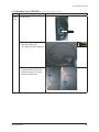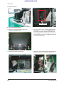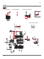
1
DLP TV Chassis:L70A(N)_Aquamarine Model :HL61A750A1FXZA HL67A750A1FXZA SERVICE DLP TV Manual CONTENTS 1. Precaution 2. Product Specification 3. Disassembly & Reassembly 4. Troubleshooting 5. Exploded View & Part List 6. Wiring Diagram 7. Schematic Diagram HL61A750A1F HL67A750A1F Refer to the service manual in the GSPN (see the rear cover) for the more information. justmanuals.com Table of Contents 1. Precaution 1-1 Safety Precautions.......................................................................................................................................................1-1 1-2 Servicing Precautions...................................................................................................................................................1-3 1-3 Static Electricity Precautions........................................................................................................................................1-4 1-4 Installation Precautions................................................................................................................................................1-5 2. Product Specification 2-1 Product Specification....................................................................................................................................................2-1 2-2 Specifications Analysis.................................................................................................................................................2-3 2-3 Accessories..................................................................................................................................................................2-4 3. Disassembly & Reassembly 3-1 Overall Disassembly & Reassembly.............................................................................................................................3-1 4. Troubleshooting 4-1 Troubleshooting............................................................................................................................................................4-1 4-2 Adjustment....................................................................................................................................................................4-6 4-3 Upgrade........................................................................................................................................................................4-30 5. Exploded View & Part List 5-1 HL61A750A1FXZA Exploded View..............................................................................................................................5-1 5-2 HL67A750A1FXZA Exploded View..............................................................................................................................5-3 5-3 HL61A750A1FXZA Service Item..................................................................................................................................5-5 5-4 HL67A750A1FXZA Service Item..................................................................................................................................5-6 6. Wiring Diagram 6-1 Overall Wiring...............................................................................................................................................................6-1 7. Schematic Diagram 7-1 Circuit Description........................................................................................................................................................7-1 7-2 K880 Engine.................................................................................................................................................................7-2 7-3 Schematic Diagram......................................................................................................................................................7-3 Precaution 1. Precaution To avoid possible damage, electric shocks or exposure to radiation, follow the instructions below with regard to safety, installation, service and ESD. 1-1 Safety Precautions 1. Make sure all protective devices are properly installed including non-metallic handles and compartment covers when installing or re-installing the chassis or chassis assemblies. 2. Make sure that no gaps exist between the cabinets for children to insert their fingers in. To prevent children from being electrocuted Errors may occur when the resistance is below 1.0㏁ or over 5.2㏁. In these cases, make sure that the device is repaired before sending it back to the customer. 3. Check for Electricity Leakage (Fig. 1-1) Warning: Do not use an insulated transformer for checking the leakage. Use only those current leakage testers or mirroring systems that comply with ANSIC 101.1 and the Underwriter Laboratory’s specifications (UL1410, 59.7). DEVICE UNDER TEST LEAKAGE CURRENT TESTER (READING SHOULD NOT BE ABOVE 0.5mA) TEST ALL EXPOSED METAL SURFACES EARTH GROUND Fig. 1-1 AC Leakage Test 4. A high voltage is maintained within the specified limits using safety parts, calibration and tolerances. When voltage exceeds the specified limits, check each special part. 5. Warning for Engineering Changes: Never make any changes or additions to the circuit design or the internal part for this product. Samsung Electronics 6. Warning - Hot Chassis: Some TV chassis are directly connected to one end of the AC power cord for electrical reasons. Without insulated transformers, the product can only be repaired safely when the chassis is connected to the earthed end of the AC power source. To make sure the AC power cord is properly connected, follow the instructions below. Use the voltmeter to measure the voltage between the chassis and the earthed ground. If the measurement is over 1.0V, unplug the AC power cord and change the polarity before re-inserting it. Measure the voltage between the chassis and the ground again. 7. Some TV chassis are shipped with an additional secondary grounding system. The secondary system is adjacent to the AC power line. These two grounding systems are separated in the circuit using an unbreakable/unchangeable insulation material. 8. When any parts, materials or wirings appear overheated or damaged, replace them with new regular ones immediately. When any damage or overheating is detected, correct this immediately and make a regular check of possible errors. 2-WIRE CORD ALSO TEST WITH PLUG REVERSED (USING AC ADAPTER PLUG AS REQUIRED) Ex: Do not add any audio or video accessory connectors. This might cause physical damage. Furthermore, any changes or additions to the original design/engineering will invalidate the warranty. 9. Check for the original shape of the lead, especially that of the antenna wiring, any sharp edges, the AC power and the high voltage power. Carefully check if the wiring is too tight, incorrectly placed or loose. Never change the space between the part and the printed circuit board. Check the AC power cord for possible damages. Keep the part or the lead away from any heat-emitting materials. 1-1 justmanuals.com Precaution 10.Safety Indication: Some electrical circuits or device related materials require special attention to their safety features, which cannot be viewed by the naked eye. If an original part is replaced with another irregular one, the safety or protective features will be lost even if the new one has a higher voltage or more watts. Critical safety parts should be bracketed with ( , ). Use only regular parts for replacements (in particular, flame resistance and dielectric strength specifications). Irregular parts or materials may cause electric shock or fire. 11. Pay additional attention to the current leakage as the voltage between the power board and the ballast is 220 to 440V, i.e. very high. And also beware of possible electric shock from the primary power source. 1-2 Samsung Electronics Precaution 1-2 Servicing Precautions Warning 1:First carefully read the “Safety Instruction” in this service manual. When there is a conflict between the service and the safety instructions, follow the safety instruction at all times. Warning 2:Any electrolytic capacitor with the wrong polarity will explode. 1. The service instructions are printed on the cabinet, and should be followed by any service personnel. 2. Make sure to unplug the AC power cord from the power source before starting any repairs. (a) Remove or re-install parts or assemblies. (b) Disconnect the electric plug or connector, if any. (c) Connect the test part in parallel with the electrolytic capacitor. 3. Some parts are placed at a higher position than the printed board. Insulated tubes or tapes are used for this purpose. The internal wiring is clamped using buckles to avoid contact with heat emitting parts. These parts are installed back to their original position. 7. Any B+ interlock should not be damaged. If the metal heat sink is not properly installed, no connection to the AC power should be made. 8. Make sure the grounding lead of the tester is connected to the chassis ground before connecting to the positive lead. The ground lead of the tester should be removed last. 9. Beware of risks of any current leakage coming into contact with the high-capacity capacitor. 10.The sharp edges of the metal material may cause physical damage, so protect yourself by wearing gloves during the repair. 4. After the repair, make sure to check if the screws, parts or cables are properly installed. Make sure no damage is caused to the repaired part and its surroundings. 5. Check for insulation between the blade of the AC plug and that of any conductive materials (i.e. the metal panel, input terminal, earphone jack, etc). 6. Insulation Check Process: Unplug the power cord from the AC source and turn the switch on. Connect the insulating resistance meter (500V) to the AC plug blade. The insulating resistance between the blade of the AC plug and that of the conductive material should be more than 1 ㏁. Samsung Electronics 1-3 justmanuals.com Precaution 1-3 Static Electricity Precautions 1. Some semi-conductive (“solid state”) devices are vulnerable to static electricity. These devices are known as ESD. ESD includes the integrated circuit and the field effect transistor. To avoid any materials damage from electrostatic shock, follow the instructions described below. 2. Remove any static electricity from your body by connecting the earth ground before handling any semi-conductive parts or assemblies. Alternatively, wear a dischargeable wristbelt. (Make sure to remove any static electricity before connecting the power source - this is a safety instruction for avoiding electric shock) 5. Use only grounded-tip irons for soldering purposes. 6. Use only anti-static solder removal devices. Most solder removal devices do not support an anti-static feature. A solder removal device without an anti-static feature can store enough static electricity to cause damage to the ESD. 7. Do not remove the ESD from the protective box until the replacement is ready. Most ESD replacements are covered with lead, which will cause a short to the entire unit due to the conductive foam, aluminum foil or other conductive materials. 3. Remove the ESD assembly and place it on a conductive surface such as aluminum foil to prevent accumulating static electricity. 8. Remove the protective material from the ESD replacement lead immediately after connecting it to the chassis or circuit assembly. 4. Do not use any Freon-based chemicals. Such chemicals will generate static electricity that causes damage to the ESD. 9. Take extreme caution in handling any uncovered ESD replacements. Actions such as brushing clothes or lifting your leg from the carpet floor can generate enough static electricity to damage the ESD. CAUTION These servicing instructions are for use by qualified service personnel only. To reduce the risk of electric shock do not perform any servicing other than that contained in the operating instructions unless you are qualified to do so. 1-4 Samsung Electronics Precaution 1-4 Installation Precautions 1. For safety reasons, more than two people are required for carrying the product. 5. Make sure to turn the power off and unplug the power cord from the outlet before repositioning the product. Also check the antenna cable or the external connectors if they are fully unplugged. Damage to the cord may cause fire or electric shock. 6. Keep the antenna far away from any high-voltage cables and install it firmly. Contact with the high-voltage cable or the antenna falling over may cause fire or electric shock. 2. Keep the power cord away from any heat emitting devices, as a melted covering may cause fire or electric shock. 3. When installing the product, make sure to keep it away from the wall (more than 10cm/4 inches spacing should be around the Top, Back, and both sides of the unit) for ventilation purposes. Poor ventilation may cause an increase in the internal temperature of the product, resulting in a shortened component life and degraded performance. 7. When connecting the RF antenna, check for a DTV receiving system and install a separate DTV reception antenna for areas with no DTV signal. 8. Check the basics of the screen test. - Image position/size, Tilt adjustment, Actuator activation 4. Bend the external antenna cable when connecting it to the product. This is a measure to protect it from being exposed to moisture. Otherwise, it may cause a fire or electric shock. om ls.c a u n a ustm j Samsung Electronics 1-5 justmanuals.com MEMO 1-6 Samsung Electronics Product Specification 2. Product Specification 2-1 Product Specification Features Block Specification Major IC RF Integrated HDTV Tuner (QAM NIM TUNER Embedded) QamLink DMD Panel Resolution : 1920 x 1080 xHD5 DMD Panel Power Input Voltage : AC110V~120V Stand-By : under 1W Stand-by (VIPER12A) Video Component Interface : 480i/480p/720p/1080i/1080p Digital Interface : 3 HDMI In (HDMI1.3) (DVI Comfortable with adaptive jack only) DNIe BAYHILL+, MST3360CCLK Sound SRS TruSurround XT, Dolby Digital BAYHILL+ STA335BW SGTV5910 Cabinet K8 Design Remark Specification Model HL61A750A1F HL67A750A1F Screen Size 61 inches (1372 x 782mm) 67 inches (1524 x 875mm) Dimensions (WxHxD) 54.8 x 37.7 x 15.4 inches (1391 x 957 x 392 mm) 60.7 x 41.5 x 16.5 inches (1544 x 1054 x 420.5 mm) Weight 74.7 lbs (33.9 Kg) 86.6 lbs (39.3 Kg) Voltage AC 110 - 120V, 60Hz PC Resolution Analog : 640x350, 720x400, 640x480, 800x600, 1024x768, 1152x864, 1280x960, 1280x1024, 1920x1080 HDMI3/DVI : 640x350, 720x400, 640x480, 800x600, 1024x768, 1280x1024, 1920x1080 ANTENNA input Antenna Input 1: Air, Cable VIDEO input Composite Video Input1/2, S-Video1 Component1: 480i/480p/720p/1080i/1080p Component2: 480i/480p/720p/1080i/1080p HDMI1 : 480p/720p/1080i//1080p HDMI2 : 480p/720p/1080i//1080p HDMI3/DVI : 480p/720p/1080i//1080p * HDMI3 support DVI signal for PC input Video Output No Video Output AUDIO input Composite L/R Input 1/2, S-Video L/R Input 1 Component1 Input L/R, Component2 Input L/R DVI Audio L/R PC Audio Input Audio Output Optical (SPDIF), Audio L/R Output Speaker Output 10W + 10W New Features Wiselink (USB2.0), 3D Ready, Anynet+ Samsung Electronics 2-1 justmanuals.com Product Specification ■ New Features explanation - The Entertainment mode enables you to select the optimal display and sound for sports, cinema and games. ▪ Off: Switches the Entertainment function off. ▪ Sports: Provides the optimal picture and sound quality for sports. ▪ Cinema: Provides the optimal picture and sound quality for movie watching. You can experience a richer picture and enhanced sound. ▪ Game: Provides the optimal picture and sound quality for games. This mode accelerates the playing speed when using an external game console connected to the TV. - WISELINK (USB2.0) : This function enables you to view and play photo (JPEG) and audio files (MP3) through the TV’s WISELINK jack. - 3D/Dual-View : The HLT generation of Samsung DLP HDTVs are capable of displaying future 3D games, movies and other programming vis 3D compatible glasses and hardware. - ANYNET+ (HDMI CEC) : AV network system that enables you to control all connected Samsung AV devices with your Samsung TV’s remote. The Anynet+ system can be used only with Samsung AV devices that have the Anynet+ feature. To be sure your Samsung AV device has this feature, check if there is an Anynet+ mark on it. ■ PIP Table (1 tuner = Analog/Digital, O: PIP, X : PIP doesn’t operate) Sub Main TV digital TV analog Video1,2 S-Video1 COMP1,2 HDMI1,2,3 PC TV digital TV analog Video1,2 S-Video1 COMP1,2 HDMI1,2,3 PC X X X X X X X X X X X O O O X X X X X X X X X X X X X X X X X X X X X X X X X X X X X X X X X X X - PIP is only available in RF (TV) mode. 2-2 Samsung Electronics Product Specification 2-2 Specifications Analysis ※ : application, : non-application Model HL61A750 HL67A750 HL-T6189S Design Picture Audio Features Connections Display Device DLP DLP DLP Built-in Tuner Clear QAM Clear QAM Clear QAM Display Format 1080p, 1080i, 720p, 480p, 480i 1080p, 1080i, 720p, 480p, 480i 1080p, 1080i, 720p, 480p, 480i Screen Size 61 inch 67 inch 61 inch Aspect ratio 16:9 16:9 16:9 Progressive scan Yes Yes Yes Digital Comb Filter 3D Comb 3D Comb 3D Comb First Surface Mirror Yes Yes Yes Brightness 600cd/㎡ 600cd/㎡ 600cd/㎡ Contrast 10000:1 10000:1 10000:1 Color Wheel Size/Bearing No Color Wheel No Color Wheel No Color Wheel Anti-glare Sun Screen No No No Screen Pitch 0.098mm 0.098mm 0.098mm Image enhancer BAYHILL+ BAYHILL+ FBEx DMD xHD5 xHD5 xHD5 Base/Tremble/Balance No No No Equalizer 7 Band 7 Band 7 Band Auto Volume Leveler Yes Yes Yes Surround Sound TruSurround XT Dolby Digital TruSurround XT Dolby Digital TruSurround XT Dolby Digital Speaker system Hidden Hidden Hidden Output Power 10Wx2 10Wx2 10Wx2 Tuner 1 Input 1Tuner 1 Input 1Tuner 2 Input 1Tuner Split-screen Side-by-Side Yes Yes Yes MTS with dbx Noise Reduction/SAP Yes Yes Yes Still Picture Yes Yes Yes Wise Link Yes Yes Yes Plug & Play Yes Yes Yes S-Video In Rear 1 Rear 1 Rear 2 HDTV Component Video Input (Y, Pb, Pr) 1080p/1080i/480P /480i/720P Rear 2 Rear 2 Rear 2 PC Yes Yes Yes HDMI 3 3 3 Digital Sound Optical 1 Optical 1 Optical 1 LED LED LED LED BLUETOOTH No No Yes Samsung Electronics 2-3 justmanuals.com Product Specification 2-3 Accessories Accessories that can be purchased additionally Supplied Accessories Accessories 2-4 Item Item code Remote Control Batteries BN59-00673A 4301-000103 Power Cord 3903-000144 Owner’s Instructions BP68-00658A Warranty Card Registration Card Safety Guide Manual BN68-00872B AA68-03242L Cloth-Clean BN63-01798A HDMI/DVI cable - HDMI Cable - S-VIDEO Cable - Antenna Cable - Component Cables (RCA) - 1Stereo/2RCA Cable - PC Audio Cable - Audio/Video Cables - Remark Samsung Service center Electronics Store/ Internal shopping mall Samsung Electronics Disassembly & Reassembly 3. Disassembly & Reassembly 3-1 Overall Disassembly & Reassembly 3-1-1 Separation of the back cover and the chassis (Disassembly is in reverse order of the assembly) Part Name Description Back Cover ①Remove 10 screws to remove the back bottom cover. :BH,+,B,M4,L12,ZPC(BLK),SWRCH18 Terminal Board ① Remove the Terminal Board by hands Holder Chassis ① Remove 1 screw at the left side of Main Assy. :BH,+,B,M4,L12,ZPC(BLK),SWRCH18 Samsung Electronics Description Photo 3-1 justmanuals.com Disassembly & Reassembly Part Name Description Holder Chassis ① Remove 1 screw at the right side of Main Assy. :BH,+,B,M4,L12,ZPC(BLK),SWRCH18 Description Photo ① Seperate the LVDS Cable. ① Separate 10PIN DMD power cable, 2PIN Sub SMPS Wire and, 2 pin Inlet cable at the right side of Main Assy. ① Separate 12 pin Wire, and the Speaker wire at the left side of Main Assy. 3-2 Samsung Electronics Disassembly & Reassembly Part Name Holder Chassis Description Description Photo ① Pull out the holder Chassis. Side direction. 3-1-2 Separation of the Main Board and Power Board (Disassembly is in reverse order of the assembly) Part Name Description Description Photo Main Assy ①Separate the 24PIN SMPS Wire, 1PIN GT Wire and. ① Remove 5 screws. :BH,+,-,S,M3,L6,ZPC(WHT), SWRCH18A ② Separate the SMPS Board. Samsung Electronics 3-3 justmanuals.com Disassembly & Reassembly Part Name Description Description Photo Main Assy ① Remove 4 screws. :PWH,+,B,M3,L10,ZPC(YEL), SWRCH18A ② Separate the Top Shield Case. ① Remove 1 screws. :PWH,+,B,M3,L10,ZPC(YEL), SWRCH18A ② Separate the Bottom Shield Case. 3-4 Samsung Electronics Disassembly & Reassembly 3-1-3 Separation of the Optical Engine (Disassembly is in reverse order of the assembly) Part Name Description Optical Engine ①Remove the 10 PIN DMD Power Cable and LVDS Cable (the bottom one on the left side). Description Photo ① Remove the 6 PIN LED Power Cable. ① Remove the 2 screw. : BH,+,B,M4,L12,ZPC(BLK),SWRCH18 ② Remove the engine by pulling it out of the cabinet. :Be careful when removing the Light Engine as it may get caught up by the upper cable of the case. Samsung Electronics 3-5 justmanuals.com Disassembly & Reassembly 3-1-4 Separation of the Sub Power Board (Disassembly is in reverse order of the assembly) Part Name Sub Power Board Description Description Photo ①Separate the 6PIN LED Power cable, 2PIN Sub SMPS Wire and 1PIN GT Wire. ① Remove 2 screws. :BH,+,B,M4,L12,ZPC(BLK),SWRCH18 ② Pull out the chassis. ① Remove the screws and detach the boards from the holder chassis. :PWH,+,-,B,M3,L10,ZPC(WHT), SWRCH18A,- 3-6 Samsung Electronics Disassembly & Reassembly 3-1-5 Separation of the LED Driver Board (Disassembly is in reverse order of the assembly) Part Name LED Driver Board Description Description Photo ① Separate the optical chassis from the Cabinet. ② Remove the 2 screws. :BH,+,B,M4,L12,ZPC(BLK),SWRCH18 ③ Remove the Cover-P/J Lens from the Optical chassis. ① Separate the cables. ① Remove the FAN. Samsung Electronics 3-7 justmanuals.com Disassembly & Reassembly Part Name Description LED Driver Board ① Remove the 3 screws. :PH,+,M4,L12,NI PLT,SWRCH18A,FP,- Description Photo ① Remove the 4 screws. :PWH,+,-,B,M3,L6,ZPC(WHT), SWRCH18A,- 3-8 Samsung Electronics Disassembly & Reassembly 3-1-6 Actuator (Smooth Picture) Replacement (Disassembly is in reverse order of the assembly) Part Name Actuator Description Description Photo ①Remove the cable at the Actuator. ① Remove the 3 screws. :BH,+,WSP,M3,L16,ZPC(WHT), SWRCH18A,-,- ① Replace it with a new actuator. ① Actuator, fixing bolts. Samsung Electronics 3-9 justmanuals.com Disassembly & Reassembly 3-1-7 Separation of the DMD Board and Panel (Disassembly is in reverse order of the assembly) Part Name DMD Board Description Description Photo ① Separate the optical chassis from the Cabinet. ② Remove the 2 screws. :BH,+,B,M4,L12,ZPC(BLK),SWRCH18 ③ Remove the Cover-P/J Lens from the Optical chassis. ① Remove the FAN in front of the DMD Board. ② Separate the 8point Cables. ① Remove the 4 point screws. :PWH,+,-,M3,L30,NI PLT,SWRCH18A,UP,② After pushing the part of Spring_H/S DMD then separate it. ① Remove the 4 screws. :PWH,+,,B,M3,L6,ZPC(WHT), SWRCH18A,② Remove the Shield Case-DMD(R). 3-10 Samsung Electronics Disassembly & Reassembly Part Name DMD Board Description Description Photo ① Remove the 4 point screws. :BH,+,M3,L12,NI PLT,SWRCH18A,-,② Remove the Bracket. :Don’t remove the 3 Yellow point screws ① Remove the DMD Board. Separate DMD Panel. DMD Panel DMD Panel DMD Panel ① DMD Board DMD Panel Samsung Electronics 3-11 justmanuals.com Disassembly & Reassembly 3-1-8 Separation of the LEDs (Disassembly is in reverse order of the assembly) Part Name LED Description Description Photo ① Separate the optical chassis from the Cabinet. ② Remove the 2 screws. :BH,+,B,M4,L12,ZPC(BLK),SWRCH18 ③ Remove the Cover-P/J Lens from the Optical chassis. ① Remove the 6 point screws. :BH,+,-,B,M3,L8,ZPC(BLK), SWRCH18A,② Separate the COVER-TOP. ① Remove the FAN. 3-12 Samsung Electronics Disassembly & Reassembly Part Name LED Description Description Photo ① Remove the FAN. ① Remove the 4 point screws of Heat Sink-Pipe and then Remove the Heat Sink-Pipe. : ① Remove the BLUE LED. ① Remove the GREEN LED. Samsung Electronics 3-13 justmanuals.com Disassembly & Reassembly Part Name LED Description Description Photo ① Remove the RED LED. ① LED 3-14 Samsung Electronics Disassembly & Reassembly 3-1-9 Separation of the SCREEN (Disassembly is in reverse order of the assembly) Part Name Description Description Photo FRONT, ①Separate 12 screws for fixing REAR COVER-REAR and COVER-FRONT. disassembly : TH, M4, L15, BLK ①Separate 10 screws for fixing COVER-REAR, Bottom and COVER-FRONT. : TH, M4, L15, BLK ①Separate Bottom and COVER-REAR pull right and then take them off. Samsung Electronics 3-15 justmanuals.com Disassembly & Reassembly Part Name Description Description Photo HOLDER- ① After separating COVER-REAR and TERMINAL Bottom, separate HOLDER-TERMINAL. disassembly CONNECTOR ①Remove 1 Screw disassembly : TH, M4, L15, BLK ② Separate the 2 connectors from the main board 3-16 Samsung Electronics Disassembly & Reassembly Part Name Description Description Photo FRONT ① Separate COVER-FRONT from SET. COVER disassembly ② Separate 3 screws fixing BRKT-SCREEN : TH, M4, L12, YELLOW TOP BRACKET ① Remove the BRKT-SCREEN by SCREEN pushing it toward the direction of the disassembly arrow. TOP TOP Left - Right Left - Right Left - Right Bottom Bottom Bottom Samsung Electronics 3-17 justmanuals.com Disassembly & Reassembly Part Name Description Description Photo SCREEN ①Place your hand at the bottom center of disassembly the screen then pick it up while pulling it towards you. ①Separate the screen in the COVERFRONT. 3-18 Samsung Electronics Disassembly & Reassembly 3-1-10Separation of the COVER-DUST (Disassembly is in reverse order of the assembly) Part Name COVER DUST Description Description Photo ①COVER-DUST COVER-DUST COVER-DUST ①Separate 1 screw for fixing COVERCOVER-DUST REAR and^pCOVER-DUST : BH,+,B,M4,L12,ZPC(BLK),SWRCH18 ②Push the indicating sign of the picture and separate SNAP of C/DUST from C/REAR. (Pushing part : the upper or lower part of jointing Screw) Samsung Electronics 3-19 justmanuals.com Disassembly & Reassembly Part Name COVER DUST Description Description Photo ③Separate C/DUST with using the gap which occurs when^pSNAP of C/DUST is separated. ①Separate the screen in the COVERFRONT. 3-20 Samsung Electronics Troubleshooting 4. Troubleshooting 4-1 Troubleshooting 4-1-1 First Checklist for Troubleshooting ■ Basics: - The DDP3021 on the DMD board has a feature to display internal test patterns. - The BAYHILL+ is the output of the Main. DMD is the final one. ■ Diagnosis By Module 1. Access Service Mode (In Standby mode, press MUTE, 1, 8, 2 and POWER to turn the screen on and enter service mode) 2. Check if there is an error in the DMD board DDP3021 → TEST PATTERN → Press the right arrow key: Options of FULL WHITE, BLACK, RED, GREEN and BLUE PATTERN and so on are displayed on the screen. If “Pattern” does not appear or same symptom is appeared on DDP3021 pattern, this is a DMD board error. 3. Check if there is an error in the main board. Check for a power signal from SMPS to other board see the schematic diagram. (7-3) And check for indicated power signal. DMD MAIN SCREEN ATV, DTV, AV I N P U T BAYHILL+ PC Component HDMI DDP3021 MST336 CCLK OSD OK? NG OK DDP 3021 Pattern OK DMD Panel CHECK THE SCREEN NG CHECK THE SOURCE Main BOARD ERROR Samsung Electronics DMD BOARD ERROR 4-1 justmanuals.com Troubleshooting ■ Flow Chart for Malfunction Yes Does the TV turn on? No Can you see anything on the screen? Yes No Yes Can you see OSD menu running on the screen? No Check Cables connected to Main Board. If necessary, replace the Main Board Check the Power Cord Can you see Digital Channel broadcast ? No Yes Replace the Main Board No Is LED for illumination off? 1) Check the LVDS Cable connected between the Main Board and the DMD Board. If necessary, replace LVDS Cable. Check Cables connected to DMD Board. If necessary, replace DMD Board. Yes Check Logic Power (CN9007) Yes 12V OK? (Pin 18) No Check Cables connected to DMD Board (CN801 Pin 18). If necessary, replace DMD Board. No Check Cables connected to DMD Board (CN801 Pin 21, 22). If necessary, replace DMD Board. Yes 5V OK? (Pin 21/22) Yes Check Driver Power (CN9005) Yes 16V OK? (Pin 2/4/6) R9010 Gronding No Check Sub SMPS Yes Operate driver in internal mode (grounding R9010) LED On? No Replace driver Yes Check Cables connected to DMD Board. If necessary, replace DMD Board. 4-2 Samsung Electronics Troubleshooting ■ Installation & Connection ●:Light is On ◑:Light is Blinking ○:Light is Off TIMER LED STAND BY/ TEMP ● ○ ○ Standby state. ○ ○ ◑ The picture will automatically appear in about 15 seconds. ○ ● ○ Auto Timer ON/OFF has been set and the set will automatically be turned on in about 15 seconds. ◑ ◑ ○ A cooling fan inside the set is not operating normally. ◑ ○ ○ The inner Power Signal on the main board may be short or opened. Please contact a certified technician. ◑ ◑ ◑ LED may be defective. Please contact a certified technician. Indication ■ Protect Status 1. Attempting to turn the LED ASSY on fails repeatedly If turning the LED on fails, the set automatically tries turning the LED ASSY on 3 times. If all attempts fail, all LED’s on the front panel will blink. Check the LED ASSY, LED Driver and the Sub power or SMPS and replace them if necesscary. Samsung Electronics 4-3 justmanuals.com Troubleshooting 4-1-2 Faults and Corrective Actions Symptom Related Image Causes and Countermeasures 40 Vertical lines 16 pixels wide DDP3021 or BGA, DMD panel interference. - Replace the DMD board Horizontal Bar or No Raster Error in DDP3021 or the DMD panel. - Replace the DMD board Dotted Vertical Bar Error in Rambus Dram (IC301) or the soldering. - Replace the DMD board Beehive mosaic patterns all over the screen Error in the LVDS Receiver (IC101,IC102) or the soldering. The H sync signals are not transferred to DDP3021. - Replace the DMD board. 4-4 Samsung Electronics Troubleshooting 1. Noise: Internal noise may be caused by a foreign substance on the fan or driving device. For a DLP TV, the LED fans and DMD board fan are vulnerable to noise. Sometimes the connector wire around the lamp or DMD fan makes contact with the fan. When irregular noise occurs for no particular reason, check the inside of the TV for any foreign substances. The DLP projection TV may cause noise because the physical space is empty inside, causing a resonance at a particular frequency. Thus a low vibration is not a malfunction. Any ‘creaking’ noise is mostly from the structure of the device itself. A short, harsh noise may occur from a distortion or malformation due to thermal expansion between the metal joints, screws and loaded parts, respectively. Any intermittent ‘creaking’ noise can be removed by loosening the screws. 2. Black Screen (Voice Output):Replace the DMD board 3. A black screen with the LED on : Replace the DMD Board. 4. Line Pattern: Regular line patterns occur vertically or horizontally: Replace the DMD board. 5. Voice Distortion: Replace the main board. 6. Outside Light: This is not a product malfunction, but a possible installation or human error. This occurs when the projected light from the surrounding illumination reflects onto the screen. This disappears as the TV starts operating and the TV lamp gets brighter. However, you can avoid outside light by changing the position of the TV or the installation angle. Decreasing the illumination or changing the indoor lighting may work. 7. Screen Flip-over: Enter Factory mode in DDP3021 and perform H-Flip (flip horizontally) and V-Flip (flip vertically). The screen will flip over horizontally or vertically. Samsung Electronics 4-5 justmanuals.com Troubleshooting 4-2 Adjustment 4-2-1 Service Instruction ■ Check items listed after changing each Check Items Replaced Items S/W Version Front LED Actuator Gain V-Position H-Position LED control Board LED ● ● ● ● ● ● Main Board Main Power Board ● Sub Power Board ● Optical Engine ● DMD Board ● ● ● ● ● ● LED (R/G/B) ● ● Front LED Assy ● ● Detect Board ● LED Driver board 1. Software version check : After Entering the Service mode, Check the list below *S/W Notation “T-AQMAUSC-XXXX” indicates “AquaMarine Model US VER XXXX” 2. Front Information Window check : See page 4-4. 3. DMD 0x00000001 indicates DMD board bit sequence program version. 4. Actuator Gain adjustment : See page 4-24. Tilt Focus ● ● ● ● ● ● T-AQMAUSC-XXXX T-AQMAUSM-XXXX EDID SUCCESS RFS : T-AQMAUSC-YYYYMMDD YYYY-MM-DD DMD XX, DSP-X-X-X DTP-LM-XXXX Date of Purchase : DD/MM/YYYY 5. Vertical / Horizontal Position adjustment : See page 4-21. 6. CCA : See page 4-22. 7. Board LED check : Check the LED is turned on. (In the DMD Board) 8. Tilt/Focus adjustment : See page 4-25 ~4-28. 4-6 Samsung Electronics Troubleshooting 4-2-2 How to Access Service Mode 1. Turn off the power to put the unit into the STAND-BY mode. 2. In order to enter the Service Mode, press MUTE 1 8 2 In case entry into SERVICE MODE is unsuccessful, repeat the procedures above. POWER button on the remote control. 3. Initial DISPLAY State in times of Service Mode Switch overs Option Byte DDP3021 CCA(ON) Cinema CCA Desaturation(ON) SP Actuator WB EPA Standard BHP_VDEC MST336C BHP_DP Sharpness FBE3 LNA+ Expert Setting Expert D-Setting Expert Gray Scale Expert C-Space Expert Others SOUND EDID ESP CHECKSUM SERVICE DEFECT LOG Font Data Viewer T-AQMAUSC-XXXX T-AQMAUSM-XXXX EDID SUCCESS RFS : T-AQMAUSC-YYYYMMDD YYYY-MM-DD DMD XX, DSP-X-X-X DTP-LM-XXXX Date of Purchase : DD/MM/YYYY 4. Buttons operations within Service Mode MENU Full Menu Display / Move to Parent Menu Item Selection by Moving the Cursor Direction keys ▲/ ▼ Direction keys ◀ / ▶ Data Increase/Decrease for the Selected Item Source Cycles through the active input source that are connected to the unit Enter Item Selection/execution Samsung Electronics 4-7 justmanuals.com Troubleshooting 4-2-3 Factory Data ♦ The underlined are items applied during the service adjustment. None of the others should be adjusted. 1. Option Byte No Item Range Default Remark 1 Factory Reset OFF/ON OFF Clear user data and Digital to DMD. 2 WB Reset OFF/ON OFF Clear WB Data When EEPROM Reset, If it is ON. 3 EEPROM Reset OFF/ON Clear EEPROM related with picture setting data and user data. 4 User Reset OFF/ON Clear EEPROM related with the informaion of user like channel, time, etc. 5 DIGITAL → DMD Transfer CCA data from Main to DMD B’d 6 LED Clear Clear LED Life time 7 LED Life The time for LED On 8 Auto Power 9 Mute Time[RF] 10 The set set turns on automatically when it is plug in after the sets is plug out while the set is on OFF/ON ON 0~1000ms 600ms PROTECT OFF/ON OFF Check Fan Error, Temperation, Cover detect 11 Watchdog Enable OFF/ON OFF Watch Dog ON/OFF selection 12 Watchdog Count 13 DEBUG/RS232 Debug/RS232 Debug 14 PC Mode Ident Auto/Enable Auto PC is always ident on enable Mode. 15 HDMI Hot Plug Enable/Disable Enable Hot Plug is Enable on Enable Mode 16 HDMI Hot Plug Delay 0~5000ms 1500ms Set the time of Hot Plug Delay 17 HDMI Mute Time Not Used 18 Shop Mode OFF/ON 19 DMD → DIGITAL 20 DDP 3D Test OK/NG 21 Expert Adj. OFF/ON OFF Expert control the set by RS-232 22 SUB MICOM DOWN OFF/ON OFF Enable Sub Micom download when it is on. 23 SSC ON/OFF ON ON/OFF Control the Spread Spectrum. Controled by Engineer. 24 SSC MRR 0 Control the Spread Spectrum. Controled by Engineer. 25 SSC MFR 0 Control the Spread Spectrum. Controled by Engineer. 26 SSC QLC 0 Control the Spread Spectrum. Controled by Engineer. 27 VISUAL TEST 4-8 0 Time which the screen will be black while switching Count for Watch Dog event Toggle between RS232 and Debug Mode Set the HDMI Mute time OFF Shop mode on OFF, Home mode on ON Transfer CCA data from DMD B’d to Main B’d Enable/Disable Test the 3D ready function. Disable OSD is semitransparent on Disable Samsung Electronics Troubleshooting 2. DDP3021 No Item Range Default Remark 1 H/V-Position H:0/V:0 ~:60/ V:60 H:56/V:42 2 V-FLIP Flip/Normal Normal Vertical Flip Operation 3 H-FLIP Flip/Normal Normal Horizontal Flip Operation 4 GAMMA 5 MPC ON/OFF ON MPC function On/Off 6 3D GLS_TRANS 0~4000 1800 Horizontal Flip Operation 7 Calibration Gamma Table Selection Test Pattern(DDP) This displays the built-in pattern of the DDP3021 chip. DDP3021 drives the DMD panel, so displaying this pattern means there is no error in the DDP3021 projection function and the panel itself. 8 Samsung Electronics Horizontal and Vertical image adjustment Gamma Table Selection 0~18 0 4-9 justmanuals.com Troubleshooting 3. CCA(ON) No Item Range Default Remark 1 CCA Control On/Off On CCA On/Off Selection 2 Sensor Status OK/NG OK Color Sensor valure save 3 Red-x 0.000~0.999 703 Red-x measurement value using CA210 4 Red-y 0.000~0.999 292 Red-y measurement value using CA210 5 Red-Y (0~65535) 80.0 Red-Y measurement value using CA210 6 Green-x 0.000~0.999 173 Green-x measurement value using CA210 7 Green-y 0.000~0.999 731 Green-y measurement value using CA210 8 Green-Y (0~65535) 300.0 Green-Y measurement value using CA210 9 Blue-x 0.000~0.999 146 Blue-x measurement value using CA210 10 Blue-y 0.000~0.999 31 Blue-y measurement value using CA210 11 Blue-Y (0~65535) 25.0 Blue-Y measurement value using CA210 12 Color Sensor Save OK - 13 WB Spread OK - 14 [COOL2] DW-X 0.000~0.999 264 15 [COOL2] DW-Y 0.000~0.999 267 16 [COOL1] DW-X 0.000~0.999 269 17 [COOL1] DW-Y 0.000~0.999 274 18 [NORMAL] DW-X 0.000~0.999 276 19 [NORMAL] DW-Y 0.000~0.999 282 20 [WARM1] DW-X 0.000~0.999 285 21 [WARM1] DW-Y 0.000~0.999 293 22 [WARM2] DW-X 0.000~0.999 300 23 [WARM2] DW-Y 0.000~0.999 310 24 Max Current RED 0~255 232 25 Max Current GRN 0~255 228 26 Max Current BLU 0~255 232 27 Sens Red-A - 2604 28 Sens Green-B - 2244 29 Sens Blue-C - 3238 30 [TI - COOL2] X 0.000~0.999 264 31 [TI - COOL2] Y 0.000~0.999 267 32 [TI - COOL1] X 0.000~0.999 269 33 [TI - COOL1] Y 0.000~0.999 274 34 [TI - NORMAL] X 0.000~0.999 276 35 [TI - NORMAL] Y 0.000~0.999 282 36 [TI - WARM1] X 0.000~0.999 300 37 [TI - WARM1] Y 0.000~0.999 310 38 [TI - WARM2] X 0.000~0.999 311 39 [TI - WARM2] Y 0.000~0.999 327 40 TI Offset Adjust ON/OFF ON 4-10 Samsung Electronics Troubleshooting 4. Cinema CCA No Item Range Default Remark 1 [COOL2] DWhiteX 0 ~ 32766 269 Target Red X value for CCA 2 [COOL2] DWhiteY 0 ~ 32766 274 Target Red Y value for CCA 3 [COOL1] DWhiteX 0 ~ 32766 276 Target Green X value for CCA 4 [COOL1] DWhiteY 0 ~ 32766 282 Target Green Y value for CCA 5 [NORMAL] DWhiteX 0 ~ 32766 285 Target Blue X value for CCA 6 [NORMAL] DWhiteY 0 ~ 32766 293 Target Blue Y value for CCA 7 [WARM1] DWhiteX 0 ~ 32766 300 Target Cyan X value for CCA 8 [WARM1] DWhiteY 0 ~ 32766 310 Target Cyan Y value for CCA 9 [WARM2] DWhiteX 0 ~ 32766 313 Target Magenta X value for CCA 10 [WARM2] DWhiteY 0 ~ 32766 329 Target Magenta Y value for CCA m .co s l a u n a justm Samsung Electronics 4-11 justmanuals.com Troubleshooting 5. Desaturation(ON) No Item Range Default 1 Desaturation Control ON/OFF ON 2 Desaturation Mode Normal, Wide, RGB 0 [Normal] 3 [NORMAL] Red-x 0 - 1000 660 4 [NORMAL] Red-y 0 - 1000 315 5 [NORMAL] Green-x 0 - 1000 260 6 [NORMAL] Green-y 0 - 1000 640 7 [NORMAL] Blue-x 0 - 1000 150 8 [NORMAL] Blue-y 0 - 1000 50 9 [NORMAL] Cyan-x 0 - 1000 179 10 [NORMAL] Cyan-y 0 - 1000 293 11 [NORMAL] Magenta-x 0 - 1000 263 12 [NORMAL] Magenta-y 0 - 1000 108 13 [NORMAL] Yellow-x 0 - 1000 412 14 [NORMAL] Yellow-y 0 - 1000 518 15 [WIDE] Red-x 0 - 1000 680 16 [WIDE] Red-y 0 - 1000 305 17 [WIDE] Green-x 0 - 1000 165 18 [WIDE] Green-y 0 - 1000 700 19 [WIDE] Blue-x 0 - 1000 150 20 [WIDE] Blue-y 0 - 1000 38 21 [WIDE] Cyan-x 0 - 1000 163 22 [WIDE] Cyan-y 0 - 1000 293 23 [WIDE] Magenta-x 0 - 1000 265 24 [WIDE] Magenta-y 0 - 1000 95 25 [WIDE] Yellow-x 0 - 1000 413 26 [WIDE] Yellow-y 0 - 1000 520 27 [sRGB] Red-x 0 - 1000 640 28 [sRGB] Red-y 0 - 1000 330 29 [sRGB] Green-x 0 - 1000 295 30 [sRGB] Green-y 0 - 1000 595 31 [sRGB] Blue-x 0 - 1000 150 32 [sRGB] Blue-y 0 - 1000 60 33 [sRGB] Blue-y 0 - 1000 225 34 [sRGB] Cyan-y 0 - 1000 390 35 [sRGB] Magenta-x 0 - 1000 365 36 [sRGB] Magenta-y 0 - 1000 170 37 [sRGB] Yellow-x 0 - 1000 422 38 [sRGB] Yellow-y 0 - 1000 494 39 Over lap 0~2 0 4-12 Remark Samsung Electronics Troubleshooting 6. SP Actuator No Item Range Default Remark 1 Actu Gain [Patt1] 0~175 45 Actuator Gain adjustment 2 Actu Gain [Patt2] 0~175 45 Actuator Gain adjustment 3 Actu On/Off 0~1 ON Actuator On/Off selection 4 DB On/Off 0~1 OFF 5 DB Border ON/OFF OFF 6 DB BP Weight - 0 7 DB Gain 0~3 0 8 DB Aperture ON/OFF ON 9 SB Gain 0~255 0 7. WB (White Balance) No Item Range Default 1 Sub Brightness 0~255 128 2 R-Offset 0~1023 512 3 G-Offset 0~1023 512 4 B-Offset 0~1023 512 5 Sub Contrast 0~ 255 128 6 R-Gain 0~1023 512 7 G-Gain 0~1023 512 8 B-Gain 0~1023 512 Range Default Remark 8. EPA Standard No Item Remark 1 Standard Contrast 0~100 95 Setting Contrast in Standard Mode 2 Standard Brightness 0~100 45 Setting Brightness in Standard Mode 3 Standard Sharpness 0~100 50 Setting Sharpness in Standard Mode 4 Standard Color 0~100 50 Setting Color in Standard Mode 5 Standard Tint 0~100 50 Setting Tint in Standard Mode 6 Standard Backlight 0~10 7 Setting Backlight in Standard Mode Samsung Electronics 4-13 justmanuals.com Troubleshooting 9. BHP_VDEC No Item Range Default 0~1 1 0~8184 880 Remark 1 agc_mode 2 Y_Gain_Man 3 saturation 255 128 4 hue 255 0 5 Y_shape_sel 13 6 C_shape_sel 4 7 If_iir 0 If comp filter bypass 8 if_filt_sel 7 If comp filter selection 9 LTI_en 0 10 LTI_filt_sel 0 Select filter response as part of LTI (0:filter response 0, 1:filter response 1) 11 LTI_level 15 Bigger value:less obvious sharpening of luma transients, 0:max transient improvement 12 CTI_en 0 CTI level 13 CTI_filt_set 1 Select filter response as part of CTI (0:filter response 0, 1:filter response 1) 14 CTI_level 15 CTI level 15 V_Delay_adj 1 16 U_Delay_adj 0 17 ST_Beg_NTSC 0 18 vs_slice_level 3 Vs slice level 00 → lowest, 11 highest 19 hs_slice_level 6 Hs slice level 00 → lowest, 11 highest 20 synctip_noise 17 Synctip noise readback 21 bl_auto_speed_control 0 1 → auto speed up/down hs pll based on input quality, 0 → don’t 22 bl_force_slow 0 Hsync pll parameter 23 bl_force_fast 0 Hsync pll parameter 24 3D_DNR_en 1 25 3D_DNR_Gain 11 26 allow_3d_filt_sel 0 27 3d_comb_noise_sns 0 Larger values allow more temporal comb for noisy RF signals but may also introduce motion error 28 3d_comb_chroma_sns 8 Larger values decrease 3D comb motion detection sensitivity to chroma motion and noise 29 3d_comb_chroma_sns 8 Larger values increase 3D comb motion detection sensitivity to chroma motion and noise 30 3d_comb_luma_core 8 Larger values decrease 3D comb motion detection sensitivity to luma motion and noise 31 3d_comb_luma_sns 8 Larger values increase 3D comb motion detection sensitivity to luma motion and noise 32 cmd_gain_mts_ntsc 0 4-14 Saturation Positive range 0x0000 00 → 0x3F (brightest), Negative range 0x40 (darkest) → 0xFF Larger values give narrower bandwidth and more noise reduction but also more motion blur DNR noise bandwidth Samsung Electronics Troubleshooting 10.MST336C No Item Range Default 1 RED CUTOFF 0~255 128 2 GREEN CUTOFF 0~255 128 3 BLUE CUTOFF 0~255 128 4 PHASE 0~63 46 5 RED GAIN 0~255 192 6 GREEN GAIN 0~255 192 7 BLUE GAIN 0~255 192 8 SOGMID_CTRL 0~31 23 9 SEP_THR 0~255 45 10 PRECST 0~255 11 11 POSTCST 0~255 11 12 ADC_BWR 0~15 0 13 ADC_BWG 0~15 0 14 ADC_BWB 0~15 0 15 SOG_BW 0~255 0 16 D_R_offset 0~127 0 17 D_G_offset 0~127 0 18 D_B_offset 0~127 0 19 D_CALDLYC 0~255 224 20 D_SMPDLY 0~255 12 21 D_SMPDURC 0~255 8 22 CAL_CTRL0 0~255 157 Samsung Electronics Remark INACTIVE 4-15 justmanuals.com Troubleshooting 11. BHP_DP No Item Range Default 0~3 1 1 Deblock_ON 2 MixTH1 0~255 110 3 MixTH2 0~255 55 4 NARS_ON 0~3 0 5 SD_CSC 0~9999 7094 6 HD_CSC 0~9999 7438 7 M_SD_CSC 0~9999 7094 8 M_HD_CSC 0~9999 7438 Range Default Remark 12.Sharpness No Item 1 sharp75 0~100 75 2 Pre_GainH1 0~15 0 3 Pre_GainH2 0~15 2 4 Pre_GainV1 0~15 1 5 Pre_GainV2 0~15 7 6 Post_GainH1 0~15 6 7 Post_GainH2 0~15 7 8 Post_GainH3 0~15 7 9 Post_GainV1 0~15 3 10 Post_GainV2 0~15 10 11 CTI_Gain 0~15 15 12 Pre_LTIH 0~15 2 13 Pre_LTIV 0~15 2 14 Post_LTIH 0~15 2 15 Post_LTIV 0~15 2 16 CDataCoring 0~3 2 17 Sub Color 0~80 60 4-16 Remark Samsung Electronics Troubleshooting 13.FBE3 No Item Range Default 0 0 1 Pattern-sel 2 B-Slope gain 0~255 60 3 B-Tilt min 0~511 30 4 B-Tilt max 0~511 110 5 Lfunc-basis 0~255 75 6 Hfunc-basis 0~255 80 7 Mean-Offset1 0~1023 30 8 Mean-Offset2 0~1023 235 9 Mean-Slope 0~511 112 10 ACR-Offset 0~511 15 11 ACR-th1 0~255 20 12 ACR-th2 0~255 110 13 Skin-Enable on off ON 14 Skin-UV 0~255 128 15 Sub Color 0~255 128 16 M-Skin_UV 0~255 128 17 M-Sub Color 0~255 128 18 Sub Contrast 0~150 10 19 Sub Brightness 0~511 250 Range Default Remark Black Adjust 14.LNA+ No Item 1 Off_NR_Gain 0~31 0 2 db0_NR_Gain 0~31 4 3 db1_NR_Gain 0~31 6 4 db2_NR_Gain 0~31 8 5 db3_NR_Gain 0~31 10 6 Off 0~11 0 7 Low 0~11 1 8 Medium 0~11 2 9 Hign 0~11 5 10 Auto 0~11 0 11 Still_Check 0,1 1 Samsung Electronics Remark 4-17 justmanuals.com Troubleshooting 15.Expert Setting No Item Range Default ON ON 1 Calibration 2 P-Mode Movie, Calibration Calibration 3 Color Tone WARM1, WARM2 WARM1 4 Backlight 0~10 5 5 Contrast 0~100 80 6 Brightness 0~100 45 7 Color 0~100 50 8 Tint 0~100 50 9 Sharpness 0~100 20 Remark 16.Expert D-settings No Item Range Default 1 Black adjust off, Low, Mid, High Off 2 Dynamic Contrast off, Low, Mid, High Off 3 Gamma -3~3 0 4 Flesh tone -15~15 0 5 Edge Enhance off,On Off 6 xvYCC … Remark Inactive 17.Expert Gray Scale No Item Range Default 1 R-Offset 0~50 25 2 G-Offset 0~50 25 3 B-Offset 0~50 25 4 R-GAIN 0~50 25 5 G-GAIN 0~50 25 6 B-GAIN 0~50 25 4-18 Remark Samsung Electronics Troubleshooting 18.Expert C-Space No Item Range Default Wide, Auto, Custom Wide 1 Color Space 2 Custom_R_red … 3 Custom_R_green … 4 Custom_R_blue … 5 Custom_G_red … 6 Custom_G_green … 7 Custom_G_blue … 8 Custom_B_red … 9 Custom_B_green … 10 Custom_B_blue … 11 Custom_C_red … 12 Custom_C_green … 13 Custom_C_blue … 14 Custom_M_red … 15 Custom_M_green … 16 Custom_M_blue … 17 Custom_Y_red … 18 Custom_Y_green … 19 Custom_Y_blue … Remark 19.Expert Others No Item Range Default 4:3, 16:9, just scan Just Scan 1 Size 2 H-Positioin 5 3 V-Positioin 5 4 NR 5 HDMI Black Level 6 Film Mode 7 Auto Motioin Plus Samsung Electronics off, Low, Mid, High, auto Remark Auto … off, on Off off, Low, Mid, High Off 4-19 justmanuals.com Troubleshooting 20.Sound No Item Range Default 1 Delay_ATV 0~120 70 2 Delay_DTV 0~120 60 3 Spdif_Delay off, on Off 4 AMP Volume 255 41 5 Limitter_Attact 0~15 9 6 Limitter_Release 0~16 15 7 Post_Scale 0~127 94 8 Carrie Mute on, off ON 9 Hi-Deviation on, off OFF 10 Speaker_EQ on, off ON Remark 21.EDID No Item Range Default Off/On OFF Remark 1 EDID ON/OFF 2 ALL EDID Success/NG Success Download ALL EDID 3 PC EDID Success/NG Success Download PC EDID 4 HDMI1 EDID Success/NG Success Download HDMI1 EDID 5 HDMI2 EDID Success/NG Success Download HDMI2 EDID 6 HDMI3 EDID Success/NG Success Download HDMI3 EDID 7 EDID HDMI1 Ver HDMI 1.3 HDMI 1.3 Range Default Off : Protect EEPROM, ON : unprotect EEPROM 22.ESP No Item 1 Dynamic Global OnOff OFF/ ON OFF 2 Dynamic Local OnOff OFF/ ON OFF 3 Dynamic Skin OnOff OFF/ ON OFF 4 Dynamic Strength Low/Mid/Max Mid 5 Dynamic Cont Gain 0~100 0 6 Dynamic Satu OFF/ ON OFF 7 Dynamic Satu Gain 0~255 128 8 Sharp Picture OFF/ ON ON 9 VLUT 0~3 TBD0 10 Sharp Filter 0~3 HD High 11 Sharp Picture Gain 0~255 75 4-20 Remark Samsung Electronics Troubleshooting 23.CHECKSUM No 1 Item Range Default MAIN Remark checksum 24.SERVICE No Item Range Default - - 1 H/V-Position 2 User Control - 3 CCA Control ON 4 DMD → DIGITAL - 5 DIGITAL → DMD - 6 LED Life - - 7 LED Clear - - 8 Mute Time[RF] 0~1000ms 600ms 9 Actu Gain[Patt1] 0~175 40 10 Actu Gain[Patt2] 0~175 40 11 Visual TEST Range Default DEFECT/NVRAM DEFECT Remark Check the check sum. 25.DEFECT LOG No Item 1 Select Log Type 2 VIEW LOG Remark - 26.Font Data Viewer You can see the font in the set. Samsung Electronics 4-21 justmanuals.com Troubleshooting 4-2-4 Service Adjustment ■ Vertical / Horizontal Position Adjustment 1. Turn off the power to put the unit into the STAND-BY mode. 2. In order to enter the Service Mode, press MUTE 1 8 2 POWER buttons on the remote control. 3. Select “DDP3021” on the first display of the Service mode menu. 4. Select “H/V-Position” for vertical positioning and Horizontal positioning by using ▲/▼/◄/► the buttons. Press the (Up, Down, Left, Right) buttons to adjust the screen position. 4-22 Samsung Electronics Troubleshooting ■ CCA Adjustment Service Methods : CCA Adjustment is needed after changing a light engine, main board and DMD board - CCA : In DLP TV, even the same RGB color may differ depending on the light engine. CCA (Color Coordinate Adjustment) corrects the color to achieve the color accuracy. CCA performs color correction after measuring and inputting the current light engine’s data on actual color coordinates for displayed Red, Green, Blue, and White color patterns, using a color coordinate measuring equipment. At this moment, color correction is performed below. 1) This procedure is needed if the Main board, DMD Board,and light engine are changed. 2) Turn off power to put the unit into the STAND-BY mode. 3) In order to enter the Service Mode, press MUTE 1 8 2 POWER control. buttons on the remote 4) Select “Option” on the display of the Service mode menu 5) If either the DMD or Light Engine is changed. Press the ▼ ▲ (Up or Down) button to move to Digital → DMD, then press ENTER to select. 6) Then Press ENTER to save CCA information to the DMD board. Samsung Electronics 4-23 justmanuals.com Troubleshooting 7) If the Main Board is changed, Press the ▼ ▲ (Up or Down) button to move to DMD → Digital, then press ENTER to select. 8) Then Press ENTER to save CCA information to the Main board *Attention Performing CCA is independent on current display’s resolution and input signal type if you don’t measure color coordinates data. Measuring color coordinates data requires specific equipment not possessed by service personnel, that makes performing manual adjustment impossible. Adjusting CCA is applied to all the signal mode. Don’t change desired value because it will be harmful to the color of the SET. 4-24 Samsung Electronics Troubleshooting ■ ACTUATOR GAIN Adjustment 1. Before Adjustment 1) Turn off the power to put the unit into the STAND-BY mode. 2) In order to enter the Service Mode, press MUTE 1 8 2 POWER button on the remote control. 3) Select “Service” on the first display of the Service mode menu. 4) Press the ▲ ▼ (Up or Down) button to move to ACTUATOR GAIN [Patt 1], ACTUATOR GAIN [Patt 2], then press ENTER to select. 5) The Actuator gain setup screen will be displayed. 6) Press the ◀▶ (Left of Right) button to adjust. check the smooth picture at it’s minimum and maximum values of changing, then adjust to the mean value. - ACTUATOR [Patt 1], ACTUATOR GAIN [Patt 2] 2] - ACTUATORGAIN GAIN[Patt 1],ACTUATOR GAIN[Patt Before Adjusting Actuator Gain After Adjusting 40 2. Making Adjustments 1) As shown in the picture above, change the actuator values to eliminate saw tooth shapes. - To fine tune, increase the data value ensuring that you get the center between the starting and ending points of the disappearing saw tooth shape. Samsung Electronics 4-25 justmanuals.com Troubleshooting 4-2-5 Replacements & Calibration ■ Tilt the Screen 1. Remove the 14 point screws. Remove the Bottom cover. :TH,B,M4.L15,BLK,SWRCH18A 2. Loosen the 3 points screws. *Left 2 points screws :PWH,S,M3,L8,ZPC(YEL),SWRCH18A *Right 1 points screw : PWH,S,M3,L7,ZPC(YEL),SWRCH18A 3. Turn off the power to put the unit into the STAND-BY mode. In order to enter the Service Mode, press “Mute” → “1” → “8” → “2” → “POWER” buttons on the Remote Control. Select “DDP3021 (LED)” on the first display of the Service Mode menu. Press the ▲ ▼ (Up or Down) buttons to select the test pattern option, then press ENTER to select. Press the ► (Right) button until you see the CROSSHATCH PATTERN. Then, adjust the screen position, byCROSSHATCH holding both of the upper corners of the DMD PATTERN board. CROSSHATCH PATTERN 4-26 Samsung Electronics Troubleshooting ※Even when those screws are loosened, the board does not separate it can be moved within the adjustable range because there are spring screws at the center holding it. ※When adjusting the screen, it is better for two people to work together. One person should adjust the picture position while the other person looks at the screen. ※The movement direction of the board and the picture are opposite. - When the board is lifted upward, the screen descends down. - When it is tilted to the left, the screen tilts to the right. ※When the picture adjustment is completed: First, tighten the two screws on the left of the DMD board and then slowly tighten the one screw on the bottom right. Be careful not to touch the board while tightening the screws. (When using an electric-powered screwdriver, be careful that the torque is not too high.) ■ Align the Focus 1. Remove the 2 screws. : TH,B,M4.L15,BLK,SWRCH18A 3. Adjust the Lens Focus Samsung Electronics Focus Alignment Focus Alignment 1)Input a Crosshatch pattern or enter service mode and use the internal generated patterns. 2)Insert your hand/finger into the unit as shown in the figure and adjust the focus alignment dial of the Projection Lens Clockwise or Counter Clockwise (See picture in step 4) until the picture is clear. 3)Since the alignment is done from the rear use a mirror or a second person to confirm the adjustment is complete or remove the side port and view the screen through the port on the side for Focus Alignment. 4-27 justmanuals.com Troubleshooting 4. Adjust the Lens focus. Focus Alignment ■ The Illumination Adjustment 1. Remove the 14 point screws and the Bottom cover. :TH,B,M4.L15,BLK,SWRCH18A 2. Turn off the power to put the unit into the STAND-BY mode. Press “Mute” → “1” → “8” →”2” →”POWER” buttons on the Remote Control. Select “DDP3021” and enter the Test Pattern (DDP) Menu Press the ▲ ▼ (Up or Down) buttons, then press ENTER to select. Press the ▶ (Right) button until you see the Full White picture. 3. Rotate the 2 points fine adjustment dials. 4. Upper knob is for the vertical illumination adjustment and the lower knob is for the horizontal illumination adjustment. 4-28 Samsung Electronics Troubleshooting ※According to the white pattern of the screen when the those dials are rotated, find the direction of the adjustment dials. ※Until Full White pattern without the brindle is made in the Best Illumination situation, adjust the dials delicately. Out of I lluminat ion Samsung Electronics Best I ll umi nat ion Out of I lluminat ion 4-29 justmanuals.com Troubleshooting 4-3 Upgrade 4-3-1 How to Update Software 1. Insert a USB drive containing the firmware upgrade into the USB Upgrade Port on the side of the TV. TV Rear Panel USB Drive 3. If the firmware on the USB is properly recognized, the message. “Upgrade version xxxx to version xxxx? The system would be reset after upgrade.” is displayed. Press the ◀ or ▶ button to select OK, then press the ENTER button. The upgrade starts. Please be careful to not disconnect the power or remove the USB drive while upgrades are being applied. The TV will shut off and turn on automatically after completing the firmware upgrade. Please check the firmware version after the upgrades are complete. ※The firmware and upgrade process may be different by country and region. 4-30 Entertainment : Off PIP Setup 2. Press the MENU button. Press the ▲ or ▼ button to select Setup, then press the ENTER button. Press the ▲ or ▼ button to select SW Upgrade, then press the ENTER button. The message “Scanning for USB may take up to 30 seconds” is displayed. SW Upgrade ► Software Upgrade Scanning for USB..... It may take up to 30 seconds. Software Upgrade Upgrade version XXXX to version XXXX ? The system would be reset after upgrade. OK Cancel T-AQMAUSC-XXXX T-AQMAUSM-XXXX EDID SUCCESS RFS : T-AQMAUSC-YYYYMMDD YYYY-MM-DD DMD XX, DSP-X-X-X DTP-LM-XXXX Date of Purchase : DD/MM/YYYY Samsung Electronics Troubleshooting 4-3-2 How to Check the Version of the Program 1. Procedures for checking in the Factory Menu. When entering Factory Mode, the version of the software is displayed at the bottom of the menu as described on page 4-7. Option Byte DDP3021 CCA(ON) Cinema CCA Desaturation(ON) SP Actuator WB EPA Standard BHP_VDEC MST336C BHP_DP Sharpness FBE3 LNA+ Expert Setting Expert D-Setting Expert Gray Scale Expert C-Space Expert Others SOUND EDID ESP CHECKSUM SERVICE DEFECT LOG Font Data Viewer T-AQMAUSC-XXXX T-AQMAUSM-XXXX EDID SUCCESS RFS : T-AQMAUSC-YYYYMMDD YYYY-MM-DD DMD XX, DSP-X-X-X DTP-LM-XXXX Date of Purchase : DD/MM/YYYY S/W Version 2. Procedures for checking in the User Menu You can check the S/W Version using the customer menu using the following procedure. - Push the MENU button on remote control - Select Setup Menu - Select SW Upgrade - Push the INFO button on remote control Samsung Electronics 4-31 5-1 T0056 T0003 M0112 T0445 T0054 T0059 T0137 M0541 T0175 T0053 T0444 M0521 T0022 T0445 T0443 T0507 M0013 T0444 T0260 M0006 T0129 T0159 T0081 T0130 M0014 M0096 T0081 M0006 T0130 justmanuals.com Exploded View & Part List 5. Exploded View & Part List 5-1 HL61A750A1FXZA Exploded View Samsung Electronics Exploded View & Part List Loc. No. Code No. Description Specification Q’ty SA/SNA Remark M0006 BP63-00880A COVER-REAR BOTTOM 56K6(SLIM),PS,V0,BK500 1 S.N.A M0006 BP63-00883A COVER-REAR 61K8(SLIM),PS,V0,BK500,NON-DE 1 S.N.A M0013 BP96-02056A ASSY COVER P-REAR 61K8,PS,V0,BK500,NON-D 1 S.A M0014 BP94-02326A ASSY PCB MAIN HL61A750A1FXZA,AQUAMARINE 1 S.A M0096 BP96-01743C ASSY COVER P-REAR BOTTOM K8(LED),,PS,V0, 1 S.A M0112 BP63-01071A COVER-FRONT 61A750,ABS+PMMA,HB,BK23,STEA 1 S.N.A M0521 BP96-01802A ASSY PCB P-KEY CONTROL HLT5075SX/XAA,L64 1 S.A M0541 BP96-02052A ASSY BOARD P-RMC AquaMarine,CT5000-5750A 1 S.A T0003 BP96-02022A ASSY COVER P-FRONT D750 61”,ABS+PMMA,HB, 1 S.A T0022 BP64-00610B KNOB CONTROL K6/K8,ABS,HB,ORIGINAL COLOR 1 S.N.A T0053 BP67-00361A SCREEN FRESNEL CITRINE,1.9T,61W, 1372mm 1 S.A T0054 BP67-00344A SCREEN LENTI Laurel,1.7T,61W, 1372mm x 7 1 S.A T0056 BP63-01092A COVER-DECORATION 61A750,HIPS HB,DGM-1713 1 S.N.A T0059 BP64-00625A INDICATOR LED 56K6(SLIM),PC,CLEAR 1 S.N.A T0081 BP61-01408A BRACKET-POWER 56K8(SLIM LED),SECC,T0.8,N 1 S.N.A T0081 BP61-01601A BRACKET-MAIN 750 series,SECC,T0.5,NTR 1 S.N.A T0129 BP91-02113A ASSY ENGINE A750(61,67 INCH),GEN 2.3 LED 1 S.N.A T0130 BP63-00968A COVER DUCT 56K8(SLIM LED),ABS,-,-,-,V0(N 1 S.N.A T0130 BP96-02023A ASSY COVER P-TERMINAL BOARD D650/750,PS 1 S.A T0137 BP96-01861A ASSY PCB P-LED K6,-,-,-,(BP94-02304C),- 1 S.A T0159 BP96-01726B ASSY PCB P-SMPS Aquamarin,LED DLP TV,DC2 1 S.A T0175 BP96-01794A ASSY SPEAKER P 8ohm,Horn type,10W,1100/4 1 S.A T0260 BP67-00321A MIRROR-FRONT 61K6,Glass,1274×644×717× 1 S.A T0443 BP96-01755A ASSY BRACKET P-SCREEN TOP -,61K8,-,AL606 1 S.N.A T0444 BP96-01753A ASSY BRACKET P-SCREEN SIDE -,61K8(LEFT), 1 S.N.A T0444 BP96-01754A ASSY BRACKET P-SCREEN SIDE -,61K8(RIGHT) 1 S.N.A T0445 BP96-01819A ASSY BRACKET P-SCREEN BOTTOM -,61K8,TOP, 1 S.N.A T0445 BP96-01752A ASSY BRACKET P-SCREEN BOTTOM -,61K8,-,AL 1 S.N.A T0507 BP63-00832A COVER-DUST 46K5(SLIM),PS,HB,BK500 2 S.N.A Samsung Electronics 5-2 5-3 T0056 M0112 T0003 T0445 T0054 T0059 T0137 M0541 T0175 T0053 M0521 T0444 T0022 T0445 T0443 T0507 T0159 M0006 T0129 T0260 T0514 M0013 T0444 T0081 T0130 M0014 M0096 T0081 M0006 T0130 justmanuals.com Exploded View & Part List 5-2 HL67A750A1FXZA Exploded View Samsung Electronics Exploded View & Part List Loc. No. Code No. Description Specification Q’ty M0006 BP63-00880A COVER-REAR BOTTOM 56K6(SLIM),PS,V0,BK500 1 S.N.A M0006 BP63-01074A COVER-REAR 67A750,PS,V0,BK500,NON-DECA 1 S.N.A M0013 BP96-02025A ASSY COVER P-REAR D750 67” 1 S.A M0014 BP94-02326A ASSY PCB MAIN HL61A750A1FXZA,AQUAMARINE 1 S.A M0096 BP96-01743C ASSY COVER P-REAR BOTTOM K8(LED),,PS,V0, 1 S.A M0112 BP63-01072A COVER-FRONT 67A750,ABS+PMMA,HB,BK23,STEA 1 S.N.A M0521 BP96-01802A ASSY PCB P-KEY CONTROL HLT5075SX/XAA,L64 1 S.A M0541 BP96-02052A ASSY BOARD P-RMC AquaMarine,CT5000-5750A 1 S.A T0003 BP96-02024A ASSY COVER P-FRONT D750 67”,ABS+PMMA,HB, 1 S.A T0022 BP64-00610B KNOB CONTROL K6/K8,ABS,HB,ORIGINAL COLOR 1 S.N.A T0053 BP67-00352A SCREEN FRESNEL K3, 67inch, DNP,MS,offset 1 S.A T0054 BP67-00355A SCREEN LENTI aquamarine, 67inch, DNP,MS, 1 S.A T0056 BP63-01093A COVER-DECORATION 67A750,HIPS HB,DGM-1713 1 S.N.A T0059 BP64-00625A INDICATOR LED 56K6(SLIM),PC,CLEAR 1 S.N.A T0081 BP61-01408A BRACKET-POWER 56K8(SLIM LED),SECC,T0.8,N 1 S.N.A T0081 BP61-01601A BRACKET-MAIN 750 series,SECC,T0.5,NTR 1 S.N.A T0129 BP91-02113B ASSY ENGINE A750(67 INCH),GEN 2.3 LED 1 S.N.A T0130 BP63-00968A COVER DUCT 56K8(SLIM LED),ABS,-,-,-,V0(N 1 S.N.A T0130 BP96-02023A ASSY COVER P-TERMINAL BOARD D650/750,PS 1 S.A T0137 BP96-01861A ASSY PCB P-LED K6,-,-,-,(BP94-02304C),- 1 S.A T0159 BP96-01726B ASSY PCB P-SMPS Aquamarin,LED DLP TV,DC2 1 S.A T0175 BP96-01794A ASSY SPEAKER P 8ohm,Horn type,10W,1100/4 1 S.A T0260 BP67-00353A MIRROR-FRONT 67K8,Glass,1407.84×719×79 1 S.A T0267 BP61-01628A BRACKET-MIRROR TOP 67A750,AL 6063 EXTR 1 S.N.A T0443 BP96-02030A ASSY BRACKET P-SCREEN TOP D750 67”,AL606 1 S.N.A T0444 BP96-02026A ASSY BRACKET P-SCREEN SIDE D750 67”(RIGH 1 S.N.A T0444 BP96-02031A ASSY BRACKET P-SCREEN SIDE D750 67”(LEFT 1 S.N.A T0445 BP96-02027A ASSY BRACKET P-SCREEN BOTTOM D750 67”(BO 1 S.N.A T0445 BP96-02029A ASSY BRACKET P-SCREEN BOTTOM D750 67”(TO 1 S.N.A T0507 BP63-00832A COVER-DUST 46K5(SLIM),PS,HB,BK500 2 S.N.A T0514 BP61-01631A BRACKET-SUPPORT 67A750,SECC,T1.2,NTR,BAC 2 S.N.A Samsung Electronics SA/SNA Remark 5-4 justmanuals.com Exploded View & Part List 5-3 HL61A750A1FXZA Service Item ※ This is the list which is available to repair the real material at the time of service. Loc. No. Code No. Description Specification Q’ty M0013 BP96-02056A ASSY COVER P-REAR 61K8,PS,V0,BK500,NON-D 1 S.A M0014 BP94-02326A ASSY PCB MAIN HL61A750A1FXZA,AQUAMARINE 1 S.A M0096 BP96-01743C ASSY COVER P-REAR BOTTOM K8(LED),,PS,V0, 1 S.A M2893 BN39-00640C LEAD CONNECTOR HLS5686W,UL1007#26,UL/CSA 1 S.A M2893 BP39-00174J LEAD CONNECTOR HL56A650C,UL1007#22,UL/CS 1 S.A M2893 BP39-00180D LEAD CONNECTOR HLS4676SX/XAA,UL1015#18,U 1 S.A M2893 BP39-00247A LEAD CONNECTOR LAUREL.,UL1617#22,UL/CSA, 1 S.A M2893 BP39-00254B LEAD CONNECTOR HLT5687SX/XAA,UL2835#28,U 1 S.A M2893 BP39-00255A LEAD CONNECTOR HLT5687SX/XAA,UL1061#28,U 1 S.A M2893 BP39-00265B LEAD CONNECTOR Laurel,UL1015 #14,UL/CSA, 1 S.A M2893 BP39-00265B LEAD CONNECTOR Laurel,UL1015 #14,UL/CSA, 1 S.A M2893 BP39-00266B LEAD CONNECTOR Laurel,UL1015 #14,UL/CSA, 1 S.A M2893 BP39-00266B LEAD CONNECTOR Laurel,UL1015 #14,UL/CSA, 1 S.A M2893 BP39-00267B LEAD CONNECTOR Laurel,UL1015 #14,UL/CSA, 1 S.A M2893 BP39-00267B LEAD CONNECTOR Laurel,UL1015 #14,UL/CSA, 1 S.A M2893 BP39-00268B LEAD CONNECTOR aquamarine,UL1061#28,UL/C 1 S.A M2893 BP39-00268B LEAD CONNECTOR aquamarine,UL1061#28,UL/C 1 S.A M2893 BP39-00274B LEAD CONNECTOR LOTUS,UL2464#26,UL2464 #2 1 S.A M2893 BP39-00297A LEAD CONNECTOR HLT5689SX/XAA,UL1617#22,U 1 S.A M2893 BP39-00297A LEAD CONNECTOR HLT5689SX/XAA,UL1617#22,U 1 S.A M2893 BP39-00298A LEAD CONNECTOR HLT5689SX/XAA,UL1061#28,5 1 S.A M2893 BP39-00299A LEAD CONNECTOR HLT5689SX/XAA,UL1617#22,U 1 S.A T0003 BP96-02022A ASSY COVER P-FRONT D750 61”,ABS+PMMA,HB, 1 S.A T0053 BP67-00361A SCREEN FRESNEL CITRINE,1.9T,61W, 1372mm 1 S.A T0054 BP67-00344A SCREEN LENTI Laurel,1.7T,61W, 1372mm x 7 1 S.A T0074 BN59-00673A REMOCON PEARL,TM96A,49,USA,SAMSUNG,TOOL S 1 S.A T0159 BP96-01726B ASSY PCB P-SMPS Aquamarin,LED DLP TV,DC2 1 S.A T0175 BP96-01794A ASSY SPEAKER P 8ohm,Horn type,10W,1100/4 1 S.A T0764 BP44-01001A SMPS-DLP TV PN082DPS-VF(A),AC/DC,90V-132 1 S.A 5-5 SA/SNA Remark Samsung Electronics Exploded View & Part List 5-4 HL67A750A1FXZA Service Item ※ This is the list which is available to repair the real material at the time of service. Loc. No. Code No. Description Specification Q’ty SA/SNA Remark M0013 BP96-02025A ASSY COVER P-REAR D750 67” 1 S.A M0014 BP94-02326A ASSY PCB MAIN HL61A750A1FXZA,AQUAMARINE 1 S.A M0096 BP96-01743C ASSY COVER P-REAR BOTTOM K8(LED),,PS,V0, 1 S.A M2893 BP39-00174J LEAD CONNECTOR HL56A650C,UL1007#22,UL/CS 1 S.A M2893 BP39-00180D LEAD CONNECTOR HLS4676SX/XAA,UL1015#18,U 1 S.A M2893 BP39-00247A LEAD CONNECTOR LAUREL.,UL1617#22,UL/CSA, 1 S.A M2893 BP39-00254B LEAD CONNECTOR HLT5687SX/XAA,UL2835#28,U 1 S.A M2893 BP39-00255A LEAD CONNECTOR HLT5687SX/XAA,UL1061#28,U 1 S.A M2893 BP39-00265B LEAD CONNECTOR Laurel,UL1015 #14,UL/CSA, 1 S.A M2893 BP39-00265B LEAD CONNECTOR Laurel,UL1015 #14,UL/CSA, 1 S.A M2893 BP39-00266B LEAD CONNECTOR Laurel,UL1015 #14,UL/CSA, 1 S.A M2893 BP39-00266B LEAD CONNECTOR Laurel,UL1015 #14,UL/CSA, 1 S.A M2893 BP39-00267B LEAD CONNECTOR Laurel,UL1015 #14,UL/CSA, 1 S.A M2893 BP39-00267B LEAD CONNECTOR Laurel,UL1015 #14,UL/CSA, 1 S.A M2893 BP39-00268B LEAD CONNECTOR aquamarine,UL1061#28,UL/C 1 S.A M2893 BP39-00268B LEAD CONNECTOR aquamarine,UL1061#28,UL/C 1 S.A M2893 BP39-00274B LEAD CONNECTOR LOTUS,UL2464#26,UL2464 #2 1 S.A M2893 BP39-00297A LEAD CONNECTOR HLT5689SX/XAA,UL1617#22,U 1 S.A M2893 BP39-00297A LEAD CONNECTOR HLT5689SX/XAA,UL1617#22,U 1 S.A M2893 BP39-00298A LEAD CONNECTOR HLT5689SX/XAA,UL1061#28,5 1 S.A M2893 BP39-00299A LEAD CONNECTOR HLT5689SX/XAA,UL1617#22,U 1 S.A T0003 BP96-02024A ASSY COVER P-FRONT D750 67”,ABS+PMMA,HB, 1 S.A T0053 BP67-00352A SCREEN FRESNEL K3, 67inch, DNP,MS,offset 1 S.A T0054 BP67-00355A SCREEN LENTI aquamarine, 67inch, DNP,MS, 1 S.A T0159 BP96-01726B ASSY PCB P-SMPS Aquamarin,LED DLP TV,DC2 1 S.A T0175 BP96-01794A ASSY SPEAKER P 8ohm,Horn type,10W,1100/4 1 S.A T0764 BP44-01001A SMPS-DLP TV PN082DPS-VF(A),AC/DC,90V-132 1 S.A m co . s l ua n a m t s ju Samsung Electronics 5-6 justmanuals.com MEMO 5-7 Samsung Electronics Wiring Diagram 6. Wiring Diagram 6-1 Overall Wiring Power Signal CN803 13 FAN 1 FAN 2 CN1001 CN804 CN801 FAN 3 CN805 D M D CN800 CN9005 CN9007 11 CN1002 CN801 CN102 CN101 12 LED Driver 1 SUB SMPS 10 CN1 J2 SP Actuator Color Sensor 8 9 CN702 CN1301 6 CN101 CN811 CN801 CN201 PD801S CN701 GT805 GT601 5 MAIN SMPS MAIN 2 CN000 CN1 CN2 CN3 SPEAKER CN101 LED INDICATOR Samsung Electronics 3 4 KEY CONTROL RMC 6-1 justmanuals.com Wiring Diagram ※ The code number of cable (Lead-connector) can be changed, see “5. Exploded View & Part List.” Use ① Actuator_SP ② MISC-LED 12P/13P ③ RMC 5P Code BN39-00640C BP39-00254A BP39-00257A Use ④ Key Control 4p ⑤ Ground discharge cable 1p ⑥ Power 24p Code BP39-00255A BP39-00180D BP39-00174J Use ⑦ Inlet ⑧ Ballast cable ⑨ Main to DMD cable Code BP96-02046A BP39-00247A BP39-00274B Use ⑩ LVDS(350mm) ⑪ Sub Power ⑫ 22P 300mm Cable Code BP96-01970C BP39-00297A BP39-00299A Photo Photo Photo Photo Use ⑬ LVDS(350mm) Code BP96-01970C Photo 6-2 Samsung Electronics Wiring Diagram 6-1-1 Pin Connection 1 DMD(CN101) ↔ SP Actuator 5 SMPS(GT805) ↔ MAIN(GT601) PIN No. Signal PIN No. Signal 1 GND 1 GND 2 P12V 3 GND 4 P_ACTOUT 2 Main(CN701) ↔ LED INDICATOR(CN1) 6 SMPS(GT805) ↔ MAIN(GT601) PIN No. Signal 1 STB5V 2 N.C PIN No. Signal 3 GND 1 BLEU_LED 4 16VB 2 POWER_SW 5 STB5V 3 GND 6 GND 4 LAMP_GRN 7 GND 5 TIMER_GRN 8 16VB 6 STB_RED 9 POWER_SW 7 KEY1 10 GND 8 KEY2 11 5.7VB 9 GND 12 5.7VB 10 IR 13 GND 11 STB_5V 14 GND 12 GND 15 12VB 16 12VB 17 GND 18 GND 4 LED INDICATOR(CN2) ↔ KEY CONTROL(CN101) PIN No. Signal 19 12VB 1 GND 20 12VB 2 12V 21 GND 3 GND 22 GND 4 P_ACTOUT 23 GND 24 12VB Samsung Electronics 6-3 justmanuals.com Wiring Diagram 7 MAIN SMPS(PD801S) ↔ Inlet 9 MAIN(CN702) ↔ DMD(CN102) PIN No. Signal PIN No. Signal 1 Live 1 GND 2 Netural 2 D12V 3 D12V 4 GND 5 FAN1_ERR 6 FAN2_ERR 8 SMPS(CN801) ↔ SUB SMPS(CN800) PIN No. Signal 1 + 7 FAN3_ERR 2 - 8 GND 9 GND 10 GND 0 MAIN(CN1301) ↔ DMD(CN1002) 6-4 PIN No. Signal PIN No. Signal 1 GND 22 LVDS_E_TX0- 2 3D_SIGNAL 23 LVDS_E_TX0+ 3 GND 24 LVDS_E_TX1- 4 LAMP_ERROR 25 LVDS_E_TX1+ 5 GND 26 LVDS_E_TX2- 6 GND 27 LVDS_E_TX2+ 7 GND 28 LVDS_E_TXCLK- 8 LVDS_O_TX0- 29 LVDS_E_TXCLK+ 9 LVDS_O_TX0+ 30 LVDS_E_TX3- 10 LVDS_O_TX1- 31 LVDS_E_TX3+ 11 LVDS_O_TX1+ 32 LVDS_E_TX4- 12 LVDS_O_TX2- 33 LVDS_E_TX4+ 13 LVDS_O_TX2+ 34 GND 14 LVDS_O_TXCLK- 35 SCL_DMD 15 LVDS_O_TXCLK+ 36 SDA_DMD 16 LVDS_O_TX3- 37 GND 17 LVDS_O_TX3+ 38 DDP_READY 18 LVDS_O_TX4- 39 PWR_GOOD 19 LVDS_O_TX4+ 40 nLVDS_EN 20 GND 41 GND 21 GND Samsung Electronics Wiring Diagram ! SUB SMPS(CN801) ↔ LED DRIVER(CN9005) PIN No. Signal 1 GND 2 16V 3 GND 4 16V 5 GND 6 16V 7 GND 8 N.C. @ DMD(CN805) ↔ Color Sensor(CN1) # DMD(CN805) ↔ LED DRIVER(CN9007) PIN No. Signal 1 GND 2 LED_SENS 3 LED_B 4 LED_G 5 LED_R 6 GND 7 LED_SUBFRAME 8 LED_LAMPLITZ 9 LED_EN 10 GND 11 LED_DRV_DOUT 12 LED_DRV_DIR PIN No. Signal 13 LED_DRV_DIN 1 8V 14 GND 2 GND 15 LED_DRV_OE 3 Sensor_RST 16 LED_DRV_SCLK 4 RGB_SENSE 17 GND 5 GND 18 12V 19 GND 20 GND 21 5V 22 5V Samsung Electronics 6-5 justmanuals.com Wiring Diagram 6-1-2 Connector role No. 6-6 Cable Name Description 1 Actuator_SP This sends a 60Hz signal to the signal to the actuator module. 2 MISC-LED 12P/13P Connection with Function Boards. (IR Board, LED indicator Board, and Side Key Board.) 3 RMC 5P Transfer IR Signal 4 Key Control Transfer Key Function Signal 5 Ground Discharge Cable 1P Anti-lightning wire connected to the digital board. The anti-lightning wire should be installed for safety 6 Power 24P Transfers Power sources from Power Board. 7 Inlet Supply Power to Main SMPS 8 Ballast Cable Supply Power to Sub SMPS 9 Main to DMD Cable Supply Power to DMD and transfer Fan Error. 10 LVDS Cable This transfers the image data to DMD Board. 11 Sub Power Supply Power to LED Driver 12 22P 300mm Transfers I2C signal and LED Control Signal to LED Driver. And transfers Power. 13 5P 200mm Transfers Power and signal to Color Sensor. Samsung Electronics Schematic Diagram 7. Schematic Diagram 7-1 Circuit Description S peaker K eypad Si g n al Po w e r L ight IR /L E D Sc r e e n Jac k B o ar d A /V In 1 ,2 S - V id e o 1 A c t u at o r C o m p o n e n t 1 ,2 Se n s o r H D M I 1 ,2 ,3 M a in B o a r d P C In DMD W is e L in k B o a rd M o n ito r O u t DMD Panel R F In ( A ir ,C a b le ) A C In p u t M ir r or SMPS Sub B o a rd SMPS LED D r iv e r B o a rd L ED L ED L ED O p tic S y s te m The DLP TV is largely divided into: Power part, Engine part and Main parts. The ass’y that consists of the DMD board, Detect (Actuator) board, LED light source, LED driver board illumination part, Color sensor and optical devices is called the Engine. The main board parts receive the AV signals to output voice signals and process the remote control signals. The engine part displays the video data on the screen, which is generated in the main board. The AV signals are input through the main and rear boards which processes the CPU functions, MPEG and I2S. Finally, the improved DNle image is sent to the DMD engine board. The final data by LED light source is processed in DDP3021 of the DMD board to display the image on the DMD panel. This image is created by the light of the LED light source through the illumination part and Optical Module which is enlarged and projected onto the screen. This is the DLP of the K8 type that the actuator operates additionally during this process. The power terminal generates the DC power needed for the product and sends it to the main board. The main board supplies the power to the digital and DMD boards. In the meantime, the power source board supplies DC220V - 400V directly to the Sub SMPS board. And then Sub SMPS board supplies 12V and 16V to the LED Driver board. The LED Driver board is like a stabilizer for lighting the LED light source. The ultimate purpose of the TV set is to project an image onto the screen and output the voice signals synchronized with the image. Samsung Electronics 7-1 justmanuals.com Schematic Diagram 7-2 K880 Engine Engine Image Actuator LED Driver LED Illumination Part FAN1 FAN3 FAN2 Color Sensor DMD Board Description 7-2 ▶Actuator: used to get the smooth picture as shaking Mirror in the 60Hz. ▶LED Driver : Controls LED Turn and Color-sensor & drivers DMD Panel. ▶LED : KEY COMPONENTS which are used to make R,G,B Colors. ▶Illumination Part : KEY COMPONENT which consists of Lens, Reflection-mirrors, and Light Tunnel. It is used to mix colors from the LEDs, which is then displayed on the screen. ▶Fan : put heat, generated from LEDs and DMD Board, out of SET. ▶Color Sensor : checks the color passing in the illuminance part, then feedback the color status to the LED Driver. ▶DMD Board : makes a screen data, received from Main board, as a real screen in the DMD panel. Samsung Electronics Schematic Diagram 7-3 Schematic Diagram 7-3-1 Main Board-1 This Document can not be used without Samsung’s authorization. Power Samsung Electronics 7-3 justmanuals.com Schematic Diagram 7-3-2 Main Board-2 This Document can not be used without Samsung’s authorization. Power AUDIO MUTE CTL 7 NF 7 NF 7 NF 7 NF 7 NF 7 NF 7 NF 7 NF 7 NF 7 NF 7 NF 7 NF E SGTV_6.5V 220PF 50V BD306 Q204 KTC3875S-Y BEAD_CHIP 10UF 10V C371 100NF 25V 100NF 25V 100NF 25V 1NF 50V 2 C31 40 C367 AI NL 5 AI NR5 NC NC AI NR4 AI NL 4 AI NL 3 AI NR3 AI NR2 NC AI NL 2 NC AGND AVDDHV CAP4 CAP2 CAP3 AI NL 1 AI NR0 AI NR1 AGND CAP1 GPI O2 _ I NT GPI O1 _ SPDI F _ I N GPI O0 I 2 SAI N_ DI N NC I 2 SAI N_ L RCL K DGND I 2 SAI N_ SCL K DVDD1 _ 8 DVDD3 _ 3 I 2 S_ DI N1 I 2 S_ L RCL K I 2 S_ SCL K I 2 S_ DI N0 DGND SYS_ MCL K I 2 S_ DOUT 0 I 2 S_ DI N2 _ DOUT 1 DGND NC DVDD1 _ 8 I 2 SAI NOUT _ DAT A I 2 SAI NOUT _ SCL K NC NC NC NC 2 50 49 48 47 46 45 44 43 42 41 40 39 38 37 36 35 34 33 32 31 30 29 28 27 26 2 C330 1 10NF 50V C331 2 1 10NF 50V R385 R386 C3101 1 100OHM C3102 1 100OHM 210UF 10V 210UF 10V MONITOR_L_OUT MONITOR_R_OUT B3.3V 1 2 3 4 5 6 7 8 9 10 11 12 13 14 15 16 17 18 19 20 21 22 23 24 25 NC I 2 SAI NOUT _ L RCL K RESET# 1 1 NC NC BEAD_CHIP NC SGTV_1.8V NC BD305 AVDDHV I2C_ADR1 MST_1.8V AOUTR2 1 AVDD1 _ 8 I2C_CLK I2C_ADR0 AOUTL2 D360 75V 1N4148WS-F AOUTR1 C379 1UF 10V POWER_DET SGTV5910 AOUTL1 R372 100OHM 10KOHM 10KOHM IC303 DGND R373 R374 50V I2C_DATA 0OHM 47OHM 47OHM RESET_AMP X_TAL_CHIP AOUTR0 R359 R370 R371 SDA_MAIN SCL_MAIN 2 18PF DGND 1 C376 DVDD1_8 24.576MHz SPDIF_OUT 2 50V 18PF X301 AOUTL0 220NF 16V 220NF 16V C375 1 SUB_OUT C373 C374 MAIN_OUTR 50V AGND 820PF 76 77 78 79 80 81 82 83 84 85 86 87 88 89 90 91 92 93 94 95 96 97 98 99 100 XTAL_OUT C348 TU_SIF 100NF 25V 1UF 2 50V MAIN_OUTL C378 C372 1 AI NL 0 2 10UF 10V HP_OUTR C377 1 SIF1 100NF 25V XTAL_IN C360 100NF 25V AGND C351 100NF 25V AVDDHV C345 1UF 10V SIF0 C338 75 74 73 72 71 70 69 68 67 66 65 64 63 62 61 60 59 58 57 56 55 54 53 52 51 SGTV_1.8V BD304 BEAD_CHIP AVDD1_8 MST_1.8V HP_OUTL C278 10V CAP7 10UF C358 SIF_GND 4.7KOHM C349 AINR9 21 4. 4. 4. 4. 4. 4. 4. 4. 4. 4. 4. 4. 1 C B Q203 KTC3875S-Y 2 E 1 R210 SOUND_MUTE 2 C AINL9 POWER_DET B 4.7KOHM E 1 1 KTA1505Y MONITOR_R_OUT 3 3 2 R217 21 3 KTC3875S-Y Q201 220PF 50V C397 MONITOR_L_OUT 4.7KOHM Q202 3 3 4.7KOHM C B C CAP6 R2 0 1 3 . 3 KOHM 2 R216 1 E B AINR8 2 . 2 KOHM R2 1 1 2 1N4148WS-F 75V 2 AGND GND 2 AINL8 R202 10KOHM D206 1 C395 100NF 25V C396 CAP5 IC203 3 SET,RESET VDD 1N4148WS-F R212 3.3KOHM R214 2 AVDD1_8 1N4148WS-F C201 4.7NF 50V RT9818C-42PV 1 C394 AINR7 D204 75V D205 75V 25V 10UF 10V C210 100UF 16V 75V 2 10V C393 AINL7 2 1N4148WS-F D208 1 C392 10UF 100NF AINR6 D203 75V 1 N4 1 4 8 WS- F D202 75V 75V D207 A3.3V B3.3V 1 N4 1 4 8 WS- F 1 N4 1 4 8 WS- F VL Z 5 V6 B D201 5.30-5.63V A5V 6.3V 6.3V 6.3V 6.3V 6.3V 6.3V 6.3V 6.3V 6.3V 6.3V 6.3V 6.3V AINL6 B5V 1UF 1UF 1UF 1UF 1UF 1UF 1UF 1UF 1UF 1UF 1UF 1UF C3 4 7 C3 5 0 C3 5 2 C3 5 3 C3 5 5 C3 5 9 C3 6 1 C3 6 2 C3 6 3 C3 6 8 C3 6 9 C3 7 0 A3.3V B12V C380 C381 C382 C383 C384 C385 C386 C387 C388 C389 C390 C391 VIDEO1_SR_IN VIDEO1_SL_IN VIDEO2_SR_IN VIDEO2_SL_IN COMP1_SR_IN COMP1_SL_IN COMP2_SR_IN COMP2_SL_IN DVI_SR_IN DVI_SL_IN PC_SR_IN PC_SL_IN C339 1UF 10V C346 100NF 25V C354 100NF 25V C398 100NF 25V C364 100NF I2S_SCLK_AMP 25V I2S_LRCLK_AMP I2S_DATA_MONITOR R375 R376 R377 0OHM 0OHM 0OHM 1 R327 R329 1 R365 1 R378 2 0OHM 2 0OHM 2 0OHM 0OHM R379 R380 R381 R382 22OHM 22OHM 22OHM 22OHM EXT_I2S_DATA EXT_MCLK EXT_I2S_SCLK EXT_I2S_LRCLK C2 4 7 50V 1 . 2 NF C2 4 0 1 0 0 NF 50V C2 4 1 1 0 0 NF 50V C2 4 5 50V 1 . 2 NF C2 3 5 25V 2 2 0 NF C2 2 8 1 0 0 NF 50V C2 2 9 1 0 0 NF 50V C2 3 3 25V 2 2 0 NF R2 2 8 1 2 OHM 1/ 10W R2 2 9 1 2 OHM 1/ 10W 1 2 3 4 1 L202 C223 330PF 50V CN_S_004_F C2 4 8 50V 1 . 2 NF OUT3A/DDX3A R+ RL+ L- 4 3 2 1 BEAD_CHIP C2 4 6 50V 1 . 2 NF OUT3B/DDX3B BD209 C2 4 2 1 0 0 NF 50V EAPD/OUT4A CONFIG R221 R223 47OHM 47OHM 1/10W 1/10W C2 4 3 1 0 0 NF 50V TWARN/OUT4B VDD C2 3 7 25V 2 2 0 NF VDD_DIG GND1 OUT1A GND_REG BEAD_CHIP C2 3 8 25V 2 2 0 NF GND_DIG BEAD_CHIP BD208 C2 3 4 25V 2 2 0 NF POWRDN VCC1 C2 3 0 1 0 0 NF 50V PLL_VDD OUT1B C2 3 1 1 0 0 NF 50V PLL_FILTER OUT2A CN201 BEAD_CHIP R2 3 0 1 2 OHM 1/ 10W PLL_GND 35312-0419 BD206 BD207 R2 3 1 1 2 OHM 1/ 10W XTI VCC2 C2 2 6 1 0 0 NF 50V BICKI GND2 R2 2 6 1 2 OHM 1/ 10W LRCKI 2 SDI OUT2B 1 RESET L201 C222 50V 330PF 50V 4 VCC_REG INT_LINE C216 100NF C2 2 0 1 0 0 NF 50V SDA 1 2 3 4 5 6 7 8 9 10 11 12 13 14 15 16 17 18 C2 1 7 1 0 0 NF 50V VSS 2 TESTMODE SCL 3 16V 1 0 0 NF C2 0 3 BEAD_CHIP 10V 1 0 UF C2 0 2 BD201 SA GND_DIG 50V 1 0 0 NF C2 2 1 BEAD_CHIP R219 3.3OHM 1/10W GND_SUB VDD_DIG CMI - SPC8 L 8 0 F - 1 5 0 M B3.3V C208 1.2NF 50V 16V 1 0 0 NF C2 0 9 C207 100PF 50V R215 2.2KOHM 1/10W 36 35 34 33 32 31 30 29 28 27 26 25 24 23 22 21 20 19 50V 1 0 0 NF C2 1 9 C205 220PF 50V R220 R222 47OHM 47OHM 1/10W 1/10W STA335BWS IC201 MGND1 1/ 10W 16V 1 0 0 NF 1 0 KOHM C2 0 6 R2 1 3 1/10W 1/10W 1/10W 1/10W 50V 1 0 PF C2 0 4 I2S_DATA_AMP I2S_LRCLK_AMP I2S_SCLK_AMP I2S_MCLK_AMP 100OHM 100OHM 100OHM 100OHM R206 R207 R208 R209 R218 3.3OHM 1/10W CMI - SPC8 L 8 0 F - 1 5 0 M RESET_AMP 33OHM 1/10W R205 R2 2 4 1 2 OHM 1/ 10W C2 2 4 1 0 0 NF 50V C218 100UF 25V 100UF 25V 2 C215 C2 2 5 R2 2 5 1 2 OHM 1 0 0 NF 50V 1/ 10W 1 10V 1 0 UF C2 1 4 16V 1 0 0 NF C2 1 3 16V 1 0 0 NF C2 1 2 B3.3V C2 2 7 R2 2 7 1 2 OHM 1 0 0 NF 1/ 10W 50V 33OHM 1/10W 33OHM 1/10W R203 R204 16V 1 0 0 NF C2 1 1 SCL_MAIN SDA_MAIN C2 3 6 25V 2 2 0 NF BEAD_ CHI P BD2 0 3 A16V B3.3V BD202 POWER_DET 7-4 Samsung Electronics Schematic Diagram 7-3-3 Main Board-3 This Document can not be used without Samsung’s authorization. Power FROM TERMINAL BLOCK USB2.0 5VB_3D_IR 7 5 OHM R3 4 5 C3 2 2 D3 5 8 PC_SR_IN PC_SL_IN 2 B5V 1 6. 2V 1 2 1 VIN GND NC ENABLE NC 1 2 3 R368 160OHM USB_PW_EN FGND FGND C320 330PF 50V R351 R352 47KOHM R343 R348 47KOHM 470OHM 470OHM USBN_ 2 . 0 2 10UH 10UH 4 7 KOHM VOUT DVI_SL_IN DVI_SR_IN C323 330PF 50V USB_VCC 7 5 OHM R3 4 7 4 7 KOHM R3 4 4 7 5 OHM 50V 1 0 0 PF R3 4 1 C3 2 1 7 5 OHM 50V 1 0 0 PF C3 1 9 50V 1 0 0 PF C3 1 8 R3 4 0 D3 4 9 D3 4 8 R353 R354 R355 R356 R357 100OHM 100OHM 100OHM 100OHM 470OHM D301 NUP4201MR6 COMP2_Y COMP2_IDENT COMP2_PB COMP2_PR COMP2_SL_IN 10UH MGND1 C325 330PF 50V R350 47KOHM USB_VCC USBN_2.0 USBP_2.0 GND CN302 MGND2 4 3 5 2 6 1 2 3 4 1 0OHM 0OHM R366 R367 NEAR TO D501 D3 3 3 D3 3 2 D3 4 5 6 5 4 USBP_ 2 . 0 1 6. 2V D3 5 7 2 D3 5 2 D3 4 4 D3 4 3 FGND MGND3 D3 4 2 D3 4 1 16V C329 16V 100NF STV_SPDIF_OUT L312 L313 D3 3 8 D3 3 7 UART_RX UART_TX BD302 IC405 SP619EK-L/TR C328 10UF 2 100OHM VL Z 6 V2 B D3 5 9 1 USB_VCC 1 C327 330PF 50V 100OHM D3 3 5 D3 3 4 D3 3 1 100OHM 100OHM R363 R364 L311 R3 3 7 4 7 KOHM D3 2 3 D3 2 2 D3 2 8 D3 2 7 3 3 0 PC F3 1 6 50V D3 1 1 D3 1 8 470OHM 10UH R3 3 6 4 7 KOHM R335 SVHS1_IDENT SVHS1_C_BAY SVHS1_Y_BAY 2 D3 5 6 D3 5 5 D3 5 1 D3 5 0 2 4 6 8 10 12 14 16 18 20 22 24 26 28 30 32 34 36 38 40 42 44 46 48 50 D3 4 0 D3 3 9 D3 2 9 D3 3 0 D3 2 6 D3 2 5 D3 2 4 D3 2 1 D3 2 0 MGND1 L317 COMP2_SR_IN VIDEO1_CVBS VIDEO1_IDENT VIDEO1_SR_IN VIDEO1_SL_IN 5VB_3D_IR 5VB_3D_IR 3D_SIGNAL GND VIDEO2_SR_IN VIDEO2_SL_IN VIDEO2_CVBS VIDEO2_IDENT MONITOR_R_OUT MONITOR_L_OUT GND COMP1_IDENT COMP1_PB COMP1_PR GND COMP1_SR_IN COMP1_SL_IN GND COMP1_Y GND COMP2_SR_IN Samsung Electronics 1 0 0 PF 50V 1 2 1 D3 3 6 1 0 0 NF 25V 2 1 D3 1 7 D3 1 6 D3 0 9 D3 0 6 D3 1 4 D3 1 3 D3 1 0 C3 1 3 D3 0 5 D3 0 4 MGND4 D3 1 9 C3 1 0 R3 2 5 4 7 KOHM 7 5 OHM R3 2 2 7 5 OHM 50V 1 0 0 PF R3 2 0 C3 0 7 7 5 OHM 50V 1 0 0 PF R3 1 8 C3 0 5 C3 0 3 R3 3 1 7 5 OHM D3 0 2 D3 0 3 R3 3 0 C3 1 1 50V 1 0 0 PF 7 5 OHM 50V 1 0 0 PF 10UH 10UH L307 L308 D3 1 2 100OHM 100OHM 100OHM 470OHM 470OHM 100OHM R3 3 2 4 7 KOHM R3 3 3 4 7 KOHM D3 0 8 D3 0 7 4 7 KOHM C3 0 9 3 3 0 PF 50V 10UH L306 R3 2 3 R3 2 1 C3 0 8 R3 1 9 C3 0 6 R3 1 7 C3 0 4 R3 1 6 C3 0 2 4 7 KOHM 50V 3 3 0 PF 4 7 KOHM 50V 3 3 0 PF 4 7 KOHM 50V 3 3 0 PF 4 7 KOHM 50V 3 3 0 PF 4 7 KOHM 50V 3 3 0 PF 100OHM 100OHM 50V 1 0 0 PF R309 R310 R311 R312 R313 R314 3.3UH MGND2 2 33OHM 2 33OHM 10UH R361 10UH R362 C326 R346 330PF 47KOHM 50V R342 47KOHM MGND MGND COMP1_IDENT COMP1_PB COMP1_PR COMP1_SR_IN COMP1_SL_IN COMP1_Y 1 3 5 7 9 11 13 15 17 19 21 23 25 27 29 31 33 35 37 39 41 43 45 47 49 L305 10UH R3 1 5 R307 R308 3.3UH L310 4 7 KOHM 100OHM 3 3 0 PF 50V R306 50V 3 3 0 PRF3 2 8 470OHM 470OHM 10UH L302 L303 10UH 10UH L304 L315 L316 UJB-19-02F 10UH C3 1 2 R304 R305 L309 L301 C3 0 1 MONITOR_R_OUT MONITOR_L_OUT 100OHM 470OHM 470OHM 100OHM R358 R470 1 1 R360 6.2V CN301 MGND1 MGND2 VIDEO2_SR_IN VIDEO2_SL_IN VIDEO2_CVBS_BAY VIDEO2_IDENT R301 R302 R303 C317 10UF 16V 100OHM R334 3D_SIGNAL VIDEO1_CVBS_BAY VIDEO1_IDENT VIDEO1_SR_IN VIDEO1_SL_IN B5V C314 100NF 25V D3 5 4 D3 5 3 6 5 4 VOUT NC ENABLE NC 6. 2V C3 1 5 0OHM GND 2 3D_PW_EN VIN D3 1 5 R324 D3 4 7 D3 4 6 IC406 SP619EK-L/TR 1 2 3 4 7 KOHM R3 3 8 R3 3 9 R326 10KOHM 3.3UH L314 7 5 OHM R3 4 9 C3 2 4 BD301 1 0 0 PF 50V B5V B3.3V SVIHS1_IDENT SVHS1_C SVHS1_Y GND PC_SR_IN PC_SL_IN GND RX_DEBUG TX_DEBUG GND D5V GND SPDIF_OUT GND DVI_SL_IN DVI_SR_IN GND COMP2_Y GND COMP2_IDENT COMP2_PB GND COMP2_PR GND COMP2_SL_IN 7-5 justmanuals.com Schematic Diagram 7-3-4 Main Board-4 This Document can not be used without Samsung’s authorization. Power 4 .27 KOHM 2 4 . 7 KOHM C4 3 2 C4 3 0 R4 516 R4 519 R466 1 R467 1 R468 1 R469 1 4.7OHM 2 4.7OHM 2 1 /OE1 2 2 0OHM 2 3 0OHM A1 B2 4 /OE2 B1 GND A2 3 HDMI2_RX2HDMI2_RX2+ 1 2 1 0 0 PF 50V D450 5.30-5.63V VLZ5V6B HDMI2_DDC_WP B5V IC503 1 C551 8 7 6 5 VCC HDMI2_RX1HDMI2_RX1+ DDC_VCC 2 2 1 1 0 0 PF 50V C4 3 5 1 1 0 0 PF 50V C4 3 4 1 2 1 HDMI2_RX0HDMI2_RX0+ 4.7OHM 2 4.7OHM 2 3 3 3 3 2 2 1 0 0 PF 50V C4 3 3 C4 2 3 1 1 2 2 1 2 1 0 0 PF 50V C4 2 1 1 1 0 0 PF 50V C4 1 5 1 0 0 PF 50V C4 1 9 2 1 2 1 2 1 0 0 PF 50V C4 0 7 1 0 0 PF 50V C4 0 9 1 2 1 2 1 0 0 PF 50V C4 0 5 1 2 HDMI2_RXCLKHDMI2_RXCLK+ 4.7OHM 2 4.7OHM 2 D4 4 9 1 0 0 PF 50V C4 0 3 4.7OHM 2 4.7OHM 2 HDMI1_DDC_WP R550 1 R551 1 1 2 3 4 FGND B5V SCL_NIM SDA_NIM A2 VSS R464 1 R465 1 FGND IC504 A1 SDA R462 1 R463 1 D4 4 8 FGND D4 4 6 D427 5.30-5.63V VLZ5V6B D4 4 5 CN_DSUB_19_G4 D4 4 2 D434 MMBD4148SE 100V DDC_VCC D4 3 9 C4 0 1 8 7 6 5 D4 3 7 D4 2 5 D4 2 3 D4 1 9 D4 1 7 D4 1 5 D4 1 1 1 D4 3 6 1 2EXC28CG900U 3 FT406 4 1 0 0 PF 50V C4 2 9 HDMI1_RX2HDMI1_RX2+ 1 HDMI1_RX1HDMI1_RX1+ 8 7 6 5 3 4.7OHM 2 4.7OHM 2 A0 SCL HDMI2_IDENT HDMI2_DDC_SDA HDMI2_DDC_SCL HDMI_CEC 1 2EXC28CG900U FT405 3 4 WP HDMI2_HPD 100NF 100OHM 11/10W 21/10W 10OHM 210OHM R450 2 R451 1 R452 1 2 R427 1 R428 1 HDMI1_RX0HDMI1_RX0+ R439 0OHM TP506 3 R425 1 R426 1 4.7OHM 2 4.7OHM 2 10KOHM R441 VCC 25V C431 1 4.7OHM 2 4.7OHM 2 1 2 R423 1 R424 1 HDMI1_RXCLKHDMI1_RXCLK+ 1 1 0 0 PF 50V C4 2 5 4.7OHM 2 4.7OHM 2 TP505 8 7 6 5 47OHM 47OHM 10OHM D447 BZX84C8V2 R453 R440 1KOHM 1 0 0 PF 50V C4 2 7 19 18 17 16 15 14 13 12 11 10 9 8 7 6 5 4 3 2 3 R421 1 R422 1 3 3 3 MGND3 MGND1 MGND4 MGND2 D4 0 8 FGND 3 3 3 8 7 6 5 3 1 2EXC28CG900U FT402 3 4 Q403 HMR41-AK5200 HDMI1_IDENT HDMI1_DDC_SDA HDMI1_DDC_SCL 8 7 6 5 10UF 100NF IC404 24LC02B-E/SN R460 R461 1 1 2EXC28CG900U 3 FT401 4 CN403 3 1 1 100NF 100OHM 1/10W 210OHM 1/10W 210OHM R407 R408 1 R409 1 D404 MMBD4148SE 100V CN_DSUB_19_G4 VSS DDC_WP 16V HDMI2_5V 25V HDMI_CEC MGND2 SDA HDMI1_HPD 1 0 0 PF 50V R401 0OHM 1 MGND4 10OHM D421 BZX84C8V2 TP502 C413 10KOHM R405 A2 1 TP501 D D4 0 1 S 19 18 17 16 15 14 13 12 11 10 9 8 7 6 5 4 3 2 A1 SCL D403 R413 R403 1KOHM G MGND1 1 2 3 4 A0 WP S MGND3 VCC D4 2 9 Q401 HMR41-AK5200 8 7 6 5 47OHM 47OHM 2 R419 R420 10V D440 MMBD4148SE MMBD4148SE 1 0 0 PF 50V C4 2 4 2 R4 115 R4 116 HDMI1_5V CN401 DDC_WP IC401 24LC02B-E/SN D4 3 3 4 .27 KOHM C4 1 4 10UF TP507 1 D 16V 100NF G 10V D407 D412 MMBD4148SE MMBD4148SE 4 . 7 KOHM DDC_VCC C4 1 1 DDC_VCC 2 1UF 6.3V R554 1 R555 1 2 0OHM 2 0OHM HDMI1_DDC_SCL HDMI1_DDC_SDA 1 R548 1 R549 1 SCL_NIM SDA_NIM /OE1 2 2 0OHM 2 3 0OHM A1 1 8 7 6 5 VCC /OE2 B2 4 C548 GND B1 A2 2 1UF 6.3V R552 1 R553 1 2 0OHM 2 0OHM HDMI2_DDC_SCL HDMI2_DDC_SDA TC7WB125FK TC7WB125FK NEAR TO IC404 NEAR TO IC401 DDC_VCC 1 2 2 1 1 2 D438 D441 D443 3 PC_RED PC_GREEN R435 1 R436 1 4.7OHM 2 4.7OHM 2 R437 1 R438 1 4.7OHM 2 4.7OHM 2 HDMI3_RXCLKHDMI3_RXCLK+ HDMI3_RX0HDMI3_RX0+ HDMI3_RX1HDMI3_RX1+ BEAD_CHIP BD403 BEAD_CHIP 1 1 1 100OHM R445 2 R446 100OHM 1 100OHM PC_H_SYNC PC_5V PC_V_SYNC 22OHM PC_IDENT R447 VCC WP A0 A1 SCL A2 SDA VSS 1 2 3 4 C437 16V 100NF TP508 TP509 R444 2 MGND1 CN404 1 2 DDC_VCC 47OHM 47OHM R443 22OHM 8 7 R457 6 R458 5 D451 D430 D431 D432 D444 C426 50V 8.2V 100PFBZX84C8V2 D435 8.2VBZX84C8V2 C428 50V 100PF EMU_SDA 1 EMU_SCL D428 5.30-5.63V VLZ5V6B 2 1 0 0 PF 50V 2 1 FGND BD402 DDC_WP 24LC02B-E/SN IC402 4.7KOHM BEAD_CHIP 3 HDMI3_RX2HDMI3_RX2+ R442 R448 R449 4.7KOHM 75OHM 75OHM 75OHM BD401 2 11 7 2 12 8 3 13 9 4 14 10 5 15 R1 455 R1 454 6 3 4.7OHM 2 4.7OHM 2 C436 DDC_VCC 10V 10UF PC_BLUE 2 VSS 3 SDA MMBD4148SE 1 2 3 4 3 2 R4 117 R4 118 R433 1 R434 1 3 2 1 1 0 0 PF 50V C4 2 0 2 1 2 1 0 0 PF 50V C4 1 8 1 2 1 0 0 PF 50V C4 1 0 1 3 3 3 3 2 2 1 0 0 PF 50V C4 0 6 2 1 1 0 0 PF 50V C4 0 4 C4 0 2 4.7OHM 2 4.7OHM 2 D4 2 6 1 R431 1 R432 1 D4 2 4 D4 2 0 D4 1 8 D4 1 6 D4 1 3 FGND D4 1 0 D406 MMBD4148SE 100V MGND2 CN_DSUB_19_G4 8 7 6 5 1 0 0 PF 50V C4 0 8 1 MGND4 8 7 6 5 1 2EXC28CG900U 3 FT404 4 A2 HDMI3_IDENT HDMI3_DDC_SDA HDMI3_DDC_SCL 210OHM 210OHM HDMI_CEC 1 2EXC28CG900U FT403 3 4 A1 SCL MGND2 100NF 100OHM 1 R410 R411 1 R412 1 A0 WP 25V C416 2 TP504 VCC HDMI3_HPD 1 0 0 PF 50V C4 2 2 1 10KOHM 1 R402 0OHM 1 3 R406 TP503 3 19 18 17 16 15 14 13 12 11 10 9 8 7 6 5 4 3 2 R404 1KOHM D D4 0 2 S MGND1 8 7 6 5 47OHM 47OHM 10OHM D422 BZX84C8V2 R414 G MGND3 IC403 24LC02B-E/SN R429 R430 D4 0 9 D4 0 5 Q402 HMR41-AK5200 DDC_WP 16V HDMI3_5V CN402 4 . 7 KOHM 4 .27 KOHM 10V 10UF 100NF 1 D414 MMBD4148SE MMBD4148SE C4 1 7 C4 1 2 A5V FGND PC_DDC_WP B5V IC505 HDMI3_DDC_WP B5V IC506 SCL_NIM SDA_NIM R558 1 R559 1 1 2 2 0OHM 2 3 0OHM 4 /OE1 A1 B2 GND VCC /OE2 B1 A2 C553 1 8 7 6 5 1UF 6.3V 2 SCL_NIM SDA_NIM R556 1 R557 1 1 /OE1 4 GND 2 2 0OHM 2 3 0OHM A1 B2 VCC /OE2 B1 A2 C552 1 8 7 6 5 1UF 6.3V 2 R560 1 R561 1 2 0OHM 2 0OHM EMU_SCL EMU_SDA TC7WB125FK R562 1 R563 1 2 0OHM 2 0OHM HDMI3_DDC_SCL HDMI3_DDC_SDA NEAR TO IC402 TC7WB125FK NEAR TO IC403 7-6 Samsung Electronics Schematic Diagram 7-3-5 Main Board-5 This Document can not be used without Samsung’s authorization. Power HDMI1_DDC_SDA HDMI1_DDC_SCL HDMI1_RXCLKHDMI1_RXCLK+ HDMI1_RX0HDMI1_RX0+ HDMI1_RX1HDMI1_RX1+ HDMI1_RX2HDMI1_RX2+ HDMI2_RXCLKHDMI2_RXCLK+ HDMI2_RX0HDMI2_RX0+ HDMI2_RX1HDMI2_RX1+ HDMI2_RX2HDMI2_RX2+ HDMI3_RXCLKHDMI3_RXCLK+ HDMI3_RX0HDMI3_RX0+ HDMI3_RX1HDMI3_RX1+ HDMI3_RX2HDMI3_RX2+ HDMI3_DDC_SCL HDMI3_DDC_SDA m .co s l a nu a m t s ju 25V C5 3 6 144 143 142 141 140 139 138 137 136 135 134 133 132 131 130 129 128 127 126 125 124 123 122 121 120 119 118 117 116 115 114 113 112 111 110 109 VDDP VSOUT HSOUT SOGOUT/DE DATACK GIN2P VDDP 10BIT SEQUENTIAL MODE [B0/B1] RGB 4:4:4 = [0x04/0x01], w RB SWAP YCbCr 4:4:4 = [0x14/0x01], w RB SWAP YCbCr 4:2:2 = [0x24/0x00], wo RB SWAP XOUT XIN HWRESET A0 D[4] D[5] D[6] D[7] D[8] SCL SDA GND VDDP DATA[ 1 2 ] DATA[ 1 4 ] DATA[ 1 3 ] DATA[ 1 5 ] D[ 1 3 ] D[ 1 2 ] D[ 1 1 ] D[ 1 0 ] DATA[ 1 6 ] DATA[ 1 7 ] VDDP DATA[ 1 8 ] DATA[ 1 9 ] INT D[ 1 9 ] D[ 1 8 ] D[ 1 7 ] D[ 1 6 ] D[ 1 5 ] D[ 1 4 ] GND VDDP DATA[1] D[0] D[1] D[2] D[3] DATA[2] DATA[3] DATA[4] DATA[5] VDDP DATA[6] DATA[7] DATA[8] DATA[9] DATA[10] 2 BD502 R542 R543 R544 R545 33OHM 33OHM 33OHM 33OHM 100NF 25V C541 C542 100NF 25V C543 DVI_VSYNC DVI_HSYNC DVI_DE DVI_CLK B3.3V IC502 APL1117-18UC-TRL 100NF 25V R535 33OHM C544 100NF 25V R536 33OHM R546 R547 0 1 2 3 3 MST_ROUT<0..9> C547 25V 100NF C616 10UF 10V 33OHM 33OHM VIN VOUT MST_1.8V 2 ADJ C550 10V 10UF 4 5 6 7 8 9 MST_VDDC MST_1.8V 2 5 V C5 3 8 1 0 0 NF 2 5 V C5 3 7 1 0 0 NF 1 0 0 NF C5 3 5 25V BEAD_CHIP R5 0 4 R5 0 3 25V R5 3 3 R5 3 4 9 3 3 OHM 8 3 3 OHM 7 6 5 3 3 OHM 4 3 3 OHM R5 0 2 R5 0 1 3 3 OHM R5 3 1 R5 3 2 3 3 OHM 3 3 OHM C546 10V 10UF 3 2 1 3 3 OHM 0 C532 100NF 25V C5 3 4 1 0 0 NF 1 0 0 NF 25V MST_NINT C5 3 1 1 HDMI_I2S_LRCLK HDMI_I2S_SCLK HDMI_I2S_DATA BD504 C502 10UF 10V BEAD_CHIP SPDIF_IN_BAY HDMI_MCLK 10OHM 10OHM 10OHM D[ 9 ] AVDD_MPLL DATA[ 1 1 ] GND DATA[0] F I EL D/ CEC AVDD_33 VDDC RIN2P 10OHM 10OHM R539 R540 R541 1 RXACKN AVDD_ 1 8 GND RXA0 P RXA0 N RXACKP RXA1 N RXA2 N RXA2 P RXA1 P RXBCKN AVDD_ 3 3 GND RXB0 P RXB0 N RXBCKP RXB1 P RXB1 N GND RXB2 N RXB2 P AVDD_ 3 3 RXCCKN RXCCKP GND RXC0 N RXC1 N RXC0 P GND RXC1 P RXC2 N RXC2 P REXT GND GND R537 R538 2 SOGIN2 NC VDDC 100NF 25V C540 1 BIN2P NC GPIO/CEC 108 107 106 105 104 103 102 101 100 99 98 97 96 95 94 93 92 91 90 89 88 87 86 85 84 83 82 81 80 79 78 77 76 75 74 73 2 RINN MST336CCLK-LF-170 3.3V(250mA), 1.8V(200mA) DATA[ 2 0 ] MST_VDDP RIN1P DATA[ 2 1 ] R529 10OHM GINN DATA[ 2 2 ] 10KOHM GIN1P NC IC501 DATA[ 2 3 ] R509 100NF 25V SOGIN1 VDDC 10KOHM BINN 37 38 39 40 41 42 43 44 45 46 47 48 49 50 51 52 53 54 55 56 57 58 59 60 61 62 63 64 65 66 67 68 69 70 71 72 B3.3V DEL R508 BIN1P GND 9C/9D 9E/9F VSYNC1 VDDP MST_VDDP AUSD HSYNC1 DATA[ 2 6 ] 10OHM 10OHM AUSCK RIN0P DATA[ 2 7 ] R506 R507 AUWS GIN0P DATA[ 2 4 ] SCL_MAIN SDA_MAIN C527 AUMUTE SOGIN0 DATA[ 2 5 ] MST_PRSTO 1 C501 10UF 10V C526 MCKO BIN0P DATA[ 2 8 ] R505 50V 22PF 50V 22PF 100OHM 2 BEAD_CHIP SPDIFO/CEC GND D[ 2 3 ] D[ 2 2 ] D[ 2 1 ] D[ 2 0 ] BD501 DDCDC_SCL DATA[ 2 9 ] COMP2_PR DDCDC_SDA AVDD_33 VDDP MST_VMPLL VDDP VSYNC0 DATA[ 3 0 ] B3.3V HSYNC0 DATA[ 3 1 ] COMP2_PB COMP2_Y GND DATA[ 3 2 ] COMP1_PR C513 C514 C515 C516 C517 C518 C519 C520 C521 C522 C523 C524 C525 DDCDA_SDA VREFN DATA[ 3 3 ] COMP1_Y 33OHM 68OHM 390OHM 33OHM 68OHM 33OHM 68OHM 33OHM 390OHM 33OHM 33OHM C509 C510 C511 C512 DDCDA_SCL VREFP DATA[ 3 4 ] R518 R519 R520 R521 R522 R523 R524 R525 R526 R527 R528 COMP1_PB C508 DDCDB_SDA D[ 2 9 ] D[ 2 8 ] D[ 2 7 ] D[ 2 6 ] D[ 2 5 ] D[ 2 4 ] PC_RED 100NF NC PC_BLUE PC_GREEN C529 100NF 1 2 3 4 5 6 100NF 7 8 47NF 9 1NF 50V 47NF 25V 10 47NF 25V 11 12 13 14 47NF 25V 15 47NF 25V 16 1NF 50V 17 47NF 25V 18 47NF 25V 19 47NF 25V 20 47NF 25V 21 47NF 25V 22 1NF 50V 23 47NF 25V 24 47NF 25V 25 100NF 26 100NF 27 X501 28 29 30 X_TAL_CHIP 31 14.31818MHZ 32 33 34 C528 35 36 C507 NC PC_H_SYNC PC_V_SYNC 33PF 50V 2.2KOHM 1KOHM 1KOHM 220PF 50V 10KOHM 33OHM 390OHM 33OHM 33OHM DATA[ 3 5 ] C503 R510 R511 R512 C504 R513 R514 R515 R516 R517 AVDD_ 3 3 DDCDB_ SCL C506 100NF BEAD_CHIP 1 C505 10UF 10V 1 BEAD_CHIP MST_1.8V BD505 C5 4 5 2 BD503 MST_AVDD18 C539 10UF 10V 1 0 0 NF 25V R530 1% 390OHM 1 0 0 NF MST_AVDD33 1 0 0 NF 25V C5 3 3 B3.3V 1 0 0 NF 2 5 V C5 3 0 HDMI2_DDC_SCL HDMI2_DDC_SDA 3 2 1 0 9 8 7 6 5 4 MST_GOUT<0..9> MST_BOUT<0..9> Samsung Electronics 7-7 justmanuals.com Schematic Diagram 7-3-6 Main Board-6 This Document can not be used without Samsung’s authorization. Power ATSC HALF NIM TUNER TU33V_NIM B5V_TUNER TP602 BD602 R610 200KOHM C608 47PF 50V MGND3 MGND4 L601 2 C611 10UF 16V R616 20KOHM C612 100PF 50V 100NF C606 16V GT601 2 C607 100NF 16V 22PF 50V TU33V_NIM L603 3.9UH R620 1KOHM R618 390KOHM IC601 1 2 3 4 RT CT FB COMP ENB GND GD VCC 8 7 6 5 R617 3.3KOHM C613 10NF 50V C615 1UF 50V R619 15KOHM C614 100PF 50V D G 22PF 50V 7-8 TP609 1 D601 MMBD4148SE 100V L602 100UH 1 1 2 2 R604 1KOHM C605 47PF 50V C716 IFOUT_BAY- OPTION FOR ALL-CH TEST 2 IFOUT_BAY+ R603 1KOHM TP608 C715 R602 470OHM 1 0OHM R601 1KOHM R609 1 1/10W 2 B12V 1 IF_AGC TU_CVBS 1/10W 100OHM TU_SIF R607 2 1 1/10W R608 2 1 100OHM TU33V 1 1 B5V_TUNER 1 T P6 0 7 AFT_NIM MGND2 2 1 2 3 4 R612 100KOHM 5 1 R615 TP605 0OHM TP612 6 7 8 R613 0OHMFGND 9 TP611 0OHM 10 1 R614 TP603 11 1 12 13 TP604 TP606 14 1 15 1 1 16 R611 0OHM 1 AGC_NIM MGND1 2 1 0 0 PF 50V TP610 FGND FGND FGND FGND SCL_NIM SDA_NIM TU601 TDQU2-K01A FGND FGND C6 0 4 1 0 NF 50V C6 0 3 1 C601 10UF 10V C6 0 2 1 2 3.3UH 1 0 0 NF 50V 1 BD601 2 C610 100NF 50V 1 C609 1UF 50V TP601 MGND4 MGND3 IF_OUT(-) IF_OUT(+) IF_AGC TP(IF) DATA CLOCK SIF NC CVBS NC NC GND VT AFT 5V AGC 3.3UH 1 2 MGND2 MGND1 1 S Q601 2N7002 VERY CLOSED TO RF INPUT PORT Samsung Electronics Schematic Diagram 7-3-7 Main Board-7 This Document can not be used without Samsung’s authorization. Power FROM IR/LED/CONTROL PCB CONNECTOR WITH DMD POWER AND ETC POWER CHECK INDICATOR LED MP DELETE B3.3V A5V MICOM DEBUG B12V 1 TDA_MICOM_DEBUG RDA_MICOM_DEBUG BEAD_CHIP CN703 C712 100NF 25V C711 10UF 16V 2 CDS3 C3 0 GTH CDS3 C3 0 GTH BEAD_CHIP RX_MICOM_DEBUG GND CN702 1 BD702 2 4 3 2 1 D7 0 9 D7 0 8 48V R766 R768 R769 A3.3V TX_MICOM_DEBUG GND GND GND TEMP_FAN3 GND DMD_FAN2 DMD_FAN1 GND B12V B12V 48V CDS3 C3 0 GTH CDS3 C3 0 GTH D7 0 7 D7 0 6 48V 48V CDS3 C3 0 GTH CDS3 C3 0 GTH D7 0 4 D7 0 5 48V 48V CDS3 C3 0 GTH CDS3 C3 0 GTH D7 0 3 D7 0 2 48V R7 6 0 0OHM 0OHM KEY_PWR LED_BLUE 48V 0OHM TEMP_FAN3 DMD_FAN2 DMD_FAN1 KEY2 KEY1 LED_STB LED_TIMER LED_LAMP CN701 4 . 7 KOHM 4 . 7 KOHM R7 1 9 LTST-C150GKT IR R7 5 9 10KOHM R7 5 8 13 12 11 10 9 8 7 6 5 4 3 2 1 NC GND A5V IR GND KEY2 KEY1 LED_STB LED_TIMER LED_LAMP GND KEY_PWR LED_BLUE 10 9 8 7 6 5 4 3 2 1 A3.3V BD703 A2008WVO-10P 2KOHM 100NF 25V OP7 0 3 C7 0 1 R7 0 2 BEAD_CHIP JE200-AIT-NP-13 CN_S_010 BD701 4 . 7 KOHM B12V B3.3V AND B1.2V OVER_VOLTAGE DETECT A3.3V A5V 12 FGND SW701 KPS-1105PYN PA7/CLAMP/AD7 PB3/FDO/NIRQ4 PA6/1/2HO/AD6 PB2/FDI/NIRQ3 PA5/1/2HO/AD5 PA3/RXDA PA2 / TXDA PA1 / DSCL PA0 / DSDA PC0 / AD0 PC1 / AD1 PC2 / AD2 PB0/NIRQ1 PA4/AD4 PC3 / AD3 PB1/NIRQ2 R732 R733 R815 1 R816 1 R817 1 R818 1 R819 1 R820 1 R821 1 R822 1 R734 R735 R736 R737 100OHM 33 32 31 30 29 28 27 26 25 24 23 KTC3875S-Y E 21 R775 2 R27 4 9 R27 5 1 R27 5 2 R7 5 3 R7 5 4 R7 5 5 32 2 1 R7 4 8 1 0 KOHM 1 0 KOHM 1 SW_9PIN_MICOM SW_DEBUG_RS232 DDP_READY CPU_NRESET SW_POWER 100OHM 2 100OHM 2 100OHM 2 100OHM 2 100OHM 2 100OHM 2 100OHM 2 100OHM 2 100OHM 100OHM 100OHM 100OHM 100OHM H: PROTECT L: WRITE SOUND_MUTE PWR_GOOD SCL_EEPROM SDA_EEPROM RDA_MICOM_DEBUG TDA_MICOM_DEBUG SCL_DOWN SDA_DOWN FGND 4.7KOHM 2 2 4.7KOHM 100OHM 100OHM 100OHM 100OHM 100OHM 2 100OHM 2 100OHM 2 100OHM 2 A5V 4 . 7 KOHM 2 R7 216 4 . 7 KOHM R7 1 8 D7 1 2 3 H: (D/L) B 4. 4. 4. 4. SMICOM_DOWN R770 AT24C256BN-10SU-1.8 TP704 TP707 IC703 8 7 6 5 MICOM_EEPROM_WP SCL_EEPROM SDA_EEPROM TP703 - TP705 - VCC WP A0 A1 SCL A2 SDA VSS 1 2 3 4 H:(D/L) 4.7KOHM L:DEFAULT SMICOM_DOWN R757 1 22 C B Q703 KTC3875S-Y IC704 FGND FGND EMU_SCL SCL_DOWN R771 0OHM TP709 R772 0OHM EMU_SDA SDA_DOWN TP708 A3.3V C713 25V 100NF E 1KOHM TP706 A5V R774 4.7KOHM FST3125MX 1 2 3 4 5 6 7 /OE1 1A 1B /OE2 2A VCC /OE4 4A 4B /OE3 2B 3A GND 3B 14 13 12 11 10 9 8 FGND SDA_EEPROM_BAY SDA_EEPROM SCL_EEPROM_BAY SCL_EEPROM TP701 R756 FGND TP702 100OHM KEY_PWR KEY1 KEY2 AGC_NIM AFT_NIM RDB_MICOM TDB_MICOM OVER_VOLTAGE_DOWN LVDS_EN Q704 C KTC3875S-Y E B 2 POWER_DET 47KOHM R773 FGND B3.3V SW_DDC 4.7KOHM 1 C A3.3V C710 16V 100NF A3.3V R721 R722 R723 R724 R704 1 R715 1 R717 1 R720 1 1 SS1 8 4 ( T5 L , F , T) 1 SS1 8 4 ( T5 L , F , T) D7 1 1 D7 1 0 1 SS1 8 4 ( T5 L , F , T) Q702 A3.3V FGND HDMI3_5V L: DEFAULT KTC3875S-Y TP7 1 0 - 100OHM 100OHM 100OHM E Q706 3 R729 R730 R731 B R763 C FGND LED_STB LED_LAMP LED_TIMER LAMP_ERROR R745 1 R746 1 R708 1KOHM 7 KOH1 M 7 KOH1 M 7 KOH1 M 7 KOHM 3 100OHM 22 3 PD0/VOUT PB4/PAT/CLKO/NIRQ5 R725 1KOHM 1 1 PD1/HOUT R764 4.7KOHM 1 PD2/PWM7/P13 100OHM HDMI2_5V DDC_WP FGND - PD3/PWM6/P12 KTC3875S-Y - PD4/PWM5/P11 PB5/MSCL C705 50V 1NF DDC_VCC E R7 5 0 4 . 7 KOHM HI N1 PD6 / PWM3 / HI N2 NC PE3 PD7 / PWM2 / VIVN I 2N1 NRES PE0 / PWM0 PE1 / PWM1 / PWM PLE2 I C7 0 1 VDD3 V 44 43 42 41 40 39 38 37 36 35 34 PD5/PWM4/P10 PB6/MSDA A5V DZ701 PC_5V CDS3C30GTH 48V HDMI1_5V FGND 10OHM OSCI PC4 / P1 4 / RXDB POWER_DET R703 0OHM OSCO PC5 / P1 5 / TXDB R714 GND PC6 / P1 6 / NI RQ6 2 100OHM 100OHM 100OHM 100OHM 100OHM VDD5V PC7 / SOGI N/ P1 7 S Q701 1 22PF R709 R710 R711 R712 R713 1 2 3 4 5 6 7 8 9 10 11 R728 12 13 14 15 16 17 18 19 20 21 22 G R776 100OHM D 1 2 2 1 HDMI_CEC WT6 1 P6 S- RN4 4 0 R7 0 5 4 . 7 KOHM R7 0 6 4 . 7 KOHM R7 0 7 1 0 KOHM 1 2 3 SW_DDC HW_RESET MICOM_EEPROM_WP RESET_AMP IR R701 C706 16V 100NF C703 FGND 27KOHM X701 24.0MHZ 4 . 7 KOHM 1 0 KOHM 1 0 KOHM 1 0 KOHM 1 0 KOHM 1 0 KOHM 1 0 KOHM 1 0 KOHM 1 0 KOHM 1 0 0 NF 16V FGND X_TAL_CHIP Q705 LED_BLUE FGND A3.3V C702 22PF F GND delete R7 3 8 R7 3 9 R7 4 0 R7 4 1 R7 4 2 R7 4 3 R7 4 4 R7 4 7 2 C7 0 7 1 4 OVER_VOLTAGE_DOWN C B A3.3V A5V C7 0 8 1 0 UF 10V 3 FGND D701 MMBD4148SE 100V 22 FGND A3.3V C704 50V 10NF A3.3V 1 1 1 FGND R761 4.7KOHM 2 FGND 1 1 2 2 1/ 10W 2 . 2 KOHM 25V D713 VLZ6V2B R7 2 7 C709 16V 100NF R762 4.7KOHM D7 1 5 C714 1UF D7 1 4 RL Z6 . 2 B /RESET,RESET VDD 3 GND RL Z6 . 2 B RT9818C-42PV 1 B1.2V 2 IC702 B3.3V A5V 1 R716 2.2KOHM FGND Samsung Electronics 7-9 justmanuals.com Schematic Diagram 7-3-8 Main Board-8 This Document can not be used without Samsung’s authorization. Power UART PORT FOR SVC & DEBUGGING A3.3V A3.3V A3.3V BD801 BD802 R801 R802 10KOHM 10KOHM C801 100NF 25V SW_DEBUG_RS232 B C E Q801 KRC104S BD803 R809 R810 10KOHM 10KOHM C802 100NF 25V IC801 C803 10UF 10V SW_9PIN_MICOM B 74VHC244MTCX C E Q802 KRC104S C804 100NF IC803 25V ADM3232EARUZ-REEL IC802 74VHC244MTCX <=> RS232C JACK TX_DEBUG RX_DEBUG TX_RS232 RX_RS232 R803 R804 R805 R806 100OHM 100OHM 100OHM 100OHM 1 2 3 4 5 6 7 8 9 10 /OE1 I0 O4 I1 O5 I2 O6 I3 O7 GND VCC /OE2 O0 I4 O1 I5 O2 I6 O3 I7 20 19 18 17 16 15 14 13 12 11 RX_CPU 1 2 3 4 5 6 7 8 9 10 /OE1 I0 O4 I1 O5 I2 O6 I3 O7 GND VCC /OE2 O0 I4 O1 I5 O2 I6 O3 I7 20 19 18 17 16 15 14 13 12 11 UART_TX UART_RX R811 R812 R813 R814 16 15 100OHM14 100OHM13 1KOHM12 1KOHM11 10 9 C1+ VCC V+ GND T1OUT R1IN R1OUT T1IN T2IN C1C2+ C2V- T2OUT R2OUT R2IN C805 100NF 25V 1 2 C806 3 4 C807 5 6 C808 7 100NF 8 25V 100NF 25V 100NF 25V TX_CPU R807 0OHM R808 0OHM HIGH/LOW SW_DEBUG_RS232 SW_9P_MICOM 7-10 TDB_MICOM RDB_MICOM IC203 DEL OPTION <=> WT MICOM ACTION H RS232 JACK USE DEBUG L RS232JACK USE RS232 CONTROL H RS232-JACK CONNECT MICOM L RS232-JACK CONNECT X260 Samsung Electronics Schematic Diagram 7-3-9 Main Board-9 This Document can not be used without Samsung’s authorization. Power TU_SIF_BAY OPTION R901 62OHM R902 62OHM C904 100NF 25V TU_CVBS_BAY TU_CVBS C901 33PF 50V C929 100NF 25V TU_SIF_BAY TU_SIF C902 33PF 50V C925 50V 33PF C924 50V 33PF B3.3V R9 0 6 R9 0 7 2 2 0 OHM 2 R9 0 5 1 KOHM C950 10UF 10V C954 25V 100NF 1 R9 0 4 1 KOHM IC1001 1 KOHM CML_CH S4LJ003X B1.2V B1.2V_AFE BD903 B3.3V_AFE1 IC901 BD901 NCP1117DT33T5 C903 10UF 10V C905 25V 100NF BD902 1 ADJ 2 VIN VOUT B3.3V_AFE2 TDATA_2 TDATA_3 TDATA_4 TDATA_5 TDATA_6 TDATA_7 TCLKB TVLDB TDATB TCLKC TVLDC TDATC TSYNC XTALO_28 AIP_CH AIN_CH SCLTU_CH SDATU_CH RFAGCO_CH IFAGCO_CH CML_CH REFT_CH REFC_CH GPIO_CH AVDD12A_CH AVDD12D_CH AVDD33A_CH AVDD33D_CH AVSS12A_CH VDD12DA12_TOP AVSS12D_CH VDD12AP2_TOP AVSS33A_C1 VDD12XTL AVSS33D_C1 VDD33AA1_TOP VSS12DA12_TOP VDD33AA2_TOP VSS12AP2_TOP VDD33DA1_TOP VSS12XTL VDD33DA2_TOP VSS33AA1_TOP VDD33AP_TOP VSS33AA2_TOP VDD33IO VSS33DA1_TOP VDD33XTL1 VSS33DA2_TOP VDD33XTL2 VSS33AP_TOP VSS33IO VSS33XTL1 VSS33XTL2 VSS33GA1_TOP VSS33GA2_TOP 1 0OHM 4.7KOHM R910 2 1 X_TAL_CHIP B1.2V B3.3V BEAD_CHIP C955 25V 100NF 1 R929 2 IF_AGC C961 10NF 50V C951 10UF 10V 2 24.576MHz C937 18PF 50V IFOUT_BAY+ IFOUT_BAY- 0OHM B1.2V_CH 1 PLL_OPTION 1/10W C960 10NF 50V BD904 CML_CH REFT_CH REFC_CH 0OHM 2 R9082 R909 1 XTALI_28 X902 1MOHM 1/10W C945 10PF 50V 2 TDATA_1 XTALO_24 2 470OHM 2 0OHM 2 TDATA_0 REFT_CH R1096 1 R9181 2 TVLDA CML2 C946 10PF 50V REFC_CH 2 1 HDMI1_DDC_WP HDMI2_DDC_WP HDMI3_DDC_WP TCLKA CML1 C952 10UF 10V BD905 BEAD_CHIP C956 25V 100NF 1 B E SIF_IN REFIN XTALI24 AFE_REFT1 AFE_REFC1 AFE_REFT2 AFE_REFC2 AFE_REFIN AFE_CML1 AFE_CML2 1 2 C2 REFC2 P3 T2 V3 R3 V1 R5 V2 AB6 AA6 W5 W6 AD2 AC2 AD4 AD5 AD6 AE1 AC3 AC5 AC4 AC6 R903 AA2 AA1 AD1 AB2 AB3 AA3 AD3 AE2 U2 Y3 AB4 N3 U5 T3 U3 W4 Y2 Y6 AA4 N4 W2 1 KTC3875S-Y Q901 100OHM 100OHM 100OHM 100OHM 2 100OHM 2 100OHM 2 100OHM 2 100OHM Y2 REFT2 1 R914 R915 R916 R917 R920 1 R921 1 R922 1 1 R923 3 MICOM_EEPROM_WP C1 REFC1 1 100OHM Y1 REFT1 1 HDMI1_HPD HDMI2_HPD HDMI3_HPD PC_DDC_WP 4.7KOHM TEMP_FAN3 DMD_FAN2 DMD_FAN1 PC_IDENT C R911 CVBS4 2 R913 CVBS3 2 TU_SIF_BAY B3.3V B5V 25V 25V 25V 25V 25V CVBS2 2 SVHS1_Y_BAY SVHS1_C_BAY 100NF 100NF 100NF 100NF 100NF CVBS1 C933 10UF 10V C934 10UF 10V C935 16V 100NF C936 16V 100NF 1 C959 C920 C921 C922 C923 P2 P1 P5 R1 P4 W3 R2 T4 U4 H4 E1 D1 L4 C1 E3 E2 E4 G6 L5 F3 H3 F2 F1 G2 G3 G4 R4 V5 AB5 N5 Y1 U1 T5 Y5 V4 Y4 AA5 1 VIDEO1_CVBS_BAY VIDEO2_CVBS_BAY TU_CVBS_BAY 100NF 25V 100NF 25V 2 C918 C919 B3.3V_AFE1 B1.2V_CH C938 10UF 10V C940 10UF 10V C943 25V 100NF C947 10V 47UF C948 25V 100NF C949 10V 47UF C953 25V 100NF C957 25V 100NF C958 25V 100NF C915 25V 100NF AFE_CML2 2 C911 10UF 10V 1 C908 25V 100NF 1 C906 10UF 10V B3.3V_AFE2 2 2 1 AFE_REFC1 C930 25V 100NF 2 C926 10UF 10V 1 C914 10UF 10V 1 C910 25V 100NF B3.3V_AFE1 1 AFE_CML1 2 AFE_REFT1 2 2 INTERNAL AFE BOLCK OPTION R919 470OHM 1/10W 2 1 ES2 INTERNAL AFE BOLCK OPTION C931 25V 100NF B1.2V_AFE C939 10UF 10V 2 INTERNAL AFE BOLCK OPTION 2 C944 25V 100NF 2 C928 10UF 10V C932 25V 100NF 1 R912 470OHM 1/10W C941 10UF 10V INTERNAL AFE BOLCK OPTION 2 AFE_REFT2 C916 10UF 10V 1 C912 25V 100NF C909 25V 100NF C913 10UF 10V C917 25V 100NF 1 1 C907 10UF 10V 2 2 AFE_REFC2 Samsung Electronics 1 AFE_REFIN ES2 INTERNAL AFE BOLCK OPTION 1 B3.3V_AFE2 1 2 1 C927 10UF 10V 7-11 justmanuals.com Schematic Diagram 7-3-10Main Board-10 This Document can not be used without Samsung’s authorization. Power B3.3V PLL_FLT_AUDA R1 0 8 4 R1 0 8 3 R1 0 8 2 R1 0 7 8 B3.3V R1 0 7 7 C1005 50V 1.8NF R1 0 7 6 PLL_FLT_AUDB C1001 50V 1.8NF 4 . 7 KOHM 4 . 7 KOHM 4 . 7 KOHM 4 . 7 KOHM R1092 4.7KOHM CN1001 cn_s_008_g2 3 SLAN_INT0 4 . 7 KOHM 4 . 7 KOHM B3.3V R1034 1KOHM B E C1006 50V 180PF KTC3875S-Y Q1001 R1085 R1086 R1087 R1088 R1089 R1090 0OHM 0OHM 0OHM 0OHM 0OHM 0OHM JTRST JTDI JTMS JTCK JTDO JRTCK 1 C1002 50V 1.8NF SLAN_INT C TRST TDI TMS TCK TDO RTCK 2 PLL_FLT_SSVID PLL_FLT_VID 2 1 2 3 4 5 6 7 8 MGND1 MGND2 1 R1005 1KOHM 2 KOHM R1 0 1 2 2 KOHM R1 0 1 0 2 KOHM R1 0 0 6 2 KOHM R1 0 0 8 2 KOHM R1 0 0 4 2 KOHM R1 0 0 3 2 KOHM R1 0 0 2 2 KOHM R1 0 0 1 USB1_DP GPIO_0 USB1_DN GPIO_1 USB_ATEST GPIO_2 USB1_OVCUR GPIO_3 UARTA_TX GPIO_4 UARTA_RX GPIO_5 UARTB_TX GPIO_6 UARTB_RX GPIO_7 UARTC_TX JTCK_CPU UARTC_RX JTMS_CPU IRB JTDI_CPU IRR JTDO_CPU JTRSTn_CPU JRTCK_CPU I2CA_SCL I2CA_SDA I2CB_SCL I2CB_SDA I2CC_SCL I2CC_SDA I2CD_SCL I2CD_SDA XTALI_RTC XTALO_RTC FLT_VID FLT_SSVID FLT_AUDA FLT_AUDB nRESETI nRESETO CLK27 CLK27PWM CLKAUD1 CLKAUD2 CLKVID PWMOUT ENDIAN TEST_EN I2STX1_MCLK I2STX1_BCLK I2STX1_LRCLK I2STX1_SDOUT I2STX2_SDOUT I2STX3_MCLK I2STX3_BCLK I2SRX1_MCLK I2STX3_LRCLK I2SRX1_BCLK I2STX3_SDOUT I2SRX1_LRCLK SPDIF_OUT I2SRX1_SDIN VDD33 I2SRX2_MCLK DVDD I2SRX2_BCLK VDD33REG1 I2SRX2_LRCLK VSSAC I2SRX2_SDIN DVSS SPDIF_IN VSSA_U0 7-12 2 4 . 7 KOHM 4 . 7 KOHM 4 . 7 KOHM 4 . 7 KOHM 4 . 7 KOHM R1 0 1 5 R1 0 1 6 R1 0 9 3 R1 0 9 4 R1 0 9 5 VSSA_U1 50V 27PF C1016 10UF 10V FGND B3.3V 2 100NF 16V TX_DEBUG RX_DEBUG TX_RS232 RX_RS232 TX_CPU RX_CPU R1050 33OHM 0OHM R1069 10KOHM R1070 4.7KOHM PWM 1KOHM CPU_NRESET NRESETO A3.3V SYS27M_BAY C1013 2 4.7UF 1 10V 1KOHM R1072 1 2 PWM 0OHM 0OHM 0OHM 10KOHM 0OHM 0OHM 22OHM 22OHM 22OHM 22OHM 22OHM 22OHM 22OHM 22OHM 22OHM 22OHM C1017 25V 100NF 2 USB_DM EXT_INT_5 C1010 USBX_OUT USBP_2.0 USBN_2.0 R1098 1KOHM R1097 1 2 Q1002 I2S_MCLK_AMP I2S_SCLK_AMP 1KOHM I2S_LRCLK_AMP HW_RESET OPTION I2S_DATA_AMP I2S_DATA_MONITOR R1071 0OHM R1099 1KOHM D G S 1 1 HW_RESET B3.3V STV_SPDIF_OUT 1 USB_DP EXT_INT_4 1 USB_XO EXT_INT_3 R1074 R1075 SYS27M_BAY 47OHM 22OHM 2 USB_XI EXT_INT_2 R1035 R1036 R1037 R1038 R1039 R1040 R1041 R1042 R1043 R1044 R1045 R1046 R1047 R1048 R1049 C1012 1 1 EXT_INT_1 AL11 44.2OHM AJ12 0OHM AL12 0OHM AN11 0OHM AP11 0OHM AM10 0OHM AN10 0OHM AJ13 0OHM AL10 4.7KOHM AM21 100OHM AN21 100OHM AK22 100OHM AK21 100OHM AL22 100OHM AL21 100OHM AP4 AN7 AN9 R1051 AK10 R1052 AP19 AP20 R1053 AM20 R1054 AN20 R1055 AL20 R1056 AJ9 R1057 AJ10 R1058 AM9 R1059 K2 R1060 K1 R1061 L1 R1062 K3 R1063 M3 R1064 L3 R1065 K5 R1066 K4 R1067 L2 R1068 H2 AM11 AN12 AJ11 AK12 AM12 AP12 AK11 12 2 2 B3.3V C1003 100NF R1019 USB_REXT 2 D1 B3.3V EXT_INT_0 C1023 16V 100NF 2 C1014 50V 10PF C1015 10PF 50V C1018 16V 330NF R1073 4.7KOHM IC1002 B3.3V ICS475G-16 1 2 3 4 5 6 7 8 S2 VIN S0 S1 VDD VDD /PDTS GND CLK1 CLK4 CLK2 CLK3 GND VDD X1 1 X2 X1001 27MHz C1019 2PF 50V 16 15 14 13 12 11 10 9 R1079 4.7KOHM R1080 R1081 22OHM C1021 50V 10PF 2 X_TAL USBX_OUT PLL_OPTION 47OHM C1022 50V 18PF R1091 150OHM C1020 2PF 50V 1 S1 FDC6301N B1 F5 H5 D3 D2 B2 G5 A1 E5 C3 A2 F6 C2 D4 AA31 Y34 W33 Y33 W32 Y31 AP5 AP7 AK9 AM8 AP6 AL9 AN8 AP8 AJ20 AK20 AN15 AN16 AN13 AN14 22OHM J3 J2 N2 M5 M4 J5 M2 J4 G1 2 4 . 7 KOHM R1 0 1 4 4 . 7 KOHM 4 . 7 KOHM R1 0 1 1 2 1 PLL_FLT_VID PLL_FLT_SSVID PLL_FLT_AUDA PLL_FLT_AUDB C1004 EXT_MCLK 100NF EXT_I2S_SCLK EXT_I2S_LRCLK EXT_I2S_DATA HDMI_MCLK HDMI_I2S_SCLK HDMI_I2S_LRCLK HDMI_I2S_DATA SPDIF_IN_BAY B3.3V S4LJ003X R1020 R1021 R1022 R1023 R1024 R1025 R1026 R1027 R1028 R1029 R1030 R1031 R1032 R1033 3 D2 G1 SDA_NIM 5 6 S2 SCL_NIM SCL_EEPROM_BAY SDA_EEPROM_BAY R1018 SCL_MAIN 4.7KOHM SDA_MAIN IC1003 4 3 SCL_DMD SDA_DMD G2 1 1 B5V R1017 4.7KOHM IC1001 0OHM 0OHM 0OHM 0OHM 0OHM 0OHM 100OHM 100OHM 100OHM 100OHM 100OHM 100OHM 100OHM 100OHM JTCK JTMS JTDI JTDO JTRST JRTCK R1 0 1 3 B3.3V R1 0 0 9 R1 0 0 7 4 . 7 KOHM SLAN_INT0 8100_INT MST_NINT VIDEO1_IDENT VIDEO2_IDENT SVHS1_IDENT MST_PRSTO COMP2_IDENT USB_PW_EN 3D_PW_EN COMP1_IDENT HDMI1_IDENT HDMI2_IDENT HDMI3_IDENT 4 . 7 KOHM B3.3V B1.2V BD1001 C1007 16V 100NF C1008 16V 100NF C1009 16V 100NF C1011 16V 100NF Samsung Electronics Schematic Diagram 7-3-11Main Board-11 This Document can not be used without Samsung’s authorization. Power Signal B1.8V B1.8V C1101 C1102 C1104 C1107 C1109 C1111 C1113 C1116 C1118 C1121 C1125 C1126 C1127 C1128 C1129 C1130 C1131 C1132 C1133 C1134 25V 100NF 25V 100NF 25V 100NF 25V 100NF 25V 100NF 25V 100NF 25V 100NF 25V 100NF 25V 100NF 25V 100NF 25V 100NF 25V 100NF 25V 100NF 25V 100NF 25V 100NF 25V 100NF 25V 100NF 25V 100NF 25V 100NF 25V 100NF B1.8V IC1101 DDR2_B_ADD_<0..12> DDR2_B_ODT K9 DDR2_B_BA1 DDR2_B_BA0 L3 L2 R8 R2 P7 M2 P3 P8 P2 N7 N3 N8 N2 M7 M3 M8 12 11 10 9 8 7 6 5 4 3 2 1 0 ODT VDDQ VDDQ BA1 VDDQ BA0 VDDQ NC VDDQ A12 VDDQ A11 VDDQ A10/AP VDDQ A9 VDDQ VDDQ A8 A7 VDD A6 VDD A5 VDD A4 VDD A3 VDD A2 A1 VDDL A0 VSSDL DDR2_B_CS L8 DDR2_B_RAS DDR2_B_CAS K7 L7 /RAS DDR2_B_DQM1 DDR2_B_DQM0 B3 F3 UDM DQ13 LDM DQ12 K3 DDR2_B_WE DDR2_B_DQS1 DDR2_B_DQS1N DDR2_B_DQS0 DDR2_B_DQS0N F7 E8 K2 DDR2_B_CKE DDR2_B_CLK DDR2_B_CLKN R1101 B7 A8 J8 K8 100OHM A2 DDR2_B_BA2 E2 L1 R3 R7 A3 E3 J3 N1 P9 FGND /CS VREF /CAS DQ15 DQ14 DQ11 /WE DQ10 DQ9 UDQS /UDQS DQ8 DQ7 DQ6 LDQS DQ5 /LDQS DQ4 DQ3 CKE DQ2 DQ1 CK DQ0 /CK VSSQ NC VSSQ NC VSSQ NC VSSQ NC VSSQ NC VSSQ VSSQ VSS VSSQ VSS VSSQ VSS VSSQ A9 C1 C3 C7 C9 E9 G1 G3 G7 G9 B1.8V BD1101 C1119 25V 100NF A1 E1 J9 M9 R1 DDR2_ADD_<0..12> C1122 10V 1UF DDR2_B_VREFA J1 C1124 25V 100NF J7 15 14 13 12 11 10 9 8 7 6 5 4 3 2 1 0 DDR2_ODT K9 DDR2_BA1 DDR2_BA0 L3 L2 ODT DDR2_B_DATA_<0..15> BA1 VDDQ BA0 VDDQ NC VDDQ A12 VDDQ A11 VDDQ A10/AP VDDQ A9 VDDQ VDDQ A8 A7 VDD A6 VDD A5 VDD A4 VDD A3 VDD A2 A1 VDDL A0 VSSDL DDR2_CS L8 DDR2_RAS DDR2_CAS K7 L7 /RAS DDR2_DQM1 DDR2_DQM0 B3 F3 UDM DQ13 LDM DQ12 /CS VREF /CAS DQ11 /WE UDQS /UDQS DDR2_CKE K2 DDR2_CLK DDR2_CLKN J8 K8 R1106 100OHM DDR2_BA2 VSS DQ7 LDQS DQ5 /LDQS DQ4 DQ3 CKE DQ2 DQ1 CK DQ0 /CK VSSQ A2 E2 L1 R3 R7 NC VSSQ NC VSSQ NC VSSQ NC VSSQ NC VSSQ VSSQ A3 E3 J3 N1 P9 VSS DQ8 DQ6 F7 E8 DDR2_DQS0 DDR2_DQS0N DQ10 DQ9 B7 A8 DDR2_DQS1 DDR2_DQS1N DQ15 DQ14 K3 DDR2_WE H8 H2 F8 F2 E7 D8 D2 B8 B2 A7 VDDQ VDDQ R8 R2 P7 M2 P3 P8 P2 N7 N3 N8 N2 M7 M3 M8 12 11 10 9 8 7 6 5 4 3 2 1 0 J2 B9 B1 D9 D1 D3 D7 C2 C8 F9 F1 H9 H1 H3 H7 G2 G8 B1.8V IC1102 K4T51163QE-ZCE7 K4T51163QE-ZCE7 VSS VSSQ VSS VSSQ VSS VSSQ S4LJ003X DDR2_DATA_<0..15> A9 C1 C3 C7 C9 E9 G1 G3 G7 G9 C1135 25V 100NF A1 E1 J9 M9 R1 0 1 2 3 4 5 6 7 8 9 10 11 12 13 14 15 B1.8V BD1102 C1137 10V 1UF DDR2_VREFA J7 B9 B1 D9 D1 D3 D7 C2 C8 F9 F1 H9 H1 H3 H7 G2 G8 15 14 13 12 11 10 9 8 7 6 5 4 3 2 1 0 DDR2_DATA_<0..15> DDR2_DQM0 DDR2_DQM1 DDR2_DQS0 DDR2_DQS0N DDR2_DQS1 DDR2_DQS1N H8 H2 F8 F2 E7 D8 D2 B8 B2 A7 DDR2_B_DATA_<0..15> 0 1 2 3 4 5 6 7 8 9 10 11 12 13 14 15 VSS FGND B1.8V R1102 1KOHM R1107 1KOHM B3.3V R1108 1KOHM 2 10OHM 2 10OHM 2 10OHM 2 10OHM MDQ_A_0 MDQ_A_1 MDQ_A_2 MDQ_A_3 MDQ_A_4 MDQ_A_5 MDQ_A_6 MDQ_A_7 MDQ_A_8 MDQ_A_9 MDQ_A_10 MDQ_A_11 MDQ_A_12 MDQ_A_13 MDQ_A_14 MDQ_A_15 MDQ_A_16 MDQ_A_17 MDQ_A_18 MDQ_A_19 MDQ_A_20 MDQ_A_21 MDQ_A_22 MDQ_A_23 MDQ_A_24 MDQ_A_25 MDQ_A_26 MDQ_A_27 MDQ_A_28 MDQ_A_29 MDQ_A_30 MDQ_A_31 MDQM_A_0 MDQM_A_1 MDQM_A_2 MDQM_A_3 MDQS_A_0 MDQSn_A_0 MDQS_A_1 MDQSn_A_1 MDQS_A_2 MDQSn_A_2 MDQS_A_3 MDQSn_A_3 MDQ_B_0 MDQ_B_1 MDQ_B_2 MDQ_B_3 MDQ_B_4 MDQ_B_5 MDQ_B_6 MDQ_B_7 MDQ_B_8 MDQ_B_9 MDQ_B_10 MDQ_B_11 MDQ_B_12 MDQ_B_13 MDQ_B_14 MDQ_B_15 MDQM_B_0 MDQM_B_1 MDQS_B_0 MDQSn_B_0 MDQS_B_1 MADDR_A_0 MADDR_A_1 MADDR_A_2 MADDR_A_3 MADDR_A_4 MADDR_A_5 MADDR_A_6 MADDR_A_7 MADDR_A_8 MADDR_A_9 MADDR_A_10 MADDR_A_11 MADDR_A_12 MADDR_A_13 MBA_A_0 MBA_A_1 MBA_A_2 MCLK_A MCLKn_A MCLKE_A MCS_A MRASn_A MCAS_A MCASn_A MZQ_A MODT_A GATEI_A GATEO_A VDDQZQ_A VSSQZQ_A MVREF_A0 MVREF_A1 MADDR_B_0 MADDR_B_1 MADDR_B_2 MADDR_B_3 MADDR_B_4 MADDR_B_5 MADDR_B_6 MADDR_B_7 MADDR_B_8 MADDR_B_9 MADDR_B_10 MADDR_B_11 MADDR_B_12 MADDR_B_13 MBA_B_0 MBA_B_1 MBA_B_2 MCLK_B MCLKn_B MCLKE_B MCS_B MRASn_B MCASn_B MWEn_B MZQ_B MODT_B GATEI_B GATEO_B VDDQZQ_B VSSQZQ_B MVREF_B0 MVREF_B1 E23 0 C23 1 E22 2 C24 3 C21 4 B24 5 B21 6 E26 7 D21 8 B25 9 A24 10 E21 11 E25 12 F21 DDR2_BA0 A23 DDR2_BA1 D22 DDR2_BA2 B23 DDR2_CLK C25 R1155 22OHM D25 R1156 DDR2_CLKN 22OHM DDR2_CKE C22 DDR2_CS E24 DDR2_RAS D24 DDR2_CAS D23 DDR2_WE B22 F15 R1161 DDR2_ODT E20 F23 C1145 F22 R1157 22OHM 100NF E15 F16 C1141 J29 BAY1_VREFA 100NF C1142 K29 BAY2_VREFA 100NF F34 0 R31 1 F32 2 R30 3 F31 4 T33 5 E34 6 T32 7 F33 8 T31 9 R32 10 E32 11 T30 12 G31 DDR2_B_BA0 P31 DDR2_B_BA1 P30 DDR2_B_BA2 R33 DDR2_B_CLK G34 R1158 22OHM DDR2_B_CLKN G33 R1159 22OHM DDR2_B_CKE N30 DDR2_B_CS G30 DDR2_B_RAS H30 DDR2_B_CAS J31 DDR2_B_WE M30 R1162 B34 DDR2_B_ODT G32 L30 K31 R1160 22OHM BD1104 C34 D33 E16 BAY1_B_VREFA C1143 100NF E30 BAY2_B_VREFA C1144 100NF 300OHM BD1105 B1.8V 25V 25V DDR2_B_ADD_<0..12> 300OHM B1.8V 25V 25V MDQSn_B_1 B1.8V R1112 1KOHM IC1103 APL1117-18UC-TRL B1.8V B1.8V R1104 1KOHM DDR2_B_VREFA R1105 1KOHM ADJ 2 1 2 VIN VOUT C1140 47UF 10V B1.8V R1109 1KOHM BAY2_B_VREFA C1139 16V 100NF 1 2 1 C1205 10V 10UF 2 3 BD1103 1 C1105 C1106 C1108 C1110 C1112 C1114 C1115 C1117 C1120 C1123 25V 25V 25V 25V 25V 25V 25V 25V 25V 25V 100NF 100NF 100NF 100NF 100NF 100NF 100NF 100NF 100NF 100NF Samsung Electronics 2 10OHM 2 10OHM 2 10OHM 2 10OHM 4.7KOHM 4.7KOHM 4.7KOHM 4.7KOHM 22OHM 22OHM 22OHM 22OHM 22OHM 22OHM 22OHM 22OHM 22OHM 22OHM 22OHM 22OHM 22OHM 22OHM 22OHM 22OHM B14 B20 C14 D20 A20 D14 C20 C15 A16 B18 B16 B19 C19 C16 D18 D17 D26 B32 C26 A33 C32 B26 C31 A27 C28 C30 B28 B31 A31 A28 A30 A29 A19 C18 A32 B30 A15 B15 C17 B17 C27 B27 B29 C29 H33 P33 H32 P32 R34 H31 P34 J32 K33 N31 K32 N33 N32 J33 M32 K34 M31 M33 L33 L34 L32 L31 R1111 1KOHM BAY1_VREFA R1103 1KOHM R1131 1 R1132 1 R1133 1 R1134 1 R1163 R1164 R1165 R1166 R1135 R1136 R1137 R1138 R1139 R1140 R1141 R1142 R1143 R1144 R1145 R1146 R1147 R1148 R1149 R1150 DDR2_B_DQM0 DDR2_B_DQM1 DDR2_B_DQS0 R1151 1 DDR2_B_DQS0N R1152 1 DDR2_B_DQS1 R1153 1 DDR2_B_DQS1N R1154 1 B1.8V BAY2_VREFA DDR2_VREFA B1.8V 22OHM 22OHM 22OHM 22OHM 22OHM 22OHM 22OHM 22OHM 22OHM 22OHM 22OHM 22OHM 22OHM 22OHM 22OHM 22OHM J2 FGND B1.8V R1115 R1116 R1117 R1118 R1119 R1120 R1121 R1122 R1123 R1124 R1125 R1126 R1127 R1128 R1129 R1130 C1136 25V 100NF J1 VSS FGND DDR2_ADD_<0..12> IC1001 R1110 1KOHM R1113 1KOHM BAY1_B_VREFA R1114 1KOHM 7-13 justmanuals.com Schematic Diagram 7-3-12Main Board-12 This Document can not be used without Samsung’s authorization. Power Signal B3.3V S4LJ003X AP33 R1286 AN33 R1287 AN28 R1288 AP34 R1289 AM28 AL30 AN29 AP30 AM30 AN31 AP32 AM32 AL31 AP29 AM29 AN30 AP31 AM31 AN32 AN34 AK30 AK24 AP28 AL28 AL27 AP27 AN27 AM27 AN26 AM26 AL26 AN25 AM25 AL25 AN24 AM24 AL23 AJ28 AK28 AK27 AJ27 AK26 AK25 AK29 AL29 AK23 AK31 AJ29 AP24 AM23 AN23 AP23 AM22 AN22 AL32 R1290 AL24 R1291 SMDATA_3 PCIAD_8 SMDATA_4 PCIAD_9 SMDATA_5 PCIAD_10 SMDATA_6 SMDATA_7 PCIAD_11 SMDATA_8 PCIAD_12 PCIAD_13 SMDATA_9 PCIAD_14 SMDATA_10 PCIAD_15 SMDATA_11 PCIAD_16 SMDATA_12 PCIAD_17 SMDATA_13 PCIAD_18 SMDATA_14 PCIAD_19 SMDATA_15 PCIAD_20 XADDR_0 PCIAD_21 XADDR_1 PCIAD_22 XADDR_2 PCIAD_23 XADDR_3 PCIAD_24 XADDR_4 PCIAD_25 XADDR_5 PCIAD_26 XADDR_6 PCIAD_27 XADDR_7 XADDR_8 PCIAD_28 PCIAD_29 XADDR_9 PCIAD_30 XADDR_10 PCIAD_31 XADDR_11 PREQn_1 XADDR_12 PRGNTn_1 XADDR_13 PREQn_2 XADDR_14 PRGNTn_2 XADDR_15 PREQn_3 XADDR_16 PRGNTn_3 XADDR_17 PCLK XADDR_18 PRSTn XADDR_19 PCBEn_0 XADDR_20 PCBEn_1 XADDR_21 PCBEn_2 XADDR_22 PCBEn_3 XADDR_23 PFRMEn XADDR_24 PIRDYn XADDR_25 PTRDYn XnCS_0 PDEVSEL XnCS_1 PSTOPn XnCS_2 PLOCKn XnCS_3 PPERRn XnCS_4 PSERRn XnCS_5 PPAR XnCS_6 PINTn XnCS_7 XnRE SUB-BOARD CONNECTOR CN1201 MGND1 NCS_0 NCS_1 NCS_LAN 22OHM 22OHM 68 34 67 33 66 32 65 31 64 30 63 29 62 28 61 27 60 26 59 25 58 24 57 23 56 22 55 21 54 20 53 19 52 18 51 17 50 16 49 15 48 14 47 13 46 12 45 11 44 10 43 9 42 8 41 7 40 6 39 5 38 4 37 3 36 2 35 1 B3.3V FLEX_NRD FLEX_NWR NCS_0 F L EX_ ADD2 F L EX_ ADD1 F L EX_ ADD7 F L EX_ ADD1 1 F L EX_ ADD4 F L EX_ ADD3 F L EX_ ADD6 F L EX_ ADD5 XnWE FLEX_DATA0 FLEX_DATA1 FLEX_DATA2 FLEX_DATA3 FLEX_DATA4 FLEX_DATA5 FLEX_DATA6 FLEX_DATA7 FLEX_DATA8 FLEX_DATA9 FLEX_DATA10 FLEX_DATA11 FLEX_DATA12 FLEX_DATA13 FLEX_DATA14 FLEX_DATA15 FLEX_ADD0 FLEX_ADD1 FLEX_ADD2 FLEX_ADD3 FLEX_ADD4 FLEX_ADD5 FLEX_ADD6 FLEX_ADD7 FLEX_ADD8 FLEX_ADD9 FLEX_ADD10 FLEX_ADD11 FLEX_ADD12 FLEX_ADD13 FLEX_ADD14 FLEX_ADD15 FLEX_ADD16 FLEX_ADD17 FLEX_ADD18 FLEX_ADD19 FLEX_ADD20 FLEX_ADD21 FLEX_ADD22 FLEX_ADD23 FLEX_ADD24 R1 2 1 1 9 PCIAD_7 4 . 7 KOHM SMDATA_2 R1 2 1 1 7 SMDATA_1 PCIAD_6 R1 2 1 1 4 SMDATA_0 PCIAD_5 4 . 7 KOHM SMWAIT PCIAD_4 R12102 4.7KOHM FLEX_CLK R1 2 1 1 2 PCIAD_3 22OHM 22OHM 22OHM 22OHM 4 . 7 KOHM ONENAND_CLK PCIAD_2 R1 2 1 0 8 NOCNT PCIAD_1 4 . 7 KOHM CANSM PCIAD_0 4 . 7 KOHM AG2 AF2 AE4 AH1 AH2 AE3 AH4 AG3 AJ1 AE5 AE6 AH3 AJ3 AK1 AK3 AK2 AK5 AL4 AG4 AM1 AG5 AM3 AN1 AM2 AL6 AN2 AM6 AK7 AL7 AM5 AM7 AN5 AJ8 AH5 AP1 AK8 AJ6 AG6 AN6 AF6 AH6 AF4 AL3 AN4 AL2 AK4 AL1 AF5 AF3 AL8 AJ2 AJ4 AJ5 AP3 F GND IC1001 NCS_1 NCS_LAN FLEX_NRD 2 2 OHM 2 2 OHM 2 2 OHM 2 2 OHM 2 2 OHM 2 2 OHM 2 2 OHM 2 2 OHM 2 2 OHM 2 2 OHM R1 2 6 5 R1 2 6 7 R1 2 6 9 R1 2 7 1 R1 2 7 3 R1 2 7 4 R1 2 7 6 R1 2 7 9 R1 2 8 1 R1 2 8 3 FLEX_NWR NC DQ1 NC DQ6 DQ5 A1 5 DQ0 DQ4 DQ7 FGND 2 2 OHM 2 2 OHM 2 2 OHM 2 2 OHM 2 2 OHM 2 2 OHM R1 2 7 5 R1 2 7 7 R1 2 7 8 R1 2 8 0 R1 2 8 2 R1 2 8 4 C1204 50V 10NF R1 2 1 2 0 FLEX_DATA2 ONENAND_CS FLEX_CLK R1 2 1 1 0 R1 2 1 0 7 22OHM 22OHM 22OHM SW1201 OPTION ONENAND_CS NCS_0 NCS_SEF R1210 0OHM 1 FGND FLEX_NRD FLEX_ADD8 FLEX_NWR FLEX_ADD7 SLAN_INT FLEX_ADD6 FLEX_CLK FLEX_ADD5 NRESETO FLEX_ADD4 NCS_LAN FLEX_ADD3 S_ONENAND_CS FLEX_ADD2 NCS_SF0 FLEX_ADD1 NBR_CS BR_SEL1 FLEX_BE1 BR_SEL0 FLEX_BE0 B3.3V MGND2 6 CN_SMD_Z_068_G2_F 2 3 4 5 7 8 9 10 NCS_1 S_ONENAND_CS FGND KSA-2441 FGND FGND F L EX_ DAT A1 5 F L EX_ ADD1 3 F L EX_ DAT A0 F L EX_ ADD1 6 F L EX_ DAT A5 F L EX_ DAT A6 FGND C1203 25V 100NF F L EX_ DAT A7 F L EX_ DAT A4 F L EX_ DAT A1 1 F L EX_ DAT A1 0 F L EX_ DAT A3 FGND C1202 25V 100NF 2 2 OHM 2 2 OHM 2 2 OHM 2 2 OHM 2 2 OHM C1201 25V 100NF R1299 R12100 R12101 R1285 10KOHM C1 C2 C3 C4 C5 C6 D1 D2 D3 D4 D5 D6 A1 2 CLK DQ1 5 /CE VCC_CORE VCC_ I O DQ9 DQ3 DQ2 DQ1 0 /OE 1 0 KOHM A9 DQ8 SW1201 MGND1 A14 DQ12 FLEX_ADD14 FLEX_ADD15 FLEX_ADD10 MGND3 DQ13 A13 FLEX_ADD9 FLEX_ADD12 FLEX_ADD8 FLEX_DATA7 FLEX_ADD16 FLEX_DATA6 FLEX_ADD15 FLEX_DATA5 FLEX_ADD14 FLEX_DATA4 FLEX_ADD13 FLEX_DATA3 FLEX_ADD12 FLEX_DATA2 FLEX_ADD11 FLEX_DATA1 FLEX_ADD10 FLEX_DATA0 FLEX_ADD9 MGND2 KFG1216U2B-DIB6 IC1201 VSS 22OHM 22OHM 22OHM 22OHM 22OHM 22OHM 22OHM MGND4 /AVD R1292 R1293 R1294 R1295 R1296 R1297 R1298 1 0 KOHM VSS F6 F5 F4 F3 F2 F1 E6 E5 E4 E3 E2 E1 1 0 KOHM A7 1 A11 DQ14 2 A0 A1 I NT A6 NC RDY A8 /RP R1 2 6 4 R1 2 6 6 R1 2 6 8 R1 2 7 0 R1 2 7 2 BEAD 7-14 A1 0 A4 A5 /WE B3.3V CB2012GA121T BD1201 A2 NC 22OHM 22OHM 22OHM 22OHM 22OHM 22OHM A1 A2 A3 A4 A5 A6 B1 B2 B3 B4 B5 B6 DQ1 1 R1204 R1205 R1206 R1207 R1208 R1209 FLEX_DATA13 FLEX_DATA12 FLEX_DATA8 FLEX_DATA1 FLEX_NRD FLEX_DATA9 22OHM 22OHM 22OHM F GND R1201 R1202 R1203 FLEX_NWR NRESETO FLEX_DATA14 A3 H6 H5 H4 H3 H2 H1 G6 G5 G4 G3 G2 G1 B3.3V FLEX_DATA15 FLEX_ADD24 FLEX_DATA14 FLEX_ADD23 FLEX_DATA13 FLEX_ADD22 FLEX_DATA12 FLEX_ADD21 FLEX_DATA11 FLEX_ADD20 FLEX_DATA10 FLEX_ADD19 FLEX_DATA9 FLEX_ADD18 FLEX_DATA8 FLEX_ADD17 Samsung Electronics Schematic Diagram 7-3-13Main Board-13 This Document can not be used without Samsung’s authorization. Power CN1301 FI-RE41S-VF IC1001 S4LJ003X MST_GOUT<0..9> MST_BOUT<0..9> 0 1 2 3 4 5 6 7 8 9 0 1 2 3 4 5 6 7 8 9 0 1 2 3 4 5 6 7 8 9 DVI_DE DVIHSYNC DVIVSYNC DVIDATA_0 DVIDATA_1 DVIDATA_2 DVIDATA_3 DVIDATA_4 DVIDATA_5 DVIDATA_6 DVIDATA_7 DVIDATA_8 DVIDATA_9 DVIDATA_10 DVIDATA_11 DVIDATA_12 DVIDATA_13 DVIDATA_14 DVIDATA_15 DVIDATA_16 DVIDATA_17 DVIDATA_18 DVIDATA_19 DVIDATA_20 DVIDATA_21 DVIDATA_22 DVIDATA_23 DVIDATA_24 DVIDATA_25 DVIDATA_26 DVIDATA_27 DVIDATA_28 DVIDATA_29 DVIDE DVIFID TAN0 TAP0 TBN0 TBP0 TCN0 TCP0 TDN0 TDP0 TEN0 TEP0 TFN0 TFP0 TCLKN0 TCLKP0 ROUT0 TAN1 TAP1 TBN1 TBP1 TCN1 TCP1 TDN1 TDP1 TEN1 TEP1 TFN1 TFP1 TCLKN1 TCLKP1 ROUT1 HSYNC_LC VSYNC_LC I2EANA I2EPWM AVDD33A0_LVDS AVSS33_LVDS1 AVDD33A1_LVDS AVSS33_LVDS2 AVDD33D0_LVDS AVSS33_LVDS3 AVDD33D1_LVDS AVSS33_LVDS4 AVDD33P0_LVDS AVSS33_LVDS5 AVDD33P1_LVDS AVSS33_LVDS6 Y32 AA32 AA33 AA34 AB31 AB32 AC33 AD32 AD33 AD34 AE33 AE34 AC31 AC32 AB33 AF31 AF32 AG31 AG32 AG33 AH32 AJ32 AJ33 AJ34 AK33 AK34 AL34 AH33 AH34 AF33 W30 W31 F4 H6 AD30 AG30 Y30 AE30 AC30 AF30 R1308 1 R1309 1 R1310 1 R1311 1 R1312 1 R1313 1 1 R1314 R1315 1 R1316 1 R1317 1 R1318 1 R1319 1 R1320 1 R1321 1 R1322 1 1 R1323 R1324 1 R1325 1 R1326 1 R1327 1 R1328 1 R1329 1 R1330 1 R1331 1 R1332 1 1 R1333 R1334 1 R1335 1 R1336 1 R1337 1 R1338 R1339 1 R1340 1 R1341 1 2 0OHM 2 0OHM 2 0OHM 2 0OHM 2 0OHM 2 0OHM 2 0OHM 2 0OHM 2 0OHM 2 0OHM 2 0OHM 2 0OHM 2 0OHM 2 0OHM 2 7.5KOHM 2 R1342 0OHM 2 0OHM 2 0OHM 2 0OHM 2 0OHM 2 0OHM 2 0OHM 2 0OHM 2 0OHM 2 0OHM 2 0OHM 2 0OHM 2 0OHM 2 0OHM 7.5KOHM R1343 2 0OHM 2 0OHM 2 0OHM 2 0OHM LCD_ODD_TX0LCD_ODD_TX0+ LCD_ODD_TX1LCD_ODD_TX1+ LCD_ODD_TX2LCD_ODD_TX2+ LCD_ODD_TX3LCD_ODD_TX3+ LCD_ODD_TX4LCD_ODD_TX4+ LCD_ODD_TXCLKLCD_ODD_TXCLK+ 1KOHM LCD_EVEN_TX0LCD_EVEN_TX0+ LCD_EVEN_TX1LCD_EVEN_TX1+ LCD_EVEN_TX2LCD_EVEN_TX2+ LCD_EVEN_TX3LCD_EVEN_TX3+ LCD_EVEN_TX4LCD_EVEN_TX4+ LCD_EVEN_TXCLKLCD_EVEN_TXCLK+ 1KOHM FGND LAMP_ERROR R1302 LCD_ODD_TX0LCD_ODD_TX0+ LCD_ODD_TX1LCD_ODD_TX1+ LCD_ODD_TX2LCD_ODD_TX2+ LCD_ODD_TXCLKLCD_ODD_TXCLK+ LCD_ODD_TX3LCD_ODD_TX3+ LCD_ODD_TX4LCD_ODD_TX4+ LCD_EVEN_TX0LCD_EVEN_TX0+ LCD_EVEN_TX1LCD_EVEN_TX1+ LCD_EVEN_TX2LCD_EVEN_TX2+ LCD_EVEN_TXCLKLCD_EVEN_TXCLK+ LCD_EVEN_TX3LCD_EVEN_TX3+ LCD_EVEN_TX4LCD_EVEN_TX4+ SCL_DMD SDA_DMD B3.3V_LVDS 1 2 3 4 5 6 FGND 7 8 9 10 11 12 13 14 15 16 17 18 19 FGND 20 21 22 23 24 25 26 27 28 29 30 31 32 33 FGND 34 100OHM35 100OHM36 FGND 37 38 0OHM 39 0OHM 40 FGND 41 FGND 3D_SIGNAL DDP_READY PWR_GOOD LVDS_EN R1362 R1363 R1364 R1304 MGND1 1 DVICLK FGND 100OHM 1 MGND5 FGND MGND6 MGND7 FGND MGND8 MGND9 FGND MGND10 3D_SIGNAL LAMP_ERROR LCD_ODD_TX0LCD_ODD_TX0+ LCD_ODD_TX1LCD_ODD_TX1+ LCD_ODD_TX2+ LCD_ODD_TX2LCD_ODD_TXCLKLCD_ODD_TXCLK+ LCD_ODD_TX3LCD_ODD_TX3+ LCD_ODD_TX4LCD_ODD_TX4+ TP1401TP1307TP1308TP1309TP1310TP1311TP1312TP1313TP1314TP1315TP1316TP1317TP1318TP1319TP1320- LCD_EVEN_TX0LCD_EVEN_TX0+ LCD_EVEN_TX1LCD_EVEN_TX1+ LCD_EVEN_TX2LCD_EVEN_TX2+ LCD_EVEN_TXCLKLCD_EVEN_TXCLK+ LCD_EVEN_TX3LCD_EVEN_TX3+ LCD_EVEN_TX4LCD_EVEN_TX4+ SCL_DMD SDA_DMD DDP_READY PWR_GOOD LVDS_EN TP1323TP1324TP1325TP1326TP1327TP1328TP1329TP1330TP1331TP1332TP1333TP1334 TP1335 TP1336 TP1337 TP1338 TP1339 MGND12 MGND4 R1301 0OHM C12 A12 E7 D13 E13 D12 E12 D11 E11 E10 E9 D8 E8 A11 B11 C11 B10 C10 D10 B9 C9 D9 A8 B8 C8 A7 B7 C7 A6 B6 C6 A5 B5 B12 D7 AA30 AB30 AD31 AE31 AH31 AE32 F GND MST_ROUT<0..9> DVI_CLK DVI_HSYNC DVI_VSYNC FGND MGND1 MGND3 MGND2 FGND FGND B3.3V B3.3V_LVDS C1304 25V 100NF C1305 25V 100NF 2 C1303 25V 100NF C1307 10UF 10V C1308 10UF 10V 1 C1302 25V 100NF 1 BEAD_CHIP 2 BD1301 FGND Samsung Electronics 7-15 justmanuals.com Schematic Diagram 7-3-14Main Board-14 This Document can not be used without Samsung’s authorization. Power B3.3V_1 B3.3V_1 B1.2V_CORE S4LJ003X IC1001 VDDI_2 VDDI_3 VDDI_4 VDDI_5 VDDI_6 VDDI_7 VDDI_8 VDDI_9 VDDI_10 VDDI_11 VDDI_12 VDDI_13 VDDI_14 VDDI_15 VDDI_16 VDDI_17 VDDI_18 VDDI_19 VDDI_20 VDDI_21 VDDI_22 VDDI_23 VDDI_24 VDDI_25 VDDI_26 VDDI_27 VDDI_28 VDDI_29 VDDI_30 VDDI_31 VDDI_32 VDDI_33 VDDI_34 VDDI_35 VDDI_36 VDDI_37 VDDI_38 VDDI_39 VDDI_40 VDDI_41 VDDI_42 VDDI_43 VDDI_44 VDDI_45 VDDI_46 VDDI_47 VDDI_48 VDDI_49 VDDI_50 VDDI_51 VDDI_52 VDDI_53 VDDI_54 VDDI_55 VDDI_56 VDDI_57 VDDI_58 VDDI_59 VDDI_60 VDDI_61 VDDI_62 VDDI_63 VDDI_64 VDDI_65 VDDI_66 VDDI_67 VDDI_68 VDDI_69 VDDI_70 VDDI_71 VDDC_1 VDDC_2 VDDC_3 VDDC_4 VDDOP_1 VDDOP_2 VDDOP_3 VDDOP_4 VDDOP_5 VDDOP_6 VDDOP_7 VDDOP_8 VDDOP_9 VDDOP_10 VDDOP_11 VDDOP_12 VDDOP_13 VDDOP_14 VDDOP_15 VDDOP_16 VDDOP_17 VDDOP_18 VDDOP_19 VDDOP_20 VDDOP_21 VDDOP_22 VDDOP_23 VDDOP_24 VDDOP_25 VDDOP_26 VDDOP_27 VDDOP_28 VDDOP_29 VDDOP_30 VDDOP_31 VDDOP_32 VDDOP_33 VDDOP_34 VDDOP_35 VDDOP_36 VDDOP_37 VDDOP_38 VDDQ_1 VDDQ_2 VDDQ_3 VDDQ_4 VDDQ_5 VDDQ_6 VDDQ_7 VDDQ_8 VDDQ_9 VDDQ_10 VDDQ_11 VDDQ_12 VDDQ_13 VDDQ_14 VDDQ_15 VDDQ_16 VDDQ_17 VDDQ_18 VDDQ_19 VDDQ_20 VDDQ_21 VDDQ_22 AVDD12A_CPU AVDD12A_AE AVDD12A_VID AVDD12A_VIDS AVDD12A_AUD1 AVDD12A_AUD2 AVDD12A_DDR AVDD12D_CPU AVDD12D_AE AVDD12D_VID AVDD12D_VIDS AVDD12D_AUD1 AVDD12D_AUD2 AVDD12D_DDR AP2 A3 B3 AN3 C4 AM4 D5 AL5 E6 J6 K6 R6 T6 AK6 F7 AC7 AD7 AG7 AH7 AJ7 F8 AH11 AH12 AJ15 AJ16 AJ21 AJ22 AJ24 AJ26 W29 Y29 AC29 AD29 AH29 AH30 AK32 AL33 AM34 C13 F14 E17 F18 D19 E19 F24 E27 F28 E29 G29 L29 R29 D30 U30 D31 U31 U32 B33 U33 A34 U34 AM18 AM19 AM15 AM16 AM13 AM14 AK17 AK18 AK19 AK15 AK16 AK13 AK14 AM17 C1430 25V 100NF C1436 25V 100NF C1442 25V 100NF C1448 25V 100NF C1453 25V 100NF C1458 25V 100NF 1 VDDI_1 C1423 25V 100NF BD1402 BEAD_CHIP C1401 10UF 10V S4LJ003X IC1001 B1.8V_1 L6 M6 N6 P6 U6 V6 G7 H7 AH8 F9 P9 V9 AB9 K10 AE10 F11 R11 AA11 F12 J14 P14 R14 U14 V14 Y14 AA14 AF14 L15 P15 AA15 AD15 AH15 P17 AA17 AJ17 J18 P18 AA18 AF18 AH19 P20 AA20 L21 P21 R21 U21 V21 Y21 AA21 AD21 J22 AF22 AJ23 R24 AA24 AH24 AJ25 K26 P26 V26 AB26 AE26 AG28 AH28 AA29 AB29 AE29 AF29 AJ30 D15 G16 G20 G24 D28 E28 G28 H28 M28 T28 P29 V29 K30 B1.8V 2 BD1501 1 BEAD_CHIP AS CLOSE AS POSSIBLE TO BH+ IC B1.2V_PLL B1.2V BD1404 BEAD_CHIP VDDC_5 VDDC_6 VDDC_7 VDDC_8 VDDC_9 VDDC_10 VDDC_11 VDDC_12 VDDC_13 VDDC_14 VDDC_15 VSSI_1 VSSOP_1 VSSI_2 VSSOP_2 VSSI_3 VSSOP_3 VSSI_4 VSSOP_4 VSSI_5 VSSOP_5 VSSI_6 VSSOP_6 VSSI_7 VSSOP_7 VSSI_8 VSSI_9 VSSOP_8 VSSOP_9 VSSI_10 VSSOP_10 VSSI_11 VSSOP_11 VSSI_12 VSSOP_12 VSSI_13 VSSOP_13 VSSI_14 VSSOP_14 VSSI_15 VSSOP_15 VSSI_16 VSSOP_16 VSSI_17 VSSOP_17 VSSI_18 VSSOP_18 VSSI_19 VSSOP_19 VSSI_20 VSSOP_20 VSSI_21 VSSOP_21 VSSI_22 VSSOP_22 VSSI_23 VSSOP_23 VSSI_24 VSSOP_24 VSSI_25 VSSOP_25 VSSI_26 VSSOP_26 VSSI_27 VSSOP_27 VSSI_28 VSSOP_28 VSSI_29 VSSOP_29 VSSI_30 VSSOP_30 VSSI_31 VSSOP_31 VSSI_32 VSSOP_32 VSSI_33 VSSOP_33 VSSI_34 VSSI_35 VSSOP_34 VSSOP_35 VSSI_36 VSSOP_36 VSSI_37 VSSOP_37 VSSI_38 VSSOP_38 VSSI_39 VSSOP_39 VSSI_40 VSSOP_40 VSSI_41 VSSOP_41 VSSI_42 VSSOP_42 VSSI_43 VSSOP_43 VSSI_44 VSSOP_44 VSSI_45 VSSOP_45 VSSI_46 VSSOP_46 VSSI_47 VSSOP_47 VSSI_48 VSSOP_48 VSSI_49 VSSOP_49 VSSI_50 VSSOP_50 VSSI_51 VSSQ_1 VSSI_52 VSSQ_2 VSSI_53 VSSQ_3 VSSI_54 VSSQ_4 VSSI_55 VSSQ_5 VSSI_56 VSSQ_6 VSSI_57 VSSQ_7 VSSI_58 VSSQ_8 VSSI_59 VSSQ_9 VSSI_60 VSSQ_10 VSSI_61 VSSQ_11 VSSI_62 VSSQ_12 VSSI_63 VSSQ_13 VSSI_64 VSSQ_14 VSSI_65 VSSQ_15 VSSI_66 VSSQ_16 VSSI_67 VSSQ_17 VSSI_68 VSSQ_18 VSSI_69 VSSQ_19 VSSC_1 VSSQ_20 VSSC_2 VSSC_3 VSSQ_21 VSSQ_22 VSSC_4 VSSQ_23 VSSC_5 AVSS12A_CPU VSSC_6 AVSS12A_AE VSSC_7 AVSS12A_VID VSSC_8 AVSS12A_VIDS VSSC_9 AVSS12A_AUD1 VSSC_10 AVSS12A_AUD2 VSSC_11 AVSS12A_DDR VSSC_12 AVSS12D_CPU VSSC_13 AVSS12D_AE AVSS12D_VID AVSS12D_VIDS AVSS12D_AUD1 AVSS12D_AUD2 AVSS12D_DDR FGND A4 B4 C5 D6 T14 W14 R15 T15 U15 V15 W15 Y15 P16 R16 T16 U16 V16 W16 Y16 AA16 R17 T17 U17 V17 W17 Y17 R18 T18 U18 V18 W18 Y18 P19 R19 T19 U19 V19 W19 Y19 AA19 R20 T20 U20 V20 W20 Y20 T21 W21 AJ31 AM33 B13 E14 D16 F17 E18 F19 F27 D29 F29 H29 M29 T29 F30 V30 E31 V31 D32 V32 C33 D34 E33 V33 V34 AL18 AL19 AL15 AL16 AL13 AL14 AN18 AN19 AJ19 AP16 AN17 AJ14 AP15 AL17 C1413 25V 100NF C1421 25V 100NF C1426 25V 100NF C1434 25V 100NF C1439 25V 100NF C1446 25V 100NF C1450 25V 100NF C1456 25V 100NF C1460 25V 100NF FGND B1.2V_CORE C1406 25V 100NF C1402 25V 100NF C1414 25V 100NF C1409 25V 100NF C1422 25V 100NF C1418 25V 100NF C1431 25V 100NF C1427 25V 100NF C1440 25V 100NF C1435 25V 100NF C1447 25V 100NF C1443 25V 100NF C1454 25V 100NF C1451 25V 100NF C1461 25V 100NF C1457 25V 100NF C1464 25V 100NF C1463 25V 100NF C1466 25V 100NF C1465 25V 100NF C1468 25V 100NF C1467 25V 100NF C1469 25V 100NF FGND B1.8V_1 C1403 C1407 C1411 C1415 C1419 C1424 C1428 C1432 C1437 C1441 C1445 C1449 C1452 C1455 C1459 C1462 25V 100NF 25V 100NF 25V 100NF 25V 100NF 25V 100NF 25V 100NF 25V 100NF 25V 100NF 25V 100NF 25V 100NF 25V 100NF 25V 100NF 25V 100NF 25V 100NF 25V 100NF 25V 100NF FGND B1.2V_PLL FGND C1404 C1408 C1412 C1416 C1420 C1425 C1429 C1433 C1438 25V 100NF 25V 100NF 25V 100NF 25V 100NF 25V 100NF 25V 100NF 25V 100NF 25V 100NF 25V 100NF 2 BEAD_CHIP L7 M7 R7 T7 W7 Y7 G8 H8 AB8 AG8 K9 N9 U9 AE9 F10 P11 Y11 G12 J13 P13 R13 U13 V13 Y13 AA13 AF13 L14 N14 AB14 AD14 N15 AB15 AH16 J17 N17 AB17 AF17 N18 AB18 AJ18 L20 N20 AB20 AD20 AH20 J21 N21 AB21 AF21 P22 R22 U22 V22 Y22 AA22 AH23 P24 Y24 K25 AE25 N26 U26 AA26 AG27 AH27 W28 Y28 AC28 AD28 AG29 G11 F13 G15 G19 F20 G23 F25 F26 D27 G27 H27 R28 L28 N29 U29 J30 C1417 25V 100NF 2 BD1401 C1410 25V 100NF B3.3V C1444 10UF 10V 1 B1.2V FGND 7-16 Samsung Electronics Schematic Diagram 7-3-15DMD Board-15 This Document can not be used without Samsung’s authorization. 1 1 1 1 1 1 2 2 2 2 2 L104 1 1 2 2 1 1 2 1 2 RX32 VCC RL 0 + RL 1 - RL 0 - RL 1 + RL 2 - RL 2 + RL 3 - RCL K- L VDS_ VCC RX4 RX6 RX7 RX31 RX8 RX30 RX9 1 3 5 7 247OHM 4RA108 6 8 1 3 5 7 247OHM 4RA107 6 8 1/16W 1/16W 4RA106 6 8 1/ 16W 24 7 OHM 6 8 4RA105 1/ 16W 24 7 OHM 1/ 16W 24 7 OHM 4RA104 6 8 4RA103 6 8 1 C114 1NF 50V P1_G_Y<0:9> 4 5 6 7 8 9 2 3 0 1 RX1 8 CL KOUT GND RX1 9 247OHM 4RA109 6 8 17 18 19 20 21 22 23 24 25 26 27 28 29 30 31 32 RX2 2 RX15 RX2 0 RX14 GND RX2 1 RX17 RX2 4 RX13 RX2 5 RX23 RX2 6 RX12 RX2 7 VCC RX28 VCC RX29 1/16W 1 3 5 7 1 3 5 7 1 3 5 7 1 3 5 7 4 5 6 7 8 9 2 3 0 1 2 C117 1NF 50V P1_WCLK P1_HSYNC P1_VSYNC P1_DATAEN 2 1 L103 P1_B_CB<0:9> 1 C116 100NF 16V 2 1 2 C115 10UF 10V 4RA115 6 8 1/ 16W 24 7 OHM 1/16W P2_G_Y<0:9> P12V CN102 SMW200-10G MGND2 1 3 5 7 1 3 5 7 1 3 5 7 1 3 5 7 4 5 6 7 8 9 2 3 0 1 P2_B_CB<0:9> 1 TP100 1 TP101 1 2 3 4 5 6 7 8 9 10 FAN1_ERR FAN2_ERR FAN3_ERR 1 1 1 TP_ACTOUT TP102 TP103 P12V TP107 CN101 TP917 D101 1 BD102 2 C135 100UF 25V 1 2 3 4 C132 10UF 16V 1 2 1 4 5 6 7 8 9 2 3 0 1 2 RX1 8 RX1 9 CL KOUT RX2 0 GND RX2 1 4RA114 6 8 1/ 16W 24 7 OHM 1/ 16W 24 7 OHM 4RA113 6 8 4RA112 6 8 1 247OHM 4RA116 6 8 2 1 1 2 2 1 1 2 2 2 C131 1NF 50V 1 3 5 7 SMW2 0 0 - 0 4 G C125 10UF 10V C126 C127 C128 C129 C130 100NF100NF 100NF 100NF 1NF 16V 16V 16V 16V 50V 2 1 1 2 1/ 16W 24 7 OHM 17 18 19 20 21 22 23 24 25 26 27 28 29 30 31 32 RX2 4 RX15 RX2 5 RX14 GND RX2 2 RX13 RX17 VCC RX23 RX2 6 RX12 RX2 7 VCC RX28 2 RX9 RX29 1/16W 1 RX8 RX30 247OHM 4RA117 6 8 1 RX31 1 3 5 7 1 RX7 1 RX6 MGND1 RX4 MGND2 VCC 1 RX32 C134 100NF 16V P_ACTOUT R154 100OHM 2 RX3 IC102 DTC35LF90 RX33 1 GND RX34 247OHM 4RA118 6 8 2 R_FB 1/16W 1 3 5 7 1 RX2 P2_R_CR_CBCR<0:9> 1 OE 48 47 46 45 44 43 42 41 40 39 38 37 36 35 34 33 4 5 6 7 8 9 2 3 0 1 MGND1 RL 0 - RL 0 + RL 1 + RL 1 - L VDS_ VCC RL 2 - RL 2 + RCL K- RCL K+ RL 3 - L VDS_ GND RL 4 - RL 4 + RL 3 + RX1 RX1 6 P3P3V RX0 /PDN RX1 0 R147 0OHM 1 3 5 7 1 3 5 7 VCC TEST RX1 1 1 12 * 2 DO NOT INSTALL LVDS_EN GND RX5 2 R142 10KOHM 1 2 3 1 4 1/16W 5 247OHM 6 4RA110 7 6 8 81/16W 9 247OHM10 4RA111 11 12 6 13 8 14 15 16 R138 10KOHM PL L _ GND 64 63 62 61 60 59 58 57 56 55 54 53 52 51 50 49 C120 1NF 50V PL L _ VCC 1 1 1 C119 100NF 16V 2 L105 RL 3 + RX3 IC101 DTC35LF90 RX33 RX1 6 1 P3P3V 2 C118 10UF 10V 1 RCL K+ GND RX34 48 47 46 45 44 43 42 41 40 39 38 37 36 35 34 33 P1_R_CR_CBCR<0:9> 4 5 6 7 8 9 2 3 0 1 2 2 1 C104 1NF 50V P3P3V LVDS_E_RX2LVDS_E_RX2+ LVDS_E_RXCLVDS_E_RXC+ LVDS_E_RX3LVDS_E_RX3+ LVDS_E_RX4LVDS_E_RX4+ P3P3V L VDS_ GND RX2 R_FB 1 3 5 7 1 2 100OHM 100OHM 100OHM 100OHM 100OHM 100OHM LVDS_E_RX0LVDS_E_RX0+ LVDS_E_RX1LVDS_E_RX1+ C103 100NF 16V R128 1 R127 1 R126 2 R125 2 1 2 R124 2 2 1 1 C109 C110 C111 C112 C113 100NF100NF 100NF 100NF 1NF 16V 16V 16V 16V 50V 2 2 2 C108 10UF 10V R123 RL 4 - OE 1/ 16W 24 7 OHM 2 1 R1061 0OHM L102 2 1 RL 4 + RX1 C100 10UF 10V TP7_FB_F-IR PL L _ GND RX0 /PDN RX5 12 2 R120 0OHM VCC TEST RX1 1 1 3 5 7 1 3 5 7 LVDS_EN GND RX1 0 1 C101 100NF 16V 1 SDA P3P3V 1 2 VSS 2 IIC0_SCL IIC0_SDA 1 SCL 2 WP A2 L100 64 63 62 61 60 59 58 57 56 55 54 53 52 51 50 49 2 2 2 8 7 6 5 VCC A1 * 1 2 A0 DO NOT INSTALL P3P3V BD100 2 1 2 3 4 R115 10KOHM R111 * 2.2KOHM 2.2KOHM IC100 S-24CS02AFJ-TB-GE 1 2 3 4 1/16W 5 247OHM 6 4RA101 7 6 8 81/16W 9 247OHM10 RA102 11 4 12 6 13 8 14 15 16 R112 10KOHM PL L _ VCC 1 1 1 C107 1NF 50V P3P3V DO NOT INSTALL UART0_TXD LAMPSTAT MGND2 C106 100NF 16V 2 2 1 2 C105 10UF 10V 1 MGND4 C102 10UF 10V 2 * R110 P3P3V 2 2 MGND12 L101 1 OP100 LTST-C150GKT LVDS_O_RX4+ LVDS_O_RX4LVDS_O_RX3+ LVDS_O_RX3LVDS_O_RXC+ LVDS_O_RXCLVDS_O_RX2+ LVDS_O_RX2LVDS_O_RX1+ LVDS_O_RX1LVDS_O_RX0+ LVDS_O_RX0- R105 1 1 MGND10 R106 1KOHM LVDS_E_RX4+ LVDS_E_RX4LVDS_E_RX3+ LVDS_E_RX3LVDS_E_RXC+ LVDS_E_RXCLVDS_E_RX2+ LVDS_E_RX2LVDS_E_RX1+ LVDS_E_RX1LVDS_E_RX0+ LVDS_E_RX0- 1 MGND9 P3P3V 1 MGND8 ASIC_READY_LED IIC0_SDA IIC0_SCL R104 LVDS_O_RX2LVDS_O_RX2+ LVDS_O_RXCLVDS_O_RXC+ LVDS_O_RX3LVDS_O_RX3+ LVDS_O_RX4LVDS_O_RX4+ 1 MGND7 2 2 100OHM 1 MGND6 100OHM R107 1 R108 1 1 MGND5 LVDS_EN POWERGOOD ASIC_READY 2 1 2 3 4 5 6 7 8 9 10 11 12 13 14 15 16 17 18 19 20 21 22 23 24 25 26 27 28 29 30 31 32 33 34 35 36 37 38 39 40 41 MGND3 R103 100OHM 100OHM 100OHM 100OHM 100OHM 100OHM LVDS_O_RX0LVDS_O_RX0+ LVDS_O_RX1LVDS_O_RX1+ MGND1 MGND11 R102 2 CN1002 FI-RE41S-VF R101 2 R100 TP_FAN3 TP_FAN2 TP_FAN1 INPUT(LVDS) Samsung Electronics 7-17 justmanuals.com Schematic Diagram 7-3-16DMD Board-16 This Document can not be used without Samsung’s authorization. DDP3021 I/O IC200 DDP3021 A13 D14 C14 B14 P1_WCLK P1_DATAEN P1_HSYNC P1_VSYNC P1_B_CB<0:9> P1_G_Y<0:9> P1_R_CR_CBCR<0:9> 0 1 2 3 4 5 6 7 8 9 A14 D15 C15 B15 E16 D16 C16 B16 D17 C17 0 1 2 3 4 5 6 7 8 9 B17 A17 D18 C18 B18 A18 E19 D19 C19 B19 0 1 2 3 4 5 6 7 8 9 D20 C20 B20 D21 C21 B21 A21 D22 C22 B22 D13 C13 B13 P1_DATAEN P1_HSYNC P1_VSYNC 0 1 2 3 4 5 6 7 8 9 1R201 0OHM B12 1 2 D5 C5 B5 A5 D6 C6 B6 A6 E7 D7 0 1 2 3 4 5 6 7 8 9 C7 B7 D8 C8 B8 D9 C9 B9 A9 D10 0 1 2 3 4 5 6 7 8 9 C10 B10 A10 E11 D11 C11 B11 E12 D12 C12 TP_TST_MODE P2_B_CB<0:9> P2_G_Y<0:9> P2_R_CR_CBCR<0:9> P1P2V 7-18 DDA_P_0 P1_DATAEN DDA_P_1 P1_HSYNC DDA_P_2 P1_VSYNC DDA_P_3 DDA_P_4 P1_A_0 DDA_P_5 P1_A_1 DDA_P_6 P1_A_2 DDA_P_7 P1_A_3 DDA_P_8 P1_A_4 DDA_P_9 P1_A_5 DDA_P_10 P1_A_6 DDA_P_11 P1_A_7 DDA_P_12 P1_A_8 DDA_P_13 P1_A_9 DDA_P_14 DDA_P_15 P1_B_0 P1_B_1 DDA_N_0 P1_B_2 DDA_N_1 P1_B_3 DDA_N_2 P1_B_4 DDA_N_3 P1_B_5 DDA_N_4 P1_B_6 DDA_N_5 P1_B_7 DDA_N_6 P1_B_8 DDA_N_7 P1_B_9 DDA_N_8 P1_C_0 DDA_N_10 P1_C_1 DDA_N_11 P1_C_2 DDA_N_12 P1_C_3 DDA_N_13 P1_C_4 DDA_N_14 P1_C_5 DDA_N_15 DDA_N_9 P1_C_6 P1_C_7 DCKA_P P1_C_8 DCKA_N P1_C_9 SCA_P SCA_N P2_DATAEN P2_HSYNC DDB_P_0 P2_VSYNC DDB_P_1 DDB_P_2 BPD_MSB DDB_P_3 DDB_P_4 P2_A_0 DDB_P_5 P2_A_1 DDB_P_6 P2_A_2 DDB_P_7 P2_A_3 DDB_P_8 P2_A_4 DDB_P_9 P2_A_5 DDB_P_10 P2_A_6 DDB_P_11 P2_A_7 DDB_P_12 P2_A_8 DDB_P_13 P2_A_9 DDB_P_14 DDB_P_15 P2_B_0 P2_B_1 DDB_N_0 P2_B_2 DDB_N_1 P2_B_3 DDB_N_2 P2_B_4 DDB_N_3 P2_B_5 DDB_N_4 P2_B_6 DDB_N_5 P2_B_7 DDB_N_6 P2_B_8 DDB_N_7 P2_B_9 DDB_N_8 P2_C_0 DDB_N_10 P2_C_1 DDB_N_11 P2_C_2 DDB_N_12 P2_C_3 DDB_N_13 P2_C_4 DDB_N_14 P2_C_5 DDB_N_15 DDB_N_9 P2_C_6 P2_C_7 DCKB_P P2_C_8 DCKB_N P2_C_9 SCB_P SCB_N AL16 AN16 AN15 AM14 AP14 AM13 AP13 AL12 AN11 AM10 AP10 AM9 AP9 AN8 AL7 AN7 0 1 2 3 4 5 6 7 8 9 10 11 12 13 14 15 AK16 AM16 AM15 AL14 AN14 AL13 AN13 AK12 AM11 AL10 AN10 AL9 AN9 AM8 AK7 AM7 0 1 2 3 4 5 6 7 8 9 10 11 12 13 14 15 AL11 AK11 AN12 AM12 AM17 AP18 AM18 AN19 AL19 AN20 AP21 AM21 AN23 AL23 AN24 AL24 AP25 AM25 AP26 AM26 0 1 2 3 4 5 6 7 8 9 10 11 12 13 14 15 AL17 AN18 AL18 AM19 AK19 AM20 AN21 AL21 AM23 AK23 AM24 AK24 AN25 AL25 AN26 AL26 0 1 2 3 4 5 6 7 8 9 10 11 12 13 14 15 AP22 AN22 AM22 AL22 DDA_P<0:15> DDA_N<0:15> DCLK_AP DCLK_AN SCTRL_AP SCTRL_AN DDB_P<0:15> DDB_N<0:15> DCLK_BP DCLK_BN SCTRL_BP SCTRL_BN VMID1 VMID3 VMID2 2 C207 1NF 50V 1 2 C206 1NF 50V 1 2 C205 100NF 16V 1 2 C204 100NF 16V 1 2 C203 100NF 16V 1 1 2 AL6 AN27 AP17 P1_WCLK C208 1NF 50V Samsung Electronics Schematic Diagram 7-3-17DMD Board-17 This Document can not be used without Samsung’s authorization. RLD_VTT C342 1NF 50V C343 1NF 50V P1P8V R323 1 R324 1 R325 1 2 C356 100NF 16V 1 2 C355 100NF 16V 1 2 C354 100NF 16V 1 2 C353 100NF 16V 1 2 C352 100NF 16V 1 2 C351 100NF 16V 1 2 C350 100NF 16V 1 2 C349 100NF 16V 1 2 C348 100NF 16V 1 2 2 C346 C347 100NF 100NF 16V 16V 1 2 C363 10UF 10V 1 1 RLD_DK0_P RLD_DK0_N R326 1 RLD_DK1_P RLD_DK1_N P12 RLD_DM C375 1NF 50V 2 C376 1NF 50V VSS11 DQ8 VSS12 DQ9 VSS13 DQ10 VSS14 DQ11 VSS15 DQ12 VSS16 DQ13 DQ14 VDDQ1 DQ15 VDDQ2 DQ16 VDDQ3 DQ17 VDDQ4 DQ18 VDDQ5 DQ19 VDDQ6 DQ20 VDDQ7 DQ21 VDDQ8 DQ22 DQ23 VDD1 DQ24 VDD2 DQ25 VDD3 DQ26 VDD4 DQ27 VDD5 DQ28 VDD6 DQ29 VDD7 DQ30 VDD8 DQ31 VDD9 DQ32 VDD10 DQ33 VDD11 DQ34 VDD12 DQ35 VDD13 VDD14 DK0 VDD15 /DK0 VDD16 DK1 VEXT1 /DK1 VEXT2 VEXT3 DM VEXT4 TMS VREF1 TDI VREF2 TCK ZQ C4 E4 P4 T4 C9 E9 P9 T9 B1 G4 J3 J4 K3 K4 M4 U1 B12 G9 J9 J10 K9 K10 M9 U12 A3 V3 A10 V10 A1 V1 1 2 2 1 1 2 2 1 2 2 1 2 2 2 2 1 1 2 1 1 2 1 2 2 2 2 1 P1P5V P1P5V C326 100UF 16V C327 10UF 10V C322 100NF 16V C323 100NF 16V 2 DQ7 C321 1NF 50V C324 100NF 16V C325 100NF 16V 1 VSS10 C320 1NF 50V PLACE NEAR MEMORY C328 100NF 16V P1P8V C334 1NF 50V C329 100NF 16V C330 100NF 16V C331 100NF 16V 2 VSS9 DQ6 C315 100NF 16V C332 1NF 50V C333 1NF 50V 1 VSS8 DQ5 C319 1NF 50V 1 VSS7 DQ4 C318 1NF 50V 2 VSS6 DQ3 C317 100NF 16V 1 DQ2 C316 100NF 16V 2 VSS5 C314 100NF 16V 1 DQ1 A4 H3 H4 L3 L4 R1 V4 A9 D12 H9 H10 L9 L10 R12 V9 1 VSS4 2 VSS3 1 VSS2 DQ0 2 VSS1 BA2 C313 100NF 16V 1 BA1 2 VSSQ12 BA0 1 VSSQ11 2 A22 1 VSSQ10 C312 100NF 16V 2 VSSQ9 A21 2 VSSQ8 A20 C311 100NF 16V 1 A19 C310 100NF 16V 1 VSSQ7 2 VSSQ6 A18 2 VSSQ5 A17 2 VSSQ4 A16 1 VSSQ3 A15 RLD_VTT 2 A14 B4 D4 F4 N4 R4 U4 B9 D9 F9 N9 R9 U9 1 VSSQ2 1 A13 2 1 1 1 2 1 2 1 VSSQ1 A2 A12 C335 1NF 50V RLD_VREF P2P5V C357 100NF 16V C358 100NF 16V C359 100NF 16V C360 100NF 16V C361 1NF 50V C362 1NF 50V RLD_VREF jus 1 2 2 C374 1NF 50V 1 C373 1NF 50V 1 2 2 C372 1NF 50V 1 C371 1NF 50V 1 2 2 C370 1NF 50V 1 C369 1NF 50V 1 2 2 C368 100NF 16V 1 1 C366 C367 100NF 100NF 16V 16V 1 2 2 2 C365 100NF 16V 1 1 C364 100NF 16V 1 2 R327 1 R328 1 A11 V12 2 A12 1KOHM 2 V2 270OHM VTT4 A11 2 1 2 1 5 0 OHM 2 2 C341 1NF 50V VTT3 A10 m C340 1NF 50V VTT2 A9 C1 T1 C12 T12 als .co C339 100NF 16V A8 C307 100NF 16V an u C338 100NF 16V VTT1 C304 4.7UF 16V tm C337 100NF 16V A7 1 2 1 KOHM 1 R3 0 9 2 1 R3 0 8 2 1 2 1 5 0 OHM 1 5 0 OHM R3 0 7 R3 0 6 R3 0 5 1 1 2 1 5 0 OHM 1 5 0 OHM 2 1 R3 0 3 R3 0 4 2 1 1 1 R3 0 2 R3 0 1 1 5 0 OHM 2 2 1 5 0 OHM 1 5 0 OHM 2 1 5 0 OHM 1 5 0 OHM 1 R3 0 0 C336 100NF 16V A6 C300 C305 100NF 10UF 16V 10V 2 RLDRAM_DM C345 10UF 10V C344 100UF 16V RLD_VTT A5 C306 100NF 16V 1 RLDRAM_DK1_N RLD_DK0_P RLD_DK0_N RLD_DK1_P RLD_DK1_N RLD_DM A4 C309 10UF 10V 2 RLDRAM_DK1_P A3 C308 10UF 10V 1 RLDRAM_DK0_N U4 U3 W3 W2 AA4 R312 10KOHM 2 RLDRAM_DK0_P PLACE NEAR DDP3021 V11 A2 1 RLDRAM_DQ_2 TDO A1 MGND1 1 RLDRAM_DQ_3 P2P5V C303 10UF 10V 2 RLDRAM_DQ_4 P5V 10 9 1 2 8 R310 7 10KOHM 6 VDDQSNS VIN VLDOIN S5 VTT GND PGND S3 VTTSNS VTTREF 1 RLDRAM_DQ_5 A0 1 RLDRAM_DQ_6 1 2 3 4 5 RLD_QVLD 2 RLDRAM_DQ_7 F12 C302 10UF 10V 1 RLDRAM_DQ_8 QVLD C301 10UF 10V 2 RLDRAM_DQ_9 /REF RLD_QK1_P RLD_QK1_N 2 RLDRAM_DQ_10 /QK1 /WE RLD_QK0_P RLD_QK0_N R2 R3 1 RLDRAM_DQ_11 QK1 D11 D10 2 RLDRAM_DQ_12 /CS QK0 /QK0 1 RLDRAM_DQ_13 /CK 2 RLDRAM_DQ_14 2 3 4 5 6 7 8 9 10 11 12 13 14 15 16 17 18 19 20 21 22 23 24 25 26 27 28 29 30 31 32 33 2 B11 2 B10 C11 C10 E11 E10 F11 F10 B2 B3 C2 C3 D2 D3 E2 E3 F2 F3 U2 U3 T2 T3 P2 P3 N2 N3 U11 U10 T11 T10 R11 R10 P11 P10 2 N11 1KOHM 2 N10 1KOHM 2 100OHM J1 J2 2 100OHM K1 K2 CK 1 RLDRAM_DQ_15 2 RLDRAM_DQ_16 1 RLDRAM_DQ_17 1 RLDRAM_DQ_18 RLDRAM_DQ<2:33> R3 2 2 RLDRAM_DQ_19 2 RLDRAM_DQ_20 1 RLDRAM_DQ_21 RLD_VTT 1 5 0 OHM RLDRAM_DQ_22 1 RLDRAM_DQ_23 R3 2 1 RLDRAM_DQ_24 1 R315 1KOHM 1 2 RLDRAM_DQ_25 R314 1KOHM 1 RLDRAM_DQ_26 2 RLDRAM_DQ_27 J11 K11 H1 RLD_BA_0 RLD_BA_1 RLD_BA_2 1 5 0 OHM RLDRAM_DQ_28 1 RLDRAM_DQ_29 RLDRAM_DQ<2:33> R3 2 0 RLDRAM_DQ_30 33 32 31 30 29 28 27 26 25 24 23 22 21 20 19 18 17 16 15 14 13 12 11 10 9 8 7 6 5 4 3 2 2 RLDRAM_DQ_31 AD2 AD3 AE1 AE2 AF2 AF3 AF4 AG2 AC3 AB3 AB4 AC2 AD4 AC5 AE3 AE4 N1 N4 L5 M4 K4 K3 K1 J3 J1 J2 N2 N3 M2 M3 L2 L3 1 5 0 OHM RLDRAM_DQ_32 RLDRAM_A_17 RLDRAM_A_18 1 RLDRAM_DQ_33 RLD_BA_0 RLD_BA_1 RLD_BA_2 R3 1 9 RLDRAM_BA_2 2 T5 U1 U2 2 RLDRAM_BA_1 RLDRAM_A_13 RLDRAM_A_14 1 RLDRAM_BA_0 R313 220OHM 1 1 5 0 OHM RLDRAM_BIAS W5 2 RLDRAM_VREF2 RLDRAM_A_8 RLDRAM_A_9 RLDRAM_A_10 1 RLDRAM_VREF1 J4 AG3 R3 1 8 RLDRAM_A_18 2 RLDRAM_A_17 1 RLDRAM_A_14 1 5 0 OHM RLDRAM_A_13 RLDRAM_A_3 RLDRAM_A_4 RLDRAM_A_5 R3 1 7 RLDRAM_A_9 RLDRAM_A_10 2 RLDRAM_A_8 G12 G11 G10 H12 H11 F1 G2 G3 G1 H2 M12 M11 M10 L12 L11 P1 M2 M3 N1 N12 E12 E1 D1 RLDRAM_A_0 1 5 0 OHM RLDRAM_A_5 RLDRAM_A_0 RLDRAM_A_3 RLDRAM_A_4 RLDRAM_A_5 RLDRAM_A_8 RLDRAM_A_9 RLDRAM_A_10 RLDRAM_A_13 RLDRAM_A_14 RLDRAM_A_17 RLD_VREF RLDRAM_A_18 1 RLDRAM_A_4 T2 R4 T4 P4 R3 T3 AA1 V4 V3 W4 AA2 R3 1 6 RLDRAM_A_3 IC302 MT49H8M36HT-TI M1 L1 RLD_WEZ RLD_REFZ 2 RLDRAM_A_0 RLD_CSZ 1 RLDRAM_REFZ 2 L2 2 RLDRAM_WEZ 1 J12 K12 1 RLDRAM_CSZ RLD_VREF P1P5V IC301 R311 100OHM RLD_CK_P RLD_CK_N RLD_CK_P RLD_CK_N RLD_CSZ RLD_WEZ RLD_REFZ 2 RLDRAM_CK_N V2 V1 Y3 Y4 Y2 1 RLDRAM_CK_P 1 RLDRAM_QK0_P RLD_QK1_N RLD_QK1_P RLD_QK0_N RLD_QK0_P 2 RLDRAM_QK0_N RLD_QVLD AB2 AB1 P2 P1 1 RLDRAM_QK1_P P3 2 RLDRAM_QVLD RLDRAM_QK1_N RLD_VTT 1 RLDRAM IC200 DDP3021 P1P5V Samsung Electronics 7-19 justmanuals.com Schematic Diagram 7-3-18DMD Board-18 This Document can not be used without Samsung’s authorization. DAD2000 2 P5V 2 0OHM 2 0OHM 2 0OHM R408 1 R409 1 2 0OHM 2 33OHM X1/CLKIN X2 FS0 VDD FS1 /PDTS SS_EN FS2 VDD VDD GND GND FS3 VDDO 48M 50M 16 15 14 13 12 11 10 9 1 R407 0OHM 1 1 BD402 2 2 R410 33OHM 8 C407 C408 100NF 100NF 16V 16V DGND DB6 VOUT DB5 NC DB4 AGND DB3 REFIN DB2 VDD DB1 /CLR DB0 /LDAC /CS /PD /WR DGND 1 20 19 18 17 16 15 14 13 12 11 P_ACTOUT 2 2 P2P5V 1 2 2 R400 100OHM 1 R401 2 100OHM 1 R405 1MOHM 2 C401 10UF 10V C400 100NF 16V 1 R403 1 R404 1 R406 1 1 2 3 4 5 6 7 8 1 2 IC401 ICS650GI-41LF DO NOT INSTALL 1 2 2 1 DB7 R402 1MOHM 1 X400 25.0MHZ 2 1 2 3 4 5 6 7 8 9 10 7 6 5 4 3 2 1 0 2 1 T P_ 4 0 0 1 1 IC400 AD7801BRU ACT_CTL<0:8> 1 C404 10NF 50V 1 C403 100NF 16V C406 27PF 50V 2 2 C402 100NF 16V C405 27PF 50V 1 2 2 BD401 2 1 BD4 0 0 P3P3V 1 MOSC MTR_ARSTZ EXT_ARSTZ_0 OCLKA 11 TP_OCLKA R416 AL32 22OHM ETM_TRACEPKT_0 HW_TESTEN ETM_PIPESTAT_2 ETM_PIPESTAT_1 ETM_PIPESTAT_0 ETM_TRACESYNC ETM_TRACECLK P3P3V IC406 74LVC1G17GV EXT_ARSTZ_0 7-20 1 2 3 NC VCC A GND Y 5 4 1 RTCK C445 100NF 16V T31 T30 R33 R32 R31 P34 2 25 26 35 36 65 66 75 76 1 2 1 2 1 2 1 13 12 1 7 14 20 41 46 53 55 60 C436 100NF 50V C437 100NF 50V C438 100NF 50V 2 1 2 1 2 1 2 1 2 C431 C433 C430 3.3UF 100NF 100NF 50V 50V 50V C429 100NF 50V 1 C442 10UF 16V 1 C441 100NF 50V 1 1 VRESET 51 52 54 C428 100NF 50V C439 3.3UF 16V C440 3.3UF 16V 2 V32 V31 U34 U33 U32 U31 T33 T32 23 28 33 38 63 68 73 78 C427 100NF 50V 2 SCD_MLPF ETM_TRACEPKT_7 MOSCZ ETM_TRACEPKT_6 CGD_MLPF ETM_TRACEPKT_5 MTR_ARSTZ ETM_TRACEPKT_4 EXT_ARSTZ ETM_TRACEPKT_3 OCLKB ETM_TRACEPKT_2 OCLKA ETM_TRACEPKT_1 VOFFSET C432 100NF 50V C426 100NF 50V 2 SPC_DATA_8 L400 C425 100NF 50V 1 SPC_DATA_7 1 2 SPC_DATA_6 D401 1 SPC_DATA_5 2 2 SPC_DATA_4 VBIAS 8 10 1 PWRGOOD SPC_DATA_3 C419 C420 C422 100NF 100NF 100NF 50V 50V 50V 1 POS_ARSTZ SPC_DATA_2 VOFFSET 9 49 2 CGD_MAVD SPC_DATA_1 21 30 31 40 61 70 71 80 1 CGD_MAVS SPC_DATA_0 C421 2 CGD_MDVS ACT_CTL<0:8> 0 1 2 3 4 5 6 7 8 47 VBIAS VOFFSET VBIAS_RAIL VBIAS_RAIL VBIAS_RAIL VBIAS_SWL VBIAS_RAIL VBIAS_RAIL VBIAS_LHI VBIAS_RAIL VBIAS_RAIL VBIAS_RAIL NC VOFFSET_RAILNC VOFFSET_RAILNC VOFFSET_RAIL VOFFSET_RAIL VOFFSET_RAIL VRESET VOFFSET_RAIL VRESET_SWL VOFFSET_RAIL VOFFSET_RAIL GND VRESET_RAILGND VRESET_RAILGND VRESET_RAILGND VRESET_RAILGND VRESET_RAILGND VRESET_RAILGND VRESET_RAILGND VRESET_RAILGND 1 CGD_MDVD AN31 AL30 AM30 AN30 AP30 AL29 AM29 AN29 AP29 V5REG 2 SCD_MAVD AM31 P12V P12V P12V (8V) VBIAS (-26V) VRESET D402 1 2 C446 100NF 50V L401 C447 100NF 50V 2 2 SPC_FDBACK VRESET D400 33UF 25V C443 3.3UF 50V 1 G4 AK3 AN5 AJ34 AJ33 AJ32 2 AJ31 SCD_MAVS C418 100NF 50V (+26V) C415 100NF 16V 2 AK31 AK32 CW_INDEX 11 48 50 1 POSENSE PWR_GOOD CW_TACH SCD_MDVS 2 2 1 C435 100NF 16V SCD_MDVD 1 C414 10UF 10V 1 C434 BD408 1 2 100NF 16V 1 BD409 2 1 2 CW_PWM C27 C26 B26 SSP0_RXD 1 P2P5V SEQSYNC P12V 2 2 LMPSTAT MOSC LAMPCTRL LAMPSTAT 1 1 AP5 AM5 DASYNC D27 A26 A22 2 2 AN4 AM4 LMPCTRL R415 1KOHM 2 2 C424 100NF 16V TSTPT_0 FSD12 P3P3V 1 1 BD407 TSTPT_1 DADSTRB DAD_MODE_0 DAD_MODE_1 DAD_OEZ EXT_ARSTZ SSP0_CLK SSP0_TXD SSP0_CSZ_1 DAD_SEL_0 DAD_SEL_1 DAD_STRB BD406 DADINTZ MBRST<0:15> 0 1 2 3 4 5 6 7 8 9 10 11 12 13 14 15 2 1 C423 100NF 16V TSTPT_2 DEV_ID0 DEV_ID1 MODE0 MODE1 OEZ RESETZ SCPCK SCPDI SCPENZ SEL0 SEL1 STROBE 43 22 24 27 29 32 34 37 39 62 64 67 69 72 74 77 79 42 2 P1P5V TSTPT_3 44 45 3 2 6 59 56 57 58 5 4 15 IRQZ OUT00 OUT01 OUT02 OUT03 OUT04 OUT05 OUT06 OUT07 OUT08 OUT09 OUT10 OUT11 OUT12 OUT13 OUT14 OUT15 SCPDO 1 G3 G5 TSTPT_4 DADSEL_1 PLACE TOP SIDE A0 A1 A2 A3 2 C416 BD404 C417 1 2 100NF 100NF 16V 16V 1 BD405 2 1 2 1 2 TSTPT_5 DADSEL_0 TSTPT_7 TSTPT_6 TSTPT_5 TSTPT_4 TSTPT_3 TSTPT_2 TSTPT_1 TSTPT_0 19 18 17 16 C444 100NF 50V 1 F3 F4 DADOEZ 1 1 1 1 1 1 1 1 AG31 AF34 AF33 AF32 AF31 AE34 AE33 AE32 IC405 MGND1 P2P5V TSTPT_6 R414 10KOHM MGND1 AK2 MOSC TSTPT_7 2 2 DADMODE_1 2 1 D23 E23 DADMODE_0 DAD_ADDR_0 DAD_ADDR_1 DAD_ADDR_2 DAD_ADDR_3 1 2 B24 DAD_STRB TDO1 2 1 C413 100NF 16V TDO2 R413 10KOHM 1 2 BD403 TMS1 DADADDR_3 1 1 C412 100NF 16V DADADDR_2 1 P1P5V TMS2 1 B25 C25 DAD_SEL_0 DAD_SEL_1 TDI DADADDR_1 C450 100NF 50V 2 D25 DAD_OEZ TCK DADADDR_0 TP7_FB TRSTZ TCK TDI TMSARM TMSBSD TDOARM TDOBSD AK1 AJ4 AJ3 AL2 AK4 AM2 AL3 2 D26 A25 DAD_MODE_0 DAD_MODE_1 TRSTZ 2 C24 D24 E24 B23 DAD_ADDR_0 DAD_ADDR_1 DAD_ADDR_2 DAD_ADDR_3 DAD_INT 1 C23 DADINTZ 1 IC200 DDP3021 2 2 P3P3V RTCK 2 EXT_ARSTZ Samsung Electronics Schematic Diagram 7-3-19DMD Board-19 This Document can not be used without Samsung’s authorization. FLASH/GPIO P3P3V 12KOHM HOLD_BOOTZ DO NOT INSTALL 1 2 R517 1KOHM 1 2 2 R515 R516 1KOHM 1KOHM 1 1 2 R514 10KOHM 1 R513 1 R530 1 M33 N32 N33 SSP1_CSZ_0 SSP1_CLK SSP1_RXD UART0_CTSZ UART0_RXD UART0_TXD UART0_RTSZ IIC0_SDA IIC0_SCL SSP0_CSZ_0 SSP0_CLK SSP0_RXD SSP0_TXD SSP1_TXD 1 1 1 1 N34 P31 P33 P32 Y33 AA31 AC31 AC33 AD30 GPIO_6 PM_DATA_6 GPIO_7 PM_DATA_7 GPIO_8 PM_DATA_8 GPIO_9 PM_DATA_9 GPIO_10 PM_DATA_10 GPIO_11 PM_DATA_11 GPIO_12 PM_DATA_12 GPIO_13 PM_DATA_13 GPIO_14 PM_DATA_14 GPIO_15 PM_DATA_15 GPIO_16 GPIO_17 PM_CSZ_0 GPIO_18 PM_CSZ_1 GPIO_19 GPIO_20 PM_ADDR_0 GPIO_21 PM_ADDR_1 GPIO_22 PM_ADDR_2 GPIO_23 PM_ADDR_3 GPIO_24 PM_ADDR_4 GPIO_25 PM_ADDR_5 GPIO_26 PM_ADDR_6 GPIO_27 PM_ADDR_7 GPIO_28 PM_ADDR_8 GPIO_29 PM_ADDR_9 GPIO_30 PM_ADDR_10 GPIO_31 PM_ADDR_11 SSP1_CSZ_0 SSP1_CLK SSP1_RXD UART0_CTSZ UART0_RXD UART0_TXD UART0_RTSZ PM_ADDR_12 PM_ADDR_13 PM_ADDR_14 PM_ADDR_15 PM_ADDR_16 PM_ADDR_17 PM_ADDR_18 PM_ADDR_19 PM_ADDR_20 PM_ADDR_21 IIC0_SDA PM_ADDR_22 IIC0_SCL PM_ADDR_23 SSP0_CSZ_0 PM_WEZ SSP0_CLK PM_OEZ SSP0_RXD PM_LBZ PM_UBZ AD32 AD31 ISERCLK AC32 N31 SSP0_TXD AE31 AD33 OSERCLK E32 E33 E34 F31 F32 F33 F34 G30 G31 G32 G33 H31 H32 H33 J31 J32 J33 J34 K31 K32 K33 K34 L30 L31 L32 L33 E31 D33 D32 C33 PM_CSZ_0 0 1 2 3 4 5 6 7 8 9 10 11 12 13 14 15 16 17 18 19 20 21 PM_ADDR<0:21> 1 PM_WEZ PWR_GOOD WRITEPROTECT 18 17 7 6 5 4 3 2 1 R501 0OHM R508 1 R509 1 * R510 1 2 IC500 A16 A15 A14 /BYTE A13 VSS A12 DQ15,A-1 A11 DQ7 A10 DQ14 DQ6 A9 DQ13 A8 DQ5 A19,NC A20,NC DQ12 DQ4 /WE VCC /RESET DQ11 NC /WP,ACC,NCDQ3 DQ10 RY,/BY DQ2 A18 A17 DQ9 A7 DQ1 A6 DQ8 A5 DQ0 A4 /QE A3 VSS A2 /CE A1 A0 48 47 46 45 44 43 42 41 40 39 38 37 36 35 34 33 32 31 30 29 28 27 26 25 1 PM_DATA<0:15> 15 7 14 6 13 5 12 4 R511 1 11 3 10 2 9 1 8 0 R512 1 2 33OHM PM_OEZ 33OHM 2 PM_CSZ_0 0 PM_WEZ PM_OEZ P3P3V P3P3V ISERDATA R518 10KOHM SSP1_TXD DO NOT INSTALL R519 10KOHM R520 10KOHM DMD_BIN1 DMD_BIN2 CN501 * OSERDATA 25419WS-02 2 1 * R521 0OHM FLASH_WPROTECT * R522 0OHM 1 WRITEPROTECT Samsung Electronics C502 10UF 10V MX29LV320CBTI-70 1 2 3 4 5 6 7 8 2 9 0OHM 10 2 11 33OHM 12 2 13 0OHM 14 2 15 0OHM 16 17 18 19 20 21 22 23 24 R507 1 * * 1 1 21 15 14 13 12 11 10 9 8 19 20 C501 100NF 16V 2 PM_DATA_5 C500 100NF 16V 2 PM_DATA_4 GPIO_5 DO NOT INSTALL 2 PM_DATA_3 GPIO_4 16 1 CN500 25419WS-02 1 1 1 GPIO_3 PM_ADDR<0:21> 2 HOL D_ BOOT Z PWM_STD_0 PWM_STD_1 PWM_STD_2 PMDINTZ PWM_DYN_AP GPIO_16 M_DSP_INITZ M_DSP_READY STB_R STB_G STB_B STB_SENS M_FUT_0 M_FUT_1 SUBFRAME M_VS GPIO_27 M_FUT_3 DMD_BIN1 DMD_BIN2 PM_DATA_2 PM_DATA<0:15> 2 M_ASIC_READY 1 1 1 PM_DATA_1 GPIO_2 0 1 2 3 4 5 6 7 8 9 10 11 12 13 14 15 1 TP13 GPIO_8 GPIO_9 GPIO_1 B27 E28 D28 C28 B28 D29 C29 B29 A29 D30 C30 B30 A30 C31 B31 B32 1 DO NOT INSTALL PM_DATA_0 2 * 2 0OHM GPIO_0 2 R5 010 2 .22 KOHM 2 .22 KOHM R5 016 R5 015 1 01KOHM 0OHM 2 1 2 C2 B3 C4 B4 M30 M31 M32 V33 V34 W30 W31 W32 W33 Y31 Y32 AA32 AA33 AA34 AB31 AB32 AB33 AB34 AC30 AG32 AG33 AH30 AH31 2 0OHM AH32 AH33 2 0OHM AK33 AK34 D2 M_ASIC_CFG0 M_ASIC_CFG1 M_ASIC_CFG2 1 R531 1 R532 1 IC200 DDP3021 2 SCI_TXD M_DSP_SPARE0 IIC1_SCL IIC1_SDA SSP0_CSZ_1 R5 022 2 C520 100NF 16V R5 023 1 1 01KOHM 1 BD5 0 0 2 P3P3V DO NOT INSTALL 7-21 justmanuals.com Schematic Diagram 7-3-20DMD Board-20 This Document can not be used without Samsung’s authorization. P3P3V VCC33 2 2 1 2 2 1 2 2 1 1 2 1 2 2 1 1 2 2 1 C642 1NF 50V 1 C651 1NF 50V 1 1 2 1 2 2 1 1 2 1 2 1 2 2 1 2 2 2 2 1 1 2 1 2 1 2 2 1 1 2 2 1 2 2 1 1 2 2 2 1 1 2 1 1 1 2 1 C686 100NF 16V C687 1NF 50V C688 1NF 50V 2 2 C689 1NF 50V 1 2 1 2 1 C683 100NF 16V 2 1 2 C682 100NF 16V C673 100NF 16V C690 1NF 50V 1 C685 100NF 16V C681 100NF 16V 1 VCC15 C684 100NF 16V C680 100NF 16V C672 100NF 16V 2 VCC33 C632 100NF 16V C659 C660 100NF 100NF 16V 16V 1 VCC15 C650 1NF 50V 2 VCC33 C641 1NF 50V 1 VCC15 1 VCC33 C622 100NF 16V C631 100NF 16V 2 VCC15 1 VCC15 VCC33 2 VCC33 1 VCC15 2 VCC15 VCC33 C679 100NF 16V 1 VCC33 C678 100NF 16V 2 VCC15 C677 100NF 16V 1 VCC15 VCC33 C675 C676 100NF 100NF 16V 16V C670 C671 100NF 100NF 16V 16V 2 VCC33 C674 100NF 16V C658 100NF 16V 1 VCC15 1 VCC15 VCC33 C640 1NF 50V C649 1NF 50V C611 100NF 16V C621 100NF 16V C630 100NF 16V 2 VCC33 1 VCC15 2 VCC15 VCC33 1 VCC33 2 VCC15 C669 100NF 16V 1 VCC15 VCC33 C657 100NF 16V 2 VCC33 C668 100NF 16V C656 100NF 16V 1 VCC15 C666 C667 100NF 100NF 16V 16V C655 100NF 16V 2 VCC33 C654 100NF 16V 1 VCC15 1 VCC33 2 VCC15 1 VCC33 C665 100NF 16V C663 10UF 10V 2 VCC15 C664 100NF 16V C662 10UF 10V 1 VCC33 C648 1NF 50V 2 VCC15 C647 1NF 50V 1 VCC33 C639 1NF 50V 2 VCC15 C638 1NF 50V C620 100NF 16V C629 100NF 16V 1 VCC33 1 VCC15 C628 100NF 16V 2 VCC33 1 VCC15 C661 10UF 10V 2 VCC33 C653 100NF 16V 1 VCC15 C652 100NF 16V 2 VCC33 C619 100NF 16V C610 100NF 16V 2 1 VCC15 BD601 2 VCC15 VCC33 C646 1NF 50V 1 VCC33 1 VCC15 2 VCC15 VCC33 1 VCC33 1 2 VCC15 1 VCC15 VCC33 2 VCC33 C637 1NF 50V C609 100NF 16V VCC15 1 VCC15 C645 1NF 50V 2 VCC15 VCC33 P1P5V C636 1NF 50V 1 VCC33 1 VCC15 C618 100NF 16V C626 C627 100NF 100NF 16V 16V 2 VCC15 VCC33 C644 1NF 50V 1 VCC33 C643 1NF 50V 1 VCC15 2 VCC15 VCC33 2 VCC33 1 VCC15 2 VCC33 1 VCC15 C617 100NF 16V C608 100NF 16V 2 VCC33 C607 100NF 16V 1 VCC15 1 VCC33 C606 100NF 16V C616 100NF 16V C635 1NF 50V 2 VCC15 1 VCC33 1 VCC15 2 VCC33 2 VCC15 1 VCC33 C615 100NF 16V C634 1NF 50V 2 VCC15 C633 1NF 50V 1 VCC15 2 VDDT_HSTL 1 VCC15 C605 100NF 16V C624 C625 100NF 100NF 16V 16V 2 VDDT_HSTL E8 E15 E20 E27 H1 H2 H3 H5 H30 K5 M1 P5 R5 R30 T1 V5 Y1 Y5 Y30 AB5 AD1 AF5 AG5 AG30 AH1 AH2 AH3 AK8 AK9 AK13 AK15 AK17 AK20 AK21 AK25 AK27 AM6 AN6 AP6 AP7 AP11 AP15 AP19 AP23 AP27 1 VCC25 VDDT_HSTL 1 VDDT_HSTL VCC15 2 VCC25 2 VCC25 1 VDD2_HSTL C614 100NF 16V C623 100NF 16V 2 VCC25 1 VCC25 VDD2_HSTL 2 VDD2_HSTL 1 VCC25 2 2 C699 1NF 50V C700 1NF 50V 1 C698 1NF 50V 1 C697 1NF 50V 2 2 2 2 2 2 C696 1NF 50V 1 VCC33 C695 1NF 50V 1 VCC33 C694 1NF 50V 1 P2P5V VCC33 C693 1NF 50V 1 VCC33 C692 1NF 50V 1 C691 1NF 50V 1 VCC33 1 2 VCC33 2 VCC33 1 A1 A2 A4 A8 A12 A16 A20 A24 A28 A32 B1 B33 C32 C34 D1 D31 E1 E2 E6 E10 E14 E18 E22 E26 E30 F1 F2 F5 G34 J30 L34 N30 R34 U30 W34 AA30 AC34 AE30 AG34 AJ30 AK28 AK29 AL28 AL34 AN34 AP31 AP33 AP34 AL33 VCC25 VDD2_HSTL 2 VCC33 VDD2_HSTL AK5 AL4 AL5 AM1 AM3 AN2 AN3 AP3 1 K2 M5 AC4 AF1 VCC25 2 RLD_VTT VDD2_HSTL VCC25 1 H4 L4 R2 AA3 AD5 AG4 C613 100NF 16V 2 IC200 DDP3021 VCC25 2 2 1 2 1 C603 C604 100NF 100NF 16V 16V 1 C602 100NF 16V 2 C612 10UF 10V 2 C601 100NF 16V 1 C600 100NF 16V 2 2 2 DDP3021 POWER IC200 DDP3021 2 1 BD600 1 VCC25 BD602 GND GND GND GND GND GND GND GND GND GND GND GND GND GND GND GND GND GND GND GND GND GND GND GND GND GND GND GND GND GND GND GND GND GND GND GND GND GND GND GND GND GND GND GND GND GND GND GND GND GND GND GND GND GND GND GND GND GND GND GND GND GND GND GND GND GND GND GND GND GND GND GND GND GND GND GND GND GND GND GND GND GND GND GND GND GND GND GND GND GND GND GND GND GND GND GND GND GND GND GND GND GND GND GND GND GND GND GND GND GND GND GND GND GND GND GND GND GND GND GND GND GND GND GND GND GND GND GND GND GND GND GND GND GND GND GND GND GND GND GND GND GND GND GND GND GND GND GND GND GND GND GND AM33 AP32 AP28 AP24 AP20 AP16 AP12 AP8 AP4 AP2 AP1 AN33 AN32 AN28 AN17 AN1 AM34 AM32 AM28 AM27 AL31 AL27 AL20 AL15 AL8 AL1 AK30 AK26 AK22 AK18 AK14 AK10 AK6 AJ5 AJ2 AJ1 AH34 AH5 AH4 AG1 AF30 AE5 AD34 AC1 AB30 AA21 AA20 AA19 AA18 AA17 AA16 AA15 AA14 AA5 Y34 Y21 Y20 Y19 Y18 Y17 Y16 Y15 Y14 W21 W20 W19 W18 W17 W16 W15 W14 W1 V30 V21 V20 V19 2 2 2 1 1 2 C709 100NF 16V 2 C707 C708 100NF 100NF 16V 16V 1 2 2 C705 C706 100NF 100NF 16V 16V 1 C704 100NF 16V 1 2 2 C703 100NF 16V 1 C717 100UF 16V 1 1 2 C702 100NF 16V 2 1 C701 100NF 16V 2 1 2 1 A3 A7 A11 A15 A19 A23 A27 A31 A33 A34 B2 B34 C1 C3 D3 D4 D34 E3 E4 E5 E9 E13 E17 E21 E25 E29 F30 G1 G2 H34 J5 K30 L1 M34 N5 P14 P15 P16 P17 P18 P19 P20 P21 P30 R1 R14 R15 R16 R17 R18 R19 R20 R21 T14 T15 T16 T17 T18 T19 T20 T21 T34 U5 U14 U15 U16 U17 U18 U19 U20 U21 V14 V15 V16 V17 V18 7-22 2 C725 100NF 16V 1 1 C723 C724 100NF 100NF 16V 16V 1 2 C722 1NF 50V 1 2 C721 1NF 50V 1 2 2 1 C720 1NF 50V C716 1NF 50V 1 C715 1NF 50V 1 C714 1NF 50V 1 C713 100NF 16V 1 C712 100NF 16V 1 C711 100NF 16V 1 1 C710 100NF 16V C719 1NF 50V 1 C718 1NF 50V 1 2 2 2 2 2 2 2 2 RLD_VTT Samsung Electronics Schematic Diagram 7-3-21DMD Board-21 This Document can not be used without Samsung’s authorization. PMD1000 2 2 2 1 R754 10KOHM 1 R753 10KOHM 1 R752 10KOHM 1 R751 10KOHM 1 R750 10KOHM 2 2 P3P3V IC750 PMD1000 14 V5 LX5 7 19 44 FB1 GND VLIN1 GND GD2 GND FB2 D751 1 R759 1KOHM 2 1 R757 2KOHM 2 P1P2V 1 1 1 2 22UH C767 47UF 16V 2 C773 100NF 16V C774 100NF 16V C775 100NF 16V C765 10UF 10V 2 2 C764 47UF 16V C768 10UF 10V 1 2 1 ADJ 1 1 2 C763 10UF 10V VIN VOUT 2 NCP1117DT18T5G 3 1 2 D753 IC751 C777 100NF 16V P5V L753 1 1 1 BD750 C776 100NF 16V C766 10UF 10V C762 47UF 16V D752 P1P8V C772 100NF 16V 2 2 2 C761 10UF 10V 2 2 1 C759 47UF 16V P3P3V C771 100NF 16V P3P3V L752 10UH 1 C760 10UF 10V C758 47UF 16V 1 2 L751 33UH 2 LX33 1 2 V3P3 P2P5V 1 LX25 TRIM 2 2 V2P5 VREG 1 46 41 45 43 24 23 31 29 33 32 1 CP2 R758 2.49KOHM 2 CP1 30 C757 10UF 10V 1 2 FBC R756 2.2KOHM 2 VCP 18 17 20 47 C755 220NF 25V GDC LXC C756 47UF 16V D750 1 VBB4 2 1 ISEN 27 28 26 25 2 1 2 ISENK C770 100NF 16V 1 L750 1 10UH 1 1 21 VBB2 VBB3 P1P5V 2 GMIN 2 C754 220NF 25V 22 37 42 2 8 7 6 5 1 SENSE 5 R755 0.1OHM 2 MGND1 8 1 2 3 4 1 1 TACH VMSW SI4800BDY-T1-E3 2 VM Q750 P12V 1 CTAP 10 1 OUTC 12 15 16 13 2 C752 C753 330NF 330NF 50V 50V 1 VBB1 11 2 2 2 1 2 1 P12V C751 330NF 50V OUTA OUTB 9 C750 330NF 50V OSC P12V 1 6 F3SW 2 P12V RESETZ 1 EXT_ARSTZ 40 39 38 2 F2SW 1 F1SW 48 1 PMDINTZ SSP0_CSZ_0 SSP0_CLK SSP0_RXD SSP0_TXD 2 DIN 36 PMDINTZ DOUT 1 POSENSE 4 2 1 3 2 CLK 34 POSENSE CSZ 1 PWRGOOD 2 PWR_GOOD 2 35 PLACE NEAR RLDRAM Samsung Electronics 7-23 Schematic Diagram 7-3-22DMD Board-22 This Document can not be used without Samsung’s authorization. P2P5V P2P5V P3P3V P2P5V 2 R806 10KOHM 1 R805 10KOHM 1 R804 10KOHM 1 R803 10KOHM 2 2 2 2 R802 10KOHM 1 1 R801 10KOHM 1 * R800 10KOHM 1 1 1 1 1 1 1 1 1 1 1 8V_FAN 2 1 1 1 MGND2 TP803 MGND1 2 1 1 C814 1NF 50V SMW200-03G TP_FAN800 1 FAN3_ERR CN804 3 1 2 1 SMW200-03G TP_FAN801 2 2 2 MGND2 MGND2 C813 1NF 50V SMW200-03G TP_FAN802 2 2 2 TP802 R822 100OHM 2 1 C1039 1NF 50V 1 FAN2_ERR CN803 3 12 1 1 2 TP801 C808 100NF 16V R821 100OHM 1 1 FAN1_ERR CN1001 3 1 2 1 1 R820 4.7KOHM TP916 MGND1 2 R1057 100OHM 1 1 C812 100NF 16V 1 TP800 TP915 C807 100NF 16V 2 1 1 1 1 2 C811 10UF 16V 2 2 C1038 100NF 16V C832 100NF 16V BEAD_CHIP 1 1 1 BD811 2 2 R818 390OHM 2 2 1 R819 3.9KOHM 1 1 1 2 T P_ SENS_ 1 2 V T P_ GND T P_ SENSOR_ RST T P_ RGB_ SENSE - C810 100NF 16V SENSOR_8V BD861 1 SENSOR_RST RGB_SENSE 1 C830 100NF 16V A1255WRO-5PS-HK 2 CN_SMD_S_005 C831 1NF 50V 2 MGND2 1 2 3 4 5 ADJ 1 1 1 C809 10UF 16V 2 C833 100NF 16V 8V_FAN 2 VOUT VIN VOUT 1 1 1 1 MGND1 CN805 BEAD_ CHI P ANGLE TYPE 8V_FAN 3 2 LM317EMP 2 1 IC801 BD804 1 MGND1 UNINSTALL FOR ARM ICE DEBUG MODE CONNECTOR FOR COLOR SENSOR BD802 1 P12V INSTALL FOR NORMAL OPERTATION C865 100NF 16V BD803 BD1005 DO NOT INSTALL 8V_FAN 2 2 8V_FAN MGND1 R817 0OHM 1 1 FAN 2 * R816 10KOHM 1 * R815 10KOHM 2 TRSTZ TDI TMSARM TCK RTCK TDOARM ICE_RSTZ 2 - TP_GND0 TP_2P5 TP_TRSTZ TP_TDI TP_TMSARM TP_TCK TP_RTCK TP_TDOARM TP_ICERSTZ TP_GND1 2 2 DO NOT INSTALL P3P3V SIGNAL BUFFER P3P3V 2 3D_INTERFACE P3P3V B VCC A GND Y SN74LVC1G07DCKR 1 2 3 5 4 R1056 1 2 POWERGOOD TP7_FB_F-IR 100OHM NC VCC A GND Y 2 1 1 IC803 SN74LVC1G07DCKR 5 4 PWR_GOOD 1 2 3 MTR_ARSTZ NC VCC A GND Y C1036 100NF 16V 2 1 2 3 IC804 2 TC7SZ86FU GPIO_27 TP7_FB R862 4.7KOHM 5 4 DSP_RSTZ 1 C821 100NF C1037 1NF 50V 16V 2 2 2 2 T P_ M -_ F UT _ 3 SC-I _ RXD SC-I _ T XD IC901 C864 100NF 16V 2 2 C863 10UF 16V R861 3.9KOHM CN_SMD_S_006 1 1 1 R860 390OHM 1 1 1 ADJ BD1004 C817 100NF 16V 1 1 1 1 C862 100NF 16V C944 100NF 16V 2 1 2 SCI_TXD C861 10UF 16V 1 BEAD_CHIP C860 100NF 16V SENSOR_8V VOUT VIN VOUT 1 M_FUT_3 SCI_RXD 2 IIC0_SCL 3 1 IIC0_SDA LM317EMP 2 2 2 100OHM 1 100OHM 2 R1062 1 R1063 1 2 MGND1 MGND2 SMW2 0 0 - 0 6 G 1 2 3 4 5 6 BD860 1 1 IC860 CN802 MGND1 BD805 2 CONNECTOR FOR SCI P12V CONNECTOR FOR LED DRIVER 2 T P_ 8 1 6 T P_ 8 1 7 T P_ 8 1 8 T P_ 8 1 9 T P_ 8 2 0 T P_ 8 2 1 T P_ 8 2 2 T P_ 8 2 3 1 1 1 C834 100NF 16V 2 BEAD_ CHI P 2 1 7-24 P3P3V R823 - - - - - - - 10KOHM P3P3V P3P3V P5V 2 1 LED_SENS LED_B LED_G LED_R 1 1 1 1 1 1 2 2 M_ASIC_READY ASIC_READY_LED LED_LAMPLITZ LAMPSTAT /OE1 VCC D1 /OE4 O1 D4 /OE2 O4 D2 /OE3 O2 D3 GND O3 14 13 12 11 10 9 8 STB_R LED_R M_ASIC_READY ASIC_READY STB_G LED_G 1 2 3 4 5 6 7 1/OE VCC 1A4/OE 1Y 4A 2/OE4Y 2A3/OE 2Y 3A GND3Y 2 1 1 2 3 4 5 6 7 IC806 74ALVC125D 14 13 12 11 10 9 8 1 C822 100NF 16V STB_B LED_B STB_SENS LED_SENS C823 100NF 16V IC807 74ALVC125D M_VS LED_VSYNC LAMPCTRL LED_EN 1 2 3 4 5 6 7 1/OE VCC 1A4/OE 1Y 4A 2/OE4Y 2A3/OE 2Y 3A GND3Y 14 13 12 11 10 9 8 2 2 C824 100NF 16V IC805 MM74HCT125M SUBFRAME LED_SUBFRAME T P- _ 8 0 0 T P- _ 8 0 1 T P- _ 8 0 2 T P- _ 8 0 3 T P- _ 8 0 4 T P- _ 8 0 5 1 1 T P_ DRV-_ 1 2 V T P_ DRV_ GND2 1 1 LED_DRV_DOUT LED_DRV_DIR LED_DRV_DIN 1 1 BD810 BD809 BD808 LED_SUBFRAME LED_LAMPLITZ LED_EN LED_DRV_OE LED_DRV_SCLK 1 1 1 1 1 1 1 1 1 1 2 3 4 5 6 7 8 9 10 11 12 13 14 15 16 17 18 19 20 21 22 T P_ DR-V_ 5 V T P_ DRV_ GND MGND2 MGND1 CN801 BEAD_ CHI P ANGLE TYPE P12V BD851 2 P5V BD850 Samsung Electronics Schematic Diagram 7-3-23DMD Board-23 IC900 DDA_ P<0 : 1 5 > 15 14 VCC_DMD PL22323-1640-01F G2 G6 H1 H3 H5 H7 J4 G33 G37 H32 H34 H36 H38 J35 H2 H6 J1 J3 J5 J7 K4 H33 H37 J32 J34 J36 J38 K35 A3 A5 A7 C2 C4 C6 D1 D3 D5 D7 F2 F4 F6 G1 G3 G5 G7 K1 K2 K3 K5 K6 K7 L4 M1 M2 15 13 14 12 13 12 11 10 10 11 8 9 9 7 7 8 5 6 6 4 5 3 4 2 3 1 2 1 (+3.3V) C3 E3 D4 A2 B2 B3 SSP1_CLK SSP1_TXD SSP1_RXD SSP1_CSZ_0 EXT_ARSTZ P1 R1 A4 F7 E7 E6 B4 J6 D6 (+8V) D_ AN1 5 D_ AP1 5 D_ AN1 4 D_ AN1 3 D_ AP1 4 D_ AP1 3 D_ AN1 2 D_ AP1 2 D_ AN1 1 D_ AP1 1 D_ AN9 D_ AP1 0 D_ AN1 0 D_ AP9 D_ AN8 D_ AP8 D_ AP7 D_ AN7 D_ AN6 D_ AP6 D_ AN5 D_ AP5 D_ AN4 D_ AN3 D_ AP4 D_ AP3 D_ AN2 D_ AP2 D_ AN1 D_ AP1 D_ AN0 D_ AP0 SCT RL _ AN TP0 SCT RL _ AP DCL K_ AP G4 E4 F3 DCL K_ AN B3 7 A3 7 E3 4 F34 E3 8 F38 C7 B7 D3 7 E3 7 B6 A6 E3 6 F36 C5 B5 E3 5 D3 5 B3 8 C3 8 E3 3 D3 3 B3 6 C3 6 H3 5 G3 5 A3 5 B3 5 F32 E3 2 B3 4 C3 4 B3 2 C3 2 A3 3 B3 3 0 0 DCL K_ AP DCL K_ AN SCT RL _ AP SCT RL _ AN DMD DDA_ N<0 : 1 5 > This Document can not be used without Samsung’s authorization. F5 J2 READOUTA0 TP1 READOUTA1 TP2 E5 D2 BIST_A RESERVED_TS BIST_B SCPCLK MBRST00 SCPDI MBRST01 SCPDO MBRST02 nSCPEN MBRST03 nDMD_RESETB MBRST04 MBRST05 IC900 PL22323-1640-01F EVCC EVCC MBRST06 MBRST07 MBRST08 MBRST09 SCP_TEST_MUX MBRST10 FUSE_CLK MBRST11 FUSE_DATA MBRST12 PROG_FUSE_EN MBRST13 RESERVED_U0 MBRST14 RESERVED_L0 MBRST15 RESERVED_SM RESERVED_PL RESERVED_PT RESERVED_PB RESERVED_PR MBRST<0:15> D_ BN1 5 D_ BP1 5 D_ BN1 4 D_ BP1 4 D_ BN1 3 D_ BP1 3 D_ BN1 1 D_ BN1 2 D_ BP1 2 D_ BP1 1 D_ BN1 0 D_ BP1 0 D_ BN9 D_ BP9 D_ BN8 D_ BP8 D_ BN7 D_ BN6 D_ BP7 D_ BP6 D_ BN5 D_ BP5 D_ BN4 D_ BP4 D_ BN3 D_ BP3 D_ BN2 D_ BN1 D_ BP2 D_ BP1 D_ BP0 READOUTB1 D_ BN0 SCT RL _ BN SCT RL _ BP 0 1 2 3 4 5 6 7 8 9 10 11 12 13 14 15 15 14 13 12 11 10 9 8 7 6 5 4 3 2 1 DDB_ P<0 : 1 5 > VCC GND VCC GND VCC GND VCC GND VCC GND VCC GND VCC GND VCC GND VCC GND VCC GND VCC GND VCC GND VCC GND VCC2 GND VCC2 GND VCC2 GND VCC2 GND VCC2 GND VCC2 GND VCC2 GND VCC2 GND VCC2 GND VCC2 GND VCC2 GND VCC2 GND VCC2 GND VCC2 GND GND GND GND GND GND GND GND GND GND GND GND GND GND GND GND GND GND GND GND GND GND GND GND GND GND GND GND GND GND GND GND GND GND GND GND GND GND GND GND GND GND GND GND GND GND GND GND GND GND GND GND GND T38 T36 T34 T32 P37 P35 P33 N38 N36 N34 N32 L37 L35 L33 K38 K36 K34 K32 G38 G36 G34 G32 F37 F35 F33 D38 D36 D34 D32 C37 C35 C33 A38 A36 A34 A32 T7 T5 T4 T3 T2 T1 R5 P6 P4 P3 P2 N7 N1 M7 M6 M5 M3 DDB_ N<0 : 1 5 > 15 14 13 12 11 10 9 8 7 6 5 4 3 2 1 0 DCL K_ BP DCL K_ BN SCT RL _ BP SCT RL _ BN 0 R3 7 T37 M3 4 L34 M3 8 L38 R7 P7 N3 7 M3 7 R6 T6 M3 6 L36 K3 7 J 37 M3 5 N3 5 R3 8 P3 8 M3 3 N3 3 R3 6 P3 6 J 33 K3 3 T35 R3 5 L32 M3 2 R3 4 P3 4 R3 2 P3 2 T33 R3 3 DCL K_ BP M4 L2 L6 L7 L1 N5 L3 N2 R2 L5 R3 N3 N6 R4 P5 H4 C1 E1 N4 F1 E2 B1 READOUTB0 DCL K_ BN VCC2_DMD VCC (+8V) Samsung Electronics C903 C905 100NF 100NF 16V 16V C907 100NF 16V C909 1NF 50V C938 10UF 16V (+3.3V) VCC_DMD C916 C918 100NF 100NF 16V 16V C924 100NF 16V 2 2 2 1 1 2 1 2 2 1 C932 1NF 50V C937 1NF 50V 1 2 1 C928 C930 100NF 100NF 16V 16V C935 1NF 50V 1 1 C933 1NF 50V 1 C931 1NF 50V 2 1 2 C926 100NF 16V C929 100NF 16V 2 1 1 2 C927 100NF 16V 2 1 1 2 1 2 C922 100NF 16V C925 100NF 16V 2 1 1 C920 100NF 16V C923 100NF 16V 2 1 2 C921 100NF 16V 2 1 1 2 2 1 2 1 1 2 C919 100NF 16V 1 1 2 C941 C942 C943 10UF 10UF 10UF 10V 10V 10V C917 100NF 16V 2 1 C940 10UF 10V 2 C939 10UF 10V 1 2 2 C914 1NF 50V C915 100NF 16V 1 2 C913 100NF 16V 1 1 C912 1NF 50V 2 1 2 BD901 2 P3P3V 1 2 1 1 1 1 1 1 1 1 1 1 1 1 C911 100NF 16V 2 D900 MMSZ5240B 10V C901 100NF 16V BD900 2 2 1 1 C910 1NF 50V 2 C908 1NF 50V 2 2 C906 100NF 16V 2 2 C904 100NF 16V 2 2 C902 100NF 16V 2 2 2 1 C900 100NF 16V 2 VCC2_DMD 2 VOFFSET C934 1NF 50V C936 1NF 50V 7-25 Schematic Diagram 7-3-24DMD Board-24 This Document can not be used without Samsung’s authorization. PULL UP & DOWN P3P3V C1001 100NF 16V C1006 100NF 16V TEST2 GPIO1-EPWM1B GPIO2-EPWM2A TRSTN GPIO3-EPWM2B TCK GPIO4-EPWM3A TMS GPIO5-EPWM3B-ECAP1 TDI GPIO6-EPWMSYNCI-EPWMSYNCO TDO GPIO7-ECAP2 EMU0 GPIO8-ADCSOCAON EMU1 GPIO9 GPIO10-ADCSOCBON VDDAIO GPIO11 VSSAIO GPIO12-TZ1N-SPISIMOB GPIO13-TZ2N-SPISOMIB VDD1A18 GPIO14-TZ3N-SPICLKB VDD2A18 GPIO15-TZ4N-SPISTEB GPIO16-SPISIMOA-TZ5N GPIO17-SPISOMIA-TZ6N VSS1AGND VSS2AGND GPIO18-SPICLKA VDDA2 GPIO19-SPISTEA VSSA2 GPIO20-EQEP1A GPIO21-EQEP1B VSS2 GPIO22-EQEP1S VSS3 GPIO23-EQEP1I GPIO24-ECAP1-SPISIMOB GPIO25-ECAP2-SPISOMIB GPIO26-SPICLKB VSS4 VSS5 VSS6 VSS7 GPIO27-SPISTEB VSS8 GPIO28-SCIRXDA-TZ5N VSS9 GPIO29-SCITXDA-TZ6N VSS10 GPIO30-CANRXA VSS11 GPIO31-CANTXA VSS12 1 2 2 2 2 2 2 2 2 2 2 2 2 2 1 1 1 1 1 1 1 1 1 XCLKOUT 84 75 74 73 76 80 81 DSP_TRSTZ DSP_TCK R1033 DSP_TMS 33OHM DSP_TDI 1 RA1003 2 4 6 8 10KOHM 1/16W 97 98 TEST1 GPIO0-EPWM1A 1 * R1030 R1032 1 R1026 1 R1028 1 2 100KOHM 2 100KOHM 2 100KOHM 2 100KOHM R1035 1 R1037 1 R1039 1 R1041 1 2 100KOHM 2 100KOHM 2 100KOHM 2 100KOHM M_DSP_SPARE1 LED_SENS_DOUT DSP_GPIO26 LED_SENS_DIN DGND VDDA3.3V 2 DSP_EMU0 DSP_EMU1 VDDA1.8V DSP_TDO DSP_1P8V 26 25 VDDA1.8V 12 40 BD1001 1 13 39 2 15 14 2 11 41 49 55 62 69 77 87 89 94 DSP POWER DGND C110 2 6 XCLKOUT ADCREFIN 1 10KOHM 1/16W 1 3 5 7 ADCINB4 ADCINB5 ADCINB6 ADCINB7 DO NOT INSTALL 2.2UF 10V C1024 DGND 2 ADCLO XCLKIN STB_B M_FUT_1 DSP_GPIO27 M_DSP_SPARE0 DGND DGND DSP_3P3V P5V BD1002 NCP1117ST33T3G GPIO32-SDAA-EPWMSYNCI-ADCSOCAON GPIO33-SCLA-EPWMSYNCO-ADCSOCBON 1 GPIO34 1 OUT IN OUT 3 GND C1027 10UF 10V VDDA3.3V DSP_P3P3V IC1002 2 C1029 2.2UF 10V C1028 10UF 10V C1032 1NF 50V DGND DGND DGND DGND 1 1 2 C1030 C1031 100NF 100NF 16V 16V 1 XCLKIN 90 66 2 4 6 8 C110 2 5 ADCRESEXT DSP_RSTZ 88 86 RA1002 1 NF 50V X2 ADCREFM 78 C1020 100NF 16V 1 3 5 7 ADCINB0 ADCINB1 ADCINB2 ADCINB3 2 X1 ADCREFP C1019 100NF 16V C1013 10UF 10V 2 100KOHM 2 100KOHM 2 100KOHM 2 100KOHM 1 XRSN ADCINB7 C1017 C1018 100NF 100NF 16V 16V C1021 100NF 16V 1 1 ADCINB6 C1014 C1015 C1016 100NF 100NF 100NF 16V 16V 16V C1012 10UF 10V 1 0 0 NF 16V VDD7 ADCINB5 2 ADCINB4 ADJ 2 VDD6 R1019 1 R1021 1 R1023 1 R1024 1 2 M_FUT_3 VDD5 ADCINB3 2 100KOHM 2 100KOHM 2 100KOHM 2 100KOHM 2 100 5 43 VDD4 ADCINB2 R1015 1 R1016 1 R1017 1 R1018 1 STB_R SUBFRAME STB_G M_VS 10KOHM 1/16W 3 VOUT VIN 2 IIC1_SDA IIC1_SCL VDD3 ADCINB1 2 2 100KOHM 2 100KOHM 2 100KOHM 2 100KOHM LED_DRV_OE M_FUT_0 M_DSP_READY M_DSP_INITZ 2 4 6 8 2 LED_DRV_DIN LED_DRV_DOUT LED_DRV_SCLK LED_DRV_OE STB_R STB_G STB_B M_FUT_1 M_DSP_SPARE0 M_DSP_SPARE1 DSP_GPIO26 DSP_GPIO27 SCI_RXD SCI_TXD LED_DRV_DIR DSP_GPIO31 ADCINB0 NCP1117DT18T5G 10 42 59 68 85 93 RA1001 1 50 52 54 57 63 67 71 72 83 91 99 79 92 4 6 7 VDD2 R1011 1 R1012 1 R1013 1 R1014 1 2 LOCATE NEAR DSP ADCINA7 1 3 5 7 ADCINA4 ADCINA5 ADCINA6 ADCINA7 IC1001 2 100KOHM 2 100KOHM 2 100KOHM 2 100KOHM LED_DRV_DIN SENSOR_RST LED_DRV_DOUT STB_SENS 2 4 6 8 10KOHM 1/16W DSP_P3P3V DSP_1P8V 3 46 65 82 RA1000 1 DGND 47 44 45 48 51 53 56 58 60 61 64 70 1 95 8 9 LED_FAN_0 LED_FAN_1 LED_FAN_2 LED_FAN_3 SENSOR_RST PWM_DYN_AP STB_SENS M_FUT_0 M_DSP_READY M_DSP_INITZ SUBFRAME M_VS LED_SENS_DIN LED_SENS_DOUT LED_SENS_SCLK LED_SENS_OE VDDIO4 ADCINA6 C1003 10UF 10V R1006 1 R1008 1 R1009 1 R1010 1 2 37 36 38 24 35 2 2 2.2UF 10V 2 22KOHM 2 0OHM VDDIO3 ADCINA5 C1002 10UF 10V 2 100KOHM 2 100KOHM 2 100KOHM 2 100KOHM LED_FAN_1 LED_FAN_2 LED_FAN_0 LED_FAN_3 1 3 5 7 ADCINA1 ADCINA2 ADCINA3 R1000 1 R1001 1 R1002 1 R1004 1 LED_DRV_DIR DSP_GPIO31 LED_SENS_SCLK LED_SENS_OE 2 C1022 1 10V C1023 1 R1020 1 R1022 1 VDDIO2 ADCINA4 0OHM 2 MGND1 2.2UF VDDIO1 ADCINA3 0OHM 2 R1007 1 1 - DGND ADCINA2 1 2 C1050 1.5NF 50V ADCINA1 96 2 1 2 1 R1080 100OHM 1/10W ADCINA1 ADCINA2 ADCINA3 ADCINA4 ADCINA5 ADCINA6 ADCINA7 ADCINB0 ADCINB1 ADCINB2 ADCINB3 ADCINB4 ADCINB5 ADCINB6 ADCINB7 VDD3VFL 1 C1007 100NF 16V IC1000 TMS320F2801PZA-XHD5 ADCINA0 BD1000 1 1 C1004 C1005 100NF 100NF 16V 16V 1 1 2 23 22 21 20 19 18 17 16 27 28 29 30 31 32 33 34 R1005 1 DGND DSP_P3P3V DSP_3P3V 2 2 C1000 100NF 16V RGB_SENSE 2 0OHM 1 1 DSP R1003 1 LOCATE NEAR DSP P3P3V JTAG INTERFACE R1047 2.2KOHM P3P3V 210KOHM 210KOHM 210KOHM 210KOHM 210KOHM DO NOT INSTALL P3P3V LOCATE NEAR DSP TCK PIN 2 R1051 10KOHM TP_DSP1 TP_DSP3 TP_DSP7 TP_DSP9 TP_DSP11 TP_DSP13 7-26 TP_DSP2 TP_DSP4 TP_DSP6 TP_DSP8 TP_DSP10 TP_DSP12 TP_DSP14 1 DSP_TMS DSP_TCK DSP_EMU0 1 4 1 R1049 100OHM 20.0MHZ VCC OUT SW GND 3 1 R1048 22OHM 2 2 C1035 22PF 50V XCLKIN 2 2 100KOHM 2 100KOHM 2 100KOHM JUMPER 3-4 NOT INSTALLED NOT INSTALLED NOT INSTALLED C1033 100NF 16V C1034 15PF 50V NOT INSTALLED JUMPER 1-2 BOOT MODE NOT INSTALLED FLASH INSTALLED SCI NOT INSTALLED INSTALLED NOT INSTALLED SPI NOT INSTALLED INSTALLED INSTALLED I2C INSTALLED NOT INSTALLED NOT INSTALLED ECAN 1 DSP_TDO 2 1 DSP_TDI X1000 BD1003 1 DSP_EMU1 1 1 1 1 1 1 1 1 1 1 1 1 20OHM 20OHM R1050 1 R1053 1 R1055 1 JUMPER 5-6 INSTALLED NOT INSTALLED INSTALLED RAM INSTALLED INSTALLED NOT INSTALLED OTP INSTALLED INSTALLED INSTALLED I/O 2 P3P3V 1 1 * R1052 1 1 * R1054 2 2 DSP_TRSTZ LED_DRV_SCLK SCI_TXD M_FUT_3 OSC CLOCK FOR DSP 2 1 R1042 1 R1043 1 R1044 1 R1045 1 R1046 1 BOOT MODE JUMPER SETTINGS BOOT MODE JUMPER Samsung Electronics