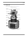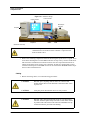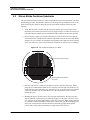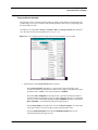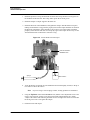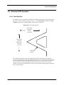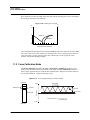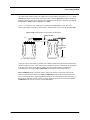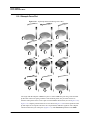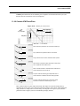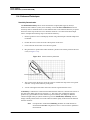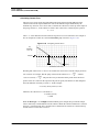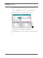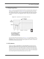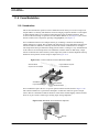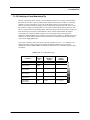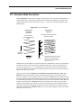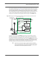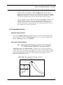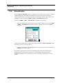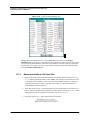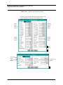
1
MultiMode SPM Instruction Manual NanoScope Software Version 5 004-210-000 004-210-100 Copyright © [1996, 1997, 2004] Veeco Instruments Inc. All rights reserved. Document Revision History: MultiMode SPM Instruction Manual Revision Date Section(s) Affected Reference B 3-09-04 All. N/A 4.31ce “A” 27OCT97 Chapters 3, 5 and 8 168, 185, 189 4.22ce 14FEB97 TOC, TOW, Chapters 2, 5, 7, 11, 12, 13, 15 and Index 139 4.22 15JUL96 Released 8 Approval C. Kowalski Notices: The information in this document is subject to change without notice. NO WARRANTY OF ANY KIND IS MADE WITH REGARD TO THIS MATERIAL, INCLUDING, BUT NOT LIMITED TO, THE IMPLIED WARRANTIES OF MERCHANTABILITY AND FITNESS FOR A PARTICULAR PURPOSE. No liability is assumed for errors contained herein or for incidental or consequential damages in connection with the furnishing, performance, or use of this material. This document contains proprietary information which is protected by copyright. No part of this document may be photocopied, reproduced, or translated into another language without prior written consent. Copyright: Copyright © 2004 Veeco Instruments Inc. All rights reserved. Trademark Acknowledgments: The following are registered trademarks of Veeco Instruments Inc. All other trademarks are the property of their respective owners. Product Names: NanoScope® MultiMode™ Dimension™ BioScope™ Atomic Force Profiler™ (AFP™) Dektak® Software Modes: TappingMode™ Tapping™ TappingMode+™ LiftMode™ AutoTune™ TurboScan™ Fast HSG™ PhaseImaging™ DekMap 2™ HyperScan™ StepFinder™ SoftScan™ Hardware Designs: TrakScan™ StiffStage™ Hardware Options: TipX® Signal Access Module™ and SAM™ Extender™ TipView™ Interleave™ LookAhead™ Quadrex™ Software Options: NanoScript™ Navigator™ FeatureFind™ Miscellaneous: NanoProbe® Table of Contents Chapter 1 Introduction to the Digital Instruments MultiMode SPM 1 1.1 Introduction . . . . . . . . . . . . . . . . . . . . . . . . . . . . . . . . . . . . . . . . . . . . . . . . 2 1.2 Safety . . . . . . . . . . . . . . . . . . . . . . . . . . . . . . . . . . . . . . . . . . . . . . . . . . . . . 4 1.2.1 Six Rules of Safety . . . . . . . . . . . . . . . . . . . . . . . . . . . . . . . . . . . . . . . . . . . . . 4 1.2.2 Safety Requirements . . . . . . . . . . . . . . . . . . . . . . . . . . . . . . . . . . . . . . . . . . . . 5 1.2.3 Safety Precautions . . . . . . . . . . . . . . . . . . . . . . . . . . . . . . . . . . . . . . . . . . . . . . 6 1.3 Microscope Specifications . . . . . . . . . . . . . . . . . . . . . . . . . . . . . . . . . . . . 13 1.3.1 Image Size and Resolution . . . . . . . . . . . . . . . . . . . . . . . . . . . . . . . . . . . . . . 13 1.3.2 Scanning Techniques with the MultiMode SPM . . . . . . . . . . . . . . . . . . . . . . 13 1.3.3 Controller Electronics and Auxiliary Channels . . . . . . . . . . . . . . . . . . . . . . . 15 Chapter 2 SPM Fundamentals for the MultiMode 17 2.1 Hardware . . . . . . . . . . . . . . . . . . . . . . . . . . . . . . . . . . . . . . . . . . . . . . . . . 18 2.1.1 2.1.2 2.1.3 2.1.4 2.1.5 MultiMode SPM . . . . . . . . . . . . . . . . . . . . . . . . . . . . . . . . . . . . . . . . . . . . . . 19 SPM Head . . . . . . . . . . . . . . . . . . . . . . . . . . . . . . . . . . . . . . . . . . . . . . . . . . . 20 Scanners . . . . . . . . . . . . . . . . . . . . . . . . . . . . . . . . . . . . . . . . . . . . . . . . . . . . . 21 Tipholders . . . . . . . . . . . . . . . . . . . . . . . . . . . . . . . . . . . . . . . . . . . . . . . . . . . 24 Probes . . . . . . . . . . . . . . . . . . . . . . . . . . . . . . . . . . . . . . . . . . . . . . . . . . . . . . 25 2.2 Control Mechanisms and Feedback . . . . . . . . . . . . . . . . . . . . . . . . . . . . . 28 2.2.1 A brief history of SPM control mechanisms . . . . . . . . . . . . . . . . . . . . . . . . . 28 2.3 Feedback Gains . . . . . . . . . . . . . . . . . . . . . . . . . . . . . . . . . . . . . . . . . . . . 30 2.3.1 2.3.2 2.3.3 2.3.4 2.3.5 2.3.6 2.3.7 2.3.8 2.3.9 Proportional and Integral Gain An Analogy . . . . . . . . . . . . . . . . . . . . . . . . 30 Proportional Gain . . . . . . . . . . . . . . . . . . . . . . . . . . . . . . . . . . . . . . . . . . . . . 31 Integral Gain . . . . . . . . . . . . . . . . . . . . . . . . . . . . . . . . . . . . . . . . . . . . . . . . . 32 LookAhead Gain . . . . . . . . . . . . . . . . . . . . . . . . . . . . . . . . . . . . . . . . . . . . . . 32 Completing the Analogy Feedback Gains in SPM . . . . . . . . . . . . . . . . . . . 32 Setpoint . . . . . . . . . . . . . . . . . . . . . . . . . . . . . . . . . . . . . . . . . . . . . . . . . . . . . 33 The SPM Electronic Feedback Loop . . . . . . . . . . . . . . . . . . . . . . . . . . . . . . . 33 More about Feedback and Images . . . . . . . . . . . . . . . . . . . . . . . . . . . . . . . . . 34 What Data Type of Image? . . . . . . . . . . . . . . . . . . . . . . . . . . . . . . . . . . . . . . 36 2.4 Control Parameters and Feedback . . . . . . . . . . . . . . . . . . . . . . . . . . . . . . 37 2.4.1 2.4.2 2.4.3 2.4.4 Rev. B Reexamining the Control Loop . . . . . . . . . . . . . . . . . . . . . . . . . . . . . . . . . . . 37 General Description of Main Menu Items . . . . . . . . . . . . . . . . . . . . . . . . . . . 38 User Example . . . . . . . . . . . . . . . . . . . . . . . . . . . . . . . . . . . . . . . . . . . . . . . . 39 Review of General Operating Concepts . . . . . . . . . . . . . . . . . . . . . . . . . . . . 39 MultiMode SPM Instruction Manual 3 2.5 Review of TappingMode AFM . . . . . . . . . . . . . . . . . . . . . . . . . . . . . . . . 43 2.5.1 General Operating Concepts . . . . . . . . . . . . . . . . . . . . . . . . . . . . . . . . . . . . . 43 2.5.2 Optimizing the TappingMode AFM Signal after Engagement . . . . . . . . . . . 45 2.6 Terms and Abbreviations. . . . . . . . . . . . . . . . . . . . . . . . . . . . . . . . . . . . . 46 Chapter 3 Setup & Installation 49 3.1 Installing the MultiMode SPM . . . . . . . . . . . . . . . . . . . . . . . . . . . . . . . . 49 3.2 Component List . . . . . . . . . . . . . . . . . . . . . . . . . . . . . . . . . . . . . . . . . . . . 49 3.2.1 Unpack The System . . . . . . . . . . . . . . . . . . . . . . . . . . . . . . . . . . . . . . . . . . . . 51 3.2.2 Vibration Isolation . . . . . . . . . . . . . . . . . . . . . . . . . . . . . . . . . . . . . . . . . . . . . 55 3.2.3 System Power Up . . . . . . . . . . . . . . . . . . . . . . . . . . . . . . . . . . . . . . . . . . . . . 56 Chapter 4 Cantilever Preparation 57 4.1 Silicon Cantilever Substrates . . . . . . . . . . . . . . . . . . . . . . . . . . . . . . . . . 57 4.1.1 Tip Shape of Etched Silicon Probes . . . . . . . . . . . . . . . . . . . . . . . . . . . . . . . 59 4.2 Silicon Nitride Cantilever Substrates . . . . . . . . . . . . . . . . . . . . . . . . . . . 64 4.2.1 Tip Shape of Silicon Nitride Probes . . . . . . . . . . . . . . . . . . . . . . . . . . . . . . . 66 Chapter 5 Head, Probe and Sample Preparation 69 5.1 Initial Preparation for Contact AFM Imaging . . . . . . . . . . . . . . . . . . . . . 72 5.1.1 5.1.2 5.1.3 5.1.4 Prepare the Sample . . . . . . . . . . . . . . . . . . . . . . . . . . . . . . . . . . . . . . . . . . . . 72 Load the Sample . . . . . . . . . . . . . . . . . . . . . . . . . . . . . . . . . . . . . . . . . . . . . . 73 Load Probe in Tipholder . . . . . . . . . . . . . . . . . . . . . . . . . . . . . . . . . . . . . . . . 75 Install the Tipholder . . . . . . . . . . . . . . . . . . . . . . . . . . . . . . . . . . . . . . . . . . . . 77 5.2 Laser Alignment . . . . . . . . . . . . . . . . . . . . . . . . . . . . . . . . . . . . . . . . . . . 78 5.2.1 Method 1: OMV Method . . . . . . . . . . . . . . . . . . . . . . . . . . . . . . . . . . . . . . . . 78 5.2.2 Method 2: The Projection Method. . . . . . . . . . . . . . . . . . . . . . . . . . . . . . . . . 79 5.2.3 Maximize the SUM Signal . . . . . . . . . . . . . . . . . . . . . . . . . . . . . . . . . . . . . . 83 5.3 Start the Microscope Program. . . . . . . . . . . . . . . . . . . . . . . . . . . . . . . . . 84 5.4 MultiMode SPM Voltage Meters . . . . . . . . . . . . . . . . . . . . . . . . . . . . . . 85 Chapter 6 Contact AFM Mode 87 6.1 Preparation Prior to Imaging . . . . . . . . . . . . . . . . . . . . . . . . . . . . . . . . . . 88 6.1.1 6.1.2 6.1.3 6.1.4 Adjust the Detector Offsets . . . . . . . . . . . . . . . . . . . . . . . . . . . . . . . . . . . . . . 88 Signal Settings . . . . . . . . . . . . . . . . . . . . . . . . . . . . . . . . . . . . . . . . . . . . . . . . 89 Adjust tip height above sample surface . . . . . . . . . . . . . . . . . . . . . . . . . . . . . 90 Position Tip with OMV . . . . . . . . . . . . . . . . . . . . . . . . . . . . . . . . . . . . . . . . . 90 6.2 Suggested Initial Control Settings. . . . . . . . . . . . . . . . . . . . . . . . . . . . . . 91 6.2.1 Show All Items . . . . . . . . . . . . . . . . . . . . . . . . . . . . . . . . . . . . . . . . . . . . . . . 91 6.2.2 Initial Scan Parameter Settings . . . . . . . . . . . . . . . . . . . . . . . . . . . . . . . . . . . 92 6.3 Initiate the Engage Command . . . . . . . . . . . . . . . . . . . . . . . . . . . . . . . . . 95 6.3.1 Adjust Setpoint with Force Calibration . . . . . . . . . . . . . . . . . . . . . . . . . . . . . 95 6.3.2 Adjust Sensitivity (if required) . . . . . . . . . . . . . . . . . . . . . . . . . . . . . . . . . . . 98 4 MultiMode SPM Instruction Manual Rev. B 6.4 Beyond the Basics of AFM Operation . . . . . . . . . . . . . . . . . . . . . . . . . . . 98 6.4.1 Cantilever Selection . . . . . . . . . . . . . . . . . . . . . . . . . . . . . . . . . . . . . . . . . . . . 98 6.5 Optimization of Scanning Parameters . . . . . . . . . . . . . . . . . . . . . . . . . . . 99 6.5.1 6.5.2 6.5.3 6.5.4 6.5.5 6.5.6 Chapter 7 Data type . . . . . . . . . . . . . . . . . . . . . . . . . . . . . . . . . . . . . . . . . . . . . . . . . . . . 99 Gain settings . . . . . . . . . . . . . . . . . . . . . . . . . . . . . . . . . . . . . . . . . . . . . . . . 100 Scan size and Scan rate . . . . . . . . . . . . . . . . . . . . . . . . . . . . . . . . . . . . . . . . 100 Setpoint . . . . . . . . . . . . . . . . . . . . . . . . . . . . . . . . . . . . . . . . . . . . . . . . . . . . 101 Lowpass filter . . . . . . . . . . . . . . . . . . . . . . . . . . . . . . . . . . . . . . . . . . . . . . . 101 Highpass filter . . . . . . . . . . . . . . . . . . . . . . . . . . . . . . . . . . . . . . . . . . . . . . . 101 TappingMode AFM 103 7.1 Basic Principle of TappingMode . . . . . . . . . . . . . . . . . . . . . . . . . . . . . . 104 7.2 Preparation Prior to Imaging . . . . . . . . . . . . . . . . . . . . . . . . . . . . . . . . . 105 7.2.1 7.2.2 7.2.3 7.2.4 7.2.5 7.2.6 7.2.7 Switch to TappingMode . . . . . . . . . . . . . . . . . . . . . . . . . . . . . . . . . . . . . . . . 105 Show All Items . . . . . . . . . . . . . . . . . . . . . . . . . . . . . . . . . . . . . . . . . . . . . . 105 Check Parameters . . . . . . . . . . . . . . . . . . . . . . . . . . . . . . . . . . . . . . . . . . . . 106 Adjust Laser and Photodetector . . . . . . . . . . . . . . . . . . . . . . . . . . . . . . . . . . 107 Additional preparations . . . . . . . . . . . . . . . . . . . . . . . . . . . . . . . . . . . . . . . . 109 Tune the Cantilever . . . . . . . . . . . . . . . . . . . . . . . . . . . . . . . . . . . . . . . . . . . 109 Setting the Drive Amplitude and Setpoint . . . . . . . . . . . . . . . . . . . . . . . . . . 112 7.3 Engaging The Microscope . . . . . . . . . . . . . . . . . . . . . . . . . . . . . . . . . . . 113 7.4 Withdrawing the Tip . . . . . . . . . . . . . . . . . . . . . . . . . . . . . . . . . . . . . . . . 115 7.5 Beyond Basics with Resonating Techniques . . . . . . . . . . . . . . . . . . . . . 115 7.5.1 Subtleties of Cantilever Oscillation . . . . . . . . . . . . . . . . . . . . . . . . . . . . . . . 115 7.5.2 Tuning the Cantilever Drive Frequency . . . . . . . . . . . . . . . . . . . . . . . . . . . 117 7.5.3 Optimization of Scanning Parameters . . . . . . . . . . . . . . . . . . . . . . . . . . . . . 118 Chapter 8 Fluid Operation 121 8.1 Introduction . . . . . . . . . . . . . . . . . . . . . . . . . . . . . . . . . . . . . . . . . . . . . . 123 8.2 General Fluid Operation . . . . . . . . . . . . . . . . . . . . . . . . . . . . . . . . . . . . . 123 8.2.1 Clean Fluid Cell and O-ring . . . . . . . . . . . . . . . . . . . . . . . . . . . . . . . . . . . . 125 8.2.2 Select the Probe . . . . . . . . . . . . . . . . . . . . . . . . . . . . . . . . . . . . . . . . . . . . . . 125 8.2.3 Remove Organic Contamination from the Tip . . . . . . . . . . . . . . . . . . . . . . 126 8.2.4 Load the Fluid Cell with a Probe . . . . . . . . . . . . . . . . . . . . . . . . . . . . . . . . . 126 8.2.5 Sample Mounting . . . . . . . . . . . . . . . . . . . . . . . . . . . . . . . . . . . . . . . . . . . . 127 8.2.6 Align the Laser. . . . . . . . . . . . . . . . . . . . . . . . . . . . . . . . . . . . . . . . . . . . . . . 131 8.2.7 Adjust the Detector Offsets and Setpoint (Contact Mode) . . . . . . . . . . . . . 132 8.2.8 Engage the Surface . . . . . . . . . . . . . . . . . . . . . . . . . . . . . . . . . . . . . . . . . . . 132 8.2.9 Adjust Scan Parameters (Contact Mode). . . . . . . . . . . . . . . . . . . . . . . . . . . 132 8.2.10 Clean and Dry Parts When Done. . . . . . . . . . . . . . . . . . . . . . . . . . . . . . . . 133 8.3 TappingMode in Fluids . . . . . . . . . . . . . . . . . . . . . . . . . . . . . . . . . . . . . 134 8.3.1 Procedure for TappingMode Imaging in Fluid . . . . . . . . . . . . . . . . . . . . . . 134 8.3.2 Plotting Amplitude vs. Distance (Force Cal Curve) . . . . . . . . . . . . . . . . . . 136 8.3.3 Optimizing Image Quality . . . . . . . . . . . . . . . . . . . . . . . . . . . . . . . . . . . . . . 137 Rev. B MultiMode SPM Instruction Manual 5 8.4 Troubleshooting Tips. . . . . . . . . . . . . . . . . . . . . . . . . . . . . . . . . . . . . . . 138 8.4.1 8.4.2 8.4.3 8.4.4 8.4.5 Cantilever Tune Plot Looks Poor: Loose Probetip . . . . . . . . . . . . . . . . . . . 138 Laser Sum Signal Absent or Weak: Air Bubbles . . . . . . . . . . . . . . . . . . . . . 138 Poor Image Quality . . . . . . . . . . . . . . . . . . . . . . . . . . . . . . . . . . . . . . . . . . . 138 Lost Particulate Samples: Attracted to Cantilever. . . . . . . . . . . . . . . . . . . . 139 Drift in AFM Image Because O-ring Slid Across Sample Surface . . . . . . . 139 8.5 General Notes on Sample Binding . . . . . . . . . . . . . . . . . . . . . . . . . . . . 141 8.6 Lysozyme on Mica A Model Procedure for Protein Binding . . . . . . . 142 8.6.1 Protein Binding Theory . . . . . . . . . . . . . . . . . . . . . . . . . . . . . . . . . . . . . . . . 142 8.6.2 Protein Binding Procedure . . . . . . . . . . . . . . . . . . . . . . . . . . . . . . . . . . . . . 142 8.7 Binding DNA to Mica . . . . . . . . . . . . . . . . . . . . . . . . . . . . . . . . . . . . . . 145 8.7.1 DNA Binding Theory . . . . . . . . . . . . . . . . . . . . . . . . . . . . . . . . . . . . . . . . . 145 8.7.2 DNA Binding Procedure . . . . . . . . . . . . . . . . . . . . . . . . . . . . . . . . . . . . . . . 145 8.7.3 Acknowledgments . . . . . . . . . . . . . . . . . . . . . . . . . . . . . . . . . . . . . . . . . . . . 146 Chapter 9 Scanning Tunneling Microscopy (STM) 147 9.1 STM Introduction . . . . . . . . . . . . . . . . . . . . . . . . . . . . . . . . . . . . . . . . . 148 9.1.1 9.1.2 9.1.3 9.1.4 Overview of STM . . . . . . . . . . . . . . . . . . . . . . . . . . . . . . . . . . . . . . . . . . . . 148 STM Hardware . . . . . . . . . . . . . . . . . . . . . . . . . . . . . . . . . . . . . . . . . . . . . . 149 Sample Surface . . . . . . . . . . . . . . . . . . . . . . . . . . . . . . . . . . . . . . . . . . . . . . 150 Vibration isolation . . . . . . . . . . . . . . . . . . . . . . . . . . . . . . . . . . . . . . . . . . . . 150 9.2 Basic STM Operation . . . . . . . . . . . . . . . . . . . . . . . . . . . . . . . . . . . . . . 151 9.2.1 System Setup . . . . . . . . . . . . . . . . . . . . . . . . . . . . . . . . . . . . . . . . . . . . . . . . 151 9.3 Spectroscopy with the STM . . . . . . . . . . . . . . . . . . . . . . . . . . . . . . . . . 153 9.3.1 STS plot modes . . . . . . . . . . . . . . . . . . . . . . . . . . . . . . . . . . . . . . . . . . . . . . 153 9.3.2 Operation of STS . . . . . . . . . . . . . . . . . . . . . . . . . . . . . . . . . . . . . . . . . . . . . 154 9.4 Troubleshooting for STM . . . . . . . . . . . . . . . . . . . . . . . . . . . . . . . . . . . 155 9.4.1 Head and Microscope-related Problems . . . . . . . . . . . . . . . . . . . . . . . . . . . 155 9.5 Low-Current STM. . . . . . . . . . . . . . . . . . . . . . . . . . . . . . . . . . . . . . . . . 156 9.5.1 9.5.2 9.5.3 9.5.4 9.5.5 9.5.6 Description . . . . . . . . . . . . . . . . . . . . . . . . . . . . . . . . . . . . . . . . . . . . . . . . . 156 Hardware Description . . . . . . . . . . . . . . . . . . . . . . . . . . . . . . . . . . . . . . . . . 157 Precautions . . . . . . . . . . . . . . . . . . . . . . . . . . . . . . . . . . . . . . . . . . . . . . . . . 157 Installation . . . . . . . . . . . . . . . . . . . . . . . . . . . . . . . . . . . . . . . . . . . . . . . . . . 158 Operation . . . . . . . . . . . . . . . . . . . . . . . . . . . . . . . . . . . . . . . . . . . . . . . . . . . 160 Servicing the Converter . . . . . . . . . . . . . . . . . . . . . . . . . . . . . . . . . . . . . . . . 162 9.6 Etching Tungsten Tips. . . . . . . . . . . . . . . . . . . . . . . . . . . . . . . . . . . . . . 164 9.6.1 Procedure . . . . . . . . . . . . . . . . . . . . . . . . . . . . . . . . . . . . . . . . . . . . . . . . . . . 165 Chapter 10 Lateral Force Mode 167 10.1 Basic LFM Operation . . . . . . . . . . . . . . . . . . . . . . . . . . . . . . . . . . . . . 168 10.2 Advanced LFM Operation . . . . . . . . . . . . . . . . . . . . . . . . . . . . . . . . . 169 10.2.1 Scan Direction . . . . . . . . . . . . . . . . . . . . . . . . . . . . . . . . . . . . . . . . . . . . . . 169 10.2.2 Tip selection. . . . . . . . . . . . . . . . . . . . . . . . . . . . . . . . . . . . . . . . . . . . . . . . 170 10.2.3 Understanding the LFM Signal . . . . . . . . . . . . . . . . . . . . . . . . . . . . . . . . . 170 6 MultiMode SPM Instruction Manual Rev. B 10.2.4 10.2.5 10.2.6 10.2.7 Chapter 11 Understanding the Color Scale . . . . . . . . . . . . . . . . . . . . . . . . . . . . . . . . . 171 Using TMR Voltage to Measure Friction . . . . . . . . . . . . . . . . . . . . . . . . . 172 Enhancing the LFM Data by Subtracting Two Images . . . . . . . . . . . . . . . 172 Height Artifacts in the Signal . . . . . . . . . . . . . . . . . . . . . . . . . . . . . . . . . . 173 Force Imaging 175 11.1 Force Plots—An Analogy. . . . . . . . . . . . . . . . . . . . . . . . . . . . . . . . . . . . 177 11.2 Force Calibration Mode . . . . . . . . . . . . . . . . . . . . . . . . . . . . . . . . . . . . 178 11.2.1 Example Force Plot . . . . . . . . . . . . . . . . . . . . . . . . . . . . . . . . . . . . . . . . . . 180 11.2.2 Contact AFM Force Plots . . . . . . . . . . . . . . . . . . . . . . . . . . . . . . . . . . . . . 181 11.3 Force Calibration Control Panels and Menus. . . . . . . . . . . . . . . . . . . . 183 11.3.1 11.3.2 11.3.3 11.3.4 11.3.5 11.3.6 Main Controls (Ramp Controls) . . . . . . . . . . . . . . . . . . . . . . . . . . . . . . . . 184 Main Controls Panel (Display) . . . . . . . . . . . . . . . . . . . . . . . . . . . . . . . . . 185 Channel 1, 2, 3 Panels . . . . . . . . . . . . . . . . . . . . . . . . . . . . . . . . . . . . . . . . 186 Feedback Controls Panel . . . . . . . . . . . . . . . . . . . . . . . . . . . . . . . . . . . . . . 187 Scan Mode Panel (Advanced Mode Only) . . . . . . . . . . . . . . . . . . . . . . . . 188 Menu Bar Commands . . . . . . . . . . . . . . . . . . . . . . . . . . . . . . . . . . . . . . . . 190 11.4 Force Calibration (Contact Mode AFM) . . . . . . . . . . . . . . . . . . . . . . . 191 11.4.1 11.4.2 11.4.3 11.4.4 Obtaining a Good Force Curve . . . . . . . . . . . . . . . . . . . . . . . . . . . . . . . . . 191 Helpful Suggestions. . . . . . . . . . . . . . . . . . . . . . . . . . . . . . . . . . . . . . . . . . 192 Advanced Techniques . . . . . . . . . . . . . . . . . . . . . . . . . . . . . . . . . . . . . . . . 194 Interpreting Force Curves . . . . . . . . . . . . . . . . . . . . . . . . . . . . . . . . . . . . . 198 11.5 Force Calibration (TappingMode) . . . . . . . . . . . . . . . . . . . . . . . . . . . . 199 11.5.1 11.5.2 11.5.3 11.5.4 Force Plots . . . . . . . . . . . . . . . . . . . . . . . . . . . . . . . . . . . . . . . . . . . . . . . . . 199 Obtaining a Force Plot (TappingMode) . . . . . . . . . . . . . . . . . . . . . . . . . . . 201 High Contact Force . . . . . . . . . . . . . . . . . . . . . . . . . . . . . . . . . . . . . . . . . . 203 Tip Selection . . . . . . . . . . . . . . . . . . . . . . . . . . . . . . . . . . . . . . . . . . . . . . . 203 11.6 Force Modulation . . . . . . . . . . . . . . . . . . . . . . . . . . . . . . . . . . . . . . . . . 204 11.6.1 11.6.2 11.6.3 11.6.4 11.6.5 Introduction . . . . . . . . . . . . . . . . . . . . . . . . . . . . . . . . . . . . . . . . . . . . . . . . 204 Selecting a Force Modulation Tip . . . . . . . . . . . . . . . . . . . . . . . . . . . . . . . 205 Operating Principle . . . . . . . . . . . . . . . . . . . . . . . . . . . . . . . . . . . . . . . . . . 206 Force Modulation Procedure . . . . . . . . . . . . . . . . . . . . . . . . . . . . . . . . . . . 206 Notes About Artifacts . . . . . . . . . . . . . . . . . . . . . . . . . . . . . . . . . . . . . . . . 211 11.7 Force Modulation with Negative LiftMode . . . . . . . . . . . . . . . . . . . . 213 11.7.1 Set Interleave Controls. . . . . . . . . . . . . . . . . . . . . . . . . . . . . . . . . . . . . . . . 213 11.7.2 Obtain a TappingMode Image . . . . . . . . . . . . . . . . . . . . . . . . . . . . . . . . . . 214 11.7.3 Obtain a Negative LiftMode Force Modulation Image . . . . . . . . . . . . . . . 214 11.8 Force Volume . . . . . . . . . . . . . . . . . . . . . . . . . . . . . . . . . . . . . . . . . . . . 215 Chapter 12 Interleave Scanning and LiftMode 217 12.1 Preface: Interleave Scanning & LiftMode . . . . . . . . . . . . . . . . . . . . . . 218 12.2 Interleave Mode Description . . . . . . . . . . . . . . . . . . . . . . . . . . . . . . . . 219 12.3 Lift Mode Description . . . . . . . . . . . . . . . . . . . . . . . . . . . . . . . . . . . . . 220 12.4 Operation of Interleave Scanning / Lift Mode . . . . . . . . . . . . . . . . . . . 220 Rev. B MultiMode SPM Instruction Manual 7 12.5 Use of LiftMode with TappingMode . . . . . . . . . . . . . . . . . . . . . . . . . 222 12.5.1 12.5.2 12.5.3 12.5.4 12.5.5 Chapter 13 Main Drive Amplitude and Frequency selection. . . . . . . . . . . . . . . . . . . . 222 Setpoint Selection . . . . . . . . . . . . . . . . . . . . . . . . . . . . . . . . . . . . . . . . . . . 222 Interleave Drive Amplitude and Frequency Selection. . . . . . . . . . . . . . . . 223 Amplitude Data Interpretation . . . . . . . . . . . . . . . . . . . . . . . . . . . . . . . . . . 223 Cantilever Oscillation Amplitude . . . . . . . . . . . . . . . . . . . . . . . . . . . . . . . 224 Magnetic Force (MFM) Imaging 225 13.1 Magnetic Force Imaging Theory. . . . . . . . . . . . . . . . . . . . . . . . . . . . . 226 13.2 MFM Using Interleave Scanning and LiftMode. . . . . . . . . . . . . . . . . 227 13.2.1 Procedure . . . . . . . . . . . . . . . . . . . . . . . . . . . . . . . . . . . . . . . . . . . . . . . . . . 228 13.2.2 Frequency Modulation. . . . . . . . . . . . . . . . . . . . . . . . . . . . . . . . . . . . . . . . 232 13.3 Installation of the Extender Electronics Modules . . . . . . . . . . . . . . . . 232 13.3.1 Basic Extender. . . . . . . . . . . . . . . . . . . . . . . . . . . . . . . . . . . . . . . . . . . . . . 232 13.3.2 Quadrex Extender . . . . . . . . . . . . . . . . . . . . . . . . . . . . . . . . . . . . . . . . . . . 233 13.3.3 NanoScope IV . . . . . . . . . . . . . . . . . . . . . . . . . . . . . . . . . . . . . . . . . . . . . . 233 13.4 Software Setup Configuration (Basic, Quadrex or NSIV) . . . . . . . . . 234 13.5 Troubleshooting Suggestions . . . . . . . . . . . . . . . . . . . . . . . . . . . . . . . 234 13.5.1 MFM Image Verification . . . . . . . . . . . . . . . . . . . . . . . . . . . . . . . . . . . . . . 234 13.5.2 Saturation in Amplitude Detection . . . . . . . . . . . . . . . . . . . . . . . . . . . . . . 235 13.5.3 Optical Interference . . . . . . . . . . . . . . . . . . . . . . . . . . . . . . . . . . . . . . . . . . 235 13.6 Advanced Topics . . . . . . . . . . . . . . . . . . . . . . . . . . . . . . . . . . . . . . . . . 235 13.6.1 Lift Scan Height and Magnetic Imaging Resolution . . . . . . . . . . . . . . . . . 235 13.6.2 Fine Tuning Interleave Controls . . . . . . . . . . . . . . . . . . . . . . . . . . . . . . . . 236 Chapter 14 Electric Force (EFM) Imaging 239 14.1 Electric Force Microscopy Overview . . . . . . . . . . . . . . . . . . . . . . . . . 240 14.1.1 Electric Field Gradient Imaging Overview . . . . . . . . . . . . . . . . . . . . . . . . 241 14.1.2 Surface Potential Imaging Overview. . . . . . . . . . . . . . . . . . . . . . . . . . . . . 242 14.2 Electric Field Gradient Detection Theory . . . . . . . . . . . . . . . . . . . . 242 14.3 Electric Field Gradient Detection Preparation . . . . . . . . . . . . . . . . . 244 14.3.1 Jumper Configurations for systems without the Basic Extender Module . 246 14.3.2 Jumper Configurations for systems with the Basic Extender Module. . . . 251 14.4 Electric Field Gradient Detection Procedures . . . . . . . . . . . . . . . . . 256 14.4.1 Phase Detection . . . . . . . . . . . . . . . . . . . . . . . . . . . . . . . . . . . . . . . . . . . . . 257 14.4.2 Amplitude Detection . . . . . . . . . . . . . . . . . . . . . . . . . . . . . . . . . . . . . . . . . 259 14.5 Surface Potential Detection Theory . . . . . . . . . . . . . . . . . . . . . . . . . 261 14.6 Surface Potential Detection Preparation . . . . . . . . . . . . . . . . . . . . . 263 14.6.1 Applying Voltage to the Sample Directly . . . . . . . . . . . . . . . . . . . . . . . . . 264 14.6.2 Applying Voltage to the Sample Through Piezo Cap . . . . . . . . . . . . . . . . 264 14.7 Surface Potential Imaging Procedure . . . . . . . . . . . . . . . . . . . . . . . . 265 14.7.1 Troubleshooting the Surface Potential Feedback Loop. . . . . . . . . . . . . . . 269 8 MultiMode SPM Instruction Manual Rev. B Chapter 15 Calibration, Maintenance, Troubleshooting and Warranty 271 15.1 SPM Calibration Overview . . . . . . . . . . . . . . . . . . . . . . . . . . . . . . . . . 275 15.1.1 Theory Behind Calibration . . . . . . . . . . . . . . . . . . . . . . . . . . . . . . . . . . . . 276 15.1.2 Calibration References . . . . . . . . . . . . . . . . . . . . . . . . . . . . . . . . . . . . . . . 280 15.2 Calibration Setup . . . . . . . . . . . . . . . . . . . . . . . . . . . . . . . . . . . . . . . . . 281 15.2.1 15.2.2 15.2.3 15.2.4 Check Scanner Parameter Values . . . . . . . . . . . . . . . . . . . . . . . . . . . . . . . 281 Align Calibration Reference . . . . . . . . . . . . . . . . . . . . . . . . . . . . . . . . . . . 281 Set Realtime Parameters . . . . . . . . . . . . . . . . . . . . . . . . . . . . . . . . . . . . . . 282 Set Up SPM for Contact AFM. . . . . . . . . . . . . . . . . . . . . . . . . . . . . . . . . . 282 15.3 Check Sample Orthogonality . . . . . . . . . . . . . . . . . . . . . . . . . . . . . . . . 283 15.3.1 Measure Orthogonality . . . . . . . . . . . . . . . . . . . . . . . . . . . . . . . . . . . . . . . 283 15.3.2 Adjust Sample Orthogonality . . . . . . . . . . . . . . . . . . . . . . . . . . . . . . . . . . 283 15.4 Linearity Correction Procedure . . . . . . . . . . . . . . . . . . . . . . . . . . . . . . 284 15.4.1 Adjust Mag0 and Arg. . . . . . . . . . . . . . . . . . . . . . . . . . . . . . . . . . . . . . . . . 284 15.4.2 Adjusting Fast Mag1 . . . . . . . . . . . . . . . . . . . . . . . . . . . . . . . . . . . . . . . . . 287 15.4.3 Adjust Slow Mag1 . . . . . . . . . . . . . . . . . . . . . . . . . . . . . . . . . . . . . . . . . . . 288 15.5 X-Y Calibration using Capture Calibration and Autocalibration . . . . . 289 15.5.1 Capture Calibration . . . . . . . . . . . . . . . . . . . . . . . . . . . . . . . . . . . . . . . . . . 289 15.6 Autocalibration . . . . . . . . . . . . . . . . . . . . . . . . . . . . . . . . . . . . . . . . . . . 292 15.7 Fine-tuning for X-Y Calibration. . . . . . . . . . . . . . . . . . . . . . . . . . . . . . 294 15.7.1 15.7.2 15.7.3 15.7.4 15.7.5 15.7.6 Prepare System for Fine-Tuning . . . . . . . . . . . . . . . . . . . . . . . . . . . . . . . . 294 Measure Horizontally at 440V Scan Size . . . . . . . . . . . . . . . . . . . . . . . . . 294 Measure Vertically at 440V Scan Size. . . . . . . . . . . . . . . . . . . . . . . . . . . . 296 Measure Horizontally at 150V Scan Size . . . . . . . . . . . . . . . . . . . . . . . . . 297 Measure Vertically at 150V Scan Size. . . . . . . . . . . . . . . . . . . . . . . . . . . . 298 Change Scan angle and Repeat Calibration Routines . . . . . . . . . . . . . . . . 298 15.8 Calibrating Z. . . . . . . . . . . . . . . . . . . . . . . . . . . . . . . . . . . . . . . . . . . . . 299 15.8.1 15.8.2 15.8.3 15.8.4 15.8.5 15.8.6 15.8.7 Engage . . . . . . . . . . . . . . . . . . . . . . . . . . . . . . . . . . . . . . . . . . . . . . . . . . . . 299 Capture and Correct an Image . . . . . . . . . . . . . . . . . . . . . . . . . . . . . . . . . . 300 Measure Vertical Features . . . . . . . . . . . . . . . . . . . . . . . . . . . . . . . . . . . . . 301 Correct Z Sensitivity . . . . . . . . . . . . . . . . . . . . . . . . . . . . . . . . . . . . . . . . . 303 Recheck Z-axis Measuring Accuracy . . . . . . . . . . . . . . . . . . . . . . . . . . . . 303 Calculate Retracted and Extended Offset Deratings . . . . . . . . . . . . . . . . . 304 Finding a Pit with an A Scanner . . . . . . . . . . . . . . . . . . . . . . . . . . . . . . 305 15.9 Calibration of A Scanners for Atomic-scale Measurement . . . . . . . 306 15.9.1 Prepare Sample . . . . . . . . . . . . . . . . . . . . . . . . . . . . . . . . . . . . . . . . . . . . . 306 15.10 Quick Guide to Piezo Tube Calibration . . . . . . . . . . . . . . . . . . . . . . . 309 15.10.1 15.10.2 15.10.3 15.10.4 Linearize Scanner . . . . . . . . . . . . . . . . . . . . . . . . . . . . . . . . . . . . . . . . . . 309 Run Autocalibration Software (Factory Operation) . . . . . . . . . . . . . . . . 310 Fine Tune the X-Y Scanner . . . . . . . . . . . . . . . . . . . . . . . . . . . . . . . . . . . 310 Calibrate the Z Piezo . . . . . . . . . . . . . . . . . . . . . . . . . . . . . . . . . . . . . . . . 311 15.11 Contact AFM Troubleshooting . . . . . . . . . . . . . . . . . . . . . . . . . . . . . . 313 15.11.1 False engagement. . . . . . . . . . . . . . . . . . . . . . . . . . . . . . . . . . . . . . . . . . . 313 15.11.2 Head appears engaged but does not track surface features . . . . . . . . . . . 314 Rev. B MultiMode SPM Instruction Manual 9 15.11.3 Head does not engage . . . . . . . . . . . . . . . . . . . . . . . . . . . . . . . . . . . . . . . 314 15.11.4 Head engages immediately . . . . . . . . . . . . . . . . . . . . . . . . . . . . . . . . . . . 315 15.11.5 Displacement of material. . . . . . . . . . . . . . . . . . . . . . . . . . . . . . . . . . . . . 315 15.11.6 Lines in the image . . . . . . . . . . . . . . . . . . . . . . . . . . . . . . . . . . . . . . . . . . 315 15.11.7 Problems with silicon nitride cantilevers. . . . . . . . . . . . . . . . . . . . . . . . . 315 15.11.8 Image vertical dimensions are not correct . . . . . . . . . . . . . . . . . . . . . . . . 316 15.11.9 Z Center Position goes out of range . . . . . . . . . . . . . . . . . . . . . . . . . . . . 316 15.11.10 Poor image quality. . . . . . . . . . . . . . . . . . . . . . . . . . . . . . . . . . . . . . . . . 317 15.11.11 Force Calibration command does not seem to work . . . . . . . . . . . . . . . 318 15.11.12 Image features appear washed out. . . . . . . . . . . . . . . . . . . . . . . . . . . . . 318 15.11.13 Image is only black and white . . . . . . . . . . . . . . . . . . . . . . . . . . . . . . . . 318 15.11.14 Image goes white . . . . . . . . . . . . . . . . . . . . . . . . . . . . . . . . . . . . . . . . . . 318 15.12 TappingMode AFM Troubleshooting . . . . . . . . . . . . . . . . . . . . . . . . 319 15.12.1 15.12.2 15.12.3 15.12.4 15.12.5 Streaks on the trailing edge of surface features. . . . . . . . . . . . . . . . . . . . 319 Lines across the image. . . . . . . . . . . . . . . . . . . . . . . . . . . . . . . . . . . . . . . 320 Rings around features on the surface. . . . . . . . . . . . . . . . . . . . . . . . . . . . 321 Multiple or repeating patterns . . . . . . . . . . . . . . . . . . . . . . . . . . . . . . . . . 322 Image goes white or black . . . . . . . . . . . . . . . . . . . . . . . . . . . . . . . . . . . . 323 15.13 Fluid Imaging Troubleshooting. . . . . . . . . . . . . . . . . . . . . . . . . . . . . 323 15.13.1 Image drifts . . . . . . . . . . . . . . . . . . . . . . . . . . . . . . . . . . . . . . . . . . . . . . . 323 15.13.2 Leaks . . . . . . . . . . . . . . . . . . . . . . . . . . . . . . . . . . . . . . . . . . . . . . . . . . . . 324 15.14 Adjustment Screw Maintenance Procedure . . . . . . . . . . . . . . . . . . . 324 15.14.1 15.14.2 15.14.3 15.14.4 15.14.5 15.14.6 Inspection . . . . . . . . . . . . . . . . . . . . . . . . . . . . . . . . . . . . . . . . . . . . . . . . 324 Remove Adjustment Screws . . . . . . . . . . . . . . . . . . . . . . . . . . . . . . . . . . 326 Inspect for Physical Damage . . . . . . . . . . . . . . . . . . . . . . . . . . . . . . . . . . 326 Clean Guide Bushings . . . . . . . . . . . . . . . . . . . . . . . . . . . . . . . . . . . . . . . 327 Lubricate . . . . . . . . . . . . . . . . . . . . . . . . . . . . . . . . . . . . . . . . . . . . . . . . . 327 Reinstall . . . . . . . . . . . . . . . . . . . . . . . . . . . . . . . . . . . . . . . . . . . . . . . . . . 327 15.15 Fuse Replacement Procedure . . . . . . . . . . . . . . . . . . . . . . . . . . . . . . 328 15.16 Vertical Engagement Scanners Installation, Use, and Maintenance 329 15.16.1 Hardware Installation . . . . . . . . . . . . . . . . . . . . . . . . . . . . . . . . . . . . . . . 330 15.16.2 Select scanner . . . . . . . . . . . . . . . . . . . . . . . . . . . . . . . . . . . . . . . . . . . . . 331 15.16.3 Inspect scanner . . . . . . . . . . . . . . . . . . . . . . . . . . . . . . . . . . . . . . . . . . . . 331 15.17 Troubleshooting the Vertical Engagement Scanners. . . . . . . . . . . . . 332 15.17.1 Scanner is not properly calibrated . . . . . . . . . . . . . . . . . . . . . . . . . . . . . . 332 15.17.2 Sample will not move (Tip Up/Down switch doesn t work) . . . . . . . . 332 15.18 Warranty . . . . . . . . . . . . . . . . . . . . . . . . . . . . . . . . . . . . . . . . . . . . . . 333 Index 10 335 MultiMode SPM Instruction Manual Rev. B Rev. B MultiMode SPM Instruction Manual 11/(12 Blank) List of Figures Chapter 1 Introduction to the Digital Instruments MultiMode SPM . . . . . . . . .1 Figure 1.1a MultiMode SPM System Components . . . . . . . . . . . . . . . . . . . . .3 Figure 1.2a Safety Symbols Key . . . . . . . . . . . . . . . . . . . . . . . . . . . . . . . . . . .5 Chapter 2 SPM Fundamentals for the MultiMode . . . . . . . . . . . . . . . . . . . . . .17 Figure 2.1a Figure 2.1b Figure 2.1c Figure 2.1d Figure 2.1e Figure 2.1f Figure 2.1g MultiMode SPM System Hardware . . . . . . . . . . . . . . . . . . . . . .18 MultiMode SPM . . . . . . . . . . . . . . . . . . . . . . . . . . . . . . . . . . . . .19 MultiMode SPM Head and Major Components . . . . . . . . . . . . .20 Quad Photodetector Arrangement. . . . . . . . . . . . . . . . . . . . . . . .21 Various Scanners Available with the MultiMode SPM . . . . . . . .21 Typical Scanner Piezo Tube and X-Y-Z Electrical Configurations22 Voltages Applied to the X- and Y-axes Produce a Raster Scan Pattern 23 Figure 2.1h Various Tipholders utilized with the MultiMode SPM . . . . . . . .24 Figure 2.1i Diamond Tip Mounted on Wire for Microhardness Testing and Lithography Work . . . . . . . . . . . . . . . . . . . . . . . . . . . . . .25 Figure 2.1j Two Types of Cantilevered Probes. . . . . . . . . . . . . . . . . . . . . . . .26 Figure 2.2a Tunneling Phenomenon Between Tip and Sample . . . . . . . . . . .28 Figure 2.2b Early Contact AFM which allowed Imaging Non-conductive Samples 29 Figure 2.2c Optical Lever for Monitoring Tip Movement . . . . . . . . . . . . . . .29 Figure 2.4a Contact AFM Concepts (Steps 1-5 exaggerated.) . . . . . . . . . . . .41 Figure 2.5a TappingMode AFM Concepts . . . . . . . . . . . . . . . . . . . . . . . . . . .44 Chapter 3 Setup & Installation . . . . . . . . . . . . . . . . . . . . . . . . . . . . . . . . . . . . . .49 Figure 3.2a Figure 3.2b Figure 3.2c Figure 3.2d Figure 3.2e Figure 3.2f Rev. B MultiMode SPM Head . . . . . . . . . . . . . . . . . . . . . . . . . . . . . . . .50 Typical MultiMode Shipping Boxes . . . . . . . . . . . . . . . . . . . . . .51 Hardware Setup . . . . . . . . . . . . . . . . . . . . . . . . . . . . . . . . . . . . . .52 Rear View of Computer on Standard MultiMode Systems. . . . .53 Installing the Scanner . . . . . . . . . . . . . . . . . . . . . . . . . . . . . . . . .54 Installing the Head. . . . . . . . . . . . . . . . . . . . . . . . . . . . . . . . . . . .55 MultiMode SPM Instruction Manual 13 List of Figures Chapter 4 Cantilever Preparation . . . . . . . . . . . . . . . . . . . . . . . . . . . . . . . . . . . 57 Figure 4.1a Figure 4.1b Figure 4.1c Figure 4.1d Figure 4.1e Figure 4.1f Figure 4.2a Figure 4.2b Figure 4.2c Figure 4.2d Figure 4.2e Chapter 5 Silicon Cantilever Substrates in Wafer. . . . . . . . . . . . . . . . . . . . Silicon Cantilever—Theoretical Tip Shape . . . . . . . . . . . . . . . . Silicon Probe Tip Profile Artifact (front to back). . . . . . . . . . . . Silicon Probe Tip Step Profile Artifact (side-to-side) . . . . . . . . Silicon Probe—Common Shape Artifact . . . . . . . . . . . . . . . . . . Common Silicon Probe Profile—Resultant Scan Artifact . . . . . Silicon Nitride Cantilevers in a Wafer . . . . . . . . . . . . . . . . . . . . Substrate Break-Off . . . . . . . . . . . . . . . . . . . . . . . . . . . . . . . . . . Substrate Shown with the 100 and 200µm Long Cantilevers . . Silicon Nitride Cantilevers—Specifications and Tip Shape . . . Silicon Nitride Cantilevers—Sidewall Profile Effect. . . . . . . . . 58 59 60 61 62 63 64 65 65 66 67 Head, Probe and Sample Preparation . . . . . . . . . . . . . . . . . . . . . . . 69 Figure 5.1a Figure 5.1b Figure 5.1c Figure 5.1d Figure 5.1e Figure 5.1f Figure 5.1g Figure 5.2a Figure 5.2b Figure 5.2c Figure 5.2d Gently Press the Sample onto the Sticky Tab Until Secured . . . 72 MultiMode Base with Scanner Mounted on Support Ring . . . . 73 Head is Held Securely Using Retaining Springs . . . . . . . . . . . . 74 Tip Up / Down Switch on the MultiMode SPM’s Base. . . . . . . 74 Silicon Nitride Probe Tip Installation . . . . . . . . . . . . . . . . . . . . 75 Underside Detail of Fluid Cell . . . . . . . . . . . . . . . . . . . . . . . . . . 76 Install Tipholder in Head without Touching the Sample . . . . . . 77 Laser Alignment with Piece of Paper. . . . . . . . . . . . . . . . . . . . . 79 Etched Silicon Tip Laser Alignment . . . . . . . . . . . . . . . . . . . . . 80 Silicon Nitride Laser Alignment . . . . . . . . . . . . . . . . . . . . . . . . 81 Signals Produced by the Photodetector are Optimized using the Head’s Various Adjustments . . . . . . . . . . . . . . . . . . . . . . . . . . . 83 Figure 5.3a NanoScope Software Window . . . . . . . . . . . . . . . . . . . . . . . . . . 84 Figure 5.3b Microscope Select Dialog Box . . . . . . . . . . . . . . . . . . . . . . . . . 84 Chapter 6 Contact AFM Mode . . . . . . . . . . . . . . . . . . . . . . . . . . . . . . . . . . . . . . 87 Figure 6.1a Figure 6.1b Figure 6.2a Figure 6.2b Figure 6.2c Figure 6.2d Figure 6.2e Figure 6.2f Figure 6.2g 14 Photodetector Mirror Adjustments—Rear View . . . . . . . . . . . . 88 Laser Adjustment Knobs—Top View . . . . . . . . . . . . . . . . . . . . 89 Select Show All Items . . . . . . . . . . . . . . . . . . . . . . . . . . . . . . . . 91 Enable Parameters . . . . . . . . . . . . . . . . . . . . . . . . . . . . . . . . . . . 91 Scan Controls Panel Settings for Initial Setup (Contact Mode) 92 Interleave Controls Panel Settings for Initial Setup (Contact Mode)93 Channel 1 Panel for Initial Setup (Contact Mode). . . . . . . . . . . 93 Feedback Controls Panel Settings for Initial Setup (Contact Mode)94 Other Controls Panel Settings for Initial Setup (Contact Mode).94 MultiMode SPM Instruction Manual Rev. B List of Figures Chapter 7 TappingMode AFM. . . . . . . . . . . . . . . . . . . . . . . . . . . . . . . . . . . . . .103 Figure 7.1a Tapping Cantilever in Free Air . . . . . . . . . . . . . . . . . . . . . . . . .104 Figure 7.1b Tapping cantilever on sample surface. Note deflection of cantilever and return signal (exaggerated).. . . . . . . . . . . . . . . . . . . . . .104 Figure 7.2a Select Show All Items . . . . . . . . . . . . . . . . . . . . . . . . . . . . . . . .105 Figure 7.2b Enable Parameters. . . . . . . . . . . . . . . . . . . . . . . . . . . . . . . . . . .105 Figure 7.2c Photodetector adjustment knobs and SPM voltage meters. . . .107 Figure 7.2d Voltage meters on the MultiMode base reveal a great deal about the amplitude and alignment of the TappingMode laser signal on a tuned tip operating at its resonant frequency. . . . . . . . .108 Figure 7.2e Cantilever Tune Panels . . . . . . . . . . . . . . . . . . . . . . . . . . . . . . .110 Figure 7.2f Sweep control panels for Graph Controls (left) and Main Controls (right). . . . . . . . . . . . . . . . . . . . . . . . . . . . . . . . . . . . . . .111 Figure 7.3a Suggested Scan Controls Settings During TappingMode Setup113 Figure 7.3b Suggested Other Controls Settings During TappingMode Setup114 Figure 7.5a Cantilever Response Curve . . . . . . . . . . . . . . . . . . . . . . . . . . . .115 Figure 7.5b Scope Trace with High Scan Rate. . . . . . . . . . . . . . . . . . . . . . .116 Figure 7.5c Scope trace with Correct Scan Rate . . . . . . . . . . . . . . . . . . . . .117 Figure 7.5d Suggested Range for Drive Frequency . . . . . . . . . . . . . . . . . . .117 Chapter 8 Fluid Operation . . . . . . . . . . . . . . . . . . . . . . . . . . . . . . . . . . . . . . . .121 Figure 8.2a Figure 8.2b Figure 8.2c Figure 8.2d Figure 8.2e Fluid Cells . . . . . . . . . . . . . . . . . . . . . . . . . . . . . . . . . . . . . . . . .124 Load Probe into Fluid Cell . . . . . . . . . . . . . . . . . . . . . . . . . . . .127 Fill the Fluid Cell with Liquid . . . . . . . . . . . . . . . . . . . . . . . . .128 Stainless Steel Sample Puck with Teflon Cover . . . . . . . . . . . .130 Flush the Fluid Cell Before Installation to Reduce Bubble Formation 130 Figure 8.2f Imaging a Sample Covered by a Drop of Fluid. . . . . . . . . . . . .131 Figure 8.3a A 100µm, Narrow-legged, Si3N4 Cantilever Fluid Tune Curve 135 Figure 8.6a Proteins will typically bind to negatively charged mica when the pH is reduced below the protein’s isoelectric point, pI . . . . .142 Figure 8.6b TappingMode image of lysozyme in buffer solution using above sample preparation (Scan size = 500nm). . . . . . . . . . . .144 Figure 8.7a Negatively charged DNA may be bound to negatively charged mica in the presence of divalent counterions, such as Ni+2. . . .145 Chapter 9 Scanning Tunneling Microscopy (STM) . . . . . . . . . . . . . . . . . . . . .147 Figure 9.1a Figure 9.2a Figure 9.2b Figure 9.5a STM Converter Head . . . . . . . . . . . . . . . . . . . . . . . . . . . . . . . .149 Select Show All Items . . . . . . . . . . . . . . . . . . . . . . . . . . . . . . . .152 Enable Parameters. . . . . . . . . . . . . . . . . . . . . . . . . . . . . . . . . . .152 Low-Current Converter components: MultiMode head and Picoamp Boost Box.. . . . . . . . . . . . . . . . . . . . . . . . . . . . . . . . . . .157 Figure 9.5b STM current and height images of HOPG surface. Scan size = 6.0nm, Itun = 1.6pA, Vbias = 29mV.. . . . .161 Rev. B MultiMode SPM Instruction Manual 15 List of Figures Figure 9.5c STM current image of layered crystal a-RuCl3. Scan size = 4.48nm, Itun = 1.5pA, Vbias = 42mV. . . . 161 Figure 9.5d STM height image of alkanethiol layer on Au (111) substrate. Scan size = 178.5nm, Itun = 2pA, Vbias = 1V. (Courtesy of Dr. I. Tuzov, NCSU) . . . . . . . . . . . . . . . . . . . . . . . . . . . . . 162 Figure 9.5e Molecular-scale STM current image of alkanethiol layer on Au (111) substrate. Scan size = 10.0nm, Itun = 13pA, Vbias = 1V. (Courtesy of Dr. I. Tuzov, NCSU) . . . . . . 162 Chapter 10 Lateral Force Mode . . . . . . . . . . . . . . . . . . . . . . . . . . . . . . . . . . . . . 167 Figure 10.2a Figure 10.2b Figure 10.2c Figure 10.2d Figure 10.2e Chapter 11 Force Imaging . . . . . . . . . . . . . . . . . . . . . . . . . . . . . . . . . . . . . . . . . 175 Figure 11.1a Figure 11.1b Figure 11.2a Figure 11.2b Figure 11.2c Figure 11.2d Figure 11.3a Figure 11.3b Figure 11.4a Figure 11.4b Figure 11.4c Figure 11.4d Figure 11.4e Figure 11.5a Figure 11.5b Figure 11.5c Figure 11.6a Figure 11.6b Figure 11.6c Figure 11.6d Figure 11.6e Figure 11.6f Chapter 12 Scan Angle Selection . . . . . . . . . . . . . . . . . . . . . . . . . . . . . . . 169 Example of Frictional Forces on Tip During Scan (Front View)170 Friction Data . . . . . . . . . . . . . . . . . . . . . . . . . . . . . . . . . . . . . 171 TMR Data . . . . . . . . . . . . . . . . . . . . . . . . . . . . . . . . . . . . . . . 172 Height Artifacts in LFM Data . . . . . . . . . . . . . . . . . . . . . . . . 173 Comparative Index of Pulling Forces . . . . . . . . . . . . . . . . . . 177 Pulling Forces Graph . . . . . . . . . . . . . . . . . . . . . . . . . . . . . . . 178 Z-axis Voltage During Force Plot Scanning. . . . . . . . . . . . . . 178 Relationship of Z Scan Start and Scan Size. . . . . . . . . . . . . . 179 Tip-Sample Interaction During a Force Plot . . . . . . . . . . . . . 180 Anatomy of a Force Curve. . . . . . . . . . . . . . . . . . . . . . . . . . . 181 Advanced Force Calibration Control Window (Contact Mode AFM) 183 Absolute and Relative Triggers . . . . . . . . . . . . . . . . . . . . . . . 188 Typical Force Calibration Curve . . . . . . . . . . . . . . . . . . . . . . 191 False Engagement (G Scanner) . . . . . . . . . . . . . . . . . . . . . . . 193 Set the Sensitivity Parameter . . . . . . . . . . . . . . . . . . . . . . . . . 194 Computing Contact Force . . . . . . . . . . . . . . . . . . . . . . . . . . . 196 Force Curve Examples . . . . . . . . . . . . . . . . . . . . . . . . . . . . . . 198 Piezo Extension Versus RMS Amplitude and Deflection . . . 200 TappingMode Force Plot Parameter Settings (Force Calibrate)202 Amplitude Force Plot with High Contact Force. . . . . . . . . . . 203 Contrast Generated in Force Modulation Mode . . . . . . . . . . 204 MultiMode Force Modulation Tipholder. . . . . . . . . . . . . . . . 204 Auto Tune Controls Panel . . . . . . . . . . . . . . . . . . . . . . . . . . . 207 Typical Frequency Sweep Plot. . . . . . . . . . . . . . . . . . . . . . . . 208 Correctly Tuned Force Modulation Frequency . . . . . . . . . . . 209 Friction on Force Modulation Images . . . . . . . . . . . . . . . . . . 212 Interleave Scanning and LiftMode. . . . . . . . . . . . . . . . . . . . . . . . . 217 Figure 12.2a X-Y Scan Pattern . . . . . . . . . . . . . . . . . . . . . . . . . . . . . . . . . . 219 Figure 12.3a LiftMode Profiles . . . . . . . . . . . . . . . . . . . . . . . . . . . . . . . . . . 220 16 MultiMode SPM Instruction Manual Rev. B List of Figures Chapter 13 Magnetic Force (MFM) Imaging . . . . . . . . . . . . . . . . . . . . . . . . . . .225 Figure 13.1a MFM LiftMode principles . . . . . . . . . . . . . . . . . . . . . . . . . . .226 Figure 13.1b Basic Extender for NanoScope III, IIIa and Quadrex Extender for NanoScope IIIa Controllers (required for MFM phase detection and frequency modulation) . . . . . . . . . . . . . . . . . . . . . .227 Figure 13.2a Cantilever Tune for phase detection and frequency modulation228 Figure 13.2b Shift in phase at fixed Drive frequency. . . . . . . . . . . . . . . . . .229 Figure 13.2c Cantilever Tune for Amplitude Detection . . . . . . . . . . . . . . . .230 Figure 13.2d Shift in amplitude at fixed drive frequency. . . . . . . . . . . . . . .230 Figure 13.2e Topographic (left) and magnetic force gradient image (right) of metal evaporated tape at 100nm Lift scan height . . . . . . . . . .231 Figure 13.4a Microscope Select Dialog Box . . . . . . . . . . . . . . . . . . . . . . . .234 Figure 13.6a High-resolution magnetic force gradient image of metal evaporated tape at 30nm Lift scan height . . . . . . . . . . . . . . . . . . . .236 Figure 13.6b Tip heights and oscillation amplitudes in TappingMode and LiftMode 238 Chapter 14 Electric Force (EFM) Imaging . . . . . . . . . . . . . . . . . . . . . . . . . . . . .239 Figure 14.1a Extender Electronics Modules required for frequency phase detection MFM and EFM . . . . . . . . . . . . . . . . . . . . . . . . . . . . . . .240 Figure 14.1b EFM LiftMode principles . . . . . . . . . . . . . . . . . . . . . . . . . . . .241 Figure 14.1c EFM probe tip holder, top and bottom view (left to right) . . .241 Figure 14.2a Comparison of attractive and repulsive forces to action of a taut spring attached to the tip . . . . . . . . . . . . . . . . . . . . . . . .242 Figure 14.2b Diagram of Extender Electronics Modules in phase and frequency measurement mode . . . . . . . . . . . . . . . . . . . . . . . . . . . .243 Figure 14.3a Diagram of MultiMode baseplate showing location and orientation of jumpers . . . . . . . . . . . . . . . . . . . . . . . . . . . . . . . . . . . . .245 Figure 14.3b Normal Jumper Configuration (for systems without the Basic Extender Module). . . . .246 Figure 14.3c Jumper configuration for application of voltage to tip (for systems without the Basic Extender Module). . . . .247 Figure 14.3d Jumper configuration for application of voltage to sample (for systems without the Basic Extender Module). . . . .248 Figure 14.3e Jumper configuration for applying external voltage to tip (for systems without the Basic Extender Module). . . . .249 Figure 14.3f Jumper configuration for applying external voltage to sample (for systems without the Basic Extender Module). . . . .250 Figure 14.3g Normal Jumper Configuration (for systems with Basic Extender Module installed). . .251 Figure 14.3h Jumper configuration for application of voltage to tip (for systems with the Basic Extender Module). . . . . . .252 Figure 14.3i Jumper configuration for application of voltage to sample (for systems with the Basic Extender Module). . . . . . .253 Figure 14.3j Jumper configuration for applying external voltage to tip (for systems with the Basic Extender Module). . . . . . .254 Rev. B MultiMode SPM Instruction Manual 17 List of Figures Figure 14.3k Jumper configuration for applying external voltage to sample (for systems with the Basic Extender Module).. . . . . . 255 Figure 14.4a Toggle Switches on Back of Basic Extender Module . . . . . . 256 Figure 14.4b Phase detection Cantilever Tune (for systems with the Basic Extender Module installed)257 Figure 14.4c Shift in Phase at Fixed Drive Frequency . . . . . . . . . . . . . . . . 258 Figure 14.4d Shift in amplitude at fixed Drive Frequency (Basic Extender Module not installed). . . . . . . . . . . . . 259 Figure 14.4e Amplitude Detection Cantilever Tune (Basic Extender Module not Installed). . . . . . . . . . . . . 260 Figure 14.5a Simplified Block Diagram of Basic Extender Module in Surface Potential Mode. . . . . . . . . . . . . . . . . . . . . . . . . . . . . . . 262 Figure 14.6a Normal jumper configuration as shipped from factory (for systems with the Basic Extender Module). Sample is held at ground. . . . . . . . . . . . . . . . . . . . . . . . . . . . . . . . . . . . 263 Figure 14.6b Applying Voltage to Sample Diagram . . . . . . . . . . . . . . . . . . 264 Figure 14.6c Jumper configuration for application of voltage to sample via sample chuck.. . . . . . . . . . . . . . . . . . . . . . . . . . . . . . . . . . . . . . 264 Figure 14.7a Toggle Switches on Back of Basic Extender Module . . . . . . 265 Chapter 15 Calibration, Maintenance, Troubleshooting and Warranty . . . . . 271 Figure 15.1a Figure 15.1b Figure 15.1c Figure 15.3a Figure 15.4a Figure 15.4b Figure 15.4c Figure 15.5a Figure 15.5b Figure 15.5c Figure 15.7a Figure 15.7b Figure 15.8a Figure 15.8b Figure 15.8c Figure 15.8d Figure 15.8e Figure 15.8f Figure 15.8g Scanner Crystal Voltage and Photodiode Voltage . . . . . . . . . 277 Effect of Nonlinearity and Hysteresis . . . . . . . . . . . . . . . . . . 278 Veeco Silicon Calibration Reference . . . . . . . . . . . . . . . . . . . 280 Non-Orthogonal and Corrected, Orthogonal Image . . . . . . . 283 Fast Scan Linearization: Mag0 . . . . . . . . . . . . . . . . . . . . . . . 285 Fast Scan Linearization: Arg . . . . . . . . . . . . . . . . . . . . . . . . . 286 Slow Scan Linearization: Arg . . . . . . . . . . . . . . . . . . . . . . . . 287 Capture Calibration Dialog Box . . . . . . . . . . . . . . . . . . . . . . 289 Capture Control Dialog Box . . . . . . . . . . . . . . . . . . . . . . . . . 290 Calibration Images . . . . . . . . . . . . . . . . . . . . . . . . . . . . . . . . . 291 Calibration Horizontal Reference . . . . . . . . . . . . . . . . . . . . . 295 Scanner Calibration Dialog Box . . . . . . . . . . . . . . . . . . . . . . 296 Z Calibration Image . . . . . . . . . . . . . . . . . . . . . . . . . . . . . . . . 300 Draw a Stopband . . . . . . . . . . . . . . . . . . . . . . . . . . . . . . . . . . 301 Depth Analysis Screen . . . . . . . . . . . . . . . . . . . . . . . . . . . . . . 301 Draw a Cursor Box . . . . . . . . . . . . . . . . . . . . . . . . . . . . . . . . 302 Z Calibration Configure Dialog Box . . . . . . . . . . . . . . . . . . . 302 Z Calibration Depth Dialog Box . . . . . . . . . . . . . . . . . . . . . . 303 Scope Trace screen will display a step when the tip encounters a pit in the reference sample. . . . . . . . . . . . . . . . . . . . . . . . . . . 305 Figure 15.9a Typical atomic scan of graphite. Note the highly regular lattice of the atoms. The cursor line describes a distance of 6.66Å.. 307 Figure 15.10a Calibration Recommended Parameters . . . . . . . . . . . . . . . . 312 Figure 15.12a Images With/Without Streaks . . . . . . . . . . . . . . . . . . . . . . . 320 18 MultiMode SPM Instruction Manual Rev. B List of Figures Figure 15.12b Figure 15.12c Figure 15.12d Figure 15.16a Figure 15.16b Chapter 16 Rev. B Rings During High Frequency Operation . . . . . . . . . . . . . . .321 Dull or Dirty Tip . . . . . . . . . . . . . . . . . . . . . . . . . . . . . . . . . .322 Double or Multiple Tips . . . . . . . . . . . . . . . . . . . . . . . . . . . .322 MultiMode Scanner. . . . . . . . . . . . . . . . . . . . . . . . . . . . . . . .329 Stabilizing screw for securing the vertical scanner to the support ring. MultiMode AFM screw (left), and screw for other SPMs (right). . . . . . . . . . . . . . . . . . . . . . . . . . . . . . . . . . . . . . .330 Index . . . . . . . . . . . . . . . . . . . . . . . . . . . . . . . . . . . . . . . . . . . . . . . . .335 MultiMode SPM Instruction Manual 19/(20 Blank) Chapter 1 Introduction to the Digital Instruments MultiMode SPM The following sections are covered in this chapter: • Introduction: Section 1.1 • Safety: Section 1.2 • Six Rules of Safety: Section 1.2.1 • Safety Requirements: Section 1.2.2 • Safety Precautions: Section 1.2.3 • Microscope Specifications: Section 1.3 • Image Size and Resolution: Section 1.3.1 • Scanning Techniques with the MultiMode SPM: Section 1.3.2 • Controller Electronics and Auxiliary Channels: Section 1.3.3 Rev. B MultiMode SPM Installation Manual 1 Introduction to the Digital Instruments MultiMode SPM Introduction 1.1 Introduction The MultiMode scanning probe microscope (MM-SPM) is designed for imaging small (approx. 1.5cm dia.) samples using a series of interchangeable scanners and is able to provide images from the atomic scale to 175µm in size. This manual is designed to assist operators with using the MMSPM. Refer to the Command Reference Manual (004-122-000) (or appropriate software manual) for more information. This manual is designed for use with the NanoScope III or IIIa; if you have a NanoScope IV, or an Extender, refer to those manuals as well. The MM-SPM is designed around a stationary probe. That is, samples are scanned back and forth beneath the probe. (This is opposite to other Veeco designs—e.g., Dimension Series SPMs—in which mounted samples are stationary while the probe scans back and forth above them.) Typically, samples are fixed to round 1.5cm metal disks (“pucks”), then magnetically attached to the top of the scanner tube. As the scanner moves back and forth, the sample moves with it, allowing the probe to extract information from the sample surface much like a phonograph needle plays a vinyl record. Because the size of features imaged with SPM is often below the visible wavelength of light, all information gathered from sample surfaces is electronically derived and rendered. The MultiMode is electronically controlled by the present software control system, NanoScope Version 5. Veeco has divided its SPM software into a two-function architecture: Realtime and Offline. The Realtime software functions are dedicated to running the actual microscope, changing the size and location of scans, controlling gains, and so on. Images produced from scans may be analyzed and/ or modified using the Offline functions. Offline mode yields sectional profiles, corrects for noise and artifacts, analyzes for depth, roughness, grain size and power spectral density, and performs many other functions. One major advantage to the NanoScope design is that both modes may be run simultaneously. That is, the microscope can save (“capture”) images in Realtime mode while the operator analyzes earlier images in the Offline mode, making the MM-SPM a maximumproductivity tool. 2 MultiMode SPM Installation Manual Rev. B Introduction to the Digital Instruments MultiMode SPM Introduction Figure 1.1a MultiMode SPM System Components Computer Control monitor Display monitor 037 NanoScope Controller Keyboard Rev. B Mouse MultiMode SPM MultiMode SPM Installation Manual 3 Introduction to the Digital Instruments MultiMode SPM Safety 1.2 Safety 1.2.1 Six Rules of Safety Here is a summary of precautions to follow during your learning phase. If you follow the rules below, the MM-SPM can come to little harm and you may feel free to experiment boldly. Read the manuals! Even if you have prior experience with the MM-SPM, be sure to read Chapter 1 – Chapter 5 in this manual before doing any imaging work. Each of the remaining chapters are dedicated to specific types of imaging. Chapter 6 provides an introduction to contact AFM, which is a good place for beginners to start. Other chapters may be read as required. Also consult the Command Reference Manual for a complete explanation of software controls. Follow good “rules of engagement” “Engagement” refers to the process of bringing the tip and surface together. This is harder than it sounds, and the software routine for controlling the process is complex. Some probes (especially crystal silicon TappingMode probes) are prone to breakage if engaged too quickly or with too much force. Ensure that engagement settings never exceed the limits of safety (see Chapter 5) and never attempt to engage manually using coarse adjustment screws. Never move the head while imaging The head contains the tipholder, laser and photodiode array. An X-Y translation stage is provided for moving the head and tip several millimeters across the sample for coarse adjustment. Even for relatively smooth samples, the head should NEVER be moved with the tip engaged. This almost always results in tip breakage. Always disengage first before using the X-Y stage to move the tip. Never leave your controller ON while the computer is turned OFF Operators are advised to turn OFF their controller and computer when finished with imaging. If the controller is left ON for an extended period without an energized computer, damage to the scanner may result. (This is especially true if the scan has been heavily offset in X and Y.) Do not unplug cables to/from energized hardware. Turn OFF first Unplugging energized hardware is not recommended and may result in damage to the MM-SPM. Always turn OFF hardware before making connections. 4 MultiMode SPM Installation Manual Rev. B Introduction to the Digital Instruments MultiMode SPM Safety Check all connections before hardwiring external equipment External equipment which is hard-wired into the MM-SPM, such as for EFM and ECSTM imaging, requires special cautions. To prevent damage to your microscope, always check connections carefully against documentation before energizing the system. For more information, see Support Note 210. The first step to gaining a working knowledge of your microscope is to learn about its various parts and what they do. Chapter 2 provides a quick tour of the MM-SPM hardware and principles of operation. 1.2.2 Safety Requirements Figure 1.2a Safety Symbols Key Symbol Definition This symbol identifies conditions or practices that could result in damage to the equipment or other property, and in extreme cases, possible personal injury. Ce symbole indique des conditions d'emploi ou des actions pouvant endommager les équipements ou accessoires, et qui, dans les cas extrêmes, peuvent conduire à des dommages corporels. Dieses Symbol beschreibt Zustände oder Handlungen die das Gerät oder andere Gegenstände beschädigen können und in Extremfällen zu Verletzungen führen können. This symbol identifies conditions or practices that involve potential electric shock hazard. Ce symbole indique des conditions d'emploi ou des actions comportant un risque de choc électrique. Dieses Symbol beschreibt Zustände oder Handlungen, die einen elekrischen Schock verursachen können. This symbol identifies a laser hazard. Exposure could result in eye damage. Ce symbole indique un risque lié à un laser. Une exposition à ce laser peut entraîner des blessures aux yeux. Dieses Symbol bedeutet “Gefährliche Laserstrahlung”. Laserstrahlung kann zu Beschädigung der Augen führen. This symbol identifies a mechanical crushing hazard. Moving parts can result in serious injury to hands or fingers. Ce symbole indique un risque d'écrasement. Déplacer des pièces de l'appareil peut entraîner des blessures sévères des mains ou des doigts. Dieses Zeichen bedeutet “Quetschungsgefahr durch mechanisch bewegte Teile”. Bewegliche Teile können zu erheblichen Quetschverletzungen von Fingern oder Händen führen. This symbol identifies a corrosive material hazard. Corrosive material can cause serious damage to the equipment. Ce symbole indique un risque de la matière corrosive. La matière corrosive peut causer des dommages sérieux au matériel. Dieses Symbol bedeutet “Gefahr durch Korrosive Materialien”. Korrosive Materialien können erhebliche Schäden am Gerät oder anderen Gegenständen verursachen. Rev. B MultiMode SPM Installation Manual 5 Introduction to the Digital Instruments MultiMode SPM Safety 1.2.3 Safety Precautions Because the MultiMode SPM features independently motorized components, it is crucial that operators become familiar with precautions to avoid injury to themselves and/or damage to samples. This section of the manual should be read by ALL persons working with or around the system. General Operator Safety WARNING: Service and adjustments should be performed only by qualified personnel who are aware of the hazards involved. AVERTISSEMENT:Tout entretien ou réparation doit être effectué par des personnes qualifiées et conscientes des dangers qui peuvent y être associés. WARNUNG: Service- und Einstellarbeiten sollten nur von qualifizierten Personen, die sich der auftretenden Gefahren bewußt sind, durchgeführt werden. WARNING: Follow company and government safety regulations. Keep unauthorized personnel out of the area when working on equipment. AVERTISSEMENT:Il est impératif de suivre les prérogatives imposées tant au niveau gouvernmental qu’au niveau des entreprises. Les personnes non autorisées ne peuvent rester près du système lorsque celui-ci fonctionne. WARNUNG: 6 Befolgen Sie die gesetzlichen Sicherheitsbestimmungen Ihres Landes. Halten Sie nicht authorisierte Personen während des Betriebs vom Gerät fern. MultiMode SPM Installation Manual Rev. B Introduction to the Digital Instruments MultiMode SPM Safety CAUTION: Please contact Veeco before attempting to move the MultiMode SPM system. ATTENTION: Il est impératif de contacter Veeco avant de déplacer le MultiMode SPM. VORSICHT: Bitte kontaktieren Sie Veeco bevor Sie das MultiMode SPM System transportieren. WARNING: Voltages supplied to and within certain areas of the system are potentially dangerous and can cause injury to personnel. Powerdown all components and unplug from power sources before doing any electrical servicing. (Veeco service personnel, only). AVERTISSEMENT:Les tensions utilisées dans le système sont potentiellement dangeureuses et peuvent blesser les utilisateurs. Avant toute intervention électrique, ne pas oublier de débrancher le système. (Réservé au personnel de Veeco, seulement.) WARNUNG: Die elektrischen Spannungen, die dem System zugeführt werden, sowie Spannungen im System selbst sind potentiell gefährlich und können zu Verletzungen von Personen führen. Bevor elektrische Servicearbeiten irgendwelcher Art durchgeführt werden ist das System auszuschalten und vom Netz zu trennen. (Nur Veeco Personal.) WARNING: Never alter pneumatics or wiring on the MultiMode SPM. AVERTISSEMENT:Ne jamais toucher les cables et l'installation pneumatique sur le boîtier accoustique du MultiMode. WARNUNG: Rev. B Ändern Sie niemals etwas am pneumatischen System oder der Verdrahtung der Schallschutzhaube. MultiMode SPM Installation Manual 7 Introduction to the Digital Instruments MultiMode SPM Safety WARNING: The MultiMode SPM contains a diode laser with an output of less than 1.0mW at 670nm. AVERTISSEMENT:Le microscope “MultiMode SPM” est équipé d’une diode laser dont la puissance de sortie est inférieure à 1mW à 670nm. WARNUNG: Das MultiMode SPM ist mit einem Halbleiterlaser ausgerüstet, dessen Ausgangsleistung kleiner ist als 1.0mW bei 670nm. WARNING: Do not use acetone to clean the MultiMode SPM. AVERTISSEMENT:Ne pas utiliser d’acétone pour nettoyer le MultiMode SPM. WARNUNG: 8 Bitte verwenden sie kein Azeton um das MultiMode SPM zu reinigen. MultiMode SPM Installation Manual Rev. B Introduction to the Digital Instruments MultiMode SPM Safety WARNING: The MultiMode SPM uses a halogen lamp to illuminate samples. Exposure to non-ionizing radiation from this lamp is well within the current exposure guidelines published by the American Conference of Governmental Industrial Hygienists (ACGIH). Typical IR exposure to the user from the sample illuminator is less than 3 mW/cm2. UV radiation is not detectable. AVERTISSEMENT:Le microscope MultiMode SPM est équipé d'une lampe halogène pour illuminer les échantillons. L'exposition aux radiations nonionisantes de cette lampe est trés inférieure aux recommandations publiées par “l' American Conference of Governmental Industrial Hygienists (ACGIH)”. Les radiations IR dues à cette lampe sont typiquement inférieures à 3 mW/cm2. Les radiations UV ne sont pas détectables. WARNUNG: Rev. B Das MultiMode SPM System ist mit einer Halogenlampe ausgestattet, um die Probe zu beleuchten. Die von dieser Lampe ausgehende Strahlenbelastung der nichtionisierenden Strahlung liegt weit unter den publizierten Richtwerten der American Conference of Govermental Industrial Hygienists (ACGIH). Die fuer den Benutzer typische IR Strahlenbelastung der Beleuchtungseinheit ist kleiner als 3 mW/cm2. UV Strahlung ist nicht nachweisbar. MultiMode SPM Installation Manual 9 Introduction to the Digital Instruments MultiMode SPM Safety Microscope To avoid operator injury and equipment damage, observe the following cautions regarding the MultiMode microscope. 10 CAUTION: If you use the equipment in a manner not specified by the manufacturer, you can impair the protection provided by the instrument. CAUTION: Stage microscopes feature an automated X-Y stage and Z-axis capable of programmed movement. The movements of all axes are slow, but are capable of exerting high forces. A hand caught in the stage of a MultiMode SPM could be injured severely ATTENTION: La platine des microscopes est automatisée dans les directions X, Y et Z, et est programmable. Les mouvements selon ces 3 axes sont lents, but peuvent excercer des forces importantes. La main d’un utilisateur pourrait être sévèrement endommagée si elle se trouvait coincée par cette platine. VORSICHT: Mikroskope mit automatisiertem Probentisch können programmierte Bewegungen in X-, Y- und Z-Richtung durchführen. Die Bewegungen in allen drei Richtungen sind langsam, können aber sehr große Kräfte ausüben. Eine Hand, die vom Probentisch des MultiMode SPMs erfaßt wird, kann leicht ernsthaft verletzt werden. MultiMode SPM Installation Manual Rev. B Introduction to the Digital Instruments MultiMode SPM Safety WARNING: Do not attempt repairs on electrical components. If it is necessary to enter the electrical chassis for any reason (e.g., to replace a computer card), power-down the entire system and disconnect it from its power source. AVERTISSEMENT:Ne pas essayer de réparer les parties électroniques. Si il est nécessaire d’accéder au boitier électronique (pour remplacer une carte dans l’ordinateur par exemple), éteindre tout le système et le déconnecter. Rev. B WARNUNG: Versuchen Sie nicht, elektrische Komponenten selbst zu reparieren. Falls es aus irgend einem Grund notwendig sein sollte, ein Gehäuse mit elektrischen Bauteilen zu öffnen (z.B., um eine Computer-Karte auszutauschen), schalten Sie das gesamte System ab, und trennen Sie es von der Spannungsquelle. CAUTION: Avoid spilling fluids onto the microscope stage or into electrical assemblies, particularly the SPM head. If it is necessary to use fluids, apply only small amounts as needed. ATTENTION: Eviter d’éclabousser la platine du microscope et les assemblages électriques, en particulier la tête du microscope. Si il est nécessaire d’utiliser des liquides, ne les employer qu’en faibles quantités. VORSICHT: Vermeiden Sie es, Flüssigkeiten auf dem Probentisch oder über elektronische Bauteile, insbesondere den Mikroskopkopf, zu verschütten. Wenn es notwendig ist, Flüssigkeiten zu verwenden, benutzen Sie dem Bedarf entsprechend nur geringe Mengen. MultiMode SPM Installation Manual 11 Introduction to the Digital Instruments MultiMode SPM Safety Sample Safeguards 12 CAUTION: Do not change samples in the middle of operation. Verify that the stage is clear of tools, objects, and debris at all times. Use alcohol wipes periodically to keep the stage clean of dust. Dispose of wipes in an appropriately labelled solvent-contaminated waste container. ATTENTION: Ne pas changer d’échantillon en cours d’utilisation. Vérifier que la platine n’est pas encombrée, par des outils par exemple. Employer des tampons d’alcool régulièrement pour dépoussiérer la platine. VORSICHT: Tauschen Sie keine Proben aus, während sich das System im Betrieb befindet. Der Probentisch sollte von Werkzeug, anderen Objekten und Überresten ständig freigehalten werden. Benutzen Sie ein mit Alkohol getränktes Tuch, um den Probentisch regelmäßig von Staub zu reinigen. CAUTION: All interlocks are provided to ensure operator and sample safety. Do not attempt to bypass interlocks. ATTENTION: Tous les intelocks sont fournis pour assurer toute sécurité à l’utilisateur. Ne pas essayer de ne pas les employer. VORSICHT: Alle Sperrvorrichtungen des Systems sind dazu vorgesehen, Personal und Probe zu schützen. Versuchen Sie nicht, Sperrvorrichtungen zu umgehen. MultiMode SPM Installation Manual Rev. B Introduction to the Digital Instruments MultiMode SPM Microscope Specifications 1.3 Microscope Specifications The MultiMode SPM can be fitted with any of several scanners, depending upon the imaging requirements. Generally, the smaller the scan, the smaller the scanner used. This is especially true of atomic-scale scans, which are most often conducted with “A” or “E” scanners. Larger scans are normally performed using “J” scanners. 1.3.1 Image Size and Resolution Images consist of raster-scanned, electronic renderings of sample surfaces. There are three default sizes: 128 x 128 pixels, 256 x 256 pixels, and 512 x 512 pixels. In addition, nine width-to-height aspect ratios may be specified by the user: 1:1, 2:1, 4:1, 8:1, 16:1, 32:1, 64:1, 128:1 and 256:1. Thus, it is possible to obtain “strip scans” which require less time to capture. The controller provides 16-bit resolution on all three axes, with three independent 16-bit digital-toanalog converters (DACs) in X and Y for control of the scan pattern, scaling and offset. This configuration provides 16-bit resolution of the lateral scanning motion at any scan size, and the ability to perform atomic resolution imaging throughout the full lateral range of the scanner. The patented digital feedback is governed by integral and proportional gain controls, providing immediate response to scanning parameter changes. The MultiMode can scan up to 200µm laterally (in X and Y) and 10µm vertically (Z axis). Table 2.1a summarizes each scanner’s capabilities. 1.3.2 Scanning Techniques with the MultiMode SPM The MultiMode is so called because it offers multiple SPM modes, including AFM, ECAFM, ECSTM, STM and TappingMode. A complete range of Atomic Force Microscopy (AFM) and Scanning Tunneling Microscopy (STM) techniques is available with the MultiMode SPM. Some of these techniques are available only through Veeco. • Contact AFM—Measures topography by sliding the probe’s tip across the sample surface. Operates in both air and fluids. See Chapter 6. • TappingMode AFM— Measures topography by tapping the surface with an oscillating tip. This eliminates shear forces which can damage soft samples and reduce image resolution. TappingMode is available in air and fluids (patented). This is now the technique of choice for most AFM work. See Chapter 7. • Phase Imaging—Provides image contrast caused by differences in surface adhesion and viscoelasticity. Requires a Basic Extender Module in conjunction with a NanoScope III or IIIA controller. See Chapter 7 and Chapter 13. • Non-contact AFM—Measures topography by sensing Van der Waals attractive forces between the surface and the probe tip held above the surface. Provides lower resolution than either contact AFM or TappingMode. Rev. B MultiMode SPM Installation Manual 13 Introduction to the Digital Instruments MultiMode SPM Microscope Specifications • Magnetic Force Microscope (MFM)—Measures magnetic force gradient distribution above the sample surface. Performed using LiftMode to track topography (Basic Extender Module recommended for NanoScope III or IIIA). See Chapter 13. • Electric Force Microscope (EFM)— Measures electric field gradient distribution above sample surfaces. Performed using LiftMode to track topography (Basic Extender Module recommended for NanoScope III or IIIA). See Chapter 14. • Surface Potential Microscopy—Measures differences in local surface potential across the sample surface. Performed using LiftMode to track topography (Basic Extender Module only for NanoScope III or IIIA). See Chapter 14. • LiftMode—A combined, two-pass technique that separately measures topography (using TappingMode) and another selected property (e.g., magnetic or electric force), using the topographical information to track the probe tip at a constant height above the surface (patented). See Chapter 12. • Force Modulation—Measures relative elasticity/stiffness of surface features (patented). Force modulation is only one of several types of force imaging which are possible. See Chapter 11. • Lateral Force Microscopy (LFM)—Measures frictional forces between the probe tip and sample surface. See Chapter 10. • Scanning Tunneling Microscopy (STM)—Measures topography of the sample surface using a tunneling current which is dependent on the separation between the probe tip and a conductive sample surface. An optional Low-Current STM Converter allows operation in the sub-picoamp tunneling current region which can be useful when scanning poorly conductive samples. Tunneling spectroscopy may also be performed. See Chapter 9. • Electrochemical Microscopy (ECSTM and ECAFM)—Measures the surface structure and properties of conducting materials immersed in electrolyte solutions with or without potential control. See ECSTM/ECAFM manuals. • Lithography—Use of a probe tip to mechanically scribe or indent a sample surface. May be used to generate patterns, test surfaces for microhardness, etc. Performed using AFM and STM. See the Command Reference Manual and Support Note 225. Most of these imaging techniques are discussed in this manual. If you do not find sufficient information here, refer to Veeco web site (http://www.veeco.com) to order the necessary support notes or obtain technical support. 14 MultiMode SPM Installation Manual Rev. B Introduction to the Digital Instruments MultiMode SPM Microscope Specifications 1.3.3 Controller Electronics and Auxiliary Channels The MultiMode utilizes a NanoScope Controller having a digital signal processor (DSP) with a 20MHz peak rate for arithmetic operations. The MultiMode is equipped with four auxiliary digitalto-analog converters (DACs). Three DACs have ±10V outputs, and one DAC has a ± 12V and ±220V outputs; all four channels have 16-bit resolution. In addition, there are two ±10V analog-to-digital converters (ADCs) having 14-bit resolution and software-selectable filters. One ADC has four-way mutliplexing. All Veeco SPMs may be attached to an optional Signal Access Module (SAM), which provides direct access (via BNC connectors) to all input and output signals between the controller and the microscope. Generally, the SAM is useful for customized use or modification of the SPM. Rev. B MultiMode SPM Installation Manual 15 Introduction to the Digital Instruments MultiMode SPM Microscope Specifications 16 MultiMode SPM Installation Manual Rev. B Chapter 2 SPM Fundamentals for the MultiMode The following sections are covered in this chapter: • Hardware: Section 2.1 • MultiMode SPM: Section 2.1.1 • SPM Head: Section 2.1.2 • Scanners: Section 2.1.3 • Tipholders: Section 2.1.4 • Probes: Section 2.1.5 • Control Mechanisms and Feedback: Section 2.2 • A brief history of SPM control mechanisms: Section 2.2.1 • Feedback Gains: Section 2.3 • Proportional and Integral Gain—An Analogy: Section 2.3.1 • Proportional Gain: Section 2.3.2 • Integral Gain: Section 2.3.3 • LookAhead Gain: Section 2.3.4 • Completing the Analogy—Feedback Gains in SPM: Section 2.3.5 • Setpoint: Section 2.3.6 • The SPM Electronic Feedback Loop: Section 2.3.7 • More about Feedback and Images: Section 2.3.8 • What Data Type of Image?: Section 2.3.9 • Control Parameters and Feedback: Section 2.4 Rev. B MultiMode SPM Instruction Manual 17 SPM Fundamentals for the MultiMode Hardware • Reexamining the Control Loop: Section 2.4.1 • General Description of Main Menu Items: Section 2.4.2 • User Example: Section 2.4.3 • Review of General Operating Concepts: Section 2.4.4 • Review of TappingMode AFM: Section 2.5 • General Operating Concepts: Section 2.5.1 • Optimizing the TappingMode AFM Signal after Engagement: Section 2.5.2 • Terms and Abbreviations: Section 2.6 2.1 Hardware This section provides a quick tour of the MultiMode SPM and its hardware. The MultiMode SPM consists of seven major components: SPM, controller, computer, keyboard, mouse, display monitor and control monitor. Mouse movements automatically transfer the cursor between monitors, enabling the operator to seamlessly switch between control and display functions. Figure 2.1a MultiMode SPM System Hardware Control monitor Display monitor Mouse moves cursor between monitors Computer Keyboard 18 Controller Mouse MultiMode SPM Instruction Manual SPM Rev. B SPM Fundamentals for the MultiMode Hardware 2.1.1 MultiMode SPM The heart of the system is the SPM itself, shown below (see Figure 2.1b) Figure 2.1b MultiMode SPM Photodiode adjustment knob Laser adjustment knobs SPM tip Head Tipholder Sample Scanner (Shown: “A”) Coarse adjustment screws X-Y head translator Retaining springs Scanner support ring Motor control switch Mode selector switch A-B A+B display Base (A+C)-(B+D) A+B+C+D display Signal sum display (elliptical) Rev. B MultiMode SPM Instruction Manual 19 SPM Fundamentals for the MultiMode Hardware 2.1.2 SPM Head Figure 2.1c below shows a MM-SPM head with various adjustment knobs. The head and attached X-Y stage are kinematically mated to the scanner via three contact points. A pair of retaining springs hold down the head, allowing it to be raised and lowered using adjustment screws threaded through the scanner body. On older models, two screws are manually adjusted by the operator; the rear-most screw is motorized and under computer control. Newer, “vertical” scanners use motorized single-screw adjustment. Figure 2.1c MultiMode SPM Head and Major Components Laser Y-axis adjust Photodiode adjust Laser X-axis adjust KEY 1. Laser 2. Mirror 3. Cantilever 4. Tilt Mirror 5. Photodetector Head X-axis stage adjust Head Y-axis stage adjust Photodiode array—The four elements of the quad photodiode (position sensitive detector) are combined to provide different information depending on the operating mode. In all modes the four elements combine to form the SUM signal. The amplified differential signal between the top two elements and the two bottom elements provides a measure of the deflection of the cantilever. This differential signal is used directly in the contact AFM. It is fed into an RMS converter (or phase module if attached) for TappingMode operation. Similarly, the amplified differential signal between the sum of two left photodiodes and the sum of the two right photodiodes provides a measure of the torsion in the cantilever and is used in Lateral Force Microscopy (Image data type: Friction). Figure 2.1d shows the arrangement of the photodiode elements in the MultiMode head. Different segments of the photodetector are used for generating AFM and LFM signals. 20 MultiMode SPM Instruction Manual Rev. B SPM Fundamentals for the MultiMode Hardware Figure 2.1d Quad Photodetector Arrangement Laser LFM Photodetector segments Photodetector B Mirror A AFM C D Cantilever 2.1.3 Scanners Figure 2.1e below shows the various, interchangeable scanners. The maximum scan size and resolution of images depend upon the choice of scanner (see chart). Longer scanners, e.g., type “J,” yield larger scan sizes; shorter scanners, e.g., type “A,” offer smaller images down to the atomicscale. Smaller scanners tend to be more noise-free at acoustic frequencies because of their compact size and rigidity. Larger scanner offer wider scans, while requiring extra noise dampening precautions at smaller scan sizes of high resolution. Figure 2.1e Various Scanners Available with the MultiMode SPM AS-130V (vertical “J”) AS-200 (“K”) AS-130 (“J”) AS-0.5 (“A”) Not shown: AS-12 (“E”) Note: Rev. B All scanners are interchangeable. MultiMode SPM Instruction Manual 21 SPM Fundamentals for the MultiMode Hardware Because each scanner exhibits its own unique piezo properties, each has its own parameter file. When scanners are changed, the parameter file for the new scanner is changed along with it, ensuring maximum accuracy at any scan size. Loading new parameter files requires only a few seconds. Table 2.1a describes the range capabilities of each MultiMode SPM scanner. Table 2.1a MultiMode SPM Scanner Specifications Model Scan Size Vertical Range AS-0.5 (“A”) 0.4µm x 0.4µm 0.4µm AS-12 (“E”) 10µm x 10µm 2.5µm AS-12V (“E” vertical) 10µm x 10µm 2.5µm AS-130 (“J”) 125µm x 125µm 5.0µm AS-130V (“J” vertical) 125µm x 125µm 5.0µm AS-200 200µm x 200µm 8.0µm Figure 2.1f depicts the electrode configuration used on one type of scanner piezo tube. Electrodes are oriented as shown when the MultiMode is viewed from the front. AC signals applied to conductive areas of the tube create piezo movement along the three major axes. With the Scan angle parameter in the control panel set to 0.00, the fast-scan direction is in the direction of the Xaxis. Figure 2.1f Typical Scanner Piezo Tube and X-Y-Z Electrical Configurations ±Z ~ Z X X ~ ±Y ~ ±X Y Y 22 MultiMode SPM Instruction Manual Rev. B SPM Fundamentals for the MultiMode Hardware AC voltages applied to the scanner crystal X-Y axes produce a raster-type scan motion as represented in Figure 2.1g. The horizontal axis presented on the display monitor is referred to as the “fast axis” (in this example, the X-axis, although either axis may be designated as the “fast axis.”) and scans at a Scan rate entered by the user. The orthogonal axis is known as the “slow axis” (in this example, the Y-axis). Figure 2.1g Voltages Applied to the X- and Y-axes Produce a Raster Scan Pattern Rev. B MultiMode SPM Instruction Manual 23 SPM Fundamentals for the MultiMode Hardware 2.1.4 Tipholders The sample and mode of SPM to be performed dictate the choice of tip and tipholder. For example, if contact AFM is to be used for imaging, a silicon nitride cantilever mounted in a standard tipholder is the usual choice. If TappingMode is to be used for imaging a biological specimen in fluid, a special fluid cell is employed. STM utilizes a special tipholder, having a tiny tube holder adapted for holding wire tips. Examples of each tipholder are shown below in Figure 2.1h. Figure 2.1h Various Tipholders utilized with the MultiMode SPM Contact and TappingMode EFM Force Modulation 029 Top View 24 030 Bottom View CAUTION: Some early-model AFM tipholders may short out power supplies when used with MM-SPMs. If you suspect your tipholder is from an older AFM, check with Veeco or your international representative before using. ATTENTION: Certains modèles de support de bras de leviers pour AFM de contact peuvent endommager les alimentations électriques quand ils sont utilisés avec un MultiMode (MM-SPMs). En cas de doute, contacter Veeco ou son représentant légal pour verification. VORSICHT: Einige ältere Ausführungen des AFM-Spitzenhalters können einen Kurzschluß verursachen falls sie mit einem MultiMode-AFM verwendet werden. Bitte wenden Sie sich im Zweifelsfall an Veeco bzw. an die für Sie zuständige Veeco-Vertretung. MultiMode SPM Instruction Manual Rev. B SPM Fundamentals for the MultiMode Hardware 2.1.5 Probes Probes come in a variety of sizes, shapes and materials and are chosen according to the chosen type of imaging. Wire Probes STM probes usually consist of wire, cut and/or etched to produce atomically sharp tips at one end. Usually these are made from tungsten or platinum-iridium alloy wires. A potential is established so that electrons flow between the tip and sample. A similar type of wire probe is used for lithography. These often consist of ordinary tungsten STM tips and/or a wire with a tiny diamond fixed to its end. Lithography tips are used for mechanically deforming sample surfaces in the form of controlled dents and scratches. Essentially, the tip serves as a scribe or punch. It may be used to test surfaces for microhardness, etch patterns or explore material characteristics. Figure 2.1i Diamond Tip Mounted on Wire for Microhardness Testing and Lithography Work Rev. B MultiMode SPM Instruction Manual 25 SPM Fundamentals for the MultiMode Hardware Cantilevered Probes Most SPM work is done using cantilevered probes. These consist of a flexible cantilever extending from a rigid substrate, to which a tip has been attached. In contact AFM, the cantilever flexibility acts as a nanometric spring, allowing the tip to measure surface forces. In TappingMode, the probe is oscillated up and down at its resonant frequency while its amplitude and phase are monitored. Figure 2.1j Two Types of Cantilevered Probes Siliscon Nitride Crystal Silicon Cantilevered Probes—silicon nitride Most contact AFM is conducted with silicon nitride tips. These tips exhibit excellent flexibility, making them easier to use and more “forgiving” than stiffer crystal silicon cantilevers. They are offered in a variety of sizes and coatings, allowing the user to match them to the sample being imaged. One characteristic of silicon nitride tips is that they are easily captured by the sample’s surface tension (capillary) properties; that is, trapped within a microscopic layer of condensed atmospheric water vapor on the sample surface. This surface tension effect exerts considerable force at the probe’s atomically sharp tip. Although this may prove unproblematic on harder samples, it is frequently enough to deform softer samples. Adjustment to the Setpoint parameter can offset much of this force; however, it may still prove troublesome on delicate samples. Silicon nitride tips may also be operated in TappingMode, although they are not optimal for this purpose. Cantilevered Probes—TappingMode Veeco’s answer to minimizing contact AFM forces is TappingMode, a proprietary form of AFM. In this instance, a stiff crystal silicon probe is oscillated to its resonant frequency. Because the tip describes a high-frequency (e.g., 100-plus kHz), oscillating arc, it possesses sufficient energy to break free of surface tension forces. The probe is considerably stiffer than silicon nitride, making it more brittle and less forgiving. Thus, the operator must be more cautious while setting up the tip and sample. 26 MultiMode SPM Instruction Manual Rev. B SPM Fundamentals for the MultiMode Hardware Cantilevered Probes—MFM Another variation of the TappingMode tip is the MFM probe. This is basically a crystal silicon TappingMode probe having a magnetic coating on the tip. As the magnetized tip oscillates through magnetic fields on the sample surface, it modulates the cantilever’s phase and frequency. These are monitored, providing a measure of magnetic field strength and providing images of magnetic domains. Cantilevered Probes—EFM Similar to MFM (see above), EFM is also conducted using NanoProbe tips. Tips may be electrically connected to the microscope’s circuitry to obtain surface potential maps of the surface, or oscillated while monitoring phase changes due to electrostatic forces. These techniques yield images of the sample’s electrical domains. Note: Both MFM and EFM may be conducted using the MM-SPM alone; however, best results are obtained using a NanoScope III with an Basic Extender Module attached, or a NanoScope IV Controller. For more information regarding this attachment, contact Veeco. Specialized Probes As the field of SPM continues its explosive growth, new probes are constantly introduced. Here are a few examples of specialized probes: • Scanning capacitance microscopy (SCM)—Tip acts as an RF antennae to image microcapacitance phenomena. MFM tips may be used for SCM. • Chemical doped tips—Tips doped with a chemical species of interest to the investigator. The chemically doped tip measures chemical bonding forces on sample surface, images receptor sites on biological membranes, etc. • Thermal imaging—Tip incorporates a tiny thermocouple to image heat. • Focused ion beam (FIB)—TappingMode tips up to 6 µm in length cut from crystalline silicon with a focused ion beam. Improved aspect ratio gives them improved angular resolution on steep side walls. Rev. B MultiMode SPM Instruction Manual 27 SPM Fundamentals for the MultiMode Control Mechanisms and Feedback 2.2 Control Mechanisms and Feedback To produce quality images, the SPM must be capable of controlling the tip-sample interaction with great precision. This is accomplished with the use of an electronic feedback loop, which safeguards the tip and sample by keeping forces between them at a user-specified Setpoint level. Although signal processing varies according to the image mode used, the feedback loop performs essentially the same function. 2.2.1 A brief history of SPM control mechanisms The first SPMs were scanning tunneling microscopes (STMs), which use tunneling current to monitor tip-sample separation. By monitoring the flow of electrons from tip to sample (or vice versa), the tip’s height above the surface can be precisely maintained. The tip-sample separation is typically maintained at several atomic diameters, or about 10Å. As tip-sample separation decreases and increases due to feature height, the tunneling current increases and decreases respectively, obeying an exponential relationship. A diagram portraying the tunneling effect during STM is shown in Figure 2.2a. In this example, electron activity describes a zone several angstroms wide. Because electrons flow exponentially across the gap, depending upon tip-sample separation, dramatic differences in current are shown as the tip-sample distance is varied slightly. This monitoring mechanism remains the most sensitive used in SPM, achieving greater resolution than any other method. Figure 2.2a Tunneling Phenomenon Between Tip and Sample Tip Tunneling electrons Surface STM’s biggest difficulty is that it requires electrically conductive samples. Soon after its introduction, a method was sought which would allow non-conducting samples to be imaged. Efforts lead to the first contact AFMs, which continued using tunneling current as the monitoring mechanism. Figure 2.2b portrays an early contact AFM scheme. In this scheme, a contact probe was scanned over the surface. As the tip encountered features, it moved up and down. Positioned directly above the surface of the contacting probe’s cantilever was an STM probe. Fluctuations in current between the STM tip and contact probe were used as the feedback mechanism and to render 28 MultiMode SPM Instruction Manual Rev. B SPM Fundamentals for the MultiMode Control Mechanisms and Feedback an electronic image. The main disadvantage of this method was difficulty in aligning the contacting tip’s cantilever and the STM tip directly above it. Figure 2.2b Early Contact AFM which allowed Imaging Non-conductive Samples STM tip Flexible cantilever Sample AFM tip Preceding the first SPMs, some profilometers had relied upon optical methods to monitor the rise and fall of a sharp stylus over sample surfaces. This approach offered good sensitivity by reflecting a laser beam off the end of the stylus and into a photodetector to obtain an “optical lever” capable of detecting even the smallest movements (see Figure 2.2c). This approach was then applied to SPMs. A related method utilized interference to detect shifts in interference fringes. Figure 2.2c Optical Lever for Monitoring Tip Movement Laser Photodetector Cantilever and tip Scanner Laser beam movement is monitored over two axes: vertically and horizontally. As the tip traces various surface features, its upward and downward movement shifts the beam between upper and lower photodiode components, creating voltage differences which are electronically rendered into height information. Lateral movements of the beam are also monitored, corresponding to frictional phenomena on the surface. Rev. B MultiMode SPM Instruction Manual 29 SPM Fundamentals for the MultiMode Feedback Gains 2.3 Feedback Gains The feedback system used to control tip-sample interactions and render images must be optimized for each new sample. This is accomplished by adjusting various gains in the SPM’s feedback circuit. This section discusses gains and how they are used to obtain images. 2.3.1 Proportional and Integral Gain—An Analogy To better understand gains and how they control SPM probes, consider the analogy of a hot air balloon carrying three balloonists. Each rider controls a separate valve on the balloon’s gas burner. The valves are mounted in parallel, such that if any one valve is open, gas flows to the burners, causing the balloon to rise. Similarly, each balloonist may turn their burner off to reduce altitude. Mounted beneath the balloon’s gondola is a camera, which automatically takes a photograph of the ground below. The balloon’s objective is to obtain detailed photographs of the surface. To obtain the highest resolution images, the balloon must track the surface as closely as possible without crashing into it. This poses a dilemma to the balloonists: how to tightly control the balloon’s position relative to the ground. setpoint altitude 100 meters Because the balloon will drift slightly up and down due to the effects of wind and temperature, the balloonists must establish some minimum altitude as a safety zone. Let us call this the “setpoint” altitude, and let us assume that it is set at an altitude of 100m. Note: For the sake of simplicity, “setpoint” in this analogy applies to the balloon’s altitude; however, setpoint in SPM is applied to tip-sample forces, not the tip’s height above the surface When the terrain is flat, the problem is simplified. The balloonists need only ensure a constant supply of gas is supplied to the balloon’s burners to keep the balloon aloft. As the terrain becomes hilly, the task becomes more complex. If the terrain rises, the balloonists must respond by firing the burners to lift the balloon. As the balloon clears the hill and terrain drops away, the balloonists must turn the burners off to reduce height and continue tracking the terrain. The type and intensity of the balloonists’ responses to terrain can be modeled in terms of three types of feedback: proportional, integral and LookAhead. 30 MultiMode SPM Instruction Manual Rev. B SPM Fundamentals for the MultiMode Feedback Gains 2.3.2 Proportional Gain Proportional gain means that something is done proportionally in response to something else. In the case of our first balloonist, Peter, this means producing hot air in proportion to the balloon’s altitude above the terrain: where the terrain rises sharply, Peter uses large amounts of gas to lift the balloon; where the terrain is relatively flat, Peter supplies a small, steady amount of gas to maintain the setpoint altitude above the surface. If altitude > 100 meters, turn burners off. range finder If altitude < 100 meters, fire burners. A simple feedback loop emerges in this analogy: let us say Peter uses a range finder every 30 seconds to determine the distance between the balloon and ground. If the balloon is below its setpoint altitude, he fires the burners. If the balloon is above its setpoint altitude, he turns off the burners to lower the balloon. The higher the proportional gain, the more Peter reacts to changes in altitude. For example, at a proportional gain of 1, if the balloon is 25 meters too low, he opens his valve at 10 liters per second; if the balloon is 50 meters too low, he opens his valve at 20 liters per second. The proportional gain value serves as a multiplier such that at a proportional gain of 2, the gas flow rates are doubled from a proportional gain of 1, and so on. Although this sort of feedback gain works well for simple, linear models, it does not function as well for nonlinear models. There remains always some residual error which causes the system to approach, but not quite reach, the target state. Assuming that the balloonists wants to get as close as possible without crashing, the response will depend upon, among other things, the balloon’s speed over the terrain. When the balloon is being carried swiftly, it is necessary to apply feedback earlier to compensate. (That is, more gas must be used earlier.) On the other hand, if there is little or no wind, the balloon may achieve a closer tracking of the terrain. There may also be sufficient knowledge of the terrain to anticipate its rises and falls. In order to compensate for these effects, integral and LookAhead gain feedbacks may also be employed. These are discussed next. Rev. B MultiMode SPM Instruction Manual 31 SPM Fundamentals for the MultiMode Feedback Gains 2.3.3 Integral Gain Integral gain is used to correct the cumulative error between a system and its target state. In the case of the balloon, it is not enough to use only proportional gain. As we have seen, the balloon will maintain a constant error around the setpoint altitude if it relies on proportional gain alone. It is also necessary to consider whether the total error between the balloon’s actual altitude and its setpoint altitude is increasing or decreasing over some interval of time. To correct for cumulative error, our second balloonist, Irene, utilizes integral gain. Let us assume that Peter announces the balloon’s altitude every 30 seconds from his range finder. Irene uses a stopwatch and clipboard to record the amount of error at each measuring interval, averaging the error over a preceding interval of time (e.g., 3 minutes). Irene fires the burners based upon her observations: if she notices that the running average error puts the balloon below the setpoint altitude, she fires the balloon’s burners, if she notices that the average error puts the balloon above the setpoint, she turns the burners off. The effect of integral gain feedback is to reduce total error by addressing error over a longer period of time. This tends to smooth out the short-term, fluctuating effects of proportional gain while narrowing the error closer to the setpoint value. Unfortunately, if the integral gain is set too high, there is a tendency to overshoot the setpoint. Therefore, integral gain is highly sensitive and must be used carefully. 2.3.4 LookAhead Gain Finally, the third balloonist, Larry, employs yet another type of gain to ensure optimal tracking over the terrain: LookAhead gain. For our example, Larry uses a map to anticipate the rise and fall of the terrain. When his map indicates a mountain, he opens his valve to fire the burners and lift the balloon. When a valley is indicated on the map, he turns his burner off to lower the balloon. The effect of LookAhead gain is to keep the balloon within the proper altitude zone so that proportional and integral gains will perform better by maintaining the balloon closer to its proper setpoint altitude. When the terrain is comprised of regular rises and falls, the LookAhead balloonist is at his best, easily anticipating rises and falls. In these instances, LookAhead gain can be maximized. Conversely, when the terrain is rough and broken, the LookAhead balloonist must struggle with the balloon’s sluggish response to anticipate every irregular rise and fall, and may actually make control of the balloon more difficult. In these instances, LookAhead gain should be minimized or turned off. 2.3.5 Completing the Analogy—Feedback Gains in SPM Feedback gains used to control an SPM’s probe tip are not far removed from those controlling a hot air balloon. In the case of a probe tip, the objective is quite similar: the operator assigns a setpoint value corresponding to a certain amount of tip-sample force, then adjusts gains to track the surface as closely as possible while maintaining the setpoint. Instead of gas-fired burners, however, the Zaxis piezo crystal uses voltage to retract and lower the probe. In addition, such parameters as Scan rate must be figured in. Just as a balloonist would find it difficult to closely track rough terrain in a fast-moving balloon, the microscopist must frequently adjust Scan rate and Setpoint to track samples successfully. 32 MultiMode SPM Instruction Manual Rev. B SPM Fundamentals for the MultiMode Feedback Gains 2.3.6 Setpoint In our ballooning example, “setpoint” referred to the target altitude to be maintained. In scanning probe microscopy, “setpoint” refers to how much tip-sample force is maintained. There are two ways of defining setpoint, depending upon whether one is referring to contact AFM or TappingMode. In contact AFM, setpoint is determined by the amount of cantilever flexion—as the setpoint increases, the cantilever flexes more and tip-sample forces increase. In TappingMode, setpoint is determined by the RMS amplitude of the oscillating tip—as setpoint decreases, RMS amplitude decreases, but tip-sample forces increase. Note: At first glance, this may seem counterintuitive. However, recall that an oscillating tip in TappingMode attains its fullest amplitude when it is in free air and not interacting with a sample. As the oscillating tip is brought against the sample, its RMS amplitude decreases due to damping effects. The harder the tip is pressed into the sample, the more RMS oscillation is reduced. Thus, requesting a Setpoint of 0.00 in TappingMode commands the system to press the tip against the sample so hard that the cantilever cannot oscillate at all. In TappingMode, reducing setpoint increases tip-sample forces...the opposite of contact AFM. 2.3.7 The SPM Electronic Feedback Loop Just as the balloonists in the example above want to get close to the ground without crashing into it, the SPM is designed to tightly control the tip’s position relative to the sample surface. In the case of contact AFM, this usually means applying a very light force to the tip—just enough to trace surface features, but not so much force that the tip is broken off or the surface damaged. In the case of TappingMode, it means holding the tapping force (measured in terms of the oscillating probe’s amplitude) to the setpoint level. In the earliest SPMs (which were scanning tunneling microscopes), the tip was scanned at a constant height above a very flat sample surface (e.g., cleaved graphite) while the tip’s current was monitored. Because tunneling current flows exponentially as a function of tip-sample distance, the image was rendered from mapped current values at X-Y coordinates. This gave a height rendering of features based upon current flow. As long as the sample was atomically flat, the tip could be scanned safely above it and an image produced. Unfortunately, this arrangement did not work well for rougher surfaces: the tip would crash into raised features, damaging itself and/or the surface. The next generation of SPMs added a Z-axis piezo crystal to the arrangement and used a feedback loop to profile the sample’s features. Now, instead of using tip-sample current flow to produce an image directly, the current was used instead as the feedback signal to activate the Z-axis piezo. This allowed the tip to be lifted and lowered, keeping tip height constant over surface features and accommodating rougher samples. But how were images produced? Instead of using the tip-sample current directly to render an image, the feedback loop was monitored indirectly. This process allowed the feedback loop to protect the tip and sample while giving quality images. In addition, the feedback circuit could be monitored at various points to access new types of information about the tip-sample interaction. As SPM evolved beyond its scanning tunneling roots, the feedback circuit was modified to accommodate new types of imaging. The first major change arrived with contact AFM, which Rev. B MultiMode SPM Instruction Manual 33 SPM Fundamentals for the MultiMode Feedback Gains permitted non-conducting surfaces to be imaged. Tunneling current was now used indirectly to monitor a cantilevered tip as it profiled samples. Although this method allowed imaging of nonconducting samples, it was unreliable due to adjustment difficulties with the STM probe and cantilever flexion. The next great leap in SPM design which presaged the present state of the art was the introduction of light beam deflection. In one design, a laser is employed to configure a “light lever” similar to those used with surface profilometers in industry. As the tip encounters surface features it flexes, causing the incident laser beam to move across a photodiode detector. Another design relies upon interferometric measurements; however, this design has been superseded by the light lever’s simpler, more reliable design. As new modes of SPM have been added to the field, the analysis of feedback signals has evolved to keep up with changes. The next section discusses how signals are actually processed inside the NanoScope to render images. 2.3.8 More about Feedback and Images Veeco’s unique digital signal feedback architecture is described in numerous patents filed with the US Patent Office. In summary, the basic feedback processes may be broken down as follows: LookAhead Gain In the example above, having a record of previous flights over terrain enabled three balloonists to better anticipate the rises and falls of the terrain below them. Similarly, the feedback controller relies upon data from the previous (immediately adjacent) scan line to anticipate local features. It is easier to image samples which contain regular, periodic features (e.g., gratings) since scan lines change relatively little from scan-to-scan. Consider, for example, scan lines tracing the surface of a penny. Although this scan is much larger than normally found in SPM, it illustrates how an adjacent, lagging scan line can be used to determine local scan lines on regular surfaces. In most places (e.g., the forehead), each scan line changes little from the line next to it. In some local areas (such as under the nose) there are small, sudden changes; however, these are relatively isolated. In contrast, 34 MultiMode SPM Instruction Manual Rev. B SPM Fundamentals for the MultiMode Feedback Gains a similar trace of an irregular, random surface would reveal that each scan line bears little resemblance to its adjacent line. The entire purpose of LookAhead gain is to take full advantage of regular features by using every line to anticipate the next one. In NanoScope software, the LookAhead gain value may be adjusted between a range of 0 (off) to 16 (maximum). As values are adjusted upward from 0, the LookAhead gain is weighted to apply more data from the adjacent (lagging) line. Although LookAhead gain is relatively useless for random surfaces, it is a tremendous help on regular surfaces. When LookAhead gain is switched on (> 0), it is the first gain calculated in the feedback process and is used to weight the integral gain as follows: LA G int = z x + ( z (x), (y-1) – z ( x+1 ),(y-1) )G LA LA That is, the LookAhead-weighted integral gain, G int , is calculated by subtracting the adjacent pixel’s Z-axis value from the one immediately next to it, then multiplying this difference by the LookAhead gain value and summing the product with the current data value. A diagram of the affected pixels appears as shown here: z(x),(y-1) z(x+1),(y-1) Previous scan line zx Direction of scan Local scan line Next scan line Note: Although the LookAhead gain value can be set by the operator to values between 0 and 1.0, these are not the values plugged into the equation. This is a digital signal feedback process and the actual value multiplied varies between 0 and 224. A similar rule holds also for both Integral and Proportional gain At start-up, there is no information yet recorded from an adjacent scan line; therefore, the LookAhead gain is effectively 0 until three lines have been scanned. This allows the system to settle down and record data. Integral Gain and Average Error The second step in the feedback process uses integral gain to correct for error by averaging (integrating) the total error. In the ballooning example, Irene kept a running average of the balloon’s altitude error, then responded by firing the burners or turning them off to bring the balloon closer to the setpoint altitude. Similarly, the SPM’s feedback process maintains a running average of the error and responds to it. As we have seen, enabling the LookAhead gain by setting it > 0 conditions the Integral gain entered by the operator. If LookAhead gain is turned off (= 0), integral gain enters the feedback process unchanged. The integral gain is then used to calculate a running average of error as follows: new z acc Rev. B LA = error ⋅ G int old + z acc MultiMode SPM Instruction Manual 35 SPM Fundamentals for the MultiMode Feedback Gains new old where z acc is the new average error calculated by adding the old average error z acc to the product new of the integral gain times the error. The running average represented by z acc maintains itself continually until one or more of the major scanning parameters is changed by the operator. Whenever major scan parameters are changed (e.g., Setpoint), the error accumulator is dumped and begins a new running average. With the average error calculated, the feedback system is prepared to make its final error correction based upon proportional gain. Proportional Gain The third and final step in the feedback process uses proportional gain to complete error correction. Recall that proportional gain responds to error in proportion to how much it differs from the setpoint. Proportional gain is used to calculate the final correction voltage sent to the Z-axis piezo according to the relation new z voltage = z acc + error ⋅ G prop As suggested in the equation, by the time proportional gain is figured in, the bulk of error correction has already been completed. This tends to make Proportional gain a less “touchy” control when compared to Integral and LookAhead gain. Nevertheless, the system can be driven into oscillation whenever gains are excessive, including Proportional gain. REMINDER: Gain values entered on the Realtime > Feedback Controls panel do not directly translate to any real quantity, but are merely self-referencing; e.g., a Proportional gain value of 2.0 is not the same as Integral or LookAhead gain values of 2.0. 2.3.9 What Data Type of Image? SPM technology at Veeco has rapidly grown beyond its scanning tunneling roots to encompass numerous types of microscopy. This includes: ECSTM, contact AFM, ECAFM, TappingMode in air, TappingMode in fluids, amplitude and phase magnetic force microscopy (MFM), surface potential and field gradient electric force microscopy (EFM), lateral force microscopy (LFM), force modulation imaging, scanning capacitance microscopy (SCM), thermal imaging, and force volume imaging. In addition, there are numerous variations and combinations of the above; new types of SPM are added continually as the field expands. Each of these variations reveals something unique by using Veeco’s feedback system to process and extract signals in slightly different ways. The NanoScope system allows up to three simultaneous image channels, plus auxiliary channels. Each of the image Channel control panels (Channel 1, 2, and 3) contains a Data type parameter specifying the type of image to be shown on that channel. The Data type, in turn, is determined by the currently selected microscope (Realtime > Microscope > Select) and AFM mode shown on the Other Controls panel. For example, although Height data can be displayed for most types of imagery, only TappingMode displays Amplitude data. Similarly, only contact AFM displays Friction data. Whenever the AFM mode and Data type parameters are changed, some new portion of the feedback signal is utilized and/or processed differently. Some users tap the NanoScope’s auxiliary channels to generate new type of images from the feedback system. 36 MultiMode SPM Instruction Manual Rev. B SPM Fundamentals for the MultiMode Control Parameters and Feedback To better understand what is being viewed when selecting different Data types, consider the diagram below: height Signal out (to Z piezo) Feedback Controller Signal in (Inaux) Signal in (In0) Microscope deflection, amplitude, current auxiliary: phase, frequency, deflection during TappingMode, friction. As this diagram shows, different portions of the feedback loop are being accessed, depending upon what is selected at the AFM mode and Data type parameters. During STM, the signal coming into the feedback controller (at line In0) is Current. In contact AFM, the same line now conveys Deflection voltage. In TappingMode, the same line conveys Amplitude data. In addition, the auxiliary channels utilize line InA through InD. Note: Although there are four separate auxiliary lines (InA through InD), the controller can only access one at a time, plus the In0 line. The controller is designed to handle two input signals simultaneously (In0 and one auxiliary line). Because it is extracted from a different (output) portion of the feedback loop, a third channel can be used to simultaneously extract Height data without affecting the input signals. This allows a maximum of three Data types for any one sample. For example, a sample being imaged with contact AFM can show Height, Deflection and Friction all at the same time. 2.4 Control Parameters and Feedback The feedback scheme described in Section 2.3 above provides a general platform for imaging sample surfaces; however, vast differences in samples require additional controls to obtain optimal images. The NanoScope imaging system utilizes over 1000 parameters. The vast majority of these are never seen by users, but those that are common should be reviewed. This section provides a brief description of some of the more commonly used parameters. 2.4.1 Reexamining the Control Loop Recall that the NanoScope control system performs two main functions: 1) it generates drive voltages to control the X-Y scans of the piezoelectric transducer; 2) it maintains an incoming analog signal from the microscope detection circuitry at a constant value. This is done by way of a closed-loop feedback control system. The computer is programmed to read voltage from a Rev. B MultiMode SPM Instruction Manual 37 SPM Fundamentals for the MultiMode Control Parameters and Feedback comparator circuit through an analog-to-digital (A/D) converter. It is programmed to keep the two inputs of the comparator circuit equal (0V). An output voltage generated by the computer continuously moves the piezoelectric transducer in the Z direction to correct for differences read into the A/D converter. This closed-loop feedback control is the heart of the imaging portion of the control station. 2.4.2 General Description of Main Menu Items This section is a general overview of various Realtime menu items. Refer to the Command Reference Manual for more information about these settings. Scan size—Size of the scan along one side of a square. If the scan is non-square (as determined by the Aspect ratio parameter), the value entered is the longer of the two sides. Aspect ratio—Determines whether the scan is to be square (Aspect ration 1:1), or non-square (Aspect ratio 2:1, 4:1, 8:1, 16:1, 32:1, 69:1, 128:1 or 256:1). The number of lines limits the Aspect ratio parameter. You can scan a minimum of two lines. X offset; Y offset—These controls allow adjustment of the lateral scanned area and the center of the scanned area. Scan angle—Combines X-axis and Y-axis drive voltages, causing the piezo to scan the sample at varying X-Y angles. Scan rate—Sets the number of lines scanned per second in the fast scan (X-axis on display monitor) direction. Samples/Lines—Set the number of pixels displayed per line. Line—Set the number of lines scanned per frame. Slow scan axis—Starts and stops the slow scan (Y-axis on display monitor). This control is used to allow the user to check for lateral mechanical drift in the microscope or assist in tuning the feedback gains. Always set to Enable unless checking for drift or tuning gains. Z limit—Limits the amount of drive voltage available to the Z piezo circuit. The Z control system uses a 16-bit D/A converter which drives an amplifier capable of outputting voltages from +220V to -220V. This means that the resolution of the control over the Z direction is approximately 6.7mV per bit (440V divided by 65536). This setting defaults to 440V automatically. Reducing the Z limit is useful, when using a “E” or “J” scanner, if scanning samples with relatively small Z features (less than 10 nm peak-to-valley). For example, setting the Z limit to 55V means that 55 Volts is divided by the same 16-bit digital control. This gives eight times finer control over the Z direction of the scanner. Integral gain and Proportional gain—Controls the response time of the feedback loop. The feedback loop tries to keep the output of the SPM equal to the setpoint reference chosen. It does this by moving the piezo in Z to keep the SPM's output on track with the setpoint reference. Piezoelectric transducers have a characteristic response time to the feedback voltage applied. The gains are simply values that magnify the difference read at the A/D convertor. This causes the 38 MultiMode SPM Instruction Manual Rev. B SPM Fundamentals for the MultiMode Control Parameters and Feedback computer to think that the SPM output is further away from the setpoint reference than it really is. The computer essentially overcompensates for this by sending a larger voltage to the Z piezo than is truly needed. This causes the piezo scanner to move faster in Z. This is done to compensate for the mechanical hysteresis of the piezo element. The effect is smoothed out due to the fact that the piezo is adjusted up to four times the rate of the display rate. 2.4.3 User Example Try this experiment with an easy sample to see how changing parameters influence an image. A good choice of sample is a diffraction grating or the calibration reference supplied with the system. • Display both the input and the output of the feedback loop. This means setting the display to show both Height data and the appropriate microscope signal (STM = Current, Contact AFM = Deflection; TappingMode AFM = Amplitude). • Engage the microscope and reduce the gains until they are close to zero. The input display data will become larger in Z, and the height data will blur or become smeared. Raise the gains using the left and right arrow keys until the input voltage is minimized. • Try increasing and decreasing the scan rate parameter. This will increase or decrease the traveling velocity of the tip. Note that it will be necessary to increase the gain settings at faster scan speeds and decrease the gains at slower scan speeds. 2.4.4 Review of General Operating Concepts The AFM system is comprised of two main components: 1) the scanner; 2) the AFM detection system. The scanner houses the piezoelectric transducer. The piezo element physically moves the sample in the X, Y and Z direction. The detection system consists of a laser which generates a spot of light that is reflected off of a microfabricated cantilever onto a mirror and finally into a photodetector (see Figure 2.4a). The position of the spot is determined by circuitry which generates a voltage from the difference between the photodiode segments (A - B). The circuit outputs a voltage ranging from +10V to -10V depending on the position of the spot on the two photodiodes. The AFM system maintains the tip at the end of the cantilever in contact with the sample surface. The sample is scanned under the tip in X and Y. Features on the sample surface deflect the cantilever, which in turn change the position of the laser spot on the photodiodes. This position change is read by the feedback loop. The feedback loop moves the sample in Z to restore the spot to its original position.(see Figure 2.4a). 1. A flat portion of the sample surface is scanned beneath the tip left-to-right, maintaining the laser beam at the center of the photodiode array. 2. As the tip encounters a raised feature, the cantilever is pushed up, deflecting the laser beam upward onto the “A” portion of the array. With the “A” photodiode receiving an increased portion of the laser light, its voltage increases while portion “B’s” decreases (A > B). Rev. B MultiMode SPM Instruction Manual 39 SPM Fundamentals for the MultiMode Control Parameters and Feedback 3. The Vertical Deflection (A-B) voltage differential is sensed by the feedback electronics, causing a dropped voltage to the Z piezo crystal—the piezo retracts. As the Z piezo retracts, the cantilever recenters the laser beam onto the photodiode array (A = B). 4. As the tip encounters a decline in the sample topology, the tip drops. This directs more of the beam onto the “B” portion of the photodiode array. With the “B” photodiode receiving an increased portion of the laser light, its voltage increases while portion “A’s” decreases (A < B). 5. Again, the Vertical Deflection (A-B) voltage differential is sensed by the feedback electronics, increasing voltage to the Z piezo crystal—the piezo extends. As the Z piezo extends, the tip is pushed down until the laser beam recenters on the photodiode array (A = B). 40 MultiMode SPM Instruction Manual Rev. B SPM Fundamentals for the MultiMode Control Parameters and Feedback Figure 2.4a Contact AFM Concepts (Steps 1-5 exaggerated.) Photodiode Array Photodiode “B” Mirror Laser Photodiode “A” Laser beam Tip A-B (Vertical Deflection) Voltage O Volts Setpoint Voltage Reflected Laser Beam Sample Z piezo A/D Converter Scanner Tube Computer “B” “A” Step 1 Step 2 Step 4 Srep 3 Step 5 The AFM always first engages in the repulsive region of its operating range. In other words, the cantilever needs to exert a positive pressure on the sample surface. The AFM block diagram shows the relationship between the cantilever movement and the laser spot on the photodiode array. The diagram shows that the spot moves up (more on “A”) when the cantilever is pushed up. The initial setup is to have the Vertical Deflection (A-B) voltage about 2-3V more negative than the Setpoint voltage. Veeco recommends starting with the Setpoint voltage set to 0V and the Vertical Deflection (A-B) set to -2V. The reason for this is that 0V is the middle of the control range. The Rev. B MultiMode SPM Instruction Manual 41 SPM Fundamentals for the MultiMode Control Parameters and Feedback indication of a good engagement is a distinct jump of about 1V from the Vertical Deflection (A-B) voltage to the Setpoint voltage. The displayed image is an average of the corrections made to Z in a given display period (number of samples menu item). The two gains are set to values to effectively “tune” the feedback response to the particular sample topology. This will set response time of the system so that there is no difference between the SPM's signal and the setpoint reference during scanning. Proportional gain—The computer multiplies this number times the value read from the comparison circuit every time the A/D converter is read. It is the high frequency feedback control. Integral gain—This number is multiplied times an accumulated average of A/D readings. This is the low frequency feedback control. One of the easiest ways to set the gains properly is to view the input of the feedback loop. This means displaying the STM current, the AFM deflection, or the TMAFM amplitude signal. Then raise the gain values until the input of the feedback is minimized. Note that this will result in an image that shows only large transitions in Z; this is normal. There will always be a time lag between the input and the output (height data) of the feedback loop. Usually, the Integral gain is the most sensitive control. Raise the gains together until the input signal (current, deflection or amplitude) is minimum. Don't set them so high as to cause oscillations in the image. Oscillations are an indication of too much feedback correction voltage sent to Z. This is generally known as feedback oscillation. The Proportional gain can usually be set about 20 percent higher then the Integral gain, but it is not required. 42 MultiMode SPM Instruction Manual Rev. B SPM Fundamentals for the MultiMode Review of TappingMode AFM 2.5 Review of TappingMode AFM 2.5.1 General Operating Concepts One advantage of TappingMode AFM is an absence of frictional forces which exert torque on the cantilever. Unlike traditional contact AFM, the feedback loop keeps a vibrating cantilever at a constant amplitude, rather than keeping a cantilever at a constant deflection. The tip on the cantilever is modulated through mechanical excitation at its resonance. A laser beam is reflected off of a microfabricated cantilever, onto a mirror, then reflected onto a photodiode array. The laser spot oscillates vertically across the array as a result of the vibrating cantilever. The signal from the photodiodes is rectified, then lowpass filtered into a DC voltage (RMS Ampl.). The magnitude of the RMS amplitude is proportional to the amount of cantilever motion. The feedback system compares the RMS amplitude to the setpoint voltage. The two voltages are kept equal by controlling the amount of cantilever movement. The sample surface is in close proximity to the cantilever. The distance is such that the tip touches the surface only at the lowest point of its oscillation. The RMS voltage is reduced to the setpoint voltage by the feedback loop moving the tip into the sample. The sample restricts the cantilever movement until the desired RMS voltage is reached. The damping of the cantilever is held constant by moving the tip in Z as it is simultaneously translated in X and Y. The engagement of TappingMode AFM requires that the setpoint voltage be smaller than the RMS voltage, which is set automatically by the software. The tip is lowered until the RMS reaches the setpoint (see Figure 2.5a and Section 2.5.2 for explanation). Rev. B MultiMode SPM Instruction Manual 43 SPM Fundamentals for the MultiMode Review of TappingMode AFM Figure 2.5a TappingMode AFM Concepts Photodiode Array Photodiode “B” Mirror Laser Photodiode “A” Laser beam Reflected Laser Beam Oscillating tip A-B (Vertical Deflection) Voltage Reflected Laser Beam Sample Z piezo Vx O Volts A/D Converter Scanner Tube Vs Setpoint Voltage Figure A Computer Figure B Figure C Setpoint Voltage RMS Voltage RMS Voltage Figure D RMS Voltage Setpoint Voltag RMS Voltage Setpoint Voltage Setpoint Voltage 0 Volts RMS 0 Volts RMS 0 Volts RMS 0 Volts RMS Figure 2.5a shows the relationship between the RMS and the setpoint voltage during the engage cycle. The initial setpoint voltage is determined by the computer rather than the user. The computer sets the setpoint equal to 95 percent of the RMS amplitude. The tip is then lowered until the RMS matches the setpoint. The computer then tests for true engagement as follows: 1) the motor halts the tip’s descent; 2) the setpoint is lowered slightly; 3) the feedback control monitors movement of the Z piezo. Depending upon the tip’s relationship to the sample, one of the two following conditions will result: • A small piezo movement indicates the cantilever is truly engaged with the sample surface. • 44 A large Z piezo movement indicates that the cantilever is being damped by air trapped between the cantilever and sample surface (not in contact with the actual, solid surface)—this is a false engagement condition. The setpoint is readjusted and the engage cycle repeated until the computer reads a small change in Z when the setpoint voltage is lowered further. One symptom that this condition is occurring is when the “tip travel µm” display stops momentarily, then starts again. MultiMode SPM Instruction Manual Rev. B SPM Fundamentals for the MultiMode Review of TappingMode AFM 2.5.2 Optimizing the TappingMode AFM Signal after Engagement The figures on the bottom of Figure 2.5a show the relationship between the RMS and the setpoint voltages. There are some basic rules to remember: 1. The setpoint voltage is always lower than the RMS voltage. 2. The difference between the RMS voltage when the tip is off the surface, and the setpoint voltage dictates the amount of damping or “tapping force.” The larger the difference, the greater the tapping force. 3. The RMS voltage controls the amount of energy that is in the cantilever (figs. A and D). This is important to note because some samples are stickier than others. The tip may stick and, therefore, be held to the sample surface if the RMS amplitude is too small. The initial setup for TappingMode AFM is to: 4. Tune the cantilever at its resonance. a. Select View > Sweep > Cantilever Tune (or click the Cantilever Tune icon). For Auto Tune Controls, make sure the Start Frequency is at 100kHz and the End Frequency is at 500kHz. Target Amplitude should be 2-3V. b. Click Auto Tune. A “Tuning...” sign should appear and then disappear once Auto Tune is done. When done, quit the Cantilever Tune menu. c. Set the Peak Offset to 3-10 percent. The Peak Offset is the percentage of the cantilever’s free-air resonant frequency to be automatically offset. Peak offset is used to compensate for changes in resonance before engagement due to the tip’s interaction with the surface after engagement. Range and Settings: 0-50 percent. Positive values offset the Drive frequency rightward on the graph. 5. Engage the microscope. Rev. B MultiMode SPM Instruction Manual 45 SPM Fundamentals for the MultiMode Terms and Abbreviations 2.6 Terms and Abbreviations This section contains a brief list of terms and abbreviations to assist the reader. Other terms and abbreviations are referenced in the Index at the back of this manual. AFM—Atomic force microscopy; atomic force microscope. aliasing—Electronic image error due to differences in resolution between surface features and the pixels used to represent them. bias—Electrical potential applied to a tip or sample which causes electron flow to ensue from one to the other. (STM and EFM only.) calibration—Measurement of known features to ensure accuracy of SPM images. cantilever—Flexible portion of probe extending from the substrate and to which the tip is attached. cantilever tune—Process of finding a cantilever’s natural, resonant frequency by exciting the cantilever through a range of frequencies until maximum amplitude is obtained. The frequency at which maximum amplitude is obtained is the resonant frequency. DSP—Digital signal processor. Computer processor used to control SPM feedback loop. drive amplitude—Amplitude of the signal used to oscillate a tip in TappingMode. drive frequency—Frequency of the signal used to oscillate a tip in TappingMode. ECAFM—Electrochemical atomic force microscopy; electrochemical atomic force microscope. EFM—Electric force microscope; electric force microscopy. Method of SPM used to image electric forces on samples. engagement—Process of bringing a probe tip and sample together in a controlled manner such that useful information about the surface is obtained without damaging either the tip or the sample. error—Difference between actual tip-sample force measured at the detector and the setpoint force. false engagement—Condition due to surface effects or insufficient setpoint (too low during contact AFM; too high during TappingMode) in which the feedback controller attempts imaging a sample that is not engaged with the tip. feedback—Process of self-correction between probe’s actual, real-time height-surface force and its intended height-surface force based upon the probe’s signal. fluid cell—Accessory used for imaging materials in fluid, consisting of a specialized tipholder and O-ring. force modulation—SPM mode used to image visco-elastic properties of materials. 46 MultiMode SPM Instruction Manual Rev. B SPM Fundamentals for the MultiMode Terms and Abbreviations integral gain—Amount of correction applied in response to the average error between setpoint force and actual force measured by the detector. LFM—Lateral force microscopy; lateral force microscope. Frictional measurements of surfaces based upon a tip’s lateral and torsional response. LiftMode—Two-part, proprietary method of imaging surfaces consisting of a surface scan to obtain height data, followed by a second scan to extract other information about the surface (such as magnetic force or elasticity) while the tip profiles the previous Z path at a constant height. The two images are subtracting from each other to yield an image uninfluenced by topography. LookAhead gain—Amount of correction applied in response to the error signal between setpoint force and actual force measured by the detector, based upon recorded information from the adjacent scan line. MFM—Magnetic force microscope; magnetic force microscopy. NanoScope—Trademark name applied to Veeco’s SPM products. probe—Integrated mechanical device used to image surfaces, including a substrate, cantilever and tip. proportional gain—Correction applied in response to the error signal between setpoint force and actual force measured by the detector, in direct proportion to the error. RMS amplitude—Root mean square (RMS) signal measured at the detector. (TappingMode only.) SPM—Scanning probe microscopy; scanning probe microscope. A general term encompassing all types of microscopy which utilize a scanned micro-sharpened probe and feedback circuitry to image nanometric phenomena. Includes AFM, ECAFM, ECSTM, EFM, MFM, STM, and many others. STM—Scanning tunneling microscopy; scanning tunneling microscope. sensitivity—Amount of movement produced by a scanner piezo for a given amount of voltage. setpoint—Operator-selected force threshold between tip and sample used as the feedback control loop’s target. spring constant—Amount of force required to bend a cantilever some given amount. TappingMode—Proprietary mode of SPM exclusive to Veeco which utilizes an oscillating probe to obtain nanometric images. Advantages include negligible surface impacts, high resolution and sensing of magnetic, electric and chemical forces. tipholder—Removable appliance for mounting SPM probes. On MultiMode SPMs, the tipholder is installed within the head of the microscope. On Dimension Series SPMs, the tipholder plugs onto the end of the scanner tube. Rev. B MultiMode SPM Instruction Manual 47/(46 Blank) Chapter 3 Setup & Installation The following sections describe the setup and installation of your MultiMode microscope: • Installing the MultiMode SPM: Section 3.1 • Component List: Section 3.2 • Unpack The System: Section 3.2.1 • Vibration Isolation: Section 3.2.2 • System Power Up: Section 3.2.3 3.1 Installing the MultiMode SPM Set up the computer, main controller and two monitors as described in this chapter. Refer to support note MultiMode and Bioscope Facilities Requirements (013-311-000) for facilities requirements and environmental specifications. 3.2 Component List If this is a first-time installation, verify you received all necessary components. The MultiMode SPM system includes the following: • MultiMode SPM base • NanoScope SPM controller • MultiMode SPM Instruction Manual (this document) • Command Reference Manual • NanoScope software restore CD • NanoScope controller-to-MultiMode SPM cable, 37-to-25 pin, D-type • Fiber optic illuminator, Fiber-Lite, Model 190 Rev. B MultiMode SPM Instruction Manual 49 Setup & Installation Component List • Vibration isolation pad • Scanner calibration reference: XYZ, 10µm x 10µm, 200nm vertical (all scanners); Mica sample (“A” scanners); 1µm XY grating (“E” scanners) • Package of Contact Mode cantilevers - silicon nitride type • Package of TappingMode cantilevers - single crystal silicon • MultiMode SPM head (see Figure 3.2a) Figure 3.2a MultiMode SPM Head • MultiMode SPM scanner (with retaining springs if not a vertical engage scanner). • Tweezer kit containing: SM3-SA; SA-2A; 88 MM; 7-SA • 45X magnifier with mounting stand • Sample disks (pucks) • Sample adhesives • Noise reduction hood • Intel computer • 2 Monitors 50 MultiMode SPM Instruction Manual Rev. B Setup & Installation Component List 3.2.1 Unpack The System The NanoScope system is normally shipped in five separate boxes. Each monitor is shipped in its own box, the computer and controller are shipped in separate boxes, and the MultiMode SPM, cables and hardware are shipped in one box (see Figure 3.2b). Figure 3.2b Typical MultiMode Shipping Boxes Each monitor is shipped separately. The SPM is packed in a separate box. 1. Clear a table for the microscope. You will require a table of at least 76 x 152cm (30" x 60") size. The table should be level, of sturdy construction, and located where it will not be vibrated or jarred by foot traffic. It should be located away from sources of heat and cold; avoid windows, air conditioning and heating ducts, blowers, etc. 2. First remove the computer and controller. Heavy hardware should be removed carefully from each box with the help of 2-3 people. The controller may be used to support the display monitor as shown in the setup below (see Figure 3.2c). Rev. B MultiMode SPM Instruction Manual 51 Setup & Installation Component List Figure 3.2c Hardware Setup Display monitor Control monitor NanoScope controller Computer Keyboard Mouse SPM (Extender not shown) CAUTION: The NanoScope controller will overheat if the computer or controller ventilation holes are blocked or if the controller is exposed to heat from an outside source. 3. Remove the remaining components and locate them using the layout above as a guide. Some users find it advantageous to set the SPM on the floor or atop a heavy concrete cinder block. This will reduce vibrational noise which can affect scans. If a tripod vibration isolator or similar mount will be used, locate it next to the table. All units are supplied with a round vibration isolation pad to set the SPM on. This can be used between the SPM and table top or floor to reduce vibrational noise. Cabling 1. Before connecting cables, review the following precautions: 52 CAUTION: DO NOT power anything until all cables are connected and double-checked. Power cords should be connected to their source of power last. CAUTION: Verify the power disconnection device is easily located. CAUTION: DO NOT route cables through pinch-points or over sharp edges. The table should be pulled away from walls so that cables will not be pinched. The cable between the controller and SPM carries up to 440V and must be protected from chaffing. MultiMode SPM Instruction Manual Rev. B Setup & Installation Component List 2. Connect computer cables (monitors, keyboard, mouse and controller) as shown below (see Figure 3.2d). Figure 3.2d Rear View of Computer on Standard MultiMode Systems Power *Verify that voltage selection switch is set correctly for your voltage. Mouse Keyboard Display monitor Control monitor NanoScope controller Note: Printers are also user-supplied. Serial ports COM1 and COM2 may be configured by the user for peripheral equipment. 3. Connect cables to the back of the NanoScope controller: the power cable should be connected to the controller’s receptacle on one side, the controller-to-computer cable on the other. Connect the computer-to-controller cable to the back of the computer using the connector labeled “To NanoScope Controller.” DO NOT connect this cable to LPT1. CAUTION: Rev. B DO NOT connect the power cable to a source of power yet. MultiMode SPM Instruction Manual 53 Setup & Installation Component List 4. The SPM is connected to the front of the controller with the 37-pin ribbon connector. Verify that the ribbon cable is securely connected; otherwise, the microscope may not engage or exhibit other problems. Note: If a Basic Extender Module is included, install it now between the SPM and controller. Verify that it has been properly configured per instructions provided in Installation of the Extender Electronics Modules: Section 13.3 of this manual BEFORE powering the NanoScope controller. If the Quadrex Extender Module is included, follow the installation instructions provided in the Quadrex PhaseImaging support note (013-322-000, Rev. C). Connect the Quadrex to COM1. For the NanoScope IV, refer to that manual for more information. 5. Install the scanner on the support ring with the scanner cap upright. If the motorized scanner screw will not seat securely into the coupling on the base, manually rotate the screw slightly until it aligns and seats with the coupling. If installing a non-vertical engagement scanner, attach retaining springs to the support ring by inserting into holes and securing with screws. Secure the scanner to the base by inserting the thumb screw (if not a vertical engage scanner). Plug the scanner into the receptacle on the support ring as shown below. Figure 3.2e Installing the Scanner (Shown: “J” scanner) Plug scanner into support ring here. Motorized scanner screw must seat with coupling here. Front View Rear View 6. Carefully set the MultiMode’s head atop the SPM scanner. The head should mate kinematically with the scanner’s contact balls. Secure the head using both retaining springs by stretching the springs up and hooking them over posts located on both sides of the head. Plug the head into the receptacle on the support ring as shown below. 54 MultiMode SPM Instruction Manual Rev. B Setup & Installation Component List Figure 3.2f Installing the Head (Shown: “A” scanner) Plug head into support ring here. Front View Rear View 7. Recheck all cable connections. Review the steps above one last time to ensure that all connections are properly made. Make certain that the controller cable is NOT plugged into the parallel port of the computer or damage to the electronics will result. 3.2.2 Vibration Isolation The microscope must be isolated from sources of vibration in the acoustic and sub-acoustic frequencies. This requirement can be relaxed somewhat for large-scale images, but atomic-scale imaging is sensitive to ordinary room vibrations. Adequate vibration isolation can usually be obtained with the black vibration isolation pad supplied with the system. In many cases, the pad provides enough vibration isolation to run the microscope on the table, but the pads are especially effective when placed on a massive object isolated from the fan noise of the computer. Another effective vibration isolation system consists of a large mass, 20 or more pounds, suspended from elastic bungee cords. The mass should stretch the cords at least one foot, but not so much that the cords reach their elastic limit. The SPM should be placed on the large mass having a natural frequency of about 1 Hz or less both vertically and horizontally. Test this by gently pushing on the mass and measure the rate at which it swings or bounces. A ready-to-use tripod isolation system is also available from Veeco (model TRVI). Experience suggests that air tables often have poor horizontal isolation. If an air table is used, it may require additional horizontal isolation for atomicscale images. As a final note, the best way to reduce coupling from vibrations is to eliminate as many sources of vibration as possible. Remember that vibrations can be transmitted to the SPM over the cables. To reduce this phenomenon, prevent tension in the cables and keep them away from fans and other noise sources. Also, keep the microscope away from sources of acoustic noise. Loud noises (including conversation) can disrupt atomic images, so it is best to isolate the SPM as much as possible. Use the noise reduction hood supplied with the system to alleviate acoustic noise. Rev. B MultiMode SPM Instruction Manual 55 Setup & Installation Component List 3.2.3 System Power Up CAUTION: The following section is required only during installation or after servicing and should NOT be used by untrained personnel. Prepare the System for Power-up 1. Verify that the power cord is plugged into a grounded power receptacle. 2. Verify the following electrical requirements: • 1.8W; single phase • 100V, 120V or 240V duplex outlet • dedicated circuit • 50/60Hz 3. Verify that all cables are connected properly, especially the NanoScope III SPM controller to the computer. CAUTION: Cables should not be removed or installed while power is applied to the system. These restrictions do not apply to the small black cable that connects the microscope head to the stage control electronics. Power-up Sequence 1. Turn on the computer using the push-button switch located on the front of the computer. 2. Turn on the monitors (2) using the push-button switches located on the front of the monitors. 3. Turn on the NanoScope III controller using the power switch located on the rear of the NanoScope III controller. 56 MultiMode SPM Instruction Manual Rev. B Chapter 4 Cantilever Preparation The MultiMode microscope comes furnished with etched silicon cantilever substrates for TappingMode AFM and silicon nitride cantilevers for Contact AFM Modes. In both cases, the cantilever probes should be inspected under the microscope when being used for the first time to get a better understanding of how the probes and substrates are connected and taken apart. The procedure for removing individual substrates from the wafer varies depending on the wafer. It will be easier to accomplish this task with the aid of a stereo microscope having 50–70X magnification. The following sections are included in this chapter: • Silicon Cantilever Substrates: Section 4.1 • Tip Shape of Etched Silicon Probes: Section 4.1.1 • Silicon Nitride Cantilever Substrates: Section 4.2 • Tip Shape of Silicon Nitride Probes: Section 4.2.1 4.1 Silicon Cantilever Substrates The silicon cantilever substrates used in TappingMode can be removed from the wafer with the following procedure. Note that the cantilevers are stored tip-side-up, and that the silicon is very brittle. Contacting the cantilever during this operation will almost certainly break it off of the substrate. 1. Inspect the wafer with an optical microscope to get a feel for the orientation of the cantilever substrates and to inspect the cantilevers themselves. (A 10–70X stereo microscope is useful for this task.) The cantilevers are tip side up as viewed in the wafer holder. Included with the MultiMode microscope is a wafer tool kit which contains tweezers and wafer handling tools. 2. Disconnect the substrate from the bulk of the wafer by pressing down gently on the noncantilever end of the substrate. Alternatively, using the sharp pointed tweezers, carefully break the 2 substrate supporting arms connecting the substrate to the silicon wafer frame. The supporting arms connecting the substrate to the bulk of the wafer will shatter as pressure is applied. See Figure 4.1a for clarification. Rev. B MultiMode SPM Instruction Manual 57 Cantilever Preparation Silicon Cantilever Substrates 3. It may be convenient to break several substrates from the wafer at one time. Extras may be safely stored in a specially prepared closable container. At the bottom of the container, place X4-grade, GEL-PAK™ adhesive strips. Place the substrates, tips facing up, on the adhesive to permit easy removal of the substrates when needed. Cover the container when not in use. Figure 4.1a Silicon Cantilever Substrates in Wafer Cantilever Press here to break out substrate Substrate Supporting Arm Cantilever Substrate 4. Use the curved, sharp-pointed tweezers to remove the cantilever substrate from the wafer container. Grasp the sides of the substrate, away from the lever and probe tip. It may be helpful to tip the substrate to one side to help grasp it in the tweezers. Be very careful about avoiding any contact with the probe lever, since it will immediately snap off. Silicon is very brittle. 58 MultiMode SPM Instruction Manual Rev. B Cantilever Preparation Silicon Cantilever Substrates 4.1.1 Tip Shape of Etched Silicon Probes Etched silicon probes provide the highest aspect ratio and most consistent tip sharpness of the probes supplied at present. There are some subtleties in general shape that should be understood to gain the best advantage from the etched silicon tips when imaging samples with steep walls over steps of 100nm to several microns in height. Figure 4.1b Silicon Cantilever—Theoretical Tip Shape 17.0° 17.0° TIP 25.0° 10.0° Cantilever The present process creates a tip which has symmetry from side to side with a 17+ 2° half cone angle (refer to top of Figure 4.1b). Front-to-back, along the length of the lever, the tip is asymmetric (refer to lower-right of Figure 4.1b). Another factor affecting the interaction of the tip shape with the surface is the substrate mounting angle. Along the front edge of the tip, the half angle is nominally 25°, and at the back edge of the tip the half angle is approximately 10°, with both of these numbers not accounting for the tilt of the substrate. With the mounting angle of the substrate taken into account, the front is 35° and the back is zero degrees. From the tip side, the cross-section of the tip near the lever is approximated by an inverted “kite” shape. All of these subtleties arise from the etching process used to make the tip, which employs caustic solutions to perform wet anisotropic etching of the silicon. Rev. B MultiMode SPM Instruction Manual 59 Cantilever Preparation Silicon Cantilever Substrates Figure 4.1c Silicon Probe Tip Profile Artifact (front to back) Scan line produced using a theoretical probe tip shape on a 1 - 2 µm deep vertical wall trench Scan direction = 0 deg. 10° 11 ˚ 55° 80° Scan Line Profile 1 µm - 2 µm Deep Trench Note: Any wall angle on the left wall that is > 55 deg. will be shown as 55 deg. in the image. The best orientation of the sample to measure sidewall angles, uses the back edge of the tip (that which faces back towards the cantilever substrate) to measure step angles (refer to Figure 4.1c). Using the back edge, step angles approaching 80 degrees can be measured routinely, depending on the step height. Ensure that the area of measurement offers sufficient clearance so that other faces and edges of the tip and lever do not interfere with the measurement. This method does not work well in small openings of less than 5µm where, depending on the depth of the step, other edges of the tip could contact the other faces of the small opening. Wall angle measurements are best measured in open areas for these reasons. 60 MultiMode SPM Instruction Manual Rev. B Cantilever Preparation Silicon Cantilever Substrates Figure 4.1d Silicon Probe Tip Step Profile Artifact (side-to-side) Scan line produced using theoretical probe tip shape on a 1 - 2 µm deep vertical wall trench Scan direction = 90 deg. 73° 73° Scan Line Profile 1 - 2 µm Deep Trench Note: Any wall angle that is > 73 deg. will be shown as 73 deg. in the image. Measurements of line pitch are often best measured using the side-to-side faces of the tip, which exhibits symmetry. Because of the approximate 17° half angle of the tip, the line or space measurement is best done at the top of the line for simplification of the measurement artifacts (see Figure 4.1d). Rev. B MultiMode SPM Instruction Manual 61 Cantilever Preparation Silicon Cantilever Substrates Figure 4.1e Silicon Probe—Common Shape Artifact 20 - 30° Due to the nature of the etching process that shapes the tip, there is often a short angled ridge near the highest point of the tip. The exact length of the ridge is variable but rarely exceeds 0.5µm in total length. It is inclined steeply, so that for reasonably flat surfaces the highest point is the only one which interacts with the surface. Depending on the tip in use, sample features of approximately 0.5µm in height can begin to produce artifacts of an apparent shallow slope over scan fields of larger than 1–2µm. 62 MultiMode SPM Instruction Manual Rev. B Cantilever Preparation Silicon Cantilever Substrates Figure 4.1f Common Silicon Probe Profile—Resultant Scan Artifact Subsequent scan line produced by using the realistic probe tip shape 10° 11˚ 55° 70 - 80° Scan Line Profile 1 µm - 2 µm Deep Trench Note: Any wall angle on the left wall that is > 55 deg. will be shown as 55 deg. in the image. Any wall angle on the right wall that is >70-80 deg. will be shown as 70 -> 80 deg. in the image. Shown above in Figure 4.1f is the resultant effect of the angled back ridge on the step angle measurement for a deeper trench depth. This will be tip and topography dependent. The above discussions for Figure 4.1b–Figure 4.1f are in relation to microscopic scale shape characteristics. There is one further detail which can come into play affecting the wall angle over shorter (nominal 100nm) step height measurements: the shaped cusp at the end of the tip. The shaped cusp at the end of the tip is formed to increase the sharpness of the point of the tip to a length of 100nm from the end of the tip. It is formed in such a manner that the radius of curvature of a silicon tip can be in the range of 5–10nm (on a very good tip). Rev. B MultiMode SPM Instruction Manual 63 Cantilever Preparation Silicon Nitride Cantilever Substrates 4.2 Silicon Nitride Cantilever Substrates The silicon nitride cantilever substrates used in Contact Mode can be removed from the wafer with the following procedure. Note that the cantilevers are stored tip-side-up and that the silicon is very brittle. Contacting the cantilever during this operation will almost certainly break it off of the substrate. 1. Verify that the wafer is oriented with the tips facing upward (gold coated surface down). Inspect the wafer with an optical microscope. We suggest using a 10–70X stereo microscope to become familiar with the styles and orientation of the cantilevers on the probe substrate. 2. Remove the Pyrex strips by resting the silicon ring on a glass slide or ruler, then applying downward pressure with the tweezers until the strip breaks free from the silicon ring. While doing this, be very careful to avoid pushing strips together as the cantilevers are between the strips. (All cantilevers on one side of both strips could break off, if this occurs accidentally). Figure 4.2a Silicon Nitride Cantilevers in a Wafer Press here to break out strip. Position glass slide underneath for support. 3. Place the strip down on a white piece of paper to inspect it under the microscope. When doing this, be careful that the cantilevers are on the top side of the strip. The cantilevers are on the same side as the reinforcing ring, while the saw-cuts are on the opposite side from the cantilevers. Between each one on the down side of the strip should be a saw-cut almost through the Pyrex. 4. Handling the strip by its ends, place it on a glass slide (taped down to the edge of a table) with the substrate or spacer piece to be removed, hanging over the edge, as shown in Figure 4.2b. The saw cut should be approximately on the edge of the slide. While holding down the next substrate on the strip with the wooden end of a cotton swab, grip the overhanging piece with a pair of wide tweezers and rotate downward. It should pop right off. Repeat this process until as many cantilever substrates as required have been removed. 64 MultiMode SPM Instruction Manual Rev. B Cantilever Preparation Silicon Nitride Cantilever Substrates Figure 4.2b Substrate Break-Off Cantilever Cantilever SubstrateSubstrate Hold down here with Edge of Glass end of cotton swab Slide Edge of Glass Slide Grip here with wide tweezers. Rotate downward until substrate snaps off. Saw Cuts Saw-Cuts Press Here to Break Off Extra substrates are easily stored in a covered container. The shipped substrates are held on X0grade, GEL-PAK™ adhesive strips. The strips are used to permit easy removal of the substrates. If GEL-PAK adhesive strips can't be found, a simple substitute is the adhesive area from a Post-it note. When placing the substrates on the adhesive, be careful that the cantilevers are on the top side of the substrate. 5. Each substrate has two cantilevers on each end of the substrate. Both 100 and 200µm length cantilevers with two different leg widths are provided. When ready to use a cantilever substrate, it may be desirable to remove the unused cantilevers from that substrate, but it is not necessary. For most applications, use the 100µm cantilever with the wider legs. For atomic scale images, the 200µm triangular cantilever with the wider legs can yield good results. Figure 4.2c Substrate Shown with the 100 and 200µm Long Cantilevers Wider Cantilevers Slimmer Cantilevers Rev. B MultiMode SPM Instruction Manual 65 Cantilever Preparation Silicon Nitride Cantilever Substrates 4.2.1 Tip Shape of Silicon Nitride Probes Silicon nitride probes provide low cost and durable probes suitable for Contact Mode imaging. There are some subtleties in general shape that should be understood to gain the best advantage from the silicon nitride tips when imaging samples with steps of 0.1 to several microns in height. Bear in mind that the probe tip is approximated by a pyramid formed by intersecting <111> planes in silicon. The approximate shape of the tip is shown in the upper right in Figure 4.2d. In the same figure are dimensions and approximate values for spring constants and resonant frequencies. Figure 4.2d Silicon Nitride Cantilevers—Specifications and Tip Shape 45° 35° 4 µm A C D B Lever Type 100 µm Wide 200 µm Wide 100 µm Narrow 200 µm Narrow A 115 193 115 193 B 122 205 122 205 C 21 36 15 20 Spring constant D (N/m) 60 0.58** 113 0.12** 69 0.38** 150 0.06** Measured Fr (kHz) 40 12.3-22.1 † - Because the silicon nitride probe tips have lower aspect ratios than single-crystal etched silicon probes, the steepest measurable step wall angle is appreciably lower. The highest measurable angle using silicon nitride probes is approximately 65° (Figure 4.2e) using the inner face of the tip (towards the cantilever holder). The steepest measurable angle from side to side (parallel to the edge of the probe's substrate) is approximately 55°. Both of these figures assume that the measurement does not have interference from other edges. 66 MultiMode SPM Instruction Manual Rev. B Cantilever Preparation Silicon Nitride Cantilever Substrates Figure 4.2e Silicon Nitride Cantilevers—Sidewall Profile Effect 45.0° 65.0° 11˚ 10.0° Scanning Profile Two types of silicon nitride cantilever probes are available: standard and oxide-sharpened tip processes. The standard devices have the nitride deposited directly into the etched silicon mold pit formed by the intersecting <111> planes, and have points that are slightly rounded with respect to the tips produced using the oxidation sharpening process. The oxide-sharpened silicon nitride probes have a thermally grown silicon dioxide film deposited in the mold pit used to shape the nitride tip, prior to silicon nitride film deposition. The oxide has two effects: it shapes the inner contours of the pyramidal pit so that there is a slight cusp formed at the point of the pyramid, and the oxide protects the tip from excessive exposure to a long duration wet silicon etch used to free the cantilevers from the silicon substrate. The result is a noticeably sharper point at the end of the pyramid. Regrettably, along with the increased sharpness of the tip comes a slight increase in double tip effect experienced with the oxide sharpened process. Rev. B MultiMode SPM Instruction Manual 67/(66 Blank) Chapter 5 Head, Probe and Sample Preparation This chapter provides instructions for head, probe and sample preparation for imaging with the MultiMode SPM. It describes how to remove and install the microscope head, how to change the probe tipholder, how to mount the probe, load and position samples, and a general description of how to engage and withdraw the tip. These procedures are common for most types of MultiMode SPM imaging. Please refer to the following sections: • Initial Preparation for Contact AFM Imaging: Section 5.1 • Prepare the Sample: Section 5.1.1 • Load the Sample: Section 5.1.2 • Load Probe in Tipholder: Section 5.1.3 • Install the Tipholder: Section 5.1.4 • Laser Alignment: Section 5.2 • Method 1: OMV Method: Section 5.2.1 • Method 2: The Projection Method: Section 5.2.2 • Maximize the SUM Signal: Section 5.2.3 • Start the Microscope Program: Section 5.3 • MultiMode SPM Voltage Meters: Section 5.4 Rev. B MultiMode SPM Instruction Manual 69 Head, Probe and Sample Preparation Other chapters in this manual describe how to perform specific types of imagery. The table below outlines where you will find additional information for each type of imagery. If you are new to SPM and want to practice, we suggest you begin with contact AFM in Chapter 6. See Chapter: For Specific Information Regarding: Fluid Operation 5 Contact AFM 6 TappingMode 7 Scanning Tunneling Microscopy (STM) 9 Lateral Force Microscopy (LFM) 10 Force Imaging: Force Modulation, etc. 11 Interleave Scanning 12 Magnetic Force Microscopy (MFM) 13 Electric Force Microscopy (EFM) 14 This instrument uses a semiconductor diode laser emitting a maximum 1.14mW beam at 690nm. The light is emitted downward and normally reflects back into the system’s optics from the back of the cantilever probe. Note that the laser is powered when the SPM head is plugged into the microscope’s support ring and the Mode switch is set to either AFM & LFM or TM AFM (TappingMode). (As a safety precaution, the MultiMode SPM head features an internal switch to shut power off to the laser when the head is tilted. Operators should use care, however, to avoid staring into beams reflected from sample surfaces). 70 MultiMode SPM Instruction Manual Rev. B Head, Probe and Sample Preparation WARNING: During and prior to set up of the laser, it is especially important to avoid looking directly at the laser beam or at the laser spot. The laser head should never be plugged into the microscope control electronics unless the head is installed in the Z-stage mount. Care should be taken when highly reflective samples are inserted onto the chuck. Avoid looking at all reflected laser light. Operators should use care to avoid staring into beams that may be reflected from sample surfaces. AVERTISSEMENT:Avant d’utiliser le laser, et durant tout le temps pendant lequel il fonctionne, il est impératif de ne pas regarder directement le faisceau. La sonde laser ne doit jamais être branchée sur l’électronique de contrôle du microscope, tant que la tête de mesure n’est pas installée dans son support. Il est impératif de faire très attention lorsque des échantillons très réfléchissants sont déposés sur la platine. Eviter toute exposition à la lumière laser. Durant l’utilisation, ne pas fixer les faisceaux laser réfléchis par les surfaces d’échantillons. WARNUNG: Rev. B Es ist sehr wichtig, vor und während der Laserjustierung nicht in den Laserstrahl oder auf den Laserpunkt zu schauen. Der Laser sollte niemals an die Mikroskopelektronik angeschlossen werden, wenn er nicht in der Halterung der Z-Verschiebeeinheit installiert ist. Seien Sie bitte sehr vorsichtig, wenn stark reflektierende Proben auf dem Probenteller liegen. Vermeiden Sie unter allen Umständen, in das reflektierte Laserlicht zu schauen. Alle Bediener des Mikroskops sollten größte Vorsicht walten lassen um zu vermeiden, in den von der Probenoberfläche reflektierten Laserstrahl zu schauen. MultiMode SPM Instruction Manual 71 Head, Probe and Sample Preparation Initial Preparation for Contact AFM Imaging 5.1 Initial Preparation for Contact AFM Imaging 5.1.1 Prepare the Sample Verify that your sample will fit atop the scanner tube and is less than 8mm thick. If you already have prior experience with loading samples into the MultiMode SPM system, load your sample now. Otherwise, read the next section for suggestions on how to prepare and load small samples. If it is your first time operating the microscope, we recommend that you image the calibration sample provided with the instrument (usually a 10µm-pitch grid of 200nm step height). 1. The calibration sample or other small sample should be placed on one of the 15mm diameter metal disks used for sample mounting. The MultiMode SPM is provided with several steel sample disks that can be attached to the magnetic sample holder, located atop the scanner tube. 2. Provided with the instrument are red and white colored “sticky tabs,” which are 2-sided adhesive patches. Peel off a “sticky tab” from the provided sheet, and place it on the steel small sample puck, then peel off the red-and-white paper. This leaves a patch of the twosided adhesive on the steel sample disk, which will hold the sample chip to the disk. 3. Using tweezers, place the small sample to be imaged firmly on the “sticky tab” adhesive (see Figure 5.1a). Alternatively, a small sample can be glued down to the sample puck using cyanoacrylate glue (superglue). 4. Place the small sample disk atop the scanner. Figure 5.1a Gently Press the Sample onto the Sticky Tab Until Secured 72 MultiMode SPM Instruction Manual Rev. B Head, Probe and Sample Preparation Initial Preparation for Contact AFM Imaging 5.1.2 Load the Sample Remove Head and Load Sample 1. If the head is not already removed, do so now by unfastening the retaining springs on either side and unplugging the head’s micro-D connector. 2. Gently lift the head off and set aside. This will expose the top of the scanner tube. 3. Mount the sample puck with the calibration standard atop the scanner tube. An internal magnet supplied with most units holds the puck down. Figure 5.1b MultiMode Base with Scanner Mounted on Support Ring Top of scanner tube. Place sample puck here. Retaining springs Reinstall the Head • With the sample in place, remount the head by gently lowering it over the scanner tube while checking for clearance. The top of the sample should protrude no more than a few millimeters above the top of the head’s X-Y translation stage. • Secure both retaining springs and plug the head’s connector into the support ring (see Figure 5.1c). Rev. B MultiMode SPM Instruction Manual 73 Head, Probe and Sample Preparation Initial Preparation for Contact AFM Imaging Figure 5.1c Head is Held Securely Using Retaining Springs Reattach retaining springs (2) Check Head for Free Vertical Movement Verify basic function of the motorized Z-axis by toggling the Up switch on the MultiMode base (see Figure 5.1d). This activates the leadscrew at the rear of the unit to lift the head upward. If you are using a standard, three-screw scanner, the two forward screws will also have to be rotated to keep the head level while lifting. (Single-screw, vertical scanners require only that the rear, motorized screw be rotated to raise and lower the head.) To verify rotation of the motorized screw, feel the flexible coupling on the base with your finger while you toggle the Tip Up / Down switch. Figure 5.1d Tip Up / Down Switch on the MultiMode SPM’s Base Tip down Tip up 74 MultiMode SPM Instruction Manual Rev. B Head, Probe and Sample Preparation Initial Preparation for Contact AFM Imaging 5.1.3 Load Probe in Tipholder • Contact Mode: Install a silicon nitride probe tip in the AFM tipholder. Figure 5.1e shows the AFM tipholder. Detailed procedures for silicon nitride cantilever substrate preparation are given in Chapter 4, including a description of the procedure to break out substrates from the wafer. Ensure the gold-plated side of the substrate is placed down towards the substrate mount, with the nitride film side attached to the cantilever oriented up away from the substrate mount. • TappingMode: The procedure for single crystal silicon probe tips is essentially the same as for contact AFM (see above paragraph). The substrate should be face-up, with the probe’s cantilever pointing away from the AFM tipholder. This ensures that the cantilever and tip are facing toward the sample once the tipholder is mounted in the head. Refer to Chapter 4 for a description of the procedure to break out each substrate from the wafer. Figure 5.1e Silicon Nitride Probe Tip Installation Handle probes with tweezers. Apply gentle downward pressure to lift spring clip. Spring clip (Underside of AFM Tipholder) Locate probe flush against inside edges of groove. Rev. B MultiMode SPM Instruction Manual 75 Head, Probe and Sample Preparation Initial Preparation for Contact AFM Imaging Figure 5.1f Underside Detail of Fluid Cell Probe Wire clip Lift wire clip by pressing plunger on opposite side of tipholder. Insert probe with tweezers, then release clip. Load Probe in Tipholder Refer to Figure 5.1f. Turn the tipholder upside down with the groove facing up as shown. Apply gentle upward pressure against the plunger to lift the spring clip. With the spring clip lifted, carefully slide the probe into the tipholder's groove until it is located squarely against the innermost edges, then lower the spring clip by releasing pressure against the plunger. This will hold the probe securely in the tipholder’s groove. Check that the probe's substrate is flush with the back of the groove and flat against one side (this keeps the probe's cantilever oriented in the correct direction). If identical probes are loaded the same way each time, aiming the laser onto the cantilever will be much quicker and easier. Fluid cell probe installation is similar to AFM/LFM tipholders. 76 CAUTION: The spring clip is extremely fragile and must be handled with great care to prevent bending. ATTENTION: Les embouts de ressort sont extrêmement fragiles et doivent être manipulés avec une extrême précaution. VORSICHT: Die Haltefeder ist sehr empfindlich und muß sehr vorsichtig behandelt werden, um ein Verbiegen zu vermeiden. MultiMode SPM Instruction Manual Rev. B Head, Probe and Sample Preparation Initial Preparation for Contact AFM Imaging 5.1.4 Install the Tipholder Figure 5.1g Install Tipholder in Head without Touching the Sample Rotate clamping screw CW (rear side of head) to secure tipholder (Rear view) Clamping screw Once the tipholder is loaded with a probe (see Figure 5.1.3 above), the tipholder is placed inside the SPM’s head and clamped into position using the clamping screw at rear of head. 1. Verify that the head is sufficiently raised to clear the sample with the tip. (The top of the sample should protrude no more than 1-2mm above the plane of the head’s bottom hole.) 2. Insert the loaded AFM tipholder into the MultiMode’s head by lifting the tipholder carefully over the sample. Do not touch the sample with the tipholder. 3. Press gently forward, then lower the tipholder (see Figure 5.1g). Three precision ball mounts inside the head mate kinematically with the tipholder underside. If the scanner cap has been properly positioned, the tipholder will come to rest with the probe just above the sample surface. If the scanner cap is adjusted too high, the tip will be plunged into the sample surface and broken. If it appears the probe may crash when the tipholder is installed, remove the tipholder completely and use the Up switch on the MultiMode base to obtain sufficient clearance. It is recommended that beginners practice with scrap probes and samples to learn proper loading procedures. Rev. B MultiMode SPM Instruction Manual 77 Head, Probe and Sample Preparation Laser Alignment 5.2 Laser Alignment This section describes two methods for aligning the laser for all modes except STM. The first method uses an Optical Viewing Microscope (OMV). The second method is a “projection” method. In the projection method you remove the MultiMode head and shine a laser onto a piece of white paper, producing diffraction patterns. The interpretation of these patterns serves as a guide to aligning the laser. The projection method is more often used if you do not have an OMV, or if your sample does not reflect the laser well enough to be viewed in the OMV. 5.2.1 Method 1: OMV Method WARNING: Staring at a bright beam or reflection can result in eye damage. Be sure that you are using a magnifier with a laser filter installed. AVERTISSEMENT:Fixer un faisceau lumineux puissant ou sa réflexion peuvent entrainer des dommages au niveau des yeux. Il est impératif d’utiliser un filtre laser. WARNUNG: Der direkte Blick in den Laserstrahl oder dessen Reflektion kann Augenschädigungen hervorrufen. Bitte stellen Sie auf jeden Fall sicher, daß ein optisches Gerät, mit dem Sie in den Laserstrahl schauen, mit einem Laserschutzfilter ausgestattet ist. 1. Use the OMV to locate and focus on the cantilever. Then focus below the tip on the surface. Next bring the head/tip down using the front manual screws and the stepper motor until the cantilever is almost in focus. Note: If you have an EV or JV scanner, you can just adjust the stepper motor in this step. 2. While remaining in focus, use the OMV stage screws to locate the red laser reflection spot. Once located, use the manual laser knobs on top of the head to move the laser onto the end of the cantilever. 3. Place a piece of paper in front of the photodetector to ensure the laser reflection is solid, Insert a narrow (1cm wide) slip of paper into the head and observe the laser reflected from the top side of the cantilever. This is a very quick method for checking laser alignment. Note: 78 Because the slip of paper prevents light from reaching the photodetector, the sum signal cannot be monitored while using this method. MultiMode SPM Instruction Manual Rev. B Head, Probe and Sample Preparation Laser Alignment Figure 5.2a Laser Alignment with Piece of Paper 4. Reposition the laser with the screws on top of the optical head, if necessary. 5.2.2 Method 2: The Projection Method CAUTION: Turn down the illuminator intensity before proceeding with laser alignment. You can also align the laser by moving the laser beam relative to the cantilever while observing the laser spot on a piece of white paper below the optical head. If the laser is not on the cantilever substrate, the laser appears as a bright red spot on the surface below. When the laser is aligned on the cantilever, a shadow appears on the surface below. The X direction runs along the major axis of the substrate (parallel to the length of the cantilever). The right-front laser control knob, atop the optical head, controls the laser beam movement along the X direction. The back-left laser knob, atop the optical, head, moves the beam along the Y direction perpendicular to the cantilever and substrate's major axis. In the vision system display, the X direction is right-to-left across the screen, and the Y direction is top-to-bottom. The procedure for aligning the laser is slightly different between TappingMode and Contact Mode AFM. The sections below detail the procedures for aligning the laser on the cantilever and tips for each mode respectively. Rev. B MultiMode SPM Instruction Manual 79 Head, Probe and Sample Preparation Laser Alignment Etched Silicon Tips (TappingMode) 1. In this procedure, shining the laser beam on a piece of white paper serves as a guide to aligning the laser beam with the end of the cantilever. CAUTION: Use extreme caution if you choose to remove the optical head and hold it over a piece of paper. Hold the head firmly, and be mindful of the wire between the head and base. Dropping the optical head would most likely result in damage and could result in necessary factory repairs. 2. Verify the laser beam is visible on the surface below. If it is not, turn the front-right laser control knob counter-clockwise until the laser spot appears on the surface below. 3. Turn the front-right laser control knob clockwise to move the laser in the X positive direction until the laser spot disappears from the surface below. Turn the front-rear laser control knob counter-clockwise until the laser spot just reappears. The laser is now positioned at the edge of the substrate (see Point 1 in Figure 5.2b). Figure 5.2b Etched Silicon Tip Laser Alignment Reflections on Laser or View Screen 2 On cantilever leg or tip 3 1 4. Turn the back-left laser control knob clockwise or counter-clockwise to move the laser in the Y direction (parallel to the substrate edge and perpendicular to the cantilever) until the beam crosses the cantilever and a shadow appears over the laser spot on the surface below. The laser is now positioned over the cantilever (see Point 2 in Figure 5.2b). 5. Verify that the laser is deflecting off the cantilever by moving the laser on, over, and off the cantilever by turning the back-left laser control knob less than 1/8 of a turn. 6. Turn the front-right laser control knob counter-clockwise to move the laser in the X negative direction on the cantilever until the laser crosses the tip-end of the cantilever and falls on the surface below. 7. Move the laser onto the tip-end of the cantilever by reversing the direction of the front-right laser control knob clockwise until the spot disappears from the surface below (see Point 3 in Figure 5.2b). 80 MultiMode SPM Instruction Manual Rev. B Head, Probe and Sample Preparation Laser Alignment 8. Verify the laser spot by placing a piece of paper in front of the photodetector (see Section 5.2.1, Step 3). If necessary, reposition the laser with the front-rear and back-left knobs. Silicon Nitride Tips (Contact Mode AFM) 1. In this procedure, shining the laser beam on a piece of paper serves as a guide to aligning the laser beam with the end of the cantilever. CAUTION: Use extreme caution if you choose to remove the optical head and hold it over the granite or a piece of paper. Hold the head firmly, and be mindful of the wire between the head and base. Dropping the optical head would most likely result in damage and could result in necessary factory repairs. 2. Verify the laser beam is visible on the surface below. If it is not, turn the front-right laser control knob counter-clockwise until the laser spot appears on the surface below. 3. Turn the front-right laser control knob clockwise to move the laser in the X positive direction until the laser spot disappears from the surface below. Turn the right-rear laser control knob counter-clockwise until the laser spot just reappears and stop turning the knob. The laser is now positioned at the edge of the substrate (see Point 1 in Figure 5.2c). Figure 5.2c Silicon Nitride Laser Alignment 2 Reflections on Laser View Screen 3 On cantilever leg or tip 1 1 Near cantilever tip (Optimized for Sensitivity) 4. Once the laser is positioned just off the edge of the substrate, use the back-left laser control knob to move in the Y direction (parallel to the edge of the substrate) until the laser crosses a maximum of four legs on the two V-shaped cantilevers (see Point 2 in Figure 5.2c). Note: Rev. B This occurs when moving in one direction (either up or down from end to end). If the laser is close to the substrate, you should detect four distinct occurrences of the laser spot disappearing and reappearing on the surface below. MultiMode SPM Instruction Manual 81 Head, Probe and Sample Preparation Laser Alignment 5. If the laser is positioned between a pair of legs of one cantilever (laser spot on surface below) turn the front-right laser control knob counter-clockwise to move the laser left in the X direction until the laser spot disappears on the surface below (see Point 3 in Figure 5.2c). 6. Verify the laser is located on the portion of the cantilever connecting the two lever arms near the tip location by moving the laser on and off the cantilever, repeatedly, with an 1/8 turn of the back-left control knob. Then, place the laser back on the cantilever. 7. Turn the front-right laser control knob counter-clockwise to move the laser in the X negative direction on the cantilever until the laser crosses the tip-end of the cantilever and falls on the surface below (see Figure 5.2c). 8. Move the laser onto the tip-end of the cantilever by reversing the direction of the front-right laser control knob clockwise until the spot disappears from the surface below. 9. The laser is now on one of the two cantilevers. To determine which cantilever the laser is on: Note: During this step do not adjust the back-right laser knob, or you may accidentally return to the original cantilever. Only use the back-right knob when you need to place the laser on the other cantilever. a. Rotate the back-left laser control knob in either direction until the laser disappears and does not reappear with an 1/8 turn. b. Use the same back-left laser control knob to rotate the laser the opposite direction, past the original cantilever. c. Determine which cantilever you are on: • If the laser was on the longer cantilever at then beginning of this step, then the laser will not cross any other cantilever legs during this movement. • If the laser was on the small cantilever, then the laser will cross the two longer cantilever legs. d. Select the cantilever for imaging by returning to the original cantilever, or locate the other end of this cantilever. 10. Verify that a laser spot appears in the head filter screen. If there is no laser spot, adjust the photodetector mirror using the photodetector adjustment knobs located on the left side of the optical head. 82 MultiMode SPM Instruction Manual Rev. B Head, Probe and Sample Preparation Laser Alignment 5.2.3 Maximize the SUM Signal This section describes what to do after the laser spot is aligned on the cantilever and assumes knowledge of how to read voltages from the meters mounted on the front of the MultiMode base. If you are unfamiliar with reading the MultiMode voltage meters, skip ahead to MultiMode SPM Voltage Meters: Section 5.4, then return to this section. Additional information is provided in each of the various chapters on imaging. After the laser beam is aligned on the tip of the cantilever using one of the methods described above, move the mirror lever on the back of the head (Figure 5.2d) to maximize the SUM signal. Next, adjust the photodiode positioner to set the output signal to the desired value. Figure 5.2d Signals Produced by the Photodetector are Optimized using the Head’s Various Adjustments Photodetector mirror adj. A-B signal Tipholder clamping screw Photodetector mirror lever Y-axis X-axis (Front-Top View) Photodetector mirror adj. C-D signal (Rear View) This adjustment is much less sensitive than the laser position adjustments. The maximized sum signal should be approximately 4.0 - 9.0V for silicon nitride cantilevers. The value of this signal varies with many factors. It is important to note that it is possible to see a large response on the bar graph without having the laser beam on the cantilever, so it is important to visually verify that the laser beam is on the cantilever and not rely on the bar graph alone. Attempting to engage with the laser beam improperly aligned will usually destroy the cantilever and may damage the sample. Rev. B MultiMode SPM Instruction Manual 83 Head, Probe and Sample Preparation Start the Microscope Program 5.3 Start the Microscope Program After any necessary software installation is complete, you are ready to start the NanoScope software. 1. To start the NanoScope software, double-click the NanoScope startup icon on the computer desktop. You will see the NanoScope software window (see Figure 5.3a), which can span one or two monitor displays. This large window will contain all the areas and panels you use to control the microscope and analyze your results. Figure 5.3a NanoScope Software Window 2. Select di > Microscope Select (see Figure 5.3a). In the Microscope Select dialog box choose the microscope you are using (see Figure 5.3b). Figure 5.3b Microscope Select Dialog Box 84 MultiMode SPM Instruction Manual Rev. B Head, Probe and Sample Preparation MultiMode SPM Voltage Meters 3. Select the scanner you plan to use (Edit > Scanner). Note: In the Microscope Select dialog box, you can add a new set of hardware configuration parameters by clicking New or edit the parameters of the selected microscope by clicking Edit. The parameters include things such as the controller, extender, and vision system. 4. Select OK when you finish changing all microscope parameters. 5. In the Other Controls panel, select the Microscope Mode. • For TappingMode, set the Microscope Mode to Tapping. • For Contact AFM, set the Microscope Mode to Contact. 6. After this is completed, click on the Scan Controls panel to access the most important control settings used for imaging. 5.4 MultiMode SPM Voltage Meters • A complete description of the signals coming into and out of the MultiMode SPM is available in Support Note 210, NanoScope Signal Access Module (SAM)—Description and Use. The SAM is normally used for accessing these signals directly. A brief description of the SPM’s voltages and their interpretation using the meters on the front of the base is provided here for quick reference. • The MultiMode SPM base is equipped with meters which indicate voltage coming from the four-segment photodetector. The photodetector array is represented here: B Vertical deflection A Lateral deflection Lateral deflection C D Vertical deflection • The MultiMode SPM’s bottom, (SUM) meter indicates the total voltage generated by the photodetector. That is, the combined voltage of photodetector segments. This is displayed during all modes (except STM when all meters are off). Rev. B MultiMode SPM Instruction Manual 85 Head, Probe and Sample Preparation MultiMode SPM Voltage Meters RMS VERT -2.6 0.00 SUM 8.4 TappingMode or Contact AFM Output Signal (V) Vertical or Horizontal Difference Sum The bottom digital meter 2 reads differences in voltage between various segments of the photodetector. With the mode switch toggled to AFM & LFM, it indicates the voltage difference (C - D), that is, the left segments minus the right segments. With the mode switch toggled to TM AFM (TappingMode), it indicates the voltage difference (A - B)—that is, the bottom segments minus the top segments. The topmost digital meter 3 indicates the output signal of the SPM. Depending upon the mode selected, the topmost meter reads either the (A - B) voltage difference (mode switch toggled to AFM & LFM), or the RMS voltage (mode switch toggled to TM AFM). 86 MultiMode SPM Instruction Manual Rev. B Chapter 6 Contact AFM Mode This chapter covers procedures for operating the MultiMode SPM in Contact AFM Mode. It is assumed the operator has previously prepared a Contact Mode probe and aligned the MultiMode head per instructions provided in Chapter 5 of this manual. Specific information regarding tip preparation is provided in Chapter 6; Appendix A of the Command Reference Manual contains further information regarding tips. The following sections are included in this chapter: • Preparation Prior to Imaging: Section 6.1 • Adjust the Detector Offsets: Section 6.1.1 • Signal Settings: Section 6.1.2 • Adjust tip height above sample surface: Section 6.1.3 • Position Tip with OMV: Section 6.1.4 • Suggested Initial Control Settings: Section 6.2 • Show All Items: Section 6.2.1 • Initial Scan Parameter Settings: Section 6.2.2 • Initiate the Engage Command: Section 6.3 • Adjust Setpoint with Force Calibration: Section 6.3.1 • Adjust Sensitivity (if required): Section 6.3.2 • Beyond the Basics of AFM Operation: Section 6.4 • Cantilever Selection: Section 6.4.1 • Optimization of Scanning Parameters: Section 6.5 • Data type: Section 6.5.1 • Gain settings: Section 6.5.2 Rev. B MultiMode SPM Instruction Manual 87 Contact AFM Mode Preparation Prior to Imaging • Scan size and Scan rate: Section 6.5.3 • Setpoint: Section 6.5.4 • Lowpass filter: Section 6.5.5 • Highpass filter: Section 6.5.6 6.1 Preparation Prior to Imaging 6.1.1 Adjust the Detector Offsets Verify that the MultiMode head has been fitted with a Contact Mode probe tip per instructions provided in Chapter 5 of this manual. The laser beam should already be positioned on the back of the cantilever. This will provide a starting point for adjusting the laser sum value. To adjust the detector setting, first review the operation of the various adjustment screws (see Figure 6.1a). The detector adjustment screws are at the left side of the head. Figure 6.1a Photodetector Mirror Adjustments—Rear View Photodetector Vertical Adjustment Knob (A - B) Tilt Mirror Lever Photodetector Horizontal Adjustment Knob (C-D) Refer to Figure 6.1b. For laser aligning screws atop the SPM head, the right-front screw moves the laser spot left-to-right (horizontally or along the X-axis). Turning this screw clockwise moves the laser spot to the right. The left-rear laser aligning screw moves the laser spot top-to-bottom (vertically along the Y-axis). Turning this screw clockwise moves the laser spot rearward. Note: Use of the laser aligning screws to adjust the laser sum signal is NOT advised; users should adjust the laser sum signal from the photodetector adjustments only. For initial adjustment, center the spot on the cantilever as described in Chapter 5. 88 MultiMode SPM Instruction Manual Rev. B Contact AFM Mode Preparation Prior to Imaging Vertical. Figure 6.1b Laser Adjustment Knobs—Top View Horizontal Adj. Laser Spot 6.1.2 Signal Settings In Contact AFM Mode, the vertical deflection (Vert Defl.) signal is used to provide the dynamic feedback signal for surface height tracking. The horizontal deflection (Horiz Defl.) is only used for lateral force measurements in Contact Mode LFM. When disengaged in Contact AFM Mode and preparing for engagement, set the detector Vert Defl. adjustment to between -3.0 and -2.0V for (SiNi cantilevers) or -0.5 and -1.0 (Si cantilevers). If performing LFM, set Horiz Defl. to -1.0 to +1.0V. This is recommended for a 0.0V Setpoint. Note: Large offsets are not recommended between engage and disengage (2V) with etched silicon cantilevers in Contact Mode (450µm long only) because breakage is likely. With etched silicon contact probes, it may be necessary to reduce the offset between engage and disengage to a value of 1.0—1.5V. The large difference is recommended for first-time use of silicon nitride cantilevers. The difference between the vertical deflection before engage and the setpoint is related to the force. A larger, more positive setpoint voltage results in a larger contact force. Rev. B MultiMode SPM Instruction Manual 89 Contact AFM Mode Preparation Prior to Imaging 6.1.3 Adjust tip height above sample surface Next, use the adjustment screws to adjust the tip height just above the sample surface. The magnifier can be used to monitor the tip while this is done. The coarse adjustment screws (if so equipped) are located in front and may be used to make gross adjustments. The tip should be positioned just high enough to reach the surface when engaged, but not so low as to risk crashing into it. Use the motorized screw to ensure the head is reasonably level. (This is not a problem on single-screw scanners.) One method employed to adjust the height of silicon nitride tips on noncritical samples is to very slowly lower the tip using the adjustment screws until a sudden change is noted on the sum display of the MultiMode base. Most silicon nitride cantilevers are flexible and, if lowered slowly and carefully, may be gently touched to the surface without damage to either the tip or the surface. Watch for the change on the elliptical sum signal display! When the sum signal change is noted, stop lowering immediately. The Tip Up switch may then be toggled briefly to lift the tip just above the surface (the sum signal should resume its normal value). This method works well on samples which are not delicate and which can be imaged without concern for damage. 6.1.4 Position Tip with OMV Focus the OMV on the sample, then increase the OMV focus until the sample is just out of focus. Lower the tip until the sample is back in focus. 90 MultiMode SPM Instruction Manual Rev. B Contact AFM Mode Suggested Initial Control Settings 6.2 Suggested Initial Control Settings 6.2.1 Show All Items Before changing any parameters, you should display all of the available parameters. If you cannot view a parameter in a panel, you might need to enable this parameter. 1. Click the “minus box” in the upper left corner of the panel, and click Show all items. Figure 6.2a Select Show All Items a.Click here 045 b.Select this 2. Ensure there is a “X” in the check box to the left of all parameters. Note: Those parameters without a X will not display in normal Realtime mode. Figure 6.2b Enable Parameters With “X” Parameter will display 044 Without “X” Parameter will not display 3. Click the “minus box” in the upper left corner of the panel, and click Show all items. The panel will once again appear in normal Realtime mode. Rev. B MultiMode SPM Instruction Manual 91 Contact AFM Mode Suggested Initial Control Settings 6.2.2 Initial Scan Parameter Settings Before making changes to Scan Controls panel screen parameters, go to the Other Controls panel (Panels > Other) and verify that the Microscope Mode parameter is set to Contact. Scan Controls Panel 1. Select Panels > Scan. Set the Scan size as large as desired to 1.0µm and set the X and Y offsets to 0.0. 2. Set the Scan angle to 0.0°, Scan rate to 2-3Hz (for single crystal silicon contact cantilevers 450µm long you may want to set this to 1.5-2Hz). Note: When starting, set the Samples/line to 256 to expedite setup; later, the value may be increased to 512 for better image clarity. 3. Make sure the Slow scan axis is Enabled. 001 Figure 6.2c Scan Controls Panel Settings for Initial Setup (Contact Mode) 92 MultiMode SPM Instruction Manual Rev. B Contact AFM Mode Suggested Initial Control Settings Interleave Controls Panel If it is not already present, open the Interleave Controls Panel by selecting Panels > Interleave. Verify that the Interleave mode field is set to Disabled. (Do not attempt to set Interleave mode to Enabled at this point). Figure 6.2d Interleave Controls Panel Settings for Initial Setup (Contact Mode) Channel 1, 2 and 3 Panel On the Channel 1 panel, set Data type to Height (see Figure 6.2e). Set Data Scale to a reasonable value for the sample. (For example, for the 180nm step height calibration sample a reasonable Data Scale setting would be 300nm initially). Line direction can be set to either Trace or Retrace. 002 Figure 6.2e Channel 1 Panel for Initial Setup (Contact Mode) On the Channel 2 panel, set Data type to Off to disable the secondary channel (select Panels > Channels > Channel 2 to view the Channel 2 Panel). Rev. B MultiMode SPM Instruction Manual 93 Contact AFM Mode Suggested Initial Control Settings Feedback Controls Panel 1. Next, select Panels > Feedback. 2. Set both Integral and Proportional gain to 2.0 each and the Deflection Setpoint to 0.0V. 003 Figure 6.2f Feedback Controls Panel Settings for Initial Setup (Contact Mode) Other Controls Panel 1. Using the mouse, select Panels > Other to display the Other Controls panel. 2. Verify that the Microscope mode is set to Contact. 3. Set the Z Limit to 440V. 4. Set Units to Volts, Color table to 2. 005 Figure 6.2g Other Controls Panel Settings for Initial Setup (Contact Mode). 94 MultiMode SPM Instruction Manual Rev. B Contact AFM Mode Initiate the Engage Command 6.3 Initiate the Engage Command Select Motor > Engage (or click the Engage icon). A pre-engage check, followed by Z-stage motor sound should be observed. If for any reason the engage aborts because the SPM head is still too far away from the surface, click on the Abort button and readjust the screws to start the tip closer to the sample surface. Assuming the tip is better positioned before engaging again, an image should begin to appear on the image monitor. After good engagement is obtained, gradually reduce the setpoint offset (disengage-minus-setpoint) to give a smaller contact force. A large offset between the setpoint and disengaged signal is recommended during a first try, because sometimes there are difficulties in engagement that can be reduced with a larger offset. On subsequent engagements, try smaller signal offsets as confidence in use of the instrument is gained. 6.3.1 Adjust Setpoint with Force Calibration The most accurate way to minimize the Setpoint value is by using Force Calibration (Realtime > View > Force Mode > Calibration). This consists of obtaining a force plot, then adjusting the Setpoint value until the tip almost pulls free of the surface. In this way, it is possible to minimize tip-sample forces and reduce wear on both the tip and surface. Getting a good Force Calibration plot Force plots are discussed in detail in Chapter 11 of this manual. For standard force calibration plots, start with the following parameter values: Panel Z Scan Controls Channel 1 Parameter Setting Scan Size 500 nm —1µma X offset 0.00 nm Y offset 0.00 nm Scan angle 0.00 deg Scan rate 9.00 Hz Number of samples 512 Average count 1 Display mode Both Trigger mode Off Start mode Calibrate Data type Deflection Z range (Set to maximum) a. A good Z-axis scan size is from 500 nm to 1µm. Scans larger than 1µm may diminish details and make them hard to see. Scans smaller than 500nm may be too small and make it difficult to pull the tip clear of the surface. Rev. B MultiMode SPM Instruction Manual 95 Contact AFM Mode Initiate the Engage Command What is happening? The piezo is being retracted from the Z scan start position to the Z scan start-plus-Scan size position. The Z scan start point is at the left-most portion of the plot. The Z scan start-plus-Scan size point is the right-most portion of the plot. This corresponds to the Z Center Position that was being used while scanning just before starting Force Calibration. This means that the Z scan start is recalculated at every cycle to Force Calibration. The Scan size will be automatically changed if its value is bigger than the difference between the Z Center Position and the fully retracted position. Procedure When you first enter force cal the graph will probably look like this: The tip is being moved up and down above the surface without touching it. If the line is railed at the top or bottom of the image click on the Setpoint 0 button in the Feedback panel. Then you should see the above graph. To get it to touch the surface you need to increase the Scan start. Doing this with an arrow key works well. After a few key presses, you should see a graph similar to the one shown here: If the line slants to the bottom of the graph and stays there, the tip is sticking to the surface and not popping off the surface when the tip is fully retracted. To get the tip clear of the surface, increase the Scan size until you can see it come off. 96 MultiMode SPM Instruction Manual Rev. B Contact AFM Mode Initiate the Engage Command Now adjust the Setpoint for imaging. Having the setpoint anywhere above the line where the tip is off the surface will work. The farther it is above, the more force is placed onto the sample. To adjust tip-sample force to the minimum amount, you can run in the area where the tip is actually pulling up but the liquid layer is holding the tip on the surface. However, this is not a stable way to image: if the tip pops free of the surface, the Setpoint must be increased to reattach the tip. To minimize tip-sample forces, lower the Setpoint until the tip pulls free of the surface and record the Setpoint value: this is the pull-off value. Increase the Setpoint again to regain the surface, then lower the Setpoint to a point just above the pull-off value. At this point, tip-sample forces should be at their minimum. If Setpoint is the only parameter requiring adjustment, skip ahead to Section 6.4 below; otherwise, go to the next section to adjust the Sensitivity parameter. Rev. B MultiMode SPM Instruction Manual 97 Contact AFM Mode Beyond the Basics of AFM Operation 6.3.2 Adjust Sensitivity (if required) If imaging in Deflection mode instead of Height mode, adjust the detector’s Sensitivity parameter to the cantilever as described in this section. Use the mouse to draw a line parallel to the part of the plot where the tip is on the surface. To clear the screen, click the mouse’s right button while in the graph. Click and drag line parallel to sloped portion of plot. 6.4 Beyond the Basics of AFM Operation The above section provided a quick introduction to setup of the MultiMode microscope in the Contact AFM Mode. Although a great deal can be accomplished from this starting point, there is far more to the operation of the AFM. More regarding tip-sample interactions can be learned in Chapter 2 of the NanoScope Software 6.11 User Guide. Force Calibration (Contact Mode AFM): Section 11.4 in this instructional manual contains valuable information regarding the precise measurement of tip-sample forces. Cantilever selection is an important area and it will become more important as tip and cantilever technology continues to develop. A clear understanding of the parameters in the Realtime control panel allows the user to tune the microscope to a wide variety of samples. Force mode imaging provides a great deal of information if the user fully understands its nuances. For more information regarding force mode imaging, see Chapter 11 in this manual. 6.4.1 Cantilever Selection Two basic cantilever configurations are available for the Contact AFM Mode. Traditional triangular silicon nitride cantilevers have been used successfully for years. They are robust and relatively inexpensive. Etched silicon cantilevers with integral tips provide another scanning option. They have a higher aspect ratio and a smaller radius of curvature than the silicon nitride cantilevers. Silicon nitride cantilevers for this system are available in two process variations: standard and sharpened. Usually, the standard silicon nitride cantilevers and resonant mode etched silicon probes are shipped with the MultiMode. Sharpened silicon nitride cantilevers have an almost identical appearance, but have slightly sharper tips. Note that this system does not require the “stand-alone” 98 MultiMode SPM Instruction Manual Rev. B Contact AFM Mode Optimization of Scanning Parameters type silicon nitride probes which are used in some older, interferometric microscope heads; however, they may still be used. Each silicon nitride cantilever substrate includes four cantilever probes with different sizes and spring-constants. Two of the cantilevers on each substrate measure 115µm from the substrate to the apex of the triangular cantilever (these are referred to as 100µm cantilevers) while the other two cantilevers measure 193µm from the substrate to the apex of the triangular cantilever (these are referred to as 200µm cantilevers). Both cantilever lengths are available with wide legs and narrow legs; however, thickness of both cantilevers is the same. The calculated spring constants for common cantilever configurations are listed below and in Appendix A of the Command Reference Manual. These values are approximate; some variability will occur. The tabulated values should be used to approximate the contact force unless more accurate values are measured by the user. Table 6.4a Cantilever Spring Constants k (N/m) (narrow legs) k (N/m) (wide legs) 100µm (triangular) 0.38 0.58 200µm (triangular) 0.06 0.12 Cantilever Type The 100µm wide-legged cantilever can be used on most samples. If the image degrades rapidly because the probe is damaging the sample surface, it may be beneficial to switch to a cantilever with a lower spring-constant. Cantilevers with smaller spring-constants should be used on softer samples which will be destroyed by imaging with high-contact forces. 6.5 Optimization of Scanning Parameters Careful selection of the scan parameters is important to the successful application of Contact AFM Mode. In most cases, the optimal parameter selection depends on the sample. All parameters in the Realtime control panel are discussed in the Command Reference Manual. The user is encouraged to review these descriptions carefully. This section analyzes the effects of the most important parameters. 6.5.1 Data type Data type is the first parameter to set because the settings of other parameters depend on it. The Data type parameter in the Channel control panels selects the type of data that is collected by the system. Height data corresponds to the change in piezo height needed to keep the cantilever deflection constant. Deflection data comes from the differential signal off of the top and bottom photodiode segments. The Sensitivity parameter in the Force Mode Calibration panel must be determined, as described in the discussion of Force Calibration mode, before deflection data is accurate. The scan parameters required to collect good height data are different from the optimal parameters for deflection data. To collect height data, the feedback gains must be high so that the tip tracks the sample surface with minimal cantilever deflection. The position of the piezo during the scan reflects Rev. B MultiMode SPM Instruction Manual 99 Contact AFM Mode Optimization of Scanning Parameters the height of the sample. Deflection data should be collected with low feedback gains so the piezo remains at a constant position relative to the sample. In this case, the tip and cantilever will be deflected by the features on the sample surface. The output fluctuations in the cantilever deflection voltage from the top and bottom photodiode segments are recorded as a measure of the variation in the sample surface. To collect accurate topographical data, the Data type parameter should be set to Height in most instances. Deflection data collected with high feedback gains is essentially the derivative of the height. This is commonly referred to as the error-signal mode. The error-signal mode provides a sensitive edgedetection technique. Using dual screen mode, it is possible to capture both Height and Deflection data simultaneously. 6.5.2 Gain settings The Integral, Proportional, and LookAhead gains in the Feedback Controls panel control the feedback on the piezo height. The feedback loop tries to keep the deflection signal constant by adjusting the height of the piezo tube. If the gains are high, as they should be for Height data, the piezo height will change to keep the cantilever deflection nearly constant. If the gains are low, as they should be for topographical Deflection data, the cantilever will deflect from its nominal position as features in the sample are encountered. In general, the Integral and Proportional gain can be set to 2–3 to start scanning. To optimize the gains for height data, increase the Integral gain until the piezo begins to oscillate, then eliminate the oscillations by reducing the gain with two or three clicks of the left-arrow key. Repeat the process for the Proportional gain. Piezo oscillations typically cause high frequency wavy lines in the Realtime image. For deflection data, engage the microscope with the gains high, then lower them as much as possible once the system is scanning. The LookAhead gain includes information from the previous scan line to determine the current gain setting. It should only be used on samples with step-like features which are oriented perpendicular to the fast scan direction. Otherwise, it should be left at 0. 6.5.3 Scan size and Scan rate In general, the Scan rate must be decreased as the Scan size is increased. Scan rates of 1.5–2.5Hz should be used for large scans on samples with tall features. High scan rates help reduce drift, but they can only be used on very flat samples with small scan sizes. 100 MultiMode SPM Instruction Manual Rev. B Contact AFM Mode Optimization of Scanning Parameters 6.5.4 Setpoint The Setpoint parameter defines the desired voltage (and, therefore, the desired deflection of the cantilever) for the feedback loop. The setpoint voltage is constantly compared to the present photodiode cantilever deflection voltage to calculate the desired change in the piezo position. When the gain values are high, as they should be when the Data type is set to Height, the Z piezo position changes to keep the photodiode output signal close to the Setpoint; therefore, the cantilever deflection remains nearly constant. When the gain values are low as they should be when the Data type is set to Deflection, the piezo height does not change, and the photodiode signal varies around the Setpoint value. In Contact Mode, increased Setpoint yields higher tip-sample forces. The Setpoint can be adjusted to increase or decrease the cantilever deflection and, therefore, the contact force of the tip on the sample. The Force Calibration command in the View menu of Realtime allows the setpoint to be adjusted while viewing a graph of the tip position versus the deflection voltage. Using this procedure, which is described in detail in the next portion of this section, the contact force of the tip on the sample can be minimized. This is especially important on soft materials such as biological samples. 6.5.5 Lowpass filter The Lowpass filter invokes a digital, one-pole, lowpass filter to remove high-frequency noise from the Realtime data. The filter operates on the collected digital data regardless of the scan direction. Settings for this item range from Off through 9. Off implies no lowpass filtering of the data, while settings of 1 through 9, successively, lower the cut-off frequency of the filter applied to the data stream. 6.5.6 Highpass filter The Highpass filter parameter invokes a digital, two-pole, highpass filter which removes low frequency effects, such as ripples caused by torsional forces on the cantilever when the scan reverses direction. As with the Lowpass filter, it also operates on the digital data stream regardless of scan direction. This parameter can be Off or set from 1 through 9. Settings of 1 through 9, successively, lower the cut-off frequency of the filter applied to the data stream. It is important to realize that in removing low frequency information from the image, the Highpass filter distorts the height information in the image. As a result, this filter must be Off when accurate height information is desired. The Highpass filter is usually used only for atomic images. Rev. B MultiMode SPM Instruction Manual 101/(100 Blank) Chapter 7 TappingMode AFM This chapter covers procedures for operating the MultiMode SPM using TappingMode in air. It is assumed that the operator has previously prepared a TappingMode probe tip and aligned the SPM head per instructions provided in Chapter 5 of this manual. Additional information regarding cantilever preparation is provided in Chapter 4. Note: TappingMode is disabled for users of NanoScope E configurations. The following sections are included in this chapter: • Basic Principle of TappingMode: Section 7.1 • Preparation Prior to Imaging: Section 7.2 • Switch to TappingMode: Section 7.2.1 • Show All Items: Section 7.2.2 • Check Parameters: Section 7.2.3 • Adjust Laser and Photodetector: Section 7.2.4 • Additional preparations: Section 7.2.5 • Tune the Cantilever: Section 7.2.6 • Setting the Drive Amplitude and Setpoint: Section 7.2.7 • Engaging The Microscope: Section 7.3 • Withdrawing the Tip: Section 7.4 • Beyond Basics with Resonating Techniques: Section 7.5 • Subtleties of Cantilever Oscillation: Section 7.5.1 • Tuning the Cantilever Drive Frequency: Section 7.5.2 • Optimization of Scanning Parameters: Section 7.5.3 Rev. B MultiMode SPM Instruction Manual 103 TappingMode AFM Basic Principle of TappingMode 7.1 Basic Principle of TappingMode Figure 7.1a represents a cantilever oscillating in free air at its resonant frequency. A piezo stack excites the cantilever substrate vertically, causing the tip to bounce up and down. As the cantilever bounces vertically, the reflected laser beam is deflected in a regular pattern over a photodiode array, generating a sinusoidal electronic signal. The signal is converted to a root mean square (RMS) amplitude value, which is displayed in volts on the topmost (TappingMode Output Signal) meter located on the front of the MultiMode base. Figure 7.1b represents the same cantilever at the sample surface. Although the piezo stack continues to excite the cantilever’s substrate with the same energy, the tip is deflected in its encounter with the surface. The reflected laser beam (return signal) reveals information about the vertical height of the sample surface and some characteristics of the sample material itself. These material characteristics may include elasticity (hardness), magnetic and/or electric forces present. Figure 7.1a Tapping Cantilever in Free Air Laser beam Cantilever Return signal Figure 7.1b Tapping cantilever on sample surface. Note deflection of cantilever and return signal (exaggerated). Laser beam Sample surface Return signal (deflected) 104 MultiMode SPM Instruction Manual Rev. B TappingMode AFM Preparation Prior to Imaging 7.2 Preparation Prior to Imaging 7.2.1 Switch to TappingMode The microscope must be switched to TappingMode. Go to the Realtime > Microscope > Profile and select the profile TappingAFM. Toggle the selector switch on the left side of the MultiMode base to TM AFM; the tiny LED indicator on the front of the base should glow green. 7.2.2 Show All Items Before changing any parameters, you should display all of the available parameters. If you cannot view a parameter in a panel, you might need to enable this parameter. 1. Click the “minus box” in the upper left corner of the panel, and click Show all items. Figure 7.2a Select Show All Items a.Click here 045 b.Select this 2. Ensure there is a “X” in the check box to the left of all parameters. Note: Those parameters without a X will not display in normal Realtime mode. Figure 7.2b Enable Parameters Without “X” Parameter will not display Rev. B MultiMode SPM Instruction Manual 044 With “X” Parameter will display 105 TappingMode AFM Preparation Prior to Imaging 3. Click the “minus box” in the upper left corner of the panel, and click Show all items. The panel will once again appear in normal Realtime mode. 7.2.3 Check Parameters Check that the Realtime control panel parameters are set within reasonable limits for TappingMode operation. If you are uncertain what parameter settings to start with, try the values below: Panel Parameter (V) 10.8 Scan Controls 3.6 7.2 6.0 Feedback Controls Other Controls Interleave Controls Setting Scan Size 1µm X offset 0.00nm 8.4 Y offset 0.00nm Scan angle 0.00° Scan rate 1.00Hz Number of samples 256 Slow scan axis Enabled Integral gain 0.500 Proportional gain 0.700 LookAhead gain 0.00 Setpoint a Drive frequency b Drive amplitude c Z limit (set at maximum) Engage Setpoint 1.00 Interleave mode Disabled a. Setpoint is initially set by the software during engagement. It may be adjusted up or down afterward. b. Drive frequency is determined during Cantilever Tune (Section 7.2.6). c. Drive amplitude is determined during Cantilever Tune (Section 7.2.6). 106 MultiMode SPM Instruction Manual Rev. B TappingMode AFM Preparation Prior to Imaging 7.2.4 Adjust Laser and Photodetector Verify that the tipholder has been fitted with a TappingMode, single crystal silicon probe and aligned per instructions provided in Chapter 5 of this manual. Photodetector voltage values are displayed on meters mounted on the front of the MultiMode base. The laser photodetector is adjusted using the photodetector adjustment knobs on the left-top and left-rear of the head (see Figure 7.2c below). Recall that RMS amplitude is an AC signal which does not have any real meaning until cantilever tuning is completed (see Section 7.2.5). The laser spot will need to be approximately centered prior to entering the Cantilever Tune routine. Figure 7.2c Photodetector adjustment knobs and SPM voltage meters. Photodetector adjustment knobs. Photodetector output signal (RMS AC volts). This value is directly influenced by the Drive amplitude parameter when tip is at resonance. Sum signal. This value changes according to how much of the beam falls on the photodetector. Rev. B RMS VERT 0.26 0.00 Deflection voltage. This changes according to how beam is centered vertically. At 0.00 Volts beam is centered. SUM 4.0 MultiMode SPM Instruction Manual 107 TappingMode AFM Preparation Prior to Imaging Figure 7.2d Voltage meters on the MultiMode base reveal a great deal about the amplitude and alignment of the TappingMode laser signal on a tuned tip operating at its resonant frequency. Small laser signal amplitude yields low output voltage. RMS VERT 0.06 9.91 SUM 1.2 Sum voltage low due to misalignment of laser on cantilever or laser on photodetector. RMS VERT 0.28 0.00 Vertical voltage difference high because laser signal falls on bottom half of photodetector only. Larger laser signal amplitude yields higher output voltage. SUM 3.8 Sum voltage higher due to stronger laser signal. All of beam falls on photodetector. 108 Well centered laser beam yields a vertical voltage difference of zero. MultiMode SPM Instruction Manual Rev. B TappingMode AFM Preparation Prior to Imaging 7.2.5 Additional preparations In TappingMode, the RMS amplitude representing AC voltage signal is used to provide the dynamic feedback signal for surface height tracking. The vertical deflection signal (displayed on the “Vertical or Horizontal Difference” meter) should be close to zero (± 1.0V) prior to running Cantilever Tune and/or attempting engagement. If you are uncertain how to set parameters for the Channel 1 panel, try the following settings: Panel Parameter Channel 1 Setting Data type Height Z range 0-4.50µma Line direction Trace Scan line Main Realtime Planefit Line Offline planefit Full High-pass filter Off Low-pass filter Off a. A Z range value of 4.50µm is the maximum for most “J” scanners. Always start with a low Z range value if feature height is unknown, then increase until the image is optimized. On the 200nm step height calibration sample, a reasonable Z range setting would be 300nm initially 7.2.6 Tune the Cantilever This section describes steps required to find the resonance peak of the cantilever and adjust the oscillation voltage so the cantilever will vibrate at an appropriate amplitude. A range of vibration frequencies will be applied to the cantilever to determine the frequency which produces the largest response (the resonance frequency). In most instances, the resonance peak will have a sharp Gaussian distribution but sometimes the peak can be somewhat asymmetric. The system will tolerate some deviation in the shape of the peak. • Click View > Sweep > Cantilever Tune, or use the Cantilever Tune icon. Several panels will appear (see Figure 7.2e). Rev. B MultiMode SPM Instruction Manual 109 TappingMode AFM Preparation Prior to Imaging 031 Figure 7.2e Cantilever Tune Panels The Frequency Sweep (a plot of cantilever response as a function of applied vibrational frequency) is shown on the display monitor. The two main panels, Sweep Controls and Auto Tune Controls (see Table 7.2a), allow the operator to either manually or automatically tune the cantilever. For most purposes, the Auto Tune function will suffice. To tune the cantilever automatically, simply click on the Auto Tune button; the computer and controller will do the rest, setting such parameters as Setpoint and Drive amplitude automatically. Table 7.2a Auto Tune Default Values Parameter Setting Start Freq. 100kHz End Freq. 500kHz Target Amp. 1-2V Peak Offset 0-10% At times, it may be useful to tune the cantilever manually, for example, to purposefully offset the drive frequency above or below the resonant frequency as is often done during MFM and EFM imaging. Note: 110 More than one type of cantilever exists. Different types have different dimensions and therefore different resonance frequencies. Check the box used to ship the cantilever to see what its resonant frequency is, or refer to Appendix A in the Command Reference Manual. MultiMode SPM Instruction Manual Rev. B TappingMode AFM Preparation Prior to Imaging Tuning cantilevers manually The parameter values, especially the drive frequency and the sweep width, given in the following example apply to one type of cantilever. The nominal parameter values may vary depending upon the actual cantilever used. For initial set-up, select View > Sweep > Cantilever Tune. The Sweep Controls panel should be set to the values shown in the example below (see Figure 7.2f). 013 Figure 7.2f Sweep control panels for Graph Controls (left) and Main Controls (right). 1. Set parameters in the Sweep Controls panel as follows: • Set the Drive frequency parameter to a value near the center of the range of the resonance frequencies specified for the cantilever. For example, if the frequency range is specified as 240—420kHz, select a drive frequency of 330kHz. • Start with a Drive amplitude of about 300 mV. It is possible to detach the cantilever from the substrate by applying too large of a drive amplitude; therefore, it is important to exercise some caution when adjusting the Drive amplitude parameter. Note that the Drive amplitude is set automatically during the engage process. • Set the Sweep width to about the same value as the Drive Frequency, or at least some value large enough to cover the frequency range specified for the wafer. • Zero the Amplitude Setpoint. Note that the Amplitude Setpoint will be reset automatically during the engage process. Rev. B MultiMode SPM Instruction Manual 111 TappingMode AFM Preparation Prior to Imaging 2. If a peak in the frequency response plot does not appear, perform the following steps: • Increase the Drive amplitude to 600mV. • Increase Sweep width to the maximum value. If the peak still has not appeared, then increase the Sweep width by first increasing the Drive Frequency, then maximizing the Sweep width. If there is still no peak on the response plot, check the laser alignment. 3. After identifying the maximum amplitude peak with the lowest frequency in the frequency response plot, center the peak on the frequency sweep plot shown on the display monitor. This is most easily accomplished with the Zoom In and Offset subcommands in the menu bar of the display monitor. The Offset subcommand shifts the plot by setting the center frequency equal to the cursor position. The Zoom In subcommand stretches the plot by decreasing the sweep width and shifting the center frequency value. If the top of the resonance peak is off the plot, increase the Amplitude Setpoint until it appears. Continue to Zoom In and center the peak until the peak coincides with the vertical center line within about 10Hz. The value displayed for center frequency is now used as the resonant frequency of the cantilever. The system will work well in TappingMode if the drive frequency is at, or below, the peak in the resonance plot. The Drive Frequency can be decreased to the point where the vibrational amplitude reaches 90% of the maximum value. It is often preferable to operate at a frequency lower than the resonant frequency due to shifting of the resonant frequency upon approach of the tip to the surface. 7.2.7 Setting the Drive Amplitude and Setpoint After tuning the cantilever to its resonant frequency, the free-vibration amplitude must be specified. The desired operating amplitude depends on the sample, and other scanning conditions. Prior to engagement, the Amplitude Setpoint parameter is used to scale the cantilever response (vertical) axis of the frequency sweep display graph. It does not actually adjust the operating feedback setpoint, since the computer automatically determines the initial engagement setpoint during engagement. Only after engagement does the Setpoint parameter in the control panel define the operating amplitude to be maintained by the feedback loop. Perform the following operations to adjust the oscillation drive amplitude and the frequency sweep graph vertical axis scaling. 1. Increase the Drive amplitude until the peak amplitude in the Frequency Sweep plot reaches the desired amplitude. A good amplitude would be 1—3V. In general, the peak amplitude will reach 3V with the drive amplitude set to under 500mV. The amplitude value can be determined by adjusting the amplitude setpoint value until the center frequency crosses in the middle (horizontally) of the cantilever tune graph. You can also Quit the Cantilever Tune menu and adjust the Drive amplitude until the RMS value is appropriate. The 112 MultiMode SPM Instruction Manual Rev. B TappingMode AFM Engaging The Microscope actual setpoint value adjusted by the user prior to engage is meaningless because the operating setpoint is determined automatically during engage by the control program. 2. Select View > Image Mode, or click the Back to Image Mode button or the Image Mode icon. and the parameters set in the Cantilever Tune control panel will now appear in the Feedback Controls panel. The value of the RMS amplitude displayed on the laser signal display will now hold steady at the amplitude that coincided with the selected Drive frequency. After the microscope is engaged, the RMS amplitude value displayed on the display monitor will match the Setpoint parameter specified in the Feedback Controls panel. 7.3 Engaging The Microscope After cantilever oscillation has been adjusted and the operating point is defined, the microscope is nearly ready to engage. The following items remain to be done: 1. Recheck all control panel parameters. For the calibration standard, set the parameters as shown in Figure 7.3a and Figure 7.3b. The feedback gains and the scan rate are the most important parameters. Start with the Integral gain set to 0.50 and the Proportional gain set to about 0.7 and set the LookAhead gain to zero. The scan rate should be set below 2Hz. 006 Figure 7.3a Suggested Scan Controls Settings During TappingMode Setup Rev. B MultiMode SPM Instruction Manual 113 TappingMode AFM Engaging The Microscope 007 Figure 7.3b Suggested Other Controls Settings During TappingMode Setup 2. Move the probe to the area of interest using the X-Y translation knobs on the MultiMode head. 3. Use the meters to verify that the vertical deflection is between -1 and +1, the RMS amplitude (topmost meter) is 1-2V, and the sum voltage is greater than 1V. 4. The operator should now be ready to engage. Go to the upper Realtime menu bar and click on Motor followed by Engage. You should now see a pre-engage check. If for any reason the engage aborts because the tip is still too far away from the surface, use the coarse adjustment screws and/or the Tip Down motor control switch to bring the tip and surface closer together. If all goes well after re-engaging, a well-formed image will begin to appear on the display monitor. If it becomes necessary to image another part of the sample, execute a Withdraw command before moving the X-Y translation stage; otherwise, the tip may be damaged. After the tip is engaged, the control panel values can be readjusted to provide the desired scan parameters. Refer to Section 7.5 below for scan parameter optimization. 114 MultiMode SPM Instruction Manual Rev. B TappingMode AFM Withdrawing the Tip 7.4 Withdrawing the Tip Select Withdraw from the Motor menu. The SPM will stop scanning, then ascend approximately 10µm. If more clearance between tip and sample is desired, toggle the Up / Down switch on the top-right side of the MultiMode base. Never withdraw samples without carefully observing that the tip has adequate clearance during the entire sample removal sequence. 7.5 Beyond Basics with Resonating Techniques This section discusses some of the subtle aspects of the operation of the MultiMode in TappingMode. Without a thorough understanding of principles associated with cantilever resonating techniques, distorted data may be generated. Understanding the Cantilever Tune process and the effects of Realtime scan parameters is very important to effective operation of the microscope. It is also very important to understand similarities and differences between the force calibration mode of contact AFM and force calibration mode while in TappingMode. 7.5.1 Subtleties of Cantilever Oscillation The response of the cantilever to inputs plays an important role in the operation of the MultiMode microscope while in TappingMode. There is an important trade-off between the response time of the cantilever and the force applied to the sample. The cantilever does not respond instantly to perturbations in its vibrational amplitude. The cantilever drive system pumps energy gradually into the cantilever oscillation. Figure 7.5a shows a typical response curve of the cantilever amplitude as a function of time. To demonstrate the conflicting requirements, the performance of the system will be analyzed at two operating points. Cantilever Vibration Amplitude Figure 7.5a Cantilever Response Curve Free Amplitude ∆x ∆x Setpoint 1 Setpoint 2 ∆t 2 ∆t1 Time Rev. B MultiMode SPM Instruction Manual 115 TappingMode AFM Beyond Basics with Resonating Techniques At Setpoint 1 the operating point is only slightly lower than the free vibration amplitude. This has the advantage of dissipating very little energy to the sample surface. (The drawback is that the system takes longer to recover from a given perturbation in the amplitude.) Consider the case where the tip travels off a step with a height of ∆x. At Setpoint 1 it takes longer for the amplitude of the cantilever oscillation to increase. Therefore, the feedback system will be slow in responding to the error created by going off of the step. At operating Setpoint 2 the cantilever amplitude builds up more rapidly. Therefore, the feedback system will sense the error caused by going off of the step and respond more rapidly. Unfortunately, more energy is transferred to the sample surface while scanning at this operating point. Making the choice between response time and contact force can be made easier by the nature of the sample. For example, harder samples can withstand higher contact forces so the response time can be improved by lowering the Setpoint amplitude. Soft samples that are relatively flat should be run with higher Setpoint values to reduce the energy imparted to the sample. In general, the solution to the problem is to decrease the scan rate and increase the feedback gains. In some situations, the feedback gains cannot be increased without causing piezo oscillations; in such cases there is no choice but to reduce the scan rate. It should be noted that this effect is only a problem when the tip encounters a low point in the sample. The amplitude of the cantilever vibration decreases very quickly when taller portions of the sample are encountered. As a result, the system response can be markedly different depending on whether the tip is climbing or descending a feature in the sample. For this reason, the Scope Mode can be very useful when setting scan parameters. As the tip descends, features can be evaluated by comparing the Trace and Retrace in the Scope Mode. Figure 7.5b shows the effects of poorly selected scan parameters on a calibration standard that includes a series of sharp-walled pits. Regardless of the scan direction, the tip does not track the wall of the pit when the tip encounters a pit. It does, however, track the surface closely when moving out of the pit. Figure 7.5b Scope Trace with High Scan Rate Trace Retrace Z Range 50.00 nm/div Scan Size - 2.50 µm/div Figure 7.5c shows the same sample with a slight increase in the Integral gain and a two-fold decrease in the Scan rate. The tip now tracks the surface when it descends into the pit as well as when it exits. The Trace/Retrace lines now coincide closely. 116 MultiMode SPM Instruction Manual Rev. B TappingMode AFM Beyond Basics with Resonating Techniques Figure 7.5c Scope trace with Correct Scan Rate Trace Retrace Z Range 50.00 nm/div Scan Size - 2.50 µm/div 7.5.2 Tuning the Cantilever Drive Frequency The Drive frequency selected to oscillate the cantilever plays an important role in the performance of the microscope while in TappingMode. As a first step it is important to determine the resonance frequency of the cantilever, but the Drive frequency should be further tuned to improve scanning performance. It has been determined that the microscope produces better data in TappingMode when the Drive frequency is set lower than the resonance peak of the cantilever. The Drive frequency should be set such that it coincides with a 10% decrease in the vibration amplitude. Figure 7.5d shows the suggested operating region. It should be noted that this is a suggestion based on our observations; users are certainly encouraged to experiment with the microscope and decide what produces the best results. Figure 7.5d Suggested Range for Drive Frequency Drive Frequency should be within this range. Cantilever Response 12.54 nm/div Setpoint Center Frequency - 338.8723 KHz 5.0 KHz/div Rev. B MultiMode SPM Instruction Manual 117 TappingMode AFM Beyond Basics with Resonating Techniques 7.5.3 Optimization of Scanning Parameters Careful selection of the scan parameters is important to the successful application of the MultiMode in TappingMode. In general, the effects of the various scan parameters are the same for the TappingMode as they are for contact AFM mode. The user is encouraged to review Section 5.1. which discusses parameter optimization for contact AFM. This section focuses on parameters specific to TappingMode. As with other operating modes, the optimal parameter selection depends greatly on the sample. All of the parameters in the Realtime control panel are discussed in the Command Reference Manual. The user is encouraged to review all parameter descriptions. This manual analyzes the effects of the most important parameters. Data Type (Channel Panels) Data type is the first parameter to set because the settings of other parameters depend on it. The Data type parameter in the Channel 1, Channel 2 and Channel 3 panels selects the type of data that is collected by the system. Height data corresponds to the change in piezo height needed to keep the vibrational amplitude of the cantilever constant. Amplitude data describes the change in the amplitude directly. The Sensitivity parameter in the Force Calibration control panel must be determined, as described in the discussion of the Force Calibration mode, before Amplitude data is accurate. The scan parameters required to collect good Height data are different than the optimal parameters for Amplitude data. To collect Height data while tracking the sample surface with minimal change in the tip’s vibrational amplitude, the feedback gains must be high. The position of the piezo during the scan reflects the height of the sample. TappingMode microscopy should not be conducted with low feedback gain values, as this will cause damage to both the tip and sample. The maximum amplitude of the cantilever oscillation is not sufficient to track tall features. Amplitude data collected with high feedback gains is essentially the derivative of the height; this is commonly referred to as the error-signal mode. The error-signal mode provides a sensitive edge detection technique. With the dual screen mode it is possible to capture both Height and Amplitude data simultaneously. Gain Settings The Integral, Proportional, and Look ahead gains on the Feedback Controls panel must be high enough to force the feedback system to track the sample surface. When scanning in TappingMode, the Integral and Proportional gains must be set to lower values than are used in the contact mode. Oscillation usually occurs with Integral gains of 1-2. The Proportional gain can usually be set a factor of 2-10 times higher than the Integral gain. To optimize the gains, increase the Integral gain until the piezo begins to oscillate, then eliminate the oscillations by reducing the gain with two or three clicks of the left arrow key. Repeat the process for the Proportional gain. Piezo oscillations typically cause high frequency wavy lines in the Real-time image. The LookAhead gain is typically set at 0.0. 118 MultiMode SPM Instruction Manual Rev. B TappingMode AFM Beyond Basics with Resonating Techniques Scan Size, Scan Rate, and Setpoint As discussed above, the Scan size, Scan rate, and Setpoint values have dramatic effects on the data. As in contact mode, the Scan rate must be decreased as the Scan size is increased. Scan rates of 0.5-1.0Hz should be used for large scans on samples with tall features. High scan rates help reduce drift, but they can only be used on flat samples with small scan sizes. The Setpoint parameter defines the desired voltage for the feedback loop. The Setpoint voltage is constantly compared to the present RMS amplitude voltage to calculate the desired change in the piezo position. When the gain values are high, as they should be when the Data type is set to Height, the Z piezo position changes to keep the amplitude voltage close to the Setpoint; therefore, the vibration amplitude remains nearly constant. As discussed above, changing the Setpoint alters the response of the cantilever vibration and changes the amount of force applied to the sample. The force applied by the tip on the sample increases as the setpoint is decreased. To minimize the force on the sample, increase the setpoint using the right arrow key on the computer keyboard. Increase the setpoint until the tip is no longer interacting with the surface. This can be observed by monitoring the trace and retrace lines in View > Scope Mode, and by monitoring the Z Center position display in the Image Monitor. When the tip is no longer interacting with the surface, the Z Center position will move to the retracted limit. Then, slowly decrease the setpoint using the left arrow key on the keyboard until features appear in the trace and retrace lines in Scope Mode. The Setpoint can also be adjusted by using View > Force Mode > Calibrate. Force Calibration Mode compares the amplitude of the cantilever oscillation on the surface to the free-air amplitude. Other uses of Force Calibration include characterizing the forces on the cantilever tip, diagnosing the performance, and calibrating the RMS amplitude voltage as a function of the oscillation amplitude of the cantilever. The use of Force Calibration is described in Chapter 11. Surface Tune It is often desirable to check the cantilever tune after engaging. You will notice that the Cantilever Tune icon is unavailable when the tip is engaged. However, you can still access the Cantilever Tuning panel by selecting View > Sweep > Cantilever Tune. A warning will appear indicating that cantilever tuning while engaged can result in damage to the tip or sample. This warning will prompt the user to enter a tip offset. This is the distance above the sample that the tip will be raised before displaying the tuning spectrum. Use a minimum offset of 100-200nm. Observe the plot of amplitude vs. frequency to see if the cantilever tuning curve shifted during the engagement. The drive frequency can be adjusted to compensate for such a shift by using the Offset command located above the cantilever tune plot. the phase response curve can be adjusted as well. Rev. B MultiMode SPM Instruction Manual 119/(118 Blank) Chapter 8 Fluid Operation This chapter addresses scanning probe microscope (SPM) imaging of samples in fluid using a MultiMode. Refer to the following for your specific area of interest: • Introduction: Section 8.1 • General Fluid Operation: Section 8.2 • Clean Fluid Cell and O-ring: Section 8.2.1 • Select the Probe: Section 8.2.2 • Remove Organic Contamination from the Tip: Section 8.2.3 • Load the Fluid Cell with a Probe: Section 8.2.4 • Sample Mounting: Section 8.2.5 • Align the Laser: Section 8.2.6 • Adjust the Detector Offsets and Setpoint (Contact Mode): Section 8.2.7 • Engage the Surface: Section 8.2.8 • Adjust Scan Parameters (Contact Mode): Section 8.2.9 • Clean and Dry Parts When Done: Section 8.2.10 • TappingMode in Fluids: Section 8.3 • Procedure for TappingMode Imaging in Fluid: Section 8.3.1 • Plotting Amplitude vs. Distance (Force Cal Curve): Section 8.3.2 • Optimizing Image Quality: Section 8.3.3 • Troubleshooting Tips: Section 8.4 • Cantilever Tune Plot Looks Poor: Loose Probetip: Section 8.4.1 • Laser Sum Signal Absent or Weak: Air Bubbles: Section 8.4.2 Rev. B MultiMode SPM Instruction Manual 121 Fluid Operation • Poor Image Quality: Section 8.4.3 • Lost Particulate Samples: Attracted to Cantilever: Section 8.4.4 • Drift in AFM Image Because O-ring Slid Across Sample Surface: Section 8.4.5 • General Notes on Sample Binding: Section 8.5 • Lysozyme on Mica—A Model Procedure for Protein Binding: Section 8.6 • Protein Binding Theory: Section 8.6.1 • Protein Binding Procedure: Section 8.6.2 • Binding DNA to Mica: Section 8.7 • DNA Binding Theory: Section 8.7.1 • DNA Binding Procedure: Section 8.7.2 • Acknowledgments: Section 8.7.3 122 MultiMode SPM Instruction Manual Rev. B Fluid Operation Introduction 8.1 Introduction Imaging of samples in fluid is a growing application of AFM technology. This may be prompted by a desire to minimize surface forces on delicate samples, the need to observe biological specimens in their natural, fluid environments, and/or the necessity to make real time observations of samples undergoing electrochemical reactions (ECAFM). In order to conduct ECAFM observations with electrical potentials, it is necessary to connect an external potentiostat unit. Contact Veeco for more information. Imaging samples under fluid eliminates attractive forces due to surface tension. This enables the sample surface to be imaged with a minimum of cantilever tip force—a decided advantage when imaging biological specimens and delicate materials. Essentially, the procedure for observing samples under fluid is the same as that for Contact Mode or TappingMode™ AFM in air; however, special hardware is utilized to contain the fluid. In addition, minor adjustments must be made to correct for refractive effects as the laser beam transits air-fluid boundaries. This chapter describes Contact Mode and TappingMode AFM operation of the MultiMode SPM in fluid, including loading the probe into the probe holder, mounting the probe holder into the head and aligning the laser on the cantilever portion of the probe and then engaging the probe tip with the sample. This chapter assumes familiarity with Contact Mode and TappingMode AFM operation of the MultiMode in air. If you are not familiar with air operation of the MultiMode, refer to the procedures outlined in Chapter 6 and Chapter 7 before attempting to operate the AFM with a fluid cell. 8.2 General Fluid Operation The fluid cell consists of a small glass assembly with a wire clip for holding an AFM probe (see Figure 8.2a). The glass surfaces provide a flat, beveled interface so that the AFM laser beam may pass into the fluid without being distorted by an unstable fluid surface. The probe is mounted in a rectangular groove on the bottom of the fluid cell, and held in place by a gold-coated wire clip. A circular groove surrounds the probe and is used to seat the (optional) O-ring. Additionally, there are two fluid ports located on the front side of the fluid cell. These ports allow for the introduction and removal of fluid. Rev. B MultiMode SPM Instruction Manual 123 Fluid Operation General Fluid Operation 039 Figure 8.2a Fluid Cells TappingMode Fluid Cell Contact Mode Fluid Cell There are two fluid cells that are commonly used for fluid imaging: • Model FC is a fluid cell can be used for imaging samples in fluid using Contact Mode only. • Model MTFML is a fluid cell that can be used for imaging samples in fluid using either TappingMode or Contact Mode. These two fluid cells differ only in that the TappingMode fluid cell has a piezoelectric element that provides the probe oscillation needed for TappingMode. The fluid cell comes with the following accessories: • 10 glass cover slips (for use as sample substrates) • silicone tubing • 5cc syringe • 4 male Luer fittings • 2 female Luer fittings • 2 tube clamps • 6 silicone O-rings • Silicone grease • Lens paper 124 MultiMode SPM Instruction Manual Rev. B Fluid Operation General Fluid Operation The male Luer fittings can be inserted into the fluid ports on the front of the fluid cell, and the opposite side of the fitting is connected to the silicone tubing. The female Luer fittings connect the silicone tubing to the syringe. Use of the O-rings is optional. Instructions for operating the fluid cell with and without the O-ring are detailed in this chapter. The previous O-ring design was based on a circular cross-section. The new O-ring design has an “S” shaped cross-section with thin, flexible walls. This new design makes insertion of the O-ring easier, reducing the chances of leaking and minimizing imaging artifacts caused by lateral friction. Two additional fluid cell designs are available from Veeco: • Contact Mode electrochemical fluid cell (Model ECFC) • TappingMode electrochemical fluid cell (Model MMTMEC) These fluid cells have additional ports for the insertion of a reference electrode and a counter electrode. Note: It is necessary to connect an external potentiostat to perform electrochemical measurements. Contact Veeco for more information. 8.2.1 Clean Fluid Cell and O-ring To reduce contamination problems and to obtain high-quality images, clean the fluid cell, and Oring if applicable, as follows: 1. While soaking the fluid cell and O-ring in warm, soapy water, place a few drops of liquid dish soap on them. Use nonabrasive soap to prevent scratching the glass surfaces. 2. Gently rub the fluid cell and O-ring with a cotton swab or finger. Avoid scratching the glass surface with abrasive material. 3. Using distilled water, rinse the fluid cell and O-ring of all soap. 4. Using 0.2µm-filtered, compressed air or dry nitrogen, blow dry the fluid cell until all moisture evaporates. 8.2.2 Select the Probe AFM probes featuring low stiffness cantilevers produce the best results for biological applications. We recommend sharpened tips to start: 100µm (“short”), V-shaped cantilevers with oxidesharpened silicon nitride tips; for example, models NP-S (standard) or NP-STT (oriented twin tip). Stiffer etched silicon probes (model FESP, single beam, 225µm long) used at very small oscillation amplitudes also obtain good results. Experiment to find which probes work best for your sample. Note: Rev. B For additional information on selecting a probe, please refer to the applications note “Choosing AFM Probes for Biological Applications.” MultiMode SPM Instruction Manual 125 Fluid Operation General Fluid Operation 8.2.3 Remove Organic Contamination from the Tip Contaminants on the tip may limit AFM resolution. You may use ultraviolet (UV) light to remove contaminants, as follows: 1. Place the fluid cell with installed tip face-up on a clean surface. 2. Position a UV lamp very close (3-5mm) to the fluid cell and irradiate the probe for 15-30 minutes at full intensity. Note: Washing probes in 1-5% SDS (Sodium Dodecyl Sulfate) is also effective. 8.2.4 Load the Fluid Cell with a Probe The probe is held in a small pocket on the bottom side of the fluid cell by a gold-plated, stainless steel wire clip. A tiny coil spring mounted on the top of the fluid cell holds the wire clip against the probe. Load a probe into the fluid cell by performing the following procedure: 1. Hold the fluid cell with one hand and use the other hand to gently raise the wire clip by pressing the spring from beneath. Note: Do not press harder than enough to completely compress the spring! 2. Use the clear ball to the side of the spring to rotate the wire clip away from the pocket. 3. Use tweezers to slide a probe into the pocket. Lower the clip to hold the probe (see Figure 8.2b). 4. Verify that the probe is squarely set against one side of the pocket and flush against the back. Verify the probe is held firmly by the wire. CAUTION: 126 Avoid scratching the fluid cell glass surface with the tweezers or the probe, especially in the area under the probe. MultiMode SPM Instruction Manual Rev. B Fluid Operation General Fluid Operation Figure 8.2b Load Probe into Fluid Cell Probe Wire Clip Pocket Fluid Cell (Bottom) 8.2.5 Sample Mounting Secure a sample support (e.g., mica or a glass cover slip) to a magnetic stainless steel sample puck. Supports may be secured to the puck with epoxy. Select epoxy as follows: • For non-critical applications, use Devcon 2-Ton Epoxy or 5-Minute Epoxy. • For applications where contamination control is more critical, use a more inert, solventfree epoxy such as Master Bond EP21LV or EP21AR or a hot melt adhesive. Note: CAUTION: Follow the manufacturer’s directions for mixing and curing to obtain the best resistance to leaching and chemical attack. Do not use cyanoacrylate glue (e.g., SuperGlue™) for mounting samples in fluid. Method 1 (with an O-ring) The O-ring protects the AFM scanner tube from spilled liquids. To mount the sample with an Oring: Rev. B MultiMode SPM Instruction Manual 127 Fluid Operation General Fluid Operation 1. Install the protective O-ring into the fluid cell. Insert the O-ring into the recessed groove in the underside of the fluid cell. The O-ring slides up into the recessed groove. 2. Install the sample or sample support in the fluid cell. 3. Install the fluid cell in the AFM head, and tighten the clamp to hold the fluid cell in place, making certain that the O-ring positions properly between the sample and fluid cell. Position the fluid cell in the head to ensure that the O-ring creates a seal on the sample around the periphery of the fluid cell and does not overlap any edges of the sample. If necessary, use the XY translation knobs on the head to center the O-ring. Figure 8.2c Fill the Fluid Cell with Liquid Fluid cell installed in MultiMode head. Syringe Buffer Solution 4. Verify the head is leveled side-to-side and that the head is tilted slightly forward, so the tip is level when it contacts the surface. Note: If you are using a vertical-engage scanner, leveling problems are eliminated. 5. Using the Tip Down switch on the MultiMode base (and the coarse adjustment screws if not using a vertical engage scanner), lower the tip toward the sample until the tip is within ~30µm of the surface. This will bring the fluid cell close enough to the surface to ensure that the O-ring will create a seal against the sample. 6. Fill the fluid cell with liquid. 128 MultiMode SPM Instruction Manual Rev. B Fluid Operation General Fluid Operation Note: To minimize the risk of fluid leakage, introduce fluid to the fluid cell under vacuum using the following technique: • Attach a piece of silicone tubing to one of the fluid ports using a male Luer fitting. Place the free end of the tubing into a beaker containing the buffer. • Attach a piece of silicone tubing to the other fluid port using a male Luer fitting. • Fill the fluid cell with fluid by withdrawing the plunger on the syringe. This will draw fluid from the beaker containing the buffer through the fluid cell. Stop withdrawing the plunger on the syringe when fluid begins to fill the syringe. • Check for leaks and wick away any spilled liquid with filter paper until AFM components are dry. 7. Bubbles inside the fluid cell near or on the probe can interfere with the laser beam. Remove bubbles by performing the following procedure: a. Observe the fluid cell and probe through the viewing port using an optical microscope. b. Rapidly pull liquid through the cell with a syringe. If sufficient force is applied, the bubbles will be carried out of the fluid cell. Method 2: Without an O-ring CAUTION: Without the O-ring, this method poses a potential spill hazard to microscope electronics and must always be undertaken with extreme caution. Limit the volume of liquid in the fluid cell to 3050µl when possible. In many cases, it is possible to image a sample under a drop of fluid without use of a closed fluid cell. This technique is recommended for aqueous buffers, when evaporation is not an issue; (for example, in short experiments and those involving no use of volatile solvents). Limit risk of leakage as follows: • Use a sample support larger than the puck. • Use the recommended adhesive Loctite 770 to affix a Teflon cover over the steel sample puck. The Teflon should extend slightly over the edge of the sample puck. Use epoxy to attach the sample support to the Teflon. The hydrophobic Teflon helps confine the solution without installing an O-ring (see Figure 8.2d). Rev. B MultiMode SPM Instruction Manual 129 Fluid Operation General Fluid Operation Figure 8.2d Stainless Steel Sample Puck with Teflon Cover Mica Aqueous Sample Teflon Stainless Steel Sample Puck You may load the sample on the support now, or you may inject it when the fluid cell is installed inside the AFM head. Two variations of this method are possible: starting with a dry sample and starting with a sample in solution. 1. Complete the following if starting with a dry sample: a. Attach the sample support (e.g., mica) to a puck. b. Deposit your sample on the support. Note: It is easier to first align the AFM head and mounted fluid cell (probe installed) with the dry sample puck before installing the liquid-coated sample. Allow 0.5mm clearance between the tip and dry substrate surface. c. Occasionally air bubbles form in the fluid cell and block laser light. Reduce the chance of forming bubbles as follows: • Before installing the fluid cell into the head, insert a syringe filled with liquid solution into a fluid port, or connect the syringe to the inlet tubing on the fluid cell. • Push enough fluid through the fluid chamber to flood the fluid cell port with buffer solution, allowing liquid to drip out the bottom of the cell. • Leave the buffer-filled syringe inserted. A small amount of buffer solution should be held to the bottom of the cell by surface tension (see Figure 8.2e). Figure 8.2e Flush the Fluid Cell Before Installation to Reduce Bubble Formation Fluid Cell Syringe Note: 130 Liquid Drop The liquid is held by surface tension between the sample surface and the fluid cell (see Figure 8.2f). Because the aqueous sample changes the light deflection, the laser photodetector must be re-adjusted. MultiMode SPM Instruction Manual Rev. B Fluid Operation General Fluid Operation Figure 8.2f Imaging a Sample Covered by a Drop of Fluid Fluid Probe Holder Meniscus Scanner 4134 Sample Puck 2. Complete the following if starting with a sample in solution: a. Incubate 30-40µl of your sample on the support mounted on the puck (the liquid should form a small dome over the support). During this incubation the sample should adhere to the support (e.g., mica). b. Install the sample support on the AFM scanner. c. Carefully install the fluid cell inside the head. • Inspect from the front to make sure the fluid is well confined to the mica area only. • Aim the laser on the cantilever and adjust the photodiode detector position (see Section 8.2.7). Note: Always verify that the microscope is dry and that all MultiMode surfaces are free of spilled fluid. Wick away moisture and droplets with filter paper. Note: Over time, evaporation of the fluid may necessitate replenishing the fluid cell using a standard micropipette or syringe. 8.2.6 Align the Laser Use either of the techniques for aligning the laser on the probe (see Chapter 5, Laser Alignment: Section 5.2.) The following considerations apply: • Refraction causes the laser beam path to bend slightly entering and exiting the fluid surrounding an immersed probe as compared to the path in air. However, the basic process is essentially the same. • It may be necessary to adjust the tilt of the mirror to position the laser on the photodetector. • In the fluid cell, the probe rests flat on an angled, glass surface. This surface produces a false laser reflection, even when the laser is not aimed at the probe. This reflection from the glass surface does not affect operation of the MultiMode, but it can be a source of confusion when aligning the laser. Ignore this faint reflection and focus on the much brighter reflection from the cantilever. • The Sum signal on the display monitor typically displays less than 1V when the laser is not aligned on the probe. The Sum signal should rise well above 1V when the laser is reflecting off the probe. Rev. B MultiMode SPM Instruction Manual 131 Fluid Operation General Fluid Operation 8.2.7 Adjust the Detector Offsets and Setpoint (Contact Mode) Adjust the detector mirror adjustment screws: • In Contact Mode (i.e., Other Controls > Microscope mode set to Contact and Feedback Controls > SPM Feedback set to Deflection), to achieve a vertical deflection signal of roughly -1.0V. Set the Feedback Controls > Deflection Setpoint to 0V to begin. • The difference between the vertical deflection signal before engaging and the setpoint determines the amount of force that the probe applies to the sample. • Typically, samples are softer in liquid than in air. Before engaging, verify that there is not so large a difference between the setpoint and the vertical deflection signal as to damage the sample. • Verify reasonable values for scan parameters (e.g., Scan rate, Scan size, Integral gain and Proportional gain). • Once engaged, reduce the setpoint to minimize the tracking force. 8.2.8 Engage the Surface 1. Using the Motor down switch (and coarse adjustment screws if not using a vertical engage scanner), lower the tip until it is just above the level of the sample surface. • The Motor down switch is located on the MultiMode base. • Watch the engagement closely through the 25× magnifier or using the vertical optical microscope. 2. In the Real Time > Motor menu, click Engage, or click the Engage icon. • The motor begins to move the AFM head and probe down to the sample. • When the tip reaches the surface, the system should automatically stop, beep, and begin to image the sample. • In Contact Mode, if the system engages immediately or before the tip reaches the surface, try increasing the Setpoint approximately 2.0V, then repeat this step. 8.2.9 Adjust Scan Parameters (Contact Mode) 1. Once engaged, adjust the scan parameters to obtain the best image. Note: 132 This procedure is similar to operation in air, except that samples are often softer in fluid. Adjusting the applied force can be critical. MultiMode SPM Instruction Manual Rev. B Fluid Operation General Fluid Operation 2. To avoid sample damage, reduce the Deflection Setpoint as low as possible: a. Stop when the tip pulls off the surface and the Z Center Position on the display monitor jumps to Limit (-220V). 3. Increase the setpoint until the tip begins to touch the surface again and an image appears. • As an alternative, use the Force Calibration command to select the setpoint and estimate the contact force (see Chapter 11). • Because the tip typically adheres to the sample surface much less in fluid, it is possible to image at much smaller contact forces in liquid than in air. • The optimal integral and proportional gains and scan rate may be different from air operation, because the dynamics of the cantilever change in fluid. 4. Set the two gains as high as possible (starting with the integral gain) without causing oscillation distortion to appear in your image. 5. Choose a scan rate that is sufficiently slow to image without degrading your data. 8.2.10 Clean and Dry Parts When Done 1. When sample imaging is complete, drain the fluid cell and carefully remove it from the head. Avoid spilling fluid. 2. Rinse and dry the fluid cell, and O-ring if applicable, to prevent the buildup of salts or other contaminants on these parts. CAUTION: Rev. B When cleaning the fluid cell, use care to avoid scratching the glass surfaces in the center of the fluid cell. MultiMode SPM Instruction Manual 133 Fluid Operation TappingMode in Fluids 8.3 TappingMode in Fluids Operation of TappingMode in fluid provides the same advantages of TappingMode in air, with the additional ability to image samples under native liquid conditions. In fluid TappingMode, the probe is oscillated so that it only intermittently contacts the sample surface. This can reduce or eliminate lateral forces that can damage soft or fragile samples in Contact Mode. The following sections provide general instructions for TappingMode imaging in fluid. Note: Before attempting TappingMode in fluids, it is recommended that the user becomes familiar with standard TappingMode operation in air (see Chapter 7) and Contact Mode in fluid. 8.3.1 Procedure for TappingMode Imaging in Fluid 1. Follow the directions described in the Contact Mode section (see Section 8.2.1 on page 125) to clean the fluid cell and O-ring. clean and mount a probe and then the sample. 2. Align the laser on the free end of the cantilever portion of the probe. 3. Center the photodiode to give a deflection signal near 0V. 4. Set up the system for TappingMode operation. • Select Microscope > Profile and choose a TappingMode profile. • Set mode selection switch on left side of MultiMode base to TMAFM. 5. Manual Cantilever Tune: Enter the View > Sweep > Cantilever Tune menu to select a drive frequency. • This is similar to the Cantilever Tune process used for standard TappingMode in air. Unlike operation in air, the cantilever resonance will be largely damped by liquid and the AutoTune function cannot be used. • When viewing a wide bandwidth cantilever tune sweep, observe that there is no single, well-defined resonance peak, but, rather a number of broader maxima. Manually select a peak. Note: 134 For the short, narrow Si3N4 probe recommended for soft samples (e.g., models DNPS or OTR4), the resonant frequency in fluid is a broad peak centered around 10kHz (see Figure 8.3a). Best results are achieved by tuning the cantilever to a peak between 7-12kHz. Higher and lower frequencies have also been used depending on the type of probe employed. Start with a Sweep width of 20kHz and a Drive frequency of 10kHz in the Sweep Controls menu. MultiMode SPM Instruction Manual Rev. B Fluid Operation TappingMode in Fluids Figure 8.3a A 100µm, Narrow-legged, Si3N4 Cantilever Fluid Tune Curve • Manually adjust the Zoom in and Offset functions above the Cantilever Tune display. Note: If the expected peak does not appear in the spectrum, choose another peak, engage on the surface and disengage immediately. With the tip closer to the surface, the peak at 8 to 9 kHz appears. Adjust the Drive Amplitude until a desired probe RMS amplitude is obtained. • An RMS amplitude of 0.5V is appropriate for soft samples and typically results from a Drive Amplitude of 250-500mV. A Drive Amplitude >1.0V generally works poorly with soft samples. • For rougher samples, target 1-2V RMS amplitude. Experiment to find what level of probe oscillation gives best results for specific applications. a. Set the Scan Rate to 1Hz. b. Set the Integral gain to 0.5. c. Set the Proportional gain to 0.7. d. Set the Z range to 50nm. e. Select the Channel 1 Data type as Height. f. Select the Channel 2 Data type as Amplitude. g. Optional: Select the Channel 3 Data type as Phase. • The RMS amplitude must be adjusted when the AFM tip is near the sample surface (<50µm). • Verify that the tip is very close to the sample surface when tuning the probe under fluid. Rev. B MultiMode SPM Instruction Manual 135 Fluid Operation TappingMode in Fluids • Adjust and optimize these settings for each imaging condition and sample. 6. Center the laser spot on the photodiode detector. • Adjust the photodiode until deflection is roughly zero. • The deflection signal can drift when the probe is first in fluid, so it is best to adjust just prior to engaging. 7. Click the Engage icon to bring the tip into tapping range. • The NanoScope software automatically selects a setpoint, then stops the engagement when the surface is detected. 8. Adjust the setpoint when engaged. • The best topographic images are usually obtained at setpoints 10-20 percent less than the RMS amplitude before engaging. • The setpoint may be optimized using the Force Cal (View > Force Mode > Calibrate) command and by optimizing the image quality. Both techniques are described in the next section. • It may be necessary to check the cantilever tune after engaging. Select View > Sweep > Cantilever Tune. When prompted for a Tip Offset, enter 100-200nm. Observe the cantilever tune spectrum and the offset drive frequency if required. 8.3.2 Plotting Amplitude vs. Distance (Force Cal Curve) The View > Force Mode > Calibrate command plots the cantilever oscillation amplitude versus the sample position. The curve shows a mostly flat region where the probe has not yet reached the surface and a sloped region where the amplitude is being reduced by the tapping interaction. 1. Set up Force Calibrate as described for TappingMode in air (experienced users may prefer the Force Step command instead). CAUTION: To protect the tip and sample, do not reduce the cantilever oscillation amplitude to zero. 2. Adjust the setpoint until the green setpoint line on the graph is just barely below the flat region of the Force Cal curve. • This setpoint applies the lowest force to the sample. 136 MultiMode SPM Instruction Manual Rev. B Fluid Operation TappingMode in Fluids Note: The slope of the Force Cal curve during probe interaction with the sample surface is defined as the sensitivity of the fluid TappingMode measurement. In general, higher sensitivity results in better image quality. If the sensitivity is poor, check the mounting of the sample and fluid cell. 8.3.3 Optimizing Image Quality Adjust the setpoint by monitoring image quality, as follows: 1. Select an appropriate Scan size. Wait until the current scan line is over a tall feature, then disable the slow scan axis. Select View > Scope Mode and observe the agreement between the trace and retrace lines. 2. Increase the setpoint in small increments until the probe pulls off the surface and the Z Center position voltage goes to retracted (i.e., -220V). 3. Reduce the setpoint in small increments until an image appears. 4. Continue reducing the setpoint until the image is optimized. • The best images are obtained at setpoints just below where an image appears. • The NanoScope Controller attempts to keep the cantilever oscillation amplitude constant during the scan. 5. Optimize the Integral gain and Proportional gain so the Height trace shows the sharpest contrast and there are minimal variations in the Amplitude trace (the error signal). 6. Optimize the Scan rate to obtain the sharpest image. Rev. B MultiMode SPM Instruction Manual 137 Fluid Operation Troubleshooting Tips 8.4 Troubleshooting Tips 8.4.1 Cantilever Tune Plot Looks Poor: Loose Probetip The Cantilever Tune plot can be used as a diagnostic tool. Become familiar with its characteristics when good images are obtained. If the plot looks substantially different from previous successful experiments, there may be a problem with the fluid cell. For example, the probe may be loose in its holder. Check the clip which holds the probe in place, and verify the probe is not loose. Contact Veeco for assistance if needed. 8.4.2 Laser Sum Signal Absent or Weak: Air Bubbles Verify that all bubbles are removed from the probe. Bubbles may attach themselves to the probe, causing the laser beam to be diffracted. While bubbles can sometimes be removed by forcing fluid through the fluid cell, it is often necessary to dry the fluid cell with absorbent paper (e.g., Kimwipe). Degassing your imaging fluid prior to use in the AFM reduces bubble problems. 8.4.3 Poor Image Quality Contaminated Tip Some types of samples (e.g., certain proteins) may adhere to the cantilever or tip. This reduces resolution, resulting in blurred images. If tip contamination is a problem, it is necessary to protect the tip against contamination. There are two ways this may be accomplished: 1. If the sample is adhered to a surface through absorption (e.g., diffusion of protein onto mica): a. Diffuse the sample substance into the substrate, then rinse with buffer. b. Lower the tip into a fluid containing little or no stray substances which may adhere to the tip. 2. If the sample is short-lived and must be imaged quickly, it may be possible to mask the tip against contamination by bringing the tip into gentle contact with an uncontaminated substrate surface: a. Put the MultiMode into Contact Mode: set Other Controls > Microscope mode to Contact and engage the substrate surface using a 0 Scan size. 138 MultiMode SPM Instruction Manual Rev. B Fluid Operation Troubleshooting Tips b. While the tip is kept in gentle contact with the substrate surface, add the sample substance to be imaged and allow it to diffuse/settle onto the substrate. c. After a diffusion/settling period has lapsed, quickly lift the tip from the substrate surface. d. Switch Other Controls > Microscope mode to Tapping and image the sample before it becomes contaminated. Dull Tip Change to a new probe. AFM probe tips can become dull during use and some unused tips may be defective. Check the probe type being used. Oxide sharpened silicon nitride probes are usually much sharper than standard silicon nitride probes. Multiple Tip Change or clean the AFM tip. Probes can have multiple protrusions at the apex of the tip, which result in image artifacts. Features on the surface appear two or more times in an image, usually separated by several nanometers. 8.4.4 Lost Particulate Samples: Attracted to Cantilever Some particulate samples such as proteins may prove difficult to find directly beneath a cantilever if the cantilever has remained stationary during a diffusion or settling period. This may be due to the fact that some types of particulates are more attracted to the cantilever than to the substrate intended to support them. The result is a “shadow” on the substrate directly beneath the cantilever where fewer sample individuals can be located; they are stuck to the cantilever instead. If you suspect this problem, shift the imaging site to a new location away from where the probe had remained motionless. 8.4.5 Drift in AFM Image Because O-ring Slid Across Sample Surface Note: This problem is eliminated by the new “S” shaped O-ring design. Set up the fluid cell so there is minimal lateral movement of the optical head with respect to the sample once the O-ring is installed. Keep the head level while positioning the tip close to the surface, to minimize tip lateral motion during engagement. Other countermeasures: • Unlike three-point supports, the vertical engage scanner allows the tip to approach samples without lateral offset, eliminating stress on the O-ring during engagement. For more detail, contact Veeco. • Lightly coating the area of the O-ring which contacts the sample surface with white petrolatum or vacuum grease allows the O-ring to slide across the surface, minimizing Rev. B MultiMode SPM Instruction Manual 139 Fluid Operation Troubleshooting Tips lateral stress. This also forms a fluid-tight seal between the O-ring and sample. However, some solvents (i.e., nonpolar organic solvents) may dissolve some of the lubricant into the fluid. • Substitute an alternative for the O-ring: • Replace the O-ring with a slice of thin-walled glass, plastic or stainless steel tubing. • Choose the diameter and thickness of the ring of tubing so that it does not contact the inner or outer walls of the circular groove in the fluid cell. This allows the optical head to move laterally during engagement and helps in positioning the tip over the sample surface. • Choose the length of the ring of tubing so that it is sufficient to reach the sample surface and to reach the bottom of the fluid cell before engagement. • Glue the ring of tubing to the steel sample puck or to the sample to prevent leaks. • When positioning the fluid cell over the sample surface, adjust the positioning knob at the base of the optical head to move it slightly forward. This will counter some of the lateral stress on the O-ring resulting from the optical head moving back during engagement. 140 MultiMode SPM Instruction Manual Rev. B Fluid Operation General Notes on Sample Binding 8.5 General Notes on Sample Binding Samples for AFM imaging should be immobilized on a rigid substrate. Macroscopic samples (biomaterials, crystals, polymer membranes, etc.) can be attached directly to a stainless steel sample disk with an adhesive. Dissolved or suspended samples like cells, proteins, DNA, etc. are usually bound to a flat substrate like mica or glass, for example. Many different sample preparations have been developed and SPM applications articles are an excellent source of information on sample binding. For a list of articles describing biological applications of AFM, including sample preparation techniques, contact Veeco. Binding Specimens to Mica The following procedures will describe how to bind two different samples to a mica substrate. Mica is commonly used because atomically flat substrates can be simply and inexpensively prepared. In aqueous solutions, the mica cleavage surface becomes negatively charged. Specimen binding is usually accomplished using electrostatic attraction between charges on the specimen and those on the mica surface. Proteins, for example, can usually be made to stick to mica by operating at a pH where they exhibit positively charged domains. DNA, on the other hand, is negatively charged and can be bound either by altering the mica surface charge from negative to positive (using a silanization process) or by dissolving the DNA in a divalent metal counter ion (e.g. Mg++, Ni++). Both of these techniques are discussed separately below. Many other techniques are being developed for chemically modifying mica, glass and other substrates to bind a variety of biological samples. Contact Veeco for a bibliography of references on imaging of biological specimens. Rev. B MultiMode SPM Instruction Manual 141 Fluid Operation Lysozyme on Mica—A Model Procedure for Protein Binding 8.6 Lysozyme on Mica—A Model Procedure for Protein Binding 8.6.1 Protein Binding Theory All proteins contain free amino groups that become positively charged at sufficiently low pH. If sufficient free amino groups are located on the outside surface of the protein, then the protein will bind to a negatively charged mica surface. Proteins will become positively charged at pH below their isoelectric point and are then able to bind to mica. The protein lysozyme, for example, becomes sufficiently positively charged to bind to mica at pH 6. This is shown schematically below in Figure 8.6a. Figure 8.6a Proteins will typically bind to negatively charged mica when the pH is reduced below the protein’s isoelectric point, pI Proteins Buffer pH < pI +++ +++ Mica 8.6.2 Protein Binding Procedure The following section gives a detailed procedure for preparing and imaging the protein lysozyme by TappingMode in fluid. The procedure was kindly provided by Monika Fritz at the University of California, Santa Barbara and is described in the following paper: • Radmacher, M., M. Fritz, H.G. Hansma, P.K. Hansma (1994). “Direct Observation of Enzyme Activity with Atomic Force Microscopy.” Science 265, 1577. 1. Obtain the required materials: • Deionized water • Mica substrates • Lysozyme protein L-6876 from Sigma Chemical • Phosphate buffer solution, 10 mM KH2PO4, 150 mM KCl, pH 6 (buffer may be adjusted for other proteins) 142 MultiMode SPM Instruction Manual Rev. B Fluid Operation Lysozyme on Mica—A Model Procedure for Protein Binding • TappingMode Fluid Cell, Model MMTFC • Cantilevers (Oxide-Sharpened Silicon Nitride tips, Model NP-S, work well) • Source of filtered (0.2 µm), compressed air or dry nitrogen • UV lamp, high-intensity; Oriel Mod. 6035 pencil-style spectral calibration lamp or equivalent (optional for cantilever cleaning). • Syringes: (1) 1 cc; (2) 5 cc; Micropipettes • Fluid cell liquid lines (silicone tubing and fittings) • Fluid cell o-ring (optional, see Method 1 (with an O-ring): Page 127). • Hemostats or similar clamping device (for liquid lines). • Filter paper 2. Dissolve the lysozyme in phosphate buffer (PBS) solution to a concentration of 1µg per ml (this concentration provides a convenient coverage for AFM imaging and may be used for a variety of similar size samples). This mixture should be drawn into a clean, 1 cc syringe and capped. Prepare another 5 cc syringe of straight buffer solution. CAUTION: When imaging fluid samples, use extraordinary precautions against spillage. 3. Prepare the fluid cell for TappingMode in fluid operation. Clean the fluid cell and load a cantilever. For best results, clean the cantilever with UV light. 4. Cleave a fresh mica surface by first pressing some adhesive tape against the top mica surfaces, then peeling off the tape. 5. Deposit 50µl of protein solution on the freshly cleaved mica. 6. Allow 20-30 minutes for the protein solution to bind to the mica substrate. Binding time may vary with different samples. For longer binding times, put the mica in a covered dish with a wet piece of filter paper to keep the liquid from evaporating. 7. Rinse the sample with a large quantity of buffer to remove unbound protein. Leave a drop of buffer on the mica. 8. Mount the sample on the scanner end cap. Seal the fluid cell and fill with buffer. Rev. B MultiMode SPM Instruction Manual 143 Fluid Operation Lysozyme on Mica—A Model Procedure for Protein Binding 9. After the fluid cell has been flushed with buffer solution, reclamp the drain line. This is important for low-noise, low drift imaging. The sample is now ready for TappingMode imaging. A good TappingMode image of lysozyme protein on mica is shown in Figure 8.6b Figure 8.6b TappingMode image of lysozyme in buffer solution using above sample preparation (Scan size = 500nm). Note: 144 It is also possible to prepare samples inside the fluid cell by flowing the protein solution through the fluid cell. In this case, it may be helpful to engage the tip in contact mode with a zero Scan size to protect proteins from binding to the tip. MultiMode SPM Instruction Manual Rev. B Fluid Operation Binding DNA to Mica 8.7 Binding DNA to Mica 8.7.1 DNA Binding Theory DNA and mica are both negatively charged, and so it is necessary to modify the mica surface or the DNA counter ion to allow binding. The counterion method is done by adsorbing the DNA onto the mica in the presence of a divalent (+2 charged) ion, like Ni+2. The divalent ion will serve as a counterion on the negatively charged DNA backbone and will also provide additional charge to bind the mica. This is shown schematically in Figure 8.7a. Figure 8.7a Negatively charged DNA may be bound to negatively charged mica in the presence of divalent counterions, such as Ni+2. DNA molecule Ni+2 or Mg+2 ions Buffer solution Mica - --- --- - -++ - -++-++- ++ - ++ - -++-++- ++- +- 8.7.2 DNA Binding Procedure The following procedure is adapted from these sources: • Dunlap, D.D., A. Maggi, M.R. Soria & L. Monaco (1997) “Nanoscopic Structure of DNA Condensed for Gene Delivery.” Nucl. Acids Res. 25, 3095. • Kasas, S., N.H. Thomson, B.L. Smith, H.G. Hasma, X. Zhu, M. Guthold, C. Bustamante, E.T. Kool, M. Kashlev & P.K. Hasma (1997) “Escherichia coli RNA polymerase activity observed using atomic force microscopy.” Biochemistry 36, 461. • Lyubchenko, Y.L. & L.S. Shlyakhtenko (1997) “Direct Visualization of Supercoiled DNA in situ with Atomic Force Microscopy.” Proc. Natl. Acad. Sci. USA 94, 496. Many other references regarding DNA imaging are listed in the Digital Instruments Biological Applications Bibliography; call Veeco for a copy. Rev. B MultiMode SPM Instruction Manual 145 Fluid Operation Binding DNA to Mica 1. Obtain the required materials: • Mica substrates • DNA: BlueScript II SK9(+) double stranded plasmid DNA, 2961 base pairs, 1mg/ml in 10mM Tris, 1mM ethylenediaminetetraacetic acid (EDTA) from Stratagene, La Jolla, CA. • Buffer solution: 10 mM HEPES and 5 mM NiCl2 pH 7.6 (for loose binding and air imaging), or NiCl2 (for tight binding and fluid imaging) 2. Dilute DNA in buffer solution to a final concentration of 2.5 ng/µl. 3. Glue a piece of mica to a metal support as described in Section 8.2.5 on page 127. Cleave mica substrate with a piece of adhesive tape. Place 30µl of the DNA solution in the center of mica disk. The DNA will bind to the mica within 1 minute. 4. Load prepared sample onto the AFM scanner and assemble the fluid cell, as previously described in Section 8.2.5 on page 127. It may be helpful to wait for the temperature of the buffer to stabilize (20 minutes or more) before imaging. The sample is now ready for TappingMode imaging. 8.7.3 Acknowledgments Veeco wishes to express its appreciation to the following individuals for sharing their experience to assist in preparing this section: Monika Fritz, Manfred Radmacher, Magdalena Bezanilla, Helen G. Hansma, Paul Hansma, Jason Cleveland, Jan H. Hoh, Serge Magonov, Chris Johnson, Don Hersch, Tom Kovaleski, Gouliang Yang, Jamie Vesenka, and Eric Henderson. 146 MultiMode SPM Instruction Manual Rev. B Chapter 9 Scanning Tunneling Microscopy (STM) STM STM relies on “tunneling current” between the probe and the sample to sense the topography of the sample. The STM probe, a sharp metal tip (in the best case, atomically sharp), is positioned a few atomic diameters above a conducting sample which is electrically biased with respect to the tip. At a distance under 1 nanometer (0.001µm), a tunneling current will flow from sample to tip. In operation, the bias voltages typically range from 10 to 1000mV while the tunneling currents vary from 0.2 to 10nA. The tunneling current changes exponentially with the tip-sample separation, typically decreasing by a factor of two as the separation is increased 0.2nm. The exponential relationship between the tip separation and the tunneling current makes the tunneling current an excellent parameter for sensing the tip-to-sample separation. In essence, a reproduction of the sample surface is produced by scanning the tip over the sample surface and sensing the tunneling current. The following sections are included in this chapter: • STM Introduction: Section 9.1 • Overview of STM: Section 9.1.1 • STM Hardware: Section 9.1.2 • Sample Surface: Section 9.1.3 • Vibration isolation: Section 9.1.4 • Basic STM Operation: Section 9.2 • System Setup: Section 9.2.1 • Spectroscopy with the STM: Section 9.3 • STS plot modes: Section 9.3.1 • Operation of STS: Section 9.3.2 • Troubleshooting for STM: Section 9.4 • Head and Microscope-related Problems: Section 9.4.1 Rev. B MultiMode SPM Instruction Manual 147 Scanning Tunneling Microscopy (STM) STM Introduction • Low-Current STM: Section 9.5 • Description: Section 9.5.1 • Hardware Description: Section 9.5.2 • Precautions: Section 9.5.3 • Installation: Section 9.5.4 • Operation: Section 9.5.5 • Servicing the Converter: Section 9.5.6 • Etching Tungsten Tips: Section 9.6 • Procedure: Section 9.6.1 9.1 STM Introduction 9.1.1 Overview of STM STM relies on a precise scanning technique to produce very high-resolution, three-dimensional images of sample surfaces. The STM scans the sample surface beneath the tip in a raster pattern while sensing and outputting the tunneling current to the NanoScope control station. The digital signal processor (DSP) in the workstation controls the Z position of the piezo based on the tunneling current error signal. The STM operates in both “constant height” and “constant current” data modes, depending on gain settings on the Feedback Controls panel. The DSP always adjusts the height of the tip based on the tunneling current error signal, but if the feedback gains are low (e.g., Integral gain < 1.0; Proportional gain < 0.5), the piezo remains at a nearly constant height while tunneling current data is collected. With the gains high (e.g., Integral gain > 1.0; Proportional gain > 0.5), the piezo height changes to keep the tunneling current nearly constant, and changes in piezo height are used to construct the image. The exponential relationship between tip-sample separation and tunneling current allows the tip height to be controlled very precisely. For example, if the tunneling current stays within 20% of the setpoint value (the current to be maintained by the feedback system), the variation in the tip-sample separation is less than 0.02nm. 148 MultiMode SPM Instruction Manual Rev. B Scanning Tunneling Microscopy (STM) STM Introduction 9.1.2 STM Hardware Some individual STM components are described below: STM Converter head and tipholder—To perform STM, you need to add a MultiMode STM convertor head (see Figure 9.1a). The STM converter head (so-called because it “converts” the MultiMode to a scanning tunneling microscope) consists of a rigid ring bisected by a solid support for the tipholder. Because of the converter head’s compact construction, it holds the STM tip rigid, minimizing vibrational noise. Mounted within the converter head is a circuit which contains the preamplifier for the tunneling current and provides interconnections to the MultiMode SPM electronics. Figure 9.1a STM Converter Head There are three types of STM converter heads available: a standard version which measures current in the nanoampere range (Model #MMSTMC), a special, low-current version which measures current in the picoampere range (Model #MMSTMLC), and an electrochemistry version (Model #MMSTMEC). The low-current converter head includes an in-line electronics package. Note: The STM microscope heads were not designed to operate in UHV. STM Probes—Probes for the NanoScope STM must be 0.01" in diameter to fit into the tipholder. The two most commonly used tips are made from either a platinum iridium (PtIr, see below) alloy or tungsten. In general, most of the discussion in this manual involving tips and noise reduction applies to both types of tips, but there are some applications that are tip-specific. PtIr Probes—PtIr probes are mechanically formed and can be purchased directly from Veeco. PtIr probes seem to give better atomic resolution than tungsten, most likely due to the lower reactivity of platinum. The PtIr probes are not as uniformly shaped as the tungsten tips. The quality of the mechanically-formed PtIr probes will vary. Tungsten Probes—Tungsten probes are electrochemically etched from tungsten wire (see Etching Tungsten Tips: Section 9.6). Tungsten probes are more uniformly shaped. They may perform better on samples with steeply sloped features. Rev. B MultiMode SPM Instruction Manual 149 Scanning Tunneling Microscopy (STM) STM Introduction 9.1.3 Sample Surface Samples to be imaged with a scanning tunneling microscope must conduct electricity. In many cases nonconductive samples can be coated with a thin layer of a conductive material to facilitate imaging. The sample surface must be conductive enough to allow a few nanoamps of current to flow from the bias voltage source to the area to be scanned. STMs have been used to scan gold, silver, platinum, nickel, copper under oil, chrome plating, doped silicon under oil, conducting polymers, amorphous carbon, blue diamond, diamond-like carbon films, carbon fibers, graphite, iron-oxide compounds, semi-metals, doped semiconductors (molybdenum disulfide), cobaltchromium compounds, stainless steel and liquid crystals. Oxide layers more than a few atoms thick on the sample tend to affect the scanning and wear down the tip as it is dragged through the oxide. The feedback loop will extend the tip until a tunneling current flows, even if it must push the tip through an oxide layer. For samples that tend to oxidize, tunneling under oil or scanning in a glove box filled with inert gas can improve the imaging. Silicon oil or paraffin oil (mineral oil) also work well with some samples. One minor problem involved with the use of oil is the increased difficulty in the coarse positioning of the tip. The reflection of the tip comes off the liquid instead of the surface of the sample. It is difficult to tell when the tip is close to the sample surface. The best approach is to lower the tip until it just touches the surface of the oil, then select Engage. Note: The STM microscope heads were not designed to operate in UHV. 9.1.4 Vibration isolation The microscope should be isolated from sources of vibration in the acoustic and subacoustic frequencies. This requirement can be relaxed somewhat for large-scale images, but atomic-scale work is extraordinarily sensitive to ordinary room vibrations. As a final note, the best way to reduce coupling from vibrations is to eliminate as many sources of vibration as possible. Remember that vibrations can be transmitted to the microscope over the cable. To reduce this phenomenon, prevent tension in the cable and keep it away from fans and other noise sources. Also, keep the microscope away from sources of acoustic noise. Loud conversation can disrupt atomic scale images. Air currents can also disturb atomic images, so it is best to run the microscope with a cover on. 150 MultiMode SPM Instruction Manual Rev. B Scanning Tunneling Microscopy (STM) Basic STM Operation 9.2 Basic STM Operation 9.2.1 System Setup This section explains how to use the NanoScope to image a conductive sample. Select the STM option in the software Select Microscope > Profile > STM or Other Controls panel > Microscope mode > STM. Prepare the sample The STM bias voltage is supplied to the sample through the top of the scanner. The sample surface must be electrically connected to the scanner end cap. Attach the sample to a metal puck using an electrically conductive (e.g., silver-based) epoxy such as Dynaloy 325 or equivalent. It is not necessary to glue the metal puck to the scanner. The magnet that holds the metal puck to the scanner cap will provide a good electrical connection to the scanner cap. Note: If the sample you are going to measure is a conductive film on an insulative substrate, you need to bring the conductive path to the surface. Use additional conductive glue on the edge of the sample to ensure that the surface of the sample is connected to the metal puck. Prepare the microscope 1. Insert a new STM probe in the STM converter head tipholder. The tips come in a small, plastic snap-box filled with foam. Grip the tip with tweezers near the sharp end and insert the blunt end of the tip into the tipholder tube until all about 1mm of the tip protrudes from the holder. It is normal to feel a slight resistance as you insert the tip into the tube. The tip holder tube is slightly curved. The curve in the tube provides a good mechanical and electrical connection to the STM probe. Note: For older tipholders (before 1995), it may be necessary to put a slight bend in the tip to help it stay in. 2. Place the converter head atop the scanner, checking for clearance between the tip and the sample as the head is lowered. If the tip appears to be too low and threatens to crash into the sample, adjust the scanner screw(s) to obtain more clearance. 3. Secure the STM converter to the scanner by hooking the springs on the side of the scanner or MultiMode’s base to the metal pins on the side of the converter. (The MultiMode head attaches to the scanner in a similar way). 4. Verify that the mode switch on the MultiMode’s base is on STM. The LED next to the STM setting on the base should glow and the LCD display on the front of the base will display “STM”. Rev. B MultiMode SPM Instruction Manual 151 Scanning Tunneling Microscopy (STM) Basic STM Operation Set Initial Scan Parameters 1. “Show All Items”: Before changing any parameters, you should display all of the available parameters. If you cannot view a parameter in a panel, you might need to enable this parameter. a. Click the “minus box” items. in the upper left corner of the panel, and click Show all Figure 9.2a Select Show All Items a.Click here 045 b.Select this b. Ensure there is a “X” in the check box to the left of all parameters. Note: Those parameters without a X will not display in normal Realtime mode. Figure 9.2b Enable Parameters With “X” Parameter will display 044 Without “X” Parameter will not display c. Click the “minus box” in the upper left corner of the panel, and click Show all items. The panel will once again appear in normal Realtime mode. 152 MultiMode SPM Instruction Manual Rev. B Scanning Tunneling Microscopy (STM) Spectroscopy with the STM 2. Prior to engaging the microscope it is necessary to set the Bias voltage and Current Setpoint. A good typical Current Setpoint is 1-2nA. A good recommended Bias voltage is 20-50mv for highly conductive samples like graphite or gold. Try using Bias voltages of 100-500mv for less conductive materials. Usually if Scan Size is greater than 1µm, altering the values of Current and Bias voltage do little. Varying the setpoint current on the bias voltage can help improve imaging quality on smaller scan sizes where atomic resolution is desired. 3. Set the integral and proportional gain setting in the feedback controls to values typically used for Contact AFM. 4. Set the Scan Rate to a value typically used for Contact AFM. 9.3 Spectroscopy with the STM The NanoScope STM performs spectroscopic operations under the two scanning tunneling spectroscopy STS modes of operation. The variation of the tunneling current due to variations of the bias voltage or tip-to-sample separation can be tested and recorded at a single point with the View > STS Plot modes. These are discussed in this section. 9.3.1 STS plot modes In the STS Plot modes, the tip is positioned at a point on the surface, and a spectroscopic plot is acquired and displayed in a scope format. Between plots, the feedback is run to establish the tunneling current to the setpoint value. The different types of STS Plots that can be acquired are: • STS i(v)—The tunneling current as a function of the bias voltage is displayed. The tip height is held constant while the current (I) versus voltage (V) plot is being acquired. In addition to I versus V, it is also possible to plot the following: di ------ versus V dv d ln ( i ) --------------- versus V dv d ln ( i ) ---------------- versus V d ln ( v ) • STS i(s)—The tunneling current as a function of the tip height is displayed. The bias voltage is held constant while the current (I) versus tip height (S) plot is being acquired. In addition to I versus S, it is also possible to plot ln ( I ) versus S. Rev. B MultiMode SPM Instruction Manual 153 Scanning Tunneling Microscopy (STM) Spectroscopy with the STM 9.3.2 Operation of STS In the following sections, the operation of the spectroscopic functions of the NanoScope III STM will be discussed. Additional information can be obtained from the Command Reference Manual. STS Plot There are several items that you should be aware of when using the NanoScope to acquire spectroscopic plots with the STS Plot commands. The spectroscopic capabilities can provide information that can help to distinguish different species, although exact species identification is difficult, especially in air. The spectroscopic plots should aid in comparative studies between samples or between different regions on a sample, but they will not reveal the precise make-up of that sample. A comparison to STM imaging reveals two somewhat conflicting requirements. The sample and tip should produce consistent STM images. The images should repeat well from frame-to-frame and be fairly free of noise or areas on the surface that appear unstable. For current-versus-voltage type plots, the spectroscopic plots may be smooth and repeat well, but switching back to the STM imaging mode reveals noisy images because tip quality and uniformity are probably more critical for imaging than for making the simpler spectroscopic plots. This is generally not true for the I vs. S plots. Some general recommendations for acquiring spectroscopic plots are: 1. Low settings for the Integral gain are preferred. Since the tip is not tracking any topography, the lower gains are acceptable and tend to make the plots more stable. 2. The maximum input range of ±100nA on the NanoScope with the standard preamps will restrict the current-versus-voltage plots. 3. The spectroscopic functions do not adjust for any loss of bias voltage due to IR losses caused by the input impedance of the preamplifier. This has different effects for the STS i(v) and STS i(s) functions which are discussed individually below: STS i(v) The spectroscopic plots do not correct for reductions in bias voltage caused by the preamplifier, which for current-versus-voltage is typically small, anyway. For example, a 1V scan on the bias voltage, producing a 50nA response in the tunneling current would have a 5 percent error at the extremes of the scan (50 nA X 1 MΩ = 50mV or 5 percent of 1V). Input impedance of the preamplifier leads to reduced bias voltages at increased tunneling currents. This effect can cause the I vs. S plot to be inaccurate. For example, a bias voltage of 20mV will restrict the upper limit of the tunneling current to 20nA since that level of current would effectively reduce the bias voltage to zero. Even before the tunneling current gets to 20nA, the reduced bias voltage will make the measured current appear lower than it should be for a given tip height. 154 MultiMode SPM Instruction Manual Rev. B Scanning Tunneling Microscopy (STM) Troubleshooting for STM 9.4 Troubleshooting for STM This section addresses errors or malfunctions encountered during the operation of the MultiMode as an STM. See Chapter 15 in this manual for additional troubleshooting tips. 9.4.1 Head and Microscope-related Problems This section deals with problems related to the scanners or the microscope. If a problem exists with a scanner, try a second one under the same conditions, if possible. Otherwise, the following list of symptoms and cures may be helpful: Table 9.4a Head and Microscope Troubleshooting Head/Tip Problem Troubleshooting Tip Head Engages Immediately If the STM engages immediately after initiating the Motor > Engage command, then one of the following probably occurred: Tip on surface Make sure the tip is not touching the surface of the sample. Adjust the coarse-adjustment screws upward until the tip is far from the surface. Controller off Verify that power to the controller is on and that the controller is connected to the computer workstation via the beige 25-pin cable. MultiMode base switch not set for STM Verify that the switch on the left side of the MultiMode base is toggled to STM. Disconnected Verify that the 15-pin microconnector from the head is plugged into the microscope and the microscope is plugged into the controller. Tip Never Engages If the tip never engages, test for the following: Disconnected Make sure the microscope is connected to the controller. Binding on drive screw Feel the rear, motor-driven adjustment screw during engagement to verify that it is rotating. If the motion is erratic, then the screw is fouled with debris and binding. Remove the screw, clean threads and regrease per instructions provided in Vertical Engagement Scanners—Installation, Use, and Maintenance: Section 15.16 in this manual. Bias shorted Measure the bias by using a voltmeter between the head and stage chuck. If this is not in agreement with the settings in the Bias voltage item in the STM Parameter control panel and appears to be grounded, then check to see if anything is providing a conduction path between the Base and the Base Support or any other ground. Bias not applied to sample surface In some cases the sample consists of a layer of electrically conductive material on top of an insulator. A conduction path must be provided between the sample puck and the sample surface. Carbon glue or silver epoxy can be used to connect the bias voltage to the sample surface. Tip Crashes If the tip always crashes into the surface with the Z Center Position either changing erratically or stuck in the fully retracted position, try the following: Rev. B MultiMode SPM Instruction Manual 155 Scanning Tunneling Microscopy (STM) Low-Current STM Head/Tip Problem Check sample conductivity Troubleshooting Tip There are two problems associated with sample conductivity: 1). The bulk conductivity of the sample may make it difficult to image. If the resistance of the sample is greater than 1KΩ/cm, higher bias voltages should be tried. If the resistance is greater than 1MΩ, bias voltages of 100mV or more should be used. Samples with resistances 1MΩ or greater will be difficult to image even with high bias voltages. These types of semiconducting materials are not suitable for STM measurement. 2). Oxide and contamination layers on the sample surface can make imaging very difficult. Higher bias voltages are required for these types of samples. 9.5 Low-Current STM The following sections provide detailed instructions for performing low-current (sub-picoamp) STM using two Veeco devices: the Low Current STM Converter for MultiMode AFM (Model #MMSTMLC), or with the Basic Extender Module (Model #MMSTMLCE). 9.5.1 Description Operation of conventional STMs with current (Itun) in the nanoamp range is characterized by strong tip-sample force interactions. The forces applied to the sample during STM imaging in air actually exceed the forces in atomic force microscopy (AFM). The effects of high STM forces were found when imaging materials which included graphite [1a], inorganic layered compounds[1b], organic conducting crystals [1c] and organic adsorbates on conducting substrates [1d]. For metallic surfaces, the tip-sample gap resistance, R gap = V bias ⁄ I tun , can be used as a qualitative measure of tip-sample separation. Where V bias = bias voltage I tun = setpoint current In general, decreasing I tun will increase the tip-sample separation and decrease the tip-sample force. By operating at R gap in the GΩ range, for example, V bias = 1.0 V and I tun = 1 pA the tipsample distance increases enough to allow less-destructive imaging of a variety of surfaces. Picoampere-level STM provides the opportunity to image semi-insulating samples deposited on conducting substrates. Indeed, it was shown that using STM at ultra high Rgap allows imaging of the topmost layers of alkanethiol adsorbates on gold surfaces and to reveal earlier unknown surface features. 156 MultiMode SPM Instruction Manual Rev. B Scanning Tunneling Microscopy (STM) Low-Current STM 9.5.2 Hardware Description The Low Current STM head, which allows STM measurements with Itun in the pA range is constructed for operation with our MultiMode and AFM bases. Low-current STM operation also requires the Picoamp Boost Box, which is installed between the control unit or extender box and the MultiMode or AFM base. Figure 9.5a Low-Current Converter components: MultiMode head and Picoamp Boost Box. The gain is switchable between 1010 V/A or 1011 V/A and the bandwidth is switchable among 400Hz, 1.5kHz and 4kHz. Lower bandwidths allow for lower noise levels which are essential for operation at sub-picoampere I tun . IMPORTANT: The default calibration value of standard STM preamplifier electronics is 10 nA/V. This value must be changed to either 0.1 or 0.01nA/V for operation of the low-current head with gain factors of either 1010 and 1011 respectively. To changes this value, click on Realtime > Microscope > Calibrate > Z. The Current sensitivity parameter is listed on the Z Calibration panel and can be changed by simply entering the new value. Preamp Setting Current Sensitivity Setting 1010 0.1nA/V 1011 0.01nA/V 9.5.3 Precautions Due to the low-current head’s highly sensitive electronic components, special precautions must be taken. 1. The input stage operational amplifier is extremely vulnerable to electrostatic discharge (ESD) and is easily destroyed. It is recommended that the user be grounded with a wristband at all times that the low current head is handled, especially when tips are installed. 2. The feedback resistor and capacitor in the input stage are extremely vulnerable to contamination. At no time should these delicate components ever be touched with the hands. Rev. B MultiMode SPM Instruction Manual 157 Scanning Tunneling Microscopy (STM) Low-Current STM 3. Good grounding is essential for low-noise performance. A good contact between the SPM base and the metallic cover (can) included with the low current head is needed to reduce the electrical noise level. A simple grounding kit is included with the converter which includes a length of wire and connecting lugs. Make certain that the can cover and SPM base are electrically connected by the wire and that the can cover is in place. The can cover acts as a Faraday shield. 4. Please note that cables connecting the SPM base, the Picoamp Boost Box and the NanoScope controller should not be lengthened. CAUTION: Always disconnect the Picoamp Boost Box and Low-current STM Converter head before performing other types of imaging. 9.5.4 Installation The low-current STM converter is designed to be installed on any of the following Veeco devices: • MultiMode SPM (standard) • MultiMode SPM (with Extender base • The dedicated AFM Generally, installation consists only of cable connections. 158 MultiMode SPM Instruction Manual Rev. B Scanning Tunneling Microscopy (STM) Low-Current STM MultiMode SPM IMPORTANT! If you are installing on a MultiMode SPM equipped with the Basic Extender Module, you must install the Picoamp Boost box with the jumpers inside set for extended. A label on the outside of the Boost box indicates whether it was set for standard (Model MMSTMLC) or Extender (Model MMSTMLCE) at the factory. If you are not certain which base your MultiMode has, contact Veeco for guidance. 1. Turn off all power to the SPM controller. Disconnect and remove the MultiMode head. 2. Connect the picoamp booster box (male receptacle) to the controller using the 37-pin-to-25pin connector cable. If an Basic Extender Module is being used with the system, insert it between the controller and picoamp booster as diagrammed below in this section. 3. Connect the picoamp booster to the SPM base using the 25-pin-to-25-pin cable connector. 4. Connect the low-current converter head to the MultiMode’s support ring using the micro-D, 15-pin connector cable. Set switches on the picoamp booster to the desired current level and bandwidth. 5. Before repowering the system, double-check all cable connections. If atomic-level scans are intended, verify the cable between the SPM and picoamp booster box is unstrained (a taut cable will transmit vibrations). The cable should rest loosely. Before loading samples and running the SPM, attach the ESD wristband to prevent sudden electrical discharges. Controller 37-pin-to-37-pin cable Low-current Converter Head Basic Extender Module (if equipped) 37-pin-to-25-pin cable 25-pin-to-25-pin cable Picoamp Boost Box MultiMode Base 6. Verify that the current sensitivity settings in the software are set to the appropriate value: IMPORTANT: The default calibration value of standard STM preamplifier electronics is 10 nA/V. This value must be changed to either 0.1 or 0.01nA/V for operation of the low-current head with gain factors of either 1010 and 1011 respectively. To changes this value, click on Realtime > Microscope > Calibrate > Z. The Current Sensitivity parameter is on the Z Calibration panel and can be changed by simply entering the new value. Rev. B MultiMode SPM Instruction Manual 159 Scanning Tunneling Microscopy (STM) Low-Current STM Preamp Setting Current Sensitivity Setting 1010 0.1nA/V 1011 0.01nA/V 9.5.5 Operation The operation of the low-current STM head is typically checked in the atomic-scale imaging of graphite and the large-scale imaging of a gold-coated grating. The atomic-lattice of graphite is well resolved in the images obtained with Itun in the 2-20pA and Vbias in the 20-100mV range. Mechanically-sharpened Pt/Ir tips are generally used for such measurements, and a tripod is good enough for the vibrational isolation of the SPM base. Peculiarities The transition to low current brings some limitations, which are absent in STM measurements with standard heads. The bandwidth of the amplifier and, consequently, of feedback frequency response is substantially narrower than that used for standard STM measurements in the nA range (12kHz). This must be taken into account during imaging. The scan rate is typically reduced by at least half as compared to scan speeds normally used in the standard STM system. However, the low current STM head can be used for imaging of atomically flat surfaces such as graphite and inorganic layered crystals at scan rates up to 50Hz and still achieve atomic-scale resolution in the Current data type. Illustrative Examples Several images obtained using low-current STM are presented below. 160 MultiMode SPM Instruction Manual Rev. B Scanning Tunneling Microscopy (STM) Low-Current STM Figure 9.5b STM current and height images of HOPG surface. Scan size = 6.0nm, Itun = 1.6pA, Vbias = 29mV. Figure 9.5c STM current image of layered crystal α-RuCl3. Scan size = 4.48nm, Itun = 1.5pA, Vbias = 42mV. Rev. B MultiMode SPM Instruction Manual 161 Scanning Tunneling Microscopy (STM) Low-Current STM Figure 9.5d STM height image of alkanethiol layer on Au (111) substrate. Scan size = 178.5nm, Itun = 2pA, Vbias = 1V. (Courtesy of Dr. I. Tuzov, NCSU) Figure 9.5e Molecular-scale STM current image of alkanethiol layer on Au (111) substrate. Scan size = 10.0nm, Itun = 13pA, Vbias = 1V. (Courtesy of Dr. I. Tuzov, NCSU) 9.5.6 Servicing the Converter The Low-current STM Converter features sensitive components which may be damaged if exposed to sudden voltage spikes. Spikes may be due to electrostatic discharge (ESD), or from external voltage sources. Operators should always wear an anti-static, grounding wristband (included in Low Current STM converter kit) while handling the head to protect against ESD. The input op-amp is the most vulnerable component; therefore a spare is shipped with the unit. If the op-amp is damaged, it may be replaced by doing the following: 1. Turn off the microscope. Disconnect the Low-current STM Converter head by unplugging its cable from the support ring. Set the head on a workbench area grounded against ESD. Ensure that an ESD wristband is being worn. 162 MultiMode SPM Instruction Manual Rev. B Scanning Tunneling Microscopy (STM) Low-Current STM 2. Use the 0.050" allen wrench, included in the converter kit, to loosen the two retaining screws which secure the head’s cover. It is not necessary to remove the screws. Loosen these two screws. 3. Pull the cover straight up and off to expose the PC board and electronics. It will appear as shown below. Op-amp Precision resistor and capacitor. DO NOT TOUCH! CAUTION: Throughout Step 4 - Step 6 below, avoid touching the precision resistor and capacitor. Any contaminant from the hands, including body oils, may cause excessive current flow, disabling the head. If these components are touched, they will have to be recleaned immediately using highly purified degreasing compounds. 4. Remove the op-amp by grasping it and pulling straight up. It should slide out of its socket. 5. Remove the new op-amp from its protective package. The op-amp is stored in conductive foam and its leads have been preformed to fit the socket. Be careful not to bend any of the leads. Orient the op-amp so that the metal tab on the edge of the can is in the “10:00” position as shown below. Rev. B MultiMode SPM Instruction Manual 163 Scanning Tunneling Microscopy (STM) Etching Tungsten Tips Metal tab at “10:00” position. To remove, pull straight up. To install, push straight down. (Do not bend leads) 6. Verify that each of the op-amp’s wire leads is properly aligned with the appropriate hole, then press the op-amp gently into its socket. Do not bend wire leads. 7. Replace the metal cover on the head. Retighten retaining screws to secure. 9.6 Etching Tungsten Tips You can purchase tungsten tips from Veeco or make them yourself. This section describes the process of etching tungsten tips. Materials and Equipment Required: • Variac auto transformer • Optical microscope (20-100X) • Sodium nitrite (NaNO2) • Distilled water • Ethyl alcohol • WD-40 (anti-oxidant) • Two 50-ml beakers • Tipholder (see below) • Platinum wire • Tungsten Wire, 0.010" Diameter • Miscellaneous Wire/Clips 164 MultiMode SPM Instruction Manual Rev. B Scanning Tunneling Microscopy (STM) Etching Tungsten Tips 9.6.1 Procedure 1. Mix a 5% (by weight) solution of Sodium Nitrite in water. 2. Pour ≈ 40ml of the Sodium Nitrite solution into a beaker. 3. Pour ≈ 40ml of WD 40 into a beaker. 4. Construct an electrode out of the platinum wire and insert it into the beaker. 5. Adjust the variac for 30V, and with it Off, connect one output to the platinum electrode. 6. Cut 10 to 12 pieces of tungsten wire ≈ 1.25cm long. Before etching, check to make sure that at least one end of the wire has not split by inserting the ends into a tip holder. If an end has split, you will not be able to insert it into the tipholder. You can etch the end that has split, however, preserve the unspoiled end. 7. Place the tungsten tips into a holder. We like to use an IC socket (the low cost, edge-grip square contact type, not the machine-grip round contact type), with all the pins soldered together. The tips will then be held in place while inverting them over the solution. We also find it helpful to solder the IC socket to the back of a proto-board (perf-board). You can then invert the tips over a beaker with the proto-board sitting on the rim of the beaker. 8. Invert the tips over the Sodium Nitrite solution with ≈2mm of the tips’ surface submerged. More than 2mm will cause excessive foaming of the solution during etching, and less than 2mm will result in tips that are too blunt. 9. Connect the other output of the variac to the common of all the tips. 10. Turn on the variac and etch the tips. While the tips are etching, the solution will foam, and the tips will start to glow. As the tips etch towards the surface, the foaming will be reduced. Continue to etch the tip until it stops. 11. Re-submerge the tips ≈1mm into the solution for ≈15 seconds at 30V. Turn on the variac and re-etch the tips. There should be only slight bubbling from the tip and it should not glow. Note: It possible to vary the tip shape at this point by lowering the voltage on the variac and increasing or decreasing the amount of time the tips are submerged. Longer time gives blunter tips. 12. Dip the tips into ethyl alcohol to clean them. If you plan to keep the tips around for more than a day, dip them into the WD 40 after cleaning. 13. Examine the tips under the optical microscope. Ones that are too long, too blunt, or split at the end will hardly ever be good tips and can be thrown out at this time. Of course, this is a subjective process. As your experience in etching grows, you will get better at throwing out the bad ones. 14. Repeat the etching procedure. Replace the etching solution when a fairly large amount of residue is present. Typically, you can etch 60 to 80 tips in a 40ml solution. Rev. B MultiMode SPM Instruction Manual 165/(166 Blank) Lateral Force Mode Chapter 10 Lateral Force Mode The MultiMode SPM is capable of measuring frictional forces on the surfaces of samples using a special measurement known as lateral force microscopy (LFM). The name derives from the fact that cantilevers scanning laterally (perpendicular to their lengths) are torqued more as they transit high-friction sites; low-friction sites tend to torque cantilevers less. The relative measure of lateral forces encountered along a surface yields a map of high- and low-friction sites. After obtaining a good topographical image in Contact Mode, it is relatively easy to use LFM to view and acquire lateral force data. It is important to obtain a good image in Contact mode before measuring LFM data. The NanoScope system will continue to run the feedback based on measuring the vertical deflection signal and feedback gains in the control panel while LFM data is acquired and displayed. The following sections are included in this chapter: • Basic LFM Operation: Section 10.1 • Advanced LFM Operation: Section 10.2 • Scan Direction: Section 10.2.1 • Tip selection: Section 10.2.2 • Understanding the LFM Signal: Section 10.2.3 • Understanding the Color Scale: Section 10.2.4 • Using TMR Voltage to Measure Friction: Section 10.2.5 • Enhancing the LFM Data by Subtracting Two Images: Section 10.2.6 • Height Artifacts in the Signal: Section 10.2.7 Rev. B MultiMode SPM Instruction Manual 167 Lateral Force Mode Basic LFM Operation 10.1 Basic LFM Operation 1. Set up and run the system in Contact mode as described in Chapter 6, assigning the Channel 1 image to Data Type: Height and the Channel 2 image to Data Type: Friction. Set the Scan angle to 90.00. 2. Optimize the scan parameters in AFM mode for Channel 1. 3. For Channel 2, set Line direction to Trace. This will place high lateral forces on the top of the color bar and low lateral forces on the bottom of the color bar. If the Line direction parameter is changed to Retrace, the plus-minus sign of the lateral force changes and low lateral force will be displayed on the top of the color bar. LFM data can now be collected and stored. 168 Note: LFM is a qualitative measurement, not quantitative. NanoScope software does not provide a way to calibrate the torsional spring constant of a cantilever. Note: The trace and retrace LFM signals may not be the same magnitude. The tip will never be exactly perpendicular to the sample. In most cases, internal stress in the material of the cantilever will cause the cantilever to have a natural bias in some direction. MultiMode SPM Instruction Manual Rev. B Lateral Force Mode Advanced LFM Operation 10.2 Advanced LFM Operation 10.2.1 Scan Direction The cantilever is most susceptible to frictional effects when the scan direction runs perpendicular to the major axis of the cantilever as shown in Figure 10.2a. The Scan angle parameter in the Scan Controls panel must be set to 90° or 270° to produce this scan direction. Figure 10.2a Scan Angle Selection Scan Direction without Scan Rotation scan angle 0° Scan Direction for Friction Measurements scan angle 90° or 270° Cantilever (Top View) The contact mode setpoint voltage will slightly adjust the gain of the lateral force signal. By increasing the setpoint, the contact force applied will increase, and so will the frictional or torsional forces in an approximately linear fashion. If the frictional effects are far too large or too small, it will be necessary to resort to changing the cantilever probe used, but if the value is near the dynamic range desired, adjustment of the contact force will produce modest changes in the lateral force or frictional signal. Rev. B MultiMode SPM Instruction Manual 169 Lateral Force Mode Advanced LFM Operation 10.2.2 Tip selection The analog-to-digital converter on the auxiliary input channel which is used for LFM data has a maximum input range of ±10V. This, and the anticipated interaction between tip and sample define the selection of the cantilever to be used for the measurement. The 200µm cantilever with wide legs provides a good starting point for frictional measurements. It is flexible enough to provide reasonable signal levels on samples with moderate friction. If the signal exceeds + 10.00V with the 200µm wide-legged cantilever, one of the stiffer 100µm cantilevers should be used. If the signal level is too small, the narrow-legged 200µm cantilever will provide a larger signal. 10.2.3 Understanding the LFM Signal To understand LFM, examine a sample’s trace and retrace in scope mode. Figure 10.2b below illustrates the movement of the tip as it encounters friction during a scan. Figure 10.2b Example of Frictional Forces on Tip During Scan (Front View) 1 2 3 4 5 Trace Horizontal Deflection Retrace 10 9 8 7 6 = Higher Frictional Areas 170 MultiMode SPM Instruction Manual Rev. B Lateral Force Mode Advanced LFM Operation Table 10.2a Key for LFM Example Above Number Trace or Retrace? Tip Movement Level of Friction 1 trace slightly right slight slightly positive 2 “ severely right higher increases positive 3 “ straightens slight returns to slightly positive 4 “ severely right higher increases positive 5 “ straightens slight returns to slightly positive 6 retrace slightly left slight slightly negative 7 “ severely left higher increases negative 8 “ straightens slight returns to slightly negative 9 “ severely left higher increases negative 10 “ straightens slight returns to slightly negative Photo Diode Voltage 10.2.4 Understanding the Color Scale LFM data is typically monitored in the trace direction with the scan angle set to 90 degrees. The data then follows a convention where lighter colors mean higher friction. Darker colors mean less friction. The sign of the color is inverted if Retrace is monitored (see Figure 10.2c). Figure 10.2c Friction Data High Friction Trace Low Friction Retrace High Friction Rev. B MultiMode SPM Instruction Manual 171 Lateral Force Mode Advanced LFM Operation 10.2.5 Using TMR Voltage to Measure Friction The signal called TMR (Trace minus Retrace) in the scope mode display measures the voltage difference between the Trace and the Retrace scan directions. In the case of LFM data, this directly corresponds to the amount of total tip twist that occurs as the tip scans back and forth across the sample. It is common to study the frictional differences between two different samples. Monitoring the TMR voltage between two different samples will give you a comparative frictional measurement. Figure 10.2d TMR Data Less Frictional Surface TMR 0.123V More Frictional Surface TMR 0.456V Be aware that friction force is also affected by the amount of tracking force. The force needs to be the same when comparing two samples. You should use the force calibration curve to verify the force after substituting samples. Also note that the laser spot position and changing the probe will also cause changes in the LFM measurement. 10.2.6 Enhancing the LFM Data by Subtracting Two Images It is possible to enhance the magnitude of the LFM data by subtracting the trace from the retrace. This is done by collecting three data channels with one scan. 1. Set Channel 1 to Height. 2. Set Channel 2 to Friction – Trace – Offline plane fit = none. 3. Set Channel 3 to Friction – Retrace – Offline plane fit = none. 4. Collect a scan at 90 degree scan angle. 5. Use the Image subtract feature in Offline mode to subtract Retrace from Trace. The resulting data will show double the LFM data and half the background noise caused by tracking error. Note: 172 The X-Y motion of an open loop scanner in trace and retrace does not overlap exactly. You can still use image subtraction, but some erroneous height data might be added to the LFM data in the final image. This is not an issue for closed loop scanners. MultiMode SPM Instruction Manual Rev. B Lateral Force Mode Advanced LFM Operation 10.2.7 Height Artifacts in the Signal LFM is subject to height artifacts due to coupling with surface topography. Delay in the feedback loop causes the tip to momentarily twist as it climbs up an edge. This will be visible in the friction data if it’s severe enough. To distinguish real friction data from height artifacts, remember that friction causes the cantilever to twist in the opposite direction as it travels. Actual LFM information will always show up as a mirror image in the trace and retrace directions in the scope display. Height artifacts will be the same direction in the scope display (see Figure 10.2e). Figure 10.2e Height Artifacts in LFM Data High Friction Trace Low Friction Retrace High Friction Rev. B MultiMode SPM Instruction Manual 173/(174 Blank) Chapter 11 Force Imaging Force plots are used to measure tip-sample interactions and determine optimal setpoints. More recently, microscopists have begun to collect force measurements across entire surfaces to reveal new information about the sample. This area of SPM promises to open new chapters in materials science, biology and other investigative areas. Specifically, this chapter details the following topics: • Force Plots–An Analogy: Section 11.1 • Force Calibration Mode: Section 11.2 • Example Force Plot: Section 11.2.1 • Contact AFM Force Plots: Section 11.2.2 • Force Calibration Control Panels and Menus: Section 11.3 • Main Controls (Ramp Controls): Section 11.3.1 • Main Controls Panel (Display): Section 11.3.2 • Channel 1, 2, 3 Panels: Section 11.3.3 • Feedback Controls Panel: Section 11.3.4 • Scan Mode Panel (Advanced Mode Only): Section 11.3.5 • Menu Bar Commands: Section 11.3.6 • Force Calibration (Contact Mode AFM): Section 11.4 • Obtaining a Good Force Curve: Section 11.4.1 • Helpful Suggestions: Section 11.4.2 • Advanced Techniques: Section 11.4.3 • Interpreting Force Curves: Section 11.4.4 Rev. B MultiMode SPM Instruction Manual 175 Force Imaging • Force Calibration (TappingMode): Section 11.5 • Force Plots: Section 11.5.1 • Obtaining a Force Plot (TappingMode): Section 11.5.2 • High Contact Force: Section 11.5.3 • Tip Selection: Section 11.5.4 • Force Modulation: Section 11.6 • Introduction: Section 11.6.1 • Selecting a Force Modulation Tip: Section 11.6.2 • Operating Principle: Section 11.6.3 • Force Modulation Procedure: Section 11.6.4 • Notes About Artifacts: Section 11.6.5 • Force Modulation with ‘Negative LiftMode’: Section 11.7 • Set Interleave Controls: Section 11.7.1 • Obtain a TappingMode Image: Section 11.7.2 • Obtain a Negative LiftMode Force Modulation Image: Section 11.7.3 • Force Volume: Section 11.8 176 MultiMode SPM Instruction Manual Rev. B Force Imaging Force Plots–An Analogy 11.1 Force Plots–An Analogy A force plot is an observation of tip-sample interactions which yields information regarding the sample and tip. By way of analogy, suppose a materials researcher must determine how powerful two different types of magnets are. One magnet is made of iron, the other is a stronger, so-called “rare earth” magnet. A simple way of measuring each magnet’s power would be to determine its pull upon a steel plate. For example, the researcher could hang each magnet from a simple spring scale, “zero” the scale, then lower the magnet toward a heavy steel plate. At regular distances from the plate, the amount of pull shown on the scale is recorded. At some unique height above the plate, each magnet is attracted strongly enough to attach itself to the plate. A plot of height, H, versus magnetic pull gives a comparative index of each magnet’s power. Similarly, after attachment the researcher could pull each magnet away from the plate and measure the pulling force at regular intervals until the magnet breaks free. The pull-off point of each magnet gives an additional index of its holding power.1 A representation of this setup during a lowering cycle of one magnet is illustrated in Figure 11.1a. Figure 11.1a Comparative Index of Pulling Forces H = 11 cm F = 0 kg (0 N) H = 10 cm F =.08 kg (0.8 N) H H = 9 cm F =.12 kg (1.2 N) H = 8 cm F =.30 kg (2.9 N) 11 H = 7 cm F = 1.0 kg (9.8 N) 10 9 8 7 6 5 4 3 2 Steel plate The pulling force is measured at 1cm height intervals while the scale and magnet lower and lift in a controlled cycle. Figure 11.1b depicts a plot of this experiment using two magnets. The plot depicts each magnet’s attraction as it approaches the plate, and its tenacity when pulled off the plate. Assuming both magnets are the same size, this reveals information about each magnet’s power. 1. For the sake of simplicity, forces are represented here using a common scale in kilogram units; however, force is properly measured in Newtons (1 kg = 9.8 N). Rev. B MultiMode SPM Instruction Manual 177 Force Imaging Force Calibration Mode First, magnet #1 is weaker, attaching to the steel plate with 7N of pulling force at 6cm, and magnet #2 is stronger, attaching at 7cm with 10N. Figure 11.1b Pulling Forces Graph kg +1 N 10 0 Magnet #2 -5 -10 0 Magnet #1 -1 2 3 4 5 6 7 8 9 10 11 Height above steel plate (cm) This oversimplified model depicts activity between SPM tips and various materials. In reality, SPM force plots reveal far more. For example, by combining force curves at regularly spaced intervals across the sample, you may generate a force map of the sample’s electric properties, elastic modulus, and chemical bonding strengths. 11.2 Force Calibration Mode The Force Calibration command in the View > Force Mode > Calibrate menu allows you to quickly check the interaction between cantilever and sample. In Force Calibration mode, the X and Y voltages applied to the piezo tube are held constant while a triangular waveform (similar to the one depicted below) is applied to the Z piezo tube. Figure 11.2a Z-axis Voltage During Force Plot Scanning Retracted - 220 Ramp Size Scan period Z Center Z scan start Z Voltage Z Scan Start Scan size Time 1 Scan period (sec) = ------------------------------------------Z scan rate (Hz) + 220 Extended 178 MultiMode SPM Instruction Manual Rev. B Force Imaging Force Calibration Mode As a result of the applied voltage, the sample moves up and down as shown in Figure 11.2c. The Z scan start parameter sets the offset of the piezo travel, while the Ramp size parameter defines the total travel distance of the piezo. Therefore, the maximum travel distance is obtained by setting the Z scan start to +220V, with the Scan size set to 440V. Figure 11.2b represents a tip-sample-piezo relationship on a MultiMode system. The piezo positions the sample below the tip, then extends a known distance closer to the tip (the Scan size). Figure 11.2b Relationship of Z Scan Start and Scan Size Z scan start Tip Ramp size distance fixed by adjustment screws Z = Z Scan Start - Ramp Size Z = Z Scan Start As the piezo moves the sample up and down, the cantilever-deflection signal from the photodiode is monitored. The force curve, a plot of the cantilever deflection signal as a function of voltage applied to the piezo tube, shows on the display monitor. The control panel detailing parameters for controlling the microscope in Force Calibration mode displays on the control monitor. Force Calibration mode is frequently used to adjust and calculate contact forces between the cantilever and the sample. Other uses of Force Calibration mode include characterization of the forces on the cantilever tip, diagnosing AFM performance, and determination of the sensitivity of the cantilever deflection voltage in terms of voltage applied to the piezo. If used correctly, Force Calibration mode provides a variety of useful information. Rev. B MultiMode SPM Instruction Manual 179 Force Imaging Force Calibration Mode 11.2.1 Example Force Plot Figure 11.2c Tip-Sample Interaction During a Force Plot 1 2 3 6 4 5 7 Let’s begin with the simplest of SPM force plots: a contact AFM force plot using a silicon nitride tip. Because of the lower spring constant of silicon nitride probes, they are more sensitive to attractive and repulsive forces. A force plot in contact AFM is shown below (see also Figure 11.2c). Figure 11.2c compares portions of the force curve shown in Figure 11.2d to relative positions of the tip and sample at seven points. The force curve represents the deflection signal for each complete extension-retraction cycle of the piezo (Figure 11.2a). The Z scan rate parameter in the Main 180 MultiMode SPM Instruction Manual Rev. B Force Imaging Force Calibration Mode Controls panel defines the rate at which the piezo completes an extension-retraction cycle (and therefore the rate at which new curves are displayed). 11.2.2 Contact AFM Force Plots 1 2 Up Piezo extension Piezo retraction 4 2 Down Cantilever deflection Figure 11.2d Anatomy of a Force Curve 3 6 1 7 5 Piezo extends; tip descends. No contact with surface yet. Tip is pulled down by attractive forces near surface. As tip presses into the surface, cantilever bends upward. 3 4 Piezo retracts. Cantilever relaxes downward until tip forces are in equilibrium with surface forces. Piezo continues retraction. Cantilever bends downward as surface attraction holds onto the tip. 5 As piezo continues retracting, tip finally breaks free of surface attraction. Cantilever rebounds sharply upward. 6 7 As piezo continues retracting, tip continues its ascent. No further contact with surface during this cycle. Here, the horizontal axis plots sample movement. The sample is raised toward the probe by extending the Z-axis piezo crystal, which is plotted from right-to-left in white on the NanoScope display monitor. A sample descent is achieved by retracting the Z-axis piezo crystal, which is plotted from left-to-right in yellow on the NanoScope display monitor. Rev. B MultiMode SPM Instruction Manual 181 Force Imaging Force Calibration Mode The cantilever’s deflection is plotted on the vertical axis of the graph: when the cantilever is deflected downward, it is plotted on the graph’s downward vertical; when the cantilever is deflected upward, it is plotted on the graph’s upward vertical. The graph reveals at least two very important things: • Sample-tip attraction—As the tip approaches the sample, various attractive forces reach out and “grab” the tip. This is evidenced at point 2 (slight dip) in the graph above (see Figure 11.2c). Notice how the tip suddenly plunges toward the sample here during its descent. This is sometimes called the “jump-to-contact” point and is usually due to electrostatic attraction and/or surface tension (capillary) forces. Attraction is also evident between points 4 and 5 (sloped line) as the cantilever is pulled away from the sample. If attractive forces are strong enough, the tip will cling to the sample surface as it is pulled clear. Eventually, the sample “lets go” and the tip rebounds sharply upward (dashed line, between points 5 and 6). By knowing the spring constant of the cantilever, it is possible to measure the attractive forces of tip-sample interactions with good precision. Note: Although attractive forces appear small, remember that the tip is extremely sharp. Since only a few nanometers of the tip actually touch the sample, even minute forces are distributed over an exceedingly small area, which add up quickly. Many materials are easily dented by the tip under such conditions. Force plots may be used to adjust a setpoint which applies minimal force to the sample during contact AFM. (More on this topic below.) • Material elasticity—It is possible to extract some information regarding the elasticity of the material by studying force curves. In the graph above, the tip is in constant contact with the sample between points 2 and 5. As the tip is pressed further and further into the material, the probe’s cantilever flexes. The amount of cantilever flexion for a given amount of downward tip movement gives an indication of the material’s elasticity. For example, if the material is extremely hard, pressing the sample upward will result in a relatively large amount of cantilever flexion. On the other hand, if the material is soft, the cantilever will flex less during the ascent of the sample. The shape and slope of the contacted portion of the force curve gives detailed information about surface elasticity. It is sometimes possible to obtain quantitative measurements of sample elasticity. (See, for example: Radmacher, et al. 1994. Science, Vol. 265:1577-1579.) Two imaging techniques may be employed to measure and display elasticity at multiple points on a sample surface: force modulation (see Section 11.6 below) and force volume imaging (see Section 11.8 below). 182 MultiMode SPM Instruction Manual Rev. B Force Imaging Force Calibration Control Panels and Menus 11.3 Force Calibration Control Panels and Menus The Force Calibration Control window (see Figure 11.3a) manipulates the microscope in Force Calibration mode. The parameters control the rate, start position and amplitude of the triangle wave applied to the Z piezo. You can also adjust the Setpoint value of the cantilever deflection voltage used in the feedback loop during imaging. The Capture button stores the force curve for Offline viewing. Some parameters influence the operation of the microscope during imaging; most of the menu parameters affect only Force Calibration mode. 038 Figure 11.3a Advanced Force Calibration Control Window (Contact Mode AFM) There are 2 methods to enter Force Calibration Mode: • View > Force Mode > Calibrate will open a simplified subset of the parameters and commands available. • View > Force Mode > Advanced includes the full set of available parameters and commands. Additionally: • View > Force Mode > Step enters force mode with the parameter start mode = step and the piezo fully retracted. • View > Force Mode > Volume enters Force Volume Mode. Items in the Force Calibration Control Window are discussed individually below. Rev. B MultiMode SPM Instruction Manual 183 Force Imaging Force Calibration Control Panels and Menus 11.3.1 Main Controls (Ramp Controls) Ramp Channel (Advanced Only) This parameter specifies the channel you will ramp. To collect force plots, this parameter should be set to Z. For IV curves, Bias is typically selected. Ramp Size As shown in Figure 11.2a, this parameter defines the amplitude of the triangular waveform applied to the Z piezo. The units of this item are volts or nanometers, depending on the setting of the Units parameter. Regardless of the size of the scan, the entire scan is shown in the force curve; therefore, increasing the value of this parameter increases the horizontal axis scale on the force plot. Z Scan Start This parameter defines the maximum voltage applied to the Z electrodes of the piezo during force calibration operation. The triangular waveform shown in Figure 11.2a displaces the piezo up and down in relation to the value of Z scan start. Increasing the value of the Z scan start parameter moves the cantilever closer to the sample by extending the piezo tube. The units of this item are volts or nanometers, depending on the setting of the Units parameter. The initial value of Z scan start is equal to the average Z-center voltage defined by the feedback just prior to entering the Force Calibration mode. Decreasing the value of this parameter shifts the force curve on the display to the left, while increasing the parameter shifts the curve to the right. Scan Rate This parameter defines the rate that force plots are collected (typically ~1Hz). The ramp size, forward velocity and reverse velocity determine the scan rate. Forward Velocity (Advanced Mode Only) This parameter defines the piezo speed to bring together the tip and sample. Reverse Velocity (Advanced Mode Only) This parameter defines the piezo speed to separate the tip and sample. X Offset, Y Offset These parameters define the X and Y positions where the force plot will be collected. 184 MultiMode SPM Instruction Manual Rev. B Force Imaging Force Calibration Control Panels and Menus Number of Samples This parameter defines the number of data points captured during each extend and retract operation of the Z piezo during Force Calibration. This parameter does not affect the number of samples used in Image Mode. Average Count (Advanced Mode Only) This parameter defines the number of Force Calibration scans taken to average in the display of the Force Calibration graph. Set to 1 unless the user needs to reduce noise. Otherwise, set between 1 and 1024. No curves are displayed until “Average Count” curves have been collected. Also, drift may cause systemic error in the resulting plot. 11.3.2 Main Controls Panel (Display) Spring Constant The parameter defines the spring constant of the cantilever. The spring constant will be saved with captured force plots. Display Mode This parameter defines the display as either the approach, the retract, or both. Units This item selects the units, either metric lengths or volts on the piezo, that define the parameters and the axes of the graph. Changing this item in Force Calibration mode also changes it in the Realtime imaging mode. X Rotate X Rotate allows you to move the tip in the X direction during ramping. This is useful because the cantilever is at an angle relative to the surface. X Rotate prevents the cantilever from plowing the surface laterally, typically along the X direction, while it indents in the sample surface (in the Z direction). Plowing occurs when the cantilever bends during indentation or with X movement caused by coupling of the Z and X axes of the piezo scanner. X Rotate moves the scanner in the same direction in which the cantilever points. Without X Rotate control, the tip moves in the direction of the cantilever during indentation. Normally, it is set to about 22.0 degrees. This parameter typically ranges between 12 and 25 degrees. Rev. B MultiMode SPM Instruction Manual 185 Force Imaging Force Calibration Control Panels and Menus 11.3.3 Channel 1, 2, 3 Panels Data Type This parameter allows you to select the type of data you want to display on the vertical axis. Data Scale This parameter sets the vertical scale in the force plot. Increasing this parameter expands the range of the display about the centerline causing more of the force curve to fall on the graph. Initially, set this parameter to its maximum value, then gradually reduce. Data Center This parameter shifts the displayed force plot in the vertical axis. Note: For Data type = Deflection in Contact Mode or Data type = Amplitude in TappingMode, the data is also shifted by the setpoint.(i.e., if the Data type = Deflection and Data Center = 0, then the setpoint is at the center of the vertical scale. Deflection Sensitivity Deflection Sensitivity (B) relates the cantilever deflection signal in volts from the controller to the actual deflection of the cantilever (in nm). It equals the inverse of the slope of the deflection versus Z piezo position line when the tip is in contact with a very hard, stiff sample as shown in Figure 11.4c. The NanoScope system automatically calculates and enters the value from the graph once you use the mouse to draw a line parallel to the graph. You must properly determine the deflection sensitivity value before deflection data in nanometers can accurately display. For a proper force curve, the line has a negative slope with typical values of 10-100 nm/V; however, by convention, values appear as positive in the menu. Amplitude Sensitivity (TappingMode) Amplitude Sensitivity relates the vibrational amplitude of the cantilever (in nm) to the amplitude signal (in V) from the controller. To calculate the Amplitude Sensitivity, measure the slope of the RMS amplitude versus the Z piezo position when the tip is in contact with a very hard, stiff sample. The NanoScope software automatically calculates and enters the value from the graph after you use the mouse to draw a line to the graph. You must properly calibrate the Amplitude Sensitivity before amplitude data can be correctly displayed in nm. 186 MultiMode SPM Instruction Manual Rev. B Force Imaging Force Calibration Control Panels and Menus 11.3.4 Feedback Controls Panel All of the parameters in the Feedback Controls panel also affect Image mode. Deflection Setpoint (Contact Mode) By changing the deflection setpoint, you can adjust the cantilever deflection voltage maintained by the feedback loop in Image mode. This parameter defines the center of the range of Cantilever Deflection Voltages that can be collected. If the Data Center = 0, then the setpoint is at the center line of the force plot shown on the display monitor. Changing the setpoint shifts the force calibration curve on the graph. For example, if the setpoint is set to -3.0V and the data center is 0, the cantilever deflection axis of the graph centers around -3.0V. Raising the setpoint to -2.0V shifts the force calibration curve down by one volt so the graph centers at -2.0V. Changing the value of this parameter in Force Calibration mode also changes the Image mode. Amplitude Setpoint (TappingMode) The RMS value of the cantilever deflection voltage maintained by the feedback loop in Image mode can be adjusted by changing Setpoint. In a TappingMode force plot mode, the setpoint defines the centerline of the vertical, “Amplitude” axis of the amplitude calibration plot shown on the display monitor (the Data Center must be 0 for that Channel). Changing the Setpoint shifts the amplitude curve on the graph. For example, if the setpoint is at 3.0V, the RMS amplitude axis of the graph will be centered around 3.0V; raising the setpoint to 4.0V will shift the amplitude curve down by one volt, so the graph will be centered at 4.0V. Changing the value of this parameter in the Amplitude Calibration mode also changes the setpoint parameter in Image mode. Deflection/Amplitude Limit This parameter changes the gain applied to the input signal. You can reduce the input signal by a factor of eight for a NanoScope IIIa (or set it to one of seven different levels for a NanoScope IV) to see more of the Force Calibration plot deflection or amplitude. This parameter also affects Image mode and the resolution of the system; therefore, change the value to 2.5V for a NanoScope IIIa (or 5V for a NanoScope IV) before returning to imaging. Drive Frequency (TappingMode) This parameter defines the frequency at which the cantilever is vibrated. This frequency should be close to the resonant frequency of the cantilever. Changing the value of this parameter in the Force Plot menu also changes the Drive frequency parameter in the Image mode. Drive Amplitude (TappingMode AFM) This parameter defines the amplitude of the voltage applied to the piezo system which drives the cantilever vibration. Changing the value of this parameter in Force Plot mode also changes the Drive amplitude parameter in the Image mode. Rev. B MultiMode SPM Instruction Manual 187 Force Imaging Force Calibration Control Panels and Menus 11.3.5 Scan Mode Panel (Advanced Mode Only) Trigger Mode The Scan Mode panel allows you to use various triggers when obtaining Force Plot and Force Volume plots. The idea of triggering simple: it limits the total amount of force exerted by the tip upon the sample. Depending upon which trigger you use and how it is set, you may operate the trigger independent of drift (Relative) or at some arbitrarily fixed point (Absolute). Figure 11.3b Absolute and Relative Triggers Total Force The plots in Figure 11.3b show the effect of drift on each of the two trigger types. The plot series shown on the right side of Figure 11.3b utilizes a Relative trigger and maintains force at a constant level defined by the Trig threshold parameter. The Relative trigger threshold is relative to the data at the right of the plot where the cantilever is typically undeflected. As illustrated, the total force is maintained, even as the system drifts. The plot series on the left side of Figure 11.3b utilizes an Absolute trigger. Notice that as the system drifts (plot moves slowly downward), total force increases. Drift may be due to mechanical causes, or due to thermal effects on the cantilever. An Absolute trigger permits the total force to be set using Setpoint values. Trigger Channel This parameter defines the channel to watch to determine when to reverse the ramp. 188 MultiMode SPM Instruction Manual Rev. B Force Imaging Force Calibration Control Panels and Menus Trigger Threshold This parameter as well as the Trigger Direction and Trigger Mode define the level at which trigger occurs. Trigger Direction The Trigger Directions are defined as follows: • Positive: Trigger occurs on positive values only (Trigger Threshold must be positive) • Negative: Trigger occurs on negative values only (Trigger Threshold must be negative) • Absolute: Sign of Trigger Threshold is ignored (trigger may occur on positive or negative values). Start Mode The Start Mode parameters are defined as follows: • Calibrate and Step: Normal ramping (no stepping) unless you use Probe > Approach Single or Approach Continuous . • Motor Step: Uses the stepper motor to offset ramp instead of the piezo. End Mode The End Mode parameters specify the location of the tip when the mode is switched back to Image mode. Retracted is the typical setting. CAUTION: Use caution when using the Extended Mode parameter; you could damage the tip. Z Step Size This parameter defines the size of Z step for Step or Motor Step modes. For Step, it the amount to move the piezo; for Motor Step it is the amount to move the motor. Auto Start When Enabled this parameter starts taking force curves upon entering Force Calibrate Mode. Rev. B MultiMode SPM Instruction Manual 189 Force Imaging Force Calibration Control Panels and Menus Ramp Delay This parameter sets the amount of time to wait with the piezo extended before retracting. Reverse Delay This parameter sets a delay to occur each time the piezo is retracted while continuously ramping. Auto Offset If the trigger is not achieved within a range twice the ramp size, then the retract will begin without reaching the trigger voltage. Enabling this parameter allows the software to automatically move the range to attempt to reach the trigger. 11.3.6 Menu Bar Commands Capture The Capture button stores the force plot for Offline viewing. Use other options in the Capture menu to change a capture filename and for “continuous capture” of all the force plots collected. Probe Menu Commands These commands allow for highly controlled tip movement designed to prevent damage to the tip. Each of these commands has an icon to access directly from the menu bar. • Run Continuous—The tip is continuously lowered and raised by a distance equal to the Z scan size. This is the normal, default motion during Force Calibrate. “Raising” and “lowering” are relative to your system (e.g., On MultiModes the sample is lowered and raised beneath the tip; however other SPMs, such as Dimension Series SPMs, raise and lower the tip to the surface.). • Run Single—Lowers and raises tip once by a distance equal to the Z scan size, then halts. • Stop—Halts all tip movement. Note: 190 View additional menu subcommands by accessing the advanced Force Mode command. MultiMode SPM Instruction Manual Rev. B Force Imaging Force Calibration (Contact Mode AFM) Motor The Motor menu allows you to withdraw or manually control the tip position using the stepper motor. Selecting Step Motor opens a dialog box containing the following buttons: • Tip Up: This command moves the tip up by the SPM step size displayed inside the window. • Tip Down: This command moves the tip down by the SPM step size displayed inside the window. 11.4 Force Calibration (Contact Mode AFM) 11.4.1 Obtaining a Good Force Curve Figure 11.4a Typical Force Calibration Curve Cantilever Off Surface Cantilever Deflection Voltage + 3 2 1 4 6 Setpoint V csmin 5 (Z Scan start) Z Piezo Voltage (Z Scan start -Ramp size) Slope = Volts of Deflection/nanometers (or volts) of piezo travel To minimize or calculate the contact force between the tip and sample, obtain a good force curve which shows the typical features displayed in the example curve in Figure 11.2c. However, the force curve rarely looks “typical” immediately after invoking Force Calibration mode. This section discusses general approach adjustments to improve force curves obtained after engaging the microscope. The basic approach to obtaining a good force curve entails adjusting the Z motion of the piezo relative to the sample (with the Z scan start and Ramp size parameters) and shifting the graph (with the Setpoint parameter) so the pull-off point of the tip displays on the graph. In general, use the following steps to obtain a good force curve: 1. Engage and verify the tip is tracking the surface. Then switch to Force Calibration mode. 2. Maximize the Deflection Limit parameter in the Feedback Controls panel. Rev. B MultiMode SPM Instruction Manual 191 Force Imaging Force Calibration (Contact Mode AFM) 3. In the Channel 1 panel select Deflection as the Data Type. 4. Maximize the Data Scale parameter. 5. Adjust the Ramp size parameter to about 1µm. 6. If the tip does not reach the sample surface (for example, see Figure 11.4a, between points 2 and 3), slowly increase the Z scan start value. 7. As the Z scan start increases, the traces on the force curve move to the right. 8. Adjust the Setpoint parameter. Note: Adjusting the Setpoint value moves traces up and down on the graph. Decreasing the value moves the curve up while increasing the value moves the curve down. (Remember that the green horizontal centerline of the graph is equal to the Setpoint if the Data Center = 0, so that changing the Setpoint actually shifts the graph up and down.) Typically, changing the Setpoint value to -2 volts shows the desired features of the force curve. If it does not, decrease the Setpoint value further. Note: Sometimes the entire ramp will occur in the contact portion of the curve (see Figure 11.4a, between points 3 and 5). If this occurs, increase the Ramp size and/or decrease the Z scan start. 11.4.2 Helpful Suggestions To minimize or calculate the contact force between the tip and sample, it is important to obtain a good force curve; however, there will be situations where you will not obtain a good force curve no matter how much you adjust the Ramp size, Z scan start and Setpoint. The following sections discuss a few such situations. Suggestions on working in Force Calibration mode are included. False Engagement Figure 11.4b illustrates a force curve resulting from a falsely engaged tip. The photodiode receives light reflected off the sample, causing an increase in the deflection signal until the signal equals the setpoint and the system “engages” (even though the tip is not on the surface). Interference in the reflected light causes the hump-shaped waveform. The easiest way to correct a false engagement is to withdraw the tip, adjust the photodetector positioner to make the top/bottom differential voltage more negative, then re-engage the tip. This compensates for the slight slope in Figure 11.4b). 192 MultiMode SPM Instruction Manual Rev. B Force Imaging Force Calibration (Contact Mode AFM) Figure 11.4b False Engagement (G Scanner) Retracting Extending Possible False Engage Points Tip Deflection 0.48 V/div Setpoint Z Position - 9.27 V/div Motor Control Motor Control > Tip Up and Tip Down buttons provide coarse adjustment of Z center voltage. With these buttons the SPM head moves vertically. The feedback loop causes the Z piezo to adjust to compensate for the head movement. If you use Tip Up, the Z piezo extends. If you use Tip Down, the Z piezo retracts. Note: The Step Motor function is generally used only when the scanning range of the Z piezo is exceeded or when it is necessary to position a force measurement in the center of the scanner range. Because the Z-axis leadscrew has some backlash, it may be necessary to rotate the leadscrew several turns by clicking on the Tip Up or Tip Down buttons before obtaining movement. Adjust Photodiode In an analogous manner, you can use the photodiode positioner as a coarse adjustment for Setpoint voltage. Changing the laser beam position on the photodiode by rotating the photodiode adjustment knobs shifts the force curve on the graph. Rotating the top photodiode adjustment knob counterclockwise shifts the curve up, just as decreasing the Setpoint parameter shifts the curve up. Conversely, rotating the top photodiode adjustment knob clockwise moves the curve down. Rev. B MultiMode SPM Instruction Manual 193 Force Imaging Force Calibration (Contact Mode AFM) 11.4.3 Advanced Techniques Sensitivity Determination The Deflection Sensitivity allows conversion from the raw photodiode signal (in Volts) to deflection of the cantilever (in nm), and is normally set from the Force Calibration mode. The sensitivity must be calibrated before accurate deflection data can be obtained. Sensitivity is equal to the inverse of the slope of the force curve while the cantilever is in contact with a hard sample surface. Complete the following steps to calculate the sensitivity: 1. Obtain a good force curve on the display monitor using a hard sample so that the sample does not deform. 2. Position the cursor on one end of the contact portion of the curve. 3. Click on the left mouse button to fix the line segment. 4. Drag the mouse to position the “rubber band line” parallel to the contact portion of the force curve (see Figure 11.4c). Figure 11.4c Set the Sensitivity Parameter Click and drag line parallel to plot 5. The second click on the mouse causes the system to calculate the slope of the line segment and enter -1/slope as the Sensitivity in the panel. 6. A click of the right mouse button will remove the line segment from the screen. If Sensitivity is calibrated on a material much stiffer than the cantilever, it measures the inverse of the value of the AFM’s optical lever sensitivity; i.e., how many volts of deflection signal are produced by a given deflection of the cantilever tip. The sensitivity will change for different cantilever lengths and styles (shorter cantilevers give lower Sensitivities). Sensitivity will also change with the position of the laser on the cantilever and the quality of the laser beam reflection from the cantilever. Note: 194 It is important to calibrate the Sensitivity parameter on a hard substrate as described here BEFORE using the force curve’s vertical scale for quantitative measurements. MultiMode SPM Instruction Manual Rev. B Force Imaging Force Calibration (Contact Mode AFM) Note: Deflection Sensitivity can be expressed in terms of the photodiode voltage versus the distance traveled by the piezo, or the photodiode voltage versus the voltage applied to the piezo, depending on the setting of the Units parameter. Force Minimization Force Calibration mode allows minimization of the contact force of the cantilever on the sample surface. The force curve clearly illustrates the relationship between the Setpoint and the cantilever deflection voltage when the cantilever is off the sample surface. You can adjust the Setpoint to set the normal deflection of the cantilever and, therefore, the normal force applied by the cantilever during data collection. You can run the microscope below the point of zero deflection of the cantilever to minimize the contact force of the cantilever on the sample. It is possible to get a negative deflection whenever the cantilever sticks to the surface. To engage, you must the set Setpoint greater than the deflection voltage when the tip is not interacting with the surface. However, you can change the setpoint after engaging. In Force Calibration mode, you can lower the setpoint to the zero cantilever-deflection point and beyond, while viewing the force curve. You can adjust the setpoint (most often made more negative) so that it lies between the flat segment of the force curve which corresponds to the zero deflection point, and the tip of the retraction scan where the cantilever pulls off the sample surface VCSmin (see Figure 11.4d). The contact force is at its minimum when VCSmin is on the centerline of the deflection-signal axis (Setpoint = VCSmin). In practice, VCSmin must be a little below the centerline because VCSmin is the point where the cantilever pulls off the surface and operation at this deflection is unstable. Changing the Setpoint option in the Feedback Controls panel changes the setting of the Setpoint parameter in its Image Mode counterpart when you exit the Force Calibration Mode. After exiting, if the image looks good, you can decrease the force further by lowering the Setpoint in small increments until the cantilever pulls off the sample surface. Resetting the Setpoint to a value higher than the voltage when the tip is not interacting with the surface, recaptures the cantilever. (Slowly adjust to a more positive value until the tip is back on the surface.) Adjusting the Setpoint a few tenths of a volt above the point where the cantilever pulled off provides a low contact force. If a high initial contact force adversely affects the sample, engage the cantilever with a very small scan size. Then, minimize the force while the tip is confined to a small area of the sample where it experiences the relatively high initial engagement force. Once the force is minimized, increase the Ramp size or offset the scan to a different area of the sample. However, keep in mind that if the force is minimized in a smooth area of the sample, the cantilever may pull off when it translates to a rougher part of the sample. Rev. B MultiMode SPM Instruction Manual 195 Force Imaging Force Calibration (Contact Mode AFM) Calculating Contact Force The force curve clearly shows the relationship between the setpoint and the deflection of the cantilever. Because the setpoint defines the value of the deflection signal maintained by the feedback loop, the force curve can be used to calculate the contact force of the tip on the sample if the spring-constant, k , of the cantilever is known. The contact force is defined by the equation: F = k×d where “ d ” is the deflection measured from the setpoint to VCSmin in nanometers. An example of how to compute the contact force from the Force Plot graph is shown in Figure 11.4d. Figure 11.4d Computing Contact Force Tip Deflection 1.0 V / div Setpoint VCSmin Z Position (10.0 V / div) Recalling that contact force F = kd, we can calculate the contact force from the sample plot above. 0.6N Let us assume, for example, that the spring constant of the cantilever is k = ----------m and that 70nm deflection sensitivity = -------------- . The plot above may be measured at the points where the retract V portion of the curve intersects the setpoint to the pull-off (point). The distance is then multiplied times the deflection sensitivity to obtain d . In this example: d = (4.5 div) (1V/div) (70nm/v) = 315nm Therefore, the contact force is calculated as:* F = (0.6N/m) (315nm) = 189nN When the Data type is set to Height with the feedback gains set high, the tip tracks the sample surface with nearly constant deflection of the cantilever. When the cantilever deflection is constant, the force is constant and the force calculation above determines the contact force between the tip and the surface over the entire scan area. 196 MultiMode SPM Instruction Manual Rev. B Force Imaging Force Calibration (Contact Mode AFM) Force calculations are not as straightforward on images captured with the Data type set to Deflection. When collecting deflection data, the feedback gains are ideally set low so the sample stays at a nearly constant position relative to the cantilever holder. In this case, the cantilever deflection (and therefore the force applied to the sample) varies as features on the surface are encountered. The contact force can be calculated by adding the deflection data from the image to d before multiplying by the spring constant: F = k (deflection image data + d). Note that the Sensitivity parameter must be accurate—that is, previously determined and entered—before the deflection data will be accurate. A simple alternative to calculating force is to follow these five steps: 1. Set sensitivity using the mouse. 2. Change units to metric. 3. Count vertical units from Setpoint to VCS min. 4. Multiply by Deflection Scale (adjacent to plot). 5. Multiply by the spring-constant, k. Rev. B MultiMode SPM Instruction Manual 197 Force Imaging Force Calibration (Contact Mode AFM) 11.4.4 Interpreting Force Curves An examination of force curves can prove useful in determining adhesion, hardness, and elastic characteristics of samples. The examples in Figure 11.4e represent some of the general variations in force curves. For more information regarding force imaging, refer to Veeco’s application note Probing Nano-Scale Forces with the Atomic Force Microscope. Figure 11.4e Force Curve Examples Large adhesion Small adhesion Stiff sample Soft sample Long-range repulsion Long-range attraction Plastic Deformation 198 MultiMode SPM Instruction Manual Rev. B Force Imaging Force Calibration (TappingMode) 11.5 Force Calibration (TappingMode) CAUTION: Because TappingMode cantilevers are relatively stiff, Force Mode can potentially damage the tip and/or surface. Before using Force Calibration, read and understand the following section. Force Mode allows the imaging of forces between the tip and surface, including chemical bonds, electrostatic forces, surface tension and magnetic forces. In TappingMode, you can observe forces by measuring changes in tip RMS amplitude, phase, or TM deflection. The user may collect force plots in one of two forms: Force Plot and Force Volume. The two forms are similar, with Force Volume generating a map of many individual force plots. To produce high-quality force plots, it is necessary to precisely control tip position relative to the surface. 11.5.1 Force Plots When performing Force Plot in TappingMode, the piezo moves to the center of the current X-Y scan, then turns off the X-Y scan motion. Next, a triangular waveform is applied to the Z electrodes of the piezo tube resulting in the sample moving up and down relative to the oscillating tip. The same Z-axis piezo motion occurs in Contact Mode AFM force plots. However, in TappingMode, the force plot is a graph of the piezo’s extension versus oscillating tip amplitude, phase or TM deflection, instead of deflection or friction. Uses of Force Calibration in TappingMode include characterizing forces on the cantilever tip, diagnosing SPM performance, calibrating the RMS amplitude or TM deflection, and configuring Lift Mode. For example, as the oscillating tip is brought closer to the surface, tip motion is dampened, which shows as an immediate drop in amplitude. When plotted, the graph resembles Figure 11.5a. Rev. B MultiMode SPM Instruction Manual 199 Force Imaging Force Calibration (TappingMode) Figure 11.5a Piezo Extension Versus RMS Amplitude and Deflection Piezo extension 1 Piezo retraction 5 Tip is clear of the surface 2 z - 10.00nm/div 4 047 3 z - 10.00nm/div Figure 11.5a illustrates a two-channel TappingMode force plot. The vertical axes of the graphs represent the amplitude (top) and TM deflection signal (bottom) of the cantilever. The position of the Z piezo plots along the horizontal axis. Channel 1 (top) demonstrates how the cantilever amplitude decreases as the tip moves closer to the sample. The plot represents the amplitude for one complete extension-retraction cycle of the piezo. The Scan rate parameter in the Main Controls panel defines the rate at which the piezo completes an extension-retraction cycle; therefore, the rate at which new curves display. At point 1, the tip encounters the sample surface. Upon encountering the surface, the tip oscillation amplitude decreases, dropping off as the tip moves closer to the sample surface. Between points 1 and 2, voltage to the Z piezo is increased, bringing the tip about 50 nm closer to the surface. Over the same interval, the cantilever amplitude diminishes about 2 volts due to dampening effects. Collecting a force plot on a hard sample and dividing the change in amplitude by the change in Z piezo position gives the responsiveness of the electronics that measure the amplitude. The Amplitude Sensitivity value in the Main Controls menu is the inverse of the responsiveness. You can determine this value by using the mouse to draw a line parallel to the plot’s slope in the region between points 1 and 2 where the tip amplitude dampens. Tip damping occurs as a result of mechanical-acoustic coupling between the tip and sample. As the z piezo is extended further, oscillation eventually ceases and the amplitude drops to zero (point 2). For TappingMode in air on a hard sample, each nanometer decrease in the cantilever position decreases the peak-to-peak vibration of the cantilever by two nanometers. Once the tip encounters the sample surface, the oscillation amplitude of the cantilever decreases as the piezo is extended. 200 MultiMode SPM Instruction Manual Rev. B Force Imaging Force Calibration (TappingMode) When the piezo turns around and begins to retract, the oscillation amplitude of the cantilever increases until the tip is free of the surface, leveling off at the free-air amplitude (point 5). Channel 2 (bottom) in Figure 11.5a plots average cantilever deflection (TM deflection) versus piezo extension. The deflection signal is low-pass filtered to eliminate the high-frequency TappingMode oscillation. Even as tip RMS amplitude dampens during its encounters with the sample surface, the average deflection is unchanged. This condition changes once the tip is so close to the sample that all oscillation ceases. Extending the piezo still further causes the average deflection to increase, applying an increasing force to the sample (point 2). At point 3 in Figure 11.5a, the cantilever begins to deflect. The region between points 3 and 4 may be hazardous to the tip, because the tip is pressed firmly against the sample surface. Most single crystal silicon TappingMode tips rapidly become dull in this region, depending upon the hardness of the sample. 11.5.2 Obtaining a Force Plot (TappingMode) CAUTION: Use Force Calibration with caution or when it is important to obtain experimental information shown in Force Calibration. When using stiff TappingMode cantilevers, it is easy to blunt the tip with excess contact force during Force Calibration measurements. When obtaining force plots in TappingMode, set up scan parameters so that the reduction of amplitude is minimal (approximately 25 percent of the free air amplitude). If the amplitude is reduced to zero, the tip and sample may sustain damage. To generate a TappingMode force plot of a silicon calibration reference, complete the following steps: 1. Verify the cantilever holder is loaded with a TappingMode tip. 2. Mount the calibration reference on the SPM stage. 3. Set the AFM mode parameter to Tapping, engage, and obtain a TappingMode image. Note: You are now in Image mode. 4. To switch to Force Mode, click on the Realtime > View > Force Mode > Calibration or Advanced option. At least two panels should be visible: • Main Controls • Channel 1 Panel Note: Rev. B Collectively, these panels control tip-sample interactions. If any panels do not appear, pull down the Panels menu to select them. The Probe menu offers a number of tip approach options detailed in the Command Reference Manual. MultiMode SPM Instruction Manual 201 Force Imaging Force Calibration (TappingMode) 5. Set the Main Controls and Channel 1 panel parameters to the settings shown in Figure 11.5b. Note: The Sensitivity value shown in Figure 11.5b may differ from yours. 037 Figure 11.5b TappingMode Force Plot Parameter Settings (Force Calibrate) 6. Set the Data type parameter to Amplitude under the Channel 1 panel. 7. Adjust the Z scan start parameter to obtain a satisfactory force plot using the left-right arrow keys. 202 MultiMode SPM Instruction Manual Rev. B Force Imaging Force Calibration (TappingMode) 11.5.3 High Contact Force Figure 11.5c shows a curve produced when the tip pushes too far into the sample. The flat portion on the left side of the amplitude curve in Figure 11.5c occurs because the tip is so close to the surface that it no longer vibrates. As the piezo extends the tip further, the amplitude of vibration does not change because the tip is always in contact with the sample surface. The contact force is very high due to the stiffness of the TappingMode cantilevers. The tip may shatter if deflection continues. 3536 Figure 11.5c Amplitude Force Plot with High Contact Force You can avoid this situation by using triggers (see Section 11.3.5) or by reducing the value of Z scan start until there is no flat portion on the left side of the curve. Rapidly increasing the value of Z scan start is dangerous because the total oscillation amplitude of the cantilever is small relative to the total Z travel of the long-range scanner. 11.5.4 Tip Selection You may use virtually any TappingMode tip to obtain TappingMode force plots; however, the ultimate choice depends upon the delicacy of the sample and the magnitude of the forces to be gauged. Longer cantilevers have lower spring constants (i.e., they are more pliant) and therefore offer greater sensitivity for most samples. Shorter cantilevers afford better control when gauging strong attractive forces and are less prone to entrapment by surface tension forces. Sharper tips are more likely to plastically deform the sample and are less sensitive to adhesive forces than tips that are more blunt. Experiment to determine the tip that best meets your needs. Rev. B MultiMode SPM Instruction Manual 203 Force Imaging Force Modulation 11.6 Force Modulation 11.6.1 Introduction This section describes the operation of force modulation mode, which you can use to image local sample stiffness or elasticity. This method is useful for imaging composite materials or soft samples on hard substrates where you can obtain contrast between regions of different elasticity. This section assumes knowledge of operation of Contact Mode AFM in air (see Chapter 6). It is useful, but not essential, to have experience operating in TappingMode (see Chapter 7). Force modulation measures local sample elasticity by oscillating a cantilever such that the tip indents slightly into a sample. The tip indents soft materials more easily than harder materials. The amount of cantilever deflection is inversely related to the amount of indentation. For example, a soft sample allows the tip to indent more deeply into the surface, resulting in a very small deflection of the cantilever. A hard sample allows less indentation, with the cantilever deflected by a larger amount. To measure the relative elasticity of the sample the system records the amplitude of the tip deflection versus position over the sample as depicted in Figure 11.6a. Figure 11.6a Contrast Generated in Force Modulation Mode Small cantilever response on soft material Soft Material Large Indentation Large cantilever response on hard material Hard Material Small Indentation Force modulation requires the use of a special optional cantilever holder, shown in Figure 11.6b. This cantilever holder uses a piezoelectric bimorph to oscillate the cantilever against a sample surface. The force modulation cantilever holder is similar to the standard tapping cantilever holder; however, its piezo stack is much larger, allowing larger driving amplitudes. Figure 11.6b MultiMode Force Modulation Tipholder Bimorph 204 MultiMode SPM Instruction Manual Rev. B Force Imaging Force Modulation 11.6.2 Selecting a Force Modulation Tip The key consideration when selecting a force modulation cantilever is its spring constant. Ideally, the cantilever must have a spring constant which compliments the pliancy of the two contrasting materials (or close to the pliancy of one, but not the other). This way, the tip indents into one material more than the other providing good force modulation image contrast. If the tip is so stiff that it indents equally into both materials, or so soft that it indents neither material, then you will not see contrast in the force modulation image. Instead, the image will consist primarily of edge and frictional artifacts. It may take experimentation to find a cantilever that matches the sample's requirements. For rubber and plastic samples Veeco recommends using 225µm long force modulation (Model # FESP) silicon cantilevers. For more delicate, samples, use 450µm long silicon cantilevers or silicon nitride cantilevers. For hard materials, use stiffer tips like the 125µm single crystal silicon TappingMode tips. Veeco offers cantilevers with a wide range of spring constants (see Table 11.6a). Choosing a tip depends upon how stiff the sample is For samples of unknown hardness, start with a force modulation cantilever (Model FESP) and determine whether the tip is sufficiently stiff then adjust accordingly. Table 11.6a Force Modulation Tips Rev. B Spring Constant Standard Silicon Nitride NP, DNP 100—200µm 0.01—0.6 N/m Oxide-sharpened Silicon Nitride NP-S, DNP-S 100—200µm 0.01—0.6 N/m Contact AFM Etched Silicon ESP 450µm 0.02—0.1 N/m Force Modulation Etched Silicon FESP 225µm 1—5 N/m TappingMode Etched Silicon LTESP 225µm 20—70 N/m TappingMode Etched Silicon TESP 125µm 20—100 N/m MultiMode SPM Instruction Manual SOFTER Cantilever Length HARDER Model No. Cantilever 205 Force Imaging Force Modulation 11.6.3 Operating Principle Force modulation mode is very similar to Contact Mode AFM. The NanoScope system scans the cantilever over the sample surface while trying to keep the cantilever deflection constant. The deflection setpoint determines the average deflection during operation. In addition, the cantilever is oscillated up and down by a piezoelectric bimorph in the tipholder so that the tip indents slightly into the sample surface as it is scanned across the surface. The NanoScope system records the amplitude of the cantilever, motion, which indicates the relative indentation of the tip into the surface. For softer samples the tip penetrates further into the surface resulting in a smaller change in the angle of the cantilever. A small change in angle results in a small measured amplitude which displays as a bright area on the image. For harder samples the tip penetrates less into the surface resulting in a larger change in angle of the cantilever. A large change in angle causes a large measured amplitude which displays as a dark area on the image. 11.6.4 Force Modulation Procedure This section gives instructions for operating in Force Modulation mode. 1. Choose the Force Modulation profile under Microscope > Profile. 2. Verify that the Microscope mode parameter in the Other Controls panel is set to Tapping and the SPM Feedback in the Feedback Controls panel is set to TM Deflect. 3. Load the special force modulation cantilever holder with a cantilever. The procedure for loading a cantilever is exactly the same as for operation with the standard air cantilever holder. Note: Refer to the section on Tip Selection earlier in this chapter to help you choose an appropriate cantilever. 4. Install the cantilever holder on the MultiMode SPM head. 5. Align the laser on the cantilever. Note: Methods for aligning the laser are discussed in Chapter 5. 6. Adjust the Setpoint. Begin with a Setpoint of 0V. Recall that higher setpoints cause the cantilever to push harder on the surface during scanning. 7. Turn the photodetector adjustment knobs to center the laser spot on the laser detector. Adjust the Vertical Deflection to approximately -0.5V for FESP or TESP cantilevers, -2V for NP cantilevers. Note: 206 The force the cantilever applies to the surface is related to the difference between the Vertical Deflection and the Setpoint and the spring constant of the cantilever used. If the sample is very delicate, set the Vertical Deflection value closer to the chosen Setpoint. MultiMode SPM Instruction Manual Rev. B Force Imaging Force Modulation 8. Find the Bimorph Resonant Frequency: The cantilever is oscillated by a small piezoelectric bimorph mounted in the cantilever holder. For Force Modulation, oscillate the bimorph at or near its resonant frequency. The bimorph resonance frequency is usually the largest peak in the 5-30kHz range. This ensures the cantilever moves with sufficient amplitude to produce elasticity contrast. Note: You need to find the bimorph’s resonant frequency only once. (Resonant frequencies are unique to each force modulation cantilever holder.) Once you find the resonant frequency, write it down for future use. This Drive frequency may be used as a starting place each time you perform force modulation imaging; however, recheck the bimorph’s resonant frequency in free air using Cantilever Tune each time you install a new cantilever. a. Use a FESP or TESP cantilever. NP probes have confusing low frequency resonances. b. Select View > Sweep > Cantilever Tune or click on the Cantilever Tune icon. c. The display monitor plots the Frequency Sweep, showing cantilever oscillation amplitude versus frequency. To set the parameters controlling the Frequency Sweep plot, use the parameters in the Sweep Controls panel and the commands on the top menu bar of the display monitor. 049 Figure 11.6c Auto Tune Controls Panel d. Set the Drive frequency to 15kHz and the Sweep width to 30kHz. e. Set the Drive amplitude at 1V to start. You can readjust this value later. Note: Rev. B A series of peaks display on the Frequency Sweep plot. A typical Frequency Sweep plot is shown in Figure 11.6d. MultiMode SPM Instruction Manual 207 Force Imaging Force Modulation Figure 11.6d Typical Frequency Sweep Plot Peaks due to bimorph Note: f. Peaks due to cantilever The large drive amplitude is necessary because peaks are smaller than normally seen during TappingMode operation. This is due to the cantilever not at resonance; therefore, its motion is mostly vertical. Vertical motion is not amplified by the beam deflection detection technique which is sensitive primarily to changes in cantilever angle. Adjust the Sweep width, Data scale and the Drive amplitude until you can clearly see peaks. Bimorph resonances typically occur between 8-20kHz. g. Choose a peak, then click on the Zoom In command (top menu bar of display monitor) with the left mouse button. Two vertical lines appear on the Frequency Sweep plot. h. Use the mouse to move the vertical lines until the selected peak is centered between the lines. i. Increase or decrease the zoom range by clicking the left mouse button. j. When the peak centers and the zoom width is adjusted, double-click the right mouse button to automatically adjust the Drive Frequency and Sweep width, and zoom in on the selected peak. k. Use the Offset command on the display monitor to center the peak in the graph. Click on the Offset command with the left mouse button; a vertical, green line appears on the plot. l. Move the line until centered on the desired peak (usually the frequency with the highest amplitude), then double-click the left button to lock it. m. Click Execute. The computer automatically changes the Drive Frequency so that the peak is centered. You may need to click on this command more than once to properly center the peak. Note: 208 Once you choose the desired frequency, the Frequency Sweep plot should be recentered similarly to the plot shown in (see Figure 11.6e). MultiMode SPM Instruction Manual Rev. B Force Imaging Force Modulation n. Adjust the Drive amplitude so the maximum response amplitude is about 1V. Recenter the peak if necessary. 020 Figure 11.6e Correctly Tuned Force Modulation Frequency Note: You may also change the Drive Frequency by clicking on the Drive Frequency parameter on the control monitor’s Feedback Controls panel, and entering a new value. Note: Bimorph resonance should be between 5 kHz and 30 kHz. If peaks are found at a much higher frequency, these are cantilever resonances, not bimorph resonances. o. Record the Drive frequency. This is the resonant frequency of your force modulation bimorph. 9. Bring the tip near the sample with the manual motor controls. 10. Check the scan parameters Scan speed, Scan size and Integral gain to verify they are reasonable for Contact Mode AFM imaging. Also, it may be desirable to readjust the detector mirror adjustment screws if the Vertical Difference signal has drifted from the value originally set. 11. For the Channel 1 image, select Data Type > Height. Select Data Type > Amplitude for the Channel 2 image. The multi-image capability views both the topography data and the force modulation (elasticity) data at the same time. 12. Reduce the Drive Amplitude to 0 before engaging. 13. Select Motor > Engage. Note: Rev. B The motor moves the SPM head down towards the sample and stops once the cantilever deflects to the chosen Setpoint. Under some conditions the system may “false engage” before the cantilever actually reaches the surface. Increase the Setpoint and engage again. MultiMode SPM Instruction Manual 209 Force Imaging Force Modulation 14. Adjust the Integral Gain, Proportional Gain, Setpoint, and Scan Speed to obtain a good topography (Height) image. For force modulation operation, set the Integral Gain and Proportional Gain to values of 1-10 and set the Setpoint as low as possible using the cursor keys (or by typing in new Setpoint values) until the cantilever pulls off the surface and the Zcenter voltage jumps to -220V. 15. Record the Setpoint value where the cantilever pulls off the surface (the “pull-off value”). 16. Increase the Setpoint until the cantilever touches the surface, and an image appears. Then decrease the setpoint to a value just above the value where the pull-off occurred. Note: If you adjust the Setpoint very close to the pull-off value, imaging perform with the smallest and least damaging force. However, in this condition imaging may be more unstable, as the cantilever may pull off the surface unexpectedly. The setpoint value affects the force modulation contrast. Examine the contrast of the force modulation image. 17. Optimize Drive amplitude for Force Modulation imaging. The amount of contrast and the quality of both Height and Amplitude images depends on the Drive amplitude. In general, increasing the Drive amplitude provides greater contrast in the force modulation image. Note: It is possible to set the Drive amplitude too high. If this occurs, the Drive amplitude no longer increases the contrast in the amplitude image. Instead, the overall contrast in the force modulation image remains roughly constant, but you will observe more artifacts in the image. For example, if the drive amplitude is too high, the force modulation image becomes contaminated by “edge effects” or “friction effects.” Operate at the lowest drive amplitude that gives sufficient contrast to examine the sample. Low drive amplitudes also help extend the life of the cantilever tip and reduce sample damage. Procedure for Optimizing Drive Amplitude 1. Start with a small Drive amplitude value of 50mV. 2. Increase the Drive amplitude with the right arrow keys or type in new values. The contrast of the Amplitude (force modulation) image increases. 3. Continue increasing the Drive amplitude until sufficient contrast appears in the Amplitude image. If the Drive amplitude increases to the point where contrast is no longer improving, reduce the Drive amplitude slightly. Note: Force modulation contrast also depends on the Setpoint. In general, if using a larger Setpoint (larger tracking force) use a smaller Drive Amplitude to obtain good force modulation images without artifacts. If it is difficult to obtain a clear force modulation image that is free of artifacts, try reducing or increasing the Setpoint and then optimizing the Drive Amplitude. 4. Readjust gains (if necessary). 210 MultiMode SPM Instruction Manual Rev. B Force Imaging Force Modulation 5. The value of the Drive amplitude may also affect the Contact Mode AFM image, causing the system to go into unwanted oscillations. If the Drive amplitude changes by a large amount, readjust the Integral gain and Proportional gain. Set the gains as high as possible to track the sample topography, but not so high that they cause oscillation due to the bimorph oscillation. Sometimes an oscillation that appears in the data will be due to “aliasing” as described in the next section. If you cannot adjust gains to eliminate unwanted oscillations without compromising the height image’s quality, see Section 11.6.5. 11.6.5 Notes About Artifacts It is possible to see artifacts in force modulation images that are not due to differences in elasticity. Some artifacts to look for are outlined below: Aliasing Under some conditions, unwanted oscillations appear in the data due to aliasing of the Drive Frequency with the image pixel rate. This problem can be eliminated by changing the Drive Frequency by small increments. Use the arrow keys to change the Drive Frequency up or down very slightly until the oscillation disappears. On some materials, shifting the Drive Frequency slightly (1-3Hz) below or above a resonant peak value may improve image contrast. Operators are encouraged to experiment. Edge Effects Sometimes force modulation images show changes in amplitude at the edge of topographic features like steps or bumps. These artifacts typically look like the derivative of the sample topography. To see if a feature is an edge effect, try reversing the Scan direction from Trace to Retrace, for example. If the contrast reverses or the amplitude change now appears on the other side of the topographic feature, then the amplitude change is likely due to the topographic edge, not differences in elasticity. To minimize edge effects, reduce Drive amplitude, Setpoint or Scan speed. Set the Integral gain and Proportional gain as high as possible without causing unwanted oscillations. Frictional Effects Because the cantilever is held at an angle to the sample surface, the cantilever tip will slide laterally (“skate”) as the tip pushes into the sample (see Figure 11.6f). The amplitude of cantilever motion is affected by differences in friction between two different materials. For this reason, force modulation images may contain information about differences in local frictional forces. To reduce the influence of frictional effects, use a smaller Setpoint or Drive amplitude. Or, if you are using “Negative LiftMode” (see Section 11.7), use a more positive Lift Height. Rev. B MultiMode SPM Instruction Manual 211 Force Imaging Force Modulation Figure 11.6f Friction on Force Modulation Images 1516 tip moves down and left substrate moves down Effect of friction on force modulation images Tip Shape The amount of indentation into a surface for a given applied force depends on the shape of the cantilever tip. For the same Drive Amplitude a sharper tip indents deeper than a dull tip. Because it is possible for the tip to dull during imaging, replace the cantilever if the force modulation contrast deteriorates over time. Also, note that it will be difficult to obtain reproducible, quantitative elasticity measurements between different samples and different cantilevers because the tip shapes may be different. In general, the force modulation technique is a qualitative tool for identifying regions of harder and softer material on a sample, rather than a tool for quantitative analysis. Not all samples lend themselves to standard force modulation imaging. Even samples with excellent elasticity contrast may not show up in force modulation if their absolute elasticity is out of instrumental range. “Negative LiftMode” may prove useful for imaging otherwise difficult materials (see Section 11.7.3). 212 MultiMode SPM Instruction Manual Rev. B Force Imaging Force Modulation with ‘Negative LiftMode’ 11.7 Force Modulation with ‘Negative LiftMode’ A new form of force modulation imaging utilizing TappingMode and LiftMode operation known as “Negative LiftMode,” allows imaging of certain materials previously not visible with Contact Mode AFM force modulation. This method is especially suited for softer materials, yielding higher resolution. Best results using negative LiftMode are obtained on relatively smooth samples (< 500nm vertical features); however, Veeco encourages experimenting with this technique on rougher surfaces as well. A general procedure for Force Modulation with “Negative LiftMode” is described in Section 11.7.3. Note: Force modulation contrast is very sensitive to the spring constant of the tip, which varies according to the length and thickness of the cantilever. You may perform TappingMode easily with either force modulation or TappingMode cantilevers, but you may have difficulty with Contact Mode AFM silicon and silicon nitride cantilevers (see Table 11.6a). 1. Verify the probe is withdrawn from the sample surface. 2. Switch modes under Microscope > Profile to TappingMode. 3. Verify in the Main Controls panel that SPM Feedback = Amplitude. 11.7.1 Set Interleave Controls In the Interleave Controls panel (select Panels > Interleave to open it if it is not open), set the following 1. Click the Enable buttons next to the Drive frequency and Drive amplitude parameters; when enabled the buttons appear green. 2. Set the Drive amplitude on the Interleave Controls panel to 200-400mV. 3. Set the Drive Frequency on the Interleave Controls panel to the bimorph resonant frequency found in Section 11.6.4. 4. Set Lift start height and Lift scan height to 0.00nm. 5. For now, set the Interleave mode parameter to Disabled. Rev. B MultiMode SPM Instruction Manual 213 Force Imaging Force Modulation with ‘Negative LiftMode’ 11.7.2 Obtain a TappingMode Image While negative LiftMode force modulation data is imaged using Channel 2, height data is obtained using TappingMode on Channel 1. You must obtain a satisfactory TappingMode image to generate good data. 1. Verify that the Interleave mode parameter on the Interleave Controls panel is Disabled. 2. Verify that the AFM mode parameter in the Other Controls panel is set to Tapping. 3. Select Realtime > View > Sweep > Cantilever or the Cantilever Tune icon. Enter a main controls Start frequency value of 5kHz and End frequency value of 100kHz for FESP tips. 4. Set Target Amplitude to 1-2V, and click the Auto Tune button, or tune manually. 5. Click the Interleave Controls button to verify that the bimorph drive parameters are correct. 6. Exit the Cantilever Tune dialog box. 7. Verify that all Scan controls and Feedback Controls parameters are set for obtaining a TappingMode image. 8. Set the Channel 1 panel Data type parameter to Height. 9. Set the Line direction to Retrace and enter an appropriate Data Scale value for your sample. 10. Engage the tip on the surface and obtain a good TappingMode image. 11.7.3 Obtain a Negative LiftMode Force Modulation Image 1. Set the Data type parameter in the Channel 2 panel to Amplitude. Set the Line direction parameter to Retrace. 2. Switch the Interleave mode parameter in the Interleave Controls panel to Lift. Negative LiftMode imaging is now in effect. 3. Using the left arrow key, optimize the negative LiftMode image by slowly decreasing the Lift scan height parameter in the Interleave Controls panel from zero until you reach the surface. In most cases, you should not go below -60.0nm. Note: 214 This is sometimes best performed while in Realtime > View > Scope Mode.When the interleaved scan is enabled, the tip’s TappingMode height above the sample reduces by the Lift scan height amount. This places the oscillating tip in contact with the sample as surface features are profiled. The contrast between light and dark reveals areas of high and low elasticity, with the dark area indicating harder material and the lighter areas indicating softer material. MultiMode SPM Instruction Manual Rev. B Force Imaging Force Volume Note: If the Lift scan height is too large, the interleave may be tapping, and therefore not in the continuous contact required for force modulation. 4. Adjust the interleaved Drive amplitude and Lift scan height until the force modulation image is optimized. This may require some experimentation. Note: If you see a lot of contrast in the amplitude image before reaching the surface, try reducing the Integral and Proportional gains in the Feedback Controls panel. Adjust gains slightly lower than when performing normal TappingMode imagery. Verify by setting a Lift scan height of 100nm, then adjusting the gains (and possibly Drive amplitude) until you see the minimum amount of contrast in the amplitude image. Once you minimize contrast, enter a Lift scan height of 0.0nm and approach the surface. 11.8 Force Volume Force volume imaging with the atomic force microscope (AFM), available with NanoScope software versions 4.22 and higher, combines force measurement and topographic imaging capabilities. A force volume data set can be used to map in two or three dimensions the interaction forces between a sample and the AFM tip and correlate the force data with topographic information. Possible applications include elasticity, adhesion, electrostatic, magnetic, and binding studies. Advantages of force volume imaging include the ability to collect distributions of forces at various Z-positions and at thousands of XY positions during a single image scan, correlation of surface topography to interaction force, better quantization of the interaction force, and new methods of analysis. For detailed information regarding force volume imaging, contact Veeco for a copy of Support Note 240A, Force Volume. Rev. B MultiMode SPM Instruction Manual 215/(216 Blank) Chapter 12 Interleave Scanning and LiftMode The following sections are included in this chapter: • Preface: Interleave Scanning & LiftMode: Section 12.1 • Interleave Mode Description: Section 12.2 • Lift Mode Description: Section 12.3 • Operation of Interleave Scanning / Lift Mode: Section 12.4 • Use of LiftMode with TappingMode: Section 12.5 • Main Drive Amplitude and Frequency selection: Section 12.5.1 • Setpoint Selection: Section 12.5.2 • Interleave Drive Amplitude and Frequency Selection: Section 12.5.3 • Amplitude Data Interpretation: Section 12.5.4 • Cantilever Oscillation Amplitude: Section 12.5.5 Rev. B MultiMode SPM Instruction Manual 217 Interleave Scanning and LiftMode Preface: Interleave Scanning & LiftMode 12.1 Preface: Interleave Scanning & LiftMode Interleave is an advanced feature of NanoScope software which allows the simultaneous acquisition of two data types. Enabling Interleave alters the scan pattern of the piezo. After each main scan line trace and retrace (in which topography is typically measured), a second (Interleave) trace and retrace is made with data acquired to produce an image concurrently with the main scan. Typical applications of interleave scanning include MFM (magnetic force microscopy) and EFM (electric force microscopy) measurements; Chapter 13 provides detailed instructions for obtaining MFM images of a standard magnetic sample. Enabling Interleave with the mode set to Lift enacts LiftMode. During the interleave scan, the feedback is turned off and the tip is lifted to a userselected height above the surface to perform far field measurements such as MFM and EFM. By recording the cantilever deflection or resonance shifts caused by the magnetic or electric forces on the tip, a magnetic force or electric force image is produced; see Chapter 13 and Chapter 14. LiftMode was developed to isolate purely MFM and EFM data from topographic data. Interleave can also be used in Interleave mode. In this mode, the feedback is kept on while additional topography, phase lateral force, or force modulation data is acquired. The Interleave commands utilize a set of Interleave Controls which allow several scan controls (Drive amplitude, Setpoint, and various gains) to be set independently of those in the main scan controls. This chapter provides a general discussion of the Interleave action and commands, with emphasis on LiftMode. Chapter 13 and Chapter 14 provide step-by-step instructions for using Interleave scanning and LiftMode for obtaining magnetic and electric force data. For purposes of learning to use Interleave scanning, this section may be useful even to those users whose end application is not magnetic force microscopy. 218 MultiMode SPM Instruction Manual Rev. B Interleave Scanning and LiftMode Interleave Mode Description 12.2 Interleave Mode Description Enabling Interleave changes the scan pattern of the tip relative to the imaged area. With Interleave mode disabled, the tip scans back and forth in the fast scan direction while slowly moving in the orthogonal direction as shown on the left of Figure 12.2a. This is the standard scan pattern of the NanoScope III. Figure 12.2a X-Y Scan Pattern INTERLEAVE DISABLED (standard) INTERLEAVE ENABLED four Main and four Interleave scan lines shown four scan lines (trace/retrace pairs) shown slow scan direction INTERLEAVE trace and retrace fast scan direction MAIN trace and retrace With INTERLEAVE enabled scanner executes trace/retrace pairs, alternately performing a MAIN pair, then an INTERLEAVED pair. Vertical Scan speed is 1/2 normal rate with twice the number of lines. With Interleave mode enabled, the system first performs a standard trace and retrace with the Main Feedback Controls in effect. The tip moves at half the normal rate in the slow scan direction. As shown on the right of Figure 12.2a, an additional trace and retrace are then performed with the Interleave Feedback Controls enacted. The frame rate halves because twice as many scan lines are performed for the same scan rate. Four modes are possible for Interleave scan: Interleave, Linear, Retrace Lift and Lift. With Interleave selected, the feedback remains on during the Interleave pass with the values under Interleave Feedback Controls (Setpoint, Gains, etc.) in effect. In Lift mode, the feedback is instead turned off, and the tip lifted off the surface and scanned at a user-selected height. Topography data recorded during the main pass is used to keep the tip a constant distance from the surface during the interleave trace and retrace. In Linear mode, the tip is lifted above the surface to the specified height using the median value of the main scan line as the reference for the lift height. If there are any features taller than the lift height you entered, the system will lift the tip over those features rather than crashing the tip. In Retrace Lift the tip is on the surface during the main scan, and lifts during the retrace scan line. Rev. B MultiMode SPM Instruction Manual 219 Interleave Scanning and LiftMode Lift Mode Description 12.3 Lift Mode Description With the Interleave scan option set to Lift, the motion of the tip during the Interleave trace and retrace is as shown in Figure 12.3a. Figure 12.3a LiftMode Profiles Lift Trace Main Trace (Height Data) Lift Start Height Lift Scan Height Lift Scan Height The tip first moves to the Lift start height, then to the Lift scan height. A large Lift start height can be used to pull the tip from the surface and eliminate sticking. The Lift scan height is the final tip height. This value is added point-by-point to the height data obtained during the Main topography trace and retrace. Values can be positive or negative. 12.4 Operation of Interleave Scanning / Lift Mode These instructions apply to STM, contact AFM, or TappingMode AFM modes. It is assumed the user is familiar with TappingMode or contact AFM to obtain good images of surface topography. Use of Interleave scanning requires the steps below; see Chapter 13 for specific examples using MFM. 1. Obtain a topography scan using the appropriate (usually Contact or TappingMode) method: When using LiftMode, it is important that the gains and setpoint under Feedback Controls be adjusted to give a faithful image of the surface. Because the height data is used in the lift pass to trace the topography, a poor measurement of surface height may give inaccurate measurement during the lift pass or cause the tip to strike the surface. Typically, the height data is displayed on Channel 1. 2. Adjust the Interleave Controls panel to desired settings: Choose the Interleave mode (Interleave, Lift, Linear or Retrace Lift) appropriate for the measurements to be performed. Set the Interleave Controls as desired. When using TappingMode, the Drive amplitude, Drive frequency, Gains, and Setpoint can be set differently in the Interleave Controls panel than in the main Feedback Controls panel; see Section 12.5. However, it is often convenient to begin with the main and interleave values set equal; this can be done by toggling the bullets to the left of the appropriate Interleave parameters to an “off” (grayed) condition. The values can be changed once engaged. If using Lift, set the Lift start height and Lift scan height. If using Interleave mode, set the Gains and Setpoint. 220 MultiMode SPM Instruction Manual Rev. B Interleave Scanning and LiftMode Operation of Interleave Scanning / Lift Mode Note that certain constraints are imposed: scan sizes, offsets, angles, and rates and numbers of samples per scan line are the same for the main and interleave data, and the imaging context (contact, TappingMode, or force modulation) must also match. 3. Choose the Interleave Data Type: Depending on the type of microscope, Interleave mode allows the options of amplitude, phase, frequency, potential, input potential, or data types for doing far-field (MFM or EFM) imaging; see Chapter 13 for detailed examples. Auxiliary channels are also available for some applications. Once the Interleave Data Type is chosen, Interleave mode is automatically enabled, triggering Interleave scanning. Interleave data typically displays as the second (right) image. Note that the scan rate in the slow direction is halved. 4. Display the interleave data by switching Scan line (in the Channel panels) to Interleave. • Lift scan height: The lateral and vertical resolutions of the Lift data depend on the distance between tip and sample: the lower the tip, the higher the resolution. However, the Lift scan height must be high enough that the tip does not contact the sample during the Lift trace and retrace. • Tip Shape: As shown in Figure 12.3a, the tip separation in the LiftMode is defined in terms of the Z direction only. The Lift scan height is added to the height values taken from previous scan lines point-by-point. However, the tip may be closer to the sample than the Z separation indicates. On features with steep edges, the tip may get very close to the sample even though the Z separation is constant; see Figure 12.3a. • Scan Line Direction: The Line direction should be set to Retrace for both the main and interleaved scans. If it is set instead to Trace, a band may appear along the left side of the images due to the ramp between the surface and the Lift scan height. Rev. B MultiMode SPM Instruction Manual 221 Interleave Scanning and LiftMode Use of LiftMode with TappingMode 12.5 Use of LiftMode with TappingMode There are additional considerations when using LiftMode with TappingMode. 12.5.1 Main Drive Amplitude and Frequency selection As usual, these parameters are set in Cantilever Tune before engaging. It is helpful to keep in mind the measurements to be done in LiftMode when setting these values. For example, if Amplitude data will be monitored during the Lift scan for magnetic force imaging, the Drive frequency should be set to the side of the resonance; see Chapter 13. (However, certain parameters can be set independently for the Interleave scan; see below.) 12.5.2 Setpoint Selection When the main and interleave Drive amplitudes and Drive frequencies are equal (bullets under Interleave Controls disabled), the cantilever oscillation amplitude increases to the free oscillation amplitude when the tip is lifted off the surface in LiftMode. If a small setpoint value forces the oscillation amplitude low while the feedback is running, the amplitude can grow considerably when the tip is lifted free of the sample surface. The change can also be large if the main Drive amplitude was increased or the main Drive frequency altered after the tip was engaged. (The vibration amplitude remains at the setpoint during the main scan even if these parameters are changed.) This could make the tip hit the surface in the lift scan for small Lift scan Heights. 222 MultiMode SPM Instruction Manual Rev. B Interleave Scanning and LiftMode Use of LiftMode with TappingMode 12.5.3 Interleave Drive Amplitude and Frequency Selection The cantilever drive amplitude can be set differently in the Lift scan as compared to the main scan by toggling the flag on the left of the corresponding Interleave Control to “on” (green) and adjusting the value. This allows the tuning of a measurement in the Lift scan lines without disturbing the topography data acquired during the Main scan lines. The Interleave Drive amplitude must be set low enough that the tip does not strike the surface during the Lift pass. WARNING: Before enabling the Interleave Drive Amplitude, check that its value is not much larger than the main Drive Amplitude value to prevent possible damage to the tip. AVERTISSEMENT:Lors d’un travail en mode intercalé (Interleave Mode), vérifier que la tension appliquée pour osciller le bras de levier lorsqu’il est en positon haute n’est pas beaucoup plus importante que la tension appliquée lorsque ce même bras de levier est en position basse (Main Drive Amplitude). Le non respect de cette procédure peut entraîner la destruction de la pointe. WARNUNG: Bevor Sie im Interleave-Mode die “Interleave Drive-Amplitude“ einschalten, vergewissern Sie sich bitte, daß der dort eingetragene Wert nicht wesentlich größer ist, als der Wert der “Main DriveAmplitude“, um evtl. Beschädigungen der Spitze vorzubeugen. The Interleave Drive frequency can also be adjusted, which may be useful if acquiring amplitude data in LiftMode; see Chapter 13. Note: The cantilever drive circuit features a filter capacitor to limit the rate at which the drive amplitude is changed between Main and Interleave scanning. If using scan rates above a few hertz, it may be advantageous to remove or disable the filter. For more information on how to disable the filter, contact Veeco technical support. 12.5.4 Amplitude Data Interpretation When monitoring amplitude data in LiftMode, brighter regions correspond to smaller amplitude, and darker regions to larger amplitude. Rev. B MultiMode SPM Instruction Manual 223 Interleave Scanning and LiftMode Use of LiftMode with TappingMode 12.5.5 Cantilever Oscillation Amplitude The selection of the oscillation amplitude in LiftMode depends on the quantity to be measured. For force gradients which are small in magnitude but occur over relatively large distances (sometimes hundreds of nm, as with magnetic or electric forces), the oscillation amplitude can be large, which for some applications may be beneficial. The Lift scan height must be correspondingly large so that the tip does not strike the surface. However, the lateral resolution of far field (MFM or EFM) measurements decreases with distance from the surface. Typically, the resolution is limited to a value (in nm) roughly equal to the Lift scan height; see Chapter 13 and Chapter 14. Small amplitudes must be used to sense force gradients, such as Van der Waals forces, which occur over short distances (typically a few nm). As much of the cantilever travel as possible should be within the range of the force gradient. 224 MultiMode SPM Instruction Manual Rev. B Chapter 13 Magnetic Force (MFM) Imaging This chapter describes how to perform Magnetic Force Microscopy (MFM) using the Interleave and LiftMode procedures discussed in Chapter 12. Please review those sections prior to attempting MFM. Best results will be obtained with either the Digital Instruments Veeco Basic Extender Module or the Quadrex Extender Module. These hardware units allows phase detection and frequency modulation for optimal MFM imaging. Specifically, this chapter discusses the following topics: • Magnetic Force Imaging Theory: Section 13.1 • MFM Using Interleave Scanning and LiftMode: Section 13.2 • Procedure: Section 13.2.1 • Frequency Modulation: Section 13.2.2 Installation of the Extender Electronics Modules: Section 13.3 • Basic Extender: Section 13.3.1 • Quadrex Extender: Section 13.3.2 • NanoScope IV: Section 13.3.3 • Software Setup Configuration (Basic, Quadrex or NSIV): Section 13.4 • Troubleshooting Suggestions: Section 13.5 • Rev. B • • MFM Image Verification: Section 13.5.1 • Saturation in Amplitude Detection: Section 13.5.2 • Optical Interference: Section 13.5.3 Advanced Topics: Section 13.6 • Lift Scan Height and Magnetic Imaging Resolution: Section 13.6.1 • Fine Tuning Interleave Controls: Section 13.6.2 MultiMode SPM Instruction Manual 225 Magnetic Force (MFM) Imaging Magnetic Force Imaging Theory 13.1 Magnetic Force Imaging Theory MFM imaging utilizes the Interleave and LiftMode procedures discussed in Chapter 12; users are advised to read appropriate sections prior to attempting MFM imaging. Best results will be obtained with Digital Instruments Quadrex Extender or Basic Extender Modules. These hardware units allow phase detection and frequency modulation for optimal MFM imaging. Instructions for software installation for both extender modules can be found at the end of this chapter; complete instructions for hardware and software installation are included when you purchase your extender module. In MFM, a tapping cantilever equipped with a special tip is first scanned over the surface of the sample in TappingMode to obtain topographic information. Using LiftMode as shown in Figure 13.1a, the tip is then raised just above the sample surface. Surface topography from the initial scan is added to the lift height to maintain constant separation during the lifted scan. The influence of magnetic force is measured using the principle of force gradient detection. In the absence of magnetic forces, the cantilever has a resonant frequency f0. This frequency is shifted by an amount ∆f proportional to vertical gradients in the magnetic forces on the tip. The shifts in resonant frequency tend to be very small, typically in the range 1-50Hz for cantilevers having a resonant frequency f0 ~100kHz. These frequency shifts can be detected three ways: phase detection, which measures the cantilever’s phase of oscillation relative to the piezo drive; amplitude detection, which tracks variations in oscillation amplitude; and frequency modulation, which directly tracks shifts in resonant frequency. Phase detection and frequency modulation produce results that are generally superior to amplitude detection. Figure 13.1a MFM LiftMode principles 4 3 5 2 1&2 3 4&5 1 Cantilever traces surface topography on first trace and retrace. Cantilever ascends to Lift scan Height. Lifted cantilever profiles topography while responding to magnetic influences on second trace and retrace. All standard MultiModes are capable of MFM imaging using amplitude detection techniques. By adding a Basic Extender or Quadrex Extender to a NanoScope IIIa controller (see Figure 13.1b), or by using a NanoScope IV controller, a MultiMode may also be used for frequency modulation or phase detection, giving improved results. Amplitude detection has largely been superseded by frequency modulation and phase detection. A more extensive discussion of force gradient detection and MFM imaging is given in the reprint Magnetic Force Microscopy: Recent Advances and Applications. Contact Veeco to obtain a copy. Note: 226 In the instructions below, steps specific to phase and amplitude imaging are described independently. Use the icons in the margin to locate steps specific to either frequency modulation and phase detection, or amplitude detection. MultiMode SPM Instruction Manual Rev. B Magnetic Force (MFM) Imaging MFM Using Interleave Scanning and LiftMode 034 Figure 13.1b Basic Extender for NanoScope III, IIIa and Quadrex Extender for NanoScope IIIa Controllers (required for MFM phase detection and frequency modulation) Basic Extender Quadrex Extender 13.2 MFM Using Interleave Scanning and LiftMode This section provides instructions for using the LiftMode of Interleave scanning to obtain MFM images. These guidelines will help in obtaining an MFM image of a standard magnetic sample (metal-evaporated video tape). Standard tape samples are provided with purchase of MFM probes, and can be obtained free of charge from Veeco. Other samples can also be used; however, you will not have the benefit of comparing your results with the images shown here. Obtaining a good image of the tape sample will familiarize you with Interleave and MFM techniques and provide a check that the system is correctly tuned to image magnetic samples of interest. Many of the principles discussed here also apply to Electric Force Microscopy (EFM), described in Chapter 14. For MFM procedures, magnetic coated tips are required. Various kinds of MFM probes are available for specific applications; contact Veeco for more information. The remainder of this chapter assumes that the reader is familiar with the operation of TappingMode to obtain topographical images of a sample surface and has read the description of Interleave scanning in their manual. LiftMode allows the imaging of relatively weak but long-range magnetic interactions while minimizing the influence of topography (Figure 13.1a). Measurements are taken in two passes across each scan line; each pass consists of one trace and one retrace. In the first pass, topographical data is taken in TappingMode on one trace and retrace. The tip is then raised to the lift scan height and a second trace and retrace performed while maintaining a constant separation between the tip and local surface topography. Magnetic interactions are detected during this second pass. Using LiftMode, topographical features are virtually absent from the MFM image (see Figure 13.2e). The procedure below gives suggested parameter values that should work well for most applications. Further adjustment will, in some cases, improve the quality of MFM scans, and some experimentation may be needed to optimize the imaging of specific samples. See the suggestions at the end of this section. As mentioned above, the NanoScope controllers use force gradient detection for MFM imaging. Within this general technique, there are three possible schemes, known as frequency modulation, phase detection, and amplitude detection. Phase detection and frequency modulation are available Rev. B MultiMode SPM Instruction Manual 227 Magnetic Force (MFM) Imaging MFM Using Interleave Scanning and LiftMode for all TappingMode-capable microscopes in the form of Digital Instruments Veeco’s Basic Extender Electronics Module (Basic Extender) and Quadrex Extender Electronics Module (Quadrex Extender). (Microscopes without an Extender addition cannot utilize phase detection; for more information, contact Veeco.) The design of the NanoScope IV integrates the Quadrex Extender. Phase detection and frequency modulation detection are superior methods for magnetic force imaging, offering greater ease of use, better signal-to-noise ratios, and reduced artifact content as compared to amplitude detection. Extender electronics are strongly recommended for extensive MFM imaging. 13.2.1 Procedure 1. Mount a magnetic-coated probe on the scanner or tip holder. The tip should be magnetized with a strong permanent magnet before installing the tip holder on the AFM head. Tips are usually magnetized with the field aligned along the tip axis (perpendicular to the sample surface). The MFM then senses force gradients due to the perpendicular component of the samples’s stray field. Tip magnetizers can be purchased from Veeco. 2. Set up the AFM as usual for TappingMode operation. In all Channel panels, the Highpass and Lowpass filters should be Off. Set the Rounding parameter in the Microscope > Calibrate > Scanner window to zero (0.00). 3. The procedure to tune the cantilever drive frequency and amplitude depends on whether you are using phase detection or amplitude detection. Both cases rely on automatic Cantilever tune just as when preparing for TappingMode; see Chapter 8 of the product instruction manual. MFM cantilevers typically have resonant frequencies between 50 and100kHz. If using the AutoTune feature, these values can be used as bounds for the frequency sweep. With the Extender option, two curves appear in the Cantilever Tune box: the amplitude curve in white, and the phase curve in yellow (see Figure 13.2a). Microscopes without the Basic Extender Module display only the amplitude curve. • Setting a Drive Frequency for Phase Detection: The Drive frequency should be set to the center of the cantilever resonance, as shown in Figure 13.2a. This will be done automatically if using AutoTune. 035 Figure 13.2a Cantilever Tune for phase detection and frequency modulation 228 MultiMode SPM Instruction Manual Rev. B Magnetic Force (MFM) Imaging MFM Using Interleave Scanning and LiftMode To correctly track the cantilever phase, the Phase offset parameter must be adjusted. This is automatically done in AutoTune; alternatively, Zero Phase can be selected from the Channel 2 panel. The phase curve should appear as in Figure 13.2a, decreasing with increasing frequency, and crossing the center line (corresponding to a 90° phase lag) at the peak frequency. The phase curve then measures the phase lag between the drive voltage and the cantilever response. Again, vertical gradients in the magnetic force cause a shift ∆f0 in the resonance frequency. In this case, resonance shifts give rise to phase shifts ∆φ which then give an image of the magnetic force gradients; see Figure 13.2b. Note: The Extender electronic modules give a measure of the phase lag of the cantilever oscillation relative to the piezo drive. This measurement is monotonic versus frequency as is the true phase lag in degrees. The Extender measurement; however, has slightly different nonlinear characteristics vs. frequency. The measurement technique allows optimal signal-to-noise ratios; however, absolute values of phase data should be taken as approximate. Users requiring quantitative measures of force gradient are advised to use frequency modulation (see Section 13.2.2). Proceed to Step 4 below. Figure 13.2b Shift in phase at fixed Drive frequency 180 Phase (deg) ∆F0 90 ∆φ 0 Drive Frequency • Setting a Drive Frequency for Amplitude Detection: Set the Drive frequency to the left side of the cantilever resonance curve, as shown in Figure 13.2c. This can be done by using the AutoTune feature to first find the resonance peak, then using Offset under the Cantilever Tune menu bar to manually move the drive frequency to the side of the resonance. For maximum sensitivity, set the Drive frequency to the steepest part of the resonance curve. As the tip oscillates above the sample, a gradient in the magnetic force will shift the resonance frequency f0; (see Figure 13.2d). Tracking the variations in oscillation amplitude while in LiftMode yields an image of the magnetic force gradients. Proceed to Step 4 below. Rev. B MultiMode SPM Instruction Manual 229 Magnetic Force (MFM) Imaging MFM Using Interleave Scanning and LiftMode 036 Figure 13.2c Cantilever Tune for Amplitude Detection Figure 13.2d Shift in amplitude at fixed drive frequency Amplitude ∆F0 Drive Frequency 4. Adjust the Drive Amplitude so that the RMS voltage response of the photodetector is approximately 2V. (Somewhat larger values may be beneficial if using amplitude detection.) This can be done with Auto Tune by selecting an appropriate Target Amplitude (in this case, 2V) before tuning, or by exiting Cantilever Tune and manually adjusting the Drive Amplitude parameter under Feedback Controls. 5. Quit Cantilever Tune and return to Image Mode. 6. Under Interleave Controls set the Lift start height to 0nm, and Lift scan height to 100nm. (The lift height can be optimized later.) Set the remaining Interleave parameters (Setpoint, Drive Amplitude, Drive frequency, and gains) to the Main Controls values. This can be done by setting the flags left of the Interleave Control column to “off” (grayed bullets). 7. Under Scan Controls, set the Scan size to 5µm and Scan rate to 1–2 Hz. 8. Set the Channel 1 Data type to Height, the Data scale to 75 nm, the Line direction to Retrace, and the Scan line to Main. 230 MultiMode SPM Instruction Manual Rev. B Magnetic Force (MFM) Imaging MFM Using Interleave Scanning and LiftMode 9. Engage the AFM and make the necessary adjustments to obtain a good topographical image while displaying height data. Use the highest possible Setpoint to ensure that the tip is contacting the surface only lightly. The image should be similar to the topographic image shown on the left of Figure 13.2e. The surface is fairly flat with lubrication nodules of various sizes. A good image of the nodules indicates that the tip is sharp. Figure 13.2e Topographic (left) and magnetic force gradient image (right) of metal evaporated tape at 100nm Lift scan height Note: The MFM data displays in Channel 2; however, the parameter settings are different depending on whether Phase Detection or Amplitude Detection is being used Phase Detection Set the Channel 2 image Data type to Phase, Data Scale to 3 degrees, and Line direction to Retrace. Note: • It is important that the Scan direction be set to Retrace for both the main and interleave scans. If instead it is set instead to Trace, a band may appear along the left side of the images due to the time taken for the tip to move between the surface and the lift scan height. Amplitude Detection: Set the Channel 2 image Data type to Amplitude, Data Scale to 1 nm, and Line direction to Retrace. Change Interleave mode to Lift to invoke LiftMode. Set the Channel 2 Scan line to Interleave to display the interleaved data. This can only be done after Interleave mode is enabled (set to a selection other than None.) A magnetic force gradient image similar to that shown on the right of Figure 13.2e should appear as the Channel 2 image. The alternating dark and light stripes represent the recorded magnetic information, and signify a varying resonant frequency and hence magnetic force gradient on the tip. As usual, keep the Setpoint as large as possible while consistent with a good image. Wider scans (> 25µm) will reveal separate tracks in which the magnetic stripes are at different angles. Rev. B MultiMode SPM Instruction Manual 231 Magnetic Force (MFM) Imaging Installation of the Extender Electronics Modules 13.2.2 Frequency Modulation With the Basic Extender Module, it may be desirable to use frequency modulation. This activates a feedback loop which modulates the Drive Frequency to keep the cantilever’s phase lag at 90 degrees relative to the drive, corresponding to resonance. The frequency Data Type displays the resulting shift in Drive Frequency in Hz, and gives the most direct, quantitative image of force gradients. To enable frequency modulation, follow the procedure above for obtaining an MFM image with phase detection. In the Interleave Controls panel set the Input Feedback to Frequency and turn it on by selecting the bullet next to the parameter (the bullet will turn from gray to green). Switch the Channel 2 image Data type to Frequency. Try a Data Scale (frequency shift) of approximately 10Hz. Select Other Controls, then adjust the frequency modulation gains. A good starting point is to set both frequency modulation Integral gain and Proportional gain to 50 for a Basic Extender, and 0.6 for a Quadrex Extender or NanoScope IV. As with the topography gains, the scan can be optimized by increasing the gains to maximize feedback response, but not so high that oscillation sets in. 13.3 Installation of the Extender Electronics Modules 13.3.1 Basic Extender For MultiMode systems, the Basic Extender is installed using a 37-to-37 pin ribbon cable between the NanoScope III or IIIA SPM controller and the Basic Extender Module, and a 37-to-25 pin ribbon cable from the Basic Extender to the microscope. The hardware change consists of replacing a circuit board in the base of the microscope (this may be done by either the customer or a factory representative). Detailed installation instructions are provided with the new hardware when shipped. For more information, contact Veeco. The Basic Extender box is equipped with a slider switch for switching internal electronics between Dimension-series and MultiMode SPM signals. This switch may be accessed through a hole on the underside of the box. In the drawing below, the switch is set to “MultiMode.” Dimension MultiMode For MultiMode SPMs, it should always be set to “MultiMode.” Use a pencil to access the switch through the hole. Note: 232 This switch is not required for Quadrex Extender use. MultiMode SPM Instruction Manual Rev. B Magnetic Force (MFM) Imaging Installation of the Extender Electronics Modules WARNING: Do not insert a conducting object (e.g., screwdriver) into the Extender Electronics while it is engergized. AVERTISSEMENT: WARNUNG: Ne pas insérer d’ objet conducteur (par exemple: un tournevis) dans le boîtier d’extension de electronique (Extender Electronics) quand celuici est sous tension. Stecken Sie keine leitfähigen Teile (zum Beispiel Schraubenzieher) in die Extender Electronics, während diese eingeschaltet ist. Important Points • Extender-compatible microscope electronics are required to permit operation of the phase detection extender option. Standard electronics on these microscopes require hardware upgrades. Consult your Veeco sales representative for details. • Turn off the power to the NanoScope controller whenever connecting or disconnecting the Extender. 13.3.2 Quadrex Extender The Quadrex Extender installs to a NanoScope IIIA in the same way as the Basic Extender described above and has similar hardware requirements. Quadrex operation requires NanoScope software version 5.12 or later. 13.3.3 NanoScope IV The NanoScope IV integrates Quadrex electronics into the design and requires no modifications or additions for MFM. Rev. B MultiMode SPM Instruction Manual 233 Magnetic Force (MFM) Imaging Software Setup Configuration (Basic, Quadrex or NSIV) 13.4 Software Setup Configuration (Basic, Quadrex or NSIV) 1. Select di > Microscope Select to display the Microscope Select dialog box (see Figure 13.4a). 012 Figure 13.4a Microscope Select Dialog Box 2. Click the Edit button to open the Equipment dialog box. 3. Select the appropriate Controller. 4. Select the appropriate Extender. Note: This step is not necessary for NanoScope IV. 5. Click the Ok button when complete. 13.5 Troubleshooting Suggestions 13.5.1 MFM Image Verification The procedure described above should produce a good magnetic force gradient image of the videotape sample. If there is a problem, check that the Interleave Mode is set to Lift, that Interleave is Enabled and that the Scan Line is set to Interleave. Check also that the Interleave values of Drive Amplitude and Drive Frequency are initially set equal to the main Scan Controls values. 234 MultiMode SPM Instruction Manual Rev. B Magnetic Force (MFM) Imaging Advanced Topics 13.5.2 Saturation in Amplitude Detection If using amplitude detection, the magnetic force image can saturate (appear completely featureless) if the Interleave Drive Amplitude is significantly different than the Drive Amplitude in the main scan. Adjust the Interleave Setpoint to restore the image. (Note that the Interleave Setpoint has no physical effect in LiftMode since there is no surface feedback during the lift pass. 13.5.3 Optical Interference When using Amplitude Detection, optical interference may sometimes appear in the Lift (magnetic force gradient) image when imaging highly reflective samples. Optical interference appears as evenly spaced, sometimes wavy lines with ~1–2µm spacing superimposed on the lift image. This occurs when ambient laser light (i.e., light passing around or through the cantilever, then reflecting off the sample) interferes with laser light reflecting from the cantilever. Interference can be alleviated by moving the beam spot up the cantilever away from the tip; about one-third of the cantilever length works well. The adjustment can be refined by carefully moving the beam spot laterally a small distance on the cantilever while scanning until interference fringes are minimized. Be careful not to move the beam off the cantilever or feedback may be lost. Note: Optical interference is essentially eliminated by using phase detection or frequency modulation.) 13.6 Advanced Topics 13.6.1 Lift Scan Height and Magnetic Imaging Resolution The most important parameter affecting imaging resolution is the Lift scan height. The range of 10–200nm is most useful. In general, MFM resolution is roughly equal to the lift height: smaller Lift Scan heights give better resolution; conversely, magnetic features smaller than the Lift Scan height may not be resolved. The tip also experiences stronger fields close to the surface, giving improved signal-to-noise ratios. For example, the image of metal-evaporated tape in Figure 13.2e has a resolution limited by the 100nm Lift Scan height. To improve the resolution, try reducing the Lift scan height to ~ 25nm. Ensure that the tip does not strike the surface on the low point of its swing in the Lift image. Tip strikes appear as black or white spots, or even noisy, high-contrast streaks crossing the image. If the tip begins to strike the surface, reduce the Interleave Drive Amplitude. (In general, MFM tips are not damaged by intermittent tip strikes, except in extreme cases of very large amplitude and small lift heights.) An example of an image of the metal-evaporated tape taken with a Lift scan height of 30nm is shown in Figure 13.6a. Note the fine magnetic structure that is not visible in Figure 13.2e. When imaging a sample for the first time, begin with moderate Lift scan heights (50nm or greater), then adjust downward. On relatively smooth samples (e.g., hard disks), lift heights down to 0nm can be used, as long as the drive amplitude is adjusted accordingly. (Lift scan heights of 0nm still correspond to a non-zero mean tip-sample distance. See “Setpoint” on page 238 below). It Rev. B MultiMode SPM Instruction Manual 235 Magnetic Force (MFM) Imaging Advanced Topics is usually not beneficial to use Lift scan heights much smaller than the surface roughness. Users are encouraged to experiment for the best images on their samples. The ultimate lateral resolution of MFM is near 20nm. Resolution is affected by properties of the tip, including mechanical sharpness and magnetic structure. When in good condition, magneticallycoated tips routinely give 50nm resolution, and many achieve 30nm or better. Figure 13.6a High-resolution magnetic force gradient image of metal evaporated tape at 30nm Lift scan height 13.6.2 Fine Tuning Interleave Controls Certain scanning parameters found under Interleave Controls can be set to values in the Interleave (Lift) scan that differ from the values in the main scan. These parameters are enabled by clicking on the circular flag to the immediate left of the desired Interleave control, toggling its state from “off” (gray bullet) to “on” (green bullet). When the flag is set to “off”, the main scan control parameter setting takes precedence. When the flag is set to “on,” the displayed Interleave scan value is active, overriding the main scan value. Drive amplitude For MFM, of particular use is the Interleave Drive Amplitude. This parameter can affect a magnetic force image in a variety of ways. • 236 Increasing the Drive Amplitude can improve the signal-to-noise ratio when using phase detection or frequency modulation. This is because intrinsic, low-level noise interferes less when measuring the phase of a larger cantilever oscillation amplitude and hence stronger photodetector output. As an illustration, try setting the Interleave Drive Amplitude to 0; the resulting phase image will be pure noise because measuring the phase of a non-oscillating cantilever is meaningless. MultiMode SPM Instruction Manual Rev. B Magnetic Force (MFM) Imaging Advanced Topics In LiftMode, the Interleave Drive Amplitude can often be set to a value larger than in the main scan, thus giving optimal signal-to-noise. In some cases this is beneficial as long as the Drive Amplitude is not increased to the extent that the tip strikes the surface on the low point of its swing. The signatures of tip-sample contact are white and black spots in the image, or, in extreme cases, noisy, high-contrast streaks across the whole image. It is usually safe to increase the Drive Amplitude until the first signs of tip strike are noticed, then reduce the amplitude slightly. WARNING: Before enabling the Interleave Drive Amplitude, check that its value is not much larger than the main Drive Amplitude value to prevent possible damage to the tip. AVERTISSEMENT: WARNUNG: • Bevor Sie im Interleave-Mode die “Interleave DriveAmplitude“ einschalten, vergewissern Sie sich bitte, daß der dort eingetragene Wert nicht wesentlich größer ist, als der Wert der “Main Drive-Amplitude“, um evtl. Beschädigungen der Spitze vorzubeugen. When using amplitude detection, variations in Drive Amplitude affect sensitivity and image contrast as well as signal-to-noise ratio. This is because changes in the oscillation amplitude change the slope of the amplitude vs. frequency curve, and hence the effective sensitivity; see Figure 13.2d. With phase detection and frequency modulation, changes in amplitude produce no change in contrast, and results are thus more reproducible than with amplitude detection. Note: Rev. B Lors d’un travail en mode intercalé (Interleave Mode), vérifier que la valeur de tension appliquée à l’oscillateur piézo-électrique est inférieure à celle appliquée à l’oscillateur en mode imagerie (Main Drive Amplitude). Le non respect de cette procédure peut entraîner la destruction de la pointe. On some microscope models, there is a lowpass filter in the scanning electronics that prevents fast switching of the Drive Amplitude between main and Interleave scanning. This can interfere with very fast rates (> a few Hz). MultiMode SPM Instruction Manual 237 Magnetic Force (MFM) Imaging Advanced Topics Setpoint For the most reproducible results, it is best to use a consistent setpoint. In LiftMode, the total tipsample distance htot is the sum of the average tip-sample distance in TappingMode hT, and the lift scan height hlift (see Figure 13.6b). In TappingMode, the average tip-sample distance hT is equal to the oscillation amplitude, which is determined by the setpoint. Large variations in setpoint can thus change the total tip-sample distance in Liftmode, sometimes with visible results in the magnetic image. For this reason, reproducible results are most easily obtained by using consistent setpoints. Note that a lift scan height of 0nm still gives a mean tip-sample distance of hT in LiftMode. Figure 13.6b Tip heights and oscillation amplitudes in TappingMode and LiftMode Lift pass TappingMode pass htot= hT + hlift hlift hT The relationship between setpoint voltage and oscillation amplitude is known as the sensitivity. Its value can be determined with Force Calibration; see Chapter 11 in the product instruction manual. For 225µm MFM cantilevers, the sensitivity is typically in the range 15-20nm/V. A 1V Setpoint typically corresponds to hT ~15-20nm. 238 MultiMode SPM Instruction Manual Rev. B Chapter 14 Electric Force (EFM) Imaging The following sections are included in this chapter: • Electric Force Microscopy Overview: Section 14.1 • Electric Field Gradient Imaging Overview: Section 14.1.1 • Surface Potential Imaging Overview: Section 14.1.2 • Electric Field Gradient Detection—Theory: Section 14.2 • Electric Field Gradient Detection—Preparation: Section 14.3 • • Jumper Configurations for systems without the Basic Extender Module: Section 14.3.1 • Jumper Configurations for systems with the Basic Extender Module: Section 14.3.2 Electric Field Gradient Detection—Procedures: Section 14.4 • Phase Detection: Section 14.4.1 • Amplitude Detection: Section 14.4.2 • Surface Potential Detection—Theory: Section 14.5 • Surface Potential Detection—Preparation: Section 14.6 • • Applying Voltage to the Sample Directly: Section 14.6.1 • Applying Voltage to the Sample Through Piezo Cap: Section 14.6.2 Surface Potential Imaging—Procedure: Section 14.7 • Rev. B Troubleshooting the Surface Potential Feedback Loop: Section 14.7.1 MultiMode SPM Instruction Manual 239 Electric Force (EFM) Imaging Electric Force Microscopy Overview 14.1 Electric Force Microscopy Overview Note: If you have an extender electronics module (Basic or Quadrex) or a NanoScope IV, please consult the provided documentation associated with these options, prior to engaging in electric force microscopy. This chapter describes how to perform electric force microscopy (EFM) imaging on a MultiMode SPM system. Similar to magnetic force microscopy (MFM)—and sharing many of it’s procedural techniques—this mode utilizes the Interleave and LiftMode procedures discussed in previous chapters. Please read those chapters prior to attempting electric force measurements. All standard MultiMode SPMs are capable of EFM imaging using amplitude detection techniques. By adding an extender electronics module (Basic Extender Module or Quadrex Extender Module) or the NanoScope IV Controller, the MultiMode SPM may also be used for frequency modulation or phase detection, giving improved results. Amplitude detection has largely been superseded by frequency modulation and phase detection. One of these hardware units is required for surface potential imaging, and is strongly recommended for electric field gradient imaging. 034 Figure 14.1a Extender Electronics Modules required for frequency phase detection MFM and EFM Basic Extender Quadrex Extender Two types of electric force microscopy are available using the MultiMode SPM system: 1) electric field gradient imaging; and, 2) surface potential imaging. Each of the electric field measurement techniques are based on a two-pass LiftMode measurement. LiftMode allows the imaging of relatively weak but long-range magnetic and electrostatic interactions while minimizing the influence of topography (see Figure 14.1b). Measurements are taken in two passes (each consisting of one trace and one retrace) across each scan line. First, topographical data is taken in TappingMode on one trace and retrace. The tip is then raised to the final scan height, and a second trace and retrace performed while maintaining a constant separation between the tip and local surface topography. Both methods of electric force measurement are explained in this chapter. 240 MultiMode SPM Instruction Manual Rev. B Electric Force (EFM) Imaging Electric Force Microscopy Overview Figure 14.1b EFM LiftMode principles 3 2 Force Gradient Scope Data (Interleave scan) 1521 1 Electric Fields 1 2 3 Topographic Scope Data (Main scan) Cantilever measures surface topography on first (main) scan. Cantilever ascends to lift scan height. Cantilever follows stored surface topography at the lift height above sample while responding to electric influences on second (interleave) scan. Figure 14.1c EFM probe tip holder, top and bottom view (left to right) 14.1.1 Electric Field Gradient Imaging Overview Electric field gradient imaging is a technique which measures variations in the electric field gradient above a sample. The sample may be conducting, nonconducting, or mixed. Since the electric field gradient is also shaped by the surface topography (e.g. sharp points on the surface concentrate the field gradient), large differences in topography can make it difficult to distinguish electric field variations. In general, the best samples for electric field gradient imaging are samples that have applied voltages of roughly 1V or more and samples with fairly smooth topography. Samples with insulating layers (passivation) on top of conducting regions may also be good candidates for electric field gradient imaging. Rev. B MultiMode SPM Instruction Manual 241 Electric Force (EFM) Imaging Electric Field Gradient Detection—Theory 14.1.2 Surface Potential Imaging Overview Surface potential imaging measures the effective surface voltage of the sample by adjusting the voltage on the tip so that it feels a minimum electric force from the sample. (In this state, the voltage on the tip and sample is the same.) Samples for surface potential measurements should have an equivalent surface voltage of less than ±10V, and operation is easiest for voltage ranges of ±5V. The noise level of this technique can be as low as a few mV. Samples may consist of conducting and nonconducting regions, but the conducting regions should not be passivated. Samples with regions of different materials will also show contrast due to contact potential differences. Semiquantitative voltage measurements can be made on samples if the system is carefully calibrated on a sample at a known voltage. This method requires one of the Electronics Modules or NanoScope IV, as well as version 3.1 or later of the NanoScope software. 14.2 Electric Field Gradient Detection—Theory Electric field gradient imaging is analogous to standard MFM, except that gradients being sensed are due to electrostatic forces. In this method, the cantilever is vibrated by a small piezoelectric element near its resonant frequency. The cantilever’s resonant frequency changes in response to any additional force gradient. Attractive forces make the cantilever effectively “softer,” reducing the cantilever resonant frequency. Conversely, repulsive forces make the cantilever effectively “stiffer,” increasing the resonant frequency. A comparison of these force additives is shown in Figure 14.1c. Amplitude Figure 14.2a Comparison of attractive and repulsive forces to action of a taut spring attached to the tip ∆F0 Amplitude Frequency Attractive gradient equivalent to additional spring in tension attached to tip, reducing the cantilever resonance frequency. ∆F0 Frequency Repulsive gradient equivalent to additional spring in compression attached to tip, increasing the cantilever resonance frequency. Changes in cantilever resonant frequency can be detected in one of the following ways: 242 • Phase detection—with Basic Extender Module only. • Frequency modulation (FM)—with Quadrex Extender Module only. • Amplitude detection—not recommended due to artifacts. MultiMode SPM Instruction Manual Rev. B Electric Force (EFM) Imaging Electric Field Gradient Detection—Theory All of the above methods rely on the change in resonant frequency of the cantilever due to vertical force gradients from the sample. Figure 14.2a shows a diagram of how the Basic Extender Module provides the signal enhancement and feedback allowing gradient detection. The best candidates for electric field gradient imaging are samples that have large contrasts in the electric force gradient due to material differences or regions at substantially different potentials (voltage differences of 1.0 or more). For other samples having rough surface topography or small voltage variations, this technique may be undesirable because topographic features will appear in the LiftMode image. Figure 14.2b Diagram of Extender Electronics Modules in phase and frequency measurement mode Cantilever Deflection Signal Photodiode signal Conditioning RMS Detector Phase Detector Laser Beam Reference Signal Amplitude Signal Phase Signal Signals to NanoScope Servo Controller (Feedback loop adjusts oscillation frequency until phase lag is zero) Frequency Control lines Photodetector Frequency Signal High Resolution Oscillator Tapping Piezo Oscillator Signal Basic Extender Module Sample Topographic features appear in the LiftMode image because local force gradients are heavily influenced by surface structure. That is, sharp features on sample surfaces concentrate the local force gradient. This happens on all roughness scales, so the local force gradient will also vary in much the same way as does the surface topography. Thus, electric field LiftMode images measured by amplitude, phase or frequency detection often show contrast that is very similar to the surface topography. Samples with rough surface topography or with smaller potential variations are more successfully imaged by the surface potential measurement method described below. Note: Rev. B In most cases, it is necessary to apply a voltage across the tip or sample to achieve a high-quality image. Various methods for applying voltages to the tip and sample are included in the sections that follow. Samples with permanent electric fields may not require the application of voltage. MultiMode SPM Instruction Manual 243 Electric Force (EFM) Imaging Electric Field Gradient Detection—Preparation 14.3 Electric Field Gradient Detection—Preparation This section explains how to conduct electric field gradient imaging by applying a voltage to the tip or sample to generate electric fields. Note: If the sample being imaged has a permanent electric field which does not require the external application of voltage, the steps below are not required and you can proceed to Section 14.4. Please consider the following before proceeding: • Before attempting to reconfigure the jumpers, carefully read the following Jumper Configuration sections. • A modified cantilever is required to bias the tip in EFM. Contact Veeco tech support for more information. When it is necessary to apply voltage to the tip or sample, minor changes must be made to the jumpers in the microscope’s baseplate and the toggle switches on the Basic Extender Module (if equipped). Original jumper configurations and jumper changes are dependent on the microscope being used and the measurements desired. Section 14.3.1 provides jumper configuration instructions for basic microscope models operating without the Basic Extender Module in four sections: • “Voltage Applied to the Tip” on page 246 • “Voltage Applied to the Sample” on page 248 • “External Voltage Source Applied to the Tip” on page 249 • “External Voltage Source Applied to the Sample” on page 250 Section 14.3.2 provides jumper configuration instructions for basic microscope models operating with the Basic Extender Module in four sections: • “Voltage Applied to the Tip” on page 252 • “Voltage Applied to the Sample” on page 253 • “External Voltage Source Applied to the Tip” on page 254 • “External Voltage Source Applied to the Sample” on page 255 The location and orientation of the jumpers in the baseplate of the MultiMode is shown below in Figure 14.3a. To change the jumpers, it should not be necessary to remove the baseplate; they can easily be changed through the rectangular opening in the bottom of the baseplate using a pair of non-conducting tweezers. For non-EFM applications and surface potential operation, jumpers are usually left in their original positions or returned to their original positions. 244 MultiMode SPM Instruction Manual Rev. B Electric Force (EFM) Imaging Electric Field Gradient Detection—Preparation Figure 14.3a Diagram of MultiMode baseplate showing location and orientation of jumpers Jumpers, inside baseplate window To er ntroll pe Co dule o c S Nano ender Mo t or Ex 1. Carefully examine the following figures and identify which jumper configuration, if any, is appropriate for your application. 2. Power down the NanoScope III controller and turn off all peripherals. Unplug the NanoScope III power cable from the microscope’s controller electronics box. 3. Ensure the tip is not engaged on the sample. Disconnect and remove the microscope head and the scanner. 4. Carefully tilt the MultiMode so that the baseplate is oriented as shown in Figure 14.3a. Locate header and jumpers. As shipped from the factory, jumpers on systems without the Basic Extender Module should appear as shown in Figure 14.3b, whereas jumper systems with the Basic Extender option should appear as in Figure 14.3g. If the microscope is to be used for EFM imaging in cases where voltage is applied to the tip or sample, it is necessary to change the jumpers. 5. Depending upon whether voltage is to be applied to the tip or sample, and the amount of voltage to be used, reconfigure jumpers on the baseplate header using the jumper configuration as shown in the appropriate sections below. 6. After the jumpers are correctly configured, apply power to the microscope and all peripherals. Boot the computer and start the NanoScope software. 7. If the jumpers are configured to use an external voltage source, click on the Microscope > Calibrate > Detector option to display the Detectors Parameters window. Switch the Allow in attenuation field to Allow. 8. Imaging can now be accomplished using the procedures in Section 14.4. Rev. B MultiMode SPM Instruction Manual 245 Electric Force (EFM) Imaging Electric Field Gradient Detection—Preparation 14.3.1 Jumper Configurations for systems without the Basic Extender Module As shipped from the factory, the jumper configuration on a MultiMode SPM without the Basic Extender Module should appear as shown in Figure 14.3h below. Figure 14.3b Normal Jumper Configuration (for systems without the Basic Extender Module). Ground Piezo Cap Analog 2 Gain Select Analog 2 To AFM Tip Auxiliary D (to NanoScope III controller) STM Indicates jumpers Voltage Applied to the Tip The jumper configuration in Figure 14.3c connects the Analog 2 signal from the NanoScope III controller (± 12 VDC range) to the tip. Note: In all configurations which apply voltage to the tip, an E-field cantilever holder is required. Contact Veeco for more information. Enabling the Analog 2 Voltage Line The “Analog 2” voltage line is normally used by the NanoScope to control the attenuation (1x or 8x) of the main feedback signal. This application of EFM imaging uses the Analog 2 signal for EFM data. Therefore, input attenuation must be disabled for the duration of the EFM experiments. To do this, select di > Microscope Select > Edit > Advanced to display the Equipment dialog box. Set Analog 2 to User-defined. Return to the main Feedback Controls panel; the Analog 2 field should now be enabled. This signifies that voltage is now being supplied via the “Analog 2” pin located on the baseplate header. Remember to restore (Allow in attenuation) upon completion of EFM imaging. 246 MultiMode SPM Instruction Manual Rev. B Electric Force (EFM) Imaging Electric Field Gradient Detection—Preparation Figure 14.3c Jumper configuration for application of voltage to tip (for systems without the Basic Extender Module). Ground Tip Piezo Cap Analog 2 Analog 2 Sample Gain Select Analog 2 To AFM Tip Auxiliary D (to NanoScope III controller) STM Indicates jumpers Rev. B MultiMode SPM Instruction Manual 247 Electric Force (EFM) Imaging Electric Field Gradient Detection—Preparation Voltage Applied to the Sample The jumper configuration in Figure 14.3d connects the Analog 2 signal from the NanoScope III controller (± 12 VDC range) to the sample chuck. Enabling the Analog 2 Voltage Line The “Analog 2” voltage line is normally used by the NanoScope to control the attenuation (1x or 8x) of the main feedback signal. This application of EFM imaging uses the Analog 2 signal for EFM data. Therefore, input attenuation must be disabled for the duration of the EFM experiments. To do this, select di > Microscope Select > Edit > Advanced to display the Equipment dialog box. Set Analog 2 to User-defined. Return to the main Feedback Controls panel; the Analog 2 field should now be enabled. This signifies that voltage is now being supplied via the “Analog 2” pin located on the MultiMode baseplate header. Remember to restore (Allow in attenuation) upon completion of EFM imaging. Figure 14.3d Jumper configuration for application of voltage to sample (for systems without the Basic Extender Module). Ground Tip Piezo Cap Analog 2 Sample Analog 2 Gain Select Analog 2 To AFM Tip Auxiliary D (to NanoScope III controller) STM Indicates jumpers 248 MultiMode SPM Instruction Manual Rev. B Electric Force (EFM) Imaging Electric Field Gradient Detection—Preparation External Voltage Source Applied to the Tip In some cases, it may be advantageous to use voltages greater than 12 VDC, or to use a pulsed power supply. If an external source of voltage is to be applied to the tip, configure jumpers as shown in Figure 14.3e. Note: In all configurations which apply voltage to the tip, an E-field cantilever holder is required. Contact Veeco for more information. Figure 14.3e Jumper configuration for applying external voltage to tip (for systems without the Basic Extender Module). Ground Tip + Piezo Cap Analog 2 Sample V – Gain Select Unused To AFM Tip Auxiliary D (to NanoScope III controller) STM >10 MW (+) (-) External Voltage Source Indicates jumpers A current-limiting resistor (e.g., 10–100MΩ) should be placed in series with the external voltage supply as shown to protect the tip and sample from damage. Current-limited power supplies may also be used. Voltage leads should be connected to pins on the header using soldered, push-on connectors. Do not solder leads directly to the header pins, as the heat may cause damage and/or make jumpering the pins difficult. The connection to ground can be made to the AFM chassis or externally. Rev. B MultiMode SPM Instruction Manual 249 Electric Force (EFM) Imaging Electric Field Gradient Detection—Preparation External Voltage Source Applied to the Sample In some cases, it may be advantageous to use voltages greater than 12 VDC, or to use a pulsed power supply. If an external source of voltage is to be applied to the sample, configure jumpers as shown in Figure 14.3f. Figure 14.3f Jumper configuration for applying external voltage to sample (for systems without the Basic Extender Module). (–) Ground External Voltage Source Piezo Cap Analog 2 Gain Select (+) >10 MΩ Tip Unused To AFM Tip + Sample Auxiliary D >10 MΩ V – STM Indicates jumpers A current-limiting resistor (e.g., 10–100 MΩ) should be placed in series with the external voltage supply as shown to protect the tip and sample from damage. Current-limited power supplies may also be used. Voltage leads should be connected to pins on the header using soldered, push-on connectors. Do not solder leads directly to the header pins, as the heat may cause damage and/or make jumpering the pins difficult. 250 MultiMode SPM Instruction Manual Rev. B Electric Force (EFM) Imaging Electric Field Gradient Detection—Preparation 14.3.2 Jumper Configurations for systems with the Basic Extender Module REMINDER: Power down the microscope and turn off all peripherals. Unplug the NanoScope III control and power cables from the system before attempting to adjust jumper configurations. As shipped from the factory, systems with the Basic Extender option, should have an original baseplate jumper configuration as shown in Figure 14.3g. Figure 14.3g Normal Jumper Configuration (for systems with Basic Extender Module installed). Ground Piezo Cap Analog 2 Unused Analog 2 To AFM Tip Auxiliary D (to NanoScope III controller) STM Indicates jumpers Rev. B MultiMode SPM Instruction Manual 251 Electric Force (EFM) Imaging Electric Field Gradient Detection—Preparation Voltage Applied to the Tip Notice that the jumper configuration in Figure 14.3h connects the Analog 2 signal from the NanoScope III controller (± 12 VDC range) to the tip, and is exactly the same as the jumper configuration shown in Figure 14.3g, the standard configuration as shipped from the factory. Note: In all configurations which apply voltage to the tip, an E-field cantilever holder is required. Contact Veeco for more information. Enabling the Analog 2 Voltage Line The “Analog 2” voltage line is normally used by the NanoScope to control the attenuation (1x or 8x) of the main feedback signal. This application of EFM imaging uses the Analog 2 signal for EFM data. Therefore, input attenuation must be disabled for the duration of the EFM experiments. To do this, select di > Microscope Select > Edit > Advanced to display the Equipment dialog box. Set Analog 2 to User-defined. Return to the main Feedback Controls panel; the Analog 2 field should now be enabled. This signifies that voltage is now being supplied via the “Analog 2” pin located on the MultiMode baseplate header. Remember to restore (Allow in attenuation) upon completion of EFM imaging. Figure 14.3h Jumper configuration for application of voltage to tip (for systems with the Basic Extender Module). Ground Tip Piezo Cap Analog 2 Analog 2 Sample Unused Analog 2 To AFM Tip Auxiliary D (to NanoScope III controller) STM 252 MultiMode SPM Instruction Manual Indicates jumpers Rev. B Electric Force (EFM) Imaging Electric Field Gradient Detection—Preparation Voltage Applied to the Sample The jumper configuration in Figure 14.3i connects the Analog 2 signal from the NanoScope III controller (± 12 VDC range) to the sample. Enabling the Analog 2 Voltage Line The “Analog 2” voltage line is normally used by the NanoScope to control the attenuation (1x or 8x) of the main feedback signal. This application of EFM imaging uses the Analog 2 signal for EFM data. Therefore, input attenuation must be disabled for the duration of the EFM experiments. To do this, select di > Microscope Select > Edit > Advanced to display the Equipment dialog box. Set Analog 2 to User-defined. Return to the main Feedback Controls panel; the Analog 2 field should now be enabled. This signifies that voltage is now being supplied via the “Analog 2” pin located on the baseplate header. Remember to restore (Allow in attenuation) upon completion of EFM imaging. Figure 14.3i Jumper configuration for application of voltage to sample (for systems with the Basic Extender Module). Ground Piezo Cap Tip Analog 2 Unused Sample Analog 2 Analog 2 To AFM Tip Auxiliary D (to NanoScope III controller) STM Indicates jumpers Rev. B MultiMode SPM Instruction Manual 253 Electric Force (EFM) Imaging Electric Field Gradient Detection—Preparation External Voltage Source Applied to the Tip In some cases, it may be advantageous to use voltages greater than 12 VDC, or to use a pulsed power supply. If an external source of voltage is to be applied to the tip, configure jumpers as shown in Figure 14.3j. Note: In all configurations which apply voltage to the tip, an E-field cantilever holder is required. Contact Veeco for more information. Figure 14.3j Jumper configuration for applying external voltage to tip (for systems with the Basic Extender Module). Ground Tip Piezo Cap + Analog 2 Sample Unused V – Unused To AFM Tip Auxiliary D (to NanoScope III controller) STM >10 MΩ (+) (-) External Voltage Source Indicates jumpers A current-limiting resistor (e.g., 10–100MΩ) should be placed in series with the external voltage supply as shown to protect the tip and sample from damage. Current-limited power supplies may also be used. Voltage leads should be connected to pins on the header using soldered, push-on connectors. Do not solder leads directly to the header pins, as the heat may cause damage and/or make jumpering the pins difficult. 254 MultiMode SPM Instruction Manual Rev. B Electric Force (EFM) Imaging Electric Field Gradient Detection—Preparation External Voltage Source Applied to the Sample In some cases, it may be advantageous to utilize voltages greater than 12 VDC, or to utilize a pulsed power supply. If an external source of voltage is to be applied to the sample, configure jumpers as shown in Figure 14.3k. Figure 14.3k Jumper configuration for applying external voltage to sample (for systems with the Basic Extender Module). (–) Ground External Voltage Source (+) Piezo Cap >10 MΩ Analog 2 Unused Tip Unused To AFM Tip Auxiliary D + Sample >10 MΩ V – STM Indicates jumpers A current-limiting resistor (e.g., 10-100MΩ) should be placed in series with the external voltage supply as shown to protect the tip and sample from damage. Current-limited power supplies may also be used. Voltage leads should be connected to pins on the header using soldered, push-on connectors. Do not solder leads directly to the header pins, as the heat may cause damage and/or make jumpering the pins difficult. Rev. B MultiMode SPM Instruction Manual 255 Electric Force (EFM) Imaging Electric Field Gradient Detection—Procedures 14.4 Electric Field Gradient Detection—Procedures Note: Amplitude detection is the only procedure described here that can be done without the Basic Extender Module; however, this method is no longer recommended (see “Without Basic Extender Module” on page 259). 1. Locate the two toggle switches on the backside of the Basic Extender box (Figure 14.4a), then verify that they are toggled as shown in Table 14.4a. Figure 14.4a Toggle Switches on Back of Basic Extender Module Mode Tip or Sample Voltage FM/Phase Gnd/Surface Potential Surface Potential To cro s To Analog 2 ope Sc Nano Mi co pe Table 14.4a Basic Extender Module Toggle Switch Settings Mode FM/Phase Tip or Sample Voltage Surface Potential GND/Surface Potential Analog 2 TappingMode Contact AFM √ √ MFM Surface Potential Apply voltage to tip or sample (Use for electric field gradient imaging; tunneling AFM) Note: √ √ √ √ The toggle switch combination of Surface Potential = ON and Analog2 = ON is not recommended and can produce erratic, undefined results. 2. Electrically connect the sample by mounting it to a standard sample disk or stage using conducting epoxy or silver paint. Ensure the connection is good; a poor connection will introduce noise. 256 MultiMode SPM Instruction Manual Rev. B Electric Force (EFM) Imaging Electric Field Gradient Detection—Procedures 3. Mount a metal-coated NanoProbe cantilever into the electric field cantilever holder. MFMstyle cantilevers (225µm long, with resonant frequencies around 70kHz) usually work well. It is also possible to deposit custom coatings on model FESP silicon TappingMode cantilevers. Make sure that any deposited metal you use adheres strongly to the silicon cantilever. 4. Set up the AFM as usual for TappingMode operation. In the Channel panels, be certain all Highpass and Lowpass filters are Off. Set the Rounding parameter in the Microscope > Calibrate > Scanner window to zero (0.00). 5. Select View > Cantilever Tune. 6. Follow the instructions below for the type of electric force imaging desired, Phase Detection or Amplitude Detection. 14.4.1 Phase Detection Phase Detection is only available when the Basic Extender Module has been correctly configured into the system. • In the Cantilever Tune window, set Start frequency and End frequency to appropriate values for your cantilever (e.g., for 225µm MFM cantilevers, set Start frequency to 40kHz and End frequency to 100kHz). Select Autotune. • Two curves appear on the Cantilever Tune graph: the amplitude curve in white, and the phase curve in yellow. (In Figure 14.4e, the phase curve is the dashed line and the amplitude curve is the solid line). Figure 14.4b Phase detection Cantilever Tune (for systems with the Basic Extender Module installed) The phase should decrease with increasing frequency and cross the center line (90° point) at the peak frequency. The phase curve then correctly reflects the phase lag between the drive voltage and the cantilever response. Again, gradients in the electric force will cause a shift ∆F0 in the resonance frequency. In this case, resonance shifts give rise to phase shifts ∆φ which can then give an image of the electric force gradients; see Figure 14.4c. Rev. B MultiMode SPM Instruction Manual 257 Electric Force (EFM) Imaging Electric Field Gradient Detection—Procedures Figure 14.4c Shift in Phase at Fixed Drive Frequency 180 Phase (deg) ∆F0 90 ∆φ 0 Drive Frequency 258 • Under Interleave Controls set the Lift start height to 0nm, and Lift scan height to 100nm. (The lift height can later be optimized.) Set the remaining Interleave parameters (Setpoint, Drive amplitude, Drive frequency, and gains) to the main Feedback Controls values. This can be done by setting the flags (left of the Interleave Control column) to “off” (grayed bullets). Set the Analog 2 to 1V (this will be optimized later). • Quit Auto Tune and return to Image Mode • Engage the AFM and make the necessary adjustments to obtain a good topography (Height) image on Channel 2. • Select the Interleave Controls panel. Set the Setpoint, Drive amplitude, Drive frequency to Main (“off” grayed bullets). Verify that Interleave scan is set to Lift. • Choose a Lift scan height of 100nm. This will be optimized later. Set the Channel 1 image Data type to Phase and choose Retrace for the scan Line direction on both Channel 1 and 2 images. • Switch Interleave mode to Enable to start LiftMode. Set the Channel 1 Scan line to Interleave to display interleave data. This screen should now display the cantilever phase change due to electrical force gradients from the sample in the left image and topography in the right image. • Optimize the Lift height. For high-resolution, make the Lift scan height as small as possible without crashing the tip into the surface. If the tip crashes into the surface it creates bright or dark streaks across the image. Also, if the Lift scan height is set extremely low, the tip may continuously “tap” on the surface during the LiftMode scan. Check this by toggling between the Interleave and main scan lines for the phase image. The two images will look very similar if the tip is continuously tapping on the surface during the LiftMode scan. In this case, increase the Lift scan height until the Interleave scan image abruptly changes, indicating that it is now oscillating above the surface and not continuously tapping. MultiMode SPM Instruction Manual Rev. B Electric Force (EFM) Imaging Electric Field Gradient Detection—Procedures • Adjust the sample or tip voltage to confirm that contrast is due to electrical force gradients. On very rough samples, contrast in LiftMode images may be from air damping between the tip and surface. It is often useful to look at the phase data in Scope Mode while adjusting the tip or sample voltage up and down. Contrast due to electrical force gradients should increase or decrease as the tip-sample voltage is changed. • For more quantitative results, switch the to the frequency Data Type for Channel 1. This technique provides a direct measure of the change in resonant frequency felt by the cantilever. It may be necessary to optimize the FM (frequency modulation) gain to properly track the shifts in resonant frequency. This is described in detail in Chapter 13 of the appropriate product instruction manual. 14.4.2 Amplitude Detection With Basic Extender Module To set up for Amplitude Detection field gradient imaging on systems with the Extender module installed, follow the instructions in Phase Detection: Section 14.4.1, with the exception that the Channel 1 Data Type should be set to Amplitude.) Without Basic Extender Module Note: This imaging method, although described here, is not recommended without the Basic Extender Module due to the presence of artifacts. Amplitude Detection, unlike Phase Detection, is available with or without the optional Basic Extender Module. This section describes the differences in software set up and imaging for EFM systems without the Extender module. When EFM imaging without the Extender module, changes in the cantilever amplitude provide an indirect measure of shifts in the cantilever resonance frequency as shown in Figure 14.4d. Figure 14.4d Shift in amplitude at fixed Drive Frequency (Basic Extender Module not installed). Amplitude ∆F0 Drive Frequency Rev. B MultiMode SPM Instruction Manual 259 Electric Force (EFM) Imaging Electric Field Gradient Detection—Procedures • Set the Drive frequency to the left side of the cantilever resonance curve, as shown in Figure 14.4e below. Figure 14.4e Amplitude Detection Cantilever Tune (Basic Extender Module not Installed). • For maximum sensitivity, set the Drive frequency to the steepest part of the resonance curve. As the tip oscillates above the sample, a gradient in the magnetic force will shift the resonance frequency F0; (see Figure 14.4d). Tracking the variations in oscillation amplitude while in LiftMode yields an image of the electric force gradients. Either side of the resonance may be used, though we have obtained slightly better results on the low side, as shown in Figure 14.4d • When using Amplitude Detection, optical interference may sometimes appear in the lift (magnetic force) image when imaging highly reflective samples. Optical interference appears as evenly spaced, sometimes wavy lines with about 1–2µm spacing superimposed on the lift image. This occurs when ambient laser light (i.e., light passing around or through the cantilever, then reflecting off the sample) interferes with laser light reflecting from the cantilever. Interference can be alleviated by moving the beam spot up the cantilever away from the tip; about one-third of the cantilever length from the tip usually works well. On the MultiMode head, the adjustment can be refined by carefully moving the beam spot laterally on the cantilever while scanning until interference fringes are minimized. Note: 260 Optical interference is essentially eliminated by using phase detection or frequency modulation, available only with the Basic Extender Module. MultiMode SPM Instruction Manual Rev. B Electric Force (EFM) Imaging Surface Potential Detection—Theory 14.5 Surface Potential Detection—Theory Note: Surface potential detection EFM is only possible using the one of the extender modules or the NanoScope IV controller. This section does not apply to microscopes which are not equipped with the Basic or Quadrex Modules, or the NanoScope IV controller. The Basic Extender Module allows measurement of local sample surface potential. This is similar to techniques called Scanning Maxwell Stress Microscopy and Kelvin Probe Microscopy. Surface potential detection is a two-pass system where the surface topography is obtained in the first pass and the surface potential is measured on the second pass. The two measurements are interleaved, that is, they are each measured one line at a time with both images displayed on the screen simultaneously. A block diagram of the surface potential measurement system is shown in Figure 14.5a. On the first pass, the sample topography is measured by standard TappingMode. In TappingMode the cantilever is physically vibrated near its resonant frequency by a small piezoelectric element. On the second pass, the piezo that normally vibrates the cantilever is turned off. Instead, to measure the surface potential, an oscillating voltage V ac cos ωt is applied directly to the cantilever tip. This creates an oscillating electrostatic force at the frequency ω on the cantilever. The oscillating force has the following amplitude: dC F = ------- V dc V ac dz dC where ------- is the vertical derivative of the tip/sample capacitance. dz V dc = V tip – V sample , the dc voltage difference between the tip and the sample, and V ac is the amplitude of the oscillating voltage applied to the cantilever tip. Rev. B MultiMode SPM Instruction Manual 261 Electric Force (EFM) Imaging Surface Potential Detection—Theory Figure 14.5a Simplified Block Diagram of Basic Extender Module in Surface Potential Mode Cantilever Deflection Signal Photodiode Signal RMS Detector Amplitude Signal Lock-in Amplifier Reference Signal Laser Beam Photodetector Tapping Piezo To Tip DC Voltage Sum AC Servo Controller (Feedback loop adjusts DC tip voltage to zero lockin signal) Signals to NanoScope Potential Signal Sample Oscillator Signal GND High Resolution Oscillator Basic Extender Module The key here is that the force on the cantilever depends on the product of the ac drive voltage and the dc voltage difference between the tip and the sample. And, when the tip and sample are at the same dc voltage (Vdc=0), the cantilever will feel no oscillating force. The Basic Extender Module uses this fact to determine the effective surface potential on the sample, Vsample. The Extender determines the local surface potential by adjusting the dc voltage on the tip, Vtip, until the oscillation amplitude becomes zero. At this point the tip voltage will be the same as the unknown surface potential. The voltage applied to the cantilever tip Vtip is recorded by the NanoScope III to construct a voltage map of the surface. 262 MultiMode SPM Instruction Manual Rev. B Electric Force (EFM) Imaging Surface Potential Detection—Preparation 14.6 Surface Potential Detection—Preparation It is often desirable to apply a voltage to one or more areas of a sample. This may be done in two ways: by connecting a voltage to the sample mounting chuck, or by making direct contact to the sample. In both cases, jumper configurations in the bottom of the microscope must be changed to match the environment desired. Note: In addition to any reconfigured jumpers, remember to connect the common or negative terminal of an external power supply to the MultiMode ground or the AFM chassis. 1. Power down the NanoScope controller and turn off all peripherals. Unplug the NanoScope power cable from the microscope’s electronic box. 2. Locate the jumpers on the electronic board, visible in a “window” on the bottom of the MultiMode per Figure 14.3a. As shipped from the factory, the baseplate jumpers should appear as shown in Figure 14.6a. Figure 14.6a Normal jumper configuration as shipped from factory (for systems with the Basic Extender Module). Sample is held at ground. Ground Piezo Cap GND/OSC + DC Unused GND/OSC + DC To AFM Tip Auxiliary D (to NanoScope III controller) STM Indicates jumpers 3. Depending upon whether voltage is to be applied to the sample directly or indirectly, reconfigure jumpers if indicated. Rev. B MultiMode SPM Instruction Manual 263 Electric Force (EFM) Imaging Surface Potential Detection—Preparation 14.6.1 Applying Voltage to the Sample Directly When voltage is applied directly to the sample, there is no need to reconfigure the jumpers. They should remain jumpered as shipped from the factory (Figure 14.6a), and the sample should be electrically insulated from the chuck. Connect the external voltage source directly to the sample by attaching fine gauge wire to appropriate contacts (e.g., on integrated circuits connect electrical leads directly to pads). For normal operation, the sample chuck is held at ground; be certain to carefully any electrical connections from the sample chuck. Figure 14.6b Applying Voltage to Sample Diagram >10 MΩ External Voltage Source Sample Electrical Insulator Sample Chuck 14.6.2 Applying Voltage to the Sample Through Piezo Cap When voltage is to be applied to the sample via the sample piezo cap for indirect surface potential imaging, configure the jumpers as shown in Figure 14.6c. Figure 14.6c Jumper configuration for application of voltage to sample via sample chuck. (–) Ground External Voltage Source (+) Piezo Cap >10 MΩ GND/OSC + DC Unused GND/OSC + DC To AFM Tip Auxiliary D STM 264 Indicates jumpers MultiMode SPM Instruction Manual Rev. B Electric Force (EFM) Imaging Surface Potential Imaging—Procedure A current-limiting resistor (e.g., 10–100MΩ) should be placed in series with the external voltage supply to protect the tip and sample from damage. Current-limited power supplies may also be used. Voltage leads should be connected to pins on the header using soldered, push-on connectors. Do not solder leads directly to the header pins. Heat may cause damage and/or make jumpering the pins difficult. The sample should be electrically connected directly to the chuck or a standard sample puck using conductive epoxy or silver paint as shown below: Conductive Epoxy or Paint Sample Sample Chuck 14.7 Surface Potential Imaging—Procedure 1. Locate the two toggle switches on the backside of the Basic Extender box (Figure 14.7a), then verify that they are toggled as shown in Figure 14.7a. Figure 14.7a Toggle Switches on Back of Basic Extender Module Mode FM/Phase Surface Potential To Mi cro s Tip or Sample Voltage Gnd/Surface Potential Analog 2 To cope S Nano co Rev. B pe MultiMode SPM Instruction Manual 265 Electric Force (EFM) Imaging Surface Potential Imaging—Procedure Table 14.7a Basic Extender Module toggle switch settings for surface potential imaging. Mode FM/Phase Tip or Sample Voltage Surface Potential GND/Surface Potential Analog 2 TappingMode Contact AFM √ √ MFM Surface Potential Apply voltage to tip or sample (Use for electric field gradient imaging; tunneling AFM) Note: √ √ √ √ The toggle switch combination of Surface Potential = ON and Analog2 = ON is not recommended and can produce erratic and undefined results. 2. Mount a sample onto the sample holder. Make any external electrical connections that are necessary for the sample. 3. Mount a metal-coated NanoProbe cantilever into the electric field cantilever holder. MFMstyle cantilevers (225µm long, with resonant frequencies around 70kHz) usually work well. It is also possible to deposit custom coatings on model FESP silicon TappingMode cantilevers. Verify that all deposited metal adheres strongly to the silicon cantilever. 4. Set up the AFM as usual for TappingMode operation. 5. Use Cantilever Tune: AutoTune (as described in Step 6 of Section 14.4) to locate the cantilever resonant peak. Remember, however, that the Extender box has been reconfigured so that the phase detection circuitry now acts as a lock-in amplifier. Any procedures that are normally used to view or adjust the phase signal will now affect the lock-in signal instead (see Figure 14.5a). In this case, two curves should appear in the Cantilever Tune box: the amplitude curve in white and the lock-in curve in yellow. In the event you find more than one resonance, select a resonance that is sharp and clearly defined, but not necessarily the largest. It is also helpful to select a resonant peak where the lock-in signal also changes very sharply across the peak. Multiple peaks can often be eliminated by making sure the cantilever holder is clean and the cantilever is tightly secured. 6. Engage the AFM and make the necessary adjustments for a good TappingMode image while displaying height data. 266 MultiMode SPM Instruction Manual Rev. B Electric Force (EFM) Imaging Surface Potential Imaging—Procedure 7. Select the Interleave Controls command. This brings up a new set of scan parameters that are used for the interleaved scan where surface potential is measured. Different values from those on the main scan may be entered for any of the interleaved scan parameter. To fix any of the parameters so they are the same on the main and interleave scans, click on the green bullets to the left of particular parameter. The green bullet changes to “off” (gray) and the parameter value changes to the main Feedback Controls value. Set the interleave Drive frequency to the main feedback value. Enter an interleaved Setpoint of 0V. Set Interleave scan to Lift. 8. Enter an Interleave Controls Drive amplitude. This is the ac voltage that is applied to the AFM tip. Higher Drive amplitude produces a larger electrostatic force on the cantilever and this makes for more sensitive potential measurements. Conversely, the maximum total voltage (ac + dc) that may be applied to the tip is ±10V. So a large Drive amplitude reduces the range of the DC voltage that can be applied to the cantilever. If the sample surface potentials to be measured are very large, it is necessary to choose a small Drive amplitude, while small surface potentials can be imaged more successfully with large Drive amplitudes. To start choose a Drive amplitude of 2V. 9. Set the Channel 2 image Data type to Potential. Set the scan Line direction for the main and interleave scans to Retrace. Remember to choose the Retrace direction because the lift step occurs on the trace scan and data collection occurs on the retrace. 10. Choose a Lift start height of 0nm and a Lift scan height of 50nm. The Lift scan height can be readjusted later. Set the drive phase to -90°. This compensates for mechanical lay in the cantilever as it responds to the oscillating electric field. 11. Switch Interleave mode to Enable to start LiftMode. Now, when the microscope completes a topographic scan line (trace and retrace) the system turns off the TappingMode piezo and switches the oscillator signal to the cantilever. The cantilever is driven electrostatically according to the interleave Drive amplitude that has been selected. Also, when Potential is selected as the Data type for the Channel 2 image, a feedback circuit is enabled in the Extender box which adjusts the dc voltage on the tip to maintain the cantilever oscillation amplitude at zero. To do this, the feedback circuit uses the lock-in signal of the cantilever oscillation and tries to keep this value at zero volts. As detailed in the Section 14.5 above, when the cantilever oscillation amplitude has returned to zero, the dc voltage on the tip and sample are the same. The NanoScope records the dc voltage applied to the tip and this signal is displayed in the Potential data type. 12. Adjust the Input gains. The feedback loop that is used by the Basic Extender for surface potential measurements is the same as the one used in Frequency Modulation (FM) for magnetic and electric force gradient detection, as described previously. The feedback loop should be tuned in a similar manner to the FM setup. Select Other Controls and adjust the FM gains. Setting both Input igain and Input pgain to 15.0 is a good starting point. As with the topography gains, the scan can be optimized by increasing the gains to maximize feedback response, but not so high that oscillation sets in. The gains often need to be much lower for potential measurements than for standard FM measurements. More information on tuning the feedback loop is given in Section 14.7.1 below. Note: Rev. B In older versions of software, Input igain = FM-igain and Input pgain = FM-pgain) MultiMode SPM Instruction Manual 267/(270 Blank) Electric Force (EFM) Imaging Surface Potential Imaging—Procedure 13. Optimize the lift heights. Set the Lift scan height at the smallest value possible that does not make the Potential feedback loop unstable or cause the tip to crash into the sample surface. When the tip crashes into the surface during the Potential measurement, dark or light streaks appear in the Potential image. In this case, increase the Lift scan height until these streaks are minimized. 14. Optimize the drive phase. When using cantilevers other than MESPs, OSCM-PTs and SCM_PITs, the lag in the response of the cantilever to the electric force can be compensated for by looking at the phase cantilever with the potential feedback loop enabled, but with the Input igain and Input pgain set to zero. By looking at the phase in this state, you can see the input to the potential feedback loop. • To proceed with the drive phase adjustment, with the Input Feedback set to Potential, set the Input igain and Input pgain to zero. Set one of the Data Channels to Phase, and set Realtime Planefit to None. Select View > Scope Mode, and look at the position of the phase data relative to zero. Begin adjusting the Drive Phase under the Interleave Controls panel while observing the change in the phase signal. Find the point where the phase is minimized. For MESPs, SCM-PITs and OSCM-PTs, this value should be near 0°. For TESPs, this value is normally around -45°. Once the minimum has been found, subtract 90° from this value. This is the optimal value of drive phase shift to compensate for lag in the cantilever to the electrical drive. Set the Input igain and Input pgain to their previous values. Change the Data Type back to Potential, and proceed to collect surface potential data as needed. 15. For large sample voltages or qualitative work, select Data type = Phase instead of Potential. When the Extender box has been configured for surface potential measurements, the “phase” signal is actually the cantilever amplitude signal, as measured by a lock-in amplifier. If the feedback loop is not enabled by selecting the Data type = Potential, the lock-in cantilever amplitude depends on the voltage difference between the tip and sample in a roughly linear fashion. (The lock-in amplifier produces a voltage that is proportional to the cantilever amplitude.) Qualitative surface potential images can be collected using this lock-in signal. Also, if the sample has a surface potential that exceeds ±10V (greater than the range of the “Potential” signal), it is possible to use the lock-in signal to provide qualitative images that reflect the sample surface potential. To view the lock-in signal with the reconfigured Extender box, select the Data type = Phase. 268 MultiMode SPM Instruction Manual Rev. B Electric Force (EFM) Imaging Surface Potential Imaging—Procedure 14.7.1 Troubleshooting the Surface Potential Feedback Loop The surface potential signal feedback loop can be unstable. This instability can cause the potential signal to oscillate or become stuck at either +10V or -10V. Here are some tips to see if the feedback loop is working properly with no oscillation: • Go into Scope Mode and look at the Potential signal. If oscillation noise is evident in the signal, reduce the FM gains. If oscillations persist even at very low FM gains, try increasing the Lift scan height and/or reducing the Drive amplitude until oscillation stops. If the tip crashes into the surface the Lock-in signal becomes unstable and can cause the feedback loop to malfunction. Increasing the Lift height and reducing the Drive amplitude can prevent this problem. Once oscillation stops, the FM gains may be increased for improved performance. In Scope Mode, if the Potential signal is perfectly flat and shows no noise even with a small Zrange, the feedback loop is probably stuck at ±10V. (You can verify this by changing the value of Realtime planefit to None in the Channel 1 panel.) Reduce the Scan rate and watch the display monitor which indicates the cantilever amplitude. On the topographic trace, the voltage displayed should be the setpoint selected for the Main scan. On the Potential trace, this voltage drops close to zero if the cantilever oscillation is being successfully reduced. If the value on the display monitor instead goes to a large nonzero value, the feedback loop is probably not working properly. In this case, try reducing the Drive amplitude and increasing the Lift scan height. It may also be helpful to momentarily turn the Interleave mode to Disabled, then back to Enabled. Also try reducing any external voltage that is being applied to the sample to stabilize the feedback loop, then turn the voltage back up. Rev. B MultiMode SPM Instruction Manual 269/(270 Blank) Chapter 15 Calibration, Maintenance, Troubleshooting and Warranty This chapter provides detailed instructions for the fine calibration of Veeco MultiMode SPMs. Additionally, the latter part of the chapter focuses on problems commonly encountered during operation of the microscope and then concludes with maintenance procedures for the MultiMode SPM adjustment screws. Specifically, this chapter includes: • • • • Rev. B SPM Calibration Overview: Section 15.1 • Theory Behind Calibration: Section 15.1.1 • Calibration References: Section 15.1.2 Calibration Setup: Section 15.2 • Check Scanner Parameter Values: Section 15.2.1 • Align Calibration Reference: Section 15.2.2 • Set Realtime Parameters: Section 15.2.3 • Set Up SPM for Contact AFM: Section 15.2.4 Check Sample Orthogonality: Section 15.3 • Measure Orthogonality: Section 15.3.1 • Adjust Sample Orthogonality: Section 15.3.2 Linearity Correction Procedure: Section 15.4 • Adjust Mag0 and Arg: Section 15.4.1 • Adjusting Fast Mag1: Section 15.4.2 • Adjust Slow Mag1: Section 15.4.3 MultiMode SPM Instruction Manual 271 Calibration, Maintenance, Troubleshooting and Warranty • X-Y Calibration using Capture Calibration and Autocalibration: Section 15.5 • • Autocalibration: Section 15.6 • Fine-tuning for X-Y Calibration: Section 15.7 • • • Prepare System for Fine-Tuning: Section 15.7.1 • Measure Horizontally at 440V Scan Size: Section 15.7.2 • Measure Vertically at 440V Scan Size: Section 15.7.3 • Measure Horizontally at 150V Scan Size: Section 15.7.4 • Measure Vertically at 150V Scan Size: Section 15.7.5 • Change Scan angle and Repeat Calibration Routines: Section 15.7.6 Calibrating Z: Section 15.8 • Engage: Section 15.8.1 • Capture and Correct an Image: Section 15.8.2 • Measure Vertical Features: Section 15.8.3 • Correct Z Sensitivity: Section 15.8.4 • Recheck Z-axis Measuring Accuracy: Section 15.8.5 • Calculate Retracted and Extended Offset Deratings: Section 15.8.6 • Finding a Pit with an “A” Scanner: Section 15.8.7 Calibration of “A” Scanners for Atomic-scale Measurement: Section 15.9 • • 272 Capture Calibration: Section 15.5.1 Prepare Sample: Section 15.9.1 Quick Guide to Piezo Tube Calibration: Section 15.10 • Linearize Scanner: Section 15.10.1 • Run Autocalibration Software (Factory Operation): Section 15.10.2 • Fine Tune the X-Y Scanner: Section 15.10.3 • Calibrate the Z Piezo: Section 15.10.4 MultiMode SPM Instruction Manual Rev. B Calibration, Maintenance, Troubleshooting and Warranty • • • Rev. B Contact AFM Troubleshooting: Section 15.11 • False engagement: Section 15.11.1 • Head appears engaged but does not track surface features: Section 15.11.2 • Head does not engage: Section 15.11.3 • Head engages immediately: Section 15.11.4 • Displacement of material: Section 15.11.5 • Lines in the image: Section 15.11.6 • Problems with silicon nitride cantilevers: Section 15.11.7 • Image vertical dimensions are not correct: Section 15.11.8 • Z Center Position goes out of range: Section 15.11.9 • Poor image quality: Section 15.11.10 • Force Calibration command does not seem to work: Section 15.11.11 • Image features appear washed out: Section 15.11.12 • Image is only black and white: Section 15.11.13 • Image goes white: Section 15.11.14 TappingMode AFM Troubleshooting: Section 15.12 • Streaks on the trailing edge of surface features: Section 15.12.1 • Lines across the image: Section 15.12.2 • Rings around features on the surface: Section 15.12.3 • Multiple or repeating patterns: Section 15.12.4 • Image goes white or black: Section 15.12.5 Fluid Imaging Troubleshooting: Section 15.13 • Image drifts: Section 15.13.1 • Leaks: Section 15.13.2 MultiMode SPM Instruction Manual 273 Calibration, Maintenance, Troubleshooting and Warranty • • Inspection: Section 15.14.1 • Remove Adjustment Screws: Section 15.14.2 • Inspect for Physical Damage: Section 15.14.3 • Clean Guide Bushings: Section 15.14.4 • Lubricate: Section 15.14.5 • Reinstall: Section 15.14.6 • Fuse Replacement Procedure: Section 15.15 • Vertical Engagement Scanners—Installation, Use, and Maintenance: Section 15.16 • • 274 Adjustment Screw Maintenance Procedure: Section 15.14 • Hardware Installation: Section 15.16.1 • Remove old scanner: If the SPM is engaged, disengage from the sample by clicking on the Withdraw icon several times. Unplug and remove the SPM head from the microscope. Remove the sample, then unplug and remove the old scanner body.: Section 1. • Install vertical scanner:: Section 2. • Install scanner file: The vertical scanner is shipped with a CD containing its corresponding scanner file; this file must be loaded into the computer’s EQUIP directory. To load the file:: Section 3. • Select scanner: Section 15.16.2 • Inspect scanner: Section 15.16.3 Troubleshooting the Vertical Engagement Scanners: Section 15.17 • Scanner is not properly calibrated: Section 15.17.1 • Sample will not move (Tip “Up/Down” switch doesn’t work): Section 15.17.2 Warranty: Section 15.18 MultiMode SPM Instruction Manual Rev. B Calibration, Maintenance, Troubleshooting and Warranty SPM Calibration Overview 15.1 SPM Calibration Overview Veeco employs a software-guided calibration procedure for all its microscopes. The procedural particulars of how calibration is executed using NanoScope software are beyond the scope of this document and include proprietary methods exclusive to Veeco. The calibration procedure is summarized in the following four basic steps: Note: For a brief overview of the theory behind calibration, please see Section 15.1.1. 1. Orthogonality: The orthogonality adjustment compensates for a possible non-square scan pattern. 2. Scanner Linearization: Adjust parameters for correcting the capacitive nature of the piezo material and force the X-Y motion of the tip to move at a constant velocity. 3. X-Y Calibration: Designate the software conversion values using one or both of the following methods. • Capture Calibration and Autocalibration: A built-in software routine automatically controls the scanner while capturing a series of data files. The data files are then used to “teach” the software the actual distance that the scanner moved. This process creates a customized set of conversion values that will be used to convert the known signals to a metric scale. -or- • Fine-tuning: Manually test and adjust X-Y sensitivity and derating values to within 1% accuracy. The conversion values that scale the scanner motion are confirmed or are adjusted, if needed, to within 1%. These same values should be adjusted by the customer as the scanner ages due to use. A scanner will typically lose 10-20% of it’s scan range over the first year of typical use. The scanner will then become stable as long as it is not damaged. 4. Calibrate the Z scan tube to within 2%: A separate calibration reference table stores the conversion values for converting the control voltages applied to the Z tube. These values are determined by scanning over a sample with a known depth. Rev. B MultiMode SPM Instruction Manual 275 Calibration, Maintenance, Troubleshooting and Warranty SPM Calibration Overview Veeco recommends that you adhere to the following scanner calibration schedule (see Table 15.1a). Table 15.1a Calibration Schedule Calibration Routine Frequency Fine-Tuning Calibration First Year Every 3 months (or Full X-Y Calibration if required) Subsequent Years Every 6 months Z Calibration First Year Every 3 months (for General Applications) Subsequent Years Every 6 months Critical Height Measurements All Years Monthly Note: 15.1.1 Time Frame Small Scan Size Calibration: If using scan sizes of 5µm or smaller, Veeco recommends calibrating the scanner for small scan sizes. Contact Veeco for further instructions. Theory Behind Calibration Scanners typically consist of a hollow tube made of piezoelectric material such as PZT (lead zirconium titanate). Piezo materials contract and elongate when voltage is applied, according to whether the voltage is negative or positive, and depending upon the orientation of the material’s polarized grain structure. Scanners are used to precisely manipulate sample-tip movement in order to scan the sample surface. The scanner tube moves the sample relative to a stationary tip. Not all scanners react identically to a voltage. Because of slight variations in the orientation and size of the piezoelectric granular structure (polarity), material thickness, etc., each scanner has a unique “sensitivity,” or a ratio of piezo voltage-to-piezo movement. Sensitivity is not a linear relationship, however. Because piezo scanners exhibit more sensitivity (i.e., more movement per volt) at higher voltages than they do at lower voltages, the sensitivity curve is just that—curved. This non-linear relationship is determined for each scanner crystal and follows it for the life of the scanner. As the scanner ages, its sensitivity will decrease somewhat, necessitating periodic recalibration. The diagram below depicts scanner crystal voltage versus photodiode voltage. In this instance, detector sensitivity is given as volt per volt, a parameter provided in the Force Calibration screen. 276 MultiMode SPM Instruction Manual Rev. B Calibration, Maintenance, Troubleshooting and Warranty SPM Calibration Overview Figure 15.1a Scanner Crystal Voltage and Photodiode Voltage Photodiode voltage Laser Photodiode array Cantilever 0 VDC -220 VDC +220 VDC Scanner Photodiode Voltage +3.0 0 Detector Sensitivity -3.0 -220 0 +220 Scanner Voltage The Microscope > Calibrate > Scanner function displays the Scanner Calibration dialog box, allowing users to enter the sensitivity of their scanner’s X-Y axes. Here, sensitivity is measured in terms of lateral displacement for a given voltage (nm/V). In addition, the NanoScope software employs various derating and coupling parameters to model scanners’ nonlinear characteristics. By precisely determining points along the scanner’s sensitivity curve, then applying a rigorous mathematical model, full-range measuring capabilities can be achieved with greater than 1% accuracy. Rev. B MultiMode SPM Instruction Manual 277 Calibration, Maintenance, Troubleshooting and Warranty SPM Calibration Overview Consider the sensitivity curve represented here: Voltage 440 V 150 V 0 0 Scanner Movement (nm) This curve typifies scanner sensitivity across the full range of movement. The vertical axis denotes voltage applied to the scanner. The horizontal axis denotes scanner movement. At higher voltages, the scanner’s sensitivity increases (i.e., more movement per voltage applied). At zero volts, the scanner is “motionless.” Plotting each point along the curve describes a second-order, exponential relationship which provides a rough approximation of scanner sensitivity. However, because piezo materials exhibit hysteresis, their response to increasing voltage is not the same as their response to decreasing voltage. That is, piezo materials exhibit “memory,” which causes the scanner to behave differently as voltages recede toward zero. The graph below represents this relationship (see Figure 15.1b). Figure 15.1b Effect of Nonlinearity and Hysteresis To produce the sharp, linear movements (triangular waveform) required for accurate back-and-forth scanning, it is necessary to shape the applied voltage as shown on the top graph below. Moreover, the applied voltage must compensate for scan rate and scan size. As scan rate slows, the applied voltage must compensate for increased memory effects in the piezo material. As scan size is decreased, the piezo exhibits more linearity. These effects are further complicated by X-Y-Z coupling effects (the tendency for one axis to affect movement in other axes). 278 MultiMode SPM Instruction Manual Rev. B Calibration, Maintenance, Troubleshooting and Warranty SPM Calibration Overview Scanner Voltage Scanner Movement Time Through rigorous quality control of its scanner piezos, Veeco has achieved excellent modeling of scanner characteristics. Two calibration points are typically used for fine-tuning: 150 and 440V. (A third point is assumed at 0 nm/V.) These three points yield a second-order sensitivity curve to ensure accurate measurements throughout a broad range of scanner movements. Because scanner sensitivities vary according to how much voltage is applied to them, the reference must be thoroughly scanned at a variety of sizes and angles. The user then tells the software the distance between known features on the reference’s surface, and a parameter is recorded to compensate the scanner’s movements. The X, Y and Z axes may be calibrated in any sequential order; however, the linearization adjustments (Linearity Correction Procedure: Section 15.4) must be performed before any calibrations are attempted. Otherwise, calibrations will be undone by linearity adjustments. Rev. B MultiMode SPM Instruction Manual 279 Calibration, Maintenance, Troubleshooting and Warranty SPM Calibration Overview 15.1.2 Calibration References As described above, each scanner exhibits its own unique sensitivities; therefore, it is necessary to precisely measure these sensitivities, then establish software parameters for controlling the scanner. This task is accomplished with the use of a calibration reference (see Figure 15.1c). Figure 15.1c Veeco Silicon Calibration Reference 200nm deep 10µm 10µm This calibration reference consists of a silicon substrate having a regular series of pits, each 200nm deep. Pits are spaced apart on 10µm centers. This reference is typically used to calibrate J scanners. For calibrating E or A scanners, please refer to the table below. Other, similar surfaces are available with different dimensions. Atomic-scale calibrations are generally carried out with mica or graphite, which exhibit very regular atomic lattices. Calibration references serve as the primary tool by which SPMs are calibrated. They serve as measuring sticks with which to gauge scanner displacement for a given voltage. The SPM should be capable of measuring a calibration reference with an accuracy of 2 percent or better while scanning at the maximum Scan size setting. By using fine calibration techniques, it is possible to calibrate the SPM with greater accuracy. Table 15.1b Recommended Calibration Model # Associated with Specific Scanners Scanner J or JV MICA (AFM) 498-000-026 498-000-025 PG ISGS Calibration X-Y √ see Align Calibration Reference: Section 15.2.2 Z √ see Calibrating Z: Section 15.8 E or EV X-Y A X-Y √ Z Z 280 HOPG (STM) √ √ see Align Calibration Reference: Section 15.2.2 see Calibrating Z: Section 15.8 see Calibration of “A” Scanners for Atomic-scale Measurement: Section 15.9 √ √ see Calibrating Z: Section 15.8 MultiMode SPM Instruction Manual Rev. B Calibration, Maintenance, Troubleshooting and Warranty Calibration Setup 15.2 Calibration Setup 15.2.1 Check Scanner Parameter Values If the system's original scanner parameters are deleted, copy the scanner parameters from the software CD shipped with every system. Individually purchased scanners are shipped with a head/ scanner disk containing backup files, or a hard copy of the scanner parameters. In the event that files are not found, fax or call Veeco for scanner calibration records. 15.2.2 Align Calibration Reference Load the silicon calibration reference into the SPM. The reference will need to be aligned with the microscope scanner so that the tip scans parallel to the reference’s features with the Scan angle set at 0 degrees. Scan angle = 0° Align the reference within approximately 2 degrees of perpendicularity to the scan axes. Rev. B MultiMode SPM Instruction Manual 281 Calibration, Maintenance, Troubleshooting and Warranty Calibration Setup 15.2.3 Set Realtime Parameters Set parameters in the control panels to the following values: Panel Scan Controls Other Controls Channel 1 Parameter Setting Scan Size 440 V X offset 0.00nm Y offset 0.00nm Scan angle 0.00 deg Scan rate 2.44Hz Number of samples 256 Slow scan axis Enabled Z limit 440 V Units Volts Data type Height Z range ~ 20 Va a. Adjust the Z range parameter to obtain the best contrast. 15.2.4 Set Up SPM for Contact AFM Set up the microscope for contact AFM imaging (The microscope can also be calibrated using STM; however, this example will utilize contact AFM): 1. In the Other Controls panel set the AFM mode to Contact. Or, select the Microscope > Profile > Contact Mode > Load button. 2. Set the Scan angle to 0 degrees. 3. Adjust Realtime parameters to obtain a good-quality image (maximum Scan size = 440V). The Scan rate should be set to a value of 2.44Hz and the Number of samples parameter should be set at 256. With the sample engaged, check the scanning line relative to the reference’s features; the scan should be orthogonal to the pits on the reference. If the reference requires rotation, Withdraw and rotate the sample to improve orthogonality between sample and scan line. Repeat until features are oriented orthogonally with the scan frame. 282 MultiMode SPM Instruction Manual Rev. B Calibration, Maintenance, Troubleshooting and Warranty Check Sample Orthogonality 15.3 Check Sample Orthogonality Check the sample scan for orthogonality along both the X- and Y-axes. If the scan is aligned along one axis of the scan but not another, it may be necessary to adjust the microscope’s Orthogonality parameter in the Scanner Calibration panel. 15.3.1 Measure Orthogonality 1. To measure a captured image’s orthogonality, view it using the Offline > View > Top View function. 2. On the display monitor, select the Angle command and use the mouse to draw a cursor between the edges (or centers) of widely spaced pits (see Figure 15.3a). Figure 15.3a Non-Orthogonal and Corrected, Orthogonal Image Note: In Figure 15.3a, pits align with the vertical (slow) axis but skew with the horizontal (fast) axis. The angle should be measured with the vertex near the center of the image and the vertices in the upper-right or lower-left quadrant. The angle displays on the white status bar at the bottom of the display monitor. 3. Use the mouse to drag the cursor until it is oriented correctly then read the angle off the status bar. If the angle differs by more than a half degree, a correction is required; otherwise, move on to the next step. 15.3.2 Adjust Sample Orthogonality 1. Click Realtime > Microscope > Calibrate > Scanner to access the Scanner Calibration panel. The Orthogonality parameter is displayed on the bottom-right corner of the panel. 2. Enter the difference between 90º and the angle measured in the Top View image. Note: Rev. B For example, if the angle measured in the Top View image was 92.5º, enter a value of -2.5º in the Orthogonality parameter. MultiMode SPM Instruction Manual 283 Calibration, Maintenance, Troubleshooting and Warranty Linearity Correction Procedure 3. Click OK to exit the Scanner Calibration panel 4. Capture another image and re-measure the angle. 5. Repeat correction of Orthogonality until the scanned image shows less than 0.5º of error. Note: 15.4 After a major change to the orthogonality parameter, you may need to physically realign the calibration standard to the image frame. Linearity Correction Procedure For applications which demand good linearity, the following procedure can be used to optimize the linearity correction parameters for individual scanners. As discussed previously, linearity correction is especially important for long-range scanners. 15.4.1 Adjust Mag0 and Arg 1. Select Microscope > Calibrate > Scanner to display the Scanner Calibration dialog box. 2. Set the mag0 and arg values while noting the scan beginning and ending. 284 Note: When Line direction is set to Trace, the beginning of the fast scan is on the left, as indicated by the arrow base. Because the display monitor screen itself is not linear, use the Realtime Zoom box to check mag0 and arg. Note: When viewing up or down scans, check the image against itself, not the residual image from the previous scan. Be careful to compare only the part of the scan drawn since the last parameter change. MultiMode SPM Instruction Manual Rev. B Calibration, Maintenance, Troubleshooting and Warranty Linearity Correction Procedure Adjust Fast Mag0 1. After engaging, click on Microscope > Calibrate > Scanner to open the Scanner Calibration window. As parameters values are changed, the effects will be seen on the display monitor. 2. Move the mouse cursor to the display monitor and select Zoom Out to produce a box whose size and position can be changed by alternate clicks on the left mouse button. 3. Adjust the box until it is about one-third the size of the scan. 4. Click once on the right mouse button to set the box, free the cursor, and move to Execute. Note: Clicking twice will execute a Zoom, which you do not want to do. 5. Select Fast mag0, the first scanner parameter to modify. 6. Move the zoom box to the start of the fast scan (on the left if the Line direction is set to Trace). 7. Move and size the zoom box until the beginning third of the scan's features are exactly aligned with the zoom box. Note: The beginning third of the scan is the standard for judging almost all of the linearity values. Ignore the set of features near the edges of the scan since these may be distorted slightly. 8. Move the zoom box to the end third of the scan. 9. Align one side of the zoom box with desired features and observe how the other side aligns with the features under it. 10. Compare the beginning third of the scan to the features in the end third of the scan. If the features are too large to fit an equal number inside the zoom box, decrease the Fast mag0 value. If the features are too small, increase the Fast mag0 value. Change Fast mag0 by about 0.1 to 0.3 units at a time. 11. The entire scan axis is affected each time a parameter changes, so after every change, resize the zoom box at the beginning third of the scan and compare again with the end third. Figure 15.4a Fast Scan Linearization: Mag0 Mag0 Too Large Rev. B Mag0 Too Small MultiMode SPM Instruction Manual 285 Calibration, Maintenance, Troubleshooting and Warranty Linearity Correction Procedure Adjusting Fast Arg 1. Once the beginning third of the scan is equal to the end third, check to see if the center needs adjusting. 2. If the center features are too large for the box, decrease the Fast arg value. If the center features are too small, increase the Fast arg value. Change args by 0.2 to 0.5 units at a time. 3. Changes affect the entire scan, so continue to resize the zoom box after each change. 4. After an adjustment in Fast arg is made, Fast mag0 may need readjusting. Repeat Fast mag0 adjustment procedure until the rulings are evenly spaced across the Fast-axis. Figure 15.4b Fast Scan Linearization: Arg Arg Too Small Arg Too Large 5. After setting Fast mag0 and Fast arg, insert the values for Slow mag0 and Slow arg. These values serve as close starting points before adjusting the slow linearities. Adjusting Slow Mag0 1. Follow the same instructions as for Fast mag0. 2. After a parameter change, wait until a new third of a scan begins before setting new parameters and resizing the zoom box. Note: Setting the slow linearities requires a lot of time. 3. Move the resized box to the end of the scan and prepare to measure the end promptly. Note: You may type in a new parameter value before the scan starts again. Note: Be careful not to confuse scan top and bottom with beginning and ending, as the scan direction alternates. 4. Adjust the zoom box to fit the beginning third of the scan and check against the end third. 286 MultiMode SPM Instruction Manual Rev. B Calibration, Maintenance, Troubleshooting and Warranty Linearity Correction Procedure 5. If the features of the end third are too large for the box, decrease the parameter. If the features are too small, increase the parameter. Note: Compare only parts of the current scan, not the previous scan. Figure 15.4c Slow Scan Linearization: Arg Slow Arg Too Small Slow Arg Too Large Adjusting Slow Arg 1. Follow the same instructions for Fast arg. 2. Adjust the zoom box to fit the beginning and ending of the scan, then check the center. 3. If the features in the center are too large, reduce the Slow arg value. If the features in the center are too small, increase the Slow arg value. 4. After adjusting Slow arg values, check if Slow mag0 requires readjusting. 5. Repeat the procedure for adjusting Slow mag0 until the rulings are evenly spaced along the slow axis. 15.4.2 Adjusting Fast Mag1 Initial Adjustment 1. For initial adjustment, click OK to close the Scanner Calibration window. Note: Selecting Cancel resets parameters to default values when the box is opened. 2. Change the Scan size to 150V. 3. Select View > Scope Mode. Rev. B MultiMode SPM Instruction Manual 287 Calibration, Maintenance, Troubleshooting and Warranty Linearity Correction Procedure 4. On the display monitor, select Dual Trace. If the two scope traces do not overlap, Fast mag1 needs adjusting. 5. On the Scan Controls panel, select Slow scan axis. When tall features appear on the scope trace, press the keyboard right or left arrow key to switch the Slow scan axis to Disabled. 6. Select Microscope > Calibrate > Scanner to open the Scanner Calibration box. 7. Select Fast mag1. 8. Use the left and right arrow keys to change the value until the two traces align. Note: The yellow retrace line will shift in the same direction as the arrow. 9. When done, click OK to close the Scanner Calibration window. 10. Set Slow scan axis back to Enabled. 11. Select View > Image Mode. Fine Adjustment Initial adjustment is usually adequate; however, if more precision is desired, use the following fine adjustment techniques to adjust Fast mag1. 1. Use the same procedure for adjusting Fast mag0. 2. As before, set the Zoom box for the beginning of the scan and then check the ending. Because the scan is small, use a Zoom box up to one-half as large as the scan. 3. If the end of the scan is larger than the beginning, reduce the Fast mag1 value. If the end is too small, increase the value of Fast mag1. 15.4.3 Adjust Slow Mag1 1. With the Scan size set to 150V, select Microscope > Calibrate > Scanner. 2. Select Slow mag1 and input the value from Fast mag1. Note: For medium-sized scanners (C to F), further adjustments should not be necessary. The Slow mag1 value is usually 100-120 percent of the Fast mag1 value. 3. If more precision is desired, adjust Slow mag1 using the same procedure for adjusting Slow mag0. 4. Set the Zoom box for the beginning of the scan and then check against the ending. Because the scan is small, use a Zoom box up to one-half as large as the scan. 288 MultiMode SPM Instruction Manual Rev. B Calibration, Maintenance, Troubleshooting and Warranty X-Y Calibration using Capture Calibration and Autocalibration 5. If the end of the scan is larger than the beginning, decrease the Slow mag1 value. If the end is too small, increase the value of Slow mag1. 6. Wait one complete frame with the new value before readjusting the Slow mag1 value. 7. Check the final result by capturing an image and checking it with the Offline > Modify > Zoom window. The scanner is now ready for calibration of the X and Y parameters. 15.5 X-Y Calibration using Capture Calibration and Autocalibration 15.5.1 Capture Calibration Scanners are calibrated by setting parameters in the NanoScope software using the Capture Calibration command. The basic calibration procedure using version 5.XX software and a 10µm calibration reference (see Figure 15.1c) is described in this section. Earlier versions of NanoScope software are similar. Note that “E” scanners require a 1µm cross-ruling. 1. With the Scan rate set at 2.44Hz and Number of samples parameter at 256, a full Capture Calibration will require about 70 minutes. Note: Increasing the Number of samples, or decreasing the Scan rate will significantly increase the required time. 2. Using the mouse, click on Realtime > Capture > Capture Calibration. The Capture Calibration dialog box will display (see Figure 15.5a). 032 Figure 15.5a Capture Calibration Dialog Box 3. If this is a first-time calibration, or if the microscope’s calibration has not been checked within the last three months, verify that all parameters are selected. Rev. B MultiMode SPM Instruction Manual 289 Calibration, Maintenance, Troubleshooting and Warranty X-Y Calibration using Capture Calibration and Autocalibration 4. Click on CAPTURE to initiate the automatic calibration routine. Note: The microscope will begin an automatic series of scans on the reference which require about one hour to complete. During each scan, the scanner moves the piezo using carefully calculated movements. Many of these movements are unusual, giving rise to a variety of images which do not “look” like the normal reference. For example, pits may resemble trenches and features may be presented at various angles. 5. As each routine is executed, adjust the scan slightly to optimize the calibration image. This is accomplished using the Capture Control dialog box, which displays on the control monitor throughout the calibration routines (see Figure 15.5b). 033 Figure 15.5b Capture Control Dialog Box Note: The capture status will begin at skip 2. The program skips the current scan plus one more before capturing an image for later calibration. This allows hysteresis and drift to settle out when the scan changes direction and size between images. 6. If the scan has not settled out by the time the capture status changes to On, click on SKIP to increment the capture to skip 1, skip 2 or skip 3. Note: Do not click on Abort unless you want to stop the entire Capture Calibration program. 7. If portions of features are missing, or if the image is blank, click repeatedly on Adjust Y Offset > Up or Down to adjust the scan until more of the features are imaged. Features should extend across as much of the displayed image as possible (see Figure 15.5c). 8. Once the image is optimized, allow the software to capture the entire image without disturbing it. The software automatically indexes to the next image. Once all calibration images are obtained, the software prompts the user that it is finished. 290 MultiMode SPM Instruction Manual Rev. B Calibration, Maintenance, Troubleshooting and Warranty X-Y Calibration using Capture Calibration and Autocalibration Figure 15.5c Calibration Images 28.37 µm Partial Calibration Image Note: Improved Calibration Image After the first four images with the diagonal stripe pattern are captured, you can leave the system unattended while the program continues to completion. Some of the following images appear stretched in one dimension; however, this is normal. 9. Go to the Capture directory where all Capture Calibration files are saved. 10. Select Offline > File > Browse or click on Browse to review all Capture Calibration files. 11. Verify that all calibration images contain features spanning the full width and height of the image frame (see the right image in Figure 15.5c). 12. Recapture all images unsuitable for calibration. Record the file name extensions for all unusable files (e.g., .cxy, .dyy), then delete the files. 13. Re-engage on the reference surface and select Capture Calibration. 14. Verify that the file name prefix is identical to that of the usable files. Remove the “x” from all file name extensions (except for the unusable file names recorded in Step 12). 15. Finally, click on Capture to recapture the selected files. Rev. B MultiMode SPM Instruction Manual 291 Calibration, Maintenance, Troubleshooting and Warranty Autocalibration 15.6 Autocalibration After the Capture Calibration routine is completed, the user measures surface features contained within each image and enters their dimensions into the software. The software compares its estimates with the actual (user-entered) dimensions to make final corrections. This portion of the calibration is carried out using the Offline > Utility > Autocalibration command. To utilize the Offline > Utility > Autocalibration command, do the following: 018 1. Select one of the desired captured calibration images in the Capture directory. Select Offline > Utility > Autocalibration. The control monitor will display the X-Y Piezo Calibration dialog box: Verify that the file name prefix assigned to the captured files from the Capture Calibration routine described in Section 15.5 above is correct. 2. For normal calibration, verify that all parameters are selected in the dialog box, then click on Calibrate to execute the routine. The software sequentially presents various calibration images on the display monitor while prompting the user to draw either a vertical line or a horizontal line. The control monitor simultaneously displays various dialog boxes—one for each image—requesting you to enter a distance. 292 MultiMode SPM Instruction Manual Rev. B Calibration, Maintenance, Troubleshooting and Warranty Autocalibration 3. Use the mouse to draw a line on the image. The line should be drawn to span as many features as possible, preferably connecting similar edges. For example, consider the following: Autocalibration Draw a vertical line 041 In this example, a line is drawn from the bottom edge of one feature to the bottom edge of another feature four rows away—a distance of 40µm. The control monitor simultaneously displays a dialog box for entering the distance indicated by the white line: The distance displayed in the box (in this example, 35.95µm) is the software’s estimate (based on current calibration values) of the length of the line drawn on the image. If the line length is different from the value shown, change the value to reflect the correct line length. (In this example, the user would enter a value of 40.) 4. Enter the distance covered by the white line drawn on the image. If a 10µm reference is being employed, like portions of features are spaced 10µm apart (e.g., between bottom edges, left sides, etc.). Note: Measure features without regard to how they appear in calibration images. Features may be represented as having stretched, distorted, or angled appearances due to the unusual movements employed during Capture Calibration scanning. Regardless, features are separated by the same (e.g., 10µm) spacings. 5. Continue drawing lines and entering measured distances until all Capture Calibration images are measured. When the software is finished, it prompts the user that it is done. If Capture Calibration and Autocalibration routines are completed correctly, the SPM is calibrated within 1-2 percent accuracy over most of the scanner’s measuring range. Should it be necessary to obtain better accuracy, the SPM can be fine-tuned to obtain maximum measuring accuracy. This is accomplished through the use of calibration parameters discussed in the next section. Rev. B MultiMode SPM Instruction Manual 293 Calibration, Maintenance, Troubleshooting and Warranty Fine-tuning for X-Y Calibration 15.7 Fine-tuning for X-Y Calibration Fine-tuning is usually performed at two Scan size settings: 150 and 440V. Both horizontal and vertical measurements of sample features are made, then compared with actual distances. Based upon this comparison, computer parameters are fine tuned. To fine tune your SPM for maximum XY measuring accuracy, review each of the steps below. Note: 15.7.1 If you are using an “A” scanner to image atomic-scale features, substitute graphite or mica for the silicon calibration reference. See Section 15.9 for directions in atomic-scale calibration of the X- and Y-axes. Prepare System for Fine-Tuning 1. Set the Scan size parameter on the Scan Controls panel to the maximum value (440V). 2. Verify that the Scan angle is set at 0.00 degrees. 3. Mount a calibration reference into the SPM and begin imaging. This may consist of a generic (e.g., 10µm, silicon) reference, or a sample having features of known dimensions (e.g., grating, etc.). 4. Optimize the image quality. Note: 15.7.2 Your calibration and fine-tuning procedures are no better than the procedures and references used. Choose both carefully! Measure Horizontally at 440V Scan Size 1. Set the Scan size parameter on the Scan Controls panel to the maximum value (440V). Verify that the Scan angle is set to 0.00 degrees. Engage the surface. 2. Select two widely-spaced features on the sample image of known separation. Use the mouse to draw a horizontal line between them. (For example, on a 10µm silicon reference, draw the line from the left side of one pit to the left side of another pit as far away as possible.) The screen will display the measured distance between pits next to the line. 294 MultiMode SPM Instruction Manual Rev. B Calibration, Maintenance, Troubleshooting and Warranty Fine-tuning for X-Y Calibration Figure 15.7a Calibration Horizontal Reference Draw a horizontal line. Verify that the microscope’s measured distance agrees with the known horizontal distance. If there is significant disagreement between the two, fine tuning is required; go to Step 3 below. If the displayed distance agrees with the known distance, skip to Section 15.7.3. 3. Based upon the results in Step 2, perform the following calculation: Known distance between features ----------------------------------------------------------------------------------------------------SPM-calculated distance between features Divide the known distance by the distance displayed next to the line drawn in Step 2. Record this value. 4. Select the Realtime > Microscope > Calibrate > Scanner option. The Scanner Calibration dialog box displays (see Figure 15.7b). Rev. B MultiMode SPM Instruction Manual 295 Calibration, Maintenance, Troubleshooting and Warranty Fine-tuning for X-Y Calibration 019 Figure 15.7b Scanner Calibration Dialog Box Multiply the quotient obtained in Step 3 by the X fast sens value shown on the Scanner Calibration panel. Enter the new value. This new value adjusts the scanner’s fast scan axis to more closely match calculated distances with actual feature distances. The new sensitivity setting takes effect as soon as it is entered. To save it to the computer’s hard disk, click on the Ok button.This closes the Scanner Calibration panel. 15.7.3 Measure Vertically at 440V Scan Size 1. Return to the image of the calibration reference. Clear the horizontal line drawn in Section 15.7.2 (click the right mouse button, or click Clear). After waiting for at least three full scans (to allow the piezo to stabilize), select two widely spaced features and draw a vertical line connecting like portions of features (top edge-to-top edge, etc.). The SPM displays the calculated distance between features. 2. Verify that the microscope’s calculated distance agrees with the known vertical distance. If there is significant disagreement between the two, fine tuning is required; go to Step 3. If the displayed distance agrees with the known distance, skip to Section 15.7.4. 3. Using the results in Step 2, perform the following calculation: Known distance between features ----------------------------------------------------------------------------------------------------SPM-calculated distance between features 296 MultiMode SPM Instruction Manual Rev. B Calibration, Maintenance, Troubleshooting and Warranty Fine-tuning for X-Y Calibration Divide the known distance by the distance displayed next to the line drawn in Step 2. Write this value down. 4. Select the Realtime > Microscope > Calibrate > Scanner function to display the Scanner Calibration dialog box. 5. Multiply the quotient obtained in Step 3 by the Y slow sens value shown on the Scanner Calibration panel, then enter the new value. This should adjust the scanner’s slow scan axis to more closely match calculated distances with actual feature distances. To save the new parameter value, click on the Ok button. 15.7.4 Measure Horizontally at 150V Scan Size 1. Verify that the Scan angle is set to 0.00 degrees, and that Units (Other Controls panel) is set to Volts. Set the Scan size parameter on the Scan Controls panel to one-third the maximum (150V). Select two widely-spaced features on the sample image of known separation, then use the mouse to draw a horizontal line between them. (For example, on a 10-micron, silicon reference, draw the line from the left side of one pit to the left side of another pit as far away as possible.) The microscope will display the measured distance next to the line. 2. Check to see whether the microscope’s measured distance agrees with the known horizontal distance. If there is significant disagreement between the two, fine tuning is required; go to Step 3. If the displayed distance agrees with the known distance, skip to Section 15.7.5. 3. Adjustments may be made in one of two ways. The first method uses trial and error to “dial in” in the correct value. The second method calculates a precise correction. Trial and Error Method 1. Select Realtime > Microscope > Calibrate > Scanner to display the Scanner Calibration dialog box. 2. Select the X fast derate parameter or Y slow derate for Y-axis adjustment. 3. If the measured distance is less than the actual distance, decrease the X fast derate parameter slightly or Y slow derate for Y-axis adjustment and re-measure image features. 4. Adjust deratings up or down until measurements accord with known feature distances. Rev. B MultiMode SPM Instruction Manual 297 Calibration, Maintenance, Troubleshooting and Warranty Fine-tuning for X-Y Calibration Calculation Method 1. Select Realtime > Microscope > Calibrate > Scanner to display the Scanner Calibration dialog box. 2. Record the X fast derate or Y slow derate value. 3. Perform the following calculation where s is the X fast Sens or Y slow Sens value; a is the actual distance; d is the X fast derate or Y slow derate value you recorded earlier; m is the measured distance; and, v is the Scan size in volts: a s – ---- ⋅ [ s – d ( 440 – v ) ] m -------------------------------------------------------------440 – v 4. Return to the Scanner Calibration dialog box. 5. Select the X fast derate or Y slow derate parameter. 6. Enter the new X fast derate or Y slow derate value calculated in Step 3. This adjusts the scanner’s fast axis to more closely match calculated distances with actual feature distances. 7. To set the new parameter value, click OK. 15.7.5 Measure Vertically at 150V Scan Size 1. Select two widely-spaced features on the sample image of known separation, then use the mouse to draw a vertical line between them. (For example, on a 10µm, silicon reference, draw the line from the top edge of one pit to the top edge of another pit as far away as possible.) The microscope will display the measured distance next to the line. 2. Check to see whether the microscope’s measured distance agrees with the known vertical distance. If there is significant disagreement between the two, fine tuning will be required; go to Step 3. If the displayed distance agrees with the known distance, no further calibration is required. 3. Adjust your Y slow derate value by one of two methods: see “Trial and Error Method” on page 297. or “Calculation Method” on page 298. 15.7.6 Change Scan angle and Repeat Calibration Routines As a final step, change the Scan angle on the Scan Controls panel to 90 degrees, then repeat steps Section 15.7.2—Section 15.7.5 above for the following parameters: Y fast sens, X slow sens, Y fast der, and X slow der. This will ensure the scanner is calibrated along the X- and Y-axis for scanning at 90º. 298 MultiMode SPM Instruction Manual Rev. B Calibration, Maintenance, Troubleshooting and Warranty Calibrating Z 15.8 Calibrating Z In terms of obtaining accurate Z-axis measurements, it is generally not difficult to obtain accurate X-Y calibration references. However, it is much more difficult to obtain accurate Z-axis results. Zaxis calibration is very sample-dependent. It is difficult to control Z piezo dynamics because the Zaxis does not move at a constant rate, as the X- and Y-axes do during scanning. Furthermore, offsets affect the piezo over a period of minutes. The silicon calibration references distributed by Veeco have 200nm vertical features accurate to within ± 3 percent. The calibration reference is referred to throughout the examples provided in this section. If you require greater accuracy, you must select an appropriate calibration standard and/or a metrology head employed with a Veeco MultiMode microscope. Note: 15.8.1 Refer to the label on your calibration reference sample to verify the measurement employed is 200nm. Older systems may have samples with a different Z value. Engage 1. Set up the microscope for TappingMode imaging. 2. Select Engage under the Motor pop-down menu or click on the ENGAGE icon. 3. Find a square pit and center the pit in the image using a Scan size of approximately 10µm. Note: For “A” scanners you will only be able to image a small portion of one pit. Adjust the sample and/or microscope stage until one side of a pit is visible, along with portions of the flat area around the periphery of the pit. If you have problems locating a pit, please refer to Finding a Pit with an “A” Scanner: Section 15.8.7. 4. Change the aspect ratio to 4:1, and verify that the image includes the pit along with portions of the surrounding flat area (see Figure 15.8a). Rev. B MultiMode SPM Instruction Manual 299 Calibration, Maintenance, Troubleshooting and Warranty Calibrating Z Figure 15.8a Z Calibration Image 5. Verify that the Z Center Position value shown next to the image display is close to 0 volts (±5 volts). 6. If the Z Center Position value is not close to zero, use the Realtime > Motor > Tip Up and Tip Down buttons to adjust. 15.8.2 Capture and Correct an Image 1. Capture an image by selecting Capture in the Realtime menu, or click on the CAPTURE icon. When the image is captured, go to the Offline screen. 2. Remove all tilt and scan line errata from the image by selecting Offline > Modify > Flatten Manual. 3. Set the Flatten order parameter in the dialog box to 1. 4. Go to the display screen and draw a stopband over the pit as shown in Figure 15.8b. 300 MultiMode SPM Instruction Manual Rev. B Calibration, Maintenance, Troubleshooting and Warranty Calibrating Z Figure 15.8b Draw a Stopband 5. Click Execute to complete the flattening procedure. 6. Quit the dialog box. 15.8.3 Measure Vertical Features With the image corrected, its vertical features may now be measured. This is performed using Depth analysis to utilize more data points. 1. Select the Offline > Analyze > Depth command. Figure 15.8c Depth Analysis Screen Rev. B MultiMode SPM Instruction Manual 301 Calibration, Maintenance, Troubleshooting and Warranty Calibrating Z 2. Go to the display screen and draw a cursor box surrounding the entire image (see Figure 15.8d). Figure 15.8d Draw a Cursor Box 3. Click EXECUTE in the display monitor’s top menu bar. Note: Height data within the drawn cursor box displays on the monitor, showing two, prominent peaks. These peaks correspond to two elevations on the surface: the bottom of the pit and the top surface. There should be a line cursor on each peak. 4. If the two peaks do not appear in the display, increase the Histogram filter cut off in the Configure dialog box to 2-10nm. 5. Open the Configure dialog box by clicking the CONFIGURE button in the Depth dialog box (see Figure 15.8e). Figure 15.8e Z Calibration Configure Dialog Box 6. In the Data result dialog box located under the image on the display screen, check the Peak to Peak value and record it for future reference. 302 MultiMode SPM Instruction Manual Rev. B Calibration, Maintenance, Troubleshooting and Warranty Calibrating Z 7. Click QUIT to exit the Depth dialog box. Figure 15.8f Z Calibration Depth Dialog Box 15.8.4 Correct Z Sensitivity If the depth of the pit on the 10-micron silicon calibration reference deviates significantly from 200 nm, correct the Z sensitivity parameter in the Z Calibration dialog box. 1. Transfer to the Z Calibration dialog box by selecting Realtime > Microscope > Calibrate > Z. 2. Divide the actual depth of features (200nm for the 10µm calibration reference) by the measured depth (indicated in Depth analysis by the Peak to Peak value): 200nm ---------------------------------------------Peakto Peak value 3. Multiply this quotient by the Z sensitivity value in the Z Calibration dialog box, and replace the former Z sensitivity value with the new result. 4. Click on OK to enter the new Z sensitivity value. Note: 15.8.5 The numerator value above (200 nm) is for Veeco 10µm silicon reference. For other calibration references, set the numerator equal to the depth of features specified by the manufacturer. Ideally, calibration references should have features with heights comparable to those being imaged and measured on samples. Recheck Z-axis Measuring Accuracy After executing the steps above, recheck the Z-axis measuring accuracy of the SPM by repeating the steps outlined above until you obtain accuracy of 1 to 2%. Rev. B MultiMode SPM Instruction Manual 303 Calibration, Maintenance, Troubleshooting and Warranty Calibrating Z 15.8.6 Calculate Retracted and Extended Offset Deratings Piezoelectric materials exhibit greater sensitivity at higher voltages. In the steps outlined above, the Z-axis calibrates while scanning near the middle of its voltage range (i.e., Z Center Position ~ 0 V). In this section, you will calibrate the Z-axis piezo while extended and retracted to offset the increased sensitivity. 1. Select Engage under the Motor pop-down menu or click on the ENGAGE icon. 2. Use the Realtime > Motor > Tip Up button until the Z Center Position reads 100V (±5V). Note: By using the motor to move the tip up, the feedback loop forces the Z-axis piezo to extend to continue its tracking of the surface. 3. Refer to the steps above (Section 15.8.2 - Section 15.8.3) to determine the measured depth of the calibration standard with a 100V Z Center Position. 4. Record the measured depth. If the depth measured by the extended piezo is off by more than two percent, continue on to Step 5 - Step 8. Note: The measured depth should read 200nm on a Veeco 10µm silicon calibration reference. 5. Select the Realtime > Microscope > Calibrate > Z option to display the Z Calibration panel 6. Click on the Extended offset der parameter. 7. Perform the following calculation: (1 + current offset der) 200nm —1 meas. depth For example, if the current offset equals 4% and the measured depth equals 175nm, then: (1 + 0.04)200nm — 1 = 0.19 175nm 8. Enter the new percent value (from above example, 19%) for the Extended offset der parameter in the Z Calibration panel. Note: The procedure for calculating and setting the Retracted offset der is exactly the same as for the Extended offset der; however, the piezo must be retracted by 100V. 9. To calculate the Retracted offset derating, use the Tip Down button in the Motor Control panel to retract the piezo. Retract the Z Center position to -100V (+/-5V), then repeat Step 3 - Step above. 304 MultiMode SPM Instruction Manual Rev. B Calibration, Maintenance, Troubleshooting and Warranty Calibrating Z 15.8.7 Finding a Pit with an “A” Scanner Since it may be difficult and/or time consuming to locate a pit in the sample using an “A” scanner, an alternate method of locating a pit is to use the Scope mode in Realtime imaging. 1. After engaging on the surface of the sample set both Realtime Planefit and Offline Planefit to offset. Got to Scope mode. 2. Watching the Scope trace diagram, slowly turn the X-Y stage adjustment screws on the AFM microscope. (Do not turn more than a 1/2 turn in each direction.) 3. When the scanner tip encounters a pit in the Scope trace diagram, it will display a step in the normally flat line (see Figure 15.8g). Be sure the Z Center position is fairly close to zero (+/50V). Figure 15.8g Scope Trace screen will display a step when the tip encounters a pit in the reference sample. Scope Trace Z range 35nm/div Scan After finding the step in the Scope mode screen, click back to Image mode. The image should now encompass a portion of one pit. Scanners larger than “A” can image an entire pit. It is not necessary to change the Realtime and offline planefits for these scanners. Rev. B MultiMode SPM Instruction Manual 305 Calibration, Maintenance, Troubleshooting and Warranty Calibration of “A” Scanners for Atomic-scale Measurement 15.9 Calibration of “A” Scanners for Atomic-scale Measurement The “A” scanner is the smallest scanner, with a total travel of approximately 0.4µm along each axis. Its compact design lends excellent stability for atomic scans, and requires slightly modified X-Y calibration procedures. These are treated in this section. The procedure for X-Y calibration described below is essentially the same as those described in Section 15.7.2–Section 15.7.3 of this manual; however, they substitute graphite or mica atoms for the pits seen on silicon calibration references. A similar procedure is outlined in Chapter 9 of this manual for STM imaging of graphite. Please note that this procedure applies only to X-Y calibration of atomic-scale imaging. The Z-axis is calibrated in the normal way using a silicon calibration reference as described in Section 15.8 above. 15.9.1 Prepare Sample Perform the calibration with either highly ordered pyrolytic graphite (HOPG) or mica. Mica should be used for contact AFM; HOPG for STM. Cleave both mica and HOPG to obtain a good flat surface. Cleave by adhering tape to the surface and pulling it off; this produces a fresh surface of atoms having a regular lattice. 1. Place the sample on a puck, then attach to the scanner cap. 2. To obtain contact AFM atomic-scale images, try the following Realtime parameter settings: Panel Scan Controls Feedback Controls Other Controls 306 Parameter Setting Scan Size 12nm X offset 0.00nm Y offset 0.00nm Scan angle 0.00 deg Scan rate 61.00Hz Number of samples 256 or 512 Slow scan axis Enabled Z limit 440V Integral gain 12.00 Proportional gain 4.00 LookAhead gain 0.00 Setpoint 0V AFM mode Contact Input attenuation 1x Interleave Controls Interleave mode Disabled Channel 1 Data type Height Highpass filter 3–4 Lowpass filter 1 MultiMode SPM Instruction Manual Rev. B Calibration, Maintenance, Troubleshooting and Warranty Calibration of “A” Scanners for Atomic-scale Measurement 3. Engage the surface and adjust the Integral gain and Setpoint to obtain a good image. Keep the Setpoint low if possible, and the Z Center Position close to 0V. Notice that the Scan rate is set much higher (~ 61 Hz) for atomic-scale images, this to defeat some of the noise due to thermal drift. If difficulty is experienced obtaining an image, Withdraw and try a different site on the surface, then Engage again. Many users find it easiest to obtain good image measurements if the sample is rotated until atoms are oriented vertically. 4. After obtaining a satisfactory image, Capture it. The image should appear similar to the image of graphite shown below. The captured image will be used for the calibration procedure described in the next several steps. Figure 15.9a Typical atomic scan of graphite. Note the highly regular lattice of the atoms. The cursor line describes a distance of 6.66Å. Rev. B MultiMode SPM Instruction Manual 307 Calibration, Maintenance, Troubleshooting and Warranty Calibration of “A” Scanners for Atomic-scale Measurement 5. Go to the Offline > View > Top View option and measure the spacings between atoms using the mouse. Depending upon whether the sample is graphite or mica, measure the spacings as shown below. A C A = 0.519nm B = 0.900nm C = 1.37nm B Atomic Spacing for Mica A C A = 0.255nm B = 0.433nm C = 0.666nm B Atomic Spacing for Graphite Record the spacings between at least ten atoms observed in the captured image. Take several samples of each measurement and average them to ensure accurate results. (Achieve this quickly by alternatively “walking” the cursor line from atom to atom; the average distance displays on the bottom-right corner of the display monitor’s status bar). If the measurements vary by more than 2 percent from the dimensions shown above, make a correction. 6. Correction of the X- and Y-axis is essentially the same procedure as described in Section 15.7.2-Section 15.7.3 of this chapter and will not be repeated here. The only significant difference is that you must adjust the known distances for the smaller, atomic spacings of the atoms. Furthermore, you only adjust the sensitivity parameters for atomic-scale imaging; namely: 308 • X fast sens at 0º Scan angle • Y slow sens at 0º Scan angle • Y fast sens at 90º Scan angle • X slow sens at 90º Scan angle MultiMode SPM Instruction Manual Rev. B Calibration, Maintenance, Troubleshooting and Warranty Quick Guide to Piezo Tube Calibration Do not adjust the derating parameters for atomic-scale imaging, including: • X fast derate • X slow derate • Y fast derate • Y slow derate • Retracted offset der • Extended offset der As referenced in Section 15.7.6, you must calibrate the sensitivity parameters with the Scan angle set at both 0 degrees and at 90 degrees. 7. Complete the Z-axis calibration using a silicon calibration reference. Refer to Section 15.8 for instructions on calibrating the Z-axis. 15.10 Quick Guide to Piezo Tube Calibration 15.10.1 Linearize Scanner This calibration is not necessary during routine maintenance. 1. Engage in Contact AFM with these settings: • Scan size = 440V • Scan rate = 2.44Hz • Scan angle = 0º 2. Rotate the sample so that it is square with respect to the X-Y scan motion. 3. Adjust Orthogonality to make the scan square. 4. Adjust the Fast Mag0 to make the first (1/3) and the last (3/3) of the image have the same spacing of pits. Typical values are ~1.0 - 2.0. 5. Adjust the Fast Arg to make the middle (2/3) of the image equal to the first (1/3) and last (3/ 3) portions of the image. Typical values are ~3.0 - 4.0. 6. Adjust the Slow mag0 and Slow arg to make the slow axis linear. Follow the same procedure as with the fast axis. Rev. B MultiMode SPM Instruction Manual 309 Calibration, Maintenance, Troubleshooting and Warranty Quick Guide to Piezo Tube Calibration 7. Reduce the scan size to 150V and adjust the Fast and Slow mag1 values to make the image linear. Typical values are 0.6 - 1.5. 15.10.2 Run Autocalibration Software (Factory Operation) Note: You can use Fine Tune in place of Autocalibration. 1. Select Calibrate > Capture Calibration. Allow the software to run through the entire sequence of capturing 12 images. Adjust the up/down or left/right directions on the first four images to make the scanner scan over the pits (striped images will appear). 2. Withdraw the microscope and select Offline > Utility > Autocalibration and run program. 15.10.3 Fine Tune the X-Y Scanner Note: You can use Capture Calibrate and Autocalibrate in place of Fine Tune. Sensitivity 1. Engage the microscope and scan at 440V, 0º Scan angle. 2. Adjust the X Fast sens until the fast axis is correct. (True distance/measured distance)* sens. = correct sens. 3. Adjust the Y Slow sens until the slow axis is correct. 4. Change Scan angle to 90º. 5. Adjust the Y Fast sens until the fast axis is correct. 6. Adjust the X Slow sens until the slow axis is correct. Deratings 1. Change the Scan angle to 0º and reduce the Scan size to 150V. 2. Adjust the X Fast derate until the fast axis is correct. (Increase the derating if the distance is too large. Decrease the derating if the distance measures too small). Adjust in 0.01 increments for a 120µm scanner, 0.001 for a 12µm scanner. 3. Adjust the Y Slow derate until the slow axis is correct. 4. Change the Scan angle to 90º. 5. Adjust the Y Fast sens until the fast axis is correct. 310 MultiMode SPM Instruction Manual Rev. B Calibration, Maintenance, Troubleshooting and Warranty Quick Guide to Piezo Tube Calibration 6. Adjust the X Slow sens until the slow axis is correct. 15.10.4 Calibrate the Z Piezo This calibration is necessary during routine maintenance. 1. Set the Scan size to 150V. Scan rate to 2.44Hz. 2. Adjust the Z center voltage to 0V +/- 5V. Use Realtime > Motor > Tip Up or Tip Down if necessary. 3. Capture an image. 4. Use Flatten 1st order to flatten the image. 5. Use Depth analysis to measure the depth of the pits. The pits are 200nm deep. 6. Change the Z scan sens until the depth measures correctly. (actual depth/measured depth) *Z Sens = correct Z sens. 7. Select Realtime > Motor > Tip Up to move the Z Center position to 100V (+/-5V). 8. Capture an image and measure the depth of the pits. 9. Calculate the percentage of error in the measurement of the pit (see the equation in Calculate Retracted and Extended Offset Deratings: Section 15.8.6). 10. Enter the % of error in the Extended offset derating. Typical value is ~8%. 11. Select Realtime > Motor > Tip Down to move the Z Center position to -100V. 12. Capture an image and measure the depth of the pits. 13. Calculate the percentage of error in the measurement of the pit. 14. Enter the percent of error in the Retracted offset derating. Typical value is ~3%. 15. Recheck accuracy at 0V. Rev. B MultiMode SPM Instruction Manual 311 Calibration, Maintenance, Troubleshooting and Warranty Quick Guide to Piezo Tube Calibration Figure 15.10a Calibration Recommended Parameters To the side of some scan parameters are the recommended scan size and scan angle setting for obtaining accurate calibration values. 440V, 90° 150V, 0° 150V, 90° 440V, 90° 440V, 0° 150V, 90° 150V, 0° 440V, 0° 440V, 0° 150V, 0° 150V, 0° 440V, 0° 440V, 0° 019 440V, 0° 0V Z Center Position +100V Z Center Position 020 -100V Z Center Position 312 MultiMode SPM Instruction Manual Rev. B Calibration, Maintenance, Troubleshooting and Warranty Contact AFM Troubleshooting 15.11 Contact AFM Troubleshooting Depending on the operating mode being used, the symptoms and subsequent resolution may vary. For this reason, problems listed in this chapter are divided into Contact AFM (see Section 15.11) and TappingMode (see Section 15.12). STM problems are described in Chapter 9 of this manual. Some of the problems and cures associated with contact AFM are also relevant to TappingMode. If problems occur, it may be helpful to read through the Contact AFM problems and vice-versa. 15.11.1 False engagement The main cause of false engagement is optical interference on the photodiodes, which causes the vertical deflection (A-B) voltage to slowly move toward the setpoint voltage. Once the vertical deflection voltage reaches the setpoint voltage, the feedback loop assumes the tip has contacted the sample. The source of the optical interference comes from either: i) the reflective gold coating on the cantilever, allowing some of the laser spot through and onto the sample surface; or, ii) stray laser light from the main beam interacting with the surface directly, causing optical path length related interference. The direct substrate reflection is more of an issue with reflective substrates that have large steps or topography. These effects can cause scattered light to be reflected onto the photodiode assembly along with the reflected beam from the back of the cantilever. The scattered light causes changes in the vertical deflection (A-B) voltage as the AFM head is lowered to the sample during engagement. IMPORTANT! If a false engagement occurs, it can be detected easily by adjusting the Setpoint and observing the Z Center Position change. Increasing the Setpoint voltage by 1V should cause the Z Center Position to change by 1-5V. If the Z Center Position changes by a large amount (1020V), the system is false engaged. It is a good habit to watch the vertical deflection (A-B) differential voltage while the tip is engaging. The voltage should ideally jump (not drift slowly) from some negative value to the setpoint voltage. If it drifts slowly it means that reflected light is affecting the photodiode voltage. If this is the case, the engagement process can be aborted by clicking the Abort button in the Engage Status box shown during engagement. The photodiode position should be adjusted to make the Vertical Deflection voltage more negative than the setpoint voltage before trying the engage sequence again. Sources of false engagement include: Rev. B • Incorrect optical alignment of laser spot on cantilever. This alignment will cause a greater amount of laser light to reflect off of the sample. • The sample has a region on it that touches the cantilever before the tip does. • Foreign material stuck on the cantilever beam that is lower than the tip. MultiMode SPM Instruction Manual 313 Calibration, Maintenance, Troubleshooting and Warranty Contact AFM Troubleshooting 15.11.2 • Check the cabling between the computer and the controller, and between the controller and the microscope. Any discontinuity in the microscope signals can cause an immediate engage. • The Setpoint may be set more negative than the vertical deflection (A-B) voltage (this applies only to contact AFM modes). This false engagement is immediate and the computer will not show any motor travel or time delay after one gives the command. To correct for this condition, select Withdraw and check that the vertical deflection voltage reads a voltage more negative than the setpoint voltage. • Static charge from the sample. Head appears engaged but does not track surface features Occasionally, the head appears to be engaged but surface features do not appear on the display monitor. This usually results from false engagement (see Section 15.11.1 above), poor laser alignment, or something other than the tip coming in contact with the sample surface. An easy way to check for laser alignment problems is to check the laser beam using a magnifier or slip of paper. Click on the Withdraw command to remove the cantilever from the surface and recheck alignment with the magnifier or paper method (see Chapter 5). When satisfied with the alignment, readjust the vertical deflection voltage before re-attempting engagement. Occasionally, when the optical head is not leveled properly, something other than the cantilever tip (usually the corner of the substrate or the cantilever clip) will contact the surface during engagement. The system may engage, but the image will not contain any features. Testing the SUM signal after withdrawing the tip several times is a good test for this failure mode. Generally, the SUM signal will be far from its original value if something other than the tip contacts the surface. The head should be leveled and the laser realigned if this has occurred. 15.11.3 Head does not engage The complementary problem to false engagement is not engaging at all. Here are some common causes of this problem: 314 • The tip may have started too far from the sample. Lower the tip’s height above the sample surface by using the coarse alignment screws, then repeat the engagement procedure. • The laser may be misaligned and/or the cantilever may be broken. When this occurs, replace the cantilever substrate, realign the laser, and repeat the engagement procedure. MultiMode SPM Instruction Manual Rev. B Calibration, Maintenance, Troubleshooting and Warranty Contact AFM Troubleshooting 15.11.4 Head engages immediately If the microscope engages immediately after the Engage icon is selected, the problem may be one the following: 1) The Setpoint may be lower than the feedback voltage. Select Withdraw a few times and verify that the vertical deflection reads a negative voltage of -1.0 to -4.0V. Adjust the Setpoint to zero or slightly above and try to engage again. If the microscope still engages immediately, check the cabling between the computer and the NanoScope controller and also between the controller and the microscope. Any discontinuity in the voltage feedback will cause an immediate engage. 15.11.5 Displacement of material This is generally caused by too much tracking force. Use the Force Calibration window after engagement for setting the correct tracking force. The AFM can be tuned to operate in the attractive region of the force curve. This will take advantage of the fluid layer which captures and holds the tip to the sample. This effectively reduces the tracking force. Be aware of the fact that this means the tip is pulling away from the sample. This operating condition might cause the tip to pop off of the sample surface. 15.11.6 Lines in the image Lines can be caused by: 15.11.7 • AFM tip picking up contamination. The tip will effectively become longer and this will cause the feedback loop to raise the tip to keep the same tracking force. The contamination can come off of the tip which will cause another level shift in the image. This problem will show up as large bands in the captured image. • Friction. Some samples have a stronger frictional interaction with the tip than others. The cantilever will bend and straighten due to the tip sticking and slipping as it is dragged across the surface of the sample. The result is a line-by-line level shift in the captured image. The trace and retrace scan directions can actually be inverted from each other if the friction is high enough. A good practice is to use the scope image mode in dual trace display. The trace and retrace directions should be close to each other. Trace and retrace can invert if there is friction present between the tip and the sample surface. Problems with silicon nitride cantilevers Sometimes nitride cantilevers can be a problem due to lateral warping or torquing of the nitride beams. This causes the reflected light to spill off to the side as the tip begins to engage the sample. Warping or torquing of the cantilever is associated with some older cantilever wafers. If engagement does not work the first time, try changing the actual lever used, i.e., go to the next lever on the same chip. Usually, the wide 200µm-long lever has the most lateral warping. If this is the case, try the wide, short cantilever next to it. Generally, the narrow-legged silicon nitride cantilevers Rev. B MultiMode SPM Instruction Manual 315 Calibration, Maintenance, Troubleshooting and Warranty Contact AFM Troubleshooting (both of which are on the same side of the chip) will have difficulties with the laser optics due to laser beam spillage over the side of the cantilever. This effect is more pronounced for samples which are highly reflective. Using a microscope that has an interferometric objective lens, it is possible to observe five or more contour lines following the length of the legs of the cantilever on a warped cantilever probe. Cantilever probes which are not warped will have contour lines parallel to the substrate edge. Nikon® sells interferometric objective lenses for their Optophot and similar microscopes (such as the MPlan 40(x) DI 0.5 210/0). This is a recommended lens for observing contour lines on the cantilever for diagnostic purposes. It is beneficial to use a bandpass color filter with this lens. Please consult Nikon for further information. 15.11.8 15.11.9 Image vertical dimensions are not correct • When invoking the Highpass filter, height information will not be accurate. The Highpass filter removes the DC component of scan information. This will invalidate the height information in the image. • The Z Sensitivity parameter must be calculated (as described in Section 15.8) or height data will be inaccurate. • When acquiring deflection data for height measurements, gains must be set low to reduce movement of the Z piezo. Z Center Position goes out of range The Z Center Position voltage is a measure of the average voltage to the Z electrode. The image will disappear when the Z center position reaches either the fully extended or the fully retracted ends of the Z center indicator. Possible causes include: • Having the Z limit too low. • Tilted sample. The sample should be as level as possible, particularly for larger scans, because tilt in the sample can cause the Z scan to run out of range. • Mechanical drift will cause the sample-to-tip distance to change slowly bringing them apart completely, or too close together. If this is the case, the Z center will show either +220 (extended) or -220 (retracted), respectively. • Drift in the optical path Differentiating between optical path or mechanical drift is the first step in eliminating this problem. The force curve is a very useful tool for this purpose. Go to the force curve immediately after engaging. The force curve has two main regions: the sloping regions when the sample is in contact with the tip, and the flat region when the tip is free. Intersection of these two regions is what is important. Watch the force curve and determine whether the curve drifts vertically or horizontally; 316 MultiMode SPM Instruction Manual Rev. B Calibration, Maintenance, Troubleshooting and Warranty Contact AFM Troubleshooting vertical drift is indicative of optical path drift, while a horizontal drift is due to a mechanical change in tip-to-sample separation. Use the following as first steps in correcting drift: • Verify that the sample, tip and stage are all stabilized. There should be no free movement between any of these components • Recheck that the cantilever is firmly seated in its place and that there are no dirt particles wedged beneath it. Check that everything is tight and secure. Once this is checked, there may still be some drift. Using the Tip Up and Tip Down command can bring the sample back into range. (This may have to be done due to any number of factors). • Check for thermal stability. The SPM should not be located directly in the path of heating or air conditioning ducts; also, avoid locating the SPM near large windows which trap solar heat. Thermally caused drift due to thermal expansion of SPM components is the most common cause of mechanical drift. The MultiMode tends to heat up and drift when used with the acoustic isolation hood because it traps heat produced by electronics in the base and head. 15.11.10 Poor image quality If the tip is engaged with the vertical deflection reading a stable, near-setpoint value and the Z center position is not overly sensitive to small changes in Setpoint, then laser alignment is probably good and the tip is scanning the sample. If image quality is poor with distorted shapes and low contrast, try adjusting the gains first, then optimize the scan direction to take advantage of the best tip shape to improve image quality. Vary the Scan angle parameter in the Scan Controls panel and see if this will help clean up the image. There is some variation in the shape of tip from substrate-tosubstrate and the tip shape can affect the engagement process. (For example, a blunt tip may tend to engage falsely.) Therefore, changing the angle at which the tip scans some surfaces may have a significant effect. Other scan parameters may also have a significant effect on the image quality. Varying the Scan rate, X and Y offsets, filtering, feedback gains and ranges all may improve the image (or make it worse!). Once engaged, adjust parameters in the Scan controls panel to improve the image quality. In general, the Scan rate should be lower for large scans and for samples having tall features. The Scan rate can be increased on flat samples. The offsets and zoom commands should be used to locate good clean regions on the sample. Filtering can improve atomic-scale images, but it is usually better to go without filtering on larger scans. Highpass filtering will distort the height information in all but atomic scans. For height data, the Integral and Proportional gains should be high but not high enough to cause oscillations. For deflection data, the feedback gains should all be low (close to zero). LookAhead gain should only be used for samples with regular features oriented along the slow axis. Please review the descriptions of all the parameters in the Command Reference Manual, and experiment with parameters on a known sample. Rev. B MultiMode SPM Instruction Manual 317 Calibration, Maintenance, Troubleshooting and Warranty Contact AFM Troubleshooting Selecting a large Scan size and a high scan rate for a few scans can “sweep” an area clear. Decreasing the Scan size to image within the “swept” area can improve the quality of atomic images. Finally, adjust the force exerted on the sample. Engagement requires a positive deflection of the cantilever, but the microscope will operate at much lower forces and lowering the force sometimes improves the image quality. Decrease the Setpoint in small increments to lower the force. Once engaged and the Scan size is significantly increased, sometimes more force is necessary to keep the tip scanning on the sample surface. Increase the Setpoint in small increments to increase the force. 15.11.11 Force Calibration command does not seem to work Most often, the Force Cal. command will not provide a meaningful display, when first invoked. Z scan start and Scan size as well as Setpoint affect the position and shape of the curve, and will probably require adjustment to achieve a useful display. The negatively sloped sensitivity line should, however, always be straight for a proper force curve. 15.11.12 Image features appear washed out The Data Scale in the active Channel panel might be too large. Decrease the scale for more contrast between features. 15.11.13 Image is only black and white The Data Scale in the active Channel panel is to small. Increase the scale for less contrast between features. 15.11.14 Image goes white If, when using an “A” scanner, the image goes white after a couple of scans and the Z center voltage is still within range, check the Realtime Planefit parameter on the active Channel panel. When using an “A” scanner, it should be set to Line or Offset instead of None. In general, this will be a problem anytime there is a significant amount of drift in the Z center voltage, but drift is especially prevalent with “A” scanners. 318 MultiMode SPM Instruction Manual Rev. B Calibration, Maintenance, Troubleshooting and Warranty TappingMode AFM Troubleshooting 15.12 TappingMode AFM Troubleshooting Depending on the operating mode being used, the symptoms and subsequent resolution may vary. For this reason, problems listed in this section are divided into Contact Mode (see Section 15.11) and TappingMode (see Section 15.12). STM problems are described in Chapter 9 of this manual. Some of the problems and cures associated with contact AFM are also relevant to TappingMode. If problems occur, it may be helpful to read through the Contact AFM problems and vice-versa. The most common problem while operating in TappingMode is due to unusual resonance peaks in the Realtime > View > Cantilever Tune command. Double peaks in the resonance curve can be caused by improper seating of the cantilever or a fracture in the cantilever. In general, bad cantilevers produce strange resonance curves, so the first thing to do when an unusual resonance curve occurs is to clean the groove on the cantilever mount and reseat the cantilever. If this does not improve the resonance curve, install a new cantilever. 15.12.1 Streaks on the trailing edge of surface features Streaks are an indication of the tip not tracking the surface due to either: 1) insufficient tapping force; 2) an excessively fast scan rate; or, 3) gain values set too low. Streaking may also result from any combination of these factors (see Figure 15.12a). Try the following procedures to eliminate this condition: Rev. B • Reduce the setpoint voltage. This increases the amount of tapping force on the surface. This is probably the thing that will be most effective. Be careful when doing this on soft samples. The sample surface can still be disturbed even though the forces are very small. • Reduce the scan rate. The scan rate needs to be slower in TappingMode than in contact AFM. Typically it should be around 1-3Hz. • Increase the integral and proportional gains. This will speed up the response time of the Z piezo transducer. MultiMode SPM Instruction Manual 319 Calibration, Maintenance, Troubleshooting and Warranty TappingMode AFM Troubleshooting With Streaks 15.12.2 022 021 Figure 15.12a Images With/Without Streaks Without Streaks Lines across the image Lines oriented in the fast scan direction can be caused by the tip sticking to the surface. This condition may be remedied by increasing the RMS voltage. Working with a larger RMS has the effect of giving the tip more energy to pull off of the surface. To correct this condition, try the following approach: 1. Use arrow keys (p) to increment the Setpoint voltage positively. Do this while monitoring the Z Center Position voltage on the display monitor. Increase the Setpoint voltage until the Z Center Position voltage jumps to the fully retracted position. 2. Note the current Setpoint voltage value. This value is just slightly greater than the RMS voltage currently used. 3. Increase the Setpoint voltage another 2V. 4. Use arrow keys to increase the Drive amplitude (press 2-3 times). This will increase the RMS voltage output from the microscope. (Increasing the RMS voltage means the cantilever is oscillated harder, making it less subject to capture by a sticky surface.) 5. Use arrow keys to reduce the Setpoint voltage until the Z Center Position voltage begins to move away from the retracted position. Continue to reduce the Setpoint voltage until the topographic image on the display monitor “pops” into clear view. 320 MultiMode SPM Instruction Manual Rev. B Calibration, Maintenance, Troubleshooting and Warranty TappingMode AFM Troubleshooting 15.12.3 Rings around features on the surface This effect might also be described as the image looking as though it is half submerged beneath water (see Figure 15.12b). This is caused by operating with a drive frequency too close to cantilever resonance. Use the arrow keys to increment the drive frequency a little lower. Do this while watching the Realtime scan. Be aware that the RMS voltage might also reduce. Repeat the steps in the “lines across the image” troubleshooting description to adjust the RMS voltage. With Rings Rev. B 024 023 Figure 15.12b Rings During High Frequency Operation Without Rings MultiMode SPM Instruction Manual 321 Calibration, Maintenance, Troubleshooting and Warranty TappingMode AFM Troubleshooting 15.12.4 Multiple or repeating patterns The tip is probably chipped (see Figure 15.12c and Figure 15.12d). This is usually caused by using too much tapping force on the surface, or because the tip encountered a feature too high to successfully traverse. If this occurs, change the tip. Note: Operating with a smaller difference between the RMS voltage and the Setpoint voltage means that less tapping force is being used. This may damage the tip because the tip may not be following the surface, allowing it to crash into vertical features. 026 025 Figure 15.12c Dull or Dirty Tip 322 MultiMode SPM Instruction Manual 028 027 Figure 15.12d Double or Multiple Tips Rev. B Calibration, Maintenance, Troubleshooting and Warranty Fluid Imaging Troubleshooting 15.12.5 Image goes white or black If the image goes white or black after a few scans and the Z Center Position voltage is still within range, check the Offline Planefit sub-command on the control monitor. Offline Planefit is normally set to Full. (See full description of the Offline Planefit command in Digital Instrument’s Command Reference Manual. 15.13 Fluid Imaging Troubleshooting 15.13.1 Image drifts Occasionally, there may be some image drift due to the O-ring (used to contain fluid) sliding across the sample surface. To reduce movement of the O-ring, the fluid cell needs to be set up such that there is minimal lateral movement of the SPM head with respect to the sample once the O-ring is installed. This is best accomplished by keeping the head level and positioning the tip as closely as possible to the surface before installing the O-ring so that the lateral movement of the tip during engagement is minimized. Also, moving the positioning screws at the bottom of the optical head should also be minimized once the O-ring is installed. Further suggestions for solving this problem consist of the following: • Use the fluid cell without the O-ring as described in Chapter 7 of this manual. This technique works best on hydrophobic surfaces. If you have a surface that does not allow a liquid drop meniscus to form or stabilize (e.g., mica), a water repellent marker may be used to outline a boundary for holding the drop. This type of marker, the “PAP PEN,” can be purchased from the The Binding Site, 5889 Oberlin Drive #101, San Diego, CA 92121; 1-800-633-4484; Fax: 619-453-9189. Note: Rev. B For applications where fluid flow is necessary, this option should not be used. Be certain to check for leaks and wipe up any spilled fluid as soon as possible to avoid damage to the scanner. • The new vertical engage scanners allow the tip to approach the sample without the lateral movement caused by the stepper motor. Thus, lateral stress on the O-ring is absent. Vertical engage scanners are available in the 125µm (“J”), and 10µm (“E”) sizes. Contact Veeco for more information. • Lightly coating the area of the O-ring which contacts the sample surface with white petrolatum or vacuum grease will allow the O-ring to slide across the surface, minimizing lateral stress. This also forms a better fluid-tight seal between the O-ring and sample. Be aware that some solvents (e.g., non-polar organic solvents) may dissolve some lubricants into the fluid. MultiMode SPM Instruction Manual 323 Calibration, Maintenance, Troubleshooting and Warranty Adjustment Screw Maintenance Procedure • Replace the O-ring with a slice of thin-walled glass, plastic, or stainless steel tubing. The diameter and thickness of the ring of tubing should be chosen to prevent contacting the inner or outer walls of the circular groove in the glass cantilever holder. This gives the head more room to move laterally during engagement and for positioning the tip over the sample surface. The height of the ring of tubing must be chosen so that it is not too tall to prevent the tip from reaching the sample surface, or so short that the ring does not reach the bottom of the glass cantilever holder before engagement. Glue the ring of tubing to the steel sample puck or to the sample to prevent leaks. Note: • 15.13.2 When using the ring of tubing in the fluid cell, fluid cannot be circulated through the cell as when using the supplied O-ring. When positioning the O-ring on the surface, adjust the positioning knob at the base of the head to move it slightly forward. This will counter some of the lateral stress on the O-ring due to the head shifting rearward during engagement. Leaks To prevent leaks when using the supplied O-ring, it is best to place the O-ring on the sample before placing the head on the scanner. 15.14 Adjustment Screw Maintenance Procedure This section covers maintenance procedures for adjustment screws used on Veeco Small Sample microscopes. These screws are used to support and position the head relative to the scanner, and must be cleaned periodically to ensure smooth operation. Instructions for the removal, cleaning, lubrication and replacement of adjustment screws are included in this section. A schedule of inspection and service is recommended at least every three months. If adjustment screws are inspected and cleaned regularly, they should last the life of the scanner without replacement. Contamination of the screws with grit depends heavily upon the operating environment, types of material(s) being scanned, and operator handling. 15.14.1 Inspection Small Sample SPMs utilize fine-pitch (1/4"-80) adjustment screws; in some scanners, two of them are manually turned, and a third (rear) screw is turned by a motor located in the microscope base. The Vertical Engagement “JV” scanner has just one adjustment screw. The diagram below illustrates a screw and adjacent hardware installed on later-model (post-August 1993) microscopes. Earlier models have their brass threaded inserts installed at the top of the scanner body (rather than the bottom) and feature a Teflon bushing. Inspection and service is similar for all types. 324 MultiMode SPM Instruction Manual Rev. B Calibration, Maintenance, Troubleshooting and Warranty Adjustment Screw Maintenance Procedure Ball Bearing (top) (Scanner body) Setscrew (applies pressure to bushing) Plastic bushing Brass threaded insert Screw Screw hole (on 3-screw models) Knob Adjustment screws are threaded into brass inserts, which are affixed to the scanner body with epoxy. Although screws are not heavily lubricated, a light film of oil is applied to them at the factory to prevent galling. This allows sufficient lubrication for fine adjustment, while minimizing drift (i.e., loosening) between the screws and scanner body due to the slow displacement of lubricant from screw threads. Problems develop whenever screws become fouled with fine grit: screws may be difficult to turn and/or exhibit any of the following symptoms: • Eccentric, rotational “limp” (i.e., alternatively easy, then difficult to turn). • Faint, crunching or grinding noises when rotated. • Microscope cannot engage sample surface, i.e., motor is unable to rotate rear adjustment screw. If any of these conditions are noted, screws should be backed out and cleaned as described below. Note: If screws are frozen (i.e., cannot be rotated), DO NOT attempt to force them! Return the scanner body and screws to Veeco for repair. The user should inspect screws at least every three months, more often if possible. It is a good practice to check screws whenever the scanner body is removed by turning manually and feeling for resistance. This is especially true of the rear, motor-actuated screw, which may be fouled without the user’s notice. Rev. B MultiMode SPM Instruction Manual 325 Calibration, Maintenance, Troubleshooting and Warranty Adjustment Screw Maintenance Procedure 15.14.2 Remove Adjustment Screws To remove adjustment screws, do the following: 1. Remove SPM head and disconnect the scanner body from the Small Sample base by pulling its cable connector straight up. Hold the scanner body firmly in your hand. 2. Gently turn each screw to check for resistance. Turn counterclockwise until backed out of its screw hole. If resistance is experienced in turning the screw, stop, rotate briefly in the opposite direction, then retry. If resistance is experienced on later-model scanners, loosen the setscrew which applies pressure to the plastic bushing (see diagram above), then try again. 3. If screws are frozen (i.e., cannot be rotated at all), DO NOT attempt to force them. Return the entire scanner body and screws to Veeco for repair. 15.14.3 Inspect for Physical Damage Adjustment screws are made of hardened stainless steel; threaded inserts are made of a much softer brass. If a screw becomes fouled with hard grit it may bind against the threaded insert. If the bound adjustment screw is forcefully rotated, the screw will almost always destroy the brass insert: threaded inserts may become cross-threaded, or stripped entirely of threads. If this occurs, they will have to be pressed out and replaced; return to Veeco for repair. 1. Once screws are removed from the scanner body, they may be washed using methanol. Do not use strong solvents such as methyl chloride, MEK, benzene, etc. Use a fine brush or swab to remove grit from between threads and shoulder. Observe caution around rubberized knob surfaces; certain solvents may dissolve them! Be sure to remove all grit from surfaces; air dry. CAUTION: Do NOT splash solvent on the scanner tube or wiring at the center of the scanner body—certain components (e.g., wiring insulation) may be dissolved, causing scanner failure! ATTENTION: Ne pas éclabousser le tube en céramique piézoélectrique ou le montage à l’intérieur du tube avec un solvant. Certains composants pourraient être dissous, entraînant une défaillance du tube. VORSICHT: 326 Verwenden Sie keine Lösungsmittel auf dem ScannerRöhrchen oder den Kabelanschlüssen am Piezo manche Komponenten (z.B. Isolation der Anschlußdrähte) könnten sich auflösen und eine Fehlfunktion des Scanners nach sich ziehen. MultiMode SPM Instruction Manual Rev. B Calibration, Maintenance, Troubleshooting and Warranty Adjustment Screw Maintenance Procedure 2. Use a swab stick (e.g., Q-tip, Puritan swab, etc.) to carefully clean grit from the threaded brass inserts. Be sure to remove all grit from threads; air dry. 3. Carefully inspect surfaces for signs of wear or damage. If small burrs are visible inside of the threaded brass inserts, they may removed by gently sanding with fine emory cloth, then recleaned using a swab and solvent. If threads are cross-threaded or stripped, the unit will have to returned to Veeco for repair. 15.14.4 Clean Guide Bushings Plastic guide bushings are installed to stabilize screws and increase rigidity. Tolerances between screws and bushings are very tight, necessitating removal of all grit. Use a swab and methanol as described above to clean bushings thoroughly. Note: 15.14.5 It is not necessary to remove setscrews from the scanner base to clean bushings. (Setscrews are used only to apply pressure to the shoulder of each adjustment screw; see diagram above.) If setscrews are removed, they should be retorqued to approximately 4 in/oz., or until the adjustment screw can be turned snugly without binding. Lubricate Apply a very fine layer of lubricant to each adjustment screw. Lubricant may consist of highvacuum grease, optical coupling grease, or equivalent. Screws should exhibit a slight sheen and no more, indicating that they have been finely coated. Note: 15.14.6 Excessive use of oil and grease on screws can cause the head to drift slightly. This is due to a slow displacement of lubricant between the screw and threaded insert. As lubricant is slowly squeezed out between the screw and threaded insert, the screw settles, causing the head to lower itself (and the tip) toward the sample. This is especially apparent during atomic-resolution imaging. Reinstall 1. Verify that all screws, threaded inserts and plastic bushings are free of grit. 2. Replace adjustment screws in their threaded inserts. Carefully turn them down clockwise until the shoulder of the screw engages the plastic bushing, and the screw’s ball bearing appears at the top of the scanner body. Note: If screws bind during reinstallation, stop immediately. Back the screw out again, reclean as described above, then redo installation. Recheck that the setscrew is properly torqued at the plastic bushing. If screw still cannot be installed without binding, return to Veeco for repair. 3. Verify that each screw turns freely in both directions, but feels snug. (Adjustment screws should turn freely while exhibiting sufficient rigidity to stabilize the head). Rev. B MultiMode SPM Instruction Manual 327 Calibration, Maintenance, Troubleshooting and Warranty Fuse Replacement Procedure 15.15 Fuse Replacement Procedure The NanoScope III ships with 6 fuses: 3 identical fuses in use and 3 spare fuses. The fuse characteristics are silk-screened on the back of the NanoScope controller (see Table 15.15a). Table 15.15a NanoScope Controller Fuse Characteristics Fuse Selection Line Voltage F1 F2 F3 100V 2.0A 800mA 800mA 120V 2.0A 800mA 800mA 220V 1.0A 400mA 400mA 240V 1.0 400mA 400mA All Fuses: 250V, Time-lag, 5mm x 20mm To replace a fuse: 1. Remove all power from the system. 2. Remove the lid of the NanoScope controller (4 screws). 3. Using a screwdriver, press the slot in the fuse holder and rotate the fuse a 1/4 turn counterclockwise. 4. Gently pull the fuse away from the board. 5. Carefully remove the replacement fuse holder and insert it in the fuse holder. 6. Using a screwdriver, press the slot in the fuse holder and rotate the fuse a 1/4 turn clockwise until the fuse is secure. 7. Order another spare fuse from Veeco. Be sure to turn off all system power before placing the spare fuse back in the holder location. 328 MultiMode SPM Instruction Manual Rev. B Calibration, Maintenance, Troubleshooting and Warranty Vertical Engagement Scanners—Installation, Use, and Maintenance 15.16 Vertical Engagement Scanners—Installation, Use, and Maintenance Figure 15.16a MultiMode Scanner Veeco now offers “E” and “J” scanners which permit vertical engagement without significant lateral movement. The vertical scanners feature the following: • Completely motorized tip-sample engage. • Fully vertical engage head does not tilt. • Easy to locate tip on desired scan area. • 0.5µm lateral repeatability on subsequent engages. • Accommodates samples up to 8.0mm thick. • Integrated fluid seal at top of scanner resists fluid spillage. • Retaining springs mount permanently to scanner body. Your vertical scanner should come shipped with the following: • XXXXJV.SCN (“J” scanners) or XXXXEV.SCN (“E” scanners) parameter file on CD. • Stabilizing screw, P/N 130-000-145 In addition, you will require a calibration reference, such as a P/N 498-000-025. Rev. B MultiMode SPM Instruction Manual 329 Calibration, Maintenance, Troubleshooting and Warranty Vertical Engagement Scanners—Installation, Use, and Maintenance 15.16.1 Hardware Installation Installation of the vertical scanner is very similar to earlier models. To install the vertical scanner, do the following: 1. Remove old scanner: If the SPM is engaged, disengage from the sample by clicking on the Withdraw icon several times. Unplug and remove the SPM head from the microscope. Remove the sample, then unplug and remove the old scanner body. 2. Install vertical scanner: a. Set the vertical scanner atop the MultiMode AFM or LFM support ring with the scanner’s leadscrew at the back. The leadscrew should slip into the flexible coupling. If the leadscrew does not seat completely into the coupling, toggle the Tip Up-Down switch on the microscope base; this will rotate the coupling until the leadscrew seats. b. Plug the vertical scanner cable into the receptacle on the left-rear edge of the support ring. c. Secure the scanner to the ring using one of two screws supplied (see Figure 15.16b). Figure 15.16b Stabilizing screw for securing the vertical scanner to the support ring. MultiMode AFM screw (left), and screw for other SPMs (right). One screw is supplied with a longer shoulder (P/N 130-000-145); this screw should be used with all MultiMode SPM bases. The screw is inserted through a small hole on the front-underside of the support ring. Turn the screw until snug; do not overtighten. IMPORTANT! The use of a fastening screw is necessary to ensure optimal system resolution and noise-free operation. For high resolution imaging, be sure to use the fastening screw. 3. Install scanner file: The vertical scanner is shipped with a CD containing its corresponding scanner file; this file must be loaded into the computer’s EQUIP directory. To load the file: a. Exit the NanoScope software b. Place the CD in the CD-ROM. c. Locate the EQUIP directory on the computer’s hard drive d. Transfer the XXXX.SCN file onto it. Note: 330 There may be more than one \EQUIP directory, especially if the SPM uses more than one version of the NanoScope software. If so, copy the file to ALL directories and sub-directories labeled “EQUIP.” MultiMode SPM Instruction Manual Rev. B Calibration, Maintenance, Troubleshooting and Warranty Vertical Engagement Scanners—Installation, Use, and Maintenance The scanner file may be copied with any name, as long as it includes a .SCN extension. Make certain the vertical scanner’s file name is not the same as a preexisting file; otherwise, it will overwrite the preexisting file. 4. Once the scanner file is copied, reboot the NanoScope software to resume. Note: The vertical scanner files are identical to all other “J” and “E” scanner files except for the Motor sensitivity parameter. On vertical scanners this parameter value is larger than older models. A summary of Motor Sensitivity parameter values is provided below. Motor Sensitivity parameter value (Tip travel per half step) AFM, LFM, TipView STM 15.16.2 MultiMode AFM Vertical Scanners 80 110 3-screw Scanners 19 26 Select scanner Select Realtime > Microscope > Scanner and choose the appropriate scanner. After highlighting the newly copied scanner file, then click on the panel’s Ok button to exit. 15.16.3 Inspect scanner Load a calibration reference (e.g., P/N 498-000-025) on the MultiMode SPM, engage the tip on the surface and obtain an image. Verify that the scanner is working properly, and take a series of measurements on the calibration reference to ensure accuracy. If the calibration reference is not measuring accurately, it may be necessary to calibrate software parameters to ensure measuring accuracy. This calibration procedure is detailed in earlier sections of this chapter. Follow the instructions to properly recalibrate your vertical scanner. Rev. B MultiMode SPM Instruction Manual 331 Calibration, Maintenance, Troubleshooting and Warranty Troubleshooting the Vertical Engagement Scanners 15.17 Troubleshooting the Vertical Engagement Scanners 15.17.1 Scanner is not properly calibrated Verify that the scanner’s parameter file has been properly copied to each of the computer’s \EQUIP directories. Check the parameter file name; it should include a .SCN extension (e.g., XXXXJV.SCN). Try to reselect the scanner using the Realtime > Microscope > Scanner panel. If the parameter file is correctly selected but measures inaccurately, it may be necessary to calibrate the scanner. This calibration procedure is detailed in earlier sections of this chapter. 15.17.2 Sample will not move (Tip “Up/Down” switch doesn’t work) If the vertical scanner is adjusted to its maximum tube height, the leadscrew may disengage from the motor coupling on the MultiMode base. (This is a built-in feature to prevent motor burn-out.) To reengage the leadscrew, remove the scanner from the support ring, then manually back the screw out several turns. Replace the scanner on the support ring and reattempt motorized movement. If the leadscrew becomes fouled with grit, rotation may become difficult or impossible. To inspect, remove the scanner from the support ring and turn the leadscrew manually while feeling for resistance. If the leadscrew resists rotation, it will have to be backed out, cleaned with solvent and lubricated. (DO NOT attempt to clean the leadscrew while in the scanner body; solvents will ruin the scanner circuitry!) A leadscrew cleaning procedure is detailed in Support Note 216 available from Veeco. Note: 332 If screw is frozen (i.e., cannot be rotated), DO NOT attempt to force it! Return the scanner body and screw to Veeco for repair. MultiMode SPM Instruction Manual Rev. B Calibration, Maintenance, Troubleshooting and Warranty Warranty 15.18 Warranty All new catalog-listed standard equipment sold and/or manufactured under Veeco labels is warranted by Veeco to be free of defects in material and workmanship if properly operated and maintained. This one-year warranty covers the cost of necessary parts and labor (including, where applicable as determined by Veeco, field service labor and field service engineer transportation) during the warranty period. Warranty period takes effect ‘upon date of shipment. Except as detailed below, these warranties extend to parts which are components of standard catalog items and manufactured by persons other than Veeco. The manufacturer warranty covers purchased equipment incorporated into any item supplied by Veeco. Expendable items, including but not limited to probes, lamps, and fuses, are specifically excluded from the aforementioned warranties and are not warranted. All used equipment is sold on an “as is, where is” basis without warranty, express or implied. Equipment made or modified to purchaser specifications on special order shall carry the above warranties with respect to material and workmanship, but shall be specifically excluded from any other warranties, express or implied, including those related to performance specifications. Special components shall only carry the original manufacturer warranties. Warranty Claims Veeco’s obligation under these warranties is limited to repairing or replacing at Veeco’s option defective non-expendable parts. Veeco’s obligation shall not extend to defects that do not impair service. No claim will be allowed for any defect unless Veeco has received notice of the defect within thirty days following its discovery by purchaser. Claims for Shipment Damage No claim will be allowed for equipment damaged in shipment sold under standard terms of F.O.B. Factory. Within thirty days of purchaser's receipt of equipment, Veeco must receive notice of any defect which purchaser could have discovered by prompt inspection of equipment. In any event, Veeco shall have the option of inspection at purchaser's premises or at Veeco’s plant before allowing or rejecting the claim. Documentation Feedback Veeco is dedicated to the ongoing improvement of our products and technical documentation. If you have any comments regarding this manual or any other Veeco documentation, please e-mail us at: [email protected]. Rev. B MultiMode SPM Instruction Manual 333 Calibration, Maintenance, Troubleshooting and Warranty Warranty Warranty Eligibility To be eligible for the above warranties, purchaser must perform preventative maintenance in accordance with the schedule set forth in the manual provided. Veeco assumes no liability under the above warranties for equipment or system failures resulting from improper operation, improper preventative maintenance, abuse or modifications of the equipment or system from the original configuration. Note: This warranty is in lieu of all other warranties, expressed or implied and constitutes fulfillment of all of Veeco’s liabilities to the purchaser. Veeco does not warrant that the system can be used for any particular purpose other than that covered by the applicable specifications. Veeco assumes no liability in any event, for consequential damages, for anticipated or lost profits, incidental damages or loss of time or other losses incurred by the purchaser or any third party in connection with systems covered by this warranty or otherwise. Service Field service is available nationwide. Service and installations are performed by factory trained Veeco service personnel. Contact the Veeco Metrology sales/service office for prompt service. Veeco Metrology 112 Robin Hill Road Santa Barbara CA 93117 Attn.: Service Center Phone: (805) 967-2700 Fax: (805) 967-7717 334 MultiMode SPM Instruction Manual Rev. B Index Symbols . 218, 231 A Adjustment Screws maintenance 324 Aliasing 211 Amplitude 118 Atomic Force Microscope (AFM) operator precautions 10 sample precautions 12 Average count 185 B Bias Voltage 147 Bimorph Resonant Frequency 207 C Calibration standard 280 Z 299— 305 Calibration Procedures 306— 309 cantilever substrates 57 Cantilever Tune 115 Cantilever Tune initial settings 111 cantilevers 57 Cantilevers. See Probe Tips Capture Calibration 183, 289— 291 Center Frequency 111 Component List 49— 50 Contact AFM detector offsets 88 principles of 39— 314 Contact Force 101, 203 Contact Veeco Technical Publications 333 D Data type force modulation 209 Rev. B Data type 99, 101, 118, 119, 231 LFM 168 Date type 232 Deflection 99 DNA imaging with TappingMode 145 Drive amplitude 187, 208, 210, 211 Drive amplitude 111, 112 Drive frequency 187, 208 Drive frequency 111, 117, 232 with MFM 228, 229— 231, 257 E Edge Effects 211 EFM 218— 224, 240— 242 Electric Force Microscopy See EFM 218 Electrical Hazard symbol 5 Engage force modulation 209 Engage 114 Engagement false 313— 314 TappingMode 113— 114 Equipment Damage symbol 5 Error Signal Mode 118 F False Engagement 313— 314 Feedback Gains initial settings 100 Force Cal adjustment 195 Force Cal 99, 101, 183— 197 Force Calibration 276 Capture 190 Drive amplitude 187 Drive Frequency 187 Force Curve MultiMode SPM Instruction Manual 335 Index adjustment 191— 192, 192— 197 Force Modulation 204— 212 edge effects 210 operating procedure 206— 211 principles of 206 Frequency Modulation with MFM 232 Frequency Sweep 110 with MFM 230, 258 Frictional Measurements See Lateral Force Microscopy 167— 173 G Graph range 186, 192 H Hardware components listed 49— 50 Hardware Description 3 Hazards symbols 5 Head adjustment 107 laser aiming 88 preparation 69— 77 Head 50 Height 99, 118, 119 Highpass 228, 257 Highpass Filter 101 M I Icons attention 5 electrical hazard 5 laser hazard 5 lifting hazard 5 mechanical crushing hazard 5 safety 5 Input attenuation 187 Installation 49— 55 Integral gain 211 Integral gain 38— 42, 100, 113, 116, 118, 232 Interleave Controls 218— 224, 236— 238 Lift scan height 221 principles of 219 L Laser safety hazard 5 symbol 5 Laser Hazard 336 symbol 5 173 Lateral Force Microscopy 167— Left Image 93 LFM principles of 167 scan angle 169 Lift scan height 220, 221, 230, 258 Lift start height 220, 230, 258 Lifting Hazard symbol 5 LiftMode 218— 224 principles of 220 with MFM 227— 228 Line direction 230, 284 Line direction 168, 221 Look Ahead gain 100, 113 Look ahead gain 118 Lowpass 228, 257 Lowpass Filter 101 Lysozyme 142 Magnetic Force Microscopy 225— 238 Magnetic Force Microscopy See MFM 218 Mechanical Crushing Hazard operator precautions 10 symbol 5 MFM 218— 224, 226— 232, 234— 235 operating procedure 228— 231 principles of 227— 228 resolution 236 Microscope precautions 10 safety precautions 10— 11 Motor Engage 95 Withdraw 115 N Number of samples 185 Number of samples 38 O Offset 112 Operator Safety diode laser 8, 9 general safety warnings 6— 12 microscope precautions 10 non-ionizing radiation 9 pneumatics 7, 8 qualified personnel 6 MultiMode SPM Instruction Manual Rev. B Index sample safeguards 12 voltage 7 wiring 7, 8 Other Controls 94 P Parameters show 91, 105, 152 Personal Injury symbol 5 Probe menu Run Continuous 190 Run Single 190 Stop 190 Probe Tips EFM 227 engagement 95 force modulation 212 geometry 59— 63, 221 LFM 170 MFM 227 removal from substrates 57, 64 selection 98— 99 silicon 57— 63 silicon nitride 315 STM 149, 151 tuning 109— 113 Property Damage symbol 5 Proportional gain 211 Proportional gain 38— 42, 100, 113, 118, 232 R Radiation operator safety 9 Retrace 116 Right Image 93 RMS Amplitude 107 Rounding 228, 257 Run Continuous, Probe menu 190 Run Single, Probe menu 190 S Safety mechanical crushing hazard 10 microscope precautions 10 precautions 6— 12 sample safeguards 12 symbols 5 Safety Hazards Rev. B attention 5 electrical 5 general operator safety 6— 12 laser 5 lifting 5 mechanical crushing 5 Safety Precautions 6— 12 Sample precautions 12 Samples minimizing surface forces 195 Scan angle 168, 169 Scan direction 231 Scan rate 38, 100, 116 Scan size 230 Scan size 38, 100, 179 Scan speed 211 Scan start 179 Scanner calibration 306— 309 linearity 284— 289 piezoelectric crystals 22 Scanner Calibration 285 Sensitivity 186 Sensitivity 99, 118 Setpoint 187, 211 adjustment 192 FM 210 Setpoint 101, 112, 116, 119 defined 101 Show All Items 91, 105, 152 Silicon Cantilever Substrates 57 Silicon Nitride Cantilever Substrates 64 Slow scan axis 38 Small Sample SPM adjustment screws 324 Spring Constant specifications 99 STM 147— 165 hardware 149 Stop, Probe menu 190 Sweep graph range 208 Sweep width 208 Sweep width 111 Symbols attention 5 electrical hazard 5 MultiMode SPM Instruction Manual 337 Index Z scan start 184, 203 Zoom In 208 Zoom In 112 laser hazard 5 lifting hazard 5 mechanical crushing hazard 5 safety 5 T TappingMode 103— 203 44 principles of 43— set-up 85 Tip Down 191, 193 Tip Holder installation fixture 77 Tip Up 191 to 230 Trace 116 Troubleshooting 319— 324 adjustment screws 324 calibration 306— 309 contact force too high 315 control loop explained 37 drift during fluid imaging 323 loss of Z center position 316 no engagement 313— 314 poor image lines 315, 320 poor image repeating images 322 poor image rings around features 321 poor image streaks on trailing edges 319 poor image vertical distortion 316 poor image whiteness 323 probe tips 315 U Units 184, 185 V Van der Waals Forces 224 View All Parameters 91, 105, 152 Voltage general operator safety 7 W Warranty 333 X X offset 38 Y Y offset 38 Z Z limit 38 Z scan rate 200 Z scan size 192, 203 338 MultiMode SPM Instruction Manual Rev. B