1
Altera Transceiver PHY IP Core User
Guide
Subscribe
Send Feedback
UG-01080
2015.01.12
101 Innovation Drive
San Jose, CA 95134
www.altera.com
TOC-2
Altera Transceiver PHY IP Core User Guide
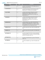
Contents
Introduction to the Protocol-Specific and Native Transceiver PHYs............... 1-1
Protocol-Specific Transceiver PHYs......................................................................................................... 1-1
Native Transceiver PHYs ...........................................................................................................................1-2
Non-Protocol-Specific Transceiver PHYs................................................................................................1-4
Transceiver PHY Modules..........................................................................................................................1-4
Transceiver Reconfiguration Controller...................................................................................................1-5
Resetting the Transceiver PHY.................................................................................................................. 1-5
Running a Simulation Testbench.............................................................................................................. 1-6
Unsupported Features................................................................................................................................. 1-9
Getting Started Overview.................................................................................... 2-1
Installation and Licensing of IP Cores...................................................................................................... 2-1
Design Flows.................................................................................................................................................2-2
MegaWizard Plug-In Manager Flow.........................................................................................................2-3
Specifying Parameters..................................................................................................................... 2-3
Simulate the IP Core........................................................................................................................2-4
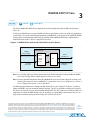
10GBASE-R PHY IP Core................................................................................... 3-1
10GBASE-R PHY Release Information.................................................................................................... 3-6
10GBASE-R PHY Device Family Support................................................................................................3-6
10GBASE-R PHY Performance and Resource Utilization for Stratix IV Devices..............................3-7
10GBASE-R PHY Performance and Resource Utilization for Arria V GT Devices.......................... 3-7
10GBASE-R PHY Performance and Resource Utilization for Arria V GZ and Stratix V
Devices..................................................................................................................................................... 3-8
Parameterizing the 10GBASE-R PHY.......................................................................................................3-8
General Option Parameters........................................................................................................................3-9
Analog Parameters for Stratix IV Devices..............................................................................................3-12
10GBASE-R PHY Interfaces.....................................................................................................................3-13
10GBASE-R PHY Data Interfaces........................................................................................................... 3-14
10GBASE-R PHY Status, 1588, and PLL Reference Clock Interfaces................................................ 3-17
Optional Reset Control and Status Interface......................................................................................... 3-18
10GBASE-R PHY Clocks for Arria V GT Devices................................................................................3-19
10GBASE-R PHY Clocks for Arria V GZ Devices................................................................................3-20
10GBASE-R PHY Clocks for Stratix IV Devices................................................................................... 3-21
10GBASE-R PHY Clocks for Stratix V Devices.....................................................................................3-22
10GBASE-R PHY Register Interface and Register Descriptions.........................................................3-23
10GBASE-R PHY Dynamic Reconfiguration for Stratix IV Devices................................................. 3-28
10GBASE-R PHY Dynamic Reconfiguration for Arria V and Stratix V Devices.............................3-29
1588 Delay Requirements......................................................................................................................... 3-30
10GBASE-R PHY TimeQuest Timing Constraints.............................................................................. 3-30
10GBASE-R PHY Simulation Files and Example Testbench.............................................................. 3-32
Altera Corporation
Altera Transceiver PHY IP Core User Guide
TOC-3
Backplane Ethernet 10GBASE-KR PHY IP Core with Early Access FEC
Option.............................................................................................................. 4-1
10GBASE-KR PHY Release Information................................................................................................. 4-3
Device Family Support................................................................................................................................ 4-3
10GBASE-KR PHY Performance and Resource Utilization..................................................................4-3
Parameterizing the 10GBASE-KR PHY....................................................................................................4-4
10GBASE-KR Link Training Parameters .................................................................................... 4-5
10GBASE-KR Auto-Negotiation and Link Training Parameters............................................. 4-7
10GBASE-R Parameters..................................................................................................................4-7
1GbE Parameters..............................................................................................................................4-9
Speed Detection Parameters.........................................................................................................4-10
PHY Analog Parameters............................................................................................................... 4-10
10GBASE-KR PHY IP Core Functional Description........................................................................... 4-10
10GBASE-KR PHY Arbitration Logic Requirements...........................................................................4-14
10GBASE-KR PHY State Machine Logic Requirements......................................................................4-15
Forward Error Correction (Clause 74)................................................................................................... 4-15
10BASE-KR PHY Interfaces.....................................................................................................................4-19
10GBASE-KR PHY Clock and Reset Interfaces.................................................................................... 4-20
10GBASE-KR PHY Data Interfaces............................................................................................ 4-22
10GBASE-KR PHY Control and Status Interfaces....................................................................4-25
Daisy-Chain Interface Signals...................................................................................................... 4-27
Embedded Processor Interface Signals....................................................................................... 4-28
Dynamic Reconfiguration Interface Signals.............................................................................. 4-29
Register Interface Signals.......................................................................................................................... 4-32
10GBASE-KR PHY Register Definitions................................................................................................4-32
PMA Registers............................................................................................................................................ 4-47
PCS Registers..............................................................................................................................................4-48
Creating a 10GBASE-KR Design............................................................................................................. 4-49
Editing a 10GBASE-KR MIF File ........................................................................................................... 4-50
Design Example..........................................................................................................................................4-52
SDC Timing Constraints.......................................................................................................................... 4-53
Acronyms....................................................................................................................................................4-53
1G/10 Gbps Ethernet PHY IP Core.....................................................................5-1
1G/10GbE PHY Release Information....................................................................................................... 5-2
Device Family Support................................................................................................................................ 5-3
1G/10 GbE PHY Performance and Resource Utilization.......................................................................5-3
Parameterizing the 1G/10GbE PHY..........................................................................................................5-4
1GbE Parameters..........................................................................................................................................5-4
Speed Detection Parameters.......................................................................................................................5-5
PHY Analog Parameters............................................................................................................................. 5-6
1G/10GbE PHY Interfaces..........................................................................................................................5-7
1G/10GbE PHY Clock and Reset Interfaces............................................................................................ 5-8
1G/10GbE PHY Data Interfaces................................................................................................................ 5-9
XGMII Mapping to Standard SDR XGMII Data.................................................................................. 5-11
Serial Data Interface.................................................................................................................................. 5-12
Altera Corporation
TOC-4
Altera Transceiver PHY IP Core User Guide
1G/10GbE Control and Status Interfaces............................................................................................... 5-12
Register Interface Signals.......................................................................................................................... 5-14
1G/10GbE PHY Register Definitions .....................................................................................................5-15
PMA Registers............................................................................................................................................ 5-16
PCS Registers..............................................................................................................................................5-17
1G/10 GbE GMII PCS Registers.............................................................................................................. 5-18
PMA Registers............................................................................................................................................ 5-20
1G/10GbE Dynamic Reconfiguration from 1G to 10GbE................................................................... 5-21
1G/10GbE PHY Arbitration Logic Requirements.................................................................................5-22
1G/10GbE PHY State Machine Logic Requirements............................................................................5-23
Editing a 1G/10GbE MIF File ................................................................................................................. 5-23
Creating a 1G/10GbE Design................................................................................................................... 5-24
Dynamic Reconfiguration Interface Signals.......................................................................................... 5-25
1G/10 Gbps Ethernet PHY IP Core.........................................................................................................5-27
Design Example..........................................................................................................................................5-29
Simulation Support....................................................................................................................................5-30
TimeQuest Timing Constraints...............................................................................................................5-30
Acronyms....................................................................................................................................................5-30
XAUI PHY IP Core............................................................................................. 6-1
XAUI PHY Release Information............................................................................................................... 6-2
XAUI PHY Device Family Support...........................................................................................................6-2
XAUI PHY Performance and Resource Utilization for Stratix IV Devices.........................................6-3
XAUI PHY Performance and Resource Utilization for Arria V GZ and Stratix V Devices............. 6-3
Parameterizing the XAUI PHY..................................................................................................................6-3
XAUI PHY General Parameters................................................................................................................ 6-4
XAUI PHY Analog Parameters..................................................................................................................6-6
XAUI PHY Analog Parameters for Arria II GX, Cyclone IV GX, HardCopy IV and Stratix IV
Devices..................................................................................................................................................... 6-6
Advanced Options Parameters.................................................................................................................. 6-8
XAUI PHY Configurations........................................................................................................................ 6-9
XAUI PHY Ports........................................................................................................................................6-10
XAUI PHY Data Interfaces...................................................................................................................... 6-11
SDR XGMII TX Interface............................................................................................................. 6-12
SDR XGMII RX Interface............................................................................................................. 6-13
Transceiver Serial Data Interface.................................................................................................6-13
XAUI PHY Clocks, Reset, and Powerdown Interfaces.........................................................................6-13
XAUI PHY PMA Channel Controller Interface....................................................................................6-15
XAUI PHY Optional PMA Control and Status Interface.................................................................... 6-16
XAUI PHY Register Interface and Register Descriptions....................................................................6-18
XAUI PHY Dynamic Reconfiguration for Arria II GX, Cyclone IV GX, HardCopy IV GX, and
Stratix IV GX.........................................................................................................................................6-25
XAUI PHY Dynamic Reconfiguration for Arria V, Arria V GZ, Cyclone V and Stratix V
Devices................................................................................................................................................... 6-25
Logical Lane Assignment Restriction..........................................................................................6-26
XAUI PHY Dynamic Reconfiguration Interface Signals......................................................... 6-26
SDC Timing Constraints.......................................................................................................................... 6-27
Simulation Files and Example Testbench...............................................................................................6-27
Altera Corporation
Altera Transceiver PHY IP Core User Guide
TOC-5
Interlaken PHY IP Core...................................................................................... 7-1
Interlaken PHY Device Family Support................................................................................................... 7-2
Parameterizing the Interlaken PHY.......................................................................................................... 7-3
Interlaken PHY General Parameters.........................................................................................................7-3
Interlaken PHY Optional Port Parameters.............................................................................................. 7-5
Interlaken PHY Analog Parameters.......................................................................................................... 7-5
Interlaken PHY Interfaces.......................................................................................................................... 7-6
Interlaken PHY Avalon-ST TX Interface................................................................................................. 7-7
Interlaken PHY Avalon-ST RX Interface............................................................................................... 7-10
Interlaken PHY TX and RX Serial Interface.......................................................................................... 7-14
Interlaken PHY PLL Interface..................................................................................................................7-14
Interlaken Optional Clocks for Deskew..................................................................................................7-15
Interlaken PHY Register Interface and Register Descriptions............................................................ 7-16
Why Transceiver Dynamic Reconfiguration......................................................................................... 7-20
Dynamic Transceiver Reconfiguration Interface.................................................................................. 7-20
Interlaken PHY TimeQuest Timing Constraints.................................................................................. 7-21
Interlaken PHY Simulation Files and Example Testbench..................................................................7-21
PHY IP Core for PCI Express (PIPE) .................................................................8-1
PHY for PCIe (PIPE) Device Family Support..........................................................................................8-3
PHY for PCIe (PIPE) Resource Utilization..............................................................................................8-3
Parameterizing the PHY IP Core for PCI Express (PIPE)..................................................................... 8-3
PHY for PCIe (PIPE) General Options Parameters................................................................................8-3
PHY for PCIe (PIPE) Interfaces.................................................................................................................8-6
PHY for PCIe (PIPE) Input Data from the PHY MAC..........................................................................8-7
PHY for PCIe (PIPE) Output Data to the PHY MAC..........................................................................8-11
PHY for PCIe (PIPE) Clocks....................................................................................................................8-13
PHY for PCIe (PIPE) Clock SDC Timing Constraints for Gen3 Designs......................................... 8-13
PHY for PCIe (PIPE) Optional Status Interface....................................................................................8-14
PHY for PCIe (PIPE) Serial Data Interface............................................................................................ 8-14
PHY for PCIe (PIPE) Register Interface and Register Descriptions...................................................8-15
PHY for PCIe (PIPE) Link Equalization for Gen3 Data Rate..............................................................8-21
Phase 0............................................................................................................................................. 8-22
Phase 1............................................................................................................................................. 8-22
Phase 2 (Optional)......................................................................................................................... 8-22
Phase 3 (Optional)......................................................................................................................... 8-23
Recommendations for Tuning Link Partner’s Transmitter.....................................................8-23
Enabling Dynamic PMA Tuning for PCIe Gen3.................................................................................. 8-23
PHY for PCIe (PIPE) Dynamic Reconfiguration.................................................................................. 8-24
Logical Lane Assignment Restriction..........................................................................................8-25
PHY for PCIe (PIPE) Simulation Files and Example Testbench........................................................ 8-25
Custom PHY IP Core.......................................................................................... 9-1
Device Family Support................................................................................................................................ 9-2
Performance and Resource Utilization.....................................................................................................9-2
Altera Corporation
TOC-6
Altera Transceiver PHY IP Core User Guide
Parameterizing the Custom PHY.............................................................................................................. 9-3
General Options Parameters.......................................................................................................... 9-3
Word Alignment Parameters......................................................................................................... 9-7
Rate Match FIFO Parameters......................................................................................................... 9-9
8B/10B Encoder and Decoder Parameters................................................................................. 9-10
Byte Order Parameters.................................................................................................................. 9-11
PLL Reconfiguration Parameters.................................................................................................9-14
Analog Parameters.........................................................................................................................9-16
Presets for Ethernet........................................................................................................................9-16
Interfaces..................................................................................................................................................... 9-19
Data Interfaces................................................................................................................................9-19
Clock Interface............................................................................................................................... 9-23
Optional Status Interface.............................................................................................................. 9-24
Optional Reset Control and Status Interface............................................................................. 9-26
Register Interface and Register Descriptions............................................................................. 9-27
Custom PHY IP Core Registers................................................................................................... 9-29
SDC Timing Constraints.............................................................................................................. 9-33
Dynamic Reconfiguration............................................................................................................ 9-33
Low Latency PHY IP Core.................................................................................10-1
Device Family Support..............................................................................................................................10-2
Performance and Resource Utilization...................................................................................................10-2
Parameterizing the Low Latency PHY....................................................................................................10-3
General Options Parameters.................................................................................................................... 10-4
Additional Options Parameters............................................................................................................... 10-7
PLL Reconfiguration Parameters...........................................................................................................10-10
Low Latency PHY Analog Parameters..................................................................................................10-12
Low Latency PHY Interfaces..................................................................................................................10-13
Low Latency PHY Data Interfaces.........................................................................................................10-13
Optional Status Interface........................................................................................................................ 10-15
Low Latency PHY Clock Interface........................................................................................................ 10-15
Optional Reset Control and Status Interface....................................................................................... 10-16
Register Interface and Register Descriptions....................................................................................... 10-17
Dynamic Reconfiguration...................................................................................................................... 10-19
SDC Timing Constraints........................................................................................................................ 10-20
Simulation Files and Example Testbench.............................................................................................10-21
Deterministic Latency PHY IP Core.................................................................11-1
Deterministic Latency Auto-Negotiation...............................................................................................11-2
Achieving Deterministic Latency............................................................................................................ 11-3
Deterministic Latency PHY Delay Estimation Logic............................................................................11-4
Deterministic Latency PHY Device Family Support............................................................................ 11-7
Parameterizing the Deterministic Latency PHY................................................................................... 11-8
General Options Parameters for Deterministic Latency PHY................................................ 11-8
Additional Options Parameters for Deterministic Latency PHY ........................................ 11-10
PLL Reconfiguration Parameters for Deterministic Latency PHY.......................................11-13
Deterministic Latency PHY Analog Parameters..................................................................... 11-15
Altera Corporation
Altera Transceiver PHY IP Core User Guide
TOC-7
Interfaces for Deterministic Latency PHY........................................................................................... 11-15
Data Interfaces for Deterministic Latency PHY..................................................................................11-16
Clock Interface for Deterministic Latency PHY................................................................................. 11-19
Optional TX and RX Status Interface for Deterministic Latency PHY............................................11-20
Optional Reset Control and Status Interfaces for Deterministic Latency PHY..............................11-21
Register Interface and Descriptions for Deterministic Latency PHY.............................................. 11-22
Dynamic Reconfiguration for Deterministic Latency PHY...............................................................11-27
Channel Placement and Utilization for Deterministic Latency PHY ............................................. 11-28
SDC Timing Constraints........................................................................................................................ 11-29
Simulation Files and Example Testbench for Deterministic Latency PHY ....................................11-30
Stratix V Transceiver Native PHY IP Core.......................................................12-1
Device Family Support for Stratix V Native PHY.................................................................................12-2
Performance and Resource Utilization for Stratix V Native PHY......................................................12-3
Parameter Presets.......................................................................................................................................12-3
Parameterizing the Stratix V Native PHY.............................................................................................. 12-4
General Parameters for Stratix V Native PHY ..........................................................................12-4
PMA Parameters for Stratix V Native PHY............................................................................... 12-6
Standard PCS Parameters for the Native PHY........................................................................ 12-13
10G PCS Parameters for Stratix V Native PHY ......................................................................12-29
Interfaces for Stratix V Native PHY .....................................................................................................12-46
Common Interface Ports for Stratix V Native PHY............................................................... 12-46
Standard PCS Interface Ports.....................................................................................................12-53
10G PCS Interface........................................................................................................................12-58
×6/×N Bonded Clocking.........................................................................................................................12-69
xN Non-Bonded Clocking......................................................................................................................12-73
SDC Timing Constraints of Stratix V Native PHY ............................................................................12-74
Dynamic Reconfiguration for Stratix V Native PHY......................................................................... 12-75
Simulation Support..................................................................................................................................12-76
Slew Rate Settings.................................................................................................................................... 12-76
Arria V Transceiver Native PHY IP Core......................................................... 13-1
Device Family Support..............................................................................................................................13-2
Performance and Resource Utilization...................................................................................................13-3
Parameterizing the Arria V Native PHY................................................................................................ 13-3
General Parameters....................................................................................................................................13-3
PMA Parameters........................................................................................................................................ 13-4
TX PMA Parameters..................................................................................................................... 13-5
TX PLL Parameters........................................................................................................................13-6
RX PMA Parameters..................................................................................................................... 13-8
Standard PCS Parameters.......................................................................................................................13-10
Phase Compensation FIFO.........................................................................................................13-12
Byte Ordering Block Parameters............................................................................................... 13-13
Byte Serializer and Deserializer..................................................................................................13-14
8B/10B........................................................................................................................................... 13-15
Rate Match FIFO..........................................................................................................................13-15
Word Aligner and BitSlip Parameters...................................................................................... 13-18
Altera Corporation
TOC-8
Altera Transceiver PHY IP Core User Guide
Bit Reversal and Polarity Inversion........................................................................................... 13-20
Interfaces...................................................................................................................................................13-23
Common Interface Ports............................................................................................................ 13-23
Standard PCS Interface Ports.....................................................................................................13-29
SDC Timing Constraints........................................................................................................................ 13-34
Dynamic Reconfiguration...................................................................................................................... 13-35
Simulation Support..................................................................................................................................13-36
Arria V GZ Transceiver Native PHY IP Core...................................................14-1
Device Family Support for Arria V GZ Native PHY............................................................................ 14-2
Performance and Resource Utilization for Arria V GZ Native PHY................................................. 14-3
Parameter Presets.......................................................................................................................................14-3
Parameterizing the Arria V GZ Native PHY......................................................................................... 14-3
General Parameters for Arria V GZ Native PHY ..................................................................... 14-4
PMA Parameters for Arria V GZ Native PHY.......................................................................... 14-6
Standard PCS Parameters for the Native PHY........................................................................ 14-13
10G PCS Parameters for Arria V GZ Native PHY ................................................................. 14-29
Interfaces for Arria V GZ Native PHY ................................................................................................ 14-46
Common Interface Ports for Arria V GZ Native PHY...........................................................14-46
Standard PCS Interface Ports.....................................................................................................14-53
10G PCS Interface........................................................................................................................14-58
SDC Timing Constraints of Arria V GZ Native PHY ....................................................................... 14-70
Dynamic Reconfiguration for Arria V GZ Native PHY.....................................................................14-71
Simulation Support..................................................................................................................................14-72
Cyclone V Transceiver Native PHY IP Core Overview.................................... 15-1
Cyclone Device Family Support...............................................................................................................15-2
Cyclone V Native PHY Performance and Resource Utilization......................................................... 15-2
Parameterizing the Cyclone V Native PHY........................................................................................... 15-2
General Parameters....................................................................................................................................15-3
PMA Parameters........................................................................................................................................ 15-4
TX PMA Parameters..................................................................................................................... 15-5
TX PLL Parameters........................................................................................................................15-6
RX PMA Parameters..................................................................................................................... 15-7
Standard PCS Parameters......................................................................................................................... 15-9
Phase Compensation FIFO.........................................................................................................15-11
Byte Ordering Block Parameters............................................................................................... 15-12
Byte Serializer and Deserializer..................................................................................................15-14
8B/10B........................................................................................................................................... 15-14
Rate Match FIFO..........................................................................................................................15-15
Word Aligner and BitSlip Parameters...................................................................................... 15-18
Bit Reversal and Polarity Inversion........................................................................................... 15-20
Interfaces...................................................................................................................................................15-22
Common Interface Ports............................................................................................................ 15-22
Cyclone V Standard PCS Interface Ports................................................................................. 15-28
SDC Timing Constraints........................................................................................................................ 15-32
Dynamic Reconfiguration...................................................................................................................... 15-33
Altera Corporation
Altera Transceiver PHY IP Core User Guide
TOC-9
Simulation Support..................................................................................................................................15-34
Transceiver Reconfiguration Controller IP Core Overview............................ 16-1
Transceiver Reconfiguration Controller System Overview................................................................. 16-2
Transceiver Reconfiguration Controller Performance and Resource Utilization............................ 16-5
Parameterizing the Transceiver Reconfiguration Controller IP Core............................................... 16-5
Parameterizing the Transceiver Reconfiguration Controller IP Core in Qsys................................. 16-6
General Options Parameters........................................................................................................ 16-6
Transceiver Reconfiguration Controller Interfaces.............................................................................. 16-8
MIF Reconfiguration Management Avalon-MM Master Interface........................................16-8
Transceiver Reconfiguration Interface....................................................................................... 16-9
Reconfiguration Management Interface...................................................................................16-10
Transceiver Reconfiguration Controller Memory Map..................................................................... 16-12
Transceiver Reconfiguration Controller Calibration Functions.......................................................16-13
Offset Cancellation...................................................................................................................... 16-13
Duty Cycle Calibration............................................................................................................... 16-13
Auxiliary Transmit (ATX) PLL Calibration............................................................................ 16-14
Transceiver Reconfiguration Controller PMA Analog Control Registers.......................................16-14
Transceiver Reconfiguration Controller EyeQ Registers...................................................................16-16
EyeQ Usage Example...................................................................................................................16-19
Transceiver Reconfiguration Controller DFE Registers.................................................................... 16-20
Controlling DFE Using Register-Based Reconfiguration.................................................................. 16-22
Turning on DFE Continuous Adaptive mode.........................................................................16-22
Turning on Triggered DFE Mode............................................................................................. 16-23
Setting the First Tap Value Using DFE in Manual Mode...................................................... 16-23
Transceiver Reconfiguration Controller AEQ Registers....................................................................16-24
Transceiver Reconfiguration Controller ATX PLL Calibration Registers.......................................16-26
Transceiver Reconfiguration Controller PLL Reconfiguration.........................................................16-28
Transceiver Reconfiguration Controller PLL Reconfiguration Registers........................................16-30
Transceiver Reconfiguration Controller DCD Calibration Registers.............................................. 16-31
Transceiver Reconfiguration Controller Channel and PLL Reconfiguration................................. 16-32
Channel Reconfiguration............................................................................................................16-33
PLL Reconfiguration................................................................................................................... 16-33
Transceiver Reconfiguration Controller Streamer Module Registers..............................................16-34
Mode 0 Streaming a MIF for Reconfiguration ....................................................................... 16-36
Mode 1 Avalon-MM Direct Writes for Reconfiguration.......................................................16-36
MIF Generation....................................................................................................................................... 16-37
Creating MIFs for Designs that Include Bonded or GT Channels................................................... 16-37
MIF Format.............................................................................................................................................. 16-38
xcvr_diffmifgen Utility............................................................................................................................16-39
Reduced MIF Creation............................................................................................................................16-42
Changing Transceiver Settings Using Register-Based Reconfiguration.......................................... 16-42
Register-Based Write...................................................................................................................16-42
Register-Based Read.................................................................................................................... 16-43
Changing Transceiver Settings Using Streamer-Based Reconfiguration.........................................16-43
Direct Write Reconfiguration.................................................................................................... 16-44
Streamer-Based Reconfiguration...............................................................................................16-45
Pattern Generators for the Stratix V and Arria V GZ Native PHYs.................................................16-46
Altera Corporation
TOC-10
Altera Transceiver PHY IP Core User Guide
Enabling the Standard PCS PRBS Verifier Using Streamer-Based Reconfiguration......... 16-46
Enabling the Standard PCS PRBS Generator Using Streamer-Based Reconfiguration ....16-47
Enabling the 10G PCS PRBS Generator or Verifier Using Streamer-Based
Reconfiguration...................................................................................................................... 16-48
Disabling the Standard PCS PRBS Generator and Verifier Using Streamer-Based
Reconfiguration ..................................................................................................................... 16-50
Understanding Logical Channel Numbering...................................................................................... 16-50
Two PHY IP Core Instances Each with Four Bonded Channels.......................................... 16-53
One PHY IP Core Instance with Eight Bonded Channels..................................................... 16-54
Two PHY IP Core Instances Each with Non-Bonded Channels...................................................... 16-55
Transceiver Reconfiguration Controller to PHY IP Connectivity....................................................16-56
Merging TX PLLs In Multiple Transceiver PHY Instances...............................................................16-57
Sharing Reconfiguration Interface for Multi-Channel Transceiver Designs.................................. 16-58
Loopback Modes......................................................................................................................................16-58
Transceiver PHY Reset Controller IP Core...................................................... 17-1
Device Family Support for Transceiver PHY Reset Controller...........................................................17-3
Performance and Resource Utilization for Transceiver PHY Reset Controller ...............................17-3
Parameterizing the Transceiver PHY Reset Controller IP...................................................................17-4
Transceiver PHY Reset Controller Parameters..................................................................................... 17-4
Transceiver PHY Reset Controller Interfaces........................................................................................17-6
Timing Constraints for Bonded PCS and PMA Channels.................................................................17-10
Transceiver PLL IP Core for Stratix V, Arria V, and Arria V GZ Devices...... 18-1
Parameterizing the Transceiver PLL PHY............................................................................................. 18-3
Transceiver PLL Parameters.....................................................................................................................18-3
Transceiver PLL Signals............................................................................................................................ 18-4
Analog Parameters Set Using QSF Assignments..............................................19-1
Making QSF Assignments Using the Assignment Editor.................................................................... 19-1
Analog Settings for Arria V Devices....................................................................................................... 19-2
Analog Settings for Arria V Devices........................................................................................... 19-2
Analog Settings Having Global or Computed Values for Arria V Devices........................... 19-4
Analog Settings for Arria V GZ Devices...............................................................................................19-11
Analog Settings for Arria V GZ Devices...................................................................................19-11
Analog Settings Having Global or Computed Default Values for Arria V GZ Devices ... 19-14
Analog Settings for Cyclone V Devices................................................................................................ 19-26
XCVR_IO_PIN_TERMINATION............................................................................................19-26
XCVR_REFCLK_PIN_TERMINATION.................................................................................19-26
XCVR_TX_SLEW_RATE_CTRL............................................................................................. 19-27
XCVR_VCCR_ VCCT_VOLTAGE..........................................................................................19-27
Analog Settings Having Global or Computed Values for Cyclone V Devices.................... 19-27
Analog Settings for Stratix V Devices................................................................................................... 19-34
Analog PCB Settings for Stratix V Devices ............................................................................. 19-34
Analog Settings Having Global or Computed Default Values for Stratix V Devices ........19-38
Altera Corporation
Altera Transceiver PHY IP Core User Guide
TOC-11
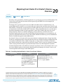
Migrating from Stratix IV to Stratix V Devices Overview............................... 20-1
Differences in Dynamic Reconfiguration for Stratix IV and Stratix V Transceivers....................... 20-2
Differences Between XAUI PHY Parameters for Stratix IV and Stratix V Devices......................... 20-3
Differences Between XAUI PHY Ports in Stratix IV and Stratix V Devices..................................... 20-5
Differences Between PHY IP Core for PCIe PHY (PIPE) Parameters in Stratix IV and Stratix
V Devices............................................................................................................................................... 20-7
Differences Between PHY IP Core for PCIe PHY (PIPE) Ports for Stratix IV and Stratix V
Devices................................................................................................................................................... 20-8
Differences Between Custom PHY Parameters for Stratix IV and Stratix V Devices....................20-11
Differences Between Custom PHY Ports in Stratix IV and Stratix V Devices................................20-13
Additional Information for the Transceiver PHY IP Core..............................21-1
Revision History for Previous Releases of the Transceiver PHY IP Core..........................................21-6
How to Contact Altera............................................................................................................................ 21-42
Altera Corporation
1
Introduction to the Protocol-Specific and
Native Transceiver PHYs
2015.01.19
UG-01080
Subscribe
Send Feedback
The Arria V, Cyclone V, and Stratix V support three types of transceiver PHY implementations or
customization.
The three types of transceiver PHY implementations are the following:
• Protocol-specific PHY
• Non-protocol-specific PHY
• Native transceiver PHY
The protocol-specific transceiver PHYs configure the PMA and PCS to implement a specific protocol. In
contrast, the native PHY provides broad access to the low-level hardware, allowing you to configure the
transceiver to meet your design requirements. Examples of protocol-specific PHYs include XAUI and
Interlaken.
You must also include the reconfiguration and reset controllers when you implement a transceiver PHY
in your design.
Protocol-Specific Transceiver PHYs
The protocol-specific transceiver PHYs configure many PCS to meet the requirements of a specific
protocol, leaving fewer parameters for you to specify.
Altera offers the following protocol-specific transceiver PHYS:
•
•
•
•
•
•
1G/10 Gbps Ethernet
10GBASE-R
Backplane Ethernet 10GBASE-KR PHY
Interlaken
PHY IP Core for PCI Express (PIPE)
XAUI
These transceiver PHYs include an Avalon® Memory-Mapped (Avalon-MM) interface to access control
and status registers and an Avalon Streaming (Avalon-ST) interface to connect to the MAC for data
transfer.
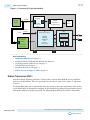
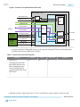
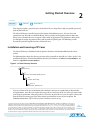
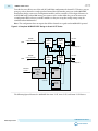
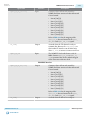
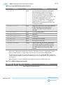
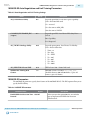
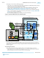
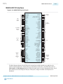
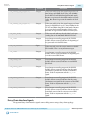
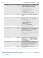
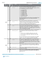
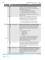
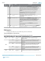
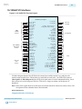
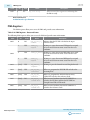
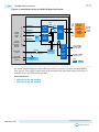
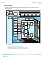
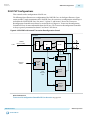
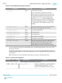
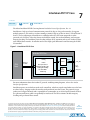
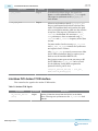
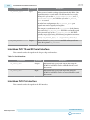
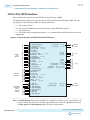
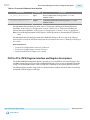
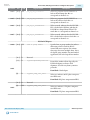
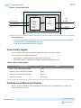
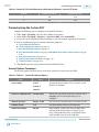
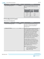
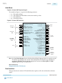
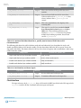
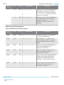
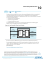
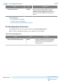
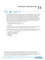
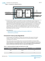
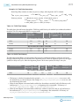
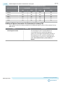
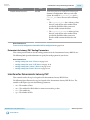
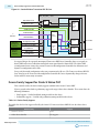
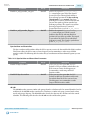
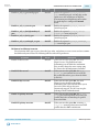
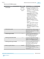
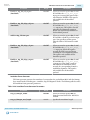
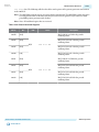
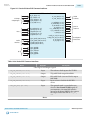
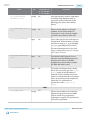
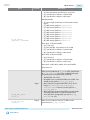
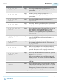
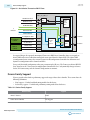
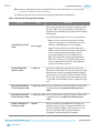
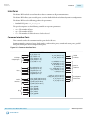
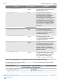
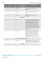
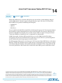
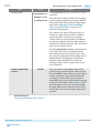
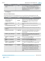
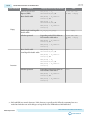
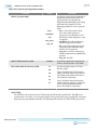
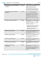
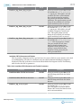
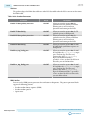
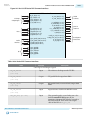
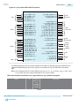
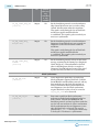
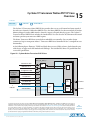
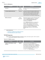
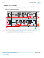
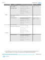
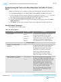
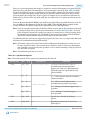
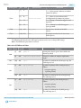
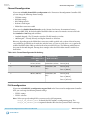
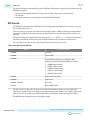
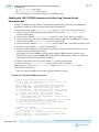
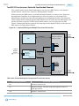
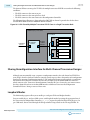
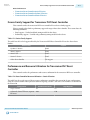
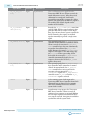
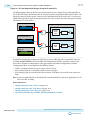
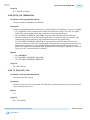
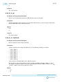
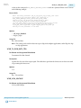
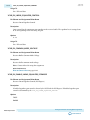
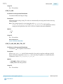
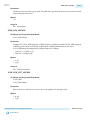
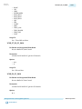
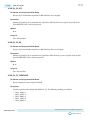
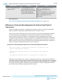
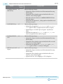
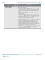
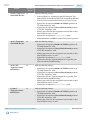
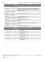
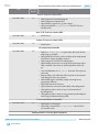
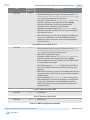
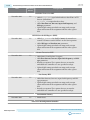
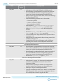
The following figure illustrates the top level modules that comprise the protocol-specific transceiver PHY
IP cores. As illustrated, the Altera Transceiver Reconfiguration Controller IP Core is instantiated
separately.
2015 Altera Corporation. All rights reserved. ALTERA, ARRIA, CYCLONE, ENPIRION, MAX, MEGACORE, NIOS, QUARTUS and STRATIX words and logos are
trademarks of Altera Corporation and registered in the U.S. Patent and Trademark Office and in other countries. All other words and logos identified as
trademarks or service marks are the property of their respective holders as described at www.altera.com/common/legal.html. Altera warrants performance
of its semiconductor products to current specifications in accordance with Altera's standard warranty, but reserves the right to make changes to any
products and services at any time without notice. Altera assumes no responsibility or liability arising out of the application or use of any information,
product, or service described herein except as expressly agreed to in writing by Altera. Altera customers are advised to obtain the latest version of device
specifications before relying on any published information and before placing orders for products or services.
©
www.altera.com
101 Innovation Drive, San Jose, CA 95134
ISO
9001:2008
Registered
1-2
UG-01080
2015.01.19
Native Transceiver PHYs
Figure 1-1: Transceiver PHY Top-Level Modules
Transceiver PHY
Avalon-MM
Control &
Status
Embedded
Controller
To MAC
Avalon-MM PHY
Management
S
S
M
Read & Write
Control & Status
Registers
Avalon-ST
TX and RX
PCS & PMA
Control & Status
Register Memory Map
PMA
PCS
Customized functionality for:
Rx Deserializer
10GBASE-R
10GBASE-KR
1G/10GBASE-R
XAUI
Interlaken
PCI Express PIPE
Altera Transceiver
Reconfiguration
Controller
S
Offset Cancellation
Analog Settings
M
Avalon-MM master interface
Reset
Controller
To HSSI Pins
Tx Serializer
PLL
S
CDR
Avalon-MM slave interface
Related Information
•
•
•
•
•
•
10GBASE-R PHY IP Core on page 3-1
Backplane Ethernet 10GBASE-KR PHY IP Core Overview
1G/10 Gbps Ethernet PHY IP Core on page 5-1
XAUI PHY IP Core on page 6-1
Interlaken PHY IP Core on page 7-1
PHY IP Core for PCI Express (PIPE) on page 8-1
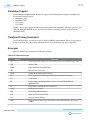
Native Transceiver PHYs
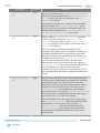
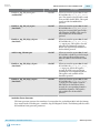
Each device family, beginning with Series V devices offers a separate Native PHY IP core to provide lowlevel access to the hardware. There are separate IP Cores for Arria V, Arria V GZ, Cyclone V, and Stratix
V devices.
The Native PHYs allow you to customize the transceiver settings to meet your requirements. You can also
use the Native PHYs to dynamically reconfigure the PCS datapath. Depending on protocol mode selected,
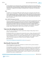
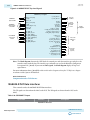
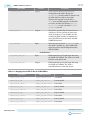
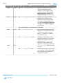
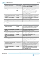
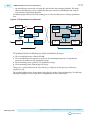
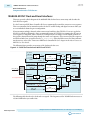
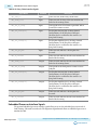
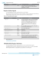
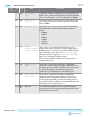
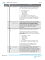
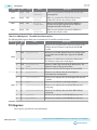
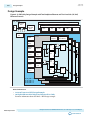
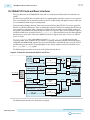
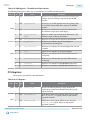
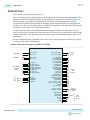
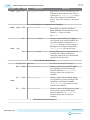
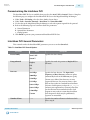
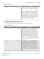
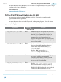
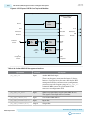
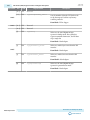
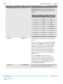
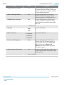
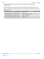
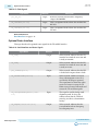
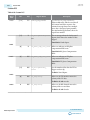
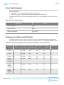
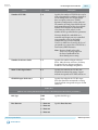
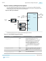
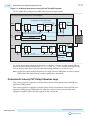
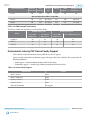
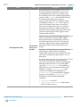
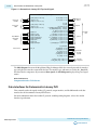
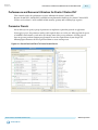
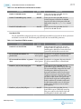
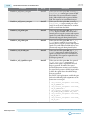
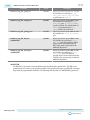
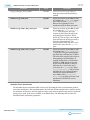
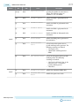
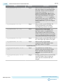
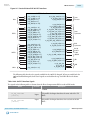
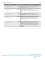
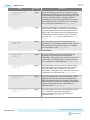
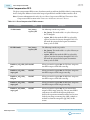
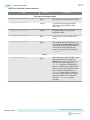
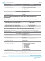
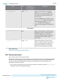
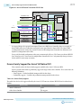
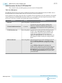
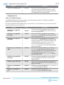
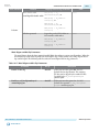
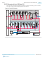
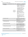
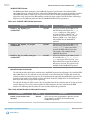
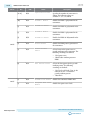
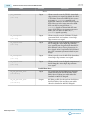
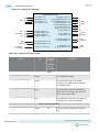
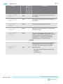
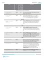
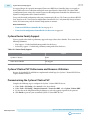
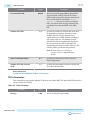
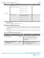
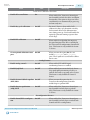
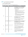
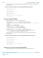
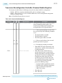
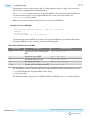
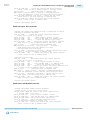
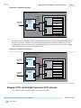
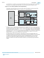
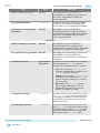
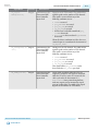
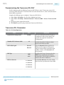
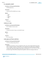
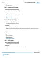
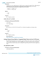
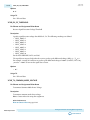
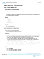
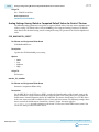
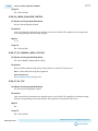
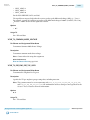
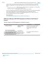
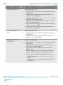
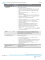
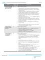
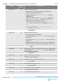
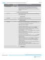
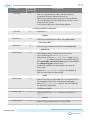
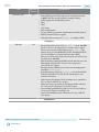
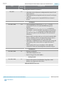
built-in rules validate the options you specify. The following figure illustrates the Stratix V Native PHY.
Altera Corporation
Introduction to the Protocol-Specific and Native Transceiver PHYs
Send Feedback
UG-01080
2015.01.19
Native Transceiver PHYs
1-3
Figure 1-2: Stratix V Transceiver Native PHY IP Core
Transceiver Native PHY
altera _xcvr_native_ <dev>
TX PLL Reference Clock
PMA
PLLs
CDR Reference Clock
RX PMA Parallel Data
TX PMA Parallel Data
(when neither PCS is enabled)
Serializer/
Clock
Generation
Block
RX PCS Parallel Data
to
FPGA fabric
10G PCS
(optional)
TX PCS Parallel Data
Transceiver
Reconfiguration
Controller
Reconfiguration to XCVR
Reconfiguration from XCVR
Standard
PCS
(optional)
TX and RX Resets
Transceiver
PHY Reset
Controller
Deserializer
RX Serial Data
Serializer
TX Serial Data
Calilbration Busy
PLL and RX Locked
As shown, the Stratix V Native PHY connects to the separately instantiated Transceiver Reconfiguration
Controller and Transceiver PHY Reset Controller.
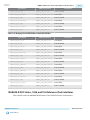
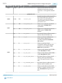
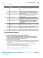
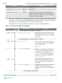
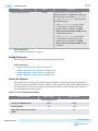
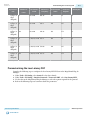
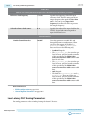
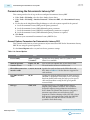
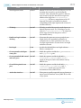
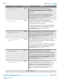
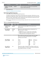
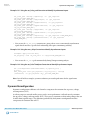
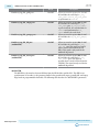
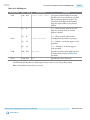
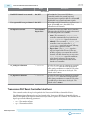
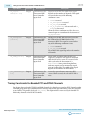
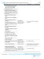
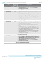
Table 1-1: Native Transceiver PHY Datapaths
Datapaths
PMA Direct:
Stratix V
Yes
Arria V
Yes
Arria V GZ
Yes
Cyclone V
-
This datapath connects the
FPGA fabric directly to the
PMA, minimizing latency.
You must implement any
required PCS functions in the
FPGA fabric.
(1)
(1)
PMA Direct mode is supported for Arria V GT, ST, and GZ devices, and for Stratix V GT devices only.
Introduction to the Protocol-Specific and Native Transceiver PHYs
Send Feedback
Altera Corporation
1-4
UG-01080
2015.01.19
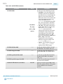
Non-Protocol-Specific Transceiver PHYs
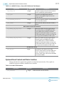
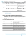
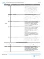
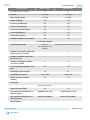
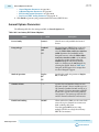
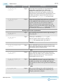
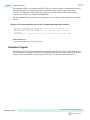
Datapaths
Standard:
Stratix V
Arria V
Arria V GZ
Cyclone V
Yes
Yes
Yes
Yes
Yes
-
Yes
-
This datapath provides a
complete PCS and PMA for
the TX and RX channels. You
can customize the Standard
datapath by enabling or
disabling individual modules
and specifying data widths.
10G:
This is a high performance
datapath. It provides a
complete PCS and PMA for
the TX and RX channels. You
can customize the 10G
datapath by enabling or
disabling individual modules
and specifying data widths.
Related Information
•
•
•
•
Analog Settings for Arria V Devices on page 19-2
Analog Settings for Arria V GZ Devices on page 19-11
Analog Settings for Cyclone V Devices on page 19-26
Analog Settings for Stratix V Devices on page 19-34
Non-Protocol-Specific Transceiver PHYs
Non-protocol specific transceiver PHYs provide more flexible settings than the protocol-specific
transceiver PHYs. They include the Custom PHY, Low Latency PHY, and Deterministic Latency PHY IP
Cores.
These PHYs include an Avalon® Memory-Mapped (Avalon-MM) interface to access control and status
registers and an Avalon Streaming (Avalon-ST) interface to connect to the MAC for data transfer.
Related Information
• Custom PHY IP Core on page 9-1
• Deterministic Latency PHY IP Core on page 11-1
• Low Latency PHY IP Core on page 10-1
Transceiver PHY Modules
The following sections provide a brief introduction to the modules included in the transceiver PHYs.
Altera Corporation
Introduction to the Protocol-Specific and Native Transceiver PHYs
Send Feedback
UG-01080
2015.01.19
Transceiver Reconfiguration Controller
1-5
PCS
The PCS implements part of the physical layer specification for networking protocols. Depending upon
the protocol that you choose, the PCS may include many different functions. Some of the most commonly
included functions are: 8B/10B, 64B/66B, or 64B/67B encoding and decoding, rate matching and clock
compensation, scrambling and descrambling, word alignment, phase compensation, error monitoring,
and gearbox.
PMA
The PMA receives and transmits differential serial data on the device external pins. The transmit (TX)
channel supports programmable pre-emphasis and programmable output differential voltage (VOD). It
converts parallel input data streams to serial data. The receive (RX) channel supports offset cancellation to
correct for process variation and programmable equalization. It converts serial data to parallel data for
processing in the PCS. The PMA also includes a clock data recovery (CDR) module with separate CDR
logic for each RX channel.
Avalon-MM PHY Management Interface
You can use the Avalon-MM PHY Management module to read and write the control and status registers
in the PCS and PMA for the protocol-specific transceiver PHY. The Avalon-MM PHY Management
module includes both Avalon-MM master and slave ports and acts as a bridge. It transfers commands
received from an embedded controller on its slave port to its master port. The Avalon-MM PHY
management master interface connects the Avalon-MM slave ports of PCS and PMA registers and the
Transceiver Reconfiguration module, allowing you to manage these Avalon-MM slave components
through a simple, standard interface. (Refer to Transceiver PHY Top-Level Modules.)
Transceiver Reconfiguration Controller
Altera Transceiver Reconfiguration Controller dynamically reconfigures analog settings in Arria V,
Cyclone V, and Stratix V devices.
Reconfiguration allows you to compensate for variations due to process, voltage, and temperature (PVT)
in 28-nm devices. It is required for Arria V, Cyclone V, and Stratix V devices that include transceivers.
For more information about the Transceiver Reconfiguration Controller, refer to Transceiver Reconfigu‐
ration Controller IP Core. The reset controller may be included in the transceiver PHY or may be a
separately instantiated component as described in Transceiver PHY Reset Controller.
Related Information
Transceiver Reconfiguration Controller IP Core Overview on page 16-1
Resetting the Transceiver PHY
This section provides an overview of the embedded reset controller and the separately instantiated
Transceiver PHY Reset Controller IP Core.
The embedded reset controller ensures reliable transceiver link initialization. The reset controller initial‐
izes both the TX and RX channels. You can disable the automatic reset controller in the Custom, Low
Latency Transceiver, and Deterministic Latency PHYs. If you disable the embedded reset controller, the
powerdown, analog and digital reset signals for both the TX and RX channels are top-level ports of the
transceiver PHY. You can use these ports to design a custom reset sequence, or you can use the Alteraprovided Transceiver Reset Controller IP Core.
Introduction to the Protocol-Specific and Native Transceiver PHYs
Send Feedback
Altera Corporation
1-6
UG-01080
2015.01.19
Running a Simulation Testbench
The Transceiver PHY Reset Controller IP Core handles all reset sequencing of the transceiver to enable
successful operation. Because the Transceiver PHY Reset Controller IP is available in clear text, you can
also modify it to meet your requirements. For more information about the Transceiver PHY Reset
Controller, refer to Transceiver Reconfiguration Controller IP Core.
To accommodate different reset requirements for different transceivers in your design, instantiate
multiple instances of a PHY IP core. For example, if your design includes 20 channels of the Custom PHY
IP core with 12 channels running a custom protocol using the automatic reset controller and 8 channels
requiring manual control of RX reset, instantiate 2 instances of the Custom PHY IP core and customize
one to use automatic mode and the other to use your own reset logic. For more information, refer to
“Enable embedded reset control” in Custom PHY General Options.
For more information about reset control in Stratix V devices, refer to Transceiver Reset Control in Stratix
V Devices in volume 3 of the Stratix V Device Handbook. For Stratix IV devices, refer to Reset Control and
Power Down in volume 4 of the Stratix IV Device Handbook. For Arria V devices, refer to Transceiver
Reset Control and Power-Down in Arria V Devices. For Cyclone V devices refer to Transceiver Reset
Control and Power Down in Cyclone V Devices.
Related Information
•
•
•
•
•
•
General Options Parameters on page 9-3
Transceiver PHY Reset Controller IP Core on page 17-1
Transceiver Reset Control in Stratix V Devices
Reset Control and Power Down
Transceiver Reset Control and Power-Down in Arria V Devices
Transceiver Reset Control and Power Down in Cyclone V Devices
Running a Simulation Testbench
When you generate your transceiver PHY IP core, the Quartus® II software generates the HDL files that
define your parameterized IP core. In addition, the Quartus II software generates an example Tcl script to
compile and simulate your design in ModelSim.
Altera Corporation
Introduction to the Protocol-Specific and Native Transceiver PHYs
Send Feedback
UG-01080
2015.01.19
Running a Simulation Testbench
1-7
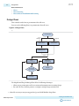
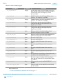
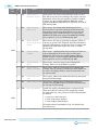
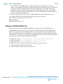
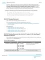
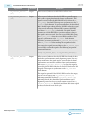
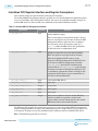
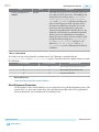
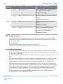
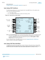
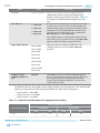
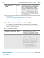
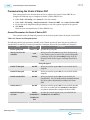
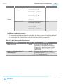
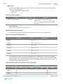
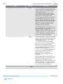
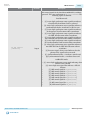
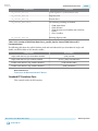
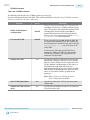
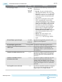
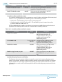
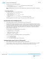
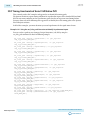
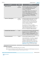
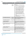
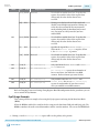
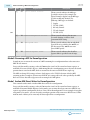
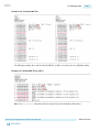
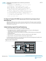
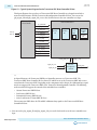
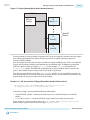
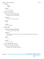
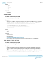
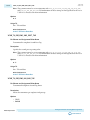
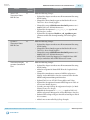
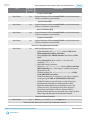
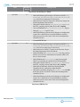
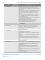
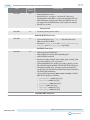
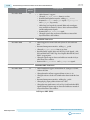
Figure 1-3: Directory Structure for Generated Files
<project_dir>
<instance_name>. v or .vhd - the parameterized transceiver PHY IP core
<instance_name> .qip - lists all files used in the transceiver PHY IP design
<instance_name> .bsf - a block symbol file for you transceiver PHY IP core
<project_dir>/<instance_name> - includes PHY IP Verilog HDL and
SystemVerilog design files for synthesis
<instance_name> _sim/altera_xcvr <PHY_IP_name> - includes plain text
files that describe all necessary files required for a successful simulation. The
plain text files contain the names of all required files and the correct order
for reading these files into your simulation tool.
<instance_name> _sim/aldec Simulation files for Riviera-PRO simulation tools
<instance_name> _sim/cadence Simulation files for Cadence simulation tools
<instance_name> _sim/mentor Simulation files for Mentor simulation tools
<instance_name> _sim/synopsys Simulation files for Synopsys simulation tools
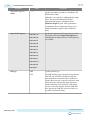
The following table describes the key files and directories for the parameterized transceiver PHY IP core
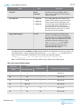
and the simulation environment which are in clear text.
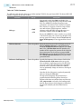
Table 1-2: Transceiver PHY Files and Directories
File Name
Description
<project_dir>
The top-level project directory.
<instance_name> .v or .vhd
The top-level design file.
<instance_name> .qip
A list of all files necessary for Quartus II compila‐
tion.
<instance_name> .bsf
A Block Symbol File (.bsf) for your transceiver
PHY.
<project_dir>/<instance_name>/
The directory that stores the HDL files that define
the protocol-specific PHY IP core. These files are
used for synthesis.
Introduction to the Protocol-Specific and Native Transceiver PHYs
Send Feedback
Altera Corporation
1-8
UG-01080
2015.01.19
Running a Simulation Testbench
File Name
Description
sv_xcvr_native.sv
Defines the transceiver. It includes instantiations of
the PCS and PMA modules and Avalon-MM PHY
management interface.
stratixv_hssi_ <module_name> _rbc. sv
These files perform rule based checking for the
module specified. For example, if the PLL type, data
rate, and FPGA fabric transceiver interface width
are not compatible, the checker reports an error.
altera_wait_generate.v
Generates waitrequest for protocol-specific
transceiver PHY IP core that includes backpressure.
alt_reset_ctrl_tgx_cdrauto.sv
Includes the reset controller logic.
<instance_name> _phy_assignments.qip
Includes an example of the PLL_TYPE assignment
statement required to specify the PLL type for each
PLL in the design. The available types are clock
multiplier unit (CMU) and auxiliary transmit
(ATX).
<project_dir>/<instance_name> _sim/ altera_xcvr_ The simulation directory.
<PHY_IP_name>/
<project_dir>/<instance_name>_sim/ aldec
Simulation files for Riviera-PRO simulation tools.
<project_dir>/<instance_name>_sim/ cadence
Simulation files for Cadence simulation tools.
<project_dir>/<instance_name>_sim/ mentor
Simulation files for Mentor simulation tools.
<project_dir>/<instance_name>_sim/ synopsys
Simulation files for Synopsys simulation tools.
The Verilog and VHDL transceiver PHY IP cores have been tested with the following simulators:
• ModelSim SE
• Synopsys VCS MX
• Cadence NCSim
If you select VHDL for your transceiver PHY, only the wrapper generated by the Quartus II software is in
VHDL. All the underlying files are written in Verilog or System Verilog. To enable simulation using a
VHDL-only ModelSim license, the underlying Verilog and System Verilog files for the transceiver PHY
are encrypted so that they can be used with the top-level VHDL wrapper without using a mixed-language
simulator.
For more information about simulating with ModelSim, refer to the Mentor Graphics ModelSim Support
chapter in volume 3 of the Quartus II Handbook.
The transceiver PHY IP cores do not support the NativeLink feature in the Quartus II software.
Generating Custom Simulation Scripts for Multiple Transceiver PHYs with ip-make-simscript
Use the ip-make-simscript utility to generate simulation command scripts for multiple transceiver
PHYs or Qsys systems. Specify all Simulation Package Descriptor files (.spd). The .spd files list the
required simulation files for the corresponding IP core. The MegaWizard Plug-In Manager and Qsys
generate the .spd files.
Altera Corporation
Introduction to the Protocol-Specific and Native Transceiver PHYs
Send Feedback
UG-01080
2015.01.19
Unsupported Features
1-9
When you specify multiple .spd files, the ip-make-simscript utility generates a single simulation script
containing all required simulation information. The default value of TOP_LEVEL_NAME is the
TOP_LEVEL_NAME defined in the IP core or Qsys .spd file. If this is not the top-level instance in your
design, specify the top-level instance of your testbench or design.
You can set appropriate variables in the script or edit the variable assignments directly in the script. If the
simulation script is a Tcl file that can be sourced in the simulator, set the variables before sourcing the
script. If the simulation script is a shell script, pass in the variables as command-line arguments to shell
script.
To run ip-make-simscript , type the following at the command prompt:
<ACDS installation path>\quartus\sopc_builder\bin\ip-make-simscript
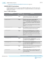
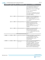
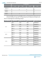
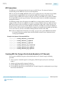
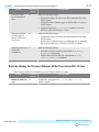
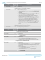
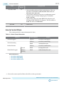
The following tables lists some of the options available with this utility.
Table 1-3: Options for the ip-make-simscript Utility
Option
--spd=<file>
Description
Status
Require
Describes the list of compiled files and
d
memory model hierarchy. If your design
includes multiple IP cores or Qsys systems
that include .spd files, use this option for each
file. For example:
ip-make-simscript --spd=ip1.spd -spd=ip2.spd
--outputdirectory=<directory>
Directory path specifying the location of
output files. If unspecified, the default setting
is the directory from which ip-makesimscript is run.
Option
al
--compile-to-work
Compiles all design files to the default work
library. Use this option only if you encounter
problems managing your simulation with
multiple libraries.
Option
al
Uses relative paths whenever possible
Option
al
--use-relative-paths
To learn about all options for the ip-make-simscript , type the following at the command prompt:
<ACDS installation path>\quartus\sopc_builder\bin\ip-make-simscript --help
Related Information
• Mentor Graphics ModelSim Support
• Simulating Altera Designs
Unsupported Features
The protocol-specific and native transceiver PHYs are not supported in Qsys in the current release.
Introduction to the Protocol-Specific and Native Transceiver PHYs
Send Feedback
Altera Corporation
2
Getting Started Overview
2015.01.19
UG-01080
Subscribe
Send Feedback
This chapter provides a general overview of the Altera IP core design flow to help you quickly get started
with any Altera IP core.
The Altera IP Library is installed as part of the Quartus II installation process. You can select and
parameterize any Altera IP core from the library. Altera provides an integrated parameter editor that
allows you to customize IP cores to support a wide variety of applications. The parameter editor guides
you through the setting of parameter values and selection of optional ports. The following sections
describe the general design flow and use of Altera IP cores.
Installation and Licensing of IP Cores
The Altera IP Library is distributed with the Quartus II software and downloadable from the Altera
website.
The following figure shows the directory structure after you install an Altera IP core, where <path> is the
installation directory. The default installation directory on Windows is C:\altera\<version number>; on
Linux it is /opt/altera<version number>.
Figure 2-1: IP Core Directory Structure
<path>
Installation directory
ip
Contains the Altera IP Library and third-party IP cores
altera
Contains the Altera IP Library
alt_mem_if
Contains the UniPHY IP core files
You can evaluate an IP core in simulation and in hardware until you are satisfied with its functionality
and performance. Some IP cores require that you purchase a license for the IP core when you want to take
your design to production. After you purchase a license for an Altera IP core, you can request a license file
from the Altera Licensing page of the Altera website and install the license on your computer. For
additional information, refer to Altera Software Installation and Licensing.
© 2015 Altera Corporation. All rights reserved. ALTERA, ARRIA, CYCLONE, ENPIRION, MAX, MEGACORE, NIOS, QUARTUS and STRATIX words and logos are
trademarks of Altera Corporation and registered in the U.S. Patent and Trademark Office and in other countries. All other words and logos identified as
trademarks or service marks are the property of their respective holders as described at www.altera.com/common/legal.html. Altera warrants performance
of its semiconductor products to current specifications in accordance with Altera's standard warranty, but reserves the right to make changes to any
products and services at any time without notice. Altera assumes no responsibility or liability arising out of the application or use of any information,
product, or service described herein except as expressly agreed to in writing by Altera. Altera customers are advised to obtain the latest version of device
specifications before relying on any published information and before placing orders for products or services.
www.altera.com
101 Innovation Drive, San Jose, CA 95134
ISO
9001:2008
Registered
2-2
UG-01080
2015.01.19
Design Flows
Related Information
• Altera
• Altera Licensing
• Altera Software Installation and Licensing
Design Flows
This section describes how to parameterize Altera IP cores.
You can use the following flow(s) to parameterize Altera IP cores:
Figure 2-2: Design Flows
(2)
Select Design Flow
Qsys or
SOPC Builder
Flow
MegaWizard
Flow
Specify Parameters
Specify Parameters
Complete Qsys or
SOPC Builder System
Optional
Perform
Functional Simulation
Does
Simulation Give
Expected Results?
Yes
Add Constraints
and Compile Design
IP Complete
Debug Design
The MegaWizard Plug-In Manager flow offers the following advantages:
• Allows you to parameterize an IP core variant and instantiate into an existing design
• For some IP cores, this flow generates a complete example design and testbench
(2)
Altera IP cores may or may not support the Qsys and SOPC Builder design flows.
Altera Corporation
Getting Started Overview
Send Feedback
UG-01080
2015.01.19
MegaWizard Plug-In Manager Flow
2-3
MegaWizard Plug-In Manager Flow
This section describes how to specify parameters and simulate your IP core with the MegaWizard Plug-In
Manager.
The MegaWizard™ Plug-In Manager flow allows you to customize your IP core and manually integrate
the function into your design.
Specifying Parameters
To specify IP core parameters, follow these steps:
1.
2.
3.
4.
Create a Quartus II project using the New Project Wizard available from the File menu.
In the Quartus II software, launch the IP Catalog.
You can select the IP core for your protocol implementation from the IP Catalog.
Specify the parameters on the Parameter Settings pages. For detailed explanations of these
parameters, refer to the "Parameter Settings" chapter in this document or the "Documentation" button
in the MegaWizard parameter editor.
Note: Some IP cores provide preset parameters for specific applications. If you wish to use preset
parameters, click the arrow to expand the Presets list, select the desired preset, and then click
Apply. To modify preset settings, in a text editor modify the <installation directory>/ip/altera/
alt_mem_if_interfaces/alt_mem_if_<memory_protocol>_emif/
alt_mem_if_<memory_protocol>_mem_model.qprs file.
5. If the IP core provides a simulation model, specify appropriate options in the wizard to generate a
simulation model.
Note: Altera IP supports a variety of simulation models, including simulation-specific IP functional
simulation models and encrypted RTL models, and plain text RTL models. These are all
cycle-accurate models. The models allow for fast functional simulation of your IP core instance
using industry-standard VHDL or Verilog HDL simulators. For some cores, only the plain text
RTL model is generated, and you can simulate that model.
Note: For more information about functional simulation models for Altera IP cores, refer to
Simulating Altera Designs in volume 3 of the Quartus II Handbook.
Caution: Use the simulation models only for simulation and not for synthesis or any other purposes.
Using these models for synthesis creates a nonfunctional design.
6. If the parameter editor includes EDA and Summary tabs, follow these steps:
a. Some third-party synthesis tools can use a netlist that contains the structure of an IP core but no
detailed logic to optimize timing and performance of the design containing it. To use this feature if
your synthesis tool and IP core support it, turn on Generate netlist.
b. On the Summary tab, if available, select the files you want to generate. A gray checkmark indicates
a file that is automatically generated. All other files are optional.
Note: If file selection is supported for your IP core, after you generate the core, a generation report
(<variation name>.html)appears in your project directory. This file contains information
about the generated files.
7. Click the Finish button, the parameter editor generates the top-level HDL code for your IP core, and a
simulation directory which includes files for simulation.
Getting Started Overview
Send Feedback
Altera Corporation
2-4
Simulate the IP Core
UG-01080
2015.01.19
Note: The Finish button may be unavailable until all parameterization errors listed in the messages
window are corrected.
8. Click Yes if you are prompted to add the Quartus II IP File (.qip) to the current Quartus II project.
You can also turn on Automatically add Quartus II IP Files to all projects.
You can now integrate your custom IP core instance in your design, simulate, and compile. While
integrating your IP core instance into your design, you must make appropriate pin assignments. You can
create a virtual pin to avoid making specific pin assignments for top-level signals while you are simulating
and not ready to map the design to hardware.
For some IP cores, the generation process also creates complete example designs. An example design for
hardware testing is located in the < variation_name > _example_design/example_project/ directory. An
example design for RTL simulation is located in the < variation_name > _example_design/simulation/
directory.
Note: For information about the Quartus II software, including virtual pins, refer to Quartus II Help.
Related Information
• Simulating Altera Designs
• Quartus II Help
Simulate the IP Core
This section describes how to simulate your IP core.
You can simulate your IP core variation with the functional simulation model and the testbench or
example design generated with your IP core. The functional simulation model and testbench files are
generated in a project subdirectory. This directory may also include scripts to compile and run the
testbench.
For a complete list of models or libraries required to simulate your IP core, refer to the scripts provided
with the testbench.
For more information about simulating Altera IP cores, refer to Simulating Altera Designs in volume 3 of
the Quartus II Handbook.
Related Information
Simulating Altera Designs
Altera Corporation
Getting Started Overview
Send Feedback
3
10GBASE-R PHY IP Core
2015.01.19
UG-01080
Subscribe
Send Feedback
The Altera 10GBASE-R PHY IP Core implements the functionality described in IEEE Standard 802.3
Clause 45.
It delivers serialized data to an optical module that drives optical fiber at a line rate of 10.3125 gigabits per
second (Gbps). In a multi-channel implementation of 10GBASE-R, each channel of the 10GBASE-R PHY
IP Core operates independently. Both the PCS and PMA of the 10GBASE-R PHY are implemented as
hard IP blocks in Stratix V devices, saving FPGA resources.
Figure 3-1: 10GBASE-R PHY with Hard PCS with PMA in Stratix V Devices
Stratix V FPGA
10GBASE-R PHY IP Core
SDR XGMII
72 bits @ 156.25 Mbps
Hard PCS
10GBASE-R
64b/66b
Scrambler
Gearbox
Avalon-MM
Control & Status
XFI/SFP+
10.3125 Gbps serial
PMA
Transceiver
Reconfiguraiton
Note: For a 10-Gbps Ethernet solution that includes both the Ethernet MAC and the 10GBASE-R PHY,
refer to the 10-Gbps Ethernet MAC MegaCore Function User Guide.
Note: For more detailed information about the 10GBASE-R transceiver channel datapath, clocking, and
channel placement, refer to the “10GBASE-R” section in the Transceiver Configurations in Stratix V
Devices chapter of the Stratix V Device Handbook.
The following figure illustrates a multiple 10 GbE channel IP core in a Stratix IV GT device. To achieve
higher bandwidths, you can instantiate multiple channels. The PCS is available in soft logic for Stratix IV
GT devices; it connects to a separately instantiated hard PMA. The PCS connects to an Ethernet MAC via
single data rate (SDR) XGMII running at 156.25 megabits per second (Mbps) and transmits data to a 10
Gbps transceiver PMA running at 10.3125 Gbps in a Stratix IV GT device.
© 2015 Altera Corporation. All rights reserved. ALTERA, ARRIA, CYCLONE, ENPIRION, MAX, MEGACORE, NIOS, QUARTUS and STRATIX words and logos are
trademarks of Altera Corporation and registered in the U.S. Patent and Trademark Office and in other countries. All other words and logos identified as
trademarks or service marks are the property of their respective holders as described at www.altera.com/common/legal.html. Altera warrants performance
of its semiconductor products to current specifications in accordance with Altera's standard warranty, but reserves the right to make changes to any
products and services at any time without notice. Altera assumes no responsibility or liability arising out of the application or use of any information,
product, or service described herein except as expressly agreed to in writing by Altera. Altera customers are advised to obtain the latest version of device
specifications before relying on any published information and before placing orders for products or services.
www.altera.com
101 Innovation Drive, San Jose, CA 95134
ISO
9001:2008
Registered
3-2
UG-01080
2015.01.19
10GBASE-R PHY IP Core
To make the most effective use of this soft PCS and PMA configuration for Stratix IV GT devices, you can
group up to four channels in a single quad and control their functionality using one Avalon-MM PHY
management bridge, transceiver reconfiguration module, and low controller. As this figure illustrates, the
Avalon-MM bridge Avalon-MM master port connects to the Avalon-MM slave port of the transceiver
reconfiguration and low latency controller modules so that you can update analog settings using the
standard Avalon-MM interface.
Note: This configuration does not require that all four channels in a quad run the 10GBASE-R protocol.
Figure 3-2: Complete 10GBASE-R PHY Design in Stratix IV GT Device
10GBASE-R PHY - Stratix IV Device
To MAC
To MAC
SDR XGMII
72 bits @ 156.25 Mbps
SDR XGMII
72 bits @ 156.25 Mbps
To Embedded
Controller
S
Avalon-MM
PHY
Management
Bridge
PCS
10GBASE-R
(64b/66b)
S
Alt_PMA
10GBASE-R
10.3 Gbps
S
To HSSI Pins
PCS
10GBASE-R
(64b/66b)
S
Alt_PMA
10GBASE-R
10.3 Gbps
S
To HSSI Pins
M
S
Avalon-MM
connections
S
10.3125 Gbps serial
10.3125 Gbps serial
Low Latency
Controller
Transceiver
Reconfig
Controller
The following figures illustrate the 10GBASE-R in Arria V GT, Arria V GZ, and Stratix V GX devices.
Altera Corporation
10GBASE-R PHY IP Core
Send Feedback
UG-01080
2015.01.19
3-3
10GBASE-R PHY IP Core
Figure 3-3: 10GBASE-R PHY IP Core In Arria V GT Devices
Arria V GT 10GBASE-R Top Level
Arria V GT 10GBASE-R
Avalon-ST
Streaming
Data
Tx Data
Rx Data
Control & Status
Conduits
(Optional or by
I/F Specification)
PMA
Data
Wiring
CMU
PLL
TX PMA
Soft PCS
Tx Serial
RX PMA & CDR
Rx Serial
Reconfiguration
Reset
Controller
Avalon-MM
Management
Interface
to Embedded
Controller
10GBASE-R PHY IP Core
Send Feedback
PMA + Reset Control & Status
(Memory Map)
10-GB BaseR
CSR
To/From
Transceiver
S
M
Avalon-MM Master
S
Avalon-MM Slave
Transceiver
Reconfiguration
Controller
S
Altera Corporation
3-4
UG-01080
2015.01.19
10GBASE-R PHY IP Core
Figure 3-4: 10GBASE-R PHY IP Core In Arria V GZ Devices
Transceiver Protocol
Avalon-ST
Streaming
Data
Arria V GZ Transceiver Protocol
Tx Data
Rx Data
Control & Status
PCS
Data
Wiring
(Optional or by
I/F Specification)
PMA
PLD-PCS & Duplex PCS
PCS-PMA
Generic
PLL
TX PMA
Tx Serial
RX PMA & CDR
Reset
Controller
Rx Serial
To/From
XCVR
PMA + Reset Control & Status
(Memory Map)
S
Avalon-MM
Management
Interface
to Embedded
Controller
M
Avalon-MM Master
S
Avalon-MM Slave
Transceiver
Reconfiguration
Controller
S
Altera Corporation
10GBASE-R PHY IP Core
Send Feedback
UG-01080
2015.01.19
10GBASE-R PHY IP Core
3-5
Figure 3-5: 10GBASE-R PHY IP Core In Stratix V Devices
Transceiver Protocol
Avalon-ST
Streaming
Data
Stratix V Transceiver Protocol
Tx Data
Rx Data
Control & Status
PCS
Data
Wiring
PMA
PLD-PCS & Duplex PCS
PCS-PMA
Generic
PLL
TX PMA
(Optional or by
I/F Specification)
Tx Serial
RX PMA & CDR
Reset
Controller
Rx Serial
To/From
XCVR
PMA + Reset Control & Status
(Memory Map)
S
Avalon-MM
Management
Interface
to Embedded
Controller
M
Avalon-MM Master
S
Avalon-MM Slave
Transceiver
Reconfiguration
Controller
S
The following table lists the latency through the PCS and PMA for Arria V GT devices with a 66-bit PMA.
The FPGA fabric to PCS interface is 64 bits wide. The frequency of the parallel clock is 156.25 MHz which
is line rate (10.3125 Gpbs)/interface width (64).
Table 3-1: Latency for TX and RX PCS and PMA Arria V Devices
PCS (Parallel Clock Cycles
PMA (UI)
TX
28
131
RX
33
99
The following table lists the latency through the PCS and PMA for Stratix V devices with a 40-bit PMA.
The FPGA fabric to PCS interface is 64 bits wide. The frequency of the parallel clock is 156.25 MHz which
is line rate (10.3125 Gbps)/interface width (64).
10GBASE-R PHY IP Core
Send Feedback
Altera Corporation
3-6
UG-01080
2015.01.19
10GBASE-R PHY Release Information
Table 3-2: Latency for TX and RX PCS and PMA Stratix V Devices
PCS (Parallel Clock Cycles)
32-bit PMA Width
Minimum
40-bit PMA Width
Maximum
Minimum
PMA (UI)
Maximum
TX
7
12
8
12
124
RX
14
33
15
34
43
Related Information
• IEEE 802.3 Clause 49
• 10-Gbps Ethernet MAC MegaCore Function User Guide
• Transceiver Configurations in Stratix V Devices
10GBASE-R PHY Release Information
Release information for the IP core.
Table 3-3: 10GBASE-R Release Information
Item
Description
Version
13.1
Release Date
November 2013
Ordering Codes(3)
IP-10GBASERPCS (primary) IPR-10GBASERPCS
(renewal)
Product ID
00D7
Vendor ID
6AF7
10GBASE-R PHY Device Family Support
Device support for the IP core.
IP cores provide either final or preliminary support for target Altera device families. These terms have the
following definitions:
• Final support—Verified with final timing models for this device.
• Preliminary support—Verified with preliminary timing models for this device.
Table 3-4: Device Family Support
Device Family
Arria V GT devices–Soft PCS and Hard PMA
(3)
Support
Final
No ordering codes or license files are required for Stratix V devices.
Altera Corporation
10GBASE-R PHY IP Core
Send Feedback
UG-01080
2015.01.19
10GBASE-R PHY Performance and Resource Utilization for Stratix IV Devices
Device Family
3-7
Support
Arria V ST devices-Soft PCS and Hard PMA
Final
Arria V GZ
Final
Stratix IV GT devices–Soft PCS and Hard PMA
Final
Stratix V devices–Hard PCS and PMA
Final
Other device families
No support
Note: For speed grade information, refer to “Transceiver Performance Specifications” in the DC and
Switching Characteristics chapter in the Stratix IV Handbook for Stratix IV devices or Stratix V
Device Datasheet.
Related Information
• DC and Switching Characteristics
• Stratix V Device Datasheet.
10GBASE-R PHY Performance and Resource Utilization for Stratix IV
Devices
Because the 10GBASE-R PHY is implemented in hard logic it uses less than 1% of the available ALMs,
memory, primary and secondary logic registers. The following table lists the typical expected device
resource utilization for duplex channels using the current version of the Quartus II software targeting a
Stratix IV GT device. The numbers of combinational ALUTs, logic registers, and memory bits are
rounded to the nearest 100.
Table 3-5: 10GBASE-R PHY Performance and Resource Utilization—Stratix IV GT Device
Channels
Combinational ALUTs
Logic Registers (Bits)
Memory Bits
1
5200
4100
4700
4
15600
1300
18800
10
38100
32100
47500
10GBASE-R PHY Performance and Resource Utilization for Arria V GT
Devices
The following table lists the resource utilization when targeting an Arria V (5AGTFD7K3F4015) device.
Resource utilization numbers reflect changes to the resource utilization reporting starting in the Quartus
II software v12.1 release for 28 nm device families and upcoming device families. The numbers of ALMs
and logic registers are rounded up to the nearest 100.
Note: For information about Quartus II resource utilization reporting, refer to Fitter Resources Reports
in the Quartus II Help.
10GBASE-R PHY IP Core
Send Feedback
Altera Corporation
3-8
UG-01080
2015.01.19
10GBASE-R PHY Performance and Resource Utilization for Arria V GZ and Stratix V
Devices
Table 3-6: 10GBASE-R PHY Performance and Resource Utilization—Arria V GT Device
Channels
1
ALMs
2800
Primary Logic
Registers
3000
Secondary Logic
Registers
300
Memory 10K
7
Related Information
Fitter Resources Reports
10GBASE-R PHY Performance and Resource Utilization for Arria V GZ and
Stratix V Devices
Because the 10GBASE-R PHY is implemented in hard logic in Arria V GZ and Stratix V devices, it uses
less than 1% of the available ALMs, memory, primary and secondary logic registers.
The following table lists the total latency for an Ethernet packet with a 9600 byte payload and an interpacket gap of 12 characters. The latency includes the number of cycles to transmit the payload from the
TX XGMII interface, through the TX PCS and PMA, looping back through the RX PMA and PCS to the
RX XGMII interface. (Stratix V Clock Generation and Distribution illustrates this datapath.)
Table 3-7: Latency
PPM Difference
Cycles
0 PPM
35
-200 PPM
35
+200 PPM
42
Note: If latency is critical, Altera recommends designing your own soft 10GBASE-R PCS and connecting
to the Low Latency PHY IP Core.
Parameterizing the 10GBASE-R PHY
The 10GBASE-R PHY IP Core is available for the Arria V, Arria V GZ, Stratix IV, or Stratix V device
families. Complete the following steps to configure the 10GBASE-R PHY IP Core:
1.
2.
3.
4.
Under Tools > IP Catalog, select the device family of your choice.
Under Tools > IP Catalog > Interface Protocols > Ethernet > select 10GBASE-R PHY.
Use the tabs on the MegaWizard Plug-In Manager to select the options required for the protocol.
Refer to the following topics to learn more about the parameters:
a. General Option Parameters on page 3-9
b. Analog Parameters for Stratix IV Devices on page 3-12
5. Click Finish to generate your parameterized 10GBASE-R PHY IP Core.
Altera Corporation
10GBASE-R PHY IP Core
Send Feedback
UG-01080
2015.01.19
General Option Parameters
3-9
General Option Parameters
This section describes general parameters.
This section describes the 10GBASE-R PHY parameters, which you can set using the MegaWizard PlugIn Manager.
Table 3-8: General Options
Name
Value
Description
General Options
Device family
Arria V
Specifies the target device.
Arria V GZ
Stratix IV GT
Stratix V
Number of channels
1-32
Mode of operation
Duplex
TX Only
The total number of 10GBASE-R PHY channels.
Arria V and Stratix V devices allow duplex, TX, or
RX mode. Stratix IV GT devices only support duplex
mode.
RX Only
PLL type
CMU, ATX
For Arria V GZ, Stratix IV, and Stratix V devices:
You can select either the CMU or ATX PLL. The
CMU PLL has a larger frequency range than the
ATX PLL. The ATX PLL is designed to improve
jitter performance and achieves lower channel-tochannel skew. Another advantage of the ATX PLL is
that it does not use a transceiver channel, while the
CMU PLL does.
Altera recommends the ATX PLL for data rates <= 8
Gbps.
Reference Clock Frequency
322.265625
MHz
644.53125 MHz
10GBASE-R PHY IP Core
Send Feedback
Arria V and Stratix V devices support both frequen‐
cies. Stratix IV GT devices only support 644.53125
MHz.
Altera Corporation
3-10
UG-01080
2015.01.19
General Option Parameters
Name
PCS / PMA interface width
Value
Description
32
For Stratix V and Arria V GZ devices only:
40
Specifies the data interface width between the 10G
PCS and the transceiver PMA. Smaller width
corresponds to lower PCS latency but higher
frequency.
• For 40 bit width, rx_recovered_clock is 257.8125
MHz and the gearbox ratio is 66:40.
• For 40 bit width, rx_recovered_clock is
322.265626 MHz and the gearbox ratio is 66:32.
32 bit PCS / PMA interface with does not support
data rates up to 10.3125 Gbps in C4/I4 Arria V GZ
device variants. Refer to Arria V GZ Device
Datasheet for details on data rates supported by
different device variants.
Additional Options
Enable additional control and
status pins
On/Off
If you turn this option On, the following 2 signals
are brought out to the top level of the IP core to
facilitate debugging: rx_hi_ber and rx_block_lock.
Enable rx_recovered_clk pin
On/Off
When you turn this option On, the RX recovered
clock signal is an output signal.
Enable pll_locked status port
On/Off
For Arria V and Stratix V devices:
When you turn this option On, a PLL locked status
signal is included as a top-level signal of the core.
Use external PMA control and
reconfig
On/Off
For Stratix IV devices:
If you turn this option on, the PMA controller and
reconfiguration block are external, rather than
included in the 10GBASE-R PHY IP Core, allowing
you to use the same PMA controller and reconfigu‐
ration IP cores for other protocols in the same
transceiver quad.
When you turn this option On, the cal_blk_
powerdown (0x021) and pma_tx_pll_is_locked
(0x022) registers are available.
Enable rx_coreclkin port
Altera Corporation
On/Off
When selected, rx_coreclkin is sourced from the
156.25 MHz xgmii_rx_clk signal avoiding the use
of a FPLL to generate this clock. This clock drives
the read side of RX FIFO.
10GBASE-R PHY IP Core
Send Feedback
UG-01080
2015.01.19
General Option Parameters
Name
Value
3-11
Description
Enable embedded reset control
On/Off
When On, the automatic reset controller initiates
the reset sequence for the transceiver. When Off you
can design your own reset logic using tx_analogreset , rx_analogreset, tx_digitalreset, rx_
digitalreset, and pll_powerdown which are
top-level ports of the Custom Transceiver PHY. You
may also use the Transceiver PHY Reset Controller
to reset the transceivers. For more information, refer
to the Transceiver Reconfiguration Controller IP
Core . By default, the CDR circuitry is in automatic
lock mode whether you use the embedded reset
controller or design your own reset logic. You can
switch the CDR to manual mode by writing the pma_
rx_setlocktodata or pma_rx_set_locktoref
registers to 1. If either the pma_rx_set_locktodata
and pma_rx_set_locktoref is set, the CDR
automatic lock mode is disabled.
Starting channel number
0-96
For Stratix IV devices, specifies the starting channel
number. Must be 0 or a multiple of 4. You only need
to set this parameter if you are using external PMA
and reconfiguration modules.
In Stratix V devices, by default, the logical channel 0
is assigned to either physical transceiver channel 1 or
channel 4 of a transceiver bank. However, if you
have already created a PCB with a different lane
assignment for logical channel 0, you can use the
work around shown in the example below.
Assignment of the starting channel number is
required for serial transceiver dynamic reconfigura‐
tion.
Enable IEEE 1588 latency
adjustment ports
On/Off
When you turn this option On, the core includes
logic to implement the IEEE 1588 Precision Time
Protocol.
Example 3-1: Changing the Default Logical Channel 0 Channel Assignments in Stratix V Devices
for ×6 or ×N Bonding
This example shows how to change the default logical channel 0 assignment in Stratix V devices
by redefining the pma_bonding_master parameter using the Quartus II Assignment Editor. In
this example, the pma_bonding_master was originally assigned to physical channel 1. (The
original assignment could also have been to physical channel 4.) The to parameter reassigns the
10GBASE-R PHY IP Core
Send Feedback
Altera Corporation
3-12
UG-01080
2015.01.19
Analog Parameters for Stratix IV Devices
pma_bonding_master to the 10GBASE-R instance name. You must substitute the instance name
from your design for the instance name shown in quotation marks.
set_parameter -name pma_bonding_master "\"1\"" -to "<PHY IP instance name>"
Related Information
• Transceiver PHY Reset Controller IP Core on page 17-1
• 1588 Delay Requirements on page 3-30
• Arria V GZ Device Datasheet
Analog Parameters for Stratix IV Devices
For Stratix IV devices, you specify analog options on the Analog Options tab.
Table 3-9: PMA Analog Options for Stratix IV Devices
Name
Transmitter termination
resistance
Value
OCT_85_OHMS,
OCT_100_OHMS,
Description
Indicates the value of the termination resistor for
the transmitter.
OCT_120_OHMS,
OCT_150_OHMS
Transmitter VOD control
setting
0–7
Sets VOD for the various TX buffers.
Pre-emphasis pre-tap
setting
0–7
Sets the amount of pre-emphasis on the TX buffer.
Invert the pre-emphasis
pre-tap polarity setting
On, Off
Determines whether or not the pre-emphasis
control signal for the pre-tap is inverted. If you
turn this option on, the pre-emphasis control
signal is inverted.
Pre-emphasis first posttap setting
0-15
Sets the amount of pre-emphasis for the 1st posttap.
Pre-emphasis second
post-tap setting
0–7
Sets the amount of pre-emphasis for the 2nd posttap.
Invert the pre-emphasis
second post-tap polarity
On, Off
Determines whether or not the pre-emphasis
control signal for the second post-tap is inverted.
If you turn this option on, the pre-emphasis
control signa is inverted.
Altera Corporation
10GBASE-R PHY IP Core
Send Feedback
UG-01080
2015.01.19
10GBASE-R PHY Interfaces
Name
Receiver common mode
voltage
Value
Tri-State
3-13
Description
Specifies the RX common mode voltage.
0.82V
1.1v
Receiver termination
resistance
OCT_85_OHMS
OCT_100_OHMs
Indicates the value of the termination resistor for
the receiver.
OCT_120_OHMS
OCT_150_OHMS
Receiver DC
0-4
Sets the equalization DC gain using one of the
following settings:
•
•
•
•
•
Receiver static equalizer
setting:
0-15
0: 0 dB
1: 3 dB
2: 6 dB
3: 9 dB
4: 12 dB
This option sets the equalizer control settings. The
equalizer uses a pass band filter. Specifying a low
value passes low frequencies. Specifying a high
value passes high frequencies.
Analog Parameters for Arria V, Arria V GZ, and Stratix V Devices
Click on the appropriate links to review the analog parameters for these devices.
Related Information
• Analog Settings for Arria V Devices on page 19-2
• Analog Settings for Arria V GZ Devices on page 19-11
• Analog Settings for Stratix V Devices on page 19-34
10GBASE-R PHY Interfaces
This section describes the 10GBASE-R PHY interfaces.
The following figure illustrates the top-level signals of the 10BASE-R PHY; <n> is the channel number.
10GBASE-R PHY IP Core
Send Feedback
Altera Corporation
3-14
UG-01080
2015.01.19
10GBASE-R PHY Data Interfaces
Figure 3-6: 10GBASE-R PHY Top-Level Signals
10GBASE-R Top-Level Signals
rx_serial_data<n>
tx_serial_data<n>
xgmii_tx_dc<n>[71:0]
tx_ready
xgmii_tx_clk
SDR XGMII TX
Inputs from MAC
SDR XGMII RX
Outputs from PCS
towards MAC
xgmii_rx_dc<n>[71:0]
rx_ready
rx_data_ready[<n>-1:0]
xgmii_rx_clk
rx_coreclkin
Avalon-MM PHY
Management
Interface
phy_mgmt_clk
phy_mgmt_clk_reset
phy_mgmt_addr[8:0]
phy_mgmt_writedata[31:0]
phy_mgmt_readdata[31:0]
phy_mgmt_write
phy_mgmt_read
phy_mgmt_waitrequest
Transceiver
Serial Data
gxb_pdn
pll_pdn
cal_blk_pdn
cal_blk_clk
pll_locked
reconfig_to_xcvr[3:0]
reconfig_from_xcvr[<n>/4)17-1:0]
reconfig_to_xcvr[(<n>70-1):0]
reconfig_from_xcvr[(<n>46-1):0]
External
PMA Control
Stratix IV
Devices
rx_block_lock
rx_hi_ber
rx_recovered_clk[<n>]
rx_latency_adj<n>[15:0]
tx_latency_adj<n>[15:0]
pll_ref_clk
Dynamic
Reconfiguration
Status, 1588
and Reference`
Clock
pll_powerdown
tx_digitalreset [<n>-1:0]
tx_analogreset [<n>-1:0]
tx_cal_busy [<n>-1:0]
rx_digitalreset [<n>-1:0]
rx_analogreset [<n>-1:0]
rx_cal_busy [<n>-1:0]
Reset Control
and Status
(Optional)
Note: The block diagram shown in the GUI labels the external pins with the interface type and places the
interface name inside the box. The interface type and name are used in the Hardware Component
Description File (_hw.tcl). If you turn on Show signals, the block diagram displays all top-level
signal names.
For more information about _hw.tcl files refer to refer to the Component Interface Tcl Reference chapter
in volume 1 of the Quartus II Handbook.
Related Information
Component Interface Tcl Reference
10GBASE-R PHY Data Interfaces
This section describes the 10GBASE-R PHY data interfaces.
The TX signals are driven from the MAC to the PCS. The RX signals are driven from the PCS to the
MAC.
Table 3-10: SDR XGMII TX Inputs
Signal Name
Direction
Description
XGMII TX Interface
Altera Corporation
10GBASE-R PHY IP Core
Send Feedback
UG-01080
2015.01.19
10GBASE-R PHY Data Interfaces
Signal Name
xgmii_tx_dc_[<n>71:0]
Direction
Input
3-15
Description
Contains 8 lanes of data and control for
XGMII. Each lane consists of 8 bits of data and
1 bit of control.
•
•
•
•
•
•
•
•
Lane 0-[7:0]/[8]
Lane 1-[16:9]/[17]
Lane 2-[25:18]/[26]
Lane 3-[34:27]/[35]
Lane 4-[43:36]/[44]
Lane 5-[52:45]/[53]
Lane 6-[61:54]/[62]
Lane 7-[70:63]/[71]
Refer toTable 3-11 for the mapping of the
xgmii_tx_dc data and control to the xgmii_
sdr_data and xgmii_sdr_ctrl signals.
tx_ready
Output
Asserted when the TX channel is ready to
transmit data. Because the readyLatency on
this Avalon-ST interface is 0, the MAC may
drive tx_ready as soon as it comes out of reset.
xgmii_tx_clk
Input
The XGMII TX clock which runs at 156.25
MHz. Connect xgmii_tx_clk to xgmii_rx_
clk to guarantee this clock is within 150 ppm
of the transceiver reference clock.
XGMII RX Interface
xgmii_rx_dc_<n>[71:0]
Output
Contains 8 lanes of data and control for
XGMII. Each lane consists of 8 bits of data and
1 bit of control.
•
•
•
•
•
•
•
•
Lane 0-[7:0]/[8]
Lane 1-[16:9]/[17]
Lane 2-[25:18]/[26]
Lane 3-[34:27]/[35]
Lane 4-[43:36]/[44]
Lane 5-[52:45]/[53]
Lane 6-[61:54]/[62]
Lane 7-[70:63]/[71]
Refer toTable 3-12 for the mapping of the
xgmii_rx_dc data and control to the xgmii_
sdr_data and xgmii_sdr_ctrl signals.
rx_ready
10GBASE-R PHY IP Core
Send Feedback
Output
Asserted when the RX reset is complete.
Altera Corporation
3-16
UG-01080
2015.01.19
10GBASE-R PHY Data Interfaces
Signal Name
Direction
Description
rx_data_ready [<n>-1:0]
Output
When asserted, indicates that the PCS is
sending data to the MAC. Because the
readyLatency on this Avalon-ST interface is 0,
the MAC must be ready to receive data
whenever this signal is asserted. After rx_
ready is asserted indicating the exit from the
reset state, the MAC should store xgmii_rx_
dc_<n>[71:0] in each cycle where rx_data_
ready<n> is asserted.
xgmii_rx_clk
Output
This clock is generated by the same reference
clock that is used to generate the transceiver
clock. Its frequency is 156.25 MHz. Use this
clock for the MAC interface to minimize the
size of the FIFO between the MAC and SDR
XGMII RX interface.
rx_coreclkin
Input
When you turn on Create rx_coreclkin port,
this signal is available as a 156.25 MHz clock
input port to drive the RX datapath interface
(RX read FIFO).
Serial Interface
rx_serial_data_<n>
Input
Differential high speed serial input data using
the PCML I/O standard. The clock is recovered
from the serial data stream.
tx_serial_data_<n>
Output
Differential high speed serial input data using
the PCML I/O standard. The clock is
embedded from the serial data stream.
Table 3-11: Mapping from XGMII TX Bus to XGMII SDR Bus
Signal Name
XGMII Signal Name
Description
xgmii_tx_dc_[7:0]
xgmii_sdr_data[7:0]
Lane 0 data
xgmii_tx_dc_[8]
xgmii_sdr_ctrl[0]
Lane 0 control
xgmii_tx_dc_[16:9]
xgmii_sdr_data[15:8]
Lane 1 data
xgmii_tx_dc_[17]
xgmii_sdr_ctrl[1]
Lane 1 control
xgmii_tx_dc_[25:18]
xgmii_sdr_data[23:16]
Lane 2 data
xgmii_tx_dc_[26]
xgmii_sdr_ctrl[2]
Lane 2 control
xgmii_tx_dc_[34:27]
xgmii_sdr_data[31:24]
Lane 3 data
xgmii_tx_dc_[35]
xgmii_sdr_ctrl[3]
Lane 3 control
xgmii_tx_dc_[43:36]
xgmii_sdr_data[39:32]
Lane 4 data
Altera Corporation
10GBASE-R PHY IP Core
Send Feedback
UG-01080
2015.01.19
10GBASE-R PHY Status, 1588, and PLL Reference Clock Interfaces
Signal Name
XGMII Signal Name
3-17
Description
xgmii_tx_dc_[44]
xgmii_sdr_ctrl[4]
Lane 4 control
xgmii_tx_dc_[52:45]
xgmii_sdr_data[47:40]
Lane 5 data
xgmii_tx_dc_[53]
xgmii_sdr_ctrl[5]
Lane 5 control
xgmii_tx_dc_[61:54]
xgmii_sdr_data[55:48]
Lane 6 data
xgmii_tx_dc_[62]
xgmii_sdr_ctrl[6]
Lane 6 control
xgmii_tx_dc_[70:63]
xgmii_sdr_data[63:56]
Lane 7 data
xgmii_tx_dc_[71]
xgmii_sdr_ctrl[7]
Lane 7 control
Table 3-12: Mapping from XGMII RX Bus to the XGMII SDR Bus
Signal Name
XGMII Signal Name
Description
xgmii_rx_dc_[7:0]
xgmii_sdr_data[7:0]
Lane 0 data
xgmii_rx_dc_[8]
xgmii_sdr_ctrl[0]
Lane 0 control
xgmii_rx_dc_[16:9]
xgmii_sdr_data[15:8]
Lane 1 data
xgmii_rx_dc_[17]
xgmii_sdr_ctrl[1]
Lane 1 control
xgmii_rx_dc_[25:18]
xgmii_sdr_data[23:16]
Lane 2 data
xgmii_rx_dc_[26]
xgmii_sdr_ctrl[2]
Lane 2 control
xgmii_rx_dc_[34:27]
xgmii_sdr_data[31:24]
Lane 3 data
xgmii_rx_dc_[35]
xgmii_sdr_ctrl[3]
Lane 3 control
xgmii_rx_dc_[43:36]
xgmii_sdr_data[39:32]
Lane 4 data
xgmii_rx_dc_[44]
xgmii_sdr_ctrl[4]
Lane 4 control
xgmii_rx_dc_[52:45]
xgmii_sdr_data[47:40]
Lane 5 data
xgmii_rx_dc_[53]
xgmii_sdr_ctrl[5]
Lane 5 control
xgmii_rx_dc_[61:54]
xgmii_sdr_data[55:48]
Lane 6 data
xgmii_rx_dc_[62]
xgmii_sdr_ctrl[6]
Lane 6 control
xgmii_rx_dc_[70:63]
xgmii_sdr_data[63:56]
Lane 7 data
xgmii_rx_dc_[71]
xgmii_sdr_ctrl[7]
Lane 7 control
10GBASE-R PHY Status, 1588, and PLL Reference Clock Interfaces
This section describes the 10GBASE-R PHY status, 1588, and PLL reference clock interfaces.
10GBASE-R PHY IP Core
Send Feedback
Altera Corporation
3-18
UG-01080
2015.01.19
Optional Reset Control and Status Interface
Table 3-13: 10GBASE-R Status, 1588, and PLL Reference Clock Outputs
Signal Name
Direction
Description
rx_block_lock
Output
Asserted to indicate that the block synchron‐
izer has established synchronization.
rx_hi_ber
Output
Asserted by the BER monitor block to
indicate a Sync Header high bit error rate
greater than 10-4.
rx_recovered_clk[<n>:0]
Output
This is the RX clock, which is recovered from
the received data stream.
pll_locked
Output
When asserted, indicates that the TX PLL is
locked.
IEEE 1588 Precision Time Protocol
rx_latency_adj_10g [15:0]
Output
When you enable 1588, this signal outputs
the real time latency in XGMII clock cycles
(156.25 MHz) for the RX PCS and PMA
datapath for 10G mode. Bits 0 to 9 represent
the fractional number of clock cycles. Bits 10
to 15 represent the number of clock cycles.
tx_latency_adj_10g [15:0]
Output
When you enable 1588, this signal outputs
real time latency in XGMII clock cycles
(156.25 MHz) for the TX PCS and PMA
datapath for 10G mode. Bits 0 to 9 represent
the fractional number of clock cycles. Bits 10
to 15 represent the number of clock cycles.
PLL Reference Clock
pll_ref_clk
Input
For Stratix IV GT devices, the TX PLL
reference clock must be 644.53125 MHz. For
Arria V and Stratix V devices, the TX PLL
reference clock can be either 644.53125 MHz
or 322.265625 MHz.
Optional Reset Control and Status Interface
This topic describes the signals in the optional reset control and status interface. These signals are
available if you do not enable the embedded reset controller.
Table 3-14: Avalon-ST RX Interface
Signal Name
pll_powerdown
Altera Corporation
Direction
Input
Description
When asserted, resets the TX PLL.
10GBASE-R PHY IP Core
Send Feedback
UG-01080
2015.01.19
10GBASE-R PHY Clocks for Arria V GT Devices
Signal Name
Direction
3-19
Description
tx_digitalreset[<n>-1:0]
Input
When asserted, reset all blocks in the TX PCS. If
your design includes bonded TX PCS channels,
refer to Timing Constraints for Reset Signals when
Using Bonded PCS Channels for a SDC constraint
you must include in your design.
tx_analogreset[<n>-1:0]
Input
When asserted, resets all blocks in the TX PMA.
Note: For Arria V devices, while compiling a
multi-channel transceiver design, you
will see a compile warning (12020) in
Quartus II software related to the signal
width of tx_analogreset. You can safely
ignore this warning. Also, per-channel
TX analog reset is not supported in
Quartus II software. Channel 0 TX
analog resets all the transceiver
channels.
tx_cal_busy[<n>-1:0]
Output
When asserted, indicates that the initial TX
calibration is in progress. It is also asserted if
reconfiguration controller is reset. It will not be
asserted if you manually re-trigger the calibration
IP. You must hold the channel in reset until
calibration completes.
rx_digitalreset[<n>-1:0]
Input
When asserted, resets the RX PCS.
rx_analogreset[<n>-1:0]
Input
When asserted, resets the RX CDR.
rx_cal_busy[<n>-1:0]
Output
When asserted, indicates that the initial RX
calibration is in progress. It is also asserted if
reconfiguration controller is reset. It will not be
asserted if you manually re-trigger the calibration
IP.
Related Information
•
•
•
•
Timing Constraints for Bonded PCS and PMA Channels on page 17-10
Transceiver Reset Control in Stratix V Devices
Transceiver Reset Control in Arria V Devices
Transceiver Reset Control in Cyclone V Devices
10GBASE-R PHY Clocks for Arria V GT Devices
The following figure illustrates Arria V GT clock generation and distribution.
10GBASE-R PHY IP Core
Send Feedback
Altera Corporation
3-20
UG-01080
2015.01.19
10GBASE-R PHY Clocks for Arria V GZ Devices
Figure 3-7: Arria V GT Clock Generation and Distribution
10GBASE-R Transceiver Channel - Arria V GT
TX
64
64
TX PCS
(soft)
TX PMA
(hard)
161.1328 MHz
xgmii_tx_clk
156.25 MHz
80
10.3125 Gbps
pll_ref_clk
644.53125 MHz
TX PLL
RX
64
RX PCS
(soft)
rx_coreclkin
64
161.1328 MHz
RX PMA
(hard)
80
10.3125 Gbps
fPLL
8/33
10GBASE-R PHY Clocks for Arria V GZ Devices
The following figure illustrates clock generation and distribution for Arria V GZ devices.
Altera Corporation
10GBASE-R PHY IP Core
Send Feedback
UG-01080
2015.01.19
10GBASE-R PHY Clocks for Stratix IV Devices
3-21
Figure 3-8: Arria V GZ Clock Generation and Distribution
10GBASE-R Hard IP Transceiver Channel - Arria V GZ
TX
40
64-bit data, 8-bit control
xgmii_tx_clk
TX PCS
TX PMA
257.8125
MHz
RX
RX PCS
156.25 MHz
rx_coreclkin
pll_ref_clk
644.53125 MHz
10.3125
Gbps serial
40
64-bit data, 8-bit control
xgmii_rx_clk
TX PLL
10.3125
Gbps serial
RX PMA
257.8125
MHz
fPLL
8/33
10GBASE-R PHY Clocks for Stratix IV Devices
The phy_mgmt_clk_reset signal is the global reset that resets the entire PHY. A positive edge on this
signal triggers a reset.
Refer to the Reset Control and Power Down chapter in volume 2 of the Stratix IV Device Handbook for
additional information about reset sequences in Stratix IV devices.
The PCS runs at 257.8125 MHz using the pma_rx_clock provided by the PMA. You must provide the
PMA an input reference clock running at 644.53725 MHz to generate the 257.8125 MHz clock.
10GBASE-R PHY IP Core
Send Feedback
Altera Corporation
3-22
UG-01080
2015.01.19
10GBASE-R PHY Clocks for Stratix V Devices
Figure 3-9: Stratix IV Clock Generation and Distribution
10GBASE-R Transceiver Channel - Stratix IV GT
TX
40
64-bit data, 8-bit control
xgmii_tx_clk
TX PCS
(soft IP)
20
TX PCS
(hard IP)
257.8125
MHz
/2
TX PMA
516.625
MHz
TX PLL
10.3125
Gbps serial
pll_ref_clk
644.53125 MHz
5/4
RX
40
64-bit data, 8-bit control
xgmii_rx_clk
RX PCS
(soft IP)
RX PCS
(hard IP)
257.8125
MHz
156.25 MHz
10.3125
Gbps serial
20
/2
RX PMA
516.625
MHz
GPLL
8/33
Related Information
Reset Control and Power Down
10GBASE-R PHY Clocks for Stratix V Devices
The following figure illustrates clock generation and distribution in Stratix V devices.
Altera Corporation
10GBASE-R PHY IP Core
Send Feedback
UG-01080
2015.01.19
10GBASE-R PHY Register Interface and Register Descriptions
3-23
Figure 3-10: Stratix V Clock Generation and Distribution
10GBASE-R Hard IP Transceiver Channel - Stratix V
TX
40
64-bit data, 8-bit control
xgmii_tx_clk
TX PCS
TX PMA
257.8125
MHz
RX
RX PCS
156.25 MHz
rx_coreclkin
pll_ref_clk
644.53125 MHz
10.3125
Gbps serial
40
64-bit data, 8-bit control
xgmii_rx_clk
TX PLL
10.3125
Gbps serial
RX PMA
257.8125
MHz
fPLL
8/33
To ensure proper functioning of the PCS, the maximum PPM difference between the pll_ref_clk and
xgmii_tx_clk clock inputs is 0 PPM. The FIFO in the RX PCS can compensate ±100 PPM between the
RX PMA clock and xgmii_rx_clk. You should use xgmii_rx_clk to drive xgmii_tx_clk. The CDR logic
recovers 257.8125 MHz clock from the incoming data.
10GBASE-R PHY Register Interface and Register Descriptions
The Avalon-MM PHY management interface provides access to the 10GBASER-R PHY PCS and PMA
registers. You can use an embedded controller acting as an Avalon-MM master to send read and write
commands to this Avalon-MM slave interface.
10GBASE-R PHY IP Core
Send Feedback
Altera Corporation
3-24
UG-01080
2015.01.19
10GBASE-R PHY Register Interface and Register Descriptions
Table 3-15: Avalon-MM PHY Management Interface
Signal Name
Direction
Description
phy_mgmt_clk
Input
The clock signal that controls the Avalon-MM
PHY management, interface. For Stratix IV
devices, the frequency range is 37.5-50 MHz.
There is no frequency restriction for Stratix V
devices; however, if you plan to use the same clock
for the PHY management interface and
transceiver reconfiguration, you must restrict the
frequency range of phy_mgmt_clk to 100-150
MHz to meet the specification for the transceiver
reconfiguration clock.
phy_mgmt_clk_reset
Input
Global reset signal that resets the entire 10GBASER PHY. This signal is active high and level
sensitive. This signal is not synchronized
internally.
phy_mgmt_addr[8:0]
Input
9-bit Avalon-MM address.
phy_mgmt_writedata[31:0]
Input
Input data.
phy_mgmt_readdata[31:0]
Output
Output data.
phy_mgmt_write
Input
Write signal. Asserted high.
phy_mgmt_read
Input
Read signal. Asserted high.
phy_mgmt_waitrequest
Output
When asserted, indicates that the Avalon-MM
slave interface is unable to respond to a read or
write request. When asserted, control signals to
the Avalon-MM slave interface must remain
constant.
Refer to the “Typical Slave Read and Write Transfers” and “Master Transfers” sections in the “Avalon
Memory-Mapped Interfaces” chapter of the Avalon Interface Specifications for timing diagrams.
The following table specifies the registers that you can access over the Avalon-MM PHY management
interface using word addresses and a 32-bit embedded processor. A single address space provides access
to all registers.
Note: Writing to reserved or undefined register addresses may have undefined side effects.
Table 3-16: 10GBASE-R Register Descriptions
Word Addr
Bit
R/W
Name
Description
PMA Common Control and Status
Altera Corporation
10GBASE-R PHY IP Core
Send Feedback
UG-01080
2015.01.19
10GBASE-R PHY Register Interface and Register Descriptions
Word Addr
Bit
R/W
Name
0x021
[31:0]
RW
cal_blk_powerdown
0x022
[31:0]
RO
pma_tx_pll_is_locked
3-25
Description
Writing a 1 to channel <n> powers
down the calibration block for
channel <n>. This register is only
available if you select Use external
PMA control and reconfig on the
Additional Options tab of the GUI.
Bit[P] indicates that the TX clock
multiplier unit CMU PLL [P] is
locked to the input reference clock.
This register is only available if you
select Use external PMA control and
reconfig on the Additional Options
tab of the GUI.
Reset Control Registers-Automatic Reset Controller
0x041
0x042
10GBASE-R PHY IP Core
Send Feedback
[31:0]
RW
reset_ch_bitmask
WO
reset_control (write)
Writing a 1 to bit 0 initiates a TX
digital reset using the reset controller
module. The reset affects channels
enabled in the reset_ch_bitmask.
Writing a 1 to bit 1 initiates a RX
digital reset of channels enabled in the
reset_ch_bitmask. Both bits 0 and 1
self-clear.
RO
reset_status (read)
Reading bit 0 returns the status of the
reset controller TX ready bit. Reading
bit 1 returns the status of the reset
controller RX ready bit.
[1:0]
Reset controller channel bitmask for
digital resets. The default value is all 1
s. Channel <n> can be reset when
bit<n> = 1. Channel <n> cannot be
reset when bit<n>=0.
Altera Corporation
3-26
UG-01080
2015.01.19
10GBASE-R PHY Register Interface and Register Descriptions
Word Addr
Bit
[31:0]
R/W
RW
Name
reset_fine_control
Description
You can use the reset_fine_
register to create your own
reset sequence. The reset control
module performs a standard reset
sequence at power on and whenever
the phy_mgmt_clk_reset is asserted.
Bits [31:4,0] are reserved.
control
[31:4,0]
RW
Reserved
[1]
RW
reset_tx_digital
[2]
RW
reset_rx_analog
[3]
RW
reset_rx_digital
0x044
It is safe to write 0s to reserved bits.
Writing a 1 causes the internal TX
digital reset signal to be asserted,
resetting all channels enabled in
reset_ch_bitmask. You must write a
0 to clear the reset condition.
Writing a 1 causes the internal RX
digital reset signal to be asserted,
resetting the RX analog logic of all
channels enabled in reset_ch_
bitmask. You must write a 0 to clear
the reset condition.
Writing a 1 causes the RX digital reset
signal to be asserted, resetting the RX
digital channels enabled in reset_ch_
bitmask. You must write a 0 to clear
the reset condition.
PMA Channel Control and Status
RW
phy_serial_loopback
0x061
[31:0]
0x064
[31:0]
RW
pma_rx_set_locktodata
0x065
[31:0]
RW
pma_rx_set_locktoref
0x066
[31:0]
RO
pma_rx_is_lockedtodata
Altera Corporation
Writing a 1 to channel <n> puts
channel <n> in serial loopback mode.
For information about pre- or postCDR serial loopback modes, refer to
Loopback Modes.
When set, programs the RX CDR PLL
to lock to the incoming data. Bit <n>
corresponds to channel <n>.
When set, programs the RX CDR PLL
to lock to the reference clock. Bit <n>
corresponds to channel <n>.
When asserted, indicates that the RX
CDR PLL is locked to the RX data,
and that the RX CDR has changed
from LTR to LTD mode. Bit <n>
corresponds to channel <n>.
10GBASE-R PHY IP Core
Send Feedback
UG-01080
2015.01.19
10GBASE-R PHY Register Interface and Register Descriptions
Word Addr
0x067
Bit
[31:0]
R/W
RO
Name
pma_rx_is_lockedtoref
3-27
Description
When asserted, indicates that the RX
CDR PLL is locked to the reference
clock. Bit <n> corresponds to channel
<n>.
10GBASE-R PCS
0x080
0x081
0x082
10GBASE-R PHY IP Core
Send Feedback
[31:0]
WO
INDIRECT_ADDR
[2]
RW
RCLR_ERRBLK_CNT
[3]
RW
RCLR_BER_COUNT
[0]
R
PCS_STATUS
[1]
R
HI_BER
[2]
R
BLOCK_LOCK
[3]
R
TX_FIFO_FULL
[4]
R
RX_FIFO_FULL
[5]
R
RX_SYNC_HEAD_ERROR
[6]
R
RX_SCRAMBLER_ERROR
[7]
R
RX_DATA_READY
Provides for indirect addressing of all
PCS control and status registers. Use
this register to specify the logical
channel number of the PCS channel
you want to access.
When set to 1, clears the error block
count register. To block: Block
synchronizer
When set to 1, clears the bit error rate
(BER) register. To block: BER
monitor
For Stratix IV devices: When asserted
indicates that the PCS link is up.
When asserted by the BER monitor
block, indicates that the PCS is
recording a high BER. From block:
BER monitor
When asserted by the block
synchronizer, indicates that the PCS
is locked to received blocks. From
Block: Block synchronizer
When asserted, indicates the TX FIFO
is full. From block: TX FIFO
When asserted, indicates the RX FIFO
is full. From block: RX FIFO
For Stratix V devices, when asserted,
indicates an RX synchronization
error. This signal is Stratix V devices
only.
For Stratix V devices: When asserted,
indicates an RX scrambler error.
When asserted indicates that the RX
interface is ready to send out received
data. From block: 10 Gbps Receiver
PCS
Altera Corporation
3-28
UG-01080
2015.01.19
10GBASE-R PHY Dynamic Reconfiguration for Stratix IV Devices
Word Addr
Bit
R/W
Name
[5:0]
R
BER_COUNT[5:0]
[13:6]
R
ERROR_BLOCK_COUNT[7:0]
[14]
R
LATCHED_HI_BER
[15]
R
LATCHED_BLOCK_LOCK
0x083
Description
For Stratix IV devices only, records
the bit error rate (BER). From block:
BER monitor
For Stratix IV devices only, records
the number of blocks that contain
errors. From Block: Block synchron‐
izer
Latched version of HI_BER . From
block: BER monitor
Latched version of BLOCK_LOCK. From
Block: Block synchronizer
Related Information
• Loopback Modes on page 16-58
• Avalon Interface Specifications
10GBASE-R PHY Dynamic Reconfiguration for Stratix IV Devices
The 10GBASE-R PHY includes additional top-level signals when configured with an external modules for
PMA control and dynamic reconfiguration.
You enable this configuration by turning on Use external PMA control and reconfig available for Stratix
IV GT devices.
Table 3-17: External PMA and Reconfiguration Signals
Signal Name
Direction
Description
gxb_pdn
Input
When asserted, powers down the entire GT block.
Active high. For Stratix IV de
pll_pdn
Input
When asserted, powers down the TX PLL. Active high.
cal_blk_pdn
Input
When asserted, powers down the calibration block.
Active high.
cal_blk_clk
Input
Calibration clock. For Stratix IV devices only. It must
be in the range 37.5-50 MHz. You can use the same
clock for the phy_mgmt_clk and the cal_blk_clk.
pll_locked
Output
When asserted, indicates that the TX PLL is locked.
reconfig_to_xcvr[3:0]
Input
Reconfiguration signals from the Transceiver Reconfi‐
guration Controller to the PHY device. This signal is
only available in Stratix IV devices.
Altera Corporation
10GBASE-R PHY IP Core
Send Feedback
UG-01080
2015.01.19
10GBASE-R PHY Dynamic Reconfiguration for Arria V and Stratix V Devices
Signal Name
Direction
Output
reconfig_from_xcvr [(<n>/4)
17-1:0]
3-29
Description
Reconfiguration RAM. The PHY device drives this
RAM data to the transceiver reconfiguration IP. This
signal is only available in Stratix IV devices.
10GBASE-R PHY Dynamic Reconfiguration for Arria V and Stratix V
Devices
For Arria V and Stratix V devices, each channel and each TX PLL have separate dynamic reconfiguration
interfaces. The MegaWizard Plug-In Manager provides informational messages on the connectivity of
these interfaces. The example below shows the messages for a single duplex channel.
Although you must initially create a separate reconfiguration interface for each channel and TX PLL in
your design, when the Quartus II software compiles your design, it reduces the number of reconfiguration
interfaces by merging reconfiguration interfaces. The synthesized design typically includes a reconfigura‐
tion interface for at least three channels because three channels share an Avalon-MM slave interface
which connects to the Transceiver Reconfiguration Controller IP Core. Conversely, you cannot connect
the three channels that share an Avalon-MM interface to different Transceiver Reconfiguration Control‐
lers. Doing so causes a Fitter error. For more information, refer to Transceiver Reconfiguration
Controller to PHY IP Connectivity on page 16-56. Allowing the Quartus II software to merge reconfi‐
guration interfaces gives the Fitter more flexibility in placing transceiver channels.
Example 3-2: Informational Messages for the Transceiver Reconfiguration Interface
Reconfiguration interface offset 0 is connected to the transceiver channel.
PHY IP will require 2 reconfiguration interfaces for connection to the external
reconfiguration controller.
Reconfiguration interface offset 0 is connected to the transceiver channel.
Reconfiguration interface offset 1 is connected to the transmit PLL.
The following table describes the signals in the reconfiguration interface; this interface uses the AvalonMM PHY Management interface clock.
Table 3-18: Reconfiguration Interface
Signal Name
reconfig_to_xcvr
Directio
n
Input
Reconfiguration signals from the Transceiver Reconfigura‐
tion Controller. <n> grows linearly with the number of
reconfiguration interfaces. This signal is only available in
Stratix V devices.
Output
Reconfiguration signals to the Transceiver Reconfiguration
Controller. <n> grows linearly with the number of reconfi‐
guration interfaces. This signal is only available in Stratix V
devices.
[(<n>70-1):0]
reconfig_from_xcvr
[(<n>46-1):0]
10GBASE-R PHY IP Core
Send Feedback
Description
Altera Corporation
3-30
UG-01080
2015.01.19
1588 Delay Requirements
1588 Delay Requirements
The 1588 protocol requires symmetric delays or known asymmetric delays for all external connections.
In calculating the delays for all external connections, you must consider the delay contributions of the
following elements:
•
•
•
•
The PCB traces
The backplane traces
The delay through connectors
The delay through cables
Accurate calculation of the channel-to-channel delay is important in ensuring the overall system accuracy.
10GBASE-R PHY TimeQuest Timing Constraints
The timing constraints for Stratix IV GT designs are in alt_10gbaser_phy.sdc. If your design does not
meet timing with these constraints, use LogicLock™ for the alt_10gbaser_pcs block. You can also
apply LogicLock to the alt_10gbaser_pcs and slightly expand the lock region to meet timing.
The following example provides the Synopsys Design Constraints file (.sdc) timing constraints for the
10GBASE-R IP Core when implemented in a Stratix IV device. To pass timing analysis, you must
decouple the clocks in different time domains. Be sure to verify the each clock domain is correctly
buffered in the top level of your design. You can find the .sdc file in your top-level working directory. This
is the same directory that includes your top-level .v or .vhd file.
Example 3-3: Synopsys Design Constraints for Clocks
#**************************************************************
# Timing Information
#**************************************************************
set_time_format -unit ns -decimal_places 3
#**************************************************************
# Create Clocks
#**************************************************************
create_clock -name {xgmii_tx_clk} -period 6.400 -waveform { 0.000 3.200 }
[get_ports {xgmii_tx_clk}]
create_clock -name {phy_mgmt_clk}
-period 20.00 -waveform { 0.000 10.000 }
[get_ports {phy_mgmt_clk}]
create_clock -name {pll_ref_clk} -period 1.552 -waveform { 0.000 0.776 }
[get_ports {ref_clk}]
#derive_pll_clocks
derive_pll_clocks -create_base_clocks
#derive_clocks -period "1.0"
# Create Generated Clocks
#**************************************************************
create_generated_clock -name pll_mac_clk -source [get_pins -compatibility_mode {*altpll_component|auto_generated|pll1|clk[0]}]
create_generated_clock -name pma_tx_clk -source [get_pins -compatibility_mode {*siv_alt_pma|pma_direct|auto_generated|transmit_pcs0|clkout}]
**************************************************************
## Set Clock Latency
#**************************************************************
#**************************************************************
# Set Clock Uncertainty
#**************************************************************
#**************************************************************
derive_clock_uncertainty
Altera Corporation
10GBASE-R PHY IP Core
Send Feedback
UG-01080
2015.01.19
10GBASE-R PHY TimeQuest Timing Constraints
3-31
set_clock_uncertainty -from [get_clocks {*siv_alt_pma|pma_ch*.pma_direct|
receive_pcs*|clkout}] -to pll_ref_clk -setup 0.1
set_clock_uncertainty -from [get_clocks {*siv_alt_pma|pma_direct|
auto_generated|transmit_pcs0|clkout}] -to pll_ref_clk -setup 0.08
set_clock_uncertainty -from [get_clocks {*siv_alt_pma|pma_ch*.pma_direct|
receive_pcs*|clkout}] -to pll_ref_clk -hold 0.1
set_clock_uncertainty -from [get_clocks {*siv_alt_pma|pma_direct|
auto_generated|transmit_pcs0|clkout}] -to pll_ref_clk -hold 0.08
#**************************************************************
# Set Input Delay
#**************************************************************
#**************************************************************
# Set Output Delay
#**************************************************************# Set Clock
Groups
#**************************************************************
set_clock_groups -exclusive -group phy_mgmt_clk -group xgmii_tx_clk -group
[get_clocks {*siv_alt_pma|pma_ch*.pma_direct|transmit_pcs*|clkout}] -group
[get_clocks {*siv_alt_pma|pma_ch*.pma_direct|receive_pcs*|clkout}] -group
[get_clocks {*pll_siv_xgmii_clk|altpll_component|auto_generated|pll1|
clk[0]}]
##**************************************************************
# Set False Path
#**************************************************************
set_false_path -from {*siv_10gbaser_xcvr*clk_reset_ctrl|rx_pma_rstn} -to
[get_clocks {{*siv_alt_pma|pma_ch*.pma_direct|transmit_pcs*|clkout}
{*siv_alt_pma|pma_ch*.pma_direct|receive_pcs*|clkout} {*pll_siv_xgmii_clk|
altpll_component|auto_generated|pll1|clk[0]} phy_mgmt_clk xgmii_tx_clk}]
set_false_path -from {*siv_10gbaser_xcvr*clk_reset_ctrl|rx_usr_rstn} -to
[get_clocks {{*siv_alt_pma|pma_ch*.pma_direct|transmit_pcs*|clkout}
{*siv_alt_pma|pma_ch*.pma_direct|transmit_pcs*|clkout} {*pll_siv_xgmii_clk|
altpll_component|auto_generated|pll1|clk[0]} phy_mgmt_clk xgmii_tx_clk}]
set_false_path -from {*siv_10gbaser_xcvr*clk_reset_ctrl|tx_pma_rstn} -to
[get_clocks {{*siv_alt_pma|pma_ch*.pma_direct|receive_pcs*|clkout}
{*siv_alt_pma|pma_ch*.pma_direct|transmit_pcs*|clkout} {*pll_siv_xgmii_clk|
altpll_component|auto_generated|pll1|clk[0]} phy_mgmt_clk xgmii_tx_clk}]
set_false_path -from {*siv_10gbaser_xcvr*clk_reset_ctrl|tx_usr_rstn} -to
[get_clocks {{*siv_alt_pma|pma_ch*.pma_direct|receive_pcs*|clkout}
{*siv_alt_pma|pma_ch*.pma_direct|transmit_pcs*|clkout} {*pll_siv_xgmii_clk|
altpll_component|auto_generated|pll1|clk[0]} phy_mgmt_clk xgmii_tx_clk}]
set_false_path -from {*siv_10gbaser_xcvr*rx_analog_rst_lego|rinit} -to
[get_clocks {{*siv_alt_pma|pma_ch*.pma_direct|receive_pcs*|clkout}
{*siv_alt_pma|pma_ch*.pma_direct|transmit_pcs*|clkout} {*pll_siv_xgmii_clk|
altpll_component|auto_generated|pll1|clk[0]} phy_mgmt_clk xgmii_tx_clk}]
set_false_path -from {*siv_10gbaser_xcvr*rx_digital_rst_lego|rinit} -to
[get_clocks {{*siv_alt_pma|pma_ch*.pma_direct|receive_pcs*|clkout}
{*siv_alt_pma|pma_ch*.pma_direct|transmit_pcs*|clkout} {*pll_siv_xgmii_clk|
altpll_component|auto_generated|pll1|clk[0]} phy_mgmt_clk xgmii_tx_clk}]
#**************************************************************
# Set Multicycle Paths
#**************************************************************
**************************************************************
# Set Maximum Delay
#**************************************************************
#**************************************************************
# Set Minimum Delay
#**************************************************************
#**************************************************************
# Set Input Transition
#**************************************************************
Note: This .sdc file is only applicable to the 10GBASE-R PHY IP Core when compiled in isolation. You
can use it as a reference to help in creating your own .sdc file.
Note: For Arria V and Stratix V devices, timing constraints are built into the HDL code.
10GBASE-R PHY IP Core
Send Feedback
Altera Corporation
3-32
10GBASE-R PHY Simulation Files and Example Testbench
UG-01080
2015.01.19
Note: The SDC timing constraints and approaches to identify false paths listed for Stratix V Native PHY
IP apply to all other transceiver PHYs listed in this user guide. Refer to SDC Timing Constraints of
Stratix V Native PHY for details.
Related Information
• SDC Timing Constraints of Stratix V Native PHY on page 12-74
This section describes SDC examples and approaches to identify false timing paths.
• About LogicLock Regions
10GBASE-R PHY Simulation Files and Example Testbench
Refer to Running a Simulation Testbench for a description of the directories and files that the Quartus II
software creates automatically when you generate your 10GBASE-R PHY IP Core.
Related Information
Running a Simulation Testbench on page 1-6
Altera Corporation
10GBASE-R PHY IP Core
Send Feedback
Backplane Ethernet 10GBASE-KR PHY IP Core
with Early Access FEC Option
4
2015.01.19
UG-01080
Subscribe
Send Feedback
The Backplane Ethernet 10GBASE-KR PHY MegaCore® function is available for Stratix® V and Arria V
GZ devices.
This transceiver PHY allows you to instantiate both the hard Standard PCS and the higher performance
hard 10G PCS and hard PMA for a single Backplane Ethernet channel. It implements the functionality
described in the IEEE Std 802.3ap-2007 Standard. Because each instance of the 10GBASE-KR PHY IP
Core supports a single channel, you can create multi-channel designs by instantiating more than one
instance of the core. The following figure shows the 10GBASE-KR transceiver PHY and additional blocks
that are required to implement this core in your design.
2015 Altera Corporation. All rights reserved. ALTERA, ARRIA, CYCLONE, ENPIRION, MAX, MEGACORE, NIOS, QUARTUS and STRATIX words and logos are
trademarks of Altera Corporation and registered in the U.S. Patent and Trademark Office and in other countries. All other words and logos identified as
trademarks or service marks are the property of their respective holders as described at www.altera.com/common/legal.html. Altera warrants performance
of its semiconductor products to current specifications in accordance with Altera's standard warranty, but reserves the right to make changes to any
products and services at any time without notice. Altera assumes no responsibility or liability arising out of the application or use of any information,
product, or service described herein except as expressly agreed to in writing by Altera. Altera customers are advised to obtain the latest version of device
specifications before relying on any published information and before placing orders for products or services.
©
www.altera.com
101 Innovation Drive, San Jose, CA 95134
ISO
9001:2008
Registered
4-2
UG-01080
2015.01.19
Backplane Ethernet 10GBASE-KR PHY IP Core with Early Access FEC Option
Figure 4-1: 10GBASE-KR PHY MegaCore Function and Supporting Blocks
Altera Device with 10.3125+ Gbps Serial Transceivers
10GBASE-KR PHY MegaCore Function
Native PHY Hard IP
TX XGMII Data
@156.25 MHz
10 Gb
Ethernet
Hard PCS
RX XGMII Data
To/From
1G/10Gb
Ethernet
MAC
Optional
1588 TX and
RX Latency
Adjust 1G
and 10G
PMA Reconfig
Request
PCS Reconfig
Request
Avalon-MM
PHY Management
Interface
TX GMII Data
@ 125 MHz
RX GMII Data
TX
Serial
Data
1.25 Gb/
10.3125 Gb
Hard PMA
1 Gb
Ethernet
Standard
Hard PCS
1 GIGE
PCS
10GBASE-KR
Auto-Negotiation
Link
Status
10GBASE-KR
Link Training
Sequencer
Copper
Backplane
RX
Serial
Data
ATX/CMU
TX PLL
For
10 GbE
322.265625 MHz
or 644.53125 MHz
Reference Clock
ATX/CMU
TX PLL
62.5 MHz or 125 MHz
For 1 GbE
Reference Clock
Soft 10G PCS &
FEC
To/From Modules in the PHY MegaCore
Control and Status
Registers
Legend
Hard IP
The Backplane Ethernet 10GBASE-KR PHY IP Core includes the following new modules to enable
operation over a backplane:
• Link Training (LT)— The LT mechanism allows the 10GBASE-KR PHY to automatically configure the
link-partner TX PMDs for the lowest Bit Error Rate (BER). LT is defined in Clause 72 of IEEE Std
802.3ap-2007.
• Auto negotiation (AN)—The Altera 10GBASE-KR PHY IP Core can auto-negotiate between
1000BASE-KX (1GbE) and 10GBASE-KR (10GbE) PHY types. The AN function is mandatory for
Backplane Ethernet. It is defined in Clause 73 of the IEEE Std 802.3ap-2007.
• Forward Error Correction—Forward Error Correction (FEC) function is an optional feature defined in
Clause 74 of IEEE 802.3ap-2007. It provides an error detection and correction mechanism allowing
noisy channels to achieve the Ethernet-mandated Bit Error Rate (BER) of 10-12 .
Related Information
IEEE Std 802.3ap-2007 Standard
Altera Corporation
Backplane Ethernet 10GBASE-KR PHY IP Core with Early Access FEC Option
Send Feedback
Soft IP
UG-01080
2015.01.19
10GBASE-KR PHY Release Information
4-3
10GBASE-KR PHY Release Information
Table 4-1: 10GBASE-KR PHY Release Information
Item
Description
Version
13.1
Release Date
November 2013
Ordering Codes
IP-10GBASEKR PHY (primary)
Product ID
0106
Vendor ID
6AF7
Device Family Support
IP cores provide either final or preliminary support for target Altera device families. These terms have the
following definitions:
• Final support—Verified with final timing models for this device.
• Preliminary support—Verified with preliminary timing models for this device.
Table 4-2: Device Family Support
Device Family
Support
Supported Speed Grades
Arria V GZ devices–Hard PCS and
PMA
Final
I3L, C3, I4, C4
Stratix V devices–Hard PCS and
PMA
Final
All speed grades except I4 and C4
Other device families
No support
Altera verifies that the current version of the Quartus II software compiles the previous version of each IP
core. Any exceptions to this verification are reported in the MegaCore IP Library Release Notes and
Errata. Altera does not verify compilation with IP core versions older than the previous release.
Note: For speed grade information, refer to DC and Switching Characteristics for Stratix V Devices in the
Stratix V Device Datasheet.
Related Information
Stratix V Device Datasheet
10GBASE-KR PHY Performance and Resource Utilization
This topic provides performance and resource utilization for the IP core in Arria V GZ and Stratix V
devices.
Backplane Ethernet 10GBASE-KR PHY IP Core with Early Access FEC Option
Send Feedback
Altera Corporation
4-4
UG-01080
2015.01.19
Parameterizing the 10GBASE-KR PHY
The following table shows the typical expected resource utilization for selected configurations using the
current version of the Quartus II software targeting a Stratix V GT (5SGTMC7K2F40C2) device. The
numbers of ALMs and logic registers are rounded up to the nearest 100. Resource utilization numbers
reflect changes to the resource utilization reporting starting in the Quartus II software v14.1 release for 28
nm device families and upcoming device families.
Table 4-3: 10GBASE-KR PHY Performance and Resource Utilization
Module Options
ALMs
Logic Registers
Memory
10GBASE-KR PHY only, no AN or LT
400
700
0
10GBASE-KR PHY with AN and
Sequencer
1000
1700
0
10GBASE-KR PHY with LT and
Sequencer,
2100
2300
0
10GBASE-KR PHY with AN, LT, and
Sequencer
2700
3300
0
10GBASE-KR MIF, Port A depth 256,
width 16, ROM (For reconfiguration from
low latency or 1GbE mode)
0
0
1 (M20K)
Low Latency MIF, Port A depth 256, width 0
16, ROM (Required for auto-negotiation
and link training.)
0
1 (M20K)
10GBASE-KR PHY with FEC
5100
40 (M20K)
3700
Parameterizing the 10GBASE-KR PHY
The10GBASE-KR PHY IP Core is available for the Arria V GZ and Stratix V device families. The IP
variant allows you specify either the Backplane-KR or 1Gb/10Gb Ethernet variant. When you select the
Backplane-KR variant, the Link Training (LT) and Auto Negotiation (AN) tabs appear. The 1Gb/10Gb
Ethernet variant (1G/10GbE) does not implement LT and AN parameters.
Complete the following steps to configure the 10GBASE-KR PHY IP Core:
1.
2.
3.
4.
Under Tools > IP Catalog, select the device family of your choice.
Under Tools > IP Catalog > Interface Protocols > Ethernet, select 10GBASE-KR PHY.
Use the tabs on the MegaWizard Plug-In Manager to select the options required for the protocol.
Specify 10GBASE-KR parameters. Refer to the topics listed as Related Links to understand 10GBASEKR parameters.
5. Click Finish to generate your parameterized 10GBASE-KR PHY IP Core.
Altera Corporation
Backplane Ethernet 10GBASE-KR PHY IP Core with Early Access FEC Option
Send Feedback
UG-01080
2015.01.19
10GBASE-KR Link Training Parameters
4-5
Related Information
•
•
•
•
•
•
10GBASE-KR Link Training Parameters on page 4-5
10GBASE-KR Auto-Negotiation and Link Training Parameters on page 4-7
10GBASE-R Parameters on page 4-7
1GbE Parameters on page 4-9
Speed Detection Parameters on page 4-10
PHY Analog Parameters on page 4-10
10GBASE-KR Link Training Parameters
The 10GBASE-KR variant provides parameters to customize the Link Training parameters.
Table 4-4: Link Training Settings
Name
Value
Description
Enable Link Training
On/Off
When you turn this option On, the core includes the
link training module which configures the remote
link-partner TX PMD for the lowest Bit Error Rate
(BER). LT is defined in Clause 72 of IEEE Std
802.3ap-2007.
Enable daisy chain mode
On/Off
When you turn this option On, the core includes
support for non-standard link configurations where
the TX and RX interfaces connect to different link
partners. This mode overrides the TX adaptation
algorithm.
Enable microprocessor
interface
On/Off
When you turn this option On, the core includes a
microprocessor interface which enables the
microprocessor mode for link training.
Maximum bit error count
15, 31,63, 127,
255
Specifies the maximum number of errors before the
Link Training Error bit (0xD2, bit 4) is set indicating
an unacceptable bit error rate. You can use this
parameter to tune PMA settings. For example, if you
see no difference in error rates between two different
sets of PMA settings, you can increase the width of
the bit error counter to determine if a larger counter
enables you to distinguish between PMA settings.
Number of frames to send
before sending actual data
127, 255
Specifies the number of additional training frames
the local link partner delivers to ensure that the link
partner can correctly detect the local receiver state.
PMA Parameters
VMAXRULE
0-63
Specifies the maximum VOD. The default value is 60
which represents 1200 mV.
Backplane Ethernet 10GBASE-KR PHY IP Core with Early Access FEC Option
Send Feedback
Altera Corporation
4-6
UG-01080
2015.01.19
10GBASE-KR Link Training Parameters
Name
Value
VMINRULE
0-63
VODMINRULE
0-63
VPOSTRULE
0-31
VPRERULE
0-15
PREMAINVAL
0-63
PREPOSTVAL
0-31
PREPREVAL
0-15
INITMAINVAL
0-63
INITPOSTVAL
0-31
INITPREVAL
0-15
Altera Corporation
Description
Specifies the minimum VOD. The default value is 9
which represents 165 mV.
Specifies the minimum VOD for the first tap. The
default value is 22 which represents 440mV.
Specifies the maximum value that the internal
algorithm for pre-emphasis will ever test in
determining the optimum post-tap setting. The
default value is 25.
Specifies the maximum value that the internal
algorithm for pre-emphasis will ever test in
determining the optimum pre-tap setting. The
default value is 15.
Specifies the Preset VOD Value. Set by the Preset
command as defined in Clause 72.6.10.2.3.1 of the
link training protocol. This is the value from which
the algorithm starts. The default value is 60.
Specifies the preset Pre-tap Value. The default value
is 0.
Specifies the preset Post-tap value. The default value
is 0.
Specifies the Initial VOD Value. Set by the Initialize
command in Clause 72.6.10.2.3.2 of the link training
protocol. The default value is 35.
Specifies the initial first Post-tap value. The default
value is 14.
Specifies the Initial Pre-tap Value. The default value
is 3.
Backplane Ethernet 10GBASE-KR PHY IP Core with Early Access FEC Option
Send Feedback
UG-01080
2015.01.19
10GBASE-KR Auto-Negotiation and Link Training Parameters
4-7
10GBASE-KR Auto-Negotiation and Link Training Parameters
Table 4-5: Auto Negotiation and Link Training Settings
Name
AN_PAUSE Pause Ability
Range
0-8
Description
Depends upon MAC. Local device pause capability
C2:0 = D12:10 of AN word.
C2 = reserved.
C1 is the same as ASM_DIR.
C0 is the same as PAUSE.
CAPABLE_FEC ENABLE_FEC
(request)
0-3
Depends upon FEC. Local device FEC abiity F1:0 =
D47:46.
F0 is Capability.
F1 is Requested.
AN_TECH Technology Ability
0-63
Depends upon options. Local Device Tech ability
T5:0 = D26:21 Other bits:
•
•
•
•
•
•
•
T24:6 = 0
T0 = Gige
T1 = XAUI
T2 = 10G
T3 = 40G
T4 = CR-4
T5 = 100G
AN_SELECTOR Selector Field
0-31
IEEE selector S4:0 = D4:0 of AN word
Width of the Training Wait
Counter
7-8
IEEE 802.3 clause 72.6.10.3.2 wait_timer_done
should be between 100 and 300 frames. 7 gives 127
frames. 8 gives 255 frames.
10GBASE-R Parameters
The 10GBASE-R parameters specify basic features of the 10GBASE-R PCS. The FEC options allow you to
specify the FEC ability.
Table 4-6: 10GBASE-R Parameters
Parameter Name
Options
Enable IEEE 1588 Precision Time On/Off
Protocol
Backplane Ethernet 10GBASE-KR PHY IP Core with Early Access FEC Option
Send Feedback
Description
When you turn this option On, the core includes
logic to implement the IEEE 1588 Precision
Time Protocol.
Altera Corporation
4-8
UG-01080
2015.01.19
10GBASE-R Parameters
Parameter Name
Reference clock frequency
Options
644.53125MHz
322.265625MHz
PLL Type
ATX
Description
Specifies the input reference clock frequency.
The default is 322.265625MHz.
Specifies the PLL type. You can specify either a
CMU or ATX PLL. The ATX PLL has better
jitter performance at higher data rates than the
CMU PLL. Another advantage of the ATX PLL
is that it does not use a transceiver channel,
while the CMU PLL does.
CMU
Enable additional control and
status pins
On/Off
When you turn this option On, the core includes
the rx_block_lock and rx_hi_ber ports.
Enable rx_recovered_clk pin
On/Off
When you turn this option On, the core includes
the rx_recovered_clk port.
Enable pll_locked status port
On/Off
When you turn this option On, the core includes
the pll_locked port.
Table 4-7: FEC Options
Parameter Name
Options
Description
Include FEC sublayer
On/Off
When you turn this option On, the core includes
logic to implement FEC and a soft 10GBASE-R
PCS.
Set FEC_ability bit on power up
and reset
On/Off
When you turn this option On, the core sets the
FEC ability bit on power up and reset.
Set FEC_Enable bit on power up
and reset
On/Off
When you turn this option On, the core sets the
FEC enable bit on power up and reset.
Set FEC_Error_Indication_
ability bit on power up and
On/Off
When you turn this option On, the core
indicates errors to the PCS.
reset
Good parity counter threshold to Default value: 4
achieve FEC block lock
Specifies the number of good parity blocks the
RX FEC module must receive before indicating
block lock as per Clause 74.10.2.1 of IEEE
802.3ap-2007.
Invalid parity counter threshold
to lose FEC block lock
Default value: 8
Specifies the number of bad parity blocks the RX
FEC module must receive before indicating loss
of block lock as per Clause 74.10.2.1 of IEEE
802.3ap-2007.
Use M20K for FEC Buffer (if
available)
On/Off
When you turn this option On, the Quartus II
software saves resources by replacing the FEC
buffer with M20K memory.
Altera Corporation
Backplane Ethernet 10GBASE-KR PHY IP Core with Early Access FEC Option
Send Feedback
UG-01080
2015.01.19
1GbE Parameters
Parameter Name
Enable FEC status ports
Options
On/Off
4-9
Description
When you turn this option the core includes the
rx_block_lock, rx_parity_good, rx_parity_
invalid, and tx_frame signals.
Note: This parameter is not implemented in
the early access release.
Related Information
Analog Parameters Set Using QSF Assignments on page 19-1
1GbE Parameters
The 1GbE parameters allow you to specify options for the 1GbE mode.
Table 4-8: 1Gb Ethernet Parameters
Parameter Name
Options
Description
Enable 1Gb Ethernet protocol
On/Off
When you turn this option On, the core includes
the GMII interface and related logic.
Enable SGMII bridge logic
On/Off
When you turn this option On, the core includes
the SGMII clock and rate adaptation logic for
the PCS. You must turn this option On if you
enable 1G mode.
Enable IEEE 1588 Precision Time On/Off
Protocol
When you turn this option On, the core includes
a module in the PCS to implement the IEEE
1588 Precision Time Protocol.
PHY ID (32 bit)
An optional 32-bit value that serves as a unique
identifier for a particular type of PCS. The
identifier includes the following components:
32-bit value
• Bits 3-24 of the Organizationally Unique
Identifier (OUI) assigned by the IEEE
• 6-bit model number
• 4-bit revision number
If unused, do not change the default value which
is 0x00000000.
PHY Core version (16 bits)
16-bit value
Reference clock frequency
125.00 MHz
62.50 MHz
This is an optional 16-bit value identifies the
PHY core version.
Specifies the clock frequency for the
1GBASE-KR PHY IP Core. The default is 125
MHz.
Related Information
1588 Delay Requirements on page 3-30
Backplane Ethernet 10GBASE-KR PHY IP Core with Early Access FEC Option
Send Feedback
Altera Corporation
4-10
UG-01080
2015.01.19
Speed Detection Parameters
Speed Detection Parameters
Selecting the speed detection option gives the PHY the ability to detect to link partners that support 1G/
10GbE but have disabled Auto-Negotiation. During Auto-Negotiation, if AN cannot detect Differential
Manchester Encoding (DME) pages from a link partner, the Sequencer reconfigures to 1GE and 10GE
modes (Speed/Parallel detection) until it detects a valid 1G or 10GbE pattern.
Table 4-9: Speed Detection
Parameter Name
Options
Enable automatic speed detection On
Avalon-MM clock frequency
Link fail inhibit time for 10Gb
Ethernet
Link fail inhibit time for 1Gb
Ethernet
Description
Off
When you turn this option On, the core includes
the Sequencer block that sends reconfiguration
requests to detect 1G or 10GbE when the Auto
Negotiation block is not able detect AN data.
100-125 MHz
Specifies the clock frequency for phy_mgmt_clk.
Specifies the time before link_status is set to
FAIL or OK. A link fails if the link_fail_
inhibit_time has expired before link_status
is set to OK. The legal range is 500-510 ms. For
more information, refer to "Clause 73 Auto
Negotiation for Backplane Ethernet" in IEEE Std
802.3ap-2007.
504 ms
40-50 ms
Specifies the time before link_status is set to
FAIL or OK . A link fails if the link_fail_inhibit_
time has expired before link_status is set to
OK. The legal range is 40-50 ms.
PHY Analog Parameters
You can specify analog parameters using the Quartus II Assignment Editor, the Pin Planner, or the
Quartus II Settings File (.qsf).
Related Information
• Analog Settings for Arria V GZ Devices on page 19-11
• Analog PCB Settings for Stratix V Devices on page 19-34
10GBASE-KR PHY IP Core Functional Description
This topic provides high-level block diagram of the 10GBASE-KR hardware.
The following figure shows the 10GBASE-KR PHY IP Core and the supporting modules required for
integration into your system.
Altera Corporation
Backplane Ethernet 10GBASE-KR PHY IP Core with Early Access FEC Option
Send Feedback
UG-01080
2015.01.19
4-11
10GBASE-KR PHY IP Core Functional Description
In this figure, the colors have the following meanings:
• Green-Altera- Cores available Quartus II IP Library, including the 1G/10Gb Ethernet MAC, the Reset
Controller, and Transceiver Reconfiguration Controller.
• Orange-Arbitration Logic Requirements. Logic you must design, including the Arbiter and State
Machine. Refer to 10GBASE-KR PHY Arbitration Logic Requirements on page 4-14 and
10GBASE-KR PHY State Machine Logic Requirements on page 4-15 for a description of this logic.
• White - 1G,10G and AN/LT settings files that you must generate. Refer to Creating a 10GBASE-KR
Design on page 4-49 for more information.
• Blue-The 10GBASE-KR PHY IP core available in the Quartus II IP Library.
Figure 4-2: Detailed 10GBASE-KR PHY IP Core Block Diagram
Backplane-KR or 1G/10Gb Ethernet PHY MegaCore Function
Backplane-KR or 1G/10Gb Ethernet PHY MegaCore Function
Backplane-KR or 1G/10Gb Ethernet PHY MegaCore Function
Native PHY Hard IP
1G/10Gb
Ethernet
MAC1G/10Gb
Ethernet
MAC1G/10Gb
TX XGMII Data
@156.25 MHz
10 Gb
Ethernet
Hard PCS
RX XGMII Data
Ethernet
MAC
TX GMII Data
@ 125 MHz
RX GMII Data
Shared Across Multiple Channels
1.25 Gb/
10.3125 Gb
Hard PMA
1 Gb
Ethernet
Standard
Hard PCS
1 GIGE
PCS
Reset
Controller
1G
TX
Serial
Data
Link
Status
Soft
10G PCS
& FEC
AN/LT
10G
RX
Serial
Data
58
Sequencer
Can Share
Across Multiple
Channels
ATX/CMU
TX PLL
For
10 GbE
FEC
Arbiter
Transceiver
Reconfig
Controller
State
Machine
<n>
<n>
S
Cntl &
Status
AN & LT
AN & LT Requests
ATX/CMU
TX PLL
For 1 GbE
322.265625 or
644.53125
Ref Clk
62.5 or 125
Ref Clk
Rate Change Requests
As this figure illustrates, the 10GBASE-KR PHY is built on the Native PHY and includes the following
additional blocks implemented in soft logic to implement Ethernet functionality defined in Clause 72 of
IEEE 802.3ap-2007.
Link Training (LT), Clause 72
This module performs link training as defined in Clause 72. The module facilitates two features:
• Daisy-chain mode for non-standard link configurations where the TX and RX interfaces connect to
different link partners instead of in a spoke and hub or switch topology.
Backplane Ethernet 10GBASE-KR PHY IP Core with Early Access FEC Option
Send Feedback
Altera Corporation
4-12
UG-01080
2015.01.19
10GBASE-KR PHY IP Core Functional Description
• An embedded processor mode to override the state-machine-based training algorithm. This mode
allows an embedded processor to establish link data rates instead of establishing the link using the
state-machine-based training algorithm.
The following figure illustrates the link training process, where the link partners exchange equalization
data.
Figure 4-3: TX Equalization for Link Partners
Encode
Handshake
Ack Change
Adapt
4
Tx
Tx
Eq
Eq
Encode
Handshake
Change Eq
3
1
Decode
Rx
Data Transmission
Send Eq
Adapt
Rx
Calculate
BER
2
Decode
Adaptation Feedback
TX equalization includes the following steps which are identified in this figure.
1. The receiving link partner calculates the BER.
2. The receiving link partner transmits an update to the transmitting link partner TX equalization
parameters to optimize the TX equalization settings
3. The transmitting partner updates its TX equalization settings.
4. The transmitting partner acknowledges the change.
This process is performed first for the VOD, then the pre-emphasis, the first post-tap, and then preemphasis pre-tap.
The optional backplane daisy-chain topology can replace the spoke or hub switch topology. The following
illustration highlights the steps required for TX Equalization for Daisy Chain Mode.
Altera Corporation
Backplane Ethernet 10GBASE-KR PHY IP Core with Early Access FEC Option
Send Feedback
UG-01080
2015.01.19
10GBASE-KR PHY IP Core Functional Description
4-13
Figure 4-4: TX Equalization in Daisy-Chain Mode
Parter B
Partner A
Encode
RX
TX
Eq
Handshake
Ack
Change
Adapt
5
2
dmo*
dmo*
4
Adapt
Ack Change
Change Eq
Change Eq
Decode
Decode
1
dmi*
dmi*
RX
Handshake
Eq
TX
Encode
Parter C
Data Transmission
RX
Adaptation Feedback
Change Eq
dmo*
Feedback/Handshake via Management
dmi*
Eq
Decode
Adapt
Ack Change
Handshake
TX
Encode
3
Data transmission proceeds clockwise from link partner A, to B, to C. TX equalization includes the
following steps which are identified in the figure :
1.
2.
3.
4.
5.
The receiving partner B calculates the BER for data received from transmitting partner A.
The receiving partner B sends updates for TX link partner C.
The receiving link partner C transmits an update to the transmitting link partner A.
Transmit partner A updates its equalization settings.
Transmit partner A acknowledges the change.
This procedure is repeated for the other two link partners.
Sequencer
The Sequencer (Rate change) block controls the start-up (reset, power-on) sequence of the PHY IP. It
automatically selects which PCS (1G, 10GbE, or Low Latency) is required and sends requests to
reconfigure the PCS. The Sequencer also performs the parallel detection function that reconfigures
between the 1G and 10GbE PCS until the link is established or times out.
Auto Negotiation (AN), Clause 73
The Auto Negotiation module in the 10GBASE-KR PHY IP implements Clause 73 of the Ethernet
standard. This module currently supports auto negotiation between 1GbE and 10GBASE-R data rates.
Backplane Ethernet 10GBASE-KR PHY IP Core with Early Access FEC Option
Send Feedback
Altera Corporation
4-14
UG-01080
2015.01.19
10GBASE-KR PHY Arbitration Logic Requirements
Auto negotiation with XAUI is not supported. Auto negotiation is run upon power up or if the auto
negotiation module is reset.
The following figures illustrate the handshaking between the Auto Negotiation, Link Training, Sequencer
and Transceiver Reconfiguration Controller blocks. Reconfig controller should use lt_start_rc signal in
combination with main_rc, post_rc, pre_rc, and tap_to_upd to change TX equalization settings.
Figure 4-5: Transition from Auto Negotiation to Link Training Mode
pcs_mode_rc[5:0]
01
02
lt_start_rc
seq_start_rc
rc_busy
tap_to_upd[2:0]
010
main_rc[5:0]
52
post_rc[4:0]
30
pre_rc[3:0]
5
init state
29
28
27
The Transceiver Reconfiguration Controller uses seq_start_rc in combination with the pcs_mode_rc
value to initiate a change to Auto Negotiation mode or from Link Training mode to 10GBASE-KR Data
mode. After TX equalization completes, this timing diagram shows the transition from Link Training
mode to 10GBASE-KR Data mode and MIF streaming.
Figure 4-6: Transition from Link Training to Data Mode
pcs_mode_rc[5:0]
02
04
lt_start_rc
seq_start_rc
rc_busy
MIF streaming
tap_to_upd[2:0]
001
main_rc[5:0]
42
post_rc[4:0]
9
pre_rc[3:0]
5
Related Information
Changing Transceiver Settings Using Streamer-Based Reconfiguration on page 16-43
10GBASE-KR PHY Arbitration Logic Requirements
This topic describes the arbitration functionality that you must implement.
The arbiter should implement the following logic. You can modify this logic based on your system
requirements:
1. Accept requests from either the Sequencer or Link Training block. Prioritize requests to meet system
requirements. Requests should consist of the following two buses:
Altera Corporation
Backplane Ethernet 10GBASE-KR PHY IP Core with Early Access FEC Option
Send Feedback
UG-01080
2015.01.19
10GBASE-KR PHY State Machine Logic Requirements
4-15
• Channel number—specifies the requested channel
• Mode—specifies 1G or 10G data modes or AN or LT modes for the corresponding channel
2. Select a channel for reconfiguration and send an ack/busy signal to the requestor. The requestor
should deassert its request signal when the ack/busy is received.
3. Pass the selected channel and rate information or PMA reconfiguration information for LT to the state
machine for processing.
4. Wait for a done signal from the state machine indicating that the reconfiguration process is complete
and it is ready to service another request.
Related Information
10GBASE-KR Dynamic Reconfiguration from 1G to 10GbE
10GBASE-KR PHY State Machine Logic Requirements
The state machine should implement the following logic. You can modify this logic based on your system
requirements:
1. Wait for reconfig_busy from the Transceiver Reconfiguration Controller to be deasserted and the
tx_ready and rx_ready signals from the Transceiver PHY Reset Controller to be asserted. These
conditions indicate that the system is ready to service a reconfiguration request.
2. Set the appropriate channel for reconfiguration.
3. Initiate the MIF streaming process. The state machine should also select the appropriate MIF (stored
in the ROMs) to stream based on the requested mode.
4. Wait for the reconfig_busy signal from the Transceiver Reconfiguration Controller to assert and
then deassert indicating the reconfiguration process is complete.
5. Toggle the digital resets for the reconfigured channel and wait for the link to be ready.
6. Deassert the ack/busy signal for the selected channel. Deassertion of ack/busy indicates to the arbiter
that the reconfiguration process is complete and the system is ready to service another request.
Related Information
• Transceiver PHY Reset Controller IP Core on page 17-1
• Transceiver Reconfiguration Controller IP Core Overview on page 16-1
Forward Error Correction (Clause 74)
The optional Forward Error Correction (FEC) function is defined in Clause 74 of IEEE 802.3ap-2007. It
provides an error detection and correction mechanism allowing noisy channels to achieve the Ethernetmandated Bit Error Rate (BER) of 10-12 .
The following figure illustrates the interface between the FEC, PCS and PMA modules as defined in
IEEE802.3ap-2007.
Backplane Ethernet 10GBASE-KR PHY IP Core with Early Access FEC Option
Send Feedback
Altera Corporation
4-16
UG-01080
2015.01.19
Forward Error Correction (Clause 74)
Figure 4-7: FEC Functional Block Diagram
XGMII
PCS
Transmit
PCS
Clause 49
Scramble
Gearbox
FEC
Clause 74
FEC (2112,2080) Encoder
PMA Service
Interface
PMA
Clause 51
PCS
Receive
Encode
Decode
Descramble
BER and Sync
Header Monitor
Block Sync
FEC (2112,2080) Decoder and Block Sync
XSBI
PMA Sublayer
MDI
The FEC capability is encoded in the FEC Ability and FEC Requested bits of the base Link Codeword.
It is transmitted within a Differential Manchester Encoded page during Auto Negotiation. The link
enables the FEC function if the link partners meet the following conditions:
• Both partners advertise the FEC Ability
• At least one partner requests FEC
Note: If neither device requests FEC, FEC is not enabled even if both devices have the FEC Ability.
The TX FEC encoder (2112, 2080) creates 2112-bit FEC blocks or codewords from 32, 64B/66B encoded
and scrambled 10GBASE-R words. It compresses the 32, 66-bit words into 32, 65-bit words and generates
32-bit parity using the following polynomial:
g(x) = x32 +
x23 + x21 + x11 + x2 + 1
Parity is appended to the encoded data. The receiving device can use parity to detect and correct burst
errors of up to 11 bits. The FEC encoder preserves the standard 10GBASE-KR line rate of 10.3125 Gbps
by compressing the 32 sync bits from 64B/66B words. The TX FEC module is clocked at 161.1 MHz.
Altera Corporation
Backplane Ethernet 10GBASE-KR PHY IP Core with Early Access FEC Option
Send Feedback
UG-01080
2015.01.19
Forward Error Correction (Clause 74)
4-17
Figure 4-8: FEC Codeword Format
T0
64 Bit Payload Word 0
T1
64 Bit Payload Word 1
T2
64 Bit Payload Word 2
T3
64 Bit Payload Word 3
T4
64 Bit Payload Word 4
T5
64 Bit Payload Word 5
T6
64 Bit Payload Word 6
T7
64 Bit Payload Word 7
T8
64 Bit Payload Word 8
T9
64 Bit Payload Word 9
T 10
64 Bit Payload Word 10
T 11
64 Bit Payload Word 11
T 12
64 Bit Payload Word 12
T 13
64 Bit Payload Word 13
T 14
64 Bit Payload Word 14
T 15
64 Bit Payload Word 15
T 16
64 Bit Payload Word 16
T 17
64 Bit Payload Word 17
T 18
64 Bit Payload Word 18
T 19
64 Bit Payload Word 19
T 20
64 Bit Payload Word 20
T 21
64 Bit Payload Word 21
T 22
64 Bit Payload Word 22
T 23
64 Bit Payload Word 23
T 24
64 Bit Payload Word 24
T 25
64 Bit Payload Word 25
T 26
64 Bit Payload Word 26
T 27
64 Bit Payload Word 27
T 28
64 Bit Payload Word 28
T 29
64 Bit Payload Word 29
T 30
64 Bit Payload Word 30
T 31
64 Bit Payload Word 31
32 Parity Bits
Total Block Length = (32 x 65) + 32 = 2,112 Bits
Error detection and correction consists of calculating the syndrome of the received codeword. The
syndrome is the remainder from the polynomial division of the received codeword by g(x). If the
syndrome is zero, the codeword is correct. If the syndrome is non-zero, you can use it to determine the
most likely error.
Figure 4-9: Codewords, Parity and Syndromes
Codeword
Data
Parity
Rem of Divide
by g(x)
Syndrome = 0 If the
Codeword Is Good
Syndrome
The Syndrome Is Also
Equal to the Local Parity
XOR Received Parity
TX FEC Module Scrambler
In addition to the TX FEC encoder, the TX FEC module includes the following functions:
• FEC Scrambler: The FEC scrambler scrambles the encoded output. The polynomial used to scramble
the encoded output ensures DC balance to facilitate block synchronization at the receiver. It is shown
below.
X = x58+ X
39
+ 1
• FEC Gearbox: The FEC gearbox adapts the FEC data width to the smaller bus width of the interface to
the PCS. It supports a special 65:64 gearbox ratio.
RX FEC Module
The RX FEC module is clocked at 161.1 MHz. It includes the following functions:
Backplane Ethernet 10GBASE-KR PHY IP Core with Early Access FEC Option
Send Feedback
Altera Corporation
4-18
Forward Error Correction (Clause 74)
UG-01080
2015.01.19
• FEC Block Synchronizer: The FEC block synchronizer achieves FEC block delineation by locking to
correctly received FEC blocks. An algorithm with hysteresis maintains block and word delineation.
• FEC Descrambler: The FEC descrambler descrambles the received data to regenerate unscrambled
data utilizing the original FEC scrambler polynomial.
• FEC Decoder:The FEC decoder performs the (2112, 2080) decoding by analyzing the received FEC
block for errors. It can correct burst errors of 11 bits per FEC block. The FEC receive gearbox adapts
the data width to the larger bus width of the PCS channel. It supports a 64:65 ratio.
• FEC Transcode Decoder: The FEC transcode decoder performs 65-bit to 64B/66B reconstruction by
regenerating the 64B/66B sync header.
Altera Corporation
Backplane Ethernet 10GBASE-KR PHY IP Core with Early Access FEC Option
Send Feedback
UG-01080
2015.01.19
10BASE-KR PHY Interfaces
4-19
10BASE-KR PHY Interfaces
Figure 4-10: 10GBASE-KR Top-Level Signals
10GBASE-KR Top-Level Signals
XGMII
and GMII
Interfaces
Avalon-MM PHY
Management
Interface
Clocks and
Reset
Interface
Embedded
Processor
Interface
(10GBASE-KR
Only)
xgmii_tx_dc[71:0]
xgmii_tx_clk
xgmii_rx_dc[71:0]
xgmii_rx_clk
gmii_tx_d[7:0]
gmii_rx_d[7:0]
gmii_tx_en
gmii_tx_err
gmii_rx_err
gmii_rx_dv
led_char_err
led_link
led_disp_err
led_an
mgmt_clk
mgmt_clk_reset
mgmt_address[7:0]
mgmt_writedata[31:0]
mgmt_readdata[31:0]
mgmt_write
mgmt_read
mgmt_waitrequest
rx_serial_data
tx_serial_data
reconfig_to_xcvr[(<n>70-1):0]
reconfig_from_xcvr[(<n>46-1):0]
rc_busy
lt_start_rc
main_rc[5:0]
post_rc[4:0]
pre_rc[3:0]
tap_to_update[2:0]
seq_start_rc
pcs_mode_rc[5:0]
dfe_start_rc
dfe_mode[1:0]
ctle_start_rc
ctle_rc[3:0]
ctle_mode[1:0]
mode_1g_10gbar
en_lcl_rxeq
rxeq_done
rx_recovered_clk
tx_clkout_1g
rx_clkout_1g
rx_coreclkin_1g
tx_coreclkin_1g
pll_ref_clk_1g
pll_ref_clk_10g
cdr_ref_clk_1g
cdr_ref_clk_10g
pll_powerdown_1g
pll_powerdown_10g
tx_analogreset
tx_digitalreset
rx_analogreset
rx_digitalreset
usr_an_lt_reset
usr_seq_reset
usr_fec_reset
usr_soft_10g_pcs_reset
upi_mode_en
upi_adj[1:0]
upe_inc
upi_dec
upi_pre
upi_init
upi_st_bert
upi_train_err
upi_lock_err
upi_rx_trained
upo_enable
upo_frame_lock
upo_cm_done
upo_bert_done
upo_ber_cnt[<w>-1:0]
upo_ber_max
upo_coef_max
rx_block_lock
rx_hi_ber
pll_locked
rx_is_lockedtodata
tx_cal_busy
rx_cal_busy
calc_clk_1g
rx_data_ready
rx_sync_status
tx_pcfifo_error_1g
rx_pcfifo_errog_1g
lcl_rf
tm_in_trigger[3:0]
tm_out_trigger[3:0]
rx_rlv
rx_clkslip
rx_latency_adj_1g[21:0]
tx_latency_adj_1g[21:0]
rx_latency_adj_10g[15:0]
tx_latency_adj_10g[15:0]
tx_frame
rx_clr_counters
rx_frame
rx_block_lock
rx_parity_good
rx_parity_invalid
rx_error_corrected
dmi_mode_en
dmi_frame_lock
dmi_rmt_rx_ready
dmi_lcl_coefl[5:0]
dmi_lcl_coefh[1:0]
dmi_lcl_upd_new
dmi_rx_trained
dmo_frame_lock
dmo_rmt_rx_ready
dmo_lcl_coefl[5:0]
dmo_lcl_coefh[1:0]
dmo_lcl_upd_new
dmo_rx_trained
Transceiver
Serial Data
Dynamic
Reconfiguration
Status
Daisy Chain
Mode Input
Interface
(10GBASE-KR
Only)
The block diagram shown in the GUI labels the external pins with the interface type and places the
interface name inside the box. The interface type and name are used in the _hw.tcl file. If you turn on
Show signals, the block diagram displays all top-level signal names. For more information about _hw.tcl
files, refer to refer to the Component Interface Tcl Reference chapter in volume 1 of the Quartus II
Handbook
Backplane Ethernet 10GBASE-KR PHY IP Core with Early Access FEC Option
Send Feedback
Altera Corporation
4-20
UG-01080
2015.01.19
10GBASE-KR PHY Clock and Reset Interfaces
Related Information
Component Interface Tcl Reference
10GBASE-KR PHY Clock and Reset Interfaces
This topic provides a block diagram of the 10GBASE-KR clock and reset connectivity and describes the
clock and reset signals.
Use the Transceiver PHY Reset Controller IP Core to automatically control the transceiver reset sequence.
This reset controller also has manual overrides for the TX and RX analog and digital circuits to allow you
to reset individual channels upon reconfiguration.
If you instantiate multiple channels within a transceiver bank they share TX PLLs. If a reset is applied to
this PLL, it will affect all channels. Altera recommends leaving the TX PLL free-running after the start-up
reset sequence is completed. After a channel is reconfigured you can simply reset the digital portions of
that specific channel instead of going through the entire reset sequence. If you are not using the sequencer
and the data link is lost, you must assert the rx_digitalreset when the link recovers. For more informa‐
tion about reset, refer to the "Transceiver PHY Reset Controller IP Core" chapter in the Altera Transceiver
PHY IP Core User Guide.
The following figure provides an overview of the clocking for this core.
Figure 4-11: Clocks for Standard and 10G PCS and TX PLLs
1G / 10G PHY
GMII TX Data
8
GIGE
PCS
tx_coreclkin_1g
125 MHz
Stratix V STD
TX PCS
40 TX data
Stratix V
TX PMA
tx_pld_clk tx_pma_clk
40
tx_clkout_1g
XGMII TX Data & Cntl
pll_ref_clk_10g
fractional
PLL
72
72
xgmii_tx_clk
156.25 MHz
64
Stratix V 10G
TX PCS
TX PLL
TX data
TX PLL
tx_pld_clk tx_pma_clk
(instantiate
separately)
GMII RX Data
red = datapath includes FEC
8
GIGE
PCS
rx_coreclkin_1g
125 MHz
Stratix V STD
RX PCS
rx_pld_clk rx_pma_clk
40
RX data
Stratix V
RX PMA
TX serial data
pll_ref_clk_1g
125 MHz
or
62.5 MHz
pll_ref_clk_10g
644.53125 MHz
or
322.265625 MHz
serial data
rx_clkout_1g
XGMII RX Data & Cntl
xgmii_rx_clk
156.25 MHz
72
72
Stratix V 10G
RX PCS
rx_pld_clk rx_pma_clk
recovered clk
257.8125 MHz
161.1 MHz
The following table describes the clock and reset signals. The frequencies of the XGMII clocks increases to
257.8125 MHz when you enable 1588.
Altera Corporation
Backplane Ethernet 10GBASE-KR PHY IP Core with Early Access FEC Option
Send Feedback
UG-01080
2015.01.19
10GBASE-KR PHY Clock and Reset Interfaces
4-21
Table 4-10: Clock and Reset Signals
Signal Name
Direction
Description
rx_recovered_clk
Output
The RX clock which is recovered from the received
data. You can use this clock as a reference to lock an
external clock source. Its frequency is 125 or
257.8125 MHz.
tx_clkout_1g
Output
GMII TX clock for the 1G TX parallel data source
interface. The frequency is 125 MHz.
rx_clkout_1g
Output
GMII RX clock for the 1G RX parallel data source
interface. The frequency is 125 MHz.
rx_coreclkin_1g
Input
Clock to drive the read side of the RX phase
compensation FIFO in the Standard PCS. The
frequency is 125 MHz.
tx_coreclkin_1g
Input
Clock to drive the write side of the TX phase
compensation FIFO in the Standard PCS. The
frequency is 125 MHz.
pll_ref_clk_1g
Input
Reference clock for the PMA block for the 1G
mode. Its frequency is 125 or 62.5 MHz.
pll_ref_clk_10g
Input
Reference clock for the PMA block in 10G mode. Its
frequency is 644.53125 or 322.265625 MHz.
pll_powerdown_1g
Input
Resets the 1Gb TX PLLs.
pll_powerdown_10g
Input
Resets the 10Gb TX PLLs.
tx_analogreset
Input
Resets the analog TX portion of the transceiver
PHY.
tx_digitalreset
Input
Resets the digital TX portion of the transceiver
PHY.
rx_analogreset
Input
Resets the analog RX portion of the transceiver
PHY.
rx_digitalreset
Input
Resets the digital RX portion of the transceiver
PHY.
usr_an_lt_reset
Input
Resets only the AN and LT logic. This signal is only
available for the 10GBASE-KR variants.
usr_seq_reset
Input
Resets the sequencer. Initiates a PCS reconfigura‐
tion, and may restart AN, LT or both if these modes
are enabled.
usr_fec_reset
Input
When asserted, resets the 10GBASE-KR FEC
module.
usr_soft_10g_pcs_reset
Input
When asserted, resets the 10G PCS associated with
the FEC module.
Related Information
• Transceiver PHY Reset Controller IP Core on page 17-1
Backplane Ethernet 10GBASE-KR PHY IP Core with Early Access FEC Option
Send Feedback
Altera Corporation
4-22
UG-01080
2015.01.19
10GBASE-KR PHY Data Interfaces
• Transceiver Reconfiguration Controller IP Core Overview on page 16-1
10GBASE-KR PHY Data Interfaces
The following table describes the signals in the XGMII and GMII interfaces. The MAC drives the TX
XGMII and GMII signals to the 10GBASE-KR PHY. The 10GBASE-KR PHY drives the RX XGMII or
GMII signals to the MAC.
Table 4-11: XGMII and GMII Signals
Signal Name
Direction
Description
10GBASE-KR XGMII Data Interface
xgmii_tx_dc[71:0]
Input
XGMII data and control for 8 lanes. Each lane
consists of 8 bits of data and 1 bit of control.
xgmii_tx_clk
Input
Clock for single data rate (SDR) XGMII TX
interface to the MAC. It should connect to xgmii_
rx_clk . The frequency is 156.25 MHz irrespective
of 1588 being enabled or disabled. Driven from the
MAC.
This clock is derived from the transceiver reference
clock (pll_ref_clk_10g).
xgmii_rx_dc[71:0]
Output
RX XGMII data and control for 8 lanes. Each lane
consists of 8 bits of data and 1 bit of control.
xgmii_rx_clk
Input
Clock for SDR XGMII RX interface to the MAC.
The frequency is 156.25 MHz irrespective of 1588
being enabled or disabled. Driven from the MAC.
This clock is derived from the transceiver reference
clock (pll_ref_clk_10g).
10GBASE-KR GMII Data Interface
gmii_tx_d[7:0]
Input
TX data for 1G mode. Synchronized to tx_clkout_
1g clock. The TX PCS 8B/10B module encodes this
data which is sent to link partner.
gmii_rx_d[7:0]
Output
RX data for 1G mode. Synchronized to rx_clkout_
1g clock. The RX PCS 8B/10B decoders decodes this
data and sends it to the MAC.
gmii_tx_en
Input
When asserted, indicates the start of a new frame. It
should remain asserted until the last byte of data on
the frame is present on gmii_tx_d .
gmii_tx_err
Input
When asserted, indicates an error. May be asserted
at any time during a frame transfer to indicate an
error in that frame.
Altera Corporation
Backplane Ethernet 10GBASE-KR PHY IP Core with Early Access FEC Option
Send Feedback
UG-01080
2015.01.19
10GBASE-KR PHY XGMII Mapping to Standard SDR XGMII Data
4-23
10GBASE-KR GMII Data Interface
gmii_rx_err
Output
When asserted, indicates an error. May be asserted
at any time during a frame transfer to indicate an
error in that frame.
gmii_rx_dv
Output
When asserted, indicates the start of a new frame. It
remains asserted until the last byte of data on the
frame is present on gmii_rx_d .
led_char_err
Output
10-bit character error. Asserted for one rx_clkout_
1g cycle when an erroneous 10-bit character is
detected
led_link
Output
When asserted, indicates successful link synchroni‐
zation.
led_disp_err
Output
Disparity error signal indicating a 10-bit running
disparity error. Asserted for one rx_clkout_1g
cycle when a disparity error is detected. A running
disparity error indicates that more than the
previous and perhaps the current received group
had an error.
led_an
Output
Clause 37 Auto-Negotiation status. The PCS
function asserts this signal when Auto-Negotiation
completes.
10GBASE-KR PHY XGMII Mapping to Standard SDR XGMII Data
The 72-bit TX XGMII data bus format is different than the standard SDR XGMII interface. The following
table lists the mapping of this non-standard format to the standard SDR XGMII interface.
Table 4-12: TX XGMII Mapping to Standard SDR XGMII Interface
Signal Name
SDR XGMII Signal Name
Description
xgmii_tx_dc[7:0]
xgmii_sdr_data[7:0]
Lane 0 data
xgmii_tx_dc[8]
xgmii_sdr_ctrl[0]
Lane 0 control
xgmii_tx_dc[16:9]
xgmii_sdr_data[15:8]
Lane 1 data
xgmii_tx_dc[17]
xgmii_sdr_ctrl[1]
Lane 1 control
xgmii_tx_dc[25:18]
xgmii_sdr_data[23:16]
Lane 2 data
xgmii_tx_dc[26]
xgmii_sdr_ctrl[2]
Lane 2 control
xgmii_tx_dc[34:27]
xgmii_sdr_data[31:24]
Lane 3 data
xgmii_tx_dc[35]
xgmii_sdr_ctrl[3]
Lane 3 control
xgmii_tx_dc[43:36]
xgmii_sdr_data[39:32]
Lane 4 data
xgmii_tx_dc[44]
xgmii_sdr_ctrl[4]
Lane 4 control
Backplane Ethernet 10GBASE-KR PHY IP Core with Early Access FEC Option
Send Feedback
Altera Corporation
4-24
UG-01080
2015.01.19
10GBASE-KR PHY Serial Data Interface
Signal Name
SDR XGMII Signal Name
Description
xgmii_tx_dc[52:45]
xgmii_sdr_data[47:40]
Lane 5 data
xgmii_tx_dc[53]
xgmii_sdr_ctrl[5]
Lane 5 control
xgmii_tx_dc[61:54]
xgmii_sdr_data[55:48]
Lane 6 data
xgmii_tx_dc[62]
xgmii_sdr_ctrl[6]
Lane 6 control
xgmii_tx_dc[70:63]
xgmii_sdr_data[63:56]
Lane 7 data
xgmii_tx_dc[71]
xgmii_sdr_ctrl[7]
Lane 7 control
The 72-bit RX XGMII data bus format is different from the standard SDR XGMII interface. The following
table lists the mapping of this non-standard format to the standard SDR XGMII interface:
Table 4-13: RX XGMII Mapping to Standard SDR XGMII Interface
Signal Name
XGMII Signal Name
Description
xgmii_rx_dc[7:0]
xgmii_sdr_data[7:0]
Lane 0 data
xgmii_rx_dc[8]
xgmii_sdr_ctrl[0]
Lane 0 control
xgmii_rx_dc[16:9]
xgmii_sdr_data[15:8]
Lane 1 data
xgmii_rx_dc[17]
xgmii_sdr_ctrl[1]
Lane 1 control
xgmii_rx_dc[25:18]
xgmii_sdr_data[23:16]
Lane 2 data
xgmii_rx_dc[26]
xgmii_sdr_ctrl[2]
Lane 2 control
xgmii_rx_dc[34:27]
xgmii_sdr_data[31:24]
Lane 3 data
xgmii_rx_dc[35]
xgmii_sdr_ctrl[3]
Lane 3 control
xgmii_rx_dc[43:36]
xgmii_sdr_data[39:32]
Lane 4 data
xgmii_rx_dc[44]
xgmii_sdr_ctrl[4]
Lane 4 control
xgmii_rx_dc[52:45]
xgmii_sdr_data[47:40]
Lane 5 data
xgmii_rx_dc[53]
xgmii_sdr_ctrl[5]
Lane 5 control
xgmii_rx_dc[61:54]
xgmii_sdr_data[55:48]
Lane 6 data
xgmii_rx_dc[62]
xgmii_sdr_ctrl[6]
Lane 6 control
xgmii_rx_dc[70:63]
xgmii_sdr_data[63:56]
Lane 7 data
xgmii_rx_dc[71]
xgmii_sdr_ctrl[7]
Lane 7 control
10GBASE-KR PHY Serial Data Interface
This topic describes the serial data interface.
Signal Name
Direction
Description
rx_serial_data
Input
RX serial input data
tx_serial_data
Output
TX serial output data
Altera Corporation
Backplane Ethernet 10GBASE-KR PHY IP Core with Early Access FEC Option
Send Feedback
UG-01080
2015.01.19
10GBASE-KR PHY Control and Status Interfaces
4-25
10GBASE-KR PHY Control and Status Interfaces
The 10GBASE-KR XGMII and GMII interface signals drive data to and from PHY.
Table 4-14: Control and Status Signals
Signal Name
Direction
Description
rx_block_lock
Output
Asserted to indicate that the block synchronizer has
established synchronization.
rx_hi_ber
Output
Asserted by the BER monitor block to indicate a
Sync Header high bit error rate greater than 10-4.
pll_locked
Output
When asserted, indicates the TX PLL is locked.
rx_is_lockedtodata
Output
When asserted, indicates the RX channel is locked
to input data.
tx_cal_busy
Output
When asserted, indicates that the initial TX calibra‐
tion is in progress. It is also asserted if reconfigura‐
tion controller is reset. It will not be asserted if you
manually re-trigger the calibration IP. You must
hold the channel in reset until calibration
completes.
rx_cal_busy
Output
When asserted, indicates that the initial RX calibra‐
tion is in progress. It is also asserted if reconfigura‐
tion controller is reset. It will not be asserted if you
manually re-trigger the calibration IP.
calc_clk_1g
Input
An independent clock to calculate the latency of the
SGMII TX and RX FIFOs. It is only required for
when you enable 1588 in 1G mode.
The calc_clk_1g should have a frequency that is
not equivalent to 8 ns (125MHz). The accuracy of
the PCS latency measurement is limited by the
greatest common denominator (GCD) of the RX
and TX clock periods (8 ns) and calc_clk_1g. The
GCD is 1 ns, if no other higher common factor
exists. When the GCD is 1, the accuracy of the
measurement is 1 ns. If the period relationship has
too small a phase, the phase measurement requires
more time than is available. Theoretically, 8.001 ns
would provide 1 ps of accuracy. But this phase
measurement period requires 1000 cycles to
converge which is beyond the averaging capability
of the design. The GCD of the clock periods should
be no less than 1/64 ns (15ps).
To achieve high accuracy for all speed modes, the
recommended frequency for calc_clk_1g is 80
MHz. In addition, the 80 MHz clock should have
same parts per million (ppm) as the 125 MHz pll_
Backplane Ethernet 10GBASE-KR PHY IP Core with Early Access FEC Option
Send Feedback
Altera Corporation
4-26
UG-01080
2015.01.19
10GBASE-KR PHY Control and Status Interfaces
Signal Name
Direction
Description
ref_clk_1g input. The random error without a rate
match FIFO mode is:
• +/- 1 ns at 1000 Mbps
• +/- 5 ns at 100 Mbps
• +/- 25 ns at 10 Mbps
rx_sync_status
Output
When asserted, indicates the Standard PCS word
aligner has aligned to in incoming word alignment
pattern.
tx_pcfifo_error_1g
Output
When asserted, indicates that the Standard PCS TX
phase compensation FIFO is full.
rx_pcfifo_error_1g
Output
When asserted, indicates that the Standard PCS RX
phase compensation FIFO is full.
lcl_rf
Input
When asserted, indicates a Remote Fault (RF).The
MAC to sends this fault signal to its link partner.
Remote Fault (RF) is encoded in bit D13 of the base
Link Codeword. Bit 3 of the Auto Negotiation
Advanced Remote Fault register (0xC2) records
this error.
tm_in_trigger[3:0]
Input
This is an optional signal that can be used for
hardware testing by using an oscilloscope or logic
analyzer to trigger events. If unused, tie this signal
to 1'b0.
tm_out_trigger[3:0]
Output
This is an optional signal that can be used for
hardware testing by using an oscilloscope or logic
analyzer to trigger events. You can ignore this signal
if not used.
rx_rlv
Output
When asserted, indicates a run length violation.
rx_clkslip
Input
When you turn this signal on, the deserializer skips
one serial bit or the serial clock is paused for one
cycle to achieve word alignment. As a result, the
period of the parallel clock can be extended by 1
unit interval (UI). This is an optional control input
signal.
rx_latency_adj_1g[21:0]
Output
When you enable 1588, this signal outputs the real
time latency in GMII clock cycles (125 MHz) for the
RX PCS and PMA datapath for 1G mode. Bits 0 to 9
represent the fractional number of clock cycles. Bits
10 to 21 represent the number of clock cycles.
tx_latency_adj_1g[21:0]
Output
When you enable 1588, this signal outputs real time
latency in GMII clock cycles (125 MHz) for the TX
PCS and PMA datapath for 1G mode. Bits 0 to 9
represent the fractional number of clock cycles. Bits
10 to 21 represent the number of clock cycles.
Altera Corporation
Backplane Ethernet 10GBASE-KR PHY IP Core with Early Access FEC Option
Send Feedback
UG-01080
2015.01.19
Daisy-Chain Interface Signals
Signal Name
Direction
4-27
Description
rx_latency_adj_10g[15:0]
Output
When you enable 1588, this signal outputs the real
time latency in XGMII clock cycles (156.25 MHz)
for the RX PCS and PMA datapath for 10G mode.
Bits 0 to 9 represent the fractional number of clock
cycles. Bits 10 to 15 represent the number of clock
cycles.
tx_latency_adj_10g[15:0]
Output
When you enable 1588, this signal outputs real time
latency in XGMII clock cycles (156.25 MHz) for the
TX PCS and PMA datapath for 10G mode. Bits 0 to
9 represent the fractional number of clock cycles.
Bits 10 to 15 represent the number of clock cycles.
rx_data_ready
Output
When asserted, indicates that the MAC can begin
sending data to the 10GBASE-KR PHY IP Core.
tx_frame
Output
Asynchronous status flag output of the TX FEC
module. When asserted, indicates the beginning of
the generated 2112-bit FEC frame.
rx_clr_counters
Input
When asserted, resets the status counters in the RX
FEC module. This is an asynchronous input.
rx_frame
Output
Asynchronous status flag output of the RX FEC
module. When asserted, indicates the beginning of a
2112-bit received FEC frame.
rx_block_lock
Output
Asynchronous status flag output of the RX FEC
module. When asserted, indicates successful FEC
block lock.
rx_parity_good
Output
Asynchronous status flag output of the RX FEC
module. When asserted, indicates that the parity
calculation is good for the current received FEC
frame. Used in conjunction with the rx_frame
signal.
rx_parity_invalid
Output
Asynchronous status flag output of the RX FEC
module. When asserted, indicates that the parity
calculation is not good for the current received FEC
frame. Used in conjunction with the rx_frame
signal.
rx_error_corrected
Output
Asynchronous status flag output of the RX FEC
module. When asserted, indicates that an error was
found and corrected in the current received FEC
frame. Used in conjunction with the rx_frame
signal.
Daisy-Chain Interface Signals
The optional daisy-chain interface signals connect link partners using a daisy-chain topology.
Backplane Ethernet 10GBASE-KR PHY IP Core with Early Access FEC Option
Send Feedback
Altera Corporation
4-28
UG-01080
2015.01.19
Embedded Processor Interface Signals
Table 4-15: Daisy Chain Interface Signals
Signal Name
Direction
Description
dmi_mode_en
Input
When asserted, enable Daisy Chain mode.
dmi_frame_lock
Input
When asserted, the daisy chain state machine has
locked to the training frames.
dmi_rmt_rx_ready
Input
Corresponds to bit 15 of Status report field. When
asserted, the remote receiver.
dmi_lcl_coefl[5:0]
Input
Local update low bits[5:0]. In daisy-chained
configurations, the local update coefficients
substitute for the coefficients that would be set
using Link Training.
dmi_lcl_coefh[1:0]
Input
Local update high bits[13:12]. In daisy-chained
configurations, the local update coefficients
substitute for the coefficients that would be set
using Link Training.
dmi_lcl_upd_new
Input
When asserted, indicates a local update has
occurred.
dmi_rx_trained
Input
When asserted, indicates that the state machine has
finished local training.
dmo_frame_lock
Output
When asserted, indicates that the state machine has
locked to the training frames.
dmo_rmt_rx_ready
Output
Corresponds to the link partner's remote receiver
ready bit.
dmo_lcl_coefl[5:0]
Output
Local update low bits[5:0]. In daisy-chained
configurations, the local update coefficients
substitute for the coefficients that would be set
using Link Training.
dmo_lcl_coefh[1:0]
Output
Local update high bits[13:12]. In daisy-chained
configurations, the local update coefficients
substitute for the coefficients that would be set
using Link Training.
dmo_lcl_upd_new
Output
When asserted, indicates a local update has
occurred.
dmo_rx_trained
Output
When asserted, indicates that the state machine has
finished local training.
Embedded Processor Interface Signals
The optional embedded processor interface signals allow you to use the embedded processor mode of
Link Training. This mode overrides the TX adaptation algorithm and allows an embedded processor to
initialize the link.
Altera Corporation
Backplane Ethernet 10GBASE-KR PHY IP Core with Early Access FEC Option
Send Feedback
UG-01080
2015.01.19
Dynamic Reconfiguration Interface Signals
4-29
Table 4-16: Embedded Processor Interface Signals
Signal Name
Direction
Description
upi_mode_en
Input
When asserted, enables embedded processor mode.
upi_adj[1:0]
Input
Selects the active tap. The following encodings are
defined:
• 2'b01: Main tap
• 2'b10: Post-tap
• 2'b11: Pre-tap
upi_inc
Input
When asserted, sends the increment command.
upi_dec
Input
When asserted, sends the decrement command.
upi_pre
Input
When asserted, sends the preset command.
upi_init
Input
When asserted, sends the initialize command.
upi_st_bert
Input
When asserted, starts the BER timer.
upi_train_err
Input
When asserted, indicates a training error.
upi_rx_trained
Input
When asserted, the local RX interface is trained.
upo_enable
Output
When asserted, indicates that the 10GBASE-KR
PHY IP Core is ready to receive commands from
the embedded processor.
upo_frame_lock
Output
When asserted, indicates the receiver has achieved
training frame lock.
upo_cm_done
Output
When asserted, indicates the master state machine
handshake is complete.
upo_bert_done
Output
When asserted, indicates the BER timer is at its
maximum count.
upo_ber_cnt[ <w>-1:0]
Output
Records the BER count.
upo_ber_max
Output
When asserted, the BER counter has rolled over.
upo_coef_max
Output
When asserted, indicates that the remote
coefficients are at their maximum or minimum
values.
Dynamic Reconfiguration Interface Signals
You can use the dynamic reconfiguration interface signals to dynamically change between 1G,10G data
rates and AN or LT mode. These signals also used to update TX coefficients during Link Training..
Table 4-17: Dynamic Reconfiguration Interface Signals
Signal Name
reconfig_to_xcvr
[(<n>70-1):0]
Direction
Input
Description
Reconfiguration signals from the Reconfiguration
Design Example. <n> grows linearly with the
number of reconfiguration interfaces.
Backplane Ethernet 10GBASE-KR PHY IP Core with Early Access FEC Option
Send Feedback
Altera Corporation
4-30
UG-01080
2015.01.19
Dynamic Reconfiguration Interface Signals
Signal Name
Direction
Description
Output
Reconfiguration signals to the Reconfiguration
Design Example. <n> grows linearly with the
number of reconfiguration interfaces.
rc_busy
Input
When asserted, indicates that reconfiguration is in
progress.
lt_start_rc
Output
When asserted, starts the TX PMA equalization
reconfiguration.
main_rc[5:0]
Output
The main TX equalization tap value which is the
same as VOD. The following example mappings to
the VOD settings are defined:
reconfig_from_xcvr
[(<n>46-1):0]
•
•
•
•
post_rc[4:0]
Output
The post-cursor TX equalization tap value. This
signal translates to the first post-tap settings. The
following example mappings are defined:
•
•
•
•
pre_rc[3:0]
Output
Output
5'b11111: FIR_1PT_6P2MA
5'b11110: FIR_1PT_6P0MA
5'b00001: FIR_1PT_P2MA
5'b00000: FIR_1PT_DISABLED
The pre-cursor TX equalization tap value. This
signal translates to pre-tap settings. The following
example mappings are defined:
•
•
•
•
tap_to_upd[2:0]
6'b111111: FIR_MAIN_12P6MA
6'b111110: FIR_MAIN_12P4MA
6'b000001: FIR_MAIN_P2MA
6'b000000: FIR_MAIN_DISABLED
4'b1111: FIR_PRE_3P0MA
4'b1110: FIR_PRE_P28MA
4'b0001: FIR_PRE_P2MA
4'b0000: FIR_PRE_DISABLED
Specifies the TX equalization tap to update to
optimize signal quality. The following encodings are
defined:
• 3'b100: main tap
• 3'b010: post-tap
• 3'b001: pre-tap
seq_start_rc
Altera Corporation
Output
When asserted, starts PCS reconfiguration.
Backplane Ethernet 10GBASE-KR PHY IP Core with Early Access FEC Option
Send Feedback
UG-01080
2015.01.19
Dynamic Reconfiguration Interface Signals
Signal Name
pcs_mode_rc[5:0]
Direction
Output
4-31
Description
Specifies the PCS mode for reconfig using 1-hot
encoding. The following modes are defined:
•
•
•
•
•
•
6'b000001: Auto-Negotiation mode
6'b000010: Link Training mode
6'b000100: 10GBASE-KR data mode
6'b001000: GigE data mode
6'b010000: Reserved
6'b100000:10G data mode with FEC
dfe_start_rc
Output
When asserted, starts the RX DFE equalization of
the PMA.
dfe_mode[1:0]
Output
Specifies the DFE operation mode. Valid at the
rising edge of the def_start_rc signal and held
until the falling edge of the rc_busy signal. The
following encodings are defined:
•
•
•
•
2'b00: Disable DFE
2'b01: DFE triggered mode
2'b10: Reserved
def_start_rcd'b11: Reserved
ctle_start_rc
Output
When asserted, starts continuous time-linear
equalization (CTLE) reconfiguration.
ctle_mode[1:0]
Output
Specifies CTLE mode. These signals are valid at the
rising edge of the ctle_start_rc signal and held
until the falling edge of the rc_busy signal. The
following encodings are defined:
• 2'b00: ctle_rc[3:0] drives the value of CTLE
set during link training
• 2'b01: Reserved
• 2b'10: Reserved
• 2'b11: Reserved
ctle_rc[3:0]
Output
RX CTLE value. This signal is valid at the rising
edge of the ctle_start_rc signal and held until the
falling edge of the rc_busy signal. The valid range
of values is 4'b0000-4'b1111.
mode_1g_10gbar
Input
This signal indicates the requested mode for the
channel. A 1 indicates 1G mode and a 0 indicates
10G mode. This signal is only used when the
sequencer which performs automatic speed
detection is disabled.
en_lcl_rxeq
Output
This signal is not used. You can leave this
unconnected.
Backplane Ethernet 10GBASE-KR PHY IP Core with Early Access FEC Option
Send Feedback
Altera Corporation
4-32
UG-01080
2015.01.19
Register Interface Signals
Signal Name
Direction
Input
rxeq_done
Description
Link training requires RX equalization to be
complete. Tie this signal to 1 to indicate that RX
equalization is complete.
Register Interface Signals
The Avalon-MM master interface signals provide access to all registers.
Refer to the Typical Slave Read and Write Transfers and Master Transfers sections in the Avalon MemoryMapped Interfaces chapter of the Avalon Interface Specifications for timing diagrams.
Table 4-18: Avalon-MM Interface Signals
Signal Name
Direction
Description
mgmt_clk
Input
The clock signal that controls the Avalon-MM PHY
management, interface. If you plan to use the same
clock for the PHY management interface and
transceiver reconfiguration, you must restrict the
frequency range to 100-125 MHz to meet the
specification for the transceiver reconfiguration
clock.
mgmt_clk_reset
Input
Resets the PHY management interface. This signal
is active high and level sensitive.
mgmt_addr[7:0]
Input
8-bit Avalon-MM address.
mgmt_writedata[31:0]
Input
Input data.
mgmt_readdata[31:0]
Output
Output data.
mgmt_write
Input
Write signal. Active high.
mgmt_read
Input
Read signal. Active high.
mgmt_waitrequest
Output
When asserted, indicates that the Avalon-MM slave
interface is unable to respond to a read or write
request. When asserted, control signals to the
Avalon-MM slave interface must remain constant.
Related Information
Avalon Interface Specifications
10GBASE-KR PHY Register Definitions
The Avalon-MM master interface signals provide access to the control and status registers.
The following table specifies the control and status registers that you can access over the Avalon-MM
PHY management interface. A single address space provides access to all registers.
Altera Corporation
Backplane Ethernet 10GBASE-KR PHY IP Core with Early Access FEC Option
Send Feedback
UG-01080
2015.01.19
10GBASE-KR PHY Register Definitions
4-33
Notes:
• Unless otherwise indicated, the default value of all registers is 0.
• Writing to reserved or undefined register addresses may have undefined side effects.
• To avoid any unspecified bits to be erroneously overwritten, you must perform read-modify-writes to
change the register values.
Table 4-19: 10GBASE-KR Register Definitions
Word
Addr
Bit
R/W
Name
0
RW
Reset SEQ
1
RW
Disable AN Timer
2
RW
Disable LF Timer
6:4
RW
SEQ Force
Mode[2:0]
Description
When set to 1, resets the 10GBASE-KR sequencer, initiates a
PCS reconfiguration, and may restart Auto-Negotiation, Link
Training or both if AN and LT are enabled (10GBASE-KR
mode). SEQ Force Mode[2:0] forces these modes. This reset
self clears.
Auto-Negotiation disable timer. If disabled ( Disable AN
Timer = 1) , AN may get stuck and require software support
to remove the ABILITY_DETECT capability if the link
partner does not include this feature. In addition, software
may have to take the link out of loopback mode if the link is
stuck in the ACKNOWLEDGE_DETECT state. To enable
this timer set Disable AN Timer = 0.
When set to 1, disables the Link Fault timer. When set to 0,
the Link Fault timer is enabled.
Forces the sequencer to a specific protocol. Must write the
Reset SEQ bit to 1 for the Force to take effect. The following
encodings are defined:
0xB0
•
•
•
•
•
•
•
16
RW
17
RW
Assert KR FEC
Ability
Enable KR FEC
Error Indication
3'b000: No force
3'b001: GigE
3'b010: Reserved
3'b011: Reserved
3'b100: 10GBASE-R
3'b101: 10GBASE-KR
Others: Reserved
When set to 1, indicates that the FEC ability is supported.
This bit defaults to 1 if the Set FEC_ability bit on power up/
reset bit is on. For more information, refer to the FEC
variable FEC_Enable as defined in Clause 74.8.2 and
10GBASE-KR PMD control register bit (1.171.0) IEEE
802.3ap-2007.
When set to 1, the FEC module indicates errors to the 10G
PCS. For more information, refer to the KR FEC variable
FEC_enable_Error_to_PCS and 10GBASE-KR PMD control
register bit (1.171.1) as defined in Clause 74.8.3 of IEEE
302.3ap-2007.
Backplane Ethernet 10GBASE-KR PHY IP Core with Early Access FEC Option
Send Feedback
Altera Corporation
4-34
UG-01080
2015.01.19
10GBASE-KR PHY Register Definitions
Word
Addr
Bit
R/W
Name
18
RW
0
R
SEQ Link Ready
1
R
SEQ AN timeout
2
R
SEQ LT timeout
When set, indicates that the Sequencer has had a timeout.
13:8
R
SEQ Reconfig
Mode[5:0]
Specifies the Sequencer mode for PCS reconfiguration. The
following modes are defined:
Assert KR FEC
Request
When set to 1, indicates that the core is requesting the FEC
ability. When this bit changes, you must assert the Reset SEQ
bit (0xB0[0]) to renegotiate with the new value.
When asserted, the sequencer is indicating that the link is
ready.
When asserted, the sequencer has had an Auto-Negotiation
timeout. This bit is latched and is reset when the sequencer
restarts Auto-Negotiation.
•
•
•
•
•
•
0xB1
0xB2
Description
16
R
17
R
0
RW
1
RW
5:2
RW
10:6
11
KR FEC Ability
Enable KR FEC
Error Indication
Ability
Bit 8, mode[0]: AN mode
Bit 9, mode[1]: LT Mode
Bit 10, mode[2]: 10G data mode
Bit 11, mode[3]: Gige data mode
Bit 12, mode[4]: Reserved for XAUI
Bit13, mode[5]: 10G FEC mode
Indicates whether or not the 10GBASE-KR PHY supports
FEC. For more information, refer to the FEC variable FEC_
Enable as defined in Clause 74.8.2 and 10GBASE-KR PMD
control register bit (1.171.0) IEEE 802.3ap-2007.
When set to 1, indicates that the 10GBASE-KR PHY is
capable of reporting FEC decoding errors to the PCS. For
more information, refer to the KR FEC variable FEC_enable_
Error_to_PCS and 10GBASE-KR PMD control register bit
(1.171.1) as defined in Clause 74.8.3 of IEEE 302.3ap-2007.
FEC TX trans
error
When asserted, indicates that the error insertion feature in
the FEC Transcoder is enabled.
FEC TX burst
error
When asserted, indicates that the error insertion feature in
the FEC Encoder is enabled.
FEC TX burst
length
Specifies the length of the error burst. Values 1-16 are
available.
Reserved
RWS FEC TX Error
C
Insert
Writing a 1 inserts 1 error pulse into the TX FEC depending
on the Transcoder and Burst error settings. Software clears
this register.
31:15 RWS Reserved
C
0xB3 31:0
Altera Corporation
RSC
FEC Corrected
Blocks
Counts the number of corrected FEC blocks. Resets to 0
when read. Otherwise, it holds at the maximum count and
does not roll over. Refer to Clause 74.8.4.1 of IEEE 802.3ap2000 for details.
Backplane Ethernet 10GBASE-KR PHY IP Core with Early Access FEC Option
Send Feedback
UG-01080
2015.01.19
10GBASE-KR PHY Register Definitions
Word
Addr
Bit
R/W
0xB4 31:0
RSC
Name
FEC Uncorrected
Blocks
0
RW
1
RW
2
RW
3
R
4
RW
5
RW
Override AN
0
RW
Reset AN
4
RW
Restart AN TX SM
8
RW
AN Next Page
1
RO
AN page received
2
RO
AN Complete
0xC0
AN enable
AN base pages
ctrl
AN next pages
ctrl
Local device
remote fault
Force TX nonce
value
0xC1
0xC2
Description
Counts the number of uncorrectable FEC blocks. Resets to 0
when read. Otherwise, it holds at the maximum count and
does not roll over. Refer to Clause 74.8.4.1 of IEEE 802.3ap2000 for details.
When set to 1, enables Auto-Negotiation function. The
default value is 1. For additional information, refer to bit
7.0.12 in Clause 73.8 Management Register Requirements, of
IEEE 802.3ap-2007.
When set to 1, the user base pages are enabled. You can send
any arbitrary data via the user base page low/high bits. When
set to 0, the user base pages are disabled and the state
machine generates the base pages to send.
When set to 1, the user next pages are enabled. You can send
any arbitrary data via the user next page low/high bits. When
set to 0, the user next pages are disabled. The state machine
generates the null message to send as next pages.
When set to 1, the local device signals Remote Faults in the
Auto-Negotiation pages. When set to 0 a fault has not
occurred.
When set to 1, forces the TX none value to support some
UNH-IOL testing modes. When set to 0, operates normally.
When set to 1, the override settings defined by the AN_TECH,
AN_FEC and AN_PAUSE registers take effect.
When set to 1, resets all the 10GBASE-KR Auto-Negotiation
state machines. This bit is self-clearing.
When set to 1, restarts the 10GBASE-KR TX state machine.
This bit self clears. This bit is active only when the TX state
machine is in the AN state. For more information, refer to bit
7.0.9 in Clause 73.8 Management Register Requirements of
IEEE 802.3ap-2007.
When asserted, new next page info is ready to send. The data
is in the XNP TX registers. When 0, the TX interface sends
null pages. This bit self clears. Next Page (NP) is encoded in
bit D15 of Link Codeword. For more information, refer to
Clause 73.6.9 and bit 7.16.15 of Clause 45.2.7.6 of IEEE
802.3ap-2007.
When set to 1, a page has been received. When 0, a page has
not been received. The current value clears when the register
is read. For more information, refer to bit 7.1.6 in Clause 73.8
of IEEE 802.3ap-2007.
When asserted, Auto-Negotiation has completed. When 0,
Auto-Negotiation is in progress. For more information, refer
to bit 7.1.5 in Clause 73.8 of IEEE 802.3ap-2007.
Backplane Ethernet 10GBASE-KR PHY IP Core with Early Access FEC Option
Send Feedback
4-35
Altera Corporation
4-36
UG-01080
2015.01.19
10GBASE-KR PHY Register Definitions
Word
Addr
Bit
R/W
Name
3
RO
4
RO
AN RX SM Idle
5
RO
AN Ability
6
RO
AN Status
7
RO
LP AN Ability
8
RO
Enable FEC
9
RO
Seq AN Failure
17:12 RO
AN ADV Remote
Fault
KR AN Link
Ready[5:0]
Description
When set to 1, fault information has been sent to the link
partner. When 0, a fault has not occurred. The current value
clears when the register is read. Remote Fault (RF) is encoded
in bit D13 of the base Link Codeword. For more information,
refer to Clause 73.6.7 of and bit 7.16.13 of IEEE 802.3ap-2007.
When set to 1, the Auto-Negotiation state machine is in the
idle state. Incoming data is not Clause 73 compatible. When
0, the Auto-Negotiation is in progress.
When set to 1, the transceiver PHY is able to perform AutoNegotiation. When set to 0, the transceiver PHY i s not able
to perform Auto-Negotiation. If your variant includes
Auto-Negotiation, this bit is tied to 1. For more information,
refer to bits 7.1.3 and 7.48.0 of Clause 45 of IEEE
802.3ap-2007.
When set to 1, link is up. When 0, the link is down. The
current value clears when the register is read. For more
information, refer to bit 7.1.2 of Clause 45 of IEEE
802.3ap-2007.
When set to 1, the link partner is able to perform
Auto-Negotiation. When 0, the link partner is not able to
perform Auto-Negotiation. For more information, refer to bit
7.1.0 of Clause 45 of IEEE 802.3ap-2007.
When asserted, indicates that auto-negotiation is complete
and that communicate includes FEC. For more information
refer to Clause 7.48.4.
When set to 1, a sequencer Auto-Negotiation failure has been
detected. When set to 0, a Auto-Negotiation failure has not
been detected.
Provides a one-hot encoding of an_receive_idle = true and
link status for the supported link as described in Clause
73.10.1. The following encodings are defined:
•
•
•
•
•
•
0xC3
Altera Corporation
15:0
RW
User base page
low
6'b000000: 1000BASE-KX
6'b000001: Reserved
6'b000100: 10GBASE-KR
6'b001000: Reserved
6'b010000: Reserved
6'b100000: Reserved
The Auto-Negotiation TX state machine uses these bits if the
AN base pages ctrl bit is set. The following bits are defined:
Backplane Ethernet 10GBASE-KR PHY IP Core with Early Access FEC Option
Send Feedback
UG-01080
2015.01.19
10GBASE-KR PHY Register Definitions
Word
Addr
Bit
R/W
Name
4-37
Description
•
•
•
•
•
•
[4:0]: Selector
[9:5]: Echoed nonce which are set by the state machine
[12:10]: Pause bits
[13]: Remote Fault bit
[14]: ACK which is controlled by the SM
[15]: Next page bit
Bit 49, the PRBS bit, is generated by the Auto-Negotiation TX
state machine.
21:16 RW
Override AN_
TECH[5:0]
Specifies an AN_TECH value to override. The following
encodings are defined:
•
•
•
•
•
•
[16]: AN_TECH[0] = 1000Base-KX
[17]: AN_TECH[1] = XAUI
[18]: AN_TECH[2] = 10GBASE-KR
[19]: AN_TECH[3] = 40G
[20]: AN_TECH[4] = CR-4
[21]: AN_TECH[5] = 100G
You must write 0xC0[5] to 1'b1 for these overrides to take
effect.
25:24 RW
Override AN_
FEC[1:0]
Specifies an AN_FEC value to override. The following
encodings are defined:
• [24]: AN_ FEC [0] = Capability
• [25]: AN_ FEC [1] = Request
You must write 0xC0[5] to 1'b1 for these overrides to take
effect.
30:28 RW
Override AN_
PAUSE[2:0]
Specifies an AN_PAUSE value to override. The following
encodings are defined:
• [28]: AN_PAUSE[0] = Pause Ability
• [29]: AN_PAUSE[1] = Asymmetric Direction
• [30]: AN_PAUSE[2] = Reserved
Need to set 0xC0 bit-5 to take effect.
0xC4 31:0
RW
User base page
high
The Auto-Negotiation TX state machine uses these bits if the
Auto-Negotiation base pages ctrl bit is set. The following bits
are defined:
• [4:0]: Correspond to bits 20:16 which are TX nonce bits.
• [29:5]: Correspond to page bit 45:21 which are the
technology ability.
Bit 49, the PRBS bit, is generated by the Auto-Negotiation TX
state machine.
Backplane Ethernet 10GBASE-KR PHY IP Core with Early Access FEC Option
Send Feedback
Altera Corporation
4-38
UG-01080
2015.01.19
10GBASE-KR PHY Register Definitions
Word
Addr
Bit
0xC5 15:0
R/W
RW
Name
User Next page
low
Description
The Auto-Negotiation TX state machine uses these bits if the
Auto-Negotiation next pages ctrl bit is set. The following bits
are defined:
•
•
•
•
•
[11]: Toggle bit
[12]: ACK2 bit
[13]: Message Page (MP) bit
[14]: ACK controlled by the state machine
[15]: Next page bit
For more information, refer to Clause 73.7.7.1 Next Page
encodings of IEEE 802.3ap-2007. Bit 49, the PRBS bit, is
generated by the Auto-Negotiation TX state machine.
0xC6 31:0
RW
0xC7 15:0
RO
User Next page
high
LP base page low
The Auto-Negotiation TX state machine uses these bits if the
Auto-Negotiation next pages ctrl bit is set. Bits [31:0]
correspond to page bits [47:16]. Bit 49, the PRBS bit, is
generated by the Auto-Negotiation TX state machine.
The AN RX state machine received these bits from the link
partner. The following bits are defined:
•
•
•
•
•
•
•
0xC8 31:0
RO
LP base page high
[4:0] Selector
[9:5] Echoed Nonce which are set by the state machine
[12:10] Pause bits
[12]: ACK2 bit
[13]: RF bit
[14]: ACK controlled by the state machine
[15]: Next page bit
The AN RX state machine received these bits from the link
partner. The following bits are defined:
• [31:30]: Reserved
• [29:5]: Correspond to page bits [45:21] which are the
technology ability
• [4:0]: Correspond to bits [20:16] which are TX Nonce bits
0xC9 15:0
RO
LP Next page low
The AN RX state machine receives these bits from the link
partner. The following bits are defined:
•
•
•
•
•
[15]: Next page bit
[14]: ACK which is controlled by the state machine
[13]: MP bit
[12] ACK2 bit
[11] Toggle bit
For more information, refer to Clause 73.7.7.1 Next Page
encodings of IEEE 802.3ap-2007.
0xCA 31:0
Altera Corporation
RO
LP Next page high
The AN RX state machine receives these bits from the link
partner. Bits [31:0] correspond to page bits [47:16]
Backplane Ethernet 10GBASE-KR PHY IP Core with Early Access FEC Option
Send Feedback
UG-01080
2015.01.19
10GBASE-KR PHY Register Definitions
Word
Addr
Bit
24:0
R/W
RO
Name
AN LP ADV Tech_
A[24:0]
4-39
Description
Received technology ability field bits of Clause 73
Auto-Negotiation. The 10GBASE-KR PHY supports A0 and
A2. The following protocols are defined:
•
•
•
•
•
•
•
A0 1000BASE-KX
A1 10GBASE-KX4
A2 10GBASE-KR
A3 40GBASE-KR4
A4 40GBASE-CR4
A5 100GBASE-CR10
A24:6 are reserved
For more information, refer to Clause 73.6.4 and AN LP base
page ability registers (7.19-7.21) of Clause 45 of IEEE
802.3ap-2007.
26:25 RO
0xCB
27
RO
30:28 RO
AN LP ADV FEC_
F[1:0]
AN LP ADV Remote
Fault
AN LP ADV Pause
Ability_C[2:0]
Received FEC ability bits. FEC [F0:F1] is encoded in bits
D46:D47 of the base Link Codeword as described in Clause
73 AN, 73.6.5. Bit[26] corresponding to F1 is the request bit.
Bit[25] corresponding to F0 is the FEC ability bit.
Received Remote Fault (RF) ability bits. RF is encoded in bit
D13 of the base link codeword in Clause 73 AN. For more
information, refer to Clause 73.6.7 and bits AN LP base page
ability register AN LP base page ability registers (7.19-7.21) of
Clause 45 of IEEE 802.3ap-2007.
Received pause ability bits. Pause (C0:C1) is encoded in bits
D11:D10 of the base link codeword in Clause 73 AN as
follows:
• C0 is the same as PAUSE as defined in Annex 28B
• C1 is the same as ASM_DIR as defined in Annex 28B
• C2 is reserved
For more information, refer to bits AN LP base page ability
registers (7.19-7.21) of Clause 45 of IEEE 802.3ap-2007.
0
RW
1
RW
dis_max_wait_tmr
2
RW
quick_mode
3
RW
pass_one
Link Training
enable
0xD0
When 1, enables the 10GBASE-KR start-up protocol. When
0, disables the 10GBASE-KR start-up protocol. The default
value is 1. For more information, refer to Clause 72.6.10.3.1
and 10GBASE-KR PMD control register bit (1.150.1) of IEEE
802.3ap-2007.
When set to 1, disables the LT max_wait_timer . Used for
characterization mode when setting much longer BER timer
values.
When set to 1, only the init and preset values are used to
calculate the best BER.
When set to 1, the BER algorithm considers more than the
first local minimum when searching for the lowest BER. The
default value is 1.
Backplane Ethernet 10GBASE-KR PHY IP Core with Early Access FEC Option
Send Feedback
Altera Corporation
4-40
UG-01080
2015.01.19
10GBASE-KR PHY Register Definitions
Word
Addr
Bit
R/W
7:4
RW
11:8
RW
14:12 RW
Name
main_step_cnt
[3:0]
prpo_step_cnt
[3:0]
equal_cnt [2:0]
Description
Specifies the number of equalization steps for each main tap
update. There are about 20 settings for the internal algorithm
to test. The valid range is 1-15. The default value is 4'b0010.
Specifies the number of equalization steps for each pre- and
post- tap update. From 16-31 steps are possible. The default
value is 4'b0001.
Adds hysteresis to the error count to avoid local minimums.
The default value is 3'b010. The following encodings are
defined:
•
•
•
•
•
•
15
RW
disable
initialize PMA on
max_wait_timeout
3'b000: 0
3'b001: 1
3'b010: 2
3'b100: 4
3'b101: 8
3'b110: 16
When set to 1, does not initialize the PMA VOD, pretap,
posttap values upon entry into the Training_Failure state as
defined in Figure 72-5 of Clause 72.6.10.4.3 of IEEE 802.3ap2007. This failure occurs when the max_wait_timer_done
timeout is reached setting the Link Training failure bit
(0xD2[3]). Used during UNH-IOL testing.
When set to 0, initializes the PMA values upon entry into
Training_Failure state.
16
RW
17
RW
19:18 RM
W
Altera Corporation
Ovride LP Coef
enable
Ovride Local RX
Coef enable
Reserved
When set to 1, overrides the link partner's equalization
coefficients; software changes the update commands sent to
the link partner TX equalizer coefficients. When set to 0, uses
the Link Training logic to determine the link partner
coefficients. Used with 0xD1 bit-4 and 0xD4 bits[7:0].
When set to 1, overrides the local device equalization
coefficients generation protocol. When set, the software
changes the local TX equalizer coefficients. When set to 0,
uses the update command received from the link partner to
determine local device coefficients. Used with 0xD1 bit-8 and
0xD4 bits[23:16]. The default value is 1.
You should not modify these bits. To update this register,
first read the value of this register then change only the value
for bits that are not reserved.
Backplane Ethernet 10GBASE-KR PHY IP Core with Early Access FEC Option
Send Feedback
UG-01080
2015.01.19
10GBASE-KR PHY Register Definitions
Word
Addr
Bit
R/W
22:20 RW
Name
rx_ctle_mode
4-41
Description
RX CTLE mode in the Link Training algorithm. The default
value is 3'b000. The following encodings are defined:
• 3'b000: CTLE tuning in link training is disabled. Retains
user set value of CTLE.
• 3'b001: Reserved.
• 3'b010: Reserved.
• 3'b011: CTLE tuning in link training is enabled.
• 3'b100 to 3'b111: reserved.
23
RW
26:24 RW
vod_up
rx_dfe_mode
When set to 1, VOD is trained to high values. The default is
set to 0 to save power and reduce crosstalk on the link.
RX DFE mode in the link training algorithm. The default
value is 3'b000. The following bits are defined:
•
•
•
•
3'b000: DFE adaptation in link training is disabled
3'b001: Reserved
3'b010: DFE is triggered at the end of link training
3'b011: DFE is triggered at the end of VOD, Post tap and
Pre-tap training
• 3'b100 to 3'b111: Reserved
28
RW
31:29 RW
0
RW
4
RW
8
RW
0xD1
max_mode
max_post_step
Restart Link
training
Updated TX Coef
new
Updated RX coef
new
When set to 1, link training operates in maximum TX
equalization mode. Modifies the link training algorithm to
settle on the max pretap and max VOD if the BER counter
reaches the maximum for all values. Link training settles on
the max_post_step for the posttap value.
Number of TX posttap steps from the initialization state
when in max_mode.
When set to 1, resets the 10GBASE-KR start-up protocol.
When set to 0, continues normal operation. This bit self
clears. For more information, refer to the state variable mr_
restart_training as defined in Clause 72.6.10.3.1 and
10GBASE-KR PMD control register bit (1.150.0) IEEE
802.3ap-2007.
When set to 1, there are new link partner coefficients
available to send. The LT logic starts sending the new values
set in 0xD4 bits[7:0] to the remote device. When set to 0,
continues normal operation. This bit self clears. Must enable
this override in 0xD0 bit16.
When set to 1, new local device coefficients are available. The
LT logic changes the local TX equalizer coefficients as
specified in 0xD4 bits[23:16]. When set to 0, continues
normal operation. This bit self clears. Must enable the
override in 0xD0 bit17.
Backplane Ethernet 10GBASE-KR PHY IP Core with Early Access FEC Option
Send Feedback
Altera Corporation
4-42
UG-01080
2015.01.19
10GBASE-KR PHY Register Definitions
Word
Addr
0xD2
0xD3
Bit
R/W
Name
0
RO
1
RO
2
RO
3
RO
4
RO
5
RO
6
RO
7
RO
CTLE Tuning Error
9:0
RW
ber_time_frames
Link Trained Receiver status
Link Training
Frame lock
Link Training
Start-up protocol
status
Link Training
failure
Link Training
Error
Link Training
Frame lock Error
CTLE Frame Lock
Loss
Description
When set to 1, the receiver is trained and is ready to receive
data. When set to 0, receiver training is in progress. For more
information, refer to the state variable rx_trained as defined
in Clause 72.6.10.3.1 and bit 10GBASE-KR PMD control
register bit 10GBASE_KR PMD status register bit (1.151.0) of
IEEE 802.3ap-2007.
When set to 1, the training frame delineation has been
detected. When set to 0, the training frame delineation has
not been detected. For more information, refer to the state
variable frame_lock as defined in Clause 72.6.10.3.1 and
10GBASE_KR PMD status register bit 10GBASE_KR PMD
status register bit (1.151.1) of IEEE 802.3ap-2007.
When set to 1, the start-up protocol is in progress. When set
to 0, start-up protocol has completed. For more information,
refer to the state training as defined in Clause 72.6.10.3.1 and
10GBASE_KR PMD status register bit (1.151.2) of IEEE
802.3ap-2007.
When set to 1, a training failure has been detected. When set
to 0, a training failure has not been detected For more
information, refer to the state variable training_failure as
defined in Clause 72.6.10.3.1 and bit 10GBASE_KR PMD
status register bit (1.151.3) of IEEE 802.3ap-2007.
When set to 1, excessive errors occurred during Link
Training. When set to 0, the BER is acceptable.
When set to 1, indicates a frame lock was lost during Link
Training. If the tap settings specified by the fields of 0xD5 are
the same as the initial parameter value, the frame lock error
was unrecoverable.
When set to 1, indicates that fram lock was lost at some point
during CTLE link training.
When set to 1, indicates that CTLE did not achieve best
results because the BER counter reached the maximum value
for each step of CTLE tuning.
Specifies the number of training frames to examine for bit
errors on the link for each step of the equalization settings.
Used only when ber_time_k_frames is 0.The following values
are defined:
• A value of 2 is about 103 bytes
• A value of 20 is about 104 bytes
• A value of 200 is about 105 bytes
The default value for simulation is 2'b11. The default value
for hardware is 0.
Altera Corporation
Backplane Ethernet 10GBASE-KR PHY IP Core with Early Access FEC Option
Send Feedback
UG-01080
2015.01.19
10GBASE-KR PHY Register Definitions
Word
Addr
Bit
R/W
19:10 RW
Name
ber_time_k_frames
4-43
Description
Specifies the number of thousands of training frames to
examine for bit errors on the link for each step of the
equalization settings. Set ber_time_m_frames = 0 for time/
bits to match the following values:
• A value of 3 is about 10 7 bits = about 1.3 ms
• A value of 25 is about 10 8 bits = about 11ms
• A value of 250 is about 10 9 bits = about 11 0ms
The default value for simulation is 0. The default value for
hardware is 0x15.
29:20 RW
ber_time_m_frames
Specifies the number of millions of training frames to
examine for bit errors on the link for each step of the
equalization settings. Set ber_time_k_frames = 4'd1000 =
0x3E8 for time/bits to match the following values:
• A value of 3 is about 1010 bits = about 1.3 seconds
• A value of 25 is about 10 11 bits = about 11 seconds
• A value of 250 is about 1012 bits = about 110 seconds
5:0
RO
or
RW
LD coefficient
update[5:0]
Reflects the contents of the first 16-bit word of the training
frame sent from the local device control channel. Normally,
the bits in this register are read-only; however, when you
override training by setting the Ovride Coef enable control
bit, these bits become writeable. The following fields are
defined:
• [5: 4]: Coefficient (+1) update
• 2'b11: Reserved
• 2'b01: Increment
• 2'b10: Decrement
• 2'b00: Hold
• [3:2]: Coefficient (0) update (same encoding as [5:4])
• [1:0]: Coefficient (-1) update (same encoding as [5:4])
0xD4
For more information, refer to bit 10G BASE-KR LD
coefficient update register bits (1.154.5:0) in Clause
45.2.1.80.3 of IEEE 802.3ap-2007.
6
RO
or
RW
7
RO
or
RW
LD Initialize
Coefficients
LD Preset
Coefficients
When set to 1, requests the link partner coefficients be set to
configure the TX equalizer to its INITIALIZE state. When set
to 0, continues normal operation. For more information,
refer to 10G BASE-KR LD coefficient update register bits
(1.154.12) in Clause 45.2.1.80.3 and Clause 72.6.10.2.3.2 of
IEEE 802.3ap-2007.
When set to 1, requests the link partner coefficients be set to
a state where equalization is turned off. When set to 0 the link
operates normally. For more information, refer to bit 10G
BASE-KR LD coefficient update register bit (1.154.13) in
Clause 45.2.1.80.3 and Clause 72.6.10.2.3.2 of IEEE
802.3ap-2007.
Backplane Ethernet 10GBASE-KR PHY IP Core with Early Access FEC Option
Send Feedback
Altera Corporation
4-44
UG-01080
2015.01.19
10GBASE-KR PHY Register Definitions
Word
Addr
Bit
13:8
R/W
RO
Name
LD coefficient
status[5:0]
Description
Status report register for the contents of the second, 16-bit
word of the training frame most recently sent from the local
device control channel. The following fields are defined:
• [5:4]: Coefficient (post-tap)
• 2'b11: Maximum
• 2'b01: Minimum
• 2'b10: Updated
• 2'b00: Not updated
• [3:2]: Coefficient (0) (same encoding as [5:4])
• [1:0]: Coefficient (pre-tap) (same encoding as [5:4])
For more information, refer to bit 10G BASE-KR LD status
report register bit (1.155.5:0) in Clause 45.2.1.81 of IEEE
802.3ap-2007.
14
RO
21:16 RO
or
RW
Link Training
ready - LD
Receiver ready
LP coefficient
update[5:0]
When set to 1, the local device receiver has determined that
training is complete and is prepared to receive data. When set
to 0, the local device receiver is requesting that training
continue. Values for the receiver ready bit are defined in
Clause 72.6.10.2.4.4. For more information refer to For more
information, refer to bit 10G BASE-KR LD status report
register bit (1.155.15) in Clause 45.2.1.81 of IEEE
802.3ap-2007.
Reflects the contents of the first 16-bit word of the training
frame most recently received from the control channel.
Normally the bits in this register are read only; however,
when training is disabled by setting low the KR Training
enable control bit, these bits become writeable. The following
fields are defined:
• [5: 4]: Coefficient (+1) update
• 2'b11: Reserved
• 2'b01: Increment
• 2'b10: Decrement
• 2'b00: Hold
• [3:2]: Coefficient (0) update (same encoding as [5:4])
• [1:0]: Coefficient (-1) update (same encoding as [5:4])
For more information, refer to bit 10G BASE-KR LP
coefficient update register bits (1.152.5:0) in Clause
45.2.1.78.3 of IEEE 802.3ap-2007.
22
Altera Corporation
RO
or
RW
LP Initialize
Coefficients
When set to 1, the local device transmit equalizer coefficients
are set to the INITIALIZE state. When set to 0, normal
operation continues. The function and values of the initialize
bit are defined in Clause 72.6.10.2.3.2. For more information,
refer to bit 10G BASE-KR LP coefficient update register bits
(1.152.12) in Clause 45.2.1.78.3 of IEEE 802.3ap-2007.
Backplane Ethernet 10GBASE-KR PHY IP Core with Early Access FEC Option
Send Feedback
UG-01080
2015.01.19
Word
Addr
10GBASE-KR PHY Register Definitions
Bit
23
R/W
RO
or
RW
29:24 RO
Name
LP Preset
Coefficients
LP coefficient
status[5:0]
4-45
Description
When set to 1, The local device TX coefficients are set to a
state where equalization is turned off. Preset coefficients are
used. When set to 0, the local device operates normally. The
function and values of the preset bit is defined in
72.6.10.2.3.1. The function and values of the initialize bit are
defined in Clause 72.6.10.2.3.2. For more information, refer
to bit 10G BASE-KR LP coefficient update register bits
(1.152.13) in Clause 45.2.1.78.3 of IEEE 802.3ap-2007.
Status report register reflects the contents of the second, 16bit word of the training frame most recently received from
the control channel: The following fields are defined:
• [5:4]: Coefficient (+1)
• 2'b11: Maximum
• 2'b01: Minimum
• 2'b10: Updated
• 2'b00: Not updated
• [3:2]: Coefficient (0) (same encoding as [5:4])
• n [1:0]: Coefficient (-1) (same encoding as [5:4])
For more information, refer to bit 10G BASE-KR LP status
report register bits (1.153.5:0) in Clause 45.2.1.79 of IEEE
802.3ap-2007.
30
RO
LP Receiver ready
When set to 1, the link partner receiver has determined that
training is complete and is prepared to receive data. When set
to 0, the link partner receiver is requesting that training
continue.
Values for the receiver ready bit are defined in Clause
72.6.10.2.4.4. For more information, refer to bit 10G BASEKR LP status report register bits (1.153.15) in Clause
45.2.1.79 of IEEE 802.3ap-2007.
Backplane Ethernet 10GBASE-KR PHY IP Core with Early Access FEC Option
Send Feedback
Altera Corporation
4-46
UG-01080
2015.01.19
10GBASE-KR PHY Register Definitions
Word
Addr
Bit
R/W
5:0
R
12:8
R
19:16 R
0xD5
Name
LT VOD setting
LT Post-tap
setting
LT Pre-tap
setting
23:20 R
RXEQ CTLE Setting
25:24 R
RXEQ CTLE Mode
27:26 R
RXEQ DFE Mode
5:0
LT VODMAX ovrd
RW
Description
Stores the most recent VOD setting that LT specified using the
Transceiver Reconfiguration Controller IP core. It reflects
Link Partner commands to fine-tune the VOD.
Stores the most recent post-tap setting that LT specified using
the Transceiver Reconfiguration Controller IP core. It reflects
Link Partner commands to fine-tune the TX pre-emphasis
taps.
Stores the most recent pre-tap setting that LT specified using
the Transceiver Reconfiguration Controller IP core. It reflects
Link Partner commands to fine-tune the TX pre-emphasis
taps.
Stores the most recent CTLE setting sent to the Transceiver
Reconfiguration IP Core during RX Equalization.
Stores the most recent CTLE mode that CTLE specified using
the Transceiver Reconfiguration IP Core during RX
Equalization.
Stores the most recent DFE setting sent to the Transceiver
Reconfiguration IP Core during RX Equalization.
Override value for the VMAXRULE parameter. When
enabled, this value substitutes for the VMAXRULE to allow
channel-by-channel override of the device settings. This only
effects the local device TX output for the channel specified.
This value must be greater than the INITMAINVAL
parameter for proper operation. Note this will also override
the PREMAINVAL parameter value.
6
0xD6 13:8
RW
RW
LT VODMAX ovrd
Enable
LT VODMin ovrd
When set to 1, enables the override value for the
VMAXRULE parameter stored in the LT VODMAX ovrd
register field.
Override value for the VODMINRULE parameter. When
enabled, this value substitutes for the VMINRULE to allow
channel-by-channel override of the device settings. This
override only effects the local device TX output for this
channel.
The value to be substituted must be less than the
INITMAINVAL parameter and greater than the
VMINRULE parameter for proper operation.
14
Altera Corporation
RW
LT VODMin ovrd
Enable
When set to 1, enables the override value for the
VODMINRULE parameter stored in the LT VODMin ovrd
register field.
Backplane Ethernet 10GBASE-KR PHY IP Core with Early Access FEC Option
Send Feedback
UG-01080
2015.01.19
PMA Registers
Word
Addr
Bit
R/W
20:16 RW
Name
4-47
Description
LT VPOST ovrd
Override value for the VPOSTRULE parameter. When
enabled, this value substitutes for the VPOSTRULE to allow
channel-by-channel override of the device settings. This
override only effects the local device TX output for this
channel.
The value to be substituted must be greater than the
INITPOSTVAL parameter for proper operation.
21
RW
27:24 RW
LT VPOST ovrd
Enable
When set to 1, enables the override value for the
VPOSTRULE parameter stored in the LT VPOST ovrd
register field.
Override value for the VPRERULE parameter. When
enabled, this value substitutes for the VPOSTRULE to allow
channel-by-channel override of the device settings. This
override only effects the local device TX output for this
channel.
LT VPre ovrd
The value greater than the INITPREVAL parameter for
proper operation.
28
RW
When set to 1, enables the override value for the VPRERULE
parameter stored in the LT VPre ovrd register field.
LT VPre ovrd
Enable
PMA Registers
The PMA registers allow you to reset the PMA and provide status information.
Table 4-20: PMA Registers - Reset and Status
The following PMA registers allow you to reset the PMA and provide status information.
Addr
0x22
0x44
0x61
Bit
Access
0
RO
1
RW
2
RW
3
RW
[31:0]
RW
Name
pma_tx_pll_is_
locked
reset_tx_
digital
reset_rx_analog
reset_rx_
digital
phy_serial_
loopback
Description
Indicates that the TX PLL is locked to the input
reference clock.
Writing a 1 causes the internal TX digital reset signal
to be asserted. You must write a 0 to clear the reset
condition.
Writing a 1 causes the internal RX analog reset signal
to be asserted. You must write a 0 to clear the reset
condition.
Writing a 1 causes the internal RX digital reset signal
to be asserted. You must write a 0 to clear the reset
condition.
Writing a 1 puts the channel in serial loopback mode.
Backplane Ethernet 10GBASE-KR PHY IP Core with Early Access FEC Option
Send Feedback
Altera Corporation
4-48
UG-01080
2015.01.19
PCS Registers
Addr
Bit
Access
0x64
[31:0]
RW
0x65
[31:0]
RW
0x66
[31:0]
RO
0x67
[31:0]
RO
Name
Description
pma_rx_set_
locktodata
When set, programs the RX CDR PLL to lock to the
incoming data.
pma_rx_set_
locktoref
When set, programs the RX clock data recovery
(CDR) PLL to lock to the reference clock.
pma_rx_is_
lockedtodata
When asserted, indicates that the RX CDR PLL is
locked to the RX data, and that the RX CDR has
changed from LTR to LTD mode.
When asserted, indicates that the RX CDR PLL is
locked to the reference clock.
pma_rx_is_
lockedtoref
Table 4-21: PMA Registers - TX and RX Serial Data Interface
The following PMA registers allow you to customize the TX and RX serial data interface
Address
0xA8
Bit
R/W
Name
Description
0
RW
tx_invpolarity
When set to 1, the TX interface inverts the polarity of the
TX data. Inverted TX data is output from the 8B/10B
encoder.
1
RW
rx_invpolarity
2
RW
rx_bitreversal_enable
3
RW
4
When set to 1, the RX channels inverts the polarity of the
received data. Inverted RX data is input to the 8B/10B
decoder.
When set to 1, enables bit reversal on the RX interface.
The RX data is input to the word aligner.
rx_bytereversal_
enable
When set, enables byte reversal on the RX interface. The
RX data is input to the byte deserializer.
RW
force_electrical_idle
When set to 1, forces the TX outputs to electrical idle.
0
R
rx_syncstatus
1
R
rx_patterndetect
2
R
rx_rlv
0xA9 3
R
rx_rmfifodatainserted
4
R
rx_rmfifodatadeleted
5
R
rx_disperr
When set to 1, indicates an RX 8B/10B disparity error.
6
R
rx_errdetect
When set to 1, indicates an RX 8B/10B error detected.
When set to 1, indicates that the word aligner is
synchronized to incoming data.
When set to 1, indicates the 1G word aligner has detected
a comma.
When set to 1, indicates a run length violation.
When set to 1, indicates the rate match FIFO inserted
code group.
When set to 1, indicates that rate match FIFO deleted
code group.
PCS Registers
These registers provide PCS status information.
Altera Corporation
Backplane Ethernet 10GBASE-KR PHY IP Core with Early Access FEC Option
Send Feedback
UG-01080
2015.01.19
Creating a 10GBASE-KR Design
4-49
Table 4-22: PCS Registers
Addr
Bit
0x80 31:0
Acce
ss
Name
Description
RW
Indirect_addr
2
RW
RCLR_ERRBLK_CNT
3
RW
RCLR_BER_COUNT
1
RO
HI_BER
2
RO
BLOCK_LOCK
0x82 3
RO
TX_FULL
When set to 1, the TX_FIFO is full.
4
RO
RX_FULL
When set to 1, the RX_FIFO is full.
5
RO
RX_SYNC_HEAD_ERROR
When set to 1, indicates an RX synchronization error.
6
RO
RX_SCRAMBLER_ERROR
When set to 1, indicates an RX scrambler error.
7
RO
Rx_DATA_READY
When set to 1, indicates the PHY is ready to receive data.
0x81
Because the PHY implements a single channel, this
register must remain at the default value of 0 to specify
logical channel 0.
Error Block Counter clear register. When set to 1, clears
the RCLR_ERRBLK_CNT register. When set to 0, normal
operation continues.
BER Counter clear register. When set to 1, clears the
RCLR_BER_COUNT register. When set to 0, normal
operation continues.
High BER status. When set to 1, the PCS is reporting a
high BER. When set to 0, the PCS is not reporting a high
BER.
Block lock status. When set to 1, the PCS is locked to
received blocks. When set to 0, the PCS is not locked to
received blocks.
Creating a 10GBASE-KR Design
Here are the steps you must take to create a 10GBASE-KR design using this PHY.
1. Generate the 10GBASE-KR PHY with the required parameterization.
2. Generate a Transceiver Reconfiguration Controller with the correct number of reconfiguration
interfaces based on the number of channels you are using. This controller is connected to all the
transceiver channels. It implements the reconfiguration process.
3. Generate a Transceiver Reset Controller.
4. Create arbitration logic that prioritizes simultaneous reconfiguration requests from multiple channels.
This logic should also acknowledge the channel being serviced causing the requestor to deassert its
request signal.
5. Create a state machine that controls the reconfiguration process. The state machine should:
a. Receive the prioritized reconfiguration request from the arbiter
b. Put the Transceiver Reconfiguration Controller into MIF streaming mode.
c. Select the correct MIF and stream it into the appropriate channel.
d. Wait for the reconfiguration process to end and provide status signal to arbiter.
6. Generate one ROM for each required configuration.
Backplane Ethernet 10GBASE-KR PHY IP Core with Early Access FEC Option
Send Feedback
Altera Corporation
4-50
UG-01080
2015.01.19
Editing a 10GBASE-KR MIF File
7. Create a MIF for each configuration and associate each MIF with a ROM created in Step 6. For
example, create a MIF for 1G with 1588 , a MIF for 10G with 1588, and a MIF for AN/LT. AN/LT MIF
is is used to reconfigure the PHY into low latency mode during AN/LT. These MIFs are the three
configurations used in the MIF streaming process. The example design contains five required MIFs
(1G, 10G, 1G with 1588,10G with 1588 and AN/LT). Altera recommends that you use these MIFs even
if you are not using the example design.
8. Generate a fractional PLL to create the 156.25 MHz XGMII clock from the 10G reference clock.
9. Instantiate the PHY in your design based on the required number of channels.
10.To complete the system, connect all the blocks.
Related Information
MIF Generation on page 16-37
Editing a 10GBASE-KR MIF File
This topic shows how to edit a 10GBASE-KR MIF file to change between 1G and 10Gb Ethernet.
The MIF format contains all bit settings for the transceiver PMA and PCS. Because the 10GBASE-KR
PHY IP Core only requires PCS reconfiguration for a rate change, the PMA settings should not change.
Removing the PMA settings from the MIF file also prevents an unintended overwrite of PMA parameters
set through other assignments. A few simple edits to the MIF file removes the PMA settings. Complete the
following steps to to remove PMA settings from the MIF file:
1.
2.
3.
4.
5.
6.
Altera Corporation
Replace line 17 with "13: 0001000000010110; -- PMA - RX changed to removed CTLE".
Replace line 20 with "16: 0010100000011001; -- PMA - RX continued".
Replace line 4 with "4: 0001000000000000; -- PMA - TX".
Remove lines 7-10. These lines contain the TX settings (VOD, post-tap, pre-tap).
Renumber the lines starting with the old line 11.
Change the depth at the top of the file from 168 to 164.
Backplane Ethernet 10GBASE-KR PHY IP Core with Early Access FEC Option
Send Feedback
UG-01080
2015.01.19
Editing a 10GBASE-KR MIF File
4-51
Example 4-1: Edits to a MIF to Remove PMA Settings
Backplane Ethernet 10GBASE-KR PHY IP Core with Early Access FEC Option
Send Feedback
Altera Corporation
4-52
UG-01080
2015.01.19
Design Example
Design Example
Figure 4-12: PHY-Only Design Example with Two Backplane Ethernet and Two Line-Side (1G/10G)
Ethernet Channels
NF_DE_WRAPPER
Test Harness
Management
Master
ISSP
Clock and
Reset
XGMII
Test
Harness
Source
XGMII
Source
JTAG-toAvalon-MM
Master
TH0_ADDR = 0xF nnn
XGMII
Sink
XGMII
Sink
XGMII
GEN
XGMII
GEN
XGMII
CHK
XGMII
CHK
TH1_ADDR
... = 0xE nnn
...
NF_IP_WRAPPER
XGMII
CLK FPLL
1G Ref CLK
CMU PLL
10G Ref CLK
ATX PLL
Reset
Control
Reset
Control
Reset
Control
Reset
Control
KR PHY IP
NF
Reconfiguration
Registers CSR
Avalon-MM Slave
NF
Registers CSR
KR PHY IP
Reconfiguration
Avalon-MM Slave
NF Hard PHY Registers CSR
Native
KR PHY IP
ReconfigurationNF
Avalon-MMRegisters
Slave CSR
Native Hard PHY Avalon-MM Slave
STD
Reconfiguration
1588 Soft
TX PMA
TX PCS
FIFOs
Native Hard PHY
1588 Soft
STD
Native Hard PHY
FIFOs 1588 Soft
Sequencer
TX PMA
TX PCS
STD
FIFOs
TX PMA
TX PCS STD
Sequencer
TX PMA
10-GB
TX PCS
GMII
Sequencer
TX PCS
RS
Sequencer
10-GB
GMII
TX PCS
10-GB
RS
GMII
TX PCS 10-GB
Auto Neg
RS
GMII
TX PCS
cls 73
RS STD
Auto Neg
RX PCS
cls 73
STD
Auto Neg
Link Training
RX PCS
cls
73
Auto
Neg
STD
cls 72
cls 73
RX PCS STD
Link Training
cls 72
RX PCS
10-GB
Link Training
RX PMA
RX
PCS
cls 72Link Training
10-GB
RX PMA
cls 72
RX PCS
10-GB
RX PMA
RX PCS 10-GB
RX PMA
Divide
RX PCS
KR PHY IP
Divide
CH0: PHY_ADDR = 0x0
CH1: PHY_ADDR = 0x1
CH2: PHY_ADDR = 0x2
CH3: PHY_ADDR = 0x3
Divide
Divide
Related Information
• Arria 10 Transceiver PHY Design Examples
• 10-Gigabit Ethernet MAC MegaCore Function User Guide
For more information about the MAC + PHY design example.
Altera Corporation
Backplane Ethernet 10GBASE-KR PHY IP Core with Early Access FEC Option
Send Feedback
UG-01080
2015.01.19
SDC Timing Constraints
4-53
SDC Timing Constraints
The SDC timing constraints and approaches to identify false paths listed for Stratix V Native PHY IP
apply to all other transceiver PHYs listed in this user guide. Refer to SDC Timing Constraints of Stratix V
Native PHY for details.
Related Information
SDC Timing Constraints of Stratix V Native PHY on page 12-74
This section describes SDC examples and approaches to identify false timing paths.
Acronyms
This table defines some commonly used Ethernet acronyms.
Table 4-23: Ethernet Acronyms
Acronym
Definition
AN
Auto-Negotiation in Ethernet as described in Clause 73 of IEEE 802.3ap-2007.
BER
Bit Error Rate.
DME
Differential Manchester Encoding.
FEC
Forward error correction.
GMII
Gigabit Media Independent Interface.
KR
Short hand notation for Backplane Ethernet with 64b/66b encoding.
LD
Local Device.
LT
Link training in backplane Ethernet Clause 72 for 10GBASE-KR and
40GBASE-KR4.
LP
Link partner, to which the LD is connected.
MAC
Media Access Control.
MII
Media independent interface.
OSI
Open System Interconnection.
PCS
Physical Coding Sublayer.
PHY
Physical Layer in OSI 7-layer architecture, also in Altera device scope is: PCS
+ PMA.
PMA
Physical Medium Attachment.
PMD
Physical Medium Dependent.
SGMII
Serial Gigabit Media Independent Interface.
WAN
Wide Area Network.
XAUI
10 Gigabit Attachment Unit Interface.
Backplane Ethernet 10GBASE-KR PHY IP Core with Early Access FEC Option
Send Feedback
Altera Corporation
1G/10 Gbps Ethernet PHY IP Core
5
2015.01.19
UG-01080
Subscribe
Send Feedback
The 1G/10 Gbps Ethernet PHY MegaCore® (1G/10GbE) function allows you to instantiate both the
Standard PCS and the higher performance 10G PCS and a PMA. The Standard PCS implements the 1
GbE protocol as defined in Clause 36 of the IEEE 802.3 2005 Standard and also supports auto-negotiation
as defined in Clause 37 of the IEEE 802.3 2005 Standard standard. The 10G PCS implements the 10 Gb
Ethernet protocol as defined in IEEE 802.3 2005 Standard.
You can switch dynamically between the 1G and 10G PCS using the Altera Transceiver Reconfiguration
Controller IP Core to reprogram the core. This Ethernet core targets 1G/10GbE applications including
network interfaces to 1G/10GbE dual speed SFP+ pluggable modules, 1G/10GbE 10GBASE-T copper
external PHY devices to drive CAT-6/7 shielded twisted pair cables, and chip-to-chip interfaces.
The following figure shows the top-level modules of the 1G/10GbE PHY IP Core. As this figure indicates,
the 1G/10 Gbps Ethernet PHY connects to a separately instantiated MAC. The 10G PCS receives and
transmits XGMII data. The Standard PCS receives and transmits GMII data. An Avalon Memory-Mapped
(Avalon-MM) slave interface provides access to PCS registers. the PMA receives and transmits serial data.
© 2015 Altera Corporation. All rights reserved. ALTERA, ARRIA, CYCLONE, ENPIRION, MAX, MEGACORE, NIOS, QUARTUS and STRATIX words and logos are
trademarks of Altera Corporation and registered in the U.S. Patent and Trademark Office and in other countries. All other words and logos identified as
trademarks or service marks are the property of their respective holders as described at www.altera.com/common/legal.html. Altera warrants performance
of its semiconductor products to current specifications in accordance with Altera's standard warranty, but reserves the right to make changes to any
products and services at any time without notice. Altera assumes no responsibility or liability arising out of the application or use of any information,
product, or service described herein except as expressly agreed to in writing by Altera. Altera customers are advised to obtain the latest version of device
specifications before relying on any published information and before placing orders for products or services.
www.altera.com
101 Innovation Drive, San Jose, CA 95134
ISO
9001:2008
Registered
5-2
UG-01080
2015.01.19
1G/10GbE PHY Release Information
Figure 5-1: Level Modules of the 1G/10GbE PHY MegaCore Function
Altera Device with 10.3125+ Gbps Serial Transceivers
1G/10Gb Ethernet PHY MegaCore Function
Native PHY Hard IP
257.8
MHz
TX XGMII Data
@156.25 MHz
To/From
1G/10Gb
Ethernet
MAC
TX GMII Data
@ 125 MHz
RX GMII Data
Optional
1588 TX and
RX Latency
Adjust 1G
and 10G
40-b
10 Gb
Ethernet
Hard PCS
RX XGMII Data
1 GIGE
PCS
40-b
(Optional)
To/From Modules in the PHY MegaCore
Avalon-MM
PHY Management
Interface
1.25 Gb/
10.3125 Gb
Hard PMA
1 Gb
Ethernet
Standard
Hard PCS
Link
Status
PCS Reconfig
Request
TX
Serial
Data
Sequencer
(Optional)
Control and Status
Registers
1 Gb SFP /
10 Gb SFP+
or XFP /
1G/10 Gb SFP+
Module/
RX Standard PHY
Serial
Product
Data
ATX/CMU
TX PLL
For
10 GbE
322.265625 MHz
or 644.53125 MHz
Reference Clock
ATX/CMU
TX PLL
For 1 GbE
62.5 MHz or 125 MHz
Reference Clock
Legend
Hard IP
1G/ 10 Gb
Ethernet
Network
Interface
Soft IP
An Avalon Memory-Mapped (Avalon-MM) slave interface provides access to the 1G/10GbE PHY IP
Core registers. These registers control many of the functions of the other blocks. Many of these bits are
defined in Clause 45 of IEEE Std 802.3ap-2007.
®
Related Information
• IEEE Std 802.3ap-2005 Standard
• IEEE Std 802.3ap-2007 Standard
1G/10GbE PHY Release Information
This topic provides information about this release of the 1G/10GbE PHY IP Core.
Table 5-1: 1G/10GbE Release Information
Item
Description
Version
13.1
Release Date
November 2013
Ordering Codes
IP-1G10GBASER PHY (primary)
Altera Corporation
1G/10 Gbps Ethernet PHY IP Core
Send Feedback
UG-01080
2015.01.19
Device Family Support
Item
5-3
Description
Product ID
0106
Vendor ID
6AF7
Device Family Support
IP cores provide either final or preliminary support for target Altera device families. These terms have the
following definitions:
• Final support—Verified with final timing models for this device.
• Preliminary support—Verified with preliminary timing models for this device.
Table 5-2: Device Family Support
Device Family
Support
Supported Speed Grades
Arria V GZ devices–Hard PCS and
PMA
Final
I3L, C3, I4, C4
Stratix V devices–Hard PCS and
PMA
Final
All speed grades except I4 and C4
Other device families
No support
Altera verifies that the current version of the Quartus II software compiles the previous version of each IP
core. Any exceptions to this verification are reported in the MegaCore IP Library Release Notes and
Errata. Altera does not verify compilation with IP core versions older than the previous release.
Note: For speed grade information, refer to DC and Switching Characteristics for Stratix V Devices in the
Stratix V Device Datasheet.
Related Information
Stratix V Device Datasheet
1G/10 GbE PHY Performance and Resource Utilization
This topic provides performance and resource utilization for the IP core in Arria V GZ and Stratix V
devices.
The following table shows the typical expected resource utilization for selected configurations using the
current version of the Quartus II software targeting a Stratix V GT (5SGTMC7K2F40C2) device. The
numbers of ALMs and logic registers are rounded up to the nearest 100. Resource utilization numbers
reflect changes to the resource utilization reporting starting in the Quartus II software v12.1 release 28 nm
device families and upcoming device families.
Table 5-3: 1G/10 GbE PHY Performance and Resource Utilization
PHY Module Options
1GbE/10GbE - 1GbE only
1G/10 Gbps Ethernet PHY IP Core
Send Feedback
ALMs
300
M20K Memory
0
Logic Registers
600
Altera Corporation
5-4
UG-01080
2015.01.19
Parameterizing the 1G/10GbE PHY
PHY Module Options
1GbE/10GbE - 1GbE only
with Sequencer
ALMs
400
M20K Memory
Logic Registers
0
700
1GbE/10GbE - 1GbE/10GbE 1000
with 1588
4
2000
1GbE/10GbE - 1GbE/10GbE 1100
with 1588 and Sequencer
4
2000
Parameterizing the 1G/10GbE PHY
The 1G/10GbE PHY IP Core is available for the Arria V GZ and Stratix V device families. The IP variant
allows you specify either the Backplane-KR or 1Gb/10Gb Ethernet variant. When you select the
Backplane-KR variant, the Link Training (LT) and Auto Negotiation (AN) tabs appear. The 1Gb/10Gb
Ethernet variant (1G/10GbE) does not implement LT and AN parameters.
Complete the following steps to configure the 1G/10GbE PHY IP Core in the MegaWizard Plug-In
Manager:
1.
2.
3.
4.
5.
Under Tools > IP Catalog, select the device family of your choice.
Under Tools > IP Catalog > Interfaces > Ethernet select 1G10GbE and 10GBASE-KR PHY.
Use the tabs on the MegaWizard Plug-In Manager to select the options required for the protocol.
Refer to the topics listed as Related Links to understand and specify 1G/10GbE parameters:
Click Finish to generate your parameterized 1G/10GbE PHY IP Core.
Related Information
• Speed Detection Parameters on page 4-10
• PHY Analog Parameters on page 4-10
• 1G/10GbE PHY Interfaces on page 5-7
1GbE Parameters
The 1GbE parameters allow you to specify options for the 1GbE mode.
Table 5-4: 1Gb Ethernet Parameters
Parameter Name
Options
Description
Enable 1Gb Ethernet protocol
On/Off
When you turn this option On, the core includes
the GMII interface and related logic.
Enable SGMII bridge logic
On/Off
When you turn this option On, the core includes
the SGMII clock and rate adaptation logic for
the PCS. You must turn this option On if you
enable 1G mode.
Altera Corporation
1G/10 Gbps Ethernet PHY IP Core
Send Feedback
UG-01080
2015.01.19
Speed Detection Parameters
Parameter Name
Options
5-5
Description
Enable IEEE 1588 Precision Time On/Off
Protocol
When you turn this option On, the core includes
a module in the PCS to implement the IEEE
1588 Precision Time Protocol.
PHY ID (32 bit)
An optional 32-bit value that serves as a unique
identifier for a particular type of PCS. The
identifier includes the following components:
32-bit value
• Bits 3-24 of the Organizationally Unique
Identifier (OUI) assigned by the IEEE
• 6-bit model number
• 4-bit revision number
If unused, do not change the default value which
is 0x00000000.
PHY Core version (16 bits)
16-bit value
Reference clock frequency
125.00 MHz
62.50 MHz
This is an optional 16-bit value identifies the
PHY core version.
Specifies the clock frequency for the
1GBASE-KR PHY IP Core. The default is 125
MHz.
Related Information
1588 Delay Requirements on page 3-30
Speed Detection Parameters
Selecting the speed detection option gives the PHY the ability to detect to link partners that support 1G/
10GbE but have disabled Auto-Negotiation. During Auto-Negotiation, if AN cannot detect Differential
Manchester Encoding (DME) pages from a link partner, the Sequencer reconfigures to 1GE and 10GE
modes (Speed/Parallel detection) until it detects a valid 1G or 10GbE pattern.
Table 5-5: Speed Detection
Parameter Name
Options
Enable automatic speed detection On
Avalon-MM clock frequency
1G/10 Gbps Ethernet PHY IP Core
Send Feedback
Description
Off
When you turn this option On, the core includes
the Sequencer block that sends reconfiguration
requests to detect 1G or 10GbE when the Auto
Negotiation block is not able detect AN data.
100-125 MHz
Specifies the clock frequency for phy_mgmt_clk.
Altera Corporation
5-6
UG-01080
2015.01.19
PHY Analog Parameters
Parameter Name
Link fail inhibit time for 10Gb
Ethernet
Link fail inhibit time for 1Gb
Ethernet
Options
504 ms
40-50 ms
Description
Specifies the time before link_status is set to
FAIL or OK. A link fails if the link_fail_
inhibit_time has expired before link_status
is set to OK. The legal range is 500-510 ms. For
more information, refer to "Clause 73 Auto
Negotiation for Backplane Ethernet" in IEEE Std
802.3ap-2007.
Specifies the time before link_status is set to
FAIL or OK . A link fails if the link_fail_inhibit_
time has expired before link_status is set to
OK. The legal range is 40-50 ms.
PHY Analog Parameters
You can specify analog parameters using the Quartus II Assignment Editor, the Pin Planner, or the
Quartus II Settings File (.qsf).
Related Information
• Analog Settings for Arria V GZ Devices on page 19-11
• Analog PCB Settings for Stratix V Devices on page 19-34
Altera Corporation
1G/10 Gbps Ethernet PHY IP Core
Send Feedback
UG-01080
2015.01.19
1G/10GbE PHY Interfaces
5-7
1G/10GbE PHY Interfaces
Figure 5-2: 1G/10GbE PHY Top-Level Signals
1G/10GbE Top-Level Signals
XGMII
and GMII
Interfaces
Avalon-MM PHY
Management
Interface
Clocks and
Reset
Interface
xgmii_tx_dc[71:0]
xgmii_tx_clk
xgmii_rx_dc[71:0]
xgmii_rx_clk
gmii_tx_d[7:0]
gmii_rx_d[7:0]
gmii_tx_en
gmii_tx_err
gmii_rx_err
gmii_rx_dv
led_char_err
led_link
led_disp_err
led_an
mgmt_clk
mgmt_clk_reset
mgmt_address[7:0]
mgmt_writedata[31:0]
mgmt_readdata[31:0]
mgmt_write
mgmt_read
mgmt_waitrequest
rx_recovered_clk
tx_clkout_1g
rx_clkout_1g
rx_coreclkin_1g
tx_coreclkin_1g
pll_ref_clk_1g
pll_ref_clk_10g
pll_powerdown_1g
pll_powerdown_10g
tx_analogreset
tx_digitalreset
rx_analogreset
rx_digitalreset
usr_seq_reset
rx_serial_data
tx_serial_data
reconfig_to_xcvr[(<n>70-1):0]
reconfig_from_xcvr[(<n>46-1):0]
rc_busy
lt_start_rc
main_rc[5:0]
post_rc[4:0]
pre_rc[3:0]
tap_to_upd[2:0]
seq_start_rc
pcs_mode_rc[5:0]
mode_1g_10gbar
en_lcl_rxeq
rxeq_done
rx_block_lock
rx_hi_ber
pll_locked
rx_is_lockedtodata
tx_cal_busy
rx_cal_busy
calc_clk_1g
rx_syncstatus
tx_pcfifo_error_1g
rx_pcfifo_error_1g
lcl_rf
tm_in_trigger[3:0]
tm_out_trigger[3:0]
rx_rlv
rx_clkslip
rx_latency_adj_1g[21:0]
tx_latency_adj_1g[21:0]
rx_latency_adj_10g[15:0]
tx_latency_adj_10g[15:0]
rx_data_ready
Transceiver
Serial Data
Reconfiguration
Status
The block diagram shown in the GUI labels the external pins with the interface type and places the
interface name inside the box. The interface type and name are used in the _hw.tcl file. If you turn on
Show signals, the block diagram displays all top-level signal names. For more information about _hw.tcl
files, refer to refer to the Component Interface Tcl Reference chapter in volume 1 of the Quartus II
Handbook
Note: Some of the signals shown in are this figure are unused and will be removed in a future release. The
descriptions of these identifies them as not functional.
Related Information
Component Interface Tcl Reference
1G/10 Gbps Ethernet PHY IP Core
Send Feedback
Altera Corporation
5-8
UG-01080
2015.01.19
1G/10GbE PHY Clock and Reset Interfaces
1G/10GbE PHY Clock and Reset Interfaces
This topic illustrates the 1G/10GbE PHY clock and reset connectivity and describes the clock and reset
signals.
Use the Transceiver PHY Reset Controller IP Core to automatically control the transceiver reset sequence.
This reset controller also has manual overrides for the TX and RX analog and digital circuits to allow you
to reset individual channels upon reconfiguration.
If you instantiate multiple channels within a transceiver bank they share TX PLLs. If a reset is applied to
this PLL, it will affect all channels. Altera recommends leaving the TX PLL free-running after the start-up
reset sequence is completed. After a channel is reconfigured you can simply reset the digital portions of
that specific channel instead of going through the entire reset sequence. If you are not using the sequencer
and the data link is lost, you must assert the rx_digitalreset when the link recovers. For more informa‐
tion about reset, refer to the "Transceiver PHY Reset IP Core" chapter in the Altera Transceiver PHY IP
Core User Guide.
Phy_mgmt_clk_reset is the Avalon-MM reset signal. Phy_mgmt_clk_reset is also an input to the
Transceiver PHY Reset Controller IP Core which is a separately instantiated module not included in the
1G/10GbE and 10GBASE-KR variants. The Transceiver PHY Reset Controller IP Core resets the TX PLL
and RX analog circuits and the TX and RX digital circuits. When complete, the Reset Controller asserts
the tx_ready and rx_ready signals.
The following figure provides an overview of the clocking for this IP core.
Figure 5-3: Clocks for Standard and 10G PCS and TX PLLs
1G / 10G PHY
GMII TX Data
8
GIGE
PCS
tx_coreclkin_1g
125 MHz
Stratix V STD
TX PCS
40 TX data
Stratix V
TX PMA
tx_pld_clk tx_pma_clk
40
tx_clkout_1g
XGMII TX Data & Cntl
pll_ref_clk_10g
fractional
PLL
72
72
xgmii_tx_clk
156.25 MHz
64
Stratix V 10G
TX PCS
TX PLL
TX data
TX PLL
tx_pld_clk tx_pma_clk
(instantiate
separately)
GMII RX Data
red = datapath includes FEC
8
GIGE
PCS
rx_coreclkin_1g
125 MHz
Stratix V STD
RX PCS
rx_pld_clk rx_pma_clk
40
RX data
Stratix V
RX PMA
TX serial data
pll_ref_clk_1g
125 MHz
or
62.5 MHz
pll_ref_clk_10g
644.53125 MHz
or
322.265625 MHz
serial data
rx_clkout_1g
XGMII RX Data & Cntl
xgmii_rx_clk
156.25 MHz
72
72
Stratix V 10G
RX PCS
rx_pld_clk rx_pma_clk
recovered clk
257.8125 MHz
161.1 MHz
The following table describes the clock and reset signals.
Altera Corporation
1G/10 Gbps Ethernet PHY IP Core
Send Feedback
UG-01080
2015.01.19
1G/10GbE PHY Data Interfaces
5-9
Table 5-6: Clock and Reset Signals
Signal Name
Direction
Description
rx_recovered_clk
Output
The RX clock which is recovered from the received
data. You can use this clock as a reference to lock an
external clock source. Its frequency is 125 or 156.25
MHz. For 10G PCS, its frequency is 257.8125 MHz.
tx_clkout_1g
Output
GMII TX clock for the 1G TX and RX parallel data
source interface. The frequency is 125 MHz.
rx_clkout_1g
Output
GMII RX clock for the 1G RX parallel data source
interface. The frequency is 125 MHz.
rx_coreclkin_1g
Input
Clock to drive the read side of the RX phase
compensation FIFO in the Standard PCS. The
frequency is 125 MHz.
tx_coreclkin_1g
Input
Clock to drive the write side of the TX phase
compensation FIFO in the Standard PCS. The
frequency is 125 MHz.
pll_ref_clk_1g
Input
Reference clock for the PMA block for the 1G
mode. Its frequency is 125 or 62.5 MHz.
pll_ref_clk_10g
Input
Reference clock for the PMA block in 10G mode. Its
frequency is 644.53125 or 322.265625 MHz.
pll_powerdown_1g
Input
Resets the 1Gb TX PLLs.
pll_powerdown_10g
Input
Resets the 10Gb TX PLLs.
tx_analogreset
Input
Resets the analog TX portion of the transceiver
PHY.
tx_digitalreset
Input
Resets the digital TX portion of the transceiver
PHY.
rx_analogreset
Input
Resets the analog RX portion of the transceiver
PHY.
rx_digitalreset
Input
Resets the digital RX portion of the transceiver
PHY.
usr_seq_rest
Input
Resets the sequencer.
1G/10GbE PHY Data Interfaces
The following table describes the signals in the XGMII and GMII interfaces. The MAC drives the TX
XGMII and GMII signals to the 1G/10GbE PHY. The 1G/10GbE PHY drives the RX XGMII or GMII
signals to the MAC.
Table 5-7: SGMII and GMII Signals
Signal Name
Direction
Description
1G/10GbE XGMII Data Interface
1G/10 Gbps Ethernet PHY IP Core
Send Feedback
Altera Corporation
5-10
UG-01080
2015.01.19
1G/10GbE PHY Data Interfaces
Signal Name
Direction
Description
xgmii_tx_dc[71:0]
Input
XGMII data and control for 8 lanes. Each lane
consists of 8 bits of data and 1 bit of control.
xgmii_tx_clk
Input
Clock for single data rate (SDR) XGMII TX
interface to the MAC. It should connect to xgmii_
rx_clk. The frequency is 156.25 MHz irrespective
of 1588 being enabled or disabled. Driven from the
MAC.
xgmii_rx_dc[71:0]
Output
RX XGMII data and control for 8 lanes. Each lane
consists of 8 bits of data and 1 bit of control.
xgmii_rx_clk
Input
Clock for SDR XGMII RX interface to the MAC.
The frequency is 156.25 MHz irrespective of 1588
being enabled or disabled.
1G/10GbE GMII Data Interface
gmii_tx_d[7:0]
Input
TX data for 1G mode. Synchronized to tx_clkout_
1g clock. The TX PCS 8B/10B module encodes this
data which is sent to link partner.
gmii_rx_d[7:0]
Output
RX data for 1G mode. Synchronized to tx_clkout_
1g clock. The RX PCS 8B/10B decoders decodes this
data and sends it to the MAC.
gmii_tx_en
Input
When asserted, indicates the start of a new frame. It
should remain asserted until the last byte of data on
the frame is present on gmii_tx_d.
gmii_tx_err
Input
When asserted, indicates an error. May be asserted
at any time during a frame transfer to indicate an
error in that frame.
gmii_rx_err
Output
When asserted, indicates an error. May be asserted
at any time during a frame transfer to indicate an
error in that frame.
gmii_rx_dv
Output
When asserted, indicates the start of a new frame. It
remains asserted until the last byte of data on the
frame is present on gmii_rx_d.
led_char_err
Output
10-bit character error. Asserted for one rx_clkout_
1g cycle when an erroneous 10-bit character is
detected.
led_link
Output
When asserted, indicates successful link synchroni‐
zation.
Altera Corporation
1G/10 Gbps Ethernet PHY IP Core
Send Feedback
UG-01080
2015.01.19
XGMII Mapping to Standard SDR XGMII Data
Signal Name
Direction
5-11
Description
led_disp_err
Output
Disparity error signal indicating a 10-bit running
disparity error. Asserted for one rx_clkout_1g
cycle when a disparity error is detected. A running
disparity error indicates that more than the
previous and perhaps the current received group
had an error.
led_an
Output
Clause 37 Auto-negotiation status. The PCS
function asserts this signal when auto-negotiation
completes.
XGMII Mapping to Standard SDR XGMII Data
Table 5-8: TX XGMII Mapping to Standard SDR XGMII Interface
The 72-bit TX XGMII data bus format is different than the standard SDR XGMII interface. This table shows the
mapping of this non-standard format to the standard SDR XGMII interface.
Signal Name
SDR XGMII Signal Name
Description
xgmii_tx_dc[7:0]
xgmii_sdr_data[7:0]
Lane 0 data
xgmii_tx_dc[8]
xgmii_sdr_ctrl[0]
Lane 0 control
xgmii_tx_dc[16:9]
xgmii_sdr_data[15:8]
Lane 1 data
xgmii_tx_dc[17]
xgmii_sdr_ctrl[1]
Lane 1 control
xgmii_tx_dc[25:18]
xgmii_sdr_data[23:16]
Lane 2 data
xgmii_tx_dc[26]
xgmii_sdr_ctrl[2]
Lane 2 control
xgmii_tx_dc[34:27]
xgmii_sdr_data[31:24]
Lane 3 data
xgmii_tx_dc[35]
xgmii_sdr_ctrl[3]
Lane 3 control
xgmii_tx_dc[43:36]
xgmii_sdr_data[39:32]
Lane 4 data
xgmii_tx_dc[44]
xgmii_sdr_ctrl[4]
Lane 4 control
xgmii_tx_dc[52:45]
xgmii_sdr_data[47:40]
Lane 5 data
xgmii_tx_dc[53]
xgmii_sdr_ctrl[5]
Lane 5 control
xgmii_tx_dc[61:54]
xgmii_sdr_data[55:48]
Lane 6 data
xgmii_tx_dc[62]
xgmii_sdr_ctrl[6]
Lane 6 control
xgmii_tx_dc[70:63]
xgmii_sdr_data[63:56]
Lane 7 data
xgmii_tx_dc[71]
xgmii_sdr_ctrl[7]
Lane 7 control
1G/10 Gbps Ethernet PHY IP Core
Send Feedback
Altera Corporation
5-12
UG-01080
2015.01.19
Serial Data Interface
Table 5-9: RX XGMII Mapping to Standard SDR XGMII Interface
The 72-bit RX XGMII data bus format is different from the standard SDR XGMII interface. This table shows the
mapping of this non-standard format to the standard SDR XGMII interface.
Signal Name
XGMII Signal Name
Description
xgmii_rx_dc[7:0]
xgmii_sdr_data[7:0]
Lane 0 data
xgmii_rx_dc[8]
xgmii_sdr_ctrl[0]
Lane 0 control
xgmii_rx_dc[16:9]
xgmii_sdr_data[15:8]
Lane 1 data
xgmii_rx_dc[17]
xgmii_sdr_ctrl[1]
Lane 1 control
xgmii_rx_dc[25:18]
xgmii_sdr_data[23:16]
Lane 2 data
xgmii_rx_dc[26]
xgmii_sdr_ctrl[2]
Lane 2 control
xgmii_rx_dc[34:27]
xgmii_sdr_data[31:24]
Lane 3 data
xgmii_rx_dc[35]
xgmii_sdr_ctrl[3]
Lane 3 control
xgmii_rx_dc[43:36]
xgmii_sdr_data[39:32]
Lane 4 data
xgmii_rx_dc[44]
xgmii_sdr_ctrl[4]
Lane 4 control
xgmii_rx_dc[52:45]
xgmii_sdr_data[47:40]
Lane 5 data
xgmii_rx_dc[53]
xgmii_sdr_ctrl[5]
Lane 5 control
xgmii_rx_dc[61:54]
xgmii_sdr_data[55:48]
Lane 6 data
xgmii_rx_dc[62]
xgmii_sdr_ctrl[6]
Lane 6 control
xgmii_rx_dc[70:63]
xgmii_sdr_data[63:56]
Lane 7 data
xgmii_rx_dc[71]
xgmii_sdr_ctrl[7]
Lane 7 control
Serial Data Interface
Table 5-10: Serial Data Signals
Signal Name
Direction
Description
rx_serial_data
Input
RX serial input data
tx_serial_data
Output
TX serial output data
1G/10GbE Control and Status Interfaces
The 10GBASE-KR XGMII and GMII interface signals drive data to and from PHY.
Table 5-11: Control and Status Signals
Signal Name
rx_block_lock
Altera Corporation
Direction
Output
Description
Asserted to indicate that the block synchronizer has
established synchronization.
1G/10 Gbps Ethernet PHY IP Core
Send Feedback
UG-01080
2015.01.19
1G/10GbE Control and Status Interfaces
Signal Name
Direction
5-13
Description
rx_hi_ber
Output
Asserted by the BER monitor block to indicate a
Sync Header high bit error rate greater than 10-4.
pll_locked
Output
When asserted, indicates the TX PLL is locked.
rx_is_lockedtodata
Output
When asserted, indicates the RX channel is locked
to input data.
tx_cal_busy
Output
When asserted, indicates that the initial TX calibra‐
tion is in progress. It is also asserted if reconfigura‐
tion controller is reset. It will not be asserted if you
manually re-trigger the calibration IP. You must
hold the channel in reset until calibration
completes.
rx_cal_busy
Output
When asserted, indicates that the initial RX calibra‐
tion is in progress. It is also asserted if reconfigura‐
tion controller is reset. It will not be asserted if you
manually re-trigger the calibration IP.
calc_clk_1g
Input
This clock is used for calculating the latency of the
soft 1G PCS block. This clock is only required for
when you enable 1588 in 1G mode.
rx_sync_status
Output
When asserted, indicates the word aligner has
aligned to in incoming word alignment pattern.
tx_pcfifo_error_1g
Output
When asserted, indicates that the Standard PCS TX
phase compensation FIFO is full.
rx_pcfifo_error_1g
Output
When asserted, indicates that the Standard PCS RX
phase compensation FIFO is full.
lcl_rf
Input
When asserted, indicates a Remote Fault (RF).The
MAC sends this fault signal to its link partner. Bit
D13 of the Auto Negotiation Advanced Remote
Fault register (0xC2) records this error.
tm_in_trigger[3:0]
Input
This is an optional signal that can be used for
hardware testing by using an oscilloscope or logic
analyzer to trigger events. If unused, tie this signal
to 1'b0.
tm_out_trigger[3:0]
Output
This is an optional signal that can be used for
hardware testing by using an oscilloscope or logic
analyzer to trigger events. You can ignore this signal
if not used.
rx_rlv
Output
When asserted, indicates a run length violation.
rx_clkslip
Input
When you turn this signal on, the deserializer skips
one serial bit or the serial clock is paused for one
cycle to achieve word alignment. As a result, the
period of the parallel clock can be extended by 1
unit interval (UI). This is an optional control input
signal.
1G/10 Gbps Ethernet PHY IP Core
Send Feedback
Altera Corporation
5-14
UG-01080
2015.01.19
Register Interface Signals
Signal Name
Direction
Description
rx_latency_adj_1g[21:0]
Output
When you enable 1588, this signal outputs the real
time latency in GMII clock cycles (125 MHz) for the
RX PCS and PMA datapath for 1G mode. Bits 0 to 9
represent fractional number of clock cycles. Bits 10
to 21 represent number of clock cycles.
tx_latency_adj_1g[21:0]
Output
When you enable 1588, this signal outputs real time
latency in GMII clock cycles (125 MHz) for the TX
PCS and PMA datapath for 1G mode. Bits 0 to 9
represent fractional number of clock cycles. Bits 10
to 21 represent number of clock cycles.
rx_latency_adj_10g[15:0]
Output
When you enable 1588, this signal outputs the real
time latency in XGMII clock cycles (156.25 MHz)
for the RX PCS and PMA datapath for 10G mode.
Bits 0 to 9 represent fractional number of clock
cycles. Bits 10 to 15 represent number of clock
cycles.
tx_latency_adj_10g[15:0]
Output
When you enable 1588, this signal outputs real time
latency in XGMII clock cycles (156.25 MHz) for the
TX PCS and PMA datapath for 10G mode. Bits 0 to
9 represent fractional number of clock cycles. Bits
10 to 15 represent number of clock cycles.
rx_data_ready
Output
When asserted, indicates that the MAC can begin
sending data to the 10GBASE-KRPHY IP Core.
Register Interface Signals
The Avalon-MM master interface signals provide access to all registers.
Refer to the Typical Slave Read and Write Transfers and Master Transfers sections in the Avalon MemoryMapped Interfaces chapter of the Avalon Interface Specifications for timing diagrams.
Table 5-12: Avalon-MM Interface Signals
Signal Name
Direction
Description
mgmt_clk
Input
The clock signal that controls the Avalon-MM PHY
management, interface. If you plan to use the same
clock for the PHY management interface and
transceiver reconfiguration, you must restrict the
frequency range to 100-125 MHz to meet the
specification for the transceiver reconfiguration
clock.
mgmt_clk_reset
Input
Resets the PHY management interface. This signal
is active high and level sensitive.
mgmt_addr[7:0]
Input
8-bit Avalon-MM address.
mgmt_writedata[31:0]
Input
Input data.
mgmt_readdata[31:0]
Output
Output data.
Altera Corporation
1G/10 Gbps Ethernet PHY IP Core
Send Feedback
UG-01080
2015.01.19
1G/10GbE PHY Register Definitions
Signal Name
Direction
5-15
Description
mgmt_write
Input
Write signal. Active high.
mgmt_read
Input
Read signal. Active high.
mgmt_waitrequest
Output
When asserted, indicates that the Avalon-MM slave
interface is unable to respond to a read or write
request. When asserted, control signals to the
Avalon-MM slave interface must remain constant.
Related Information
Avalon Interface Specifications
1G/10GbE PHY Register Definitions
You can access the 1G/10GbE registers using the Avalon-MM PHY management interface with word
addresses and a 32-bit embedded processor. A single address space provides access to all registers.
Notes:
• Unless otherwise indicated, the default value of all registers is 0.
• Writing to reserved or undefined register addresses may have undefined side effects.
• To avoid any unspecified bits to be erroneously overwritten, you must perform read-modify-writes to
change the register values.
Table 5-13: 1G/10GbE Register Definitions
Addr
Bit
0
R/W
RW
Name
Reset SEQ
1
Description
When set to 1, resets the sequencer. This bit must
be used in conjunction with SEQ Force
Mode[2:0] . This reset self clears.
Reserved.
2
RW
Disable LF Timer
6:4
RW
SEQ Force Mode[2:0]
0xB0
When set to 1, disables the Link Fault timer.
When set to 0, the Link Fault timer is enabled.
Forces the sequencer to a specific protocol.
Allows you to change speeds if you have turned
on Enable automatic speed detection in the GUI.
You must write the Reset SEQ bit to 1 for the
Force to take effect. The following encodings are
defined:
•
•
•
•
•
•
•
1G/10 Gbps Ethernet PHY IP Core
Send Feedback
3'b000: No force
3'b001: GigE
3'b010: Reserved
3'b011: Reserved
3'b100: 10GBASE-R
3'b101: Reserved
Others: Reserved
Altera Corporation
5-16
UG-01080
2015.01.19
PMA Registers
Addr
0xB1
Bit
0
R/W
RO
Name
SEQ Link Ready
Description
When asserted, the sequencer is indicating that
the link is ready.
Related Information
Avalon Interface Specifications
PMA Registers
The PMA registers allow you to reset the PMA and provide status information.
Table 5-14: PMA Registers - Reset and Status
The following PMA registers allow you to reset the PMA and provide status information.
Addr
0x22
Bit
Access
0
RO
1
RW
2
RW
3
RW
0x61
[31:0]
RW
0x64
[31:0]
RW
0x65
[31:0]
RW
0x66
[31:0]
RO
0x67
[31:0]
RO
0x44
Altera Corporation
Name
pma_tx_pll_is_
locked
reset_tx_
digital
reset_rx_analog
reset_rx_
digital
phy_serial_
loopback
Description
Indicates that the TX PLL is locked to the input
reference clock.
Writing a 1 causes the internal TX digital reset signal
to be asserted. You must write a 0 to clear the reset
condition.
Writing a 1 causes the internal RX analog reset signal
to be asserted. You must write a 0 to clear the reset
condition.
Writing a 1 causes the internal RX digital reset signal
to be asserted. You must write a 0 to clear the reset
condition.
Writing a 1 puts the channel in serial loopback mode.
pma_rx_set_
locktodata
When set, programs the RX CDR PLL to lock to the
incoming data.
pma_rx_set_
locktoref
When set, programs the RX clock data recovery
(CDR) PLL to lock to the reference clock.
pma_rx_is_
lockedtodata
pma_rx_is_
lockedtoref
When asserted, indicates that the RX CDR PLL is
locked to the RX data, and that the RX CDR has
changed from LTR to LTD mode.
When asserted, indicates that the RX CDR PLL is
locked to the reference clock.
1G/10 Gbps Ethernet PHY IP Core
Send Feedback
UG-01080
2015.01.19
PCS Registers
5-17
Table 5-15: PMA Registers - TX and RX Serial Data Interface
The following PMA registers allow you to customize the TX and RX serial data interface
Address
0xA8
Bit
R/W
Name
0
RW
tx_invpolarity
1
RW
rx_invpolarity
2
RW
rx_bitreversal_enable
3
RW
4
Description
When set to 1, the TX interface inverts the polarity of the
TX data. Inverted TX data is output from the 8B/10B
encoder.
When set to 1, the RX channels inverts the polarity of the
received data. Inverted RX data is input to the 8B/10B
decoder.
When set to 1, enables bit reversal on the RX interface.
The RX data is input to the word aligner.
rx_bytereversal_
enable
When set, enables byte reversal on the RX interface. The
RX data is input to the byte deserializer.
RW
force_electrical_idle
When set to 1, forces the TX outputs to electrical idle.
0
R
rx_syncstatus
1
R
rx_patterndetect
2
R
rx_rlv
0xA9 3
R
rx_rmfifodatainserted
4
R
rx_rmfifodatadeleted
5
R
rx_disperr
When set to 1, indicates an RX 8B/10B disparity error.
6
R
rx_errdetect
When set to 1, indicates an RX 8B/10B error detected.
When set to 1, indicates that the word aligner is
synchronized to incoming data.
When set to 1, indicates the 1G word aligner has detected
a comma.
When set to 1, indicates a run length violation.
When set to 1, indicates the rate match FIFO inserted
code group.
When set to 1, indicates that rate match FIFO deleted
code group.
PCS Registers
These registers provide PCS status information.
Table 5-16: PCS Registers
Addr
Bit
0x80 31:0
0x81
Acce
ss
Name
RW
Indirect_addr
2
RW
RCLR_ERRBLK_CNT
3
RW
RCLR_BER_COUNT
1G/10 Gbps Ethernet PHY IP Core
Send Feedback
Description
Because the PHY implements a single channel, this
register must remain at the default value of 0 to specify
logical channel 0.
Error Block Counter clear register. When set to 1, clears
the RCLR_ERRBLK_CNT register. When set to 0, normal
operation continues.
BER Counter clear register. When set to 1, clears the
RCLR_BER_COUNT register. When set to 0, normal
operation continues.
Altera Corporation
5-18
UG-01080
2015.01.19
1G/10 GbE GMII PCS Registers
Addr
Bit
Acce
ss
Name
Description
1
RO
HI_BER
High BER status. When set to 1, the PCS is reporting a
high BER. When set to 0, the PCS is not reporting a high
BER.
2
RO
BLOCK_LOCK
0x82 3
RO
TX_FULL
When set to 1, the TX_FIFO is full.
4
RO
RX_FULL
When set to 1, the RX_FIFO is full.
5
RO
RX_SYNC_HEAD_ERROR
When set to 1, indicates an RX synchronization error.
6
RO
RX_SCRAMBLER_ERROR
When set to 1, indicates an RX scrambler error.
7
RO
Rx_DATA_READY
When set to 1, indicates the PHY is ready to receive data.
Block lock status. When set to 1, the PCS is locked to
received blocks. When set to 0, the PCS is not locked to
received blocks.
1G/10 GbE GMII PCS Registers
This topic describes the GMII PCS registers.
Addr
Bit
R/W
9
RW
12
RW
15
RW
Reset
2
R
LINK_STATUS
3
R
5
R
0x90
0x91
Altera Corporation
Name
RESTART_AUTO_
NEGOTIATION
AUTO_
NEGOTIATION_
ENABLE
AUTO_
NEGOTIATION_
ABILITY
AUTO_
NEGOTIATION_
COMPLETE
Description
Set this bit to 1 to restart the Clause 37 Auto-Negotia‐
tion sequence. For normal operation, set this bit to 0
which is the default value. This bit is self-clearing.
Set this bit to 1 to enable Clause 37 Auto-Negotiation.
The default value is 1.
Set this bit to 1 to generate a synchronous reset pulse
which resets all the PCS state machines, comma
detection function, and the 8B/10B encoder and
decoder. For normal operation, set this bit to 0. This
bit self clears.
A value of 1 indicates that a valid link is operating. A
value of 0 indicates an invalid link. If link synchroni‐
zation is lost, this bit is 0.
A value of 1 indicates that the PCS function supports
Clause 37 Auto-Negotiation.
A value of 1 indicates the following status:
• The Auto-Negotiation process is complete.
• The Auto-Negotiation control registers are valid.
1G/10 Gbps Ethernet PHY IP Core
Send Feedback
UG-01080
2015.01.19
1G/10 GbE GMII PCS Registers
Addr
0x94
Bit
R/W
Name
5
RW
FD
6
RW
HD
8:7
RW
PS2,PS1
Description
Full-duplex mode enable for the local device. Set to 1
for full-duplex support.
Half-duplex mode enable for the local device. Set to 1
for half-duplex support. This bit should always be set
to 0.
Pause support for local device. The following
encodings are defined for PS1/PS2:
•
•
•
•
13:12
RW
RF2,RF1
RO
ACK
15
RW
NP
1G/10 Gbps Ethernet PHY IP Core
Send Feedback
2'b00: Pause is not supported
2'b0 1: Asymmetric pause toward link partner
2'b10: Symmetric pause
2'b11: Pause is supported on TX and RX
Remote fault condition for local device. The following
encodings are defined for RF1/RF2:
•
•
•
•
14
5-19
2'b00: No error, link is valid (reset condition)
2'b0 1: Offline
2'b10: Failure condition
2'b11: Auto-negotiation error
Acknowledge for local device. A value of 1 indicates
that the device has received three consecutive
matching ability values from its link partner.
Next page. In the device ability register, this bit is
always set to 0.
Altera Corporation
5-20
UG-01080
2015.01.19
PMA Registers
Addr
0x95
Bit
R/W
Name
5
R
FD
6
R
HD
8:7
R
PS2,PS1
Description
Full-duplex mode enable for the link partner. This bit
should always be 1 because only full duplex is
supported.
Half-duplex mode enable for the link partner. A value
of 1 indicates support for half duplex. This bit should
always be 0 because half-duplex mode is not
supported.
Specifies pause support for link partner. The following
encodings are defined for PS1/PS2:
•
•
•
•
13:12
R
RF2,RF1
Remote fault condition for link partner. The following
encodings are defined for RF1/RF2:
•
•
•
•
0x96
14
R
ACK
15
R
NP
0
R
1
R
LINK_PARTNER_
AUTO_
NEGOTIATION_
ABLE
PAGE_RECEIVE
2'b00: Pause is not supported
2'b0 1: Asymmetric pause toward link partner
2'b10: Symmetric pause
2'b11: Pause is supported on TX and RX
2'b00: No error, link is valid (reset condition)
2'b0 1: Offline
2'b10: Failure condition
2'b11: Auto-negotiation error
Acknowledge for link partner. A value of 1 indicates
that the device has received three consecutive
matching ability values from its link partner.
Next page. In link partner register. When set to 0, the
link partner has a Next Page to send. When set to 1,
the link partner does not a Next Page. Next Page is not
supported in Auto Negotiation.
Set set to 1, indicates that the link partner supports
auto negotiation. The default value is 0.
A value of 1 indicates that a new page has been
received with new partner ability available in the
register partner ability. The default value is 0 when the
system management agent performs a read access.
PMA Registers
The PMA registers allow you to customize the TX and RX serial data interface.
Altera Corporation
1G/10 Gbps Ethernet PHY IP Core
Send Feedback
UG-01080
2015.01.19
1G/10GbE Dynamic Reconfiguration from 1G to 10GbE
Address
0xA8
Bit
R/W
Name
0
RW
tx_invpolarity
1
RW
rx_invpolarity
2
RW
rx_bitreversal_enable
3
RW
4
5-21
Description
When set to 1, the TX interface inverts the polarity of the
TX data. Inverted TX data is input to the 8B/10B
encoder.
When set to 1, the RX channels inverts the polarity of the
received data. Inverted RX data is input to the 8B/10B
decoder.
When set to 1, enables bit reversal on the RX interface.
The RX data is input to the word aligner.
rx_bytereversal_
enable
When set, enables byte reversal on the RX interface. The
RX data is input to the byte deserializer.
RW
force_electrical_idle
When set to 1, forces the TX outputs to electrical idle.
0
R
rx_syncstatus
1
R
rx_patterndetect
2
R
rx_rlv
0xA9 3
R
rx_rmfifodatainserted
4
R
rx_rmfifodatadeleted
5
R
rx_disperr
When set to 1, indicates an RX 8B/10B disparity error.
6
R
rx_errdetect
When set to 1, indicates an RX 8B/10B error detected.
When set to 1, indicates that the word aligner is
synchronized to incoming data.
When set to 1, indicates the 1G word aligner has detected
a comma.
When set to 1, indicates a run length violation.
When set to 1, indicates the rate match FIFO inserted
code group.
When set to 1, indicates that rate match FIFO deleted
code group.
1G/10GbE Dynamic Reconfiguration from 1G to 10GbE
This topic illustrates the necessary logic to reconfigure between the 1G and 10G data rates.
The following figure illustrates the necessary modules to create a design that can dynamically change
between 1G and 10GbE operation on a channel-by-channel basis.
In this figure, the colors have the following meanings:
• Green-Altera- Cores available Quartus II IP Library, including the 1G/10Gb Ethernet MAC, the Reset
Controller, and Transceiver Reconfiguration Controller.
• Orange-Arbitration Logic Requirements Logic you must design, including the Arbiter and State
Machine. Refer to1G/10GbE PHY Arbitration Logic Requirements on page 5-22 and 1G/10GbE
PHY State Machine Logic Requirements on page 5-23 for a description of this logic.
• White-1G and 10G settings files that you must generate. Refer to Creating a 1G/10GbE Design on
page 5-24 for more information.
• Blue-The 1G/10GbE PHY IP core available in the Quartus II IP Library.
1G/10 Gbps Ethernet PHY IP Core
Send Feedback
Altera Corporation
5-22
UG-01080
2015.01.19
1G/10GbE PHY Arbitration Logic Requirements
Figure 5-4: Block Diagram for Reconfiguration Example
Backplane-KR or 1G/10Gb Ethernet PHY MegaCore Function
Backplane-KR or 1G/10Gb Ethernet PHY MegaCore Function
Backplane-KR or 1G/10Gb Ethernet PHY MegaCore Function
Native PHY Hard IP
1G/10Gb
Ethernet
MAC1G/10Gb
Ethernet
MAC1G/10Gb
Ethernet
MAC
Shared Across Multiple Channels
257.8
MHz
TX XGMII Data
@156.25 MHz
10 Gb
Ethernet
Hard PCS
RX XGMII Data
TX GMII Data
@ 125 MHz
RX GMII Data
1 GIGE
PCS
Arbiter
rate change
req from user
40-b
Reset
Controller
ATX/CMU
TX PLL
For
10 GbE
10G
State
Machine
S
Cntl &
Status
RX
Serial
Data
Can Share
Across Multiple
Channels
Link
Status
Transceiver
Reconfig
Controller
1.25 Gb/
10.3125 Gb
Hard PMA
1 Gb
Ethernet
Standard
Hard PCS
1G
ack to user
TX
Serial
Data
40-b
Sequencer
ATX/CMU
TX PLL
For 1 GbE
322.265625 or
644.53125
Ref Clk
62.5 or 125
Ref Clk
rate change request
1G/10GbE PHY Arbitration Logic Requirements
This topic describes the arbitration functionality that you must implement.
The arbiter should implement the following logic. You can modify this logic based on your system
requirements:
1. Accept requests from the sequencer (if Enable automatic speed detection is turned On in the GUI) .
Prioritize requests to meet system requirements. Requests should consist of the following two buses:
Altera Corporation
1G/10 Gbps Ethernet PHY IP Core
Send Feedback
UG-01080
2015.01.19
1G/10GbE PHY State Machine Logic Requirements
5-23
• Channel number—specifies the requested channel
• Mode—specifies 1G or 10G mode for the corresponding channel
2. Select a channel for reconfiguration and send an ack/busy signal to the requestor. The requestor
should deassert its request signal when the ack/busy is received.
3. Pass the selected channel and rate information to the state machine for processing.
4. Wait for a done signal from the state machine indicating that the reconfiguration process is complete
and it is ready to service another request.
1G/10GbE PHY State Machine Logic Requirements
The state machine should implement the following logic. You can modify this logic based on your system
requirements:
1. Wait for reconfig_busy from the Transceiver Reconfiguration Controller to be deasserted and the
tx_ready and rx_ready signals from the Transceiver PHY Reset Controller to be asserted. These
conditions indicate that the system is ready to service a reconfiguration request.
2. Set the appropriate channel for reconfiguration.
3. Initiate the MIF streaming process. The state machine should also select the appropriate MIF (stored
in the ROMs) to stream based on the requested mode.
4. Wait for the reconfig_busy signal from the Transceiver Reconfiguration Controller to assert and
then deassert indicating the reconfiguration process is complete.
5. Toggle the digital resets for the reconfigured channel and wait for the link to be ready.
6. Deassert the ack/busy signal for the selected channel. Deassertion of ack/busy indicates to the arbiter
that the reconfiguration process is complete and the system is ready to service another request.
Editing a 1G/10GbE MIF File
This topic shows how to edit a 1G/10GbE MIF file to change between 1G and 10Gb Ethernet.
The MIF format contains all bit settings for the transceiver PMA and PCS. Because the 1G/10GbE PHY IP
Core only requires PCS reconfiguration for a rate change, the PMA settings should not change. Removing
the PMA settings from the MIF file also prevents an unintended overwrite of PMA parameters set
through other assignments. A few simple edits to the MIF file removes the PMA settings. Complete the
following steps to edit the MIF file:
1.
2.
3.
4.
5.
6.
Replace line 17 with "13: 0001000000010110; -- PMA - RX changed to removed CTLE".
Replace line 20 with "16: 0010100000011001; -- PMA - RX continued".
Replace line 4 with "4: 0001000000000000; -- PMA - TX".
Remove lines 7-10. These lines contain the TX settings (VOD, post-tap, pre-tap).
Renumber the lines starting with the old line 11.
Change the depth at the top of the file from 168 to 164.
1G/10 Gbps Ethernet PHY IP Core
Send Feedback
Altera Corporation
5-24
UG-01080
2015.01.19
Creating a 1G/10GbE Design
Example 5-1: Edits to a MIF to Remove PMA Settings
Creating a 1G/10GbE Design
Here are the steps you must take to create a 1G/10GbE design using this PHY.
1. Generate the 1G/10GbE PHY with the required parameterization.
2. Generate a Transceiver Reconfiguration Controller with the correct number of reconfiguration
interfaces based on the number of channels you are using. This controller is connected to all the
transceiver channels. It implements the reconfiguration process.
3. Generate a Transceiver Reset Controller.
4. Create arbitration logic that prioritizes simultaneous reconfiguration requests from multiple channels.
This logic should also acknowledge the channel being serviced causing the requestor to deassert its
request signal.
5. Create a state machine that controls the reconfiguration process. The state machine should:
a. Receive the prioritized reconfiguration request from the arbiter
b. Put the Transceiver Reconfiguration Controller into MIF streaming mode.
c. Select the correct MIF and stream it into the appropriate channel.
d. Wait for the reconfiguration process to end and provide status signal to arbiter.
6. Generate one ROM for each required configuration.
7. Create a MIF for each configuration and associate each MIF with a ROM created in Step 6. For
example, create a MIF for 1G with 1588 and a MIF for 10G with 1588. These MIFs are the two configu‐
rations used in the MIF streaming process.
Altera Corporation
1G/10 Gbps Ethernet PHY IP Core
Send Feedback
UG-01080
2015.01.19
Dynamic Reconfiguration Interface Signals
5-25
8. Generate a fractional PLL to create the 156.25 MHz XGMII clock from the 10G reference clock.
9. Instantiate the PHY in your design based on the required number of channels.
10.To complete the system, connect all the blocks.
Dynamic Reconfiguration Interface Signals
You can use the dynamic reconfiguration interface signals to dynamically change between 1G,10G data
rates and AN or LT mode. These signals also used to update TX coefficients during Link Training..
Table 5-17: Dynamic Reconfiguration Interface Signals
Signal Name
Direction
Description
Input
Reconfiguration signals from the Reconfiguration
Design Example. <n> grows linearly with the
number of reconfiguration interfaces.
Output
Reconfiguration signals to the Reconfiguration
Design Example. <n> grows linearly with the
number of reconfiguration interfaces.
rc_busy
Input
When asserted, indicates that reconfiguration is in
progress.
lt_start_rc
Output
When asserted, starts the TX PMA equalization
reconfiguration.
main_rc[5:0]
Output
The main TX equalization tap value which is the
same as VOD. The following example mappings to
the VOD settings are defined:
reconfig_to_xcvr
[(<n>70-1):0]
reconfig_from_xcvr
[(<n>46-1):0]
•
•
•
•
post_rc[4:0]
Output
The post-cursor TX equalization tap value. This
signal translates to the first post-tap settings. The
following example mappings are defined:
•
•
•
•
pre_rc[3:0]
Output
Send Feedback
5'b11111: FIR_1PT_6P2MA
5'b11110: FIR_1PT_6P0MA
5'b00001: FIR_1PT_P2MA
5'b00000: FIR_1PT_DISABLED
The pre-cursor TX equalization tap value. This
signal translates to pre-tap settings. The following
example mappings are defined:
•
•
•
•
1G/10 Gbps Ethernet PHY IP Core
6'b111111: FIR_MAIN_12P6MA
6'b111110: FIR_MAIN_12P4MA
6'b000001: FIR_MAIN_P2MA
6'b000000: FIR_MAIN_DISABLED
4'b1111: FIR_PRE_3P0MA
4'b1110: FIR_PRE_P28MA
4'b0001: FIR_PRE_P2MA
4'b0000: FIR_PRE_DISABLED
Altera Corporation
5-26
UG-01080
2015.01.19
Dynamic Reconfiguration Interface Signals
Signal Name
tap_to_upd[2:0]
Direction
Output
Description
Specifies the TX equalization tap to update to
optimize signal quality. The following encodings are
defined:
• 3'b100: main tap
• 3'b010: post-tap
• 3'b001: pre-tap
seq_start_rc
Output
When asserted, starts PCS reconfiguration.
pcs_mode_rc[5:0]
Output
Specifies the PCS mode for reconfig using 1-hot
encoding. The following modes are defined:
•
•
•
•
•
•
6'b000001: Auto-Negotiation mode
6'b000010: Link Training mode
6'b000100: 10GBASE-KR data mode
6'b001000: GigE data mode
6'b010000: Reserved
6'b100000:10G data mode with FEC
dfe_start_rc
Output
When asserted, starts the RX DFE equalization of
the PMA.
dfe_mode[1:0]
Output
Specifies the DFE operation mode. Valid at the
rising edge of the def_start_rc signal and held
until the falling edge of the rc_busy signal. The
following encodings are defined:
•
•
•
•
2'b00: Disable DFE
2'b01: DFE triggered mode
2'b10: Reserved
def_start_rcd'b11: Reserved
ctle_start_rc
Output
When asserted, starts continuous time-linear
equalization (CTLE) reconfiguration.
ctle_mode[1:0]
Output
Specifies CTLE mode. These signals are valid at the
rising edge of the ctle_start_rc signal and held
until the falling edge of the rc_busy signal. The
following encodings are defined:
• 2'b00: ctle_rc[3:0] drives the value of CTLE
set during link training
• 2'b01: Reserved
• 2b'10: Reserved
• 2'b11: Reserved
ctle_rc[3:0]
Altera Corporation
Output
RX CTLE value. This signal is valid at the rising
edge of the ctle_start_rc signal and held until the
falling edge of the rc_busy signal. The valid range
of values is 4'b0000-4'b1111.
1G/10 Gbps Ethernet PHY IP Core
Send Feedback
UG-01080
2015.01.19
1G/10 Gbps Ethernet PHY IP Core
Signal Name
Direction
5-27
Description
mode_1g_10gbar
Input
This signal indicates the requested mode for the
channel. A 1 indicates 1G mode and a 0 indicates
10G mode. This signal is only used when the
sequencer which performs automatic speed
detection is disabled.
en_lcl_rxeq
Output
This signal is not used. You can leave this
unconnected.
rxeq_done
Input
Link training requires RX equalization to be
complete. Tie this signal to 1 to indicate that RX
equalization is complete.
1G/10 Gbps Ethernet PHY IP Core
The 1G/10 Gbps Ethernet PHY MegaCore® (1G/10GbE) function allows you to instantiate both the
Standard PCS and the higher performance 10G PCS and a PMA. The Standard PCS implements the 1
GbE protocol as defined in Clause 36 of the IEEE 802.3 2005 Standard and also supports auto-negotiation
as defined in Clause 37 of the IEEE 802.3 2005 Standard standard. The 10G PCS implements the 10 Gb
Ethernet protocol as defined in IEEE 802.3 2005 Standard.
You can switch dynamically between the 1G and 10G PCS using the Altera Transceiver Reconfiguration
Controller IP Core to reprogram the core. This Ethernet core targets 1G/10GbE applications including
network interfaces to 1G/10GbE dual speed SFP+ pluggable modules, 1G/10GbE 10GBASE-T copper
external PHY devices to drive CAT-6/7 shielded twisted pair cables, and chip-to-chip interfaces.
The following figure shows the top-level modules of the 1G/10GbE PHY IP Core. As this figure indicates,
the 1G/10 Gbps Ethernet PHY connects to a separately instantiated MAC. The 10G PCS receives and
transmits XGMII data. The Standard PCS receives and transmits GMII data. An Avalon Memory-Mapped
(Avalon-MM) slave interface provides access to PCS registers. the PMA receives and transmits serial data.
1G/10 Gbps Ethernet PHY IP Core
Send Feedback
Altera Corporation
5-28
UG-01080
2015.01.19
1G/10 Gbps Ethernet PHY IP Core
Figure 5-5: Level Modules of the 1G/10GbE PHY MegaCore Function
Altera Device with 10.3125+ Gbps Serial Transceivers
1G/10Gb Ethernet PHY MegaCore Function
Native PHY Hard IP
257.8
MHz
TX XGMII Data
@156.25 MHz
To/From
1G/10Gb
Ethernet
MAC
TX GMII Data
@ 125 MHz
RX GMII Data
Optional
1588 TX and
RX Latency
Adjust 1G
and 10G
40-b
10 Gb
Ethernet
Hard PCS
RX XGMII Data
1 GIGE
PCS
40-b
(Optional)
To/From Modules in the PHY MegaCore
Avalon-MM
PHY Management
Interface
Control and Status
Registers
1.25 Gb/
10.3125 Gb
Hard PMA
1 Gb
Ethernet
Standard
Hard PCS
Link
Status
PCS Reconfig
Request
TX
Serial
Data
Sequencer
(Optional)
1 Gb SFP /
10 Gb SFP+
or XFP /
1G/10 Gb SFP+
Module/
RX Standard PHY
Serial
Product
Data
ATX/CMU
TX PLL
For
10 GbE
322.265625 MHz
or 644.53125 MHz
Reference Clock
ATX/CMU
TX PLL
For 1 GbE
62.5 MHz or 125 MHz
Reference Clock
Legend
Hard IP
1G/ 10 Gb
Ethernet
Network
Interface
Soft IP
An Avalon Memory-Mapped (Avalon-MM) slave interface provides access to the 1G/10GbE PHY IP
Core registers. These registers control many of the functions of the other blocks. Many of these bits are
defined in Clause 45 of IEEE Std 802.3ap-2007.
®
Related Information
• IEEE Std 802.3ap-2005 Standard
• IEEE Std 802.3ap-2007 Standard
Altera Corporation
1G/10 Gbps Ethernet PHY IP Core
Send Feedback
UG-01080
2015.01.19
5-29
Design Example
Design Example
Figure 5-6: PHY-Only Design Example with Two Backplane Ethernet and Two Line-Side (1G/10G)
Ethernet Channels
NF_DE_WRAPPER
Test Harness
Management
Master
ISSP
Clock and
Reset
XGMII
Test
Harness
Source
XGMII
Source
JTAG-toAvalon-MM
Master
TH0_ADDR = 0xF nnn
XGMII
Sink
XGMII
Sink
XGMII
GEN
XGMII
GEN
XGMII
CHK
XGMII
CHK
TH1_ADDR
... = 0xE nnn
...
NF_IP_WRAPPER
XGMII
CLK FPLL
1G Ref CLK
CMU PLL
10G Ref CLK
ATX PLL
Reset
Control
Reset
Control
Reset
Control
Reset
Control
KR PHY IP
NF
Reconfiguration
Registers CSR
Avalon-MM Slave
NF
Registers CSR
KR PHY IP
Reconfiguration
Avalon-MM Slave
NF Hard PHY Registers CSR
Native
KR PHY IP
ReconfigurationNF
Avalon-MMRegisters
Slave CSR
Native Hard PHY Avalon-MM Slave
STD
Reconfiguration
1588 Soft
TX PMA
TX PCS
FIFOs
Native Hard PHY
1588 Soft
STD
Native Hard PHY
FIFOs 1588 Soft
Sequencer
TX PMA
TX PCS
STD
FIFOs
TX PMA
TX PCS STD
Sequencer
TX PMA
10-GB
TX PCS
GMII
Sequencer
TX PCS
RS
Sequencer
10-GB
GMII
TX PCS
10-GB
RS
GMII
TX PCS 10-GB
Auto Neg
RS
GMII
TX PCS
cls 73
RS STD
Auto Neg
RX PCS
cls 73
STD
Auto Neg
Link Training
RX PCS
cls
73
Auto
Neg
STD
cls 72
cls 73
RX PCS STD
Link Training
cls 72
RX PCS
10-GB
Link Training
RX PMA
RX
PCS
cls 72Link Training
10-GB
RX PMA
cls 72
RX PCS
10-GB
RX PMA
RX PCS 10-GB
RX PMA
Divide
RX PCS
KR PHY IP
CH0: PHY_ADDR = 0x0
CH1: PHY_ADDR = 0x1
CH2: PHY_ADDR = 0x2
CH3: PHY_ADDR = 0x3
Divide
Divide
Divide
Related Information
• Arria 10 Transceiver PHY Design Examples
• 10-Gigabit Ethernet MAC MegaCore Function User Guide
For more information about the MAC + PHY design example.
1G/10 Gbps Ethernet PHY IP Core
Send Feedback
Altera Corporation
5-30
UG-01080
2015.01.19
Simulation Support
Simulation Support
The 1G/10GbE and 10GBASE-KR PHY IP core supports the following Altera-supported simulators for
this Quartus II software release:
•
•
•
•
ModelSim Verilog
ModelSim VHDL
VCS Verilog
VCS VHDL
Stratix® V devices also support NCSIM Verilog and NCSIM VHDL simulation. When you generate a 1G/
10GbE or 10GBASE-KR PHY IP core, the Quartus II software optionally generates an IP functional
simulation model.
TimeQuest Timing Constraints
To pass timing analysis, you must decouple the clocks in different time domains. The necessary Synopsys
Design Constraints File (.sdc) timing constraints for the are included in the top-level wrapper file.
Acronyms
This table defines some commonly used Ethernet acronyms.
Table 5-18: Ethernet Acronyms
Acronym
Definition
AN
Auto-Negotiation in Ethernet as described in Clause 73 of IEEE 802.3ap-2007.
BER
Bit Error Rate.
DME
Differential Manchester Encoding.
FEC
Forward error correction.
GMII
Gigabit Media Independent Interface.
KR
Short hand notation for Backplane Ethernet with 64b/66b encoding.
LD
Local Device.
LT
Link training in backplane Ethernet Clause 72 for 10GBASE-KR and
40GBASE-KR4.
LP
Link partner, to which the LD is connected.
MAC
Media Access Control.
MII
Media independent interface.
OSI
Open System Interconnection.
PCS
Physical Coding Sublayer.
PHY
Physical Layer in OSI 7-layer architecture, also in Altera device scope is: PCS
+ PMA.
Altera Corporation
1G/10 Gbps Ethernet PHY IP Core
Send Feedback
UG-01080
2015.01.19
Acronyms
Acronym
Definition
PMA
Physical Medium Attachment.
PMD
Physical Medium Dependent.
SGMII
Serial Gigabit Media Independent Interface.
WAN
Wide Area Network.
XAUI
10 Gigabit Attachment Unit Interface.
1G/10 Gbps Ethernet PHY IP Core
Send Feedback
5-31
Altera Corporation
6
XAUI PHY IP Core
2015.01.19
UG-01080
Subscribe
Send Feedback
The Altera XAUI PHY IP Core implements the IEEE 802.3 Clause 48 specification to extend the
operational distance of the XGMII interface and reduce the number of interface signals.
XAUI extends the physical separation possible between the 10 Gbps Ethernet MAC function and the
Ethernet standard PHY component to one meter. The XAUI IP Core accepts 72-bit data (single data rate–
SDR XGMII) from the application layer at either 156.25 Mbps or 312.5 Mbps. The serial interface runs at
either 4 × 3.125 Gbps or 4 × 6.25 Gbps (DDR XAUI option).
Figure 6-1: XAUI PHY IP Core
Altera FPGA
SDR XGMII
72 bits @ 156.25 Mbps
or
72 bits @ 312.5 Mbps
Avalon-MM
Control & Status
XAUI IP Core
4
PCS
8B/10B
Word Aligner
Phase Comp
Hard PMA
4
4 x 3.125 Gbps serial
or
4 x 6.5 Gbps serial
For Stratix IV GX and GT devices, you can choose a hard XAUI physical coding sublayer (PCS) and
physical media attachment (PMA), or a soft XAUI PCS and PMA in low latency mode. You can also
combine both hard and soft PCS configurations in the same device, using all channels in a transceiver
bank. The PCS is only available in soft logic for Stratix V devices.
For more detailed information about the XAUI transceiver channel datapath, clocking, and channel
placement, refer to the “XAUI” section in the Transceiver Configurations in Stratix V Devices chapter of
the Stratix V Device Handbook.
Related Information
• IEEE 802.3 Clause 48
• Transceiver Configurations in Stratix V Devices
© 2015 Altera Corporation. All rights reserved. ALTERA, ARRIA, CYCLONE, ENPIRION, MAX, MEGACORE, NIOS, QUARTUS and STRATIX words and logos are
trademarks of Altera Corporation and registered in the U.S. Patent and Trademark Office and in other countries. All other words and logos identified as
trademarks or service marks are the property of their respective holders as described at www.altera.com/common/legal.html. Altera warrants performance
of its semiconductor products to current specifications in accordance with Altera's standard warranty, but reserves the right to make changes to any
products and services at any time without notice. Altera assumes no responsibility or liability arising out of the application or use of any information,
product, or service described herein except as expressly agreed to in writing by Altera. Altera customers are advised to obtain the latest version of device
specifications before relying on any published information and before placing orders for products or services.
www.altera.com
101 Innovation Drive, San Jose, CA 95134
ISO
9001:2008
Registered
6-2
UG-01080
2015.01.19
XAUI PHY Release Information
XAUI PHY Release Information
This section provides information about this release of the XAUI PHY IP Core.
Table 6-1: XAUI Release Information
Item
Description
Version
13.1
Release Date
November 2013
Ordering Codes(4)
P-XAUIPCS (primary)–Soft PCS
IPR-XAUIPCS (renewal)–Soft PCS
Product ID
00D7
Vendor ID
6AF7
XAUI PHY Device Family Support
This section describes device family support for the IP core.
IP cores provide either final or preliminary support for target Altera device families. These terms have the
following definitions:
• Final support—Verified with final timing models for this device.
Preliminary support—Verified with preliminary timing models for this device.
Table 6-2: Device Family Support
Device Family
Support
XAUI
(4)
Arria II GX -Hard PCS and PMA
Final
Arria II GZ-Hard PCS and PMA
Final
Arria V GX-Soft PCS + PMA
Final
Arria V SoC-Soft PCS + PMA
Final
Arria V GZ devices-Soft PCS + PMA
Final
Cyclone IV GX-Hard PCS and PMA
Final
Cyclone V-Soft PCS + PMA
Final
Cyclone V SoC-Soft PCS + hard PMA
Final
HardCopy® IV
Final
No ordering codes or license files are required for the hard PCS and PMA PHY in Arria II GX, Cyclone IV
GX, or Stratix IV GX or GT devices.
Altera Corporation
XAUI PHY IP Core
Send Feedback
UG-01080
2015.01.19
XAUI PHY Performance and Resource Utilization for Stratix IV Devices
Device Family
6-3
Support
Stratix IV GX and GT devices-Soft or hard PCS and Final
PMA
Stratix V devices-Soft PCS + PMA
Final
Other device families
No support
DXAUI
Stratix IV GX and GT
Final
Other device families
No support
XAUI PHY Performance and Resource Utilization for Stratix IV Devices
This section describes performance and resource utilization for Stratix IV Devices
The following table shows the typical expected device resource utilization for different configurations
using the current version of the Quartus II software targeting a Stratix IV GX (EP4SG230KF40C2ES)
device. The numbers of combinational ALUTs, logic registers, and memory bits are rounded to the
nearest 100.
Table 6-3: XAUI PHY Performance and Resource Utilization—Stratix IV GX Device
Implementation
Number of 3.125
Gbps Channels
Combinational
ALUTS
Dedicated Logic
Registers
Memory Bits
Soft XAUI
4
4500
3200
5100
Hard XAUI
4
2000
13000
0
XAUI PHY Performance and Resource Utilization for Arria V GZ and
Stratix V Devices
This section describes performance and resource utilization for Arria V GZ and Stratix V Devices.
For the Arria V GZ (5AGZME5K2F40C3) device, the XAUI PHY uses 1% of ALMs and less than 1% of
M20K memory, primary and secondary logic registers. Resource utilization is similar for Stratix V devices.
Parameterizing the XAUI PHY
Complete the following steps to configure the XAUI PHY IP Core:
1.
2.
3.
4.
Under Tools > IP Catalog, select the device family of your choice.
Under Tools > IP Catalog > Interfaces > Ethernet select XAUI PHY.
Use the tabs on the MegaWizard Plug-In Manager to select the options required for the protocol.
Refer the following topics to learn more about the parameters:
XAUI PHY IP Core
Send Feedback
Altera Corporation
6-4
UG-01080
2015.01.19
XAUI PHY General Parameters
a. General Parameters
b. Analog Parameters
c. Advanced Options Parameters
5. Click Finish to generate your customized XAUI PHY IP Core.
XAUI PHY General Parameters
This section describes the settings available on General Options tab.
Table 6-4: General Options
Name
Device family
Value
Arria II GX
Description
The target device family.
Arria V
Arria V GZ
Cyclone IV GX
Cyclone V
HardCopy IV
Stratix IV
Stratix V
Starting channel number
0-124
The physical starting channel number in the
Altera device for channel 0 of this XAUI PHY.
In Arria II GX, Cyclone IV GX, HardCopy IV,
and Stratix IV devices, this starting channel
number must be 0 or a multiple of 4.
In Arria V GZ and Stratix V devices, logical
lane 0 should be assigned to either physical
transceiver channel 1 or channel 4 of a
transceiver bank. However, if you have already
created a PCB with a different lane assignment
for logical lane 0, you can use the workaound
shown in Example 6-1 to remove this restric‐
tion.
Assignment of the starting channel number is
required for serial transceiver dynamic reconfi‐
guration. Check logical channel 0 restrictions
in Cyclone 5 and Arria 5.
Altera Corporation
XAUI PHY IP Core
Send Feedback
UG-01080
2015.01.19
XAUI PHY General Parameters
Name
XAUI interface type
Value
6-5
Description
Hard XAUI
The following 3 interface types are available:
Soft XAUI
• Hard XAUI–Implements the PCS and
PMA in hard logic. Available for Arria II,
Cyclone IV, HardCopy IV, and Stratix IV
devices.
• Soft XAUI–Implements the PCS in soft
logic and the PMA in hard logic. Available
for HardCopy IV, Stratix IV, Arria V,
Cyclone V, and Stratix V devices.
• DDR XAUI–Implements the PCS in soft
logic and the PMA in hard logic. Both the
application and serial interfaces run at twice
the frequency of the Soft XAUI options.
Available for HardCopy IV Stratix IV
devices.
DDR XAUII
All interface types include 4 channels.
Data rate
Device Dependent
Specifies the data rate.
PLL type
CMU
You can select either the CMU or ATX PLL.
The CMU PLL has a larger frequency range
than the ATX PLL. The ATX PLL is designed
to improve jitter performance and achieves
lower channel-to-channel skew; however, it
supports a narrower range of data rates and
reference clock frequencies. Another advantage
of the ATX PLL is that it does not use a
transceiver channel, while the CMU PLL does.
This parameter is available for the soft PCS and
DDR XAUI.
ATX
The ATX PLL is not available for all devices.
Base data rate
1 × Lane rate
2 × Lane rate
4 × Lane rate
Number of XAUI
interfaces
XAUI PHY IP Core
Send Feedback
1
The base data rate is the frequency of the clock
input to the PLL. Select a base data rate that
minimizes the number of PLLs required to
generate all the clock s required for data
transmission. By selecting an appropriate base
data rate, you can change data rates by
changing the divider used by the clock
generation block. This parameter is available
for Stratix V devices.
Specifies the number of XAUI interfaces. Only
1 is available in the current release.
Altera Corporation
6-6
UG-01080
2015.01.19
XAUI PHY Analog Parameters
Example 6-1 shows how to remove the restriction on logical lane 0 channel assignment in Stratix V
devices by redefining the pma_bonding_master parameter using the Quartus II Assignment Editor. In
this example, the pma_bonding_master was originally assigned to physical channel 1. (The original
assignment could also have been to physical channel 4.) The to parameter reassigns the
pma_bonding_master to the XAUI instance name shown in quotation marks. You must substitute the
instance name from your design for the instance name shown in quotation marks
Example 6-1: Overriding Logical Lane 0 Channel Assignment Restrictions in Stratix V Devices
set_parameter -name pma_bonding_master "\"1\"" -to "<xaui
instance name>|sv_xcvr_xaui:alt_xaui_phy|sv_xcvr_low_latency_phy_nr:
alt_pma_0|sv_xcvr_custom_native:sv_xcvr_custom_inst|sv_xcvr_native:
gen.sv_xcvr_native_insts[0].gen_bonded_group.sv_xcvr_native_inst"
XAUI PHY Analog Parameters
This section describes the analog parameters for the IP core.
Click on the appropriate link to specify the analog options for your device:
• XAUI PHY Analog Parameters for Arria II GX, Cyclone IV GX, HardCopy IV and Stratix IV
Devices on page 6-6
Related Information
•
•
•
•
Analog Settings for Arria V Devices on page 19-2
Analog Settings for Arria V GZ Devices on page 19-11
Analog Settings for Cyclone V Devices on page 19-26
Analog Settings for Stratix V Devices on page 19-34
XAUI PHY Analog Parameters for Arria II GX, Cyclone IV GX, HardCopy IV
and Stratix IV Devices
This section describes parameters for the Arria II GX, Cyclone IV GX, and Stratix IV devices; specify your
analog options on the Analog Options tab.
Table 6-5: PMA Analog Options
Name
Value
Transmitter termination resistance OCT_85_OHMS
OCT_100_OHMS
Description
Indicates the value of the termination
resistor for the transmitter.
OCT_120_OHMS
OCT_150_OHMS
Transmitter VOD control setting
Altera Corporation
0–7
Sets VOD for the various TX buffers.
XAUI PHY IP Core
Send Feedback
UG-01080
2015.01.19
XAUI PHY Analog Parameters for Arria II GX, Cyclone IV GX, HardCopy IV and Stratix
IV Devices
Name
Value
6-7
Description
Pre-emphasis pre-tap setting
0–7
Sets the amount of pre-emphasis on the
TX buffer. Available for Stratix IV.
Invert the pre-emphasis pre-tap
polarity setting
On
Determines whether or not the preemphasis control signal for the pre-tap is
inverted. If you turn this option on, the
pre-emphasis control signal is inverted.
Available for HardCopy IV and Stratix
IV devices.
Pre-emphasis first post-tap setting
0–15
Sets the amount of pre-emphasis for the
1st post-tap.
Pre-emphasis second post-tap
setting
0–7
Sets the amount of pre-emphasis for the
2nd post-tap. Available for HardCopy IV
and Stratix IV devices.
Invert the pre-emphasis second
post-tap polarity
On
Determines whether or not the preemphasis control signal for the second
post-tap is inverted. If you turn this
option on, the pre-emphasis control
signa is inverted. Available for
HardCopy IV and Stratix IV devices.
Receiver common mode voltage
Tri-state
Off
Off
Specifies the RX common mode voltage.
0.82V
1.1v
Receiver termination resistanc
OCT_85_OHMS
OCT_100_OHMS
Indicates the value of the termination
resistor for the receiver. Cyclone IV
supports 100 and 150.
OCT_120_OHMS
OCT_150_OHMS
Receiver DC gain
0–4
Sets the equalization DC gain using one
of the following settings:
•
•
•
•
•
XAUI PHY IP Core
Send Feedback
0–0 dB
1–3 dB
2–6 dB
3–9 dB
4–12 dB
Altera Corporation
6-8
UG-01080
2015.01.19
Advanced Options Parameters
Name
Receiver static equalizer setting
Value
0–15
Description
This option sets the equalizer control
settings. The equalizer uses a pass band
filter. Specifying a low value passes low
frequencies. Specifying a high value
passes high frequencies. Available for
HardCopy IV and Stratix IV devices.
Advanced Options Parameters
This section describes the settings available on the Advanced Options tab.
Table 6-6: Advanced Options
Name
Value
Description
Include control and status ports
On/Off
If you turn this option on, the top-level IP core
include the status signals and digital resets
shown in XAUI Top-Level Signals—Soft PCS
and PMA and XAUI Top-Level Signals–Hard IP
PCS and PMA . If you turn this option off, you
can access control and status information using
Avalon-MM interface to the control and status
registers. The default setting is off.
External PMA control and configu‐
ration
On/Off
If you turn this option on, the PMA signals are
brought up to the top level of the XAUI IP Core.
This option is useful if your design includes
multiple instantiations of the XAUI PHY IP
Core. To save FPGA resources, you can
instantiate the Low Latency PHY Controller and
Transceiver Reconfiguration Controller IP Cores
separately in your design to avoid having these
IP cores instantiated in each instance of the
XAUI PHY IP Core. If you turn this option off,
the PMA signals remain internal to the core. The
default setting is off.
This option is available for Arria II GX,
HardCopy IV and Stratix IV devices. In these
devices, this option must be turned On to fit 2
hard XAUI instances in adjacent transceiver
quads that share the same calibration block. In
addition, the instances must share powerdown
signals.
Enable rx_recovered_clk pin
Altera Corporation
On/Off
When you turn this option on, the RX recovered
clock signal is an output signal.
XAUI PHY IP Core
Send Feedback
UG-01080
2015.01.19
XAUI PHY Configurations
6-9
XAUI PHY Configurations
This section describes configurations of the IP core.
The following figure illustrates one configuration of the XAUI IP Core. As this figure illustrates, if your
variant includes a single instantiation of the XAUI IP Core, the transceiver reconfiguration control logic is
included in the XAUI PHY IP Core. For Arria V, Cyclone V, and Stratix V devices the Transceiver
Reconfiguration Controller must always be external. Refer to Chapter 16, Transceiver Reconfiguration
Controller IP Core for more information about this IP core. The Transceiver Reconfiguration Controller
is always separately instantiated in Stratix V and Arria V GZ devices.
Figure 6-2: XAUI PHY with Internal Transceiver Reconfiguration Control
Hard XAUI PHY
Transceiver Channel
To MAC
SDR XGMII
72 bits @ 156.25 Mbps
4
Interleave
PCS
Alt_PMA
4
S
4 x 3.125 Gbps serial
to Embedded
Controller
S
Avalon-MM
PHY
Mgmt
S
PMA Channel
Controller
S
Low Latency
Controller
M
System
Interconnect
Fabric
S
Transceiver
Reconfiguration
Controller
Related Information
Transceiver Reconfiguration Controller IP Core Overview on page 16-1
XAUI PHY IP Core
Send Feedback
Altera Corporation
6-10
UG-01080
2015.01.19
XAUI PHY Ports
XAUI PHY Ports
This section describes the ports for the IP core.
Figure 6-3 illustrates the top-level signals of the XAUI PHY IP Core for the hard IP implementation. This
variant is available for Arria II GX, Cyclone IV GX, HardCopy IV and Stratix IV GX devices.Figure 6-4
illustrates the top-level signals of the XAUI PHY IP Core for the soft IP implementation. With the
exception of the optional signals available for debugging and the signals for dynamic reconfiguration of
the transceivers, the top-level signals of the two variants is nearly identical. The DDR XAUI soft IP signals
and behavior are the same as the soft IP implementation.
The block diagram shown in the MegaWizard Plug-In Manager GUI labels the external pins with the
interface type and places the interface name inside the box. The interface type and name are used to define
component interfaces in the _hw.tcl. If you turn on Show signals, the block diagram displays all top-level
signal names.
For more information about _hw.tcl files refer to refer to the Component Interface Tcl Reference chapter
in volume 1 of the Quartus II Handbook.
Figure 6-3: XAUI Top-Level Signals–Hard IP PCS and PMA
XAUI Top-Level Signals Hard IP Implementation
SDR Tx XGMII
xgmii_tx_dc[71:0]
xgmii_tx_clk
xaui_rx_serial_data[3:0]
xaui_tx_serial_data[3:0]
SDR Rx XGMII
xgmii_rx_dc[71:0]
xgmii_rx_clk
rx_invpolarity[3:0]
rx_set_locktodata[3:0]
rx_is_lockedtodata[3:0]
rx_set_locktoref[3:0]
rx_is_lockedtoref[3:0]
tx_invpolarity[3:0]
rx_seriallpbken[3:0]
rx_channelaligned[3:0]
rx_rmfifoempty[3:0]
rx_rmfifofull[3:0]
rx_disperr[7:0]
rx_errdetect[7:0]
rx_patterndetect[7:0]
rx_rmfifodatadeleted[7:0]
rx_rmfifodatainserted[7:0]
rx_runningdisp[7:0]
rx_syncstatus[7:0]
rx_phase_comp_fifo_error[3:0]
tx_phase_comp_fifo_error[3:0]
rx_rlv[3:0]
rx_recovered_clk[3:0]
Avalon-MM PHY
Management
Interface
Clock
and
Reset
Optional
Resets
phy_mgmt_clk
phy_mgmt_clk_reset
phy_mgmt_address[8:0]
phy_mgmt_writedata[31:0]
phy_mgmt_readdata[31:0]
phy_mgmt_write
phy_mgmt_read
phy_mgmt_waitrequest
pll_ref_clk
rx_analogreset
rx_digitalreset
tx_digitalreset
reconfig_to_xcvr[3:0]
reconfig_from_xcvr[16:0]
cal_blk_powerdown
gxb_powerdown
pll_powerdown
pll_locked
rx_ready
tx_ready
Altera Corporation
Transceiver
Serial Data
Rx and Tx
Status
All Optional
Transceiver
Reconfiguration
(Optional)
Optional
PMA
Channel
Controller
XAUI PHY IP Core
Send Feedback
UG-01080
2015.01.19
XAUI PHY Data Interfaces
6-11
The following figure illustrates the top-level signals of the XAUI PHY IP Core for the soft IP implementa‐
tion for both the single and DDR rates.
Figure 6-4: XAUI Top-Level Signals—Soft PCS and PMA
XAUI Top-Level Signals
SDR TX XGMII
xgmii_tx_dc[71:0]
xgmii_tx_clk
SDR RX XGMII
xmii_rx_dc[71:0]
xgmii_rx_clk
xaui_rx_serial_data[3:0]
xaui_tx_serial_data[3:0]
rx_channelaligned
rx_disperr[7:0]
rx_errdetect[7:0]
rx_syncstatus[7:0]
phy_mgmt_clk
phy_mgmt_clk_reset
Avalon-MM PHY
Management
Interface
Transceiver
Serial Data
Rx Status
Optional
phy_mgmt_write
phy_mgmt_read
phy_mgmt_waitrequest
Clock
PMA
Channel
Controller
rx_recovered_clk[3:0]
rx_ready
tx_ready
pll_ref_clk
XAUI PHY Data Interfaces
The XAUI PCS interface to the FPGA fabric uses a SDR XGMII interface. This interface implements a
simple version of Avalon-ST protocol. The interface does not include ready or valid signals; consequently,
the sources always drive data and the sinks must always be ready to receive data.
For more information about the Avalon-ST protocol, including timing diagrams, refer to the Avalon
Interface Specifications.
Depending on the parameters you choose, the application interface runs at either 156.25 Mbps or 312.5
Mbps. At either frequency, data is only driven on the rising edge of clock. To meet the bandwidth require‐
ments, the datapath is eight bytes wide with eight control bits, instead of the standard four bytes of data
and four bits of control. The XAUI IP Core treats the datapath as two, 32-bit data buses and includes logic
to interleave them, starting with the low-order bytes.
Figure 6-5: Interleaved SDR XGMII Data Mapping
Original XGMII Data
[63:56]
[55:48]
[47:40]
[39:32]
[31:24]
[23:16]
[15:8]
[7:0]
[15:8]
[39:32]
[7:0]
Interleaved Result
[63:56]
XAUI PHY IP Core
Send Feedback
[31:24]
[55:48]
[23:16]
[47:40]
Altera Corporation
6-12
UG-01080
2015.01.19
SDR XGMII TX Interface
For the DDR XAUI variant, the start of control character (0xFB) is aligned to either byte 0 or byte 5.
Figure 6-6: Byte 0 Start of Frame Transmission Example
tx_clk
FF
01
00
txd[7:0]
start FB
frame data
txd[31:8]
preamble
AAAAAA
frame data
txc[7:0]
txd[55:40]
preamble
AA
preamble
AAAA
txd[63:56]
sfd AB
txd[39:32]
frame data
F0
FF
terminate FD
frame data
frame data
Figure 6-7: Byte 5 Start of Frame Transmission Example
tx_clk
txc[7:0]
FF
1F
00
F8
txd[7:0]
07
preamble
AA
frame data
txd[23:8]
0707
preamble
AAAA
frame data
txd[31:24]
07
preamble
sfd AB
frame data
txd[39:32]
start FB
txd[55:40]
txd[63:56]
preamble
AAAA
preamble
AA
FF
terminate FD
frame data
frame data
frame data
Related Information
Avalon Interface Specifications
SDR XGMII TX Interface
This section describes the signals in the SDR TX XGMII interface.
Altera Corporation
XAUI PHY IP Core
Send Feedback
UG-01080
2015.01.19
SDR XGMII RX Interface
6-13
Table 6-7: SDR TX XGMII Interface
Signal Name
xgmii_tx_dc[71:0]
Direction
Output
Description
Contains 4 lanes of data and control for XGMII. Each lane
consists of 16 bits of data and 2 bits of control.
•
•
•
•
xgmii_tx_clk
Input
Lane 0–[7:0]/[8], [43:36]/[44]
Lane 1–[16:9]/[17], [52:45]/[53]
Lane 2–[25:18]/[26], [61:54]/[62]
Lane 3–[34:27]/[35],[70:63]/[71]
The XGMII SDR TX clock which runs at 156.25 MHz or
312.5 for the DDR variant.
SDR XGMII RX Interface
This section describes the signals in the SDR RX XGMII interface.
Table 6-8: SDR RX XGMII Interface
Signal Name
xgmii_rx_dc_[71:0]
Direction
Input
Description
Contains 4 lanes of data and control for XGMII. Each lane
consists of 16 bits of data and 2 bits of control.
•
•
•
•
xgmii_rx_clk
Output
Lane 0–[7:0]/[8], [43:36]/[44]
Lane 1–[16:9]/[17], [52:45]/[53]
Lane 2–[25:18]/[26], [61:54]/[62]
Lane 3–[34:27]/[35],[70:63]/[71]
The XGMII SDR RX clock which runs at 156.25 MHz.
Transceiver Serial Data Interface
This section describes the signals in the XAUI transceiver serial data interface.
The XAUI transceiver serial data interface has four lanes of serial data for both the TX and RX interfaces.
This interface runs at 3.125 GHz or 6.25 GHz depending on the variant you choose. There is no separate
clock signal because it is encoded in the data.
Table 6-9: Serial Data Interface
Signal Name
Direction
Description
xaui_rx_serial_data[3:0]
Input
Serial input data.
xaui_tx_serial_data[3:0]
Output
Serial output data.
XAUI PHY Clocks, Reset, and Powerdown Interfaces
This section describes the clocks, reset, and oowerdown interfaces.
XAUI PHY IP Core
Send Feedback
Altera Corporation
6-14
UG-01080
2015.01.19
XAUI PHY Clocks, Reset, and Powerdown Interfaces
Figure 6-8: Clock Inputs and Outputs for IP Core with Hard PCS
phy_mgmt_clk
XAUI Hard IP Core
pll_ref_clk
pll_inclk
Hard PCS
xgmii_tx_clk
rx_cruclk
PMA
4
tx_coreclk
xgmii_rx_clk
4
coreclkout
4 x 3.125 Gbps serial
Figure 6-9: Clock Inputs and Outputs for IP Core with Soft PCS
phy_mgmt_clk
pll_ref_clk
XAUI Soft IP Core
pll_ref_clk
xgmii_tx_clk
xgmii_rx_clk
Soft PCS
pma_pll_inclk
pma_tx_clkout
pma_rx_clkout
sysclk
PMA
4
tx_clkout
rx_recovered_clk
4
4 x 3.125 Gbps serial
Table 6-10: Optional Clock and Reset Signals
Signal Name
Direction
Description
pll_ref_clk
Input
This is a 156.25 MHz reference clock that is used by the
TX PLL and CDR logic.
rx_analogreset
Input
This signal resets the analog CDR and deserializer logic
in the RX channel. It is available only for the hard IP
implementation.
rx_digitalreset
Input
PCS RX digital reset signal. It is available only for the
hard IP implementation.
tx_digitalreset
Input
PCS TX digital reset signal. If your design includes
bonded TX PCS channels, refer to Timing Constraints
for Reset Signals when Using Bonded PCS Channels for
a SDC constraint you must include in your design. It is
available only for the hard IP implementation.
Altera Corporation
XAUI PHY IP Core
Send Feedback
UG-01080
2015.01.19
XAUI PHY PMA Channel Controller Interface
Signal Name
Direction
6-15
Description
xgmii_tx_clk
Input
The XGMII TX clock which runs at 156.25 MHz.
Connect xgmii_tx_clk to xgmii_rx_clk to guarantee this
clock is within 150 ppm of the transceiver reference
clock.
xgmii_rx_clk
Output
This clock is generated by the same reference clock that
is used to generate the transceiver clock. Its frequency is
156.25 MHz. Use this clock for the MAC interface to
minimize the size of the FIFO between the MAX and
SDR XGMII RX interface.
Refer to Transceiver Reconfiguration Controller for additional information about reset.
Related Information
Transceiver Reconfiguration Controller IP Core Overview on page 16-1
XAUI PHY PMA Channel Controller Interface
This sectiondescribes the signals in the PMA channel controller interface.
Table 6-11: PMA Channel Controller Signals
Signal Name
Direction
Description
cal_blk_powerdown
Input
Powers down the calibration block. A high-to-low
transition on this signal restarts calibration. Only available
in Arria II GX, HardCopy IV, and Stratix IV GX, and
Stratix IV GT devices.
gxb_powerdown
Input
When asserted, powers down the entire transceiver block.
Only available in Arria II GX, HardCopy IV, and Stratix
IV GX, and Stratix IV GT devices.
pll_powerdown
Input
Powers down the CMU PLL. Only available in Arria II
GX, HardCopy IV, and Stratix IV GX, and Stratix IV GT
devices.
pll_locked
Output
Indicates CMU PLL is locked. Only available in Arria II
GX, HardCopy IV, and Stratix IV GX, and Stratix IV GT
devices.
rx_recovered_clk[3:0]
Output
This is the RX clock which is recovered from the received
data stream.
rx_ready
Output
Indicates PMA RX has exited the reset state and the
transceiver can receive data.
tx_ready
Output
Indicates PMA TX has exited the reset state and the
transceiver can transmit data.
XAUI PHY IP Core
Send Feedback
Altera Corporation
6-16
UG-01080
2015.01.19
XAUI PHY Optional PMA Control and Status Interface
XAUI PHY Optional PMA Control and Status Interface
You can access the state of the optional PMA control and status signals available in the soft IP implemen‐
tation using the Avalon-MM PHY Management interface to read the control and status registers which
are detailed in XAUI PHY IP Core Registers . However, in some cases, you may need to know the
instantaneous value of a signal to ensure correct functioning of the XAUI PHY. In such cases, you can
include the required signal in the top-level module of your XAUI PHY IP Core.
Table 6-12: Optional Control and Status Signals—Soft IP Implementation
Signal Name
Direction
Description
rx_channelaligned
Output
When asserted, indicates that all 4 RX channels
are aligned.
rx_disperr[7:0]
Output
Received 10-bit code or data group has a
disparity error. It is paired with rx_errdetect
which is also asserted when a disparity error
occurs. The rx_disperr signal is 2 bits wide
per channel for a total of 8 bits per XAUI link.
rx_errdetect[7:0]
Output
When asserted, indicates an 8B/10B code
group violation. It is asserted if the received 10bit code group has a code violation or disparity
error. It is used along with the rx_disperr
signal to differentiate between a code violation
error, a disparity error, or both. The rx_
errdetect signal is 2 bits wide per channel for
a total of 8 bits per XAUI link.
rx_syncstatus[7:0]
Output
Synchronization indication. RX synchroniza‐
tion is indicated on the rx_syncstatus port of
each channel. The rx_syncstatus signal is 2
bits per channel for a total of 8 bits per hard
XAUI link. The rx_syncstatus signal is 1 bit
per channel for a total of 4 bits per soft XAUI
link.
rx_is_lockedtodata[3:0]
Output
When asserted indicates that the RX CDR PLL
is locked to the incoming data.
rx_is_lockedtoref[3:0]
Output
When asserted indicates that the RX CDR PLL
is locked to the reference clock.
tx_clk312_5
Output
This is the clock used for the SDR XGMII
interface.
You can access the state of the PMA control and status signals available in the hard IP implementation
using the Avalon-MM PHY Management interface to read the control and status registers which are
detailed in XAUI PHY IP Core Registers. However, in some cases, you may need to know the instanta‐
Altera Corporation
XAUI PHY IP Core
Send Feedback
UG-01080
2015.01.19
XAUI PHY Optional PMA Control and Status Interface
6-17
neous value of a signal to ensure correct functioning of the XAUI PHY. In such cases, you can include the
required signal in the top-level module of your XAUI PHY IP Core.
Table 6-13: Optional Control and Status Signals—Hard IP Implementation, Stratix IV GX Devices
Name
Direction
Description
rx_invpolarity[3:0]
Input
Dynamically reverse the polarity of every bit of the RX
data at the input of the word aligner.
rx_set_locktodata[3:0]
Input
Force the CDR circuitry to lock to the received data.
rx_is_lockedtodata[3:0]
Output
When asserted, indicates the RX channel is locked to
input data.
rx_set_locktoref[3:0]
Input
Force the receiver CDR to lock to the phase and
frequency of the input reference clock.
rx_is_lockedtoref[3:0]
Output
When asserted, indicates the RX channel is locked to
input reference clock.
tx_invpolarity[3:0]
Input
Dynamically reverse the polarity the data word input to
the serializer in the TX datapath.
rx_seriallpbken
Input
Serial loopback enable.
• 1: Enables serial loopback
• 0: Disables serial loopback
This signal is asynchronous to the receiver. The status of
the serial loopback option is recorded by the PMA
channel controller, word address 0x061.
rx_channelaligned
Output
When asserted indicates that the RX channel is aligned.
pll_locked
Output
In LTR mode, indicates that the receiver CDR has locked
to the phase and frequency of the input reference clock.
rx_rmfifoempty[3:0]
Output
Status flag that indicates the rate match FIFO block is
empty (5 words). This signal remains high as long as the
FIFO is empty and is asynchronous to the RX datapath.
rx_rmfifofull[3:0]
Output
Status flag that indicates the rate match FIFO block is full
(20 words). This signal remains high as long as the FIFO
is full and is asynchronous to the RX data.
rx_disperr[7:0]
Output
Received 10-bit code or data group has a disparity error.
It is paired with rx_errdetect which is also asserted
when a disparity error occurs. The rx_disperr signal is 2
bits wide per channel for a total of 8 bits per XAUI link.
XAUI PHY IP Core
Send Feedback
Altera Corporation
6-18
UG-01080
2015.01.19
XAUI PHY Register Interface and Register Descriptions
Name
Direction
Description
rx_errdetect[7:0]
Output
Transceiver 8B/10B code group violation or disparity
error indicator. If either signal is asserted, a code group
violation or disparity error was detected on the associated
received code group. Use the rx_disperr signal to
determine whether this signal indicates a code group
violation or a disparity error. The rx_errdetect signal is
2 bits wide per channel for a total of 8 bits per XAUI link.
rx_patterndetect[7:0]
Output
Indicates that the word alignment pattern programmed
has been detected in the current word boundary. The rx_
patterndetect signal is 2 bits wide per channel for a
total of 8 bits per XAUI link.
rx_rmfifodatadeleted[7:0]
Output
Status flag that is asserted when the rate match block
deletes a ||R|| column. The flag is asserted for one clock
cycle per deleted ||R|| column.
rx_rmfifodatainserted[7:0]
Output
Status flag that is asserted when the rate match block
inserts a ||R|| column. The flag is asserted for one clock
cycle per inserted ||R|| column.
rx_runningdisp[7:0]
Output
Asserted when the current running disparity of the 8B/
10B decoded byte is negative. Low when the current
running disparity of the 8B/10B decoded byte is positive.
rx_syncstatus[7:0]
Output
Synchronization indication. RX synchronization is
indicated on the rx_syncstatus port of each channel.
The rx_syncstatus signal is 2 bits wide per channel for a
total of 8 bits per XAUI link.
Output
Indicates a RX phase comp FIFO overflow or underrun
condition.
Output
Indicates a TX phase compensation FIFO overflow or
underrun condition.
rx_rlv[3:0]
Output
Asserted if the number of continuous 1s and 0s exceeds
the number that was set in the run-length option. The
rx_rlv signal is asynchronous to the RX datapath and is
asserted for a minimum of 2 recovered clock cycles.
rx_recovered_clk
Output
This is the RX clock which is recovered from the received
data stream.
rx_phase_comp_fifo_
error[3:0]
tx_phase_comp_fifo_
error[3:0]
XAUI PHY Register Interface and Register Descriptions
This section describes the register interface and descriptions for the IP core.
The Avalon-MM PHY management interface provides access to the XAUI PHY IP Core PCS, PMA, and
transceiver reconfiguration registers.
Altera Corporation
XAUI PHY IP Core
Send Feedback
UG-01080
2015.01.19
XAUI PHY Register Interface and Register Descriptions
6-19
Table 6-14: Avalon-MM PHY Management Interface
Signal Name
Direction
Input
phy_mgmt_clk
Description
Avalon-MM clock input.
There is no frequency restriction for Stratix V
devices; however, if you plan to use the same clock
for the PHY management interface and transceiver
reconfiguration, you must restrict the frequency
range of phy_mgmt_clk to 100–150 MHz to meet
the specification for the transceiver reconfiguration
clock. For Arria II GX, Cyclone IV GX, HardCopy
IV, and Stratix IV GX the frequency range is 37.5–
50 MHz.
phy_mgmt_clk_reset
Input
Global reset signal that resets the entire XAUI PHY.
This signal is active high and level sensitive.
phy_mgmt_addr[8:0]
Input
9-bit Avalon-MM address.
phy_mgmt_writedata[31:0]
Input
32-bit input data.
phy_mgmt_readdata[31:0]
Output
32-bit output data.
phy_mgmt_write
Input
Write signal. Asserted high.
phy_mgmt_read
Input
Read signal. Asserted high.
phy_mgmt_waitrequest
Output
When asserted, indicates that the Avalon-MM slave
interface is unable to respond to a read or write
request. When asserted, control signals to the
Avalon-MM slave interface must remain constant.
For more information about the Avalon-MM interface, including timing diagrams, refer to the Avalon
Interface Specifications.
The following table specifies the registers that you can access using the Avalon-MM PHY management
interface using word addresses and a 32-bit embedded processor. A single address space provides access
to all registers.
Note: Writing to reserved or undefined register addresses may have undefined side effects.
Table 6-15: XAUI PHY IP Core Registers
Word Addr
Bits
R/W
Register Name
Description
PMA Common Control and Status Registers
0x021
[31:0]
XAUI PHY IP Core
Send Feedback
RW
cal_blk_powerdown
Writing a 1 to channel <n> powers down the
calibration block for channel <n>. This
register is not available for Stratix V devices.
Altera Corporation
6-20
UG-01080
2015.01.19
XAUI PHY Register Interface and Register Descriptions
Word Addr
0x022
Bits
[31:0]
R/W
R
Register Name
pma_tx_pll_is_locked
Description
Bit[P] indicates that the TX CMU PLL (P) is
locked to the input reference clock. There is
typically one pma_tx_pll_is_locked bit per
system. This register is not available for
Arria V, Arria V GZ, Cyclone V, or Stratix V
devices.
Reset Control Registers–Automatic Reset Controller
0x041
[31:0]
RW
reset_ch_bitmask
Bit mask for reset registers at addresses
0x042 and 0x044. The default value is all 1s.
Channel <n> can be reset when
bit<n> = 1.
0x042
W
reset_control(write)
Writing a 1 to bit 0 initiates a TX digital
reset using the reset controller module. The
reset affects channels enabled in the reset_
ch_bitmask. Writing a 1 to bit 1 initiates a
RX digital reset of channels enabled in the
reset_ch_bitmask. This bit self-clears.
R
reset_status(read)
Reading bit 0 returns the status of the reset
controller TX ready bit. Reading bit 1
returns the status of the reset controller RX
ready bit. This bit self-clears.
[1:0]
Reset Controls –Manual Mode
[31:4,0] RW
Reserved
[1]
RW
reset_tx_digital
[2]
RW
reset_rx_analog
[3]
RW
reset_rx_digital
0x044
It is safe to write 0s to reserved bits.
Writing a 1 causes the internal TX digital
reset signal to be asserted, resetting all
channels enabled in reset_ch_bitmask.
You must write a 0 to clear the reset
condition.
Writing a 1 causes the internal RX analog
reset signal to be asserted, resetting the RX
analog logic of all channels enabled in
reset_ch_bitmask. You must write a 0 to
clear the reset condition.
Writing a 1 causes the RX digital reset signal
to be asserted, resetting the RX digital
channels enabled in reset_ch_bitmask.
You must write a 0 to clear the reset
condition.
PMA Control and Status Registers
Altera Corporation
XAUI PHY IP Core
Send Feedback
UG-01080
2015.01.19
XAUI PHY Register Interface and Register Descriptions
Word Addr
Bits
R/W
Register Name
0x061
[31:0]
RW
phy_serial_loopback
0x064
[31:0]
RW
pma_rx_set_locktodata
0x065
[31:0]
RW
pma_rx_set_locktoref
0x066
[31:0]
RO
pma_rx_is_lockedtodata
0x067
[31:0]
RO
pma_rx_is_lockedtoref
6-21
Description
Writing a 1 to channel <n> puts channel
<n> in serial loopback mode. For informa‐
tion about pre- or post-CDR serial loopback
modes, refer to Loopback Modes.
When set, programs the RX CDR PLL to
lock to the incoming data. Bit <n>
corresponds to channel <n>.
When set, programs the RX CDR PLL to
lock to the reference clock. Bit <n>
corresponds to channel <n>.
When asserted, indicates that the RX CDR
PLL is locked to the RX data, and that the
RX CDR has changed from LTR to LTD
mode. Bit <n> corresponds to channel <n>.
When asserted, indicates that the RX CDR
PLL is locked to the reference clock. Bit <n>
corresponds to channel <n>.
XAUI PCS
[31:4]
-
Reserved
[3:0]
RW
invpolarity[3:0]
0x082
Inverts the polarity of corresponding bit on
the RX interface. Bit 0 maps to lane 0 and so
on. This register is only available in the hard
XAUI implementation.
To block: Word aligner.
[31:4]
-
Reserved
[3:0]
RW
invpolarity[3:0]
0x083
Inverts the polarity of corresponding bit on
the TX interface. Bit 0 maps to lane 0 and so
on. This register is only available in the hard
XAUI implementation.
To block: Serializer.
XAUI PHY IP Core
Send Feedback
Altera Corporation
6-22
UG-01080
2015.01.19
XAUI PHY Register Interface and Register Descriptions
Word Addr
Bits
R/W
Register Name
[31:16] -
Reserved
[15:8]
patterndetect[7:0]
0x084
[7:0]
Description
When asserted, indicates that the
programmed word alignment pattern has
been detected in the current word boundary.
The RX pattern detect signal is 2 bits wide
per channel or 8 bits per XAUI link. Reading
the value of the patterndetect registers
clears the bits.This register is only available
in the hard XAUI implementation.
From block: Word aligner.
R
syncstatus[7:0]
Records the synchronization status of the
corresponding bit. The RX sync status
register has 2 bits per channel for a total of 8
bits per hard XAUI link. The RX sync status
register has 1 bit per channel for a total of 4
bits per soft XAUI link; soft XAUI uses bits
0–3. Reading the value of the syncstatus
register clears the bits.
From block: Word aligner.
[31:16] -
Reserved
[15:8]
errdetect[7:0]
0x085
When set, indicates that a received 10-bit
code group has an 8B/10B code violation or
disparity error. It is used along with disperr
to differentiate between a code violation
error, a disparity error, or both. There are 2
bits per RX channel for a total of 8 bits per
XAUI link. Reading the value of the
errdetect register clears the bits.
From block: 8B/10B decoder.
R
[7:0]
-
disperr[7:0]
Indicates that the received 10-bit code or
data group has a disparity error. When set,
the corresponding errdetect bits are also
set. There are 2 bits per RX channel for a
total of 8 bits per XAUI link. Reading the
value of the errdetect register clears the
bits
From block: 8B/10B decoder.
Altera Corporation
XAUI PHY IP Core
Send Feedback
UG-01080
2015.01.19
XAUI PHY Register Interface and Register Descriptions
Word Addr
Bits
[31:8]
R/W
-
[7:4]
0x086
[3:0]
Register Name
Reserved
phase_comp_fifo_error[3:0]
R,
sticky rlv[3:0]
6-23
Description
Indicates a RX phase compensation FIFO
overflow or underrun condition on the
corresponding lane. Reading the value of the
phase_comp_fifo_error register clears the
bits. This register is only available in the
hard XAUI implementation
From block: RX phase compensation FIFO.
Indicates a run length violation. Asserted if
the number of consecutive 1s or 0s exceeds
the number that was set in the Runlength
check option. Bits 0-3 correspond to lanes 03, respectively. Reading the value of the RLV
register clears the bits. This register is only
available in the hard XAUI implementation.
From block: Word aligner.
0x087
[31:16] -
Reserved
[15:8]
rmfifodatainserted[7:0]
[7:0]
R,
sticky rmfifodatadeleted[7:0]
When asserted, indicates that the RX rate
match block inserted a ||R|| column. Goes
high for one clock cycle per inserted ||R||
column. Reading the value of the rmfifodatainserted register clears the bits. This
register is only available in the hard XAUI
implementation.
From block: Rate match FIFO.
When asserted, indicates that the rate match
block has deleted an ||R|| column. The flag
goes high for one clock cycle per deleted ||
R|| column. There are 2 bits for each lane.
Reading the value of the rmfifodatadeleted register clears the bits. This register is
only available in the hard XAUI implemen‐
tation.
From block: Rate match FIFO.
XAUI PHY IP Core
Send Feedback
Altera Corporation
6-24
UG-01080
2015.01.19
XAUI PHY Register Interface and Register Descriptions
Word Addr
Bits
[31:8]
R/W
-
[7:4]
0x088
[3:0]
Register Name
Reserved
rmfifofull[3:0]
R,
sticky rmfifoempty[3:0]
Description
When asserted, indicates that rate match
FIFO is full (20 words). Bits 0-3 correspond
to lanes 0-3, respectively. Reading the value
of the rmfifofull register clears the bits.
This register is only available in the hard
XAUI implementation
From block: Rate match FIFO.
When asserted, indicates that the rate match
FIFO is empty (5 words). Bits 0-3
correspond to lanes 0-3, respectively.
Reading the value of the rmfifoempty
register clears the bits. This register is only
available in the hard XAUI implementation
From block: Rate match FIFO.
[31:3]
-
Reserved
[2:0]
R,
phase_comp_fifo_error[2:0]
sticky
0x089
Indicates a TX phase compensation FIFO
overflow or underrun condition on the
corresponding lane. Reading the value of the
phase_comp_fifo_error register clears the
bits. This register is only available in the
hard XAUI implementation
From block: TX phase compensation FIFO.
0x08a
[0]
RW
simulation_flag
Setting this bit to 1 shortens the duration of
reset and loss timer when simulating. Altera
recommends that you keep this bit set
during simulation.
For more information about the individual PCS blocks, refer to the Transceiver Architecture chapters of
the appropriate device handbook.
Related Information
•
•
•
•
•
•
•
•
Altera Corporation
Loopback Modes on page 16-58
Avalon Interface Specifications
Transceiver Architecture in Arria II Devices
Transceiver Architecture in Arria V Devices
Cyclone IV Transceivers Architecture
Transceiver Architecture in Cyclone V Devices
Transceiver Architecture in HardCopy IV Devices
Transceiver Architecture in Stratix IV Devices
XAUI PHY IP Core
Send Feedback
UG-01080
2015.01.19
XAUI PHY Dynamic Reconfiguration for Arria II GX, Cyclone IV GX, HardCopy IV GX,
and Stratix IV GX
6-25
• Transceiver Architecture in Stratix V Devices
XAUI PHY Dynamic Reconfiguration for Arria II GX, Cyclone IV GX,
HardCopy IV GX, and Stratix IV GX
The Arria II GX, Cyclone IV GX, HardCopy IV GX, and Stratix IV GX use the ALTGX_RECONFIG
Mega function for transceiver reconfiguration.
For more information about the ALTGX_RECONFIG Megafunction, refer to ALTGX_RECONFIG
Megafunction User Guide for Stratix IV Devices in volume 2 of the Stratix IV Device Handbook.
If your XAUI PHY IP Core includes a single transceiver quad, these signals are internal to the core. If your
design uses more than one quad, the reconfiguration signals are external.
Table 6-16: Dynamic Reconfiguration Interface Arria II GX, Cyclone IV GX, HardCopy IV GX, and Stratix IV
GX devices
Signal Name
Direction
Description
reconfig_to_xcvr[3:0]
Input
Reconfiguration signals from the Transceiver Reconfigu‐
ration IP Core to the XAUI transceiver.
reconfig_from_xcvr[<n>:0]
Output
Reconfiguration signals from the XAUI transceiver to the
Transceiver Reconfiguration IP Core. The size of this bus
is depends on the device. For the soft PCS in Stratix IV GX
and GT devices, <n> = 68 bits. For hard XAUI variants,
<n> = 16. For Stratix V devices, the number of bits
depends on the number of channels specified. Refer to
Chapter 16, Transceiver Reconfiguration Controller IP
Core for more information.
Related Information
• Transceiver Reconfiguration Controller IP Core Overview on page 16-1
• ALTGX_RECONFIG Megafunction User Guide for Stratix IV Devices
XAUI PHY Dynamic Reconfiguration for Arria V, Arria V GZ, Cyclone V and
Stratix V Devices
The Arria V, Arria V GZ, Cyclone V, and Stratix V devices use the Transceiver Reconfiguration
Controller IP Core for dynamic reconfiguration.
For more information about this IP core, refer to Chapter 16, Transceiver Reconfiguration Controller IP
Core.
Each channel and each TX PLL have separate dynamic reconfiguration interfaces. The MegaWizard PlugIn Manager provides informational messages on the connectivity of these interfaces.
XAUI PHY IP Core
Send Feedback
Altera Corporation
6-26
UG-01080
2015.01.19
Logical Lane Assignment Restriction
Example 6-2: Informational Messages for the Transceiver Reconfiguration Interface
PHY IP will require 8 reconfiguration interfaces for connection to the
external reconfiguration controller.Reconfiguration interface offsets 0-3
are connected to the transceiver channels.Reconfiguration interface offsets
4-7 are connected to the transmit PLLs.
Although you must initially create a separate reconfiguration interface for each channel and TX PLL in
your design, when the Quartus II software compiles your design, it reduces the number of reconfiguration
interfaces by merging reconfiguration interfaces. The synthesized design typically includes a reconfigura‐
tion interface for at least three channels because three channels share an Avalon-MM slave interface
which connects to the Transceiver Reconfiguration Controller IP Core. Conversely, you cannot connect
the three channels that share an Avalon-MM interface to different Transceiver Reconfiguration
Controller IP Cores. Doing so causes a Fitter error. For more information, refer to “Transceiver Reconfi‐
guration Controller to PHY IP Connectivity”.
Related Information
• Transceiver Reconfiguration Controller to PHY IP Connectivity on page 16-56
• Transceiver Reconfiguration Controller IP Core Overview on page 16-1
Logical Lane Assignment Restriction
If you are using ×6 or ×N bonding, transceiver dynamic reconfiguration requires that you assign the
starting channel number.
Logical channel 0 should be assigned to either physical transceiver channel 1 or channel 4 of a transceiver
bank. However, if you have already created a PCB with a different lane assignment for logical lane 0, you
can use the workaround shown in the following example to remove this restriction. This redefines the
pma_bonding_master parameter using the Quartus II Assignment Editor. In this example, the
pma_bonding_master was originally assigned to physical channel 1. (The original assignment could also
have been to physical channel 4.) The to parameter reassigns the pma_bonding_master to the PHY IP
instance name. You must substitute the instance name from your design for the instance name shown in
quotation marks
Example 6-3: Overriding Logical Channel 0 Channel Assignment Restrictions in Stratix V
Devices for ×6 or ×N Bonding
set_parameter -name pma_bonding_master "\"1\"" -to "<PHY IP instance name>"
Related Information
• Transceiver Reconfiguration Controller to PHY IP Connectivity on page 16-56
• Transceiver Reconfiguration Controller IP Core Overview on page 16-1
XAUI PHY Dynamic Reconfiguration Interface Signals
This section describes the signals in the reconfiguration interface. This interface uses the Avalon-MM
PHY Management interface clock.
Altera Corporation
XAUI PHY IP Core
Send Feedback
UG-01080
2015.01.19
SDC Timing Constraints
6-27
Table 6-17: Reconfiguration Interface
Signal Name
reconfig_to_xcvr [(<n>70)1:0]
reconfig_from_xcvr [(<n>46)
-1:0]
Direction
Description
Input
Reconfiguration signals from the Transceiver Reconfigu‐
ration Controller. <n> grows linearly with the number of
reconfiguration interfaces. <n> initially includes the total
number transceiver channels and TX PLLs before
optimization/merging.
Output
Reconfiguration signals to the Transceiver Reconfigura‐
tion Controller. <n> grows linearly with the number of
reconfiguration interfaces. <n> initially includes the total
number transceiver channels before optimization/
merging.
Related Information
• Transceiver Reconfiguration Controller to PHY IP Connectivity on page 16-56
• Transceiver Reconfiguration Controller IP Core Overview on page 16-1
SDC Timing Constraints
The SDC timing constraints and approaches to identify false paths listed for Stratix V Native PHY IP
apply to all other transceiver PHYs listed in this user guide. Refer to SDC Timing Constraints of Stratix V
Native PHY for details.
Related Information
SDC Timing Constraints of Stratix V Native PHY on page 12-74
This section describes SDC examples and approaches to identify false timing paths.
Simulation Files and Example Testbench
Refer to “Running a Simulation Testbench” for a description of the directories and files that the Quartus
II software creates automatically when you generate your XAUI PHY IP Core.
Refer to the Altera Wiki for an example testbench that you can use as a starting point in creating your own
verification environment.
Related Information
• Running a Simulation Testbench on page 1-6
• Altera Wiki
XAUI PHY IP Core
Send Feedback
Altera Corporation
7
Interlaken PHY IP Core
2015.01.19
UG-01080
Subscribe
Send Feedback
The Altera Interlaken PHY IP Core implements Interlaken Protocol Specification, Rev 1.2.
Interlaken is a high speed serial communication protocol for chip-to-chip packet transfers. It supports
multiple instances, each with 1 to 24 lanes running at 10.3125 Gbps or greater in Arria V GZ and Stratix V
devices. The key advantages of Interlaken are scalability and its low I/O count compared to earlier
protocols such as SPI 4.2. Other key features include flow control, low overhead framing, and extensive
integrity checking. The Interlaken physical coding sublayer (PCS) transmits and receives Avalon-ST data
on its FPGA fabric interface. It transmits and receives high speed differential serial data using the PCML
I/O standard.
Figure 7-1: Interlaken PHY IP Core
Interlaken PHY IP Core
PMA
PC S
Framing:
FPGA
Fabric
Avalon-ST
Tx and Rx
Gearbox
Block Synchronization
64b/67b Encoding/Decoding
Scrambing/Descrambling
Lane-Based CRC32
DC Balancing
HSSI I/O
Serializer
DeSerializer
and CDR
tx_serial_data
up to
14.1 Gbps
rx_serial_data
For more information about the Avalon-ST protocol, including timing diagrams, refer to the Avalon
Interface Specifications.
Interlaken operates on 64-bit data words and 3 control bits, which are striped round robin across the lanes
to reduce latency. Striping renders the interface independent of exact lane count. The protocol accepts
packets on 256 logical channels and is expandable to accommodate up to 65,536 logical channels. Packets
are split into small bursts which can optionally be interleaved. The burst semantics include integrity
checking and per channel flow control.
© 2015 Altera Corporation. All rights reserved. ALTERA, ARRIA, CYCLONE, ENPIRION, MAX, MEGACORE, NIOS, QUARTUS and STRATIX words and logos are
trademarks of Altera Corporation and registered in the U.S. Patent and Trademark Office and in other countries. All other words and logos identified as
trademarks or service marks are the property of their respective holders as described at www.altera.com/common/legal.html. Altera warrants performance
of its semiconductor products to current specifications in accordance with Altera's standard warranty, but reserves the right to make changes to any
products and services at any time without notice. Altera assumes no responsibility or liability arising out of the application or use of any information,
product, or service described herein except as expressly agreed to in writing by Altera. Altera customers are advised to obtain the latest version of device
specifications before relying on any published information and before placing orders for products or services.
www.altera.com
101 Innovation Drive, San Jose, CA 95134
ISO
9001:2008
Registered
7-2
UG-01080
2015.01.19
Interlaken PHY Device Family Support
The Interlaken PCS supports the following framing functions on a per lane basis:
•
•
•
•
•
•
•
Gearbox
Block synchronization
Metaframe generation and synchronizatio
64b/67b encoding and decoding
Scrambling and descrambling
Lane-based CRC32
Disparity DC balancing
For more detailed information about the Interlaken transceiver channel datapath, clocking, and channel
placement in Stratix V devices, refer to the “Interlaken” section in the Transceiver Configurations in
Stratix V Devices chapter of the Stratix V Device Handbook.
For more detailed information about the Interlaken transceiver channel datapath, clocking, and channel
placement in Arria V GZ devices, refer to the “Interlaken” section in the Transceiver Configurations in
Arria V Devices chapter of the Arria V Device Handbook.
Refer to PHY IP Design Flow with Interlaken for Stratix V Devices for a reference design that implements
the Interlaken protocol in a Stratix V device.
Related Information
•
•
•
•
•
Interlaken Protocol Specification, Rev 1.2
Avalon Interface Specifications
Transceiver Configurations in Stratix V Devices
Transceiver Configurations in Arria V Devices
PHY IP Design Flow with Interlaken for Stratix V Devices
Interlaken PHY Device Family Support
This section describes the Interlaken PHY device family support.
IP cores provide either final or preliminary support for target Altera device families. These terms have the
following definitions:
• Final support—Verified with final timing models for this device.
• Preliminary support—Verified with preliminary timing models for this device.
Table 7-1: Device Family Support
Device Family
Support
Arria V GZ devices–Hard PCS + PMA
Final
Stratix V devices–Hard PCS + PMA
Final
Other device families
Not supported
Altera Corporation
Interlaken PHY IP Core
Send Feedback
UG-01080
2015.01.19
Parameterizing the Interlaken PHY
7-3
Parameterizing the Interlaken PHY
The Interlaken PHY IP Core is available when you select the Arria V GZ or Stratix V devices. Complete
the following steps to configure the Interlaken PHY IP Core in the MegaWizard Plug-In Manager:
1.
2.
3.
4.
Under Tools > IP Catalog, select the device family of your choice.
Under Tools > Interface Protocols > Interlaken, select Interlaken PHY.
Use the tabs on the MegaWizard Plug-In Manager to select the options required for the protocol.
Refer to the following topics to learn more about the parameters:
a. General Parameters
b. Optional Port Parameters
c. Analog Options
5. Click Finish to generate your parameterized Interlaken PHY IP Core.
Interlaken PHY General Parameters
This section describes the Interlaken PHY parameters you can set on the General tab.
Table 7-2: Interlaken PHY General Options
Parameter
Device family
Value
Arria V GZ
Description
Specifies the device family.
Stratix V
Datapath mode
Duplex,
RX,
Specifies the mode of operation as Duplex, RX, or
TX mode.
TX
Lane rate
3125 Mbps
5000 Mbps
6250 Mbps
6375 Mbps
10312.5 Mbps
10312.5 Mbps
12500 Mbps
Custom
Number of lanes
Interlaken PHY IP Core
Send Feedback
1-24
Specifies the lane data rate. The Input clock
frequency and Base data rate parameters update
automatically based on the Lane rate you specify.
Custom, user-defined, lane data rates are now
supported. However, the you must choose a lane
data rate that results in a standard board oscillator
reference clock frequency to drive the pll_ref_clk
and meet jitter requirements. Choosing a lane data
rate that deviates from standard reference clock
frequencies may result in custom board oscillator
clock frequencies which may be prohibitively
expensive or unavailable.
Specifies the number of lanes in a link over which
data is striped.
Altera Corporation
7-4
UG-01080
2015.01.19
Interlaken PHY General Parameters
Parameter
Metaframe length in
words
Value
5-8191
Description
Specifies the number of words in a metaframe. The
default value is 2048.
Although 5 -8191 words are valid metaframe length
values, the current Interlaken PHY IP Core
implementation requires a minimum of 128
Metaframe length for good, stable performance.
In simulation, Altera recommends that you use a
smaller metaframe length to reduce simulation
times.
Input clock frequency
Lane rate/<n>
Lane rate/80
Lane rate/64
Specifies the frequency of the input reference clock.
The default value for the Input clock frequency is
the Lane rate /20. Many reference clock frequencies
are available.
Lane rate/50
Lane rate/40
Lane rate/32
Lane rate/25
Lane rate/20
Lane rate/16
Lane rate/12.5
Lane rate/10
Lane rate/8
PLL type
Altera Corporation
CMU
Specifies the PLL type.
ATX
The CMU PLL has a larger frequency range than the
ATX PLL. The ATX PLL is designed to improve
jitter performance and achieves lower channel-tochannel skew; however, it supports a narrower range
of lane data rates and reference clock frequencies.
Another advantage of the ATX PLL is that it does
not use a transceiver channel, while the CMU PLL
does. Because the CMU PLL is more versatile, it is
specified as the default setting.
Interlaken PHY IP Core
Send Feedback
UG-01080
2015.01.19
Interlaken PHY Optional Port Parameters
Parameter
Base data rate
Value
1 × Lane rate
2 × Lane rate
3 × Lane rate
7-5
Description
This option allows you to specify a Base data rate to
minimize the number of PLLs required to generate
the clocks necessary for data transmission at
different frequencies. Depending on the Lane rate
you specify, the default Base data rate can be either
1, 2, or 4 times the Lane rate; however, you can
change this value. The default value specified is for
backwards compatibility with earlier Quartus II
software releases.
Interlaken PHY Optional Port Parameters
This section describes the Interlaken PHY optional port parameters you can set on the Optional Ports
tab.
Table 7-3: Optional Ports
Parameter
Value
Enable RX status signals,
(word lock, sync lock,
crc32 error) as part of rx_
parallel_data
On/Off
Create tx_coreclkin port
On/Off
Description
When you turn this option on, rx_parallel_
data[71:69] are included in the top-level module.
These optional signals report the status of word and
synchronization locks and CRC32 errors. Refer to
Avalon-ST RX Signals for more information.
The tx_coreclkin drives the write side of TX FIFO.
This clock is required for multi-lane synchroniza‐
tion but is optional for single lane Interlaken links.
If tx_coreclkin is deselected for single lane
Interlaken links, tx_user_clkout drives the TX
side of the write FIFO. You must use the tx_user_
clkout output port to drive transmit data in the
Interlaken MAC.
Create rx_coreclkin port
On/Off
When selected rx_coreclkin is available as input
port which drives the read side of RX FIFO, When
deselected rx_user_clkout, rx_clkout for all
bonded receiver lanes, is routed internally to drive
the RX read side of FIFO. rx_user_clkout is also
available as an output port for the Interlaken MAC.
Interlaken PHY Analog Parameters
This section describes the Interlaken PHY analog parameters.
Interlaken PHY IP Core
Send Feedback
Altera Corporation
7-6
UG-01080
2015.01.19
Interlaken PHY Interfaces
Click on the appropriate link to specify the analog options for your device:
Related Information
• Analog Settings for Arria V GZ Devices on page 19-11
• Analog Settings for Stratix V Devices on page 19-34
Interlaken PHY Interfaces
This section describes the Interlaken PHY interfaces.
The following figure illustrates the top-level signals of the Interlaken PHY IP Core; <n> is the channel
number so that the width of tx_data in 4-lane instantiation is [263:0].
Figure 7-2: Top-Level Interlaken PHY Signals
Interlaken Top-Level Signals
tx_serial_data
rx_serial_data
Avalon-ST
TX to/ from
MAC
tx_parallel_data
<n>[65:0]
tx_ready
tx_datain_bp <n>
tx_clkout <n>
tx_user_clkout
pll_locked
tx_sync_done
Avalon-ST
RX from/to
MAC
rx_parallel_data
<n>[71:0]
rx_ready
rx_clkout <n>
reconfig_to_xcvr[(
rx_fifo_clr <n>
reconfig_from_xcvr[(
rx_dataout_bp <n>
Avalon-MM PHY
Management
Interface
PLL
<n>
<n>
tx_coreclkin
rx_coreclkin
<n>70-1):0]
<n>46-1):0]
High Speed
Serial I/O
FIFO Clock
Input
(Optional)
Dynamic
Reconfiguation
phy_mgmt_clk
phy_mgmt_clk_reset
phy_mgmt_address[8:0]
phy_mgmt_writedata[31:0]
phy_mgmt_readdata[31:0]
phy_mgmt_write
phy_mgmt_read
phy_mgmt_waitrequest
pll_ref_clk
Note: The block diagram shown in the GUI labels the external pins with the interface type and places the
interface name inside the box. The interface type and name are used to define interfaces in the
_hw.tcl. writing.
For more information about _hw.tcl, files refer to the Component Interface Tcl Reference chapter in
volume 1 of the Quartus II Handbook.
Related Information
Component Interface Tcl Reference
Altera Corporation
Interlaken PHY IP Core
Send Feedback
UG-01080
2015.01.19
Interlaken PHY Avalon-ST TX Interface
7-7
Interlaken PHY Avalon-ST TX Interface
This section lists the signals in the Avalon-ST TX interface.
Table 7-4: Avalon-ST TX Signals
Signal Name
Direction
Description
tx_parallel_data<n>[63:0]
Input
Avalon-ST data bus driven from the FPGA fabric to
the TX PCS. This input should be synchronized to the
tx_coreclkin clock domain.
tx_parallel_data<n>[64]
Input
Indicates whether tx_parallel_data<n>[63:0]
represents control or data. When deasserted, tx_
parallel_data<n>[63:0] is a data word. When
asserted, tx_parallel_data<n>[63:0] is a control
word.
The value of header synchronization bits[65:64] of the
Interlaken word identify whether bits[63:0] are a
Framing Layer Control/Burst/IDLE Control Word or
a data word. The MAC must gray encode the header
synchronization bits. The value 2'b10 indicating
Burst/IDLE Control Word must be gray encoded to
the value 1'b1 for tx_parallel_data<n>[64]. The
value 2'b01 indicating data word must be gray
encoded to the value 1'b0 for tx_parallel_data<n>
[64]. You can also tie header synchronization bit[65]
to tx_parallel_data[64] directly.
Interlaken PHY IP Core
Send Feedback
Altera Corporation
7-8
UG-01080
2015.01.19
Interlaken PHY Avalon-ST TX Interface
Signal Name
tx_parallel_data<n>[65]
Direction
Input
Description
When asserted, indicates that tx_parallel_data<n>
[63:0] is valid and is ready to be written into the TX
FIFO. When deasserted, indicates that tx_parallel_
data<n>[63:0] is invalid and is not written into the
TX FIFO. This signal is the data valid or write enable
port of the TX FIFO. This input must be synchronized
to the tx_coreclkin clock domain.
The Interlaken MAC should gate tx_parallel_
data<n>[65] based on tx_datain_bp<n>. Or, you
can tie tx_datain_bp<n> directly to tx_parallel_
data<n>[65]. For Quartus II releases before 12.0, you
must pre-fill the transmit FIFO so this pin must be
1'b1 when tx_ready is asserted, but before tx_sync_
done is asserted to insert the pre-fill pattern. Do not
use valid data to pre-fill the transmit FIFO. Use the
following Verilog HDL assignment for Quartus II
releases prior to 12.0:
assign tx_parallel_data[65] = (!tx_sync_
done)?1'b1:tx_datain_bp[0];
tx_ready
Output
When asserted, indicates that the TX interface has
exited the reset state and is ready for service. The tx_
ready latency for the TX interface is 0. A 0 latency
means that the TX FIFO can accept data on the same
clock cycle that tx_ready is asserted. This output is
synchronous to the phy_mgmt_clk clock domain. The
Interlaken MAC must wait for tx_ready before
initiating data transfer (pre-fill pattern or valid user
data) on any lanes. The TX FIFO only captures input
data from the Interlaken MAC when tx_ready and
tx_parallel_data[65] are both asserted. The
beginning of the pre-fill stage is marked by the
assertion of tx_ready, before tx_sync_done is
asserted. The pre-fill stage should terminate when tx_
ready is high and tx_sync_done changes from Logic
0 to Logic 1 state. At this point, TX synchronization is
complete and valid TX data insertion can begin. TX
synchronization is not required for single-lane
variants. Use the following Verilog HDL assignment is
for Quartus versions earlier than 12.0:
assign tx_parallel_data[65] = (!tx_sync_
done)?1'b1:tx_datain_bp[0];
tx_datain_bp<n>
Altera Corporation
Output
When asserted, indicates that Interlaken TX lane <n>
interface is ready to receive data for transmission. In
Interlaken PHY IP Core
Send Feedback
UG-01080
2015.01.19
Interlaken PHY Avalon-ST TX Interface
Signal Name
Direction
7-9
Description
multi-lane configurations, the tx_datain_bp<n>
signals must be logically Ored. The latency on this
Avalon-ST interface is 0 cycles. The Interlaken MAC
must only drive valid user data on tx_parallel_
data<n>[64] and tx_parallel_data<n>[63:0]
data bus as soon as tx_ready<n> and tx_sync_done
are both asserted. The tx_datain_bp<n> signal is
connected to the partial empty threshold of the TX
FIFO, so that when tx_datain_bp<n> is deasserted
the TX FIFO back pressures the Interlaken MAC. Stop
sending TX data to the PHY when this signal is
deasserted.
The Interlaken MAC can continue driving data to the
TX FIFO when tx_datain_bp<n> is asserted. The
Interlaken MAC should gate tx_parallel_data<n>
[65], which operates as a data_valid signal, based on
tx_datain_bp<n> . This output is synchronous to the
tx_coreclkin clock domain. Or, you can also tie tx_
datain_bp<n> directly to tx_parallel_data<n>
[65] . For Quartus II releases prior to 12.0, you must
pre-fill the TX FIFO before tx_sync_done can be
asserted. Do not use valid data to pre-fill the TX FIFO.
Use the following Verilog HDL assignment for
Quartus II releases prior to 12.0:
assign tx_parallel_data[65] = (!tx_sync_
done)?1'b1:tx_datain_bp[0];
tx_clkout
Output
For single lane Interlaken links, tx_user_clkout is
available when you do not create the optional tx_
coreclkin . For Interlaken links with more than 1
lane, tx_coreclkin is required and tx_user_clkout
cannot be used. tx_coreclkin must have a minimum
frequency of the lane data rate divided by 67. The
frequency range for tx_coreclkin is (data rate/40) (data rate/67). For best results, Altera recommends
that tx_coreclkin = (data rate/40).
tx_user_clkout
Output
For single lane Interlaken links, tx_user_clkout is
available when you do not create the optional tx_
coreclkin. For Interlaken links with more than 1
lane, tx_coreclkin is required and tx_user_clkout
cannot be used. You can use a minimum frequency of
lane datarate divided by 67 for tx_coreclkin,
although Altera recommends that tx_coreclkin
frequency of the lane data rate divided by 40 for best
performance.
Interlaken PHY IP Core
Send Feedback
Altera Corporation
7-10
UG-01080
2015.01.19
Interlaken PHY Avalon-ST RX Interface
Signal Name
Direction
Description
pll_locked
Output
In multilane Interlaken designs, this signal is the
bitwise AND of the individual lane pll_locked signals.
This output is synchronous to the phy_mgmt_clk
clock domain.
tx_sync_done
Output
When asserted, indicates that all tx_parallel_data
lanes are synchronized and ready for valid user data
traffic. The Interlaken MAC must wait for this signal
to be asserted before initiating valid user data transfers
on any lane. This output is synchronous to the tx_
coreclkin clock domain. For consistent tx_sync_
done performance, Altera recommends using tx_
coreclkin and rx_coreclkin frequency of lane (data
rate/40).
You must invoke a hard reset using mgmt_rst_reset
and phy_mgmt_clk_reset to initiate the synchroniza‐
tion sequence on the TX lanes.
After tx_sync_done is asserted, you must never allow
the TX FIFO to underflow, doing so requires you to
hard reset to the Interlaken PHY IP Core.
For Quartus versions prior to 12.0, you must pre-fill
the TX FIFO before tx_sync_done can be asserted.
Use the following Verilog HDL assignment for
Quartus II releases prior to 12.0:
assign tx_parallel_data[65] = (!tx_sync_
done)?1'b1:tx_datain_bp[0];
Interlaken PHY Avalon-ST RX Interface
This section lists the signals in the Avalon-ST RX interface.
Table 7-5: Avalon-ST RX Signals
Signal Name
rx_parallel_data<n>
[63:0]
Altera Corporation
Direction
Output
Description
Avalon-ST data bus driven from the RX PCS to the FPGA
fabric. This output is synchronous to the rx_coreclkin clock
domain.
Interlaken PHY IP Core
Send Feedback
UG-01080
2015.01.19
Interlaken PHY Avalon-ST RX Interface
Signal Name
rx_parallel_data<n>
[64]
Direction
Output
7-11
Description
When asserted, indicates that rx_parallel_data<n>[63:0] is
valid. When deasserted, indicates the rx_parallel_data<n>
[63:0] is invalid. This output is synchronous to the rx_
coreclkin clock domain.
The Interlaken PCS implements a gearbox between the PMA
and PCS interface. The rx_parallel_data<n>[64] port is
deasserted whenever the gearbox is in the invalid region. The
Interlaken MAC should not read rx_parallel_data<n>[65,
63:0] if rx_parallel_data<n>[64] is deasserted.
rx_parallel_data<n>
[65]
Output
Indicates whether rx_parallel_data<n>[63:0] represents
control or data. When deasserted, rx_parallel_data<n>
[63:0] is a data word. When asserted, rx_paralleldata<n>
[63:0] is a control word. This output is synchronous to the rx_
coreclkin clock domain.
The value of header synchronization bits[65:64] of the
Interlaken word identify whether bits[63:0] are Framing Layer
Control/Burst/IDLE Word or a data word. The value 2’b10
indicating a Framing Layer Control/Burst/IDLE Word is gray
encoded to the value 1’b1 and rx_parallel_data<n>[65] is
asserted by the Interlaken Receive PCS. The value 2’b01
indicating data word is gray encoded to the value 1’b0 and rx_
parallel_data<n>[65] is deasserted by the Interlaken Receive
PCS. The Framing Layer Control Words (Frame Sync,
Scrambler State, Skip, and Diag) are not discarded but are sent
to the Interlaken MAC for multi-lane alignment and deskew on
the lanes.
rx_parallel_data<n>
[66]
Output
This is an active-high synchronous status signal indicating that
block lock (frame synchronization) and frame lock (metaframe
boundary delineation) have been achieved. The Interlaken
MAC must use this signal to indicate that Metaframe synchro‐
nization has been achieved for this lane. You must use this rx_
parallel_data[66] as the primary frame synchronization
status flag and only use the optional rx_parallel_data[70] as
the secondary frame synchronization status flag. This output is
synchronous to the rx_coreclkin clock domain.
If the RX PCS FIFO reaches the empty state or is in an empty
state, rx_parallel_data<n>[66] Block Lock and Frame Lock
status signals are deasserted in the next clock cycle. rx_
parallel_data<n>[70] indicating metaframe lock and rx_
parallel_data<n>[69] indicating that the first Interlaken
synchronization word alignment pattern has been received
remain asserted.
Interlaken PHY IP Core
Send Feedback
Altera Corporation
7-12
UG-01080
2015.01.19
Interlaken PHY Avalon-ST RX Interface
Signal Name
rx_parallel_data<n>
[67]
rx_parallel_data<n>
[68]
Direction
Description
Output
When asserted, indicates an RX FIFO overflow error.
Output
When asserted, indicates that the RX FIFO is partially empty
and is still accepting data from the frame synchronizer. This
signal is asserted when the RX FIFO fill level is below the rx_
fifo_pempty threshold. This output is synchronous to the rx_
coreclkin clock domain. To prevent underflow, the Interlaken
MAC should begin reading from the RX FIFO when this signal
is deasserted, indicating sufficient FIFO contents (RX FIFO
level above rx_fifo_pempty threshold). The MAC should
continue to read the RX FIFO to prevent overflow as long as
this signal is not reasserted. You can assert a FIFO flush using
the rx_fifo_clr<n> when the receive FIFO overflows. This
output is synchronous to the rx_clkout clock domain.
Therefore, you must synchronize rx_parallel_data<n>[68]
to the rx_coreclkin before making the assignment below.
You can tie this signal's inverted logic to the rx_dataout_bp<n>
receive FIFO read enable signal as the following assignment
statement illustrates:
assign rx_dataout_bp[0] =!(rx_parallel_data[68]);
rx_parallel_data<n>
[69]
Output
When asserted, indicates that the RX FIFO has found the first
Interlaken synchronization word alignment pattern. For very
short metaframes, this signal may be asserted after the frame
synchronizer state machine validates frame synchronization
and asserts rx_parallel_data<n>[70] because this signal is
asserted by the RX FIFO which is the last PCS block in the RX
datapath. This output is synchronous to the rx_coreclkin
clock domain.
This signal is optional. If the RX PCS FIFO reaches the empty
state or is in an empty state, rx_parallel_data<n>[70]
indicating metaframe lock and rx_parallel_data<n>[69]
indicating that the first Interlaken synchronization word
alignment pattern has been received remain asserted, but rx_
parallel_data<n>[66] block lock and frame lock status signal
are deasserted in the next clock cycle.
Altera Corporation
Interlaken PHY IP Core
Send Feedback
UG-01080
2015.01.19
Interlaken PHY Avalon-ST RX Interface
Signal Name
rx_parallel_data<n>
[70]
Direction
Output
7-13
Description
When asserted, indicates that the RX frame synchronization
state machine has found and received 4 consecutive, valid
synchronization words. The frame synchronization state
machine requires 4 consecutive synchronization words to exit
the presync state and enter the synchronized state. You should
only use this optional signal as a secondary status flag. The rx_
parallel_data[66] signal should be used as the primary
frame synchronization status flag. This output is synchronous
to the rx_clkout clock domain.
This signal is optional. If the RX PCS FIFO reaches an empty
state or is in an empty state, rx_parallel_data<n>[70]
indicating metaframe lock and rx_parallel_data<n>[69]
indicating that the first Interlaken synchronization word
alignment pattern has been received remain asserted but rx_
parallel_data<n>[66] block lock and frame lock status signal
are deasserted in the next clock cycle.
Output
When asserted, indicates a CRC32 error in this lane. This signal
is optional. This output is synchronous to the rx_clkout clock
domain.
rx_ready
Output
When asserted, indicates that the RX interface has exited the
reset state and is ready for service. The Interlaken MAC must
wait for rx_ready to be asserted before initiating data transfer
on any lanes. This output is synchronous to the phy_mgmt_clk
domain.
rx_clkout
Output
Output clock from the RX PCS. The frequency of this clock
equals the Lane rate divided by 40, which is the PMA serializa‐
tion factor.
rx_fifo_clr<n>
Input
When asserted, the RX FIFO is flushed. This signal allows you
to clear the FIFO if the receive FIFO overflows or if the
Interlaken MAC is not able to achieve multi-lane alignment in
the Interlaken MAC's deskew state machine. The rx_fifo_clr
signal must be asserted for 4 rx_clkout cycles to successfully
flush the RX FIFO.
rx_parallel_data<n>
[71]
This output is synchronous to the rx_clkout clock domain.
Interlaken PHY IP Core
Send Feedback
Altera Corporation
7-14
UG-01080
2015.01.19
Interlaken PHY TX and RX Serial Interface
Signal Name
rx_dataout_bp<n>
Direction
Input
Description
When asserted, enables reading of data from the RX FIFO. This
signal functions as a read enable. The RX interface has a ready
latency of 1 cycle so that rx_paralleldata<n>[63:0] and rx_
paralleldata<n>[65] are valid the cycle after rx_dataout_
bp<n> is asserted.
In multi-lane configurations, the rx_dataout_bp<n> port
signals must not be logically tied together.
This output is synchronous to the rx_coreclkin clock domain.
You can tie this rx_dataout_bp<n> RX FIFO read enable signal
to the inverted logic of the rx_parallel_data[68] RX FIFO
partially empty signal using the following assignment statement:
assign rx_dataout_bp[0] =! (rx_parallel_data[68]);
rx_user_clkout
Output
Master channel rx_user_clkout is available when you do not
create the optional rx_coreclkin.
Interlaken PHY TX and RX Serial Interface
This section describes the signals in the chip-to-chip serial interface.
Table 7-6: Serial Interface
Signal Name
Direction
Description
tx_serial_data
Output
Differential high speed serial output data using the
PCML I/O standard. Clock is embedded in the serial
data stream.
rx_serial_data
Input
Differential high speed serial input data using the
PCML I/O standard. Clock is recovered from the serial
data stream.
Interlaken PHY PLL Interface
This section describes the signals in the PLL interface.
Altera Corporation
Interlaken PHY IP Core
Send Feedback
UG-01080
2015.01.19
Interlaken Optional Clocks for Deskew
7-15
Table 7-7: PLL Interface
Signal Name
pll_ref_clk
Direction
Input
Description
Reference clock for the PHY PLLs. Refer to the Lane
rate entry in the Table 7-2table for required frequen‐
cies.
Custom, user-defined, data rates are now supported.
However, the you must choose a lane data rate that
results in standard board oscillator reference clock
frequency to drive the pll_ref_clk and meet jitter
requirements. Choosing a lane data rate that deviates
from standard reference clock frequencies may result
in custom board oscillator clock frequencies which
could be unavailable or cost prohibitive.
Interlaken Optional Clocks for Deskew
This section describes the optional clocks that you can create to reduce clock skew.
Table 7-8: Deskew Clocks
Signal Name
Direction
Description
tx_coreclkin
Input
When enabled tx_coreclkin is available as input port
which drives the write side of TX FIFO. Altera
recommends using this clock to reduce clock skew.
The minimum frequency is data rate/67. Using a lower
frequency will underflow the TX FIFO causing the
Frame Generators to go into a unrecoverable out of
alignment state and insert Skip Words into the lane. If
the Interlaken TX FIFO underflows, the alignment
state machine tries to recover continuously. When
disabled, tx_clkout drives the write side the TX FIFO.
tx_coreclkin must be used when the number of lanes
is greater than 1.
rx_coreclkin
Input
When enabled, rx_coreclkin is available as input
port which drives the read side of RX FIFO. Altera
recommends using this clock to reduce clock skew.
You should use a minimum frequency of lane data
rate/ 67 to drive rx_coreclkin. Using a lower
frequency overflows the RX FIFO corrupting the
received data.When disabled, rx_user_clkout, which
is the master rx_clkout for all the bonded receiver
lanes, is internally routed to drive the read side the RX
FIFO.
Interlaken PHY IP Core
Send Feedback
Altera Corporation
7-16
UG-01080
2015.01.19
Interlaken PHY Register Interface and Register Descriptions
Interlaken PHY Register Interface and Register Descriptions
This section describes the register interface and register descriptions.
The Avalon-MM PHY management interface provides access to the Interlaken PCS and PMA registers,
resets, error handling, and serial loopback controls. You can use an embedded controller acting as an
Avalon-MM master to send read and write commands to this Avalon-MM slave interface.
Table 7-9: Avalon-MM PCS Management Interface
Signal Name
phy_mgmt_clk
Direction
Input
Description
Avalon-MM clock input.
There is no frequency restriction for Stratix V devices;
however, if you plan to use the same clock for the PHY
management interface and transceiver reconfigura‐
tion, you must restrict the frequency range of phy_
mgmt_clk to 100–150 MHz to meet the specification
for the transceiver reconfiguration clock.
phy_mgmt_clk_reset
Input
Global reset signal that resets the entire Interlaken
PHY. This signal is active high and level sensitive.
When the Interlaken PHY IP connects to the
Transceiver PHY Reconfiguration Controller IP Core,
the Transceiver PHY Reconfiguration Controller
mgmt_rst_reset signal must be simultaneously
asserted with the phy_mgmt_clk_reset signal to bring
the Frame Generators in the link into alignment. This
is a mandatory requirement. Failure to comply to this
requirement will result in excessive transmit lane-tolane skew in the Interlaken link.
phy_mgmt_addr[8:0]
Input
9-bit Avalon-MM address.
phy_mgmt_writedata[31:0]
Input
Input data.
phy_mgmt_readdata[31:0]
Output
Output data.
phy_mgmt_write
Input
Write signal.
phy_mgmt_read
Input
Read signal.
phy_mgmt_waitrequest
Output
When asserted, indicates that the Avalon-MM slave
interface is unable to respond to a read or write
request. When asserted, control signals to the AvalonMM slave interface must remain constant.
The following table specifies the registers that you can access using the Avalon-MM PHY management
interface using word addresses and a 32-bit embedded processor. A single address space provides access
to all registers. Writing to reserved or undefined register addresses may have undefined side effects.
Note: All undefined register bits are reserved.
Altera Corporation
Interlaken PHY IP Core
Send Feedback
UG-01080
2015.01.19
Interlaken PHY Register Interface and Register Descriptions
7-17
Table 7-10: Interlaken PHY Registers
Word Addr
Bits
R/W
Register Name
Description
PMA Common Control and Status Registers
0x022
[<p>-1:0] RO
pma_tx_pll_is_locked
If <p> is the PLL number, Bit[<p>]
indicates that the TX CMU PLL (<p>) is
locked to the input reference clock.
There is typically one pma_tx_pll_is_
locked bit per system.
Reset Control Registers-Automatic Reset Controller
0x041
[31:0]
RW
reset_ch_bitmask
Reset controller channel bitmask for
digital resets. The default value is all 1s.
Channel <n> can be reset when bit<n> =
1. Channel <n> cannot be reset when
bit<n> = 0.
The Interlaken PHY IP requires the use
of the embedded reset controller to
initiate the correct the reset sequence. A
hard reset to phy_mgmt_clk_reset and
mgmt_rst_reset is required for
Interlaken PHY IP.
Altera does not recommend use of a soft
reset or the use of these reset register bits
for Interlaken PHY IP.
0x042
WO
reset_control (write)
Writing a 1 to bit 0 initiates a TX digital
reset using the reset controller module.
The reset affects channels enabled in the
reset_ch_bitmask. Writing a 1 to bit 1
initiates a RX digital reset of channels
enabled in the reset_ch_bitmask.
RO
reset_status(read)
Reading bit 0 returns the status of the
reset controller TX ready bit. Reading bit
1 returns the status of the reset
controller RX ready bit.
[1:0]
Reset Controls -Manual Mode
-
0x044
Interlaken PHY IP Core
Send Feedback
RW
reset_fine_control
You can use the reset_fine_control
register to create your own reset
sequence. The reset control module,
illustrated in Transceiver PHY TopLevel Modules, performs a standard
reset sequence at power on and
whenever the phy_mgmt_clk_reset is
asserted. Bits [31:4, 0] are reserved.
Altera Corporation
7-18
UG-01080
2015.01.19
Interlaken PHY Register Interface and Register Descriptions
Word Addr
Bits
R/W
Register Name
Description
The Interlaken PHY IP requires the use
of the embedded reset controller to
initiate the correct the reset sequence. A
hard reset to phy_mgmt_clk_reset and
mgmt_rst_reset is required for
Interlaken PHY IP.
Altera does not recommend use of a soft
reset or the use of these reset register bits
for Interlaken PHY IP.
[3]
RW
reset_rx_digital
[2]
RW
reset_rx_analog
[1]
RW
reset_tx_digital
Writing a 1 causes the RX digital reset
signal to be asserted, resetting the RX
digital channels enabled in reset_ch_
bitmask. You must write a 0 to clear the
reset condition.
Writing a 1 causes the internal RX
digital reset signal to be asserted,
resetting the RX analog logic of all
channels enabled in reset_ch_bitmask.
You must write a 0 to clear the reset
condition.
Writing a 1 causes the internal TX
digital reset signal to be asserted,
resetting all channels enabled in reset_
ch_bitmask. You must write a 0 to clear
the reset condition.
PMA Control and Status Registers
0x061
[31:0]
RW
0x064
[31:0]
RW
Altera Corporation
phy_serial_loopback
pma_rx_set_
locktodata
Writing a 1 to channel <n> puts channel
<n> in serial loopback mode. For
information about pre- or post-CDR
serial loopback modes, refer to
Loopback Modes.
When set, programs the RX CDR PLL to
lock to the incoming data. Bit <n>
corresponds to channel <n>. By default,
the Interlaken PHY IP configures the
CDR PLL in Auto lock Mode. This bit is
part of the CDR PLL Manual Lock Mode
which is not the recommended usage.
Interlaken PHY IP Core
Send Feedback
UG-01080
2015.01.19
Interlaken PHY Register Interface and Register Descriptions
Word Addr
Bits
R/W
0x065
[31:0]
RW
0x066
[31:0]
RO
00x067
[31:0]
RO
0x080
[31:0]
WO
Register Name
pma_rx_set_locktoref
pma_rx_is_
lockedtodata
pma_rx_is_
lockedtoref
indirect_addr
7-19
Description
When set, programs the RX CDR PLL to
lock to the reference clock. Bit <n>
corresponds to channel <n>. By default,
the Interlaken PHY IP configures the
CDR PLL in Auto lock Mode. This bit is
part of the CDR PLL Manual Lock Mode
which is not the recommended usage.
When asserted, indicates that the RX
CDR PLL is locked to the RX data, and
that the RX CDR has changed from LTR
to LTD mode. Bit <n> corresponds to
channel <n>.
When asserted, indicates that the RX
CDR PLL is locked to the reference
clock. Bit <n> corresponds to channel
<n>.
Provides for indirect addressing of all
PCS control and status registers. Use this
register to specify the logical channel
address of the PCS channel you want to
access.
Device Registers
[27]
RO
rx_crc32_err
Asserted by the CRC32 checker to
indicate a CRC error in the
corresponding RX lane.
From block: CRC32 checker.
0x081
[25]
RO
rx_sync_lock
Asserted by the frame synchronizer to
indicate that 4 frame synchronization
words have been received so that the RX
lane is synchronized.
From block: Frame synchronizer.
[24]
RO
rx_word_lock
Asserted when the first alignment
pattern is found. The RX FIFO generates
this synchronous signal.
From block: The RX FIFO generates this
synchronous signal.
Related Information
• Introduction Overview
• Loopback Modes on page 16-58
Interlaken PHY IP Core
Send Feedback
Altera Corporation
7-20
UG-01080
2015.01.19
Why Transceiver Dynamic Reconfiguration
Why Transceiver Dynamic Reconfiguration
Dynamic reconfiguration is necessary to calibrate transceivers to compensate for variations due to PVT.
As silicon progresses towards smaller process nodes, circuit performance is affected more by variations
due to process, voltage, and temperature (PVT). These process variations result in analog voltages that can
be offset from required ranges. Dynamic reconfiguration calibrates transceivers to compensate for
variations due to PVT,
Each channel and each TX PLL have separate dynamic reconfiguration interfaces. The MegaWizard PlugIn Manager provides informational messages on the connectivity of these interfaces. The following
example shows the messages for a 4-channel Interlaken PHY IP Core.
Example 7-1: Informational Messages for the Transceiver Reconfiguration Interface
PHY IP will require 5 reconfiguration interfaces for connection to the
external reconfiguration controller.
Reconfiguration interface offsets 0-3 are connected to the transceiver
channels.
Reconfiguration interface offset 4 is connected to the transmit PLL.
Although you must initially create a separate reconfiguration interface for each channel and TX PLL in
your design, when the Quartus II software compiles your design, it reduces the number of reconfiguration
interfaces by merging reconfiguration interfaces. The synthesized design typically includes a reconfigura‐
tion interface for at least three channels because three channels share an Avalon-MM slave interface
which connects to the Transceiver Reconfiguration Controller IP Core. Conversely, you cannot connect
the three channels that share an Avalon-MM interface to different Transceiver Reconfiguration
Controller IP cores. Doing so causes a Fitter error. For more information, refer to “Transceiver Reconfi‐
guration Controller to PHY IP Connectivity” .
Dynamic Transceiver Reconfiguration Interface
This section describes the signals in the reconfiguration interface. This interface uses the Avalon-MM
PHY Management interface clock.
Table 7-11: Reconfiguration Interface
Signal Name
reconfig_to_xcvr [(<n>
70)-1:0]
Altera Corporation
Direction
Input
Description
Reconfiguration signals from the Transceiver Reconfiguration
Controller. <n> grows linearly with the number of reconfigura‐
tion interfaces. <n> initially includes the total number
transceiver channels and TX PLLs before optimization/
merging.
Interlaken PHY IP Core
Send Feedback
UG-01080
2015.01.19
Interlaken PHY TimeQuest Timing Constraints
Signal Name
reconfig_from_xcvr
[(<n>46)-1:0]
Direction
Output
7-21
Description
Reconfiguration signals to the Transceiver Reconfiguration
Controller. <n> grows linearly with the number of reconfigura‐
tion interfaces. <n> initially includes the total number
transceiver channels before optimization/merging.
Note: Transceiver dynamic reconfiguration requires that you assign the starting channel number.
Interlaken PHY TimeQuest Timing Constraints
This section describes the Interlaken PHY TimeQuest timing constraints.
You must add the following TimeQuest constraint to your Synopsys Design Constraints File (.sdc) timing
constraint file:
derive_pll_clocks -create_base_clocks
Note: The SDC timing constraints and approaches to identify false paths listed for Stratix V Native PHY
IP apply to all other transceiver PHYs listed in this user guide. Refer to SDC Timing Constraints of
Stratix V Native PHY for details.
Related Information
SDC Timing Constraints of Stratix V Native PHY on page 12-74
This section describes SDC examples and approaches to identify false timing paths.
Interlaken PHY Simulation Files and Example Testbench
This section describes the Interlaken PHY simulation files and example testbench.
Refer to “ Running a Simulation Testbench” for a description of the directories and files that the Quartus
II software creates automatically when you generate your Interlaken PHY IP Core.
Refer to the Altera Wiki for an example testbench that you can use as a starting point in creating your
own verification environment.
Related Information
• Running a Simulation Testbench on page 1-6
• Altera Wiki
Interlaken PHY IP Core
Send Feedback
Altera Corporation
PHY IP Core for PCI Express (PIPE)
8
2015.01.19
UG-01080
Subscribe
Send Feedback
The Altera PHY IP Core for PCI Express (PIPE) implements physical coding sublayer (PCS) and physical
media attachment (PMA) modules for Gen1, Gen2, and Gen3 data rates.
The Gen1 and Gen2 datapaths are compliant to the Intel PHY I nterface for PCI Express (PIPE) Architec‐
ture PCI Express 2.0 specification. The Gen3 datapath is compliant to the PHY Interface for the PCI
Express Architecture PCI Express 3.0 specification. You must connect this PHY IP Core for PCI Express to
a third-party PHY MAC to create a complete PCI Express design.
The PHY IP Core for PCI Express supports ×1, ×2, ×4, or ×8 operation for a total aggregate bandwidth
ranging from 2 to 64 Gbps. In Gen1 and Gen2 modes, the PCI Express protocol uses 8B/10B encoding
which has a 20% overhead. Gen3 modes uses 128b/130b encoding which has an overhead of less than 1%.
The Gen3 PHY initially trains to L0 at the Gen1 data rate using 8B/10B encoding. When the data rate
changes to Gen3, the link changes to 128b/130b encoding.
Altera also provides a complete hard IP solution for PCI Express that includes the Transaction, Data Link
and PHY MAC. For more information about Altera’s complete hard IP solution, refer to the Stratix V
Hard IP for PCI Express IP Core User Guide.
Figure 8-1 illustrates the top-level blocks of the Gen3 PCI Express PHY (PIPE) for Stratix V GX devices.
Figure 8-2 illustrates the top-level blocks of the Gen1 and Gen2 IP cores. As these figures illustrate, the
PIPE interface connects to a third-party MAC PHY implemented using soft logic in the FPGA fabric. The
reconfiguration buses connect to the Transceiver Reconfiguration Controller IP Core. For more informa‐
tion about this component, refer to Transceiver Reconfiguration Controller IP Core. An embedded
processor connects to an Avalon-MM PHY management interface for control and status updates.
© 2015 Altera Corporation. All rights reserved. ALTERA, ARRIA, CYCLONE, ENPIRION, MAX, MEGACORE, NIOS, QUARTUS and STRATIX words and logos are
trademarks of Altera Corporation and registered in the U.S. Patent and Trademark Office and in other countries. All other words and logos identified as
trademarks or service marks are the property of their respective holders as described at www.altera.com/common/legal.html. Altera warrants performance
of its semiconductor products to current specifications in accordance with Altera's standard warranty, but reserves the right to make changes to any
products and services at any time without notice. Altera assumes no responsibility or liability arising out of the application or use of any information,
product, or service described herein except as expressly agreed to in writing by Altera. Altera customers are advised to obtain the latest version of device
specifications before relying on any published information and before placing orders for products or services.
www.altera.com
101 Innovation Drive, San Jose, CA 95134
ISO
9001:2008
Registered
8-2
UG-01080
2015.01.19
PHY IP Core for PCI Express (PIPE)
Figure 8-1: Gen3 PCI Express PHY (PIPE) with Hard IP PCS and PMA in Arria V GZ and Stratix V GX
Devices
Arria V GZ or Stratix V FPGA
PCIe Transaction
Data Link
Physical Layers
(Soft Logic)
Transceiver
Reconfiguration
Controller
Embedded
Controller
PHY IP Core for PCI Express - Gen3
to ASIC,
ASSP,
FPGA
Avalon-ST PIPE
Reconfiguration to/from XCVR
Avalon-MM Cntrl & Status
PCS:
TX/RX Phase Comp FIFO
Encoder/Decoder
Scrambler/Descrambler
Gearbox
TX Bit Slip
Rate Match FIFO
Block Synchronization
Rx Detection
Auto Speed Negotiation
PMA:
PCIe
Link
Analog Buffers
SERDES
10-bit Interface
Figure 8-2: Gen1 and Gen2 PCI Express PHY (PIPE) with Hard IP PCS and PMA in Arria V GZ and Stratix V
GX Devices
Arria V GZ or Stratix V GX
PCIe Transaction
Data Link
Physical Layers
(Soft Logic)
Transceiver
Reconfiguration
Controller
Embedded
Controller
PHY IP Core for PCI Express - Gen1 and Gen2
to ASIC,
ASSP,
FPGA
Avalon-ST PIPE
Reconfiguration to/from XCVR
PCS:
TX/RX Phase Comp FIFO
Byte Serialzier/Deserializer
8B/10B
Rate Match FIFO
Word Aligner
PMA:
PCIe
Link
Analog Buffers
SERDES
10-bit Interface
Avalon-MM Cntrl & Status
For more detailed information about the PCI Express PHY PIPE transceiver channel datapath, clocking,
and channel placement, refer to the “PCI Express” section in the in the Transceiver Configurations in
Arria V GZ Devices or Transceiver Configurations in Stratix V Devices as appropriate.
Related Information
• Intel PHY I nterface for PCI Express (PIPE) Architecture PCI Express 2.0
• PHY Interface for the PCI Express Architecture PCI Express 3.0
Altera Corporation
PHY IP Core for PCI Express (PIPE)
Send Feedback
UG-01080
2015.01.19
PHY for PCIe (PIPE) Device Family Support
8-3
• Stratix V Hard IP for PCI Express IP Core User Guide
• Transceiver Configurations in Arria V GZ Devices or Transceiver Configurations in Stratix V
Devices
PHY for PCIe (PIPE) Device Family Support
IP cores provide either final or preliminary support for target Altera device families. These terms have the
following definitions:
• Final support—Verified with final timing models for this device.
• Preliminary support—Verified with preliminary timing models for this device.
Table 8-1: Device Family Support
Device Family
Support
Arria V GZ devices–Hard PCS + PMA
Final
Arria V GX, GT, SX, and ST devices - Hard PCS +
PMA
Final
Stratix V devices–Hard PCS + PMA
Final
Other device families
No support
PHY for PCIe (PIPE) Resource Utilization
This section describes PIPE resource utilization.
Because the PHY IP Core for PCI Express is implemented in hard logic it uses less than 1% of the
available adaptive logic modules (ALMs), memory, primary and secondary logic registers.
Parameterizing the PHY IP Core for PCI Express (PIPE)
Complete the following steps to configure the PHY IP Core for PCI Express in the MegaWizard Plug-In
Manager:
1.
2.
3.
4.
5.
Under Tools > IP Catalog, select the device family of your choice.
Under Tools > IP Catalog >Interfaces > PCI Express, selectPHY IP Core for PCI Express (PIPE).
Use the tabs on the MegaWizard Plug-In Manager to select the options required for the protocol.
Refer to the General Options Parameters to learn more about the parameters.
Click Finish to generate your customized PHY IP Core for PCI Express variant.
PHY for PCIe (PIPE) General Options Parameters
This section describes the PHY IP Core for PCI Express parameters, which you can set using the
MegaWizard Plug-In Manager; the settings are available on the General Options tab.
PHY IP Core for PCI Express (PIPE)
Send Feedback
Altera Corporation
8-4
UG-01080
2015.01.19
PHY for PCIe (PIPE) General Options Parameters
Table 8-2: PHY IP Core for PCI Express General Options
Name
Device family
Value
Stratix V
Arria V GZ
Description
Supports all Arria V and Stratix V
devices.
Arria V GX
Arria V GT
Arria V SX
Arria V ST
Number of lanes
1, 2, 4, 8
The total number of duplex lanes.
Protocol version
Gen1 (2.5 Gbps)
The Gen1 and Gen2 implement the
Intel PHY Interface for PCI Express
(PIPE) Architecture PCI Express 2.0
specification. The Gen3 implements
the PHY Interface for the PCI Express
Architecture PCI Express 3.0 specifi‐
cation.
Gen2 (5.0 Gbps)
Gen3 (8.0 Gbps)
Gen1 and Gen2 base data rate
1 × Lane rate
2 × Lane rate
4 × Lane rate
8 ×Lane rate
Data rate
2500 Mbps
5000 Mbps
8000 Mbps
Altera Corporation
The base data rate is the output clock
frequency of the TX PLL. Select a
base data rate that minimizes the
number of PLLs required to generate
all the clocks required for data
transmission.
Specifies the data rate. This
parameter is based on the Protocol
version you specify. You cannot
change it.
PHY IP Core for PCI Express (PIPE)
Send Feedback
UG-01080
2015.01.19
PHY for PCIe (PIPE) General Options Parameters
Name
Gen1 and Gen2 PLL type
Value
CMU
ATX
8-5
Description
You can select either the CMU or
ATX PLL. The CMU PLL has a larger
frequency range than the ATX PLL.
The ATX PLL is designed to improve
jitter performance and achieves lower
channel-to-channel skew; however, it
supports a narrower range of data
rates and reference clock frequencies.
Another advantage of the ATX PLL is
that it does not use a transceiver
channel, while the CMU PLL does.
Gen3 variants require 2 PLLs for link
training which begins in Gen1 and
negotiates up to Gen3 if both sides of
the link are Gen3 capable.
Gen3 PLL type
ATX
Gen3 uses the ATX PLL because its
jitter characteristics are better than
the CMU PLL for data rates above 6
Gbps.
PLL reference clock frequency
100 MHz
You can use either the 100 MHz or
125 MHz input reference clock. (The
PCI Express specifications, require an
100 MHz reference clock.)
125 MHz
FPGA transceiver width
8, 16, 32
Specifies the width of the interface
between the PHY MAC and PHY
(PIPE).The following options are
available:
• Gen1: 8 or 16 bits
• Gen2: 16 bits
• Gen3: 32 bits
Using the Gen1 16-bit interface
reduces the required clock frequency
by half at the expense of extra FPGA
resources.
Run length
5–160
Specifies the maximum number of
consecutive 0s or 1s that can occur in
the data stream. The rx_rlv signal is
asserted if the maximum run length is
violated.
Related Information
• Intel PHY Interface for PCI Express (PIPE) Architecture PCI Express 2.0
PHY IP Core for PCI Express (PIPE)
Send Feedback
Altera Corporation
8-6
UG-01080
2015.01.19
PHY for PCIe (PIPE) Interfaces
• PHY Interface for the PCI Express Architecture PCI Express 3.0
PHY for PCIe (PIPE) Interfaces
This section describes interfaces of the PHY IP Core for PCI Express (PIPE).
The following figure illustrates the top-level pinout of the PHY IP Core for PCI Express PHY. The port
descriptions use the following variables to represent parameters:
•
•
•
•
<n>—The number of lanes
<d>—The total deserialization factor from the input pin to the PHY MAC interface.
<s>—The symbols size.
<r>—The width of the reconfiguration interface; <r> is automatically calculated based on the selected
configuration.
Figure 8-3: Top-Level Signals of the PHY IP Core for PCI Express
PHY IP Core for PCI Express Top-Level Signals
PIPE Input
from
MAC PHY
PIPE Output
to MAC PHY
Avalon-MM PHY
Management
Interface
to Embedded
Controller
pipe_txdata[31:0],[15:0],[7:0]
tx_serial_data[ <n>-1:0]
pipe_txdatak[3:0],[1:0],[0]
rx_serial_data[
<n>-1:0]
pipe_txcompliance[
<n>-1:0]
pipe_tx_data_valid[
<n>-1:0]
tx_blk_start[3:0]
tx_sync_hdr[1:0]
pll_ref_clk
pipe_txdetectrx_loopback[
<n>-1:0]
fixedclk
pipe_txelecidle[
<n>-1:0]
pipe_pclk
pipe_powerdown[2
<n>-1:0]
pipe_g3_txdeemph[17:0]
pipe_txmargin[2<n>-1:0]
rx_ready
pipe_txswing
rx_ready
pipe_rxpolarity[
<n>-1:0]
pll_locked
pipe_rate[1:0]
rx_is_lockedtodata[
<n>-1:0]
rx_eidleinfersel[2<n>-1:0]
rx_is_lockedtoref[
<n>-1:0]
pipe_rxpresethint[2:0]
rx_syncstatus[
<d>/<n><s> -1:0]
rx_signaldetect[
<d>/<n><s> -1:0]
pipe_rxdata[31:0],[15:0],[7:0]
pipe_rxdatak[3:0],[1:0],[0]
rx_blk_start[3:0]
rx_syc_hdr[1:0]
pipe_rx_data_valid[
<n>-1:0]
pipe_rxvalid[ <n>-1:0]
pipe_rxelecidle[
<n>-1:0]
rxstatus[3 <n>-1:0]
pipe_phystatus[
<n>-1:0]
phy_mgmt_clk
phy_mgmt_clk_reset
phy_mgmt_address[8:0]
phy_mgmt_writedata[31:0]
phy_mgmt_readdata[31:0]
phy_mgmt_write
phy_mgmt_read
phy_mgmt_waitrequest
reconfig_to_xcvr[(
reconfig_from_xcvr[(
<r>70 )-1:0]
<r>46)-1:0]
High Speed
Serial I/O
Clocks
Status
Dynamic
Reconfiguation
Note: The block diagram shown in the GUI labels the external pins with the interface type and places the
interface name inside the box. The interface type and name are used in the _hw.tcl file. If you turn
on Show signals, the block diagram displays all top-level signal names.
Altera Corporation
PHY IP Core for PCI Express (PIPE)
Send Feedback
UG-01080
2015.01.19
PHY for PCIe (PIPE) Input Data from the PHY MAC
8-7
For more information about _hw.tcl files, refer to refer to the Component Interface Tcl Reference chapter
in volume 1 of the Quartus II Handbook.
Related Information
Component Interface Tcl Reference
PHY for PCIe (PIPE) Input Data from the PHY MAC
Input data signals are driven from the PHY MAC to the PCS. This interface is compliant to the
appropriate PIPE interface specification.
For more information about the Avalon-ST protocol, including timing diagrams, refer to the Avalon
Interface Specifications.
Table 8-3: Avalon-ST TX Inputs
Signal Name
Direction
Description
Gen1 and Gen2
pipe_txdata[31:0],[15:0], or
[7:0]
Input
Parallel PCI Express data input bus. For the 16-bit
interface, 16 bits represent 2 symbols of transmit
data. Bits [7:0] is transmitted first; bits[15:8] are
transmitted second. Bit 0 if the first to be
transmitted. For the 32-bit interface, 32 bits
represent the 4 symbols of TX data. Bits[23:16] are
the third symbol to be transmitted and bits [31:24]
are the fourth symbol.
pipe_txdatak[(3:0],[1:0] or [0]
Input
For Gen1 and Gen2, data and control indicator for
the received data. When 0, indicates that pipe_
txdata is data, when 1, indicates that pipe_
txdata is control.
For Gen3, Bit[0] corresponds to pipe_
txdata[7:0], bit[1] corresponds to pipe_
txdata[15:8], and so on.
pipe_txcompliance
Input
Asserted for one cycle to set the running disparity
to negative. Used when transmitting the
compliance pattern. Refer to section 6.11 of the
Intel PHY Interface for PCI Express (PIPE)
Architecture for more information.
pipe_tx_data_valid[<n>-1:0]
Input
For Gen3, pipe_tx_data_valid[<n>-1:0] is
deasserted by the MAC to instruct the PHY to
ignore pipe_txdata for one clock cycle. A value of
0 indicates the PHY should use the data. A value of
1 indicates the PHY should not use the data.
PHY IP Core for PCI Express (PIPE)
Send Feedback
Altera Corporation
8-8
UG-01080
2015.01.19
PHY for PCIe (PIPE) Input Data from the PHY MAC
Signal Name
Direction
Description
tx_blk_start
Input
For Gen3, specifies start block byte location for TX
data in the 128-bit block data. Used when the
interface between the PCS and PHY MAC is 32
bits. Not used for the Gen1 and Gen2 data rates.
tx_sync_hdr[1:0]
Input
For Gen3, indicates whether the 130-bit block
being transmitted is a Data or Control Ordered Set
Block. The following encodings are defined:
• 2'b10: Data block
• 2'b01: Control Ordered Set Block
This value is read when tx_blk_start = 1b’1.
Refer to “Section 4.2.2.1. Lane Level Encoding” in
the PCI Express Base Specification, Rev. 3.0 for a
detailed explanation of data transmission and
reception using 128b/130b encoding and decoding.
Not used for the Gen1 and Gen2 data rates.
pipe_txdetectrx_loopback
Input
This signal instructs the PHY to start a receive
detection operation. After power-up asserting this
signal starts a loopback operation. Refer to section
6.4 of the Intel PHY Interface for PCI Express
(PIPE) for a timing diagram.
pipe_txelecidle
Input
This signal forces the transmit output to electrical
idle. Refer to section 7.3 of the Intel PHY Interface
for PCI Express (PIPE) for timing diagrams.
pipe_powerdown<n>[1:0]
Input
This signal requests the PHY to change its power
state to the specified state. The following encodings
are defined:
• 2’b00– P0, normal operation
• 2’b01–P0s, low recovery time latency, power
saving state
• 2’b10–P1, longer recovery time (64 us
maximum latency), lower power state
• 2’b11–P2, lowest power state. (not supported)
pipe_txdeemph
Input
Transmit de-emphasis selection. In PCI Express
Gen2 (5 Gbps) mode it selects the transmitter deemphasis:
• 1'b0: -6 dB
• 1'b1: -3.5 dB
Altera Corporation
PHY IP Core for PCI Express (PIPE)
Send Feedback
UG-01080
2015.01.19
PHY for PCIe (PIPE) Input Data from the PHY MAC
Signal Name
pipe_g3_txdeemph[17:0]
Direction
Input
8-9
Description
For Gen3, selects the transmitter de-emphasis. The
18 bits specify the following coefficients:
• [5:0]: C-1
• [11:6]: C0
• [17:12]: C+1
Refer toTable 8-4 for presets to TX de-emphasis
mappings.
In Gen3 capable designs, the TX deemphasis for
Gen2 data rates is always -6 dB. The TX
deemphasis for Gen1 data rate is always -3.5 dB.
pipe_txmargin[3<n>-1:0]
Input
Transmit VOD margin selection. The MAC PHY
sets the value for this signal based on the value
from the Link Control 2 Register. The following
encodings are defined:
• 3'b000: Normal operating range
• 3'b001: Full swing: 800 - 1200 mV; Half swing:
400 - 700 mV
• 3'b010:–3’b011: Reserved
• 3'b100–3’b111: If last value, full swing: 200 - 400
mV, half swing: 100 - 200 mV else reserved
pipe_txswing
Input
Indicates whether the transceiver is using full- or
low-swing voltages as defined by the tx_
pipemargin.
• 1’b0–Full swing.
• 1’b1–Low swing.
pipe_rxpolarity
Input
When 1, instructs the PHY layer to invert the
polarity on the received data.
pipe_rate[1:0]
Input
The 2-bit encodings have the following meanings:
• 2’b00: Gen1 rate (2.5 Gbps)
• 2’b01: Gen2 rate (5.0 Gbps)
• 2’b1x: Gen3 (8.0 Gbps)
The Rate Switch from Gen1 to Gen2 Timing
Diagram illustrates the timing of a rate switch from
Gen1 to Gen2 and back to Gen1.
PHY IP Core for PCI Express (PIPE)
Send Feedback
Altera Corporation
8-10
UG-01080
2015.01.19
PHY for PCIe (PIPE) Input Data from the PHY MAC
Signal Name
rx_eidleinfersel[3<n>-1:0]
Direction
Input
Description
When asserted high, the electrical idle state is
inferred instead of being identified using analog
circuitry to detect a device at the other end of the
link. The following encodings are defined:
• 3'b0xx: Electrical Idle Inference not required in
current LTSSM state
• 3'b100: Absence of COM/SKP OS in 128 ms
window for Gen1 or Gen2
• 3'b101: Absence of TS1/TS2 OS in 1280 UI
interval for Gen1 or Gen2
• 3'b110: Absence of Electrical Idle Exit in 2000
UI interval for Gen1 and 16000 UI interval for
Gen2
• 3'b111: Absence of Electrical Idle exit in 128 ms
window for Gen1
pipe_rxpresethint[2:0]
Input
Provides the RX preset hint for the receiver. Only
used for the Gen3 data rate.
Table 8-4: Preset Mappings to TX De-Emphasis
Preset
C+1
C0
C-1
1
001001
011010
000000
2
000110
011101
000000
3
000111
011100
000000
4
000101
011110
000000
5
000000
100011
000000
6
000000
011111
000100
7
000000
011110
000101
8
000111
011000
000100
9
000101
011010
000100
10
000000
011101
000110
11
001011
011000
000000
Related Information
• Avalon Interface Specifications
• Intel PHY Interface for PCI Express (PIPE) Architecture
• PCI Express Base Specification, Rev. 3.
Altera Corporation
PHY IP Core for PCI Express (PIPE)
Send Feedback
UG-01080
2015.01.19
PHY for PCIe (PIPE) Output Data to the PHY MAC
8-11
PHY for PCIe (PIPE) Output Data to the PHY MAC
This section describes the PIPE output signals. These signals are driven from the PCS to the PHY MAC.
This interface is compliant to the appropriate PIPE interface specification.
Table 8-5: Avalon-ST RX Inputs
Signal Name
Direction
pipe_rxdata[[(31,16or 8)1:0]
Output
Description
This is RX parallel data driven from the PCS to the MAC
PHY. The ready latency on this interface is 0, so that the
MAC must be able to accept data as soon as the PHY
comes out of reset. Width is 8 or 16 for Gen1 and Gen2.
Width is 32 for Gen3.
Transmission is little endian. For example, for Gen3,
words are transmitted in the following order:
•
•
•
•
pipe_rxdatak[(3,2
1:0]
or 1)-
Output
PIPE word 0: pipe_rxdata[7:0]
PIPE word 1: pipe_rxdata[15:8]
PIPE word 2: pipe_rxdata[23:16]
PIPE word 3: pipe_rxdata[31:24]
Data and control indicator for the source data. When 0,
indicates that pipe_rxdata is data, when 1, indicates
that pipe_rxdata is control.
Bit[0] corresponds to byte 0. Bit[]1 corresponds to byte
1, and so on.
rx_blk_start[3:0]
Output
For Gen3 operation, indicates the block starting byte
location in the received 32-bits data of the 130-bits block
data. Data reception must start in bits [7:0] of the 32-bit
data word, so that the only valid value is 4’b0001.
rx_sync_hdr[1:0]
Output
For Gen3, indicates whether the 130-bit block being
transmitted is a Data or Control Ordered Set Block. The
following encodings are defined:
• 2'b10: Data block
• 2'b01: Control Ordered Set block
This valued is read when rx_blk_start = 4'b0001.
Refer to “Section 4.2.2.1. Lane Level Encoding” in the PCI
Express Base Specification, Rev. 3.0 for a detailed
explanation of data transmission and reception using
128b/130b encoding and decoding.
PHY IP Core for PCI Express (PIPE)
Send Feedback
Altera Corporation
8-12
UG-01080
2015.01.19
PHY for PCIe (PIPE) Output Data to the PHY MAC
Signal Name
Direction
Description
pipe_rx_data_valid
Output
For Gen3, this signal is deasserted by the PHY to instruct
the MAC to ignore pipe_rxdata for one clock cycle. A
value of 1 indicates the MAC should use the data. A
value of 0 indicates the MAC should not use the data.
pipe_rxvalid[<n>-1:0]
Output
Asserted when RX data and control are valid.
pipe_rxelecidle
Output
When asserted, indicates receiver detection of an
electrical idle.
For Gen2 and Gen3 data rates, the MAC uses logic to
detect electrical idle entry instead of relying of this
signal.
Output
rxstatus<n>[2:0]
This signal encodes receive status and error codes for the
receive data stream and receiver detection.The following
encodings are defined:
•
•
•
•
•
3’b000–receive data OK
3’b001–1 SKP added
3’b010–1 SKP removed
3’b011–Receiver detected
3’b100–Both 8B/10B or 128b/130b decode error and
(optionally) RX disparity error
• 3’b101–Elastic buffer overflow
• 3’b110–Elastic buffer underflow
• 3’b111–Receive disparity error, not used if disparity
error is reported using 3’b100.
Output
pipe_phystatus
This signal is used to communicate completion of
several PHY requests.
Figure 8-4: Rate Switch from Gen1 to Gen2 Timing Diagram
In the figure, Time T1 is pending characterization and <n> is the number of lanes.
62.5 MHz (Gen1)
125 MHz (Gen2)
62.5 MHz (Gen1)
250 MHz (Gen3)
pipe_pclk
0
pipe_rate[1:0]
1
T1
pipe_phystatus[<
0
T1
2
T1
n>-1:0]
Related Information
PCI Express Base Specification, Rev. 3.0
Altera Corporation
PHY IP Core for PCI Express (PIPE)
Send Feedback
UG-01080
2015.01.19
PHY for PCIe (PIPE) Clocks
8-13
PHY for PCIe (PIPE) Clocks
This section describes the clock ports.
Table 8-6: Clock Ports
Signal Name
Direction
Description
pll_ref_clk
Input
This is the 100 MHz input reference clock source for the
PHY TX and RX PLL. You can optionally provide a 125
MHz input reference clock by setting the PLL reference
clock frequency parameter to 125 MHz as described in
PHY IP Core for PCI Express General Options.
fixedclk
Input
A 100 MHz or 125 MHz clock used for the receiver detect
circuitry. This clock can be derived from pll_ref_clk.
pipe_pclk
Output
Generated in the PMA and driven to the MAC PHY
interface. All data and status signals are synchronous to
pipe_pclk. This clock has the following frequencies:
• Gen1: 62.5 MHz
• Gen2:125 MHz
• Gen3: 250 MHz
The following table lists the pipe_pclk frequencies for all available PCS interface widths. Doubling the
FPGA transceiver width haves the required frequency.
Table 8-7: pipe_pclk Frequencies
Capability
FPGA Transceiver Width
Gen1
Gen2
Gen3
8 bits
250 MHz
—
—
16 bits
125 MHz
—
—
Gen2 capable
16 bits
125 MHz
250 MHz
—
Gen3 capable
32 bits
62.5 MHz
125 MHz
250 MHz
Gen1 only
PHY for PCIe (PIPE) Clock SDC Timing Constraints for Gen3 Designs
For Gen3 designs, you must add the following timing constraints to force Timequest to analyze the design
at Gen1, Gen2 and Gen3 data rates. Include these constraints in your top-level SDC file for the project.
Add the following command to force Timequest analysis at 250 MHz.
create_generated_clock -name clk_g3 -source [get_ports {pll_refclk}] \
-divide_by 2 -multiply_by 5 -duty_cycle 50 -phase 0 -offset 0 [get_nets
{*pipe_nr_inst|transceiver_core|inst_sv_xcvr_native|inst_sv_pcs|\
|ch[*].inst_sv_pcs_ch|inst_sv_hssi_tx_pld_pcs_interface|pld8gtxclkout}] -add
PHY IP Core for PCI Express (PIPE)
Send Feedback
Altera Corporation
8-14
UG-01080
2015.01.19
PHY for PCIe (PIPE) Optional Status Interface
Add the following command to force Timequest analysis at 62.5 MHz.
create_generated_clock -name clk_g1 -source [get_ports {pll_refclk}] \
-divide_by 8 -multiply_by 5 -duty_cycle 50 -phase 0 -offset 0 [get_nets \
{*pipe_nr_inst|transceiver_core|inst_sv_xcvr_native|inst_sv_pcs| \
ch[*].inst_sv_pcs_ch|inst_sv_hssi_tx_pld_pcs_interface|pld8gtxclkout}] -add
#creating false paths between these clock groups
set_clock_groups -asynchronous -group [get_clocks clk_g3]
set_clock_groups -asynchronous -group [get_clocks clk_g1]
set_clock_groups -asynchronous -group [get_clocks *pipe_nr_inst| \
transceiver_core|inst_sv_xcvr_native|inst_sv_pcs|ch[*]. \
inst_sv_pcs_ch|inst_sv_hssi_8g_tx_pcs|wys|clkout]
PHY for PCIe (PIPE) Optional Status Interface
This section describes the signals the optional status signals.
Table 8-8: Status Signals
Signal Name (5)
Direction
Signal Name
tx_ready
Output
When asserted, indicates that the TX interface has
exited the reset state and is ready to transmit.
rx_ready
Output
When asserted, indicates that the RX interface has
exited the reset state and is ready to receive.
pll_locked[<p>-1:0]
Output
When asserted, indicates that the TX PLL is locked to
the input reference clock. This signal is asynchronous.
rx_is_lockedtodata[<n>-1:0]
Output
When asserted, the receiver CDR is in to lock-to-data
mode. When deasserted, the receiver CDR lock mode
depends on the rx_locktorefclk signal level.
rx_is_lockedtoref[<n>-1:0]
Output
Asserted when the receiver CDR is locked to the input
reference clock. This signal is asynchronous.
rx_syncstatus[<d><n>/8-1:0]
Output
Indicates presence or absence of synchronization on
the RX interface. Asserted when word aligner identifies
the word alignment pattern or synchronization code
groups in the received data stream.
Output
When asserted indicates that the lane detects a sender
at the other end of the link.
rx_signaldetect[<d><n>/81:0]
PHY for PCIe (PIPE) Serial Data Interface
This section describes the differential serial TX and RX connections to FPGA pins.
(5)
<n> is the number of lanes. <d> is the deserialization factor. < p> is the number of PLLs.
Altera Corporation
PHY IP Core for PCI Express (PIPE)
Send Feedback
UG-01080
2015.01.19
PHY for PCIe (PIPE) Register Interface and Register Descriptions
8-15
Table 8-9: Transceiver Differential Serial Interface
Signal Name
Direction
Description
rx_serial_data[<n>-1:0]
Input
Receiver differential serial input data, <n> is the
number of lanes.
tx_serial_data[<n>-1:0]
Output
Transmitter differential serial output data <n> is the
number of lanes.
For information about channel placement, refer to “Transceiver Clocking and Channel Placement
Guidelines” in the Transceiver Configurations in Arria V GZ Devices or “Transceiver Clocking and
Channel Placement Guidelines” in the Transceiver Configurations in Stratix V Devices as appropriate.
Note: For soft IP implementations of PCI Express, channel placement is determined by the Quartus II
fitter.
For information about channel placement of the Hard IP PCI Express IP Core, refer to the Channel
Placement Gen1 and Gen2 and Channel Placement Gen3 sections in the Stratix V Hard IP for PCI Express
User Guide.
Related Information
• Transceiver Configurations in Arria V GZ Devices
• Transceiver Configurations in Stratix V Devices
• Stratix V Hard IP for PCI Express User Guide
PHY for PCIe (PIPE) Register Interface and Register Descriptions
The Avalon-MM PHY management interface provides access to the PHY IP Core for PCI Express PCS
and PMA features that are not part of the standard PIPE interface. You can use an embedded controller
acting as an Avalon-MM master to send read and write commands to this Avalon-MM slave interface.
The following figure provides a high-level view of this hardware; modules shown in white are hard logic
and modules shown in gray are soft logic.
PHY IP Core for PCI Express (PIPE)
Send Feedback
Altera Corporation
8-16
UG-01080
2015.01.19
PHY for PCIe (PIPE) Register Interface and Register Descriptions
Figure 8-5: PCI Express PIPE IP Core Top-Level Modules
PHY IP Core for PCI Express and Avalon-MM Control Interface for Non-PIPE Functionality
PHY IP Core for PCI Express
Hard PCS and PMA
Reset
Controller
PIPE reset
Reset
Clocks
Clocks
Tx Data, Datak
Tx Data, Datak
PIPE Control
to Embedded
Controller
Clocks
PIPE Control
S
Avalon-MM
PHY
Mgmt
M
S
Avalon-MM
Control
Non-PIPE
Non-PIPE
Control
System
Interconnect
Fabric
S
Avalon-MM
Status
Non-PIPE
Non-PIPE
Status
to
Reconfiguration
Controller
Rx Data, Datak
Valid
PIPE Status
Dynamic
Reconfiguration
Table 8-10: Avalon-MM PHY Management Interface
Signal Name
phy_mgmt_clk
Direction
Input
Description
Avalon-MM clock input.
There is no frequency restriction for Stratix V devices;
however, if you plan to use the same clock for the PHY
management interface and transceiver reconfiguration,
you must restrict the frequency range of phy_mgmt_clk
to 100-125 MHz to meet the specification for the
transceiver reconfiguration clock.
phy_mgmt_clk_reset
Input
Global reset signal that resets the entire PHY IP core.
This signal is active high and level sensitive.
phy_mgmt_address[8:0]
Input
9-bit Avalon-MM address.
phy_mgmt_writedata[31:0]
Input
Input data.
phy_mgmt_readdata[31:0]
Output
Output data.
Altera Corporation
PHY IP Core for PCI Express (PIPE)
Send Feedback
UG-01080
2015.01.19
PHY for PCIe (PIPE) Register Interface and Register Descriptions
Signal Name
Direction
8-17
Description
phy_mgmt_write
Input
Write signal.
phy_mgmt_read
Input
Read signal.
phy_mgmt_waitrequest
Output
When asserted, indicates that the Avalon-MM slave
interface is unable to respond to a read or write request.
When asserted, control signals to the Avalon-MM slave
interface must remain constant.
PHY for PCIe (PIPE) Register Interface and Register Descriptions on page 8-15 describes the registers
that you can access over the Avalon-MM PHY management interface using word addresses and a 32-bit
embedded processor. A single address space provides access to all registers.
Note: Writing to reserved or undefined register addresses may have undefined side effects.
Table 8-11: PCI Express PHY (PIPE) IP Core Registers
Word Addr
Bits
R/W
Register Name
Description
PMA Common Control and Status Registers
0x022
[31:0] R
pma_tx_pll_is_locked
Bit[P] indicates that the TX CMU PLL (P)
is locked to the input reference clock. There
is typically one pma_tx_pll_is_locked bit
per system.
Reset Control Registers–Automatic Reset Controller
0x041
[31:0] RW
reset_ch_bitmask
Reset controller channel bitmask for digital
resets. The default value is all 1s. Channel
<n> can be reset when
bit<n> = 1.
W
0x042
reset_control (write)
Writing a 1 to bit 0 initiates a TX digital
reset using the reset controller module. The
reset affects channels enabled in the reset_
ch_bitmask. Writing a 1 to bit 1 initiates a
RX digital reset of channels enabled in the
reset_ch_bitmask.
Refer to Timing Constraints for Reset
Signals when Using Bonded PCS Channels
for a SDC constraint you must include in
your design.
[1:0]
R
reset_status (read)
Reading bit 0 returns the status of the reset
controller TX ready bit. Reading bit 1
returns the status of the reset controller RX
ready bit.
Reset Controls –Manual Mode
PHY IP Core for PCI Express (PIPE)
Send Feedback
Altera Corporation
8-18
UG-01080
2015.01.19
PHY for PCIe (PIPE) Register Interface and Register Descriptions
Word Addr
Bits
R/W
Register Name
Description
[31:0] RW
reset_fine_control
You can use the reset_fine_control
register to create your own reset sequence.
The reset control module, illustrated in
Transceiver PHY Top-Level Modules,
performs a standard reset sequence at
power on and whenever the phy_mgmt_
clk_reset is asserted. Bits [31:4, 0] are
reserved.
[31:4] RW
Reserved
It is safe to write 0s to reserved bits.
[3]
RW
reset_rx_digital
[2]
RW
reset_rx_analog
[1]
RW
reset_tx_digital
0x044
Writing a 1 causes the RX digital reset
signal to be asserted, resetting the RX digital
channels enabled in reset_ch_bitmask.
You must write a 0 to clear the reset
condition.
Writing a 1 causes the internal RX digital
reset signal to be asserted, resetting the RX
analog logic of all channels enabled in
reset_ch_bitmask. You must write a 0 to
clear the reset condition.
Writing a 1 causes the internal TX digital
reset signal to be asserted, resetting all
channels enabled in reset_ch_bitmask.
You must write a 0 to clear the reset
condition.
Refer to Timing Constraints for Reset
Signals when Using Bonded PCS Channels
for a SDC constraint you must include in
your design.
[0]
RW
pll_powerdown
Writing a 1 causes the internal TX PLL to
powerdown. If you reset the transceiver,
you must assert pll_powerdown by writing
a 1 to this register and then writing a 0 after
1 ms.
PMA Control and Status Registers
0x061
[31:0] RW
phy_serial_loopback
0x063
[31:0] R
pma_rx_signaldetect
Altera Corporation
Writing a 1 to channel <n> puts channel
<n> in serial loopback mode.
When channel <n> =1, indicates that
receive circuit for channel <n> senses the
specified voltage exists at the RX input
buffer. This option is only operational for
the PCI Express PHY IP Core.
PHY IP Core for PCI Express (PIPE)
Send Feedback
UG-01080
2015.01.19
PHY for PCIe (PIPE) Register Interface and Register Descriptions
Word Addr
Bits
R/W
Register Name
0x064
[31:0] RW
pma_rx_set_locktodata
0x065
[31:0] RW
pma_rx_set_locktoref
0x066
[31:0] R
pma_rx_is_lockedtodata
0x067
[31:0] R
pma_rx_is_lockedtoref
8-19
Description
When set, programs the RX CDR PLL to
lock to the incoming data. Bit <n>
corresponds to channel <n>.
When set, programs the RX CDR PLL to
lock to the reference clock. Bit <n>
corresponds to channel <n>.
When asserted, indicates that the RX CDR
PLL is locked to the RX data, and that the
RX CDR has changed from LTR to LTD
mode. Bit <n> corresponds to channel <n>.
When asserted, indicates that the RX CDR
PLL is locked to the reference clock. Bit <n>
corresponds to channel <n>.
PCS for PCI Express
0x080
[31:0] RW
Lane or group number
[31:6] R
Reserved
—
[5:1]
rx_bitslipboundaryselectout
Records the number of bits slipped by the
RX Word Aligner to achieve word
alignment. Used for very latency sensitive
protocols.
R
0x081
Specifies lane or group number for indirect
addressing, which is used for all PCS
control and status registers. For variants
that stripe data across multiple lanes, this is
the logical group number. For non-bonded
applications, this is the logical lane number.
From block: Word aligner.
[0]
R
rx_phase_comp_fifo_error
When set, indicates an RX phase compensa‐
tion FIFO error.
From block: RX phase compensation FIFO.
0x082
[31:1] R
Reserved
—
[0]
tx_phase_comp_fifo_error
When set, indicates a TX phase compensa‐
tion FIFO error.
RW
From block: TX phase compensation FIFO.
PHY IP Core for PCI Express (PIPE)
Send Feedback
Altera Corporation
8-20
UG-01080
2015.01.19
PHY for PCIe (PIPE) Register Interface and Register Descriptions
Word Addr
Bits
R/W
Register Name
Description
[31:6] RW
Reserved
—
[5:1]
tx_bitslipboundary_select
Sets the number of bits the TX block needs
to slip the output. Used for very latency
sensitive protocols.
RW
0x083
From block: TX bit-slipper.
0x084
[31:1] RW
Reserved
—
[31:4] RW
Reserved
—
[3]
rx_bitslip
When set, the word alignment logic
operates in bitslip mode. Every time this
register transitions from 0 to 1, the RX data
slips a single bit.
RW
From block: Word aligner.
[2]
RW
rx_bytereversal_enable
0x085
When set, enables byte reversal on the RX
interface.
From block: Word aligner.
[1]
RW
rx_bitreversal_enable
When set, enables bit reversal on the RX
interface.
From blockk: Word aligner.
[0]
RW
rx_enapatternalign
When set, the word alignment logic
operates in pattern detect mode.
From block: Word aligner.
Altera Corporation
PHY IP Core for PCI Express (PIPE)
Send Feedback
UG-01080
2015.01.19
PHY for PCIe (PIPE) Link Equalization for Gen3 Data Rate
Word Addr
Bits
R/W
[31:20 R
]
[19:16 R
]
[15:12 R
]
Register Name
8-21
Description
Reserved
—
rx_rlv
When set, indicates a run length violation.
From block: Word aligner.
rx_patterndetect
When set, indicates that RX word aligner
has achieved synchronization.
From block: Word aligner.
[11:8] R
0x086
rx_disperr
When set, indicates that the received 10-bit
code or data group has a disparity error.
When set, the corresponding errdetect bits
are also set.
From block: 8B/10B decoder.
[7:4]
R
rx_syncstatus
When set, indicates that the RX interface is
synchronized to the incoming data.
From block: Word aligner.
[3:0]
R
rx_errdetect
When set, indicates that a received 10-bit
code group has an 8B/10B code violation or
disparity error. It is used along with RX
disparity to differentiate between a code
violation error and a disparity error, or
both.
In PIPE mode, the PIPE specific output
port called pipe_rxstatus encodes the
errors.
From block: 8B/10B decoder.
For more information about the individual PCS blocks, refer to Transceiver Architecture in Stratix V
Devices in the Stratix V Device Handbook.
Related Information
Transceiver Architecture in Stratix V Devices
PHY for PCIe (PIPE) Link Equalization for Gen3 Data Rate
Gen3 requires both TX and RX link equalization because of the data rate, the channel characteristics,
receiver design, and process variations. The link equalization process allows the Endpoint and Root Port
to adjust the TX and RX setup of each lane to improve signal quality. This process results in Gen3 links
with a receiver Bit Error Rate (BER) that is less than 10-12.
PHY IP Core for PCI Express (PIPE)
Send Feedback
Altera Corporation
8-22
Phase 0
UG-01080
2015.01.19
“Section 4.2.3 Link Equalization Procedure for 8.0 GT/s Data Rate” in the PCI Express Base Specification,
Rev. 3.0 provides detailed information about the four-stage link equalization procedure. A new LTSSM
state, Recovery.Equalization with Phases 0–3, reflects progress through Gen3 equalization. Phases 2 and 3
of link equalization are optional; however, the link must progress through all four phases, even if no
adjustments occur. Skipping Phases 2 and 3 speeds up link training at the expense of link BER optimiza‐
tion.
Related Information
PHY Interface for the PCI Express Architecture PCI Express 3.0
Phase 0
Phase 0 includes the following steps:
1. Upstream component enters Phase 0 of equalization during Recovery.Rcvrconfig by sending EQ TS2
training sets with starting presets for the downstream component. EQ TS2 training sets may be sent at
2.5 GT/s or 5 GT/s.
2. The downstream component enters Phase 0 of equalization after exiting Recovery.Speed at 8 GT/s. It
receives the starting presets from the training sequences and applies them to its transmitter. At this
time, upstream component has entered Phase 1 and is operating at 8 GT/s.
3. To move to Phase 1, the receiver must have a BER < 10-4 and should be able to decode enough
consecutive training sequences.
4. The downstream component must detect training sets with Equalization Control (EC) bits set to 2’b01
in order to move to EQ Phase 1.
Phase 1
During Phase 1 of equalization process, the link partners exchange FS (Full Swing) and LF (Low
Frequency) information. These values represent the upper and lower bounds for the TX coefficients. The
receiver uses this information to calculate and request the next set of transmitter coefficients.
1. Once training sets with EC bits set to 1’b0 are captured on all lanes, the upstream component moves to
EQ Phase 2 sending EC=2’b10 along with starting pre-cursor, main cursor, and post-cursor
coefficients.
2. The downstream component detects these new training sets, and moves to EQ Phase 2.
Phase 2 (Optional)
This section describes the (optional) Phase 2.
During Phase 2, the Endpoint tunes the TX coefficients of the Root Port. The TS1 Use Preset bit
determines whether the Endpoint uses presets for coarse resolution or coefficients for fine resolution.
Note: If you are using the PHY IP Core for PCI Express (PIPE) PCI Express as an Endpoint, you cannot
perform Phase 2 tuning. The PIPE interface does not provide any measurement metric to the Root
Port to guide coefficient preset decision making. The Root Port should reflect the existing
coefficients and move to the next phase. The default Full Swing (FS) value advertized by Altera
device is 40 and Low Frequency (LF) is 13.
If you are using the PHY IP Core for PCI Express (PIPE) PCI Express as Root Port, the End Point can
tune the Root Port TX coefficients.
Altera Corporation
PHY IP Core for PCI Express (PIPE)
Send Feedback
UG-01080
2015.01.19
Phase 3 (Optional)
8-23
The tuning sequence typically includes the following steps:
1. The Endpoint receives the starting presets from the Phase 2 training sets sent by the Root Port.
2. The circuitry in the Endpoint receiver determines the BER and calculates the next set of transmitter
coefficients using FS and LF and embeds this information in the Training Sets for the Link Partner to
apply to its transmitter.
The Root Port decodes these coefficients and presets, performs legality checks for the three transmitter
coefficient rules and applies the settings to its transmitter and also sends them in the Training Sets.
Three rules for transmitter coefficients are:
a. |C-1| <= Floor (FS/4)
b. |C-1|+C0+|C+1| = FS
c. C0-|C-1|-|C+1 |>= LF
Where:
C0 is the main cursor (boost)
C-1 is the pre-cursor (pre shoot)
C+1 is the post-cursor (de emphasis)
3. This process is repeated until the downstream component's receiver achieves a BER of < 10-12.
Phase 3 (Optional)
This section describes the (optional) Phase 3.
During this phase, the Root Port tunes the Endpoint’s transmitter. This process is analogous to Phase 2
but operates in the opposite direction.
Note: If you are using the PHY IP Core for PCI Express (PIPE) PCI Express as a Root Port, you cannot
perform Phase 3 tuning.
Once Phase 3 tuning is complete, the Root Port moves to Recovery.RcvrLock, sending EC=2’b00, along
with the final coefficients or preset agreed upon in Phase 2. The Endpoint moves to Recovery.RcvrLock
using the final coefficients or preset agreed upon in Phase 3.
Recommendations for Tuning Link Partner’s Transmitter
This section describes tuning link partner’s transmitter.
To improve the BER of the StratixV receiver, Altera recommends that you turn on Adaptive Equalization
(AEQ) one-time mode during Phase 2 Equalization for Endpoints or Phase 3 Equalization for Root Ports.
You enable AEQ through the Transceiver Reconfiguration Controller IP Core. For more information
about this component, refer to Transceiver Reconfiguration Controller IP Core. For more information
about running AEQ, refer to AEQ Registers.
Note: AEQ must be turned off while switching from Gen3 to Gen1 or from Gen3 to Gen2.
Enabling Dynamic PMA Tuning for PCIe Gen3
“Section 4.2.3 Link Equalization Procedure for 8.0 GT/s Data Rate” in the PCI Express Base Specification,
Rev. 3.0 provides detailed information about the four-stage link equalization procedure. However, in
PHY IP Core for PCI Express (PIPE)
Send Feedback
Altera Corporation
8-24
UG-01080
2015.01.19
PHY for PCIe (PIPE) Dynamic Reconfiguration
some instances you may want to override the specified four-stage link equalization procedure to
dynamically tune PMA settings. Follow these steps to override Gen3 equalization:
1. Connect the Transceiver Reconfiguration Controller IP Core to your PHY IP Core for PCI Express as
shown in PCI Express PIPE IP Core Top-Level Modules.
2. For each transmitter port, use the Quartus II Assignment Editor to assign the Transmitter VOD/
Preemphasis Control Source the value RAM_CTL.
3. Recompile your design.
You can now use the Transceiver Reconfiguration Controller to change VOD and pre-emphasis settings.
Related Information
PHY Interface for the PCI Express Architecture PCI Express 3.0
PHY for PCIe (PIPE) Dynamic Reconfiguration
Dynamic reconfiguration calibrates each channel to compensate for variations due to process, voltage,
and temperature (PVT).
For Stratix V devices, each channel and each TX PLL have separate dynamic reconfiguration interfaces.
The MegaWizard Plug-In Manager provides informational messages on the connectivity of these
interfaces. The following example shows the messages for a 8-channel PHY IP Core for PCI Express
(PIPE).
Although you must initially create a separate reconfiguration interface for each channel and TX PLL in
your design, when the Quartus II software compiles your design, it reduces the total number of reconfigu‐
ration interfaces by merging reconfiguration interfaces. The synthesized design typically includes a
reconfiguration interface for at least three channels because the three channels within each transceiver
triplet share a single physical Avalon-MM slave interface which connects to the Transceiver Reconfigura‐
tion Controller IP Core. Conversely, you cannot connect the three channels that share this single physical
Avalon-MM interface to different Transceiver Reconfiguration Controllers. Doing so causes a Fitter error.
For more information, refer to“Transceiver Reconfiguration Controller to PHY IP Connectivity”.
Example 8-1: Informational Messages for the Transceiver Reconfiguration Interface
PHY IP will require 9 reconfiguration interfaces for connection to the
external reconfiguration controller.
Reconfiguration interface offsets 0-7 are connected to the transceiver
channels.
Reconfiguration interface offset 8 is connected to the transmit PLL.
The reconfiguration interface uses the Avalon-MM PHY Management interface clock.
Altera Corporation
PHY IP Core for PCI Express (PIPE)
Send Feedback
UG-01080
2015.01.19
Logical Lane Assignment Restriction
8-25
Table 8-12: Reconfiguration Interface Signals
Signal Name
reconfig_to_xcvr [<r>701:0]
reconfig_from_xcvr [<r>461:0]
Direction
Description
Input
Reconfiguration signals from the Transceiver Reconfigu‐
ration Controller. <r> grows linearly with the number of
reconfiguration interfaces.
Output
Reconfiguration signals to the Transceiver Reconfigura‐
tion Controller. <r> grows linearly with the number of
reconfiguration interfaces.
Logical Lane Assignment Restriction
If you are using ×6 or ×N bonding, transceiver dynamic reconfiguration requires that you assign the
starting channel number.
Transceiver dynamic reconfiguration requires that you assign the starting channel number. For PCIe ×8
configurations, logical channel 0 must be assigned to either physical transceiver channel 1 or channel 4 of
a transceiver bank. For PCIe x4 configurations, logical channel 1 must be assigned to either physical
transceiver channel 1 or channel 4 of a transceiver bank. However, if you have already created a PCB with
a different lane assignment for PCIe ×8 logical lane 0 or PCIe ×4 logical lane 1, you can use the
workaound shown in the example below to remove this restriction; the example redefines the
pma_bonding_master parameter using the Quartus II Assignment Editor. In this example, the
pma_bonding_master was originally assigned to physical channel 1. (The original assignment could also
have been to physical channel 4.) The to parameter reassigns the pma_bonding_master to the PHY IP
Core for PCI Express (PIPE) instance name. You must substitute the instance name from your design for
the instance name shown in quotation marks
Example 8-2: Overriding Logical Channel 0 Channel Assignment Restrictions in Stratix V
Devices for ×6 or ×N Bonding
set_parameter -name pma_bonding_master "\"1\"" -to "<PHY IP instance name>"
PHY for PCIe (PIPE) Simulation Files and Example Testbench
Refer to Running a Simulation Testbench for a description of the directories and files that the Quartus II
software creates automatically when you generate your PHY IP Core for PCI Express.
Refer to the Altera Wiki for an example testbench that you can use as a starting point in creating your
own verification environment.
Related Information
Altera Wiki
PHY IP Core for PCI Express (PIPE)
Send Feedback
Altera Corporation
9
Custom PHY IP Core
2015.01.19
UG-01080
Subscribe
Send Feedback
The Altera Custom PHY IP Core is a generic PHY that you can customize for use in Arria V, Cyclone V,
or Stratix V FPGAs. You can connect your application’s MAC-layer logic to the Custom PHY to transmit
and receive data at rates of 0.611–6.5536 Gbps for Arria V GX devices, 0.611–10.3125 Gbps in Arria V GT
devices, 0.622–9.8304 Gbps in Arria V GZ devices, 0.611–3.125 Gbps for Cyclone V GX devices, 0.611–
5.000 Gbps for Cyclone V GT devices, and 0.622–11.0 Gbps for Stratix V devices. You can parameterize
the physical coding sublayer (PCS) to include the functions that your application requires.
The following functions are available:
•
•
•
•
8B/10B encode and decode
Three word alignment modes
Rate matching
Byte ordering
By setting the appropriate options using the MegaWizard Plug-In Manager, you can configure the
Custom PHY IP Core to support many standard protocols, including all of the following protocols:
•
•
•
•
•
•
Serial Data Converter (SDC(JESD204A))
Serial digital interface (SDI)
Ethernet (1.25 and 2.50 Gbps)
®
Serial RapidIO (SRIO) 1.3
Serial ATA (SATA) and serial attached SCSI (SAS) Gen1, Gen2, and Gen3
Gigabit-capable passive optical network (GPON)
© 2015 Altera Corporation. All rights reserved. ALTERA, ARRIA, CYCLONE, ENPIRION, MAX, MEGACORE, NIOS, QUARTUS and STRATIX words and logos are
trademarks of Altera Corporation and registered in the U.S. Patent and Trademark Office and in other countries. All other words and logos identified as
trademarks or service marks are the property of their respective holders as described at www.altera.com/common/legal.html. Altera warrants performance
of its semiconductor products to current specifications in accordance with Altera's standard warranty, but reserves the right to make changes to any
products and services at any time without notice. Altera assumes no responsibility or liability arising out of the application or use of any information,
product, or service described herein except as expressly agreed to in writing by Altera. Altera customers are advised to obtain the latest version of device
specifications before relying on any published information and before placing orders for products or services.
www.altera.com
101 Innovation Drive, San Jose, CA 95134
ISO
9001:2008
Registered
9-2
UG-01080
2015.01.19
Device Family Support
Figure 9-1: Custom PHY IP Core
Arria V, Cyclone V, or Stratix V FPGA
Deterministic Latency PHY IP Core
Avalon-ST TX and RX
Avalon-MM Cntrl and Status
to
Optical
Link
TX Serial Data
RX Serial Data
PMA:
PCS:
Phase Comp FIFOs
Byte Serializer/
Deserializer
8B/10B
Word Aligner
Bit Slipper
CDR
Serializer
Deserializer
to and from
Transceiver Reconfiguration
Controller
Related Information
• To access control and status registers in the Custom PHY, your design must include an embedded
controller with an Avalon-MM master interface
• Transceiver Configurations in Stratix V Devices
Device Family Support
IP cores provide either final or preliminary support for target Altera device families.
These terms have the following definitions:
• Final support—Verified with final timing models for this device.
• Preliminary support—Verified with preliminary timing models for this device.
Table 9-1: Device Family Support
Device Family
Support
Arria V devices-Hard PCS and PMA
Final
Cyclone V devices-Hard PCS and PMA
Final
Stratix V devices-Hard PCS and PMA
Final
Other device families
No support
Performance and Resource Utilization
Because the PCS and PMA are both implemented in hard logic, the Custom PHY IP Core requires less
than 1% of FPGA resources.
Altera Corporation
Custom PHY IP Core
Send Feedback
UG-01080
2015.01.19
Parameterizing the Custom PHY
9-3
Table 9-2: Custom PHY IP Core Performance and Resource Utilization—Stratix V GT Device
Channels
Combinational ALUTs
Logic Registers (Bits)
1
142
154
4
244
364
Parameterizing the Custom PHY
Complete the following steps to configure the Custom PHY IP Core:
1.
2.
3.
4.
Under Tools > IP Catalog, select the device family of your choice.
Under Tools > IP Catalog > Interfaces > Transceiver PHY, select Custom PHY .
Use the tabs on the MegaWizard Plug-In Manager to select the options required for the protocol.
Refer to the following topics to learn more about the parameters:
a. General Options Parameters
b. Word Alignment Parameters on page 9-7
c. Rate Match FIFO Parameters on page 9-9
d. Rate Match FIFO Parameters on page 9-98B/10B Encoder and Decoder Parameters on page
9-10
e. Byte Order Parameters on page 9-11
f. PLL Reconfiguration Parameters on page 9-14
g. Analog Parameters on page 9-16
5. Click Finish to generate your parameterized Custom PHY IP Core.
General Options Parameters
The General Options tab allows you to set the basic parameters of your transceiver PHY.
Table 9-3: Table 9-3. Custom PHY General Options
Name
Device family
Value
Arria V
Cyclone V
Description
Specifies the device family. Arria V, Cyclone V, and
Stratix V are available.
Stratix V
Parameter validation rules
Custom GIGE
Allows you to specify the transceiver protocol. Select
Custom if you are not implementing 1.25 or
2.50GIGE.
Mode of operation
Duplex TX RX
You can select to transmit data, receive data, or both.
Number of lanes
1-32
The total number of lanes in each direction.
Enable lane bonding
On/Off
When enabled, a single clock drives multiple lanes,
reducing clock skew. In Stratix V devices, up to 6
lanes can be bonded if you use an ATX PLL; 4 lanes
can be bonded if you select the CMU PLL.
Custom PHY IP Core
Send Feedback
Altera Corporation
9-4
UG-01080
2015.01.19
General Options Parameters
Name
Bonding mode
Value
Non-bonded or x1
Bonded or xN
fb_compensation
Description
Select Non-bonded or x1 to use separate clock
sources for each channel. (This option is available for
Cyclone V and Arria V devices.) If one PLL drives
multiple channels, PLL merging is required. During
compilation, the Quartus II Fitter, merges all the
PLLs that meet PLL merging requirements. Refer to
Merging TX PLLs In Multiple Transceiver PHY
Instances on page 16-57 to observe PLL merging
rules.
Select Bonded or xN to use the same clock source for
up to 6 channels in a single transceiver bank,
resulting in reduced clock skew. You must use
contiguous channels when you select ×N bonding. In
addition, you must place logical channel 0 in either
physical channel 1 or 4. Physical channels 1 and 4 are
indirect drivers of the ×N clock network.
Select fb_compensation (feedback compensation) to
use the same clock source for multiple channels
across different transceiver banks to reduce clock
skew. (This option is only available for Stratix V
devices.)
For more information about bonding, refer to
"Transmitter Clock Network" in Transceiver
Clocking in Arria V Devices in volume 2 of the
Arria V Device Handbook.
For more information about bonding, refer to
"Transmitter Clock Network" in Transceiver
Clocking in Cyclone V Devices in volume 2 of the
Cyclone V Device Handbook.
For more information about bonding, refer to
"Bonded Channel Configurations Using the PLL
Feedback Compensation Path" in Transceiver
Clocking in Stratix V Devices in volume 2 of the
Stratix V Device Handbook.
FPGA fabric transceiver
interface width
Altera Corporation
8,10,16,20, 32,40
Specifies the total serialization factor, from an input
or output pin to the MAC-layer logic.
Custom PHY IP Core
Send Feedback
UG-01080
2015.01.19
General Options Parameters
Name
PCS-PMA interface width
PLL type
Value
8, 10, 16, 20
CMU ATX
9-5
Description
The PCS-PMA interface width depends on the
FPGA fabric transceiver interface width and whether
8B/10B is enabled. The following combinations are
available:
FPGA/XCVR
8B/10B
PMA Interface
Width
8
No
8
8
Yes
10
10
No
10
16
No
8 or 16
16
Yes
10 or 20
20
No
10 or20
32
No
16
32
Yes
20
40
No
20
The CMU PLL is available for Arria V and Cyclone V
devices.
For Stratix V devices, you can select either the CMU
or ATX PLL. The CMU PLL has a larger frequency
range than the ATX PLL. The ATX PLL is designed
to improve jitter performance and achieves lower
channel-to-channel skew; however, it supports a
narrower range of data rates and reference clock
frequencies. Another advantage of the ATX PLL is
that it does not use a transceiver channel, while the
CMU PLL does.
Because the CMU PLL is more versatile, it is
specified as the default setting. An informational
message displays in the message pane telling you
whether the chosen settings for Data rate and Input
clock frequency are legal for the CMU PLL, or for
both the CMU and ATX PLLs.
Data rate
Custom PHY IP Core
Send Feedback
622-11000 Mbps
Specifies the data rate. The possible data rates depend
upon the device and configuration specified.
Altera Corporation
9-6
UG-01080
2015.01.19
General Options Parameters
Name
Base data rate
Value
1 × Data rate
2 × Data rate
4 × Data rate
Input clock frequency
Variable
Description
The base data rate is the frequency of the clock input
to the PLL. Select a base data rate that minimizes the
number of PLLs required to generate all the clocks
required for data transmission. By selecting an
appropriate base data rate, you can change data rates
by changing the divider used by the clock generation
block. For higher frequency data rates 2 × and 4×
base data rates are not available.
Specifies the frequency of the PLL input reference
clock.
Additional Options
Enable TX Bitslip
On/Off
When enabled, the TX bitslip word aligner is
operational.
Create rx_coreclkin port
On/Off
This is an optional clock to drive the coreclk of the
RX PCS
Create tx_coreclkin port
On/Off
This is an optional clock to drive the coreclk of the
TX PCS
Create rx_recovered_clk
port
On/Off
When enabled, the RX recovered clock is an output.
Create optional ports
On/Off
When you turn this option on, the following signals
are added to the top level of your transceiver for each
lane:
•
•
•
•
Enable Avalon data
interfaces and bit reversal
Altera Corporation
On/Off
tx_forceelecidle
rx_is_lockedtoref
rx_is_lockedtodata
rx_signaldetect
When you turn this option On, the order of symbols
is changed. This option is typically required if you
are planning to import your Custom PHY IP Core
into a Qsys system.
Custom PHY IP Core
Send Feedback
UG-01080
2015.01.19
Word Alignment Parameters
Name
Value
Enable embedded reset
control
9-7
Description
On/Off
When On, the automatic reset controller initiates the
reset sequence for the transceiver. When Off you can
design your own reset logic using tx_analogreset ,
rx_analogreset, tx_digitalreset, rx_digitalreset, and pll_powerdown which are top-level ports
of the Custom Transceiver PHY. You may also use
the Transceiver PHY Reset Controller' to reset the
transceivers. For more information, refer to the
Transceiver Reconfiguration Controller IP Core . By
default, the CDR circuitry is in automatic lock mode
whether you use the embedded reset controller or
design your own reset logic. You can switch the CDR
to manual mode by writing the pma_rx_setlocktodata or pma_rx_set_locktoref registers to 1. If
either the pma_rx_set_locktodata and pma_rx_
set_locktoref is set, the CDR automatic lock mode
is disabled.
Table 9-4: Reset Mode
The CDR can be put in either manual or automatic mode. The CDR mode is controlled with the
pma_rx_set_locktodata and pma_rx_set_locktoref registers. This table shows the required settings to control
the CDR mode.
rx_set_locktoref
rx_set_locktodata
CDR Lock Mode
1
0
Manual RX CDR locked to reference
X
1
Manual RX CDR locked to data
0
0
Automatic RX CDR
Related Information
Transceiver Reset Control in Stratix V Devices
Word Alignment Parameters
The word aligner restores word boundaries of received data based on a predefined alignment pattern. This
pattern can be 7, 8, 10, 16, 20, or 32 bits long. The word alignment module searches for a programmed
pattern to identify the correct boundary for the incoming stream.
Custom PHY IP Core
Send Feedback
Altera Corporation
9-8
UG-01080
2015.01.19
Word Alignment Parameters
Table 9-5: Word Aligner Options
Name
Word alignment mode
Value
Description
Manual
In this mode you enable the word alignment
function by asserting rx_enapatternalign
using the Avalon-MM interface. When the
PCS exits reset, the word aligner automati‐
cally performs an initial alignment to the
specified word alignment pattern when the
interface between the PCS and PMA is 16 or
20 bits. For other cases, you must assert rx_
enapatternalign to initiate another pattern
alignment. rx_enapatternalign is edge
sensitive in most cases; however, if the
PMA-PCS interface width is 10 bits, it is level
sensitive.
Bit slipping
You can use bit slip mode to shift the word
boundary using the Avalon-MM interface.
For every rising edge of the rx_bitslip signal,
the word boundary is shifted by 1 bit. Each
bit slip removes the earliest received bit from
the received data.
Automatic
synchronization state
machine
In this mode, word alignment is controlled by
a programmable state machine. This mode
can only be used with 8B/10B encoding. The
data width at the word aligner can be 10 or 20
bits. You can specify the following
parameters:
• Number of consecutive valid words
before sync state is reached: Specifies the
number of consecutive valid words needed
to reduce the built up error count by 1.
Valid values are 1-256.
• Number of bad data words before loss of
sync state: Specifies the number of bad
data words required for alignment state
machine to enter loss of sync state. Valid
values are 1-256.
• Number of valid patterns before sync
state is reached: Specifies the number of
consecutive patterns required to achieve
synchronization. Valid values are 1-256.
Create optional word aligner status ports:
When enabled the rx_syncstatus and rx_
patterndetect status ports are created.
Altera Corporation
• Word alignment pattern length: Allows
you to specify a 7-, 10-, or 20-bit pattern
for use in the word alignment state
Custom PHY IP Core
machine. The 20-bit pattern is available
when the PMA-PCS interface width
20
Send is
Feedback
bits.
• Word alignment pattern: Allows you to
UG-01080
2015.01.19
Rate Match FIFO Parameters
Name
Value
9-9
Description
Enable run length violation
checking
On/Off
If you turn this option on, you can specify the
run length which is the maximum legal
number of contiguous 0s or 1s.
Run length
40-640
Specifies the threshold for a run-length
violation.
Table 9-6: More Information About Word Aligner Functions
PMA-PCS Interface Width (bits)
Word Alignment
Mode
Word Alignment
Pattern Length (bits)
8
Manual alignment
8, 16
Manual alignment
10
16
Automatic
synchronized state
machine
7 , 10
Word Alignment Behavior
User-controlled signal starts
alignment process.
Alignment occurs once
unless signal is re-asserted.
User-controlled signal starts
alignment process.
Alignment occurs once
unless signal is re-asserted.
Data must be 8B/10B
encoded and aligns to
selected word aligner
pattern.
Manual alignment
8 , 16, 32
User-controlled signal starts
alignment process.
Alignment occurs once
unless signal is re-asserted.
Manual alignment
7, 10, 20
User-controlled signal starts
alignment process.
Alignment occurs once
unless signal is re-asserted.
Automatic
Synchronized State
Machine
7, 10, 20
Automatically selected word
aligner pattern length and
pattern.
20
Related Information
• Transceiver Architecture in Stratix V Devices
• Transceiver Architecture in Arria V Devices
• Transceiver Architecture in Cyclone V Devices
Rate Match FIFO Parameters
The rate match FIFO compensates for small clock frequency differences between the upstream transmitter
and the local receiver clocks by inserting or removing skip (SKP) symbols or ordered-sets from the interpacket gap (IPG) or idle streams. It deletes SKP symbols or ordered-sets when the upstream transmitter
Custom PHY IP Core
Send Feedback
Altera Corporation
9-10
UG-01080
2015.01.19
8B/10B Encoder and Decoder Parameters
reference clock frequency is greater than the local receiver reference clock frequency. It inserts SKP
symbols or ordered-sets when the local receiver reference clock frequency is greater than the upstream
transmitter reference clock frequency.
If you enable the rate match FIFO, the MegaWizard Plug-In Manager provides options to enter the rate
match insertion and deletion patterns. The lower 10 bits are the control pattern, and the upper 10 bits are
the skip pattern.
Table 9-7: Rate Match FIFO Options
Name
Enable rate match FIFO
Value
Description
On/Off
Turn this option on, to enable the
rate match functionality. Turning this
option on adds the rx_rmfifodatainserted, and rx_rmfifodatadeleted status signals to your PHY.
Rate match insertion/deletion +ve
disparity pattern
1101000011
Enter a 10-bit skip pattern (bits 1019) and a 10-bit control pattern (bits
0-9). The skip pattern must have
neutral disparity.
Rate match insertion/deletion -ve
disparity pattern
0010111100
Create optional rate match FIFO
status ports
1010000011
0101111100
On/Off
Enter a 10-bit skip pattern (bits 1019) and a 10-bit control pattern (bits
0-9). The skip pattern must have
neutral disparity.
When enabled, creates the rx_
rmfifoddatainserted and rx_
rmfifodatadeleted signals from the
rate match FIFO become output
ports.
Note: If you have the auto-negotiation state machine in your transceiver design, please note that the rate
match FIFO is capable of inserting or deleting the first two bytes (K28.5//D2.2) of /C2/ ordered sets
during auto-negotiation. However, the insertion or deletion of the first two bytes of /C2/ ordered
sets can cause the auto-negotiation link to fail. For more information, visit Altera Knowledge Base
Support Solution.
8B/10B Encoder and Decoder Parameters
The 8B/10B encoder generates 10-bit code groups (control or data word) with proper disparity from the
8-bit data and 1-bit control identifier. The 8B/10B decoder receives 10-bit data from the rate matcher and
decodes it into an 8-bit data and 1-bit control identifier.
Altera Corporation
Custom PHY IP Core
Send Feedback
UG-01080
2015.01.19
Byte Order Parameters
9-11
Table 9-8: 8B/10B Options
Name
Value
Enable 8B/10B decoder/encoder
On/Off
Enable manual disparity control
On/Off
Description
Enable this option if your application
requires 8B/10B encoding and
decoding. This option on adds the
tx_datak <n>, rx_datak <n>, and
rx_runningdisp <n> signals to your
transceiver.
When enabled, you can use the tx_
forcedisp signal to control the
disparity of the 8B/10B encoder.
Turning this option on adds the tx_
forcedisp and tx_dispval signals
to your transceiver.
Create optional 8B/10B status port
On/Off
Enable this option to include the 8B/
10B rx_errdetect and rx_disperr
error signals at the top level of the
Custom PHY IP Core.
Byte Order Parameters
The byte ordering block is available when the PCS width is doubled at the byte deserializer. Byte ordering
identifies the first byte of a packet by determining whether the programmed start-of-packet (SOP) pattern
is present; it inserts enough pad characters in the data stream to force the SOP to the lowest order byte
lane.
Note: You cannot enable Rate Match FIFO when your application requires byte ordering. Because the
rate match function inserts and deletes idle characters, it may shift the SOP to a different byte lane.
Custom PHY IP Core
Send Feedback
Altera Corporation
9-12
UG-01080
2015.01.19
Byte Order Parameters
Table 9-9: Byte Order Options
Name
Enable byte ordering block
Value
On/Off
Description
Turn this option on if your application uses
serialization to create a datapath that is larger
than 1 symbol. This option is only available if
you use the byte deserializer for the following
configurations:
• Configuration 1:
• 16-bit FPGA fabric-transceiver
interface
• No 8B/10B decoder (8-bit PMA-PCS
interface)
• Word aligner in manual alignment
mode
• Configuration 2:
• 16-bit FPGA fabric-transceiver
interface
• 8B/10B decoder (10-bit PMA-PCS
interface)
• Word aligner in automatic synchroni‐
zation state machine mode
• Configuration 3:
• 32-bit FPGA fabric-transceiver
interface
• No 8B/10B decoder (16-bit PMA-PCS
interface)
• Word aligner in manual alignment
mode
• Configuration 4:
• 32-bit FPGA fabric-transceiver
interface
• 8B/10B decoder (20-bit PMA-PCS
interface)
• Word aligner in manual alignment
mode
• Configuration 5:
• 40-bit FPGA fabric-transceiver
interface
• No 8B/10B decoder (20-bit PMA-PCS
interface)
• Word aligner in manual alignment
mode
Altera Corporation
This option creates the rx_byteordflag
signal which is asserted when the received
data is aligned to the byte order pattern
that IP Core
Custom PHY
you specified.
Send Feedback
UG-01080
2015.01.19
Byte Order Parameters
Name
Enable byte ordering block
manual control
Byte ordering pattern
Value
9-13
Description
On/Off
Turn this option on to choose manual control
of byte ordering. This option creates the rx_
enabyteord signal. A byte ordering operation
occurs whenever rx_enabyteord is asserted.
To perform multiple byte ordering
operations, deassert and reassert rx_
enabyteord.
Depends on
configuration
Specifies the pattern that identifies the SOP.
For 16-bit byte ordering pattern you must
include a 2-bit pad so that the pattern entered
is in the following format: 00 <pattern> 00
<pattern>. For example, if the required
pattern is 10111100, enter the following
pattern: 00101111000010111100
Enter the byte ordering pattern as follows
based on the 5 configurations that support
byte ordering as described in the Enable byte
ordering block:
• Configuration 1: 8-bits
• Configuration 2: 10-bits
For example: If you select a /Kx.y/ control
code group as the byte ordering pattern,
the most significant 2 bits of the 10-bit
byte ordering pattern must be 2'b01. If you
select a /Dx.y/ data code group as the byte
ordering pattern, the most significant 2bits of the 10-bit byte ordering pattern
must be 2'b00. The least significant 8-bits
must be the 8B/10B decoded version of the
code group used for byte ordering.
• Configuration 3:16-bits, 8-bits
• Configuration 4: 18-bits
• Configuration 5: 20-bits, 10-bits
For example: If you select a /Kx.y/Dx.y/
code group as the byte ordering pattern,
the most significant 2-bits of the 20-bit
byte ordering pattern must be 2'b01.
Similarly bit[9:0] must be 2'b00. Bit[18:10]
must be the 8B/10B decoded version of /
Kx.y/. Bit[7:0] must be 8B/10B decoded
version of /Dx.y/.
Custom PHY IP Core
Send Feedback
Altera Corporation
9-14
UG-01080
2015.01.19
PLL Reconfiguration Parameters
Name
Byte ordering pad pattern
Value
00000000
Description
Specifies the pad pattern that is inserted to
align the SOP. Enter the following size pad
patterns:
Data Width
8B/10B
Encoded?
Pad Pattern
8, 16, 32
No
10,20,40
No
10 bits
8, 16, 3
No
9 bits
PLL Reconfiguration Parameters
Table 9-10: PLL Reconfigurations
Name
Value
Allow PLL Reconfiguration
On/Off
Number of TX PLLs
1-4
Description
You must enable this option if you plan to
reconfigure the PLLs in your design. This
option is also required to simulate PLL
reconfiguration.
Specifies the number of TX PLLs that can be
used to dynamically reconfigure channels to
run at multiple data rates. If your design does
not require transceiver TX PLL dynamic
reconfiguration, set this value to 1. The
number of actual physical PLLs that are
implemented depends on the selected clock
network. Each channel can dynamically select
between n PLLs, where n is the number of
PLLs specified for this parameter.
You must disable the embedded reset
controller and design your own controlled
reset controller or the use the highly configu‐
rable reset core described in "Transceiver
Reconfiguration Controller IP Core" if you
intend to use more than 1 TX PLL for a
Custom PHY IP instance.
Note: For more details, refer to the
Transceiver Clocking chapter in the
device handbook for the device
family you are using.
Altera Corporation
Custom PHY IP Core
Send Feedback
UG-01080
2015.01.19
PLL Reconfiguration Parameters
9-15
Name
Value
Description
Number of reference clocks
1-5
Specifies the number of input reference
clocks. More than one reference clock may be
required if your design reconfigures channels
to run at multiple frequencies.
Main TX PLL logical index
0-3
Specifies the index for the TX PLL that
should be instantiated at startup. Logical
index 0 corresponds to TX PLL0, and so on.
CDR PLL input clock source
0-3
Specifies the index for the CDR PLL input
clock that should be instantiated at startup.
Logical index 0 corresponds to input clock 0
and so on.
TX PLL (0-3)
PLL Type
CMU
Specifies the PLL type.
ATX
PLL base data rate
1 × Lane rate
Specifies Base data rate.
2 × Lane rate
4 × Lane rate
Reference clock frequency
Selected reference clock source
Variable
0-4
Specifies the frequency of the PLL input
reference clock. The PLL must generate an
output frequency that equals the Base data
rate/2. You can use any Input clock
frequency that allows the PLLs to generate
this output frequency.
Specifies the index of the input clock for this
TX PLL. Logical index 0 corresponds to input
clock 0 and so on.
Channel Interface
Custom PHY IP Core
Send Feedback
Altera Corporation
9-16
UG-01080
2015.01.19
Analog Parameters
Name
Enable channel interface
Value
Description
On/Off
Turn this option on to enable PLL and
datapath dynamic reconfiguration. When you
select this option, the width of tx_parallel_
data and rx_parallel_data buses increases
in the following way.
• n The tx_parallel_data bus is 44 bits
per lane; however, only the low-order
number of bits specified by the FPGA
fabric transceiver interface width contain
valid data for each lane.
• n The rx_parallel_data bus is 64 bits
per lane; however, only the low-order
number of bits specified by the FPGA
fabric transceiver interface width contain
valid data.
Related Information
General Options Parameters on page 9-3
Analog Parameters
Click the appropriate link to specify the analog options for your device:
Related Information
•
•
•
•
Analog Settings for Arria V Devices on page 19-2
Analog Settings for Arria V GZ Devices on page 19-11
Analog Settings for Cyclone V Devices on page 19-26
Analog Settings for Stratix V Devices on page 19-34
Presets for Ethernet
Presets allow you to specify a group of parameters to implement a particular protocol or application. If
you apply the presets for GIGE-1.25 Gbps or GIGE–2.5 Gbps, parameters with specific required values for
those protocols are set for you. Selecting a preset does not prevent you from changing any parameter to
meet the requirements of your design.
Table 9-11: Presets for Ethernet Protocol
Parameter Name
GIGE-1.25 Gbps
GIGE-2.50 Gbps
General Options Tab
Parameter validation rules
Enable bonding
FPGA fabric transceiver interface
width
Altera Corporation
GIGE
GIGE
Off
Off
8
16
Custom PHY IP Core
Send Feedback
UG-01080
2015.01.19
Presets for Ethernet
Parameter Name
GIGE-1.25 Gbps
GIGE-2.50 Gbps
10
10
Data rate
1250 Mbps
3125 Mbps
Input clock frequency
62.5 MHz
62.5 MHz
Enable TX Bitslip
Off
Off
Create rx_coreclkin port
Off
Off
Create tx_coreclkin port
Off
Off
Create rx_recovered_clk port
Off
Off
Create optional ports
Off
Off
Avalon data interfaces
Off
Off
Enabled embedded reset controller
On
On
PCS-PMA Interface Width
9-17
Word Aligner Options
Word alignment mode
Automatic
synchronization state
machine
Automatic synchronization state machine
Number of consecutive valid words
before sync state is reached
3
3
Number of bad data words before
loss of sync state
3
3
Number of valid patterns before
sync state is reached
3
3
Create optional word aligner status
ports
Off
Off
Word aligner pattern length
10
10
0101111100
0101111100
Off
Off
-
-
Word alignment pattern
Enable run length violation
checking
Run length
Rate Match Options
Enable rate match FIFO
On
On
Rate match insertion/deletion +ve
disparity pattern
10100010010101111100
10100010010101111100
Rate match insertion/deletion -ve
disparity pattern
10101011011010000011
10101011011010000011
8B/10B Options
Custom PHY IP Core
Send Feedback
Altera Corporation
9-18
UG-01080
2015.01.19
Presets for Ethernet
Parameter Name
GIGE-1.25 Gbps
GIGE-2.50 Gbps
Enable 8B/10B decoder/encoder
On
On
Enable manual disparity control
Off
Off
Create optional 8B/10B status port
Off
Off
Byte Order Options
Enable byte ordering block
Off
Off
Enable byte ordering block manual
control
Off
Off
Byte ordering pattern
-
-
Byte ordering pad pattern
-
-
Altera Corporation
Custom PHY IP Core
Send Feedback
UG-01080
2015.01.19
Interfaces
9-19
Interfaces
Figure 9-2: Custom PHY Top-Level Signals
The variables in Figure 9–2 represent the following parameters:
•
•
•
•
<n>—The number of lanes
<w>—The width of the FPGA fabric to transceiver interface per lane
<s>— The symbol size
<p>—The number of PLLs
Figure 9-3: Custom PHY Interfaces
Custom PHY Top-Level Signals
Avalon-ST Tx
from MAC
Optional
Avalon-ST Rx
to MAC
Optional
Avalon-MM PHY
Management
Interface
Clocks
Optional
tx_parallel_data[< n><w>-1>:0]
tx_clkout
tx_datak[<n>(<w>/<s>)-1:0]
tx_forcedisp[< n>(<w>/<s>)-1:0]
tx_dispval[< n>(<w>/<s>)-1:0]
tx_serial_data[< n>-1:0]
rx_serial_data[< n>-1:0]
tx_ready
rx_ready
pll_locked[ <p>-1:0]
rx_parallel_data[< n><w>-1:0]
tx_forceelecidle[< n>-1:0]
rx_clkout[<n>-1:0]
tx_bitslipboundaryselect[ <n>5-1:0]
rx_datak[<n>(<w>/<s>)-1:0]
rx_disperr[ <n>(<w>/<s>)-1:0]
rx_runningdisp[ <n>(<w>/<s>)-1:0]
rx_errdetect[ <n>(<w>/<s>)-1:0]
rx_enabyteord[< n>-1:0]
rx_syncstatus[ <n>(<w>/<s>)
-1:0]
rx_is_lockedtoref[< n>-1:0]
rx_is_lockedtodata[< n>-1:0]
phy_mgmt_clk
rx_signaldetect[< n>-1:0]
phy_mgmt_clk_reset
rx_bitslip [<n>-1:0]
phy_mgmt_address[8:0]
rx_bitslipboundaryselectout[ <n>5-1:0]
phy_mgmt_writedata[31:0]
rx_patterndetect[< n>(<w>/<s>)-1:0]
phy_mgmt_readdata[31:0]
rx_rmfifodatainserted[< n>-1:0]
phy_mgmt_write
rx_rmfifodatadeleted[< n>-1:0]
phy_mgmt_read
rx_rlv[<n>-1:0]
phy_mgmt_waitrequest
rx_recovered_clk[ <n>-1:0]
rx_byteordflag[ <n>-1:0]
pll_ref_clk
rx_coreclkin[< n>-1:0]
pll_powerdown
tx_coreclkin[< n>-1:0]
tx_digitalreset[< n>-1:0]
tx_analogreset[< n>-1:0]
tx_cal_busy[< n>-1:0]
rx_digitalreset[< n>-1:0]
rx_analogreset[< n>-1:0]
rx_cal_busy[< n>-1:0]
reconfig_to_xcvr[( <n>70-1):0]
reconfig_from_xcvr[( <n>46-1):0]
Speed
Serial I/O
Status
(Optional)
Reset Control
and Status
(Optional)
Transceiver
Reconfiguration
Interface
Note: By default block diagram shown in the MegaWizard Plug-In Manager labels the external pins with
the interface type and places the interface name inside the box. The interface type and name are
used in the _hw.tcl file that describes the component. If you turn on Show signals, the block
diagram displays all top-level signal names.
Related Information
Component Interface Tcl Reference
Data Interfaces
This topic describes the Avalon-ST TX and RX interface signals as well as the serial interface and status
signals.
Custom PHY IP Core
Send Feedback
Altera Corporation
9-20
UG-01080
2015.01.19
Data Interfaces
Table 9-12: Avalon-ST TX Interface Signals
Signal Name
tx_parallel_data[(<n>
43:0]
Direction
Input
Description
This is TX parallel data driven from the MAC. The ready
latency on this interface is 0, so that the PHY must be able
to accept data as soon as it comes out of reset.
The bits of each 11-bit word have the following definitions
when you enable 8B/10B encoding:
• tx_parallel_data[7:0]: TX data bus.
• tx_parallel_data[8]: TX data control character.
• tx_parallel_data[9]: Force disparity. For the Gen1
and Gen2 PCIe PIPE interface, this signal forces
running disparity to negative in compliance mode.
• tx_parallel_data[10]: Disparity field.
• 1'b0: Transmit positive disparity.
• 1'b1: Transmit negative disparity.
• For Gen1 and Gen2 PCIe PIPE - Forces the TX
ouptu to electrical idle.
If 8B/10B encoding is disabled, the width of this interface is
width you specified for FPGA fabric transceiver interface
width If 8B/10B encoding is disabled, when you have
enabled dynamic reconfiguration, the following mapping
applies to each word:
• tx_parallel_data[7:0]: Data input bus.
• tx_parallel_data[10:8]: Unused.
Refer to Table 9-13 for the location of valid data for a
single- and double-word data buses, with and without the
byte serializer.
tx_clkout
tx_datak[< n >(<w>/<s>)1:0]
tx_forcedisp[< n >(<w>/
<s>)-1:0]
tx_dispval[< n >(<w>/<s>
)-1:0]
Altera Corporation
Output
This is the clock for TX parallel data, control, and status
signals.
Input
Data and control indicator for the transmitted data. When
0, indicates that tx_data is data, when 1, indicates that tx_
data is control.
Input
When asserted, this control signal enables disparity to be
forced on the TX channel. This signal is created if you turn
On the Enable manual disparity control option on the
8B/10B tab.
Input
This control signal specifies the disparity of the data. This
port is created if you turn On the Enable disparity control
option on the 8B/10B tab.
Custom PHY IP Core
Send Feedback
UG-01080
2015.01.19
Data Interfaces
9-21
Table 9-13: Location of Valid Data Words for tx_parallel_data for Various FPGA Fabric to PCS
Parameterizations
The following table shows the valid 11-bit data words with and without the byte deserializer for single- and
double-word FPGA fabric to PCS interface widths. The byte serializer allows the PCS to operate at twice the data
width of the PMA . This feature allows the PCS to run at a lower frequency and accommodates a wider range of
FPGA interface widths.
Configuration
Bus Used Bits
Single word data bus, byte deserializer disabled
[10:0] (word 0)
Single word data bus, byte serializer enabled
[32:22], [10:0] (words 0 and 2)
Double word data bus, byte serializer disabled
[21:0] (words 0 and 1)
Double word data bus, byte serializer enabled
[43:0] (words 0-3)
Custom PHY IP Core
Send Feedback
Altera Corporation
9-22
UG-01080
2015.01.19
Data Interfaces
Table 9-14: Avalon-ST RX Interface Signals
These signals are driven from the PCS to the MAC. This is an Avalon source interface.
Signal Name
rx_parallel_data[<n>63:0]
Direction
Output
Description
This is RX parallel data driven from the Custom
PHY IP Core. The ready latency on this interface
is 0, so that the MAC must be able to accept data
as soon as the PHY comes out of reset. Data
driven from this interface is always valid.
The bits of each 16-bit word have the following
definitions when you enable 8B/10B decoding:
• rx_parallel_data[7:0]: RX data bus
• rx_parallel_data[8]: RX data control
character
• rx_parallel_data[9]: Code violation
• rx_parallel_data[10]: Word alignment
status
• rx_parallel_data[11]: Disparity error
• rx_parallel_data[12]: Pattern detect
• rx_parallel_data[14:13]
• 2'b00: Normal data
• 2'b01: Deletion
• 2'b10: Insertion (or Underflow with 9'h1FE
or 9'h1F7
• 2'b11: Overflow
• rx_parallel_data[14:13]: Running disparity
value
If 8B/10B decoding is disabled, the width of this
interface is width you specified for FPGA fabric
transceiver interface width. If 8B/10B encoding is
disabled, when you have enabled dynamic reconfi‐
guration, the following mapping applies to each
word:
•
•
•
•
•
rx_parallel_data[9:0]: RX data bus
rx_parallel_data[10]: Sync status
rx_parallel_data[11]: Disparity error
rx_parallel_data[12]: Pattern detect
rx_parallel_data[14:13]
• 2'b00: Normal data
• 2'b01: Deletion
• 2'b10: Insertion (or Underflow with 9'h1FE
or 9'h1F7
• 2'b11: Overflow
• rx_parallel_data[15]: Running disparity
value
Altera Corporation
PHY IP Core
Refer to Table 9-15for the location ofCustom
valid data
for a single- and double-word data buses,
with and
Send Feedback
without the byte serializer.
UG-01080
2015.01.19
Clock Interface
Signal Name
Direction
9-23
Description
rx_clkout[< n >-1:0]
Output
This is the clock for the RX parallel data source
interface.
rx_datak[< n >(<w>/<s>)-1:0]
Output
Data and control indicator for the source data.
When 0, indicates that rx_parallel_data is data,
when 1, indicates that rx_parallel_data is
control.
Output
This status signal indicates the disparity of the
incoming data.
rx_runningdisp[< n >(<w>/<s>)1:0]
Input
rx_enabyteord[< n >-1:0]
This signal is created if you turn On the Enable
byte ordering block control option on the Byte
Order tab. A byte ordering operation occurs
whenever rx_enabyteord is asserted. To perform
multiple byte ordering operations, deassert and
reassert rx_enabyteord.
Table 9-15: Location of Valid Data Words for rx_parallel_data for Various FPGA Fabric to PCS
Parameterizations
The following table shows the valid 11-bit data words with and without the byte deserializer for single- and
double-word FPGA fabric to PCS interface widths. The byte deserializer allows the PCS to operate at twice the
data width of the PMA . This feature allows the PCS to run at a lower frequency and accommodates a wider range
of FPGA interface widths.
Configuration
Location of rx_parallel_data
Single word data bus, byte deserializer disabled
[15:0] (word 0)
Single word data bus, byte serializer enabled
[47:32], [15:0] (words 0 and 2)
Double word data bus, byte serializer disabled
[31:0] (words 0 and 1)
Double word data bus, byte serializer enabled
[63:0] (words 0-3)
Table 9-16: Serial Interface and Status Signals
Signal Name
Direction
rx_serial_data[< n >-1:0]
Input
tx_serial_data[< n >-1:0]
Output
Signal Name
Receiver differential serial input data.
Transmitter differential serial output data.
Clock Interface
The input reference clock, pll_ref_clk, drives a PLL inside the PHY-layer block, and a PLL output clock,
rx_clkout is used for all data, command, and status inputs and outputs.
Custom PHY IP Core
Send Feedback
Altera Corporation
9-24
UG-01080
2015.01.19
Optional Status Interface
Table 9-17: Clock Signals
Signal Name
Direction
Description
pll_ref_clk
Input
Reference clock for the PHY PLLs. Frequency
range is 50-700 MHz.
rx_coreclkin[<n>-1:0]
Input
This is an optional clock to drive the coreclk of the
RX PCS.
tx_coreclkin[<n>-1:0]
Input
This is an optional clock to drive the coreclk of the
TX PCS
Related Information
Data Interfaces on page 9-19
Optional Status Interface
This topic describes the optional status signals for the TX and RX interface.
Table 9-18: Serial Interface and Status Signals
Signal Name
Direction
Signal Name
tx_ready
Output
When asserted, indicates that the TX
interface has exited the reset state and
is ready to transmit.
rx_ready
Output
When asserted, indicates that the RX
interface has exited the reset state and
is ready to receive.
pll_locked[<p>-1:0]
Output
When asserted, indicates that the PLL
is locked to the input reference clock.
Input
When asserted, enables a circuit to
detect a downstream receiver. It is
used for the PCI Express protocol.
This signal must be driven low when
not in use because it causes the TX
PMA to enter electrical idle mode and
tristate the TX serial data signals.
Input
This signal is used for bit slip word
alignment mode. It selects the
number of bits that the TX block
must slip to achieve a deterministic
latency.
Output
When asserted, indicates that the
received 10-bit code or data group
has a disparity error.
tx_forceelecidle[<n>-1:0]
tx_bitslipboundaryselect [<n>51:0]
rx_disperr[<n>(<w>/<s>)-1:0]
Altera Corporation
Custom PHY IP Core
Send Feedback
UG-01080
2015.01.19
Optional Status Interface
Signal Name
Direction
9-25
Signal Name
Output
When asserted, indicates that a
received 10-bit code group has an 8B/
10B code violation or disparity error.
Output
Indicates presence or absence of
synchronization on the RX interface.
Asserted when word aligner identifies
the word alignment pattern or
synchronization code groups in the
received data stream. This signal is
optional.
rx_is_lockedtoref[ <n> -1:0]
Output
Asserted when the receiver CDR is
locked to the input reference clock.
This signal is asynchronous. This
signal is optional.
rx_is_lockedtodata[ <n> -1:0]
Output
When asserted, the receiver CDR is in
to lock-to-data mode. When
deasserted, the receiver CDR lock
mode depends on the rx_locktorefclk signal level. This signal is
optional.
rx_signaldetect[ <n> -1:0]
Output
Signal threshold detect indicator
required for the PCI Express
protocol. When asserted, it indicates
that the signal present at the receiver
input buffer is above the
programmed signal detection
threshold value.
Input
Used for manual control of bit
slipping. The word aligner slips a bit
of the current word for every rising
edge of this signal. This is an
asynchronous input signal and inside
there is a synchronizer to synchronize
it with rx_pma_clk/rx_clkout.
rx_errdetect[<n>(<w>/<s>)-1:0]
rx_syncstatus[ <n> (<w>/<s>)1:0]
rx_bitslip[ <n> -1:0]
rx_bitslipboundaryselectout
[ <n> 5-1:0]
rx_patterndetect[<n>(<w>/<s>)1:0]
Custom PHY IP Core
Send Feedback
Output
This signal is used for bit slip word
alignment mode. It reports the
number of bits that the RX block
slipped to achieve a deterministic
latency.
Output
When asserted, indicates that the
programmed word alignment pattern
has been detected in the current word
boundary.
Altera Corporation
9-26
UG-01080
2015.01.19
Optional Reset Control and Status Interface
Signal Name
Direction
Signal Name
rx_rmfifodatainserted[<n>-1:0]
Output
When asserted, indicates that the RX
rate match block inserted an ||R||
column.
rx_rmfifodatadeleted[<n>-1:0]
Output
When asserted, indicates that the RX
rate match block deleted an ||R||
column.
rx_rlv[ <n> -1:0]
Output
When asserted, indicates a run length
violation. Asserted if the number of
consecutive 1s or 0s exceeds the
number specified in the MegaWizard
Plug-In Manager.
rx_recovered_clk[<n>-1:0]
Output
This is the RX clock which is
recovered from the received data
stream.
rx_byteordflag[<n>-1:0]
Output
This status flag is asserted high the
received data is aligned to the byte
order pattern that you specify.
Optional Reset Control and Status Interface
This topic describes the signals in the optional reset control and status interface. These signals are
available if you do not enable the embedded reset controller.
Table 9-19: Avalon-ST RX Interface
Signal Name
Direction
Description
pll_powerdown
Input
When asserted, resets the TX PLL.
tx_digitalreset[<n>-1:0]
Input
When asserted, reset all blocks in the TX PCS. If
your design includes bonded TX PCS channels,
refer to Timing Constraints for Reset Signals when
Using Bonded PCS Channels for a SDC constraint
you must include in your design.
tx_analogreset[<n>-1:0]
Input
When asserted, resets all blocks in the TX PMA.
Note: For Arria V devices, while compiling a
multi-channel transceiver design, you
will see a compile warning (12020) in
Quartus II software related to the signal
width of tx_analogreset. You can safely
ignore this warning. Also, per-channel
TX analog reset is not supported in
Quartus II software. Channel 0 TX
analog resets all the transceiver
channels.
Altera Corporation
Custom PHY IP Core
Send Feedback
UG-01080
2015.01.19
Register Interface and Register Descriptions
Signal Name
tx_cal_busy[<n>-1:0]
Direction
Output
Description
When asserted, indicates that the initial TX
calibration is in progress. It is also asserted if
reconfiguration controller is reset. It will not be
asserted if you manually re-trigger the calibration
IP. You must hold the channel in reset until
calibration completes.
rx_digitalreset[<n>-1:0]
Input
When asserted, resets the RX PCS.
rx_analogreset[<n>-1:0]
Input
When asserted, resets the RX CDR.
rx_cal_busy[<n>-1:0]
Output
9-27
When asserted, indicates that the initial RX
calibration is in progress. It is also asserted if
reconfiguration controller is reset. It will not be
asserted if you manually re-trigger the calibration
IP.
Related Information
•
•
•
•
Timing Constraints for Bonded PCS and PMA Channels on page 17-10
Transceiver Reset Control in Stratix V Devices
Transceiver Reset Control in Arria V Devices
Transceiver Reset Control in Cyclone V Devices
Register Interface and Register Descriptions
The Avalon-MM PHY management interface provides access to the Custom PHY PCS and PMA
registers, resets, error handling, and serial loopback controls. You can use an embedded controller acting
as an Avalon-MM master to send read and write commands to this Avalon-MM slave interface.
Custom PHY IP Core
Send Feedback
Altera Corporation
9-28
UG-01080
2015.01.19
Register Interface and Register Descriptions
Figure 9-4: Custom PHY IP Core
Custom PHY IP Core
to
Transceiver
Reconfiguration
Controller
Clocks
Tx Data
Rx Data
Custom PHY PCS and PMA
Reconfig to and from Transceiver
Clocks
Tx Parallel Data
Rx Parallel Data
PLL
Rx Serial Data & Status
Tx Serial Data
Reset
Controller
Resets
S
Avalon-MM
Control
Control
S
Avalon-MM
Status
Status
Reset
to Embedded
Controller
S
Avalon-MM
M
PHY
Mgmt
System
Interconnect
Fabric
PMA and PCS
Registers
.
.
.
Table 9-20: Avalon-MM PHY Management Interface
Signal Name
Direction
Description
phy_mgmt_clk
Input
Avalon-MM clock input. There is no
frequency restriction for the phy_
mgmt_clk; however, if you plan to use
the same clock for the PHY
management interface and
transceiver reconfiguration, you must
restrict the frequency range of phy_
mgmt_clk to 100-150 MHz to meet
the specification for the transceiver
reconfiguration clock.
phy_mgmt_clk_reset
Input
Global reset signal. This signal is
active high and level sensitive.
phy_mgmt_address[8:0]
Input
9-bit Avalon-MM address.
phy_mgmt_writedata[31:0]
Input
Input data.
Altera Corporation
Custom PHY IP Core
Send Feedback
UG-01080
2015.01.19
Custom PHY IP Core Registers
Signal Name
Direction
Description
Output
Output data.
phy_mgmt_write
Input
Write signal.
phy_mgmt_read
Input
Read signal.
phy_mgmt_readdata[31:0]
Output
phy_mgmt_waitrequest
9-29
When asserted, indicates that the
Avalon-MM slave interface is unable
to respond to a read or write request.
When asserted, control signals to the
Avalon-MM slave interface must
remain constant.
Custom PHY IP Core Registers
This topic specifies the registers that you can access over the PHY management interface using word
addresses and a 32-bit embedded processor. A single address space provides access to all registers.
Note: Writing to reserved or undefined register addresses may have undefined side effects.
PMA Common Control and Status Registers
Table 9-21: PMA Common Control and Status Registers
Word
Addr
Bits
R/W
0x022
[31:0]
R
Register Name
pma_tx_pll_is_locked
Description
Bit[P] indicates that the TX/CMU PLL (P)
is locked to the input reference clock.
There is typically one pma_tx_pll_is_
locked bit per system.
Reset Control Registers–Automatic Reset Controller
Table 9-22: Reset Control Registers–Automatic Reset Controller
Word
Addr
Bits
R/W
0x041
[31:0]
RW
Custom PHY IP Core
Send Feedback
Register Name
reset_ch_bitmask
Description
Reset controller channel bit mask for reset
registers at 0x042 and 0x044. The default
value is all 1s. Channel <n> can be reset
when bit <n> = 1.
Altera Corporation
9-30
UG-01080
2015.01.19
Reset Controls –Manual Mode
Word
Addr
0x042
Bits
R/W
Register Name
Description
W
reset_control (write)
Writing a 1 to bit 0 initiates a TX digital
reset using the reset controller module.
The reset affects channels enabled in the
reset_ch_bitmask. Writing a 1 to bit 1
initiates a RX digital reset of channels
enabled in the reset_ch_bitmask.
R
reset_status (read)
Reading bit 0 returns the status of the
reset controller TX ready bit. Reading bit
1 returns the status of the reset controller
RX ready bit.
[1:0]
Reset Controls –Manual Mode
Table 9-23: Reset Controls –Manual Mode
Word
Addr
Bits
R/W
Register Name
[31:0]
RW
reset_fine_control
[31:4,0] are
reserved
0x044
Description
You can use the reset_fine_control
register to create your own reset sequence.
If you disable Enable embedded reset
controller on the General Options tab of
the MegaWizard Plug-In Manager, you
can design your own reset sequence using
the tx_analogreset, rx_analogreset,
tx_digitalreset, rx_digitalreset,
and pll_powerdown which are top-level
ports of the Custom Transceiver PHY. By
default, the CDR circuitry is in automatic
lock mode whether you use the embedded
reset controller or design your own reset
logic. You can switch the CDR to manual
mode by writing the pma_rx_setlocktodata or pma_rx_set_locktoref registers
to 1.
It is safe to write 0s to reserved bits.
[3]
Altera Corporation
RW
reset_rx_digital
Writing a 1 causes the internal RX digital
reset signal to be asserted, resetting the
RX digital channels enabled in reset_ch_
bitmask. You must write a 0 to clear the
reset condition.
Custom PHY IP Core
Send Feedback
UG-01080
2015.01.19
PMA Control and Status Registers
Word
Addr
Bits
R/W
Register Name
[2]
RW
reset_rx_analog
[1]
RW
reset_tx_digital
9-31
Description
Writing a 1 causes the internal RX analog
reset signal to be asserted, resetting the
RX analog logic of all channels enabled in
reset_ch_bitmask. You must write a 0 to
clear the reset condition.
Writing a 1 causes the internal TX digital
reset signal to be asserted, resetting all
channels enabled in reset_ch_bitmask.
You must write a 0 to clear the reset
condition.
PMA Control and Status Registers
Table 9-24: PMA Control and Status Registers
Word
Addr
Bits
R/W
0x061
[31:0]
RW
0x063
[31:0]
R
0x064
[31:0]
RW
pma_rx_set_locktodata
0x065
[31:0]
RW
pma_rx_set_locktoref
0x066
[31:0]
RO
pma_rx_is_lockedtodata
0x067
[31:0]
RO
pma_rx_is_lockedtoref
Custom PHY IP Core
Send Feedback
Register Name
phy _ serial _ loopback
pma_rx_signaldetect
Description
Writing a 1 to channel <n> puts channel
<n> in serial loopback mode.
When channel <n> =1, indicates that
receive circuit for channel <n> senses the
specified voltage exists at the RX input
buffer.
When set, programs the RX CDR PLL to
lock to the incoming data. Bit <n>
corresponds to channel <n>.
When set, programs the RX CDR PLL to
lock to the reference clock. Bit <n>
corresponds to channel <n>.
When 1, indicates that the RX CDR PLL is
locked to the RX data, and that the RX
CDR has changed from LTR to LTD
mode. Bit <n> corresponds to channel <n>
.
When 1, indicates that the RX CDR PLL is
locked to the reference clock. Bit <n>
corresponds to channel <n>.
Altera Corporation
9-32
UG-01080
2015.01.19
Custom PCS
Custom PCS
Table 9-25: Custom PCS
Word
Addr
Bits
R/W
Register Name
0x080
[31:0]
RW
Lane or group number
[5:1]
R
rx_bitslipboundaryselect
out
0x081
Description
Specifies lane or group number for
indirect addressing, which is used for all
PCS control and status registers. For
variants that stripe data across multiple
lanes, this is the logical group number.
For non-bonded applications, this is the
logical lane number.
This is an output from the bit slip word
aligner which shows the number of bits
slipped.
From block: Word aligner.
[0]
R
rx_phase_comp_fifo_error
When set, indicates an RX phase
compensation FIFO error.
From block: RX phase Compensation
FIFO
0x082
[0]
RW
tx_phase_comp_fifo_error
When set, indicates an TX phase
compensation FIFO error.
From block: TX phase Compensation
FIFO
[5:1]
0x083
RW
tx_bitslipboundary_
select
Sets the number of bits that the TX bit
slipper needs to slip.
To block: Word aligner.
[0]
RW
tx_invpolarity
When set, the TX interface inverts the
polarity of the TX data.
To block: 8B/10B encoder.
0x084
0
RW
rx_invpolarity
When set, the RX channels inverts the
polarity of the received data.
To block: 8B/10B decoder.
Altera Corporation
Custom PHY IP Core
Send Feedback
UG-01080
2015.01.19
SDC Timing Constraints
Word
Addr
Bits
R/W
[3]
RW
Register Name
rx_bitslip
9-33
Description
Every time this register transitions from 0
to 1, the RX data slips a single bit.
To block: Word aligner.
[2]
RW
rx_bytereversal_enable
When set, enables byte reversal on the RX
interface.
To block: Byte deserializer.
0x085
[1]
RW
rx_bitreversal_enable
When set, enables bit reversal on the RX
interface.
To block: Word aligner.
[0]
RW
rx_enapatternalign
When set in manual word alignment
mode, the word alignment logic begins
operation when this pattern is set.
To block: Word aligner.
SDC Timing Constraints
The SDC timing constraints and approaches to identify false paths listed for Stratix V Native PHY IP
apply to all other transceiver PHYs listed in this user guide. Refer to SDC Timing Constraints of Stratix V
Native PHY for details.
Related Information
SDC Timing Constraints of Stratix V Native PHY on page 12-74
This section describes SDC examples and approaches to identify false timing paths.
Dynamic Reconfiguration
As silicon progresses towards smaller process nodes, circuit performance is affected more by variations
due to process, voltage, and temperature (PVT). These process variations result in analog voltages that can
be offset from required ranges.
The calibration performed by the dynamic reconfiguration interface compensates for variations due to
PVT.
Each channel and each TX PLL have separate dynamic reconfiguration interfaces. The MegaWizard PlugIn Manager provides informational messages on the connectivity of these interfaces. The following
example shows the messages for a single duplex channel parameterized for the 1.25 GIGE protocol.
Although you must initially create a separate reconfiguration interface for each channel and TX PLL in
your design, when the Quartus II software compiles your design, it reduces the number of reconfiguration
interfaces by merging reconfiguration interfaces. The synthesized design typically includes a reconfigura‐
tion interface for at least three channels because three channels share an Avalon-MM slave interface
which connects to the Transceiver Reconfiguration Controller IP Core. Conversely, you cannot connect
the three channels that share an Avalon-MM interface to different Transceiver Reconfiguration
Controller IP Cores. Doing so causes a Fitter error.
Custom PHY IP Core
Send Feedback
Altera Corporation
9-34
UG-01080
2015.01.19
Dynamic Reconfiguration
Example 9-1: Informational Messages for the Transceiver Reconfiguration Interface
PHY IP will require 2 reconfiguration interfaces for
connection to the external reconfiguration controller.
Reconfiguration interface offset 0 is connected to the transceiver channel.
Reconfiguration interface offset 1 is connected to the transmit PLL.
Table 9-26: Reconfiguration Interface
This interface uses the Avalon-MM PHY Management interface clock.
Signal Name
reconfig_to_xcvr [( <n> 70-1):
0]
reconfig_from_xcvr [( <n> 46-1)
:0]
Direction
Description
Input
Reconfiguration signals from the
Transceiver Reconfiguration
Controller. <n> grows linearly with
the number of reconfiguration
interfaces.
Output
Reconfiguration signals to the
Transceiver Reconfiguration
Controller. <n> grows linearly with
the number of reconfiguration
interfaces.
Transceiver dynamic reconfiguration requires that you assign the starting channel number if you are
using ×6 or ×N bonding. Logical channel 0 should be assigned to either physical transceiver channel 1 or
channel 4 of a transceiver bank. However, if you have already created a PCB with a different lane
assignment for logical lane 0, you can use the workaound shown in the following example to remove this
restriction. The example redefines the pma_bonding_master parameter using the Quartus II Assignment
Editor. In this example, the pma_bonding_master was originally assigned to physical channel 1. (The
original assignment could also have been to physical channel 4.) The to parameter reassigns the
pma_bonding_master to the Custom PHY instance name. You must substitute the instance name from
your design for the instance name shown in quotation marks
Example 9-2: Overriding Logical Channel 0 Channel Assignment Restrictions in Stratix V
Devices for ×6 or ×N Bonding
set_parameter -name pma_bonding_master "\"1\"" -to
"<custom phy instance>|altera_xcvr_custom:my_custom_phy_inst|
sv_xcvr_custom_nr:S5|sv_xcvr_custom_native:transceiver_core|
sv_xcvr_native:gen.sv_xcvr_native_insts[0].gen_bonded_group.sv_xcvr_native_in
st"
Related Information
Transceiver Reconfiguration Controller to PHY IP Connectivity on page 16-56
Altera Corporation
Custom PHY IP Core
Send Feedback
Low Latency PHY IP Core
10
2015.01.19
UG-01080
Subscribe
Send Feedback
The Altera Low Latency PHY IP Core receives and transmits differential serial data, recovering the RX
clock from the RX input stream. The PMA connects to a simplified PCS, which contains a phase
compensation FIFO. Depending on the configuration you choose, the Low Latency PHY IP Core instanti‐
ates one of the following channels:
• GX channels using the Standard PCS
• GX channels using the 10G PCS
• GT channels in PMA Direct mode
An Avalon-MM interface provides access to control and status information. The following figure
illustrates the top-level modules of the Low Latency PHY IP Core.
Figure 10-1: Low Latency PHY IP Core-Stratix V Devices
Stratix V FPGA
10GBASE-R PHY IP Core
SDR XGMII
72 bits @ 156.25 Mbps
Hard PCS
10GBASE-R
64b/66b
Scrambler
Gearbox
Avalon-MM
Control & Status
XFI/SFP+
10.3125 Gbps serial
PMA
Transceiver
Reconfiguraiton
Because the Low Latency PHY IP Core bypasses much of the PCS, it minimizes the PCS latency.
For more detailed information about the Low Latency datapath and clocking, refer to the refer to the
“Stratix V GX Device Configurations” section in the Transceiver Configurations in Stratix V Devices
chapter of the Stratix V Device Handbook.
Related Information
Transceiver Configurations in Stratix V Devices
© 2015 Altera Corporation. All rights reserved. ALTERA, ARRIA, CYCLONE, ENPIRION, MAX, MEGACORE, NIOS, QUARTUS and STRATIX words and logos are
trademarks of Altera Corporation and registered in the U.S. Patent and Trademark Office and in other countries. All other words and logos identified as
trademarks or service marks are the property of their respective holders as described at www.altera.com/common/legal.html. Altera warrants performance
of its semiconductor products to current specifications in accordance with Altera's standard warranty, but reserves the right to make changes to any
products and services at any time without notice. Altera assumes no responsibility or liability arising out of the application or use of any information,
product, or service described herein except as expressly agreed to in writing by Altera. Altera customers are advised to obtain the latest version of device
specifications before relying on any published information and before placing orders for products or services.
www.altera.com
101 Innovation Drive, San Jose, CA 95134
ISO
9001:2008
Registered
10-2
UG-01080
2015.01.19
Device Family Support
Device Family Support
IP cores provide either final or preliminary support for target Altera device families. These terms have the
following definitions:
• Final support—Verified with final timing models for this device.
• Preliminary support—Verified with preliminary timing models for this device.
The following table shows the level of support offered by the Low Latency PHY IP Core for Altera device
families.
Table 10-1: Device Family Support
Device Family
Support
Arria V GZ devices
Final
Stratix V devices
Final
Other device families
No support
Performance and Resource Utilization
The following table shows the typical expected device resource utilization for different configurations
using the current version of the Quartus II software targeting a Stratix V GX (5SGSMD612H35C2) device.
Table 10-2: Low Latency PHY Performance and Resource Utilization—Stratix V GX Device
Implementa‐
tion
Number of
Lanes
Serialization
Factor
Worst-Case
Frequency
Combinational
ALUTs
Dedicated
Registers
Memory Bits
11 Gbps
1
32 or 40
599.16
112
95
0
11 Gbps
4
32 or 40
584.8
141
117
0
11 Gbps
10
32 or 40
579.71
192
171
0
6 Gbps
(10 Gbps
datapath)
1
32 or 40
608.27
111
93
0
6 Gbps
(10 Gbps
datapath)
4
32 or 40
454.96
141
117
0
6 Gbps
(10 Gbps
datapath)
10
32 or 40
562.75
192
171
0
Altera Corporation
Low Latency PHY IP Core
Send Feedback
UG-01080
2015.01.19
Parameterizing the Low Latency PHY
Implementa‐
tion
Number of
Lanes
Serialization
Factor
Worst-Case
Frequency
Combinational
ALUTs
Dedicated
Registers
10-3
Memory Bits
6 Gbps (8
Gbps
datapath)
1
32 or 40
607.16
113
93
0
6 Gbps (8
Gbps
datapath)
4
32 or 40
639.8
142
117
0
6 Gbps (8
Gbps
datapath)
10
32 or 40
621.89
193
171
0
3 Gbps (8
Gbps
datapath)
1
8, 10, 16, or 20 673.4
114
93
0
3 Gbps (8
Gbps
datapath)
4
8, 10, 16, or 20 594.88
142
117
0
3 Gbps (8
Gbps
datapath)
10
8, 10, 16, or 20 667.67
193
171
0
.
Parameterizing the Low Latency PHY
Complete the following steps to configure the Low Latency PHY IP Core in the MegaWizard Plug-In
Manager:
1.
2.
3.
4.
Under Tools > IP Catalog, select Stratix V as the device family.
Under Tools > IP Catalog > Interface Protocols > Transceiver PHY, select Low Latency PHY.
Use the tabs on the MegaWizard Plug-In Manager to select the options required for the protocol.
Refer to the following topics to learn more about the parameters:
Low Latency PHY IP Core
Send Feedback
Altera Corporation
10-4
UG-01080
2015.01.19
General Options Parameters
• General Options Parameters on page 10-4
• Additional Options Parameters on page 10-7
• PLL Reconfiguration Parameters on page 10-10
• Low Latency PHY Analog Parameters on page 10-12
5. Click Finish to generate your parameterized Low Latency PHY IP Core.
General Options Parameters
The following table lists the settings available on General Options tab:
Table 10-3: Low Latency PHY General Options
Name
Value
Description
Device family
Stratix V
This IP core is only available for Stratix V
devices.
Datapath type
Standard
The Low Latency PHY IP Core is part of a
Standard, 10G, or GT datapath. In most
cases the FPGA fabric transceiver interface
width determines the bandwidth of the
datapath; however, when the FPGA fabric
transceiver interface width is 32 or 40 bits,
you have the option of using either the
Standard datapath which is the default
mode, or changing to the 10G datapath by
selecting this option. Refer to Table 10-4
Datapath Width Support for a comprehen‐
sive list of datapath support.
10G
GT
Mode of operation
Duplex
RX
Specifies the mode of operation as Duplex,
RX, or TX mode.
TX
Number of lanes
1-32
Specifies the total number of lanes in each
direction. Stratix V devices include up to 32
GX channels (Standard or 10G) and up to 4
GT channels. You must instantiate each GT
channel in a separate Low Latency PHY IP
Core instance. You cannot specify both GX
and GT channels within the same instance.
Enable lane bonding
On/Off
When enabled, the PMA uses the same clock
source for up to 6 channels in a transceiver
bank, reducing clock skew.
Turn this option Off if you are using
multiple TX PLLs in a single Low Latency
PHY IP Core instance.
Altera Corporation
Low Latency PHY IP Core
Send Feedback
UG-01080
2015.01.19
General Options Parameters
Name
Bonding mode
Value
10-5
Description
×N
Select ×N to use the same clock source for
up to 6 channels in a single transceiver bank,
fb_compensation resulting in reduced clock skew. You must
use contiguous channels when you select ×N
bonding. In addition, you must place logical
channel 0 in either physical channel 1 or 4.
Physical channels 1 and 4 are indirect
drivers of the ×N clock network.
Select fb_compensation (feedback
compensation) to use the same clock source
for multiple channels across different
transceiver banks to reduce clock skew.
For more information about bonding, refer
to “Bonded Channel Configurations Using
the PLL Feedback Compensation Path” in
Transceiver Clocking in Stratix V Devices in
volume 2 of the Stratix V Device Handbook.
FPGA fabric transceiver interface
width
8, 10, 16, 20, 32,
40,
50, 64, 66, 128
PCS PMA interface width
8, 10, 16, 20, 32,
30, 64
PLL type
CMU
ATX
This option indicates the parallel data fabric
transceiver interface width. GT datapath
supports a single width of 128 bits. Refer to
Table 10-4 Datapath Width Support for the
supported interface widths of the Standard
and 10G datapaths.
The PCS-PMA interface width depends on
the FPGA fabric transceiver interface
width and the Datapath type. Refer to
Datapath Width Support for the supported
interface widths of the Standard and 10G
datapaths.
The CMU PLL is available for the Standard
and 10G datapaths. The ATX PLL is
available for the Standard, 10G, and GT
datapaths. The CMU PLL has a larger
frequency range than the ATX PLL. The
ATX PLL is designed to improve jitter
performance and achieves lower channel-tochannel skew; however, it supports a
narrower range of data rates and reference
clock frequencies. Another advantage of the
ATX PLL is that it does not use a transceiver
channel, while the CMU PLL does.
An informational message displays in the
message panel if the PLL type that you select
is not available at the frequency specified.
Low Latency PHY IP Core
Send Feedback
Altera Corporation
10-6
UG-01080
2015.01.19
General Options Parameters
Name
Value
Description
Data rate
Device
dependent
Specifies the data rate in Mbps. Refer to
Stratix V Device Datasheet for the data rate
ranges of datapath.
Base data rate
1 × Data rate
Select a base data rate that minimizes the
number of PLLs required to generate all the
clocks required for data transmission. By
selecting an appropriate base data rate, you
can change data rates by changing the
divider used by the clock generation block.
For higher frequency data rates 2 × and 4×
base data rates are not available.
2 × Data rate
4 × Data rate
Input clock frequency
Variable
Specifies the frequency of the PLL input
reference clock. The Input clock frequency
drop down menu is populated with all valid
frequencies derived as a function of the data
rate and base data rate. However, if you
select fb_compensation as the bonding
mode, then the input reference clock
frequency is limited to the (data rate) /
(PCS-PMA interface width).
The following table lists Standard and 10G datapath widths for the FPGA fabric-transceiver interface, the
PCS-PMA interface, and the resulting frequencies for the tx_clkout and rx_clkout parallel clocks. In
almost all cases, the parallel clock frequency is described by the following equation:
frequencyparallel
clock
= data rate/FPGA fabrictransceiver interface width
Note: The FPGA fabric transceiver interface width is always 128 bits for the GT datapath.
Table 10-4: Datapath Width Support
FPGA Fabric Transceiver Interface
Width
PCS-PMA Interface Width
Standard Datapath
10G Datapath
tx_clkout and rx_clkout frequency
8
8
—
data rate/8
10
10
—
data rate/10
16
8 or 16
—
data rate/16
20
10 or 20
—
data rate/20
32
16
32
data rate/32
40
20
40
data rate/40
Altera Corporation
Low Latency PHY IP Core
Send Feedback
UG-01080
2015.01.19
Additional Options Parameters
FPGA Fabric Transceiver Interface
Width
10-7
PCS-PMA Interface Width
Standard Datapath
10G Datapath
tx_clkout and rx_clkout frequency
50
—
40
data rate/50 (6)
64
—
32
data rate/32 (7)
64
—
64
data rate/64
66
—
40
data rate/66
Related Information
• Stratix V Device Datasheet
• Transceiver Clocking in Stratix V Devices
Additional Options Parameters
The parameters on the Additional Options tab control clocking and datapath options. Both bonded (×N)
and non-bonded modes are available. In bonded modes, a single PLL can drive all channels. In nonbonded modes, each channel may have its own PLL.
(6)
(7)
For this datapath configuration, the tx_clkout frequency generated by the Low Latency PHY is the data
rate /40. You must generate a /50 frequency clock from the /40 clock and feed this clock back into the tx_
coreclkin. The rx_clkout frequency generated by the Low Latency PHY is /40 of the data rate. You must
generate a /50 frequency from the recovered clock and feed this back into the rx_coreclkin.
For this datapath configuration, the tx_clkout frequency generated by the Low Latency PHY is the data
rate/32. You must generate a /64 frequency clock from the /32 clock and feed this clock back into the tx_
coreclkin. The rx_clkout frequency generated by the Low Latency PHY is the data rate/32. You must
generate a /64 frequency from the recovered clock and feed this back into the rx_coreclkin
Low Latency PHY IP Core
Send Feedback
Altera Corporation
10-8
UG-01080
2015.01.19
Additional Options Parameters
The following table describes the options available on the Additional Options tab:
Table 10-5: Additional Options
Name
Enable tx_coreclkin
Value
On/Off
Description
When you turn this option on, tx_coreclkin
connects to the write clock of the TX phase
compensation FIFO and you can clock the
parallel TX data generated in the FPGA fabric
using this port. This port allows you to clock the
write side of the TX phase compensation FIFO
with a user-provided clock, either the FPGA
fabric clock, the FPGA fabric-TX interface clock,
or the input reference clock. You must turn this
option On when the FPGA fabric transceiver
interface width:PCS-PMA interface width is
50:40 or when you specify the 10G datapath with
a fabric transceiver interface width:PCS-PMA
interface width of 64:32.
For the GT datapath, if you are using different
reference clock pins for the TX and RX channels,
you must instantiate two separate Low Latency
PHY IP Core instances for TX and RX channels.
The reference clock pins for each channel must
reside in the same transceiver bank.
For more information refer to the “FPGA FabricTransceiver Interface Clocking” section in the
Stratix V Transceiver Clocking chapter.
Enable rx_coreclkin
On/Off
When you turn this option on, rx_coreclkin
connects to the read clock of the RX phase
compensation FIFO and you can clock the
parallel RX output data using rx_coreclk. This
port allows you to clock the read side of the RX
phase compensation FIFO with a userprovided
clock, either the FPGA fabric clock, the FPGA
fabric RX interface clock, or the input reference
clock. rx_coreclkin is not available for the GT
datapath.
You must turn this option On when the FPGA
fabric transceiver interface width:PCS-PMA
Interface width is 50:40 or when you specify the
10G datapath with a fabric transceiver interface
width:PCS-PMA Interface width of 64:32.
For more information refer to the “FPGA FabricTransceiver Interface Clocking” section in the
Stratix V Transceiver Clocking chapter.
Altera Corporation
Low Latency PHY IP Core
Send Feedback
UG-01080
2015.01.19
Additional Options Parameters
Name
Enable TX bitslip
Value
On/Off
10-9
Description
The bit slip feature allows you to slip the
transmitter side bits before they are sent to the
gearbox. The maximum number of bits slipped is
equal to the ((FPGA fabric-to-transceiver
interface width) – 1). For example, if the FPGA
fabric-to-transceiver interface width is 64 bits, the
bit slip logic can slip a maximum of 63 bits. Each
channel has 5 bits to determine the number of
bits to slip. The value specified on the TX bitslip
bus indicates the number of bit slips. Effectively,
each value shifts the word boundary by one bit.
For example, a TX bitslip value of 1 on a 64bit
FPGA interface width shifts the word boundary
by 1 bit. That is, bit[63] from the first word and
bit[62:0] are concatenated to form a 64 bit word
(bit[62:0] from the second word, bit[63] from the
first word LSB).
This option is only available for the Standard and
10G datapaths.
Enable RX bitslip
On/Off
When enabled, the wordaligner operates in bitslip
mode. This option is available for Stratix V and
Arria V GZ devices using the 10G datapath.
Enable embedded reset control
On/Off
This option is turned on by default. When On,
the embedded reset controller initiates the reset
sequence when it receives a positive edge on the
phy_mgmt_clk_reset input signal.
Disable this option to implement your own reset
sequence using the tx_analogreset, rx_
analogreset, tx_digitalreset, rx_digitalreset, and pll_powerdown which are available as
top-level ports of the Low Latency Transceiver
PHY. When you design your own reset
controller, the tx_ready and rx_ready are not
top-level signals of the core. Another option is to
use Altera’s Transceiver PHY Reset Controller IP
Core to reset the transceivers. For more informa‐
tion, refer to the Transceiver PHY Reset Controller
IP Corechapter.
For more information about designing a reset
controller, refer to the User-Controlled Reset
Controller section in the Transceiver Reset Control
in Stratix V Devices in volume 2 of the Stratix V
Device Handbook.
Low Latency PHY IP Core
Send Feedback
Altera Corporation
10-10
UG-01080
2015.01.19
PLL Reconfiguration Parameters
Name
Avalon data interfaces
Value
On/Off
Description
When you turn this option On, the order of
symbols is changed. This option is typically
required if you are planning to import your Low
Latency Transceiver PHY IP Core into a Qsys
system.
Related Information
• User-Coded Reset Controller
• Stratix V Transceiver Clocking
• Transceiver Reset Control in Stratix V Devices
PLL Reconfiguration Parameters
The following table describes the options available on the PLL Reconfiguration tab.
Note: The PLL reconfiguration options are not available for the GT datapath.
Table 10-6: PLL Reconfigurations
Name
Allow PLL/CDR Reconfiguration
Altera Corporation
Value
On/Off
Description
You must enable this option if you plan to
reconfigure the PLLs in your design. This
option is also required to simulate PLL
reconfiguration.
Low Latency PHY IP Core
Send Feedback
UG-01080
2015.01.19
PLL Reconfiguration Parameters
Name
Number of TX PLLs
Value
1–4
10-11
Description
Specifies the number of TX PLLs that can be
used to dynamically reconfigure channels to
run at multiple data rates. If your design
does not require transceiver TX PLL
dynamic reconfiguration, set this value to 1.
The number of actual physical PLLs that are
implemented depends on the selected clock
network. Each channel can dynamically
select between n PLLs, where n is the
number of PLLs specified for this parameter.
You must disable the embedded reset
controller and design your own controlled
reset controller or the use the highly
configurable reset core described in
Transceiver PHY Reset Controller IP Core if
you intend to use more than 1 TX PLL for a
Low Latency PHY IP instance.
Note: For more details, refer to the
Transceiver Clocking chapter in
the device handbook for the
device family you are using.
Number of reference clocks
1–5
Specifies the number of input reference
clocks. More than one reference clock may
be required if your design reconfigures
channels to run at multiple frequencies.
Main TX PLL logical index
0–3
Specifies the index for the TX PLL that
should be instantiated at startup. Logical
index 0 corresponds to TX PLL0, and so on.
CDR PLL input clock source
0–3
Specifies the index for the TX PLL input
clock that should be instantiated at startup.
Logical index 0 corresponds to input clock 0
and so on.
TX PLL (0–3)
(Refer to Low Latency PHY General Options for a detailed explanation of these parameters.)
PLL Type
CMU
Specifies the PLL type.
ATX
Base data rate
1 × Data rate
Specifies Base data rate.
2 × Data rate
4 × Data rate
8 × Data rate
Low Latency PHY IP Core
Send Feedback
Altera Corporation
10-12
UG-01080
2015.01.19
Low Latency PHY Analog Parameters
TX PLL (0–3)
(Refer to Low Latency PHY General Options for a detailed explanation of these parameters.)
Reference clock frequency
Variable
Specifies the frequency of the PLL input
reference clock. The PLL must generate an
output frequency that equals the Base data
rate/2. You can use any Input clock
frequency that allows the PLLs to generate
this output frequency.
Selected reference clock source
0–4
Specifies the index of the input clock for this
TX PLL. Logical index 0 corresponds to
input clock 0 and so on.
Channel Interface
Enable Channel Interface
On/Off
Turn this option on to enable PLL and
datapath dynamic reconfiguration. When
you select this option, the width of tx_
parallel_data and rx_parallel_data
buses increases in the following way.
• Standard datapath:
• The tx_parallel_data bus is 44 bits per
lane; however, only the loworder number
of bits specified by the FPGA fabric
transceiver interface width contain valid
data for each lane.
• The rx_parallel_data bus is 64 bits per
lane; however, only the loworder number
of bits specified by the FPGA fabric
transceiver interface width contain valid
data.
• 10G datapath:
• The both the tx_parallel_data and rx_
parallel_data buses are 64 bits per
lane; however, only the loworder number
of bits specified by the FPGA fabric
transceiver interface width contain valid
data.
Related Information
• PLL Reconfiguration on page 16-33
• General Options Parameters on page 10-4
Low Latency PHY Analog Parameters
For analog parameters refer to Analog Settings for Stratix V Devices.
Altera Corporation
Low Latency PHY IP Core
Send Feedback
UG-01080
2015.01.19
10-13
Low Latency PHY Interfaces
Related Information
Analog Parameters Set Using QSF Assignments on page 19-1
Low Latency PHY Interfaces
The following figure illustrates the top-level signals of the Custom PHY IP Core. The variables in this
figure represent the following parameters:
• <n>—The number of lanes
• <w>—The width of the FPGA fabric to transceiver interface per lane
Figure 10-2: Top-Level Low Latency Signals
Low Latency PHY IP Core Top-Level Signals
Avalon-ST TX and RX
to and from MAC
Avalon-MM PHY
Management
Interface
Clocks
Optional
tx_parallel_data[
<n><w>-1:0]
tx_clkout[ <n>-1:0]
rx_parallel_data[
<n><w>-1:0]
rx_clkout[ <n>-1:0]
tx_ready[ <n>-1:0]
rx_ready[ <n>-1:0]
phy_mgmt_clk
phy_mgmt_clk_reset
phy_mgmt_address[8:0]
phy_mgmt_writedata[31:0]
phy_mgmt_readdata[31:0]
phy_mgmt_write
phy_mgmt_read
phy_mgmt_waitrequest
pll_ref_clk
tx_coreclkin[
rx_coreclkin[
<n>-1:0]
<n>-1:0]
tx_serial_data
rx_serial_data
rx_is_lockedtodata[
rx_is_lockedtoref[
pll_locked[
<n>
<n>
<n>-1:0]
<n>-1:0]
<n>-1:0]
tx_bitslip
rx_bitslip
pll_powerdown
tx_digitalreset <n>
tx_analogreset
<n>
tx_cal_busy <n>
rx_digitalreset <n>
rx_analogreset
<n>
rx_cal_busy <n>
reconfig_to_xcvr[(
reconfig_from_xcvr[(
<n>70-1):0]
<n>46-1):0]
Serial
Data
Control and
Status
(Optional)
Reset Control
and Status
(Optional)
Dynamic
Reconfiguration
Note: By default block diagram shown in the MegaWizard Plug-In Manager labels the external pins with
the interface type and places the interface name inside the box. The interface type and name are
used in the _hw.tcl file that describes the component. If you turn on Show signals, the block
diagram displays all toplevel signal names.
For more information about _hw.tcl files refer to refer to the Component Interface Tcl Reference
chapter in volume 1 of the Quartus II Handbook.
Low Latency PHY Data Interfaces
The following table describes the signals in the Avalon-ST interface. This interface drives AvalonST TX
and RX data to and from the FPGA fabric. These signals are named from the point of view of the MAC so
that the TX interface is an Avalon-ST sink interface and the RX interface is an Avalon-ST source.
Low Latency PHY IP Core
Send Feedback
Altera Corporation
10-14
UG-01080
2015.01.19
Low Latency PHY Data Interfaces
Table 10-7: Avalon-ST interface
Signal Name
Direction
Description
tx_parallel_data[<n><w>-1:0]
Input
This is TX parallel data driven from the
MAC FPGA fabric. The ready latency on
this interface is 0, so that the PCS in LowLatency Bypass Mode or the MAC in PMA
Direct mode must be able to accept data as
soon as it comes out of reset.
tx_clkout[<n>-1:0]
Output
This is the clock for TX parallel data.
tx_ready[<n>-1:0]
Output
When asserted, indicates that the Low
Latency IP Core has exited the reset state is
ready to receive data from the MAC. This
signal is available if you select Enable
embedded reset control on the Additional
Options tab.
Output
This is RX parallel data driven by the Low
Latency PHY IP Core. Data driven from
this interface is always valid.
rx_clkout[<n>-1:0]
Output
Low speed clock recovered from the serial
data.
rx_ready[<n>-1:0]
Output
This is the ready signal for the RX interface.
The ready latency on this interface is 0, so
that the MAC must be able to accept data
as soon as the PMA comes out of reset.
This signal is available if you select Enable
embedded reset control on the Additional
Options tab.
rx_parallel_data [ <n><w>-1:0]
The following table describes the signals that comprise the serial data interface:
Table 10-8: Serial Data Interface
Signal Name
Direction
Description
rx_serial_data[<n>-1:0]
Input
Differential high speed input serial data.
tx_serial_data [<n>-1:0]
Output
Differential high speed output serial data.
Altera Corporation
Low Latency PHY IP Core
Send Feedback
UG-01080
2015.01.19
Optional Status Interface
10-15
Optional Status Interface
The following table describes the signals that comprise the optional status interface:
Table 10-9: Optional Status Interface
Signal Name
Direction
Description
rx_is_lockedtodata[<n>-1:0]
Output
When asserted, indicates that the RX CDR is
locked to incoming data. This signal is optional.
If latency is not critical, you can read the value of
this signal from the Rx_is_lockedtodata
register.
rx_is_lockedtoref[<n>-1:0]
Output
When asserted, indicates that the RX CDR is
locked to the input reference clock. This signal is
optional. When the RX CDR is locked to data,
you can ignore transitions on this signal. If
latency is not critical, you can read the value of
this signal from the rx_is_lockedtoref register.
pll_locked[<n>-1:0]
Output
When asserted, indicates that the TX PLL is
locked to the input reference clock. This signal is
asynchronous.
tx_bitslip[<n>-1:0]
Input
When set, the data sent to the PMA is slipped.
The maximum number of bits that can be slipped
is equal to the value selected in the serialization
factor field - 1 or <d> -1.
rx_bitslip[<n>-1:0]
Input
When set, the RX word aligner operates in bit
slip mode.
Low Latency PHY Clock Interface
The following table describes reference clock for the Low Latency PHY. The input reference clock,
pll_ref_clk, drives a PLL inside the PHY-layer block, and a PLL output clock, rx_clkout is used for all
data, command, and status inputs and outputs.
Table 10-10: Clock Signals
Signal Name
Direction
Description
tx_coreclkin[<n>-1:0]
Input
This is an optional clock to drive the write
side of the TX FIFO.
rx_coreclkin[<n>-1:0]
Input
This is an optional clock to drive the read
side of the RX FIFO.
Low Latency PHY IP Core
Send Feedback
Altera Corporation
10-16
UG-01080
2015.01.19
Optional Reset Control and Status Interface
Signal Name
pll_ref_clk
Direction
Input
Description
Reference clock for the PHY PLLs. The
frequency range is 60–700 MHz.
Optional Reset Control and Status Interface
The following table describes the signals in the optional reset control and status interface. These signals
are available if you do not enable the embedded reset controller. For more information including timing
diagrams, refer to Transceiver Reset Control in Stratix V Devices in volume 2 of the Stratix V Device
Handbook.
Table 10-11: Avalon-ST RX Interface
Signal Name
Direction
Description
pll_powerdown
Input
When asserted, resets the TX PLL.
tx_digitalreset[<n>-1:0]
Input
When asserted, reset all blocks in the TX PCS. If
your design includes bonded TX PCS channels,
refer to Timing Constraints for Reset Signals when
Using Bonded PCS Channels for a SDC
constraint you must include in your design.
tx_analogreset[<n>-1:0]
Input
When asserted, resets all blocks in the TX PMA.
tx_cal_busy[<n>-1:0]
Output
When asserted, indicates that the initial TX
calibration is in progress. It is also asserted if
reconfiguration controller is reset. It will not be
asserted if you manually re-trigger the calibration
IP. You must hold the channel in reset until
calibration completes.
rx_digitalreset[<n>-1:0]
Input
When asserted, resets the RX PCS.
rx_analogreset[<n>-1:0]
Input
When asserted, resets the RX CDR.
rx_cal_busy[<n>-1:0]
Output
When asserted, indicates that the initial RX
calibration is in progress. It is also asserted if
reconfiguration controller is reset. It will not be
asserted if you manually re-trigger the calibration
IP.
Related Information
Timing Constraints for Bonded PCS and PMA Channels on page 17-10
Altera Corporation
Low Latency PHY IP Core
Send Feedback
UG-01080
2015.01.19
10-17
Register Interface and Register Descriptions
Register Interface and Register Descriptions
The Avalon-MM PHY management interface provides access to the Low Latency PHY PCS and PMA
registers that control the TX and RX channels, the PMA powerdown, PLL registers, and loopback modes.
The following figure provides a high level view of this hardware.
Figure 10-3: PMA Top-Level Modules
PMA and Light-Weight PCS
Tx Serial Data
Tx Data
to and from
User Logic
to Embedded
Controller
S
Avalon-MM
PHY
Mgmt
Rx Data
Avalon-MM
Control
Tx Parallel Data
Rx Parallel Data
S
M
S
Low Latency
PHY Controller
Transceiver
S Reconfiguration
Controller
<n>
Rx Serial Data
<n>
Channel
Control
Native PMA
Control
Dynamic
Reconfiguration
The following table describes the signals in the PHY Management interface:
Table 10-12: Avalon-MM PHY Management Interface
Signal Name
Direction
Description
phy_mgmt_clk
Input
Avalon-MM clock input. There is no
frequency restriction for the phy_mgmt_clk;
however, if you plan to use the same clock
for the PHY management interface and
transceiver reconfiguration, you must
restrict the frequency range of phy_mgmt_
clk to 100–150 MHz to meet the specifica‐
tion for the transceiver reconfiguration
clock.
phy_mgmt_clk_reset
Input
Global reset signal. This signal is active high
and level sensitive. This is an asynchronous
signal.
phy_mgmtaddress[8:0]
Input
9-bit Avalon-MM address.
Low Latency PHY IP Core
Send Feedback
Altera Corporation
10-18
UG-01080
2015.01.19
Register Interface and Register Descriptions
Signal Name
Direction
Description
phy_mgmt_writedata[31:0]
Input
Input data.
phy_mgmt_readdata[31:0]
Output
Output data.
phy_mgmt_write
Input
Write signal.
phy_mgmt_read
Input
Read signal.
For more information about the Avalon-MM and Avalon-ST protocols, including timing diagrams, refer
to the Avalon Interface Specifications .
The following table describes the registers that you can access over the PHY Management Interface using
word addresses and a 32-bit embedded processor. The automatic reset controller automatically performs
the required reset sequence. After this reset sequence completes, you can manually initiate TX or RX
resets using the reset_control control register. You can also specify the clock data recovery (CDR)
circuit to lock to the incoming data or the reference clock using the pma_rx_set_locktodata and
pma_rx_set_locktoref registers.
Note: Writing to reserved or undefined register addresses may have undefined side effects.
Table 10-13: Low Latency PHY IP Core Registers (Part 1 of 2)
Word Addr
Bits
R/W
Register Name
Description
Reset Control Registers–Automatic Reset Controller
0x041
0x042
0x061
[31:0]
RW
reset_ch_bitmask
W
reset_control (write)
Writing a 1 to bit 0 initiates a TX digital
reset using the reset controller module. The
reset affects channels enabled in the reset_
ch_bitmask. Writing a 1 to bit 1 initiates a
RX digital reset of channels enabled in the
reset_ch_bitmask.
R
reset_status(read)
Reading bit 0 returns the status of the reset
controller TX ready bit. Reading bit 1
returns the status of the reset controller RX
ready bit.
RW
phy_serial_loopback_
Writing a 1 to channel < n > puts channel <
n > in serial loopback mode. For informa‐
[1:0]
[31:0]
Reset controller channel bitmask for digital
resets. The default value is all 1s. Channel
<n> can be reset when bit <n> = 1.
tion about pre or postCDR serial loopback
modes, refer to Loopback Modes.
PMA Control and Status Registers
Altera Corporation
Low Latency PHY IP Core
Send Feedback
UG-01080
2015.01.19
Dynamic Reconfiguration
Word Addr
Bits
R/W
Register Name
10-19
Description
Reset Control Registers–Automatic Reset Controller
0x063
[31:0]
R
0x064
[31:0]
RW
0x065
[31:0]
RW
0x066
[31:0]
RO
0x067
[31:0]
RO
pma_rx_signaldetect
pma_rx_set_
locktodata
pma_rx_set_locktoref
pma_rx_is_lockedtodata
pma_rx_is_
lockedtoref
When channel <n> =1, indicates that receive
circuit for channel <n> senses the specified
voltage exists at the RX input buffer.
When set, programs the RX CDR PLL to
lock to the incoming data. Bit <n>
corresponds to channel <n>.
When set, programs the RX CDR PLL to
lock to the reference clock. Bit <n>
corresponds to channel <n>.
When asserted, indicates that the RX CDR
PLL is locked to the RX data, and that the
RX CDR has changed from LTR to LTD
mode. Bit <n> corresponds to channel <n>.
When asserted, indicates that the RX CDR
PLL is locked to the reference clock. Bit <n>
corresponds to channel <n>.
Dynamic Reconfiguration
As silicon progresses towards smaller process nodes, circuit performance is affected more by variations
due to process, voltage, and temperature (PVT). These process variations result in analog voltages that can
be offset from required ranges. The calibration performed by the dynamic reconfiguration interface
compensates for variations due to PVT.
Each channel and each TX PLL have separate dynamic reconfiguration interfaces. The MegaWizard PlugIn Manager provides informational messages on the connectivity of these interfaces. The following
example shows the messages for a single duplex channel.
Example 10-1: Informational Messages for the Transceiver Reconfiguration Interface
PHY IP will require 2 reconfiguration interfaces for connection to the external reconfiguration
controller.
Reconfiguration interface offset 0 is connected to the transceiver channel.
Reconfiguration interface offset 1 is connected to the transmit PLL.
Although you must initially create a separate reconfiguration interface for each channel and TX PLL in
your design, when the Quartus II software compiles your design, it reduces the number of reconfiguration
interfaces by merging reconfiguration interfaces. The synthesized design typically includes a reconfigura‐
tion interface for at least three channels because three channels share an Avalon-MM slave interface
which connects to the Transceiver Reconfiguration Controller IP Core. Conversely, you cannot connect
the three channels that share an Avalon-MM interface to different Transceiver Reconfiguration
Low Latency PHY IP Core
Send Feedback
Altera Corporation
10-20
UG-01080
2015.01.19
SDC Timing Constraints
Controller IP Cores. Doing so causes a Fitter error. For more information, refer to Transceiver Reconfigu‐
ration Controller to PHY IP Connectivity.
The following table describes the signals in the reconfiguration interface. This interface uses a clock
provided by the reconfiguration controller.
Table 10-14: Reconfiguration Interface
Signal Name
Direction
Description
reconfig_to_xcvr [(<n>70)-1:0]
Input
Reconfiguration signals from the
Transceiver Reconfiguration Controller.
<n> grows linearly with the number of
reconfiguration interfaces.
reconfig_from_xcvr [(<n>46)-1:0]
Output
Reconfiguration signals to the Transceiver
Reconfiguration Controller. <n> grows
linearly with the number of reconfiguration
interfaces.
If you are using ×6 or ×N bonding, transceiver dynamic reconfiguration requires that you assign the
starting channel number. Logical channel 0 should be assigned to either physical transceiver channel 1 or
channel 4 of a transceiver bank. However, if you have already created a PCB with a different lane
assignment for logical lane 0, you can use the workaound shown in The following example to remove this
restriction. This example redefines the pma_bonding_master parameter using the Quartus II Assignment
Editor. In this example, the pma_bonding_master was originally assigned to physical channel 1. (The
original assignment could also have been to physical channel 4.) The to parameter reassigns the
pma_bonding_master to the Low Latency PHY instance name. You must substitute the instance name
from your design for the instance name shown in quotation marks.
Example 10-2: Overriding Logical Channel 0 Channel Assignment Restrictions in Stratix V
Devices for ×6 or ×N Bonding
set_parameter -name pma_bonding_master "\"1\"" -to "<low latency phy instance>
|altera_xcvr_low_latency_phy:my_low_latency_phy_inst|sv_xcvr_low_latency_phy_nr:
sv_xcvr_low_latency_phy_nr_inst|sv_xcvr_10g_custom_native:sv_xcvr_10g_custom_native_inst
|sv_xcvr_native:sv_xcvr_native_insts[0].gen_bonded_group_native.sv_xcvr_native_inst"
SDC Timing Constraints
The SDC timing constraints and approaches to identify false paths listed for Stratix V Native PHY IP
apply to all other transceiver PHYs listed in this user guide. Refer to SDC Timing Constraints of Stratix V
Native PHY for details.
Altera Corporation
Low Latency PHY IP Core
Send Feedback
UG-01080
2015.01.19
Simulation Files and Example Testbench
10-21
Related Information
SDC Timing Constraints of Stratix V Native PHY on page 12-74
This section describes SDC examples and approaches to identify false timing paths.
Simulation Files and Example Testbench
Refer to Running a Simulation Testbench for a description of the directories and files that the Quartus II
software creates automatically when you generate your Low Latency PHY IP Core.
Refer to the Altera wiki for an example testbench that you can use as a starting point in creating your own
verification environment.
Low Latency PHY IP Core
Send Feedback
Altera Corporation
Deterministic Latency PHY IP Core
11
2015.01.19
UG-01080
Subscribe
Send Feedback
Deterministic latency enables accurate delay measurements and known timing for the transmit (TX) and
receive (RX) datapaths as required in applications such as wireless communication systems, emerging
Ethernet standards, and test and measurement equipment. The Deterministic Latency PHY IP Core
support 1-32 lanes with a continuous range of data rates from 611–6144 Mbps for Arria V devices,
0.6222–6.144 Gbps in Arria V GZ, 611–5000 Mbps in Cyclone V devices, and 611 Mbps–12200 Mbps for
Stratix V devices. By setting the appropriate options using the MegaWizard Plug-In Manager, you can
configure the Deterministic Latency PHY IP Core to support many industry-standard protocols that
require deterministic latency, including the following protocols:
• Common Public Radio Interface (CPRI)
• Open Base Station Architecture Initiative (OBSAI)
• 1588 Ethernet
For more information about using the Deterministic Latency PHY IP Core to implement CPRI, refer to
the application note, Implementing the CPRI Protocol Using the Deterministic PHY IP Core.
The following figure illustrates the top-level interfaces and modules of the Deterministic Latency PHY IP
Core. As the figure shows, the physical coding sublayer (PCS) includes the following functions:
•
•
•
•
•
TX and RX Phase Compensation FIFO
Byte serializer and deserializer
8B/10B encoder and decoder
Word aligner
TX bit slipper
© 2015 Altera Corporation. All rights reserved. ALTERA, ARRIA, CYCLONE, ENPIRION, MAX, MEGACORE, NIOS, QUARTUS and STRATIX words and logos are
trademarks of Altera Corporation and registered in the U.S. Patent and Trademark Office and in other countries. All other words and logos identified as
trademarks or service marks are the property of their respective holders as described at www.altera.com/common/legal.html. Altera warrants performance
of its semiconductor products to current specifications in accordance with Altera's standard warranty, but reserves the right to make changes to any
products and services at any time without notice. Altera assumes no responsibility or liability arising out of the application or use of any information,
product, or service described herein except as expressly agreed to in writing by Altera. Altera customers are advised to obtain the latest version of device
specifications before relying on any published information and before placing orders for products or services.
www.altera.com
101 Innovation Drive, San Jose, CA 95134
ISO
9001:2008
Registered
11-2
UG-01080
2015.01.19
Deterministic Latency Auto-Negotiation
Figure 11-1: Deterministic Latency PHY IP Core
Arria V, Cyclone V, or Stratix V FPGA
Deterministic Latency PHY IP Core
Avalon-ST TX and RX
Avalon-MM Cntrl and Status
to
Optical
Link
TX Serial Data
RX Serial Data
PMA:
PCS:
Phase Comp FIFOs
Byte Serializer/
Deserializer
8B/10B
Word Aligner
Bit Slipper
CDR
Serializer
Deserializer
to and from
Transceiver Reconfiguration
Controller
The data that the Deterministic Latency PHY receives data on its FPGA fabric interface employs the
Avalon Streaming (Avalon-ST) protocol to transmit and receive data. The Avalon-ST protocol is a simple
protocol designed for driving high bandwidth, low latency, unidirectional data. The Deterministic Latency
PHY IP Core also includes an Avalon Memory-Mapped (Avalon-MM) interface to access control and
status registers. This is a standard, memory-mapped protocol that is normally used to read and write
registers and memory. The transceiver reconfiguration interface connects to the Altera Transceiver
Reconfiguration Controller IP Core which can dynamically reconfigure transceiver settings. Finally, the
PMA transmits and receives serial data.
Related Information
• Implementing the CPRI Protocol Using the Deterministic PHY IP Core
• Avalon Interface Specifications
Deterministic Latency Auto-Negotiation
The Deterministic Latency PHY IP Core supports auto-negotiation. When required, the channels
initialize at the highest supported frequency and switch to successively lower data rates if frame
synchronization is not achieved.
If your design requires auto-negotiation, choose a base data rate that minimizes the number of PLLs
required to generate the clocks required for data transmission. By selecting an appropriate base data rate,
you can change data rates by changing the divider used by the clock generation block. The following table
shows an example where setting two base data rates, 4915.2 and 6144 Mbps, with the appropriate clock
dividers generates almost the full range of data rates required by the CPRI protocol.
Table 11-1: Recommended Base Data Rate and Clock Divisors for CPRI
Altera Corporation
Data Rate (Mbps)
Base Data Rate (Mbps)
Clock Divider
614.4
4915.2
8
1228.8
4915.2
4
Deterministic Latency PHY IP Core
Send Feedback
UG-01080
2015.01.19
Achieving Deterministic Latency
Data Rate (Mbps)
Base Data Rate (Mbps)
Clock Divider
2457.6
4915.2
2
3072.0
6144.0
2
4915.2
4915.2
1
6144.0
6144.0
1
11-3
Note: You can use PMA Direct mode in the Transceiver Native PHYs for CPRI applications that require
higher frequencies. For more information refer to the following documents:
Related Information
• Arria V Transceiver Native PHY IP Core on page 13-1
• Stratix V Transceiver Native PHY IP Core on page 12-1
Achieving Deterministic Latency
This section provides an overview of the calculation that help you achieve deterministic delay in the
Deterministic Latency PHY IP core.
This figure illustrates the TX and RX channels when configured as a wireless basestation communicating
to a remote radio head (RRH) using a CPRI or OBSAI interface. The figure also provides an overview of
the calculations that guarantee deterministic delay. As this figure illustrates, you can use a generalpurpose PLL to generate the clock that drives the TX CMU PLL or an external reference clock input pin.
Deterministic Latency PHY IP Core
Send Feedback
Altera Corporation
11-4
UG-01080
2015.01.19
Deterministic Latency PHY Delay Estimation Logic
Figure 11-2: Achieving Deterministic Latency for the TX and RX Datapaths
The TX and RX Phase Compensation FIFOs always operate in register mode.
Achieving Deterministic Latency for the TX & RX Datapaths
TX P C S
TX Data
D
Q
bitslipboundaryselect (from RX Word Aligner)
TX PMA
Serializer
TX Phase
Comp
FIFO
8B/10B
Bit Slip
tx_clkout
TX Feedback (for Remote Radio Head Only)
refclk
GPLL
TX PLL refclk
or External refclk Pin
<n>
CMU
PLL
Remote
Radio
Head
RX PMA
RX P C S
RX Data
D
Q
RX Phase
Comp
FIFO
8B/10B
rx_clkout
tx_dataout
Deserializer
Word
Aligner
refclk
(from On- or
Off-Chip PLL)
rx_datain
CDR
To control the total latency through the datapath, use sampling techniques in a delay estimate FIFO to
measure the phase difference between the tx_clkout and rx_clkout, and the clock output of the
PLL (as shown in above figure) and ensure the delay through the FIFO to a certain accuracy.
Note: Systems that require multiple frequencies in a single transceiver block must use a delay estimate
FIFO to determine delay estimates and the required phase adjustments.
Deterministic Latency PHY Delay Estimation Logic
This section provides the equations to calculate delays when the Deterministic Latency PHY IP core
implements CPRI protocol.
This section provides the equations to calculate delays when the Deterministic Latency PHY IP Core
implements CPRI protocol. CPRI defines the radio base station interface between network radio
equipment controllers (REC) and radio equipment (RE) components.
Altera Corporation
Deterministic Latency PHY IP Core
Send Feedback
UG-01080
2015.01.19
Deterministic Latency PHY Delay Estimation Logic
11-5
Example 11-1: For RE
RX _latency_ RE = <R X P CS latency in parallel clock cycles >
+ (<RX PMA latency in UI >
+ < rx_std_bitslipboundaryselect > delay )
TX_latency_RE
= <TX PCS latency in parallel clock cycles>
+ <T X PMA latency in U I > + Tx bitslip latency >
Note:
In single width (PMA =10) mode, add one UI delay per value of rx_std_bitslipboundaryselect. For
constant round-trip delay (RX+TX), set tx_std_bitslipboundaryselect <= (5'd9 - rx_std_bitslipboundaryselect).
In double width (PMA =20) mode, add one UI delay per value of (5'd9 - rx_std_bitslipboundaryselect). For constant round-trip delay (RX+TX), set tx_std_bitslipboundaryselect <=
rx_std_bitslipboundaryselect.
Example 11-2: For REC
For REC
RX_latency_REC
= <RX PCS latency in parallel clock cycles>
+ <RX PMA latency in UI> + <rx_clkout phase shift of tx_clkout>
TX_latency_REC
= <TX PCS latency in parallel clock cycles>
+ <TX PMA latency in UI>
Example 11-3: For Round Trip Delay
Launch_time (from TX pins)
=<clock arrival time> + <data arrival time>
= <clock arr ival time>
+ <TX latency in R E C> (tx bits lip=0 )
= <t P D G P L L to CM U P L L - t feedback>
+ ((<TX _late ncy in REC > × <tx_clkout_period >)
+ t TX_tc lock_output)
Arrival_time (at RX pins)
=<latency time in RE > - <R X latency time in REC >
= (<Round_trip _latency > × <tx_clkout_period >)
– ((<R X _latency in RE C > × <rx_clkout_period >)
+ <t PDI O >R X_ deser >
+ <rx_c lkout_phase_WRT_tx_clkout/360 × rx _clkout_period> )
Total Delay = <Arrival_time> - <Launch_time>
Deterministic Latency PHY IP Core
Send Feedback
Altera Corporation
11-6
UG-01080
2015.01.19
Deterministic Latency PHY Delay Estimation Logic
Example 11-4: Total Delay Uncertainty
Round trip delay estimates are subject to process, voltage, and temperature (PVT) variation.
t RXCL
K _P h ase_detector_uncertainty
t Round_trip_uncertainty
= 2 × max (<t G L L _phase_step>, <t C D R_t o_GPLL_
jitter >)
+ µ t SU + µ t H
= <t RX_CLK_Phase_detector_uncertainty + t GPLL->CMU PLL_variation >
+<t feedback_variation > + <t TX_tco_ v ar iation > + <t IO ->R X d eser_delay_variation >
+ <t PLL_multicycle_jitter > + <t offset_un cer tainty>
Table 11-2: TX PCS Total Latency
This table shows the total latency through the TX PCS in parallel clock cycles with the byte serializer/deserializer
turned off. The TX compensation FIFO is in register mode.
PCS Datapath Width
TX Phase
Comp FIFO
Serializer
8B/10B
Bitslip (tx_std_
bitslipboundaryselect)
Total TX Parallel
Clock Cycles
Byte Serializer/Deserializer Turned Off
8 bits
1.0
1.0
1.0
0
3.0
16 bits
1.0
1.0
1.0
0
3.0
Byte Serializer/Deserializer Turned On
16 bits
1.0
0.5
0.5
0
2.0
32 bits
1.0
0.5
0.5
0
2.0
Table 11-3: RX PCS Total Latency
The RX compensation FIFO is in register mode. When the byte serializer/deserializer in turned on, the latency
through is function depends on the location of the alignment pattern. When the alignment pattern is in the upper
symbol, the delay is 0.5 cycles. When the alignment pattern is in the lower symbol, the delay is 1.0 cycles.
PCS Datapath Width
RX Phase
Comp FIFO
Byte
Ordering
Deserial‐
izer
8B/10B
Word
Total RX Parallel
Aligner (10)(9) Clock Cycles (9)(10)
Byte Serializer/Deserializer Turned Off
8 bits
(8)
(9)
(10)
1.0
1.0
1.0
1.0
4.0
8.0
This latency is calculated assuming that the optional tx_std_bitslipboundaryselect is set to zero. Add
one UI of latency per value of this port. For example, if tx_std_bitslipboundaryselect is set to one, add
one UI of latency to the total.
When the word aligner is in manual mode, and the byte deserializer is turned off, add x UI of latency to the
total latency if rx_std_bitslipboundaryselect is outputting x. For constant RX + TX latency, set
tx_std_bitslipboundaryselect = 5’d9 – rx_std_bitslipboundaryselect.
When the word aligner is in manual mode, and the byte serializer is turned on, add (19-x) UI of latency to
the total latency if rx_std_bitslipboundaryselect is outputting x. For constant RX + TX latency, set
tx_std_bitslipboundaryselect = rx_std_bitslipboundaryselect.
Altera Corporation
Deterministic Latency PHY IP Core
Send Feedback
UG-01080
2015.01.19
11-7
Deterministic Latency PHY Device Family Support
PCS Datapath Width
RX Phase
Comp FIFO
Byte
Ordering
Deserial‐
izer
8B/10B
1.0
1.0
1.0
1.0
16 bits
Word
Total RX Parallel
Aligner (10)(9) Clock Cycles (9)(10)
5.0
9.0
Byte Serializer/Deserializer Turned On
16 bits
1.0
1.0
0.5 or 1.0
0.5
2.0
5.0 or 5.5
32 bits
1.0
1.0
0.5 or 1.0
0.5
2.5
5.5 or 6.0
Table 11-4: PMA Datapath Total Latency
The latency numbers in this table are actual hardware delays .
RX PMA Latency in UI
Device
TX PMA Latency in UI
PCS to PMA
Width 10 bits
PCS to PMA
Width 20 bits
PCS to PMA
Width 10 bits
PCS to PMA Width 20 bits
Cyclone V
26
31
42
62
Arria V
34
49
52
82
Stratix V
26
31
53
83
Deterministic Latency PHY Device Family Support
This section describes Deterministic Latency PHY IP core device support.
IP cores provide either final or preliminary support for target Altera device families. These terms have the
following definitions:
• Final support—Verified with final timing models for this device.
• Preliminary support—Verified with preliminary timing models for this device.
Table 11-5: Device Family Support
Device Family
Support
Arria V devices
Final
Arria V GZ devices
Final
Cyclone V devices
Final
Stratix V devices
Final
Other device families
No support
Deterministic Latency PHY IP Core
Send Feedback
Altera Corporation
11-8
UG-01080
2015.01.19
Parameterizing the Deterministic Latency PHY
Parameterizing the Deterministic Latency PHY
This section provides a list of steps on how to configure Deterministic Latency PHY
1. Under Tools > IP Catalog, select the device family of your choice.
2. Under Tools > IP Catalog > Interface Protocols > Transceiver PHY, select Deterministic Latency
PHY.
3. Use the tabs on the MegaWizard Plug-In Manager to select the options required for the protocol.
a. Set the Deterministic Latency PHY general options parameters.
b. Set the Deterministic Latency PHY additional options parameters.
c. Set the Deterministic Latency PHY PLL reconfiguration parameters as required.
d. Set the Deterministic Latency PHY additional options parameters as required.
4. Click Finish.
Generates your customized Deterministic Latency PHY IP Core.
General Options Parameters for Deterministic Latency PHY
This section describes how to set basic parameters of your transceiver PHY for the Deterministic Latency
PHY IP core using the general options tab.
Use the General Options tab to set your basic device parameter settings.
Table 11-6: General Options
Name
Value
Description
Device family
Arria V, Cyclone
V, Stratix V
Specifies the device family. Arria V, Cyclone V, and
Stratix V are available.
Mode of operation
Duplex, TX, RX
You can select to transmit data, receive data, or both.
Number of lanes
1-32
The total number of lanes in each direction.
FPGA fabric transceiver 8, 10, 16, 20, 32, 40 Specifies the word size between the FPGA fabric and
interface width
PCS. Refer to Table 11-7 for the data rates supported at
each word size.
PCS-PMA interface
width
10, 20
Specifies the datapath width between the transceiver PCS
and PMA. A deserializer in the PMA receives serial input
data from the RX buffer using the high-speed recovered
clock and deserializes it using the low-speed parallel
recovered clock.
PLL type
CMU, ATX
Specifies the PLL type. The CMU PLL has a larger
frequency range than the ATX PLL. The ATX PLL is
designed to improve jitter performance and achieves
lower channel-to-channel skew; however, it supports a
narrower range of data rates and reference clock
frequencies. Another advantage of the ATX PLL is that it
does not use a transceiver channel, while the CMU PLL
does. Because the CMU PLL is more versatile, it is
specified as the default setting.
Altera Corporation
Deterministic Latency PHY IP Core
Send Feedback
UG-01080
2015.01.19
General Options Parameters for Deterministic Latency PHY
Name
Value
11-9
Description
Data rate
Device Dependent
If you select a data rate that is not supported by the
configuration you have specified, the MegaWizard
displays a error message in the message pane. Table 11-7
for sample the channel widths that support these data
rates.
Base data rate
1 × Data rate
For systems that transmit and receive data at more than
one data rate, select a base data rate that minimizes the
number of PLLs required to generate the clocks for data
transmission. The Recommended Base Data Rate and
Clock Divisors for CPRI table lists the recommended
Base data rates for various Data rates.
2 × Data rate
4 × Data rate
8 × Data rate
The available options are dynamically computed based
on the Data rate you specified as long as those Base data
rates are within the frequency range of the PLL.
Input clock frequency
Data rate/20
Data rate/10
This is the reference clock for the PHY PLL. The
available options are based on the Base data rate
specified.
Data rate/8
Data rate/5
Data rate/4
Data rate/2.5
Data rate/2
Data rate/1.25
Data rate/1
Enable tx_clkout
feedback path for TX
PLL
On/ Off
When On, the core uses TX PLL feedback to align the
TX core clock with the source to the TX PLL which is the
RX recovered clock. This configuration is shown in
Using TX PLL Feedback to Align the TX Core Clock
with the RX Core Clock.
The following table lists the available channel widths available at selected frequencies. The channel width
options are restricted by the following maximum FPGA-PCS fabric interface frequencies:
• Arria V devices—153.6 MHz
• Cyclone V devices—153.6 MHz
• Stratix V devices—221 MHz
Table 11-7: Sample Channel Width Options for Supported Serial Data Rates
Channel Width (FPGA-PCS Fabric)
Serial Data Rate (Mbps)
614.4
Deterministic Latency PHY IP Core
Send Feedback
Single-Width
Double-Width
8-Bit
16-Bit
16-Bit
32-Bit
Yes
Yes
No
No
Altera Corporation
11-10
UG-01080
2015.01.19
Additional Options Parameters for Deterministic Latency PHY
Channel Width (FPGA-PCS Fabric)
Serial Data Rate (Mbps)
Single-Width
Double-Width
8-Bit
16-Bit
16-Bit
32-Bit
1228.8
Yes
Yes
Yes
Yes
2457.6
No
Yes
Yes
Yes
3072
No
Yes
Yes
Yes
4915.2
No
No
No
Yes
6144
No
No
No
Yes
Additional Options Parameters for Deterministic Latency PHY
This section describes the settings available on the Additional Options tab for the Deterministic Latency
PHY IP core.
Name
Word alignment mode
Altera Corporation
Value
Description
The word aligner restores word boundaries of
received data based on a predefined alignment
pattern. The word aligner automatically performs an
initial alignment to the specified word pattern after
reset deassertion. You can select 1 of the following 2
modes: Deterministic latency state machine or
Manual
Deterministic Latency PHY IP Core
Send Feedback
UG-01080
2015.01.19
Additional Options Parameters for Deterministic Latency PHY
Name
Value
11-11
Description
Deterministic latency state machine–In this mode,
the RX word aligner automatically searches for the
word alignment pattern after reset completes. After
the word aligner detects the specified word alignment
pattern, it sends RX_CLKSLIP to the RX PMA deserial‐
izer indicating the number of bits to slip to
compensate for the bits that were slipped to achieve
word alignment. When RX_CLKSLIP has a non-zero
value, the deserializer either skips one serial bit or
pauses the serial clock for one cycle. As a result, the
period of the parallel clock could be extended by 1
unit interval (UI) during the clock slip operation. This
procedure avoids using the TX bit slipper to ensure
constant round-trip delay.
Word alignment mode
In this mode, the specified word alignment pattern,
which is currently forced to K28.5 (0011111010) is
always placed in the least significant byte (LSB) of a
word with a fixed latency of 3 cycles. User logic can
assume the LSB placement. Altera recommends the
Deterministic deterministic latency state machine mode for new
designs.
latency state
machine
During the word alignment process, the parallel clock
shifts the phase to align to the data. This phase
shifting will be 2/10 cycles (20%) in 10 bit mode, 2/20
cycles (10%) in 20 bit mode, and 2/40 cycles (5%) in
40 bit mode.
For double-width datapaths using deterministic
latency state machine mode, after the initial alignment
following the deassertion of reset, the Avalon-MM
register big rx_enapatternalign (not available as a
signal) must be reasserted to initiate another pattern
alignment. Asserting rx_enapatternalign, may
cause the extra shifting in the RX datapath if rx_
enablepatternalign is asserted while bit slipping is
in progress; consequently rx_enapatternalign
should only be asserted under the following
conditions:
• rx_syncstatus is asserted
• rx_bitslipboundaryselectout changes from a
non-zero value to zero or 1
Deterministic Latency PHY IP Core
Send Feedback
Altera Corporation
11-12
UG-01080
2015.01.19
Additional Options Parameters for Deterministic Latency PHY
Name
Value
Description
Word alignment mode
Manual
Manual–In this mode, the RX word aligner parses the
incoming data stream for a specific alignment
character. After it identifies this pattern, it shifts the
input stream to align the data and also outputs the
number of bits slipped on bitslipboundaryselectout[4:0] for latency compensation on the TX
datapath. This mode is provided for backwards
compatibility with designs implemented in Stratix IV
and Arria II devices.
TX bitslip
On/ Off
TX bitslip is enabled whenever the word aligner is in
Manual alignment mode. The TX bitslipper uses the
value of bitslipboundarselect[4:0] to compensate
for bits slipped on the RX datapath to achieve
deterministic latency.
Enable run length violation
checking
On/ Off
If you turn this option on, you can specify the run
length which is the maximum legal number of
contiguous 0s or 1s. This option also creates the rx_
rlv output signal which is asserted when a run length
violation is detected.
Run length
5-160
Specifies the threshold for a run-length violation.
Must be a multiple of 5.
Create optional word aligner
status ports
On/ Off
Enable this option to include the rx_patterndetect
and rx_syncstatus ports.
Create optional 8B/10B control On/ Off
and status ports
Create PMA optional status
ports
On/ Off
Enable this option to include the 8B/10B rx_
runningdisp, rx_errdetect, and rx_disperr
signals at the top level of the Deterministic Latency
PHY IP Core.
Enable this option to include the 8B/10B rx_is_
lockedtoref, rx_is_lockedtodata, and rx_
signaldetect signals at the top level of the
Deterministic Latency PHY IP Core.
Avalon data interfaces
Altera Corporation
On/ Off
This option is typically required if you are planning to
import your Deterministic Latency PHY IP Core into
a Qsys system.
Deterministic Latency PHY IP Core
Send Feedback
UG-01080
2015.01.19
PLL Reconfiguration Parameters for Deterministic Latency PHY
Name
Enable embedded reset
controller
Value
On/ Off
11-13
Description
When you turn this option On, the embedded reset
controller handles reset of the TX and RX channels at
power up. If you turn this option Off, you must
design a reset controller that manages the following
reset signals: tx_digitalreset, tx_analogreset,
tx_cal_busy, rx_digitalreset, rx_analogreset,
and rx_cal_busy. You may also use the Transceiver
PHY Reset Controller to reset the transceivers. For
more information, refer to the Transceiver Reconfigu‐
ration Controller IP Core.
Related Information
•
•
•
•
Transceiver Reconfiguration Controller IP Core Overview on page 16-1
Transceiver Architecture in Arria V Devices
Transceiver Architecture in Cyclone V Devices
Transceiver Architecture in Stratix V Devices
PLL Reconfiguration Parameters for Deterministic Latency PHY
The section describes the PLL Reconfiguration options for the Deterministic Latency PHY IP core.
This table lists the PLL Reconfiguration options. For more information about transceiver reconfiguration
registers, refer to PLL Reconfiguration.
Table 11-8: PLL Reconfiguration Options
Name
Value
Description
Allow PLL/CDR Reconfiguration
On/Off
You must enable this option if you plan to
reconfigure the PLLs in your design. This option
is also required to simulate PLL reconfiguration.
Number of TX PLLs
Device
dependent
Specifies the number of TX PLLs that can be used
to dynamically reconfigure channels to run at
multiple data rates. If your design does not
require transceiver TX PLL dynamic reconfigura‐
tion, set this value to 1. The number of actual
physical PLLs that are implemented depends on
the selected clock network. Each channel can
dynamically select between n PLLs, where n is the
number of PLLs specified for this parameter.
Note: For more details, refer to the
Transceiver Clocking chapter in the
device handbook for the device family
you are using.
Deterministic Latency PHY IP Core
Send Feedback
Altera Corporation
11-14
UG-01080
2015.01.19
PLL Reconfiguration Parameters for Deterministic Latency PHY
Name
Value
Description
Number of reference clocks
1-5
Specifies the number of input reference clocks.
More than one reference clock may be required if
your design reconfigures channels to run at
multiple frequencies.
Main TX PLL logical index
0-3
Specifies the index for the TX PLL that should be
instantiated at startup. Logical index 0
corresponds to TX PLL0, and so on.
Main TX PLL input clock source
0-3
Specifies the index for the TX PLL input clock
that should be instantiated at startup. Logical
index 0 corresponds to input clock 0 and so on.
CDR PLL input clock source
0-4
Specifies the index for the CDR PLL input clock
that should be instantiated at startup. Logical
index 0 corresponds to input clock 0 and so on.
TX PLL (0–3) (Refer to General Options for a detailed explanation of these parameters.)
PLL Type
CMU
Specifies the PLL type.
Base data rate
1 × Lane rate
Specifies Base data rate.
2 × Lane rate
4 × Lane rate
Input clock frequency
Variable
Specifies the frequency of the PLL input reference
clock. The PLL must generate an output
frequency that equals the Base data rate/2. You
can use any Input clock frequency that allows the
PLLs to generate this output frequency.
Selected input clock source
0-4
Specifies the index of the input clock for this TX
PLL. Logical index 0 corresponds to input clock 0
and so on.
Channel Interface
Altera Corporation
Deterministic Latency PHY IP Core
Send Feedback
UG-01080
2015.01.19
Deterministic Latency PHY Analog Parameters
Name
Enable channel interface
Value
On/Off
11-15
Description
Turn this option on to enable PLL and datapath
dynamic reconfiguration. When you select this
option, the width of tx_parallel_data and rx_
parallel_data buses increases in the following
way:
• The rx_parallel_data bus is 64 bits per lane;
however, only the low-order number of bits
specified by the FPGA fabric transceiver
interface width contain valid data.
• The tx_parallel_databus is 44 bits per lane;
however, only the low-order number of bits
specified by the FPGA fabric transceiver
interface width contain valid data for each
lane.
Related Information
Transceiver Reconfiguration Controller PLL Reconfiguration on page 16-28
Deterministic Latency PHY Analog Parameters
This section provides links to describe analog parameters for the Deterministic Latency PHY IP core.
The following links provide information to specify the analog options for your device:
Related Information
•
•
•
•
Analog Settings for Arria V Devices on page 19-2
Analog Settings for Arria V GZ Devices on page 19-11
Analog Settings for Cyclone V Devices on page 19-26
Analog Settings for Stratix V Devices on page 19-34
Interfaces for Deterministic Latency PHY
This section describes the top-level signals of the Deterministic Latency PHY IP Core.
The following figure illustrates the top-level signals of the Deterministic Latency PHY IP Core. The
variables in the figure represent the following parameters:
•
•
•
•
<n>—The number of lanes
<w>—The width of the FPGA fabric to transceiver interface per lane
<s>— The symbol size
<p>—The number of PLLs
Deterministic Latency PHY IP Core
Send Feedback
Altera Corporation
11-16
UG-01080
2015.01.19
Data Interfaces for Deterministic Latency PHY
Figure 11-3: Deterministic Latency PHY Top-Level Signals
Deterministic PHY Top-Level Signals
Avalon-ST Tx
from MAC
tx_parallel_data[< n><w>-1>:0]
tx_clkout[<n>-1:0]
tx_datak[(<n>(<w>/<s>)-1:0]
Avalon-ST Rx
to MAC
rx_parallel_data[(< n><w>)-1:0]
rx_clkout[<n>-1:0]
rx_datak[<n>(<w>/<s>)-1:0]
Avalon-MM PHY
Management
Interface
Reference Clock
phy_mgmt_clk
phy_mgmt_clk_reset
phy_mgmt_address[8:0]
phy_mgmt_writedata[31:0]
phy_mgmt_readdata[31:0]
phy_mgmt_write
phy_mgmt_read
phy_mgmt_waitrequest
pll_ref_clk
tx_serial_data[< n>-1:0]
rx_serial_data[< n>-1:0]
High Speed
Serial I/O
tx_ready
rx_ready
pll_locked[ <p>-1:0]
rx_bitslipboundaryselectout[( <n>5)-1:0]
tx_bitslipboundaryselect[( <n>5)-1:0]
rx_disperr[ <n>(<w>/<s>)-1:0]
rx_errdetect[ <n>(<w>/<s>)-1:0]
rx_syncstatus[ <n>(<w>/<s>)-1:0]
rx_is_lockedtoref[ <n>(<w>/<s>)-1:0]
rx_is_lockedtodata[ <n>(<w>/<s>)-1:0]
rx_signaldetect[ <n>(<w>/<s>)-1:0]
rx_patterndetect[( <n>(<w>/<s>)-1:0]
rx_rlv[<n>-1:0]
rx_runningdisp[(< n>(<w>/<s>)-1:0]
pll_powerdown
tx_digitalreset[ <n>-1:0]
tx_analogreset[ <n>-1:0]
tx_cal_busy[ <n>-1:0]
rx_digitalreset[ <n>-1:0]
rx_analogreset[ <n>-1:0]
rx_cal_busy[ <n>-1:0]
reconfig_to_xcvr[( <n>70)-1 :0]
reconfig_from_xcvr[( <n>46)-1 :0]
Required
TX and RX
Status
Optional
Reset Control
and Status
(Optional)
Transceiver
Reconfiguration
The block diagram shown in the MegaWizard Plug-In Manager labels the external pins with the interface
type and places the interface name inside the box. The interface type and name are used in the _hw.tcl file
that describes the component. If you turn on Show signals, the block diagram displays all top-level signal
names.
Related Information
Component Interface Tcl Reference
Data Interfaces for Deterministic Latency PHY
This section describes the signals Avalon_ST protocol, output interface, and the differential serial data
interface for the Deterministic Latency PHY IP core.
For more information about the Avalon-ST protocol, including timing diagrams, refer to the Avalon
Interface Specifications.
Altera Corporation
Deterministic Latency PHY IP Core
Send Feedback
UG-01080
2015.01.19
Data Interfaces for Deterministic Latency PHY
11-17
Table 11-9: Avalon-ST TX Interface
The following table describes the signals in the Avalon-ST input interface. These signals are driven from the MAC
to the PCS. This is an Avalon sink interface.
Signal Name
Direction
Description
Input
This is TX parallel data driven from the MAC. The
ready latency on this interface is 0, so that the PHY must
be able to accept data as soon as it comes out of reset.
Refer to for definitions of the control and status signals
with 8B/10B encoding enabled and disabled. Refer to
Table 11-11 for the signals that correspond to data,
control, and status signals.
tx_clkout[<n>-:0]
Output
This is the clock for TX parallel data, control, and status
signals.
tx_datak[(<n><d>/<s>)-1:0]
Input
Data and control indicator for the transmitted data.
When 0, indicates that tx_parallel_data is data, when
1, indicates that tx_parallel_data is control.
tx_parallel_data[(<n><w>)1:0]
Table 11-10: Signal Definitions for tx_parallel_data with and without 8B/10B Encoding
The following table shows the signals within tx_parallel_data that correspond to data, control, and status signals.
TX Data Word
Description
Signal Definitions with 8B/10B Enabled
tx_parallel_data[7:0]
TX data bus
tx_parallel_data[8]
TX data control character
tx_parallel_data[9]
Force disparity, validates disparity field.
tx_parallel_data[10]
Specifies the current disparity as follows:
• 1'b0 = positive
• 1'b1 = negative
Signal Definitions with 8B/10B Disabled
tx_parallel_data[9:0]
TX data bus
tx_parallel_data[10]
Unused
Deterministic Latency PHY IP Core
Send Feedback
Altera Corporation
11-18
UG-01080
2015.01.19
Data Interfaces for Deterministic Latency PHY
Table 11-11: Avalon-ST RX Interface
The following table describes the signals in the Avalon-ST output interface. These signals are driven from the PCS
to the MAC. This is an Avalon source interface.
Signal Name
Direction
Description
rx_parallel_data [(<n><d>)-1:0]
Output
This is RX parallel data driven from the
Deterministic Latency PHY IP Core. The
ready latency on this interface is 0, so that
the MAC must be able to accept data as
soon as the PHY comes out of reset. Data
driven from this interface is always valid.
Refer to the following "Signal Definitions
for rx_parallel_data with and without 8B/
10B Encoding" table for the signals that
correspond to data, control, and status
signals.
rx_clkout[<n>-1:0]
Output
This is the clock for the RX parallel data
source interface.
rx_datak[(<n>(<d>/<s>)-:0]
Output
Data and control indicator for the source
data. When 0, indicates that rx_parallel_
data is data, when 1, indicates that rx_
parallel_data is control.
Table 11-12: Signal Definitions for rx_parallel_data with and without 8B/10B Encoding
This table shows the signals within rx_parallel_data that correspond to data, control, and status signals.
RX Data Word
Description
Signal Definitions with 8B/10B Enabled
rx_parallel_data[7:0]
RX data bus
rx_parallel_data[8]
RX data control character
rx_parallel_data[9]
Error Detect
rx_parallel_data[10]
Word Aligner / synchronization status
rx_parallel_data[11]
Disparity error
rx_parallel_data[12]
Pattern detect
rx_parallel_data[14:13]
FIFO status. The following encodings are defined:
• 2’b00: Normal data
• 2’b01: Deletion
• 2’b10: Insertion (or Underflow with 9’h1FE or
9’h1F7)
• 2’b11: Overflow
rx_parallel_data[15]
Running disparity value
Signal Definitions with 8B/10B Disabled
rx_parallel_data[9:0]
Altera Corporation
RX data bus
Deterministic Latency PHY IP Core
Send Feedback
UG-01080
2015.01.19
Clock Interface for Deterministic Latency PHY
RX Data Word
11-19
Description
rx_parallel_data[10]
Word Aligner / synchronization status
rx_parallel_data[11]
Disparity error
rx_parallel_data[12]
Pattern detect
rx_parallel_data[14:13]
FIFO status. The following encodings are defined:
• 2’b00: Normal data
• 2’b01: Deletion
• 2’b10: Insertion (or Underflow with 9’h1FE or
9’h1F7)
• 2’b11: Overflow
Running disparity value
rx_parallel_data[15]
Table 11-13: Serial Interface and Status Signals
This table describes the differential serial data interface and the status signals for the transceiver serial data
interface. <n> is the number of lanes.
Signal Name
Direction
Signal Name
rx_serial_data[<n>-:0]
Input
Receiver differential serial input data.
tx_serial_data[<n>-:0]
Output
Transmitter differential serial output data.
Related Information
Avalon Interface Specifications
Clock Interface for Deterministic Latency PHY
This section describes the clocks for the Deterministic Latency PHY IP core.
The following table describes clocks for the Deterministic Latency PHY. The input reference clock,
pll_ref_clk, drives a PLL inside the PHY-layer block, and a PLL output clock, rx_clkout is used for all
data, command, and status inputs and outputs.
Table 11-14: Clock Signals
Signal Name
pll_ref_clk
Deterministic Latency PHY IP Core
Send Feedback
Direction
Input
Description
Reference clock for the PHY PLLs.
Frequency range is 60-700 MHz.
Altera Corporation
11-20
UG-01080
2015.01.19
Optional TX and RX Status Interface for Deterministic Latency PHY
Optional TX and RX Status Interface for Deterministic Latency PHY
This section describes the optional TX and RX status interface settings for the Deterministic Latency PHY
IP core.
Table 11-15: Serial Interface and Status Signals
Signal Name
Direction
Signal Name
tx_ready
Output
When asserted, indicates that the TX
interface has exited the reset state and is
ready to transmit.
rx_ready
Output
When asserted, indicates that the RX
interface has exited the reset state and is
ready to receive.
pll_locked [<p>-1:0]
Output
When asserted, indicates that the PLL is
locked to the input reference clock.
Output
Specifies the number of bits slipped to
achieve word alignment. In 3G (10-bit)
mode, the output is the number of bits
slipped. If no bits were slipped, the output is
0. In 6G (20-bit) mode, the output is (19 - the
number of bits slipped). If no bits were
slipped, the output is 19. The default value of
rx_bitslipboundaryselectout
[(<n>5)-1:0]
rx_bitslipboundaryselectout[4:0]
before alignment is achieved is 5'b01111 in
3G mode and 5'b11111 in 6G mode.
Optional Status Signals
Input
This signal is used for bit slip word
alignment mode. It selects the number of bits
that the TX block must slip to achieve a
deterministic latency.
rx_disperr [(<n><d>/<s>)-1:0]
Output
When asserted, indicates that the received
10-bit code or data group has a disparity
error.
rx_errdetect [(<n><d>/<s>)-1:0]
Output
When asserted, indicates that a received 10bit code group has an 8B/10B code violation
or disparity error.
rx_syncstatus [(<n><d>/<s>)-1:0]
Output
Indicates presence or absence of synchroni‐
zation on the RX interface. Asserted when
word aligner identifies the word alignment
pattern or synchronization code groups in
the received data stream. This signal is
optional.
tx_bitslipboundaryselect [(<n>
5)-1:0]
Altera Corporation
Deterministic Latency PHY IP Core
Send Feedback
UG-01080
2015.01.19
Optional Reset Control and Status Interfaces for Deterministic Latency PHY
Signal Name
rx_is_lockedtoref [(<n>(<d>/<s>)
-1:0]
rx_is_lockedtodata [(<n><d>/<s>)
-1:0]
rx_patterndetect [(<n>(<d>/<s>)1:0]
rx_rlv [<n> -1:0]
rx_runningdisp [(<n>(<d>/<s>)1:0]
Direction
11-21
Signal Name
Output
Asserted when the receiver CDR is locked to
the input reference clock. This signal is
asynchronous. This signal is optional.
Output
When asserted, the receiver CDR is in to
lock-to-data mode. When deasserted, the
receiver CDR lock mode depends on the rx_
locktorefclk signal level. This signal is
optional.
Output
When asserted, indicates that the
programmed word alignment pattern has
been detected in the current word boundary.
Output
When asserted, indicates a run length
violation. Asserted if the number of consecu‐
tive 1s or 0s exceeds the number specified
using the MegaWizard Plug-In Manager.
Output
This status signal indicates the disparity of
the incoming data.
Optional Reset Control and Status Interfaces for Deterministic Latency
PHY
The following table describes the signals in the optional reset control and status interface. These signals
are available if you do not enable the embedded reset controller.
Table 11-16: Avalon-ST RX Interface
Signal Name
Direction
Description
pll_powerdown [<n>-1:0]
Input
When asserted, resets the TX PLL.
tx_digitalreset [<n>-1:0]
Input
When asserted, reset all blocks in the
TX PCS.
tx_analogreset [<n>-1:0]
Input
When asserted, resets all blocks in the
TX PMA.
tx_cal_busy [<n>-1:0]
Output
When asserted, indicates that the
initial TX calibration is in progress. It
is also asserted if reconfiguration
controller is reset. It will not be
asserted if you manually re-trigger
the calibration IP. You must hold the
channel in reset until calibration
completes.
rx_digitalreset [<n>-1:0]
Input
When asserted, resets the RX PCS.
rx_analogreset [<n>-1:0]
Input
When asserted, resets the RX CDR.
Deterministic Latency PHY IP Core
Send Feedback
Altera Corporation
11-22
UG-01080
2015.01.19
Register Interface and Descriptions for Deterministic Latency PHY
Signal Name
rx_cal_busy [<n>-1:0]
Direction
Output
Description
When asserted, indicates that the
initial RX calibration is in progress. It
is also asserted if reconfiguration
controller is reset. It will not be
asserted if you manually re-trigger
the calibration IP.
Related Information
• Transceiver Reset Control in Arria V Devices
• Transceiver Reset Control in Cyclone V Devices
• Transceiver Reset Control in Stratix V Devices
Register Interface and Descriptions for Deterministic Latency PHY
Describes the register interface and descriptions for the Deterministic Latency PHY IP core.
The Avalon-MM PHY management interface provides access to the Deterministic Latency PHY PCS and
PMA registers that control the TX and RX channels, the PMA powerdown and PLL registers, and
loopback modes.
The following figure illustrates the role of the PHY Management module in the Deterministic Latency
PHY.
Altera Corporation
Deterministic Latency PHY IP Core
Send Feedback
UG-01080
2015.01.19
Register Interface and Descriptions for Deterministic Latency PHY
11-23
Figure 11-4: Deterministic Latency PHY IP Core
Deterministic PHY IP Core
Deterministic PHY PCS and PMA
to
Transceiver
Reconfiguration
Controller
Reconfig to and from Transceiver
Clocks
Clocks
Tx Data
Tx Parallel Data
Rx Data
Rx Parallel Data
PLL
Rx Serial Data & Status
Tx Serial Data
Reset
Controller
Resets
S
Avalon-MM
Control
Control
S
Avalon-MM
Status
Status
Reset
to
Embedded
Controller
S
Avalon-MM
PHY
Mgmt
M
System
Interconnect
Fabric
System
Interconnect
Fabric
Table 11-17: Avalon-MM PHY Management Interface
Signal Name
Direction
Description
phy_mgmt_clk
Input
Avalon-MM clock input. There is no frequency
restriction for Stratix V devices; however, if you plan
to use the same clock for the PHY management
interface and transceiver reconfiguration, you must
restrict the frequency range of phy_mgmt_clk to 100150 MHz to meet the specification for the transceiver
reconfiguration clock.
phy_mgmt_clk_reset
Input
Global reset signal. This signal is active high and level
sensitive.
phy_mgmt_address[8:0]
Input
9-bit Avalon-MM address.
phy_mgmt_writedata[31:0]
Input
Input data.
phy_mgmt_readdata[31:0]
Output
Output data.
phy_mgmt_write
Input
Write signal.
phy_mgmt_read
Input
Read signal.
Deterministic Latency PHY IP Core
Send Feedback
Altera Corporation
11-24
UG-01080
2015.01.19
Register Interface and Descriptions for Deterministic Latency PHY
Signal Name
Direction
Output
phy_mgmt_waitrequest
Description
When asserted, indicates that the Avalon-MM slave
interface is unable to respond to a read or write
request. When asserted, control signals to the AvalonMM slave interface must remain constant.
Note: Writing to reserved or undefined register addresses may have undefined side effects.
This table specifies the registers that you can access over the PHY management interface using word
addresses and a 32-bit embedded processor. A single address space provides access to all registers.
Table 11-18: Deterministic Latency PHY IP Core Registers
Word Addr
Bits
R/W
Register Name
Description
PMA Common Control and Status Registers
0x021
[31:0]
RW
cal_blk_powerdown
0x022
[31:0]
R
pma_tx_pll_is_locked
Writing a 1 to channel < n > powers
down the calibration block for
channel < n > .
Bit[P] indicates that the TX CMU
PLL (P) is locked to the input
reference clock. There is typically one
pma_tx_pll_is_locked bit per system.
Reset Control Registers–Automatic Reset Controller
0x041
0x42
[31:0]
RW
reset_ch_bitmask
W
reset_control (write)
R
reset_status (read)
[1:0]
Reset controller channel bitmask for
digital resets. The default value is all
1s. Channel < n > can be reset when
bit< n > = 1.
Writing a 1 to bit 0 initiates a TX
digital reset using the reset controller
module. The reset affects channels
enabled in the reset_ch_bitmask .
Writing a 1 to bit 1 initiates a RX
digital reset of channels enabled in
the reset_ch_bitmask .
Reading bit 0 returns the status of the
reset controller TX ready bit.
Reading bit 1 returns the status of the
reset controller RX ready bit.
Reset Controls –Manual Mode
Altera Corporation
Deterministic Latency PHY IP Core
Send Feedback
UG-01080
2015.01.19
Register Interface and Descriptions for Deterministic Latency PHY
Word Addr
Bits
[31:0]
R/W
RW
Register Name
reset_fine_control
11-25
Description
You can use the reset_fine_
control register to create your own
reset sequence. In manual mode,
only the TX reset occurs automati‐
cally at power on and when the phy_
mgmt_clk_reset is asserted. When
pma_rx_setlocktodata or pma_rx_
setlocktodata is set, the transceiver
PHY is placed in manual mode.
[31:4,0]
RW
Reserved
[3]
RW
reset_rx_digital
[2]
RW
reset_rx_analog
[1]
RW
reset_tx_digital
0x044
It is safe to write 0s to reserved bits.
Writing a 1 causes the internal RX
digital reset signal to be asserted,
resetting the RX digital channels
enabled in reset_ch_bitmask . You
must write a 0 to clear the reset
condition.
Writing a 1 causes the internal RX
analog reset signal to be asserted,
resetting the RX analog logic of all
channels enabled in reset_ch_
bitmask . You must write a 0 to clear
the reset condition.
Writing a 1 causes the internal TX
digital reset signal to be asserted,
resetting all channels enabled in
reset_ch_bitmask . You must write
a 0 to clear the reset condition.
PMA Control and Status Registers
0x061
[31:0]
RW
phy _ serial _ loopback
0x064
[31:0]
RW
pma_rx_set_locktodata
0x065
[31:0]
RW
pma_rx_set_locktoref
0x066
[31:0]
RO
pma_rx_is_lockedtodata
Deterministic Latency PHY IP Core
Send Feedback
Writing a 1 to channel < n > puts
channel < n > in serial loopback
mode. For information about pre- or
post-CDR serial loopback modes,
refer to Loopback Modes.
When set, programs the RX CDR
PLL to lock to the incoming data. Bit
< n> corresponds to channel < n>.
When set, programs the RX CDR
PLL to lock to the reference clock. Bit
< n> corresponds to channel < n>.
When asserted, indicates that the RX
CDR PLL is locked to the RX data,
and that the RX CDR has changed
from LTR to LTD mode. Bit <n>
corresponds to channel <n>.
Altera Corporation
11-26
UG-01080
2015.01.19
Register Interface and Descriptions for Deterministic Latency PHY
Word Addr
0x067
Bits
[31:0]
R/W
RO
Register Name
pma_rx_is_lockedtoref
Description
When asserted, indicates that the RX
CDR PLL is locked to the reference
clock. Bit < n> corresponds to
channel < n>.
PCS
0x080
[31:0]
RW
Lane or group number
[31:6]
R
pcs8g_rx_status
[5:1]
R
[0]
R
Reserved.
-
[31:1]
R
pcs8g_tx_status
Reserved.
[0]
RW
Reserved
-
[31:6]
RW
pcs8g_tx_control
Reserved.
[5:1]
RW
[0]
RW
tx_invpolarity
[31:1]
RW
Reserved.
[0]
RW
rx_invpolarity
0x081
0x082
0x083
0x084
Altera Corporation
rx_
bitslipboundaryselect
out
tx_bitslipboundary_
select
Specifies lane or group number for
indirect addressing, which is used for
all PCS control and status registers.
For variants that stripe data across
multiple lanes, this is the logical
group number. For non-bonded
applications, this is the logical lane
number.
Reserved.
This is an output from the bit slip
word aligner which shows the
number of bits slipped. From block:
Word aligner.
Sets the number of bits that the TX
bit slipper needs to slip. To block:
Word aligner.
When set, the TX interface inverts
the polarity of the TX data. To block:
8B/10B encoder.
When set, the RX channels inverts
the polarity of the received data. To
block: 8B/10B decoder.
Deterministic Latency PHY IP Core
Send Feedback
UG-01080
2015.01.19
Dynamic Reconfiguration for Deterministic Latency PHY
Word Addr
0x085
Bits
R/W
Register Name
[31:4]
RW
pcs8g_rx_wa_control
[3]
RW
rx_bitslip
[2]
RW
rx_bytereversal_enable
[1]
RW
rx_bitreversal_enable
[0]
RW
rx_enapatternalign
11-27
Description
Reserved.
Every time this register transitions
from 0 to 1, the RX data slips a single
bit. To block: Word aligner.
When set, enables byte reversal on
the RX interface. To block: Byte
deserializer RX Phase Comp FIFO.
When set, enables bit reversal on the
RX interface. To block: Word
aligner.
When set in manual word alignment
mode, the word alignment logic
begins operation when this bit is set.
To block: Word aligner.
Related Information
Loopback Modes on page 16-58
Dynamic Reconfiguration for Deterministic Latency PHY
Dynamic reconfiguration compensates for circuit variations due to process, voltage, and temperature
(PVT).
These process variations result in analog voltages that can be offset from required ranges. The calibration
performed by the dynamic reconfiguration interface compensates for variations due to PVT.
Each channel and each TX PLL has a separate dynamic reconfiguration interfaces. The MegaWizard PlugIn Manager provides informational messages on the connectivity of these interfaces. The following
example shows the messages for a single duplex channel.
Although you must initially create a separate reconfiguration interface for each channel and TX PLL in
your design, when the Quartus II software compiles your design, it reduces the number of reconfiguration
interfaces by merging reconfiguration interfaces. The synthesized design typically includes a reconfigura‐
tion interface for at least three channels because three channels share an Avalon-MM slave interface
which connects to the Transceiver Reconfiguration Controller IP Core. Conversely, you cannot connect
the three channels that share an Avalon-MM interface to different Transceiver Reconfiguration
Controller IP Cores. Doing so causes a Fitter error. For more information, refer to Transceiver Reconfigu‐
ration Controller to PHY IP Connectivity.
Example 11-5: Information Messages for the Transceiver Reconfiguration Interface
PHY IP will require 2 reconfiguration interfaces for
connection to the external reconfiguration controller.
Reconfiguration interface offset 0 is connected to the
transceiver channel.
Reconfiguration interface offset 1 is connected to the
transmit PLL.
Deterministic Latency PHY IP Core
Send Feedback
Altera Corporation
11-28
UG-01080
2015.01.19
Channel Placement and Utilization for Deterministic Latency PHY
Table 11-19: Reconfiguration Interface
This table lists the signals in the reconfiguration interface. This interface uses the Avalon-MM PHY Management
interface clock.
Signal Name
Direction
Description
reconfig_to_xcvr [(<n>70)-1:0]
Input
Reconfiguration signals from the Transceiver
Reconfiguration Controller. <n> grows
linearly with the number of reconfiguration
interfaces.
reconfig_from_xcvr [(<n>46)-1:0]
Output
Reconfiguration signals to the Transceiver
Reconfiguration Controller. <n> grows
linearly with the number of reconfiguration
interfaces.
Related Information
Transceiver Reconfiguration Controller to PHY IP Connectivity on page 16-56
Channel Placement and Utilization for Deterministic Latency PHY
This section describes the channel placement utilization restrictions for the Deterministic Latency PHY IP
core.
The Deterministic Latency PHY IP Core has the following restriction on channel placement:
• Channels 1 and 2 in transceiver banks GXB_L0 and GXB_R0 of Arria V devices are not available for
deterministic latency protocols. However, in Arria V GZ devices, these channels are available for
deterministic latency protocols.
The following figure shows the placement of transceiver banks in Arria V devices and indicates the
channels that are not available.
Altera Corporation
Deterministic Latency PHY IP Core
Send Feedback
UG-01080
2015.01.19
SDC Timing Constraints
11-29
Figure 11-5: Channel Placement and Available Channels in Arria V Devices
Ch 5
Ch 4
Ch 3
Ch 2
Ch 1
Ch 0
GXB_L0
Not Available for
Deterministic
Protocols (1)
5AGXA5HF35
5AGXA7HF35
5AGXB1HF35
5AGXB1HF40
5AGXB3HF35
5AGXB3HF40
5AGXB5HF35
5AGXB7HF35
PCIe Hard IP
GXB_L1
Ch 5
Ch 4
Ch 3
Ch 2
Ch 1
Ch 0
5AGXB5KF40
5AGXB7KF40
PCIe Hard IP
GXB_L2
Ch 5
Ch 4
Ch 3
Ch 2
Ch 1
Ch 0
Ch 5
Ch 4
Ch 3
Ch 2
Ch 1
Ch 0
GXB_R2
Ch 5
Ch 4
Ch 3
Ch 2
Ch 1
Ch 0
GXB_R1
Ch 5
Ch 4
Ch 3
Ch 2
Ch 1
Ch 0
GXB_R0
Not Available for
Deterministic
Protocols
(1)
5AGXA1EF31
5AGXA3EF31
Devices Available
Number of Channels Per Bank
Transceiver Bank Names
Note:
(1) In Arria V GZ devices, channel 1 and 2 are available for deterministic latency protocols.
SDC Timing Constraints
The SDC timing constraints and approaches to identify false paths listed for Stratix V Native PHY IP
apply to all other transceiver PHYs listed in this user guide. Refer to SDC Timing Constraints of Stratix V
Native PHY for details.
Deterministic Latency PHY IP Core
Send Feedback
Altera Corporation
11-30
UG-01080
2015.01.19
Simulation Files and Example Testbench for Deterministic Latency PHY
Related Information
SDC Timing Constraints of Stratix V Native PHY on page 12-74
This section describes SDC examples and approaches to identify false timing paths.
Simulation Files and Example Testbench for Deterministic Latency PHY
This section describes simulation file requirements for the Deterministic Latency PHY IP core.
Refer to Running a Simulation Testbench for a description of the directories and files that the Quartus II
software creates automatically when you generate your Deterministic Latency PHY IP Core.
Related Information
Running a Simulation Testbench
Altera Corporation
Deterministic Latency PHY IP Core
Send Feedback
Stratix V Transceiver Native PHY IP Core
12
2015.01.19
UG-01080
Subscribe
Send Feedback
The Stratix V Transceiver Native PHY IP Core provides direct access to all control and status signals of
the transceiver channels. Unlike protocol-specific PHY IP Cores, the Native PHY IP Core does not
include an Avalon Memory-Mapped (Avalon-MM) interface. Instead, it exposes all signals directly as
ports. The Stratix V Transceiver Native PHY IP Core provides the following three datapaths:
• Standard PCS
• 10G PCS
• PMA Direct
You can enable the Standard PCS, the 10G PCS, or both if your design uses the Transceiver Reconfigura‐
tion Controller to change dynamically between the two PCS datapaths. The transceiver PHY does not
include an embedded reset controller. You can either design custom reset logic or incorporate Altera’s
“Transceiver PHY Reset Controller IP Core” to implement reset functionality. In PMA Direct mode, the
Native PHY provides direct access to the PMA from the FPGA fabric; consequently, the latency for
transmitted and received data is very low. However, you must implement any PCS function that your
design requires in the FPGA fabric.
The following figure illustrates the use of the Stratix V Transceiver Native PHY IP Core. As this figure
illustrates, TX PLL and clock data recovery (CDR) reference clocks from the pins of the device are input
to the PLL module and CDR logic. When enabled, the 10G or Standard PCS drives TX parallel data and
receives RX parallel data. When neither PCS is enabled the Native PHY operates in PMA Direct mode.
© 2015 Altera Corporation. All rights reserved. ALTERA, ARRIA, CYCLONE, ENPIRION, MAX, MEGACORE, NIOS, QUARTUS and STRATIX words and logos are
trademarks of Altera Corporation and registered in the U.S. Patent and Trademark Office and in other countries. All other words and logos identified as
trademarks or service marks are the property of their respective holders as described at www.altera.com/common/legal.html. Altera warrants performance
of its semiconductor products to current specifications in accordance with Altera's standard warranty, but reserves the right to make changes to any
products and services at any time without notice. Altera assumes no responsibility or liability arising out of the application or use of any information,
product, or service described herein except as expressly agreed to in writing by Altera. Altera customers are advised to obtain the latest version of device
specifications before relying on any published information and before placing orders for products or services.
www.altera.com
101 Innovation Drive, San Jose, CA 95134
ISO
9001:2008
Registered
12-2
UG-01080
2015.01.19
Device Family Support for Stratix V Native PHY
Figure 12-1: Stratix V Native Transceiver PHY IP Core
Transceiver Native PHY
altera _xcvr_native_ <dev>
TX PLL Reference Clock
PMA
PLLs
CDR Reference Clock
RX PMA Parallel Data
TX PMA Parallel Data
RX PCS Parallel Data
to
FPGA fabric
Transceiver
Reconfiguration
Controller
(when neither PCS is enabled)
Serializer/
Clock
Generation
Block
TX PCS Parallel Data
10G PCS
(optional)
Reconfiguration to XCVR
Reconfiguration from XCVR
Transceiver
PHY Reset
Controller
TX and RX Resets
Standard
PCS
(optional)
Deserializer
RX Serial Data
Serializer
TX Serial Data
Calilbration Busy
PLL and RX Locked
In a typical design, the separately instantiated Transceiver PHY Reset Controller drives reset signals to
Native PHY and receives calibration and locked status signal from the Native PHY. The Native PHY
reconfiguration buses connect the external Transceiver Reconfiguration Controller for calibration and
dynamic reconfiguration of the PLLs.
You specify the initial configuration when you parameterize the IP core. The Transceiver Native PHY IP
Core connects to the Transceiver Reconfiguration Controller IP Core to dynamically change reference
clocks and PLL connectivity at runtime.
Device Family Support for Stratix V Native PHY
This section describes the device family support available in the Stratix V native PHY.
IP cores provide either final or preliminary support for target Altera device families. These terms have the
following definitions:
• Final support—Verified with final timing models for this device.
• Preliminary support—Verified with preliminary timing models for this device.
Table 12-1: Device Family Support
This tables lists the level of support offered by the Stratix V Transceiver Native PHY IP Core for Altera device
families.
Device Family
Support
Stratix V devices
Final
Other device families
No support
Altera Corporation
Stratix V Transceiver Native PHY IP Core
Send Feedback
UG-01080
2015.01.19
Performance and Resource Utilization for Stratix V Native PHY
12-3
Performance and Resource Utilization for Stratix V Native PHY
This section describes the performance resource utilization for Stratix V native PHY.
Because the 10G PCS, Standard PCS, and PMA are implemented in hard logic, the Stratix V Native PHY
IP Core uses less than 1% of the available ALMs, memory, primary and secondary logic registers.
Parameter Presets
Presets allow you to specify a group of parameters to implement a particular protocol or application.
If you apply a preset, the parameters with specific required values are set for you. When applied, the preset
is in boldface and remains as such unless you change some of the preset parameters. Selecting a preset
does not prevent you from changing any parameter to meet the requirements of your design. The
following figure illustrates the Preset panel and form to create custom presets.
Figure 12-2: Preset Panel and Form To Create Custom Presets
Stratix V Transceiver Native PHY IP Core
Send Feedback
Altera Corporation
12-4
UG-01080
2015.01.19
Parameterizing the Stratix V Native PHY
Parameterizing the Stratix V Native PHY
This section provides a list of instructions on how to configure the Stratix V Native PHY IP core
Complete the following steps to configure the Stratix V Native PHY IP Core
1.
2.
3.
4.
Under Tools > IP Catalog, select Stratix V as the device family.
Under Tools > IP Catalog > Interface Protocols > Transceiver PHY, select Stratix V Native PHY.
Use the tabs on the MegaWizard Plug-In Manager to select the options required for the protocol.
Click Finish.
Generates your customized Stratix V Native PHY IP Core.
General Parameters for Stratix V Native PHY
This section describes the datapath parameters in the General Options tab for the Stratix V native PHY.
Table 12-2: General and Datapath Options
The following table lists the parameters available on the General Options tab. Note that you can enable the
Standard PCS, the 10G PCS, or both if you intend to reconfigure between the two available PCS datapaths.
Name
Device speed grade
Message level for rule
violations
Range
Description
fastest - 3_H3
Specifies the speed grade.
When you select the error message level, the Quartus II
rules checker reports an error if you specify incompatible
parameters. If you select the warning message level, the
Quartus II rules checker reports a warning instead of an
error.
error
warning
Datapath Options
Enable TX datapath
On/Off
When you turn this option On, the core includes the TX
datapath.
Enable RX datapath
On/Off
When you turn this option On, the core includes the RX
datapath.
Enable Standard PCS
On/Off
When you turn this option On, the core includes the
Standard PCS . You can enable both the Standard and 10G
PCS if you plan to dynamically reconfigure the Native
PHY.
Enable 10G PCS
On/Off
When you turn this option On, the core includes the 10G
PCS. You can enable both the Standard and 10G PCS if
you plan to dynamically reconfigure the Native PHY.
Initial PCS datapath
selection
Enable
Standard PCS
Specifies the active datapath when you enable both the
Standard PCS and 10G PCS.
Enable 10G
PCS
Altera Corporation
Stratix V Transceiver Native PHY IP Core
Send Feedback
UG-01080
2015.01.19
General Parameters for Stratix V Native PHY
Name
Number of data channels
Bonding mode
Range
Device
Dependent
12-5
Description
Specifies the total number of data channels in each
direction. From 1-32 channels are supported.
Non-bonded or In Non-bonded or x1 mode, each channel is paired with a
x1
PLL. If one PLL drives multiple channels, PLL merging is
required. During compilation, the Quartus II Fitter,
×6/×N
merges all the PLLs that meet PLL merging requirements.
fb_compensa‐ Refer to Merging TX PLLs In Multiple Transceiver PHY
tion
Instances on page 16-57 to observe PLL merging rules.
When you select ×6/×N Bonding Mode, the Quartus II
software uses a single TX PLL to generate the clock for up
to 6 channels in a single transceiver bank. If the channels
used cross a transceiver bank boundary, the Quartus II
software uses the ×N clock lines to route the same clock
source to the channels.
Bonded channels do not support dynamic reconfiguration
of the transceiver.
Select fb_compensation (feedback compensation) to use
the same clock source for multiple channels across
different transceiver banks to reduce clock skew. For more
information about bonding, refer to "Bonded Channel
Configurations Using the PLL Feedback Compensation
Path" in volume 2 of the Stratix V Device Handbook.
Enable simplified data
interface
On/Off
When you turn this option On, the Native PHY presents
only the relevant data bits. When you turn this option Off,
the Native PHY presents the full raw interface to the fabric.
If you plan to dynamically reconfigure the Native PHY,
you must turn this option Off and you need to understand
the mapping of data to the FPGA fabric. Refer to Table
12-10 for more information. When you turn this option
On , the Native PHY presents an interface that includes
only the data necessary for the single configuration
specified.
Related Information
Transceiver Clocking in Stratix V Devices
Stratix V Transceiver Native PHY IP Core
Send Feedback
Altera Corporation
12-6
UG-01080
2015.01.19
PMA Parameters for Stratix V Native PHY
PMA Parameters for Stratix V Native PHY
This section describes the PMA parameters for the Stratix V native PHY.
Table 12-3: PMA Options
The following table describes the options available for the PMA. For more information about the PMA, refer to
the PMA Architecture section in the Transceiver Architecture in Stratix V Devices.
Some parameters have ranges where the value is specified as Device Dependent. For such parameters, the possible
range of frequencies and bandwidths depends on the device, speed grade, and other design characteristics. Refer
to the Stratix V Device Datasheet for specific data for Stratix V devices.
Parameter
Data rate
TX local clock division factor
Range
Description
Device Dependent Specifies the data rate.
1, 2, 4, 8
Specifies the value of the divider available in the
transceiver channels to divide the input clock to
generate the correct frequencies for the parallel and
serial clocks.
TX PLL base data rate
Device Dependent Specifies the base data rate for the clock input to the
TX PLL. Select a base data rate that minimizes the
number of PLLs required to generate all the clocks
required for data transmission. By selecting an
appropriate base data rate, you can change data rates
by changing the divider used by the clock generation
block.
PLL base data rate
Device Dependent Shows the base data rate of the clock input to the TX
PLL. The PLL base data rate is computed from the
TX local clock division factor multiplied by the data
rate.
Select a PLL base data rate that minimizes the
number of PLLs required to generate all the clocks for
data transmission. By selecting an appropriate PLL
base data rate, you can change data rates by changing
the TX local clock division factor used by the clock
generation block.
Altera Corporation
Stratix V Transceiver Native PHY IP Core
Send Feedback
UG-01080
2015.01.19
PMA Parameters for Stratix V Native PHY
12-7
TX PMA Parameters
Table 12-4: TX PMA Parameters
The following table describes the TX PMA options you can specify.
For more information about the TX CMU, ATX, and fractional PLLs, refer to the Stratix V PLLs section in
Transceiver Architecture in Stratix V Devices.
Parameter
Range
Enable TX PLL dynamic
reconfiguration
On/Off
Use external TX PLL
On/Off
Description
When you turn this option On, you can dynamically
reconfigure the PLL to use a different reference clock
input. This option is also required to simulate TX PLL
reconfiguration. If you turn this option On, the
Quartus II Fitter prevents PLL merging by default;
however, you can specify merging using the XCVR_TX_
PLL_RECONFIG_GROUP QSF assignment.
When you turn this option On, the Native PHY does
not automatically instantiate a TX PLL. Instead, you
must instantiate an external PLL and connect it to the
ext_pll_clk[<p> -1 : 0] port of the Stratix Native
PHY.
Use the Stratix V Transceiver PLL IP Core to
instantiate a CMU or ATX PLL. Use Altera PhaseLocked Loop (ALTERA_ PLL) Megafunction to
instantiate a fractional PLL.
Number of TX PLLs
1-4
Specifies the number of TX PLLs that can be used to
dynamically reconfigure channels to run at multiple
data rates. If your design does not require transceiver
TX PLL dynamic reconfiguration, set this value to 1.
The number of actual physical PLLs that are
implemented depends on the selected clock network.
Each channel can dynamically select between n PLLs,
where n is the number of PLLs specified for this
parameter.
Note: Refer to Transceiver Clocking in Stratix V
Devices chapter for more details.
Main TX PLL logical index
0-3
Specifies the index of the TX PLL used in the initial
configuration.
Number of TX PLL reference
clocks
1-5
Specifies the total number of reference clocks that are
shared by all of the PLLs.
Stratix V Transceiver Native PHY IP Core
Send Feedback
Altera Corporation
12-8
UG-01080
2015.01.19
PMA Parameters for Stratix V Native PHY
Table 12-5: TX PLL Parameters
The following table describes how you can define multiple TX PLLs for your Native PHY. The Native PHY GUI
provides a separate tab for each TX PLL.
Parameter
PLL type
Range
CMU
ATX
Description
You can select either the CMU or ATX PLL. The
CMU PLL has a larger frequency range than the ATX
PLL. The ATX PLL is designed to improve jitter
performance and achieves lower channel-to-channel
skew; however, it supports a narrower range of data
rates and reference clock frequencies. Another
advantage of the ATX PLL is that it does not use a
transceiver channel, while the CMU PLL does.
Because the CMU PLL is more versatile, it is specified
as the default setting. An error message displays in the
message pane if the settings chosen for Data rate and
Input clock frequency are not supported for selected
PLL.
PLL base data rate
Device Dependent Shows the base data rate of the clock input to the TX
PLL.The PLL base data rate is computed from the
TX local clock division factor multiplied by the Data
rate. Select a PLL base data rate that minimizes the
number of PLLs required to generate all the clocks for
data transmission. By selecting an appropriate PLL
base data rate, you can change data rates by changing
the TX local clock division factor used by the clock
generation block.
Reference clock frequency
Device Dependent Specifies the frequency of the reference clock for the
Selected reference clock source index you specify.
You can define a single frequency for each PLL. You
can use the Transceiver Reconfiguration Controller
shown in Stratix V Native Transceiver PHY IP Core
to dynamically change the reference clock input to the
PLL.
Note that the list of frequencies updates dynamically
when you change the Data rate.
The Input clock frequency drop down menu is
populated with all valid frequencies derived as a
function of the data rate and base data rate. However,
if fb_compensation is selected as the bonding mode
then the input reference clock frequency is limited to
the data rate divided by the PCS-PMA interface
width.
Selected reference clock
source
Altera Corporation
0-4
You can define up to 5 frequencies for the PLLs in
your core. The Reference clock frequency selected
for index 0 , is assigned to TX PLL<0>. The Reference
clock frequency selected for index 1 , is assigned to
TX PLL<1>, and so on.
Stratix V Transceiver Native PHY IP Core
Send Feedback
UG-01080
2015.01.19
PMA Parameters for Stratix V Native PHY
12-9
RX CDR Options
Table 12-6: RX PMA Parameters
The following table describes the RX CDR options you can specify. For more information about the CDR
circuitry, refer to the Receiver Clock Data Recovery Unit section in Clock Networks and PLLs in Stratix V
Devices.
Parameter
Enable CDR dynamic
reconfiguration
Range
On/Off
Description
When you turn this option On, you can dynamically
change the reference clock input the CDR circuit.
This option is also required to simulate TX PLL
reconfiguration.
Number of CDR reference
clocks
1-5
Specifies the number of reference clocks for the
CDRs.
Selected CDR reference clock
0-4
Specifies the index of the selected CDR reference
clock.
Selected CDR reference clock Device Dependent Specifies the frequency of the clock input to the CDR.
frequency
PPM detector threshold
Enable rx_is_lockedtodata
port
+/- 1000 PPM
On/Off
Specifies the maximum PPM difference the CDR can
tolerate between the input reference clock and the
recovered clock.
When you turn this option On, the rx_is_lockedto-
data port is an output of the PMA.
Enable rx_is_lockedtoref
port
On/Off
When you turn this option On, the rx_is_
lockedtoref port is an output of the PMA.
Enable rx_set_locktodata
and rx_set_locktoref ports
On/Off
When you turn this option On, the rx_set_
locktodata and rx_set_locktoref ports are
Enable rx_pma_bitslip_port
On/Off
When you turn this option On, the rx_pma_bitslip
is an input to the core. The deserializer slips one clock
edge each time this signal is asserted. You can use this
feature to minimize uncertainty in the serialization
process as required by protocols that require a
datapath with deterministic latency such as CPRI.
Enable rx_seriallpbken port
On/Off
When you turn this option On, the rx_seriallpbken
is an input to the core. When your drive a 1 on this
input port, the PMA operates in loopback mode with
TX data looped back to the RX channel.
Stratix V Transceiver Native PHY IP Core
Send Feedback
outputs of the PMA.
Altera Corporation
12-10
UG-01080
2015.01.19
PMA Parameters for Stratix V Native PHY
PMA Optional Ports
Table 12-7: RX PMA Parameters
The following table describes the optional ports you can include in your IP Core. The QPI interface implements
the Intel Quickpath Interconnect.
For more information about the CDR circuitry, refer to the Receiver Clock Data Recovery Unit section in Clock
Networks and PLLs in Stratix V Devices.
Parameter
Range
Enable tx_pma_qpipullup
port (QPI)
On/Off
Description
When you turn this option On, the core includes tx_
pma_qpipullup control input port. This port is only
used for QPI applications.
Enable tx_pma_qpipulldn
port (QPI)
On/Off
When you turn this option On, the core includes tx_
pma_qpipulldn control input port. This port is only
used for QPI applications.
Enable tx_pma_txdetectrx
port (QPI)
On/Off
When you turn this option On, the core includes tx_
pma_txdetectrx control input port. This port is only
Enable tx_pma_rxfound port
(QPI)
used for QPI applications. The RX detect block in the
TX PMA detects the presence of a receiver at the
other end of the channel. After receiving a tx_pma_
txdetectrx request, the receiver detect block initiates
the detection process.
/Off
When you turn this option On, the core includes tx_
pma_rxfound output status port. This port is only
used for QPI applications. The RX detect block in the
TX PMA detects the presence of a receiver at the
other end of the channel. tx_pma_rxfound indicates
the result of detection.
Enable rx_pma_qpipulldn
port (QPI)
On/Off
When you turn this option On, the core includes the
rx_pma_qpipulldn port. This port is only used for
QPI applications.
Enable rx_pma_clkout port
On/Off
When you turn this option On, the RX parallel clock
which is recovered from the serial received data is an
output of the PMA.
Enable rx_is_lockedtodata
port
On/Off
Enable rx_is_lockedtoref
port
On/Off
When you turn this option On, the rx_is_
lockedtoref port is an output of the PMA.
Enable rx_set_lockedtodata
and rx_set_locktoref ports
On/Off
When you turn this option On, the rx_set_lockedtdata and rx_set_lockedtoref ports are outputs of the
PMA.
Altera Corporation
When you turn this option On, the rx_is_lockedto-
data port is an output of the PMA.
Stratix V Transceiver Native PHY IP Core
Send Feedback
UG-01080
2015.01.19
PMA Parameters for Stratix V Native PHY
Parameter
Range
12-11
Description
Enable rx_clkslip port
On/Off
When you turn this option On, the rx_clkslip
control input port is enabled. The deserializer slips
one clock edge each time this signal is asserted. You
can use this feature to minimize uncertainty in the
serialization process as required by protocols that
require a datapath with deterministic latency such as
CPRI.
Enable rx_seriallpbken port
On/Off
When you turn this option On, the rx_seriallpbken
is an input to the core. When your drive a 1 on this
input port, the PMA operates in loopback mode with
TX data looped back to the RX channel.
The following table lists the best case latency for the most significant bit of a word for the RX deserializer
for the PMA Direct datapath. For example, for an 8-bit interface width, the latencies in UI are 11 for bit 7,
12 for bit 6, 13 for bit 5, and so on.
Table 12-8: Latency for RX Deserialization in Stratix V Devices
FPGA Fabric Interface Width
Stratix V Latency in UI
8 bits
11
10 bits
13
16 bits
19
20 bits
23
32 bits
35
40 bits
43
64 bits
99
80 bits
123
Table 12-9: Latency for TX Serialization in Stratix V Devices
The following table lists the best- case latency for the LSB of the TX serializer for all supported interface widths for
the PMA Direct datapath.
FPGA Fabric Interface Width
Stratix V Latency in UI
8 bits
44
10 bits
54
16 bits
68
20 bits
84
32 bits
100
40 bits
124
64 bits
132
80 bits
164
Stratix V Transceiver Native PHY IP Core
Send Feedback
Altera Corporation
12-12
UG-01080
2015.01.19
PMA Parameters for Stratix V Native PHY
The following tables lists the bits used for all FPGA fabric to PMA interface widths. Regardless of the
FPGA Fabric Interface Width selected, all 80 bits are exposed for the TX and RX parallel data ports.
However, depending upon the interface width selected not all bits on the bus will be active. The following
table lists which bits are active for each FPGA Fabric Interface Width selection. For example, if your
interface is 16 bits, the active bits on the bus are [17:10] and [7:0] of the 80 bit bus. The non-active bits are
tied to ground.
Table 12-10: Active Bits for Each Fabric Interface Width in PMA Direct Mode
FPGA Fabric Interface Width
Bus Bits Used
8 bits
[7:0]
10 bits
[9:0]
16 bits
{[17:10], [7:0]}
20 bits
[19:0]
32 bits
{[37:30], [27:20], [17:10], [7:0]}
40 bits
[39:0]
64 bits
{[77:70], [67:60], [57:50], [47:40], [37:30], [27:20],
[17:10], [7:0]}
80 bits
[79:0]
Related Information
• Transceiver Architecture in Stratix V Devices
• Stratix V Device Datasheet
• Transceiver Clocking in Stratix V Devices
Altera Corporation
Stratix V Transceiver Native PHY IP Core
Send Feedback
UG-01080
2015.01.19
Standard PCS Parameters for the Native PHY
12-13
Standard PCS Parameters for the Native PHY
This section shows the complete datapath and clocking for the Standard PCS and defines the parameters
available in the GUI to enable or disable the individual blocks in the Standard PCS.
Figure 12-3: The Standard PCS Datapath
tx_coreclkin
Serializer
TX
Bit-Slip
8B/10B
Encoder
tx_serial_data
Transmitter
PMA
Byte
Serializer
Transmitter Standard PCS
TX Phase
Compensation
FIFO
FPGA
Fabric
PRBS
Generator
/2
tx_clkout
rx_serial_data
Deserializer
Word Aligner
Deskew FIFO
Rate Match FIFO
8B/10B Decoder
Byte
Deserializer
Byte Ordering
RX Phase
Compensation
FIFO
rx_coreclkin
CDR
Receiver
PMA
Receiver Standard PCS
Parallel Clock (Recovered)
/2
rx_clkout
Parallel Clock (from Clock Divider)
PRBS
Verifier
Central/Local Clock Divider
CMU / ATX /
fPLL PLL
Clock Divider
Serial Clock
Parallel and Serial Clocks
Parallel Clock
Serial Clock
Parallel and Serial Clocks
Input Reference Clock
from dedicated reference clock pin or fPLL
Stratix V Transceiver Native PHY IP Core
Send Feedback
Altera Corporation
12-14
UG-01080
2015.01.19
Standard PCS Parameters for the Native PHY
Table 12-11: General and Datapath Parameters
The following table describes the general and datapath options for the Standard PCS.
Parameter
Standard PCS protocol mode
Range
basic
cpri
gige
srio_2p1
Description
Specifies the protocol that you intend to
implement with the Native PHY. The
protocol mode selected guides the
MegaWizard in identifying legal settings for
the Standard PCS datapath. Use the following
guidelines to select a protocol mode:
• basic -select this mode for when none of
the other options are appropriate. You
should also select this mode to enable
diagnostics, such as loopback.
• cpri select this mode if you intend to
implement CPRI or another protocol that
requires deterministic latency. Altera
recommends that you select the
appropriate CPRI preset for the CPRI
protocol.
• gige -select this mode if you intend to
implement Gigabit Ethernet. Altera
recommends that you select the
appropriate GIGE preset for the Ethernet
bandwidth you intend to implement.
• srio_2p1 -select this mode if you intend to
implement the Serial RapidIO protocol.
Standard PCS/PMA interface width
8, 10, 16,
20, 32, 40
64, 80
Specifies the width of the datapath that
connects the FPGA fabric to the PMA. The
transceiver interface width depends upon
whether you enable 8B/10B. To simplify
connectivity between the FPGA fabric and
PMA, the bus bits used are not contiguous for
16- and 32-bit buses. 16-, 32-, and 64-bit
buses. Refer to Table 12-10 for the bits used.
FPGA fabric/Standard TX PCS
interface width
8, 10, 16, 20
Shows the FPGA fabric to TX PCS interface
width which is calculated from the Standard
PCS/PMA interface width.
FPGA fabric/Standard RX PCS
interface width
8, 10, 16, 20
Shows the FPGA fabric to RX PCS interface
width which is calculated from the Standard
PCS/PMA interface width.
On/ Off
When you turn this option On, all PCS
functions are disabled. This option creates a
the lowest latency Native PHY that allows
dynamic reconfigure between multiple PCS
datapaths.
Enable Standard PCS low latency mode
Altera Corporation
Stratix V Transceiver Native PHY IP Core
Send Feedback
UG-01080
2015.01.19
Standard PCS Parameters for the Native PHY
12-15
Phase Compensation FIFO
The phase compensation FIFO assures clean data transfer to and from the FPGA fabric by compensating
for the clock phase difference between the low-speed parallel clock and FPGA fabric interface clock. The
following table describes the options for the phase compensation FIFO.
Table 12-12: Phase Compensation FIFO Parameters
Parameter
TX FIFO mode
RX FIFO mode
Range
low_latency
Description
The following 2 modes are possible:
register_fifo
• low_latency : This mode adds 3-4 cycles of
latency to the TX datapath.
• register_fifo : In this mode the FIFO is
replaced by registers to reduce the latency
through the PCS. Use this mode for
protocols that require deterministic
latency, such as CPRI.
low_latency
The following 2 modes are possible:
register_fifo
• low_latency : This mode adds 2-3 cycles of
latency to the TX datapath.
• register_fifo : In this mode the FIFO is
replaced by registers to reduce the latency
through the PCS. Use this mode for
protocols that require deterministic
latency, such as CPRI.
Enable tx_std_pcfifo_full port
On/Off
When you turn this option On, the TX Phase
compensation FIFO outputs a FIFO full status
flag.
Enable tx_std_pcfifo_empty port
On/Off
When you turn this option On, the TX Phase
compensation FIFO outputs a FIFO empty
status flag.
Enable rx_std_pcfifo_full port
On/Off
When you turn this option On, the RX Phase
compensation FIFO outputs a FIFO full status
flag.
Enable rx_std_pcfifo_empty port
On/ Off
When you turn this option On, the RX Phase
compensation FIFO outputs a FIFO empty
status flag.
Byte Ordering Block Parameters
The RX byte ordering block realigns the data coming from the byte deserializer. This block is necessary
when the PCS to FPGA fabric interface width is greater than the PCS datapath. Because the timing of the
RX PCS reset logic is indeterminate, the byte ordering at the output of the byte deserializer may or may
not match the original byte ordering of the transmitted data. The following table describes the byte
ordering block parameters.
Stratix V Transceiver Native PHY IP Core
Send Feedback
Altera Corporation
12-16
UG-01080
2015.01.19
Standard PCS Parameters for the Native PHY
Parameter
Range
Description
Enable RX byte ordering
On/Off
When you turn this option On, the PCS
includes the byte ordering block.
Byte ordering control mode
manual
Specifies the control mode for the byte
ordering block. The following modes are
available:
auto
• Manual : Allows you to control the byte
ordering block
• Auto : The word aligner automatically
controls the byte ordering block once
word alignment is achieved.
Byte ordering pattern width
8-10
Shows width of the pad that you must specify.
This width depends upon the PCS width and
whether nor not 8B/10B encoding is used as
follows:
Width
8/16,32
10,20,40
8,16,32
Byte ordering symbol count
1-2
8B/10B
No
No
Yes
Pad Pattern
8 bits
10 bits
9 bits
Specifies the number of symbols the word
aligner should search for. When the PMA is
16 or 20 bits wide, the byte ordering block can
optionally search for 1 or 2 symbols.
Byte order pattern (hex)
User-specified Specifies the search pattern for the byte
8-10 bit pattern ordering block.
Byte order pad value (hex)
User-specified Specifies the pad pattern that is inserted by
8-10 bit pattern the byte ordering block. This value is inserted
when the byte order pattern is recognized.
The byte ordering pattern should occupy the
least significant byte (LSB) of the parallel TX
data. If the byte ordering block identifies the
programmed byte ordering pattern in the
most significant byte (MSB) of the bytedeserialized data, it inserts the appropriate
number of user-specified pad bytes to push
the byte ordering pattern to the LSB position,
restoring proper byte ordering.
Altera Corporation
Stratix V Transceiver Native PHY IP Core
Send Feedback
UG-01080
2015.01.19
Standard PCS Parameters for the Native PHY
Parameter
Enable rx_std_byteorder_ena port
Range
On/Off
12-17
Description
Enables the optional rx_std_byte_order_
ena control input port. When this signal is
asserted, the byte ordering block initiates a
byte ordering operation if the Byte ordering
control mode is set to manual. Once byte
ordering has occurred, you must deassert and
reassert this signal to perform another byte
ordering operation. This signal is an synchro‐
nous input signal; however, it must be
asserted for at least 1 cycle of rx_std_clkout.
Enable rx_std_byteorder_flag port
On/Off
Enables the optional rx_std_byteorder_
flag status output port. When asserted,
indicates that the byte ordering block has
performed a byte order operation. This signal
is asserted on the clock cycle in which byte
ordering occurred. This signal is synchronous
to the rx_std_clkout clock.
Byte Serializer and Deserializer
The byte serializer and deserializer allow the PCS to operate at twice the data width of the PMA serializer.
This feature allows the PCS to run at a lower frequency and accommodate a wider range of FPGA
interface widths. The following table describes the byte serialization and deserialization options you can
specify.
Table 12-13: Byte Serializer and Deserializer Parameters
Parameter
Range
Description
Enable TX byte serializer
On/Off
When you turn this option On, the PCS
includes a TX byte serializer which allows the
PCS to run at a lower clock frequency to
accommodate a wider range of FPGA
interface widths.
Enable RX byte deserializer
On/Off
When you turn this option On, the PCS
includes an RX byte deserializer and deserial‐
izer which allows the PCS to run at a lower
clock frequency to accommodate a wider
range of FPGA interface widths.
8B/10B
The 8B/10B encoder generates 10-bit code groups from the 8-bit data and 1-bit control identifier. In 8-bit
width mode, the 8B/10B encoder translates the 8-bit data to a 10-bit code group (control word or data
word) with proper disparity. The 8B/10B decoder decodes the data into an 8-bit data and 1-bit control
identifier. The following table describes the 8B/10B encoder and decoder options.
Stratix V Transceiver Native PHY IP Core
Send Feedback
Altera Corporation
12-18
UG-01080
2015.01.19
Standard PCS Parameters for the Native PHY
Table 12-14: 8B/10B Encoder and Decoder Parameters
Parameter
Range
Description
Enable TX 8B/10B encoder
On/Off
When you turn this option On, the PCS
includes the 8B/10B encoder.
Enable TX 8B/10B disparity control
On/Off
When you turn this option On, the PCS
includes disparity control for the 8B/10B
encoder. Your force the disparity of the 8B/
10B encoder using the tx_forcedisp control
signal.
Enable RX 8B/10B decoder
On/Off
When you turn this option On, the PCS
includes the 8B/10B decoder.
Rate Match FIFO
The rate match FIFO compensates for the very small frequency differences between the local system clock
and the RX recovered clock. The following table describes the rate match FIFO parameters.
Table 12-15: Rate Match FIFO Parameters
Parameter
Enable RX rate match FIFO
Range
On/Off
Description
When you turn this option On , the PCS
includes a FIFO to compensate for the very
small frequency differences between the local
system clock and the RX recovered clock.
RX rate match insert/delete +ve
pattern (hex)
User-specified Specifies the +ve (positive) disparity value for
20 bit pattern the RX rate match FIFO as a hexadecimal
string.
RX rate match insert/delete -ve pattern
(hex)
User-specified Specifies the -ve (negative) disparity value for
20 bit pattern the RX rate match FIFO as a hexadecimal
string.
Enable rx_std_rm_fifo_empty port
On/Off
When you turn this option On, the rate
match FIFO outputs a FIFO empty status flag.
The rate match FIFO compensates for small
clock frequency differences between the
upstream transmitter and the local receiver
clocks by inserting or removing skip (SKP)
symbols or ordered sets from the inter-packet
gap (IPG) or idle stream. This port is only
used for XAUI, GigE, and Serial RapidIO in
double width mode. In double width mode,
the FPGA data width is twice the PCS data
width to allow the fabric to run at half the
PCS frequency.
Enable rx_std_rm_fifo_full port
On/Off
When you turn this option On, the rate
match FIFO outputs a FIFO full status flag.
This port is only used for XAUI, GigE, and
Serial RapidIO in double width mode.
Altera Corporation
Stratix V Transceiver Native PHY IP Core
Send Feedback
UG-01080
2015.01.19
Standard PCS Parameters for the Native PHY
12-19
When you enable the simplified data interface and enable the rate match FIFO status ports, the rate match
FIFO bits map to the high-order bits of the data bus as listed in the following table. This table uses the
following definitions:
• Basic double width: The Standard PCS protocol mode GUI option is set to basic. The FPGA data
width is twice the PCS data width to allow the fabric to run at half the PCS frequency.
• SerialTM RapidIO double width: You are implementing the Serial RapidIO protocol. The FPGA data
width is twice the PCS data width to allow the fabric to run at half the PCS frequency.
Note: If you have the auto-negotiation state machine in your transceiver design, please note that the rate
match FIFO is capable of inserting or deleting the first two bytes (K28.5//D2.2) of /C2/ ordered sets
during auto-negotiation. However, the insertion or deletion of the first two bytes of /C2/ ordered
sets can cause the auto-negotiation link to fail. For more information, visit Altera Knowledge Base
Support Solution.
Table 12-16: Status Flag Mappings for Simplified Native PHY Interface
Status Condition
Protocol
PHY IP Core for PCI
Express (PIPE)
Basic double width
Mapping of Status Flags to RX Data
RXD[62:62] = rx_
rmfifostatus[1:0], or
Value
2'b11 = full
RXD[46:45] = rx_rmfifostatus[1:0], or
RXD[30:29] = rx_
rmfifostatus[1:0], or
RXD[14:13] = rx_rmfifostatus[1:0]
Full
XAUI, GigE, Serial RapidIO rx_std_rm_fifo_full
double width
All other protocols
Depending on the FPGA fabric to
PCS interface width either:
1'b1 = full
2'b11 = full
RXD[46:45] = rx_rmfifostatus[1:0], or
RXD[14:13] = rx_rmfifostatus[1:0]
Stratix V Transceiver Native PHY IP Core
Send Feedback
Altera Corporation
12-20
UG-01080
2015.01.19
Standard PCS Parameters for the Native PHY
Status Condition
Protocol
PHY IP Core for PCI
Express (PIPE)
Basic double width
Mapping of Status Flags to RX Data
RXD[62:62] = rx_
rmfifostatus[1:0], or
Value
(2'b10 AND (PAD
OR EDB) = empty)
RXD[46:45] = rx_rmfifostatus[1:0], or
RXD[30:29] = rx_
rmfifostatus[1:0], or
RXD[14:13] = rx_rmfifostatus[1:0]
Empty
XAUI, GigE, Serial RapidIO rx_std_rm_fifo_empty
double width
All other protocols
1'b1 = empty
Depending on the FPGA fabric to
PCS interface width either:
(2'b10 AND (PAD
OR EDB) = empty)
(11)
RXD[46:45] = rx_rmfifostatus[1:0], or
RXD[14:13] = rx_rmfifostatus[1:0]
Basic double width
Serial RapidIO double width
RXD[62:62] = rx_
rmfifostatus[1:0], or
2'b10
RXD[46:45] = rx_rmfifostatus[1:0], or
RXD[30:29] = rx_
rmfifostatus[1:0], or
RXD[14:13] = rx_rmfifostatus[1:0]
Insertion
All other protocols
Depending on the FPGA fabric to
PCS interface width either:
2'b10
RXD[46:45] = rx_rmfifostatus[1:0], or
RXD[14:13] = rx_rmfifostatus[1:0]
(11)
PAD and EBD are control characters. PAD character is typically used fo fill in the remaining lanes in a
multi-lane link when one of the link goes to logical idle state. EDB indicates End Bad Packet.
Altera Corporation
Stratix V Transceiver Native PHY IP Core
Send Feedback
UG-01080
2015.01.19
Standard PCS Parameters for the Native PHY
Status Condition
Protocol
Basic double width
Serial RapidIO double width
Mapping of Status Flags to RX Data
RXD[62:62] = rx_
rmfifostatus[1:0], or
12-21
Value
2'b01
RXD[46:45] = rx_rmfifostatus[1:0], or
RXD[30:29] = rx_
rmfifostatus[1:0], or
RXD[14:13] = rx_rmfifostatus[1:0]
Deletion
All other protocols
Depending on the FPGA fabric to
PCS interface width either:
2'b01
RXD[46:45] = rx_rmfifostatus[1:0], or
RXD[14:13] = rx_rmfifostatus[1:0]
Word Aligner and Bit-Slip Parameters
The word aligner aligns the data coming from RX PMA deserializer to a given word boundary. When the
word aligner operates in bit-slip mode, the word aligner slips a single bit for every rising edge of the bit
slip control signal. The following table describes the word aligner and bit-slip parameters.
Table 12-17: Word Aligner and Bit-Slip Parameters
Parameter
Range
Description
Enable TX bit-slip
On/Off
When you turn this option On, the PCS
includes the bit-slip function. The outgoing
TX data can be slipped by the number of bits
specified by the tx_bitslipboundarysel
control signal.
Enable tx_std_bitslipboundarysel
control input port
On/Off
When you turn this option On , the PCS
includes the optional tx_std_bitslipboundarysel control input port.
Stratix V Transceiver Native PHY IP Core
Send Feedback
Altera Corporation
12-22
UG-01080
2015.01.19
Standard PCS Parameters for the Native PHY
Parameter
RX word aligner mode
Range
bit_slip
sync_sm
manual
RX word aligner pattern length
7, 8, 10
16, 20, 32
RX word aligner pattern (hex)
1-256
Number of invalid words to lose sync
1-256
Number of valid data words to
decrement error count
1-256
Altera Corporation
Specifies one of the following 3 modes for the
word aligner:
• Bit_slip : You can use bit slip mode to
shift the word boundary. For every rising
edge of the rx_bitslip signal, the word
boundary is shifted by 1 bit. Each bit-slip
removes the earliest received bit from the
received data
• Sync_sm : In synchronous state machine
mode, a programmable state machine
controls word alignment. You can only use
this mode with 8B/10B encoding. The data
width at the word aligner can be 10 or 20
bits. When you select this word aligner
mode, the synchronous state machine has
hysteresis that is compatible with XAUI.
However, when you select cpri for the
Standard PCS Protocol Mode, this option
selects the deterministic latency word
aligner mode.
• Manual : This mode Enables word
alignment by asserting the rx_std_wa_
patternalign. This is an edge sensitive
signal.
Specifies the length of the pattern the word
aligner uses for alignment.
User-specified Specifies the word aligner pattern in hex.
Number of word alignment patterns to
achieve sync
Run length detector word count
Description
0-63
Specifies the number of valid word alignment
patterns that must be received before the
word aligner achieves synchronization lock.
The default is 3.
Specifies the number of invalid data codes or
disparity errors that must be received before
the word aligner loses synchronization. The
default is 3.
Specifies the number of valid data codes that
must be received to decrement the error
counter. If the word aligner receives enough
valid data codes to decrement the error count
to 0, the word aligner returns to synchroniza‐
tion lock.
Specifies the maximum number of contiguous
0s or 1s in the data stream before the word
aligner reports a run length violation.
Stratix V Transceiver Native PHY IP Core
Send Feedback
UG-01080
2015.01.19
Standard PCS Parameters for the Native PHY
Parameter
Range
Enable rx_std_wa_patternalign port
On/Off
12-23
Description
Enables the optional rx_std_wa_patternacontrol input port. A rising edge on this
signal causes the word aligner to align the
next incoming word alignment pattern when
the word aligner is configured in manual
mode.
lign
Enable rx_std_wa_a1a2size port
On/Off
Enables the optional rx_std_wa_a1a2size
control input port.
Enable rx_std_wa_bitslipboundarysel
port
On/Off
Enables the optional rx_std_wa_bitslipboundarysel status output port.
Enable rx_std_wa_bitslip port
On/Off
Enables the optional rx_std_wa_bitslip
control input port.
Enable rx_std_wa_runlength_err port
On/Off
Enables the optional rx_std_wa_runlength_
err control input port.
Bit Reversal and Polarity Inversion
These functions allow you to reverse bit order, byte order, and polarity to correct errors and to accommo‐
date different layouts of data. The following table describes these parameters.
Parameter
Range
Description
Enable TX bit reversal
On/Off
When you turn this option On, the word
aligner reverses TX parallel data before
transmitting it to the PMA for serialization.
You can only change this static setting using
the Transceiver Reconfiguration Controller.
Enable RX bit reversal
On/Off
When you turn this option On, the rx_st_
bitrev_ena port controls bit reversal of the
RX parallel data after it passes from the PMA
to the PCS.
Enable RX byte reversal
On/Off
When you turn this option On, the word
aligner reverses the byte order before
transmitting data. This function allows you to
reverse the order of bytes that were
erroneously swapped. The PCS can swap the
ordering of both 8 and10 bit words.
Enable TX polarity inversion
On/Off
When you turn this option On, the tx_std_
polinv port controls polarity inversion of TX
parallel data before transmitting the parallel
data to the PMA.
Enable RX polarity inversion
On/Off
When you turn this option On, asserting rx_
std_polinv controls polarity inversion of RX
parallel data after PMA transmission.
Stratix V Transceiver Native PHY IP Core
Send Feedback
Altera Corporation
12-24
UG-01080
2015.01.19
Standard PCS Parameters for the Native PHY
Parameter
Enable rx_std_bitrev_ena port
Range
On/Off
Description
When you turn this option On, asserting rx_
std_bitrev_ena control port causes the RX
data order to be reversed from the normal
order, LSB to MSB, to the opposite, MSB to
LSB. This signal is an asynchronous input.
Enable rx_std_byterev_ena port
On/Off
When you turn this option On, asserting rx_
std_byterev_ena input control port causes
swaps the order of the individual 8- or 10-bit
words received from the PMA.
Enable tx_std_polinv port
On/Off
When you turn this option On, the tx_std_
polinv input is enabled. You can use this
control port to swap the positive and negative
signals of a serial differential link if they were
erroneously swapped during board layout.
Enable rx_std_polinv port
On/Off
When you turn this option On, the rx_std_
polinv input is enabled. You can use this
control port to swap the positive and negative
signals of a serial differential link if they were
erroneously swapped during board layout.
Enable tx_std_elecidle port
On/Off
When you turn this option On, the tx_std_
elecidle input port is enabled. When this
signal is asserted, it forces the transmitter to
electrical idle. This signal is required for the
PCI Express protocol.
Enable rx_std_signaldetect port
On/Off
When you turn this option On, the optional
tx_std_signaldetect output port is
enabled. This signal is required for the PCI
Express protocol. If enabled, the signal
threshold detection circuitry senses whether
the signal level present at the RX input buffer
is above the signal detect threshold voltage
that you specified.
For SATA / SAS applications, enable this port
and set the following QSF assignments to the
transceiver receiver pin:
• set_instance_assignment -name XCVR_
RX_SD_ENABLE ON
• set_instance_assignment -name XCVR_
•
•
RX_SD_THRESHOLD 7
set_instance_assignment -name XCVR_
RX_COMMON_MODE_VOLTAGE VTT_OP55V
set_instance_assignment -name XCVR_
RX_SD_OFF 1
• set_instance_assignment -name XCVR_
RX_SD_ON 2
Altera Corporation
Stratix V Transceiver Native PHY IP Core
Send Feedback
UG-01080
2015.01.19
Standard PCS Pattern Generators
12-25
PRBS Verifier
You can use the PRBS pattern generators for verification or diagnostics. The pattern generator blocks
support the following patterns:
• Pseudo-random binary sequence (PRBS)
• Square wave
Table 12-18: PRBS Parameters
Parameter
Range
Enable rx_std_prbs ports
Description
On/Off
When you turn this option On, the PCS
includes the rx_std_prbs_done and rx_std_
prbs_err signals to provide status on PRBS
operation.
Related Information
Transceiver Architecture in Stratix V Devices
Standard PCS Pattern Generators
The Standard PCS includes a pattern generator that generates and verifies the PRBS patterns.
Table 12-19: Standard PCS PRBS Patterns
PATTERN
POLYNOMIAL
PRBS-7
X7 + X6 + 1
PRBS-8
X8 + X7 +X3 + X2 + 1
PRBS-10
X10 + X7 + 1
PRBS-15
X15 + X14 + 1
PRBS-23
X23 + X18 + 1
PRBS-31
X31+ X28 + 1
The Standard PCS requires a specific word alignment for the PRBS pattern. You must specify a word
alignment pattern in the verifier that matches the generator pattern specified. In the Standard PCS, PRBS
patterns available depend upon the PCS-PMA width. The following table below illustrates the patterns are
available based upon the PCS-PMA width.
Table 12-20: PRBS Patterns in the 8G PCS with PCS-PMA Widths
PCS-PMA Width
8-Bit
PRBS-7
X
PRBS-8
X
Stratix V Transceiver Native PHY IP Core
Send Feedback
10-Bit
16-Bit
X
20-Bit
X
Altera Corporation
12-26
UG-01080
2015.01.19
Standard PCS Pattern Generators
PCS-PMA Width
8-Bit
10-Bit
16-Bit
20-Bit
X
PRBS-10
PRBS 15
X
PRBS 23
X
PRBS 31
X
X
X
X
X
X
X
X
X
Unlike the 10G PRBS verifier, the Standard PRBS verifier uses the Standard PCS word aligner. You must
specify the word aligner size and pattern. The following table lists the encodings for the available choices.
Table 12-21: Word Aligner Size and Word Aligner Pattern
PCS-PMA Width
8-bit
10-bit
16-bit
Altera Corporation
PRBS Patterns
PRBS Pattern Select
Word Aligner Size
Word Aligner Pattern
PRBS 7
3’b010
3’b001
0x0000003040
PRBS 8
3’b000
3’b001
0x000000FF5A
PRBS 23
3’b100
3’b001
0x0000003040
PRBS 15
3’b101
3’b001
0x0000007FFF
PRBS 31
3’b110
3’b001
0x000000FFFF
PRBS 10
3’b000
3’b010
0x00000003FF
PRBS 15
3’b101
3’b000
0x0000000000
PRBS 31
3’b110
3’b010
0x00000003FF
PRBS 7
3’b000
3’b010
0x0000003040
PRBS 23
3’b001
3’b101
0x00007FFFFF
PRBS 15
3’b101
3’b011
0x0000007FFF
PRBS 31
3’b110
3’b011
0x000000FFFF
Stratix V Transceiver Native PHY IP Core
Send Feedback
UG-01080
2015.01.19
Standard PCS Pattern Generators
PCS-PMA Width
20-bit
PRBS Patterns
PRBS Pattern Select
Word Aligner Size
12-27
Word Aligner Pattern
PRBS 7
3’b000
3’b100
0x0000043040
PRBS 23
3’b001
3’b110
0x00007FFFFF
PRBS 15
3’b101
3’b100
0x0000007FFF
PRBS 31
3’b110
3’b110
0x007FFFFFFF
Registers and Values
The following table lists the offsets and registers for the Standard PCS pattern generator and verifier.
Note: All undefined register bits are reserved.
Table 12-22: Offsets for the Standard PCS Pattern Generator and Verifier
Offset
OffsetBits
R/W
Name
[9]
R/W
PRBS TX Enable
[8:6]
R/W
PRBS Pattern Select
0x99 [9]
R/W
Clock Power Down TX
[5]
R/W
PRBS RX Enable
[4]
R/W
PRBS Error Clear
[15:14]
R/W
Sync badcg
[13]
R/W
Enable Comma Detect
[11]
R/W
Enable Polarity
[10:8]
R/W
Word Aligner Size
[7:0]
R/W
0x97
0xA0
0xA1
0xA2 [15:0]
R/W
Stratix V Transceiver Native PHY IP Core
Send Feedback
Word Aligner Pattern
[39:32]
Word Aligner Pattern
[31:16]
Description
When set to 1'b1, enables the PRBS
generator.
Specifies the encoded PRBS pattern
defined in the previous table.
When set to 1'b1, powers down the
PRBS Clock in the transmitter. When
set to 1'b0, enables the PRBS
generator.
When set to 1'b1, enables the PRBS
verifier in the receiver.
When set to 1'b1, deasserts rx_prbs_
done and restarts the PRBS pattern.
Must be set to 2'b00 to enable the
PRBS verifier.
Must be set to 1'b0 to enable the
PRBS verifier.
Must be set to 1'b0 to enable the
PRBS verifier.
Specifies the word alignment size
using the encodings defined in the
previous table.
Stores the high-order 8 bits of the
word aligner pattern as specified in
the previous table.
Stores the middle 16 bits of the word
aligner pattern as specified in the
previous table.
Altera Corporation
12-28
UG-01080
2015.01.19
Standard PCS Pattern Generators
Offset
OffsetBits
R/W
0xA3 [15:0]
R/W
0xA4 [15]
R/W
0xA6 [5]
R/W
0xB8 [13]
R/W
0xB9 [11]
R/W
0xB
A
R/W
Altera Corporation
[11]
Name
Word Aligner Pattern
[15:0]
Sync State Machine
Disable
Auto Byte Align Disable
DW Sync State Machine
Enable
Deterministic Latency
State Machine Enable
Clock Power Down RX
Description
Stores the least significant 16 bits
from the word aligner pattern as
specified in the previous table.
Disables the synchronization state
machine. When the PCS-PMA Width
is 8 or 10, the value must be 1. When
the PCS-PMA Width is 16 or 20, the
value must be 0.
Auto aligns the bytes. Must be set to
1'b0 to enable the PRBS verifier.
Enables the double width state
machine. Must be set to 1'b0 to enable
the PRBS verifier.
Enables a deterministic latency state
machine. Must be set to 1'b0 to enable
the PRBS verifier.
When set to 1'b, powers down the
PRBS clock in the receiver.
Stratix V Transceiver Native PHY IP Core
Send Feedback
UG-01080
2015.01.19
10G PCS Parameters for Stratix V Native PHY
12-29
10G PCS Parameters for Stratix V Native PHY
This section shows the complete datapath and clocking for the 10G PCS and defines parameters available
in the GUI to enable or disable the individual blocks in the 10G PCS.
Figure 12-4: The 10G PCS datapath
Serializer
TX
Gear Box
Disparity
Generator
Scrambler
64B/66B Encoder
and TX SM
CRC32
Generator
tx_coreclkin
TX
FIFO
Frame Generator
FPGA
Fabric
tx_serial_data
Transmitter PMA
Transmitter 10G PCS
PRP
Generator
PRBS
Generator (1)
rx_coreclkin
rx_serial_data
Deserializer
Receiver PMA
RX
Gear Box
Block
Synchronizer
Disparity Checker
Descrambler
Frame Sync
64B/66B Decoder
and RX SM
RX
FIFO
CRC32
Checker
Receiver 10G PCS
CDR
tx_clkout
PRBS
Verifier
PRP
Verifier
rx_clkout
BER
Monitor
Central/ Local Clock Divider
CMU PLL /
ATX PLL /
fPLL
Clock Divider
Serial Clock
Parallel and Serial Clocks
Parallel Clock
Serial Clock
Parallel and Serial Clocks
Input Reference Clock
(From Dedicated Input Reference Clock Pin)
Note:
1. The PRBS pattern generator can dynamically invert the data pattern that leaves the PCS block.
Stratix V Transceiver Native PHY IP Core
Send Feedback
Altera Corporation
12-30
UG-01080
2015.01.19
10G PCS Parameters for Stratix V Native PHY
Table 12-23: General and Datapath Parameters
Parameter
Range
10G PCS protocol mode
basic
interlaken
sfis
teng_baser
teng_1588
teng_sdi
Description
Specifies the protocol that you intend to
implement with the Native PHY. The
protocol mode selected guides the
MegaWizard in identifying legal settings
for the 10G PCS datapath. Use the
following guidelines to select a protocol
mode:
• basic : Select this mode for when
none of the other options are
appropriate. You should also select
this mode to enable diagnostics, such
as loopback.
• interlaken: Select this mode if you
intend to implement Interlaken.
• sfis : Select this mode if you intend to
implement the SERDES Framer
Interface Level 5 protocol.
• teng_baser : select this mode if you
intend to implement the 10GBASE-R
protocol.
• teng_1588: select this mode if you
intend to implement the 10GBASE-R
protocol with the 1588 precision
time stamping feature.
• teng_sdi : 10G SDI
10G PCS/PMA interface width
32, 40, 64
Specifies the width of the datapath that
connects the FPGA fabric to the PMA.
FPGA fabric/10G PCS interface width
32, 40, 50
Specifies the FPGA fabric to TX PCS
interface width .
64, 66, 67
The 66-bit FPGA fabric/PCS interface
width is achieved using 64-bits from the
TX and RX parallel data and the lower
2-bits from the control bus.
The 67-bit FPGA fabric/PCS interface
width is achieved using the 64-bits from
the TX and RX parallel data and the
lower 3-bits from the control bus.
10G TX FIFO
The TX FIFO is the interface between TX data from the FPGA fabric and the PCS. This FIFO is an
asynchronous 73-bit wide, 32-deep memory buffer It also provides full, empty, partially full, and empty
flags based on programmable thresholds. The following table describes the 10G TX FIFO parameters.
Altera Corporation
Stratix V Transceiver Native PHY IP Core
Send Feedback
UG-01080
2015.01.19
10G PCS Parameters for Stratix V Native PHY
12-31
Table 12-24: 10G TX FIFO Parameters
Parameter
TX FIFO Mode
Range
Interlaken
phase_comp
register
TX FIFO full threshold
0-31
TX FIFO empty threshold
0-31
TX FIFO partially full threshold
0-31
TX FIFO partially empty threshold
0-31
Enable tx_10g_fifo_full port
Stratix V Transceiver Native PHY IP Core
Send Feedback
On/Off
Description
Specifies one of the following 3 modes:
• interlaken : The TX FIFO acts as an
elastic buffer. The FIFO write clock
frequency (coreclk) can exceed that
of the effective read clock, tx_
clkout. You can control writes to
the FIFO with tx_data_valid. By
monitoring the FIFO flags, you can
avoid the FIFO full and empty
conditions. The Interlaken frame
generator controls reads.
• phase_comp : The TX FIFO
compensates for the clock phase
difference between the coreclkin
and tx_clkout which is an internal
PCS clock.
• register : The TX FIFO is bypassed.
tx_data and tx_data_valid are
registered at the FIFO output. You
must control tx_data_valid
precisely based on gearbox ratio to
avoid gearbox underflow or overflow
conditions.
Specifies the full threshold for the 10G
PCS TX FIFO. The active high TX FIFO
full flag is synchronous to coreclk. The
default value is 31.
Specifies the empty threshold for the
10G PCS TX FIFO. The active high TX
FIFO empty flag is synchronous to
coreclk. The default value is 0.
Specifies the partially full threshold for
the 10G PCS TX FIFO. The active high
TX FIFO partially full flag is synchro‐
nous to coreclk. The default value is 23.
Specifies the partially empty threshold
for the 10G PCS TX FIFO. The active
high TX FIFO partially empty flag is
synchronous to coreclk.
When you turn this option On , the 10G
PCS includes the active high tx_10g_
fifo_full port. tx_10g_fifo_full is
synchronous to coreclk.
Altera Corporation
12-32
UG-01080
2015.01.19
10G PCS Parameters for Stratix V Native PHY
Parameter
Range
Description
Enable tx_10g_fifo_pfull port
On/Off
When you turn this option On , the 10G
PCS includes the active high tx_10g_
fifo_pfull port. tx_10g_fifo_pfull
is synchronous to coreclk.
Enable tx_10g_fifo_empty port
On/Off
When you turn this option On, the 10G
PCS includes the active high tx_10g_
fifo_empty port. tx_10g_fifo_empty
is pulse-stretched. It is asynchronous to
coreclk and synchronous to tx_
clkout which is the read clock.
Enable tx_10g_fifo_pempty port
On/Off
When you turn this option On, the 10G
PCS includes the tx_10g_fifo_pempty
port.
Enable tx_10g_fifo_del port
(10GBASE-R)
On/Off
When you turn this option On, the 10G
PCS includes the active high tx_10g_
fifo_del port. This signal is asserted
when a word is deleted from the TX
FIFO. This signal is only used for the
10GBASE-R protocol.
Enable tx_10g_fifo_insert port
(10GBASE-R)
On/Off
When you turn this option On, the 10G
PCS includes the active high tx_10g_
fifo_insert port. This signal is
asserted when a word is inserted into the
TX FIFO. This signal is only used for the
10GBASE-R protocol.
10G RX FIFO
The RX FIFO is the interface between RX data from the FPGA fabric and the PCS. This FIFO is an
asynchronous 73-bit wide, 32-deep memory buffer It also provides full, empty, partially full, and empty
flags based on programmable thresholds. The following table describes the 10G RX FIFO parameters.
Altera Corporation
Stratix V Transceiver Native PHY IP Core
Send Feedback
UG-01080
2015.01.19
10G PCS Parameters for Stratix V Native PHY
12-33
Table 12-25: 10G RX FIFO Parameters
Parameter
RX FIFO Mode
Range
Interlaken
clk_comp
phase_comp
register
RX FIFO full threshold
0-31
RX FIFO empty threshold
0-31
RX FIFO partially full threshold
0-31
RX FIFO partially empty threshold
0-31
Enable RX FIFO alignment word deletion
(Interlaken)
Stratix V Transceiver Native PHY IP Core
Send Feedback
On/Off
Description
Specifies one of the following 3 modes:
• interlaken : Select this mode for the
Interlaken protocol. To implement
the deskew process. In this mode the
FIFO acts as an elastic buffer. The
FIFO write clock can exceed the read
clock. Your implementation must
control the FIFO write (tx_
datavalid) by monitoring the FIFO
flags. The read enable is controlled
by the Interlaken Frame Generator.
• clk_comp : This mode compensates
for the clock difference between the
PLD clock (coreclkin) and
rxclkout. After block lock is
achieved, idle ordered set insertions
and deletions compensate for the
clock difference between RX PMA
clock and PLD clock up to ± 100
ppm. Use this mode for 10GBASE-R.
• phase_comp : This mode
compensates for the clock phase
difference between the PLD clock
(coreclkin) and rxclkout.
• register : The TX FIFO is bypassed.
rx_data and rx_data_valid are
registered at the FIFO output.
Specifies the full threshold for the 10G
PCS RX FIFO. The default value is 31.
Specifies the empty threshold for the
10G PCS RX FIFO. The default value is
0.
Specifies the partially full threshold for
the 10G PCS RX FIFO. The default
value is 23.
Specifies the partially empty threshold
for the 10G PCS RX FIFO.
When you turn this option On, all
alignment words (sync words),
including the first sync word, are
removed after frame synchronization is
achieved. If you enable this option, you
must also enable control word deletion.
Altera Corporation
12-34
UG-01080
2015.01.19
10G PCS Parameters for Stratix V Native PHY
Parameter
Range
Enable RX FIFO control word deletion
(Interlaken)
On/Off
Enable rx_10g_fifo_data_valid port
On/Off
Description
When you turn this option On , the rx_
control_del parameter enables or
disables writing the Interlaken control
word to RX FIFO. When disabled, a
value of 0 for rx_control_del writes all
control words to RX FIFO. When
enabled, a value of 1 deletes all control
words and only writes the data to the RX
FIFO.
When you turn this option On, the 10G
PCS includes the rx_data_valid signal
which Indicates when rx_data is valid.
This option is available when you select
the following parameters:
• 10G PCS protocol mode is Interlaken
• 10G PCS protocol mode is Basic and
RX FIFO mode is phase_comp
• 10G PCS protocol mode is Basic and
RX FIFO mode is register
Enable rx_10g_fifo_full port
On/Off
When you turn this option On, the 10G
PCS includes the active high rx_10g_
fifo_full port. rx_10g_fifo_full is
synchronous to rx_clkout.
Enable rx_10g_fifo_pfull port
On/Off
When you turn this option On, the 10G
PCS includes the active high rx_10g_
fifo_pfull port. rx_10g_fifo_pfull
is synchronous to rx_clkout.
Enable rx_10g_fifo_empty port
On/Off
When you turn this option On, the 10G
PCS includes the active high rx_10g_
fifo_empty port.
Enable rx_10g_fifo_pempty port
On/Off
When you turn this option On, the 10G
PCS includes the rx_10g_fifo_pempty
port.
Enable rx_10g_fifo_del port
(10GBASE-R)
On/Off
When you turn this option On, the 10G
PCS includes the rx_10g_fifo_del
port. This signal is asserted when a word
is deleted from the RX FIFO. This signal
is only used for the 10GBASE-R
protocol.
Enable rx_10g_fifo_insert port
(10GBASE-R)
On/Off
When you turn this option On, the 10G
PCS includes the rx_10g_fifo_insert
port. This signal is asserted when a word
is inserted into the RX FIFO. This signal
is only used for the 10GBASE-R
protocol.
Altera Corporation
Stratix V Transceiver Native PHY IP Core
Send Feedback
UG-01080
2015.01.19
10G PCS Parameters for Stratix V Native PHY
Parameter
Range
12-35
Description
Enable rx_10g_fifo_rd_en port
(Interlaken)
On/Off
When you turn this option On, the 10G
PCS includes the rx_10g_fifo_rd_en
input port. Asserting this signal reads a
word from the RX FIFO. This signal is
only available for the Interlaken
protocol.
Enable rx_10g_fifo_align_val port
(Interlaken)
On/Off
When you turn this option On, the 10G
PCS includes the rx_10g_fifo_align_
val output port. This signal is asserted
when the word alignment pattern is
found. This signal is only available for
the Interlaken protocol.
enable rx10g_clk33out port
On/Off
When you turn this option On, the 10G
PCS includes a divide by 33 clock output
port. You typically need this option
when the fabric to PCS interface width
is 66.
Enable rx_10g_fifo_align_clr port
(Interlaken)
On/Off
When you turn this option On, the 10G
PCS includes the rx_10g_fifo_align_
clr input port. When this signal is
asserted, the FIFO resets and begins
searching for a new alignment pattern.
This signal is only available for the
Interlaken protocol.
Enable rx_10g_fifo_align_en port
(Interlaken)
On/Off
When you turn this option On, the 10G
PCS includes the rx_10g_fifo_align_
en input port. This signal is used for
FIFO deskew for Interlaken. When
asserted, the corresponding channel is
enabled for alignment. This signal is
only available for the Interlaken
protocol.
Interlaken Frame Generator
TX Frame generator generates the metaframe. It encapsulates the payload from MAC with the framing
layer control words, including sync, scrambler, skip and diagnostic words. The following table describes
the Interlaken frame generator parameters.
Table 12-26: Interlaken Frame Generator Parameters
Parameter
Range
Description
teng_tx_framgen_enable
On/Off
When you turn this option On, the
frame generator block of the 10G PCS is
enabled.
teng_tx_framgen_user_length
0-8192
Specifies the metaframe length.
Stratix V Transceiver Native PHY IP Core
Send Feedback
Altera Corporation
12-36
UG-01080
2015.01.19
10G PCS Parameters for Stratix V Native PHY
Parameter
Range
Description
teng_tx_framgen_burst_enable
On/Off
When you turn this option On, the
frame generator burst functionality is
enabled.
Enable tx_10g_frame port
On/Off
When you turn this option On, the 10G
PCS includes the tx_10g_frame output
port. When asserted, tx_10g_frame
indicates the beginning of a new
metaframe inside the frame generator.
Enable tx_10g_frame_diag_status port
On/Off
When you turn this option On, the 10G
PCS includes the tx_10g_frame_diag_
status 2-bit input port. This port
contains the lane Status Message from
the framing layer Diagnostic Word,
bits[33:32]. This message is inserted into
the next Diagnostic Word generated by
the frame generation block. The
message must be held static for 5 cycles
before and 5 cycles after the tx_frame
pulse.
Enable tx_10g_frame_burst_en port
On/Off
When you turn this option On, the 10G
PCS includes the tx_10g_frame_burst_
en input port. This port controls frame
generator data reads from the TX FIFO.
The value of this signal is latched once at
the beginning of each Metaframe. It
controls whether data is read from the
TX FIFO or SKIP Words are inserted
for the current Metaframe. It must be
held static for 5 cycles before and 5
cycles after the tx_frame pulse. When
tx_10g_frame_burst_en is 0, the frame
generator does not read data from the
TX FIFO for current Metaframe. It
insert SKIPs. When tx_10g_frame_
burst_en is 1, the frame generator reads
data from the TX FIFO for current
Metaframe.
Interlaken Frame Synchronizer
The Interlaken frame synchronizer block achieves lock by looking for four synchronization words in
consecutive metaframes. After synchronization, the frame synchronizer monitors the scrambler word in
the metaframe and deasserts the lock signal after three consecutive mismatches and starts the synchroni‐
zation process again. Lock status is available to the FPGA fabric. The following table describes the
Interlaken frame synchronizer parameters.
Altera Corporation
Stratix V Transceiver Native PHY IP Core
Send Feedback
UG-01080
2015.01.19
10G PCS Parameters for Stratix V Native PHY
12-37
Table 12-27: Interlaken Frame Synchronizer Parameters
Parameter
Range
Description
teng_tx_framsync_enable
On/Off
When you turn this option On, the 10G
PCS frame generator is enabled.
Enable rx_10g_frame port
On/Off
When you turn this option On, the 10G
PCS includes the rx_10g_frame output
port. This signal is asserted to indicate
the beginning of a new metaframe
inside.
Enable rx_10g_frame_lock_port
On/Off
When you turn this option On, the 10G
PCS includes the rx_10g_frame_lock
output port. This signal is asserted to
indicate that the frame synchronization
state machine has achieved frame lock.
Enable rx_10g_frame_mfrm_err port
On/Off
When you turn this option On, the 10G
PCS includes the rx_10g_frame_mfrm_
err output port. This signal is asserted
to indicate an metaframe error.
Enable rx_10g_frame_sync_err port
On/Off
When you turn this option On, the 10G
PCS includes the rx_10g_frame_sync_
err output port. This signal is asserted
to indicate synchronization control
word errors. This signal remains
asserted during the loss of block_lock
and does not update until block_lock is
recovered.
Enable rx_10g_frame_skip_ins port
On/Off
When you turn this option On, the 10G
PCS includes the rx_10g_frame_skip_
ins output port. This signal is asserted
to indicate a SKIP word was received by
the frame sync in a non-SKIP word
location within the metaframe.
Enable rx_10g_frame_pyld_ins port
On/Off
When you turn this option On, the 10G
PCS includes the rx_10g_frame_pyld_
ins output port. This signal is asserted
to indicate a SKIP word was not
received by the frame sync in a SKIP
word location within the metaframe.
Enable rx_10g_frame_skip_err port
On/Off
When you turn this option On, the 10G
PCS includes the rx_10g_frame_skip_
err output port. This signal is asserted
to indicate the frame synchronization
has received an erroneous word in a
Skip control word location within the
Metaframe. This signal remains asserted
during the loss of block_lock and does
update until block_lock is recovered.
Stratix V Transceiver Native PHY IP Core
Send Feedback
Altera Corporation
12-38
UG-01080
2015.01.19
10G PCS Parameters for Stratix V Native PHY
Parameter
Range
Description
Enable rx_10g_frame_diag_err port
On/Off
When you turn this option On, the 10G
PCS includes the rx_10g_frame_diag_
err output port. This signal is asserted
to indicate a diagnostic control word
error. This signal remains asserted
during the loss of block_lock and does
update until block_lock is recovered.
Enable rx_10g_frame_diag_status port
On/Off
When you turn this option On, the 10G
PCS includes the rx_10g_frame_diag_
status 2-bit output port per channel.
This port contains the lane Status
Message from the framing layer
Diagnostic Word, bits[33:32]. This
message is inserted into the next
Diagnostic Word generated by the
frame generation block.
Interlaken CRC32 Generator and Checker
CRC-32 provides a diagnostic tool on a per-lane basis. You can use CRC-32 to trace interface errors back
to an individual lane. The CRC-32 calculation covers the whole metaframe including the Diagnostic
Word itself. This CRC code value is stored in the CRC32 field of the Diagnostic Word. The following
table describes the CRC-32 parameters.
Table 12-28: Interlaken CRC32 Generator and Checker Parameters
Parameter
Range
Description
Enable Interlaken TX CRC32 Generator
On/Off
When you turn this option On, the TX
10G PCS datapath includes the CRC32
function.
Enable Interlaken RX CRC32 Generator
On/Off
When you turn this option On, the RX
10G PCS datapath includes the CRC32
function.
Enable rx_10g_crc32_err port
On/Off
When you turn this option On, the 10G
PCS includes the rx_10g_crc32_err
port. This signal is asserted to indicate
that the CRC checker has found an error
in the current metaframe.
10GBASE-R BER Checker
The BER monitor block conforms to the 10GBASE-R protocol specification as described in IEEE
802.3-2008 Clause-49. After block lock is achieved, the BER monitor starts to count the number of invalid
synchronization headers within a 125-us period. If more than 16 invalid synchronization headers are
observed in a 125-us period, the BER monitor provides the status signal to the FPGA fabric, indicating a
high bit error. The following table describes the 10GBASE-R BER checker parameters.
Altera Corporation
Stratix V Transceiver Native PHY IP Core
Send Feedback
UG-01080
2015.01.19
10G PCS Parameters for Stratix V Native PHY
12-39
Table 12-29: 10GBASE-R BER Checker Parameters
Parameter
Range
Description
Enable rx_10g_highber port
(10GBASE-R)
On/Off
When you turn this option On, the TX
10G PCS datapath includes the rx_10g_
highber output port. This signal is
asserted to indicate a BER of >10 4 . A
count of 16 errors in 125- m s period
indicates a BER > 10 4 . This signal is
only available for the 10GBASE-R
protocol.
Enable rx_10g_highber_clr_cnt port
(10GBASE-R)
On/Off
When you turn this option On, the TX
10G PCS datapath includes the rx_10g_
highber_clr_cnt input port. When
asserted, the BER counter resets to 0.
This signal is only available for the
10GBASE-R protocol.
Enable rx_10g_clr_errblk_count port
(10GBASE-R)
On/Off
When you turn this option On, the 10G
PCS includes the rx_10g_clr_errblk_
count input port. When asserted, error
block counter that counts the number of
RX errors resets to 0. This signal is only
available for the 10GBASE-R protocol.
64b/66b Encoder and Decoder
The 64b/66b encoder and decoder conform to the 10GBASE-R protocol specification as described in IEEE
802.3-2008 Clause-49. The 64b/66b encoder sub-block receives data from the TX FIFO and encodes the
64-bit data and 8-bit control characters to the 66-bit data block required by the 10GBASE-R protocol. The
transmit state machine in the 64b/66b encoder sub-block checks the validity of the 64-bit data from the
MAC layer and ensures proper block sequencing.
The 64b/66b decoder sub-block converts the received data from the descrambler into 64-bit data and 8-bit
control characters. The receiver state machine sub-block monitors the status signal from the BER
monitor. The following table describes the 64/66 encoder and decoder parameters.
Table 12-30: 64b/66b Encoder and Decoder Parameters
Parameter
Range
Enable TX sync header error
insertion
On/Off
When you turn this option On, the 10G PCS records.
This parameter is valid for the Interlaken and
10GBASE-R protocols.
Enable TX 64b/66b encoder
On/Off
When you turn this option On, the 10G PCS
includes the TX 64b/66b encoder.
Enable TX 64b/66b encoder
On/Off
When you turn this option On, the 10G PCS
includes the RX 64b/66b decoder.
Stratix V Transceiver Native PHY IP Core
Send Feedback
Description
Altera Corporation
12-40
UG-01080
2015.01.19
10G PCS Parameters for Stratix V Native PHY
Scrambler and Descrambler Parameters
TX scrambler randomizes data to create transitions to create DC-balance and facilitate CDR circuits based
on the x58 + x39 +1 polynomial. The scrambler operates in the following two modes:
• Synchronous—The Interlaken protocol requires synchronous mode.
• Asynchronous (also called self-synchronized)—The 10GBASE-R protocol requires this mode as
specified in IEEE 802.3-2008 Clause-49.
The descrambler block descrambles received data to regenerate unscrambled data using the x58+x39+1
polynomial. The following table describes the scrambler and descrambler parameters.
Table 12-31: Scrambler and Descrambler Parameters
Parameter
Range
Enable TX scrambler
TX scrambler seed
On/Off
Description
When you turn this option On, the TX
10G PCS datapath includes the
scrambler function. This option is
available for the Interlaken and
10GBASE-R protocols.
User-specified 15- You must provide a different seed for
bit value
each lane. This parameter is only
required for the Interlaken protocol.
Enable RX scrambler
On/Off
When you turn this option On, the RX
10G PCS datapath includes the
scrambler function. This option is
available for the Interlaken and
10GBASE-R protocols.
Enable rx_10g_descram_err port
On/Off
When you turn this option On, the 10G
PCS includes the rx_10g_descram_err
port.
Interlaken Disparity Generator and Checker
The Disparity Generator monitors the data transmitted to ensure that the running disparity remains
within a ±96-bit bound. It adds the 67th bit to indicate whether or not the data is inverted. The Disparity
Checker monitors the status of the 67th bit of the incoming word to determine whether or not to invert
bits[63:0] of the received word. The following table describes Interlaken disparity generator and checker
parameters.
Table 12-32: Interlaken Disparity Generator and Checker Parameters
Parameter
Range
Description
Enable Interlaken TX disparity generator
On/Off
When you turn this option On, the 10G
PCS includes the disparity generator.
This option is available for the
Interlaken protocol.
Enable Interlaken RX disparity generator
On/Off
When you turn this option On, the 10G
PCS includes the disparity checker. This
option is available for the Interlaken
protocol.
Altera Corporation
Stratix V Transceiver Native PHY IP Core
Send Feedback
UG-01080
2015.01.19
10G PCS Parameters for Stratix V Native PHY
12-41
Block Synchronization
The block synchronizer determines the block boundary of a 66-bit word for the 10GBASE-R protocol or a
67-bit word for the Interlaken protocol. The incoming data stream is slipped one bit at a time until a valid
synchronization header (bits 65 and 66) is detected in the received data stream. After the predefined
number of synchronization headers is detected, the block synchronizer asserts rx_10g_blk_lock to other
receiver PCS blocks down the receiver datapath and to the FPGA fabric. The block synchronizer is
designed in accordance with both the Interlaken protocol specification and the 10GBASE-R protocol
specification as described in IEEE 802.3-2008 Clause-49.
Table 12-33: Bit Reversal and Polarity Inversion Parameters
Parameter
Range
Description
Enable RX block synchronizer
On/Off
When you turn this option On, the 10G
PCS includes the RX block synchron‐
izer. This option is available for the
Interlaken and 10GBASE-R protocols.
Enable rx_10g_blk_lock port
On/Off
When you turn this option On, the 10G
PCS includes the rx_10G_blk_lock
output port. This signal is asserted to
indicate the receiver has achieved block
synchronization. This option is available
for the Interlaken, 10GBASE-R, and
other protocols that user the PCS lock
state machine to achieve and monitor
block synchronization.
Enable rx_10g_blk_sh_err port
On/Off
When you turn this option On, the 10G
PCS includes the rx_10G_blk_sh_err
output port. This signal is asserted to
indicate that an invalid sync header has
been received. This signal is active after
block lock is achieved. This option is
available for the Interlaken,
10GBASE-R, and other protocols that
user the PCS lock state machine to
achieve and monitor block synchroniza‐
tion.
Gearbox
The gearbox adapts the PMA data width to a wider PCS data width when the PCS is not two or four times
the PMA width.
Table 12-34: Gearbox Parameters
Parameter
Enable TX data polarity inversion
Stratix V Transceiver Native PHY IP Core
Send Feedback
Range
On/Off
Description
When you turn this option On, the
gearbox inverts the polarity of TX data
allowing you to correct incorrect
placement and routing on the PCB.
Altera Corporation
12-42
UG-01080
2015.01.19
10G PCS Pattern Generators
Parameter
Range
Description
Enable TX data bitslip
On/Off
When you turn this option On, the TX
gearbox operates in bitslip mode.
Enable RX data polarity inversion
On/Off
When you turn this option On, the
gearbox inverts the polarity of RX data
allowing you to correct incorrect
placement and routing on the PCB.
Enable RX data bitslip
On/Off
When you turn this option On, the 10G
PCS RX block synchronizer operates in
bitslip mode.
Enable tx_10g_bitslip port
On/Off
When you turn this option On, the 10G
PCS includes the tx_10g_bitslip input
port. The data slips 1 bit for every
positive edge of the tx_10g_bitslip
input. The maximum shift is <
pcswidth> -1 bits, so that if the PCS is 64
bits wide, you can shift 0-63 bits.
Enable rx_10g_bitslip port
On/Off
When you turn this option On, the 10G
PCS includes the rx_10g_bitslip input
port. The data slips 1 bit for every
positive edge of the rx_10g_bitslip
input. he maximum shift is < pcswidth>
-1 bits, so that if the PCS is 64 bits wide,
you can shift 0-63 bits.
PRBS Verifier
You can use the PRBS pattern generators for verification or diagnostics. The pattern generator blocks
support the following patterns:
• Pseudo-random binary sequence (PRBS)
• Pseudo-random pattern
• Square wave
Table 12-35: PRBS Parameters
Parameter
Enable rx_10g_prbs ports
Range
On/Off
Description
When you turn this option On, the PCS
includes the rx_10g_prbs_done , rx_10g_
prbs_err and rx_10g_prbs_err_clrsignals
to provide status on PRBS operation.
Related Information
Transceiver Archictecture in Stratix V Devices
10G PCS Pattern Generators
The 10G PCS supports the PRBS, pseudo-random pattern, and square wave pattern generators. You
enable the pattern generator or verifiers in the 10G PCS, by writing a 1 to the TX Test Enable and RX
Altera Corporation
Stratix V Transceiver Native PHY IP Core
Send Feedback
UG-01080
2015.01.19
10G PCS Pattern Generators
12-43
Test Enable bits. The following table lists the offsets and registers of the pattern generators and verifiers
in the 10G PCS.
Note: The 10G PRBS generator inverts its pattern before transmission. The 10G PRBS verifier inverts the
received pattern before verification. You may need to invert the patterns if you connect to thirdparty PRBS pattern generators and checkers.
Note: Note: All undefined register bits are reserved.
Table 12-36: Pattern Generator Registers
Offset
Bits
R/W
Name
Description
0x12D
[15:0]
Bits [15:0] of seed A for the pseudorandom pattern.
0x12E
[15:0]
Bits [31:16] of seed A for the pseudorandom pattern.
0x12F
[15:0]
0x130
[9:0]
Bits [57:48] of seed A for the pseudorandom pattern.
0x131
[15:0]
Bits [15:0] of seed B for the pseudorandom pattern.
0x132
[15:0]
Bits [31:16] of seed B for the pseudorandom pattern.
0x133
[15:0]
0x134
[9:0]
R/W
R/W
Stratix V Transceiver Native PHY IP Core
Send Feedback
Seed A for PRP
Bits [47:21] of seed A for the pseudorandom pattern.
Seed B for PRP
Bits [47:32] of seed B for the pseudorandom pattern.
Bits [57:48] of seed B for the pseudorandom pattern.
Altera Corporation
12-44
UG-01080
2015.01.19
10G PCS Pattern Generators
Offset
0x135
Bits
R/W
Name
Description
[15:12]
R/W
Square Wave Pattern
Specifies the number of consecutive 1s
and 0s. The following values are
available: 1, 4, 5, 6, 8, and 10.
[10]
R/W
TX PRBS 7 Enable
Enables the PRBS-7 polynomial in the
transmitter.
[8]
R/W
TX PRBS 23 Enable
Enables the PRBS-23 polynomial in the
transmitter.
[6]
R/W
TX PRBS 9 Enable
Enables the PRBS-9 polynomial in the
transmitter.
[4]
R/W
TX PRBS 31 Enable
Enables the PRBS-31 Polynomial in the
transmitter.
[3]
R/W
TX Test Enable
Enables the PRBS pattern generator in
the transmitter.
[1]
R/W
TX Test Pattern
Select
Selects between the square wave or
pseudo-random pattern generator. The
following encodings are defined:
• 1’b1: Square wave
• 1’b0: Pseudo-random pattern or
PRBS
[0]
R/W
Data Pattern Select
Selects the data pattern for the pseudorandom pattern. The following
encodings are defined:
• 1’b1: Two Local Faults. Two, 32-bit
ordered sets are XORd with the
pseudo-random pattern.
• 1’b0: All 0’s
0x137
Altera Corporation
[2]
R/W
TX PRBS Clock Enable
Enables the transmitter PRBS clock.
[1]
R/W
TX Square Wave Clock
Enable
Enables the square wave clock.
Stratix V Transceiver Native PHY IP Core
Send Feedback
UG-01080
2015.01.19
10G PCS Pattern Generators
Offset
Bits
R/W
Name
12-45
Description
[14]
R/W
RX PRBS 7 Enable
Enables the PRBS-7 polynomial in the
receiver.
[13]
R/W
RX PRBS 23 Enable
Enables the PRBS-23 polynomial in the
receiver.
[12]
R/W
RX PRBS 9 Enable
Enables the PRBS-9 polynomial in the
receiver.
[11]
R/W
RX PRBS 31 Enable
Enables the PRBS-31 polynomial in the
receiver.
[10]
R/W
RX Test Enable
Enables the PRBS pattern verifier in the
receiver.
0x164
[10]
R/W
RX PRBS Clock Enable
Enables the receiver PRBS Clock.
0x169
[0]
R/W
RX Test Pattern
Select
Selects between a square wave or
pseudo-random pattern. The following
encodings are defined:
0x15E
• 1’b1: Square wave
• 1’b0: Pseudo-random pattern or
PRBS
PRBS Pattern Generator
To enable the PRBS pattern generator, write 1'b1 to the RX PRBS Clock Enable and TX PRBS Clock
Enable bits.
The following table shows the available PRBS patterns:
Table 12-37: 10G PCS PRBS Patterns
Pattern
Polynomial
PRBS-31
X31+x28+1
PRBS-9
X9+x5+1
PRBS-23
X23+x18+1
PRBS-7
X7+x6+1
Pseudo-Random Pattern Generator
The pseudo-random pattern generator is specifically designed for the 10GBASE-R and 1588 protocols. To
enable this pattern generator, write the following bits:
• Write 1'b0 to the TX Test Pattern Select bit.
• Write 1'b1 to the TX Test Enable bit.
Stratix V Transceiver Native PHY IP Core
Send Feedback
Altera Corporation
12-46
UG-01080
2015.01.19
Interfaces for Stratix V Native PHY
In addition you have the following options:
• You can toggle the Data Pattern Select bit switch between two data patterns.
• You can change the value of Seed A and Seed B.
Unlike the PRBS pattern generator, the pseudo-random pattern generator does not require a configurable
clock.
Square Wave Generator
To enable the square wave, write the following bits:
•
•
•
•
Write 1'b1 to the TX Test Enable bit.
Write 1'b1 to the Square Wave Clock Enable bit.
Write 1'b1 to the TX Test Select bit.
Write the Square Wave Pattern to 1, 4, 5, 6, 8 or 10 consecutive 1s or 0s.
The RX datapath does not include a verifier for the square wave and does drive a clock.
Interfaces for Stratix V Native PHY
This section describes the common, Standard and 10G PCS interfaces for the Stratix V Native PHY.
The Native PHY includes several interfaces that are common to all parameterizations. It also has separate
interfaces for the Standard and 10G PCS datapaths. If you use dynamic reconfiguration to change between
the Standard and 10G PCS datapaths, your top-level HDL file includes the port for both the Standard and
10G PCS datapaths. In addition, the Native PHY allows you to enable ports, even for disabled blocks to
facilitate dynamic reconfiguration.
The Native PHY uses the following prefixes for port names:
• Standard PCS ports—tx_std_, rx_std_
• 10G PCS ports—tx_10g_, rx_10g_
• PMA ports—tx_pma_, rx_pma_
The port descriptions use the following variables to represent parameters:
• <n>—The number of lanes
• <p>—The number of PLLs
• <r>—the number of CDR references clocks selected
Common Interface Ports for Stratix V Native PHY
This section describes the interface ports for the Stratix V native PHY.
Common interface consists of reset, clock signals, serial interface ports, control and status ports, parallel
data ports, PMA ports and reconfig interface ports. The following figure illustrates these ports.
Altera Corporation
Stratix V Transceiver Native PHY IP Core
Send Feedback
UG-01080
2015.01.19
Common Interface Ports for Stratix V Native PHY
12-47
Figure 12-5: Stratix V Native PHY Common Interfaces
Native PHY Common Interfaces
ext_pll_clk[<p>-1:0]
tx_pll_refclk[<r>-1:0]
tx_pma_clkout[<n>-1:0]
rx_pma_clkout[<n>-1:0]
rx_cdr_refclk[<r>-1:0]
Clock Input
& Output Signals
pll_powerdown[<p>-1:0]
tx_analogreset[<n>-1:0]
tx_digitalreset[<n>-1:0]
rx_analogreset[<n>-1:0]
rx_digitalreset[<n>-1:0]
Resets
tx_serial_data[<n>-1:0]
rx_serial_data[<n>-1:0]
TX & RX
Serial Ports
rx_seriallpbken[<n>-1:0]
rx_setlocktodata[<n>-1:0]
rx_setlocktoref[<n>-1:0]
pll_locked[<p>-1:0]
rx_is_lockedtodata[<n>-1:0]
rx_is_lockedtoref[<n>-1:0]
rx_clkslip[<n>-1:0]
Control &
Status Ports
reconfig_to_xcvr [(<n>70-1):0]
reconfig_from_xcvr [(<n>46-1):0]
tx_pma_parallel_data[<n>80-1:0]
tx_cal_busy[<n>-1:0]
rx_pma_parallel_data[<n>80-1:0]
rx_cal_busy[<n>-1:0]
tx_parallel_data[<n>64-1:0]
rx_parallel_data[<n>64-1:0]
Parallel
Data Ports
Reconfiguration
Interface Ports
tx_pma_qpipullup
tx_pma_qpipulldn
tx_pma_txdetectrx
tx_pma_rxfound
rx_pma_qpipulldn
QPI
Table 12-38: Native PHY Common Interfaces
Name
Direction
Description
Clock Inputs and Output Signals
tx_pll_refclk[ <r> -1:0]
Input
The reference clock input to the TX PLL.
tx_pma_clkout[ <n> -1:0]
Output
TX parallel clock output from PMA
rx_pma_clkout[ <n> -1:0]
Output
RX parallel clock (recovered clock) output
from PMA
rx_cdr_refclk[ <n> -1:0]
Input
Input reference clock for the RX PFD
circuit.
ext_pll_clk[ <p> -1:0]
Input
This optional signal is created when you
select the Use external TX PLL option. If
you instantiate a fractional PLL which is
external to the Native PHY IP, then connect
the output clock of this PLL to ext_pll_
clk.
Resets
Stratix V Transceiver Native PHY IP Core
Send Feedback
Altera Corporation
12-48
UG-01080
2015.01.19
Common Interface Ports for Stratix V Native PHY
Name
Direction
Description
pll_powerdown[ <p> -1:0]
Input
When asserted, resets the TX PLL. Active
high, edge sensitive reset signal. By default,
the Stratix V Native Transceiver PHY IP
Cores creates a separate pll_powerdown
signal for each logical PLL. However, the
Fitter may merge the PLLs if they are in the
same transceiver bank. PLLs can only be
merged if their pll_powerdown signals are
driven from the same source. If the PLLs are
in separate transceiver banks, you can
choose to drive the pll_powerdown signals
separately.
tx_analogreset[ <n> -1:0]
Input
When asserted, resets for TX PMA, TX
clock generation block, and serializer.
Active high, edge sensitive reset signal.
tx_digitalreset[ <n> -1:0]
Input
When asserted, resets the digital
components of the TX datapath. Active
high, edge sensitive reset signal.If your
design includes bonded TX PCS channels,
refer to Timing Constraints for Reset Signals
when Using Bonded PCS Channels for a SDC
constraint you must include in your design.
rx_analogreset[ <n> -1:0]
Input
When asserted, resets the RX CDR, deserial‐
izer, Active high, edge sensitive reset signal.
rx_digitalreset[ <n> -1:0]
Input
When asserted, resets the digital
components of the RX datapath. Active
high, edge sensitive reset signal.
Parallel Data Ports
tx_pma_parallel_data[ <n> 801:0]
rx_pma_parallel_data[ <n> 801:0]
Altera Corporation
Input
Output
TX parallel data for the PMA Direct
datapath. Driven directly from the FPGA
fabric to the PMA. Not used when you
enable either the Standard or 10G PCS
datapath.
RX PMA parallel data driven from the PMA
to the FPGA fabric. Not used when you
enable either the Standard or 10G PCS
datapath.
Stratix V Transceiver Native PHY IP Core
Send Feedback
UG-01080
2015.01.19
Common Interface Ports for Stratix V Native PHY
Name
Direction
tx_parallel_data[ <n> 64-1:0]
Input
12-49
Description
PCS TX parallel data. Used when you enable
either the Standard or 10G datapath. For the
Standard datapath, if you turn on Enable
simplified data interface , tx_parallel_
data includes only the data and control
signals necessary for the current configura‐
tion. Dynamic reconfiguration of the
interface is not supported. For the 10G PCS,
if the parallel data interface is less than 64
bits wide, the low-order bits of tx_parallel_
data are valid. For the 10G PCS operating in
66:40 Basic mode, the 66 bus is formed as
follows: { tx_parallel_data[63:0],tx_10g_
control[0], tx_10g_control[1]}.
For the Standard PCS, refer to Table 12-39:
Signal Definiations for tx_parallel_data with
and with 8B/10B Encoding for bit
definitions. Refer to Table 12-40: Location of
Valid Data Words for tx_parallel_data for
Various FPGA Fabric to PCS Parameteriza‐
tions for various parameterizations.
rx_parallel_data[ <n> 64-1:0]
Output
PCS RX parallel data. Used when you enable
either the Standard or 10G datapath. For the
Standard datapath, if you turn on Enable
simplified data interface , rx_parallel_
data includes only the data and control
signals necessary for the current configura‐
tion. Dynamic reconfiguration of the
interface is not supported. For the 10G PCS,
if the parallel data interface is less than 64
bits wide, the low-order bits of rx_
parallel_data are valid. For the 10G PCS
operating in 66:40 mode, the 66 bus is
formed as follows: { rx_parallel_
data[63:0],rx_10g_control[0], rx_10g_
control[1]}.
For the Standard PCS, refer to Table 12-41:
Signal Definitions for rx_parallel_data with
and without 8B/10B Encoding for bit
definitions. Refer to Table 12-42: Location of
Valid Data Words for rx_parallel_data for
Various FPGA Fabric to PCS Parameteriza‐
tions for various parameterizations.
QPI
Stratix V Transceiver Native PHY IP Core
Send Feedback
Altera Corporation
12-50
UG-01080
2015.01.19
Common Interface Ports for Stratix V Native PHY
Name
Direction
Description
tx_pma_qpipullup
Input
Control input port for Quick Path Intercon‐
nect (QPI) applications. When asserted, the
transmitted pulls the output signal to high
state. Use this port only for QPI applica‐
tions.
tx_pma_qpipulldn
Input
Control input port for Quick Path Intercon‐
nect (QPI) applications. This is an active
high signal. When asserted, the transmitter
pulls the output signal in low state. Use this
port only for QPI applications.
tx_pma_txdetectrx
Input
When asserted, the RX detect block in the
TX PMA detects the presence of a receiver
at the other end of the channel. After
receiving a tx_pma_txdetectrx request, the
receiver detect block initiates the detection
process. Only for QPI applications.
tx_pma_rxfound
rx_pma_qpipulldn
Output
Input
Indicates the status of an RX detection in
the TX PMA. Only for QPI applications.
Control input port for Quick Path Intercon‐
nect (QPI) applications. This is an active
high signal. When asserted, the receiver
pulls the input signal in low state. Use this
port only for QPI applications.
TX and RX Serial Ports
tx_serial_data[ <n> -1:0]
Output
TX differential serial output data.
rx_serial_data[ <n> -1:0]
Input
RX differential serial output data.
Control and Status Ports
rx_seriallpbken[ <n> -1:0]
Input
When asserted, the transceiver enters
loopback mode. Loopback drives TX data to
the RX interface.
rx_set_locktodata[ <n> -1:0]
Input
When asserted, programs the RX CDR to
manual lock to data mode in which you
control the reset sequence using the rx_
setlocktoref and rx_setlocktodata.
Refer to Reset Sequence for CDR in Manual
Lock Mode in Transceiver Reset Control in
Stratix V Devices for more information
about manual control of the reset sequence.
Altera Corporation
Stratix V Transceiver Native PHY IP Core
Send Feedback
UG-01080
2015.01.19
Common Interface Ports for Stratix V Native PHY
Name
rx_set_locktoref[ <n> -1:0]
Direction
Input
Description
When asserted, programs the RX CDR to
manual lock to reference mode in which
you control the reset sequence using the rx_
setlocktoref and rx_setlocktodata.
Refer to Reset Sequence for CDR in Manual
Lock Mode in Transceiver Reset Control in
Stratix V Devices for more information
about manual control of the reset sequence.
pll_locked[ <p> -1:0]
Output
When asserted, indicates that the PLL is
locked to the input reference clock.
rx_is_lockedtodata[ <n> -1:0]
Output
When asserted, the CDR is locked to the
incoming data.
rx_is_lockedtoref[ <n> -1:0]
Output
When asserted, the CDR is locked to the
incoming reference clock.
rx_clkslip[ <n> -1:0]
Input
12-51
When you turn this option on, the deserial‐
izer performs clock slip operation to acheive
word alignment. The clock slip operation
alternates between skipping 1 serial bit and
pausing the serial clock for 2 cycles to
achieve word alignment. As a result, the
period of the parallel clock could be
extended by 2 unit intervals (UI) during the
clock slip operation. This is an optional
control input signal.
Reconfig Interface Ports
reconfig_to_xcvr [( <n> 70-1):
0]
Input
Reconfiguration signals from the
Transceiver Reconfiguration Controller.
<n> grows linearly with the number of
reconfiguration interfaces.
Output
Reconfiguration signals to the Transceiver
Reconfiguration Controller. <n> grows
linearly with the number of reconfiguration
interfaces.
tx_cal_busy[ <n> -1:0]
Output
When asserted, indicates that the initial TX
calibration is in progress. It is also asserted
if reconfiguration controller is reset. It will
not be asserted if you manually re-trigger
the calibration IP. You must hold the
channel in reset until calibration completes.
rx_cal_busy[ <n> -1:0]
Output
When asserted, indicates that the initial RX
calibration is in progress. It is also asserted
if reconfiguration controller is reset. It will
not be asserted if you manually re-trigger
the calibration IP.
reconfig_from_xcvr [( <n> 46-1)
:0]
Stratix V Transceiver Native PHY IP Core
Send Feedback
Altera Corporation
12-52
UG-01080
2015.01.19
Common Interface Ports for Stratix V Native PHY
Table 12-39: Signal Definitions for tx_parallel_data with and without 8B/10B Encoding
The following table shows the signals within tx_parallel_data that correspond to data, control, and status
signals for a single 11-bit word. The tx_parallel_data bus is always 64 bits to enable reconfigurations between
the Standard and 10G PCS datapaths. If you only enable the Standard datapath, the 20, high-order bits are not
used.
TX Data Word
Description
Signal Definitions with 8B/10B Enabled
tx_parallel_data[7:0]
TX data bus
tx_parallel_data[8]
TX data control character
tx_parallel_data[9]
Force disparity, validates disparity field.
tx_parallel_data[10]
Specifies the current disparity as follows:
• 1'b0 = positive
• 1'b1 = negative
Signal Definitions with 8B/10B Disabled
tx_parallel_data[7:0]
TX data bus
tx_parallel_data[10]
Unused
Table 12-40: Location of Valid Data Words for tx_parallel_data for Various FPGA Fabric to PCS
Parameterizations
The following table shows the valid 11-bit data words with and without the byte deserializer for single- and
double-word FPGA fabric to PCS interface widths.
Configuration
Bus Used Bits
Single word data bus, byte deserializer disabled
[10:0] (word 0)
Single word data bus, byte serializer enabled
[32:22], [10:0] (words 0 and 2)
Double word data bus, byte serializer disabled
[21:0] (words 0 and 1)
Double word data bus, byte serializer enabled
[43:0] (words 0-3)
Table 12-41: Signal Definitions for rx_parallel_data with and without 8B/10B Encoding
This table shows the signals within rx_parallel_data that correspond to data, control, and status signals.
RX Data Word
Description
Signal Definitions with 8B/10B Enabled
rx_parallel_data[9:0]
RX data bus
rx_parallel_data[10]
Synchronization status
rx_parallel_data[11]
Disparity error
rx_parallel_data[12]
Pattern detect
Altera Corporation
Stratix V Transceiver Native PHY IP Core
Send Feedback
UG-01080
2015.01.19
Standard PCS Interface Ports
RX Data Word
12-53
Description
The following encodings are defined:
rx_parallel_data[14:13]
• 2’b00: Normal data
• 2’b01: Deletion
• 2’b10: Insertion (or Underflow with 9’h1FE or
9’h1F7)
• 2’b11: Overflow
Running disparity value
rx_parallel_data[15]
Signal Definitions with 8B/10B Disabled
rx_parallel_data[9:0]
RX data bus
rx_parallel_data[10]
Synchronization status
rx_parallel_data[11]
Disparity error
rx_parallel_data[12]
Pattern detect
rx_parallel_data[14:13]
The following encodings are defined:
• 2’b00: Normal data
• 2’b01: Deletion
• 2’b10: Insertion (or Underflow with 9’h1FE or
9’h1F7)
• 2’b11: Overflow
rx_parallel_data[15]
Running disparity value
Table 12-42: Location of Valid Data Words for rx_parallel_data for Various FPGA Fabric to PCS
Parameterizations
The following table shows the valid 16-bit data words with and without the byte deserializer for single- and
double-word FPGA fabric to PCS interface widths.
Configuration
Single word data bus, byte deserializer disabled
Single word data bus, byte serializer enabled
Bus Used Bits
[15:0] (word 0)
[47:32], [15:0] (words 0 and 2)
Double word data bus, byte serializer disabled
[31:0] (words 0 and 1)
Double word data bus, byte serializer enabled
[63:0] (words 0-3)
Related Information
Timing Constraints for Bonded PCS and PMA Channels on page 17-10
Standard PCS Interface Ports
This section describes the PCS interface.
Stratix V Transceiver Native PHY IP Core
Send Feedback
Altera Corporation
12-54
UG-01080
2015.01.19
Standard PCS Interface Ports
Figure 12-6: Standard PCS Interfaces
Standard PCS Interface Ports
Clocks
Phase
Compensation
FIFO
Byte
Ordering
Byte Serializer &
Deserializer
tx_std_clkout[<n>-1:0]
rx_std_clkout[<n>-1:0]
tx_std_coreclkin[<n>-1:0]
rx_std_coreclkin[<n>-1:0]
rx_std_polinv[<n>-1:0]
tx_std_polinv[<n>-1:0]
rx_std_rmfifo_empty[<n>-1:0]
rx_std_rmfifo_full[<n>-1:0]
rx_std_bitrev_ena[<n>-1:0]
tx_std_bitslipboundarysel[5<n>-1:0]
rx_std_pcfifo_full[<n>-1:0]
rx_std_pcfifo_empty[<n>-1:0] rx_std_bitslipboundarysel[5< n>-1:0]
rx_std_runlength_err[<n>-1:0]
tx_std_pcfifo_full[<n>-1:0]
rx_std_wa_patternalign[<n>-1:0]
tx_std_pcfifo_empty[<n>-1:0]
rx_std_comdet_ena[<n>-1:0]
rx_std_wa_a1a2size[< n>-1:0]
rx_std_bitslip[<n>-1:0]
rx_std_byteorder_ena[<n>-1:0]
rx_std_byteorder_flag[<n>-1:0]
rx_std_prbs_done
rx_std_prbs_err
rx_std_byterev_ena[<n>-1:0]
tx_std_elecidle[<n>-1:0]
rx_std_signaldetect[<n>-1:0]
Polarity
Inversion
Rate
Match FIFO
Word
Aligner
PRBS
PMA
Ports
Table 12-43: Standard PCS Interface Ports
Name
Dir
Synchronous to
tx_std_coreclkin/
rx_std_coreclkin
Description
Clocks
tx_std_clkout[<n>-1:0]
Output
—
TX Parallel clock output.
rx_std_clkout[<n>-1:0]
Output
—
RX parallel clock output. The CDR
circuitry recovers RX parallel clock from
the RX data stream.
tx_std_coreclkin[<n>-1:0]
Input
—
TX parallel clock input from the FPGA
fabric that drives the write side of the TX
phase compensation FIFO.
rx_std_coreclkin[<n>-1:0]
Input
—
RX parallel clock that drives the read side
of the RX phase compensation FIFO.
Phase Compensation FIFO
rx_std_pcfifo_full[<n>1:0]
Altera Corporation
Output
Yes
RX phase compensation FIFO full status
flag.
Stratix V Transceiver Native PHY IP Core
Send Feedback
UG-01080
2015.01.19
Standard PCS Interface Ports
Name
Dir
Synchronous to
tx_std_coreclkin/
rx_std_coreclkin
12-55
Description
rx_std_pcfifo_empty[<n>1:0]
Output
Yes
RX phase compensation FIFO status
empty flag.
tx_std_pcfifo_full[<n>1:0]
Output
Yes
TX phase compensation FIFO status full
flag.
tx_std_pcfifo_empty[<n>1:0]
Output
Yes
TX phase compensation FIFO status
empty flag.
Byte Ordering
rx_std_byteorder_ena[<n>1:0]
Input
No
Byte ordering enable. When this signal is
asserted, the byte ordering block initiates a
byte ordering operation if the Byte
ordering control mode is set to manual.
Once byte ordering has occurred, you
must deassert and reassert this signal to
perform another byte ordering operation.
This signal is an synchronous input signal;
however, it must be asserted for at least 1
cycle of rx_std_clkout.
rx_std_byteorder_flag[<n>
-1:0]
Output
Yes
Byte ordering status flag. When asserted,
indicates that the byte ordering block has
performed a byte order operation. This
signal is asserted on the clock cycle in
which byte ordering occurred. This signal
is synchronous to the rx_std_clkout
clock. You must a synchronizer this signal.
Byte Serializer and Deserializer
rx_std_byterev_ena[<n>1:0]
Input
No
This control signal is available in when the
PMA width is 16 or 20 bits. When asserted,
enables byte reversal on the RX interface.
8B/10B
Stratix V Transceiver Native PHY IP Core
Send Feedback
Altera Corporation
12-56
UG-01080
2015.01.19
Standard PCS Interface Ports
Name
Dir
Synchronous to
tx_std_coreclkin/
rx_std_coreclkin
Description
rx_std_polinv[<n>-1:0]
Input
No
Polarity inversion for the 8B/10B decoder,
When set, the RX channels invert the
polarity of the received data. You can use
this signal to correct the polarity of
differential pairs if the transmission
circuitry or board layout mistakenly
swapped the positive and negative signals.
The polarity inversion function operates
on the word aligner input.
tx_std_polinv[<n>-1:0]
Input
No
Polarity inversion, part of 8B10B encoder,
When set, the TX interface inverts the
polarity of the TX data.
Rate Match FIFO
rx_std_rmfifo_empty[<n>1:0]
Output
No
Rate match FIFO empty flag. When
asserted, the rate match FIFO is empty.
This port is only used for XAUI, GigE, and
Serial RapidIO in double width mode. In
double width mode, the FPGA data width
is twice the PCS data width to allow the
fabric to run at half the PCS frequency
rx_std_rmfifo_full[<n>1:0]
Output
No
Rate match FIFO full flag. When asserted
the rate match FIFO is full. You must
synchronize this signal. This port is only
used for XAUI, GigE, and Serial RapidIO
in double width mode.
Word Aligner
rx_std_bitrev_ena[<n>1:0]
Input
No
When asserted, enables bit reversal on the
RX interface. Bit order may be reversed if
external transmission circuitry transmits
the most significant bit first. When
enabled, the receive circuitry receives all
words in the reverse order. The bit reversal
circuitry operates on the output of the
word aligner.
tx_std_bitslipboundarysel[5<n>-1:0]
Input
No
BitSlip boundary selection signal. Specifies
the number of bits that the TX bit slipper
must slip.
Altera Corporation
Stratix V Transceiver Native PHY IP Core
Send Feedback
UG-01080
2015.01.19
Standard PCS Interface Ports
Name
Dir
Synchronous to
tx_std_coreclkin/
rx_std_coreclkin
12-57
Description
rx_std_bitslipboundarysel[5<n>-1:0]
Output
No
This signal operates when the word aligner
is in bitslip word alignment mode. It
reports the number of bits that the RX
block slipped to achieve deterministic
latency.
rx_std_runlength_err[<n>1:0]
Output
No
When asserted, indicates a run length
violation. Asserted if the number of
consecutive 1s or 0s exceeds the number
specified in the parameter editor GUI.
rx_st_wa_patternalign
Input
No
Active when you place the word aligner in
manual mode. In manual mode, you align
words by asserting rx_st_wa_patternalign.
rx_st_wa_patternalign is edge sensitive.
For more information refer to the Word
Aligner section in the Transceiver Architec‐
ture in Arria V Devices.
rx_std_wa_a1a2size[<n>1:0]
Input
No
Used for the SONET protocol. Assert
when the A1 and A2 framing bytes must
be detected. A1 and A2 are SONET
backplane bytes and are only used when
the PMA data width is 8 bits.
rx_std_bitslip[<n>-1:0]
Input
No
Used when word aligner mode is bitslip
mode. For every rising edge of the rx_std_
bitslip signal, the word boundary is
shifted by 1 bit. Each bitslip removes the
earliest received bit from the received data.
This is an asynchronous input signal and
inside there is a synchronizer to
synchronize it with rx_pma_clk/rx_
clkout.
PRBS
rx_std_prbs_done
Stratix V Transceiver Native PHY IP Core
Send Feedback
Output
Yes
When asserted, indicates the verifier has
aligned and captured consecutive PRBS
patterns and the first pass through a
polynomial is complete. The generator has
restarted the polynomial.
Altera Corporation
12-58
UG-01080
2015.01.19
10G PCS Interface
Name
rx_std_prbs_err
Dir
Output
Synchronous to
tx_std_coreclkin/
rx_std_coreclkin
Yes
Description
When asserted, indicates an error only
after the rx_std_prbs_done signal has
been asserted. This signal pulses for every
error that occurs. Errors can only occur
once per word.
To clear the PRBS pattern and deassert the
rx_std_prbs_done signal by writing to the
memory-mapped register PRBS Error
Clear that you access through the
Transceiver Reconfiguration Controller IP
Core.
Miscellaneous
tx_std_elecidle[<n>-1:0]
Input
rx_std_signaldetect[<n>1:0]
Output
When asserted, enables a circuit to detect a
downstream receiver. This signal must be
driven low when not in use because it
causes the TX PMA to enter electrical idle
mode with the TX serial data signals in
tristate mode.
No
Signal threshold detect indicator. When
asserted, it indicates that the signal present
at the receiver input buffer is above the
programmed signal detection threshold
value. You must synchronize this signal.
Related Information
Transceiver Architecture in Arria V Devices
10G PCS Interface
The following figure illustrates the top-level signals of the 10G PCS. If you enable both the 10G PCS and
Standard PCS your top-level HDL file includes all the interfaces for both.
Altera Corporation
Stratix V Transceiver Native PHY IP Core
Send Feedback
UG-01080
2015.01.19
12-59
10G PCS Interface
Figure 12-7: Stratix V Native PHY 10G PCS Interfaces
10G PCS Interface Ports
tx_10g_coreclkin[<n>-1:0]
rx_10g_coreclkin[<n>-1:0]
tx_10g_clkout[<n>-1:0]
rx_10g_clkout[<n>-1:0]
rx_10g_clk33out[<n>-1:0]t
Clocks
tx_10g_diag_status[2<n>-1:0]
tx_10g_burst_en[<n>-1:0]
tx_10g_frame[<n>-1:0]
tx_10g_control[8<n>-1:0]
tx_10g_data_valid[<n>-1:0]
tx_10g_fifo_full[<n>-1:0]
tx_10g_fifo_pfull[<n>-1:0]
tx_10g_fifo_empty[<n>-1:0]
tx_10g_fifo_pempt[<n>-1:0]y
tx_10g_fifo_del[<n>-1:0]
tx_10g_fifo_insert[<n>-1:0]
TX FIFO
rx_10g_frame[<n>-1:0]
rx_10g_frame_lock[<n>-1:0]
rx_10g_pyld_ins[<n>-1:0]
rx_10g_frame_mfrm_err[<n>-1:0]
rx_10g_frame_sync_err[<n>-1:0]
rx_10g_scram_err[<n>-1:0]
rx_10g_frame_skip_ins[<n>-1:0]
rx_10g_frame_skip_err[<n>-1:0]
rx_10g_frame_diag_err[<n>-1:0]
rx_10g_frame_diag_status[2<n>-1:0]
Frame
Synchronizer
rx_10g_blk_lock[<n>-1:0]
rx_10g_blk_sh_err[<n>-1:0]
Block
Synchronizer
rx_10g_control[10<n>-1:0]
rx_10g_fifo_rd_en[<n>-1:0]
rx_10g_data_valid[<n>-1:0]
rx_10g_fifo_full[<n>-1:0]
rx_10g_fifo_pfull[<n>-1:0]
rx_10g_fifo_empty[<n>-1:0]
rx_10g_fifo_pempty[<n>-1:0]
rx_10g_fifo_align_clr[<n>-1:0]
rx_10g_fifo_align_en[<n>-1:0]
rx_10g_align_val[<n>-1:0]
rx_10g_fifo_del[<n>-1:0]
rx_10g_fifo_insert[<n>-1:0]
RX FIFO
CRC32
Frame
Generator
rx_10g_bitslip[<n>-1:0]
tx_10g_bitslip[7<n>-1:0]
Bit-Slip
Gearbox
Feature
rx_10g_clr_errblk_count[<n>-1:0]
64B/66B
rx_10g_highber[<n>-1:0]
rx_10g_clr_highber_cnt[<n>-1:0]
BER
rx_10g_prbs_done
rx_10g_prbs_err
rx_10g_prbs_err_clr
rx_10g_crc32err[<n>-1:0]
PRBS
The following table describes the signals available for the 10G PCS datapath. When you enable both the
10G and Standard datapaths, both sets of signals are included in the top-level HDL file for the Native
PHY.
Table 12-44: 10G PCS Interface Signals
The signals in the following table are shown when the Phase Compensation FIFO is used in FIFO mode.
Name
Direction
Description
Clocks
tx_10g_coreclkin
[<n>-1:0]
rx_10g_coreclkin
[<n>-1:0]
Stratix V Transceiver Native PHY IP Core
Send Feedback
Input
Input
TX parallel clock input that drive the write side of the TX
FIFO.
RX parallel clock input that drives the read side of the RX
FIFO. .
Altera Corporation
12-60
UG-01080
2015.01.19
10G PCS Interface
Name
tx_10g_clkout
[<n>-1:0]
rx_10g_clkout
[<n>-1:0]
rx_10g_clk33out
[<n>-1:0]
Direction
Description
Output
TX parallel clock output for the TX PCS.
Output
RX parallel clock output which is recovered from the RX
data stream.
Output
This clock is driven by the RX deserializer. Its frequency
is RX CDR PLL clock frequency divided by 33 or
equivalently the RX PMA data rate divided by 66. It is
typically used for ethernet applications that use 66b/64b
decoding.
TX FIFO
TX control signals for the Interlaken, 10GBASE-R, and
Basic protocols. Synchronous to tx_10g_coreclk_in. The
following signals are defined:
tx_10g_control
[9<n>-1:0]
Input
Interlaken mode:
• [8]: Active-high synchronous error insertion control
bit
• [7:3]: Not Used
Altera Corporation
Stratix V Transceiver Native PHY IP Core
Send Feedback
UG-01080
2015.01.19
10G PCS Interface
Name
Direction
12-61
Description
• [2]: Inversion signal, must always be set to 1'b0.
• [1]: Sync Header, 1 indicates a control word
• [0]: Sync Header, 1 indicates a data word
10G BaseR mode:
• [8]: Active-high synchronous error insertion control
signal
• [7]: MII control signal for tx_data[63:56]
• [6]: MII control signal for tx_data[55:48]
• [5]: MII control signal fortx_data[47:40]
• [4]: MII control signal for tx_data[39:32]
• [3]: MII control signal for tx_data[31:24]
• [2]: MII control signal for tx_data[23:16]
• [1]: MII control signal for tx_data[15:8]
• [0]: MII control signal for tx_data[7:0]
tx_10g_control
[9<n>-1:0] (continued)
Basic mode: 67-bit word width:
•
•
•
•
[8:3]: Not used
[2]: Inversion Bit - must always be set to 1'b0.
[1]: Sync Header, 1 indicates a control word)
[0]: Sync Header, 1 indicates a data word)
Basic mode: 66-bit word width:
• [8:2]: Not used
• [1]: Sync Header, 1 indicates a control word)
• [0]: Sync Header, 1 indicates 1 data word)
Basic mode: 64-bit, 50-bit, 40-bit, 32-bit word widths:
[8:0]: Not used
When asserted, indicates if tx_data is valid. Synchronous
to tx_10g_coreclk_in. Use of this signal depends upon
the protocol you are implementing, as follows:
Input
• 10G BASE-R: Tie to 1'b1
• Interlaken: Acts as control for FIFO write enable. You
should tie this signal to tx_10g_fifo_pempty.
• Basic with phase compensation FIFO: Tie to 1'b1 as
long as tx_coreclkin = data_rate/pld_pcs
interface width. Otherwise, tie this signal to tx_
10g_fifo_pempty.
• Basic with phase compensation FIFO in register mode.
This mode only allows a 1:1 gear box ratio such as
32:32 and 64:64; consequently, you can tie tx_10g_
data_valid to 1’b1.
tx_10g_data_valid
[<n>-1:0]
tx_10g_fifo_full
[<n>-1:0]
Stratix V Transceiver Native PHY IP Core
Send Feedback
Output
When asserted, indicates that the TX FIFO is full.
Synchronous to tx_10g_coreclkin.
Altera Corporation
12-62
UG-01080
2015.01.19
10G PCS Interface
Name
tx_10g_fifo_pfull
[<n>-1:0]
tx_10g_fifo_empty
[<n>-1:0]
tx_10g_fifo_pempty
[<n>-1:0]
tx_10g_fifo_del
[<n>-1:0]
tx_10g_fifo_insert
[<n>-1:0]
Direction
Description
Output
When asserted, indicates that the TX FIFO is partially
full. Synchronous to tx_10g_coreclkin.
Output
TX FIFO empty flag. Synchronous to tx_10g_clkout.
This signal is pulse-stretched; you must use a synchron‐
izer.
Output
TX FIFO partially empty flag. Synchronous to tx_10g_
clkout. This signal is pulse-stretched; you must use a
synchronizer.
Output
When asserted, indicates that a word has been deleted
from the rate match FIFO. This signal is used for the
10GBASE-R protocol. This signal is synchronous to tx_
10g_coreclkin.
Output
When asserted, indicates that a word has been inserted
into the rate match FIFO. This signal is used for the
10GBASE-R protocol. This signal is pulse-stretched, you
must use a synchronizer. This signal is synchronous to
tx_clkout.
RX FIFO
Altera Corporation
Stratix V Transceiver Native PHY IP Core
Send Feedback
UG-01080
2015.01.19
10G PCS Interface
Name
Direction
12-63
Description
RX control signals for the Interlaken, 10GBASE-R, and Basic
protocols. These are synchronous to rx_10g_coreclkin. The
following signals are defined:
Interlaken mode:
•
•
•
•
•
•
•
rx_10g_control
[10<n>-1:0]
Output
•
•
•
[9]: Active-high synchronous status signal that indicates
when block lock and frame lock are achieved
[8]: Active-high synchronous status signal that indicates a
synchronization header, metaframe or CRC32 error
[7]: Active-high synchronous status signal that indicates
the Diagnostic Word location within a metaframe
[6]: Active-high synchronous status signal that indicates
the SKIP Word location within a metaframe
[5]: Active-high synchronous status signal that indicates
the Scrambler State Word location within a metaframe
[4]: Active-high synchronous status signal that indicates
the Synchronization Word location within a metaframe
[3]: Active-high synchronous status signal that indicates a
non-SKIP Word in the SKIP Word location within a
metaframe
[2]: Inversion signal, when asserted indicates that the
polarity of the signal has been inverted.
[1]: Synchronization header, a 1 indicates control word
[0]: Synchronization header, a 1 indicates data word
10GBASE-R mode:
• [9]: Active-high synchronous status signal indicating when
Block Lock is achieved
•
[8]: Active-high status signal that indicates a Idle/OS
deletion
•
[7]: MII control signal for rx_data[63:56]
•
[6]: MII control signal for rx_data[55:48]
•
[5]: MII control signal for rx_data[47:40]
•
[4]: MII control signal for rx_data[39:32]
•
[3]: MII control signal for rx_data[31:24]
•
[2]: MII control signal for rx_data[23:16]
•
[1]: MII control signal for rx_data[15:8]
•
[0]: MII control signal for rx_data[7:0]
Stratix V Transceiver Native PHY IP Core
Send Feedback
Altera Corporation
12-64
UG-01080
2015.01.19
10G PCS Interface
Name
Direction
Description
Basic mode: 67-bit mode with Block Sync:
• [9]: Active-high synchronous status signal that
indicates when Block Lock is achieved.
• [8]: Active-high synchronous status signal that
indicates a sync header error
• [7:3]: Not used [2]: Used
• [1]: Synchronization header, a 1 indicates control
word
• [0]: Synchronization header, a 1 indicates data word
Basic mode: 66-bit mode with Block Sync:
[9]: Active-high synchronous status signal that indicates
when Block Lock is achieved.
[8]: Active-high synchronous status signal that indicates a
sync header error.
rx_10g_control
[10<n>-1:0] (continued)
[7:2]: Not used
• [1]: Synchronization header, a 1 indicates control
word
• [0]: Synchronization header, a 1 indicates data word
Basic mode: 67-bit mode without Block Sync:
[9:3]: Not used
66-bit mode without Block Sync:
[9:2]: Not used
• [1]: Synchronization header, a 1 indicates control
word
• [0]: Synchronization header, a 1 indicates data word
Basic mode: 64-bit, 50-bit, 40-bit and 32-bit modes:
[9:0]: Not used
rx_10g_fifo_rd_en
[<n>-1:0]
rx_10g_data_valid
[<n>-1:0]
Altera Corporation
Input
Output
Active high read enable signal for RX FIFO. Asserting
this signal reads 1 word from the RX FIFO.
Active valid data signal with the following use:
• 10GBASE-R: Always high
• Interlaken: Toggles indicating when rx_data is valid.
• Basic - Phase compensation: Toggles indicating when
rx_data is valid.
• Basic - Register: Toggles indicating when rx_data is
valid.
Stratix V Transceiver Native PHY IP Core
Send Feedback
UG-01080
2015.01.19
10G PCS Interface
Name
rx_10g_fifo_full
[<n>-1:0]
rx_10g_fifo_pfull
[<n>-1:0]
rx_10g_fifo_empty
[<n>-1:0]
rx_10g_fifo_pempty
[<n>-1:0]
rx_10g_fifo_align_clr
[<n>-1:0]
rx_10g_fifo_align_en
[<n>-1:0]
rx_10g_align_val
[<n>-1:0]
Rx_10g_fifo_del
[<n>-1:0]
Rx_10g_fifo_insert
[<n>-1:0]
Direction
12-65
Description
Output
Active high RX FIFO full flag. Synchronous to rx_10g_
clkout. This signal is pulse-stretched; you must use a
synchronizer.
Output
RX FIFO partially full flag. Synchronous to rx_10g_
clkout. This signal is pulse-stretched; you must use a
synchronizer.
Output
Output
Active high RX FIFO empty flag. Synchronous to rx_
10g_coreclkin.
Active high. RX FIFO partially empty flag. Synchronous
to rx_10g_coreclkin.
Input
For the Interlaken protocol, this signal clears the current
word alignment when the RX FIFO acts as a deskew
FIFO. When it is asserted, the RX FIFO is reset and
searches for a new alignment pattern. Synchronous to rx_
10g_coreclkin.
Input
For the Interlaken protocol, you must assert this signal to
enable the RX FIFO for alignment. Synchronous to rx_
10g_coreclkin.
Output
For the Interlaken protocol, an active high indication that
the alignment pattern has been found. Synchronous to
rx_10g_coreclkin.
Output
When asserted, indicates that a word has been deleted
from the TX FIFO. This signal is used for the 10GBASE-R
protocol. This signal is pulse-stretched; you must use a
synchronizer. Synchronous to rx_10g_clkout.
Output
Active-high 10G BaseR RX FIFO insertion flag. Synchro‐
nous to rx_10g_coreclkin.
When asserted, indicates that a word has been inserted
into the TX FIFO. This signal is used for the 10GBASE-R
protocol.
CRC32
rx_10g_crc32err
[<n>-1:0]
Output
For the Interlaken protocol, asserted to indicate that the
CRC32 Checker has found a CRC32 error in the current
metaframe. Is is asserted at the end of current metaframe.
This signal is pulse-stretched; you must use a synchron‐
izer. Synchronous to rx_10g_clkout.
Frame Generator
Stratix V Transceiver Native PHY IP Core
Send Feedback
Altera Corporation
12-66
UG-01080
2015.01.19
10G PCS Interface
Name
tx_10g_diag_status
[2<n>-1:0]
tx_10g_burst_en
[<n>-1:0]
tx_10g_frame
[<n>-1:0]
Direction
Description
Input
For the Interlaken protocol, provides diagnostic status
information reflecting the lane status message contained
in the Framing Layer Diagnostic Word (bits[33:32]). This
message is inserted into the next Diagnostic Word
generated by the Frame Generation Block. The message
must be held static for 5 cycles before and 5 cycles after
the tx_frame pulse. Synchronous to tx_10g_clkout.
Input
For the Interlaken protocol, controls frame generator
reads from the TX FIFO. Latched once at the beginning
of each metaframe.When 0, the frame generator inserts
SKIPs. When 1, the frame generator reads data from the
TX FIFO. Must be held static for 5 cycles before and 5
cycles after the tx_frame pulse. Synchronous to tx_10g_
clkout.
Output
For the Interlaken protocol, asserted to indicate the
beginning of a new metaframe inside the frame generator.
This signal is pulse-stretched; you must use a synchron‐
izer to synchronize with tx_10g_clkout.
Frame Synchronizer
rx_10g_frame
[<n>-1:0]
rx_10g_frame_lock
[<n>-1:0]
Rx_10g_pyld_ins
[<n>-1:0]
rx_10g_frame_mfrm_err
[<n>-1:0]
Altera Corporation
Output
For the Interlaken protocol, asserted to indicate the
beginning of a new metaframe inside the frame
synchronizer. This signal is pulse-stretched, you must use
a synchronizer. This signal is pulse-stretched; you must
use a synchronizer to synchronize with rx_10g_clkout.
Output
For the Interlaken protocol, asserted to indicate that the
frame synchronizer state machine has achieved frame
lock. This signal is pulse-stretched, you must use a
synchronizer. This signal is pulse-stretched; you must use
a synchronizer to synchronize with rx_10g_clkout.
Output
For the Interlaken protocol, asserted to indicate a SKIP
Word was not received by the frame synchronizer in a
SKIP Word location within the metaframe. This signal is
pulse-stretched, you must use a synchronizer. This signal
is pulse-stretched; you must use a synchronizer to
synchronize with rx_10g_clkout.
Output
For the Interlaken protocol, asserted to indicate an error
has occurred in the metaframe. This signal is
pulse-stretched, you must use a synchronizer to
synchronize with rx_10g_clkout.
Stratix V Transceiver Native PHY IP Core
Send Feedback
UG-01080
2015.01.19
10G PCS Interface
Name
rx_10g_frame_sync_err
[<n>-1:0]
Direction
Output
12-67
Description
For the Interlaken protocol, asserted to indicate a
synchronization Control Word error was received in a
synchronization Control Word location within the
metaframe.
This signal is sticky if block lock is lost and does not
update until block lock is re-established.This signal is
pulse-stretched; you must use a synchronizer to
synchronize with rx_10g_clkout.
rx_10g_scram_err
[<n>-1:0]
Output
For the Interlaken protocol, asserted to indicate,
Scrambler Control Word errors in a Scrambler Control
Word location within the metaframe.
This signal is sticky during the loss of block lock and does
not update until block lock is re-established. This signal is
pulse-stretched; you must use a synchronizer to
synchronize with rx_10g_clkout.
rx_10g_frame_skip_ins
[<n>-1:0]
rx_10g_frame_skip_err
[<n>-1:0]
Output
For the Interlaken protocol, asserted to indicate to a SKIP
Word was received by the frame synchronizer in a nonSKIP Word location within the metaframe. This signal is
pulse-stretched; you must use a synchronizer to
synchronize with rx_10g_clkout.
Output
For the Interlaken protocol, asserted to indicate a Skip
Control Word error was received in a Skip Control Word
location within the metaframe.
This signal is sticky during the loss of block lock and does
not update until block lock is re-established. This signal is
pulse-stretched; you must use a synchronizer to
synchronize with rx_10g_clkout.
rx_10g_frame_diag_
err[<n>-1:0]
Output
For the Interlaken protocol, asserted to indicate a
Diagnostic Control Word error was received in a
Diagnostic Control Word location within the metaframe.
This signal is sticky during the loss of block lock and does
not update until block lock is re-established. This signal is
pulse-stretched; you must use a synchronizer to
synchronize with rx_10g_clkout.
rx_10g_frame_diag_status
[2<n>-1:0]
Output
For the Interlaken protocol, reflects the lane status
message contained in the framing layer Diagnostic Word
(bits[33:32]). This information is latched when a valid
Diagnostic Word is received in a Diagnostic Word
Metaframe location. This signal is pulse-stretched; you
must use a synchronizer to synchronize with rx_10g_
clkout.
Block Synchronizer
Stratix V Transceiver Native PHY IP Core
Send Feedback
Altera Corporation
12-68
UG-01080
2015.01.19
10G PCS Interface
Name
rx_10g_blk_lock
[<n>-1:0]
rx_10g_blk_sh_err
[<n>-1:0]
Direction
Description
Output
Active-high status signal that is asserted when block
synchronizer acquires block lock. Valid for the
10GBASE-R and Interlaken protocols, and any basic
mode that uses the lock state machine to achieve and
monitor block synchronization for word alignment. Once
the block synchronizer acquires block lock, it takes at
least 16 errors for rx_10g_blk_lock to be deasserted.
Output
Error status signal from block synchronizer indicating an
invalid synchronization header has been received. Valid
for the 10GBASE-R and Interlaken protocols, and any
legal basic mode that uses the lock state machine to
achieve and monitor block synchronization for word
alignment. Active only after block lock is achieved. This
signal is generated by rx_pma_clk and is pulse-stretched
by 3 clock cycles. You must use a synchronizer.
Bit-Slip Gearbox Feature Synchronizer
rx_10g_bitslip
[<n>-1:0]
tx_10g_bitslip
[7<n>-1:0]
Input
User control bit-slip in the RX Gearbox. Slips one bit per
rising edge pulse.
Input
TX bit-slip is controlled by tx_bitslip port.
Shifts the number of bit location specified by tx_
bitslip. The maximum shift is <pcswidth-1>.
64b/66b
rx_10g_clr_errblk_count
[<n>-1:0]
Input
For the 10GBASE-R protocol, asserted to clear the error
block counter which counts the number of times the RX
state machine enters the RX error state.
BER
rx_10g_highber
[<n>-1:0]
rx_10g_clr_highber_cnt
[<n>-1:0]
Output
Input
For the 10GBASE-R protocol, status signal asserted to
indicate a bit error ratio of >10-4. A count of 16 in 125us
indicates a bit error ratio of >10–4. Once asserted, it
remains high for at least 125 us.
For the 10GBASE-R protocol, status signal asserted to
clear the BER counter which counts the number of times
the BER state machine enters the BER_BAD_SH state.
This signal has no effect on the operation of the BER state
machine.
PRBS
rx_10g_prbs_done
Altera Corporation
Output
When asserted, indicates the verifier has aligned and
captured consecutive PRBS patterns and the first pass
through a polynomial is complete.
Stratix V Transceiver Native PHY IP Core
Send Feedback
UG-01080
2015.01.19
×6/×N Bonded Clocking
Name
rx_10g_prbs_err
Direction
Output
12-69
Description
When asserted, indicates an error only after the rx_10g_
prbs_done signal has been asserted. This signal pulses for
every error that occurs. An error can only occur once per
word. This signal indicates errors for both the PRBS and
pseudo-random patterns. Synchronous to rx_10g_
coreclkin.
rx_10g_prbs_err_clr
Input
When asserted, clears the PRBS pattern and de-asserts the
rx_10g_prbs_done signal. Synchronous to rx_10g_
coreclkin.
×6/×N Bonded Clocking
The Native PHY supports bonded clocking in which a single TX PLL generates the clock that drives the
transmitter for up to 27 contiguous channels. Bonded configurations conserve PLLs and reduce channelto-channel clock skew. Bonded channels do not support dynamic reconfiguration of the transceiver.
When you specify ×6/×N bonding, the transceiver channels that reside in the same bank as the TX PLL
are driven over the x6 clock line. Channels outside of the this bank are driven on the ×N clock lines, as the
following figure illustrates.
Stratix V Transceiver Native PHY IP Core
Send Feedback
Altera Corporation
12-70
UG-01080
2015.01.19
×6/×N Bonded Clocking
Figure 12-8: x6 and xN Routing of Clocks
×N_top
Clock Line (1)
Transceiver Bank
Ch5
Local Clock
Divider
Ch4
Central Clock
Divider
Ch3
Local Clock
Divider
Ch2
Local Clock
Divider
Ch1
Central Clock
Divider
Ch0
Local Clock
Divider
×6 Clock Lines (1)
Transceiver Bank
Ch5
Local Clock
Divider
Ch4
Central Clock
Divider
Ch3
Local Clock
Divider
Ch2
Local Clock
Divider
Ch1
Central Clock
Divider
Ch0
Local Clock
Divider
Stratix V Transceiver Native PHY IP Core
Altera Corporation
×6 Clock Lines (1)
x6 Clock Lines
xN Clock Lines
Send Feedback
UG-01080
2015.01.19
×6/×N Bonded Clocking
12-71
Bonded clocks allow you to use the same PLL for up to 13 contiguous channels above and below the TX
PLL for a total of 27 bonded channels as the following figure illustrates.
Stratix V Transceiver Native PHY IP Core
Send Feedback
Altera Corporation
12-72
UG-01080
2015.01.19
×6/×N Bonded Clocking
Figure 12-9: Channel Span for xN Bonded Channels
Transceiver
Bank 4
13
12
11
Transceiver
Bank 3
10
9
8
7
6
5
Transceiver
Bank 2
4
3
2
Altera Corporation
ATX
PLL
1
1
Up to 7
Up to 13
channels
channels
above &Stratix V Transceiverabove
&
Native PHY IP Core
below the
below
the
Send Feedback
ATX PLL
ATX PLL
UG-01080
2015.01.19
xN Non-Bonded Clocking
12-73
You can use the tx_clkout from any channel to transfer data, control, and status signals between the
FPGA fabric and the transceiver channels. Using the tx_clkout from the central channel results in
overall lower clock skew across lanes. In the FPGA fabric, you can drive the tx_clkout from the
connected channel to all other channels in the bonded group. For bonded clocking, connecting more than
one tx_clkout from the transceiver channel to the FPGA fabric results in a Fitter error. You can also
choose the tx_pll_refclk to transfer data, control, and status signals between the FPGA fabric and the
transceiver channels. Because this reference clock is also the input to the TX PLL, it has the required 0
ppm difference with respect to tx_clkout.
ATX, CMU and Fractional PLLs
For data rates above 8 Gbps, Altera recommends the ATX PLL because it has better jitter performance.
Refer to "Clock Network Maximum Data Rate Transmitter Specifications" in the Stratix V Device
Datasheet for detailed information about maximum data rates for the three different PLLs. The supported
data rates are somewhat higher when a design specifies up to 7 contiguous channels above and below the
ATX PLL rather than the maximum of 13 contiguous channels above and below the ATX PLL.
You can also use the CMU or fractional PLLs at lower data rates. If you select the CMU PLL as the TX
PLL it must be placed in physical channel 1 or 4 of the transceiver bank. That channel is not available as
an RX channel because the CMU PLL is not available to recover the clock from received data.
Consequently, the using the CMU PLL creates a gap in the contiguous channels.
Related Information
• Stratix V Device Datasheet
• Transceiver Clocking in Stratix V Devices
xN Non-Bonded Clocking
Non-bonded clocking routes only the high-speed serial clock from the TX PLL to the transmitter
channels. The local clock divider of each channel generates the low-speed parallel clock. Non-bonded
channels support dynamic reconfiguration of the transceiver.
xN non-bonded clocking has the following advantages:
• Supports data rate negotiation between link partners on a per-channel basis.
• Supports data rates are not simple integer multiples of a single base data rate.
• Supports PLL and channel reconfiguration.
The Native PHY preset for CPRI specifies non-bonded clocks. In multi-channel configurations, CPRI can
use both ATX PLLs in a transceiver bank to generate two base data rates. When necessary, CPRI uses
dynamic reconfiguration to change the local clock dividers to generate the negotiated clock rate.
The channel span for xN non-bonded clocks is almost identical to the span for bonded clocks as
illustrated in Figure 12-9. However, the center channel that provides central clock divider cannot be used
as a data channel because this channel cannot generate the parallel clock. The maximum channel span is
26 channels. There is a single-channel break in the contiguous channel sequence.
Related Information
Transceiver Clocking in Stratix V Devices
Stratix V Transceiver Native PHY IP Core
Send Feedback
Altera Corporation
12-74
UG-01080
2015.01.19
SDC Timing Constraints of Stratix V Native PHY
SDC Timing Constraints of Stratix V Native PHY
This section describes SDC examples and approaches to identify false timing paths.
The Quartus II software reports timing violations for asynchronous inputs to the Standard PCS and 10G
PCS. Because many violations are for asynchronous paths, they do not represent actual timing failures.
You may choose one of the following three approaches to identify these false timing paths to the Quartus
II or TimeQuest software.
In all of these examples, you must substitute you actual signal names for the signal names shown.
Example 12-1: Using the set_false_path Constraint to Identify Asynchronous Inputs
You can cut these paths in your Synopsys Design Constraints (.sdc) file by using the
set_false_path command as shown in following example.
set_false_path -through {*10gtxbursten*} -to [get_registers
*10g_tx_pcs*SYNC_DATA_REG*]
set_false_path -through {*10gtxdiagstatus*} -to [get_registers
*10g_tx_pcs*SYNC_DATA_REG*]
set_false_path -through {*10gtxwordslip*} -to [get_registers
*10g_tx_pcs*SYNC_DATA_REG*]
set_false_path -through {*10gtxbitslip*} -to [get_registers
*10g_tx_pcs*SYNC_DATA_REG*]
set_false_path -through {*10grxbitslip*} -to [get_registers
*10g_rx_pcs*SYNC_DATA_REG*]
set_false_path -through {*10grxclrbercount*} -to [get_registers
*10g_rx_pcs*SYNC_DATA_REG*]
set_false_path -through {*10grxclrerrblkcnt*} -to [get_registers
*10g_rx_pcs*SYNC_DATA_REG*]
set_false_path -through {*10grxprbserrclr*} -to [get_registers
*10g_rx_pcs*SYNC_DATA_REG*]
set_false_path -through {*8gbitslip*} -to [get_registers
*8g_rx_pcs*SYNC_DATA_REG*]
set_false_path -through {*8gbytordpld*} -to [get_registers
*8g_rx_pcs*SYNC_DATA_REG*]
set_false_path -through {*8gcmpfifoburst*} -to [get_registers
*8g_rx_pcs*SYNC_DATA_REG*]
set_false_path -through {*8gphfifoburstrx*} -to [get_registers
*8g_rx_pcs*SYNC_DATA_REG*]
set_false_path -through {*8gsyncsmen*} -to [get_registers
*8g*pcs*SYNC_DATA_REG*]
set_false_path -through {*8gwrdisablerx*} -to [get_registers
*8g_rx_pcs*SYNC_DATA_REG*]
set_false_path -through {*rxpolarity*} -to [get_registers *SYNC_DATA_REG*]
set_false_path -through {*pldeidleinfersel*} -to [get_registers
*SYNC_DATA_REG*]
Altera Corporation
Stratix V Transceiver Native PHY IP Core
Send Feedback
UG-01080
2015.01.19
Dynamic Reconfiguration for Stratix V Native PHY
12-75
Example 12-2: Using the max_delay Constraint to Identify Asynchronous Inputs
You can use the set_max_delay constraint on a given path to create a constraint for asynchronous
signals that do not have a specific clock relationship but require a maximum path delay. The
following example illustrates this approach.
# Example: Apply 10ns max delay
set_max_delay -from *tx_from_fifo* -to *8g*pcs*SYNC_DATA_REG1 10
Example 12-3: Using the set_false TimeQuest Constraint to Identify Asynchronous Inputs
You can use the set_false path command only during Timequest timing analysis. The following
example illustrates this approach.
#if {$::TimeQuestInfo(nameofexecutable) eq "quartus_fit"} {
#} else {
#set_false_path -from [get_registers {*tx_from_fifo*}] -through
{*txbursten*} -to [get_registers *8g_*_pcs*SYNC_DATA_REG
Dynamic Reconfiguration for Stratix V Native PHY
Dynamic reconfiguration calibrates each channel to compensate for variations due to process, voltage,
and temperature (PVT).
As silicon progresses towards smaller process nodes, circuit performance is affected more by variations
due to PVT. These process variations result in analog voltages that can be offset from required ranges. The
calibration performed by the dynamic reconfiguration interface compensates for variations due to PVT.
For more information about transceiver reconfiguration refer to Chapter 16, Transceiver Reconfiguration
Controller IP Core.
Example 12-4: Informational Messages for the Transceiver Reconfiguration Interface
For non-bonded clocks, each channel and each TX PLL has a separate dynamic reconfiguration
interfaces. The MegaWizard Plug-In Manager provides informational messages on the
connectivity of these interfaces. The following example shows the messages for the Stratix V
Native PHY with four duplex channels, four TX PLLs, in a non-bonded configuration.
PHY IP will require 8 reconfiguration interfaces for connection to the
external reconfiguration controller.
Reconfiguration interface offsets 0-3 are connected to the transceiver
channels.
Reconfiguration interface offsets 4–7 are connected to the transmit PLLs.
Stratix V Transceiver Native PHY IP Core
Send Feedback
Altera Corporation
12-76
UG-01080
2015.01.19
Simulation Support
Example 12-5: Overriding Logical Channel 0 Channel Assignment Restrictions in Stratix V
Device for ×6 or ×N Bonding
If you are using ×6 or ×N bonding, transceiver dynamic reconfiguration requires that you assign
the starting channel number. Logical channel 0 should be assigned to either physical transceiver
channel 1 or channel 4 of a transceiver bank. However, if you have already created a PCB with a
different lane assignment for logical lane 0, you can use the workaound shown in the following
example to remove this restriction. The following example redefines the pma_bonding_master
parameter using the Quartus II Assignment Editor. In this example, the pma_bonding_master
was originally assigned to physical channel 1. (The original assignment could also have been to
physical channel 4.) The to parameter reassigns the pma_bonding_master to the Deterministic
Latency PHY instance name. You must substitute the instance name from your design for the
instance name shown in quotation marks
set_parameter -name pma_bonding_master "\"1\"" -to "<PHY IP instance name>"
Simulation Support
The Quartus II release provides simulation and compilation support for the Stratix V Native PHY IP
Core. Refer to Running a Simulation Testbench for a description of the directories and files that the
Quartus II software creates automatically when you generate your Stratix V Transceiver Native PHY IP
Core.
Slew Rate Settings
The following transceiver slew rate settings are allowed in Quartus II software. These settings are
applicable for Stratix V and Arria V GZ devices.
Protocol / Datarate
Allowed Quartus II
Settings
IBIS-AMI Setting
PCI Express Gen3, Gen2, CEI
4
*_30ps
PCI Express Gen1, XAUI
3
*_50ps
Gigabit Ethernet
1
*_160ps
=<1 Gbps
1,2,3
*_160ps, *_90ps, *_50ps
1 Gbps - 3 Gbps
2,3
*_90ps, *_50ps
>3 Gbps - 6 Gbps
3,4
*_50ps, *_30ps
>6 Gbps
4,5
*_30ps, *_15ps
Assigning an invalid slew rate will result in an error message similar to the one below:
Error (15001): Assignment XCVR_TX_SLEW_RATE_CTRL of value "4" conflicts with the valid
parameter values for pm_tx_slew_rate_ctrl
Altera Corporation
Stratix V Transceiver Native PHY IP Core
Send Feedback
UG-01080
2015.01.19
Slew Rate Settings
12-77
• Protocol declarations take priority over datarate. For example, XAUI has a per-lane datarate of 3.125
Gbps, but only a setting of "3" is allowed. A setting of "4" is not allowed for XAUI.
• For protocols not listed in the table, you should use the slew settings associated with your datarate.
• The IBIS-AMI slew rate figure is defined as the approximate transmitter 20% - 80% rise time. The "ps"
figure should not be considered quantitative and is an approximate label only.
• The IBIS-AMI models will allow you to simulate any slew rate setting for any datarate or protocol.
Stratix V Transceiver Native PHY IP Core
Send Feedback
Altera Corporation
Arria V Transceiver Native PHY IP Core
13
2015.01.19
UG-01080
Subscribe
Send Feedback
The Arria V Transceiver Native PHY IP Core provides direct access to all control and status signals of the
transceiver channels. Unlike other PHY IP Cores, the Native PHY IP Core does not include an Avalon
Memory-Mapped (Avalon-MM) interface. Instead, it exposes all signals directly as ports. The Arria V
Transceiver Native PHY IP Core provides the following datapaths:
• Standard PCS—When you enable the Standard PCS, you can select the PCS functions and control and
status ports that your transceiver PHY requires.
• PMA Direct—When you select PMA Direct mode, the Native PHY provides direct access to the PMA
from the FPGA fabric; consequently, the latency for transmitted and received data is lower. However,
you must implement any PCS function that your design requires in the FPGA fabric. PMA Direct
mode is supported for Arria V GT, ST, and GZ devices only.
The Native Transceiver PHY does not include an embedded reset controller. You can either design
custom reset logic or incorporate Altera’s “Transceiver PHY Reset Controller IP Core” to implement reset
functionality. The Native Transceiver PHY’s primary use in Arria V GT devices is for data rates greater
than 6.5536 Gbps.
As the following figure illustrates, TX PLL and clock data recovery (CDR) reference clocks from the pins
of the device are input to the PLL module and CDR logic. When enabled, the Standard PCS drives TX
parallel data and receives RX parallel data. In PMA Direct mode, the PMA serializes TX data it receives
from the fabric and drives RX data to the fabric.
© 2015 Altera Corporation. All rights reserved. ALTERA, ARRIA, CYCLONE, ENPIRION, MAX, MEGACORE, NIOS, QUARTUS and STRATIX words and logos are
trademarks of Altera Corporation and registered in the U.S. Patent and Trademark Office and in other countries. All other words and logos identified as
trademarks or service marks are the property of their respective holders as described at www.altera.com/common/legal.html. Altera warrants performance
of its semiconductor products to current specifications in accordance with Altera's standard warranty, but reserves the right to make changes to any
products and services at any time without notice. Altera assumes no responsibility or liability arising out of the application or use of any information,
product, or service described herein except as expressly agreed to in writing by Altera. Altera customers are advised to obtain the latest version of device
specifications before relying on any published information and before placing orders for products or services.
www.altera.com
101 Innovation Drive, San Jose, CA 95134
ISO
9001:2008
Registered
13-2
UG-01080
2015.01.19
Device Family Support
Figure 13-1: Arria Native Transceiver PHY IP Core
Transceiver Native PHY
altera _xcvr_native_av
TX PLL Reference Clock
CDR Reference Clock
to
FPGA fabric
PMA
CMU
PLLs
Serializer/
Clock
Generation
Block
RX PMA Parallel Data
TX PMA Parallel Data
RX PCS Parallel Data
TX PCS Parallel Data
Transceiver
Reconfiguration
Controller
Reconfiguration to XCVR
Reconfiguration from XCVR
Standard
PCS
(optional)
TX and RX Resets
Transceiver
PHY Reset
Controller
DeSerializer
RX Serial Data
Serializer
TX Serial Data
Calilbration Busy
PLL and RX Locked
In a typical design, the separately instantiated Transceiver PHY Reset Controller drives reset signals to
Native PHY and receives calibration and locked status signal from the Native PHY. The Native PHY
reconfiguration buses connect the external Transceiver Reconfiguration Controller for calibration and
dynamic reconfiguration of the channel and PLLs.
You specify the initial configuration when you parameterize the IP core. The Transceiver Native PHY IP
Core connects to the “Transceiver Reconfiguration Controller IP Core” to dynamically change reference
clocks, PLL connectivity, and the channel configurations at runtime.
Device Family Support
IP cores provide either final or preliminary support for target Altera device families. These terms have the
following definitions:
• Final support—Verified with final timing models for this device.
• Preliminary support—Verified with preliminary timing models for this device.
Table 13-1: Device Family Support
Device Family
Support
Arria V devices
Final
Other device families
No support
Altera Corporation
Arria V Transceiver Native PHY IP Core
Send Feedback
UG-01080
2015.01.19
Performance and Resource Utilization
13-3
Performance and Resource Utilization
This section describes performance and resource utilization for the IP core.
Because the Standard PCS and PMA are implemented in hard logic, the Arria V Native PHY IP Core
requires minimal resources.
Parameterizing the Arria V Native PHY
By default, the Arria V Native PHY Transceiver PHY IP defaults to the PMA direct datapath and an
internal PLL. You can change the default configuration to include the PCS or an external fractional PLL.
1.
2.
3.
4.
Under Tools > IP Catalog, select Arria V as the device family.
Under Tools > IP Catalog > Interface Protocols > Transceiver PHY, select Arria V Native PHY.
Use the tabs on the MegaWizard Plug-In Manager to select the options required for the protocol.
Click Finish to generate your customized Arria V Native PHY IP Core.
Note: The Arria V Transceiver Native PHY provides presets for CPRI, GIGE, and the Low Latency
Standard PCS. The presets specify the parameters required to the protocol specified.
General Parameters
This section lists the parameters available on the General Options tab.
Table 13-2: General and Datapath Options
Name
Range
Description
Device speed grade
3fastest–6_H6 Specifies the speed grade.
Message level for rule
violations
error warning
Allows you to specify the message level, as follows:
• error: Quartus II checker will not create an instance
with invalid parameters. You must change incompatible
parameter selections to proceed.
• warning: Quartus II checker will allow instance creation
with invalid parameters, but the instance will not
compile successfully.
Datapath Options
Enable TX datapath
On/Off
When you turn this option On, the core includes the TX
datapath.
Enable RX datapath
On/Off
When you turn this option On, the core includes the RX
datapath.
Enable Standard PCS
On/Off
When you turn this option On, the core includes the
Standard PCS.
Arria V Transceiver Native PHY IP Core
Send Feedback
Altera Corporation
13-4
UG-01080
2015.01.19
PMA Parameters
Name
Range
Description
Number of data channels
1-36
Specifies the total number of data channels in each
direction.
Bonding mode
Bonded or xN
In Non–bonded mode, each channel is assigned a PLL.
Non-bonded
or x1
If one PLL drives multiple channels, PLL merging is
required. During compilation, the Quartus II Fitter, merges
all the PLLs that meet PLL merging requirements. Refer to
Merging TX PLLs In Multiple Transceiver PHY Instances
on page 16-57 to observe PLL merging rules.
Select ×N to use the same clock source for up to 6 channels
in a single transceiver bank or the same clock source for all
the transceivers on one side of the device. ×N bonding
results in reduced clock skew. You must use contiguous
channels when you select ×N bonding.
For more information about the clock architecture of
bonding, refer to “Transmitter Clock Network” in
Transceiver Clocking in Arria V Devices in volume 2 of the
Arria V Device Handbook.
Enable simplified data
interface
On/Off
When you turn this option On, the data interface provides
only the relevant interface to the FPGA fabric for the
selected configuration. You can only use this option for
static configurations.
When you turn this option Off, the data interface provides
the full physical interface to the fabric. Select this option if
you plan to use dynamic reconfiguration that includes
changing the interface to the FPGA fabric.
Refer to “Active Bits for Each Fabric Interface Width” for
guidance.
Related Information
Transceiver Clocking in Arria V Devices
PMA Parameters
This section describes the options available for the PMA.
For more information about the PMA, refer to the PMA Architecture section in the Transceiver Architec‐
ture in Arria V Devices. Some parameters have ranges where the value is specified as Device Dependent.
For such parameters, the possible range of frequencies and bandwidths depends on the device, speed
grade, and other design characteristics. Refer to Device Datasheet for Arria V Devices for specific data for
Arria V devices.
Altera Corporation
Arria V Transceiver Native PHY IP Core
Send Feedback
UG-01080
2015.01.19
TX PMA Parameters
13-5
Table 13-3: PMA Options
Parameter
Range
Description
Data rate
Device Dependent
Specifies the data rate. The
maximum data rate is 12.5 Gbps.
PMA direct interface width(12)
8.10,16,20,64,80
Specifies the PMA to FPGA
fabric interface width for PMA
Direct mode.
TX local clock division factor
1, 2, 4, 8
Specifies the value of the divider
available in the transceiver
channels to divide the input
clock to generate the correct
frequencies for the parallel and
serial clocks. This divisor divides
the fast clock from the PLL in
nonbonded configurations.
PLL base data rate
Device Dependent
Shows the base data rate of the
clock input to the TX PLL.The
PLL base data rate is computed
from the TX local clock division
factor multiplied by the data
rate.
Select a PLL base data rate that
minimizes the number of PLLs
required to generate all the
clocks for data transmission. By
selecting an appropriate PLL
base data rate, you can change
data rates by changing the TX
local clock division factor used
by the clock generation block.
Related Information
• Transceiver Architecture in Arria V Devices
• Device Datasheet for Arria V Devices
TX PMA Parameters
This section describes the TX PMA options you can specify.
Note: For more information about PLLs in Arria V devices, refer to the Arria V PLLs section in Clock
Networks and PLLs in Arria V Devices.
(12)
PMA Direct mode is supported for Arria V GT, ST, and GZ devices only.
Arria V Transceiver Native PHY IP Core
Send Feedback
Altera Corporation
13-6
UG-01080
2015.01.19
TX PLL Parameters
Table 13-4: TX PMA Parameters
Parameter
Range
Description
Enable TX PLL dynamic
reconfiguration
On/Off
When you turn this option On, you can dynamically
reconfigure the PLL. This option is also required to
simulate TX PLL reconfiguration. If you turn this option
On, the Quartus II Fitter prevents PLL merging by
default; however, you can specify merging using the
XCVR_TX_PLL_RECONFIG_GROUP QSF assignment.
Use external TX PLL
On/Off
When you turn this option On, the Native PHY does not
automatically instantiate a TX PLL. Instead, you must
instantiate an external PLL and connect it to the ext_
pll_clk[<p> -1 : 0] port of the Arria V Native PHY.
Use the Arria V Transceiver PLL IP Core to instantiate a
CMU PLL. Use Altera Phase-Locked Loop (ALTERA_
PLL) Megafunction to instantiate a fractional PLL.
Number of TX PLLs
1–4
Specifies the number of TX PLLs that can be used to
dynamically reconfigure channels to run at multiple data
rates. If your design does not require transceiver TX PLL
dynamic reconfiguration, set this value to 1. The number
of actual physical PLLs that are implemented depends on
the selected clock network. Each channel can
dynamically select between n PLLs, where n is the
number of PLLs specified for this parameter.
Note: Refer to Transceiver Clocking in Arria V
Devices chapter for more details.
Main TX PLL logical
index
0–3
Specifies the index of the TX PLL used in the initial
configuration.
Number of TX PLL
reference clocks
1–5
Specifies the total number of reference clocks that are
used by all the PLLs.
Related Information
Transceiver Clocking in Arria V Devices
TX PLL Parameters
This section allows you to define multiple TX PLLs for your Native PHY. The Native PHY GUI provides a
separate tab for each TX PLL.
Altera Corporation
Arria V Transceiver Native PHY IP Core
Send Feedback
UG-01080
2015.01.19
TX PLL Parameters
13-7
Table 13-5: TX PLL Parameters
Parameter
PLL type
PLL base data rate
Range
CMU
Device
Dependent
Description
This is the only PLL type available.
Shows the base data rate of the clock input to the
TX PLL.The PLL base data rate is computed
from the TX local clock division factor
multiplied by the Data rate.
Select a PLL base data rate that minimizes the
number of PLLs required to generate all the
clocks for data transmission. By selecting an
appropriate PLL base data rate, you can change
data rates by changing the TX local clock
division factor used by the clock generation
block.
Reference clock frequency
Device
Dependent
Specifies the frequency of the reference clock for
the Selected reference clock source index you
specify. You can define a single frequency for
each PLL. You can use the Transceiver Reconfi‐
guration Controller to dynamically change the
reference clock input to the PLL.
Note that the list of frequencies updates
dynamically when you change the Data rate. The
Input clock frequency drop down menu is
populated with all valid frequencies derived as a
function of the Data rate and Base data rate.
Selected reference clock source
Selected clock network
0–4
x1 ×N
You can define up to 5 reference clock sources for
the PLLs in your core. The Reference clock
frequency selected for index 0, is assigned to TX
PLL<0>. The Reference clock frequency selected
for index 1, is assigned to TX PLL<1>, and so on.
Selects the clock network for the TX PLL.
In non-bonded mode, each channel is assigned to
one PLL. PLL merging is required when multiple
channels are assigned to one PLL. During
compilation, the Quartus II Fitter, merges all the
PLLs that meet PLL merging requirements. Refer
to Merging TX PLLs In Multiple Transceiver
PHY Instances on page 16-57 for more details.
Arria V Transceiver Native PHY IP Core
Send Feedback
Altera Corporation
13-8
UG-01080
2015.01.19
RX PMA Parameters
RX PMA Parameters
Note: For more information about the CDR circuitry, refer to the Receiver PMA Datapath section in the
Transceiver Architecture in Arria V Devices .
Table 13-6: RX PMA Parameters
Parameter
Range
Description
Enable CDR dynamic
reconfiguration
On/Off
When you turn this option On, you can dynamically
change the data rate of the CDR circuit.
Number of CDR
reference clocks
1–5
Specifies the number of reference clocks for the CDRs.
Selected CDR reference
clock
0–4
Specifies the index of the selected CDR reference clock.
Selected CDR reference
clock frequency
Device Dependent Specifies the frequency of the clock input to the CDR.
PPM detector threshold
+/- 1000 PPM
Specifies the maximum PPM difference the CDR can
tolerate between the input reference clock and the
recovered clock.
Enable rx_pma_clkout
port
On/Off
When you turn this option On, the RX parallel clock
which is recovered from the serial received data is an
output of the PMA.
Enable rx_is_lockedto‐
data port
On/Off
When you turn this option On, the rx_is_lockedto-
data port is an output of the PMA.
Enable rx_is_lockedtoref On/Off
port
When you turn this option On, the rx_is_lockedtoref
port is an output of the PMA.
Enable rx_set_lockedto‐
data and rx_set_
locktoref ports
On/Off
When you turn this option On, the rx_set_lockedtdata and rx_set_lockedtoref ports are outputs of the
Enable rx_pma_bitslip_
port
On/Off
When you turn this option On, the rx_pma_bitslip is
an input to the core. The deserializer slips one clock edge
each time this signal is asserted. You can use this feature
to minimize uncertainty in the serialization process as
required by protocols that require a datapath with
deterministic latency such as CPRI.
Enable rx_seriallpbken
port
On/Off
When you turn this option On, the rx_seriallpbken is
an input to the core. When your drive a 1 on this input
port, the PMA operates in serial loopback mode with TX
data looped back to the RX channel.
Altera Corporation
PMA.
Arria V Transceiver Native PHY IP Core
Send Feedback
UG-01080
2015.01.19
RX PMA Parameters
13-9
The following table lists the best case latency for the most significant bit of a word for the RX deserializer
for the PMA Direct datapath. PMA Direct mode is supported for Arria V GT, ST, and GZ devices only.
Table 13-7: Latency for RX Deserialization in Arria V Devices
FPGA Fabric Interface Width
Arria V Latency in UI
8 bits
19
10 bits
23
16 bits
35
20 bits
43
64 bits
99
80 bits
123
The following table lists the best- case latency for the LSB of the TX serializer for all supported interface
widths for the PMA Direct datapath.
Table 13-8: Latency for TX Serialization n Arria V Devices
FPGA Fabric Interface Width
Arria V Latency in UI
8 bits
43
10 bits
53
16 bits
67
20 bits
83
64 bits
131
80 bits
163
The following table shows the bits used for all FPGA fabric to PMA interface widths. Regardless of the
FPGA Fabric Interface Width selected, all 80 bits are exposed for the TX and RX parallel data ports.
However, depending upon the interface width selected not all bits on the bus will be active. The following
table shows which bits are active for each FPGA Fabric Interface Width selection. For example, if your
interface is 16 bits, the active bits on the bus are [17:0] and [7:0] of the 80 bit bus. The non-active bits are
tied to ground.
Table 13-9: Active Bits for Each Fabric Interface Width
FPGA Fabric Interface Width
Bus Bits Used
8 bits
[7:0]
Arria V Transceiver Native PHY IP Core
Send Feedback
Altera Corporation
13-10
UG-01080
2015.01.19
Standard PCS Parameters
FPGA Fabric Interface Width
Bus Bits Used
10 bits
[9:0]
16 bits
{[17:10], [7:0]}
20 bits
[19:0]
40 bits
[39:0]
64 bits
{[77:70], [67:60], [57:50], [47:40], [37:30], [27:20],
[17:10], [7:0]}
80 bits
[79:0]
Related Information
Transceiver Architecture in Arria V Devices
Standard PCS Parameters
This section describes the standard PCS parameters.
The following figure shows the complete datapath and clocking for the Standard PCS. You use parameters
available in the GUI to enable or disable the individual blocks in the Standard PCS.
Figure 13-2: The Standard PCS Datapath
Transmitter PCS
TX Phase
Compensation
FIFO
Byte Serializer
8B/10B Encoder
FPGA Fabric
TX Bit Slip
Serializer
tx_serial_data
Transmitter PMA
tx_parallel data
tx_std_coreclkin
Serial
Clock
/2
/2
Altera Corporation
RX Phase
Compensation
FIFO
Byte Ordering
Byte Deserializer
8B/10B Decoder
Rate Match FIFO
Deserializer
CDR
rx_serial_data
Word Aligner
Receiver PCS
Receiver PMA
Parallel Clock
tx_std_clkout
rx_parallel data
rx_std_coreclkin
rx_std_clkout
Serial Clock
Parallel Clock
Arria V Transceiver Native PHY IP Core
Send Feedback
UG-01080
2015.01.19
Standard PCS Parameters
13-11
Note: For more information about the Standard PCS, refer to the PCS Architecture section in the
Transceiver Architecture in Arria V Devices.
The following table describes the general and datapath options for the Standard PCS.
Table 13-10: General and Datapath Parameters
Parameter
Range
Description
Specifies the protocol that you intend to implement with
the Native PHY. The protocol mode selected guides the
MegaWizard in identifying legal settings for the Standard
PCS datapath.
Use the following guidelines to select a protocol mode:
Standard PCS protocol
mode
basic cpri gige
• basic–select this mode for when none of the other
options are appropriate. You should also select this
mode to enable diagnostics, such as loopback.
• cpri–select this mode if you intend to implement
CPRI or another protocol that requires deterministic
latency. Altera recommends that you select the
appropriate CPRI preset for the CPRI protocol.
• gige–select this mode if you intend to implement
either the 1.25 Gbps or 2.5 Gbps Ethernet protocol.
Altera recommends that you select the appropriate
preset for the Ethernet protocol.
Standard PCS/PMA
interface width
8, 10,16, 20
FPGA fabric/Standard
TX PCS interface width
8, 10,16, 20, 32, 40 Shows the FPGA fabric to TX PCS interface width which
is calculated from the Standard PCS/PMA interface
width .
FPGA fabric/Standard
RX PCS interface width
8, 10,16, 20, 32, 40 Shows the FPGA fabric to RX PCS interface width which
is calculated from the Standard PCS/PMA interface
width .
Enable ‘Standard PCS’
low latency mode
On/Off
Arria V Transceiver Native PHY IP Core
Send Feedback
Specifies the width of the datapath that connects the
FPGA fabric to the PMA. The transceiver interface width
depends upon whether you enable 8B/10B. To simplify
connectivity between the FPGA fabric and PMA, the bus
bits used are not contiguous for 16 and 32bit buses. Refer
to Active Bits for Each Fabric Interface Width for the bits
used.
When you turn this option On, all PCS functions are
disabled except for the phase compensation FIFO, byte
serializer and byte deserializer. This option creates the
lowest latency Native PHY that allows dynamic
reconfigure between multiple PCS datapaths.
Altera Corporation
13-12
UG-01080
2015.01.19
Phase Compensation FIFO
Phase Compensation FIFO
The phase compensation FIFO assures clean data transfer to and from the FPGA fabric by compensating
for the clock phase difference between the lowspeed parallel clock and FPGA fabric interface clock.
Note: For more information refer to the Receiver Phase Compensation FIFO and Transmitter Phase
Compensation FIFO sections in the Transceiver Architecture in Arria V Devices.
Table 13-11: Phase Compensation FIFO Parameters
Parameter
Range
Description
TX FIFO mode
low_latency
register_fifo
The following 2 modes are possible:
RX FIFO mode
low_latency
register_fifo
• low_latency: This mode adds 3–4 cycles of latency to
the TX datapath.
• register_fifo: In this mode the FIFO is replaced by
registers to reduce the latency through the PCS. Use
this mode for protocols that require deterministic
latency, such as CPRI.
The following 2 modes are possible:
• low_latency: This mode adds 2–3 cycles of latency to
the TX datapath.
• register_fifo: In this mode the FIFO is replaced by
registers to reduce the latency through the PCS. Use
this mode for protocols that require deterministic
latency, such as CPRI.
Enable tx_std_pcfifo_full On/Off
port
When you turn this option On, the TX Phase compensa‐
tion FIFO outputs a FIFO full status flag.
Enable tx_std_pcfifo_
empty port
On/Off
When you turn this option On, the TX Phase compensa‐
tion FIFO outputs a FIFO empty status flag.
Enable rx_std_pcfifo_
full port
On/Off
When you turn this option On, the RX Phase compensa‐
tion FIFO outputs a FIFO full status flag.
Enable rx_std_pcfifo_
empty port
On/Off
When you turn this option On, the RX Phase compensa‐
tion FIFO outputs a FIFO empty status flag.
Enable rx_std_rmfifo_
empty port
On/Off
When you turn this option On, the rate match FIFO
outputs a FIFO empty status flag. The rate match FIFO
compensates for small clock frequency differences
between the upstream transmitter and the local receiver
clocks by inserting or removing skip (SKP) symbols or
ordered sets from the interpacket gap (IPG) or idle
stream.
Altera Corporation
Arria V Transceiver Native PHY IP Core
Send Feedback
UG-01080
2015.01.19
Byte Ordering Block Parameters
Parameter
Range
Enable rx_std_rmfifo_
full port
13-13
Description
On/Off
When you turn this option On, the rate match FIFO
outputs a FIFO full status flag.
Related Information
Transceiver Architecture in Arria V Devices
Byte Ordering Block Parameters
This section describes the byte ordering block parameters.
The RX byte ordering block realigns the data coming from the byte deserializer. This block is necessary
when the PCS to FPGA fabric interface width is greater than the PCS datapath. Because the timing of the
RX PCS reset logic is indeterminate, the byte ordering at the output of the byte deserializer may or may
not match the original byte ordering of the transmitted data.
Note: For more information refer to the Byte Ordering section in the Transceiver Architecture in Arria V
Devices.
Table 13-12: Byte Ordering Block Parameters
Parameter
Range
Description
Enable RX byte
ordering
On/Off
When you turn this option On, the PCS includes the byte
ordering block.
Byte ordering
control mode
manual
Specifies the control mode for the byte ordering block. The
following modes are available:
auto
• Manual: Allows you to control the byte ordering block
• Auto: The word aligner automatically controls the byte
ordering block once word alignment is achieved.
Shows width of the pattern that you must specify. This width
depends upon the PCS width and whether or not 8B/10B
encoding is used as follows:
Byte ordering
pattern width
Byte ordering
symbol count
8–10
1–2
Arria V Transceiver Native PHY IP Core
Send Feedback
Width
8B/10B
Pad Pattern
8, 16,32
No
8 bits
10,20,40
No
10 bits
8,16,32
Yes
9 bits
Specifies the number of symbols the word aligner should search
for. When the PMA is 16 or 20 bits wide, the byte ordering block
can optionally search for 1 or 2 symbols.
Altera Corporation
13-14
UG-01080
2015.01.19
Byte Serializer and Deserializer
Parameter
Range
Description
Byte order pattern
(hex)
User-specified 8- Specifies the search pattern for the byte ordering block.
10 bit pattern
Byte order pad
value (hex)
User–specified 8- Specifies the pad pattern that is inserted by the byte ordering
10 bit pattern
block. This value is inserted when the byte order pattern is
recognized.
The byte ordering pattern should occupy the least significant
byte (LSB) of the parallel TX data. If the byte ordering block
identifies the programmed byte ordering pattern in the most
significant byte (MSB) of the byte-deserialized data, it inserts the
appropriate number of user-specified pad bytes to push the byte
ordering pattern to the LSB position, restoring proper byte
ordering.
Enable rx_std_
On/Off
byteorder_ena port
Enables the optional rx_std_byte_order_ena control input
port. When this signal is asserted, the byte ordering block
initiates a byte ordering operation if the Byte ordering control
mode is set to manual. Once byte ordering has occurred, you
must deassert and reassert this signal to perform another byte
ordering operation. This signal is an synchronous input signal;
however, it must be asserted for at least 1 cycle of rx_std_
clkout.
Enable rx_std_
On/Off
byteorder_flag port
Enables the optional rx_std_byteorder_flag status output
port. When asserted, indicates that the byte ordering block has
performed a byte order operation. This signal is asserted on the
clock cycle in which byte ordering occurred. This signal is
synchronous to the rx_std_clkout clock.
Related Information
Transceiver Architecture in Arria V Devices
Byte Serializer and Deserializer
The byte serializer and deserializer allow the PCS to operate at twice the data width of the PMA serializer.
This feature allows the PCS to run at a lower frequency and accommodate a wider range of FPGA
interface widths.
Note: For more information refer to the Byte Serializer and Byte Deserializer sections in the Transceiver
Architecture in Arria V Devices.
Altera Corporation
Arria V Transceiver Native PHY IP Core
Send Feedback
UG-01080
2015.01.19
8B/10B
13-15
Table 13-13: Byte Serializer and Deserializer Parameters
Parameter
Range
Description
Enable TX byte serializer On/Off
When you turn this option On, the PCS includes a TX
byte serializer which allows the PCS to run at a lower
clock frequency to accommodate a wider range of FPGA
interface widths.
Enable RX byte deserial‐ On/Off
izer
When you turn this option On, the PCS includes an RX
byte deserializer which allows the PCS to run at a lower
clock frequency to accommodate a wider range of FPGA
interface widths.
Related Information
Transceiver Architecture in Arria V Devices
8B/10B
The 8B/10B encoder generates 10-bit code groups from the 8-bit data and 1-bit control identifier.
In 8-bit width mode, the 8B/10B encoder translates the 8-bit data to a 10-bit code group (control word or
data word) with proper disparity. The 8B/10B decoder decodes the data into an 8-bit data and 1-bit
control identifier.
Note: For more information refer to the 8B/10B Encoder and 8B/10B Decoder sections in the Transceiver
Architecture in Arria V Devices.
Table 13-14: 8B/10B Encoder and Decoder Parameters
Parameter
Range
Description
Enable TX 8B/10B
encoder
On/Off
When you turn this option On, the PCS includes the 8B/
10B encoder.
Enable TX 8B/10B
disparity control
On/Off
When you turn this option On, the PCS includes
disparity control for the 8B/10B encoder. You force the
disparity of the 8B/10B encoder using the tx_forcedisp
and tx_dispval control signal.
Enable RX 8B/10B
decoder
On/Off
When you turn this option On, the PCS includes the 8B/
10B decoder.
Related Information
Transceiver Architecture in Arria V Devices
Rate Match FIFO
The rate match FIFO compensates for the very small frequency differences between the local system clock
and the RX recovered clock.
For more information refer to the Rate Match FIFO sections in the Transceiver Architecture in Arria V
Devices.
Arria V Transceiver Native PHY IP Core
Send Feedback
Altera Corporation
13-16
UG-01080
2015.01.19
Rate Match FIFO
Table 13-15: Rate Match FIFO Parameters
Parameter
Range
Description
Enable RX rate match
FIFO
On/Off
When you turn this option On, the PCS includes a FIFO
to compensate for the very small frequency differences
between the local system clock and the RX recovered
clock.
RX rate match insert/
delete +ve pattern (hex)
User-specified 20
bit pattern
Specifies the +ve (positive) disparity value for the RX rate
match FIFO as a hexadecimal string.
RX rate match insert/
delete -ve pattern (hex)
User-specified 20
bit pattern
Specifies the -ve (negative) disparity value for the RX rate
match FIFO as a hexadecimal string.
When you enable the simplified data interface and enable the rate match FIFO status ports, the rate match
FIFO bits map to the high-order bits of the data bus as listed in the following table. This table uses the
following definitions:
• Basic double width: The Standard PCS protocol mode GUI option is set to basic. The FPGA data
width is twice the PCS data width to allow the fabric to run at half the PCS frequency.
• SerialTM RapidIO double width: You are implementing the Serial RapidIO protocol. The FPGA data
width is twice the PCS data width to allow the fabric to run at half the PCS frequency.
Note: If you have the auto-negotiation state machine in your transceiver design, please note that the rate
match FIFO is capable of inserting or deleting the first two bytes (K28.5//D2.2) of /C2/ ordered sets
during auto-negotiation. However, the insertion or deletion of the first two bytes of /C2/ ordered
sets can cause the auto-negotiation link to fail. For more information, visit Altera Knowledge Base
Support Solution.
Altera Corporation
Arria V Transceiver Native PHY IP Core
Send Feedback
UG-01080
2015.01.19
Rate Match FIFO
13-17
Table 13-16: Status Flag Mappings for Simplified Native PHY Interface
Status Condition
Protocol
PHY IP Core for PCI
Express (PIPE)
Basic double width
Mapping of Status Flags to RX Data
RXD[62:62] = rx_
rmfifostatus[1:0], or
Value
2'b11 = full
RXD[46:45] = rx_rmfifostatus[1:0], or
RXD[30:29] = rx_
rmfifostatus[1:0], or
RXD[14:13] = rx_rmfifostatus[1:0]
Full
XAUI, GigE, Serial RapidIO rx_std_rm_fifo_full
double width
All other protocols
Depending on the FPGA fabric to
PCS interface width either:
1'b1 = full
2'b11 = full
RXD[46:45] = rx_rmfifostatus[1:0], or
RXD[14:13] = rx_rmfifostatus[1:0]
PHY IP Core for PCI
Express (PIPE)
Basic double width
RXD[62:62] = rx_
rmfifostatus[1:0], or
(2'b10 AND (PAD
OR EDB) = empty)
(13)
RXD[46:45] = rx_rmfifostatus[1:0], or
RXD[30:29] = rx_
rmfifostatus[1:0], or
RXD[14:13] = rx_rmfifostatus[1:0]
Empty
XAUI, GigE, Serial RapidIO rx_std_rm_fifo_empty
double width
All other protocols
Depending on the FPGA fabric to
PCS interface width either:
1'b1 = empty
(2'b10 AND (PAD
OR EDB) = empty)
RXD[46:45] = rx_rmfifostatus[1:0], or
RXD[14:13] = rx_rmfifostatus[1:0]
(13)
PAD and EBD are control characters. PAD character is typically used fo fill in the remaining lanes in a
multi-lane link when one of the link goes to logical idle state. EDB indicates End Bad Packet.
Arria V Transceiver Native PHY IP Core
Send Feedback
Altera Corporation
13-18
UG-01080
2015.01.19
Word Aligner and BitSlip Parameters
Status Condition
Protocol
Basic double width
Serial RapidIO double width
Mapping of Status Flags to RX Data
RXD[62:62] = rx_
rmfifostatus[1:0], or
Value
2'b10
RXD[46:45] = rx_rmfifostatus[1:0], or
RXD[30:29] = rx_
rmfifostatus[1:0], or
RXD[14:13] = rx_rmfifostatus[1:0]
Insertion
All other protocols
Depending on the FPGA fabric to
PCS interface width either:
2'b10
RXD[46:45] = rx_rmfifostatus[1:0], or
RXD[14:13] = rx_rmfifostatus[1:0]
Basic double width
Serial RapidIO double width
RXD[62:62] = rx_
rmfifostatus[1:0], or
2'b01
RXD[46:45] = rx_rmfifostatus[1:0], or
RXD[30:29] = rx_
rmfifostatus[1:0], or
RXD[14:13] = rx_rmfifostatus[1:0]
Deletion
All other protocols
Depending on the FPGA fabric to
PCS interface width either:
2'b01
RXD[46:45] = rx_rmfifostatus[1:0], or
RXD[14:13] = rx_rmfifostatus[1:0]
Related Information
Transceiver Architecture in Arria V Devices
Word Aligner and BitSlip Parameters
The word aligner aligns the data coming from RX PMA deserializer to a given word boundary. When the
word aligner operates in bitslip mode, the word aligner slips a single bit for every rising edge of the bit slip
control signal.
Note: For more information refer to the Word Aligner section in the Transceiver Architecture in Arria V
Devices.
Altera Corporation
Arria V Transceiver Native PHY IP Core
Send Feedback
UG-01080
2015.01.19
Word Aligner and BitSlip Parameters
13-19
Table 13-17: Word Aligner and BitSlip Parameters
Parameter
Enable TX bit slip
Range
On/Off
Description
When you turn this option On, the PCS
includes the bitslip function. The outgoing TX
data can be slipped by the number of bits
specified by the tx_bitslipboundarysel
control signal.
Enable tx_std_bitslipboundarysel On/Off
control input port.
When you turn this option On, the PCS
includes the optional tx_std_bitslipboundarysel control input port.
RX word aligner mode
Specifies one of the following 3 modes for the
word aligner:
bit_slip
sync_sm
manual
• Bit_slip: You can use bit slip mode to shift
the word boundary. For every rising edge of
the rx_bitslip signal, the word boundary is
shifted by 1 bit. Each bitslip removes the
earliest received bit from the received data.
• Sync_sm: In synchronous state machine
mode, a programmable state machine
controls word alignment. You can only use
this mode with 8B/10B encoding. The data
width at the word aligner can be 10 or 20
bits. When you select this word aligner
mode, the synchronous state machine has
hysteresis that is compatible with XAUI.
However, when you select cpri for the
Standard PCS Protocol Mode, this option
selects the deterministic latency word aligner
mode.
• Manual: This mode enables word alignment
by asserting the rx_std_wa_pattern. This is
an edge sensitive signal.
RX word aligner pattern length
7,8,10,16,20, 32,40 Specifies the length of the pattern the word
aligner uses for alignment. The pattern is
specified in LSBtoMSB order.
RX word aligner pattern (hex)
User-specified
Number of word alignment
patterns to achieve sync
1–256
Arria V Transceiver Native PHY IP Core
Send Feedback
Specifies the word aligner pattern in hex.
Specifies the number of valid word alignment
patterns that must be received before the word
aligner achieves synchronization lock. The
default is 3.
Altera Corporation
13-20
UG-01080
2015.01.19
Bit Reversal and Polarity Inversion
Parameter
Range
Number of invalid words to lose
sync
1–256
Number of valid data words to
decrement error count
1–256
Run length detector word count
0–63
Description
Specifies the number of invalid data codes or
disparity errors that must be received before the
word aligner loses synchronization. The default
is 3.
Specifies the number of valid data codes that
must be received to decrement the error
counter. If the word aligner receives enough
valid data codes to decrement the error count to
0, the word aligner returns to synchronization
lock.
Specifies the maximum number of contiguous
0s or 1s in the data stream before the word
aligner reports a run length violation.
Enable rx_std_wa_patternalign
port
On/Off
Enables the optional rx_std_wa_patternalign
control input port.
Enable rx_std_wa_a1a2size port
On/Off
Enables the optional rx_std_wa_a1a2size
control input port.
Enable rx_std_bitslipboundarysel On/Off
port
Enables the optional rx_std_wa_bitslipboundarysel status output port.
Enable rx_std_bitslip port
On/Off
Enables the optional rx_std_wa_bitslip
control input port.
Enable rx_std_runlength_err
port
On/Off
Enables the optional rx_std_wa_runlength_
err control input port.
Related Information
Transceiver Architecture in Arria V Devices
Bit Reversal and Polarity Inversion
The bit reversal and polarity inversion functions allow you to reverse bit order, byte order, and polarity to
correct errors and to accommodate different layouts of data.
Altera Corporation
Arria V Transceiver Native PHY IP Core
Send Feedback
UG-01080
2015.01.19
Bit Reversal and Polarity Inversion
13-21
Table 13-18: Bit Reversal and Polarity Inversion Parameters
Parameter
Range
Enable TX bit reversal
On/Off
Enable RX bit reversal
On/Off
Description
When you turn this option On, the
word aligner reverses TX parallel data
before transmitting it to the PMA for
serialization. You can only change this
static setting using the Transceiver
Reconfiguration Controller.
When you turn this option On, the rx_
std_bitrev_ena port controls bit
reversal of the RX parallel data after it
passes from the PMA to the PCS.
Enable RX byte reversal
On/Off
Enable TX polarity inversion
On/Off
When you turn this option On, the
word aligner reverses the byte order
before transmitting data. This function
allows you to reverse the order of bytes
that were erroneously swapped. The
PCS can swap the ordering of both 8
and10 bit words.
When you turn this option On, the tx_
std_polinv port controls polarity
inversion of TX parallel data before
transmitting the parallel data to the
PMA.
Enable RX polarity inversion
On/Off
When you turn this option On,
asserting rx_std_polinv controls
polarity inversion of RX parallel data
after PMA transmission.
Enable rx_std_bitrev_ena port
On/Off
When you turn this option On,
asserting rx_std_bitrev_ena control
port causes the RX data order to be
reversed from the normal order, LSB to
MSB, to the opposite, MSB to LSB.
This signal is an asynchronous input.
Enable rx_std_byterev_ena port
On/Off
When you turn this option On,
asserting rx_std_byterev_ena input
control port swaps the order of the
individual 8 or 10bit words received
from the PMA.
Arria V Transceiver Native PHY IP Core
Send Feedback
Altera Corporation
13-22
UG-01080
2015.01.19
Bit Reversal and Polarity Inversion
Parameter
Enable tx_std_polinv port
Range
On/Off
Description
When you turn this option On, the tx_
std_polinv input is enabled. You can
use this control port to swap the
positive and negative signals of a serial
differential link if they were
erroneously swapped during board
layout.
Enable rx_std_polinv port
On/Off
When you turn this option On, the rx_
std_polinv input is enabled. You can
use this control port to swap the
positive and negative signals of a serial
differential link if they were
erroneously swapped during board
layout.
Enable tx_std_elecidle port
On/Off
When you turn this option On, the tx_
std_elecidle input port is enabled.
When this signal is asserted, it forces
the transmitter to electrical idle.
Enable rx_std_signaldetect port
On/Off
When you turn this option On, the
optional rx_std_signaldetect output
port is enabled. This signal is required
for the PCI Express protocol. If
enabled, the signal threshold detection
circuitry senses whether the signal level
present at the RX input buffer is above
the signal detect threshold voltage that
you specified.
For SATA / SAS applications, enable
this port and set the following QSF
assignments to the transceiver receiver
pin:
• set_instance_assignment -name
XCVR_RX_SD_ENABLE ON
• set_instance_assignment -name
XCVR_RX_SD_THRESHOLD 7
• set_instance_assignment -name
•
•
Altera Corporation
XCVR_RX_COMMON_MODE_VOLTAGE
VTT_OP55V
set_instance_assignment -name
XCVR_RX_SD_OFF 1
set_instance_assignment -name
XCVR_RX_SD_ON 2
Arria V Transceiver Native PHY IP Core
Send Feedback
UG-01080
2015.01.19
Interfaces
13-23
Interfaces
The Native PHY includes several interfaces that are common to all parameterizations.
The Native PHY allows you to enable ports, even for disabled blocks to facilitate dynamic reconfiguration.
The Native PHY uses the following prefixes for port names:
• Standard PCS ports—tx_std, rx_std
The port descriptions use the following variables to represent parameters:
• <n>—The number of lanes
• <p>—The number of PLLs
• <r>—The number of CDR references clocks selected
Common Interface Ports
This section describes the common interface ports for the IP core.
Common interface consists of reset, clock signals, serial interface ports, control and status ports, parallel
data ports, PMA ports and reconfig interface ports.
Figure 13-3: Common Interface Ports
Native PHY Common Interfaces
Clock Input
& Output Signals
Resets
Parallel
Data Ports
QPI
Arria V Transceiver Native PHY IP Core
Send Feedback
ext_pll_clk[<p>-1:0]
tx_pll_refclk[<r>-1:0]
tx_pma_clkout[<n>-1:0]
rx_pma_clkout[<n>-1:0]
rx_cdr_refclk[<r >-1:0]
pll_powerdown[<p>-1:0]
tx_analogreset[<n>-1:0]
tx_digitalreset[<n>-1:0]
rx_analogreset[<n>-1:0]
rx_digitalreset[<n>-1:0]
tx_serial_data[<n>-1:0]
rx_serial_data[<n>-1:0]
TX & RX
Serial Ports
rx_seriallpbken[<n>-1:0]
rx_setlocktodata[<n>-1:0]
rx_setlocktoref[<n>-1:0]
pll_locked[<p>-1:0]
rx_is_lockedtodata[<n>-1:0]
rx_is_lockedtoref[<n>-1:0]
rx_clkslip[<n>-1:0]
Control &
Status Ports
reconfig_to_xcvr [(<n>70-1):0]
reconfig_from_xcvr [(<n>46-1):0]
tx_pma_parallel_data[<n>80-1:0]
tx_cal_busy[<n>-1:0]
rx_pma_parallel_data[<n>80-1:0]
rx_cal_busy[<n>-1:0]
tx_parallel_data[<n>44-1:0]
rx_parallel_data[<n>64-1:0]
Reconfiguration
Interface Ports
tx_pma_qpipullup
tx_pma_qpipulldn
tx_pma_txdetectrx
tx_pma_rxfound
rx_pma_qpipulldn
Altera Corporation
13-24
UG-01080
2015.01.19
Common Interface Ports
Table 13-19: Native PHY Common Interfaces
Name
Direction
Description
Clock Inputs and Output Signals
tx_pll_refclk[<r>-1:0]
Input
The reference clock input to the TX PLL.
tx_pma_clkout[<n>-1:0]
Output
TX parallel clock output from PMA.
This clock is only available in PMA
direct mode.
rx_pma_clkout[<n>-1:0]
Output
RX parallel clock (recovered clock)
output from PMA
rx_cdr_refclk[<n>-1:0]
Input
Input reference clock for the RX PFD
circuit.
ext_pll_clk[ <p> -1:0]
Input
This optional signal is created when you
select the Use external TX PLL option. If
you instantiate a fractional PLL which is
external to the Native PHY IP, then
connect the output clock of this PLL to
ext_pll_clk.
Resets
pll_powerdown[<p>-1:0]
Altera Corporation
Input
When asserted, resets the TX PLL. Active
high, edge sensitive reset signal. By
default, the Arria V Native Transceiver
PHY IP Core creates a separate pll_
powerdown signal for each logical PLL.
However, the Fitter may merge the PLLs
if they are in the same transceiver bank.
PLLs can only be merged if their pll_
powerdown signals are driven from the
same source. If the PLLs are in separate
transceiver banks, you can choose to
drive the pll_powerdown signals
separately.
Arria V Transceiver Native PHY IP Core
Send Feedback
UG-01080
2015.01.19
Common Interface Ports
Name
tx_analogreset[<n>-1:0]
Direction
Input
13-25
Description
When asserted, resets for TX PMA, TX
clock generation block, and serializer.
Active high, edge sensitive reset signal.
Note: For Arria V devices, while
compiling a multi-channel
transceiver design, you will
see a compile warning
(12020) in Quartus II
software related to the signal
width of tx_analogreset. You
can safely ignore this
warning. Also, per-channel
TX analog reset is not
supported in Quartus II
software. Channel 0 TX
analog resets all the
transceiver channels.
tx_digitalreset[<n>-1:0]
Input
When asserted, resets the digital
components of the TX datapath. Active
high, edge sensitive, asynchronous reset
signal. If your design includes bonded
TX PCS channels, refer to Timing
Constraints for Reset Signals when Using
Bonded PCS Channels for a SDC
constraint you must include in your
design.
rx_analogreset[<n>-1:0]
Input
When asserted, resets the RX CDR,
deserializer. Active high, edge sensitive,
asynchronous reset signal.
rx_digitalreset[<n>-1:0]
Input
When asserted, resets the digital
components of the RX datapath. Active
high, edge sensitive, asynchronous reset
signal.
Parallel data ports
tx_pma_parallel_data[79:0]
Input
TX parallel data for the PMA Direct
datapath. Driven directly from the FPGA
fabric to the PMA. Not used when you
enable the Standard PCS datapath.
rx_pma_parallel_data[79:0]
Output
RX PMA parallel data driven from the
PMA to the FPGA fabric. Not used when
you enable the Standard PCS datapath.
Arria V Transceiver Native PHY IP Core
Send Feedback
Altera Corporation
13-26
UG-01080
2015.01.19
Common Interface Ports
Name
Direction
Description
tx_parallel_data[43:0]
Input
PCS TX parallel data representing 4, 11bit words. Used when you enable the
Standard datapath. Refer to Table
13-20for bit definitions. Refer to Table
13-21 various parameterizations.
rx_parallel_data[63:0]
Output
PCS RX parallel data, representing 4, 16bit words. Used when you enable the
Standard datapath. Refer to Table 13-22
for bit definitions. Refer to Table 13-23
for various parameterizations.
TX and RX serial ports
tx_serial_data[<n>-1:0]
Output
TX differential serial output data.
rx_serial_data[<n>-1:0]
Input
RX differential serial output data.
Control and Status ports
rx_seriallpbken[<n>-1:0]
Input
When asserted, the transceiver enters
serial loopback mode. Loopback drives
serial TX data to the RX interface.
rx_set_locktodata[<n>-1:0]
Input
When asserted, programs the RX CDR to
manual lock to data mode in which you
control the reset sequence using the rx_
set_locktoref and rx_set_
locktodata. Refer to “Transceiver Reset
Sequence” in Transceiver Reset Control
in Arria V Devices for more information
about manual control of the reset
sequence.
rx_set_locktoref[<n>-1:0]
Input
When asserted, programs the RX CDR to
manual lock to reference mode in which
you control the reset sequence using the
rx_set_locktoref and rx_set_
locktodata. Refer to Refer to
“Transceiver Reset Sequence” in
Transceiver Reset Control in Arria V
Devices for more information about
manual control of the reset sequence.
pll_locked[<p>-1:0]
Output
When asserted, indicates that the PLL is
locked to the input reference clock.
rx_is_lockedtodata[<n>-1:0]
Output
When asserted, the CDR is locked to the
incoming data.
Altera Corporation
Arria V Transceiver Native PHY IP Core
Send Feedback
UG-01080
2015.01.19
Common Interface Ports
Name
Direction
13-27
Description
rx_is_lockedtoref[<n>-1:0]
Output
When asserted, the CDR is locked to the
incoming reference clock.
rx_clkslip[<n>-1:0]
Input
When you turn this signal on, the
deserializer performs a clock slip
operation to achieve word alignment.
The clock slip operation alternates
between skipping 1 serial bit and pausing
the serial clock for 2 cycles to achieve
word alignment. As a result, the period
of the parallel clock can be extended by 2
unit intervals (UI) during the clock slip
operation. This is an optional control
input signal.
Reconfig Interface Ports
reconfig_to_xcvr [(<n>70-1):0]
Input
Reconfiguration signals from the
Transceiver Reconfiguration Controller.
<n> grows linearly with the number of
reconfiguration interfaces.
reconfig_from_xcvr [(<n>46-1):0]
Output
Reconfiguration signals to the
Transceiver Reconfiguration Controller.
<n> grows linearly with the number of
reconfiguration interfaces.
tx_cal_busy[<n>-1:0]
Output
When asserted, indicates that the initial
TX calibration is in progress. It is also
asserted if reconfiguration controller is
reset. It will not be asserted if you
manually re-trigger the calibration IP.
You must hold the channel in reset until
calibration completes.
rx_cal_busy[<n>-1:0]
Output
When asserted, indicates that the initial
RX calibration is in progress. It is also
asserted if reconfiguration controller is
reset. It will not be asserted if you
manually re-trigger the calibration IP.
Table 13-20: Signal Definitions for tx_parallel_data with and without 8B/10B Encoding
The following table shows the signals within tx_parallel_data that correspond to data, control, and status
signals for a single 11-bit word.
TX Data Word
Description
Signal Definitions with 8B/10B Enabled
tx_parallel_data[7:0]
TX data bus
tx_parallel_data[8]
TX data control character
Arria V Transceiver Native PHY IP Core
Send Feedback
Altera Corporation
13-28
UG-01080
2015.01.19
Common Interface Ports
TX Data Word
Description
tx_parallel_data[9]
Force disparity, validates disparity field.
tx_parallel_data[10]
Specifies the current disparity as follows:
• 1'b0 = positive
• 1'b1 = negative
Signal Definitions with 8B/10B Disabled
tx_parallel_data[9:0]
TX data bus
tx_parallel_data[10]
Unused
Table 13-21: Location of Valid Data Words for tx_parallel_data for Various FPGA Fabric to PCS
Parameterizations
The following table shows the valid 11-bit data words with and without the byte deserializer for single- and
double-word FPGA fabric to PCS interface widths.
Configuration
Bus Used Bits
Single word data bus, byte deserializer disabled
[10:0] (word 0)
Single word data bus, byte serializer enabled
[32:22], [10:0] (words 0 and 2)
Double word data base, bye serializer disabled
[21:0] (words 0 and 1)
Double word data base, bye serializer disabled
[43:0] (words 0-3)
Table 13-22: Signal Definitions for rx_parallel_data with and without 8B/10B Encoding
This table shows the signals within rx_parallel_data that correspond to data, control, and status signals.
RX Data Word
Description
Signal Definitions with 8B/10B Enabled
rx_parallel_data[7:0]
RX data bus
rx_parallel_data[8]
RX data control character
rx_parallel_data[9]
Error detect
rx_parallel_data[10]
Word alignment / synchronization status
rx_parallel_data[11]
Disparity error
rx_parallel_data[12]
Pattern detect
rx_parallel_data[14:13]
The following encodings are defined:
•
•
•
•
rx_parallel_data[15]
2’b00: Normal data
2’b01: Deletion
2’b10: Insertion
2’b11: Underflow
Running disparity value
Signal Definitions with 8B/10B Disabled
rx_parallel_data[9:0]
Altera Corporation
RX data bus
Arria V Transceiver Native PHY IP Core
Send Feedback
UG-01080
2015.01.19
Standard PCS Interface Ports
RX Data Word
13-29
Description
rx_parallel_data[10]
Word alignment / synchronization status
rx_parallel_data[11]
Disparity error
rx_parallel_data[12]
Pattern detect
rx_parallel_data[14:13]
The following encodings are defined:
• 2’b00: Normal data
• 2’b01: Deletion
• 2’b10: Insertion (or Underflow with 9’h1FE or
9’h1F7)
• 2’b11: Overflow
rx_parallel_data[15]
Running disparity value
Table 13-23: Location of Valid Data Words for rx_parallel_data for Various FPGA Fabric to PCS
Parameterizations
The following table shows the valid 16-bit data words with and without the byte deserializer for single- and
double-word FPGA fabric to PCS interface widths.
Configuration
Single word data bus, byte deserializer disabled
Single word data bus, byte serializer enabled
Bus Used Bits
[15:0] (word 0)
[47:32], [15:0] (words 0 and 2)
Double word data base, bye serializer disabled
[31:0] (words 0 and 1)
Double word data base, bye serializer disabled
[63:0] (words 0-3)
Related Information
Transceiver Architecture in Arria V Devices
Standard PCS Interface Ports
This section describes the PCS interface.
Arria V Transceiver Native PHY IP Core
Send Feedback
Altera Corporation
13-30
UG-01080
2015.01.19
Standard PCS Interface Ports
Figure 13-4: Standard PCS Interfaces
Standard PCS Interface Ports
Clocks
Phase
Compensation
FIFO
Byte
Ordering
Byte Serializer &
Deserializer
tx_std_clkout[<n>-1:0]
rx_std_clkout[<n>-1:0]
tx_std_coreclkin[<n>-1:0]
rx_std_coreclkin[<n>-1:0]
rx_std_polinv[<n>-1:0]
tx_std_polinv[<n>-1:0]
rx_std_rmfifo_empty[<n>-1:0]
rx_std_rmfifo_full[<n>-1:0]
rx_std_bitrev_ena[<n>-1:0]
tx_std_bitslipboundarysel[5<n>-1:0]
rx_std_pcfifo_full[<n>-1:0]
rx_std_pcfifo_empty[<n>-1:0] rx_std_bitslipboundarysel[5< n>-1:0]
rx_std_runlength_err[<n>-1:0]
tx_std_pcfifo_full[<n>-1:0]
rx_std_wa_patternalign[<n>-1:0]
tx_std_pcfifo_empty[<n>-1:0]
rx_std_comdet_ena[<n>-1:0]
rx_std_wa_a1a2size[< n>-1:0]
rx_std_bitslip[<n>-1:0]
rx_std_byteorder_ena[<n>-1:0]
rx_std_byteorder_flag[<n>-1:0]
rx_std_prbs_done
rx_std_prbs_err
rx_std_byterev_ena[<n>-1:0]
tx_std_elecidle[<n>-1:0]
rx_std_signaldetect[<n>-1:0]
Polarity
Inversion
Rate
Match FIFO
Word
Aligner
PRBS
PMA
Ports
Table 13-24: Standard PCS Interface Ports
Name
Dir
Synchronous to
tx_std_coreclkin/
rx_std_coreclkin
Description
Clocks
tx_std_clkout[<n>-1:0]
Output
—
TX Parallel clock output.
rx_std_clkout[<n>-1:0]
Output
—
RX parallel clock output. The CDR
circuitry recovers RX parallel clock from
the RX data stream.
tx_std_coreclkin[<n>-1:0]
Input
—
TX parallel clock input from the FPGA
fabric that drives the write side of the TX
phase compensation FIFO.
rx_std_coreclkin[<n>-1:0]
Input
—
RX parallel clock that drives the read side
of the RX phase compensation FIFO.
Phase Compensation FIFO
rx_std_pcfifo_full[<n>1:0]
Altera Corporation
Output
Yes
RX phase compensation FIFO full status
flag.
Arria V Transceiver Native PHY IP Core
Send Feedback
UG-01080
2015.01.19
Standard PCS Interface Ports
Name
Dir
Synchronous to
tx_std_coreclkin/
rx_std_coreclkin
13-31
Description
rx_std_pcfifo_empty[<n>1:0]
Output
Yes
RX phase compensation FIFO status
empty flag.
tx_std_pcfifo_full[<n>1:0]
Output
Yes
TX phase compensation FIFO status full
flag.
tx_std_pcfifo_empty[<n>1:0]
Output
Yes
TX phase compensation FIFO status
empty flag.
Byte Ordering
rx_std_byteorder_ena[<n>1:0]
Input
No
Byte ordering enable. When this signal is
asserted, the byte ordering block initiates a
byte ordering operation if the Byte
ordering control mode is set to manual.
Once byte ordering has occurred, you
must deassert and reassert this signal to
perform another byte ordering operation.
This signal is an synchronous input signal;
however, it must be asserted for at least 1
cycle of rx_std_clkout.
rx_std_byteorder_flag[<n>
-1:0]
Output
Yes
Byte ordering status flag. When asserted,
indicates that the byte ordering block has
performed a byte order operation. This
signal is asserted on the clock cycle in
which byte ordering occurred. This signal
is synchronous to the rx_std_clkout
clock. You must a synchronizer this signal.
Byte Serializer and Deserializer
rx_std_byterev_ena[<n>1:0]
Input
No
This control signal is available in when the
PMA width is 16 or 20 bits. When asserted,
enables byte reversal on the RX interface.
8B/10B
Arria V Transceiver Native PHY IP Core
Send Feedback
Altera Corporation
13-32
UG-01080
2015.01.19
Standard PCS Interface Ports
Name
Dir
Synchronous to
tx_std_coreclkin/
rx_std_coreclkin
Description
rx_std_polinv[<n>-1:0]
Input
No
Polarity inversion for the 8B/10B decoder,
When set, the RX channels invert the
polarity of the received data. You can use
this signal to correct the polarity of
differential pairs if the transmission
circuitry or board layout mistakenly
swapped the positive and negative signals.
The polarity inversion function operates
on the word aligner input.
tx_std_polinv[<n>-1:0]
Input
No
Polarity inversion, part of 8B10B encoder,
When set, the TX interface inverts the
polarity of the TX data.
Rate Match FIFO
rx_std_rmfifo_empty[<n>1:0]
Output
No
Rate match FIFO empty flag. When
asserted, the rate match FIFO is empty.
This port is only used for XAUI, GigE, and
Serial RapidIO in double width mode. In
double width mode, the FPGA data width
is twice the PCS data width to allow the
fabric to run at half the PCS frequency
rx_std_rmfifo_full[<n>1:0]
Output
No
Rate match FIFO full flag. When asserted
the rate match FIFO is full. You must
synchronize this signal. This port is only
used for XAUI, GigE, and Serial RapidIO
in double width mode.
Word Aligner
rx_std_bitrev_ena[<n>1:0]
Input
No
When asserted, enables bit reversal on the
RX interface. Bit order may be reversed if
external transmission circuitry transmits
the most significant bit first. When
enabled, the receive circuitry receives all
words in the reverse order. The bit reversal
circuitry operates on the output of the
word aligner.
tx_std_bitslipboundarysel[5<n>-1:0]
Input
No
BitSlip boundary selection signal. Specifies
the number of bits that the TX bit slipper
must slip.
Altera Corporation
Arria V Transceiver Native PHY IP Core
Send Feedback
UG-01080
2015.01.19
Standard PCS Interface Ports
Name
Dir
Synchronous to
tx_std_coreclkin/
rx_std_coreclkin
13-33
Description
rx_std_bitslipboundarysel[5<n>-1:0]
Output
No
This signal operates when the word aligner
is in bitslip word alignment mode. It
reports the number of bits that the RX
block slipped to achieve deterministic
latency.
rx_std_runlength_err[<n>1:0]
Output
No
When asserted, indicates a run length
violation. Asserted if the number of
consecutive 1s or 0s exceeds the number
specified in the parameter editor GUI.
rx_st_wa_patternalign
Input
No
Active when you place the word aligner in
manual mode. In manual mode, you align
words by asserting rx_st_wa_patternalign.
rx_st_wa_patternalign is edge sensitive.
For more information refer to the Word
Aligner section in the Transceiver Architec‐
ture in Arria V Devices.
rx_std_wa_a1a2size[<n>1:0]
Input
No
Used for the SONET protocol. Assert
when the A1 and A2 framing bytes must
be detected. A1 and A2 are SONET
backplane bytes and are only used when
the PMA data width is 8 bits.
rx_std_bitslip[<n>-1:0]
Input
No
Used when word aligner mode is bitslip
mode. For every rising edge of the rx_std_
bitslip signal, the word boundary is
shifted by 1 bit. Each bitslip removes the
earliest received bit from the received data.
This is an asynchronous input signal and
inside there is a synchronizer to
synchronize it with rx_pma_clk/rx_
clkout.
PRBS
rx_std_prbs_done
Arria V Transceiver Native PHY IP Core
Send Feedback
Output
Yes
When asserted, indicates the verifier has
aligned and captured consecutive PRBS
patterns and the first pass through a
polynomial is complete. The generator has
restarted the polynomial.
Altera Corporation
13-34
UG-01080
2015.01.19
SDC Timing Constraints
Name
rx_std_prbs_err
Dir
Output
Synchronous to
tx_std_coreclkin/
rx_std_coreclkin
Yes
Description
When asserted, indicates an error only
after the rx_std_prbs_done signal has
been asserted. This signal pulses for every
error that occurs. Errors can only occur
once per word.
To clear the PRBS pattern and deassert the
rx_std_prbs_done signal by writing to the
memory-mapped register PRBS Error
Clear that you access through the
Transceiver Reconfiguration Controller IP
Core.
Miscellaneous
tx_std_elecidle[<n>-1:0]
Input
rx_std_signaldetect[<n>1:0]
Output
When asserted, enables a circuit to detect a
downstream receiver. This signal must be
driven low when not in use because it
causes the TX PMA to enter electrical idle
mode with the TX serial data signals in
tristate mode.
No
Signal threshold detect indicator. When
asserted, it indicates that the signal present
at the receiver input buffer is above the
programmed signal detection threshold
value. You must synchronize this signal.
Related Information
Transceiver Architecture in Arria V Devices
SDC Timing Constraints
This section describes SDC timing constraints.
The Quartus II software reports timing violations for asynchronous inputs to the Standard PCS and 10G
PCS. Because many violations are for asynchronous paths, they do not represent actual timing failures.
You may choose one of the following three approaches to identify these false timing paths to the
Quartus II or TimeQuest software.
• You can cut these paths in your Synopsys Design Constraints (.sdc) file by using the set_false_path
command as shown in the following example.
Altera Corporation
Arria V Transceiver Native PHY IP Core
Send Feedback
UG-01080
2015.01.19
Dynamic Reconfiguration
13-35
Example 13-1: Using the set_false_path Constraint to Identify Asynchronous Inputs
set_false_path -through {*8gbitslip*} -to [get_registers
*8g_rx_pcs*SYNC_DATA_REG*]
set_false_path -through {*8gbytordpld*} -to [get_registers
*8g_rx_pcs*SYNC_DATA_REG*]
set_false_path -through {*8gcmpfifoburst*} -to [get_registers
*8g_rx_pcs*SYNC_DATA_REG*]
set_false_path -through {*8gphfifoburstrx*} -to [get_registers
*8g_rx_pcs*SYNC_DATA_REG*]
set_false_path -through {*8gsyncsmen*} -to [get_registers
*8g*pcs*SYNC_DATA_REG*]
set_false_path -through {*8gwrdisablerx*} -to [get_registers
*8g_rx_pcs*SYNC_DATA_REG*]
set_false_path -through {*rxpolarity*} -to [get_registers *SYNC_DATA_REG*]
set_false_path -through {*pldeidleinfersel*} -to [get_registers
*SYNC_DATA_REG*]
• You can use the set_max_delay constraint on a given path to create a constraint for asynchronous
signals that do not have a specific clock relationship but require a maximum path delay.
Example 13-2: Using the max_delay Constraint to Identify Asynchronous Inputs
# Example: Apply 10ns max delay
set_max_delay -from *tx_from_fifo* -to *8g*pcs*SYNC_DATA_REG1 10
• You can use the set_false path command only during Timequest timing analysis.
Example 13-3: Using the set_false TimeQuest Constraint to Identify Asynchronous Inputs
#if {$::TimeQuestInfo(nameofexecutable) eq "quartus_fit"} {
#} else {
#set_false_path -from [get_registers {*tx_from_fifo*}] -through
{*txbursten*} -to [get_registers *8g_*_pcs*SYNC_DATA_REG
Note: In in all of these examples, you must substitute you actual signal names for the signal names
shown.
Dynamic Reconfiguration
Dynamic reconfiguration calibrates each channel to compensate for variations due to process, voltage,
and temperature (PVT).
As silicon progresses towards smaller process nodes, circuit performance is affected more by variations
due to process, voltage, and temperature (PVT). These process variations result in analog voltages that can
be offset from required ranges. The calibration performed by the dynamic reconfiguration interface
compensates for variations due to PVT.
Arria V Transceiver Native PHY IP Core
Send Feedback
Altera Corporation
13-36
UG-01080
2015.01.19
Simulation Support
For nonbonded clocks, each channel and each TX PLL has a separate dynamic reconfiguration interfaces.
The MegaWizard Plug-In Manager provides informational messages on the connectivity of these
interfaces. The following example shows the messages for the Arria V Native PHY with four duplex
channels, four TX PLLs, in a nonbonded configuration.
For more information about transceiver reconfiguration refer to Transceiver Reconfiguration Controller
IP Core.
Example 13-4: Informational Messages for the Transceiver Reconfiguration Interface
PHY IP will require 8 reconfiguration interfaces for connection to the
external reconfiguration controller.
Reconfiguration interface offsets 0-3 are connected to the transceiver
channels.
Reconfiguration interface offsets 4–7 are connected to the transmit PLLs.
Related Information
Transceiver Architecture in Arria V Devices
Simulation Support
The Quartus II release provides simulation and compilation support for the Arria V Native PHY IP Core.
Refer to Running a Simulation Testbench for a description of the directories and files that the Quartus II
software creates automatically when you generate your Arria V Transceiver Native PHY IP Core.
Altera Corporation
Arria V Transceiver Native PHY IP Core
Send Feedback
Arria V GZ Transceiver Native PHY IP Core
14
2015.01.19
UG-01080
Subscribe
Send Feedback
Unlike other PHY IP Cores, the Native PHY IP Core does not include an Avalon Memory-Mapped
(Avalon-MM) interface. Instead, it exposes all signals directly as ports. The Arria V GZ Transceiver
Native PHY IP Core provides the following three datapaths:
• Standard PCS
• 10G PCS
• PMA Direct
You can enable the Standard PCS, the 10G PCS, or both if your design uses the Transceiver Reconfigura‐
tion Controller to change dynamically between the two PCS datapaths. The transceiver PHY does not
include an embedded reset controller. You can either design custom reset logic or incorporate Altera’s
“Transceiver PHY Reset Controller IP Core” to implement reset functionality.
In PMA Direct mode, the Native PHY provides direct access to the PMA from the FPGA fabric;
consequently, the latency for transmitted and received data is very low. However, you must implement
any PCS function that your design requires in the FPGA fabric.
The following figure illustrates the use of the Arria V GZ Transceiver Native PHY IP Core. As this figure
illustrates, TX PLL and clock data recovery (CDR) reference clocks from the pins of the device are input
to the PLL module and CDR logic. When enabled, the 10G or Standard PCS drives TX parallel data and
receives RX parallel data. When neither PCS is enabled the Native PHY operates in PMA Direct mode.
© 2015 Altera Corporation. All rights reserved. ALTERA, ARRIA, CYCLONE, ENPIRION, MAX, MEGACORE, NIOS, QUARTUS and STRATIX words and logos are
trademarks of Altera Corporation and registered in the U.S. Patent and Trademark Office and in other countries. All other words and logos identified as
trademarks or service marks are the property of their respective holders as described at www.altera.com/common/legal.html. Altera warrants performance
of its semiconductor products to current specifications in accordance with Altera's standard warranty, but reserves the right to make changes to any
products and services at any time without notice. Altera assumes no responsibility or liability arising out of the application or use of any information,
product, or service described herein except as expressly agreed to in writing by Altera. Altera customers are advised to obtain the latest version of device
specifications before relying on any published information and before placing orders for products or services.
www.altera.com
101 Innovation Drive, San Jose, CA 95134
ISO
9001:2008
Registered
14-2
UG-01080
2015.01.19
Device Family Support for Arria V GZ Native PHY
Figure 14-1: Arria V GZ Native Transceiver PHY IP Core
Transceiver Native PHY
altera _xcvr_native_ <dev>
TX PLL Reference Clock
PMA
PLLs
CDR Reference Clock
RX PMA Parallel Data
TX PMA Parallel Data
RX PCS Parallel Data
to
FPGA fabric
Transceiver
Reconfiguration
Controller
(when neither PCS is enabled)
Serializer/
Clock
Generation
Block
TX PCS Parallel Data
10G PCS
(optional)
Reconfiguration to XCVR
Reconfiguration from XCVR
TX and RX Resets
Transceiver
PHY Reset
Controller
Standard
PCS
(optional)
Deserializer
RX Serial Data
Serializer
TX Serial Data
Calilbration Busy
PLL and RX Locked
In a typical design, the separately instantiated Transceiver PHY Reset Controller drives reset signals to
Native PHY and receives calibration and locked status signal from the Native PHY. The Native PHY
reconfiguration buses connect the external Transceiver Reconfiguration Controller for calibration and
dynamic reconfiguration of the PLLs.
You specify the initial configuration when you parameterize the IP core. The Transceiver Native PHY IP
Core connects to the “Transceiver Reconfiguration Controller IP Core” to dynamically change reference
clocks and PLL connectivity at runtime.
Device Family Support for Arria V GZ Native PHY
This section describes the device family support available in the Arria V GZ native PHY.
IP cores provide either final or preliminary support for target Altera device families. These terms have the
following definitions:
• Final support—Verified with final timing models for this device.
• Preliminary support—Verified with preliminary timing models for this device.
Table 14-1: Device Family Support
This tables lists the level of support offered by the Arria V GZ Transceiver Native PHY IP Core for Altera device
families.
Device Family
Support
Arria V GZ devices
Final
Other device families
No support
Altera Corporation
Arria V GZ Transceiver Native PHY IP Core
Send Feedback
UG-01080
2015.01.19
Performance and Resource Utilization for Arria V GZ Native PHY
14-3
Performance and Resource Utilization for Arria V GZ Native PHY
Because the 10G PCS, Standard PCS, and PMA are implemented in hard logic, the Arria V GZ Native
PHY IP Core uses less than 1% of the available ALMs, memory, primary and secondary logic registers.
Parameter Presets
Presets allow you to specify a group of parameters to implement a particular protocol or application.
If you apply a preset, the parameters with specific required values are set for you. When applied, the preset
is in boldface and remains as such unless you change some of the preset parameters. Selecting a preset
does not prevent you from changing any parameter to meet the requirements of your design. The
following figure illustrates the Preset panel and form to create custom presets.
Figure 14-2: Preset Panel and Form To Create Custom Presets
Parameterizing the Arria V GZ Native PHY
This section provides a list of instructions on how to configure the Arria V GZ native PHY IP core.
Complete the following steps to configure the Arria V GZ Native PHY IP Core:
1.
2.
3.
4.
Under Tools > IP Catalog, select Arria V GZ as the device family.
Under Tools > IP Catalog > Interface Protocols > Transceiver PHY, select Arria V GZ Native PHY.
Use the tabs on the MegaWizard Plug-In Manager to select the options required for the protocol.
Click Finish.
Arria V GZ Transceiver Native PHY IP Core
Send Feedback
Altera Corporation
14-4
UG-01080
2015.01.19
General Parameters for Arria V GZ Native PHY
Clicking Finish generates your customized Arria V GZ Native PHY IP Core.
General Parameters for Arria V GZ Native PHY
This section describes the datapath parameters in the General Options tab for the Arria V GZ native PHY.
Table 14-2: General and Datapath Options
The following table lists the parameters available on the General Options tab. Note that you can enable the
Standard PCS, the 10G PCS, or both if you intend to reconfigure between the two available PCS datapaths.
Name
Device speed grade
Message level for rule
violations
Range
fastest - 3_H3
error
warning
Description
Specifies the speed grade.
When you select the error message level, the
Quartus II rules checker reports an error if you
specify incompatible parameters. If you select the
warning message level, the Quartus II rules checker
reports a warning instead of an error.
Datapath Options
Enable TX datapath
On/Off
When you turn this option On, the core includes the
TX datapath.
Enable RX datapath
On/Off
When you turn this option On, the core includes the
RX datapath.
Enable Standard PCS
On/Off
When you turn this option On, the core includes the
Standard PCS . You can enable both the Standard
and 10G PCS if you plan to dynamically reconfigure
the Native PHY.
Enable 10G PCS
On/Off
When you turn this option On, the core includes the
10G PCS. You can enable both the Standard and
10G PCS if you plan to dynamically reconfigure the
Native PHY.
Number of data channels
Altera Corporation
Device Dependent
Specifies the total number of data channels in each
direction. From 1-32 channels are supported.
Arria V GZ Transceiver Native PHY IP Core
Send Feedback
UG-01080
2015.01.19
General Parameters for Arria V GZ Native PHY
Name
Bonding mode
Range
Non-bonded or x1
Bonded or ×6/xN
fb_compensation
14-5
Description
In Non-bonded or x1 mode, each channel is paired
with a PLL.
If one PLL drives multiple channels, PLL merging is
required. During compilation, the Quartus II Fitter,
merges all the PLLs that meet PLL merging require‐
ments. Refer to Merging TX PLLs In Multiple
Transceiver PHY Instances on page 16-57 to
observe PLL merging rules.
Select ×6 to use the same clock source for up to 6
channels in a single transceiver bank, resulting in
reduced clock skew. You must use contiguous
channels when you select ×6 bonding. In addition,
you must place logical channel 0 in either physical
channel 1 or 4. Physical channels 1 and 4 are indirect
drivers of the ×6 clock network.
Select fb_compensation (feedback compensation) to
use the same clock source for multiple channels
across different transceiver banks to reduce clock
skew. For more information about bonding, refer to
"Bonded Channel Configurations Using the PLL
Feedback Compensation Path" in Transceiver
Clocking in Arria V devices chapter of the Arria V
Device Handbook.
Enable simplified data
interface
On/Off
When you turn this option On, the Native PHY
presents only the relevant data bits. When you turn
this option Off, the Native PHY presents the full raw
interface to the fabric. If you plan to dynamically
reconfigure the Native PHY, you must turn this
option Off and you need to understand the mapping
of data to the FPGA fabric. Refer to Table 14-10 for
more information. When you turn this option On ,
the Native PHY presents an interface that includes
only the data necessary for the single configuration
specified.
Related Information
Transceiver Clocking in Arria V Devices
Arria V GZ Transceiver Native PHY IP Core
Send Feedback
Altera Corporation
14-6
UG-01080
2015.01.19
PMA Parameters for Arria V GZ Native PHY
PMA Parameters for Arria V GZ Native PHY
This section describes the PMA parameters for the Arria V GZ native PHY.
Table 14-3: PMA Options
The following table describes the options available for the PMA. For more information about the PMA, refer to
the PMA Architecture section in the Transceiver Architecture in Arria V GZ Devices.
Some parameters have ranges where the value is specified as Device Dependent. For such parameters, the possible
range of frequencies and bandwidths depends on the device, speed grade, and other design characteristics. Refer
to the Arria V GZ Device Datasheet for specific data for Arria V GZ devices.
Parameter
Data rate
TX local clock division factor
Range
Description
Device Dependent Specifies the data rate.
1, 2, 4, 8
Specifies the value of the divider available in the
transceiver channels to divide the input clock to
generate the correct frequencies for the parallel and
serial clocks.
TX PLL base data rate
Device Dependent Specifies the base data rate for the clock input to the
TX PLL. Select a base data rate that minimizes the
number of PLLs required to generate all the clocks
required for data transmission. By selecting an
appropriate base data rate, you can change data rates
by changing the divider used by the clock generation
block.
PLL base data rate
Device Dependent Shows the base data rate of the clock input to the TX
PLL. The PLL base data rate is computed from the
TX local clock division factor multiplied by the data
rate.
Select a PLL base data rate that minimizes the
number of PLLs required to generate all the clocks for
data transmission. By selecting an appropriate PLL
base data rate, you can change data rates by changing
the TX local clock division factor used by the clock
generation block.
Altera Corporation
Arria V GZ Transceiver Native PHY IP Core
Send Feedback
UG-01080
2015.01.19
PMA Parameters for Arria V GZ Native PHY
14-7
TX PMA Parameters
Table 14-4: TX PMA Parameters
The following table describes the TX PMA options you can specify.
For more information about the TX CMU, ATX, and fractional PLLs, refer to the Arria V GZ PLLs section in
Transceiver Architecture in Arria V GZ Devices.
Parameter
Range
Enable TX PLL dynamic
reconfiguration
On/Off
Use external TX PLL
On/Off
Description
When you turn this option On, you can dynamically
reconfigure the PLL to use a different reference clock
input. This option is also required to simulate TX PLL
reconfiguration. If you turn this option On, the
Quartus II Fitter prevents PLL merging by default;
however, you can specify merging using the XCVR_TX_
PLL_RECONFIG_GROUP QSF assignment.
When you turn this option On, the Native PHY does
not automatically instantiate a TX PLL. Instead, you
must instantiate an external PLL and connect it to the
ext_pll_clk[<p> -1 : 0] port of the Arria V GZ
Native PHY.
Use the Arria V GZ Transceiver PLL IP Core to
instantiate a CMU or ATX PLL. Use Altera PhaseLocked Loop (ALTERA_ PLL) Megafunction to
instantiate a fractional PLL.
Number of TX PLLs
1-4
Specifies the number of TX PLLs that can be used to
dynamically reconfigure channels to run at multiple
data rates. If your design does not require transceiver
TX PLL dynamic reconfiguration, set this value to 1.
The number of actual physical PLLs that are
implemented depends on the selected clock network.
Each channel can dynamically select between n PLLs,
where n is the number of PLLs specified for this
parameter.
Note: Refer to Transceiver Clocking in Arria V
Devices chapter for more details.
Main TX PLL logical index
0-3
Specifies the index of the TX PLL used in the initial
configuration.
Number of TX PLL reference
clocks
1-5
Specifies the total number of reference clocks that are
shared by all of the PLLs.
Arria V GZ Transceiver Native PHY IP Core
Send Feedback
Altera Corporation
14-8
UG-01080
2015.01.19
PMA Parameters for Arria V GZ Native PHY
TX PLL<n>
Table 14-5: TX PLL Parameters
The following table describes how you can define multiple TX PLLs for your Native PHY. The Native PHY GUI
provides a separate tab for each TX PLL.
Parameter
PLL type
Range
CMU
ATX
Description
You can select either the CMU or ATX PLL. The
CMU PLL has a larger frequency range than the ATX
PLL. The ATX PLL is designed to improve jitter
performance and achieves lower channel-to-channel
skew; however, it supports a narrower range of data
rates and reference clock frequencies. Another
advantage of the ATX PLL is that it does not use a
transceiver channel, while the CMU PLL does.
Because the CMU PLL is more versatile, it is specified
as the default setting. An error message displays in the
message pane if the settings chosen for Data rate and
Input clock frequency are not supported for selected
PLL.
PLL base data rate
Device Dependent Shows the base data rate of the clock input to the TX
PLL.The PLL base data rate is computed from the
TX local clock division factor multiplied by the Data
rate. Select a PLL base data rate that minimizes the
number of PLLs required to generate all the clocks for
data transmission. By selecting an appropriate PLL
base data rate, you can change data rates by changing
the TX local clock division factor used by the clock
generation block.
Reference clock frequency
Device Dependent Specifies the frequency of the reference clock for the
Selected reference clock source index you specify.
You can define a single frequency for each PLL. You
can use the Transceiver Reconfiguration Controller
shown in Arria V GZ Native Transceiver PHY IP
Core to dynamically change the reference clock input
to the PLL.
Note that the list of frequencies updates dynamically
when you change the Data rate.
The Input clock frequency drop down menu is
populated with all valid frequencies derived as a
function of the data rate and base data rate. However,
if fb_compensation is selected as the bonding mode
then the input reference clock frequency is limited to
the data rate divided by the PCS-PMA interface
width.
Altera Corporation
Arria V GZ Transceiver Native PHY IP Core
Send Feedback
UG-01080
2015.01.19
PMA Parameters for Arria V GZ Native PHY
Parameter
Selected reference clock
source
Range
0-4
14-9
Description
You can define up to 5 frequencies for the PLLs in
your core. The Reference clock frequency selected
for index 0 , is assigned to TX PLL<0>. The Reference
clock frequency selected for index 1 , is assigned to
TX PLL<1>, and so on.
RX CDR Options
Table 14-6: RX PMA Parameters
The following table describes the RX CDR options you can specify. For more information about the CDR
circuitry, refer to the Receiver Clock Data Recovery Unit section in Clock Networks and PLLs in Arria V Devices.
Parameter
Enable CDR dynamic
reconfiguration
Range
On/Off
Description
When you turn this option On, you can dynamically
change the reference clock input the CDR circuit.
This option is also required to simulate TX PLL
reconfiguration.
Number of CDR reference
clocks
1-5
Specifies the number of reference clocks for the
CDRs.
Selected CDR reference clock
0-4
Specifies the index of the selected CDR reference
clock.
Selected CDR reference clock Device Dependent Specifies the frequency of the clock input to the CDR.
frequency
PPM detector threshold
+/- 1000 PPM
Specifies the maximum PPM difference the CDR can
tolerate between the input reference clock and the
recovered clock.
Enable rx_pma_clkout port
On/Off
When you turn this option On, the RX parallel clock
which is recovered from the serial received data is an
output of the PMA.
Enable rx_is_lockedtodata
port
On/Off
When you turn this option On, the rx_is_lockedto-
data port is an output of the PMA.
Enable rx_is_lockedtoref
port
On/Off
When you turn this option On, the rx_is_
lockedtoref port is an output of the PMA.
Enable rx_set_lockedtodata
and rx_set_locktoref ports
On/Off
When you turn this option On, the rx_set_lockedtdata and rx_set_lockedtoref ports are outputs of the
Enable rx_clkslip port
On/Off
Arria V GZ Transceiver Native PHY IP Core
Send Feedback
PMA.
When you turn this option On, the rx_clkslip
control input port is enabled. The deserializer slips
one clock edge each time this signal is asserted. You
can use this feature to minimize uncertainty in the
serialization process as required by protocols that
require a datapath with deterministic latency such as
CPRI.
Altera Corporation
14-10
UG-01080
2015.01.19
PMA Parameters for Arria V GZ Native PHY
Parameter
Enable rx_seriallpbken port
Range
On/Off
Description
When you turn this option On, the rx_seriallpbken
is an input to the core. When your drive a 1 on this
input port, the PMA operates in loopback mode with
TX data looped back to the RX channel.
PMA Optional Ports
Table 14-7: RX PMA Parameters
The following table describes the optional ports you can include in your IP Core. The QPI are available to
implement the Intel Quickpath Interconnect.
For more information about the CDR circuitry, refer to the Receiver Clock Data Recovery Unit section in Clock
Networks and PLLs in Arria V GZ Devices.
Parameter
Range
Enable tx_pma_qpipullup
port (QPI)
On/Off
Description
When you turn this option On, the core includes tx_
pma_qpipullup control input port. This port is only
used for QPI applications.
Enable tx_pma_qpipulldn
port (QPI)
On/Off
When you turn this option On, the core includes tx_
pma_qpipulldn control input port. This port is only
used for QPI applications.
Enable tx_pma_txdetectrx
port (QPI)
On/Off
When you turn this option On, the core includes tx_
pma_txdetectrx control input port. This port is only
Enable tx_pma_rxfound port
(QPI)
On/Off
Enable rx_pma_qpipulldn
port (QPI)
On/Off
When you turn this option On, the core includes the
rx_pma_qpipulldn port. This port is only used for
QPI applications.
Enable rx_pma_clkout port
On/Off
When you turn this option On, the RX parallel clock
which is recovered from the serial received data is an
output of the PMA.
Enable rx_is_lockedtodata
port
On/Off
Enable rx_is_lockedtoref
port
On/Off
Altera Corporation
used for QPI applications. The RX detect block in the
TX PMA detects the presence of a receiver at the
other end of the channel. After receiving a tx_pma_
txdetectrx request, the receiver detect block initiates
the detection process.
When you turn this option On, the core includes tx_
pma_rxfound output status port. This port is only
used for QPI applications. The RX detect block in the
TX PMA detects the presence of a receiver at the
other end of the channel. tx_pma_rxfound indicates
the result of detection.
When you turn this option On, the rx_is_lockedto-
data port is an output of the PMA.
When you turn this option On, the rx_is_
lockedtoref port is an output of the PMA.
Arria V GZ Transceiver Native PHY IP Core
Send Feedback
UG-01080
2015.01.19
PMA Parameters for Arria V GZ Native PHY
Parameter
Range
14-11
Description
Enable rx_set_lockedtodata
and rx_set_locktoref ports
On/Off
When you turn this option On, the rx_set_lockedtdata and rx_set_lockedtoref ports are outputs of the
Enable rx_pma_bitslip_port
On/Off
When you turn this option On, the rx_pma_bitslip
is an input to the core. The deserializer slips one clock
edge each time this signal is asserted. You can use this
feature to minimize uncertainty in the serialization
process as required by protocols that require a
datapath with deterministic latency such as CPRI.
Enable rx_seriallpbken port
On/Off
When you turn this option On, the rx_seriallpbken
is an input to the core. When your drive a 1 on this
input port, the PMA operates in loopback mode with
TX data looped back to the RX channel.
PMA.
The following table lists the best case latency for the most significant bit of a word for the RX deserializer
for the PMA Direct datapath. For example, for an 8-bit interface width, the latencies in UI are 11 for bit 7,
12 for bit 6, 13 for bit 5, and so on.
Table 14-8: Latency for RX Deserialization in Arria V GZ Devices
FPGA Fabric Interface Width
Arria V GZ Latency in UI
8 bits
11
10 bits
13
16 bits
19
20 bits
23
32 bits
35
40 bits
43
64 bits
99
80 bits
123
Table 14-9: Latency for TX Serialization in Arria V GZ Devices
The following table lists the best- case latency for the LSB of the TX serializer for all supported interface widths for
the PMA Direct datapath.
FPGA Fabric Interface Width
Arria V GZ Latency in UI
8 bits
44
10 bits
54
16 bits
68
20 bits
84
32 bits
100
40 bits
124
64 bits
132
Arria V GZ Transceiver Native PHY IP Core
Send Feedback
Altera Corporation
14-12
UG-01080
2015.01.19
PMA Parameters for Arria V GZ Native PHY
FPGA Fabric Interface Width
Arria V GZ Latency in UI
80 bits
164
The following tables lists the bits used for all FPGA fabric to PMA interface widths. Regardless of the
FPGA Fabric Interface Width selected, all 80 bits are exposed for the TX and RX parallel data ports.
However, depending upon the interface width selected not all bits on the bus will be active. The following
table lists which bits are active for each FPGA Fabric Interface Width selection. For example, if your
interface is 16 bits, the active bits on the bus are [17:0] and [7:0] of the 80 bit bus. The non-active bits are
tied to ground.
Table 14-10: Active Bits for Each Fabric Interface Width
FPGA Fabric Interface Width
Bus Bits Used
8 bits
[7:0]
10 bits
[9:0]
16 bits
{[17:10], [7:0]}
20 bits
[19:0]
32 bits
{[37:30], [27:20], [17:10], [7:0]}
40 bits
[39:0]
64 bits
{[77:70], [67:60], [57:50], [47:40], [37:30], [27:20],
[17:10], [7:0]}
80 bits
[79:0]
Related Information
• Arria V Device Handbook Volume 2: Transceivers
• Device Datasheet for Arria V Devices
Altera Corporation
Arria V GZ Transceiver Native PHY IP Core
Send Feedback
UG-01080
2015.01.19
Standard PCS Parameters for the Native PHY
14-13
Standard PCS Parameters for the Native PHY
This section shows the complete datapath and clocking for the Standard PCS and defines the parameters
available in the GUI to enable or disable the individual blocks in the Standard PCS.
Figure 14-3: The Standard PCS Datapath
tx_coreclkin
Serializer
TX
Bit-Slip
8B/10B
Encoder
tx_serial_data
Transmitter
PMA
Byte
Serializer
Transmitter Standard PCS
TX Phase
Compensation
FIFO
FPGA
Fabric
PRBS
Generator
/2
tx_clkout
rx_serial_data
Deserializer
Word Aligner
Deskew FIFO
Rate Match FIFO
8B/10B Decoder
Byte
Deserializer
Byte Ordering
RX Phase
Compensation
FIFO
rx_coreclkin
CDR
Receiver
PMA
Receiver Standard PCS
Parallel Clock (Recovered)
/2
rx_clkout
Parallel Clock (from Clock Divider)
PRBS
Verifier
Central/Local Clock Divider
CMU / ATX /
fPLL PLL
Clock Divider
Serial Clock
Parallel and Serial Clocks
Parallel Clock
Serial Clock
Parallel and Serial Clocks
Input Reference Clock
from dedicated reference clock pin or fPLL
Arria V GZ Transceiver Native PHY IP Core
Send Feedback
Altera Corporation
14-14
UG-01080
2015.01.19
Standard PCS Parameters for the Native PHY
Table 14-11: General and Datapath Parameters
The following table describes the general and datapath options for the Standard PCS.
Parameter
Standard PCS protocol mode
Range
basic
cpri
gige
srio_2p1
Description
Specifies the protocol that you intend to
implement with the Native PHY. The
protocol mode selected guides the
MegaWizard in identifying legal settings for
the Standard PCS datapath. Use the following
guidelines to select a protocol mode:
• basic -select this mode for when none of
the other options are appropriate. You
should also select this mode to enable
diagnostics, such as loopback.
• cpri select this mode if you intend to
implement CPRI or another protocol that
requires deterministic latency. Altera
recommends that you select the
appropriate CPRI preset for the CPRI
protocol.
• gige -select this mode if you intend to
implement Gigabit Ethernet. Altera
recommends that you select the
appropriate GIGE preset for the Ethernet
bandwidth you intend to implement.
• srio_2p1 -select this mode if you intend to
implement the Serial RapidIO protocol.
Standard PCS/PMA interface width
8, 10, 16,
20, 32, 40
64, 80
Specifies the width of the datapath that
connects the FPGA fabric to the PMA. The
transceiver interface width depends upon
whether you enable 8B/10B. To simplify
connectivity between the FPGA fabric and
PMA, the bus bits used are not contiguous for
16- and 32-bit buses. 16-, 32-, and 64-bit
buses. Refer to Table 14-10 for the bits used.
FPGA fabric/Standard TX PCS
interface width
8, 10, 16, 20
Shows the FPGA fabric to TX PCS interface
width which is calculated from the Standard
PCS/PMA interface width.
FPGA fabric/Standard RX PCS
interface width
8, 10, 16, 20
Shows the FPGA fabric to RX PCS interface
width which is calculated from the Standard
PCS/PMA interface width.
On/ Off
When you turn this option On, all PCS
functions are disabled. This option creates a
the lowest latency Native PHY that allows
dynamic reconfigure between multiple PCS
datapaths.
Enable Standard PCS low latency mode
Altera Corporation
Arria V GZ Transceiver Native PHY IP Core
Send Feedback
UG-01080
2015.01.19
Standard PCS Parameters for the Native PHY
14-15
Phase Compensation FIFO
The phase compensation FIFO assures clean data transfer to and from the FPGA fabric by compensating
for the clock phase difference between the low-speed parallel clock and FPGA fabric interface clock. The
following table describes the options for the phase compensation FIFO.
Table 14-12: Phase Compensation FIFO Parameters
Parameter
TX FIFO mode
RX FIFO mode
Range
low_latency
Description
The following 2 modes are possible:
register_fifo
• low_latency : This mode adds 3-4 cycles of
latency to the TX datapath.
• register_fifo : In this mode the FIFO is
replaced by registers to reduce the latency
through the PCS. Use this mode for
protocols that require deterministic
latency, such as CPRI.
low_latency
The following 2 modes are possible:
register_fifo
• low_latency : This mode adds 2-3 cycles of
latency to the TX datapath.
• register_fifo : In this mode the FIFO is
replaced by registers to reduce the latency
through the PCS. Use this mode for
protocols that require deterministic
latency, such as CPRI.
Enable tx_std_pcfifo_full port
On/Off
When you turn this option On, the TX Phase
compensation FIFO outputs a FIFO full status
flag.
Enable tx_std_pcfifo_empty port
On/Off
When you turn this option On, the TX Phase
compensation FIFO outputs a FIFO empty
status flag.
Enable rx_std_pcfifo_full port
On/Off
When you turn this option On, the RX Phase
compensation FIFO outputs a FIFO full status
flag.
Enable rx_std_pcfifo_empty port
On/ Off
When you turn this option On, the RX Phase
compensation FIFO outputs a FIFO empty
status flag.
Byte Ordering Block Parameters
The RX byte ordering block realigns the data coming from the byte deserializer. This block is necessary
when the PCS to FPGA fabric interface width is greater than the PCS datapath. Because the timing of the
RX PCS reset logic is indeterminate, the byte ordering at the output of the byte deserializer may or may
not match the original byte ordering of the transmitted data. The following table describes the byte
ordering block parameters.
Arria V GZ Transceiver Native PHY IP Core
Send Feedback
Altera Corporation
14-16
UG-01080
2015.01.19
Standard PCS Parameters for the Native PHY
Parameter
Range
Description
Enable RX byte ordering
On/Off
When you turn this option On, the PCS
includes the byte ordering block.
Byte ordering control mode
manual
Specifies the control mode for the byte
ordering block. The following modes are
available:
auto
• Manual : Allows you to control the byte
ordering block
• Auto : The word aligner automatically
controls the byte ordering block once
word alignment is achieved.
Byte ordering pattern width
8-10
Shows width of the pad that you must specify.
This width depends upon the PCS width and
whether nor not 8B/10B encoding is used as
follows:
Width
8/16,32
10,20,40
8,16,32
Byte ordering symbol count
1-2
8B/10B
No
No
Yes
Pad Pattern
8 bits
10 bits
9 bits
Specifies the number of symbols the word
aligner should search for. When the PMA is
16 or 20 bits wide, the byte ordering block can
optionally search for 1 or 2 symbols.
Byte order pattern (hex)
User-specified Specifies the search pattern for the byte
8-10 bit pattern ordering block.
Byte order pad value (hex)
User-specified Specifies the pad pattern that is inserted by
8-10 bit pattern the byte ordering block. This value is inserted
when the byte order pattern is recognized.
The byte ordering pattern should occupy the
least significant byte (LSB) of the parallel TX
data. If the byte ordering block identifies the
programmed byte ordering pattern in the
most significant byte (MSB) of the bytedeserialized data, it inserts the appropriate
number of user-specified pad bytes to push
the byte ordering pattern to the LSB position,
restoring proper byte ordering.
Altera Corporation
Arria V GZ Transceiver Native PHY IP Core
Send Feedback
UG-01080
2015.01.19
Standard PCS Parameters for the Native PHY
Parameter
Enable rx_std_byteorder_ena port
Range
On/Off
14-17
Description
Enables the optional rx_std_byte_order_
ena control input port. When this signal is
asserted, the byte ordering block initiates a
byte ordering operation if the Byte ordering
control mode is set to manual. Once byte
ordering has occurred, you must deassert and
reassert this signal to perform another byte
ordering operation. This signal is an synchro‐
nous input signal; however, it must be
asserted for at least 1 cycle of rx_std_clkout.
Enable rx_std_byteorder_flag port
On/Off
Enables the optional rx_std_byteorder_
flag status output port. When asserted,
indicates that the byte ordering block has
performed a byte order operation. This signal
is asserted on the clock cycle in which byte
ordering occurred. This signal is synchronous
to the rx_std_clkout clock.
Byte Serializer and Deserializer
The byte serializer and deserializer allow the PCS to operate at twice the data width of the PMA serializer.
This feature allows the PCS to run at a lower frequency and accommodate a wider range of FPGA
interface widths. The following table describes the byte serialization and deserialization options you can
specify.
Table 14-13: Byte Serializer and Deserializer Parameters
Parameter
Range
Description
Enable TX byte serializer
On/Off
When you turn this option On, the PCS
includes a TX byte serializer which allows the
PCS to run at a lower clock frequency to
accommodate a wider range of FPGA
interface widths.
Enable RX byte deserializer
On/Off
When you turn this option On, the PCS
includes an RX byte deserializer and deserial‐
izer which allows the PCS to run at a lower
clock frequency to accommodate a wider
range of FPGA interface widths.
8B/10B
The 8B/10B encoder generates 10-bit code groups from the 8-bit data and 1-bit control identifier. In 8-bit
width mode, the 8B/10B encoder translates the 8-bit data to a 10-bit code group (control word or data
word) with proper disparity. The 8B/10B decoder decodes the data into an 8-bit data and 1-bit control
identifier. The following table describes the 8B/10B encoder and decoder options.
Arria V GZ Transceiver Native PHY IP Core
Send Feedback
Altera Corporation
14-18
UG-01080
2015.01.19
Standard PCS Parameters for the Native PHY
Table 14-14: 8B/10B Encoder and Decoder Parameters
Parameter
Range
Description
Enable TX 8B/10B encoder
On/Off
When you turn this option On, the PCS
includes the 8B/10B encoder.
Enable TX 8B/10B disparity control
On/Off
When you turn this option On, the PCS
includes disparity control for the 8B/10B
encoder. Your force the disparity of the 8B/
10B encoder using the tx_forcedisp control
signal.
Enable RX 8B/10B decoder
On/Off
When you turn this option On, the PCS
includes the 8B/10B decoder.
Rate Match FIFO
The rate match FIFO compensates for the very small frequency differences between the local system clock
and the RX recovered clock. The following table describes the rate match FIFO parameters.
Table 14-15: Rate Match FIFO Parameters
Parameter
Enable RX rate match FIFO
Range
On/Off
Description
When you turn this option On , the PCS
includes a FIFO to compensate for the very
small frequency differences between the local
system clock and the RX recovered clock.
RX rate match insert/delete +ve
pattern (hex)
User-specified Specifies the +ve (positive) disparity value for
20 bit pattern the RX rate match FIFO as a hexadecimal
string.
RX rate match insert/delete -ve pattern
(hex)
User-specified Specifies the -ve (negative) disparity value for
20 bit pattern the RX rate match FIFO as a hexadecimal
string.
Enable rx_std_rm_fifo_empty port
On/Off
When you turn this option On, the rate
match FIFO outputs a FIFO empty status flag.
The rate match FIFO compensates for small
clock frequency differences between the
upstream transmitter and the local receiver
clocks by inserting or removing skip (SKP)
symbols or ordered sets from the inter-packet
gap (IPG) or idle stream. This port is only
used for XAUI, GigE, and Serial RapidIO in
double width mode. In double width mode,
the FPGA data width is twice the PCS data
width to allow the fabric to run at half the
PCS frequency.
Enable rx_std_rm_fifo_full port
On/Off
When you turn this option On, the rate
match FIFO outputs a FIFO full status flag.
This port is only used for XAUI, GigE, and
Serial RapidIO in double width mode.
Altera Corporation
Arria V GZ Transceiver Native PHY IP Core
Send Feedback
UG-01080
2015.01.19
Standard PCS Parameters for the Native PHY
14-19
When you enable the simplified data interface and enable the rate match FIFO status ports, the rate match
FIFO bits map to the high-order bits of the data bus as listed in the following table. This table uses the
following definitions:
• Basic double width: The Standard PCS protocol mode GUI option is set to basic. The FPGA data
width is twice the PCS data width to allow the fabric to run at half the PCS frequency.
• SerialTM RapidIO double width: You are implementing the Serial RapidIO protocol. The FPGA data
width is twice the PCS data width to allow the fabric to run at half the PCS frequency.
Note: If you have the auto-negotiation state machine in your transceiver design, please note that the rate
match FIFO is capable of inserting or deleting the first two bytes (K28.5//D2.2) of /C2/ ordered sets
during auto-negotiation. However, the insertion or deletion of the first two bytes of /C2/ ordered
sets can cause the auto-negotiation link to fail. For more information, visit Altera Knowledge Base
Support Solution.
Table 14-16: Status Flag Mappings for Simplified Native PHY Interface
Status Condition
Protocol
PHY IP Core for PCI
Express (PIPE)
Basic double width
Mapping of Status Flags to RX Data
RXD[62:62] = rx_
rmfifostatus[1:0], or
Value
2'b11 = full
RXD[46:45] = rx_rmfifostatus[1:0], or
RXD[30:29] = rx_
rmfifostatus[1:0], or
RXD[14:13] = rx_rmfifostatus[1:0]
Full
XAUI, GigE, Serial RapidIO rx_std_rm_fifo_full
double width
All other protocols
Depending on the FPGA fabric to
PCS interface width either:
1'b1 = full
2'b11 = full
RXD[46:45] = rx_rmfifostatus[1:0], or
RXD[14:13] = rx_rmfifostatus[1:0]
Arria V GZ Transceiver Native PHY IP Core
Send Feedback
Altera Corporation
14-20
UG-01080
2015.01.19
Standard PCS Parameters for the Native PHY
Status Condition
Protocol
PHY IP Core for PCI
Express (PIPE)
Basic double width
Mapping of Status Flags to RX Data
RXD[62:62] = rx_
rmfifostatus[1:0], or
Value
(2'b10 AND (PAD
OR EDB) = empty)
RXD[46:45] = rx_rmfifostatus[1:0], or
RXD[30:29] = rx_
rmfifostatus[1:0], or
RXD[14:13] = rx_rmfifostatus[1:0]
Empty
XAUI, GigE, Serial RapidIO rx_std_rm_fifo_empty
double width
All other protocols
1'b1 = empty
Depending on the FPGA fabric to
PCS interface width either:
(2'b10 AND (PAD
OR EDB) = empty)
(14)
RXD[46:45] = rx_rmfifostatus[1:0], or
RXD[14:13] = rx_rmfifostatus[1:0]
Basic double width
Serial RapidIO double width
RXD[62:62] = rx_
rmfifostatus[1:0], or
2'b10
RXD[46:45] = rx_rmfifostatus[1:0], or
RXD[30:29] = rx_
rmfifostatus[1:0], or
RXD[14:13] = rx_rmfifostatus[1:0]
Insertion
All other protocols
Depending on the FPGA fabric to
PCS interface width either:
2'b10
RXD[46:45] = rx_rmfifostatus[1:0], or
RXD[14:13] = rx_rmfifostatus[1:0]
(14)
PAD and EBD are control characters. PAD character is typically used fo fill in the remaining lanes in a
multi-lane link when one of the link goes to logical idle state. EDB indicates End Bad Packet.
Altera Corporation
Arria V GZ Transceiver Native PHY IP Core
Send Feedback
UG-01080
2015.01.19
Standard PCS Parameters for the Native PHY
Status Condition
Protocol
Basic double width
Serial RapidIO double width
Mapping of Status Flags to RX Data
RXD[62:62] = rx_
rmfifostatus[1:0], or
14-21
Value
2'b01
RXD[46:45] = rx_rmfifostatus[1:0], or
RXD[30:29] = rx_
rmfifostatus[1:0], or
RXD[14:13] = rx_rmfifostatus[1:0]
Deletion
All other protocols
Depending on the FPGA fabric to
PCS interface width either:
2'b01
RXD[46:45] = rx_rmfifostatus[1:0], or
RXD[14:13] = rx_rmfifostatus[1:0]
Word Aligner and Bit-Slip Parameters
The word aligner aligns the data coming from RX PMA deserializer to a given word boundary. When the
word aligner operates in bit-slip mode, the word aligner slips a single bit for every rising edge of the bit
slip control signal. The following table describes the word aligner and bit-slip parameters.
Table 14-17: Word Aligner and Bit-Slip Parameters
Parameter
Range
Description
Enable TX bit-slip
On/Off
When you turn this option On, the PCS
includes the bit-slip function. The outgoing
TX data can be slipped by the number of bits
specified by the tx_bitslipboundarysel
control signal.
Enable tx_std_bitslipboundarysel
control input port
On/Off
When you turn this option On , the PCS
includes the optional tx_std_bitslipboundarysel control input port.
Arria V GZ Transceiver Native PHY IP Core
Send Feedback
Altera Corporation
14-22
UG-01080
2015.01.19
Standard PCS Parameters for the Native PHY
Parameter
RX word aligner mode
Range
bit_slip
sync_sm
manual
RX word aligner pattern length
7, 8, 10
16, 20, 32
RX word aligner pattern (hex)
1-256
Number of invalid words to lose sync
1-256
Number of valid data words to
decrement error count
1-256
Altera Corporation
Specifies one of the following 3 modes for the
word aligner:
• Bit_slip : You can use bit slip mode to
shift the word boundary. For every rising
edge of the rx_bitslip signal, the word
boundary is shifted by 1 bit. Each bit-slip
removes the earliest received bit from the
received data
• Sync_sm : In synchronous state machine
mode, a programmable state machine
controls word alignment. You can only use
this mode with 8B/10B encoding. The data
width at the word aligner can be 10 or 20
bits. When you select this word aligner
mode, the synchronous state machine has
hysteresis that is compatible with XAUI.
However, when you select cpri for the
Standard PCS Protocol Mode, this option
selects the deterministic latency word
aligner mode.
• Manual : This mode Enables word
alignment by asserting the rx_std_wa_
patternalign. This is an edge sensitive
signal.
Specifies the length of the pattern the word
aligner uses for alignment.
User-specified Specifies the word aligner pattern in hex.
Number of word alignment patterns to
achieve sync
Run length detector word count
Description
0-63
Specifies the number of valid word alignment
patterns that must be received before the
word aligner achieves synchronization lock.
The default is 3.
Specifies the number of invalid data codes or
disparity errors that must be received before
the word aligner loses synchronization. The
default is 3.
Specifies the number of valid data codes that
must be received to decrement the error
counter. If the word aligner receives enough
valid data codes to decrement the error count
to 0, the word aligner returns to synchroniza‐
tion lock.
Specifies the maximum number of contiguous
0s or 1s in the data stream before the word
aligner reports a run length violation.
Arria V GZ Transceiver Native PHY IP Core
Send Feedback
UG-01080
2015.01.19
Standard PCS Parameters for the Native PHY
Parameter
Range
Enable rx_std_wa_patternalign port
On/Off
14-23
Description
Enables the optional rx_std_wa_patternacontrol input port. A rising edge on this
signal causes the word aligner to align the
next incoming word alignment pattern when
the word aligner is configured in manual
mode.
lign
Enable rx_std_wa_a1a2size port
On/Off
Enables the optional rx_std_wa_a1a2size
control input port.
Enable rx_std_wa_bitslipboundarysel
port
On/Off
Enables the optional rx_std_wa_bitslipboundarysel status output port.
Enable rx_std_wa_bitslip port
On/Off
Enables the optional rx_std_wa_bitslip
control input port.
Enable rx_std_wa_runlength_err port
On/Off
Enables the optional rx_std_wa_runlength_
err control input port.
Bit Reversal and Polarity Inversion
These functions allow you to reverse bit order, byte order, and polarity to correct errors and to accommo‐
date different layouts of data. The following table describes these parameters.
Parameter
Range
Description
Enable TX bit reversal
On/Off
When you turn this option On, the word
aligner reverses TX parallel data before
transmitting it to the PMA for serialization.
You can only change this static setting using
the Transceiver Reconfiguration Controller.
Enable RX bit reversal
On/Off
When you turn this option On, the rx_st_
bitrev_ena port controls bit reversal of the
RX parallel data after it passes from the PMA
to the PCS.
Enable RX byte reversal
On/Off
When you turn this option On, the word
aligner reverses the byte order before
transmitting data. This function allows you to
reverse the order of bytes that were
erroneously swapped. The PCS can swap the
ordering of both 8 and10 bit words.
Enable TX polarity inversion
On/Off
When you turn this option On, the tx_std_
polinv port controls polarity inversion of TX
parallel data before transmitting the parallel
data to the PMA.
Enable RX polarity inversion
On/Off
When you turn this option On, asserting rx_
std_polinv controls polarity inversion of RX
parallel data after PMA transmission.
Arria V GZ Transceiver Native PHY IP Core
Send Feedback
Altera Corporation
14-24
UG-01080
2015.01.19
Standard PCS Parameters for the Native PHY
Parameter
Enable rx_std_bitrev_ena port
Range
On/Off
Description
When you turn this option On, asserting rx_
std_bitrev_ena control port causes the RX
data order to be reversed from the normal
order, LSB to MSB, to the opposite, MSB to
LSB. This signal is an asynchronous input.
Enable rx_std_byterev_ena port
On/Off
When you turn this option On, asserting rx_
std_byterev_ena input control port causes
swaps the order of the individual 8- or 10-bit
words received from the PMA.
Enable tx_std_polinv port
On/Off
When you turn this option On, the tx_std_
polinv input is enabled. You can use this
control port to swap the positive and negative
signals of a serial differential link if they were
erroneously swapped during board layout.
Enable rx_std_polinv port
On/Off
When you turn this option On, the rx_std_
polinv input is enabled. You can use this
control port to swap the positive and negative
signals of a serial differential link if they were
erroneously swapped during board layout.
Enable tx_std_elecidle port
On/Off
When you turn this option On, the tx_std_
elecidle input port is enabled. When this
signal is asserted, it forces the transmitter to
electrical idle. This signal is required for the
PCI Express protocol.
Enable rx_std_signaldetect port
On/Off
When you turn this option On, the optional
tx_std_signaldetect output port is
enabled. This signal is required for the PCI
Express protocol. If enabled, the signal
threshold detection circuitry senses whether
the signal level present at the RX input buffer
is above the signal detect threshold voltage
that you specified.
For SATA / SAS applications, enable this port
and set the following QSF assignments to the
transceiver receiver pin:
• set_instance_assignment -name XCVR_
RX_SD_ENABLE ON
• set_instance_assignment -name XCVR_
•
•
RX_SD_THRESHOLD 7
set_instance_assignment -name XCVR_
RX_COMMON_MODE_VOLTAGE VTT_OP55V
set_instance_assignment -name XCVR_
RX_SD_OFF 1
• set_instance_assignment -name XCVR_
RX_SD_ON 2
Altera Corporation
Arria V GZ Transceiver Native PHY IP Core
Send Feedback
UG-01080
2015.01.19
Standard PCS Pattern Generators
14-25
PRBS Verifier
You can use the PRBS pattern generators for verification or diagnostics. The pattern generator blocks
support the following patterns:
• Pseudo-random binary sequence (PRBS)
• Square wave
Table 14-18: PRBS Parameters
Parameter
Range
Enable rx_std_prbs ports
Description
On/Off
When you turn this option On, the PCS
includes the rx_std_prbs_done and rx_std_
prbs_err signals to provide status on PRBS
operation.
Related Information
Transceiver Architecture in Stratix V Devices
Standard PCS Pattern Generators
The Standard PCS includes a pattern generator that generates and verifies the PRBS patterns.
Table 14-19: Standard PCS PRBS Patterns
PATTERN
POLYNOMIAL
PRBS-7
X7 + X6 + 1
PRBS-8
X8 + X7 +X3 + X2 + 1
PRBS-10
X10 + X7 + 1
PRBS-15
X15 + X14 + 1
PRBS-23
X23 + X18 + 1
PRBS-31
X31+ X28 + 1
The Standard PCS requires a specific word alignment for the PRBS pattern. You must specify a word
alignment pattern in the verifier that matches the generator pattern specified. In the Standard PCS, PRBS
patterns available depend upon the PCS-PMA width. The following table below illustrates the patterns are
available based upon the PCS-PMA width.
Table 14-20: PRBS Patterns in the 8G PCS with PCS-PMA Widths
PCS-PMA Width
8-Bit
PRBS-7
X
PRBS-8
X
Arria V GZ Transceiver Native PHY IP Core
Send Feedback
10-Bit
16-Bit
X
20-Bit
X
Altera Corporation
14-26
UG-01080
2015.01.19
Standard PCS Pattern Generators
PCS-PMA Width
8-Bit
10-Bit
16-Bit
20-Bit
X
PRBS-10
PRBS 15
X
PRBS 23
X
PRBS 31
X
X
X
X
X
X
X
X
X
Unlike the 10G PRBS verifier, the Standard PRBS verifier uses the Standard PCS word aligner. You must
specify the word aligner size and pattern. The following table lists the encodings for the available choices.
Table 14-21: Word Aligner Size and Word Aligner Pattern
PCS-PMA Width
8-bit
10-bit
16-bit
Altera Corporation
PRBS Patterns
PRBS Pattern Select
Word Aligner Size
Word Aligner Pattern
PRBS 7
3’b010
3’b001
0x0000003040
PRBS 8
3’b000
3’b001
0x000000FF5A
PRBS 23
3’b100
3’b001
0x0000003040
PRBS 15
3’b101
3’b001
0x0000007FFF
PRBS 31
3’b110
3’b001
0x000000FFFF
PRBS 10
3’b000
3’b010
0x00000003FF
PRBS 15
3’b101
3’b000
0x0000000000
PRBS 31
3’b110
3’b010
0x00000003FF
PRBS 7
3’b000
3’b010
0x0000003040
PRBS 23
3’b001
3’b101
0x00007FFFFF
PRBS 15
3’b101
3’b011
0x0000007FFF
PRBS 31
3’b110
3’b011
0x000000FFFF
Arria V GZ Transceiver Native PHY IP Core
Send Feedback
UG-01080
2015.01.19
Standard PCS Pattern Generators
PCS-PMA Width
20-bit
PRBS Patterns
PRBS Pattern Select
Word Aligner Size
14-27
Word Aligner Pattern
PRBS 7
3’b000
3’b100
0x0000043040
PRBS 23
3’b001
3’b110
0x00007FFFFF
PRBS 15
3’b101
3’b100
0x0000007FFF
PRBS 31
3’b110
3’b110
0x007FFFFFFF
Registers and Values
The following table lists the offsets and registers for the Standard PCS pattern generator and verifier.
Note: All undefined register bits are reserved.
Table 14-22: Offsets for the Standard PCS Pattern Generator and Verifier
Offset
OffsetBits
R/W
Name
[9]
R/W
PRBS TX Enable
[8:6]
R/W
PRBS Pattern Select
0x99 [9]
R/W
Clock Power Down TX
[5]
R/W
PRBS RX Enable
[4]
R/W
PRBS Error Clear
[15:14]
R/W
Sync badcg
[13]
R/W
Enable Comma Detect
[11]
R/W
Enable Polarity
[10:8]
R/W
Word Aligner Size
[7:0]
R/W
0x97
0xA0
0xA1
0xA2 [15:0]
R/W
Arria V GZ Transceiver Native PHY IP Core
Send Feedback
Word Aligner Pattern
[39:32]
Word Aligner Pattern
[31:16]
Description
When set to 1'b1, enables the PRBS
generator.
Specifies the encoded PRBS pattern
defined in the previous table.
When set to 1'b1, powers down the
PRBS Clock in the transmitter. When
set to 1'b0, enables the PRBS
generator.
When set to 1'b1, enables the PRBS
verifier in the receiver.
When set to 1'b1, deasserts rx_prbs_
done and restarts the PRBS pattern.
Must be set to 2'b00 to enable the
PRBS verifier.
Must be set to 1'b0 to enable the
PRBS verifier.
Must be set to 1'b0 to enable the
PRBS verifier.
Specifies the word alignment size
using the encodings defined in the
previous table.
Stores the high-order 8 bits of the
word aligner pattern as specified in
the previous table.
Stores the middle 16 bits of the word
aligner pattern as specified in the
previous table.
Altera Corporation
14-28
UG-01080
2015.01.19
Standard PCS Pattern Generators
Offset
OffsetBits
R/W
0xA3 [15:0]
R/W
0xA4 [15]
R/W
0xA6 [5]
R/W
0xB8 [13]
R/W
0xB9 [11]
R/W
0xB
A
R/W
Altera Corporation
[11]
Name
Word Aligner Pattern
[15:0]
Sync State Machine
Disable
Auto Byte Align Disable
DW Sync State Machine
Enable
Deterministic Latency
State Machine Enable
Clock Power Down RX
Description
Stores the least significant 16 bits
from the word aligner pattern as
specified in the previous table.
Disables the synchronization state
machine. When the PCS-PMA Width
is 8 or 10, the value must be 1. When
the PCS-PMA Width is 16 or 20, the
value must be 0.
Auto aligns the bytes. Must be set to
1'b0 to enable the PRBS verifier.
Enables the double width state
machine. Must be set to 1'b0 to enable
the PRBS verifier.
Enables a deterministic latency state
machine. Must be set to 1'b0 to enable
the PRBS verifier.
When set to 1'b, powers down the
PRBS clock in the receiver.
Arria V GZ Transceiver Native PHY IP Core
Send Feedback
UG-01080
2015.01.19
10G PCS Parameters for Arria V GZ Native PHY
14-29
10G PCS Parameters for Arria V GZ Native PHY
This section shows the complete datapath and clocking for the 10G PCS and defines parameters available
in the GUI to enable or disable the individual blocks in the 10G PCS.
Figure 14-4: The 10G PCS datapath
Serializer
TX
Gear Box
Disparity
Generator
Scrambler
64B/66B Encoder
and TX SM
CRC32
Generator
tx_coreclkin
TX
FIFO
Frame Generator
FPGA
Fabric
tx_serial_data
Transmitter PMA
Transmitter 10G PCS
PRP
Generator
PRBS
Generator
rx_coreclkin
rx_serial_data
Deserializer
Receiver PMA
RX
Gear Box
Block
Synchronizer
Disparity Checker
Descrambler
Frame Sync
64B/66B Decoder
and RX SM
RX
FIFO
CRC32
Checker
Receiver 10G PCS
CDR
tx_clkout
PRBS
Verifier
PRP
Verifier
rx_clkout
BER
Monitor
Central/ Local Clock Divider
CMU PLL /
ATX PLL /
fPLL
Clock Divider
Serial Clock
Parallel and Serial Clocks
Parallel Clock
Serial Clock
Parallel and Serial Clocks
Input Reference Clock
(From Dedicated Input Reference Clock Pin)
Arria V GZ Transceiver Native PHY IP Core
Send Feedback
Altera Corporation
14-30
UG-01080
2015.01.19
10G PCS Parameters for Arria V GZ Native PHY
Table 14-23: General and Datapath Parameters
Parameter
Range
10G PCS protocol mode
Specifies the protocol that you intend to
implement with the Native PHY. The
protocol mode selected guides the
MegaWizard in identifying legal settings
for the 10G PCS datapath. Use the
following guidelines to select a protocol
mode:
basic
interlaken
sfi5
teng_baser
teng_sdi
10G PCS/PMA interface width
FPGA fabric/10G PCS interface width
Description
32, 40, 64
32
40
50
64
66
67
• basic : Select this mode for when
none of the other options are
appropriate. You should also select
this mode to enable diagnostics, such
as loopback.
• interlaken: Select this mode if you
intend to implement Interlaken.
• sfi5 : Select this mode if you intend
to implement the SERDES Framer
Interface Level 5 protocol.
• teng_baser : select this mode if you
intend to implement the 10GBASE-R
protocol.
• teng_sdi : 10G SDI
Specifies the width of the datapath that
connects the FPGA fabric to the PMA.
Specifies the FPGA fabric to TX PCS
interface width .
The 66-bit FPGA fabric/PCS interface
width is achieved using 64-bits from the
TX and RX parallel data and the lower
2-bits from the control bus.
The 67-bit FPGA fabric/PCS interface
width is achieved using the 64-bits from
the TX and RX parallel data and the
lower 3-bits from the control bus.
10G TX FIFO
The TX FIFO is the interface between TX data from the FPGA fabric and the PCS. This FIFO is an
asynchronous 73-bit wide, 32-deep memory buffer It also provides full, empty, partially full, and empty
flags based on programmable thresholds. The following table describes the 10G TX FIFO parameters.
Altera Corporation
Arria V GZ Transceiver Native PHY IP Core
Send Feedback
UG-01080
2015.01.19
10G PCS Parameters for Arria V GZ Native PHY
14-31
Table 14-24: 10G TX FIFO Parameters
Parameter
Range
TX FIFO Mode
Specifies one of the following 3 modes:
Interlaken
phase_comp
register
TX FIFO full threshold
0-31
TX FIFO empty threshold
0-31
TX FIFO partially full threshold
0-31
TX FIFO partially empty threshold
0-31
Enable tx_10g_fifo_full port
Arria V GZ Transceiver Native PHY IP Core
Send Feedback
Description
On/Off
• interlaken : The TX FIFO acts as an
elastic buffer. The FIFO write clock
frequency (coreclk) can exceed that
of the effective read clock, tx_
clkout. You can control writes to
the FIFO with tx_data_valid. By
monitoring the FIFO flags, you can
avoid the FIFO full and empty
conditions. The Interlaken frame
generator controls reads.
• phase_comp : The TX FIFO
compensates for the clock phase
difference between the coreclkin
and tx_clkout which is an internal
PCS clock.
• register : The TX FIFO is bypassed.
tx_data and tx_data_valid are
registered at the FIFO output. You
must control tx_data_valid
precisely based on gearbox ratio to
avoid gearbox underflow or overflow
conditions.
Specifies the full threshold for the 10G
PCS TX FIFO. The active high TX FIFO
full flag is synchronous to coreclk. The
default value is 31.
Specifies the empty threshold for the
10G PCS TX FIFO. The active high TX
FIFO empty flag is synchronous to
coreclk. The default value is 0.
Specifies the partially full threshold for
the 10G PCS TX FIFO. The active high
TX FIFO partially full flag is synchro‐
nous to coreclk. The default value is 23.
Specifies the partially empty threshold
for the 10G PCS TX FIFO. The active
high TX FIFO partially empty flag is
synchronous to coreclk.
When you turn this option On , the 10G
PCS includes the active high tx_10g_
fifo_full port. tx_10g_fifo_full is
synchronous to coreclk.
Altera Corporation
14-32
UG-01080
2015.01.19
10G PCS Parameters for Arria V GZ Native PHY
Parameter
Range
Description
Enable tx_10g_fifo_pfull port
On/Off
When you turn this option On , the 10G
PCS includes the active high tx_10g_
fifo_pfull port. tx_10g_fifo_pfull
is synchronous to coreclk.
Enable tx_10g_fifo_empty port
On/Off
When you turn this option On, the 10G
PCS includes the active high tx_10g_
fifo_empty port. tx_10g_fifo_empty
is pulse-stretched. It is asynchronous to
coreclk and synchronous to tx_
clkout which is the read clock.
Enable tx_10g_fifo_pempty port
On/Off
When you turn this option On, the 10G
PCS includes the tx_10g_fifo_pempty
port.
Enable tx_10g_fifo_del port
(10GBASE-R)
On/Off
When you turn this option On, the 10G
PCS includes the active high tx_10g_
fifo_del port. This signal is asserted
when a word is deleted from the TX
FIFO. This signal is only used for the
10GBASE-R protocol.
Enable tx_10g_fifo_insert port
(10GBASE-R)
On/Off
When you turn this option On, the 10G
PCS includes the active high tx_10g_
fifo_insert port. This signal is
asserted when a word is inserted into the
TX FIFO. This signal is only used for the
10GBASE-R protocol.
10G RX FIFO
The RX FIFO is the interface between RX data from the FPGA fabric and the PCS. This FIFO is an
asynchronous 73-bit wide, 32-deep memory buffer It also provides full, empty, partially full, and empty
flags based on programmable thresholds. The following table describes the 10G RX FIFO parameters.
Altera Corporation
Arria V GZ Transceiver Native PHY IP Core
Send Feedback
UG-01080
2015.01.19
10G PCS Parameters for Arria V GZ Native PHY
14-33
Table 14-25: 10G RX FIFO Parameters
Parameter
Range
RX FIFO Mode
Specifies one of the following 3 modes:
Interlaken
clk_comp
phase_comp
register
RX FIFO full threshold
0-31
RX FIFO empty threshold
0-31
RX FIFO partially full threshold
0-31
RX FIFO partially empty threshold
0-31
Enable RX FIFO deskew (interlaken)
Arria V GZ Transceiver Native PHY IP Core
Send Feedback
Description
On/ Off
• interlaken : Select this mode for the
Interlaken protocol. To implement
the deskew process. In this mode the
FIFO acts as an elastic buffer. The
FIFO write clock can exceed the read
clock. Your implementation must
control the FIFO write (tx_
datavalid) by monitoring the FIFO
flags. The read enable is controlled
by the Interlaken Frame Generator.
• clk_comp : This mode compensates
for the clock difference between the
PLD clock (coreclkin) and
rxclkout. After block lock is
achieved, idle ordered set insertions
and deletions compensate for the
clock difference between RX PMA
clock and PLD clock up to ± 100
ppm. Use this mode for 10GBASE-R.
• phase_comp : This mode
compensates for the clock phase
difference between the PLD clock
(coreclkin) and rxclkout.
• register : The TX FIFO is bypassed.
rx_data and rx_data_valid are
registered at the FIFO output.
Specifies the full threshold for the 10G
PCS RX FIFO. The default value is 31.
Specifies the empty threshold for the
10G PCS RX FIFO. The default value is
0.
Specifies the partially full threshold for
the 10G PCS RX FIFO. The default
value is 23.
Specifies the partially empty threshold
for the 10G PCS RX FIFO.
When you turn this option On, the RX
FIFO also performs deskew. This option
is only available for the Interlaken
protocol.
Altera Corporation
14-34
UG-01080
2015.01.19
10G PCS Parameters for Arria V GZ Native PHY
Parameter
Range
Enable RX FIFO alignment word deletion
(interlaken)
On/Off
Enable RX FIFO control word deletion
(interlaken)
On/Off
Enable rx_10g_fifo_data_valid port
On/Off
Description
When you turn this option On, all
alignment words (sync words),
including the first sync word, are
removed after frame synchronization is
achieved. If you enable this option, you
must also enable control word deletion.
When you turn this option On , the rx_
control_del parameter enables or
disables writing the Interlaken control
word to RX FIFO. When disabled, a
value of 0 for rx_control_del writes all
control words to RX FIFO. When
enabled, a value of 1 deletes all control
words and only writes the data to the RX
FIFO.
When you turn this option On, the 10G
PCS includes the rx_data_valid signal
which Indicates when rx_data is valid.
This option is available when you select
the following parameters:
• 10G PCS protocol mode is Interlaken
• 10G PCS protocol mode is Basic and
RX FIFO mode is phase_comp
• 10G PCS protocol mode is Basic and
RX FIFO mode is register
Enable rx_10g_fifo_full port
On/Off
When you turn this option On, the 10G
PCS includes the active high rx_10g_
fifo_full port. rx_10g_fifo_full is
synchronous to rx_clkout.
Enable rx_10g_fifo_pfull port
On/Off
When you turn this option On, the 10G
PCS includes the active high rx_10g_
fifo_pfull port. rx_10g_fifo_pfull
is synchronous to rx_clkout.
Enable rx_10g_fifo_empty port
On/Off
When you turn this option On, the 10G
PCS includes the active high rx_10g_
fifo_empty port.
Enable rx_10g_fifo_pempty port
On/Off
When you turn this option On, the 10G
PCS includes the rx_10g_fifo_pempty
port.
Enable rx_10g_fifo_del port
(10GBASE-R)
On/Off
When you turn this option On, the 10G
PCS includes the rx_10g_fifo_del
port. This signal is asserted when a word
is deleted from the RX FIFO. This signal
is only used for the 10GBASE-R
protocol.
Altera Corporation
Arria V GZ Transceiver Native PHY IP Core
Send Feedback
UG-01080
2015.01.19
10G PCS Parameters for Arria V GZ Native PHY
Parameter
Range
14-35
Description
Enable rx_10g_fifo_insert port
(10GBASE-R)
On/Off
When you turn this option On, the 10G
PCS includes the rx_10g_fifo_insert
port. This signal is asserted when a word
is inserted into the RX FIFO. This signal
is only used for the 10GBASE-R
protocol.
Enable rx_10g_fifo_rd_en port
(Interlaken)
On/Off
When you turn this option On, the 10G
PCS includes the rx_10g_fifo_rd_en
input port. Asserting this signal reads a
word from the RX FIFO. This signal is
only available for the Interlaken
protocol.
Enable rx_10g_fifo_align_val port
(Interlaken)
On/Off
When you turn this option On, the 10G
PCS includes the rx_10g_fifo_align_
val output port. This signal is asserted
when the word alignment pattern is
found. This signal is only available for
the Interlaken protocol.
enable rx10g_clk33out port
On/Off
When you turn this option On, the 10G
PCS includes a divide by 33 clock output
port. You typically need this option
when the fabric to PCS interface width
is 66.
Enable rx_10g_fifo_align_clr port
(Interlaken)
On/Off
When you turn this option On, the 10G
PCS includes the rx_10g_fifo_align_
clr input port. When this signal is
asserted, the FIFO resets and begins
searching for a new alignment pattern.
This signal is only available for the
Interlaken protocol.
Enable rx_10g_fifo_align_en port
(Interlaken)
On/Off
When you turn this option On, the 10G
PCS includes the rx_10g_fifo_align_
en input port. This signal is used for
FIFO deskew for Interlaken. When
asserted, the corresponding channel is
enabled for alignment. This signal is
only available for the Interlaken
protocol.
Interlaken Frame Generator
TX Frame generator generates the metaframe. It encapsulates the payload from MAC with the framing
layer control words, including sync, scrambler, skip and diagnostic words. The following table describes
the Interlaken frame generator parameters.
Arria V GZ Transceiver Native PHY IP Core
Send Feedback
Altera Corporation
14-36
UG-01080
2015.01.19
10G PCS Parameters for Arria V GZ Native PHY
Table 14-26: Interlaken Frame Generator Parameters
Parameter
Range
Description
teng_tx_framgen_enable
On/Off
When you turn this option On, the
frame generator block of the 10G PCS is
enabled.
teng_tx_framgen_user_length
0-8192
Specifies the metaframe length.
teng_tx_framgen_burst_enable
On/Off
When you turn this option On, the
frame generator burst functionality is
enabled.
Enable tx_10g_frame port
On/Off
When you turn this option On, the 10G
PCS includes the tx_10g_frame output
port. When asserted, tx_10g_frame
indicates the beginning of a new
metaframe inside the frame generator.
Enable tx_10g_frame_diag_status port
On/Off
When you turn this option On, the 10G
PCS includes the tx_10g_frame_diag_
status 2-bit input port. This port
contains the lane Status Message from
the framing layer Diagnostic Word,
bits[33:32]. This message is inserted into
the next Diagnostic Word generated by
the frame generation block. The
message must be held static for 5 cycles
before and 5 cycles after the tx_frame
pulse.
Enable tx_10g_frame_burst_en port
On/Off
When you turn this option On, the 10G
PCS includes the tx_10g_frame_burst_
en input port. This port controls frame
generator data reads from the TX FIFO.
The value of this signal is latched once at
the beginning of each Metaframe. It
controls whether data is read from the
TX FIFO or SKIP Words are inserted
for the current Metaframe. It must be
held static for 5 cycles before and 5
cycles after the tx_frame pulse. When
tx_10g_frame_burst_en is 0, the frame
generator does not read data from the
TX FIFO for current Metaframe. It
insert SKIPs. When tx_10g_frame_
burst_en is 1, the frame generator reads
data from the TX FIFO for current
Metaframe.
Interlaken Frame Synchronizer
The Interlaken frame synchronizer block achieves lock by looking for four synchronization words in
consecutive metaframes. After synchronization, the frame synchronizer monitors the scrambler word in
the metaframe and deasserts the lock signal after three consecutive mismatches and starts the synchroni‐
Altera Corporation
Arria V GZ Transceiver Native PHY IP Core
Send Feedback
UG-01080
2015.01.19
10G PCS Parameters for Arria V GZ Native PHY
14-37
zation process again. Lock status is available to the FPGA fabric. The following table describes the
Interlaken frame synchronizer parameters.
Table 14-27: Interlaken Frame Synchronizer Parameters
Parameter
Range
Description
teng_tx_framsync_enable
On/Off
When you turn this option On, the 10G
PCS frame generator is enabled.
Enable rx_10g_frame port
On/Off
When you turn this option On, the 10G
PCS includes the rx_10g_frame output
port. This signal is asserted to indicate
the beginning of a new metaframe
inside.
Enable rx_10g_frame_lock_port
On/Off
When you turn this option On, the 10G
PCS includes the rx_10g_frame_lock
output port. This signal is asserted to
indicate that the frame synchronization
state machine has achieved frame lock.
Enable rx_10g_frame_mfrm_err port
On/Off
When you turn this option On, the 10G
PCS includes the rx_10g_frame_mfrm_
err output port. This signal is asserted
to indicate an metaframe error.
Enable rx_10g_frame_sync_err port
On/Off
When you turn this option On, the 10G
PCS includes the rx_10g_frame_sync_
err output port. This signal is asserted
to indicate synchronization control
word errors. This signal remains
asserted during the loss of block_lock
and does not update until block_lock is
recovered.
Enable rx_10g_frame_skip_ins port
On/Off
When you turn this option On, the 10G
PCS includes the rx_10g_frame_skip_
ins output port. This signal is asserted
to indicate a SKIP word was received by
the frame sync in a non-SKIP word
location within the metaframe.
Enable rx_10g_frame_pyld_ins port
On/Off
When you turn this option On, the 10G
PCS includes the rx_10g_frame_pyld_
ins output port. This signal is asserted
to indicate a SKIP word was not
received by the frame sync in a SKIP
word location within the metaframe.
Arria V GZ Transceiver Native PHY IP Core
Send Feedback
Altera Corporation
14-38
UG-01080
2015.01.19
10G PCS Parameters for Arria V GZ Native PHY
Parameter
Range
Description
Enable rx_10g_frame_skip_err port
On/Off
When you turn this option On, the 10G
PCS includes the rx_10g_frame_skip_
err output port. This signal is asserted
to indicate the frame synchronization
has received an erroneous word in a
Skip control word location within the
Metaframe. This signal remains asserted
during the loss of block_lock and does
update until block_lock is recovered.
Enable rx_10g_frame_diag_err port
On/Off
When you turn this option On, the 10G
PCS includes the rx_10g_frame_diag_
err output port. This signal is asserted
to indicate a diagnostic control word
error. This signal remains asserted
during the loss of block_lock and does
update until block_lock is recovered.
Enable rx_10g_frame_diag_status port
On/Off
When you turn this option On, the 10G
PCS includes the rx_10g_frame_diag_
status 2-bit output port per channel.
This port contains the lane Status
Message from the framing layer
Diagnostic Word, bits[33:32]. This
message is inserted into the next
Diagnostic Word generated by the
frame generation block.
Interlaken CRC32 Generator and Checker
CRC-32 provides a diagnostic tool on a per-lane basis. You can use CRC-32 to trace interface errors back
to an individual lane. The CRC-32 calculation covers the whole metaframe including the Diagnostic
Word itself. This CRC code value is stored in the CRC32 field of the Diagnostic Word. The following
table describes the CRC-32 parameters.
Table 14-28: Interlaken CRC32 Generator and Checker Parameters
Parameter
Range
Enable Interlaken TX CRC32 Generator
On/Off
When you turn this option On, the TX
10G PCS datapath includes the CRC32
function.
Enable Interlaken RX CRC32 Generator
On/Off
When you turn this option On, the RX
10G PCS datapath includes the CRC32
function.
Enable rx_10g_crc32_err port
On/Off
When you turn this option On, the 10G
PCS includes the rx_10g_crc32_err
port. This signal is asserted to indicate
that the CRC checker has found an error
in the current metaframe.
Altera Corporation
Description
Arria V GZ Transceiver Native PHY IP Core
Send Feedback
UG-01080
2015.01.19
10G PCS Parameters for Arria V GZ Native PHY
14-39
10GBASE-R BER Checker
The BER monitor block conforms to the 10GBASE-R protocol specification as described in IEEE
802.3-2008 Clause-49. After block lock is achieved, the BER monitor starts to count the number of invalid
synchronization headers within a 125-ms period. If more than 16 invalid synchronization headers are
observed in a 125-ms period, the BER monitor provides the status signal to the FPGA fabric, indicating a
high bit error. The following table describes the 10GBASE-R BER checker parameters.
Table 14-29: 10GBASE-R BER Checker Parameters
Parameter
Range
Description
Enable rx_10g_highber port
(10GBASE-R)
On/Off
When you turn this option On, the TX
10G PCS datapath includes the rx_10g_
highber output port. This signal is
asserted to indicate a BER of >10 4 . A
count of 16 errors in 125- m s period
indicates a BER > 10 4 . This signal is
only available for the 10GBASE-R
protocol.
Enable rx_10g_highber_clr_cnt port
(10GBASE-R)
On/Off
When you turn this option On, the TX
10G PCS datapath includes the rx_10g_
highber_clr_cnt input port. When
asserted, the BER counter resets to 0.
This signal is only available for the
10GBASE-R protocol.
Enable rx_10g_clr_errblk_count port
(10GBASE-R)
On/Off
When you turn this option On, the 10G
PCS includes the rx_10g_clr_errblk_
count input port. When asserted, error
block counter that counts the number of
RX errors resets to 0. This signal is only
available for the 10GBASE-R protocol.
64b/66b Encoder and Decoder
The 64b/66b encoder and decoder conform to the 10GBASE-R protocol specification as described in IEEE
802.3-2008 Clause-49. The 64b/66b encoder sub-block receives data from the TX FIFO and encodes the
64-bit data and 8-bit control characters to the 66-bit data block required by the 10GBASE-R protocol. The
transmit state machine in the 64b/66b encoder sub-block checks the validity of the 64-bit data from the
MAC layer and ensures proper block sequencing.
The 64b/66b decoder sub-block converts the received data from the descrambler into 64-bit data and 8-bit
control characters. The receiver state machine sub-block monitors the status signal from the BER
monitor. The following table describes the 64/66 encoder and decoder parameters.
Table 14-30: 64b/66b Encoder and Decoder Parameters
Parameter
Range
Enable TX sync header error
insertion
On/Off
Arria V GZ Transceiver Native PHY IP Core
Send Feedback
Description
When you turn this option On, the 10G PCS records.
This parameter is valid for the Interlaken and
10GBASE-R protocols.
Altera Corporation
14-40
UG-01080
2015.01.19
10G PCS Parameters for Arria V GZ Native PHY
Parameter
Range
Description
Enable TX 64b/66b encoder
On/Off
When you turn this option On, the 10G PCS
includes the TX 64b/66b encoder.
Enable TX 64b/66b encoder
On/Off
When you turn this option On, the 10G PCS
includes the RX 64b/66b decoder.
Scrambler and Descrambler Parameters
TX scrambler randomizes data to create transitions to create DC-balance and facilitate CDR circuits based
on the x58 + x39 +1 polynomial. The scrambler operates in the following two modes:
• Synchronous—The Interlaken protocol requires synchronous mode.
• Asynchronous (also called self-synchronized)—The 10GBASE-R protocol requires this mode as
specified in IEEE 802.3-2008 Clause-49.
The descrambler block descrambles received data to regenerate unscrambled data using the x58+x39+1
polynomial. The following table describes the scrambler and descrambler parameters.
Table 14-31: Scrambler and Descrambler Parameters
Parameter
Range
Enable TX scrambler
TX scrambler seed
On/Off
Description
When you turn this option On, the TX
10G PCS datapath includes the
scrambler function. This option is
available for the Interlaken and
10GBASE-R protocols.
User-specified 15- You must provide a different seed for
bit value
each lane. This parameter is only
required for the Interlaken protocol.
Enable RX scrambler
On/Off
When you turn this option On, the RX
10G PCS datapath includes the
scrambler function. This option is
available for the Interlaken and
10GBASE-R protocols.
Enable rx_10g_descram_err port
On/Off
When you turn this option On, the 10G
PCS includes the rx_10g_descram_err
port.
Interlaken Disparity Generator and Checker
The Disparity Generator monitors the data transmitted to ensure that the running disparity remains
within a ±96-bit bound. It adds the 67th bit to indicate whether or not the data is inverted. The Disparity
Checker monitors the status of the 67th bit of the incoming word to determine whether or not to invert
bits[63:0] of the received word. The following table describes Interlaken disparity generator and checker
parameters.
Altera Corporation
Arria V GZ Transceiver Native PHY IP Core
Send Feedback
UG-01080
2015.01.19
10G PCS Parameters for Arria V GZ Native PHY
14-41
Table 14-32: Interlaken Disparity Generator and Checker Parameters
Parameter
Range
Description
Enable Interlaken TX disparity generator
On/Off
When you turn this option On, the 10G
PCS includes the disparity generator.
This option is available for the
Interlaken protocol.
Enable Interlaken RX disparity generator
On/Off
When you turn this option On, the 10G
PCS includes the disparity checker. This
option is available for the Interlaken
protocol.
Block Synchronization
The block synchronizer determines the block boundary of a 66-bit word for the 10GBASE-R protocol or a
67-bit word for the Interlaken protocol. The incoming data stream is slipped one bit at a time until a valid
synchronization header (bits 65 and 66) is detected in the received data stream. After the predefined
number of synchronization headers is detected, the block synchronizer asserts rx_10g_blk_lock to other
receiver PCS blocks down the receiver datapath and to the FPGA fabric. The block synchronizer is
designed in accordance with both the Interlaken protocol specification and the 10GBASE-R protocol
specification as described in IEEE 802.3-2008 Clause-49.
Table 14-33: Bit Reversal and Polarity Inversion Parameters
Parameter
Range
Description
Enable RX block synchronizer
On/Off
When you turn this option On, the 10G
PCS includes the RX block synchron‐
izer. This option is available for the
Interlaken and 10GBASE-R protocols.
Enable rx_10g_blk_lock port
On/Off
When you turn this option On, the 10G
PCS includes the rx_10G_blk_lock
output port. This signal is asserted to
indicate the receiver has achieved block
synchronization. This option is available
for the Interlaken, 10GBASE-R, and
other protocols that user the PCS lock
state machine to achieve and monitor
block synchronization.
Enable rx_10g_blk_sh_err port
On/Off
When you turn this option On, the 10G
PCS includes the rx_10G_blk_sh_err
output port. This signal is asserted to
indicate that an invalid sync header has
been received. This signal is active after
block lock is achieved. This option is
available for the Interlaken,
10GBASE-R, and other protocols that
user the PCS lock state machine to
achieve and monitor block synchroniza‐
tion.
Arria V GZ Transceiver Native PHY IP Core
Send Feedback
Altera Corporation
14-42
UG-01080
2015.01.19
10G PCS Parameters for Arria V GZ Native PHY
Gearbox
The gearbox adapts the PMA data width to a wider PCS data width when the PCS is not two or four times
the PMA width.
Table 14-34: Gearbox Parameters
Parameter
Range
Description
Enable TX data polarity inversion
On/Off
When you turn this option On, the
gearbox inverts the polarity of TX data
allowing you to correct incorrect
placement and routing on the PCB.
Enable TX data bitslip
On/Off
When you turn this option On, the TX
gearbox operates in bitslip mode.
Enable RX data polarity inversion
On/Off
When you turn this option On, the
gearbox inverts the polarity of RX data
allowing you to correct incorrect
placement and routing on the PCB.
Enable RX data bitslip
On/Off
When you turn this option On, the 10G
PCS RX block synchronizer operates in
bitslip mode.
Enable tx_10g_bitslip port
On/Off
When you turn this option On, the 10G
PCS includes the tx_10g_bitslip input
port. The data slips 1 bit for every
positive edge of the tx_10g_bitslip
input. The maximum shift is <
pcswidth> -1 bits, so that if the PCS is 64
bits wide, you can shift 0-63 bits.
Enable rx_10g_bitslip port
On/Off
When you turn this option On, the 10G
PCS includes the rx_10g_bitslip input
port. The data slips 1 bit for every
positive edge of the rx_10g_bitslip
input. he maximum shift is < pcswidth>
-1 bits, so that if the PCS is 64 bits wide,
you can shift 0-63 bits.
PRBS Verifier
You can use the PRBS pattern generators for verification or diagnostics. The pattern generator blocks
support the following patterns:
• Pseudo-random binary sequence (PRBS)
• Pseudo-random pattern
• Square wave
Altera Corporation
Arria V GZ Transceiver Native PHY IP Core
Send Feedback
UG-01080
2015.01.19
10G PCS Pattern Generators
14-43
Table 14-35: PRBS Parameters
Parameter
Range
Enable rx_10g_prbs ports
On/Off
Description
When you turn this option On, the PCS
includes the rx_10g_prbs_done , rx_10g_
prbs_err and rx_10g_prbs_err_clrsignals
to provide status on PRBS operation.
Related Information
Transceiver Archictecture in Arria V GZ Devices
10G PCS Pattern Generators
The 10G PCS supports the PRBS, pseudo-random pattern, and square wave pattern generators. You
enable the pattern generator or verifiers in the 10G PCS, by writing a 1 to the TX Test Enable and RX
Test Enable bits. The following table lists the offsets and registers of the pattern generators and verifiers
in the 10G PCS.
Note: The 10G PRBS generator inverts its pattern before transmission. The 10G PRBS verifier inverts the
received pattern before verification. You may need to invert the patterns if you connect to thirdparty PRBS pattern generators and checkers.
Note: Note: All undefined register bits are reserved.
Table 14-36: Pattern Generator Registers
Offset
Bits
R/W
Name
Description
0x12D
[15:0]
Bits [15:0] of seed A for the pseudorandom pattern.
0x12E
[15:0]
Bits [31:16] of seed A for the pseudorandom pattern.
0x12F
[15:0]
0x130
[9:0]
Bits [57:48] of seed A for the pseudorandom pattern.
0x131
[15:0]
Bits [15:0] of seed B for the pseudorandom pattern.
0x132
[15:0]
Bits [31:16] of seed B for the pseudorandom pattern.
0x133
[15:0]
0x134
[9:0]
R/W
R/W
Arria V GZ Transceiver Native PHY IP Core
Send Feedback
Seed A for PRP
Bits [47:21] of seed A for the pseudorandom pattern.
Seed B for PRP
Bits [47:32] of seed B for the pseudorandom pattern.
Bits [57:48] of seed B for the pseudorandom pattern.
Altera Corporation
14-44
UG-01080
2015.01.19
10G PCS Pattern Generators
Offset
0x135
Bits
R/W
Name
Description
[15:12]
R/W
Square Wave Pattern
Specifies the number of consecutive 1s
and 0s. The following values are
available: 1, 4, 5, 6, 8, and 10.
[10]
R/W
TX PRBS 7 Enable
Enables the PRBS-7 polynomial in the
transmitter.
[8]
R/W
TX PRBS 23 Enable
Enables the PRBS-23 polynomial in the
transmitter.
[6]
R/W
TX PRBS 9 Enable
Enables the PRBS-9 polynomial in the
transmitter.
[4]
R/W
TX PRBS 31 Enable
Enables the PRBS-31 Polynomial in the
transmitter.
[3]
R/W
TX Test Enable
Enables the PRBS pattern generator in
the transmitter.
[1]
R/W
TX Test Pattern
Select
Selects between the square wave or
pseudo-random pattern generator. The
following encodings are defined:
• 1’b1: Square wave
• 1’b0: Pseudo-random pattern or
PRBS
[0]
R/W
Data Pattern Select
Selects the data pattern for the pseudorandom pattern. The following
encodings are defined:
• 1’b1: Two Local Faults. Two, 32-bit
ordered sets are XORd with the
pseudo-random pattern.
• 1’b0: All 0’s
0x137
Altera Corporation
[2]
R/W
TX PRBS Clock Enable
Enables the transmitter PRBS clock.
[1]
R/W
TX Square Wave Clock
Enable
Enables the square wave clock.
Arria V GZ Transceiver Native PHY IP Core
Send Feedback
UG-01080
2015.01.19
10G PCS Pattern Generators
Offset
Bits
R/W
Name
14-45
Description
[14]
R/W
RX PRBS 7 Enable
Enables the PRBS-7 polynomial in the
receiver.
[13]
R/W
RX PRBS 23 Enable
Enables the PRBS-23 polynomial in the
receiver.
[12]
R/W
RX PRBS 9 Enable
Enables the PRBS-9 polynomial in the
receiver.
[11]
R/W
RX PRBS 31 Enable
Enables the PRBS-31 polynomial in the
receiver.
[10]
R/W
RX Test Enable
Enables the PRBS pattern verifier in the
receiver.
0x164
[10]
R/W
RX PRBS Clock Enable
Enables the receiver PRBS Clock.
0x169
[0]
R/W
RX Test Pattern
Select
Selects between a square wave or
pseudo-random pattern. The following
encodings are defined:
0x15E
• 1’b1: Square wave
• 1’b0: Pseudo-random pattern or
PRBS
PRBS Pattern Generator
To enable the PRBS pattern generator, write 1'b1 to the RX PRBS Clock Enable and TX PRBS Clock
Enable bits.
The following table shows the available PRBS patterns:
Table 14-37: 10G PCS PRBS Patterns
Pattern
Polynomial
PRBS-31
X31+x28+1
PRBS-9
X9+x5+1
PRBS-23
X23+x18+1
PRBS-7
X7+x6+1
Pseudo-Random Pattern Generator
The pseudo-random pattern generator is specifically designed for the 10GBASE-R and 1588 protocols. To
enable this pattern generator, write the following bits:
• Write 1'b0 to the TX Test Pattern Select bit.
• Write 1'b1 to the TX Test Enable bit.
Arria V GZ Transceiver Native PHY IP Core
Send Feedback
Altera Corporation
14-46
UG-01080
2015.01.19
Interfaces for Arria V GZ Native PHY
In addition you have the following options:
• You can toggle the Data Pattern Select bit switch between two data patterns.
• You can change the value of Seed A and Seed B.
Unlike the PRBS pattern generator, the pseudo-random pattern generator does not require a configurable
clock.
Square Wave Generator
To enable the square wave, write the following bits:
•
•
•
•
Write 1'b1 to the TX Test Enable bit.
Write 1'b1 to the Square Wave Clock Enable bit.
Write 1'b1 to the TX Test Select bit.
Write the Square Wave Pattern to 1, 4, 5, 6, 8 or 10 consecutive 1s or 0s.
The RX datapath does not include a verifier for the square wave and does drive a clock.
Interfaces for Arria V GZ Native PHY
This section describes the interfaces available for the Arria V GZ native PHY.
The Native PHY includes several interfaces that are common to all parameterizations. It also has separate
interfaces for the Standard and 10G PCS datapaths. If you use dynamic reconfiguration to change between
the Standard and 10G PCS datapaths, your top-level HDL file includes the port for both the Standard and
10G PCS datapaths. In addition, the Native PHY allows you to enable ports, even for disabled blocks to
facilitate dynamic reconfiguration.
The Native PHY uses the following prefixes for port names:
• Standard PCS ports—tx_std_, rx_std_
• 10G PCS ports—tx_10g_, rx_10g_
• PMA ports—tx_pma_, rx_pma_
The port descriptions use the following variables to represent parameters:
• <n>—The number of lanes
• <p>—The number of PLLs
• <r>—the number of CDR references clocks selected
Common Interface Ports for Arria V GZ Native PHY
This section describes the interface ports for the Arria V GZ native PHY.
Common interface consists of reset, clock signals, serial interface ports, control and status ports, parallel
data ports, PMA ports and reconfig interface ports. The following figure illustrates these ports.
Altera Corporation
Arria V GZ Transceiver Native PHY IP Core
Send Feedback
UG-01080
2015.01.19
Common Interface Ports for Arria V GZ Native PHY
14-47
Figure 14-5: Arria V GZ Native PHY Common Interfaces
Native PHY Common Interfaces
Clock Input
& Output Signals
Resets
Parallel
Data Ports
QPI
ext_pll_clk[<p>-1:0]
tx_pll_refclk[<r>-1:0]
tx_pma_clkout[<n>-1:0]
rx_pma_clkout[<n>-1:0]
rx_cdr_refclk[<r>-1:0]
pll_powerdown[<p>-1:0]
tx_analogreset[<n>-1:0]
tx_digitalreset[<n>-1:0]
rx_analogreset[<n>-1:0]
rx_digitalreset[<n>-1:0]
tx_serial_data[<n>-1:0]
rx_serial_data[<n>-1:0]
TX & RX
Serial Ports
rx_seriallpbken[<n>-1:0]
rx_setlocktodata[<n>-1:0]
rx_setlocktoref[<n>-1:0]
pll_locked[<p>-1:0]
rx_is_lockedtodata[<n>-1:0]
rx_is_lockedtoref[<n>-1:0]
rx_clkslip[<n>-1:0]
Control &
Status Ports
reconfig_to_xcvr [(<n>70-1):0]
reconfig_from_xcvr [(<n>46-1):0]
tx_pma_parallel_data[<n>80-1:0]
tx_cal_busy[<n>-1:0]
rx_pma_parallel_data[<n>80-1:0]
rx_cal_busy[<n>-1:0]
tx_parallel_data[<n>64-1:0]
rx_parallel_data[<n>64-1:0]
Reconfiguration
Interface Ports
tx_pma_qpipullup
tx_pma_qpipulldn
tx_pma_txdetectrx
tx_pma_rxfound
rx_pma_qpipulldn
Table 14-38: Native PHY Common Interfaces
Name
Direction
Description
Clock Inputs and Output Signals
tx_pll_refclk
Input
The reference clock input to the TX PLL.
[<r> -1:0]
tx_pma_clkout
Output
TX parallel clock output from PMA
Output
RX parallel clock (recovered clock) output from
PMA
[<n> -1:0]
rx_pma_clkout
[<n> -1:0]
rx_cdr_refclk
Input
Input reference clock for the RX PFD circuit.
Input
This optional signal is created when you select
the Use external TX PLL option. If you
instantiate a fractional PLL which is external to
the Native PHY IP, then connect the output
clock of this PLL to ext_pll_clk.
[<n> -1:0]
ext_pll_clk[ <p> -1:0]
Arria V GZ Transceiver Native PHY IP Core
Send Feedback
Altera Corporation
14-48
UG-01080
2015.01.19
Common Interface Ports for Arria V GZ Native PHY
Name
Direction
Description
Resets
pll_powerdown
Input
When asserted, resets the TX PLL. Active high,
edge sensitive reset signal. By default, the Arria
V GZ Native Transceiver PHY IP Core creates
a separate pll_powerdown signal for each
logical PLL. However, the Fitter may merge the
PLLs if they are in the same transceiver bank.
PLLs can only be merged if their pll_
powerdown signals are driven from the same
source. If the PLLs are in separate transceiver
banks, you can choose to drive the pll_
powerdown signals separately.
Input
When asserted, resets for TX PMA, TX clock
generation block, and serializer. Active high,
edge sensitive reset signal.
Input
When asserted, resets the digital components of
the TX datapath. Active high, edge sensitive
reset signal.If your design includes bonded TX
PCS channels, refer to Timing Constraints for
Reset Signals when Using Bonded PCS Channels
for a SDC constraint you must include in your
design.
Input
When asserted, resets the RX CDR, deserializer,
Active high, edge sensitive reset signal.
Input
When asserted, resets the digital components of
the RX datapath. Active high, edge sensitive
reset signal.
[<n> -1:0]
tx_analogreset
[<n> -1:0]
tx_digitalreset
[<n> -1:0]
rx_analogreset
[<n> -1:0]
rx_digitalreset
[<n> -1:0]
Parallel Data Ports
tx_pma_parallel_data
Input
TX parallel data for the PMA Direct datapath.
Driven directly from the FPGA fabric to the
PMA. Not used when you enable either the
Standard or 10G PCS datapath.
Output
RX PMA parallel data driven from the PMA to
the FPGA fabric. Not used when you enable
either the Standard or 10G PCS datapath.
[<n> 80-1:0]
rx_pma_parallel_data
[<n> 80-1:0]
Altera Corporation
Arria V GZ Transceiver Native PHY IP Core
Send Feedback
UG-01080
2015.01.19
Common Interface Ports for Arria V GZ Native PHY
Name
tx_parallel_data
Direction
Input
14-49
Description
PCS TX parallel data. Used when you enable
either the Standard or 10G datapath. For the
Standard datapath, if you turn on Enable
simplified data interface , tx_parallel_data
includes only the data and control signals
necessary for the current configuration.
Dynamic reconfiguration of the interface is not
supported. For the 10G PCS, if the parallel data
interface is less than 64 bits wide, the low-order
bits of tx_parallel_data are valid. For the 10G
PCS operating in 66:40 Basic mode, the 66 bus
is formed as follows: { tx_parallel_
data[63:0],tx_10g_control[0], tx_10g_
control[1]}.
[<n> 64-1:0]
For the Standard PCS, refer to Table 14-39 for
bit definitions. Refer to Table 14-40 for various
parameterizations.
rx_parallel_data
Output
[<n> 64-1:0]
PCS RX parallel data. Used when you enable
either the Standard or 10G datapath. For the
Standard datapath, if you turn on Enable
simplified data interface , rx_parallel_data
includes only the data and control signals
necessary for the current configuration.
Dynamic reconfiguration of the interface is not
supported. For the 10G PCS, if the parallel data
interface is less than 64 bits wide, the low-order
bits of rx_parallel_data are valid. For the 10G
PCS operating in 66:40 mode, the 66 bus is
formed as follows: { rx_parallel_data[63:0],rx_
10g_control[0], rx_10g_control[1]}.
For the Standard PCS, refer to Table 14-41 for
bit definitions. Refer to Table 14-42 for various
parameterizations.
QPI
tx_pma_qpipullup
Input
Control input port for Quick Path Interconnect
(QPI) applications. When asserted, the
transmitted pulls the output signal to high state.
Use this port only for QPI applications.
tx_pma_qpipulldn
Input
Control input port for Quick Path Interconnect
(QPI) applications. This is an active low signal.
When asserted, the transmitter pulls the output
signal to low state. Use this port only for QPI
applications.
Arria V GZ Transceiver Native PHY IP Core
Send Feedback
Altera Corporation
14-50
UG-01080
2015.01.19
Common Interface Ports for Arria V GZ Native PHY
Name
tx_pma_txdetectrx
tx_pma_rxfound
rx_pma_qpipulldn
Direction
Input
Output
Input
Description
When asserted, the RX detect block in the TX
PMA detects the presence of a receiver at the
other end of the channel. After receiving a tx_
pma_txdetectrx request, the receiver detect
block initiates the detection process. Only for
QPI applications.
Indicates the status of an RX detection in the
TX PMA. Only for QPI applications.
Control input port for Quick Path Interconnect
(QPI) applications. This is an active low signal.
When asserted, the receiver pulls the input
signal to low state. Use this port only for QPI
applications.
TX and RX Serial Ports
tx_serial_data
Output
TX differential serial output data.
Input
RX differential serial output data.
[<n> -1:0]
rx_serial_data
[<n> -1:0]
Control and Status Ports
rx_seriallpbken
Input
When asserted, the transceiver enters loopback
mode. Loopback drives TX data to the RX
interface.
Input
When asserted, programs the RX CDR to
manual lock to data mode in which you control
the reset sequence using the rx_setlocktoref
and rx_setlocktodata. Refer to Reset
Sequence for CDR in Manual Lock Mode in
Transceiver Reset Control in Arria V GZ Devices
for more information about manual control of
the reset sequence.
Input
When asserted, programs the RX CDR to
manual lock to reference mode in which you
control the reset sequence using the rx_
setlocktoref and rx_setlocktodata. Refer
to Reset Sequence for CDR in Manual Lock
Mode in Transceiver Reset Control in Arria V
GZ Devices for more information about manual
control of the reset sequence.
Output
When asserted, indicates that the PLL is locked
to the input reference clock.
Output
When asserted, the CDR is locked to the
incoming data.
[<n> -1:0]
rx_set_locktodata
[<n> -1:0]
rx_set_locktoref
[<n> -1:0]
pll_locked
[<p> -1:0]
rx_is_lockedtodata
[<n> -1:0]
Altera Corporation
Arria V GZ Transceiver Native PHY IP Core
Send Feedback
UG-01080
2015.01.19
Common Interface Ports for Arria V GZ Native PHY
Name
rx_is_lockedtoref
Direction
Output
[<n> -1:0]
Input
rx_clkslip
[<n> -1:0]
14-51
Description
When asserted, the CDR is locked to the
incoming reference clock.
When you turn this signal on, deserializer
performs a clock slip operation to achieve word
alignment. The clock slip operation alternates
between skipping 1 serial bit and pausing the
serial clock for 2 cycles to achieve word
alignment. As a result, the period of the parallel
clock could be extended by 2 unit intervals (UI)
during the clock slip operation. This is an
optional control input signal.
Reconfig Interface Ports
reconfig_to_xcvr
Input
Reconfiguration signals from the Transceiver
Reconfiguration Controller. <n> grows linearly
with the number of reconfiguration interfaces.
Output
Reconfiguration signals to the Transceiver
Reconfiguration Controller. <n> grows linearly
with the number of reconfiguration interfaces.
Output
When asserted, indicates that the initial TX
calibration is in progress. It is also asserted if
reconfiguration controller is reset. It will not be
asserted if you manually re-trigger the calibra‐
tion IP. You must hold the channel in reset
until calibration completes.
Output
When asserted, indicates that the initial RX
calibration is in progress. It is also asserted if
reconfiguration controller is reset. It will not be
asserted if you manually re-trigger the calibra‐
tion IP.
[(<n> 70-1):0]
reconfig_from_xcvr
[(<n> 46-1):0]
tx_cal_busy
[<n> -1:0]
rx_cal_busy
[<n> -1:0]
Table 14-39: Signal Definitions for tx_parallel_data with and without 8B/10B Encoding
The following table shows the signals within tx_parallel_data that correspond to data, control, and status
signals for a single 11-bit word. The tx_parallel_data bus is always 64 bits to enable reconfigurations between
the Standard and 10G PCS datapaths. If you only enable the Standard datapath, the 20, high-order bits are not
used.
TX Data Word
Description
Signal Definitions with 8B/10B Enabled
tx_parallel_data[7:0]
TX data bus.
tx_parallel_data[8]
TX data control character.
tx_parallel_data[9]
Force disparity, validates disparity field.
Arria V GZ Transceiver Native PHY IP Core
Send Feedback
Altera Corporation
14-52
UG-01080
2015.01.19
Common Interface Ports for Arria V GZ Native PHY
TX Data Word
Description
Specifies the current disparity as follows:
tx_parallel_data[10]
• 1'b0 = positive
• 1'b1 = negative
Signal Definitions with 8B/10B Disabled
TX data bus. <w> is the width specified in the
component GUI.
tx_parallel_data[<w>-1:0]
Unused .<w> is the width specified in the
component GUI.
tx_parallel_data[10:<w>]
Table 14-40: Location of Valid Data Words for tx_parallel_data for Various FPGA Fabric to PCS
Parameterizations
The following table shows the valid 11-bit data words with and without the byte deserializer for single- and
double-word FPGA fabric to PCS interface widths.
Configuration
Bus Used Bits
Single word data bus, byte deserializer disabled
[10:0] (word 0)
Single word data bus, byte serializer enabled
[32:22], [10:0] (words 0 and 2)
Double word data bus, byte serializer disabled
[21:0] (words 0 and 1)
Double word data bus, byte serializer enabled
[43:0] (words 0-3)
Table 14-41: Signal Definitions for rx_parallel_data with and without 8B/10B Encoding
This table shows the signals within rx_parallel_data that correspond to data, control, and status signals.
RX Data Word
Description
Signal Definitions with 8B/10B Enabled
rx_parallel_data[<w>-1:0]
RX data bus; <w> is the width you specify in the
component GUI, typically 8 bits
rx_parallel_data[10]
Synchronization status
rx_parallel_data[11]
Disparity error
rx_parallel_data[12]
Pattern detect
rx_parallel_data[14:13]
The following encodings are defined:
• 2’b00: Normal data
• 2’b01: Deletion
• 2’b10: Insertion (or Underflow with 9’h1FE or
9’h1F7)
• 2’b11: Overflow
rx_parallel_data[15]
Running disparity value
Signal Definitions with 8B/10B Disabled
rx_parallel_data[9:0]
Altera Corporation
RX data bus
Arria V GZ Transceiver Native PHY IP Core
Send Feedback
UG-01080
2015.01.19
Standard PCS Interface Ports
RX Data Word
14-53
Description
rx_parallel_data[10]
Synchronization status
rx_parallel_data[11]
Disparity error
rx_parallel_data[12]
Pattern detect
rx_parallel_data[14:13]
The following encodings are defined:
• 2’b00: Normal data
• 2’b01: Deletion
• 2’b10: Insertion (or Underflow with 9’h1FE or
9’h1F7)
• 2’b11: Overflow
rx_parallel_data[15]
Running disparity value
Table 14-42: Location of Valid Data Words for rx_parallel_data for Various FPGA Fabric to PCS
Parameterizations
The following table shows the valid 16-bit data words with and without the byte deserializer for single- and
double-word FPGA fabric to PCS interface widths.
Configuration
Single word data bus, byte deserializer disabled
Single word data bus, byte serializer enabled
Bus Used Bits
[15:0] (word 0)
[47:32], [15:0] (words 0 and 2)
Double word data bus, byte serializer disabled
[31:0] (words 0 and 1)
Double word data bus, byte serializer enabled
[63:0] (words 0-3)
Related Information
Timing Constraints for Bonded PCS and PMA Channels on page 17-10
Standard PCS Interface Ports
This section describes the PCS interface.
Arria V GZ Transceiver Native PHY IP Core
Send Feedback
Altera Corporation
14-54
UG-01080
2015.01.19
Standard PCS Interface Ports
Figure 14-6: Standard PCS Interfaces
Standard PCS Interface Ports
Clocks
Phase
Compensation
FIFO
Byte
Ordering
Byte Serializer &
Deserializer
tx_std_clkout[<n>-1:0]
rx_std_clkout[<n>-1:0]
tx_std_coreclkin[<n>-1:0]
rx_std_coreclkin[<n>-1:0]
rx_std_pcfifo_full[<n>-1:0]
rx_std_pcfifo_empty[<n>-1:0]
tx_std_pcfifo_full[<n>-1:0]
tx_std_pcfifo_empty[<n>-1:0]
rx_std_bitrev_ena[<n>-1:0]
tx_std_bitslipboundarysel[5<n>-1:0]
rx_std_bitslipboundarysel[5< n>-1:0]
rx_std_runlength_err[<n>-1:0]
rx_std_wa_patternalign[<n>-1:0]
rx_std_comdet_ena[<n>-1:0]
rx_std_wa_a1a2size[< n>-1:0]
rx_std_bitslip[<n>-1:0]
rx_std_byteorder_ena[<n>-1:0]
rx_std_byteorder_flag[<n>-1:0]
rx_std_polinv[<n>-1:0]
tx_std_polinv[<n>-1:0]
rx_std_rmfifo_empty[<n>-1:0]
rx_std_rmfifo_full[<n>-1:0]
rx_std_byterev_ena[<n>-1:0]
tx_std_elecidle[<n>-1:0]
rx_std_signaldetect[<n>-1:0]
Word
Aligner
Polarity
Inversion
Rate
Match FIFO
PMA
Ports
Table 14-43: Standard PCS Interface Ports
Name
Dir
Synchro‐
nous to tx_
std_
coreclkin/
rx_std_
coreclkin
Description
Clocks
tx_std_clkout[<n>-1:0]
Output
—
TX Parallel clock output.
rx_std_clkout[<n>-1:0]
Output
—
RX parallel clock output. The CDR
circuitry recovers RX parallel clock from
the RX data stream.
tx_std_coreclkin[<n>-1:0]
Input
—
TX parallel clock input from the FPGA
fabric that drives the write side of the TX
phase compensation FIFO.
rx_std_coreclkin[<n>-1:0]
Input
—
RX parallel clock that drives the read side
of the RX phase compensation FIFO.
Phase Compensation FIFO
rx_std_pcfifo_full[<n>1:0]
Altera Corporation
Output
Yes
RX phase compensation FIFO full status
flag.
Arria V GZ Transceiver Native PHY IP Core
Send Feedback
UG-01080
2015.01.19
Standard PCS Interface Ports
Name
Dir
Synchro‐
nous to tx_
std_
coreclkin/
rx_std_
coreclkin
14-55
Description
rx_std_pcfifo_empty[<n>1:0]
Output
Yes
RX phase compensation FIFO status
empty flag.
tx_std_pcfifo_full[<n>1:0]
Output
Yes
TX phase compensation FIFO status full
flag.
tx_std_pcfifo_empty[<n>1:0]
Output
Yes
TX phase compensation FIFO status
empty flag.
Byte Ordering
rx_std_byteorder_ena[<n>1:0]
Input
No
Byte ordering enable. When this signal is
asserted, the byte ordering block initiates a
byte ordering operation if the Byte
ordering control mode is set to manual.
Once byte ordering has occurred, you
must deassert and reassert this signal to
perform another byte ordering operation.
This signal is an synchronous input signal;
however, it must be asserted for at least 1
cycle of rx_std_clkout.
rx_std_byteorder_flag[<n>
-1:0]
Output
Yes
Byte ordering status flag. When asserted,
indicates that the byte ordering block has
performed a byte order operation. This
signal is asserted on the clock cycle in
which byte ordering occurred. This signal
is synchronous to the rx_std_clkout
clock. You must a synchronizer this signal.
Byte Serializer and Deserializer
rx_std_byterev_ena[<n>1:0]
Input
No
This control signal is available in when the
PMA width is 16 or 20 bits. When
asserted, enables byte reversal on the RX
interface.
8B/10B
Arria V GZ Transceiver Native PHY IP Core
Send Feedback
Altera Corporation
14-56
UG-01080
2015.01.19
Standard PCS Interface Ports
Name
Dir
Synchro‐
nous to tx_
std_
coreclkin/
rx_std_
coreclkin
Description
rx_std_polinv[<n>-1:0]
Input
No
Polarity inversion for the 8B/10B decoder,
When set, the RX channels invert the
polarity of the received data. You can use
this signal to correct the polarity of
differential pairs if the transmission
circuitry or board layout mistakenly
swapped the positive and negative signals.
The polarity inversion function operates
on the word aligner input.
tx_std_polinv[<n>-1:0]
Input
No
Polarity inversion, part of 8B10B encoder,
When set, the TX interface inverts the
polarity of the TX data.
Rate Match FIFO
rx_std_rmfifo_empty[<n>1:0]
Output
No
Rate match FIFO empty flag. When
asserted, the rate match FIFO is empty.
This port is only used for XAUI, GigE, and
Serial RapidIO in double width mode. In
double width mode, the FPGA data width
is twice the PCS data width to allow the
fabric to run at half the PCS frequency
rx_std_rmfifo_full[<n>1:0]
Output
No
Rate match FIFO full flag. When asserted
the rate match FIFO is full. You must
synchronize this signal. This port is only
used for XAUI, GigE, and Serial RapidIO
in double width mode.
Word Aligner
rx_std_bitrev_ena[<n>1:0]
Altera Corporation
Input
No
When asserted, enables bit reversal on the
RX interface. Bit order may be reversed if
external transmission circuitry transmits
the most significant bit first. When
enabled, the receive circuitry receives all
words in the reverse order. The bit reversal
circuitry operates on the output of the
word aligner.
Arria V GZ Transceiver Native PHY IP Core
Send Feedback
UG-01080
2015.01.19
Standard PCS Interface Ports
Name
Dir
Synchro‐
nous to tx_
std_
coreclkin/
rx_std_
coreclkin
14-57
Description
tx_std_bitslipboundarysel[5<n>-1:0]
Input
No
BitSlip boundary selection signal. Specifies
the number of bits that the TX bit slipper
must slip.
rx_std_bitslipboundarysel[5<n>-1:0]
Output
No
This signal operates when the word aligner
is in bitslip word alignment mode. It
reports the number of bits that the RX
block slipped to achieve deterministic
latency.
rx_std_runlength_err[<n>1:0]
Output
No
When asserted, indicates a run length
violation. Asserted if the number of
consecutive 1s or 0s exceeds the number
specified in the parameter editor GUI.
rx_st_wa_patternalign
Input
No
Active when you place the word aligner in
manual mode. In manual mode, you align
words by asserting rx_st_wa_patternalign.
rx_st_wa_patternalign is edge sensitive.
For more information refer to the Word
Aligner section in the Transceiver Architec‐
ture in Arria V Devices.
rx_std_wa_a1a2size[<n>1:0]
Input
No
Used for the SONET protocol. Assert
when the A1 and A2 framing bytes must
be detected. A1 and A2 are SONET
backplane bytes and are only used when
the PMA data width is 8 bits.
rx_std_bitslip[<n>-1:0]
Input
No
Used when word aligner mode is bitslip
mode. For every rising edge of the rx_
std_bitslip signal, the word boundary is
shifted by 1 bit. Each bitslip removes the
earliest received bit from the received data.
This is an asynchronous input signal and
inside there is a synchronizer to
synchronize it with rx_pma_clk/rx_
clkout.
Miscellaneous
Arria V GZ Transceiver Native PHY IP Core
Send Feedback
Altera Corporation
14-58
UG-01080
2015.01.19
10G PCS Interface
Name
Dir
tx_std_elecidle[<n>-1:0]
Input
rx_std_signaldetect[<n>1:0]
Output
Synchro‐
nous to tx_
std_
coreclkin/
rx_std_
coreclkin
Description
When asserted, enables a circuit to detect a
downstream receiver. This signal must be
driven low when not in use because it
causes the TX PMA to enter electrical idle
mode with the TX serial data signals in
tristate mode.
No
Signal threshold detect indicator. When
asserted, it indicates that the signal present
at the receiver input buffer is above the
programmed signal detection threshold
value. You must synchronize this signal.
Related Information
Transceiver Architecture in Arria V Devices
10G PCS Interface
The following figure illustrates the top-level signals of the 10G PCS. If you enable both the 10G PCS and
Standard PCS your top-level HDL file includes all the interfaces for both.
Altera Corporation
Arria V GZ Transceiver Native PHY IP Core
Send Feedback
UG-01080
2015.01.19
14-59
10G PCS Interface
Figure 14-7: Arria V Native PHY 10G PCS Interfaces
10G PCS Interface Ports
tx_10g_coreclkin[<n>-1:0]
rx_10g_coreclkin[<n>-1:0]
tx_10g_clkout[<n>-1:0]
rx_10g_clkout[<n>-1:0]
rx_10g_clk33out[<n>-1:0]t
Clocks
tx_10g_diag_status[2<n>-1:0]
tx_10g_burst_en[<n>-1:0]
tx_10g_frame[<n>-1:0]
tx_10g_control[8<n>-1:0]
tx_10g_data_valid[<n>-1:0]
tx_10g_fifo_full[<n>-1:0]
tx_10g_fifo_pfull[<n>-1:0]
tx_10g_fifo_empty[<n>-1:0]
tx_10g_fifo_pempt[<n>-1:0]y
tx_10g_fifo_del[<n>-1:0]
tx_10g_fifo_insert[<n>-1:0]
TX FIFO
rx_10g_frame[<n>-1:0]
rx_10g_frame_lock[<n>-1:0]
rx_10g_pyld_ins[<n>-1:0]
rx_10g_frame_mfrm_err[<n>-1:0]
rx_10g_frame_sync_err[<n>-1:0]
rx_10g_scram_err[<n>-1:0]
rx_10g_frame_skip_ins[<n>-1:0]
rx_10g_frame_skip_err[<n>-1:0]
rx_10g_frame_diag_err[<n>-1:0]
rx_10g_frame_diag_status[2<n>-1:0]
Frame
Synchronizer
rx_10g_blk_lock[<n>-1:0]
rx_10g_blk_sh_err[<n>-1:0]
Block
Synchronizer
rx_10g_control[10<n>-1:0]
rx_10g_fifo_rd_en[<n>-1:0]
rx_10g_data_valid[<n>-1:0]
rx_10g_fifo_full[<n>-1:0]
rx_10g_fifo_pfull[<n>-1:0]
rx_10g_fifo_empty[<n>-1:0]
rx_10g_fifo_pempty[<n>-1:0]
rx_10g_fifo_align_clr[<n>-1:0]
rx_10g_fifo_align_en[<n>-1:0]
rx_10g_align_val[<n>-1:0]
rx_10g_fifo_del[<n>-1:0]
rx_10g_fifo_insert[<n>-1:0]
RX FIFO
CRC32
Frame
Generator
rx_10g_bitslip[<n>-1:0]
tx_10g_bitslip[7<n>-1:0]
Bit-Slip
Gearbox
Feature
rx_10g_clr_errblk_count[<n>-1:0]
64B/66B
rx_10g_highber[<n>-1:0]
rx_10g_clr_highber_cnt[<n>-1:0]
BER
rx_10g_prbs_done
rx_10g_prbs_err
rx_10g_prbs_err_clr
rx_10g_crc32err[<n>-1:0]
PRBS
The following table describes the signals available for the 10G PCS datapath. When you enable both the
10G and Standard datapaths, both sets of signals are included in the top-level HDL file for the Native
PHY.
Note: In the following table, the column labeled “Synchronous to tx_10_coreclkin/rx_10g_coreclkin” refers
to cases where the phase compensation FIFO is not in register mode.
Table 14-44: Name Dir Synchronous to tx_10g_coreclkin/rx_10g_coreclkin Description
Name
Dir
Synchro‐
nous to tx_
10g_
coreclkin/
rx_10g_
coreclkin
Description
Clocks
Arria V GZ Transceiver Native PHY IP Core
Send Feedback
Altera Corporation
14-60
UG-01080
2015.01.19
10G PCS Interface
Name
tx_10g_coreclkin
[<n>-1:0]
rx_10g_coreclkin
[<n>-1:0]
tx_10g_clkout
[<n>-1:0]
rx_10g_clkout
[<n>-1:0]
rx_10g_clk33out
[<n>-1:0]
Dir
Synchro‐
nous to tx_
10g_
coreclkin/
rx_10g_
coreclkin
Description
Input
—
Input
—
RX parallel clock input that drives the read side of
the RX FIFO.
Output
—
TX parallel clock output for the TX PCS.
Output
—
RX parallel clock output which is recovered from
the RX data stream.
Output
—
This clock is driven by the RX deserializer. Its
frequency is RX CDR PLL clock frequency divided
by 33 or equivalently the RX PMA data rate
divided by 66. It is typically used for ethernet
applications that use 66b/64b decoding.
TX parallel clock input that drive the write side of
the TX FIFO.
TX FIFO
TX control signals for the Interlaken, 10GBASE-R,
and Basic protocols. Synchronous to tx_10g_
coreclk_in. The following signals are defined:
tx_10g_control
[9<n>-1:0]
Input
Yes
Interlaken mode:
• [8]: Active-high synchronous error insertion
control bit
• [7:3]: Not Used
Altera Corporation
Arria V GZ Transceiver Native PHY IP Core
Send Feedback
UG-01080
2015.01.19
10G PCS Interface
Name
Dir
Synchro‐
nous to tx_
10g_
coreclkin/
rx_10g_
coreclkin
14-61
Description
• [2]: Inversion signal, must always be set to 1'b0.
• [1]: Sync Header, 1 indicates a control word
• [0]: Sync Header, 1 indicates a data word
10G BaseR mode:
tx_10g_control
[9<n>-1:0]
(continued)
• [8]: Active-high synchronous error insertion
control signal
• [7]: MII control signal for tx_data[63:56]
• [6]: MII control signal for tx_data[55:48]
• [5]: MII control signal for tx_data[47:40]
• [4]: MII control signal for tx_data[39:32]
• [3]: MII control signal for tx_data[31:24]
• [2]: MII control signal for tx_data[23:16]
• [1]: MII control signal for tx_data[15:8]
• [0]: MII control signal for tx_data[7:0]
Basic mode: 67-bit word width:
•
•
•
•
[8:3]: Not used
[2]: Inversion Bit - must always be set to 1'b0.
[1]: Sync Header, 1 indicates a control word)
[0]: Sync Header, 1 indicates a data word)
Basic mode: 66-bit word width:
• [8:2]: Not used
• [1]: Sync Header, 1 indicates a control word)
• [0]: Sync Header, 1 indicates 1 data word)
Basic mode: 64-bit, 50-bit, 40-bit, 32-bit word
widths:
[8:0]: Not used
Arria V GZ Transceiver Native PHY IP Core
Send Feedback
Altera Corporation
14-62
UG-01080
2015.01.19
10G PCS Interface
Name
Dir
Synchro‐
nous to tx_
10g_
coreclkin/
rx_10g_
coreclkin
Description
When asserted, indicates if tx_data is valid Use of
this signal depends upon the protocol you are
implementing, as follows:
Input
Yes
Output
Yes
When asserted, indicates that the TX FIFO is full.
Synchronous to tx_std_clkout,
Output
Yes
When asserted, indicates that the TX FIFO is
partially full.
Output
No
TX FIFO empty flag. Synchronous to tx_std_
clkout. This signal is pulse-stretched; you must
tx_10g_data_valid
[<n>-1:0]
tx_10g_fifo_full
[<n>-1:0]
tx_10g_fifo_pfull
[<n>-1:0]
tx_10g_fifo_empty
[<n>-1:0]
tx_10g_fifo_pempty
[<n>-1:0]
tx_10g_fifo_del
[<n>-1:0]
tx_10g_fifo_insert
[<n>-1:0]
• 10G BASE-R: Tie to 1'b1
• Interlaken: Acts as control for FIFO write
enable. You should tie this signal to tx_10g_
fifo_pempty.
• Basic with phase compensation FIFO: Tie to
1'b1 as long as tx_coreclkin = data_rate/
pld_pcs interface width. Otherwise, tie this
signal to tx_10g_fifo_pempty.
• Basic with phase compensation FIFO in register
mode. This mode only allows a 1:1 gear box
ratio such as 32:32 and 64:64; consequently,
you can tie tx_10g_data_valid to 1’b1.
use a synchronizer.
Output
No
TX FIFO partially empty flag. Synchronous to tx_
std_clkout. This signal is pulse-stretched; you
must use a synchronizer.
Output
Yes
When asserted, indicates that a word has been
deleted from the rate match FIFO. This signal is
used for the 10GBASE-R protocol.
Output
No
When asserted, indicates that a word has been
inserted into the rate match FIFO. This signal is
used for the 10GBASE-R protocol. This signal is
pulse-stretched, you must use a synchronizer.
RX FIFO
Altera Corporation
Arria V GZ Transceiver Native PHY IP Core
Send Feedback
UG-01080
2015.01.19
10G PCS Interface
Name
Dir
Synchro‐
nous to tx_
10g_
coreclkin/
rx_10g_
coreclkin
14-63
Description
RX control signals for the Interlaken, 10GBASE-R,
and Basic protocols. The following signals are
defined:
Interlaken mode:
rx_10g_control
[10<n>-1:0]
Output
Yes
• [9]: Active-high synchronous status signal that
indicates when block lock and frame lock are
achieved
• [8]: Active-high synchronous status signal that
indicates a synchronization header, metaframe
or CRC32 error
• [7]: Active-high synchronous status signal that
indicates the Diagnostic Word location within
a metaframe
• [6]: Active-high synchronous status signal that
indicates the SKIP Word location within a
metaframe
• [5]: Active-high synchronous status signal that
indicates the Scrambler State Word location
within a metaframe
• [4]: Active-high synchronous status signal that
indicates the Synchronization Word location
within a metaframe
• [3]: Active-high synchronous status signal that
indicates a non-SKIP Word in the SKIP Word
location within a metaframe
• [2]: Inversion signal, when asserted indicates
that the polarity of the signal has been inverted.
• [1]: Synchronization header, a 1 indicates
control word
• [0]: Synchronization header, a 1 indicates data
word
10GBASE-R mode:
Arria V GZ Transceiver Native PHY IP Core
Send Feedback
• [9]: Active-high synchronous status signal
indicating when Block Lock is achieved
• [8]: Active-high status signal that indicates a
Idle/OS deletion
• [7]: MII control signal for tx_data[63:56]
• [6]: MII control signal for tx_data[55:48]
• [5]: MII control signal for tx_data[47:40]
• [4]: MII control signal for tx_data[39:32]
• [3]: MII control signal for tx_data[31:24]
• [2]: MII control signal for tx_data[23:16]
• [1]: MII control signal for tx_data[15:8]
• [0]: MII control signal for tx_data[7:0]
Altera Corporation
14-64
UG-01080
2015.01.19
10G PCS Interface
Name
Dir
Synchro‐
nous to tx_
10g_
coreclkin/
rx_10g_
coreclkin
Description
Basic mode: 67-bit mode with Block Sync:
• [9]: Active-high synchronous status signal that
indicates when Block Lock is achieved.
• [8]: Active-high synchronous status signal that
indicates a sync header error
• [7:3]: Not used [2]: Used
• [1]: Synchronization header, a 1 indicates
control word
• [0]: Synchronization header, a 1 indicates data
word
Basic mode: 66-bit mode with Block Sync:
[9]: Active-high synchronous status signal that
indicates when Block Lock is achieved.
[8]: Active-high synchronous status signal that
indicates a sync header error.
[7:2]: Not used
rx_10g_control
[10<n>-1:0]
(continued)
• [1]: Synchronization header, a 1 indicates
control word
• [0]: Synchronization header, a 1 indicates data
word
Basic mode: 67-bit mode without Block Sync:
[9:3]: Not used
66-bit mode without Block Sync:
[9:2]: Not used
• [1]: Synchronization header, a 1 indicates
control word
• [0]: Synchronization header, a 1 indicates data
word
Basic mode: 64-bit, 50-bit, 40-bit and 32-bit
modes:
[9:0]: Not used
rx_10g_fifo_rd_en
[<n>-1:0]
Altera Corporation
Input
Yes
Active high read enable signal for RX FIFO.
Asserting this signal reads 1 word from the RX
FIFO.
Arria V GZ Transceiver Native PHY IP Core
Send Feedback
UG-01080
2015.01.19
10G PCS Interface
Name
rx_10g_data_valid
[<n>-1:0]
rx_10g_fifo_full
[<n>-1:0]
rx_10g_fifo_pfull
[<n>-1:0]
rx_10g_fifo_empty
[<n>-1:0]
rx_10g_fifo_pempty
[<n>-1:0]
rx_10g_fifo_align_clr
[<n>-1:0]
rx_10g_fifo_align_en
[<n>-1:0]
rx_10g_align_val
[<n>-1:0]
Rx_10g_fifo_del
[<n>-1:0]
Arria V GZ Transceiver Native PHY IP Core
Send Feedback
Dir
Synchro‐
nous to tx_
10g_
coreclkin/
rx_10g_
coreclkin
Output
Yes
14-65
Description
Active valid data signal with the following use:
• 10GBASE-R: Always high
• Interlaken: Toggles indicating when rx_data is
valid.
• Basic - Phase compensation: Toggles indicating
when rx_data is valid.
• Basic - Register: Toggles indicating when rx_
data is valid.
Output
No
Active high RX FIFO full flag. Synchronous to rx_
10g_clkout. This signal is pulse-stretched; you
must use a synchronizer.
Output
No
RX FIFO partially full flag. Synchronous to rx_
10g_clkout. This signal is pulse-stretched; you
must use a synchronizer.
Output
Yes
Active high RX FIFO empty flag,
Output
Yes
Active high. RX FIFO partially empty flag,
Input
Yes
For the Interlaken protocol, this signal clears the
current word alignment when the RX FIFO acts as
a deskew FIFO. When it is asserted, the RX FIFO is
reset and searches for a new alignment pattern.
Input
Yes
For the Interlaken protocol, you must assert this
signal to enable the RX FIFO for alignment.
Output
Yes
For the Interlaken protocol, an active high
indication that the alignment pattern has been
found
Output
No
When asserted, indicates that a word has been
deleted from the TX FIFO. This signal is used for
the 10GBASE-R protocol. This signal is pulsestretched; you must use a synchronizer.
Altera Corporation
14-66
UG-01080
2015.01.19
10G PCS Interface
Name
Rx_10g_fifo_insert
[<n>-1:0]
Dir
Synchro‐
nous to tx_
10g_
coreclkin/
rx_10g_
coreclkin
Output
Yes
Description
Active-high 10G BaseR RX FIFO insertion flag
When asserted, indicates that a word has been
inserted into the TX FIFO. This signal is used for
the 10GBASE-R protocol.
CRC32
rx_10g_crc32err
[<n>-1:0]
Output
No
For the Interlaken protocol, asserted to indicate
that the CRC32 Checker has found a CRC32 error
in the current metaframe. Is is asserted at the end
of current metaframe. This signal is
pulse-stretched; you must use a synchronizer.
Frame Generator
tx_10g_diag_status
[2<n>-1:0]
tx_10g_burst_en
[<n>-1:0]
tx_10g_frame
[<n>-1:0]
Input
No
For the Interlaken protocol, provides diagnostic
status information reflecting the lane status
message contained in the Framing Layer
Diagnostic Word (bits[33:32]). This message is
inserted into the next Diagnostic Word generated
by the Frame Generation Block. The message must
be held static for 5 cycles before and 5 cycles after
the tx_frame pulse.
Input
No
For the Interlaken protocol, controls frame
generator reads from the TX FIFO. Latched once
at the beginning of each metaframe.When 0, the
frame generator inserts SKIPs. When 1, the frame
generator reads data from the TX FIFO. Must be
held static for 5 cycles before and 5 cycles after the
tx_frame pulse.
Output
No
For the Interlaken protocol, asserted to indicate
the beginning of a new metaframe inside the frame
generator. This signal is pulse-stretched; you must
use a synchronizer.
Frame Synchronizer
rx_10g_frame
[<n>-1:0]
Altera Corporation
Output
No
For the Interlaken protocol, asserted to indicate
the beginning of a new metaframe inside the frame
synchronizer. This signal is pulse-stretched, you
must use a synchronizer. This signal is
pulse-stretched; you must use a synchronizer.
Arria V GZ Transceiver Native PHY IP Core
Send Feedback
UG-01080
2015.01.19
10G PCS Interface
Name
rx_10g_frame_lock
[<n>-1:0]
Rx_10g_pyld_ins
[<n>-1:0]
rx_10g_frame_mfrm_err
[<n>-1:0]
rx_10g_frame_sync_err
[<n>-1:0]
14-67
Dir
Synchro‐
nous to tx_
10g_
coreclkin/
rx_10g_
coreclkin
Description
Output
No
For the Interlaken protocol, asserted to indicate
that the frame synchronizer state machine has
achieved frame lock. This signal is pulse-stretched,
you must use a synchronizer. This signal is
pulse-stretched; you must use a synchronizer.
Output
No
For the Interlaken protocol, asserted to indicate a
SKIP Word was not received by the frame
synchronizer in a SKIP Word location within the
metaframe. This signal is pulse-stretched, you
must use a synchronizer. This signal is
pulse-stretched; you must use a synchronizer.
Output
No
For the Interlaken protocol, asserted to indicate an
error has occurred in the metaframe. This signal is
pulse-stretched, you must use a synchronizer. This
signal is pulse-stretched; you must use a synchron‐
izer.
Output
No
For the Interlaken protocol, asserted to indicate a
synchronization Control Word error was received
in a synchronization Control Word location
within the metaframe.
This signal is sticky if block lock is lost and does
not update until block lock is re-established.This
signal is pulse-stretched; you must use a synchron‐
izer.
rx_10g_scram_err
[<n>-1:0]
Output
No
For the Interlaken protocol, asserted to indicate,
Scrambler Control Word errors in a Scrambler
Control Word location within the metaframe.
This signal is sticky during the loss of block lock
and does not update until block lock is
re-established. This signal is pulse-stretched; you
must use a synchronizer.
rx_10g_frame_skip_ins
[<n>-1:0]
Arria V GZ Transceiver Native PHY IP Core
Send Feedback
Output
No
For the Interlaken protocol, asserted to indicate to
a SKIP Word was received by the frame synchron‐
izer in a non-SKIP Word location within the
metaframe. This signal is pulse-stretched; you
must use a synchronizer.
Altera Corporation
14-68
UG-01080
2015.01.19
10G PCS Interface
Name
rx_10g_frame_skip_err
[<n>-1:0]
Dir
Synchro‐
nous to tx_
10g_
coreclkin/
rx_10g_
coreclkin
Output
No
Description
For the Interlaken protocol, asserted to indicate a
Skip Control Word error was received in a Skip
Control Word location within the metaframe.
This signal is sticky during the loss of block lock
and does not update until block lock is
re-established. This signal is pulse-stretched; you
must use a synchronizer.
rx_10g_frame_diag_
err[<n>-1:0]
Output
No
For the Interlaken protocol, asserted to indicate a
Diagnostic Control Word error was received in a
Diagnostic Control Word location within the
metaframe.
This signal is sticky during the loss of block lock
and does not update until block lock is
re-established. This signal is pulse-stretched; you
must use a synchronizer.
rx_10g_frame_diag_
status
[2<n>-1:0]
Output
No
For the Interlaken protocol, reflects the lane status
message contained in the framing layer Diagnostic
Word (bits[33:32]). This information is latched
when a valid Diagnostic Word is received in a
Diagnostic Word Metaframe location. This signal
is pulse-stretched; you must use a synchronizer.
Block Synchronizer
rx_10g_blk_lock
[<n>-1:0]
rx_10g_blk_sh_err
[<n>-1:0]
Altera Corporation
Output
No
Active-high status signal that is asserted when
block synchronizer acquires block lock. Valid for
the 10GBASE-R and Interlaken protocols, and any
basic mode that uses the lock state machine to
achieve and monitor block synchronization for
word alignment. Once the block synchronizer
acquires block lock, it takes at least 16 errors for
rx_10g_blk_lock to be deasserted.
Output
No
Error status signal from block synchronizer
indicating an invalid synchronization header has
been received. Valid for the 10GBASE-R and
Interlaken protocols, and any legal basic mode that
uses the lock state machine to achieve and monitor
block synchronization for word alignment. Active
only after block lock is achieved. This signal is
generated by rx_pma_clk and is pulse-stretched by
3 clock cycles. You must use a synchronizer.
Arria V GZ Transceiver Native PHY IP Core
Send Feedback
UG-01080
2015.01.19
10G PCS Interface
Name
Dir
Synchro‐
nous to tx_
10g_
coreclkin/
rx_10g_
coreclkin
14-69
Description
Bit-Slip Gearbox Feature Synchronizer
rx_10g_bitslip
[<n>-1:0]
tx_10g_bitslip
[7<n>-1:0]
Input
No
User control bit-slip in the RX Gearbox. Slips one
bit per rising edge pulse.
Input
No
TX bit-slip is controlled by tx_bitslip port.
Shifts the number of bit location specified by tx_
bitslip. The maximum shift is <pcswidth-1>.
64b/66b
rx_10g_clr_errblk_
count
[<n>-1:0]
Input
No
For the 10GBASE-R protocol, asserted to clear the
error block counter which counts the number of
times the RX state machine enters the RX error
state.
BER
rx_10g_highber
[<n>-1:0]
rx_10g_clr_highber_
cnt
[<n>-1:0]
Output
No
For the 10GBASE-R protocol, status signal
asserted to indicate a bit error ratio of >10–4. A
count of 16 in 125us indicates a bit error ratio of >
10–4. Once asserted, it remains high for at least 125
us.
Input
No
For the 10GBASE-R protocol, status signal
asserted to clear the BER counter which counts the
number of times the BER state machine enters the
BER_BAD_SH state. This signal has no effect on
the operation of the BER state machine.
PRBS
rx_10g_prbs_done
Output
When asserted, indicates the verifier has aligned
and captured consecutive PRBS patterns and the
first pass through a polynomial is complete.
rx_10g_prbs_err
Output
When asserted, indicates an error only after the
rx_10g_prbs_done signal has been asserted. This
signal pulses for every error that occurs. An error
can only occur once per word. This signal
indicates errors for both the PRBS and pseudorandom patterns.
rx_10g_prbs_err_clr
Arria V GZ Transceiver Native PHY IP Core
Send Feedback
Input
When asserted, clears the PRBS pattern and deasserts the rx_10g_prbs_done signal.
Altera Corporation
14-70
UG-01080
2015.01.19
SDC Timing Constraints of Arria V GZ Native PHY
SDC Timing Constraints of Arria V GZ Native PHY
This section describes SDC examples and approaches to identify false timing paths.
The Quartus II software reports timing violations for asynchronous inputs to the Standard PCS and 10G
PCS. Because many violations are for asynchronous paths, they do not represent actual timing failures.
You may choose one of the following three approaches to identify these false timing paths to the Quartus
II or TimeQuest software.
In all of these examples, you must substitute you actual signal names for the signal names shown.
Example 14-1: Using the set_false_path Constraint to Identify Asynchronous Inputs
You can cut these paths in your Synopsys Design Constraints (.sdc) file by using the
set_false_path command as shown in following example.
set_false_path -through {*10gtxbursten*} -to [get_registers
*10g_tx_pcs*SYNC_DATA_REG*]
set_false_path -through {*10gtxdiagstatus*} -to [get_registers
*10g_tx_pcs*SYNC_DATA_REG*]
set_false_path -through {*10gtxwordslip*} -to [get_registers
*10g_tx_pcs*SYNC_DATA_REG*]
set_false_path -through {*10gtxbitslip*} -to [get_registers
*10g_tx_pcs*SYNC_DATA_REG*]
set_false_path -through {*10grxbitslip*} -to [get_registers
*10g_rx_pcs*SYNC_DATA_REG*]
set_false_path -through {*10grxclrbercount*} -to [get_registers
*10g_rx_pcs*SYNC_DATA_REG*]
set_false_path -through {*10grxclrerrblkcnt*} -to [get_registers
*10g_rx_pcs*SYNC_DATA_REG*]
set_false_path -through {*10grxprbserrclr*} -to [get_registers
*10g_rx_pcs*SYNC_DATA_REG*]
set_false_path -through {*8gbitslip*} -to [get_registers
*8g_rx_pcs*SYNC_DATA_REG*]
set_false_path -through {*8gbytordpld*} -to [get_registers
*8g_rx_pcs*SYNC_DATA_REG*]
set_false_path -through {*8gcmpfifoburst*} -to [get_registers
*8g_rx_pcs*SYNC_DATA_REG*]
set_false_path -through {*8gphfifoburstrx*} -to [get_registers
*8g_rx_pcs*SYNC_DATA_REG*]
set_false_path -through {*8gsyncsmen*} -to [get_registers
*8g*pcs*SYNC_DATA_REG*]
set_false_path -through {*8gwrdisablerx*} -to [get_registers
*8g_rx_pcs*SYNC_DATA_REG*]
set_false_path -through {*rxpolarity*} -to [get_registers *SYNC_DATA_REG*]
set_false_path -through {*pldeidleinfersel*} -to [get_registers
*SYNC_DATA_REG*]
Altera Corporation
Arria V GZ Transceiver Native PHY IP Core
Send Feedback
UG-01080
2015.01.19
Dynamic Reconfiguration for Arria V GZ Native PHY
14-71
Example 14-2: Using the max_delay Constraint to Identify Asynchronous Inputs
You can use the set_max_delay constraint on a given path to create a constraint for asynchronous
signals that do not have a specific clock relationship but require a maximum path delay. The
following example illustrates this approach.
# Example: Apply 10ns max delay
set_max_delay -from *tx_from_fifo* -to *8g*pcs*SYNC_DATA_REG1 10
Example 14-3: Using the set_false TimeQuest Constraint to Identify Asynchronous Inputs
You can use the set_false path command only during Timequest timing analysis. The following
example illustrates this approach.
#if {$::TimeQuestInfo(nameofexecutable) eq "quartus_fit"} {
#} else {
#set_false_path -from [get_registers {*tx_from_fifo*}] -through
{*txbursten*} -to [get_registers *8g_*_pcs*SYNC_DATA_REG
Dynamic Reconfiguration for Arria V GZ Native PHY
Dynamic reconfiguration calibrates each channel to compensate for variations due to process, voltage,
and temperature (PVT).
As silicon progresses towards smaller process nodes, circuit performance is affected more by variations
due to process, voltage, and temperature (PVT). These process variations result in analog voltages that can
be offset from required ranges. The calibration performed by the dynamic reconfiguration interface
compensates for variations due to PVT.
For more information about transceiver reconfiguration refer to Chapter 16, Transceiver Reconfiguration
Controller IP Core.
Example 14-4: Informational Messages for the Transceiver Reconfiguration Interface
For non-bonded clocks, each channel and each TX PLL has a separate dynamic reconfiguration
interfaces. The MegaWizard Plug-In Manager provides informational messages on the
connectivity of these interfaces. The following example shows the messages for the Arria V GZ
Native PHY with four duplex channels, four TX PLLs, in a non-bonded configuration.
PHY IP will require 8 reconfiguration interfaces for connection to the
external reconfiguration controller.
Reconfiguration interface offsets 0-3 are connected to the transceiver
channels.
Reconfiguration interface offsets 4–7 are connected to the transmit PLLs.
Arria V GZ Transceiver Native PHY IP Core
Send Feedback
Altera Corporation
14-72
UG-01080
2015.01.19
Simulation Support
Example 14-5: Overriding Logical Channel 0 Channel Assignment Restrictions in Arria V GZ
Device for ×6 or ×N Bonding
If you are using ×6 or ×N bonding, transceiver dynamic reconfiguration requires that you assign
the starting channel number. Logical channel 0 should be assigned to either physical transceiver
channel 1 or channel 4 of a transceiver bank. However, if you have already created a PCB with a
different lane assignment for logical lane 0, you can use the workaound shown in the following
example to remove this restriction. The following example redefines the pma_bonding_master
parameter using the Quartus II Assignment Editor. In this example, the pma_bonding_master
was originally assigned to physical channel 1. (The original assignment could also have been to
physical channel 4.) The to parameter reassigns the pma_bonding_master to the Deterministic
Latency PHY instance name. You must substitute the instance name from your design for the
instance name shown in quotation marks
set_parameter -name pma_bonding_master "\"1\"" -to "<PHY IP instance name>"
Simulation Support
The Quartus II release provides simulation and compilation support for the Arria V GZ Native PHY IP
Core. Refer to Running a Simulation Testbench for a description of the directories and files that the
Quartus II software creates automatically when you generate your Arria V GZ Transceiver Native PHY IP
Core.
Altera Corporation
Arria V GZ Transceiver Native PHY IP Core
Send Feedback
Cyclone V Transceiver Native PHY IP Core
Overview
15
2015.01.19
UG-01080
Subscribe
Send Feedback
The Cyclone V Transceiver Native PHY IP Core provides direct access to all control and status signals of
the transceiver channels. Unlike other PHY IP Cores, the Native PHY IP Core does not include an Avalon
Memory-Mapped (Avalon-MM) interface. Instead, it exposes all signals directly as ports. The Cyclone V
Transceiver Native PHY IP Core includes the Standard PCS. You can select the PCS functions and control
and status port that your transceiver PHY requires.
The Native Transceiver PHY does not include an embedded reset controller. You can either design
custom reset logic or incorporate Altera’s “Transceiver PHY Reset Controller IP Core” to implement reset
functionality.
As the following figure illustrates, TX PLL and clock data recovery (CDR) reference clocks from the pins
of the device are input to the PLL module and CDR logic. The Standard PCS drives TX parallel data and
receives RX parallel data.
Figure 15-1: Cyclone Native Transceiver PHY IP Core
Transceiver Native PHY
altera _xcvr_native_cv
TX PLL Reference Clock
PMA
PLLs
CDR Reference Clock
Transceiver
Reconfiguration
Controller
Transceiver
PHY Reset
Controller
to
FPGA fabric
CDR
Reconfiguration to XCVR
Reconfiguration from XCVR
TX and RX Resets
Calilbration Busy
PLL and RX Locked
DeSerializer
RX Serial Data
Serializer
TX Serial Data
RX PCS Parallel Data
TX PCS Parallel Data
Standard
PCS
© 2015 Altera Corporation. All rights reserved. ALTERA, ARRIA, CYCLONE, ENPIRION, MAX, MEGACORE, NIOS, QUARTUS and STRATIX words and logos are
trademarks of Altera Corporation and registered in the U.S. Patent and Trademark Office and in other countries. All other words and logos identified as
trademarks or service marks are the property of their respective holders as described at www.altera.com/common/legal.html. Altera warrants performance
of its semiconductor products to current specifications in accordance with Altera's standard warranty, but reserves the right to make changes to any
products and services at any time without notice. Altera assumes no responsibility or liability arising out of the application or use of any information,
product, or service described herein except as expressly agreed to in writing by Altera. Altera customers are advised to obtain the latest version of device
specifications before relying on any published information and before placing orders for products or services.
www.altera.com
101 Innovation Drive, San Jose, CA 95134
ISO
9001:2008
Registered
15-2
UG-01080
2015.01.19
Cyclone Device Family Support
In a typical design, the separately instantiated Transceiver PHY Reset Controller drives reset signals to
Native PHY and receives calibration and locked status signal from the Native PHY. The Native PHY
reconfiguration buses connect the external Transceiver Reconfiguration Controller for calibration and
dynamic reconfiguration of the channel and PLLs.
You specify the initial configuration when you parameterize the IP core. The Transceiver Native PHY IP
Core connects to the “Transceiver Reconfiguration Controller IP Core” to dynamically change reference
clocks, PLL connectivity, and the channel configurations at runtime.
Related Information
• Transceiver PHY Reset Controller IP Core on page 17-1
• Transceiver Reconfiguration Controller IP Core Overview on page 16-1
Cyclone Device Family Support
IP cores provide either final or preliminary support for target Altera device families. These terms have the
following definitions:
• Final support—Verified with final timing models for this device.
• Preliminary support—Verified with preliminary timing models for this device.
Table 15-1: Device Family Support
Device Family
Support
Cyclone V devices
Final
Other device families
No support
Cyclone V Native PHY Performance and Resource Utilization
Because the Standard PCS and PMA are implemented in hard logic, the Cyclone V Native PHY IP Core
requires minimal resources.
Parameterizing the Cyclone V Native PHY
Complete the following steps to configure the Cyclone V Native PHY IP Core in:
1.
2.
3.
4.
Altera Corporation
Under Tools > IP Catalog, select Arria V as the device family.
Under Tools > IP Catalog > Interface Protocols > Transceiver PHY, select Cyclone V Native PHY.
Use the tabs on the MegaWizard Plug-In Manager to select the options required for the protocol.
Click Finish to generate your customized Cyclone V Native PHY IP Core.
Cyclone V Transceiver Native PHY IP Core Overview
Send Feedback
UG-01080
2015.01.19
General Parameters
15-3
Note: The Cyclone V Transceiver Native PHY provides presets for CPRI, GIGE, and the Low Latency
Standard PCS. The presets specify the parameters required to the protocol specified.
General Parameters
This section lists the parameters available on the General Options tab.
Table 15-2: General and Datapath Options
Name
Range
Device speed grade
fastest
Description
Specifies the speed grade.
Allows you to specify the message level, as
follows:
Message level for rule violations
error
warning
• error: Quartus II checker will not create an
instance with invalid parameters. You must
change incompatible parameter selections to
proceed.
• warning: Quartus II checker will allow
instance creation with invalid parameters, but
the instance will not compile successfully.
Datapath Options
Enable TX datapath
On/Off
When you turn this option On, the core includes
the TX datapath.
Enable RX datapath
On/Off
When you turn this option On, the core includes
the RX datapath.
Initial PCS datapath selection
Number of data channels
Cyclone V Transceiver Native PHY IP Core Overview
Send Feedback
Standard
The Cyclone V Native PHY only supports the
Standard datapath.
1-36
Specifies the total number of data channels in
each direction.
Altera Corporation
15-4
UG-01080
2015.01.19
PMA Parameters
Name
Bonding mode
Range
Description
Non-bonded or In Non-bonded or x1 mode, each channel is
x1
assigned a PLL.
Bonded or xN
If one PLL drives multiple channels, PLL merging
is required. During compilation, the Quartus II
Fitter, merges all the PLLs that meet PLL merging
requirements. Refer to Merging TX PLLs In
Multiple Transceiver PHY Instances on page
16-57 to observe PLL merging rules.
Select Bonded or xN to use the same clock source
for up to 6 channels in a single transceiver bank
or the same clock source for all the transceivers
on one side of the device. ×N bonding results in
reduced clock skew. You must use contiguous
channels when you select ×N bonding.
For more information about the clock architec‐
ture of bonding, refer to “Transmitter Clock
Network” in Transceiver Clocking in CycloneV
Devices chapter of the Cyclone V Device
Handbook.
Enable simplified data interface
On/Off
When you turn this option On, the data interface
provides only the relevant interface to the FPGA
fabric for the selected configuration. You can only
use this option for static configurations.
When you turn this option Off, the data interface
provides the full physical interface to the fabric.
Select this option if you plan to use dynamic
reconfiguration that includes changing the
interface to the FPGA fabric.
Refer to “Active Bits for Each Fabric Interface
Width” for guidance.
Related Information
Transceiver Clocking in Cyclone V Devices
PMA Parameters
This section describes the options available for the PMA.
For more information about the PMA, refer to the PMA Architecture section in the Transceiver Architec‐
ture in Cyclone V Devices. Some parameters have ranges where the value is specified as Device Dependent.
For such parameters, the possible range of frequencies and bandwidths depends on the device, speed
grade, and other design characteristics. Refer to Device Datasheet for Cyclone V Devices for specific data
for Cyclone V devices.
Altera Corporation
Cyclone V Transceiver Native PHY IP Core Overview
Send Feedback
UG-01080
2015.01.19
TX PMA Parameters
15-5
Table 15-3: PMA Options
Parameter
Data rate
TX local clock division factor
PLL base data rate
Range
Description
Device
Dependent
Specifies the data rate. The maximum data rate is
12.5 Gbps.
1, 2, 4, 8
Specifies the value of the divider available in the
transceiver channels to divide the input clock to
generate the correct frequencies for the parallel
and serial clocks. This divisor divides the fast
clock from the PLL in nonbonded configurations.
Device
Dependent
Shows the base data rate of the clock input to the
TX PLL.The PLL base data rate is computed
from the TX local clock division factor
multiplied by the data rate.
Select a PLL base data rate that minimizes the
number of PLLs required to generate all the
clocks for data transmission. By selecting an
appropriate PLL base data rate, you can change
data rates by changing the TX local clock
division factor used by the clock generation
block.
Related Information
• Transceiver Architecture in Cyclone V Devices
• Device Datasheet for Cyclone V Devices
TX PMA Parameters
Note: For more information about PLLs in Cyclone V devices, refer to the Cyclone V PLLs section in
Clock Networks and PLLs in Cyclone V Devices.
Table 15-4: TX PMA Parameters
Parameter
Range
Enable TX PLL dynamic reconfi‐
guration
On/Off
Cyclone V Transceiver Native PHY IP Core Overview
Send Feedback
Description
When you turn this option On, you can
dynamically reconfigure the PLL. This option is
also required to simulate TX PLL reconfiguration.
If you turn this option On, the Quartus II Fitter
prevents PLL merging by default; however, you
can specify merging using the XCVR_TX_PLL_
RECONFIG_GROUP QSF assignment.
Altera Corporation
15-6
UG-01080
2015.01.19
TX PLL Parameters
Parameter
Range
Description
Use external TX PLL
On/Off
When you turn this option On, the Native PHY
does not include TX PLLs. Instead, the Native
PHY includes a input clock port for connection to
the fast clock from an external PLL, ext_pll_
clk[<p>-1:0] that you can connect to external
PLLs. Use feature when need to perform TX PLL
switching between fractional PLL and a CMU
PLL.
Number of TX PLLs
1–4
Specifies the number of TX PLLs that can be used
to dynamically reconfigure channels to run at
multiple data rates. If your design does not
require transceiver TX PLL dynamic reconfigura‐
tion, set this value to 1. The number of actual
physical PLLs that are implemented depends on
the selected clock network. Each channel can
dynamically select between n PLLs, where n is the
number of PLLs specified for this parameter.
Note: Refer to Transceiver Clocking in
Cyclone V Devices chapter for more
details.
Main TX PLL logical index
0–3
Specifies the index of the TX PLL used in the
initial configuration.
Number of TX PLL reference
clocks
1–5
Specifies the total number of reference clocks that
are used by all of the PLLs.
Related Information
Cyclone V Device Handbook Volume 2: Transceivers
TX PLL Parameters
This section allows you to define multiple TX PLLs for your Native PHY. The Native PHY GUI provides a
separate tab for each TX PLL.
Table 15-5: TX PLL Parameters
Parameter
PLL type
Altera Corporation
Range
CMU
Description
This is the only PLL type available.
Cyclone V Transceiver Native PHY IP Core Overview
Send Feedback
UG-01080
2015.01.19
RX PMA Parameters
Parameter
PLL base data rate
Range
Device
Dependent
15-7
Description
Shows the base data rate of the clock input to the
TX PLL.The PLL base data rate is computed
from the TX local clock division factor
multiplied by the Data rate.
Select a PLL base data rate that minimizes the
number of PLLs required to generate all the
clocks for data transmission. By selecting an
appropriate PLL base data rate, you can change
data rates by changing the TX local clock
division factor used by the clock generation
block.
Reference clock frequency
Device
Dependent
Specifies the frequency of the reference clock for
the Selected reference clock source index you
specify. You can define a single frequency for
each PLL. You can use the Transceiver Reconfi‐
guration Controller to dynamically change the
reference clock input to the PLL.
Note that the list of frequencies updates
dynamically when you change the Data rate. The
Input clock frequency drop down menu is
populated with all valid frequencies derived as a
function of the Data rate and Base data rate.
Selected reference clock source
Selected clock network
0–4
x1 ×N
You can define up to 5 reference clock sources for
the PLLs in your core. The Reference clock
frequency selected for index 0, is assigned to TX
PLL<0>. The Reference clock frequency selected
for index 1, is assigned to TX PLL<1>, and so on.
Selects the clock network for the TX PLL.
In non-bonded mode, each channel is assigned to
one PLL. PLL merging is required when multiple
channels are assigned to one PLL. During
compilation, the Quartus II Fitter, merges all the
PLLs that meet PLL merging requirements. Refer
to Merging TX PLLs In Multiple Transceiver
PHY Instances on page 16-57 for more details.
RX PMA Parameters
This section describes the RX PMA options you can specify.
Note: For more information about the CDR circuitry, refer to the Receiver PMA Datapath section in the
Transceiver Architecture in Cyclone V Devices Cyclone V Devices.
Cyclone V Transceiver Native PHY IP Core Overview
Send Feedback
Altera Corporation
15-8
UG-01080
2015.01.19
RX PMA Parameters
Table 15-6: RX PMA Parameters
Parameter
Enable CDR dynamic reconfigura‐
tion
Range
On/Off
Description
When you turn this option On, you can
dynamically change the data rate of the CDR
circuit.
Number of CDR reference clocks
1–5
Specifies the number of reference clocks for the
CDRs.
Selected CDR reference clock
0–4
Specifies the index of the selected CDR reference
clock.
Selected CDR reference clock
frequency
Device
Dependent
Specifies the frequency of the clock input to the
CDR.
+/- 1000 PPM
Specifies the maximum PPM difference the CDR
can tolerate between the input reference clock
and the recovered clock.
Enable rx_pma_clkout port
On/Off
When you turn this option On, the RX parallel
clock which is recovered from the serial received
data is an output of the PMA.
Enable rx_is_lockedtodata port
On/Off
When you turn this option On, the rx_is_
lockedtodata port is an output of the PMA.
Enable rx_is_lockedtoref port
On/Off
When you turn this option On, the rx_is_
lockedtoref port is an output of the PMA.
Enable rx_set_lockedtodata and
rx_set_locktoref ports
On/Off
When you turn this option On, the rx_set_
lockedtdata and rx_set_lockedtoref ports are
Enable rx_pma_bitslip_port
On/Off
PPM detector threshold
outputs of the PMA.
When you turn this option On, the rx_pma_
bitslip is an input to the core. The deserializer
slips one clock edge each time this signal is
asserted. You can use this feature to minimize
uncertainty in the serialization process as
required by protocols that require a datapath with
deterministic latency such as CPRI.
Enable rx_seriallpbken port
On/Off
When you turn this option On, the rx_
seriallpbken is an input to the core. When your
drive a 1 on this input port, the PMA operates in
serial loopback mode with TX data looped back
to the RX channel.
Related Information
Transceiver Architecture in Cyclone V Devices Cyclone V Devices
Altera Corporation
Cyclone V Transceiver Native PHY IP Core Overview
Send Feedback
UG-01080
2015.01.19
15-9
Standard PCS Parameters
Standard PCS Parameters
This section illustrates the complete datapath and clocking for the Standard PCS and defines the
parameters available to enable or disable the individual blocks in the Standard PCS.
Figure 15-2: The Standard PCS Datapath
Cyclone V
FPGA Fabric
TX Phase
Compensation
FIFO
Byte Serializer
TX Bit Slip
8B/10B Encoder
Transmitter PCS
Serializer
tx_serial_data
Transmitter PMA
tx_parallel data
tx_coreclkin
Serial
Clock
/2
RX Phase
Compensation
FIFO
Byte Ordering
Byte Deserializer
8B/10B Decoder
Rate Match FIFO
Word Aligner
Receiver PCS
Deserializer
CDR
rx_serial_data
Receiver PMA
tx_clkout
rx_parallel data
rx_coreclkin
Recovered Clock
from Master Channel
/2
Parallel Clock
rx_clkout
Serial Clock
Parallel Clock
Note: For more information about the Standard PCS, refer to the PCS Architecture section in the
Transceiver Architecture in Cyclone V Devices.
The following table describes the general and datapath options for the Standard PCS.
Cyclone V Transceiver Native PHY IP Core Overview
Send Feedback
Altera Corporation
15-10
UG-01080
2015.01.19
Standard PCS Parameters
Table 15-7: General and Datapath Parameters
Parameter
Range
Description
Specifies the protocol that you intend to
implement with the Native PHY. The protocol
mode selected guides the MegaWizard in
identifying legal settings for the Standard PCS
datapath.
Use the following guidelines to select a protocol
mode:
basic
Standard PCS protocol mode
cpri
gige
Standard PCS/PMA interface
width
8, 10,16, 20
• basic–select this mode for when none of the
other options are appropriate. You should also
select this mode to enable diagnostics, such as
loopback.
• cpri–select this mode if you intend to
implement CPRI or another protocol that
requires deterministic latency. Altera
recommends that you select the appropriate
CPRI preset for the CPRI protocol.
• gige–select this mode if you intend to
implement either the 1.25 Gbps or 2.5 Gbps
Ethernet protocol. Altera recommends that
you select the appropriate preset for the
Ethernet protocol.
Specifies the width of the datapath that connects
the FPGA fabric to the PMA. The transceiver
interface width depends upon whether you enable
8B/10B. To simplify connectivity between the
FPGA fabric and PMA, the bus bits used are not
contiguous for 16 and 32bit buses. Refer to Active
Bits for Each Fabric Interface Width for the bits
used.
FPGA fabric/Standard TX PCS
interface width
8, 10,16, 20, 32, Shows the FPGA fabric to TX PCS interface width
40
which is calculated from the Standard PCS/PMA
interface width .
FPGA fabric/Standard RX PCS
interface width
8, 10,16, 20, 32, Shows the FPGA fabric to RX PCS interface
40
width which is calculated from the Standard
PCS/PMA interface width .
Altera Corporation
Cyclone V Transceiver Native PHY IP Core Overview
Send Feedback
UG-01080
2015.01.19
Phase Compensation FIFO
Parameter
Enable Standard PCS low latency
mode
Range
On/Off
15-11
Description
When you turn this option On, all PCS functions
are disabled except for the phase compensation
FIFO, byte serializer and byte deserializer. This
option creates the lowest latency Native PHY that
allows dynamic reconfigure between multiple
PCS datapaths.
Phase Compensation FIFO
The phase compensation FIFO assures clean data transfer to and from the FPGA fabric by compensating
for the clock phase difference between the low speed parallel clock and FPGA fabric interface clock.
Note: For more information refer to the Receiver Phase Compensation FIFO and Transmitter Phase
Compensation FIFO sections in the Transceiver Architecture in Cyclone V Devices.
Table 15-8: Phase Compensation FIFO Parameters
Parameter
TX FIFO mode
RX FIFO mode
Range
Description
low_latency
register_fifo
The following 2 modes are possible:
low_latency
register_fifo
The following 2 modes are possible:
• low_latency: This mode adds 3–4 cycles of
latency to the TX datapath.
• register_fifo: In this mode the FIFO is
replaced by registers to reduce the latency
through the PCS. Use this mode for
protocols that require deterministic
latency, such as CPRI.
• low_latency: This mode adds 2–3 cycles of
latency to the TX datapath.
• register_fifo: In this mode the FIFO is
replaced by registers to reduce the latency
through the PCS. Use this mode for
protocols that require deterministic
latency, such as CPRI.
Enable tx_std_pcfifo_full port
On/Off
When you turn this option On, the TX Phase
compensation FIFO outputs a FIFO full status
flag.
Enable tx_std_pcfifo_empty port
On/Off
When you turn this option On, the TX Phase
compensation FIFO outputs a FIFO empty
status flag.
Cyclone V Transceiver Native PHY IP Core Overview
Send Feedback
Altera Corporation
15-12
UG-01080
2015.01.19
Byte Ordering Block Parameters
Parameter
Range
Description
Enable rx_std_pcfifo_full port
On/Off
When you turn this option On, the RX Phase
compensation FIFO outputs a FIFO full status
flag.
Enable rx_std_pcfifo_empty port
On/Off
When you turn this option On, the RX Phase
compensation FIFO outputs a FIFO empty
status flag.
Enable rx_std_rmfifo_empty port
On/Off
When you turn this option On, the rate match
FIFO outputs a FIFO empty status flag. The
rate match FIFO compensates for small clock
frequency differences between the upstream
transmitter and the local receiver clocks by
inserting or removing skip (SKP) symbols or
ordered sets from the interpacket gap (IPG) or
idle stream.
Enable rx_std_rmfifo_full port
On/Off
When you turn this option On, the rate match
FIFO outputs a FIFO full status flag.
Related Information
Transceiver Architecture in Cyclone V Devices
Byte Ordering Block Parameters
The RX byte ordering block realigns the data coming from the byte deserializer. This block is necessary
when the PCS to FPGA fabric interface width is greater than the PCS datapath.
Because the timing of the RX PCS reset logic is indeterminate, the byte ordering at the output of the byte
deserializer may or may not match the original byte ordering of the transmitted data.
Note: For more information refer to the Byte Ordering section in the Transceiver Architecture in
Cyclone V Devices.
Table 15-9: Byte Ordering Block Parameters
Parameter
Range
Description
Enable RX byte ordering On/Off
When you turn this option On, the PCS includes the
byte ordering block.
Byte ordering control
mode
Specifies the control mode for the byte ordering block.
The following modes are available:
Altera Corporation
manual
auto
• Manual: Allows you to control the byte ordering
block
• Auto: The word aligner automatically controls the
byte ordering block once word alignment is achieved.
Cyclone V Transceiver Native PHY IP Core Overview
Send Feedback
UG-01080
2015.01.19
Byte Ordering Block Parameters
Parameter
Range
15-13
Description
Shows width of the pattern that you must specify. This
width depends upon the PCS width and whether or not
8B/10B encoding is used as follows:
Byte ordering pattern
width
8–10
Width
8B/10B
Pad Pattern
8, 16,32
No
8 bits
10,20,40
No
10 bits
8,16,32
Yes
9 bits
Byte ordering symbol
count
1–2
Byte order pattern (hex)
User-specified 8-10 Specifies the search pattern for the byte ordering block.
bit pattern
Byte order pad value
(hex)
User–specified 810 bit pattern
Specifies the number of symbols the word aligner should
search for. When the PMA is 16 or 20 bits wide, the byte
ordering block can optionally search for 1 or 2 symbols.
Specifies the pad pattern that is inserted by the byte
ordering block. This value is inserted when the byte
order pattern is recognized.
The byte ordering pattern should occupy the least
significant byte (LSB) of the parallel TX data. If the byte
ordering block identifies the programmed byte ordering
pattern in the most significant byte (MSB) of the bytedeserialized data, it inserts the appropriate number of
user-specified pad bytes to push the byte ordering
pattern to the LSB position, restoring proper byte
ordering.
Enable rx_std_
byteorder_ena port
On/Off
Enables the optional rx_std_byte_order_ena control
input port. When this signal is asserted, the byte
ordering block initiates a byte ordering operation if the
Byte ordering control mode is set to manual. Once byte
ordering has occurred, you must deassert and reassert
this signal to perform another byte ordering operation.
This signal is an synchronous input signal; however, it
must be asserted for at least 1 cycle of rx_std_clkout.
Enable rx_std_
byteorder_flag port
On/Off
Enables the optional rx_std_byteorder_flag status
output port. When asserted, indicates that the byte
ordering block has performed a byte order operation.
This signal is asserted on the clock cycle in which byte
ordering occurred. This signal is synchronous to the rx_
std_clkout clock.
Cyclone V Transceiver Native PHY IP Core Overview
Send Feedback
Altera Corporation
15-14
UG-01080
2015.01.19
Byte Serializer and Deserializer
Related Information
Transceiver Architecture in Cyclone V Devices
Byte Serializer and Deserializer
The byte serializer and deserializer allow the PCS to operate at twice the data width of the PMA serializer.
This feature allows the PCS to run at a lower frequency and accommodate a wider range of FPGA
interface widths.
Note: For more information refer to the Byte Serializer and Byte Deserializer sections in the Transceiver
Architecture in Cyclone V Devices.
Table 15-10: Byte Serializer and Deserializer Parameters
Parameter
Range
Description
Enable TX byte serializer
On/Off
When you turn this option On, the PCS
includes a TX byte serializer which allows the
PCS to run at a lower clock frequency to
accommodate a wider range of FPGA interface
widths.
Enable RX byte deserializer
On/Off
When you turn this option On, the PCS
includes an RX byte deserializer which allows
the PCS to run at a lower clock frequency to
accommodate a wider range of FPGA interface
widths.
Related Information
Transceiver Architecture in Cyclone V Devices
8B/10B
The 8B/10B encoder generates 10-bit code groups from the 8-bit data and 1-bit control identifier. The
8B/10B decoder decodes the data into an 8-bit data and 1-bit control identifier.
In 8-bit width mode, the 8B/10B encoder translates the 8-bit data to a 10-bit code group (control word or
data word) with proper disparity.
Note: For more information refer to the 8B/10B Encoder and 8B/10B Decoder sections in the Transceiver
Architecture in Cyclone V Devices.
Table 15-11: 8B/10B Encoder and Decoder Parameters
Parameter
Enable TX 8B/10B encoder
Altera Corporation
Range
On/Off
Description
When you turn this option On, the PCS includes
the 8B/10B encoder.
Cyclone V Transceiver Native PHY IP Core Overview
Send Feedback
UG-01080
2015.01.19
Rate Match FIFO
Parameter
Range
15-15
Description
Enable TX 8B/10B disparity
control
On/Off
When you turn this option On, the PCS includes
disparity control for the 8B/10B encoder. You
force the disparity of the 8B/10B encoder using
the tx_forcedisp and tx_dispval control
signal.
Enable RX 8B/10B decoder
On/Off
When you turn this option On, the PCS includes
the 8B/10B decoder.
Related Information
Transceiver Architecture in Cyclone V Devices
Rate Match FIFO
The rate match FIFO compensates for the very small frequency differences between the local system clock
and the RX recovered clock.
For more information refer to the Rate Match FIFO sections in the Transceiver Architecture in Cyclone V
Devices.
Table 15-12: Rate Match FIFO Parameters
Parameter
Range
Description
Enable RX rate match FIFO
On/Off
When you turn this option On,
the PCS includes a FIFO to
compensate for the very small
frequency differences between
the local system clock and the
RX recovered clock.
RX rate match insert/delete +ve
pattern (hex)
User-specified 20 bit pattern
Specifies the +ve (positive)
disparity value for the RX rate
match FIFO as a hexadecimal
string.
RX rate match insert/delete -ve
pattern (hex)
User-specified 20 bit pattern
Specifies the -ve (negative)
disparity value for the RX rate
match FIFO as a hexadecimal
string.
When you enable the simplified data interface and enable the rate match FIFO status ports, the rate match
FIFO bits map to the high-order bits of the data bus as listed in the following table. This table uses the
following definitions:
• Basic double width: The Standard PCS protocol mode GUI option is set to basic. The FPGA data
width is twice the PCS data width to allow the fabric to run at half the PCS frequency.
• SerialTM RapidIO double width: You are implementing the Serial RapidIO protocol. The FPGA data
width is twice the PCS data width to allow the fabric to run at half the PCS frequency.
Cyclone V Transceiver Native PHY IP Core Overview
Send Feedback
Altera Corporation
15-16
UG-01080
2015.01.19
Rate Match FIFO
Note: If you have the auto-negotiation state machine in your transceiver design, please note that the rate
match FIFO is capable of inserting or deleting the first two bytes (K28.5//D2.2) of /C2/ ordered sets
during auto-negotiation. However, the insertion or deletion of the first two bytes of /C2/ ordered
sets can cause the auto-negotiation link to fail. For more information, visit Altera Knowledge Base
Support Solution.
Table 15-13: Status Flag Mappings for Simplified Native PHY Interface
Status Condition
Protocol
PHY IP Core for PCI
Express (PIPE)
Basic double width
Mapping of Status Flags to RX Data
RXD[62:62] = rx_
rmfifostatus[1:0], or
Value
2'b11 = full
RXD[46:45] = rx_rmfifostatus[1:0], or
RXD[30:29] = rx_
rmfifostatus[1:0], or
RXD[14:13] = rx_rmfifostatus[1:0]
Full
XAUI, GigE, Serial RapidIO rx_std_rm_fifo_full
double width
All other protocols
Depending on the FPGA fabric to
PCS interface width either:
1'b1 = full
2'b11 = full
RXD[46:45] = rx_rmfifostatus[1:0], or
RXD[14:13] = rx_rmfifostatus[1:0]
Altera Corporation
Cyclone V Transceiver Native PHY IP Core Overview
Send Feedback
UG-01080
2015.01.19
Rate Match FIFO
Status Condition
Protocol
PHY IP Core for PCI
Express (PIPE)
Basic double width
Mapping of Status Flags to RX Data
RXD[62:62] = rx_
rmfifostatus[1:0], or
15-17
Value
(2'b10 AND (PAD
OR EDB) = empty)
RXD[46:45] = rx_rmfifostatus[1:0], or
RXD[30:29] = rx_
rmfifostatus[1:0], or
RXD[14:13] = rx_rmfifostatus[1:0]
Empty
XAUI, GigE, Serial RapidIO rx_std_rm_fifo_empty
double width
All other protocols
Depending on the FPGA fabric to
PCS interface width either:
1'b1 = empty
(2'b10 AND (PAD
OR EDB) = empty)
(15)
RXD[46:45] = rx_rmfifostatus[1:0], or
RXD[14:13] = rx_rmfifostatus[1:0]
Basic double width
Serial RapidIO double width
RXD[62:62] = rx_
rmfifostatus[1:0], or
2'b10
RXD[46:45] = rx_rmfifostatus[1:0], or
RXD[30:29] = rx_
rmfifostatus[1:0], or
RXD[14:13] = rx_rmfifostatus[1:0]
Insertion
All other protocols
Depending on the FPGA fabric to
PCS interface width either:
2'b10
RXD[46:45] = rx_rmfifostatus[1:0], or
RXD[14:13] = rx_rmfifostatus[1:0]
(15)
PAD and EBD are control characters. PAD character is typically used fo fill in the remaining lanes in a
multi-lane link when one of the link goes to logical idle state. EDB indicates End Bad Packet.
Cyclone V Transceiver Native PHY IP Core Overview
Send Feedback
Altera Corporation
15-18
UG-01080
2015.01.19
Word Aligner and BitSlip Parameters
Status Condition
Protocol
Mapping of Status Flags to RX Data
Basic double width
Serial RapidIO double width
RXD[62:62] = rx_
rmfifostatus[1:0], or
Value
2'b01
RXD[46:45] = rx_rmfifostatus[1:0], or
RXD[30:29] = rx_
rmfifostatus[1:0], or
RXD[14:13] = rx_rmfifostatus[1:0]
Deletion
All other protocols
Depending on the FPGA fabric to
PCS interface width either:
2'b01
RXD[46:45] = rx_rmfifostatus[1:0], or
RXD[14:13] = rx_rmfifostatus[1:0]
Related Information
Transceiver Architecture in Cyclone V Devices
Word Aligner and BitSlip Parameters
The word aligner aligns the data coming from RX PMA deserializer to a given word boundary. When the
word aligner operates in bitslip mode, the word aligner slips a single bit for every rising edge of the bit slip
control signal.
Note: For more information refer to the Word Aligner section in the Transceiver Architecture inCycloneV
Devices.
Table 15-14: Word Aligner and BitSlip Parameters
Parameter
Range
Description
Enable TX bit slip
On/Off
When you turn this option On, the PCS
includes the bitslip function. The outgoing TX
data can be slipped by the number of bits
specified by the tx_bitslipboundarysel
control signal.
Enable tx_std_bitslipboundarysel
control input port.
On/Off
When you turn this option On, the PCS
includes the optional tx_std_bitslipboundarysel control input port.
Altera Corporation
Cyclone V Transceiver Native PHY IP Core Overview
Send Feedback
UG-01080
2015.01.19
Word Aligner and BitSlip Parameters
Parameter
RX word aligner mode
Range
bit_slip
sync_sm
manual
RX word aligner pattern length
7,8,10,16
20, 32,40
RX word aligner pattern (hex)
User-specified
Number of word alignment
patterns to achieve sync
1–256
Number of invalid words to lose
sync
1–256
Number of valid data words to
decrement error count
1–256
Run length detector word count
Cyclone V Transceiver Native PHY IP Core Overview
Send Feedback
0–63
15-19
Description
Specifies one of the following 3 modes for the
word aligner:
• Bit_slip: You can use bit slip mode to shift
the word boundary. For every rising edge of
the rx_bitslip signal, the word boundary is
shifted by 1 bit. Each bitslip removes the
earliest received bit from the received data.
• Sync_sm: In synchronous state machine
mode, a programmable state machine
controls word alignment. You can only use
this mode with 8B/10B encoding. The data
width at the word aligner can be 10 or 20
bits. When you select this word aligner
mode, the synchronous state machine has
hysteresis that is compatible with XAUI.
However, when you select cpri for the
Standard PCS Protocol Mode, this option
selects the deterministic latency word aligner
mode.
• Manual: This mode enables word alignment
by asserting the rx_std_wa_pattern. This is
an edge sensitive signal.
Specifies the length of the pattern the word
aligner uses for alignment. The pattern is
specified in LSBtoMSB order.
Specifies the word aligner pattern in hex.
Specifies the number of valid word alignment
patterns that must be received before the word
aligner achieves synchronization lock. The
default is 3.
Specifies the number of invalid data codes or
disparity errors that must be received before the
word aligner loses synchronization. The default
is 3.
Specifies the number of valid data codes that
must be received to decrement the error
counter. If the word aligner receives enough
valid data codes to decrement the error count to
0, the word aligner returns to synchronization
lock.
Specifies the maximum number of contiguous
0s or 1s in the data stream before the word
aligner reports a run length violation.
Altera Corporation
15-20
UG-01080
2015.01.19
Bit Reversal and Polarity Inversion
Parameter
Range
Description
Enable rx_std_wa_patternalign
port
On/Off
Enables the optional rx_std_wa_patternalign
control input port.
Enable rx_std_wa_a1a2size port
On/Off
Enables the optional rx_std_wa_a1a2size
control input port.
Enable rx_std_bitslipboundarysel
port
On/Off
Enables the optional rx_std_wa_bitslipboundarysel status output port.
Enable rx_std_bitslip port
On/Off
Enables the optional rx_std_wa_bitslip
control input port.
Enable rx_std_runlength_err
port
On/Off
Enables the optional rx_std_wa_runlength_
err control input port.
Related Information
Transceiver Architecture inCycloneV Devices
Bit Reversal and Polarity Inversion
The bit reversal and polarity inversion functions allow you to reverse bit order, byte order, and polarity to
correct errors and to accommodate different layouts of data.
Table 15-15: Bit Reversal and Polarity Inversion Parameters
Parameter
Range
Enable TX bit reversal
On/Off
Enable RX bit reversal
On/Off
Description
When you turn this option On, the
word aligner reverses TX parallel data
before transmitting it to the PMA for
serialization. You can only change this
static setting using the Transceiver
Reconfiguration Controller.
When you turn this option On, the rx_
std_bitrev_ena port controls bit
reversal of the RX parallel data after it
passes from the PMA to the PCS.
Enable RX byte reversal
Altera Corporation
On/Off
When you turn this option On, the
word aligner reverses the byte order
before transmitting data. This function
allows you to reverse the order of bytes
that were erroneously swapped. The
PCS can swap the ordering of both 8
and10 bit words.
Cyclone V Transceiver Native PHY IP Core Overview
Send Feedback
UG-01080
2015.01.19
Bit Reversal and Polarity Inversion
Parameter
Enable TX polarity inversion
Range
On/Off
15-21
Description
When you turn this option On, the tx_
std_polinv port controls polarity
inversion of TX parallel data before
transmitting the parallel data to the
PMA.
Enable RX polarity inversion
On/Off
When you turn this option On,
asserting rx_std_polinv controls
polarity inversion of RX parallel data
after PMA transmission.
Enable rx_std_bitrev_ena port
On/Off
When you turn this option On,
asserting rx_std_bitrev_ena control
port causes the RX data order to be
reversed from the normal order, LSB to
MSB, to the opposite, MSB to LSB.
This signal is an asynchronous input.
Enable rx_std_byterev_ena port
On/Off
When you turn this option On,
asserting rx_std_byterev_ena input
control port swaps the order of the
individual 8 or 10bit words received
from the PMA.
Enable tx_std_polinv port
On/Off
When you turn this option On, the tx_
std_polinv input is enabled. You can
use this control port to swap the
positive and negative signals of a serial
differential link if they were
erroneously swapped during board
layout.
Enable rx_std_polinv port
On/Off
When you turn this option On, the rx_
std_polinv input is enabled. You can
use this control port to swap the
positive and negative signals of a serial
differential link if they were
erroneously swapped during board
layout.
Enable tx_std_elecidle port
On/Off
When you turn this option On, the tx_
std_elecidle input port is enabled.
When this signal is asserted, it forces
the transmitter to electrical idle.
Cyclone V Transceiver Native PHY IP Core Overview
Send Feedback
Altera Corporation
15-22
UG-01080
2015.01.19
Interfaces
Parameter
Enable rx_std_signaldetect port
Range
On/Off
Description
When you turn this option On, the
optional rx_std_signaldetect output
port is enabled. This signal is required
for the PCI Express protocol. If
enabled, the signal threshold detection
circuitry senses whether the signal level
present at the RX input buffer is above
the signal detect threshold voltage that
you specified.
For SATA / SAS applications, enable
this port and set the following QSF
assignments to the transceiver receiver
pin:
• set_instance_assignment -name
•
•
•
•
XCVR_RX_SD_ENABLE ON
set_instance_assignment -name
XCVR_RX_SD_THRESHOLD 7
set_instance_assignment -name
XCVR_RX_COMMON_MODE_VOLTAGE
VTT_OP55V
set_instance_assignment -name
XCVR_RX_SD_OFF 1
set_instance_assignment -name
XCVR_RX_SD_ON 2
Interfaces
The Native PHY includes several interfaces that are common to all parameterizations.
The Native PHY allows you to enable ports, even for disabled blocks to facilitate dynamic reconfiguration.
The Native PHY uses the following prefixes for port names:
• Standard PCS ports—tx_std, rx_std
The port descriptions use the following variables to represent parameters:
• <n>—The number of lanes
• <p>—The number of PLLs
• <r>—The number of CDR references clocks selected
Common Interface Ports
Common interface consists of reset, clock signals, serial interface ports, control and status ports, parallel
data ports, and reconfig interface ports.
Altera Corporation
Cyclone V Transceiver Native PHY IP Core Overview
Send Feedback
UG-01080
2015.01.19
Common Interface Ports
15-23
Figure 15-3: Common Interface Ports
Native PHY Common Interfaces
ext_pll_clk[<p>-1:0]
tx_pll_refclk[<r>-1:0]
tx_pma_clkout[<n>-1:0]
rx_pma_clkout[<n>-1:0]
rx_cdr_refclk[<r>-1:0]
Clock Input
& Output Signals
pll_powerdown[<p>-1:0]
tx_analogreset[<n>-1:0]
tx_digitalreset[<n>-1:0]
rx_analogreset[<n>-1:0]
rx_digitalreset[<n>-1:0]
Resets
Parallel
Data Ports
tx_serial_data[<n>-1:0]
rx_serial_data[<n>-1:0]
TX & RX
Serial Ports
rx_seriallpbken[<n>-1:0]
rx_setlocktodata[<n>-1:0]
rx_setlocktoref[<n>-1:0]
pll_locked[<p>-1:0]
rx_is_lockedtodata[<n>-1:0]
rx_is_lockedtoref[<n>-1:0]
rx_clkslip[<n>-1:0]
Control &
Status Ports
reconfig_to_xcvr [(<n>70-1):0]
reconfig_from_xcvr [(<n>46-1):0]
tx_cal_busy[<n>-1:0]
rx_cal_busy[<n>-1:0]
tx_parallel_data[<n>44-1:0]
rx_parallel_data[<n>64-1:0]
Reconfiguration
Interface Ports
Table 15-16: Native PHY Common Interfaces
Name
Direction
Description
Clock Inputs and Output Signals
tx_pll_refclk[<r>-1:0]
Input
The reference clock input to the TX PLL.
rx_pma_clkout[<n>-1:0]
Output
rx_cdr_refclk[<n>-1:0]
Input
Input reference clock for the RX PFD
circuit.
ext_pll_clk[ <p> -1:0]
Input
This optional signal is created when you
select the Use external TX PLL option. If
you instantiate a fractional PLL which is
external to the Native PHY IP, then
connect the output clock of this PLL to
ext_pll_clk.
RX parallel clock (recovered clock)
output from PMA
Resets
Cyclone V Transceiver Native PHY IP Core Overview
Send Feedback
Altera Corporation
15-24
UG-01080
2015.01.19
Common Interface Ports
Name
Direction
Description
pll_powerdown[<p>-1:0]
Input
When asserted, resets the TX PLL. Active
high, edge sensitive reset signal. By
default, the Cyclone Native Transceiver
PHY IP Core create a separate pll_
powerdown signal for each logical PLL.
However, the Fitter may merge the PLLs
if they are in the same transceiver bank.
PLLs can only be merged if their pll_
powerdown signals are driven from the
same source. If the PLLs are in separate
transceiver banks, you can choose to
drive the pll_powerdown signals
separately.
tx_analogreset[<n>-1:0]
Input
When asserted, resets for TX PMA, TX
clock generation block, and serializer.
Active high, edge sensitive reset signal.
tx_digitalreset[<n>-1:0]
Input
When asserted, resets the digital
components of the TX datapath. Active
high, edge sensitive, asynchronous reset
signal. If your design includes bonded
TX PCS channels, refer to Timing
Constraints for Reset Signals when Using
Bonded PCS Channels for a SDC
constraint you must include in your
design.
rx_analogreset[<n>-1:0]
Input
When asserted, resets the RX CDR,
deserializer. Active high, edge sensitive,
asynchronous reset signal.
rx_digitalreset[<n>-1:0]
Input
When asserted, resets the digital
components of the RX datapath. Active
high, edge sensitive, asynchronous reset
signal.
Parallel data ports
tx_parallel_data[43:0]
Input
PCS TX parallel data, consisting of 4, 11bit words. Refer to Table 15-16 for bit
definitions. Refer to Table 15-17 for the
locations of valid words in each
parameter.
rx_parallel_data[63:0]
Output
PCS RX parallel data, consisting of 4, 16bit words. Refer to Table 15-18 for bit
definitions. Refer to Table 15-19 for the
locations of valid words in each
parameter .
Altera Corporation
Cyclone V Transceiver Native PHY IP Core Overview
Send Feedback
UG-01080
2015.01.19
Common Interface Ports
Name
Direction
15-25
Description
TX and RX serial ports
tx_serial_data[<n>-1:0]
Output
TX differential serial output data.
rx_serial_data[<n>-1:0]
Input
RX differential serial output data.
Control and Status ports
rx_seriallpbken[<n>-1:0]
Input
When asserted, the transceiver enters
serial loopback mode. Loopback drives
serial TX data to the RX interface.
rx_set_locktodata[<n>-1:0]
Input
When asserted, programs the RX CDR to
manual lock to data mode in which you
control the reset sequence using the rx_
set_locktoref and rx_set_
locktodata. Refer to “Transceiver Reset
Sequence” in Transceiver Reset Control
in Cyclone V Devices for more informa‐
tion about manual control of the reset
sequence.
rx_set_locktoref[<n>-1:0]
Input
When asserted, programs the RX CDR to
manual lock to reference mode in which
you control the reset sequence using the
rx_set_locktoref and rx_set_
locktodata. Refer to Refer to
“Transceiver Reset Sequence” in
Transceiver Reset Control in CycloneV
Devices for more information about
manual control of the reset sequence.
pll_locked[<p>-1:0]
Output
When asserted, indicates that the PLL is
locked to the input reference clock.
rx_is_lockedtodata[<n>-1:0]
Output
When asserted, the CDR is locked to the
incoming data.
rx_is_lockedtoref[<n>-1:0]
Output
When asserted, the CDR is locked to the
incoming reference clock.
Cyclone V Transceiver Native PHY IP Core Overview
Send Feedback
Altera Corporation
15-26
UG-01080
2015.01.19
Common Interface Ports
Name
Direction
Input
rx_clkslip[<n>-1:0]
Description
When you turn this signal on, the
deserializer performs a clock slip
operation to achieve word alignment.
The clock slip operation alternates
between skipping 1 serial bit and pausing
the serial clock for 2 cycles to achieve
word alignment. As a result, the period
of the parallel clock can be extended by 2
unit intervals (UI) during the clock slip
operation. This is an optional control
input signal.
Reconfig Interface Ports
Input
Reconfiguration signals from the
Transceiver Reconfiguration Controller.
<n> grows linearly with the number of
reconfiguration interfaces.
reconfig_from_xcvr [(<n>46-1):0]
Output
Reconfiguration signals to the
Transceiver Reconfiguration Controller.
<n> grows linearly with the number of
reconfiguration interfaces.
tx_cal_busy[<n>-1:0]
Output
When asserted, indicates that the initial
TX calibration is in progress. It is also
asserted if reconfiguration controller is
reset. It will not be asserted if you
manually re-trigger the calibration IP.
You must hold the channel in reset until
calibration completes.
rx_cal_busy[<n>-1:0]
Output
When asserted, indicates that the initial
RX calibration is in progress. It is also
asserted if reconfiguration controller is
reset. It will not be asserted if you
manually re-trigger the calibration IP.
reconfig_to_xcvr [(<n>70-1):0]
Table 15-17: Signal Definitions for tx_parallel_data with and without 8B/10B Encoding
The following table shows the signals within tx_parallel_data that correspond to data, control, and status
signals for a single 11-bit word.
TX Data Word
Description
Signal Definitions with 8B/10B Enabled
tx_parallel_data[7:0]
TX data bus
tx_parallel_data[8]
TX data control character
tx_parallel_data[9]
Force disparity, validates disparity field.
Altera Corporation
Cyclone V Transceiver Native PHY IP Core Overview
Send Feedback
UG-01080
2015.01.19
Common Interface Ports
TX Data Word
15-27
Description
Specifies the current disparity as follows:
tx_parallel_data[10]
• 1'b0 = positive
• 1'b1 = negative
Signal Definitions with 8B/10B Disabled
tx_parallel_data[9:0]
TX data bus
tx_parallel_data[10]
Unused
Table 15-18: Location of Valid Data Words for tx_parallel_data for Various FPGA Fabric to PCS
Parameterizations
The following table shows the valid 11-bit data words with and without the byte deserializer for single- and
double-word FPGA fabric to PCS interface widths.
Configuration
Bus Used Bits
Single word data bus, byte deserializer disabled
[10:0] (word 0)
Single word data bus, byte serializer enabled
[32:22], [10:0] (words 0 and 2)
Double word data bus, byte serializer disabled
[21:0] (words 0 and 1)
Double word data bus, byte serializer enabled
[43:0] (words 0-3)
Table 15-19: Signal Definitions for rx_parallel_data with and without 8B/10B Encoding
This table shows the signals within rx_parallel_data that correspond to data, control, and status signals.
RX Data Word
Description
Signal Definitions with 8B/10B Enabled
rx_parallel_data[9:0]
RX data bus
rx_parallel_data[10]
Synchronization status
rx_parallel_data[11]
Disparity error
rx_parallel_data[12]
Pattern detect
rx_parallel_data[14:13]
The following encodings are defined:
• 2’b00: Normal data
• 2’b01: Deletion
• 2’b10: Insertion (or Underflow with 9’h1FE or
9’h1F7)
• 2’b11: Overflow
Running disparity value
rx_parallel_data[15]
Signal Definitions with 8B/10B Disabled
rx_parallel_data[<w>-1:0]
RX data bus. <w> is the width specified in the
component GUI
rx_parallel_data[10]
Synchronization status
rx_parallel_data[11]
Disparity error
Cyclone V Transceiver Native PHY IP Core Overview
Send Feedback
Altera Corporation
15-28
UG-01080
2015.01.19
Cyclone V Standard PCS Interface Ports
RX Data Word
Description
rx_parallel_data[12]
Pattern detect
rx_parallel_data[14:13]
The following encodings are defined:
• 2’b00: Normal data
• 2’b01: Deletion
• 2’b10: Insertion (or Underflow with 9’h1FE or
9’h1F7)
• 2’b11: Overflow
rx_parallel_data[15]
Running disparity value
Table 15-20: Location of Valid Data Words for rx_parallel_data for Various FPGA Fabric to PCS
Parameterizations
The following table shows the valid 16-bit data words with and without the byte deserializer for single- and
double-word FPGA fabric to PCS interface widths.
Configuration
Single word data bus, byte deserializer disabled
Single word data bus, byte serializer enabled
Bus Used Bits
[15:0] (word 0)
[47:32], [15:0] (words 0 and 2)
Double word data bus, byte serializer disabled
[31:0] (words 0 and 1)
Double word data bus, byte serializer enabled
[63:0] (words 0-3)
Related Information
• Timing Constraints for Bonded PCS and PMA Channels on page 17-10
• Transceiver Architecture in Cyclone V Devices
• Transceiver Architecture in Cyclone V Devices
Cyclone V Standard PCS Interface Ports
This section describes the signals that comprise the Standard PCS interface.
Altera Corporation
Cyclone V Transceiver Native PHY IP Core Overview
Send Feedback
UG-01080
2015.01.19
15-29
Cyclone V Standard PCS Interface Ports
Figure 15-4: Standard PCS Interfaces
Standard PCS Interface Ports
Clocks
Phase
Compensation
FIFO
Byte
Ordering
Byte Serializer &
Deserializer
tx_std_clkout[<n>-1:0]
rx_std_clkout[<n>-1:0]
tx_std_coreclkin[<n>-1:0]
rx_std_coreclkin[<n>-1:0]
Polarity
Inversion
rx_std_polinv[<n>-1:0]
tx_std_polinv[<n>-1:0]
rx_std_rmfifo_empty[<n>-1:0]
rx_std_rmfifo_full[<n>-1:0]
Rate
Match FIFO
rx_std_bitrev_ena[<n>-1:0]
tx_std_bitslipboundarysel[5<n>-1:0]
rx_std_bitslipboundarysel[5< n>-1:0]
rx_std_runlength_err[<n>-1:0]
rx_std_wa_patternalign[<n>-1:0]
rx_std_comdet_ena[<n>-1:0]
rx_std_wa_a1a2size[< n>-1:0]
rx_std_bitslip[<n>-1:0]
rx_std_byteorder_ena[<n>-1:0]
rx_std_byteorder_flag[<n>-1:0]
rx_std_prbs_done
rx_std_prbs_err
rx_std_pcfifo_full[<n>-1:0]
rx_std_pcfifo_empty[<n>-1:0]
tx_std_pcfifo_full[<n>-1:0]
tx_std_pcfifo_empty[<n>-1:0]
rx_std_byterev_ena[<n>-1:0]
Word
Aligner
PRBS
PMA
Ports
tx_std_elecidle[<n>-1:0]
rx_std_signaldetect[<n>-1:0]
Table 15-21: Standard PCS Interface Ports
Name
Dir
Synchronous to
tx_std_coreclkin/
rx_std_coreclkin
Description
Clocks
tx_std_clkout[<n>-1:0]
Output
—
TX Parallel clock output.
rx_std_clkout[<n>-1:0]
Output
—
RX parallel clock output. The CDR
circuitry recovers RX parallel clock from
the RX data stream.
tx_std_coreclkin[<n>-1:0]
Input
—
TX parallel clock input from the FPGA
fabric that drives the write side of the TX
phase compensation FIFO.
rx_std_coreclkin[<n>-1:0]
Input
—
RX parallel clock that drives the read side
of the RX phase compensation FIFO.
Phase Compensation FIFO
rx_std_pcfifo_full[<n>1:0]
Output
Yes
RX phase compensation FIFO full status
flag.
rx_std_pcfifo_empty[<n>1:0]
Output
Yes
RX phase compensation FIFO status
empty flag.
Cyclone V Transceiver Native PHY IP Core Overview
Send Feedback
Altera Corporation
15-30
UG-01080
2015.01.19
Cyclone V Standard PCS Interface Ports
Name
Dir
Synchronous to
tx_std_coreclkin/
rx_std_coreclkin
Description
tx_std_pcfifo_full[<n>1:0]
Output
Yes
TX phase compensation FIFO status full
flag.
tx_std_pcfifo_empty[<n>1:0]
Output
Yes
TX phase compensation FIFO status
empty flag.
Byte Ordering
rx_std_byteorder_ena[<n>1:0]
Input
No
Byte ordering enable. When this signal is
asserted, the byte ordering block initiates a
byte ordering operation if the Byte
ordering control mode is set to manual.
Once byte ordering has occurred, you
must deassert and reassert this signal to
perform another byte ordering operation.
This signal is an synchronous input signal;
however, it must be asserted for at least 1
cycle of rx_std_clkout.
rx_std_byteorder_flag[<n>
-1:0]
Output
Yes
Byte ordering status flag. When asserted,
indicates that the byte ordering block has
performed a byte order operation. This
signal is asserted on the clock cycle in
which byte ordering occurred. This signal
is synchronous to the rx_std_clkout
clock. You must a synchronizer this signal.
Byte Serializer and Deserializer
rx_std_byterev_ena[<n>1:0]
Input
No
This control signal is available in when the
PMA width is 16 or 20 bits. When asserted,
enables byte reversal on the RX interface.
8B/10B
rx_std_polinv[<n>-1:0]
Altera Corporation
Input
No
Polarity inversion for the 8B/10B decoder,
When set, the RX channels invert the
polarity of the received data. You can use
this signal to correct the polarity of
differential pairs if the transmission
circuitry or board layout mistakenly
swapped the positive and negative signals.
The polarity inversion function operates
on the word aligner input.
Cyclone V Transceiver Native PHY IP Core Overview
Send Feedback
UG-01080
2015.01.19
Cyclone V Standard PCS Interface Ports
Name
Dir
Synchronous to
tx_std_coreclkin/
rx_std_coreclkin
tx_std_polinv[<n>-1:0]
Input
No
15-31
Description
Polarity inversion, part of 8B10B encoder,
When set, the TX interface inverts the
polarity of the TX data.
Rate Match FIFO
rx_std_rmfifo_empty[<n>1:0]
Output
No
Rate match FIFO empty flag. When
asserted, the rate match FIFO is empty.
rx_std_rmfifo_full[<n>1:0]
Output
No
Rate match FIFO full flag. When asserted
the rate match FIFO is full. You must
synchronize this signal.
Word Aligner
rx_std_bitrev_ena[<n>1:0]
Input
No
When asserted, enables bit reversal on the
RX interface. Bit order may be reversed if
external transmission circuitry transmits
the most significant bit first. When
enabled, the receive circuitry receives all
words in the reverse order. The bit reversal
circuitry operates on the output of the
word aligner.
tx_std_bitslipboundarysel[5<n>-1:0]
Input
No
BitSlip boundary selection signal. Specifies
the number of bits that the TX bit slipper
must slip.
rx_std_bitslipboundarysel[5<n>-1:0]
Output
No
This signal operates when the word aligner
is in bitslip word alignment mode. It
reports the number of bits that the RX
block slipped to achieve deterministic
latency.
rx_std_runlength_err[<n>1:0]
Output
No
When asserted, indicates a run length
violation. Asserted if the number of
consecutive 1s or 0s exceeds the number
specified in the parameter editor GUI.
Cyclone V Transceiver Native PHY IP Core Overview
Send Feedback
Altera Corporation
15-32
UG-01080
2015.01.19
SDC Timing Constraints
Name
rx_st_wa_patternalign
Dir
Synchronous to
tx_std_coreclkin/
rx_std_coreclkin
Input
No
Description
Active when you place the word aligner in
manual mode. In manual mode, you align
words by asserting rx_st_wa_patternalign.
rx_st_wa_patternalign is edge sensitive.
For more information refer to the Word
Aligner section in the Transceiver Architec‐
ture in Cyclone V Devices.
rx_std_wa_a1a2size[<n>1:0]
Input
No
Used for the SONET protocol. Assert
when the A1 and A2 framing bytes must
be detected. A1 and A2 are SONET
backplane bytes and are only used when
the PMA data width is 8 bits.
rx_std_bitslip[<n>-1:0]
Input
No
Used when word aligner mode is bitslip
mode. For every rising edge of the rx_std_
bitslip signal, the word boundary is
shifted by 1 bit. Each bitslip removes the
earliest received bit from the received data.
You must synchronize this signal.
Miscellaneous
tx_std_elecidle[<n>-1:0]
Input
rx_std_signaldetect[<n>1:0]
Output
When asserted, enables a circuit to detect a
downstream receiver. This signal must be
driven low when not in use because it
causes the TX PMA to enter electrical idle
mode with the TX serial data signals in
tristate mode.
No
Signal threshold detect indicator. When
asserted, it indicates that the signal present
at the receiver input buffer is above the
programmed signal detection threshold
value. You must synchronize this signal.
Related Information
Transceiver Architecture in Cyclone V Devices
SDC Timing Constraints
This section describes SDC timing constraints for the Cyclone V Native PHY.
Altera Corporation
Cyclone V Transceiver Native PHY IP Core Overview
Send Feedback
UG-01080
2015.01.19
Dynamic Reconfiguration
15-33
The Quartus II software reports timing violations for asynchronous inputs to the Standard PCS. Because
many violations are for asynchronous paths, they do not represent actual timing failures. You may choose
one of the following three approaches to identify these false timing paths to the Quartus II or TimeQuest
software.
• You can cut these paths in your Synopsys Design Constraints (.sdc) file by using the set_false_path
command as shown in the following example.
Example 15-1: Using the set_false_path Constraint to Identify Asynchronous Inputs
set_false_path -through {*8gbitslip*} -to [get_registers
*8g_rx_pcs*SYNC_DATA_REG*]
set_false_path -through {*8gbytordpld*} -to [get_registers
*8g_rx_pcs*SYNC_DATA_REG*]
set_false_path -through {*8gcmpfifoburst*} -to [get_registers
*8g_rx_pcs*SYNC_DATA_REG*]
set_false_path -through {*8gphfifoburstrx*} -to [get_registers
*8g_rx_pcs*SYNC_DATA_REG*]
set_false_path -through {*8gsyncsmen*} -to [get_registers
*8g*pcs*SYNC_DATA_REG*]
set_false_path -through {*8gwrdisablerx*} -to [get_registers
*8g_rx_pcs*SYNC_DATA_REG*]
set_false_path -through {*rxpolarity*} -to [get_registers *SYNC_DATA_REG*]
set_false_path -through {*pldeidleinfersel*} -to [get_registers
*SYNC_DATA_REG*]
• You can use the set_max_delay constraint on a given path to create a constraint for asynchronous
signals that do not have a specific clock relationship but require a maximum path delay.
Example 15-2: Using the max_delay Constraint to Identify Asynchronous Inputs
# Example: Apply 10ns max delay
set_max_delay -from *tx_from_fifo* -to *8g*pcs*SYNC_DATA_REG1 10
• You can use the set_false path command only during Timequest timing analysis.
Example 15-3: Using the set_false TimeQuest Constraint to Identify Asynchronous Inputs
#if {$::TimeQuestInfo(nameofexecutable) eq "quartus_fit"} {
#} else {
#set_false_path -from [get_registers {*tx_from_fifo*}] -through
{*txbursten*} -to [get_registers *8g_*_pcs*SYNC_DATA_REG
Note: In all of these examples, you must substitute your actual signal names for the signal names shown.
Dynamic Reconfiguration
Dynamic reconfiguration calibrates each channel to compensate for variations due to process, voltage,
and temperature (PVT).
These process variations result in analog voltages that can be offset from required ranges. The calibration
performed by the dynamic reconfiguration interface compensates for variations due to PVT.
Cyclone V Transceiver Native PHY IP Core Overview
Send Feedback
Altera Corporation
15-34
UG-01080
2015.01.19
Simulation Support
For non-bonded clocks, each channel and each TX PLL has a separate dynamic reconfiguration interfaces.
The MegaWizard Plug-In Manager provides informational messages on the connectivity of these
interfaces. The following example shows the messages for the Cyclone V Native PHY with four duplex
channels, four TX PLLs, in a nonbonded configuration.
For more information about transceiver reconfiguration refer to Transceiver Reconfiguration Controller
IP Core.
Example 15-4: Informational Messages for the Transceiver Reconfiguration Interface
PHY IP will require 8 reconfiguration interfaces for connection to the
external reconfiguration controller.
Reconfiguration interface offsets 0-3 are connected to the transceiver
channels.
Reconfiguration interface offsets 4–7 are connected to the transmit PLLs.
Related Information
Transceiver Architecture in Cyclone V Devices
Simulation Support
The Quartus II release provides simulation and compilation support for the Native PHY IP Core. Refer to
Running a Simulation Testbench for a description of the directories and files that the Quartus II software
creates automatically when you generate your Native PHY IP Core.
Related Information
Running a Simulation Testbench on page 1-6
Altera Corporation
Cyclone V Transceiver Native PHY IP Core Overview
Send Feedback
Transceiver Reconfiguration Controller IP Core
Overview
16
2015.01.19
UG-01080
Subscribe
Send Feedback
The Altera Transceiver Reconfiguration Controller dynamically reconfigures analog settings in Arria V,
Arria V GZ, Cyclone V, and Stratix V devices. Dynamic reconfiguration allows you to compensate for
variations due to process, voltage, and temperature (PVT) in 28-nm devices.
Dynamic reconfiguration is required for Arria V, Arria V GZ, Cyclone V, and Stratix V devices that
include transceivers. The reconfiguration functionality available in Arria V and Cyclone V devices is a
subset of the functionality available for Stratix V devices.
Note: Some of the reconfiguration features not available for Arria V and Cyclone V devices in the current
release, may be available in subsequent releases. Arria V and Cyclone V devices do not include
ATX PLLs. Stratix V and Arria V GZ devices include ATX PLLs.
Table 16-1: Device Support for Dynamic Reconfiguration
Area
Calibration
Functions
Analog Features
Loopback modes
PLL reconfigura‐
tion
Feature
Stratix V
Arria V
Arria V GZ
Cyclone V
Offset cancellation
Yes
Yes
Yes
Yes
Duty cycle distortion calibration
—
Yes
—
Yes
ATX PLL calibration
Yes
—
Yes
—
On-chip signal quality
monitoring
Yes
—
Yes
—
Decision feedback equalization
(DFE)
Yes
—
Yes
—
Adaptive equalization
Yes
—
Yes
—
Pre-CDR reverse serial loopback
Yes
Yes
Yes
Yes
Post-CDR reverse serial loopback Yes
Yes
Yes
Yes
Reference clock switching (CDR,
ATX PLLs, and TX PLLs)
Yes
Yes
Yes
Yes
TX PLL connected to a
transceiver channel
reconfiguration
Yes
Yes
Yes
Yes
© 2015 Altera Corporation. All rights reserved. ALTERA, ARRIA, CYCLONE, ENPIRION, MAX, MEGACORE, NIOS, QUARTUS and STRATIX words and logos are
trademarks of Altera Corporation and registered in the U.S. Patent and Trademark Office and in other countries. All other words and logos identified as
trademarks or service marks are the property of their respective holders as described at www.altera.com/common/legal.html. Altera warrants performance
of its semiconductor products to current specifications in accordance with Altera's standard warranty, but reserves the right to make changes to any
products and services at any time without notice. Altera assumes no responsibility or liability arising out of the application or use of any information,
product, or service described herein except as expressly agreed to in writing by Altera. Altera customers are advised to obtain the latest version of device
specifications before relying on any published information and before placing orders for products or services.
www.altera.com
101 Innovation Drive, San Jose, CA 95134
ISO
9001:2008
Registered
16-2
UG-01080
2015.01.19
Transceiver Reconfiguration Controller System Overview
Area
Transceiver
Channel/PLL
Reconfiguration
Feature
Stratix V
Arria V
Arria V GZ
Cyclone V
RX CDR reconfiguration
Yes
Yes
Yes
Yes
Reconfiguration of PCS blocks
Yes
Yes
Yes
Yes
TX PLL switching
Yes
Yes
Yes
Yes
ATX PLL switching
Yes
—
Yes
—
TX local clock divider
reconfiguration (1,2,4,8)
Yes
Yes
Yes
Yes
FPGA fabric-transceiver channel
data width reconfiguration
Yes
Yes
Yes
Yes
For more information about the features that are available for each device refer to the following device
documentation: Dynamic Reconfiguration in Stratix V Devices, Dynamic Reconfiguration in Arria V
Devices, and Dynamic Reconfiguration in Cyclone V Devices. These chapters are included in the Stratix V,
Arria V, and Cyclone V device handbooks, respectively.
Related Information
• Dynamic Reconfiguration in Stratix V Devices
• Dynamic Reconfiguration in Arria V Devices
• Dynamic Reconfiguration in Cyclone V Devices
Transceiver Reconfiguration Controller System Overview
This section describes the Transceiver Reconfiguration Controller’s role. You can include the embedded
controller that initiates reconfiguration in your FPGA or use an embedded processor on the PCB.
Altera Corporation
Transceiver Reconfiguration Controller IP Core Overview
Send Feedback
UG-01080
2015.01.19
Transceiver Reconfiguration Controller System Overview
16-3
Figure 16-1: Transceiver Reconfiguration Controller
Altera V-Series FPGA
Streaming Data
User Application
Including MAC
Reconfiguration
Management
Interface
to and from
Embedded
Controller
Transceiver
Reconfiguration
Controller
S
Transceiver PHY
reconfig_from_xcvr[ <n>:0]
M
reconfig_to_xcvr[ <n>:0]
.
. Registers to
. reconfigure
S
Master
M
reconfig_mif_address[31:0]
reconfig_mif_read
TX and RX
Serial Data
.
.
.
reconfig_mif_readdata[15:0]
reconfig_mif_waitrequest
S
MIF
ROM
M
Avalon-MM master interface
S
Avalon-MM slave interface
An embedded controller programs the Transceiver Reconfiguration Controller using its Avalon-MM
slave interface. The reconfig_to_xcvr and reconfig_from_xcvr buses include the Avalon-MM address,
read, write, readdata, writedata, and signals that connect to features related to calibration and signal
integrity.
Transceiver Reconfiguration Controller IP Core Overview
Send Feedback
Altera Corporation
16-4
UG-01080
2015.01.19
Transceiver Reconfiguration Controller System Overview
The Transceiver Reconfiguration Controller provides two modes to dynamically reconfigure transceiver
settings:
• Register Based—In this access mode you can directly reconfigure a transceiver PHY IP core using the
Transceiver Reconfiguration Controller’s reconfiguration management interface. You initiate reconfi‐
guration using a series of Avalon-MM reads and writes to the appropriate registers of the Transceiver
Reconfiguration Controller. The Transceiver Reconfiguration Controller translates the device
independent commands received on the reconfiguration management interface to device dependent
commands on the transceiver reconfiguration interface. For more information, refer to Changing
Transceiver Settings Using Register-Based Reconfiguration.
For more information about Avalon-MM interfaces including timing diagrams, refer to the Avalon
Interface Specifications.
• Streamer Based —This access mode allows you to either stream a MIF that contains the reconfigura‐
tion data or perform direct writes to perform reconfiguration. The streaming mode uses a memory
initialization file (.mif) to stream an update to the transceiver PHY IP core. The .mif file can contain
changes for many settings. For example, a single .mif file might contain changes to the PCS datapath
settings, clock settings, and PLL parameters. You specify the .mif using write commands on the
Avalon-MM PHY management interface. After the streaming operation is specified, the update
proceeds in a single step. For more information, refer to Changing Transceiver Settings Using StreamerBased Reconfiguration. In the direct write mode, you perform Avalon-MM reads and writes to initiate
a reconfiguration of the PHY IP. For more information, refer to Direct Write Reconfiguration.
The following table shows the features that you can reconfigure or control using register-based and MIFbased access modes for Stratix V devices.
Table 16-2: Reconfiguration Feature Access Modes
Feature
Register-Based
Streamer-Based
PMA settings, including VOD, pre-emphasis, RX equalization
DC gain, RX equalization control
Yes
Yes
Pre-CDR and post-CDR loopback modes
Yes
—
DFE post taps and polarity
Yes
—
AEQ mode
Yes
—
Eye Monitor
Yes
—
ATX Tuning
Yes
Yes
Reference clock
Yes
Yes
TX PLL clock switching
—
Yes
Channel interface
—
Yes
Related Information
•
•
•
•
Altera Corporation
Changing Transceiver Settings Using Register-Based Reconfiguration on page 16-42
Changing Transceiver Settings Using Streamer-Based Reconfiguration on page 16-43
Direct Write Reconfiguration on page 16-44
Avalon Interface Specifications
Transceiver Reconfiguration Controller IP Core Overview
Send Feedback
UG-01080
2015.01.19
Transceiver Reconfiguration Controller Performance and Resource Utilization
16-5
Transceiver Reconfiguration Controller Performance and Resource
Utilization
This section describes the approximate device resource utilization for a the Transceiver Reconfiguration
Controller for Stratix V devices. The numbers of combinational ALUTs and logic registers are rounded to
the nearest 50.
Note: To close timing, you may need to instantiate multiple instances of the Transceiver Reconfiguration
Controller IP Core to the multiple transceiver PHYs in your design to reduce routing delays.
However, you cannot connect multiple Transceiver Reconfiguration Controllers to a single
transceiver PHY.
Table 16-3: Resource Utilization for Stratix V Devices
Component
ALUTs
Registers
Memory Blocks
M20Ks
Run Time
Transceiver Calibration Functions
Offset Cancellation
500
400
0
0
100 us/channel
Duty cycle calibration
350
400
0
0
70 us/channel
ATX PLL calibration
650
450
0
4
60 us/channel
Analog Features
EyeQ
300
200
0
0
-
AEQ
700
500
0
0
40 us/channel
Reconfiguration Features
Channel and PLL reconfi‐
guration
400
PLL reconfiguration (only) 250
500
0
0
- (16)
350
0
0
Parameterizing the Transceiver Reconfiguration Controller IP Core
Complete the following steps to configure the Transceiver Reconfiguration Controller IP Core in the
MegaWizard Plug-In Manager:
1.
2.
3.
4.
(16)
Under Tools > IP Catalog, select the device family of your choice.
Under Tools > Interfaces > Transceiver PHY > Transceiver Reconfiguration Controller
Select the options required for your design.
Click Finish to generate your parameterized Reconfiguration Controller IP Core.
The time to complete these functions depends upon the complexity of the reconfiguration operation.
Transceiver Reconfiguration Controller IP Core Overview
Send Feedback
Altera Corporation
16-6
UG-01080
2015.01.19
Parameterizing the Transceiver Reconfiguration Controller IP Core in Qsys
Parameterizing the Transceiver Reconfiguration Controller IP Core in
Qsys
Complete the following steps to configure the Transceiver Reconfiguration Controller IP Core in Qsys:
1. On the Project Settings tab, select Arria V, Arria V GZ, Cyclone V, or Stratix V from the list.
2. On the Component Library tab, type the following text string in the search box: reconfig. Qsys filters
the component library and shows all components matching the text string you entered.
3. Click Transceiver Reconfiguration Controller and then click +Add.
4. Select the options required for your design. For a description of these options, refer to the General
Options Parameters.
5. Click Finish to generate your customized Transceiver Reconfiguration Controller PHY IP Core.
General Options Parameters
This section lists the available options.
Table 16-4: General Options
Name
Device family
Value
Arria V
Arria V GZ
Cyclone V
Stratix V
Description
Specifies the device family. The reconfigura‐
tion functions available for Arria V and
Cyclone V devices are a subset of those
available for Stratix V devices. Refer to Device
Support for Dynamic Reconfiguration for
more information about available functions.
Interface Bundles
Number of reconfiguration
interfaces
<IF>
Specifies the total number of reconfiguration
interfaces that connect to the Transceiver
Reconfiguration Controller. There is one
interface for each channel and TX PLL.
When you specify the parameters for a
transceiver PHY, the message window
displays the number of interfaces required.
Optional interface grouping
<Grp1>,<Grp2>,
<Grp3>
Specifies the grouping of reconfiguration
interfaces as a comma-separated list with each
integer indicating the total number of reconfi‐
guration interfaces that are connected to a
transceiver PHY instance. Leave this entry
blank if all reconfiguration interfaces connect
to the same transceiver PHY instance.
Refer to Understanding Logical Channel
Numbering for more information about
grouping interfaces.
Altera Corporation
Transceiver Reconfiguration Controller IP Core Overview
Send Feedback
UG-01080
2015.01.19
General Options Parameters
Name
Value
16-7
Description
Transceiver Calibration Functions
Enable offset cancellation
On
When enabled, the Transceiver Reconfigura‐
tion Controller includes the offset cancellation
functionality. This option is always on. Offset
cancellation occurs automatically at power-up
and runs only once.
Enable duty cycle calibration
On/Off
For Arria V devices, when enable, DCD
calibrates for duty cycle distortion caused by
clock network skew. DCD calibration runs
once during power up. You should enable this
option for protocols running at greater than
4.9152 Gbps.
Enable PLL calibration
On/Off
When enabled, an algorithm that improves
the signal integrity of the PLLs is included in
the Transceiver Reconfiguration Controller IP
Core. This feature is only available for Stratix
V devices.
Create optional calibration status
ports
On/Off
When you turn this option On, the core
includes tx_cal_busy and rx_cal_busy
ports. These signals are asserted when calibra‐
tion is active.
Analog Features
Enable Analog controls
On/Off
When enabled, TX and RX signal
conditioning features are enabled.
Enable EyeQ block
On/Off
When enabled, you can use the EyeQ, the onchip signal quality monitoring circuitry, to
estimate the actual eye opening at the receiver.
This feature is only available for Stratix V
devices.
Enable decision feedback equalizer On/Off
(DFE) block
When you turn this option On, the
Transceiver Reconfiguration Controller
includes logic to perform DFE
Enable adaptive equalization
(AEQ) block
When enabled, the Transceiver Reconfigura‐
tion Controller includes logic to perform
AEQ. This feature is only available for Stratix
V devices.
On/Off
Reconfiguration Features
Enable channel/PLL reconfigura‐
tion
On/Off
Transceiver Reconfiguration Controller IP Core Overview
Send Feedback
When enabled, the Transceiver Reconfigura‐
tion Controller includes logic to include both
channel and PLL reconfiguration.
Altera Corporation
16-8
UG-01080
2015.01.19
Transceiver Reconfiguration Controller Interfaces
Name
Value
Enable PLL reconfiguration
support block
On/Off
Description
When enabled, the Transceiver Reconfigura‐
tion Controller includes logic to perform PLL
reconfiguration.
Transceiver Reconfiguration Controller Interfaces
This section describes the top-level signals of the Transceiver Reconfiguration Controller.
Figure 16-2: Top-Level Signals of the Transceiver Reconfiguration Controller
Transceiver Reconfiguration Controller Top-Level Signals
reconfig_mif_address[31:0]
reconfig_mif_read
reconfig_mif_readdata[15:0]
reconfig_mif_waitrequest
cal_busy_in
MIF Reconfiguration
Avalon-MM Master
Interface
reconfig_to_xcvr[(
reconfig_from_xcvr[(
<n>70-1):0]
<n>46-1):0]
reconfig_busy
tx_cal_busy
rx_cal_busy
Transceiver
Reconfiguration
mgmt_clk_clk
mgmt_rst_reset
reconfig_mgmt_address[6:0]
reconfig_mgmt_writedata[31:0]
reconfig_mgmt_readdata[31:0]
reconfig_mgmt_write
reconfig_mgmt_read
reconfig_mgmt_waitrequest
Reconfiguration
Management
Avalon-MM Slave
Interface
Note: By default, the Block Diagram shown in the MegaWizard Plug-In Manager labels the external pins
with the interface type and places the interface name inside the box. The interface type and name
are used in the Hardware Component Description File (_hw.tcl). If you click Show signals, the
block diagram expands to show all of the signals of the component given the options currently
selected in the MegaWizard Plug-In Manager.
For more information about _hw.tcl files refer to the Component Interface Tcl Reference in volume 1 of
the Quartus II Handbook.
Related Information
Component Interface Tcl Reference
MIF Reconfiguration Management Avalon-MM Master Interface
This section describes the signals that comprise of the MIF Reconfiguration Management Interface. The
Transceiver Reconfiguration Controller communicates to an on-chip ROM or any other memory used to
store the MIF using this interface.
Table 16-5: MIF Reconfiguration Management Avalon-MM Master Interface
Signal Name
reconfig_mif_address[31:0]
Altera Corporation
Direction
Output
Description
This is the Avalon-MM address. This is a byte
address.
Transceiver Reconfiguration Controller IP Core Overview
Send Feedback
UG-01080
2015.01.19
Transceiver Reconfiguration Interface
Signal Name
Direction
16-9
Description
reconfig_mif_read
Output
When asserted, signals an Avalon-MM read
request.
reconfig_mif_readdata[15:0]
Input
The read data.
reconfig_mif_waitrequest
Input
When asserted, indicates that the MIF Avalon-MM
slave is not ready to respond to a read request.
cal_busy_in
Input
In Arria V and Cyclone V devices, acts as a status
port for DCD calibration to prevent simultaneous
DCD calibration for multiple channels on the same
side of the device. This signal is only available
when you select Create optional calibration status
ports.
If your design includes more than 1 Transceiver
Reconfiguration Controller on the same side of the
FPGA, you must daisy chain the tx_cal_busy
output ports to the cal_busy_in input ports on the
same side of the FPGA. Arria V devices require
DCD calibration for channels with data rates equal
to or greater than 4.9152 Gbps.
Transceiver Reconfiguration Interface
This section describes the signals that comprise the dynamic reconfiguration interface. The Transceiver
Reconfiguration Controller communicates with the PHY IP cores using this interface. In the following
table, <n> is the number of reconfiguration interfaces connected to the Transceiver Reconfiguration
Controller.
Table 16-6: Transceiver Reconfiguration Interface
Signal Name
reconfig_to_xcvr[(<n>×70)1:0]
reconfig_from_xcvr[(<n>×46)
-1:0]
reconfig_busy
Direction
Output
Parallel reconfiguration bus from the Transceiver
Reconfiguration Controller to the PHY IP Core.
Input
Parallel reconfiguration bus from the PHY IP core to the
Transceiver Reconfiguration Controller.
Output
When asserted, indicates that a reconfiguration
operation is in progress and no further reconfiguration
operations should be performed. You can monitor this
signal to determine the status of the Transceiver
Reconfiguration Controller. Alternatively, you can
monitor the busy bit of the control and status
registers of any reconfiguration feature to determine the
status of the Transceiver Reconfiguration Controller.
Transceiver Reconfiguration Controller IP Core Overview
Send Feedback
Description
Altera Corporation
16-10
UG-01080
2015.01.19
Reconfiguration Management Interface
Signal Name
tx_cal_busy
Direction
Output
Description
This optional signal is asserted while initial TX calibra‐
tion is in progress and no further reconfiguration
operations should be performed. It is also asserted if
reconfiguration controller is reset. It will not be asserted
if you manually re-trigger the calibration IP. You can
monitor this signal to determine the status of the
Transceiver Reconfiguration Controller. Arria V devices
require DCD calibration for channels with data rates
equal to or greater than 4.9152 Gbps.
In Arria V devices, you cannot run DCD calibration for
multiple channels on the same side of a device simulta‐
neously. If your design includes more than 1 Transceiver
Reconfiguration Controller on a single side of the
FPGA, you must daisy chain the tx_cal_busy output
port to the next cal_busy_in input port on the same
side of the FPGA.
rx_cal_busy
Output
This optional signal is asserted while initial RX calibra‐
tion is in progress and no further reconfiguration
operations should be performed. It is also asserted if
reconfiguration controller is reset. It will not be asserted
if you manually re-trigger the calibration IP. You can
monitor this signal to determine the status of the
Transceiver Reconfiguration Controller.
Reconfiguration Management Interface
This section describes the reconfiguration management interface.
The reconfiguration management interface is an Avalon-MM slave interface. You can use an embedded
controller to drive this interface. Alternatively, you can use a finite state machine to control all AvalonMM reads and writes to the Transceiver Reconfiguration Controller. This interface provides access to the
Transceiver Reconfiguration Controller’s Avalon-MM registers.
For more information about the Avalon-MM protocol, including timing diagrams, refer to the Avalon
Interface Specifications.
Altera Corporation
Transceiver Reconfiguration Controller IP Core Overview
Send Feedback
UG-01080
2015.01.19
Reconfiguration Management Interface
16-11
Table 16-7: Reconfiguration Management Interface
Signal Name
mgmt_clk_clk
Direction
Input
Description
Avalon-MM clock input. The frequency range for the mgmt_
clk_clk is 100-125 MHz for Stratix V and Arria V GZ
devices. It is 75-125 MHz for Arria V devices. For Cyclone
V devices, the frequency range is 75-125MHz if the Cyclone
V Hard IP for PCI Express IP Core is not enabled. When the
Hard IP for PCI Express is enabled, the frequency range is
75-100 MHz. Falling outside of the required frequency
range may reduce the accuracy of the calibration functions.
If your design includes the following components:
• The Stratix V Hard IP for PCI Express with CvP enabled
• Any additional transceiver PHY connected to the same
Transceiver Reconfiguration Controller
then you must connect the PLL reference clock which is
called refclk in the Stratix V Hard IP for PCI Express IP
Core to the mgmt_clk_clk signal of the Transceiver Reconfi‐
guration Controller and the additional transceiver PHY. In
addition, if your design includes more than one Transceiver
Reconfiguration Controllers on the same side of the FPGA,
they all must share the mgmt_clk_clk signal.
Note: The frequency range depends on the device speed
grade. Slower speed grade variants of Stratix V
and Arria V GZ devices may require a 100 MHz
reconfiguration clock to close timing.
mgmt_rst_reset
Input
This signal resets the Transceiver Reconfiguration
Controller. This signal is active high and level sensitive.
If the Transceiver Reconfiguration Controller IP Core
connects to an Interlaken PHY IP Core, the Reconfiguration
Controller IP Core mgmt_rst_reset must be simultane‐
ously asserted with phy_mgmt_clk_reset to bring the
Frame Generators in the link into alignment. Failure to
meet to this requirement will result in excessive transmit
lane-to-lane skew in the Interlaken link.
reconfig_mgmt_
address[6:0]
reconfig_mgmt_
writedata[31:0]
reconfig_mgmt_
readdata[31:0]
reconfig_mgmt_write
Input
Avalon-MM address.
Input
Input data.
Output
Output data.
Input
Write signal. Active high.
Transceiver Reconfiguration Controller IP Core Overview
Send Feedback
Altera Corporation
16-12
UG-01080
2015.01.19
Transceiver Reconfiguration Controller Memory Map
Signal Name
Direction
Input
reconfig_mgmt_read
Description
Read signal. Active high.
Related Information
Avalon Interface Specifications
Transceiver Reconfiguration Controller Memory Map
Each register-based feature has its own Avalon-MM address space within the Transceiver Reconfiguration
Controller.
Figure 16-3: Memory Map of the Transceiver Reconfiguration Controller Registers
Transceiver Reconfiguration Controller
Signal Integrity
Features
Address Offset
Avalon-MM
Registers
PMA
...
0x00
...
...
ADCE
ADCE
S
...
M
0x33
ATX
...
Streamer
...
PLL
0x7F
...
DCD
DFE
0x2B
...
Embedded
Controller
Avalon-MM Interface
reconfig_mgmt_*
0x0B
0x1B
DFE
Direct Addressing
EyeQ
0x13
EyeQ
PMA
Analog
ATX
Tuning
0x3B
0x43
0x48
MIF
Streamer
PLL
Reconfig
DCD
Calibration
Altera Corporation
Transceiver Reconfiguration Controller IP Core Overview
Send Feedback
UG-01080
2015.01.19
Transceiver Reconfiguration Controller Calibration Functions
16-13
The following table lists the address range for the Transceiver Reconfiguration Controller and the reconfi‐
guration and signal integrity modules. The Avalon-MM interface uses byte addresses.
Table 16-8: Transceiver Reconfiguration Controller Address Map
Address
Link
7'h08-7'h0C
PMA Analog Control Registers
7'h10-7'h14
EyeQ Registers
7'h18-7'h1C
DFE Registers
7'h28-7'h2C
AEQ Registers
7'h30-7'h34
ATX PLL Calibration Registers
7'h38-7'h3C
Streamer Module Registers
7'h40-7'h44
PLL Reconfiguration
Transceiver Reconfiguration Controller Calibration Functions
The Transceiver Reconfiguration Controller supports various calibration functions to enhance the
performance and operation of any connected transceiver PHY IP core. Refer to Resource Utilization for
Stratix V Devices for the resource utilization of these calibration functions.
Offset Cancellation
The offset cancellation function adjusts the offsets within the RX PMA and the CDR parameters for
process variations to achieve optimal performance.
Offset cancellation runs only once upon power-up. The RX buffers are unavailable while this function is
running. This calibration feature is run automatically and enabled by default. Arria V and Cyclone V
devices do not require offset cancellation for the RX buffer.
Duty Cycle Calibration
The TX clocks generated by the CMU and travel across the clock network may introduce duty cycle
distortion (DCD). DCD calibration function reduces this distortion.
DCD runs once during device power up and you can manually trigger DCD after power up. Altera
recommends that you enable DCD for Arria V and Cyclone V devices if either of the following conditions
is true:
• The data rate is greater than or equal to 4.9152 Gbps
• The design dynamically reconfigures the TX PLL and the data rate is greater than or equal to 4.9152
Gbps
Related Information
AN 676: Using the Arria V and Cyclone V Reconfiguration Controller to Perform Dynamic
Reconfiguration
Transceiver Reconfiguration Controller IP Core Overview
Send Feedback
Altera Corporation
16-14
UG-01080
2015.01.19
Auxiliary Transmit (ATX) PLL Calibration
Auxiliary Transmit (ATX) PLL Calibration
ATX calibration tunes the parameters of the ATX PLL for optimal performance. This function runs once
after power up. You can rerun this function by writing into the appropriate memory-mapped registers.
The RX buffer is unavailable while this function is running. You should run the ATX calibration after
reconfiguring the PLL. You may need to rerun ATX calibration if you reset an ATX PLL and it does not
lock after the specified lock time.
For more information about the Auxiliary Transmit (ATX) PLL Calibration refer to ATX PLL Calibration
Registers.
Refer to the Parameterizing the Transceiver Reconfiguration Controller IP Core in the MegaWizard Plug-In
Manager section for information about how to enabled these functions.
Note: If you are using a PHY IP with DFE enabled with a reconfiguration controller and/or if you are
using ATX PLLs in your design, then the reference clock to the PHY IP must be stable before the
reconfiguration controller is taken out of reset state.
Transceiver Reconfiguration Controller PMA Analog Control Registers
You can use the Transceiver Reconfiguration Controller to reconfigure the following analog controls:
•
•
•
•
•
Differential output voltage (VOD)
Pre-emphasis taps
Receiver equalization control
Receiver equalization DC gain
Reverse serial loopback
Note: All undefined register bits are reserved.
Table 16-9: PMA Analog Registers
Reconfig Addr
7’h08
Altera Corporation
Bits
[9:0]
R/W
RW
Register Name
logical channel number
Description
The logical channel number. Must be
specified when performing dynamic
updates. The Transceiver Reconfiguration
Controller maps the logical address to the
physical address.
Transceiver Reconfiguration Controller IP Core Overview
Send Feedback
UG-01080
2015.01.19
Transceiver Reconfiguration Controller PMA Analog Control Registers
Reconfig Addr
Bits
[9]
R/W
Register Name
R
16-15
Description
Error. When asserted, indicates an error.
This bit is asserted if any of the following
conditions occur:
• The channel address is invalid.
• The PHY address is invalid.
• The PMA offset is invalid.
7’h0A
control and status
[8]
R
Busy. When asserted, indicates that a
[1]
W
Read. Writing a 1 to this bit triggers a read
operation.
[0]
W
Write. Writing a 1 to this bit triggers a
7’h0B
[5:0]
RW
pma offset
7’h0C
[6:0]
RW
data
reconfiguration operation is in progress.
write operation.
Specifies the offset of the PMA analog
setting to be reconfigured. Table 16-10
describes the valid offset values.
Reconfiguration data for the PMA analog
settings. Refer to Table 16-10 for valid
data values.
Refer to the Arria V Device Datasheet, the Cyclone V Device Datasheet, or the Stratix V Device Datasheet
for more information about the electrical characteristics of each device. The final values are currently
pending full characterization of the silicon.
Note: All undefined register bits are reserved.
Table 16-10: PMA Offsets and Values
Offset
0x0
Bits
[5:0]
R/W
RW
Register Name
VOD
Description
VOD. The following encodings are
defined:
• 6’b000000:6’b111111:0–63
0x1
[4:0]
RW
Pre-emphasis pre-tap
The following encodings are defined:
• 5’b00000 and 5’b10000: 0
• 5’b00001–5’b01111: -15 to -1
• 5’b10001–5b’11111: 1 to 15
0x2
[4:0]
RW
Pre-emphasis first post-tap
The following encodings are defined:
• 5’b00000–5’b11111: 0–31
Transceiver Reconfiguration Controller IP Core Overview
Send Feedback
Altera Corporation
16-16
UG-01080
2015.01.19
Transceiver Reconfiguration Controller EyeQ Registers
Offset
0x3
Bits
[4:0]
R/W
RW
Register Name
Description
Pre-emphasis second post-tap
The following encodings are defined:
• 5’b00000 and 5’b10000: 0
• 5’b00001–5’b01111: -15 to -1
• 5’b10001–5b’11111: 1 to 15
0x10
[2:0]
RW
RX equalization DC gain(17)
The following encodings are defined:
• 3’b000–3’b011:0–3
• 3'b100-3'b110:4
• 3'b111:Reserved
0x11
[3:0]
RW
RX equalization control
The following encodings are defined:
• 4’b0000–4’b1111: 0–15
0x20
[0]
WO
Pre-CDR Reverse Serial Loopback
Writing a 1 to this bit enables reverse
serial loopback. Writing a 0 disables
pre-CDR reverse serial loopback.
0x21
[0]
WO
Post-CDR Reverse Serial Loopback
Writing a 1 to this bit enables postCDR reverse serial loopback. Writing
a 0 disables post-CDR reverse serial
loopback.
Refer to Changing Transceiver Settings Using Register-Based Reconfiguration and Changing Transceiver
Settings Using Streamer-Based Reconfiguration for the procedures you can use to update PMA settings.
Related Information
•
•
•
•
Arria V Device Datasheet
Cyclone V Device Datasheet
Stratix V Device Datasheet
Application Note 645: Dynamic Reconfiguration of PMA Controls in Stratix V Devices
Transceiver Reconfiguration Controller EyeQ Registers
EyeQ is a debug and diagnostic tool that analyzes the incoming data, including the receiver’s gain, noise
level, and jitter after the receive buffer. EyeQ is only available for Stratix V and Arria V GZ devices.
(17)
There are two possible methods to modify the RX linear equalization settings:
• Using the reconfiguration controller (offset 0x11)
• Using the QSF assignments
Different values are used for each method. The settings for using the reconfiguration controller range from 0
to 15 and the settings for using the QSF assignments are from 1 to 16. For example, setting 0 in the
transceiver reconfiguration controller corresponds to setting 1 for the QSF assignments and so forth.
Altera Corporation
Transceiver Reconfiguration Controller IP Core Overview
Send Feedback
UG-01080
2015.01.19
Transceiver Reconfiguration Controller EyeQ Registers
16-17
EyeQ uses a phase interpolator and sampler to estimate the vertical and horizontal eye opening using the
values that you specify for the horizontal phase and vertical height as described in the Table 16-12table.
The phase interpolator generates a sampling clock and the sampler examines the data from the sampler
output. As the phase interpolator output clock phase is shifted by small increments, the data error rate
goes from high to low to high if the receiver is good. The number of steps of valid data is defined as the
width of the eye. If none of the steps yields valid data, the width of the eye is equal to 0, which means the
eye is closed.
When the Bit Error Rate Block (BERB) is not enabled, the sampled data is deserialized and sent to the IP
core; the PRBS checker determines the Bit Error Rate (BER). When the BER Block is enabled, the Bit
checker determines the BER by comparing the sampled data to the CDR sampled data.
Note: If you are using the EyeQ monitor with DFE enabled, you must put the EyeQ monitor in 1D mode
by writing the EyeQ 1D-eye bit. For more information, refer to the Table 16-12 table . The EyeQ
path is designed to measure the sampled eye margin. To estimate the pre-CDR eye opening using
the measured eye margin data, you can add 10ps to the measured eye margin value for RX input
signals with moderate amounts of jitter which is typical in most data streams.
The following table lists the memory-mapped EyeQ registers that you can access using Avalon-MM reads
and writes on reconfiguration management interface.
Note: All channels connected to same Transceiver Reconfiguration Controller IP Core share one set of
bit error rate block counters. You can monitor one channel at a time. If Transceiver Reconfigura‐
tion Controller is interrupted by other operations, such as channel switching or AEQ, the bit error
rate data will be corrupted.
Note: All undefined register bits are reserved.
Table 16-11: Eye Monitor Registers
Note: The default value for all the register bits mentioned in this table is 0.
Reconfig Addr
7’h10
Bits
R/W
[9:0]
RW
[9]
R
Register Name
logical channel number
Description
The logical channel number. Must be
specified when performing dynamic
updates. The Transceiver Reconfiguration
Controller maps the logical address to the
physical address.
Error.When asserted, indicates an invalid
channel or address.
[8]
7’h12
R
Busy. When asserted, indicates that a
control and status
reconfiguration operation is in progress.
[1]
W
Read. Writing a 1 to this bit triggers a read
operation.
[0]
W
Write. Writing a 1 to this bit triggers a
7’h13
[5:0]
RW
7’h14
[15:0] RW
write operation.
eyeq offset
data
Transceiver Reconfiguration Controller IP Core Overview
Send Feedback
Specifies the 6-bit offset of the EyeQ
register.
Reconfiguration data for the transceiver
PHY registers.
Altera Corporation
16-18
UG-01080
2015.01.19
Transceiver Reconfiguration Controller EyeQ Registers
Note: All undefined register bits are reserved.
Table 16-12: EyeQ Offsets and Values
Note: The default value for all the register bits mentioned in this table is 0.
Offset
Bits
[4:3]
R/W
RW
Register Name
BERB Snap Shot and
Reset
Description
Only available when you turn on the Enable Bit
Error Rate Block in the Transceiver Reconfigura‐
tion Controller IP Core GUI. The following
encodings are defined:
• 2'b00: Reserved.
• 2'b01: Reset everything, snapshot and counters
are reset to 0.
• 2'b10: Take a snapshot. Copy the counter
values into local registers for read access. These
values are not updated until another snapshot
is taken.
• 2'b11: Snapshot and reset. Take a snapshot of
the counter values. Reset the counters and
leave the snap shot untouched.
0x0
[2]
RW
Counter Enable
Only available when you turn on the Enable Bit
Error Rate Block in the Transceiver Reconfigura‐
tion Controller IP Core GUI.
When set to 1, the counters accumulate bits and
errors. When set to 0, pauses accumulation,
preserving the current values.
[1]
RW
BERB Enable
Only available when you turn on the Enable Bit
Error Rate Block in the Transceiver Reconfigura‐
tion Controller IP Core GUI.
When set to 1, enables the BER. When set to 0,
disables the BER counters and the bit checker.
[0]
RW
Enable Eye Monitor
0x1
[5:0]
RW
Horizontal phase
0x2
[5:0]
RW
Vertical height
Altera Corporation
Writing a 1 to this bit enables the Eye monitor.
Taken together, the Horizontal phaseand
vertical height specify the Cartesian x-y
coordinates of the sample point on the eye
diagram. You can increment through 64 phases
over 2 UI on the horizontal axis.
Taken together, the horizontal phase and
vertical height specify the Cartesian x-y
coordinates of the sample point on the eye
diagram. You can specify 64 heights on the
vertical axis.
Transceiver Reconfiguration Controller IP Core Overview
Send Feedback
UG-01080
2015.01.19
EyeQ Usage Example
Offset
0x3
Bits
R/W
Register Name
16-19
Description
[15:4] RMW Reserved
You should not modify these bits. To update this
register, first read the value of this register then
change only the value for bits that are not
reserved.
[13]
Writing a 1 to this bit selects 1D Eye mode and
disables vertical height measurement. Writing a 0
to this bit selects normal 2D Eye measurement
mode including both the horizontal and vertical
axes. You must use 1D Eye mode if you have
enabled DFE.
RW
1D-Eye
[12:3] RMW Reserved
You should not modify these bits. To update this
register, first read the value of this register then
change only the value for bits that are not
reserved.
[2]
RW
Specifies the sign of the Vertical height .
When 0, the Vertical height is negative. When
1, the Vertical height is positive.
[1:0]
RMW Reserved
Polarity (18)
0x5
[31:0] R
Bit Counter[31:0]
0x6
[31:0] R
Bit Counter[63:32]
You should not modify these bits. To update this
register, first read the value of this register then
change only the value for bits that are not
reserved.
Only valid when the BERB Enable and Counter
Enable bits are set.
Bit Counter[63:0] reports the total number of
bits received since you enabled or reset BER
counters. Each increment represents 256 bits.
0x7
[31:0] R
Err Counter[31:0]
0x8
[31:0] R
Err Conter[63:32]
Only available when the BERB Enable and
Counter Enable bits are set. Err Counter[63:0]
reports the total number of error bits received
since you enabled or reset BER counters.
Refer to Changing Transceiver Settings Using Register-Based Reconfiguration for the procedures you can
use to control the Eye Monitor.
EyeQ Usage Example
This section provides an example of accessing the EyeQ registers and using the Bit Error Rate Block
(BERB).
When the BERB is enabled, the serial bit checker compares the data from CDR path and EyeQ path. The
BERB accumulates the total received bit numbers and the error bit numbers. You can use the BERB block
(18)
Writing a 1 to the Enable Eye Monitor register will reset the polarity to be positive.
Transceiver Reconfiguration Controller IP Core Overview
Send Feedback
Altera Corporation
16-20
UG-01080
2015.01.19
Transceiver Reconfiguration Controller DFE Registers
as a diagnostic tool to perform in-system link analysis without interrupting the link traffic. The steps
below provide BERB operation example:
•
•
•
•
Write 3'b111 to bit[2:0] in offset 0x0 to enable BERB
Set Horizontal Phase and/or Vertical High in offset 0x1 and/or 0x2
Set 2'b01 to bit[4:3] in offset 0x0 to reset the counters
Set 2'b10 to bit [4:3] in offset 0x0 to take a snapshot of the counters. Read the counter values from
offsets 0x5 to 0x8.
• Repeat steps 2 to 4 to measure the bit error rate (BER) for another horizontal phase / veritical height.
Transceiver Reconfiguration Controller DFE Registers
The DFE is an infinite impulse response filter (non-linear) that compensates for inter-symbol interference
(ISI). Because the values of symbols previously detected are known, the DFE engine can estimate the ISI
contributed by these symbols and cancel out this ISI by subtracting the predicted value from subsequent
symbols.
This mechanism allows DFE to boost the signal to noise ratio of the received data. You can use DFE in
conjunction with the receiver's linear equalization and with the transmitter's pre-emphasis feature. DFE is
only available for Stratix V devices.
DFE automatically runs offset calibration and phase interpolator (PI) phase calibration on all channels
after power up. You can run DFE manually to determine the optimal settings by monitoring the BER of
the received data at each setting and specify the DFE settings that yield the widest eye.
Note: If you are using the EyeQ monitor with DFE enabled, you must put the EyeQ monitor in 1D mode
by writing the EyeQ 1D-eye bit. For more information, refer to EyeQ Offsets and Values.
Note: If you are using a PHY IP that has DFE enabled with a reconfiguration controller and/or if you are
using ATX PLLs in your design, then the reference clock to the PHY IP must be stable before the
reconfiguration controller is taken out of reset state.
The following table lists the direct DFE registers that you can access using Avalon-MM reads and writes
on reconfiguration management interface.
Note: All undefined register bits are reserved.
Table 16-13: DFE Registers
Reconfig Addr
7’h18
Altera Corporation
Bits
[9:0]
R/W
RW
Register Name
logical channel address
Description
The logical channel address. Must be
specified when performing dynamic
updates. The Transceiver Reconfiguration
Controller maps the logical address to the
physical address.
Transceiver Reconfiguration Controller IP Core Overview
Send Feedback
UG-01080
2015.01.19
Transceiver Reconfiguration Controller DFE Registers
Reconfig Addr
7’h1A
Bits
R/W
Register Name
16-21
Description
[9]
R
Error.When asserted, indicates an invalid
channel or address.
[8]
R
Busy. When asserted, indicates that a
control and status
reconfiguration operation is in progress.
[1]
W
Read. Writing a 1 to this bit triggers a read
operation.
[0]
W
Write. Writing a 1 to this bit triggers a
7’h1B
[5:0]
RW
7’h1C
[15:0] RW
write operation.
dfe_offset
data
Specifies the 6-bit offset of the DFE
register.
Reconfiguration data for the transceiver
PHY registers.
The following table describes the DFE registers that you can access to change DFE settings.
Note: All undefined register bits are reserved.
Table 16-14: DFE Offset and Values
Offset
0x0
0x1
Bits
R/W
Register Name
[1]
RW
power on
[0]
RW
adaptation engine enable
[3:0] RW
tap 1
[3]
tap 2 polarity
RW
Description
Writing a 0 to this bit powers down DFE in the
channel specified.
Writing a 1 enables the adaptive equalization
engine.
Specifies the coefficient for the first post tap. The
valid range is 0–15.
Specifies the polarity of the second post tap as
follows:
• 0: negative polarity
• 1: positive polarity
0x2
[2:0] RW
tap 2
[3]
tap 3 polarity
RW
Specifies the coefficient for the second post tap.
The valid range is 0–7.
Specifies the polarity of the third post tap as
follows:
• 0: negative polarity
• 1: positive polarity
0x3
[2:0] RW
tap 3
Transceiver Reconfiguration Controller IP Core Overview
Send Feedback
Specifies the coefficient for the third post tap.
The valid range is 0–7.
Altera Corporation
16-22
UG-01080
2015.01.19
Controlling DFE Using Register-Based Reconfiguration
Offset
Bits
[3]
R/W
RW
Register Name
tap 4 polarity
Description
Specifies the polarity of the fourth post tap as
follows:
• 0: negative polarity
• 1: positive polarity
0x4
[2:0] RW
tap 4
[3]
tap 5 polarity
RW
Specifies the coefficient for the fourth post tap.
The valid range is 0–7.
Specifies the polarity of the fifth post tap as
follows:
• 0: negative polarity
• 1: positive polarity
0x5
0xB
[2:0] RW
tap 5
[0]
DFE_adaptation
RW
Specifies the coefficient for the fifth post tap.
The valid range is 0–3.
Writing a 0 or 1 to this bit turns on the DFE
power and initiates triggered DFE mode for the
specified channel. Ensure busy bit is 0 to
complete the reconfiguration process. Reading
(0xB) register bit as 1 and busy bit as 0, indicates
that the DFE is in triggered mode. To turn off
the triggered DFE mode, write 0 to bit 1 of
register 0x0.
Controlling DFE Using Register-Based Reconfiguration
In register-based mode, you use a sequence of Avalon-MM reads and writes to configure the DFE and to
turn it on and off. There are three ways to control the DFE using a sequence of register-based
reconfiguration reads and writes.
Turning on DFE Continuous Adaptive mode
Complete the following steps to turn on DFE continuous adaptive mode:
1. Read the DFE control and status register busy bit (bit 8) until it is clear.
2. Write the logical channel number of the channel to be updated to the DFE logical channel number
register.
3. Write the DFE_offset address to 0x0.
4. Write the data value 2'b11 to the data register. This data powers on DFE and enables the DFE
continuous adaptation engine.
5. Write the control and status register write bit to 1'b1.
6. Read the control and status register busy bit. Continue to read the busy bit while its value is 1b’1.
7. When busy = 1’b0, the Transceiver Reconfiguration Controller has updated the logical channel
specified in Step 2 with the data specified in Steps 3 and 4.
Altera Corporation
Transceiver Reconfiguration Controller IP Core Overview
Send Feedback
UG-01080
2015.01.19
Turning on Triggered DFE Mode
16-23
The register-based write to turn on continuous adaptive DFE for logical channel 0 is as shown in the
following example:
Example 16-1: Register-Based Write To Turn On Adaptive DFE for Logical Channel 0
#Setting logical channel 0
write_32 0x18 0x0
#Setting DFE offset to 0x0
write_32 0x1B 0x0
#Setting data register to 3
write_32 0x1C 0x3
#Writing the data to turn on adaptive DFE
write_32 0x1A 0x1
Turning on Triggered DFE Mode
Complete the following steps to turn on triggered DFE mode:
1. Read the DFE control and status register busy bit (bit 8) until it is clear.
2. Write the logical channel number of the channel to be updated to the DFE logical channel number
register.
3. Write the DFE_offset address of 0xB.
4. Write the data value 1'b1 or 1'b0 to the data register.
5. Write the control and status register write bit to 1'b1.
This turns on DFE power and initiates triggered DFE mode.
6. Read the DFE control and status register busy bit (bit 8) until it is clear.
7. When busy equals 1b’0, the Transceiver Reconfiguration Controller has updated the logical
channel specified in Step 2 with the data specified in Steps 3 and 4.
The register-based write to turn on the triggered DFE mode for logical channel 0 is shown in the
following example:
Example 16-2: Register-Based Write To Turn On Triggered DFE Mode for Logical Channel 0
#Setting logical channel 0
write_32 0x18 0x0
#Setting DFE offset to 0xB
write_32 0x1B 0xB
#Setting data register to 1
write_32 0x1C 0x1
#Writing the data to turn on triggered DFE
write_32 0x1A 0x1
Setting the First Tap Value Using DFE in Manual Mode
Complete the following steps to use DFE in Manual mode and set first DFE tap value to 5:
Transceiver Reconfiguration Controller IP Core Overview
Send Feedback
Altera Corporation
16-24
UG-01080
2015.01.19
Transceiver Reconfiguration Controller AEQ Registers
1. Read the DFE control and status register busy bit (bit 8) until it is clear.
2. Write the logical channel number of the channel to be updated to the DFE logical channel number
register.
3. Write the DFE_offset address of 0x0 (DFE control register).
4. Write the data value 2'b10 to the data register to enable DFE power.
This powers up the DFE and DFE adaptation engine is disabled.
5. Write the control and status register write bit to 1'b1.
6. Read the DFE control and status register busy bit (bit 8) until it is clear.
7. Write the DFE_offset address of 0x1 (DFE Tap 1 register).
8. Write the data value 3'b101 to the data register.
9. Write the control and status register write bit to 1'b1.
10.Read the control and status register busy bit. Continue to read the busy bit while its value is 1‘b1.
11.When busy equals 1b’0, the Transceiver Reconfiguration Controller has updated the logical channel.
The register-based write to use DFE in manual mode and set the first DFE tap value to 5 for logical
channel 0 as shown in the following example:
Example 16-3: Register-Based Write To Use DFE in Manual Mode and Set the First DFE Tap
Value to 5 for Logical Channel 0
#Setting logical channel 0
write_32 0x18 0x0
#Setting DFE offset to 0x0
write_32 0x1B 0x0
#Setting data register to 2
write_32 0x1C 0x2
#Writing the data to use DFE in Manual mode
write_32 0x1A 0x1
#Setting DFE offset to 0x1
write_32 0x1B 0x1
#Setting data register to 5
write_32 0x1C 0x5
#Writing the data to set DFE 1st tap value to 5
write_32 0x1A 0x1
Transceiver Reconfiguration Controller AEQ Registers
Adaptive equalization compensates for backplane losses and dispersion which degrade signal quality.
AEQ can be run once to help control the four-stage continuous time linear equalizer (CTLE), which is a
manual tool that compensates for backplane losses and dispersion.
The following table lists the direct AEQ registers that you can access using Avalon-MM reads and writes
on reconfiguration management interface.
Note: All undefined register bits are reserved.
Altera Corporation
Transceiver Reconfiguration Controller IP Core Overview
Send Feedback
UG-01080
2015.01.19
Transceiver Reconfiguration Controller AEQ Registers
16-25
Table 16-15: AEQ Registers
Reconfig Addr
7’h28
7’h2A
Bits
R/W
Register Name
Description
[9:0]
RW
[9]
R
Error.When asserted, indicates an error.
This bit is asserted when the channel
address is invalid.
[8]
R
Busy. When asserted, indicates that a
logical channel number
control and status
The logical channel number of the AEQ
hardware to be accessed. Must be specified
when performing dynamic updates. The
Transceiver Reconfiguration Controller
maps the logical address to the physical
address.
reconfiguration operation is in progress.
[1]
W
Read. Writing a 1 to this bit triggers a read
operation.
[0]
W
Write. Writing a 1 to this bit triggers a
7’h2B
[3:0]
RW
7’h2C
[15:0] RW
write operation.
aeq_offset
data
Specifies the address of the AEQ register to
be read or written. Refer to Table 16-16
for details.
Specifies the read or write data.
The following table describes the AEQ registers that you can access to change AEQ settings.
Note: All undefined register bits are reserved.
Transceiver Reconfiguration Controller IP Core Overview
Send Feedback
Altera Corporation
16-26
UG-01080
2015.01.19
Transceiver Reconfiguration Controller ATX PLL Calibration Registers
Table 16-16: AEQ Offsets and Values
Offset
Bits
[8]
R/W
R
Register Name
adapt_done
Description
When asserted, indicates that adaptation has
completed. In One-Time Adaptation Mode,
AEQ stops searching new EQ settings even if
the signal quality of incoming serial data is
inadequate.
Default Value
1b’0
For some extreme cases, when the channel loss
is too much for AEQ to compensate, the
adapt_done signal may never be asserted. The
AEQ engine can take up to 50,000 reconfigura‐
tion clock cycles before selecting the final
equalization settings.
0x0
[1:0] RW
mode
Specifies the following address modes:
2’b00
• 2’b00: Low power manual equalization
mode
• 2’b01: One-time AEQ adaptation at power
up
• 2’b11: Reserved
0x1
[3:0] R
equalization
results
This is the value set by the automatic AEQ
4’b0000
adaptation performed at startup. If you choose
to perform manual equalization using the
linear equalizer, you can use this value as a
reference. Although automatic and manual
equalization do not provide identical
functionality, specifying this value enables
manual equalization to approximate the
original setting.
Refer to Changing Transceiver Settings Using Register-Based Reconfiguration for the procedures you can
use to control AEQ.
Transceiver Reconfiguration Controller ATX PLL Calibration Registers
The ATX PLL Calibration registers allow you to rerun ATX calibration after power up. The Transceiver
Reconfiguration Controller automatically runs ATX calibration at power up.
Note: You may need to rerun ATX calibration if you reset an ATX PLL and it does not lock after the
specified lock time.
The following table lists the direct access ATX registers that you can access using Avalon-MM reads and
writes on reconfiguration management interface.
Note: All undefined register bits are reserved.
Altera Corporation
Transceiver Reconfiguration Controller IP Core Overview
Send Feedback
UG-01080
2015.01.19
Transceiver Reconfiguration Controller ATX PLL Calibration Registers
16-27
Table 16-17: ATX Tuning Registers
ATX Addr
Bits
7’h30
R/W
[9:0]
RW
[9]
R
7’h32
Register Name
logical channel number
Description
The logical channel number. The
Transceiver Reconfiguration Controller
maps the logical address to the physical
address.
Error. When asserted, indicates an invalid
control and status
channel or address. This bit is asserted
after a write operation if the selected
logical channel number selects a logical
channel interface that is not connected to
an ATX PLL. It is also be asserted if the
tuning algorithm failed to converge on a
working setting after a manual calibration.
[8]
R
Busy. When asserted, indicates that a
[1]
W
Read. Writing a 1 to this bit triggers a read
[0]
W
Write. Writing a 1 to this bit triggers a
write operation.
7’h33
[3:0]
RW
7’h34
[15:0] RW
reconfiguration operation is in progress.
operation.
atx_offset
data
Specifies the 4-bit register address used for
indirect accesses on the reconfiguration
bus. Refer to Table 16-18 for offsets and
values.
Reconfiguration data for the transceiver
PHY registers.
Table 16-18: ATX PLL Tuning Offsets and Values
Offset
Bits
R/W
0x0
[0]
RW
0x1
[1]
RW
Register Name
Control
Description
Writing a 1 to this bit triggers ATX PLL calibration. This
register self-clears. Unused bits of this register must be
set to 0. The tx_cal_busy signal is asserted at initial
runtime or if you reset the reconfiguration controller. It
is not asserted if you manually re-trigger the ATX PLL
calibration process. Writing a 1 to this bit will not
trigger ATX PLL calibration if the PLL is already locked.
Writing a 1 to this bit triggers the ATX PLL calibration
even if the PLL is already locked.
Refer to Changing Transceiver Settings Using Register-Based Reconfiguration for the procedures you can
use to control ATX tuning.
Transceiver Reconfiguration Controller IP Core Overview
Send Feedback
Altera Corporation
16-28
UG-01080
2015.01.19
Transceiver Reconfiguration Controller PLL Reconfiguration
Transceiver Reconfiguration Controller PLL Reconfiguration
You can use the PLL reconfiguration registers to change the reference clock input to the TX PLL or the
clock data recovery (CDR) circuitry.
The PLL registers for dynamic reconfiguration feature are available when you select one of the following
transceiver PHY IP cores:
•
•
•
•
Custom PHY IP Core
Low Latency PHY IP Core
Deterministic Latency PHY IP Core
Arria V, Arria V GZ, Cyclone V, and Stratix V Native PHYs
You can establish the number of possible PLL configurations on the Reconfiguration tab of the
appropriate transceiver PHY IP core. The Reconfiguration tab allows you to specify up to five input
reference clocks and up to four TX PLLs. You can also change the input clock source to the CDR PLL; up
to five input clock sources are possible. If you plan to dynamically reconfigure the PLLs in your design,
you must also enable Allow PLL Reconfiguration and specify the Main TX PLL logical index
which is the PLL that the Quartus II software instantiates at power up. The following figures illustrates
these parameters.
Figure 16-4: Reconfiguration Tab of Custom, Low Latency, and Deterministic Latency Transceiver PHYs
Altera Corporation
Transceiver Reconfiguration Controller IP Core Overview
Send Feedback
UG-01080
2015.01.19
Transceiver Reconfiguration Controller PLL Reconfiguration
16-29
Figure 16-5: Reconfiguration Tab of Native Transceiver PHYs
Note: If you dynamically reconfigure PLLs, you must provide your own reset logic by including the
Altera Reset Controller IP Core or your own custom reset logic in your design. For more informa‐
tion about the Altera-provided reset controller, refer to Chapter 17, Transceiver PHY Reset
Controller IP Core.
For more information about the Stratix V reset sequence, refer to Transceiver Reset Control in Stratix V
Devices in volume 2 of the Stratix V Device Handbook. For Arria V devices, refer to Transceiver Reset
Control and Power-Down in Arria V Devices. For Cyclone V devices refer to Transceiver Reset Control and
Power Down in Cyclone V Devices.
When you specify multiple PLLs, you must use the QSF assignment, XCVR_TX_PLL_RECONFIG_GROUP, to
identify the PLLs within a reconfiguration group using the Assignment Editor. The
XCVR_TX_PLL_RECONFIG_GROUP assignment identifies PLLs that the Quartus II Fitter can merge. You can
assign TX PLLs from different transceiver PHY IP core instances to the same group.
Note: You must create the XCVR_TX_PLL_RECONFIG_GROUP even if one transceiver PHY IP core instance
instantiates multiple TX PLLs.
Transceiver Reconfiguration Controller IP Core Overview
Send Feedback
Altera Corporation
16-30
UG-01080
2015.01.19
Transceiver Reconfiguration Controller PLL Reconfiguration Registers
Related Information
• Transceiver Reset Control in Stratix V Devices
• Transceiver Reset Control and Power-Down in Arria V Devices
• Transceiver Reset Control and Power Down in Cyclone V Devices
Transceiver Reconfiguration Controller PLL Reconfiguration Registers
Lists the PLL reconfiguration registers that you can access using Avalon-MM read and write commands
on reconfiguration management interface.
Note: All undefined register bits are reserved.
Table 16-19: PLL Reconfiguration Registers
Reconfig Addr
7’h40
Bits
[9:0]
R/W
RW
Register Name
logical channel number
Description
The logical channel number. Must be
specified when performing dynamic
updates. The Transceiver Reconfiguration
Controller maps the logical address to the
physical address.
When reconfiguring the reference clock
for the TX PLL you must specify the PLL's
logical channel number. When reconfi‐
guring the reference clock for the CDR you
must specify the channel's logical channel
number.
[9]
7’h42
7’h43
Altera Corporation
R
When asserted, indicates an error. This bit
is asserted if any of the following
conditions occur:
• The channel address is invalid.
• The PHY address is invalid.
• The address offset is invalid.
control and status
[8]
R
MIF Busy. When asserted, indicates that a
[1]
W
Read. Writing a 1 to this bit triggers a read
[0]
W
Write. Writing a 1 to this bit triggers a
write operation.
[3:0]
RW
reconfiguration operation is in progress.
operation.
pll_offset
Specifies the 4-bit register address used for
indirect to the PLL registers on the reconfi‐
guration bus. Refer to Table 16–21 for
offsets and values.
Transceiver Reconfiguration Controller IP Core Overview
Send Feedback
UG-01080
2015.01.19
Transceiver Reconfiguration Controller DCD Calibration Registers
Reconfig Addr
7’h44
Bits
R/W
[15:0] RW
Register Name
16-31
Description
Specifies the read or write data.
data
Note: All undefined register bits are reserved.
Table 16-20: PLL Reconfiguration Offsets and Values
Offset
0x0
Bits
[2:0]
R/W
RW
Name
logical refclk selection
Description
When written initiates reference clock
change to the logical reference clock
indexed by bits [2:0].
This index refers to the Number of
input clocks on the Reconfiguration
tab. You can specify up to 5 input
clocks. When performing a reference
clock switch for an ATX PLL you
must stream in an ATX MIF.
This offset is used to switch the
reference clock for CMU PLLs. To
perform a reference clock switch for
ATX PLLs use MIF mode 0 and
stream the ATX PLL MIF.
0x1
[2:0]
RW
logical PLL selection
When written initiates a clock
generation block (CGB) switch to
logical PLL indexed by bits [2:0].
This index refers to the Number of
TX PLLs selected on the Reconfigu‐
ration tab. You can specify up to 4
input clocks. If you set the Main TX
PLL logical index to 0, the Quartus II
software initializes your design using
the first PLL defined.
0x2
[24:0]
RO
refclk physical mapping
0x3
[14:0]
RO
PLL physical mapping
Specifies the logical to physical refclk
for current logical channel.
Specifies the logical to physical clock
generation block word for current
logical channel.
Transceiver Reconfiguration Controller DCD Calibration Registers
Transceiver Reconfiguration Controller IP Core Overview
Send Feedback
Altera Corporation
16-32
UG-01080
2015.01.19
Transceiver Reconfiguration Controller Channel and PLL Reconfiguration
DCD runs automatically at power up. After power up, you can rerun DCD by writing to the DCD control
register. Altera recommends that you run DCD calibration for Arria V and Cyclone V devices if the data
rate is greater than 4.9152 Gbps.
Note: All undefined register bits are reserved.
Table 16-21: DCD Registers
Reconfig Addr
Bits
R/W
Register Name
7’h48
[9:0]
RW
logical channel number
7’h4B
[6:0]
RW
dcd offset
7’h4C
[6:0]
RW
dcd_data
Description
The logical channel number. Must be
specified when performing dynamic
updates. The Transceiver Reconfiguration
Controller maps the logical address to the
physical address.
Specifies the offset of the DCD setting to
be reconfigured. #nik1398984276755/
table_
A420703A5C8042E3872CA7C66487930E
describes the valid offset values.
Reconfiguration data for the PMA analog
settings.
Note: All undefined register bits are reserved.
Table 16-22: DCD Offsets and Values
Offset
0x0
Bits
[5:0]
R/W
RW
Register Name
dcd_control
Description
Writing 1'b1 to this bit to manually
triggers DCD calibration