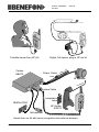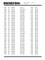
1
Product: TDP80DN /
11.10.2001
SERVICE MANUAL
BENEFON EXION
TDP80DN
Dp_80ngbTOC.fm
1
Product: TDP80DN /
11.10.2001
CONTENTS
1.0 GENERAL . . . . . . . . . . . . . . . . . . . . . . . . . . . . . . . . . . 1 - 1
1.1 TECHNICAL INFORMATION . . . . . . . . . . . . . . . . . . . . . . . . 1 - 1
1.1.1 Network standard . . . . . . . . . . . . . . . . . . . . . . . . . . . 1 - 1
1.1.2 Dimensions . . . . . . . . . . . . . . . . . . . . . . . . . . . . . . . . 1 - 1
1.1.3 Display . . . . . . . . . . . . . . . . . . . . . . . . . . . . . . . . . . . 1 - 1
1.1.4 Keypad and editing . . . . . . . . . . . . . . . . . . . . . . . . . . 1 - 1
1.1.5 Personal organiser . . . . . . . . . . . . . . . . . . . . . . . . . . 1 - 2
1.1.6 Other phone features . . . . . . . . . . . . . . . . . . . . . . . . 1 - 2
1.1.7 Call management . . . . . . . . . . . . . . . . . . . . . . . . . . . 1 - 2
1.1.8 Phone book and memory functions . . . . . . . . . . . . . . 1 - 2
1.1.9 Short messages service (SMS)
(Operator dependent function) . . . . . . . . . . . . . . . . . . . . . . 1 - 3
1.1.10 Security and call counters . . . . . . . . . . . . . . . . . . . . 1 - 3
1.1.11 Tone control . . . . . . . . . . . . . . . . . . . . . . . . . . . . . . 1 - 3
1.1.12 Battery packs and operating times . . . . . . . . . . . . . 1 - 4
1.1.13 Power Consumption . . . . . . . . . . . . . . . . . . . . . . . . 1 - 4
1.1.14 Accessories . . . . . . . . . . . . . . . . . . . . . . . . . . . . . . . 1 - 4
1.1.15 BeneWin . . . . . . . . . . . . . . . . . . . . . . . . . . . . . . . . . 1 - 5
1.1.16 Manufacturer . . . . . . . . . . . . . . . . . . . . . . . . . . . . . . 1 - 5
1.2 PRODUCT FAMILY . . . . . . . . . . . . . . . . . . . . . . . . . . . . . . . 1 - 6
2.0 OWNER’S MANUAL . . . . . . . . . . . . . . . . . . . . . . . . . . 2 - 1
3.0 INSTALLATION INSTRUCTIONS . . . . . . . . . . . . . . . 3 - 1
3.1 Phone Programming . . . . . . . . . . . . . . . . . . . . . . . . . . . . . . . 3 - 1
3.1.1 To program Using the Phone Keys . . . . . . . . . . . . . . 3 - 1
3.1.2 To program Using the BeneLoc Program . . . . . . . . . 3 - 6
3.2 CAR KIT . . . . . . . . . . . . . . . . . . . . . . . . . . . . . . . . . . . . . . . . 3 - 8
3.2.1 Power Cable . . . . . . . . . . . . . . . . . . . . . . . . . . . . . . . 3 - 8
3.2.2 Hf Holder KGS75 . . . . . . . . . . . . . . . . . . . . . . . . . . . 3 - 8
3.2.3 Microphone . . . . . . . . . . . . . . . . . . . . . . . . . . . . . . . . 3 - 8
3.2.4 Button Unit . . . . . . . . . . . . . . . . . . . . . . . . . . . . . . . . 3 - 9
3.2.5 Car Box UBH75 . . . . . . . . . . . . . . . . . . . . . . . . . . . . . 3 - 9
3.2.6 Hf Speaker . . . . . . . . . . . . . . . . . . . . . . . . . . . . . . . . 3 - 9
Dp_80ngbTOC.fm
2
Product: TDP80DN /
11.10.2001
3.2.7 Installation Material Bag . . . . . . . . . . . . . . . . . . . . . . 3 - 9
3.3 Operation and Testing after Installation . . . . . . . . . . . . . . . . 3 - 9
4.0 BeneLoc . . . . . . . . . . . . . . . . . . . . . . . . . . . . . . . . . . . 4 - 1
4.0.1 Installation of BeneLoc program . . . . . . . . . . . . . . . . 4 - 1
4.0.2 To start the BeneLoc program . . . . . . . . . . . . . . . . . 4 - 2
4.0.3 Using the BeneLoc program . . . . . . . . . . . . . . . . . . . 4 - 3
5.0 PHONE’S CONSTRUCTION . . . . . . . . . . . . . . . . . . . . 5 - 1
5.1 General description for the baseband . . . . . . . . . . . . . . . . . . 5 - 2
5.2 DSP-processor . . . . . . . . . . . . . . . . . . . . . . . . . . . . . . . . . . . 5 - 2
5.2.1 Pin description of the DSP baseband asic . . . . . . . . 5 - 3
5.2.2 Connectors . . . . . . . . . . . . . . . . . . . . . . . . . . . . . . . . 5 - 7
5.2.3 Functions . . . . . . . . . . . . . . . . . . . . . . . . . . . . . . . . . . 5 - 9
5.3 RX SYNTHESIZER . . . . . . . . . . . . . . . . . . . . . . . . . . . . . . . 5 - 11
5.3.1 General . . . . . . . . . . . . . . . . . . . . . . . . . . . . . . . . . . 5 - 11
5.3.2 Functional Description . . . . . . . . . . . . . . . . . . . . . . . 5 - 11
5.3.3 Control- and Output-Signals . . . . . . . . . . . . . . . . . . 5 - 11
5.4 TX-SYNTHESIZER . . . . . . . . . . . . . . . . . . . . . . . . . . . . . . . 5 - 12
5.4.1 General . . . . . . . . . . . . . . . . . . . . . . . . . . . . . . . . . . 5 - 12
5.4.2 Function Description . . . . . . . . . . . . . . . . . . . . . . . . 5 - 12
5.4.3 Control- and Output-Signals . . . . . . . . . . . . . . . . . . 5 - 13
5.5 RECEIVER . . . . . . . . . . . . . . . . . . . . . . . . . . . . . . . . . . . . . 5 - 13
5.5.1 General . . . . . . . . . . . . . . . . . . . . . . . . . . . . . . . . . . 5 - 13
5.5.2 Input- and Output-Signals . . . . . . . . . . . . . . . . . . . . 5 - 14
5.6 TRANSMITTER . . . . . . . . . . . . . . . . . . . . . . . . . . . . . . . . . 5 - 15
5.6.1 General . . . . . . . . . . . . . . . . . . . . . . . . . . . . . . . . . . 5 - 15
5.6.2 Function Description . . . . . . . . . . . . . . . . . . . . . . . . 5 - 15
5.6.3 Control- and Output-Signals . . . . . . . . . . . . . . . . . . 5 - 15
5.7 Module OC2720 (The Layout PC2700 A1) . . . . . . . . . . . . . 5 - 16
5.7.1 Parts list . . . . . . . . . . . . . . . . . . . . . . . . . . . . . . . . . 5 - 16
5.7.2 Layouts . . . . . . . . . . . . . . . . . . . . . . . . . . . . . . . . . . 5 - 26
5.7.3 Circuit Diagrams . . . . . . . . . . . . . . . . . . . . . . . . . . . 5 - 28
5.8 Keyboard . . . . . . . . . . . . . . . . . . . . . . . . . . . . . . . . . . . . . . 5 - 35
Dp_80ngbTOC.fm
3
Product: TDP80DN /
General
9.2.2001
1.0 GENERAL
General
1.1 TECHNICAL INFORMATION
1.1.1 Network standard
NMT-450i
Output power=1,2 W
1.1.2 Dimensions
(with 900 mAh Lion)
Size: 46 x 100 x 21 mm
Weight: 109 g
Volume: 81 cm³
1.1.3 Display
Full-graphics high-contrast screen
Electro-luminescent lighting
Resolution 100 x 48 pixels
Up to 5 lines of text
Indicators: fields strength, battery status, charging, time, date, timers, alarm, keylock, silent, message, call divert and roaming, voice priaxiaty, mic muting
Graphical icons and scroll bars
Gyrillic alphabets
1.1.4 Keypad and editing
Automatic and manual key lock
Full-screen editor
International access (+) function (Operator dependent function)
Any-key answering
2DP_80GB.fm
1
Product: TDP80DN /
General
9.2.2001
1.1.5 Personal organiser
Clock and date
Alarm clock with snooze
Calendar
Calendar appointment manager with reminders
Phone power on and off timers
1.1.6 Other phone features
Autonomous Power Control
Calculator and currency converter
Several games for entertainment
Personalised ringing melody groups
External antenna connector
Vibrating alert
NMT-pager (DTMF)
1.1.7 Call management
One-touch dialling
Last or recent numbers redial (10)
Multiparty calls (Operator dependent function)
Calling Line Identification Presentation (CLIP) (Operator dependent function)
Caller Line Name Presentation (CLNP) (Operator dependent function)
DTMF transmission
Semiautomatic and manual network selection
Optional automatic network selection
Automatic answer with headset and car kit
1.1.8 Phone book and memory functions
Supports up to 300 phone book entries
Various ways to scroll or search the phone book memory
Dialled calls (10) list with time or date stamp
2DP_80GB.fm
2
Product: TDP80DN /
General
9.2.2001
Answered calls (10) list with time or date stamp and calling number or name identification
Received DTMF-messages (10) with time and date stamp
Unanswered calls (10) list with time or date stamp and calling number or name identification
Access phone book for sending SMS
Pick SMS sender’s number for phone book
Show sender number or name (if stored in phone book) as an SMS header
Customized ringing tones for 5 phone book groups
1.1.9 Short messages service (SMS) (Operator dependent function)
Send and receive text messages of up to 160 characters
Time and date stamp for received messages
Answer to message
Forward message
Pick sender number from message text
Call SMS sender
1.1.10 Security and call counters
SIS-security check
Call timers: last outgoing/incoming calls, all outgoing/incoming calls
Phone lock code
Voice privacy
1.1.11 Tone control
40 different ringing tones and melodies for incoming call, alarm, calendar and short
messages
Downloadable ringing melody using BeneWin
User-compasable ringing melodies using BeneWin
Adjustable ringing tone volume levels, including silent mode
Keypad tone volume levels
Several tone set-ups for different environments
2DP_80GB.fm
3
Product: TDP80DN /
General
9.2.2001
1.1.12 Battery packs and operating times
Initially two battery packs are available for Benefon Exion, namely
Battery type
Stand-by
time
Talk time
Charging time
Fast
Charging time
Normal
Lithium ion 900 mAh
20 h -150 h
50 min - 1 h 40 min
1 h 45 min
4 h 30 min
1 h 10 min -2 h 20 min
2 h 30 min
5 h 30 min
Lithium ion 1200 mAh 26 h - 200 h
Operating times can vary substantially depending on distance to base station, network settings and network usage.
1.1.13 Power Consumption
Batteries: 3,6 V Lion
Sleep current: app. 600 µA
Standby current: app. 43 mA
Conversation mode, high power: app. 1.1 A
Conversation mode, low power: app. 0.45 A
1.1.14 Accessories
Mains charger
Cigarette lighter charger
Portable hands free (HF) kit
Digital, full duplex, plug-in HF car kit
Hands free car kit with voice recognition and external antenna
Car cradle
Belt clip
BeneWin software & editor cable
Carrying case
Line interface for data transmission
Antenna alternatives: city, standard, off-road and super 1/2-wave
2DP_80GB.fm
4
Product: TDP80DN /
General
9.2.2001
1.1.15 BeneWin
BeneWin PC software:
Edit and back up phone book memory
Send and receive SMS messages by using a PC keyboard
Compose and change ringing melodies with BeneWin Maestro
Manage phone settings
1.1.16 Manufacturer
BENEFON OYJ
P.O. Box 84
(Meriniitynkatu 11)
FIN 24101 SALO
FINLAND
Telephone: + 358 2 77 400
Facsimile: + 358 2 332 633
2DP_80GB.fm
5
Product: TDP80DN /
General
9.2.2001
1.2 PRODUCT FAMILY
- BENEFON EXION HANDPORTABLE TDP80DN
- MAINS CHARGER
- CIGARETTE LIGHTER CHARGER
- PORTABLE HANDS FREE (HF) KIT
- DIGITAL, FULL DUPLEX, PLUG-IN HF CAR KIT
- HANDS FREE CAR KIT WITH VOICE RECOGNITION AND
EXTERNAL ANTENNA
- CAR CRADLE
- BELT CLIP
- BENEWIN SOFTWARE & EDITOR CABLE
- CARRYING CASE
- LINE INTERFACE FOR DATA TRANSMISSION
- ANTENNA ALTERNATIVES: CITY, STANDARD, OFF-ROAD
AND SUPER 1/2-WAVE
Benefon Exion and chargers
2DP_80GB.fm
6
Product: TDP80DN /
General
9.2.2001
Portable hands free (HF) kit
Digital, full duplex, plug-in HF car kit
Carbox
UBH75
Power Cable
2V
+1
,
t
at
Vb
fuse
Hf Speaker
na
ten
n
a
to
System Cable
Installation
base
Button Unit
HF Holder
KGS75
Microphone
Hands free car kit with voice recognition and external antenna
2DP_80GB.fm
7
Product: TDP80DN /
General
9.2.2001
Car cradle
Belt clip
BeneWin software & editor cable
Line interface for data
transmission
2DP_80GB.fm
8
2.0 OWNER’S MANUAL
1user_gb.fm
1
Product: TDP80DN /
Installation Instructions
11.10.2001
3.0 INSTALLATION INSTRUCTIONS
Installation Instructions
3.1 Phone Programming
You can program Benefon Exion by using either the keys on your phone, or the
BeneLoc computer program and maintenance adapter. In either case, you will
need a localbox.
Programming Menu Commands:
3.1.1 To program Using the Phone Keys
1. Connect the QPS50 localbox via maintenance adapter to your phone, and
turn the phone on. ö will be flashing in the display in stand-by mode.
Press y.
The menu symbols are displayed on the upper row. Use n to scroll through the
menus. Press -SELECT to enter the Benefon local menu. Select the
desired sub-menus with n. Press - CHANGE. Press -OK after each
setting.
Press -QUIT to cancel the operation and return previous menu level.
6DP_80GB.fm
1
Product: TDP80DN /
Installation Instructions
11.10.2001
3.1.1.1 Sales Date
1. Select the Sales date sub-menu with n. Press - CHANGE.
2. Press - CHANGE. |XXXXXX will be replaced by the date
[daydaymonthmonthyearyear]. Remember to check that the date is correct.
If the date is correct, press - OK. If the date is incorrect, delete it by choosing
- CLEAR and enter the correct date (six digits in the following form:
daydaymonthmonthyearyear). To save the date, press - OK.
NOTE! It is possible to program the sales date ONLY ONCE, which means that you will
not be able to change it again afterwards. If the sales date has not been
programmed, your phone will not enter the normal stand-by mode.
3.1.1.2 Radio Path Identification
1. Select the Radio path id sub-menu with n. Press - CHANGE.
2. Enter the radio path identification (ten digits), and save the identification by
pressing - OK. Remember to check that the radio path identification is
correct.
3.1.1.3 Own number
1. Select the Own number sub-menu with n. Press - CHANGE.
2. Enter the own number (follow the instruction of the operator), and save it by
pressing - OK. Remember to check that the own number is correct.
NOTE! SMS doesn’t work if the own number has not been programmed.
6DP_80GB.fm
2
Product: TDP80DN /
Installation Instructions
11.10.2001
3.1.1.4 Phone code
1. Select the Phone code sub-menu with n. Press - CHANGE.
2. Enter the phone code (four digits), and save the code by pressing - OK.
3.1.1.5 Y1 Y3 ID (Additional operator indicator)
Use this feature only in case the operator name is missing ie. RU1 works if Y3
is in use.
It is possible to change old/add new operator indicator which operates in
automatic roaming mode. (network selection mode: Automatic)
1. Select the Y1 Y3 Identity sub-menu with n. Press - CHANGE.
2. Select the Y1 with n. Press - CHANGE.
3. Enter Y1 (Country code: one digit) and save it by pressing
- OK.
Enter Y3 (Operator code: two digits) and save it by pressing - OK.
Enter ID (Operator indicator, 3 characters) and save it by pressing - OK.
6DP_80GB.fm
3
Product: TDP80DN /
Installation Instructions
11.10.2001
3.1.1.6 Sw version
3.1.1.7 Sak
After ID is programmed SAK changes to normal mode.
3.1.1.8 Update localbox
3.1.1.9 Interleaving
The Dealer activates or deactives them according to the operator's or the
customer's likings.
6DP_80GB.fm
4
Product: TDP80DN /
Installation Instructions
11.10.2001
3.1.1.10 Automatic roaming
The Dealer activates or deactives them according to the operator's or the
customer's likings.
3.1.1.11 Reset RAM
Resets user settings and phone book.
3.1.1.12 Closing Instructions
1. Having programmed the necessary information press - QUIT to return to
stand-by mode.
2. Turn off your phone, and disconnect the localbox.
3. Turn the phone on once more, and make a test call.
6DP_80GB.fm
5
Product: TDP80DN /
Installation Instructions
11.10.2001
3.1.2 To program Using the BeneLoc Program
power
5V log
gen
flash
5V log
meter
Start the installed program by clicking the icon. The phone must be connected
to the system as discribed above.
Main window
Press Dealer-key to enter the programming window.
6DP_80GB.fm
6
Product: TDP80DN /
Installation Instructions
11.10.2001
You can read the phone data by pressing the Read -key. You can change the
miscellanous settings with the computer and transfer them to phone by
pressing the Write -key.
BeneLoc includes Help-program for further information.
6DP_80GB.fm
7
Product: TDP80DN /
Installation Instructions
11.10.2001
3.2 CAR KIT
The Car Kit includes a hf holder, a car box, an installation base, a hf speaker, a
microphone, a button unit, a power cable and a system cable. The Car Kit
sales package also includes an installations material bag, which contains the
necessary installation equipment. On the third page you will find a diagram of
connections explaining how to install the Car Kit.
Caution:
The Car Kit should only be installed by a Benefon authorized installer. The end
user should never attempt to install the Car Kit without professional assistance.
Professional installers have the required tools and knowledge for installing the
Car Kit properly and safely. The terms of warranty also require that the Car Kit
is installed by professionally trained personnel. Cable routing may cause
interference with the components of the vehicle's electronic systems (such as
ignition and braking systems). It is recommended that cables not be routed
next to such electronic components. Make sure that the hf holder, button unit,
microphone and speaker do not obstruct the air bag system.
3.2.1 Power Cable
The Car Kit should be installed only in vehicles with 12 Volts, negative on
chassis system. When connecting the power cable make sure that it is not
connected to the car box.
Obtain the necessary (+)-electrical current from a suitable place, preferably
directly from the battery of the vehicle. Connect the fuse chamber to the (+)wire. You will find the fuse chamber in the installation materials bag. Connect
the ground lead to the frame of the car with a short wire.
3.2.2 Hf Holder KGS75
Choose such a place for the hf holder in the vehicle that will be both easy and
safe when using the phone. First, fix the installation base to the place you have
chosen, and then install the hf holder in the installation base.
3.2.3 Microphone
The microphone should be located 20-50 cm from the driver’s mouth, and at
least 90 cm from the loudspeaker. Make sure that the “eyes” are directed
towards the driver. Mount the microphone using the supplied adhesive tape.
A good place for the microphone is near the rearview mirror where the noise
level is lower than, for example, beside a windshield pillar. It is also possible to
install the microphone on a sun visor, but then it will be inconvenient to use the
sun visor and microphone at the same time.
6DP_80GB.fm
8
Product: TDP80DN /
Installation Instructions
11.10.2001
3.2.4 Button Unit
The button unit enables easy operation of the Car Kit. The unit consists of
plastic base and buttons. Decide where to install the buttons unit. Possible
locations are on the dashboard or on the handbrake lever. Mount the plastic
base using supplied screws, bands or adhesive tape. Attach the buttons to the
base. Make sure the plastic snaps are locked.
Note: The unit can be mounted without the plastic base
3.2.5 Car Box UBH75
Place the car box out of sight inside the dashboard of the car or in another
suitable place.
If required, attach the unit to the car interior using 4 screws (not supplied).
3.2.6 Hf Speaker
Install the speaker in a suitable place near the floor of the car. The loudspeaker
should be located at least 90 cm from the microphone. Mount the loudspeaker
using the supplied bracket and screws.
Note: It is possible to use the front right-side car’s loudspeaker instead of a
dedicated loudspeaker.
3.2.7 Installation Material Bag
The installation material bag contains the standard installation equipment. You
may not need everything in the bag.
3.3 Operation and Testing after Installation
Once completing the installation, perform the following tests:
1. Connect all cables, except for the power cable, to the car box.
2. Make sure there is no phone connected in the hf holder.
3. Connect the power cable to the car box.
4. Turn on the ignition key (no need to start the engine).
5. After few seconds a short beep will be heard from the loudspeaker, signaling
that the system is operating.
6. Place the phone in the hf holder and connect it. A double beep should be
heard, and both LED's on the button unit will light.
7. Record (long press on the Green Button of the button unit) and playback
(Long Press on the Red button of the button unit and then long press on the
Green button of the button unit) to ensure that the microphone is installed
correctly.
6DP_80GB.fm
9
Product: TDP80DN /
Installation Instructions
11.10.2001
8. Make a cellular conversion to ensure that the Car Kit is installed correctly.
Note: Whenever the car box is disconnected from the car's battery and then
reconnected to the battery, make sure there is no phone connected in the hf
holder.
A Diagram of Connections
Carbox
UBH75
Power Cable
V
12
,+
t
t
a
Vb
fuse
Hf Speaker
System Cable
te
an
to
a
nn
Installation
base
Button Unit
HF Holder
KGS75
Microphone
8-pin Power Cable
Red
Positive (+) 12V – fused
Brown
Negative/chassis (-)
Blue
Ignition
Yellow
Radio mute input (up to 100 mA)
White
Positive (+) lead of the front-right radio output
Black
Negative (-) lead of the front-right radio output
Violet
Hf speaker or positive (+) lead of the front-right car’s loudspeaker
Green
Hf speaker or negative (-) lead of the front-right car’s loudspeaker
6DP_80GB.fm
10
Product: TDP80DN /
BeneLoc
9.2.2001
4.0 BeneLoc
BeneLoc
power
5V log
gen
flash
5V log
meter
BeneLoc program is designed to help service person on tuning and service purpose.
With Flasher Program you can change the software to Benefon phones.
Both, BeneLoc and Flasher program will need Power Supply and Localbox with service rights to work.
4.0.1 Installation of BeneLoc program
Start Windows. Close all other programs except Program Manager.
Insert BeneLoc Installation Disc 1 in the floppy disk drive of your computer. In the
Program Manager window, choose Run from File menu.
Type the letter A: or B: to indicate your floppy disc drive, and then type SETUP.EXE.
For example, A:\SETUP.EXE.
Click the OK button, and follow the instructions displayed on your screen.
The Setup Program will ask you to specify the drive and directory in which you want
3dp_80gb.fm
1
Product: TDP80DN /
BeneLoc
9.2.2001
to install the BeneLoc Program. The Program suggests the following: C:\BeneApp\BeneLoc. Accept the drive and directory by clicking Next button. You can also
type your own directory for BeneLoc Program.
The Setup Program creates all necessary directories and subdirectories to your
computer. Setup Program also creates its own group window in Program Manager.
4.0.2 To start the BeneLoc program
Connect the Service Localbox to serial port of your computer, which is called COM1
or COM2. The serial ports are usually located in the back of your computer, and
more precise instructions can be found in the manual accompanying the computer.
Adjust the Power Supply voltage to 4.0 Vdc. Connect the Service Localbox to the
Power Supply.
Connect the Service Adapter to the phone. Plug the cable with flat connector into the
connector at the bottom of the phone. When the cable has been connected and the
phone is switched on, the phone should be in LOCAL mode. You can test this by
pressing arrow button. There should be ***Benefon local*** on the display, if not,
clean connectors and try again. When phone is in LOCAL mode you can start the
BeneLoc Program.
To start the BeneLoc Program, double click the BeneLoc icon.
In the BeneLoc Startup window, first select the correct serial port. Then, you have to
select type of the phone. After selection click OK to start BeneLoc Program. When
operating without external power supply the phone may be on sleep mode and registration fails. You can wake up the phone by pressing some buttons on the phone.
3dp_80gb.fm
2
Product: TDP80DN /
BeneLoc
9.2.2001
4.0.3 Using the BeneLoc program
In the main window of the BeneLoc, you will find submenus and buttons. Clicking the
buttons you can go to the submenus.
Change
For changing phone to another similar you do not need to do more than enter into
main menu. It means that this button is not needed. If you are going to change the
tested phone to one having different software in, clicking Change will start the registration protocol again.
Help
About BeneLoc submenu will tell you version of the BeneLoc Program and also the
state of memory.
About Cellular submenu will show you information of the phone. Type of phones
software, sales date, date of the software, serial number and present tuning values
of the phone. You can not change the tuning values from Help menu.
Dealer
From Dealer submenu you can make or check programming of the phone. You will
also find the SIS information from Dealer submenu.
3dp_80gb.fm
3
Product: TDP80DN /
BeneLoc
9.2.2001
Service
You can control the audio lines (for example, switch Rx audio and compander on/off)
in the Service main menu. It is also possible to control the phone to desired channel.
There is also possible to change the power of transmitter.
In the Ports submenu is you can see the status of different digital ports. There is
also possible to control some of the output ports.
You can read the status of the A/D converters from the A/D submenu. Select 8 different topics to view. By clicking SCAN AD button The Beneloc will scan A/D the state
of converters continuously. Scanning can stopped by clicking STOP AD.
Memory submenu allows you to make Ram reset.
By clicking Initialize You can clear all LOCAL settings in service menu.
Home button will return you back to main menu.
Tunings
From Tunings main menu you can select different tunings to do. Every tuning have
they own instruction window. Follow given instructions to do tunings. Clicking
START will start tuning. The value will be stored only by clicking SAVE. Some of the
tunings are chained and you can enter to next phase by clicking NEXT.
3dp_80gb.fm
4
Product: TDP80DN /
BeneLoc
9.2.2001
System
You select used mobile phone system from this submenu.
File
From settings submenu you can manually change settings of the communication
port.
3dp_80gb.fm
5
Product: TDP80DN /
11.10.2001
MD
2500
YO
2710
5.0 PHONE’S CONSTRUCTION
7dp_80gb.fm
1
Product: TDP80DN /
OC2720 Processor/Audio/RF
9.2.2001
LOGIC / AUDIO
OC2720 Processor/Audio/RF
5.1 General description for the baseband
The baseband is built with DSP asic (Digital Signal Processor) made by VLSI.
All the functions are found within a single OC2700 board. The processor controls the
RF parts, internal devices and external accessories. The audio functions are done
with the DSP. The keyboard is situated on separate board and it is connected to
logic module with 10 pin connector. The keypad and display is illuminated with ELsheet.
5.2 DSP-processor
The DSP-processor performs all the baseband functions.
The chip includes VS_DSP processor, memory, an analog audio interface and a
variety of peripheral devices
- VS_DSP processor
- 64k x 16-bit data RAM
- 4k x 32-bit program RAM
- 4k x 32-bit program ROM
Peripheral devices:
- a 32-bit general IO port
- 2 RS232 serial ports
- LCD controller
- PLL (synthesizer) controller
- 450 kHz frequency counter
- a keyboard controller
- 8-bit interrupt IO port
- 6 timers (32-bit)
- synchronous serial port (SSP)
4Z2700GB.fm
2
Product: TDP80DN /
OC2720 Processor/Audio/RF
9.2.2001
Analog interface:
- 2 speech Analog-to-digital converters (ADC), for microphone and RX
- 2 speech Digital-to-analog converters (DAC), for earphone and TX
- 8-input 10-bit ADC
- 6 10-bit DACs
An interrupt controller
An external bus interface
A real-time clock
Power on/off logic
5.2.1 Pin description of the DSP baseband asic
180 pin FBGA
Pin Name
CAP
MIC1+
MIC1MIC2+
MIC2XMIC
RX 1
MOD 4
DAC0
DAC1
DAC2
DAC3
DAC4
DAC5
ADC0
ADC1
ADC2
ADC3
ADC4
ADC5
ADC6
ADC7
HEAR
XEAR
EAR+
EARAGND0
AGND1
AGND2
AGND3
4Z2700GB.fm
Number
176
172
169
170
171
173
A1
C3
178
179
180
177
2
6
157
158
159
160
161
162
164
165
10
5
7
9
11
163
166
168
Pin
A3
A4
B5
D6
C5
B4
AI
AO
C4
A2
B2
B3
B1
C1
A8
C8
D8
B7
A7
C7
B6
A6
D1
C2
D4
D2
D3
D7
C6
A5
Type
AIO
AI
AI
AI
AI
AI
AO
AO
AO
AO
AO
AO
AI
AI
AI
AI
AI
AI
AI
AI
AO
AO
AO
AO
P
P
P
P
Function
Blocking capacitor of voltage reference
Positive microphone input
Negative microphone input
Positive microphone input
Negative microphone input
External microphone input
Receive signal analog input
Transmit signal analog output
Digital to analog converter 0 output
Digital to analog converter 1 output
Digital to analog converter 2 output
Digital to analog converter 3 output
Digital to analog converter 4 output
Digital to analog converter 5 output
Analog to digital converter 0 input
Analog to digital converter 1 input
Analog to digital converter 2 input
Analog to digital converter 3 input
Analog to digital converter 4 input
Analog to digital converter 5 input
Analog to digital converter 6 input
Analog to digital converter 7 input
Headset earphone output
External earphone output
Positive earphone output
Negative earphone output
Analog ground
Analog ground
Analog ground
Analog ground
3
Product: TDP80DN /
OC2720 Processor/Audio/RF
9.2.2001
AGND4
AVDD0
AVDD1
PGND
PVDD
RTCOSC1
OSC0
OSC1
XRESET
XRESETOUT
TEST
BATTERY
PWRKEY
VCHARGE
REGUEN
ALARM
A0
A1
A2
A3
A4
A5
A6
A7
A8
A9
A10
A11
A12
A13
A14
A15
A16
A17
A18
A19
A20
A21
A22
A23
D0
D1
D2
D3
D4
D5
D6
D7
D8
D9
D10
4Z2700GB.fm
174
167
175
8
3
66
70
71
51
E6
E7
D5
E5
G5
P7
P8
P3
P
P
P
P
P
AO
AI
AO
DI
Analog ground
Analog power supply
Analog power supply
Earphone driver ground
Earphone driver power supply
Crystal oscillator output for real time clock
Crystal oscillator input (13 or 26 MHz)
Crystal oscillator output (13 or 26 MHz)
Reset input, active low
63
P6
DO
Reset output, active low
64
62
56
60
12
13
121
120
119
117
116
115
113
112
111
109
108
107
105
104
103
101
100
99
96
95
94
92
91
90
146
145
144
141
140
139
135
134
133
132
131
M6
N6
M4
M5
E4
E2
F12
F14
F13
G12
G14
G13
H12
H14
H13
J12
J14
J13
K12
K14
K13
L12
L14
L13
M14
M13
M12
N14
P14
N13
C11
A11
B11
A12
B12
C12
B13
B14
C12
C13
C14
DI
DI
DI
DI
DO
DO
DO
DO
DO
DO
DO
DO
DO
DO
DO
DO
DO
DO
DO
DO
DO
DO
DO
DO
DO
DO
DO
DO
DO
DO
DIO
DIO
DIO
DIO
DIO
DIO
DIO
DIO
DIO
DIO
DIO
Manufacturing test mode select
VBATTERY detect
Power key input
VCHARGE detect
Regulator enable
RTC alarm output
Address output of external memory bit 0
Address output of external memory bit 1
Address output of external memory bit 2
Address output of external memory bit 3
Address output of external memory bit 4
Address output of external memory bit 5
Address output of external memory bit 6
Address output of external memory bit 7
Address output of external memory bit 8
Address output of external memory bit 9
Address output of external memory bit 10
Address output of external memory bit 11
Address output of external memory bit 12
Address output of external memory bit 13
Address output of external memory bit 14
Address output of external memory bit 15
Address output of external memory bit 16
Address output of external memory bit 17
Address output of external memory bit 18
Address output of external memory bit 19
Address output of external memory bit 20
Address output of external memory bit 21
Address output of external memory bit 22
Address output of external memory bit 23
Data IO of external memory bit 0
Data IO of external memory bit 1
Data IO of external memory bit 2
Data IO of external memory bit 3
Data IO of external memory bit 4
Data IO of external memory bit 5
Data IO of external memory bit 6
Data IO of external memory bit 7
Data IO of external memory bit 8
Data IO of external memory bit 9
Data IO of external memory bit 10
4
Product: TDP80DN /
OC2720 Processor/Audio/RF
9.2.2001
D11
D12
D13
D14
D15
XCS0
XCS1
XCS2
XCS3
XWE
XOE
IO0
IO1
IO2
IO3
IO4
IO5
IO6
IO7
IO8
IO9
IO10
IO11
IO12
IO13
IO14
IO15
IO16
IO17
IO18
IO19
IO20
IO21
IO22
IO23
IO24
IO25
IO26
IO27
IO28
IO29
IO30
IO31
INTIO0
INTIO1
INTIO2
INTIO3
INTIO4
INTIO5
INTIO6
INTIO7
KEYIN0
4Z2700GB.fm
128
127
126
124
123
86
87
88
89
137
136
14
15
17
18
19
20
21
22
23
24
25
26
27
29
30
31
33
34
36
37
40
52
53
57
72
76
81
85
97
98
102
130
142
143
147
153
154
155
156
32
38
D13
D14
E12
E13
E14
P12
N12
M11
P13
A13
A14
E1
E3
F2
F1
F3
F4
G2
G1
G3
G4
H2
H1
H3
J2
J1
J3
K1
K2
K3
L1
K4
L4
K5
L5
M8
M9
M10
L10
L11
K10
K11
E11
D11
E10
D10
A9
C9
D9
B8
D8
L2
DIO
DIO
DIO
DIO
DIO
DO
DO
DO
DO
DO
DO
DIO
DIO
DIO
DIO
DIO
DIO
DIO
DIO
DIO
DIO
DIO
DIO
DIO
DIO
DIO
DIO
DIO
DIO
DIO
DIO
DIO
DIO
DIO
DIO
DIO
DIO
DIO
DIO
DIO
DIO
DIO
DIO
DIO
DIO
DIO
DIO
DIO
DIO
DIO
DIO
DI
Data IO of external memory bit 11
Data IO of external memory bit 12
Data IO of external memory bit 13
Data IO of external memory bit 14
Data IO of external memory bit 15
Chip select 0 of an external memory
Chip select 1 of an external memory
Chip select 2 of an external memory
Chip select 3 of an external memory
Write enable of an external memory
Output enable of an external memory
General purpose IO, bit 0
General purpose IO, bit 1
General purpose IO, bit 2
General purpose IO, bit 3
General purpose IO, bit 4
General purpose IO, bit 5
General purpose IO, bit 6
General purpose IO, bit 7
General purpose IO, bit 8
General purpose IO, bit 9
General purpose IO, bit 10
General purpose IO, bit 11
General purpose IO, bit 12
General purpose IO, bit 13
General purpose IO, bit 14
General purpose IO, bit 15
General purpose IO, bit 16
General purpose IO, bit 17
General purpose IO, bit 18
General purpose IO, bit 19
General purpose IO, bit 20
General purpose IO, bit 21
General purpose IO, bit 22
General purpose IO, bit 23
General purpose IO, bit 24
General purpose IO, bit 25
General purpose IO, bit 26
General purpose IO, bit 27
General purpose IO, bit 28
General purpose IO, bit 29
General purpose IO, bit 30
General purpose IO, bit 31
Interrupt IO, bit 0
Interrupt IO, bit 1
Interrupt IO, bit 2
Interrupt IO, bit 3
Interrupt IO, bit 4
Interrupt IO, bit 5
Interrupt IO, bit 6
Interrupt IO, bit 7
Keyboard interface input #0
5
Product: TDP80DN /
OC2720 Processor/Audio/RF
9.2.2001
KEYIN1
KEYIN2
KEYIN3
KEYIN4
KEYOUT0
KEYOUT1
KEYOUT2
KEYOUT3
KEYOUT4
BUZ
SDA
SCL
TXD0
RXD0
TXD1
RXD1
SISCLK
IF
LCDSCLK
LCDTX
LCDXCS
LCDA0
PLLSCLK
PLLTX 59
DVDD0
DVDD1
DVDD2
DVDD3
DVDD4
DVDD5
DVDD6
DVDD7
DVDD8
DVDD9
DVDD10
DGND0
DGND1
DGND2
DGND3
DGND4
DGND5
DGND6
DGND7
DGND8
DGND9
DGND10
DGND11
4Z2700GB.fm
41
42
43
44
45
46
47
49
50
54
83
82
148
149
150
152
55
68
78
79
74
75
58
P5
28
48
69
73
77
93
114
118
122
138
159
16
35
39
61
65
80
84
106
110
125
129
151
M1
M2
L3
N1
N2
P1
P2
M3
N3
N4
N11
P11
B10
A10
C10
B9
P4
M7
P10
N10
N9
P9
N5
DO
H4
K7
L7
L8
K8
H10
H11
G11
G10
D8
F5
J4
J5
K6
L6
L9
K9
J10
J11
F11
F10
E9
DI
DI
DI
DI
DO
DO
DO
DO
DO
DO
DIO
DI
DO
DI
DO
DI
DO
AI
DO
DO
DO
DO
DO
PLL
P
P
P
P
P
P
P
P
P
P
P
P
P
P
P
P
P
P
P
P
P
P
P
Keyboard interface input #1
Keyboard interface input #2
Keyboard interface input #3
Keyboard interface input #4
Keyboard interface output #0
Keyboard interface output #1
Keyboard interface output #2
Keyboard interface output #3
Keyboard interface output #4
Buzzer drive output
Data IO of serial interface
Clock output of serial interface
Data output of RS232 interface #0
Data input of RS232 interface #0
Data output of RS232 interface #1
Data input of RS232 interface #1
Clock output (4.3 MHz)
Input of intermediate frequency counter
LCD serial clock
LCD serial data
LCD chip select
LCD A0
PLL serial clock
serial data
Digital power supply
Digital power supply
Digital power supply
Digital power supply
Digital power supply
Digital power supply
Digital power supply
Digital power supply
Digital power supply
Digital power supply
Digital power supply
Digital ground
Digital ground
Digital ground
Digital ground
Digital ground
Digital ground
Digital ground
Digital ground
Digital ground
Digital ground
Digital ground
Digital ground
6
Product: TDP80DN /
OC2720 Processor/Audio/RF
9.2.2001
5.2.2 Connectors
5.2.2.1 The system connector
Nbr
1
2
NAME
AGND
RS1CTS /
!2CINT
FUNCTION
Analog Ground
RS1 Clear to Send /
I2C Interrupt (NMT)
3
EXTMIC
External MIC line
4
RS1RTS /
ACCPWR
5
EXTERP
6
CHARGE
7
HEADSETDET
RS1 Ready to Send /
Accessory pwr control
External ERP line +
BOOT pin
Charging Current + Power On
Headset Detector / Accessory pwr
control
8
RS1RX
RS1 Receive Data
9
VBAT
Battery Voltage
10
RS1TX
RS1 Transmit Data
NMEAIN /
I2CDATA
NMEAOUT /
I2CCLK
13
AUXDET
NMEA input (GPS) /
I2C data (NMT)
NMEA output (GPS) /
I2C clock (NMT)
Headset Hook /
Accessory Detector
14
RS2RX
RS2 Receive Data
15
RS2TX
RS2 Transmit Data
16
17
18
19
20
DGND
NC
DGND
NC
CHARGE
Digital Ground
Not connected
Digital Ground
Not connected
Charging Current + Power On
11
12
STATE
0V
0V
2,7V
0V -1,5V pp
DC
0V
2,7V
0V -1,5V pp
0V/12V DC
0V
2,7V
0V
2,7V
2,7V - 6,0V
0V
2,7V
0V
2,7V
0V
2,7V
0V
2,7V
0V
2,7V
0V
2,7V
0V
IN/OUT
in
in
out
out
out
in
in
in/out
in
out
out
in/out
out
in
in
out
in
0V
in
in
PIN 6: Charging current input, max. 1,0A. Connecting a charger to this pin will
also powers on the mobile phone.
PIN 9: The maximum current from the VBAT line is 300 mA.
PIN 16: The maximum current of DGND pin is 1,0A.
PIN 18: Same as pin 16. The maximum current of DGND pin is 1,0A.
PIN 20: Same as pin 6. The maximum current of CHARGE pin is 1,0A.
The maximum current of all pins except pins 6, 9 and 16 - 20 is 10 mA.
4Z2700GB.fm
7
Product: TDP80DN /
OC2720 Processor/Audio/RF
9.2.2001
5.2.2.2 Battery connector, V50
1
2
VB
GND
3 – 5 V DC
ground
5.2.2.3 Battery identification connector, V51
1
2
SBAT_ID0
SBAT_ID1
Battery temperature, pulled at VCCS
Detect different battery packs, pulled at VCCS
5.2.2.4 Display connector, V80
1
2
3
4
5
6
7
8
9
10
11
12
13
14
15
16
17
18
VRAM
GND
GND
GND
VRAM
SI
SCL
NC
NC
NC
NC
NC
NC
NC
NC
A0
2.5 V
0V
0V
0V
2.5 V
Serial data input
Serial clock 0 / 2.8 V pulses
Not connected
Not connected
Not connected
Not connected
Not connected
Not connected
Not connected
Not connected
Control data / Display data
X_LOGRST
CS1
Reset, 0 V reset active, normally 2.8 V
Display chip select
5.2.2.5 Keyboard connector, V52
1
2
3
4
5
6
7
8
9
10
Keyin 00
Keyin 01
Keyin 02
Keyin 03
Keyin 04
Keyout 00
Keyout 01
Keyout 02
Keyout 03
PWRKEY
Keypad matrix input
Keypad matrix input
Keypad matrix input
Keypad matrix input
Keypad matrix input
Keypad matrix output, 17.5 kHz square
Keypad matrix output, 17.5 kHz square
Keypad matrix output, 17.5 kHz square
Keypad matrix output, 17.5 kHz square
Normally high (VB), grounded when key pressed
Keypad matrix inputs normally low state, when key pressed 17.5 kHz square wave is
seen also in corresponding key input port.
4Z2700GB.fm
8
Product: TDP80DN /
OC2720 Processor/Audio/RF
9.2.2001
5.2.2.6 Circuit Diagram
The processor, audio and RF circuit circuit diagrams are split into seven pages.
Logic diagrams are found in first four pages.
Pages:
1 of 7
2 of 7
3 of 7
4 of 7
5-7 of 7
Module connector pins
Power supply and on/off logic
Memory, DSP logic and SIS function
Audio parts
RF parts
5.2.3 Functions
5.2.3.1 Processor I151
All the logic and audio function are implemented in the digital signal processor
(DSP).
Audio filters, copander/expander, limiter, scarmbler, modem, uart etc. are done
with DSP code. DSP program is executed once for each input sample by the
operating system.
Information between the DSP code and the higher level C code is passed
trough variables and events
5.2.3.2 Memories
The chip contains a total of 64k x 16-bit data RAM. The RAM is powered by the
VRAM-supply, so the the RAM keeps its information when the phone is
powered off. There is also a backup battery coupled with VRAM. It is for a short
voltage break in the main battery pack.
The program code is stored in the 16 Mbit flash memory (I201).
5.2.3.3 Sleep timer
The phone puts the central functions to sleep for a time. Although everything
seems normal to the user, but most of the functions are closed down. The DSP
still has a power supply, but the processor is halted and has minimal power
consumption. Only a sleep timer and its 32 kHz crystal oscillator remain active.
The phone is ”woken up” by interrupting the sleep timer or changing the state
of the keyboard.
5.2.3.4 Power switch
When the power switch is pressed, the PWRKEY line goes low and drives the
transistor conductive. The PWRSW line goes approximately to 2.5 V caused
4Z2700GB.fm
9
Product: TDP80DN /
OC2720 Processor/Audio/RF
9.2.2001
from voltage divider R143, R144 and depending also from the battery voltage
(VB).
The PWRSW line is coupled to DSP on/off logic. The DSP drives REGUEN
signal high and it drives the main regulator (I111) to operate.
The power off operation is done with the same way. The power switch is
pressed a little longer and the shutdown procedure begins. The REGUEN
signal goes low and powers off the phone.
5.2.3.5 Sis
SIM is performed by a BENEFON ASIC IG2048 manufactured by ATMEL.
Integrated circuit IG2048 is E2 logic array. This type of array incorporates both
electrically and programmable read only memory (EEPROM) and a gate array
for SIM funcrtion.
User specific information is stored in EEPROM which CANNOT be read from
outside the chip. Allexternal attempts to read the information clear both
EEPROM and RAM (fill with FF).
5.2.3.6 Charging control
The charging function is controlled by the software. The charger is detected by
PWRCHG line (High = charger detected, low = charger not detected). The type
of charger (fast or slow) is detected by the voltage at V_CHG_ADC line.
The charger switches also the power on.
There is a NTC resistor in the battery pack to measure the temperature. This is
done with SBAT_ID0 line and the voltage is read by an AD converter in DSP.
The type of battery pack in detected in a same way with SBAT_ID1 line with
another channel of ADC.
ID resistors in battery pack:
N/A
900 mAh
1150 mAh
1400 mAh
1600 mAh
adapter
battery fail
4Z2700GB.fm
0 ohm
47 kohm
100 kohm
150 kohm
220 kohm
10 kohm
open
reserved for future use
900 – 1000 mAh
1050 – 1300 mAh
1350 - 1550 mAh
> 1600
mAh
adapter
not detected
10
Product: TDP80DN /
OC2720 Processor/Audio/RF
9.2.2001
RF
5.3 RX SYNTHESIZER
5.3.1 General
The RX synthesizer generates an upper side injection frequency for the receiver.
The injection frequency is fed to the receiver's first mixer.
Operating voltage
Current consumption
Output level to the receiver
Frequency range
3.0 VDC
14 mA
+1 dBm
540.950...545.925 MHz
5.3.2 Functional Description
The RX injection frequency is generated with a phase locked loop. The Voltage Controlled Oscillator (VCO) produces the injection frequency determined by the control
voltage. After the VCO stage comes the amplifier stage Q430. After the amplifier
stage, part of the signal is fed to the synthesizer circuits I400 pre-scaller Fin1. The
synthesizer circuit contains a pre-scaler, programmable divider, reference frequency
divider, and a phase detector.
The synthesizer circuit produces current pulses at output DO1 as controlled by the
phase detector. The current pulses either charge or discharge the loop filter. The
VCO control voltage is derived from the loop filter output.
The synthesizer 12.5kHz reference frequency is made by dividing the 13.00 MHz
signal from the temperature compensated oscillator (TCXO). The series-form signal
which controls the channel frequency comes from the processor. SDATA, SCLK and
SLE signals are common to both TX- and RX-synthesizers. A positive pulse in the
SLE line loads the division ratio (corresponding to the frequency of the channel) fed
to the SDATA line, to the synthesizer circuit I400.
5.3.3 Control- and Output-Signals
VRX
SCLK
SDATA
SLE
RXINJ
RX_REG
4Z2700GB.fm
RX synthesizer operating voltage
Clock signal for the synthesizer control data
Synthesizer control data
ENABLE pulse to the synthesizer
RX synthesizer output to the receiver
Control line for VRX-regulator
3.0 V
+1 dBm
11
Product: TDP80DN /
OC2720 Processor/Audio/RF
9.2.2001
5.4 TX-SYNTHESIZER
5.4.1 General
The TX synthesizer generates the final modulated transmission frequency, which is
fed to the transmitter.
Operating voltage
Current consumption
Output level to the transmitter
Frequency range
3.0 VDC
<30 mA
+6 dBm
452.500...457.475 MHz
5.4.2 Function Description
The TX frequency is generated with a phase locked loop (PLL). The VCO produces
the injection frequency determined by the control voltage, and the VCO also has a
modulation input. After the VCO stage come two amplifier stages Q470 and Q480.
These ensure separation between the VCO and transmitter, and also boost the
injection level sufficiently. Part of the signal is fed from between the amplifier stages
to the synthesizer circuit I400 pre-scaler input Fin2. The synthesizer circuit contains
a pre-scaler, programmable divider, reference frequency divider, and a phase detector.
The synthesizer circuit produces current pulses at output DO2 as a result of the
phase detection. The current pulses either charge or discharge the loop filter condensators. The VCO control voltage is derived from the loop filter output.
The synthesizer 12.5kHz reference frequency is made by dividing the 13.00 MHz
signal from the temperature compensated oscillator (TCXO). The series-form signal
which controls the channel frequency comes from the processor. SDATA and SCLK
signals are common to both TX- and RX-synthesizers. A positive pulse in the SLEline loads the division ratio (corresponding to the TX frequency of the channel) fed to
the SDATA line, to the synthesizer circuit I400.
Modulation is fed to the TX synthesizer TX-AUDIO line. The frequency response is
corrected by the components R455 - R458, C454 and C455. Modulation sensitivity
is set by the resistor R459.
4Z2700GB.fm
12
Product: TDP80DN /
OC2720 Processor/Audio/RF
9.2.2001
5.4.3 Control- and Output-Signals
VTXS
TXAUDIO
13MHz
SCLK
SDATA
SLE
TXINJ
AFC
TXS_REG
TX synthesizer operating voltage (3.0 V)
Transmitter audio signal
13.00 MHz signal to the receiver circuit.
Clock signal for synthesizer control data
Synthesizer control data
ENABLE pulse to the synthesizer
TX synthesizer output to the transmitter (+6 dBm)
AFC control voltage from processor
Control line for VTXS-regulator
5.5 RECEIVER
5.5.1 General
The module contains all FM-receiver functional blocks.
RF-amplifier
1. mixer
1. IF-amplifier
FM IF system
3SK320
balanced mixer
3SK320
SA 607 includes the following blocks:
2. mixer
IF limiter
quadrature detector
RSSI (received signal strength indicator)
When the RF signal is received it is brought through the RX-filter(X500) to the amplifier stage Q500. The amplified signal is passed through the attenuator to the balanced mixer.The balanced mixer is made by using discrete components, diode D510
and RF-transformer M510.
The upper side injection frequency is brought from the synthesizer through a small
resistive attenuator to the mixer. The 78.45 MHz intermediate frequency from the
mixer output is fed through the IF- filter X520 to the FM IF-circuit I550.
RX injection frequency 540.950...545.925MHz
Injection-level/impedance +1 dBm / 50 ohm
The second intermediate-frequency local-oscillator-frequency required by the FM IFcircuit is generated by multiplying the 13.00 MHz reference-oscillator frequency by
six. The multiplier circuit is made with transistor Q530.
The second intermediate frequency is 450 kHz. The phase-shift required by the
quadrature detector is made with the L550. The detected AF-signal temperature correction is done in the buffer amplifier stage.
4Z2700GB.fm
13
Product: TDP80DN /
OC2720 Processor/Audio/RF
9.2.2001
5.5.2 Input- and Output-Signals
RF input from the duplex filter
RXINJ
13MHz
VRX
450 kHz
RXAUDIO
RSSI
462.500...467.475 MHz
RX injection signal to the balanced mixer
13.00 MHz signal to the multiplier for the
2.mixer
RX operating voltage 3.0V from the regulator
Output from 2. IF to the AFC detector
Receiver audio output 175mVrms
Received signal strength indicator output
0,5...2V
SENSITIVITY CHECK
4Z2700GB.fm
channel
RF input
SINAD psof.
001
180
-113 dBm
-113 dBm
>20 dB
>20 dB
14
Product: TDP80DN /
OC2720 Processor/Audio/RF
9.2.2001
5.6 TRANSMITTER
5.6.1 General
Operating voltage
Current consumption
Input level from the synthesizer
Output level to the duplex filter
Frequency range
3.5 ... 4.5 v
mid power max. 1.1 A
low power max. 0.45 A
+6 dBm
mid power 33 dBm (2.0W)
low power 24.7 dBm (0.3W)
452.500...457.475 MHz
5.6.2 Function Description
The transmitter unit is comprised of three amplifier stages and two filters. The amplifier chain consists of pre-amplifier Q620/Q621 and power module I650.
The attenuator R620/R621 is included to enhance the electric separation between
the TX synthesizer and the transmitter.
The filter X620 and duplexfilter X660 ensure that unwanted signals will not reach the
antenna.
The operational amplifier I640 and transistors Q641 and Q642 serve as a power regulator circuit, which adjusts the power level so that the voltage from the transmitter
power detector X650/D660 and the control voltage TXPWR from the processor unit
are equal at inputs of I640.
The negative voltage is generated with the Switched Capacitor Voltage Inverter
I610.
The switching frequency is typically 100 kHz and resistors R611/R612 sets the output voltage to -2.5 V.
I600 serves as voltage regulator for pre-amplifier and for the negative voltage
generetor.
Q631 is ON/OFF switch for the power amplifier.
5.6.3 Control- and Output-Signals
VBAT
TXBIAS
TXPWR
TXINJ
RXDUPLEX
4Z2700GB.fm
Transmitter operating voltage from the
battery-pack (fused)
Power ON/OFF control
Power level control signal from the D/A
converter
RF signal from the TX synthesizer
To RX duplex filter
0...3V
+6dBm
15
Product: TDP80DN /
OC2720_A1
11.10.2001
5.7 Module OC2720 (The Layout PC2700 A1)
OC2720_A1
5.7.1 Parts list
CODE
PART
DESCRIPT.
VALUE
MANUF.
TYPE
AB0612
AM1840
AE0023
AE2700
CG0101
CG0471
CH0105
CG0101
CH0105
CU3106
CG0471
CG0101
CH0105
CG0101
CG0101
CG0104
CH0105
CG0101
CH0105
CH0105
CG0471
CF0105
CG0471
CU3106
CC2103
CG0471
CG0471
CG0100
CG0104
CG0104
CG0100
CG0104
CG0104
CG0104
CG0104
CG0220
CG0104
CG0104
CG0104
CG0104
CG0220
CG0104
CG0104
CG0104
CG0104
CG0103
CG0103
CG0104
CG0104
CG0471
CG0104
A101
A301
A321
A322
C1
C10
C101
C102
C103
C104
C11
C111
C112
C113
C114
C115
C116
C117
C118
C119
C12
C121
C122
C123
C124
C13
C131
C141
C142
C143
C144
C145
C146
C147
C148
C149
C150
C151
C152
C153
C154
C155
C156
C157
C158
C161
C162
C163
C164
C2
C221
Backup-battery 3V
Electret Condenser micr.
Dynamic transducer
Buzzer
SMD capasitor X7R
SMD capasitor X7R
SMD capasitor
SMD capasitor X7R
SMD capasitor
SMD tantal
SMD capasitor X7R
SMD capasitor X7R
SMD capasitor
SMD capasitor X7R
SMD capasitor X7R
SMD capasitor
SMD capasitor
SMD capasitor X7R
SMD capasitor
SMD capasitor
SMD capasitor X7R
SMD capasitor
SMD capasitor X7R
SMD tantal
SMD capasitor
SMD capasitor X7R
SMD capasitor X7R
SMD capasitor NPO
SMD capasitor
SMD capasitor
SMD capasitor NPO
SMD capasitor
SMD capasitor
SMD capasitor
SMD capasitor
SMD capasitor NPO
SMD capasitor
SMD capasitor
SMD capasitor
SMD capasitor
SMD capasitor NPO
SMD capasitor
SMD capasitor
SMD capasitor
SMD capasitor
SMD capasitor X7R
SMD capasitor X7R
SMD capasitor
SMD capasitor
SMD capasitor X7R
SMD capasitor
Manganese Lithium
with rubber holder
13,3x2,6 low Z
1,5V/80mA 10x3x10mm
100pF Ò5%
470pF Ò10%
1uF/-20/+80%/16V
100pF Ò5%
1uF/-20/+80%/16V
10uF / 6V +-20%
470pF Ò10%
100pF Ò5%
1uF/-20/+80%/16V
100pF Ò5%
100pF Ò5%
100nF/10% 6,3V X5R
1uF/-20/+80%/16V
100pF Ò5%
1uF/-20/+80%/16V
1uF/-20/+80%/16V
470pF Ò10%
1uF 10% 6,3V X5R
470pF Ò10%
10uF / 6V +-20%
10nF 10% 100V X7R
470pF Ò10%
470pF Ò10%
10pF-+0.25pF
100nF/10% 6,3V X5R
100nF/10% 6,3V X5R
10pF-+0.25pF
100nF/10% 6,3V X5R
100nF/10% 6,3V X5R
100nF/10% 6,3V X5R
100nF/10% 6,3V X5R
22pF Ò5%
100nF/10% 6,3V X5R
100nF/10% 6,3V X5R
100nF/10% 6,3V X5R
100nF/10% 6,3V X5R
22pF Ò5%
100nF/10% 6,3V X5R
100nF/10% 6,3V X5R
100nF/10% 6,3V X5R
100nF/10% 6,3V X5R
10nF Ò10%
10nF Ò10%
100nF/10% 6,3V X5R
100nF/10% 6,3V X5R
470pF Ò10%
100nF/10% 6,3V X5R
Panasonic
?????????
Philips
Shinwoo
Murata
Murata
Murata
Murata
Murata
VISHAY
Murata
Murata
Murata
Murata
Murata
Murata
Murata
Murata
Murata
Murata
Murata
TaiyoYuden
Murata
VISHAY
AVX
Murata
Murata
Murata
Murata
Murata
Murata
Murata
Murata
Murata
Murata
Murata
Murata
Murata
Murata
Murata
Murata
Murata
Murata
Murata
Murata
Murata
Murata
Murata
Murata
Murata
Murata
ML612/F9D
OBG-18S40-C33CEC
WD00518/32U
SMSS1030I27U0
4C2720_A1GB.fm
GRM40Y5V105Z16D
GRM40Y5V105Z16D
293D106X9010A2T
GRM40Y5V105Z16D
GRM36Y5V104Z216GRM40Y5V105Z16D
GRM40Y5V105Z16D
GRM40Y5V105Z16D
JKM107BJ105KA-T
293D106X9010A2T
12061C103KAT2A
GRM36Y5V104Z216GRM36Y5V104Z216GRM36Y5V104Z216GRM36Y5V104Z216GRM36Y5V104Z216GRM36Y5V104Z216GRM36Y5V104Z216GRM36Y5V104Z216GRM36Y5V104Z216GRM36Y5V104Z216GRM36Y5V104Z216GRM36Y5V104Z216GRM36Y5V104Z216GRM36Y5V104Z216-
GRM36Y5V104Z216GRM36Y5V104Z216GRM36Y5V104Z216-
16
Product: TDP80DN /
OC2720_A1
11.10.2001
CODE
CG0103
CG0104
CG0223
CG0103
CG0471
CG0330
CG0330
CF0105
CG0101
CF0103
CF0103
CF0105
CG0102
CG0101
CG0101
CG0101
CG0101
CF0105
CD0106
CG0102
CG0470
CG0470
CG0104
CG0101
CG0101
CG0101
CH0105
CG0104
CG0104
CG0104
CG0102
CG0222
CF0105
CF0105
CG0471
CG0223
CF0105
CF0105
CG0223
CD0223
CD0334
CD0103
CF0223
CG0101
CG0120
CG0479
CG0150
CG0120
CG0270
CG0101
CG0223
CG0339
CG0101
CG0101
CU3106
CG0103
CF0105
CG0330
CG0101
CG0103
PART
C222
C241
C242
C243
C3
C301
C302
C303
C305
C306
C307
C308
C309
C321
C322
C323
C324
C331
C332
C333
C334
C335
C351
C352
C353
C354
C355
C356
C357
C358
C359
C360
C361
C362
C4
C400
C401
C402
C403
C410
C411
C412
C413
C420
C421
C423
C424
C425
C426
C430
C431
C433
C434
C435
C436
C440
C441
C442
C443
C444
4C2720_A1GB.fm
DESCRIPT.
SMD capasitor X7R
SMD capasitor
SMD capasitor X7R
SMD capasitor X7R
SMD capasitor X7R
SMD capasitor NPO
SMD capasitor NPO
SMD capasitor
SMD capasitor X7R
SMD capasitor
SMD capasitor
SMD capasitor
SMD capasitor X7R
SMD capasitor X7R
SMD capasitor X7R
SMD capasitor X7R
SMD capasitor X7R
SMD capasitor
SMD capasitor
SMD capasitor X7R
SMD capasitor NPO
SMD capasitor NPO
SMD capasitor
SMD capasitor X7R
SMD capasitor X7R
SMD capasitor X7R
SMD capasitor
SMD capasitor
SMD capasitor
SMD capasitor
SMD capasitor X7R
SMD capasitor X7R
SMD capasitor
SMD capasitor
SMD capasitor X7R
SMD capasitor X7R
SMD capasitor
SMD capasitor
SMD capasitor X7R
SMD capasitor
SMD capasitor
SMD capasitor
SMD capasitor
SMD capasitor X7R
SMD capasitor NPO
SMD capasitor NPO
SMD capasitor NPO
SMD capasitor NPO
SMD capasitor NPO
SMD capasitor X7R
SMD capasitor X7R
SMD capasitor NPO
SMD capasitor X7R
SMD capasitor X7R
SMD tantal
SMD capasitor X7R
SMD capasitor
SMD capasitor NPO
SMD capasitor X7R
SMD capasitor X7R
VALUE
10nF Ò10%
100nF/10% 6,3V X5R
22nF 20%
10nF Ò10%
470pF Ò10%
33pF Ò5%
33pF Ò5%
1uF 10% 6,3V X5R
100pF Ò5%
10 nF 10% 50 V X7R
10 nF 10% 50 V X7R
1uF 10% 6,3V X5R
1nF Ò10%
100pF Ò5%
100pF Ò5%
100pF Ò5%
100pF Ò5%
1uF 10% 6,3V X5R
10uF/6,3V Y5V
1nF Ò10%
47pF Ò5%
47pF Ò5%
100nF/10% 6,3V X5R
100pF Ò5%
100pF Ò5%
100pF Ò5%
1uF/-20/+80%/16V
100nF/10% 6,3V X5R
100nF/10% 6,3V X5R
100nF/10% 6,3V X5R
1nF Ò10%
2.2nF Ò10%
1uF 10% 6,3V X5R
1uF 10% 6,3V X5R
470pF Ò10%
22nF 20%
1uF 10% 6,3V X5R
1uF 10% 6,3V X5R
22nF 20%
22 nF 10% 50 V X7R
330nF 10% 16V X7R
10 nF 10% 50 V X7R
22 nF 10% 50 V X7R
100pF Ò5%
12pF Ò5%
4.7pF Ò0,25pF
15pF Ò5%
12pF Ò5%
27pF Ò5%
100pF Ò5%
22nF 20%
3.3pF Ò0,25pF
100pF Ò5%
100pF Ò5%
10uF / 6V +-20%
10nF Ò10%
1uF 10% 6,3V X5R
33pF Ò5%
100pF Ò5%
10nF Ò10%
MANUF.
Murata
Murata
Murata
Murata
Murata
Murata
Murata
TaiyoYuden
Murata
Philips
Philips
TaiyoYuden
Murata
Murata
Murata
Murata
Murata
TaiyoYuden
TaiyoYuden
Murata
Murata
Murata
Murata
Murata
Murata
Murata
Murata
Murata
Murata
Murata
Murata
Murata
TaiyoYuden
TaiyoYuden
Murata
Murata
TaiyoYuden
TaiyoYuden
Murata
Philips
AVX
Philips
Philips
Murata
Murata
Murata
Murata
Murata
Murata
Murata
Murata
Murata
Murata
Murata
VISHAY
Murata
TaiyoYuden
Murata
Murata
Murata
TYPE
GRM36Y5V104Z216-
JKM107BJ105KA-T
JKM107BJ105KA-T
JKM107BJ105KA-T
JMK212F106ZG
GRM36Y5V104Z216-
GRM40Y5V105Z16D
GRM36Y5V104Z216GRM36Y5V104Z216GRM36Y5V104Z216-
JKM107BJ105KA-T
JKM107BJ105KA-T
JKM107BJ105KA-T
JKM107BJ105KA-T
293D106X9010A2T
JKM107BJ105KA-T
17
Product: TDP80DN /
OC2720_A1
11.10.2001
CODE
CD0473
CD0105
CD0103
CD0223
CD0334
CD0334
CG0101
CG0101
CG0829
CG0479
CG0120
CG0120
CG0390
CG0101
CG0223
CG0109
CG0390
CG0101
CG0101
CU3106
CG0101
CG0101
CG0101
CG0109
CG0479
CH0105
CG0104
CU3106
CG0102
CD0105
CG0104
CU3106
CG0102
CD0224
CG0471
CG0101
CF0569
CG0101
CG0101
CG0180
CG0339
CG0101
CG0180
CG0279
CG0101
CG0101
CG0101
CG0829
CG0101
CG0390
CG0150
CG0102
CG0102
CG0829
CG0569
CG0101
CG0103
CG0101
CG0101
CG0150
PART
C450
C451
C452
C453
C454
C455
C456
C460
C461
C463
C464
C465
C466
C470
C471
C472
C473
C474
C475
C476
C480
C481
C482
C483
C484
C490
C491
C492
C493
C494
C495
C496
C497
C498
C5
C50
C500
C501
C502
C503
C505
C506
C507
C509
C51
C510
C511
C513
C52
C520
C521
C522
C523
C524
C525
C526
C527
C53
C530
C531
4C2720_A1GB.fm
DESCRIPT.
SMD capasitor
SMD capasitor
SMD capasitor
SMD capasitor
SMD capasitor
SMD capasitor
SMD capasitor X7R
SMD capasitor X7R
SMD capasitor NPO
SMD capasitor NPO
SMD capasitor NPO
SMD capasitor NPO
SMD capasitor NPO
SMD capasitor X7R
SMD capasitor X7R
SMD capasitor NPO
SMD capasitor NPO
SMD capasitor X7R
SMD capasitor X7R
SMD tantal
SMD capasitor X7R
SMD capasitor X7R
SMD capasitor X7R
SMD capasitor NPO
SMD capasitor NPO
SMD capasitor
SMD capasitor
SMD tantal
SMD capasitor X7R
SMD capasitor
SMD capasitor
SMD tantal
SMD capasitor X7R
SMD capasitor
SMD capasitor X7R
SMD capasitor X7R
SMD capasitor
SMD capasitor X7R
SMD capasitor X7R
SMD capasitor NPO
SMD capasitor NPO
SMD capasitor X7R
SMD capasitor NPO
SMD capasitor NPO
SMD capasitor X7R
SMD capasitor X7R
SMD capasitor X7R
SMD capasitor NPO
SMD capasitor X7R
SMD capasitor NPO
SMD capasitor NPO
SMD capasitor X7R
SMD capasitor X7R
SMD capasitor NPO
SMD capasitor NPO
SMD capasitor X7R
SMD capasitor X7R
SMD capasitor X7R
SMD capasitor X7R
SMD capasitor NPO
VALUE
47 nF 10% 50 V X7R
1uF/16V%10% X5R
10 nF 10% 50 V X7R
22 nF 10% 50 V X7R
330nF 10% 16V X7R
330nF 10% 16V X7R
100pF Ò5%
100pF Ò5%
8.2pF Ò0,25pF
4.7pF Ò0,25pF
12pF Ò5%
12pF Ò5%
39pF Ò5%
100pF Ò5%
22nF 20%
1.0pF Ò0,25pF
39pF Ò5%
100pF Ò5%
100pF Ò5%
10uF / 6V +-20%
100pF Ò5%
100pF Ò5%
100pF Ò5%
1.0pF Ò0,25pF
4.7pF Ò0,25pF
1uF/-20/+80%/16V
100nF/10% 6,3V X5R
10uF / 6V +-20%
1nF Ò10%
1uF/16V%10% X5R
100nF/10% 6,3V X5R
10uF / 6V +-20%
1nF Ò10%
220 nF 10% 50 V X7R
470pF Ò10%
100pF Ò5%
5.6 pF/0.25pF 50 V NP0
100pF Ò5%
100pF Ò5%
18pF Ò5%
3.3pF Ò0,25pF
100pF Ò5%
18pF Ò5%
2.7pF Ò0,25pF
100pF Ò5%
100pF Ò5%
100pF Ò5%
8.2pF Ò0,25pF
100pF Ò5%
39pF Ò5%
15pF Ò5%
1nF Ò10%
1nF Ò10%
8.2pF Ò0,25pF
5.6pF Ò0,25pF
100pF Ò5%
10nF Ò10%
100pF Ò5%
100pF Ò5%
15pF Ò5%
MANUF.
Philips
TaiyoYuden
Philips
Philips
AVX
AVX
Murata
Murata
Murata
Murata
Murata
Murata
Murata
Murata
Murata
Murata
Murata
Murata
Murata
VISHAY
Murata
Murata
Murata
Murata
Murata
Murata
Murata
VISHAY
Murata
TaiyoYuden
Murata
VISHAY
Murata
Philips
Murata
Murata
Philips
Murata
Murata
Murata
Murata
Murata
Murata
Murata
Murata
Murata
Murata
Murata
Murata
Murata
Murata
Murata
Murata
Murata
Murata
Murata
Murata
Murata
Murata
Murata
TYPE
EMK212BJ105KG-T
293D106X9010A2T
GRM40Y5V105Z16D
GRM36Y5V104Z216293D106X9010A2T
EMK212BJ105KG-T
GRM36Y5V104Z216293D106X9010A2T
18
Product: TDP80DN /
OC2720_A1
11.10.2001
CODE
CG0103
CG0103
CG0102
CG0103
CG0150
CG0399
CG0330
CG0399
CG0102
CG0279
CG0479
CG0223
CG0101
CG0223
CG0223
CG0223
CG0223
CG0223
CG0100
CG0223
CF0471
CG0101
CG0103
CG0103
CF0105
CG0331
CH0105
CU3106
CG0102
CG0223
CG0101
CG0101
CG0471
CG0101
CG0102
CG0103
CG0104
CU1105
CU3106
CG0101
CF0105
CF0105
CF0105
CF0105
CF0105
CG0103
CG0101
CG0101
CG0104
CG0220
CG0101
CG0569
CH0105
CH0105
CH0105
CG0222
CG0332
CF0105
CF0105
CG0102
PART
C532
C533
C534
C535
C536
C537
C538
C539
C54
C540
C541
C542
C55
C550
C551
C552
C553
C554
C555
C556
C557
C56
C560
C561
C562
C563
C57
C570
C571
C572
C58
C59
C6
C60
C601
C602
C603
C604
C605
C61
C610
C611
C612
C613
C614
C615
C62
C620
C621
C622
C623
C624
C63
C630
C631
C640
C641
C642
C643
C644
4C2720_A1GB.fm
DESCRIPT.
SMD capasitor X7R
SMD capasitor X7R
SMD capasitor X7R
SMD capasitor X7R
SMD capasitor NPO
SMD capasitor NPO
SMD capasitor NPO
SMD capasitor NPO
SMD capasitor X7R
SMD capasitor NPO
SMD capasitor NPO
SMD capasitor X7R
SMD capasitor X7R
SMD capasitor X7R
SMD capasitor X7R
SMD capasitor X7R
SMD capasitor X7R
SMD capasitor X7R
SMD capasitor NPO
SMD capasitor X7R
SMD capasitor
SMD capasitor X7R
SMD capasitor X7R
SMD capasitor X7R
SMD capasitor
SMD capasitor X7R
SMD capasitor
SMD tantal
SMD capasitor X7R
SMD capasitor X7R
SMD capasitor X7R
SMD capasitor X7R
SMD capasitor X7R
SMD capasitor X7R
SMD capasitor X7R
SMD capasitor X7R
SMD capasitor
SMD tantal
SMD tantal
SMD capasitor X7R
SMD capasitor
SMD capasitor
SMD capasitor
SMD capasitor
SMD capasitor
SMD capasitor X7R
SMD capasitor X7R
SMD capasitor X7R
SMD capasitor
SMD capasitor NPO
SMD capasitor X7R
SMD capasitor NPO
SMD capasitor
SMD capasitor
SMD capasitor
SMD capasitor X7R
SMD capasitor X7R
SMD capasitor
SMD capasitor
SMD capasitor X7R
VALUE
10nF Ò10%
10nF Ò10%
1nF Ò10%
10nF Ò10%
15pF Ò5%
3.9pF Ò0,25pF
33pF Ò5%
3.9pF Ò0,25pF
1nF Ò10%
2.7pF Ò0,25pF
4.7pF Ò0,25pF
22nF 20%
100pF Ò5%
22nF 20%
22nF 20%
22nF 20%
22nF 20%
22nF 20%
10pF-+0.25pF
22nF 20%
470 pF 5% 50 V NP0
100pF Ò5%
10nF Ò10%
10nF Ò10%
1uF 10% 6,3V X5R
330pF Ò10%
1uF/-20/+80%/16V
10uF / 6V +-20%
1nF Ò10%
22nF 20%
100pF Ò5%
100pF Ò5%
470pF Ò10%
100pF Ò5%
1nF Ò10%
10nF Ò10%
100nF/10% 6,3V X5R
1uF/16V
10uF / 6V +-20%
100pF Ò5%
1uF 10% 6,3V X5R
1uF 10% 6,3V X5R
1uF 10% 6,3V X5R
1uF 10% 6,3V X5R
1uF 10% 6,3V X5R
10nF Ò10%
100pF Ò5%
100pF Ò5%
100nF/10% 6,3V X5R
22pF Ò5%
100pF Ò5%
5.6pF Ò0,25pF
1uF/-20/+80%/16V
1uF/-20/+80%/16V
1uF/-20/+80%/16V
2.2nF Ò10%
3.3nF Ò10%
1uF 10% 6,3V X5R
1uF 10% 6,3V X5R
1nF Ò10%
MANUF.
Murata
Murata
Murata
Murata
Murata
Murata
Murata
Murata
Murata
Murata
Murata
Murata
Murata
Murata
Murata
Murata
Murata
Murata
Murata
Murata
Philips
Murata
Murata
Murata
TaiyoYuden
Murata
Murata
VISHAY
Murata
Murata
Murata
Murata
Murata
Murata
Murata
Murata
Murata
AVX
VISHAY
Murata
TaiyoYuden
TaiyoYuden
TaiyoYuden
TaiyoYuden
TaiyoYuden
Murata
Murata
Murata
Murata
Murata
Murata
Murata
Murata
Murata
Murata
Murata
Murata
TaiyoYuden
TaiyoYuden
Murata
TYPE
JKM107BJ105KA-T
GRM40Y5V105Z16D
293D106X9010A2T
GRM36Y5V104Z216TAJR105M016R
293D106X9010A2T
JKM107BJ105KA-T
JKM107BJ105KA-T
JKM107BJ105KA-T
JKM107BJ105KA-T
JKM107BJ105KA-T
GRM36Y5V104Z216-
GRM40Y5V105Z16D
GRM40Y5V105Z16D
GRM40Y5V105Z16D
JKM107BJ105KA-T
JKM107BJ105KA-T
19
Product: TDP80DN /
OC2720_A1
11.10.2001
CODE
CG0102
CF0105
CG0101
CG0101
CG0101
CG0471
CG0471
CG0101
CG0101
CG0101
CG0101
CG0101
CG0101
CG0471
DY0054
DY0384
DZ3327
DS0019
DS1070
DY0016
DS1070
DS1099
DC0229
DC0229
DY0071
PART
C645
C646
C650
C651
C652
C7
C8
C80
C81
C82
C83
C84
C85
C9
D101
D102
D111
D121
D131
D132
D321
D331
D420
D460
D510
DESCRIPT.
SMD capasitor X7R
SMD capasitor
SMD capasitor X7R
SMD capasitor X7R
SMD capasitor X7R
SMD capasitor X7R
SMD capasitor X7R
SMD capasitor X7R
SMD capasitor X7R
SMD capasitor X7R
SMD capasitor X7R
SMD capasitor X7R
SMD capasitor X7R
SMD capasitor X7R
Shottky diode
SMD shottky barrier diod
SMD zenerdiode
SMD diode
SMD diode pair
SMD shottky diode
SMD diode pair
SMD diode pair
SMD silicon tuning diode
SMD silicon tuning diode
SMD shottky diode
DY0063
AF1035
AF4300
IR7063
IR7080
IX5061
IX0826
IG2000
IM1603
IG2048
IS2335
IR1230
IR1230
IV6070
IR1230
IR2687
IA2211
IW2391
LC2334
D660
F1
F50
I101
I111
I112
I121
I151
I201
I241
I400
I490
I495
I550
I600
I610
I640
I650
L1
SMD shcottky diode
PolySwitch
SMD fuse
Regulator
Regulator
Power supply reset monit
EL-lamp driver
DSP-asic, Basic
Flash memory
SIS ASIC
Dual freg.synthesizer
Regulator
Regulator
FM IF-system
Regulator
Negative regulator
Single op. amp.
RF-power amplifier
SMD inductor
LC0567
LC5224
LC3153
L121
L420
L430
SMD inductors
SMD inductor
SMD inductor
560uH 10% 3,2x2,5mm
220n +-5%
15n -+2%
LC5224
LC1682
LC3333
LC3183
L460
L461
L470
L480
SMD inductor
SMD induktor
SMD inductor
SMD inductor
220n +-5%
6.8nH 3%
33n -+2%
18n -+2%
LC3223
LC3183
L500
L501
SMD inductor
SMD inductor
22n -+2%
18n -+2%
LC3562
LC3183
L502
L503
SMD inductor
SMD inductor
5n6 -+2%
18n -+2%
4C2720_A1GB.fm
VALUE
1nF Ò10%
1uF 10% 6,3V X5R
100pF Ò5%
100pF Ò5%
100pF Ò5%
470pF Ò10%
470pF Ò10%
100pF Ò5%
100pF Ò5%
100pF Ò5%
100pF Ò5%
100pF Ò5%
100pF Ò5%
470pF Ò10%
15V/200mA/VF=0.35V
2V7 5% 500mW
100v / 200mA
70V/100mA common cathode
40V/1,33A VF=0.55V
70V/100mA common cathode
70 V 200 mA
1V/19pF...4V/11pF
1V/19pF...4V/11pF
70V 15mA
40V 20mA
3A
50mA, 2,5V
2,85V 100mA/SOT23-5
or/ 2,6V
4,5V / 120V
180pin BGA, 64k RAM VSDSP
16Mb90ms 3V
PLL+prescaler 1.2GHz
3,0V
3,0V
3,0V
2,7 - 10V 150mW
450MHz-485MHz
330 nH/+-10%
MANUF.
Murata
TaiyoYuden
Murata
Murata
Murata
Murata
Murata
Murata
Murata
Murata
Murata
Murata
Murata
Murata
Philips
Toshiba
PHILIPS
Philips
Philips
Shindengen
Philips
Philips
Toshiba
Toshiba
SGSThomso
Siemens
Raychem
Littlefuse
Impala
Impala
Impala
Supertex
CSM
SST
Atmel
NationalSe
Toko
Toko
Philips
Toko
Nat.Semico
Texas Inst
Iwatsu
TAIYOYUDEN
Murata
TaiyoYuden
PANASONIC
TaiyoYuden
TaiyoYuden
Panasonic
PANASONIC
Panasonic
PANASONIC
Panasonic
PANASONIC
TYPE
JKM107BJ105KA-T
BAT 54
1SS384-TE85L
BZX248B2V7
BAS19
BAV 70W
M1FS4
BAV 70W
BAV 99W 115
1SV229
1SV229
BAS 70-04
BAT 62-07W
miniSMDC035-2
0430003.WR
ILC7062CM-25
ILC7081AIM5-28
ILC5061M-26
HV826MG
BENE IG2000
SST39VF160-90-4C
LMX23352TMX
TK11230BM
TK11230BM
SA607DK
TK11230BM
LM2687
TLV2211CDBV
HAB239B
LK2125R33K-T
LQH3C561K34
HK2125 R22J-T
ELJRE15NGF2
HK2125 R22J-T
HK2125 6N8C-T
ELJRE33NGF2
ELJRE18NGF2
ELJRE22NGF2
ELJRE18NGF2
ELJRE5N6ZF2
ELJRE18NGF2
20
Product: TDP80DN /
OC2720_A1
11.10.2001
CODE
LC3333
LC3273
LC3332
LC3334
LC3334
LC3224
LC3104
LC3334
LI0450
LG0273
LC3332
LC3562
LT1019
QS1847
QS1857
QS0060
QS0718
QS1847
QF0200
QS1857
QS1847
QF0200
QF0200
QA4867
QA4867
QS1847
QA4867
QA4867
QA4867
QF0320
QF0320
QA4867
QA4867
QA4867
QF0138
QF7663
QS1847
QS1847
QS0031
RG0101
RG0101
RG0104
RG0103
RG0223
RG0101
RG0101
RG0104
RG0472
RG0103
RG0223
RG0103
RG0101
RG0102
RG0102
RG0564
RG0224
RG0472
RG0472
RG0101
RG0104
PART
L504
L510
L513
L520
L521
L530
L531
L540
L550
L620
L660
L661
M510
Q101
Q102
Q121
Q131
Q132
Q133
Q141
Q221
Q321
Q331
Q420
Q430
Q440
Q460
Q470
Q480
Q500
Q520
Q530
Q620
Q621
Q630
Q631
Q640
Q641
Q642
R1
R10
R101
R102
R103
R104
R11
R111
R112
R113
R114
R115
R12
R121
R122
R123
R124
R125
R126
R13
R131
4C2720_A1GB.fm
DESCRIPT.
SMD inductor
SMD inductor
SMD inductor
SMD inductor
SMD inductor
SMD inductor
SMD inductor
SMD inductor
SMD Quad. coil
SMD inductor
SMD inductor
SMD inductor
RF-transformer SM-T4
piensignaali yleistransi
piensignaali yleistransi
SMD transistor arrey
SMD transistori
piensignaali yleistransi
N-channel MOSFET
piensignaali yleistransi
piensignaali yleistransi
N-channel MOSFET
N-channel MOSFET
SMD RF-transistor
SMD RF-transistor
piensignaali yleistransi
SMD RF-transistor
SMD RF-transistor
SMD RF-transistor
SMD Dual FET
SMD Dual FET
SMD RF-transistor
SMD RF-transistor
SMD RF-transistor
N-channel fet
P-channel MOSFET
piensignaali yleistransi
piensignaali yleistransi
SMD transistor
SMD resistor
SMD resistor
SMD resistor
SMD resistor
SMD resistor
SMD resistor
SMD resistor
SMD resistor
SMD resistor
SMD resistor
SMD resistor
SMD resistor
SMD resistor
SMD resistor
SMD resistor
SMD resistor
SMD resistor
SMD resistor
SMD resistor
SMD resistor
SMD resistor
VALUE
33n -+2%
27nH -+2%
3n3 -+2%
330nH +-10%
330nH +-10%
220nH+-10%
100nH+-10%
330nH +-10%
450kHz
Multilayer 27nF-+5%
3n3 -+2%
5n6 -+2%
1:1:1, 4,5->600MHz
NPN 100mA/45V hfe=200...450
PNP 100mA/45V hfe=220...470
NPN/PNP 100mA/50V
PNPswitching power
NPN 100mA/45V hfe=200...450
20V/0,73A
PNP 100mA/45V hfe=220...470
NPN 100mA/45V hfe=200...450
20V/0,73A
20V/0,73A
NPN G=13dB NF=1.2dB/1GHz
NPN G=13dB NF=1.2dB/1GHz
NPN 100mA/45V hfe=200...450
NPN G=13dB NF=1.2dB/1GHz
NPN G=13dB NF=1.2dB/1GHz
NPN G=13dB NF=1.2dB/1GHz
N-channel
N-channel
NPN G=13dB NF=1.2dB/1GHz
NPN G=13dB NF=1.2dB/1GHz
NPN G=13dB NF=1.2dB/1GHz
50V/0,2A
Rds 0.020,
NPN 100mA/45V hfe=200...450
NPN 100mA/45V hfe=200...450
PNP 1A/25V
100R 5% 0.063W
100R 5% 0.063W
100k 5% 0.063W
10k 5% 0.063W
22k 5% 0.063W
100R 5% 0.063W
100R 5% 0.063W
100k 5% 0.063W
4k7 5% 0.063W
10k 5% 0.063W
22k 5% 0.063W
10k 5% 0.063W
100R 5% 0.063W
1k0 5% 0.063W
1k0 5% 0.063W
560k 5% 0.063W
220k 5% 0.063W
4k7 5% 0.063W
4k7 5% 0.063W
100R 5% 0.063W
100k 5% 0.063W
MANUF.
Panasonic
Panasonic
Panasonic
TaiyoYuden
TaiyoYuden
TaiyoYuden
TaiyoYuden
TaiyoYuden
Sagami
Murata
Panasonic
Panasonic
Neosid
Philips
Philips
Siemens
Zetex
Philips
TEMIC
Philips
Philips
TEMIC
TEMIC
Sanyo
Sanyo
Philips
Sanyo
Sanyo
Sanyo
Toshiba
Toshiba
Sanyo
Sanyo
Sanyo
Motorola
IR
Philips
Philips
Sanyo
Kamaya
Kamaya
Kamaya
Kamaya
Kamaya
Kamaya
Kamaya
Kamaya
Kamaya
Kamaya
Kamaya
Kamaya
Kamaya
Kamaya
Kamaya
Kamaya
Kamaya
Kamaya
Kamaya
Kamaya
Kamaya
TYPE
ELJRE33NGF2
ELJRE27NGF2
ELJRE3N3ZF2
LK1608R33K-T
LK1608R33K-T
LK1608R22K-T
LK1608 R10K-T
LK1608R33K-T
950997404
LQG10A27NJ00
ELJRE3N3ZF2
ELJRE5N6ZF2
00 5532 05
BC847BW-115
BC857BW-115
BCR 10PN
FMMT718TA
BC847BW-115
TN0200T
BC857BW-115
BC847BW-115
TN0200T
TN0200T
2SC4867-4or5
2SC4867-4or5
BC847BW-115
2SC4867-4or5
2SC4867-4or5
2SC4867-4or5
3SK320
3SK320
2SC4867-4or5
2SC4867-4or5
2SC4867-4or5
BSS138LT1
IRF7663
BC847BW-115
BC847BW-115
2SB1119S-TD
RMC1/16S
RMC1/16S
RMC1/16S
RMC1/16S
RMC1/16S
RMC1/16S
RMC1/16S
RMC1/16S
RMC1/16S
RMC1/16S
RMC1/16S
RMC1/16S
RMC1/16S
RMC1/16S
RMC1/16S
RMC1/16S
RMC1/16S
RMC1/16S
RMC1/16S
RMC1/16S
RMC1/16S
21
Product: TDP80DN /
OC2720_A1
11.10.2001
CODE
RG0103
RG0331
RG0104
RG0102
RG0101
RG0472
RG0104
RG0104
RG0154
RG0274
RF0106
RG0154
RG0104
RG0102
RG0470
RG0105
RG0470
RG0104
RG0684
RG0102
RG0102
RG0684
RT2500
RG0105
RG0105
RG0470
RG0470
RG0101
RG0101
RG0101
RG0101
RG0101
RG0103
RG0104
RG0103
RG0103
RG0104
RG0101
RG0103
RG0472
RG0472
RG0101
RG0102
RG0101
RG0101
RG0104
RG0681
RG0272
RG0272
RG0331
RG0332
RG0332
RG0332
RG0104
RG0104
RG0100
RG0100
RG0101
RG0104
RG0103
PART
R132
R133
R134
R135
R14
R141
R142
R143
R144
R145
R146
R147
R148
R149
R15
R150
R16
R161
R162
R163
R164
R165
R166
R167
R168
R17
R18
R19
R2
R20
R21
R22
R221
R222
R223
R224
R23
R24
R241
R25
R26
R27
R28
R29
R3
R30
R301
R302
R303
R305
R306
R307
R308
R31
R32
R321
R322
R323
R324
R33
4C2720_A1GB.fm
DESCRIPT.
SMD resistor
SMD resistor
SMD resistor
SMD resistor
SMD resistor
SMD resistor
SMD resistor
SMD resistor
SMD resistor
SMD resistor
SMD resistor
SMD resistor
SMD resistor
SMD resistor
SMD resistor
SMD resistor
SMD resistor
SMD resistor
SMD resistor
SMD resistor
SMD resistor
SMD resistor
NTC resistor
SMD resistor
SMD resistor
SMD resistor
SMD resistor
SMD resistor
SMD resistor
SMD resistor
SMD resistor
SMD resistor
SMD resistor
SMD resistor
SMD resistor
SMD resistor
SMD resistor
SMD resistor
SMD resistor
SMD resistor
SMD resistor
SMD resistor
SMD resistor
SMD resistor
SMD resistor
SMD resistor
SMD resistor
SMD resistor
SMD resistor
SMD resistor
SMD resistor
SMD resistor
SMD resistor
SMD resistor
SMD resistor
SMD resistor
SMD resistor
SMD resistor
SMD resistor
SMD resistor
VALUE
10k 5% 0.063W
330R 5% 0.063W
100k 5% 0.063W
1k0 5% 0.063W
100R 5% 0.063W
4k7 5% 0.063W
100k 5% 0.063W
100k 5% 0.063W
150k 5% 0.063W
270k 5% 0.063W
10 M 5% 0.125 W
150k 5% 0.063W
100k 5% 0.063W
1k0 5% 0.063W
47R 5% 0.063W
1M0 5% 0.063W
47R 5% 0.063W
100k 5% 0.063W
680k 5% 0.063W
1k0 5% 0.063W
1k0 5% 0.063W
680k 5% 0.063W
150k+-5% B=4750
1M0 5% 0.063W
1M0 5% 0.063W
47R 5% 0.063W
47R 5% 0.063W
100R 5% 0.063W
100R 5% 0.063W
100R 5% 0.063W
100R 5% 0.063W
100R 5% 0.063W
10k 5% 0.063W
100k 5% 0.063W
10k 5% 0.063W
10k 5% 0.063W
100k 5% 0.063W
100R 5% 0.063W
10k 5% 0.063W
4k7 5% 0.063W
4k7 5% 0.063W
100R 5% 0.063W
1k0 5% 0.063W
100R 5% 0.063W
100R 5% 0.063W
100k 5% 0.063W
680R 5% 0.063W
2k7 5% 0.063W
2k7 5% 0.063W
330R 5% 0.063W
3k3 5% 0.063W
3k3 5% 0.063W
3k3 5% 0.063W
100k 5% 0.063W
100k 5% 0.063W
10 R 5% 0.063W
10 R 5% 0.063W
100R 5% 0.063W
100k 5% 0.063W
10k 5% 0.063W
MANUF.
Kamaya
Kamaya
Kamaya
Kamaya
Kamaya
Kamaya
Kamaya
Kamaya
Kamaya
Kamaya
Kamaya
Kamaya
Kamaya
Kamaya
Kamaya
Kamaya
Kamaya
Kamaya
Kamaya
Kamaya
Kamaya
Kamaya
TaiyoYuden
Kamaya
Kamaya
Kamaya
Kamaya
Kamaya
Kamaya
Kamaya
Kamaya
Kamaya
Kamaya
Kamaya
Kamaya
Kamaya
Kamaya
Kamaya
Kamaya
Kamaya
Kamaya
Kamaya
Kamaya
Kamaya
Kamaya
Kamaya
Kamaya
Kamaya
Kamaya
Kamaya
Kamaya
Kamaya
Kamaya
Kamaya
Kamaya
Kamaya
Kamaya
Kamaya
Kamaya
Kamaya
TYPE
RMC1/16S
RMC1/16S
RMC1/16S
RMC1/16S
RMC1/16S
RMC1/16S
RMC1/16S
RMC1/16S
RMC1/16S
RMC1/16S
RMC1/16S
RMC1/16S
RMC1/16S
RMC1/16S
RMC1/16S
RMC1/16S
RMC1/16S
RMC1/16S
RMC1/16S
RMC1/16S
RMC1/16S
TBPS1R154J475H5Q
RMC1/16S
RMC1/16S
RMC1/16S
RMC1/16S
RMC1/16S
RMC1/16S
RMC1/16S
RMC1/16S
RMC1/16S
RMC1/16S
RMC1/16S
RMC1/16S
RMC1/16S
RMC1/16S
RMC1/16S
RMC1/16S
RMC1/16S
RMC1/16S
RMC1/16S
RMC1/16S
RMC1/16S
RMC1/16S
RMC1/16S
RMC1/16S
RMC1/16S
RMC1/16S
RMC1/16S
RMC1/16S
RMC1/16S
RMC1/16S
RMC1/16S
RMC1/16S
RMC1/16S
RMC1/16S
RMC1/16S
RMC1/16S
RMC1/16S
22
Product: TDP80DN /
OC2720_A1
11.10.2001
CODE
RG0473
RG0472
RG0000
RG0330
RG0330
RG0103
RG0104
RG0102
RG0102
RG0102
RG0152
RG0561
RG0101
RG0470
RG0220
RG0220
RG0470
RG0472
RG0472
RG0472
RG0272
RG0152
RG0152
RG0100
RG0682
RG0152
RG0680
RG0220
RG0392
RG0102
RG0151
RG0151
RG0100
RG0103
RG0100
RG0473
RG0104
RG0103
RG0182
RG0472
RG0472
RG0100
RG0183
RG0823
RG0103
RG0472
RG0151
RG0682
RG0152
RG0101
RG0220
RG0392
RG0102
RG0101
RG0101
RG0100
RG0182
RG0392
RG0220
RG0100
PART
R331
R332
R333
R334
R335
R336
R337
R351
R352
R353
R354
R355
R4
R400
R401
R402
R403
R404
R405
R406
R411
R412
R413
R414
R420
R421
R422
R430
R431
R432
R433
R434
R435
R440
R441
R442
R443
R444
R451
R452
R453
R454
R455
R456
R457
R458
R459
R460
R461
R462
R470
R471
R472
R473
R474
R475
R480
R481
R482
R483
4C2720_A1GB.fm
DESCRIPT.
SMD resistor
SMD resistor
-RG9999
SMD resistor
SMD resistor
SMD resistor
SMD resistor
SMD resistor
SMD resistor
SMD resistor
SMD resistor
SMD resistor
SMD resistor
SMD resistor
SMD resistor
SMD resistor
SMD resistor
SMD resistor
SMD resistor
SMD resistor
SMD resistor
SMD resistor
SMD resistor
SMD resistor
SMD resistor
SMD resistor
SMD resistor
SMD resistor
SMD resistor
SMD resistor
SMD resistor
SMD resistor
SMD resistor
SMD resistor
SMD resistor
SMD resistor
SMD resistor
SMD resistor
SMD resistor
SMD resistor
SMD resistor
SMD resistor
SMD resistor
SMD resistor
SMD resistor
SMD resistor
SMD resistor
SMD resistor
SMD resistor
SMD resistor
SMD resistor
SMD resistor
SMD resistor
SMD resistor
SMD resistor
SMD resistor
SMD resistor
SMD resistor
SMD resistor
SMD resistor
VALUE
47k 5% 0.063W
4k7 5% 0.063W
SMD resistor 0.063W
33R 5% 0.063W
33R 5% 0.063W
10k 5% 0.063W
100k 5% 0.063W
1k0 5% 0.063W
1k0 5% 0.063W
1k0 5% 0.063W
1k5 5% 0.063W
560R 5% 0.063W
100R 5% 0.063W
47R 5% 0.063W
22R 5% 0.063W
22R 5% 0.063W
47R 5% 0.063W
4k7 5% 0.063W
4k7 5% 0.063W
4k7 5% 0.063W
2k7 5% 0.063W
1k5 5% 0.063W
1k5 5% 0.063W
10 R 5% 0.063W
6k8 5% 0.063W
1k5 5% 0.063W
68R 5% 0.063W
22R 5% 0.063W
3k9 5% 0.063W
1k0 5% 0.063W
150R 5% 0.063W
150R 5% 0.063W
10 R 5% 0.063W
10k 5% 0.063W
10 R 5% 0.063W
47k 5% 0.063W
100k 5% 0.063W
10k 5% 0.063W
1k8 5% 0.063W
4k7 5% 0.063W
4k7 5% 0.063W
10 R 5% 0.063W
18k 5% 0.063W
82k 5% 0.063W
10k 5% 0.063W
4k7 5% 0.063W
150R 5% 0.063W
6k8 5% 0.063W
1k5 5% 0.063W
100R 5% 0.063W
22R 5% 0.063W
3k9 5% 0.063W
1k0 5% 0.063W
100R 5% 0.063W
100R 5% 0.063W
10 R 5% 0.063W
1k8 5% 0.063W
3k9 5% 0.063W
22R 5% 0.063W
10 R 5% 0.063W
MANUF.
Kamaya
Kamaya
Kamaya
Kamaya
Kamaya
Kamaya
Kamaya
Kamaya
Kamaya
Kamaya
Kamaya
Kamaya
Kamaya
Kamaya
Kamaya
Kamaya
Kamaya
Kamaya
Kamaya
Kamaya
Kamaya
Kamaya
Kamaya
Kamaya
Kamaya
Kamaya
Kamaya
Kamaya
Kamaya
Kamaya
Kamaya
Kamaya
Kamaya
Kamaya
Kamaya
Kamaya
Kamaya
Kamaya
Kamaya
Kamaya
Kamaya
Kamaya
Kamaya
Kamaya
Kamaya
Kamaya
Kamaya
Kamaya
Kamaya
Kamaya
Kamaya
Kamaya
Kamaya
Kamaya
Kamaya
Kamaya
Kamaya
Kamaya
Kamaya
Kamaya
TYPE
RMC1/16S
RMC1/16S
RMC 1/16S....
RMC1/16S
RMC1/16S
RMC1/16S
RMC1/16S
RMC1/16S
RMC1/16S
RMC1/16S
RMC1/16S
RMC1/16S
RMC1/16S
RMC1/16S
RMC1/16S
RMC1/16S
RMC1/16S
RMC1/16S
RMC1/16S
RMC1/16S
RMC1/16S
RMC1/16S
RMC1/16S
RMC1/16S
RMC1/16S
RMC1/16S
RMC1/16S
RMC1/16S
RMC1/16S
RMC1/16S
RMC1/16S
RMC1/16S
RMC1/16S
RMC1/16S
RMC1/16S
RMC1/16S
RMC1/16S
RMC1/16S
RMC1/16S
RMC1/16S
RMC1/16S
RMC1/16S
RMC1/16S
RMC1/16S
RMC1/16S
RMC1/16S
RMC1/16S
RMC1/16S
RMC1/16S
RMC1/16S
RMC1/16S
RMC1/16S
RMC1/16S
RMC1/16S
RMC1/16S
RMC1/16S
RMC1/16S
RMC1/16S
RMC1/16S
RMC1/16S
23
Product: TDP80DN /
OC2720_A1
11.10.2001
CODE
RG0221
RG0473
RG0473
RG0101
RG0102
RG0101
RG0471
RG0100
RG0103
RG0333
RG0102
RG0271
RG0180
RG0271
RG0103
RG0102
RG0220
RG0472
RG0102
RG0471
RG0102
RG0100
RG0333
RG0473
RG0471
RG0102
RG0472
RG0102
RG0272
RG0102
RG0222
RG0332
RG0273
RG0102
RG0393
RG0683
RTN157
RG0102
RG0682
RG0473
RG0683
RG0222
RG0102
RG0220
RG0102
RG0103
RG0101
RG0103
RG0473
RG0103
RG0100
RG0224
RG0184
RG0680
RG0103
RG0220
RG0101
RG0821
RG0222
RG0222
PART
R484
R493
R497
R5
R50
R501
R502
R503
R504
R505
R51
R510
R511
R512
R513
R52
R520
R521
R522
R523
R53
R530
R531
R532
R533
R54
R540
R55
R550
R551
R552
R553
R554
R56
R560
R561
R562
R563
R564
R565
R567
R569
R57
R570
R58
R59
R6
R60
R600
R61
R610
R611
R612
R613
R62
R620
R621
R622
R623
R624
4C2720_A1GB.fm
DESCRIPT.
SMD resistor
SMD resistor
SMD resistor
SMD resistor
SMD resistor
SMD resistor
SMD resistor
SMD resistor
SMD resistor
SMD resistor
SMD resistor
SMD resistor
SMD resistor
SMD resistor
SMD resistor
SMD resistor
SMD resistor
SMD resistor
SMD resistor
SMD resistor
SMD resistor
SMD resistor
SMD resistor
SMD resistor
SMD resistor
SMD resistor
SMD resistor
SMD resistor
SMD resistor
SMD resistor
SMD resistor
SMD resistor
SMD resistor
SMD resistor
SMD resistor
SMD resistor
(RNT157)NTC resistor
SMD resistor
SMD resistor
SMD resistor
SMD resistor
SMD resistor
SMD resistor
SMD resistor
SMD resistor
SMD resistor
SMD resistor
SMD resistor
SMD resistor
SMD resistor
SMD resistor
SMD resistor
SMD resistor
SMD resistor
SMD resistor
SMD resistor
SMD resistor
SMD resistor
SMD resistor
SMD resistor
VALUE
220R 5% 0.063W
47k 5% 0.063W
47k 5% 0.063W
100R 5% 0.063W
1k0 5% 0.063W
100R 5% 0.063W
470R 5% 0.063W
10 R 5% 0.063W
10k 5% 0.063W
33k 5% 0.063W
1k0 5% 0.063W
270R 5% 0.063W
18R 5% 0.063W
270R 5% 0.063W
10k 5% 0.063W
1k0 5% 0.063W
22R 5% 0.063W
4k7 5% 0.063W
1k0 5% 0.063W
470R 5% 0.063W
1k0 5% 0.063W
10 R 5% 0.063W
33k 5% 0.063W
47k 5% 0.063W
470R 5% 0.063W
1k0 5% 0.063W
4k7 5% 0.063W
1k0 5% 0.063W
2k7 5% 0.063W
1k0 5% 0.063W
2k2 5% 0.063W
3k3 5% 0.063W
27k 5% 0.063W
1k0 5% 0.063W
39k 5% 0.063W
68k 5% 0.063W
22k 5% B=3750
1k0 5% 0.063W
6k8 5% 0.063W
47k 5% 0.063W
68k 5% 0.063W
2k2 5% 0.063W
1k0 5% 0.063W
22R 5% 0.063W
1k0 5% 0.063W
10k 5% 0.063W
100R 5% 0.063W
10k 5% 0.063W
47k 5% 0.063W
10k 5% 0.063W
10 R 5% 0.063W
220k 5% 0.063W
180k 5% 0.063W
68R 5% 0.063W
10k 5% 0.063W
22R 5% 0.063W
100R 5% 0.063W
820R 5% 0.063W
2k2 5% 0.063W
2k2 5% 0.063W
MANUF.
Kamaya
Kamaya
Kamaya
Kamaya
Kamaya
Kamaya
Kamaya
Kamaya
Kamaya
Kamaya
Kamaya
Kamaya
Kamaya
Kamaya
Kamaya
Kamaya
Kamaya
Kamaya
Kamaya
Kamaya
Kamaya
Kamaya
Kamaya
Kamaya
Kamaya
Kamaya
Kamaya
Kamaya
Kamaya
Kamaya
Kamaya
Kamaya
Kamaya
Kamaya
Kamaya
Kamaya
Ohizumi
Kamaya
Kamaya
Kamaya
Kamaya
Kamaya
Kamaya
Kamaya
Kamaya
Kamaya
Kamaya
Kamaya
Kamaya
Kamaya
Kamaya
Kamaya
Kamaya
Kamaya
Kamaya
Kamaya
Kamaya
Kamaya
Kamaya
Kamaya
TYPE
RMC1/16S
RMC1/16S
RMC1/16S
RMC1/16S
RMC1/16S
RMC1/16S
RMC1/16S
RMC1/16S
RMC1/16S
RMC1/16S
RMC1/16S
RMC1/16S
RMC1/16S
RMC1/16S
RMC1/16S
RMC1/16S
RMC1/16S
RMC1/16S
RMC1/16S
RMC1/16S
RMC1/16S
RMC1/16S
RMC1/16S
RMC1/16S
RMC1/16S
RMC1/16S
RMC1/16S
RMC1/16S
RMC1/16S
RMC1/16S
RMC1/16S
RMC1/16S
RMC1/16S
RMC1/16S
RMC1/16S
RMC1/16S
157-223-65001
RMC1/16S
RMC1/16S
RMC1/16S
RMC1/16S
RMC1/16S
RMC1/16S
RMC1/16S
RMC1/16S
RMC1/16S
RMC1/16S
RMC1/16S
RMC1/16S
RMC1/16S
RMC1/16S
RMC1/16S
RMC1/16S
RMC1/16S
RMC1/16S
RMC1/16S
RMC1/16S
RMC1/16S
RMC1/16S
RMC1/16S
24
Product: TDP80DN /
OC2720_A1
11.10.2001
CODE
RG0222
RG0100
RG0103
RG0103
RG0224
RG0224
RG0223
RG0224
RG0332
RG0102
RG0271
RG0271
RG0101
RG0224
RG0103
RG0104
RG0103
RG0339
RG0339
RG0100
RG0000
AS2502
AS2502
VN2301
VN2503
VM0002
VM0002
VN2501
VR2502
VN2303
VR0248
LF0062
X26000
X32768
XR1668
XO0174
LF0062
XW0465
PART
R625
R626
R63
R630
R631
R632
R633
R640
R641
R642
R643
R644
R645
R650
R651
R652
R653
R7
R8
R81
R82
S351
S352
V1
V331
V50
V51
V52
V600
V80
V902
X1
X141
X142
X420
X440
X50
X500
DESCRIPT.
SMD resistor
SMD resistor
SMD resistor
SMD resistor
SMD resistor
SMD resistor
SMD resistor
SMD resistor
SMD resistor
SMD resistor
SMD resistor
SMD resistor
SMD resistor
SMD resistor
SMD resistor
SMD resistor
SMD resistor
SMD resistor
SMD resistor
SMD resistor
-RG9999
Side switch
Side switch
In phone connector
Connector
Modulat cntact
Modulat cntact
Board to board connector
EXT-RF-connector
SMD connector
SMA connector
SMD EMI filter
26MHz smd crystal
SMD quartz crystal
Coaxial resonator
VCTCXO 3,5*6,0mm
SMD EMI filter
SAW Rx-filter
VALUE
2k2 5% 0.063W
10 R 5% 0.063W
10k 5% 0.063W
10k 5% 0.063W
220k 5% 0.063W
220k 5% 0.063W
22k 5% 0.063W
220k 5% 0.063W
3k3 5% 0.063W
1k0 5% 0.063W
270R 5% 0.063W
270R 5% 0.063W
100R 5% 0.063W
220k 5% 0.063W
10k 5% 0.063W
100k 5% 0.063W
10k 5% 0.063W
3R3 5% 0.063W
3R3 5% 0.063W
10 R 5% 0.063W
SMD resistor 0.063W
LF0062
XF7846
XC7450
XC7450
XW0454
X51
X520
X550
X551
X620
SMD EMI filter
Crystal filter
SMD ceramic filter
SMD ceramic filter
SAW Tx-filter
10nF/2A
78.45 MHz
450kHz ?pole
450kHz ?pole
XI0005
XW0455
X650
X660
Directional coupler
SAW Tx-filter
NMT450
PC2700
Y253
*** EI KOODATTU VARASTOON ***
2pin,receptacle,vertical
2pin 2A/pin
2pin 2A/pin
10 pin
18 pin 0,5mm pitch
10nF/2A
+-30ppm 16pF-30...+80C.
32.768kHz +-30ppm
ceramic F=668MHz 2x2x12mm
13.0 MHz 2,5ppm 3V+-5%
10nF/2A
MANUF.
Kamaya
Kamaya
Kamaya
Kamaya
Kamaya
Kamaya
Kamaya
Kamaya
Kamaya
Kamaya
Kamaya
Kamaya
Kamaya
Kamaya
Kamaya
Kamaya
Kamaya
KOA
KOA
Kamaya
Kamaya
ITT Cannon
ITT Cannon
L&K
AVX/Kyocer
Bours
Bours
Matsustiha
AMP
Elco
?????????
Panasonic
Megtec
MicroCryst
Transtech
Raltron
Panasonic
TemexS.A.
W
Panasonic
KDS
Murata
Murata
TemexS.A.
W
MKT Taisei
TemexS.A.
W
TYPE
RMC1/16S
RMC1/16S
RMC1/16S
RMC1/16S
RMC1/16S
RMC1/16S
RMC1/16S
RMC1/16S
RMC1/16S
RMC1/16S
RMC1/16S
RMC1/16S
RMC1/16S
RMC1/16S
RMC1/16S
RMC1/16S
RMC1/16S
RMC1/16S
RMC 1/16S....
KSS223G
KSS223G
HO1433G9-A1
70AAJ002M0
70AAJ002M0
AXK5F10545
619026Rev C1
046239018001800
982589
ELKE103FA
MEG S635FJ
MS2V-TS
SR9000SMQ0668BY
RTVY-174EF230S13
ELKE103FA
TSF0465-03
ELKE103FA
DSF334SAF
SFUXC450EH110H
SFUXC450EH110H
TSF0455-02
DCS3120-09
Last
update
28.09.01
4C2720_A1GB.fm
25
Product: TDP80DN /
OC2720_A1
11.10.2001
The Top Side Layout PC2700 A1
5.7.2 Layouts
4C2720_A1GB.fm
26
Product: TDP80DN /
OC2720_A1
11.10.2001
Danger of explosion if
battery is incorrectly
replaced. Replace
only with the same or
equivalent type recommended by the
equipment manufacturer.
Discard used batteries according to manufacturer's instructions.
4C2720_A1GB.fm
The Bottom Side Layout PC2700 A1
CAUTION
27
Product: TDP80DN /
OC2720_A1
11.10.2001
5.7.3 Circuit Diagrams
4C2720_A1GB.fm
28
Product: TDP80DN /
OC2720_A1
11.10.2001
4C2720_A1GB.fm
29
Product: TDP80DN /
OC2720_A1
11.10.2001
4C2720_A1GB.fm
30
Product: TDP80DN /
OC2720_A1
11.10.2001
4C2720_A1GB.fm
31
Product: TDP80DN /
OC2720_A1
11.10.2001
4C2720_A1GB.fm
32
Product: TDP80DN /
OC2720_A1
11.10.2001
4C2720_A1GB.fm
33
Product: TDP80DN /
OC2720_A1
11.10.2001
4C2720_A1GB.fm
34
Product:TDP80DN /
OK2500
11.10.2001
5.8 Keyboard
OK2500
4k2500gb.fm
35
Product:TDP80DN /
OK2500
11.10.2001
4k2500gb.fm
36