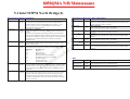
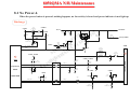
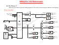
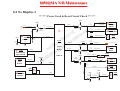
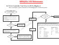
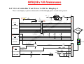
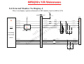
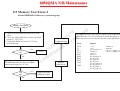
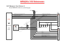
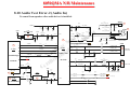
1
SERVICE MANUAL FOR 8050QMA BY: ZX Xiao Repair Technology Research Department /EDVD Jun.2005 / R01 8050QMA N/B Maintenance Contents 1. Hardware Engineering Specification ……………………………………………………………………… 4 1.1 Introduction ……………………………………………………………………………………………………………….. 4 1.2 System Hardware Parts …………………………………………………………………………………………………... 7 1.3 Other Functions …………………………………………………………………………………………………………… 32 1.4 Power Management ………………………………………………………………………………………………………. 39 1.5 Appendix 1 : Intel ICH6-M GPIO Definitions …………………………………………………………………………. 42 1.6 Appendix 2 : W83L950D KBC Pins Definitions ………………………………………………………………………… 44 1.7 Appendix 3 : 8050QMA Product Spec ……………………………………………………………………………….. … 46 t t n e e r c m e u S c c Do 2. System View and Disassembly ……………………………………………………………………………... a iT ial M t n e 3. Definition & Location of Connectors id/ Switches ………………………………………………………….. f n o C 49 2.1 System View ……………………………………………………………………………………………………………….. 49 2.2 Tools Introduction …………………………………………………………………………………………………..……. 52 2.3 System Disassembly ……………………………………………………………………………………………………….. 53 74 3.1 Mother Board (Side A) …………………………………………………………………………………………………… 74 3.2 Mother Board (Side B) …………………………………………………………………………………………………… 75 4. Definition & Location of Major Components …………………………………………………………….. 76 4.1 Mother Board (Side A) …………………………………………………………………………………………………… 76 4.2 Mother Board (Side B) …………………………………………………………………………………………………… 77 1 8050QMA N/B Maintenance Contents 5. Pin Description of Major Component …….………………………………………………………………. 78 5.1 Intel 915PM North Bridge ………………………………………………………………………………………………. 78 5.2 Intel ICH6-M South Bridge ……………………………………………………………………………………………… 88 t t n 7. Maintenance Diagnostics …………………………………………………………………………………… e e r c m e u S c c Do a 8. Trouble Shooting ……………………………………………………………………………………………. iT ial M t n e id f n o C 6. System Block Diagram ……………………………………………………………………………………… 98 99 7.1 Introduction ……………………………………………………………………………………………………………….. 99 7.2 Maintenance Diagnostics………………………………………………………………………………………………….. 100 7.3 Error Codes ……………………………………………………………………………………………………………….. 101 103 8.1 No Power …………………………………………………………………………………………………………………… 105 8.2 No Display …………………………………………………………………………………………………………………. 112 8.3 VGA Controller Failure LCD No Display ……………………………………………………………………………….. 115 8.4 External Monitor No Display …………………………………………………………………………………………….. 117 8.5 Memory Test Error ……………………………………………………………………………………………………….. 119 8.6 Keyboard (K/B) Touch-Pad (T/P) Test Error …………………………………………………………………………… 121 8.7 Hard Drive Test Error …………………………………………………………………………………………………… 123 8.8 CD-ROM Drive Test Error ……………………………………………………………………………………………… 125 8.9 USB Port Test Error ………………………………………………………………………………………………………. 127 8.10 Audio Failure …………………………………………………………………………………………………………….. 129 8.11 LAN Test Error ………………………………………………………………………………………………………….. 132 2 8050QMA N/B Maintenance Contents 8.12 PC Card Socket Failure ………………………………………………………………………………………………… 134 9. Spare Parts List ……………………………………………………………………………………………... 136 10. Reference Material …...……………………………………………………………………………………. 150 t t n e e r c m e u S c c Do a iT ial M t n e id f n o C 3 8050QMA N/B Maintenance 1. Hardware Engineering Specification 1.1 Introduction 1.1.1 General Description t t n e e r c m 1.1.2 System Overview e u S c c Do a iT ial M t n e id f n o C This document describes the brief introduction for MiTAC 8050QMA portable notebook computer system. The MiTAC 8050Q model is designed for Intel Dothan processor with 533MHz FSB with Micro-FCPGA package. This system is based on PCI architecture and is fully compatible with IBM PC/AT specification, which has standard hardware peripheral interface. The power management complies with Advanced Configuration and Power Interface. It also provides easy configuration through CMOS setup, which is built in system BIOS software and can be pop-up by pressing F2 key at system start up or warm reset. System also provides icon LEDs to display system status, such as AC Power indicator, Battery Power indicator, Battery status indicator, HDD,CD-ROM, NUM LOCK, CAP LOCK, SCROLL LOCK, Wireless on/off Card Reader Accessing. It also equipped with LAN, 56K Fax MODEM, 4 USB port, S-Video and audio line in/out , external microphone function. The memory subsystem supports DDR or DDR2 SDRAM channels (64-bits wide). The 915PM MCH Host Memory Controller integrates a high performance host interface for Intel Dothan processor, a high performance PCI Express interface, a high performance memory controller and Direct Media Interface 4 8050QMA N/B Maintenance (DMI) connecting with Intel ICH6-M. The Intel ICH6-M integrates three Universal Serial Bus 2.0 Host Controllers Interface (UHCI), the Audio Controller with AC97 interface, the Ethernet includes a 32-bit PCI controller, the IDE Master/Slave controllers, the SATA controller and Direct Media Interface technology. The Realtek RTL8100CL is a highly integrated, cost-effective single-chip Fast Ethernet controller that provides 32bit performance, PCI bus master capability, and full compliance with IEEE 802.3u 100Base-T specifications and IEEE 802.3x Full Duplex Flow Control. It also supports the Advanced Configuration Power management Interface (ACPI). t t n e e r c m e u S c c Do a iT ial M t n e id f n o C The VT6301S is a single chip PCI Host Controller for IEEE 1394-1995 Release 1.0 and IEEE 1394a P2000. It implements the Link and PHY layers for IEEE 1394-1995 High Performance Serial Bus specification release 1.0 and 1394a P2000. It is compliant with 1394 Open HCI 1.0 and 1.1 with DMA engine support for high performance data transfer via a 32-bit bus master PCI host bus interface. The VT6301S supports 100, 200 and 400 Mbit/sec transmission via an integrated 1-port PHY. The VT6301S services two types of data packets: asynchronous and isochronous (real time). The 1394 link core performs arbitration requesting, packet generation and checking, and bus cycle master operations. It also has root node capability and performs retry operations. The ENE CB712 CardBus/Media Reader controller functions as a single slot PCI to Cardbus bridge and also PCI interface MS/SD/MMC flash card reader. The CB712 provide one Cardbus slot and all reader interface may operate simultaneously. The W83L950D is a high performance microcontroller on-chip supporting functions optimized for embedded control. These include ROM, RAM, four types of timers, a serial communication interface, optional I²C bus interface, host interface, A/D converter, D/A converter, I/O ports and other functions needed in control system 5 8050QMA N/B Maintenance configurations, so that compact, high performance systems can be implemented easily. A full set of software drivers and utilities are available to allow advanced operating systems such as Windows ME, Windows 2000 and Windows XP to take full advantage of the hardware capabilities. Features such as bus mastering IDE, Plug and Play, Advanced Power Management (APM) with application restart, software-controlled power shutdown. t t n e e r c m e u S c c Do a iT ial M t n e id f n o C Following chapters will have more detail description for each individual sub-systems and functions. 6 8050QMA N/B Maintenance 1.2 System Hardware Parts CPU Intel® Pentium® M Processor (Dothan) 90nm, 2M L2, 533 MHz FSB Intel® Celeron® M processor, 90nm, 512K L2, 400 MHz FSB Core logic Intel 915PM + ICH6-M chipset System BIOS SST49LF004A Memory VGA Control Clock Generator IEEE1394 LAN t t n e e r c m e u S c c Do a iT ial M t n e id f n o C 0MB DDR2-SDRAM on Board Expandable with combination of optional 128MB/256MB/512MB/1GB(P) memory Two 200-pin DDR2 400/533 SDRAM Memory Module Type I MXM Interface (max 25W) with 8 cells Vram Priority at launch: NV44M + 32MB discrete Vram + Turbo Memory ICS 954226 VT6301S RTL8100CL PCMCIA + 4 IN 1 CARD ENE CB712 Audio System AC97 CODEC: Advance Logic, Inc, ALC655 Power Amplifier: TI TPA0212 Modem AC97 Link: MDC (Mobile Daughter Card) Askey: V1456VQL-P1(INT) 7 8050QMA N/B Maintenance 1.2.1 Intel Dothan Processors in Micro-FCBGA Package Intel Dothan Processors with 479 pins Micro-FCBGA package. It will be manufactured on Intel’s advanced 90 nanometer process technology with copper interconnect. It’s features include Intel Architecture with Dynamic Execution, On-die primary 32-kB instruction cache and 32-kB write-back data cache, on-die 2-MB second level cache with advanced Transfer Cache Architecture, Data Prefetch Logic, Streaming SIMD Extensions 2 (SSE2), 533-MHz FSB. t t n e e r c m e u S c c Do a iT ial M t n e id f n o 1.2.2 Clock Generator C The Streaming SIMD Extensions 2 (SSE2) enable break-through levels of performance in multimedia applications including 3-D graphics, video decoding/encoding, and speech recognition. Use Source-Synchronous Transfer (SST) of address and data to improve performance by transferring data four times per bus clock. Support Enhanced Intel SpeedStep technology, which enables real-time dynamic switching of the voltage and frequency between two performance modes. System frequency synthesizer: ICS954226 is a CK410M Compliant clock synthesizer. It provides a single-chip solution for mobile systems built with Intel P4-M processors and Intel mobile chipsets. It is driven with a 14.318MHz crystal and generates CPU outputs up to 400MHz. It provides the tight ppm accuracy required by Serial ATA and PCI-Express. 8 8050QMA N/B Maintenance • Supports tight ppm accuracy clocks for Serial-ATA and SRC. • Supports spread spectrum modulation, 0 to –0.5% down spread. • Uses external 14.318MHz crystal, external crystal load caps are required for frequency tuning. • Supports undriven differential CPU, SRC pair in PD# for power management. t t n e e 1.2.3 The Mobile Intel 915PM Express Chipset r c m e u S c c Do a iT ial M t n e id f n o C The Mobile Intel 915PM Express Chipset integras a memory controller hub (MCH) designed for use with the Dothan, Yonah and Intel Celeron M Processor. It is PCI Express based Graphics. The 915PM MCH integrates a system memory DDR/DDR2 controller with two, 64-bit wide interfaces. Only Double Data Rate (DDR/DDR2) memory is supported; the buffers support DDR SSTL_2 and DDR2 SSTL_18 signaling interfaces. The memory controller interface is fully configurable through a set of control registers. It integras a high performance transition interface PCI Express Interface. PCI Express operates at a data rate of 2.5 for 8050QMA project. GB/s. This allows a maximum theoretical bandwidth of 40 GB/s each direction. The 915PM MCH integrates Direct media interface (DMI) chip-to-chip interconnect between the MCH and ICH6-M. DMI supports DMI x2 and DMI x4 configuration. Features: Processor/FSB Support 9 8050QMA N/B Maintenance • Intel® Dothan processor • AGTL+ bus driver technology with integrated GTL termination resistors (gated AGTL+ receivers for reduced power) • Supports 32-bit AGTL+ host bus addressing • Supports system bus at 533MT/s (533 MHz) and 400MT/s (400 MHz) t t n e e r c m e u S c c Do a iT ial M t n e id f n o C • 2X Address, 4X data • Host bus dynamic bus inversion HDINV support • 12 deep, in-order queue Memory System • Directly supports to two DDR or DDR2 SDRAM channels, 64-bts wide. • Supports SO-DIMMs of the same type (e.g.,all DDR or all DDR2), not mixed. • Maximum of two, double-sided unbuffered SO-DIMMs (4 rows populated) • Minimum amount of memory supported is 128 MB (16 MB x 16-b x 4 devices x 1 rows = 128 MB) using 256-MB technology • Maximum amount of memory supported is 2 GB using 1-GB technology. 10 8050QMA N/B Maintenance • 256-MB, 512-MB and 1-GB technology using x8 and x16 devices. • Three memory channel organizations are supported for DDR / DDR2 : – Single channel – Dual channel interleaved – Dual channel asymmetric t t n e e r c m e u S c c Do a iT ial M t n e id f n o C • Supports DDR 333 devices and DDR2 400 /533 devices – Supports on-die termination (ODT) for DDR2 • Supports Fast Chip Select mode • Supports partial write to memory using Data Mask signal (DM) • Supports high-density memory package for DDR or DDR2 type devices PCI Express Interface • One x16 (16 lanes) PCI Express port intended for graphics attach • Maximum theoretical realized bandwidth on interface of 4 GB/s in each direction simultaneously, for an average of 8 GB/s when x16 • Automatic discovery, negotiation and training of link out of reset • Supports traditional PCI style traffic (asynchronous snooped, PCI ordering) 11 8050QMA N/B Maintenance • Supports only 1.5-V AGP electrics • 32 deep AGP request queue • Hierarchical PCI-compliant configuration mechanism for downstream devices • Direct Media Interface (DMI) t t n e e r c m e u S c c Do a T al i 1.2.4 I/O Controller Hub :M Intel ICH6-M i t n e id f n • o C – Chip-to-chip interconnect between the GMCH and ICH6-M – DMI x2 and DMI x4 configuration supported – Bit swapping is supported – Lane reversal is not supported The ICH6 provides extensive I/O support. Functions and capabilities include: PCI Express Base Specification, Revision 1.0a-compliant • PCI Local Bus Specification, Revision 2.3-compliant with support for 33 MHz PCI operations(supports up to seven Req/Gnt pairs) • ACPI Power Management Logic Support • Enhanced DMA controller, interrupt controller and timer functions 12 8050QMA N/B Maintenance • Integrated Serial ATA host controller with independent DMA operation on two ports and AHCI support • Integrated IDE controller supports Ultra ATA100/66/33 • USB host interface with support for three USB ports; three UHCI host controllers; one EHCI high-speed USB2.0 Host controller • Integrated LAN controller t t n e e r c m e u S c c Do a iT ial M t n e id f n o C • System Management Bus (SMBus) Specification, Version 2.0 with additional support for I2C devices • Supports Audio Codec ’97, Revision 2.3 Specification (a.k.a.,AC ’97 Component Specification, Revision 2.3) which provides a link for Audio and Telephony codecs (up to 7 channels) • Supports Intel High Definition Audio • Low Pin Count (LPC) interface • Firmware Hub (FWH) interface support 1.2.5 CardBus: CB712 Features: 3.3V operation with 5V tolerant LFBGA 169-ball package 13 8050QMA N/B Maintenance Pin out Compatible with CB1410 • PCI Interface – Compliant with PCI Local Bus Specification Revision 2.3 – Compliant with PCI Bus Power Management Interface Specification Revision 1.1 – Compliant with PCI Mobile Design Guide Version 1.1 t t n e e r c m e u S c c Do a iT ial M t n e id f n o C – Compliant with Advanced Configuration and Power Interface Specification Revision 1.0 • CardBus Interface – Compliant with PC Card Standard 8.0 – Support Standardized Zoomed Video Register Model – Support SPKROUT CAUDIO and RIOUT# • Secure Digital Interface – Compliant with SD Host Controller Standard Specification Version 1.0 – Support SD Suspend/Resume Functionality – Support DMA Mode to Minimize CPU Overhead – Support High Speed with the SD Clock Frequency Up to 50Mhz – Contain two 512-byte buffer to maximize the transfer speed – Support Traffic LED Light – Support Over Current Protection 14 8050QMA N/B Maintenance • Memory Stick Interface – Compliant with Memory Stick PRO Format Specification Version 1.0 – Support 4-bit Parallel Data Transfer Mode – Memory Stick Clock Frequency Up to 40Mhz – Support DMA Mode to Minimize CPU Overhead t t n e e r c m e u S c c Do a iT ial M t n e id f n o C – Support Traffic LED Light – Support Over Current Protection • Interrupt Configuration – Support Parallel PCI Interrupts – Support Parallel IRQ and Parallel PCI Interrupts – Support Serialized IRQ and Parallel PCI Interrupts – Support Serialized IRQ and PCI Interrupts • Power Management Control Logic – Support CLKRUN# protocol – Support SUSPEND# – Support PCI PME# from D3, D2, D1 and D0 – Support PCI PME# from D3cold • Support Zoomed Video port 15 8050QMA N/B Maintenance • Support parallel 4-wire power switch interface 1.2.6 AC’97 Audio System: Advance Logic, Inc, ALC655 The ALC655 is a 16-bit, full duplex AC'97 2.3 compatible six channels audio CODEC designed for PC multimedia systems, including host/soft audio and AMR/CNR based designs. The ALC655 incorporates proprietary converter technology to meet performance requirements on PC99/2001 systems. The ALC655 CODEC provides three pairs of stereo outputs with 5-Bitvolume controls, a mono output, and multiple stereo and mono inputs, along with flexible mixing, gain and mute functions to provide a complete integrated audio solution for PCs. The digital interface circuitry of the ALC655 CODEC operates from a 3.3V power supply for use in notebook and PC applications. The ALC655 integrates 50mW/20ohm headset audio amplifiers at t t n e e r c m e u S c c Do a iT ial M t n e id f n o C Front-Out and Surr-Out, built-in 14.318M 24.576MHz PLL and PCBEEP generator, those can save BOM costs. The ALC655 also supports the S/PDIF input and output function, which can offer easy connection of PCs to consumer electronic products, such as AC3 decoder/speaker and mini disk devices. ALC655 supports host/soft audio from Intel ICH6 chipsets as well as audio controller based VIA/SIS/ALI/AMD/nVIDIA/ATI chipset. Bundled Windows series drivers (WinXP/ME/2000/98/NT), EAX/ Direct Sound 3D/ I3DL2/ A3D compatible sound effect utilities (supporting Karaoke, 26-kind of environment sound emulation,10-band equalizer), HRTF 3D positional audio and Sensaura™ 3D (optional) provide an excellent entertainment package and game experience for PC users. Besides, ALC655 includes Realtek’s impedance sensing techniques that makes device load on outputs and inputs can be detected. 16 8050QMA N/B Maintenance • Meets performance requirements for audio on PC99/2001 systems • Meets Microsoft WHQL/WLP 2.0 audio requirements • 16-bit Stereo full-duplex CODEC with 48KHz sampling rate • Compliant with AC’97 2.3 specifications t t n e e r c m e u S c c Do a iT ial M t n e id f n o C – 14.318MHz- 24.576MHz PLL to save crystal – 12.288MHz BITCLK input can be consumed – Integrated PCBEEP generator to save buzzer – Interrupt capability • Three analog line-level stereo inputs with 5-bit volume control: LINE_IN, CD, AUX • High quality differential CD input • Two analog line-level mono input: PCBEEP,PHONE-IN • Two software selectable MIC inputs applications (software selectable) • Boost preamplifier for MIC input 50mW/20 amplifier • External Amplifier Power Down (EAPD) capability • Power management and enhanced power saving features 17 8050QMA N/B Maintenance • Stereo MIC record for AEC/BF application • Supports Power Off CD function • Adjustable VREFOUT control Supports double sampling rate (96KHz) of DVD audio playback • Support 48KHz of S/PDIF output is compliant with AC’97 rev2.3 specification t t n e e r c m e 1.2.7 MDC: Pctel Modem Daughter Card PCT2303W u (Askey V1456VQL-P1) S c c Do a iT ial M t n e id f n o C • Power support: Digital: 3.3V; Analog: 3.3V/5V The PCT2303W chipset is designed to meet the demand of this emerging worldwide AMR/MDC market. The combination of PC-TEL’s well proven PCT2303W chipset and the HSP56TM MR software modem driver allows systems manufactures to implement modem functions in PCs at a lower bill of materials (BOM) while maintaining higher system performance. PC-TEL has streamlined the traditional modem into the Host Signal Processing (HSP) solution. Operating with the Pentium class processors, HSP becomes part of the host computer’s system software. It requires less power to operate and less physical space than standard modem solutions. PC-TEL’s HSP modem is an easily integrated, costeffective communications solution that is flexible enough to carry you into the future. The PCT2303W chip set is an integrated direct access arrangement (DAA) and Codec that provides a programmable line interface to meet international telephone line requirements. The PCT2303W chip set is available in two 16-pin 18 8050QMA N/B Maintenance small outline packages (AC’97 interface on PCT303A and phone-line interface on PCT303W). The chip set eliminates the need for an AFE, an isolation transformer, relays, opto-isolators, and 2-to 4-wire hybrid. The PCT2303W chip set dramatically reduces the number of discrete components and cost required to achieve compliance with international regulatory requirements. The PCT2303W complies with AC’97 Interface specification Rev. 2.1. t t n e e r c m e u S c c Do a iT ial M t n e id f n o C The chip set is fully programmable to meet world-wide telephone line interface requirements including those described by CTR21, NET4, JATE, FCC, and various country-specific PTT specifications. The programmable parameters of the PCT2303W chip set include AC termination, DC termination, ringer impedance, and ringer threshold. The PCT2303W chip set has been designed to meet stringent world-wide requirements for out-of-band energy, billing-tone immunity, lightning surges, and safety requirements. Features: Virtual com port with a DTE throughout up to 460.8Kbps. G3 Fax compatible Auto dial and auto answer Ring detection Codec/DAA Features • AC97 2.1 compliant • 86dB dynamic range TX/RX paths 19 8050QMA N/B Maintenance • 2-4-wire hybrid • Integrated ring detector • High voltage isolation of 4000V • Support for “Caller ID” t t n e e r c m e u S c c Do a iT ial M t n e id f n o C • Compliant with FCC Part68, CTR21, Net4 and JATE • Low power standby • Low profile SOIC package 16 pins 10x3x1.55mm • Low power consumption • 10mA @ 3.3V operation • 1mA @ 3.3V power down • Integrated modem codec 20 8050QMA N/B Maintenance Standard Features • Data – ITU-T V.90 (56Kbps), V.34 (4.8Kbps TO 33.6 Kbps), V.32 bis (4.8Kbps to 14.4Kbps), V.22 bis (1.2 bps to 2.4 Kbps), V.21 and Bell 103 and 212A(300 to 1200 bps) modulation protocol – Data Compression ITU-T V.42bis MNP Class 5 t t n e e r c m e u S c c Do a iT ial M t n e id f n o C – Error Correction ITU-T V.42 LAPM MNP 2-4 • Fax – ITU-T V. 17, V.29, V.27ter, V.21, Channel 2, Group 3, EIA Class I 21 8050QMA N/B Maintenance 1.2.8 IEEE1394 VT6301S 1.2.8.1 Overview The VT6301S IEEE 1394 OHCI Host Controller provides high performance serial connectivity. It implements the Link and Phy layers for IEEE 1394-1995 High Performance Serial Bus specification release 1.0 and 1394a2000. It is compliant with 1394 Open HCI 1.0 and 1.1 with DMA engine support for high performance data transfer via a 32-bit bus master PCI host bus interface. The VT6301S supports 100, 200 and 400 Mbit/sec transmission via an integrated 1-port PHY. The VT6301S services two types of data packets: asynchronous and isochronous (real time). The 1394 link core performs arbitration requesting, packet generation and checking, and bus cycle master operations. It also has root node capability and performs retry operations. The VT6301S is ready to provide industry-standard IEEE 1394 peripheral connections for desktop and mobile PC platforms. Support for the VT6301S is built into Microsoft Windows 98, Windows ME, Windows 2000 and Windows XP 1.2.8.2 Features t t n e e r c m e u S c c Do a iT ial M t n e id f n o C • 32 bit CRC generator and checker for receive and transmit data • On-chip isochronous and asynchronous receive and transmit FIFOs for packets (2K for general receive plus 2K for isochronous transmit plus 2K for asynchronous transmit) • 8 isochronous transmit contexts • 4 isochronous receive contexts 22 8050QMA N/B Maintenance • 3-deep physical post-write queue • 2-deep physical response queue • Dual buffer mode enhancements • Skip Processing enhancements t t n e e r • c m e u S c c o a 1.2.9 System Flash Memory (BIOS) D iT ial M t n e id f n o C • Block Read Request handling Ack_tardy processing Firmware Hub for Intel® 810, 810E, 815, 815E,815EP, 820, 840, 850 Chipsets Flexible Erase Capability – Uniform 4 KByte Sectors – Uniform 16 KByte overlay blocks for SST49LF002A – Uniform 64 KByte overlay blocks for SST49LF004A – Top boot block protection – 16 KByte for SST49LF002A – 64 KByte for SST49LF004A 23 8050QMA N/B Maintenance – Chip-Erase for PP Mode Single 3.0-3.6V Read and Write Operations Superior Reliability Firmware Hub Hardware Interface Mode Supports Intel High Definition Audio t t n e e r c m e u S c c Do a iT ial M t n e id f n o 1.2.10 Memory System C – 5-signal communication interface supporting byte Read and Write – 33 MHz clock frequency operation – WP# and TBL# pins provide hardware write protect for entire chip and/or top Boot Block – Block Locking Register for all blocks – Standard SDP Command Set – Data# Polling and Toggle Bit for End-of-Write detection – 5 GPI pins for system design flexibility – 4 ID pins for multi-chip selection 1.2.10.1 256MB, 512MB, 1GB (x64) 200-Pin DDR2 SDRAM SODIMMs • JEDEC-standard 200-pin, small-outline, dual in-line memory module (SODIMM) • VDD=+1.8V±0.1V, VDDQ=+1.8V±0.1V 24 8050QMA N/B Maintenance • JEDEC standard 1.8V I/O (SSTL_18-compatible) • Differential data strobe (DQS,DQS#) option • Four-bit prefetch architecture • Differential clock input (CK,CK#) t t n e e r c m e u S c c Do a iT ial M t n e id f n o C • Command entered on each rising CK edge • DQS edge-aligned with data for Reads • DQS center-aligned with data for Writes • Duplicate output strobe (RDQS) option for x8 configuration • DLL to align DQ and DQS transitions with CK • Four internal banks for concurrent operation • Data mask (DM) for masking write data • Programmable CAS Latency (CL) : 2,3,4 and 5 • Posted CAS additive latency (AL) : 0,1,2,3 and 4 • Write latency = Read latency – 1tCK 25 8050QMA N/B Maintenance • Programmable burst lengths : 4 or 8 • Read burst interrupt supported by another READ • Write burst interrupt supported by another WRITE • Adjustable data – output drive strength t t n e e r • c m e u S • c c Do a • iT ial M t • n e id f 1.2.11 LAN PHY: RTL8100C(L) n o C • Concurrent auto precharge option is supported Auto Refresh (CBS) and Self Refresh Mode 64ms, 8,192-cycle refresh Off-chip drive (OCD) impedance calibration On-die termination (ODT) General The Realtek RTL8100C(L) is a highly integrated, cost-effective single-chip Fast Ethernet controller that provides 32bit performance, PCI bus master capability, and full compliance with IEEE 802.3u 100Base-T specifications and IEEE 802.3x Full Duplex Flow Control. It also supports the Advanced Configuration Power management Interface (ACPI), PCI power management for modern operating systems that are capable of Operating System Directed Power 26 8050QMA N/B Maintenance Management (OSPM) to achieve the most efficient power management possible. The RTL8100C(L) does not support CardBus mode as the RTL8139C does. In addition to the ACPI feature, the RTL8100C(L) also supports remote wake-up (including AMD Magic Packet, LinkChg, and Microsoft® wake-up frame) in both ACPI and APM environments. The RTL8100C(L) is capable of performing an internal reset through the application of auxiliary power. When auxiliary power is applied and the main power remains off, the RTL8100C(L) is ready and waiting for the Magic Packet or Link Change to wake the system up. Also, the LWAKE pin provides 4 different output signals including active high, active low, positive pulse, and negative pulse. The versatility of the RTL8100C(L) LWAKE pin provides motherboards with Wake-On-LAN (WOL) functionality. The RTL8100C(L) also supports Analog Auto-Power-down, that is, the analog part of the RTL8100C(L) can be shut down temporarily according to user requirements or when the RTL8100C(L) is in a power down state with the wakeup function disabled. In addition, when the analog part is shut down and the IsolateB pin is low (i.e. the main power is off), then both the analog and digital parts stop functioning and the power consumption of the RTL8100C(L) will be negligible. The RTL8100C(L) also supports an auxiliary power auto-detect function and will auto-configure related bits of their own PCI power management registers in PCI configuration space. t t n e e r c m e u S c c Do a iT ial M t n e id f n o C • 128 pin QFP/LQFP • Integrated Fast Ethernet MAC, Physical chip and transceiver in one chip • 10 Mb/s and 100 Mb/s operation • Supports 10 Mb/s and 100 Mb/s N-way Auto-negotiation operation • PCI local bus single-chip Fast Ethernet controller 1. Compliant to PCI Revision 2.2 27 8050QMA N/B Maintenance 2. Supports PCI clock 16.75MHz-40MHz 3. Supports PCI target fast back-to-back transaction 4. Provides PCI bus master data transfers and PCI memory space or I/O space mapped data transfers of RTL8100C(L)'s operational registers 5. Supports PCI VPD (Vital Product Data) 6. Supports ACPI, PCI power management t t n e e r c m e u S c c Do a iT ial M t n e id f n o C • Supports 25MHz crystal or 25MHz OSC as the internal clock source. The frequency deviation of either crystal or OSC must be within 50 PPM. • Compliant to PC99/PC2001 standard • Supports Wake-On-LAN function and remote wake-up (Magic Packet*, LinkChg and Microsoft® wake-up frame) • Supports 4 Wake-On-LAN (WOL) signals (active high, active low, positive pulse and negative pulse) • Supports auxiliary power-on internal reset, to be ready for remote wake-up when main power still remains off • Supports auxiliary power auto-detect, and sets the related capability of power management registers in PCI configuration space • Includes a programmable, PCI burst size and early Tx/Rx threshold • Supports a 32-bit general-purpose timer with the external PCI clock as clock source, to generate timer-interrupt • Contains two large (2Kbyte) independent receive and transmit FIFOs 28 8050QMA N/B Maintenance • Advanced power saving mode when LAN function or wakeup function is not used • Uses 93C46 (64*16-bit EEPROM) to store resource configuration, ID parameter and VPD data • Supports LED pins for various network activity indications • Supports loop back capability t t n e e r • c m e u S c c o a D 1.2.12 Keyboard System: Winbond W83L950D iT ial M t n e id f n o C • Half/Full duplex capability Supports Full Duplex Flow Control (IEEE 802.3x) The Winbond Keyboard controller architecture consists of a Turbo 51 core controller surrounded by various registers, nine general purpose I/O port, 2k+256 bytes of RAM, four timer/counters, dual serial ports, 40K MTP-ROM that is divided into four banks, two SMBus interface for master and slave, Support 4 PWM channels, 2 D-A and 8 A-D converters. • 8051 uC based • Keyboard Controller Embedded Controller • Supply embedded programmable flash memory (internal ROM size: 40KB) and RAM size is 2 KB • Support 4 Timer (8 bit) signal with 3 prescalers 29 8050QMA N/B Maintenance • Support 2 PWM channels, 2 D-A and 8 A-D converters • Reduce Firmware burden by Hardware PS/2 decoding • Support 72 useful GPIOs totally • Support Flash utility for on board re-flash t t n e e r • c m e u S c c o a 1.2.13 Hard Disk Drive D iT ial M t n e id f n o C • • Support ACPI Hardware fast Gate A20 with software programmable IDE HDD The ICH6 IDE controller features one set of interface signals that can be enabled, tri-stated or driven low. The IDE interfaces of the ICH6 can support several types of data transfers: Programmed I/O (PIO): processor is in control of the data transfer • 8237 style DMA: DMA protocol that resembles the DMA on the ISA bus, although it does not use the 8237 in the ICH6. This protocol off loads the processor from moving data. This allows higher transfer rate of up to 16MB/s 30 8050QMA N/B Maintenance • Ultra ATA/33/66/100: DMA protocol that redefines signals on the IDE cable to allow both host and target throttling of data and transfer rates of up to 33/66/100 MB/s t t n e e r c m e u S c c Do a iT ial M t n e id f n o C 31 8050QMA N/B Maintenance 1.3 Other Functions 1.3.1 Hot Key Function Keys Combination Feature Meaning t t n e e r c m e u S c c Do a iT ial M t n e id f n o C Fn + F1 Power down Mini PCI power down Fn + F2 Reserve Fn + F3 Volume Down Fn + F4 Volume Up Fn + F5 LCD/external CRT switching Rotate display mode in LCD only, CRT only, and simultaneously display. Fn + F6 Brightness down Decreases the LCD brightness Fn + F7 Brightness up Increases the LCD brightness Fn + F10 Battery Low Beep On/Off Battery Low Beep Fn + F11 Panel Off/On Toggle Panel on/off Fn + F12 Suspend to DRAM / HDD Force the computer into either Suspend to HDD or Suspend to DRAM mode depending on BIOS Setup. 32 8050QMA N/B Maintenance 1.3.2 Power On/Off/Suspend/Resume Button 1.3.2.1 APM Mode At APM mode, Power button is on/off system power. 1.3.2.2 ACPI Mode t t n e e r c m e u S c c Do a iT ial M t n e 1.3.3 Cover Switch id f n o C At ACPI mode. Windows power management control panel set power button behavior. You could set “standby”, “power off” or “hibernate”(must enable hibernate function in power Management) to power button function. Continue pushing power button over 4 seconds will force system off at ACPI mode. System automatically provides power saving by monitoring Cover Switch. It will save battery power and prolong the usage time when user closes the notebook cover. At ACPI mode there are four functions to be chosen at windows power management control panel. 1. None 2. Standby 33 8050QMA N/B Maintenance 3. Off 4. Hibernate (must enable hibernate function in power management) 1.3.4 LED Indicators t t n e e r c m e u S c c Do a iT ial M t n e id f n o C 1.3.4.1 Three LED Indicators at Front Side: From left to right that indicate BATTERY POWER, BATTERY STATUS and AC POWER -- AC POWER: This LED lights green when the notebook was powered by AC power line, Flashes (on 1 second, off 1 second) when entered suspend to RAM state with AC powered. The LED is off when the notebook is in power off state or powered by battery. -- BATTERY POWER This LED lights green when the notebook is being powered by Battery, and flashes (on 1 second, off 1 second) when entered suspend to RAM state with AC powered. The LED is off when the notebook is in power off state or powered by AC adapter. -- BATTERY STATUS: During normal operation, this LED stays off as long as the battery is charged. When the battery charge drops to 10% of capacity, the LED lights red, flashes per 1 second and beeps per 2 second. When AC is 34 8050QMA N/B Maintenance connected, this indicator glows green if the battery pack is fully charged or orange (amber) if the battery is being charged. AC POWER: This LED lights green when AC is powering the notebook, and flash (on 1 second, off 1 second) when Suspend to RAM no matter using AC power or Battery power. The LED is off when the notebook is off or powered by battery. t t n e e r c m e u S 1.3.4.2 Seven LED Indicators: c c Do a iT ial M t n e id f 1.3.5 Battery Status n o C BATTERY POWER: This LED lights green when the notebook is being powered by Battery, and flash (on 1 second, off 1 second) when Battery is low. The LED is off when the notebook is off or powered by AC adaptor. System has seven status LED indicators at front side which to display system activity. From left to right that indicate HARD DISK, CD-ROM, NUM LOCK, CAPS LOCK, SCROLL LOCK, Wireless on/off, Card Reader Accessing Blue-Tooth. 1.3.5.1 Battery Warning -- System also provides Battery capacity monitoring and gives users a warning signal to alarm they to store data before battery dead. This function also protects system from mal-function while battery capacity is low. 35 8050QMA N/B Maintenance -- Battery Warning: Capacity below 10%, Battery Capacity LED flashes , and system beeps per 2 seconds. -- System will Suspend to HDD after 2 Minutes to protect users data. 1.3.5.2 Battery Low State After Battery Warning State, and battery capacity is below 5%, system will generate beep sound for twice per second. t t n e e 1.3.5.3 Battery Dead State r c m e u S c c Do a iT ial M t 1.3.6 Fan Power On/Off Management n e id f n o C When the battery voltage level reaches 11.5 volts, system will shut down automatically in order to extend the battery packs' life. FAN is controlled by W83L950D embedded controller-using ADT7460 to sense CPU and VGA temperature and PWM control fan speed. Fan speed is depended on CPU and VGA temperature. Higher CPU or VGA temperature faster Fan Speed. 1.3.7 CMOS Battery CR2032 3V 220mAh lithium battery 36 8050QMA N/B Maintenance When AC in or system main battery inside, CMOS battery will consume no power. AC or main battery not exists, CMOS battery life at less (220mAh/5.8uA) 4 years. 1.3.8 I/O Port t t n e e r c m e u S c c Do a iT ial M t n e id f n o C One Power Supply Jack One External DVI-I Connector For DVI Display Supports four USB port for all USB devices. One MODEM RJ-11 phone jack for PSTN line One RJ-45 for LAN. One IEEE1394 port One TV-Out port Reserve 1 connector on board for USB 2.0 Device Headphone Out Jack. Microphone Input Jack. 37 8050QMA N/B Maintenance Line in Jack 1.3.9 Battery Current Limit and Learning Implanted H/W current limit and battery learning circuit to enhance protection of battery. t t n e e r c m e u S c c Do a iT ial M t n e id f n o C 38 8050QMA N/B Maintenance 1.4 Power Management The 8050MB system has built in several power saving modes to prolong the battery usage for mobile purpose. User can enable and configure different degrees of power management modes via ROM CMOS setup (booting by pressing F2 key). Following are the descriptions of the power management modes supported. t t n 1.4.1.1 Full on Mode e e r c m e u S c c Do a 1.4.1.2 Doze Mode iT ial M t n e id f n o 1.4.1.3 Standby Mode C 1.4.1 System Management Mode In this mode, each device is running with the maximal speed. CPU clock is up to its maximum. In this mode, CPU will be toggling between on & stop grant mode either. The technology is clock throttling. This can save battery power without loosing much computing capability. The CPU power consumption and temperature is lower in this mode. For more power saving, it turns of the peripheral components. In this mode, the following is the status of each device: -- CPU: Stop grant 39 8050QMA N/B Maintenance -- LCD: backlight off -- HDD: spin down 1.4.1.4 Suspend to DRAM The most chipset of the system is entering power down mode for more power saving. In this mode, the following is the status of each device: Suspend to DRAM -- CPU: off t t n e e r c m e u S c c Do a iT ial M t n e id f n o C -- Intel 915GM: Partial off -- VGA: Suspend -- PCMCIA: Suspend -- Audio: off -- SDRAM: self refresh Suspend to HDD -- All devices are stopped clock and power-down -- System status is saved in HDD 40 8050QMA N/B Maintenance -- All system status will be restored when powered on again 1.4.2 Other Power Management Functions Implanted H/W current limit and battery learning circuit to enhance protection of battery. t t n e e r c m e u S c c Do a iT ial M t n e id f n o C 1.4.2.1 HDD & Video Access System has the ability to monitor video and hard disk activity. User can enable monitoring function for video and/or hard disk individually. When there is no video and/or hard disk activity, system will enter next PMU state depending on the application. When the VGA activity monitoring is enabled, the performance of the system will have some impact. 41 8050QMA N/B Maintenance 1.5 Appendix 1: Intel ICH6-M GPIO Definitions (1) Pin name Current Define GPIO0 PCI_REQ6# I MAIN GPIO1 MINIPCI_ACT# I MAIN GPIO2 PCI_INTE# I MAIN GPIO3 PCI_INTF# I MAIN PCI_INTG# I MAIN PCI_INTH# I MAIN PM_BMBUSY# I MAIN X I RESUME GPIO4 GPIO5 GPIO6 GPIO9 GPIO10 GPIO11 GPIO12 GPIO13 GPIO14 GPIO15 GPIO16 GPIO17 GPIO18 GPIO20 GPIO23 GPIO24 GPIO25 GPIO26 GPIO27 Power plane t t n e e r c m e u S c c Do a iT ial M t n e id f n o C X I RESUME SMBALERT# I RESUME KBD_US/JP# I MAIN WAKE_UP# I RESUME X I RESUME X I RESUME SB_BY_ON# O MAIN SCI# I MAIN STOP_PCI# O MAIN STOP_CPU# O MAIN WIRELESS_PD# O MAIN SPK_OFF I/O RESUME I/O RESUME PANEL_ID0 I MAIN X I/O RESUME 42 8050QMA N/B Maintenance 1.5 Appendix 1: Intel ICH6-M GPIO Definitions (2) Continue to previous page Pin name Current Define Power plane GPIO28 X I/O RESUME GPIO29 PANEL_ID1 I MAIN GPIO30 PANEL_ID2 I MAIN PANEL_ID3 I MAIN PCLKRUN# I/O MAIN MB_ID0 I/O MAIN GPIO31 GPIO32 GPIO33 GPIO34 GPIO40 GPIO41 GPIO48 GPIO49 t t n e e r c m e u S c c Do a iT ial M t n e id f n o C MB_ID1 I/O MAIN MXM_DETECT# I MAIN CRT_IN# I MAIN X O MAIN HPWRGD OD O MAIN 43 8050QMA N/B Maintenance 1.6 Appendix 2: W83L950D KBC Pins Definitions (1) Port Pin P0 P1 P3 0-7 0-7 0-7 0 1 2 3 4 5 6 7 0 1 2 3 4 5 6 7 0 1 2 3 4 5 6 7 P2 P4 P5 Function Scan matrix LPC enable GPIO x1 Implement KO[0..7] KO[8..15] KI[0..7] H8_THRM# H8_WAKE_UP# BATT_G# BATT_R# EXTSMI# CAP# NUM# SCROLL# H8_ENABKL CHARGING LEARING H8_SUSB H8_HRCIN# A20GATE H8_SCI H8_PWRON SW_VDD3 H8_LIDSW# BATT_DEAD# H8_ADEN# BATT_LED# KBC_PWRON_VDD3S BLADJ H8_I_CTR t t n e e r c m e u S c c Do a iT ial M t n e id f n o C SMBUS1 or UART GPIO x4 Xcin/cout or PWM 2,3 GPIO x2 (INT1) KBRST A20 GPIO x2 GPIO x1 GPIO x3 (INT20,30,40) GPIO x2 D/A, PWM 2,3 44 8050QMA N/B Maintenance 1.6 Appendix 2: W83L950D KBC Pins Definitions (2) Continue to previous page Port P6 P7 P8 Pin 0 1 2 3 4 5 6 7 0 1 2 3 4 5 6 7 0 1 2 3 4 5 6 7 Function Implement PWRBTN# KBC_RI# AC_ POWER# BATT_V BATT_T H8_I_LIMIT H8_PROCHOT# +BC_CPUCORE T_DATA H8_RSMRST ICH_PWRBTN T_CLK H8_PWRON_SUSB# SUSC# BAT_DATA BAT_CLK PCICLK_KBC SERIRQ LAD3 LAD2 LAD1 LAD0 KBC_PCIRST# LFRAME# t t n e e r c m e u S c c Do a iT ial M t n e id f n o C A/D (INT5-12) PS/2 port x3 SMBUS LPC interface 45 8050QMA N/B Maintenance 1.7 Appendix 3: 8050QMA Product Spec (1) Item CPU Core logic System BIOS Memory VGA Controller Description Intel® Pentium® M Processor (Dothan) 90nm, 2M L2, 533 MHz FSB Intel® Celeron® M processor, 90nm, 512K L2, 400 MHz FSB - CPU Thermal ceiling: 27W Intel 915PM + ICH6M - Dual Channel Memory Support - DDR2 400/533 Expandable to 2048MB(P) Inside 512KB Flash EPROM Include System BIOS, VGA BIOS t t n e e r c m e u S c c Do a iT ial M t n e id f n o C ACPI2.0; 2.31 compliants Boot from USB mass storage device - 200-pin SO-DIMM DDR2 Memory Slot x2 - Support DDR2 400/533 - 0MB Memory onboard ; Expandable to 2.0GB(P) - Type I MXM Interface (max 25W) with 8 cells Vram - Priority at launch: NV44M + 32MB discrete Vram + Turbo Memory 12.7mm Optical Drive - Combo Drive ROM Drive - DVD Dual - DVD Super Multi drive HDD Display One 2.5" 9.5 mm height HDD; - 5400/7200 RPM Serial PATA HDD - 40/60/80 GB Capacity 15.4" Wide WXGA TFTLCD - Resolution: 1280 x 800 Keyboard - Key pitch: 19mm, Key travel: 3.0mm - Windows Logo Key x 2 - W/z Hot Key Functions Touch Pad - Intelligence Glide pad without scroll button - 2 touch pad buttons 46 8050QMA N/B Maintenance 1.7 Appendix 3: 8050QMA Product Spec (2) Continue to previous page Item Description Audio/AV Function - AC97, support S/PDIF output - 5.1 channel analog output - 2.1 channel system speaker. two full range speakers(1W*2 Front), one subwoofer(3W) - Build in microphone Multi Card reader Indicator on board PC CARD t t n e e r c m e u S c c Do a iT ial M t n e id f n o C - 4 in 1 Card Reader (SD/MMC/MS/MS Pro) 3 LEDs for Power/Battery status (AC In status/Battery status/Reserved Power System Status) (on inverter board) 2 LEDs for HDD Access, ODD Access 3 LEDs for Number lock, Caps lock, Scroll lock 1 LED for Wireless on/off 1 LED for Card Reader Accessing 1x Type II PCMCIA Interface without Zoom Video Support Support 3.3V, 5V device I/O: USB (support USB 1.1 and USB 2.0) port x 4 Reserve 1 connector on board for USB 2.0 Device RJ-11 port x 1 (4Pin) RJ-45 port x 1 DC input (2.5 * 5.5 * 11mm) x 1 IEEE1394 x 1(4 pin). Type III B MiniPCI x 1 (For wireless LAN) I/O Ports Audio(Normal /5.1Analog output): Line - out/SPDIF x 1 (5.1 mode: Front 2 channels) Mic - in x 1 (5.1 mode: LBF/Middle channels) Line - in x 1 (5.1 mode: Rear 2 channels) Video DVI- I x 1 TV-Out x 1 (7 Pin S-Video connector NTSC/PAL) 47 8050QMA N/B Maintenance 1.7 Appendix 3: 8050QMA Product Spec (3) Continue to previous page Item Description Communication PCI 10/100 LAN MDC 56K, V.90 Modem 802.11g wireless LAN (Mini PCI optional) with built-in Antenna Power Supply 6 cell Li-ion (2400mAH/3.7V) Battery pack Battery Life > 3HRs AC adapter Dimensions Weight Manuals Accessories SAFETY LOCK Architecture Sales Region Agency t t n e e r c m e u S c c Do a iT ial M t n e id f n o C Universal AC adapter 2 Pin 2.5*5.5*11 65W 19V DC output, Input: 100-240V, 50/60Hz AC 35mm x 250mm x 25 ~ 38mm(Max)(P) 2.8KG (TBD) EN, GR , Pan-EU AC Adapter, Power Cord, RJ-11 cable, (Option) Security Lock hole (Kensington Lock) - Support PC2001 specifications; - WHQL-certified for Windows XP Professional/Home edition SP2 Europe USA FCC, CE, CB, CPU Memory Wireless Card Retailer Option Summary HDD Battery ODD MDC 48 8050QMA N/B Maintenance 2. System View and Disassembly 2.1 System View 2.1.1 Front View t t n e e r c m e u S c c Do a iT ial M t n e 2.1.2 Left-side View id f n o C 1394 Port Line Out Connector Line In Connector MIC In Connector MS/SD/MMC Card Slot Top Cover Latch DVI Port USB Ports *2 S-Video Port Ventilation Openings RJ-11 Connector RJ-45 Connector PCMCIA Card Socket 49 8050QMA N/B Maintenance 2.1.3 Right-side View CD/DVD-ROM Drive Kensington Lock 2.1.4 Rear View t t n e e r c m e u S c c Do a iT ial M t n e id f n o C Lock AC Power Connector USB Ports *2 50 8050QMA N/B Maintenance 2.1.5 Bottom View Hard Disk Drive CPU Battery Park Stereo Speaker Set t t n e e r c m e u S c c Do a 2.1.6 Top-open View iT ial M t n e id f n o C LCD Screen Power Button Stereo Speaker Set Keyboard Internal MIC In Device LED Indicators Touch Pad AC Power Indicator Battery Charge Indicator Battery Power Indicator 51 8050QMA N/B Maintenance 2.2 Tools Introduction 1. Minus screw driver with bit size 2mm for notebook assembly & disassembly. 2mm t t n e e 2mm r c m e u S c c Do a iT ial M t n e id f n o C 2. Auto screw driver for notebook assembly & disassembly. Screw Size 1. M2.0 Tooling Auto-Screw driver Tor. 2.0-2.5 kg/cm2 Bit Size #0 Bit Size #0 52 8050QMA N/B Maintenance 2.3 System Disassembly The section discusses at length each major component for disassembly/reassembly and show corresponding illustrations.Use the chart below to determine the disassembly sequence for removing components from the notebook. NOTE: Before you start to install/replace these modules, disconnect all peripheral devices and make sure the notebook is not turned on or connected to AC power. t t n e e r c m e u S c c Do a iT ial M t n e id f n o C 2.3.1 Battery Pack 2.3.2 Keyboard Modular Components 2.3.3 CPU 2.3.4 HDD Module 2.3.5 CD/DVD-ROM Drive 2.3.6 DDR-SDRAM NOTEBOOK 2.3.7 Modem Card 2.3.8 LCD Assembly LCD Assembly Components 2.3.9 LCD Panel 2.3.10 Inverter Board Base Unit Components 2.3.11 System Board 2.3.12 Touch Pad 53 8050QMA N/B Maintenance 2.3.1 Battery Pack Disassembly 1. Carefully put the notebook upside down. 2. Slide the two release lever outwards to the “unlock” position (), while take the battery pack out of the compartment (). (Figure 2-1) t t n e e r c m e u S c c Do a iT ial M t n e id f n o C Figure 2-1 Remove the battery pack Reassembly 1. Replace the battery pack into the compartment. The battery pack should be correctly connected when you hear a clicking sound. 2. Slide the release lever to the “lock” ( ) position. 54 8050QMA N/B Maintenance 2.3.2 Keyboard Disassembly 1. Remove the battery pack. (Refer to section 2.3.1 Disassembly) 2. Open the top cover. 3. Loosen the five latches locking the keyboard. (Figure 2-2) t t n e e r c m e u S c c Do a iT ial M t n e id f n o C Figure 2-2 Loose the five latches 55 8050QMA N/B Maintenance 4. Slightly lift up the keyboard and disconnect the cable from the system board, then separate the keyboard. (Figure 2-3) t t n e e r c m e u S c c Do a iT ial M t n e id f n o C Figure 2-3 Free the keyboard Reassembly 1. Reconnect the keyboard cable and fit the keyboard back into place. 2. Replace the keyboard fasten the five latches. 3. Replace the battery pack. (Refer to section 2.3.1 Reassembly) 56 8050QMA N/B Maintenance 2.3.3 CPU Disassembly 1. Remove the battery pack. (Refer to section 2.3.1 Disassembly) 2. Remove the seven screws fastening the CPU cover. (Figure 2-4) 3. Remove the four spring screws and two screws that secure the heatsink upon the CPU and disconnect the fan’s power cord from the system board. (Figure 2-5) t t n e e r c m e u S c c Do a iT ial M t n e id f n o C Figure 2-4 Remove the seven screws Figure 2-5 Free the heatsink 57 8050QMA N/B Maintenance 4. To remove the existing CPU, loosen the screw by a flat screwdriver, upraise the CPU socket to unlock the CPU. (Figure 2-6) t t n e e r c m e u S c c Do a iT ial M t n e id f n o C Figure 2-6 Remove the CPU Reassembly 1. Carefully, align the arrowhead corner of the CPU with the beveled corner of the socket, then insert CPU pins into the holes. Tighten the screw by a flat screwdriver to locking the CPU. 2. Connect the fan’s power cord to the system board, fit the heatsink upon the CPU, then secure with four spring screws and two screws. 3. Replace the CPU cover and secure with seven screws. 4. Replace the battery pack. (Refer to section 2.3.1 Reassembly) 58 8050QMA N/B Maintenance 2.3.4 HDD Module Disassembly 1. Carefully put the notebook upside down. Remove the battery pack. (Refer to section 2.3.1 Disassembly) 2. Remove the two screws fastening the HDD compartment cover. (Figure 2-7) 3. Remove the one screw and slide the HDD module out of the compartment. (Figure 2-8) t t n e e r c m e u S c c Do a iT ial M t n e id f n o C Figure 2-7 Remove the HDD compartment cover Figure 2-8 Remove HDD module 59 8050QMA N/B Maintenance 4. Remove the four screws to separate the hard disk drive from the bracket, remove the hard disk drive. (Figure 2-9) t t n e e r c m e u S c c Do a iT ial M t n e id f n o C Figure 2-9 Remove hard disk drive Reassembly 1. Attach the bracket to hard disk drive and secure with four screws. 2. Slide the HDD module into the compartment and secure with one screw. 3. Place the HDD compartment cover and secure with two screws. 4. Replace the battery pack. (Refer to section 2.3.1 Reassembly) 60 8050QMA N/B Maintenance 2.3.5 CD/DVD-ROM Drive Disassembly 1. Carefully put the notebook upside down. Remove the battery pack. (See section 2.3.1 Disassembly) 2. Remove the one screw fastening the CD/DVD-ROM drive. (Figure 2-10) 3. Insert a small rod, such as a straightened paper clip, into CD/DVD-ROM drive’s manual eject hole () and push firmly to release the tray. Then gently pull out the CD/DVD-ROM drive by holding the tray that pops out (). t t n e e r c m e u S c c Do a iT ial M t n e id f n o C Figure 2-10 Remove the CD/DVD-ROM drive Reassembly 1. Push the CD/DVD-ROM drive into the compartment and secure with one screw. 2. Replace the battery pack. (See section 2.3.1 Reassembly) 61 8050QMA N/B Maintenance 2.3.6 DDR-SDRAM Disassembly 1. Carefully put the notebook upside down. Remove the battery pack. (See section 2.3.1 Disassembly) 2. Remove the seven screws fastening the CPU cover. (Refer to the step 2 of section 2.3.3 Disassembly) t t n e e r c m e u S c c Do a iT ial M t n e id f n o C Figure 2-11 Remove the SO-DIMM 3. Pull the retaining clips outwards () and remove the SO-DIMM (). (Figure 2-11) Reassembly 1. To install the DDR, match the DDR's notched part with the socket's projected part and firmly insert the SO-DIMM into the socket at 20-degree angle. Then push down until the retaining clips lock the DDR into position. 2. Replace the CPU cover and secure with seven screws. (Refer to the step 3 of section 2.3.3 Reassembly) 3. Replace the battery pack. (See section 2.3.1 Reassembly) 62 8050QMA N/B Maintenance 2.3.7 Modem Card Disassembly 1. Carefully put the notebook upside down. Remove the battery pack. (Refer to section 2.3.1 Disassembly) 2. Remove seven screws fastening CPU cover. (Refer to step 2 of section 2.3.3 Disassembly) 3. Remove two screws fastening the modem card. (Figure 2-12) 4. Lift up the modem card and disconnect the cord. (Figure 2-13) t t n e e r c m e u S c c Do a iT ial M t n e id f n o C Figure 2-12 Remove two screws Reassembly Figure 2-13 Disconnect the cord 1. Reconnect the cord and fit the modem card. 2. Fasten the modem card by two screws. 3. Replace the CPU cover by seven screws. (Refer to step 3 of section 2.3.3 Reassembly). 4. Replace the battery pack. (Refer to section 2.3.1 Reassembly) 63 8050QMA N/B Maintenance 2.3.8 LCD ASSY Disassembly 1. Remove the battery pack, keyboard, CPU, hard disk drive, CD/DVD-ROM drive, DDR and modem card. (See sections 2.3.1, 2.3.2, 2.3.3, 2.3.4, 2.3.5, 2.3.6 and 2.3.7 Disassembly) 2. Remove the eighteen screws fastening the housing and separate the antenna from the Mini PCI compartment. (Figure 2-14) 3. Disconnect the touch pad’s cable from the system board and remove the two screws, then free the top cover. (Figure 2-15) t t n e e r c m e u S c c Do a iT ial M t n e id f n o C Figure 2-14 Remove the eighteen screws and separate the antenna Figure 2-15 Free the top cover 64 8050QMA N/B Maintenance 4. Remove the seven screws and lift the top shielding up, then free the top shielding. (Figure 2-16) 5. Separate the antenna and disconnect the two cables from the system board. (Figure 2-17) t t n e e r c m e u S c c Do a iT ial M t n e id f n o C Figure 2-16 Remove the seven screws Figure 2-17 Disconnect the two cables and separate the antenna 65 8050QMA N/B Maintenance 6. Remove the two screws and lift the two hinge covers up, then free the two hinge covers. (Figure 2-18) 7. Remove the four screws, then free the LCD assembly. (Figure 2-19) t t n e e r c m e u S c c Do a iT ial M t n e id f n o C Figure 2-18 Free the two hinge covers Reassembly Figure 2-19 Free the LCD assembly 1. Attach the LCD assembly to the base unit and secure with four screws. 2. Replace the antenna back into Mini PCI compartment. 3. Reconnect the two cables to the system board. 4. Replace the two hinge covers and secure with two screws. 5. Replace the top shielding and secure with seven screws. 6. Replace the top cover and secure with two screws, then reconnect the touch pad’s cable into the system board. 7. Secure with eighteen screws fasten the housing. 8. Replace the modem card, DDR, CD/DVD-ROM drive, hard disk drive, CPU, keyboard and battery pack. (Refer to previous section reassembly) 66 8050QMA N/B Maintenance 2.3.9 LCD Panel Disassembly 1. Remove the battery, keyboard, CPU, hard disk drive, CD/DVD-ROM drive, DDR, modem card and LCD assembly. (Refer to section 2.3.1, 2.3.2, 2.3.3, 2.3.4, 2.3.5, 2.3.6, 2.3.7 and 2.3.8 Disassembly) 2. Remove the two rubber pads and two screws on the corners of the panel. (Figure 2-20) 3. Insert a flat screwdriver to the lower part of the LCD cover and gently pry the frame out. Repeat the process until the cover is completely separated from the housing. 4. Remove the ten screws and disconnect the cable. (Figure 2-21) t t n e e r c m e u S c c Do a iT ial M t n e id f n o C Figure 2-20 Remove LCD cover Figure 2-21 Remove the ten screws and disconnect the cable 67 8050QMA N/B Maintenance 5. Remove the four screws that secure the LCD brackets. (Figure 2-22) 6. Disconnect the cable to free the LCD panel. (Figure 2-23) t t n e e r c m e u S c c Do a iT ial M t n e id f n o C Figure 2-22 Remove the four screws Reassembly Figure 2-23 Free the LCD panel 1. Replace the cable to the LCD panel. 2. Attach the LCD panel’s brackets back to LCD panel and secure with four screws. 3. Replace the LCD panel into LCD housing and secure with ten screws. 4. Reconnect one cable to inverter board. 5. Fit the LCD cover and secure with two screws and rubber pads. 6. Replace the LCD assembly, modem card, DDR, CD/DVD-ROM drive, hard disk drive, CPU, keyboard and battery pack. (Refer to previous section reassembly) 68 8050QMA N/B Maintenance 2.3.10 Inverter Board Disassembly 1. Remove the battery, keyboard, CPU, hard disk drive, CD/DVD-ROM drive, DDR, modem card, LCD assembly and LCD panel. (Refer to section 2.3.1, 2.3.2, 2.3.3, 2.3.4, 2.3.5, 2.3.6, 2.3.7, 2.3.8 and 2.3.9 Disassembly) 2. Remove the one screw fastening the inverter board, then free the inverter board. (Figure 2-24) t t n e e r c m e u S c c Do a iT ial M t n e id f n o C Figure 2-24 Free the inverter board Reassembly 1. Fit the inverter board back into place and secure with one screw. 2. Replace the LCD panel, LCD assembly, modem card, DDR, CD/DVD-ROM drive, hard disk drive, CPU keyboard and battery pack. (Refer to previous section reassembly) 69 8050QMA N/B Maintenance 2.3.11 System Board Disassembly 1. Remove the battery, keyboard, CPU, hard disk drive, CD/DVD-ROM drive, DDR, modem card and LCD assembly. (Refer to sections 2.3.1, 2.3.2, 2.3.3, 2.3.4, 2.3.5, 2.3.6, 2.3.7 and 2.3.8 Disassembly) 2. Remove the two screws fastening the housing. (Figure 2-25) 3. Remove the two screws fastening the housing. (Figure 2-26) t t n e e r c m e u S c c Do a iT ial M t n e id f n o C Figure 2-25 Remove the two screws Figure 2-26 Remove the two screws 70 8050QMA N/B Maintenance 4. Disconnect the three speakers’ cables from the system board and separate the (R&L) rear covers. (Figure 2-27) 5. Remove the four screws and lift the system board from the housing. (Figure 2-28) t t n e e r c m e u S c c Do a iT ial M t n e id f n o C Figure 2-27 Disconnect the cables and separate the rear covers Figure 2-28 Remove the four screws 71 8050QMA N/B Maintenance 6. Remove the two screws and separate the I/O bracket from the system board, then free the system board. (Figure 2-29) t t n e e r c m e u S c c Do a iT ial M t n e id f n o C Figure 2-29 Free the system board Reassembly 1. Fit the system board into the I/O bracket and secure with two screws. 2. Replace the system board into the housing and secure with four screws. 3. Reconnect the three speakers’ cables into the system board and replace the (R&L) rear covers. 4. Secure with four screws fasten the housing. 5. Replace the LCD assembly, modem card, DDR, CD/DVD-ROM drive, hard disk drive, CPU, keyboard and battery pack. (Refer to the section 2.3.8, 2.3.7, 2.3.6, 2.3.5, 2.3.4, 2.3.3, 2.3.2 and 2.3.1 Reassembly) 72 8050QMA N/B Maintenance 2.3.12 Touch Pad Disassembly 1. Remove the battery pack, keyboard, CPU, hard disk drive, CD/DVD-ROM drive, DDR and modem card. (See sections 2.3.1, 2.3.2, 2.3.3, 2.3.4, 2.3.5, 2.3.6 and 2.3.7 Disassembly) 2. Remove the top cover. (Refer to the steps 1-3 of 2.3.8 section Disassembly) 3. Remove the four screws and lift the shielding, then free the touch pad. (Figure 2-30) t t n e e r c m e u S c c Do a iT ial M t n e id f n o C Figure 2-30 Free the touch pad Reassembly 1. Replace the touch pad, then fit the shielding and secure with two screws. 2. Replace the top cover. (Refer to the step 6 of section 2.3.8 Disassembly) 3. Replace the modem card, DDR, CD/DVD-ROM drive, hard disk drive, CPU, keyboard and battery pack. (See sections 2.3.8, 2.3.7, 2.3.6, 2.3.5, 2.3.4, 2.3.3, 2.3.2 and 2.3.1 Reassembly) 73 8050QMA N/B Maintenance 3. Definition & Location of Connectors / Switches 3.1 Mother Board (Side A) J1 : Inverter Board Connector t t n e e r c m e u S c c Do a iT ial M t n e id f n o C J3 J2 J8 J1 SW2 J2 : LCD Panel Connector J3 : Internal Left Speaker Connector J4 : Touch-pad Module Connector J5 : Internal Key-board Connector J7 : Internal Right Speaker Connector J8 : PCMCIA Card Connector SW3 J4 J7 J5 SW2 : Power Button SW3 : Left Button Switch of Touch-pad SW4 : Right Button Switch of Touch-pad SW4 74 8050QMA N/B Maintenance 3. Definition & Location of Connectors / Switches 3.2 Mother Board (Side B) J701&J706 : USB Port Connector J709 J503 J706 J704 t t n e e r c m e u S c c Do a iT ial M t n e id f n o C J507 J702 : DVI Connector J504 J701 J703 : Battery Connector J716 J704 : S-video Connector PJ701 J709 : RJ45 & RJ11 Connector J719 J509 J715 : Hard Disk Driver Connector J721 J716 : Mini-PCI Connector J720 J723 : MXM_Connector J501 : Internal Subwoofer Speaker J703 J508 J501 J710 : CD-ROM IDE Connector J713&J714 : DDR SO-DIMM Module Socket J713 J723 J502 J714 J702 PJ701 : AC Adaptor Connector J710 J715 J502 : FAN Connector J504 : FAN Connector J508 : MS/SD/MMC Connector 75 8050QMA N/B Maintenance 4. Definition & Location of Major Components 4.1 Mother Board (Side A) PU2 : +3VS/+5VS Voltage Generator t t n e e r c m e u S c c Do a iT ial M t n e id f n o C PU3 : Charging Voltage Controller PU2 PU5 : CPU_Core Voltage Generator PU6 : +1.5VS/+1.05VS Voltage Generator PU12 : +1.8V_P/0.9VS_P Voltage Generate U7 : CLOCK SYNTHERIZER U14 U7 U19 PU6 U13 : WINBOND KBC Controller U14 : SYSTEM BIOS U18 U18 : SUBWOOFER AMP Controller PU3 PU12 U19 : AUDIO AMPLIFIER PU5 U13 76 8050QMA N/B Maintenance 4. Definition & Location of Major Components 4.2 Mother Board (Side B) t t n e e r c m e u S c c Do a iT ial M t n e id f n o C U709 : Intel ICH6-M South Bridge U717 U710 : Intel 915PM North Bridge U709 U711 : Intel Dothan CPU U717 : LAN-RTL8100CL Controller U722 U722 : IEEE1394 Controller U724 : Serial ATA Bridge 88SA8040 U517 : Audio CODEC(ALC655) U710 U517 U711 U724 77 8050QMA N/B Maintenance 5. Pin Descriptions of Major Components 5.1 Intel 915PM North Bridge(1) Host Interface Signals Signal Name HADS# Type I/O AGTL+ HBNR# I/O AGTL+ HBPRI# O AGTL+ HBREQ0# I/O AGTL+ HCPURST# O AGTL+ HDBSY# I/O AGTL+ HDEFER# O AGTL+ HDINV[3:0]# I/O AGTL+ Host Interface Signals (Continued) Description Signal Name Host Address Strobe: The system bus owner asserts HADS# to indicate the first of two cycles of a request phase. The GMCH can also assert this signal for snoop cycles and interrupt messages. Host Block Next Request: Used to block the current request bus owner from issuing a new request. This signal is used to dynamically control the CPU bus pipeline depth. Host Bus Priority Request: The GMCH is the only Priority Agent on the system bus. It asserts this signal to obtain the ownership of the address bus. This signal has priority over symmetric bus requests and will cause the current symmetric owner to stop issuing new transactions unless the HLOCK# signal was asserted. Host Bus Request 0#: The GMCH pulls the processor bus HBREQ0# signal low during HCPURST#. The signal is sampled by the processor on the active-to-inactive transition of HCPURST#. HBREQ0# should be tri-stated after the hold time requirement has been satisfied. Host CPU Reset: The CPURST# pin is an output from the GMCH. The GMCH asserts HCPURST# while RSTIN# is asserted and for approximately 1 ms after RSTIN# is deasserted. HCPURST# allows the processor to begin execution in a known state. Host Data Bus Busy: Used by the data bus owner to hold the data bus for transfers requiring more than one cycle. Host Defer: Signals that the GMCH will terminate the transaction currently being snooped with either a deferred response or with a retry response. Host Dynamic Bus Inversion: Driven along with the HFD[63:0]# signals. Indicates if the associated signals are inverted or not. HDINVF[3:0]# are asserted such that the number of data bits driven electrically low (low voltage) within the corresponding 16-bit group never exceeds 8. HDINV# Data Bits HDINV[3]# HD[63:48]# HDINV[2]# HD[47:32]# HDINV[1]# HD[31:16]# HDINV[0]# HD[15:0]# HDRDY# HA[31:3]# Type I/O AGTL+ I/O AGTL+ 2X Description Host Data Ready: Asserted for each cycle that data is transferred. Host Address Bus: HA[31:3]# connects to the CPU address bus. During processor cycles the HA[31:3]# are inputs. The GMCH drives HA[31:3]# during snoop cycles on behalf of DMI. HA[31:3]# are transferred at 2x rate. Note that the address is inverted on the CPU bus. Host Address Strobe: HA[31:3]# connects to the CPU address bus. During CPU cycles, the source synchronous strobes are used to transfer HA[31:3]# and HREQ[4:0]# at the 2x transfer rate. Strobe Address Bits HADSTB[0]# HA[16:3]#, HREQ[4:0]# HADSTB[1]# HA[31:17]# Host Data: These signals are connected to the CPU data bus. HD[63:0]# are transferred at 4x rate. Note that the data signals are inverted on the CPU bus depending on the HDINV[3:0]# signals. Host Differential Host Data Strobes: The differential source synchronous strobes are used to transfer HD[63:0]# and HDINV[3:0]# at the 4x transfer rate. Strobe Data Bits HDSTBP[3]#, HDSTBN[3]# HD[63:48]#, HDINV[3]# HDSTBP[2]#, HDSTBN[2]# HD[47:32]#, HDINV[2]# HDSTBP[1]#, HDSTBN[1]# HD[31:16]#, HDINV[1]# HDSTBP[0]#, HDSTBN[0]# HD[15:00]#, HDINV[0]# Host Hit: Indicates that a caching agent holds an unmodified version of the requested line. Also, driven in conjunction with HITM# by the target to extend the snoop window. Host Hit Modified: Indicates that a caching agent holds a modified version of the requested line and that this agent assumes responsibility for providing the line. Also, driven in conjunction with HIT# to extend the snoop window. t t n e e r c m e u S c c Do a iT ial M t n e id f n o C HADSTB[1:0]# I/O AGTL+ 2X HD[63:0]# I/O AGTL+ 4X HDSTBP[3:0]# HDSTBN[3:0]# I/O AGTL+ 4X HHIT# I/O AGTL+ HHITM# I/O AGTL+ 78 8050QMA N/B Maintenance 5.1 Intel 915PM North Bridge(2) Host Interface Reference and Compensation Host Interface Signals (Continued) Signal Name HLOCK# HREQ[4:0]# Type I AGTL+ I/O AGTL+ 2X HTRDY# O AGTL+ HRS[2:0]# O AGTL+ HDPWR# O AGTL+ HCPUSLP# O CMOS Signal Name Description Host Lock: All CPU bus cycles sampled with the assertion of HLOCK# and HADS#, until the negation of HLOCK# must be atomic, i.e. PCI Express graphics access to System Memory is allowed when HLOCK# is asserted by the CPU. Host Request Command: Defines the attributes of the request. HREQ[4:0]# are transferred at 2x rate. Asserted by the requesting agent during both halves of the Request Phase. In the first half the signals define the transaction type to a level of detail that is sufficient to begin a snoop request. In the second half the signals carry additional information to define the complete transaction type. Host Target Ready: Indicates that the target of the processor transaction is able to enter the data transfer phase. Host Response Status: Indicates the type of response according to the following the table: HRS[2:0]# Response type 000 Idle state 001 Retry response 010 Deferred response 011 Reserved (not driven by GMCH) 100 Hard Failure (not driven by GMCH) 101 No data response 110 Implicit Write back 111 Normal data response Host Data Power: Used by GMCH to indicate that a data return cycle is pending within 2 HCLK cycles or more. CPU use’s this signal during a read-cycle to activate the data input buffers in preparation for HDRDY# and the related data. Host CPU Sleep: When asserted in the Stop-Grant state, causes the processor to enter the Sleep state. During Sleep state, the processor stops providing internal clock signals to all units, leaving only the Phase-Locked Loop (PLL) still operating. Processors in this state will not recognize snoops or interrupts. Type HVREF I A HXRCOMP I/O A Description Host Reference Voltage: Reference voltage input for the Data, Address, and Common clock signals of the Host AGTL+ interface. Host X RCOMP: Used to calibrate the Host AGTL+ I/O buffers. This signal is powered by the Host Interface termination rail (VCCP). Host X SCOMP: Slew Rate Compensation for the Host Interface Host X Voltage Swing: These signals provide reference voltages used by the HXRCOMP circuits. Host Y RCOMP: Used to calibrate the Host AGTL+ I/O buffers. Host Y SCOMP: Slew Rate Compensation for the Host Interface Host Y Voltage Swing: These signals provide reference voltages used by the HYRCOMP circuitry. t t n e e r c m e u S c c Do a iT ial M t n e id f n o C HXSCOMP HXSWING HYRCOMP HYSCOMP HYSWING I/O A I A I/O A I/O A I A DMI Signal Name Type Description DMI_RXP[1:0] I DMI input from ICH6-M: DMI_RXN[1:0] PCIE Direct Media Interface receive differential pair DMI_TXP[1:0] O DMI output to ICH6-M: DMI_TXN[1:0] PCIE Direct Media Interface transmit differential pair DMI x2 is supported for Intel 915GMS chipset 79 8050QMA N/B Maintenance 5.1 Intel 915PM North Bridge(3) DDR / DDR2 SDRAM Channel A Interface Signal Name SA_DQ[63:0] SA_DM[7:0] SA_DQS[7:0] SA_DQS[7:0]# SA_MA[13:0] SA_BS[2:0] Type DDR / DDR2 SDRAM Channel A Interface (Continued) Signal Name Description I/O Data Bus: SSTL1.8/2 DDR / DDR2 Channel A data signal interface to the SDRAM data 2x bus. Single channel mode: Route to SO-DIMM 0 & SO-DIMM1 Dual channel mode: Route to SO-DIMM A I/O Data Mask: SSTL1.8/2 These signals are used to mask individual bytes of data in the case of 2x a partial write, and to interrupt burst writes. When activated during writes, the corresponding data groups in the SDRAM are masked. There is one SA_DM[7:0] for every data byte lane. Single channel mode: Route to SO-DIMM 0 & SO-DIMM1 Dual channel mode: Route to SO-DIMM A I/O Data Strobes: SSTL1.8 DDR: The rising and falling edges of SA_DQS[7:0] are used for 2x capturing data during read and write transactions. DDR2: SA_DQS[7:0] and its complement signal group make up a differential strobe pair. The data is captured at the crossing point of SA_DQS[7:0] and its SA_DQS[7:0]# during read and write transactions. Single channel mode: Route to SO-DIMM 0 & SO-DIMM1 Dual channel mode: Route to SO-DIMM A I/O Data Strobe Complements SSTL1.8 DDR1: No Connect. These signals are not used for DDR devices 2x DDR2 : These are the complementary DDR2 strobe signals. Single channel mode: Route to SO-DIMM 0 & SO-DIMM1 Dual channel mode: Route to SO-DIMM A O Memory Address: SSTL1.8/2 These signals are used to provide the multiplexed row and column address to the SDRAM. Single channel mode: Route to SO-DIMM 0 Dual channel mode: Route to SO-DIMM A Note: SA_MA13 is for support of 1 Gb devices. O Bank Select: SSTL1.8/2 These signals define which banks are selected within each SDRAM rank. Single channel mode: Route to SO-DIMM 0 Dual channel mode: Route to SO-DIMM A Note: SA_BS2 is for support for DDR2 only for 8 bank devices. Type Description SA_RAS# O RAS Control signal: SSTL1.8/2 Used with SA_CAS# and SA_WE# (along with SM_CS#) to define the SDRAM commands. Single channel mode: Route to SO-DIMM 0 Dual channel mode: Route to SO-DIMM A SA_CAS# O CAS Control signal: SSTL1.8/2 Used with SA_RAS# and SA_WE# (along with SM_CS#) to define the SDRAM commands. Single channel mode: Route to SO-DIMM 0 Dual channel mode: Route to SO-DIMM A SA_WE# O Write Enable Control signal: SSTL1.8/2 Used with SA_RAS# and SA_CAS# (along with SM_CS#) to define the SDRAM commands. Single channel mode: Route to SO-DIMM 0 Dual channel mode: Route to SO-DIMM A SA_RCVENIN# O Clock Input: SSTL1.8/2 Used to emulate source-synch clocking for reads. Connects internally to SA_RCVENOUT#. Leave as No Connect. SA_RCVENOUT O Clock Output: # SSTL1.8/2 Used to emulate source-synch clocking for reads. Connects internally to SA_RCVENIN#. Leave as No Connect. t t n e e r c m e u S c c Do a iT ial M t n e id f n o C PCI Express Based Graphics Interface Signals Signal Name Type Description EXP_RXN[15:0] EXP_RXP[15:0] EXP_TXN[15:0] EXP_TXP[15:0] EXP_ICOMPO I PCI Express Receive Differential Pair PCIE O PCI Express Transmit Differential Pair PCIE I PCI Express Output Current and Resistance Compensation A EXP_COMPI I PCI Express Input Current Compensation A PCI Express Based Graphics is supported for Intel 915GM and Intel 915PM chipsets. 80 8050QMA N/B Maintenance 5.1 Intel 915PM North Bridge(4) DDR / DDR2 SDRAM Channel B Interface Signal Name SB_DQ[63:0] SB_DM[7:0] SB_DQS[7:0] SB_DQS[7:0]# SB_MA[13:0] SB_BS[2:0] Type DDR / DDR2 SDRAM Channel B Interface (Continued) Description Signal Name I/O Data Lines: SSTL1.8/2 DDR / DDR2 Channel B data signal interface to the SDRAM data 2x bus. Single Channel mode: No connect. Dual channel mode: Route to SO-DIMM B NOTE: Signals do not exist in Intel 915GMS. O Data Mask: SSTL1.8/2 When activated during writes, the corresponding data groups in the 2x SDRAM are masked. There is one SB_DM[7:0] for every data byte lane. These signals are used to mask individual bytes of data in the case of a partial write, and to interrupt burst writes. Single Channel mode: No connect. Dual channel mode: Route to SO-DIMM B NOTE: Signals do not exist in Intel 915GMS. I/O Data Strobes: SSTL1.8/2 DDR: The rising and falling edges of SB_DQS[7:0] are used for 2x capturing data during read and write transactions. DDR2: SB_DQS[7:0] and its complement signal group make up a differential strobe pair. The data is captured at the crossing point of SB_DQS[7:0] and its SB_DQS[7:0]# during read and write transactions. Single Channel mode: No connect. Dual channel mode: Route to SO-DIMM B NOTE: Signals do not exist in Intel 915GMS. I/O Data Strobe Complements (DDR2 only): SSTL1.8 DDR1: No Connect. These signals are not used for DDR devices 2x DDR2 : These are the complementary DDR2 strobe signals. Single Channel mode: No connect. Dual channel mode: Route to SO-DIMM B NOTE: Signals do not exist in Intel 915GMS. O Memory Address: SSTL1.8/2 These signals are used to provide the multiplexed row and column address to the SDRAM. Single channel mode: Route to SO-DIMM 1 Dual channel mode: Route to SO-DIMM B NOTE: SB_MA13 is for support of 1 Gb devices. O Bank Select: SSTL1.8/2 These signals define which banks are selected within each SDRAM rank. Single channel mode: Route to SO-DIMM 1 Dual channel mode: Route to SO-DIMM B NOTE: SB_BS2 is for DDR2 support only. Type Description SB_RAS# O RAS Control signal: SSTL1.8/2 Used with SB_CAS# and SB_WE# (along with SM_CS#) to define the SDRAM commands. Single channel mode: Route to SO-DIMM 1 Dual channel mode: Route to SO-DIMM B SB_CAS# O CAS Control signal: SSTL1.8/2 Used with SB_RAS# and SB_WE# (along with SM_CS#) to define the SDRAM commands. Single channel mode: Route to SO-DIMM 1 Dual channel mode: Route to SO-DIMM B SB_WE# O Write Enable Control signal: SSTL1.8/2 Used with SB_RAS# and SB_CAS# (along with SM_CS#) to define the SDRAM commands. Single channel mode: Route to SO-DIMM 1 Dual channel mode: Route to SO-DIMM B SB_RCVENIN# I Clock Input: SSTL1.8/2 Used to emulate source-synch clocking for reads. Leave as No Connect. NOTE: Signals do not exist in Intel 915GMS. SB_RCVENOUT O Clock Output: # SSTL1.8/2 Used to emulate source-synch clocking for reads. Leave as No Connect. NOTE: Signals do not exist in Intel 915GMS. t t n e e r c m e u S c c Do a iT ial M t n e id f n o C DMI Signal Name Type Description DMI_RXP[3:0] I DMI input from ICH6-M: DMI_RXN[3:0] PCIE Direct Media Interface receive differential pair DMI_TXP[3:0] O DMI output to ICH6-M: DMI_TXN[3:0] PCIE Direct Media Interface transmit differential pair DMI x2 or x4 is supported for Intel 915GM, Intel 915PM and Intel 910GML chipsets. 81 8050QMA N/B Maintenance 5.1 Intel 915PM North Bridge(5) DDR / DDR2 Common Signals Signal Name SM_CK[1:0], SM_CK[4:3] SM_CK[1:0]#, SM_CK[4:3]# SM_CS[3:0]# SM_CKE[3:0] Type DDR / DDR2 Common Signals (Continued) Signal Name Description O SDRAM Differential Clock: SSTL1.8/2 The crossing of the positive edge of SM_CKx and the negative edge of its complement SM_CKx# are used to sample the command and control signals on the SDRAM. SM_CK[0:1] and its complement SM_CK[1:0]# signal make a differential clock pair output. Single channel mode: Route to SO-DIMM 0 Dual channel mode: Route to SO-DIMM A SM_CK[4:3] and its complement SM_CK[4:3]# signal make a differential clock pair output. Single channel mode: Route to SO-DIMM 1 Dual channel mode: Route to SO-DIMM B NOTE: SM_CK2 and SM_CK5 are reserved and not supported. O SDRAM Inverted Differential Clock: SSTL1.8/2 These are the complementary Differential DDR2 Clock signals. NOTE: SM_CK2# and SM_CK5# are reserved and not supported. O Chip Select: (1 per Rank): SSTL1.8/2 These signals select particular SDRAM components during the active state. There is one Chip Select for each SDRAM rank SM_CS[1:0]# : Single channel mode: Route to SO-DIMM 0 Dual channel mode: Route to SO-DIMM A SM_CS[3:2]# : Single channel mode: Route to SO-DIMM 1 Dual channel mode: Route to SO-DIMM B O Clock Enable: (1 per Rank): SSTL1.8/2 SM_CKE[3:0] is used: .To initialize the SDRAMs during power-up .To power-down SDRAM ranks . To place all SDRAM ranks into and out of self-refresh during STR. SM_CKE[1:0]: Single channel mode: Route to SO-DIMM 0 Dual channel mode: Route to SO-DIMM A SM_CKE[3:2]: Single channel mode: Route to SO-DIMM 1 Dual channel mode: Route to SO-DIMM B SM_ODT[3:0] Type Description O On Die Termination: Active Termination Control. (DDR2 only) SSTL1.8/2 SM_ODT[1:0]: Single channel mode: Route to SO-DIMM 0 Dual channel mode: Route to SO-DIMM A Signal Description The crossing of the positive edge of SM_CKx and the negative edge of its complement SM_CKx# are used to sample the command and control SM_CK[0:1] and its complement SM_CK[1:0]# signal make a differential SM_CK[4:3] and its complement SM_CK[4:3]# signal make a differential NOTE: SM_CK2 and SM_CK5 are reserved and not supported. These are the complementary Differential DDR2 Clock signals. NOTE: SM_CK2# and SM_CK5# are reserved and not supported. These signals select particular SDRAM components during the active To place all SDRAM ranks into and out of self-refresh during STR. On Die Termination: Active Termination Control. (DDR2 only) SM_ODT[3:2]: Single channel mode: Route to SO-DIMM 1 Dual channel mode: Route to SO-DIMM B DDR: Leave as no connects. Not used for DDR devices. DDR2: On-die termination for DDR2 devices. t t n e e r c m e u S c c Do a iT ial M t n e id f n o C 82 8050QMA N/B Maintenance 5.1 Intel 915PM North Bridge(6) Analog TV-out Signals CRT DAC Signals Signal Name RED RED# GREEN GREEN# BLUE BLUE# REFSET HSYNC VSYNC Type O A Description Signal Name RED Analog Video Output: This signal is a CRT Analog video output from the internal color palette DAC. O RED# Analog Output: A This signal is an analog video output from the internal color palette DAC. This signal is used to provide noise immunity. O GREEN Analog Video Output: This signal is a CRT Analog video output from the internal color A palette DAC. O GREEN# Analog Output: A This signal is an analog video output from the internal color palette DAC. This signal is used to provide noise immunity. O BLUE Analog Video Output: This signal is a CRT Analog video output from the internal color A palette DAC. O BLUE# Analog Output: This signal is an analog video output from the internal color palette A DAC. This signal is used to provide noise immunity. O Resistor Set: A Set point resistor for the internal color palette DAC. A 256-Ω ± 1% resistor is required between REFSET and motherboard ground. O CRT Horizontal Synchronization: HVCMOS This signal is used as the horizontal sync (polarity is programmable) or “sync interval”. O CRT Vertical Synchronization: HVCMOS This signal is used as the vertical sync (polarity is programmable). Type TVDAC_A O A TVDAC_B O A Description TVDAC Channel A Output: TVDAC_A supports the following: Composite: CVBS signal Component: Chrominance (Pb) analog signal TVDAC Channel B Output: TVDAC_B supports the following: S-Video: Luminance analog signal Component: Luminance (Y) analog signal TVDAC Channel C Output: TVDAC_C supports the following: S-Video: Chrominance analog signal Component: Chrominance (Pr) analog signal Current Return for TVDAC Channel A: Connect to ground on board Current Return for TVDAC Channel B: Connect to ground on board Current Return for TVDAC Channel C: Connect to ground on board TV Resistor set: TV Reference Current uses an external resistor to set internal reference voltage levels. A 5-k §Ù ± 0.5% resistor is required between REFSET and motherboard ground. t t n e e r c m e u S c c Do a iT ial M t n e id f n o C TVDAC_C O A TV_IRTNA O A O A O A O A TV_IRTNB TV_IRTNC TV_REFSET 83 8050QMA N/B Maintenance 5.1 Intel 915PM North Bridge(7) Display Data Channel (DDC) and GMBUS Support Signal Name LCTLA_CLK LCTLB_DATA DDCCLK DDCDATA LDDC_CLK LDDC_DATA SDVOCTRL_CL K SDVOCTRL_DA TA Type Description I/O COD I/O COD I/O COD I/O COD I/O COD I/O COD I/O COD I/O COD I2C Based control signal (Clock) for External SSC clock chip control – I2C Based control signal (Data) for External SSC clock chip control – CRT DDC clock monitor control support LVDS Signals Signal Name Type Description LADATAP[2:0] I/O LVDS I/O LVDS I/O LVDS I/O LVDS Channel A differential data output - positive LDVS Channel A LADATAN[2:0] LACLKP EDID support for flat panel display EDID support for flat panel display I2C Based control signal (Clock) for SDVO device I2C Based control signal (Data) for SDVO device LACLKN Signal Name SMRCOMPP SMXSLEWIN SMXSLEWOUT SMYSLEWIN SMYSLEWOUT SMVREF[1:0] SMOCDCOMP[1 :0] Type I/O A I/O A I A O A I A O A I A I A Description System Memory RCOMP N: Buffer compensation This signal is powered by the System Memory rail (2.5 V for DDR, 1.8 V for DDR2). System Memory RCOMP P: Buffer compensation This signal is powered by the System Memory rail X Buffer Slew Rate Input control. X Buffer Slew Rate Output control. Y Buffer Slew Rate Input control. Y Buffer Slew Rate Output control. SDRAM Reference Voltage: Reference voltage inputs for each DQ, DQS, & RCVENIN#. Also used during ODT RCOMP. On-Die DRAM OCD driver compensation OCD compensation Channel A differential clock output – negative LDVS Channel B LBDATAP[2:0] LBDATAN[2:0] LBCLKP LBCLKN SMRCOMPN Channel A differential clock output – positive t t n e e r c m e u S c c Do a iT ial M t n e id f n o C CRT DDC Data monitor control support DDR SDRAM Reference and Compensation Channel A differential data output –negative LVDD_EN LBKLT_EN LBKLT_CRTL I/O LVDS I/O LVDS I/O LVDS I/O LVDS Channel B differential data output – positive NOTE: Signals do not exist in Intel 915GMS. Channel B differential data output –negative NOTE: Signals do not exist in Intel 915GMS. Channel B differential clock output – positive NOTE: Signals do not exist in Intel 915GMS. Channel B differential clock output – negative NOTE: Signals do not exist in Intel 915GMS. LFP Panel power and backlight control O LVDS panel power enable: Panel power control enable control. HVCMOS This signal is also called VDD_DBL in the CPIS specification and is used to control the VDC source to the panel logic. O LVDS backlight enable: Panel backlight enable control. HVCMOS This signal is also called ENA_BL in the CPIS specification and is used to gate power into the backlight circuitry. O Panel backlight brightness control: Panel brightness control. HVCMOS This signal is also called VARY_BL in the CPIS specification and is used as the PWM Clock input signal. LVDS Reference signals LIBG I/O LVDS Reference Current. – Ref 1.5 kΩ Pull down resistor needed LVREFH I Reserved. - No connect. Ref LVREFL I Reserved. - No connect. Ref LVBG O Reserve. - No connect A Note: LVDS Channel B interface is not supported and do not exist for Intel 915GMS 84 8050QMA N/B Maintenance 5.1 Intel 915PM North Bridge(8) Serial DVO Interface. Serial DVO Interface (Continued) Signal Name Type Description Signal Name Type Description SDVOB_CLKP O PCIE O PCIE O PCIE O PCIE O PCIE O PCIE O PCIE O PCIE Serial Digital Video B Clock. Multiplexed with EXP_TXP_3. Serial Digital Video B Clock Complement. Multiplexed with EXP_TXN_3. Serial Digital Video B Red Data. Multiplexed with EXP_TXP_0. Serial Digital Video B Red Data Complement. Multiplexed with EXP_TXN_0. Serial Digital Video B Green Data. Multiplexed with EXP_TXP_1. Serial Digital Video B Green Data Complement. Multiplexed with EXP_TXN_1. Serial Digital Video B Blue Data. Multiplexed with EXP_TXP_2. Serial Digital Video B Blue Data Complement. Multiplexed with EXP_TXN_2. SDVO C Interface SDVOC_CLKP O PCIE SDVOC_CLKN O PCIE Serial Digital Video C Clock. Multiplexed with EXP_TXP_7. NOTE: Signals do not exist in Intel 915GMS. Serial Digital Video C Clock Complement. Multiplexed with EXP_TXN_7. NOTE: Signals do not exist in Intel 915GMS. SDVO Common Signals SDVOC_RED O PCIE Serial Digital Video C Red Data / SDVO B Alpha. Multiplexed with EXP_TXP_4. NOTE: Signals do not exist in Intel 915GMS.. Serial Digital Video C Red Complement / Alpha Complement. Multiplexed with EXP_TXN_4. NOTE: Signals do not exist in Intel 915GMS. Serial Digital Video C Green. Multiplexed with EXP_TXP_5. NOTE: Signals do not exist in Intel 915GMS. Serial Digital Video C Green Complement. Multiplexed with EXP_TXN_5. NOTE: Signals do not exist in Intel 915GMS. Serial Digital Video Channel C Blue. Multiplexed with EXP_TXP_6. NOTE: Signals do not exist in Intel 915GMS. Serial Digital Video C Blue Complement. Multiplexed with EXP_TXN_6. NOTE: Signals do not exist in Intel 915GMS. SDVOB_INT# SDVOC_RED# O PCIE SDVO B Interface SDVOB_CLKN SDVOB_RED SDVOB_RED# SDVOB_GREEN SDVOB_GREEN # SDVOB_BLUE SDVOB_BLUE# SDVOC_GREEN O PCIE SDVOC_GREEN # O PCIE SDVOC_BLUE O PCIE SDVOC_BLUE# O PCIE SDVO C Interface t t n e e r c m e u S c c Do a iT ial M t n e id f n o C SDVO_TVCLKI N SDVO_TVCLKI N# SDVO_FLDSTA LL SDVO_FLDSTA LL# SDVOB_INT SDVOC_INT SDVOC_INT# I PCIE I PCIE I PCIE I PCIE I PCIE I PCIE I PCIE I PCIE Serial Digital Video TVOUT Synchronization Clock. Multiplexed with EXP_RXP_0. Serial Digital Video TV-out Synchronization Clock Complement. Multiplexed with EXP_RXN_0. Serial Digital Video Field Stall. Multiplexed with EXP_RXP_2. Serial Digital Video Field Stall Complement. Multiplexed with EXP_RXN_2. Serial Digital Video Input Interrupt. Multiplexed with EXP_RXP_1. Serial Digital Video Input Interrupt Complement. Multiplexed with EXP_RXN_1. Serial Digital Video Input Interrupt. Multiplexed with EXP_RXP_5. Serial Digital Video Input Interrupt Complement. Multiplexed with EXP_RXN_5. 85 8050QMA N/B Maintenance 5.1 Intel 915PM North Bridge(9) Reset and Miscellaneous Signals Signal Name RSTIN# PWROK H_BSEL [2:0] (CFG[2:0]) CFG[17:3] CFG[20:18] BM_BUSY# THRMTRIP# EXT_TS[1:0]# Type PLL Signals Description Signal Name I Reset In: HVCMOS When asserted this signal will asynchronously reset the GMCH logic. This signal is connected to the PLT_RST# output of the ICH6-M. This input has a Schmitt trigger to avoid spurious resets. This input buffer is 3.3-V tolerant. I Power OK: HVCMOS When asserted, PWROK is an indication to the GMCH that core power has been stable for at least 10 µs. This input buffer is 3.3-V tolerant. I Host Bus Speed Select: HVCMOS At the deassertion of RSTIN#, the value sampled on these pins determines the expected frequency of the bus. External pull-ups are required. I HW straps: AGTL+ CFG [17:3] has internal pull up. NOTE: Not all CFG Balls are supported for Intel 915GMS. I HW straps: HVCMOS CFG [20:18] has internal pull down NOTE: Not all CFG Balls are supported for Intel 915GMS. O GMCH Integrated Graphics Busy: HVCMOS Indicates to the ICH that the integrated graphics engine within the MCH is busy and transitions to low power states should not be attempted until that is no longer the case. O GMCH Thermal Trip: COD Assertion of THERMTRIP# (Thermal Trip) indicates the GMCH junction temperature has reached a level beyond which damage may occur. Upon assertion of THERMTRIP#, the GMCH will shut off its internal clocks (thus halting program execution) in an attempt to reduce the GMCH core junction temperature. To protect GMCH, its core voltage (Vcc) must be removed following the assertion of THERMTRIP#. Once activated, THERMTRIP# remains latched until RSTIN# is asserted. While the assertion of the RSTIN# signal will deassert THERMTRIP#, if the GMCH’s junction temperature remains at or above the trip level, THERMTRIP# will again be asserted. I External Thermal Sensor Input: HVCMOS If the system temperature reaches a dangerously high value then this signal can be used to trigger the start of system memory throttling. NOTE: EXT_TS1# functionality is not supported in 915GMS. A pull up is required on this pin HCLKP Type I Diff Clk Description Differential Host Clock In: Differential clock input for the Host PLL. Used for phase cancellation for FSB transactions. This clock is used by all of the GMCH logic that is in the Host clock domain. Also used to generate core and system memory internal clocks. This is a low voltage differential signal and runs at ¼ the FSB data rate. Differential Host Clock Input Complement: t t n e e r c m e u S c c Do a iT ial M t n e id f n o C HCLKN GCLKP I Diff Clk I Diff Clk Differential PCI Express based Graphics / DMI Clock In: These pins receive a differential 100 MHz Serial Reference clock from the external clock synthesizer. This clock is used to generate the clocks necessary for the support of PCI Express. GCLKN I Differential PCI Express based Graphics / DMI Clock In Diff Clk complement DREF_CLKP I Display PLLA Differential Clock In – Diff Clk Display PLL Differential Clock In, no SSC support – DREF_CLKN I Display PLLA Differential Clock In Complement – Diff Clk Display PLL Differential Clock In Complement - no SSC support DREF_SSCLKP I Display PLLB Differential Clock In – Diff Clk Optional Display PLL Differential Clock In for SSC support – NOTE: Differential Clock input for optional SSC support for LVDS display. DREF_SSCLKN I Display PLLB Differential Clock In complement – Diff Clk Optional Display PLL Differential Clock In Complement for SSC support NOTE: Differential Clock input for optional SSC support for LVDS display. Note: PLL interfaces signal group are supported the Mobile Intel 915GM/PM/GMS and Intel 910GML Express chipsets, unless otherwise noted. 86 8050QMA N/B Maintenance 5.1 Intel 915PM North Bridge(10) Power and Ground Interface Host DRAM Ball Name Power and Ground (Continued) Interface Description VTT (VCCP) FSB power supply (1.05 V) - (VCCP) VCCA_SM VCCSM VCCASM is the Analog power supply for SM data buffers used for DLL & other logic (1.5 V) System memory power supply (DDR=2.5 V; DDR2=1.8 V) VCC3G PCI Express / DMI Analog power supply (1.5 V) PCI Express Based Graphics /DMI VCCA_3GBG PCI Express / DMI band gap power supply (2.5 V) PLL Analog VCCA_HPLL Power supply for the Host VCO in the host/mem/core PLL (1.5 V) TVDAC VCCA_DPLL Display A PLL power supply (1.5 V) A VCCA_DPLL Display B PLL power supply (1.5 V) B VCCHV Power supply for the HV buffers (2.5 V) VCCA_CRTD Analog power supply for the DAC (2.5 V) AC VSSA_CRTD Analog ground for the DAC AC VCC_SYNC Power supply for HSYNC/ VSYNC (2.5 V) VCCD_LVDS Digital power supply (1.5 V) VCCTX_LVD Data/Clk Tx power supply (2.5 V) S VCCA_LVDS LVDS analog power supply (2.5 V) VSSALVDS LVDS analog VSS VCCA_TVBG TV DAC Band Gap Power (3.3 V) VCCD_TVDA C VCCDQ_TVD AC VCCA_TVDA CA VCCA_TVDA CB VCCA_TVDA CC VCC Dedicated Power Supply for TVDAC (1.5 V) Power Supply for Digital Quiet TVDAC (1.5 V) t t n e e r c m e u S c c Do a iT ial M t n e id f n o C VSSA_3GBG PCI Express / DMI band gap ground VCCD_HMPL Power Supply for the digital dividers in the HMPLL (1.5 V) L VCCA_3GPLL Power supply for the 3GIO PLL (1.5 V) LVDS Description VSSA_TVBG TV DAC Band Gap VSS VCCA_MPLL Power supply for the mem VCO in the host/mem/core PLL (1.5 V) High Voltage Interfaces CRT DAC Ball Name Core Ground NCTF VSS Power Supply for TV Out Channel A (3.3 V) Power Supply for TV Out Channel B (3.3 V) Power Supply for TV Out Channel C (3.3 V) Core VCC – (1.05 V or 1.5 V) Ground Non-Critical To Function power signals: “NCTF” (Non-Critical To Function) have been designed into the package footprint to enhance the Solder Joint Reliability of our products by absorbing some of the stress introduced by the Characteristic Thermal Expansion (CTE) mismatch of the Die to package interface. It is expected that in some cases, these balls may crack partially or completely, however, this will have no impact to our product performance or reliability. Intel has added these balls primarily to serve as sacrificial stress absorbers. NOTE: Signals do not exist in Intel 915GMS. VTT_NCTF NCTF FSB power supply (1.05 V or 1.2 V) VCC_NCTF NTCF Core VCC – (1.05 V or 1.5 V) VCCSM_NCT NTCF System memory power supply (DDR=2.5 V; DDR2=1.8 V) F VSS_NCTF NTCF Ground 87 8050QMA N/B Maintenance 5.2 Intel ICH6-M South Bridge(1) PCI Interface Signals Name Type AD[31:0] I/O C/BE[3:0]# I/O DEVSEL# I/O FRAME# I/O PCI Interface Signals (Continued) Description Name PCI Address/Data: AD[31:0] is a multiplexed address and data bus. During the first clock of a transaction, AD[31:0] contain a physical address (32 bits). During subsequent clocks, AD[31:0] contain data. The Intel® ICH6 will drive all 0s on AD[31:0] during the address phase of all PCI Special Cycles. Bus Command and Byte Enables: The command and byte enable signals are multiplexed on the same PCI pins. During the address phase of a transaction, C/BE[3:0]# define the bus command. During the data phase C/BE[3:0]# define the Byte Enables. C/BE[3:0]# Command Type 0000b Interrupt Acknowledge 0001b Special Cycle 0010b I/O Read 0011b I/O Write 0110b Memory Read 0111b Memory Write 1010b Configuration Read 1011b Configuration Write 1100b Memory Read Multiple 1110b Memory Read Line 1111b Memory Write and Invalidate All command encodings not shown are reserved. The ICH6 does not decode reserved values, and therefore will not respond if a PCI master generates a cycle using one of the reserved values. Device Select: The ICH6 asserts DEVSEL# to claim a PCI transaction. As an output, the ICH6 asserts DEVSEL# when a PCI master peripheral attempts an access to an internal ICH6 address or an address destined DMI (main memory or graphics). As an input, DEVSEL# indicates the response to an ICH6-initiated transaction on the PCI bus. DEVSEL# is tri-stated from the leading edge of PLTRST#. DEVSEL# remains tri-stated by the ICH6 until driven by a target device. Cycle Frame: The current initiator drives FRAME# to indicate the beginning and duration of a PCI transaction. While the initiator asserts FRAME#, data transfers continue. When the initiator negates FRAME#, the transaction is in the final data phase. FRAME# is an input to the ICH6 when the ICH6 is the target, and FRAME# is an output from the ICH6 when the ICH6 is the initiator. FRAME# remains tri-stated by the ICH6 until driven by an initiator. IRDY# Type I/O Description Initiator Ready: IRDY# indicates the ICH6's ability, as an initiator, to complete the current data phase of the transaction. It is used in conjunction with TRDY#. A data phase is completed on any clock both IRDY# and TRDY# are sampled asserted. During a write, IRDY# indicates the ICH6 has valid data present on AD[31:0]. During a read, it indicates the ICH6 is prepared to latch data. IRDY# is an input to the ICH6 when the ICH6 is the target and an output from the ICH6 when the ICH6 is an initiator. IRDY# remains tri-stated by the ICH6 until driven by an initiator. Target Ready: TRDY# indicates the ICH6's ability as a target to complete the current data phase of the transaction. TRDY# is used in conjunction with IRDY#. A data phase is completed when both TRDY# and IRDY# are sampled asserted. During a read, TRDY# indicates that the ICH6, as a target, has placed valid data on AD[31:0]. During a write, TRDY# indicates the ICH6, as a target is prepared to latch data. TRDY# is an input to the ICH6 when the ICH6 is the initiator and an output from the ICH6 when the ICH6 is a target. TRDY# is tri-stated from the leading edge of PLTRST#. TRDY# remains tri-stated by the ICH6 until driven by a target. Stop: STOP# indicates that the ICH6, as a target, is requesting the initiator to stop the current transaction. STOP# causes the ICH6, as an initiator, to stop the current transaction. STOP# is an output when the ICH6 is a target and an input when the ICH6 is an initiator. Calculated/Checked Parity: PAR uses “even” parity calculated on 36 bits, AD[31:0] plus C/BE[3:0]#. “Even” parity means that the ICH6 counts the number of one within the 36 bits plus PAR and the sum is always even. The ICH6 always calculates PAR on 36 bits regardless of the valid byte enables. The ICH6 generates PAR for address and data phases and only guarantees PAR to be valid one PCI clock after the corresponding address or data phase. The ICH6 drives and tri-states PAR identically to the AD[31:0] lines except that the ICH6 delays PAR by exactly one PCI clock. PAR is an output during the address phase (delayed one clock) for all ICH6 initiated transactions. PAR is an output during the data phase (delayed one clock) when the ICH6 is the initiator of a PCI write transaction, and when it is the target of a read transaction. ICH6 checks parity when it is the target of a PCI write transaction. If a parity error is detected, the ICH6 will set the appropriate internal status bits, and has the option to generate an NMI# or SMI#. t t n e e r c m e u S c c Do a iT ial M t n e id f n o C TRDY# I/O STOP# I/O PAR I/O 88 8050QMA N/B Maintenance 5.2 Intel ICH6-M South Bridge(2) PCI Interface Signals (Continued) Name PERR# REQ[0:3]# REQ[4]# / GPI[40] REQ[5]# / GPI[1] REQ[6]# / GPI[0] GNT[0:3]# GNT[4]# / GPO[48] GNT[5]# / GPO[17]# GNT[6]# / GPO[16]# PCICLK PCIRST# PLOCK# SERR# PME# Type I/O I O Serial ATA Interface Signals Description Name Parity Error: An external PCI device drives PERR# when it receives data that has a parity error. The ICH6 drives PERR# when it detects a parity error. The ICH6 can either generate an NMI# or SMI# upon detecting a parity error (either detected internally or reported via the PERR# signal). PCI Requests: The ICH6 supports up to 7 masters on the PCI bus. The REQ[4]#, REQ[5]#, and REQ[6]# pins can instead be used as a GPI. Type SATA[0]TXP SATA[0]TXN SATA[0]RXP SATA[0]RXN SATA[1]TXP SATA[1]TXN SATA[1]RXP SATA[1]RXN SATA[2]TXP SATA[2]TXN SATA[2]RXP SATA[2]RXN SATA[3]TXP SATA[3]TXN SATA[3]RXP SATA[3]RXN SATARBIAS O SATARBIAS# I SATA[0]GP / GPI[26] I SATA[1]GP / GPI[29] I SATA[2]GP / GPI[30] I I O Description Serial ATA 0 Differential Transmit Pair: These are outbound high-speed differential signals to Port 0. Serial ATA 0 Differential Receive Pair: These are inbound high-speed differential signals from Port 0. Serial ATA 1 Differential Transmit Pair: These are outbound high-speed differential signals to Port 1. Serial ATA 1 Differential Receive Pair: These are inbound high-speed differential signals from Port 1. Serial ATA 2 Differential Transmit Pair: These are outbound high-speed differential signals to Port 2. Serial ATA 2 Differential Receive Pair: These are inbound high-speed differential signals from Port 2. Serial ATA 3 Differential Transmit Pair: These are outbound high-speed differential signals to Port 3. Serial ATA 3 Differential Receive Pair: These are inbound high-speed differential signals from Port 3. Serial ATA Resistor Bias: These are analog connection points for an external resistor to ground. Serial ATA Resistor Bias Complement: These are analog connection points for an external resistor to ground. Serial ATA 0 General Purpose: This is an input pin which can be configured as an interlock switch corresponding to SATA Port 0. When used as an interlock switch status indication, this signal should be drive to ‘0’ to indicate that the switch is closed and to ‘1’ to indicate that the switch is open. If interlock switches are not required, this pin can be configured as GPI[26]. NOTE: All SATAxGP pins must be configured with the same function: as either SATAxGP pins or GPI pins. Serial ATA 1 General Purpose: Same function as SATA[0]GP, except for SATA Port 1. If interlock switches are not required, this pin can be configured as GPI[29]. Serial ATA 2 General Purpose: Same function as SATA[0]GP, except for SATA Port 2. If interlock switches are not required, this pin can be configured as GPI[30]. t t n e e r c m e u S c c Do a iT ial M t n e id f n o C PCI Grants: The ICH6 supports up to 7 masters on the PCI bus. The GNT[4]# pin can instead be used as a GPO. Pull-up resistors are not required on these signals. If pull-ups are used, they should be tied to the Vcc3_3 power rail. GNT[5]#/GPO[17] and GNT[6]#/GPO[17] both have an internal pull-up. NOTE: GNT[6] is sampled at the rising edge of PWROK as a functional strap. See Section 2.22.1 for more details. There is a weak, integrated pull-up resistor on the GNT[6] pin. I PCI Clock: This is a 33 MHz clock. PCICLK provides timing for all transactions on the PCI Bus. O PCI Reset: This is the Secondary PCI Bus reset signal. It is a logical OR of the primary interface PLTRST# signal and the state of the Secondary Bus Reset bit of the Bridge Control register (D30:F0:3Eh, bit 6). NOTE: PCIRST# is in the VccSus3_3 well. PCI Lock: This signal indicates an exclusive bus operation and may I/O require multiple transactions to complete. ICH6 asserts PLOCK# when it performs non-exclusive transactions on the PCI bus. PLOCK# is ignored when PCI masters are granted the bus. OD I/O System Error: SERR# can be pulsed active by any PCI device that detects a system error condition. Upon sampling SERR# active, the ICH6 has the ability to generate an NMI, SMI#, or interrupt. OD I PCI Power Management Event: PCI peripherals drive PME# to wake the system from low-power states S1–S5. PME# assertion can also be enabled to generate an SCI from the S0 state. In some cases the ICH6 may drive PME# active due to an internal wake event. The ICH6 will not drive PME# high, but it will be pulled up to VccSus3_3 by an internal pull-up resistor. I O I O I O 89 8050QMA N/B Maintenance 5.2 Intel ICH6-M South Bridge(3) LAN Connect Interface Signals Serial ATA Interface Signals (Continued) Name SATA[3]GP / GPI[31] SATALED# Type I OC O Description Name Serial ATA 3 General Purpose: Same function as SATA[0]GP, except for SATA Port 3. If interlock switches are not required, this pin can be configured as GPI[31]. Serial ATA LED: This is an open-collector output pin driven during SATA command activity. It is to be connected to external circuitry that can provide the current to drive a platform LED. When active, the LED is on. When tri-stated, the LED is off. An external pull-up resistor to Vcc3_3 is required. NOTE: An internal pull-up is enabled only during PLTRST# assertion. Type LAN_CLK I LAN_RXD[2:0] I LAN_TXD[2:0] O LAN_RSTSYNC O Description LAN I/F Clock: This signal is driven by the LAN Connect component. The frequency range is 5 MHz to 50 MHz. Received Data: The LAN Connect component uses these signals to transfer data and control information to the integrated LAN controller. These signals have integrated weak pull-up resistors. Transmit Data: The integrated LAN controller uses these signals to transfer data and control information to the LAN Connect component. LAN Reset/Sync: The LAN Connect component’s Reset and Sync signals are multiplexed onto this pin. t t n e e r c m e u S c c Do a iT ial M t n e id f n o C Other Clocks Name Interrupt Signals Name SERIRQ PIRQ[D:A]# PIRQ[H:E]# / GPI[5:2] IDEIRQ Type I/O OD I OD I I Description Serial Interrupt Request: This pin implements the serial interrupt protocol. PCI Interrupt Requests: In non-APIC mode the PIRQx# signals can be routed to interrupts 3, 4, 5, 6, 7, 9, 10, 11, 12, 14 or 15 as described in the Interrupt Steering section. Each PIRQx# line has a separate Route Control register. In APIC mode, these signals are connected to the internal I/O APIC in the following fashion: PIRQA# is connected to IRQ16, PIRQB# to IRQ17, PIRQC# to IRQ18, and PIRQD# to IRQ19. This frees the legacy interrupts. PCI Interrupt Requests: In non-APIC mode the PIRQx# signals can be routed to interrupts 3, 4, 5, 6, 7, 9, 10, 11, 12, 14 or 15 as described in the Interrupt Steering section. Each PIRQx# line has a separate Route Control register. In APIC mode, these signals are connected to the internal I/O APIC in the following fashion: PIRQE# is connected to IRQ20, PIRQF# to IRQ21, PIRQG# to IRQ22, and PIRQH# to IRQ23. This frees the legacy interrupts. If not needed for interrupts, these signals can be used as GPI. IDE Interrupt Request: This interrupt input is connected to the IDE drive. Type CLK14 I CLK48 I SATA_CLKP SATA_CLKN I DMI_CLKP, DMI_CLKN I Description Oscillator Clock: This clock is used for 8254 timers. It runs at 14.31818 MHz. This clock is permitted to stop during S3 (or lower) states. 48 MHz Clock: This clock is used to run the USB controller. IT runs at 48.000 MHz. This clock is permitted to stop during S3 (or lower) states. 100 MHz Differential Clock: These signals are used to run the SATA controller. Runs at 100 MHz. This clock is permitted to stop during S3 (or lower) states. 100 MHz Differential Clock: These signals are used to run the Direct Media Interface. Runs at 100 MHz. LPC Interface Signals Name LAD[3:0] / FWH[3:0] LFRAME# / FWH[4] LDRQ[0]# LDRQ[1]# / GPI[41] Type I/O O I Description LPC Multiplexed Command, Address, Data: For LAD[3:0], internal pull-ups are provided. LPC Frame: LFRAME# indicates the start of an LPC cycle, or an abort. LPC Serial DMA/Master Request Inputs: LDRQ[1:0]# are used to request DMA or bus master access. These signals are typically connected to external Super I/O device. An internal pull-up resistor is provided on these signals. LDRQ[1]# may optionally be used as GPI. 90 8050QMA N/B Maintenance 5.2 Intel ICH6-M South Bridge(4) IDE Interface Signals (Continued) IDE Interface Signals Name Type DCS1# O DCS3# O DA[2:0] O DD[15:0] I/O DDREQ I DDACK# DIOR# / (DWSTB / RDMARDY#) O O Description IDE Device Chip Selects for 100 Range: For ATA command register block. This output signal is connected to the corresponding signal on the IDE connector. IDE Device Chip Select for 300 Range: For ATA control register block. This output signal is connected to the corresponding signal on the IDE connector. IDE Device Address: These output signals are connected to the corresponding signals on the IDE connector. They are used to indicate which byte in either the ATA command block or control block is being addressed. IDE Device Data: These signals directly drive the corresponding signals on the IDE connector. There is a weak internal pull-down resistor on DD7. IDE Device DMA Request: This input signal is directly driven from the DRQ signal on the IDE connector. It is asserted by the IDE device to request a data transfer, and used in conjunction with the PCI bus master IDE function and are not associated with any AT compatible DMA channel. There is a weak internal pull-down resistor on this signal. IDE Device DMA Acknowledge: This signal directly drives the DAK# signal on the IDE connector. DDACK# is asserted by the Intel ICH6 to indicate to IDE DMA slave devices that a given data transfer cycle (assertion of DIOR# or DIOW#) is a DMA data transfer cycle. This signal is used in conjunction with the PCI bus master IDE function and are not associated with any AT-compatible DMA channel. DIOR# / Disk I/O Read (PIO and Non-Ultra DMA): This is the command to the IDE device that it may drive data onto the DD lines. Data is latched by the ICH6 on the de-assertion edge of DIOR#. The IDE device is selected either by the ATA register file chip selects (DCS1# or DCS3#) and the DA lines, or the IDE DMA acknowledge (DDAK#) Disk Write Strobe (Ultra DMA Writes to Disk): This is the data write strobe for writes to disk. When writing to disk, ICH6 drives valid data on rising and falling edges of DWSTB. Disk DMA Ready (Ultra DMA Reads from Disk): This is the DMA ready for reads from disk. When reading from disk, ICH6 de-asserts RDMARDY# to pause burst data transfers. Name Type DIOW# / (DSTOP) O Description Disk I/O Write (PIO and Non-Ultra DMA): This is the command to the IDE device that it may latch data from the DD lines. Data is latched by the IDE device on the de-assertion edge of DIOW#. The IDE device is selected either by the ATA register file chip selects (DCS1# or DCS3#) and the DA lines, or the IDE DMA acknowledge (DDAK#). Disk Stop (Ultra DMA): ICH6 asserts this signal to terminate a burst. I/O Channel Ready (PIO): This signal will keep the strobe active (DIOR# on reads, DIOW# on writes) longer than the minimum width. It adds wait-states to PIO transfers. Disk Read Strobe (Ultra DMA Reads from Disk): When reading from disk, ICH6 latches data on rising and falling edges of this signal from the disk. Disk DMA Ready (Ultra DMA Writes to Disk): When writing to disk, this is de-asserted by the disk to pause burst data transfers. t t n e e r c m e u S c c Do a iT ial M t n e id f n o C IORDY / (DRSTB / WDMARDY#) I System Management Interface Signals Name INTRUDER# SMLINK[1:0] LINKALERT# Type Description I Intruder Detect: This signal can be set to disable system if box detected open. This signal’s status is readable, so it can be used like a GPI if the Intruder Detection is not needed. OD I/O System Management Link: SMBus link to optional external system management ASIC or LAN controller. External pull-ups are required. Note that SMLINK0 corresponds to an SMBus Clock signal, and SMLINK1 corresponds to an SMBus Data signal. OD I/O SMLink Alert: Output of the integrated LAN and input to either the integrated ASF or an external management controller in order for the LAN’s SMLINK slave to be serviced. SM Bus Interface Signals Name Type Description SMBDATA OD I/O SMBus Data: External pull-up resistor is required. SMBCLK OD I/O SMBus Clock: External pull-up resistor is required. SMBALERT#/ GPI[11] I SMBus Alert: This signal is used to wake the system or generate SMI#. If not used for SMBALERT#, it can be used as a GPI. 91 8050QMA N/B Maintenance 5.2 Intel ICH6-M South Bridge(5) USB Interface Signals Name USBP[0]P, USBP[0]N, USBP[1]P, USBP[1]N USBP[2]P, USBP[2]N, USBP[3]P, USBP[3]N Type I/O I/O USBP[4]P, USBP[4]N, USBP[5]P, USBP[5]N I/O USBP[6]P, USBP[6]N, USBP[7]P, USBP[7]N I/O I OC[3:0]# OC[4]# / GPI[9] OC[5]# / GPI[10] OC[6]# / GPI[14] OC[7]# / GPI[15] USBRBIAS O USBRBIAS# I EEPROM Interface Signals Description Name Universal Serial Bus Port [1:0] Differential: These differential pairs are used to transmit Data/Address/Command signals for ports 0 and 1. These ports can be routed to UHCI controller #1 or the EHCI controller. NOTE: No external resistors are required on these signals. The ICH6 integrates 15 KΩ?pull-downs and provides an output driver impedance of 45Ωwhich requires no external series resistor Universal Serial Bus Port [3:2] Differential: These differential pairs are used to transmit data/address/command signals for ports 2 and 3. These ports can be routed to UHCI controller #2 or the EHCI controller. NOTE: No external resistors are required on these signals. The ICH6 integrates 15 KΩ?pull-downs and provides an output driver impedance of 45Ωwhich requires no external series resistor Universal Serial Bus Port [5:4] Differential: These differential pairs are used to transmit Data/Address/Command signals for ports 4 and 5. These ports can be routed to UHCI controller #3 or the EHCI controller. NOTE: No external resistors are required on these signals. The ICH6 integrates 15 KΩ?pull-downs and provides an output driver impedance of 45Ωwhich requires no external series resistor Universal Serial Bus Port [7:6] Differential: These differential pairs are used to transmit Data/Address/Command signals for ports 6 and 7. These ports can be routed to UHCI controller #4 or the EHCI controller. NOTE: No external resistors are required on these signals. The ICH6 integrates 15 KΩ?pull-downs and provides an output driver impedance of 45Ωwhich requires no external series resistor Overcurrent Indicators: These signals set corresponding bits in the USB controllers to indicate that an overcurrent condition has occurred. OC[7:4]# may optionally be used as GPIs. NOTE: OC[7:0]# are not 5 V tolerant. USB Resistor Bias: Analog connection point for an external resistor. Used to set transmit currents and internal load resistors. USB Resistor Bias Complement: Analog connection point for an external resistor. Used to set transmit currents and internal load resistors. Type EE_SHCLK O EE_DIN I EE_DOUT O Description EEPROM Shift Clock: This signal is the serial shift clock output to the EEPROM. EEPROM Data In: This signal transfers data from the EEPROM to the Intel ® ICH6. This signal has an integrated pull-up resistor. EEPROM Data Out: This signal transfers data from the ICH6 to the EEPROM. EEPROM Chip Select: This is the chip select signal to the EEPROM. t t n e e r c m e u S c c Do a iT ial M t n e id f n o C EE_CS O Miscellaneous Signals Name Type Description INTVRMEN I SPKR O RTCRST# I TP[0] I TP[1] O Internal Voltage Regulator Enable: This signal enables the internal 1.5 V Suspend regulator when connected to VccRTC. When connected to Vss, the internal regulator is disabled Speaker: The SPKR signal is the output of counter 2 and is internally “ANDed” with Port 61h bit 1 to provide Speaker Data Enable. This signal drives an external speaker driver device that in turn drives the system speaker. Upon PLTRST#, its output state is 0. NOTE: SPKR is sampled at the rising edge of PWROK as a functional strap. See Section 2.22.1 for more details. There is a weak integrated pull-down resistor on SPKR pin. RTC Reset: When asserted, this signal resets register bits in the RTC well. NOTES: 1. Unless CMOS is being cleared (only to be done in the G3 power state), the RTCRST# input must always be high when all other RTC power planes are on. 2. In the case where the RTC battery is dead or missing on the platform, the RTCRST# pin must rise before the RSMRST# pin. Test Point 0: This signal must have an external pull-up to VccSus3_3. Test Point 1: Route signal to a test point. TP[2] O Test Point 2: Route signal to a test point. TP[3] I Test Point 3: Route signal to a test point. TP[4] O Test Point 4: Route signal to a test point. 92 8050QMA N/B Maintenance 5.2 Intel ICH6-M South Bridge(6) Power Management Interface Signals (Continued) Power Management Interface Signals Name Type PWRBTN# I RI# I SYS_RESET# I RSMRST# I LAN_RST# I WAKE# I MCH_SYNC# I SUS_STAT# / LPCPD# O SUSCLK O VRMPWRGD I Description Name Power Button: The Power Button will cause SMI# or SCI to indicate a system request to go to a sleep state. If the system is already in a sleep state, this signal will cause a wake event. If PWRBTN# is pressed for more than 4 seconds, this will cause an unconditional transition (power button override) to the S5 state. Override will occur even if the system is in the S1-S4 states. This signal has an internal pull-up resistor and has an internal 16 ms de-bounce on the input. Ring Indicate: This signal is an input from a modem. It can be enabled as a wake event, and this is preserved across power failures. System Reset: This pin forces an internal reset after being debounced. The ICH6 will reset immediately if the SMBus is idle; otherwise, it will wait up to 25 ms ± 2 ms for the SMBus to idle before forcing a reset on the system. Resume Well Reset: This signal is used for resetting the resume power plane logic. LAN Reset: When asserted, the internal LAN controller will be put into reset. This signal must be asserted for at least 10 ms after the resume well power (VccSus3_3 and VccSus1_5) is valid. When de-asserted, this signal is an indication that the resume well power is stable. NOTE: LAN_RST# must de-assert at some point to complete ICH6 power up sequencing. PCI Express* Wake Event: Sideband wake signal on PCI Express asserted by components requesting wakeup. MCH SYNC: This input is internally ANDed with the PWROK input. Connected to the ICH_SYNC# output of (G)MCH. Suspend Status: This signal is asserted by the ICH6 to indicate that the system will be entering a low power state soon. This can be monitored by devices with memory that need to switch from normal refresh to suspend refresh mode. It can also be used by other peripherals as an indication that they should isolate their outputs that may be going to powered-off planes. This signal is called LPCPD# on the LPC I/F. Suspend Clock: This clock is an output of the RTC generator circuit to use by other chips for refresh clock. VRM Power Good: This should be connected to be the processor’s VRM Power Good signifying the VRM is stable. This signal is internally ANDed with the PWROK input. PLTRST# Type O Description Platform Reset: The ICH6 asserts PLTRST# to reset devices on the platform (e.g., SIO, FWH, LAN, (G)MCH, IDE, TPM, etc.). The ICH6 asserts PLTRST# during power-up and when S/W initiates a hard reset sequence through the Reset Control register (I/O Register CF9h). The ICH6 drives PLTRST# inactive a minimum of 1 ms after both PWROK and VRMPWRGD are driven high. The ICH6 drives PLTRST# active a minimum of 1 ms when initiated through the Reset Control register (I/O Register CF9h). NOTE: PLTRST# is in the VccSus3_3 well. Thermal Alarm: This is an active low signal generated by external hardware to generate an SMI# or SCI. Thermal Trip: When low, this signal indicates that a thermal trip from the processor occurred, and the ICH6 will immediately transition to a S5 state. The ICH6 will not wait for the processor stop grant cycle since the processor has overheated. S3 Sleep Control: SLP_S3# is for power plane control. This signal shuts off power to all non-critical systems when in S3 (Suspend To RAM), S4 (Suspend to Disk), or S5 (Soft Off) states. S4 Sleep Control: SLP_S4# is for power plane control. This signal shuts power to all non-critical systems when in the S4 (Suspend to Disk) or S5 (Soft Off) state. NOTE: This pin must be used to control the DRAM power in order to use the ICH6’s DRAM power-cycling feature. Refer to Chapter 5.14.10.2 for details. S5 Sleep Control: SLP_S5# is for power plane control. This signal is used to shut power off to all non-critical systems when in the S5 (Soft Off) states. Power OK: When asserted, PWROK is an indication to the ICH6 that core power has been stable for at least 99 ms and PCICLK has been stable for at least 1 mS. An exception to this rule is if the system is in S3 HOT , in which PWROK may or may notstay asserted even though PCICLK may be inactive. PWROK can be driven asynchronously. When PWROK is negated, the ICH6 asserts PLTRST#. NOTE: PWROK must de-assert for a minimum of three RTC clock periods in order for the ICH6 to fully reset the power and properly generate the PLTRST# output t t n e e r c m e u S c c Do a iT ial M t n e id f n o C THRM# I THRMTRIP# I SLP_S3# O SLP_S4# O SLP_S5# O PWROK I 93 8050QMA N/B Maintenance 5.2 Intel ICH6-M South Bridge(7) Processor Interface Signals Name Type A20M# O CPUSLP# O FERR# IGNNE# I O INIT# O INIT3_3V# O INTR O Processor Interface Signals (Continued) Description Name Mask A20: A20M# will go active based on either setting the appropriate bit in the Port 92h register, or based on the A20GATE input being active. Processor Sleep: This signal puts the processor into a state that saves substantial power compared to Stop-Grant state. However, during that time, no snoops occur. The Intel® ICH6 can optionally assert the CPUSLP# signal when going to the S1 state, and will always assert it when going to C3 or C4. Numeric Coprocessor Error: This signal is tied to the coprocessor error signal on the processor. FERR# is only used if the ICH6 coprocessor error reporting function is enabled in the OIC.CEN register (Chipset ConfigurationRegisters:Offset 31FFh: bit 1). If FERR# is asserted, the ICH6 generates an internal IRQ13 to its interrupt controller unit. It is also used to gate the IGNNE# signal to ensure that IGNNE# is not asserted to the processor unless FERR# is active. FERR# requires an external weak pull-up to ensure a high level when the coprocessor error function is disabled. NOTE: FERR# can be used in some states for notification by the processor of pending interrupt events. This functionality is independent of the OIC register bit setting. Ignore Numeric Error: This signal is connected to the ignore error pin on the processor. IGNNE# is only used if the ICH6 coprocessor error reporting function is enabled in the OIC.CEN register (Chipset Configuration Registers:Offset 31FFh: bit 1). If FERR# is active, indicating a coprocessor error, a write to the Coprocessor Error register (I/O register F0h) causes the IGNNE# to be asserted. IGNNE# remains asserted until FERR# is negated. If FERR# is not asserted when the Coprocessor Error register is written, the IGNNE# signal is not asserted. Initialization: INIT# is asserted by the ICH6 for 16 PCI clocks to reset the processor. ICH6 can be configured to support processor Built In Self Test (BIST). Initialization 3.3 V: This is the identical 3.3 V copy of INIT# intended for Firmware Hub. Processor Interrupt: INTR is asserted by the ICH6 to signal the processor that an interrupt request is pending and needs to be serviced. It is an asynchronous output and normally driven low. NMI Type O Description Non-Maskable Interrupt: NMI is used to force a non-Maskable interrupt to the processor. The ICH6 can generate an NMI when either SERR# is asserted or IOCHK# goes active via the SERIRQ# stream. The processor detects an NMI when it detects a rising edge on NMI. NMI is reset by setting the corresponding NMI source enable/disable bit in the NMI Status and Control register (I/O Register 61h). System Management Interrupt: SMI# is an active low output synchronous to PCICLK. It is asserted by the ICH6 in response to one of many enabled hardware or software events. Stop Clock Request: STPCLK# is an active low output synchronous to PCICLK. It is asserted by the ICH6 in response to one of many hardware or software events. When the processor samples STPCLK# asserted, it responds by stopping its internal clock. Keyboard Controller Reset CPU: The keyboard controller can generate INIT# to the processor. This saves the external OR gate with the ICH6’s other sources of INIT#. When the ICH6 detects the assertion of this signal, INIT# is generated for 16 PCI clocks. NOTE: The ICH6 will ignore RCIN# assertion during transitions to the S1, S3, S4, and S5 states. A20 Gate: A20GATE is from the keyboard controller. The signal acts as an alternative method to force the A20M# signal active. It saves the external OR gate needed with various other chipsets. Processor Power Good: This signal should be connected to the processor’s PWRGOOD input to indicate when the processor power is valid. This is an open- drain output signal (external pull-up resistor required) that represents a logical AND of the ICH6’s PWROK and VRMPWRGD signals. This signal may optionally be configured as a GPO. t t n e e r c m e u S c c Do a iT ial M t n e id f n o C SMI# O STPCLK# O RCIN# I A20GATE I CPUPWRGD / GPO[49] OD O 94 8050QMA N/B Maintenance 5.2 Intel ICH6-M South Bridge(8) General Purpose I/O Signals 1,2 General Purpose I/O Signals 1,2 (Continued) Name Type Tolerance Power Well Description GPO[49] OD O V_CPU_IO `Core GPO[48] O 3.3 V Core N/A N/A N/A GPI[41] I 3.3 V Core GPI[40] I 5V Core GPIO[39:35] N/A N/A N/A GPIO[34:33] I/O 3.3 V Core GPIO[32] GPIO[47:42] Tolerance Power Well Description GPO[18] O 3.3 V Core This signal is fixed as input only and can be used instead as LDRQ1#. This signal is fixed as input only and can be used instead as REQ4#. This signal is not implemented. GPO[17] O 3.3 V Core t t n e e r c m e u S c c Do a iT ial M t n e id f n o C This signal can be input or output and is unmultiplexed This signal can be input or output. I/O 3.3 V Core I 3.3 V Core GPI[30] I 3.3 V Core GPI[29] I 3.3 V Core I/O 3.3 V Resume I 3.3 V Core GPIO[25] I/O 3.3 V Resume GPIO[24] I/O 3.3 V Resume GPO[23] O 3.3 V Core This signal is fixed as input only and can instead be used for SATA[3]GP. This signal is fixed as input only and can instead be used for SATA[2]GP. This signal is fixed as input only and can instead be used for SATA[1]GP. This signal can be input or output and is unmultiplexed. This signal is fixed as input only and can instead be used for SATA[0]GP. This signal can be input or output and is unmultiplexed. It is a strap for internal Vcc2_5 regulator. See Section 2.22.1. This signal can be input or output and is unmultiplexed. This signal is fixed as output only. GPIO[22] N/A N/A N/A This signal is not Implemented GPO[21] O 3.3 V Core GPO[20] O 3.3 V Core This signal is fixed as output only and is unmultiplexed This signal is fixed as output only. GPO[19] O 3.3 V Core GPI[26] Type This signal is fixed as output only and can instead be used as CPUPWRGD. This signal is fixed as output only and can instead be used as GNT4#. This signal is not implemented. GPI[31] GPIO[28:27] Name This signal is fixed as output only. NOTE: GPO[19] may be programmed to blink (controllable by GPO_BLINK (D31:F0:Offset GPIOBASE+18h:bit 19)). GPO[16] O 3.3 V Core GPI[15:14]3 I 3.3 V Resume GPI[13]3 I 3.3 V Resume GPI[12]3 I 3.3 V Core GPI[11]3 I 3.3 V Resume GPI[10:9]3 I 3.3 V Resume GPI[8]3 I 3.3 V Resume GPI[7]3 I 3.3 V Core GPI[6]3 I 3.3 V Core GPI[5:2]3 I 5V Core GPI[1:0]3 I 5V Core This signal is fixed as output only. NOTE: GPO[18] will blink by default immediately after reset (controllable by GPO_BLINK (D31:F0:Offset GPIOBASE+18h:bit 18)). This signal is fixed as output only and can be used instead as PCI GNT[5]#. This signal is fixed as output only and can be used instead as PCI GNT[6]#. This signal is fixed as input only and can be used instead as OC[7:6]# This signal is fixed as input only and is unmultiplexed. This signal is fixed as input only and is unmultiplexed. This signal is fixed as input only and can be used instead as SMBALERT#. This signal is fixed as input only and can be used instead as OC[5:4]#. This signal is fixed as input only and is unmultiplexed. This signal is fixed as input only and is unmultiplexed. This signal is fixed as input only. This signal is fixed as input only and can be used instead as PIRQ[H:E]#. This signal is fixed as input only and can be used instead as PCI REQ[6:5]#. NOTES: 1.All inputs are sticky. The status bit remains set as long as the input was asserted for two clocks.GPIs are sampled on PCI clocks in S0/S1. GPIs are sampled on RTC clocks in S3/S4/S5. 2.Some GPIOs exist in the VccSus3_3 power plane. Care must be taken to make sure GPIO signals are not driven high into powered-down planes. Some ICH6 GPIOs may be connected to pins on devices that exist in the core well. If these GPIOs are outputs, there is a danger that a loss of core power (PWROK low) or a Power Button Override event will result in the Intel ICH6 driving a pin to a logic 1 to another device that is powered down. 3.GPI[15:0] can be configured to cause a SMI# or SCI. Note that a GPI can be routed to either an SMI# or an SCI, but not both. 95 8050QMA N/B Maintenance 5.2 Intel ICH6-M South Bridge(9) AC ’97/Intel ® High Definition Audio Link Signals Name Type ACZ_RST# O ACZ_SYNC O ACZ_BIT_CLK I/O ACZ_SDOUT ACZ_SDIN[2:0] O I Name AC ’97/Intel ® High Definition Audio Reset: Master hardware reset to external codec(s). AC ’97/Intel High Definition Audio Sync: 48 kHz fixed rate sample sync to the codec(s). Also used to encode the stream number. AC ’97 Bit Clock Input: 12.288 MHz serial data clock generated by the external codec(s). This signal has an integrated pull-down resistor (see Note below). Intel High Definition Audio Bit Clock Output: 24.000 MHz serial data clock generated by the Intel® High Definition Audio controller (the Intel ICH6). Thissignal has an integrated pull-down resistor so that ACZ_BIT_CLK does not float when an Intel High Definition Audio codec (or no codec) is connected but the signals are temporarily configured as AC ’97. AC ’97/Intel High Definition Audio Serial Data Out: Serial TDM data output to the codec(s). This serial output is double-pumped for a bit rate of 48 Mb/s for Intel High Definition Audio. NOTE: ACZ_SDOUT is sampled at the rising edge of PWROK as a functional strap. See Section 2.22.1 for more details. There is a weak integrated pull-down resistor on the ACZ_SDOUT pin. AC ’97/Intel High Definition Audio Serial Data In [2:0]: Serial TDM data inputs from the three codecs. The serial input is single-pumped for a bit rate of 24 Mb/s for Intel High Definition Audio. These signals have integrated pull-down resistors, which are always enabled. Firmware Hub Interface Signals Name Type I/O O Vcc3_3 Vcc1_5_A Vcc1_5_B Description 3.3 V supply for core well I/O buffers (22 pins). This power may be shut off in S3, S4, S5 or G3 states. 1.5 V supply for core well logic, group A (52 pins). This power may be shut off in S3, S4, S5 or G3 states. 1.5 V supply for core well logic, group B (45 pins). This power may be shut off in S3, S4, S5 or G3 states. 2.5V supply for internal logic (2 pins). This power may be shut off in S3, S4, S5 or G3 states. NOTE: This voltage may be generated internally (see Section 2.22.1 for strapping option). If generated internally, these pins should not be connected to an external supply. Reference for 5 V tolerance on core well inputs (2 pins). This power may be shut off in S3, S4, S5 or G3 states. 3.3 V supply for resume well I/O buffers (20 pins). This power is not expected to be shut off unless the system is unplugged. 1.5 V supply for resume well logic (3 pin). This power is not expected to be shut off unless the system is unplugged. This voltage may be generated internally (see Section 2.22.1 for strapping option). If generated internally, these pins should not be connected to an external supply. Reference for 5 V tolerance on resume well inputs (1 pin). This power is not expected to be shut off unless the system is unplugged. 3.3 V (can drop to 2.0 V min. in G3 state) supply for the RTC well (1 pin). This power is not expected to be shut off unless the RTC battery is removed or completely drained. NOTE: Implementations should not attempt to clear CMOS by using a jumper to pull VccRTC low. Clearing CMOS in an ICH6-based platform can be done by using a jumper on RTCRST# or GPI. 1.5 V supply for core well logic (1 pin). This signal is used for the USB PLL. This power may be shut off in S3, S4, S5 or G3 states. This signal must be powered even if USB not used. 1.5 V supply for core well logic (1 pins). This signal is used for the DMI PLL. This power may be shut off in S3, S4, S5 or G3 states. 1.5 V supply for core well logic (1 pins). This signal is used for the SATA PLL. This power may be shut off in S3, S4, S5 or G3 states. This signal must be powered even if SATA not used. Powered by the same supply as the processor I/O voltage (3 pins). This supply is used to drive the processor interface signals listed in Table 2-13. Grounds (172 pins). t t n e e r c m e u S c c Do a iT ial M t n e id f n o C NOTES: 1. Some signals have integrated pull-ups or pull-downs. Consult table in Section 3.1 for details. 2. Intel High Definition Audio mode is selected through D30:F1:40h, bit 0: AZ/AC97#. This bit selects the mode of the shared Intel High Definition Audio/AC ‘97 signals. When set to 0 AC ’97 mode is selected. When set to 1 Intel High Definition Audio mode is selected. The bit defaults to 0 (AC ‘97 mode). FWH[3:0] / LAD[3:0] FWH[4] / LFRAME# Power and Ground Signals Description Vcc2_5 V5REF VccSus3_3 VccSus1_5 V5REF_Sus VccRTC VccUSBPLL VccDMIPLL VccSATAPLL Description Firmware Hub Signals. These signals are multiplexed with the LPC address signals. Firmware Hub Signals. This signal is multiplexed with the LPC LFRAME# signal. V_CPU_IO Vss 96 8050QMA N/B Maintenance 5.2 Intel ICH6-M South Bridge(10) Functional Strap Definitions 1 Signal GNT[6]#/ GPO[16] LINKALERT # SPKR Usage When Sampled Top-Block Swap Rising Edge of Override PWROK Reserved GNT[5]#/ GPO[17] The signal has a weak internal pull-up. If the signal is sampled low, this indicates that the system is strapped to the “top-block swap” mode (ICH6 inverts A16 for all cycles targeting FWH BIOS space). The status of this strap is readable via the Top Swap bit (Chipset Configuration Registers:Offset 3414h:bit 0). Note that software will not be able to clear the Top-Swap bit until the system is rebooted without GNT6# being pulled down. This signal requires an external pull-up resistor. Signal EE_DOUT ACZ_SDOU T Rising Edge ofPWROK Reserved Boot BIOS Destination Selection Rising Edge of PWROK Usage When Sampled Reserved XOR Chain Entrance / PCI Express* Port Configu-ration bit 1 Rising Edge of PWROK t t n e e r c m e u S c c Do a iT ial M t n e id f n o C ACZ_SYNC No Reboot INTVRMEN IntegratedVccSu Always 1_5VRM Enable/Disable GPIO[25] Integrated Rising Edge of Vcc2_5 VRM RSMRST# Enable/ Disable EE_CS Functional Strap Definitions 1 (Continued) Description The signal has a weak internal pull-down. If the signal is.sampled high, this indicates that the system is strapped to.the “No Reboot” mode (ICH6 will disable the TCO Timer. system reboot feature). The status of this strap is readable. via the NO REBOOT bit (Chipset Configuration. Registers:Offset 3410h:bit 5). This signal enables integrated VccSus1_5 VRM when.sampled high. This signal enables integrated Vcc2_5 VRM when sampled low. This signal has a weak internal pull-up during RSMRST# and is disabled within 100 ms after RSMRST# de-asserts. This signal has a weak internal pull-down. NOTE: This signal should not be pulled high. This signal has a weak internal pull-up. Allows for select memory ranges to be forwarded out the PCI Interface as opposed to the Firmware Hub. When sampled high, destination is LPC. Also controllable via Boot BIOS Destination bit (Chipset Configuration Registers:Offset 3410h:bit 3). NOTE: This functionality intended for debug/testing only. PCI Express Por Rising Edge of PWROK Configu-ration bit 0 TP[1] Reserved SATALED# Reserved REQ[4:1]# XOR Chain Selection XOR Chain Entrance TP[3] Rising Edge of PWROK Rising Edge of PWROK Description This signal has a weak internal pull-up. NOTE: This signal should not be pulled low. Allows entrance to XOR Chain testing when TP[3] pulled low at rising edge of PWROK. See Chapter 24 for XOR Chain functionality information. When TP[3] not pulled low at rising edge of PWROK, sets bit 1 of RPC.PC (Chipset Configuration Registers:Offset 224h). See Section 7.1.30 for details. This signal has a weak internal pull-down. This signal has a weak internal pull-down. Sets bit 0 of RPC.PC (Chipset Configuration Registers: Off set 224h). See Section 7.1.30 for details. This signal has a weak internal pull-down. NOTE: This signal should not be pulled high. This signal has a weak internal pull-up enabled only when PLTRST# is asserted. NOTE: This signal should not be pulled low. See Chapter 24 for functionality information. See Chapter 24 for functionality information. This signal has a weak internal pull-up. NOTE: This signal should not be pulled low unless using XOR Chain testing. Real Time Clock Interface Name RTCX1 RTCX2 Type Description Special Crystal Input 1: This signal is connected to the 32.768 kHz crystal. If no external crystal is used, then RTCX1 can be driven with the desired clock rate. Special Crystal Input 2: This signal is connected to the 32.768 kHz crystal. If no external crystal is used, then RTCX2 should be left floating. 97 8050QMA N/B Maintenance 6. System Block Diagram U711 U7 Clock Generator ICS954226 THRMDA/THRMDC Intel CPU Dothan FSB MINI PCI Slot t t n e e r c m e u S c c Do a iT ial M t n e id f n o C MXM_Connector U710 North Bridge 915PM 200 Pins DDR2 SO-DIMM Socket * 2 U517 USB * 4 U722 IEEE1394 VT6301T Card Bus CD-ROM CB712 J719 1394 port U509 Power Switch CP2211A U717 LAN Controller RTL8110SBL IDE RGB Signal DVI Connector TV Signal TV Connector ALC655 Mic-in Connector U19 Amplifier TPA0212 South Bridge ICH6-M LPC BUS U18 SUBWOOFER AMP J507 M.D.C Internal Speaker Headphone Subwoofer Jack RJ-11 Jack FAN Power Button PCI-E_LAN FWH BUS U13 SMBUS Keyboard BIOS U14 PCMCIA Slot Audio Codec U709 U724 SATA Bridge PATA HDD Flat Panel DMI PCI Bus U715 LVDS Signal System BIOS Winbond W83L950D Touch Pad U505 ADT7460 Keyboard RJ-45 Jack 98 8050QMA N/B Maintenance 7. Maintenance Diagnostics 7.1 Introduction Each time the computer is turned on, the system BIOS runs a series of internal checks on the hardware. This poweron self test (post) allows the computer to detect problems as early as the power-on stage. Error messages of post can alert you to the problems of your computer. t t n e e r c m e u S c c Do a iT ial M t n e id f n o C If an error is detected during these tests, you will see an error message displayed on the screen. If the error occurs before the display is initialized, then the screen cannot display the error message. Error codes or system beeps are used to identify a post error that occurs when the screen is not available. The value for the diagnostic port is written at the beginning of the test. Therefore, if the test failed, the user can determine where the problem occurred by reading the last value written to the port-80H by the debug card plug at MINI PCI slot. 99 8050QMA N/B Maintenance 7.2 Maintenance Diagnostics 7.2.1 Diagnostic Tool for Mini PCI Slot : t t n e e r c m e u S c c Do a iT ial M t n e id f n o C P/N:411906900001 Description: PWA; PWA-MPDOG/MINI PCI DOGKILLER CARD Note: Order it from MIC/TSSC 100 8050QMA N/B Maintenance 7.3 Error Codes-1 Following is a list of error codes in sequent display on the MINI PCI debug board. Code POST Routine Description Code POST Routine Description 10h Some Type of Lone Reset 20h Test Keyboard 11h Turn off FAST A20 for Post 21h Test Keyboard Controller 12h Signal Power On Reset 22h Check if CMOS RAM valid 13h Initialize the Chipset 23h Test Battery Fail & CMOS X-SUM 14h Search for ISA Bus VGA Adapter 24h Test the DMA Controller 15h Reset Counter / Timer 1 25h Initialize 8237A Controller 16h User Register Config through CMOS 26h Initialize Int Vectors 17h Size Memory 27h RAM Quick Sizing 18h Dispatch to RAM Test 28h Protected Mode Entered Safely 19h Check sum the ROM 29h RAM Test Completed 1Ah Reset PIC’s 2Ah Protected Mode Exit Successful 1Bh Initialize Video Adapter(s) 2Bh Setup Shadow 1Ch Initialize Video (6845Regs) 2Ch Going to Initialize Video 1Dh Initialize Color Adapter 2Dh Search for Monochrome Adapter 1Eh Initialize Monochrome Adapter 2Eh Search for Color Adapter 1Fh Test 8237A Page Registers 2Fh Sign on Messages Displayed t t n e e r c m e u S c c Do a iT ial M t n e id f n o C 101 8050QMA N/B Maintenance 7.3 Error Codes-2 Following is a list of error codes in sequent display on the MINI PCI debug board. Code POST Routine Description Code POST Routine Description 30h Special Init of Keyboard Controller 40h Configure the COMM and LPT ports 31h Test if Keyboard Present 41h Initialize the Floppies 32h Test Keyboard Interrupt 42h Initialize the Hard Disk 33h Test Keyboard Command Byte 43h Initialize Option ROMs 34h Test, Blank and Count all RAM 44h OEM’s Init of Power Management 35h Protected Mode Entered Safely(2) 45h Update NUMLOCK Status 36h RAM Test Complete 46h Test for Coprocessor Installed 37h Protected Mode Exit Successful 47h OEM functions before Boot 38h Update Output Port 48h Dispatch to Operate System Boot 39h Setup Cache Controller 49h Jump into Bootstrap Code 3Ah Test if 18.2Hz Periodic Working 3Bh Test for RTC ticking 3Ch Initialize the Hardware Vectors 3Dh Search and Init the Mouse 3Eh Update NUMLOCK status 3Fh Special Init of COMM and LPT Ports t t n e e r c m e u S c c Do a iT ial M t n e id f n o C 102 8050QMA N/B Maintenance 8. Trouble Shooting 8.1 No Power(*1) 8.2 No Display(*2) t t n e e r c m e u S c c Do a iT ial M t n e id f n o C 8.3 VGA Controller Test Error LCD No Display 8.4 External Monitor No Display 8.5 Memory Test Error 8.6 Keyboard (K/B) Touch-Pad (T/P) Test Error 8.7 Hard Drive Test Error 8.8 CD-ROM Drive Test Error 8.9 USB Port Test Error 8.10 Audio Test Error 8.11 LAN Test Error 8.12 PC Card Socket Test Error 103 8050QMA N/B Maintenance *1: No Power Definition Base on ACPI Spec. We define the no power as while we press the power button, the system can’t leave S5 status or none the PG signal send out from power supply. Judge condition: Check whether there are any voltage feedback control to turn off the power. Check whether no CPU power will cause system can’t leave S5 status. t t n e e r c m e *2: No Display Definition u S c c Do a iT ial M t n e id f n o C If there are not any diagram match these condition, we should stop analyzing the schematic in power supply sending out the PG signal. If yes, we should add the effected analysis into no power chapter. Base on the digital IC three basic working conditions: working power, reset, Clock. We define the no display as while system leave S5 status but can’t get into S0 status. Judge condition: Check which power will cause no display. Check which reset signal will cause no display. Check which Clock signal will cause no display Base on these three conditions to analyze the schematic and edit the no display chapter. Keyword: S5: Soft Off S0: Working For detail please refer the ACPI specification 104 8050QMA N/B Maintenance 8.1 No Power-1 When the power button is pressed, nothing happens, no fan activity is heard and power indicator is not light up. Check following parts and signals: No Power t t n e e r c m e u S c c Do a iT ial M t n e id f n o C Main Board Is the notebook connected to power (either AC adaptor or battery)? Yes No Board-level Troubleshooting Connect AC adaptor or battery. Try another known good battery or AC adapter. Where from power source problem (first use AC to power it)? AC Power Parts Signals Parts Signals PJ701 PL1 PF1 PQ501 PD502 U513 U515 Q37 Q50 U11 ADINP LEARNING H8_I_LIMIT SW_VDD3 +PWR_VDDIN +DVMAIN ADINP LEARNING I_LIMIT Check following parts and signals: Power OK? No Parts: Replace Motherboard Battery Yes Replace the faulty AC adaptor or battery. PU3 PL507 PF501 PQ506 PD505 PL508 PD507 PQ503 Signals: BATT BAT_T BAT_V BAT_CLK BAT_DATA 105 8050QMA N/B Maintenance 8.1 No Power-2 When the power button is pressed, nothing happens, no fan activity is heard and power indicator is not light up. Main Voltage Map L73 PF501,PL506,PQ503 PU3,PL507,PL508,PD507 P27 +5VS_P JS501~ JS504 L503,U502 P26 L504 P25 +5V L64 +5VS t t n e e r c m e u S c c Do a iT ial M t n e id f n o C BATT Charge PU501,PL502 PR527 PU2 P32 J703 L49 PQ506 P22 AMPVDD P14 +5VS_HDD P14 +5VS_CDROM Discharge P31 POWER IN PJ701 PF1 PL1 PL2 P32 PQ501 P28 PD503 ADINP U8 Discharge PD505 PWR_VDDIN F4,U513 P26 +VDD5 U515 P26 +VDD3_AVREF Q37 P26 +VDD3 Q49 D34, Q50 P26 +VDD3S PU502,PL503 PR508 U11 P26 +VDD1.5 P11 PF502,PL512 PL506,PU5 PU503,PU504 PU506,PU511 PU512 P30 P27 +3VS_P JS505~ JS507 R711 P26 U504,L509 P26 L501 P25 +3V +KBC_CPUCORE +3V PR42 PU12 PU509,PU510 PL516 P29 +1.8V_P JS6, JS515 P29 +0.9VS_P P25 +1.8V JS517~ JS518 R606 R242 +DVDD L37 P26 L35 +2.5VS L531 P15 L44 +AVDDL U9 +3VS P23 +CPU_CORE Q12 +2.5V +VDD3_RTC P26 L533 +DVMAIN P32 PD502 P32 L39 P15 L563 L531 L31 L32 L40,L33 L41 L42 P26 +1.8VS P14 P6 +2.5VS_TXLVDS P6 +2.5VS_HV P6 +2.5VS_ALVDS P14 L562 +3VS_HDD P6 +2.5VS_CRTDAC +1.8VS_HDD L564 P14 +3VS_HDD_ANALOG P19 +1394_AVCC P9 +3VS_CLK P6 +3VS_TVDAC[A,B,C] P6 +3VS_ATVBG P8 +DDR2_VREF P25 +0.9VS 106 8050QMA N/B Maintenance 8.1 No Power-3 When the power button is pressed, nothing happens, no fan activity is heard and power indicator is not light up. Main Voltage Map t t n e e r c m e u S c c Do a iT ial M t n e id f n o C PU507,PL514 P28 +1.05VS_P JS508~ JS510 P25 +VCCP L50 P6 +VCC_GMCH L34 P28 +DVMAIN PL514,PL515 PU6 L46 L519 L518 PU508,PL515 P28 +1.5VS_P JS511~ JS513 P25 +1.5VS L51 L43 L38 L63 L516 L36 P6 +1.5VS_DPLLA P6 +1.5VS_DPLLB P6 +1.5VS_HPLL P6 +1.5VS_MPLL P6 +1.5VS_3GPLL P6 +1.5VS_QTVDAC P6 +1.5VS_DLVDS P6 +1.5VS_DDRDLL P6 +1.5VS_PCIE P6 +1.5VS_TVDAC NOTE : P25 : Page 25 on M/B Board circuit diagram. 107 8050QMA N/B Maintenance 8.1 No Power-4 When the power button is pressed, nothing happens, no fan activity is heard and power indicator is not light up. A PL1 120Z/100M PF1 7A/24VDC 1 2~4 3 2 1 JO2,JO1 SPARKGAP_6 ADINP t t n e e r c m e u S c c Do a iT ial M t n e id f n o C PC501 1U PC502 0.01U PD501 PR502 RLZ24D 470K PC520 0.01µ G PC2 0.01U K +PWR_VDDIN PD502 SCS140P PR501 .01 8 7 6 5 S PR506 4.7K A PD505 SCS140P K PC528 0.01µ PD504 SBM1040 PU1 4 5 6 PR1 10 RS+ RS- P31 OUT VCC GND0 GND1 3 1 2 PQ502 2N7002 PC1 0.01U I_LIMIT PC3 1U U513 NTC78L05 3 +PWR_VDDIN U13 Keyboard 23 LEARNING LEARNING IN P26 2 OUT U515 AMS3107 +VDD5 1 1 C324 10µ +PWR_VDDIN +VDD3 +3V +VDD3 INPUT P26 2,4 OUTPUT +VDD3_AVREF Q37 AO3413 3 D C689 10µ C327 0.1µ SW_VDD3 BIOS 76 H8_I_LIMIT SW_VDD3 +VDD3 S Q50 AO3413 S C389 4.7µ R397 100K W83L950D 17 D +3V G F4 C767 3216FF-1 1µ P23 PR505 1M MAX4173FEUT-T +DVMAIN PC532 1000P PR503 100K G POWER IN PL2 120Z/100M PQ501 AQ4407 D PJ701 P31 JO502 OPEN-SMT4 R340 0 Q47 DDTC144WCA 108 8050QMA N/B Maintenance 8.1 No Power-5 When the power button is pressed, nothing happens, no fan activity is heard and power indicator is not light up. Charge PQ503 AO4407 PL506 BEAD_120Z/100M PC533 10µ PR45 4.7K PR47 0 PR46 4.7K PC534 10µ G PC525 0.01µ 4 PC524 0.01µ PL507 3.0µH PD507 SSA34 t t n e e r c m e u S c c Do a iT ial M t n e id f n o C S ADINP P32 PL508 33µH 8 7 6 5 3 2 1 PD506 SSA34 PC536 0.01µ PC535 10µ PR135 2M PD509 BZV55C15V PC17 0.1µ PR59 100K PQ11 MMBT2222A PR24 13.7K P23 PQ8 2N7002 S From H8 U13 P23 PR26 0 12 13 5 6 PC21 1000P 14 PR34 7.5K VCC P32 C1,C2 2IN+ OUTPUTCTRL CT RT REF PU3 1IN- 16 FEEDBACK DTC 2IN- 2IN+ PR25 124K 2 PWM TL594C 3 From H8 U510 PC18 0.01µ PJS1 SHORT-SMT3 4 +VDD3 +DVMAIN +VDD3 PC23 0.1µ PC22 0.01µ GND REF P23 PR12 2.49K 15 PR35 10K PQ5 2N7002 CHARGING 8,11 PC29 0.01µ PR136 976K PC30 1µ PC33 0.01µ PR38 1K PR37 100K 1.25V 6 PQ6 SCK431CSK-5 P23 To H8 U13 5 PR32 100K PC25 0.1µ BATT_DEAD# PR36 590K 8 G PJOL1 OPEN-SMT4 PJOH1 OPEN-SMT4 PC24 0.1µ PR33 80.6K + 7 _ 4 CHARGING PR28 287K H8_I_CTRL From U13 D PR27 20K 2IN+ PD4 BAS32L PQ7 DTA144WK BATT 12.65V D PF501 TR/3216FF-3A BATT_DEAD Q43 DDTC144TCA PU4B LMV393M PR11 .02 GND GNDB 109 8050QMA N/B Maintenance 8.1 No Power-6 When the power button is pressed, nothing happens, no fan activity is heard and power indicator is not light up. Discharge Q49 SI2301DS BATT D G L81 120Z/100M R378 100K t t n e e r c m e u S c c Do a iT ial M t n e id f n o C PC526 1000P +VDD3 8 7 6 5 RP502 10K 3 2 1 ADEN# PD505 SCS140P A K PR512 100K S D20 BAS32L +DVMAIN PQ506 AO4407 PC527 0.01µ D S +VDD3S G +VDD3 +PWR_VDDIN 4 12 KBC_PWRON_VDD3S 14 ADEN# PC617 1000P +VDD3_AVREF 3 P23 PQ504 2N7002 +VDD3_AVREF U13 2 1 77 78 C332 0.1µ BIOS C333 0.1µ PR510 499K RP4 22*4 7 2 BAT_T 8 1 BAT_V PR29 100K +VDD3 +VDD3 2 R385 2.7K R344 2.7K BAT_CLK 6 3 BAT_C 3 BAT_DATA 5 4 BAT_D PR13 0 PC514 0.01µ 5 PC10 0.1µ +VDD3 1 1 PD3 BAV99 PD2 BAV99 2 PC523 0.01µ P31 1,2 3 W83L950D PF701 TR/SFT-10A PL505 120Z/100M PR134 4.99K PR8 20K PC19 0.1µ J703 PL504 120Z/100M Battery Connector D16 BAV70LT1 Keyboard PR511 33K PQ507 DTC144WCA ADINP 2 PR509 226K 3 R1 Q40 DDTC144TCA 3 4 PR14 0 JO10 SPARKGAP-6 JP1 SPARKGAP-6 110 8050QMA N/B Maintenance 8.1 No Power-7 When the power button is pressed, nothing happens, no fan activity is heard and power indicator is not light up. Power Controller +VDD3 U726 AHC1G08DCK +DVMAIN 5 18 +KBC_CPUCORE +VDD3_AVREF +VDD3 2 t t n e e r c m e u S c c Do a iT ial M t n e id f n o C H8_PWRON P27 PU2 LTC3728L H8_PWRON 1 H8_PWRON C326 22P P29 +DVMAIN +1.8V_P PU12 SC486 +0.9VS_P 2 KBC_X- R328 1M 1 U13 C7 1000P SW2 TCD010-PSS11CET KBC_X+ +VDD3 C330 22P 7 1 Keyboard BIOS +VDD3 H8_RESET# RESET U21 IMP811 VCC 25 W83L950D 5 H8_PWRON_SUSB# PWRON_SUSB# 5 GND PWRON_SUSB1# U6A 74AHC14_V +DVMAIN 14 3 6 7 R396 100K 2 +VDD3 14 R358 10K R435 10K +DVMAIN U6C 74AHC14_V 4 PWRON_SUSB2# U6B 74AHC14_V +VDD3 +2.5V 14 South Bridge ICH6-M RSMRST# D 7 9 +3VS AO4419 Q45 FDV301N G S ICH_PWRBTN PWRON_SUSB6# P26 U504 7 ICH_PWRBTN# +3V H8_RSMRST 8 R43 0 +5V PWRON_SUSB5# P26 U502 AO4419 8 PWRON_SUSB3# U6D 74AHC14_V +VDD3 +5VS 14 U709 R347 0 R69 0 +DVMAIN 10 PWRON_SUSB4# 11 7 P11 P28 PU6 ISL6227 +1.5VS_P +1.05VS_P +VDD3S 7 +VDD3 C388 0.01µ 28 14 PWRBTN# X2 8MHz 1 R12 1K P26 +3VS_P P23 C325 10µ 29 MN +5VS_P 3 H8_RESET# 4 U6E 74AHC14_V P30 PU5 ISL6218 P26 Q12 AO3413 P29 PU12 SC486 +CPU_CORE +2.5VS +1.8V_P +0.9VS_P 111 8050QMA N/B Maintenance 8.2 No Display-1 There is no display on both LCD and VGA monitor after power on although the LCD and monitor is known-good. No Display Monitor or LCD module OK? No Board-level Troubleshooting Yes Make sure that CPU module, DIMM memory are installed Properly. Display OK? Yes No 1.Try another known good CPU module, DIMM module and BIOS. 2.Remove all of I/O device ( HDD, CD-ROM…….) from motherboard except LCD or monitor. Display OK? No t t n e e r c m e u S c c Do a iT ial M t n e id f n o C Replace monitor or LCD. Yes System BIOS writes error code to port 378H? Correct it. Replace Motherboard Yes Refer to port 378H error code description section to find out which part is causing the problem. No Check system clock, reset circuit and reference power 1. Replace faulty part. 2. Connect the I/O device to the M/B one at a time to find out which part is causing the problem. To be continued Clock,reset and power checking 112 8050QMA N/B Maintenance 8.2 No Display-2 ****** System Clock Check ****** L31 120Z/100M +3VS C80 2.2µ L32 120Z/100M C78 2.2µ R76 10K To J714,J713 North Bridge 33 DREFCLK# R100 33 DREFSSCLK R99 33 DREFSSCLK# R87 33 CLK_GMCH R111 33 CLK_GMCH# R113 33 HCLK_MCH R125 33 HCLK_MCH# GMCH R124 CFG1 R71 1K CFG2 R72 1K 33 46 15 17 18 30 41 U715 CB712 PCICLK_CARD R94 SMBCLK 12 31 52 P9 R131 PCICLK_LAN U14 SST49LF004A P23 U13 W83L950D 31 PCICLK_FWH PCICLK_KBC R93 33 PCICLK_ICH R80 33 CLK_USB48 12.1 P11 U709 14M_ICH STOP_PCI# CLK_CPU_STOP# STOP_CPU# FS_B 16 FS_C 53 U7 33 24 R98 33 CLK_ICH 25 R97 33 CLK_ICH# 26 R96 33 CLK_SATA 27 R95 33 CLK_SATA# 36 R123 33 CLK_ITP_CPU 35 R122 33 CLK_ITP_CPU# 44 R127 33 HCLK_CPU 43 R126 33 HCLK_CPU# 5 South Bridge R105 33 R114 33 P2 U711 CPU DOTHAN HBSEL1 FS_C FS_B FS_A BCLK Frequency H L H 100 MHz (Default) L L H 133 MHz 2 R104 33 ICH6-M HBSEL0 C97 56P X1 14.318MHz 4 C98 56P J716 3 9 70 SMB_CLK S CLK_PCI_STOP# 50 P24 SMB_DATA G 54 1 28 Q13 2N7002 D R207 2.2K 55 49 U717 RTL8100CL R206 2.2K 40 ICS954226 P15 +VDD3S Q14 2N7002 S D 8 Clock Generator P18 R144 10K G P8 SMBDATA 14 PCICLK_F0 R101 R142 10K FS_A U710 DREFCLK R103 10K t t n e e r c m e u S c c Do a iT ial M t n e id f n o C 47 P4 +3VS +3VS +3VS_CLK 39 R92 R136 33 PCICLK_MINIPCI R710 0 25 P20 475 56 113 8050QMA N/B Maintenance 8.2 No Display-3 ****** Power Good & Reset Circuit Check ****** +3VS From PU5 VRMPWRGD 12 PWROK RESET U20 MAX809 +3VS 3 VCC C374 0.1µ 14 11 7 P26 R548 22 14 13 2 JL22 JP_NET10 PCIRST# U715 Card Bus CB712 ICH_VGATE 9 10 U10C 74AHC08_V 8 t t n e e r c m e u S c c Do a iT ial M t n e id f n o C U10D 74AHC08_V PCI_PCIRST# 7 P30 P18 CARD_GRST# +3VS JL23 JP_NET10 P9 JL25 JP_NET10 LAN_PCIRST# MINIPCI_PCIRST# P15 U717 LAN Controller 27 26 R392 10K U709 GND JL26 JP_NET10 LAN_RST# 1 J716 P20 PWROK MINI-PCI Slot JL21 JP_NET10 GMCH_RST# To North Bridge U710 +3VS South 14 JL20 JP_NET10 P4 U710 North Bridge Intel 915PM Bridge 6 4 5 HCPURST# 14 1 2 R169 200 HPWRGD J723 MXM_RST# +3VS U10A 74AHC08_V 3 JL19 JP_NET10 P5 KBC_PCIRST# R319 0 MXM Connector 64 JL18 JP_NET10 17 IDE_RST# MDC P21 P21 11 P23 U13 W83L950D P14 U724 88SA8040 25 ACRST# IDE_RST# J507 U517 Audio Codec ALC655 2 7 U711 CPU Dothan FWH_PCIRST# U14 System BIOS U10B 74AHC08_V JL17 JP_NET10 ICH6-M +VCCP P2 PLT_RST# 7 PWROK P24 +5VS +5VS R293 10K R311 10K Q18 DDTC144TCA J710 RSTDRV# 5 P14 CDROM Connector Q17 DDTC144TCA 114 8050QMA N/B Maintenance 8.3 VGA Controller Test Error LCD No Display-1 There is no display or picture abnormal on LCD although power-on-self-test is passed. VGA Controller Failure LCD No Display 1. Confirm LCD panel or monitor is good and check the cable are connected properly. 2. Try another known good monitor or LCD module. Display OK? Yes Remove all the I/O device & cable from motherboard except LCD panel or extended monitor. Yes Check if J1, J2 are cold solder? Board-level Troubleshooting Replace Motherboard Connect the I/O device & cable to the M/B one at a time to find out which part is causing the problem. Yes Re-soldering. No One of the following parts on the mother-board may be defective, use an oscilloscope to check the following signal or replace the parts one at a time and test after each replacement. Replace faulty LCD or monitor. No Display OK? t t n e e r c m e u S c c Do a iT ial M t n e id f n o C Main Board Daughter Board Parts Signals Parts Signals U710 U709 U13 J506 J1 J2 J723 +3VS LVDS_TX[0..2]+ LVDS_TX[0..2]LVDS_CLK+ LVDS_CLKLVDS_ENBKL H8_ENABKL L10~L13 SW1 R3 C1 R1 ENABKL BLADJ COVER_SW No 115 8050QMA N/B Maintenance 8.3 VGA Controller Test Error LCD No Display-2 There is no display or picture abnormal on LCD although power-on-self-test is passed. Q4 AO4419 F1 2A P5 From J723 R28 0 Q5 2N7002 IGP_LVDS_CLK# North Bridge IGP_EDID_CLK Intel 915PM IGP_LVDS_TX2 IGP_LVDS_TX2# IGP_LVDS_TX1 IGP_LVDS_TX1# LVDS_ENBKL R14 20K South Bridge P10 LVDS_CLK 13 LVDS_CLK# 15 EDID_CLK 19 EDID_DATA 21 LVDS_TX2 25 LVDS_TX2# 27 LVDS_TX1 20 LVDS_TX1# 22 +3VS +3VS +3VS +3VS R13 20K PANEL_ID0 U709 C10 1µ C15 0.22µ J723 P5 MXM_Connector R15 20K P9 D LCD Connector IGP_EDID_DATA D IGP_LVDS_CLK G 1,2 t t n e e r c m e u S c c Do a iT ial M t n e id f n o C S U710 R31 1M R33 10K G P5 LVDS_ENVDD J2 L19 120Z/100M 8 7 6 5 3 2 1 S +3VS LCD R25 20K PANEL_ID1 17 PANEL_ID2 19 PANEL_ID3 20 +3VS ICH6-M L22 130Z/100M 1 LVDS_ENBKL ENABKL_VGA 2 R3 0 P23 H8_ENABKL 11 BLADJ 3 L21 130Z/100M 4 U13 +3V Keyboard BIOS W83L950D +VDD3S 16 H8_LIDSW# R1 470K C1 0.1µ R511 1K SW1 30V/0.1A +DVMAIN C22 0.01µ L23 120Z/100M 9 L25 120Z/100M C11 1000P Inverter Board P10 Inverter 80 J1 1,2 C13 0.1µ C12 0.1µ Cover Switch 116 8050QMA N/B Maintenance 8.4 External Monitor No Display-1 There is no display or picture abnormal on CRT monitor, but it is OK for LCD. External Monitor No Display 1. Confirm monitor is good and check the cable are connected properly. 2. Try another known good monitor. Display OK? Yes Connect the I/O device & cable to the M/B one at a time to find out which part is causing the problem. Yes Re-soldering. No One of the following parts on the mother-board may be defective, use an oscilloscope to check the following signal or replace the parts one at a time and test after each replacement. Replace faulty monitor. Remove all the I/O device & cable from motherboard except monitor. Display OK? Check if J702 are cold solder? Board-level Troubleshooting No Yes t t n e e r c m e u S c c Do a iT ial M t n e id f n o C Replace Motherboard Parts: Signals: U710 U2 J702 J723 L11 L2 L10 L30 +3VS CRT_DDDA CRT_HSYNC CRT_VSYNC CRT_DDCK CRT_RED CRT_GREEN CRG_BLUE No 117 8050QMA N/B Maintenance 8.4 External Monitor No Display-2 There is no display or picture abnormal on CRT monitor, but it is OK for LCD. +DVMAIN J723 MXM_Connector L30 120Z/100M J702 +3VS 220 5 2A VCC P10 1Y 6 141 CRT_VSYNC L14 130Z/100M 2Y 3 139 CRT_HSYNC U2 SN74LVC2G125 Intel 915PM GMCH IGP_CRT_RED IGP_CRT_GREEN IGP_CRT_BLUE CON_DDCK 15 CON_VSYNC 14 CON_HSYNC 13 JO50 JO48 CP1 47P*4 4 1 North Bridge 12 L15 130Z/100M 5 8 IGP_CRT_HSYNC 1A CON_DDDA JO47 JO49 136 CRT_RED L2 130OHM/100M CON_RED 140 CRT_GREEN L11 130OHM/100M CON_GREEN 2 CRT_BLUE L10 130OHM/100M 144 CON_BLUE JO53 JO52 P10 External DVI Connector U710 2 L569 130Z/100M 7 IGP_CRT_VSYNC DVI_DDCK R219 0 6 8 DVI_DDDA R216 0 2 IGP_CRT_DDCK L568 130Z/100M t t n e e r c m e u S c c Do a iT ial M t n e id f n o C 218 IGP_CRT_DDDA 3 P5 1 3 JO51 118 8050QMA N/B Maintenance 8.5 Memory Test Error-1 Extend DDRAM is failure or system hangs up. Memory Test Error t t n e e r c m e u S c c Do a iT ial M t n e id f n o C 1. Check if on board SDRAM chips are no cold solder. 2. Check the extend SDRAM module is installed properly. ( J713,J714) 3. Confirm the SDRAM socket (J713,J714) is ok,no band pins. Test OK? Yes No If your system host bus clock running at 266MHZ then make sure that SO-DIMM module meet require of PC 266. Test OK? Yes Board-level Troubleshooting Correct it. Replace Motherboard One of the following components or signals on the motherboard may be defective ,Use an oscilloscope to check the signals or replace the parts one at a time and test after each replacement. Parts: Signals: U710 U7 J713 J714 R691 R692 R606 R242 C285 C604 +1.8V +3VS S[A..B]_MA[0..13] CKE#[0..3] CS#[0..3] ODT[0..3] S[A..B]_BS#[0..2] S[A..B]_CAS# S[A..B]_RAS# S[A..B]_WE# S[A..B]_DQS#[0..7] S[A..B]_DQS[0..7] S[A..B]_DM[0..7] S[A..B]_DQ[0..63] SMBDATA SMBCLK NB_CLK _DDR[0,1,3,4] NB_CLK _DDR[0,1,3,4]# Replace the faulty DDRAM module. No 119 8050QMA N/B Maintenance 8.5 Memory Test Error-2 Extend DDRAM is failure or system hangs up. +0.9VS R243,R263…. 56 J713 SA_BS#[0..2], SA_CAS#, SA_RAS#, SA_WE# S[A..B]_BS#[0..2], S[A..B]_CAS#, S[A..B]_RAS#, S[A..B]_WE# SA_MA[0..13], CKE#[0..1], CS#[0..1], ODT[0..1] S[A..B]_DQS#[0..7], S[A..B]_DQS[0..7] SA_DQS#[0..7], SA_DQS[0..7] S[A..B]_DM[0..7], S[A..B]_DQ[0..63] SA_DM[0..7], SA_DQ[0..63] NB_CLK_DDR[0,1,3,4], NB_CLK_DDR[0,1,3,4]# NB_CLK_DDR[0,1], NB_CLK_DDR[0,1]# SMBDATA P7 SMBCLK +1.8V U710 North Bridge P9 U7 47 915PM Clock Generator GMCH ICS954226 46 R692 10K +DDR2_VREF R606 75 +3VS R691 10K R242 75 P8 DDR SODIMM P4 t t n e e r c m e u S c c Do a iT ial M t n e id f n o C S[A..B]_A[0..13], CKE#[0..3], CS#[0..3], ODT[0..3] C285 0.1µ C604 2.2µ C304 0.1µ C295 2.2µ SMBDATA J714 SMBCLK P8 SMBCLK SMBDATA SB_MA[0..13], CKE#[2..3], CS#[2..3], ODT[2..3] SB_DQS#[0..7], SB_DQS[0..7] SB_DM[0..7], SB_DQ[0..63] DDR SODIMM SB_BS#[0..2], SB_CAS#, SB_RAS#, SB_WE# NB_CLK_DDR[3,4], NB_CLK_DDR[3,4]# 120 8050QMA N/B Maintenance 8.6 Keyboard (K/B) Touch-Pad (T/P) Test Error-1 Error message of keyboard or touch-pad failure is shown or any key does not work. Keyboard or Touch-Pad Test Error Is K/B or T/P cable connected to notebook properly? Yes Try another known good Keyboard or Touch-pad. Test Ok? No Yes No t t n e e r c m e u S c c Do a iT ial M t n e id f n o C Check J4, J5 for cold solder? Board-level Troubleshooting Yes Re-soldering. Correct it. Replace Motherboard Replace the faulty Keyboard or Touch-Pad. No One of the following parts or signals on the motherboard may be defective, use an oscilloscope to check the signals or replace the parts one at a time and test after each replacement. Parts Signals U13 U14 U709 X2 SW3 SW4 F2 J4 J5 L48 +3VS +VDD3 +KBC_CPUCORE KI[0..7] KO[0..15] T_CLK T_DATA 121 8050QMA N/B Maintenance 8.6 Keyboard (K/B) Touch-Pad (T/P) Test Error-2 Error message of keyboard or touch-pad failure is shown or any key does not work. t t n e e r c m e u S c c Do a iT ial M t n e id f n o C 71 +VDD3 +3VS P11 U709 +3VS 74 +KBC_CPUCORE R704 10K 55~62 KI[0..7] 39~54 KO[0..15] 69 SERIRQ Internal Keyboard Connector J4 R146 10K 17~24 P23 1~16 25 KBD_US/JP# P23 KBD_US/JP# South Bridge LFRAME# ICH6-M U13 LAD[0..3] +5VS P24 13~15,17 23 U14 63 LFRAME# 25,27 Keyboard BIOS W83L950D R348 10K 8 R315 4.7K 7 R317 4.7K C330 22P X2 8MHZ +5V 130Z/100M TP_CLK 11,12 9 T_DATA L72 130Z/100M TP_DATA 9,10 2 4 5 SW_LEFT 7,8 SW_RIGHT 5,6 C540 47P 29 P24 SW3 C539 47P C542 47P C541 47P C537 0.1µ SW4 28 SST49LF004A J5 1,2 L47 C694 0.1µ R328 1M +5V T_CLK +3VS C709 4.7µ R346 10K L48 120Z/100MHZ F2 0.5A/POLYSW 6 1 3 32,1 SYSTEM BIOS 65~68 LAD[0..3] R168 0 1 3 2 4 5 Touch-Pad C326 22P 122 8050QMA N/B Maintenance 8.7 Hard Disk Drive Test Error-1 Either an error message is shown, or the drive motor spins non-stop, while reading data from or writing data to hard disk. Hard Disk Drive Test Error 1. Check if BIOS setup is OK?. 2. Try another working drive. Re-boot OK? Yes No Check the system driver for proper installation. Re - Test OK? No Yes t t n e e r c m e u S c c Do a iT ial M t n e id f n o C Board-level Troubleshooting Replace the faulty parts. Replace Motherboard End One of the following parts or signals on the motherboard may be defective, use an oscilloscope to check the signals or replace the parts one at a time and test after each replacement. Parts: Signals: U709 U724 J715 X4 L64 D26 C294 C303 C309 C575 C577 C580 C582 +5VS +5VS_HDD SATA_RXN0 SATA_RXP0 SATA_TXN0 SATA_TXP0 DDRQ DIORDY DIRQ DD[0..15] DA[0..2] DCS[0..1]# 123 8050QMA N/B Maintenance 8.7 Hard Disk Drive Test Error-2 Either an error message is shown, or the drive motor spins non-stop, while reading data from or writing data to hard disk. J715 +5VS_HDD +5VS 3,4 L64 120Z/100MHZ t t n e e r c m e u S c c Do a iT ial M t n e id f n o C R439 470 C309 0.1µ C303 0.1µ C294 22µ P14 D26 CL-190G R422 0 +5VS HDD_LED# 6 +3VS 44 +3VS_HDD P11 41,56 C575 3900P U709 SATA_RXN SATA_RXN0 C577 3900P SATA_RXP SATA_RXP0 South Bridge C580 3900P SATA_TXN0 ICH6-M C582 3900P SATA_TXP0 31 R817 5.6K U724 28 SATA_TXP 27 R819 8.2K 60 DDRQ 24 55 DIORDY 18 53 DIRQ 14 DD[0..15] 27~42 DA[0..2] 9,10,12 DCS[0..1]# 7,8 DACK#,DIOR#,DIOW#,DRST# 16,20,22,44 P14 32 SATA_TXN R818 4.7K 1~3,5~7… 49~51 88SA8040 47,48 54,58,59,16 PATA HDD Connector +1.8VS_HDD 23 R225 1M 22 R824 10k R825 470 C126 12P X4 25MHZ 11 17 C125 12P 124 8050QMA N/B Maintenance 8.8 CD-ROM Drive Test Error-1 An error message is shown when reading data from CD-ROM drive. CD-ROM Driver Test Error 1. Try another known good compact disk. 2. Check install for correctly. Test OK? Yes No Check the CD-ROM drive for proper installation. Re - Test OK? No Yes t t n e e r c m e u S c c Do a iT ial M t n e id f n o C Board-level Troubleshooting Replace the faulty parts. Replace Motherboard End One of the following parts or signals on the motherboard may be defective, use an oscilloscope to check the signals or replace the parts one at a time and test after each replacement. Parts: Signals: U709 J710 L49 D27 C198 C208 C209 R198 R414 R441 R558 +5VS +5VS_CDROM SD_D[0..15] SDA1 IDEIRQ SDDACK# SIORDY SDIOW# SDDREQ SDIOR# SDA0 SDCS1# SDCS3# SDA2 125 8050QMA N/B Maintenance 8.8 CD-ROM Drive Test Error-2 An error message is shown when reading data from CD-ROM drive. R441 470 D27 CL-190G J710 R414 0 CD_LED# +5VS 37 +5VS_CDROM SD_D[0..15] +3VS P11 RSTDRV# Refer Section 8.2(No display-3) SDA1 U709 IDEIRQ SDDACK# SIORDY South Bridge SDIOW# SDDREQ SDIOR# ICH6-M SDA0 SDCS1S# SDCS3S# SDA2 38~42 L49 120Z/100MHZ R558 4.7K C208 0.1µ C209 0.1µ P14 C198 10µ SD_D[0..15] 6~21 RSTDRV# 5 +3VS R198 8.2K SDA1 31 IDEIRQ 29 SDDACK# 28 SIORDY 27 SDIOW# 25 SDDREQ 22 SDIOR# 24 SDA0 33 SDCS1# 35 SDCS3# 36 SDA2 34 CD-ROM Connector t t n e e r c m e u S c c Do a iT ial M t n e id f n o C +5VS 126 8050QMA N/B Maintenance 8.9 USB Test Error-1 An error occurs when a USB I/O device is installed. USB Test Error Check if the USB device is installed properly. t t n e e r c m e u S c c Do a iT ial M t n e id f n o C Board-level Troubleshooting Test OK? Yes No Replace another known good USB device. Correct it. Replace Motherboard Re-test OK? No Yes Correct it. Check the following parts for cold solder or one of the following parts on the mother-board may be defective, use an oscilloscope to check the following signal or replace the parts one at a time and test after each replacement. Parts: Signals: U709 U501 U503 J701 J706 L5 L6 L10 L13 F503 F504 C2 C501 USB_OC0# USB_OC1# USBP[0..3]+ USBP[0..3]+VCC_USB_0 +VCC_USB_1 +VCC_USB_2 +VCC_USB_3 +5V SW_VDD3 127 8050QMA N/B Maintenance 8.9 USB Test Error-2 An error occurs when a USB I/O device is installed. U501 RT9701-CB +5V 3 R791 22 4 P SW_VDD3 23 From U13 USB_OC0# VIN CE VOUT0,1 P14 GND USBP0+ R180 0 USBP0- R192 0 R186 0 USBP1- USBP1+ U709 P USB_OC1# ICH6-M 3 2 4 1 4 1 3 2 R190 0 USBP2- R786 0 R787 0 3 4 2 L501 120Z/100M VIN CE VOUT0,1 P14 GND +VCC_USB_1 A2 A3 C502 0.1µ L1 120Z/100M 2 C4 0.1µ R10 33K R159 47K C2 150µ F504 1.1A J706 +VCC_USB_2 3 1 4 3 2 L552 120Z/100M L13 90Z/100M 1 P14 L10 90Z/100M 2 A1 1,5 C163 1000P USBP3- USBP3+ P14 +VCC_USB_3 A1 A2 1 4 2 3 USB Port USBP2+ J701 1 3 U503 RT9701-CB C178 1µ R191 0 F503 1.1A +VCC_USB_0 L6 90Z/100M R792 22 SW_VDD3 23 From U13 C504 150µ R503 47K L5 90Z/100M +5V South Bridge C505 1000P C503 0.1µ R502 33K USB Port R179 0 2 t t n e e r c m e u S c c Do a iT ial M t n e id f n o C C172 1µ P11 L502 120Z/100M 1,5 A3 C769 0.1µ 128 8050QMA N/B Maintenance 8.10 Audio Test Error-1 No sound from speaker after audio driver is installed. Audio Failure 1. Check if speaker cables are connected properly. 2. Make sure all the drivers are installed properly. Yes Test OK? No Try another known good speaker, CD-ROM. Re-test OK? No t t n e e r c m e u S c c Do a iT ial M t n e id f n o C Board-level Troubleshooting 1.If no sound cause of line out, check the following parts & signals: Correct it. Replace Motherboard Yes Correct it. Check the following parts for cold solder or one of the following parts on the motherboard may be defective,use an oscilloscope to check the following signal or replace parts one at a time and test after each replacement. 2. If no sound cause of MIC, check the following parts & signals: 3. If no sound cause of CD-ROM, check the following parts & signals: Parts: Signals: Parts: Signals: Parts: Signals: U517 U19 U709 J509 J7 J3 L60 L61 Q48 L20 L18 L73 Q510 AMP_RIGHT AMP_LEFT DEVICE_DECT DECT_HP#OPT SPDIFOUT SPK_OFF EAPD OPTIN# U517 U709 U16 U17 MIC1 J720 J721 L71 L74 D4 L554 L543 L548 +5VS +3VS +VA MIC_VREF MIC1 MIC2 MIC_EXT U709 U517 J710 R420 R407 R438 R419 R406 R434 CDROM_LEFT CDROM_RIGHT CDROM_COMM 129 8050QMA N/B Maintenance 8.10 Audio Test Error-2 (Audio In) No sound from speaker after audio driver is installed. 1,9 +3VS C581 10µ U17 RT9167-47CB +5VS 1 2 3 VIN GND CE C351 10µ 4 ADJ AGND MIC1 C755 0.1µ C725 0.1µ C364 0.01µ 21 AVDD1,2 P21 AGND 22 MIC C757 1µ MIC2 R391 ACSDIN0 8 22 20 5 ACSDOUT U517 U709 11 ACRST# L74 ACBITCLK SPK_OFF ICH6-M SBSPKR 1 3 U715 PC14510GHK CARDSPK R205 0 R338 47K 1 2 VCC A B P21 Y JO518 R335 1K C334 100P PC_BEEP 1 External MIC CAGND R420 6.8K J710 CAGND CDROM_RIGHT 2 19 R438 0 CDROM_COMM 3 23 35 12 1 L548 120OHM/100MHZ C385 0.22µ C763 1µ C756 1µ AGND LINE_IN/L LINE_IN/R R418 22K C335 1µ R336 4 10K 2 1 36 5 4 CDROM_LEFT C339 0.1µ From U13 2 3 R407 6.8K AOUT_R AOUT_L R406 6.8K R436 0 L79 BEAD_600Z/100M R417 0 L78 BEAD_600Z/100M R756 0 R771 0 R767 0 31 C748 1µ 32 C746 1µ P14 CDROM Connector R434 0 R437 22K AGND R758 0 P21 4 3 6 AGND C377 1µ R419 6.8K J720 5 MIC_EXT To next page Audio Codec U16 NC7S32 JO517 L543 BEAD_600Z/100M L554 BEAD_600Z/100M C380 1µ P21 - R783 0 R785 0 SPDIFOUT +VA P23 P18 6 + 18 24 R337 47K KBC_DEEP 22 ALC655 To next page D31 BAV70LT1 2 R390 220 South Bridge AGND 10 ACSYNC 2 L520 BEAD_600Z/100M R784 4.7K 48 P11 1 MIC_VREF t t n e e r c m e u S c c Do a iT ial M t n e id f n o C 25,38 C764 1µ MIC1 L62 BEAD_600Z/100M C751 1µ R412 5.6K L71 120Z/100M 5 OUT P19 +VA 28 DVDD1,2 C578 0.1µ C741 0.1µ R405 0 C381 100P 2 J721 3,5 C378 100P J10 P21 Line In Jack J9 CAGND CAGND CAGNDCAGND AMP_RIGHT AMP_LEFT To next page AGND 130 8050QMA N/B Maintenance 8.10 Audio Test Error-3 (Audio Out) No sound from speaker after audio driver is installed. +5VS +AMPVDD L73 120Z/100M 19 7,18 VDD PVDD0/PVDD1 ROUT+ C734 0.1µ C735 0.1µ LOUT+ P22 AGND C356 1µ AMP_RIGHT 20 From previous page 23 C347 1µ +5VS +5VS R729 4.7K From previous page R73 0 OPTIN# 1 R1 R208 1K 3 16 R60 BEAD_600Z/100M 2 4 R18 BEAD_600Z/100M 1 9 R20 BEAD_600Z/100M 2 RHPIN RLINEIN L83 R404 BEAD_600Z/100M 22 U19 R343 1K Audio SPK_OFF# 22 Amplifier AGND 15,17 C345 100P R380 1K C360 1µ From previous page 6 5 C355 1µ L GAIN1 GAIN0 3 C365 100P L76 R379 22 BEAD_600Z/100M R381 4.7K R775 10K J509 L547 BEAD_600Z/100M P22 5 L546 AGND 0 4 3 2 L77 DECT_HP#OPT BEAD_600Z/100M 1 L539 BEAD_600Z/100M From previous page SPDIFOUT 7 8 9 R400 10K L538 BEAD 600Z/100M DEVICE_DECT DEVICE_DECT# AGND Q509 AM2301P D LED Drive IC LINE OUT +3VS S R754 10K OPTIN# R741 100K DECT_HP#OPT 2 R362 100K P22 Internal Speaker Connector +VA LHPIN LLINEIN J3 +VA Q48 DDTC144TCA GND R P22 Internal Speaker Connector C354 100µ C341 100µ TPA0212 GND AMP_LEFT R365 1.3M LOUT- J7 1 G SPK_OFF Q31 DDTC144TCA D514 BAW56 2 BEAD_600Z/100M t t n e e r c m e u S c c Do a iT ial M t n e id f n o C ROUT- C342 100µ R61 21 R1 Q510 DDTC144TCA DEVICE_DECT# 131 8050QMA N/B Maintenance 8.11 LAN Test Error-1 An error occurs when a LAN device is installed. LAN Test Error 1.Check if the driver is installed properly. 2.Check if the notebook connect with the LAN properly. t t n e e r c m e u S c c Do a iT ial M t n e id f n o C Board-level Troubleshooting Test OK? Yes No Check if BIOS setup is ok. Correct it. Replace Motherboard Re-test OK? Yes Correct it. Check the following parts for cold solder or one of the following parts on the mother-board may be defective, use an oscilloscope to check the following signal or replace the parts one at a time and test after each replacement. Parts: Signals: U717 U709 U511 J506 U507 X503 L508 L510 L511 L512 R682 R683 R667 R670 +3V ICH_PME# PCI_C/BE#[0..3] PCIKRUN# PCI_DEVESEL# PMDI[0..3]+ PMDI[0..3]EECS EECK EEDI EEDO PCI_SERR# No 132 8050QMA N/B Maintenance 8.11 LAN Test Error-2 An error occurs when a LAN device is installed. +3V R696 3.6K +3V 106 +AVDDL 111 +AVDDH +DVDD PCI_AD20 ICH_PME# P11 2 EECK CS P15 SK VCC R508 100 46 P15 31 44… PCLKRUN# 65 EEDI 3 C660 1µ 108 EEDO 4 DI 93C46 DO PCI_DEVSEL# 68 PCI_FRAME# 61 PCI_GNT3# 29 PCI_REQ3# South Bridge PCI_INTE# PCI_IRDY# PMDI0+ 12 2 PMDI0- 11 5 PMDI1+ 9 6 PMDI1- ICH6-M PCI_TRDY# PMDI2+ PMDI2- 18 PMDI3+ 19 PMDI3- R683 49.9 RTL8100CL R682 49.9 R670 49.9 C668 0.01µ R667 49.9 C651 0.01µ GND PCI_PERR# 70 GND 122 LAN_XTAL2 75 PCI_STOP# 69 MDI0- 16 MDI1+ 8 17 6 19 2 4 1 PJTX0L63 90Z/100M U507 20 3 2 NS692408 22 23 L68 90Z/100M MDI2+ 4 MDI2- 1 MDO2L67 90Z/100M MDI3+ MDI3- 5 MDO3+ 7 3 2 4 1 MDO3- 8 MCT1 21 15 MDO2+ 4 2 24 18 PJRX1+ 3 1 PJRX1- 6 4 MDI1- P15 2 2 3 5 PJTX0+ 1 3 MCT2 R202 75 MCT3 MCT4 R227 75 121 LAN_XTAL1 PCI_SERR# 14 J506 L512 90Z/100M 3 Controller 67 76 MDI0+ LAN 25 PCI_PAR P15 13 U717 30 63 5 1 15 R213 0 GND RJ45 LAN Connector PCI_C/BE[0..3] 109 14 U709 8 U511 t t n e e r c m e u S c c Do a iT ial M t n e id f n o C 33… PCI_AD[0..31] 1 EECS R20 75 R204 75 R686 1M C263 1000P C681 27P X503 25MHZ C682 27P GND_45 133 8050QMA N/B Maintenance 8.12 PC Card Socket Test Error-1 An error occurs when a PC card device is installed. PC Card Socket Failure 1. Check if the PC Card device is installed properly. 2. Confirm PC Card driver is installed ok. Test OK? Yes No Try another known good PC Card or device. Re-test OK? t t n e e r c m e u S c c Do a iT ial M t n e id f n o C Board-level Troubleshooting Check the following parts for cold solder or one of the following parts on the mother-board may be defective, use an oscilloscope to check the following signal or replace the parts one at a time and test after each replacement. Correct it Replace Motherboard Yes Change the faulty part then end. Parts: Signals U715 PCI_REQ0# PCI_PME# U709 PCI_SERR# U509 PCI_PERR# J8 PCI_DEVSEL# R625 PCI_FRAME# R604 PCI_IRDY# R240 PCI_TRDY# PCI_GNT0# PIC_PAR PCI_AD[0..31] PCI_C/BE#[0..3] VCC5_EN# VCC3_EN# VPPD0 VPPD1 PCI_STOP# PCLKRUN# No 134 8050QMA N/B Maintenance 8.12 PC Card Socket Test Error-2 An error occurs when a PC card device is installed. +3VS +3VS CARD_VCC +3VS 5,6 VCCA1/2 C628 0.1µ VCC5_EN# P11 PCI_PME# PCI_C/BE#[0..3] PCI_PAR, PCI_STOP# U709 PCI_SERR#, PCI_PERR# 1 VCC3_EN# 2 VPPD0 15 VPPD1 14 SHDN 5VA,B VCCD0 3.3VA,B P16 OC U509 VCCD1 VDDP0 VDDP1 C603 0.1µ AVCCC,B,A CP2211A AVPP 16 3,4 8 R604 10K +CARD_VCC +VPPOUT J8 11-13 10 C610 0.1µ P16 C650 0.1µ C657 0.1µ C662 0.1µ U715 CardBus CPAR, CPERR#, CSERR# CRST#, CCD[1,2]#,CVS[1,2]# Controller CFRAME#, CIRDY#, CTRDY#, Card Bus Socket R240 43.2 R625 10K t t n e e r c m e u S c c Do a iT ial M t n e id f n o C VCC[1..10] P18 CARD_PCIRST# Refer Section 7.2(No display-3) +5VS CREQ#, CGNT#, CINT# PCI_GNT0#, PCI_REQ0# CBLOCK#, CSTOP#, CDEVSEL# PCI_FRAME# South Bridge PCI_TRDY#, PCI_IRDY# PCI_DEVSEL# PCLKRUN# ICH6-M CB712 R2_D2, R2_D14, R2_A18 CAUDIO, CSTSCHG CAD[0..31], CC/BE[0..3]# PCI_AD[0..31] IDSEL 135 Reference Material Intel Pentium-M Processor Intel, INC Intel 915PM North Bridge Data Sheet Intel, INC Intel ICH6 South Bridge Data Sheet Intel, INC System Explode View Technology.Corp./MiTAC 8050QMA Hardware Engineering Specification Technology.Corp./MiTAC SERVICE MANUAL FOR 8050QMA Sponsoring Editor : Jesse Jan Author : ZX.Xiao Assistant Editor : Ping Xie Publisher : MiTAC International Corp. Address : 1, R&D Road 2, Hsinchu Science-Based Industrial, Hsinchu, Taiwan, R.O.C. Tel : 886-3-5779250 Fax : 886-3-5781245 First Edition : Jun. 2005 E-mail : Willy.Chen @ mic.com.tw Web : http: //www.mitac.com http: //www.mitacservice.com