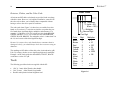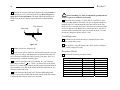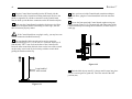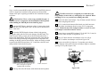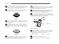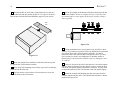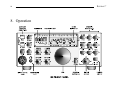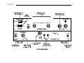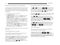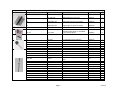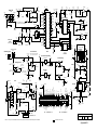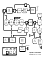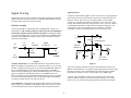
1
ELECRAFT K2 TRANSCEIVER BAND + + F RCL BAND ELECRAFT K 2 DISPLAY S1 5 MENU EDIT + RF/ALC - ANT 1/2 RF 3 5 7 10 ALC NB ANT2 PRE ATT TUNE NB KEYER A B RIT 1 A=B 2 3 VOX REV SPLIT PRE/ATT AGC XFIL + XIT POWER A/B MODE 9 +20 40 + STORE T R A N S CE I VE R 4 5 6 SPOT CW RV AFIL RIT XIT MSG + + LEVEL PF1 8 7 PF2 9 REC 0 AF GAIN + RF GAIN RATE -1 0 LOCK O W N E R’S M A N U A L +1 ON OFF ELECRAFT K2 160-10 Meter SSB/CW Transceiver Owner’s Manual Revision I, March 29, 2012 Copyright 2012 Elecraft, LLC All Rights Reserved Elecraft www.elecraft.com P.O. Box 69 Aptos, CA 95001-0069 (831) 763-4211 Fax: (831) 763-4218 ® ELECRAFT® 2 Table of Contents 1. INTRODUCTION.................................................................................................................................................................................. 3 2. SPECIFICATIONS ............................................................................................................................................................................... 5 3. PREPARATION FOR ASSEMBLY ..................................................................................................................................................... 7 4. CONTROL BOARD ........................................................................................................................................................................... 13 5. FRONT PANEL BOARD ................................................................................................................................................................... 23 6. RF BOARD ........................................................................................................................................................................................ 34 7. FINAL ASSEMBLY............................................................................................................................................................................ 81 8. OPERATION ...................................................................................................................................................................................... 84 9. CIRCUIT DETAILS .......................................................................................................................................................................... 110 10. OPTIONS ......................................................................................................................................................................................... 117 PARTS LIST ............................................................................................................................................................................ APPENDIX A SCHEMATIC ............................................................................................................................................................................ APPENDIX B BLOCK DIAGRAM .................................................................................................................................................................. APPENDIX C PHOTOGRAPHS ..................................................................................................................................................................... APPENDIX D TROUBLESHOOTING .............................................................................................................................................................APPENDIX E PARTS PLACEMENT DRAWINGS ......................................................................................................................................... APPENDIX F 100-WATT STAGE AND RS232 I/O (K2/100) .......................................................... APPENDIX G (SUPPLIED WITH KPA100 OPTION) Elecraft www.elecraft.com P.O. Box 69 Aptos, CA 95001-0069 (831) 763-4211 Fax: (831) 763-4218 ELECRAFT® 3 1. Introduction The Elecraft K2 is a high-performance, synthesized, CW/SSB transceiver that covers all HF bands. It is a true dual-purpose transceiver, combining the operating features you’d expect in a home-station rig with the small size and weight of a rugged, go-anywhere portable. The K2 is an intermediate-level kit, yet you’ll be pleasantly surprised at how uncomplicated it is to build. All of the RF (radio-frequency) circuitry is contained on a single board, while two plug-in modules provide front panel and control functions. Wiring is minimal, unlike traditional kits which depend on complex wiring harnesses. The basic K2 operates on 80-10 meter CW, and provides over 10 watts of RF output. If you prefer a full-power station, you can complete your K2 as a K2/100 at any time by adding the internal 100-watt final stage (KPA100 option). Assembly of the KPA100 is covered in Appendix G, a separate manual supplied with the KPA100 kit. A unique feature of the K2 is that it provides its own built-in test equipment, including a digital voltmeter, ammeter, wattmeter, complete RF probe, and frequency counter. These circuits are completed early in assembly, so they're ready to be used when you begin construction and alignment of the RF board. We also provide complete troubleshooting and signal-tracing information. You can customize your K2 by choosing from a wide range of additional options: In addition to this owner’s manual, you’ll find extensive support for the K2 on our website, www.elecraft.com. Among the available materials are manual updates, application notes, photographs, and information on new products. There’s also an e-mail forum; sign-up is available from the web page. It’s a great way to seek advice from the K2’s designers and your fellow builders, or to tell us about your first QSO using the K2. SSB adapter with optimized 7-pole crystal filter Automatic antenna tuner (20 W internal or 150 W external) 160-m adapter with receive antenna switch 60-m adapter with low-level transverter interface Computer control interface (RS232) Noise blanker Digital or analog audio filter, each with real-time clock Internal 2.9-Ah rechargeable battery Programmable band decoder High-Performance VHF and UHF transverters For a complete description of available options, see page 117. In addition to the options, a companion enclosure the same size and style as the K2 is available for those who wish to build their own matching station accessories (model EC2). We’d like to thank you for choosing the K2 transceiver, and hope it meets your expectations for operation both at home and in the field. Wayne Burdick, N6KR Eric Swartz, WA6HHQ Pre-Wound Toroids Available You can obtain a set of pre-wound toroids for the K2 if you prefer not to wind them yourself. Refer to our web site for details. 4 ELECRAFT® Customer Service Information Technical Assistance You can send e-mail to [email protected] and we will respond quickly - typically the same day Monday through Friday. Telephone assistance is available from 9 A.M. to 5 P.M. Pacific time (weekdays only) at 831-763-4211. Please use e-mail rather than calling when possible since this gives us a written record of the details of your problem and allows us to handle a larger number of requests each day. Repair / Alignment Service (We want to make sure everyone succeeds!) If necessary, you may return your Elecraft product to us for repair or alignment. (Note: We offer unlimited email and phone support to get your kit running, so please try that route first as we can usually help you find the problem quickly.) IMPORTANT: You must contact Elecraft before mailing your product to obtain authorization for the return, what address to ship it to and current information on repair fees and turnaround times. (Frequently we can determine the cause of your problem and save you the trouble of shipping it back to us.) Our repair location is different from our factory location in Aptos. We will give you the address to ship your kit to at the time of repair authorization. Packages shipped to Aptos without authorization will incur an additional shipping charge for reshipment from Aptos to our repair depot. To ship the unit, first seal it in a plastic bag to protect the finish. Use a sturdy packing carton with at least 3-in (8 cm) of foam or shredded paper on all sides. Seal the package with reinforced tape. (Neither Elecraft or the carrier will accept liability for damage due to improper packaging.) Elecraft 1-Year Limited Warranty This warranty is effective as of the date of first consumer purchase (or if shipped from the factory, the date the product is shipped to the customer). It covers both our kits and fully assembled products. For kits, before requesting warranty service, you should fully complete the assembly, carefully following all instructions in the manual. Who is covered: This warranty covers the original owner of the Elecraft product as disclosed to Elecraft at the time of order. Elecraft products transferred by the purchaser to a third party, either by sale, gift, or other method, who is not disclosed to Elecraft at the time of original order, are not covered by this warranty. If the Elecraft product is being bought indirectly for a third party, the third party’s name and address must be provided at time of order to ensure warranty coverage. What is covered: During the first year after date of purchase, Elecraft will replace defective or missing parts free of charge (post-paid). We will also correct any malfunction to kits or assembled units caused by defective parts and materials. Purchaser pays inbound shipping to us for warranty repair; we pay shipping to return the repaired equipment to you by UPS ground service or equivalent to the continental USA and Canada. For Alaska, Hawaii, and other destinations outside the U.S. and Canada, actual return shipping cost is paid by the owner. What is not covered: This warranty does not cover correction of kit assembly errors. It also does not cover misalignment; repair of damage caused by misuse, negligence, battery leakage or corrosion, or builder modifications; or any performance malfunctions involving non-Elecraft accessory equipment. The use of acid-core solder, water-soluble flux solder, or any corrosive or conductive flux or solvent will void this warranty in its entirety. Also not covered is reimbursement for loss of use, inconvenience, customer assembly or alignment time, or cost of unauthorized service. Limitation of incidental or consequential damages: This warranty does not extend to non-Elecraft equipment or components used in conjunction with our products. Any such repair or replacement is the responsibility of the customer. Elecraft will not be liable for any special, indirect, incidental or consequential damages, including but not limited to any loss of business or profits. ELECRAFT® 5 2. Specifications Frequency ranges,2 MHz All measurements were made using a 14.0 V supply and 50-ohm load unless otherwise indicated. Values are typical; your results will be somewhat different. Specifications are subject to change without notice. (See option manuals for additional specifications.) Basic kit 160 m (opt.) 60 m (opt.) General VFO Size 3.0" H x 7.9" W x 8.3" D (7.5 x 20 x 21 cm) 3.4" H x 7.9" W x 9.9" D (8.5 x 20 x 25 cm) Stability < 100 Hz total drift typ. from cold start at 25° C Accuracy3 +/- 30 Hz over a 500 kHz range (typ) when calibrated Weight 3.3 lbs. (1.5 kg), excluding options Resolution 10 Hz Supply voltage 9 to 15 VDC; reverse-polarity protection; internal self-resetting fuse Tuning steps 10 Hz, 50 Hz, and 1000 Hz nominal (other step sizes available via menu) Memories 20 (10 assigned to 160-10 m Bands; 10 general-purpose) Cabinet Overall Current drain, RIT/XIT range Receive 120-150 mA in minimum-current configuration; 180-250 mA typical Transmit1 Frequency control 1 3.5-4.0, 7.0-7.3, 10.0-10.2, 14.0-14.5, 18.0-18.2, 21.0-21.6, 24.8-25.0, 28.0-28.8 1.8-2.0 5.0-5.5 +/- 0.6 to +/- 4.8 kHz (selectable); 10-40 Hz steps depending on range. Fine RIT mode steps 2-3 Hz typ. 2.0 A typical at 10 watts; programmable current limiting PLL synthesizer w/single VCO covering 6.7-24 MHz in 10 bands; fine steps via DAC-tuned reference Current varies with band, supply voltage, configuration, and load impedance. We recommend a minimum 3.5-amp power supply. 2 The K2 can receive well outside the indicated bands, but this extended range is not specified or guaranteed. Transmit ranges may be limited for export to some countries. The K2/100 (KPA100 option) limits transmit from 25-27.999 MHz to 10 watts or less. 3 See Frequency Calibration Techniques (page 105). ELECRAFT® 6 Transmitter Receiver Preamp On -135 dBm 0 to +7.55 +70 Preamp Off -130 dBm +10 +70 Blocking 125 dB 133 dB Two-tone 96 97 Power output range <0.5 W to >10 W (typ.); power setting resolution 0.1 W, accuracy 10% @ 5 W Sensitivity (MDS) 3rd-order intercept 2nd-order intercept Min. supply voltage recommended4 9.0 V min for 2 watts out 9.5 V min for 5 watts out 10.0 V min for 7 watts out 10.5 V min for 10 watts out Dynamic range, Duty cycle 5 W, 100%; 10 W, 50% Spurious products -40 dB or better @ 10 W (-50 typ) Harmonic content -45 dB or better @ 10 W (-55 typ) Load tolerance 2:1 or better SWR recommended; I.F. 4.915 MHz (single conversion) Selectivity, will survive operation CW 7-pole variable-bandwidth crystal filter, approx. 200-2000 Hz SSB6 7-pole fixed-bandwidth crystal filter, 2.2 kHz typ. into high SWR T-R delay approx. 10 ms-2.5 sec, adjustable Audio output 1 watt max. into 4-ohm load External keying 70 WPM max. Speaker internal: 4 ohm, 3 W; CW sidetone 400-800 Hz in 10 Hz steps Rear-panel jack for external speaker Headphones Keyer Keying modes Iambic A and B; adjustable weight Speed range 9 - 50 WPM Message memory 9 buffers of 250 bytes each; 1-level chaining; auto-repeat (0 - 255 s) 5 4 For reference only; not guaranteed. If higher power than shown here is to be used for a given supply voltage, monitor transmitter output signal. 4 - 32 ohms, stereo or mono Varies with band. With optional SSB adapter. Other CW and SSB fixed crystal filter options may be available 6 ELECRAFT® 7 3. Preparation for Assembly Overview of the Kit The K2 uses modular construction, both physically and electrically. This concept extends to the chassis (Figure 3-1). Any chassis element can be removed during assembly or troubleshooting. (Also see photos in Appendix D.) If the KPA100 is installed, it takes the place of the original top cover. As shown in Figure 3-2, there are three printed circuit boards (PCBs) in the basic K2 kit: the Front Panel board, Control Board, and RF board. Option modules plug into the RF or Control board, but are not shown here. Side Panel RF Control Top Cover Heat Sink Front Panel Front Panel Bottom Cover (Right side panel not shown) Figure 3-2 Figure 3-1 ELECRAFT® 8 Board-to-board Connectors The circuit boards in the K2 are interconnected using board-to-board connectors, which eliminates nearly all hand wiring. Gold-plated contacts are used on these connectors for reliability and corrosion resistance. board. Similarly, right-angle connector P1 on the Control Board mates with J6 on the RF board. (Not shown in this drawing are two additional right-angle connectors on the Control board, P2 and P3, which mate with J7 and J8 on the RF board.) Figure 3-3 shows a side view of the PC boards and board-to-board connectors. As can be seen in the drawing, the Front Panel board has a connector J1 which mates with right-angle connector P1 on the RF These multi-pin connectors are very difficult to remove once soldered in place. Refer to Figure 3-3 during assembly to make sure you have each connector placed correctly before soldering. Front Panel Control Board P1 RF Board J6 J1 P1 Figure 3-3 ELECRAFT® 9 There are six steps in the K2 assembly process: Inventory 1. 2. 3. 4. 5. 6. We strongly recommend that you do an inventory of parts before beginning to assemble the kit. It is not necessary to inventory the resistors, which are supplied attached to tape in assembly order. Control Board assembly Front Panel Board assembly RF Board assembly and test, part I (control circuits) RF Board assembly and test, part II (receiver and synthesizer) RF Board assembly and test, part III (transmitter) Final assembly This assembly sequence is important because later steps build on the previous ones. For example, in step 3 you’ll put the modules together for the first time, allowing you to try out the K2’s built-in frequency counter. The counter will then be used in step 4 to align and test the receiver and synthesizer on 40 meters. In step 5 all the pieces will come together when you complete the transmitter and filters, then align the K2 on all bands. The last few details—speaker, tilt stand, etc.—will be wrapped up in step 6. Unpacking and Inventory When you open the kit you should find the following items: six chassis pieces (Figure 3-1) three printed circuit boards (Figure 3-2) FRONT PANEL board components bag CONTROL board components bag RF board components in two bags MISCELLANEOUS components bag (includes hardware) WIRE bag 4-ohm Speaker, 5 small knobs, and large tuning knob plastic tube containing the latching relays an envelope containing the LCD bezel, green LED bargraph filter, serial number label, thermal insulators, and other items Even if you don’t do an inventory, it is helpful to familiarize yourself with the parts list, Appendix A. Additional information on identifying capacitor, chokes, and resistors is provided below. Identifying Capacitors Small-value fixed capacitors are usually marked with one, two, or three digits and no decimal point. If one or two digits are used, that is always the value in picofarads (pF). If there are three digits, the third digit is a multiplier. For example, a capacitor marked "151" would be 150 pF (15 with a multiplier of 101). Similarly, "330" would be 33 pF, and "102" would be 1000 pF (or .001 µF). In rare cases a capacitor manufacturer may use "0" as a decimal placeholder. For example, "820" might mean 820 pF rather than the usual 82 pF. Such exceptions are usually covered in the parts lists. To be safe, measure the values of all capacitors below 1000 pF (most DMMs include capacitance measurement capability). Fixed capacitors with values of 1000 pF or higher generally use a decimal point in the value, such as .001 or .02. This is the value in microfarads (µF). Capacitors also may have a suffix after the value, such as ".001J." In some cases the suffixes or other supplemental markings may be useful in identifying capacitors. Hard-to-identify capacitor values: 3.3 pF: These capacitors may have pillow-shaped, dark-green bodies about 1/8" (3 mm) square, with a black mark on the top. The "3.3" label may be difficult to read without a magnifying glass. 150 pF: These are correctly marked "151" on one side, but the other side may be marked #21 ASD, where "#21" looks like "821." ELECRAFT® 10 Color Code Resistors, Chokes, and the Color Code All resistor and RF choke color bands are provided in the text along with their values. However, it is helpful to familiarize yourself with the color code to allow you to identify these components without having to refer to the text or parts list each time. The color-code chart, Figure 3-4, shows how to read the four color bands on 5% resistors. 1% resistors are similar, except that they use five bands (three significant digits, multiplier, and tolerance). For example, a 1,500 ohm (1.5 k) 5% resistor has color bands BROWN, GREEN, and RED. A 1.5 k, 1% resistor has color bands BROWN, GREEN, BLACK, BROWN. The multiplier value is 1 rather than 2 in the 1% case because of the third significant digit. Because 1% resistors have color bands that are sometimes hard to distinguish clearly, you should always check their resistance using an ohmmeter. The markings on RF chokes reflect their value in microhenries (µH). Like 5% resistors, chokes use two significant digits and a multiplier. Example: an RF choke with color bands RED, VIOLET, BLACK would have a value of 27 µH. Tools The following specialized tools are supplied with the K2: .050" (1.3 mm) Allen Wrench, short handle 5/64" (2 mm) Allen Wrench, long handle Double-ended plastic inductor alignment tool Tolerance (gold = 5%, silver = 10%) Multiplier Second Digit First Digit Color Black Brown Red Orange Yellow Green Blue Violet Gray White Silver Gold Digit Multiplier 0 1 2 3 4 5 6 7 8 9 --Figure 3-4 x1 x 10 x 100 x 1K x 10K x 100K x 1M x .01 x 0.1 ELECRAFT® In addition to the tools supplied, you will need these standard tools: Fine-tip soldering iron, 20-40 watt (temperature-controlled preferred, with 700 or 800°F tip [370-430°C] IC-grade, small-diameter (.031") solder (DO NOT use acid-core solder, water-soluble flux solder, additional flux, or solvents of any kind, which will void your warranty) Desoldering tools (wick, solder-sucker, etc.) Needle-nose pliers Small-point diagonal cutters, preferably flush-cutting Small Phillips screwdriver Jeweler’s flat-blade screwdriver While not required, the following items are recommended: DMM (digital multimeter) for doing resistance and voltage checks. A DMM with capacitance measurement capability is strongly recommended (see Identifying Capacitors). Magnifying glass Conductive wrist strap Assembly Notes i This symbol is used to alert you to important information about assembly, alignment, or operation of the K2. 11 In some steps you will actually be installing multiple components of a particular type. In this case the instructions will be followed by a table listing all of the components to be installed, so you won’t need to refer to the parts list during assembly. The order that the components are installed corresponds to their PCB locations. Do not skip any assembly steps; you may find that you’ve installed one component that hinders the installation of another. Forming component leads: In a few cases you’ll find that the space provided for a component on the PC board is larger than the distance between the leads on the part itself. In such cases, you’ll need to carefully bend the leads out and then down to fit the given space. Always use needle-nose pliers to accomplish this task, and bend the leads–don’t tug on them. This is especially important with capacitor leads, which are fragile. Bottom-Mounted Components A number of components in the K2 are mounted on the bottom of the PC boards to improve component spacing or for electrical reasons. Component outline symbols are provided on both sides of each board, so it will always be clear which side a particular component goes on. You’ll be able to tell the top of the board from the bottom easily: the top side has far more parts. Bottom-mounted parts are identified on the schematic by this symbol: Photographs You should review the photographs in Appendix D to get an idea of what the completed PC board assemblies look like. Step-by-Step Assembly Each step in the assembly process is accompanied by a check-box: Top/bottom interference: In a few cases, top-mounted parts may interfere with the trimming and soldering of a bottom-mounted part. In this case, pre-trim the leads of the bottom-mounted part before final placement, and solder it on the bottom rather than on the top. (Since all holes are plated-through, you can solder on either side.) ELECRAFT® 12 Integrated Circuits and ESD The K2 transceiver uses integrated circuits and transistors that can be damaged by electrostatic discharge (ESD). Problems caused by ESD can often be difficult to troubleshoot because components may only be degraded, at first, rather than fail completely. To avoid such problems, simply touch an unpainted, grounded metal surface before handling any components, and occasionally as you build. We also recommend that you take the following anti-static precautions (in order of importance): Leave ESD-sensitive parts in their anti-static packaging until you install them Ground yourself using a wrist strap with a series 1 megohm resistor (do NOT ground yourself directly, as this poses a shock hazard) Make sure your soldering iron has a grounded tip Use an anti-static mat on your work bench IC Sockets Sockets are used for only the largest ICs. You should not use sockets for the other ICs because they tend to be unreliable and can cause problems due to added lead length. Since sockets are not used in most cases, you must double-check the part number and orientation of each IC before soldering. When you solder components on these boards, the solder fills the plated holes, making excellent contact. This means that you do not need to leave a large "fillet" or build-up of solder on top of the pads themselves. A small amount of solder will do for all connections. Unfortunately, removing components from double-sided PC boards can be difficult, since you must get all of the solder back out of the hole before a lead can be removed. To do this, you'll need solder wick and a vacuum desoldering tool (see techniques below). The best strategy for avoiding de-soldering is to place all components properly the first time. Double-check values and orientations, and avoid damaging parts via ESD. When removing components: Soldering, Desoldering, and Plated-Through Holes CAUTION: Solder contains lead, and its residue can be toxic. Always wash your hands after handling solder. The printed circuit boards used in the K2 have circuitry on both sides ("double-sided"). Boards of this type require plated-through holes to complete electrical connections between the two sides. Don't pull a lead or pin out of a hole unless the solder has been removed, or you are applying heat. Otherwise, you can literally pull out the plating on the plated-through hole. Limit soldering iron contact to a few seconds at a time. Use small-size solder-wick, about 0.1" or 2.5 mm wide. Use the wick on both the top and bottom pads when possible. This helps get all of the solder out of the hole. Buy and learn how to use a large hand-operated vacuum desoldering tool, such as the "Soldapullt," model DS017LS. Small solder suckers are not effective. With ICs and connectors, clip all of the pins at the body first, then remove all of the pins slowly, one at a time. You may damage pads and traces by trying to remove a component intact, possibly leaving a PC board very difficult to repair. Invest in a PC board vice with a heavy base if possible. This makes parts removal easier because it frees up both hands. If in doubt about a particular repair, ask for advice from Elecraft or from a someone else with PCB repair experience. Our e-mail reflector is also an excellent source for help. ELECRAFT® 13 4. Control Board The Control board is the "brain" of the K2. It monitors all signals during receive and transmit, and handles display and control functions via the Front Panel board. The microcontroller, analog and digital control circuits, automatic gain control (AGC), and audio amplifier are located on this board. Components i Review the precautions described in the previous section before handling any IC’s or transistors. These components can be damaged by static discharge, and the resulting problems are often difficult to troubleshoot. Open the bag of components labeled CONTROL and sort the parts into groups (resistors, diodes, capacitors, etc.). If any of the components are unfamiliar, identify them using the illustrations in the parts list, Appendix A. Locate the Control board. It is the smallest of the three K2 PC boards, labeled "K2 CONTROL" on the front side, in the lower righthand corner. The lower left-hand corner is notched. Open the bag labeled MISCELLANEOUS and empty the contents into a shallow box or pan. This will prevent loss of any of the small hardware while allowing you to locate items as needed. i The Allen wrenches are located in a small bag with the MISCELLANEOUS items. These wrenches may have been oiled during manufacturing. Remove the wrenches and wipe off the oil, if any, then discard the bag. i There are five sizes of 4-40 machine screws provided with the kit. The relative sizes of the screws are shown below for identification purposes (not to scale). All of the screws are black anodized except for the 7/16" (11 mm) screws. The 3/16" (4.8 mm) pan-head screws are the most numerous, and will be referred to as chassis screws throughout the manual. There is only one flat-head, 3/16" screw. Flat-head, 3/16” (4.8 mm) Pan-head, 3/16” (4.8 mm) (chassis screws) Pan-head, 3/8” (9.5 mm) Pan-head, 7/16” (11 mm) Pan-head, 1/2” (12.7 mm) Identify all of the 4-40 screws and sort them into groups. ELECRAFT® 14 Assembly The side of the Control board with most of the components is the top side. With the top side of the Control board facing you and the notch at the lower left, locate the position of resistor R5, near the left edge. The label "R5" appears just below the resistor’s outline. Install a 33-k resistor (orange-orange-orange) at R5, with the orange bands at the top and the gold band (indicating 5% tolerance) at the bottom. Make sure it is seated flush with the board, then bend the leads on the bottom to hold it in place. Do not solder this resistor until the remaining fixed resistors have been installed in the next step. Install the remaining fixed resistors, which are listed below in left-to-right PC board order. The resistors should all be oriented with their first significant-digit band toward the left or top. This will make the color codes easier to read if you need to re-check the values after installation. Check 1% resistors with an ohmmeter. Note: When multiple items appear on one line in a component list such as the one below, complete all items on one line before moving on to the next, as indicated by the small arrow. (In other words, install R5 first, then R2, then go to the second line.) __ R5, 33 k (ORG-ORG-ORG) __ R2, 3.3 M (ORG-ORG-GRN) __ R3, 10 k (BRN-BLK-ORG) __ R4, 5.6 k (GRN-BLU-RED) __ R6, 100 (BRN-BLK-BRN) __ R7, 1.78 k, 1% (BRN-VIO-GRY-BRN) __ R8, 100, 1% (BRN-BLK-BLK-BLK) __ R9, 806 k, 1% (GRY-BLK-BLU-ORG) __ R10, 196 k, 1% (BRN-WHT-BLU-ORG) __ R16, 10 (BRN-BLK-BLK) __ R17, 3.3 M (ORG-ORG-GRN) __ R21, 270 k (RED-VIO-YEL) __ R20, 2.7 ohms (RED-VIO-GLD) Solder all of the resistors, then trim the leads as close as possible to the solder joints. Some builders prefer to trim the leads before soldering. Either method can be used. Note: Save clipped leads from 1/4-watt resistors that are at least 1/2” (13 mm) long. You’ll need several of them for ground test points and other uses later on. Locate RP6, a 5.1 k, 10-pin resistor network. ("RP" means "resistor pack," another name for resistor networks.) RP6 is usually labeled "770103512." Check the parts list for alternative resistor network labels if necessary. Pin 1 of RP6 is indicated by a dot. Locate the component outline for RP6 at the left end of the PC board. Install the resistor network so that the end with the dot is lined up with the "1" label. Make sure the resistor network is seated firmly on the board, then bend the leads at the far ends in opposite directions to hold it in place. (Do not trim the leads.) Do not solder RP6 yet. i Components with many leads are difficult to remove once soldered. Double-check the part numbers and orientation. Install the remaining resistor networks in the order listed below. Do not solder them until the next step. __ RP1, 3.9 k, 10 pins (770103392) __ RP7, 33 k, 8 pins (8A3.333G) __ RP2, 82 k, 8 pins (77083823) __ RP3, 47 k, 10 pins (10A3.473G) __ RP5, 470, 10 pins (10A3.471G) __ RP4, 82 k, 8 pins (77083823) Solder the resistor networks. (No need to trim the leads.) Install potentiometer R1 (50 k), located at the left side of the board. R1 will sit above the board due to the shoulders on its pins. Hold it in place (flat, not tilted) while soldering. ELECRAFT® 15 Install the 82 mH shielded inductor (L1) as shown by its component outline. Make sure the L1 is pressed down onto the PC board as far as it can go, then bend the leads slightly to hold it in place while soldering. Install the 1N4148 diodes listed below. D1 is in the upper lefthand corner of the PC board. If a diode has only one band, the end with the band (the cathode) should be oriented toward the banded end of the corresponding PC board outline. If a diode has multiple bands, the widest band indicates the cathode end. __ D1, 1N4148 __ D2, 1N4148 Double-check the orientation of the diodes, then solder. Find the component outline for diode D3, near the top edge of the board (right end). Install and solder resistor R22 at this location (82 k, gray-red-orange). Install the small fixed capacitors listed below, beginning with C2 in the upper left-hand corner of the board. (This list includes all of the fixed capacitors on the Control board except the tall, cylindrical electrolytic types, which will be installed later.) The list shows both the value and the capacitor labels, using notation explained in the previous section. After installing each capacitor, bend the leads outward to hold it in place, but do not solder. Note: Remember to complete all items in each line before moving on to the next. (Install C2, C3, and C4, then C7, etc.) __ C2, .001 (102) __ C7, 330 (331) __ C9, .01 (103) __ C5, .01 (103) __ C42, 0.1 (104) __ C19, .047 (473) __ C3, .01 (103) __ C6, .047 (473) __ C10, .01 (103) __ C14, .047 (473) __ C16, .047 (473) __ C21, 33 (33) __ C4, 0.47 (474) __ C8, 39 (39) __ C12, .0027 (272) __ C17, .01 (103) __ C11, .01 (103) __ C23, .01 (103) __ C43, .001 (102) __ C26, 0.1 (104) __ C34, .001 (102) __ C35, .01 (103) __ C41, .01 (103) __ C20, .001 (102) __ C27, .022 (223) __ C24, .0027 (272) __ C30, .047 (473) __ C36, .0027 (272) __ C37, .01 (103) __ C18, .01 (103) __ C25, 0.1 (104) __ C31, .01 (103) __ C40, .01 (103) __ C39, .01 (103) __ C38, 680 (681) Solder all of the small fixed capacitors. ELECRAFT® 16 Install and solder the electrolytic capacitors listed below, which are polarized. Be sure that the (+) lead is installed in the hole marked with a "+" symbol. The (+) lead is usually longer than the (–) lead, and the (–) lead is identified by a black stripe (Figure 4-1). - + Install the remaining TO-92 package transistors in the order listed below. Figure 4-1 __ C1, 2.2 µF __ C28, 220 µF __ C32, 22 µF __ C13, 22 µF __ C29, 220 µF __ C15, 100 µF __ C33, 2.2 µF Install and solder ceramic trimmer capacitor C22. Orient the flat side of this trimmer as shown on its PC board outline. Using a small flat-blade screwdriver, set C22 so that its screwdriver slot is parallel to the outline of nearby crystal X2. Locate Q12 (type PN2222A), which is a small, black TO-92 package transistor. Q12 and other TO-92 transistors may have either of the two shapes shown in Figure 4-2. The large flat side of the device must be aligned with the flat side of the component outline. The part number may be found on either side. Figure 4-2 Install Q12 near the upper left-hand corner of the PC board. Align the large flat side of Q12 with its PC board outline as in Figure 4-2. The body of the transistor should be about 1/8" (3 mm) above the board; don’t force it down too far or you may break the leads. Bend the leads of the transistor outward slightly on the bottom to hold it in place. Solder Q12. __ Q11, PN2222A __ Q3, 2N7000 __ Q6, J310 __ Q9, MPS5179 __ Q1, 2N3906 __ Q4, 2N7000 __ Q7, J310 __ Q10, MPS5179 __ Q2, 2N3906 __ Q5, 2N7000 __ Q8, PN2222A Solder and trim the leads of these transistors. ELECRAFT® 17 Install crystals X1 and X2 so that they are flat against the board. X1 is 5.068 MHz and is located near the notch in the lower left-hand corner. X2 is 4.000 MHz, and is located near the center of the board. Solder the crystals. Prepare two 3/4" (19 mm) jumpers wires from discarded component leads. These short jumpers will be used to ground the crystal cans in the next step. i Grounding the crystal cans in the following step is required to ensure proper crystal oscillator performance. i The voltage regulators, U4 and U5, will be installed in the following steps. These regulators have different voltages and must not be interchanged. Check the labels before soldering. Install U4 (LM2930T-8) and U5 (78M05, 7805T, L7805, etc.), forming the leads as indicated (Figure 4-4). Fold the pins over the shaft of a small screwdriver to create smooth bends. After inserting the leads into the proper holes, secure each IC with a 4-40 x 3/8" (9.5 mm) machine screw, #4 lock washer, and 4-40 nut. (These regulators may have either plastic or metal mounting tabs.) Use smooth bend, not sharp Referring to Figure 4-3, insert the jumper wires into the grounding holes provided near X1 and X2. Fold each wire over the top of the crystal and solder it to the top of the can. (Only a small amount of solder is required.) Then solder and trim the wire on the bottom of the board. X1 X2 Figure 4-4 Solder the voltage regulator ICs. Trim the IC leads as close to the PC board as possible. Figure 4-3 Install a 40-pin IC socket at U6. (The microcontroller will be inserted into the socket in a later step.) Orient the notched end of the socket to the left as shown on the PC board outline. Bend two of the socket’s diagonal corner leads slightly to hold the socket in place, then solder only these two pins. If the socket does not appear to be seated flat on the PC board, reheat the solder joints one at a time while pressing on the socket. Solder the remaining pins of the 40-pin socket. ELECRAFT® 18 Install a shorting jumper onto the two right-hand pins of P7. i The connectors used in the following steps have plastic bodies that can may melt if too much heat is applied during soldering, causing the pins to be mis-positioned. Limit soldering time for each pin to 3 seconds maximum (1 to 2 seconds should be adequate). Install the 2-pin male connectors, P5 and P6. As shown in Figure 4-5, the polarizing tab on each connector should be closest to the top edge of the board. P5, the voltmeter input connector, can be found near the upper left-hand corner of the board. P6 is used for frequency counter input, which is in the upper right-hand corner. Locking Tab Top side of PC Board Figure 4-5 Install the 10-pin, dual-row connector, P4 (to the left of P5). The short ends of the 10 pins are inserted into the board. P4 must be seated flat on the board before soldering. Install P7, a 3-pin male connector (to the right of P5). The short ends of the 3 pins are inserted into the board. At the upper left and right corners of the board are short jumpers, labeled with ground symbols ( ). Use discarded component leads to make 3/4" (19 mm) long U-shaped wires for each jumper (Figure 4-6). Solder the jumpers on the bottom of the board, with the top of the Ushape approx. 1/4" (6 mm) above the board. Figure 4-6 Locate the outlines for resistors R18 and R19 on the bottom side of the Control board. i The pads used for R18 and R19 are shared with connectors J1 and J2, which are labeled on the top side of the board. These connectors are provided with the KAF2 and KDSP2 audio filter options. You should not install J1 and J2, or an audio filter option, until after K2 assembly and checkout have been completed. Install short wire jumpers at R18 and R19. Make the jumpers from discarded component leads as you did above, but keep them flat against the board. Solder the jumpers on the top side. Install the following resistors on the bottom side of the board (solder on the top side): __ R12, 820 (GRY-RED-BRN) __ R11, 47 k (YEL-VIO-ORG) ELECRAFT® 19 Top side of PC Board i The connectors along the bottom edge of the board (P1, P2 and P3) will be installed next. It is very difficult to remove them once they are soldered. Follow all instructions carefully. P3 Hold the Control board vertically as shown in the side view below (Figure 4-7). The top side of the board--the side with most of the components--should be to the right. Turn to page 8 and review Figure 3-3, which shows how the Control board plugs into the RF board. P1, P2, and P3 will all be installed on the top side of the Control board as shown. Position 6-pin right-angle connector P1 as shown in the side view below (Figure 4-7). Do not solder P1 until the next step. The plastic part of the connector must be seated flat against the PC board, and the pins must be parallel to the board. Do not bend or trim the pins on the bottom of the board. Figure 4-8 Install P3, the 20-pin, dual-row right-angle connector (Figure 4-8). Use the same method you used for P1. Do not solder P3 until you are sure that it is seated properly. Install P2, the 36-pin, dual-row, right-angle connector. Use the same method you used for P1 and P3. i Top side of PC Board P1 When you install ICs in the following steps, always straighten the leads of each IC first as shown in Figure 4-9. The two rows of pins must be straight and parallel to each other to establish the proper pin spacing for insertion into the PC board or socket. To straighten the pins, rest one entire row of pins against a hard, flat surface. Press down gently on the other row of pins and rock the IC forward to bend the pins into position as shown below. Figure 4-7 Solder just the two end pins of P1, then examine the placement of the connector. If P1 is not flat against the board, re-heat the solder on the end pins one at a time while pressing firmly on the connector. Once it is in the right position, solder all pins. Do not trim the leads. Flared Straight Figure 4-9 ELECRAFT® 20 i Before handling any IC, touch an unpainted, grounded metal surface or put on a conductive wrist-strap. Locate U2, an 8-pin IC, part number LM833. (LM833 is the basic part number. There may be an additional prefix or suffix or other markings.) This and all remaining ICs on the Control board are DualInline Packages, or DIPs. Referring to Figure 4-10, identify the notched or dimpled end of the IC. IC pins are counted starting from pin 1 (as shown below) and going counter-clockwise. Notch Pin 1 Bend two of U2’s corner pins out slightly on the bottom of the board to hold the IC firmly in place, flat against the top of the board. Find pin 1 and verify that its pad is either round or oval. Once U2 is properly seated, solder all eight pins, using a minimum of solder. Install the ICs listed below. Bend the pins to hold each IC in place as you did with U2, but do not solder until the next step. The notched or dimpled end of each IC must be aligned with the notched end of its PC board outline. Note: For U1, the IC type supplied may be either NE602 or SA602. __ U1, NE602 __ U8, MAX534 Figure 4-10 __ U7, 25LC320 __ U10, LMC660 Check the orientation of pin 1 on each IC by looking at the associated PC board pads, as before. Then solder all of the ICs. Dimple Pin 1 __ U3, LM6482 __ U9, LM380 Locate the microcontroller, U6. Straighten the pins of U6 (see Figure 4-9). With a large IC such as this, you can hold the IC body at both ends as you re-form each row of pins. Straighten the leads of U2 (see Figure 4-9). Install U2 in the orientation shown by its PC board outline, near the upper left-hand corner of the PC board, but do not solder it yet. Make sure the notched or dimpled end is lined up with the notched end of the PC board outline. Even though the outline is covered when the IC is installed, you can still verify that the IC is installed correctly by looking at pin 1. The PC board pad corresponding to pin 1 will be either oval or round. i You may overheat the IC pins or PC pads if you take an excessive length of time to solder. After a few tries, you should be able to solder an IC pin in about 1 or 2 seconds. i When the microcontroller is pressed in its socket, you must be careful to avoid jamming its pins. Make sure that all pins are lined up with the associated holes in the socket before pressing down on the IC. Watch the pins on both rows as you press down, re-aligning them with the socket holes individually if necessary. Insert the microcontroller, U6, into its socket. Make sure that pin 1 on the IC itself is lined up with the pin 1 label near the lower left-hand corner of the PCB outline. Note: The revision label on the IC (usually white) may not be oriented the same direction as the text printed on the IC. Do not use the label as a guide--use the notch or dimple to identify pin 1. ELECRAFT® 21 Key Shaping Components (Required) Your K2 kit includes recent changes that provide an optimized keying envelope shape (sigmoidal, or S-shaped leading and trailing edges). The result is completely click-free CW transmission. Two of the parts for this change must be installed on the back of the Control board as described below. Locate the green insulated hookup wire. Strip two 1/4" (6.4 mm) lengths of insulation from one end of the wire. These will be used to insulate the leads of C46 in the following steps. Slip the two lengths of insulation over the leads of a .01 µf capacitor ("103"). This is a new component (C46), not present on the board. i Figure 4-11, below, shows the bottom side of the Control board. Components shown with dotted outlines are located on the top side. On the bottom side of the Control board, solder C46 between R21 and the base lead of Q8 as shown below. Keep lead length short. Figure 4-11 A 22 µF electrolytic capacitor has also been added (C45). Solder C45 as indicated above, between U8 pin 2 (+ lead) and U8 pin 14 (- lead). Carefully compare your installation of C46 and C45 to Figure 4-11. Make sure the leads of these capacitors are soldered to the indicated pads. Verify the orientation of the (+) and (-) leads on C45. ELECRAFT® 22 Option Components Resistance Checks All component locations on the Control board should now be filled except for the following: In the table below, "<" means "less than," and ">" means "greater than." When measuring resistances that show a minimum value in the table (such as > 100 k), your resistance reading may be much higher or even infinite. This is typical when using a DMM (digital multimeter). If you use an analog meter you may find that some or all resistance measurements are too low. Note: Some digital multimeters will flash their display to indicate an infinite resistance. C44 (top side of the board near the microcontroller, U6). This capacitor will not be used. J1 and J2 (bottom side). These two connectors are provided for an audio filter option (KAF2 or KDSP2). An audio filter should not be installed until the K2 has been completed and tested. Visual Inspection Nearly all problems with kits are due to incorrectly installed components or poor solder joints. You can avoid these problems by doing a simple visual inspection. A few minutes spent here may save you hours of troubleshooting time. Make sure there are no components installed backwards. Check all diodes, resistor networks, electrolytic capacitors, and ICs. (The parts placement drawings in Appendix F will be helpful when checking diode orientation.) Examine the bottom of the PC board carefully for the following (use a magnifying glass if available): cold solder joints solder bridges unsoldered pins Perform the resistance checks listed below to ensure that there are no shorts in the most critical control circuits. (The Control board will be fully tested in a later section.) Test Point P2 pin 1 U5, OUT ("5V" pin) U4, OUT ("8V" pin) Q1 collector Q2 collector U3 pin 8 U6 pin 13 U6 pin 14 U6 pin 29 U6 pin 30 U8 pin 2 U8 pin 15 U8 pin 16 Signal Name 12V 5A 8A 8T 8R 12V IN OSC1 OSC2 DASH DOT/PTT VPWR VBIAS-XFIL VBFO Res. (to GND) > 10 k >2k 3-7k >1M >1M > 10 k > 100 k > 100 k 70 - 90 k 70 - 90 k > 100 k > 100 k > 100 k ELECRAFT® 23 5. Front Panel Board The Front Panel board includes all of the control and display devices that you’ll use when operating the K2, including the liquid-crystal display (LCD), LED bargraph, push-button switches, and potentiometers. See Appendix D for photos of the completed front panel assembly. SWITCH SPACING TOOL Components Open the bag labeled FRONT PANEL and sort the parts into groups (resistors, diodes, capacitors, etc.). Observe anti-static precautions when handling ICs and transistors. Locate the front panel PC board, which is just a bit larger than the Control board. It is labeled "K2 FP" on the top side, in the lower righthand corner. Assembly Figure 5-1 Position pushbutton switches S1 and S2 as shown in Figure 5-2, using the switch spacing tool to set the switch height. Make sure all four legs of each switch are centered in their holes, then gently push each switch until it is resting flush against the switch-spacing tool. (Caution: switch pins are fragile.) Do not solder yet. S1 i Your K2’s appearance and operation will be adversely affected if the controls or display are not mounted correctly, and in the indicated sequence. There are also special instructions for installing components on the bottom of the board. Locate the Spacer Set PC board (Figure 5-1). Using long-nose pliers, carefully break out the pushbutton switch spacing tool and the four backlight LED spacers. Break the material only at the four indicated points. Note: The switch spacing tool doubles as the PC board for the RF probe, which will be assembled later. Figure 5-2 S2 ELECRAFT® 24 i Top of board 1/16” When you install the resistor networks in the next step, you must align the dotted end of the network with the pin 1 label on the PC board outline. Install the resistor networks listed below (top side of the board). Double-check pin 1 orientation and values before soldering. Figure 5-3 Figure 5-3 shows a side view of a switch that is properly mounted (spacing tool not shown). The leads of the switches will just be visible on the bottom of the board. Proper switch height is important for maintaining an even appearance. Once you’re satisfied that S1 and S2 are seated correctly, solder the leads (on the bottom side of the board). Leave the spacing tool in place until you’ve finished soldering both switches. Install the remaining switches, S3-S16, using the same technique. When you get to S8 through S16, you may install three switches at a time using the spacing tool. Install the following 1/4-watt fixed resistors, which are listed in left-to-right PC board order. Solder the resistors after all have been installed. (R13 and a few other parts are part of the SSB adapter option, and are not included in the basic K2 kit. A check-list of these components is provided at the end of this section.) __ R12, 120 (BRN-RED-BRN) __ R10, 33 (ORG-ORG-BLK) __ R9, 220 (RED-RED-BRN) __ R11, 470 (YEL-VIO-BRN) __ R6, 4.7 k (YEL-VIO-RED) __ R7, 4.7 k (YEL-VIO-RED) __ R14, 100 k (BRN-BLK-YEL) Install the following resistors on the bottom of the board. Solder them on the bottom side. Keep your iron tip away from the bodies of the resistors. __ R16, 15 k (BRN-GRN-ORG) __ R15, 10 k (BRN-BLK-ORG) __ RP2, 120, 10 pins (770101121) (dotted end should be near "RP2" label) __ RP1, 100 k, 10 pins (10A1.104G) (dotted end near "RP1" label) Install and solder the diodes listed below, observing proper orientation as described in the previous section. __ D4, 1N5817 __ D5, 1N5817 __ D6, 1N5817 Install and solder the following capacitors. C9 is located on the bottom of the board and must be soldered on the top side. __ C1, .047 (473) __ C2, .01 (103) __ C3, .047 (473) __ C9, .01 (103), on bottom Install PN2222A transistors at Q1 and Q2, near the middle of the board, and solder. These transistors must be mounted so the lead length above the PC board is less than 1/8" (3 mm) to prevent them from hitting the front panel. There are two ground jumpers on the Front Panel board, one at the far left and the other at the lower right, labeled with a symbol. Use discarded component leads to make 3/4" (19 mm) long U-shaped wires for each jumper. Solder them on the bottom side. Install a 40-pin IC socket at U1, on the bottom of the board. (The IC will be inserted into this socket later.) Orient the notched end of the socket to the left as shown on the PC board outline. ELECRAFT® i The ICs to be installed in the next step are very sensitive to static discharge. Touch a grounded surface before handling each IC. Also note that U4's label will read upside-down (pin 1 at the right) when properly installed. 25 Install the microphone jack (J2) in the lower left-hand corner of the board, with its polarizing nub at the top (Figure 5-4). Press the jack down until it is completely flat against the PC board. Re-check the orientation of the polarizing nub before soldering. Install the following ICs. Before soldering, verify that the ICs are oriented correctly (pin 1 associated with a round or oval pad). __ U4, A6B595KA or TPIC6B595 __ U3, A6B595KA or TPIC6B595 __ U2, 74HC165 i The bargraph LED will be installed in the following two steps. This component must be seated flat on the PC board or it will interfere with final front panel assembly. Also, any misalignment will be visible from the front of the K2. Locate the bargraph LED, DS2. The bargraph has a beveled corner or edge that indicates pin 1. Install DS2 as shown by its PC board outline, just to the left of the LCD. Bend two opposite corner pins slightly to hold it to the board, then solder only these two pins. Polarizing nub Figure 5-4 Install two 3/16" (4.8 mm) diameter x 1/4" (6.4 mm) long round standoffs on the top of the board, adjacent to the microphone jack (Figure 5-5). Use two #4 lock washers between each standoff and the PC board as shown. Secure the standoffs from the bottom side with chassis screws. Recall that "chassis screw" is short-hand for 3/16" (4.8 mm) long pan-head machine screws. If the bargraph is not perfectly flat against the PC board, re-heat the solder on the corner pins alternately while pressing it down. There may be small nubs on the back of the bargraph LED. If so do not remove them. Simply be sure all four nubs are against the PC board. Once it is in the correct position, solder the remaining pins. i Double check to ensure you have soldered ALL the pins on the LED bargraph. Many builders miss pin 1. Remove any hardware supplied with the microphone jack, J2. The nut and washer will not be used. Figure 5-5 ELECRAFT® 26 Install another 3/16" (4.8 mm) diameter x 1/4" (6.4 mm) long round standoff on the top of the PC board, on the left side of the large square hole in the middle of the board. The standoff mounting hole is below C2. Use the same hardware as indicated in Figure 5-5, including two #4 lock washers and one chassis screw. Install the audio-taper potentiometer, R3, in the lower left-hand corner. (The PCB is labeled "AUDIO" at R3.) Push only on the frame, not the shaft. Make sure that the potentiometer body is parallel to the PC board and is pressed against the board as far as it will go before soldering. Install two 1/4" (6.4 mm) diameter x 1/2" (12.7 mm) long hex standoffs on the bottom of the board (Figure 5-6). The holes for these standoffs are indicated by large pads on the top and bottom of the board. Use one lock washer and a chassis screw for each standoff. Insert the lock washer between the standoff and PC board. Install the four 5-k linear-taper potentiometers at R1, R2, R4, and R5. (The PC board is labeled "LINEAR" at each pot.) Verify correct positioning as you did in the previous step. i Before installing J1 in the following step, review Figure 3-3 (page 8) to be sure you have J1 on the correct side of the board. Bottom of PCB The front panel attaches to the RF board via J1, a 20-pin singlerow female connector. Install J1 on the bottom side of the board (Figure 5-7). Solder just two pins, one at either end. Bottom side of PC Board Figure 5-6 J1 Identify the two different types of panel-mount potentiometers. Four of them are 5-kohm linear-taper types, labeled "B5K". The fifth is an audio-taper type, labeled "A5K". They may be physically identical or have slightly different shafts, body colors, etc. Figure 5-7 i When you install the panel-mount potentiometers in the next two steps, do not push on the shafts, which may damage the part. Push only on the metal frame. Re-heat the two end pins and press the connector down until J1 is seated flat against the board, then solder the remaining pins. ELECRAFT® 27 Install rectangular gray key caps on S1 and S3 so the key caps are parallel to the long axis of the PC board (Figure 5-8). The caps are installed simply by pressing them onto the switch plungers. Gray keycaps Position the backlight assembly between the mounting holes labeled D2 and D3 as shown in Figures 5-9 and 5-10 with two 3/4" (19 mm) long spacers under each end. The diffuser must be parallel to and 1/8" (3 mm) above the PC board. Use a rubber band to hold the backlight assembly and spacers in place. LED leads diffuser Square Keycap Figure 5-8 Install a square black key cap on S7 as shown above. Install rectangular black key caps on the remaining switches. spacers 2 under each end (remove after soldering LED leads) pc board Figure 5-9 i Before handling U1, touch an unpainted, grounded metal surface or put on a conductive wrist-strap. Straighten the pins of U1, the LCD driver (PCF8566), as you did with the microcontroller on the Control board. Insert U1 into its socket on the bottom of the board. (This must be done before continuing with LCD installation, since the LCD’s presence will make pressing U1 into its socket much more difficult.) Be sure that U1 is completely seated with no bent pins. diffuser D2 D3 LED Figure 5-10 Locate the LCD backlight assembly, which is about 3" (7.5 cm) long. It includes the diffuser and two small LEDs, one at each end. Do not remove the backing from either side of the diffuser. Examine the backlight assembly closely to ensure that it is parallel to the Front Panel board and seated against the spacers (exactly 1/8" [3 mm] above the board). Make sure the LEDs in the LCD backlight assembly are pressed into the diffuser and are not mis-aligned or loose. Solder D2 and D3. If the backlight assembly is no longer flat against the PC board, re-heat the LED pins one at a time and press it into place. ELECRAFT® 28 LCD i CAUTION: The LCD and its pins are fragile—handle carefully. Do not drop the LCD on a hard surface, as it is made of glass and may break. Do not remove the protective plastic film from the front surface of the LCD until later in this section when the front panel assembly is completed. Carefully remove the LCD from its packing materials. i CAUTION: Do not peel off the thick plastic material on either side of the LCD, or the LCD will have to be replaced (not covered under warranty). Hold the LCD up to a bright light and look at both sides for the presence of a very thin, clear protective film (like transparent tape). All LCDs have such film on the front surface of the LCD, which will be removed in a later step. But the back of some LCDs (not all) may also have such film, with faintly visible yellow or gray diagonal lines. If protective film is found on the back side, use a fingernail at one corner of the LCD to dislodge it, then peel it away. The LCD has six pins along its lower edge (three on each side), and 24 pins along the upper edge. Place the LCD in its proper position on the board but do not solder yet. The LCD must be seated flat against the diffuser as shown in the edge view (Figure 5-11). If the LCD does not appear to be seated correctly, it may be because the backlight LEDs or spacers are misaligned. When the assembly is installed correctly, the LCD’s pins will all protrude the same distance from the bottom of the board. The leads may not extend through the solder pad holes. Figure 5-11 Solder the four corner pins of the LCD, and then re-check the alignment of the LCD assembly. If everything looks correct, solder the remaining pins. LCD pins can be soldered on the top of the board if they do not protrude from the bottom. If the leads do not reach through the holes, be sure the solder fills the gap between the lead and solder pad (see Figure 5-9). After soldering, remove the spacers at each end. The leads will hold the assembly securely in place. Attach two thin, 1/4" (6.4 mm) self-adhesive rubber pads to the bottom side of the Front Panel board in the positions indicated in Figure 5-12. The pads should be placed as close as possible to the corners, but should not hang over on either edge. These pads establish the correct spacing for the Front Panel board. Pad Pad Top Edge (Bottom of PC Board) Figure 5-12 ELECRAFT® 29 Uninstalled Components Resistance Checks Check off each of the components in the list below, verifying that they are not yet installed. __ C4, .01 (103) __ C7, .01 (103) __ C5, .01 (103) __ C8, .01 (103) __ C6, .01 (103) __ R13, 68 k, 1% __ RP3, 10 k resistor network __ Q3, 2N3906 __ P1 (Mic. Configuration connector, on the bottom of the board) The unfilled locations (above) are for parts that are provided with the SSB adapter (model KSB2). If you have the SSB adapter kit, you should install them now. Follow the third and fourth assembly steps under Front Panel Board Components in the KSB2 manual (page 16). Visual Inspection Make sure there are no components installed backwards. Check all diodes, resistor networks, electrolytic capacitors, and ICs. The parts placement drawings in Appendix F will be helpful in verifying the orientation of diodes. Examine the bottom of the PC board for solder bridges, cold solder joints, or unsoldered components. Set all potentiometers to their mid-points (approx.). Perform the resistance checks (to ground) listed below. U1 is on the back of the board. Test Point U1 pin 1 U1 pin 2 U1 pin 3 U1 pin 4 U1 pin 5 U1 pin 6 - 11 U1 pin 12 U1 pin 13 - 40 J1 pin 1 J1 pin 2 J1 pin 3 J1 pin 4 J1 pin 5 J1 pin 6 J1 pin 7 J1 pin 8 J1 pin 9 J1 pin 10 J1 pin 11 J1 pin 12 J1 pin 13 J1 pin 14 J1 pin 15 J1 pin 16 J1 pin 17 J1 pin 18 J1 pin 19 J1 pin 20 Signal Name IDAT ICLK /SYNC CLK 5A Ground 2V LCD segments AF gain 1 AF gain 2 AF gain 3 DOT/PTT MIC AF ENC B AUXBUS Ground SR DOUT SR DIN SR WRT SR CK ENC A SR RD VPOTS ICLK IDAT 5A RF gain Ground Res. (to GND) 25 - 35 k 25 - 35 k 40 - 60 k > 50 k 15 - 40 k 0 9 - 11 k > 50 k >1M >1M >1M >1M >1M > 50 k >1M 0 > 50 k > 50 k > 50 k > 50 k > 50 k > 50 k 10 - 60 k 25 - 35 k 25 - 35 k 15 - 40 k 1.5 - 3.5 k 0 ELECRAFT® 30 Front Panel Final Assembly Locate the front panel chassis piece. Place it on a soft cloth to protect the finish and labeling. i In the following step, the paint masking material will be removed from the inside of the front panel. The masking material is usually green, but may appear gray because of paint overspray. DO NOT remove the masking material from the other chassis pieces at this time. Some holes in the front panel were masked on the inside surface during painting. If masking tape (usually green in color) is still present, you'll need to remove it. The holes that are masked are in the four corners, along the top and bottom edges. Locate the green plastic bargraph filter and two pieces of doublebacked tape. These items will be found in a small bag with the serial number label. i Caution: The adhesive on the double-backed tape is very strong. Once you position the tape on the green filter, you will not be able to remove it. Be very careful to align the tape with the long edges of the filter as explained below. Remove the white paper backing from one side of each piece of tape. Attach the tape to the long edges of the green filter (Figure 5-13). Be careful not to get any adhesive on the center portion of the filter, since it might be visible after installation. Masking tape should be removed as follows: Using a blunt instrument such as a ball-point pen, push on the tape through a hole until the tape begins to lift away from the surface. Peel the tape completely off, using a sharp tool if necessary. Be careful not to nick or scratch the outer surface of the panel. align edge of tape with filter After removing any masking tape, place the front panel chassis piece face-down, with the large, round microphone jack hole on the right. Figure 5-13 ELECRAFT® 31 Remove the brown paper backing from the other side of each piece of tape, then turn the filter/tape assembly adhesive-side down. Carefully center the green plastic filter over the inside of the bargraph LED hole (Figure 5-14). Turn the front panel face up. Position the clear plastic LCD bezel over the LCD and bargraph holes as shown in Figure 5-15. The bezel goes on the outside of the panel. Secure the bezel with four 2-56 screws (stainless steel) as shown in Figure 5-15. Tighten the 2-56 screws only the amount needed to hold the bezel to the front panel. Over-tightening may crack the bezel or strip the threaded holes in the panel. Green Film E L E C R A F T K2 T R A N S C E I V E R Tape 2-56 Screw (4) Figure 5-14 Figure 5-15 LCD Bezel ELECRAFT® 32 Remove the insulation from four 1.5" (38 mm) lengths of green hookup wire. Install the bare wires on the bottom of the front panel PC board, using the four pads below the large rectangular hole (Figure 5-16). Solder and trim the wires on the top side of the board. The wires will be connected to the optical encoder, Z1, in a later step. Insert the front panel PC board assembly into the front panel. The pushbutton switch caps on both sides of the LCD should protrude slightly as shown in the side view, Figure 5-17a. Note: the board/panel assembly will not be rigidly held in place until it is mated with the RF and Control boards in a later section. (b) (a) Figure 5-16 Remove the protective plastic film from the face of the LCD. Be careful not to scratch the glass. Caution: Do not peel off the LCD glass, just the thin protective film. The LCD will not be usable if you lift the glass itself. Figure 5-17 A 1/4" (6.4 mm) standoff on the PC board should now be visible through the hole just to the left of the encoder mounting hole. Secure the panel to this standoff using the 4-40 x 3/16" (4.8 mm) flat-head screw as shown in Figure 5-17b. ELECRAFT® 33 Open the K2 Encoder Assembly Kit (K2ENCASY) and follow the instructions included with it to install the encoder. Set all potentiometers to midway in their rotation. i In the next step, a small knob may fit too tightly onto its potentiometer shaft. If so, rotate the shaft until it bumps up against one of its stops, place the knob at the top of the shaft, and rotate it slowly in the same direction while gently pressing it down. Attach small knobs to the potentiometer shafts, starting with the KEYER and POWER controls. Each knob's two set screws can be tightened using the small Allen wrench (.050", 1.3 mm). The knobs should be mounted as close as possible to the panel without touching it. Align the pointers per panel labeling. Locate the 1" (25 mm) dia. by 1/16" (1.6 mm) thick felt washer, and place it over the encoder nut (Figure 5-19). The washer should be seated on the front panel, with the nut inside it. Figure 5-18 Place the large knob on the encoder shaft. Push the knob on until it just touches the felt washer. If the knob does not spin freely, move it out slightly. If the knob is not contacting the felt washer at all, it may "drift" slightly once it stops spinning. Using the larger Allen wrench (5/64", 2 mm), tighten the two set screws alternately, in small increments. i At this point, the pushbutton switches may not all protrude an equal distance. The switch height will become equalized once the front panel assembly is mated to the RF board in a later step. ELECRAFT® 34 6. RF Board Most of the K2’s receiver and transmitter circuits are located on the RF board, including filters, oscillators, and RF amplifiers. The front panel and Control boards plug into the RF board, and the chassis pieces are designed to form a tight enclosure around it (see photos in Appendix D). In addition, many option boards plug directly into the RF board to minimize wiring. Assembly and testing of the RF board is broken into three parts: Part I: The DC and control circuits are installed so that the front panel and Control boards can be plugged in and tested. The I/O controller (U1 on the RF board) is also installed and tested at this time. Once this phase of assembly is completed, you’ll have the K2’s built-in test equipment available for testing and aligning the remaining circuits. Part II: Synthesizer and receiver components are installed and tested. By the end of Part II you’ll have the K2 receiving on 40 meters. Part III. Transmitter components and all remaining filter components are installed. The K2 is then aligned on all bands. Components i Review anti-static precautions before handling transistors or ICs. Open the bags labeled RF and sort the components into related groups. In later steps you’ll sort some of the components according to value to reduce the likelihood of assembly errors. Locate the RF board and place it in front of you with the component side up (the side with most of the parts), and the front edge facing you (the edge with the irregular cutouts). Throughout this section we’ll refer to the different areas of the board in terms of their proximity to you. For example, "front-left" means the corner closest to you on the left. ELECRAFT® 35 Take a moment to familiarize yourself with the RF board using Figure 6-1 to identify the major sections. If you flip the board over you’ll see that there are a few components on the bottom of the board, primarily in the transmitter section. Install 2-D fasteners at 5 locations on the bottom of the board as shown in Figure 6-3. Secure each fastener from the top side of the board using two chassis screws (black, 3/16" [4.7 mm]) and two #4 lock washers. The washers go on the top side of the board. T-R Switch Band-Pass Filters XMTR Low-pass Filters U1 (I/O Controller) Synthesizer Holes offset from center Figure 6-2 RCVR (Bottom of board) 2-D Fasteners (5) Figure 6-1 Assembly, Part I 1/4" Standoffs Locate a 2-D fastener and hold it vertically as shown in Figure 6-2. Looking at a side with two holes, note that the holes are offset from the center. When you install the fasteners in the following step, be sure to position them so that the holes in the fastener are shifted in the same direction as the holes in the PC board outlines on the bottom of the board. Figure 6-3 ELECRAFT® 36 Make sure that the 2-D fasteners on the edges line up with the edge of the PC board and do not hang over. If they hang over or do not match their component outlines, they are installed backwards. Install two 3/16" (4.8 mm) diameter by 1/4" (6.4 mm) long round standoffs on the bottom of the board at the locations identified in Figure 6-3. Secure these standoffs from the top side with chassis screws and #4 lock washers. Do not put lock washers between the bottom of the board and the standoffs. Turn the board back over to the top side. Install the 28-pin IC socket at U1, near the middle of the board (Figure 6-1). The notched end of the socket should be at the left. Make sure the socket is flat against the PC board before soldering. (U1 itself will be installed in a later step.) i Solder all of the remaining relay pins. Install R1 and R2 (220 ohms, RED-RED-BRN), near the back left corner of the board. i To avoid stray signal coupling, all capacitors on the RF board must be mounted as close to the PC board as possible (without damaging the leads or their epoxy coating). Install C1 and C2 (.001 µF, "102"), which are on the left edge. Install electrolytic capacitors C105 and C106 (2.2 µF), located near the front-left corner. Install R35 and R36 (82, GRY-RED-BLK) just to the right of C105. In the following steps you will install the latching relays (K1K17). Relay pins must not be bent or trimmed, even after placement on the PC board, as this may cause unreliable mechanical operation. Since the pins cannot be bent to hold the relays on the board, an alternative assembly technique using a flat surface must be used. For this technique to work, the relays must be installed before any of the taller components. Install R115 (.05 ohms, 3 watts) at the front right corner of the board. Form the leads as indicated by the component outline. Place relays K1 through K17 on the top side of the RF board. One end of each relay has a heavy line printed across the top to indicate the pin 1 end. This end must be matched with the same end of the relay’s PC board outline. Do not solder the relays yet. Install the internal speaker connector, P5, which is a 2-pin connector like that shown in Figure 4-5. P5 is mounted near the on-off switch (S1). Position the connector as shown by its component outline, with the vertical locking ramp toward S1. When all of the relays have been placed on the board, lay a flat object such as a book or piece of cardboard on top of the relays to keep them in place, then flip the board over. Install high-current diodes D10 and D12 (large black body), located near the right edge of the board: Solder only two pins (at opposite corners) on each relay. Do not bend or trim relay leads. Turn the board back over and verify that all of the relays are in the correct orientation and are seated flat on the board. Install the following components to the left of R115. __ C111, 2.2 µF electrolytic __ R113, 82 (GRY-RED-BLK) ("+" lead goes into the square pad) __ D10, 95SQ015 __ D12, SB530 (a 1N5821 may be substituted for D12) Install the following components near D10: __ C77, .001 (102) __ R69, 100 k (BRN-BLK-YEL) __ C196, .047 (473) __ R66, 2.7 k (RED-VIO-RED) ELECRAFT® 37 Install the self-resetting fuse, F1, near D10. F1 is yellow and looks like a square-bodied capacitor. One side is labeled "G300". Install the key jack, J1, at the back-left corner of the board. Before soldering, make sure that the jack is aligned with its PC board outline. Install the headphone jack, J2, on the small board extension near the front left corner. The pins on J2 are not very long, so they will be nearly flush with the bottom of the board. Solder the pin closest to the front edge first (ground), then verify that the jack is seated flat on its plastic nubs before soldering the remaining pins. Install the power switch, S1, at the right front corner. (S1's key cap will be installed later.) Install D8 and D18 (1N4148), on the bottom of the board, toward the right edge. Make sure the banded end of each diode is aligned with the band on its component outline. i In the steps that follow you’ll install the connectors that mate with the control and Front Panel boards. These connectors must be installed properly to ensure reliable mechanical connection. They are very difficult to remove once installed, so follow all instructions carefully. Review Figure 3-3 (page 8) for correct placement. Install the 6-pin, single-row female connector, J6, which is just left of the power switch. It must be seated vertically on the board and must not be tilted (Figure 6-4). Solder just one pin near the center of J6. Install the DC input jack, J3, at the back right corner. The 3 leads on the jack must be lined up with the slot-shaped holes in the component outline. If the holes are a tight fit, press firmly until the connector snaps into position. J6 Install the antenna jack, J4 (BNC), just to the left of J3. Install the following components near U1 (at the middle of the board). You may need to confirm the part number of U2 (78L06), since it is easy to confuse it with U8 (78L05). Use a magnifying glass if necessary. __ U2 (78L06) __ C140, .001 (102) __ C139, 0.1 (104) __ R64, 100 (BRN-BLK-BRN) Install the ceramic resonator, Z5, near U1. (Z5 looks like a capacitor with 3 pins.) It can be installed in either orientation. Install R65 (10 k, BRN-BLK-ORG) on the bottom of the board, near U1. Figure 6-4 If J6 does not appear to be completely flush with the board, reheat the soldered pin and press down. Once it is installed correctly, solder the remaining pins. Install the 20-pin, dual-row female connector, J8, near the front left corner of the board. Use the same technique you used for J6. This connector must be seated flush with the board before soldering. Install 36-pin dual-row female connector J7 in the same manner as J6 and J8. ELECRAFT® 38 Position 20-pin male right-angle connector P1 on the bottom of the board (Figure 6-5), but do not solder P1 yet. Review Figure 3-3 (page 8) for correct placement. The short ends of the bent pins are inserted into the holes, and the long ends must be parallel with the board. Front edge Top of board i Before handling U1, touch an unpainted, grounded metal surface or put on a conductive wrist-strap. Install the I/O controller, U1 (PIC16F872 or 16F872A), in its socket (near the middle of the board). Be sure to align the notched or dimpled end of U1 with the notched end of the socked (to the left). Make sure U1 is seated as far down in the socket as it will go and that none of its pins are bent. Note: The revision label on U1 may not be oriented in the same direction as the text printed on the IC. Use only the notch or dimple to identify the pin 1 end. Visual Inspection P1 Figure 6-5 Solder just the two end pins of P1. Look closely at P1 to make sure that its plastic support is pressed down as far as it will go, and that the pins are parallel to the board. If not, re-heat the soldered ends while pressing it into place. Once it is seated properly, solder the remaining pins. To the left and right of the I/O controller, U1, you’ll find two short jumpers labeled " " or "GND" (on the top side of the board). Form 3/4" (19 mm) long U-shaped ground jumpers and install them at these locations as you did on the control and Front Panel boards. Use discarded component leads. On the bottom of the board you’ll find two additional ground jumpers, one near the middle and the other near the back edge. Install U-shaped ground jumpers in these two locations. Examine the RF board carefully for unsoldered pins, solder bridges, or cold solder joints. Set switch S1 on the RF board to the "OFF" position. (Plunger OUT is OFF, plunger IN is ON.) Resistance Checks Perform the following resistance checks. Test Point R115, right end (near S1) U1 pin 1 U1 pin 4 U1 pin 9 U1 pin 10 U1 pin 28 R1 (end near R2) R2 (end near R1) Signal Name 12V IN 6V K13 control OSC1 OSC2 AUXBUS DOT/PTT DASH Res. (to GND) > 500 ohms > 500 ohms > 20 k > 20 k > 20 k > 20 k >1M >1M ELECRAFT® 39 i When working with the side panels in the following steps, place a soft cloth on your work surface to protect the paint. Locate the two side panels. Remove any masking tape from the panels using the same technique described in the Front Panel section, taking care not to scratch the outer surfaces. Holes offset away from panel Arrange the two panels as shown in Figure 6-6, and verify that they are mirror images of each other. The 2-D fasteners to be attached in the next step go on the inside surface, which has bare aluminum areas that were masked during painting. (Note: the actual size and shape of masked areas may vary.) Figure 6-7 Left Side Panel (inside surface) Right Side Panel (inside surface) Figure 6-6 Install two 2-D fasteners on each side panel at the locations indicated by small rectangles in Figure 6-6. Use one chassis screw to hold each fastener to the side panel (see Figure 6-7). The two unused holes on each fastener must be offset away from the side panel. ELECRAFT® 40 i Since the K2 chassis is made up of a number of individual panels and fasteners, you may need to loosen the fasteners and readjust them once or twice during assembly. Attach the side panels to the RF board using two chassis screws per side panel. The side panels are attached to the 2-D fasteners that are already in place on the RF board. Figure 6-8 shows the approximate location of the two screws used to secure the right side panel. Locate the tilt stand, which can be found in the MISCELLANEOUS component bag. It has three parts: two oval feet and a tilt bail (Figure 6-9). Note: the screws that will be used to hold the tilt bail in place are not the black anodized type. They are standard steel/zinc plated screws, 7/16" (11 mm) long, so you won’t confuse them with the 3/8" (9.5 mm) or 1/2" (12 mm) black screws. Remove any masking tape from the bottom cover chassis piece. Each oval foot has a notch into which the bail will be inserted. Install one of the oval feet on the bottom cover using two 7/16" (11 mm) 4-40 screws, #4 lock washers, and 4-40 nuts. The notch in the foot should be facing inwards (toward the other foot). The nuts and lock washers go on the inside of the bottom cover. Install the tilt bail, then the second oval foot. The bail should be compressed firmly between the two feet. You may need to adjust the positions of the feet slightly before tightening the hardware. Make sure the two feet are at exactly the same distance from the front edge of the bottom cover. If they are not equally spaced, the tilt stand may "rock" when in use. Figure 6-8 Figure 6-9 ELECRAFT® 41 Turn the RF board/side panel assembly upside down. Check for any untrimmed component leads on the bottom of the board. Position the bottom cover as shown in Figure 6-10, then secure it using six chassis screws. (The heat sink and rear feet will not be installed until Part III when the transmitter is assembled.) With the entire assembly still upside down or resting on one side panel, plug the front panel assembly into the RF board (Figure 6-10). Align the two assemblies so that connector J1 on the bottom of the front panel PC board mates with P1 on the bottom of the RF board. The arrow in Figure 6-10 shows the approximate location of P1 on the RF board. Once the front panel assembly is in place, the headphone jack (on the RF board) should be just flush with the front panel. The small rubber pads in the upper corners of the Front Panel board should be just touching the 2-D fasteners on the RF board. If this is not the case, the front panel must be pushed farther in. Secure the front panel to the side panels and RF board using 4 chassis screws. (Refer to the photos in Appendix D.) You may need to make slight adjustments to the 2-D fasteners at the top edge. Figure 6-10 ELECRAFT® 42 Plug the Control board assembly into the RF board, with the component side of the Control board facing backwards. (Refer to the photos in Appendix D.) All three connectors on the Control board must be lined up with the three connectors on the RF board at all pins. Make sure the Control board is pushed as far down as it will go; it should be flat against the RF board along its entire edge, with all three connectors properly mated. Once you have tried the Control board extraction technique described above, plug the Control board back in for the tests that follow. Secure the front panel and Control boards together using two chassis screws (Figure 6-12). The upper left and right corners of the Control board may be touching the 2-D fasteners, or there may be a small gap. i If the Control board does not plug in easily, you may have one or more connectors installed incorrectly. The long-handled Allen wrench can be used to extract the Control board (Figure 6-11). To the left of J7 on the RF board you’ll find the label "LIFT" near a hole at the base of the Control board. Insert the Allen wrench into this hole, then rest the knee of the wrench on the nearby screw head. Pry the board up with the wrench while guiding the board out at the top. Figure 6-12 Long-handled allen wrench Figure 6-11 Push the black keycap onto S1’s plunger until it snaps into place. Test S1’s action (push on, push-off). Leave the switch in the OFF position (out). ELECRAFT® 43 Alignment and Test, Part 1 In this section you’ll test most of the circuits on the Control board and front panel. Along the way you’ll become familiar with basic operation of the K2, including use of the front panel switches, display, and menu. Before proceeding with initial test, turn to the first page of the Operation section of the manual to familiarize yourself with the K2’s front panel layout. Do not turn on power to the K2 at this time. The Tap/Hold Rule Each of the push-button switches on the front panel has two functions, one activated by a TAP (short press) and the other activated by a HOLD (long press, about 1/2 second). The upper label on each switch shows the TAP function (white lettering), and the lower label shows the HOLD function (yellow lettering). To highlight this in the text, we use two different typographical styles to identify switches: T AP and HOLD . Initial Test i If any test or alignment step fails, refer to the Troubleshooting section (Appendix E). Set the controls on the front panel as follows: AF GAIN: RF GAIN: KEYER: POWER: OFFSET: midway (12 o’clock) maximum (clockwise) midway minimum (counter-clockwise) midway Locate P7 on the Control board. A shorting jumper should be installed onto the two pins of P7 nearest the "P7" label. For the remaining test and alignment steps, you’ll need a wellregulated 12-14 V power supply or a battery. A power supply rated at 300 mA or more of output current will suffice for the tests in Parts I and II, but higher currents (3-3.5 A) will be needed for transmitter tests in Part III. If your power supply or battery does not already have a plug that mates with the power jack (J3), use the supplied mating plug and prepare a suitable power cable. The center lead of the plug is positive (+). Make sure the K2 is turned OFF (power switch S1 out). Plug your power supply or battery into J3 on the rear panel. Fold the tilt stand out to improve the viewing angle if desired. i If you see or smell smoke when you turn the K2 on for the first time, turn off power and disconnect the power supply immediately. Normally, you should hear the relays being reset by the I/O controller. Next, nonvolatile configuration memory (EEPROM) will be initialized. This process takes approximately 10 seconds. During this period, you should see INFO 201 on the LCD. Displays of this kind are referred to as "INFO messages," and are used to alert you to possible problems. In this case, the info message is just a reminder that EEPROM has been initialized. Turn on the K2 using S1. After about 10 seconds, you should see the default K2 frequency display for 40 meters: 7100.00c . The letter C indicates CW mode. The annunciator for VFO A will also be turned on. (If you see any other INFO messages or the display does not come on, refer to Troubleshooting.) ELECRAFT® 44 Turn the K2 off and wait for a few seconds, then turn it back on. The display should now show ELECRAFT for about two seconds, followed by the frequency display. Now that the EEPROM is initialized, this is the display you should always see on power-up. The "R" and "T" in "ELECRAFT" appear in lower-case letters due to the limitations of the seven-segment LCD characters. Tap the D I S P L AY switch once to select voltage/current display. The display should now show something similar to this: E12.0 i0.08 This would indicate that the power supply voltage (E) is about 12.0 V, and the supply current (I) is about 80-100 mA.7 Optical Encoder Test Tap the D I S P L AY switch to return to the frequency display. Turn the VFO knob in both directions and verify that the displayed frequency changes accordingly. Tap the P R E / AT T N switch three times. You should hear relays switch each time. RF Probe Assembly The Switch Spacing Tool used during Front Panel can now be used as the PC board for the RF probe. All parts for the probe, including a ground alligator clip, 2 feet of RG174 coax, and banana plugs for a DMM, are supplied with the kit. You can assemble the probe at any time, using the instructions on page 9 of Appendix E. Voltmeter Probe Assembly If you do not have a DMM (digital multimeter), you can use the simple DC voltage probe shown below in conjunction with the built-in voltmeter. The crimp pin and 2-pin housing can be found in the MISCELLANEOUS components bag. Assemble the voltage probe as shown in Figure 6-13 using greeninsulated hookup wire. No ground connection is needed since you will be measuring voltages inside the K2. Tap the R AT E switch to the right of the knob to change the tuning rate, and repeat the VFO test at each rate. Hookup wire, 12” (0.3m) Relay Test Housing Tap B AN D + . After a short delay the K2 will switch to the next band. At the same time, you’ll hear one or more relays. Tap the B AN D + switch 7 more times to verify that you hear relays being switched with each band change. Note: The 1.8 MHz (160 m) and 5 MHz (60 m) bands will not appear in the band list unless the associated options are installed. This can be done only after assembly and alignment have been completed. 7 The supply voltage reading will reflect a small drop across D10, the reversepolarity protection diode, typically 0.1 V on receive. Current readings may vary at this stage of assembly, but should be under 150 mA. Tinned lead, 0.5” (13mm) Crimp pin Figure 6-13 Plug the voltage probe assembly into P5 on the Control board. The probe should be oriented so that the hookup wire is connected to the (+) side of P5. ELECRAFT® Move the voltage select jumper (Control board, P7) toward P5. Select voltage/current display mode using the D I S P L AY switch. The voltage reading on the LCD should go to 00.0 . To test the voltage probe, touch the tinned end of the hookup wire to pin 1 of the I/O controller, U1 (RF board). The voltage displayed on the LCD should be approximately 6 V. Return the voltage select jumper to the "12 V" position. Note: Always disconnect the voltage probe when it is not in use. It may cause shorts or noise pickup if left inside the K2 during normal operation Menu Tutorial We’ll present a brief tutorial on using the menu here. A complete list of menu functions can be found in the Operation section. Tap the M E N U switch on the K2. The first entry will be displayed: 45 Tap M E N U again to bring up the menu. Turn the VFO knob now, and you’ll see the other menu entries and their parameters scroll by. (You can also tap the B AN D + or B AN D - switches to scroll through menu entries.) Scroll the menu until you see INP HAND This menu entry is used to select the keying device. HAND means that the key jack is configured for a hand key or external keyer. Press and hold the E D I T switch for 1/2 second to activate the EDIT function. (Remember the TAP/HOLD rule: when you HOLD a switch in, you activate the function indicated by the lower label on the switch.) The display should now show: INP HAND Notice that the underline has moved to the parameter (HAND ). This tells you that you’re in EDIT mode, and that turning the VFO knob will now change the parameter for the current menu entry. You can also change the parameter using B AN D + and B AN D - . ST L 040 This is the sidetone level menu entry. 040 is the associated parameter, in this case the sidetone volume setting. The row of annunciators under ST L serves as an underline, indicating that turning the VFO knob will change the menu entries. Tap the M E N U switch again and you’ll return to the frequency or voltage/current display, depending on what display mode was selected when you entered the menu. Turn the VFO knob now to see the various keying input selections. PDLn and PDLr configure the key jack for a keyer paddle, wired for either normal (tip = dot) or reverse (tip = dash) operation. Tap the M E N U switch again to exit EDIT mode. The underline should return to the menu entry. ELECRAFT® 46 Using the Calibration Functions Scroll the menu until you see CAL OFF . This is the entry point into the calibration sub-menu, which you’ll be using during alignment. Enter EDIT mode by holding E D I T as before, moving the underline to the OFF parameter. Then turn the VFO knob to see the various CAL functions, including FCTR (frequency counter), CUR (transmit current limiting), tPA (KPA100 temperature calibration), S LO / S HI (S-meter calibration), FIL (crystal filter configuration), and PLL (VFO calibration). Once you select a CAL function, holding E D I T again activates the function. The selected CAL function remains active until you tap M E N U again, which returns you to the menu. Another tap of M E N U returns you to the normal K2 display. In the following section you’ll activate the CAL FCTR (frequency counter) function. For now, just tap M E N U once or twice to return to the normal display. Frequency Counter Probe Assembly In the bag labeled MISCELLANEOUS you’ll find the components for the frequency counter probe (Figure 6-14). These components include a 10 pF axial-lead capacitor, two crimp pins, a 2pin housing, and a 1-pin male connector (probe tip). Cut a 7" (18 cm) length of RG-174 cable and carefully remove 1/2" (13 mm) of the coax jacket from each end. Be careful not to nick the braid. Separate the braid from the center conductor at both ends. Remove 1/4" (6 mm) of insulation from each center conductor. At one end, cut the braid off completely right at the coax jacket (a ground connection will not be needed for frequency measurements). The braid should be twisted into a fine bundle at the other end. Solder crimp pins onto the center conductor and shield at the housing end of the cable. Solder quickly, so that the heat from soldering does not melt the center insulator of the coax and cause a shield-to-center short. Insert the pins into the crimp housing as shown in Figure 6-14. They should snap into place. Each crimp pin has a small tab on the back that latches into a hole in the housing. Trim the leads of the 10 pF axial-lead capacitor down to 1/4" (6 mm). Solder one end to the center conductor of the coax cable. Probe tip 10pF RG-174 Coax, 7” (18cm) Heat-shrink tubing (2 layers) Crimp housing Figure 6-14 Solder the probe tip to the other end of the 10 pF capacitor. Slip a 1" (2.5 cm) length of the larger size heatshrink tubing onto the probe tip components. Shrink the tubing using a heat gun. (You can also use a soldering iron, but avoid melting the tubing.) Add a second, identical length of heatshrink tubing on top of the first, then shrink it. This strengthens the assembly. Plug the frequency counter probe assembly into P6, which is at the far left end of the Control board (as viewed from the front of the transceiver). The connector can only be plugged in one way. ELECRAFT® 47 Turn on the K2 and tap M E N U to bring up the menu, then scroll to the CAL menu entry. Hold E D I T , then scroll the CAL parameter until the display shows CAL FCTR . Hold E D I T again to activate the frequency counter function of the CAL sub-menu. The LCD should show 00000.00 . (The frequency counter circuitry is sensitive, so it may pick up a stray signal and show it on the display.) To test the counter, you can read the frequency of the 4 MHz oscillator on the Control board. Touch the counter probe tip to the left side of trimmer capacitor C22, which is just below U1, the microcontroller. The LCD should now read within +/- .02 kHz of 04000.00 .8 Remove the frequency counter probe. Audio Amplifier and Tone Generator Test Plug in a pair of low-impedance (4 to 32 ohm) headphones, stereo or mono. Tap M E N U and scroll to the sidetone level menu entry (ST L ). Hold E D I T to activate the sidetone. You should now hear a clean 600Hz audio tone. Turning the VFO knob should vary the volume. Notice that turning the AF GAIN control does not affect the sidetone volume. The sidetone is injected into the AF amplifier after the volume control, so AF GAIN affects only the receiver volume. Tap M E N U to turn off the sidetone, then scroll up to the sidetone pitch menu entry (ST P) using the VFO knob or by tapping the B AN D + switch. The display will show: ST P 0.60 8 This is not a valid indication of how well the 4 MHz oscillator is calibrated, since this oscillator is used as the reference for the frequency counter itself. The 4 MHz counter will be calibrated in a later step. This indicates that the sidetone pitch is set for 0.60 kHz (600 Hz). Hold E D I T to turn on the sidetone, then vary the VFO knob. The pitch of the sidetone should change to match the display. Keyer In the following steps you’ll test the keyer (audio tone generation only). This tests the keyer jack, speed control, and potentiometer read circuits, including the A-to-D converter on the microcontroller. Tap M O D E until C is displayed at the right end of the LCD, indicating CW mode. Plug a keyer paddle into the key jack. The plug must be stereo (2 circuit). A mono plug will key the transmitter continuously. (A mating stereo plug for the keyer jack is supplied with the kit.) Using the menu’s INP entry, set up the keyer input for either PDLn or PDLr as described previously. Adjust the KEYER control. As soon as you turn it, the display should show the keying speed (approx. 9-50 WPM). While listening with headphones, test the keyer paddle to verify that both dot and dash are working. Note: No sidetone will be generated when LSB or USB mode is selected (L or U). Setting the AGC Threshold Make sure the RF GAIN control is rotated fully clockwise. Locate potentiometer R1 on the Control board (right side, as viewed from the front of the K2). Set your DMM for DC volts. Connect the (-) lead of the DMM to one of the ground jumpers or to the K2 chassis ground. ELECRAFT® 48 Touch the (+) lead to pin 5 of U2 on the Control board. (U2 is located just above trimmer R1. Pin 5 is the pin nearest diode D1.) Adjust R1 for a reading of 3.80 volts on the DMM. This is the suggested setting, but it can be adjusted later to suit the operator. If you cannot set the voltage to 3.8 volts, turn to the AGC Level application note included with your kit and follow those instructions to add the 15K resistor to the control board. An extra 15K resistor is included in your K2 kit for that purpose. i The S-meter must be realigned anytime the AGC threshold setting is changed. S-meter alignment is covered in the following steps. S-Meter Alignment Using the menu, select the CAL S LO function (S-meter zero). Hold E D I T a second time to activate it. Elecraft XG1 or XG2 test oscillator or other calibrated signal source (see page 90). Bargraph Current Test In the following steps, you’ll test the current measurement circuit by using the bargraph LEDs to establish a known current drain. Enter the menu and verify that GRPH (LED bargraph mode) is set to DOT , not to BAR or OFF . Set the RF GAIN control for minimum gain. Segment 10 of the LED bargraph should now be on if you have done the S-meter adjustment as described above. Using the menu, select the LCD menu entry. Change the parameter from NITE to DAY . At this point you’ll see the LCD backlight turn off, and segment 10 of the LED bargraph will become much brighter. Exit the menu and tap D I S P L AY to switch to voltage/current mode. Write down the voltage and current readings. Turn the VFO knob until you see only the left-most segment of the LED bargraph lit. Then turn the knob a bit more clockwise until this LED just turns off. Use the menu to change the GRPH mode to BAR . All 10 segments of the LED should now be on. Exit the CAL S LO function by tapping M E N U . Enter the menu again and select CAL S HI (S-meter full-scale sensitivity). Exit the menu and check the current. It should now be about 0.16 to 0.18 amps higher. Turn RF GAIN fully counter-clockwise. Adjust the VFO knob until bargraph segment 9 lights, then turn it a bit more counterclockwise until segment 10 just turns on (right-most segment). Turn the RF GAIN control back to its full clockwise position. Exit the CAL S HI function by tapping M E N U . i After you complete assembly, the S-meter can be further calibrated for an S-9 reading with a 50 µV signal level if you have an Use the menu to change GRPH to DOT , and LCD to NITE . i The combination of LCD DAY and GRPH BAR can result in high peak current drain on receive. DOT or OFF are preferred for battery operation. See Advanced Operating Features. ELECRAFT® Assembly, Part II In this section you’ll install the components for the synthesizer and receiver circuits. Most of the components to be installed are on the front half of the board (see Figure 6-1). After all of the parts are installed, individual stages will be aligned and tested. Detailed troubleshooting procedures are provided in the Troubleshooting section should you need them (Appendix E). The supplied RF probe will be very useful if you need to do signal tracing. RF probe assembly instructions start on page 9 of Appendix E. In some steps a large number of components will be installed, then soldered as a group. Check for unsoldered leads after completing each group. A final complete check will be done later. Remove the screws holding the Control board to the Front Panel board, then unplug the Control board. To avoid damaging any Control board components, use the long-handled Allen wrench as described in Part I. Remove the bottom cover (six screws). Remove the screws from the front panel assembly and unplug it from the RF board. Pull it straight out from the bottom edge, near the middle of the panel. This may be easier to do with the transceiver sitting on its right side so that you can steady it with one hand and pull with the other. Remove the side panels by taking out the two screws along the bottom edge of each panel. Install the following 1/4-watt resistors, orienting them so that the first band is at the left or toward the back of the board. The resistors are listed in the order they appear on the RF board, starting with R9 (near the left edge, about halfway back). Note: Remember to complete each line of resistors before proceeding to the next line (i.e., install R9, then R16, then R10). 49 __ R9, 100 k (BRN-BLK-YEL) __ R10, 470 (YEL-VIO-BRN) __ R32, 10 k (BRN-BLK-ORG) __ R30, 120 (BRN-RED-BRN) __ R20, 270 (RED-VIO-BRN) __ R22, 3.3 M (ORG-ORG-GRN) __ R16, 100 k (BRN-BLK-YEL) __ R31, 10 k (BRN-BLK-ORG) __ R33, 15 k (BRN-GRN-ORG) __ R28, 27 k (RED-VIO-ORG) __ R21, 100 k (BRN-BLK-YEL) __ R25, 2.7 k (RED-VIO-RED) __ R15, 33 (ORG-ORG-BLK) __ R13, 10 k (BRN-BLK-ORG) __ R17, 100 k (BRN-BLK-YEL) __ R5, 2.7 k (RED-VIO-RED) __ R6, 100 (BRN-BLK-BRN) __ R8, 100 (BRN-BLK-BRN) __ R24, 2.7 k (RED-VIO-RED) __ R14, 10 k (BRN-BLK-ORG) __ R12, 560 (GRN-BLU-BRN) __ R11, 560 (GRN-BLU-BRN) __ R78, 22 (RED-RED-BLK) __ R7, 68 (BLU-GRY-BLK) __ R92, 33 (ORG-ORG-BLK) __ R93, 820 (GRY-RED-BRN) __ R72, 470 (YEL-VIO-BRN) __ R96, 2.7 k (RED-VIO-RED) __ R73, 2.7 k (RED-VIO-RED) __ R91, 820 (GRY-RED-BRN) __ R95, 2.7 k (RED-VIO-RED) __ R74, 47 (YEL-VIO-BLK) __ R97, 33 (ORG-ORG-BLK) __ R80, 680 (BLU-GRY-BRN) __ R81, 1.8 k (BRN-GRY-RED) __ R79, 1.8 k (BRN-GRY-RED) __ R82, 18 (BRN-GRY-BLK) __ R101, 10 k (BRN-BLK-ORG) __ R107,100 k (BRN-BLK-YEL) __ R111 5.6 k (GRN-BLU-RED) __ R112, 22 (RED-RED-BLK) __ R90, 470 (YEL-VIO-BRN) __ R89, 100 (BRN-BLK-BRN) __ R88, 470 (YEL-VIO-BRN) __ R84, 18 (BRN-GRY-BLK) __ R85, 150 (BRN-GRN-BRN) __ R83, 4.7 ohms (YEL-VIO-GLD) Install the resistor networks. Start with RP2, which is in the front left-hand corner. Align the pin 1 mark on each resistor network with the pin 1 end of its component outline. __ RP2, 10 k, 8 pins (8A3.103G) __ RP6, 100 k, 8 pins (8A3.104G) __ RP4, 100 k, 6 pins (6A3.104G) __ RP5, 100 k, 6 pins (6A3.104G) NOTE: RP3 is not used. The Thermistor PC board will be installed at this location as described on the next page. ELECRAFT® 50 Locate the PLL Upgrade kit, which should include the Thermistor PC board and all other parts listed below. Ref RA RB RC RD RE, RF THM MISC MISC Description 33K 1/4W Resistor (org-org-org) 12K 1/8W Resistor (brn-red-org) 2.2K 1/8W Resistor (red-red-red) 1.8K 1/8W Resistor (brn-gray-red) 10K 1/8W Resistor (brn-blk-org) Thermistor, 10K, 3% (small orange body with black and brown stripes near leads) Thermistor PC Board #24 Green Wire, Insulated, solid conductor Qty 1 1 1 1 2 1 1 1 ft. (30 cm) The remaining 8 holes on one edge of the board are used as leads to insert into the pads provided for the original resistor network, RP3. Solder one wire into each of the holes, with most of the lead protruding from the component side. On the component side, bend each lead at a 90-degree angle so that it points away from the board (but parallel to it). Locate the position for resistor network RP3 (near the front-left corner, adjacent to U6). Slide each of the 8 leads of the thermistor board through the corresponding holes at RP3. The components on the thermistor board should be facing U6, and the thermistor should be oriented toward the location of crystal X1. (See Figure 6-14a.) Locate the thermistor printed circuit board. One side will be labeled with THM and the letters A through F. All components will be installed on the labeled side, and soldered on the other side. Install 1/8th-watt resistors RB, RC, RD, RE, and RF in their respective positions as shown on the board. (Color codes are listed above; be sure to check them carefully.) Do not pull on the resistor leads, as they may be fragile. Bend the leads outward. Solder all of the leads. Trim off excess lead length. Install resistor RA (33 k, 1/4 watt). Solder and trim its leads. Locate the thermistor, which has an orange body with black and brown stripes. The thermistor is fragile, so avoid bending its leads any more than necessary. Insert the thermistor at THM. (The part is symmetrical and can be installed in either orientation.) Hold the thermistor body so that it is just touching the circuit board, then solder and trim its leads. Remove the insulation from a 6” (15 cm) length of green hookup wire. Cut the bare wire into 8 pieces of about 0.75” (2 cm) in length. Figure 6-14a Once all of the leads are inserted, slide the board down until it is flush against the RF Board. It may be necessary to bend the thermistor board toward U6 slightly so that the solder joints on the bottom of the thermistor board can clear C87 on the RF board. The thermistor board and its parts should not be touching U6 or its pads. Make sure the edge of the thermistor board is contacting the RF Board along its full length. Then solder the eight connections on the bottom side of the RF Board. Examine the area closely. There should be no shorts between the thermistor board and nearby components. ELECRAFT® 51 Locate all of the small glass-bodied diodes. You should have a number of 1N4148 diodes, and one 1N5711, which will be similar in size but should have different markings. Use a piece of masking tape to identify the 1N5711 as "D9, 1N5711." Install the remaining 1SV149 diodes listed below, keeping them flat against the PC board, with no excess lead length. D17, D21 and D22 are in the front-left corner. D29 through D34 are on the right side near the crystal filter. Install the following diodes, located near the outline for toroidal transformer T5, in the synthesizer area. Be sure to orient the diodes according to their outlines. __ D17 __ D29 __ D32 __ D11, 1N4148 __ D6, 1N4007 __ D13, 1N4148 __ D7, 1N4007 Varactor diodes have a small plastic package, like a TO-92 transistor, but with only two leads. Sort the varactor diodes into groups: type MV209 and type 1SV149. (1SV149 diodes are labeled "V149" and may have a center lead that has been cut flush with the body of the device.) The K2 will not function correctly if the varactor diode types are interchanged. Install the MV209 diodes listed below. The flat side of each diode must match the flat side of its PC board outline. These diodes must be pushed all the way down on the board to prevent stray signal coupling. Bend the leads slightly to hold them in place. D16 and D23-D26 are in the front-left corner. D39 is to the right of J7 (Control board). __ D16 __ D25 __ D23 __ D26 __ D24 __ D39 Note: Do not install D19 and D20. These are supplied with the K60XV option, which should not be installed until the K2 has been aligned and tested. Install type 1SV149 diodes at D37 and D38, near the SSB option connector. Keep them flat against the PC board, with no excess lead length. __ D21 __ D30 __ D33 __ D22 __ D31 __ D34 Install the TO-92 package transistors listed below. Start with Q17, near the middle-left edge. __ Q17, 2N7000 __ Q19, J310 __ Q25, PN2222A __ Q16, PN2222A __ Q20, 2N7000 __ Q18, J310 __ Q24, J310 Install Q21 (2N5109), which is located near U1 in the middle of the board. Align the small tab on the transistor’s case with the tab on its component outline. Bend the leads on the bottom to hold Q21 in place, then solder. Install Q22 (2N5109), which is to the right of the "ELECRAFT" label. Make sure Q22 is flat against the board before soldering. Carefully press a 3/4" (19 mm) dia. by 0.25" (6.4 mm) high star heat sink onto Q22. The heat sink should be pressed down as far as it will go, and should not touch the components around the transistor. The heat sink is fragile. If you need to spread it slightly, use a blunted wooden pencil or a plastic wire nut. Install Q12 (2N7000), which is to the right of Q22. Install Q23 (2N7000), near the right-front edge of the board. Install C167 (.001 µF, "102"), which is near J11, the connector for the SSB adapter. The leads on this capacitor should be formed to match its PC board outline. ELECRAFT® 52 Sort all of the remaining capacitors by value to reduce the possibility of assembly errors in the next step. If you are unsure of any capacitor’s value and do not have a capacitance meter, the pictures in the parts list (Appendix A) may help. Install the following capacitors, starting with C86 in the front-left corner. Integer values are in pF and fractional values are in µF. __ C86, 0.1 (104) __ C100, .001 (102) __ C71, 82 (82) __ C74, 20 (20) __ C84, 120 (121) __ C95, .01 (103) __ C72, 270 (271) __ C85, 120 (121) __ C96, 1 µF (105) __ C73, 47 (47) __ C82, .001 (102) __ C79, .001 (102) __ C55, .01 (103) __ C65, 0.1 (104) __ C80, .001 (102) __ C59, 0.1 (104) __ C61, .01 (103) __ C54, .01 (103) __ C81, .001 (102) __ C38, .001 (102) __ C58, .01 (103) __ C68, 10 pF (10) __ C63, .01 (103) __ C89, .001 (102) __ C62, .01 (103) __ C64, .001 (102) __ C92, .022 (223) __ C87, .01 (103) __ C154, 100 (101) __ C67, 0.1 (104) __ C94, 0.047 (473) __ C175, .01 (103) __ C144, 100 (101) __ C156, .047 (473) __ C52, .01 (103) __ C146, .01 (103) __ C153, 68 (68) __ C158, .01 (103) __ C141, .01 (103) __ C151, 0.1 (104) __ C155, .01 (103) __ C53, .01 (103) __ C57, .001 (102) __ C145, .01 (103) __ C172, .01 (103) __ C177, .022 (223) __ C178, 0.1 (104) __ C169, 390 (391) __ C159, .01 (103) __ C174, 82 (82) __ C176, 0.1 (104) __ C168, .01 (103) __ C143, .01 (103) __ C173, 220 (221) __ C165, .01 (103) __ C160, .01 (103) __ C142, .01 (103) __ C163, .01 (103) __ C170, .047 (473) __ C182, 180 (181) __ C185, 0.1 (104) __ C162, .047 (473) __ C166, .047 (473) __ C184, .01 (103) __ C181, .01 (103) __ C164, .01 (103) __ C179, 100 (101) Install the following ICs, aligning the notched end of each IC with the notch on its component outline. U6 is at the front-left. __ U6, LMC662 __ U3, LT1252 __ U11, NE602 __ U5, LTC1451 __ U10, NE602 __ U4, MC145170 __ U9, LT1252 Note: A surface-mount RoHS compliant, version of the MC1350 integrated circuit is used at U12. This device is furnished pre-installed on a tiny printed circuit board that mounts in the space originally provided for the 8-pin dual in-line (DIP) version of the part. Locate the SMT1A board and the two four-pin headers provided. Insert the pins of the headers into the solder pads in the SMT1A board as shown below. Position the SMT1A board and headers into the solder pads for MC1350 U12 as shown below. Be sure pins 1 and 8 on the SMT1A board are at the end with the notch shown in the outline on the RF board. i When soldering the header pins, do not apply heat for more than two or three seconds at a time to avoid melting the plastic header. Solder (8 places on top) Pins 1 and 8 must be at end above the notch outline on the board ELECRAFT® 53 Solder the pins on the bottom of the RF board. Solder a pin at opposite corners first, then make sure the headers are resting against the board. If necessary re-heat the pins while pressing the assembly against the board. When the assembly is in position, solder all 8 pins. Looking at the bottom of the RF board, locate U4 (MC145170, near C90). As shown by the "X" in Figure 6-14b, the short trace from pin 16 of U4 to C89 (on the top side) has been cut at the factory. Install U8 (78L05), which has a plastic TO-92 package like a transistor. U8 is located near the front left corner of the board. Option-bypass jumpers W5, W2 and W3 are located on the right side of the board, near the crystal filter. Use component leads to make these jumpers, or remove the insulation from appropriate lengths of green hookup wire. These jumpers should be formed so that they lie flat on the board, and should not touch any adjacent components. Test points TP1, TP2, and TP3 are round, yellow, single-pin female connectors. TP1 and TP3 can be found in the synthesizer area of the board. TP2 is near the SSB option connector, J11. Install and solder all three test points. Pin 16 MC145170 (bottom view) Install the receive mixer, Z6 (TUF-1 or TOP-1), below the "ELECRAFT" label at the middle of the board. Make sure that Z6 is lined up with its component outline and is flush with the board before soldering. Install the electrolytic capacitors in the order listed below, starting with C60 near the far left-hand edge. Insert the (+) lead of each capacitor into the hole with the (+) symbol. __ C60, 100 µF __ C93, 10 µF __ C103, 220 µF C90 Figure 6-14b NOTE: There are five 100 µH RF chokes in the kit. If one is slightly smaller than the others, set it aside to use at RFC15. Install RF choke RFC13 (100 µH, BRN-BLK-BRN), near the middle of the board. Orient the first color band to the left. X C88 68 Pin 13 RFC15 100 C91 .001 C90 Figure 6-14c ELECRAFT® 54 Solder C91 (.001 µF, "102") to the two pads shown in Figure 614c. Use short leads. Solder C88 (68 pF, "68" or "680") between pins 12 and 13 of U4 as shown above. Use short leads. Locate the 100 µH RF choke, RFC15 (brown-black-brown). This choke may be the same size, or nearly so, as the other chokes. When installing adjust the leads to reach the pads shown in Figure 6-14c. Solder RFC15 to the pads indicated above. Use short leads. Examine C88, C91 and RFC15 closely. Their leads should not contact adjacent pads or traces. Locate the crystals used on the RF board: 12.096 MHz (1), 4.9152 MHz for BFO (2) and 4.9136 MHz for crystal filters (7). Do not mix the BFO and filter crystals, which have different characteristics. The bag of 7 filter crystals should have a number written on it. Record the number here: ___________. (This identifies the tested frequency of the crystals, and can be used in aligning filters.) Install the 12.096 MHz crystal, X1, at the lower left. The crystal should be seated flat on the board before soldering (it is OK to bend the pins to hold it to the board). X2 is not used. To the left of X1 (along the edge of the board) you’ll find a pad for grounding the crystal case. Use short lengths of bare wire to ground the crystal on at the top of the can. Install the BFO crystals at X3 and X4 (near J7). Important: trim X3's leads, and fold them down flat against their pads, before soldering. Then use a minimal amount of solder. This is necessary to avoid interference between X3 and L33 in a later step. Ground the cases of X3 and X4. The ground pads are to the left of the crystals. Install the 4.9136 MHz filter crystals at X5 through X11. Ground the cases of X5 and X6. The ground pads are near where the two crystals meet. A special grounding technique is required for X7-X11. There are two ground pads for each of these crystals, one on either side. Use bare wires (10 total) for grounding the crystals as you did in previous steps, but do not solder the wires to the tops of the crystals. The wires must be soldered to the sides of the crystals, instead, about 1/4" (6 mm) up from the surface of the PC board. Be very careful not to overheat the crystals. Use a temperaturecontrolled iron, and limit soldering time to about 3 seconds per soldering attempt. i In the following steps you’ll install several toroidal inductors. Use the number of turns indicated. Do not attempt to alter the turns to match inductances specified in the parts list. Sort the black and dark gray toroidal cores into three groups to avoid mis-identifying them in later steps. You should have eight FT3743 ferrite cores (3/8", 9.5 mm); four T44-10 iron powder cores (0.44", 11 mm); and one FT50-43 ferrite core (0.5", 12.7 mm). Ferrite cores are dark gray; T44-10 cores are black. Locate a 3/8" (9.5 mm) diameter ferrite toroidal core (type FT3743) as described above. ELECRAFT® 55 Find RFC14’s component outline on the RF board, near the front left-hand corner. Compare this component outline to Figure 6-15, which shows two views of a typical toroidal inductor. RFC14 will be mounted vertically as shown at the right side of the drawing, with one wire exiting at the core’s upper left, and the other at the lower right. There are pads on the PC board in these two locations. Stripping Toroid Leads The enamel wire supplied with the kit can be heat-stripped. One way to do this is to place a small amount of solder (a "blob") on the end of your soldering iron, then insert the wire into the hot solder for a few seconds. Another possibility is to burn the insulation off by heating it with a match or small butane lighter for a few seconds, then use finegrain sandpaper to remove the enamel residue. Avoid scraping insulation off with a razor blade, as this may nick the wire. Strip and tin the leads of the toroid before you mount it on the board. As shown in Figure 6-15, you should remove the enamel from the leads up to about 1/8" (3 mm) from the core. You should see only bare wire (no insulation) on the side to be soldered. Install RFC14 vertically as shown by its component outline, near the front left-hand corner of the board, then pull the leads taut on the bottom of the board. Remove insulation Figure 6-15 Note: Toroid illustrations such as the one above do not always show the actual number of turns used. To wind RFC14, cut a 9" (23 cm) length of #26 red enamelcoated wire, then "sew" the long end of the wire through the core exactly 10 times. Each pass through the core counts as one turn. The finished winding should look very similar to Figure 6-15, but with 10 turns rather than 14. Verify that the turns of RFC14 are not bunched together. They should be evenly-spaced and occupy about 85% of the core’s circumference. If the turns are all bunched together, RFC14’s inductance value will not be correct. (Unless otherwise specified, about 80 to 90% of the core should always be used.) Solder the leads of RFC14. When soldering, make sure that the solder binds well to the leads. If the lead appears to be an "island" in a small pool of solder, chances are it is not making good contact. Measure from pad to pad (not wire to wire) using an ohmmeter to be sure the leads are making contact. i Do not use adhesives or fixatives of any kind to secure toroids to the PC board. Toroids will be adequately held to the board by their leads alone. (T5 is the only exception.) ELECRAFT® 56 RFC16 is wound on an FT37-43 core (dark gray) using 16 turns of red enamel wire (12", 30 cm). Wind this inductor in the same manner as RFC14. Install RFC16 vertically, to the right of RFC14. RFC11 is wound on an FT37-43 core using 20 turns of red enamel wire (16", 40 cm). Wind this inductor and prepare its leads in the same manner as RFC14. Install RFC11 horizontally, on the bottom side of the board, as shown by its component outline (near the center of the board). The pads for RFC11 are the two that just touch the outline. Pull the leads taut on the top to keep the toroid secured to the board, then solder. Carefully strip and tin the leads of T5’s 1-2 winding. T5’s other winding, 3–4, uses 4 turns of green enamel wire (7", 18 cm). Wind the 3–4 winding on top of the 1–2 winding, interleaving the turns as shown in Figure 6-16. The turns should be secure, not loose. Strip and tin the leads of the 3–4 winding. Note: T5’s 3–4 winding must be wound exactly as illustrated or the VFO will not function correctly. 3 1 i T5 is a toroidal transformer, with two numbered windings. These numbers are printed next to each pad on the PC board. T5’s windings are 1–2 and 3–4. Locate the large yellow core (T50-6) for use at T5. The core is 1/2" (12.7 mm) in diameter. Wind the first winding, 1-2, using 16 turns of red enamel wire (15", 38 cm). This winding must occupy 85% of the core, and will look very similar to Figure 6-15. Remember that each pass through the core counts as one turn. Green, 4 turns 2 4 Figure 6-16 ELECRAFT® 57 Install T5 as shown by its component outline in the synthesizer area of the board. Figure 6-17 shows how the 1–2 and 3–4 windings are oriented with the numbered pads. (Also shown are the nylon washer and screw, which will be installed in the next step.) Pull T5’s leads taut on the bottom of the board, but do not solder yet. Wind T7's 1–2 winding using 5 turns of green enamel wire (6", 15 cm). Strip and tin the leads of both windings. 2 1 Secure T5 to the board as shown in Figure 6-17 using a 3/8" (9.5 mm) diameter nylon washer, 1/2" (12.7 mm) long nylon 4-40 screw, and a #4 nylon nut. Tighten the nylon nut just enough to hold the assembly in place. Do not over-tighten as this will strip the threads. Solder T5, checking for good solder joints as before. 3 1 3 4 Figure 6-18 2 4 Figure 6-17 T7 is a toroidal transformer wound on a 3/8" (9.5 mm) diameter ferrite core (dark gray, FT37-43). T7’s orientation and windings will appear similar to Figure 6-18. Wind T7’s 3–4 winding first, using 20 turns of red enamel wire (20", 51 cm). (The drawing shows 14 turns.) Install T7 as shown by its component outline near the front-right corner of the board, with the windings oriented as shown in Figure 6-18. Pull the leads taut on the bottom and solder. ELECRAFT® 58 Transformer T6 is mounted vertically, near the middle of the board. It uses a different winding technique where the wires for the two windings are twisted together before winding ("bi-filar"). Cut two 12" (30 cm) lengths of enamel wire, one red and one green. Twist them together over their entire length. The wires should cross over each other about once every 1/2" or 12 mm. Wind the twisted wires onto a 3/8" (9.5 mm) ferrite core (FT3743), using exactly 10 turns. Use the same method you used when winding non-twisted wires, covering about 85% of the core. Figure 6-19 shows how the winding should look from two views (your turns count will be 10 rather than 8 as in the drawing). (a) Clip and untwist the ends of the red/green pairs so that the leads of the transformer look like those in Figure 6-19 (b). The pin numbers shown match the component outline, with the red wires numbered 1-3 and the green wires numbered 2-4. Strip and tin all four wires. Be careful not to strip the leads so close to the core that the red/green wire pairs might short together. Install T6 vertically, with the wires inserted as indicated in Figure 6-19 (b). Pull the leads taut on the bottom, then solder. Sort the slug-tuned shielded inductors into two groups: 1 µH (small slot, red line, quantity 4) and 4.7 µH (large slot, no mark, quantity 8). Install 4.7 µH inductors at L30 and L34 (large slot, no mark). Press these inductors down as far as they’ll go before soldering. Install the components listed below, starting with C39 in the back left corner (near the key jack). 2 (GRN) 1 (RED) __ C39, .001 (102) __ C5, 100 (101) __ C7, 100 (101) __ C4, 820 (821) __ C9, .001 (102) __ C8, 820 (821) __ W6 (option bypass jumper) __ R38, 1 k (BRN-BLK-RED) __ C108, .01 (103) __ D1, 1N4007 __ D2, 1N4007 __ RFC1, 100 µH (BRN-BLK-BRN) (b) 4 (GRN) 3 (RED) Figure 6-19 __ C107, .01 (103) __ C110, .01 (103) __ D5, 1N4007 __ R37, 100 k (BRN-BLK-YEL) __ C109, .01 (103) __ D3, 1N4007 __ D4, 1N4007 __ R39, 1 k (BRN-BLK-RED) __ C113, .01 (103) __ W1 (option bypass jumper) __ C114, .01 (103) ELECRAFT® 59 Review Figure 4-2 before installing Q2 in the next step. Q2 is a ZVN4424A transistor, which has a slightly modified TO-92 package. It is flat on both sides, and the labeling may be on the smaller flat side. The wider flat side must be aligned with the flat side of the component outline. Install Q2, which is near C113 (just installed). Be sure to orient Q2 as shown in Figure 4-2. RFC3 is wound on an FT37-43 core (dark gray) using 16 turns of red enamel wire (12", 30 cm). Wind this inductor in the same manner as RFC14. Install RFC3 vertically, just to the left of W1. Install 4.7 µH slug-tuned shielded inductors (large slot, no mark) at L1 and L2, near the back-left edge of the board. Install the 40-meter low-pass filter components, which are listed below. These components are located near Q22 (2N5109 transistor with heat sink). __ C225, 390 (391) __ C226, 680 (681) __ C228, 56 (56) __ C229, 220 (221) __ C227, 330 (331) __ L25, T44-2 (red), 14 turns #26 red enamel wire, 14" (35 cm) __ L26, T44-2 (red), 12 turns #26 red enamel wire, 13" (33 cm) i The leads of some bottom-mounted components may need to be pre-trimmed before mounting and soldering. See page 11. Install the following components on the bottom side of the board, starting with C207 at the back left. Once all components have been installed, solder them on the top side, being careful not to damage any adjacent top-mounted components. __ C207, .001 (102) __ C224, .047 (473) __ C204, .001 (102) __ C216, .001 (102) __ C223, .001 (102) (bend body down before soldering) __ C208, .001 (102) __ C195, .001 (102) (continued) __ C133, 0.1 (104) (bend body down before soldering) __ C135, .01 (103) __ C17, .001 (102) __ C29, 12 (12) __ C122, 56 (56) __ C27, .001 (102) __ C28, 12 (12) __ C119, .01 (103) __ C104, 68 (68) __ R34, 2.7 k (RED-VIO-RED) __ RFC2, 100 µH (BRN-BLK-BRN) __ RFC7, 15 µH (BRN-GRN-BLK) Install C6 (4.7pF) next to the “C6” label along the back edge of the board as shown. Note that the center hole is not used. These pads are labeled “J15” on the top side of the board (for use with the K60XV option). Locate L31, a 12 µH shielded solenoidal inductor (black case; may not be color coded). L31 is mounted on the bottom of the board, near the right edge. Install the group of components listed below on the bottom of the board. C183 is near the front left corner. __ C183, .01 (103) __ C161, .01 (103) __ C186, .01 (103) __ C150, 330 (331) __ C90, .047 (473) __ C157, .047 (473) (bend body down before soldering) (bend body down before soldering) __ R77, 220 (RED-RED-BRN) __ R75, 680 (BLU-GRY-BRN) __ R99, 270 (RED-VIO-BRN) __ R100, 820 (GRY-RED-BRN) __ R114, 3.9k (ORG-WHT-RED) __ R29, 10 k (BRN-BLK-ORG) __ R76, 10 (BRN-BLK-BLK) __ R94, 82 (GRY-RED-BLK) __ R98, 270 (RED-VIO-BRN) __ R110, 5.6 k (GRN-BLU-RED) __ R18, 1 M (BRN-BLK-GRN) __ R19, 2.7 k (RED-VIO-RED) __ RFC12, 100 µH (BRN-BLK-BRN) __ RFC10, 1 mH (BRN-BLK-RED) ELECRAFT® 60 Note: A surface-mount RoHS compliant version of the PIN diode used at D36 is supplied pre-installed on tiny printed circuit board that mounts in the space originally provided for D36. Install the new part as follows. i i The BFO toroid, L33, is supplied pre-wound due to the large number of turns and very small gauge wire required. When handling L33, be very careful not to damage the leads. ESD-Sensitive! Wear a wrist strap grounded through a 1meghom resistor or frequently touch an unpainted metal ground when handling the SMT1B part in the following steps. Locate the rubber stem bumper. Clip off about one-half of the tip of the stem using diagonal cutters. Locate the SMT1B part. Attach two of the 1/4 watt resistor leads you saved earlier to solder pads 2 and 3 on the board as shown below. Pad 1 is not used. L33 is located on the bottom of the board, near the front center. Place the rubber stem bumper directly on top of L33's component outline. Flush-trim the leads of all parts under or near L33 so the stem bumper can sit flat on the PC board. Position the SMT1B board as shown with the leads passing through the solder pads for D36 on the bottom of the RF board. The lead from pad 3 must go to the pad on the RF board indicated by a band on the diode outline. That is the pad nearest R99. Note that this results in the SMT1B markings being upside down compared to the markings on the RF board as shown below. Adjust the leads as needed to position the SMT1B board about 1/8” (3mm) above the RF board and spread the leads to hold it in place. Locate the pre-wound BFO inductor, L33 (41 µH, 5%). It may be supplied in a small envelope or bag labeled "L33". Press L33 down onto the stem bumper as far as it will go. Position L33 and the stem bumper as shown in Figure 6-20. Locate resistor R116 (1/8th watt, 5.1 megohm, green-browngreen). Bend the leads of R116 down at 90-degree angles to match the spacing of L33's pads (Figure 6-20). R116 L33 Stem Bumper Pin 3 lead goes to pad at banded end of outline Pad 1 not used On the top side of the RF board, solder both leads and clip them flush. Leads Figure 6-20 ELECRAFT® 61 Insert R116's leads into L33's pads, then press the resistor down directly on top of L33. The resistor's body should be partially recessed into the "well" left in the center of the toroid (Figure 6-21). Use the leads of R116 to hold L33 firmly to the board (Figure 6-21), bending them outward on the top side. Solder R116. i D40 and D41 were added to the receiver I.F. circuit to prevent saturation when a station a few feet away transmits on your frequency. These diodes will be installed in the steps below. On the bottom of the RF board, locate resistor R114, which is near the power switch. Near R114 you'll find the 8 pads for I.F amp U12, which is on the top side of the board (Figure 6-23). Solder 1N4148 diodes D40 and D41 to the two round pads just to the right of R114 (pads #3 and #4 of T7, which is on the top side). The banded ends of the diodes go in opposite directions. Figure 6-21 R114 D40 D41 Solder L33's leads to the leads of the resistor points as shown in Figure 6-22. Keep L33's leads as short as possible, and away from any nearby component pads. U12 Trim off the excess portion of L33's leads. Note: Trimming fine wire may be difficult with worn or poor-quality diagonal cutters. Be careful not to stress L33's leads in the process. Use a magnifying glass if necessary. Figure 6-23 Visual Inspection Examine the bottom side of the RF board carefully for unsoldered pins, solder bridges, or cold solder joints. Since this is a large board, you should break the examination up into three parts: Figure 6-22 To ensure that R116 cannot short to the bottom cover, attach a thin self-adhesive insulator to the bottom cover in the area directly beneath L33. Electrical or other types of tape may be used. __ perimeter of the board __ front half __ back half Examine the top side in the same manner. Set S1 on the RF board to OFF position. (Plunger OUT). ELECRAFT® 62 Resistance Checks Perform the following resistance checks: Test Point R115, right end (near S1) U6 pin 8 U4 pin 16 U11 pin 8 U10 pin 8 U12 pin 1 Signal Name 12V IN 8B 5B 8A 8T 8R Res. (to GND) > 500 ohms > 100 ohms >1k > 250 ohms > 500 ohms > 500 ohms i It's very important to re-assemble the chassis as described below before attempting the alignment steps in the next section. If you don’t put the chassis together, some results will not be accurate. Install the side panels and secure with two chassis screws each. Plug in the front panel assembly. Secure with two chassis screws. Plug in the Control board. Secure the front panel and Control boards together using two chassis screws. i Before installing the bottom cove in the next step, verify that all components on the bottom of the RF board have an installed height of 1/4" (6 mm) or less. Capacitors or other parts that stand above this height must be bent downward at an angle to prevent them from hitting the bottom cover. Install the bottom cover and secure it temporarily using six chassis screws. ELECRAFT® Alignment and Test, Part II In this section you’ll test and align the PLL (phase-locked-loop) synthesizer and receiver circuits. Once this is completed you’ll be able to test the receiver using all modes on 40 meters. Connect your power supply or battery and turn on the K2. 4 MHz Oscillator Calibration Plug the frequency counter probe into P6 (Control board). Connect the probe tip to the PLL reference oscillator test point, TP3 (left-front corner of the RF board, near U4). Using the menu, select CAL FCTR , then hold E D I T a second time to enable the frequency counter. The counter should show a frequency of 12090 kHz +/- 30 kHz. If it is 0000.00, changing rapidly, or out of range, you could have a problem with the counter probe or the PLL Reference Oscillator. Use one of the following methods to adjust C22 on the Control board (listed in order of preference): Connect a calibrated external frequency counter probe to TP3, without removing the K2's internal counter probe. Adjust C22 until the K2's reading matches the external counter's reading. Alternatively, you can use a calibrated short-wave or ham-band receiver. Set the receiver for LSB or USB mode. Connect a short length of wire to the receiver's antenna jack, and lay the end near the 4 MHz crystal on the K2 Control board. Find the oscillator signal on the receiver. Tune the receiver to 4.000 MHz, and adjust C22 until you hear a zero-beat (pitch = 0 Hz). If you don't have a counter or receiver, leave C22 set at its midpoint for now. You can improve the calibration later using a calibrated signal generator or an on-air signal, such as WWV (at 10.000 MHz). 63 PLL Reference Oscillator Range Test Set up the K2 internal counter as described for 4 MHz Oscillator Calibration (at left, first three steps). If you have an external frequency counter probe connected to TP3 along with the K2's internal counter probe, disconnect it. When you’re in frequency counter mode, the B AN D + and switches can be used to check the range of the PLL reference oscillator. First, tap B AN D + and write down the frequency reading below (typically about 12100 kHz). Then tap B AN D - and write down this frequency reading (typically 12080-12090 kHz). B AN D - Ref. High Freq. Ref. Low Freq. ____________ ____________ __________ Range (kHz) Subtract the lower frequency reading from the higher reading. The range must be between 9.8 and 15 kHz (if not, see Troubleshooting). Tap M E N U to exit CAL FCTR . VCO (Voltage-Controlled Oscillator) Test Use B AN D + or B AN D - to select the 80-meter band, and set the VFO for a frequency of about 4000.10 kHz. Connect the frequency counter probe to the VCO test point, TP1. Activate the frequency counter using CAL FCTR as before. You should now see a frequency counter reading in the 8 to 10 MHz range. It may or may not be stable at this time (i.e., the frequency may be changing). If the reading is 0000 kHz or is changing rapidly, you probably don’t have the counter cable connected to the VCO test point. If the reading is fairly stable but not between 8 and 10 MHz, refer to Troubleshooting. Tap M E N U to exit CAL FCTR . ELECRAFT® 64 Table 6-1. VCO Voltage Readings VCO Alignment In the following steps you’ll adjust the VCO inductor (L30) so that the VCO control voltage is in the proper range. Disconnect the internal frequency counter probe and remove it completely from the K2. Select 80 meters, and set the VFO for about 4000 kHz. Connect a DMM (digital multimeter) to the left end of resistor R30 (near the center of the synthesizer area of the RF board) and ground. Use a small alligator clip to ensure a good connection. (You can also use the built-in voltmeter to measure the VCO control voltage. Refer to Voltmeter Probe Assembly in Part I.) i It is possible to damage the slugs in slug-tuned inductors if you use a metal tool or if you tune the slug too far in or out. The tuning tool provided will not damage the slugs. Using the wide end of the plastic tuning tool, adjust the slug in inductor L30 until the voltage at R30 reads 6.0 V. If the voltmeter reading does not change at all as you tune L30 through its full range, refer to Troubleshooting. If the voltage changes but you cannot get to 6.0 V, you have probably wound the VCO inductor (T5) incorrectly or have installed the wrong value at L30 or C72. Set the VFO for approximately 3500 kHz. Measure and write down the VCO control voltage at this frequency in Table 6-1 (using pencil). For each remaining band, set the VFO to the low and high frequencies listed in Table 6-1 and write down the VCO control voltages.9 (You can tune quickly to the approximate frequencies in the table by selecting the 1-kHz tuning rate.) 9 Usable VFO coverage extends well beyond the ranges given in the table. 15 MHz is used as the upper boundary on 20 meters to allow reception of WWV at this frequency. Band 80 m 40 m 30 m 20 m 17 m 15 m 12 m 10 m Low Freq. 3500 7000 10000 14000 18000 21000 24800 28000 Voltage ______ ______ ______ ______ ______ ______ ______ ______ High Freq. 4000 7300 10150 15000 18200 21450 25000 28800 Voltage ______ ______ ______ ______ ______ ______ ______ ______ If some VCO control voltage readings above are < 1.5 V, or some of them are > 7.5 V, you may be able to shift the entire set of readings so that they are all within the 1.5 to 7.5 V range. Switch to the band (and frequency) that had the highest or lowest voltage, then adjust L30 to bring that reading into range. Then re-measure all of the voltages to make sure they're in range. i If you have some voltages that are < 1.5 V and others that are > 7.5 V, you have probably installed the wrong value at one or more of the VCO capacitors (C71-C74) or varactor diodes (D21-D26). Another possibility is that T5 has the wrong number of turns or that you installed the wrong type of slug-tuned inductor at L30. If you change any of these components, repeat the VCO alignment procedure. Disconnect the DMM from R30. Connect the internal frequency counter probe to the BFO test point, TP2 (right side of the RF board, near the crystal filter). ELECRAFT® 65 BFO Test The BFO (beat-frequency oscillator) will be tested in the following steps. Switch to the 40-m band. Connect the frequency counter to the BFO test point (TP2), which is on the right side of the RF board near the crystal filter. Using the menu, select CAL FCTR . The counter should show a frequency between 4908 and 4918 kHz. i If you see a reading of 0000.00 kHz, or one that is changing rapidly, you may not have the frequency counter probe connected properly, or the BFO may not be working (see Troubleshooting). If you see a stable frequency reading that is nowhere near 4908-4918 kHz, you may have installed the wrong crystals in the BFO (X3/X4). When you’re in frequency counter mode, the B AN D + and B AN D - switches can be used to check the range of the BFO. First, tap B AN D + and write down the frequency reading below (typically about 4916-4917 kHz). Then tap B AN D - and write down this frequency reading (usually about 4909-4912 kHz). Finally, calculate the BFO range (high - low) in kHz. Typical range is 4 to 6 kHz. BFO High Freq.___________ (must be >= 4916.3 kHz) BFO Low Freq. ___________ (must be <= 4912.7 kHz) Range (High - Low) ___________ (must be >= 3.6 kHz) If your BFO range is less than 3.6 kHz, you may have the wrong varactor diodes installed at D37 or D38, or the wrong crystals installed at X3 or X4. If the BFO frequencies are shifted too high or too low, it may be due to one of the following: If you didn't calibrate the K2's internal frequency counter using an external counter, it may not be reading accurately. If possible, borrow an accurate counter and re-do the 4 MHz Oscillator Calibration. The BFO range shift could be due to the inductance of L33 being too high or too low. However, since L33 is supplied pre-wound and tested, this is unlikely. The leads of R116 may have been heated excessively during soldering, shorting out a portion of L33's turns. One of L33's leads could be broken. Look closely at the leads using a magnifying glass. One or more of the capacitors or varactor diodes in the BFO circuit could be of the wrong value. ELECRAFT® 66 BFO Alignment The K2 uses a variable-bandwidth crystal filter, allowing the operator to set up as many as four filter bandwidths for each operating mode. Each of these filter configurations requires an appropriate BFO setting, which determines the pitch you hear. Filter and BFO set up is done with the CAL FIL calibration function. CAL FIL is described in detail in the Operation section of the manual, under Calibration Functions. Rather than duplicate this information here, we'll refer you to the instructions and example in the Operation section. Make sure the bottom cover is securely attached. Tap P R E / AT T until the PRE annunciator is turned on. (Turning the preamp on will provide some background noise so you can hear the effect of changing filter bandwidths.) Follow all instructions on page 91 to become familiar with the CAL FIL function. Perform the steps in the example on page 93 to set up all filters. You'll use the filter and BFO data from Table 8-1 (for a CW-only K2), since the SSB adapter is not installed. If you later install the SSB adapter, you can easily change the settings to take advantage of the optimized, fixed-bandwidth SSB filter. VFO Linearization Make sure the bottom cover is securely attached. Allow the K2 to stabilize for at least 10 minutes at room temperature (approx. 20-25C). (Note: Avoid using a high-wattage work lamp direct above the K2 during calibration. With the top cover removed, this could heat the RF board to a higher temperature than would ever be seen during normal operation.) Connect the internal frequency counter cable to the VCO output test point (TP1). Use the procedure listed below to linearize the VFO. If you see any INFO messages, refer to Troubleshooting. 1. Use B AN D + or B AN D - to select 40 meters. Select CW normal mode and filter FL1. 2. Set the VFO to anywhere in the range 7000-7100 kHz. 3. Enter the menu and select CAL PLL , then hold E D I T a second time to start the VFO linearization sequence. 4. The frequency counter will show the VCO frequency as it decreases through a range of about 10-13 kHz. (The letter "d " will flash each time a calibration data point is stored.) 5. When calibration is completed (4-8 minutes), you'll see the message End on the LCD. You can then tap any switch to return to normal operation. If you see an INFO message rather than End , refer to Troubleshooting (Appendix E). ELECRAFT® I.F. Amplifier Alignment L34, located near the right front corner of the RF board, is used to peak the output of the I.F. amplifier. Using the wide end of the plastic tuning tool, adjust the slug in L34 until it is near the top of the can. Stop turning the slug when it appears to be at the top or when you feel resistance. Turn L34’s slug one full turn clockwise (down into the can). Set the band to 40 meters using B AN D + or B AN D - . Select CW Normal and FL2 (700 Hz nominal bandwidth). Make sure the RF GAIN control is fully clockwise (max. gain). Disconnect the antenna from J4, if one was connected. Tap P R E / AT T N until the PRE annunciator turns on. 67 Using the plastic tuning tool, adjust both L1 and L2 (back left corner) for peak signal strength. You may be able to use the bargraph if the signal is strong enough. If you do not hear any signals or noise, see Troubleshooting. i In CW mode, the frequency shown on the display takes into account an offset equal to your sidetone pitch. This allows you to determine a station's actual carrier frequency by matching their pitch to your sidetone, rather than by zero-beating the signal. The S P O T switch can be used for this purpose. This completes 40-meter receiver alignment. You may wish to become familiar with the K2’s receiver features before proceeding (see Operation). In Part III you’ll install the remaining band-pass filters and align the transmitter and receiver on all bands. Connect a pair of headphones (stereo or mono) to the front panel jack, and turn the AF GAIN control to about midway. Assembly, Part III Slowly tune the VFO to locate the weak internally-generated signal near 7000 kHz. If you can't hear the signal at all, you may have a receiver problem. Try the 40-meter Band Pass Filter Alignment, below, then refer to Troubleshooting if necessary. In this final RF board assembly section you’ll install the transmitter components, as well as the remaining band-pass and low-pass filters. This will allow you to align and test the K2 on all bands. While listening to the signal at 7000 kHz, adjust L34 for best signal strength and lowest noise. This setting occurs at about 1 to 1.5 turns below the top of the can. (You can use your DMM on AC volts, at the speaker jack, to obtain a more sensitive indication.) 40-Meter Band Pass Filter Alignment Connect an antenna or a signal generator to the antenna jack on the rear panel. If you use a signal generator, set it for approx. 7150 kHz at an output level of about -100 dBm, or strong enough to activate the S-meter. If you're using an antenna, tune in a signal in the range of 7100-7200 kHz. If you cannot find a signal, you can use atmospheric noise from the antenna to peak the filter. Turn off the K2 and disconnect the power supply. Remove the two screws holding the Front Panel board to the Control board, then unplug the Control board. Use the long-handled Allen wrench as described in Part I. Remove the bottom cover. Remove the screws from the front panel assembly and unplug it from the RF board. Remove the side panels by taking out the two screws along the bottom edge of each panel. ELECRAFT® 68 Install the following 1/4-watt resistors, starting with R46 which is just to the left of I/O controller U1. __ R46, 270 (RED-VIO-BRN) __ R59, 4.7 k (YEL-VIO-RED) __ R49, 120 (BRN-RED-BRN) __ R41, 560 (GRN-BLU-BRN) __ R45, 47 (YEL-VIO-BLK) __ R61, 120 (BRN-RED-BRN) __ R40, 470 (YEL-VIO-BRN) __ R55, 33 (ORG-ORG-BLK) __ C219, 12 (12) __ C221, 39 (39) __ C213, 33 (33) __ C199, 220 (221) __ C201, 220 (221) __ C138, .047 (473) __ C220, 220 (221) __ C212, 150 (151) __ C200, 150 (151) __ C192, 1200 (122) __ C222, 100 (101) __ C214, 68 (68) __ C203, 47 (47) __ C202, 120 (121) i There are two types of ceramic trimmer capacitors used in the band-pass filters: 30 pF and 50 pF. These may look identical. They will either be bagged separately, or the 50-pF trimmers will have a red marking. __ R53, 4.7 ohms (YEL-VIO-GLD) __ R56, 33 (ORG-ORG-BLK) __ R54, 4.7 ohms (YEL-VIO-GLD) __ R60, 100 ohms (BRN-BLK-BRN) __ R62, 2.7 k (RED-VIO-RED) __ R67, 1.5 k, 1% (BRN-GRN-BLK-BRN) __ R68, 226 ohms, 1% (RED-RED-BLU-BLK) Install the trimmers listed below, starting with C21 near the backleft corner. Orient the flat side of each trimmer capacitor with the flat side of its component outline. This orientation is required to prevent RF pickup during alignment. i The 150 pF and 3.3 pF capacitors to be installed below may be hard to identify. See capacitor information on page 9. Install the capacitors listed below. C12 is near the back left corner. Note: C13 and C14 will not be installed; they are included with the 160 m/RX Antenna option (K160RX). __ C12, 560 (561) __ C16, 1800 (182) __ C20, 47 (47) __ C24, 47 (47) __ C37, .001 (102) __ C11, 1800 (182) __ C15, 560 (561) __ C19, 330 (331) __ C25, 330 (331) __ C36, 470 (471) __ C26, .001 (102) __ C22, 3.3 pF (3.3) __ C30, 470 (471) __ C35, 56 (56) __ C33, 2.2 pF (2.2) __ C49, .001 (102) __ C43, 33 (33) __ C45, 1 pF (1) __ C118, .01 (103) __ C120, .01 (103) __ C31, 56 (56) __ C48, 330 (331) __ C115, .01 (103) __ C116, 33 (33) __ C131, 0.1 (104) __ C42, 330 (331) __ C47, 33 (33) __ C117, .047 (473) __ C121, 0.01 (103) __ C124, 0.1 (104) __ C129, .01 (103) __ C190, 1200 (122) __ C210, 82 (82) __ C130, 0.1 (104) __ C127, 680 (681) __ C197, 100 (101) __ C211, 10 (10) __ C128, 680 (681) __ C191, 1800 (182) __ C198, 27 (27) __ C218, 150 (151) __ C21, 50 pF __ C23, 50 pF __ C32, 30 pF __ C44, 30 pF __ C34, 30 pF __ C46, 30 pF Set all of the trimmer capacitors just installed to their mid-way points (see Figure 6-23). Use a small flat-blade screwdriver. Figure 6-23 Install L5, a 33 µH RF choke (ORG-ORG-BLK), near the backleft corner. Install the following transistors, which are located near the I/O Controller (U1). __ Q10, 2N7000 __ Q11, PN2222A __ Q13, PN2222A ELECRAFT® 69 Ferrite-bead assemblies Z1 and Z2 will be installed vertically near transformer T3 as indicated by their component outlines. To make these assemblies, string two ferrite beads onto a 1" (25 mm) length of bare hookup wire (or discarded component leads) as shown in Figure 6-24. Install the following components on the bottom of the board, working from left to right. __ R63, 220 (RED-RED-BRN) Note: bend the leads of R58 exactly as shown by its component outline. __ R58, 180 ohms, 1/2 watt (BRN-GRY-BRN) __ RFC8, __ RFC9, __ RFC4, 10 µH (BRN-BLK-BLK) __ RFC6, 0.68 µH (BLU-GRY-SILVER) __ RFC5, 10 µH (BRN-BLK-BLK) __ R50, 1.5 ohms, 1/2-watt (BRN-GRN-GLD) __ R48, 120 (BRN-RED-BRN) __ R43, 22 (RED-RED-BLK) Figure 6-24 Install Z1 and Z2, bending the leads on the bottom of the board to hold them in place. Make sure that the beads are seated flat against the PC board, then solder. Locate D9, the 1N5711 diode which you identified and set aside earlier. Install D9 near the right edge of the board. Install electrolytic capacitors C126 (47 µF) and C137 (100 µF), Near the "ELECRAFT" label at the center of the board. Insert the (+) lead of each capacitor into the hole marked (+). Install electrolytic capacitor C125 (22 µF) which is near U1. Install Q5 (2N5109). Be sure Q5 is firmly seated on the board and has its tab oriented as shown by the component outline before soldering. __ R47, 47 (YEL-VIO-BLK) __ R42, 4.7 ohms (YEL-VIO-GLD) __ R44, 2.7 k (RED-VIO-RED) Make sure you have separated the remaining slug-tuned shielded inductors into 1 µH and 4.7 µH types. Install these inductors in the order indicated below, on the top of the board. These inductors are difficult to remove once soldered, so double-check the tops of these parts. The 4.7 µH inductors have a large slot and the 1 µH inductors have a small slot and a red line. __ L3, 4.7 µH (large slot, no mark) __ L8, 4.7 µH __ L4, 4.7 µH __ L9, 4.7 µH __ L10, 1 µH (small slot, red line) __ L12, 1 µH __ L11, 1 µH __ L13, 1 µH ELECRAFT® 70 i TO-220 package transistors Q6, 7, and 8 look identical, but Q6 is different. Locate the two 2SC1969’s (labeled "C1969"), Q7 and Q8, and set them to one side. The remaining transistor, Q6, will be either a 2SC2166 (C2166) or a 2SC5739 (C5739). This transistor will be installed first. Attach a self-adhesive thermal pad to the PC board on top of the component outline for Q6. The hole in the thermal pad must be aligned precisely with Q6's mounting hole on the board. Prepare the leads of Q6 as you did with the voltage regulators on the Control board (Figure 4-4, page 17), using gradual bends to avoid lead breakage. Insert Q6 as shown by its component outline. Secure Q6 to the board using a 4-40 x 3/8" (9.5 mm) screw, #4 lock washer and 4-40 nut. The screw should be inserted from the bottom side of the RF board; the washer and nut go on the top. Verify that the body of Q6 is not touching the leads of any adjacent components, then solder. Wind and install each of the low-pass filter inductors listed below, starting at the back-right with L16 and L17 (80 meters). Wind each of the toroids using the core type and number of turns indicated (use red enamel wire). Review the toroid winding instructions and illustrations for RFC14 (Page 55). __ L16 __ L17 __ L18 __ L19 __ L20 T44-2 (red), 21 turns T44-2 (red), 21 turns T44-2 (red), 9 turns T44-2 (red), 8 turns T44-2 (red), 7 turns 19" (48 cm) 19" (48 cm) 10" (25 cm) 9" (23 cm) 8" (18 cm) Note: The black cores below are all of the powdered-iron (ceramic) type, not ferrite. If necessary you can identify them by measuring their diameter, which is 0.44" (11 mm), not 3/8" (9.5 mm). __ L21 __ L22 __ L23 __ L24 T44-10 (black), 9 turns T44-10 (black), 8 turns T44-10 (black), 11 turns T44-10 (black), 10 turns 10" (25 cm) 9" (23 cm) 11" (28 cm) 10" (25 cm) i It is very important to wind and install toroidal transformers T1 through T4 exactly as described in the following steps. Remember that transformer windings are identified by numbered pairs of leads, which correspond to the PC board and schematic. T1 is wound on an FT37-43 ferrite core (dark gray) and has windings similar to those shown in Figure 6-25. The 1–2 winding is 9 turns of red enamel wire (10", 25 cm). The 3–4 winding is 3 turns of green enamel wire (5", 13 cm). (The drawing shows more than 9 turns on the larger winding.) Prepare T1’s leads as in Part II. Completely remove the insulation to within about 1/8" (3 mm) of the core, then tin the leads. 3 1 2 4 Figure 6-25 Install T1 horizontally near Q5, inserting the leads into the matching numbered holes as indicated by the above illustration and by the component outline. ELECRAFT® 71 T2 is wound on the same core type as T1 (FT37-43). Its windings must be spaced as shown in Figure 6-26(a), with the 3-4 winding occupying about half the diameter of the core. T2’s 1–2 winding is 12 turns of red enamel wire (13", 33 cm), and its 3–4 winding is 8 turns of green (9", 23 cm). Wind the twisted wires onto a 1/2" (12.7 mm) dia. ferrite core (FT50-43), using exactly 5 turns and covering about 85% of the core. Figure 6-27 shows how the winding should look. The leads of T3 are labeled with letters A through D on the PC board to avoid confusing them with the numbered leads of T2 and T4. Prepare T2’s leads, but leave an extra 1/2" of insulation on leads 3 and 4 (green) as shown in Figure 6-26(a). Separate T3’s leads as shown in Figure 6-27. Strip and tin the leads, being careful not to let the red/green wire pairs short together. Fold the leads of T2's green winding (3-4) down and under the core as shown in Figure 6-26(b). Install T3 vertically as shown by its component outline. T3 must be seated flat against the PC board, with its leads pulled tight on the bottom side. Install T2 horizontally, just to the right of Q6. To ensure that the leads do not contact any adjacent pads or components, T2 should be mounted so that it is elevated slightly above the board (about 1/16" [1.5 mm]). 1 3 3 4 2 A (GRN) C (RED) 4 D (RED) (b) (a) Figure 6-26 Transformer T3 is mounted vertically, to the right of T2. The wires for the two windings must be twisted together before winding (bi-filar). First, cut two 10" (25 cm) lengths of enamel wire, one red, and one green. Then twist the wires together over their entire length. The wires should cross each other once every 1/2" or 1 cm. B (GRN) Figure 6-27 ELECRAFT® 72 Locate the "binocular" (2-hole) ferrite core for T4. Wind 2 turns of green-insulated hookup wire (5", 13 cm) through the core as shown in Figure 6-28. This forms the 1–2 winding. (Do not use enamel-coated wire.) Before installing T4, verify that the screws holding the 2-D fastener beneath it are tightened, and that #4 internal-tooth lock washers were used. It is important that these screws not come loose sometime after T4 has been installed. Cut and strip the two leads using the lengths shown. Be careful not to nick the wire. Install T4 to the right of T3, inserting leads for the 1–2 and 3–4 windings into their matching numbered holes. T4 should rest directly on top of the screws that secure the 2-D fastener beneath it. T4 should also be parallel to the board, not tilted to one side. Pull the leads taut on the bottom and bend them to hold the transformer in place. Do not solder T4 yet. 1 Use two 2" (5 cm) lengths of bare hookup wire to form the 5–6 and 7–8 windings on T4 (Figure 6-30). (These are more accurately described as links, each being just a single turn.) Route the bare wires through the core first, then bend them down and insert them into their numbered holes. Do not solder yet. 2 1/2” (13mm) 7/8” (22mm) Figure 6-28 5 6 8 7 Wind a 3-turn winding (3–4) on top of the 1-2 winding, but with the wire starting and ending on the opposite side (Figure 6-29). Use 7" (18 cm) of white-insulated hookup wire (not enamel-coated wire). Prepare the leads in the same manner as above. 3 Figure 6-30 4 Figure 6-29 Adjust all of the windings of T4 as needed so that the transformer is positioned directly above its component outline. Pull the leads tight on the bottom, then solder. Inspect all four transformers in the transmitter area closely, on both top and bottom, for shorts or cold solder joints. ELECRAFT® 73 i PA transistors Q7 and Q8 (2SC1969) must be installed on the bottom of the PC board, with their metal tabs facing away from the board, as explained in the following steps. Locate the component outlines on the bottom of the board before proceeding. Prepare the leads of Q7 as shown in Figure 6-31. Bend the leads upward, away from the tab--the opposite of the way you bent the leads of Q6. Form the leads using the shaft of a small screwdriver to create gradual bends. Do not install Q7 yet. Place Q7 on the bottom of the board so that the leads are inserted into the PC board as indicated by Q7’s component outline. The mounting screw and hardware should appear as shown in Figure 6-31. Do not solder yet. Make sure the smaller part of the shoulder washer is visible through the hole in Q7’s metal tab. Secure Q7 and its hardware temporarily using a 4-40 nut and #4 lock washer. Tighten the nut only finger-tight. Once Q7 and its hardware appears to be parallel to the PC board as shown in Figure 6-31, solder Q7 on the top of the board. Repeat the steps above for the other PA transistor, Q8. Uninstalled Components Figure 6-31 Insert a 4-40 x 1/2" (12.7 mm) screw through the PC board hole for Q7’s tab (see Figure 6-31). Then slip the hardware listed below onto this mounting screw from the bottom side. (The shoulder washer can be found with the MISCELLANEOUS components.) __ #4 fibre washer (black) __ 1/4" (6.4 mm) dia., 1/8" (3 mm) long phenolic standoff (brown) __ #4 nylon shoulder washer (black) i Do not use any hardware other than that supplied. The height of the PA transistor assembly is critical for maintaining good heat dissipation. Check off the components in the list below, verifying that they are not yet installed. All of these components are on the top side of the board. Note: Most of these components are provided with option kits, as indicated in the list. Some of the connectors can be pre-installed, as will be explained on the next page. __ J14 (near antenna jack); supplied with K160RX __ C13 and __ C14 (in 160 m band-pass filter); supplied with K160RX __ C75 (synthesizer area); supplied with K160RX __ J15 (3-pin connector in 40 m band-pass filter); supplied with K60XV __ J13 (transverter conn., near 40 m band-pass filter); supplied with K60XV __ D19 and D20 (synthesizer area); supplied with K60XV __ P6 (near DC input jack); supplied with KAT2 or KPA100 __ P3 (near crystal filter); supplied with KBT2 or KPA100 __ J9, __ J10, and J11 (near crystal filter); supplied with KSB2 __ J12 (near crystal filter); supplied with KNB2 __ J5 (near BFO crystals); reserved for future use __ X2 (front left corner); not used ELECRAFT® 74 i If you have already purchased option kits, you may install selected option components now, as explained in the following steps. This will simplify installation of the options after K2 alignment and test have been completed. If you have the KNB2 (Noise Blanker) option, locate the Installation section of the KNB2 manual. Complete only the installation of J12 and the standoff. Do not remove W5, R88, R89 or R90 at this time. i Do not remove the option bypass jumpers (W1, W2, etc.). The K2 must be aligned and tested before the jumpers are removed and option modules installed. Do not attempt to pre-install parts supplied with the K60XV option. The K2 must be completed and tested first. K160RX Component Installation (optional) Visual Inspection Locate the Installation section of the K160RX kit manual. Cross out the first three steps (turning off the K2, removing hardware, etc.), which are not applicable since the K2 is already disassembled. Skip the next two steps. Do not remove W1. Complete the steps for J14 through C13 and C14. Cross out the next two steps (examination of Q7 and Q8). The remaining steps should be completed after K2 alignment. KSB2 Component Installation (optional) Examine the bottom (solder side) of the RF board carefully for unsoldered pins, solder bridges, or cold solder joints. Since this is a large board, you should break the examination up into three parts: __ perimeter area __ front half __ back half Examine the top (component side) of the RF board for unsoldered pins, solder bridges, or cold solder joints. This step is necessary because some components are installed on the bottom of the board and soldered on top. Make sure switch S1 on the RF board is in the OFF position. (Plunger OUT is OFF.) Locate KSB2 Module Installation in the KSB2 manual. Complete only the steps required to install J11, J9, and J10, and the standoff. Do not remove W2, W3, or C167 at this time. Complete the remaining steps after alignment. Other Option Component Installation (optional) If you have the KAT2 (ATU) or KPA100 (Amplifier) option, install 2-pin connector P6. Use the option manual's instructions. If you have the KBT2 (Battery) or KPA100 option, install 2-pin connector P3. Use the option manual's instructions. Resistance Checks Perform the following resistance checks. Test Point Q7 collector Q6 base Q7 base U11 pin 8 U10 pin 8 U12 pin 1 Signal Name 12V Driver bias PA bias 8A 8T 8R Res. (to GND) > 500 ohms 100-140 ohms 2.5 - 3.0 k > 250 ohms > 500 ohms > 500 ohms ELECRAFT® Install the two side panels and secure with two chassis screws each as you did in Part I and Part II. Plug in the front panel assembly and make sure the connectors are completely mated. Secure the front panel with four chassis screws. Verify that all components on the bottom of the RF board have an installed height of 1/4" (6 mm) or less. Capacitors that stand above this height must be bent downward so that they won’t hit the bottom cover or heat sink. Install the bottom cover and secure it using six chassis screws. Plug in the Control board. Make sure that all three connectors are completely mated. Secure the front panel and Control boards together using two chassis screws. Locate the heat sink panel. You'll need to remove all of the masking tape from this panel except that covering the "RCV ANT" and "XVTR IN/OUT" holes. Use a sharp tool to cut though the tape, leaving a 1/2" (12 mm) border around these holes. Then peel the tape off, leaving these holes covered. Attach two round rubber feet to the heat sink using 4-40 x 7/16" (11 mm) screws, #4 lock washers, and 4-40 nuts. The screws are standard steel/zinc-plated, not black anodized. The nuts go on the inside surface of the heat sink. (The rubber feet can be found with the MISCELLANEOUS items.) Remove the finishing nuts and washers from the shafts of the antenna and key jacks. They will be re-installed later. Turn the K2 up on its left side. This will keep the PA transistor screws from slipping out during the following steps. 75 Remove the 4-40 nuts and #4 lock washers from the mounting screws for Q7 and Q8, but do not pull the screws out. (If you pull these screws out, the associated hardware will fall off and will have to be reinstalled.) i In the next step you'll install thermal insulation pads on the power amplifier transistors, Q7 and Q8. These pads must be positioned correctly to keep the collectors of the transistors from shorting to ground. Proper positioning is also required to guarantee good heat conduction. Place self-adhesive thermal pads on top of Q7 and Q8 as shown in Figure 6-32, with the hole in the pad centered over the hole in the transistor tab. The adhesive side must be in contact with the transistor. 4-40 screw Thermal Pad Figure 6-32 Back out the mounting screws for Q7 and Q8 until the ends of the screws protrude only slightly from the transistor tabs. Keep the K2 on its left side so the screws don’t slip out further. Make sure that the thermal pads on Q7 and Q8 are centered, and that you can see the shoulder washers inside the tab holes. If the shoulder washers have come out of the tab holes, re-align the PA transistor hardware as needed. ELECRAFT® 76 Keeping the K2 on its left side, slip the heat sink over the rearpanel connectors and into position (Figure 6-33). Figure 6-34 shows how the heat sink and associated hardware appear in cross-section. Secure Q7 and Q8 on the bottom of the heat sink using 4-40 nuts and #4 lock washers. Do not over-tighten the nuts, as this may cause the thermal pads to scrape against the heat sink, possibly causing a short to ground. Heat Sink Figure 6-34 Figure 6-33 Make sure that the four small holes in the heat sink line up with Q7/Q8 and the 2-D block between them. Press the Q7/Q8 mounting screws all the way back in so that they protrude from the heat sink. Use two chassis screws and two #4 lock washers to secure the heat sink firmly to the 2-D fastener. Using an ohmmeter on a low resistance scale, check for a short from Q7 or Q8 collector to ground. (This test should also be performed any time the heat sink is removed and re-installed.) If a short is measured, remove the heat sink and investigate the cause. The most likely reason for a short is mis-alignment of a shoulder washer or thermal pad. If a thermal pad or shoulder washer is damaged, it must be replaced. There are four more #4 holes in the heat sink: two on the bottom and two on the back panel. Use four chassis screws to secure the heat sink to the side panels and RF board at these locations. You may need to adjust the positions of the 2-D fasteners on the side panels slightly. Install the washers and finishing nuts that you removed earlier from the antenna and key jacks. (The antenna jack hardware is shown installed in Figure 6-34.) ELECRAFT® Alignment and Test, Part III In this section you’ll complete alignment and test of the K2 on all bands. Make sure the power switch, S1, is in the OFF position (out). Connect your power supply or battery. For transmitter tests, a battery or well-regulated power supply that can handle at least 2 amps is recommended. Avoid using a switching power supply unless it is well shielded and includes EMI filtering. A linear-mode supply will typically generate much less noise in the HF bands. (See any recent ARRL Handbook for examples of both types.) Connect a 50-ohm dummy load such as the Elecraft DL1 to the antenna jack. The dummy load should be rated at 10 watts or higher. (The DL1 is rated at 20 watts.) Connect a pair of headphones and a key or keyer paddle. Set the POWER control fully counter-clockwise (minimum power output). Turn on the K2. You should see ELECRAFT on the LCD, followed by the frequency display. 77 Select voltage/current display mode by tapping D I S P L AY to make sure the receiver is not drawing excess current. (Typical current drain will be 180-250 mA depending on menu settings.) Return to frequency display mode. Switch to CW and select FL1 using X F I L . Use the menu to set up the desired CW sidetone volume and pitch if you have not already done so, using ST L and ST P . The pitch can be set from 400 to 800 Hz, although 500-600 Hz is recommended. The sidetone volume and tone will vary a small amount as the pitch is changed, but it should have a pleasant sinewave sound at any setting. Set up the desired keying device using INP . If you’re using a hand key or external keyer, use INP HAND . To use the internal keyer, select PDLn or PDLr (normal or reverse paddle). You can also connect a computer or external keyer along with the keyer paddle. Refer to the Operation section for details on this "auto-detect" feature (Page 99). To verify that the sidetone is functioning, hold the switch. Tap any switch to turn the SPOT tone off. SPOT ELECRAFT® 78 40-Meter Transmitter Alignment i To align the transmitter you’ll need some means for monitoring power output as you adjust the band-pass filters. An analog wattmeter or oscilloscope is ideal. However, in the instructions that follow we’ll assume that you’re using the K2’s built-in digital wattmeter, which will also provide satisfactory results. Set the POWER control for 2.0 watts. Switch to the 40 meter band and set the VFO for about 7100 kHz. Locate the 40-meter band-pass filter inductors, L1 and L2, and be prepared to adjust them using the wide end of the tuning tool. i In the following steps you’ll place the K2 into "TUNE" mode by holding T U N E . You should limit key-down periods to about 5 or 10 seconds during tune-up for safety reasons. If you see or smell smoke turn the K2 off and refer to Troubleshooting. Note: While in tune mode, it is normal to see power drift upward several tenths of a watt. You may also see a sudden jump in power during alignment. Adjust the POWER control as needed to maintain the output between 1 and 2 watts. Put the K2 into tune mode and activate the built-in wattmeter by holding T U N E . Using the alignment tool, adjust L1 for maximum output. Tap any switch to exit TUNE mode. If necessary, repeat the adjustment of L1 and L2 two or three times to be sure that you have the inductors peaked correctly. If you cannot get power output to 2.0 watts or higher, see Troubleshooting. Make sure the bar graph is set for DOT mode using the GRPH menu entry. Set power output to 5.0 W using the POWER control. Tap D I S P L AY to enter voltage/current display mode. When this display is selected, you can use T U N E to check your voltage and current in transmit mode. Enter tune mode and note the change in voltage and current. Current drain at 5 watts is typically 1.3 to 1.6 amps.10 If the current reading is much higher than this, or if the voltage drops more than 1 V, you may have a problem in the transmitter, load, or power supply (see Troubleshooting). Return to frequency display using the D I S P L AY switch. Set the POWER control for 10.0 watts. Enter tune mode just long enough to verify that the wattmeter reads approximately 10 watts. If you then switch to voltage/current display and hold T U N E again, you should see a current drain of typically 1.8 to 2 amps. If you see a "HI CUR" warning message (high current), use CAL CUR to set your transmit current limit higher. If current is much higher than 2 A, see Troubleshooting. This completes transmitter alignment and test on 40 meters. Enter tune mode again and adjust L2 for maximum output. Tap any switch to exit. 10 The K2 transmitter is most efficient at 10 watts and higher; current drain at 5 watts CW may be higher than expected. This is unavoidable because the K2 is capable of up to 15 W output. Also, for a given power level, SSB transmission requires more transmitter "overhead" to prevent distortion. ELECRAFT® Receiver Pre-Alignment Since the same filters are used on both receive and transmit, it is possible to align all the remaining bands on transmit only. However, you can pre-align the filters on receive by using a signal or noise generator (such as the Elecraft N-Gen), separate ham transceiver, or on-air signals and atmospheric noise. This pre-alignment on receive will make transmitter alignment easier, since the filter adjustments will already be at or close to their final values. Switch to 80 meters and set the VFO for about 3750 kHz (midband). Turn on the RF preamp by tapping P R E / AT T N until you see the PRE annunciator turn on. Use a signal generator or an antenna to inject a signal or noise at this frequency. Adjust L3 and L4 for maximum signal strength. i Since some inductors are shared between two bands, you must always align the remaining bands in the order indicated. Always use this procedure if you re-align the filters later. 79 Switch to 20 meters (14100 kHz) and turn on the preamp. Set C21 and C23 to their mid-points. Adjust L8 and L9 for maximum signal strength. (This step pre-sets C21, C23, L8, and L9 before final adjustment in the next two steps.) Switch to 30 meters (10100 kHz) and turn on the preamp. Adjust L8 and L9 for maximum signal strength. Switch back to 20 meters (14100 kHz). Adjust C21 and C23 for maximum signal strength. Switch to 15 meters (21100 kHz) and turn on the preamp. Adjust L10 and L11 for maximum signal strength. Switch to 17 meters (18100 kHz) and turn on the preamp. Adjust C32 and C34 for maximum signal strength. Switch to 10 meters (28200 kHz) and turn on the preamp. Adjust L12 and L13 for maximum signal strength. Switch to 12 meters (24900 kHz) and turn on the preamp. Adjust C44 and C46 for maximum signal strength. This completes receiver alignment. i During receiver alignment, you may have noticed that signal strength is somewhat lower in volume when you select the narrowest filter (100 Hz setting, FL4). This is because the K2's crystal filter is optimized for wider bandwidths (250-800 Hz). Despite the slightly greater attenuation, the narrower settings are very useful in reducing QRM (interference) from strong, nearby signals. (Any of the filter settings can be changed, and FL2-FL4 can even be turned OFF. See page 91 for information on customizing filter settings.) ELECRAFT® 80 Transmitter Alignment If you did the receiver alignment, above, you may find that little or no transmit adjustment is required on most bands. Set the POWER control for 2.0 watts. Switch to 80 meters and set the VFO for about 3750 kHz (midband). Enter tune mode and adjust L3 and L4 for maximum power as indicated on the internal wattmeter. (Use a more sensitive analog instrument if available.) Limit tune-up time to 5 or 10 seconds. i Since some inductors are shared between two bands, you must always align the remaining bands in the order indicated. Always use this procedure if you re-align the filters later. Switch to 20 meters (14100 kHz). Set C21 and C23 to their midpoints. Adjust L8 and L9 for maximum power output. (This step presets C21, C23, L8, and L9 before final adjustment in the next two steps.) Switch to 30 meters (10100 kHz) and adjust L8 and L9 for maximum power output. Switch to 20 meters (14100 kHz) and adjust C21 and C23 for maximum power output. Switch to 15 meters (21100 kHz) and adjust L10 and L11 for maximum power output. Switch to 17 meters (18100 kHz) and adjust C32 and C34 for maximum power output. Switch to 10 meters (28200 kHz) and adjust L12 and L13 for maximum power output. Switch to 12 meters (24900 kHz) and adjust C44 and C46 for maximum power output. This completes transmitter alignment. ELECRAFT® 81 7. Final Assembly Place the top cover upside down as shown in Figure 7-1, with its rear panel facing away from you. The illustration shows how the speaker, 2-conductor cable, external speaker jack and other hardware will be attached to the top cover. D D 3/8" (9.5 mm) A Place #4 fibre washers (black) at each of the top cover's four speaker mounting holes (Figure 7-1). Trim the corners of the grille cloth so it just fits between the fibre washers, not touching them. Place the speaker on top of the fibre washers and grille cloth. Secure it with four 3/8" (9.5 mm) screws, #4 lock washers, and 4-40 nuts (Figure 7-2). Do not over-tighten the nuts. A Cable Ties (3) B Trim the supplied grille cloth to the size of the speaker frame. B 9" (23 cm) Top Cover Figure 7-2 15" (38 cm) C C Figure 7-1 Locate the two holes marked A in Figure 7-1. Use two 4-40 x 3/8" (9.5 mm) screws to fill these holes, securing them with #4 lock washers and 4-40 nuts. (The holes are for the battery option.) Install 2-D fasteners at the two locations marked B in Figure 7-1. The 2-D fasteners should line up exactly with the edges. Use two chassis screws per 2-D fastener. ELECRAFT® 82 Using a sharp tool, cut through and peel off about 1/2" x 1/2" (12 x 12 mm) of the masking material covering the EXT SPKR hole. Note: Leave the other holes covered with masking material until the associated options are installed. Ground AF Install the external speaker jack in the EXT SPKR hole. Orient the jack as shown in Figure 7-1 and Figure 7-4, with the "AF" tab nearest the inside of the top cover. (Caution: Mis-identification of the three tabs could result in a ground short.) SP 24" (61 cm) of 2-conductor speaker cable is supplied. Cut it into two pieces, 15" (38 cm) and 9" (23 cm) long. Solder crimp pins to the two wires at one end of the 15" (38 cm) length of speaker cable (Figure 7-3). Copper wire Pin 1 side Crimp pin Housing Figure 7-3 i When you insert crimp pins into the housing in the next step, they should snap into place. Each pin has a small tab on the back that latches into a hole in the housing when inserted. Insert the copper wire into the pin 1 position of a two-pin housing Connect as shown. Insert the other wire into the pin 2 position. the other end of this cable to the external speaker jack as shown in Figure 7-4. The copper wire must be connected to the "AF" lug of the speaker jack. Solder only the copper wire. Do Not Solder Yet Copper Wire (Solder) Figure 7-4 Connect one end of the 9" (23 cm) speaker cable to the speaker terminals. The copper wire should be connected to the lug marked (+) on the speaker. Solder both wires. Connect the other end of this cable to the external speaker jack as shown in Figure 7-5. The copper wire must be connected to the lug marked "SP" below. Solder all three lugs. Solder Both Wires Ground AF Copper Wire (Solder) SP Figure 7-5 Use three cable ties at the points shown in Figure 7-1 to hold the speaker cables in place. (Save the fourth cable tie for use with the supplied RF probe.) The ties should be pulled tight. Trim any excess cable tie length. ELECRAFT® 83 Finishing Touches Examine the Control board one last time to be sure that it is correctly plugged into the RF board. All three connectors must be mated completely. Attach the self-adhesive serial number label to the rear panel of the heat sink in the space provided. Write the serial number on the inside cover of your manual. Leave the frequency counter test cable connected to the BFO test point (TP2). This will allow you to modify your filter and BFO settings if necessary during normal operation. 1 2 If there are any missing chassis screws in the bottom cover, heat sink, side panels, or front panel, install them now. Plug the internal speaker cable into P5 on the RF board, just behind the on-off switch, S1. The connector is keyed and can only be plugged in one way. i Remove the masking material from the two top-cover mounting holes marked C in Figure 7-1. Place the top cover onto the chassis and secure it using six chassis screws as shown in Figure 7-6. i When removing the top cover in the future, take out only the six screws shown in Figure 7-6. 6 5 Even if you have purchased some K2 options, you should not assemble and install them yet. The option manuals assume that you are familiar with basic K2 operation. Cut through and peel off about 1/2" x 1/2" (12 x 12 mm) of masking material from around the top-cover mounting holes marked D in Figure 7-1. These holes are in the far corners of the top cover's rear panel, corresponding to screws 1 and 2 in Figure 7-6. 4 3 Figure 7-6 This completes assembly of your K2. Please read the Operation section, which follows, and try each of the K2's features. i If you did not have access to a frequency counter or calibrated receiver when aligning the 4-MHz oscillator, you may wish to use the one of the alternative VFO calibration techniques described in the Operation section (page 105). You can use an on-air signal, such as WWV at 10 MHz, to obtain better than +/- 50 Hz VFO dial calibration on all bands. 84 8. Operation ELECRAFT® ELECRAFT® 85 ELECRAFT® 86 This section of the manual explains how to set up and operate the K2. Refer to the illustrations on the previous pages for control locations. A comprehensive "mini-manual" is also available for the K2; see our web site for details. Connections Power Supply Antenna A well-matched antenna (50 Ω) or an antenna tuner should be used with the K2. Some high SWR conditions may result in excessive current drain unless power is reduced. If you have the KAT2 antenna tuner option installed, the K2's power control and power output display will be much more accurate under all SWR conditions. Keying Devices You can power the basic K2 (without the KPA100 amplifier) from any 9-15 V DC power supply. A mating connector for the DC input jack is provided with the kit. Current drain is typically 1.5-2 A on transmit, but can be over 3 A at the highest power settings or with high SWR. (See Current Limiting, below.) Any type of hand key, bug, or external keyer can be plugged into the KEY jack, or you can use the K2's built-in memory keyer. In all cases, you must use a stereo plug with the keying device (a suitable plug is provided with the kit). Also see CW Operation (page 99). Internal Battery: An optional 12 V, 2.9-Ah rechargeable battery can be installed inside the K2 (model KBT2). A 14.0 V power supply can then be used to recharge the battery and power the transceiver. If an external battery is connected, the internal battery must be disabled using the INT BATTERY switch. Microphone Low Battery Warning: If the supply voltage drops below about 11 V, you’ll see a brief LO BATT message flashed on the LCD once every 8 minutes (approx.). If this happens, reduce power and recharge your battery. For tips on battery operation, see page 104. Headphones Self-Resetting Fuse: If the K2's internal 12 V line is shorted to ground, fuse F1 will temporarily open, limiting current drain to about 100 mA. The display will remain blank. If this happens, turn power off until the problem is located and corrected. Current Limiting: You can specify the maximum transmit current (see CAL CUR , page 90). You'll see HI CUR on the LCD if the programmed limit is reached. 50/60-Hz Interference: Do not place the K2 beside, or on top of, any equipment that uses a large AC power transformer. This could result in modulation of the K2's low-level signal sources. A standard 8-pin microphone jack is provided on the front panel. A jumper block on the front panel PCB is used to configure the mic jack for specific microphones. Refer to the SSB adapter manual. Any type of mono or stereo headphones at nearly any impedance will work with the K2. However, for best results we recommend high-quality stereo headphones with full ear covers and 1/8" (3 mm) plug. External Speaker The K2 has a built-in, high-sensitivity 4-ohm speaker. You can also plug in an external 4 or 8-ohm speaker at the "EXT. SPKR" jack. Option Connectors A number of mounting holes are provided on the back panel of the K2 for specific option connectors. See Options (page 117). Two new holes were recently added to the lower rear panel to provide more convenient low-level transverter I/O. Refer to the K60XV manual. ELECRAFT® 87 Controls and Display Advanced Operating Features for other cases where decimal points flash (scanning, page 103; AGC OFF, page 104). LCD and Bargraph Meter SPLIT/RIT/XIT LED (Optional) The LCD shows the operating frequency and other information depending on selected display mode. The LED bargraph functions as an S-meter on receive, and RF out or ALC meter on transmit. Power-Up Messages: The LCD will display ELECRAFT for two seconds on power-up. If a problem is detected, the display will show INFO 100 or a similar message. The number shown corresponds to a paragraph in the Troubleshooting section. Mode Indicator: A letter at the right end of the display tells you the operating mode: C (CW), L (LSB), or U (USB). A fourth mode, RTTY/data, can also be enabled, and uses the letter r (page 108). If a small bar appears above the C or r, it means that the CW sideband is inverted (CW reverse or DATA reverse). The mode indicator will also flash slowly in two cases: CW TEST mode (see page 100) and SPEECH (VOX) mode (see page 102). You can install an LED on the front panel that will turn on whenever SPLIT, RIT, or XIT is in effect. See the associated application note, Adding a SPLIT/RIT/XIT LED to the K2. Potentiometers AF GAIN receiver audio level RF GAIN receiver RF level11 Turning this control CCW (counter-clockwise) decreases receiver RF sensitivity. At the same time it increases the bargraph S-meter indication to remind you that you’re not at full receive sensitivity. The farther CCW the control is set, the stronger a signal must be before it results in a meter deflection. KEYER keyer speed control Annunciators: The LCD provides eight Chevron-shaped annunciators, or status indicators: When you turn this control, keyer speed in words per minute (WPM) will be displayed, e.g. SPD 18 . The speed can be set from about 9 to 50 WPM. NB POWER ANT2 PRE ATTN A B RIT XIT F noise blanker on (flashes if Low Threshold setting is selected using L E V E L ) ant. 2 selected (requires ATU) pre-amp on (approx. +14 dB) attenuator in (-10 dB) VFO A selected (flashes in SPLIT mode) VFO B selected (flashes in SPLIT mode) RIT turned on (flashes if wide range selected) XIT turned on (flashes if wide range selected) Fast Play CW Message Mode enabled (flashes alternately with C) Decimal Points: The decimal point to the right of the 1 kHz digit will flash slowly if the VFO is locked by holding L O C K . See power output control When you turn this control, power output will be displayed in watts, e.g. P 5.0 . The range is 0.1 to 15 W for the basic K2, and 1 to 100 W if you have the KPA100 amplifier installed. See Basic K2 Operation for details on controlling power output (page 97). OFFSET RIT/XIT offset This control provides a default range of +/- 0.6 kHz in 10 Hz steps when R I T and/or X I T are enabled. You can also select a wider RIT/XIT range (see RIT menu entry, page 108). 11 As in many transceivers, this control actually varies the I.F. gain. ELECRAFT® 88 Switch Functions P R E / AT T SPOT turn on preamp or attenuator CW audio spot signal on/off Each pushbutton switch as two primary functions, indicated by the upper and lower labels. T AP a switch to access its upper function; H O L D a switch for over 1/2 second to access its lower function. RIT PF1 turn on RIT (see RIT menu entry, page 108) activate programmable function 1 A/ B REV select A or B VFO temporary A/B VFO swap (used in SPLIT) AG C CW RV select FAST/SLOW AGC toggle between CW norm/reverse or USB/LSB XIT PF2 turn on XIT (see RIT menu entry, page 108) activate programmable function 2 Numeric Keypad: In addition to their tap/hold functions, ten of the switches are labeled with digits 0 through 9. A digit can be entered using either a TAP or HOLD (e.g. 5 , or 5 ). In some cases the difference between the two is significant, as indicated below. Tap and Hold Functions B AN D + RCL select next higher band recall memory #0 -9 (to start scan, use #0 -9 ) A= B SPLIT set both VFO’s to current VFO frequency toggle between SPLIT and NORMAL transceive B AN D STORE select next lower band store memory #0 -9 (to start scan, use #0 -9 ) XFIL AF I L select next crystal filter (FL1-4) audio filter mode (OFF, AF1-2, CF1-4, SF1-4)* MENU EDIT enter the menu edit current menu parameter MSG REC play or chain CW msg #0 -8 (to repeat, use #0 -8 ) record CW message #0 -8 (M S G cancels record) D I S P L AY R F / AL C show voltage/current, time*, DSP parameters* select SSB transmit bargraph mode (RF or ALC) Two-Switch Combinations (hold both switches) AN T 1 / 2 TUNE toggle between ATU antenna jacks 1 and 2* key transmitter; activates ATU if installed NB LEVEL select noise blanker mode (OFF/NB1/NB2)* toggle noise blanker threshold (low or high)* R AT E LOCK select VFO tuning rate (see RATES menu entry) lock/unlock VFO (DP flashes) B AN D + + B AN D - P R E / AT T select operating mode (CW/LSB/USB) CW: oper/test; SSB*: PTT/SPEECH (0.2-1.0) *These functions require option modules; see page 117. AGC on/off (mode letter dec. pt. flashes) XFIL + AG C display crystal filter # and bandwidth (plus audio filter setting, if applicable*) AF I L + SPLIT DSP notch filtering on/off* AF I L + REC DSP noise reduction on/off* D I S P L AY MODE VOX + AG C direct frequency entry (e.g., #7 0 4 0 ) RIT + TUNE + XFIL override ATU T U N E power limit* turn FINE RIT on/off (see page 106) ELECRAFT® 89 Using the Menu Primary Menu Functions There are two menus: primary and secondary. You'll use the primary menu far more often; see list at right. The secondary menu is described starting at page 107. All primary menu functions are listed below (secondary menu functions are listed on page 107). Supplemental parameters accessed with D I S P L AY are marked (*); see explanation at left. To access the menu: Tap M E N U . The display will show the menu entry last used, with an underline. For example, you might see: LCD DAY , indicating that the LCD is in "day" mode (i.e., backlight off). You can scroll to a desired menu entry by turning the VFO knob or by tapping the B AN D + and B AN D - switches. ST L ST P T-R RPT INP To modify a menu entry's parameter: Hold E D I T to move the underline to the parameter, rather than the menu entry name. In the case of LCD , the parameter can be DAY or NITE . Change the parameter using the VFO knob or B AN D + / B AN D - . When you’re finished, tap M E N U to return to scrolling. Another tap of M E N U will return you to normal operation. D I S P L AY Switch Usage in E D I T Mode: The D I S P L AY switch is used to access supplemental parameters when editing certain menu entries (marked "*" at right). You will normally not need to change these settings. Entries which use D I S P L AY include: Entry D I S P L AY Switch Usage in E D I T mode Selects the sidetone source, U6-25 or U8-4. Use U8-4 (default). When using firmware version 2.04R or later, there are two possible sources (U6-24 and U8-4). When D I S P L AY is tapped in ST P menu entry, U8-4 will always be displayed. T-R Specifies "8R" behavior, 8r hold or 8r nor . "Hold" mode (default) holds the 8R line low during the user-programmed QSK delay. Selects auto-detect mode, ADET On (default) or INP ADET Off . E D I T Shortcut: If the menu entry you want to change is the last one used, you don't need to tap M E N U ; just hold E D I T . Change the parameter as usual, then exit by holding E D I T once more. ST L IAB SSBA SSBC LCD GRPH OPT ATU RANT CAL PF1 / PF2 12 sidetone level (volume): 0-255 (Tone Source*) sidetone pitch: 0.40 to 0.80 kHz in 10 Hz steps QSK delay: 0.00 to 2.55 sec. (8R Mode*) CW message repeat interval: 0 to 255 seconds CW input selection (Auto-detect on/off*): PDLn (internal keyer/norm. w/auto-detect12) PDLr (internal keyer/reversed w/auto-detect) HAND (hand key or external keying device) iambic mode: A or B SSB audio level (mic gain): 1 , 2 , 3 , or BAL SSB speech compression level: 1-1 through 4-1; in RTTY/data mode, a separate compression level is provided, and the menu entry is SSBCr DAY (backlight off, bargraph bright) or NITE (backlight on, bargraph normal) LED bargraph selection: OFF , DOT , BAR (OPT BATT overrides GRPH BAR , forcing DOT mode) receiver optimization: PERFormance or BATTery (see page 104) ATU operating mode RX antenna: OFF or ON , per-band (page 104) calibration submenu (page 90) programmable functions (page 104); can be assigned to any menu function, SCAN , or FPon (Fast-Play) If auto-detect is turned on, a computer, hand key, or external keyer can be connected along with the paddle. See page 99. ELECRAFT® 90 Calibration Functions The CAL menu provides the following functions: FCTR CUR TPA S LO S HI PLL FIL Frequency counter Programmable transmit current limit PA temperature set (see KPA100 manual) S-meter zero set S-meter full-scale sensitivity set VFO linearization Filter settings (see next page) After selecting a CAL function, hold E D I T to activate it. Frequency Counter (CAL FCTR) CAL FCTR displays the frequency of the signal at P6 on the Control board during alignment (see page 63). Transmit Current Limit (CAL CUR) CAL CUR allows you to set a safe maximum transmit current. The recommended setting is 3.50 A. A lower setting may be appropriate if you're using 5 watts or less, or if your power supply has a lower current rating. S-meter Calibration (CAL S LO, CAL S HI) To set the S-meter zero level: 1. 2. 3. 4. Disconnect the antenna. Make sure the RF GAIN control is fully clockwise (max gain). Select CAL S LO in the menu. Turn the VFO knob until the left-most bargraph segment is just barely turned off . 5. Exit CAL mode by tapping M E N U . To set S-meter sensitivity: 1. 2. 3. 4. Disconnect the antenna. Turn the RF GAIN control fully counter-clockwise (minimum gain). Select CAL S HI in the menu. Turn the VFO knob until the right-most bargraph segment is just barely turned on. 5. Exit CAL mode by tapping M E N U . Note: The S-meter must be recalibrated anytime the AGC threshold is changed. The AGC threshold adjustment is described on page 47. To set calibrate the S-meter S-9 level: If you have an Elecraft XG1 or XG2 test oscillator or other calibrated signal source, you may use it to calibrate your S-meter to indicate S-9 when the signal level at the antenna jack is 50 µV as follows: 1. Disconnect the antenna from the K2 and attach your test oscillator or signal generator. 2. Turn the RF GAIN fully clockwise (maximum gain). 3. Set the test oscillator or signal generator for an output of 50 microvolts (-73 dBm). 4. Tune in the test oscillator or signal generator and adjust the tuning for maximum indicated signal. 5. Select CAL S HI in the menu. 6. Turn the K2 main tuning knob until the S-meter indicates S-9 on the bargraph. 7. Tap M E N U to exit CAL mode. ELECRAFT® VFO Linearization (CAL PLL) The CAL PLL function automatically calibrates VFO finetuning13. You can repeat CAL PLL at any time, although this should not normally be necessary. One reason you might re-run CAL PLL is after calibrating the frequency counter (see Advanced Operating Features, page 105). In general, you'll need to re-run CAL PLL and CAL FIL anytime you change the setting of C22 (Control board), which is used to align the 4 MHz crystal oscillator. To Linearize the VFO: Remove the top cover. The bottom cover must be installed. Allow a 10-minute warm-up period at room temperature. Connect the internal frequency counter cable to TP1 (VCO). Exit the menu if you were using it. Switch to 40 meters and set the VFO anywhere in the 7000-7100 kHz range. 6. Use the menu to activate CAL PLL . 7. When calibration is completed (4-8 minutes), you'll hear a short alert tone and see End on the LCD. You can then tap any switch to return to normal operation. 1. 2. 3. 4. 5. Filter Settings (CAL FIL) 91 Basic CAL FIL Setup 1. Connect the frequency counter test cable to TP2 (BFO). 2. Set AF GAIN high enough to hear some background noise. 3. Switch to a band between 160 m and 17 m. (The sideband is inverted on 15 m and above, which may be confusing during filter setup.) 7. Select CW mode using M O D E . If a bar appears above the C, the K2 is in CW Reverse mode; hold C W R V to select CW Normal mode. 4. Tap X F I L until FL1 is selected. 5. Tap M E N U and scroll to CAL. Hold E D I T to move the underline to OFF , then scroll until you see CAL FIL . Finally, hold E D I T again to activate the filter display. Filter Bandwidth Display The initial CAL FIL display shows the present filter bandwidth and the operating mode, e.g. FL1 1.50c . The number 1.50 indicates a bandwidth of roughly 1.50 kHz.14 This parameter has a range of 0.00 2.49 . Above 2.49 , the parameter changes to OP1 - OP5 , which can be used to select optional filters. For example, the filter on the SSB adapter (KSB2) is OP1 . Note the present bandwidth setting, then try using the VFO knob to change it. You'll hear the "shape" (or pitch) of the noise change. (Return to the original bandwidth after experimenting.) This section explains how to use CAL FIL to select the bandwidth and BFO settings. An example appears on the next page. The Elecraft web site provides information on other filter setup methods, including a method that uses a personal computer sound card. For a discussion of how the crystal filter and BFO settings are related, see page 111. 13 What you're actually calibrating is the relationship between the PLL (phase-locked loop) divider and the crystal reference oscillator. (See Circuit Details.) 14 The number shown should be used only as a relative indication of filter bandwidth. Actual bandwidth will probably be narrower. ELECRAFT® 92 BFO Displays Other CAL FIL Operations Tap B AN D - to display the BFO setting for filter FL1, which will be similar to BF1t110c . The 3-digit number is the BFO control parameter. This number can be changed using the VFO knob, but you'll use a different BFO-setting method described below. The letter t after BF1 is a reminder that the BF1 BFO frequency is always used on transmit, which is important for SSB operation. When you're in CAL FIL you can always tap X F I L to change to the next filter, tap M O D E to change modes, and hold C W R V to switch from CW normal to CW reverse. Whenever you switch modes or filters, the K2 will first record your new settings, if they have been changed. Whenever the BFO control parameter is displayed, you can tap D I S P L AY to show the actual BFO frequency in kHz. The VFO knob can then be used to set the BFO directly. This method is used in the filter-setup example. Note: After changing the BFO setting, you can tap AG C to remeasure and save the BFO information without switching filters. This is useful if you want to try various BFO settings for a particular filter to find the one with the best audio peak. B AN D + switches to the filter bandwidth display, and B AN D - switches to the BFO display. Tapping M E N U exits CAL FIL and returns to the normal display. (On exit from CAL FIL , changes are saved.) Turning Selected Filters Off FL2, 3, or 4 can be individually disabled. To turn off a filter, display the filter bandwidth using CAL FIL , then set the bandwidth number to OFF . (To get to OFF , go to 0.00 first, then turn the VFO knob a bit farther counter-clockwise.) ELECRAFT® 93 CAL FIL Example (setting up all filters): Table 8-1 shows the recommended filer settings for a CW-only K2. If you already have the SSB adapter installed, use the SSB settings from the KSB2 manual. 1. Read the CAL FIL instructions on the previous page if you haven't already. You'll need to be familiar with CAL FIL displays and controls before proceeding. 2. Do the Basic CAL FIL Setup from the previous page exactly as described. You should then see a display similar to FL1 1.50c . 3. Using the VFO knob, set FL1 to the value shown for CW Normal (1.50). Tap X F I L to save the new value and move to FL2 . (The CW Reverse bandwidth will also be updated.) 4. Set up FL2 , FL3 , and FL4 in the same manner. 5. Use X F I L to return to FL1 . Tap B AN D - to show BF1 . 6. Tap D I S P L AY to show the actual BFO frequency. Use the VFO knob to select the value shown in the table. Typically you'll be able to get to within +/- 20 Hz of the target frequency. 7. Tap X F I L to save the new value and move to BF2 . Repeat steps 6 and 7 to set up BF2 , BF3 , and BF4 . 8. Switch to CW Reverse by holding C W R V . Then repeat steps 6 and 7 for each CW Reverse BFO setting (BF1 -BF4 ). 9. Tap B AN D + to return to the filter bandwidth display. Use the M O D E switch to select LSB, and return to FL1 using X F I L . 10. Set up each LSB filter bandwidth according to the table. (This also updates the USB filter bandwidths.) 11. Tap B AN D - and set up each LSB BFO as you did for CW. 12. Tap M O D E to select USB, and set up each USB BFO. 13. If you use settings that differ from the defaults, record them in Table 8-2. Use pencil, since you may change them later. Table 8-1. Recommended Filter and BFO Settings, CW-only K2 Mode CW Norm. FL1 1.50 CW Rev. LSB BF1 4913.6 FL2 0.70 4915.0 2.20 USB 4913.7 BF2 4913.2 FL3 0.40 4914.4 2.00 4916.0 4913.7 BF3 4913.2 FL4 0.20 4914.4 1.80 4915.7 4913.5 BF4 4913.1 4914.4 1.60 4915.6 4913.5 4915.3 Table 8-2. Filter and BFO Settings Used (record in pencil) Mode CW Norm. CW Rev. LSB USB FL1 BF1 FL2 BF2 FL3 BF3 FL4 BF4 94 Basic K2 Operation Mode Selection Tap M O D E to cycle through the operating modes, noting the change in the mode indicator letter (C = CW, L = lower sideband, U = upper sideband). If RTTY/data mode is enabled, r = RTTY/data will also appear in the mode list (see page 108). Sideband Inversion: The K2 inverts the sideband on 15 meters and above due to the frequency mixing scheme (the upper and lower sidebands of the signal become reversed). In CW Normal mode, the pitch of CW signals goes up with frequency on the lower bands; on 15 m and up, the pitch goes down with frequency. Receiver Configuration Gain Controls: The RF GAIN control should normally be set fully clockwise. Adjust the AF GAIN control for comfortable volume. Sidetone volume is set using ST L (page 100). Crystal Filter Selection: Each operating mode provides up to four filter settings, FL1-FL4. Bandwidth and BFO settings can be customized using CAL FIL (page 91)15. Tapping X F I L cycles through the filters. FL2, 3, or 4 can also be turned OFF. Filters and Operating Modes: The CW Normal and CW Reverse crystal filter selections are tied together. For example, if you switch to FL2 when in CW Normal mode, CW Reverse also switches to FL2. The same applies to the LSB and USB modes. Checking Filter Status: You can check the current filter number and its bandwidth without changing filters by holding X F I L + AG C . For example, you might see FL2 0.80c . If a KAF2 or KDSP2 audio filter is installed and enabled, you'll see audio filter info after the crystal filter display (e.g. AF1 , CF1 , SF1 ). 15 Bandwidth settings below 0.20 may cause excessive signal attenuation. ELECRAFT® Audio Filter Control: If you have a KAF2 or KDSP2 option (audio filter and real-time clock) installed, AF I L will control audio filter selection. Tap D I S P L AY to activate other features. Preamp: The preamp provides about 14 dB gain. If you experience strong in-band interference, you may want to turn the preamp off. Attenuator: If necessary, 10 dB of attenuation can be switched in by turning on the attenuator. This is more effective than using the RF GAIN control in the case of strong-signal overload. Scanning: See Advanced Operating Features, page 103. Antenna Selection: If you're using a KAT2 or KAT100 automatic antenna tuner, the AN T 1 / 2 switch will toggle between the two ATU antenna jacks. This also instantly recalls the ATU's stored L-C parameters for each antenna. Refer to the relevant ATU manual. Noise Blanker Controls: The KNB2 option is required to use these controls. The noise blanker is always turned OFF on power-up, and you should leave it off unless needed. When it is turned on, the receiver will be more susceptible to interference from strong signals. To turn on the noise blanker, tap the N B switch. You’ll see NB1 , NB2 , and OFF in that order. The NB1 and NB2 modes provide short or wide pulse blanking intervals, respectively. One may be more effective than the other, depending on the type of noise. In either mode, the NB annunciator will turn on. The noise blanker provides two thresholds of noise detection: high and low. If you hold L E V E L the noise blanker will toggle between these two modes, with the display showing HI THR or LO THR . High threshold is the default and should be used in most cases. If you select low threshold, the noise blanker may be more effective on certain types of noise, but it will also leave the receiver more vulnerable to strong in-band signals. When LO THR is selected, the NB annunciator flashes as a reminder. ELECRAFT® 95 LCD and Bargraph Configuration Frequency and Band Selection Day/Night Selection: For daytime outdoor operation, use the menu to select LCD DAY (LCD backlight off, and high-brightness LED bargraph). Indoors or at night, use LCD NITE (backlight on, reduced bargraph brightness). The basic K2 covers 80-10 meters, and you can also tune well above and below the ham bands.16 160 meters can be added with the K160RX option, and 60 meters with the K60XV. 60-meter users will probably want to set up channel hopping (see page 103). Bargraph Modes: You have a choice of OFF , DOT , or BAR for the LED bargraph. If you select DOT , just one bargraph segment representing the current meter level will be illuminated. If you select BAR , all LED segments to the left of the current level will also be illuminated, resulting in a more visible display. OFF mode turns off the bargraph completely during receive but uses DOT mode on transmit (see Advanced Operating Features). Transverter Bands: The K2 provides up to six programmable transverter band displays for use with external transverters. Refer to the TRNx menu entry (page 109). Display Modes: Tapping D I S P L AY alternates between frequency display mode and voltage/current display mode. If you have the KAF2 or KDSP2 option installed (audio filter and real-time-clock), a time/date display will also be accessible (plus DSP settings in the case of the KDSP2). In frequency display mode, the LCD will show the operating frequency, mode indicator, and any annunciators that are enabled, e.g. 24945.04c . This is the display you’ll use most often. In voltage/current display mode, the LCD will show supply voltage (E) in 0.1 V increments and supply current (I) in 0.02 A increments, e.g. E13.8i1.40 . This is useful for monitoring battery condition. It can also be used with a simple voltage probe to check DC voltages inside the K2. Jumper P7, on the Control board, selects either 12 V monitoring or the voltage probe (P5). If the display shows 0.0 volts, P7 may be in the probe position. In time/date/DSP display mode, the LCD will show either time (e.g. 08.05.00 ) or date (e.g. 11-28-02 ) or DSP settings. You can toggle between time and date by holding B AN D + and B AN D - together. Refer to the KAF2 or KDSP2 manual for details on setting the time and date as well as other features. Transmit Limits: Some countries require transmit to be disabled outside of specified amateur bands. If you key the transmitter with the VFO set outside fixed limits, you’ll see End on the LCD. You can change bands in one of three ways: tap B AN D + or B AN D hold R C L (memory recall); see below use Direct Frequency Entry (described later) Whenever you change bands or recall a frequency memory, a number of parameters are saved in nonvolatile memory (EEPROM). This update also occurs periodically if you’ve moved the VFO (see Backup Timer). The parameters that are saved on a per-band basis include: 16 A and B VFO frequencies and VFO tuning rate Current VFO (A or B) Operating mode (CW, USB, LSB) and CW Normal/reverse AGC slow/fast Preamp and attenuator on/off Noise blanker on/off (requires noise blanker option) ANT1/2 selection (ATU option) Receive antenna on/off (160 m/RX ant. option) The receiver is not intended to be general coverage; narrow band-pass filters are used at the front end to reject out-of-band signals. If you attempt to tune too far outside an available band, receiver sensitivity and transmit power will greatly decrease, and at some point the synthesizer will lose lock. ELECRAFT® 96 Default Frequency Memories: When you first turn on the K2, each band memory is preset as follows: There are three possible results from using direct frequency entry: VFO A is set to the first multiple of 100 kHz above the band edge (e.g. 7100, 24900). VFO B is set to the U.S. CW QRP frequency for that band Other defaults include: CW mode; VFO A; fast AGC; preamp ON above 40 meters and OFF on 40 m and below; noise blanker OFF and high threshold; antenna 2 OFF (antenna 1 selected); receive antenna OFF (normal receive operation) Memories #1-8 are preset to the same values as the 160-10 meter band memories, respectively. Store and Recall: Ten memories are provided, numbered 0 through 9. Each memory stores the same information that is stored per-band. To store the current setup in a frequency memory, hold S T O R E until you see ENT 0-9 , then tap one of the numeric keypad switches. To recall a stored setup, hold R C L until you see ENT 0-9 , then tap the number of the memory you wish to recall. In both cases you can cancel the operation by tapping any non-numeric switch. Note: If you hold rather than tap a numeric keypad digit when doing either a store or recall, you will initiate scanning. See page 103. Direct Frequency Entry: To do direct frequency entry, hold both B AN D + and B AN D - simultaneously. When you see "-----" on the LCD, release the two switches, then enter the target frequency using the numeric keypad. To enter a frequency in the 160 meter band, you must enter 5 digits, starting with a leading 0, e.g. 0 1 8 3 5 . For other bands below 10 MHz, you need only enter 4 digits (e.g., 7 0 4 0 ). On transverter bands, direct frequency entry can only be used to go to a new frequency within the present band. (see TRNx menu entry, page 109). If you enter a frequency within the current band, only the current VFO will be updated. If you enter a frequency that is in a different band, a band change results, and the entire configuration for the target band will be loaded, except that the current VFO will now be at the frequency you just entered. If you enter a frequency that is too far outside any available band, you’ll be switched to the closest available band, and the frequency will be set to the one last used on that band. For example, if you try to switch to 8400 kHz--which is typically outside the range of the synthesizer--the K2 will switch to 40 meters and setup the VFOs as they last were on this band. Tuning Rates: The VFO tuning rate is selected by tapping R AT E . Default tuning rates include 10 Hz, 50 Hz, and 1 kHz per step, resulting in 1 kHz, 5 kHz, and 100 kHz per VFO knob turn. Other tuning rates can be selected; see the RATES menu entry (page 107). The frequency display changes to remind you of the current tuning rate. At 10 Hz/step, two decimal places are shown (100 Hz and 10 Hz). When you select 50 Hz/step, the 10 Hz digit is blank. When you select 1 kHz/step, both decimal places are blank. VFO Lock: The current VFO frequency can be locked by holding the L O C K switch until LOC is displayed. The decimal point will then flash slowly as a reminder. Split Operation: Lock applies only to the current (receive) VFO. So, while you are holding the R E V switch (temporary VFO reverse), you can change the frequency of the other VFO (transmit), overriding lock. This is very useful when operating SPLIT, since it allows you to check and modify your transmit frequency without unlocking the receive VFO. Holding the switch again cancels lock and displays NOR (normal). ELECRAFT® 97 Power Control VFO Selection Turn the POWER control to set the power output directly in watts (e.g., P 5.0 ). The normal range of the control is 0.1 to 15 watts. If you have the KPA100 option installed and enabled, the range is 0.1 to 110 watts, with the amplifier module disabled at 10 watts or lower. In CW mode, you must send a few CW characters or press TUNE to allow the ALC (automatic level control) to lock-in the new power level. To select the A or B VFO, tap A/ B . To set the unused VFO equal in frequency to the current VFO, tap A= B . The currently-selected VFO will determine both the transmit and receive frequencies unless you’re running SPLIT (see below). A and B VFO frequencies are saved in EEPROM on a per-band basis, and are updated periodically (see Backup Timer at the end of this section). Requested vs. Actual Power: The POWER control sets the requested power, which may exceed the actual power that the transmitter can achieve. To see actual power output, use T U N E (see below). In tune mode, the display always shows the actual power output (except when the display is showing voltage and current, or when the ATU is doing an autotune). The power displayed will be accurate to within about 10% if the load at the antenna is matched (50 ohms). Using T U N E : Hold T U N E to key the transmitter. You’ll hear one beep when you start tune, and another when you terminate tune by tapping any switch or hitting the keyer paddle. ATU: If you're using a KAT2 or KAT100 automatic antenna tuner, pressing T U N E will drop power to either 2 or 20 watts maximum (depending on whether the KPA100 is in use), and may trigger a retune of the antenna matching network. You can also override power reduction by holding T U N E + D I S P L AY (see page 98). Split and Reverse Operation Split operation means transmitting and receiving on different frequencies. This is useful for DX work, since many DX stations will ask you to call them above or below their carrier frequency to avoid interference. To enter split mode, hold S P L I T until the message SPLIT appears on the LCD. Holding S P L I T in again will display NOR (normal). The active VFO annunciator (A or B) will flash slowly when you’re in SPLIT mode to remind you that this feature is enabled and that your receive and transmit frequencies are different. Also, each time you transmit when in SPLIT mode, the transmit frequency is displayed for a minimum of 1/2 second. Transverter Bands: Maximum power output on each transverter band can be set in watts or milliwatts (the latter requires the K60XV option). See page 109. When you're using split, you can switch between your transmit and receive frequencies by tapping A/ B . However, there are times when you only want to quickly listen on your transmit frequency, not switch VFOs. In this case you can hold in the R E V switch (reverse), which temporarily swaps the VFOs. When you release REV, the LCD will return immediately to the receive frequency. When using split, experienced operators can simultaneously hold in the REV switch and adjust the VFO knob--all with one hand--to quickly find a clear spot to transmit. (R E V overrides VFO lock as described previously.) Current Limiting: To protect the transmitter and power supply/battery from excess current drain, you can program a transmit current limit using CAL CUR (see Calibration Functions). You can install an LED on the front panel that will turn on whenever SPLIT, RIT, or XIT is in effect. See the associated application note, Adding a SPLIT/RIT/XIT LED to the K2. ELECRAFT® 98 RIT and XIT Automatic Antenna Tuner (ATU) You can turn on RIT (receive incremental tuning) by tapping R I T . The RIT annunciator then turns on. It flashes slowly if you have selected a wide-range RIT/XIT offset (see RIT menu entry, page 108). The OFFSET knob controls the receive offset. Both the low-power internal automatic antenna tuner (model KAT2) and high-power external antenna tuner (KAT100) can match nearly any coax-fed or random-length antenna on multiple bands. ATU functions will be covered briefly here; refer to the specific ATU manual for details. The +1 and -1 kHz marks on the offset control apply only if the RIT/XIT range is set to +/- 1.2 kHz using the RIT menu entry. Regardless of the range used, the exact offset can be determined by comparing the VFO frequencies with RIT on and off.17 When X I T is turned on, it works similarly to R I T , except that the transmit frequency is varied with the OFFSET control. This can be useful for small-split operation (for example, when a DX station you're listening to says to call "UP 1" kHz), or to adjust your transmitted frequency at the request of another station. The transmitted frequency is not displayed during receive mode, so if you need to determine the exact setting of the offset control when using X I T , you can briefly turn on R I T . It's OK to have both X I T and R I T on at the same time. In this case the OFFSET control can be thought of as an extension to the main tuning knob, but covering only a small frequency range. As with S P L I T , if you have R I T or X I T enabled, the transmit frequency will be displayed when you transmit, and the receive frequency will be restored a minimum of 1/2 second later. FINE RIT: In some cases you may want to control the VFO in smaller steps to fine-tune signals on receive. This can be done using the FINE RIT feature, described on page 106. 17 We did not include detent on the offset knob because experience has shown that knob detent mechanisms degrade over time, making it difficult to adjust the offset near the zero point. However, you can always return the offset knob to the zero point by simply matching the RIT-on and RIT-off frequency displays, or by turning RIT off. The operating mode of the KAT2 or KAT100 is selected using the ATU menu entry, and is normally set to AUTO . The menu entry also allows you to see the L and C selection, step through ATU relays, etc. Note: If you have both a KAT2 and a KAT100 connected to your K2, the ATU menu entry will control only the KAT100. The KAT2 will be placed in through mode (L and C = 0), and will be set to antenna 1. The ATU is activated whenever you press T U N E . The K2 display will show SWR or forward/reflected power, depending on the tuner's mode. If a KPA100 is installed, its T U N E display will be used. Power is reduced to 2 watts during TUNE mode (20 watts if the KPA100 is enabled). This power reduction can be overridden by holding T U N E + D I S P L AY . In this case, no auto-tune will be attempted. Two antenna jacks are provided on both ATUs, with the matching network data for both antennas stored on a per-band basis. You can tap AN T 1 / 2 to switch antennas. Since the relays take only a small fraction of a second to switch, it becomes practical to quickly try both antennas anytime the distant station is weak. This is particularly useful for Field-Day and similar contests, where you might use two end-fed random wires running in different directions. Backup Timer While you're moving the VFO, a 30-second data backup timer is being continuously re-started. Once you have completely stopped tuning the VFO for at least 30 seconds, the K2 will then save your current operating frequency in EEPROM. As long as you stay on a particular frequency, no further updates will be done. ELECRAFT® CW Operation The K2 provides a number of features for the CW operator: fast I.F.-derived AGC with fast/slow/off control full break-in operation with no relays accurate control of sidetone volume and sidetone pitch/offset memory keyer with Iambic modes A and B, nine programmable message buffers; chaining and auto-repeat software-selectable paddle selection (normal or reverse) multiple crystal filter bandwidths and opposite-sideband CW dedicated S P O T switch for accurate signal pitch matching. optional analog or digital audio filter Several advanced CW features are covered in later sections: Fast-Play ("one touch") message buffers (page 107) Adjustable keying weight (page 107) "smart" CW signal scanning (page 103) FINE RIT for fine-tuning CW signals (page 106) 99 Internal Keyer: To use a keyer paddle, use the menu to choose INP PDLn or INP PDLr (normal or reverse paddle). With PDLn selected, the "tip" contact on the stereo key jack is DOT and "ring" (the middle contact) is DASH. PDLr is the reverse. External Keying Auto-Detect: If you wish to connect a handkey, external keyer or computer along with a keyer paddle, you can use the K2’s "auto-detect" feature. Simply connect your external keying device to the DOT and DASH lines through two diodes as shown in Figure 8-1, along with the keyer paddle. Be sure you have selected INP PDLn or INP PDLR in the menu. TO K2 KEY JACK GROU N D DOT DASH KEYLINE HANDKEY, COMPUTER, OR EXTERNAL KEYER 1N5817, 1N4148, etc. GROUND Keying Device Selection A single connector in the back is provided for your keyer paddle, hand key, keyer, or computer. It is also possible to connect both a paddle and an external keyer or computer at the same time (see External Keying Auto-Detect, below). You must use a stereo (2-circuit) plug, even if you use only a hand key or external keyer. This should not affect the use of the keying device with other equipment, since the middle contact on the plug (often called the "ring" contact) is only used with keyer paddles. Hand key or External Keying Device: To use a hand key or external keying device, select INP HAND using the menu. Use the "tip" contact (DOT) of the key jack with a hand key or external keying device. You can key the K2 externally at up to 70 WPM. PADDLE Figure 8-1 When you connect the keying devices in this way, you can continue to use the paddle as usual. But if the external keying device is keyed, both the DOT and DASH lines will be pulled low simultaneously via the diodes. The K2 firmware interprets this as direct external keying rather than as DOT or DASH triggers. Auto Detect can be turned off if desired. Find the INP menu entry, E D I T the parameter, then tap D I S P L AY to select ADET OFF . ELECRAFT® 100 Basic CW Setup The SPOT Switch Mode Selection: To place the rig in CW mode, tap the M O D E switch until the mode indicator changes to C. The S P O T switch can be used to zero-in on received signals or to test your sidetone pitch quickly, without having to key the transmitter or enter the menu. It’s important to use S P O T before using CW reverse. Once a signal has been SPOTted, you’ll only hear a slight change in pitch when you use the C W R V switch. Filter Selection: Select a crystal filter using the X F I L switch. FL1 is usually configured as the widest filter. Similarly, use AF I L to select an audio filter (requires KAF2 or KDSP2). Note: If you have the KSB2 installed, you can use CAL FIL to configure FL1 as OP1 (SSB option filter) in CW and CW reverse modes, and leave FL2-4 at the narrower factory defaults (0.7, 0.4, and 0.2). Details on how to do this setup can be found in the SSB adapter manual. CW Frequency Display: In CW mode, the frequency shown on the LCD takes into account an offset equal to your sidetone pitch. This allows you to determine a station's actual carrier frequency by matching their pitch to your sidetone, rather than by zero-beating the signal. The S P O T switch can be used for this purpose. Operate vs. Test mode: If you want to try out the keying without actually transmitting, hold the V O X switch until the display shows TEST . The mode letter C on the LCD will flash to remind you that you have disabled transmit. Holding the V O X switch in again returns to OPERate . Sidetone Setup: Key the rig in TEST mode and listen to the sidetone volume and pitch. To change the volume, use the menu’s ST L entry (sidetone level). The pitch can be changed using the ST P entry (sidetone pitch). ST L is used often, so you might want to assign it to P F 1 or P F 2 (see Advanced Operating Features). Break-in (QSK) delay: The QSK delay is set using the T-R menu option. A setting of 0.00 is fastest, although you may prefer the break-in sound with 0.01 selected, especially when using headphones. 0.05 is about right for casual operation. You can select a longer delay (up to 2.5 seconds) for slower CW work or to prevent unmuting when sending a repeating beacon message. When you use S P O T , receiver audio will not be muted. This allows you to listen to another station and turn the VFO knob until the pitch of the received signal matches that of the sidetone. Once the two match, you’ll be very close to the station’s frequency if you call. (Exception: If you’re using R I T , X I T , or S P L I T , your transmit and receive frequencies will differ by more than just the normal transmit/receive offset. Turn off these features when using S P O T .) Matching audio pitch may be difficult for some operators. Basically, you’ll need to tune the VFO up and down until the station you’re hearing seems to "disappear" under the sidetone--that is, until you can’t hear any difference between the two. When this happens, you’ll know the two pitches are matched. Using the Internal Keyer Two menu entries are provided to set up the keyer: IAB allows you to select Iambic mode A or B. (Mode A is similar to Curtis mode A; mode B is similar to Super CMOS Keyer III mode B. If you aren't sure which to use, start with mode A, which has less critical timing requirements.) INP selects paddle normal (PDLn ), paddle reverse (PDLr ), or hand key/ext. keyer (HAND ) These settings are stored in EEPROM, so you won’t lose them when you turn power off. Use the KEYER control to select the desired CW speed. The display shows the speed in WPM as soon as you start turning the knob. You can adjust the keyer speed even while transmitting. ELECRAFT® Message Memories The K2 provides nine CW message memories of 250 bytes each. Playback features include message repeat and 1-level chaining. CW messages can only be recorded using a keyer paddle connected directly to the K2's key jack. Set INP to PDLn or PDLr . To record a message: Hold R E C , and when prompted tap a numbered switch (#0 -8 ) to select one of the nine message buffers. The display will then show REC 250, indicating that 250 bytes of storage are available in this message buffer. This number will count down toward 0 as long as you are sending. Whenever you stop sending, up to two standard-length word spaces will be inserted. To stop recording, tap M S G . If you do this before starting to send, the original message contents will not be lost. To play back a message: Tap M S G , then select a message buffer (#0 8 ). Message play can be canceled at any time by hitting M S G again or by tapping the keyer paddle. To listen to a message without transmitting, use TEST mode (V O X switch). Auto-Repeat: Any message memory can be auto-repeated when played. To auto-repeat, tap M S G as usual, then hold the desired numbered switch (#0 -8 ). The message will then play back continuously until you tap M S G again or hit your key or paddle. The buffer # will flash at the end of each transmission (e.g., B6 ). Note: You cannot change the frequency with the VFO knob during a repeating message, but you can use RIT (if enabled) to listen above and below your receive frequency between calls. Setting the Auto-Repeat Interval: The length of the pause between messages during auto-repeat can be programmed using the RPT menu entry (0-255 sec.). Long delays are useful for beacons. 101 Message Chaining and chain/repeat: While a message is playing, you can tap #0 -8 to chain a message onto the end of the current one. The buffer number will be displayed twice: once when you hit the numbered switch, and again when the chained message starts. To chain a repeating message onto the current message, HOLD rather than TAP the numbered switch (i.e., use #0 -8 ). Chaining is useful during contests. For example, you might set up message 5 as "QSL 73" and message 6 as "CQ TEST DE N6KR." You could then hit M S G 5 6 at the end of a QSO to sign with the previous contact, then begin a repeating CQ. CW Reverse CW Reverse allows you to listen to CW using the opposite sideband. Sometimes this can eliminate or reduce interference from a strong station without reducing the strength of the desired signal. To switch to the opposite sideband, hold the C W R V (CW reverse) switch. A bar will appear above the mode letter C on the LCD. (Use S P O T first to stay on frequency when you switch to CW reverse.) Sidetone Pitch and Receive Offset When you change the sidetone pitch using the ST P menu entry, you’re also changing the CW receive offset. The two always match within approximately 10 Hz. This ensures that when you listen to other stations at same pitch as the sidetone, your transmitted signal will be right on that station’s frequency. To see how the receive offset tracks the sidetone pitch: Use S P O T to tune in a station at your current sidetone pitch as described earlier. Then use ST P to change the pitch. As soon as you exit the menu, you’ll notice that the station you were listening to has also been shifted to the new sidetone pitch. Changing the sidetone pitch does not automatically re-adjust the BFO frequencies in relation to the crystal filter passband. So if you change your sidetone pitch, you should use CAL FIL to manually optimize the BFO settings. ELECRAFT® 102 SSB Operation You can receive SSB and data-mode signals with a basic K2, but transmitting in these modes requires a KSB2 SSB adapter. For complete details on SSB transmit, refer to the KSB2 manual. SSB Controls Operating Mode: Use M O D E to select L (LSB) or U (USB). To alternate directly between USB and LSB, use C W R V . LSB is usually used on 40 meters and below, and USB is used on the higher bands. Crystal Filter Selection: If the SSB adapter is installed, you'll be able to take advantage of its 7-pole fixed-bandwidth filter, designated OP1 in CAL FIL . This filter can be used in all modes. DSP Filtering, Notch, and Noise Reduction: Refer to the KDSP2 option manual for details on these features. SSB Menu Entries: SSBA is used to set the mic audio level (mic gain), from 1 to 3 . An additional setting, BAL , is used during SSB adapter alignment. SSBC is used to set the speech compression level, from 1-1 to 4-1 . Higher settings add "punch" and are especially useful at low power levels. PTT/VOX Selection: By default the K2 uses PTT (push-to-talk) via your mic's PTT switch. To use VOX (voice-operated transmit), hold the V O X switch until you see SPCH 0.2 , 0.4 , or 1.0 on the LCD. The number 0.2 - 1.0 is the VOX delay time in seconds. Holding V O X again restores the setting to PTT . Power/ALC Metering: If you have the SSB adapter installed, you’ll be able to switch between RF and ALC bargraph meter modes by holding R F / AL C . ALC metering is used only in SSB modes, and may help in setting the mic gain and speech compression level. The ALC reading starts from the right end of the bargraph rather than the left, using BAR mode, so you won’t confuse it with the RF display. Use RF meter mode except when checking ALC level. Microphone Configuration You’ll need to configure the MIC CONFIG header on the Front Panel board in order to transmit SSB on the K2. Most microphones with standard 8-pin connectors can be used. All Elecraft microphones include 8 small jumper blocks to simply installation. On many mics, the Up and Down buttons can be configured to switch between VFO A and B. You'll hear one beep on switching to VFO A, and two beeps when switching to VFO B. RTTY/Data Operation RTTY/data operation can be accomplished in SSB modes by using AFSK (audio frequency shift keying) or other modulation modes. Audio must be fed into the mic jack from a computer or modem, and the K2’s audio output routed to the computer or modem from either the headphone or speaker jack. Either LSB or USB can be used; this will probably be determined by your software. You can use either the SSB adapter's fixed filter (OP1 ) or the variable-bandwidth crystal filter for receive purposes. On transmit, OP1 is always used. Since some RTTY/data mode duty cycles approach 100%, you should reduce power to about 5W or avoid transmitting at 10W for longer than 1-2 minutes at a time. (Power levels above 10 W are not recommended.) You can key the transmitter via either the key jack or the mic jack, since the DOT line is also the PTT line. RTTY/Data Mode (mode letter r): This is a special fourth mode of operation that provides independent crystal filter selections for use with RTTY, PSK31, etc. For details on configuring and using RTTY/data mode, see page 108. FINE RIT: Fine RIT allows you to vary the receive frequency in increments smaller than 10 Hz. This is especially useful with PSK31 and other narrow-band data modes. See page 106. ELECRAFT® Advanced Operating Features A number of specialized operating techniques are described in this section: Scanning and channel hopping (see below) Reducing current drain for portable operation Using a separate receive antenna Programming the PF1/PF2 functions AGC on/off control VFO frequency calibration techniques Checking firmware revision numbers Resetting to factory defaults Using computer control of the K2 FINE RIT mode 103 To use continuous scanning (from VFO A to VFO B): Also see Secondary Menu Functions (page 107). Scanning and Channel Hopping The K2's scanning features let the K2 tune any band segment continuously, or channel-hop among two or more memories, with or without the receiver squelched. Scanning when squelched allows the K2 to ignore stable carriers (key-down signals with no modulation), stopping only when "interesting" signals are found. Scanning with the receiver "live" (unsquelched) is especially useful when listening for weak signals on very quiet bands. 60-Meter Channels: Channel-hopping (manually or using scan) is intended primarily for use on 60 meters. The present U.S. 60-meter channel designations are 5330.5, 5346.5, 5366.5, 5371.5, and 5403.5 kHz (USB only). Typically these would be programmed into memories 1-5. See channel hopping details at right. Scan Resume: Scan-mode users may wish to use the menu to program P F 2 (or P F 1 ) as SCAN RESUME. Holding that switch will then restart scan without having to use the R C L / S T O R E method. Setup VFOs A and B for the two ends of the band of interest. VFO A must be set for a frequency lower than VFO B. Select the operating mode, preamp/attenuator setting, and tuning rate (R AT E ). Select a narrow filter if the band is noisy. Store this setting in any memory (using the S T O R E switch), but instead of tapping the switch for the desired memory, hold the numbered switch (0 -9 ) until you see SCAN on the display. You can also initiate scanning when you recall a stored memory. Just hold R C L , then hold the numbered switch, as with S T O R E . The memories can store up to 10 scan ranges for instant recall. To scan with the receiver live (unsquelched), continue to hold the numbered button until you see AF ON . If the tuning rate is set for 10 Hz steps, live scanning proceeds at 50 kHz/minute. During squelched scanning, when a station is found, the receiver will un-squelch and will stay on that frequency for about 25 seconds or until the signal fades. You can stop scanning by tapping any switch, key, or PTT. Use SCAN RESUME (P F 1 or P F 2 , see at left) to restart scan. To resume "live" scanning, hold until you see AF ON . To use channel hopping (manually or with scanning): Set up and S T O R E two or more memories for the target band (using VFO A only). Then choose one memory as the "initializer" to be used when starting channel scan, and R C L it. Edit the RATES secondary menu parameter (page 107); tap D I S P L AY to select CH SC (channel scan) or CH SC-TN (channel scan plus manual hopping); exit the menu; S T O R E this memory. If manual hopping is enabled, you can now use the VFO to hop among memories assigned to this band. Scanning can be initiated via R C L or S T O R E . The scan rate is 0.2 seconds per channel (0.5 seconds per channel for "live" scanning). Note: VFO B can be set up differently on a per-channel basis for split operation, if desired, or you can fine-tune channels when necessary by turning on both R I T and X I T . ELECRAFT® 104 Reducing Current Drain for Portable Operation Programmable Function Switches (PF1/PF2) You can use any of the methods listed below to reduce receive-mode current drain and thus extend battery life. These techniques will have only a small effect on transmit current drain, however. Reduce power output to the lowest effective level if you're transmitting frequently on a weak battery. The P F 1 and P F 2 switches (below R I T and X I T , respectively) can be programmed as direct edit shortcuts to any two menu entries of your choice, including secondary menu entries (see page 107). Two special functions can also be assigned to P F 1 or P F 2 : Fast Play (FPon, page 107) and SCAN RESUME (SCAN, page 103). To program P F 1 or P F 2 : Enter the menu and scroll to PF1 or PF2 , then change the parameter to the desired entry. Exit the menu. Use headphones or reduce speaker volume. Turn off the RF preamp. Set GRPH to DOT mode. There's also an OFF mode, which completely disables the S-meter and forces DOT mode for transmit power display. Set OPT (Optimization) to BATT (battery); this reduces the I.F. post-mixer amplifier current by about 40 mA and automatically forces the bargraph to use DOT mode if set for BAR . Receive performance is minimally affected by this setting unless you have very strong in-band stations nearby. Set LCD to DAY to turn off the LCD backlight. This is most effective if you also set GRPH to OFF , since each bargraph LED segment that is turned on in DAY mode uses about 18 mA. (Each segment uses only 6 mA in NITE mode.) Note: Voltage/current display mode can be used to verify the effect of each setting. Using a Separate Receive Antenna The 160 m/RXANT option (K160RX) provides a separate receive antenna which can be enabled on a pre-band basis. To enable the receive antenna: Switch to the desired band. Use the menu to change the RANT option to ON . The preamp and attenuator settings with RANT ON can be set independently from of their normal settings. If you switch between the normal and receive antennas often, you can program P F 1 or P F 2 as RANT , and it will switch immediately (one switch press). To use P F 1 or P F 2 : HOLD one of these switches to activate the selected menu shortcut, then change the menu parameter (which will be underlined) using the VFO knob or B AN D + / B AN D - . To return to normal operation, tap any switch or the keyer paddle. Exceptions: the FPon , SCAN and RANT functions take effect immediately. Using P F 1 or P F 2 as secondary menu shortcuts: Enter the menu and scroll to PF1 or PF2 . To switch to the secondary menu entries, tap D I S P L AY . (Tapping D I S P L AY again will return to the primary menu entries.) Select the desired parameter, then exit the menu. AGC On/Off Control Some operators prefer to turn AGC off and use manual RF GAIN control under certain weak-signal conditions. To turn off AGC: Hold both the P R E / AT T and AG C switches simultaneously. Release the switches when you see OFF flashed on the LCD. To remind you that AGC is off, the decimal point to the left of the mode indicator will flash slowly. Received signals will no longer affect the S-meter level. Turning the RF GAIN control counterclockwise will increase the S-meter reading. ELECRAFT® 105 The VFO is only as accurate as the 4.000 MHz oscillator on the Control board, which is calibrated using C22. C22 can be fine-tuned using one of the following methods: least one count, then return it to the original setting. Tap M E N U to exit without switching filters. This will force the K2 to re-measure the BFO frequency. 10. Repeat step 2. If the VFO dial is still off, repeat steps 3 - 9. 11. Modify all BFO settings using CAL FIL (as in step 9). Using an External Counter or Ham-Band Receiver: Firmware Revision Numbers These methods are described in detail in Alignment, Part II (4 MHz Oscillator Calibration). After setting C22 using either technique, you must re-run CAL PLL (with the counter probe on TP1). You'll also need to use CAL FIL (with the probe on TP2) to re-adjust each BFO setting, which will allow the K2 to store new, more accurate BFO frequency measurements. You can check the K2's main microcontroller and I/O controller firmware revisions by holding in any switch on power-up. Two numbers will then be displayed briefly. For example, you might see 2.04P 1.09 . The first number is the main microcontroller's firmware revision and letter suffix. The second number is the I/O controller's firmware revision. Using a Calibrated Signal Source: The KAT2 or KAT100 firmware revision is one of the parameters in the ATU submenu, e.g. F1.00 . The KPA100 firmware revision can be found in the PA submenu. The KSB2 firmware revision can be obtained by first setting the SSBA menu entry to BAL , then holding the V O X switch. (Return the SSBA menu entry to its normal setting after checking the firmware revision.) Frequency Calibration Techniques You can calibrate C22 using a signal generator, ham transmitter, or strong AM carrier such as WWV at 10 MHz. The K2’s receiver is used to zero-beat this signal to determine how far off the VFO is, then C22 is adjusted to compensate. Here's the procedure: 1. Select LSB or USB mode on the K2. 2. Zero-beat the calibrated signal source on the K2, then note the VFO dial error. For example, 10 MHz WWV might zero-beat at 10000.20 kHz. The error is then 10000.20 - 10000.00 = +0.20. Do not move the VFO from this position. 3. Connect the K2's internal counter to the VCO test point (TP1). 4. Select and activate CAL FCTR using the menu. 5. Note the displayed VCO frequency. (In this example, 14913.88 kHz. Your VCO frequency will be somewhat different.) 6. Subtract the VFO dial error from the VCO to obtain a target VCO frequency. (In our example, 14913.88 - 0.20 = 14913.68.) 7. Adjust C22 until the VCO is at the target frequency. 8. Re-run CAL PLL (see Calibration Functions). Tap M E N U to exit CAL PLL when "End" appears. 9. Move the counter probe to TP2 (BFO). Using CAL FIL , change the BFO control parameter for the filter presently being used by at The firmware revisions for other options may also be accessible; refer to the individual option manuals. ELECRAFT® 106 Resetting the Configuration to Factory Defaults Fine RIT Mode You should reset configuration data to defaults only if the K2’s EEPROM is accidentally corrupted. (This is extremely unlikely to happen.) The most likely symptom that this has occurred would be an unexpected frequency setting showing up on a particular band, or strange characters appearing on the LCD. Before resetting the configuration to defaults, try simply re-entering the correct frequency and storing it in the affected memory. The K2's FINE RIT feature provides receiver tuning in steps smaller than 10 Hz. The primary use of FINE RIT is for data modes such as PSK31, which can benefit from a reduction in T/R frequency shift between FL1 and one other filter18. FINE RIT mode is only effective for this if FL1 is configured as OP1 (SSB crystal filter). FINE RIT can also be used to accurately zero-beat AM stations, or to fine-tune CW signals when a narrow filter is used. If you find it necessary to reset to defaults, record the following data first: Limitations: Entering FINE RIT mode turns off SPLIT, RIT, and XIT, which cannot be used in combination with FINE RIT. If you move the VFO while using FINE RIT, you may need to readjust the OFFSET control due to small differences in linearity over the VFO's tuning range. filter and BFO settings for all modes/filters (using CAL FIL) other CAL parameters, e.g. S-meter HI/LO, current limiting primary menu parameters secondary menu parameters, if applicable To reset to defaults: Turn the K2 off, then hold down the 4 , 5 , and 6 switches, and turn power back on. The EEPROM will be rewritten with factory defaults. You can then re-enter the data saved above using the menu functions. Re-doing CAL PLL is also recommended. Computer Control of the K2 If you have the RS232 interface adapter installed (model KIO2), or the 100-watt stage (KPA100), you’ll be able to use a computer to control the K2. Both the KIO2 and KPA100 provide true RS232 levels (at 4800 baud), with no need for a level converter. The K2's computer-control capabilities are compatible with nearly all contesting, logging, and remote-control software, including Elecraft's k2remote and k2voice programs. Control over the internet is also possible. You can write your own programs as well (see the KIO2 Programmer's Reference, on our web site). Refer to the KIO2 or KPA100 manuals for additional details. To use FINE RIT: Select a narrow data-mode filter (FL2 - FL4 ) using X F I L . Next, hold R I T and X F I L together; the display will show FINE ON , and the RIT and XIT annunciators will alternate on/off slowly. Only FL1 and the selected narrow filter will now be available; the other two will be temporarily disabled. You can then use the OFFSET knob to fine-adjust the signal pitch of the narrow filter without affecting the pitch of FL1. Turning the OFFSET knob will display the filter selection and the FINE RIT offset, from -15 to +15 units (e.g., FL3 -12 ). One unit is about 1 to 3 Hz (finer on lower bands). When you transmit (always through OP1 ), you will be closer to the received station's carrier frequency, and on receive, switching filters will result in few if any lost characters. To cancel FINE RIT: Hold R I T + X F I L , or change modes or bands. FINE OFF will be displayed. 18 In data modes, the TX and RX frequency will always be exactly the same if you use only FL1 (if set to OP1 ), and avoid using splits. However, you may wish to switch to a narrow filter when QRM is present. The shift in frequency between OP1 (which is used on transmit) and the narrow filter can cause the signal to "walk" up or down the band if "net" is turned on in the demodulation software. Most software provides a means of turning off "net" (i.e. locking the TX frequency). FINE RIT provides a supplemental tool. ELECRAFT® 107 Secondary Menu Functions To access the secondary menu, tap M E N U , then tap D I S P L AY . You'll see SEC . All secondary menu functions are listed and described here. Additional parameters accessed with D I S P L AY during E D I T mode are marked (*); see below. SLCH RATES DOT FPLY PORT SPLT Po28 RTTY RTC RIT ACC D19 PA TRN1-3/4-6 Squelch level R AT E switch selections Dot/space ratio (keying weight) Fast Play switch selections RS232 interface on/off (Port Test*) S P L I T , R I T , X I T configuration 10 / 12 meter SSB power output limit RTTY (data) mode control Real-time clock control RIT/XIT offset range (up to +/- 4.8 kHz) Accessory output control Leave at default (n ) unless K60XV option installed K2/100 final stage mode selection (Fan Mode*) Transverter band setup (Parameter*) D I S P L AY Switch Usage in E D I T Mode: The D I S P L AY switch is used to access supplemental parameters when editing certain menu entries (marked "*" above). You will normally not need to change these settings. Entries which use D I S P L AY include: Menu Entry D I S P L AY Usage PORT PA TRN1-6 D19 Sends an RS232 test message if PORT is ON Selects PA fan mode (see KPA100 manual) Selects transverter parameters (see page 109) Selects PA low-pass filter to use on 60 meters. PA60=80 (80 m filter) or PA60= 40 (40/30 m filter). See instructions in K60XV manual. Squelch (SLCH) Squelch defaults to OFF . You can set the threshold to 1 -10 , corresponding to the S-meter's bargraph segments. Transmitting holds squelch open for about 10 seconds. Tuning Rate Selection (RATES) The RATES menu entry lets you specify how the R AT E switch works. The four options are: 3N 3R 3C 2 3 rates, normal order (10/50/1000 Hz steps) 3 rates, reverse order (1000/50/10 Hz steps) 3 rates, CW optimized (10/20/1000 Hz steps) 2 rates (10/50 Hz steps only) Keying Weight (DOT) DOT sets the internal keyer's dot/space ratio (keying weight). The range is 0.90 -1.40 , roughly 90% to 140% of "normal" weighting. The default is 1.10 . Fast-Play CW Messages (FPLY) CW messages are normally played by tapping M S G , then 0 -8 . During contests, some operators prefer to have one-touch access, which we refer to as Fast-Play. To use Fast-Play: First, program P F 1 or P F 2 as FPon for use in turning Fast-Play mode on/off. Next, use the FPLY menu entry to select a switch group. For example, if you have FPLY 2-5 selected, you can use 2 , 3 , 4 , and 5 for Fast-Play. (The T AP functions of these switches won't be available in CW mode; H O L D functions are unaffected.) When Fast-Play is on, the letter F will replace the mode letter c once every few seconds as a reminder. A tap of any Fast-Play switch will play its message buffer one time. To auto-repeat, you must still use M S G as described on page 101. ELECRAFT® 108 RS232 Interface Setup (PORT) Real-Time Clock (RTC) Use the PORT menu entry to turn on 4800-baud RS232 communication. When PORT is ON , tapping D I S P L AY sends an "FA" command (VFO A frequency) for test purposes. Refer to the KIO2 or KPA100 manual for details. If RTC is set to ON and a KAF2 or KDSP2 option is installed, the D I S P L AY switch can access a time or date display. (The KDSP2 also provides DSP features which are accessible via the D I S P L AY switch.) Refer to the KAF2 or KDSP2 manual. SPLIT/RIT/XIT Configuration (SPLT) RIT/XIT Range Selection (RIT) Normally, the K2's S P L I T , R I T , and X I T selections stay the same as you switch from one band to the next. To have these selections stored on a per-band basis and retained when power is off, set SPLT to PER (per-band). RIT is used to select one of four RIT/XIT OFFSET ranges. If the selected range is +/- 1.2 kHz or higher, the RIT/XIT annunciators flash whenever R I T or X I T are turned on. Accessory Outputs (ACC) 10 and 12 m Power Limit in SSB/RTTY Modes (Po28) The highest distortion-free single-sideband power output level may be less than 15 watts, especially on 10 and 12 m. We recommend leaving Po28 at 10.0 watts. (Does not apply to CW mode.) This menu entry can be used in conjunction with the Elecraft KRC2 programmable band decoder to control equipment external to the K2. Refer to the KRC2 manual for details. Extended VFO Range (D19) RTTY/Data Mode (RTTY) RTTY/Data mode (mode letter lower-case r ), if enabled, provides four independent crystal filter settings for use with data modes. To enable RTTY/Data mode, set the RTTY menu parameter to ON . The M O D E list will then include C , L , U and r . r -NORMAL mode uses lower sideband, and r -REVERSE (with a "bar" over the r ) uses upper sideband. To select r -REVERSE, hold the C W R V switch. (FINE RIT is also very useful in data modes; see page 106). Filter configuration (CAL FIL): r mode defaults to the same settings as LSB and USB. Use CAL FIL (on 17 meters or below) to modify the r -mode filter bandwidths or BFO settings as needed. Speech compression (SSBCr): The SSBC menu entry will change to SSBCr when r mode is selected. A setting of 1-1 (1:1, or speech compression off) is recommended for RTTY/data. Leave D19 set to the default, n (no), unless you have installed varactor diodes D19 and D20 in conjunction with the K60XV option (60 meters plus low-level transverter I/O). At that time the parameter should be set to Y . Note: Do not install D19 and D20 until the K60XV option is installed. K2/100 Mode Selection (PA) If you have the KPA100 option installed, the PA menu entry shows the 100-watt stage's operating mode. While editing the PA parameter, tapping D I S P L AY selects the fan mode (nor , LoHi , Hi ). For more details, refer to the KPA100 manual (Appendix G of the K2 owner's manual, which is supplied with the KPA100 kit). ELECRAFT® 109 Transverter Bands (TRN1-TRN6) Six user-definable bands are provided for use with transverters. Once enabled individually using the TRN1-3 / 4-6 menu entries, these bands will appear in the band rotation following 10 meters. You can use Elecraft XV-Series transverters and most other transverter types with the K2. Transverter switching: Up to six Elecraft XV-Series transverters can be controlled automatically using the K60XV option (60 meter adapter and low-level transverter I/O). Refer to the K60XV manual for further details. Transverter configuration: These bands are set up using the TRN13/4-6 menu entries. First, tap M E N U , select the secondary menu (SEC ) using D I S P L AY , and scroll to TRN1 , 2 , or 3 . (Tapping AN T 1 / 2 switches to TRN4-6 .) Next, hold E D I T to highlight the first parameter. You can then tap D I S P L AY to rotate through the parameters. Finally, change parameters as needed using the VFO knob or B AN D + / B AN D - . Changes take effect when you exit EDIT mode. ON / OFF RF IF OFS OUT ADR 19 Set to ON to enable this transverter band Transverter operating frequency (0-999 MHz; GHz digits not used) K2 band to use as the I.F. (7, 14, 21, or 28 MHz)19 Display offset (+/- 9.99 kHz); calibrate based on transverter oscillator offset, if any Power output limit, L0.01 -L1.27 mW (requires K60XV) or H00.0 -H12.7 watts; can reduce setting using POWER control Elecraft XV-Series transverter selection address (see K60XV manual) When you first select a different I.F., the displayed A and B VFOs may end up outside the intended RF band. To correct this, tune the VFO up or down to the desired frequency, or use direct frequency entry. Using transverter bands: When you switch to a transverter band (using B AN D + / B AN D - ), the message TRN1, 2 or 3 is flashed. The LCD shows up to 999 MHz by shifting one place to the right. Note: If you select 10 Hz tuning steps with R AT E , the hundreds of MHz digit will briefly disappear so you can see the 10-Hz digit. Direct Frequency Entry on transverter bands is in-band only. For bands over 99 MHz, the first digit is made part of the prompt. For example, on a transverter band in the 430 MHz range, you'd see - - - - 4 when you hold B AN D + and B AN D - together to initiate Direct Frequency Entry. To get to 432.100 MHz, you'd then enter 32100 . Controlling transverter relays: The 8R HOLD feature can prevent excessive transverter relay switching in CW mode. To change the 8R HOLD setting, locate the T-R menu entry (primary menu), edit the parameter, and tap D I S P L AY to select 8r hold . (This is the default setting and is recommended for use in all operating modes, whether or not transverters are used.) Using the K60XV option with transverters: In addition to 60 meter coverage, the K60XV option provides a low-level, split RX/TX path transverter interface. This interface can be selected on a pertransverter-band basis by adjusting the OUT field for an output value in milliwatts (L0.01 -L1.27 ). In T U N E mode, power in mW is displayed, plus LP for "low power" (e.g. P1.00 LP ). The K60XV also provides a buffered relay keying output, and logic outputs for transverter switching. Additional control capabilities are available with the Elecraft KRC2 programmable band decoder. (Refer to the K60XV and KRC2 manuals.) ATU considerations: Use caution when connecting both a transverter and an HF antenna to the KAT2: you could accidentally transmit at high power into the transverter. For example, suppose that you have TRN1 set up for an I.F. of 14 MHz and a 1.0-watt power limit. If you switch the K2 to 14 MHz--where there is no power limit--you must remember not to transmit into the KAT2 antenna jack that is connected to the transverter. ELECRAFT® 110 9. Circuit Details Before reading this section you should become familiar with the Schematics (Appendix B) and Block Diagram (Appendix C). Signal Flow System Overview The block diagram (Appendix C) shows overall signal flow in the K2. Transmit and receive paths are shown for sideband operation. For CW transmit, the BFO signal is routed directly to the transmit mixer. The K2’s modular design allows flexibility in configuration and provides for future expansion. At the core of this modular architecture are the three main circuit boards: Front Panel Control Board RF Board User interface, including display and controls MCU, DC control, AGC, and AF amplifier All RF circuitry, relays, and I/O controller (IOC) This functional division allows related circuits to be grouped together, but also provides a high degree of isolation between the analog and digital sections of the transceiver. The RF board serves as a "mother board," while the front panel and Control boards plug into the RF board at its front edge. The front panel and Control boards are mounted back-to-back, with their ground-plane layers forming a partial enclosure that helps minimize radiated digital noise. The K2’s custom enclosure is also modular. It is fabricated in six pieces, with a unique 2-D fastener used at each joint and also for PCB support. This design provides a rugged but light-weight enclosure that is ideal for field or home use. The top cover, which includes the upper portion of the rear panel, can support a variety of built-in options such as an internal battery, automatic antenna tuner, and RS-232 interface. The top cover can be replaced with a 100 W power amplifier module, converting the K2 into a medium-power station. The K2 receiver is a single-conversion superhet, utilizing double-tuned bandpass filters on each band and down-conversion to a low I.F (4.915 MHz). This approach results in excellent CW and SSB performance. The low I.F. is compatible with narrow, variable-bandwidth CW crystal filtering and allows the use of fast I.F.-derived AGC. An I.F. of 4.915 MHz also results in nearly no birdies across all nine bands. The BFO is microcontroller controlled to allow upper and lower sideband reception on any band, as well as CW on either sideband. AM signals can be received in SSB modes thanks to the stable VFO, although AM transmit is not currently supported. Individual (per-band) band-pass filters offer improved intermodulation performance when compared to up-conversion designs that use only a single low-pass filter to remove image products ahead of the receiver. Upconversion also requires the use of a second I.F. to obtain good CW performance, increasing cost and producing additional spurious signals. (An alternative is up-conversion followed directly by a product detector and audio filter. While this results in minimal parts count, it was not considered since the resulting CW and AGC performance would have been poor.) On transmit signal flow is reversed, so the BFO is combined with the VCO to generate an output at the operating frequency, which is filtered by the bandpass and low-pass filters. A highly stable power amplifier chain up to 10-15 watts on all bands, and the output level can be set in 0.2-W increments (0.1– W increments below 10 W). The transmit strip is conservatively rated to provide excellent reliability and immunity to high SWR. High-isolation PINdiode T-R switching is used to provide silent, no-relays QSK. (Please refer to the RF Board section for further details.) ELECRAFT® 111 Coverage of 160-10 meters is provided by a single wide-range VCO (voltagecontrolled oscillator). High-side and low-side injection are both used, depending on the band, so the overall VCO range is limited to about 6 to 24 MHz. Only one VCO is needed, with a single high-Q inductor and three small DPDT relays configured to select one or more fixed capacitors. The VCO is driven by a PLL synthesizer. 5 kHz frequency steps are used at the PLL, while 10 Hz increments are provided by a 12-bit DAC driving an 11 MHz VCXO (PLL reference oscillator). The signals you tune in on the K2's receiver are "shaped" by the crystal filter, which passes only a narrow range of frequencies. The pitch of these signals is determined by the BFO (beat-frequency oscillator). Figure 9-1 shows an example of how these signals are related. The BFO frequency is below the filter passband; this is the case for the CW "normal" and LSB modes on the K2. Two different filters are shown: FL2 (narrow, for CW), and FL1 (wide, for LSB voice). Frequencies in the 4915 kHz range are shown because this is the K2’s intermediate frequency, or I.F. 4913.0 BFO 4913.5 4914.0 FL1 Signal 1 4914.5 FL2 4913.5 Crystal Filters and BFO Settings FL2 Figure 9-2 shows the BFO positioned above the same two filters, which will allow the K2 to receive USB and CW Reverse (opposite-sideband CW). Since the upper boundary of the filter moves as the filter is widened, the BFO frequency must move the same amount. BFO2 is used with FL2, and BFO1 is used with FL1. 4915.0 Signal 2 Figure 9-1 CW Normal or LSB. In this example, filter FL2’s bandwidth is set for about 1 kHz, and it is centered at 4914.0 kHz. The BFO is set for 4913.0 kHz. Signal 1 (4914.0 kHz) will be passed by FL2, and you’ll hear it at an audio pitch of 1 kHz (4914-4913). Signal 2 (4915.0 kHz) will be rejected by FL2, but passed by FL1, and heard at 2 kHz. The same BFO setting can be used for both filters, because the lower boundary of the K2’s variable-bandwidth crystal filter stays fixed as it is made wider. Only the upper edge moves significantly. 4914.0 FL1 4914.5 4915.0 BFO2 4915.5 BFO1 Figure 9-2. CW Reverse or USB. The CAL FIL menu function provides the means to control how wide the filters are, and where the BFOs are located in relation to them. (The numeric parameters you select using CAL FIL are translated into voltages that control the filter and BFO by means of voltage-variable-capacitance diodes, or varactors.) Microcontroller (MCU) The K2’s microcontroller is an integral part of all transceiver operations. Firmware is used to advantage to provide many functions traditionally provided by discrete control logic. For example, the VCXO (PLL reference oscillator) is linearized on each band by a firmware auto-calibration routine, with resulting tables stored in EEPROM. Another example is firmware ALC, which is used on CW to maintain the user-specified power level across all bands. The SSB adapter, when installed, provides its own optimized hardware ALC. Extensive use of firmware also results in many useful operating features not usually found on transceivers in this price class. These features include builtin test equipment (frequency counter and digital voltmeter), auto-calibration, dual VFOs, memories, split operation, RIT/XIT, and a versatile keyer. Provisions have also been made in firmware to support a wide range of option modules. (See full feature list elsewhere on the web site.) ELECRAFT® 112 Latching Relays Front Panel Board Latching relays are used for all filter, VCO, and option switching, so there is no relay current drawn during normal operation. This, combined with careful power control at all stages in the transceiver, results in receive-mode current drain as low as 100 mA. The latching relays are all controlled by a single device, the I/O Controller (see below), which also handles other miscellaneous I/O tasks on the RF board. DPDT relays are used for all filter switching, reducing the number of relays needed by a factor of two. 50-ohm switching is used for all filters, and this combined with careful layout and guard-banding of the relays results in excellent filter input/output isolation. The front panel PC board plugs into the RF board via a 20-pin single-row connector, P1. The Front Panel is made up of a number of user-interface elements as detailed below. Co-Processors and the AuxBus In keeping with the K2’s modular system architecture, much of the I/O switching is handled by co-processors. There is only one co-processor in the basic K2, the I/O Controller (IOC). Some option modules, such as the SSB adapter, have their own co-processors. This distributed processing technique allows future modifications to be made to option boards without changing the transceiver itself. It also reduces cost of the basic K2, since fewer mainprocessor control lines are needed. The IOC, as well as all co-processors on option modules, go into "sleep" mode with their own 4 MHz clocks suspended during normal operation. For this reason, there is virtually no digital noise on the RF board to cause receiver EMI. When the operator performs an operation that changes relay states, the main microcontroller (on the Control board) wakes up the co-processors and sends one of them a configuration command. These commands are transmitted on a one-wire network called the AuxBus. The AuxBus network line sits at a logic high during normal operation, and is only activated when needed. The receiver is muted during commands, so the operator never hears any digital noise due to AuxBus activity. Most AuxBus transmissions occur due to operator requests such as a band change. However, the AuxBus may also be used during transmit to relay numeric data such as SWR or ALC from a coprocessor to the main microcontroller. Waking up the coprocessors during transmit has no effect on the transmitted signal. The LCD, DS1, is an 8-digit 7-segment transflective type with three backplanes (triplexed). Its driver, U1, receives display commands via an I2C interface.20 The LCD backlight LEDs, D2 and D3, are used to provide enough brightness to handle low-lighting situations ("NITE" mode in the menu), while drawing only a small amount of current (<30 mA). However, they can be turned off when ambient lighting is sufficient ("DAY" mode) because the LCD is transflective, i.e. it can either reflect or transmit light. The LCD displays the operating frequency and status messages, and also has 8 annunciators which indicate the settings of various controls. A 10-segment LED bargraph, DS2, is used to display received and transmitted signal strength and ALC level. Using the menu, the operator can select OFF, DOT or BAR mode for the bargraph, with OFF or DOT modes typically used to save current during battery operation. U3 and U4 are 8output MOSFET driver arrays which control the bargraph, among other things. Q1 and Q2 form a brightness control. When the NIGHT(low) control line is pulled to ground by U3, the bargraph supply voltage drops to 2.7 V, resulting in about 6 mA/LED. The LCD backlight is also turned ON in this case. When NIGHT(low) is left high for daytime use, each LED draws about 18 mA, and the LCD backlight is OFF. A high-quality optical shaft encoder, Z1, provides 100 counts per turn. VFO tuning steps of 10, 50, or 1000 Hz per increment are used, resulting in 1, 5 and 100 kHz per turn, respectively. The encoder is also used to modify parameters in the menu. The encoder can be turned off by U3 to save current under certain operating conditions. S1-S16 are pushbutton switches. Switch data is read by U2, an 8-bit parallelto-serial shift register. Each switch has at least two functions: the top label corresponds to a TAP (short press) and the bottom label corresponds to a HOLD (long press, ~0.5s). Switch combinations are also supported, although only two are used (BAND+ and BAND- together enter direct frequency entry mode, and AGC with PRE/ATTN turns AGC on or off). 20 I2C stands for Inter-IC Communication, an industry standard serial interface protocol used by Philips and other IC manufacturers. ELECRAFT® Potentiometers R1, R2 and R5 (Keyer Speed, Power Out, and RIT/XIT Offset) are multiplexed onto a single A-to-D input of the MCU, the "VPOTS" line, so their position can be read. Firmware hysteresis is used for these controls to prevent noise from interfering with the readings, with more hysteresis on transmit. The AF GAIN control is not read by the MCU; its leads go directly to the input of the AF amp on the Control Board. (The entire path from product detector to AF amp is balanced to prevent common-mode noise pickup—see Control Board for details.) As is true of most modern transceivers, the RF GAIN control actually controls the receiver’s IF gain; it varies the DC control voltage on pin 5 of U12 (RF Board). The circuitry associated with J2, the mic jack, is only present if the SSB option is installed. P1 is a configuration header that the user can wire as needed to support any of several industry-standard microphones with an 8-pin circular connector. Q3 and its associated resistors are used to multiplex the UP, DOWN, and FUNCTION lines from P1 onto the VPOTS line to allow the mic to send commands to the MCU. The PTT line from the MIC activates the DOT-PTT line to initiate transmit. The MICAF line, mic audio output, is amplified and processed by circuitry on the SSB adapter (see Option Modules). Control Board The Control board plugs into the RF board via connectors P1, P2, and P3 (along the bottom edge of the schematic). P1 handles the AGC signals while P2 provide miscellaneous I/O. Redundant connections are provided for ground, supply voltages, low-impedance signals (such as audio output) and a few other critical signals. U6 is a PIC18C452 microcontroller (MCU), with 8 k of EPROM, 300+ bytes RAM, serial I/O, parallel I/O, and A-to-D inputs. It is self-contained with the exception of its 4 MHz crystal oscillator, X2. Even when running at 4 MHz, the PIC processor is very efficient: it only draws a few milliamps at 5 V. Also, since the program and data memories are located on-chip, there is very little noise radiation from the MCU. 113 To get the most out of the available I/O on the MCU, much of the communication from MCU to the rest of the K2 is done via serial interfaces: RS232: Used for communicating with a computer via P4 (Aux I/O) 2 I C: Display driver data SPI: The serial peripheral interface is used to access various peripherals, including the PLL and DACs. AuxBus: 1-wire data network for co-processor control Shift registers: serial-to-parallel shift registers are used to access MOSFET LED drivers on the front panel; a parallel-toserial shift register on the front panel is used for reading pushbuttons. In addition to the microcontroller the Control board provides a number of specialized hardware interfaces. Circuitry is described moving from left to right, top to bottom on the schematic. U10A and associated circuitry are used to accurately control power output as well as provide CW waveform shaping. The keying waveform is sigmoidal (S-shaped) on both rising and falling edges in order to provide totally clickfree keying. Q9 and Q10 form a two-stage amplifier, supplying a square wave signal to the MCU when the frequency counter is enabled and a probe is connected to P6. The counter amp is turned off at all times except when one of the calibration routines is being used. The four outputs from the quad DAC (U8) provide: audio tones (via U10B), BFO frequency control (U10D), and crystal filter bandwidth control (U10C). Audio tone pitch, amplitude, and wave shape are controlled in firmware to yield clean sidetone from 400-800 Hz, as well as general-purpose tones. The bandwidth control line doubles as the transmitter driver bias control on transmit. Note: The sidetone signal is actually generated at pin 4 of U8, which is a logic output, while sidetone volume is set by a D-to-A output of the DAC using Q5 as a variable-drain-voltage saturated switch. The DAC cannot be used to generate sidetone directly because the 60 dB channel-to-channel isolation is not adequate to prevent slight modulation of the VBFO and BVIAS lines on transmit. ELECRAFT® 114 U7 provides 2 kbytes of non-volatile configuration data storage. This memory is used for VCO lookup tables, CW messages, frequency memories and other variables that must be permanently saved. The EEPROM can be written millions of times without loss of data. During normal operation on a single frequency (such as when in a QSO), the EEPROM is not accessed at all. However, whenever the VFO is moved, a 30-second timer is triggered. Once the VFO has stopped moving for 30 seconds, the EEPROM is updated with the latest VFO frequency. In this way, the K2 always saves the most recent "important" frequency. (The EEPROM update also takes place any time you change bands or operating modes, etc., so you don’t have to wait for 30 seconds to record an important configuration change.) An alternative strategy used by many rigs is to use battery-backed-up RAM, continuously recording the operating frequency. We preferred to eliminate the backup battery, which often has a high failure rate and must be periodically replaced. The Control board provides a built-in voltmeter and ammeter. By jumpering P7 appropriately, the operator can monitor either the internal 12 V supply voltage or the voltage from a test probe plugged into P5. U3B buffers the DC signal from the probe, and also is used in conjunction with Q11 to provide supply current monitoring. The current sense resistor, which has a value of 50 milliohms, is located on the RF board (R115). U4 is a low-dropout 8 V regulator, which is stable with a K2 input DC voltage as low as 8.2 V. Since all signal-generating and signal monitoring stages in the K2 run from this 8 V supply, the transceiver will function normally even when running from very depleted batteries; most transceivers use a higher regulated voltage for these stages and in some cases will not operate reliably even at a battery voltage of 11 V. (Transmit power will be scaled back and a warning message displayed if the battery voltage drops below a critical value or if current drain is excessive.) U5 provides 5 V for logic circuits on the front panel and Control board, but this signal does not appear on the RF board, so noise is minimized. 8 V Switching: Q1 and Q2 provide stable +8 V sources on transmit (8T) and receive (8R). (Q23 on the RF board is used to guarantee that 8R goes to 0 V on receive to maintain proper reverse voltage on T-R switch diodes.) An optional audio filter module (KAF2 or KDSP2) can be mounted on the bottom of the Control board. These options provide analog or digital filtering functions. The audio filter module has its own co-processor. Q6 and Q7 disconnect the AF amplifier from the product detector on transmit, which is necessary for clean QSK. U9 is an LM380 audio amp IC, supplying approximately 1W of audio drive to a 4-ohm speaker in the cover of the K2. Sidetone is injected post-volume control so that sidetone and receiver audio volume can be controlled independently. The AGC circuit is the only RF stage located on the Control board. Mixer/oscillator U1 generates a low-level signal at about 5.068 MHz, then mixes it with the 4.915 MHz I.F. signal from the RF board to produce a new auxiliary I.F. of about 150 kHz. This auxiliary I.F. signal is then amplified by U2B and detected by D1 to create a positive-going AGC voltage, which is then routed back to the RF board to control the I.F. amp (U12). While it is possible to generate the same AGC voltage by simply amplifying and detecting the 4.915 MHz signal itself, this technique often necessitates shielding of the AGC RF amplifier stages to prevent radiation of the I.F. or BFO signals back into the receiver I.F. strip. We obtain all of the gain at 150 kHz instead, so the 4.915 MHz signal is not re-radiated. 150 kHz is high enough to obtain fast AGC response—two orders of magnitude faster than is possible when audio-derived AGC is employed. RF Board The RF board is the largest of the three K2 boards, and serves as a structural element that the chassis and the other boards attach to. This board contains all of the RF circuits (amplifiers, oscillators, filters, etc.). Refer to the RF board schematic (Appendix B). Sheet 1: Synthesizer The K2 uses a PLL (phase-locked-loop) synthesizer IC (U4) in conjunction with a wide-range, band-switched VCO (Q18). The synthesizer provides approximately +7 dBm output from 6 to 24 MHz, which is then injected at the transmit and receive mixers (sheet 2). Phase noise performance of the synthesizer is very good despite its low parts count and absence of shielding. The reference oscillator for the PLL IC is temperature-compensated by the components on the thermistor PC board. This circuit works by applying a variable offset voltage to varactor diodes D16 and D17 to compensate for drift As temperature increases, the uncompensated oscillator would drift down in frequency. The thermistor causes a slight increase in the bias voltage to these diodes as the temperature increases. The relative values of RA-RD and the thermistor, Rt, (see below) set the rate of gain change with temperature. ELECRAFT® U4 provides coarse tuning (5 kHz steps). Fine steps are achieved using a 12bit DAC (U5) to tune a voltage-controlled crystal oscillator (Q19), which is the PLL reference oscillator. The reference oscillator range needed on each band varies in proportion to the VCO output frequency. To cover exactly 5 kHz in 10 Hz steps on each band, an automatic calibration routine is provided in firmware. The DAC is swept from its highest output voltage down, and the DAC word needed to select each 100 Hz step is recorded in EEPROM on a per-band basis. 10 Hz steps are then interpolated based on the 100 Hz table data. Crystal X1 in the PLL reference oscillator can be tuned by varactor diodes D16 and D17 over a range of about 10 kHz, which is required in order to tune the full 5 kHz on the lowest band (160 m), but still provides better than 10 Hz resolution on the highest bands. The synthesizer design is unique in that three inexpensive DPDT latching relays are used to select one of eight VCO ranges, thus requiring only a single high-Q VCO inductor (T5). The relays are optimally interconnected to allow for maximum coverage of the nine HF bands, plus a large out-of-band tuning range. Computer simulation was used to find a relay topology that allowed for the use of standard 5% fixed capacitors along with the smallest practical varactor diode capacitance. As a result, the VCO exhibits low noise on all bands and has a low max/min tuning ratio on each band. 115 Sheet 2: Receiver and Low-Level Transmitter Circuits The receiver is a single-conversion superhet with an I.F. (intermediate frequency) of 4.915 MHz. The preamp and attenuator are switched in using latching relays so that no current is required except when switching them on or off. The mixer is a diode ring type, providing good dynamic range (Z6), and is followed by a strong post-mixer amplifier, Q22. The current drain in Q22 can be reduced by the operator using a menu option that turns off Q12. A 5-pole variable-bandwidth crystal filter is used on CW (X7-X11). This filter is optimized for use at low bandwidths (~200 to 500 Hz), but can be set both narrower and wider as needed with only a small additional loss. The shape factor and passband ripple content are optimized at around 300 Hz. (On SSB, a separate fixed filter is switched in; this filter is located on the SSB adapter.) AGC is derived from the output of the I.F. amp by using an auxiliary, lowfrequency I.F. of about 150 kHz (see Control Board). The AGC signal is then applied to pin 5 of the I.F. amp (U12). In order to provide some allowance for unit-to-unit variance in T5, a much higher value slug-tuned inductor (L30) is placed across T5’s high-impedance winding. L30 has only a small effect on the Q of T5, but provides about a 20% tuning range. The combined parallel inductance is very small (only 1 µH), resulting in a very large C/L ratio on the lowest bands. A second crystal filter (X6/X5) follows the I.F. amp to reduce wideband noise. This filter is also tunable. Varactor diode D39’s capacitance is increased during CW use, but on SSB is reduced, making the response quite broad. Q25 turns on only if the optional SSB adapter is installed and its fixedbandwidth "OP1" filter is selected. This pulls capacitor C179 to ground, which interacts with L34 to shift the second crystal filter's center frequency so that it matches that of the OP1 filter. U3 buffers the VCO signal. Q16/Q17 provide stable ALC to keep the VCO voltage fairly constant over the entire frequency range despite variations in the VCO transistor, Q18. The product detector is a Gilbert-cell mixer/oscillator (U11). Due to the loss in the second crystal filter, the input voltage to U11 never exceeds the range that the device can handle. Also shown on sheet 1 is the DC input circuitry (bottom right-hand corner), which is designed to protect the K2 and its power supply from almost any conceivable mis-connection or short. D10 protects the K2 from reverse polarity at the DC input, while dropping only 0.1-0.2 volt. F1 is a thermal self-resetting fuse that goes into a high-resistance state if a short or other high-current situation exists anywhere inside the K2. F1 resets quickly once the source of the short is removed. D12 provides reverse-polarity protection for the internal battery, if applicable. U11 also provides the BFO signal, which is tunable over about a 4 to 5 kHz range by varactor diodes D37 and D38. X3 and X4 have carefully-controlled characteristics and are well matched. As in the PLL VCXO (Q19, sheet 1), the two crystals de-Q each other to increase the tuning range of the BFO. On transmit, the BFO buffer/attenuator (Q24) is turned on. Q24’s drain voltage is controlled by the microcontroller, providing BFO amplitude control. Precision PIN diode D36 provides additional reduction in low-level signal leakage when Q24 is turned off. U10 mixes the VCO with the BFO on transmit, and video amplifier U9 increases the signal level while providing a low-impedance output to drive the bandpass filters (sheet 3). ELECRAFT® 116 Sheet 3: Filters and I/O Controller The band-pass and low-pass filters are switched with latching relays to minimize loss and current drain. Only five band-pass filters and seven DPDT relays are required to cover nine bands (160-10 m). This is accomplished by switching fixed capacitors in or out using two additional relays. For example, on 160 meters, relay K3 places C13 and C14 across the 80 m band-pass filter. But relay K3 also used to switch the 20 meter band-pass filter to 30 meters by shorting C21 and C23 to ground. K6 places C32/C34 across the 15 m inductors to select 17 meters, or C44/C46 across the 10 m inductors to select 12 meters. The band-pass response is a compromise on 80 and 160 meters but on all other bands is similar to what would be obtained with separate filters. The low-pass filters also serve double-duty in most cases; five filters cover 8 bands (80-10 m). The 30/20 m filter uses three pi-sections to provide good roll-off of the 20 MHz second harmonic when operating on 30 meters. Most of the filters are elliptic, aiding attenuation of specific harmonics. But elliptic filters are not needed on 40 and 80 meters since these each cover only one band. The 2nd harmonic attenuation provided by the push-pull power amplifier is quite good even pre-filter (sheet 4). DPDT relays are used for the low-pass and band-pass filters rather than the traditional SPDT approach which requires twice as many relays. This is possible by virtue of careful guard-banding techniques on both top and bottom of the PC board in the filter areas. Isolation between input and output of each filter is excellent across the entire frequency range. The T-R switch (D1-D5) provides very high isolation using low-cost silicon diodes with a PIN characteristic (1N4007). Q2 is a very high-voltage MOSFET that provides a ground path on receive for D3 and D4, but on transmit this transistor can easily handle the high voltages present on the power amplifier collectors. U1, a 28-pin PIC microcontroller (16F872 or 16F872A), drives all of the latching relays and a few other I/O lines. U1 is referred to it as the I/O controller (IOC) because it handles nearly all I/O functions for the main microcontroller. It also has the job of determining whether the 160 m/RXANT option board is installed by sensing the presence or absence of the two relays on the module. Finally, the IOC contains all of the per-band and per-memory initialization data in ROM, which is sent to the main microcontroller as needed to initialize EEPROM data tables. A number of different regional band plans and other customized parameters can be accommodated in U1’s data tables. The latching relays are wired with a single common drive line so that when one relay needs to be turned on or off, the others are pulled in the opposite direction. This arrangement requires no drivers of any kind. U1’s I/O lines are protected from relay transients by its own internal shottky clamping diodes to 6 V and ground. Measured transients are well within the current rating of the clamping diodes. Transients are reduced in amplitude by the series resistance of the other non-switched relays and U1’s own MOSFET driver impedance. The relays are rated at 5 V nominal (250-ohm coils). The actual impressed voltage is in the 5 V to 6 V range, depending on ambient temperature, reflecting the best and worst-case sink/source current limits of the 16F872. The IOC communicates with the main microcontroller over the 1-wire AuxBus. U1’s 4 MHz clock is turned off and the device is in sleep mode at all times, except when it is processing an AuxBus message, so there is no digital noise on receive. The main microcontroller runs from a 5 V supply, while the IOC runs from 6 V. The AuxBus is designed to accommodate devices running at both voltage levels. Sheet 4: Transmitter Amplifier Q5 and Q6 are class-A pre-driver and driver stages, respectively. Q5’s bias is provided directly by the 8 V transmit line (8T), while Q6’s bias is switched on by the 8T line but is gated by Q10. This is necessary because the DAC output that supplies the bias voltage for the driver is used as the crystal filter bandwidth control voltage on receive. The bias to Q6 can be varied under firmware control to optimize efficiency for CW vs. SSB and at different output levels. This is useful in maintaining high overall efficiency during battery operation. Q7 and Q8 form a conservatively-rated push-pull power amplifier that can easily supply 10 watts or higher output on all bands. Q11 and Q13 are used as a bias voltage regulator. The bias regulator is effectively out of the circuit on CW because of the large size of resistor R62, resulting in approximately a class-B bias level. On SSB, resistor R63 is grounded by the I/O controller, causing much more current flow through Q13 and stabilizing the bias for class AB operation. ELECRAFT® 117 10. Options The K2 can be customized using a variety of internal and external options, which are briefly described here. Note: If you press a switch associated with a missing option module, you'll see NOT INST (not installed) on the LCD. Menu parameters for missing options will be displayed as "-- ". KSB2 SSB Adapter: The KSB2 allows the K2 to transmit and receive LSB and USB, which enables use of voice as well as PSK31, RTTY (AFSK), SSTV, and other data modes. VOX and PTT are supported, and power output can be set from about 0.5 to 15 watts (PEP). The adapter's crystal filter is optimized for SSB transmit and receive, but can also be used for CW or AM receive. Mic gain and speech compression level can be set using the menu. Our MH2 Heil/Elecraft hand mic is ideally suited to use with the KSB2. KNB2 Noise Blanker: The KNB2 is effective on a wide range of noise sources, and includes two gain settings as well as two different blanking pulse widths. The noise blanker is controlled using two dedicated front-panel functions, N B and L E V E L . KAT2 Automatic Antenna Tuner (ATU): Our internal QRP ATU handles a wide range of impedances, tunes nearly any antenna–on any band–in seconds, and stores all data for instant band recall. Best of all, it includes an integral dual antenna switch (controlled by AN T 1 / 2 ), providing the functionality of two antenna tuners in one. The KAT2 uses latching relays, so current drain is nearly zero except when an antenna is being tuned. KAT100 High-Power Automatic Antenna Tuner (ATU): The KAT100 is a rugged, external ATU that's the ideal companion for the K2/100. It can handle up to 150 watts, and like the KAT2, provides two antenna jacks accessible with the AN T 1 / 2 switch. The KAT100 offers the same matching range, menu control features, and display capabilities of the KAT2, and in addition offers 10 LEDs for real-time monitoring of SWR. Note: The KAT100 can be used with the basic K2 as well as the K2/100. The basic K2 must have the KIO2 option installed to control the tuner. K60XV 60-m Adapter and Transverter Interface: The K60XV adds 60 meter coverage and a low-level, split RX/TX transverter interface (~0 dBm). K160RX 160 m Adapter and RX ANT Switch: The K160RX option adds 160 meters a separate receive antenna switch. The receive antenna can have a separate preamp/attenuator setting from the normal antenna (per-band). KBT2 Internal 12-V Battery: The rechargeable battery fits snugly into the top cover along with the KAT2 ATU and/or KIO2. Recharging requires an external 14-V regulated power supply, which can also power the transceiver. KIO2 RS232 Interface: This option allows full computer control of the K2, and uses true RS232 signal levels. It works with most transceiver control and logging software, as well as our own k2remote and k2voice programs. KDSP2 or KAF2 Audio Filter and Real-Time Clock: The KDSP2 provides advanced DSP filtering, auto-notch, and noise reduction. The KAF2 provides analog low-pass and narrow CW band-pass functions. Both include time/date display and an on-board, long-life backup battery. KPA100 Internal 100-Watt Stage with RS232 I/O: The KPA100 completes the K2 as a 100 W PEP/CW transceiver. The kit comes with its own top cover/heat sink that replaces the K2's original top cover. The original top cover can be re-installed in about one minute for lightweight field operation. KRC2 Programmable Band Decoder: The KRC2 can be used to control antennas, amplifiers, transverters, filters, or other station equipment directly from the K2. Custom configuration is possible using a PC. XV-Series Transverters: Elecraft's transverters are an ideal match for the K2, providing high-performance receive and 20-25 watts output on VHF/UHF bands. The K2 can directly control up to six transverters. Appendix A PICTURE K2 Packing Box Parts List Designators PCB3 B1 B2 B3 B4 B5 B6 Bag, Wire Pack Bag, Front Panel Parts Bag, RF Parts Bag, Control Parts Bag, Misc. Parts K1, K2, K3, K4, K5, K6, K7, K8, K9, K10, K11, K12, K13, K14, K15, K16, K17 Manual SP1 Value Description Part Number QTY RF left side right side front panel rear panel / heatsink top cover bottom cover Printed Circuit Board, RF Chassis piece, painted Chassis piece, painted Chassis piece, painted/silk-screened Chassis piece, painted/silk-screened Chassis piece, painted/silk-screened Chassis piece, painted Wire, coax, heatshrink tubing Front Panel board parts RF board parts Control board parts Hardware and Misc. parts E100086 E100076L E100076R E100072SS E100075SS E100073SS E100074 E850005 E850003 E850001A & B E850002 E850004 1 1 1 1 1 1 1 1 1 1 1 1 Latching Relay, 5V K2 Manual Speaker In plastic tube; 10-pin DIP 4-ohm, 3-watt, high-sensitivity speaker E640001 E740001 E980007 17 1 1 Main Tuning Knob, weighted, 1/4" (6.4mm) shaft (supplied in the K2EASY encoder kit) E640020 1 E980016 E740038 5 1 KN1 Knob, 1.6" diam KN2, KN3, KN4, KN5, KN6 Docs Knob, 0.5" diam Toroid Order Form Small Control Knobs, 6mm shaft Page 1 Box and Serial # Appendix A Items inside back of manual E850011 PICTURE Designators Value Description Misc Covers LCD and LED bargraph (FRONT Acrylic display bezel PANEL) E100080 1 HW S/N Thermal insulator, Adhesive Thermal Insulators for Q6, TO220 Q7, Q8 (RF BOARD) Serial Number Label E700002 E980010 3 1 Misc Green filter w/ adhesive E980011 1 Part Number QTY 1.15” x 0.95” with adhesive strips. (FRONT PANEL) Page 2 Box and Serial # Appendix A PICTURE K2 Misc. Bag Parts List (p/n E850004) Designators Value Description Part Number internal tooth fillister head, STAINLESS 2-56 x 1/8”,slotted, for LCD bezel E700010 41 HW #4 lockwasher 2-56,screw , 1/8", STAINLESS E700023 4 HW HW 2-D Fastener 4-40 nut, Steel-ZN Chassis fasteners E100078 E700011 11 18 HW 4-40 screw, 3/8”, black E700008 11 HW 4-40 screw, 3/16", black 4-40 screw, 82 deg. Flt Hd, black E700015 56 E700025 E700030 1 2 E700032 6 Threaded Threaded hex 0.5" x 0.25" dia. E700026 E700007 5 2 E700001 E980002 2 4 E980019 1 E700031 6 E620035 1 HW HW HW 4-40 screw 1/2", black 4-40 screw 7/16", steel-ZN HW pan-head Phillips screw, black oxide steel (incl. spares) pan-head Phillips screw, black oxide steel (incl. spares) 3/16”, flathead Phillips, 82 deg, 0.21 dia head, black oxide steel (front panel) Phillips, for mounting PA transistors Phillips, for mounting feet and tilt stand HW HW 4-40 standoff 1/4" long x 3/16" 4-40 standoff, 1/2" x 1/4" Dia. HW HW Shoulder washer, nylon, black Cable tie - Small HW Tilt stand set + 4 feet HW #4 washer, fibre, black For PA transistors For speaker wiring and RF probe Two oval front feet, tilt stand, two rear feet For speaker and PA transistor mounting SPK-J2 1/8” phone jack, mono w/switch Panel-mount jack for ext. speaker Page 1 QTY Misc., Probe, Wire Appendix A PICTURE K2 Misc. Bag Parts List (p/n E850004) Designators Value Part Number QTY SPK-J1 2 pin female conn. Housing 0.1” spacing w/locking ramp, int. speaker plug E620021 1 ACC-P1 2.1mm male conn. Mates with DC power jack E620032 1 ACC-P2 stereo 1/8” phone plug Plug for hand key/keyer/paddle/computer input E620033 1 Misc female crimp pins For 2-pin speaker housing (SPK-J1) E620022 2 Misc plastic tuning tool, p/n MARS-12 E980012 1 Misc Allen wrench For aligning slug-tuned inductors (GREEN) Long-handled, for large knobs and for Control board removal E980004 1 Allen wrench Short-handled, for small knobs E980008 1 Misc Description Page 2 Misc., Probe, Wire Appendix A PICTURE K2 Misc. Bag Parts List (p/n E850004) K2 Probe Assemblies Parts List (p/n E850036 envelope in E850004 Misc bag) Designators Value Description FCP-C1 10pf cap Axial Leads (like a resistor); counter probe RFP-C1 .01 µF cap Monolithic capacitor, for optional RF probe RFP-D1 1N34A diode For RF probe; germanium FCP-E1 1 pin male probe tip For counter probe Part Number E530067 E530009 E560000 E620044 FCP-J1, VMP-J1 2 pin female housing For counter and voltmeter probes E620021 2 Misc Misc Misc Misc RFP-R1 female crimp pins Aligator clip, insulated Banana plug, red Banana plug, black 4.7M Resistor For counter and voltmeter probes For RF probe (ground) For RF probe (DMM positive lead) For RF probe (DMM negative lead) 5%, 1/4W; For RF probe E620022 E700074 E700076 E700075 E500048 3 1 1 1 1 Description For toroids For toroids Part Number E760002 E760004 Insulated wire for T4, misc. wiring E760008 3 ft Insulated wire for T4, misc. wiring E760013 1 ft For RF probe For counter and RF probes E760016 E760010 6" 3 ft For speaker and ext. speaker jack Must be cut to speaker size; see text For counter probe. E760012 E850089 E980028 2 ft 3x3" 4" QTY 1 1 1 1 Appendix A PICTURE K2 Wire Bag Parts List (p/n E850005 bag) Designators Value Misc #26 Red Enamel Wire Misc #26 Green Enamel Wire Green solid hookup wire, Misc #24 White solid hookup Wire, Misc #24 Black stranded hookup Misc wire, #24 Misc RG174 Coax Cable #24 Dual-conductor Misc speaker wire Misc Grill Cloth Misc Heat Shrink; 3/16" dia. QTY 30 ft 8 ft Page 3 Misc., Probe, Wire Appendix A PICTURE K2 RF Board Parts List (p/n E850001A and E850001B) Designators Value Description C1, C2, C9, C17, C26, C27, C37, C38, C39, C49, C57, C64, C77, C79, C80, C81, C82, C89, C91, C100, C140, C167, C195, C204, C207, C208, C216, C223 .001 Monolithic Cap, "102" C52, C53, C54, C55, C58, C61, C62, C63, C87, C95, C107, C108, C109, C110, C113, C114, C115, C118, C119, C120, C121, C129, C135, C141, C142, C143, C145, C146 C155, C158, C159, C160, C161, C163, C164, C165, C168, C172, C175, C181, C183, C184, C186 .01 Monolithic Cap, "103" C92, C177 .022 Monolithic, "223" C90, C94, C117, C138, C156, C157, C162, C166, C170, C196, C224 .047 Monolithic, "473" C59, C65, C67, C86, C124, C130, C131, C133, C139, C151, C176, C178, C185 0.1 Monolithic, "104" C45 1 pF NPO, "1", black top C33 2.2 pf (alt: 2 pF) NPO, "2R2" or "2" C22 p ( pF) NPO, "2R7", "3", "3.3", or "3R3" 4.7pf (alternate: 5 C6 pF) NPO, "4.7" C68, C211 10 NPO, "10" or "100" (see page 9) C28, C29, C219 12 NPO, "12" or "120" C74 20 NPO, "20" or "200" C198 27 NPO, "27" or "271" C43, C47, C116, C213 33 NPO, "33" or "330" Part Number E530001 QTY 28 E530009 E530056 43 2 E530025 11 E530011 E530068 E530047 E530065 13 1 1 1 E530048 E530006 E530058 E530059 E530060 E530064 1 2 3 1 1 4 Page 1 RF Appendix A PICTURE K2 RF Board Parts List (p/n E850001A and E850001B) Designators Value Description C221 39 NPO, "39" or "390" C20, C24, C73, C203 47 NPO, "47" or "470" C31, C35, C122, C228 56 NPO, "56" or "560" C88, C153, C104, C214 68 NPO, "68" or "680" C71, C174, C210 82 NPO, "82" or "820" C5, C7, C144, C154, C179, C197, C222 100 NPO, "101" C84, C85, C202 120 NPO, "121" NPO, "151"; markings on rear side C200, C212, C218 150 may include: "041 RKF" C182 180 NPO, "181" C173, C199, C201, C220, C229 220 NPO, "221" C72 270 NPO, "271" C19,C25,C42,C48,C150,C22 330 NPO, "331" 7 C169, C225 390 NPO, "391" C30, C36 470 NPO, "471" C12, C15 560 NPO, "561" C127, C128, C226 680 NPO, "681" NPO, "821" (Do not confuse with C4, C8 820 150pf) C190, C192 1200 NPO, "122" C11, C16, C191 1800 NPO, "182" C96 1uF Monolithic Cap (Thick) "105" C105, C106, C111 2.2uF Electrolytic C93 10uF Electrolytic C125 22uF Electrolytic C126 47uF Electrolytic C60, C137 100uF Electrolytic C103 220uF Electrolytic Part Number E530036 E530014 E530015 E530007 E530038 QTY 1 4 4 4 3 E530016 E530041 7 3 E530049 E530008 3 1 E530042 E530050 5 1 E530043 6 E530051 E530004 E530052 E530053 2 2 2 3 E530066 E530005 E530035 E530037 E530023 E530045 E530012 E530063 E530061 E530062 2 2 3 1 3 1 1 1 2 1 Page 2 RF Appendix A PICTURE K2 RF Board Parts List (p/n E850001A and E850001B) Designators Value Description ceramic trimmer (see below to tell C44, C46, C32, C34 var,5-30pF from 50 pF) QTY E540001 4 C21, C23 D9 D1, D2, D3, D4, D5, D6, D7 var,8-50pF 1N5711 1N4007 ceramic trimmer (red mark or bagged separately) orange glass body large black body, silver band E540000 E560004 E560001 2 1 7 D8, D11, D13, D18, D40, D41 1N4148 clear or blue glass body E560002 6 D36 SMT1B E120014 1 D10 95SQ015 SB530 (alternate: 1N5821) E560009 1 shottky diode, 5A, very large black body E560003 1 MV209 TO-92, 2 leads D19-D20 supplied with K60XV option E560006 6 1SV149 TO-92, 2 leads E560005 11 F1 J8 RGE300 10x2,female socket Resettable fuse; (YELLOW) "G300" Looks like a larger monolithic cap. 10 x 2 female socket E980018 E620038 1 1 J7 18x2,female socket 18 x 2 female socket E620039 1 D12 D16, D23, D24, D25, D26, D39 (also D19-D20--see description) D17, D21, D22, D29, D30, D31, D32, D33, D34, D37, D38 Part Number pin diode supplied on pc daughterboard ultra-low-drop shottky diode, 9A, very large black body Page 3 RF Appendix A PICTURE K2 RF Board Parts List (p/n E850001A and E850001B) Designators Value Description Part Number J3 2.1mm jack 2.1 mm DC barrel connector E620026 1 J6 6p,female socket 6 x 1 female socket E620037 1 J4 BNC Antenna connector E620020 1 J1 SJ-373 Keyer Jack, Threaded, Stereo, Vertical orientation E620027 1 J2 Stereo+iso sw. Headphone jack. Horizontal Orientation E620028 1 L10, L11, L12, L13 Variable Ind, 1µh TOKO, 15/17m BPF, 10/12m BPF. Red Line and small adjustment slot E690002 4 L30, L1, L2, L3, L4, L8, L9, L34 Variable Ind, 4.7µH "T1005Z" TOKO, VCO, IF, 40m BPF, 80/160m BPF, 20/30m BPF. No red line and large adjustment slot E690001 8 QTY Page 4 RF Appendix A PICTURE K2 RF Board Parts List (p/n E850001A and E850001B) Designators Value Description Part Number L31 E690019 1 E690018 1 12µH , Shielded L33 Pre-wound toroidal inductor, 41 µH, 5%, T44-7 core L21, L22, L23, L24 T44-10 L16, L17, L18, L19, L20, L25, L26 L5 RFC6 RFC1, RFC2, RFC12, RFC13, RFC4, RFC5, RFC8, RFC9 RFC15 RFC7 RFC10 T44-2 33µH solenoidal 0.68µH solenoidal 100µH solenoidal 10µH solenoidal 100µH solenoidal, subminiature 15µH solenoidal 1mH solenoidal RFC3, RFC11, RFC14, RFC16 T1, T2, T6, T7 FT37-43 T3 FT50-43 FT50-43 T5 T50-6 T50-6 solenoidal, shielded (BLACK) QTY FRAGILE LEADS--HANDLE WITH CARE. SEE TEXT FOR MOUNTING INSTRUCTIONS USING 1/8W RESISTOR Toroid (BLACK); 12/10m LPF(.32µH, .26µH); 17/15mLPF(.45µH) Toroid (RED); 80m LPF(2.50µH); 20/30m LPF(.58µH, .44µH, .37µH); 40M LPF (1.25µH, 0.89µH) orange-orange-black blue-gray-silver E680009 4 E680012 E690007 E690008 7 1 1 brown-black-brown brown-black-black E690004 E690009 4 4 brown-black-brown brown-green-black brown-black-red 0.37" dia. ferrite core (GRAY) RFC3, 47µH, 16T; RFC11, 100µH, 20T RFC14, 18µH, 10T; RFC16, 47µH, 16T 0.37" dia. ferrite core (GRAY) T1, 9:3T; T2, 12:8T; T6, 10T bifilar; T7, 5:20T Toroidal transformer on 0.50" dia. ferrite core (GRAY). 5T bifilar. Toroidal transformer on 0.50” dia. iron-powder core (YELLOW), 1.3μH, 16:4T E690013 E690006 E690010 1 1 1 E680003 8 E680008 1 E680010 1 Page 5 RF Appendix A PICTURE K2 RF Board Parts List (p/n E850001A and E850001B) Designators Value Description Part Number QTY 1 T4 Z1, Z2 Binocular core 2:3:1:1, Balun Core; Square, Two Holes Ferrite Bead 2 (GRAY) ferrite beads ea. on bare wire (see text) E690011 4 E980029 1 P1 20 x 1 ,male, RA P5 2p,male 20 pin male, right angle. To Front Panel, J1 2 pin male. For Speaker; Locking Ramp E620029 E620024 1 3 Q5, Q21, Q22 2N5109 Pre-Amp, Post Amp, Pre-Driver E580013 Q7, Q8 2SC1969 Push-Pull Finals E580008 Q6 2SC 5739 or 2SC2166 Driver E580007 2 1 Page 6 RF Appendix A PICTURE K2 RF Board Parts List (p/n E850001A and E850001B) Designators Value Description Q10, Q12, Q17, Q20, Q23 2N7000 TO-92 Q18, Q19, Q24 J310 TO-92 Q11, Q13, Q16, Q25 PN2222A TO-92 Q2 ZVN4424A Slightly Thinner TO-92 Style R115 0.05 ohm R116 5.1 megohm R68 R67 R50 R42, R53, R54, R83 R76 R82, R84 R43, R78, R112 R15, R55, R56, R92, R97 R45, R47, R74 R7 R35, R36, R94, R113 R6, R8, R60, R64, R89 R30, R48, R49, R61 R85 R58 R1, R2, R63, R77 R20, R46, R98, R99 R10, R40, R72, R88, R90 R11, R12, R41 226 1.5k 1.5 ohm 4.7 ohm 10 18 22 33 47 68 82 100 120 150 180 ohm 220 270 470 560 1%, 3W Current Sense, (BLACK) 5%, 1/8W (grn-brn-grn); for L33--see text (BLUE) 1%, 1/4 watt (BLUE) 1%, 1/4 watt (TAN) 5%,1/2 watt (TAN) 5%,1/4 watt (TAN) 5%, 1/4 watt (TAN) 5%, 1/4 watt (TAN) 5%, 1/4 watt (TAN) 5%, 1/4 watt (TAN) 5%, 1/4 watt (TAN) 5%, 1/4 watt (TAN) 5%, 1/4 watt (TAN) 5%, 1/4 watt (TAN) 5%, 1/4 watt (TAN) 5%, 1/4 watt (TAN) 5%, 1/2 watt (TAN) 5%, 1/4 watt (TAN) 5%, 1/4 watt (TAN) 5%, 1/4 watt (TAN) 5%, 1/4 watt Part Number E580002 E580012 E580001 E580005 QTY 5 3 4 1 E500050 1 E500086 1 E500033T E500034T E500025T E500062T E500054T E500061T E500028T E500036T E500019T E500058T E500038T E500010T E500022T E500011T E500049T E500002T E500039T E500003T E500046T 1 1 1 4 1 2 3 5 3 1 4 5 4 1 1 4 4 5 3 Page 7 RF Appendix A PICTURE K2 RF Board Parts List (p/n E850001A and E850001B) Designators Value Description R75, R80 680 (TAN) 5%, 1/4 watt R91, R93, R100 820 (TAN) 5%, 1/4 watt R38, R39 1K (TAN) 5%, 1/4 watt R79, R81 1.8K (TAN) 5%, 1/4 watt R5, R19, R24, R25, R34, R44, R62, R66, R73, R95, (TAN) 5%, 1/4 watt R96 2.7K R114 3.9K (TAN) 5%, 1/4 watt R59 4.7K (TAN) 5%, 1/4 watt R110, R111 5.6K (TAN) 5%, 1/4 watt R13, R14, R29, R31, R32, (TAN) 5%, 1/4 watt R65, R101 10K R33 15K (TAN) 5%, 1/4 watt R28 27K (TAN) 5%, 1/4 watt R9, R16, R17, R21, R37, (TAN) 5%, 1/4 watt R69, R107 100K R18 1M (TAN) 5%, 1/4 watt R22 3.3M (TAN) 5%, 1/4 watt 100K,3R ISO; "6A3- SIP; resistor pack, 6 pins; ALT: RP4,RP5 104G" "77063104" 100K,4R ISO; "8A3- SIP; resistor pack, 8 pins; ALT: RP6 104G" "77083104" or "B104G" Thermistor board installed here (see RP3 n/a text) 10K,4R ISO; "8A3SIP; resistor pack, 8 pins; ALT: RP2 103G" "77083103" TP1, TP2, TP3 test point, female VFO, BFO, PLL REF test points Part Number E500040T E500001T E500013T E500004T QTY 2 3 2 2 E500005T E500009T E500047T E500007T 11 1 1 2 E500015T E500060T E500056T 7 1 1 E500006T E500024T E500021T 7 1 1 E510017 2 E510018 1 n/a 0 E510005 E620036 1 3 U1 16F872 Relay Driver PIC; I/O Controller; programmed E610004 1 U2 78L06AWC TO-92, 6v Reg. For relays E600001 1 Page 8 RF Appendix A PICTURE K2 RF Board Parts List (p/n E850001A and E850001B) Designators Value Description U3, U9 LT1252 8 pin DIP, VFO Buffer; TX Buffer 8 pin DIP, 12-Bit DAC for Reference U5 LTC1451 Freq. Of PLL 8 pin DIP, (rail-to-rail out); PLL Loop U6 LMC662 filter U10, U11 NE/SA602 8 pin DIP, mixer; alt: NE/SA612 U12 IF Amp/AGC SMC on daughterboard with 2 ea. 4-pin headers. SMT1A Part Number E600020 E600030 E600026 E600006 E1200013 QTY 2 1 1 2 1 1 U8 78L05 5-volt reg. (100mA) E600029 U4 W1, W2, W3, W5, W6 MC145170P2 (or P1) 1" bare wire X1 (X2 not used) 12096 kHz X3, X4 4915.2 kHz X5, X6, X7, X8, X9, X10, X11 4913.6 kHz 16 pin DIP, PLL Use component leads PLL reference oscillator crystal; HC49 BFO crystals; matched set; HC-49 Typical labeling: ECS D 4.91 -S Filter crystals; matched set, HC-49 Typical labeling: ECS V 4.9136-S Z5 4.000MHz Resonator Ceramic resonator w/caps; 0.2% tolerance 1 E600016 0 E850007 E850008 E850006 1 2 7 1 E660001 Page 9 RF Appendix A PICTURE K2 RF Board Parts List (p/n E850001A and E850001B) Designators Value Description Part Number QTY 1 Z6 TUF-1 or TOP-1 Balanced diode mixer E980025 1 S1 MISC MISC DPDT Keycap; TAC-BLK 28 pin socket, 0.3" DIP MISC PLL Upgrade parts Power Switch Power Switch Keycap; rectangular E640006 E980023 Socket for U1 Small envelope; contents listed on page 49 of the manual E620011 E850146 1 1 1 1 HW HW HW HW HW HW heatsink TO5 Flush standoff, 1/8"H x 1/4" D, phenolic (COLOR: BROWN) stem bumper, 0.5" dia., black rubber washer, nylon, #4 4-32, nut, nylon 4-32,screw, nylon x 1/2" Crown heatsink; for Q22 E700029 For PA Transistor Mounting E700034 2 1 For L33 (BFO) 0.375" diameter (For T5) nut, nylon (For T5) E980005 E700035 E700021 screw, pan head, nylon (For T5) E700022 1 1 1 Page 10 RF Appendix A PICTURE K2 Front Panel Board Parts List (p/n E850003) Designators Value Description Part Number C1, C3 .047 Monolithic, "473" E530025 D2, D3 .01 LCD Backlight Assy Monolithic, "103" LED Backlights mounted in Diffuser E530009 E570004 D4, D5, D6 1N5817 (BLACK) E560008 VIM-838-DP 4-character, 7-Segment multiplexed LCD QTY 2 2 C2, C9 1 3 DS1 1 E570003 1 DS2 10LED array Hi-eff. Green LED bargraph E570005 1 HW Felt Washer, 1" OD HW Spacer Set (made from PCB stock) Mounts under main tuning knob (4) 0.75" spacers for Backlight LEDs; (1) spacing tool for push button switches E700033 1 E100079 1 J2 8p male Mic Jack; Male; PCB Mount, Round E620034 Page 1 Front Panel Appendix A PICTURE K2 Front Panel Board Parts List (p/n E850003) Designators Value Misc Keycap, rect, black Misc Misc Keycap, rect, gray Keycap, square, black Description Black keycaps for Push Buttons ( BLACK) Band up/down keycap; S1, S3 (GRAY) Rate / Lock Keycap; S7, (BLACK, Square) Q1, Q2 PN2222A R1, R2, R4, R5 Part Number QTY E980000 13 E980027 2 E980009 1 Plastic Body, TO-92 E580001 2 5K potentiometer, linear taper "B5K"; Keyer Speed, Power Out, I.F. Gain, RIT/XIT Offset E520004 4 R3 R10 R12 R9 R11 R6, R7 R15 R16 5K potentiometer, audio taper 33 120 220 470 4.7K 10K 15K "A5K"; Audio Gain Control 1/4W, 5% resistor. (TAN Color) 1/4W, 5% resistor. (TAN Color) 1/4W, 5% resistor. (TAN Color) 1/4W, 5% resistor. (TAN Color) 1/4W, 5% resistor. (TAN Color) 1/4W, 5% resistor. (TAN Color) 1/4W, 5% resistor. (TAN Color) E520003 E500036T E500022T E500002T E500003T E500047T E500015T E500060T 1 1 1 1 1 2 1 11 R14 100K 1/4W, 5% resistor. (TAN Color) E500006T 1 Rubber bumper; .040 or .047 thick, x .312" square 120Ω SIP, "770101121" 100K SIP, "10A1104G" For top corners of FP PCB SIP 10pin resistor pack; ALT: "10A1121G" SIP 10pin resistor pack; ALT: "770101104" E980017 2 E510012 1 E510010 1 RB1, RB2 RP2 RP1 1 Note: A second (extra) 15K, 1/4W resistor in included in case it is needed to set the AGC level correctly as described on page 48 of the assembly instructions. Page 2 Front Panel Appendix A PICTURE K2 Front Panel Board Parts List (p/n E850003) Designators Value Description Part Number S1, S2, S3, S4, S5, S6, S7, S8, S9, S10, S11, S12, S13, S14, S15, S16 switch, push button Front Panel push button switches E640005 16 Misc 40 pin socket for LCD driver chip, U1 E620017 1 U1 PCF8566PN LCD Driver chip, 40 pin E600027 1 U2 74HC165N 8-bit parallel-in, serial-out shift register, 16 pin E600028 1 TPIC6B595N Alt: 6B595KA 8-bit serial-in, parallel-out shift register, 20 pin E600032 2 Z1 Shaft Encoder Encoder subassembly kit; VFO main tuning control K2ENCASY 1 PCB2 front panel Printed Circuit Board, Front Panel E100083 1 U3, U4 QTY Page 3 Front Panel Appendix A PICTURE K2 Control Board Parts List (p/n E850002) Designators Value Description Part Number C2, C20, C34, C43 C12, C24, C36 C3,C5,C9-C11,C17,C18, C23, C31,C35,C37,C39-C41,C46 C27 C6, C14, C16, C19, C30 C25, C26, C42 C4 C21 C8 C7 C38 C1, C33 .001 .0027 Monolithic Cap, "102" Monolithic Cap, "272" E530001 E530055 4 3 .01 .022 .047 0.1 0.47uF 33 39 330 680 2.2µF Monolithic Cap, "103" Monolithic Cap, "223" Monolithic Cap, "473" Monolithic Cap, "104" Monolithic Cap, "474" p, ( p g 9) NPO disc cap, "39" or "390" NPO disc cap, "331" NPO disc cap, "681" Electrolytic cap E530009 E530056 E530025 E530011 E530057 E530064 E530036 E530043 E530053 E530023 15 1 5 3 1 1 1 1 1 2 C13, C32, C45 22µF Electrolytic cap E530012 3 C15 C28, C29 100µF 220µF Electrolytic cap Electrolytic cap E530061 E530062 1 2 C22 var, 8-50pF Ceramic trim cap (Green paint on screw with RED Marking on side; or no markings at all.) E540000 1 D1, D2 1N4148 Silicon switching diode, small glass body E560002 2 82 mH inductor, 5% Shielded, cylindrical, dark gray E690015 1 L1 QTY Page 1 Control Appendix A PICTURE K2 Control Board Parts List (p/n E850002) Designators Value Description Part Number P1 6P male, RA Right Angle 6 pin connector E620041 1 P2 18x2 male, RA Right Angle 18 x 2 pin connector E620043 1 P3 P4 10x2 male, RA 5x2 pin male Right Angle 10 x 2 pin connector 5 x 2 pin connector; for Aux I/O E620042 E620040 1 1 P5, P6 2 pin male Includes locking ramp; for Volt Meter, Freq. Counter Inputs E620024 2 P7 Q1, Q2 Q3, Q4, Q5 Q6, Q7 Q8, Q11, Q12 Q9,Q10 R8 R7 R10 R9 3p male 2N3906 2N7000 J310 PN2222A MPS5179 100, 1% 1.78k, 1% 196K, 1% 806K, 1% E620007 E580000 E580002 E580012 E580001 E580014 E500059T E500026T E500051T E500052T 1 2 3 2 3 2 1 1 1 1 R18, R19 0 ohm n/a 2 R20 R16 R6 R12 R4 R3 R5 R11 R22 R21 R2, R17 2.7 ohm, 5% 10, 5% 100, 5% 820, 5% 5.6K, 5% 10K, 5% 33K, 5% 47K, 5% 82K, 5% 270K, 5% 3.3M, 5% E500055T E500054T E500010T E500001T E500007T E500015T E500057T E500067T E500119T E500101T E500021T 1 1 1 1 1 1 1 1 1 1 2 For voltmeter source selection TO-92 TO-92 TO-92 TO-92 TO-92 (BLUE) (BLUE) (BLUE) (BLUE) Use short wire jumpers on back (see text) (TAN) (TAN) (TAN) (TAN) (TAN) (TAN) (TAN) (TAN) (TAN) (TAN) (TAN) Page 2 QTY Control Appendix A PICTURE K2 Control Board Parts List (p/n E850002) Designators Value Description Part Number AGC Threshold SIP resistor pack, 10 pins; ALT: "770103471" SIP resistor pack, 10 pins; ALT: "10A3392G" Sip resistor pack, 10 pins; ALT: "10A3512G" SIP resistor pack, 8 pins; ALT: "77083333" SIP resistor pack, 10 pins; ALT: 770103473" SIP resistor pack, 8 pins; ALT: "08A3823G" AGC Mixer (SA612 Alt.), 8 pins Dual Op Amp, 8 pins Dual Op Amp, 8 pins Audio Amplifier, 8 pins EEPROM; 4K x 8, 8 pins Quad Op Amp, 14 pins E520011 1 E510015 1 E510014 1 E510013 1 E510016 1 E510007 1 RP2, RP4 U1 U2 U3 U9 U7 U10 50K Trimmer 470,5R ISO "10A3471G" 3.9K,5R ISO "770103392" 5.1K,5R ISO "770103512" 33K,4R ISO "8A3333G" 47K,5R ISO "10A3473G" 82K,4R ISO "77083823" SA602AN LM833N LMC6482AIN LM380N-8 25LC320 LMC660 E510011 E600006 E600012 E600011 E600019 E600009 E600025 2 1 1 1 1 1 1 U8 U4 MAX534 LM2930T-8 Quad, 8-bit DAC, 16 pins 8 Volt regulator, TO-220 Pkg. E600031 E600018 1 1 U5 78M05 Alt: 7805, 7805T, L7805 5 Volt regulator, TO-220 Pkg. E600024 1 U6 PIC18C452 MCU, Programmed, 40 pins E610002 1 R1 RP5 RP1 RP6 RP7 RP3 QTY Page 3 Control Appendix A PICTURE K2 Control Board Parts List (p/n E850002) Designators Value Description Part Number QTY X1 5.068Mhz Crystal, HC49 (may be standard or low-profile) E660009 1 X2 MISC 4.000MHz 40 pin socket Crystal, HC49 (standard) socket for MCU E660006 E620017 1 1 MISC PCB1 2-pin shorting jumper Control For use with P7 (voltage source select) Printed Circuit Board, Control E620055 E100084 1 1 Page 4 Control Relay Table Diodes SET Relays MV209, 1SV149 Band BPF LPF VCO 160m 80m +60m *40m ALT 40m 30m 20m 17m 15m 12m 10m K2 K2, K3 K1, 60m-K1 K1 K1 K3, K4 K4 K5 K5, K6 K6, K7 K7 160m-K1 K8 K12 K12 K12 K9 K9 K11 K11 K10 K10 K13 K13, K13, K14 K14, K13, K13, K15 K13, K13, 1Nxxxx - K14 K14 Transistors K15 K14, K15 K15 K14, K15 K15 + 60 meters is available only if the K60XV option is installed. *40m ALT applies if D19-D20 are not installed. NOTE: All relays are single-coil latching type and are 2N7000 2N3906 PN2222A ZVN4424 MPS5179 S E G shown in the RESET position in schematics. Relay pins 5 and 6 are not connected internally. VCO Table Band 160m 80m 60m ***40m ALT 40m 30m 20m 17m 15m 12m 10m B C 2N5109 C J310 D S G C E B B C E Integrated Circuits PLASTIC DIP VOLTAGE REGULATORS (DUAL-INLINE PACKAGE) Fixed Cap., pF Total Cap., pF* VCO Freq. at band edge** C75 (470) C72 (270) C71+C73 (129) C71+C73 (129) C71 (120) C73+C74 (67) C74 (20) none (0) C73 (47) C74 (20) none (0) 525-629 325-429 215-259 163-209 154-203 102-131 55-84 35-64 82-111 55-84 35-64 6715 (subtract) 8415 (subtract) 10165 (subtract) 11915 (subtract) 11915 (subtract) 14915 (subtract) 18915 (subtract) 22915 (subtract) 16085 (add) 19975 (add) 23085 (add) * This includes capacitance of varactor diodes D23-D26 on all bands, D21-D22 on 80 -160 m, and D19-D20 on 40 and 60 meters (if applicable). Only a portion of the indicated capacitance range is actually used to cover each Amateur band segment. VCO frequency can be calculated based on a total inductance of 0.95 µH (T5 in parallel with L30). ** Based on an I.F. of 4915 kHz (e.g., 6715 - 4915 = 1800). 5250 kHz used as 60-meter lower band edge (pending U.S. FCC ruling). ***40m ALT applies if D19-D20 are not installed. D 2SC2166 2SC1969 2930T-8, 78XX 78L05, -06 1 2 3 4 8 7 6 5 GND OUT GND IN COUNT PINS STARTING AT PIN 1 AND GOING COUNTER- IN CLOCKWISE (8-PIN DIP SHOWN) OUT GND Special Symbols Jumper = On bottom of PC board. Elecraft K2 Schematic Key By W. Burdick E.Swartz Rev. Date D 10/23/02 Appendix B Sht. 1 of 1 S23 S22 S20 S19 S18 S17 S16 S15 S14 S13 S12 S11 S10 S9 S8 S7 S6 S5 S4 S3 S21 COM2 35 6 S17 S16 S15 S14 S13 S12 S11 S10 S9 S8 S7 S6 S5 S4 OSC A0 A1 A2 SA0 VSS VLCD BP0 BP2 BP1 BP3 S0 S1 S2 S3 CLK 10 5 15 7 6 5 4 3 2 MENU EDIT S5 NB S6 D7 D0 D3 5A Pushbutton Switches First switch label corresponds to switch TAP, Second label corresponds to switch HOLD. S7 - S16 can also be used as a numeric keypad. 5 6 H Keyer Speed /SPD RD 8 4 3 14 13 12 11 5A R1 5K D4 R2 5K SR CK SR DOUT 5A SR WRT Power Out /BANK1 To RF Board, P1 D5 7 GND 8 8 GND C4 C5 C6 C7 .01 .01 .01 .01 P1 Mic Config. RP3 10K 4 RP3 Q3 2N3906 R13 68.1K, 1% V POTS 13 14 15 16 17 18 19 R5 5K R4 5K 20 RIT/XIT Offset 5A cw /BANK2 cw ccw ccw D6 1N5817 V POTS R7 V POTS RP3 10K 4.7K 5A R3 1 R14 100K 5A AF Gain R6 ccw /MIC RD 5K (audio taper) These components are supplied with SSB adapter. 12 2 cw 3 11 R.F. Gain /DOT-PTT 5 10 MIC AF 6 C8 .01 9 4.7K IDAT 5V 7 8 ICLK 6 6 7 /SR RD FUNC 6 ENC A 5 5 5 SR CK 4 UP 4 SR DIN DN 3 SR WRT 3 3 4 2 SR DOUT PTT RP3 10K 7 1 AUXBUS (NC) 2 2 8 5A ENC B 1 AF cw ccw J1 1 cw ccw C3 .047 U3 6B595 J2 Mic MSG REC #9 D0 D7 U2 74HC165 GND G 16 7 VCC F /QH E 9 QH D 10 SER C 2 CLK B A ENC A ENC B CLK INH SH/LD 1 1 15 SOUT /Q7 18 2 5A 10 GND GND 17 11 15 16 /Q6 GND /Q4 /Q5 SIN SRCK 3 19 7 6 5 4 14 13 8 /SRCLR /Q3 /Q2 12 RCK /Q1 /Q0 VCC /G 9 2 17 16 15 14 7 6 5 18 SOUT 10 11 GND /Q7 /Q6 19 GND /Q5 3 SIN /Q4 SRCK 13 8 /SRCLR /Q3 /Q2 RCK 4 /Q0 /Q1 12 GND C2 .01 S16 1 3 Shaft Encoder V+ 4 B VCC XIT PF2 #8 S15 9 10 Z1 A /G RIT PF1 #7 S14 /SR RD SR CK SR DIN 5A U4 XFIL AFIL #6 D6 8 (spare) V- 9 D2 7 /BANK1 R15 10K /ENC RD 6B595 S13 6 R16 15K .01 DS2 LED Array AGC CW REV #5 S12 D1 RP1 100K 2V C9 1 11 12 13 14 15 16 17 18 19 20 2 RATE LOCK #0 S7 LEVEL S0 /MIC RD 8 PRE/ATTN SPOT #4 D5 20 R12 120 /BANK2 9 D1 D0 D1 D2 D3 D4 D5 D6 D7 /SPD RD 10 A=B SPLIT #3 D3 5 9 10 S10 D4 S11 4 8 ANT1/2 TUNE S4 3 7 D4 2 6 BANDSTORE 21 S18 S20 SCL /SYNC 1 25 VDD S21 SDA 5 D5 D6 S19 S22 S23 4 S9 /BANK2 U1 PCF8566 30 IDAT ICLK 3 S8 A/B REV #2 /BANK1 D2 1 2 DISPLAY RF/ALC S2 MODE VOX #1 (S0 through S23 connected to DS1; only S0 and S23 shown) PN2222A 4.0V DAY (18mA/LED) 2.7V NIGHT (6mA/LED) (based on LED Vf=1.9V) /BANK2 COM1 1A,G,D COM3 1B,C,DP 1F,E,AN 2B,C,DP 2A,G,D 2F,E,AN 3B,C,DP 3A,G,D 3F,E,AN 4B,C,DP 5 BAND+ RECALL S1 7 4 S23 Q2 120 4A,G,D 4F,E,AN 5B,C,DP 5A,G,D 5F,E,AN 6B,C,DP 6A,G,D 6F,E,AN 7B,C,DP 7A,G,D 7F,E,AN COM2 3 LCD Driver C1 .047 10 VIM-838-DP 8-DIGIT LCD 40 RP2 15 /BANK1 S3 /NIGHT Q1 20 R10 33 R11 470 R9 220 2 COM3 COM1 1 8B,C,DP 8A,G,D D3 25 8F,E,AN DS1 D2 Bargraph Brightness Control S1 30 Backlight LEDs 5A S2 S0 5A Elecraft By W. Burdick E. Swartz K2 Front Panel Board Rev. C Date 10/6/02 Appendix B Sht. 1 of 1 SR WRT ENC A RE0 RB0 SR DIN 5A X2 2 COUNT Q10 VDD RD7 VSS RD6 /DASH OSC1 RD5 RX OSC2 RD4 TX RC7 RC6 /MUTE RC2 RC5 SCK RC3 RC4 RD0 RD3 RD1 RD2 20 /PLLCS V SENSE PN2222A 3 4 6 10 12 14 16 20 22 24 26 V ALC AUXBUS 28 30 32 5 7 9 11 13 15 17 19 21 23 25 27 29 31 33 35 5 R19 0Ω 1 2 3 R17 TONEVOL TX Q6 J310 9 8 S S D RP1 3.9K 4 1 3 C23 .01 6 8 10 12 14 16 5 7 9 11 13 15 4 5 6 P1 P2 18 U9 5A 20 17 19 To RF Board, J7 VOL1 P3 SDO 8T VOL1 LM380N-8 RP4 82K 5 8 8 C32 + 22µF R20 2.7Ω 6 RP4 82K 7 RP5 470 C29 220µF L1 82 mH 9 RP5 470 10 R16 10 12V C28 220µF 7 C41 .01 To RF Board, J8 K2 Control Board Elecraft To RF Board, J6 By W. Burdick E. Swartz NOTE 1: Jumpers are used at R18 and R19. They must be removed if the Audio Filter option is installed. C26 0.1 .022 C27 /DASH 8R V BFO ICLK 12V 5A 8A Q7 J310 D VOL3 AF OUT R4 5.6K G VOL2 Q4 RX VOL2 2 G C25 0.1 10 2N7000 7 3.3M /MUTE C30 .047 3 4 J2 Mute 8R 6 34 36 3 J1 AF Amp 18 2 R18 1 2 Q2 2N3906 V BIAS-XFIL IDAT 8 PD1 12V + 2 12V 5A 8A 1 R.F. GAIN 1 1 V RFDET 9 AUXBUS 8 I.F. OUT SDO U2A LM833 V AGC 8R SDI 4 6 RP6 5.1K RP6 5.1K 8 5 Audio Filter PD2 SCK 7 7 C3 .01 1 5A 6 v+ X1 5.068MHz C7 330 5 R1 50K AGC THR. - 8 7 8T 3 5 47K NC BYPASS cw + 2 R2 8R 3.3M 8A 3 SCK IN1 C8 39 2 5.1K /WP Q3 5A RP3 1 RP6 4 ccw 4 U10C 10 9 2 C10 .01 7 /HOLD VSS 8 + 6 3 C2 .001 U2B VCC SDO (NOTE 1) 10 + nc V3 7 4 Q1 2N3906 C19 .001 7 6 5 5 2 - 3 V BIAS-XFIL - 8 /CS V SMTR RP6 5.1K RP2 47K + 9 5 4 10 U10D 7 RP3 OUT V+ /DAC1CS 11 8 GND 6 6 82K U7 25LC320 .047 C11 RP2 V BFO 14 - IN2 1 2 RP1 3.9K 8A 10 9 8 /EECS C4 0.47µF D1 1N4148 R3 10K 5 0Ω OUT GND IN C14 1 11 RP1 3.9K .047 Q12 PN2222A R5 33K C9 .01 8 2 12 + 13 5A GND 8A U1 NE602 + /SLOW AGC 13 3 C6 .047 /CS 8A 4 12 4 D2 1N4148 SCLK DOUT 78M05 U5 R7 1.78k, 1% RP6 5.1K DIN /CLR 5V Reg. C44 Not Used C1 2.2µF DGND .01 C40 14 EEPROM C16 .047 2.2µF U10B 15 8V Switching C15 I SENSE AGC PDE 2 100µF LMC6482AIN Q11 0.00-5.10A (.02 A resolution) U3B U3A 4 5A U8 MAX534 RP7 33K ENC B 7 - 196K, 1% /AGC OFF 1 8T 6 R10 1 + V POTS + - SR DOUT 5 3 VDD /DOT-PTT 1% 0-25.5V (0.1V res.) AGND UPO 1 21 C33 + 7 - C36 .0027 C35 .01 RXD 8A OUT GND IN C13 22µF 6 82K + C17 .01 8 + R9 806K, 1% 2 6 16 8V Low-Dropout Reg. U4 R8 100 Voltage Sense 8 TXD LM2930T-8 C42 0.1 REF 12V 3 SR WRT 2 Note: Current sense resistor is R115 on the RF board. SR CK 1 OUTD 5A /SR RD 1 OUTA /LDAC 7 C20 OUTC /DAC2CS P7 2 6 OUTB MCU Current Sense 12V IN P5 25 5 .001 18C452 EXT INT 4 /DOT-PTT U6 Voltmeter Source Voltmeter Input - + RP7 33K VSS RC1 4 5A VDD RC0 2 3 RE1 30 1 3 RE2 ENC B /DAC2CS MPS5179 MPS5179 10 5 + 7 Quad, 8-bit DAC V PWR 5A SR CK 8 LMC660 5 SIDETONE RB1 C22 8-50 Q9 P6 RA5 4 1 100kHz-40MHz 35 V POTS 15 3 C38 680 SR DOUT /PLLCS 2 1 6 RB3 4 RP7 33K SCK RP4 82K 3 RA3 RB2 /AGC OFF C21 33 /SR RD RA4 4.000MHz RP5 470 IDAT RB4 RP3 47K 3 .0027 Q5 2N7000 AF OUT C37 .01 5 RB5 /SLOW AGC R12 820 5V FCTR RA1 RA2 VOL3 RP4 82K 1 RP3 47K 82K C39 .01 RP5 470 V SENSE C12 .0027 ICLK EXT ALC 10 4 RP2 2 5 RB6 8R 8 9 3 I SENSE 40 RB7 RA0 AF OUT 6 7 Part of CW key shaping mod; solder on back (see text) V RFDET MCLR V SMTR 4 EXT ALC 1 5A V ALC .001 C34 * Freq. Ctr Input 1 - U10A LMC660 ALC 12V .01 2 RP3 47K C24 6 5 PD2 * C31 .01 Q8 PN2222A + AUXBUS R6 100 R11 47K RP7 33K .01 12V IN 4 5 C5 8T R21 270K 82K C45 22µF 3 ENC A 2 3 8R + 1 RXD C43 .001 R22 AUXBUS C18 8A C46 .01 SR DIN P4 TXD * ("D3" on PCB) PD1 V PWR Aux I/O Rev. F Date 1/27/04 = on bottom of PC board Appendix B Sht. 1 of 1 PLL Reference Oscillator PLL Synthesizer RFC15 12.090-12.100 MHz X1 12.096MHz Q19 L31 D (NOTE 1) C84 120 R21 1 2 1 S 4 RP2 D16 MV209 3 5 6 /PLLCS 7 SCK 8 RFC14 18µH D17 10K 4 SDO C87 .01 C85 120 3 R22 3.3M 1SV149 VDD OSCIN 2 C86 0.1 100 µH OSCOUT PH V REFOUT PH R FIN PDOUT DIN VSS /ENB LD CLK FV DOUT FR C91 .001 16 C95 C94 .047 (NOTE 3) 14 R24 13 12 C88 68 10 - 5 C92 .022 (NOTE 3) 1 R29 10K 2 SDO 4 DIN VOUT LD /CS REF DOUT GND 8 7 3 6 2 5 - 1 4 2, 3 RF 10K 6, 7 C175 .01 nc 9 3 TP1 D21 R12 560 Q17 2N7000 D22 C63 ~2Vpp R9 100K D C60 VFO ALC G 100µF D11 1N4148 S 3 4 R11 560 .01 nc VFO Range Selection Relays are shown in RESET position. See relay table (key). 9 C73 47 Q16 PN2222A C75 470 C71 C72 82 270 R16 C59 0.1 100K R18 1M 2 3 5 10 7 9 12 SCK /DAC2CS /DOT-PTT AF OUT PD2 V ALC AUXBUS 8T EXT ALC 8R 12V IN V POTS ENC A SR DOUT 14 16 18 20 22 24 26 28 30 11 13 15 17 19 21 23 25 27 32 29 34 31 36 33 2 35 4 6 8 10 12 14 16 18 3 5 7 9 11 13 15 17 R36 82 SDO R115 Phones 17 18 19 ON NOTE 1: X2 is not used. NOTE 2: D19-D20 are supplied with the K60XV option. They must not be installed unless the K60XV option is also installed (60 m band and transverter I/O). C71 must be changed to 120 pF if D19-D20 are installed. NOTE 3: These components improve PLL stability; they must be soldered on the back of the board (see text). D12 OFF SB530 S1 Power 20 R.F. GAIN 16 5A 14 15 IDAT 13 ICLK 12 V POTS 11 /SR RD 10 ENC A 9 SR CK 8 SR DIN 7 SR WRT 6 SR DOUT 5 ENC B 4 AUXBUS 3 MIC AF VOL1 Speaker 2 Q23 8T 2N7000 + 2 P5 J2 8R Board P1 1 1 F1 RGE300 12V IN 0.05Ω, 1%, 3W Current Sense Panel 2 R113 82 VOL3 + C106 2.2µF /DOT-PTT + Front 95SQ015 1 19 /DASH /PLLCS VOL3 AF OUT VOL1 D10 Aux. 12V 20 + 1 PD1 V BFO ENC B SR DIN 8T 12V 5A 8A VOL2 R35 82 C196 .047 12V R.F. GAIN V AGC .001 I.F. OUT VOL2 J8 1 8R /DASH V BIAS-XFIL J7 C1 /DOT-PTT 8 8R 6 6 SR WRT 5 4 SR CK 4 12V DC AF OUT C105 2.2µF C62 .01 P3 ICLK 3 IDAT 12V 5A 8A J6 2 V RFDET Control Board 1 C2 .001 C58 .01 R10 470 2 8 (NOTE 2) /SR RD Key/Keyer/Paddle R1 RX VFO J3 J1 220 6 4 (replaces RP3 on PC board) R2 + 4, 5 Thermistor Board 220 U3 LT1252 7 R14 10K 8B 1SV149 7 C90 .047 220µF 1.2µH Buffer TX VFO 2 D8 1N4148 2 OUT C103 R13 10K C64 .001 C61 .01 C74 20 1 3 R33 15K 8 K13 T5 3 7 C89 .001 D13 1N4148 8B 5B 78L05 RC 2.2K Rt 10K Thermistor RE 10K 8B IN RD 1.8K RB 12K D20 D19 MV209 U8 + (Vout = 0 to 4.096V) 4V RFC16 47µH 8A 8 RA 33K 9 4 8 + Q18 S 4 1 2 K14 (NOTE 2) U6A LMC662 12-Bit DAC 8B D26 8 5B D 8B 3 4 7 8B VCC 2 + 3 /DAC2CS K15 2.7K CLK 10K R32 10K U4 MC145170 C65 0.1 33 G R17 100K D25 R15 J310 R31 120 LMC662 R19 U5 LTC1451 SCK R30 7 + R20 270 C100 .001 C68 10pF D24 C93 10µF 4V C67 0.1 VFO MV209 D23 U6B 6 2.7K 2.7K 11 9 R25 4.7µH RFC10 1mH 27K 15 L30 C96 1µF .01 R28 + 100K RP2 10K TP3 G X2 12µH 8B J310 D18 1N4148 5B (NOTE 3) Elecraft By W. Burdick C111 2.2µF E. Swartz K2 RF Board Rev. F Date 1/27/04 Appendix B Sht. 1 of 4 C165 8R R72 470 12V 2.7K R73 K16 9 2 R7 68 R6 100 4 Z6 TUF-1 3 1 R75 680 -10dB 2.7K D7 1N4007 3 4 5 6 7 12V 8 C170 .047 8R R89 2N5109 680 R83 4.7Ω R79 1.8K 100 W5 NB Bypass R84 18 R88 470 +14dB C164 .01 C146 .01 R77 220 R97 33 Buffer 2 Q22 R80 RF Preamp R76 10 1 C161 .01 3 Rcv. Mixer Attenuator (Sh. 3) 1.8K J12 RFC11 100µH C163 .01 2 Q21 2N5109 BPF R5 4 C145 .01 R81 C159 .01 12V T6 R8 100 +7dBm 1 Noise Blanker .01 8 2 D6 1N4007 18 C158 R74 47 7 4 7 4 K17 .01 R82 C160 .01 C143 .01 C142 .01 3 9 C141 .01 8 3 2 C53 .01 RFC12 100µH R78 22 RX VFO AUXBUS C52 .01 C162 .047 8R R85 150 -5dB, Z= 150Ω HI IP Q12 2N7000 Post-Mixer Amp. R90 470 NOTE: If Noise Blanker is installed, R88 and R90 must be removed, and R89 replaced with a jumper. 12V U9 LT1252 C54 R92 .01 33 RFC13 100µH 2 - 4 4.9136 MHz Variable-Bandwidth Crystal Filter 3 + V BIAS-XFIL IF Amp R101 10K R95 2.7K R93 820 V XFIL2 Q20 RP4 R94 82 C55 .01 8T D29 (NOTE 2) 6 4 2 2N7000 RP4 1 RP4 1 3 RP5 3 5 1N4148 5 .047 RP5 RP5 C157 1 .047 2 C150 W2 X7 330 X8 D30 X10 X9 D31 W3 X11 3 4 3 D41 5 6 J9 3 4 5 6 7 8 9 10 11 12 SSB 8 4 MIC AF V RFDET 8T 8A X6 1 2 .01 C179 100 C183 .01 V6 7 C144 100pF 3 D39 MV209 I.F. OUT 2nd Xtal Filter C155 .01 3 V+ 4 3 PD2 5 2 C176 0.1 1 2 NE602 8 C177 .022 V6 7 C174 PD1 V BFO 82 1 X3 Q25 X4 BFO Q24 J310 C168 .01 41µH D R99 D36 270 5082-3081 TP2 BFO Buffer/Attenuator 5 6 2 8 7 RP6 100K D38 1SV149 4 G C169 390 RP6 100K C173 220 4.917MHz PN2222A (NOTE 1) NOTE 2: D40 and D41 were added to improve handling of extremely strong signals (from nearby transmitters). These diodes must be soldered on the back of the PC board (see text). J5 Aux. AF U11 R110 5.6K C181 270 NOTE 1: Remove C167 when SSB Adapter is installed. 0.1 1 C182 180 S U10 NE602 820 X5 V ALC .001 C178 8A R98 Adapter R100 R107 100K V+ 5 C154 100 8 V XFIL2 L34 4.7uH C186 .01 EXT ALC C167 C153 68 TX VFO /DOT-PTT 8R 8T 1 Product Det. MC1350 XFIL Out AUXBUS C156 .047 R91 820 2 J10 XFIL In Xmit Mixer 7 C184 .01 SSB Control 3 2 1 V AGC 3 1 2 AGC 3.9K 2 22 U12 4 R114 D29-D34: 1SV149 1 0.1 D33 D32 J11 R112 D40 T7 6 D34 4 2 C185 8R C166 RP4, RP5: 100K L33 7 6 R96 2.7K 5.6K 0.1 R111 C151 D37 1SV149 3 RP6 100K C172 .01 RP6 100K Elecraft K2 RF Board By W. Burdick E.Swartz Rev. F Date 1/27/04 Appendix B Sht. 2 of 4 J15 60m 40/60m L5 C12 560 3 C13 C11 1800 K2A K1B 1200 20m/ 160m 4 30m/80m 4 5 6 7 G 8 X 8T 8R 8T D3 C114 .01 1N4007 D4 D2 1N4007 C110 .01 D5 W6 C28 12 R39 1K R37 100K C33 2.2 C34 RFC7 C36 470 L11 1µH 2 C42 330 BPF (Sh. 2) L12 1µH 8 13 14 15 R65 10K 16 P6 Aux. RF 2 3 20/30m 1 7 L17 K8B 8 C191 C192 1800 1200 C190 1200 9 L18 L19 L20 C198 27 C200 150 C202 120 8 C201 220 C199 220 C197 100 4 LPF 7 3 K9A Q2 L21 (Sh. 4) 9 7 L22 8 2 (Sh. 4) C211 10 C210 82 K10A Low-Pass Filters K9B C203 47 3 10/12m C104 68 80m L16 2 C113 .01 4 C46 5-30pF 10/12m 7 C47 33 1 L13 1µH C48 330 12V IN OUT 9 C213 33 C214 68 C212 150 L23 K10B 7 L24 1 1 160RY VCO Relays K13 10 RXRY 5 K14 K15 ALL RELAY BYPASS CAPACITORS ARE .001µF C17, C27, C195, C204, C207, C216, C223 /CLASS AB Z5 4.0MHz 10 C82 .001 Pre/Attn. Relays NOTE1: When the K60XV (transverter and 60 m) option is installed, C6 must be removed and J15 installed in its place, on the top side of the PC board. K16 1 AUXBUS PIC16C72 or 16F872 C139 Band-Pass Filters R64 100 U1 6V 0.1 MCLR 14 RB7 RA0 RB6 RA1 RB5 RA2 RB4 RA3 RB3 RA4 RB2 RA5 RB1 VSS RB0 OSC1 VDD OSC2 VSS RC0 RC7 RC1 10 RC5 RC3 RC4 10 1 C221 39 C220 220 4 K2 K3 25 K1 40/60m L25 C225 390 C226 K6 .001 10 15 680 9 C227 330 RF Output Detector C39 1 7 L26 C229 220 C228 56 K7 HI IP K11B 8 K5 20 9 C222 100 3 2 K4 R67 1.5K D9 R66 V RFDET 2.7K K10 RF K11 G 1% 1N5711 C77 R69 100K R68 226Ω 1% .001 K12 K8 K17 K9 C207 C216 C223 RY COM C195 C57 .001 C218 150 K11A BPF Relays 28 RC6 RC2 C219 12 C140 .001 C204 NOTE2: Pins 5 and 6 of relays are not connected internally. However, these pins may be connected to other relay pins or to other components on either side of the PC board. 8 3 2 6V 8 9 15/17m I/O Controller U2 78L06 K7B C9 3 C45 K5B K6 12 4 2 T-R Switch PRE-DRIVER 15µH 11 160RY RX Ant. Bypass 8R C27 C43 33 10 4 C37 4 9 7 3 5-30pF C44 K7A 4 12m/15m 8 9 10m/17m K5A 7 ZVN4424A C49 L10 1µH C107 .01 8 C109 .01 8T 7 C35 56 5-30pF 15/17m 2 C30 470 2 5-30pF 9 K4B C38 C31 56 3 6 W1 RFC3 G 100µH D1 1N4007 C81 C32 4 8 C25 330 C23 50pF 5 47µH S C29 12 4 D 2.7K RFC1 C80 C21 50pF R34 1N4007 7 C79 330 2 K4A R38 1K XVTR Bypass C24 47 4.7µH 20/30m C19 3 L9 9 4 C22 3.3 pF L8 4.7µH 3 K8A 8R C20 47 2 C224 .047 K2B L4 4.7µH 1 RXRY RY COM RFC2 100µH 9 A n t. C108 .01 6V 8 C16 1800 K3 3 7 7 3 L3 4.7µH 2 8R C15 560 C14 80/160m 2 2 9 33µH 8 4 1 LPF Relays Elecraft C208 .001 By W. Burdick E. Swartz K2 RF Board Rev. F Date 1/27/04 Appendix B Sht. 3 of 4 K12B K1A 160m/ RX J13 8 C8 820 4.7µH J4 Ant. 6V J14 K12A 2 L2 4.7µH 7 C7 100 4.7pF C6 L1 C4 820 Xverter Interface 3 C17 C5 100 3 2 C26 1 9 4 AUXBUS (NOTE 1) 12V RFC4 10µH + C119 .01 C126 47µF C133 0.1 R45 47 C135 .01 Z1 C127 T2 RFC5 680 12:8, FT37-43 10µH 2 C122 56 C115 .01 Q7 2SC1969 3 R53 4.7Ω 4 1 RFC8 10µH R55 33 LPF C129 .01 5 C A (Sh. 3) 6 1 3 R58 2 4 1/2W T3 2 C116 33 8T 1 R44 2.7K C120 .01 C121 .01 3 R49 120 4 RFC6 R54 4.7Ω R56 33 RFC9 10µH B 8 0.68µH Q8 T1 9:3, FT37-43 7 T4 2:3:1:1 2SC1969 C128 680 Q6 180 2SC2166 or 2SC5739 R40 C118 470 .01 Z2 R47 47 R48 120 R50 C131 0.1 1.5Ω 1/2 W Q5 PRE-DRIVER Power Amplifier (PA) 2N5109 C125 22µF R42 + (Sh. 3) R41 560 D C130 0.1 C124 0.1 NOTE: WIND T4 2:2:1:1 FOR BETTER EFFICIENCY AT 5W (SEE "MODIFICATIONS" SECTION) Driver 4.7Ω S R43 22Ω C117 0.047 Q10 2N7000 G 8T PA Bias D 8T R46 270 R59 4.7K Pre-Driver R61 120 Q13 V BIAS-XFIL PN2222A Q11 PN2222A + C137 100µF C138 .047 R60 100 /CLASS AB R63 220 Elecraft R62 2.7K K2 RF Board By W. Burdick E.Swartz Rev. F Date 1/27/04 Appendix B Sht. 4 of 4 T-R BANDPASS FILTERS T-R T-R POWER AMP (15W) DRIVER LOW-PASS FILTERS AGC 4.915MHz ATTEN. AND PREAMP POSTMIXER AMP RCV MIXER NOISE BLANKER BUFFER PLL SYNTH. VCO 6 - 24MHz T-R CRYSTAL FILTERS XMIT MIXER T-R BAL. MOD. MCU AND SUPPORT CIRCUITS BFO 4.915MHz I.F. AMP PROD. DETECTOR AUDIO FILTER, AF AMP Shaft Encoder KEY Common Transmit Receive DISPLAY AND CONTROLS Appendix C BLOCK DIAGRAM W. Burdick/E. Swartz Rev. D 1-9-04 Appendix D - K2 Detail Pictures Figure 1 K2 rear right view with side panel removed. Appendix D - K2 Detail Pictures Figure 2 K2 Rear View Appendix D - K2 Detail Pictures Note: Latest K2’s use a different encoder (main tuning control). Figure 3 K2 Front Panel PCB Figure 4 Figure 5 Figure 6 Detail of Control to Front Panel PCB Mounting. Detail of P1 (bottom of RF board) to Front Panel Five pole 4.915MHz crystal filter detail. Appendix D - K2 Detail Pictures Figure 9 Figure 7 Figure 8 PA and Low Pass Filter Detail PA transformer (T4), Bifilar PA collector transformer (T3) and Driver to PA transformer, (T2). Z1, Z2 feedback ferrite beads are also shown. Figure 10 PLL VCO transformer (T5) detail. L30 and VCO relays are also shown PA Transistor mounting detail on bottom of RF PCB. Right angle bend of transistor leads shown along with self-retaining mounting spacer and black shoulder washer (between spacer and transistor tab). 2D block shown between transistors. Appendix E, Troubleshooting General Troubleshooting (000-049) If you have any difficulty with your K2: Problem 000 Unit appears to be completely dead when power switch is turned on (no display, no audio) Closely examine all PC boards for poor solder joints and incorrect, broken or missing components. Look for your problem in the Troubleshooting Tables (below). Follow the step-by-step receiver and transmitter Signal-Tracing procedures at the end of this section. Also included are complete DC Voltage Tables for all ICs and transistors. Troubleshooting Tables There are five troubleshooting tables (listed below). Within each table, problems are identified by 3-digit numbers in the ranges shown. In most cases you’ll know which table to look in based on the symptoms you observe. If in doubt, start with the General Troubleshooting table. General Troubleshooting Control Circuits Receiver Transmitter Operation and Alignment 000-049 050-099 100-149 150-199 200-249 003 LCD is dim When referring to components on the various K2 boards in the table, we will sometimes use a shorthand form such as “RF-U11,” which means U11 on the RF board. INFO Messages If you see a message such as INFO 100 on the LCD, look up the corresponding entry in the troubleshooting tables. Note: INFO messages can be cleared by pressing any switch. However, the cause of these messages should be investigated before continuing to operate the transceiver. 004 Display turns on but unit still appears functionally dead or is “running slowly” 005 No display, but audio is OK 1 Troubleshooting Steps Make sure your power supply or battery is connected, turned on, and isn’t plugged in backwards Check power supply and battery fuses if applicable The K2’s internal self-resetting fuse, F1, may have gone into a high-resistance state due to a short from the 12-V line to ground; unplug the power supply and check for such shorts Examine power cable for shorts or opens Verify control board is plugged in and that its connectors are fully seated Check for 12 VDC at the power jack Make sure speaker, battery, and other internal option connectors are not swapped or plugged in backwards Measure the +5V and +8V regulated power supplies. If either is incorrect, check the regulators (050). Check the MCU (075) Check values of R16 and R15 on the front panel Check continuity from LCD driver (U1) to LCD. Also look for bent pins on driver. Check the MCU, Control-U6 (075) Verify that the control and front panel boards are plugged in correctly The MCU oscillator may be shorted out due to solder flux residue, especially if you used water-soluble flux solder (030) Remove the bottom cover and verify that the front panel connector is properly mated with the RF board If the front panel is plugged in correctly but the problem still persists, check all LCD voltages and control lines (060) 009 LO BATT displayed 010 Battery voltage too low for proper voltage regulation 011 No audio, but display is OK 012 Display, VFO knob, switches, or potentiometers do not function correctly or are intermittent 015 Current drain excessive on receive 016 Current drain excessive on transmit P7 on the control board may be jumpered for ext. 12V. Move the jumper to the "12V" pos. Battery voltage may be below 10.5V. Recharge the battery as soon as possible. If you saw INFO 010 on the LCD, your battery voltage is too low (< 8.5V). This usually happens on transmit when your battery is weak. Disconnect the battery from the K2 and measure its voltage; if the battery voltage quickly rises back to 11 or 12V, the K2 may be loading the battery down. But if the battery stays stabilizes at under about 10 V when measured outside of the K2, it has become fully discharged or may be defective. If you suspect the K2 is pulling the voltage down, tap any button to clear the INFO message then use D I S P L AY to show the voltage and current drain. If the current drain is > 200 mA with no signal and the bargraph OFF, something is shorting either the 12V line or one of the regulators (050). Make sure that a working antenna is connected; check audio filter option, antenna switch, tuner, SWR bridge, etc. See Receiver Troubleshooting (100) Front panel or control board may not be plugged in correctly Check the MCU (075) Check all regulated supply voltages (050) RP1 or RP2 on the front panel board may be installed backwards. Check receive-mode current drain (140) 018 Supply voltage drops when K2 is turned on 019 Supply voltage drops too low when transmitter is keyed 025 Battery won’t charge up to the correct voltage, or discharges too quickly Connect the K2 to a known 50 ohm load (preferably a dummy load); if current drain returns to normal, you probably have a mismatched antenna and will have to improve the match or reduce output power If you have set the power level control significantly above the level that the transmitter is capable of, current may 029 Small error in actual vs. displayed frequency 2 increase significantly; try reducing the power setting or use CAL CUR to set up a current limit Use voltage/current monitor mode to see if the power supply voltage drops below 11V on transmit; if so, you may be exceeding the capability of your power supply or battery (025) If the supply voltage and antenna impedance are correct, the driver or PA transistors may not be operating efficiently (150) Use voltage/current monitor mode to see if the receive-mode current drain is too high (015) If voltage drops but current drain is normal, you probably have a power supply problem or a battery that is not fully charged (025); review power supply requirements (Specifications) Use voltage/current monitor mode to see if transmit-mode current drain is too high (016) If voltage drops but current drain on transmit is normal, you probably have a weak battery or inadequate power supply (025) Batteries must be charged using the right voltage or their usable life will be greatly reduced; if you have the K2 internal battery option, refer to the charging instructions in the option manual Battery life can be extended by reducing power output and by turning off selected features using the menu; see Operation Always disable the K2’s internal battery using the rear-panel battery on-off switch if you plan to use an external battery or a reduced-voltage power supply that is inadequate for charging purposes Make sure your 4.000-MHz oscillator (control board, X2) is calibrated. Two methods are provided in the Operation section (Advanced Operating Features). 030 VFO frequency jumps or drifts, or operating frequency appears to be entirely incorrect Make sure the bottom cover is installed when doing CAL FIL and CAL PLL . Also, if you calibrate at room temperature but operate the radio at much lower or higher temperatures, calibration will be worse. Re-do CAL FIL after calibrating the 4.000–MHz oscillator Re-do CAL PLL after calibrating the 4.000-MHz oscillator Use CAL FCTR with probe on TP1 and tune very slowly through about 10 kHz of VFO range; if you see any sudden jumps of > 50 Hz over this range even after doing CAL PLL, your 12.096-MHz oscillator crystal may be defective (RF, X1). You must align both the VCO and BFO using the CAL PLL and CAL FIL before operating the K2; otherwise the VFO cannot be tuned properly and the synthesizer may not be locked (see Operation as well as RF board Alignment and Test, Part II) Make sure the supply voltage is above 8.5V at all times or the 8V regulator may not function correctly. If you used solder with water-soluble flux, you may have conductive paths all over the PC boards. These can cause numerous problems with the VFO, BFO, and logic circuits (anything high impedance). Try cleaning the entire board with hot water and a Q-tip, or follow solder manufacturer’s recommendations (except immersion). If you used CAL FIL to change the BFO settings, make sure you placed the BFO on the correct side of the zero-pitch value for each operating mode (see Operation, Filter Settings) If you tune beyond the lock range of the VCO, the frequency will stop changing and may “hunt” near the end of this range. If you are in a range that the VCO should be capable of tuning, re-check VCO alignment (see RF board Alignment and Test, Part II) If the displayed frequency is “garbage,” see Resetting the Configuration to Defaults in Advanced Operating Features. Control Circuits (050-099) Problem 050 Regulated voltage(s) incorrect 051 General problem with control circuits (switches, knobs, display, bargraph, T-R switching) 052 +5V too low (< 4.75V) 3 Troubleshooting Steps Remove all option boards, since any one of them might be causing a short on a regulated supply line Make sure that the DC input voltage at J3 is > 8.5 (the minimum voltage needed by the voltage regulators) If +5V is too low (< 4.5V) go to 052 If +8V is too low (< 7.5V) go to 053 Check all DC voltages using the voltage tables (later in this section). Start with the control board. If the problem involves the front panel, measure those voltages next. If the problem is with T-R switching, check the RF board voltages next. You may have RP1 or RP2 on the front panel board installed backwards. Remove the front panel to see if it is was pulling the 5V line low. If not, the problem is likely to be on the control board. Pull the control board out and inspect the entire 5V line looking for heat-damaged components or shorts. The schematic can be used to identify components on the 5V line. Remove the microprocessor to see if it is loading the 5V line down. Unsolder the output pin of the 5V regulator and bend it up slightly to break contact with the PC board. If the voltage is still too low measured at the pin, replace the regulator. 053 +8V too low (< 7.5V) 060 No display on LCD Inspect the entire 8V path on the RF and control boards. Look for heat-damaged components or solder bridges. Unsolder the output pin of the 8V regulator and bend it up slightly to break contact with the PC board. If the voltage is still too low measured at the pin, replace the regulator. There are a number of places where you can easily break the 8V line to eliminate parts of the circuit in your search for the problem. One example is RFC16 on the RF board. If you lift one end of this inductor it will disconnect the entire synthesizer from the 8V line. A number of circuits have resistors in series with the 8V line, for example R112 in series with the I.F. amplifier (U12). If you measure voltage on both sides of these resistors you may find a circuit that is drawing high current or is shorted. Example: If you measured 7V on one side of R112 and 3V on the other, it would indicate that U12 had a current drain of 180 mA, which is much too high (I = E/R = 4/22 = 0.18). 065 Relay Problem 4 If the bar-graph is also not working, check the 5V regulator (052) Remove the front panel hardware and panel from the front panel PC board and inspect the entire board for shorts or incorrect components. You may have LCD driver U1 in backwards or it may have a bent pin. Check the values of R15 and R16 on the bottom of the board; these resistors set the voltage for the LCD itself. Re-install the front panel board and turn on the K2. Using a voltmeter, measure the voltages on pins 16 and 17 of front panel connector J1 (ICLK and IDAT). These lines should show DC voltages between 0 and 5V due to data transmission from the microprocessor to the LCD driver. If the voltages are fixed at either 0 V or 5V rather than being somewhere in-between, the MCU may not be functioning (075) If you suspect a ground short in any relaycontrolled circuit (LPF, BPF, VCO) you can simplify debugging by pulling out the control board, then turning power ON and back OFF. This places all relays in the RESET condition (see schematic). If you hear no relays on power-up, check the IOC (080) 075 Possible MCU problem 080 IOC Problem 081 AuxBus problem Measure the voltage on pin 32 of the MCU (U6, control board). If it is not 5V, check the 5V regulator (052). Remove the control board and carefully inspect the microprocessor. Make sure it is not installed backwards, has no bent pins, and is seated firmly in its socket. Verify that the MCU oscillator components all have the correct values and are soldered properly, with no shorts (X2, C21, C22). Listen for the 4-MHz oscillator signal using another ham-band receiver. If you can't hear the signal, try putting a 1M resistor across X2 on the control board. Also try rotating C22. If you saw the message INFO 080 , the I/O controller (IOC, RF-U1) or other auxBus device did not respond to messages from the main processor (MCU). Turn power OFF and back ON; if you hear some relays switching on power-up, the IOC may be OK, and the problem is likely to be with the AuxBus (081) If you do not hear any relays switching on power-up, your IOC (RF-U1) may be defective. Inspect U1 carefully to see if you have installed it backwards or if any pins are bent. Pull U1 out, check its pins, then re-install it, making sure all pins make good contact with the IC socket. Check the 4-MHz oscillator (075). Remove the bottom cover and verify that all pins of U1’s socket are soldered, as well as those of the 6V regulator (RF-U2), and U1’s 4 MHz oscillator (RF-Z5). With power ON, check all voltages associated with U1. You should see 6V at pins 1 and 20 at all times, even when the IOC is sleeping (not being accessed by the MCU). 090 EEPROM test #1 failed 091 EEPROM test #2 failed 5 You may have an option board installed that is causing a problem with the AuxBus. Try removing each option board and turning power off and back on. Verify that R64 is installed (RF board, near U1). Check the voltage at pin 1 of the IOC (RF, U1). If it isn’t approximately 6V, U2 may be bad (6V regulators). Check the voltage at pin 28 of the IOC (RF– U1). It should be between 5 and 6V. If it is zero volts, you probably have a short somewhere on the AuxBus line. Turn power OFF, then measure pin 28 of U1 to ground. If it is a short, pull the control board out to see if the short is on that board. If the voltage at pin 28 is between 5V and 6V, try pressing the B AN D + button a number of times while watching the voltage carefully (use an oscilloscope if possible). The voltage should drop below 5V briefly if the MCU (CTRL-U6) is sending a message to the IOC. If the voltage does not change at all, the MCU itself may not be sending AuxBus messages. Check the AuxBus signal at the MCU, pin 40 (CTRL-U6). If you don’t see this voltage drop below 5V briefly when the band is changed, the MCU may not be functioning (075). If you saw the message INFO 090 or INFO 091 on the LCD, one of the EEPROM write tests has failed. Check all voltages on the EEPROM (CTRLU7). Remove the control board and inspect U7 and surrounding traces. Verify that U7 is properly soldered. 110 AF amp not working Receiver (100-149) Problem 100 Low (or no) audio output from receiver, or general receiver gain problem Troubleshooting Steps If you hear audio output on some bands but not all of them, check the band-pass and lowpass filters and T-R switch (120) Make sure you have headphones or speaker connected, and AF GAIN not at minimum Check for missing audio filter option (KDSP2 or KAF2) or their bypass jumpers Check the key jack for a short to ground Make sure RF GAIN is at maximum The AGC threshold control (R1, Control board) may be set incorrectly. Typical voltage at U2 pin 5 is 3.80 volts (no antenna, RF GAIN at max). You can set R1 for a slightly higher voltage at U2 pin 5 to increase the no-signal I.F. gain. If R1 is adjusted, you'll need to re-adjust CAL S HI and CAL S LO (S-meter). If you have the 160 m/RXANT option board installed, you may have menu entry RANT turned ON but no receive antenna connected; this may affect only one band since RANT can be set individually for each band. Peak the band-pass filters if you have not already done so Check for ground shorts in the LPF and BPF by first resetting all of the relays (065) Turn the AF GAIN to maximum If you don’t hear any “hiss” at the receiver output, troubleshoot the AF amplifier (110) Check the 8V regulated supply voltage and troubleshoot if necessary (053) Measure the 8R line (+8V receive) at the anode of D6 on the RF board. It should be 8V +/- 0.5V. If not, look for a problem in the 8V switching circuitry (control board). Try using signal tracing (see procedure later in this section) 114 AGC or S-meter not working 120 Signal loss only on some bands 6 Use the menu to set a sidetone level of 60 (ST L 060 ). Hold S P O T . If you hear a strong tone, the A.F. amplifier itself is probably working; check the mute circuit (CTRL-Q6 and Q7) and trace the volume control lines back to the product detector (RF-U11) Remove the control board and inspect the entire A.F. amplifier and mute circuit for mis-installed components, shorts, and opens If AGC appears to be working but the Smeter isn’t, try re-calibrating the meter using CAL S HI and CAL S LO . If the Smeter is “stuck,” you may have an open, short, or incorrect component in the area of U2 on the control board. Make sure the RF gain control is at maximum If the AGC and S-meter are both not working, you may have a dead 5.068 MHz oscillator crystal, X1 (control board). Listen for the 2nd harmonic of X1 at about 10.136 MHz while touching a screwdriver blade to pin 7 of U1 (NE602). If you can’t hear this signal, try soldering a 22 k resistor from pin 7 to pin 3 on U1 (NE602). If you have the 160 m/RXANT option installed, make sure you have menu entry rANT set to OFF , or if it is ON that you have a receive antenna connected If K60XV option connectors are installed (J13 and J15 on RF board), but the module is removed, install C6 and W6. Peak appropriate band-pass filters Inspect T-R switch components and voltages Trace signal from band-pass filters to the antenna using an RF signal generator Make sure the VCO is oscillating on affected bands by using the frequency counter 140 Receiver current drain is too high If you saw the message INFO 140 , your receive-mode current drain was measured at over 500 mA during normal operation. Continue with the checks below. Use DISPLAY to show voltage and current on the LCD. If the current shown is > 300 mA with no incoming signal or > 200 mA with the bargraph turned OFF and no signal, you may have a short or excessive load on the 8V or 8R lines (053). You may have the speaker and/or external speaker jack wired incorrectly. This can place a short across the audio amp output, causing very low audio output (if any) and current as high as 500 to 800 mA. Transmitter (150-199) Problem 150 General Transmitter problem 155 Power output is low or zero Troubleshooting Steps If power output is too low, go to 155 If power output slowly increases during keydown, go to 160 If current drain on transmit is too high for the given power level or you see HI CUR, go to 175 If the transmitter output power seems to be unstable go to 160 If the transmitter stops transmitting by itself go to 170 If the keyer isn’t working properly, go to 180 Use the signal tracing procedure You may have CAL CUR (current limit) set too low; 2.00 A recommended at 10 W Check power output when using a 50Ω dummy load; if the output is correct on a dummy load but not when using an antenna, your antenna is probably not matched Install the bottom cover (all six screws) to prevent RF pick-up by low-level circuits Check all component values in the RF 160 Power output fluctuates 7 detector; you may have two resistors swapped (R67/R68, R66/R69) or the wrong detector diode (D9, should be 1N5711) You may have a short in the LPF or BPF; reset all of the relays before trying to look for shorts (065) Examine transformers T1-T4 carefully; these must be wound as indicated in part III of the RF board assembly section (see this section for drawings) Check all DC voltages in the transmitter (RF board, Q5/Q6/Q7/Q8) as well as the ALC circuitry (control board, U10A and RF board, Q24). One component that should be checked specifically is R50 (driver), which can open if the driver current goes too high. Make an RF probe and signal-trace through the transmitter to find where signal is lost (see probe and procedure later in this section) Check for any components getting hot Turn the K2 OFF and remove the heat sink; inspect all parts and check for shorts or opens If you stay in key-down (T U N E ) mode for several seconds, it is normal to see some increase in power; this is due to slow junction heating in the final amplifier transistors. It is not indicative of a problem unless current drain is too high for the given power output. If power goes up and down significantly during normal keying, you may have a poorly-matched antenna OR you may have power set too high for your battery or power supply to handle; try reducing power to see if it stabilizes If you have seen a slow (10-20Hz) oscillation superimposed on the transmitter's output signal, it could be due to ALC modulation. Increase the value of R98 (RF board) to the largest size that permits full output on 10 m. If the transmitter is truly unstable 170 Output power drops to zero suddenly 175 Current drain too high on transmit (or HI CUR warning) 180 Keyer Problem (oscillating) even when connected to a 50-Ω load, you may have an incorrect component value or a toroid-winding error; go through the checks at 155 Make sure none of the diodes in the T-R switch circuits are in backwards If you have transmit power set too high for your battery or power supply, the supply voltage may drop so low on transmit that it resets the MCU (CTRL-U6) or the I/O controller (RF-U1). Reduce power. You may have power set higher than the final amplifier can achieve, resulting in overdrive of all transmitter stages. Try reducing power to see if normal current drain is observed at lower power levels Damaged PA transistors or other components could cause inefficiency in any stage of the transmitter. Check all DC voltages and components; signal trace if necessarily (155) If the keyer is stuck at a fixed speed or the sidetone pitch won’t change, go into the menu and see what sidetone pitch your have. If it’s not in the range of 0.40-0.80 kHz, you may have bad data in the EEPROM. See “Resetting the Configuration to Defaults” in the Advanced Operating Features section. If the keyer is generally erratic when transmitting and seems to get worse as power is increased, you probably have RF leaking into the keyline. Try bypassing your key with .001 µF capacitors; also try 100 µH RF chokes in series with the paddle and ground connections. If your antenna is connected directly to the rig with no coax (i.e., internal ATU), the only way to cure RF problems with the keyer and other circuits may be to reduce transmit power, seek a better antenna match, or improve your ground system Operation and Alignment (200-249) Problem 201 EEPROM initialized 230 BFO not connected to frequency counter 231 VCO not connected to frequency counter 232 CAL PLL on wrong band 235 PLL ref. oscillator range error 8 Troubleshooting Steps INFO 201 is an informational message only, not a problem indication. You will see INFO 201 one time on power-up. The only other time you might see this message is if you install a new version of the firmware that requires a reformat of EEPROM. (In most cases new firmware should not cause an EEPROM reformat, however.) INFO 230 is displayed if you try to use CAL FIL without the frequency counter connected to the BFO test point (RF-TP2) INFO 231 is displayed if you try to use CAL PLL without the frequency counter connected to the VCO test point (RF-TP1) INFO 232 is most likely to be displayed if you use CAL PLL without first selecting 40 meters. INFO 235 is displayed if CAL PLL cannot complete VFO linearization due to inadequate PLL reference oscillator range (RF-Q19). You may have the frequency counter probe on the wrong test point (should be on TP1) Re-test the PLL reference oscillator using the procedure described under “PLL Reference Oscillator Test” in Part II of the RF board Alignment and Test section. If the PLL reference oscillator range is found to be inadequate, X1 may be defective. Also check D16, D17, C84, C85, and L31 for proper value. Signal Tracing Signal Generator A simple crystal oscillator (Figure 2) can be used in lieu of a signal generator. This oscillator takes its output from the crystal itself, resulting in fairly low harmonic content. This results in very slight “pulling” of the oscillator frequency as you adjust the output level, but this is of no concern for signal tracing. The oscillator will run on voltages as low as 8 V, but 12 V or more is recommended to guarantee enough output for all signal tracing steps. The components are not critical, and can vary 20% with little variation in performance. Nearly any NPN RF transistor will work in the circuit. Signal tracing is the primary method by which radio equipment is tested and repaired. You can solve nearly all receiver and transmitter problems yourself by following the steps in this section carefully. RF Probe Assembly Your K2 kit includes a complete RF probe, including the PC board, coax, and connectors. The switch spacing tool, which you used in assembling the Front Panel, doubles as the PC board for the probe. The RF probe (Figure 1) converts RF signals to DC so they can be measured using a DMM. The DC readings on your DMM will be approximately equal to the signal voltage in Vrms (root-mean-square). + 22K E1 probe tip C1 .01µF R1 4.7Mohm E2 24" (60 cm) 2N2222A, 2N3904, etc. P1 RF OUTPUT Level P2 560½ (-) To DMM ground 10 MHz (see text) COAX, (+) D1 1N34A .01µF 8-14VDC 39pF 10K 150pF 50 or 100½ (non-inductive) Figure 1 Assembly Instructions: Use a discarded lead from a large diode such as an SB530 or 95SQ015 as the probe tip (E1). It should be about 1" (2.5 cm) long. All other components for the probe can be found in the MISCELLANEOUS bag. An insulated alligator clip is provided for ground (E2). It should be connected to the board using 4" of black insulated hookup wire. Two banana plugs are supplied for connecting the probe to your DMM (P1-P2). Use RG174 coax between the probe board and the banana plugs. The coax should be secured to the board using one cable tie. Thread the cable tie through the two holes provided, near the coax end of the board. Figure 2 Any crystal frequency that falls in or near a ham band can be used, but 10 MHz is recommended since our signal tracing measurements were done using this band. If you have only completed the K2 up through part II of the RF board (40 m), you'll have to use a crystal in the 6.8 to 7.5 MHz range. You may wish to build the oscillator into an enclosure fitted with a BNC connector and level control. Use short leads for all wiring. Use very short leads (2”) or coax to connect the signal generator to the K2’s antenna jack. To use the Probe: Connect E2 to the nearest ground test point, and plug the banana jacks into your DMM. Set the DMM for DC volts (20 or 30 V scale). Avoid touching the tip or discrete components while taking measurements. 9 Preparation for Receiver Signal Tracing 1. 2. 3. Verify that basic display and control circuits are functioning. Using your DMM, check the 5-V and 8-V regulator outputs. Measure the voltages on the anodes (right end) of D6 and D7 (on the RF board, near the I/O controller, U1). In receive mode, D6’s anode should be at about 8 V, and D7’s should be near 0 V. 4. Connect the RF probe’s output to your DMM’s +/- DC input jacks. 5. Select a 2 or 3-V DC range. 6. The DMM should read close to 0.000 V DC. The reading should increase when you touch the RF probe tip with your finger. 7. Turn on the K2 and switch to 30 m (or the appropriate band for your signal generator). Select CW Normal mode. 8. Using the menu, select OPT PERF . 9. Use CAL FIL to set up CW normal filter FL1 for a bandwidth of 1.50 . If you can hear some noise on your receiver, set up the BFO for this filter as described in the Operation section of the manual. Otherwise, set the BFO to the factory default value. 10. Exit CAL FIL , then select the 1.50-bandwidth filter using X F I L . T-R Switch Band-Pass Filters XMTR Low-pass Filters U1 (I/O Controller) Synthesizer RCVR PLL Reference Oscillator and VCO (RF board schematic, sheet 1) 1. Figure 3 2. Receiver and Synthesizer 3. In the following steps you’ll use the RF probe and other techniques to find the stage where the received signal is getting attenuated. (Figure 3 shows the approximate location of the synthesizer, receiver, and other circuits on the RF board.) You can then use voltage tables, resistance checks and close examination to find the bad component or connection. 4. 5. Perform all measurements in the order listed. In general, your measurements can vary 20-25% from those shown and still be acceptable. Space is provided to record your own measurements (in pencil), which will be very useful if you need to re-test a particular circuit after repairs. 10 Connect the RF probe’s ground clip to the ground jumper near the synthesizer circuitry. Reference Oscillator Output: Measure the reference oscillator signal at pin 1 of U4 (MC145170), which is near the front-left corner of the RF board (near the control board). Expected: 0.8-1.8 Vrms. Actual: ______. VCO Output: Measure the VCO signal at pin 3 of U3 (LT1252). Expected: 0.30-0.40 Vrms. Actual: ______. If this signal is zero, you may have the secondary winding of T5 reversed. VCO Buffer Output: Measure the signal on pin 6 of U3. Expected: 0.60-0.75Vrms. Actual: ______. Check the VCO frequency (RF Board, Alignment and Test Part II). BFO (RF, sheet 2) Mixer, I.F. Amplifiers, and Crystal Filter (sheet 2) 1. 1. 2. 3. 4. Attenuator Off Test: Measure the signal at the end of R72 closest to Q21. Expected: .077 Vrms. Actual: _____. 2. Preamp Off Test: Measure the signal at the end of R73 closest to Z6. Expected: .077 Vrms. Actual: _____. (Preamp gain will be tested later.) 3. Composite Mixer Output: Measure the signal at the right end of R80. Expected: .079 Vrms. Actual: _____. 4. Post-Mixer Amp Output: Measure the signal at the case (collector) of Q22 (2N5109). Expected: 2.20 Vrms. Actual: _____. 5. -5 dB Pad Output: Measure the signal at jumper W2, near the crystal filter. Expected: 1.40 Vrms. Actual: _____. 6. Crystal Filter Output: Touch the RF probe to jumper W3, near the crystal filter. Adjust the VFO for a peak in the DMM reading. Expected: 0.35 Vrms. Actual: _____. If this reading is low, it may be due to a nonoptimal setting of the BFO in CAL FIL. Try a different BFO setting, then adjust the VFO for peak again and re-measure the filter loss. (Note: this measurement exaggerates the filter loss because the input to the filter is a composite of many signals besides the desired one.) 7. T7 Step-Up Ratio: Measure the signal at U12, pin 4 (MC1350). Expected: 0.4-0.8 Vrms. Actual: _____. Note: Limited by D40-D41. 8. I.F. Amp Saturated Output: Measure the signal at U12, pin 8. It may be anywhere between 0.00 and 0.30 Vrms. Adjust the signal generator level until the DMM reads approx. 0.15 Vrms. (If your signal generator is running from a 9-V battery you may have trouble getting the output this high. Try running the generator from 12V or more in this case.) 9. 2nd Crystal Filter Output: Measure the signal at U11, pin 1 (NE602). Expected: approx. 0.27 Vrms. Actual: _____. 10. Product Detector Saturated Output: Measure the signal at U11, pin 5 (NE602). Expected: 0.58 Vrms. Actual: _____. BFO Output: Measure the signal on U11, pin 6 (NE602). Expected: 0.20-0.70 Vrms. Actual: ______. Use the menu to select CAL FCTR . Press EDIT again to confirm; the display will now show a frequency reading (it will depend on where you have the frequency counter probe connected). BFO Buffer Output: Measure the amplitude of the signal at TP2 using the RF probe. Expected: 0.025-0.070 Vrms. Actual: _______. Exit CAL FCTR . Check the BFO frequency (RF Board, Alignment and Test Part II). Low-Pass Filter, Bandpass Filter, and T-R Switch (RF, sheet 3) 1. 2. 3. 4. 5. Turn both the attenuator and preamp OFF using P R E / AT T . Set RF GAIN to minimum. Set AF GAIN to about 10% and connect a pair of headphones. Switch to the 30 m (or the correct band for your signal generator). Connect a signal generator or test oscillator to the antenna jack. Set the signal generator for 0.14 Vrms as indicated by the RF probe. 6. If possible, tune the VFO until you hear the signal. It may be quite strong even if your receiver is attenuating the signal somewhere. Find the approximate signal peak by ear. Set AF GAIN to minimum. 7. Align the band-pass filter for the current band if possible: (a) Put the RF probe on the banded end (cathode) of D6 (to the left of the I/O controller, U1); (b) adjust the band-pass filter for the current band for a peak indication on the DMM (on 30 m: adjust L8 and L9). 8. Aligning the band-pass filter may have changed the input impedance of the receiver. Put the RF probe back on the antenna input and adjust the signal generator for 0.14 Vrms again. 9. Low-Pass Filter Output: Measure the signal at jumper W1, near the PA transistors (Q7/Q8). Expected: 0.13 Vrms. Actual: _______. 10. T-R Switch #1 Output: Measure the signal at W6, which is just to the right of the transverter/60 meter option connector, J13 (near the back edge of the board). Expected: .093 Vrms. Actual: _______. 11. Band-Pass Filter Output: Measure the signal at the left side of D6. Expected: .086 Vrms. Actual: ______. 12. T-R Switch #2 Output: Measure the signal at the right side of D6. Expected: .077 Vrms. Actual: ______. AGC (Control Board) 1. 2. 3. 4. 5. 11 Disconnect the RF probe from the DMM. Connect the DMM’s (-) lead to chassis ground. Turn the signal generator completely OFF (remove its power). Set RF GAIN to maximum. No-Signal AGC, Max. IF Gain: Measure the DC voltage on pin 1 of U2 (LM833). Expected: 3.6 V. Actual: _____. Set RF GAIN to minimum. 6. 7. 8. 9. No-Signal AGC, Min. IF Gain: Measure the DC voltage on pin 1 of U2. Expected: 4.6 V. Actual: _____. Turn the signal generator back on. AGC @ Saturation: Measure the DC voltage on pin 1 of U2. Expected: 6.9 V. Actual: _____. Adjust the VFO to make sure this voltage is at its peak. I.F. Amp AGC Input: Measure the DC voltage on pin 5 of U12 (RF, sheet 2). Expected: 5.0 V. Actual: _____. Final Steps If you have completed receiver signal tracing and any necessary repairs, you should then do the following: 1. 2. Product Detector and AF Amp (RF, Sheet 2) 1. 2. 3. 4. 3. 4. Set up the DMM to read AC volts (use a 2 or 3-V meter range). Touch the (+) lead of the DMM to pin 5 of U11 (NE602). Decrease the signal generator level until the AC voltage at pin 5 reads .025 Vrms. (The K2’s RF GAIN control should still be at minimum.) Disconnect the headphones and speaker. Turn the AF GAIN control to maximum. Measure the signal at the speaker jack, P5 pin 1 (near the on/off switch, S1). Expected: 1.6 Vrms. Actual: _____. Transmitter The following procedure can be used to isolate problems with the transmitter (the transmitter area of the RF board is identified in Figure 3). CW mode is used for these tests. If you’re having difficulty with the SSB adapter, make sure the transmitter works on CW first, then proceed with the signal tracing instructions in the SSB adapter manual. I.F. Amp Noise Gain (RF, sheet 2) 1. 2. 3. 4. 5. 6. 7. 8. 9. Re-install the bottom cover and heat sink. Re-do calibration of the VCO, BFO, band-pass filters, crystal filters, etc. as needed (see RF Board Alignment and Test, parts I, II, and III). If you peaked L8 and L9 when signal tracing through the 30-m band-pass filter, you’ll need to re-peak C21 and C23 on 20 m. Leave the frequency counter cable connected to TP2 (BFO) Connect the speaker and re-install the top cover. Once you find a location where the signal appears to be much lower than expected, stop signal tracing and check that circuit. Check all component values and DC voltages (see DC Voltage Tables). Closely examine the PC board for unsoldered pins and solder bridges. One of most likely causes of a transmitter problem is a poorly-soldered toroid lead. Re-heat any suspect leads or solder joints. Turn the signal generator off and disconnect it from the antenna jack. Connect a 50-ohm dummy load. Turn off all nearby equipment (especially computers or signal sources). Set AF GAIN to maximum. Set RF GAIN to minimum. Make sure the preamp and attenuator are both OFF. Verify that FL1 is selected (bandwidth = 1.50), as well as CW Normal mode. AF Output, Min. IF gain: Setup the DMM for its lowest AC volts range. Measure the signal at the speaker jack, P5 (near the on/off switch, S1). Expected: 0.000-0.001 Vrms. Actual: _____. AF Output, Max. IF gain: Set RF GAIN to maximum. Measure the signal at P5, pin 1. Expected: 0.007-0.013 Vrms. Actual: _____. Preamp Noise Gain: Turn on the preamp. Measure the signal at P5. Expected: 0.030-0.060 Vrms. Actual: _____. Noise Increase w/Antenna: Connect an antenna. The signal at P5 should increase substantially even if atmospheric conditions are quiet. A typical reading on 30 or 40 m is 0.20-0.40 Vrms. In general, the longer or higher your antenna is, the greater the noise increase will be. Preparation for Transmitter Signal Tracing 1. 2. 3. 12 Make sure basic display and control circuits are functioning before attempting transmitter testing. Remove the SSB adapter (if installed) and install temporary jumpers at J9 and J10. Temporarily re-install C167 (.001 µF or higher) between pins 7 and 12 of J11. (See RF board, sheet 2.) 12 V supply check: Use your DMM to check the DC voltage at the cathode (banded end) of D10 (right edge of the board). Expected: 9 to 14 V. Actual: _____. Verify that the same voltage (or slightly lower) can be found on the case (collector) of Q5 and the tab (collector) of Q6 when the K2 is turned on and is in receive mode. 4. 5. 6. 7. 8. 9. 10. 11. 12. 13. Sidetone (Control Board) If you don’t have an RF probe, you can build the one from Figure 1. Note: do not use the RF probe to directly measure the transmitter’s power output unless you have the power set for 2 W or less. The 1N34A diode in the RF probe may be damaged at higher power levels. Test Shared Circuits: Do the receiver signal tracing (above). This tests a number of circuits that are shared by both transmitter and receiver, including the VCO, BFO, BFO buffer, T-R switches, band-pass filters, and low-pass filters. It’s important not to skip this step, even if the receiver seems to be working correctly. Shared circuits that are working marginally may affect the transmitter more than the receiver, so their actual output levels must be measured. Set up the K2 for 40 meters (about 7100 kHz), CW Normal mode. Plug in a 50-ohm dummy load (10-W or higher rating). Set the power level to 5 watts. Connect a hand key or keyer paddle to the key jack. Connect a speaker or headphones. Use the menu to set ST L 030, ST P 0.50, and T-R 0.05. Select hand key mode (INP HAND ). Set up a transmit current limit of 2.50 amps using CAL CUR . Note: If the sidetone is already functioning correctly, you can skip this section. 1. Make sure you’re in CW mode. The sidetone will not function in SSB modes. 2. Disconnect the headphones and speaker. 3. Use the menu to set ST L to 255 (maximum sidetone level). 4. Use the V O X button to select CW TEST mode (the mode letter will then flash). This is a safe setting for sidetone tests, since there is no power output. 5. Set your DMM for AC volts, 2 or 3-V range. Touch the positive lead of the DMM to pin 4 of U8 on the control board (18C452). (This is the source of the sidetone signal.) 6. Key the transmitter using the hand key (T U N E does not activate the sidetone). Measure the AC voltage on pin 4 of U8. Expected: 2.5 Vrms. Actual: _____. Un-key the transmitter. 7. Move the DMM probe to the drain of Q5 (control board, 2N7000). Key the transmitter and measure the AC drain voltage. Expected: 2.4 Vrms. Actual: _____. If this is zero, either Q5 is defective or there is no drain voltage supply from pin 1 of U8 (MAX534, D-to-A converter). 8. Measure the AC voltage on pin 7 of U10 (LMC660). Expected: 0.5 Vrms. Actual: _____. 9. Measure the AC voltage on pin 8 of U9 (LM380). Expected: 0.5 Vrms. Actual: _____. 10. Measure the AC voltage on pin 6 of U9. Expected: 0.5 Vrms. Actual: _____. This signal should also be present on the speaker jack, P5 pin 1 (RF board). 11. Return the ST L setting to 030. 12. Use the V O X button to put the transmitter back into OPERate mode. Basic voltage checks (RF schematic, sheet 2) Note: When using T U N E to key the transmitter, be sure to tap T U N E again within 5 seconds or less each time. This will reduce the chance of damaging any components in the transmitter that are consuming excess power. 1. 2. 3. 4. 5. Switch to voltage/current display mode using D I S P L AY . Hold T U N E to key the transmitter, and verify that supply voltage does not drop by more than about 0.8 V. If it drops more than this, either your power supply is inadequate or the transmitter is drawing excess current. Actual transmit-mode voltage: _____ V. Current: _____ A. Return to normal display mode using D I S P L AY . Measure the key-down DC voltages on the anodes (right end) of D6 and D7 (near U1, the I/O controller). During transmit, the voltage on the anode of D7 should be about 8 V, and on D6, near 0 V. Actual TX-mode voltages, D6: _____ V; D7: _____ V. Use T U N E and note the actual power output: _____ W. ALC (control board) 1. 2. 3. 13 Make sure the POWER control is set for 5 watts, and that you’re in CW/Operate mode. Set up the DMM for DC volts, 20 or 30-V range. Power Control Test (VPWR line): The VPWR line, pin 2 of U8 (MAX534), is where transmit power control begins. On key-down, the microprocessor (U6) starts increasing the voltage on VPWR until it sees the desired power indication from the RF output detector (RF board, 4. 5. 2. sheet 3, lower right-hand corner). To test VPWR, set the DMM for DC volts, then measure the DC voltage on pin 2 of U8 when T U N E is pressed. Expected: 0.7-2.5 VDC. Actual: _____. If VPWR reading is high (> 4.5 V): The ALC software will set VPWR to its highest level (about 5 V) if the transmitter cannot be driven to the requested power level. This happens for one of two reasons: (a) the transmitter gain is low (or transmitter isn’t working at all); (b) the RF detector has an incorrect component. Check all component values in the RF detector. If you can’t find a problem with the RF detector, continue with the next signal tracing section (transmit mixer, etc.). If VPWR reading is low (< 0.4V): VPWR can be too low because: (a) the ALC software is being “fooled” by a signal from the RF detector that says the power is higher than it really is; (b) because U8 on the control board is defective or has a pin shorted to ground or not soldered. Check all component values in the RF detector (RF, sheet 3). If these appear correct, check DC voltages on U8 (control), as well as resistance to ground on all pins. 3. 4. 5. 6. 7. Transmit Mixer, Buffer, Band-Pass Filter, T-R Switch (RF, sheets 2-3) Note: The measurements in this section and the next may vary widely, especially if you do the measurements on a band other than 40 m. However, the ratio between any two back-to-back measurements should remain fairly constant, and is a good indication of gain or loss of a stage in the transmitter. For example, the ratio of measurements in steps 3 and 2 below is about 12. 1. 2. 3. 4. 5. DC Voltage Tables Connect the RF probe to the DMM. Set the DMM for a 2 or 3-V DC volts range. Xmit Mixer Output: Measure the key-down signal at U10, pin 4. Expected: 0.016 Vrms. Actual: _____. Buffer Output: Measure the key-down signal at U9, pin 6 (LT1252). Expected: 0.200 Vrms. Actual: _____. Band-Pass Filter Output: Measure the key-down signal at W6. Expected: 0.030 Vrms. Actual: _____. T-R Switch #1 Output: Measure the key-down signal at the anode of D1. Expected: 0.029 Vrms. Actual: _____. The tables on the following pages provide DC voltages for all ICs and transistors on each of the three boards, as well as the diodes in the T-R switch (RF board). Typically, your readings will match these within 10%.The voltages were measured using a high-impedance DMM (10-11 Megohm). The K2’s internal voltmeter can also be used for most measurements. Receive-mode voltages are listed except as noted. Most of the Control board measurements were made with the Front Panel module removed for easier access. Exceptions are indicated by (**). Equipment Setup: Supply voltage 14.0 V; no antenna; LCD = NITE; GRPH = DOT; receive mode; no headphones or speaker connected; RF GAIN midrange; AF GAIN minimum; OFFSET mid-range. Pre-driver, Driver, and PA (RF, sheet 4) 1. Driver Input: Measure the key-down signal on the base of Q6 (2SC5739 or 2SC2166; pins are labeled B, C, E). Expected: 0.026 Vrms. Actual: _____. Driver Output: Measure the key-down signal at the tab (collector) of Q6. Expected: 1.8 Vrms. Actual: _____. PA Input (Q7): Measure the key-down signal at the base of Q7 (2SC1969 on bottom of the board; pins are labeled on the top). Expected: 0.38 Vrms. Actual: _____. PA Input (Q8): Measure the key-down signal at the base of Q8. Expected: 0.38 Vrms. Actual: _____. RF Detector Input: Measure the key-down signal on the anode (nonbanded end) of D9 (1N5711, middle of the right edge of the board). Expected: 2.0 Vrms. Actual: _____. (This voltage should be fairly constant regardless of the band used.) PA Transistor Tests: If the PA input voltages were higher than expected, but the RF detector input was too low, one or both PA transistors could be defective. After checking DC voltages and transformer leads, turn off power to the K2 and use your DMM’s diode/transistor test range to test the transistors. With the DMM’s positive lead on the base of Q7, you should measure about 0.6 k to the emitter or collector. With the DMM’s negative lead on the base of Q7, you should measure about 1.3 k to the emitter and > 3 k to the collector. These also apply to Q8. Pre-Driver Output: Measure the key-down signal at the case (collector) of Q5 (2N5109). Expected: 0.120 Vrms. Actual: _____. 14 CONTROL BOARD (Front panel removed except ** = CAL FCTR mode w/front Panel plugged in; * = approximate and/or may fluctuate) Ref. Q1 Q2 Q3 Q4 Q5 Q6 Q7 Q8 Q9 Q10 Q11 Pin E B C E B C S G D S G D S G D G S D G S D E B C E B C E B C E B C VDC 8.0 8.0 0.0 8.0 7.3 7.5 0.0 0.0 8.0 0.0 5.0 0.0 0.0 0 or 5 0-5 2.7* 5-6* 5-6* 2.7* 5-6* 5-6* 7.0** 7.7** 8.0** 0.0 0.7** 2 ** 0.0 0.7** 2** 0.2* 0.9* 13.5 Ref. Q12 U1 U2 U3 U4 U5 Pin E B C 1 2 3 4 5 6 7 8 1 2 3 4 5 6 7 8 1 2 3 4 5 6 7 8 IN GND OUT IN GND OUT VDC 6.3 7.0 8.0 1.4 1.4 0.0 6.9 6.9 8.0 7.5 8.0 6.9 6.9 6.9 0.0 7.3 7.3 7.3 8.0 0.4* 13.7 13.7 0.0 2.5 2.5 2.5 13.7 13.7 0.0 8.0 13.7 0.0 5.0 Ref. U6 Pin 1 2 3 4 5 6 7 8 9 10 11 12 13 14 15 16 17 18 19 20 21 22 23 24 25 26 27 28 29 30 31 32 33 VDC 5.0 0.0* 5.0* 0.2* 2.6* 4.7* 0-5* 0-5* 0 or 5 5.0** 5.0 0.0 2.3* 2.4* 2** 0-5* 2.7* 0.0 5.0 5.0 5.0 5.0 5.0 5.0 0.0 5.0 0.0 5.0 5.0 5.0 0.0 5.0 5.0 15 Ref. U6 U7 U8 Pin 34 35 36 37 38 39 40 1 2 3 4 5 6 7 8 1 2 3 4 5 6 7 8 9 10 11 12 13 14 15 16 VDC 0.0 0.2* 0.8* 5.0 1.2* 0.2* 5.5 5.0 5.0 5.0 0.0 5.0 0.0 5.0 5.0 0-5* 5.0** 5.0 0.0 0.0 5.0 5.0 0 or 5 5.0 0.0 5.0 0.0 5.0 0.0 0-5* 0-5* Ref. U9 U10 Pin 1 2 3 4 5 6 7 8 1 2 3 4 5 6 7 8 9 10 11 12 13 14 VDC 0.4* .02* .02* 0.0 0.0 6.7 13.7 6.8 7.7* 5.0* 5.0* 8.0 5.0 5.0 5.0 0-8* 0-8* 0-8* 0.0 0-8* 0-8* 0-8 Ref. Pin VDC FRONT-PANEL BOARD (* = approximate and/or may fluctuate; ** = not accessible due to LCD) Ref. Q1 Q2 U1 Pin E B C E B C VDC 2.7 3.4 5.0 2.7 3.4 5.0 1 2 3 4 5 6 7 8 9 10 11 12 13 14 15 16 17 18 19 20 21 22 23 24 25 ** ** ** ** ** ** ** ** ** ** ** ** ** ** ** ** ** ** ** ** 3.5 3.5 3.5 3.5 3.5 Ref. U1 U2 Pin 26 27 28 29 30 31 32 33 34 35 36 37 38 39 40 1 2 3 4 5 6 7 8 9 10 11 12 13 14 15 16 VDC 3.5 3.5 3.5 3.5 3.5 3.5 3.5 3.5 3.5 3.5 3.5 3.5 3.5 3.5 3.5 5.0 0.2* 5.0 5.0 5.0 5.0 5.0 0.0 0.1* 0.0 5.0 5.0 5.0 5.0 0.0 5.0 Ref. U3 U4 Pin 1 2 3 4 5 6 7 8 9 10 11 12 13 14 15 16 17 18 19 20 1 2 3 4 5 6 7 8 9 10 11 12 13 14 VDC 0.0 5.0 0.8* >0 >0 4.0* 2.0* 5.0 0.0 0.0 0.0 .02* 0.2* 3.1* 0.8* 4.0* 0.1 3.6* 0.0 0.0 0.0 5.0 3.6* >0 >0 >0 >0 5.0 0.0 0.0 0.0 .02* 0.2* 0.0 16 Ref. U4 Pin 15 16 17 18 19 20 VDC 0.0 0.0 0.0 0.4* 0.0 0.0 Ref. Pin VDC Ref. Pin VDC RF BOARD (Shaded areas indicate transmit-mode voltage measurements) Ref. D1 D2 D3 D4 D5 D6 D7 Q2 Q5 Q6 Q7 Q8 Q10 Q11 Pin A C A C A C A C A C A C A C S G D E B C B C E B C E B C E S G D E B C VDC 0.0 7.5 8.0 7.5 8.0 7.5 8.0 7.5 0.0 8.0 8.0 7.5 0.0 7.5 0.0 8.0 0.0 0.6 1.3 12.4 1.1 13.3 0.4 0.6 13.4 0.0 0.6 13.4 0.0 1.6 8.1 1.6 0.0 0.6 1.3 Ref. Q12 Q13 Q16 Q17 Q18 Q19 Q20 Q21 Q22 Q23 Q24 Pin S G D E B C E B C S G D G S D G S D S G D E B C E B C S G D G S D VDC 0.0 6.0 0.0 0.6 1.3 7.5 0.0 0.6 2.2 0.0 2.2 2 to 3 -1.0 2 to 3 6.3 0.0 0.8 8.0 0.0 8.0 0.0 1.6 2.3 13.2 1.3 2.0 12.5 0.0 0.0 8.0 0.0 1.2 1.3 Ref. U1 U2 U3 Pin 1 2 3 4 5 6 7 8 9 10 11 12 13 14 15 16 17 18 19 20 21 22 23 24 25 26 27 28 IN GND OUT 1 2 3 4 5 VDC 6.0 6.0 0.0 0.0 0.0 0.0 0.0 0.0 0.2 0.15 0.0 0.0 0.0 0.0 0.0 0.0 0.0 6.0 0.0 6.0 0.0 0.0 0.0 0.0 0.0 0.0 0.0 5.5 13.7 0.0 6.0 0.0 4.3 4.1 0.0 0.0 17 Ref. U3 U4 U5 U6 Pin 6 7 8 1 2 3 4 5 6 7 8 9 10 11 12 13 14 15 16 1 2 3 4 5 6 7 8 1 2 3 4 5 6 7 8 VDC 4.3 8.0 0.0 2.1 2.4 0.0 2.3 5.0 5.0 0.0 0.1 0.0 0.0 0.0 0.0 4.0 5.0 5.0 5.0 0.0 5.0 5.0 5.0 0.0 2.0 0 to 4 5.0 0 to 8 0 to 4 0 to 4 0.0 4.0 4.0 0 to 8 8.0 Ref. U8 U9 U10 U11 U12 Pin IN GND OUT 1 2 3 4 5 6 7 8 1 2 3 4 5 6 7 8 1 2 3 4 5 6 7 8 1 2 3 4 5 6 7 8 VDC 8.0 0.0 5.0 0.0 6.9 6.9 0.0 0.0 6.9 13.8 0.0 1.4 1.4 0.0 5.0 5.0 6.0 5.5 6.1 1.4 1.4 0.0 5.0 5.0 6.1 5.6 6.1 7.9 7.9 0.0 2.5 3.9 2.5 0.0 7.9 Ref. Pin VDC J1 C19 C30 K6 C31 C32 K4 C22 C42 C34 C25 C24 K2 C9 L1 L3 C13 C4 K3 C5 J15 K7 C33 L5 K5 C7 C48 C35 J2 S5 S3 S1 C7 C6 C8 X1 R1 S6 S4 S2 C9 C10 +C1 R3 1 U6 + C93 C17 R4 D2 RP6 5.1K U5 P1 U4 R3 C4 C15 7805 2930 U3 LINEAR R1 AUDIO 8V U6 R12 5V Q3 R4 C5 C6 D4 C7 C8 Q2 Q1 LINEAR 10K D5 U3 1 T2 J7 SSB 1252 C177 J5 1 C172 J11 U9 1 R1 C20 D37 X3 U7 R10 P2 U2 25 R60 C2 R11 R9 25 X2 C22 Q1 4 3 2 1 10 R62 1 J1 J2 1 R17 Q7 Q6 R16 Z1 Q2 20 S7 L34 Q25 R82 D3 + 1 R88 R89 + Q8 1 C3 R14 R5 S14 S11 R6 R7 S8 P3 C181 + S15 S12 S9 1 SPKR P5 X8 X7 S1 Q10 C38 Q9 L1 P6 COUNTER S16 1 K2 FP Rev. B C 2002 ELECRAFT D6 S13 S10 K2 CONTROL Rev. B C 2002 ELECRAFT RP5 RP4 470 82K 1 D12 X11 X10 X9 D29 F1 AUX 12V 1 - + P3 C196 C212 AUX RF 1 P6 L20 RP2 82K U10 W3 J10 J6 C41 C30 C32+ C39 C33 C40 C35 C36 LMC660 LINEAR R20 3 R115 C24 1 RP3 47K C29 R113 R111 X6 4 1 RP4 100K D33 2 T7 1 RP5 100K D32 C166 D31 J9 W2 1 1 D9 C77 C229 C226 + J3 C202 C220 C221 L24 J12 C170 R83 C162 R85 R84 Q12 R68 R67 C227 K11 K10 C222 C201 C192 C199 L17 L19 C214 L22 K9 C203 R90 D30 W5 C164 3 8 0 U9 D3 1 Q22 L25 K12 L23 C163 R79 Q23 D39 C176 X5 C169 C165 R107 RP7 Q5 33K C28 + R101 TP2 MAX534 C111 1 C178 D38 R81 R80 L18 J4 C218 L21 7 4 3 6 C126 C225 C160 Q24 Z6 R97 C168 U8 Elecraft RF Probe 320 T6 K17 R73 U1 AND ITS SOCKET ARE MOUNTED ON THE OTHER SIDE C21 15 C19 T4 Q13 C138 + C155 C167 INSTALL SOCKET FIRST PIC18C452 C18 Z2 2 Q8 8 B K8 W1 C197 C191 C 2002 ELECRAFT C153 X4 1 Z1 T3 5 C190 J14 K2 RF Rev. B + RP6 100K R93 C146 B C E D Q11 C 3 4 A C E B RFC3 Q7 D4 C114 C137 Q2 Q21 C57 C141 R8 Z5 4.7M Q4 C44 C11 1 C140 C139 C124 1 2 Q6 R37 R39 FRONT PANEL BOARD RFC16 Q3 C16 DS1 LINEAR R2 + D2 1 1 40 R7 C158 R91 1N34A RP1 3.9K Q11 1 C1 .01 D1 LIFT C175 CONTROL BOARD C42 E2 U4 1 4 5 1 U5 TP3 Q20 R92 R78 K16 C63 C144 R13 R14 C154 R15 R24 BEVELED CORNER RP3 R13 DS2 C1 RP2 1 2 0 1 + C14 + C53 R12 TP1 1252 R11 U1 B C E D3 16C72 (SOCKET) C52 R6 4 3 R61 R59 R64 C125 + C116 U3 R46 RFC13 C55 L13 Q10 2 Q5 R38 T1 D1 1 D2 1 R45 L11 C36 C37 L9 145170 J8 1 R41 R40 J13 L2 80m 6482 P5 EXT INT 12V P7 TIP E1 R35 R36 R22 C89 R6 R7 R8 R9 R10 + C67 U8 C64 R17 C58 D24 D26 C92 C94 R25 D23 D25 RFC14 10K 662 J2 P4 R21 R20 C86 1 RP3 C84 C85 C106 C105 + Q19 RP2 10K D17 + R5 R2 X2 C2 C3 C4 D1 D16 X1 1 R30 R28 C95 D20 D22 C100 R31 C71 R32 C96 R33 D19 D21 D6 D7 C15 C8 K1 L4 L12 C43 Q17 Q16 C45 C47 C59 C44 C46 D11 R16 T5 C61 R9 R10 C79 1 3 C81 C80 4 C82 2 L30 K13 K14 K15 L10 L8 R2 C11 R1 C39 Appendix F Parts Placement Drawing, Top Appendix F Parts Placement Drawing, Bottom X