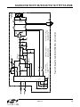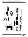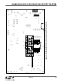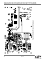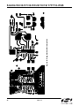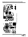
1
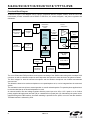
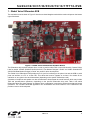
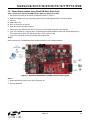
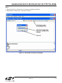
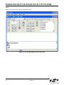
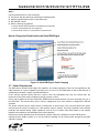
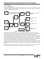
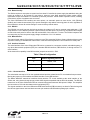
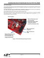
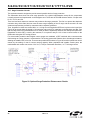
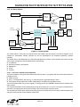
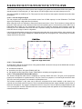
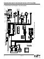
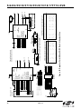
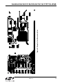
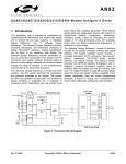
G l o b a l Vo i c e I S O m o d e m - E V B Evaluation Board for the Si2494/39/38/37/36/35/29/19/18/17 ISOModem Description Features The Global Voice ISOmodem EVB evaluation board provides the system designer with an easy way of evaluating the ISOmodem. The Voice ISOmodem EVB consists of a motherboard with a complete removable daughter card The Voice ISOmodem is a complete controller based modem chipset with an integrated and programmable direct access arrangement (DAA) that meets the global telephone line requirements. It is available in a 24-pin or 38-pin system side device and a 16-pin line side device. The hardware versions at the time of publication are: This evaluation board includes the following: Socketed module with the modem chipset USB or asynch RS232 Serial Interface RJ11 connection to the phone line Onboard relay-excludable RJ11 connection RS232 and USB interface to the PC Direct access to the ISOmodem signals for embedded system evaluation Power from a provided 8.5–13.5 V dc power supply or from the USB port Handset connector (J1) Onboard hookswitch External hookswitch connector Jumper matrix that allows any handset wiring scheme to work with this board Onboard speakerphone microphone RCA jack connector to an optional off-board speakerphone electret microphone Selectable and adjustable electret power supplies for both handset and speakerphone microphones Onboard 300 mW audio power amplifier (into a 4 load) for driving either onboard or external speaker. Onboard voice coil driven loudspeaker for call monitoring LED display of all RS232 signals Voice Mother Board Si24xxVMB Rev 2.0 Modem Daughter Card Si24xx2G-DC Rev 2.0 Modem Daughter Card Si24xx2G-QFN38-DC Rev 1.0 The voice daughter card is populated with the correct ISOmodem system side chip (Si2494/39/38/37/36/35/ 29/19/18/17) and the correct line side DAA chip, the Si3018 to suit the voice applications. The ISOmodem eliminates the need for a separate DSP data pump, modem controller, memories, codec, isolation transformers, relays, opto-isolators and a 3-4 wire hybrid. The ISOmodem is ideal for embedded modem and voice applications due to its small board area, controller based architecture, low power consumption and global compliance. An onboard rectifier, filter, and voltage regulator allow the power input to be 7.5–13 V ac or dc (either polarity) supplied through a screw terminal (J8) or a standard 2 mm power jack (J9). Alternatively, power can be supplied through the USB interface (whether the USB or RS232 interface is used). The Power Source Selection in automatic, while the signaling port is selected by a jumper (JP23). The evaluation board audio power amplifier can drive an external speaker for either call progress monitoring or speakerphone function. A small onboard speaker, suitable for call progress monitoring, is installed. Please note that fax modem versions listed in the title require a software driver in order to implement fax send/ receive functionality. The driver must be compliant with the Silicon Labs ISOmodem and with applicable ITU-T standards (e.g., T.30, T.31, T.4 and T.6) Contact Silicon Labs for details. Rev. 0.4 8/11 Copyright © 2011 by Silicon Laboratories Si24xxVMB-EVB Si2494/39/38/37/36/35/29/19/18/17FT18-EVB Functional Block Diagram As shown in Figure 1, the daughter card is a plug-in component with the complete modem, while the rest of the motherboard provides selectable serial RS232 or USB links, the sound subsystem, and power regulation and distribution. I/O LED Display USB/RS232 Connectors J11/J10 Power Connectors Interface Logic ISOmodem Daughter Card Si2494/ Si2438 Series ISOmodem Sound Subsystem Call Progress Audio PCM Pwr Amp Si3000 Ext. Speaker JP11 Handset RJ10 EXT. Microphone J2 Regulation & Switching Silicon Labs SI3018 DAA LED Status Display On Board Hook Switch Exclusion Relay RJ 11 Telephone Connector RJ 11 Telephone Connector Loudspeaker Figure 1. Functional Block Diagram The voice ISOmodem EVB provides a sound system consisting of the Si3000 codec along with a handset RJ10 connector as well as onboard microphone and loudspeaker with options for these devices to be placed off-board. The bias voltages for both the onboard microphone and the handset microphone can modified and alternate sources used. This allows the board to be used as a telephone or as a speakerphone as is, or to be integrated into the customer's system. The evaluation board can drive an external speaker or a small onboard speaker. For speaker-phone applications it is recommended that an off board loudspeaker be used. An onboard rectifier, filter and voltage regulator allow the power input to be 8.5 to 13.5 V peak ac or dc of either polarity supplied through screw terminals (J8) or a standard 2 mm power jack (J9). Alternatively the power can be supplied through the USB interface. Automatic switching is provided for the power, but not for the data interface. That data interface is selected by JP23. 2 Rev. 0.4 Si2494/39/38/37/36/35/29/19/18/17FT18-EVB 1. Global Voice ISOmodem EVB The evaluation board is shown in Figure 2. Note the socketed daughter card with the modem chipset on the bottom right of the board. Figure 2. Global Voice ISOmodem Evaluation Board The ISOmodem chip requires software driver in order to perform either FAX or sound functionality. Contact Silicon Labs for details. “AN244: Si2438/37/36/35/29/19/18/17 Fax Modem Designer’s Guide” and “AN93: Si2494/93/57/ 39/34/15/04 Data Modem Designer’s Guide” are useful for driver development. The Global Voice ISOmodem EVB provides an RJ11 jack for interfacing to the phone line and the USB or serial ports can interface to a PC or a host CPU. This allows the board to operate as a class 1 fax modem for an evaluation or as a global voice and data modem (depending on the specific ISOmodem used). A handset, microphone and speaker can also be attached to demonstrate the sound features, which may include TAM and speaker-phone operations, depending on the specific ISOmodem chip used. Table 1 lists which ISOmodem chips have these features. A software driver or application is required to perform these data and sound operations. The included UltraCOM application can demonstrate the sound features of the ISOmodem and provides a tool to aid development. Rev. 0.4 3 Si2494/39/38/37/36/35/29/19/18/17FT18-EVB 2. Daughter Cards There are two types of daughter cards available for this EVB. One supports the TSSOP version of the system side chip, and the other supports the QFN38 version of the system side. An example of the TSSOP version of the daughter card is shown in Figure 3. It has the ISOmodem system-side chip as well as the Si3018 DAA chip. The left side of the board contains the system side while the right side contains the DAA chip along with the few interface parts needed to connect tot a telephone line. Figure 3. Daughter Card Although this card is provided as part of the global voice EVB, it can also be directly connected to an embedded system using TTL logic. When run by a software driver the chipset on this daughter card is capable of making fax calls, telephone calls with a handset, data calls and both. TAM and speaker-phone operations. Table 1 lists the various ISOmodem chips and their features. Table 1. ISOModem Features 4 Part Number Fax Data Handset TAM Speaker Phone Si2417 ≤V.17 — — — Si2418 ≤V.17 — Si2419 ≤V.17 ≤V.32bis — — Si2429 ≤ V.29 — Si2435 ≤V.34 — — — Si2436 ≤V.34 — Si2437 ≤V.34 ≤V.34 — — Si2438 ≤V.34 ≤V.34 Si2439 — ≤V.34 Si2494 — ≤V.92 Rev. 0.4 Si2494/39/38/37/36/35/29/19/18/17FT18-EVB 3. Setup and Evaluation This section explains how to set up the Voice ISOmodem EVB for evaluation as an RS-232 or USB interface. Jumper settings and system interconnections are given, as well as the use of an demonstration and test application provided called UltraCOM. See the following documents for additional technical details Si2494/39/38/37/36/35/29/19/18/17 data sheets “AN244: Fax Modem Designer's Guide" “AN93: Data Modem Designer’s Guide” Diagrams and tables are provided here that define the operation of all the jumpers, settings and connectors, as well as their default states. A typical global voice EVB as it arrives from the factory can be connected into a system by using only four cables. Figure 4. Global Voice ISOmodem EVB Connection The UltraCOM application provided on the included CD can be used to demonstrate: Telephone Operation. Speakerphone Operation Telephone answering machine operation. Fax Operation can be demonstrated but requires a fax driver application. Rev. 0.4 5 6 Rev. 0.4 JP33 Autobaud enable J10. DB9 connection to Host if JP 23 selects it. JP23 Selects USB or RS232 operation but If no jumper is in place neither is used and host must connnect via J103 to connect J11. USB connection to Host if JP 23 selects it. J1. Handset Connector J2. Optional mic. Input connector JP8. On board mic. And jumper to enable it. J6. Uart Signaling options. Shown for TSSOP and QFN default setup. JP5. Mic. fixed gain vs adjustable gain jumper J30. Aux Audio connector J103. Alternate signal connection path to host. Used if no jumper is at JP23. CMOS signaling JP6, JP15, JP9. Si3000 line in mixer jumpers for : microphone, AUX in (J30), & AOUT R13. Speakerphone mic gain control R24. Audio power amplifier gain control T1, V1A, V1B, Y2A, Y2B, PSTN protection devices. Alternate footprints support most possible configurations JP24 Chooses EEPROM operation instead of Si3000 for non QFN daughter cards Daughter Cards (rev 2.0 TSSOP , or rev 1.0 QFN) plug into J101, and JP16. here. JP12. On Board Power Amp Enable. T59, TP12,TP13. Shunt Resistor and test points for current measurements JP10, JP7, JP13. PWR Amp input mixer jumpers for : AOUT, Si3000 line out, & AUX IN (J30) Figure 5. Function and Location of Global Voice ISOmodem EVB Jumpers UART signal LED displays and test points JP1, 2, 3, 4. Jumpers that configure handset wiring to any style. See schematic for details. JP34 Enable Exclusion Relay (operated by RI pin) J5. PSTN RJ11 connection J5. Telephone RJ11 connection JP11, Audio power output. Recommended for speakerphone operation. J8, J9. Alternate power supply connector options. LS1, On Board Speaker. JP14, On Board Speaker enable jumper Si2494/39/38/37/36/35/29/19/18/17FT18-EVB 3.1. Jumpers Figure 5 shows the function and location of the jumpers present on the global fax EVB. Si2494/39/38/37/36/35/29/19/18/17FT18-EVB Table 2 explains the use of the data related jumpers. It also shows the default state. Check all jumper settings on the EVB before applying power. These default data related jumper settings shown below configure the EVB for USB serial operation with auto baud as a default. Any terminal emulator program configured to communicate through the virtual com port created by the provided driver can be used to communicate with the EVB. There are no BAUD settings required since the modem has an auto baud feature. The USB virtual com port drivers needed for the USB link to work are on the provided CD. Customers that want to use an RS232 port only need to change JP23 and connect an RS232 cable to the host. As with the USB configuration, any terminal emulator program configured to communicate through a PC COM port can be used to communicate with the EVB. Although the user can exercise many of the modem commands (including voice features) using a terminal emulator program, a fax driver is required to implement fax send/receive functionality. This EVB also provides an application, UltraCOM distributed on the CD that can act as a terminal emulator and as a sound feature demonstration vehicle. See Appendix I for an UltraCOM quick start guide that shows how to run this demonstration. Table 2. Digital Data Related Jumpers Jumper Number JP23 Pins Jumped Default State 1–2 2–3 Comments USB selected UART selected Typical Si2438/37/36/35/29/19/18/17 FT setup (24 pin pkg) J6 1-2, 4-5, 7-8, 10-11, 13-14 JP33 1-2 Disable Auto baud 1-2 Enable EEPROM JP24 2-3 Rev. 0.4 Enable Si3000 7 Si2494/39/38/37/36/35/29/19/18/17FT18-EVB Table 3 explains the use of the analog audio oriented jumpers and adjustments, while showing the default state. These jumpers and adjustments can be used to tailor the operation of the global fax EVB so that it interfaces well with the users host system and provides the maximum flexibility as the choice of loudspeaker microphone and alternate sources of sound. Table 3. Sound Related Jumpers Jumper Number Pins Jumped JP34 1–2 JP1 1–2 Handset pin 4 connection (ground)* JP2 1–2 Handset pin 3 connection (ground)* JP3 4–5 Handset pin 2 connection (earpiece signal)* JP4 2–3 Handset pin 1 connection (mouthpiece signal)* JP24 JP5 Default State Comments Enable Exclusion Relay 1–2 Enable EEPROM (factory use only) 2–3 Enable Si3000 1–2 Variable mic gain = 6 to 34 dB 3–3 Fixed mic gain = 21 dB JP6 1–2 JP15 1–2 External Line In to input mixer JP9 1–2 AOUT to input mixer JP8 1–2 JP10 1–2 JP7 1–2 JP13 1–2 Aux Input to power amp mixer JP14 1–2 On Board Speaker connected JP12 1–2 Mic to input mixer Connects on board mic AOUT to power amp mixer Si3000 line out to power amp mixer Enable Pwr Amp. *Note: For typical Cisco handset. 8 Rev. 0.4 Si2494/39/38/37/36/35/29/19/18/17FT18-EVB 3.2. I/O and Adjustments Table 4 explains the use of the adjustable analog audio-oriented controls as well as their default state. Table 4. Audio Adjustments Ref Default State R13 4 turns CW R24 CCW(21.4 dB) Comments Mic Preamp Gain 6 dB to 34 dB Power Amp Gain 21.4 dB to 46.4 dB WRT line out 3.3. USB Interface Data Link Setup Quick Start 1. Set jumpers according to the default configuration shown in Table 2 on page 7. 2. Connect: Install USB cable and provided driver. RJ-11 to phone line or test box. 3. Open the terminal emulator program, and apply power to the EVB. 4. Select the serial COM channel used. 5. Type "AT" followed by a carriage return. (Autobaud automatically adjusts modem DTE speed and protocol.). The modem should echo "AT" and then send the "OK" response code. 6. Type ATH1 and ATH0 to seize and release the telephone line. 3.4. UltraCOM Installation Instructions Perform the following steps: 1. Double-click the ultracom.msi file to launch the installer. Click Next. Figure 6. UltraCOM Setup Wizard 2. Accept the default installation path and click Next. Rev. 0.4 9 Si2494/39/38/37/36/35/29/19/18/17FT18-EVB Figure 7. Select Installation Folder Dialog Box 3. Click Install to start the installation. Figure 8. Install Dialog Box 10 Rev. 0.4 Si2494/39/38/37/36/35/29/19/18/17FT18-EVB 4. After installation is complete, click Finish to close the installer. Figure 9. Completing UltraCOM Setup Wizard 5. UltraCOM may be launched from the desktop link or from the Start menu: Start Programs→UltraCOM→UltraCOM 6. From the UltraCOM main menu, select Help Index. This will load the help file. 7. Select the Quick Start link from the main menu and review the information. Rev. 0.4 11 Si2494/39/38/37/36/35/29/19/18/17FT18-EVB Figure 10. Quick Start 3.5. USB Interface Data Link Setup Quick Start 1. Set jumpers according to the default configuration shown in Figure 5. 2. Install the USB driver for your operating system from the CD supplied with the evaluation board. 3. Connect: USB cable to PC RJ-11 to phone line or test box 4. Open the terminal emulator program. 5. Select one of the USB Virtual Com Port numbers in the emulator program's user interface. 6. Type "AT" followed by a carriage return. (Autobaud automatically adjusts modem DTE speed and protocol.). The modem should echo "AT" and then send the "OK" response code. 7. Type ATH1 and ATH0 to seize and release the telephone line. 12 Rev. 0.4 Si2494/39/38/37/36/35/29/19/18/17FT18-EVB 3.6. Sound Demonstration Using UltraCOM Quick Start Guide Step 1: Perform the Quick Start USB Interface Data Link Setup Quick Start 1. Set jumpers according to the default configuration shown in Figure 5. 2. Install the USB driver for your operating system from the CD supplied with the evaluation board. 3. Connect: USB cable to PC RJ-11 to phone line or test box 4. Open the terminal emulator program. 5. Select one of the USB Virtual Com Port numbers in the emulator program's user interface. 6. Type "AT" followed by a carriage return. (Autobaud automatically adjusts modem DTE speed and protocol.). The modem should echo "AT" and then send the "OK" response code. 7. Type ATH1 and ATH0 to seize and release the telephone line. Step 2 Add connections to a loudspeaker and a handset as shown in the following diagram. Figure 11. Sound Demonstration Hardware Interconnect Guide Step 3: 1. Install UltraCOM (provided in this kit) on Windows XP 2. Launch UltraCOM. Rev. 0.4 13 Si2494/39/38/37/36/35/29/19/18/17FT18-EVB Step 4: Select "Terminal-Open" making sure the serial configuration is as shown (except for port selection), then select OK. Figure 12. UltraCOM Serial Configuration Dialog Box 14 Rev. 0.4 Si2494/39/38/37/36/35/29/19/18/17FT18-EVB Step 5: 1. Select Open Plug-In (The Green Icon) in the screen snapshot that follows. 2. Respond OK to "Load Plug-in" "24xx Voice Functions" Figure 13. UltraCOM Load Plug-In Dialog Box Rev. 0.4 15 Si2494/39/38/37/36/35/29/19/18/17FT18-EVB Step 6: Wait for the screen below to open and the patch to load. Figure 14. UltraCOM Plug-Ins Patch Load Phase 16 Rev. 0.4 Si2494/39/38/37/36/35/29/19/18/17FT18-EVB Step 7: Use the interface above to do the following: Go off hook with the handset by selecting the handset symbol Select the speakerphone button to start that mode. Dial a DTMF number. Note the following suggestions. Use the external off-board speaker for speakerphone functionality the on-board electret for the microphone. Use the PSTN, a PBX or a Line Simulator for the phone line. Use How to Change the Patch Used in the UltraCOM Plug-In Figure 15. UltraCOM Plug-In Patch Changing 3.7. Power Requirements The EVB has an onboard diode bridge, filter capacitor, and voltage regulators. Power can be supplied from the USB connection or a source capable of providing 8.5–13.5 V dc or 6–9.5 VRMS peak ac and at least 300 mA. A suitable wall mounted 9 V supply is provided with the kit. Of the 300 mA required current 200 mA is used to drive the loudspeaker and may be removed from the requirement if the power amp is enabled by placing a jumper on JP12. Power may be applied to the Voice ISOmodem EVB through the screw terminals, J8, the 2 mm power jack, J9, or the USB cable. The modem cable may be used to supply power even if the modem is configured for RS-232 operation. The power consumed by the audio section is limited with an active limiter. This circuit will protect the power sources when the sound is overdriven or if the amplifier output is shorted. The power amplifier is also naturally protected with thermal limiting. Digital operations such as host to modem serial data transfer or the modem telephone line operations are unaffected by the limiter operation. Note that the modem will take power from wherever it finds it and that it is possible to use the RS232 port for signaling and the USB for power or to use the USB for signaling and to provide power through the provided external 9 V supply. Rev. 0.4 17 Si2494/39/38/37/36/35/29/19/18/17FT18-EVB 3.8. EVB Part Numbers The Voice ISOmodem evaluation boards are offered in multiple versions. The first four numbers indicate the system-side device. The options include speed and various audio capabilities as well as package and temperature. See Figure 16: S i2 4 3 8 F T 1 8 -E V B S i2 4 3 7 F T 1 8 -E V B S i2 4 3 6 F T 1 8 -E V B S i2 4 3 5 F T 1 8 -E V B S i2 4 1 9 F T 1 8 -E V B S i2 4 1 8 F T 1 8 -E V B S i2 4 1 7 F T 1 8 -E V B S i2 4 9 4 A F M 1 8 -E V B S i2 4 3 9 A F M 1 8 -E V B Figure 16. EVB Part Number Example 18 Rev. 0.4 Si2494/39/38/37/36/35/29/19/18/17FT18-EVB 4. Voice ISOmodem EVB Functional Description The Voice ISOmodem EVB is a multipurpose evaluation system. The modem daughter card illustrates the small size and few components required to implement an entire controller-based modem with global compatibility. The daughter card can be used independently of, or in conjunction with, the motherboard. The motherboard adds features that enhance the ease of evaluating the many capabilities of the Si24xx ISOmodem. 4.1. Motherboard The motherboard provides a convenient interface to the Si24xx ISOmodem DC (daughter card). The versatile power supply allows for a wide range of ac and dc voltages to power the board. A versatile digital IO system allows either a USB virtual com port to be used to interface to the board or an RS-232 transceivers with a DB9 connector allowing the EVB to be easily connected to a PC or other terminal device. A jumper option allows direct access to the LVCMOS/TTL level serial inputs to the Si24xx, bypassing the RS-232 transceivers or USB interface. This is particularly useful for directly connecting the Si24xx to embedded systems. The motherboard provides connectivity to a telephone line or a phone extension via a pair of RJ11connectors. The extension connector may be actively excluded by an onboard relay. A switch and a connector is provided on the motherboard that is read by the modem firmware and can perform the hookswitch function. The motherboard also contains a complete sound system including microphone, loudspeaker and handset connector. The sound system includes easy to adjust gain controls and extra inputs that allow system generated noises to be added to the sound. A functional block diagram of the system as a whole can be seen below. USB Connector J11 Direct Access Header LED Drivers & Display USB Interface CP2101 J103 Sound Subsystem J101 Call Progress Audio PWM RXD, TXD, CTSb JP23 jumper selects USB vs. UART or neither RS232 Connector J10 RS232 Drivers & receivers MUX CD, RI, DTR, RTS, DSR Si24xx ISOmodem Optioning Switch Matrix J6 PCM Handset RJ10 Si3000 Ext. Speaker JP11 EXT. Microphone J2 Silicon Labs Si3018 DAA ISOmodem Daughter Card JP16 RIb Enabled by JP34 Tip and Ring Exclusion Relay RJ 11 Telephone Connector RJ 11 Telephone Connector Figure 17. Sound System Block Diagram Rev. 0.4 19 Si2494/39/38/37/36/35/29/19/18/17FT18-EVB 4.1.1. Power Supply 4.1.1.1. Power Distribution The power distribution diagram for the global voice EVB can be seen in Figure 18 below. Analog and Digital voltages are separately regulated while the audio power amplifier supply is current limited to prevent accidental overload and disruption of the digital supplies. USB Connector J11 Switch (2 diodes) Current Limiter +(4-5)V Audio Pwr Amp 5 Volt Regulator 3.3 Volt Regulator External Power Connector J8 +5V Power Rectifier Bridge & Capacitor External Power Connector J9 +3.3V Analog 5 Volt Regulator Switch (2 diodes) Manual Reset Switch 3.3 Volt Regulator Reset Generator +3.3V Digital Master Reset Figure 18. Power Distribution Diagram The onboard full-wave rectifier and filter ensure the correct polarity is applied to the Voice ISOmodem EVB. Daughter card 3.3 V power is supplied through voltage regulator U3. Daughter card current can be measured by connecting a DVM across R59, a 1 current sensing resistor in the 3.3 V supply line to the daughter card. The input voltage to either J8 or J9 must be between 8.5 and 13.5 V dc, or 6 and 9.5 VPEAK ac. The motherboard includes a diode bridge (D12) to guard against a polarity reversal of the dc voltage or to rectify an ac voltage. The power source must be capable of continuously supplying at least 100 mA. The voltage regulator, U10, can provide 5 V for the motherboard and the input for voltage regulator U3, which outputs 3.3 V for use on the motherboard and to power the daughter card. Alternately, power may be supplied to U3 through D11 from the USB port. The power consumed by the audio section is limited with an active limiter. This circuit will protect both power sources and the audio amplifier when the sound is overdriven or if the amplifier output is shorted. Digital operations such as host to modem serial data transfer or the modem telephone line operations are unaffected by the limiter operation. Two indicator LEDs indicate main power (+5 V) and audio amp power (~+4.5 V). See Figure 15 for locations. You will notice the one for the audio power blinking when audio is loud and clipping. This is normal. 20 Rev. 0.4 Si2494/39/38/37/36/35/29/19/18/17FT18-EVB 4.1.2. Reset Circuitry The Si24xx requires a reset pulse to remain low for at least 5.0 ms after the power supply has stabilized during the power up sequence or for at least 5.0 ms during a power-on reset. Most production Si24xx modem chipset applications require that RESET be controlled by the host processor. Certain Si24xx operation modes, including power down, require a hardware reset to recover. The Voice ISOmodem EVB contains two reset options, an automatic power-on reset device, U18 (DS1818) (default), and a manual reset switch (S1) to permit resetting the chip without removing power. A reset, regardless of the mechanism, causes all modem settings to revert to factory default values. 4.1.3. DS1818 The DS1818 is a small, low-cost device that monitors the voltage on VD and an external reset pushbutton. If VD drops below 3.0 V, the DS1818 provides a 220 ms active-low reset pulse. On power up, the DS1818 also outputs an active low reset pulse for 220 ms after VD reaches 90% of the nominal 3.3 V value. The DS1818 outputs a 220 ms reset pulse any time the power supply voltage exceeds the 3.3 V 10% window. 4.1.4. Manual Reset The manual reset switch (S1) performs a power-on reset. This resets the Si24xx to factory defaults without turning off power. Pressing S1 activates the reset monitor in the DS1818 and produces a 220 ms active low reset pulse. 4.1.5. Interface Selection The serial interface of the Voice ISOmodem EVB can be connected to a computer, terminal, embedded system, or any other data terminal equipment (DTE) via a standard RS-232 interface, USB interface, or through a direct TTL serial interface. At the heart of this capability is the MUX and the jumper that controls it: JP23. Table 5. Board Configuration JP23 Modem Signalling Done Via X Header, J103 1–2 Jumped USB Port 2–3 Not Jumped Serial Port 4.1.5.1. RS-232 Interface The serial cable connects to J10 on the motherboard and provides a data link the PC or embedded host processor. Moving the jumper on JP23 enables the RS232 interface or the USB interface. The Maxim MAX3237 transceiver interfaces directly with the TTL levels available at the serial interface of the Si24xx and, using internal charge pumps, makes these signals compatible with the RS-232 standard. The RS-232 transceiver on the Voice ISOmodem EVB can communicate at rates between 300 bps and 1 Mbps. This simplifies the connection to PCs and other data terminal equipment (DTE). The signals available on the Voice ISOmodem EVB serial interface (DB9 connector) are listed in Table 6 along with the various signal names used and both connector pin numbers and ISOmodem package pin numbers. Rev. 0.4 21 Si2494/39/38/37/36/35/29/19/18/17FT18-EVB Table 6. DB9 Pin Connections (J10) J10 Name J10 Symbol J10 Pin ISOmodem Pin Number ISOmodem Signal Name Carrier Detect CD 1* See Note* DCD/EESD Received Data RXD 2 9 RXD Transmit Data TXD 3 10 TXD Data Terminal Ready DTR 4* See Note* ESC/RI Signal Ground SG 5 6 GND Data Set Ready DSR 6* See Note* INT/AOUT Ready to Send RTS 7* See Note* RTS/RXCLK Clear to Send CTS 8 11 CTS Ring Indicator RD 9* 17 RI *Note: JP6 jumper option. 4.1.5.2. USB Interface The USB cable connects to J11 on the motherboard and provides both data and power. This operation mode uses the standard factory jumper settings illustrated in Table 2 on page 7. Installing a jumper on J23 enables the USB interface and disables the RS-232 interface. The USB interface is provided by U12. A USB driver for this chip is available for most PC and MAC operating systems on the CD. 4.1.5.3. Direct Access Interface The direct access interface header (J103) can be used to connect the motherboard to an embedded system. If J103 is used in this manner, it is necessary to remove the jumber from JP23 to disable both the RS-232 and USB interface and prevent signal contention. See Table 5. In this mode, the motherboard continue to supply a few other signals and functions such as power (derived from J8, J9, or USB) as well as a power-on reset signal and the telephone line connection via the exclusion relay contact and the RJ-11 jack connected to the modem line side. J103 provides access to all the ISOmodem system side signals available on the daughter card. If the user wishes to go further and use his embedded system's power supply or reset line, he can remove the daughter card from the mother board and integrate it directly into his system. 22 Rev. 0.4 Si2494/39/38/37/36/35/29/19/18/17FT18-EVB 4.1.6. Exclusion Relay The exclusion relay (Figure 19) on the motherboard allows the modem to turn on the relay and exclude the phone line connection from an auxiliary device such as a telephone connected to the second RJ11 socket. The relay is enabled via jumper JP34. The control signal used is the one called RIb and is managed by special command sequences (see application notes AN93 or AN244). RIb goes low to turn on the relay via a driver transistor. See the diagram below for the location of the connectors and the relay. Note that the RIb signal must be kept high during the reset pulse, due to the use of this pin for special manufacturing functions. This demands that this pin drive either an NMOS relay driver transistor or a 3.3 V referenced buffer like the one used here. Exclusion Relay Optional Footprints to be used if customer longitudinal surge voltage requirements exceed capability of exclusion relay. RJ11 connection to Telephone RJ11 connection to PSTN Optional Footprints to be used if customer has unusual metallic surge voltage requirements. Figure 19. Exclusion Relay and Surge Protection Rev. 0.4 23 Si2494/39/38/37/36/35/29/19/18/17FT18-EVB 4.1.7. Surge Protection Circuits This evaluation board is designed to provide several possible levels of surge protection. The ISOmodem alone does not need surge protection for a global implementation except for the components normally selected and implemented on the daughter card. These are the P3100B sidactor and the Y2 caps used for C1, C2, C8, and C9. There are two basic reasons a customer may enhance this surge protection. The first is to protect the telephone exclusion relay, which often does not meet the same surge capability of the Y2 caps, and the second is to meet enhanced requirements put forth by customers and/or corporate guidelines. Thus, footprints for either low-current 800 V or 1 kV high-current longitudinal GDTs are in place on the board (see Figure 20) to protect either the typical 2.5 kV exclusion relay or the 5 kV capacitors on the daughter card. But, note that the relay used on this motherboard is 5 kV rated (as are the capacitors) and does not need special protection. Regardless of which GDT is used by the customer, it is required to stay at 1 kV or less to control stress on the ISOmodem during the GDT arcing process. For extra metallic protection where higher current surges are mandated, a GDT combined with a common-mode choke acting as a delay element is recommended. The choke protects the Sidactor due to its leakage inductance, allowing the metallic GDT to fire first. There are two possible GDTs shown in Figure 20, and the optimal one can be chosen by the trading of cost for current carrying capacity. When populated with capable ceramic parts, the motherboard and modem can survive 15 kV/ 2 , 1.2/50 µs combination waveform, i.e. 7.5 kA surge current. Figure 20. Optional Surge Protection Enhancement Circuits 24 Rev. 0.4 Si2494/39/38/37/36/35/29/19/18/17FT18-EVB 4.1.8. The Sound System JP13 Aux In (JP30) JP10 Mixer & Jumpers External Speaker JP11 Power Amp JP7 AOUT R24 sets gain, JP12 enables Line Out Internal Microphone Filter PWM ISOmodem PCM Local Speaker Enabled by JP14 Handset Type Matrix JP1-4 Si3000 Handset J1 JP8 SI3000 LINE IN (J30) Line In JP6 Mixer JP5 & R13 set gain JP15 SPKR_L Preamp LINE_O External Microphone J2 SPKR_R JP9 JP30 Optional Connections Figure 21. Sound System The sound system on the board is centered around the Si3000 code chip shown in the above diagram, and is designed to demonstrate handset operation as well as speakerphone and telephone answering machine operation. The Si3000 links to the ISOmodem via a PCM bus that allows the transfer of audio between the modem and the various audio "peripherals" that the Si3000 links to the following: Loudspeaker Handset microphone and speaker Microphone Line In Line Out 4.1.8.1. The Power Amplifier and Loudspeaker The Power amplifier on the global Voice ISOmodem EVB can drive a 4 speaker with 300 mW of audio that has 3 possible sources: Si3000 Line out Aux in, J30 signal SPKR_AUX_IN (e.g., a customer system's generated beeps or ticks) Call progress analog signal from modem. (ISOmodem's call dialing and negotiation tones) The power amplifier itself is a low cost, rugged 3.3 V bridge device, the LM4862M. Similar parts are available from other vendors. The sources listed above can be independently turned off by jumpers JP7, 10, and 13 or be gain controlled with no interaction, by changing the value of the summing node current injection resistors' values. The inverted input of this chip is used as a summing junction for an audio mixer for the inputs mentioned above and with gain control effected via the feedback resistor R24. Rev. 0.4 25 Si2494/39/38/37/36/35/29/19/18/17FT18-EVB The customer can change the resistor values when integrating the global Voice ISOmodem EVB to his system, but should keep the RC formed by the 1 µF input caps at a 50 Hz or higher corner to avoid a thump on turn on. The power amplifier is enabled by JP12. This jumper can also be tied to a host signal to allow the host to shut down the amplifier. 4.1.8.2. The Call Progress Signal The call progress tone discussed in this section comes from a PWM output pin on the ISOmodem. The PWM signal is processed by a high-pass filter (see below). When using this circuit it is important to extend the modem reset time to 10 ms. This is the time to charge C83 via the built in weak pull ups in case that the modem has been operating prior to reset and has put the AOUT into a PWM state that is 100% low. Any modifications to this circuit or reset time should be done keeping in mind the following rule: The ISOmodem reset time and AOUT capacitive loading must be balanced so that the AOUT pin must have time to charge it's load to a high state. It should be noted that when creating the call progress output with this circuit, about half the noise present in the audio bandwidth on the modem supply pins is passed along with the call progress tone. Consequently, the modem supply needs to be fairly clean. PWM Filter Figure 22. High-Pass Filter 4.1.8.3. The Input Mixer An input mixer is also in the sound section of the global fax EVB. It drives the line input of the Si3000 with a mixture of the following possible sources: An electret microphone An auxiliary line input, J30 signal (Si3000_LINE_IN) Call progress analog signal from modem. (ISOmodem's call dialing and negotiation tones) 4.1.8.4. The Speakerphone Electret Microphone The electret microphone listed above is amplified by a preamp before this mixer. The gain of the microphone preamp can be adjusted via a potentiometer if JP5 pins 1 and 2 are jumpered, or is fixed by R12 and R15 when JP5 pins 2 and 3 are jumpered. It is intended for speakerphone use. This electret microphone in this case can be either the microphone that comes installed on this board or an external one connected to the RCA jack J2. There is a dedicated electret power supply available to power either of these two microphones. The supply is configured so that it is easy for the user to adjust its voltage between 0 and 3.3 V by varying R27 and R30. This allows the user to most closely match the operation of his intended target. The onboard electret is enabled by JP8. 26 Rev. 0.4 Si2494/39/38/37/36/35/29/19/18/17FT18-EVB 4.1.8.5. The Handset The handset signals are all processed by the Si3000 chip. The board provides a matrix of connectors to allow ANY handset pin configuration to be used. This jumper array is shown in Figure 23. The default setting is shown in Table 3 on page 8. Microphone Signal Earpiece Signal Figure 23. Handset Rev. 0.4 27 Si2494/39/38/37/36/35/29/19/18/17FT18-EVB 4.2. Daughter Cards There are two types of daughter card; one is for QFN packaged modem chips, and one is for smaller packages. The daughter card itself is a complete modem solution perfectly suited for use in an embedded system. The daughter card requires a 3.3 V supply capable of providing at least 35 mA. Be sure to provide the proper power-on reset pulse to the daughter card if it is used in the stand-alone mode. The Voice ISOmodem EVB motherboard connects to the daughter card through two connectors, J101 and JP16. JP101 is an 8x2 socket providing connection to all Si24xx digital signals and a regulated 3.3 V power. The Si24xx digital signals and power also appear at JP103 and they are LVCMOS and TTL compatible. JP103 can be used for monitoring purposes or may be used as the interface to the users host if JP23 has no jumper, thus disabling the on board digital multiplexer. In this case note that the PCM link to the Si3000 is still in place and is still connected to the daughter card signals. JP16 is a 4x1 socket providing connection between the daughter card and both the RJ-11 phone jack and the exclusion relay on the motherboard. The daughter cards for this global Voice ISOmodem EVB come with the appropriate ISOmodem system side chip installed and are identical otherwise. The possible ISOmodem system side chips are shown in Figure 24: Si2438FT Si2437FT Si2436FT Si2435FT Si2419FT Si2418FT Si2417FT Si2494FM Si2439FM Figure 24. ISOmodem System-Side Chip Part Number Scheme The line side chip on the daughter card is the Si3018 DAA chip. It works with a few low cost discrete parts that complete the telephone line interface. Small 33 pF capacitors link the system side to the isolated side and provide both data and power transfer to the isolated telephone line circuit. The connection between the Si3018 chip and the telephone line is done via a diode bridge to control line polarity and beads to control EMI. A Sidactor is placed across the phone line for surge arresting reasons, while a pair of capacitors link the tip and ring to system ground in order to minimize EMI radiation and EMI Susceptibility. PCB layout for this circuit is somewhat critical, for link integrity, EMI, and surge reasons,. Anyone planning to design a PCB layout should check application note AN244 or AN93 and also submit the PCB design to Silicon Labs for checking. The layout used on this daughter card is shown in this user's guide. 28 Rev. 0.4 Si2494/39/38/37/36/35/29/19/18/17FT18-EVB 4.2.1. Reset Requirements The Voice ISOmodem daughter card must be properly reset at powerup. The reset pin (pin 8) of the Si24xx (J101, pin 13) must be held low for at least 5.0 ms after power is applied and stabilized to ensure the device is properly reset. 4.2.2. Crystal Requirements Clock accuracy and stability are important in modem applications. To ensure reliable communication between modems, the clock must remain within 100 ppm of the design value over the life of the modem. The crystal selected for use in a modem application must have a frequency tolerance of less than 100 ppm for the combination of initial frequency tolerance, drift over the normal operating temperature range, and five year aging. Other considerations, such as production variations in PC board capacitance and the tolerance of loading capacitors, must also be taken into account. 4.2.3. Protection The Voice ISOmodem EVB meets or exceeds all FCC and international PTT requirements and recommendations for high-voltage surge and isolation testing without any modification. The protection/isolation circuitry includes C1, C2, C8, C9, FB1, FB2, and RV1. The PCB layout is also a key "component" in the protection circuitry. The Voice ISOmodem EVB provides isolation to 3 kV. Contact Silicon Laboratories for information about designing to higher levels of isolation. 4.2.4. Daughter Card Strapping and Jumper Options Both types of daughter cards have some strapping options that are preconfigured at the factory. These are explained in the schematic and in more detail in AN93. The QFN daughter card also has a two jumper options. One, JP1, selects SPI operation, which is usable if the user also does not use a jumper at JP23 on the motherboard and provides host SPI connectivity at J103. The other jumper, JP2, enables the operation of the EEPROM chip, which is on the daughter card. There is an EEPROM chip on the motherboard, which is only used with the TSSOP daughter card. Rev. 0.4 29 681 681 R163 R42 "RS232" "USB" R41 R162 D53 10K 10K D52 U13 RED RED JP23 JP1/3 1 2 3 4 5 6 7 8 9 10 11 12 13 14 15 16 Si24xx CLKOUT/EECS/A0 SDO/EECLK_RTSb/D5 FSYNCH/D6 DCDb/D4 RTSb/D7 GND RXD/RD ESC/D3 TXD/WR SDI/EESD/D2 CTSb/CS RIb/D1 RESET INTb/D0 VD AOUT/INTb Table NOT on silkscreen 1B2 2B2 3B2 4B2 1B1 2B1 3B1 4B1 1B2 2B2 3B2 4B2 1B1 2B1 3B1 4B1 Si2401 NC GPIO1 GPIO5 GPIO2 NC GND RXD GPIO3 TXD NC CTS NC RESET NC VD GPIO4 15 1 4 7 9 12 0.1uF 15 1 4 7 9 12 0.1uF RXD TXD CTSb CD_M ENABLE_MUXb SELECT OE S 1A 2A 3A 4A C72 +3.3V OE S 1A 2A 3A 4A C71 +3.3V BAV23A D54 3 6 10 13 2 5 11 14 IDT74CBTLV3257 U14 3 6 10 13 2 5 11 14 IDT74CBTLV3257 Net names correspond to Si24xx. See table for Si2401 equivalents RS232 +3.3V USB RI_T DTR_T RTS_T DSR_T RI_U DTR_U RTS_U DSR_U RXD_T TXD_T CTS_T CD_T RXD_U TXD_U CTS_U CD_U To Host Interface Page RESETb R59 GND GND GND GND TP8 Turret TP9 Turret TP2 Turret GND R40 10K TP7 Turret TP25 Turret +3.3V RI_M DTR_M RTS_M DSR_M Select High Chooses B2 port 1.0 1uF C69 RXD TXD CTSb CD RIb RTSb RTSb DSRb C70 560pF 1 19 2 3 4 5 6 7 8 9 ESC NC DCD 2401 SOIC16 Y1 Y2 Y3 Y4 Y5 Y6 Y7 Y8 U26 74LCX541 18 17 16 15 14 13 12 11 0.1uF INTb NC C75 RIb ESC RTSb NC NC DCD DCD ESC 24xx TSSOP24 24xx SOIC16 ESC RIb DCDb 2 4 6 8 10 12 14 16 TP23 TP22 TP21 TP20 TP19 TP17 TP16 TP24 R170 R169 R160 R159 R158 R157 R156 R155 HEADER 5x3 J6 Leaded 681 681 681 681 681 681 681 681 DSR RTS DTR RI CD CTS TXD RXD AOUT_INTb D48 D47 D46 D45 D44 D43 D42 D41 +3.3V AOUT/INTb INTb NC RIb 15 RIb FSYNCH NC 24xx SOIC16 CLKOUT_EECSb FSYNCHb ESC SDI_EESD RIb INTb AOUT_INTb SDO_EECLK_RTSb DCDb INTb/AOUT GPIO1 NC RIb NC 2401 SOIC16 JP6 Right Pin Signals SDI/EESD 24xx TSSOP24 RTSb RIb FSYNCHb SDI_EESD Si2401 16 pin RIGHT LEFT DCD or nc NC or RIb ESC or NC nc or GPIO1 nc or INTb/AOUT "SDO_EECLK_RTSb" "DCDb" "GND" "ESC" "SDI_EESD" "RIb" "INT" "AOUT_INTb" ESC SDI_EESD RIb INTb AOUT_INTb SDO_EECLK_RTSb DCDb 12 SDO_EECLK_RTSb SDO/EECLK 9 6 3 "SOIC16: 1-2, 5-6, 7-8, 11-12, 14-15" "TSSOP24: 1-2, 4-5, 7-8, 10-11, 13-14" 1 2 4 5 7 8 10 11 13 14 2 4 6 8 10 12 14 16 Silk Screen Text 1 3 5 7 9 11 13 15 Leaded RS-232 Si24xx 24 pin Si24xx 16 pin RIGHT LEFT RIGHT LEFT CD DCD or NC DCD or SDI/EESD RI NC or RIb RI or FSYNCH DTR ESC or NC ESC or RIb RTS NC or RTSb RTS or SDO/EECLK NC or INTb DSR INTb or AOUT/INTb "Recommended J6 settings" 2 4 6 8 10 12 14 16 Leaded 1 3 5 7 9 11 13 15 2 4 6 8 10 12 14 16 J103 8X2 Shrouded Header 1 3 5 7 9 11 13 15 J101 HEADER 8x2 "CLKOUT_EECSb" 1 3 "FSYNCHb" 5 "RTSb" 7 "RXD" 9 "TXD" 11 "CTSb" 13 "RESETb" 15 "+3.3V" "J6 Jumper Connectiveity" +3.3V CLKOUT_EECSb FSYNCHb RTSb RXD TXD CTSb RESETb RTSb RTS_M INTb DSR_M DTR_M RI_M CD_M Table on back silkscreen for J6 10K CLKOUT_EECSb FSYNCHb RTSb RXD TXD CTSb RESETb VCC_Modem 10K R43 Figure 25. Motherboard Main Digital Logic G1 G2 A1 A2 A3 A4 A5 A6 A7 A8 +3.3V NC NC NOPOP R39 C73 560pF JP6 Left Pin Signals +3.3V 1uF C74 1 R49 10K 10K JP33 1 Autobaud Dis. 2 SDO_EECLK_RTSb SDI_EESD R51 "SI3000 EN" C33 R70 JP24 R87 0 0 +3.3V IN1 IN2 IN3 IN4 NC1 NC2 NC3 NC4 Q1 COM1 COM2 COM3 COM4 R101 R60 CLKOUT_EECSb SDI_EESD FSYNCHb V2A 10K R91 1.5k R85 8 10 0 NI 5 3 0 NI 200 10K 2 15 10 7 C35 6 5 2 1 10K SCLK MOSI MISO /CS +3.3V 5 4 3 2 1 NOPOP J7 5 4 3 2 1 /WP /HOLD +3.3V 0.1uF 3 7 D6 MMBD3004S-7-F TP6 BLUE TIP TP5 BLUE RING 7 8 9 10 11 12 1 2 3 4 5 6 J5B RJ-11 PSTN LINE J5A RJ-11 TELEPHONE Extra High Surge Protection: Large Ceramic GDT's To Si3000 Codec on Voice and Call Progress Page SDI_EESD FSYNCHb SSI_CLKOUT SSI_SDO AOUT_INTb To AOUT circuit on Voice and Call Progress Page +5V_RAW Fujitsu FTR-C1GA4.5G K1A 5 kV rated Relay Pull Down Can strap FSYNCHb to GND enabling EEPROM R52 R84 1.5k 800V GTCA28-801L-P05 NOPOP V1B 350V GTCA28-351L-P05 NOPOP V2B D5 EXCLUSION +5V_RAW U5 EEPROM 32K U27 MAX4521 Q5 +3.3V K1C MMBTA06LT1 +3.3V 1 16 9 8 9 MMBT3906-7-F 0.1uF 3 14 11 6 K1B R114 4 V1A 1000V RA-102M-C6-Y NOPOP 350V RA-351M-C6-Y NOPOP R115 R113 10K 10K Extra Surge Protection: Small Glass GDT's. R69 T1 3.3mH NOPOP SDO_EECLK_RTSb CLKOUT_EECSb Exclusion En. JP34 +3.3V "EEPROM EN" 2 Leaded JP16 4X1 Socket T1 and GDT's may be needed for unnusual surge requirements. For details contact the factory. 4 1 From Power Supply Page 16 VCC GND 8 16 VCC GND 8 3 2 Connectors for ISOModem module. 13 V+ FB11 600 Ohm BLM18AG601SN1 12 VL V- TP13 RED Isense 20 VCC GND 5 12 TP12 RED +3.3V GND 10 8 VCC Rev. 0.4 4 1 - GND 30 + 4 +3.3V Si2494/39/38/37/36/35/29/19/18/17FT18-EVB 5. Motherboard and Daughter Card Schematics AOUT_INTb EXT MIC. To MODEM LCL. MIC. MK1 EN. LCL MIC RCA JACK J2 RESETb SDI_EESD FSYNCHb 1 2 D3 0.1uF C24 JP8 0.1uF C25 R33 1K 2K 100uF C17 0.1uF C14 R21 MMBD3004S-7-F 0.1uF C26 R34 1K + VGND 7 U20B 0.1uF C27 R35 1K R28 200 AD8602ARM R10 4.7K 5.1K VGND U21B AD8602ARM 7 1K 5 6 2 3 - + 2 3 V- 1 R17 0.1uF 0.1uF RESET* HDST 0.1uF JP6 JUMPER JP9 1 JUMPER JP15 1 JUMPER 1 Si3000 U2 C30 R2 2 2 2 MCLK SDO Output Input SDI FSYNC SCLK +3V3_A 9 3 7 5 4 6 8 R5 100K 0.1uF C4 CAPS FOR AD8602ARM OPAMPS C29 10K C28 R25 10K 10K 5.5KHz pole SI3000_LINE_IN R20 AD8602ARM V+ U22A V- 1 V+ U20A 49.9K R15 560pF D1 0 VGND R19 2 3 - + C15 2.2nF GND 11 15 1 16 10 V- V+ 1 AD8602ARM U21A 1uF C31 100K R38 R37 100K +3V3_A +3V3_A 10K power Consumption Here is 20 mA at 3.3 Volts LINEI LINEO SPKR_R SPKR_L MIC_IN 2 GND 0.1uF C3 MIC_BIAS NI 6 5 - + 7 C34 1uF R31 10K R44 3.01K R29 3.01K R22 499 1uF 1uF JP13 JP10 JP7 C98 2 1 3 5 7 9 J30 2 4 6 8 10 2 4 6 8 10 10uF JP12 1uF 1uF 4.7uF 1 2 3 4 LM4862 SHUTDOWN BYPASS IN+ IN- U4 +4.5V 14KHZ pole 5X2 Shrouded Header 1 3 5 7 9 C8 0.1uF C10 R7 Several footprint compatiple variations of this amplifier are in production allowing an easy price vs power tradeoff. EG. LM4819. 0 R32 C37 2 C18 2 Pwr Amp Enable C23 C22 1 1 1 D2 MMBD3004S-7-F +3V3_A High Pass set for 50 Hz Corner SPKR_AUX_IN SI3000_LINE_IN SPKR_AUX_IN VGND C11 1uF 1uF AD8602ARM U22B R11 2K C7 0.1uF C5 Figure 26. Motherboard Sound Processing Circuits 100K R45 - + +3V3_A R30 10M C13 +3V3_A AD8602ARM VGND 324K 1uF C20 10K R4 EXT MIC IN GAIN SEL 1-2 Variable 2-3 Fixed R27 +3V3_A VGND 100K R36 5 6 JP5 0 R16 R18 100K 3 R14 1K R12 R9 Si3000 Option Strapping EXT MIC IN GAIN ADJ CW: 34 dB CCW: 6 dB 1 R13 0.1uF 50K C12 +3V3_A 2 SSI_CLKOUT SSI_SDO 2 1 8 4 12 VD 13 VA GND 14 +3.3V 8 4 8 4 MMBD3004S-7-F 2 1 6 VDD GND 7 VO2 VO1 C21 1uF C19 2.2nF R23 3.01K 2K 200 R3 8 5 2 C6 R6 2K FB4 FB3 FB2 FB1 100uF 600 Ohm 600 Ohm 600 Ohm 600 Ohm JP14 50K "Pin 1" ATT Ref Handset Speaker at pins 2&3 Mic. in. is at pin 4 with GND at pin 1. Cisco Ref Handset Speaker at pins 2&3, Mic. in. is at pin 1 and GND is pin 4 En. Lcl. Speaker SPEAKER LS1 DIFF SPKR OUT JP11 "Do not gound speaker+ or Speaker - Gain WRT to Line Out: CW/46.4 dB CCW: 21.4 dB R24 Pin 5 Pin 5 1 2 3 4 J1 Differing handsets can be accomodated as shown in these two examples + EXT DIFF SPKR GAIN ADJ "Pin 1" JP1 JP2 JP3 JP4 3 1 +3V3_A 2 To MUX + - + - Rev. 0.4 1 +3.3V JP4 JP1 Pin 1 JP1 Pin 1 JP4 HANDSET Si2494/39/38/37/36/35/29/19/18/17FT18-EVB 31 USB SG DTR(I) TXD(I) RXD(O) RD(O) CTS(O) RTS(I) 9 8 7 6 R108 0 NOPOP +V DD+ GND J11 USB Type B 1 2 3 4 0.01uF C60 Keep Very Close D14 600 Ohm BLM18AG601SN1 FB9 RS-232, Female, Front View 5 4 3 DSR(O) MH MH 10 11 2 CD(O) DB9 J10 D15 15V DN1 0.1uF C63 15V DN2 15V DN3 5 4 7 8 DD+ 560pF RST RI DCD DTR DSR TXD RXD RTS CTS SUSPEND SUSPEND CP2102 REGIN VBUS U12 FB8 9 2 1 28 27 26 25 24 23 11 12 R112 10K TXD_232 RTS_232 DTR_232 DSR_232 RD_232 CD_232 CTS_232 RXD_232 0.1uF 600 Ohm BLM18AG601SN1 C53 C52 C62 0.1uF C55 1uF +3.3V Figure 27. Motherboard Host I/O 0.1uF C61 15V DN4 15V DN5 15V DN6 GND 3 15V DN7 15V DN8 C57 C56 10K R109 14 15 11 9 8 12 10 7 6 5 4 0.1uF 27 0.1uF SHDN MBAUD R3IN R2IN R1IN T5OUT T4OUT T3OUT T2OUT T1OUT V- V+ 26 VCC GND 2 1 C54 1uF EPAD SH SH 6 5 6 VDD Rev. 0.4 GND 10K R111 MAX3237 EN R3OUT R2OUT R1OUT R1OUTB T5IN T4IN T3IN T2IN T1IN C2- C2+ C1- C1+ U11 13 18 20 21 16 17 19 22 23 24 3 1 25 28 C58 0.1uF 0.1uF C59 10K 32 R110 +3.3V RI_U CD_U DTR_U DSR_U TXD_U RXD_U RTS_U CTS_U VCC_USB TXD_T RTS_T DTR_T DSR_T RI_T CD_T CTS_T RXD_T Output voltages: CMOS, 0 and 5 Volts input threshold of 0.8 and 2.4 Volts Si2494/39/38/37/36/35/29/19/18/17FT18-EVB Rev. 0.4 7-12V AC/DC PWR J9 3 2 1 7-12V AC/DC PWR 2 1 FB6 600 Ohm FB7 - 600 Ohm 25V 0.01uF C51 Bridge Rectifier D12 0.01uF 25V + J8 C42 R105 R103 1.6 1.6 470uF C45 + R98 0.05 IN OUT GND U10 LM2937ES-5.0 TO263-3N OUT GND 0.1uF 50V C48 VCC_USB IN D9 R104 0.05 C39 10uF D7 C49 10uF D13 D11 STPS140Z SOD-123 STPS140Z STPS140Z STPS140Z SOD-123 +5V_RAW C65 1uF C43 1uF IN IN R97 200 3.57 R96 MMBTA06LT1 Q4 OUT GND U1 LT1963A-3.3 V SOT223 OUT GND U3 LT1963A-3.3 V SOT223 200 R99 FCX1051ATA Q3 + R57 0.05 D50 RED R1 0.05 C2 10uF 0.1uF R161 C41 560uF 6.3V C96 +3.3V PWR C66 10uF Figure 28. Motherboard Power Supply and Reset 470uF C44 + 50V 0.1uF C40 U8 LM2937ES-5.0 TO263-3N 3 2 RST RESET DS1818 GND VCC U18 681 1 S1 1.33K R102 RED D51 R100 1.33K +4.5V D49 C1 TP1 RED +3V3_A 0.1uF NOPOP MMBD3004S-7-F TP10 RED +4.5V +3V3_A +3.3V +4.5V RESETb Si2494/39/38/37/36/35/29/19/18/17FT18-EVB 33 Rev. 0.4 RESETb RXD TXD CTSb RTSb C54 1uF R18 FB5 12 CLKOUT_EECSb_AO FSYNCH RTSb RXD R110 200 TXD R111 200 R112 200 CTSb RESETb C56 0.1uF 1.2K 3 8 9 10 11 CTSb AOUT_INTb FSYNCH INTb RIb DCDb CLKOUT_EECSb_AO 16 17 18 INTb RIb SDI_EESD PKG_16.7 & PKG_24.11 PKG_16.11 & PKG_24.15 PKG_16.3 & PKG_24.4 PKG_24.16 PKG_24.17 PKG_16.15 & PKG_24.23 VDD 7 VDB 19 24 23 22 15 4 VDA C53 0.22uF SDO_EECLK_RTSb DCDb ESC AOUT_INTb FSYNCH U12 1 3 5 7 9 11 13 15 2 4 6 8 10 12 14 16 10K 10K 10K 10K 1K 10K 13 SDO_EECLK_RTSb DCDb ESC SDI_EESD RIb INTb AOUT_INTb 1 2 Y3 27 MHz C2A C1A OUT VCC 3 4 VDD C55 0.1uF 8 XTALI No Yes Yes No Yes No No No No No Yes Yes No No No X X Yes No Yes No No No No Pin11 Pin3 Pin15 AOUT_INTb FSYNCH(RI) DCDb R102 R103 R106 Pin7 CTSb R101 C40 33pF 33pF RESET U13 Si24xx-16 pin RIb R120 9 NI NI These components are for internal Silabs use only. No No No Yes Yes No No Yes No SPI 32 kHz SPI 27 MHz UART 32 kHz SPI 4.9252 MHz No No No No No X X No No No Yes Yes Yes Pin16 Pin15 AOUT_INTb INTb R102 R104 X X No No Yes No Yes No X X Yes No X No X Yes Pin17 Pin23 RIb DCDb R105 R106 32.768 kHz 4.9152 MHz 27 Mhz Parallel 4.9152 MHz Parallel 27 Mhz UART 27 Mhz UART 4.9152 MHz UART 32.768 kHz SPI SPI SPI C2A C1A XTALO 2 10 XTALI C52 0.1uF 1 SDI_EESD R121 C2A C1A XTALO CLKIN/XTALI C50 0.1uF TSSOP24 System Side Strapping Table No No Pin11 CTSb R101 UART 27 MHz UART 4.9152 MHz SOIC16 System Side Strapping Table VDD RTSb_SPI_CSb RXD_SPI_MISO TXD_SPI_MOSI CTSb_SPI_SCLK DCDb ESC RIb INTb VA Y1B Y1 32.768KHz 4.9152MHz XTALO C41 RESETb 16 5 6 7 15 14 3 11 VDA 13 SDO_EECLK_RTSb RXD TXD CTSb DCDb ESC FSYNCH AOUT_INTb C51 0.22uF Y1, Y1B & Y3 are alternate footprints and frequencies. The Values of C40 & C41 vary. See The BOM. GND NC XTALO 2 14 XTALI 1 2QO\RQH6\VWHPVLGHSDUWLV VROGHUHGDWWLPH8RU8 Figure 29. Daughter Card (Si24xx2G-DC Rev 2.0) System Side J1 SOCKET 8x2 1 3 5 7 9 11 13 15 R101 R102 R103 R104 R105 R106 2 4 6 8 10 12 14 16 C2A RESET C1A RTSb/SPI_CSb/D7 RXD/SPI_MISO/RDb TXD/SPI_MOSI/WRb CTS/SPI_SCLK/CSb XTALO CLKIN/XTALI Si2493 CLKOUT/EECSb/A0 INTb/D0 RIb/D1 SDI/EESD/D2 SDO/EECLK/D5 DCDb/D4 ESC/D3 AOUT/INTb FSYNCH/D6 VDB VDA VDD 4 VDD3.3 5 21 VD3.3 VD 3.3 GND GND 6 20 GND 34 12 :LUHVFRPPRQWR SLQSDUWV Si2494/39/38/37/36/35/29/19/18/17FT18-EVB C2A C1A 56.2 R13 56.2 R12 1M R9 Bias C2 C1 C6 10 7 4 6 5 0.1uF 0.1uF C0603 C0603 C5 33pF 33pF QB DCT2 DCT3 DCT RX VREG2 14 2 3 R1 1.07K 8 9 1 12 13 16 20M 20M 2.49K R4 2.7nF I_GND 3.65K R3 Z1 43V 0.01uF C10 0.01uF C3 + - I_GND D1 HD04 Figure 30. Daughter Card (Si24xx2G-DC Rev 2.0) Line Side Keep 5 mm creepage rules between this DAA section and all else. I_GND 100K R6 Place C3 near D1 Q3 MMBTA42LT1 Q2 MMBTA92LT1 Add 0.020 to 0.030 sq. inches of Cu at all transistor collectors Ring Detect/CID/Voltage monitoring 100K R5 Q1 MMBTA42LT1 Q4 MMBTA06LT1 No GND or I_GND copper planes in DAA section. R7 R8 150 R2 73.2 R11 DC Term 536 R10 C4 1uF C7 Q5 MMBTA06LT1 I_GND RNG1 RNG2 QE QE2 Si3018 VREG IB C2B C1B U2 IGND 15 Rev. 0.4 SC + 11 1uF C4X X8R 25V C9 680pF 600 Ohm FB1 600 Ohm FB2 C8 680pF R15 0 P3100SB RV1 R16 0 TIP RING J2 TSM-104-01-T-SV 4X1 Header Si2494/39/38/37/36/35/29/19/18/17FT18-EVB 35 AOUT Rev. 0.4 VDD C56 0.1uF FB5 TPV7 TPV1 TPV2 TPV3 TPV4 TPV5 TPV6 EESDI EESDO EECS EECLK C2A RIb VDD 16 15 14 20 34 33 32 31 30 29 28 24 23 22 21 19 35 0 0 SDI U1 Si2493 C1A 1 3 5 7 9 11 13 15 37 36 18 17 7 1 3 5 7 9 11 13 15 10K 10K 2 4 6 8 10 12 14 16 C50 JP1 JP2 C51 0.22uF 0.1uF C0402 2 4 6 8 10 12 14 16 J1 SOCKET 8x2 XTALO CLKIN/XTALI C1A C2A VREG Pin 2 FSYNCH R104 Pin 35 INTb R101 CLKOUT FSYNCH RTSb_SPI_CS RXD_SPI_MISO TXD_SPI_MOSI CTSb_SPI_SCLK RESETb RESET_ AOUT AOUTb GPIO11/A0 GPIO18/D0 GPIO17/D1 GPIO16/D2 GPIO25/D3 GPIO24/D4 EC/D5 DCD_/D6 UART_RTS_/SPI_CS_/D7 UART_TXD/SPI_MOSI/WR_ UART_RXD/SPI_MISO/RD_ UART_CTS_/SPI_SCLK/CS_ RIb INT_ EESDI EESDO EECS EECLK FSYNCH_ CLKOUT SDI SDO NC1 NC2 NC3 GPIO1 26 VDD 5 VDD C1A C2A EE En SPI En INTb AOUT ESC SDI SDO DCDb XTALO XTALI 0.1uF C0402 C52 R123 R122 6 5 2 1 C57 0 GPIO1 0 RIb 0.1uF 3 No No RIb DCDb No Yes Pin 19 Pin 28 Yes Y1C Yes No Y1B No No Y1A Y1A 32.768KHz XTALO XTALI Y1B 4.9152MHz No Yes No RIb R102 R102 R103 No No Yes DCDb R103 C41 33pF C40 33pF The two Crystals are alternate footprints and frequencies. The values of C40 and C41 are different at the two frequencies. See The BOM. 1K 10K 32.768 kHz 4.9152 MHz 27 Mhz ** R102 is 1k because Voice motherboards use a 10 k pullup on RIb when the exclusion relay driver is enabled via the jumper. 3 7 VDD /WP /HOLD VDD OUT 4 0.1uF VCC SCLK MOSI MISO /CS Y1C 27 MHz U3 EEPROM 32K GND NC EECLK EESDI EESDO EECS 2 1 C55 The 27 MHz oscillator is a stand-in for a customer provide system clock, saving the cost of a crystal and two caps. Figure 31. QFN Daughter Card (Si24xx2G-QFN38-DC Rev 1.0) System Side R120 R121 2 3 8 9 10 11 12 13 1.2K R18 1 4 27 38 These components are for internal Silabs use only. C54 1uF P13 RESETb P16 ESC DCDb RTSb_SPI_CS TXD_SPI_MOSI RXD_SPI_MISO CTSb_SPI_SCLK RIb INTb P14 P8 P4 P5 P9 P7 P11 P12 FSYNCH CLKOUT SDI SDO P3 P1 P10 P2 GPIO1 GND 25 GND 6 8 VCC GND 36 4 VDD Si2494/39/38/37/36/35/29/19/18/17FT18-EVB C2A C1A 56.2 R13 56.2 C2 C1 1M R9 Bias 33pF 33pF C6 0.1uF 0.1uF C0603 C0603 C5 10 7 4 6 5 Rev. 0.4 VREG2 I_GND QB DCT2 DCT3 DCT RX RNG1 RNG2 QE QE2 Si3018 VREG IB C2B C1B IGND 15 R12 11 R1 1.07K R7 R8 150 R2 20M 20M R4 Q4 MMBTA06LT1 2.49K 100K R5 3.65K R3 Q1 MMBTA42LT1 I_GND Ring Detect/CID/Voltage monitoring 73.2 R11 DC Term 536 2.7nF Z1 43V 0.01uF C10 Q3 MMBTA42LT1 Q2 MMBTA92LT1 0.01uF C3 + I_GND 100K R6 Place C3 near D1 Hookswitch - I_GND D1 HD04 FB2 C9 680pF 600 Ohm FB1 600 Ohm R15 0 P3100SB RV1 C8 680pF R16 0 No Ground Plane In DAA Section Figure 32. Daughter Card (Si24xx2G-QFN38-DC Rev 1.0) Line Side 8 9 1 12 13 16 Q5 MMBTA06LT1 14 2 3 C7 R10 C4 1uF 1uF C4X X8R 25V + SC U2 Add 0.020 to 0.030 sq. inches of Cu at all transistor collectors TIP RING 4X1 Header TSM-104-01-T-SV J2 Si2494/39/38/37/36/35/29/19/18/17FT18-EVB 37 Si2494/39/38/37/36/35/29/19/18/17FT18-EVB Figure 33. Motherboard Primary Side Component and Silkscreen View 6. Motherboard and Daughter Card PCB Layouts 38 Rev. 0.4 Figure 34. Motherboard Bottom Side Component and Silkscreen View Si2494/39/38/37/36/35/29/19/18/17FT18-EVB Rev. 0.4 39 Figure 35. Motherboard Primary Side Signal Layer Si2494/39/38/37/36/35/29/19/18/17FT18-EVB 40 Rev. 0.4 Figure 36. Motherboard Layer 2 Ground Plane Si2494/39/38/37/36/35/29/19/18/17FT18-EVB Rev. 0.4 41 Figure 37. Motherboard Layer 3 Power Plane Si2494/39/38/37/36/35/29/19/18/17FT18-EVB 42 Rev. 0.4 Figure 38. Motherboard Secondary Side, Signal Layer Si2494/39/38/37/36/35/29/19/18/17FT18-EVB Rev. 0.4 43 Figure 39. Daughter Card Primary Side, Component and Silkscreen Si2494/39/38/37/36/35/29/19/18/17FT18-EVB 44 Rev. 0.4 Figure 40. Daughter Card Secondary Side, Component and Silkscreen Si2494/39/38/37/36/35/29/19/18/17FT18-EVB Rev. 0.4 45 Si2494/39/38/37/36/35/29/19/18/17FT18-EVB Figure 41. Daughter Card Primary Side . 46 Rev. 0.4 Figure 42. Daughter Card Secondary Side Si2494/39/38/37/36/35/29/19/18/17FT18-EVB Rev. 0.4 47 Figure 43. QFN Daughter Card Primary Side, Component and Silkscreen Si2494/39/38/37/36/35/29/19/18/17FT18-EVB 48 Rev. 0.4 Figure 44. QFN Daughter Card Secondary Side, Component and Silkscreen Si2494/39/38/37/36/35/29/19/18/17FT18-EVB Rev. 0.4 49 Figure 45. QFN Daughter Card Primary Side Si2494/39/38/37/36/35/29/19/18/17FT18-EVB 50 Rev. 0.4 Figure 46. QFN Daughter Card Secondary Side Si2494/39/38/37/36/35/29/19/18/17FT18-EVB Rev. 0.4 51 Si2494/39/38/37/36/35/29/19/18/17FT18-EVB 7. Bill of Materials The following sections contain the bills of materials for the motherboard and daughter card. 7.1. Motherboard Bill of Materials Table 7. MotherBoard Bill of Materials Item NI Qty Ref Value Rating 48 NI 3 R2, R114, R115 0 1A 1 NOPOP 1 C1 0.1 µF 33 NOPOP 1 J7 2 mm, RT ANG 63 NOPOP 6 R39, R49, R51 10 k 1/10W 71 NOPOP 1 R108 0 1A 77 NOPOP 1 T1 3.3 mH 90 NOPOP 1 V1A 1000 V 91 NOPOP 1 V1B 92 NOPOP 1 93 NOPOP Type PCB Footprint Mfr Part Number Mfr ThickFilm R0603 CR0603-16W-000 Venkel X7R C0402 C0402X7R100-104M Venkel SHROUDE D CONN1X5-S5B-PHSM4-TB S5B-PH-SM4-TB JST ThickFilm R0603 CR0603-10W-1002F Venkel ThickFilm R0603 CR0603-16W-000 Venkel TelCom IND-CMC-7X8 750311349 Wurth/Midcom 1000V GDT GDT-RA-C6-Y RA-102M-C6-Y OKAYA 800 V 800V GDT GDT-450-6X8MM GTCA28-801L-P05 Tyco V2A 350 V 350V GDT GDT-RA-C6-Y RA-351M-C6-Y OKAYA 1 V2B 350 V 350V GDT GDT-450-6X8MM GTCA28-351L-P05 Tyco 2 2 C2 C39 10 µF 10V ±20% X7R C1206 C1206X7R100-106M Venkel 3 27 C3, C4, C5, C10, C12, C14, C24, C25, C26, C27, C28, C29, C30, C33, C35, C53, C56, C57, C58, C59, C61, C62, C63, C71, C72, C75, C96 0.1 µF 10V ±20% X7R C0402 C0402X7R100-104M Venkel 4 2 C6, C17 100 µF 16V ±20% Alum_Elec C6.6X6.6MM EEEFK1C101P Panasonic 5 16 C7, C11, C18, C20, C21, C22, C23, C31, C34, C37, C43, C54, C55, C65, C69, C74 1 µF 10V ±10% X7R C0603 C0603X7R100-105K Venkel 6 3 C8, C49, C66 10 µF 16V ±10% X5R C0805 C0805X5R160-106K Venkel 7 4 C13, C52, C70 C73 560 pF 16V ±10% X7R C0603 C0603X7R160-561K Venkel 8 2 C15, C19 2.2 nF 16V ±10% X7R C0603 C0603X7R160-222K Venkel 9 2 C40, C48 0.1 µF 50V ±10% X7R C0603 C0603X7R500-104K Venkel 52 Voltage 10V Tol ±20% ±1% Rev. 0.4 Si2494/39/38/37/36/35/29/19/18/17FT18-EVB Table 7. MotherBoard Bill of Materials (Continued) Item NI Qty Ref Value 10 1 C41 11 3 12 Rating Voltage Tol Type PCB Footprint Mfr Part Number Mfr 560 µF 6.3V ±20% Alum_Elec C3.5X8MM-RAD EEUFM0J561 Panasonic C42, C51, C60 0.01 µF 25 V ±10% X7R C0402 C0402X7R250-103K Venkel 2 C44, C45 470 µF 25 V ±20% Alum_Elec C10.3X10.3MM EMVE250ADA471MJ A0G United Chemicon 13 1 C98 4.7 µF 6.3 V ±10% X5R C0603 C0603X5R6R3-475K Venkel 14 8 DN1, DN2, DN3, DN4, DN5, DN6, DN7, DN8, 15 V 225 mW 15 V Zener, Dual SOT23-AAK MMBZ15VDLT1G On Semi 15 7 D1, D2, D3, D6, D14, D15, D49 MMBD3004S-7-F 225 mA 300 V DUAL SOT23-AKC MMBD3004S-7-F Diodes Inc. 16 13 D5, D41, D42, D43, D44, D45, D46, D47, D48, D50, D51, D52, D53 RED 25 mA 1.9 V SMT, ChipLED LED-HSMX-C170 HSMC-C170 Avago Technologies 17 4 D7, D9, D11, D13 STPS140Z 1.0 A 40 V Schottky SOD-123 STPS140Z ST MICRO 18 1 D12 Bridge Rectifier 0.8 A 100 V BRIDGE MiniDIP4 HD01-T Diodes Inc. 19 1 D54 BAV23A 400 mA 200 V DUAL SOT23-KKA BAV23A Diodes Inc. 20 9 FB1, FB2, FB3, FB4, FB6, FB7, FB8, FB9, FB11 600 200 mA SMT L0603 BLM18AG601SN1 MuRata 21 4 HD5, HD6, HD7, HD8 Screw MH-125NP NSS-4-4-01 Richco Plastic Co 22 4 HW1, HW2, HW3, HW4 Standoff N/A 2397 SPC Technology 23 4 JP1, JP2, JP3, JP4 Header 5x1 Header CONN1X5-TSW TSW-105-07-T-S Samtec 24 3 JP5, JP23, JP24 Header 1x3 Header CONN-1X3 TSW-103-07-T-S Samtec 25 9 JP6, JP7, JP8, JP9, JP10, JP12, JP13, JP14, JP15 Jumper Header CONN-1X2 TSW-102-07-T-S Samtec 26 1 JP11 HEADER 4X1 Header CONN-1X4 TSW-104-07-T-S Samtec 27 1 JP16 4X1 Socket Socket CONN-1X4 SSW-104-01-T-S Samtec 28 2 JP33, JP34 JUMPER Unshrouded CONN-1X2 68000-402 Berg 29 1 J1 RJ10 - Handset Handset RJ10-4P4C 806-GMX-N-44 Mouser 30 1 J2 RCA Jack RCA CONN-RCA-RCJ04X 161-0097-E Kobiconn Rev. 0.4 53 Si2494/39/38/37/36/35/29/19/18/17FT18-EVB Table 7. MotherBoard Bill of Materials (Continued) Item Qty Ref Value Type PCB Footprint Mfr Part Number Mfr 31 1 J5 RJ–11 RJ-11 RJ11-DUAL-MTJG MTJG-2-64-2-2-1 ADAM TECH 32 1 J6 HEADER 5x3 Header CONN3X5 TSW-105-07-S-T Samtec 34 1 J8 CONN TRBLK 2 TERM BLK CONN-1X2-TB 1729018 PHOENIX CONTACT 35 1 J9 Power Jack BARREL CONN-3-PWR ADC-002-1 Adam Tech 36 1 J10 DB9 D-SUB CONN-9-DBF D09S33E4GX00LF FCI 37 1 J11 USB Type B USB CONN-USB-B 292304-1 Tyco 38 1 J30 5x2 Shrouded Header Shrouded CONN2X5-4W 5103309-1 Tyco 39 1 J101 HEADER 8x2 Header CONN2X8 TSW-108-07-S-D Samtec 40 1 J103 8x2 Shrouded Header Shrouded CONN2X8-4W 5103309-3 Tyco 41 1 K1 Relay HV DPDT RLY-TXS2SA FTR-C1GA4.5G Fujitsu 42 1 LS1 Speaker 0.5 W Max SPEAKERRE2308NL RE-2308-NL Regal 43 1 MK1 Microphone MIC-6X2.7mm CMC-2742PBJ-A CUI Inc 44 2 Q1 Q4 MMBTA06LT1 500 mA 80 V NPN SOT23-BEC MMBTA06LT1 On Semi 45 1 Q3 FCX1051ATA 2W 40 V NPN SOT89-BCE FCX1051ATA Zetex 46 1 Q5 MMBT3906-7-F 200 mA 40 V PNP SOT23-BEC MMBT3906-7-F Diodes Inc. 47 4 R1, R57, R98, R104 0.05 1/4 W ±5% ThickFilm R0805 LCR0805-R050J Venkel 49 2 R3, R28 200 1/10 W ±1% ThickFilm R0603 CR0603-10W-2000F Venkel 50 16 R4, R17, R19, R20, R25, R31, R40, R41, R42, R43, R52, R60, R87, R91 R109, R110, R111, R112, R113 10 k 1/10 W ±1% ThickFilm R0603 CR0603-10W-1002F Venkel 51 6 R5, R18, R36, R37, R38, R45 100 k 1/10 W ±1% ThickFilm R0603 CR0603-10W-1003F Venkel 52 4 R6, R7, R11, R21 2 k 1/10 W ±1% ThickFilm R0603 CR0603-10W-2001F Venkel 53 2 R9, R32 0 1A ThickFilm R0603 CR0603-16W-000 Venkel 54 1 R10 4.7 k 1/16 W ±5% ThickFilm R0603 CR0603-16W-472J Venkel 55 1 R12 5.1 k 1/16 W ±5% ThickFilm R0603 CR0603-16W-512J Venkel 56 2 R13, R24 50 k TRIM POT-PV37W PV37W503C01B00 Murata 57 5 R14, R16, R33, R34, R35 1 k ThickFilm R0603 CR0603-16W-1001F Venkel 54 NI Rating Voltage Tol 1A 1/16 W ±1% Rev. 0.4 Si2494/39/38/37/36/35/29/19/18/17FT18-EVB Table 7. MotherBoard Bill of Materials (Continued) Item NI Qty Ref Value Rating 58 1 R15 49.9 k 59 1 R22 60 3 61 Voltage Tol Type PCB Footprint Mfr Part Number Mfr 1/16 W ±0.5 % ThickFilm R0603 CR0603-16W-4992D Venkel 499 1/10 W ±1% ThickFilm R0603 CR0603-10W-4990F Venkel R23, R29, R44 3.01 k 1/16 W ±1% ThickFilm R0603 CR0603-16W-3011F Venkel 1 R27 324 k 1/10 W ±1% ThickFilm R0603 CR0603-10W-3243F Venkel 62 1 R30 10 M 1/16 W ±1% ThickFilm R0603 CR0603-16W-1005F Venkel 64 1 R59 1 1/10 W ±1% ThickFilm R0603 CR0603-10W-1R00F Venkel 65 2 R69, R70 0 10 A 0 Wire RES-7MM ZOR-12-R Yageo 66 2 R84, R85 1.5 k 1/16 W ±5% ThickFilm R0603 CR0603-16W-152J Venkel 67 1 R96 3.57 1/10 W ±1% ThickFilm R0603 CR0603-10W-3R57F Venkel 68 3 R97, R99, R101 200 1/10 W ±5% ThickFilm R0603 CR0603-10W-2000J Venkel 69 2 R100, R102 1.33 K 1/10 W ±1% ThickFilm R0603 CR0603-10W-1331F Venkel 70 2 R103, R105 1.6 1/4 W ±5% ThickFilm R1206 CR1206-8W-1R6J Venkel 72 11 R155, R156, R157, R158, R159, R160, R161, R162, R163, R169, R170 681 1/10 W ±1% ThickFilm R0603 CR0603-10W-6810F Venkel 73 1 S1 SW Pushbutton 50 mA Tactile SW4N6.5X4.5-PB 101-0161-EV Mountain Switch 74 4 TP1, TP10, TP12, TP13 Red Loop Testpoint 151-207-RC Kobiconn 75 5 TP2, TP7, TP8, TP9, TP25 Turret Turret TP[12594] 2551-2-00-44-00-0007-0 Mill-Max 76 10 TP5, TP6, TP16, TP17, TP19, TP20, TP21, TP22, TP23, TP24, Blue Loop Testpoint 151-205-RC Kobiconn 78 2 U1, U3 LT1963A-3.3 V LDO SOT223 LT1963AEST3.3#PBF Linear Technologies 79 1 U2 Si3000 VOICE CODEC SO16N6.0P1.27 SI3000-KS SiLabs 80 1 U4 LM4862 SO8N6.0P1.27 LM4862M National Semiconductor 81 1 U5 EEPROM 32K Serial TSSOP8N6.4P0.65 25LC320A-I/ST Microchip Technology 82 2 U8, U10 5 LDO TO263-3N LM2937ES-5.0 National Semiconductors 83 1 U11 MAX3237 RS232 TSSOP28 MAX3237EIPWR TI 12 Vdc 1.5 A max 0.5 A max 5.5 V Rev. 0.4 55 Si2494/39/38/37/36/35/29/19/18/17FT18-EVB Table 7. MotherBoard Bill of Materials (Continued) Item NI Qty Ref Value 84 1 U12 85 2 86 Rating Voltage Type PCB Footprint Mfr Part Number Mfr CP2102 MCU QFN28N5X5P0.5 CP2102-GM SiLabs U13, U14 IDT74CBTLV3257 MUX TSSOP16N6.4P0.65 IDT74CBTLV3257PG G IDT 1 U18 DS1818 SOT-23 DS1818-10 Dallas Semiconductor 87 3 U20, U21, U22 AD8602ARM SOP8N4.9P0.65 AD8602ARM Analog Devices 88 1 U26 74LCX541 TSSOP20N6.4P0.65 74LCX541MTC Fairchild 89 1 U27 MAX4521 TSSOP16N6.4P0.65 MAX4521CUE+ Maxim 3.3 V Tol 10% Buffer Table 8. Motherboard Bill of Materials (Non-Populated Footprints) Item Qty Reference Value Rating 91 3 R1,R73,R102 0R 92 2 R31,R32 10k 93 1 C10 10 uF 56 PCB Footprint Manufacturer Part Number Manufacturer 1/16 W RC0603 CR0603-16W-000T Venkel 1/16 W ±5% RC0603 CR0603-16W-103JT Venkel CC0805 GRM21BR71A106KE51L Murata 10 V Tol ±10 % Dielectric X7R Rev. 0.4 Si2494/39/38/37/36/35/29/19/18/17FT18-EVB 7.2. Daughter Card Bill of Materials Table 9. Si24xx Daughter Card Bill of Materials Item Qty Ref Value Rating Voltage Tol Type PCB Footprint Mfr Part Number Mfr 1 2 C1, C2 33 pF Y2 250 V ±10% Y2 C1808 SCC1808X330K502T Holy Stone 2 1 C3 0.01 µF 250 V ±10% X7R C0805 GRM21BR72E103KW03L Murata 3 1 C4 1 µF 50 V ±20% Alum_Elec C3.3X3.3MM EEE1HS010SR Panasonic 4 2 C5, C6 0.1 µF 16 V ±20% X7R C0603 C0603X7R160-104M Venkel 5 1 C7 2.7 nF 50 V ±20% X7R C0603 C0603X7R500-272M Venkel 6 2 C8, C9 680 pF 250 V ±10% Y2 C1808 SCC1808X681K502T Holy Stone 7 1 C10 0.01 µF 16 V ±20% X7R C0603 C0603X7R160-103M Venkel 8 2 C40, C41 18 pF 50 V ±5% COG C0603 C0603COG500-180J Venkel 9 3 C50, C52, C56 0.1 µF 10 V ±20% X7R C0603 C0603X7R100-104M Venkel 10 2 C51, C53 0.22 µF 6.3 V ±10% X5R C0603 C0603X7R6R3-224K Venkel 25 V ±10% Y2 11 1 C54 1 µF 12 1 D1 HD04 0.8 A 13 3 FB1, FB2, FB5 600 200 mA 14 1 J1 SOCKET 8x2 15 1 J2 4X1 Header_0 16 2 Q1 Q3 MMBTA42LT1 200 mA 300 V 17 1 Q2 MMBTA92LT1 100 mA 300 V 18 2 Q4 Q5 MMBTA06LT1 500 mA 19 1 RV1 P3100SB 20 1 R1 1.07 k 1/2 W 21 1 R2 150 22 1 R3 3.65 k 400 V X5R C0603 C0603X5R250-105K Venkel BRIDGE MiniDIP4 HD04-T Diodes Inc. SMT L0603 BLM18AG601SN1 Murata SOCKET SOCKETX8-100-SMT SSW-108-22-G-D-VS Samtec CONN1X4-100-SMT TSM-104-01-T-SV Berg NPN SOT23-BEC MMBTA42LT1 On Semi PNP SOT23-BEC MMBTA92LT1 On Semi 80 V NPN SOT23-BEC MMBTA06LT1 On Semi 275 V Sidactor DO-214AA-NP P3100SBL Littelfuse ±1% ThickFilm R2010 CR2010-2W-1071F Venkel 1/16 W ±5% ThickFilm R0603 CR0603-16W-151J Venkel 1/2 W ±1% ThickFilm R2010 CR2010-2W-3651F Venkel 23 1 R4 2.49 k 1/2 W ±1% ThickFilm R2010 CR2010-2W-2491F Venkel 24 2 R5, R6 100 k 1/16 W ±5% ThickFilm R0603 CR0603-16W-104J Venkel 25 2 R7, R8 20 M 1/8 W ±5% ThickFilm R0805 CR0805-8W-206J Venkel 26 1 R9 1 M 1/16 W ±1% ThickFilm R0603 CR0603-16W-1004F Venkel 27 1 R10 536 1/4 W ±1% ThickFilm R1206 CR1206-4W-5360F Venkel 28 1 R11 73.2 1/2 W ±1% ThickFilm R2010 CR2010-2W-73R2F Venkel 29 2 R12, R13 56.2 1/16 W ±1% ThickFilm R0603 CR0603-16W-56R2F Venkel 30 2 R15, R16 0 1A ThickFilm R0603 CR0603-16W-000 Venkel 31 2 R120, R121 0 1A ThickFilm R0603 CR0603-16W-000 Venkel 32 1 R18 1.2 k 1/10 W ±5% ThickFilm R0603 CR0603-10W-121J Venkel 33 4 R101, R102, R103, R104, R106 10 k 1/10 W ±5% ThickFilm R0603 CR0603-10W-103J Venkel 34 1 R105 1 k 1/10 W ±5% ThickFilm R0603 CR0603-10W-102J Venkel Rev. 0.4 57 Si2494/39/38/37/36/35/29/19/18/17FT18-EVB Table 9. Si24xx Daughter Card Bill of Materials (Continued) Item Qty Ref Value Rating 35 3 R110, R111, R112 200 1/10 W 36 1 U2 Si3018 Voltage Tol Type PCB Footprint Mfr Part Number Mfr ±5% ThickFilm R0603 CR0603-10W-2000J Venkel LineSide SO16N6.0P1.27 Si3018-F-GS SiLabs ISOMODEM 300 V 37 1 U12 Si24xx TSSOP24N6.4P0.65 Si2493-E-FT SiLabs 38 1 U13 Si24xx 16pin SOIC Si24xx Silicon Laboratories 39 1 Y1B (Y1, Y3) 32.768 kHz XTAL-3X8-LD ECS–.327–12.5–8X ECS International 40 1 Z1 43 V SOD-123 BZT52C43-7-F Diodes Inc. 500 mW 43 V Zener Table 10. Daughter Card Bill of Materials (Non-Populated Footprints) Item Qty 58 Reference Value Rating Tol Dielectric PCB Footprint Manufacturer Part Number Manufacturer 1 1 C50 0.1 µF 16 V ±20% X7R CC0603 C0603X7R160-104MNE Venkel 2 2 C55,C56 0.1 µF 10 V ±20% X7R CC0603 C0603C124K Kemet 3 1 R18 1.3 k 1/16 W ±5% RC0603 CR0603-16W-132JT Venkel 4 5 R19,R20, R21,R22,R23 0 1/16W ±5% RC0603 CR0603-16W-000J Venkel 5 1 U4 Si2401 16pin SOIC Rev. 0.4 Silicon Labs Si2494/39/38/37/36/35/29/19/18/17FT18-EVB 7.3. QFN Daughter Card Bill of Materials Table 11. Si24xx QFN Daughter Card Bill of Materials Item Qty Ref Value Rating Voltage Tol Type PCB Footprint Mfr Part Number Mfr 1 2 C1, C2 33 pF Y2 250 V ±10% Y2 C1808 SCC1808X330K502T Holy Stone 2 1 C3 0.01 µF 250 V ±10% X7R C0805 C0805X7R251-103K Venkel 3 1 C4 1 µF 50 V ±20% Alum_Elec C3.3X3.3MM EEE1HS010SR Panasonic 5 2 C5, C6 0.1 µF 16 V ±20% X7R C0603 C0603X7R160-104M Venkel 6 1 C7 2.7 nF 50 V ±20% X7R C0603 C0603X7R500-272M Venkel 7 2 C8, C9 680 pF 250 V ±10% Y2 C1808 SCC1808X681K502T Holy Stone 8 1 C10 0.01 µF 16 V ±20% X7R C0603 C0603X7R160-103M Venkel 9B 2 C40, C41 18 pF 50 V ±5% COG C0603 C0603COG500-180J Venkel 10 5 C50, C52, C55, C56, C57 0.1 µF 10 V ±10% X7R C0402 C0402X7R100-104K Venkel 11 1 C51 0.22 µF 10 V ±10% X7R C0603 C0603X7R100-224K Venkel 12 1 C54 1 µF 25 V ±10% X5R C0603 C0603X5R250-105K Venkel 13 1 D1 HD04 0.8 A BRIDGE MiniDIP4 HD04-T Diodes Inc. 14 3 FB1, FB2, FB5 600 200 mA SMT L0603 BLM18AG601SN1 MuRata 15 2 JP1, JP2 JUMPER Header CONN-1X2 TSW-102-07-T-S Samtec 16 1 J1 SOCKET 8x2 SOCKET SOCKETX8-100-SMT SSW-108-22-G-D-VS Samtec 17 1 J2 4X1 Header SMT CONN1X4-TSM TSM-104-01-T-SV Samtec 18 2 Q1, Q3 MMBTA42LT1 200 mA 300 V NPN SOT23-BEC MMBTA42LT1 On Semi 19 1 Q2 MMBTA92LT1 100 mA 300 V PNP SOT23-BEC MMBTA92LT1 On Semi 20 2 Q4, Q5 MMBTA06LT1 500 mA 80 V NPN SOT23-BEC MMBTA06LT1 On Semi 21 1 RV1 P3100SB 275 V Sidactor DO-214AA-NP P3100SBL Littelfuse 22 1 R1 1.07 k 1/2 W ±1% ThickFilm R2010 CR2010-2W-1071F Venkel 23 1 R2 150 1/16 W ±5% ThickFilm R0603 CR0603-16W-151J Venkel 24 1 R3 3.65 k 1/2 W ±1% ThickFilm R2010 CR2010-2W-3651F Venkel 25 1 R4 2.49 k 1/2 W ±1% ThickFilm R2010 CR2010-2W-2491F Venkel 26 2 R5, R6 100 k 1/16 W ±5% ThickFilm R0603 CR0603-16W-104J Venkel 27 2 R7, R8 20 M 1/8 W ±5% ThickFilm R0805 CR0805-8W-206J Venkel 28 1 R9 1 M 1/16 W ±1% ThickFilm R0603 CR0603-16W-1004F Venkel 29 1 R10 536 1/4 W ±1% ThickFilm R1206 CR1206-4W-5360F Venkel 30 1 R11 73.2 1/2 W ±1% ThickFilm R2010 CR2010-2W-73R2F Venkel 31 2 R12, R13 56.2 1/16 W ±1% ThickFilm R0603 CR0603-16W-56R2F Venkel 32 2 R15, R16 0 1A ThickFilm R0603 CR0603-16W-000 Venkel Y2 400 V Rev. 0.4 59 Si2494/39/38/37/36/35/29/19/18/17FT18-EVB Table 11. Si24xx QFN Daughter Card Bill of Materials Item Qty Ref Value Rating 33 1 R18 1.2 k 34 2 R101, R104 36 1 38 Voltage Tol Type PCB Footprint Mfr Part Number Mfr 1/16 W ±5% ThickFilm R0402 CR0402-16W-122J Venkel 10 k 1/10 W ±5% ThickFilm R0603 CR0603-10W-103J Venkel R122 0 1A ThickFilm R0402 CR0402-16W-000 Venkel 1 U1 Si2494/39 ISOMODEM QFN38N5X7P0.5 Si2494-A-FM/Si2439-AFM SiLabs 39 1 U2 Si3018 LineSide SO16N6.0P1.27 Si3018-F-GS SiLabs 40 1 U3 EEPROM 32K Serial TSSOP8N6.4P0.65 25LC320A-I/ST Microchip Technology 41 1 Y1A 32.768 kHz XTAL-3X8-LD ECS–.327–12.5–8X ECS International 44 1 Z1 43 V SOD-123 BZT52C43-7-F Diodes Inc. 300 V 500 mW 43 V Zener Table 12. Si24xx QFN Daughter Card Bill of Materials (Non-Populated Footprints) Item Qty Ref Value 4 1 C4X 1 µF 9 2 C40, C41 33 pF 32B 2 R120, R121 0 1A 34 1 R103 10 k 1/10 W 35 1 R102 1 k 1/10 W 36B 1 R123 0 1A 42 1 Y1B 4.9152 MHz 43 1 Y1C 27 MHz 60 Rating Voltage Tol Type PCB Footprint Mfr Part Number Mfr 25 V ±10% X8R C1206 C3216X8R1E105K TDK 50 V ±5% COG C0402 C0402COG500-330J Venkel ThickFilm R0603 CR0603-16W-000 Venkel ±5% ThickFilm R0603 CR0603-10W-103J Venkel ±5% ThickFilm R0603 CR0603-10W-1001J Venkel ThickFilm R0402 CR0402-16W-000 Venkel XTAL-HC49U-SMT FOXSDLF/049-20 FOX Electronic FOX924B-27.000 FOX 3.3 V XTAL OSC OSC4N5X3.2-FOX924 Rev. 0.4 Si2494/39/38/37/36/35/29/19/18/17FT18-EVB 8. Complete Design Package on CD (See Sales Representative for Details) Silicon Laboratories can provide a complete design package of the Voice ISOmodem EVB including the following: OrCad Schematics Gerber Files Please contact your local sales representative or Silicon Laboratories headquarters sales for ordering information. Rev. 0.4 61 Si2494/39/38/37/36/35/29/19/18/17FT18-EVB DOCUMENT CHANGE LIST Revision 0.2 to Revision 0.3 62 Updated Table 3, “Sound Related Jumpers,” on page 8. Corrected R13 adjustment information. Changed obsolete references, such as “JP5”. Updated Table 5, “Board Configuration,” on page 21. Revision 0.1 to Revision 0.2 Updated Voice Motherboard description, schematics, silkscreens, and configuration from 1.0 to 2.0 revision. Updated Daughtercard description, schematics, silkscreens, and configuration. Added support for Si2494/39 voice and data modems. Updated "Description" on page 1. Updated "2.Daughter Cards" on page 4. Added "4.1.7.Surge Protection Circuits" on page 24. Updated "4.1.8.2.The Call Progress Signal" on page 26. Updated "4.2.Daughter Cards" on page 28. Added "4.2.4.Daughter Card Strapping and Jumper Options" on page 29. Added "7.3.QFN Daughter Card Bill of Materials" on page 59. Added "8.Complete Design Package on CD" on page 61. Updated Figure 5, “Function and Location of Global Voice ISOmodem EVB Jumpers,” on page 6. Updated Figure 29 on page 34. Added Figure 31, “QFN Daughter Card (Si24xx2GQFN38-DC Rev 1.0) System Side,” on page 36. Added Figure 32, “Daughter Card (Si24xx2GQFN38-DC Rev 1.0) Line Side,” on page 37. Added Figure 43, “QFN Daughter Card Primary Side, Component and Silkscreen,” on page 48. Added Figure 44, “QFN Daughter Card Secondary Side, Component and Silkscreen,” on page 49. Added Figure 45, “QFN Daughter Card Primary Side,” on page 50. Added Figure 46, “QFN Daughter Card Secondary Side,” on page 51. Updated Table 2, “Digital Data Related Jumpers,” on page 7. Added Table 11, “Si24xx QFN Daughter Card Bill of Materials,” on page 59. Added Table 12, “Si24xx QFN Daughter Card Bill of Materials (Non-Populated Footprints),” on page 60. Added missing jumper information. Revision 0.3 to Revision 0.4 Rev. 0.4 Updated "3.3.USB Interface Data Link Setup Quick Start" on page 9. Removed JP5 reference. Si2494/39/38/37/36/35/29/19/18/17FT18-EVB NOTES: Rev. 0.4 63 Si2494/39/38/37/36/35/29/19/18/17FT18-EVB CONTACT INFORMATION Silicon Laboratories Inc. 400 West Cesar Chavez Austin, TX 78701 Tel: 1+(512) 416-8500 Fax: 1+(512) 416-9669 Toll Free: 1+(877) 444-3032 Please visit the Silicon Labs Technical Support web page: https://www.silabs.com/support/pages/contacttechnicalsupport.aspx and register to submit a technical support request. The information in this document is believed to be accurate in all respects at the time of publication but is subject to change without notice. Silicon Laboratories assumes no responsibility for errors and omissions, and disclaims responsibility for any consequences resulting from the use of information included herein. Additionally, Silicon Laboratories assumes no responsibility for the functioning of undescribed features or parameters. Silicon Laboratories reserves the right to make changes without further notice. Silicon Laboratories makes no warranty, representation or guarantee regarding the suitability of its products for any particular purpose, nor does Silicon Laboratories assume any liability arising out of the application or use of any product or circuit, and specifically disclaims any and all liability, including without limitation consequential or incidental damages. Silicon Laboratories products are not designed, intended, or authorized for use in applications intended to support or sustain life, or for any other application in which the failure of the Silicon Laboratories product could create a situation where personal injury or death may occur. Should Buyer purchase or use Silicon Laboratories products for any such unintended or unauthorized application, Buyer shall indemnify and hold Silicon Laboratories harmless against all claims and damages. Silicon Laboratories, Silicon Labs, and ISOmodem are trademarks of Silicon Laboratories Inc. Other products or brandnames mentioned herein are trademarks or registered trademarks of their respective holders. 64 Rev. 0.4