1
HITACHI INVERTER
SJ700-2 SERIES
SERVICE MANUAL
After reading this manual, keep it handy for future reference.
NTS204X
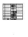
Revision History
No.
1
Revision content
First edition
Date of issue
Octover 2007
Manual code
NTS204X
- The current edition of this Instruction Manual also includes some corrections of simple misprints,
missing letters, misdescriptions and certain added explanations other than those listed in the above
Revision History table.
Table of contents
Chapter 1 Investigation of the inverter
1.1 Spesification label(Model name,manufacturing number:MFG) ················································1 - 1
1.1.1 Model name, ················································································································1 - 1
1.1.2 MFG number················································································································1 - 1
1.2 Precautions for Data Setting·····································································································1 - 2
1.2.1 Monitor Mode···············································································································1 - 2
1.2.2 Function Mode·············································································································1 - 3
1.2.3 Extended Function Mode ····························································································1 - 4
1.3 Code display system and key operations ·················································································1 - 20
1.3.1 Example of operation in basic display mode(“b037”=”04”[factory setting])·················1 - 21
1.3.2 Example of operation in full display mode(“b037”=”00”[factory setting])·····················1 - 23
1.3.3 Code/data display and key operator in extended function mode U ····························1 - 24
Chapter 2 Troubleshooting
2.1 Inverter trip contents,remedy,advise·························································································2 - 1
2.2 Option board error codes··········································································································2 - 5
2.2.1 Error indications by protective functions with the feedback option board (SJ-FB) mounted
·································································································································2 - 5
2.2.2 Error indications by protective functions with the digital option board (SJ-DG) mounted
·································································································································2 - 6
2.2.3 Error indications by protective functions with the DeviceNet option board (SJ-DN) mounted
·································································································································2 - 7
2.2.4 Error indications by protective functions with the easy sequence function used ········2 - 8
2.3 Trip conditions monitoring ········································································································2 - 9
2.4 Warning Codes·························································································································2 -10
2.5 Initialization setting ················································································································2 -11
Chapter 3 Debug Mode
3.1 Monitor Modes ··························································································································3 - 1
3.2 Function Modes ························································································································3 - 2
3.3 How To Reference the Data Area (d105) Corresponding to Trip History··································3 - 2
3.4 Inverter Setting ·························································································································3 - 3
3.4.1 Setting procedure ········································································································3 - 3
3.4.2 Confirming the completion of initialization···································································3 - 4
Chapter 4 The check of control power supply voltage and a control signal
4.1 Control power supply ················································································································4 - 1
4.2 Control signal ····························································································································4 - 1
Chapter 5 Maintenance and Inspection
5.1 Precautions for Maintenance and Inspection ···········································································5 - 1
5.1.1 Daily inspection············································································································5 - 1
5.1.2 Cleaning·······················································································································5 - 1
5.1.3 Periodic inspection·······································································································5 - 1
5.2 Daily and Periodic Inspections·································································································5 - 2
5.3 Ground Resistance Test with a Megger ···················································································5 - 3
5.4 Withstand Voltage Test·············································································································5 - 3
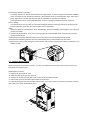
5.5 Method of Checking the Inverter and Converter Circuits·························································5 - 4
5.6 Replacing Parts························································································································5 - 5
5.7 Inverter Replacement···············································································································5 - 8
iii
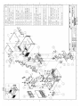
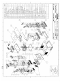
Appendix
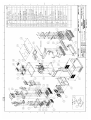
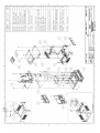
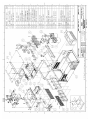
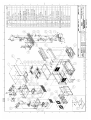
Circuit Diagram····························································································································6 - 1
Internal block diagram ·················································································································6 - 2
Structure figure ····························································································································6 - 15
iv
1. Investigation of the inverter
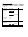
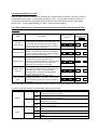
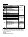
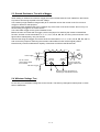
1.1 Specification label(Model name,Manufacturing number:MFG)
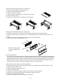
・There is a specification label attached to the inverter as shown in Figure 1-1.
Specification
label
Figure 1-1 Location of the specifications label
・Please confirm the model name and MFG number from the specification label as follows.
Inverter model
Maximum applicable motor capacity
Input ratings
Output ratings
Serial number
Model:
kW/(HP):
SJ700-150HFF2
15/(20)
Input/Entree:
Output/Sortie:
50Hz,60Hz
V
1 Ph
A
50Hz,60Hz
380-480V
3 Ph
35A
0 -400Hz
380-480V
3 Ph
MFGNo.
77AAT12345 A 001
Hitachi Industrial Equipment
Systems Co.,Ltd.
32A
Date: 0707
MADE IN JAPAN
NE
Figure 1-2 Contents of the specifications label
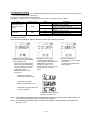
1.1.1 Model name
SJ700-150 H F F 2
2:type2
F:with EMC filter
F:with digital operator
L:3Ø200V class
H:3Ø400V class
Applicable motor(150:15kW)
Model name
1.1.2 MFG number
77 A T12345 7 001
Serial No.(001-999)
Year of production(7:2007)
Production No.
REV.No.(1 charactor or 2 character)
Production year & month(78:2007/August)
1-1
1.2 Precautions for Data Setting
The default display mode limits the screens (parameters) that can be displayed on the monitor. To enable the display
of all parameters, specify "00" (full display) for the function code display restriction (b037).
To enable the parameters to be changed while the inverter is operating, specify "10" for the software lock mode
selection (b031).
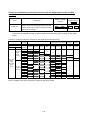
1.2.1 Monitoring Mode
Code
Function name
d001
Output frequency monitoring
0.00 to 99.99, 100.0 to 400.0 (Hz)
Monitored data or setting
d002
Output current monitoring
0.0 to 999.9, 1000 to 9999 (A)
d003
Rotation direction minitoring
F (forward rotation), o (stopped), r (reverse rotation)
d004
Process variable (PV), PID feedback
monitoring
0.00 to 99.99, 100.0 to 999.9, 1000. to 9999.
1000 to 9999 (10000 to 99990), 100 to 999 (100000 to 999000)
d005
Intelligent input terminal status
8
d006
(Example)
Terminals FW, 7, 2, and 1: ON
Terminals 8, 6, 5, 4, and 3: OFF
FW
7 6
5 4
3 2
1
Intelligent output terminal status
(Example)
Terminals 12 and 11: ON
Terminals AL, 15, 14, and 13: OFF
AL 15 14
13 12
11
d007
Scaled output frequency monitoring
0.00 to 99.99, 100.0 to 999.9, 1000. to 9999., 1000 to 3996 (10000 to 39960)
d008
Actual-frequency monitoring
-400. to -100., -99.9 to 0.00 to 99.99, 100.0 to 400.0 (Hz)
d009
Torque command monitoring
-200. to +200. (%)
d010
Torque bias monitoring
-200. to +200. (%)
d012
Torque monitoring
-200. to +200. (%)
d013
Output voltage monitoring
0.0 to 600.0 (V)
d014
Power monitoring
0.0 to 999.9 (kW)
d015
Cumulative power monitoring
0.0 to 999.9, 1000. to 9999.
1000 to 9999 (10000 to 99990), 100 to 999 (100000 to 999000)
d016
Cumulative operation RUN time
monitoring
0. to 9999., 1000 to 9999 (10000 to 99990), 100 to 999 (100000 to 999000) (hr)
d017
Cumulative power-on time monitoring
0. to 9999., 1000 to 9999 (10000 to 99990), 100 to 999 (100000 to 999000) (hr)
d018
Heat sink temperature monitoring
-020. to 200.0 ( C)
d019
Motor temperature monitoring
-020. to 200.0 ( C)
d022
Life-check monitoring
1: Capacitor on main circuit board
2: Cooling-fan speed drop
ON
OFF
2
d023
Program counter
0 to 1024
d024
Program number monitoring
0000 to 9999
1
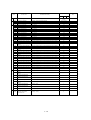
1-2
Default
Note
Code
Function name
Monitored data or setting
Default
d025
User monitor 0
-2147483647 to 2147483647 (upper 4 digits including “-“)
−
d026
User monitor 1
-2147483647 to 2147483647 (upper 4 digits including “-“)
−
d027
User monitor 2
-2147483647 to 2147483647 (upper 4 digits including “-“)
−
d028
Pulse counter
0 to 2147483647 (upper 4 digits)
−
d029
Position setting monitor
-1073741823 to 1073741823 (upper 4 digits including “-“)
−
d030
Position feedback monitor
-1073741823 to 1073741823 (upper 4 digits including “-“)
−
d080
Trip Counter
0. to 9999., 1000 to 6553 (10000 to 65530) (times)
−
Trip monitoring 1
Factor, frequency (Hz), current (A), voltage across P-N (V), running time (hours),
power-on time (hours)
−
Trip monitoring 2
Factor, frequency (Hz), current (A), voltage across P-N (V), running time (hours),
power-on time (hours)
−
Trip monitoring 3
Factor, frequency (Hz), current (A), voltage across P-N (V), running time (hours),
power-on time (hours)
−
Trip monitoring 4
Factor, frequency (Hz), current (A), voltage across P-N (V), running time (hours),
power-on time (hours)
−
Trip monitoring 5
Factor, frequency (Hz), current (A), voltage across P-N (V), running time (hours),
power-on time (hours)
−
Trip monitoring 6
Factor, frequency (Hz), current (A), voltage across P-N (V), running time (hours),
power-on time (hours)
−
d090
Programming error monitoring
Warning code
−
d102
DC voltage monitoring
0.0 to 999.9 (V)
−
d103
BRD load factor monitoring
0.0 to 100.0 (%)
−
d104
Electronic thermal overload monitoring
0.0 to 100.0 (%)
−
d081
d082
d083
d084
d085
d086
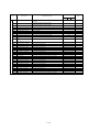
1.2.2 Function Mode
Default
Code
Function name
Monitored data or setting
_FF
Output frequency setting
F001
0.0, "start frequency" to "maximum frequency" (or maximum frequency,
2nd/3rd motors) (Hz)
0.0 to 100.0 (when PID function is enabled)
_FEF
0.00
F002
Acceleration (1) time setting
0.01 to 99.99, 100.0 to 999.9, 1000. to 3600. (s)
30.00
F202
Acceleration (1) time setting, 2nd
motor
0.01 to 99.99, 100.0 to 999.9, 1000. to 3600. (s)
30.00
F302
Acceleration (1) time setting, 3rd
motor
0.01 to 99.99, 100.0 to 999.9, 1000. to 3600. (s)
30.00
F003
Deceleration (1) time setting
0.01 to 99.99, 100.0 to 999.9, 1000. to 3600. (s)
30.00
F203
Deceleration time setting, 2nd motor
0.01 to 99.99, 100.0 to 999.9, 1000. to 3600. (s)
30.00
30.00
F303
Deceleration time setting, 3rd motor
0.01 to 99.99, 100.0 to 999.9, 1000. to 3600. (s)
F004
Keypad Run key routing
00 (forward rotation), 01 (reverse rotation)
1-3
00
_FUF
Note
1.2.3 Extended Function Mode
Default
Code
Function name
Frequency source setting
A001
Basic settings
_FEF
_FUF
02
01
01
01 (control circuit terminal block), 02 (digital operator), 03 (RS485), 04 (option
1), 05 (option 2)
02
01
01
A003
Base frequency setting
30. to "maximum frequency " (Hz)
60.
50.
60.
A203
Base frequency setting, 2nd
motor
30. to "maximum frequency, 2nd motor" (Hz)
60.
50.
60.
A303
Base frequency setting, 3rd
motor
30. to "maximum frequency, 3rd motor" (Hz)
60.
50.
60.
A004
Maximum frequency setting
30. to 400. (Hz)
60.
50.
60.
A204
Maximum frequency setting, 2nd 30. to 400. (Hz)
motor
60.
50.
60.
A304
Maximum frequency setting, 3rd 30. to 400. (Hz)
motor
60.
50.
60.
[AT] selection
A005
[O2] selection
A006
Analog input and others
00 (keypad potentiometer) (*1), 01 (control circuit terminal block), 02 (digital
operator), 03 (RS485), 04 (option 1), 05 (option 2), 06 (pulse-string input), 07
(easy sequence), 10 (operation function result)
Note
_FF
Run command source setting
A002
00 (switching between O and OI terminals), 01 (switching between O and O2
terminals), 02 (switching between O terminal and keypad potentiometer) (*1),
03 (switching between OI terminal and keypad potentiometer) (*1), 04
(switching between O2 and keypad potentiometer) (*1)
00
00 (single), 01 (auxiliary frequency input via O and OI terminals)
(nonreversible), 02 (auxiliary frequency input via O and OI terminals)
(reversible), 03 (disabling O2 terminal)
03
A011
[O]-[L] input active range start
frequency
0.00 to 99.99, 100.0 to 400.0 (Hz)
A012
[O]-[L] input active range end
frequency
0.00 to 99.99, 100.0 to 400.0 (Hz)
A013
[O]-[L] input active range start
voltage
0. to "[O]-[L] input active range end voltage" (%)
A014
[O]-[L] input active range end
voltage
"[O]-[L] input active range start voltage" to 100. (%)
A015
[O]-[L] input active range start
frequency selection
00 (external start frequency), 01 (0 Hz)
A016
External frequency filter time
const.
1. to 30. or 31. (500 ms filter ±0.1 Hz with hysteresis)
A017
Easy sequence function
selection
00 (disabling), 01 (enabling)
Multispeed operation selection
00 (binary: 16 speeds selectable with 4 terminals), 01 (bit: 8 speeds selectable
with 7 terminals)
A020
Multispeed frequency setting
0.0 or “start frequency” to “maximum frequency” (Hz)
A220
Multispeed frequency setting,
2nd motor
0.0 or “start frequency” to “maximum frequency, 2nd motor” (Hz)
A320
Multispeed frequency setting,
3rd motor
0.0 or “start frequency” to “maximum frequency, 3rd motor” (Hz)
A021
Multispeed 1 setting
0.0 or “start frequency” to “1st maximum frequency” (Hz)
A019
Multispeed operation and jogging
Monitored data or setting
0.00
0.00
0.
100.
01
31.
00
00
0.00
0.00
0.00
0.00
A022
Multispeed 2 setting
0.0 or “start frequency” to “2nd maximum frequency” (Hz)
0.00
A023
Multispeed 3 setting
0.0 or “start frequency” to “3rd maximum frequency” (Hz)
0.00
A024
Multispeed 4 setting
0.0 or “start frequency” to “n-th maximum frequency” (Hz)
0.00
A025
Multispeed 5 setting
0.0 or “start frequency” to “n-th maximum frequency” (Hz)
0.00
A026
Multispeed 6 setting
0.0 or “start frequency” to “n-th maximum frequency” (Hz)
0.00
A027
Multispeed 7 setting
0.0 or “start frequency” to “n-th maximum frequency” (Hz)
0.00
A028
Multispeed 8 setting
0.0 or “start frequency” to “n-th maximum frequency” (Hz)
0.00
A029
Multispeed 9 setting
0.0 or “start frequency” to “n-th maximum frequency” (Hz)
0.00
A030
Multispeed 10 setting
0.0 or “start frequency” to “n-th maximum frequency” (Hz)
0.00
A031
Multispeed 11 setting
0.0 or “start frequency” to “n-th maximum frequency” (Hz)
0.00
A032
Multispeed 12 setting
0.0 or “start frequency” to “n-th maximum frequency” (Hz)
0.00
A033
Multispeed 13 setting
0.0 or “start frequency” to “n-th maximum frequency” (Hz)
0.00
A034
Multispeed 14 setting
0.0 or “start frequency” to “n-th maximum frequency” (Hz)
0.00
A035
Multispeed 15 setting
0.0 or “start frequency” to “n-th maximum frequency” (Hz)
0.00
A038
Jog frequency setting
"Start frequency" to 9.99 (Hz)
1.00
Jog stop mode
00 (free-running after jogging stops [disabled during operation]), 01
(deceleration and stop after jogging stops [disabled during operation]), 02 (DC
braking after jogging stops [disabled during operation]), 03 (free-running after
jogging stops [enabled during operation]), 04 (deceleration and stop after
jogging stops [enabled during operation]), 05 (DC braking after jogging stops
[enabled during operation])
A039
.
1-4
00
Default
Code
Function name
Monitored data or setting
Note
PID control
Frequency upper/lower limit and jump frequency
DC braking
V/f characteristic
_FF
_FEF
A041
Torque boost method selection
00 (manual torque boost), 01 (automatic torque boost)
A241
Torque boost method selection,
2nd motor
00 (manual torque boost), 01 (automatic torque boost)
00
00
A042
Manual torque boost value
0.0 to 20.0 (%)
1.0
A242
Manual torque boost value, 2nd
motor
0.0 to 20.0 (%)
1.0
A342
Manual torque boost value, 3rd
motor
0.0 to 20.0 (%)
1.0
A043
Manual torque boost frequency
adjustment
0.0 to 50.0 (%)
5.0
A243
Manual torque boost frequency
adjustment, 2nd motor
0.0 to 50.0 (%)
5.0
A343
Manual torque boost frequency
adjustment, 3rd motor
0.0 to 50.0 (%)
5.0
A044
V/F characteristic curve
selection, 1st motor
00 (VC), 01 (VP), 02 (free V/f), 03 (sensorless vector control), 04 (0Hz-range
sensorless vector), 05 (vector with sensor)
00
A244
V/F characteristic curve
selection, 2nd motor
00 (VC), 01 (VP), 02 (free V/f), 03 (sensorless vector control), 04 (0Hz-range
sensorless vector)
00
A344
V/F characteristic curve
selection, 3rd motor
00(VC), 01(VP)
00
A045
V/f gain setting
20. to 100. (%)
100.
A046
Voltage compensation gain
setting for automatic torque
boost. 1st motor
0. to 255.
100.
A246
Voltage compensation gain
setting for automatic torque
boost, 2nd motor
0. to 255.
100.
A047
Slippage compensation gain
setting for automatic torque
boost, 1st motor
0. to 255.
100.
A247
Slippage compensation gain
setting for automatic torque
boost, 2nd motor
0. to 255.
100.
A051
DC braking enable
00 (disabling), 01 (enabling), 02 (set frequency only)
A052
DC braking frequency setting
0.00 to 99.99, 100.0 to 400.0 (Hz)
0.50
A053
DC braking wait time
0.0 to 5.0 (s)
0.0
A054
DC braking force during
deceleration
0. to 100. (%)
0.
A055
DC braking time for deceleration 0.0 to 60.0 (s)
0.0
A056
DC braking/edge or level
detection for [DB] input
00 (edge operation), 01 (level operation)
01
A057
DC braking force for starting
0. to 100.(%)
0.
A058
DC braking time for starting
0.0 to 60.0(s)
0.0
A059
DC braking carrier frequency
setting
0.5 to 15.0(kHz)
5.0
A061
Frequency upper limit setting
0.00 or "1st minimum frequency limit" to "maximum frequency" (Hz)
0.00
A261
Frequency upper limit setting,
2nd motor
0.00 or "2nd minimum frequency limit" to "maximum frequency, 2nd motor" (Hz)
0.00
A062
Frequency lower limit setting
0.00 or "start frequency" to "maximum frequency limit"
(Hz)
0.00
A262
Frequency lower limit setting,
2nd motor
0.00 or "start frequency" to "maximum frequency, 2nd motor limit"
(Hz)
0.00
A063
Jump (center) frequency setting
1
0.00 to 99.99, 100.0 to 400.0 (Hz)
0.00
A064
Jump (hysteresis) frequency
width setting 1
0.00 to 10.00 (Hz)
0.50
A065
Jump (center) frequency setting
2
0.00 to 99.99, 100.0 to 400.0 (Hz)
0.00
A066
Jump (hysteresis) frequency
width setting 2
0.00 to 10.00 (Hz)
0.50
A067
Jump (center) frequency setting
3
0.00 to 99.99, 100.0 to 400.0 (Hz)
0.00
A068
Jump (hysteresis) frequency
width setting 3
0.00 to 10.00 (Hz)
0.50
A069
Acceleration stop frequency
setting
0.00 to 99.99, 100.0 to 400.0 (Hz)
0.00
A070
Acceleration stop time frequency
0.0 to 60.0 (s)
setting
A071
PID Function Enable
00 (disabling), 01 (enabling), 02 (enabling inverted-data output)
00
A072
PID proportional gain
0.2 to 5.0
1.0
A073
PID integral time constant
0.0 to 999.9, 1000. to 3600. (s)
1.0
A074
PID derivative gain
0.00 to 99.99, 100.0 (s)
0.00
1.00
00
0.0
A075
PV scale conversion
0.01 to 99.99
A076
PV source setting
00 (input via OI), 01 (input via O), 02 (external communication), 03 (pulse-string
frequency input), 10 (operation result output)
A077
Output of inverted PID deviation 00(OFF), 01 (ON)
A078
PID variation range
0.0 to 100.0 (%)
A079
PID feed forward selection
00 (disabled), 01 (O input), 02 (OI input), 03 (O2 input)
00
00
0.00
1-5
00
_FUF
Default
Acceleration and
deceleration
Operation-target frequency
n and
deceleratio
External frequency adjustment
Operation mode and acceleration/deceleration function
AVR
Code
Function name
Monitored data or setting
Note
_FF
_FEF
_FUF
02
00
00
A081
AVR function select
00 (always on), 01 (always off), 02 (off during deceleration)
A082
AVR voltage select
200 V class: 200, 215, 220, 230, 240 (V)
400 V class: 380, 400, 415, 440, 460, 480 (V)
A085
Operation mode selection
00 (normal operation), 01 (energy-saving operation), 02 (fuzzy operation)
A086
Energy saving mode tuning
0.1 to 100.0
A092
Acceleration (2) time setting
0.01 to 99.99, 100.0 to 999.9, 1000. to 3600. (s)
15.00
A292
Acceleration (2) time setting,
2nd motor
0.01 to 99.99, 100.0 to 999.9, 1000. to 3600. (s)
15.00
A392
Acceleration (2) time setting,
3rd motor
0.01 to 99.99, 100.0 to 999.9, 1000. to 3600. (s)
15.00
A093
Deceleration (2) time setting
0.01 to 99.99, 100.0 to 999.9, 1000. to 3600. (s)
15.00
A293
Deceleration (2) time setting,
2nd motor
0.01 to 99.99, 100.0 to 999.9, 1000. to 3600. (s)
15.00
A393
Deceleration (2) time setting,
3rd motor
0.01 to 99.99, 100.0 to 999.9, 1000. to 3600. (s)
15.00
A094
Select method to switch to
Acc2/Dec2 profile
00 (switching by 2CH terminal), 01 (switching by setting), 02 (switching only
when rotation is reversed)
00
A294
Select method to switch to
Acc2/Dec2, 2nd motor
00 (switching by 2CH terminal), 01 (switching by setting), 02 (switching only
when rotation is reversed)
00
A095
Acc1 to Acc2 frequency
transition point
0.00 to 99.99, 100.0 to 400.0 (Hz)
0.00
A295
Acc1 to Acc2 frequency
transition point, 2nd motor
0.00 to 99.99, 100.0 to 400.0 (Hz)
0.00
A096
Dec1 to Dec2 frequency
transition point
0.00 to 99.99, 100.0 to 400.0 (Hz)
0.00
A296
Dec1 to Dec2 frequency
transition point, 2nd motor
0.00 to 99.99, 100.0 to 400.0 (Hz)
0.00
A097
Acceleration curve selection
00 (linear), 01 (S curve), 02 (U curve), 03 (inverted-U curve), 04 (EL-S curve)
00
A098
Deceleration curve setting
00 (linear), 01 (S curve), 02 (U curve), 03 (inverted-U curve), 04 (EL-S curve)
00
A101
[OI]-[L] input active range start
frequency
0.00 to 99.99, 100.0 to 400.0 (Hz)
0.00
A102
[OI]-[L] input active range end
frequency
0.00 to 99.99, 100.0 to 400.0 (Hz)
0.00
A103
[OI]-[L] input active range start
current
0. to "[OI]-[L] input active range end current" (%)
20.
A104
[OI]-[L] input active range end
current
"[OI]-[L] input active range start current" to 100. (%)
100.
A105
[OI]-[L] input start frequency
enable
00 (external start frequency), 01 (0 Hz)
A111
[O2]-[L] input active range start
frequency
-400. to -100., -99.9 to 0.00 to 99.99, 100.0 to 400.0 (Hz)
0.00
A112
[O2]-[L] input active range end
frequency
-400. to -100., -99.9 to 0.00 to 99.99, 100.0 to 400.0 (Hz)
0.00
A113
[O2]-[L] input active range start
voltage
-100. to 02 end-frequency rate (%)
-100.
A114
[O2]-[L] input active range end
voltage
"02 start-frequency rate" to 100. (%)
100.
A131
Acceleration curve constants
setting
01 (smallest swelling) to 10 (largest swelling)
02
A132
Deceleration curve constants
setting
01 (smallest swelling) to 10 (largest swelling)
02
Operation-target frequency
selection 1
00 (digital operator), 01 (keypad potentiometer), 02 (input via O), 03 (input via
OI), 04 (external communication), 05 (option 1), 06 (option 2), 07 (pulse-string
frequency input)
02
A142
Operation-target frequency
selection 2
00 (digital operator), 01 (keypad potentiometer), 02 (input via O), 03 (input via
OI), 04 (external communication), 05 (option 1), 06 (option 2), 07 (pulse-string
frequency input)
03
A143
Operator selection
00 (addition: A141 + A142), 01 (subtraction: A141 - A142), 02 (multiplication:
A141 x A142)
A145
Frequency to be added
0.00 to 99.99, 100.0 to 400.0 (Hz)
A146
Sign of the frequency to be
added
00 (frequency command + A145), 01 (frequency command - A145)
00
A150
EL-S-curve acceleration
ratio 1
0. to 50. (%)
25.
A151
EL-S-curve acceleration
ratio 2
0. to 50. (%)
25.
A152
EL-S-curve deceleration
ratio 1
0. to 50. (%)
25.
A153
EL-S-curve deceleration
ratio 2
0. to 50. (%)
25.
A141
200/400 230/400 230/460
00
50.0
00
00
0.00
1-6
Default
Code
Function name
Monitored data or setting
Note
Restart after instantaneous power failure or tripping
_FF
b001
b002
b003
b004
b005
b006
b007
b008
b009
b010
b011
b012
b212
Electronic thermal function
b312
00
Allowable under-voltage power
0.3 to 25.0 (s)
failure time
Retry wait time before motor restart 0.3 to 100.0 (s)
Instantaneous power
failure/under-voltage trip alarm
enable
Number of restarts on power
failure/under-voltage trip events
Phase loss detection enable
Restart frequency threshold
1.0
1.0
00 (disabling), 01 (enabling), 02 (disabling during stopping and decelerating
to stop)
00
00 (16 times), 01 (unlimited)
00
00 (disabling), 01 (enabling)
0.00 to 99.99, 100.0 to 400.0 (Hz)
00 (tripping), 01 (starting with 0 Hz), 02 (starting with matching frequency), 03
Selection of retry after tripping
(tripping after deceleration and stopping with matching frequency), 04
(restarting with active matching frequency)
Selection of retry after undervoltage 00 (16 times), 01 (unlimited)
Selection of retry count after
1 to 3 (times)
overvoltage or overcurrent
Retry wait time after tripping
0.3 to 100.0 (s)
Electronic thermal setting
(calculated within the inverter from 0.20 x "rated current" to 1.00 x "rated current" (A)
current output)
Electronic thermal setting
(calculated within the inverter from 0.20 x "rated current" to 1.00 x "rated current" (A)
current output), 2nd motor
Electronic thermal setting
(calculated within the inverter from 0.20 x "rated current" to 1.00 x "rated current" (A)
current output), 3rd motor
00
0.00
00
00
3
1.0
Rated current of inverter
Rated current of inverter
Rated current of inverter
Electronic thermal characteristic
00 (reduced-torque characteristic), 01 (constant-torque characteristic), 02
(free setting)
00
01
01
b213
Electronic thermal characteristic, 2nd 00 (reduced-torque characteristic), 01 (constant-torque characteristic), 02
motor
(free setting)
00
01
01
b313
Electronic thermal characteristic, 3rd 00 (reduced-torque characteristic), 01 (constant-torque characteristic), 02
motor
(free setting)
00
01
01
b015
b016
b018
b019
b020
Overload restriction and overcurrent restraint
00 (tripping), 01 (starting with 0 Hz), 02 (starting with matching frequency), 03
(tripping after deceleration and stopping with matching frequency), 04
(restarting with active matching frequency)
_FUF
b013
b017
Free setting, electronic thermal
frequency (1)
Free setting, electronic thermal
current (1)
Free setting, electronic thermal
frequency (2)
Free setting, electronic thermal
current (2)
Free setting, electronic thermal
frequency (3)
Free setting, electronic thermal
current (3)
0. to 400. (Hz)
0.
0.0 to rated current (A)
0.0
0. to 400. (Hz)
0.
0.0 to rated current (A)
0.0
0. to 400. (Hz)
0.
0.0 to rated current (A)
0.0
b021
00 (disabling), 01 (enabling during acceleration and deceleration), 02
Overload restriction operation mode (enabling during constant speed), 03 (enabling during acceleration and
deceleration (increasing the speed during regeneration))
b022
Overload restriction setting
0.20 x "rated current" to 1.00 x "rated current" (A)
b023
Deceleration rate at overload
restriction
0.10 to 30.00 (s)
b024
00 (disabling), 01 (enabling during acceleration and deceleration), 02
Overload restriction operation mode
(enabling during constant speed), 03 (enabling during acceleration and
(2)
deceleration (increasing the speed during regeneration))
b025
b026
b027
b028
b029
b030
Software
lock
Selection of restart mode
_FEF
b031
Overload restriction setting (2)
Deceleration rate at overload restriction
(2)
Overcurrent suppression enable
Active frequency matching, scan
start frequency
Active frequency matching,
scan-time constant
Active frequency matching, restart
frequency select
Software lock mode selection
01
Rated current of inverter x
1.50
1.00
0.20 x "rated current" to 2.00 x "rated current" (A)
0.10 to 30.00 (s)
01
Rated current of inverter x
1.50
1.00
00 (disabling), 01 (enabling)
01
0.20 x "rated current" to 2.00 x "rated current" (A)
0.10 to 30.00 (s)
Rated current of inverter
0.50
00 (frequency at the last shutoff), 01 (maximum frequency), 02 (set
frequency)
00 (disabling change of data other than "b031" when SFT is on), 01 (disabling
change of data other than "b031" and frequency settings when SFT is on), 02
(disabling change of data other than "b031"), 03 (disabling change of data
other than "b031" and frequency settings), 10 (enabling data changes during
operation)
1-7
00
01
Default
Code
Function name
Monitored data or setting
Note
Window comparator
Non-stop operation at momentary power
failure
Torque limitation
Others
_FF
_FEF
b034
Run/power-on warning time
0. to 9999. (0 to 99990), 1000 to 6553 (10000 to 655300) (hr)
0.
b035
Rotational direction restriction
00 (enabling both forward and reverse rotations), 01 (enabling only
forward rotation), 02 (enabling only reverse rotation)
00
b036
Reduced voltage start selection
0 (minimum reduced voltage start time) to 255 (maximum reduced voltage
start time)
6
Function code display restriction
00 (full display), 01 (function-specific display), 02 (user setting), 03 (data
comparison display), 04 (basic display)
04
b038
Initial-screen selection
00 (screen displayed when the STR key was pressed last), 01 (d001), 02
(d002), 03 (d003), 04 (d007), 05 (F001)
01
b039
Automatic user-parameter
setting function enable
00 (disabling), 01 (enabling)
00
b040
Torque limit selection
00 (quadrant-specific setting), 01 (switching by terminal), 02 (analog
input), 03 (option 1), 04 (option 2)
00
b041
Torque limit (1) (forward-driving
in 4-quadrant mode)
0. to 200. (%), no (disabling torque limitation)
150.
b042
Torque limit (2)
(reverse-regenerating in
4-quadrant mode)
0. to 200. (%), no (disabling torque limitation)
150.
b043
Torque limit (3) (reverse-driving
in 4-quadrant mode)
0. to 200. (%), no (disabling torque limitation)
150.
b044
Torque limit (4)
(forward-regenerating in
4-quadrant mode)
0. to 200. (%), no (disabling torque limitation)
150.
b045
Torque limit LADSTOP enable
00 (disabling), 01 (enabling)
00
b046
Reverse Run protection enable
00 (disabling), 01 (enabling)
00
b050
Controller deceleration and stop
on power loss
00 (disabling), 01 (nonstop deceleration to stop), 02 (DC voltage constant
control, with resume), 03 ( without resume)
00
b051
DC bus voltage trigger level
during power loss
0.0 to 999.9, 1000. (V)
220/440
b052
Over-voltage threshold during
power loss
0.0 to 999.9, 1000. (V)
360/720
b053
Deceleration time setting during
power loss
0.01 to 99.99, 100.0 to 999.9, 1000. to 3600. (s)
1.00
b054
Initial output frequency decrease
during power loss
0.00 to 10.00 (Hz)
0.00
b055
Proportional gain setting for
nonstop operation at power loss
0.00 to 2.55
0.20
b056
Integral time setting for nonstop
operation at power loss
0.000 to 9.999 /10.00 to 65.53 (s)
0.100
b060
Maximum-limit level of window
comparators O
0. to 100. (lower limit : b061 + b062 / 2) (%)
100
b061
Minimum-limit level of window
comparators O
0. to 100. (lower limit : b060 - b062 / 2) (%)
0
b062
Hysteresis width of window
comparators O
0. to 10. (lower limit : b061 - b062 / 2) (%)
0
b063
Maximum-limit level of window
comparators OI
0. to 100. (lower limit : b064 + b066 / 2) (%)
100
b064
Minimum-limit level of window
comparators OI
0. to 100. (lower limit : b063 - b066 / 2) (%)
0
b065
Hysteresis width of window
comparators OI
0. to 10. (lower limit : b063 - b064 / 2) (%)
b066
Maximum-limit level of window
comparators OI
-100. to 100. (lower limit : b067 + b068 / 2) (%)
100
b067
Minimum-limit level of window
comparators O/OI/O2
-100. to 100. (lower limit : b066 - b068 / 2) (%)
0
b068
Hysteresis width of window
comparators O/OI/O2
0. to 10. (lower limit : b066 - b067 / 2) (%)
0
b070
Operation level at O
disconnection
0. to 100. (%) or "no" (ignore)
no
b071
Operation level at OI
disconnection
0. to 100. (%) or "no" (ignore)
no
b072
Operation level at O2
disconnection
-100. to 100. (%) or "no" (ignore)
no
b037
1-8
0
_FUF
Default
Code
Function name
Monitored data or setting
Note
Others
Free setting of V/f characteristic
Others
_FF
_FEF
b078
Cumulative input power data
clearance
b079
Cumulative input power display
gain setting
1. to 1000.
b082
Start frequency adjustment
0.10 to 9.99 (Hz)
0.50
b083
Carrier frequency setting
0.5 to 15.0 (kHz) (subject to derating)
5.0
b084
Initialization mode (parameters or
trip history)
00 (clearing the trip history), 01 (initializing the data),
02 (clearing the trip history and initializing the data)
b085
Country code for initialization
00 (Japan), 01 (EU), 02 (U.S.A.)
b086
Frequency scaling conversion
factor
0.1 to 99.0
1.0
b087
STOP key enable
00 (enabling), 01 (disabling), 02 (disabling only the function to stop)
00
b088
Restart mode after FRS
00 (starting with 0 Hz), 01 (starting with matching frequency), 02 (starting
with active matching frequency)
00
b089
Automatic carrier frequency
reduction
00: invalid, 01: valid
00
b090
Dynamic braking usage ratio
0.0 to 100.0 (%)
0.0
b091
Stop mode selection
00 (deceleration until stop), 01 (free-run stop)
00
b092
Cooling fan control
00 (always operating the fan), 01 (operating the fan only during inverter
operation [including 5 minutes after power-on and power-off])
00
b095
Dynamic braking control
00 (disabling), 01 (enabling [disabling while the motor is topped]), 02
(enabling [enabling also while the motor is topped])
00
b096
Dynamic braking activation level
330 to 380, 660 to 760(V)
b098
Thermistor for thermal protection
control
00 (disabling the thermistor), 01 (enabling the thermistor with PTC), 02
(enabling the thermistor with NTC)
b099
Thermal protection level setting
0. to 9999. (Ω)
b100
Free-setting V/f frequency (1)
0. to "free-setting V/f frequency (2)" (Hz)
0.
b101
Free-setting V/f voltage (1)
0.0 to 800.0 (V)
0.0
b102
Free-setting V/f frequency (2)
0. to "free-setting V/f frequency (3)" (Hz)
0.
b103
Free-setting V/f voltage (2)
0.0 to 800.0 (V)
0.0
b104
Free-setting V/f frequency (3)
0. to "free-setting V/f frequency (4)" (Hz)
0.
b105
Free-setting V/f voltage (3)
0.0 to 800.0 (V)
0.0
b106
Free-setting V/f frequency (4)
0. to "free-setting V/f frequency (5)" (Hz)
0.
b107
Free-setting V/f voltage (4)
0.0 to 800.0 (V)
0.0
b108
Free-setting V/f frequency (5)
0. to "free-setting V/f frequency (6)" (Hz)
0.
b109
Free-setting V/f voltage (5)
0.0 to 800.0 (V)
0.0
b110
Free-setting V/f frequency (6)
0. to "free-setting V/f frequency (7)" (Hz)
0.
b111
Free-setting V/f voltage (6)
0.0 to 800.0 (V)
0.0
b112
Free-setting V/f frequency (7)
0. to 400. (Hz)
0.
b113
Free-setting V/f voltage (7)
0.0 to 800.0 (V)
0.0
b120
Brake Control Enable
00 (disabling), 01 (enabling)
b121
Brake Wait Time for Release
0.00 to 5.00 (s)
0.00
b122
Brake Wait Time for Acceleration
0.00 to 5.00 (s)
0.00
b123
Brake Wait Time for Stopping
0.00 to 5.00 (s)
0.00
b124
Brake Wait Time for Confirmation
0.00 to 5.00 (s)
0.00
b125
Brake Release Frequency Setting
0.00 to 99.99, 100.0 to 400.0 (Hz)
b126
Brake Release Current Setting
0.0 to 2.00 x "rated current"
b127
Braking frequency
0.00 to 99.99, 100.0 to 400.0 (Hz)
b130
Overvoltage suppression enable
00 (disabling the restraint), 01 (controlled deceleration), 02 (enabling
acceleration)
Clearance by setting "01" and pressing the STR key
_FUF
00
1.
00
00
01
02
360/
720
00
3000.
00
0.00
Rated current of inverter
0.00
00
b131
Overvoltage suppression level
330 to 390 (V) (200 V class model), 660 to 780 (V) (400 V class model)
380/
760
b132
Acceleration and deceleration
rate at overvoltage suppression
0.10 to 30.00 (s)
1.00
b133
Overvoltage suppression
propotional gain
0.00 to 2.55
0.50
b134
Overvoltage suppression Integral
time
0.000 to 9.999 / 10.00 to 65.53 (s)
0.060
1-9
Default
Code
Function name
Monitored data or setting
Note
Intelligent input terminals
_FF
C001
Terminal [1] function (*2)
C002
Terminal [2] function
C003
Terminal [3] function (*2)
C004
Terminal [4] function
C005
Terminal [5] function
C006
Terminal [6] function
C007
Terminal [7] function
C008
Terminal [8] function
01 (RV: Reverse RUN), 02 (CF1: Multispeed 1 setting), 03 (CF2: Multispeed 2
setting), 04 (CF3: Multispeed 3 setting), 05 (CF4: Multispeed 4 setting), 06 (JG:
Jogging), 07 (DB: external DC braking), 08 (SET: Set 2nd motor data), 09 (2CH:
2-stage acceleration/deceleration), 11 (FRS: free-run stop), 12 (EXT: external trip),
13 (USP: unattended start protection), 14: (CS: commercial power source enable),
15 (SFT: software lock), 16 (AT: analog input voltage/current select), 17 (SET3: 3rd
motor control), 18 (RS: reset), 20 (STA: starting by 3-wire input), 21 (STP: stopping
by 3-wire input), 22 (F/R: forward/reverse switching by 3-wire input), 23 (PID: PID
disable), 24 (PIDC: PID reset), 26 (CAS: control gain setting), 27 (UP: remote
control UP function), 28 (DWN: remote control DOWN function), 29 (DWN: remote
control data clearing), 31 (OPE: forcible operation), 32 (SF1: multispeed bit 1), 33
(SF2: multispeed bit 2), 34 (SF3: multispeed bit 3), 35 (SF4: multispeed bit 4), 36
(SF5: multispeed bit 5), 37 (SF6: multispeed bit 6), 38 (SF7: multispeed bit 7), 39
(OLR: overload restriction selection), 40 (TL: torque limit enable), 41 (TRQ1: torque
limit selection bit 1), 42 (TRQ2: torque limit selection bit 2), 43 (PPI: P/PI mode
selection), 44 (BOK: braking confirmation), 45 (ORT: orientation), 46 (LAC: LAD
cancellation), 47 (PCLR: clearance of position deviation), 48 (STAT: pulse train
position command input enable), 50 (ADD: trigger for frequency addition [A145]), 51
(F-TM: forcible-terminal operation), 52 (ATR: permission of torque command input),
53 (KHC: cumulative power clearance), 54 (SON: servo-on), 55 (FOC: forcing), 56
(MI1: general-purpose input 1), 57 (MI2: general-purpose input 2), 58 (MI3:
general-purpose input 3), 59 (MI4: general-purpose input 4), 60 (MI5:
general-purpose input 5), 61 (MI6: general-purpose input 6), 62 (MI7:
general-purpose input 7), 63 (MI8: general-purpose input 8), 65 (AHD: analog
command holding), 66 (CP1: multistage position settings selection 1 ), 67 (CP2:
multistage position settings selection 2), 68 (CP3: multistage position settings
selection 3), 69 (ORL: Zero-return limit function), 70 (ORG: Zero-return trigger
function), 71 (FOT: forward drive stop), 72 (ROT: reverse drive stop), 73 (SPD:
speed / position switching), 74 (PCNT: pulse counter), 75 (PCC: pulse counter
clear), no (NO: no assignment)
_FEF _FUF
18
(*2)
16
06
(*2)
11
09
03
03
02
01
C011
Terminal [1] active state
00 (NO) / 01 (NC)
00
C012
Terminal [2] active state
00 (NO) / 01 (NC)
00
C013
Terminal [3] active state
00 (NO) / 01 (NC)
00
C014
Terminal [4] active state
00 (NO) / 01 (NC)
00
C015
Terminal [5] active state
00 (NO) / 01 (NC)
00
C016
Terminal [6] active state
00 (NO) / 01 (NC)
00
C017
Terminal [7] active state
00 (NO) / 01 (NC)
00
C018
Terminal [8] active state
00 (NO) / 01 (NC)
00
C019
Terminal [FW] active state
00 (NO) / 01 (NC)
00
1 - 10
13
Default
Code
Function name
Monitored data or setting
Note
Intelligent output
terminals
Analog monitoring
Intelligent output terminals
_FF
_FEF
C021
Terminal [11] function
C022
Terminal [12] function
C023
Terminal [13] function
C024
Terminal [14] function
C025
Terminal [15] function
C026
Alarm relay terminal function
C027
[FM] siginal selection
00 (output frequency), 01 (output current), 02 (output torque), 03 (digital
output frequency), 04 (output voltage), 05 (input power), 06 (electronic
thermal overload), 07 (LAD frequency), 08 (digital current monitoring), 09
(motor temperature), 10 (heat sink temperature), 12 (general-purpose
output YA0)
00
C028
[AM] siginal selection
00 (output frequency), 01 (output current), 02 (output torque), 04 (output
voltage), 05 (input power), 06 (electronic thermal overload), 07 (LAD
frequency), 09 (motor temperature), 10 (heat sink temperature), 11 (output
torque [signed value]), 13 (general-purpose output YA1)
00
C029
[AMI] siginal selection
00 (output frequency), 01 (output current), 02 (output torque), 04 (output
voltage), 05 (input power), 06 (electronic thermal overload), 07 (LAD
frequency), 09 (motor temperature), 10 (heat sink temperature), 14
(general-purpose output YA2)
00
C030
Digital current monitor reference
value
0.20 x "rated current" to 2.00 x "rated current" (A)
(Current with digital current monitor output at 1,440 Hz)
C031
Terminal [11] active state
00 (NO) / 01 (NC)
00
C032
Terminal [12] active state
00 (NO) / 01 (NC)
00
C033
Terminal [13] active state
00 (NO) / 01 (NC)
00
C034
Terminal [14] active state
00 (NO) / 01 (NC)
00
C035
Terminal [15] active state
00 (NO) / 01 (NC)
00
C036
Alarm relay active state
00 (NO) / 01 (NC)
01
00 (RUN: running), 01 (FA1: constant-speed reached), 02 (FA2: set
frequency overreached), 03 (OL: overload notice advance signal (1)), 04
(OD: output deviation for PID control), 05 (AL: alarm signal), 06 (FA3: set
frequency reached), 07 (OTQ: over-torque), 08 (IP: instantaneous power
failure), 09 (UV: undervoltage), 10 (TRQ: torque limited), 11 (RNT:
operation time over), 12 (ONT: plug-in time over), 13 (THM: thermal alarm
signal), 19 (BRK: brake release), 20 (BER: braking error), 21 (ZS: 0 Hz
detection signal), 22 (DSE: speed deviation maximum), 23 (POK:
positioning completed), 24 (FA4: set frequency overreached 2), 25 (FA5:
set frequency reached 2), 26 (OL2: overload notice advance signal (2)), 27
(Odc: Analog O disconnection detection), 28 (OIDc: Analog OI
disconnection detection), 29 (O2Dc: Analog O2 disconnection detection),
31 (FBV: PID feedback comparison), 32 (NDc: communication line
disconnection), 33 (LOG1: logical operation result 1), 34 (LOG2: logical
operation result 2), 35 (LOG3: logical operation result 3), 36 (LOG4: logical
operation result 4), 37 (LOG5: logical operation result 5), 38 (LOG6: logical
operation result 6), 39 (WAC: capacitor life warning), 40 (WAF: cooling-fan
speed drop), 41 (FR: starting contact signal), 42 (OHF: heat sink overheat
warning), 43 (LOC: low-current indication signal), 44 (M01:
general-purpose output 1), 45 (M02: general-purpose output 2), 46 (M03:
general-purpose output 3), 47 (M04: general-purpose output 4), 48 (M05:
general-purpose output 5), 49 (M06: general-purpose output 6), 50 (IRDY:
inverter ready), 51 (FWR: forward rotation), 52 (RVR: reverse rotation), 53
(MJA: major failure), 54(WCO: window comparator O), 55(WCOI: window
comparator OI), 56 (WCO2: window comparator O2)
(When alarm code output is selected for "C062", functions "AC0" to "AC2"
or "AC0" to "AC3" [ACn: alarm code output] are forcibly assigned to
intelligent output terminals 11 to 13 or 11 to 14, respectively.)
1 - 11
_FUF
01
00
03
07
40
05
Rated current of
inverter
Default
Code
Function name
Monitored data or setting
Note
Meter
adjustment
Others
Adjustment
Communication function
Levels and output terminal status
_FF
C038
Low-current indication signal
output mode selection
C039
Low-current indication signal
detection level
00 (output during acceleration/deceleration and constant-speed operation),
01 (output only during constant-speed operation)
0.0 to 2.00 x "rated current" (A)
C040
Overload signal output mode
00 (output during acceleration/deceleration and constant-speed operation),
01 (output only during constant-speed operation)
_FEF
_FUF
01
Rated current of
inverter
01
Rated current of
inverter
C041
Overload level setting
0.0 to 2.00 x "rated current" (A)
C042
Frequency arrival setting for accel.
0.00 to 99.99, 100.0 to 400.0 (Hz)
0.00
C043
Frequency arrival setting for decel.
0.00 to 99.99, 100.0 to 400.0 (Hz)
0.00
C044
PID deviation level setting
0.0 to 100.0 (%)
3.0
C045
Frequency arrival setting for
acceleration (2)
0.00 to 99.99, 100.0 to 400.0 (Hz)
0.00
C046
Frequency arrival setting for
deceleration (2)
0.00 to 99.99, 100.0 to 400.0 (Hz)
0.00
C052
Maximum PID feedback data
0.0 to 100.0 (%)
100.0
C053
Minimum PID feedback data
0.0 to 100.0 (%)
0.0
C055
Over-torque (forward-driving) level
setting
0. to 200. (%)
100.
C056
Over-torque (reverse
regenerating) level setting
0. to 200. (%)
100.
C057
Over-torque (reverse driving) level
setting
0. to 200. (%)
100.
C058
Over-torque (forward
regenerating) level setting
0. to 200. (%)
100.
C061
Electronic thermal warning level
setting
0. to 100. (%)
80.
C062
Alarm code output
00 (disabling), 01 (3 bits), 02 (4 bits)
C063
Zero speed detection level
0.00 to 99.99, 100.0 (Hz)
0.00
C064
Heat sink overheat warning level
0. to 200.0 (°C)
120.
C071
Communication speed selection
02 (loopback test), 03 (2,400 bps), 04 (4,800 bps), 05 (9,600 bps), 06
(19,200 bps)
04
C072
Node allocation
1. to 32.
1.
C073
Communication data length
selection
7 (7 bits), 8 (8 bits)
7
C074
Communication parity selection
00 (no parity), 01 (even parity), 02 (odd parity)
00
00
C075
Communication stop bit selection
1 (1 bit), 2 (2 bits)
1
C076
Selection of the operation after
communication error
00 (tripping), 01 (tripping after decelerating and stopping the motor), 02
(ignoring errors), 03 (stopping the motor after free-running), 04
(decelerating and stopping the motor)
02
C077
Communication timeout limit
before tripping
0.00 to 99.99 (s)
C078
Communication wait time
0. to 1000. (ms)
0.
C079
Communication mode selection
00(ASCII), 01(Modbus-RTU)
00
C081
[O] input span calibration
0. to 9999., 1000 to 6553(10000 to 65530)
Factory setting
C082
[OI] input span calibration
0. to 9999., 1000 to 6553(10000 to 65530)
Factory setting
0.00
C083
[O2] input span calibration
0. to 9999., 1000 to 6553(10000 to 65530)
Factory setting
C085
Thermistor input tuning
0.0 to 999.9, 1000.
Factory setting
C091
Debug mode enable
(Do not change this parameter, which is intended for factory adjustment.)
00
C101
Up/Down memory mode selection
00 (not storing the frequency data), 01 (storing the frequency data)
00
C102
Reset mode selection
00 (resetting the trip when RS is on), 01 (resetting the trip when RS is off), 2
(enabling resetting only upon tripping [resetting when RS is on])
00
C103
Restart mode after reset
00 (starting with 0 Hz), 01 (starting with matching frequency), 02 (restarting
with active matching frequency),03(resetting only trip)
C105
FM gain adjustment
50. to 200. (%)
00
100.
C106
AM gain adjustment
50. to 200. (%)
100.
C107
AMI gain adjustment
50. to 200. (%)
100.
C109
AM bias adjustment
0. to 100. (%)
0.
C110
AMI bias adjustment
0. to 100. (%)
20.
1 - 12
Default
Code
Function name
Monitored data or setting
Note
Other
Input terminal response
Output terminal operation function
Adjust
ment
Term
inal
_FF
_FEF
_FUF
Rated current of
inverter
C111
Overload setting (2)
0.0 to 2.00 x "rated current" (A)
C121
[O] input zero calibration
0. to 9999., 1000 to 6553 (10000 to 65530)
C122
[OI] input zero calibration
0. to 9999., 1000 to 6553 (10000 to 65530)
Factory setting
C123
[O2] input zero calibration
0. to 9999., 1000 to 6553 (10000 to 65530)
Factory setting
Factory setting
C130
Output 11 on-delay time
0.0 to 100.0 (s)
0.0
C131
Output 11 off-delay time
0.0 to 100.0 (s)
0.0
C132
Output 12 on-delay time
0.0 to 100.0 (s)
0.0
C133
Output 12 off-delay time
0.0 to 100.0 (s)
0.0
C134
Output 13 on-delay time
0.0 to 100.0 (s)
0.0
C135
Output 13 off-delay time
0.0 to 100.0 (s)
0.0
C136
Output 14 on-delay time
0.0 to 100.0 (s)
0.0
C137
Output 14 off-delay time
0.0 to 100.0 (s)
0.0
C138
Output 15 on-delay time
0.0 to 100.0 (s)
0.0
C139
Output 15 off-delay time
0.0 to 100.0 (s)
0.0
C140
Output RY on-delay time
0.0 to 100.0 (s)
0.0
C141
Output RY off-delay time
0.0 to 100.0 (s)
0.0
C142
Logical output signal 1 selection 1
Same as the settings of C021 to C026 (except those of LOG1 to LOG6)
00
C143
Logical output signal 1 selection 2
Same as the settings of C021 to C026 (except those of LOG1 to LOG6)
00
C144
Logical output signal 1 operator
selection
00 (AND), 01 (OR), 02 (XOR)
00
C145
Logical output signal 2 selection 1
Same as the settings of C021 to C026 (except those of LOG1 to LOG6)
00
00
C146
Logical output signal 2 selection 2
Same as the settings of C021 to C026 (except those of LOG1 to LOG6)
C147
Logical output signal 2 operator
selection
00 (AND), 01 (OR), 02 (XOR)
00
C148
Logical output signal 3 selection 1
Same as the settings of C021 to C026 (except those of LOG1 to LOG6)
00
00
C149
Logical output signal 3 selection 2
Same as the settings of C021 to C026 (except those of LOG1 to LOG6)
C150
Logical output signal 3 operator
selection
00 (AND), 01 (OR), 02 (XOR)
00
C151
Logical output signal 4 selection 1
Same as the settings of C021 to C026 (except those of LOG1 to LOG6)
00
00
C152
Logical output signal 4 selection 2
Same as the settings of C021 to C026 (except those of LOG1 to LOG6)
C153
Logical output signal 4 operator
selection
00 (AND), 01 (OR), 02 (XOR)
00
C154
Logical output signal 5 selection 1
Same as the settings of C021 to C026 (except those of LOG1 to LOG6)
00
C155
Logical output signal 5 selection 2
Same as the settings of C021 to C026 (except those of LOG1 to LOG6)
00
C156
Logical output signal 5 operator
selection
00 (AND), 01 (OR), 02 (XOR)
00
C157
Logical output signal 6 selection 1
Same as the settings of C021 to C026 (except those of LOG1 to LOG6)
00
C158
Logical output signal 6 selection 2
Same as the settings of C021 to C026 (except those of LOG1 to LOG6)
00
C159
Logical output signal 6 operator
selection
00 (AND), 01 (OR), 02 (XOR)
00
C160
Input terminal response time
setting 1
0. to 200. ( ¯2ms)
1
C161
Input terminal response time
setting 2
0. to 200. ( ¯2ms)
1
C162
Input terminal response time
setting 3
0. to 200. ( ¯2ms)
1
C163
Input terminal response time
setting 4
0. to 200. ( ¯2ms)
1
C164
Input terminal response time
setting 5
0. to 200. ( ¯2ms)
1
C165
Input terminal response time
setting 6
0. to 200. ( ¯2ms)
1
C166
Input terminal response time
setting 7
0. to 200. ( ¯2ms)
1
C167
Input terminal response time
setting 8
0. to 200. ( ¯2ms)
1
C168
Input terminal response time
setting FW
0. to 200. ( ¯2ms)
1
C169
Multistage speed/position
determination time
0. to 200. ( ¯10ms)
0
1 - 13
Default
Code
Function name
Monitored data or setting
Note
_FF
Auto-tuning Setting
00 (disabling auto-tuning), 01 (auto-tuning without rotation), 02 (auto-tuning
with rotation)
00
Motor data selection, 1st motor
00 (Hitachi standard data), 01 (auto-tuned data),
02 (auto-tuned data [with online auto-tuning function])
00
H202
Motor data selection, 2nd motor
00 (Hitachi standard data), 01 (auto-tuned data),
02 (auto-tuned data [with online auto-tuning function])
H003
Motor capacity, 1st motor
0.20 to 75.00 (kW)
Factory setting
Factory setting
H001
H002
Control constants
_FEF
_FUF
00
H203
Motor capacity, 2nd motor
0.20 to 75.00 (kW)
H004
Motor poles setting, 1st motor
2, 4, 6, 8, 10 (poles)
H204
Motor poles setting, 2nd motor
2, 4, 6, 8, 10 (poles)
H005
Motor speed constant, 1st motor
0.001 to 9.999, 10.00 to 80.00 (10.000 to 80.000)
1.590
4
4
H205
Motor speed constant, 2nd motor
0.001 to 9.999, 10.00 to 80.00 (10.000 to 80.000)
1.590
H006
Motor stabilization constant, 1st
motor
0. to 255.
100.
H206
Motor stabilization constant, 2nd
motor
0. to 255.
100.
H306
Motor stabilization constant, 3rd
motor
0. to 255.
H020
Motor constant R1, 1st motor
0.001 to 9.999, 10.00 to 65.53 (Ω)
Depending on motor capacity
H220
Motor constant R1, 2nd motor
0.001 to 9.999, 10.00 to 65.53 (Ω)
Depending on motor capacity
H221
Motor constant R2, 1st motor
0.001 to 9.999, 10.00 to 65.53 (Ω)
Depending on motor capacity
H221
Motor constant R2, 2nd motor
0.001 to 9.999, 10.00 to 65.53 (Ω)
Depending on motor capacity
H222
Motor constant L, 1st motor
0.01 to 99.99, 100.0 to 655.3 (mH)
Depending on motor capacity
H222
Motor constant L, 2nd motor
0.01 to 99.99, 100.0 to 655.3 (mH)
Depending on motor capacity
H223
Motor constant Io
0.01 to 99.99, 100.0 to 655.3 (A)
Depending on motor capacity
H223
Motor constant Io, 2nd motor
0.01 to 99.99, 100.0 to 655.3 (A)
Depending on motor capacity
H224
Motor constant J
0.001 to 9.999, 10.00 to 99.99, 100.0 to 999.9, 1000. to 9999.
Depending on motor capacity
H224
Motor constant J, 2nd motor
0.001 to 9.999, 10.00 to 99.99, 100.0 to 999.9, 1000. to 9999.
Depending on motor capacity
H030
Auto constant R1, 1st motor
0.001 to 9.999, 10.00 to 65.53 (Ω)
Depending on motor capacity
H230
Auto constant R1, 2nd motor
0.001 to 9.999, 10.00 to 65.53 (Ω)
Depending on motor capacity
H231
Auto constant R2, 1st motor
0.001 to 9.999, 10.00 to 65.53 (Ω)
Depending on motor capacity
H231
Auto constant R2, 2nd motor
0.001 to 9.999, 10.00 to 65.53 (Ω)
Depending on motor capacity
H232
Auto constant L, 1st motor
0.01 to 99.99, 100.0 to 655.3 (mH)
Depending on motor capacity
H232
Auto constant L, 2nd motor
0.01 to 99.99, 100.0 to 655.3 (mH)
Depending on motor capacity
H233
Auto constant Io, 1st motor
0.01 to 99.99, 100.0 to 655.3 (A)
Depending on motor capacity
H233
Auto constant Io, 2nd motor
0.01 to 99.99, 100.0 to 655.3 (A)
Depending on motor capacity
H234
Auto constant J, 1st motor
0.001 to 9.999, 10.00 to 99.99, 100.0 to 999.9, 1000. to 9999.
Depending on motor capacity
H234
Auto constant J, 2nd motor
0.001 to 9.999, 10.00 to 99.99, 100.0 to 999.9, 1000. to 9999.
Depending on motor capacity
100.
1 - 14
Default
Code
Function name
Note
Monitored data or setting
Control constants
_FF
_FEF
H050
PI proportional gain for 1st motor
0.0 to 999.9, 1000.
100.0
H250
PI proportional gain for 2nd motor
0.0 to 999.9, 1000.
100.0
H051
PI integral gain for 1st motor
0.0 to 999.9, 1000.
100.0
H251
PI integral gain for 2nd motor
0.0 to 999.9, 1000.
100.0
H052
P proportional gain setting for 1st
motor
0.01 to 10.00
1.00
H252
P proportional gain setting for 2nd
motor
0.01 to 10.00
1.00
H060
Zero LV lmit for 1st motor
0.0 to 100.0
100.0
H260
Zero LV lmit for 2nd motor
0.0 to 100.0
100.0
H061
Zero LV starting boost current for
1st motor
0. to 50. (%)
50.
H261
Zero LV starting boost current for
2nd motor
0. to 50. (%)
50.
H070
Terminal selection PI proportional
gain setting
0.0 to 999.9, 1000.
100.0
H071
Terminal selection PI integral gain
setting
0.0 to 999.9, 1000.
100.0
H072
Terminal selection P proportional
gain setting
0.00 to 10.00
1.00
H073
Gain switching time
0. to 9999. (ms)
100.
1 - 15
_FUF
Default
Code
Function name
Monitored data or setting
Note
Optional functions
_FF
_FEF
P001
Operation mode on expansion card
1 error
00 (tripping), 01 (continuing operation)
00
P002
Operation mode on expansion card
2 error
00 (tripping), 01 (continuing operation)
00
P011
Encoder pulse-per-revolution
(PPR) setting
128. to 9999., 1000 to 6553(10000 to 65535) (pulses)
P012
Control pulse setting
00 (ASR), 01 (APR), 02 (APR2), 03 (HAPR)
00
P013
Pulse train mode setting
00 (mode 0), 01 (mode 1), 02 (mode 2)
00
P014
Home search stop position setting
0. to 4095.
P015
Home search speed setting
"start frequency" to "maximum frequency" (up to 120.0) (Hz)
1024.
0.
5.00
P016
Home search direction setting
00 (forward), 01 (reverse)
00
P017
Home search completion range
setting
0. to 9999., 1000 (10000) (pulses)
5.
P018
Home search completion delay
time setting
0.00 to 9.99 (s)
P019
Electronic gear set position
selection
00 (feedback side), 01 (commanding side)
00
P020
Electronic gear ratio numerator
setting
0. to 9999.
1.
P021
Electronic gear ratio denominator
setting
0. to 9999.
1.
P022
Feed-forward gain setting
0.00 to 99.99, 100.0 to 655.3
0.00
P023
Position loop gain setting
0.00 to 99.99, 100.0
0.50
P024
Position bias setting
-204 (-2048.) / -999. to 2048.
0.
P025
Temperature compensation
thermistor enable
00 (no compensation), 01 (compensation)
00
P026
Over-speed error detection level
setting
0.0 to 150.0 (%)
135.0
P027
Speed deviation error detection
level setting
0.00 to 99.99, 100.0 to120.0 (Hz)
7.50
P028
Numerator of motor gear ratio
0. to 9999.
P029
Denominator of motor gear ratio
0. to 9999.
1.
P031
Accel/decel time input selection
00 (digital operator), 01 (option 1), 02 (option 2), 03 (easy sequence)
00
P032
Positioning command input
selection
00 (digital operator), 01 (option 1), 02 (option 2)
00
P033
Torque command input selection
00 (O terminal), 01 (OI terminal), 02 (O2 terminal), 03 (digital operator)
00
P034
Torque command setting
0. to 200. (%)
0.
P035
Polarity selection at the torque
command input via O2 terminal
00 (as indicated by the sign), 01 (depending on the operation direction)
00
P036
Torque bias mode
00 (disabling the mode), 01 (digital operator), 02 (input via O2 terminal)
00
P037
Torque bias value
-200. to +200. (%)
0.
P038
Torque bias polarity selection
00 (as indicated by the sign), 01 (depending on the operation direction)
00
P039
Speed limit for torque-controlled
operation (forward rotation)
0.00 to "maximum frequency" (Hz)
0.00
P040
Speed limit for torque-controlled
operation (reverse rotation)
0.00 to "maximum frequency" (Hz)
0.00
P044
DeviceNet comm watchdog timer
0.00 to 99.99 (s)
1.00
P045
Inverter action on DeviceNet comm
error
00 (tripping), 01 (tripping after decelerating and stopping the motor), 02
(ignoring errors), 03 (stopping the motor after free-running), 04
(decelerating and stopping the motor)
01
P046
DeviceNet polled I/O: Output
instance number
20, 21, 100
21
P047
DeviceNet polled I/O: Input
instance number
70, 71, 101
71
P048
Inverter action on DeviceNet idle
mode
00 (tripping), 01 (tripping after decelerating and stopping the motor), 02
(ignoring errors), 03 (stopping the motor after free-running), 04
(decelerating and stopping the motor)
01
P049
DeviceNet motor poles setting for
RPM
0, 2, 4, 6, 8, 10, 12, 14, 16, 18, 20, 22, 24, 26, 28, 30, 32, 34, 36, 38
(poles)
P055
Pulse-string frequency scale
1.0 to 50.0 (kHz)
25.0
P056
Time constant of pulse-string
frequency filter
0.01 to 2.00 (s)
0.10
P057
Pulse-string frequency bias
-100. to +100. (%)
P058
Pulse-string frequency limit
0. to 100. (%)
0.00
1.
0
0.
100.
1 - 16
_FUF
Default
Code
Function name
Monitored data or setting
Note
_FF
Multistage position setting 0
Position setting range reverse side to forward side
(upper 4 digits including “-“)
0
Multistage position setting 1
Position setting range reverse side to forward side
(upper 4 digits including “-“)
0
Multistage position setting 2
Position setting range reverse side to forward side
(upper 4 digits including “-“)
0
Multistage position setting 3
Position setting range reverse side to forward side
(upper 4 digits including “-“)
0
Multistage position setting 4
Position setting range reverse side to forward side
(upper 4 digits including “-“)
0
Multistage position setting 5
Position setting range reverse side to forward side
(upper 4 digits including “-“)
0
Multistage position setting 6
Position setting range reverse side to forward side
(upper 4 digits including “-“)
0
P067
Multistage position setting 7
Position setting range reverse side to forward side
(upper 4 digits including “-“)
0
P068
Zero-return mode selection
00(Low) / 01 (Hi1) / 00 (Hi2)
00
P069
Zero-return direction selection
00 (FW) / 01 (RV)
00
P070
Low-speed zero-return frequency
0.00 to 10.00 (Hz)
0.00
P071
High-speed
frequency
0.00 to 99.99 / 100.0 to Maximum frequency setting, 1st motor (Hz)
0.00
P072
Position
(forward)
range
specification
0 to 268435455 (when P012 = 02)
0 to 1073741823 (when P012 = 03) (upper 4 digits)
268435455
P073
Position
(reverse)
range
specification
-268435455 to 0 (when P012 = 02)
-1073741823 to 0 (when P012 = 03) (upper 4 digits)
-268435455
P074
Teaching selection
00 (X00) / 01 (X01) / 02 (X02) / 03 (X03) /
04 (X04) / 05 (X05) / 06 (X06) / 07 (X07) /
00
P100
Easy sequence user parameter U
(00)
0. to 9999., 1000 to 6553 (10000 to 65535)
0.
P101
Easy sequence user parameter U
(01)
0. to 9999., 1000 to 6553 (10000 to 65535)
0.
P102
Easy sequence user parameter U
(02)
0. to 9999., 1000 to 6553 (10000 to 65535)
0.
P103
Easy sequence user parameter U
(03)
0. to 9999., 1000 to 6553 (10000 to 65535)
0.
P104
Easy sequence user parameter U
(04)
0. to 9999., 1000 to 6553 (10000 to 65535)
0.
P105
Easy sequence user parameter U
(05)
0. to 9999., 1000 to 6553 (10000 to 65535)
0.
P106
Easy sequence user parameter U
(06)
0. to 9999., 1000 to 6553 (10000 to 65535)
0.
P107
Easy sequence user parameter U
(07)
0. to 9999., 1000 to 6553 (10000 to 65535)
0.
P108
Easy sequence user parameter U
(08)
0. to 9999., 1000 to 6553 (10000 to 65535)
0.
P109
Easy sequence user parameter U
(09)
0. to 9999., 1000 to 6553 (10000 to 65535)
0.
P110
Easy sequence user parameter U
(10)
0. to 9999., 1000 to 6553 (10000 to 65535)
0.
P111
Easy sequence user parameter U
(11)
0. to 9999., 1000 to 6553 (10000 to 65535)
0.
P112
Easy sequence user parameter U
(12)
0. to 9999., 1000 to 6553 (10000 to 65535)
0.
P113
Easy sequence user parameter U
(13)
0. to 9999., 1000 to 6553 (10000 to 65535)
0.
P114
Easy sequence user parameter U
(14)
0. to 9999., 1000 to 6553 (10000 to 65535)
0.
P115
Easy sequence user parameter U
(15)
0. to 9999., 1000 to 6553 (10000 to 65535)
0.
P060
P061
P062
P063
Absolute position control
P064
Easy sequence function
_FEF
P065
P066
zero-return
1 - 17
_FUF
Default
Code
Function name
Monitored data or setting
Note
Easy sequence function
_FF
_FEF
P116
Easy sequence user parameter U
(16)
0. to 9999., 1000 to 6553 (10000 to 65535)
0.
P117
Easy sequence user parameter U
(17)
0. to 9999., 1000 to 6553 (10000 to 65535)
0.
P118
Easy sequence user parameter U
(18)
0. to 9999., 1000 to 6553 (10000 to 65535)
0.
P119
Easy sequence user parameter U
(19)
0. to 9999., 1000 to 6553 (10000 to 65535)
0.
P120
Easy sequence user parameter U
(20)
0. to 9999., 1000 to 6553 (10000 to 65535)
0.
P121
Easy sequence user parameter U
(21)
0. to 9999., 1000 to 6553 (10000 to 65535)
0.
P122
Easy sequence user parameter U
(22)
0. to 9999., 1000 to 6553 (10000 to 65535)
0.
P123
Easy sequence user parameter U
(23)
0. to 9999., 1000 to 6553 (10000 to 65535)
0.
P124
Easy sequence user parameter U
(24)
0. to 9999., 1000 to 6553 (10000 to 65535)
0.
P125
Easy sequence user parameter U
(25)
0. to 9999., 1000 to 6553 (10000 to 65535)
0.
P126
Easy sequence user parameter U
(26)
0. to 9999., 1000 to 6553 (10000 to 65535)
0.
P127
Easy sequence user parameter U
(27)
0. to 9999., 1000 to 6553 (10000 to 65535)
0.
P128
Easy sequence user parameter U
(28)
0. to 9999., 1000 to 6553 (10000 to 65535)
0.
P129
Easy sequence user parameter U
(29)
0. to 9999., 1000 to 6553 (10000 to 65535)
0.
P130
Easy sequence user parameter U
(30)
0. to 9999., 1000 to 6553 (10000 to 65535)
0.
P131
Easy sequence user parameter U
(31)
0. to 9999., 1000 to 6553 (10000 to 65535)
0.
1 - 18
_FUF
Default
Code
Function name
Monitored data or setting
Note
User parameters
_FF
_FEF
U001
User-selected function 1
no/d001 to P131
no
U002
User-selected function 2
no/d001 to P131
no
U003
User-selected function 3
no/d001 to P131
no
U004
User-selected function 4
no/d001 to P131
no
U005
User-selected function 5
no/d001 to P131
no
U006
User-selected function 6
no/d001 to P131
no
U007
User-selected function 7
no/d001 to P131
no
U008
User-selected function 8
no/d001 to P131
no
U009
User-selected function 9
no/d001 to P131
no
U010
User-selected function 10
no/d001 to P131
no
U011
User-selected function 11
no/d001 to P131
no
U012
User-selected function 12
no/d001 to P131
no
1 - 19
_FUF
1.3 Code display system and key operations
This section describes typical examples of digital operator operation (in basic and full display modes) and
an example of special digital operator operation in extended function mode U.
The initial display on the monitor screen after power-on depends on the setting of function "b038". For
details, see Section 4.2.81, "Initial-screen selection," (on page 4-76).
When the setting of function "b038" is "01" (factory setting), the monitor initially shows
the setting of function "d001" (output frequency monitoring). Pressing the
changes the display to
FUNC
as
key in this status
.
Note: The display contents on the monitor depend on the settings of functions "b037" (function code
display restriction), "b038" (initial-screen selection), and "b039" (automatic setting of user
parameters). For details, see Sections 4.2.80, "Function code display restriction," (on page 4-74),
4.2.81, "Initial-screen selection," (on page 4-76), and 4.2.82, "Automatic user-parameter setting," (on
page 4-77).
Item
Function code
Function code display
restriction
b037
Data
00
01
02
03
04
00
Initial-screen selection
(Initial display at
power-on)
b038
(*1)
Selection of automatic
user-parameter settings
b039
(*1)
01
02
03
04
05
00
01
Description
Full display
Function-specific display
User setting
Data comparison display
Basic display (factory setting)
Screen displayed when the [STR] key was pressed last
(same as the operation on the SJ300 series)
d001 (output frequency monitoring)
d002 (output current monitoring)
d003 (rotation direction minitoring)
d007 (Scaled output frequency monitoring)
F001 (output frequency setting)
Disable
Enable
*1 Not displayed with the factory setting
* The following procedure enables you to turn the monitor display back to
regardless of the current display mode:
- Hold down the FUNC key for 3 seconds or more. The monitor shows
alternately.
During this status, press the FUNC key. The monitor will show only
which is shown when the FUNC is pressed.
or
(*1)
and
(*1)
or
(*1),
*1 The monitor shows
only when the motor driven by the inverter is stopped. While the
motor is running, the monitor shows an output frequency.
1 - 20
1.3.1
Example of operation in basic display mode ("b037" = "04" [factory setting])
- Only basic parameters can be displayed in basic display mode. (All parameters in monitor mode,
four parameters in function mode, or 20 parameters in extended function mode)
- Other parameters are not displayed. To display all parameters, select the full display mode ("b037" =
"00").
<Displayable parameters and sequence of display>
No.
1
2
3
4
5
6
7
8
9
10
11
12
13
14
15
16
17
18
19
20
21
22
23
24
Display code
d001 to d104
F001
F002
F003
F004
A001
A002
A003
A004
A005
A020
A021
A022
A023
A044
A045
A085
b001
b002
b008
b011
b037
b083
b084
25
b130
26
27
28
29
b131
C021
C022
C036
Item
Monitor display
Output frequency setting
Acceleration (1) time setting
Deceleration (1) time setting
Operation direction setting
Frequency source setting
Run command source setting
Base frequency setting
Maximum frequency setting
[AT] selection
Multispeed frequency setting
Multispeed 1 setting
Multispeed 2 setting
Multispeed 3 setting
1st control method
V/f gain setting
Operation mode selection
Selection of restart mode
Allowable under-voltage power failure time
Retry-after-trip selection
Retry wait time after trip
Function code display restriction
Carrier frequency setting
Initialization mode selection
Selection of overvoltage suppression
function
Setting of overvoltage suppression level
Setting of intelligent output terminal 11
Setting of intelligent output terminal 12
Alarm relay active state
1 - 21
Note:
If a desired parameter is not displayed, check
the setting of function "b037" (function code
display restriction). To display all parameters,
specify "00" for "b037".
Key operation and transition of the
codes on display
Key operation and transition of the monitored data on display
Pressing the 1 or 2 key respectively scrolls up or down the code displayed in code display mode or
increases or decreases the numerical data displayed in data display mode.
Press the 1 or 2 key until the desired code or numerical data is shown. To scroll codes or
increase/decrease numerical data faster, press and hold the key.
Monitor mode
Pressing the FUNC key with a function code displayed shows the
FUNC
monitored data corresponding to the function code.
(Monitor display) (*1)
FUNC
or
STR
Pressing the FUNC or STR key with the monitored data displayed reverts
to the display of the function code corresponding to the monitored data.
* With the factory setting, the monitor shows
initially after
power-on.
Pressing the FUNC key in this status changes the display to
.
Function or extended function mode
Pressing the FUNC key with a function code displayed shows the data
corresponding to the function code.
(Data display) (*1)(*2)
Up to the
maximum limit
Data setting
Pressing the 1 or 2 key respectively increases or
decreases the displayed numerical data.
(Press the key until the desired data is shown.)
Pressing the STR key with numerical data displayed
stores the data and then returns to the display of the
corresponding function code.
Note that pressing the FUNC key with numerical data
displayed returns to the display of the function code
corresponding to the numerical data without updating
the data, even if it has been changed on display.
FUNC
FUNC
or
STR
Down to the
minimum limit
*1
*2
The content of the display varies depending on the
parameter type.
To update numerical data, be sure to press the
key after changing the data.
STR
1 - 22
1.3.2
Example of operation in full display mode ("b037" = "00")
All parameters can be displayed in full display mode. The display sequence of parameters matches
their sequence shown in Chapter 8, "List of Data Settings."
Key operation and
transition of codes on
display (in monitor or
function mode)
Key operation and
transition of monitored
data on display (in monitor
or function mode)
Key operation and
transition of codes on
display (in extended
function mode)
Key operation and
transition of monitored
data on display (in
extended function mode)
Pressing the 1 or 2 key respectively scrolls up or down the code displayed in code display mode or
increases or decreases the numerical data displayed in data display mode.
Press the 1 or 2 key until the desired code or numerical data is shown. To scroll codes or
increase/decrease numerical data fast, press and hold the key.
Monitor
mode
*1
FUNC
(Monitor
display)
*2
(*1)
FUNC
or
The content of the display varies depending on the
parameter type.
To update numerical data, be sure to press the
STR key after changing the data.
STR
Function
mode
FUNC
(Data display)
(*1) (*2)
(Data display)
(*1) (*2)
FUNC
or
Extended
function
mode A
STR
FUNC
FUNC
FUNC
or
STR
FUNC
FUNC
or
Extended
function
mode B
FUNC
or
STR
FUNC
Extended
function
mode C
FUNC
or
STR
FUNC
Extended
function
mode H
FUNC
or
STR
FUNC
Extended
function
mode P
FUNC
FUNC
FUNC
or
STR
or
STR
For the display and key
operation in extended
function mode U, see the
next page.
1 - 23
STR
1.3.3
Code/data display and key operation in extended function mode U
The extended function mode U differs in operation from other extended function modes because the
extended function mode U is used to register (or automatically record) other extended-function codes
as user-specified U parameters.
Key operation and
transition of codes on
display (in monitor or
function mode)
*1
*2
Key operation and transition
of codes on display (when
displaying extended-function
mode parameters from the
extended function mode U)
Key operation and
transition of codes on
display (in extended
function mode U)
The content of the display varies depending on the
parameter type.
To update numerical data, be sure to press the
STR key after changing the data.
Key operation and
transition of codes on
display (in monitor,
function, or extended
(*1) (*2)
(Data display)
Extended
function
mode A
FUNC
FUNC
or
STR
Extended
function
mode B
STR
Pressing the
key
reflects the value set here in
the corresponding parameter.
Note that the value is not
reflected in the corresponding
U parameter.
Extended
function
mode C
Extended
function
mode H
Extended
function
mode U
Extended
function
mode P
FUNC
FUNC
(Display with the
factory setting)
FUNC
FUNC
or
STR
Monitor
mode
You cannot restore the
display with the
key.
Pressing the STR key
stores the value set here
in the corresponding U
parameter.
STR
Function
mode
1 - 24
2. Troubleshooting
2.1 Inverter trip contents,remedy,advise
Name
Description
If the motor is constrained
or suddenly accelerated
During
or decelerated, a high
constantcurrent will flow in the
speed
inverter and the inverter
operation
may fail. To avoid this
problem, the inverter
shuts off its output and
During
displays the error code
shown on the right when it deceleration
detects a current higher
Overcurrent than a specified level.
protection This protective function
uses a DC current
During
detector (CT) to detect
acceleration
overcurrent.
When a current as high as
about 220% of the
inverter's rated output
current is detected, the
protective circuit operates
Others
and the inverter trips.
This protective function monitors the
inverter output current, and shuts off the
inverter output and displays the error code
shown on the right when the internal
electronic thermal protection circuit
Overload detects a motor overload.
protection If the error occurs, the inverter will trip
according to the setting of the electronic
(*1)
thermal function.
Braking
resistor
overload
protection
When the BRD operation rate exceeds
the setting of "b090", this protective
function shuts off the inverter output and
displays the error code shown on the
right.
If the DC voltage across the P and N
terminals rises too high, an inverter failure
may result. To avoid this problem, this
protective function shuts off the inverter
output and displays the error code shown
on the right when the DC voltage across
the P and N terminals exceeds a specified
Overvoltage
level because of an increase in the energy
protection
regenerated by the motor or the input
voltage (during operation).
The inverter will trip if the DC voltage
across the P and N terminals exceeds
about 400 VDC (in case of the 200 V class
models) or about 800 VDC (in case of the
400 V class models).
When an internal-EEPROM is caused by
external noise or an abnormal
EEPROM temperature rise, the inverter shuts off its
error
output and displays the error code shown
(*2) (*3) on the right.
Note: An EEPROM error may result in a
CPU error.
Display on
Display on
digital operator remote operator
OC.Drive
OC.Decel
OC.Accel
Over.C
Over.L
OL.BRD
Over.V
EEPROM
Troubleshooting and corrective action
Check whether the load has fluctuated sharply.
(Eliminate the load fluctuation.)
Check for the short circuit of output
connections.
(Check the output cables.)
Check for the ground fault.
(Check the output cables and motor.)
Check whether the inverter has decelerated the
motor quickly.
(Increase the deceleration time.)
Check whether the inverter has accelerated the
motor quickly.
(Increase the acceleration time.)
Check whether the motor has been locked.
(Check the motor and wiring.)
Check whether the torque boost current has
been set too high.
(Reduce the boost current.)
Check whether the DC braking force is too high.
(Reduce the braking force.)
Check whether the current detector (CT) is
normal.
(Replace or repair the CT.)
Check whether the motor load is too high.
(Reduce the load factor.)
Check whether the thermal level is appropriate.
(Adjust the level appropriately.)
Note:
The electronic thermal protection is easily
triggered when the output frequency is 5 Hz or
less. If the moment of inertia of the load is large,
this protective function may operate when the
inverter accelerates the motor and the
acceleration may be disabled. If this problem
occurs, increase the torque boost current or
adjust other settings as needed.
Check whether the inverter has decreased the
motor quickly.
(Increase the deceleration time.)
Check whether the operation cycle is too short.
(Prolong the operation cycle.)
Check whether the set BRD operation rate is
too low.
(Adjust the setting to an appropriate level.)
Note: confirm the maximum allowable capacity
of the resistor.
Check whether the inverter has decreased the
motor quickly.
(Increase the deceleration time.)
Check for a ground fault.
(Check the output cables and motor.)
Check whether the motor has been rotated by
the action of the load.
(Reduce the regenerative energy.)
Check for the noise sources located near the
inverter.
(Remove noise sources.)
Check whether the cooling efficiency has
deteriorated.
(Check the heat sink for clogging, and clean it.)
(Replace the cooling fan.)
*1 The inverter will not accept any reset command within about 10 seconds after tripping (i.e., after the protective function operates).
*2 The inverter will not accept any reset command after an EEPROM error occurs with error code
displayed. Turn off the
inverter power once. If error code "E08" is displayed when the inverter power is turned on subsequently, the internal memory
device may have failed or parameters may have not been stored correctly. In such cases, initialize the inverter, and then re-set the
parameters.
*3 The inverter will not accept reset commands input via the RS terminal or entered by the STOP/RESET key. Therefore, turn off the
inverter power.
2-1
Name
Description
If the inverter input voltage drops, the
control circuit of the inverter cannot
function normally. Therefore, the inverter
shuts off its output when the input
voltage falls below a specified level.
Undervoltage
The inverter will trip if the DC voltage
across the P and N terminals exceeds
about 175 VDC (in case of the 200 V
class models) or about 345 VDC (in case
of the 400 V class models).
If an error occurs in the internal current
detector (CT), the inverter will shut off its
output and display the error code shown
CT error
on the right. The inverter will trip when
the CT outputs about 0.6 V or more at
power-on.
If the internal CPU malfunctions or an
error occurs in it, the inverter will shut off
CPU error its output and display the error code
(*3)
shown on the right.
Note: Reading an abnormal data from
the EEPROM may result in a CPU error.
If an error occurs in the external
equipment or device connected to the
inverter, the inverter will fetch the error
External trip
signal and shut off its output. (This
protective function is enabled when the
external trip function is enabled.)
A USP error is indicated when the
inverter power is turned on with an input
operation signal remaining in the
USP error
inverter. (This protective function is
enabled when the USP function is
enabled.)
When the inverter power is turned on,
this protective function detects the
ground fault between the inverter output
Ground-fault
circuit and the motor to protect the
protection
inverter. (This function does not operate
(*3)
when a residual voltage remains in the
motor.)
Input
overvoltage
protection
Instantaneous power
failure
protection
Temperature
error due to
low
cooling-fan
speed
Temperature
error
This protective function determines an
error if the input voltage is kept above
the specification level for 100 seconds
while the inverter is stopped.
The inverter will trip if the DC voltage of
the main circuit is kept above about 390
VDC (in case of the 200 V class models)
or about 780 VDC (in case of the 400 V
class models).
If an instantaneous power failure lasts 15
ms or more, the inverter will shut off its
output.
When the power failure duration is long,
the inverter assumes a normal power-off.
If a restart mode has been selected and
an operation command remains in the
inverter, the inverter will restart after the
power is recovered.
The inverter will display the error code
shown on the right if the lowering of
cooling-fan speed is detected at the
occurrence of the temperature error
described below.
If the main circuit temperature rises
because of a high ambient temperature
or for other reasons, the inverter will shut
off its output.
Display on
Display on
digital operator remote operator
Troubleshooting and corrective action
Under.V
Check whether the power supply voltage has
dropped.
(Check the power supply.)
Check whether the power supply capacity is
sufficient.
(Check the power supply.)
Check whether the thyristor has been damaged.
(Check the thyristor.)
CT
Check whether the inverter has failed.
(Repair the inverter.)
CPU
Check for the noise sources located near the
inverter.
(Remove noise sources.)
Check whether the inverter has failed.
(Repair the inverter.)
EXTERNAL
USP
GND.Flt
OV.SRC
Inst.P-F
OH.stFAN
OH.fin
Check whether an error has occurred in the
external equipment (when the external trip
function has been enabled).
(Recover the external equipment from the error.)
Check whether the inverter power has been
turned on with an input operation signal remaining
in the inverter (when the USP function has been
enabled).
(Reset the operation command, and then turn on
the inverter power.)
Check for the ground fault.
(Check the output cables and motor.)
Check the inverter itself for abnormality.
(Remove the output cables from the inverter, and
then check the inverter.)
Check the main circuit for abnormality.
(Check the main circuit with reference to
Chapter 6.) (Repair the inverter.)
Check whether the input voltage is high while the
inverter is stopped.
(Lower the input voltage, suppress the power
voltage fluctuation, or connect an AC reactor
between the power supply and the inverter input.)
Check whether the power supply voltage has
dropped.
(Recover the power supply.)
Check the MCB and magnetic contactors for poor
contacts.
(Replace the MCB and the magnetic contactor.)
Check whether the cooling efficiency has been
lowered.
(Replace the cooling fan.)
Check the heat sink for clogging.
(Clean the heat sink.)
Check whether the inverter is installed vertically.
(Check the installation.)
Check whether the ambient temperature is high.
(Lower the ambient temperature.)
*3 The inverter will not accept reset commands input via the RS terminal or entered by the STOP/RESET key. Therefore, turn off the
inverter power.
2- 2
Name
Description
Display on
Display on
digital operator remote operator
Gate array If an error occurs in the communication
communica- between the internal CPU and gate
tion error
array, the inverter will trip.
Phase loss
input
protection
GA.COM
When the phase loss input protection
has been enabled (b006 = 01), the
inverter will trip to avoid damage if an
phase loss input is detected. The inverter
trips when the phase loss input
continues for about 1 second or more.
PH.fail
The inverter will trip if the gate array
cannot confirm the on/off state of IGBT
Main circuit
because of a malfunction due to
error (*3)
noise,short or damage to the main circuit
element.
IGBT error
Thermistor
error
Main.Cir
If instantaneous overcurrent occurs, the
main circuit element temperature is
abnormal, or the main circuit element
drive power drops, the inverter will shut
off its output to protect the main circuit
element. (After tripping because of this
protective function, the inverter cannot
retry the operation.)
The inverter monitors the resistance of
the thermistor (in the motor) connected
to the inverter's TH terminal, and will
shut off the inverter output if the motor
temperature rises.
IGBT
TH
When "01" has been specified for the
Brake Control Enable (b120), the
inverter will trip if it cannot receive the
braking confirmation signal within the
Braking error Brake Wait Time for Confirmation (b124)
after the output of the brake release
signal.
BRAKE
If the EMR signal (on three terminals) is
turned on when the slide switch (SW1)
on the logic board is set to ON, the
Emergency inverter hardware will shut off the
stop (*4)
inverter output and display the error code
shown on the right.
Malfunction due to incoming noise,in
case EMR terminal is not ON.
If overload occurs during the motor
operation at a very low speed at 0.2 Hz
or less, the electronic thermal protection
Low-speed
circuit in the inverter will detect the
overload
overload and shut off the inverter output.
protection
(2nd electronic thermal control)
(Note that a high frequency may be
recorded as the error history data.)
If timeout occurs because of line
disconnection during the communication
Modbus
in Modbus-RTU mode, the inverter will
communicadisplay the error code shown on the
tion error
right. (The inverter will trip according to
the setting of "C076".)
The inverter detects errors in the option
board mounted in the optional slot 1. For
Option 1 error
details, refer to the instruction manual for
the mounted option board.
EMR
OL-LowSP
NET.ERR
OP1-0
to
OP1-9
Troubleshooting and corrective action
Check for the noise sources located near the
inverter.
(Remove noise sources.)
Check whether the communication cable has
been disconnected.
(Check the connectors.)
Check for the phase loss power input.
(Check the power supply input wiring.)
Check the MCB and magnetic contactors for
poor contacts.
(Replace the MCB and magnetic contactors.)
Check for the noise sources located near the
inverter.
(Remove noise sources.)
Check the main circuit element for damage.
Check the output circuit for a short circuit.
(Check the IGBT.)
Check the inverter for abnormality.
(Repair the inverter.)
Check the output circuit for a short circuit.
(Check the output cables.)
Check for the ground fault.
(Check the output cables and motor.)
Check the main circuit element for damage.
(Check the IGBT.)
Check the heat sink for clogging.
(Clean the heat sink.)
Check whether the motor temperature is high.
(Check the motor temperature.)
Check whether the internal thermistor of the
motor has been damaged.
(Check the thermistor.)
Check whether noise has been mixed in the
thermistor signal.
(Separate the thermistor wiring from other
wirings.)
Check whether the brake has been turned on
and off or not.
(Check the brake.)
Check whether the wait time (b124) is too
short.
(Increase the wait time [b124].)
Check whether the braking confirmation
signal has been input.
(Check the wiring.)
Check whether an error has occurred in the
external equipment since the emergency stop
function was enabled.
(Recover the external equipment from the
error.)
Check for the noise sources located near the
inverter.(Remove noise sources.)
Check whether the motor load is too high.
(Reduce the load factor.)
Check whether the communication speed
setting is correct.
Check whether the wiring distance is
appropriate.
(Check the connections.)
Check whether the option board is mounted
correctly.
(Check the board mounting.)
Check whether the option board is used
correctly.
(Check the instruction manual for the option
board.)
*3 The inverter will not accept reset commands input via the RS terminal or entered by the STOP/RESET key. Therefore, turn off the
inverter power.
*4 The inverter will not accept the reset command entered from the digital operator. Therefore, reset the inverter by turning on the RS
terminal.
2-3
Name
Option 2
error
Description
The inverter detects errors in the option
board mounted in the optional slot 2.
For details, refer to the instruction
manual for the mounted option board.
If the input voltage falls, the inverter will
shut off its output, display the code
shown on the right, and wait for the
recovery of the input voltage.
Waiting in The inverter will display the same error
undervoltage code also during an instantaneous
status
power failure.
(remark) Inverter trips with under
voltage when this status continues for
40 seconds.
If a problem occurs in the
communication between the digital
Communica- operator and inverter, the inverter will
tion error display the code shown on the right.
Waiting for
retry
Power-off
Restricted
operation
command
Empty trip
history
When the retry after instantaneous
power failure or tripping has been
enabled, the inverter displays the code
shown on the right while awaiting retry
after an instantaneous power failure or
tripping.
The inverter displays the code shown
on the right when the inverter power is
turned off.
When an operation direction has been
restricted by the setting of "b035", the
inverter will display the error code
shown on the right if the operation
command specifying the restricted
operation direction is input.
If the inverter has not tripped before,the
inverter displays
.
Display on
digital operator
to
Display on remote
operator
Troubleshooting and corrective action
Check whether the option board is
mounted correctly.
OP2-0
(Check the board mounting.)
Check whether the option board is used
correctly.
OP2-9
(Check the instruction manual for the
option board.)
Check whether the power supply voltage
has fallen.
(Recover the power supply.)
Check the MCB and magnetic contactors
for poor contacts.
UV.WAIT
(Replace the MCB and magnetic
contactors.)
Check whether the voltage across the P
and N terminals is normal.
(Check the voltage across the P and N
terminals.)
Check whether the relay plug is fitted
R-ERROR COMM<1> correctly.
(Check the relay plug for connection.)
R-ERROR COMM<2> Check whether the digital operator is
connected correctly.
(Check the digital operator for connection.)
RESTART
ADJUST
POWER OFF
RUN.CMD DISABLE
?
2- 4
2.2 Option boards error codes
When an option board is mounted in the optional port 1 (located near the operator connector), the error
code display format is "E6*. " (on the digital operator) or "OP1-*" (on the remote operator). When it is
mounted in the optional port 2 (located near the control circuit terminal block), the error code display
format is "E7*. " (on the digital operator) or "OP2-*" (on the remote operator).
2.2.1 Error indications by protective functions with the feedback option board (SJ-FB)
mounted
Name
Encoder
disconnection
Excessive speed
Positioning error
Position control
range trip
SJ-FB connection
error
Description
If the encoder wiring is disconnected, an encoder
connection error is detected, the encoder fails, or an
encoder that does not support line driver output is
used, the inverter will shut off its output and display
the error code shown on the right.
If the motor speed rises to "maximum frequency
(A004) x over-speed error detection level (P026)" or
more, the inverter will shut off its output and display
the error code shown on the right.
If, in position control mode, the deviation of the
current position from that specified by the
positioning command increases to 1,000,000 pulses
or more, the inverter will shut off its output and
display the error code shown on the right.
In absolute position control mode, the inverter shuts
off its output and indicates an error when the range
specified by the position range specification
(forward) (P072) or position range specification
(reverse) (P073) is exceeded.
If a faulty connection (i.e., mounting) of the
feedback option board is detected, the inverter will
shut off its output and display the error code shown
on the right.
Display on digital
operator
Display on
remote operator
ERR1***
OP1-0
OP2-0
OP1-1
OP2-1
OP1-2
OP2-2
OP1-3
OP2-3
OP1-9
OP2-9
Note: If the option board does not operate normally, confirm the DIP switch settings on the option board.
Functions of the DIP switches on the feedback option board (SJ-FB)
DIP switch
Switch No.
ON
1
OFF
SWENC
ON
2
OFF
1
ON
OFF
SWR
2
ON
OFF
Setting
Enabling the detection of encoder disconnection when the encoder
phases A and B are not connected
Disabling the detection of encoder disconnection when the encoder
phases A and B are not connected
Enabling the detection of encoder disconnection when the encoder
phase Z is not connected
Disabling the detection of encoder disconnection when the encoder
phase Z is not connected
Enabling the terminating resistor between the SAP and SAN terminals
(150Ω)
Disabling the terminating resistor between the SAP and SAN terminals
Enabling the terminating resistor between the SBP and SBN terminals
(150Ω)
Disabling the terminating resistor between the SBP and SBN terminals
Note: For details, refer to the instruction manual for the option board.
2-5
2.2.2 Error indications by protective functions with the digital option board (SJ-DG)
mounted
Name
Display on digital
operator
Description
SJ-DG error
If timeout occurs during the communication
between the inverter and digital option board, the
inverter will shut off its output and display the error
code shown on the right.
Display on
remote operator
ERR1***
OP1-0
OP2-0
Note: The input mode is determined by a combination of DI switch and rotary switch settings. If the option
board does not operate normally, confirm the DIP switch and rotary switch settings on the option
board.
Functions of the DIP and rotary switches on the digital option board (SJ-DG)
DIP switch
Type
Switch No.
1
2
OFF: PAC
(batch
input
mode)
OFF: BIN
(binary
input)/
ON: BCD
(BCD
input)
ON: DIV
(divided-inp
ut mode)
Rotary
switch
Code
Code for
setting
0
1
2
3
4
5
6
0
1
2
3
4
5
6
7
8
9
A
B
Acceleration/
deceleration time setting
Data resolution
Frequency setting
0.01 Hz
○
0.1 Hz
○
1 Hz
○
Rate
0.01 sec
0.1 sec
1 sec
○
○
○
○
○
○
○
○: Input mode specified by switch settings
Note: For details, refer to the instruction manual for the option board.
2- 6
1%
1 pulse
○
○
○
Torque limit Position
setting
setting
○
○
○
○
○
○
○
○
○
○
○
2.2.3Error indications by protective functions with the DeviceNet option board (SJ-DN)
mounted
Name
Display on
digital operator
Description
Display on
remote operator
If the disconnection due to the Bus-Off
signal or timeout occurs during the
DeviceNet operation using DeviceNet commands,
communicatio the inverter will shut off its output and
n error
display the error code shown on the right.
(The inverter will trip according to the
settings of "p45" and "P048".)
If two or more devices having the same
MAC ID are detected in the same
Duplicate
network, the inverter will display the error
MAC ID
code shown on the right.
Troubleshooting and corrective action
OP2-0
Check whether the communication speed
setting is correct.
Check whether the wiring distance is
appropriate.
Check the connections.
OP1-1
Check whether duplicate MAC IDs are
used.
OP1-0
OP2-1
If the Force Fault/Trip bit of Attribute 17 in
the Instance 1 of the Control Supervisory
External trip object is set to "1", the inverter will shut
off its output and display the error code
shown on the right.
If timeout occurs during the
Inverter
communication between the inverter and
communicatio DeviceNet option board, the inverter will
n error
shut off its output and display the error
code shown on the right.
Check whether the Attribute 17 in the
Instance 1 of Class 29 is "1". (If so, clear
the bit to "0".)
OP1-2
OP2-2
Check whether the option board has been
disconnected from the inverter.
OP1-9
OP2-9
Note: If the option board does not operate normally, confirm the DIP switch settings on the option board.
Functions of the DIP switches on the DeviceNet option board (SJ-DN)
Setting of DeviceNet baud rate (DIP switches No. 1 and No. 2)
Baud rate
125 kbps
DR
DIP switch setting
250 kbps
DR
ON
↓
↓ ↓
DR1
DRO
OFF
DR1
ON
DR
↑
↑
DRO
500 kbps
OFF
DR1
ON
↓
DRO
OFF
Setting of MAC ID (DIP switches No. 3 to No. 8)
MAC ID
Dip switch setting
The left-most switch indicates the highest-order bit of MAC ID. Therefore, the
example of switch settings shown on the left indicates the following MAC ID:
= 29 (hexadecimal) = 41 (decimal)
Note: For details, refer to the instruction manual for the option board.
2-7
2.2.4 Error indications by protective functions with the easy sequence function used
Name
Invalid instruction
Nesting count
error
Execution error 1
Description
- The inverter will display the error code shown on the
right if an invalid instruction is found in a downloaded
program. (*1)
- The inverter will display the error code if the PRG
terminal is turned on when no program has been
loaded.
The inverter will display the error code shown on the
right if subroutines, "for" instructions, and "next"
instructions are nested in more than eight levels.
- The inverter will display the error code shown on the
right if the "for" or another instruction to start nesting is
not found at the jump destination of a "go to"
instruction, and the "next" or another instruction to end
nesting precedes the nesting-start instruction.
- An error is assumed when an arithmetic operation
instruction has resulted in overflow or underflow or a
division by zero has been attempted.
- An error is assumed when a "chg param" or "mon
param" instruction has attempted to reference an
undefined parameter, set the data beyond the
specified setting range in a parameter, or update a
parameter that cannot be changed during the inverter
operation.
The inverter outputs an error code when a trip instruction
is executed.
Display on
remote operator
ERR1***
PRG.CMD
PRG.NST
PRG.ERR1
~
User trips 0 to 9
Display on
digital operator
PRG-0
PRG-9
*1 The error code is output when the relevant program runs.
2- 8
2.3 Trip conditions monitoring
1) Trip factor
These digits indicate a trip factor.
See Section 5.1.1.
This digit indicates the inverter status at tripping.
Explanation of display
: Resetting
2) Output frequency (Hz) at tripping
: Initialization at power-on or with the reset terminal turned on
: Stopping the motor
: Decelerating or operating the motor at constant speed
3) Output current (A) at tripping
: Accelerating the motor
: Status after receiving a zero-frequency operation command
: Starting the motor
4) DC voltage (V) across P and N terminals at tripping
: Applying DC braking to the motor
: Overload-restricted operation
: Forcible or servo-on operation
5) Accumulated time (h) for which the inverter has
been running before tripping
6) Accumulated time for which the inverter power
has been on before tripping
Note: The above descriptions indicate the inverter status at the
occurrence of tripping, which may not correspond to the apparent
operation of the motor.
(Example)
When the PID control is used or the frequency command is input as an
analog signal (a voltage or current signal), the inverter may repeat
acceleration and deceleration alternately at short intervals to make up
for the fluctuations of the analog signal, even if the motor is apparently
running at constant speed.
In such cases, the inverter status at tripping may not correspond to the
apparent operation of the motor.
2-9
2.4 Warning Codes
The following table lists the warning codes and the contents of parameter readjustments:
Warning code
001/ 201
002/ 202
004/ 204/ 304
005/ 205/ 305
006/ 206/ 306
009
012/ 212
015/ 215
016/ 216
019
021/ 221
025/ 225
031/ 231
032/ 232
035/ 235/ 335
036
037
085/ 285/ 385
086
091/ 291
092/ 292
095/ 295
096
110
120
Target function code
Frequency upper limit setting (A061/A261)
Frequency lower limit setting (A062/A262)
Base frequency setting (A003/A203/A303) (*1)
Output frequency setting (F001), multispeed 0
(A202/A220/A320) (*2)
Multispeed 1 to 15 settings (A021 to A035)
Home search speed setting (P015)
Fequency lower limit setting (A062/A262)
Output frequency setting (F001), multispeed 0
(A202/A220/A320) (*2)
Multispeed 1 to 15 settings (A021 to A035)
Frequency upper limit setting (A061/A261)
Condition
>
>
>
>
Maximum frequency setting
(A004/A204/A304)
>
>
>
>
Frequency upper limit setting
(A061/A261)
>
<
<
Output frequency setting (F001), multispeed 0
(A202/A220/A320) (*2)
Frequency upper limit setting (A061/A261)
Fequency lower limit setting (A062/A262)
Output frequency setting (F001), multispeed 0
(A202/A220/A320) (*2)
Multispeed 1 to 15 settings (A021 to A035)
Jog frequency setting (A038)
Output frequency setting (F001), multispeed 0
(A202/A220/A320) (*2)
Basic function code
<
Home search speed setting
(P015)
Fequency lower limit setting
(A062/A262)
<
<
<
Start frequency adjustment (b082)
<
<
<>
Multispeed 1 to 15 settings (A021 to A035)
<>
Frequency upper limit setting (A061/A261)
Fequency lower limit setting (A062/A262)
Output frequency setting (F001), multispeed 0
(A202/A220/A320) (*2)
Multispeed 1 to 15 settings (A021 to A035)
Free-setting V/f frequency (1) to (6) (b100, b102, b104, b106,
b108, b110)
Free-setting V/f frequency (2) to (6) (b102, b104, b106, b108,
b110)
Free-setting V/f frequency (1) (b100)
Free-setting V/f frequency (3) to (6) (b104, b106, b108, b110)
Free-setting V/f frequency (1) (2) (b100, b102)
Free-setting V/f frequency (4) to (6) (b106, b108, b110)
Free-setting V/f frequency (1) to (3) (b100, b102, b104, b110)
Free-setting V/f frequency (5) (6) (b108, b110)
Free-setting V/f frequency (1) to (4) (b100, b102, b104, b106)
Free-setting V/f frequency (6) (b110)
Free-setting V/f frequency (1) to (5) (b100, b102, b104, b106,
b108)
>
>
>
>
Jump (center) frequency settings
1/2/3 ± " Jump (hysteresis)
frequency width settings 1/2/3"
A063 ± A064, A065 ± A066,
A067 ± A068 (*3)
Free-setting V/f frequency (7)
(b112)
>
<
>
<
>
<
>
<
>
<
>
Free setting, electronic thermal frequency (2) (3) (b017/b019)
<
Free setting, electronic thermal frequency (1) (b015)
Free setting, electronic thermal frequency (3) (b019)
>
<
Free setting, electronic thermal frequency (1) (2) (b015/b017)
>
Free-setting V/f frequency (1)
(b100)
Free-setting V/f frequency (2)
(b102)
Free-setting V/f frequency (3)
(b104)
Free-setting V/f frequency (4)
(b106)
Free-setting V/f frequency (5)
(b108)
Free-setting V/f frequency (6)
(b110)
Free setting, electronic thermal
frequency (1) (b015)
Free setting, electronic thermal
frequency (2) (b017)
Free setting, electronic thermal
frequency (3) (b019)
The inverter displays a warning code when the data set as a target function code satisfies the condition (specified in
the Condition column) in relation to the data set as the corresponding basic function code.
Each parameter (target function code) is readjusted to the data set as the basic function code (by updating at the
inverter start-up).
*1 In this case, the base frequency is rewritten at parameter readjustment. If the base frequency is updated to an
inappropriate value, a motor burnout may result. Therefore, if the warning is displayed, change the current base
frequency data to an appropriate value.
*2 These parameters are checked, even when the digital operator (02) is not specified for the frequency source
setting (A001).
*3 The current value of the jump (center) frequency is updated to "'the current value of the jump frequency' - 'value of
the Jump (hysteresis) frequency width (minimum)'".
2- 10
2.5 Initialization setting
The initialization function allows you to initialize the adjusted settings on the inverter to restore the factory settings. You
can also clear the trip history data alone.
The settings of initialization are described below.
The settings of "P100" to "P131", running-time data, and power-on time data cannot be cleared.
Item
Function code
Initialization mode
(parameters or trip
history)
b084
Country code for
initialization
b085
Data
00
01
02
00
01
02
Description
Clearing on the trip history data
Initializing only the settings
The factory settings are restored.
Clearing the trip history data and initializing the
settings
Defaults intended for Japan
Defaults intended for Europe
Defaults intended for the U.S.A.
(Initializing procedure)
Adjust the above settings as required, and then perform the following procedure:
1) Holding down the FUNC and [2]
(down) keys, press and hold down
the STOP/RESET key.
- After the monitor starts blinking,
release only the STOP/RESET
key. (The display on the monitor
changes to that shown in the
middle figure above.
- Release the FUNC and [2]
(down) keys.
2) Initialization is in progress.
- The above figure shows the
monitor display (indicating that the
initialization is in progress)
intended for Japan. Those
intended for other regions and trip
history clearance are shown
below.
3) When the initialization is
completed, the monitor displays
code "d001".
Confirm that the settings have
been initialized.
Initialization-in-progress
display intended for Europe
Initialization-in-progress
display intended for the U.S.A.
Initialization-in-progress display for
trip history clearance
In the far-left digit, the lighting
segments move round for
Note 1: The initialization operation does not initialize the analog input settings (C081, C082, C083, C121,
C122, and C123) and thermistor coefficient setting (C085).
Note 2: The initialization operation does not initialize the settings of easy sequence user parameters
(P100 to P131).
2 - 11
3. Debug Mode
Specifying "01" (ON) for the debugging-mode selection function (C091) displays the functions described below.
Note: The debugging-mode selection function (C091) is not displayed when the factory settings are applied. To
enable the display of said function, specify "00" (ALL) for the display selection function (b037).
3.1 Monitor Modes
No.
1
2
3
4
5
6
Function name
Monitoring of control frequency
Monitoring of trip factor determined
by gate array
Monitoring of MCU No
Monitoring of maximum voltage
Monitoring of temperature on printed
circuit board
Monitoring of maximum temperature
on printed circuit board
Function code
d101
d105
Range of monitoring
0.00-99.99/100.0-400.0(Hz)
00-FF
d106
d109
d110
0000-9999
0.0-999.9(V)
-20.0-200.0(°C)
d111
-20.0-200.0(°C)
Each monitoring function is described below.
(1)Monitoring of control frequency (d101)
This monitoring function displays on the monitor the final control frequency output by the inverter.
(2) Monitoring of trip factor determined by gate array (d105)
Upon detecting a trip factor, the gate array transfers an 8-bit signal indicating the trip factor to the MCU as follows:
bit7
bit6
Gate array IGBT error
error
Phase W
(E25)
(E30)
*NOTE1
bit5
IGBT error
Phase V
(E30)
*NOTE1
bit4
bit3
bit2
Temperature Overvoltage Undervoltage
error
protection (E09)
(E20 or E21)
*NOTE3
(E07)
*NOTE2
bit1
IGBT error
Phase U
(E30)
*NOTE1
bit0
Ground
fault
of
optional unit
(E14)
Note 1: The phase of an IGBT error cannot be determined on inverter models in which a single power module is
mounted. In such cases, bit 6 indicates all IGBT errors.
Note 2: Error code "E20" is displayed upon the detection of lower cooling-fan speed.
This monitoring function (d105) displays a hexadecimal code on the monitor.
Example 1: Display of "10"
10 (hexadecimal) = 00010000 (binary)
Since bit 4 of the binary code is "1", this code indicates that a temperature error caused the trip.
Example 2: Display of "62"
62 (hexadecimal) = 01100010 (binary)
Since bits 6, 5, and 1 of the binary code are "1", this code indicates that IGBT errors in phases U, V, and W
caused the trip.
Note 3: This monitoring function can be used to check the trip content only while the inverter is in a tripping state.
See Section 3.3 for how to check the trip content according to the trip history.
Note 4: Normally, the inverter is automatically self-reset periodically from the trip due to undervoltage detected by
the gate array. Therefore, bit 2 of the trip factor signal may not be set to "1" even if undervoltage occurs.
Also note that undervoltage may be detected as a gate array error (E25) in case of undervoltage signal chatter.
(3)Monitoring of MCU No. (d106)
This monitoring function displays the software management number of preinstalled MCU software.
(4) Monitoring of maximum voltage (d109)
This monitoring function displays the maximum voltage detected across terminals P and N while the inverter is
stopped.
(5) Monitoring of temperature on printed circuit board (d110)
This monitoring function displays the temperature on the printed board of main circuit in the power module.
(6) Monitoring of maximum temperature on printed circuit board (d111)
This monitoring function displays the maximun temperature on the printed board of main circuite board in the
power module.
3-1
3.2 Function Modes
No.
5
6
7
8
9
3.3
Function name
Function for factory adjustment
Region code for inverter
Capacity code for inverter
Voltage class code for inverter
Inverter mode
Function code
C170-C194
C195
C196
C197
C198
Range of data
Change inhibited
JP (intended for Japan)
0.2 to 55.0 (kW)
200 (200 V class) or 400 (400 V class)
00(SJ700)
How To Reference the Data Area (d105) Corresponding to Trip History
In the data area you can directly reference the factors (determined by the gate array) of the past six trips. Do not
change the value set as "C172".
(1) Specify "FFFF" for "C170".
(2) Specify "A56A" for "C171".
(3) Reference the data of "C172". Record the last two digits of the data. (The range of data is "**00" to "**05".)
(4) Specify one of the values listed in the table below for "C171" according to the target trip history data and the value
of "C172".
Target
history
data
d081
d082
d083
d084
d085
d086
**00
**01
A56E
A5D2
A5BE
A5AA
A596
A582
A582
A56E
A5D2
A5BE
A5AA
A596
Value of "C172"
**02
**03
A596
A582
A56E
A5D2
A5BE
A5AA
A5AA
A596
A582
A56E
A5D2
A5BE
**04
**05
A5BE
A5AA
A596
A582
A56E
A5D2
A5D2
A5BE
A5AA
A596
A582
A56E
Example 1: Referencing the history data of "d083" when "C172" is "**02"
(1) As shown in the above table, the data of "d083" is "A56E" when "C172" is "**02".
(2) Specify "A56E" for "C171".
(5) Reference the value displayed as "C172". The first two digits of the 4-digit value displayed correspond to the value
of "d105".
□□□□
Code of the trip factor determined by gate array
Example 2:
When the value of "C172" is "08**", the trip factor is overvoltage protection because bit 3 is "1".
3-2
3.4 Inverter Setting
The logic board is common to all inverter models. If you change the inverter capacity or voltage class, you must
also adjust the relevant settings of the logic board to those of the inverter.
3.4.1 Setting procedure
(1) Prepare for power-on.
(1.1) Connect the digital operator to the inverter.
(2) Turn the inverter power on.
(2.1) Select "00" (ALL) for the display selection (b037).
(3) Set the region, output capacity, voltage class, and default data codes.
(3.1) Switch the inverter to debug mode.
(Setting method)
Display code "C091" on the monitor, press the FUNC key, enter "01", and then press the STR key.
(3.2)Set the region code.
(Setting method)
Display code "C195" on the monitor, press the FUNC key, select one of the codes listed in the table below, and
then press the STR key.
Region where to
Region code
use the inverter
(C195)
Japan
JP
Europe
EU
U.S.A.
USA
Note: Do not set any code other than "JP".
(3.3) Set the capacity code.
(Setting method)
Display code "C196" on the monitor, press the FUNC key, select one of the codes listed in the table below, and
then press the STR key.
Inverter model
150LF**/150HF**
185LF**/185HF**
220LF**/220HF**
300LF**/300HF**
370LF**/370HF**
Capacity code
(C196)
15.0
18.5
22.0
30.0
37.0
(3.4) Set the voltage class code.
(Setting method)
Display code "C196" on the monitor, press the FUNC key, select one of the codes listed in the table below, and
then press the STR key.
Voltage class
200 V class
400 V class
Voltage class
(C197)
200
400
(3.5) Select default data.
(Setting method)
Display code "b085" on the monitor, press the FUNC key, select one of the codes listed in the table below,
and then press the STR key.
Region where to
use the inverter
for Japan
for Europe
for the U.S.A.
Default data code
(b085)
00
01
02
(4) Perform data initialization. (See Section 2.5.)
(5) After initialization ends (with code "d001" displayed on the monitor), turn the inverter power off.
(6) Turn the inverter power on.
3-3
3.4.2
Confirming the completion of initialization
(1)Confirm the voltage class setting.
(Confirming method)
Display code "A082" on the monitor, press the FUNC key, and then confirm that data shown in the table below is
displayed on the monitor.
Note: Initialization switches the display mode of the digital operator to basic mode. Therefore, display code "b037"
on the monitor before confirmation, and then select "00".
Inverter model
-LFF/-LFUF
-HFF/-HFUF/-HFEF
Value of "b082"
200
400
(2) Confirm the capacity setting.
(Confirming method)
Display code "H003" on the monitor, press the FUNC key, and then confirm that the set capacity code data is
displayed on the monitor. After confirmation, change the value of "b037" back to "04".
3-4
4.The check of control power supply voltage and a control signal
4.1 Control power supply
Item
Measurement place
Tolerance level
+
-
4.5-5.5V
J1 connector 5pin,6pin
Control terminal L
PV12 +12V power supply
10.8V-13.2V
J1 connector 3pin
Control terminal L
Nv12 -12V power supply
-13.2V--10.8V
J1 connector 4pin
Control terminal L
PV24 +24V power supply
21.6V-26.4V
J1 connector 2pin,3pin
Control terminal P24
Control terminal CM1
PV5 +5V power supply
4.2 Control signal
Signal
VDC
Measurement place
The controls of operation
J1 connector 32pin-L
A main circuit direct-current voltage detected
signal
VDC=6.396V/400V*VPN(200Vclass)
VDC=6.396V/800V*VPN(400Vclass)
J1 connector 31pin-L
J1 connector 30pin-L
A motor current detected signal
At the time of inverter rated load:About 3.3V
peak.
Observation waveform
Direct-current voltage
3.3V
IUF
IWF
0V
-3.3V
TRIP
J1 connector 17pin-L
The signal at the time of carrying out a trip by the
trip factor which a gate array judges (P3-1
reference)
Direct-current voltage
PHF
J1 connector 37pin-L
Phase failure protection detected signal
Normal:5V(H)
Phase failure detection :about 0.5V(L)
Direct-current voltage
IPL
J1 connector 33pin-L
The instantaneous power failure signal of R0-T0
part.
Power On :about 0.5V(L)
Power Off : 5V(H)
Direct-current voltage
GS
J1 connector 36pin-L
Power-module protection
Under operation :about 5V(H)
Under a stop :about 0.5V(L)
Direct-current voltage
US
VS
WS
TRES
J1 connector 15pin-L
J1 connector 35pin-L
J1 connector 36pin-L
J1 connector 40pin-L
PWM signal
Upper arm ON :about 3.5V(L)
Lower arm ON :about 5V(H)
The trip distinguished by GA is canceled.
Normal :about 5V(H)
Under reset :about 0.5V(L)
4-1
5
3.5
0
Upper arm
ON
Lower arm
ON
5
0.5
0
Reset
Reset
5. Maintenance and Inspection
5.1 Precautions for Maintenance and Inspection
5.1.1 Daily inspection
Basically check your system during the inverter operation to confirm that:
1) the motor is operating according to the settings on the inverter,
2) the installation environment is normal,
3) the cooling system is normal,
4) no abnormal vibrations and noise are generated,
5) no equipment overheating and discoloration are found, and
6) there are no unusual smells.
While the inverter is operating, measure the inverter input power voltage with a multimeter to confirm that:
1) the power supply voltage does not fluctuate often, and
2) the voltages between the power supply wires are balanced.
5.1.2 Cleaning
Always keep the inverter clean. When cleaning the inverter, wipe off dirt and stains on the inverter surface
lightly with a soft cloth dipped in a neutral detergent solution.
Note:
Do not use solvents such as acetone, benzene, toluene, and alcohol for cleaning. These solvents cause
the inverter surface to dissolve or the coating on the surface to peel off. In particular, never use a detergent
or alcohol to clean the monitor of the digital operator.
5.1.3 Periodic inspection
Check those inverter sections and parts which are accessible only while the inverter is stopped and which
should be inspected regularly. When you intend to carry out a periodic inspection, contact your local
Hitachi Distributor.
During a periodic inspection, perform the following:
1) Check that the cooling system is normal. Clean the air filter as needed.
2) Check the screws and bolts for tightness, and retighten them. Screws and bolts may have loosened
because of vibrations and temperature changes. Check them carefully.
3) Check to ensure conductors and insulators are not corroded or damaged.
4) Measure the dielectric breakdown voltage of insulators.
5) Check the cooling fan, smoothing capacitors, and relays, and replace them if necessary.
5-1
5.2 Daily and Periodic Inspections
Part to
inspect
Inspection cycle
Inspection item
Detail of inspection
Daily
Inspection method
Periodic
Criterion
Test equipment
Annual Biennial
General
Main
circuit
Environment
Check the ambient temperature,
humidity, and dust.
Whole inverter
Check for abnormal vibrations and
noise.
Power supply
voltage
Check that the main circuit voltage
is normal.
General check
(1) Check the ground resistance
between the main circuit and
ground terminals with a megger.
See Section 2.1, "Installation."
The ambient temperature must Thermometer,
be within -10°C to +50°C without hygrometer,
congelation.
The
ambient recorder
humidity must be 90% RH or less
without condensation.
{
Check visually and by listening.
There must be no abnormality
found.
{
Measure the voltage between the
main circuit terminals R, S, and T.
The measured voltage must be Tester, digital
within the allowable tolerance for multimeter
AC power voltage.
{
Disconnect all input and output cables
500 VDC class
from the inverter's main circuit terminal
megger
block, detach the control circuit terminal
block from the inverter, and remove the
jumper for switching the inverter's
The measured ground resistance
internal filter function. Subsequently,
measure the insulation resistance
must be 5MΩ or more.
between the ground terminal and the
jumper connecting all the following
terminals:
R, S, T, U, V, W, P, PD, N, RB, R0, and
T0
{
(2) Check screws and bolts for
loosening.
{
Retighten loose screws and bolts.
There must be no abnormality
found.
(3) Check each part for any trace of
overheating.
{
Check visually.
There must be no abnormality
found.
(1) Check the conductors for
distortion.
{
Check visually
(2) Check the cable insulations for
damage.
{
Terminal block
Check the terminal blocks for
damage.
{
Inverter circuit
and converter
circuit (including
resistors)
Check the resistance between
terminals.
Connecting
conductors and
cables
Smoothing
capacitor
Relay
{
(1) Check for liquid leak.
{
(2) Check that the relief valve does
not protrude or swell.
{
(1) Check that no fluttering sound is
generated during the relay
operation.
{
(2) Check the contacts for damage.
Control
and
protective
circuits
Cooling
system
Operation
Cooling fan
There must be no abnormality
found.
{
(1) While performing a unit
operation of the inverter, check
the balance output voltage
among the individual phases.
{
(2) Carry out a sequential
protection operation test, and
check the protective and display
circuits for any abnormality.
{
(1) Check for abnormal vibrations
and noise
Check visually
There must be no abnormality
found.
Remove all cables from the
inverter's main circuit terminal block.
Use a tester (in 1Ω range mode) to
measure the following:
- Resistance between terminals R,
S, and T and terminals P and N
- Resistance between terminals U,
V, and W and terminals P and N
See Section 6.5, "Method of
Checking the Inverter and
Converter Circuits." Standard
operating life of inverter circuit
until replacement: 106 cycles of
starting and stopping (*3)
Check visually.
There must be no abnormality Capacitance
found.
meter
Target
operating
life
until
replacement: 10 years
(*1) (*3)
Check by listening.
There must be no abnormality
found.
Check visually.
There must be no abnormality
found.
Measure the voltage between the
The inter-phase voltage balance
cables connected to the main circuit must be as follows:
terminals U, V, and W.
200 V class models: 4 V or less
400 V class models: 8 V or less
Short-circuit or open the protective
circuit outputs as a simulation.
Turn the fan manually during the
inverter power-off status.
{
(2) Check the joints for loosening.
Display
Check for clogging.
Monitor
(1) Check that all LEDs light up
normally.
{
{
(2) Clean the monitor.
Motor
Meter
Check that meter readings are
normal.
General
Insulation
resistance
Check visually.
Check visually.
The heat sink must not be
clogged.
Check visually.
The LEDs must light up normally.
Clean the monitor with a rag.
{
{
Check the meter readings on the
panel.
(1) Check for abnormal vibrations
and noise.
{
Check vibrations and noise visually, There must be no abnormality
by listening, and with physical
found.
senses.
(2) Check for unusual smells.
{
Check for any unusual smells
caused by overheating or damage.
Check the ground resistance
between all motor terminals and the
ground terminal with a megger.
Digital
multimeter,
rectifier
instrument, and
voltmeter
An error must be detected
according to the sequence.
The fan must rotate smoothly.
There must be no abnormality
found.
Standard operating life until
replacement: 10 years
(*2) (*3)
{
Heat sink
Analog tester
{
The readings must meet the Voltmeter and
standard and control values.
ammeter
There must be no abnormality
found.
Remove the cables from the
500 VDC class
inverter's main circuit terminals U, V,
megger
and W, connect the motor wires (for The measured ground resistance
three phases) with one another, and must be 5MΩ or more.
measure the ground resistance
between the motor wires and the
ground terminal.
*1 The operating life of the smoothing capacitor is under the influence of the ambient temperature. Refer to Section 6.6, "Smoothing-Capacitor Life Curve," as a standard for the
operating life until replacement.
*2 The operating life of the cooling fan varies depending on environmental conditions, including the ambient temperature and dust. Check the status of the cooling-fan operation
during daily inspections.
*3 The standard operating life (number of years or operation cycles) and the data described in Section 6.6, "Smoothing-Capacitor Life Curve," are based on the expected design
life, but they do not indicate the guaranteed life of any parts.
5-2
5.3 Ground Resistance Test with a Megger
When testing an external circuit with a megger, disconnect all the external circuit cables from the inverter
to prevent it from being exposed to the test voltage.
Use a tester (in high-resistance range mode) for a conduction test on the control circuit. Do not use a
megger or buzzer for that purpose.
Apply the ground resistance test using a megger only to the main circuit of the inverter. Do not carry out
the test using a megger for its control circuit.
Use a 500 VDC megger for the ground resistance test.
Before the main circuit test with a megger, remove the jumper for switching the inverter's internal filter
function, and then connect terminals R, S, T, U, V, W, P, PD, N, RB, R0, and T0 by wires as shown in the
figure below. Subsequently, carry out the test.
After the test using the megger, remove the wires from terminals R, S, T, U, V, W, P, PD, N, RB, R0, and T0,
and connect the jumper for switching the inverter's internal filter function at the original position.
Note that only inverter models with a capacity of less than 22 kW have the RB terminal.
Motor
R
Power supply
S
T
Do not connect
power supply cables
to the inverter.
P
R0
T0
P
N
R
U
V
Ground
terminal
IM
Ground W
terminal
Do not connect the
inverter cables to the
motor.
500 VDC megger
Be sure to remove the jumper for
switching the internal filter function.
5.4 Withstand Voltage Test
Do not carry out a withstand voltage test for the inverter. The test may damage its internal parts or cause
them to deteriorate.
5-3
5.5 Method of Checking the Inverter and Converter Circuits
You can check the quality of the inverter and converter circuits by using a tester.
(Preparation)
1) Remove the external power supply cables from terminals R, T, and T, the motor cables from terminals
U, V, and W, and the regenerative braking resistor cables from terminals P and RB.
2) Prepare a tester. (Use the 1Ω-measuring range.)
(Checking method)
Measure the current conduction at each of the inverter's main circuit terminals R, S, T, U, V, W, RB, P, and
N while switching the tester polarity alternately.
Note 1:
Note 2:
Note 3:
D1
Converter circuit
D2
D3
D4
D5
D6
TR1
Inverter circuit
TR2
TR3
TR4
TR5
BRD circuit
TR6
TR7
Before checking the circuits, measure the voltage across terminals P and N with the tester in DC
voltage range mode to confirm that the smoothing capacitor has fully discharged electricity.
When the measured terminal is nonconductive, the tester reads a nearly infinite resistance. The
tester may not read the infinite resistance if the measured terminal flows a current momentarily
under the influence of the smoothing capacitor.
When the measured terminal is conductive, the tester reading is several ohms to several tens of
ohms. The measured values may vary slightly, depending on the types of circuit devices and
tester. However, if the values measured at the terminals are almost the same, the inverter and
converter circuits have adequate quality.
Only inverter models with capacity of 22 kW or less have the BRD circuit.
Tester polarity
(red)
(black)
R
PD
PD
R
S
PD
PD
S
T
PD
PD
T
R
N
N
R
S
N
N
S
T
N
N
T
U
P
P
U
V
P
P
V
W
P
P
W
U
N
N
U
V
N
N
V
W
N
N
W
RB
P
P
RB
RB
N
N
RV
Measurement result
Nonconductive
Conductive
Nonconductive
Conductive
Nonconductive
Conductive
Conductive
Nonconductive
Conductive
Nonconductive
Conductive
Nonconductive
Nonconductive
Conductive
Nonconductive
Conductive
Nonconductive
Conductive
Conductive
Nonconductive
Conductive
Nonconductive
Conductive
Nonconductive
Nonconductive
Conductive
Nonconductive
Nonconductive
BRD circuit
Converter circuit
PD P
RB
Inverter circuit
TR1
TR2
TR3
D1 D2 D3
R
U
S
V
C+
T
W
TR7
D4 D5 D6
TR4
N
5-4
TR5
TR6
5.6
Replacing Parts
The inverter consists of many parts and it functions normally only when all the parts operate normally.
The table below lists the parts that may be subject to changes in characteristics and malfunctions after long-time use,
even normally, over a specified number of years.
Each part should be replaced at specified intervals to prevent inverter faults and changes in inverter characteristics.
Be sure to periodically replace the parts for preventive maintenance.
Part name
Cooling fan
DC bus capacitors of
main circuit
Electrolytic capacitors
on the board
Relay
Standard
replacement
interval
10 years
10 years
10 years
-
Replacement and maintenance
methods
Replace with a new part.
Replace with a new part. (Decide
whether to replace after
examination.)
Replace with a new part. (Decide
whether to replace after
examination.)
Inspect the part after examination.
(1) Cooling fans
The inverter has cooling fans to cool the internal heat-generating parts. The service life of each cooling-fan bearing
is assumed to be about 100,000 hours, though it may vary depending on the inverter operating environment.
On an inverter being run continuously, the cooling-fan unit must usually be replaced at 10-year intervals. Even
during the expected 10-year lifespan, the cooling-fan unit must be immediately replaced in case any abnormal
vibrations or sounds are detected when inspecting the inverter.
1) Removing the molded-case type of cooling-fan unit
<1> Remove the terminal block cover and front cover.
<2> Confirm that the Charge lamp goes off.
<3> While pushing in the claws of the cooling-fan mounting plate,
lift the plate to remove it from the inverter.
<4> Remove the fan connector.
<5> Remove the cooling fans from the cooling-fan mounting plate.
2) Mounting the molded-case type of cooling-fan unit
<1> Attach the cooling fans to the cooling-fan mounting plate so that
the fans are correctly oriented.
<2> Connect the fan connector to terminal J21 or J22 (depending on the
inverter model) of the main circuit board.
<3> Mount the cooling-fan mounting plate on the inverter.
<4> Mount the front cover and terminal block cover.
5-5
Position the
cooling-fan unit
so that its
nameplate faces
this side.
3) Removing the sheet-metal-case type of cooling-fan unit
<1> Remove the terminal block cover and front cover.
<2> Make sure that the Charge lamp goes off.
<3> Remove the screws at the top.
<4> Lift the cooling-fan mounting plate to remove it from the inverter.
<5> Remove the fan connector.
<6> Remove the cooling fans from the cooling-fan mounting plate.
4) Mounting the sheet-metal-case type of cooling-fan unit
<1> Attach the cooling fans to the cooling-fan mounting plate so that the fans are oriented correctly.
<2> Connect the fan connector to terminal J21, J22, or J23 (depending on the inverter model) of the main circuit
board.
<3> Mount the cooling-fan mounting plate on the inverter and secure it with screws.
<4> Mount the front cover and terminal block cover.
Position the cooling-fan unit
so that its nameplate faces
this side.
(2) Smoothing capacitors
The DC section of the inverter main circuit uses high-capacity aluminum electrolytic capacitors as smoothing filter
components. Since chemical reactions occur inside the capacitors, the service life of these parts largely depends on
the ambient temperature and operating conditions. Capacitors used in a standard operating environment must be
replaced after about 10 years. However, each capacitor must be immediately replaced if found abnormal upon a
visual inspection or if periodic inspection finds capacity to be 80% or less of the rating.
1) Removing the molded-case type of smoothing capacitors
(note)This feature to remove the smoothing capacitor easily is not available for the mold case type(up to 11Kw)
<1> Remove the terminal block cover.
<2> Make sure that the Charge lamp goes off.
<3> Remove the backing plate.
<4> Remove the screws connecting the capacitor unit to the main circuit terminal block.
<5> Remove the screws fixing the capacitor mounting plate to the inverter casing.
<6> Pull down the capacitor mounting plate.
<7> Remove the capacitor unit from the capacitor mounting plate.
5-6
2) Mounting the molded-case type of smoothing capacitors
(note)This feature to remove the smoothing capacitor easily is not available for the mold case type(up to 11Kw)
<1> Place the capacitor unit on the capacitor mounting plate.
<2> Fit both edges of the capacitor mounting plate into the guide grooves in the inverter casing, and then insert the
plate into the inverter.
<3> Secure the capacitor board to the main circuit terminal block by using the connection terminal screws.
<4> Fix the capacitor mounting plate to the inverter casing by using the screws.
<5> Mount the backing plate.
<6> Mount the terminal block cover.
3) Removing the sheet-metal-case type of smoothing capacitors
<1> Remove the terminal block cover.
<2> Make sure that the Charge lamp goes off.
<3> Remove the lower screws from terminal block terminals P and N.
<4> Remove the screws fixing the capacitor mounting plate.
<5> Pull down the capacitor mounting plate.
<6> Remove the busbar and resistors, and then remove the capacitor unit from the capacitor mounting plate.
4) Mounting the sheet-metal-case type of smoothing capacitors
<1> Set the capacitor unit on the capacitor mounting plate and secure the unit in place by using the screws.
<2> Mount the busbar and resistors in the original positions, and then secure these parts in place by using the screws.
<3> Fit the capacitor mounting plate into the inverter casing.
<4> Fix the capacitor mounting plate to the inverter casing by using the screws.
<5> Attach the lower screws to terminal block terminals P and N.
<6> Mount the terminal block cover.
<5>
<3>
<4>
5-7
(3) Smoothing capacitors (on PCB)
Smoothing capacitors on PCB is recommended to be replaced after 10 years of usage under standard installation,
which is the same as main Smoothing capacitors. If abnormality is found by visual inspection and/or if the control
power supply is not activated after the power ON, the capacitors are required to be replaced.
(The replacement is done by the PCB replacement, since the capacitors themselves cannot be replaced.)
(How to replace)
The replacement is done by refering to the structure diagram attached. Please pay attention to the length of the
screws. Make sure you're using the correct screws when re-assembling.
(Note)
Please pay attention to the tab portion when disassembling. There is a possibility of damaging the mold case type.
(model up to 22kW.)
<1> Remove the terminal block cover, front cover and cooling fan mounting plate, which is the same procedure as
cooling fan replacement.
<2>Remove the connection cable (flat cable), which is connected to the control board and main board.
<3>Remove the cable fixing plate and short circuit bar attached to the P-PD terminal of the main board.
<4>Remove two screws on the mold case, and remove the case as shown in figure below. Please pay attention not to
damage the tabs.
5.7
Inverter Replacement
When replacing your inverter with a new one, you can do so without disconnecting the wiring on the control circuit
terminal block of the old inverter.
(Replacement procedure)
<1> Remove the terminal block cover.
<2> Make sure that the Charge lamp goes off.
<3> Remove the screws from both sides of the control circuit terminal block board.
<4> Pull out the control circuit terminal block board toward the front.
<5> When mounting the control circuit terminal block board on the new inverter, be careful not to bend the connector
pins on the control circuit terminal block board.
5-8
6-1
N
(N)
(N)
VDC
(L)
IWF
IUF
IWF
PD SCRG
FW
7
Emergency
Stop
8
Overcurrent
detection
TRIP
PHF
Opt coupler
(N)
STR
5
4
A/D
3
2
1
GARXD TRES GARES GASCK GASRS
for communicatio n.
Operates duri ng
stoppin g.
(L)
GARXD TRES GARES GASCK GASRS
Opt
coupler
(L)
BRD
Slide switch S1
6
ZG
(N)
GY
(L)
PHF
Opt
coupler
(N)
GZ
(L)
VS
TH
FM
(L)
WS
US
VS
CM2
15
WS
(L)
(N)
GU
VE
PWM signal
US
High speed
opt coupler
GA
(5V)
(N)
GS0
UE
SH Microprocessor (3.45V)
(L)
TRIP
Opt
coupler
(N)
GX
(suppress cir cuit)
YG
(suppress cir cuit)
XG
Lower arm dri ve circuit
Power supply
for IGBT
lower arms
(PV15)
NN
BRD drive circuit
RB BRDG
Opt
coupler
"L" when
phase loss
N
Output
shutoff circuit
(N)
SCR
Opt
coupler
"L" when
tripping
Power supply
for THY gate
(5V)
(incl. suppress ci rcuit)
Thyristo r drive
circuit
Inrush current
limit circuit
PKD
+-3.3Vpeak at
rated output
(L)
IUF
(N)
IPL
P24 CM1 CM1 PLC
BRD
"H" when
BRD is ON
Control board
40 signals between Main
board and contro l board
(L)
(N)
RPHF
BRD
RPHF
RPHF
Opt
coupler
T
Opt
Opt
Opt
coupler coupler coupler
S
Phase fail detect
R
Inst. power
failure detect
Main board
CB circuit
P
(L)
14
GS
"L" when
gate
suppress
GS
(N)
GW
Opt
coupler
(N)
GV
WE
VG
WG
12
11
(L)
MVF1
(U-V)
Opt
coupler
MVF1
(N)
A/D
12bit
THF
Temp.
detection on
heatsink
(L)
MVF2
(W-U)
Opt
coupler
P
(L)
THP
D/A
10bit
THP
(L)
IWF
Current
detect
(W)
W
H
L
THCOM
Temp.
detection on
PCB
(L)
THF
(L)
IUF
Current
detect (U)
U
AL0 AL1 AL2
MVF2
Signals for freq.
matching
(L)
VDC
Phase
voltage
detection
Power
supply for
IGBT upper
arm (W)
P
f - theta detection
Power
supply for
IGBT upper
arm (V)
Voltage division
circuit
(N)
WN
Isolation AMP
apprx. 6.4 V at
OV level
13
(N)
VN
OV detection
(N)
UN
Power
supply for
IGBT upper
arm (U)
(suppress cir cuit)
Upper arm driv e circuit
UG
L
(L)
(L)
O2
PV12 PV12
O
L
(L)
(L)
NV12
L
(L)
(L)
L
OI
L
L
NV12 NV12
FFLT
(L)
FFLT
Opt
coupler
AM
(L)
NV12 NV12
(N)
OH
AMI
PV5
(L)
(L)
PV5
(L)
PV5
(L)
(L)
PV5
L
Power supply
for control
(5V)
L
(L)
(N)
PV5N
L
Power supply
for GA (5V)
(CM1)
Fan rotation
error detect
FF1 FF2
(L)
PV5
PV5
AVR
PV5
L
L
L
L
(L)
(N)
UV
UV detect
CM1
(L)
IPL
Opt
coupler
PV24 PV24 CM1
CM1
Power supply for I/F
IPL
"H" when
inst. power
failure
(L)
IPL
R0
T0
CM1
PV24
Inst. power
failure detect
(CM1) (CM1) (CM1) (CM1)
PV24 PV24 CM1
(N)
FAN
Opt
coupler
(CM1) (CM1)
PV24 CM1
Power supply
for I/F (24V)
Power supply for digital signal
(L)
PV5
THCOM
PV5
THF THP
Power supply for analog signal
(L)
PV12 PV12
(L)
PV12
Power supply for
control (+-12V)
Temp.
error
detect
OH1
6-2
T0 R0
1
STOP
/RESET
2
HITACHI
FUNC
RUN
PRG
RUN
Charge
Lamp
STR
%
A
V
Hz
kW
ALARM
POWER
J91
R0T0 TM
Board
T
R
G
J92
with Jumper
(EU/JPN switch)
J51
Ground Terminal
G
R
S
T
RB
P
PD
N
G2
PLUG
TM2(RS422/MODBUS-RTU)
L
H
O
O2
OI
AM
FM
AMI
1
21
FW
8
P24 PLC CM1
TH
CN1
TMC
7
CM1
Logic Board
4
21
J1
20
Main Board
Bus Capacitor
Board
1
J1
PIM
Circuit Diagram
G1
OPEC
J91
J92
SJ700-055-110LF**2
6
5
4
3
2
20
40
Flat Cable
1
15 CM2
14
13
12
AL1
AL0 AL2
11
Control Terminal Board
-
+
OPT2C
OPT1C
J31
J36
J72
J73
CTW
CTU
J22
FAN
W
V
U
R
R
Thermistor
Thermistor
Option Board-2
Option Board-1
J21
FAN
6-3
T0 R0
1
STOP
/RESET
2
HITACHI
FUNC
RUN
PRG
RUN
J92
STR
%
A
V
Hz
kW
ALARM
POWER
T
R
G2
PLUG
OPEC
J91
J92
(EU/JPN switch)
with Jumper
Ground Terminal
ZCL
G1
L
H
TMT
6
O
O2
J10
OI
AM
7
TM2(RS422/MODBUS-RTU)
J1
AMI
R
J72
+
TH
FW
8
P24 PLC CM1
FM
CN1
TMC
+
7
CM1
Logic Board
1
21
Main Board
TMN1 TMP1
4
TMS
0
R
21
2
1
20
TMR
3
4
5
DM
Circuit Diagram
1
J1
SJ700-150LF**2 185LF**2
R0T0 TM
Board
Charge
Lamp
J51
G
G
R
S
T
RB
P
PD
N
6
5
4
3
2
TMN
B
J11
20
40
1
14
15 CM2
13
12
AL1
AL0 AL2
11
J22
FAN
Flat Cable
J21
FAN
Control Terminal Board
TMP
N
P
W
V
U
OPT2C
OPT1C
JCT
IPM
J31
J36
Thermistor
Thermistor
W
V
U
Option Board-2
Option Board-1
CT
6-4
1
J92
T0 R0
STOP
/RESET
2
STR
%
A
V
Hz
kW
ALARM
POWER
J91
Board
R0T0 TM
HITACHI
FUNC
RUN
PRG
RUN
J51
T
R
PLUG
G1
H
R
O
O2
OI
AM
AMI
FM
J72
R
FW
8
P24 PLC CM1
TH
CN1
TMC
7
CM1
Logic Board
1
21
6
+ +
Main Board
TMTG TMPD TMN1 TMP1
40
L
G
21
TM2(RS422/MODBUS-RTU)
J1
TMT
R2
20
TMS
-
+
1
J1
TMR
T
S
R
DM
Circuit Diagram
G2
OPEC
J91
J92
Ground Terminal
with Jumper
(EU/JPN switch)
ZCL
SJ700-220LF**2
Charge
Lanp
G
G
R
S
T
P
PD
N
RB
5
4
3
2
TMN
B
J11
20
40
1
14
15 CM2
13
12
AL0
11
AL2
AL1
J22
FAN
Flat Cable
J21
FAN
Control Terminal Board
TMP
N
P
J23
W
V
U
OPT2C
OPT1C
JCT
IPM
J31
J36
Thermistor
Thermistor
W
V
U
Option Board-2
Option Board-1
CT
6-5
T0
1
STOP
/RESET
2
ZCL
J92
R0
%
A
V
Hz
kW
ALARM
POWER
J91
STR
TM
T
R
G2
PLUG
OPEC
J91
J92
Ground Terminal
with Jumper
(EU/JPN switch)
R0T0
HITACHI
FUNC
RUN
PRG
RUN
J51
Charge
Lamp
G
G
R
S
T
P
PD
N
SJ700-300LF**2
G1
TM2(RS422/MODBUS-RTU)
L
H
O
O2
OI
AM
FM
AMI
J72
R
FW
8
P24 PLC CM1
TH
CN1
TMC
7
CM1
Logic Board
1
21
6
+ +
Main Board
40
J1
R
TMTG TMPD TMN1 TMP1
G
21
TMT
R2
20
TMS
-
+
1
J1
TMR
T
S
R
DM
Circuit Diagram
5
4
3
2
TMN
J11
20
40
1
15 CM2
14
13
12
AL0
11
AL2
AL1
J22
FAN
Flat Cable
J21
FAN
Control Terminal Board
TMP
N
P
W
V
U
JCT
OPT2C
OPT1C
J23
FAN
IPM
J31
J36
Thermistor
Thermistor
Option Board-2
Option Board-1
CT
W
V
U
6-6
J51
1
J92
T0
STOP
/RESET
2
R0
STR
%
A
V
Hz
kW
ALARM
POWER
J91
R0T0 TM
Board
HITACHI
FUNC
RUN
PRG
RUN
ZCL
Ground Terminal
with Jumper
(EU/JPN switch)
Charge
Lamp
G
G
T
R
S
P
PD
N
T
R
G2
G1
PLUG
OPEC
J91
J92
SJ700-370LF**2
J95F
3
L
H
O
O2
OI
J10
G
AM
K
FM
1
TM2(RS422/MODBUS-RTU)
J1
AMI
R
J72
+
FW
8
P24 PLC CM1
TH
CN1
TMC
7
CM1
Logic Board
1
21
6
+
Main Board
40
1
THY
2
R
21
J95
1
3
DM3
2
20
1
3
DM2
2
1
J1
DM1
2
Circuit Diagram
5
4
3
2
1
TMP
J11
20
40
Flat Cable
J21
FAN
14
13
12
AL0
11
AL2
AL1
Control Terminal Board
TMN
15 CM2
N
P
J22
FAN
W
V
U
OPT2C
OPT1C
IPM
J31
J36
Thermistor
Thermistor
W
V
U
Option
Option Board-1
CTW
CTU
6-7
J51
1
J92
T0
STOP
/RESET
2
R0
%
A
V
Hz
kW
ALARM
POWER
J91
STR
Board
R0T0 TM
HITACHI
FUNC
RUN
PRG
RUN
ZCL
T
R
TG2
TG1
PLUG
OPEC
J91
J92
SJ700-450LF**2
Ground Terminal
with Jumper
(EU/JPN switch)
Charge
Lamp
G
G
T
R
S
P
PD
N
J66
1
3
J23
L
FAN
H
O
O2
OI
J10
G
AM
K
1
TM2(RS422/MODBUS-RTU)
J1
AMI
FM
CB1
+
CB8
+
FW
8
P24 PLC CM1
TH
CN1
TMC
7
CM1
Logic Board
1
21
Main Board
40
J22
1
THY
2
R
21
J21
FAN
3
DM3
2
20
3
1
DM2
2
1
J1
DM1
2
Circuit Diagram
6
5
4
J60
3
2
1
J53
J53
JU
20
40
Flat Cable
J54
J54
Driver Board
JV
14
13
12
AL0
11
AL2
AL1
Control Terminal Board
15 CM2
N
P
J55
J55
JW
W
V
U
OPT2C
OPT1C
IPM
JCTU
J31
J36
CTW
Thermistor
Thermistor
W
V
U
Option Board-2
Option Board-1
JCTW
CTU
6-8
J51
1
STOP
/RESET
J92
T0
2
R0
STR
%
A
V
Hz
kW
ALARM
POWER
J91
R0T0 TM
Board
HITACHI
FUNC
RUN
PRG
RUN
ZCL
Ground Terminal
with Jumper
(EU/JPN switch)
Charge
Lamp
G
G
T
R
S
P
PD
N
T
R
TG2
TG1
PLUG
OPEC
J91
J92
SJ700-550LF**2
J66
1
L
J23
FAN
H
O
O2
OI
J10
G
AM
K
1
TM2(RS422/MODBUS-RTU)
J1
FM
AMI
+
CB8
+
FW
8
P24 PLC CM1
TH
CN1
TMC
7
CM1
Logic Board
1
21
Main Board
CB1
40
J22
FAN
3
THY
2
R
21
J21
FAN
3
1
DM3
2
20
3
1
DM2
2
1
J1
DM1
2
Circuit Diagram
6
5
4
J60
3
2
J53
J53
JU
20
40
Flat Cable
J54
J54
Driver Board
JV
1
15 CM2
14
13
12
AL0
11
AL2
AL1
Control Terminal Board
N
P
J55
J55
JW
W
V
U
OPT2C
OPT1C
IPM
JCTU
Thermistor
Thermistor
W
V
U
Option Board-2
Option Board-1
J31
J36
CTW
JCTW
CTU
6-9
1
STOP
/RESET
J92
T0 R0
2
STR
%
A
V
Hz
kW
ALARM
POWER
J91
R0T0 TM
Board
HITACHI
FUNC
RUN
PRG
RUN
J51
T
R
Ground Terminal
with Jumper
(EU/JPN switch)
Charge
Lamp
G
G
R
S
T
RB
P
PD
N
PLUG
OPEC
J91
J92
G2
G1
SJ700-055-110HF**2
TM2(RS422/MODBUS-RTU)
H
O
O2
OI
AM
AMI
FM
1
FW
8
P24 PLC CM1
TH
CN1
TMC
7
CM1
Logic Board
40
21
21
Main Board
20
L
Bus
Capacitor
Board
1
J1
J1
PIM
Circuit Diagram
6
5
4
3
2
1
20
40
Flat Cable
15 CM2
14
13
12
AL0
11
AL2
AL1
Control Terminal Board
-
+
OPT2C
OPT1C
J31
J36
J72
J73
CTW
CTU
J22
FAN
W
V
U
Thermistor
Option Board-2
R
R
Thermistor
Option Board-1
J21
FAN
6-10
T0 R0
1
STOP
/RESET
2
T
R
STR
%
A
V
Hz
kW
ALARM
POWER
J91
R0T0 TM
Board
J92
Ground Terminal
with Jumper
(EU/JPN switch)
ZCL
G2
PLUG
OPEC
J91
J92
SJ700-150HF**2
HITACHI
FUNC
RUN
PRG
RUN
J51
Charge
Lamp
G
G
R
S
T
P
PD
N
RB
G1
H
O
O2
OI
J10
AM
7
TM2(RS422/MODBUS-RTU)
J1
AMI
FM
J72
R
+
+
FW
8
P24 PLC CM1
TH
CN1
TMC
7
CM1
Logic Board
1
21
Main Board
TMN1 TMP1
40
L
TMT
6
21
TMS
0
R
20
2
1
1
J1
TMR
3
4
5
DM
Circuit Diagram
6
5
4
3
2
1
TMP
TMN
B
J11
20
40
14
15 CM2
13
12
AL0
11
AL2
AL1
J21
FAN
Flat Cable
Control Terminal Board
N
P
J22
FAN
W
V
U
OPT2C
OPT1C
JCT
IPM
J31
J36
Thermistor
Thermistor
W
V
U
Option Board-2
Option Board-1
CT
6-11
1
J92
T0
STOP
/RESET
2
R0
STR
%
A
V
Hz
kW
ALARM
POWER
J91
T
R
G2
PLUG
OPEC
J91
J92
Ground Terminal
with Jumper
(EU/JPN switch)
ZCL
R0T0 TM
Board
HITACHI
FUNC
RUN
PRG
RUN
J51
Charge
Lamp
G
G
T
R
S
P
PD
N
RB
SJ700-185HF**2
G1
L
O
O2
OI
AM
FM
AMI
R
J72
21
FW
8
P24 PLC CM1
TH
CN1
TMC
7
CM1
Logic Board
1
+
+
Main Board
40
TM2(RS422/MODBUS-RTU)
R
TMTG TMPD TMN1 TMP1
H
G
21
TMT
R2
20
TMS
-
+
1
J1
J1
TMR
T
S
R
DM
220HF**2 Circuit Diagram
6
5
4
3
2
TMN
B
J11
20
40
1
15 CM2
14
13
12
AL0
11
AL2
AL1
J22
FAN
Flat Cable
J21
FAN
Control Terminal Board
TMP
N
P
JCT
W
V
U
OPT2C
OPT1C
J23
IPM
J31
J36
Thermistor
Thermistor
W
V
U
Option Board-2
Option Board-1
CT
6-12
T0
1
STOP
/RESET
2
R0
STR
%
A
V
Hz
kW
ALARM
POWER
J91
Board
R0T0 TM
J92
T
R
G2
PLUG
OPEC
J91
J92
Ground Terminal
with Jumper
(EU/JPN switch)
ZCL
SJ700-300HF**2
HITACHI
FUNC
RUN
PRG
RUN
Charge
Lamp
J51
G
G
T
R
S
P
PD
N
G1
R
H
O
O2
OI
AM
AMI
FM
J72
R
FW
8
P24 PLC CM1
TH
CN1
TMC
7
CM1
Logic Board
1
21
+
+
Main Board
TMTG TMPD TMN1 TMP1
40
L
G
21
TM2(RS422/MODBUS-RTU)
J1
TMT
R2
20
TMS
-
+
1
J1
TMR
T
S
R
DM
Circuit Diagram
6
5
4
3
2
TMP
1
TMN
J11
20
40
14
15 CM2
13
12
AL0
11
AL2
AL1
J22
FAN
Flat Cable
J21
FAN
Control Terminal Board
N
P
J23
FAN
W
V
U
OPT2C
OPT1C
JCT
IPM
J31
J36
Thermistor
Thermistor
W
V
U
Option Board-2
Option Board-1
CT
6-13
J51
T0
1
STOP
/RESET
J92
2
R0
STR
%
A
V
Hz
kW
ALARM
POWER
J91
R0T0 TM
Board
HITACHI
FUNC
RUN
PRG
RUN
ZCL
Ground Terminal
with Jumper
(EU/JPN switch)
Charge
Lamp
G
G
T
R
S
P
PD
N
T
R
G2
G1
PLUG
OPEC
J91
J92
SJ700-370HF**2
J95F
L
O
OI
FM
AMI
1
21
FW
8
P24 PLC CM1
TH
CN1
TMC
7
CM1
Logic Board
40
AM
J72
R
+
+
Main Board
21
O2
R
20
H
J10
G
R2
+
1
-
TM2(RS422/MODBUS-RTU)
J1
J1
J95
T
S
R
DM
Circuit Diagram
6
5
4
3
2
TMN
J11
20
40
1
15 CM2
14
13
12
AL0
11
AL2
AL1
J21
FAN
Flat Cable
Control Terminal Board
TMP
N
P
J22
FAN
W
V
U
OPT2C
OPT1C
IPM
J31
J36
Thermistor
Thermistor
W
V
U
Option Board-2
Option Board-1
CTW
CTU
6-14
J51
T0
1
STOP
/RESET
J92
2
R0
STR
%
A
V
Hz
kW
ALARM
POWER
J91
R0T0 TM
Board
HITACHI
FUNC
RUN
PRG
RUN
ZCL
Ground Terminal
with Jumper
(EU/JPN switch)
Charge
Lamp
G
G
R
S
T
P
PD
N
T
R
TG2
TG1
PLUG
OPEC
J91
J92
SJ700-450HF**2
J66
H
O
O2
OI
AM
FM
J23
J21
TM2(RS422/MODBUS-RTU)
J1
AMI
CB7
+ CB8
+
+
+
FW
8
P24 PLC CM1
TH
CN1
TMC
7
CM1
6
Logic Board
1
21
Main Board
FAN
CB2
CB1
FAN
40
L
J10
-
R
21
G
R2
20
T
S
R
+
Circuit Diagram
1
J1
DM
550HF**2
5
4
3
J60
2
1
J53
J53
JU
20
40
Flat Cable
J54
J54
Driver Board
JV
15 CM2
14
13
12
AL0
11
AL2
AL1
Control Terminal Board
N
P
J55
J55
JW
W
V
U
OPT2C
OPT1C
IPM
JCTU
J31
J36
CTW
Thermistor
Thermistor
W
V
U
Option Board-2
Option Board-1
JCTW
CTU