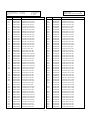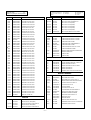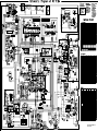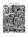
1
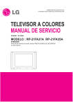
website:http://biz.LGservice.com
e-mail:http://www.LGEservice.com/techsup.html
COLOR TV
SERVICE MANUAL
CHASSIS : MC-019A
MODEL : CF/CT-21Q21KE/KEX/KX/22KEX
MODEL : CT-51F82/51F92T
MODEL : CT-21Q60EX/21Q92EX
MODEL : CT-21Q61KE/62KE/21Q91KE
CAUTION
BEFORE SERVICING THE CHASSIS,
READ THE SAFETY PRECAUTIONS IN THIS MANUAL.
P/NO : 3828VD0087G
March,2002
Printed in Korea
CONTENTS
Contents ................................................................................................................. 2
Safety Precautions ............................................................................................3
Servicing Precautions ..................................................................................... 4
Specifications ..................................................................................................... 6
Description of Controls .................................................................................. 7
Disassembly Instructions .............................................................................10
Adjustment ............................................................................................................11
Purity & Convergence Adjustment ..........................................................14
Block Diagram ......................................................................................................17
Exploded View .................................................................................................. 18
Exploded View Parts List ..............................................................................19
Replacement Parts List ............................................................................... 24
SVC. Sheet ................................................................................................................
- 2 -
SAFETY PRECAUTIONS
IMPORTANT SAFETY NOTICE
Many electrical and mechanical parts in this chassis have special safety-related characteristics. These parts are identified by
in
the Schematic Diagram and Replacement Parts List.
It is essential that these special safety parts should be replaced with the same components as recommended in this manual to
prevent X-RADIATION, Shock, Fire, or other Hazards.
Do not modify the original design without permission of manufacturer.
General Guidance
Before returning the receiver to the customer,
An lsolation Transformer should always be used during
the servicing of a receiver whose chassis is not isolated from
the AC power line. Use a transformer of adequate power rating
as this protects the technician from accidents resulting in
personal injury from electrical shocks.
always perform an AC leakage current check on the exposed
metallic parts of the cabinet, such as antennas, terminals, etc.,
to be sure the set is safe to operate without damage of
electrical shock.
Leakage Current Cold Check(Antenna Cold Check)
It will also protect the receiver and it's components from being
damaged by accidental shorts of the circuitary that may be
inadvertently introduced during the service operation.
If any fuse (or Fusible Resistor) in this TV receiver is blown,
replace it with the specified.
When replacing a high wattage resistor (Oxide Metal Film
Resistor, over 1W), keep the resistor 10mm away from PCB.
Keep wires away from high voltage or high temperature parts.
Due to high vacuum and large surface area of picture tube,
extreme care should be used in handling the Picture Tube.
Do not lift the Picture tube by it's Neck.
X-RAY Radiation
Warning:
The source of X-RAY RADIATION in this TV receiver is the
High Voltage Section and the Picture Tube.
For continued X-RAY RADIATION protection, the
replacement tube must be the same type tube as specified in
the Replacement Parts List.
To determine the presence of high voltage, use an accurate
high impedance HV meter.
With the instrument AC plug removed from AC source,
connect an electrical jumper across the two AC plug prongs.
Place the AC switch in the on positioin, connect one lead of
ohm-meter to the AC plug prongs tied together and touch other
ohm-meter lead in turn to each exposed metallic parts such as
antenna terminals, phone jacks, etc.
If the exposed metallic part has a return path to the chassis, the
measured resistance should be between 1MΩ and 5.2MΩ.
When the exposed metal has no return path to the chassis the
reading must be infinite.
An other abnormality exists that must be corrected before the
receiver is returned to the customer.
Leakage Current Hot Check (See below Figure)
Plug the AC cord directly into the AC outlet.
Do not use a line Isolation Transformer during this check.
Connect 1.5K/10watt resistor in parallel with a 0.15uF capacitor
between a known good earth ground (Water Pipe, Conduit, etc.)
and the exposed metallic parts.
Measure the AC voltage across the resistor using AC
voltmeter with 1000 ohms/volt or more sensitivity.
Reverse plug the AC cord into the AC outlet and repeat AC
voltage measurements for each esposed metallic part. Any
voltage measured must not exceed 0.75 volt RMS which is
corresponds to 0.5mA.
In case any measurement is out of the limits sepcified, there is
possibility of shock hazard and the set must be checked and
repaired before it is returned to the customer.
Leakage Current Hot Check circuit
Adjust brightness, color, contrast controls to minimum.
Measure the high voltage.
The meter reading should indicate
23.5 ¡ 1.5KV: 14-19 inch, 26 ¡ 1.5KV: 19-21 inch,
29.0 ¡ 1.5KV: 25-29 inch, 30.0 ¡ 1.5KV: 32 inch
If the meter indication is out of tolerance, immediate service
and correction is required to prevent the possibility of
premature component failure.
AC Volt-meter
To Instrument's
exposed
METALLIC PARTS
Good Earth Ground
such as WATER PIPE,
CONDUIT etc.
0.15uF
1.5 Kohm/10W
- 3 -
SERVICING PRECAUTIONS
CAUTION: Before servicing receivers covered by this service
manual and its supplements and addenda, read and follow the
SAFETY PRECAUTIONS on page 3 of this publication.
NOTE: If unforeseen circumstances create conflict between the
following servicing precautions and any of the safety
precautions on page 3 of this publication, always follow the
safety precautions. Remember: Safety First.
General Servicing Precautions
1. Always unplug the receiver AC power cord from the AC
power source before;
a. Removing or reinstalling any component, circuit board
module or any other receiver assembly.
b. Disconnecting or reconnecting any receiver electrical plug
or other electrical connection.
c. Connecting a test substitute in parallel with an electrolytic
capacitor in the receiver.
CAUTION: A wrong part substitution or incorrect
polarity installation of electrolytic capacitors may result
in an explosion hazard.
d. Discharging the picture tube anode.
2. Test high voltage only by measuring it with an appropriate
high voltage meter or other voltage measuring device (DVM,
FETVOM, etc) equipped with a suitable high voltage probe.
Do not test high voltage by "drawing an arc".
3. Discharge the picture tube anode only by (a) first connecting
one end of an insulated clip lead to the degaussing or kine
aquadag grounding system shield at the point where the
picture tube socket ground lead is connected, and then (b)
touch the other end of the insulated clip lead to the picture
tube anode button, using an insulating handle to avoid
personal contact with high voltage.
4. Do not spray chemicals on or near this receiver or any of its
assemblies.
5. Unless specified otherwise in this service manual, clean
electrical contacts only by applying the following mixture to
the contacts with a pipe cleaner, cotton-tipped stick or
comparable nonabrasive applicator; 10% (by volume)
Acetone and 90% (by volume) isopropyl alcohol (90%-99%
strength)
CAUTION: This is a flammable mixture.
Unless specified otherwise in this service manual, lubrication
of contacts in not required.
6. Do not defeat any plug/socket B+ voltage interlocks with
which receivers covered by this service manual might be
equipped.
7. Do not apply AC power to this instrument and/or any of its
electrical assemblies unless all solid-state device heat sinks
are correctly installed.
8. Always connect the test receiver ground lead to the
receiver chassis ground before connecting the test receiver
positive lead.
Always remove the test receiver ground lead last.
9. Use with this receiver only the test fixtures specified in this
service manual.
CAUTION: Do not connect the test fixture ground strap to
any heatsink in this receiver.
Electrostatically Sensitive (ES) Devices
Some semiconductor (solid state) devices can be damaged
easily by static electricity. Such components commonly are
called Electrostatically Sensitive (ES) Devices. Examples of
typical ES devices are integrated circuits and some fieldeffect
transistors and semicounductor "chip" components. The
following techniques should be used to help reduce the
incidence of component damage caused by static by static
electricity.
1. Immediately before handling any semiconductor component
or semiconductor-equipped assembly, drain off any
electostatic charge on your body by touching a known earth
ground. Alternatively, obtain and wear a commercially
available discharging wrist strap device, which should be
removed to prevent potential shock reasons prior to
applying power to the unit under test.
2. After removing an electrical assembly equipped with ES
devices, place the assembly on a conductive surface such as
aluminum foil, to prevent electrostatic charge buildup or
exposure of the assembly.
3. Use only a grounded-tip soldering iron to solder or unsolder
ES devices.
4. Use only an anti-static type solder removal device. Some
solder removal devices not classified as "anti-static" can
generate electrical charges sufficent to demage ES devices.
5. Do not use freon-propelled chemicals. These can generate
electrical charges sufficient to damage ES devices.
6. Do not remove a repalcement ES device from its protective
package until immediately before you are ready to install it.
(Most replacement ES devices are packaged with leads
electrically shorted together by conductive foam, aluminum
foil or comparable conductive material).
7. Immediately before removing the protective material from
the ieads of a replacement ES device, touch the protective
material to the chassis or circuit assembly into which the
device will be installed.
CAUTION:Be sure no power is applied to the chassis or
circuit, and observe all other safety precautions.
8. Minimize bodily motions when handling unpackaged
replacement ES devices. (Otherwise harmless motion such
as the bruching together of your clothes fabric or the lifting
of your foot from a carpeted floor can generate static
electricity sufficient to damage an ES device.)
General Soldering Guidelines
1. Use a grounded-tip, low-wattage soldering iron and
appropriate tip size and shape that will maintan tip
temperature within the range or 500¡£
F to 600¡£
F.
2. Use an appropriate gauge of RMA resin-core solder
composed of 60 parts tin/40 parts lead.
3. Keep the soldering iron tip clean and well tinned.
4. Thorohly clean the surfaces to be soldered. Use a mall
wirebristle (0.5 inch, or 1.25cm) brush with a metal handle.
Do not use freon-propelled spray-on cleaners.
5. Use the following unsoldering technique
a. Allow the soldering iron tip to reach normal temperature.
(500¡£
F to 600¡£
F)
b. Heat the component lead until the solder melts.
c. Quickly draw the melted solder with an anti-static,
suction-type solder removal device or with solder braid.
CAUTION: Work quickly to avoid overheating the
circuiboard printed foil.
6. Use the following soldering technique.
a. Allow the soldering iron tip to reach a normal
temperature (500¡£
F to 600¡£
F)
b. First, hold the soldering iron tip and solder the strand
against the component lead until the solder melts.
- 4 -
c. Qulckly move the soldering iron tip to the junction of the
component lead and the printed circuit foil, and hold it
there only until the solder flows onto and around both the
component lead and the foil.
CAUTION: Work quickly to avoid overheating the circuit
board printed foil.
d. Closely inspect the solder area and remove any excess
or splashed solder with a small wire-bristle brush.
IC Remove/Replacement
Some chassis circuit boards have slotted holes (oblong) through
which the IC leads are inserted and then bent flat against the
circuit foil. When holes are the slotted type, the following
technique should be used to remove and replace the IC. When
working with boards using the familiar round hole, use the
standard technique as outlined in parapraphs 5 and 6 above.
Removal
1. Desolder and straighten each IC lead in one operation by
gently prying up on the lead with the soldering iron tip as the
solder melts.
2. Draw away the melted solder with an anti-static suctiontype solder removal device (or with solder braid) before
removing the IC.
Replacement
1. Carefully insert the replacement IC in the circuit boare.
2. Carefully bend each IC lead against the circuit foil pad and
solder it.
3. Clean the soldered areas with a small wire-bristle brush.
(It is not necessary to reapply acrylic coating to the areas).
"Small-Signal" Discrete Transistor
Removal/Replacement
1. Remove the defective transistor by clipping its leads as
close as possible to the component body.
2. Bend into a "U" shape the end of each of three leads
remaining on the circuit board.
3. Bend into a "U" shape the replacement transistor leads.
4. Connect the replacement transistor leads to the
corresponding leads extending from the circuit board and
crimp the "U" with long nose pliers to insure metal to metal
contact then solder each connection.
Power Output, Transistor Device
Removal/Replacement
1. Heat and remove all solder from around the transistor leads.
2. Remove the heatsink mounting screw (if so equipped).
3. Carefully remove the transistor from the heat sink of the
circuit board.
4. Insert new transistor in the circuit board.
5. Solder each transistor lead, and clip off excess lead.
6. Replace heatsink.
Diode Removal/Replacement
1. Remove defective diode by clipping its leads as close as
possible to diode body.
2. Bend the two remaining leads perpendicula y to the circuit
board.
3. Observing diode polarity, wrap each lead of the new diode
around the corresponding lead on the circuit board.
4. Securely crimp each connection and solder it.
5. Inspect (on the circuit board copper side) the solder joints of
the two "original" leads. If they are not shiny, reheat them
and if necessary, apply additional solder.
Fuse and Conventional Resistor
Removal/Replacement
1. Clip each fuse or resistor lead at top of the circuit board
hollow stake.
2. Securely crimp the leads of replacement component around
notch at stake top.
3. Solder the connections.
CAUTION: Maintain original spacing between the replaced
component and adjacent components and the circuit board
to prevent excessive component temperatures.
Circuit Board Foil Repair
Excessive heat applied to the copper foil of any printed circuit
board will weaken the adhesive that bonds the foil to the circuit
board causing the foil to separate from or "lift-off" the board.
The following guidelines and procedures should be followed
whenever this condition is encountered.
At IC Connections
To repair a defective copper pattern at IC connections use the
following procedure to install a jumper wire on the copper
pattern side of the circuit board. (Use this technique only on IC
connections).
1. Carefully remove the damaged copper pattern with a sharp
knife. (Remove only as much copper as absolutely
necessary).
2. carefully scratch away the solder resist and acrylic coating
(if used) from the end of the remaining copper pattern.
3. Bend a small "U" in one end of a small gauge jumper wire and
carefully crimp it around the IC pin. Solder the IC connection.
4. Route the jumper wire along the path of the out-away
copper pattern and let it overlap the previously scraped end
of the good copper pattern. Solder the overlapped area and
clip off any excess jumper wire.
At Other Connections
Use the following technique to repair the defective copper
pattern at connections other than IC Pins. This technique
involoves the installation of a jumper wire on the component
side of the circuit board.
1. Remove the defective copper pattern with a sharp knife.
Remove at least 1/4 inch of copper, to ensure that a
hazardous condition will not exist if the jumper wire opens.
2. Trace along the copper pattern from both sides of the
pattern break and locate the nearest component that is
directly connected to the affected copper pattern.
3. Connect insulated 20-gauge jumper wire from the lead of
the nearest component on one side of the pattern break to
the lead of the nearest component on the other side.
Carefully crimp and solder the connections.
CAUTION: Be sure the insulated jumper wire is dressed so
the it does not touch components or sharp edges.
- 5 -
SPECIFICATIONS
Note : Specification and others are subject to change without notice for improvement.
O
O
O
Video input system:
PAL-B/G, D/K, I/I
SECAM-B/G, D/K,L/L’
NTSC M
NTSC 4.43
SOUND IF :
Intermediate Frequency (Unit : MHz)
VISION IF : 38.9MHz
COLOR IF : 34.47MHz(4.43)
35.32MHz(3.58)
: NTSC-M
VIF-4.25000MHz ): SECAM
(
VIF-4.40625MHz
O
Power requirement : 110~240V, 50/60Hz
O
Power consumption : 95
O
STAND-BY : 3W
Tuning range
Band
For TV
B/G
D/K
VHF-Low
Ch2-4
Ch1-5
VHF-High
Ch5-12
Ch6-12
For CATV
I/I
NTSC
S1'-S3', S1
Ch2-13
Ch4-13
S21-S41
UHF
Ch21-69
Ch14-69
Tuning system :
FVS
100 Programme memory
200 Programme memory(W/O TXT)
O
O
Antenna input impedance : VHF/UHF 75 ohm, unbalanced
O
OSD (On Screen Display) : EASY-MENU
O
Voice coil impedance : 8 ohm
O
O
O
Sound output : 7W¡¿2(MAX)
Dual/Stereo : A2/NICAM(Option)
External connection :
S2-S10,
S11-S20
Hyper
O
33.4MHz (B/G)
32.9MHz (I/I)
32.4MHz (D/K)
34.4MHz (M)
Head Phone Jack
A/V in : 2
PERI Connector(Full Scart) : 1
DVD in
External In/Output
Audio-In:0.5Vrms!3dB,over 10Kohm
Audio-Out:0.5Vrms!3dBb,below 1Kohm
Video-In/Out:1Vp-p!3dB,75ohm
DVD In Y: 1Vp-p!3dB
Pb,Pr : 0.7Vp-p!3dB
- 6 -
Feature : Auto programme/Manual programme
CSM (Color Status Memory)
Auto Sleep
Turbo Picture & Sound
Programme Editing
PSM (Picture Status Memory)
Teletext (TOP/FLOF/LIST)
ACMS
Auto Volume Level
Game
SSM(Sound Status Memory)
Favorite Program
DECRIPTIONS OF CONTROLS
All the functions can be controlled with the remote control handset.
Some functions can also be adjusted with the buttons on the front
panel of the set.
Remote control handset
Before you use the remote control handset, please install the batteries. See the next page.
POWER
10
1
2
1
2
3
4
5
6
7
8
9
0
3
TV
EYE
/
I / II /
Q.VIEW
LIST
11
4. I/II/ (option)
12
selects the language during dual language broadcast. (option)
13
selects the sound output.
*
( )
PR
6
VOL
5. EYE/ (option)
switches the eye function on or off.
*
VOL
OK
6.
PR
( )
TEXT/MIX
SIZE
HOLD
SLEEP
M
7
UPDATA
TIME
REVEAL
8
9
14
PSM
15
?
SSM/
2. NUMBER BUTTONS
switches the set on from standby or directly select a number.
3. MENU (or INDEX)
selects a menu.
selects an index page in the teletext mode (only TELETEXT
models).
TV/AV
MENU/INDEX
4
5
1. POWER
switches the set on from standby or off to standby.
MUTE
PICTURE SOUND
TURBO/
/
16
D ( DD ) / E ( EE ) (Programme Up/Down)
selects a programme or a menu item.
switches the set on from standby.
scans programmes automatically.
F / G (Volume Up/Down)
adjusts the volume.
adjusts menu settings.
OK
accepts your selection or displays the current mode.
7. TELETEXT BUTTONS (option)
These buttons are used for teletext.
For further details, see the ‘Teletext’ section.
8. SSM/ (option) (Sound Status Memory)
recalls your preferred sound setting.
*
(With TELETEXT)
9. TURBO PICTURE / SOUND BUTTON (option)
selects Turbo picture and sound.
- 7 -
10. MUTE
switches the sound on or off.
11. TV/AV
selects TV or AV mode.
clears the menu from the screen.
switches the set on from standby.
12. Q.VIEW
returns to the previously viewed programme.
selects a favorite programme.
MUTE
POWER
13. LIST
displays the programme table.
10
1
14. SLEEP
sets the sleep timer.
2
15. PSM (Picture Status Memory)
recalls your preferred picture setting.
1
2
3
4
5
6
7
8
9
TV/AV
MENU
0
3
16. SURROUND (º
º/ ) (option)
selects surround sound.
*
4
5
COLOURED BUTTONS : These buttons are used for teletext (only
TELETEXT models) or programme edit.
EYE
/
I / II /
Q.VIEW
LIST
11
12
13
( )
PR
6
VOL
OK
Battery installation
VOL
PR
( )
The remote control handset is powered by two AAA type batteries.
To load the batteries, turn the remote control handset over and
open the battery compartment. Install two batteries as indicated by
the polarity symbols ( + and - ) marked inside the compartment.
14
SLEEP
15
SSM/
8
9
Note : To avoid damage from possible battery leakage, remove the
batteries if you do not plan to use the remote control handset for an
extended period of time.
- 8 -
PSM
PICTURE SOUND
TURBO/
/
(Without TELETEXT)
16
Front panel
RF/RT-21FA30/31/32 series
CF/CT-21Q64K/65K/66K series
VIDEO
TV/AV
L AUDIO R
9
(VOL)
VIDEO
( ) PR ( )
L AUDIO R
ON/OFF
MENU OK
VOL
PR
AV
ON/OFF
1
2
3
4
5
9 10
1 2 3 67 8
9 10
11
10
CF/CT-21Q20K/21K/22K series
AV
CF/CT-21Q60K/61K/62K series
TV/AV
VIDEO
L AUDIO R
ON/OFF
TV/AV
ON/OFF
VOL
AV
VOL
PR
PR
VIDEO
1
AV
L AUDIO
9
10 9 6 7 8
23
1 2 3
11
6 7
8
11
R
10
(Side panel)
CF/CT-21Q90K/91K/92K series
CF/CT-15Q90K/91K/92K series
MENU
VOL
OK
PR
1 23
4
5
11
1. MAIN POWER (ON/OFF)
switches the set on or off.
7.
2. POWER/STANDBY INDICATOR
illuminates brightly when the set is in standby
mode.
dims when the set is switched on.
blinks when signal is input from the remote
control.
3. REMOTE CONTROL SENSOR
4. MENU
selects a menu.
5. OK
accepts your selection or displays the current
mode.
F / G (Volume Up/Down)
adjusts the volume.
adjusts menu settings.
D / E (Programme Up/Down)
selects a programme or a menu item.
switches the set on from standby.
6. TV/AV
selects TV or AV mode.
clears the menu from the screen.
switches the set on from standby.
MENU
VOL
SOUND
OK
PR
PICTURE
TURBO
DIGITAL TURBO SOUND
ON/OFF
ON/OFF
1 23
4
5
11
(Function)
selects volume, EYE (option), picture items or
brief auto programme while the menus not display.
8. +/- (D /E )
adjusts the function or selects a programme.
switches the set on from standby.
9. AUDIO/VIDEO IN SOCKETS (AV) (option)
Connect the audio/video out sockets of external equipment to these sockets.
Note :If both the input jacks on the front/side
panel and back panel have been connected to
external equipments simultaneously, only the
input jacks on the front/side panel can be
received.
10. HEADPHONE SOCKET (option)
Connect the headphone plug to this socket.
11. EYE (option)
adjusts picture according to the surrounding
conditions.
Note : Do not place any heavy objects (over 4Kg) on
the RF/RT-21FA30/31/32 series models.
- 9 -
DISASSEMBLY INSTRUCTIONS
Important note
Chassis Assy Removal
This set is disconnected from the power supply through the
converter transformer. An isolating transformer is necessary
for service operations on the primary side of the converter
transformer.
Grasp both side of Frame and pull it backward smoothly.
Back Cabinet Removal
Remove the screws residing on the back cabinet and carefully
separate the back cabinet from the front cabinet. (Fig. 2-1).
CPT Removal
PICTURE TUBE HANDLING CAUTION
1. Pull out the CPT board from the CPT neck.
2. Place the front cabinet on soft material not to mar the front
surface or damage control knobs.
3. Remove 5 screws securing the picture tube mounting
brackets to the front cabinet.
4. Carefully separate CPT from the front cabinet.
Due to high vacuum and large surface area of picture tube, great
care must be exercised when handling picture tube. Always lift
picture tube by grasping it firmly around faceplate.
NEVER LIFT TUBE BY ITS NECK! The picture tube must not be
scratched or subjected to excessive pressure as fracture of
glass may result in an implosion of considerable violence which
can cause personal injury or property damage.
CPT
board
Remove
Screws
Main
PCB
ANT IN
75Ω
Fig. 2-2
Fig. 2-1
- 10 -
ADJUSTMENT
Safety Precautions
O
Option
1. It is safe to adjust after using insulating transformer
between the power supply line and chassis input to
prevent the risk of electric shock and protect the
instrument.
2. Never disconnect leads while the TV receiver is on.
3. Don't short any portion of circuits while power is on.
4. The adjustment must be done by the correct appliances.
But this is changeable in view of productivity.
5. Unless otherwise noted, set the line voltage to
110~240Vac !10%, 50/60Hz.
6. The adjustment of TV should be performed afther warming
up for 20 minutes.
O
Test Equipment required
4 KEY
MONO
W/O TBS
1
WITH TBS
0
W/O EYE
1
WITH EYE
0
W/O 4 KEY
1
WITH 4 KEY
14,16” CPT
15” CPT
1
12
8
FLAT
Remark
10
200 PRO
CHA
+ AU
20,21” CPT
12
FLAT
ACMS
T-SCH
OPTION Data Adjustment(OPTION-1,OPTION-2)
1) Press OK buttons on both TV set and Remote Controller at
the same time to get into SVC mode.
2) Press the Yellow button several times to find OPTION-1 or
OPTION-2.
3) Input the correspond OPTION data referring to Table below
with the numeric buttons.
4) Press the OK(V ) button to memorize the data.
Table 1. OPTION 1 Function
Option
Code
0
C MUTE
DVD
2 IN 1
TOP
SCART
Function
ACTIVE
T-P/S
CURVE
0
Auto Abnormal ON
1
Not Used
0
W/O GAME PACK
1
WITH GAME PACK
0
100 PRO
1
200 PRO
0
Except China,Austrailia
1
China,Austrailia
0
W/O DUAL
1
WITH DUAL
0
Austrailia
1
Except Austrailia
0
W/O TURBO SEARCH
1
WITH TURBO SEARCH
0
W/O TURBO P/S
1
WITH TURBO P/S
0
NORMAL VOLUME CURVE
1
M-A,India VOLUME CURVE
RESER
VED
0
1
Function
***
***
0
W/O HOTEL
W/O DVD
1
W/HOTEL
1
DVD(REAR JACK)
0
BG/L
0
W/O 2 IN 1TUNER
1
BG/I/DK
1
1
NOT ACTIVE
0
Remark
Table 3. OPTION 3 Function
Option Code
Remark
Function
Code
4) Press the OK(V ) button to memorize the data.
O
FORCED MONO
Table 2. OPTION 2 Function
DUAL
CDL Data
Remark
0
GAME
1) Press the SVC button to get into the SVC-0 Mode.
2) Press the Channel UP/DOWN button to select CDL12.
3) Press the Volume UP/DOWN button until the CDL data is
the same as the Table below.
Function
0
BCF
CDL Data Adjustment(LINE SVC-0)
21” FCD
EYE
Option
1. Multimeter (volt meter)
2. Oscilloscope
3. 10:1 PROBE
4. Color Analyzer
O
TBS
Code
HOTEL
WITH 2 IN 1TUNER
2
BG/I/DK/M
0
FLOF TXT
3
BG/I/DK DUAL
1
TOP TXT
4
BG/I/DK/M DUAL
0
PHONO JACK
5
2nd IF BG
1
SCART JACK
6
2nd IF I
7
2nd IF DK
SYSTEM
- 11 -
Remark
Option Code
OSD-L
(EU)
Function
Remark
FOCUS Adjustment
O
0
ENG. ONLY
1
EU-7EA
English,Deutsch,Francais,Italiano,Espanol
2
EU ALL
English,Nederlands,Svenska,Dansk,Suomi,Por
English
Test Point
Adjust
tugues,Romaneste,Polski,Cesky,Pyccknn
3
EU EAST
0
ENG. ONLY
1
ARABIC
English,Arab,,Urdu,French
2
PARSI
English,Parsi,Urdu,French
3
ARAB,FARSI,URDE
0
ENG.ONLY
1
ASIA-ALL
0
ENG.ONLY
1
E+CHINA
English,Chinese
2
E+HINDI
English,Hindi
0
W-EU
1
E-EU
2
CYRILLIC
3
UKRAINIAN
TXT-L
(E-ASIA)
0
WEST-EU
TXT-L
(ARAB)
0
WEST-EU
1
ARABIC
TXT-L
(FARSI)
0
WEST-EU
1
FARSI
OSD-L
(MASIA)
OSD-L
(E-ASIA)
OSD-L
(CH+HI)
TXT-L
(EU)
O
1) Tune the TV set to receive a PAL 05CH.
2) Adjust the Focus Volume of FBT for best focus.
English,Romaneste,Polski,Cesky,Pyccknn,Magyar
English
Screen Voltage Adjustment
O
Test Point
Adjust
English,French,Arab,Urdu,Parsi
: Observing Display
: Focus Volume of FBT
English
1) Connect the probe of oscilloscope to the RK (Red Cathode)
of CPT Board.
2) Set the oscilloscope to 50V/div and 20Us/div and after
putting GND line upon the lowest grid line of the scope by
pressing GND button,enter into DC mode.
3) Tune the TV set to receive a PAL-B/G 05CH.
4) Adjust Screen Volume of FBT so that the waveform is the
same as below figure (DC 140!3V).
English,Malay,Vietnam,Indonesian,Thai
English
Horizontal
FlyBack Time
Black level
140Vp-p
White level
GND for dc
AGC Adjustment (SERVICE 1)
: AGC TP (C101)
: Remote Controller
14”
OTHERS
DC 130V!3 V
DC 140V!3 V
White Balance Adjustment.(LINE SVC-0)
O
Test Point
Adjust
: RK (Red Cathode of CPT Board)
: Screen Volume of FBT
NOTE : This adjustment should be performed after screen voltage
adjustment.
1) Tune the TV set to receive an 100% white pattern.
2) Press OK(V ) buttons on TV set and remote controller at the
same time to get into SVC mode.
3) Press Yellow button on remote controller. (Standard mode)
4) Press Channel UP/DOWN button for desirous function
adjustment.
5) Adjust VOL+ or VOL-button in each status of "RG--"/"BG--" for
X=272!8, Y=288!8 with color analyzer.(Europe Model :
X=288!8, Y=295!X=272!8, 11,000K)
1) Connect RF signal (70dB!0.2dB) and turn on the TV.
¡ Standard adjustment Channel
- EU 05 Ch. (frf = 175.25MHz)
2) Press the OK buttons on TV set and Remote Controller at the
same time to get into SVC-0 mode.
3) Press the Channel UP/DOWN button on the Remote
Controller several times to find AGC??.
4) Press the Volume UP/DOWN button until the AGC Voltage is
the same as the Table below.
5) Press the OK(V ) button to memorize the data.
Tuner P/N
6700VPF009G
6700VPF016A
Marker
LG Innotek(W/S TUNER)
DAEWOO(W/S TUNER)
AGC Voltage
2.7! 0.05V
2.7! 0.05V
Tuner P/N
6700VPF009S
Marker
LG Innotek(TBS TUNER)
AGC Voltage
2.5! 0.05V
Status
Initial Data
RG
31
GG
31
BG
31
BLO-R
31
BLO-G
31
Remark
7) Press the OK(V ) button to memorize the data.
- 12 -
O
Deflection Data Adjustment (Line SVC-1)
NOTE: To enter SVC mode, press "OK" buttons on both TV set
and the Remote control at the same time.
1. Preparation for Deflection Adjustment
1) At SVC mode, press the Yellow colored button.
And then, deflection data adjustment OSD (SVC1 mode) will
be displayed.
2) Tune the TV set to receive a PAL 05 CH and set the ARC
mode is standard.
2. Deflection Initial Setup Data
Status
Default
21" FLAT S/S
21" FLAT LG
VL
31
31
31
VA
31
31
31
VS
31
31
31
HS
31
31
31
SC
25
25
25
3. Deflection Adjustment Procedure
VL (Vertical Linearity)
Adjust so that the boundary line between upper and lower half
is in accord with geometric horizontal center of the CPT.
VA (Vertical Amplitude)
Adjust so that the circle of a digital circle pattern may be
located within the effective screen of the CPT.
SC (Vertical “S” Correction)
Adjust so that all distance between each horizontal lines are
to be the same.
VS (Vertical Shift)
Adjust so that the horizontal center line of a digital circle
pattern is in accord with geometric horizontal center of the
CPT.
HS (Horizontal Shift)
Adjust so that the vertical center line of a digital circle pattern is
in accord with geometric vertical center of the CPT.
Press the OK(V ) button to memorize the data.
- 13 -
PURITY & CONVERGENCE ADJUSTMENT
Caution:
Convergence and Purity have been factory aligned. Do not
attempt to tamper with these alignments.
However, the effects of adjacent receiver components, or
replacement of picture tube or deflection yoke may require the
need to readjust purity any convergence.
5. Reconnect the internal degaussing coil.
6. Position the beam bender locking rings at the 9 o'clock
position and the other three pairs of tabs (2,4 and 6 pole
magnets) at the 12 o'clock position.
DEFLECTION YOKE
PURITY &CONVERGENCE
MAGNET ASSEMBLY
6-POLE
6-POLE
MAGNETS
MAGNES
PURITY MAGNET(2-POLE)
6-POLE
,
,,,,,,,,,,
,,,,,,
,,,,,,,,,,
,
,
,
,,,,,,,
,,,,,,
RUBBER
WEDGES
,,,,,,,,,,,,,
,
,,,,,,,,
,,,,,,,
,,,,
4-POLE
X-AXIS YOKE MAGNET
POSITIONING
(L/R PURITY)
PURITY MAGNET
4-POLE
GLASS CLOTH TAPE
CONVERGENCE
MAGNET ASSEMBLY
CONVERGENCE MAGNET ASSEMBLY
¡ Purity Adjustment
This procedure DOES NOT apply to bonded yoke and picture
tube assemblies.
The instrument should be at room temperature (60 degrees F or
above) for six (6) hours and be operating at low beam current
(dark background) for approximately 20 to 30 minutes before
performing purity adjustments.
7. Perform the following steps, in the order given, to prepare the
receiver for the purity adjustment procedure.
CAUTION: Do not remove any trim magnets that may be
attached to the bell of the picture tube.
1. Remove the AC power and disconnect the internal
degaussing coil.
2. Remove the yoke from the neck of the picture tube.
3. If the yoke has the tape version beam bender, remove it and
replace it with a adjustable type beam bender (follow the
instructions provided with the new beam bender)
4. Replace the yoke on the picture tube neck, temporarily
remove the three (3) rubber wedges from the bell of the
picture tube and then slide the yoke completely forward.
- 14 -
a. Face the receiver in the "magnetic north" direction.
b. Externally degauss the receiver screen with the television
power turned off.
c. Turn the television on for approximately 10 seconds to
perform internal degaussing and then turn the TV off.
d. Unplug the internal degaussing coil. This allows the
thermistor to cool down while you are performing the purity
adjustment. DO NOT MOVE THE RECEIVER FROM ITS
"MAGNETIC NORTH" POSITION.
e. Turn the receiver on and obtain a red raster by increasing
the red bias control (CW) and decreasing the bias controls
for the remaining two colors (CCW).
f. Attach two round magnets on the picture tube screen at 3
o'clock and 9 o'clock positions, approximately one (1) inch
from the edge of the mask (use double-sided tape).
2 .ADJUST BEAM BENDER 2 POLE
MAGNET TO GET FOUR EQUAL
COLOR CIRCLES
1.ADJUST YOKE Z-AXIS FIRST
TO GET EQUAL BLUE
COLOR CIRCLES
MAGNETS
RED
RED
8. Referring to above, perform the following two steps:
a. Adjust the yoke Z-axis to obtain equal blue circles.
b. Adjust the appropriate beam bender tabs to obtain correct
purity (four equal circles).
6. Reconnect the internal degaussing coil and apply AC power.
9. After correct purity is set, tighten the yoke clamp screw and
remove the two screen magnets.
8. Unplug the internal degaussing-coil.
10. Remove the AC power and rotate the receiver 180 degrees
(facing "magnetic south").
11. Reconnect the internal degaussing coil.
12. Turn the receiver on for 10 seconds (make sure the receiver
came on) to perform internal degaussing, and then turn the
receiver off.
7. Turn the receiver on for 10 seconds to perform internal
degaussing and then turn the receiver off again.
9. Turn on the receiver, connect a signal generator to the VHF
antenna terminal and apply a crosshatch signal.
Caution: During the convergence adjustment procedure, be
very careful not to disturb the purity adjustment tabs
are accidentally move, purity should be confirmed
before proceeding with the convergence adjustments.
Note: Make sure the focus is set correctly on this instrument
before proceeding with the following adjustment.
13. Unplug the internal degaussing coil.
14. Turn on the receiver and check the purity by holding one (1)
round magnet at the 3 o'clock and a second round magnet at
9 o'clock position. If purity is not satisfactory, repeat steps 8
through 14.
15. Turn off the receiver and reconnect the internal degaussing
coil.
10. Converge the red and blue vertical lines to the green vertical
line at the center of the screen by performing the following
steps (below TABLE).
a. Carefully rotate both tabs of the 4-pole ring magnet
simultaneously in opposite directions from the 12 o'clock
position to converge the red and blue vertical lines.
b. Carefully rotate both tabs of the 6-pole ring magnet
simultaneously in opposite directions form the 12 o'clock
position to converge the red and blue (now purple)
vertical lines with the green vertical line.
¡ Convergence Adjustment
Caution: This procedure DOES NOT apply to bonded yoke and
picture tube assemblies.
Do not use screen magnets during this adjustment
procedure. Use of screen magnets will cause an
incorrect display.
1. Remove AC power and disconnect the internal degaussing
coil.
2. Apply AC Power and set the brightness to the Picture Reset
condition. Set the Color control to minimum.
3. Make a horizontal line.
11. Converge the red and blue horizontal with the green line at
the center of the screen by performing the following steps.
(below TABLE)
a. Carefully rotate both tabs of the 4-pole ring magnet
simultaneously in the same direction (keep the spacing
between the two tabs the same) to converge the red and
blue horizontal lines.
b. Carefully rotate both tabs of the 6-pole ring magnet
simultaneously in same direction (keep the spacing
between the two tabs the same) to converge the red and
blue (now purple) horizontal lines with the green
horizontal line.
c. Secure the tabs previsouly adjusted by locking them in
place with the locking tabs on the beam bender.
4. Adjust the Red, Green and Blue Bias controls to get a dim
white line.
5. Restore the screen by removing the horizontal line.
- 15 -
ROTATION DIRECTION
OF BOTH TABS
RING
PAIRS
MOVEMENT OF RED
AND BLUE BEAMS
B
B
OR
OPPOSITE
R
4
POLE
SAME
B
R
R
OR
B
B
R
B
OR
OPPOSITE
R
R
6
POLE
SAME
B
UP/DOWN ROCKING OF THE YOKE
UP/DOWN
ROCKINGROTATION
OF THE YOKE
CAUSES
OPPOSITE
OF RED
CAUSES
AND
BLUE OPPOSITE
RASTERS ROTATION OF RED
R
OR
B
R
LEFT/RIGHT ROCKING OF THE YOKE
LEET/RIGHT
ROCKING
OF THE YOKE
CAUSES
OPPOSITE
SIZE CHANGE
OF THE
CAUSES
OPPOSITE
SIZE CHANGE OF
RED
AND BLUE
RASTERS
AND BLUE RASTERS
THE RED AND BLUE RASTERS
GREEN
GREEN
ADJUSTMENT
VIEWING
AREA
GREEN
BLUE
ADJUSTMENT
VIEWING
AREA
RED
RED
BLUE
BLUE
RED
RED
RED
RED
GREEN
BLUE
TV
SCREEN
GREEN
12. While watching the 6 o'clock positions on the screen, rock the
front of the yoke in a vertical (up/down) direction to converge
the red and blue vertical lines. (Fig upper left)
13. Temporarily place a rubber wedge at the 12 o'clock position
to hold the vertical position or the yoke.
14. Check the 3 o'clock and 9 o'clock areas to confirm that the red
and blue horizontal lines are converged.
If the lines are not converged, slightly offset the vertical tilt of the
yoke (move the rubber wedge if necessary) to equally balance the
convergence error of the horizontal lines at 3 o'clock and 9 o'clock
and the vertical lines at 6 o'clock and 12 o'clock.
15. Place a 1.5 inch piece of glass tape over the rubber foot at
the rear of the 12 o'clock wedge.
16. While watching the 6 o'clock and 12 o'clock areas of the
screen, rock the front of the yoke in the horizontal (left to
right) motion to converge the red and blue horizontal lines.
(Fig. upper right)
17. Temporarily place a rubber wedge at the 5 o'clock and 7
o'clock positions to hold the horizontal position of the yoke.
18. Check the 3 o'clock and 9 o'clock areas to confirm that the
red and blue vertical lines are converged. If the lines are not
converged, slightly offset the horizontal tilt of the yoke (move
the temporary rubber wedges if necessary) to equally
balance the convergence error of the horizontal lines at 6
o'clock and 12 o'clock and the vertical lines at 3 o'clock and 9
o'clock.
19. Using a round magnet confirm purity at the center, right and
left sides and corners. See Purity Adjustment Procedure.
20. Reconfirm convergence and apply a 1.5 inch piece of glass
tape over the rubber foot at the rear of the 5 o'clock and the 7
o'clock wedges.
- 16 -
5.1V
8V
From
IC844
5V
From
IC131
SW2
SW1
VIDEO
AUDIO
SIF
TUNER
SDA
SCL
5V
°‹
1
°‹
2
°‹
44
FM-SIF-IN
47
°‹
MSP3410D
AM-IN
(L/L Only)
25
28
°‹
H-out
Va 22
Vb 21
SIF 32
38
IFout
PJ201
DVD
(FLAT OPT.)
Rear_AV(1)
2
4
Va
Vb
7
IC131
5V REG
°‹
FBT
HDT
3 B+
1
Collector
9 HEATER
8 ABL
10 AFC
2 185V
5 -14V
6
14V
V_DY
B+
(110/115V)
9.5V
12 14V
10
MONO
( ~B01L )
STEREO
( ~B01K
~ A13P)
SMPS
TRANS
(14/17V)
9 AUDIO B+
AC
INPUT
(110~240V)
VERTICAL AMP
LA7840
H-Vcc
IC844
8V REG
IC842
5V REG
ST-BY
TRANS
(3W Opt)
IC591
LA7016(DVD / GameOpt))
DVD Y / Game Video
A(R/L)-OUT (MNT/TV-OUT)
Y/Pb/Pr
Thai
Opt.
SIF(CE Mono)
From Tuner
°‹
SFE 5.74M
MNT/TV-A(R/L)-OUT
Video-OUT(TV/MNT OUT)
33
Int.
CVBS
°‹
( SCART / PHONE)
V-OUT
39
30
31
Sound
Trap Part
8V
From IC844
14
UOC
TDA9361(TXT)
TDA9381(Non-TXT)
EXT.RGB
°‹
3.3V
14 39 39
Audio(Game)
IC02
3.3V Reg.
SDA
SCL
44 Audio Out
HIC01
Game Pack(Game Opt)
3, 4, 5
°‹
°‹
/ Game Audio (From HIC01)
IC651
4
LA7016(Mono Opt)
TV Audio(From UOC #28)
15 18
7
MNT Audio Out(Mono)
TV Audio Out (CL Mono)
IC631
A1/A2(R/L)-IN 1
AV
STEREO
°‹
32
30
TDA9859
28
41 42
40
IC661
°‹
39 DVD(R/L)-IN / Game Audio
RF
STEREO
24
51~53 50 42 35
EXT
RGB IK EXT
Audio-in
OUT
Video-in
R.G.B AMP. &
CPT DRIVE
(TDA6107Q)
TO
IC631
#1,#5
Video(Game)
A1(R/L)-IN
5V
From
IC842
IC03
EEPROM
24C08/16
SPK(R/L)-OUT
SPK(L)-OUT
From UOC
AV-IN
PJ202
5V
SPK.
Front-AV(2)
MONO
SOUND AMP
TDA2006
STEREO,
STEREO,
Sound Max
SOUND
SOUND AMP.
AMP.
TDA7266/97
TDA7266/97
H/P
SPK.
2
°‹
EXT Video(To UOC #42)
IIC Bus Line
Audio(Mono)
(TV OUT)
- 17 -
EXT Video
Option Part
BLOCK DIAGRAM
EXPLODED VIEW : 21Q21/22
943
400
913
170
150
153
112
OPTION
174
520
530
124
123
300
120
310
330
320
315
700
- 18 -
The components identified by mark
critical for safety.
Replace only with part number specified.
EXPLODED VIEW PARTS LIST
LOCA. NO
112
PART NO
DESCRIPTIONS
6341V21009B
CPT ASSY,A51QDX991X
6335V21008D
CPT
120
120-D38C
123
4810V00123A
BRACKET,CASE
124
4810V00124A
BRACKET,COVER
150
150-D02X
153
6150V-1014G
170
170-A01N
CPT EARTH 21” 64T 2LUG
174
174-009Q
CORD,POWER(W/HOLD,HOUSING)L=300,4.0
300
3091V00274K
CABINET ASSY
3091V00274T
CABINET ASSY (W/O EYE)
310
5020V00340A
BUTTON,CONTROL 4KEY
315
3580V00037A
DOOR,CONRTOL
320
320-070G
330
5020V00337B
BUTTON,POWER
400
3809V00154B
BACK COVER ASSY
3809V00154U
BACK COVER ASSY(SCART)
3809V00243L
BACK COVER ASSY(SCART)
520
SPEAKER,MID-RANGE 8 OHM 15/25W
COIL,DEGAUSSING CU 21” 60TURN 12 OHM
DY,DIF-2192AA(NF5)
SPRING,COIL
6871VMM676D
PWB ASSY,MAIN CT-21Q21KE.
6871VMM676W
PWB ASSY,MAIN CT-21Q21KEX.
6871VMM676E
PWB ASSY,MAIN CT-21Q22KEX
6871VMM676J
PWB ASSY,MAIN CT-21Q22KEX
6871VMM676G
PWB ASSY,MAIN CT-21Q21KE(SCART)
6871VMM745G
PWB ASSY,MAIN CT-21Q22KEX(X-RAY)
6871VMMA26B
PWB ASSY,MAIN CT-21Q21KE(PH/AV ST)
6871VMMB67A
PWB ASSY,MAIN CF-21Q21KX
530
6871VSM986A
PWB ASSY,CONT(019A) Q22,CTL+AV+POWER(3
700
0IGL120104A
IC,CDS SENSOR MODULE(P1201-04)
913
332-057B
SCREW ASSY,HEXAGON HEAD
943
1PTF0403116
SCREW,TAP TITE(P) D4.0 L16.0
- 19 -
is
EXPLODED VIEW : 21Q61/62
943
400
913
170
150
153
112
OPTION
174
520
530
124
123
300
120
310
330
320
700
600
- 20 -
The components identified by mark
critical for safety.
Replace only with part number specified.
EXPLODED VIEW PARTS LIST
LOCA. NO
PART NO
DESCRIPTIONS
112
6341V21009A
120
120-D38C
CPT ASSY,A51QDX991X 21” S/S FLAT
123
4810V00123A
BRACKET,CASE
124
4810V00124A
BRACKET,COVER
150
150-D02X
153
6150V-1019C
170
170-A01N
174
174-225H
300
3091V00366C
CABINET ASSY
310
5020V00368B
BUTTON,CONTROL 4KEY
SPEAKER,MID-RANGE 8 OHM 15/25W 87
COIL,DEGAUSSING CU 21” 60TURN 12 OHM
DY,DIF-2192AA 21” SAMSUNG .
CPT EARTH21” 64T 2LUG 1P
CORD,POWER(L4=350MM)
320
320-070S
330
5020V00369A
SPRING,COIL
400
3809V00173C
BACK COVER ASSY(PHONE JACK)
520
6871VMM676X
PWB ASSY,MAIN 019A
BUTTON,POWER
6871VMM810R
PWB ASSY,MAIN 019A 21Q62KE
530
6871VSM986A
PWB ASSY,CONT (019A) CTL+AV+POWER(3
600
6871VSM963H
700
0IGL120104A
PWB ASSY,SIDE A/V
IC,CDS SENSOR MODULE(P1201-04)
913
332-057B
SCREW ASSY,HEXAGON HEAD
943
1PTF0403116
SCREW,TAP TITE(P) D4.0 L16.0
- 21 -
is
EXPLODED VIEW : 21Q91/92
943
400
913
170
150
153
112
OPTION
501
520
530
124
123
300
120
121
540
310
330
320
700
600
- 22 -
174
The components identified by mark
critical for safety.
Replace only with part number specified.
EXPLODED VIEW PARTS LIST
LOCA. NO
PART NO
DESCRIPTIONS
112
6341V21009A
120
120-D38C
CPT ASSY,A51QDX991X 21” S/S FLAT
SPEAKER,MID-RANGE 8 OHM 15/25W 87
121
6400VG0002A
SPEAKER,TWEETER T0520101 8 OHM 10
123
4810V00267A
BRACKET,SPK
124
4810V00124A
BRACKET,COVER
150
150-D02X
153
6150V-1019C
170
170-A01N
CPT EARTH 21” 64T 2LUG 1P HSG
174
174-009E
CORD,POWER(W/HOLD,HOUSING)
174-224G
POWER,CORD
300
3091V00282C
CABINET ASSY
310
5020V00431A
BUTTON,CONTROL
320
320-062E
330
5020V00430A
BUTTON,POWER
400
3809V00208F
BACK COVER ASSY(MC019A,PHONE) .
501
4810V00266A
BRACKET,MAIN
520
6871VMM676R
PWB ASSY,MAIN
6871VMM814C
PWB ASSY,MAIN 21Q91KEX
6871VMM814H
PWB ASSY,MAIN 21Q92KE
6871VMM745K
PWB ASSY,MAIN 21Q92KEX
530
6871VSM962E
PWB ASSY,(019A)21Q90 POWER
540
6871VSM962F
PWB ASSY,(019A)21Q90 CONTROL KEY
600
6871VSM963J
PWB ASSY,(019A)21Q91/92 SIDE A/V
700
0IGL120104A
IC,CDS SENSOR MODULE(P1201-04)
913
332-057B
943
1PTF0403116
COIL,DEGAUSSING CU 21” 60TURN 12 OHM
DY,DIF-2192AA 21” SAMSUNG .
SPRING,KNOB
SCREW ASSY,HEXAGON HEAD
SCREW,TAP TITE(P)[TRUSS HEAD] + D4.0 L16.0 MSWR3/FZB
- 23 -
is
The components identified by mark
are
critical for safety.
Replace only with part number specified.
LOCA. NO
PART NO
REPLACEMENT PARTS LIST
DESCRIPTION
LOCA. NO
IC
PART NO
DESCRIPTION
ZD601
0DZ910009BD
DIODE,ZENER GDZJ9.1B TP GRANDE DO34 0.5W
ZD901
0DZ750009BE
DIODE,ZENER GDZJ7.5B TP GRANDE DO34 0.5W
IC01
0ICTMPH005A
IC,TD9381PS/N2/3,L8011(ARAB) W/O TXT
“
0ICTMPH003A
IC,TD9361PS/N2/4,LG801(ARAB) W/TXT
“
0ICTMPH002A
IC,TDA9361PS/N2/4,LG801
Q102
0TR319709AB
TR,KTC3197,TP(KTC388A),KEC
“
0ICTMPH006A
IC,TDA9361PS/N2/4,PHILIPS
Q103
0TR102009AB
TR,KRC102M,TP(KRC1202),KEC
IC02
0ISG111733B
IC,LD1117V33C 3SIP ST REGULATOR
Q301
0TR198009BA
TR,2SA1980Y TP AUK - -
IC03
0IAL241600B
IC,AT24C16-10PC 8D EEPROM 16K
Q402
0TR570200AA
TR,KSD5702 BK SAMSUNG TO3PF H-OUT
IC130
0IKE780500Q
IC,KIA7805API 3P
Q442
0TR233109AA
TR,KSC2331-Y TP SAMSUNG TO-92L
IC301
0ISA784070A
IC,LA7840 7S VERTICAL
Q443
0TR534309AA
TR,2SC5343Y TP AUK - -
IC602
0ISG729700A
IC,TDA7297 15P,SIP BK 2CH 15W DUA
Q551
0TR198009BA
TR,2SA1980Y TP AUK - -
“
0ISG726600A
IC,TDA7266S 15 SDIP
Q552
0TR198009BA
TR,2SA1980Y TP AUK - -
IC603
0IFA754207A
IC,KA75420ZTA(KA7542ZTA) 3P,TO-92
Q553
0TR198009BA
TR,2SA1980Y TP AUK - -
IC631
0IMCRPH010A
IC,TDA9859 PHILIPS 32P SDIP ST UN
Q554
0TR534309AA
TR,2SC5343Y TP AUK - -
IC661
0IIT341000J
IC,MSP3410D-C5 52P SDIP BK MULTI
Q555
0TR534309AA
TR,2SC5343Y TP AUK - -
IC662
0IFA753307A
IC,KA75330ZTA(KA7533ZTA) 3P,TO-92
Q571
0TR198009BA
TR,2SA1980Y TP AUK - -
IC801
0ILI817000G
IC,LTV817M-VB 4P,DIP BK PHOTO COU
Q621
0TR534309AA
TR,2SC5343Y TP AUK - -
IC802
0ILI817000G
IC,LTV817M-VB 4P,DIP BK PHOTO COU
Q651
0TR534309AA
TR,2SC5343Y TP AUK - -
IC803
0ISK665413C
IC,STR-F6654R(LF1352) 5 SIP BK ST
Q653
0TR198009BA
TR,2SA1980Y TP AUK - -
IC804
0ISK110000A
IC,SE110N(LF12) 3P 110V ERROR AMP
Q671
0TR198009BA
TR,2SA1980Y TP AUK - -
IC842
0IMCRUK002A
IC,S78DL05 3P
Q672
0TR198009BA
TR,2SA1980Y TP AUK - -
IC844
0IMCRKE001A
IC,KIA78R08PI KEC 4PIN,TO220IS-4
Q801
0TR102009AB
TR,KRC102M,TP(KRC1202),KEC
IC901
0IPH610700A
IC,TDA6107Q SIP9 BK VIDEO OUT AMP
Q802
0TR102009AB
TR,KRC102M,TP(KRC1202),KEC
Q806
0TR102009AB
TR,KRC102M,TP(KRC1202),KEC
Q1101
0TR198009BA
TR,2SA1980Y TP AUK - -
TRANSISTOR
DIODE
D101
0DD414809ED
DIODE,1N4148 TA
D102
0DSVH00019A
DIODE,SWITCHING BA282 DO35 35V 100MM
D301
0DD400509AA
DIODE,RECTIFIER 1N4005 GP TA
C01
0CN1020K519
1000P 50V K B TA52
D401
0DD150009CA
DIODE,RECTIFIER RGP15J,TP(52MM),GI
C02
0CN1030F679
10000P 16V M Y TA52
D441
0DD060009AC
DIODE,TVR06J 0.6A/600V 250NS TP G.I
C03
0CE107DD618
100UF STD 10V M FL TP5
D442
0DD060009AC
DIODE,TVR06J 0.6A/600V 250NS TP G.I
C04
0CC2200K415
22P 50V J NPO TS
D443
0DD060009AC
DIODE,TVR06J 0.6A/600V 250NS TP G.I
C05
0CC2200K415
22P 50V J NPO TS
D501
0DD414809ED
DIODE,1N4148 TA
C07
0CE107DD618
100UF STD 10V M FL TP5
D571
0DD414809ED
DIODE,1N4148 TA
C51
0CN1030F679
10000P 16V M Y TA52
D802
0DD100009AM
DIODE,RECTIFIER EU1ZV(1) TP
C101
0CN1030F679
10000P 16V M Y TA52
D803
0DD414809ED
DIODE,1N4148 TA
C102
0CE106DF618
10UF STD 16V M FL TP5
D805
0DD200009AH
DIODE,RU2AMV
“
0CE105DK618
1UF STD 50V M FL TP5
D806
0DD100009AM
DIODE,RECTIFIER EU1ZV(1) TP
C107
0CE107DD618
100UF STD 10V M FL TP5
D807
0DD300009AC
DIODE,RECTIFIER RU3AMV(1) TP
C109
0CE476DK618
47UF STD 50V M FL TP5
D808
0DD060009AC
DIODE,TVR06J 0.6A/600V 250NS
C110
0CN1030F679
10000P 16V M Y TA52
D815
0DD420000BB
DIODE,D4L20U SHINDENGEN
C111
0CN1030F679
10000P 16V M Y TA52
D824
0DD420000BB
DIODE,D4L20U SHINDENGEN
C112
0CN1030F679
10000P 16V M Y TA52
D901
0DR210009AC
DIODE,RECTIFIER BAV21 TP
C121
0CN1010K519
100P 50V K
D902
0DR210009AC
DIODE,RECTIFIER BAV21 TP
C131
0CE107DD618
100UF STD 10V M FL TP5
D903
0DR210009AC
DIODE,RECTIFIER BAV21 TP
C201
0CE227DD618
220UF STD 10V M FL TP5
D904
0DR140049AC
DIODE,RECTIFIER 1N4004A T-81
C202
0CN4710K519
470P 50V K B
DB801
0DD260000BB
DIODE,BRIDGE D2SBA60(STK)
C204
0CN4710K519
470P 50V K B
LD1101
4930V00183B
HOLDER LED MODULE ASSY.4PIN
C206
0CN4710K519
470P 50V K B
ZD01
0DZ910009AJ
DIODE,ZENER MTZJ9.1B TP ROHM-K DO34 0.5W
C207
0CN4710K519
470P 50V K B
ZD101
0DZ510009AK
DIODE,ZENER GDZJ5.1B TP GRANDE DO34 0.5W
C208
0CE226DF618
22UF STD 16V M FL TP5
ZD441
0DZ620009AK
DIODE,ZENER GDZJ6.2B TP GRANDE DO34 0.5W
C209
0CE226DF618
22UF STD 16V M FL TP5
ZD442
0DZ820009BF
DIODE,ZENER GDZJ8.2B TP GRANDE DO34 0.5W
C210
0CN1030F679
10000P 16V M Y TA52
ZD443
0DZ330009DG
DIODE,ZENER GDZJ33B TP GRANDE DO34 0.5W
C211
0CN1010K519
100P 50V K B
ZD447
0DZ240009BH
DIODE,ZENER GDZJ24B
C212
0CN1010K519
100P 50V K B
ZD501
0DZ820009BF
DIODE,ZENER GDZJ8.2B TP GRANDE DO34 0.5W
CAPACITOR
- 24 -
For Capacitor & Resistors,
the charactors at 2nd and 3rd
digit in the P/No. means as
follows;
LOCA. NO
CC, CX, CK, CN : Ceramic
CQ : Polyestor
CE : Electrolytic
PART NO
The components identified by mark
are
critical for safety.
Replace only with part number specified.
RD : Carbon Film
RS : Metal Oxide Film
RN : Metal Film
RF : Fusible
DESCRIPTION
LOCA. NO
PART NO
DESCRIPTION
C258
0CN1030F679
10000P 16V M Y TA52
C605
0CQ4721N509
0.0047U 100V K POLY TP
C259
0CN1030F679
10000P 16V M Y TA52
C606
0CF2241L438
0.22UF D 63V 5% TP 5 M/PE NI
C261
0CN1010K519
100P 50V K
C607
0CN1030F679
10000P 16V M Y TA52
C262
0CN1010K519
100P 50V K
C612
0CE477DH618
470UF STD 25V M FL TP5
C301
0CQ1041N509
0.1U 100V
C631
0CF4741L438
0.47UF D 63V 5% TP 5 M/PE NI
C302
0CQ3931N509
0.0390UF 100V K PE TP
C632
0CF4741L438
0.47UF D 63V 5% TP 5 M/PE NI
C303
0CK1810W515
180P
500V K B
C633
0CE107DD618
100UF STD 10V M FL TP5
C304
0CE107DJ618
100UF STD 35V M FL TP5
C634
0CN1030F679
10000P 16V M Y TA52
C307
0CQ6821N509
0.0068U 100V K POLY
C635
0CE106DF618
10UF STD 16V M FL TP5
C401
181-013Q
MPP 400V 0.36UF J
C636
0CQ6821N509
0.0068U 100V K POLY
C402
0CE475DP618
4.7UF STD 160V 20% FL
C637
0CF1541L438
0.15UF D 63V 5% TP 5 M/PE NI
C403
181-015E
MPP 1600V 0.0068UF H
C638
0CQ5621N509
0.0056U 100V K POLY
TP
C404
0CK8210W515
820P 500V K B TS
C639
0CQ5621N509
0.0056U 100V K POLY
TP
C405
181-091U
2KV R 221K TP7.5
C640
0CF1541L438
0.15UF D 63V 5% TP 5 M/PE NI
C441
0CQ1531N509
0.015U 100V K POLY
C641
0CQ6821N509
0.0068U 100V K POLY
TP
C443
0CE477DH618
470UF STD 25V M FL TP5
C642
0CQ5621N509
0.0056U 100V K POLY
TP
C444
0CE475DR618
4.7UF STD 250V 20% FL TP
C644
0CQ4731N509
0.047U 100V K POLY TP
C446
0CE477DH618
470UF STD 25V M FL TP5
C646
0CF4741L438
0.47UF D 63V 5% TP 5 M/PE NI
C447
0CQ3321N509
0.0033U 100V K POLY
C661
0CX4700K409
47P 50V J SL TA52
C449
181-009V
PP 200V 0.047UF K
C662
0CX4700K409
47P 50V J SL TA52
C452
0CE106DK618
10UF STD 50V M FL TP5
C663
0CE227DD618
220UF STD 10V M FL TP5
C501
0CF2241L438
0.22UF D 63V 5% TP 5 M/PE
C664
0CN1030F679
10000P 16V M Y TA52
C502
0CN1030F679
10000P 16V M Y TA52
C665
0CN1030F679
10000P 16V M Y TA52
C503
0CE107DD618
100UF STD 10V M FL TP5
C666
0CE335DK618
3.3UF STD 50V 20% FL TP 5
C504
0CE225DK618
2.2UF STD 50V 20% FL TP 5
C667
0CN3320F569
3300P 16V K X TA52
C505
0CQ2221N509
0.0022U 100V K POLY
C668
0CN3320F569
3300P 16V K X TA52
C506
0CE105DK618
1UF STD 50V M FL TP5
C669
0CE226DF618
22UF STD 16V M FL TP5
C507
0CQ2221N509
0.0022U 100V K POLY
C670
0CE106DF618
10UF STD 16V M FL TP5
C509
0CE106DF618
10UF STD 16V M FL TP5
C671
0CE107DD618
100UF STD 10V M FL TP5
C511
0CE105DK618
1UF STD 50V M FL TP5
C672
0CE106DF618
10UF STD 16V M FL TP5
C512
0CN1020K519
1000P 50V K B TA52
C673
0CN1030F679
10000P 16V M Y TA52
C513
0CN1020K519
1000P 50V K B TA52
C674
0CN1030F679
10000P 16V M Y TA52
C514
0CQ1041N455
0.1000UF 100V J PP NI FM7.5
C675
0CE106DF618
10UF STD 16V M FL TP5
C515
0CQ2231N509
0.022U 100V K POLY
C678
0CF3341L438
0.33UF D 63V 5% TP 5 M/PE NI
C516
0CQ3321N509
0.0033U 100V K POLY
C679
0CF3341L438
0.33UF D 63V 5% TP 5 M/PE NI
C517
0CE106DF618
10UF STD 16V M FL TP5
C680
0CN1030F679
10000P 16V M Y TA52
C524
0CN1030F679
10000P 16V M Y TA52
C681
0CE106DF618
10UF STD 16V M FL TP5
C530
0CQ1041N509
0.1U 100V
C684
0CN1030F679
10000P 16V M Y TA52
C534
0CN1030F679
10000P 16V M Y TA52
C685
0CE106DF618
10UF STD 16V M FL TP5
C538
0CF4741L438
0.47UF D 63V 5% TP 5 M/PE NI
C686
0CX5600K409
56P 50V J SL TA52
C540
0CN2230H949
22000P 25V
Z
C687
0CX5600K409
56P 50V J SL TA52
C541
0CN2230H949
22000P 25V
Z
C688
0CX5600K409
56P 50V J SL TA52
C542
0CN2230H949
22000P 25V
Z
C689
0CC0200K115
2P
50V
D NP0 TS
C548
0CN8210K519
820P
C690
0CC0200K115
2P
50V
D NP0 TS
C549
0CQ4721N509
0.0047U 100V K POLY TP
C695
0CE475DK618
4.7UF STD 50V
C561
0CE107DD618
100UF STD 10V M FL TP5
C696
0CE475DK618
4.7UF STD 50V
C573
0CE476DF618
47UF STD 16V M FL TP5
C801
0CE107BJ618
100UF KME 35V M FL TP5
C574
0CQ1021N509
0.001U 100V K POLY
TP
C802
181-091U
2KV R 221K TP7.5
C594
0CQ1041N509
0.1U 100V
TP
C803
0CK4710W515
470PF 500V K B TR
C601
0CE226DF618
22UF STD 16V M FL TP5
C804
0CQ1041N509
0.1U 100V
C602
0CF2241L438
0.22UF D 63V 5% TP 5 M/PE NI
C806
181-001V
CE 450V 220UF M
C603
0CQ4721N509
0.0047U 100V K POLY TP
C807
0CK10201515
1000P 1KV K B TS
50V
K POLY
K POLY
TP
TP
TP
K B TA52
K POLY
- 25 -
K POLY
TP
TP
The components identified by mark
are
critical for safety.
Replace only with part number specified.
LOCA. NO
PART NO
For Capacitor & Resistors,
the charactors at 2nd and 3rd
digit in the P/No. means as
follows;
DESCRIPTION
LOCA. NO
CC, CX, CK, CN : Ceramic
CQ : Polyestor
CE : Electrolytic
PART NO
RD : Carbon Film
RS : Metal Oxide Film
RN : Metal Film
RF : Fusible
DESCRIPTION
C808
0CK10201515
1000P 1KV K B TS
L506
0LA0102K119
INDUCTOR,10UH K
C811
181-120K
2200PF 4KV M E FMTW LEAD 4.5
L551
0LA0681K119
INDUCTOR,6.8UH K
C812
0CE108DH618
1000UF STD 25V M FL TP5
L552
0LA0561K119
INDUCTOR,5.6UH K
C813
0CK4710W515
470PF 500V K B TR
L611
0LA0102K049
INDUCTOR,10UH 10
C815
0CK4710W515
470PF 500V K B TR
L661
0LA0102K119
INDUCTOR,10UH K
C816
0CN1030F679
10000P 16V M Y TA52
L662
0LA0102K119
INDUCTOR,10UH K
C817
0CK4710W515
470PF 500V K B TR
L663
0LA0102K119
INDUCTOR,10UH K
C818
0CE107BH618
100UF KME 25V M FL TP5
L801
150-C02F
COIL,CHOKE 82UH R1217
C819
181-091Y
2KV R 681K TP7.5
R443
0LA0101K119
INDUCTOR,1.0UH K
C820
0CE227DP650
220UF STD 160V M FM7.5 BULK
R545
0LA0681K119
INDUCTOR,6.8UH K
C821
181-120N
1000PF 4KV M E FMTW LEAD4.5
R546
0LA0681K119
INDUCTOR,6.8UH K
C823
0CK4710K515
470PF 50V K B TR
R547
0LA0681K119
INDUCTOR,6.8UH K
C825
181-091P
1KV SL 271J TP5
T401
6174V-6006E
FBT,BSC23-N0107 20”/21”
C828
0CE107DF618
100UF STD 16V M FL TP5
T402
6170VC0003A
TRANSFORMER,H-DRIVER DRUM BASE 10MM
C829
0CF1021047A
1000PF D 800V 5% TP 7.5 M/PP N
T802
151-A13P
TRANSFORMER,SMPS EC4215 265UH
C830
0CE475DK618
4.7UF STD 50V 20% FL TP 5
6170VMCB01K
TRANSFORMER,EER4215 340UH
C831
0CE108BF618
1000UF KME 16V M FL TP5
C832
181-091P
SL 270PF 1KV 10%
C834
0CE476CP618
47U SHL 160V M FL TP5
P301
366-043K
CONNECTOR PLUG(4P)
C835
0CE107DF618
100UF STD 16V M FL
P902
387-603E
CONNECTOR ASSY 9PIN (IL-J)
C841
0CE477DD618
470UF STD 10V M FL TP5
P1107
387-A04B
CONNECTOR ASSY,4P (L=150)
C901
0CE475DR618
4.7UF STD 250V 20% FL TP 5
P1205
387-A08C
CONNECTOR ASSY,8P (L=200)
C902
0CQ1044R539
0.1UF TE 250V K M/PE NI TP5
P1206
387-A05C
CONNECTOR ASSY,5P (L=200)
C903
0CK12202510
1200P 2KV K B S
C904
0CE475DR618
4.7UF STD 250V 20% FL TP 5
C905
0CN5610K519
560P 50V K B TA52
C253
0RD4702F609
47K OHM 1/6W 5
C1111
0CQZVBK002C
A.C 275V 0.22UF K (S=22.5)
C255
0RD4702F609
47K OHM 1/6W 5
C1121
0CE107DD618
100UF STD 10V M FL TP5
C258
0RD4702F609
47K OHM 1/6W 5
C1161
0CE106DK618
10UF STD 50V M FL TP5
C259
0RD4702F609
47K OHM 1/6W 5
C1162
0CE106DK618
10UF STD 50V M FL TP5
D813
0RS0272H609
27OHM 1/2W 5
C1253
0CN1030F679
10000P 16V M Y TA52
FR441
0RF0470J607
0.47 OHM 1 W 5.00% TA62
C1255
0CN1030F679
10000P 16V M Y TA52
FR442
0RF0151J607
1.5 OHM 1 W 5.00% TA62
C1260
0CE226DF618
22UF STD 16V M FL TP5
FR443
0RF0470J607
0.47 OHM 1 W 5.00% TA62
R655
0CN1030F679
10000P 16V M Y TA52
FR802
0RF0470H609
0.47 OHM 1/2 W 5.00% TA52
FR901
0RF0151J607
1.5 OHM 1 W 5.00% TA62
J30
0RD2200F609
220 OHM 1/6 W 5.00% TA52
“
CONNECTOR
RESISTOR
COIL & TRANSFORMER
J57
0LA0102K119
INDUCTOR,10UH K
J33
0RD2200F609
220 OHM 1/6 W 5.00% TA52
L04
0LA1000K119
INDUCTOR,100UH K
J39
0RD2200F609
220 OHM 1/6 W 5.00% TA52
L05
0LA0102K119
INDUCTOR,10UH K
J149
0RD1001F609
1K OHM 1/6 W 5.00% TA52
L102
0LA0680K119
INDUCTOR,0.68UH K
J154
0RD6800F609
680 OHM 1/6 W 5.00% TA52
L202
0LA0102K119
INDUCTOR,10UH K
L10
0RD0102F609
10 OHM 1/6 W 5.00% TA52
L203
0LA0102K119
INDUCTOR,10UH K
L1101
0RD1500F609
150 OHM 1/6 W 5.00% TA52
L204
0LA0102K119
INDUCTOR,10UH K
L251
0RD2002F609
20K OHM 1/6 W 5.00% TA52
L205
0LA0102K119
INDUCTOR,10UH K
L252
0RD2002F609
20K OHM 1/6 W 5.00% TA52
L210
0LA0102K119
INDUCTOR,10UH K
R01
0RD1002F609
10K OHM 1/6 W 5.00% TA52
L251
0LA0102K119
INDUCTOR,10UH K
R03
0RD1000F609
100 OHM 1/6 W 5.00% TA52
L252
0LA0102K119
INDUCTOR,10UH K
R04
0RD3301F609
3.3K OHM 1/6 W 5.00% TA52
L401
6140VE0001V
COIL,LINEARITY 60UH 0.6PHY
R05
0RD3301F609
3.3K OHM 1/6 W 5.00% TA52
L402
6140VB0001F
COIL,CHOKE 130UH 0.45PHY
R06
0RD4701F609
4.7K OHM 1/6 W 5.00% TA52
L501
0LA0102K119
INDUCTOR,10UH K
R07
0RD4701F609
4.7K OHM 1/6 W 5.00% TA52
L502
0LA0102K119
INDUCTOR,10UH K
R09
0RD1000F609
100 OHM 1/6 W 5.00% TA52
L503
0LA0102K119
INDUCTOR,10UH K
R10
0RD1000F609
100 OHM 1/6 W 5.00% TA52
- 26 -
For Capacitor & Resistors,
the charactors at 2nd and 3rd
digit in the P/No. means as
follows;
LOCA. NO
CC, CX, CK, CN : Ceramic
CQ : Polyestor
CE : Electrolytic
PART NO
The components identified by mark
are
critical for safety.
Replace only with part number specified.
RD : Carbon Film
RS : Metal Oxide Film
RN : Metal Film
RF : Fusible
DESCRIPTION
LOCA. NO
PART NO
DESCRIPTION
R12
0RD1001F609
1K OHM 1/6 W 5.00% TA52
R446
0RD1001F609
1K OHM 1/6 W 5.00% TA52
R13
0RD1000F609
100 OHM 1/6 W 5.00% TA52
R447
0RD2001F609
2K OHM 1/6 W 5.00% TA52
R14
0RD1603F609
160KOHM 1/6 W 5.00% TA52
R450
0RD4701H609
4.7K OHM 1/2 W 5.00% TA52
R15
0RD1001F609
1K OHM 1/6 W 5.00% TA52
R451
0RD1200H609
120 OHM 1/2 W 5.00% TA52
“
0RD1000F609
100 OHM 1/6 W 5.00% TA52
R453
0RS5602H609
56K OHM 1/2 W 5.00% TA52
R16
0RD4701F609
4.7K OHM 1/6 W 5.00% TA52
R455
0RS2702K607
27K OHM 2 W 5.00% TA62
R17
0RD1000F609
100 OHM 1/6 W 5.00% TA52
R456
0RS2202H609
22K OHM 1/2 W 5.00% TA52
R18
0RD1203F609
120KOHM 1/6 W 5.00% TA52
R501
0RD2202F609
22K OHM 1/6 W 5.00% TA52
R19
0RD1000F609
100 OHM 1/6 W 5.00% TA52
R502
0RD1002F609
10K OHM 1/6 W 5.00% TA52
R41
0RD6200F609
620 OHM 1/6 W 5.00% TA52
R504
0RN3902F409
39K OHM 1/6 W 1.00% TA52
R51
0RD1000F609
100 OHM 1/6 W 5.00% TA52
R505
0RD6800F609
680 OHM 1/6 W 5.00% TA52
R52
0RD1000F609
100 OHM 1/6 W 5.00% TA52
R506
0RD1001F609
1K OHM 1/6 W 5.00% TA52
R101
0RD1002F609
10K OHM 1/6 W 5.00% TA52
R518
0RD3302F609
33K OHM 1/6 W 5.00% TA52
R102
0RD1202F609
12K OHM 1/6 W 5.00% TA52
R521
0RD1000F609
100 OHM 1/6 W 5.00% TA52
R103
0RD1802F609
18K OHM 1/6 W 5.00% TA52
R522
0RD2702F609
27K OHM 1/6 W 5.00% TA52
R105
0RD1000F609
100 OHM 1/6 W 5.00% TA52
R523
0RD1003F609
100K OHM 1/6 W 5.00% TA52
R106
0RD1000F609
100 OHM 1/6 W 5.00% TA52
R524
0RD3001F609
3K OHM 1/6 W 5.00% TA52
R107
0RS0272J607
27 OHM 1 W 5.00% TA62
R525
0RD3900F609
390 OHM 1/6 W 5.00% TA52
R108
0RD0392F609
39 OHM 1/6 W 5.00% TA52
R526
0RD2001F609
2K OHM 1/6 W 5.00% TA52
R109
0RD0562F609
56 OHM 1/6 W 5.00% TA52
R537
0RD1000F609
100 OHM 1/6 W 5.00% TA52
R110
0RD1201F609
1.2K OHM 1/6 W 5.00% TA52
R538
0RD1000F609
100 OHM 1/6 W 5.00% TA52
R111
0RD3601F609
3.6K OHM 1/6 W 5.00% TA52
R539
0RD1000F609
100 OHM 1/6 W 5.00% TA52
R112
0RD1000F609
100 OHM 1/6 W 5.00% TA52
R540
0RD1000F609
100 OHM 1/6 W 5.00% TA52
R113
0RD6800F609
680 OHM 1/6 W 5.00% TA52
R542
0RD1002F609
10K OHM 1/6 W 5.00% TA52
R114
0RD0272F609
27 OHM 1/6 W 5.00% TA52
R544
0RD2701F609
2.7K OHM 1/6 W 5.00% TA52
R115
0RD1000F609
100 OHM 1/6 W 5.00% TA52
R551
0RD1200F609
120 OHM 1/6 W 5.00% TA52
R116
0RD6801F609
6.8K OHM 1/6 W 5.00% TA52
R552
0RD1200F609
120 OHM 1/6 W 5.00% TA52
R117
0RD2201F609
2.2K OHM 1/6 W 5.00% TA52
R553
0RD3300F609
330 OHM 1/6 W 5.00% TA52
R118
0RD2201F609
2.2K OHM 1/6 W 5.00% TA52
R555
0RD1800F609
180 OHM 1/6 W 5.00% TA52
R201
0RD0912F609
91 OHM 1/6 W 5.00% TA52
R556
0RD1500F609
150 OHM 1/6 W 5.00% TA52
“
0RD0512F609
51 OHM 1/6 W 5.00% TA52
R557
0RD4701F609
4.7K OHM 1/6 W 5.00% TA52
R204
0RD0752F609
75 OHM 1/6 W 5.00% TA52
R558
0RD4701F609
4.7K OHM 1/6 W 5.00% TA52
R205
0RD0822F609
82 OHM 1/6 W 5.00% TA52
R559
0RD1800F609
180 OHM 1/6 W 5.00% TA52
R206
0RD0822F609
82 OHM 1/6 W 5.00% TA52
R572
0RD5600F609
560 OHM 1/6 W 5.00% TA52
R207
0RD0822F609
82 OHM 1/6 W 5.00% TA52
R573
0RD2403F609
240K OHM 1/6 W 5.00% TA52
R208
0RD1001F609
1K OHM 1/6 W 5.00% TA52
R601
0RD4701F609
4.7K OHM 1/6 W 5.00% TA52
R251
0RD1300F609
130 OHM 1/6 W 5.00% TA52
R602
0RD1002F609
10K OHM 1/6 W 5.00% TA52
“
0RD0752F609
75 OHM 1/6 W 5.00% TA52
R604
0RD3301F609
3.3K OHM 1/6 W 5.00% TA52
R301
0RD0101F609
1 OHM 1/6 W 5.00% TA52
“
0RD2401F609
2.4K OHM 1/6 W 5.00% TA52
R302
0RN1501F409
1.5K OHM 1/6 W 1.00% TA52
R606
0RD7501F609
7.5K OHM 1/6 W 5.00% TA52
R304
0RD0221H609
2.2 OHM 1/2 W 5.00% TA52
R608
0RD3301F609
3.3K OHM 1/6 W 5.00% TA52
R305
0RD0221H609
2.2 OHM 1/2 W 5.00% TA52
“
0RD2401F609
2.4K OHM 1/6 W 5.00% TA52
R306
0RS2700K607
270 OHM 2 W 5.00% TA62
R609
0RD7501F609
7.5K OHM 1/6 W 5.00% TA52
R307
0RD1501F609
1.5K OHM 1/6 W 5.00% TA52
R610
0RD4702F609
47K OHM 1/6 W 5.00% TA52
R310
0RD1801F609
1.8K OHM 1/6 W 5.00% TA52
R611
0RD4702F609
47K OHM 1/6 W 5.00% TA52
R311
0RD4701H609
4.7K OHM 1/2 W 5.00% TA52
R631
0RD1302F609
13K OHM 1/6 W 5.00% TA52
R312
0RD2201F609
2.2K OHM 1/6 W 5.00% TA52
R632
0RD1000F609
100 OHM 1/6 W 5.00% TA52
R313
0RD1002F609
10K OHM 1/6 W 5.00% TA52
R633
0RD1000F609
100 OHM 1/6 W 5.00% TA52
R401
0RD1501H609
1.5K OHM 1/2 W 5.00% TA52
R634
0RD1302F609
13K OHM 1/6 W 5.00% TA52
R402
0RS2702K607
27K OHM 2 W 5.00% TA62
R651
0RD4700F609
470 OHM 1/6 W 5.00% TA52
R442
0RD5100H609
510 OHM 1/2 W 5.00% TA52
R652
0RD2200F609
220 OHM 1/6 W 5.00% TA52
R444
0RD0392H609
39 OHM 1/2 W 5.00% TA52
R657
0RD4300F609
430 OHM 1/6 W 5.00% TA52
- 27 -
The components identified by mark
are
critical for safety.
Replace only with part number specified.
LOCA. NO
PART NO
For Capacitor & Resistors,
the charactors at 2nd and 3rd
digit in the P/No. means as
follows;
DESCRIPTION
R662
0RD1000F609
100 OHM 1/6 W 5.00% TA52
R663
0RD1000F609
100 OHM 1/6 W 5.00% TA52
R664
0RD1002F609
10K OHM 1/6 W 5.00% TA52
R665
0RD3901F609
3.9K OHM 1/6 W 5.00% TA52
R666
0RD3901F609
R667
LOCA. NO
“
CC, CX, CK, CN : Ceramic
CQ : Polyestor
CE : Electrolytic
PART NO
RD : Carbon Film
RS : Metal Oxide Film
RN : Metal Film
RF : Fusible
DESCRIPTION
140-313B
SWITCH,TACT 2 LEAD(21Q91)
140-315A
SWITCH,TACT SKHV17910B NON 12V
140-313B
SWITCH,TACT 2 LEAD(21Q91)
SW1105
140-313B
SWITCH,TACT 2 LEAD(21Q91)
3.9K OHM 1/6 W 5.00% TA52
SW1106
140-313B
SWITCH,TACT 2 LEAD(21Q91)
0RD0102F609
10 OHM 1/6 W 5.00% TA52
SW1107
140-313B
SWITCH,TACT 2 LEAD(21Q91)
R670
0RD1001F609
1K OHM 1/6 W 5.00% TA52
SW1108
140-313B
SWITCH,TACT 2 LEAD(21Q91)
R671
0RD1001F609
1K OHM 1/6 W 5.00% TA52
SW1111
6600VM2002A
SWITCH,PUSH SDKEA3 250V 8A HORIZO
R801
0RD2701F609
2.7K OHM 1/6 W 5.00% TA52
R802
0RD2201F609
2.2K OHM 1/6 W 5.00% TA52
R803
0RD1001F609
1K OHM 1/6 W 5.00% TA52
FB801
125-022R
FILTER,EMC BI3857 FEELUX 5.7X3.6MM
R804
0RD4701F609
4.7K OHM 1/6 W 5.00% TA52
FB802
125-022R
FILTER,EMC BI3857 FEELUX 5.7X3.6MM
R805
180-A01P
0.13 OHM 2 W 5% TA62 RWR
FB803
125-022R
FILTER,EMC BI3857 FEELUX 5.7X3.6MM
R806
0RD2401F609
2.4K OHM 1/6 W 5.00% TA52
T551
6200VST001E
FILTER,BAND PASS XT6.0MB
R808
0RD4701F609
4.7K OHM 1/6 W 5.00% TA52
T552
166-C04C
FILTER,BAND PASS TPWRD5M50B02-A0
R809
0RS4702K607
47K OHM 2 W 5.00% TA62
T553
6200VST001C
FILTER,BAND PASS XT4.5MB
R812
0RK8204H609
8.2M OHM 1/2 W 5.00% TA52
T1111
150-F06J
FILTER,EMC SQE2930 18MH PHY TURN
R813
0RD1002F609
10K OHM 1/6 W 5.00% TA52
“
150-F09C
FILTER,EMC SQE2828 18-35MH
R815
0RD0751H609
7.5 OHM 1/2 W 5.00% TA52
Z102
6200VQS004A
FILTER,SAW 0FWK7252M EPCOS 38.9MHZ 5PIN
R816
0RD2001F609
2K OHM 1/6 W 5.00% TA52
“
6200VQS001L
FILTER,SAW 0FWK2971M
R903
0RD2200F609
220 OHM 1/6 W 5.00% TA52
Z551
6200VCT001B
FILTER,LT5.5MH
R904
0RD2200F609
220 OHM 1/6 W 5.00% TA52
6200VCT001D
FILTER,LT6.5MH
R905
0RD2200F609
220 OHM 1/6 W 5.00% TA52
R906
0RD1000F609
100 OHM 1/6 W 5.00% TA52
R907
0RD1000F609
100 OHM 1/6 W 5.00% TA52
A1
3828VA0262F
MANUAL,OWNERS LG AR/EN
R908
0RD1000F609
100 OHM 1/6 W 5.00% TA52
A1
3828VA0262G
MANUAL,OWNERS IN/REG NO.LG IN/EN 070
R909
0RS1501H609
1.5K OHM 1/2 W 5.00% TA52
A2
6710V00070A
REMOTE CONTROLLER W/TXT
R910
0RS1501H609
1.5K OHM 1/2 W 5.00% TA52
A2
6710V00070B
REMOTE CONTROLLER W/O TXT 28KEY
R911
0RS1501H609
1.5K OHM 1/2 W 5.00% TA52
A2
6710V00061D
REMOTE CONTROLLER
R912
0RD2204H609
2.2M OHM 1/2 W 5.00% TA52
A2
6710V00061G
REMOTE CONTROLLER
R1101
0RD1201F609
1.2K OHM 1/6 W 5.00% TA52
A3
5010V00005D
ANTENNA,2 POLE 3 SECTION 700MM 750MM
R1102
0RD4701F609
4.7K OHM 1/6 W 5.00% TA52
R1103
0RD2201F609
2.2K OHM 1/6 W 5.00% TA52
R1104
0RD2201F609
2.2K OHM 1/6 W 5.00% TA52
F812
131-096N
FUSE,4000MA 125 V 2.5X7.6 CY/CE UL
R1105
0RD1201F609
1.2K OHM 1/6 W 5.00% TA52
F1111
0FS4001B53C
FUSE,4000MA 250 V 5.2X20
R1106
0RD4701F609
4.7K OHM 1/6 W 5.00% TA52
FR803
131-096N
FUSE,4000MA 125 V 2.5X7.6 CY/CE UL
R1121
0RD2201F609
2.2K OHM 1/6 W 5.00% TA52
PA1101
6726VV0006J
REMOTE CONTROLLER RECEIVER TSOP2238MQ1
R1122
0RD3902F609
39K OHM 1/6 W 5.00% TA52
PJ201
6612VJH011C
JACK,RCA PPJ109C A/V IN/OUT 6
R1123
0RD2200F609
220 OHM 1/6 W 5.00% TA52
“
6612VMH001A
JACK,SCART UPJ-R1 018
R1125
0RD1201F609
1.2K OHM 1/6 W 5.00% TA52
PJ202
6613V00006E
JACK ASY,PJ6062E
R1126
0RD1601F609
1.6K OHM 1/6 W 5.00% TA52
PJ1202
6613V00004F
JACK ASSY,PPJ107F A/V 3P
R1127
0RD3601F609
3.6K OHM 1/6 W 5.00% TA52
PJ1203
380-068B
JACK,EARPHONE WITH SW STEREO 3.5
R1254
0RD5100H609
510 OHM 1/2 W 5.00% TA52
SK901
6620VBC003A
SOCKET,CPT PCS030A 8PIN 14/360
R1255
0RD5100H609
510 OHM 1/2 W 5.00% TA52
TH801
163-051F
THERMISTOR,J503P84D140M290Q
RC801
180-822N
RWR 7W 1.0 OHM J PD
TU101
6700VPF009V
TUNER,TAEL-G579D LG MULTI FS
“
6700VPF009R
TUNER,TAFL-Z242D
“
6700VPF016A
TUNER,DT5-BF70D
SW1104
“
FILTER & CRYSTAL
“
ACCESSORIES
MISCELLANEOUS
SWITCH
SW1101
“
SW1102
“
SW1103
140-315A
SWITCH,TACT SKHV17910B NON 12V
VD1111
164-003G
VARISTOR,TVR621D14A 620V 10%
140-313B
SWITCH,TACT 2 LEAD(21Q91)
X01
156-A02B
RESONATOR,CRYSTAL HC49U 12.000MHZ 30P
140-315A
SWITCH,TACT SKHV17910B NON 12V
X661
156-A02M
RESONATOR,CRYSTAL HC49U
140-313B
SWITCH,TACT 2 LEAD(21Q91)
140-315A
SWITCH,TACT SKHV17910B NON 12V
- 28 -
P/NO:3854VA0083A-S
2001.04.20
PRINTED CIRCUIT BOARD
COMPONENT LOCATION GUIDE
C01.........B4
C02.........B4
C03.........B3
C04.........B4
C05.........B4
C06 ........C4
C07.........B3
C09 ........C4
C10.........B3
C11.........B4
C16.........F1
C21.........E1
C51.........B4
C101.......A5
C102.......A5
C103.......B5
C104.......B5
C105.......B5
C106.......A5
C107.......A5
C108.......A5
C109.......A4
C110.......B5
C111.......B5
C112.......B5
C113.......A4
C114.......A4
C121.......A4
C123.......A4
C131.......A4
C132.......A4
C201 ......C5
C202.......B5
C203 ......C5
C204.......B5
C205 ......C5
C206 ......D5
C207 ......D5
C208 ......D5
C209 ......D5
C210.......E5
C211 ......D5
C212 ......D5
C221 ......D5
C222 ......D5
C223 ......D5
C224.......E5
C251 ......D1
C253 ......C1
C255 ......C1
C256.......B1
C257.......B1
C258 ......C1
C259 ......C1
C260 ......C1
C261 ......C1
C262 ......C1
C301.......F4
C302.......E4
C303.......E4
C304.......E4
C305.......E4
C306.......E4
C307.......F4
C401 ......G4
C402.......F3
C403 ......G4
C404 ......G4
C405 ......G4
C441 ......G3
C442.......E5
C443.......E5
C444 ......G5
C445.......E5
C446.......E5
C449.......F5
C450 ......G5
C452 ......G3
C453.......E4
C457 ......G5
C501 ......C4
C502.......B5
C503 ......C5
C504 ......C4
C505 ......C4
C506 ......C5
C507 ......C5
C508 ......C3
C509 ......C4
C510 ......C4
C511 ......C5
C512 ......D4
C513 ......D4
C514 ......C4
C515 ......C5
C516 ......C5
C517 ......C4
C518 ......D4
C519 ......C4
C524 ......D4
C529 ......D4
C530 ......C4
C531 ......C4
C532.......B2
C534 ......C4
C535 ......C4
C536 ......C4
C538 ......C3
C540 ......C4
C541 ......C4
C542 ......C4
C543 ......C3
C544 ......C3
C545 ......C3
C546 ......C3
C548 ......D4
C549 ......C4
C551 ......D4
C552 ......D4
C553 ......D3
C561 ......C4
C573.......E5
C574.......E5
C593 ......C3
C594 ......C4
C595 ......C1
C601.......B3
C602.......B2
C603.......B2
C604.......B3
C605.......B2
C606.......A2
C607.......B3
C611.......B3
C612.......B3
C621.......A2
C622.......A3
C623.......A3
C624.......B2
C625.......A2
C626.......A2
C631 ......D1
C632 ......D2
C633 ......D1
C634 ......C1
C635 ......D1
C636 ......C1
C637 ......C1
C638 ......C1
C639 ......C2
C640 ......C2
C641 ......C2
C642 ......D2
C643 ......D2
C644 ......D1
C645 ......D2
C646 ......D1
C653 ......D2
C654 ......D3
C655 ......C1
C661 ......C3
C662 ......C3
C663 ......C3
C664 ......C3
C665 ......D3
C666 ......D2
C667 ......D3
C668 ......D3
C669 ......D3
C670 ......D2
C671 ......D2
C672 ......D2
C673 ......D2
C674 ......D2
C675 ......C2
C676 ......D2
C677 ......D2
C678 ......C2
C679 ......C2
C680 ......C2
C681 ......C2
C682 ......C2
C683 ......C2
C684 ......C2
C685 ......C2
C686 ......C2
C687 ......C2
C688 ......C2
C689 ......C2
C690 ......C2
C801.......F2
C802.......F2
C803 ......G2
C804.......F3
C806.......F2
C807.......F2
C808 ......G2
C809 ......G1
C811 ......G3
C812.......E2
C813 ......D2
C814 ......D1
C815.......E3
C816.......E3
C817.......E3
C818 ......D3
C819.......E4
C820.......E3
C821.......E2
C822.......E3
C823 ......G3
C824 ......D1
C825 ......G3
C826 ......D1
C828 ......D2
C829 ......G2
C830.......E2
C831.......E3
C832.......F3
C833.......F4
C834.......F4
C835 ......D1
C841 ......D3
C901.......B1
C902.......A1
C903.......A2
C904.......B2
C905.......A1
C906.......B1
D101.......B5
D102 ......C5
D301.......E4
D302.......E4
D401 ......G4
D403.......F4
D441 ......G4
D442.......E5
D443.......E5
D444 ......G5
D501.......B3
D571.......F5
D602.......B3
D621.......A3
D801.......E2
D802.......F3
D803.......F3
D804.......E2
D805.......E2
D806.......F2
D807.......E4
D808.......E3
D809 ......D1
D810.......E1
D811 ......D1
D812.......E1
D813 ......D2
D814.......E2
D901.......A1
D902.......A1
D903.......A1
D904.......B2
DB801....G2
F802.......G2
F811 .......E2
F812 .......E2
F801A ....G2
F801B ....G1
FB801.....F2
FB802.....F2
FB803.....E3
FR441 ....E5
FR442 ....E5
FR443 ....E5
FR802 ....E3
FR803 ....E2
FR901 ....B1
HIC01.....D3
IC01........B4
IC02........B3
IC03........B4
IC130......A4
IC301......E4
IC591 .....C3
IC601 .....D1
IC602......A3
IC603......B3
IC621......A3
IC631 .....D1
IC661 .....C2
IC662 .....C2
IC801......F3
IC802......F3
IC803 .....G2
IC804......F3
IC842 .....D2
IC844......E3
IC901......A1
L01 .........E1
L04 .........B4
L05 .........B3
L10 .........B3
L102 .......B5
L201 .......C5
L202 .......B5
L203 .......C5
L204 .......D5
L205 .......D5
L210 .......E5
L251 .......C1
L252 .......C1
L253 .......B1
L254 .......B1
L255 .......C1
L260 .......C1
L401 .......F4
L402 .......F4
L501 .......C5
L502 .......D4
L503 .......D4
L506 .......D4
L551 .......D3
L552 .......D3
L553 .......D4
L601 .......D2
L611 .......D3
L621 .......D3
L631 .......D2
L661 .......B2
L662 .......D3
L663 .......C2
L801 .......E4
L802 .......E3
LD01.......F1
P102.......B5
P302.......E5
P541.......C3
P601.......B2
P602.......B2
P701.......B2
P901.......A2
P902.......B1
P903.......B2
P01A ......A4
P02A ......D1
P03A ......D1
P05A ......C1
P06A ......B2
P301A.....F4
P301B.....F4
P301C ....F4
P301D....G4
P801A ....G1
P801B ....G1
P802A.....F1
P802B.....F1
PA01.......F1
PJ201.....C5
PJ202.....C1
Q01 ........E1
Q11 ........B5
Q101 ......B5
Q102 ......B5
Q103 ......C5
Q123 ......A4
Q211 ......D4
Q212 ......D4
Q213 ......E5
Q214 ......D5
Q215 ......E4
Q216 ......E5
Q301 ......E4
Q402 ......G4
Q442 ......G3
Q443 ......G5
Q551 ......C3
Q552 ......D4
Q553 ......D3
Q554 ......D3
Q555 ......C3
Q571 ......E5
Q621 ......A3
Q651 ......D5
Q652 ......D5
Q653 ......D4
Q671 ......D3
Q672 ......D3
Q801 ......E4
Q802 ......E4
Q803 ......E2
Q804.......F4
Q805 ......E4
Q806 ......E4
R01.........B4
R02.........B4
R03.........B4
R04.........B4
R05.........B4
R06.........B3
R07.........B3
R08.........B4
R09.........B4
R10.........B4
R11.........B4
R12.........B4
R13.........B4
R14.........B5
R15.........B5
R16.........B4
R17.........B4
R18.........B5
R19.........B4
R20.........A4
R21.........E1
R22.........E1
R23.........E1
R25.........E1
R26 ........D1
R27 ........D1
R28.........B5
R29 ........D1
R30.........B5
R31.........B5
R32.........E1
R41.........A4
R51.........B4
R52.........B4
R101.......B5
R102.......B5
R103.......B5
R105.......B5
R106.......B5
R107.......A5
R108.......B5
R109.......B5
R110.......B5
R111.......B5
R112.......B5
R113.......B5
R114.......B5
R115 ......C5
R116 ......C5
R117 ......C5
R118 ......C5
R121.......A4
R122.......A4
R123.......A5
R124.......A5
R132.......A4
R133.......A4
R134.......A4
R201 ......C5
R204 ......C5
R205 ......C5
R206 ......C5
R207 ......C5
R208.......E5
R212 ......D5
R213 ......D5
R214.......E5
R215.......E5
R216 ......D5
R217 ......D5
R218 ......D5
R219 ......D5
R220 ......D5
R221 ......D5
R222 ......D5
R223 ......D5
R224 ......D5
R225 ......D5
R226.......E5
R227 ......D5
R228 ......D5
R251 ......C1
R254.......B2
R255.......B2
R301.......E4
R302.......E4
R304.......E4
R305.......E4
R306.......F4
R307.......E4
R308.......E4
R310 ......D4
R311.......E4
R312.......E4
R313.......E4
R401.......F4
R402.......F4
R442 ......G3
R443.......F3
R444 ......G4
R446.......F5
R447.......E5
R448 ......G5
R450.......E5
R451.......F3
R453.......F5
R454 ......G3
R455.......E5
R456.......F5
R501 ......C5
R502 ......D3
R503 ......C3
R504 ......C4
R505 ......C5
R506 ......D5
R518 ......D4
R521 ......D4
R522 ......D4
R523 ......D4
R524 ......D4
R525 ......D4
R526 ......C4
R537 ......C3
R538 ......C3
R539 ......C3
R540 ......C3
R541 ......C3
R542 ......C3
R544 ......D4
R545 ......C3
R546 ......C3
R547 ......C3
R548 ......C3
R551 ......C4
R552 ......C4
R553 ......C4
R554 ......D4
R555 ......D4
R556 ......D4
R557 ......D3
R558 ......C4
R559 ......C3
R560 ......D4
R561 ......D4
R572.......E5
R573.......E5
R601.......B3
R602.......B3
R603.......B3
R604.......B2
R606.......B2
R608.......B2
R609.......B2
R610 ......C3
R611 ......C3
R621.......A3
R622.......A3
R623.......A3
R624.......A3
R625.......A3
R626.......A3
R627.......A3
R628.......A2
R631 ......C1
R632 ......C2
R633 ......C2
R634 ......C2
R651 ......D5
R652 ......D4
R653.......E5
R654 ......D5
R655 ......D5
R656 ......D5
R657 ......D4
R662.......B2
R663.......B2
R664 ......C3
R665 ......D3
R666 ......D3
R667 ......D2
R668 ......D2
R669 ......D2
R670 ......C2
R671 ......C2
R672 ......C3
R801.......F3
R802.......F3
R803 ......G2
R804 ......G3
R805 ......G2
R806.......F3
R807 ......D2
R808.......E4
R809 ......G2
R810.......E2
R811 ......D1
R812 ......G3
R813.......E3
R814.......E3
R815.......F3
R816.......F3
R819.......F4
R820.......F4
R822.......F4
R823.......E4
R824.......E4
R901.......B1
R902.......B1
R903.......B1
R904.......B1
R905.......B1
R906.......A1
R907.......A1
R908.......A1
R909.......A1
R910.......A1
R911.......A2
R912.......B1
RC801 ....F2
RL801.....E2
SG901 ....A1
SG902 ....A1
SG903 ....A2
SG904 ....A2
SW01 .....D1
SW02 .....D1
SW03 .....D1
SW04 .....D1
SW05 .....E1
SW06 .....E1
SW801 ...G1
T101 .......B5
T401 .......F5
T402.......G4
T551.......D3
T552.......D3
T553.......D3
T801 .......F1
T802 .......F3
T803 .......E1
TH801 ....E1
TH802.....F2
TU101 ....B5
VD801....G1
X01.........B4
X661.......C2
Z102.......C5
Z551.......D4
ZD01 ......A4
ZD101 ....A5
ZD441.....F4
ZD442 ....E5
ZD443 ....E4
ZD447 ....G5
ZD501 ....C3
ZD601 ....B3
ZD801 ....E4
ZD901 ....B1
ZD902 ....B1
ZD903 ....B1
ZD904 ....B1
SVC. SHEET : 3854VA0083A-S
SVC. SHE