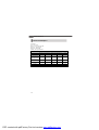
1
Fuzzy CX700/CX700D
MS-9802 (V1.X) Mainboard
G52-98021X2
i
PDF created with pdfFactory Pro trial version www.pdffactory.com
Copyright Notice
Th e material in this d ocument is the in tellectual p rop erty of MICRO-STAR
INTERNATIONAL. We take every care in the preparation of this document, but no
guarantee is given as to the correctness of its contents. Our products are under
continual improvement and we reserve the right to make changes without notice.
Trademarks
All trademarks are the properties of their respective owners.
Intel® and Pentium® are registered trademarks of Intel Corporation.
AMD, Athlon™, Athlon™ XP, Thoroughbred™, and Duron™ are registered trademarks of AMD Corporation.
NVIDIA, the NVIDIA logo, DualNet, and nForce are registered trademarks or trademarks of NVIDIA Corporation in the United States and/or other countries.
PS/2 and OS ®/2 are registered trademarks of International Business Machines
Corporation.
Windows® 98/2000/NT/XP/Vista are registered trademarks of Microsoft Corporation.
Netware® is a registered trademark of Novell, Inc.
Award® is a registered trademark of Phoenix Technologies Ltd.
AMI® is a registered trademark of American Megatrends Inc.
Revision History
Revision
V1.1
Revision History
Updating memory & SATA
Date
June 2008
Technical Support
If a problem arises with your system and no solution can be obtained from the user’s
manual, please contact your place of purchase or local distributor. Alternatively,
please try the following help resources for further guidance.
Visit th e MSI web site at http://global.msi.com.tw/index.php?
func=service for FAQ, technical guide, BIOS updates, driver updates, and
other information.
Contact our technical staff at http://ocss.msi.com.tw.
ii
PDF created with pdfFactory Pro trial version www.pdffactory.com
Safety Instructions
1.
Always read the safety instructions carefully.
2.
Keep this User’s Manual for future reference.
3.
Keep this equipment away from humidity.
4.
Lay this equipment on a reliable flat surface before setting it up.
5.
The openings on the enclosure are for air convection hence protects the equipment from overheating. DO NOT COVER THE OPENINGS.
6.
Make sure the voltage of the power source and adjust properly 110/220V before connecting the equipment to the power inlet.
7.
Place the power cord such a way that people can not step on it. Do not place
anything over the power cord.
8.
Always Unplug the Power Cord before inserting any add-on card or module.
9.
All cautions and warnings on the equipment should be noted.
10. Never pour any liquid into the opening that could damage or cause electrical
shock.
11. If any of the following situations arises, get the equipment checked by service
personnel:
† The power cord or plug is damaged.
† Liquid has penetrated into the equipment.
† The equipment has been exposed to moisture.
† The equipment does not work well or you can not get it work according to
User’s Manual.
† The equipment has dropped and damaged.
† The equipment has obvious sign of breakage.
12. DO NOT LEAVE THIS EQUIPMENT IN AN ENVIRONMENT UNCONDITIONED, STORAGE TEMPERATURE ABOVE 600 C (1400F), IT MAY DAMAGE THE EQUIPMENT.
CAUTION: Dan g er of exp losion if b attery is in correctl y rep laced .
Replace on ly with the same or equivalent type recommen ded by the
manufacturer.
iii
PDF created with pdfFactory Pro trial version www.pdffactory.com
FCC-B Radio Frequency Interference Statement
Th is eq u ip men t h as been
tested and found to comply
with the limits for a Class B
digital device, pursuant to Part
15 of the FCC Rules. These limits are designed to provide reasonable protection
against harmful interference in a residential installation. This equipment generates,
uses and can radiate radio frequency energy and, if not installed and used in accordance with the instructions, may cause harmful interference to radio communications.
However, there is no guarantee that interference will not occur in a particular
installation. If this equipment does cause harmful interference to radio or television
reception, which can be determined by turning the equipment off and on, the user is
encouraged to try to correct the interference by one or more of the measures listed
bel ow.
† Reorient or relocate the receiving antenna.
† Increase the separation between the equipment and receiver.
† Connect the equipment into an outlet on a circuit different from that to
which the receiver is connected.
† Consult the dealer or an experienced radio/television technician for help.
Notice 1
The changes or modifications not expressly approved by the party responsible for
compliance could void the user’s authority to operate the equipment.
Notice 2
Shielded interface cables and A.C. power cord, if any, must be used in order to
comply with the emission limits.
VOIR LA NOTICE D’INSTALLATION AVANT DE RACCORDER AU RESEAU.
Micro-Star International
MS-9802
This device complies with Part 15 of the FCC Rules. Operation is subject to the
following two conditions:
(1) this device may not cause harmful interference, and
(2) this device must accept any interference received, including interference that
may cause undesired operation.
iv
PDF created with pdfFactory Pro trial version www.pdffactory.com
WEEE (Waste Electrical and Electronic Equipment) Statement
v
PDF created with pdfFactory Pro trial version www.pdffactory.com
vi
PDF created with pdfFactory Pro trial version www.pdffactory.com
vii
PDF created with pdfFactory Pro trial version www.pdffactory.com
CONTENTS
Copyright Notice .................................................................................................... iii
Trademarks ............................................................................................................ iii
Revision History .................................................................................................... iii
Technical Support ................................................................................................. iii
Safety Instructions ................................................................................................ iii
FCC-B Radio Frequency Interference Statement .................................................... v
WEEE (Waste Electrical and Electronic Equipment) Statement ................................ v
Chapter 1 Product Overview .......................................................................... 1-1
Mainboard Specifications ............................................................................. 1-2
Block Diagram ............................................................................................... 1-4
Mainboard Layout ........................................................................................ 1-5
Board Dimension .......................................................................................... 1-6
I/O Shield Drawing ....................................................................................... 1-7
Power Consumption .................................................................................... 1-8
General Purpose I/O Lines ........................................................................... 1-9
Onboard Connector Part Number ................................................................. 1-9
Safety Compliance & MTBF ........................................................................ 1-10
Chapter 2 Hardware Setup ............................................................................. 2-1
Quick Components Guide ............................................................................. 2-2
Memory ....................................................................................................... 2-3
Power Supply .............................................................................................. 2-4
Back Panel ................................................................................................... 2-5
Connectors .................................................................................................. 2-7
Jumpers ..................................................................................................... 2-16
Slots .......................................................................................................... 2-18
Chapter 3 BIOS Setup ...................................................................................... 3-1
Entering Setup ............................................................................................. 3-2
The Menu Bar .............................................................................................. 3-4
Main ............................................................................................................. 3-5
Advanced .................................................................................................... 3-7
Boot ........................................................................................................... 3-21
Security ..................................................................................................... 3-22
System ...................................................................................................... 3-23
PC Health ................................................................................................... 3-25
Exit ............................................................................................................ 3-26
Chapter 4 System Resources ....................................................................... 4-1
Watch Dog Timer Setting .............................................................................. 4-2
Award POST Code ...................................................................................... 4-4
Check Point & Beep Code List .................................................................... 4-10
PCI Configuration ....................................................................................... 4-17
Resource List ............................................................................................ 4-18
viii
PDF created with pdfFactory Pro trial version www.pdffactory.com
Product Overview
Chapter 1
Product Overview
Thank you for choosing the Fuzzy CX700/CX700D (MS9802 v1.X) Mini ITX mainboard from MSI.
Based on the innovative VIA CX700/ CX700M/ CX700M2
controller for optimal system efficiency, the Fuzzy
CX700/CX700D accommodates VIA C7/ Eden/ Eden ULV
processor and supports one 240-pin 400/533MHz DDR2
DIMM slot to provide the maximum of 1GB memory
capacity.
Noiseless, fanless and low power consumption are
the advantages of the Fuzzy CX700/CX700D, making it
an ideal choice for IPC special application.
1-1
PDF created with pdfFactory Pro trial version www.pdffactory.com
MS-9802 Mainboard
Mainboard Specifications
Processor Support
- VIA C7/ Eden/ Eden ULV processor with nanoBGA2 footprint
- 3-pin CPU fan pinheader with Smart Fan Speed Control
- Power Saver TM Technology enabled
CPU Frequency
- 1GHz, 1.5GHz, or 2GHz (Optional)
- Supports FSB to 400/800MHz (Optional)
Chipset
- Single chip solution: VIA CX700/ CX700M/ CX700M2
Memory Support
- DDR2 400/533 SDRAM or ECC DDR2 400 only (1GB Max)
- 1 DDR2 DIMM slot (240pin / 1.8V)
LAN
- 2 PCI Gb LAN by Realtek RTL8110SC
Audio
- Realtek ALC888 7.1-channel HDA codec
- 6 watt amplifier
IDE
- 1 40-pin IDE connector
- Supports 2 IDE devices
CF
- 1 CF Type II socket
SATA
- 2 SATA II ports by VIA CX700/ CX700M/ CX700M2
- Supports storage and data transfers at up to 3Gb/s
Expansion Slots
- 1 PCI slot
- 1 Mini PCI socket
1-2
PDF created with pdfFactory Pro trial version www.pdffactory.com
Product Overview
Connectors
Rear I/O
- 1 PS/2 mouse port
- 1 PS/2 keyboard port
- 1 COM port stack connector (2 RS-232 ports)
- 1 VGA/ DVI stack connector
- 2 RJ45/ USB stack connectors
- 1 3-jack audio connector
Onboard Connector
- 1 USB connector (2 ports)
- 1 parallel port connector (LPT)
- 2 serial port connectors (RS-232)
- 1 LVDS connector
- 1 DIO connector (4 IN/ 4 OUT)
- 1 TV-Out connector
- 1 audio connector (7.1-channel)
- 1 amplifier connector
- 1 front panel connector
- 1 SMBUS connector
- 1 CPU fan connector
- 1 system fan connector
- 2 SATA connectors
- 1 IrDA infrared module connector
Form Factor
- Mini-ITX (17.0cm X17.0cm)
Mounting
- 4 mounting ho les
Environmental
Operation Environment
- Temperature: 0 oC ~ 60 o C
- Humidity: 10% ~ 80% RH
Storage Environment
- Temperature: -20 oC ~ 80 o C
- Humidity: 25% ~ 90% RH
1-3
PDF created with pdfFactory Pro trial version www.pdffactory.com
MS-9802 Mainboard
Block Diagram
1-4
PDF created with pdfFactory Pro trial version www.pdffactory.com
Product Overview
Top:
COM3
Mouse
Bot tom:
Key board
J2
J3
J4
J5
J1
CPUFAN1
VIA
C7 CPU
C OM4
Serial
Ports
JL PT1
J6
ATX1
Back Panel I/O
Mainboard Layout
VIA
CX700/ C X700 M/ CX70 0M2
Top:
VGA Port
Bottom:
DVI-D Port
JLVDS1 VIA
VT163 2A
J7
JTV1
TV/CRT1
SATA1
SATA2
BIOS
JAUD2
TPA3005
SYSFAN1
IRDA1
F_USB1
MIN IPCI1
T: Line-In JCD1
ALC 888
M: Line- Out
B: Mic- In
JAUD1
PCI1
RTL
8 110SC
DIMM1
Top: LAN Jack
Bottom: USB Ports
BATT
+
Top: LAN Jack
Bottom: USB Ports
IDEB1
JFP1
JCF_SEL1
CLR_CMOS1
CF1
RTL
8 110SC
Fuzzy CX700/CX700D (MS-9802 v1.X) Mini ITX Mainboard
1-5
PDF created with pdfFactory Pro trial version www.pdffactory.com
MS-9802 Mainboard
Board Dimension
1-6
PDF created with pdfFactory Pro trial version www.pdffactory.com
Product Overview
I/O Shield Drawing
1-7
PDF created with pdfFactory Pro trial version www.pdffactory.com
MS-9802 Mainboard
Power Consumption
Configuration
CPU:VIA C7 1GHz
Memory:Samsung PC2-3200 1GB
SATA HDD:HITACHI 80GB
SATA HDD:Maxtor 80GB
CDROM:Samsung CD-RW/DVD
Power Consumption
Mainboard 5VSB Mainboard +12V
System
Consumption
Mainboard +3.3V
Mainboard +5V
Current (A)
Current (A)
Current (A)
Current (A)
Watts
A. Full Running (CPU /
Memory / HDD / LAN
stress & Play Audio CD)
1.33
1.07
0.04
0.67
18.0773
B. Running Network
Application - Files Copy
1.33
1.04
0.039
0.6
17.0905
C. Idle
0.56
0.94
0.04
0.39
11.482
D. S3 Mode
0
0
0.318
0
1.6345
E. Running 3D stress
1.972
6.2115
0.1748
7.709
16.0673
1-8
PDF created with pdfFactory Pro trial version www.pdffactory.com
Product Overview
General Purpose I/O Lines
General Purpose I/O Lines
Parameter
Conditions
Min
Input High Voltage (VIH)
-
2V
2V
Input High Voltage (VIL)
-
-0.5V
0.8V
Input Current (II)
Out High Voltage (VoH)
Out Low Voltage (VoL)
Max
-
-
+(-)1uA
IOH = -50uA
4.4V
-
IOH = -16uA
3.8V
-
IOL = 50uA
-
0.1V
IOH = 16uA
-
0.55V
Onboard Connector Part Number
Onboard Connector
Part Number
Description
DC 12V power connector
HORNG TONG ( E20221-222123 )
2x2-pin, 4.2mm
AMP audio header
FOXCONN ( HB1104H )
1x4-pin, 2.54mm
GPIO box header
HORNG TONG ( A10271-0A1129 )
2x5-pin, 2mm
Parallel port box header
HORNG TONG ( A26371-0A1120 )
2x13-pin, 2mm
LVDS panel box header
HORNG TONG ( B2205J-926430 )
RS-232 box header (internal) HORNG TONG ( A10332-A12220 )
2x20pin, 1.25mm
2x5pin, 2.54mm ( take out of 1-pin )
TV-OUT header
HORNG TONG ( C2036A-21212R ) 2x3-pin, 2.54mm ( take out of 1-pin )
Front panel I/O header
HORNG TONG ( C205A1-21412Z ) 2x5-pin, 2.54mm ( take out of 1-pin )
IrDA header
HORNG TONG ( C2035A-21212R ) 2x3-pin, 2.54mm ( take out of 1-pin )
USB header (internal)
HORNG TONG ( C2059A-21412X ) 2x5-pin, 2.54mm ( take out of 1-pin )
Front audio header
HORNG TONG ( C2074A-25212R ) 2x7-pin, 2.54mm ( take out of 1-pin )
1-9
PDF created with pdfFactory Pro trial version www.pdffactory.com
MS-9802 Mainboard
Safety Compliance & MTBF
Standard number
Certification
CE
BSMI
CNS 13438 乙類(1997年版)
C-Tick
AS/NZS CISPR 22:2004
FCC
VCCI
Title of standard
EN 55022:1998+A1:2000+A2:2003 Class B Product family standard
Limits for harmonic current
EN 6100-3-2:2000 Class D
emission
RFI
Limitation of voltage
EN 6100-3-3:1995+A1:2001
fluctuation and flicker in lowvoltage supply system
Immunity EN 55024:1998+A1:2001+A2:2003
Product family standard
FCC CFR Title 47 Part 15 Subpart B: 2005 Class B
CISPR 22: 2005
VCCI V-3:2004, Class B
VCCI V-4:2004, Class B
MTBF - Reliability Prediction
Calculation Model
Operation Temperature Operating Environment Duty Cycle
MTBF
Telcordia Issue 1
35
Ground Benign
100%
186,718
MIL-HDBK-217 FN2
55
Ground Mobile
100%
3,182
1-10
PDF created with pdfFactory Pro trial version www.pdffactory.com
Hardware Setup
Chapter 2
Hardware Setup
This chapter provides you with the information about
hardware setup procedures. While doing the installation,
be careful in holding the components and follow the
installation procedures. For some components, if you
install in the wrong orientation, the components will not
work properly.
Use a grounded wrist strap before handling computer
comp onen ts. Static el ectricity may damag e th e
components.
2-1
PDF created with pdfFactory Pro trial version www.pdffactory.com
MS-9802 Mainboard
Quick Components Guide
COM4, p.2-13
COM3, p.2-13
Back Panel,
p.2-5
J1, p.2-15
J2~J5,
p.2-17
CPUFAN1, p.2-12
DIMM1,
p.2-3
J6, p.2-11
J LPT1 ,
p.2-12
JLVDS1,
p.2-14
ATX1,
p.2-4
J7, p.2-17
SATA1/2,
p.2-8
JTV1, p.2-15
SYSFAN1,
p.2-12
TV/CRT1,
p.2-16
IRDA1,
p.2-15
JAUD1, p.2-9
JCD1, p.2-14
PCI1, p.2-18
JCF_SEL1,
p.2-7
JFP1, p.2-10
F_USB1, p.2-13
JAUD2, p.2-9
MINIPCI1,
p.2-18
CLR_CMOS1,
p.2-16
IDEB1, p.2-7
2-2
PDF created with pdfFactory Pro trial version www.pdffactory.com
Hardware Setup
Memory
The DIMM slot is intended for system memory modules.
DDR2
240-pin, 1.8V
64x2=128 pin
56x2=112 pin
Installing Memory Modules
1. Locate the DIMM slots on the mainboard. Flip open the retaining clip at each side
of the DIMM slot.
2. Align the notch on the DIMM with the key on the slot. Insert the DIMM vertically into
the DIMM slot. Then push it in until the golden finger on the DIMM is deeply inserted
in the DIMM slot. The retaining clip at each side of the DIMM slot will automatically
close if the DIMM is properly seated.
Important
You can barely see the golden finger if the DIMM is properly inserted in the
DIMM slot.
3. Manually check if the DIMM has been locked in place by the retaining clips at the
sides.
Volt
Notch
2-3
PDF created with pdfFactory Pro trial version www.pdffactory.com
MS-9802 Mainboard
Power Supply
ATX 20-Pin System Power Connector: ATX1
This connector allows you to connect to an ATX power supply. To connect to the ATX
power supply, make sure the plug of the power supply is inserted in the proper
orientation and the pins are aligned. Then push down the power supply firmly into the
connector.
ATX1 Pin Definition
ATX1
11 1
20 10
PIN
SIGNAL
PIN
SIGNAL
1
2
3
4
5
6
7
8
9
3.3V
3.3V
GND
5V
GND
5V
GND
PW_OK
5V_SB
10
12V
11
12
13
14
15
16
17
18
19
20
3.3V
-12V
GND
PS_ON
GND
GND
GND
-5V
5V
5V
2-4
PDF created with pdfFactory Pro trial version www.pdffactory.com
Hardware Setup
Back Panel
Serial Port
M ouse
VGA Port
LAN
LAN
Line-In
Line-Out
Keyboard
Serial Port
DVI-D Port
USB
USB
Mic-In
Mouse/Keyboard Connector
The standard PS/2® mouse/keyboard DIN connector is for a PS/2® mouse/keyboard.
Serial Port
The serial port is a 16550A high speed communications port that sends/ receives 16
bytes FIFOs. You can attach a serial mouse or other serial devices directly to the
connector.
VGA Port
The DB15-pin female connector is provided for video monitors.
DVI-D Port
The DVI (Digital Visual Interface) connector allows you to connect an LCD monitor. It
provides a high-speed digital interconnection
Display Matrix
between the computer and its display device.
CRT
DVI
LVDS TV OUT
To connect an LCD monitor, simply plug your
CRT
V
V
X
monitor cable into the DVI connector, and
DVI
V
V
V
make sure that the other end of the cable is
LVDS
V
V
V
properly connected to your monitor (refer to
TV OUT
X
V
V
your monitor manual for more information.)
V : Support
X : No Support
USB Connectors
The UHCI (Universal Host Controller Interface) Universal Serial Bus root is for attaching
USB devices such as keyboard, mouse, or other USB-compatible devices.
Audio Port Connectors
These audio connectors are used for audio devices. You can differentiate the color
of the audio jacks for different audio sound effects.
Line-In (Blue) - Line In is used for external CD player, tapeplayer or
other audio devices.
Line-Out (Green) - Line Out, is a connector for speakers or headphones.
Mic-In (Pink) - Mic In, is a connector for microphones.
2-5
PDF created with pdfFactory Pro trial version www.pdffactory.com
MS-9802 Mainboard
LAN (RJ-45) Jacks
The standard RJ-45 jacks are for connection
to Local Area Network (LAN). You can
connect network cables to them.
100M Cable Plug-in
1000M Cable Plug-in
Link Indicator
Le ft LED
Right LED
Active LED
100M/1000M Speed LED
Yellow
Green/Orange
No Transmission
OFF
OFF
Transition
Yellow(Blinking)
OFF
No Transmission
OFF
Green(Lighting)
Transition
Yellow(Blinking)
Green(Lighting)
No Transmission
OFF
Orange(Lighting)
Transition
Yellow(Blinking)
Orange(Lighting)
OFF
OFF
LED Color
10M Cable Plug-in
Activity Indicator
In S3/S4/S5 Standby State
2-6
PDF created with pdfFactory Pro trial version www.pdffactory.com
Hardware Setup
Connectors
IDE Connector: IDEB1
The mainboard has a 32-bit Enhanced PCI IDE and Ultra DMA 33/66/100/133 controller
that provides PIO mode 0~4, Bus Master, and Ultra DMA 33/66/100/133 function. You
can connect hard disk drives, CD-ROM and other IDE devices.
The Ultra ATA133 interface boosts data transfer rates between the computer and the
hard drive up to 133 megabytes (MB) per second.
IDEB1
CompactFlash Card Slot: CF1
This CompactFlash slot shares one channel of the IDE controller. You can install one
CompactFlash typeI / type II device.
CF1
CF Mode Selecting Jumper:
JCF_SEL1
This jumper is used to select Master/
Slave mode of the CF device.
JCF_SEL1
1
3
1
Master
1
3
Slave
Important
* The CF1 slot and the IDEB1 connector shares and uses the same channel.
CF1 and IDEB1 can support up to 2 IDE devices without CF device or 1 IDE
device with 1 CF device.
* If you install two IDE devices, you must configure the second drive to Slave
mode by setting its jumper. Refer to the hard disk documentation supplied by
hard disk vendors for jumper setting instructions.
* If you install one IDE device with ATA133 IDE cable and one CF device, you
must configure the CF drive to Master mode by setting jumper JCF_SEL1. CF
only supports Master mode by using the ATA133 IDE cable.
* CF only supports Slave mode by using ATA33 IDE cable.
2-7
PDF created with pdfFactory Pro trial version www.pdffactory.com
MS-9802 Mainboard
Serial ATA Connectors: SATA1, SATA2
SATA1~SATA2 are high-speed SATA interface ports and support SATA data rates of
300MB/s. Each SATA connector can connect to 1 hard disk device and is fully compliant
with Serial ATA 2.0 specifications.
SATA2
SATA1
Important
Please do not fold the Serial ATA cable into 90-degree angle. Otherwise,
data loss may occur during transmission.
2-8
PDF created with pdfFactory Pro trial version www.pdffactory.com
Hardware Setup
Audio Amplifier Connector: JAUD1
The 6W JAUD1 is used to connect audio amplifiers to enhance audio performance.
Pin Definition
PIN
JAUD1
1
SIGNAL
1
AMP_R+
2
AMP_R-
3
AMP_L+
4
AMP_L-
Front Audio Connector: JAUD2
This connector is designed to connect an optional audio bracket that provides extra
front panel audio IO jacks.
13
14
1
2
JAUD2
Audio Bracket
(Optional)
JAUD2 Pin Definition
PIN
SIGNAL
PIN
SIGNAL
1
5V_SB
2
VCC3
3
5
7
9
11
13
SPDF_OUT
GND
LEF_OUT
CEN_OUT
JAUD_DET
SIDE_SURR_L
4
6
8
10
12
14
NA
SPDF_IN
SURR_OUT_R
SURR_OUT_L
AUDIO GND
SIDE_SURR_R
2-9
PDF created with pdfFactory Pro trial version www.pdffactory.com
MS-9802 Mainboard
Front Panel Connector: JFP1
The mainboard provides one front panel connector for electrical connection to the
front panel switches and LEDs. The JFP1 is compliant with Intel® Front Panel I/O
Connectivity Design Guide.
JFP1 Pin Definition
JFP1
HDD +
LED Reset Switch +
1
2
9
Power
LED
+ Power
- Switch
10
PIN
SIGNAL
DESCRIPTION
1
2
3
4
5
6
7
8
9
HD_LED +
FP PWR/SLP
HD_LED FP PWR/SLP
RST_SW PWR_SW +
RST_SW +
PWR_SW RSVD_DNU
Hard disk LED pull-up
MSG LED pull-up
Hard disk active LED
MSG LED pull-up
Reset Switch low reference pull-down to GND
Power Switch high reference pull-up
Reset Switch high reference pull-up
Power Switch low reference pull-down to GND
Reserved. Do not use.
Reset Circuit
VCC3
4.7K ohm
FP_RST#
0.1uf
W DTO#
0 ohm
External circuit
HDD LED Circuit
VCC3
200 ohm
4.7K ohm
1
VCC3
SATALED#
1
LED
D
IDEACTP#
VCC3
2
HDDLED#
2
3
4.7K ohm
External circuit
2-10
PDF created with pdfFactory Pro trial version www.pdffactory.com
Hardware Setup
Power LED Circuit
VCC5_SB
330 ohm
2
1
SUSPEND LED
PWR_LED
LED2
LED1
2
1
SUS_LED
POWER LED
VCC5_SB
330 ohm
External circuit
Power Button Circuit
VCC3_SB
4.7K ohm
PWRBTN
0.1uf
68 ohm
100 ohm
External circuit
Digital IO Connector: J6
The J6 connects to the General-Purpose Input/Output (GPIO) peripheral module.
J6 Pin Definition
J6
2
1
10
9
PIN
SIGNAL
PIN
SIGNAL
1
GND
2
VCC5F
3
N_GPO3
4
N_GPO1
5
N_GPO2
6
N_GPO0
7
N_GPI3
8
N_GPI1
9
N_GPI2
10
N_GPI0
DIO Circuit
74LV244A
74LV244A
Input (0~3)
Vih=3.5~5.5V
Vil=0~1.5V
Output (0~3)
VOL max=0V
VOH max=5V
IOL max=16mA
External circuit
2-11
PDF created with pdfFactory Pro trial version www.pdffactory.com
MS-9802 Mainboard
Parallel Port Header: JLPT1
The mainboard provides a 26-pin header for connection to an optional parallel port
bracket. The parallel port is a standard printer port that supports Enhanced Parallel
Port (EPP) and Extended Capabilities Parallel Port (ECP) mode.
JLPT1
26
25
2
1
PIN
SIGNAL
PIN
SIGNAL
PIN
SIGNAL
PIN
SIGNAL
1
RSTB#
2
AFD#
15
PRND6
16
GND
3
5
7
9
11
13
PRND0
PRND1
PRND2
PRND3
PRND4
PRND5
4
6
8
10
12
14
ERR#
PINIT#
LPT_SLIN#
GND
GND
GND
17
19
21
23
25
PRND7
ACK#
BUSY
PE
SLCT
18
20
22
24
26
GND
GND
GND
GND
GND
Fan Power Connectors: CPUFAN1, SYSFAN1
The fan power connectors support system cooling fan with +12V. When connecting
the wire to the connectors, always take note that the red wire is the positive and
should be connected to the +12V, the black wire is Ground and should be connected
to GND. If the mainboard has a System Hardware Monitor chipset on-board, you must
use a specially designed fan with speed sensor to take advantage of the CPU fan
control.
GND
+1 2V
SENSOR
CPUFAN1
GND
+1 2V
SENSOR
SYSFAN1
Important
Please refer to the recommended CPU fans at VIA’s official website or consult
the vendors for proper CPU cooling fan.
2-12
PDF created with pdfFactory Pro trial version www.pdffactory.com
Hardware Setup
Serial Port Connector: COM3, COM4
The mainboard provides two 9-pin headers as serial ports. These ports are 16550A
high speed communication port that sends/receives 16 bytes FIFOs. You can attach
a serial mouse or other serial devices directly to them.
Pin Definition
9
8
PIN
1
2
COM3
8
2
1
9
1
2
3
4
5
6
7
8
9
SIGNAL
DESCRIPTION
DCD
SIN
SOUT
DTR
GND
DSR
RTS
CTS
VCC_COM3
Data Carry Detect
Serial In or Receive Data
Serial Out or Transmit Data
Data Terminal Ready
Ground
Data Set Ready
Request To Send
Clear To Send
Power Source
COM4
Front USB Connector: F_USB1
The mainboard provides one USB 2.0 pinheader that is compliant with Intel ® I/O
Connectivity Design Guide. USB 2.0 technology increases data transfer rate up to a
maximum throughput of 480Mbps, which is 40 times faster than USB 1.1, and is ideal
for connecting high-speed USB interface peripherals such as USB HDD, digital
cameras, MP3 players, printers, modems and the like.
Pin Definition
F_USB1
10
2
9
1
PIN
SIGNAL
PIN
SIGNAL
1
VCC
2
VCC
3
USB0-
4
USB1-
5
USB0+
6
USB1+
7
GND
8
GND
9
Key (no pin)
10
USBOC
Important
Note that the pins of VCC and GND must be connected correctly to avoid
possible damage.
2-13
PDF created with pdfFactory Pro trial version www.pdffactory.com
MS-9802 Mainboard
CD-In Connector: JCD1
The connector is for CD-ROM audio connector.
JCD1
R
GND
L
LVDS Flat Panel Connector: JLVDS1
The LVDS (Low Voltage Differential Signal) connector provides a digital interface
ty p i ca l l y u se d w it h fl at p a n e l s. Aft er
Display Matrix
connecting an LVDS interfaced flat panel to
CRT
DVI
LVDS TV OUT
th e JLVDS1, be sure to check th e p an el
CRT
V
V
X
d atash eet an d set th e J1 LVDS Power
DVI
V
V
V
Selection Jumper to a proper voltage.
V
X
LVDS
TV OUT
V
V
V : Support
SIGNAL
JLVDS1
1
2
39
40
V
V
X : No Support
PIN
SIGNAL
+12V
2
1
+12V
+12V
4
3
+12V
GND
6
5
+12V
GND
8
7
VCC3/VCC5
LCD_VDD
10
9
LCD_VDD
LDDC_DATA
12
11
LDDC_CLK
LVDS_VDDEN
14
13
L_BKLTCTL
GND
16
15
L_BKLTEN
LA_DATA0
18
17
LA_DATA0#
LA_DATA1
20
19
LA_DATA1#
LA_DATA2
22
21
LA_DATA2#
LA_CLK
24
23
LA_CLK#
LA_DATA3
26
25
LA_DATA3#
GND
28
27
GND
LB_DATA0
30
29
LB_DATA0#
LB_DATA1
32
31
LB_DATA1#
LB_DATA2
34
33
LB_DATA2#
LB_CLK
36
35
LB_CLK#
LB_DATA3
38
37
LB_DATA3#
GND
40
39
GND
2-14
PDF created with pdfFactory Pro trial version www.pdffactory.com
Hardware Setup
TV-Out Connector: JTV1
JTV1
The mainboard provides a TV-Out connector.
2
1
Display Matrix
CRT
DVI
LVDS
V
CRT
DVI
LVDS
TV OUT
V
V
X
V : Support
TV OUT
V
V
V
V
5
JTV1 Pin Definition
V
X : No Support
X
V
V
Pin
Description
Pin
Description
1
TVGND
2
LCVBS
3
LY
4
TVGND
5
LC
6
Key (no pin )
IrDA Infrared Module Header: IRDA1
The connector allows you to connect to IrDA Infrared module. You must configure the
setting through the BIOS setup to use the IR function. IRDA1 is compliant with Intel®
Front Panel I/O Connectivity Design Guide.
Pin Definition
IRDA1
6
5
2
1
Pin
Signal
1
2
3
4
5
6
NC
Key (no pin)
VCC5
GND
IRTX
IRRX
I2C Bus Connector: J1
The mainboard provides one I2C (also known as I2C) Bus connector for users to
connect System Management Bus (SMBus) interface.
Pin Definition
J1
1
4
Pin
Signal
1
VCC5F
2
SMBCLK
3
GND
4
SMBDATA-
2-15
PDF created with pdfFactory Pro trial version www.pdffactory.com
MS-9802 Mainboard
Jumpers
Display Jumper: TV/CRT1
This jumper is used to select the display type.
TV/CRT1
1
1
3
3
TV Out
1
CRT
CRT
DVI
LVDS
TV OUT
CRT Out
Display Matrix
DVI
LVDS
V
V
V
X
V
V
V : Support
TV OUT
V
V
X
V
V
V
X : No Support
Clear CMOS Jumper: CLR_CMOS1
There is a CMOS RAM onboard that has a power supply from external battery to keep
the data of system configuration. With the CMOS RAM, the system can automatically
boot OS every time it is turned on. If you want to clear the system configuration, set
this jumper to clear data.
CLR_CMOS1
1
3
1
Clear Data
1
3
Keep Data
Important
You can clear CMOS by shorting 2-3 pin while the system is off. Then return
to 1-2 pin position. Avoid clearing the CMOS while the system is on; it will
damage the mainboard.
2-16
PDF created with pdfFactory Pro trial version www.pdffactory.com
Hardware Setup
LCD Power Source Jumper: J7
This jumper is used to select the power source of LCD.
J7
1
1
1
5V
3.3V
Pin Definition
Pin
Signal
1
VCC3
2
LCD_SRC (default VCC3)
3
VCC5
COM Port Power Jumpers: J2, J3, J4, J5
These jumpers specify the operation voltage of the serial port COM1~4.
1
1
1
1
J2 -> COM2
J3 -> COM1
J4 -> COM4
J5 -> COM3
1
1
12V
5V
Pin Definition
Pin
Signal
1
VCC12F
2
VCC_COM
3
VCC5F
2-17
PDF created with pdfFactory Pro trial version www.pdffactory.com
MS-9802 Mainboard
Slots
PCI (Peripheral Component Interconnect) Slot
The PCI slot supports LAN cards, SCSI cards, USB cards, and other add-on cards
that comply with PCI specifications. At 32 bits and 33 MHz, it yields a throughput rate
of 133 MBps.
32-bit PCI Slot
Mini PCI Slot
Mini PCI Slot
PCI Interrupt Request Routing
The IRQ, acronym of interrupt request line and pronounced I-R-Q, are hardware lines
over which devices can send interrupt signals to the microprocessor. The PCI IRQ
pins are typically connected to the PCI bus pins as follows:
32-bit PCI1
Order 1
Order 2
Order 3
Order 4
INT A#
INT B#
INT C#
INT D#
Important
When adding or removing expansion cards, make sure that you unplug the
power supply first. Meanwhile, read the documentation for the expansion card
to configure any necessary hardware or software settings for the expansion
card, such as jumpers, switches or BIOS configuration.
2-18
PDF created with pdfFactory Pro trial version www.pdffactory.com
BIOS Setup
Chapter 3
BIOS Setup
This chapter provides information on the BIOS Setup
program and allows you to configure the system for
optimum use.
You may need to run the Setup program when:
² An error message appears on the screen during the
system booting up, and requests you to run SETUP.
² You want to change the default settings for customized features.
3-1
PDF created with pdfFactory Pro trial version www.pdffactory.com
MS-9802 Mainboard
Entering Setup
Power on the computer and the system will start POST (Power On Self Test) process.
When the message below appears on the screen, press <F1> key to enter Setup.
Press F1 to enter SETUP
If the message disappears before you respond and you still wish to enter Setup,
restart the system by turning it OFF and On or pressing the RESET button. You may
also restart the system by simultaneously pressing <Ctrl>, <Alt>, and <Delete> keys.
Important
1. The items under each BIOS category described in this chapter are under
continuous update for better system performance. Therefore, the description may be slightly different from the latest BIOS and should be held for
reference only.
2. Upon boot-up, the 1st line appearing after the memory count is the BIOS
version. It is usually in the format:
P9802VMS V1.0 011507 where:
1st digit refers to BIOS maker as A = AMI, W = AWARD, and P =
PHOENIX.
2nd - 5th digit refers to the model number.
6th digit refers to the chipset as I = Intel, N = nVidia, and V = VIA.
7th - 8th digit refers to the customer as MS = all standard customers.
V1.0 refers to the BIOS version.
011507 refers to the date this BIOS was released.
3-2
PDF created with pdfFactory Pro trial version www.pdffactory.com
BIOS Setup
Control Keys
<↑>
<↓>
<←>
<→>
<Enter>
<Esc>
<+/PU>
<-/PD>
<F6>
<F7>
<F10>
Move to the previous item
Move to the next item
Move to the item in the left hand
Move to the item in the right hand
Select the item
Jumps to the Exit menu or returns to the main menu from a
submenu
Increase the numeric value or make changes
Decrease the numeric value or make changes
Load Optimized Defaults
Load Fail-Safe Defaults
Save all the CMOS changes and exit
Getting Help
After entering the Setup menu, the first menu you will see is the Main Menu.
Main Menu
The main menu lists the setup functions you can make changes to. You can use the
arrow keys ( ↑↓ ) to select the item. The on-line description of the highlighted setup
function is displayed at the bottom of the screen.
Sub-Menu
If you find a right pointer symbol (as shown in the right view) appears to the left of
certain fields that means a sub-menu can be launched from
this field. A sub-menu contains additional options for a field
parameter. You can use arrow keys ( ↑↓ ) to highlight the
field and press <Enter> to call up the sub-menu. Then you
can use the control keys to enter values and move from field to field within a submenu. If you want to return to the main menu, just press the <Esc >.
General Help <F1>
The BIOS setup program provides a General Help screen. You can call up this screen
from any menu by simply pressing <F1>. The Help screen lists the appropriate keys
to use and the possible selections for the highlighted item. Press <Esc> to exit the
Help screen.
3-3
PDF created with pdfFactory Pro trial version www.pdffactory.com
MS-9802 Mainboard
The Menu Bar
Main
Use this menu for basic system configurations, such as time, date etc.
Advanced
Use this menu to set up the items of special enhanced features available on your
system’s chipset.
Boot
Use this menu to specify the priority of boot devices.
Security
Use this menu to set Supervisor and User Passwords.
System
This entry shows your system summary.
PC Health
This entry monitors your hardware health status.
Exit
This menu allows you to load the BIOS default values or factory default settings into
the BIOS and exit the BIOS setup utility with or without changes.
3-4
PDF created with pdfFactory Pro trial version www.pdffactory.com
BIOS Setup
Main
Date (mm:dd:yy)
The date format is <Day>, <Month> <Date> <Year>.
Time (hh:mm:ss)
The time format is <Hour> <Minute> <Second>.
IDE Channel 0/1 Master/Slave
Press <Enter> to enter the sub-menu.
IDE HDD Auto-Detection
Press [Enter] to auto-detect the HDD on this channel. If detection is successful,
it fills the remaining fields on this menu.
IDE Channel 0/1 Master/Slave
Selecting “manual” lets you set the remaining fields on this screen. It selects the
type of fixed disk. “User Type” will let you select the number of cylinders,
heads, etc.
Note: PRECOMP=65535 means NONE!
Access M ode
Choose the access mode for this hard disk.
3-5
PDF created with pdfFactory Pro trial version www.pdffactory.com
MS-9802 Mainboard
Capacity
This setting shows the formatted size of the storage device. Note that this size
is usually slightly greater than the size of a formatted disk given by a disk
checking program.
Cylinder
Set the number of cylinders for this hard disk.
Head
Set the number of read/write heads.
Precomp
This setting specifies the write precompensation.
Warning: Setting avalue of 65535 means no hard disk.
Landing Zone
This setting shows cylinder location of the landing zone.
Sector
This setting shows the number of sectors per track.
Base Memory
This setting displays the amount of conventional memory detected during boot up.
Extended Memory
This setting displays the amount of extended memory detected during boot up.
Total Memory
This setting displays the total memory available in the system.
3-6
PDF created with pdfFactory Pro trial version www.pdffactory.com
BIOS Setup
Advanced
Advanced BIOS Features
Virus Warning
The item is to set the Virus Warning feature for IDE Hard Disk boot sector
3-7
PDF created with pdfFactory Pro trial version www.pdffactory.com
MS-9802 Mainboard
protection. If the function is enabled and any attempt to write data into this area
is made, BIOS will display a warning message on screen and beep.
Quick Power On Self Test
Select [Enabled] to reduce the amount of time required to run the power-on selftest (POST). A quick POST skips certain steps. We recommend that you normally disable quick POST. Better to find a problem during POST than lose data
during your work.
Boot Up NumLock Status
This setting is to set the Num Lock status when the system is powered on.
Setting to [On] will turn on the Num Lock key when the system is powered on.
Setting to [Off] will allow users to use the arrow keys on the numeric keypad.
Typematic Rate Setting
This item is used to enable or disable the typematic rate setting including Typematic
Rate & Typematic Delay.
Typematic Rate (Chars/Sec)
After Typematic Rate Setting is enabled, this item allows you to set the rate
(characters/second) at which the keys are accelerated.
Typematic Delay (Msec)
This item allows you to select the delay between when the key was first
pressed and when the acceleration begins.
MPS Version Control For OS
This field allows you to select which MPS (Multi-Processor Specification) version to be used for the operating system. You need to select the MPS version
supported by your operating system. To find out which version to use, consult
the vendor of your operating system.
Video BIOS Shadow
This allows you to copy Video BIOS to shadow RAM. When setting to [Enabled],
the performance improves.
Small Logo(EPA) Show
This item enables you to show the EPA logo (brand specific graphics) on the
bootup screen. Settings are:
[Disabled]
Shows the normal POST screen at boot.
[Enabled]
Shows a still image (EPA logo) on the screen at boot.
3-8
PDF created with pdfFactory Pro trial version www.pdffactory.com
BIOS Setup
Advanced Chipset Features
AGP & P2P Bridge Control
VGA Share Memory Size
The system shares memory to the onboard VGA card. This setting controls
the exact memory size shared to the VGA card.
Direct Frame Buffer
When [Enabled], a fixed VGA frame buffer from A000h to BFFFh and a CPUto-PCI write buffer are implemented.
3-9
PDF created with pdfFactory Pro trial version www.pdffactory.com
MS-9802 Mainboard
Select Display Device
Use the field to select the type of device you want to use as the display(s)
of the system.
Panel Type
Use this field to specify the panel type.
Output Port
Use this field to specify the video output channel.
Dithering
Dithering is the most common means of reducing the color range of images
down to the 256 (or fewer) colors seen in 8-bit GIF images. It is the process
of juxtaposing pixels of two colors to create the illusion that a third color is
present. Setting this field to [Enabled] can improve the appearance of a
graphic when few colors are available.
*** Refer to the following table for configuration of Panel Type, Output
Port, and Dithering.
TV Type
Select the TV standard which is used as the video signal format of your TV
if you have connected a TV to the system.
TV Connector
This setting specifies the TV connector.
3-10
PDF created with pdfFactory Pro trial version www.pdffactory.com
BIOS Setup
HDTV Type
Select the HDTV standard which is used as the video signal format of your
HDTV if you have connected a HDTV to the system.
HDTV Connector
This setting specifies the HDTV connector.
System BIOS Cacheable
Selecting [Enabled] allows caching of the system BIOS ROM at F0000h-FFFFFh,
resulting in better system performance. However, if any program writes to this
memory area, a system error may result.
Video RAM Cacheable
Selecting [Enabled] allows caching of the video memory (RAM) at A0000h to
AFFFFh, resulting in better video performance. However, if any program writes
to this memory area, a memory access error may result.
Init Display First
This item specifies which VGA card is your primary graphics adapter.
3-11
PDF created with pdfFactory Pro trial version www.pdffactory.com
MS-9802 Mainboard
Integrated Peripherals
VIA OnChip IDE Device
SATA Controller
This setting enables/disables the on-chip SATA controller.
IDE DMA Transfer Access
Setting to [Enabled] will open DMA bus master and execute DMA action in
DOS, which will make the data transferring faster.
3-12
PDF created with pdfFactory Pro trial version www.pdffactory.com
BIOS Setup
OnChip IDE Channel 1
The integrated peripheral controller contains an IDE interface with support
for one IDE channel. Choose [Enabled] to activate the IDE channel 1.
IDE Prefetch Mode
The onboard IDE drive interfaces support IDE prefetching, for faster drive
accesses. When you install a primary and/or secondary add-in IDE interface,
set this option to [Disabled] if the interface does not support prefetching.
Secondary Master/Slave PIO
The IDE PIO (Programmed Input/Output) fields let you set a PIO mode for the
IDE devices that the onboard IDE interface supports. Modes 0 through 4
provide successively increased performance. In [Auto] mode, the system
automatically determines the best mode for each device.
Secondary Master/Slave UDMA
Ultra DMA 33/66/100/133 implementation is possible only if your IDE hard
drive supports it and the operating environment includes a DMA driver
(Windows ME, XP or a third-party IDE bus master driver). If your hard drive
and your system software both support Ultra DMA/33, Ultra DMA/66, Ultra
DMA/100 and Ultra DMA/133, select [Auto] to enable BIOS support.
IDE HDD Block Mode
Block mode is also called block transfer, multiple commands, or multiple
sector read/write. If your IDE hard drive supports block mode (most new
drives do), select [Enabled] for automatic detection of the optimal number of
block read/writes per sector the drive can support.
VIA OnChip PCI Device
3-13
PDF created with pdfFactory Pro trial version www.pdffactory.com
MS-9802 Mainboard
Azalia HDA Controller
Azalia is the codename of “High Definition Audio.” This setting controls the
High Definition Audio interface integrated in the Southbridge.
Super IO Device
Onboard Serial Port 1 / 2
Select an address and corresponding interrupt for Serial Port 1/2.
UART Mode Select
This setting allows you to specify the operation mode for serial port 2.
[Normal]
RS-232C Serial Port
[IrDA]
IrDA-compliant Serial Infrared Port
[ASKIR]
Amplitude Shift Keyed Infrared Port
RxD, TxD Active
This setting controls the receiving and transmitting speed of the IR
peripheral in use.
IR Transmission Delay
This setting determines whether the IR transmission rate will be delayed
while converting to receiving mode.
UR2 Duplex Mode
This setting controls the operating mode of IR transmission/reception. Under
[Full] Duplex mode, synchronous, bi-directional transmission/reception is
allowed. Under [Half] Duplex mode, only asynchronous, bi-directional transmission/reception is allowed.
3-14
PDF created with pdfFactory Pro trial version www.pdffactory.com
BIOS Setup
Use IR Pins
Consult your IR peripheral documentation to select the correct setting of
the TxD and RxD signals.
Onboard Serial Port 3 / 4
Select an address and corresponding interrupt for Serial Port 3/4.
Onboard Parallel Port
This setting specifies the I/O port address and IRQ of the onboard parallel
port.
Parallel Port Mode
[SPP]
Standard Parallel Port
[EPP]
Enhanced Parallel Port
[ECP]
Extended Capability Port
[ECP + EPP]
Extended Capability Port + Enhanced Parallel Port
To operate the onboard parallel port as Standard Parallel Port only, choose
[SPP]. To operate the onboard parallel port in the EPP mode simultaneously,
choose [EPP]. By choosing [ECP], the onboard parallel port will operate in
ECP mode only. Choosing [ECP + EPP] will allow the onboard parallel port to
support both the ECP and EPP modes simultaneously.
EPP Mode Select
Select EPP port type 1.7 or 1.9, as required by your parallel peripheral.
ECP Mode Use DMA
The ECP mode has to use the DMA channel, so choose the onboard parallel
port with the ECP feature. After selecting it, the following message will
appear: “ECP Mode Use DMA.” At this time, the user can choose between
DMA channel [3] or [1].
USB Device Setting
3-15
PDF created with pdfFactory Pro trial version www.pdffactory.com
MS-9802 Mainboard
USB 1.1 Controller
This setting is used to enable/disable the onboard USB 1.1 controller.
USB 2.0 Controller
This setting is used to enable/disable the onboard USB 2.0 controller.
USB Operation Mode
This setting controls the USB operation speed.
USB Keyboard / Mouse / Storage Function
Set to [Enabled] if your need to use a USB-interfaced keyboard/mouse/
storage device in the operating system that does not support or have any
USB driver installed, such as DOS and SCO Unix.
Power Management Setup
ACPI Function
This item is to activate the ACPI (Advanced Configuration and Power Management Interface) Function. If your operating system is ACPI-aware, such as
Windows 98SE/2000/ME, select [Enabled].
ACPI Suspend Type
This item specifies the power saving modes for ACPI function. If your operating
system supports ACPI, such as Windows 98SE, Windows ME and Windows
2000, you can choose to enter the Standby mode in S1 (POS) or S3 (STR)
fashion through the setting of this field. Options are:
[S1(POS)] The S1 sleep mode is a low power state. In this state,
no system context is lost (CPU or chipset) and hardware maintains all system context.
3-16
PDF created with pdfFactory Pro trial version www.pdffactory.com
BIOS Setup
[S3(STR)] The S3 sleep mode is a lower power state where the
information of system configuration and open applications/files is saved to main memory that remains
powered while most other hardware components turn
off to save energy. The information stored in memory
will be used to restore the system when a “wake up”
event occurs.
Power Management Option
This item is used to select the degree (or type) of power saving and is related
to these modes: Suspend Mode and HDD Power Down. There are three
options for power management:
[Min Saving]
Minimum Power Management. Suspend Mode=1 Hour
[Max Saving] Maximum Power Management. Suspend Mode=1 Min
[User Define] Allows end users to configure each mode separately.
HDD Power Down
If HDD activity is not detected for the length of time specified in this field, the
hard disk drive will be powered down while all other devices remain active.
Suspend Mode
After the selected period of system inactivity, all devices except the CPU shut
off.
Video Off Option
This setting is used to control the mode in which the monitor will shut down.
Setting options:
[Always On]
Monitor remains on during power-saving modes.
[Suspend -> Off]
Monitor blanked when system enters Suspend mode.
[Susp, Stby->Off]
Monitor blanked when system enters either Suspend
or Standby mode.
[All Modes ->Off]
Monitor blanked when system enters any power sav
Video Off Method
This setting determines the manner in which the monitor is blanked.
Soft-Off by PWRBTN
N
This feature allows users to configure the power button function. Settings are:
[Instant-Off] The power button functions as a normal power-on/-off button.
[Delay 4 Sec.] When you press the power button, the computer enters the
suspend/sleep mode, but if the button is pressed for more
than four seconds, the computer is turned off.
AC Loss Auto Restart
This setting specifies whether your system will reboot after a power failure or
interrupt occurs. Available settings are:
[Off]
Leaves the computer in the power off state.
[On]
Leaves the computer in the power on state.
[Former-sts] Restores the system to the status before power failure or interrupt occurred.
3-17
PDF created with pdfFactory Pro trial version www.pdffactory.com
MS-9802 Mainboard
Wakeup Event Detect
PS2 KB Wakeup Select
The item specifies how the system will be awakened from power saving
mode when input signal of the PS2 keyboard is detected. Use the <PageUp>
& <PageDown> keys to select the options. When selecting [Password],
enter the desired password.
PS2 KB Wakeup Key Select
This setting only works when PS2 KB Wakeup Select is set to [Hot Key].
PS2 MS Wakeup Key Select
This setting determines whether the system will be awakened from power
saving modes when input signal of the PS/2 mouse is detected.
Power On by PCI Card
When setting to [Enabled], this setting allows your system to be awakened
from the power saving modes through any event on PCI PME (Power Management Event).
RTC Alarm Resume
When [Enabled], your can set the date and time at which the RTC (real-time
clock) alarm awakens the system from suspend mode.
Date (of Month)
When RTC Alarm Resume is set to [Enabled], the field specifies the month
for it.
Resume Time (hh:mm:ss)
You can choose what hour, minute and second the system will boot up.
3-18
PDF created with pdfFactory Pro trial version www.pdffactory.com
BIOS Setup
PnP/PCI Configurations
PNP OS Installed
When set to [Yes], BIOS will only initialize the PnP cards used for booting (VGA,
IDE, SCSI). The rest of the cards will be initialized by the PnP operating system
like Windows 98. When set to [No], BIOS will initialize all the PnP cards. So,
select [Yes] if your operating system is Plug & Play aware.
Reset Configuration Data
The ESCD (Extended System Configuration Data) NVRAM (Non-volatile Random
Access Memory) is where the BIOS stores resource information for both PNP
and non-PNP devices in a bit string format. When the item is set to [Enabled], the
system will reset ESCD NVRAM right after the system is booted up and then set
the setting of the item back to [Disabled] automatically.
Resources Controlled By
The Award Plug and Play BIOS has the capacity to automatically configure all of
the boot and Plug and Play compatible devices. However, this capability means
absolutely nothing unless you are using a Plug and Play operating system such
as Windows ® 98/2000. If you set this field to [Manual], choose specific resources by going into each sub-menu that follows this field.
IRQ Resources
Press <Enter> to enter the sub-menu.
IRQ 3/4/5/7/9/10/11/14/15
These items specify the bus where the specified IRQ line is used.
The settings determine if BIOS should remove an IRQ from the pool of available IRQs passed to devices that are configurable by the system BIOS. The
available IRQ pool is determined by reading the ESCD NVRAM. If more IRQs
3-19
PDF created with pdfFactory Pro trial version www.pdffactory.com
MS-9802 Mainboard
must be removed from the IRQ pool, the end user can use these settings to
reserve the IRQ by assigning an [Reserved] setting to it. Onboard I/O is
configured by BIOS. All IRQs used by onboard I/O are configured as
[Available]. If all IRQs are set to [Reserved], and IRQ 14/15 are allocated to
the onboard PCI IDE, IRQ 9 will still be available for PCI and PnP devices.
Important
IRQ (Interrupt Request) lines are system resources allocated to I/O devices.
When an I/O device needs to gain attention of the operating system, it signals
this by causing an IRQ to occur. After receiving the signal, when the operating
system is ready, the system will interrupt itself and perform the service required by the I/O device.
3-20
PDF created with pdfFactory Pro trial version www.pdffactory.com
BIOS Setup
Boot
Hard Disk Boot Priority
This setting allows users to set the boot priority of the specified hard disk devices.
First press <Enter> to enter the sub-menu. Then you may use the arrow keys ( ↑↓ )
to select the desired device, then press <+>, <-> or <PageUp>, <PageDown> key to
move it up/down in the priority list.
First / Second / Third Boot Device
The items allow you to set the sequence of boot devices where BIOS attempts to load
the disk operating system.
Boot Other Device
Setting the option to [Enabled] allows the system to try to boot from other device if the
system fails to boot from the first/second/third boot device.
3-21
PDF created with pdfFactory Pro trial version www.pdffactory.com
MS-9802 Mainboard
Security
Security Option
Select whether the password is required every time the system boots or only when
you enter Setup.
System
The system will not boot and access to Setup will be denied if the
correct password is not entered at the prompt.
Setup
The system will boot, but access to Setup will be denied if the correct
password is not entered at the prompt.
Note: To disable security, select PASSWORD SETTING at Main Menu and then you
will be asked to enter password. Do not type anything and just press <Enter>, it will
disable security. Once the security is disabled, the system will boot and you can
enter Setup freely.
Set Supervisor Password
Supervisor Password controls access to the BIOS Setup utility.
Set User Password
User Password controls access to the system at boot.
3-22
PDF created with pdfFactory Pro trial version www.pdffactory.com
BIOS Setup
System
System Summary
These items show the hardware specifications of your system. Read only.
3-23
PDF created with pdfFactory Pro trial version www.pdffactory.com
MS-9802 Mainboard
Halt On
The setting determines whether the system will stop if an error is detected at boot.
When the system stops for the errors preset, it will halt on for 15 seconds and then
automatically resume its operation. Available options are:
[All Errors]
[No Errors]
[All, But Keyboard]
The system stops when any error is detected.
The system doesn’t stop for any detected error.
The system doesn’t stop for a keyboard error.
3-24
PDF created with pdfFactory Pro trial version www.pdffactory.com
BIOS Setup
PC Health
Current System Temp., Current CPU Temperature, Current CPUFAN Speed,
Current SYSFAN Speed, Vcore, VDDR2, VCC3
These items display the current status of all of the monitored hardware devices/
components such as CPU voltage, temperatures and all fans’ speeds.
3-25
PDF created with pdfFactory Pro trial version www.pdffactory.com
MS-9802 Mainboard
Exit
Load Fail-Safe Defaults
Use this menu to load the default values set by the BIOS vendor for stable system
performance.
Load Optimized Defaults
Use this menu to load the default values set by the mainboard manufacturer specifically for optimal performance of the mainboard.
Save & Exit Setup
Save changes to CMOS and exit setup.
Exit Without Saving
Abandon all changes and exit setup.
3-26
PDF created with pdfFactory Pro trial version www.pdffactory.com
System Resources
Chapter 4
System Resources
This chapter provides information on the following
system resources:
1. Watch Dog Timer Setting (p.4-2);
2. Award POST Code (p.4-4);
3. Check Point & Beep Code List (p.4-10);
4. PCI Configuration (p.4-17);
5. Resource List (p.4-18).
4-1
PDF created with pdfFactory Pro trial version www.pdffactory.com
MS-9802 Mainboard
Watch Dog Timer Setting
4-2
PDF created with pdfFactory Pro trial version www.pdffactory.com
System Resources
Software code
SIO_IDX equ 4EH
SIO_DTA equ 4FH
Timer
equ 10
;reset after 10 seconds
1.
Enter configuration mode
mov dx,SIO_IDX
mov al,87h
out dx,al
out dx,al
2
Set Pin118 to WDTO#
mov dx,SIO_IDX
mov al,2Bh
out dx,al
mov dx,SIO_DTA
in
al,dx
and al,not 04h
out dx,al
3.
Set to and active LDN 08
mov dx,SIO_IDX
mov al,07h
out dx,al
mov dx,SIO_DTA
mov al,08h
out dx,al
mov
mov
out
mov
in
or
out
dx,SIO_IDX
al,30h
dx,al
dx,SIO_DTA
al,dx
al,01h
dx,al
4.
Set WatchDog Timer
mov dx,SIO_IDX
mov al,0f4h
out dx,al
mov dx,SIO_DTA
mov al,Timer
out dx,al
5.
Exit configuration mode
mov dx,SIO_IDX
mov al,0AAh
out dx,al
4-3
PDF created with pdfFactory Pro trial version www.pdffactory.com
MS-9802 Mainboard
Award POST Code
Award BIOS Error Message and Check Point (POST code) List (Need to be
modified, TBD)
• Error/Process Message.
#
Short Name
Description
Possible FRUS
1
CMOS
checksum error
- Defaults
loaded
System board
2
CPU at nnnn
Checksum of CMOS is incorrect, so the
system loads the default equipment
configuration. A checksum error may
indicate that CMOS has become corrupt.
This error may have been caused by a
weak battery. Check the battery and
replace if necessary.
Displays the running speed of the CPU.
3
Press ESC to
skip memory
test
Floppy disk(s)
fail
The user may press Esc to skip the full
memory test.
System board
Cannot find or initialize the floppy drive
controller or the drive. Make sure the
controller is installed correctly. If no floppy
drives are installed, be sure the Diskette
Drive selection in Setup is set to NONE or
AUTO.
Some hard drives require extra time to
initialize.
system board
4
5
6
HARD DISK
initializing
Please wait a
moment
HARD DISK
INSTALL
FAILURE
7
Keyboard error
or no keyboard
present
8
Memory Test:
processor
System board
Cannot find or initialize the hard drive controller System board
or the drive. Make sure the controller is
installed correctly. If no hard drives are
installed, be sure the Hard Drive selection in
Setup is set to NONE.
Cannot initialize the keyboard. Make sure
the keyboard is attached correctly and no
keys are pressed during POST. To
purposely configure the system without a
keyboard, set the error halt condition in
Setup to HALT ON ALL, BUT KEYBOARD.
The BIOS then ignores the missing
keyboard during POST.
This message displays during a full
memory test, counting down the memory
areas being tested.
System board
DIMM
System board
4-4
PDF created with pdfFactory Pro trial version www.pdffactory.com
System Resources
• Check Point List
POST (hex)
CFh
C0h
C1h
A1h
A2h
A3h
A4h
A5h
A6h
A7h
A8h
A9h
AAh
ABh
C3h
C5h
01h
02h
03h
04h
05h
06h
07h
08h
09h
0Ah
0Bh
0Ch
0Dh
0Eh
0Fh
Description
Test CMOS R/W functionality.
Early chipset initialization:
-Disable shadow RAM
-Disable L2 cache (socket 7 or below)
-Program basic chipset registers
Detect memory
-Auto-detection of DRAM size, type and ECC.
-Auto-detection of L2 cache (socket 7 or below)
Set Initial Conditions (Default Values) in EBP
Determine FSB frequency.
Begin Detection of installed DIMMS
Check for Column Latency
200Mhz or 266Mhz
Check for tRAS timing
Check for tRP timing
Check for tRCD timing
Check for ECC Support
Check for refresh timing
Verify that the DIMM's are in matched pairs
Expand compressed BIOS code to DRAM
Call chipset hook to copy BIOS back to E000 & F000 shadow
RAM.
Expand the Xgroup codes locating in physical address 1000:0
Reserved
Initial Superio_Early_Init switch.
Reserved
1. Blank out screen
2. Clear CMOS error flag
Reserved
1. Clear 8042 interface
2. Initialize 8042 self-test
1. Test special keyboard controller for Winbond 977 series Super
I/O chips.
2. Enable keyboard interface.
Reserved
1. Disable PS/2 mouse interface (optional).
2. Auto detect ports for keyboard & mouse followed by a port & interface swap
(optional).
3. Reset keyboard for Winbond 977 series Super I/O chips.
Reserved
Reserved
Reserved
Test F000h segment shadow to see whether it is R/W-able or not. If
test fails, keep beeping the speaker.
Reserved
4-5
PDF created with pdfFactory Pro trial version www.pdffactory.com
MS-9802 Mainboard
10h
11h
12h
13h
14h
15h
16h
17h
18h
19h
1Ah
1Bh
1Ch
1Dh
1Eh
1Fh
20h
21h
22h
23h
24h
25h
26h
27h
28h
29h
Auto detect flash type to load appropriate flash R/W codes into the
run time area in F000 for ESCD & DMI support.
Reserved
Use walking 1’s algorithm to check out interface in CMOS
circuitry. Also set real-time clock power status, and then check for
override.
Reserved
Program chipset default values into chipset. Chipset default
values are MODBINable by OEM customers.
Reserved
Initial Early_Init_Onboard_Generator switch.
Reserved
Detect CPU information including brand, SMI type (Cyrix or
Intel) and CPU level (586 or 686).
Reserved
Reserved
Initial interrupts vector table. If no special specified, all H/W
interrupts are directed to SPURIOUS_INT_HDLR & S/W
interrupts to SPURIOUS_soft_HDLR.
Reserved
Initial EARLY_PM_INIT switch.
Reserved
Load keyboard matrix (notebook platform)
Reserved
HPM initialization (notebook platform)
Reserved
1. Check validity of RTC value:
e.g. a value of 5Ah is an invalid value for RTC minute.
2. Load CMOS settings into BIOS stack. If CMOS checksum fails, use default
value instead.
3. Prepare BIOS resource map for PCI & PnP use. If ESCD is valid, take into
consideration of the ESCD’s legacy information.
4. Onboard clock generator initialization. Disable respective clock resource to
empty PCI & DIMM slots.
5. Early PCI initialization:
-Enumerate PCI bus number
-Assign memory & I/O resource
-Search for a valid VGA device & VGA BIOS, and put it
into C000:0.
Reserved
Reserved
Reserved
Initialize INT 09 buffer
Reserved
1. Program CPU internal MTRR (P6 & PII) for 0-640K memory address.
2. Initialize the APIC for Pentium class CPU.
3. Program early chipset according to CMOS setup. Example: onboard IDE
controller.
4. Measure CPU speed.
5. Invoke video BIOS.
4-6
PDF created with pdfFactory Pro trial version www.pdffactory.com
System Resources
2Ah
2Bh
2Ch
2Dh
2Eh
2Fh
30h
31h
32h
33h
34h
35h
36h
37h
38h
39h
3Ah
3Bh
3Ch
3Dh
3Eh
3Fh
40h
41h
42h
43h
44h
45h
46h
47h
48h
49h
4Ah
4Bh
4Ch
4Dh
4Eh
4Fh
Reserved
Reserved
Reserved
1. Initialize multi-language
2. Put information on screen display, including Award title, CPU type, CPU speed
….
Reserved
Reserved
Reserved
Reserved
Reserved
Reset keyboard except Winbond 977 series Super I/O chips.
Reserved
Reserved
Reserved
Reserved
Reserved
Reserved
Reserved
Reserved
Test 8254
Reserved
Test 8259 interrupt mask bits for channel 1.
Reserved
Test 8259 interrupt mask bits for channel 2.
Reserved
Reserved
Test 8259 functionality.
Reserved
Reserved
Reserved
Initialize EISA slot
Reserved
1. Calculate total memory by testing the last double word of each 64K page.
2. Program write allocation for AMD K5 CPU.
Reserved
Reserved
Reserved
Reserved
1. Program MTRR of M1 CPU
2. Initialize L2 cache for P6 class CPU & program CPU with proper cacheable
range.
3. Initialize the APIC for P6 class CPU.
4. On MP platform, adjust the cacheable range to smaller one in case the
cacheable ranges between each CPU are not identical.
Reserved
4-7
PDF created with pdfFactory Pro trial version www.pdffactory.com
MS-9802 Mainboard
50h
51h
52h
53h
54h
55h
56h
57h
58h
59h
5Ah
5Bh
5Ch
5Dh
5Eh
5Fh
60h
61h
62h
63h
64h
65h
66h
67h
68h
69h
6Ah
6Bh
6Ch
6Dh
6Eh
6Fh
70h
71h
72h
73h
74h
75h
Initialize USB
Reserved
Test all memory (clear all extended memory to 0)
Reserved
Reserved
Display number of processors (multi-processor platform)
Reserved
1. Display PnP logo
2. Early ISA PnP initialization
-Assign CSN to every ISA PnP device.
Reserved
Initialize the combined Trend Anti-Virus code.
Reserved
(Optional Feature)
Show message for entering AWDFLASH.EXE from FDD (optional)
Reserved
1. Initialize Init_Onboard_Super_IO switch.
2. Initialize Init_Onbaord_AUDIO switch.
Reserved
Reserved
Okay to enter Setup utility; i.e. not until this POST stage can users
enter the CMOS setup utility.
Reserved
Reserved
Reserved
Reserved
Initialize PS/2 Mouse
Reserved
Prepare memory size information for function call:
INT 15h ax=E820h
Reserved
Turn on L2 cache
Reserved
Program chipset registers according to items described in Setup &
Auto-configuration table.
Reserved
1. Assign resources to all ISA PnP devices.
2. Auto assign ports to onboard COM ports if the corresponding item in Setup
is set to “AUTO”.
Reserved
1. Initialize floppy controller
2. Set up floppy related fields in 40:hardware.
Reserved
Reserved
Reserved
(Optional Feature)
Enter AWDFLASH.EXE if :
-AWDFLASH is found in floppy drive.
-ALT+F2 is pressed
Reserved
Detect & install all IDE devices: HDD, LS120, ZIP, CDROM…..
4-8
PDF created with pdfFactory Pro trial version www.pdffactory.com
System Resources
76h
77h
78h
79h
7Ah
7Bh
7Ch
7Dh
7Eh
7Fh
80h
81h
82h
83h
84h
85h
86h
87h
88h
89h
90h
91h
92h
93h
94h
95h
96h
FFh
Reserved
Detect serial ports & parallel ports.
Reserved
Reserved
Detect & install co-processor
Reserved
Reserved
Reserved
Reserved
1. Switch back to text mode if full screen logo is supported.
-If errors occur, report errors & wait for keys
-If no errors occur or F1 key is pressed to continue:
wClear EPA or customization logo.
Reserved
Reserved
1. Call chipset power management hook.
2. Recover the text fond used by EPA logo (not for full screen logo)
3. If password is set, ask for password.
Save all data in stack back to CMOS
Initialize ISA PnP boot devices
1. USB final Initialization
2. NET PC: Build SYSID structure
3. Switch screen back to text mode
4. Set up ACPI table at top of memory.
5. Invoke ISA adapter ROMs
6. Assign IRQs to PCI devices
7. Initialize APM
8. Clear noise of IRQs.
Reserved
Reserved
Reserved
Reserved
Reserved
Reserved
Reserved
Read HDD boot sector information for Trend Anti-Virus code
1. Enable L2 cache
2. Program boot up speed
3. Chipset final initialization.
4. Power management final initialization
5. Clear screen & display summary table
6. Program K6 write allocation
7. Program P6 class write combining
1. Program daylight saving
2. Update keyboard LED & typematic rate
1. Build MP table
2. Build & update ESCD
3. Set CMOS century to 20h or 19h
4. Load CMOS time into DOS timer tick
5. Build MSIRQ routing table.
Boot attempt (INT 19h)
4-9
PDF created with pdfFactory Pro trial version www.pdffactory.com
MS-9802 Mainboard
Check Point & Beep Code List
Bootblock Initialization Code Checkpoints
Checkpoint
Description
Before D0
If boot block debugger is enabled, CPU cache-as-RAM functionality is enabled at this
point. Stack will be enabled from this point.
D0
Early Boot Strap Processor (BSP) initialization like microcode update, frequency and
other CPU critical initialization. Early chipset initialization is done.
D1
Early super I/O initialization is done including RTC and keyboard controller. Serial port
is enabled at this point if needed for debugging. NMI is disabled. Perform keyboard
controller BAT test. Save power-on CPUID value in scratch CMOS. Go to flat mode with
4GB limit and GA20 enabled.
D2
Verify the boot block checksum. System will hang here if checksum is bad.
D3
Disable CACHE before memory detection. Execute full memory sizing module. If
memory sizing module not executed, start memory refresh and do memory sizing in
Boot block code. Do additional chipset initialization. Re-enable CACHE. Verify that flat
mode is enabled.
D4
Test base 512KB memory. Adjust policies and cache first 8MB. Set stack.
D5
Bootblock code is copied from ROM to lower system memory and control is given to it.
BIOS now executes out of RAM. Copies compressed boot block code to memory in
right segments. Copies BIOS from ROM to RAM for faster access. Performs main BIOS
checksum and updates recovery status accordingly.
D6
Both key sequence and OEM specific method is checked to determine if BIOS recovery
is forced. If BIOS recovery is necessary, control flows to checkpoint E0. See Bootblock
Recovery Code Checkpoints section of document for more information.
D7
Restore CPUID value back into register. The Bootblock-Runtime interface module is
moved to system memory and control is given to it. Determine whether to execute serial
flash.
D8
The Runtime module is uncompressed into memory. CPUID information is stored in
memory.
D9
Store the Uncompressed pointer for future use in PMM. Copying Main BIOS into
memory. Leaves all RAM below 1MB Read-Write including E000 and F000 shadow
areas but closing SMRAM.
DA
Restore CPUID value back into register. Give control to BIOS POST
(ExecutePOSTKernel). See POST Code Checkpoints section of document for more
information.
DC
System is waking from ACPI S3 state
E1-E8
OEM memory detection/configuration error. This range is reserved for chipset vendors
EC-EE
& system manufacturers. The error associated with this value may be different from one
platform to the next.
4-10
PDF created with pdfFactory Pro trial version www.pdffactory.com
System Resources
Bootblock Recovery Code Checkpoints
Checkpoint
Description
E0
Initialize the floppy controller in the super I/O. Some interrupt vectors are initialized.
DMA controller is initialized. 8259 interrupt controller is initialized. L1 cache is
enabled.
E9
Set up floppy controller and data. Attempt to read from floppy.
EA
Enable ATAPI hardware. Attempt to read from ARMD and ATAPI CDROM.
EB
Disable ATAPI hardware. Jump back to checkpoint E9.
EF
Read error occurred on media. Jump back to checkpoint EB.
F0
Search for pre-defined recovery file name in root directory.
F1
Recovery file not found.
F2
Start reading FAT table and analyze FAT to find the clusters occupied by the recovery
file.
F3
Start reading the recovery file cluster by cluster.
F5
Disable L1 cache.
FA
Check the validity of the recovery file configuration to the current configuration of the
flash part.
FB
Make flash write enabled through chipset and OEM specific method. Detect proper
flash part. Verify that the found flash part size equals the recovery file size.
F4
The recovery file size does not equal the found flash part size.
FC
Erase the flash part.
FD
Program the flash part.
FF
The flash has been updated successfully. Make flash write disabled. Disable ATAPI
hardware. Restore CPUID value back into register. Give control to F000 ROM at
F000:FFF0h.
4-11
PDF created with pdfFactory Pro trial version www.pdffactory.com
MS-9802 Mainboard
POST Code Checkpoints
Checkpoint
Description
03
Disable NMI, Parity, video for EGA, and DMA controllers. Initialize BIOS, POST,
Runtime data area. Also initialize BIOS modules on POST entry and GPNV area.
Initialized CMOS as mentioned in the Kernel Variable "wCMOSFlags."
04
Check CMOS diagnostic byte to determine if battery power is OK and CMOS checksum
is OK. Verify CMOS checksum manually by reading storage area. If the CMOS
checksum is bad, update CMOS with power-on default values and clear passwords.
Initialize status register A.
Initializes data variables that are based on CMOS setup questions. Initializes both the
8259 compatible PICs in the system
05
Initializes the interrupt controlling hardware (generally PIC) and interrupt vector table.
06
Do R/W test to CH-2 count reg. Initialize CH-0 as system timer. Install the POSTINT1Ch
handler. Enable IRQ-0 in PIC for system timer interrupt. Traps INT1Ch vector to
"POSTINT1ChHandlerBlock."
07
Fixes CPU POST interface calling pointer.
08
Initializes the CPU. The BAT test is being done on KBC. Program the keyboard
controller command byte is being done after Auto detection of KB/MS using AMI KB-5.
C0
Early CPU Init Start -- Disable Cache – Init Local APIC
C1
Set up boot strap processor Information
C2
Set up boot strap processor for POST
C5
Enumerate and set up application processors
C6
Re-enable cache for boot strap processor
C7
Early CPU Init Exit
0A
Initializes the 8042 compatible Key Board Controller.
0B
Detects the presence of PS/2 mouse.
0C
Detects the presence of Keyboard in KBC port.
0E
Testing and initialization of different Input Devices. Also, update the Kernel Variables.
Traps the INT09h vector, so that the POST INT09h handler gets control for IRQ1.
Uncompress all available language, BIOS logo, and Silent logo modules.
13
Early POST initialization of chipset registers.
20
Relocate System Management Interrupt vector for all CPU in the system.
24
Uncompress and initialize any platform specific BIOS modules. GPNV is initialized at
this checkpoint.
4-12
PDF created with pdfFactory Pro trial version www.pdffactory.com
System Resources
2A
Initializes different devices through DIM.
See DIM Code Checkpoints section of document for more information.
2C
Initializes different devices. Detects and initializes the video adapter installed in the
system that has optional ROMs.
2E
Initializes all the output devices.
31
Allocate memory for ADM module and uncompress it. Give control to ADM module for
initialization. Initialize language and font modules for ADM. Activate ADM module.
33
Initializes the silent boot module. Set the window for displaying text information.
37
Displaying sign-on message, CPU information, setup key message, and any OEM
specific information.
38
Initializes different devices through DIM. See DIM Code Checkpoints section of
39
Initializes DMAC-1 & DMAC-2.
3A
Initialize RTC date/time.
3B
Test for total memory installed in the system. Also, Check for DEL or ESC keys to limit
document for more information. USB controllers are initialized at this point.
memory test. Display total memory in the system.
3C
Mid POST initialization of chipset registers.
40
Detect different devices (Parallel ports, serial ports, and coprocessor in CPU, … etc.)
successfully installed in the system and update the BDA, EBDA…etc.
52
Updates CMOS memory size from memory found in memory test. Allocates memory for
Extended BIOS Data Area from base memory. Programming the memory hole or any
kind of implementation that needs an adjustment in system RAM size if needed.
60
Initializes NUM-LOCK status and programs the KBD typematic rate.
75
Initialize Int-13 and prepare for IPL detection.
78
Initializes IPL devices controlled by BIOS and option ROMs.
7C
Generate and write contents of ESCD in NVRam.
84
Log errors encountered during POST.
85
Display errors to the user and gets the user response for error.
87
Execute BIOS setup if needed / requested. Check boot password if installed.
8C
Late POST initialization of chipset registers.
8D
Build ACPI tables (if ACPI is supported)
8E
Program the peripheral parameters. Enable/Disable NMI as selected
4-13
PDF created with pdfFactory Pro trial version www.pdffactory.com
MS-9802 Mainboard
90
Initialization of system management interrupts by invoking all handlers. Please note this
A1
Clean-up work needed before booting to OS.
A2
Takes care of runtime image preparation for different BIOS modules. Fill the free area in
checkpoint comes right after checkpoint 20h
F000h segment with 0FFh. Initializes the Microsoft IRQ Routing Table. Prepares the
runtime language module. Disables the system configuration display if needed.
A4
A7
Initialize runtime language module. Display boot option popup menu.
Displays the system configuration screen if enabled. Initialize the CPU’s before boot,
which includes the programming of the MTRR’s.
A9
Wait for user input at config display if needed.
AA
Uninstall POST INT1Ch vector and INT09h vector.
AB
Prepare BBS for Int 19 boot. Init MP tables.
AC
End of POST initialization of chipset registers. De-initializes the ADM module.
B1
Save system context for ACPI. Prepare CPU for OS boot including final MTRR values.
00
Passes control to OS Loader (typically INT19h).
4-14
PDF created with pdfFactory Pro trial version www.pdffactory.com
System Resources
Beep Codes
Boot Block Beep Codes
Number of Beeps
Description
1
Insert diskette in floppy drive A:
2
‘AMIBOOT.ROM’ file not found in root directory of diskette in A:
3
Base Memory error
4
Flash Programming successful
5
Floppy read error
6
Keyboard controller BAT command failed
7
No Flash EPROM detected
8
Floppy controller failure
9
Boot Block BIOS checksum error
10
Flash Erase error
11
Flash Program error
12
‘AMIBOOT.ROM’ file size error
13
BIOS ROM image mismatch (file layout does not match image present in flash
device)
POST BIOS Beep Codes
Number of Beeps
Description
1
Memory refresh timer error.
2
Parity error in base memory (first 64KB block)
3
Base memory read/write test error
4
Motherboard timer not operational
5
Processor error
6
8042 Gate A20 test error (cannot switch to protected mode)
7
General exception error (processor exception interrupt error)
8
Display memory error (system video adapter)
9
AMIBIOS ROM checksum error
10
CMOS shutdown register read/write error
11
Cache memory test failed
4-15
PDF created with pdfFactory Pro trial version www.pdffactory.com
MS-9802 Mainboard
Troubleshooting POST BIOS Beep Codes
Number of Beeps
Troubleshooting Action
1, 2 or 3
Reseat the memory, or replace with known good modules.
4-7, 9-11
Fatal error indicating a serious problem with the system. Consult your system
manufacturer. Before declaring the motherboard beyond all hope, eliminate the
possibility of interference by a malfunctioning add-in card. Remove all expansion
cards except the video adapter.
‧ If beep codes are generated when all other expansion cards are absent, consult
your system manufacturer’s technical support.
‧ If beep codes are not generated when all other expansion cards are absent, one
of the add-in cards is causing the malfunction. Insert the cards back into the
system one at a time until the problem happens again. This will reveal the
malfunctioning card.
8
If the system video adapter is an add-in card, replace or reseat the video adapter.
If the video adapter is an integrated part of the system board, the board may be
faulty.
4-16
PDF created with pdfFactory Pro trial version www.pdffactory.com
System Resources
PCI Configuration
PCI Interrupt Request Routing
The IRQ, acronym of interrupt request line and pronounced I-R-Q, are hardware lines
over which devices can send interrupt signals to the microprocessor. The PCI IRQ
pins are typically connected to the PCI bus pins as follows:
DEVICE
MCP1 INT Pin
IDSEL
CLOCK
REQ# / GNT#
PCI Slot
PIRQA
AD17
PCICLK 0
REQ#0 / GNT#0
Mini PCI Slot
PIRQB
AD18
PCICLK 1
REQ#1 / GNT#1
LAN1
PIRQC
AD21
CLKLAN 1
REQ#2 / GNT#2
LAN2
PIRQD
AD22
CLKLAN 2
REQ#3 / GNT#3
4-17
PDF created with pdfFactory Pro trial version www.pdffactory.com
MS-9802 Mainboard
Resource List
I/O Map
I/O Port
Description
0000-000F
DMA Controller 1
0020-0021
Interrupt Controller 1
0040-0043
System Timer
004E-004F
SIO Port
0060,0064
Keyboard Controller
0070-0073
RTC and CMOS
0080-0090
DMA Controller Page Registers
0092
Port 92h
00A0-00A1
Interrupt Controller 2
00B2-00B3
APM register
00C0-00DF
DMA Controller 2
00F0-00FF
Numeric Data Processor
0170-0177
Secondary IDE Controller
01F0-01F7
Primary IDE Controller
02E8-02EF
COM4
02F8-02FF
COM2
0376
Secondary IDE Controller
0378-037F
LPT1
03E8-03EF
COM3
03F6
Primary IDE Controller
03F8-03FF
COM1
0400-045F
ACPI I/O space
0500-050F
SMBus I/O Space
0CF8-0CFF
PCI configuration Port
4-18
PDF created with pdfFactory Pro trial version www.pdffactory.com
System Resources
PCI Devices
Devices
Bus
Dev
Fun
ADSel
Host and AGP control
0
0
0
Internal
Ints
Error Reporting
0
0
1
Internal
Host Bus Control
0
0
2
Internal
Dram Control
0
0
3
Internal
Power Management Control
0
0
4
Internal
North-South Module Interface Control
0
0
7
Internal
PCI to PCI Bridge
0
1
0
Internal
SATA and EIDE controller
0
15
0
Internal
USB 1.1 UHCI Controllers
0
16
0~2
Internal
USB 2.0 EHCI Controller
0
16
4
Internal
Bus and Power Management Control
0
17
0
Internal
South-North Module Interface Control
0
17
7
Internal
PCI to PCIE Bridge
0
19
0
Internal
PCI to PCI Bridge
0
19
1
Internal
VIA VGA Controller
1
0
0
Internal
Realtek Ethernet Controller
2
5
0
AD21
INT C
Realtek Ethernet Controller
2
6
0
AD22
INT D
VIA HDA Controller
128
0
0
Internal
PCI Slot
2
1
0
AD17
INT A
Mini PCI Socket
2
2
0
AD18
INT B
4-19
PDF created with pdfFactory Pro trial version www.pdffactory.com
MS-9802 Mainboard
SMBus Resource Allocation
Device
Address
Description
ICS952906
1101 001X
Clock Generator
MS-7
0101 111X
MSI ACPI Controller
W83786NG
0101 110X
H/W Monitor
DIMM Slot
1010 0000
SPD
ISA Interrupt Allocation
IRQ
Description
IRQ0
System Timer
IRQ1
Keyboard Controller
IRQ2
Cascade Interrupt
IRQ3
COM2
IRQ4
COM1
IRQ5
COM3
IRQ6
COM4
IRQ7
LPT1
IRQ8
RTC
IRQ9
ACPI Controller Interrupt
IRQ10
PCI Device
IRQ11
PCI Device
IRQ12
PS/2 Mouse
IRQ13
Numeric Data Processor
IRQ14
Primary IDE Controller
IRQ15
Secondary IDE Controller
ISA DMA Channel Allocation
4-20
PDF created with pdfFactory Pro trial version www.pdffactory.com