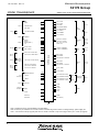
1
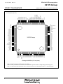
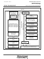
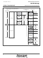
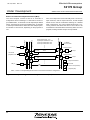
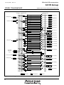
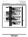
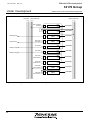
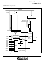
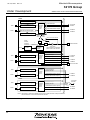
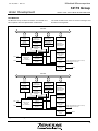
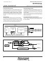
To all our customers
Regarding the change of names mentioned in the document, such as Mitsubishi
Electric and Mitsubishi XX, to Renesas Technology Corp.
The semiconductor operations of Hitachi and Mitsubishi Electric were transferred to Renesas
Technology Corporation on April 1st 2003. These operations include microcomputer, logic, analog
and discrete devices, and memory chips other than DRAMs (flash memory, SRAMs etc.)
Accordingly, although Mitsubishi Electric, Mitsubishi Electric Corporation, Mitsubishi
Semiconductors, and other Mitsubishi brand names are mentioned in the document, these names
have in fact all been changed to Renesas Technology Corp. Thank you for your understanding.
Except for our corporate trademark, logo and corporate statement, no changes whatsoever have been
made to the contents of the document, and these changes do not constitute any alteration to the
contents of the document itself.
Note : Mitsubishi Electric will continue the business operations of high frequency & optical devices
and power devices.
Renesas Technology Corp.
Customer Support Dept.
April 1, 2003
Jan. 30, 2003
Rev.1.4
Mitsubishi Microcomputers
32176 Group
Under Development
SINGLE-CHIP 32-BIT CMOS MICROCOMPUTER
Description
37-channel multijunction timers (MJT)
32176 Group is a 32-bit, single-chip RISC microcomputer
with built-in flash memory, which was developed for use in
general industrial and household equipment.
To make full use of microcomputer built-in mass volume
flash memory, this microcomputer contains a variety of peripheral functions ranging from two independent blocks of
16-channel A-D converters to 37-channel multifunction timers, 10-channel DMAs, 4-channel serial I/Os, and 1-channel
real-time debugger. Also included 2-channel Full-CAN modules and JTAG (boundary scan facility).
With lower power consumption and low noise characteris
tics also considered, these microcomputers are ideal for embedded equipment applications.
Multifunction timers are incorporated that support various
purposes of use.
16-bit output related timers ........................... 11 channels
16-bit input/output related timers .................. 10 channels
Features
M32R RISC CPU core
• Uses the M32R family RISC CPU core (Instruction set
common to all microcomputers in the M32R family)
• Five-stage pipelined processing
• Sixteen 32-bit general-purpose registers
• 16-bit/32-bit instructions implemented
• DSP function instructions (sum-of-products calculation using 56-bit accumulator)
• Built-in flash memory
• Built-in flash programming boot program
• Built-in RAM
• PLL clock generating circuit ........................... Multiply by 4
• Oscillation stop detection function
• Maximum operating frequency of the CPU clock
M32176F4VFP/M32176F3VFP/M32176F2VFP
.......... 32 MHz (when operating at -40°C to +125°C)
M32176F4TFP/M32176F3TFP/M32176F2TFP
............ 40 MHz (when operating at -40°C to +85°C)
• Single power supply: 5V (+0.5V) or 3.3V (+0.3V)
16-bit input related timers ............................... 8 channels
32-bit input related timers ............................... 8 channels
• Flexible configuration is possible through interconnection
of timers.
• The internal DMAC and A-D converter can be started by a
timer.
Real-time Debugger
• Includes dedicated clock-synchronized serial I/O that can
read and write the contents of the internal RAM independently of the CPU.
• Can look up and update the data table in real time while the
program is running.
• Can generate a dedicated interrupt based on RTD communication.
Abundant internal peripheral functions
In addition to the timers and real-time debugger, the microcomputer contains the following peripheral functions.
• DMAC ............................................................. 10 channels
• A-D converters (Sample & hold function, Disconnection detector assist function, Injection current bypass circuit)
..................................... 16 channels 10-bit converter
• Serial I/O ........................................................... 4 channels
• Interrupt controller ...... 23 interrupt sources, 8 priority levels
• Wait controller
• Full CAN (CAN Specification 2.0B active) ........ 2 channels
• JTAG (boundary scan function, Mitsubishi original SDI debug function)
• Port input threshold level select function .............. 3 levels
Table 1. Type Name List (32176 Group)
Designed to operate at high temperatures
Type Name
RAM Size
ROM Size
M32176F4VFP/M32176F4TFP
24K bytes
512K bytes
M32176F3VFP/M32176F3TFP
24K bytes
384K bytes
M32176F2VFP/M32176F2TFP
24K bytes
256K bytes
To meet the need for use at high temperatures, the microcomputer is designed to be able to operate in the temperature
range of -40 to +125°C when CPU clock operating frequency =
32 MHz. When CPU clock operating frequency = 40 MHz, the
microcomputer can be used in the temperature range of -40 to
+85°C.
Note: • This does not guarantee continuous operation at
125°C. If you are considering use of the microcomputer at 125°C, please consult Mitsubishi.
Applications
Automobile equipment control (e.g., Engine, ABS, AT), industrial equipment system control, and high-function OA
equipment (e.g., PPC)
Jan. 30, 2003
Rev.1.4
Mitsubishi Microcomputers
32176 Group
Under Development
SINGLE-CHIP 32-BIT CMOS MICROCOMPUTER
108
107
106
105
104
103
102
101
100
99
98
97
96
95
94
93
92
91
90
89
88
87
86
85
84
83
82
81
80
79
78
77
76
75
74
73
VDDE
P102/TO10
P101/TO9
P100/TO8
P117/TO7
P116/TO6
P115/TO5
P114/TO4
P113/TO3
P112/TO2
P111/TO1
P110/TO0
VSS
VCCE
FP
MOD1
MOD0
RESET#
P97/TO20
P96/TO19
P95/TO18
P94/TO17
P93/TO16
P77/RTDCLK/CRX1
P76/RTDACK/CTX1
P75/RTDRXD/RXD3
P74/RTDTXD/TXD3
P73/ HACK#
P72/HREQ#
P71/ WAIT#
P70/BCLK / WR#
P64/SBI#
P63
P62
P61
EXCVDD
Pin Assignment (top view)
JTMS
JTCK
JTRST
JTDO
JTDI
P103/TO11
P104/TO12
P105/TO13
P106/TO14
P107/TO15
P124/TCLK0
P125/TCLK1
72
71
70
69
68
67
66
65
64
63
62
61
60
59
58
57
56
55
54
53
52
51
50
49
48
47
46
45
44
43
42
41
40
39
38
37
32176 Group
VSS
P87/SCLKI1/SCLKO1
P86/RXD1
P85/TXD1
P84/SCLKI0/SCLKO0
P83/RXD0
P82/TXD0
VCCE
P175/RXD2
P174/TXD2
VSS
EXCVCC
AVSS0
AD0IN15
AD0IN14
AD0IN13
AD0IN12
AD0IN11
AD0IN10
AD0IN9
AD0IN8
AD0IN7
AD0IN6
AD0IN5
AD0IN4
AD0IN3
AD0IN2
AD0IN1
AD0IN0
AVCC0
VREF0
P17/DB15
P16/DB14
P15/DB13
P14/DB12
P13/DB11
P12/DB10
P30/A15
P31/A16
P32/A17
P33/A18
P34/A19
P35/A20
P36/A21
P37/A22
P20/A23
P21/A24
P22/A25
P23/A26
VCCE
VSS
P24/A27
P25/A28
P26/A29
P27/A30
P00/DB0
P01/DB1
P02/DB2
P03/DB3
P04/DB4
P05/DB5
P06/DB6
P07/DB7
P10/DB8
P11/DB9
P221/CRX0
P225/A12
OSC-VSS
XIN
XOUT
EXCOSC-VCC
N.C. (Note 2)
1
2
3
4
5
6
7
8
9
10
11
12
13
14
15
16
17
18
19
20
21
22
23
24
25
26
27
28
29
30
31
32
33
34
35
36
P126/TCLK2
P127/TCLK3
MOD2 (Note 1)
P130/TIN16
P131/TIN17
P132/TIN18
P133/TIN19
P134/TIN20
P135/TIN21
P136/TIN22
P137/TIN23
VCCE
P150/TIN0
P153/TIN3
P41/BLW#/BLE#
P42/BHW#/BHE#
EXCVCC
VSS
P43/RD#
P44/CS0#
P45/CS1#
P46/A13
P47/A14
P220/CTX0
109
110
111
112
113
114
115
116
117
118
119
120
121
122
123
124
125
126
127
128
129
130
131
132
133
134
135
136
137
138
139
140
141
142
143
144
Package 144P6Q-A (0.5-mm pitch)
Note 1: Please be sure to connect MOD2 to ground (GND).
Note 2: The N.C. pin indicates "non connect," and is connected to ground in which no voltage change, power supply, etc.
Note: • It is shown that the pin (signal) with which "#" sticks to the last of a pin name (signal name) is "L" active pin (signal).
Figure 1. Pin Layout Diagram
2
Jan. 30, 2003
Rev.1.4
Mitsubishi Microcomputers
32176 Group
Under Development
SINGLE-CHIP 32-BIT CMOS MICROCOMPUTER
32176
Internal bus
interface
M32R CPU core
(max 40MHz)
Multiplieraccumulator
DMAC
(10 channels)
(32 × 16 + 56)
Internal 16-bit bus
Internal flash memory
(M32176F4: 512K bytes)
(M32176F3: 384K bytes)
(M32176F2: 256K bytes)
Internal 32-bit bus
Multijunction timer
(MJT: 37 channels)
A-D converter
(10-bit, 16 channels)
Serial I/O
(4 channels)
Interrupt controller
(23 sources, 8 levels)
Internal RAM
(24K bytes)
Wait controller
Full CAN
(2 channels)
Real-time debugger
(RTD)
External bus
interface
PLL clock generation
circuit
Data
Internal power supply
generation circuit
(VDC)
Address
Input/output port (JTAG) 96 lines
Figure 2. Block Diagram
3
Jan. 30, 2003
Rev.1.4
Mitsubishi Microcomputers
32176 Group
Under Development
SINGLE-CHIP 32-BIT CMOS MICROCOMPUTER
Table 2. Outline Performance (1/2)
Functional Block
M32R CPU core
Features
M32R family CPU core,internally configured in 32 bits
Built-in multiplier-accumulator (32 × 16 + 56)
Basic bus cycle: 25 ns (CPU clock frequency at 40 MHz, Internal peripheral clock frequency at 20 MHz)
Logical address space: 4G bytes, linear
General-purpose register: 32-bit register × 16, Control register: 32-bit register × 5
accumulator: 56 bits
External data bus
16 bits data bus
Instruction set
16-bit/32-bit instruction formats
83 instructions/9 addressing modes
Internal flash memory
M32176F4VFP/M32176F4TFP: 512K bytes
M32176F3VFP/M32176F3TFP: 384K bytes
M32176F2VFP/M32176F2TFP: 256K bytes
Rewrite durability: 100 times
Internal RAM
24K bytes
DMAC
10 channels (DMA transfers between internal peripheral I/Os, between internal peripheral I/O and internal
RAM, and between internal RAMs)
Channels can be cascaded and can operate in combination with internal peripheral I/O
Multijunction timer
37 channels of multijunction timers
• 16-bit output-related timers × 11 channels (single-shot, delayed single-shot)
• 16-bit input/output-related timers × 10 channels (event count mode, single-shot, PWM, measurement)
• 16-bit input-related timers × 8 channels (measurement, event count mode)
• 32-bit input-related timers × 8 channels (measurement)
Flexible timer configuration is possible through interconnection of channels using the event bus.
A-D converter
10-bit multifunction A-D converters
• Input 16 channels
• Scan-based conversion can be switched between N (N = 1-16) channels
• Capable of interrupt conversion during scan
• 8-bit/10-bit readout function
• Sample & hold function
• Disconnection detector assist function
• Injection current bypass circuit
Serial I/O
Real-time debugger (RTD)
4 channels (The serial I/Os can be set for synchronous serial I/O or UART. SIO2, SIO3 are UART mode only)
1-channels dedicated clock-synchronized serial
• Entire area of internal RAM
• Can access the internal RAM for read/rewrite from outside independently of the CPU, and also generate an
exclusive-use interrupt.
Interrupt controller
Controls interrupts from internal peripheral I/Os
(Priority can be set to one of 8 levels including interrupt disabled)
Wait controller
Controls wait when accessing external extended area
(1 to 4 wait cycles inserted + prolonged by external WAIT# signal input)
CAN
Two channels, each having 16-channel message slots
JTAG
Boundary-Scan function
4
Jan. 30, 2003
Rev.1.4
Mitsubishi Microcomputers
32176 Group
Under Development
SINGLE-CHIP 32-BIT CMOS MICROCOMPUTER
Table 3. Outline Performance (2/2)
Function Block
Features
Clock
M32176F4VFP, M32176F3VFP, M32176F2VFP:
CPU clock: maximum 32 MHz (for CPU, internal ROM, and internal RAM access)
Internal peripheral clock (BCLK): maximum 16 MHz (for peripheral module access)
External input clock (XIN): maximum 8 MHz, built-in × 4 PLL circuit
M32176F4TFP, M32176F3TFP, M32176F2TFP:
CPU clock: maximum 40 MHz (for CPU, internal ROM, and internal RAM access)
Internal peripheral clock (BCLK): maximum 20 MHz (for peripheral module access)
External input clock (XIN): maximum 10 MHz, built-in × 4 PLL circuit
Power Supply Voltage
5V (± 0.5V) or 3.3V (± 0.3V): single power supply voltage (The internal logic operates with 2.5V, however)
Operating temperature
M32176F4VFP, M32176F3VFP, M32176F2VFP:
range (Note 1)
-40 to +125°C (CPU clock 32 MHz, internal peripheral clock 16 MHz)
M32176F4TFP, M32176F3TFP, M32176F2TFP:
-40 to +85°C (CPU clock 40 MHz, internal peripheral clock 20 MHz)
Package
0.5mm pitches /144-pin plastic LQFP
Note 1: This does not mean that the microcomputer is guaranteed for continuous operation at 125°C. If 125°C applications are desired,
please consult Mitsubishi.
5
Jan. 30, 2003
Rev.1.4
Mitsubishi Microcomputers
32176 Group
Under Development
Clock
SINGLE-CHIP 32-BIT CMOS MICROCOMPUTER
XIN
P45 / CS1#
XOUT
P44 / CS0#
P43 / RD#
EXCOSC-VCC
OSC-VSS
Port 7
Port 4
P42 / BHW# / BHE#
Bus
control
P41 / BLW#/ BLE#
P71 / WAIT#
P70 / BCLK / WR#
P72 / HREQ#
Port 7
P73 / HACK#
Reset
RESET#
Mode
MOD0
MOD1
MOD2 (Note 1)
FP
CAN0
P220 / CTX0
P221 / CRX0
19
Port 22
P20-P27 / A23-A30
P30-P37 / A15-A22
P46, P47 / A13, A14
P225 / A12
Address
bus
Port 2
Port 3
Port 4
Port 22
P00-P07 / DB0-DB7
P10-P17 / DB8-DB15
Data
bus
Port 0
Port 1
Serial
I/O
Port 8
Port 17
Real-time
debugger
Port 7
16
10
P150, P153 / TIN0, TIN3
P130-P137 / TIN16-TIN23
Port 12
Multijunction
timer
P124-P127 / TCLK0-TCLK3
P93-P97 / TO16-TO20
P100-P107 / TO8-TO15
P110-P117 / TO0-TO7
Port 11
Port 10
Port 9
P82 / TXD0
32176 Group
Port 15
Port 13
4
21
P83 / RXD0
P84 / SCLKI 0 / SCLKO 0
P85 / TXD1
P86 / RXD1
P87 / SCLKI 1 / SCLKO 1
P174 / TXD2
P175 / RXD2
16
AD0IN0-AD0IN15
A-D
converter
P74 / RTDTXD / TXD3
AVCC0
P75 / RTDRXD / RXD3
P76 / RTDACK / CTX1
VREF0
P77 / RTDCLK / CRX1
Port 6
P61-P63
Serial
I/O
CAN1
3
JTMS
Interrupt
controller
JTCK
JTRST
SBI#
VCCE
EXCVCC
JTAG
JTDO
JTDI
4
2
VDDE
N.C. (Note 2)
EXCVDD
5
VSS
Note 1: Please be sure to connect MOD2 to ground (GND).
Note 2: The N.C. pin indicates "non connect," and is connected to ground in which no voltage change, power supply, etc.
Note: • It is shown that the pin (signal) with which "#" sticks to the last of a pin name (signal name) is "L" active pin (signal).
Figure 3. Pin Function Diagram
6
Jan. 30, 2003
Rev.1.4
Mitsubishi Microcomputers
32176 Group
Under Development
SINGLE-CHIP 32-BIT CMOS MICROCOMPUTER
Table 4. Description of Pin Function (1/4)
Type
Power
Pin
Name
Input/Output
Function
VCCE
Power supply
-
Power supply (5.0V ± 0.5V or 3.3V ± 0.3V).
EXCVCC
Internal power
-
External capacitance connecting pin.
supply
VDDE
RAM power supply -
EXCVDD
Internal power
-
supply of RAM
Clock
Internal RAM backup power supply (5.0V ± 0.5V or 3.3V ± 0.3V).
Backup power supply for the internal RAM, external capacitance con
necting pin.
VSS
Ground
-
Connect all VSS pins to ground (GND).
XIN
Clock input
Input
Clock input/output pins. These pins contain a PLL-based
XOUT
Clock output
Output
frequency multiply-by-4, so input the clock whose frequency is quarter
the operating frequency. (XIN input = 10 MHz when CPU clock operates
at 40 MHz)
BCLK
System clock
Output
Outputs a clock twice the externally sourced clock frequency, XIN
(when the internal CPU memory clock is 80 MHz, BCLK output = 20
MHz).
Use this output when external sync design is desired.
Reset
Mode
EXCOSC
Internal power
-
-VCC
supply
External capacitance connecting pin.
OSC-VSS
Ground
-
Connect OSC-VSS to ground.
RESET#
Reset
Input
This pin resets the internal circuits.
MOD0,
Mode
Input
These pins set an operation mode.
MOD1
MOD0
MOD1
0
0
Mode
Single-chip mode
0
1
Expanded external mode
1
0
Processor mode
1
1
(Boot mode) (Note 1)
MOD2
Mode
Input
(Reserved)
Please be sure to connect MOD2 to ground (GND).
Flash-only
FP
Flash Protect
Input
This pin protects the flash memory against E/W in hardware.
Address
A12-A30
Address
Output
19 lines of address bus (A12-A30) are provided to accommodate two
bus
bus
channels of 1 MB memory space (max.) connected external to the
chip. A31 is not output.
Data bus
DB0-DB15
Data bus
Input/output
This is a 16-bit data bus connecting to an external device. During write
cycle, the microcomputer outputs BHW# or BLW# to indicate the valid
byte write position of the 16-bit data bus. During read cycle, the micro
computer always reads the full 16-bit data bus. Transferred to the internal
circuit of the M32R, however, is the data at only the valid byte position.
Note 1: In boot mode, the FP pin must be at the high level.
7
Jan. 30, 2003
Rev.1.4
Mitsubishi Microcomputers
32176 Group
Under Development
SINGLE-CHIP 32-BIT CMOS MICROCOMPUTER
Table 5. Description of Pin Function (2/4)
Type
Bus Control
Pin
Name
Input/Output
Function
CS0#, CS1#
Chip select
Output
Chip select signals for external devices.
RD#
Read
Output
This signal is output when reading external devices.
WR#
Write
Output
This signal is output when writing external devices.
BHW#
Byte High Write
Output
When writing to an external device, this signal indicates the valid byte
BLW#
Byte Low Write
Output
position to which data is transferred. BHW# and BLW# correspond to
the upper address side (bits 0-7 are valid) and the lower address side
(bits 8-15 are valid), respectively.
BHE#
Byte High Enable Output
During an external device access, this signal indicates that the highorder data (bits 0-7) is valid.
BLE#
Byte Low Enable
Output
During an external device access, this signal indicates that the loworder data (bits 8-15) is valid.
WAIT#
Wait
Input
If WAIT# input is low when the M32R accesses external devices, the
wait cycle extended.
HREQ#
Hold request
Input
This pin is used by an external device to request control of the external
bus. The M32R goes to a hold state when HREQ# input is pulled low.
HACK#
Hold acknowledge Output
This signal indicates to the external device that the M32R has entered
Multijunction
TIN0, TIN3
Timer input
Input
Input pin for multijunction timer .
timer
TIN16-TIN23
Timer output
Output
Output pin for multijunction timer.
Timer clock
Input
Clock input pin for multijunction timer.
Analog power
-
AVCC0 is the power supply for the A-D0 converters. Connect AVCC0
a hold state and relinquished control of the external bus.
TO0
-TO20
TCLK0
-TCLK3
A-D
AVCC0
converter
upply
AVSS0
Analog ground
to the power supply (5V or 3.3V).
-
AVSS0 is the analog ground for the A-D0 converters. Connect to
AVSS0 ground.
AD0IN0
Analog input
Input
16-channel analog input pin for A-D0 converter.
Reference
Input
VREF0 is the reference voltage input pin (5V or 3.3V) for the A-D0
-AD0IN15
VREF0
voltage input
Interrupt
controller
8
SBI#
System break
interrupt
converters.
Input
System break interrupt (SBI) input pin of the interrupt controller.
Jan. 30, 2003
Rev.1.4
Mitsubishi Microcomputers
32176 Group
Under Development
SINGLE-CHIP 32-BIT CMOS MICROCOMPUTER
Table 6. Description of Pin Function (3/4)
Type
Serial I/O
Pin
Name
Input/Output
Function
SCLKI0/
UART transmit/
Input/output
When Channel 0 is in UART mode:
SCLKO0
receive clock
Clock output derived from BRG output by dividing it by 2
output or CSIO
SCLKI1/
SCLKO1
When Channel 0 is in CSIO mode:
transmit/receive
Transmit/receive clock input when external clock is selected
clock input/output
Transmit/receive clock output when internal clock is selected
UART transmit/
Input/output
receive clock
When Channel 1 is in UART mode:
Clock output derived from BRG output by dividing it by 2
output or CSIO
When Channel 1 is in CSIO mode:
transmit/receive
Transmit/receive clock input when external clock is selected
clock input/output
Transmit/receive clock output when internal clock is selected
TXD0
Transmit data
Output
Transmit data output pin of serial I/O channel 0
RXD0
Receive data
Input
Receive data input pin of serial I/O channel 0
TXD1
Transmit data
Output
Transmit data output pin of serial I/O channel 1
RXD1
Receive data
Input
Receive data input pin of serial I/O channel 1
TXD2
Transmit data
Output
Transmit data output pin of serial I/O channel 2
RXD2
Receive data
Input
Receive data input pin of serial I/O channel 2
TXD3
Transmit data
Output
Transmit data output pin of serial I/O channel 3
RXD3
Receive data
Input
Receive data input pin of serial I/O channel 3
Real-time
RTDTXD
Transmit data
Output
Serial data output pin of the Real-time Debugger
Debugger
RTDRXD
Receive data
Input
Serial data input pin of the Real-time Debugger
RTDCLK
Clock input
Input
Serial data transmit/receive clock input pin of the Real-time Debugger
RTDACK
Acknowledge
Output
This pin outputs a low pulse synchronously with the Real-time
Debugger’s first clock of serial data output word. The low pulse width
indicates the type of the command/data the Real-time Debugger has
received.
CAN
CTX0, CTX1
CRX0, CRX1
JTAG
JTMS
JTCK
Transmit data
Output
Data output pin from CAN module.
Receive data
Input
Data input pin to CAN module.
Test mode
Input
Test select input for controlling the test circuit’s state transition.
Clock
Input
Clock input to the debugger module and test circuit.
JTRST
Test reset
Input
Test reset input for initializing the test circuit asynchronously.
JTDO
Serial output
Output
Serial output of test instruction code or test data.
JTDI
Serial input
Input
Serial input of test instruction code or test data.
9
Jan. 30, 2003
Rev.1.4
Mitsubishi Microcomputers
32176 Group
Under Development
SINGLE-CHIP 32-BIT CMOS MICROCOMPUTER
Table 7. Description of Pin Function (4/4)
Type
Pin
Name
Input/Output
Function
Input/output
P00-P07
Input/output port 0
Input/output
Programmable input/output port.
Port (Note 1)
P10-P17
Input/output port 1
Input/output
Programmable input/output port.
P20-P27
Input/output port 2
Input/output
Programmable input/output port.
P30-P37
Input/output port 3
Input/output
Programmable input/output port.
P41-P47
Input/output port 4
Input/output
Programmable input/output port.
P61-P63
Input/output port 6
Input/output
Programmable input/output port.
P70-P77
Input/output port 7
Input/output
Programmable input/output port.
P82-P87
Input/output port 8
Input/output
Programmable input/output port.
P93-P97
Input/output port 9
Input/output
Programmable input/output port.
P100-P107
Input/output port 10
Input/output
Programmable input/output port.
P110-P117
Input/output port 11
Input/output
Programmable input/output port.
P124-P127
Input/output port 12
Input/output
Programmable input/output port.
P130-P137
Input/output port 13
Input/output
Programmable input/output port.
P150, P153
Input/output port 15
Input/output
Programmable input/output port.
P174, P175
Input/output port 17
Input/output
Programmable input/output port.
P220, P221
Input/output port 22
Input/output
Programmable input/output port.
P225
(However, P221 is an input-only port)
Note 1: Input/output port 5 is reserved for future use. Input/output ports 14, 16, 18, 19, 20 and 21 do not exist.
10
Jan. 30, 2003
Rev.1.4
Mitsubishi Microcomputers
32176 Group
Under Development
SINGLE-CHIP 32-BIT CMOS MICROCOMPUTER
Outline of the CPU core
Address space
The M32176 Group uses the M32R RISC CPU core, and has
an instruction set which is common to all microcomputers in the
M32R family.
Instructions are processed in five pipelined stages consisting of instruction fetch, decode, execution, memory access,
and write back. Thanks to its “out-of-order-completion”
mechanism, the M32R CPU allows for clock cycle efficient,
instruction execution control.
The M32R CPU internally contains sixteen 32-bit generalpurpose registers. The instruction set consists of 83 discrete
instructions, which come in either 16-bit or 32-bit instruction
format. Use of the 16-bit instruction format helps to reduce
the program code size. Also, the availability of 32-bit instructions facilitates programming and increases the performance at the same clock speed, as compared to architectures with segmented address spaces.
The 32176 Group’s logical address is always handled in
width of 32-bit, providing a linear address space of up to 4G
bytes. The 32176’s address space is divided into the following spaces.
Multiply-Accumulate instructions comparable to
DSP
User space
A 2G-byte area from H’0000 0000 to H’7FFF FFFF is the
user space. Located in this space are the user ROM area,
external extended area, internal RAM area, and SFR (Special Function Register) area (internal peripheral I/O registers). Of these, the user ROM area and external extended
area are located differently depending on mode settings.
System space
A 2G-byte area from H’8000 0000 to H’FFFF FFFF is the
system area. This space is reserved for use by development
tools such as an in-circuit emulator and debug monitor, and
cannot be used by the user.
The M32R CPU contains a multiplier/accumulator that can
execute 32-bit × 16-bit in one cycle. Therefore, it executes a
32-bit × 32-bit integer multiplication instruction in three cycles.
Also, the M32R CPU supports the following four multiplyAccumulate instructions (or multiplication instructions) for
DSP function use.
(1) 16 high-order register bits × 16 high-order register bits
(2) 16 low-order register bits × 16 low-order register bits
(3) All 32 register bits × 16 high-order register bits
(4) All 32 register bits × 16 low-order register bits
Furthermore, the M32R CPU has instructions for rounding
the value stored in the accumulator to 16 or 32-bit, and instructions for shifting the accumulator value to adjust digits
before storing in a register. Because these instructions also
can be executed in one cycle, DSP comparable data processing capability can be obtained by using them in combination with high-speed data transfer instructions such as
Load & Address Update or Store & Address Update.
Three operation modes
The M32176 Group has three operation modes: single-chip
mode, external extended mode,and processor mode. These
operation modes are changed from one to another by setting the MOD0 and MOD1 pins.
11
Jan. 30, 2003
Rev.1.4
Mitsubishi Microcomputers
32176 Group
Under Development
SINGLE-CHIP 32-BIT CMOS MICROCOMPUTER
< Logical space of the M32176F4 >
Expanded external area
(4M bytes)
EIT vector entry
Logical address
H'0000 0000
User ROM area
(512K bytes)
(16M bytes)
Reserved area
(512K bytes)
H'0000 0000
H'0007 FFFF
H'0008 0000
H'000F FFFF
H'0010 0000
CS0 area
(1M bytes)
2G bytes
H'001F FFFF
H'0020 0000
User space
Ghost area
in units of
16M bytes
CS1 area
(1M bytes)
H'002F FFFF
H'0030 0000
Ghost area in
CS1
(1M bytes)
H'7FFF FFFF
H'003F FFFF
H'0040 0000
H'8000 0000
Ghost area in
units of 4M bytes
H'007F FFFF
2G bytes
System space
SFR area
(16K bytes)
Internal RAM
(24K bytes)
H'0080 0000
H'0080 3FFF
H'0080 4000
H'0080 9FFF
H'0080 8000
Reserved area
(88K bytes)
H'FFFF FFFF
H'0081 FFFF
H'0082 0000
Ghost area in
units of 128K bytes
H'00FF FFFF
Figure 4. Address Space of the M32176F4VFP/M32176F4TFP
12
Jan. 30, 2003
Rev.1.4
Mitsubishi Microcomputers
32176 Group
Under Development
SINGLE-CHIP 32-BIT CMOS MICROCOMPUTER
< Logical space of the M32176F3 >
Expanded external area
(4M bytes)
EIT vector entry
Logical address
H'0000 0000
User ROM area
(384K bytes)
(16M bytes)
Reserved area
(640K bytes)
H'0000 0000
H'0005 FFFF
H'0006 0000
H'000F FFFF
H'0010 0000
CS0 area
(1M bytes)
2G bytes
H'001F FFFF
H'0020 0000
User space
Ghost area
in units of
16M bytes
CS1 area
(1M bytes)
H'002F FFFF
H'0030 0000
Ghost area in
CS1
(1M bytes)
H'7FFF FFFF
H'003F FFFF
H'0040 0000
H'8000 0000
Ghost area in
units of 4M bytes
H'007F FFFF
2G bytes
System space
SFR area
(16K bytes)
Internal RAM
(24K bytes)
H'0080 0000
H'0080 3FFF
H'0080 4000
H'0080 9FFF
H'0080 8000
Reserved area
(88K bytes)
H'FFFF FFFF
H'0081 FFFF
H'0082 0000
Ghost area in
units of 128K bytes
H'00FF FFFF
Figure 5. Address Space of the M32176F3VFP/M32176F3TFP
13
Jan. 30, 2003
Rev.1.4
Mitsubishi Microcomputers
32176 Group
Under Development
SINGLE-CHIP 32-BIT CMOS MICROCOMPUTER
< Logical space of the M32176F2 >
Expanded external area
(4M bytes)
EIT vector entry
Logical address
H'0000 0000
User ROM area
(256K bytes)
(16M bytes)
Reserved area
(768K bytes)
H'0000 0000
H'0003 FFFF
H'0004 0000
H'000F FFFF
H'0010 0000
CS0 area
(1M bytes)
2G bytes
H'001F FFFF
H'0020 0000
User space
Ghost area
in units of
16M bytes
CS1 area
(1M bytes)
H'002F FFFF
H'0030 0000
Ghost area in
CS1
(1M bytes)
H'7FFF FFFF
H'003F FFFF
H'0040 0000
H'8000 0000
Ghost area in
units of 4M bytes
2G bytes
System space
SFR area
(16K bytes)
Internal RAM
(24K bytes)
H'007F FFFF
H'0080 0000
H'0080 3FFF
H'0080 4000
H'0080 9FFF
H'0080 8000
Reserved area
(88K bytes)
H'FFFF FFFF
H'0081 FFFF
H'0082 0000
Ghost area in
units of 128K bytes
H'00FF FFFF
Figure 6. Address Space of the M32176F2VFP/M32176F2TFP
14
Jan. 30, 2003
Rev.1.4
Mitsubishi Microcomputers
32176 Group
Under Development
0
7 8
+0
address
SINGLE-CHIP 32-BIT CMOS MICROCOMPUTER
15
0
+1
address
7 8
+0
address
H'0080 0000
15
+1
address
H'0080 07E0
Flash control
Interrupt controller
(ICU)
H'0080 007E
H'0080 0080
H'0080 07F2
A-D0 converter
H'0080 00EE
H'0080 0100
H'0080 0FE0
Serial I/O
MJT (TML1)
H'0080 0146
H'0080 0180
Multi-junction
timer (MJT)
H'0080 0FFE
H'0080 1000
CAN0
Wait Controller
H'0080 11FE
H'0080 0200
MJT (common part)
H'0080 023E
H'0080 0240
H'0080 1400
CAN1
MJT (TOP)
H'0080 15FE
H'0080 02FE
H'0080 0300
MJT (TIO)
H'0080 03BE
H'0080 03C0
Multi-junction
timer (MJT)
H'0080 3FFE
MJT (TMS)
H'0080 03D8
H'0080 03E0
MJT (TML0)
H'0080 03FE
H'0080 0400
DMAC
H'0080 0478
H'0080 0700
Input/output ports
H'0080 0756
H'0080 0760
Note: • The Real-time debugger (RTD) is an independent module operated from external circuits, and is transparent to the CPU.
Figure 7. SFR Area
15
Jan. 30, 2003
Rev.1.4
Mitsubishi Microcomputers
32176 Group
Under Development
SINGLE-CHIP 32-BIT CMOS MICROCOMPUTER
Built-in flash memory and RAM
Built-in Virtual-Flash Emulation Function
The M32176F4VFP/M32176F4TFP contains 512K bytes
flash memory and 24K bytes RAM, the M32176F3VFP/
M32176F3TFP contains 384K bytes flash memory and 24K
bytes RAM, the M32176F2VFP/ M32176F2TFP contains
256K bytes flash memory and 24K bytes RAM.
The internal flash memory can be programmed while being
mounted on the printed circuit board (on-board programming). Use of flash memory allows the same chip as those
used in mass production to be used beginning with the development stage. This means that system development can
be proceeded without having to change the printed circuit
boards during the entire course, from prototype to mass production.
Internal flash memory, which is divided from the first address in
units of 8K bytes (L banks), can be replaced in 8K bytes blocks
(H’0080 4000-H’0080 5FFF, H’0080 8000-H’0080 9FFF) from
the beginning of the internal RAM. And also the internal flash
memory, which is divided from the first address in units of 4K
bytes area (All S banks), can be replaced within two 4K bytes
areas (H’0080 6000-H’0080 7FFF).
This function allows parts of the program which are frequently changed during development to be altered or evaluated without having to reset the microcomputer each time.
What’s more, when combined with the realtime debugger,
this function helps to reduce the program evaluation period,
because data in the RAM can be rewritten without requiring
any CPU load.
< Internal flash >
H'0000 0000
H'0000 1FFF
H'0000 2000
H'0000 3FFF
H'0000 4000
H'0000 5FFF
L bank 0
(8K bytes)
L bank 1
(8K bytes)
L bank 2
(8K bytes)
< Internal RAM >
H'0080 4000
8K bytes
4K bytes
4K bytes
H'0080 5FFF
H'0080 6000
H'0080 7FFF
H'0080 8000
8K bytes
H'0080 9FFF
H'0007 C000
H'0007 DFFF
H'0007 E000
H'0007 FFFF
L bank 62
(8K bytes)
L bank 63
(8K bytes)
Notes: • If the same bank area is set in multiple virtual-flash bank registers and the virtual-flash emulation enable bit is enabled, the
corresponding internal RAM area is assigned to either bank register according to the priority FELBANK0 > FESBANK0 >
FESBANK1 > FELBANK1.
• When access is made to the 8K bytes area (L bank) specified with virtual-flash bank register 0, the internal RAM area is
accessed. During virtual-flash emulation mode, RAM data can read and written to and from both the internal RAM area and
the virtual-flash setup area.
Figure 8. Virtual-Flash Emulation Areas of the M32176F4VFP/M32176F4TFP (Replaced in Units of 8K bytes)
16
Jan. 30, 2003
Rev.1.4
Mitsubishi Microcomputers
32176 Group
Under Development
SINGLE-CHIP 32-BIT CMOS MICROCOMPUTER
< Internal flash >
H'0000 0000
H'0000 0FFF
H'0000 1000
H'0000 1FFF
H'0000 2000
H'0000 2FFF
S bank 0
(4K bytes)
S bank 1
(4K bytes)
S bank 2
(4K bytes)
< Internal RAM >
H'0080 4000
8K bytes
4K bytes
4K bytes
H'0080 5FFF
H'0080 6000
H'0080 7000
H'0080 8000
8K bytes
H'0080 9FFF
H'0007 E000
H'0007 EFFF
H'0007 F000
H'0007 FFFF
S bank 126
(4K bytes)
S bank 127
(4K bytes)
Notes: • If the same bank area is set in multiple virtual-flash bank registers and the virtual-flash emulation enable bit is enabled, the
corresponding internal RAM area is assigned to either bank register according to the priority FELBANK0 > FESBANK0 >
FESBANK1 > FELBANK1.
• When access is made to the 4K bytes area (S bank) specified with virtual-flash bank register 0 and 1, the internal RAM area
is accessed. During virtual-flash emulation mode, RAM data can read and written to and from both the internal RAM area and
the virtual-flash setup area.
Figure 9. Virtual-Flash Emulation Areas of the M32176F4VFP/M32176F4TFP (Replaced in Units of 4K bytes)
Virtual-Flash Emulation Areas of M32176F4VFP/M32176F4TFP,
M32176F3VFP/M32176F3TFP, and M32176F2VFP/M32176F2TFP
are shown as follows.
Table 8. Virtual-Flash Emulation Areas
Type Name
Virtual-Flash Emulation Areas
M32176F4VFP/M32176F4TFP
H’0000 0000-H’0007 FFFF
M32176F3VFP/M32176F3TFP
H’0000 0000-H’0005 FFFF
M32176F2VFP/M32176F2TFP
H’0000 0000-H’0003 FFFF
17
Jan. 30, 2003
Rev.1.4
Mitsubishi Microcomputers
32176 Group
Under Development
SINGLE-CHIP 32-BIT CMOS MICROCOMPUTER
Input/output Ports
Each input/output port is a dual-function pin shared with
otherinternal peripheral I/O or external extended bus signal
lines.These pin functions are selected by using the chip operation mode select or the input/output port operation mode
registers.
The microcomputer has a total of 96 input/output ports P0P22. (However, P5 is reserved for future use, P14, P16, and
P18-P21 do not exist. ) The input/output ports can be used
as input ports or output ports by setting uptheir direction registers.
Table 9. Outline of Input/output Ports
Item
Specification
Number of Port
Total 96 ports
P0
: P00-P07
(8 lines)
P1
: P10-P17
(8 lines)
P2
: P20-P27
(8 lines)
P3
: P30-P37
(8 lines)
P4
: P41-P47
(7 lines)
P6
: P61-P63
(3 lines)
P7
: P70-P77
(8 lines)
P8
: P82-P87
(6 lines)
P9
: P93-P97
(5 lines)
P10 : P100-P107
(8 lines)
P11 : P110-P117
(8 lines)
P12 : P124-P127
(4 lines)
P13 : P130-P137
(8 lines)
P15 : P150, P153
(2 lines)
P17 : P174, P175
(2 lines)
P22 : P220, P221, P225 (3 lines)
Port function
The input/output ports can be set for input or output mode bitwise by using the input/output port direction
control register. (However, P221 is CAN input-only port. )
Pin function
Dual-functions shared with peripheral I/O or external extended signals (or multi-functions shared with periph
eral I/Os which have multiple functions. )
Pin function
P0-P4: Changed by setting CPU operation mode (MOD0 and MOD1 pins)
changeover
P6-22: Changed by setting the input/output port operation mode register.
(However, peripheral I/O pin functions are selected using the peripheral I/O register. )
Note: Input/output ports P14, P16, and P18-P21 do not exist.
Table 10. CPU Operation Modes and P0-P4 Pin Functions
MOD0
MOD1
Operation mode
Pin functions of P0-P4
VSS
VSS
Single-chip mode
Input/output port pin
VSS
VCCE
External extended mode
VCCE
VSS
Processor mode (FP pin = VSS)
VCCE
VCCE
Reserved (use inhibited)
Notes: • VCCE connects to power supply, and VSS connects to GND.
• MOD2 connects to GND.
18
External extended signal pin
–
Jan. 30, 2003
Rev.1.4
Mitsubishi Microcomputers
32176 Group
Under Development
Settings
of Chip
operation
mode
(Note 1)
0
1
2
3
4
5
6
7
P0
DB0
DB1
DB2
DB3
DB4
DB5
DB6
DB7
P1
DB8
DB9
DB10
DB11
DB12
DB13
DB14
DB15
P2
A23
A24
A25
A26
A27
A28
A29
A30
P3
A15
A16
A17
A18
A19
A20
A21
A22
BLW#/
BLE#
BHW#/
BHE#
RD#
CS0#
CS1#
A13
A14
(P61)
(P62)
(P63)
SBI#
(Note 3)
P4
Reserved
SINGLE-CHIP 32-BIT CMOS MICROCOMPUTER
P5
P6
P7
BCLK/
WR#
WAIT#
HREQ#
HACK#
P8
MOD0
(Note 3)
MOD1
(Note 3)
TXD0
RXD0
SCLKI0/
SCLKO0
TXD1
RXD1
SCLKI1/
SCLKO1
TO16
TO17
TO18
TO19
TO20
P9
RTDTXD/ RTDRXD/ RTDACK/ RTDCLK/
TXD3 (Note 2) RXD3 (Note 2) CTX1 (Note 2) CRX1 (Note 2)
P10
TO8
TO9
TO10
TO11
TO12
TO13
TO14
TO15
P11
TO0
TO1
TO2
TO3
TO4
TO5
TO6
TO7
TCLK0
TCLK1
TCLK2
TCLK3
TIN20
TIN21
TIN22
TIN23
TXD2
RXD2
P12
P13
TIN16
Settings of
input/output
P14
port Operation
Mode Register
P15
TIN0
TIN17
TIN18
TIN19
TIN3
P16
P17
P18
P19
P20
P21
P22
CTX0
CRX0
A12
Note 1: The pin function are selected by setting the MOD0 and MOD1 pins.
Note 2: It is a triple function pin. It is necessary to set up the peripheral functions outputted by the peripheral output select register.
Note 3: It cannot be used as a function of an input/output ports. The input level of SBI#, MOD0, and an MOD1 pin can be read.
Note: • P14, P16, P18, P19, P20, and P21 do not exist.
Figure 10. Input/output Ports and Pin Function Assignments
19
Jan. 30, 2003
Rev.1.4
Mitsubishi Microcomputers
32176 Group
Under Development
SINGLE-CHIP 32-BIT CMOS MICROCOMPUTER
Built-in 10-Channel DMAC
The microcomputer contains 10 channels of DMAC, allowing for data transfer between internal peripheral I/Os, between internal RAM and internal peripheral I/O, and between internal RAMs.
DMA transfer requests can be issued from the user-created
software, as well as can be triggered by a signal generated by
the internal peripheral I/O (A-D converter, timer, or serial I/O).
The microcomputer also supports cascaded connection between DMA channels (starting DMA transfer on a channel at
end of transfer on another channel). This makes advanced
transfer processing possible without causing any additional
CPU load.
Table 11. Outline of the DMAC
Item
Content
Number of channels
10 channels
Transfer request
• Software trigger
• Request from internal peripheral I/O: A-D converter, timer, or serial I/O (reception completed,
transmit buffer empty)
• Cascaded connection between DMA channels possible (Note 1)
Maximum number of times transferred
256 times
Transferable address space
• 64K bytes (address space from H’0080 0000 to H’0080 FFFF)
• Transfers between internal peripheral I/Os, between internal RAM and internal peripheral IO,
and between internal RAMs are supported
Transfer data size
16-bit or 8-bit
Transfer method
Single transfer DMA (control of the internal bus is relinquished for each transfer performed), dualaddress transfer
Transfer mode
Direction of transfer
Single transfer mode
One of three modes can be selected for the source and destination of transfer:
• Address fixed
• Address increment
• 32-channel ring buffer
Channel priority
DMA 0 > DMA 1 > DMA 2 > DMA 3 > DMA 4 > DMA 5 > DMA 6 > DMA 7 > DMA 8 > DMA 9
(Fixed priority)
Maximum transfer rate
13.3M bytes per second (when internal peripheral clock = 20 MHz)
Interrupt request
Group interrupt request can be generated when each transfer count register underflows
Transfer area
64K bytes from H ’0080 0000 to H ’0080 FFFF (Transfer is possible in the entire internal RAM/
SFR area)
Note 1: The following DMA channels can be cascaded.
DMA transfer on channel 1 started at end of one DMA transfer on DMA 0
DMA transfer on channel 2 started at end of one DMA transfer on DMA 1
DMA transfer on channel 0 started at end of one DMA transfer on DMA 2
DMA transfer on channel 4 started at end of one DMA transfer on DMA 3
DMA transfer on channel 6 started at end of one DMA transfer on DMA 5
DMA transfer on channel 7 started at end of one DMA transfer on DMA 6
DMA transfer on channel 5 started at end of one DMA transfer on DMA 7
DMA transfer on channel 9 started at end of one DMA transfer on DMA 8
DMA transfer on channel 5 started at end of all DMA transfers on DMA 0 (underflow of transfer count register)
20
Jan. 30, 2003
Rev.1.4
Mitsubishi Microcomputers
32176 Group
Under Development
Internal bus
SINGLE-CHIP 32-BIT CMOS MICROCOMPUTER
DMA channel 0
Software start
Source
address register
One DMA2 transfer completed
DMA
request
selector
A-D0 conversion completed
MJT (TIO8_udf)
MJT (input event bus 2)
Destination
address register
Transfer count
register
udf
DMA channel 1
Software start
DMA
request
selector
MJT (output event bus 0)
One DMA0 transfer completed
Source
Destination
Transfer count
udf
DMA channel 2
Software start
MJT (output event bus 1)
DMA
request
selector
MJT (TIN18 input signal)
One DMA1 transfer completed
Source
Destination
Transfer count
udf
DMA channel 3
Software start
Serial I/O-0 (transmit buffer empty)
Serial I/O-1 (reception completed)
MJT (TIN0 input signal)
DMA
request
selector
Source
Destination
Transfer count
udf
DMA channel 4
Software start
One DMA3 transfer completed
Serial I/O-0 (reception completed)
DMA
request
selector
MJT (TIN19 input signal)
Source
Interrupt
request
Destination
Transfer count
udf
DMA start
Internal bus arbitration
Determination block
Software start
DMA channel 5
One DMA7 transfer completed
All DMA0 transfers completed (udf)
Serial I/O-2 (reception completed)
MJT (TIN20 input signal)
DMA
request
selector
Source
Destination
Transfer count
udf
DMA channel 6
Software start
Serial I/O-1 (transmit buffer empty)
CAN0_S0/S15
DMA
request
selector
One DMA5 transfer completed
Source
Destination
Transfer count
udf
DMA channel 7
Software start
Serial I/O-2 (transmit buffer empty)
CAN0_S1/S14
One DMA6 transfer completed
DMA
request
selector
Source
Destination
Transfer count
udf
DMA channel 8
Software start
MJT (input event bus 0)
Serial I/O-3 (reception completed)
CAN1_S0/S15
DMA
request
selector
Source
Destination
Transfer count
udf
DMA channel 9
Software start
Serial I/O-3 (transmit buffer empty)
CAN1_S1/S14
One DMA8 transfer completed
DMA
request
selector
Source
Interrupt
request
Destination
Transfer count
udf
DMA start
Determination block
Internal bus arbitration
Figure 11. Block Diagram of the DMAC
21
Jan. 30, 2003
Rev.1.4
Mitsubishi Microcomputers
32176 Group
Under Development
SINGLE-CHIP 32-BIT CMOS MICROCOMPUTER
Built-in 37-channel multijunction timers (MJT)
E/L
Input event bus
Clock bus
TCLK pin
Output related timer: 11ch
Input/output related timer: 10ch
16-bit input related timer: 8ch
32-bit input related timer: 8ch
EN
Timer
PRS
F/F
TO pin
Interrupt output
CLK
TIN pin
To DMAC,
A-D converter
Interrupt output
CLK
1/2 internal
peripheral clock
Output event bus
Also, the multijunction timers internally have a clock bus,
input event bus, and an output event bus, so that multiple
timers can be used in combination allowing for a flexible
timer configuration. The output related timers have a correcting function that allows the timer’s count value to be
incremented or decremented as necessary while count is in
progress, making real-time output control possible.
The microcomputer contains a total of 37 channels of
multijunction timers consisting of 11 channels of 16-bit output related timers, 10 channels of 16-bit input/output related
timers, 8 channels of 16-bit input related timers, 8 channels
of 32-bit input related timers. Each timer has multiple operation modes to choose from, depending on the purposes of
use.
EN
Timer
E/L
F/F
TO pin
E/L
: Edge/Level selector
PRS
: Prescaler
: Junction box (Selector)
F/F
Note: • This is a conceptual diagram and does not show the actual timer configuration.
Figure 12. Conceptual Diagram of the Multijunction Timer (MJT)
22
: Output flip-flop
Jan. 30, 2003
Rev.1.4
Mitsubishi Microcomputers
32176 Group
Under Development
SINGLE-CHIP 32-BIT CMOS MICROCOMPUTER
Table 12. Outline of the MJT
Name
Type
Number of channels
Contents
TOP
Output related
11
One of three output modes is selected in software.
(Timer Output)
16-bit timer
<With correcting function>
(down-counter)
• Single-shot output mode
• Delayed single-shot output mode
<Without correcting function>
• Continuous output mode
TIO
Input/output related
(Timer Input
16-bit timer
Output)
(down-counter)
10
One of three input modes and four output modes is selected in soft
ware.
<Input mode>
• Measure clear input mode
• Measure free-run input mode
• Noise processing input mode
<Output mode without correcting function>
• PWM output mode
• Single-shot output mode
• Delayed single-shot output mode
• Continuous output mode
TMS
Input related
(Timer Measure
16-bit timer
Small)
(up-counter)
TML
Input related
(Timer Measure
32-bit timer
Large)
(up-counter)
8
16-bit input measure timer.
8
32-bit input measure timer.
23
Jan. 30, 2003
Rev.1.4
Mitsubishi Microcomputers
32176 Group
Under Development
Clock bus
SINGLE-CHIP 32-BIT CMOS MICROCOMPUTER
Input event bus
Output event bus
3210 3210
IRQ2
clk
S
en
TOP 0
0123
F/F0
TO 0 (P110)
F/F1
TO 1 (P111)
F/F2
TO 2 (P112)
F/F3
TO 3 (P113)
F/F4
TO 4 (P114)
F/F5
TO 5 (P115)
S
F/F6
TO 6 (P116)
S
F/F7
TO 7 (P117)
S
F/F8
TO 8 (P100)
S
F/F9
TO 9 (P101)
S
F/F10
TO 10 (P102)
S
F/F11
TO 11 (P103)
S
F/F12
TO 12 (P104)
S
F/F13
TO 13 (P105)
S
F/F14
TO 14 (P106)
S
F/F15
TO 15 (P107)
S
F/F16
TO 16 (P93)
S
F/F17
TO 17 (P94)
S
F/F18
TO 18 (P95)
S
F/F19
TO 19 (P96)
F/F20
TO 20 (P97)
udf
IRQ2
TCLK0 (P124)
clk
TCLK0S
TIN0 (P150)
en
TOP 1
udf
IRQ2
IRQ9
clk
en
TOP 2
udf
IRQ2
TIN0S
clk
S
en
TOP 3
udf
IRQ2
DRQ7
clk
en
TOP 4
udf
IRQ2
clk
en
TOP 5
udf
IRQ1
clk
S
clk
S
en
TOP 6
udf
IRQ1
en
TOP 7
udf
S
IRQ6
clk
S
clk
S
clk
TOP 8
udf
IRQ6
en
TOP 9
udf
IRQ5
en
TOP 10
udf
IRQ0
IRQ12
TIN3 (P153)
en
S
TIN3S
clk
en/cap
TIO 0
udf
IRQ0
S
clk
en/cap
TIO 1
udf
IRQ0
S
clk
udf
en/cap
TIO 2
en/cap
TIO 3
udf
en/cap
TIO 4
udf
IRQ0
S
clk
IRQ4
clk
S
1/2 internal
peripheral
clock
PRS0
S
PRS1
PRS2
S
TCLK1 (P125)
IRQ4
TCLK1S
S
clk
en/cap
TIO 5
udf
en/cap
TIO 6
udf
S
TCLK2 (P126)
IRQ4
TCLK2S
S
clk
S
IRQ4
clk
S
en/cap
TIO 7
udf
S
clk
S
DRQ0
IRQ3
en/cap
TIO 8
udf
en/cap
TIO 9
udf
S
IRQ3
clk
S
S
3210
0123
3210
PRS0 - 2 : Prescaler
F/F : Output flip-flop
Figure 13. Block Diagram of Multijunction Timers (MJT) (1/3)
24
S : Selector
Jan. 30, 2003
Rev.1.4
Mitsubishi Microcomputers
32176 Group
Under Development
Clock bus
3210
TCLK3 (P127)
SINGLE-CHIP 32-BIT CMOS MICROCOMPUTER
Input event bus
Output event bus
3210
TCLK3S
0123
clk
S
cap3
IRQ7
TMS 0
cap2
cap1
cap0
TMS 1
cap2
cap1
cap0
ovf
S
S
S
S
S
clk
cap3
IRQ10
TIN16 (P130)
IRQ7
ovf
S
TIN16S
IRQ10
TIN17 (P131)
S
TIN17S
IRQ10
TIN18 (P132)
S
TIN18S
DRQ5
IRQ10
TIN19 (P133)
S
TIN19S
DRQ6
1/2 internal
peripheral
clock
S
DRQ12
TIN20 (P134)
TIN20S
TIN21 (P135)
TIN21S
TIN22 (P136)
TIN22S
TIN23 (P137)
TIN23S
TML 0
cap2
cap1
clk
cap3
IRQ11
cap0
S
IRQ11
S
IRQ11
S
IRQ11
S
AD0TRG
(To A-D0 converter)
AD0TRG
(To A-D0 converter)
1/2 internal
peripheral
clock
clk
S
cap3
cap2
TML 1
cap1
cap0
S
S
S
S
AD0TRG (To A-D0 converter)
AD0TRG (To A-D0 converter)
3210 3210
0123
Figure 14. Block Diagram of Multijunction Timers (MJT) (2/3)
25
Jan. 30, 2003
Rev.1.4
Mitsubishi Microcomputers
32176 Group
Under Development
Clock bus
3210
SINGLE-CHIP 32-BIT CMOS MICROCOMPUTER
Input event bus
0123
AD0 completed
TIO8-udf
TIN18 (P132)
SIO0-TXD
SIO1-RXD
TIN0 (P150)
SIO0-RXD
TIN19 (P133)
SIO2-RXD
TIN20 (P134)
SIO1-TXD
CAN0-S0/S15
SIO2-TXD
CAN0-S1/S14
SIO3-RXD
CAN1-S0/S15
SIO3-TXD
CAN1-S1/S14
3210
Output event bus
3210
S
DMA0
udf
end
DMAIRQ0
S
DMA1
udf
end
DMAIRQ0
S
DMA2
udf
end
DMAIRQ0
S
DMA3
udf
end
DMAIRQ0
S
DMA4
udf
DMAIRQ0
S
DMA5
udf
end
DMAIRQ1
S
DMA6
udf
end
DMAIRQ1
S
DMA7
udf
end
DMAIRQ1
S
DMA8
udf
end
DMAIRQ1
S
DMA9
udf
DMAIRQ1
3210
Figure 15. Block Diagram of Multijunction Timers (MJT) (3/3)
26
0123
Jan. 30, 2003
Rev.1.4
Mitsubishi Microcomputers
32176 Group
Under Development
SINGLE-CHIP 32-BIT CMOS MICROCOMPUTER
16-channel A-D Converters
Moreover, there is also Sample & hold function, input voltage is sampled, when A-D conversion is started, and the AD conversion of the sampling voltage is carried out.
Since there is no invalid domain near [which becomes a
problem by the external operational amplifier etc.] VCCE/
VSS, conversion by the full range is possible in this sample
& hold circuit.
When A-D conversion is finished, the converters can generate a DMA transfer request, as well as an interrupt.
The microcomputer contains 16-channel A-D0 converters
with 10-bit resolution. In addition to single conversion on
each channel, continuous A-D conversion on a combined
group of N (N = 1-16) channels is possible. The A-D converted value can be read out in either 10-bit or 8-bit.
In addition to ordinary A-D conversion, the converters support comparator mode in which the set value and A-D converted value are compared to determine which is larger or
smaller than the other.
Table 13. Outline of the A-D Converters
Item
Content
Analog input
16-channel
A-D conversion method
Successive approximation method
Resolution
10-bit (Conversion results can be read out in either 10 or 8-bit)
Absolute accuracy (Note 1)
During low speed mode : Normal mode: + 2 LSB, double speed mode: + 2 LSB
(conditions: Ta = 25°C,
During high speed mode : Normal mode: + 3 LSB, double speed mode: + 3 LSB
AVCC0, 1 = VREF0, 1 = 5.12V)
Note: The performance is the same during sample & hold function.
Conversion mode
A-D conversion mode, comparator mode
Operation mode
Single mode, single-shot scan mode, continuous scan mode
Conversion start trigger
Conversion Speed
Software start
Started by setting A-D conversion start bit to 1
Hardware start
MJT input event bus 2, MJT input event bus 3, MJT output event bus 3, and MJT (TIN23S)
During single mode
f(BCLK): Internal peripheral
(Unavailable for Sample & Hold
clock operating frequency
Available for Normal
(Note 2)
Low-speed mode
During comparator mode
14.95 µs
Double speed
173 BCLK
8.65 µs
Normal
131 BCLK
6.55 µs
89 BCLK
4.45 µs
Low-speed mode
Normal
191 BCLK
9.55 µs
Double speed
Double speed
(Available for High-speed
Sample & Hold)
299 BCLK
High-speed mode
Sample & Hold)
During single mode
Normal
High-speed mode
Low-speed mode
High-speed mode
101 BCLK
5.05 µs
Normal
95 BCLK
4.75 µs
Double speed
53 BCLK
2.65 µs
Normal
47 BCLK
2.35 µs
Double speed
29 BCLK
1.45 µs
Normal
23 BCLK
1.15 µs
Double speed
17 BCLK
0.85 µs
Sample & hold function
Validity/invalidity selectable
A-D disconnection detection
Influences of the analog input voltage wrapping around from the preceding channel are suppressed when
assist function
operating scan mode.
Interrupt request generation
When A-D conversion is finished, when comparate operation is finished
When single-shot scan is finished, or when one cycle of continuous scan is finished
DMA transfer
When A-D conversion is finished, when comparate operation is finished
request generation
When single-shot scan is finished, or when one cycle of continuous scan is finished
Note 1: The rated value of conversion accuracy here is that of the microcomputer's own as a single unit which can be exhibited when
themicrocomputer is used in an environment where it may not be affected by the power supply wiring or noise on the board.
Note 2: Conversion time at the time of f(BCLK) = 20 MHz operation (1 BCLK = 50 ns)
27
Jan. 30, 2003
Rev.1.4
Mitsubishi Microcomputers
32176 Group
Under Development
SINGLE-CHIP 32-BIT CMOS MICROCOMPUTER
Internal data bus
8-bit readout
10-bit readout
AD0DT0
Shifter
10-bit A-D0 Data Register 0
AD0DT1
10-bit A-D0 Data Register 1
AD0SIM0, 1
A-D0 Single Mode Register
AD0DT2
10-bit A-D0 Data Register 2
AD0SCM0, 1
A-D0 Scan Mode Register
AD0DT3
10-bit A-D0 Data Register 3
AD0DT4
10-bit A-D0 Data Register 4
AD0DT5
10-bit A-D0 Data Register 5
AD0DT6
10-bit A-D0 Data Register 6
AD0DT7
10-bit A-D0 Data Register 7
AD0DT8
10-bit A-D0 Data Register 8
AD0DT9
10-bit A-D0 Data Register 9
AD0DT10
10-bit A-D0 Data Register 10
AD0DT11
10-bit A-D0 Data Register 11
AD0DT12
10-bit A-D0 Data Register 12
AD0DT13
10-bit A-D0 Data Register 13
AD0DT14
10-bit A-D0 Data Register 14
AD0DT15
10-bit A-D0 Data Register 15
AD0CMP
AD0CTRG1
Input event bus 3
Input event bus 2
Output event bus 3
TIN23S
S
S
AD0STRG1
A-D comparate
Data Register
A-D Control
Circuit
AVCC0
AVSS0
10-bit A-D Successive
Approximation Register
(AD0SAR)
VREF0
10-bit D-A Converter
Mode selection
Channel selection
Interrupt request
Conversion time
selection
Flag control
Interrupt control
DMA transfer request
Comparator
AD0IN0
AD0IN1
AD0IN2
AD0IN3
AD0IN4
AD0IN5
AD0IN6
AD0IN7
AD0IN8
AD0IN9
AD0N10
AD0IN11
AD0IN12
AD0IN13
AD0IN14
AD0IN15
Sample & Hold
Control Circuit
Selector
Successive Approximation
-type A-D Converter Unit
Figure 16. Block Diagram of the A-D0 Converter
28
Jan. 30, 2003
Rev.1.4
Mitsubishi Microcomputers
32176 Group
Under Development
SINGLE-CHIP 32-BIT CMOS MICROCOMPUTER
4-channel High-speed Serial I/Os
The microcomputer contains 4 channels of serial I/Os consisting of four channels that can be set for CSIO mode
(clock-synchronized serial I/O) or UART mode (asynchronous serial I/O) and two other channels that can only be set
for UART mode.
The SIO has the function to generate a DMA transfer request when data reception is completed or the transmit register becomes empty, and is capable of high-speed serial
communication without causing any additional CPU load.
Table 14. Outline of Serial I/O
Item
Number of channels
Content
CSIO/UART : 2 channels (SIO0, SIO1)
UART only
Clock
: 2 channels (SIO2, SIO3)
During CSIO mode : Internal clock /external clock, selectable (Note 1)
During UART mode : Internal clock only
Transfer mode
Transmit half-duplex, receive half-duplex, transmit/receive full-duplex (Transfer clock inverted mode)
BRG count sourcef
f(BCLK), f(BCLK)/8, f(BCLK)/32, f(BCLK)/256 (When internal clock is selected) (Note 2)
Data format
CSIO mode : Data length = Fixed to 8 bits
Order of transfer = Fixed to LSB first
UART mode : Start bit = 1 bit
Character length = 7, 8, or 9 bits
Parity bit = Added or not added (When added, selectable between odd and even parity)
Stop bit = 1 or 2 bits
Order of transfer = Fixed to LSB first
Baud rate
CSIO mode : 152 bits per second to 2 Mbits per second (when operating with f(BCLK) = 20 MHz)
UART mode : 19 bits per second to 156 Kbits per second (when operating with f(BCLK) = 20 MHz)
Error detection
CSIO mode : Overrun error only
UART mode : Overrun, parity, and framing errors
(The error-sum bit indicates which error has occurred)
Fixed cycle clock
When using SIO0 and SIO1 as UART, this function outputs a divided-by-2 BRG clock from the SCLK pin.
output function
Note 1: During CSIO mode, the maximum input frequency of an external clock is f(BCLK) divided by 16.
Note 2: When f(BCLK) is selected for the BRG count source, the BRG set value is subject to limitations.
29
Jan. 30, 2003
Rev.1.4
Mitsubishi Microcomputers
32176 Group
Under Development
SINGLE-CHIP 32-BIT CMOS MICROCOMPUTER
SIO0
SIO0 Transmit Buffer Register
Transmit interrupt
TXD0
SIO0 Transmit Shift Register
RXD0
SIO0 Receive Shift Register
To interrupt
controller
Receive interrupt
Transmit
/receive
control
circuit
Transmit DMA transfer request
To DMAC3
Receive DMA transfer request
To DMAC4
SIO0 Receive Buffer Register
UART
mode
BCLK
When external clock selected
When internal clock selected
1/16
1
(Set value + 1)
Clock
divider
SCLKI0/ SCLKO0
1/2
Baud rate
generator
(BRG)
CSIO mode
When internal clock selected
When UART mode selected
SIO1
TXD1
RXD1
SIO1 Transmit Shift Register
Transmit
/receive
control
circuit
SIO1 Receive Shift Register
Internal data bus
BCLK,
BCLK/8,
BCLK/32,
BCLK/256
CSIO
mode
Transmit interrupt
Receive interrupt
Transmit DMA transfer request
Receive DMA transfer request
To interrupt
controller
To DMAC6
To DMAC3
SCLKI1/ SCLKO1
SIO2
TXD2
SIO2 Transmit Shift Register
RXD2
SIO2 Receive Shift Register
Transmit
/receive
control
circuit
Transmit interrupt
Receive interrupt
Transmit DMA transfer request
Receive DMA transfer request
To DMAC7
To DMAC5
SIO3
Transmit interrupt
TXD3
RXD3
SIO3 Transmit Shift Register
SIO3 Receive Shift Register
Transmit
/receive
control
circuit
Receive interrupt
Transmit DMA transfer request
Receive DMA transfer request
Notes: • When BCLK is selected for the BRG count source, the BRG set value is subject to limitations.
• SIO2 and SIO3 do not have the SCLKI/SCLKO function.
Figure 17. Block Diagram of Serial I/O
30
To interrupt
controller
To DMAC9
To DMAC8
Jan. 30, 2003
Rev.1.4
Mitsubishi Microcomputers
32176 Group
Under Development
SINGLE-CHIP 32-BIT CMOS MICROCOMPUTER
CAN Modules
The M32176 Group contains two blocks of Full-CAN modules compliant with CAN Specification V2.0B active.
The CAN modules each have 16-channel message slots
and three mask registers.
Data Bus
CAN0 Status
Register
CAN0 REC
Register
CAN0 TEC
Register
CAN0 Global
Mask Register
CAN0 Message
Slot 0-15
Control Register
CAN0 Extended ID
Register
CAN0 Configuration
Register
CAN0 Local
Mask Register A
CAN0 Local
Mask Register B
CAN0 Control
Register
CAN0 Protocol
controller
Ver. 2.0B active
CAN0 slot
Interrupt Control
Register
CAN0 error
Interrupt Control
Register
16-bit Timer
CAN0 Time Stamp
Register
CRX0
(1) Message ID
(2) Date Code
(3) Message Data
(4) Time Stamp
CAN0 Slot
Status Register
Acceptance
filtering
CTX0
Message Memory
CAN0 Transmit/Receive & Error Interrupt
CAN0 Single Shot Interrupt
Interrupt Control
circuit
DMA Control
circuit
DMAC
Data Bus
CAN1 Status
Register
CAN1 REC
Register
CAN1 TEC
Register
CAN1 Message
Slot 0-15
Control Register
CAN1 Extended ID
Register
CAN1 Configuration
Register
CAN1 Control
Register
Acceptance
filtering
CTX1
CAN1 Protocol
controller
Ver. 2.0B active
CRX1
16-bit Timer
CAN1 Time Stamp
Register
CAN1 Global
Mask Register
CAN1 Local
Mask Register A
CAN1 Local
Mask Register B
Message Memory
(1) Message ID
(2) Date Code
(3) Message Data
(4) Time Stamp
CAN1 Slot
Status Register
CAN1 slot
Interrupt Control
Register
CAN1 error
Interrupt Control
Register
CAN1 Transmit/Receive & Error Interrupt
CAN1 Single Shot Interrupt
Interrupt Control
circuit
DMA Control
circuit
DMAC
Figure 18. Block Diagram of CAN Modules
31
Jan. 30, 2003
Rev.1.4
Mitsubishi Microcomputers
32176 Group
Under Development
SINGLE-CHIP 32-BIT CMOS MICROCOMPUTER
8-level Interrupt Controller
Real-time Debugger (RTD)
The Interrupt Controller controls interrupt requests from
each internal peripheral I/O (23 sources) by using eight priority levels assigned to each interrupt source, including interrupts prohibition. In addition to these interrupts, it handles
System Break Interrupt (SBI), Reserved Instruction Exception (RIE), and Address Exception (AE) as nonmaskable interrupts.
The Real-time Debugger (RTD) provides function for accessing directly from the outside to the internal RAM. It uses
a dedicated clock-synchronized serial I/O to communicate
with the outside.
Use of the RTD communicating via dedicated serial lines
allows the internal RAM to be read out and rewritten without
having to halt the CPU.
Wait Controller
Port input threshold level select function
The Wait Controller supports access to external devices.
For access to an external extended area of up to 1Mbytes
(during external extended or processor mode), the Wait
Controller controls bus cycle extension by inserting one to
four wait cycles and using external WAIT# signal input.
The port input level switch function sets the port threshold
value to 3 different voltage levels (Schmidt ON/OFF selection also available).
32176
RTDCLK
Internal RAM
(16KB)
M32R
CPU
RTDRXD
Real-Time Debugger
(RTD)
Virtual-DPRAM
structure
Command address
Data
Data
Data
RTDTXD
RTDACK
R/W without CPU intervention
Data Bus (CPU)
Data Bus (RTD)
Figure 19. Conceptual Diagram of Real-time Debugger (RTD)
0.7VCCE
S
VT+
S
VT-
Schmitt
0.5VCCE
Pin
PORT Input
S
Input function
enable
0.35VCCE
Threshold
S
PTnSEL
VTnSELL
Standard input threshold level of
peripheral function
Figure 20. Port input threshold level select function
32
S
WFnSEL
Peripheral
function input
Jan. 30, 2003
Rev.1.4
Mitsubishi Microcomputers
32176 Group
Under Development
CPU Instruction Set
The M32R employs a RISC architecture, supporting a total
of 83 discrete instructions.
(1) Load/store instructions
Perform data transfer between memory and registers.
LD
LDB
LDUB
LDH
LDUH
LOCK
ST
STB
STH
UNLOCK
Load
Load byte
Load unsigned byte
Load halfword
Load unsigned halfword
Load locked
Store
Store byte
Store halfword
Store unlocked
(2) Transfer instructions
Perform register to register transfer or register to immediate
transfer.
LD24
LDI
MV
MVFC
MVTC
SETH
Load 24-bit immediate
Load immediate
Move register
Move from control register
Move to control register
Set high-order 16-bit
(3) Branch instructions
Used to change the program flow.
BC
BEQ
BEQZ
BGEZ
BGTZ
BL
BLEZ
BLTZ
BNC
BNE
BNEZ
BRA
JL
JMP
NOP
Branch on C-bit
Branch on equal
Branch on equal zero
Branch on greater than or equal zero
Branch on greater than zero
Branch and link
Branch on less than or equal zero
Branch on less than zero
Branch on not C-bit
Branch on not equal
Branch on not equal zero
Branch
Jump and link
Jump
No operation
(4) Arithmetic/logic instructions
Perform comparison, arithmetic/logic operation, multiplication/division, or shift between registers.
• Comparison
CMP
CMPI
CMPU
CMPUI
Compare
Compare immediate
Compare unsigned
Compare unsigned immediate
• Logical operation
AND
AND3
NOT
OR
OR3
XOR
XOR3
AND
AND 3-operand
Logical NOT
OR
OR 3-operand
Exclusive OR
Exclusive OR 3-operand
SINGLE-CHIP 32-BIT CMOS MICROCOMPUTER
• Arithmetic operation
ADD
ADD3
ADDI
ADDV
ADDV3
ADDX
NEG
SUB
SUBV
SUBX
Add
Add 3-operand
Add immediate
Add (with overflow checking)
Add 3-operand
Add with carry
Negate
Subtract
Subtract (with overflow checking)
Subtract with borrow
• Multiplication/division
DIV
DIVU
MUL
REM
REMU
Divide
Divide unsigned
Multiply
Remainder
Remainder unsigned
• Shift
SLL
SLL3
SLLI
SRA
SRA3
SRAI
SRL
SRL3
SRLI
Shift
Shift
Shift
Shift
Shift
Shift
Shift
Shift
Shift
left logical
left logical 3-operand
left logical immediate
right arithmetic
right arithmetic 3-operand
right arithmetic immediate
right logical
right logical 3-operand
right logical immediate
(5) Instructions for the DSP function
Perform 32-bit × 16-bit or 16-bit × 16-bit multiplication or
multiply-Accumulate calculation. These instructions also
perform rounding of the accumulator data or transfer between accumulator and general-purpose register.
MACHI
MACLO
MACWHI
MACWLO
MULHI
MULLO
MULWHI
MULWLO
MVFACHI
MVFACLO
MVFACMI
MVTACHI
MVTACLO
RAC
RACH
Multiply-accumulate high-order
halfwords
Multiply-accumulate low-order
halfwords
Multiply-accumulate word and
high-order halfword
Multiply-accumulate word and
low-order halfword
Multiply high-order halfwords
Multiply low-order halfwords
Multiply word and high-order
halfword
Multiply word and low-order half word
Move from accumulator high-order word
Move from accumulator low-order word
Move from accumulator middle-order
word
Move to accumulator high-order word
Move to accumulator low-order word
Round accumulator
Round accumulator halfword
(6) EIT related instructions
Start trap or return from EIT processing.
RTE
TRAP
Return from EIT
Trap
33
Jan. 30, 2003
Rev.1.4
Mitsubishi Microcomputers
32176 Group
Under Development
SINGLE-CHIP 32-BIT CMOS MICROCOMPUTER
<Multiply instruction>
0
<Multiply-accumulate instruction>
63
ACC
Rsrc1
15 16
0
H
Rsrc2
15 16
31 0
L
H
31
Rsrc1
15 16
0
L
H
Rsrc2
15 16
31 0
L
31
H
x
L
x
x
MULHI instruction
0
x
MULLO instruction
63
+
ACC
+
Rsrc1
0
32 bit
0
Rsrc2
15 16
31 0
H
MACHI instruction
31
MACLO instruction
63
ACC
L
0
63
ACC
x
x
MULHI instruction
0
Rsrc1
MULLO instruction
63
0
Rsrc2
15 16
31 0
32 bit
ACC
H
31
L
x
x
+
+
<Round off instruction>
0
ACC
ACC
RAC instruction
0
sign
MACWLO instruction
63
MACWHI instruction
0
63
63
<Accumulator-register transfer instruction>
0
data
0
MVFACMI
instruction
63
0
15 16
31 32
47 48
63
31
0
Rsrc
ACC
ACC
MVFACHI
instruction
RACH
instruction
0
sign
data
63
0
Figure 21. Instructions for the DSP Function
34
MVFACLO
instruction
0
31
Rdest
MVTACHI
instruction
0
MVTACLO
instruction
31 32
ACC
63
Jan. 30, 2003
Rev.1.4
Mitsubishi Microcomputers
32176 Group
Under Development
SINGLE-CHIP 32-BIT CMOS MICROCOMPUTER
Package Dimensions Diagram
MMP
EIAJ Package Code
LQFP144-P-2020-0.50
Plastic 144pin 20 × 20mm body LQFP
Weight (g)
1.23
JEDEC Code
-
Lead Material
Cu Alloy
MD
e
144P6Q-A
b2
D
108
73
l2
Recommended Mount Pad
72
109
144
A
A1
A2
b
c
D
E
e
HD
HE
L
L1
Lp
HE
E
Symbol
37
36
1
A
L1
F
e
L
M
Detail F
.
.
.
.
.
.
.
.
Lp
c
x
A1
b
A3
A2
A3
y
.
ME
HD
x
y
θ
b2
I2
MD
ME
Dimension in Millimeters
Min
Nom
Max
1.7
0.125
0.2
0.05
1.4
0.17
0.22
0.27
0.105
0.125
0.175
19.9
20.0
20.1
19.9
20.0
20.1
0.5
21.8
22.0
22.2
21.8
22.0
22.2
0.35
0.5
0.65
1.0
0.45
0.6
0.75
0.25
0.08
0.1
0
8
0.225
0.95
20.4
20.4
-
Keep safety first in your circuit designs!
Mitsubishi Electric Corporation puts the maximum effort into making semiconductor products better and more reliable, but there is always the possibility that trouble may occur with them. Trouble with semiconductors may lead to
personal injury, fire or property damage. Remember to give due consideration to safety when making your circuit designs, with appropriate measures such as (i) placement of substitutive, auxiliary circuits, (ii) use of non-flammable
material or (iii) prevention against any malfunction or mishap.
Notes regarding these materials
These materials are intended as a reference to assist our customers in the selection of the Mitsubishi semiconductor product best suited to the customer’s application; they do not convey any license under any intellectual property
rights, or any other rights, belonging to Mitsubishi Electric Corporation or a third party.
Mitsubishi Electric Corporation assumes no responsibility for any damage, or infringement of any third-party’s rights, originating in the use of any product data, diagrams, charts, programs, algorithms, or circuit application examples
contained in these materials.
All information contained in these materials, including product data, diagrams, charts, programs and algorithms represents information on products at the time of publication of these materials, and are subject to change by Mitsubishi
Electric Corporation without notice due to product improvements or other reasons. It is therefore recommended that customers contact Mitsubishi Electric Corporation or an authorized Mitsubishi Semiconductor product distributor for
the latest product information before purchasing a product listed herein.
The information described here may contain technical inaccuracies or typographical errors. Mitsubishi Electric Corporation assumes no responsibility for any damage, liability, or other loss rising from these inaccuracies or errors.
Please also pay attention to information published by Mitsubishi Electric Corporation by various means, including the Mitsubishi Semiconductor home page (http://www.mitsubishichips.com).
When using any or all of the information contained in these materials, including product data, diagrams, charts, programs, and algorithms, please be sure to evaluate all information as a total system before making a final decision on
the applicability of the information and products. Mitsubishi Electric Corporation assumes no responsibility for any damage, liability or other loss resulting from the information contained herein.
Mitsubishi Electric Corporation semiconductors are not designed or manufactured for use in a device or system that is used under circumstances in which human life is potentially at stake. Please contact Mitsubishi Electric
Corporation or an authorized Mitsubishi Semiconductor product distributor when considering the use of a product contained herein for any specific purposes, such as apparatus or systems for transportation, vehicular, medical,
aerospace, nuclear, or undersea repeater use.
The prior written approval of Mitsubishi Electric Corporation is necessary to reprint or reproduce in whole or in part these materials.
If these products or technologies are subject to the Japanese export control restrictions, they must be exported under a license from the Japanese government and cannot be imported into a country other than the approved
destination.
Any diversion or reexport contrary to the export control laws and regulations of Japan and/or the country of destination is prohibited.
Please contact Mitsubishi Electric Corporation or an authorized Mitsubishi Semiconductor product distributor for further details on these materials or the products contained therein.
© 2003 MITSUBISHI ELECTRIC CORP.
New publication, effective Jan. 2003.
Specifications subject to change without notice.
32176 Group Data Sheet
REVISION HISTORY
Rev.
Date
Description
Summary
Page
1.3
Oct. 15, 02
-
1.4
Jan. 30, 03
P2, P6
P2
First edition
The “VCNT pin” is altered to “N.C. pin”.
In Figure 1, “Pin Layout Diagram,” name of the pins are corrected.
P6
In Figure 3, “Pin Function Diagram,” the numbers of the VCCE and VSS are corrected.
P31
In Figure 18, “Block Diagram of CAN Modules,” DMA control circuit is added to CAN1.
(1/1)