1
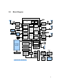
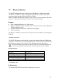
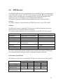
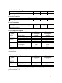
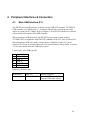
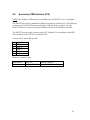
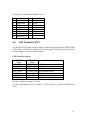
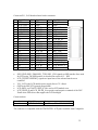
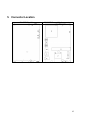
EM-X270
Embedded Mobile Device
Reference Guide
1
Table of Contents
1.
Revision Notes ............................................................................................................. 3
2.
Overview...................................................................................................................... 4
2.1. HIGHLIGHTS ..........................................................................................................4
2.2. BLOCK DIAGRAM ..................................................................................................5
2.3. FEATURES..............................................................................................................6
3.
System Components ................................................................................................... 8
3.1. PXA270 PROCESSOR.............................................................................................8
3.2. MEMORY .............................................................................................................11
3.3. GRAPHICS SYSTEM ..............................................................................................12
3.4. AUDIO SYSTEM....................................................................................................12
3.5. CELLULAR MODULE ............................................................................................15
3.6. WLAN MODULE .................................................................................................18
3.7. BLUETOOTH MODULE .........................................................................................22
3.8. GPS RECEIVER ....................................................................................................23
3.9. RTC ....................................................................................................................24
3.10. POWER SYSTEM AND POWER CONSUMPTION ......................................................25
4.
Peripheral Interfaces & Connectors ....................................................................... 28
4.1. MAIN USB INTERFACE (P1) ................................................................................28
4.2. SECONDARY USB INTERFACE (P10) ...................................................................29
4.3. RS232 (P2) .........................................................................................................30
4.4. MMC/SDIO/SD (P5) ..........................................................................................30
4.5. LCD CONNECTOR (P11)......................................................................................31
4.6. MAIN BATTERY CONNECTOR (P4).......................................................................33
4.7. AUDIO JACK (P6).................................................................................................33
4.8. SPEAKER CONNECTOR (P15) ...............................................................................33
4.9. KEYPAD AND GENERAL PURPOSE I/O (P8)..........................................................34
4.10. CAMERA MODULE CONNECTOR (P36).................................................................34
4.11. SIM CARD SOCKET (P7) .....................................................................................36
4.12. ANTENNA CONNECTORS (J3, J4, J6, J7) ..............................................................36
4.13. LED’S AND PUSH BUTTONS ................................................................................37
4.14. CELLULAR MODULE CONNECTOR (P37)..............................................................37
4.15. EXTENDER CONNECTOR (P3): LOCAL BUS, LCD, UART, SSP, I2C...................38
5.
Connector Location .................................................................................................. 45
6.
Address Range Mapping.......................................................................................... 46
7.
Mechanical Considerations...................................................................................... 47
8.
Operating Temperature Ranges.............................................................................. 48
2
1. Revision Notes
Date
01-Sep-2007
26-Nov-2007
18-Mar-2008
25-Jun-2008
Description
10-Sep-2008
28-Jan-2010
First release
Updated weight data (p. 7)
Added battery charger and power modes description (section 3.10)
Updated sleep mode power consumption data
Fixed battery connector (P4) pin-out
Fixed audio jack (P6) pin-out
Added LED functionality for DS1 and DS2 (section 4.13)
Updated keypad interface note (section 4.9)
Added NOR flash mapping note (section 6)
US and Canada GSM bands support note (section 3.5)
Corrected WLAN encryption support
Added changes for rev1.3
Added secondary USB host port (section 4.2)
Added USB host port on the extender connector
Telit GE864 module replaced with Telit 864 global form factor
connector (section 3.5)
BGW200 WLAN replaced with W2SW0001 WLAN module (section
3.6)
Touch-screen signal lines routed to the extender connector
Charging indication LED connection changed in order to support
depleted battery charging indication.
Configuration options updated.
Added absolute maximum ratings and operating conditions sections
Please check for a newer revision of this manual in CompuLab's website http://www.compulab.co.il, following [Products] >> [Developer] >> [EM-X270] links.
Compare the revision notes of the updated manual from the website with those of the
printed version you have.
3
2. Overview
2.1.
Highlights
•
Full-featured handheld computer
board for embedded applications
•
Intel's XScale PXA270 CPU, up to
520 MHz, 32+32 KB cache, WMMX
•
128 Mbyte SDRAM
•
512 Mbyte Flash Disk
•
Cellular voice and GPRS modem
•
Integrated 3.5" 480 x 640 VGA
display with touchscreen (optional)
•
Graphics controller supporting STN
and TFT panels with 800x 600 max
resolution
•
WiFi 802.11b interface
•
Bluetooth interface
•
GPS receiver, Sirf-III chipset
•
Expansion connector
•
Camera Interface
•
SD / SDIO / MMC socket
•
Sound codec with integrated speaker
and microphone
•
Slave and host USB port, serial port,
GPIO's
•
Main and backup batteries, and
battery charger
•
Very low standby and active power
consumption
•
Size - 97 x 66 mm
EM-X270 is a full-featured computer
board, designed specifically for handheld
/ mobile implementations. Its functional
contents are similar to the latest
generation of Pocket PC's and
smartphones, including all types of
wireless, satellite and cellular
connectivity found in today's state-offthe-art mobile devices. Yet, it is designed
to serve custom implementations,
retaining the flexibility expected from an
embedded computer board. Available
with an optional display, battery with
charger and keypad, the EM-X270 offers
a self-contained solution requiring just an
enclosure for implementing the final
custom product.
The feature set of the EM-X270 board
combines a 32-bit CPU, SDRAM, Flash
Disk and vital computing peripherals.
On-board wireless interfaces include
WiFi, Bluetooth, GPS and cellular
Voice/GPRS modem. The last interface
enables the device to act essentially as a
customized cellular phone.
EM-X270 has several connectors and
slots as used in PDA's and also an
internal extension connector for
application-specific add-on's. Ready-torun Windows CE and Linux packages
are available from CompuLab.
4
2.2.
Block Diagram
PXA270 MPU, 312 / 520 MHz
CPU
WMMX
MMU
Bluetooth
module
WiFi Port
socket
Keypad
SD/MMC
controller
I/O Ports
Camera
Sensor
Cache
GPS
receiver
DMA
Timers
Interrupts
Serial
Controller
Camera interf
Graphics
Controller
USB OTG
Memory &
Local Bus
Controller
RS232
GPRS/GSM
modem
AC97
Interface
SIM socket
3.5" Display
480 x 640
SDRAM
128 MB
Audio
Touchscreen
NOR Flash
WM9715L
RTC
NAND
Flash Disk
512 MB
buffers
LCD
USB 5V
Extension Connector
Backlight Supply
UART
I2C
GPIO
USB
Power
converters
Battery
Charger
Backup
Battery
Main Battery
3.7V * 3A/h
Legend: blue color - off-board devices
1.8
5
2.3.
Features
"Option" (last) column specifies the configuration code required to have the particular
feature. "+" means that the feature is available always.
CPU, Memory and Busses
CPU
RAM
NAND Flash Disk
External local bus
Intel XScale PXA270, 312 / 520 MHz, WMMX
32 KB I-cache and 32 KB D-cache, WB, 128 MB address
space. DMA and Interrupt controllers, Timers
64 / 128 MB, SDRAM, 100 MHz, 32-bit
128 / 512 Mbytes, more in future.
32-bit data, 26-bit address, variable rate up to 100 MHz
C
D
N
Y
Peripherals
Telit GC864 module. GSM 850, 900, DCS 1800 or PCS 1900
network communication services. GPRS Class 10, Voice,
Circuit Switched Data transfer, Fax, Phone-book and SMS.
On-board SIM card socket. Connector for external antenna
Bluetooth V2.0+EDR system. CSR BlueCore4-ROM chipset,
Bluetooth
2.4GHz band, up to 3Mbps. On-board ceramic chip antenna
and connector for external antenna
Implements 802.11b wireless connectivity standard.
WiFi Interface
Wi2Wi W2SW0001 chipset, 11 Mbps, 2.4 GHz band.
On-board antenna and connector for external antenna
NAVMAN Jupiter32 receiver module, Sirf-III chipset.
GPS
Supports the NMEA data messages protocol. Connector for
external antenna
Graphics Controller 4/8/16 bit color, TFT / STN, resolution up to 800 x 600 x 16
Direct camera sensor support, max resolution 2048 x 2048.
Camera Interface
30 fps @ 320x240, 15 fps @640x480
USB Host/Slave port, 12 Mbps, 24-endpoints, OHCI v1.1
USB
Additional Host port, 12 Mbps, OHCI v1.0 compliant
Serial Port (UART) 16550 compatible, max 921 kbps, RS232, full modem
Up to 16 dedicated lines. Can also be used as interrupt inputs.
General Purpose I/O
Shared with keypad interface
Wolfson WM9715L, AC97 interface. On-board microphone
Audio codec
and speaker connectors, and external audio jack
Touchscreen ctrl.
A part of the Wolfson WM9715L chip. Supports resistive
GPRS / GSM
module
K
J
W
H
+
+
+
+
+
AT
AT
6
SD / MMC socket
RTC
touch panels
Supports Multimedia Card, Secure Digital and Secure Digital
I/O communications protocols. Data-transfer rates up to 19.5
Mbps for MMC and 1-bit SD/SDIO, and up to 78 Mbps for 4bit SD/SDIO transfers
Real Time Clock, uninterrupted power supply
+
R
Electrical, Mechanical and Environmental Specifications
Charger for board's lithium polymer battery. The power is supplied
from a 5V source via the USB connector.
Active consumption All contents, excluding GPRS: 0.2 - 2 W. GPRS: 1-2 W
Sleep consumption 10 - 50 mW, depending on configuration and mode
Dimensions
97 x 66 mm. Height: board - 6 mm, LCD - 5 mm, battery - 6 mm
Weight
Board - 40 gram, LCD - 45 gram, battery - 60 gram
MTBF
> 100,000 hours
Commercial: 0o to 70o C
Operation
Extended: -20o to 70o C
temperature
Industrial: -40o to 85o C
* specified for board only, on component case
Storage temperature -40o to 85o C
10% to 90% (operation)
Relative humidity
05% to 95% (storage)
Shock
50G / 20 ms
Vibration
20G / 0 - 600 Hz
Battery charger
Off-board Devices
LCD Panel
Battery
Keypad
TPO/Philips TD035STEE1 - 3.5" TFT, 480 x 640 VGA, 16-bit
parallel RGB interface, transflective, LED backlight, integrated
touch-screen, below 1W consumption
Lithium polymer, 97 x 55 x 6 mm, 10 W/h. Designed for 8-10 hours
of continuous operation under normal conditions
9 key keypad
7
3. System Components
3.1.
PXA270 Processor
XScale PXA270 Block Diagram
The PXA270 processor is an integrated system-on-a-chip microprocessor for highperformance, low-power, portable handheld and handset devices. It incorporates Intel's
XScale micro-architecture with on-the-fly frequency scaling and sophisticated power
management to provide excellent MIPs/mW performance. The PXA270 processor is ARM
Architecture Version 5TE instruction set compliant (excluding floating point instructions)
and follows the ARM programmer’s model.
An integrated LCD display controller provides support for displays up to 800 x 600 pixels,
and permits 1-, 2-, 4-, and 8-bit grayscale and 8-, or 16-bit color pixels. A 256 entry/512
8
byte palette RAM provides flexibility in color mapping.
A set of serial devices and general system resources provide computation and connectivity
capabilities for a variety of applications. Intel XScale micro-architecture provides the
following features:
ARM Architecture Version 5TE ISA compliant
- ARM Thumb Instruction Support
- ARM DSP Enhanced Instructions
Low power consumption and high performance
Media Processing Technology
- Enhanced 16-bit Multiply
- 40-bit Accumulator
32-KByte Instruction Cache
32-KByte Data Cache
Instruction and Data Memory Management Units
Branch Target Buffer
The processor integrates XScale micro-architecture with the following peripheral set:
Clock and Power Controllers
DMA Controller
LCD Controller
Interrupt Controller
AC97
Universal Serial Bus (USB) Client
I2C
MultiMediaCard
Synchronous Serial Protocol (SSP) Port
General Purpose I/O pins
UART’s
Real-Time Clock
OS Timers
USB Host and Slave controller
Camera Interface
The PXA270 has and integrated coprocessor to accelerate multimedia applications. This
coprocessor is characterized by a 64-bit single-instruction multiple-data (SIMD)
architecture and compatibility with the integer functionality of the Intel's Wireless MMX™
technology and streaming SIMD extensions (SSE) instruction sets. Key features of this
coprocessor include:
30 media-processing instructions
64-bit architecture up to eight-way SIMD
16 x 64-bit register file
SIMD PSR flags with group-conditional execution support
9
SIMD instruction support for sum of absolute differences (SAD) and multiplyaccumulate (MAC) operations
Instruction support for alignment and video operations
Intel's MMX and SSE integer instruction compatibility
Superset of existing media-processing instructions in the Intel XScale® core
PXA270 processor has 256 Kbytes on-chip memory.
10
3.2.
Memory
DRAM
The EM-X270 board is assembled with 128 Mbytes of Synchronous DRAM. The SDRAM
interface is 32-bits wide and runs with a 100 MHz clock.
NOR Flash
The EM-X270 is assembled with 1 Mbyte of linear (NOR) Flash ROM. This memory
space is used for the boot-loader and system setup data storage. The setup block contains
vital production information including boot-loader configuration, PCB revision,
manufacturing stamp and MAC addresses for Ethernet and WLAN.
NAND Flash
The EM-X270 features 512 Mbytes of NAND Flash.
The NAND Flash is a block device – optimized for block read and write operations rather
than for random access. It is used for implementation of a Flash Disk, regarded by the
operating system as a regular disk drive.
11
3.3.
Graphics System
The EM-X270 graphics system is based on the LCD controller integrated in the PXA270
chip. The LCD controller provides an interface between the PXA270 processor and a flatpanel display module. The flat-panel display module can be either passive (DSTN) or
active (TFT), or an LCD panel with internal frame buffering.
The EM-X270 board features an LCD panel connector (P11) that is designed for
connecting the TD035STEE1 LCD module. The TD035STEE1 is a 3.5” transflective
active matrix color 480x640 TFT LCD module that includes a touch panel, backlight and
TFT LCD panel. All the signals necessary for graphics output, touch-screen support and
backlight control are routed to the LCD panel connector.
The LCD controller signals are also routed to the expansion connector. The EM-X270 may
be integrated with other types of LCD panels either through LCD connector (P11) or
through expansion connector. See section 4.5 for details about the LCD connector.
LCD Controller Features
The following list describes features supported by the PXA270 processor LCD controller:
Display modes
- Support for single- or dual-scan display modules
- Passive monochrome mode supports up to 256 gray-scale levels (8 bits)
- Support for up to 16-bit per pixel single-scan color displays without an internal frame
buffer
Support for display sizes from 1x1 to 800 x 600 pixels
Supports pixel depths of 2, 4, 8 and 16 bits per pixel (bpp) in RGB format
Supports a hardware cursor for single-scan displays (see Section 7.4.11 in PXA270
manual for cursor modes and sizes)
Programmable toggle of AC bias pin output (toggled by line count)
Programmable pixel clock from 52.0 MHz down to 25.4 kHz (104.0 MHz/2 to 13
MHz/512)
Backward compatible with the Intel's PXA255 graphics controller
3.4.
Audio System
The audio system of the EM-X270 is implemented with the Wolfson WM9715L codec
chip connected to the AC97 port of the PXA270.
12
AC’97 Controller Unit Overview
The AC’97 Controller Unit (ACUNIT) of the PXA270 processor supports AC’97 revision
2.0 features. The ACUNIT also supports the audio controller link (AC-link). The AC-link
is a serial interface for transferring digital audio, modem, mic-in, CODEC register control
and status information.
The AC’97 CODEC sends the digitized audio samples that the ACUNIT stores in memory.
For playback or synthesized audio production, the processor retrieves stored audio samples
and sends them to the CODEC through the AC-link. The external digital-to-analog
converter (DAC) in the CODEC then converts the audio samples to an analog audio
waveform.
WM9715L
The WM9715L is a highly integrated device supporting audio and touchscreen functions.
The device can connect directly to a 4-wire touch panel, mono or stereo microphones,
stereo headphones and a mono speaker. Additionally, phone input and output pins are
provided for seamless integration with wireless communication devices.
The WM9715L contains a universal touch screen interface for a 4-wire resistive touch
screen, capable of performing position, pressure and plate resistance measurements. The
touch screen interface is connected to the system’s LCD panel connector.
Audio Interconnection
The following block diagram describes the EM-X270’s audio interconnection path.
MIC IN
LINE IN L
LINE IN R
PHONE IN
RECORD
SELECT
RECORD
VOLUME
PXA270
AC`97 UNIT
ADC
L
ALC
DAC
L
BASS
BOOST
ADC
R
3D
HEADPHONE
MIXER
SPEAKER
MIXER
DAC
R
PHONE
MIXER
HP OUT L
HP OUT R
DIFF. SPK OUT
PHONE OUT
AC`97
INTERFACE
The headphone stereo output connects to the on-board audio jack (P6). This output is
designed to drive a 16Ω or 32Ω headphone or a line output.
The audio mic input is directly connected to the on-board ECM microphone.
The phone output and input are internally connected to the cellular module audio
signals.
13
The WM9715L audio amplifier differential output is routed to the system speaker
connector (P15). This output is designed to differentially drive an 8Ω mono speaker.
The line-in inputs are routed to the extender board connector (P3).
Each of the audio inputs may be multiplexed to each of the audio outputs or into the AC`97
interface for digital recording. The AC`97 interface output may also be multiplexed into
any of the analog audio outputs for digital playback.
Audio multiplexing and gain control is supported through Linux and Win CE packages
provided for the EM-X270.
Audio Specifications
PARAMETER
SYMBOL
Headphone Output
Output Power per Channel
Po
Signal to Noise Ratio
SNR
Speaker Output with 8Ω
Ω bridge tied load
Output Power at 1% TDH
Po
Abs. Max Output Power
Po_max
Signal to Noise Ratio
SNR
On-board Microphone at F=1kHz, Vs=2.0V,
Sensitivity
S/N Ratio (A)
SNR
Directivity
Line Input
Full Scale Input Signal Level
Input Resistance
Vinfs
Rin
TYP
UNIT
20
95
mW
dB
400
500
97
mW
mW
dB
-40 +/-3
58
Omni
Directional
dB
dB
1.0
17
V rms
Kohm
14
3.5.
Cellular Module
NOTE: The following section refers to EM-X270 - revisions 1.3 and higher. For previous
revisions of EM-X270 please refer to the shaded section below.
The EM-X270 cellular connectivity feature is based on the Telit 864 series of cellular
modules. The cellular module connector (P37) is conformant with the Telit global form
factor interface and can accommodate the following modules:
•
•
•
GC864 – quad-band EGSM 850 / 900 / 1800 / 1900 MHz
UC864-E – UMTS/HSDPA 2100 MHz, quad-band EGSM 850 / 900 / 1800 /
1900 MHz
CC864 – dual-band CDMA 800 / 1900 MHz
The cellular module is interfaced to the PXA270 processor via the BT_UART.
The SIM interface is connected to the on-board SIM card socket (see 4.11 for a detailed
SIM card socket description).
Audio Path Connection
The cellular module audio signals are connected to the EM-X270 audio system, providing
the audio functionality of a standard cellular phone. See section 3.4 for more details about
the audio path.
Antenna
The antenna should fulfill the following requirements:
Frequency range
Bandwidth
Gain
Impedance
Input power
VSWR absolute max
VSWR recommended
Depending on frequency band(s) provided by the network
operator, the customer shall use the most suitable antenna for
that/those band(s)
70MHz in GSM850, 80MHz in GSM900, 170 MHz in DCS,
140 MHz in PCS, 250 MHz in WCDMA2100
> 1.5 dBi
50 ohm
> 2 W peak power
10:1
< 2:1
Please refer to Telit’s specific module documentation for more details.
The antenna is connected to a standard UFL connector present on the cellular module.
15
NOTE: For some modules, the default configuration is set to the European (GSM-900
GSM-1800) band frequencies. Users in the US and Canada need to re-configure the
modem to the GSM-850 GSM-1900 bands. Use the "AT#BND=3" command to set the
proper band settings. Please see page 300 in the “Telit AT Commands Reference Guide”
for detailed info about the band configurations.
RF Specifications
Please refer to Telit’s specific module documentation for RF specifications.
LED Indication
The on-board LED DS4 shows information regarding network service availability and call
status.
LED status
Permanently off
Fast blinking (period 1s, Ton 0,5s)
Slow blinking (period 3s, Ton 0,3s)
Permanently on
Cellular module status
Cellular module off
Net search / Not registered / turning off
Registered full service
A call is active
NOTE: The following section refers to EM-X270 - revisions 1.2 and older.
The cellular GSM/GPRS connectivity feature is based on the Telit GE864 module.
The GE864 module allows digital communication services wherever a GSM 850, 900,
DCS 1800 or PCS 1900 network is present.
The GE864 includes features like GPRS Class 10, Voice, Circuit Switched Data transfer,
Fax, Phone book, SMS support and ‘EASY GPRS’ embedded TCP/IP stack.
The module also provides SIM card interface with auto-detection and hot insertion.
The interface supports phase 2 GSM11.14 - SIM 3V.
The GE864 module is interfaced to the PXA270 processor via the BT_UART.
The SIM interface is connected to the on-board SIM card socket (see 4.11 for a detailed
SIM card socket description).
Audio Path Connection
The GE864 audio signals are connected to the EM-X270 audio system, providing the audio
functionality of a standard cellular phone. See section 3.4 for more details about the audio
path.
16
Antenna
The antenna should fulfill the following requirements:
Frequency range
Bandwidth
Gain
Impedance
Input power
VSWR absolute max
VSWR recommended
Depending on frequency band(s) provided by the network
operator, the customer shall use the most suitable antenna for
that/those band(s)
136 MHz in GSM 850/900, 170 MHz in DCS, 140 MHz PCS
> 1.5 dBi
50 ohm
> 2 W peak power
10:1
< 2:1
The module RF signal is routed to a standard UFL connector for off-board antenna
connection. See section 4.12 for a detailed connector description.
NOTE: The modem default configuration is set to the European (GSM-900 GSM-1800)
band frequencies. Users in the US and Canada need to re-configure the modem to the
GSM-850 GSM-1900 bands. Use the "AT#BND=3" command to set the proper band
settings. Please see page 300 in the “Telit AT Commands Reference Guide” for detailed
info about the band configurations.
RF Specifications
Operating Frequency
Mode
Freq. TX (MHz)
E-GSM-850
E-GSM-900
824.2÷848.8
890.0 - 914.8
880.2 - 889.8
1710.2 - 1784.8
1850.2 - 1909.8
DCS-1800
PCS-1900
Output Power
Mode
GSM–850/900
DCS–1800/PCS–1900
Reference sensitivity
Mode
GSM–850/900
DCS–1800/PCS–1900
Freq. RX (MHz)
869.2÷893.8
935.0 - 959.8
925.2 - 934.8
1805.2 - 1879.8
1930.2 - 1989.8
Device class
class 4
class 1
Device class
class 4
class 1
Channels
(ARFC)
0 – 124
0 – 124
975 - 1023
512 – 885
512 – 810
TX - RX
offset
45 MHz
45 MHz
45 MHz
95 MHz
80 MHz
Nominal Peak Power
+33dBm
+30dBm
Nominal Peak Power
-107dBm
-106dBm
17
LED Indication
The onboard LED DS4 shows information regarding network service availability and call
status.
LED status
Permanently off
Fast blinking (period 1s, Ton 0,5s)
Slow blinking (period 3s, Ton 0,3s)
Permanently on
3.6.
GSM module status
GSM module off
Net search / Not registered / turning off
Registered full service
A call is active
WLAN Module
NOTE: The following section refers to EM-X270 - revisions 1.3 and higher. For previous
revisions of EM-X270 please refer to the shaded section below.
The EM-X270 incorporates full-featured 802.11 b/g capabilities, implemented with the
Wi2Wi W2SW0001 WLAN controller module. The W2SW0001 is a complete IEEE
802.11b/g solution based on the Marvell’s 88W8686 chipset.
Security features:
• WEP encryption (64 bit/128 bit)
• WPA TKIP security
• WPA2
The W2SW0001 is connected to the PXA-270 CPU using the SPI #2 interface.
Antenna Connection
The EM-X270 features a small on-board ceramic patch antenna dedicated to WLAN
connectivity. Alternatively, an external antenna may be connected via the on-board high
frequency connector. Any type of 2.45GHz WLAN antenna can be used. See section 4.12
for a detailed connector description.
Note: An external antenna cannot operate together with the on-board patch antenna. In
order to use an external WLAN antenna, the on-board antenna must be disconnected.
18
RF Specifications
802.11b RF system specifications
Transmit Power Output
Receive Sensitivity
Maximum Receive Level
Transmit Frequency Offset
Spectral Mask
Error Vector Magnitude
Carrier Suppression
Adjacent channel rejection
Transmit Power Output
Receive Sensitivity
Maximum Receive Level
Transmit Frequency Offset
Spectral Mask
Error Vector Magnitude
Carrier Suppression
Adjacent channel rejection
1 Mbps, 8% PER
2 Mbps, 8% PER
5.5 Mbps, 8% PER
11 Mbps, 8% PER
PER < 8%
Low, Middle, High
channels
Max. TX power
15
-87
-87
-87
-85
IEEE Compliant
+/-10
-40@fc+/-11MHz
-60@fc+/-22MHz
-36
Max. TX power @
11Mbps
Max. TX power
Desired channel is 3dB
above sensitivity,
11Mbps, PER < 8%
802.11g RF system specifications
6 Mbps, 10% PER
9 Mbps, 10% PER
12 Mbps, 10% PER
18 Mbps, 10% PER
24 Mbps, 10% PER
36 Mbps, 10% PER
48 Mbps, 10% PER
54 Mbps, 10% PER
PER < 8%
Low, Middle, High
channels
Max. TX power
Max. TX power @
54Mbps
Max. TX power
Desired channel is 3dB
above sensitivity,
54Mbps, PER < 8%
-25
48
15
-86
-85
-85
-84
-80
-77
-73
-72
IEEE Compliant
+/-10
-30@fc+/-11MHz
-40@fc+/-20MHz
-50@fc+/-30MHz
-29
-25
15
dBm
dBm
dBm
dBm
dBm
PPM
dBc
dB
dBc
dBc
dBm
dBm
dBm
dBm
dBm
dBm
dBm
dBm
dBm
PPM
dBc
dB
dBc
dBc
19
NOTE: The following section refers to EM-X270 - revisions 1.2 and older.
The EM-X270 incorporates full-featured 802.11b capability implemented using a Phillips
BGW200 WLAN controller. The implementation contains a baseband MAC subsystem,
RF transceiver and high-power RF front-end, thus incorporating all the components
required to provide high-quality WLAN capability.
The BGW200 is based on an internal controller sub-system with dedicated CPU, ROM and
RAM. The sub-system executes firmware, responsible for all low-level WLAN networking
functionality, thus considerably reducing the load on the main CPU.
The RF interface supports antenna diversity for improved stability. It provides +16dBm
transmitter output power - the standard level for 802.11 NIC’s.
BGW200 firmware supports both infrastructure (access point managed) and independent
(without access point) network topologies. On the other hand, firmware does not support
BGW200 acting as an access point.
Security features:
• WEP64
• WEP128
Other firmware features:
• Extended rate protection
• Regulatory domain
• Power save protocol
• Fragmentation & De-fragmentation
• Antenna diversity
Infrastructure/Ad-hoc modes:
• BSS
• IBSS
The BGW200 is connected to the PXA-270 CPU using the SPI #2 interface.
Antenna Connection
The EM-X270 features a small on-board ceramic patch antenna dedicated to WLAN
connectivity. Alternatively, an external antenna may be connected via the on-board high
frequency connector. Any type of 2.45GHz WLAN antenna can be used. See section 4.12
for a detailed connector description.
Note: An external antenna cannot operate together with the on-board patch antenna. In
order to use an external WLAN antenna, the on-board antenna must be disconnected.
20
NVM Data
During the EM-X270 manufacturing process, WLAN sub-system configuration and RF
calibration data is stored in the NOR flash. RF calibration data allows the BGW200 to
provide its best RF performance throughout a wide range of temperatures while still
staying compliant with FCC regulations. The WLAN MAC address is also stored in the
NOR flash.
RF Specifications
Symbol Parameter
Receiver sensitivity
1 Mbps sensitivity
2 Mbps sensitivity
5.5 Mbps sensitivity
11Mbps sensitivity
Maximum input level
Max input level for 2 Mbps
Max input level for 11 Mbps
Linear output power
1 Mbps and 2 Mbps output power
5.5 Mbps and 11 Mbps output power
Conditions
Typ.
value
-91
Unit
PER < 8%
PSDU = 1024 bytes
-87
-83
-83
dBm
dBm
dBm
dBm
PER < 8%
PSDU = 1024 bytes
-0.4
0.6
dBm
dBm
meets FCC restricted
band specifications
15.5
16
dBm
dBm
* All values at nominal supply voltage, 25°C and channel 6
21
3.7.
Bluetooth Module
The EM-X270 Bluetooth system is based on the CSR BlueCore 4-ROM component.
The BlueCore 4-ROM is a single-chip radio and baseband IC for Bluetooth 2.4GHz
systems including enhanced data rates (EDR) to 3Mbps.
With the on-chip CSR Bluetooth software stack, it provides a fully-compliant Bluetooth
system to v2.0 of the specification for data and voice communications.
Features:
Fully Compliant Bluetooth v2.0+EDR system
Enhanced Data Rate (EDR) compliant with v2.0 of specification for both 2Mbps and
3Mbps modulation modes
Full Speed Bluetooth Operation with Full Piconet Support
Scatternet Support
The BlueCore 4-ROM is connected to the PXA270 processor USB host port through the
USB hub.
Antenna Connection
The EM-X270 features a small on-board ceramic patch antenna dedicated to Bluetooth
connectivity. Alternatively, an external antenna may be connected via the on-board UFL
high frequency connector. See section 4.12 for a detailed connector description.
Note: The external antenna cannot operate together with the on-board patch antenna. In
order to use an external Bluetooth antenna, the on-board antenna must be disabled.
RF Specification
Standards
BlueTooth Class
Wireless Signal Rates
Wireless Transmit Power*
Wireless Operating Range*
Receiver Sensitivity*
IEEE 802.15.1
Class II device
2.1Mbps (Bluetooth 2.0)
4dBm
Up to 10m
-84dBm
* Preliminary data
LED Indication
The onboard LED DS5 indicates BlueTooth transceiver activity.
22
3.8.
GPS Receiver
The EM-X270 GPS function is implemented with the NAVMAN Jupiter32 module based
on the SiRF GSC3f chip-set. The GSC3f chip integrates baseband, RF sections and Flash
memory, thereby reducing power consumption and size. Integrated 4 Megabit flash
memory gives the user the ability to store configurations permanently.
The protocol supported is NMEA (National Marine Electronics Association) data
messages.
The Jupiter32 module is interfaced with the PXA270 processor via the STD_UART.
Antenna
The RF input is routed to a standard UFL connector for off-board antenna connection.
See section 4.12 for a detailed connector description.
The following table summarizes the recommendations for the EM-X270 GPS antenna:
Characteristic
Polarization
Receive frequency L1
Power supply
DC current
Antenna gain
Total gain
Axial ratio:
Output VSWR
Passive Antenna
Right-hand circular polarized
1.57542 GHz +/- 1.023 MHz
2 to 5 dBi with 1 dB loss (max)
in connections
< 3 dB
-
Active Antenna
Right-hand circular polarized
1.57542 GHz +/- 1.023 MHz
3V
<10mA at 3V
< 18dBi
< 3 dB
< 2.5
The active ceramic patch antenna available from Compulab (part name ANTGPS) meets
the requirements above and may be used for evaluation and pilot production.
Performance Specifications
The table below shows the corresponding TTFF times for each of the acquisition modes.
Mode
Hot start TTFF
Warm start TTFF
Cold start TTFF
Re-acquisition
(<10s obstruction)
@ –125 dBm
Typ
90%
500 ms
<1 s
32 s
38 s
34 s
42 s
@ –140 dBm
Typ
90%
<1 s
<1 s
49 s
59 s
52 s
66 s
1s
1s
23
The position and velocity accuracy are shown in the following table, assuming full
accuracy C/A code.
Parameter
Horizontal CEP
Horizontal (2 dRMS)
Vertical VEP
3.9.
Value
2.2 m
5.5 m
2.0 m
RTC
V3020 chip provides RTC functionality on the EM-X270. The real-time clock/calendar
provides seconds, minutes, hours, day, date, month, year and century information. A
time/date programmable polled ALARM is included. The end-of-the-month date is
automatically adjusted for months with fewer than 31 days, including corrections for leap
year up to the year 2100. The clock operates in either 24hr or 12hr format with an AM/PM
indicator.
Setting the time and date of V3020 RTC is supported through Linux and Win CE packages
provided for the EM-X270.
Interface
The V3020 RTC uses a single line serial I/O interface, implemented using standard R/W
operations and an MD[0] local bus data line at physical address 0x10000000 in the PXA270 CPU memory space.
The RTC chip’s power supply is connected both to the main battery and to the onboard
back-up coin cell battery. Thus, the RTC data is preserved even when the main battery is
detached from EM_X270. See section 3.10 for a more detailed explanation.
24
3.10. Power System and Power Consumption
EM-X270 Power Management Concepts
The EM-X270 system is designed as a handheld device, providing minimized power
consumption operation, very low power sleep mode, on-line battery replacement capability
and long battery life.
The main power supply source is a rechargeable lithium battery. A regulated DC power
source of 3.7V – 4V may also be used, but this will require software adaptation.
An on-board rechargeable coin cell battery provides back-up power in standby and off
modes.
The DA9030 PMIC manages most of the EM-X270's power system, providing regulated
voltages for the PXA270 processor, memories and peripheral devices.
Certain units of the EM-X270 are powered by discrete voltage regulators connected
directly to the main battery and controlled by PXA270 GPIO’s.
Battery charging and supervision are also managed by the DA9030.
EM-X270 Batteries
The EM-X270 system is designed to operate with a rechargeable lithium battery.
The battery pack must include an NTC thermistor for temperature measurement during
battery charging.
The EM-X270 power management software was designed to operate with the 10W/h LiPolymer battery available from Compulab. Custom batteries may also be integrated with
the EM-X270, but this will require software adaptation. The following battery chemistries
are supported by EM-X270:
Single-Cell Li-Ion at 4.1V
Li-Polymer Pack
Please see the “Battery charger control” section in the DA9030 datasheet for more details.
An on-board 14mAh rechargeable coin cell lithium battery is the back-up power supply for
RTC timekeeping. This battery is constantly being charged whenever the main battery is
present.
25
Battery Charging and Supervision
Battery charging is managed by the DA9030 that supports constant current / constant
voltage charging, PWM and trickle charge modes, external DC detection, pre-charge, over
voltage and current lock out, battery removal and charge watchdog functions.
The charge DC signal is applied to the USB OTG connector. Thus, the battery may be
charged from a DC charger device with a mini USB connector or from a standard USB
host with a 5V power supply. External charger voltage must be between 4.5V and 5.5V.
The charging current is set in the power management software and may vary between
100mA and 1000mA.
During charging, battery temperature, voltage and charge current must be supervised, in
order to prevent battery over-heating or overcharge. These measurements are performed
with the DA9030 internal ADCs. Please see the “Battery charger control” section in the
DA9030 datasheet and the “Power Management” section in the O/S package
documentation for more details.
Power Modes
Active Mode
The active mode is entered after a successful start-up or pre-charge mode. During this
operating mode the PXA270 processor controls the system power management and is able
to respond to any faults that have been detected. Status information is passed to PXA270
via the I2C interface. The DA9030 can flag interrupt requests to the processor via a
dedicated interrupt pin.
Sleep Mode
The sleep mode may be entered from active mode only. The PXA270 processor is in deep
sleep mode and the DA9030 is in sleep mode. All power sources except for SDRAM deep
sleep self-refresh and RTC timekeeping power are shut down. The EM-X270 will wake-up
when one of the following events is detected: sleep/resume button (SW2) is pressed; an
external charger device is connected.
Pre-charge Mode
The pre-charge power mode is entered when the EM-X270 is powered up with a heavily
discharged battery (voltage below 3.45V) and an external DC charger is connected to the
device. The system will enable battery charging and wait until the battery voltage reaches
the 3.45V threshold. Only then, the EM-X270 will proceed with the standard boot
sequence. If the battery voltage is below 3.45V and there is no charger connected, the
system will go into shutdown.
26
Absolute Maximum Ratings
Min
-0.3
Typ
Max
5.5
Units
V
Min
3.45
Typ
Max
4.3
Units
V
Max Activity
500
Idle
170
Sleep
5.5
Units
mA
Input voltage VCC_BAT
Operating Conditions
Input voltage VCC_BAT
Power Consumption
EM-X270 basic system with
minimum peripherals
On-board optional functions
Peripheral
System
WLAN
module
GSM/GPRS
module*
Audio
Test Condition
Receive mode
Transmit mode
Stand-by (GSM idle)
Voice channel mode
GPRS class 10 mode
Idle mode
Everything on
GPS receiver
Bluetooth
Max
Consumption
220mA
240mA
8mA
200mA
500mA
TBD
TBD
100mA
40mA
Typical
Consumption
210mA
230mA
4mA
170mA
250mA
2mA
25mA
30mA
TBD
* GC864 power consumption only. For other cellular modules, refer to specific module
documentation.
Off-board peripherals
Peripheral
System
Ethernet on
EB-X270
TD035STEE
1 LCD panel
Test Condition
Max
Consumption
TBD
Typical
Consumption
70mA
No backlight
Backlight at half intensity
Backlight at full intensity
30mA
150mA
260mA
30mA
150mA
260mA
All power consumption tests were performed at 25°C with the Lithium Polymer battery
pack at a nominal 3.7V.
27
4. Peripheral Interfaces & Connectors
4.1.
Main USB Interface (P1)
The EM-X270 main USB interface complies with the USB OTG standard. The PXA270
USB controller is a USB Revision 1.1-compliant, full-speed device that operates halfduplex at a baud rate of 12 Mbps. Refer to chapter 12 of the PXA270 Reference Guide for
a more detailed description of the USB controller.
When operating in USB host mode, the EM-X270 power supply system provides
5V/100mA DC (in compliance with USB OTG standard) on the VCC pin of connector P1.
When operating in USB slave mode, voltage output is disabled, and the VCC pin of
connector P1 is used as an input voltage pin of an external battery charger. Refer to section
3.10 for more details about the USB power system.
Connector P1, mini USB type AB:
Pin
1
2
3
4
5
Signal Name
USV_VCC
USB_N
USB_P
USB_ID
GND
Reference connector data:
Manufacturer
Astron
Mfg. P/N
22-2601-5G-1T-R
Mating connector
Standard USB mini-B plug.
Standard USB mini-A plug.
28
4.2.
Secondary USB Interface (P10)
NOTE: The secondary USB interface is available only on EM-X270 - rev1.3 and higher.
The EM-X270 provides an additional USB host interface on connector P10. This USB port
is connected to the PXA270 host port through a USB hub. Refer to chapter 20 of the
PXA270 Reference Guide for a more detailed description of the USB host controller.
The EM-X270 power supply system provides 5V/100mA DC (in compliance with USB
OTG standard) on the VCC pin of connector P10.
Connector P10, mini USB type AB:
Pin
1
2
3
4
5
Signal Name
USV_VCC
USB_N
USB_P
NC
GND
Reference connector data:
Manufacturer
Astron
Mfg. P/N
22-2601-5G-1T-R
Mating connector
Standard USB mini-B plug.
29
4.3.
RS232 (P2)
The FF-UART of the PXA270 is connected to the on-board RS232 driver and to the
extender board connector (see section 4.15 for details).
The RS232 driver signals are routed to the RS232 ultra-mini connector (P2).
Connector P2, ultra-mini serial, RS232 levels:
Pin
1
2
3
4
Signal Name
RS232_TXD
RS232_RTS
RS232_RXD
RS232_CTS
Pin
5
6
7
8
Signal Name
RS232_DTR
RS232_DSR
RS232_DCD
GND
Note: the Ring Indicator signal is not available.
Connector data:
Manufacturer
Wieson
Mfg. P/N
G3169-500001
Mating connector
Wieson, P/N: 4306-5000
The connector is compatible with the "DB9-F to Ultra Mini Plug" cable available from
CompuLab.
4.4.
MMC/SDIO/SD (P5)
The EM-X270’s MMC/SDIO/SD interface is based on the MMC controller of the PXA270
processor. The controller acts as a link between the software that accesses the PXA270
processor and the MMC stack (a set of memory cards) and supports Multimedia Card,
Secure Digital, and Secure Digital I/O communications protocols. The MMC controller in
the PXA270 processor is based on the standards outlined in the “Multimedia Card System
Specification Version 3.2”. The SD controller supports one SD or SDIO card based on the
standards outlined in the “SD Memory Card Specification Version 1.01” and “SDIO Card
Specification Version 1.0 (Draft 4)”.
The MMC controller signals are routed to the on-board SD socket (P5).
30
Connector P5, standard MMC/SDIO socket:
Pin
1
2
3
4
5
6
7
8
4.5.
Signal Name
MMCDAT3
MMCCMD
GND
VCC_SDIO
MMCLK
GND
MMDAT0
MMCDAT1
Pin
9
10
11
12
13
14
15
Signal Name
MMCDAT2
GND
MMC_CD
MMC_WP
GND
GND
GND
LCD Connector (P11)
The EM-X270 LCD panel connector allows seamless integration with the TD035STEE1
LCD module. LCD interface signals, LCD control signals, LCD power and touch-screen
interface signals are routed to this connector.
LCD Controller Signals
EM-X270
Name
LCD_B[5-1]
LCD_G[5-0]
LCD_R[5-1]
LCD_PCLK
LCD_FCLK
LCD_LCLK
LCD_DE_M
PXA270
Name
LDD[4-0]
LDD[5-10]
LDD[11-15]
L_PCLK_WR
L_FCLK_RD
L_LCLK_A0
L_BIAS
Description
LCD bus data lines
LCD bus data lines
LCD bus data lines
LCD bus pixel clock
LCD bus frame clock
LCD bus line clock
LCD bus output enable
All above signals are outputs, 3V level.
For more information, please see chapter 7: “LCD Controller” in the PXA270 Reference
Guide.
31
Connector P11, 2x30 board-to-board socket connector:
Pin
1
2
3
4
5
6
7
8
9
10
11
12
13
14
15
16
17
18
19
20
Signal Name
GND
LCD_TSPY
LCD_TSPX
LCD_TSMY
LCD_TSMX
GND
NC
NC
GND
NC
NC
NC
NC
NC
GND
NC
LCD_RST#
NC
NC
VCC_LCD
Pin
21
22
23
24
25
26
27
28
29
30
31
32
33
34
35
36
37
38
39
40
Signal Name
GND
GND
LCD_B1
LCD_B2
LCD_B3
LCD_B4
LCD_B5
GND
LCD_G0
LCD_G1
LCD_G2
LCD_G3
LCD_G4
LCD_G5
GND
GND
LCD_R1
LCD_R2
LCD_R3
LCD_R4
Pin
41
42
43
44
45
46
47
48
49
50
51
52
53
54
55
56
57
58
59
60
Signal Name
LCD_R5
GND
VCC_LCD
NC
GND
LCD_PCLK
GND
LCD_DE_M
SSP1_RXD
SSP1_FRM
SSP1_TXD
NC
SSP1_CLK
LCD_FCLK
LCD_LCLK
NC
NC
LCD_WLED_N
LCD_WLED_P
GND
SSP1_RXD, SSP1_FRM, SSP1_TXD, SSP1_CLK signals are SSP interface lines used
for LCD setup. The SSP interface is described in section 4.15 – SSP.
LCD_TS[PX/PY/MX/MY] signals are input lines of the onboard touch screen
controller.
VCC_LCD is the LCD module power supply line at 3V / 60mA.
GND is the EM-X270 general ground plane.
LCD_RST# is a PXA270 GPIO_87 line used as LCD module reset.
LCD_WLED_P and LCD_WLED_N are positive and negative terminals of the 20V /
20mA white LED driver that supplies the LCD backlight.
Connector data:
Manufacturer
Matsushita
Mfg. P/N
AXK5F60547YG
Mating connector
Matsushita, P/N: AXK6F60547YG
The connector is compatible with the TD035STEE1 LCD panel available from CompuLab.
32
4.6.
Main Battery Connector (P4)
Connector P4, 3pin wire-to-board:
Pin
1
2
3
Signal Name
GND
NTC_BAT
VCC_BAT
Connector data:
Manufacturer
Molex
Mfg. P/N
87438-0343
Mating connector
Molex, P/N: 87439-0300
The connector is compatible with the Li Polymer battery available from CompuLab.
4.7.
Audio Jack (P6)
Connector P6, 2.5mm jack, headphone output:
Pin
1
3
4
5
Signal Name
LOUT_R
NC
LOUT_L
LOUT_C
Mating plug pin
Middle ring
Tip
Outer ring
Jack pin-out
Mating plug
Reference connector data:
Manufacturer
Wieson
4.8.
Mfg. P/N
G7273-050001
Mating connector
Standard 2.5mm stereo plug.
Speaker Connector (P15)
Connector P7, 2-pin wire-to-board:
Pin
1
2
Name
SPK_OUT_P
SPK_OUT_N
33
Connector data:
Manufacturer
Molex
Mfg. P/N
53261-0271
Mating connector
Molex, P/N: 51021-0200
The connector is compatible with the speaker available from CompuLab.
4.9.
Keypad and General Purpose I/O (P8)
The PXA270 keypad interface is used to provide external matrix keypad connectivity.
Matrix keypads of up to 64 keys are supported. The 16 signal lines that control the keypad
interface are routed to the keypad FPC connector (P8).
Alternatively, if the keypad interface is not required, or if not all the signal lines are
utilized for keypad control, the remaining signals may be used as general purpose I/O.
Additionally, the suspend/resume signal (SUS/RES) is also routed to the keypad connector.
This allows placing the suspend/resume button on the keypad of the device.
Connector P8, 20-contacts. FPC 0.5mm:
Pin
1
2
3
4
5
6
7
8
9
10
Signal Name
MKIN0_GPIO_100
MKIN1_GPIO_101
MKIN2_GPIO_102
MKIN3_GPIO_34
SUS/RES
MKIN4_GPIO_39
MKIN5_GPIO_99
MKIN6_GPIO_91
MKIN7_GPIO_36
RESERVED
Pin
11
12
13
14
15
16
17
18
19
20
Signal Name
MKOUT0_GPIO_103
MKOUT1_GPIO_104
MKOUT2_GPIO_105
MKOUT3_GPIO_106
RESERVED
MKOUT4_GPIO_107
MKOUT5_GPIO_108
MKOUT6_GPIO_96
MKOUT7_GPIO_22
GND
Connector data:
Manufacturer
CVILux
Mfg. P/N
CF20-201D0R0
Mating connector
FFC, 20 cont, 0.5mm
4.10. Camera Module Connector (P36)
The "quick capture interface" of the PXA270 processor provides a connection between the
processor and a camera image sensor. The quick capture interface was designed to work
primarily with CMOS-type image sensors. However, it may be possible to connect some
34
CCD-type image sensors to the PXA270 processor, depending on a specific CCD sensor’s
interface requirements.
The quick capture interface acquires data and control signals from the image sensor and
performs the appropriate data formatting prior to routing the data to memory using direct
memory access (DMA). A broad range of interface and signaling options provides direct
connection. The image sensor can provide raw data through a variety of parallel and serial
formats. For sensors that provide pre-processing capabilities, the quick capture interface
supports several formats for RGB and YCbCr color space. The interface supports the
“International Telecommunication Union Recommendation ITU-R BT.656-4”
(www.itu.int) Start-of-Active-Video (SAV) and End-of-Active-Video (EAV) embedded
synchronization sequences for four- and eight-bit configurations.
For additional information, see Chapter 27: “Quick Capture Interface” in the PXA270
Reference Guide.
The quick capture interface signals are routed to the camera module connector (P36).
The camera module connector is designed to operate directly with the OPCOM
CM1314YMH-MO02 camera.
Connector P36, 24cont. FPC 0.5mm:
Pin
1
2
3
4
5
6
7
8
9
10
11
12
Signal Name
CIF_DD0
CIF_DD1
CIF_DD4
CIF_DD3
CIF_DD5
CIF_DD2
CIF_DD6
CIF_PCLK
CIF_DD7
GND
NC
CIF_MCLK
Pin
13
14
15
16
17
18
19
20
21
22
23
24
Signal Name
NC
CIF_VDD_3V
CIF_VDD_1V8
CIF_LV
GND
CIF_FV
CAM_RST
I2C_SCL
CIF_VDD_3V
I2C_SDA
GND
GND
35
Connector data:
Manufacturer
CVILux
Mfg. P/N
CF20-241D0R0
Mating connector
FFC, 24 cont, 0.5mm
4.11. SIM Card Socket (P7)
Connector P7, standard SIM card socket:
Pin
1
2
3
4
5
6
Signal Name
GPRS_SIMVCC
GPRS_SIMRST
GPRS_SIMCLK
GND
NC
Pin
7
8
9
10
11
Signal Name
GPRS_SIMIO
GND
GND
GND
GND
Reference connector data:
Manufacturer
Astron
Mfg. P/N
5190006-006-R
Mating connector
Standard SIM card.
4.12. Antenna Connectors (J3, J4, J6, J7)
The table below summarizes all the RF antennas’ connectivity of the EM-X270.
Interface
GPRS
GPS
WLAN
BlueTooth
Antenna Connector
J4*
J7
J3
J6
*Only present on EM-X270 – rev1.2 and older.
Connector data:
Manufacturer
Hirose
Mfg. P/N
U.FL-R-MT(10)
Mating connector
Hirose U.FL-LP-040
36
4.13. LED’s and Push Buttons
EM-X270 push-buttons
The EM-X270 features two user accessible push buttons:
SW2 is connected to GPIO_1 of the PXA270 processor and is used as a system
suspend-resume button.
SW3 is the main system hardware reset button.
EM-X270 LED’s
The following table describes EM-X270 LED’s.
LED
Color
System
LED activity
DS1
Green
General purpose
The LED is on when the system is
in active mode. LED function may
be redefined in software
DS2
Orange
Battery charger
The LED is on when the main
battery is being charged.
DS4
Orange
GSM/GPRS module
See section 3.5
DS5
Green
Bluetooth module
4.14. Cellular Module Connector (P37)
The EM-X270 cellular module connector (P37) is conformant with the Telit global form
factor interface and can accommodate the Telit 864 series cellular modules. Refer to
section 3.5 for more details.
37
4.15. Extender Connector (P3): Local Bus, LCD, UART, SSP,
I2C
The EM-X270 extender connector outputs the most significant internal interfaces of the
system. This allows for custom hardware boards to be interfaced with the EM-X270.
PXA270 Local Bus
The EM-X270's Local Bus is derived from PXA270 processor’s memory interface bus.
Local Bus implements the access to various types of devices sharing the same interface
lines. Interface lines’ functioning changes dynamically per-cycle, according to the type of
addressed device.
The external memory bus interface supports:
•
•
•
•
RAM / ROM memories
Variable Latency I/O
PCMCIA / Compact Flash cards
16-bit (only) aligned access
Use the memory interface configuration registers of the PXA270 processor to program the
device types. Refer to the PXA270 Processors Design Guide, “Processor Block Diagram”
for the block diagram of the Memory Controller configuration. Refer to the “Memory
Address Map” for the processor memory map. Refer to “Normal Mode Memory Address
Mapping” for alternate mode address mapping.
Local Bus Signals
EM-X270
Name
LB_D[15-0]
P_MB_D[31-16]
LB_A[9-0]
P_MB_A[25-10]
LB_WE#
LB_OE#
LB_PWE#
LB_RDY
P_MB_RD_WR#
LB_CS2#
PXA270
Name
MD[15-0]
MD[31-16]
MA[9-0]
MA[25-10]
nWE
nOE
nPWE
RDY
RDnWR
nCS<2>
Voltage
Level
3V
1.8V
3V
1.8V
3V
3V
3V
3V
1.8V
3V
Type
I/O
I/O
Output
Output
Output
Output
Output
Input
Output
Output
Description
Local bus data, lower 16 bit
Local bus data, upper 16 bit
Local bus address, lower 10 bit
Local bus address, upper 16 bit
Local Bus Write Control
Local Bus Read Control
Local Bus VLIO Write Control
Local Bus I/O Ready input
Data direction signal
Chip select for static memory
range 0x08000000-0x0C000000
38
LB_DATA_EN
-
3V
This range is dedicated to
extender board devices.
Data enable signal. Derived from
chip select signals. Should be
connected to output enable on the
data buffers.
Local Bus Buffering
The internal local bus of the EM-X270 operates at 1.8V voltage levels. A part of the bus is
level shifted to 3V on the EM-X270 board. The signals available on the extender connector
are partially at the 3V level and partially at the 1.8V level. Voltage level shifting buffering
is needed when the 1.8V signals are used.
The local bus must be used very carefully, as bad routing, overloading or contention
created by off-board circuitry will affect functionality of on-board components as well. As
a general rule, the local bus should be buffered before any further routing or connections
on the baseboard. Buffers should be located near the module's connectors. Buffer reference
design is available in the schematics of the EB-X270.
LCD Controller Bus
The PXA270 LCD controller signals are routed to the extender board connector to allow
custom LCD panels to be interfaced with the EM-X270 board.
The LCD Controller signals are described in section 4.5.
For more information, please see chapter 7 – “LCD Controller” in the PXA270 Reference
Guide. Reference design for LCD bus connection is available in the schematics of the EBX270.
Touch Screen Interface
NOTE: only available on EM-X270 – rev1.3 and higher.
The four input signals of the on-board touch screen controller are routed to the extender
board connecter.
EM-X270
Name
LCD_TSPX
LCD_TSMX
LCD_TSPY
LCD_TSMY
Type
Analogue input
Analogue input
Analogue input
Analogue input
Description
Touch-panel input: X+ (Right) for 4-wire
Touch-panel input: X- (Left) for 4-wire
Touch-panel input: Y+ (Top) for 4-wire
Touch-panel input: Y- (Bottom) for 4-wire
39
USB
NOTE: only available on EM-X270 – rev1.3 and higher.
The PXA270 USB host port is routed to the extender board connector through the on-board
USB hub.
EM-X270
Name
EXT_USB_DP
EXT_USB_DM
Type
I/O
I/O
Description
USB differential data plus.
USB differential data minus.
UART
The PXA270 FF-UART signals are routed to the extender board connector.
NOTE: The signals are at 3V levels.
EM-X270
Name
FFUART_TXD
FFUART_RXD
FFUART_RTS
FFUART_DTR
FFUART_DSR
FFUART_CTS
FFUART_DCD
PXA270
Name
FF_TXD
FF_RXD
FF_nRTS
FF_nDTR
FF_nDSR
FF_nCTS
FF_nDCD
Type
Output
Input
Output
Output
Input
Input
Input
Description
Serial data output
Serial data input
Request to send signal
Data terminal ready signal
Data set ready signal
Clear to send signal
Data carrier detect signal
SSP - Synchronous Serial Protocol
The SSP is a synchronous serial interface that connects to a variety of external analog-todigital (A/D) converters, telecommunication CODEC’s and other devices that use serial
protocols for data transfer. The SSP provides support for the following protocols:
Texas Instruments (TI) Synchronous Serial Protocol
Motorola Serial Peripheral Interface (SPI) protocol
National Semiconductor Microwire
Programmable Serial Protocol (PSP)
The SSP operates as a full-duplex device for the TI Synchronous Serial Protocol, SPI, and
PSP protocols and as a half-duplex device for the Microwire protocol. The FIFO’s can be
loaded or emptied by the CPU using programmed I/O or DMA burst transfers.
SSP port #1 of the PXA270 is routed to the extender board connector.
40
NOTE: SSP port #1 is also routed to the onboard LCD panel connector in order to control
the TD035STEE1 LCD module. Thus, this port may only be used when the TD035STEE1
LCD module is not required.
EM-X270
Name
SSP1_TXD
SSP1_RXD
SSP1_CLK
PXA270
Name
SSP1_TXD_GPIO_57
SSP1_RXD_GPIO_26
SSP1_CLK_GPIO_23
Type
Output
Input
I/O
SSP1_FRM
SSP1_FRM_GPIO_24
I/O
Description
Transmit data serialized data line
Receive data serialized data line
Serial bit-clock to control the
timing of a transfer
Serial frame signal
All signals have 3V levels
I2C
The I2C is a serial bus with a two-pin interface. The data pin is used for input and output
functions and the clock pin is used to control and reference the I2C bus. The I2C unit
allows the processor to serve as a master and slave device that resides on the I2C bus.
The PXA270 standard I2C bus is routed to the extender board connector. All signals have
3V levels.
EM-X270
Name
SDA
SCL
PXA270
Name
SDA_GPIO_118
SCL_GPIO_117
Type
Description
I/O
I/O
I2C serial data/address signal
I2C serial clock line signal
Power Signals
The DC_VBAT line is connected directly to the EM-X270 main battery positive terminal.
Thus, two power supply options exist:
1) The device is supplied from the main battery pack and the extender board circuit is
supplied through the DC_VBAT lines.
2) The EM-X270 battery is not used. The extender board features a power supply circuit
that provides regulated 3.7V – 4V on the DC_VBAT lines and supplies the EM-X270
through the extender board connector. A reference design for such a power supply
system is available in the schematics of the EB-X270.
41
IMPORTANT NOTE: The EM-X270 does not feature protection circuitry on the
DC_VBAT line. It is connected directly to the positive terminal of the battery.
Simultaneous connection of a battery and an extender board with a power supply circuit is
unsafe and will cause irreversible damage to the battery and EM-X270’s electronic circuits.
The GND line is connected to the general ground plane of the EM-X270. Connect these
signals to the extender board ground. All GND pins should be connected.
Miscellaneous Signals
EM-X270
Name
EXT_PWR_EN
PXA270
Name
GPIO_97
Voltage
Level
3V
Type
Description
I/O
EXT_IRQ1#
GPIO_114
3V
I/O
EXT_IRQ2
GPIO_41
3V
I/O
EXT_RST#
GPIO_38
3V
Output
-
Analog
Input
PXA270 GPIO line. Used in the EBX270 reference design as a power
enable line for the extender board
circuitry.
PXA270 GPIO line. Pulled up on the
EM-X270 board. Used in the EBX270 reference design as an interrupt
input line for the extender board
circuitry.
PXA270 GPIO line. Pulled down on
the EM-X270 board. Used in the EBX270 reference design as an interrupt
input line for the extender board
circuitry.
External board reset output. Active
low.
Audio line inputs. See chapter 3.4 for
details.
LIN_L, LIN_R
42
Extender Connector Pin-out
Connector P3, 2x70 pin board-to-board:
Pin
1
2
3
4
5
6
7
8
9
10
11
12
13
14
15
16
17
18
19
20
21
22
23
24
25
26
27
28
29
30
31
32
33
34
35
36
37
Signal Name
GND
SSP1_TXD
SSP1_RXD
SSP1_CLK
SSP1_FRM
LCD_BUF_FRM
DC_VBAT
GND
LCD_DE_M
LCD_PCLK
LCD_BUF_LP
LCD_B2
GND
DC_VBAT
LCD_B1
LCD_B4
LCD_B3
LCD_G0
LCD_B5
GND
LCD_G3
LCD_G1
LCD_G5
LCD_G2
GND
LCD_G4
LCD_R2
LCD_R1
LCD_R4
LCD_R3
DC_VBAT
GND
LCD_R5
LB_OE#
LB_CS2#
LB_D0
GND
Pin
48
49
50
51
52
53
54
55
56
57
58
59
60
61
62
63
64
65
66
67
68
69
70
71
72
73
74
75
76
77
78
79
80
81
82
83
84
Signal Name
LB_D10
GND
DC_VBAT
LB_D8
LB_D12
LB_D11
LB_D14
LB_D13
GND
LB_D15
P_MB_D17
P_MB_D16
P_MB_D19
GND
P_MB_D20
P_MB_D18
P_MB_D22
P_MB_D21
P_MB_D24
DC_VBAT
GND
P_MB_D23
P_MB_D27
P_MB_D25
P_MB_D29
GND
P_MB_D30
P_MB_D26
LB_RDY
P_MB_D28
LB_A1
P_MB_D31
GND
LB_A0
LB_A4
LB_A2
LB_A6
Pin
95
96
97
98
99
100
101
102
103
104
105
106
107
108
109
110
111
112
113
114
115
116
117
118
119
120
121
122
123
124
125
126
127
128
129
130
131
Signal Name
P_MB_A10
P_MB_A18
GND
P_MB_A20
P_MB_A12
P_MB_A22
P_MB_A13
LCD_TSPY*
P_MB_A15
GND
P_MB_A17
LB_PWE#
P_MB_A19
DC_VBAT
GND
EXT_USB_DP*
P_MB_A21
EXT_USB_DN*
LCD_TSPX*
RESERVED
LCD_TSMX*
GND
LB_DATA_EN
FFUART_TXD
P_MB_RD_WR#
FFUART_RXD
GND
FFUART_RTS
EXT_PWR_EN
FFUART_DTR
EXT_IRQ1#
FFUART_DSR
EXT_IRQ2
GND
LCD_TSMY*
FFUART_CTS
GND
43
38
39
40
41
42
43
44
45
46
47
LB_D2
LB_WE#
LB_D4
LB_D1
LB_D7
LB_D3
GND
LB_D5
LB_D9
LB_D6
85
86
87
88
89
90
91
92
93
94
GND
LB_A8
LB_A3
P_MB_A11
LB_A5
P_MB_A14
LB_A7
GND
LB_A9
P_MB_A16
132
133
134
135
136
137
138
139
140
SCL
FFUART_DCD
EXT_RST#
RESERVED
SDA
LIN_L
RESERVED
LIN_R
GND
*These signals are available only on EM-X270 - rev1.3 and higher.
Connector:
Manufacturer
Mfg. P/N
Mating connector
AMP
8-5353183-0
1-5353190-0 or CON140
Mating connectors and standoffs are available from CompuLab,
see [prices] >> [accessories] links in CompuLab's website.
CompuLab's p/n name for AMP/Tyco 1-5353190-0 connector is "CON140".
44
5. Connector Location
EM-X270 Top Side
EM-X270 Bottom Side, bottom view
45
6. Address Range Mapping
Memory
Address
0x60000000
:
0x4C000000
0x48000000
0x44000000
0x40000000
0x30000000
0x20000000
0x1C000000
0x18000000
0x14000000
0x10000000
0x0C000000
0x08000000
0x04000000
0x00000000
PXA270 Function
Usage in EM-X270
Reserved Address Space
Memory Mapped Registers
Memory Mapped Registers
Memory Mapped Registers
PCMCIA/CF
PCMCIA/CF
Reserved Address Space
Reserved Address Space
Static Chip Select 5
Static Chip Select 4
Static Chip Select 3
Static Chip Select 2
Static Chip Select 1
Static Chip Select 0
Memory Ctrl
LCD controller
PXA270 on-chip peripherals
Not used
Not used
Not used
Miscellaneous onboard peripherals
Reserved for onboard peripherals
Extender board peripherals
NAND flash
NOR Flash
NOR flash block mapping
Please refer to section 7 of the “U-Boot for EM-X270 Reference Guide” for NOR flash
memory map.
46
7. Mechanical Considerations
The 3D solidworks model and “dxf” assembly files of the EM-X270 board may be
downloaded following [Developer] >> [EM-X270] >> [EM-X270 Dimensions] links in
CompuLab's web-site.
47
8. Operating Temperature Ranges
The information in this section refers to the EM-X270 board only. For temperature ranges
of off-board components such as the LCD panel or battery pack, please refer to the
component’s datasheet.
The EM-X270 is available with three options of operating temperature range:
Range
Commercial
Temp.
0o to 70o C
Extended
-20o to 70o C
Industrial
-40o to 85o C
Description
Sample cards from each batch are tested for the lower
and upper temperature limits. Individual cards are not
tested.
Every card undergoes a short test for the lower limit
(-20o C) qualification.
Every card is extensively tested for both lower and
upper limits and at several midpoints.
48