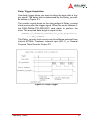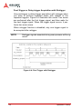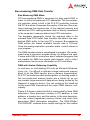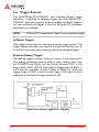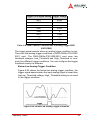
1
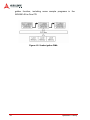
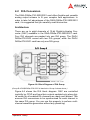
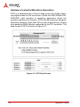
NuDAQ-2500 Series
High Performance Analog Output and
Multi-function Data Acquisition Cards
User’s Manual
Manual Rev.
2.01
Revision Date:
March 19, 2006
Part No:
50-11221-2000
Advance Technologies; Automate the World.
Copyright 2007 ADLINK TECHNOLOGY INC.
All Rights Reserved.
The information in this document is subject to change without prior
notice in order to improve reliability, design, and function and does
not represent a commitment on the part of the manufacturer.
In no event will the manufacturer be liable for direct, indirect, special, incidental, or consequential damages arising out of the use or
inability to use the product or documentation, even if advised of
the possibility of such damages.
This document contains proprietary information protected by copyright. All rights are reserved. No part of this manual may be reproduced by any mechanical, electronic, or other means in any form
without prior written permission of the manufacturer.
Trademarks
Product names mentioned herein are used for identification purposes only and may be trademarks and/or registered trademarks
of their respective companies.
Getting service
Customer satisfaction is our top priority. Contact us should you
require any service or assistance.
ADLINK TECHNOLOGY INC.
Web Site
Sales & Service
Telephone No.
Fax No.
Mailing Address
http://www.adlinktech.com
[email protected]
+886-2-8226-5877
+886-2-8226-5717
9F No. 166 Jian Yi Road, Chungho City,
Taipei Hsien 235, Taiwan, ROC
ADLINK TECHNOLOGY AMERICA, INC.
Sales & Service
Toll-Free
Fax No.
Mailing Address
[email protected]
+1-866-4-ADLINK (235465)
+1-949-727-2099
8900 Research Drive, Irvine,
CA 92618, USA
ADLINK TECHNOLOGY EUROPEAN SALES OFFICE
Sales & Service
Toll-Free
Fax No.
Mailing Address
[email protected]
+49-211-4955552
+49-211-4955557
Nord Carree 3, 40477 Düsseldorf, Germany
ADLINK TECHNOLOGY SINGAPORE PTE LTD
Sales & Service
Telephone No.
Fax No.
Mailing Address
[email protected]
+65-6844-2261
+65-6844-2263
84 Genting Lane #07-02A,
Cityneon Design Center, Singapore 349584
ADLINK TECHNOLOGY INDIA LIAISON OFFICE
Sales & Service
Telephone No.
Fax No.
Mailing Address
[email protected]
+91-80-57605817
+91-80-26671806
No. 1357, Ground Floor, “Anupama”,
Aurobindo Marg JP Nagar (Ph-1)
Bangalore - 560078
ADLINK TECHNOLOGY BEIJING
Sales & Service
Telephone No.
Fax No.
Mailing Address
[email protected]
+82-2-20570565
+82-2-20570563
4F, Kostech Building, 262-2,
Yangjae-Dong, Seocho-Gu,
Seoul, 137-130, South Korea
ADLINK TECHNOLOGY BEIJING
Sales & Service
Telephone No.
Fax No.
Mailing Address
[email protected]
+86-10-5885-8666
+86-10-5885-8625
Room 801, Building E, Yingchuangdongli
Plaza, No.1 Shangdidonglu,
Haidian District, Beijing, China
ADLINK TECHNOLOGY SHANGHAI
Sales & Service
Telephone No.
Fax No.
Mailing Address
[email protected]
+86-21-6495-5210
+86-21-5450-0414
Floor 4, Bldg. 39, Caoheting Science and
Technology Park, No.333 Qinjiang Road,
Shanghai, China
ADLINK TECHNOLOGY SHENZHEN
Sales & Service
Telephone No.
Fax No.
Mailing Address
[email protected]
+86-755-2643-4858
+86-755-2664-6353
C Block, 2nd Floor, Building A1,
Cyber-tech Zone, Gaoxin Ave. 7.S,
High-tech Industrial Park S.,
Nanshan District, Shenzhen,
Guangdong Province, China
Using this manual
1.1 Audience and scope
This manual guides you when using ADLINK NuDAQ-2500 Series
card. The card’s hardware, signal connections, and calibration
information are provided for faster application building. This manual is intended for computer programmers and hardware engineers with advanced knowledge of data acquisition and high-level
programming.
1.2 How this manual is organized
This manual is organized as follows:
Chapter 1 Introduction: This chapter introduces the NuDAQ2500 Series card including its features, specifications and software support information.
Chapter 2 Installation: This chapter presents the card’s layout, package contents, and installation.
Chapter 3 Signal Connections: This part describes the
NuDAQ-2500 Series card signal connections.
Chapter 4 Operation Theory: The operation theory of the
NuDAQ-2500 Series card functions including A/D conversion,
D/A conversion, and programmable function I/O are discussed
in this chapter.
Chapter 5 Calibration: The chapter offers information on how
to calibrate the NuDAQ-2500 Series card for accurate data
acquisition and output.
Appendix: The Appendix demonstrates several waveform
generation and other related information.
Warranty Policy: This presents the ADLINK Warranty Policy
terms and coverages.
1.3 Conventions
Take note of the following conventions used throughout the manual to make sure that you perform certain tasks and instructions
properly.
NOTE
Additional information, aids, and tips that help you perform particular tasks.
IMPORTANT Critical information and instructions that you MUST perform to
complete a task.
WARNING Information that prevents physical injury, data loss, module damage, program corruption etc. when trying to complete a particular task.
Table of Contents
Table of Contents..................................................................... i
List of Tables.......................................................................... iii
List of Figures ........................................................................ iv
1 Introduction ........................................................................ 1
1.1
1.2
1.3
1.4
1.5
Features............................................................................... 1
Applications ......................................................................... 2
Specifications....................................................................... 3
Analog Output (AO) ........................................................ 3
Analog Input (AI) ............................................................. 4
General Purpose Digital I/O (G. P. DIO) ......................... 5
General Purpose Timer/ Counter (GPTC) ...................... 5
Analog Trigger (A.Trig) ................................................... 5
System Synchronous Interface (SSI) .............................. 6
Calibration ....................................................................... 6
Physical .......................................................................... 6
Operating Environment ................................................... 6
Storage Environment ...................................................... 6
Block Diagram ..................................................................... 7
Software Support ................................................................. 8
Programming Library ...................................................... 8
DAQ-LVIEW PnP: LabVIEW Driver ................................ 9
D2K-OCX: ActiveX Controls ........................................... 9
2 Installation ........................................................................ 11
2.1
2.2
2.3
2.4
Package Contents ............................................................. 11
Unpacking.......................................................................... 12
Card Layout ....................................................................... 13
DAQe-2502/2501 .......................................................... 13
DAQ-2502/2501 ............................................................ 14
DPXI-2501/2502 ........................................................... 15
PCI Configuration .............................................................. 16
Plug and Play ............................................................... 16
Configuration ................................................................ 16
Troubleshooting ............................................................ 16
Table of Contents
i
3 Signal Connections .......................................................... 17
3.1
Connectors Pin Assignment............................................... 17
4 Operation Theory .............................................................. 21
4.1
4.2
4.3
4.4
4.5
4.6
A/D Conversion.................................................................. 21
AD Data Format ............................................................ 22
Acquisition Modes ......................................................... 23
Scan Timing and Procedure ......................................... 24
Trigger Modes ............................................................... 26
Bus-mastering DMA Data Transfer ............................... 29
D/A Conversion.................................................................. 31
Architecture ................................................................... 31
Hardware-Controlled Waveform Generation ................ 32
Data Format in FIFO and Mapping ............................... 33
Setting up the DACs ..................................................... 33
Using DACs’ Multiplying Characteristic ........................ 34
Software Update ........................................................... 34
Waveform Generation ................................................... 35
Waveform Generation Timing ....................................... 36
Trigger Modes ............................................................... 38
Iterative Waveform Generation ..................................... 41
General Purpose Digital I/O .............................................. 45
General Purpose Timer/Counter Operation ....................... 46
Basics Timer/Counter Function Basics ......................... 46
General Purpose Timer/Counter Modes ....................... 47
Trigger Sources ................................................................. 52
Software-Trigger ........................................................... 52
External Analog Trigger ................................................ 52
Timing Signals ................................................................... 56
System Synchronization Interface ................................ 57
5 Calibration ......................................................................... 59
5.1
5.2
5.3
Loading Calibration Constants........................................... 59
Auto-calibration .................................................................. 60
Saving Calibration Constants............................................. 60
Appendix ................................................................................ 61
Warranty Policy ..................................................................... 65
ii
Table of Contents
List of Tables
Table 3-1: VHDCI-type (68-pin) Connector Pin Assignment ...
Table 3-2: VHDCI-type (68-pin) Connector Legend ................
Table 4-1: Bipolar Input Range and
Converted Digital Codes .........................................
Table 4-2: Unipolar Input Range and
Converted Digital Codes .........................................
Table 4-3: Trigger Modes and
Corresponding Trigger Sources .............................
Table 4-4: Summary of Counters for Programmable Scan ......
Table 4-5: D/A Output Versus Digital Codes ...........................
Table 4-6: Trigger Signals and
Corresponding Signal Sources ...............................
Table 4-7: Summary of Counters for Waveform Generation ...
Table 4-8: Ideal Transfer Characteristic of
Analog Trigger SRC1 (EXTATRIG) ........................
List of Tables
18
19
22
22
23
24
34
35
36
53
iii
List of Figures
Figure 1-1: DAQ-/DAQe-/PXI-2502/2501 Block Diagram ............ 7
Figure 2-1: DAQe-2502/2501 Card Layout ................................ 13
Figure 2-2: DAQ-2502/2501 Card Layout .................................. 14
Figure 2-3: DAQ-2502/2501 Card Layout .................................. 15
Figure 4-1: Scan Timing............................................................. 25
Figure 4-2: Post Trigger ............................................................. 26
Figure 4-3: Delay Trigger ........................................................... 27
Figure 4-4: Post Trigger with Retrigger ...................................... 28
Figure 4-5: Scatter/gather DMA ................................................. 30
Figure 4-6: Block Diagram of D/A Group ................................... 31
Figure 4-7: FIFO Data Format.................................................... 32
Figure 4-8: Typical D/A Timing of Waveform Generation .......... 37
Figure 4-9: Post Trigger Generation .......................................... 38
Figure 4-10: Delay-Trigger Generation ........................................ 39
Figure 4-11: Post Trigger or Delay-Trigger Generation with
Retrigger .................................................................. 40
Figure 4-12: Finite Iterative Waveform Generation with
Post-trigger .............................................................. 41
Figure 4-13: Post Trigger or Delay-Trigger Generation with
Retrigger .................................................................. 41
Figure 4-14: Stop Mode I ............................................................. 43
Figure 4-15: Stop Mode II ............................................................ 44
Figure 4-16: Stop Mode III ........................................................... 44
Figure 4-17: Mode1 Operation ..................................................... 47
Figure 4-18: Mode2 Operation ..................................................... 48
Figure 4-19: Mode 3 Operation .................................................... 48
Figure 4-20: Mode4 Operation ..................................................... 49
Figure 4-21: Mode5 Operation ..................................................... 49
Figure 4-22: Mode6 Operation ..................................................... 50
Figure 4-23: Mode7 Operation ..................................................... 50
Figure 4-24: Mode8 Operation ..................................................... 51
Figure 4-25: Analog Trigger Block Diagram................................. 52
Figure 4-26: Below-Low Analog Trigger Condition ...................... 53
Figure 4-27: Above-High Analog Trigger Condition ..................... 54
Figure 4-28: Inside-Region Analog Trigger Condition.................. 54
Figure 4-29: High-Hysteresis Analog Trigger Condition............... 55
Figure 4-30: Low-Hysteresis Analog Trigger Condition ............... 55
Figure 4-31: DAQ Signals Routing............................................... 56
iv
List of Figures
1
Introduction
The NuDAQ-2500 Series features the DAQ-/DAQe-/PXI-2502/
2501 advanced analog output card based on the 32-bit PCI/PCI
Express®/PXI architecture. With high-performance designs and
state-of-the-art technology, these cards are ideal for waveform
generation, industrial process control, and signal analysis applications in medical, process control, etc.
1.1 Features
The NuDAQ-2500 Series cards come with the following features:
X
32-bit PCI/PCI Express/PXI bus, plug and play
X
Up to 1 MS/s analog output rate and up to 400 KS/s analog
input rate
X
Analog output / input channels
Z
DAQ-/DAQe-/PXI-2502: 8 / 4
Z
DAQ-/DAQe-/PXI-2501: 4 / 8
X
Programmable bipolar/unipolar range for analog input channels and individual analog output channels
X
Programmable internal/external reference for individual
analog output channels
X
D/A FIFO size:
Z
DAQ-/DAQe-/PXI-2502: 16K samples
Z
DAQ-/DAQe-/PXI-2501: 8K samples
X
A/D FIFO size: 2K samples
X
Versatile trigger sources including software trigger, external
digital trigger, analog trigger, and System Synchronization
Interface (SSI) trigger
X
A/D data transfer employing software polling and bus-mastering DMA with scatter/gather
X
D/A data transfer employing software update and bus-mastering DMA with scatter/gather
X
A/D trigger modes including post-trigger and delay-trigger
with re-trigger functionality
X
D/A outputs with waveform generation capability
Introduction
1
X
System Synchronization Interface (SSI)
X
A/D and D/A fully auto-calibration
X
Built-in programmable D/A external reference voltage compensator
X
Jumper-less operation and software-configurable
1.2 Applications
2
X
Automotive testing
X
Arbitrary waveform generator
X
Transient signal measurement
X
ATE
X
Laboratory automation
X
Biotech measurement
Introduction
1.3 Specifications
Analog Output (AO)
X
Channels:
Z
DAQ-/DAQe-/PXI-2501: 4-CH
Z
DAQ-/DAQe-/PXI-2502: 8-CH
X
DA converter: AD7945
X
Maximum update rate: 1 MS/s
X
Resolution: 12-bit
X
FIFO buffer size:
Z
DAQ-/DAQe-/PXI-2501: 8K
Z
DAQ-/DAQe-/PXI-2502: 16K
X
Data transfer: Programmed I/O, and bus-mastering DMA
with scatter/gather
X
Voltage reference: Internal 10 V or external up to ±10 V
X
Output range:
Z
Bipolar: ±10 V or ±external reference
Z
Unipolar: 0 V to 10V or 0 V to external reference
X
Settling time for –10 V to +10 V step: 2 µs
X
Slew rate: 20 V/µs
X
Output coupling: DC
X
Protection: Short-circuit to ground
X
Output impedance: 0.1 Ω max.
X
Output current: ±5 mA max.
X
Power-on state: 0V steady-state
X
Power-on glitch: ±600 mV/500 µs
X
Offset error:
X
Z
Before calibration: ±80 mV max
Z
After calibration: ±2 mV max
Gain error:
Z
Before calibration: ±0.8% of output max
Z
After calibration: ±0.02% of output max
Introduction
3
Analog Input (AI)
X
Z
DAQ-/PXI-2502: 4 single-ended
Z
DAQ-/PXI-2501: 8 single-ended
X
AD converter: LTC1416
X
Max sampling rate: 400 KS/s
X
Resolution: 14-bit
X
FIFO buffer size: 2K samples
X
Input range
Z
Bipolar: ±10 V
Z
Unipolar: 0 V to 10 V
X
Over-voltage protection: Continuous, ±35 V maximum
X
Input impedance: 1 GΩ / 6 pF
X
Trigger modes: Pre-trigger, post-trigger, middle-trigger, and
delay trigger
X
Data transfers: Programmed I/O and bus-mastering DMA
with scatter/gather
X
Input coupling: DC
X
Offset error:
X
4
Channels:
Z
Before calibration: ±40 mV max
Z
After calibration: ±1 mV max
Gain error:
Z
Before calibration: ±0.4% of max output
Z
After calibration: ±1 mV of max output
Introduction
General Purpose Digital I/O (G. P. DIO)
X
Channels: 24 programmable input/output
X
Compatibility: TTL/CMOS
X
Input voltage:
X
Z
Logic Low: VIL=0.8 V max; IIL=0.2 mA max
Z
High: VIH=2.0 V max; IIH=0.02 mA max
Output voltage:
Z
Low: VOL=0.5 V max; IOL=8 mA max
Z
High: VOH=2.7 V min; IOH=400 µA
General Purpose Timer/ Counter (GPTC)
X
Channels: Two up/down timer/counters
X
Resolution: 16-bit
X
Compatibility: TTL/CMOS
X
Clock source: Internal or external
X
Maximum source frequency: 10 MHz
Analog Trigger (A.Trig)
X
Source: External analog trigger (EXTATRIG)
X
Level: ±10V external
X
Resolution: 8-bit
X
Slope: Positive or negative (software selectable)
X
Hysteresis: Programmable
X
Bandwidth: 400 KHz
X
External Analog Trigger Input (EXTATRIG)
X
Impedance: 40 KΩ
X
Coupling: DC
X
Protection: Continuous ±35V maximum
Introduction
5
System Synchronous Interface (SSI)
X
Trigger lines: 7
Calibration
X
Recommended warm-up time: 15 minutes
X
Onboard reference: 5.0 V
X
Temperature coefficient: ±2 ppm/°C
X
Long-term stability: 6 ppm/1000 hr
Physical
X
Dimension: 175 mm by 107 mm
X
I/O connector: 68-pin female mini-SCSI type
X
Power Requirement: +5 VDC; 1.6 A typical
Operating Environment
X
Ambient temperature: 0°C to 55°C
X
Relative humidity: 10% to 90% non-condensing
Storage Environment
6
X
Ambient temperature: -20 to 70°C
X
Relative humidity: 5% to 95% non-condensing
Introduction
1.4 Block Diagram
Figure 1-1: DAQ-/DAQe-/PXI-2502/2501 Block Diagram
Introduction
7
1.5 Software Support
ADLINK provides versatile software drivers and packages for
users’ different approach to building up a system. ADLINK not only
provides pro-gramming libraries such as DLL for most Windowsbased systems, but also provide drivers for other software packages such as LabVIEW®.
All software options are included in the ADLINK CD. Non-free software drivers are protected with licensing codes. Without the software code, you can install and run the demo version for two hours
for trial/demonstration purposes. Please contact ADLINK dealers
to purchase the formal license.
Programming Library
For customers who are writing their own programs, we provide
function libraries for many different operating systems, including:
8
X
D2K-DASK: Include device drivers and DLL for Windows®
98/NT/2000/XP. DLL is binary compatible across Windows
98/NT/2000/XP. This means all applications developed with
D2K-DASK are compatible across Windows 98/NT/2000/
XP. The developing environment can be VB, VC++, Delphi,
BC5, or any Windows programming language that allows
calls to a DLL. The user’s guide and function reference
manual of D2K-DASK are in the CD. (\\Manual\Software
Package\D2K-DASK)
X
D2K-DASK/X: Include device drivers and shared library for
Linux. The developing environment can be Gnu C/C++ or
any programming language that allows linking to a shared
library. The user's guide and function reference manual of
D2K-DASK/X are in the CD. (\\Manual\Software Package\D2K-DASK-X.)
Introduction
DAQ-LVIEW PnP: LabVIEW Driver
DAQ-LVIEW PnP contains the VIs, which are used to interface
with NI’s LabVIEW software package. The DAQ-LVIEW PnP supports Windows 98/NT/2000/XP. The LabVIEW drivers is shipped
free with the card. You can install and use them without a license.
For detailed information about DAQ-LVIEW PnP, refer to the
user’s guide in the CD. (\\Manual\Software Package\DAQ-LVIEW
PnP)
D2K-OCX: ActiveX Controls
Customers who are familiar with ActiveX controls and VB/VC++
programming are suggested to use D2K-OCX ActiveX control
component libraries for developing applications. D2K-OCX is
designed for Windows 98/NT/2000/XP. For more details on D2KOCX, refer to the user's guide in the CD. (\\Manual\Software Package\D2K-OCX)
The above software drivers are shipped with the card. Refer to the
Software Installation Guide in the package to install these drivers.
In addition, ADLINK supplies ActiveX control software DAQBench.
DAQBench is a collection of ActiveX controls for measurement or
automation applications. With DAQBench, you can easily develop
custom user interfaces to display your data, analyze data you
acquired or received from other sources, or integrate with popular
applications or other data sources. For more detailed information
about DAQBench, refer to the user's guide in the CD. (\\Manual\Software Package\DAQBench Evaluation)
You can also get a free 4-hour evaluation version of DAQBench
from the CD. DAQBench is not free. Contact ADLINK or your
dealer to purchase the software license.
Introduction
9
10
Introduction
2
Installation
This chapter describes how to install the DAQ-/DAQe-/PXI-2502/
2501 card. The contents of the package and unpacking information that you should be aware of are outlined first.
The DAQ-/DAQe-/PXI-2502/2501 card performs an automatic
configuration of the IRQ and port address. You can use the
PCI_SCAN software utility to read the system configuration.
2.1 Package Contents
In addition to this User's Manual, the package includes the following items:
X
DAQ-/DAQe-/PXI-2502/2501 multi-function data acquisition card
X
ADLINK All-in-one CD
X
Software Installation Guide
If any of these items are missing or damaged, contact the dealer
from whom you purchased the product. Save the shipping materials and carton in case you want to ship or store the product in the
future.
Installation
11
2.2 Unpacking
Your DAQ-/DAQe-/PXI-2502/2501 card contains electro-static
sensitive components that can be easily be damaged by static
electricity.
Therefore, the card should be handled on a grounded anti-static
mat. The operator should be wearing an anti-static wristband,
grounded at the same point as the anti-static mat.
Inspect the card package for obvious damages. Shipping and handling may cause damage to the card. Be sure there are no shipping and handling damages on the modules carton before
continuing.
After opening the card module carton, extract the system module
and place it only on a grounded anti-static surface with component
side up.
Again, inspect the module for damages. Press down on all the
socketed IC's to make sure that they are properly seated. Do this
only with the module place on a firm flat surface.
You are now ready to install your DAQ-/DAQe-/PXI-2502/2501
card.
NOTE
12
DO NOT APPLY POWER TO THE CARD IF IT HAS
BEEN DAMAGED.
Installation
2.3 Card Layout
DAQe-2502/2501
Figure 2-1: DAQe-2502/2501 Card Layout
Installation
13
DAQ-2502/2501
Figure 2-2: DAQ-2502/2501 Card Layout
14
Installation
DPXI-2501/2502
Figure 2-3: DAQ-2502/2501 Card Layout
Installation
15
2.4 PCI Configuration
Plug and Play
With support for plug and play, the card requests an interrupt number via its PCI controller. The system BIOS responds with an interrupt assignment based on the card information and on known
system parameters. These system parameters are determined by
the installed drivers and the hardware load seen by the system.
Configuration
The board configuration is done on a board-by-board basis for all
PCI boards in the system. Because configuration is controlled by
the system and software, there is no jumper setting required for
base address, DMA, and interrupt IRQ.
The configuration is subject to change with every boot of the system as new boards are added or removed.
Troubleshooting
If your system doesn’t boot or if you experience erratic operation
with your PCI board in place, it is likely caused by an interrupt conflict. The BIOS Setup may be incorrectly configured. Consult the
BIOS documentation that comes with your system to solve this
problem.
16
Installation
3
Signal Connections
This chapter describes DAQ-/DAQe-/PXI-2502/2501 card connectors and the signal connection between the DAQ-/DAQe-/PXI2502/2501 card and external devices.
3.1 Connectors Pin Assignment
The DAQ-/DAQe-/PXI-2502/2501 card is equipped with two 68-pin
VHDCI-type connectors (AMP-787254-1). These are used for digital input/output, analog input/output, timer/counter signals, etc.
The pin assignments of the connectors are defined in Table 3-1.
Signal Connections
17
AO_0
AO_1
AO_2
AO_3
AOEXTREF_A/AI_0
AI_1
EXTATRIG/AI_2
AOEXTREF_B/AI_3
AO_4/AI_4
AO_5/AI_5
AO_6/AI_6
AO_7/AI_7
AO_TRIG_OUTA
AO_TRIG_OUTB
GPTC1_SRC
GPTC0_SRC
GPTC0_GATE
GPTC0_OUT
GPTC0_UPDOWN
RESERVED
AFI1
PB7
PB5
PB3
PB1
PC7
PC5
DGND
PC3
PC1
PA7
PA5
PA3
PA1
1
2
3
4
5
6
7
8
9
10
11
12
13
14
15
16
17
18
19
20
21
22
23
24
25
26
27
28
29
30
31
32
33
34
35
36
37
38
39
40
41
42
43
44
45
46
47
48
49
50
51
52
53
54
55
56
57
58
59
60
61
62
63
64
65
66
67
68
AGND
AGND
AGND
AGND
AGND
AGND
AGND
AGND
AGND
AGND
AGND
AGND
EXTWFTRG_A
EXTWFTRG_B
VCC
DGND
GPTC1_GATE
GPTC1_OUT
GPTC1_UPDOWN
DGND
AFI0
PB6
PB4
PB2
PB0
PC6
PC4
DGND
PC2
PC0
PA6
PA4
PA2
PA0
Table 3-1: VHDCI-type (68-pin) Connector Pin Assignment
18
Signal Connections
Legend:
Pin #
Signal Name
Reference Direction
Description
Voltage output of DA channel
<0..3>
1~4
AO_<0..3>
AGND
Output
5
AOEXTREF_A/AI_0
AGND
Input
External reference for AO
channel <0..3> / AI input 2
6
AI_1
AGND
Input
AI input 0
7
EXTATRIG/AI_2
AGND
Input
External analog trigger / AI
input 1
8
AOEXTREF_B/AI_3
AGND
Input
External reference for AO
channel <4..7> / AI input 3
9~12
AO_<4..7>/AI_<4..7>
AGND
Output/Input
Voltage output of DA channel
<4..7> / AI channel <4..7>
(only for DAQ-2501)
13,14
AO_TRIG_OUT_<A,B>
DGND
Output
AO trigger signal for channel
<0..3> <4..7>
15,16
GPTC<0,1>_SRC
DGND
Input
Source of GPTC<0,1>
17,51
GPTC<0,1>_GATE
DGND
Input
Gate of GPTC<0,1>
18,52
GPTC<0,1>_OUT
DGND
Input
Output of GPTC<0,1>
19,53
GPTC<0,1>_UPDOWN
DGND
Input
20
RESERVED
—
—
21,55
AFI<1,0>
DGND
Input
Auxiliary Function Input
Up/Down of GPTC<0,1>
Reserved Pin
,22,56,23,57
,24,58,25,59
PB<7,0>
DGND
PIO*
Programmable DIO of 8255
Port B
26,60,27,61,
29,63,30,64
PC<7,0>
DGND
PIO*
Programmable DIO of 8255
Port C
31,65,32,66,
33,67,34,68
PA<7,0>
DGND
PIO*
Programmable DIO of 8255
Port A
35~46
AGND
—
—
47,48
EXTWFTRIG_<A,B>
DGND
Input
49
VCC
DGND
Power
(Output)
28,50,54,62
DGND
—
—
Analog ground
External waveform trigger for
AO channel <0..3> <4..7>
+5V Power Source
Digital ground
Table 3-2: VHDCI-type (68-pin) Connector Legend
*PIO means Programmable Input/Output
Signal Connections
19
20
Signal Connections
4
Operation Theory
The operation theories of the DAQ-/DAQe-/PXI-2502/2501 card
are described in this chapter. The functions include A/D conversion, D/A conversion, digital I/O, and general purpose counter/
timer. This operation theory will help you understand how to configure and program the DAQ-/DAQe-/PXI-2502/2501 card.
4.1 A/D Conversion
When using an A/D converter, you must know about the properties
of the signal to be measured. You may decide which channel to
use and how to connect the signals to the card. Refer to section
3.4. In addition, users should define and control the A/D signal
configurations, including channels, gains, and polarities (unipolar/
bipolar).
The A/D acquisition is initiated by a trigger source and you must
decide how to trigger the A/D conversion. The data acquisition will
start once a trigger condition is matched.
After the end of an A/D conversion, the A/D data is buffered in a
Data FIFO. The A/D data can now be transferred into the system
memory for further processing.
Software polling and programmable scan acquisition modes are
described in this chapter, as well as timing, trigger modes, trigger
sources, and transfer methods.
Operation Theory
21
AD Data Format
The data format of the acquired 14-bit A/D data is coded in 2’s
complement. Table 4-1 and Table 4-2 lists the valid input ranges
and the ideal transfer characteristics.
Magnitude
FSR
LSB
FSR-1LSB
Bipolar Input Range
±10V
±5V
±2.5V
±1.25V
1120.78uV
610.39uV
305.19uV
152.60uV
9.998779V 4.999389V 2.499694V 1.249847V
Midscale + LSB 1120.78uV
Midscale
0V
-10V
1FFF
610.39uV
305.19uV
152.60uV
0001
0V
0V
0V
0000
-305.19uV
-152.60uV
3FFF
-2.5V
-1.25V
2000
Midscale - LSB -1120.78uV -610.39uV
-FSR
Digital code
-5V
Table 4-1: Bipolar Input Range and Converted Digital Codes
Magnitude
FSR
LSB
FSR
Unipolar Input Range
Digital code
0V ~ 10V
0 ~ +5V
0 ~ +2.5V
0 ~ +1.25V
610.39uV
305.19uV
152.60uV
76.3uV
- LSB 4.999389V 2.499694V 1.249847V 1.249923V
1FFF
Midscale + LSB 5.000611V 2.500306V 1.250153V 0.625076V
0001
Midscale
5V
2.5V
1.25V
0.625V
Midscale - LSB 4.999389V 2.499694V 1.249847V 1.249923V
-FSR
0V
0V
0V
0V
0000
3FFF
2000
Table 4-2: Unipolar Input Range and Converted Digital Codes
22
Operation Theory
Acquisition Modes
Software Polling
This is the easiest way to acquire a single A/D data. The A/D
converter starts one conversion whenever the dedicated software command is executed. Then the software would poll the
conversion status and read the A/D data back when it is available.
This method is very suitable for applications that needs to process A/D data in real time. Under this mode, the timing of the
A/D conversion is fully controlled by the software. However, it is
difficult to control the A/D conversion rate.
Programmable Scan
This method is suitable for applications that need to acquire A/
D data at a precise and fixed rate. A scan is a group of multiple
channel samples and the scan interval is defined by the
SI_counter. Likewise, the sample interval of the multiple channels is defined by the SI2_counter. Refer to Table 4-4 for more
information.
The DAQ-/DAQe-/PXI-2502/2501 card can sample multiple
channels in continuous/discontinuous ascending sequence.
For example, you may program the DAQ-/DAQe-/PXI-2502/
2501 card to perform a scan in the channel sequence of 1-2-41-2-4. Three trigger modes are available in programmable
scan: post-trigger, delay-trigger, and post/delay-trigger with
retrigger. Refer to Table 4-3 for a brief summary on trigger
modes and their trigger sources.
Trigger Mode
Description
Post-Trigger
Perform a scan right after the trigger
occurs.
Delay-Trigger
Scan delayed by the amount of time
programmed after the trigger.
Post/Delay-Trigger
with Retrigger
Perform repeated scan while trigger
occurs and it could be under PostTrigger or De-lay-Trigger mode.
Trigger Sources
Software Trigger
Digital Trigger
Analog Trigger
SSI AD Trigger
Table 4-3: Trigger Modes and Corresponding Trigger Sources
Operation Theory
23
Scan Timing and Procedure
There are four counters that need to be specified prior to programmable scans. Refer to Table 4-4 for details.
Counter Name Width
Description
Notes
SI_counter
Scan Interval defines the
24-bit interval between each
scan.
Scan Interval =
SI_counter / Time-base*
SI2_counter
Sampling Interval defines
24-bit the interval between each
sampled channel.
Sampling Interval =
SI2_counter / Timebase*
PSC_counter
Post Scan Counts defines
how many scans to be
24-bit
performed with respect to
each trigger.
Delay_counter
16-bit
Define the delay time for
scan after trigger.
Delay Time =
(Delay_counter / Timebase*), Timebase*=40M
for DAQ/DAQe/PXI-2502/
2501
Table 4-4: Summary of Counters for Programmable Scan
24
Operation Theory
The relationship between counters and acquisition timing is illustrated in Figure 4-1.
Figure 4-1: Scan Timing
NOTE
The maximum A/D sampling rate is 400 KHz for DAQ-/
DAQe-/PXI-2502/2501 card. The minimum setting of
SI2_counter is 100.
The Scan Interval may not be smaller than the interval of
data Sampling Interval multiplied by the Number of channels per Scan. For example: SI_counter >= SI2_counter
* NumChan_Counter.
Operation Theory
25
Trigger Modes
Post-Trigger Acquisition
Use post-trigger acquisition when you want to perform scans right
after a trigger signal. The number of scans to be performed after
the trigger signal is specified by the PSC_counter, as illustrated in
Figure 4-2. The total acquired data length is equal to:
(number_of_channels_enabled_for_scan_acquisition
) * PSC_counter
Figure 4-2: Post Trigger
26
Operation Theory
Delay Trigger Acquisition
Use delay trigger when you want to delay the scan after a trigger signal. The delay time is determined by the Delay_counter,
as shown in Figure 4-3.
The counter counts down on the rising edges of Delay_counter
clock source after the trigger signal. When the count reaches 0,
the DAQ-/DAQe-/PXI-2502/2501 card starts to perform the
scan. The acquired data length is equal to the:
(number_of_channels_enabled_for_scan_acquisition
) * PSC_counter
The Delay_counter clock source can be software selected from
internal 40 MHz Timebase, external input (AFI-1), or General
Purpose Timer/Counter Output 0/1.
Figure 4-3: Delay Trigger
Operation Theory
27
Post-Trigger or Delay-trigger Acquisition with Retrigger
Use post-trigger or delay-trigger acquisition with retrigger when
you want to perform repeated scans with respect to the
repeated triggers. Figure 4-4 illustrates this mode. Two scans
are performed after the first trigger signal, and then waits for
the next trigger signal. When the trigger signal occurs, it performs two more scans.
When retrigger function is disabled, only one trigger signal is
be accepted after retrigger.
NOTE
Retrigger signals asserted during scan process will be ignored.
Figure 4-4: Post Trigger with Retrigger
28
Operation Theory
Bus-mastering DMA Data Transfer
Bus Mastering DMA Mode
PCI bus-mastering DMA is necessary for high speed DAQ in
order to utilize the maximum PCI bandwidth. The bus-mastering controller, which is built in the PLX PCI controller, controls
the PCI bus when it becomes the master of the bus. Bus mastering reduces the required size of the onboard memory and
reduces the CPU loading because data is directly transferred
to the computer’s memory without host CPU intervention.
The hardware temporarily stores the acquired data in the
onboard Data FIFO buffer, then transfers the data to the userdefined DMA buffer in the host PC’s memory. Bus-mastering
DMA utilizes the fastest available transfer rate of PCI-bus.
Once the analog acquisition operation starts, control returns to
your program.
The DMA transfer mode is complicated to program. We recommend using a high-level program library to configure this card.
If users would like to know more about software programs that
can handle the DMA bus master data transfer, visit to http://
www.plxtech.com for more information on PCI controllers.
DMA with Scatter Gathering Capability
In multi-user or multi-tasking OS such as Microsoft Windows,
Linux, etc., it is difficult to allocate a large continuous memory
block to do the DMA transfer due to memory fragmentation.
PLX PCI controller provides scatter/gather or chaining mode to
link non-continuous memory blocks into a linked list, so you
can transfer large amounts of data without being limited by the
fragment of memory blocks. You can configure the linked list
for the input DMA channel and the output DMA channel, individually.
Figure 4-5 shows a linked list that is constructed by three DMA
descriptors. Each descriptor contains a PCI address, a local
address, a transfer size, and the pointer to the next descriptor.
You can collect fragmented memory blocks and chain their
associative DMA descriptors altogether. The DAQ-/DAQe-/
PXI-2502/2501 software driver simple settings for the scatter/
Operation Theory
29
gather function, including some sample programs in the
ADLINK All-in-One CD.
Figure 4-5: Scatter/gather DMA
30
Operation Theory
4.2 D/A Conversion
The DAQ-/DAQe-/PXI-2502/2501 card offers flexible and versatile
analog output scheme to fit your complex field applications. In
order to take full advantages of the DAQ-/DAQe-/PXI-2502/2501
card, it is suggested that you carefully read this section.
Architecture
There are up to eight channels of 12-bit Digital-to-Analog Converter (DAC) available in the DAQ-/DAQe-/PXI-2502/2501 card.
Four D/A channels are packed into one D/A group. The DAQ-/
DAQe-/PXI-2502 comes with two D/A groups, while the DAQ-/
DAQe-/PXI-2501 card has only one D/A group.
Figure 4-6: Block Diagram of D/A Group
(Group B of DAQ/DAQe-/PXI-2502 is identical to Group A shown above.)
Figure 4-6 shows the D/A block diagram. DAC are controlled
implicitly by CPLD and have their outputs updated only when digital codes for all enabled DA channels are ready and latched. This
ensures D/A conversions to be synchronized for each channel in
the same D/A group. You can use this property to perform multichannel waveform generation without any phase-lag.
Operation Theory
31
Hardware-Controlled Waveform Generation
FIFO is a hardware first-in first-out data queue that holds temporary digital codes for D/A conversion. When the DAQ-/DAQe-/PXI2502/2501 card operates in waveform generation mode, the
waveform patterns are stored in FIFO with 8K maximum samples.
Waveform patterns larger than 8K are also supported by utilizing
bus-mastering DMA transfer supported by the PCI controller. The
data format in FIFO is shown in Figure 4-7.
Figure 4-7: FIFO Data Format
32
Operation Theory
Data Format in FIFO and Mapping
With hardware-based waveform generation, D/A conversions are
updated automatically by CPLD rather than application software.
Unlike the conventional software-based waveform generation, the
precise hardware timing control guarantees non-distorted waveform generation even when host CPU is under heavy loading.
Detailed function setup are discussed later on this chapter.
NOTE
When using waveform generation mode, all the four
DACs in the same D/A group must be configured for the
same mode. However, any one of the DAC can be disabled. If you need to use the software update mode, you
can use another D/A group on the DAQ-/DAQe-/PXI2502 card.
Setting up the DACs
Before using the DACs, you must setup the reference source and
its polarity. Each DAC has its own reference and polarity settings.
For example, the internal voltage reference of D/A Group A is tied
to internal +10V. However, you can still connect external reference
through AOEXTREF (pin 5 on CN2) to a +3.3V voltage source,
giving each DAC in D/A Group A two reference options: 10V or
3.3V. However, DA update timing, trigger source, and trigger/stop
mode are all the same throughout a D/A Group.
The DAQ-/DAQe-/PXI-2502/2501 card provides the capability to
fine tune the voltage reference from the external source. The
external reference is fed thru an onboard calibrated circuit, with
programmable offset. You can use this capability to generate precise D/A outputs.
CAUTION
The range of external voltage reference should be within
±10V.
Operation Theory
33
Using DACs’ Multiplying Characteristic
The D/A reference selection let you fully utilize the multiplying
characteristics of the DACs. Digital codes sent to the D/A converters are multiplied by the reference to generate output.
Bipolar
Magnitude
Unipolar
Output
Output
Digital Code
FSR – LSB
+Vref * (2046 / 2048)
Vref * (4095 / 4096)
0FFF
Midscale + LSB
+Vref * (1 / 2048)
Vref * (2049 4096)
0801
Midscale
0
Vref * (2048 / 4096)
0800
Midscale – LSB
-Vref * ( 1 / 2048)
Vref * (2047 / 4096)
07FF
-FSR + LSB
-Vref * (2046 / 2048)
Vref * (
0001
-FSR
-Vref
1 / 4096)
0
0000
Table 4-5: D/A Output Versus Digital Codes
The DAQ-/DAQe-/PXI-2502/2501 card can generate standard and
arbitrary functions, continuously or piece-wisely. The Appendix
illustrates all possible waveform patterns generated by the DAQ-/
DAQe-/PXI-2502/2501 card in combination with various counters,
clock sources, and voltage references.
Software Update
This method is suitable for applications that need to generate D/A
output controlled by user programs. In this mode, the D/A converter generates one output once the software command is
issued. However, it is difficult to determine the software update
rate under a multi-task OS like Windows.
34
Operation Theory
Waveform Generation
This method is suitable for applications that need to generate
waveforms at a precise and fixed rate. Various programmable
counters will facilitate users to generate complex waveforms with
great flexibility.
Three event signals are involved in waveform generation: Start,
DAWR (DA WRite), and Stop. Refer to Table 4-6 for a brief summary of waveform generation events and their corresponding trigger sources.
Event
Signal
Descriptions
Trigger Sources
Start
Start Waveform Generation process.
Software Trigger
Ext. Digital Trigger
Analog Trigger
SSI Trigger
DAWR
Write data to the DAC on the falling
edges of DAWR.
Internal Update
External Update
SSI Update
Stop
Stop Waveform Generation
Software Trigger
Ext. Digital Trigger
Analog Trigger
Table 4-6: Trigger Signals and Corresponding Signal Sources
Operation Theory
35
Waveform Generation Timing
Six counters interact with the waveform to generate different
DAWR timing, thus forming different waveforms. These are
described in Table 4-7.
Counter Name Width
Description
Note
UI_counter
Update Interval, which
defines the update inter24-bit
val between each data
output.
UC_counter
Update Counts, which
24-bit defines the number of
data in a waveform.
IC_counter
Iteration Counts, which
defines how many times
16-bit
the waveform is generated.
DLY1_counter
Define the delay time for
16-bit waveform generation
after the trigger signal.
DLY2_counter
Define the delay time to
separate consecutive
waveform generation.
Delay Time =(DLY2_counter
16-bit
Effective only in Iterative
/ Clock Timebase)
Waveform Generation
mode.
Trig_counter
Define the acceptable
start trigger count when
16-bit
re-trigger function is
enabled
Update Interval =
UI_counter / Time-base*.
When value in UC_counter
is smaller than the size of
waveform patterns, the
waveform is generated
piece-wisely.
Delay Time =
(DLY1_counter / Clock
Timebase)
Timebase*=40M for DAQ/
PXI-2500 Series
Table 4-7: Summary of Counters for Waveform Generation
NOTE
36
The maximum D/A update rate is 1 MHz. The minimum
UI_counter setting is 40.
Operation Theory
Figure 4-8: Typical D/A Timing of Waveform Generation
(Assuming the data in the data buffer are 2V, 4V, -4V, 0V)
Operation Theory
37
Trigger Modes
Post-Trigger Generation
Use post-trigger generation when you want to generate waveform right after a trigger signal. The number of patterns to be
updated after the trigger signal is specified by UC_counter*
IC_counter, as illustrated in Figure 4-9.
Figure 4-9: Post Trigger Generation
38
Operation Theory
Delay-Trigger Generation
Use delay-trigger when you want to delay the waveform generation after the trigger signal. The delay time is determined by
DLY1_counter as shown in Figure 4-10.
The counter counts down on the rising edges of DLY1_counter
clock source after the start trigger signal. When the count
reaches zero, the DAQ-/DAQe-/PXI-2502/2501 card starts to
generate the waveform. The DLY1_counter clock source can
be software selected from the internal 40 MHz timebase, external clock input (AFI-0), or GPTC output 0/1.
Figure 4-10: Delay-Trigger Generation
Operation Theory
39
Post-Trigger or Delay-Trigger with Retrigger
Use post-trigger or delay-trigger with retrigger when you want
to generate multiple waveforms with respect to multiple incoming trigger signals. You can set Trig_counter to specify the
number of acceptable trigger signals.
Figure 4-11 illustrates this example with an Iterative Waveform
Generation. Refer to next section for details. Two waveforms
are generated after the first trigger signal. The board then waits
for another trigger signal. When the next trigger signal is
asserted, the board generates two more waveforms. After
three trigger signals, as specified in Trig_Counter, no more triggers signals are accepted unless software trigger reset command is executed.
NOTE
Start Trigger signals asserted during the waveform generation process are ignored.
Figure 4-11: Post Trigger or Delay-Trigger Generation with Retrigger
40
Operation Theory
Iterative Waveform Generation
You can set the IC_counter to generate iterative waveforms, no
matter which trigger mode is used. The IC_counter stores the iteration number. Examples shown in Figure 4-12 and Figure 4-13
assumes that the digital codes in the FIFO are 2V, 4V, 2V, and 0V.
Figure 4-12: Finite Iterative Waveform Generation with Post-trigger
Figure 4-13: Post Trigger or Delay-Trigger Generation with Retrigger
Operation Theory
41
When IC_counter is disabled, the waveform generation does not
stop until a stop trigger is asserted. For Stop Mode, refer to the
next section.
An onboard data FIFO is used to buffer the waveform patterns for
waveform generation. If the size of a single waveform is smaller
than that of the FIFO, after initially loading the data from the host
memory, the data in FIFO is re-used when a single waveform generation is completed. It does not occupy the PCI bandwidth afterwards. However, if the size of a single waveform is larger than that
of the FIFO, it needs to be intermittently loaded from the host
memory via DMA, thus occupying the PCI bandwidth.
If the value specified in UC_counter is smaller than the sample
size of the waveform patterns, the waveform is generated piecewisely. For example, if you defined a 16-sample sine wave and set
the UC_counter to two, the generated waveform will be a 1/8-cycle
sine wave for every waveform period. A complete sine wave will
be generated for every 8-iterations. If value specified in the
UC_counter is larger than the sample size of waveform LUT, i.e.
32, the generated waveform will be a 2-cycle sine wave for every
waveform period.
In conjunction with different trigger modes and counter setups, you
can manipulate a single waveform to generate different, more
complex waveforms. For more information, refer to the Appendix.
DLY2_Counter in iterative Waveform Generation
To expand the flexibility of Iterative Waveform Generation,
DLY2_counter was implemented to separate consecutive
waveform generations.
The DLY2_counter starts counting down immediately after a
single waveform generation is completed. When it reaches
zero, the next iteration of waveform generation starts. If you are
generating waveform piece-wisely, the next piece of waveform is generated. The DLY2_counter clock source can be
software selected from internal 40 MHz timebase, external
clock input (AFI-0), or GPTC output 0/1.
42
Operation Theory
Stop Modes
You may stop waveform generation while it is still in progress,
either by hardware or software trigger. The stop trigger sources
can be software selected from internal software trigger, external digital trigger (AFI-0/1), or analog trigger. Three stop modes
are provided to stop finite or infinite waveform generation.
Stop Mode I
After a mode I stop trigger is asserted, the waveform generation stops immediately. Figure 4-14 illustrates this example.
Figure 4-14: Stop Mode I
Stop Mode II
After a mode II stop trigger is asserted, the waveform generation continues to generate a complete waveform, then stops
the operation.Figure 4-15 is an example of Stop Mode II. Since
UC_counter is set to four, the total generated data points must
be a multiple of four.
You can check WFG_in_progress (waveform generation in
progress) status by software read-back to confirm the stop of a
waveform generation.
Operation Theory
43
Figure 4-15: Stop Mode II
Stop Mode III
After a mode III stop trigger is asserted, the waveform generation continues until the iterative number of waveforms specified
in IC_Counter is completed. Figure 4-16 is shown as an example. Since IC_Counter is set to three, the total generated waveforms must be a multiple of three.
You can check WFG_in_progress (waveform generation in
progress) status by software read-back to confirm the stop of a
waveform generation.
Figure 4-16: Stop Mode III
44
Operation Theory
4.3
General Purpose Digital I/O
The DAQ-/DAQe-/PXI-2502/2501 card provides a 24-line generalpurpose digital I/O (GPIO) via the 82C55A chip.
The 24-line GPIO are separated into three ports: Port A, Port B
and Port C. High nibble (bit[7…4]), and low nibble (bit[3…0]) of
each port can be individually programmed to be either inputs or
outputs. Upon system startup or reset, all GPIO pins are reset to
high impedance inputs.
For more information on 82C55A programmable I/O chip, visit
http://www.intel.com.
Operation Theory
45
4.4 General Purpose Timer/Counter Operation
Two independent 16-bit up/down timer/counter are embedded in
FPGA firmware for user applications. They have the following features:
X
Counting direction can be controlled via hardware or software
X
Selectable counter clock source from either internal or
external clock up to 10 MHz
X
Programmable gate selection
X
Programmable input and output signal polarities, either
active-high or active-low
X
Initial Count can be loaded via software
X
Current count value can be read-back by software without
affecting circuit operation
Basics Timer/Counter Function Basics
Each timer/counter has three inputs that can be controlled via
hardware or software. These are clock input (GPTC_CLK), gate
input
(GPTC_GATE),
and
up/down
control
input
(GPTC_UPDOWN).
The GPTC_CLK input acts as a clock source to the timer/counter.
Active edges on the GPTC_CLK input increment or decrement the
counter. The GPTC_UPDOWN input determines whether the
counter is counting up or down. The GPTC_GATE input is a control line that acts as a counter enable or a counter trigger signal in
different modes.
The output of timer/counter is GPTC_OUT. After power-up,
GPTC_OUT is pulled high by a 10K resistor. GPTC_OUT goes
low after the DAQ board is initialized.
All the polarities of input/output signals can be programmed via
software. In this section, all timing figures assume that
GPTC_CLK, GPTC_GATE, and GPTC_OUT are set to be positive-logic, meaning they’re triggered on the rising-edge.
46
Operation Theory
General Purpose Timer/Counter Modes
Eight programmable timer/counter modes are provided. All modes
start operations following the software start command. The GPTC
software reset command initializes the status of the counter and
re-loads the initial value to the counter.
Mode1: Simple Gated-Event Counting
The counter counts the number of pulses on the GPTC_CLK
after the software start. Initial count value can be loaded via
software. Current count value can be read-back by software at
anytime. GPTC_GATE is used to enable/disable counting.
When GPTC_GATE is inactive, the counter halts the current
count value. Figure 4-17 illustrates the operation with initial
count = 5 in down-counting mode.
Figure 4-17: Mode1 Operation
Mode2: Single Period Measurement
The counter counts the period of the signal on GPTC_GATE in
terms of GPTC_CLK. Initial count can be loaded via software.
After the software start, the counter counts the number of
active edges on GPTC_CLK between two active edges of
GPTC_GATE. After the completion of the period measurement, GPTC_OUT outputs high and current count value can be
read-back by software. Figure 4-18 illustrates the operation
where initial count = 0, up-counting mode.
Operation Theory
47
Figure 4-18: Mode2 Operation
Mode3: Single Pulse-width Measurement
The counter counts the pulse-width of the signal on
GPTC_GATE in terms of GPTC_CLK. Initial count can be
loaded via software. After the software start, the counter counts
the number of active edges on GPTC_CLK when GPTC_GATE
is active. GPTC_OUT outputs high, and current count value
can be read-back via software after the completion of the
pulse-width measurement. Figure 4-19 illustrates the operation
where initial count = 0 in up-counting mode.
Figure 4-19: Mode 3 Operation
48
Operation Theory
Mode4: Single Gated Pulse Generation
This mode generates a single pulse with programmable delay
and programmable pulse-width following the software start.
These software programmable parameters could be specified
in terms of periods of the GPTC_CLK. GPTC_GATE is used to
enable/disable counting. When GPTC_GATE is inactive, the
counter halts the counting. Figure 4-20 illustrates the generation of a single pulse with pulse-delay of two and pulse-width of
four.
Figure 4-20: Mode4 Operation
Mode5: Single Triggered Pulse Generation
This function generates a single pulse with programmable
delay and programmable pulse-width following an active
GPTC_GATE edge. These software programmable parameters can be specified in terms of periods of the GPTC_CLK
input. Once the first GPTC_GATE edge triggers the single
pulse, GPTC_GATE takes no effect until the software start is
re-executed. Figure 4-21 illustrates the generation of a single
pulse with pulse delay of two and pulse-width of four.
Figure 4-21: Mode5 Operation
Operation Theory
49
Mode6: Re-triggered Single Pulse Generation
This mode is similar to mode 5 except that the counter generates a pulse following every active edge on GPTC_GATE.
After the software start, every active GPTC_GATE edge triggers a single pulse with programmable delay and pulse-width.
Any GPTC_GATE trigger that occurs during the pulse generation is ignored. Figure 4-22 illustrates the generation of two
pulses with pulse delay of two and pulse-width of four.
Figure 4-22: Mode6 Operation
Mode7: Single Triggered Continuous Pulse Generation
This mode is similar to mode 5, except that the counter generates continuous periodic pulses with programmable pulse interval and pulse-width following the first active edge of
GPTC_GATE. Once the first GPTC_GATE edge triggers the
counter, GPTC_GATE takes no effect until the software start is
re-executed. Figure 4-23 illustrates the generation of two
pulses with pulse delay of four and pulse-width of three.
Figure 4-23: Mode7 Operation
50
Operation Theory
Mode8: Continuous Gated Pulse Generation
This mode generates periodic pulses with programmable pulse
interval and pulse-width following the software start.
GPTC_GATE is used to enable/disable counting. When
GPTC_GATE is inactive, the counter halts the current count
value. Figure 4-24 illustrates the generation of two pulses with
pulse delay of four and pulse-width of three.
Figure 4-24: Mode8 Operation
Operation Theory
51
4.5 Trigger Sources
The DAQ-/DAQe-/PXI-2502/2501 card provides flexible trigger
selections. In addition to software trigger, the DAQ-/DAQe-/PXI2502/2501 card also supports external analog and digital triggers.
You can configure the trigger source for A/D and D/A processes
individually via software.
NOTE
A/D and D/A conversions share the same analog trigger.
Software-Trigger
This trigger mode does not need any external trigger source. The
trigger asserts right after you execute the specified function call. A/
D and D/A processes can receive an individual software trigger.
External Analog Trigger
The analog trigger circuitry routing is shown in the Figure 4-25.
The analog multiplexer selects either a direct analog input from
the EXTATRIG pin (SRC1) on the 68-pin connector CN1 or the
input signal of ADC (SRC2). The range of trigger level for SRC1 is
±10V and the resolution is 78mV (refer to Table 4-8), while the
trigger range of SRC2 is the full-scale range of AD input, and the
resolution is the desired range divided by 256.
Figure 4-25: Analog Trigger Block Diagram
52
Operation Theory
Trigger Level digital setting Trigger voltage
0xFF
9.92V
0xFE
9.84V
---
---
0x81
0.08V
0x80
0
0x7F
-0.08V
---
---
0x01
-9.92V
0x00
-10V
Table 4-8: Ideal Transfer Characteristic of Analog Trigger SRC1
(EXTATRIG)
The trigger signal asserts when an analog trigger condition is met.
There are five analog trigger conditions in DAQ-/DAQe-/PXI-2502/
2501 card. The DAQ-/DAQe-/PXI-2502/2501 card uses two
threshold voltages: Low_Threshold and High_Threshold to compose five different trigger conditions. You can configure the trigger
conditions easily via software.
Below-Low Analog Trigger Condition
Figure 4-26 shows the below-low analog trigger condition, the
trigger signal asserts when the input analog signal is lower than
the Low_Threshold voltage. High_Threshold setting is not used
in this trigger condition.
Figure 4-26: Below-Low Analog Trigger Condition
Operation Theory
53
Above-High Analog Trigger Condition
Figure 4-27 shows the above-high analog trigger condition, the
trigger signal asserts when the input analog signal is higher
than the High_Threshold voltage. The Low_Threshold setting
is not used in this trigger condition.
Figure 4-27: Above-High Analog Trigger Condition
Inside-Region Analog Trigger Ccondition
Figure 4-28 shows the inside-region analog trigger condition,
the trigger signal asserts when the input analog signal level
falls in the range between the High_Threshold and the
Low_Threshold voltages.
Figure 4-28: Inside-Region Analog Trigger Condition
54
Operation Theory
High-Hysteresis Analog Trigger Condition
Figure 4-29 shows the high-hysteresis analog trigger condition.
The trigger signal asserts when the input analog signal level is
higher than the High_Threshold voltage, where the hysteresis
region is determined by the Low_Threshold voltage.
Figure 4-29: High-Hysteresis Analog Trigger Condition
Low-Hysteresis Analog trigger condition
Figure 4-30 shows the low-hysteresis analog trigger condition.
The trigger signal asserts when the input analog signal level is
lower than the Low_Threshold voltage where the hysteresis
region is determined by the High_Threshold voltage.
Figure 4-30: Low-Hysteresis Analog Trigger Condition
Operation Theory
55
4.6 Timing Signals
In order to meet the requirements for user-specific timing or synchronizing multiple boards, the DAQ-/DAQe-/PXI-2502/2501 card
provides a flexible interface for connecting timing signals with
external circuitry or other boards. The DAQ timing of the DAQ-/
DAQe-/PXI-2502/2501 card is composed of a bunch of counters
and trigger signals in the FPGA on board.
There are seven timing signals related to the DAQ timing, which in
turn influence the A/D, D/A process, and GPTC operation. These
signals are fed through the Auxiliary Function Inputs pins (AFI) or
the System Synchronization Interface bus (SSI). We implemented
a multiplexer in the FPGA to select the desired timing signal from
these inputs as shown in the Figure 4-31.
You can use the SSI to achieve synchronization between multiple
boards, or use the AFI to derive timing signals from an external
timing circuit.
Figure 4-31: DAQ Signals Routing
56
Operation Theory
System Synchronization Interface
SSI uses bi-directional I/O to provide flexible connections between
boards. You can choose each of the seven timing signals and
which board to be the SSI master. The SSI master can drive the
timing signals of the slaves. You can thus achieve better synchronization between boards.
Note that during power-up or reset, the DAQ board resets and
uses its internal timing signals.
Operation Theory
57
58
Operation Theory
5
Calibration
This chapter introduces the calibration process to minimize AD
measurement errors and DA output errors.
5.1 Loading Calibration Constants
The DAQ-/DAQe-/PXI-2502/2501 card is factory-calibrated before
shipment. The associated calibration constants of the TrimDACs
firmware to the onboard EEPROM. TrimDACs are devices containing multiple DACs within a single package. TrimDACs do not
have memory capability. That means the calibration constants do
not retain their values after the system power is turned off. Loading calibration constants is the process of loading the values of
TrimDACs firmware stored in the onboard EEPROM. ADLINK provides a software utility that automatically reads the calibration constants automatically, if necessary.
There is a dedicated space for storing calibration constants in the
EEPROM. In addition to the default bank of factory calibration constants, there is one user-utilization bank. This bank allows you to
load the TrimDACs firmware values either from the original factory
calibration or from a subsequently-performed calibration.
Because of the fact that measurements and outputs errors may
vary depending on time and temperature, it is recommended that
you calibrate the card when it is integrated in your computing environment. The auto-calibration function is presented in the following sections.
Calibration
59
5.2 Auto-calibration
Through the DAQ-/DAQe-/PXI-2502/2501 card auto-calibration
feature, the calibration software measures and corrects almost all
calibration errors without any external signal connections, reference voltage, or measurement devices.
The DAQ-/DAQe-/PXI-2502/2501 card comes with an onboard
calibration reference to ensure the accuracy of auto-calibration.
The reference voltage is measured in the production line through a
digital potentiometer and compensated in the software. The calibration constant is memorized after this measurement. We do not
recommended adjustment of the onboard calibration reference
except when an ultra-precision calibrator is available.
NOTES
• Warm the card up for at least 15 minutes before initiating auto-calibration.
•
Remove the cable before auto-calibrating the card since the DA
outputs are changed during the process.
5.3 Saving Calibration Constants
When auto-calibration is completed, you can save the new calibration constants to the user-configurable banks in the EEPROM.
The date and the temperature when you ran auto-calibration is
saved with the calibration constants. You can store three sets of
calibration constants according to three different environments
and re-load the calibration constants later. for users to save calibration constants in an easy manner.
60
Calibration
Appendix
Waveform Generation Demonstration
Combined with six counters, selectable trigger sources, external
reference sources, and time base, the DAQ-/DAQe-/PXI-2502/
2501 provides the capabilities to generate complex waveforms.
Various modes shown below can be mixed together to generate
waveforms that are even more complex.
Although you can always load a new waveform to generate any
desired waveform, we suggest using hardware capabilities to
maximize the card’s efficiency and flexibility.
Standard Function
Waveforms including sine wave, triangular
wave, saw wave, ramp, etc., can be converted
to Waveform LUT. Using larger waveform
means trading maximum output rate for lower
harmonic distortion.
Arbitrary Function
User-defined arbitrary function without size limit
can be generated. You can also concatenate
various standard functions of same length into
one arbitrary function and setup piece-wise
generation, so each standard function can be
generated in sequence, with a user-definable
intermediate space.
Standard Function w. Frequency Variant
You can alter the frequency of generated waveforms by driving DAWR from external signal via
AF0/AF1/SSI. The resultant updating rate
should be kept within 1 MHz.
Appendix
61
Iterative Generation w. Intermediate Space
Utilize DLY2_counter to separate consecutive
waveform generations in iterative generation
mode. In this demo, the original standard sine
wave is repeated several times as specified in
IC_counter, with intermediate space determined by DLY2_counter.
Piece-wise Generation
When the value specified in UC_counter is
smaller than the sample size of waveform, the
waveform is generated piece-wisely. The intermediate space between each piece is determined by DLY2_counter. In this demo, the
UC_counter is set to 1/8 of the sample size of
waveform.
Amplitude Modulated
When external D/A reference is used, applying
sinusoidal voltage reference will result in an
amplitude modulated (AM) waveform generation. You can use one D/A channel to generate
sine wave, loop it back to AOEXTREF_A/B pin,
and generate AM waveform by another D/A
channel using external reference. All can be
done in a single D/A group.
Frequency Modulated
By feeding AFI0/AFI1 with PWM source, pulse
train from VCO, or any time-varying digital signal,
DAQ-/DAQe-/PXI-2502/2501 is capable of
generating frequency modulated (FM) waveform.
Since all four channels are synchronized in a D/A
group, precise quadrature waveform generation is
guarantied, provided the waveform are shifted 90degree for the other channel. Phase difference of
any degree can also be setup. Combined with
external High-speed programmable Digital I/O
card, Phase-Shift-Keying or Phase-ReversalKeying can also be achieved.
62
Appendix
Warranty Policy
Thank you for choosing ADLINK. To understand your rights and
enjoy all the after-sales services we offer, please read the following carefully.
1. Before using ADLINK’s products please read the user manual and follow the instructions exactly. When sending in
damaged products for repair, please attach an RMA application form which can be downloaded from: http://
rma.adlinktech.com/policy/.
2. All ADLINK products come with a limited two-year warranty, one year for products bought in China:
X
The warranty period starts on the day the product is
shipped from ADLINK’s factory.
X
Peripherals and third-party products not manufactured
by ADLINK will be covered by the original manufacturers' warranty.
X
For products containing storage devices (hard drives,
flash cards, etc.), please back up your data before sending them for repair. ADLINK is not responsible for any
loss of data.
X
Please ensure the use of properly licensed software with
our systems. ADLINK does not condone the use of
pirated software and will not service systems using such
software. ADLINK will not be held legally responsible for
products shipped with unlicensed software installed by
the user.
X
For general repairs, please do not include peripheral
accessories. If peripherals need to be included, be certain to specify which items you sent on the RMA Request
& Confirmation Form. ADLINK is not responsible for
items not listed on the RMA Request & Confirmation
Form.
Warranty Policy
63
3. Our repair service is not covered by ADLINK's guarantee
in the following situations:
X
Damage caused by not following instructions in the
User's Manual.
X
Damage caused by carelessness on the user's part during product transportation.
X
Damage caused by fire, earthquakes, floods, lightening,
pollution, other acts of God, and/or incorrect usage of
voltage transformers.
X
Damage caused by unsuitable storage environments
(i.e. high temperatures, high humidity, or volatile chemicals).
X
Damage caused by leakage of battery fluid during or
after change of batteries by customer/user.
X
Damage from improper repair by unauthorized ADLINK
technicians.
X
Products with altered and/or damaged serial numbers
are not entitled to our service.
X
This warranty is not transferable or extendible.
X
Other categories not protected under our warranty.
4. Customers are responsible for shipping costs to transport
damaged products to our company or sales office.
5. To ensure the speed and quality of product repair, please
download an RMA application form from our company website: http://rma.adlinktech.com/policy. Damaged products
with attached RMA forms receive priority.
If you have any further questions, please email our FAE staff:
[email protected].
64
Warranty Policy