1
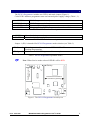
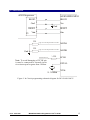
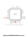
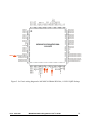
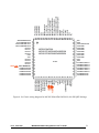
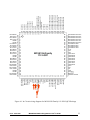
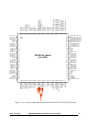
Engineering Technical Laboratory Rev. 6 MC68HC912/9S12 FLASH/EEPROM Programmer User’s Guide © ETL 2004-2006 Microcontroller Development Tool TABLE OF CONTENTS 1. PREFACE ...................................................................................................................................... 3 2. CHECKLIST AND REQUIREMENTS ........................................................................................ 3 3. INSTALLATION AND USE ........................................................................................................ 4 3.1 PROGRAMMER CHECK AND CONNECTION TO PC...................................................... 5 3.2 PROGRAMMER FIRMWARE UPDATE.............................................................................. 5 4. INTERFACE TYPES .................................................................................................................... 6 4.1 IN-CIRCUIT PROGRAMMING ............................................................................................ 6 4.2 ON-BOARD PROGRAMMING ............................................................................................. 6 5. WORKING WITH TARGET MCU.............................................................................................. 7 5.1 MC68 HC912 Devices............................................................................................................. 7 5.1.1 In-Circuit EEPROM/FLASH reading example ................................................................ 7 5.1.2 In-Circuit EEPROM/FLASH programming example....................................................... 7 5.1.3 On-Board EEPROM/FLASH reading example ................................................................ 8 5.1.4 On-Board EEPROM/FLASH programming example ...................................................... 8 5.2 MC 9S12 Devices .................................................................................................................... 9 5.2.1 Features of MC9S12xx128 Devices with 0L85D/1L85D masksets ................................. 9 6. FILE OPERATIONS ................................................................................................................... 11 6.1 LOAD FILE INTO BUFFER ................................................................................................ 11 6.2 SAVE FILE FROM BUFFER ............................................................................................... 11 7. ERRORS AND TROUBLESHOOTING .................................................................................... 12 8. WARRANTY STATEMENT...................................................................................................... 14 9. APPENDIX.................................................................................................................................. 15 Figure 2. In-Circuit programming schematic diagram for HC912/9S12 MCU............................... 15 Figure 3. In-Circuit wiring diagram for MC68HC912B32, 80-PIN QFP Package ......................... 16 Figure 4. In-Circuit wiring diagram for MC68HC912D60/DG128, 112-PIN TQFP Package........ 17 Figure 5. In-Circuit wiring diagram for MC68HC912D60A/DG128A, 112-PIN LQFP Package.. 18 Figure 6. In-Circuit wiring diagram for MC68HC(9)12D60, 80-PIN QFP Package ...................... 19 Figure 7. In-Circuit wiring diagram for MC68HC912D60A, 80-PIN QFP Package ...................... 20 Figure 8. In-Circuit wiring diagram for MC9S12Dx64/Dx128/Dx256, 80-PIN QFP Package ...... 21 Figure 9. In-Circuit wiring diagram for MC9S12Dx64/Dx128/Dx256, 112-PIN LQFP Package.. 22 Figure 10. In-Circuit wiring diagram for MC9S12H-Family 112-PIN LQFP Package .................. 23 Figure 11. In-Circuit wiring diagram for MC9S12H-Family 144-PIN LQFP Package .................. 24 ©ETL 2004-2006 MC68HC912/9S12 Programmer User’s Guide 2 1. PREFACE This manual will guide you through the installation and operation of the ETL MC68HC912/9S12 Programmer, referenced hereafter as the HC912-Programmer. The HC912-Programmer has been designed for Reading, Programming of FLASH, EEPROM contents of the next Motorola Microcontroller Unit (MCU): 9 MC68HC912 DC128A (3K91D) 9 MC68HC912 DC128 (0K50E) 9 MC68HC912 DG128 (5H55W) 9 MC68HC912 DG128A (3K91D) 9 MC68HC912 D60A (2K38K) 9 MC68HC912 D60 (0K75F) 9 MC68HC912 D60 (0K13J) 9 MC68HC912 D60 (4F73K) 9 MC68HC912 B32 (4J54E) 9 MC68HC912 B32 (9H91F) & & & 9 MC9S12 DG128B (0L85D) 9 MC9S12 DT128B (0L85D) 9 MC9S12 A128B (0L85D) 9 MC9S12 DB128B (0L85D) 9 MC9S12 DT128B (1L85D) 9 MC9S12 DG256C (2K79X) 9 MC9S12 DT256C (2K79X) 9 MC9S12 DP256C (2K79X) 9 MC9S12 DP512 (1L00M) 9 MC9S12 D64 (2L86D) 9 MC9S12 DT128B (3L40K) 9 MC9S12 H128 (1K78X) 9 MC9S12 H256 (1K78X) Note: Most number of devices can be programmed in two operating modes InCircuit and On-Board. Note: On-Board programming must be used when device secured or BDM module disabled only. See Section 4.2 for details. Note: Devices that not mentioned above in list can’t be guaranteed of correct reading, programming by HC912-Programmer. 2. CHECKLIST AND REQUIREMENTS The following describes what items are supplied with the HC912-Programmer and the system requirements if used by a PC. 9 HC912-Programmer – supplied 9 Two HC912 QFP112 Adaptors – supplied 9 Two MC9S12 112QFP Adaptors– supplied 9 Cable -A DB9 “straight-thru” cable - supplied 9 HC912-Programmer PC software on CD-ROM – Optional Extra Desktop PC and a free Serial Communication Port (COM1...8) Memory - Minimum 32 Mbytes Display - Color SVGA display recommended Power supply 12 Volt/500 mA linear power supply source OS -MS-Windows (Win98, Win2000/XP/2003) ©ETL 2004-2006 MC68HC912/9S12 Programmer User’s Guide 3 3. INSTALLATION AND USE The HC912-Programmer includes two LED’s and mode jumper (Figure 1). Color LED’s indicates programmer state and external power supply voltage (Table 1, 2). HC912-Programmer is ready. GREEN GREEN Flashing RED DARK HC912-Programmer is busy. Error occurred while operation. Voltage applied to HC912-Programmer lower than 6 Volt. Table 1. LED D1 color meaning Motorola device powered on. Motorola device powered off. Table 2. LED D4 color meaning GREEN DARK Jumper-1 (JP1) is intended for HC912-Programmer mode selection (see Table 3). JP1 Shorted JP1 Opened Normal operation. Motorola device EEPROM/FLASH Reading/Programming. Service mode. HC912-Programmer firmware update. Table 3. HC912-Programmer operation modes & Note: When Service mode selected LED D1 will be RED. 1-Pin Key Serial Port Connector COM 1...8 JP1 12V Power Connector D4 D1 Motorola Device Socket for On-Board Programming P5 BKGD GND RES VDD BDM ICP Figure 1. The HC912-Programmer board layout ©ETL 2004-2006 MC68HC912/9S12 Programmer User’s Guide 4 3.1 PROGRAMMER CHECK AND CONNECTION TO PC Connect the power supply source to HC912-Programmer (an external 12 V DC power supply source is required). Attach a COM port cable to the 9-pin connector on the programmer and to a COM port on the PC. Insert jumper JP1 (see Figure 1). Remove any adaptor from Motorola device socket. Turn On power supply source and make sure that LED D1 appear green. Start HC912-Programmer software. After few seconds you should see on display message: “MC68HC912 Programmer VerX.X detected”. In case when you should see message: “MC68HC912 Programmer Ver-X.X not found”, change COM port number. To do that select “Tools” menu item and than select “Comm Port Options”. Select new COM port number. After pressing “OK” button the new setting will be applied and software reattempts connection with programmer. Now HC912-Programmer ready to operate. & & Note: To speed up connection between HC912-Programmer and PC communication port baud rate must be set to maximum value. Note: Update HC912-Programmer firmware if required (see Section 3.2). 3.2 PROGRAMMER FIRMWARE UPDATE This section describes how to update firmware (ATMEGA and XILINX) of HC912Programmer. Remove JP1 (see Figure 1). Turn On power supply; make sure that LED D1 appears red. Start HC912-Programmer software. Compare firmware version “MC68HC912 Programmer Ver-X.X detected” and version specified in “Help>About” menu item. If versions not coincide, follow next steps to update firmware. Select menu item “Tools>Firmware Update”. After message box “Firmware Update” appeared, press “OK” button. After firmware update completed, turn Off power supply, close HC912-Programmer software. Insert JP1. Turn On power supply. Make sure that LED1 appear green. Start HC912-Programmer software on PC. New firmware version “MC68HC912 Programmer Ver-X.X detected” will appear. ©ETL 2004-2006 MC68HC912/9S12 Programmer User’s Guide 5 4. INTERFACE TYPES This section describes two interfaces, In-Circuit Programming (ICP) and On-Board Programming (OBP) of HC912-Programmer. 4.1 IN-CIRCUIT PROGRAMMING In-Circuit programming interface is basic for HC912-Programmer. With this interface HC912Programmer automatically detects target MCU bus speed. Ceramic resonator connected to target MCU must be in range from 2 MHz to 16 MHz. If target MCU secured (9S12 devices) or BDM module disabled (912 devices) there is no way to establish connection between MCU and HC912Programmer. & & Note: ECLK Pin on target MCU must be connected to circuit via resistor 1Kohm or higher to avoid damaging of this pin. Note: When using In-Circuit programming interface remove adaptor from Motorola device socket (see Figure 1). 4.2 ON-BOARD PROGRAMMING On-board programming interface designed for establishing connection with target device when MCU secured (9S12 devices) or BDM module disabled (912 devices). This interface allows Read/Program EEPROM/FLASH without any restrictions. To work with this interface type MCU must be mounted to the corresponding QFP adaptor supplied with HC912-Programmer. & & ©ETL 2004-2006 Note: When target adaptor with MCU mounted, check contacts careful to avoid short circuit. Otherwise target MCU can be damaged! Note: When On-board programming interface used, remove cable from BDM ICP connector (see Figure 1). MC68HC912/9S12 Programmer User’s Guide 6 5. WORKING WITH TARGET MCU This section contains overall information about Motorola MCUs supported by HC912Programmer. When HC912-Programmer successfully installed (see Section 3) target devices can be read, program and verify. 5.1 MC68 HC912 Devices This section describes basic rules working with next devices: 9 MC68HC912 DC128A (3K91D) 9 MC68HC912 DC128 (0K50E) 9 MC68HC912 DG128 (5H55W) 9 MC68HC912 DG128A (3K91D) 9 MC68HC912 B32 (4J54E) 9 MC68HC912 D60A (2K38K) FLASH/EEPROM memory for these devices can be read, program in both OBP and ICP interfaces. & Note: On-Board programming interface not implemented for MC68HC912B32 device. Extra care must be taken when working with EEPROM Shadow Word/Byte in ICP interface. If BDM Lockout bit (NOBDML) programmed to zero, further access to MCU will be blocked after next reset. The only one way to grant access to locked MCU is mount MCU on corresponding adaptor and use On-Board programming interface. 5.1.1 In-Circuit EEPROM/FLASH reading example Connect required pins to board with target MCU (see Appendix Figure 2). Remove any adaptor from Motorola device socket (see Figure 1). Apply power to HC912-Programmer. LED D1 became to green light (see Table 1). Select corresponding device in HC912-Programmer software (“Device” button). Select “Read Sequence” panel in HC912-Programmer software. Press “EEPROM/FLASH” button. Press “Start” button. LED D4 on HC912-Programmer became to green light. That means that +5 voltage regulator switched on and VCC applied to target MCU. Now HC912-Programmer automatically detects MCU bus speed. When LED D1 on HC912-Programmer became permanent green, reading completed. Target MCU powered off. After read sequence successfully completed it is necessarily to save memory dump to file (see Section 6.2). If some errors appeared during reading process refer to Section 7. 5.1.2 In-Circuit EEPROM/FLASH programming example Connect required pins to board with target MCU (see Appendix Figure 2). Remove any adaptor from Motorola device socket (see Figure 1). Apply power to HC912-Programmer. LED D1 became to green light (see Table 1). Select corresponding device in HC912-Programmer software (“Device” Button). ©ETL 2004-2006 MC68HC912/9S12 Programmer User’s Guide 7 Load EEPROM/FLASH data from file (see Section 6.1) or enter data to Hex Editor. Select “Program Sequence” panel in HC912-Programmer software. Press “EEPROM/FLASH” button. Press “Start” button. LED D4 on HC912-Programmer became to green light. That means that +5 voltage regulator switched on and VCC applied to target MCU. Now HC912-Programmer automatically detects MCU bus speed. When LED D1 on HC912-Programmer became permanent green, programming completed. Target MCU powered off. If some errors appeared during programming process refer to Section 7. & & Note: Extra care must be taken when programming the EEPROM Shadow Word/Byte. Note: Strongly recommended before EEPROM/FLASH programming, for a first time, read EEPROM/FLASH contents and save it to file. 5.1.3 On-Board EEPROM/FLASH reading example Mount target MCU on corresponding QFP adaptor. Insert adaptor to Motorola Device Socket on HC912-Programmer in according to 1 pinkey (see Figure 1). Remove cable from BDM ICP connector (see Figure 1). Apply power to HC912-Programmer. Select device in HC912-Programmer software (“Device” Button). Select “Read Sequence” panel in HC912-Programmer software. Press “EEPROM/FLASH” button. Press “Start” button. LED D4 on HC912-Programmer became to green light. That means that +5 voltage regulator switched on and VCC applied to target MCU. When LED D1 on HC912-Programmer became permanent green light, reading completed. When read sequence successfully completed it is necessarily to save memory dump to file (see Section 6.2). If some errors appeared during reading process refer to Section 7. & & Note: When target MCU mounted on adaptor check contacts careful to avoid short circuit. Otherwise target MCU can be damaged! Note: During removing the adaptor with target MCU HC912-Programmer must be powered off to avoid damaging of programmer and target MCU! 5.1.4 On-Board EEPROM/FLASH programming example Mount target MCU on corresponding QFP adaptor. Insert adaptor to Motorola Device Socket on HC912-Programmer in according to 1 pinkey (see Figure 1). Remove cable from BDM ICP connector (see Figure 1). Apply power to HC912-Programmer. Select device in HC912-Programmer software (“Device” Button). Load EEPROM/FLASH data from file (see Section 6.1) or enter data to Hex Editor. ©ETL 2004-2006 MC68HC912/9S12 Programmer User’s Guide 8 Select “Program Sequence” panel in HC912-Programmer software. Press “EEPROM/FLASH” button. Press “Start” button. LED D4 on HC912-Programmer became to green light. That means that +5 voltage regulator switched on and VCC applied to target MCU. When LED D1 on HC912-Programmer became permanent green light, programming completed. If some errors appeared during programming process refer to Section 7. & & & & Note: When target MCU mounted on adaptor check contacts careful to avoid short circuit. Otherwise target MCU can be damaged! Note: During removing the adaptor with target MCU HC912-Programmer must be powered off to avoid damaging of programmer and target MCU! Note: Extra care must be taken when programming the EEPROM Shadow Word/Byte. Note: Strongly recommended before EEPROM/FLASH programming, for a first time, read EEPROM/FLASH contents and save it to file. 5.2 MC 9S12 Devices This section describes basic rules working with next devices: 9 MC9S12 D64 (2L86D) 9 MC9S12 DG128B (0L85D) 9 MC9S12 DT128B (0L85D) 9 MC9S12 A128B (0L85D) 9 MC9S12 DB128B (0L85D) 9 MC9S12 DT128B (1L85D) 9 MC9S12 DG256C (2K79X) 9 MC9S12 DT256C (2K79X) 9 MC9S12 DP256C (2K79X) 9 MC9S12 DP512 (1L00M) FLASH/EEPROM memory for these devices can be read, program in both OBP and ICP interfaces. & Note: Use On-Board programming interface only if target MCU secured. Extra care must be taken when working with FLASH Option/Security byte in ICP interface. If MCU not erased (all EEPROM and FLASH bytes not equal to $FF) and FLASH Security byte not equal to XXXXXX10B, further access to MCU will be blocked after next reset. To grant access to MCU device must be mounted on corresponding adaptor and On-Board programming interface must be used. In all other respects EEPROM/FLASH programming technique similar to MC68HC912 devices (See sections 5.1.1-5.1.4) 5.2.1 Features of MC9S12xx128 Devices with 0L85D/1L85D masksets This section describes specific behavior of MC9S12xx128 (0L85D/1L85D) devices when InCircuit programming interface is used. In according to Motorola errata relative to this devices there ©ETL 2004-2006 MC68HC912/9S12 Programmer User’s Guide 9 is some problem exists with running of Sector Erase and Program Commands when MCU secured. Only Bulk Erase of FLASH and EEPROM command possible. In many cases this problem can be solved by disabling of security via Backdoor Access Key. HC912-Programmer automatically read this key and passes the security sequence. But if Backdoor Access Key disabled there is no possibilities to disable security. To solve this problem the second method of security disabling must be used. After erasing FLASH and EEPROM, target MCU can be accessed in Special Single Chip mode (HC912-Programmer In-Circuit interface). Follow instructions below: Read full EEPROM and FLASH contents in On-Board programming interface. First of all, when link with MCU completed it is necessarily to read all FLASH and EEPROM contents and save it to File. For more information see sections 5.1.3 OnBoard EEPROM/FLASH reading example. It is obligatory to save EEPROM and FLASH contents to file (see Section 6.2). Erase EEPROM and FLASH. Press Erase FLASH and EEPROM buttons on Program Sequence panel. Also, press Verify EEPROM and FLASH buttons to perform erase check. Press Start button. When LED D1 on HC912-Programmer became permanent green light, erasing completed. Disconnect power from HC912-Programmer. Remove target MCU from programmer and solder it back to board. Prepare target MCU for In-Circuit Programming. Connect required pins to board with target MCU (see Appendix Figure 2). Remove any adaptor from Motorola device socket (see Figure 1). Apply power to HC912-Programmer. LED D1 became to green light (see Table 1). Select corresponding device in HC912-Programmer software (“Device” Button). Load EEPROM/FLASH data from previous saved file. Change value of FLASH Security byte, $7BF0F Address to $FE in Hex Editor. That mean that device will be unsecured after programming. Also, some changes in EEPROM and FLASH areas are possible. If further access to MCU is not required, FLASH Security byte not need to be changed. Press “EEPROM/FLASH” button on Program Sequence Panel. Press “Start” button. LED D4 on HC912-Programmer became to green light. That means that +5 voltage regulator switched on and VCC applied to target MCU. When LED D1 on HC912-Programmer became permanent green, programming completed. Target MCU powered off. If some errors appeared during programming process refer to Section 7. & & & ©ETL 2004-2006 Note: There is no way to restore EEPROM and FLASH contents after erasing. That is strongly recommended read EEPROM and FLASH contents and save it to file before erasing. Note: When target MCU mounted on adaptor check contacts careful to avoid short circuit. Otherwise target MCU can be damaged! Note: During removing the adaptor with target MCU HC912-Programmer must be powered off to avoid damaging of programmer and target MCU! MC68HC912/9S12 Programmer User’s Guide 10 6. FILE OPERATIONS This section describes basic rules working with files. Memory dump from Hex Editor (Buffer) can be load/save from/to hard disk. Also short descriptions such as project name, MCU type and memory cell assignment can be done for future fast remind. HC912-Programmer accepts tree types of file formats: 9 BIN (Binary format) 9 Motorola S-Record (4 byte address) 9 Motorola S-Record (6 byte address) 9 EEF (Extended ETL Format) 6.1 LOAD FILE INTO BUFFER Select “File>Open” menu item. Press “Browse” button. In File Open Dialog window, select file witch need to be open. Press “Open” button. Than opposite “Auto Format Detected:” text, select correct file format. Note that software try automatically detects file format, but unknown records in file will fail this detection. “Load Entire file” check box must be checked if automatically loading procedures required. Than press “OK” button. Sometimes load data from file to specific buffer allocations required. For Example if required load buffer from $0400 address from binary file beginning from $0000 address follow next steps: Select “File>Open” menu item. Press “Browse” button. In File Open Dialog window, select file which need to be open. Press “Open” button. Than, opposite “Auto Format Detected:” select Binary format. Uncheck “Load Entire File” check box. In field “Offset Value to Place Data to Buffer:” enter 0x0400. Than press “OK” button. Now data placed to Hex Editor Buffer from the beginning of 0x0400 address. If more complicated operations with files required, for example load Hex Editor Buffer from many files “Lowest Address From File To Load”, “Highest Address From File To Load” and “Clear Buffer Before Loading File” options are available. 6.2 SAVE FILE FROM BUFFER Select “File>Save” menu item. Press “Browse” button. Select directory in which file will be saved. Type file name, for example “test1” Press “Save” button. Than select format in which file will be saved*. Press “OK” button. & & ©ETL 2004-2006 Note: Use EEF Format for future “Load File Into Buffer” automatically processing. Also, only in EEF Format Project Description, Device Name and Memory Cells attributes can be saved. Note: Use Motorola S-Record (6 byte address) Format to save all FLASH memory contents. MC68HC912/9S12 Programmer User’s Guide 11 7. ERRORS AND TROUBLESHOOTING This section describes most recently encountered problems, errors and fixing solutions. Problem: LED D1 (see Figure 1) Dark. Causes: This problem can accrue when external power supply connected to HC912Programmer is damaged or connected in wrong polarity. Solutions: Check voltage on HC912-Programmer power clamps. It must be 12 V +/- 1V. Problem: LED D1 (see Figure 1) Red. Causes: These problem can appear in two cases: if HC912-Programmer is in the service mode (JP1 removed) and if some error accrue while operation of HC912Programmer. Solutions: Insert jumper JP1 (see Figure 1), remove adaptors from Motorola device socket and cable from ICP connector, turn-off and than turn-on power supply connected to HC912-Programmer. If LED D1 still red contact ETL technical support. Error Message: MC68HC912 Programmer not found Causes: This message can appear when HC912-Programmer software couldn’t establish connection with HC912-Programmer board. Solutions: Check connection of COM port cable from PC to HC912-Programmer board. Apply power from external power supply to HC912-Programmer. In menu item “Tools>Comm Port Options” select correct COM port number. Error Message: Communication Error Causes: This message can appear when Communication between HC912Programmer and PC is broken. Solutions: Try to decrease communication baud rate in “Tools>Comm Port Options” dialog window. Also this message can appear when COM port cable has poor contact with DB-9 connectors. Error Message: RESET Line must be in 'high' state Causes: This message can appear when MCU Reset pin connected to ground through external components or no oscillation on EXTAL, XTAL pins. Solutions: Check MCU reset pin resistance relatively to VSS pin, and if it too low check passive and active components connected. Or check integrity of ceramic resonator and passive components connected to EXTAL, XTAL pins. Error Message: BKGD Line must be in 'high' state Causes: This message can appear when MCU BKGD pin connected to ground through external components. Solutions: Cut any component from pin. Error Message: Pin Tester Errors: Causes: This message can appear in On-Board programming interface when some pins has poor contact with QFP adaptor, or pins are damaged. Solutions: Clean pins from colophony. Check contacts between adaptor and target MCU pins. Check short circuits between pins to pins, pins to GND and pins to VCC. ©ETL 2004-2006 MC68HC912/9S12 Programmer User’s Guide 12 Error Message: BDM Speed Auto Detection failed Causes: This message can appear in In-Circuit programming interface if target MCU not connected correctly to HC912-Programmer or MCU secured. Solutions: Check contacts between HC912-Programmer and MCU pins. If this error not disappeared, place MCU on corresponding QFP adaptor and use OnBoard programming interface. Error Message: BDM Activation Error Causes: This message can appear when wrong Device selected. Solutions: Select correct device type; take attention on MCU maskset. Error Message: No clock on ECLK pin Causes: This message can appear in On-Board programming interface when wrong Device selected. Solutions: Select correct device type; take attention on MCU maskset. Error Message: Parallel Boot Failed Causes: This message can appear in On-Board programming interface when wrong Device selected. Solutions: Select correct device type; take attention on MCU maskset. Error Message: Monitor Loader time-out Error Causes: This message can appear when wrong Device selected. Solutions: Select correct device type; take attention on MCU maskset. Error Message: Monitor Check-sum Error Causes: This message can appear after monitor firmware loaded into target MCU with errors. Solutions: Try to reconnect to target MCU. If this error not disappeared, possible target MCU has damaged RAM. Error Message: Monitor Heap Check-sum Error Causes: This message can appear after monitor firmware transferred data into target MCU RAM with errors. Solutions: Try to reconnect to target MCU. If this error not disappeared, possible target MCU has damaged RAM. Error Message: BDM active status or monitor firmware time-out Error Causes: This message can appear if target MCU “hangs up”. Solutions: Try to reconnect to target MCU. If this error not disappeared, check contacts between HC912-Programmer and MCU pins, power supply voltage on VCC pins. Error Message: Parallel Bus active status or monitor firmware time-out Error Causes: This message can appear if target MCU “hangs up”. Solutions: Try to reconnect to target MCU. If this error not disappeared, check contacts between HC912-Programmer and MCU pins, power supply voltage on VCC pins. ©ETL 2004-2006 MC68HC912/9S12 Programmer User’s Guide 13 Error Message: Device still locked Causes: This message can appear in On-Board programming interface when target MCU secured. Solutions: Check accuracy of device type selected; take attention on MCU maskset. Try to reconnect to target MCU. Error Message: Device can't be unsecured Causes: This message can appear in In-Circuit programming interface when MCU EEPROM/FLASH erased (all data equal to $FF) and accordingly device still secured. Solutions: Check voltage on VCC pins. Try to reconnect to target MCU. Error Message: Voltage on VFP pin is below normal programming voltage level Causes: This message can appear when no or low voltage applied to VFP pin. Solutions: Apply specified by Motorola voltage to VFP pin. Error Message: On-Board Programming Interface not supported for the Device Causes: This message can appear when wrong Device selected. Solutions: Select correct device type; take attention on MCU maskset. Error Message: External power supply must be disconnected from BDM ICP connector Causes: This message can appear in On-Board programming interface when external voltage applied to BDM ICP connector (see Figure 1). Solutions: Disconnect cable from BDM ICP connector. Error Message: Vreg Overcurrent Protection Causes: This message can appear when current consumption from built-in power supply grater than 500 mA. Solutions: Check target MCU power pins on short circuit. Error Message: Vreg Output Voltage out of range CYPRESS IIC BUS Busy CYPRESS IIC Protocol Failed CYPRESS Frequency out of range Wrong Subroutine call Causes: These messages can appear when fatal problems with HC912-Programmer hardware accrued. Solutions: Contact ETL technical support. & Note: HC912-Programmer has Log Window which can be stored to file. To perform this operation right clicks on Log Window. Than click on “Save to hc912prog.log file“ menu item. Now this file can be found in the same directory as HC912-Programmer software. Log File can be send by E-mail to [email protected] for non described problem solution. 8. WARRANTY STATEMENT ETL warrants that Product delivered shall conform to applicable. Report any defects for a 45 days period, from the applicable data on invoice. ©ETL 2004-2006 MC68HC912/9S12 Programmer User’s Guide 14 9. APPENDIX HC912 Programmer HC912/9S12 MCU BKGD BKGD 1 Gnd 2 VSS Gnd RESET 4 P5 RESET VDD 6 1K 1K VDD Logic level on this pin must be “LOW” MODA Logic level on this pin must be “LOW” MODB Gnd External circuit * >1 K Note: To avoid damaging of ECLK pin it must be connected to external circuit via resistor equal or grater than 1 Kohm. ECLK EXTAL XTAL 2...16 MHz Figure 2. In-Circuit programming schematic diagram for HC912/9S12 MCU ©ETL 2004-2006 MC68HC912/9S12 Programmer User’s Guide 15 PS0 / RxD PS2 PS1 / TxD PS3 PS5 / SDO/MOSI PS4 / SDI/MISO PS6 / SCK PS7 / CS /SS PDLC6 VFP PDLC4 PDLC5 PDLC2 PDLC3 PDLC1 / DLCTx PDLC0 / DLCRx VSSX PP7 VDDX PP6 80 79 78 77 76 75 74 73 72 71 70 69 68 67 66 65 64 63 62 61 PP5 PP4 PW3 / PP3 PW2 / PP2 PW1/ PP1 PW0/ PP0 IOC0 / PT0 IOC1 / PT1 IOC2 / PT2 VDD VSS IOC3 / PT3 IOC4 / PT4 IOC5 / PT5 IOC6 / PT6 PAI / IOC7 / PT7 BKGD SMODN / TAGHI/ BKGD ADDR0 / DATA0 / PB0 ADDR1 / DATA1 / PB1 MC68HC912B32 80 QFP 60 59 58 57 56 55 54 53 52 51 50 49 48 47 46 45 44 43 42 41 VSSA VDDA PAD7 / AN7 PAD6 / AN6 PAD5 / AN5 PAD4 / AN4 PAD3 / AN3 PAD2 / AN2 PAD1 / AN1 PAD0 / AN0 VRL VRH VSS VDD PA7 / DATA15 / ADDR15 PA6 / DATA14 / ADDR14 PA5 / DATA13 / ADDR13 PA4 / DATA12 / ADDR12 PA3 / DATA11 / ADDR11 PA2 / DATA10 / ADDR10 ADDR9 / DATA9 / PA1 ADDR8 / DATA8 / PA0 IRQ / PE1 XIRQ / PE0 R/W / PE2 XTAL LSTRB / TAGLO / PE3 VDDX RESET EXTAL ECLK / PE4 VSSX GND VDD RESET MODA / IPIPE0 / PE5 MODB / IPIPE1 / PE6 DBE / PE7 ADDR7 / DATA7 / PB7 ADDR6 / DATA6 / PB6 ADDR5 / DATA5 / PB5 ADDR3 / DATA3 / PB3 ADDR4 / DATA4 / PB4 21 22 23 24 25 26 27 28 29 30 31 32 33 34 35 36 37 38 39 40 ADDR2 / DATA2 / PB2 1 2 3 4 5 6 7 8 9 10 11 12 13 14 15 16 17 18 19 20 Figure 3. In-Circuit wiring diagram for MC68HC912B32, 80-PIN QFP Package ©ETL 2004-2006 MC68HC912/9S12 Programmer User’s Guide 16 PP 3/PW3 PK 0/PIX0 PK 1/PIX1 PK 2/PIX2 PK 7/ECS VDDX VSSX RxCAN0 TxCA N0 RxCAN1 TxCA N1 PIB4 PIB5 PIB6/SDA PIB7/SCL VFP* PS 7/SS PS 6/SCK PS 5/SDO/MOSI PS 4/SDI/MISO PS 3/TxD1 PS 2/RxD1 PS 1/TxD0 PS 0/RxD0 VSSA VRL1 VRH1 VDDA MC68HC912 D60/DG128 112TQFP 84 83 82 81 80 79 78 77 76 75 74 73 72 71 70 69 68 67 66 65 64 63 62 61 60 59 58 57 29 30 31 32 33 34 35 36 37 38 39 40 41 42 43 44 45 46 47 48 49 50 51 52 53 54 55 56 1 2 3 4 5 6 7 8 9 10 11 12 13 14 15 16 17 18 19 20 21 22 23 24 25 26 27 28 PAD17/AN17 PAD07/AN07 PAD16/AN16 PAD06/AN06 PAD15/AN15 PAD05/AN05 PAD14/AN14 PAD04/AN04 PAD13/AN13 PAD03/AN03 PAD12/AN12 PAD02/AN02 PAD11/AN11 PAD01/AN01 PAD10/AN10 PAD00/AN00 VRL0 VRH0 VSS VDD PA7/ADDR15/DATA15/DATA7 PA6/ADDR14/DATA14/DATA6 PA5/ADDR13/DATA13/DATA5 PA4/ADDR12/DATA12/DATA4 PA3/ADDR11/DATA11/DATA3 PA2/ADDR10/DATA10/DATA2 PA1/ADDR9/DATA9/DATA1 PA0/ADDR8/DATA8/DATA0 ADDR5/DATA5/PB5 ADDR6/DATA6/PB6 ADDR7/DATA7/PB7 KWH7/PH7 KWH6/PH6 KWH5/P H5 KWH4/PH4 DBE/CAL/P E7 MODB/IPIPE1/P E6 MODA/IPIPE0/PE5 ECLK /P E4 VSSX GND VS TBY VDDX VDD VDDPLL XFC V SSPLL RESET RESET EX TAL XTAL K WH3/PH3 KWH2/PH2 KWH1/PH1 KWH0/PH0 LSTRB /TAGLO/PE3 R/W /PE2 IRQ/P E1 XIRQ /PE 0 BKGD PW2/PP2 PW1/PP1 PW0/PP0 IOC0/PT0 IOC1/PT1 IOC2/PT2 IOC3/PT3 KWJ7/PJ7 KWJ6/PJ6 KWJ5/PJ5 KWJ4/PJ4 VDD PK3 VSS IOC4/PT4 IOC5/PT5 IOC6/PT6 IOC7/PT7 KWJ3/PJ3 KWJ2/PJ2 KWJ1/PJ1 KWJ0/PJ0 SMODN/TAGHI/BKGD ADDR0/DATA0/PB0 ADDR1/DATA1/PB1 ADDR2/DATA2/PB2 ADDR3/DATA3/PB3 ADDR4/DATA4/PB4 112 111 110 109 108 107 106 105 104 103 102 101 100 99 98 97 96 95 94 93 92 91 90 89 88 87 86 85 External +12V for FLASH Programming Figure 4. In-Circuit wiring diagram for MC68HC912D60/DG128, 112-PIN TQFP Package ©ETL 2004-2006 MC68HC912/9S12 Programmer User’s Guide 17 PP3/PW3 PK0/PIX0 PK1/PIX1 PK2/PIX2 PK7/ECS VDDX VSSX RxCAN0 TxCAN0 RxCAN1 TxCAN1 PIB4 PIB5 PIB6/SDA PIB7/SCL TEST PS7/SS PS6/SCK PS5/SDO/MOSI PS4/SDI/MISO PS3/TxD1 PS2/RxD1 PS1/TxD0 PS0/RxD0 VSSA VRL1 VRH1 VDDA 1 2 3 4 5 6 7 8 9 10 11 12 13 14 15 16 17 18 19 20 21 22 23 24 25 26 27 28 MC68HC912 D60A/DG128A 112 LQFP 84 83 82 81 80 79 78 77 76 75 74 73 72 71 70 69 68 67 66 65 64 63 62 61 60 59 58 57 PAD17/AN17 PAD07/AN07 PAD16/AN16 PAD06/AN06 PAD15/AN15 PAD05/AN05 PAD14/AN14 PAD04/AN04 PAD13/AN13 PAD03/AN03 PAD12/AN12 PAD02/AN02 PAD11/AN11 PAD01/AN01 PAD10/AN10 PAD00/AN00 VRL0 VRH0 VSS VDD PA7/ADDR15/DATA15/DATA7 PA6/ADDR14/DATA14/DATA6 PA5/ADDR13/DATA13/DATA5 PA4/ADDR12/DATA12/DATA4 PA3/ADDR11/DATA11/DATA3 PA2/ADDR10/DATA10/DATA2 PA1/ADDR9/DATA9/DATA1 PA0/ADDR8/DATA8/DATA0 RESET EXTAL XTAL KWH3/PH3 KWH2/PH2 KWH1/PH1 KWH0/PH0 LSTRB /TAGLO /PE3 R/W /PE2 IRQ /PE1 XIRQ /PE0 RESET ADDR5/DATA5/PB5 ADDR6/DATA6/PB6 ADDR7/DATA7/PB7 KWH7/PH7 KWH6/PH6 KWH5/PH5 KWH4/PH4 ECLK /DBE/CAL/PE7 CGMTST/MODB/IPIPE1/PE6 MODA/IPIPE0/PE5 ECLK/PE4 VSSX GND VSTBY V DDX VDD V DDPLL XFC V SSPLL 29 30 31 32 33 34 35 36 37 38 39 40 41 42 43 44 45 46 47 48 49 50 51 52 53 54 55 56 BKGD PK3 V SS IOC4/PT4 IOC5/PT5 IOC6/PT6 IOC7/PT7 KWJ3/PJ3 KWJ2/PJ2 KWJ1/PJ1 KWJ0/PJ0 SMODN/TAGHI/ BKGD ADDR0/DATA0/PB0 ADDR1/DATA1/PB1 ADDR2/DATA2/PB2 ADDR3/DATA3/PB3 ADDR4/DATA4/PB4 112 111 110 109 108 107 106 105 104 103 102 101 100 99 98 97 96 95 94 93 92 91 90 89 88 87 86 85 PW2/PP2 PW1/PP1 PW0/PP0 IOC0/PT0 IOC1/PT1 IOC2/PT2 IOC3/PT3 KWJ7/PJ7 KWJ6/PJ6 KWJ5/PJ5 KWJ4/PJ4 VDD Figure 5. In-Circuit wiring diagram for MC68HC912D60A/DG128A, 112-PIN LQFP Package ©ETL 2004-2006 MC68HC912/9S12 Programmer User’s Guide 18 80 79 78 77 76 75 74 73 72 71 70 69 68 67 66 65 64 63 62 61 PP3/PW3 PP4 PP5 PP6 PP7 VDDX VSSX PCAN0/RxCAN PCAN1/TxCAN VFP* PS7/SS PS6/SCK PS5/SDO/MOSI PS4/SDI/MISO PS3/TxD1 PS2/RxD1 PS1/TxD0 PS0/RxD0 VSSAD VDDAD External +12V for FLASH Programming MC68HC(9)12D60 80 QFP 60 59 58 57 56 55 54 53 52 51 50 49 48 47 46 45 44 43 42 41 PAD07/AN07 PAD06/AN06 PAD05/AN05 PAD04/AN04 PAD03/AN03 PAD02/AN02 PAD01/AN01 PAD00/AN00 VRL0 VRH0 VSS VDD PA7/ADDR15/DATA15/DATA7 PA6/ADDR14/DATA14/DATA6 PA5/ADDR13/DATA13/DATA5 PA4/ADDR12/DATA12/DATA4 PA3/ADDR11/DATA11/DATA3 PA2/ADDR10/DATA10/DATA2 PA1/ADDR9/DATA9/DATA1 PA0/ADDR8/DATA8/DATA0 ECLK /DBE/CAL/PE7 CGMTST/MODB/IPIPE1/PE6 MODA/IPIPE0/PE5 ECLK/PE4 VSSX GND VDDX VDD VDDPLL XFC VSSPL L RESET RESET EXTAL XTAL LSTRB/TAGLO/PE3 R/W/PE2 IRQ/PE1 XIRQ/PE0 ADDR5/DATA5/PB5 ADDR6/DATA6/PB6 ADDR7/DATA7/PB7 KWH4/PH4 BKGD IOC4/PT4 IOC5/PT5 IOC6/PT6 IOC7/PT7 SMODN/TAGHI/BKGD ADDR0/DATA0/PB0 ADDR1/DATA1/PB1 ADDR2/DATA2/PB2 ADDR3/DATA3/PB3 ADDR4/DATA4/PB4 1 2 3 4 5 6 7 8 9 10 11 12 13 14 15 16 17 18 19 20 21 22 23 24 25 26 27 28 29 30 31 32 33 34 35 36 37 38 39 40 PW2/PP2 PW1/PP1 PW0/PP0 IOC0/PT0 IOC1/PT1 IOC2/PT2 IOC3/PT3 KWG4/PG4 VDD VSS Figure 6. In-Circuit wiring diagram for MC68HC(9)12D60, 80-PIN QFP Package ©ETL 2004-2006 MC68HC912/9S12 Programmer User’s Guide 19 PP3/PW3 PP4 PP5 PP6 PP7 VDDX VSSX PCAN0/RxCAN PCAN1/TxCAN TEST PS7/SS PS6/SCK PS5/SDO/MOSI PS4/SDI/MISO PS3/TxD1 PS2/RxD1 PS1/TxD0 PS0/RxD0 VSSAD VDDAD 80 79 78 77 76 75 74 73 72 71 70 69 68 67 66 65 64 63 62 61 MC68HC912D60A 80 QFP 60 59 58 57 56 55 54 53 52 51 50 49 48 47 46 45 44 43 42 41 PAD07/AN07 PAD06/AN06 PAD05/AN05 PAD04/AN04 PAD03/AN03 PAD02/AN02 PAD01/AN01 PAD00/AN00 VRL0 VRH0 VSS VDD PA7/ADDR15/DATA15/DATA7 PA6/ADDR14/DATA14/DATA6 PA5/ADDR13/DATA13/DATA5 PA4/ADDR12/DATA12/DATA4 PA3/ADDR11/DATA11/DATA3 PA2/ADDR10/DATA10/DATA2 PA1/ADDR9/DATA9/DATA1 PA0/ADDR8/DATA8/DATA0 ECLK /DBE/CAL/PE7 CGMTST/MODB/IPIPE1/PE6 MODA/IPIPE0/PE5 ECLK/PE4 VSSX GND VDDX VDD VDDPLL XFC VSSPLL RESET RESET EXTAL XTAL LSTRB /TAGLO/PE3 R/W/PE2 IRQ/PE1 XIRQ/PE0 ADDR5/DATA5/PB5 ADDR6/DATA6/PB6 ADDR7/DATA7/PB7 KWH4/PH4 BKGD IOC4/PT4 IOC5/PT5 IOC6/PT6 IOC7/PT7 SMODN/TAGHI/BKGD ADDR0/DATA0/PB0 ADDR1/DATA1/PB1 ADDR2/DATA2/PB2 ADDR3/DATA3/PB3 ADDR4/DATA4/PB4 1 2 3 4 5 6 7 8 9 10 11 12 13 14 15 16 17 18 19 20 21 22 23 24 25 26 27 28 29 30 31 32 33 34 35 36 37 38 39 40 PW2/PP2 PW1/PP1 PW0/PP0 IOC0/PT0 IOC1/PT1 IOC2/PT2 IOC3/PT3 KWG4/PG4 VDD VSS Figure 7. In-Circuit wiring diagram for MC68HC912D60A, 80-PIN QFP Package ©ETL 2004-2006 MC68HC912/9S12 Programmer User’s Guide 20 PP4/KWP4/PWM4 PP5/KWP5/PWM5 PP7/KWP7/PWM7 VDDX VSSX PM0/RXCAN0/RXB PM1/TXCAN0/TXB PM2/RXCAN1/RXCAN0/MISO0 PM3/TXCAN1/TXCAN0/SS0 PM4/RXCAN0/RXCAN4/MOSI0 PM5/TXCAN0/TXCAN4/SCK0 PJ6/KWJ6/RXCAN4/SDA/RXCAN0 PJ7/KWJ7/TXCAN4/SCL/TXCAN0 VREGEN PS3/TXD1 PS2//RXD1 PS1/TXD0 PS0/RXD0 VSSA VRL 80 79 78 77 76 75 74 73 72 71 70 69 68 67 66 65 64 63 62 61 1 2 3 4 5 6 7 8 9 10 11 12 13 14 15 16 17 18 19 20 MC9S12 D64/DG64 MC9S12 DT128/DG128/DJ128/DB128 MC9S12 DT256/DG256/DJ256/DB256 80 QFP 60 59 58 57 56 55 54 53 52 51 50 49 48 47 46 45 44 43 42 41 VRH VDDA PAD07/AN07/ETRIG0 PAD06/AN06 PAD05/AN05 PAD04/AN04 PAD03/AN03 PAD02/AN02 PAD01/AN01 PAD00/AN00 VSS2 VDD2 PA7/ADDR15/DATA15 PA6/ADDR14/DATA14 PA5/ADDR13/DATA13 PA4/ADDR12/DATA12 PA3/ADDR11/DATA11 PA2/ADDR10/DATA10 PA1/ADDR9/DATA9 PA0/ADDR8/DATA8 ADDR5/DATA5/PB5 ADDR6/DATA6/PB6 ADDR7/DATA7/PB7 XCLKS/NOACC/PE7 MODB/IPIPE1/PE6 MODA/IPIPE0/PE5 ECLK/PE4 VSSR GND VDDR VDD RESET RESET VDDPLL XFC VSSPLL EXTAL XTAL TEST LSTRB/TAGLO/PE3 R/W/PE2 IRQ/PE1 XIRQ/PE0 21 22 23 24 25 26 27 28 29 30 31 32 33 34 35 36 37 38 39 40 SS1/PWM3/KWP3/PP3 SCK1/PWM2/KWP2/PP2 MOSI1/PWM1/KWP1/PP1 MISO1/PWM0/KWP0/PP0 IOC0/PT0 IOC1/PT1 IOC2/PT2 IOC3/PT3 VDD1 VSS1 IOC4/PT4 IOC5/PT5 IOC6/PT6 IOC7/PT7 MODC/TAGHI/BKGD BKGD ADDR0/DATA0/PB0 ADDR1/DATA1/PB1 ADDR2/DATA2/PB2 ADDR3/DATA3/PB3 ADDR4/DATA4/PB4 Figure 8. In-Circuit wiring diagram for MC9S12Dx64/Dx128/Dx256, 80-PIN QFP Package ©ETL 2004-2006 MC68HC912/9S12 Programmer User’s Guide 21 PP4/KWP4/PWM4 PP5/KPW5/PWM5 PP6/KWP6/PWM6 PP7/KWP7/PWM7 PK7/ECS/ROMCTL VDDX VSSX PM0/RXCAN0/RXB PM1/TXCAN0/TXB PM2/RX_BF/RXCAN1/RXCAN0/MISO0 PM3/TX_BF/TXCAN1/TXCAN0/SS0 PM4/BF_PSYN/RXCAN0/RXCAN4/MOSI0 PM5/BF_PROK/TXCAN0/TXCAN4/SCK0 PJ6/KWJ6/RXCAN4/SDA/RXCAN0 PJ7/KWJ7/TXCAN4/SCL/TXCAN0 VREGEN PS7/SS0 PS6/SCK0 PS5/MOSI0 PS4/MISO0 PS3/TXD1 PS2/RXD1 PS1/TXD0 PS0/RXD0 PM6/BF_PERR/RXCAN4 PM7/BF_PSLM/TXCAN4 VSSA VRL 112 111 110 109 108 107 106 105 104 103 102 101 100 99 98 97 96 95 94 93 92 91 90 89 88 87 86 85 MC9S12 D64/DG64 MC9S12 DT128/DG128/DJ128/DB128 MC9S12 DT256/DG256/DJ256/DB256 MC9S12 DP512 112LQFP 84 83 82 81 80 79 78 77 76 75 74 73 72 71 70 69 68 67 66 65 64 63 62 61 60 59 58 57 29 30 31 32 33 34 35 36 37 38 39 40 41 42 43 44 45 46 47 48 49 50 51 52 53 54 55 56 1 2 3 4 5 6 7 8 9 10 11 12 13 14 15 16 17 18 19 20 21 22 23 24 25 26 27 28 VRH VDDA PAD15/AN15/ETRIG1 PAD07/AN07/ETRIG0 PAD14/AN14 PAD06/AN06 PAD13/AN13 PAD05/AN05 PAD12/AN12 PAD04/AN04 PAD11/AN11 PAD03/AN03 PAD10/AN10 PAD02/AN02 PAD09/AN09 PAD01/AN01 PAD08/AN08 PAD00/AN00 VSS2 VDD2 PA7/ADDR15/DATA15 PA6/ADDR14/DATA14 PA5/ADDR13/DATA13 PA4/ADDR12/DATA12 PA3/ADDR11/DATA11 PA2/ADDR10/DATA10 PA1/ADDR9/DATA9 PA0/ADDR8/DATA8 ADDR5/DATA5/PB5 ADDR6/DATA6/PB6 ADDR7/DATA7/PB7 KWH7/PH7 KWH6/PH6 KWH5/PH5 KWH4/PH4 XCLKS/NOACC/PE7 MODB/IPIPE1/PE6 MODA/IPIPE0/PE5 ECLK/PE4 VSSR GND VDD VDDR RESET RESET VDDPLL XFC VSSPLL EXTAL XTAL TEST SS1/KWH3/PH3 SCK1/KWH2/PH2 MOSI1/KWH1/PH1 MISO1/KWH0/PH0 LSTRB/TAGLO/PE3 R/W/PE2 IRQ/PE1 XIRQ/PE0 BKGD SS1/PWM3/KWP3/PP3 SCK1/PWM2/KWP2/PP2 MOSI1/PWM1/KWP1/PP1 MISO1/PWM0/KWP0/PP0 XADDR17/PK3 XADDR16/PK2 XADDR15/PK1 XADDR14/PK0 IOC0/PT0 IOC1/PT1 IOC2/PT2 IOC3/PT3 VDD1 VSS1 IOC4/PT4 IOC5/PT5 IOC6/PT6 IOC7/PT7 XADDR19/PK5 XADDR18/PK4 KWJ1/PJ1 KWJ0/PJ0 MODC/TAGHI/BKGD ADDR0/DATA0/PB0 ADDR1/DATA1/PB1 ADDR2/DATA2/PB2 ADDR3/DATA3/PB3 ADDR4/DATA4/PB4 Figure 9. In-Circuit wiring diagram for MC9S12Dx64/Dx128/Dx256, 112-PIN LQFP Package ©ETL 2004-2006 MC68HC912/9S12 Programmer User’s Guide 22 PT7/IOC7 PT6/IOC6 PT5/IOC5 PT4/IOC4 PT3/IOC3/FP27 PT2/IOC2/FP26 PT1/IOC1/FP25 PT0/IOC0/FP24 VSSX1 VDD X1 PK7/ECS/ROMONE/FP23 PE7/NOACC/XCLKS/FP22 PE3/LSTRB/TAGLO/FP21 PE2/R/W/FP20 PL3/FP19 PL2/FP18 PL1/FP17 PL0/FP16 PA7/ADDR15/D ATA15/FP15 PA6/ADDR14/D ATA14/FP14 PA5/ADDR13/D ATA13/FP13 PA4/ADDR12/D ATA12/FP12 PA3/ADDR11/D ATA11/FP11 PA2/ADDR10/D ATA10/FP10 PA1/ADDR9/D ATA9/FP9 PA0/ADDR8/D ATA8/FP8 PB7/ADDR7/D ATA7/FP7 PB6/ADDR6/D ATA6/FP6 112 111 110 109 108 107 106 105 104 103 102 101 100 99 98 97 96 95 94 93 92 91 90 89 88 87 86 85 1 2 3 4 5 6 7 8 9 10 11 12 13 14 15 16 17 18 19 20 21 22 23 24 25 26 27 28 MC9S12H-Family 112 LQFP 84 83 82 81 80 79 78 77 76 75 74 73 72 71 70 69 68 67 66 65 64 63 62 61 60 59 58 57 PB5/ADDR5/DATA5/FP5 PB4/ADDR4/DATA4/FP4 PB3/ADDR3/DATA3/FP3 PB2/ADDR2/DATA2/FP2 PB1/ADDR1/DATA1/FP1 PB0/ADDR0/DATA0/FP0 PK0/XADDR14/BP0 PK1/XADDR15/BP1 PK2/XADDR16/BP2 PK3/XADDR17/BP3 VLCD VSS1 VDD1 PAD07/AN07 PAD06/AN06 PAD05/AN05 PAD04/AN04 PAD03/AN03 PAD02/AN02 PAD01/AN01 PAD00/AN00 VDDA VRH VRL VSSA PE0/XIRQ PE4/ECLK PE6/IPIPE1/MODB BKGD M5C1M/PW6 M5C1P/PW7 PWM0/PP0 PWM1/PP1 R XD0/PS0 TXD0/PS1 VSS2 VDDR VDD VDDX2 VSSX2 GND MODC/TAGHI/BKGD R ESET RESET VDDPLL XFC VSSPLL EXTAL XTAL TEST RXCAN0/PM2 TXCAN0/PM3 RXCAN1/PM4 TXCAN1/PM5 MODA/IPIP0/PE5 MISO/PS4 MOSI/PS5 SCK/PS6 SS/PS7 IRQ/PE1 29 30 31 32 33 34 35 36 37 38 39 40 41 42 43 44 45 46 47 48 49 50 51 52 53 54 55 56 M0C0M/PU0 M0C0P/PU1 M0C1M/PU2 M0C1P/PU3 VDDM1 VSSM1 M1C0M/PU4 M1C0P/PU5 M1C1M/PU6 M1C1P/PU7 M2C0M/PV0 M2C0P/PV1 M2C1M/PV2 M2C1P/PV3 VDDM2 VSSM2 M3C0M/PV4 M3C0P/PV5 M3C1M/PV6 M3C1P/PV7 M4C0M/PW0 M4C0P/PW1 M4C1M/PW2 M4C1P/PW3 VDDM3 VSSM3 M5C0M/PW4 M5C0P/PW5 Figure 10. In-Circuit wiring diagram for MC9S12H-Family 112-PIN LQFP Package ©ETL 2004-2006 MC68HC912/9S12 Programmer User’s Guide 23 PT7/IOC7 PT6/IOC6 PT5/IOC5 PT4/IOC4 PT3/IOC3/FP27 PT2/IOC2/FP26 PT1/IOC1/FP25 PT0/IOC0/FP24 PJ 3/KWJ 3 PJ 2/KWJ 2 PJ 1/KWJ 1 PJ 0/KWJ 0 VSSX1 VDDX1 PK7/ECS/ROMONE/FP23 PE7/NOACC/XCLKS/FP22 PE3/LSTRB/TAGLO/FP21 PE2/R/W/FP20 PL7/FP31 PL6/FP30 PL5/FP29 PL4/FP28 PL3/FP19 PL2/FP18 PL1/FP17 PL0/FP16 PA7/ADDR15/DATA15/FP15 PA6/ADDR14/DATA14/FP14 PA5/ADDR13/DATA13/FP13 PA4/ADDR12/DATA12/FP12 PA3/ADDR11/DATA11/FP11 PA2/ADDR10/DATA10/FP10 PA1/ADDR9/DATA9/FP9 PA0/ADDR8/DATA8/FP8 PB7/ADDR7/DATA7/FP7 PB6/ADDR6/DATA6/FP6 144 143 142 141 140 139 138 137 136 135 134 133 132 131 130 129 128 127 126 125 124 123 122 121 120 119 118 117 116 115 114 113 112 111 110 109 1 2 3 4 5 6 7 8 9 10 11 12 13 14 15 16 17 18 19 20 21 22 23 24 25 26 27 28 29 30 31 32 33 34 35 36 MC9S12H-Family 144 LQFP 108 107 106 105 104 103 102 101 100 99 98 97 96 95 94 93 92 91 90 89 88 87 86 85 84 83 82 81 80 79 78 77 76 75 74 73 PB5/ADDR5/DATA5/FP5 PB4/ADDR4/DATA4/FP4 PB3/ADDR3/DATA3/FP3 PB2/ADDR2/DATA2/FP2 PB1/ADDR1/DATA1/FP1 PB0/ADDR0/DATA0/FP0 PK0/XADDR14/BP0 PK1/XADDR15/BP1 PK2/XADDR16/BP2 PK3/XADDR17/BP3 VLCD VSS1 VDD1 PAD15/AN15 PAD07/AN07 PAD14/AN14 PAD06/AN06 PAD13/AN13 PAD05/AN05 PAD12/AN12 PAD04/AN04 PAD11/AN11 PAD03/AN03 PAD10/AN10 PAD02/AN02 PAD09/AN09 PAD01/AN01 PAD08/AN08 PAD00/AN00 VDDA VRH VRL VSSA PE0/XIRQ PE4/ECLK PE6/IPIPE1/MODB RESET BKGD VDD GND M5C1M/PW6 M5C1P/PW7 PWM0/PP0 PWM1/PP1 PWM2/PP2 PWM3/PP3 PWM4/PP4 PWM5/PP5 RXD0/PS0 TXD0/PS1 RXD1/PS2 TXD1/PS3 VSS2 VDDR VDDX2 VSSX2 MODC/TAGHI/BKGD RESET VDDPLL XFC VSSPLL EXTAL XTAL TEST SDA/PM0 SCL/PM1 RXCAN0/PM2 TXCAN0/PM3 RXCAN1PM4 TXCAN1/PM5 MODA/IPIPE0/PE5 MISO/PS4 MOSI/PS5 SCK/PS6 SS/PS7 IRQ/PE1 37 38 39 40 41 42 43 44 45 46 47 48 49 50 51 52 53 54 55 56 57 58 59 60 61 62 63 64 65 66 67 68 69 70 71 72 M0C0M/PU0 M0C0P/PU1 M0C1M/PU2 M0C1P/PU3 VDDM1 VSSM1 M1C0M/PU4 M1C0P/PU5 M1C1M/PU6 M1C1P/PU7 KWH0/PH0 KWH1/PH1 KWH2/PH2 KWH3/PH3 M2C0M/PV0 M2C0P/PV1 M2C1M/PV2 M2C1P/PV3 VDDM2 VSSM2 M3C0M/PV4 M3C0P/PV5 M3C1M/PV6 M3C1P/PV7 KWH4/PH4 KWH5/PH5 KWH6/PH6 KWH7/PH7 M4C0M/PW0 M4C0P/PW1 M4C1M/PW2 M4C1P/PW3 VDDM3 VSSM3 M5C0M/PW4 M5C0P/PW5 Figure 11. In-Circuit wiring diagram for MC9S12H-Family 144-PIN LQFP Package ©ETL 2004-2006 MC68HC912/9S12 Programmer User’s Guide 24