1
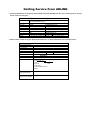
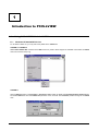
PCIS-LVIEW
LabVIEW? Interfaces of NuDAQ PCI Cards
Windows 95/98/NT/2000/XP
User’s Guide
@Copyright 1998-2002 ADLI NK Technology Inc.
All Rights Reserved.
Manual Rev. 3.33: August 23, 2002
The information in this document is subject to change without prior notice in order to improve reliability, design and
function and does not represent a commitment on the part of the manufacturer.
In no event will the manufacturer be liable for direct, indirect, special, incidental, or consequential damages arising out of
the use or inability to use the product or documentation, even if advised of the possibility of such damages.
This document contains proprietary information protected by copyright. All rights are reserved. No part of this manual
may be reproduced by any mechanical, electronic, or other means in any form without prior written permission of the
manufacturer.
Trademarks
NuDAQ, NuIPC, PCIS-LVIEW and PCI series product names are registered trademarks of ADLINK Technology Inc.
Other product names mentioned herein are used for identification purposes only and may be trademarks and/or
registered trademarks of their respective companies.
Getting Service From ADLINK
? ? Customer Satisfaction is always the most important thing for ADLINK Tech Inc. If you need any help or service,
please contact us and get it.
ADLINK Technology Inc.
Web Site
Sales & Service
Technical
Support
TEL
Address
http://www.adlinktech.com
http://www.adlinktechnology.tw
[email protected]
NuDAQ
[email protected]
NuDAM
[email protected]
NuIPC
[email protected]
NuPRO
[email protected]
Software
[email protected]
AMB
[email protected]
+886-2-82265877
FAX
+886-2-82265717
9F, No. 166, Jian Yi Road, Chungho City, Taipei, 235 Taiwan, R.O.C.
? ? Please inform or FAX us of your detailed information for a prompt, satisfactory and constant service.
Detailed Company Information
Company/Organization
Contact Person
E-mail Address
Address
Country
TEL
Web Site
FAX
Questions
Product Model
Environment to Use
Challenge Description
Suggestions for ADLINK
?OS :
?Computer Brand :
?M/B :
?CPU :
?Chipset :
?Bios :
?Video Card :
?Network Interface Card :
?Other :
Contents
CHAPTER 1 Introduction to PCIS-LVIEW.....................................................................................1
1.1
1.1.1
1.1.2
1.2
USING PCIS-LVIEW VIS IN LABVIEW..............................................................................1
Windows NT/2000/98/XP Version...............................................................................................................................1
Windows 95 Version...................................................................................................................................................2
PCIS-LVIEW NT/98/2000/XP PROGRAMMING ................................................................3
CHAPTER 2 Device Driver Handling in Windows NT/2000/98/XP...............................................4
2.1
2.2
NT 4.0 DEVICE DRIVER ...................................................................................................4
WIN2000/XP OR WIN98 DEVICE DRIVER .......................................................................5
CHAPTER 3 PCIS-LVIEW NT/2000/98/XP Utilities........................................................................7
3.1
3.2
NUDAQ REGISTRY/CONFIGURATION UTILITY (PCIUTIL)..............................................7
DATA FILE CONVERTER UTILITY (DAQCVT) .................................................................7
CHAPTER 4 PCIS-LVIEW NT/2000/98/XP Overview.....................................................................9
4.1
4.2
4.2.1
4.2.2
4.2.3
4.2.4
4.3
4.3.1
4.3.2
4.4
4.4.1
4.4.2
4.4.3
4.4.4
4.5
4.5.1
4.5.2
4.5.3
4.5.4
4.6
4.7
GENERAL CONFIGURATION FUNCTION GROUP ..........................................................9
ANALOG INPUT FUNCTION GROUP .............................................................................10
Analog Input Configuration VIs ...............................................................................................................................10
One-Shot Analog Input VIs.......................................................................................................................................10
Continuous Analog Input VIs ...................................................................................................................................10
Asynchronous Analog Input Monitoring VIs.............................................................................................................10
ANALOG OUTPUT FUNCTION GROUP .........................................................................11
Analog output Configuration VIs..............................................................................................................................11
One-Shot Analog Output Functions ..........................................................................................................................11
DIGITAL INPUT FUNCTION GROUP ..............................................................................11
Digital Input Configuration VIs ...............................................................................................................................11
One-Shot Digital Input VIs.......................................................................................................................................11
Continuous Digital Input VIs ...................................................................................................................................11
Asynchronous Digital Input Monitoring VIs .............................................................................................................12
DIGITAL OUTPUT FUNCTION GROUP ..........................................................................12
Digital Output Configuration VIs.............................................................................................................................12
One-Shot Digital Output VIs ....................................................................................................................................12
Continuous Digital Output VIs .................................................................................................................................12
Asynchronous Digital Output Monitoring VIs ..........................................................................................................12
DIO FUNCTION GROUP .................................................................................................13
TIMER/COUNTER FUNCTION GROUP ..........................................................................13
CHAPTER 5 PCIS-LVIEW/95 Overview .......................................................................................14
5.1
5.2
5.3
5.4
5.5
5.6
5.7
5.8
5.9
5.10
5.11
5.12
5.13
5.14
6208/16 VIS .....................................................................................................................15
6308 VIS ..........................................................................................................................15
7200 VIS ..........................................................................................................................15
7230 VIS ..........................................................................................................................16
7233 VIS ..........................................................................................................................16
7234 VIS ..........................................................................................................................16
7248 VIS ..........................................................................................................................16
7249 VIS ..........................................................................................................................16
7250 VIS ..........................................................................................................................16
7252 VIS ..........................................................................................................................17
7296 VIS ..........................................................................................................................17
7300A REV.B VIS............................................................................................................17
7396 VIS ..........................................................................................................................18
7432 VIS ..........................................................................................................................18
Contents ? i
5.15
5.16
5.17
5.18
5.19
5.20
5.21
5.22
5.23
7433 VIS ..........................................................................................................................18
7434 VIS ..........................................................................................................................18
8554 VIS ..........................................................................................................................18
9111 VIS ..........................................................................................................................19
9112 VIS ..........................................................................................................................19
9113 VIS ..........................................................................................................................20
9114 VIS ..........................................................................................................................21
9118 VIS ..........................................................................................................................22
9812/10 VIS .....................................................................................................................23
CHAPTER 6 Distribution of Applications ...................................................................................25
6.1
6.2
6.3
6.4
WINDOWS NT.................................................................................................................25
WINDOWS 98 .................................................................................................................25
WINDOWS 2000 .............................................................................................................26
WINDOWS 95 .................................................................................................................26
ii ? Contents
How to Use This Manual
This manual is designed to help you install the PCIS-LVIEW, the LabVIEW driver for NuDAQ PCI-bus data acquisition
cards. For the detail description of PCIS-LVIEW VIs, please refer to PCIS-LVIEW on-line help or PDF file format Function
Reference. This manual is organized as follows:
?? Chapter 1, "Introduction to PCIS-LVIEW" describes how to program your application by using PCIS-LVIEW.
?? Chapter 2, "Device Driver Handling in Windows NT/2000/98" describes how to configure the NuDAQ PCI
cards Windows NT/2000/98 device driver.
?? Chapter 3, "PCIS-LVIEW NT/2000/98 Utilities" describes the utilities included in PCIS-LVIEW Windows
NT/2000/98 version.
?? Chapter 4, "PCIS-LVIEW NT/2000/98 Overview" briefly describes each VI in PCIS-LVIEW NT, Win2000, and
Win98 versions.
?? Chapter 5, "PCIS-LVIEW/95 Overview" briefly describes each VI in PCIS-LVIEW/95.
1
Introduction to PCIS-LVIEW
1.1
1.1.1
Using PCIS-LVIEW Vis in LabVIEW
Windows NT/2000/98/XP Version
To use PCIS-LVIEW VIs, you may switch the palette to the adlink view.
LabVIEW 4 / LabVIEW 5
Select Select Palette Set command in the Edit menu from panel or block diagram in LabVIEW. Then select the adlink
view from the menu setup ring.
LabVIEW 6
Click the Options button in the Controls or Functions palette toolbar to display the Function Browser Options dialog
box. Select adlink view from the Palette Set pull-down menu. Click OK. The Functions palettes change to the adlink
view.
Introduction to PCIS LVIEW ? 1
Then you can find PCIS-LVIEW VIs in NuDAQ icon on the Functions palette.
1.1.2
Windows 95 Version
You can find the PCIS-LVIEW VIs in the User Libraries icon in the Functions palette from your block diagram in
LabVIEW.
2 ? Introduction to PCIS LVIEW
1.2
PCIS-LVIEW NT/98/2000/XP Programming
The chapter 4 PCIS-LVIEW 98/NT/2000/XP Overview briefly describes each VI in PCIS-LVIEW. All applications
developed with PCIS-LVIEW are compatible across Windows 98, Windows NT, and Windows 2000/XP.
You can find the detailed description of each VI by the following ways:
1. Select Show Help command of Help menu in LabVIEW. When you put the mouse cursor on PCIS-LVIEW VI,
LabVIEW will show the description of the VI.
2. PDF manual files in <Install Dir>\Manual directory.
PCIS-LVIEW VIs are implemented by calling the PCIS-DASK DLL functions. The Chapter PCIS-DASK Application Hints
of PCIS-DASK User’s Guide provides the programming schemes showing the function flow of that PCIS-DASK performs
analog I/O and digital I/O. Please refer to it for the information of PCIS-LVIEW programming.
Introduction to PCIS LVIEW ? 3
2
Device Driver Handling in Windows
NT/2000/98/XP
2.1
NT 4.0 Device Driver
Driver Status
After finishing the installation and re-entering Windows NT, make sure the PCI device drivers are already started. For
PCIS-LVIEW to be able to communicate with NuDAQ PCI-bus card, device driver AdlDask as well as the card’s own
device driver (e.g. PCI6208, PCI7200, PCI7230, PCI7234, PCI7250, PCI7248, PCI7296, PCI7300, PCI7432, PCI7433,
PCI7434, PCI9111, PCI9112, PCI9113, PCI9114, PCI9118, or PCI9812, etc.) must be started. You can open the “Control
Panel”, double-click “Devices”, and a Devices window will be shown as below.
If the device status is none, you have to select the AdlDask, PCI6208, PCI7200, PCI7230, PCI7234, PCI7250, PCI7248,
PCI7296, PCI7300, PCI7432, PCI7433, PCI7434, PCI9111, PCI9112, PCI9113, PCI9114, PCI9118, or PCI9812 device
and press the “Start” button.
Note: The AdlDask driver must have been started as you press Start button to start the card’s own device driver.
Driver Utility
PCIS-LVIEW provides a utility, PCI Configuration utility (PciUtil). This utility is used to register new PCI drivers, remove
installed drivers and modify AI/AO/DI/DO continuous buffer of installed drivers. The allocated buffer sizes of AI, AO, DI,
DO represent the sizes of contiguous Initially Allocated memory for continuous analog input, analog output, digital input,
digital output respectively. Its unit is page KB, i.e. 1024 bytes. Device driver will try to allocate these sizes of memory at
system startup time. If this size of memory is not able to get, driver will allocate as much memory as system can provide.
The size of initially allocated memory is the maximum memory sizes that DMA or Interrupt transfer can be performed. It
will induce an unexpected result in that DMA or Interrupt transfer performed exceeds the initially allocated size.
The PCI Configuration utility is installed with PCIS-LVIEW setup program and located in <InstallDir>\Util directory.
Using this utility to install a new driver or set the size of continuous buffer, please refer to the chpater “NuDAQ PCI
Configuration Utility” in the NuDAQ PCI and NuIPC CompactPCI DAQ Cards Software Installation Guide.
4 ? Device Driver Handling in Windows NT/2000/98/XP
2.2
Win2000/XP or Win98 Device Driver
Once Windows 98/2000/XP has started, the Plug and Play function of Windows 98/2000/XP system will find the new
NuDAQ/NuIPC cards. If this is the first time to install NuDAQ/NuIPC cards in your Windows 98/2000/XP system, you
will be informed to install the device driver. Please follow the procedures described in the section “Device Installation”
of chapter “Windows 98/NT/2000/XP” in the NuDAQ PCI and NuIPC CompactPCI DAQ Cards Software Installation
Guide to install the device.
Driver Utility
PCIS-LVIEW provides a PCI Configuration Utility (PciUtil). This utility is used to set/change the allocated buffer sizes
of AI, AO, DI and DO. The allocated buffer sizes of AI, AO, DI, DO represent the sizes of contiguous Initially Allocated
memory for continuous analog input, analog output, digital input, digital output respectively. Its unit is page KB, i.e.
1024 bytes. Device driver will try to allocate these sizes of memory at system startup time. If this size of memory is not
able to get, driver will allocate as much memory as system can provide. The size of initially allocated memory is the
maximum memory size that DMA or Interrupt transfer can be performed. It will induce an unexpected result in that
DMA or Interrupt transfer performed exceeds the initially allocated size.
The PciUtil is installed with PCIS-LVIEW, and located in <InstallDir>\Util directory.
Using PciUtil to set/change the buffer size, please refer to the chapter “NuDAQ PCI Configuration Utility” in the
NuDAQ PCI and NuIPC CompactPCI DAQ Cards Software Installation Guide.
Device Driver Handling in Windows NT/2000/98/XP ? 5
3
PCIS-LVIEW NT/2000/98/XP Utilities
3.1
NuDAQ Registry/Configuration utility (PciUtil)
PciUtil is used to register NuDAQ PCI card drivers (Windows NT4 only), remove installed drivers (Windows NT4 only),
and modify the allocated buffer sizes of AI, AO, DI and DO (Windows NT/2000/98/XP). The default location of this utility
is <InstallDir>\Util directory. Because it has been mentioned in the previous chapter, we will not introduce it here. Please
refer to the chpater “NuDAQ PCI Configuration Utility”in the NuDAQ PCI and NuIPC CompactPCI DAQ Cards Software
Installation Guide.
3.2
Data File Converter utility (DAQCvt)
The data files, generated by the PCIS-LVIEW functions performing continuous data acquisition followed by storing the
data to disk, is written in binary format. Since a binary file can’t be read by the normal text editor and can’t be used to
analyze the accessed data by Excel, PCIS-LVIEW provides a convenient tool DAQCvt to convert the binary file to the file
format read easily. The default location of this utility is <InstallDir>\Util directory. The DAQCvt main window is as the
following figure:
The DAQCvt main window includes two frames. The upper frame, Input File frame is used for the source data file and the
lower frame is used for the destination file.
To load the source binary data file, type the binary data file name in File Path field or click Browser button to select the
source file from Input File frame, and then click Load button. As the file is loaded, the information related to the data file,
e.g. data type, data width, AD Range, … etc., are shown in the corresponding fields in “Input File”frame, and the default
converted data file path and format are also listed as the figure below.
PCIS-LVIEW NT/2000/98/XP Utilities ? 7
You can select two types of destination file, Text file or CSV file. To change the default File path setting, type the file path
you wish or click the Browser button from Output File frame to select the destination file location.
DAQCvt provides three types of data format conversion.
File with scaled data :
The data in hexadecimal format is scaled to engineering unit (voltage, ample, … etc) according to the card type, data
width and data range and then written to disk in text file format. This type is available for the data accessed from
continuous AI operation only.
Binary file with scaled data :
The data in hexadecimal is scaled to engineering unit (voltage, ample, … etc) according to the card type, data width
and data range and then written to disk in binary file format. This type is available for the data accessed from
continuous AI operation only.
File with binary codes :
The data in hexadecimal format or converted to a decimal value is written to disk in text file format. If the original data
includes channel information, the raw value will be handled to get the real data value. This type is available for the
data accessed form continuous AI and DI operations.
The data separator in converted text file is selectable among space, comma and Tab.
If you want to add title/head which includes the card type information at the beginning of file, check the Title/Head box.
After setting the properties (File Path, Format, … etc) related to the converted file, you can push Start Convert button in
the Output File frame to perform the file conversion.
8 ? PCIS-LVIEW NT/2000/98/XP Utilities
4
PCIS-LVIEW NT/2000/98/XP Overview
This chapter briefly describes each VI in PCIS-LVIEW for Windows NT/2000/98/XP. The setup program detects the
system (Windows NT, 2000/XP, or 98), and installs the correct platform drivers to the system. All applications developed
with PCIS-LVIEW are compatible across Windows 98, Windows NT, and Windows 2000/XP.
You can find the detailed description of each VI by the following ways:
3. Select Show Help command of Help menu in LabVIEW. When you put the mouse cursor on PCIS-LVIEW VI,
LabVIEW will show the description of the VI.
4. Through PCIS-LVIEW on-line help
5. PDF manual files in <Install Dir>\Manual directory.
PCIS-LVIEW VIs are grouped to the following classes:
?? General Configuration Function Group
?? Analog Input Function Group
- Analog Input Configuration VIs
- One-Shot Analog Input VIs
- Continuous Analog Input Vis
?? Analog Output Function Group
- Analog output Configuration VIs
- One-Shot Analog Output VIs
?? Digital Input Function Group
- Digital Input Configuration VIs
- One-Shot Digital Input VIs
- Continuous Digital Input VIs
- Asynchronous Digital Input Monitoring VIs
?? Digital Output Function Group
- Digital Output Configuration VIs
- One-Shot Digital Output VIs
- Continuous Digital Output VIs
?? DIO Function Group
- Digital Input/Output Configuration Vis
4.1
General Configuration Function Group
Use these functions to initialize and configure data acquisition cards.
Initial VIs (6208A Initial, … ): Initializes the hardware and software states of a NuDAQ PCI-bus data acquisition card.
Initial VI must be called before any other PCIS-LVIEW VI can be called for that card.
Release Card: Tells PCIS-LVIEW driver that this card is not used currently and can be released. This would make room
for new card to initialize.
PCIS-LVIEW NT/2000/98 Overview ? 9
4.2
Analog Input Function Group
4.2.1
Analog Input Configuration VIs
AI 9111 Config: Informs PCIS-LVIEW of the trigger source and trigger mode selected for the analog input operation
of PCI9111.
AI 9112 Config: Informs PCIS-LVIEW of the trigger source selected for the analog input operation of PCI9112.
AI 9113 Config: Informs PCIS-LVIEW of the trigger source selected for the analog input operation of PCI9113.
AI 9114 Config: Informs PCIS-LVIEW of the trigger source selected for the analog input operation of PCI9114.
AI 9118 Config: Informs PCIS-LVIEW of the trigger source, trigger mode, input mode, and conversion mode
selected for the analog input operation of PCI9118.
AI 9812 Config: Informs PCIS-LVIEW of the trigger source, trigger mode, and trigger properties selected for the
analog input operation of PCI9812/9810.
AI Initial Memory Allocated: Gets the actual size of analog input memory that is available in the device driver.
4.2.2
One-Shot Analog Input VIs
AI Read Channel: Performs a software triggered A/D conversion (analog input) on an analog input channel and
returns the value converted.
AI VRead Channel: Performs a software triggered A/D conversion (analog input) on an analog input channel and
returns the value scaled to a voltage in units of volts.
AI VScale: Converts the result from an AI_ReadChannel call to the actual input voltage.
4.2.3
Continuous Analog Input VIs
AI Cont Read Channel 2-byte / AI Cont Read Channel 4-byte: Starts continuous A/D conversions on the
specified analog input channel.
AI Cont Scan Channels 2-byte / AI Cont Scan Channels 4-byte: Starts continuous A/D conversions on the
specified continuous analog input channels.
AI Cont Read Multiple Channels: Starts continuous A/D conversions on the specified analog input channels
(PCI-9118 only).
AI Cont Read Channel To File: Starts a continuous A/D conversions on the specified analog input channel and
saves the acquired data in a disk file.
AI Cont Scan Channels To File: Starts continuous A/D conversions on the specified continuous analog input
channels and saves the acquired data in a disk file.
AI Cont Read Multiple Channels To File: Starts continuous A/D conversions on the specified analog input
channels and saves the acquired data in a disk file (PCI-9118 only).
AI Cont VScale: Converts the values of an array of acquired data from an continuous A/D conversion call to the
actual input voltages.
AI Cont Status: Checks the current status of the continuous analog input operation.
4.2.4
Asynchronous Analog Input Monitoring VIs
AI Async Check: Checks the current status of the asynchronous analog input operation.
AI Async Clear: Stops the asynchronous analog input operation.
AI Async Double Buffer Mode: Enables or Disables double buffer data acquisition mode.
AI Async Double Buffer Half Ready: Checks whether the next half buffer of data in circular buffer is ready for
transfer during an asynchronous double-buffered analog input operation.
AI Async Double Buffer Transfer: Copies half of the data of circular buffer to user buffer. You can execute this
function repeatedly to return sequential half buffers of the data.
10 ? PCIS-LVIEW NT/2000/98 Overview
4.3
4.3.1
Analog Output Function Group
Analog output Configuration VIs
AO 6208A Config: Informs PCIS-LVIEW of the current range selected for the analog output operation of
PCI-6208A.
AO 9111 Config: Informs PCIS-LVIEW library of the polarity (unipolar or bipolar) that the output channel is
configured for the analog output of PCI-9111. You must call this function before calling function to perform voltage
output operation.
AO 9112 Config: Informs PCIS-LVIEW library of the reference voltage source (internal or external) and the
reference voltage value selected for the analog output channel(s) of PCI-9112. You must call this function before
calling function to perform voltage output operation.
4.3.2
One-Shot Analog Output Functions
AO Write Channel: Writes a binary value to the specified analog output channel.
AO Write Channel Volt: Accepts a voltage value, scales it to the proper binary value and writes a binary value to
the specified analog output channel.
AO Simu Write Channel: Writes binary values to the specified analog output channels simultaneously.
AO Simu Write Channel Volt: Accepts voltage values, scales them to the proper binary values and writes binary
values to the specified analog output channels simultaneously.
AO VScale: Scales a voltage to a binary value.
4.4
4.4.1
Digital Input Function Group
Digital Input Configuration VIs
DI 7200 Config: Informs PCIS-LVIEW of the trigger source and trigger properties selected for the digital input
operation of PCI7200.
DI 7300 RevA Config: Informs PCIS-LVIEW of the trigger source and trigger properties selected for the digital input
operation of PCI-7300A Rev.A board.
DI 7300 RevB Config: Informs PCIS-LVIEW of the trigger source and trigger properties selected for the digital input
operation of PCI-7300A Rev.B board.
DI Initial Memory Allocated: Gets the actual size of continuous digital input memory that is available in the device
driver.
4.4.2
One-Shot Digital Input VIs
DI Read Line: Reads the digital logic state of the specified digital line in the specified port.
DI Read Port: Reads digital data from the specified digital input port.
4.4.3
Continuous Digital Input VIs
DI Cont Read Port 8 / DI Cont Read Port 16 / DI Cont Read Port 32: Starts continuous digital input on the
specified digital input port.
DI Cont Read Port To File: Starts continuous digital input on the specified digital input port and saves the acquired
data in a disk file.
DI Cont Multi Buffer Setup 8 / DI Cont Multi Buffer Setup 16 / DI Cont Multi Buffer Setup 32: Set up
the buffer for multi-buffered continuous digital input.
DI Cont Multi Buffer Start: Starts the multi-buffered continuous digital input on the specified digital
input port at a rate as close to the rate you specified.
DI Cont Status: Checks the current status of the continuous digital input operation.
PCIS-LVIEW NT/2000/98 Overview ? 11
4.4.4
Asynchronous Digital Input Monitoring VIs
DI Async Check: Checks the current status of the asynchronous digital input operation.
DI Async Clear: Stops the asynchronous digital input operation.
DI Async Double Buffer Mode: Enables or Disables double buffer data acquisition mode.
DI Async Double Buffer Half Ready: Checks whether the next half buffer of data in circular buffer is ready for
transfer during an asynchronous double-buffered digital input operation.
DI Async Double Buffer Transfer: Copies half of the data of circular buffer to user buffer. You can execute this
function repeatedly to return sequential half buffers of the data.
DI Async Multi Buffer Next Ready: Checks whether the next buffer of data in circular buffer is ready for
transfer during an asynchronous multi-buffered digital input operation.
4.5
4.5.1
Digital Output Function Group
Digital Output Configuration VIs
DO 7200 Config: Informs PCIS-LVIEW of the trigger source and trigger properties selected for the digital input
operation of PCI7200.
Do 7300 RevA Config: Informs PCIS-LVIEW of the trigger source and trigger properties selected for the digital
input operation of PCI-7300A Rev.A board.
DO 7300 RevB Config: Informs PCIS-LVIEW of the trigger source and trigger properties selected for the digital
input operation of PCI-7300A Rev.B board.
EDO 9111 Config: Informs PCIS-LVIEW library of the mode of EDO channels of PCI9111.
DO Initial Memory Allocated: Gets the actual size of continuous digital output memory that is available in the
device driver.
4.5.2
One-Shot Digital Output VIs
DO Write Line: Sets the specified digital output line in the specified digital port to the specified state.
DO Write Port: Writes digital data to the specified digital output port.
DO Read Line: Read the digital logic state of the specified digital output line in the specified port.
DO Read Port: Read back the output digital data from the specified digital output port.
4.5.3
Continuous Digital Output VIs
DO Cont Write Port 8 / DO Cont Write Port 16 / DO Cont Write Port 32: Starts continuous digital output on the
specified digital output port.
DO Cont Status: Checks the current status of the continuous digital output operation.
DO PG Start 8 / DO PG Start 16 / DO PG Start 32: Starts pattern generation operation on PCI-7300A.
DO PG Stop: Stops pattern generation operation on PCI-7300A.
DO Cont Multi Buffer Setup 8 / DO Cont Multi Buffer Setup 16 / DO Cont Multi Buffer Setup 32:
Set up the buffer for multi-buffered continuous digital output.
DO Cont Multi Buffer Start: Starts the multi-buffered continuous digital output on the specified digital
output port at a rate as close to the rate you specified.
4.5.4
Asynchronous Digital Output Monitoring VIs
DO Async Check: Checks the current status of the asynchronous digital output operation.
DO Async Clear: Stops the asynchronous digital output operation.
12 ? PCIS-LVIEW NT/2000/98 Overview
DO Async Multi Buffer Next Ready
: Checks whether the next buffer is ready for new data during
an asynchronous multi-buffered digital output operation.
4.6
DIO Function Group
DIO Port Config: Informs PCIS-LVIEW of the port direction selected for the digital input/output operation.
4.7
Timer/Counter Function Group
CTR Read: Reads the current contents of the selected counter without disturbing the counting process.
CTR Reset: Sets the output of the selected counter to the specified state.
CTR Setup: Configures the selected counter to operate in the specified mode.
CTR 8554 ClkSrc Config: Sets the counter clock source of PCI-8554.
CTR 8554 CK1 Config: Sets the source of CK1 of PCI-8554.
CTR 8554 Debounce Config: Sets the debounce clock of PCI-8554.
GCTR Clear: Clears the general-purpose timer/counter control register and counter register.
GCTR Read: Reads the current counter value of the general-purpose counter.
GCTR Setup: Controls the general-purpose counter to operate in the specified mode.
PCIS-LVIEW NT/2000/98 Overview ? 13
5
PCIS-LVIEW/95 Overview
This chapter briefly describes each VI in PCIS-LVIEW for Windows 95. You can find the detailed description of each VI
by the following ways:
1. Select Show Help command of Help menu in LabVIEW. When you put the mouse cursor on PCIS-LVIEW/95 VI,
LabVIEW will show the description of the VI.
2. Through PCIS-LVIEW/95 on-line help
3. PDF manual files in <Install Dir>\Manual directory.
14 ? PCIS-LVIEW/95 Overview
5.1
5.2
5.3
6208/16 VIs
6208 Initial
Initialize PCI-6208/6216 card
6208 DA
Write data to D/A converters
6208 DI
Read data from digital input port
6208 DO
Write data to digital output port
6208A Volt2Current
Set PCI-6208A voltage-to-current mode control
6308 VIs
6308 Initial
Initialize PCI-6208/6216 card
6308 DA
Write data to D/A converters
6308 DA CH0-CH3
Simultaneously write data to D/A converters of
channel 0 to channel 3
6308 DA CH4-CH7
Simultaneously write data to D/A converters of
channel 4 to channel 7
6308 DI
Read data from digital input port
6308 DO
Write data to digital output port
6308A Volt2Current
Set PCI-6208A voltage-to-current mode control
7200 VIs
7200 Initial
Initialize PCI-7200 card
7200 Allocate DMA
Memory
Contact Windows 95 system to allocate a block
of contiguous memory for DMA transfer
7200 DI DMA Start
Start up digital input N times with DMA data
transfer
7200 DI DMA Status
Check the operation status of DI DMA data
transfer
7200 DI DMA Stop
Stop the DI DMA data transfer
7200 DI Timer
Set the internal timer pacer for digital input
7200 DMA Cont DI
A high level VI to perform digital input by N
times with DMA data transfer
7200 DMA Cont DO
A high level VI to perform digital output N times
with DMA data transfer
7200 DO DMA Start
Start up digital output N times with DMA data
transfer
7200 DO DMA Status
Check the operation status of DO DMA data
transfer
7200 DO DMA Stop
7200 DO Timer
Stop the DO DMA data transfer
Set the internal timer pacer for digital
output
7200 Free DMA Memory
Deallocate a system DMA memory
7200 Get Sample
Retrieve the index-th data in DMA buffer
7200 Read from Digital
Line
Read data from digital input port
7200 Read from Digital
Port
Read data from digital input port
7200 Switch Card
Select which card is used currently.
7200 Write to Digital Line Write data to digital output line.
7200 Write to Digital Port Write data to digital output port.
PCIS-LVIEW/95 Overview ? 15
5.4
5.5
5.6
5.7
7230 VIs
7230 Initial
Initialize PCI-7230 cards.
7230 DI
Read 16-bit digital input data from digital input port.
7230 DO
Write data to digital output port.
7233 VIs
7233 Initial
Initialize PCI-7233 cards.
7233 DI
Read 32-bit digital input data from digital input port.
7234 VIs
7234 Initial
Initialize PCI-7234 cards.
7234 DO
Write data to digital output port.
7248 VIs
7248 Initial
Initialize PCI-7248 card.
7248 Config Channel Configure the input or output of each channel.
7248 Config Port
5.8
Configure the input or output of each port.
7248 Digital Input
Read 8-bit digital input data from digital input port.
7248 Digital Output
Write data to digital output ports.
7248 Timer Read
Read the current contents of the counter #0.
7248 Timer Start
Configure the counter #0 to operate in the specified
mode.
7248 Timer Stop
Stop the event counting operation.
7249 VIs
7249 Initial
Initialize cPCI-7249 card.
7249 Config Channel Configure the input or output of each channel.
5.9
7249 Config Port
Configure the input or output of each port.
7249 Digital Input
Read 8-bit digital input data from digital input port.
7249 Digital Output
Write data to digital output ports.
7249 Timer Read
Read the current contents of the counter #0.
7249 Timer Start
Configure the counter #0 to operate in the specified
mode.
7249 Timer Stop
Stop the event counting operation.
7250 VIs
7250 Initial
Initialize PCI-7250 card.
7250 DI
Read digital input data from digital input port.
7250 DO
Write data to digital output port which can energized
RELAY ON/OFF.
7250 DO Readback
Read-back data from digital output port.
16 ? PCIS-LVIEW/95 Overview
5.10 7252 VIs
7252 Initial
Initialize cPCI-7252 card.
7252 DI
Read digital input data from digital input port.
7252 DO
Write data to digital output port which can energized
RELAY ON/OFF.
7252 DO Readback
Read-back data from digital output port.
5.11 7296 VIs
7296 Initial
Initialize PCI-7296 card.
7296 Config Channel Configure the input or output of each channel.
7296 Config Port
Configure the input or output of each port.
7296 Digital Input
Read 8-bit digital input data from digital input port.
7296 Digital Output
Write data to digital output port.
7296 Timer Read
Read the current contents of the counter #0.
7296 Timer Start
Configure the counter #0 to operate in the specified
mode.
7296 Timer Stop
Stop the event counting operation.
5.12 7300A Rev.B VIs
7300 Initial
Initialize PCI-7300A Rev.B card.
7300 Allocate DMA
Memory
Contact Windows 95 system to allocate a block of
contiguous memory for DMA transfer.
7300 Aux DI
Read data from auxiliary digital input port.
7300 Aux DI Channel Read data from one auxiliary digital input channel.
7200 Aux DO
Write data to auxiliary digital output port.
7200 Aux DO
Channel
Write data to one auxiliary digital output channel
(bit).
7300 Configure
Set the port DI/O configuration, terminator control,
and control signal polarity for the PCI-7300A Rev.B
card.
7300 DI DMA Start
Perform digital input with DMA data transfer
7300 DI DMA Status Check the DMA DI operation status
7300 DI DMA Abort
Stop the DMA DI operation
7300 DI Mode
Set the clock mode and start mode for the DI
operation
7300 DI Timer
Set the internal timer pacer for digital input
7300 DO DMA Start
Perform digital output with DMA data transfer
7300 DO DMA Status Check the DMA DO operation status
7300 DO DMA Abort Stop the DMA DO operation
7300 DO Mode
Set the clock mode and start mode for the DO
operation.
7300 DO Timer
Set the internal timer pacer for digital output
7300 DO PG Start
Perform pattern generation
7300 DO PG Stop
Stop pattern generation
7300 Free DMA
Memory
Deallocate a system DMA memory
7300 Get Sample
Retrieve the index-th data in DMA buffer
7300 Get Overrun
Status
Check overrun status
PCIS-LVIEW/95 Overview ? 17
7300 Set Sample
Write the output data to the index-th position in
output DMA buffer
5.13 7396 VIs
7396 Initial
Initialize PCI-7396 card.
7396 Config Port
Configure the input or output of each port.
7396 Digital Input
Read digital input data from digital input port.
7396 Digital Output
Write data to digital output port.
7396 Timer Read
Read the current contents of the counter #0.
7396 Timer Start
Configure the counter #0 to operate in the specified
mode.
7396 Timer Stop
Stop the event counting operation.
5.14 7432 VIs
7432 Initial
Initialize PCI-7432 card.
7432 DI
Read 32-bit digital input data from digital input port.
7432 DO
Write data to digital output ports.
5.15 7433 VIs
7433 Initial
Initialize PCI-7433 card.
7433 DI HiDW
Read high 32-bit digital input data from digital input
port.
7433 DI LowDW
Read low 32-bit digital input data from digital input
port.
5.16 7434 VIs
7434 Initial
Initialize PCI-7434 card.
7434 DO HiDW
Write data to high 32 bits of the 64 isolated digital
outputs.
7434 DO LowDW
Write data to low 32 bits of the 64 isolated digital
outputs.
5.17 8554 VIs
8554 Initial
Initialize PCI-8554 card.
8554 Write Counter Write command to counter #1 ~ #12 by this function.
8554 Read Counter Read counter information.
8554 Stop Counter
Stop counter.
8554 Read Status
Read current counter status.
8554 DO
Write a 8-bit data to the digital output port.
8554 DI
Read 8-bit data from digital input port.
8554 SET cntCLK
Select 8254 counter #1 ~ #10 clock source.
8554 SET CK1
Select source of CK1.
8554 SET DBCLK
Select debounce clock.
8554 Software
Reset
Reset PCI-8554 card.
18 ? PCIS-LVIEW/95 Overview
Reset
5.18 9111 VIs
9111 Initial
Initialize PCI-9111 card
9111 AD FFHF INT
Restart
Restart the FIFO half full interrupt transfer without
re-initial all the relative registers
9111 AD FFHF INT Start Initial and start up the interrupt transfer by using
AD FIFO Half-Full Interrupt transfer mode
9111 AD FFHF INT
Status
Check the status of FIFO half-full Interrupt
transfer analog input operation
9111 AD FFHF INT Stop Stop the FFHF interrupt data transfer function
9111 AD INT Start
Initial and start up the interrupt transfer by using
End-of-conversion (EOC) Interrupt transfer mode
9111 AD INT Status
Check the status of EOC Interrupt transfer analog
input operation
9111 AD INT Stop
Stop the EOC interrupt data transfer function
9111 AD Set Channel
Set A/D channel
9111 AD Set Mode
Set A/D trigger and channel scan mode
9111 AD Set Range
Set the A/D range
9111 Analog Output
Write data to D/A converters.
9111 Digital Input Line Read data from digital input line.
9111 Digital Input Port
Read data from digital input port.
9111 Digital Input from Read data from external digital input port.
EDI
9111 Digital Output
Line
Write data to digital output port.
9111 Digital Output Port Write data to digital output port.
9111 Digital Output to
EDO
Write data to extended digital output port.
9111 FIFO Interrupt
Cont AD
Performs A/D conversion N times with FFHF
interrupt data transfer by using pacer trigger.
9111 Readback EDO
Read back the output data that is written to EDO
output port last time.
9111 Reset FIFO
Reset A/D FIFO.
9111 Set EDO Function Set the mode of EDO pins.
9111 DG AD Acquire
Trigger the A/D conversion data for PCI-9111DG
by software trigger. It reads the 12-bit A/D data
when the data is ready.
9111HR AD Acquire
Trigger the A/D conversion data for PCI-9111HR
by software trigger. It reads the 16-bit A/D data
when the data is ready.
5.19 9112 VIs
9112 Initial
Initialize PCI-9112 card
9112 AD Acquire
Software trigger the A/D conversion, then poll the
A/D conversion data
9112 AD DMA Start
Initializes and starts up A/D conversion with
DMA data transfer by using the pacer trigger
(internal timer trigger)
Check the status of DMA analog input
operation
9112 AD DMA Status
PCIS-LVIEW/95 Overview ? 19
9112 AD DMA Stop
9112 AD INT Start
9112 AD INT Status
9112 AD INT Stop
Stop the DMA analog input operation
Initializes and starts up A/D conversion with
interrupt data transfer by using the pacer
trigger (internal timer trigger)
Check the status of interrupt analog input
operation
Stop the interrupt analog input operation
9112 AD Set Autoscan
Set automatic hardware channel scan to be
enable or disable
9112 AD Set Channel
Set A/D channel
9112 AD Set Mode
Set the A/D trigger and data transfer mode
9112 AD Set Range
Set the A/D range
9112 Allocate DMA
Memory
Contact Windows 95 system to allocate a block
of contiguous memory for DMA transfer
9112 Analog Output
Write data to D/A converters
9112 DMA Cont AD
Perform A/D conversion N times with DMA data
transfer by using the pacer trigger (internal timer
trigger)
9112 Free DMA Memory Deallocate a system DMA memory
9112 Get DMA Sample
Retrieve the index-th data in DMA buffer
9112 INT Cont AD
Perform A/D conversion N times with interrupt
data transfer by using the pacer trigger (internal
timer trigger)
9112 Read from Digital
Line
Read data from digital input port
9112 Read from Digital
Port
Read data from digital input port
9112 Timer Read
Read the count value of the Tomer#0
9112 Timer Start
Program the Timer #0
9112 Timer Stop
Stop the timer #0 operation
9112 Write to Digital
Port
Write data to digital output port
5.20 9113 VIs
9113 Initial
Initialize PCI-9113 card
9113 AD Acquire
Trigger the A/D conversion data for PCI-9113 by
software trigger. Then read the 12-bit A/D data
when the data is ready
9113 AD Acquire MUX
Trigger the A/D conversion data for PCI-9113 by
software trigger. Then read the 32-bit A/D data
when the data is ready
9113 AD FFHF INT
Restart
Restart the FIFO half-full interrupt transfer
without re-initial all the relative registers.
9113 AD FFHF INT Start
Initial and start up the interrupt transfer by using
AD FIFO Half-Full Interrupt transfer mode by
using internal pacer trigger
9113 AD FFHF INT Status Check the status of FIFO half-full interrupt
analog input operation
9113 AD FFHF INT Stop
Stop the FIFO half-full interrupt analog input
operation
9113 AD INT Start
Initial and start up the interrupt transfer by using
End-of-conversion (EOC) Interrupt transfer
mode by using internal pacer trigger
20 ? PCIS-LVIEW/95 Overview
9113 AD INT Status
Check the status of EOC interrupt analog input
operation
9113 AD INT Stop
Stop the EOC interrupt analog input operation
9113 AD Set Channel
Set A/D channel
9113 AD Set Mode
Set A/D trigger mode
9113 AD Set Range
Set A/D range
9113 Counter Read
Read the count value of the counter#0
9113 Counter Start
Program the counter #0.
9113 Counter Stop
Stop the timer/counter operation of the counter
#0
9113 FIFO Interrupt Cont Performs A/D conversion N times with FFHF
interrupt data transfer by using pacer trigger
AD
9113 Interrupt Cont AD
Performs A/D conversion N times with EOC
interrupt data transfer by using pacer trigger
9113 Reset FIFO
Reset A/D FIFO
5.21 9114 VIs
9114 Initial
Initialize PCI-9114 card
9114 AD Acquire
Trigger the A/D conversion data for PCI-9114 by
software trigger. Then read the 16-bit A/D data
when the data is ready.
9114 AD Acquire MUX
Trigger the A/D conversion data for PCI-9114 by
software trigger. Then read the 32-bit A/D data
when the data is ready
9114 AD FFHF INT
Restart
Restart the FIFO half full interrupt transfer
without re-initial all the relative registers
9114 AD FFHF INT Start Initialize and start up the interrupt transfer with
AD FIFO Half-Full Interrupt transfer mode by
using internal pacer trigger
9114 AD FFHF INT
Status
Check the status of FIFO half-full interrupt analog
input operation
9114 AD FFHF INT Stop Stop the FFHF interrupt data transfer function
9114 AD INT Start
Initialize and start up the interrupt transfer with
End-of-conversion (EOC) Interrupt transfer
mode by using internal pacer trigger
9114 AD INT Status
Check the status of EOC interrupt analog input
operation
9114 AD INT Stop
Stop the EOC interrupt data transfer function
9114 AD Set Channel
Set A/D channel
9114 AD Set Mode
Set A/D trigger and channel scan mode
9114 AD Set Range
Set A/D range
9114 Counter Read
Read the count value of the counter#0
9114 Counter Start
Program the counter #0
9114 Counter Stop
Stop the timer/counter operation of the counter
#0
9114 Digital Input Port
Read data from digital input ports
9114 Digital Output Port Write data to digital output port
9114 FIFO Interrupt
Cont AD
Performs A/D conversion N times with FFHF
interrupt data transfer by using pacer trigger
9114 Interrupt Cont AD Performs A/D conversion N times with EOC
interrupt data transfer by using pacer trigger
9114 Reset FIFO
Reset A/D FIFO
PCIS-LVIEW/95 Overview ? 21
5.22 9118 VIs
9118 Initial
Initialize PCI-9118 card.
9118DGHG AD
Acquire
Software trigger the A/D conversion, then poll the
A/D conversion data.
9118HR AD Acquire
Software trigger the A/D conversion, then poll the
A/D conversion data.
9118 AD Begin Set
AFIFO
After this VI is performed, the program can start to
fill out A/D Channel/Gain register to set the A/D
channel and range.
9118 AD DMA Start
Initialize and start up A/D conversion with DMA
data transfer by using the pacer trigger (internal
timer trigger)
9118 AD DMA Status
Check the status of DMA analog input
operation
Stop the DMA analog input operation
9118 AD DMA Stop
9118 AD INT Start
9118 AD INT Status
Initialize and start up A/D conversion with
interrupt data transfer by using the pacer
trigger (internal timer trigger)
Check the status of interrupt analog input
operation
9118 AD INT Stop
Stop the interrupt analog input operation
9118 AD End Set
AFIFO
Stop setting A/D channel and input range.
9118 AD Reset AFIFO Reset A/D Channel/Gain Register.
9118 AD Reset DFIFO Reset A/D Channel/Gain Register.
9118 AD Set Burst
Number
Set the number of conversion channels in a scan
trigger.
9118 AD Set Control
Register
Set the analog input mode.
9118 AD Set
Differential
Set analog input mode as differential or
single-ended.
9118 AD Set DMA
Transfer
Specify the status of DMA transfer mode.
9118 AD Set External Specify the A/D control as External Gate control
mode or Software Gate Control mode.
Gate
9118 AD Set Function Set A/D trigger mode.
Register
9118 AD Set Gain
Channel
Specify the A/D channel and input range.
9118 AD Set Hardware Specify the status of interrupt operation.
Interrupt
9118 AD Set Hardware Specify the hardware trigger source.
Trigger Source
9118 AD Set Internal
Trigger Source
Specify the internal trigger source.
9118 AD Set Scan
Set the first and last channels in a group of
consecutive channels.
9118 AD Set Software Specify the status of software Gate.
Gate
9118 AD Set Unipolar Set analog input range as uni-polar or bi-polar.
9118 Allocate AI
Memory
Contact Windows 95 system to allocate a block of
contiguous memory for DMA or interrupt transfer.
9118 DMA Cont AD
Perform A/D conversion N times with DMA data
transfer by using the pacer trigger (internal timer
22 ? PCIS-LVIEW/95 Overview
trigger).
9118 Enable/Disable
About Trigger Mode
Enable or disable About Trigger Mode.
9118 Enable/Disable
AD Burst Mode
Enable or disable AD Burst Mode.
9118 Enable/Disable
AD Burst Mode with
S&H
Enable or disable AD Burst Mode with Sample and
Hold.
9118 Enable/Disable
Post Trigger Mode
Enable or disable Post Trigger Mode.
9118 Free AI Memory Deallocate a system AI memory.
9118DGHG Get DMA
Sample
Retrieve the index-th data in system AI buffer for
DMA transfer.
9118HR Get DMA
Sample
Retrieve the index-th data in system AI buffer for
DMA transfer.
9118DGHG Get INT
Sample
Retrieve the index-th data in system AI buffer for
interrupt transfer.
9118HR Get INT
Sample
Retrieve the index-th data in system AI buffer for
interrupt transfer.
9118 INT Cont AD
Perform A/D conversion N times with interrupt data
transfer by using the pacer trigger (internal timer
trigger).
9118 INT Set Control
Register
Set Interrupt Control Register.
9118 Output Channel Write data to D/A converters.
Voltage
9118 Read from
Digital Line
Read data from digital input port.
9118 Read from
Digital Port
Read data from digital input port.
9118 Set Digital
Trigger Type
Set the active type of digital trigger.
9118 Set External
Trigger Type
Set the active type of external trigger.
9118 Set Trigger
Set up a trigger. The VI specifies the trigger mode
and post trigger count.
9118 Start/Stop AD
Burst Mode
Start or stop AD Burst Mode.
9118 Start/Stop
Trigger
Start or stop Trigger.
9118 Timer Read
Read the count value of the Tomer#0.
9118 Timer Start
Program the Timer #0.
9118 Timer Stop
Stop the timer #0 operation.
9118 Write to Digital
Port
Write data to digital output port.
5.23 9812/10 VIs
9812 Initial
Initialize PCI-9812/10 card.
9812 AD DMA Start
Initialize and start up A/D conversion with DMA
data transfer
9812 AD DMA Status
Check the status of DMA analog input
operation
Stop the DMA analog input operation
9812 AD DMA Stop
PCIS-LVIEW/95 Overview ? 23
9812 Allocate DMA
Memory
Contact Windows 95 system to allocate a block of
contiguous memory for DMA transfer.
9812 DMA Cont AD
Perform A/D conversion N times with DMA data
transfer.
9812 Free DMA
Memory
Deallocate a system DMA memory.
9812 Get Sample
Retrieve the index-th data in DMA buffer.
9812 Set Clock Rate
Specify the clock divider for ADC clock.
9812 Set Clock Source Specify the ADC clock source.
9812 Set Trigger
Set up a trigger, including the trigger mode, trigger
level (voltage), trigger source, trigger slope and
post trigger count.
24 ? PCIS-LVIEW/95 Overview
6
Distribution of Applications
To install an application using PCIS-LVIEW on another computer, you also must install the necessary driver files and
supporting libraries on the target machine. You can create an automatic installer to install your program and all of the files
needed to run that program or you can manually install the program and program files. Whichever installation method
you choose, you must install the following files:
Note: Do not replace any files on the target computer if the file on the target computer has a newer version than the file
you are installing.
6.1
Windows NT
?? LLB files:
Plv.llb in \software\pcis-lview\w98nt2k\redist\llb
?? Required support DLLs:
Plv.dll in \software\pcis-lview\w98nt2k\redist\dll. This file should be copied to Winnt\system32 directory.
?? Driver files
adldask.sys in \software\pcis-lview\w98nt2k\redist\wnt\drivers.
Winnt\system32\drivers directory.
This
file
should
be
copied
to
The corresponding driver files in \software\pcis-lview\w98nt2k\redist\wnt\drivers, e.g. pci7200.sys for PCI-7200.
These files should be copied to Winnt\system32\drivers directory.
Device configuration utility in \software\pcis-lview\w98nt2k\redist\wnt\pciutil.
?? Utility file (option)
Data Conversion utility DAQCvt.exe in \software\pcis-lview\w98nt2k\redist\daqcvt to convert the binary data file to
the file format read easily.
6.2
Windows 98
?? LLB files:
Plv.llb in \software\pcis-lview\w98nt2k\redist\llb
?? Required support DLLs:
Plv.dll in \software\pcis-lview\w98nt2k\redist\dll. This file should be copied to Windows\system directory.
?? Driver files
The corresponding driver files in \software\pcis-lview\w98nt2k\redist\w98\drivers, e.g. pci7200.sys for PCI-7200.
These files should be copied to Windows\system32\drivers directory.
The corresponding INF files in \software\pcis-lview\w98nt2k\redist\w98\inf, e.g. p7200.inf for PCI-7200. These
files should be copied to Windows\inf directory.
Device configuration utility in \software\pcis-lview\w98nt2k\redist\w98\pciutil.
?? Utility file (option)
Distribution of Applications ? 25
Data Conversion utility DAQCvt.exe in \software\pcis-lview\w98nt2k\redist\daqcvt to convert the binary data file to
the file format read easily.
6.3
Windows 2000
?? LLB files:
Plv.llb in \software\pcis-lview\w98nt2k\redist\llb
?? Required support DLLs:
Plv.dll in \software\pcis-lview\w98nt2k\redist\dll. This file should be copied to Winnt\system32 directory.
?? Driver files
The corresponding driver files in \software\pcis-lview\w98nt2k\redist\w2000\drivers, e.g. pci7200.sys for PCI-7200.
These files should be copied to Winnt\system32\drivers directory.
The corresponding INF file in \software\pcis-lview\w98nt2k\redist\w2000\inf, e.g. p7200.inf for PCI-7200. These
files should be copied to Winnt\inf directory.
Device configuration utility in \software\pcis-lview\w98nt2k\redist\w2000\pciutil.
?? Utility file (option)
Data Conversion utility DAQCvt.exe in \software\pcis-lview\w98nt2k\redist\daqcvt to convert the binary data file to
the file format read easily.
6.4
Windows 95
?? LLB files:
The corresponding LLB files in \software\pcis-lview\w95\redist\llb, e.g. 7200.llb for PCI-7200 card.
?? Required support DLLs:
The corresponding DLL files in \software\pcis-lview\w95\redist\dll, e.g. LV7200.dll for PCI-7200 card. These files
should be copied to Windows\system directory.
?? Driver files
Pciw95.vxd in \Software\Pcis-lview\W95\redist\drivers. This file should be copied to Windows\system directory.
The corresponding driver files in \Software\Pcis-lview\W95\redist\drivers. These files should be copied to
Windows\system directory. The required driver file for each device is as the following table:
Device
PCI-6208/6216
PCI-6308
PCI-7200
PCI-7230
PCI-7233
PCI-7234
PCI-7248
cPCI-7249
PCI-7250
cPCI-7252
PCI-7296
PCI-7300A Rev.B
PCI-7396
PCI-7432
PCI-7433
PCI-7434
PCI-8554
PCI-9111
PCI-9112
PCI-9113
PCI-9114
PCI-9118
PCI-9812/9810
26 ? Distribution of Applications
Driver file
Not needed
Not needed
W95_7200.vxd
W95_7230.vxd
W95_7233.vxd
Not needed
W95_7248.vxd
W95_7249.vxd
Not needed
Not needed
W95_7296.vxd
W95_7300.vxd
W95_7396.vxd
W95_7432.vxd
W95_7433.vxd
Not needed
W95_8554.vxd
W95_9111.vxd
W95_9112.vxd
W95_9113.vxd
W95_9114.vxd
W95_9118.vxd
W95_9812.vxd
The corresponding INF files in \software\pcis-lview\w95\redist\Inf, e.g. pci7200.inf for PCI-7200. These files should
be copied to Windows\system\inf\other directory.
Distribution of Applications ? 27