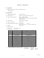
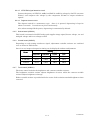
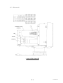
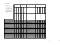
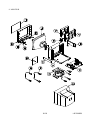
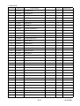
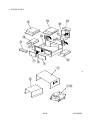
1
Ultrasound Diagnostic Scanner
Model EUB-5500
TECHNICAL GUIDE
--- Principle of Operation ---
Tokyo, Japan
L1E-EA0229-1
CONFIDENTIALITY: This material contains proprietary information of Hitachi
Medical Corporation and it shall not be disclosed to any third party or reproduced
without the prior written permission of Hitachi Medical Corporation.
Copyright © Hitachi Medical Corporation. 2003. All rights reserved.
CONTENTS
Section 1
1.1
1.2
1.3
1.4
Section 2
2.1
2.2
2.3
2.4
Section 3
Page
Introduction................................................................................................................1
- 1
Introduction
Product Overview .........................................................................................................1 - 1
System Specification ....................................................................................................1 - 2
Environmental conditions
System Organization....................................................................................................1 - 3
Safety ..........................................................................................................................2 - 1
Classification of the Equipment..................................................................................2 Cautions in Operating the Equipment .......................................................................2 Cautions in Maintaining the Equipment ...................................................................2 Symbols ........................................................................................................................2 -
1
1
1
2
Operation....................................................................................................................3
- 1
Operation
3.1 General Operation........................................................................................................3 - 1
3.2 Special Operation for Service Personnel ....................................................................3 - 1
3.2.1 Initialization of system environment ..................................................................3 - 1
3.2.2 Contents of backup data.......................................................................................3 - 3
3.2.3 Saving backup data ..............................................................................................3 - 6
3.2.4 Loading backup data ............................................................................................3 - 7
3.2.5 Displaying software and hardware versions.......................................................3 - 9
3.2.6 Action to be taken when the hard disk crashes..................................................3 - 10
3.2.7 Others of “Service Tools” ......................................................................................3 - 30
3.2.8 Cautions in replacing PCB...................................................................................3 - 39
3.2.9 Backup battery......................................................................................................3 - 40
Section 4
Principle of Operation ...............................................................................................4 - 1
4.1 System Block of EUB-5500..........................................................................................4 - 1
4.2 Basic Composition of EUB-5500 .................................................................................4 - 1
4.2.1 General and board description.............................................................................4 - 1
4.2.2 PRBSW unit circuit description...........................................................................4 - 4
4.2.3 DBF PCB circuit description................................................................................4 - 6
4.2.4 EPI PCB circuit description .................................................................................4 - 8
4.2.5 MAP PCB circuit description ...............................................................................4 - 11
4.2.6 KB & KBIF PCB description................................................................................4 - 17
4.3 BIO Unit EZU-EK25....................................................................................................4 - 20
4.3.1 General and board description.............................................................................4 - 20
4.3.2 BIO PCB circuit description.................................................................................4 - 20
4.4 Steerable CW Doppler Unit EZU-ST5 ........................................................................4 - 24
4.4.1 General and board description.............................................................................4 - 24
4.4.2 CW circuit description ..........................................................................................4 - 24
(1)
L1E-EA0229
4.5 CW Doppler Unit EZU-CW4 .......................................................................................4 - 25
4.5.1 General and board description.............................................................................4 - 25
4.5.2 CW PCB circuit description .................................................................................4 - 25
Section 5
5.1
5.2
Section 6
Power Unit .................................................................................................................5 - 1
General and Circuit Description .................................................................................5 - 1
Power Unit Connectors ................................................................................................5 - 3
Monitor Unit ..............................................................................................................6 - 1
6.1 Composition ..................................................................................................................6 6.2 Specification..................................................................................................................6 6.3 Installation ...................................................................................................................6 6.3.1 Cautions in installing the monitor ......................................................................6 6.3.2 Cautions for safety................................................................................................6 6.3.3 Replacing the fuse.................................................................................................6 6.3.4 Degaussing ............................................................................................................6 -
1
1
4
4
5
5
5
6.4 Description of Operation..............................................................................................6 6.4.1 General ..................................................................................................................6 6.4.2 Brown tube (CRT) .................................................................................................6 6.4.3 Main board (AVB401) ...........................................................................................6 6.4.4 VIDEO board (AVB411) ........................................................................................6 6.4.5 Socket board (AVB421) .........................................................................................6 6.4.6 Control board (AVB451)........................................................................................6 6.4.7 Front control (AVB431).........................................................................................6 6.4.8 Block diagram .......................................................................................................6 -
5
5
5
6
7
8
8
8
9
6.5 Adjustment ...................................................................................................................6 - 10
6.5.1 List of adjusters ....................................................................................................6 - 10
6.5.2 VR adjuster layout ................................................................................................6 - 12
6.6
6.7
6.8
Section 7
7.1
7.2
7.3
Section 8
Troubleshooting ............................................................................................................6 - 16
Removing the Cover .....................................................................................................6 - 17
Detaching and attaching the Filter ............................................................................6 - 18
Connector
Connector Arrangement ............................................................................................7 - 1
Connector Arrangement...............................................................................................7 - 1
Connection of CN Panel Connectors ...........................................................................7 - 2
Termination of Video Signals.......................................................................................7 - 5
Signal List ..................................................................................................................8 - 1
8.1 EUB-5500 Basic Unit...................................................................................................8 - 1
8.1.1 PRB PCB ...............................................................................................................8 - 1
8.1.2 AWP PCB ...............................................................................................................8 - 3
8.1.3 DBF PVB ...............................................................................................................8 - 6
8.1.4 EPI PCB.................................................................................................................8 - 10
8.1.5 MAP PCB...............................................................................................................8 - 14
8.2 BIO Unit........................................................................................................................8 - 15
8.2.1 BIO PCB ................................................................................................................8 - 15
(2)
L1E-EA0229
8.3 CW Unit EZU-ST5, EZU-CW4 ....................................................................................8 - 16
8.6.1 CW PCB .................................................................................................................8 - 16
Section 9
9.1
9.2
Maintenance...............................................................................................................9
- 1
Maintenance
Fan Filter ......................................................................................................................9 - 1
Other Maintenance Items............................................................................................9 - 1
Section 10 Parts list
list................................
................................................................
................................................................................................
................................................................................
................................................10
................ 10 - 1
10.1
10.2
10.3
10.4
10.5
10.6
10.7
10.8
10.9
Cart1............................................................................................................................10 - 1
Cart2............................................................................................................................10 - 4
Keyboard .....................................................................................................................10 - 6
PC unit ........................................................................................................................10 - 8
Cover ...........................................................................................................................10 - 10
PCB..............................................................................................................................10 - 12
Accessories ..................................................................................................................10 - 14
Monitor........................................................................................................................10 - 16
Power...........................................................................................................................10 - 18
(3)
L1E-EA0229
Section 1 Introduction
1.1 Product Overview
Overview
EUB-5500 is a compact ultrasound scanner with multiple functions equipped with Doppler,
color flow mapping function and so on, which circuits related to image quality are totally
digitalized. It can be connected with phased array probes as well as linear and convex probes,
and applicable to any type of use.
Also, it is fully equipped with various functions such as cine memory, cardiac function
measurement, patient report function and so on. In addition, EUB-5500 runs on WindowsXP
allowing it to be easily connected with various interfaces such as DICOM3.0 and so on.
Features
(1)
True Digital Architecture
All sorts of ultrasound image processing for not only the beam former as a crucial point of
image quality but also all mode of B, M, DOP, CFM and CFA are totally digitalized, and
they are controlled by software.
(2)
Improved resolution
Weighting of transmission and reception waves together with digital processing mentioned
above realizes high spatial resolution, wide dynamic range and high contrast resolution.
(3)
Improved color frame rate and image quality
Parallel beam and latest image processing technologies realize the Quadra beam process of
color image.
It achieves substantial improvement of frame rate compared with
conventional techniques, as well as provides color images with high definition and high
resolution.
(4)
Applicable to multiple uses
Not only linear and convex probes but also phased array probes can be connected. Thus it
is applicable to uses from abdomen and obstetrics to circulatory organ.
(5)
Non-interlaced monitor as a standard
The RGB non-interlaced monitor adopted allows clear images without flickering to be
viewed.
(6)
WindowsXP is adopted as an OS.
WindowsXP is adopted for the operating system (OS).
interfaces to be easily connected.
(7)
It allows DICOM3.0 and various
Easy-to-use keyboard
Key layout considering frequency of uses improves operability.
1-1
L1E-EA0229
1.2 System Specification
1.
Probe
(1)
(2)
(3)
2.
Convex type
: 2.0 ~ 10MHz
Linear type
: 2.5 ~ 13MHz
Phased array type : 2.0 ~ 7.5MHz
Image examination mode
(1)
Standard configuration
(2)Biplane probe connected
: B, B/B, B/M, M
: B/PW, PW, CW, B/CW, CFM-B/CW,
: CFM-B, CFM-B/CFM-B, CFM-B/CFM-M, CFM-M,
CFM-B/PW,
: Real time B/B (Real time biplane)
NOTE: Refer to Instruction Manual for details
1.3 Environmental conditions
Observe the following environmental conditions for safe and correct operation of the
equipment.
(1)
(2)
(3)
Environmental conditions in operation
・Ambient temperature
:
+10° C∼ +35° C
・Relative humidity
:
30∼85% (subject to no condensation)
・Atmospheric pressure
:
700∼1060hPa
・Ambient temperature
:
-10°C∼ +40°C
・Relative humidity
:
10∼90%(subject to no condensation)
・Atmospheric pressure
:
700∼1060hPa
Daily storage conditions
Environmental conditions for transportation (in packing)
・Ambient temperature
:
-10°C∼ +60°C
・Relative humidity
:
10∼95%(subject to no condensation)
・Atmospheric pressure
:
500∼1060hPa
1-2
L1E-EA0229
1.3 System Organization
Main Unit
・EUB-5500
Basic
System
Monitor
・EZU-MT24-S1
Network IF Unit
・EZU-PI6
PROBEs
・EUP-XXX
SCSI Card IF Unit
・EZU-PI1
NOTE: 1)
2)
BIO Unit
・EZU-EK25
CW Unit
・EZU-CW4
Steerable CW Unit
・EZU-ST5
・EZU-DA1
SCSI Printer
BW Printer
Option Units
and Peripherals
Color Printer
VCR
MOD(USB)
・EZU-MO1
ECG cable and electrodes are included in the BIO unit EZU-EK25.
Secure the peripheral devices to the equipment. If using the equipment without
securing the peripheral devices, they may drop down due to vibration or
inclination when moving the equipment.
For securing the peripheral devices, refer to TECHNICAL GUIDE (Installation).
1-3
6 L1E-EA0229
1.4 Peripheral Device
Table 1.4-1
Recommended Peripheral Devices
Peripheral device
Black & white
printer
Manufacturer’s model, type
NTSC (EIA)*
PAL (CCIR)**
Manufacturer
SONY
UP-895MD
P90U
UP-1800MD
-
MITSUBISHI
SONY
Color printer
MITSUBISHI
Polaroid (UK) Ltd.
S-VHS VCR
Digital VCR
UP-895CE
P90E
P91E
UP-1800EPM
UP-2800P/UP-2850P
UP-2900MD/UP2950MD
UP-21MD
CP700U
CP700E
CP900E
CP770DW with SB770(SCSI IF)
TX1300SE
SONY
SVO-9500MD
SVO-9500MDP
PANASONIC
MITSUBISHI
SONY
AG-MD835
HS-MD3000U
-
AG-MD835E
HS-MD3000E
DSR-20MDP
*
for the scaner unit of NTSC (EIA) TV display system
**
for the scaner unit of PAL (CCIR) TV display system
NOTICE:
y
These devices meet IEC60601-1 compliance.
y
To use CP-770DW, EZU-PI1 is required.
1-4
6 L1E-EA0229
Section 2 Safety
2.1 Classification of the Equipment
Classification of this ultrasound scanner by IEC60601-1 and UL2601-1 is as follows:
•
•
Classification by type of protection against electric shock : Class I equipment
Classification by grade of protection against electric shock : Type B and BF equipment
(General requirements of medical equipment safety by IEC and UL)
2.2 Cautions in Operating the Equipment
(1)
For maintenance inspection, refer to [Section 14 Maintenance and Checkup] of the Instruction
Manual.
(2)
In moving the equipment, refer to [Section 13 Movement] of the Instruction Manual.
(1)
For starting up and shutting down the system, refer to the Instruction Manual [Chapter 4
Operation procedures].
2.3 Cautions in Maintaining the Equipment
(1)
Do not use fuses other than rated.
(2)
For rating of fuses, refer to labels and marks around the fuse holder.
(3)
When removing PCB or connector, turn off ON/STANDBY switch and the breaker switch and
wait more than 10 seconds before entering into the work.
(4)
When adjusting the monitor, care should be taken for high voltage.
Table 2.3-1
Fuses of equipment
3.15A/AC250V (AC100~120V)
External Fuse
―
Power Supply
F1
6.3A/AC250V (AC220~240V)
F2
1.6A / AC250V
F1 on Filter board in HM-071C
0.5A / AC250V
F2 on Filter board in HM-071C
0.5A / AC250V
F1 on Main converter AC/DC
in HM-071C
Internal Fuse
F2 on Main converter AC/DC
in HM-071C
Monitor
F100
2-1
6.3A / AC250V
6.3A / AC250V
3.0A / AC250V
L1J-EA0229
2.4 Symbols
IEC establishes symbols to be used for the equipment. The following symbols are used outside
and inside the equipment.
Defibrillator-roof TYPE BF EQUIPMENT
2-2
8 L1E-EA0229
Section 3 Operation
3.1 General Operation
Refer to the Instruction Manual.
3.2 Special Operation for Service Personnel
NOTE: 1) In the following sentences, “click” means placing the arrow pointer onto the object
and pressing the ENTER key.
2) Operations described below are special ones exclusive for the service personnel.
Be sure not to open to the users.
3.2.1
Initialization of system environment
(1)
Press Ctrl + Alt + S key to display the “Special Function” dialog.
(2)
Select “Service Tools” from the Select item.
(3)
After entering “SERVICETOOL” for Password, click the “OK” button to start “Service
Tools”.
NOTE: 3) For entering Password, make sure to type it in capital letters. (With the state of
Caps Lock key located on the keyboard being lit in orange color.)
(2)
(3)
(4)
Click the “Reset” button in “Service Tools”.
(4)
)
3-1
L1E-EA0229
(5-A) If selecting “Yes” from “Reset Menu” and clicking the “OK” button, all the setup data is
reset to those when shipped from the factory and the system is rebooted.
NOTE: Time data is retained.
(5−A)
(5-B) If clicking “Cancel” or “Check box”( ) in “Reset Menu”, “Reset Menu” ends and the
process returns to “Service Tools”.
NOTICE:Don’t click OK button , where NO is chosen.
(5−B)
3-2
L1E-EA0229
3.2.2
Contents of backup data
(1)
(2)
(3)
(4)
(5)
(6)
(7)
(8)
(9)
(13)
(14)
(15)
(16)
(17)
(18)
(19)
(22)
(10)
(11)
(12)
(21)
3-3
L1E-EA0229
(19)
(1)
VCR
VCRSelect the type of VCR to be connected.
(2)
Printer
Select print time of the black/white video printer to be connected.
(3)
Application
Set application data.
(4)
Measure
Set a measurement method, measurement item and so on.
(5)
Annotation
Register the hospital name.
(6)
Print/REC
Select the recorder to be remotely controlled when clicking the print key and REC key.
(7)
US Power
Select the initial value of US power when booting the system.
(8)
Image Filing
Set data transfer related items.
(9)
Peripherals
Set the connection related to the network and others.
(10) 3D
Set parameters to capture 3D images
(When EZU-3D4 or EZU3D2S is mounted.)
(11) Image Print
Set format for multi-screen printer output.
(12) User Keys
Set user defined function keys.
3-4
L1E-EA0229
(13) Date/Time
Set clock data.
(14) Hosp. Name
Register hospital name.
(15) Char. Clear
Select automatic clearing comments entered onto the screen or not when freeze OFF
and changing application.
(16) Key click
Select sounding a beep or not when clicking a key.
(17) Logo Mark
Select displaying characters of “HITACHI” at the upper left of screen or not.
(18) Foot SW
Select the foot SW.
(19) Screen Saver
Set the screen saver functions.
(20) Guide Line
Register any data to displayed for the puncture guide line.
(21) Preset Operation
Register any data to displayed for the BodyMark and Charavter
(22) Trackball Sensitivity
Register any data to set up a trackball sensitivity to every trackball priority
NOTICE: When version-up software, the backup data above is maintained.
to that when shipped from the factory.
3-5
It is not reset
L1E-EA0229
3.2.3
Saving backup data
(1)
Select “Backup data” in “Setup” of “Main Menu”.
(2)
Select “Copy” in “Backup data”.
(2)
(1)
(3)
The following message appears. Set the CD-RW disk to the CD drive and click the “OK”
button. This saves backup data and returns to “Backup data” menu display. Backup
data is saved in the CD-RW disk as a folder titled “EUBBackup” in the CD-RW disk.
(3)
NOTE: Do not save backup data to CD-R. Use the CD-RW.
★ Error message when saving backup data ★
Displayed when the CD-RW disk is not prepared
due to any of the following reasons:
• The CD-RW disk is not set to the CD drive.
• The CD-RW disk is write protected.
• The CD-RW disk has no sufficient free space.
* Clicking the “OK” button returns to the “Backup
data” menu.
3-6
L1E-EA0229
3.2.4
Loading backup data
* Note that this operation deletes backup data saved in the system.
(1)
Select “Backup data” in “Setup” of “Main Menu”.
(2)
Select “Install” in “Backup data”.
(2)
(1)
(3)
The following message appears.
button.
If the backup data is to be installed, click the “Yes”
(3)
(4)
The following message appears. Set the CD-RW containing the backup data to the CD
drive and click the “OK” button. This installs the backup data and returns to “Backup
data” menu display.
(4)
3-7
L1E-EA0229
(5)
Reading of backup data is performed, and equipment will be rebooted, if the O.K.
button is clicked, since the message of the following figure is displayed after a while.
Reading of backup data is an end after a reboot
Note: This
This case has time in equipment starting depending on the contents of backup data.
When backup data is read at the time of soft upgrade, time borrows from equipment starting
10 minutes to about 15 minutes.
(5)
★ Error message when installing backup data ★
Displayedwhen the CD-RW disk is not prepared
for backup data due to any of the following
reasons:
• The CD-RW disk is not set to CD drive.
• The CD-RW disk has no backup data.
* Clicking the “OK” button returns to the
“Backup data” menu.
3-8
L1E-EA0229
3.2.5
Displaying software and hardware versions
(1)
Start “Service Tools”. Refer to 3.2.1 (1), (2) and (3).
(2)
Click the “Version” button in “Service Tools”.
(2)
(3)
Versions are displayed as shown below:
Software
version
Hardware
version
NOTE: “Not connected” in hardware version indicates no the board installed in the
equipment.
3-9
L1E-EA0229
3.2.6 Action be taken when the hard disk crashes
The followings describe an action to be taken when the hard disk crashes at the customer site.
3.2.6.1 Crash of HDD
Crash of HDD is divided into the following two cases:
1) Hardware crash: Ultrasound scanner does not start up because the HDD cannot be driven
due to degradation of HDD hardware.
2) Software crash: The ultrasound scanner does not start because some file written in HDD
is broken.
These two crashes may not be simply identified. Incase of HDD crash, take the action for
hardware crash.
In either case, the action initializes user setting information. To prevent this initialization,
it is helpful to use “Backup data” of “Main Menu” to backup user setting information
periodically. By restoring this backup to the equipment after taking the action, user setting
information can be protected (Refer to 3.2.3 and 3.2.4 for details).
The action to be taken in the two cases mentioned above will be described in the following
subsections.
3.2.6.2 Preparation before the action
Prepare the following media supplemented to EUB-5500.
1) EUB-5500 System CD (CD-R)
Needs to start Recovery Medium and includes HDD recovery tools. Also, directly it can
run the ultrasound scanner in place of HDD. Hereafter described as CD-R.
2) EUB-5500 Authentic Disk (FD)
Required when the system is provided with any onerous option.
Required for releasing protection of onerous optional functions.
Hereafter described as A-Disk.
A set of these media is supplemented to a system and exclusive to it. If these media
supplemented to the system for which an action is to be taken cannot be prepared, stop HDD
recovery.
NOTE: If using any media of the other system, the unauthorized copy protection function
makes the media unusable after that.
3 - 10
L1E-EA0229
3.2.6.3 Action to be taken when software crashes
In case of a software crash, the system can be recovered by reinstalling the ultrasound
scanner software. The time required is approximately 30 Minutes
Procedure to reinstall software..
Switch on the unit and insert System CD into the ultrasound scanner’s
(1) During the boot phase. A white bar will appear on the screen indicating that the unit is
booting from the System CD when displaying HITACHI Logo mark.
(2) When the start screen appears, ( Approximately 5 Mins ) depress “Ctrl + Alt + E” key
This operation needs to be executed just when the start screen is displayed. If not the e
ultrasound scanner completes the boot up and displays the US image.. In such a case,
turn OFF the system power and retry from the beginning.
NOTICE: The activation time of Explorer is long. Don’t push “Ctrl + Alt + E” key
frequently.
NOTICE: Except for case of invalidating STBY SW, don’t turn off by breaker SW..
3 - 11
L1E-EA0229
(3) Explorer of Windows XP Embedded is started ( Approximately 2 Mins ) and the file
directory in System CD is displayed as below.
Install Folder
System CD
HDD
C drive: System CD: XP Embedded operating system and ultrasound program and
Install program.
D drive: XP Embedded operating system, ultrasound program whitch is to be upgraded
or repaired.
NOTICE : if system setting change is displayed , select the “No” and close the dialog.
3 - 12
L1E-EA0229
(4) Open the “Install” folder on the CD and double click “shortcut of diskmgmt.exe”
(C:/Install/diskmgmt.exe)
A dialog “Computer Management” appears.
(5)Check that the HDD is partitioned as below.
Partition 1: D = 4GB(4,096MB, and primary area) NTFS: ( XP Embedded operating system
and ultrasound program )
Partition 2: F = The other is expand Logical area NTFS: ( Ultrasound work area )
Format partition D drive and actives.
NOTICE: Do not format partition F, because included the user image data.
Close Disk manager.
3 - 13
L1E-EA0229
(6) Press the “OK” button.
(7) Check below, and then press the “OK” button.
The file system is set the NTFS.
The Allocation unit size is set the Default
“Perform a quick format” is not checked. (There is no
mark in check box)
“Enable and folder compression” is not checked. (There is no
mark in check box)
Set the volume label to a blank.(refer to following photo)
(8) Click the “OK” button.
The progress is displayed on D drive in disk management.
When progress reach the 100% , format is finished and drive status become “Active”
Click the
in disk management. the disk management is closed after clicking.
3 - 14
L1E-EA0229
(9)Double click “EUBsys.exe” in Install folder, and then automatically create XP Embedded
operating system image.
(10) Copy “Eub-us” folder from CD (C:/Install) to HDD partition D.
3 - 15
L1E-EA0229
(11) Press “Ctrl + Alt + Del” and select “Shutdown”
Windows Security
Log on information
Shut down
(12) Select the “shut down” and click the OK button.
(13) Push the STBY SW after shutdown and start the system.
When BIOS logo appear on screen , push the eject button of CD drive.
And put out the CD media from CD drive . Close the tray of CD drive .
This operation needs to be executed just when the start screen is displayed. If not the
ultrasound scanner completes the boot up and displays the US image. In such case,
turn OFF the system power and retry from the beginning.
3 - 16
L1E-EA0229
(14) When the start screen appears, ( Approximately 5 Mins ) depress “Ctrl + Alt + E” key
Explorer of Windows XP Embedded is started. ( Approximately 2 Mins )
Check the drive letter of CD drive.
NOTICE: If it is not “H” , change the draive letter to “H”
NOTICE: If system setting change is displayed ,select the “No” and close the dialog. .
(15) Open the “C:/Eub-us/Tools” folder on the HDD partition and double click “shortcut of
diskmgmt.exe” (C:/Eub-us/Tools/diskmgmt.exe)
3 - 17
L1E-EA0229
(16) Move the cursor to D drive on disk0 . press undo key and click the “Change drive letter
and Paths..”.
(17) Click the “Change “ button.
(18) Select the “F” from list and click the “OK” button
3 - 18
L1E-EA0229
(19) Click the “Yes” button.
(20) Click the “Yes” button and continue assignment of drive.
(21)Confirm the drive letter is changed from D to F. Close the dialog by clicking
(22) Shut down in accordance with (11)(12).
Procedure to repairing has been completed now. After this, the ultrasound scanner can be
started as usual.
If option software(s) have been installed on the system, install them again referring to the
option’s Technical Guide.
When the ultrasound scanner software in HDD is installed, protection is applied to
onerous options. This protection needs to be released using A-Disk. For the method to
release it, refer to Appendix A.
3 - 19
L1E-EA0229
If following dialog is displayed during re-booting up , select the “Yes”.
3.2.6.4 Action to be taken when harddisk crashes
In case of Hard (HDD) crash, it is necessary to require the new HDD from factory and change it,
and install all software to the HDD. It can be used the ultrasound system by attached System
CD still sending the new HDD from factory. Refer to as followings:
The following describes a method to recover from software crash.
Procedure for starting the Ultrasound equipment from the System CD
1 Turn on the equipment.
2.
Insert the System CD into the CD drive of the Ultrasound equipment during displaying the
BIOS logo
3. The initial window appears and the Ultrasound equipment starts.
3 - 20
L1E-EA0229
[1] Procedure of System CD
(1) Power on the ultrasound equipment.
(2) Immediately insert System CD into the ultrasound scanner’s CD drive when displaying
HITACHI Logo mark.
(3) Displaying ultrasound boot up image and start up the equipment.
Note1: In case of starting up System CD, it cannot be used the optional function (ex.
SCSI printer, DICOM, Network, ODM and etc)
Note2: After starting up the ultrasound software, if displaying dialog of restart up or not
for discovering new hardware, then select “no”.
[2] Procedure to install of the new HDD
Note: In case of attached MO drive (optional EZU-MO1), take off the connector USB cable,
and install as followings. After finished the install, the Drive letter of MO setting “D”.
Power on the ultrasound equipment.
(1) Immediately insert System CD into the ultrasound scanner’s CD drive when displaying
HITACHI Logo mark.
(2) When the start screen appears, depress “Ctrl + Alt + E” key
Note: It is necessary to depress when displaying start screen. If not depress the key;
repeat from (1) by standby switch, as it is finished start up the ultrasound
software.
(3) Explorer of Windows XP Embedded is started and the file directory in System CD is
displayed.
Note: If displaying dialog of restart up or not for new hardware, then select “no”.
(4) Open the “Install” folder from the file directory and double click “shortcut of
diskmgmt.exe” (C:/Install/diskmgmt.exe)
Note: As quite new HDD is sleep mode, if appeared the dialog of discovered new HDD,
press repeating Next button and finish at last.
3 - 21
L1E-EA0229
(5) A dialog “Computer Management” appears.
(6) Move cursor to Disk0 area and press UNDO key, then appear the followings dialog and
select “New Partition…” and press ENTER key.
Note: Not recognized still making partition and logical drive.
(7) Click “Next>” button.
3 - 22
L1E-EA0229
(8) Recognized item of “Primary partition” and click “Next>” button.
(9) Input “4096” (MB) for primary partition size and click “Next>” button.
(10) Recognized “D” for drive letter and click “Next>” button.
(11) Setting item as followings and click “Next>” button.
Set File system to NTFS.
Set allocation unit Default.
Set volume label to blank.
3 - 23
L1E-EA0229
(12) Click “Finish” button.
(13) Start D drive formatting and finish to 100%.
(14) Move cursor to D drive and press UNDO key, and select “Mark partition as Active” on
menu.
(15) Displaying “Active” mark to D drive.
3 - 24
L1E-EA0229
(16) Move cursor to Disk0 unallocated area and press UNDO key, and select “New
partition…” on menu.
(17) Click “Next>” button.
(18) Select “Extended partition” and click “Next>” button.
(19) Click “Next>” button. (Partition size is max.)
3 - 25
L1E-EA0229
(20) Click “Finish” Button.
(21) Create the free space in the back of D drive.
(22) Move cursor to the free space area and press UNDO key, and select “New logical drive”
on menu.
(23) Click “Next>” button.
3 - 26
L1E-EA0229
(24) Select Logical drive and click “Next>” button.
(25) Click “Next>” button. (Logical drive size is max.)
(26) Recognized “F” for drive letter and click “Next>” button.
(27) Set item as followings and click “Next>” button.
Set File system to NTFS.
Set allocation unit Default.
Set volume label to blank.
3 - 27
L1E-EA0229
(28) Click “Finish” Button.
(29) Start F drive formatting and finish to 100% and create area
(30) Turn off diskmgmt.exe dialog, and copy all of Eub-us folder in C:/ to D:/
(31) Double click Eubsys.exe in C:/Install, then install XP Embedded system. Displaying a
dialog on installing, but close the dialog when finished.
(32) Depress “Ctrl + Alt + Del” and Displaying Windows security image. And press
“Shutdown” button.
(33) Select item of “Shutdown”, Press “OK” button. Then ultrasound equipment is shut
downed.
(34) Quite power off and power on ultrasound equipment, and start up it. When displayed
bios image of HITACHI logo, immediately take off the System CD by using eject button
in front of CD-R/RW drive. After ejected the System CD, closed CD-R/RW tray by using
the eject button again.
Note: If success taking off the System CD, start up from installed HDD. If failed taking
off the System CD, start up from the System CD. Then turn off the power by using
STAND BY SWITCH; repeat same (35) from first.
(35) When displaying the ultrasound start up image, depress “Ctrl + Alt + E”, and then
start explorer.exe program. Verified as following item and figure.
3 - 28
L1E-EA0229
A drive: Floppy Disk drive
C drive: XP Embedded operating system and ultrasound program
D drive: MO Disk drive (Option)
F drive: Ultrasound work area
H drive: CD-R/RW Disk drive
Note1: If the drive letter of device were different, change to correct drive letter by using
C:/Eub-us/Tools/diskmgmt (shortcut)
Note2: If displaying dialog of restart up or not, then select “no” for new hardware.
(36) End of install by depressing “Ctrl + Alt + Del”. Refer to item of (33) and (34) in
detailed.
3 - 29
L1E-EA0229
3.2.7 Others of “Service Tools”
Functions of (1) ~ (11) of “Service Tools” shown in the figure below:
(1)
“Guide line”
: Refer to the TECHNICAL GUIDE (Installation).
(2)
“Color Bar”
: Refer to the TECHNICAL GUIDE (Installation).
(3)
“G-Scale”
: Refer to the TECHNICAL GUIDE (Installation).
(4)
“Diagnostic tests”
: Executing the check program(refer to 3.2.5.2)
(5)
“Connectable probe list”
: Displaying the connectable probe list.
(6)
“Event viewer”
: Displaying the event log viewer for EUB application
software”
(7)
“Cntrl+Alt+Del”
: Validating the “Cntrl+Alt+Del”.
(8)
“WIDE VIEW”
:Unusable
(9)
“Option”
:Unusable
(10) “String Recovery”
:Unusable
(11) Connection”
:Unusable
(2)
(1)
(3)
(5)
(4)
(6)
(7)
(8)
(9)
(11)
(10)
3 - 30
L1E-EA0229
3.2.6
Displaying the error log.
(1) Start the “Service tool” .(Refer to 3.2.1 (1),(2),(3).
(2) Click the Event Viewer button in dialog of service tool.
(3) Select the Application to display the Application log of EUB application software.
(Refer to following)
(4) The following list show the kind of application log.
Event ID
1
2
5
6
7
8
9
10
11
12
13
14
15
16
17
18
4097
4098
Type
Information
Information
Information
Information
Information
Information
Information
Information
Information
Information
Information
Information
Information
Information
Information
Error
Information
Information
Event log
Booting started.
Data check started.
Booting completed.
BackUpDB setup started.
ApplicationDB setup started.
ApplicationResourceDB setup started.
BodyMarkDB setup started.
AnnotationDB setup started.
FilingDB setup started.
MeasureemtnDB setup started.
ProbeDB setup started.
3DDB setup started.
PrinterList setup started.
WVDB setup started.
PatientMenuDB setup started.
Software error occurred.
Backup started.
Backup completed.
3 - 31
L1E-EA0229
4099
12289
12290
12291
12292
12293
12294
12295
12296
12297
12298
16385
16386
20481
20482
20483
20484
20486
20488
20489
20490
20492
20493
20495
20496
20497
20498
20499
20500
20501
20502
20503
20504
20505
20506
20507
20508
20209
20510
20511
20512
20513
20514
20515
20216
20517
20518
20519
20520
20521
20522
Error
Error
Error
Error
Error
Error
Error
Error
Error
Warning
Error
Error
Warning
Error
Error
Error
Error
Error
Error
Error
Error
Error
Error
Error
Error
Error
Error
Error
Error
Error
Error
Error
Error
Error
Error
Error
Error
Error
Error
Error
Error
Error
Error
Error
Error
Error
Error
Error
Error
Error
Error
Backup error.
No Dus file of the probe selected.
Dus file decompression failed.
Dus file error.
BWDSC file loading error.
CFMDSC file loading error.
DCFM file loading error.
DDOP file loading error.
Smoothing file loading error.
Probe cannot be selected.
Probe ID error.
PCI-VME error.
PCI-VME key cannot be opened.
BWDSC PCB is missing.
CONT PCB is missing.
DCSP PCB is missing.
CINE PCB is missing.
CFMDSC PCB is missing.
DVP PCB is missing.
SYSTEM-ID loading error.
VME arbitration error.
Not bus error.
Probe identification failed
MPTEE interface error.
Same value at GND and ST4V.
A/D value at D/A 00 and FF is the same.
CALIB_MINI_0V is smaller than 0.
CALIB_MINI_5V is larger than 255.
ATGC A/D value at D/A 00 and FF is the same.
CALIB_TGC_0V is smaller than 0.
CALIB_TGC_5V is larger than 255.
ATT A/D value at D/A 50 and FF is the same.
CALIB_ATT_0V is smaller than 0.
CALIB_ATT_4V is larger than 255.
LOG data of DVP PCB is wrong.
TGC EXPO data of DVP PCB is wrong.
TGC MANT data of DVP PCB is wrong.
LPF COEF data of DVP PCB is wrong.
DBF1 PCB is missing.
DBF2 PCB is missing.
DBF3 PCB is missing.
DBF4 PCB is missing.
AWP2 PCB is missing.
AWP1 PCB is missing.
CONT PCB configuration error.
DVP PCB configuration error.
DCSP PCB configuration error.
CFMDSC PCB configuration error.
BWDSC PCB configuration error.
CINE PCB configuration error.
AWP1 PCB configuration error.
3 - 32
L1E-EA0229
20523
20524
20673
20674
20675
20676
28677
28678
28679
28680
28681
28682
28683
28688
28689
28690
28691
28692
28693
28694
28695
28696
28697
28698
28699
28700
28701
28702
28703
28704
28705
28706
28707
28708
28709
28710
28711
28712
28713
28714
28715
28716
28717
28718
28719
28720
28721
28722
28723
28724
28725
28726
28727
Error
Error
Error
Error
Error
Error
Error
Error
Error
Error
Error
Error
Error
Error
Error
Error
Error
Error
Error
Error
Error
Error
Error
Error
Error
Error
Error
Error
Error
Error
Error
Error
Error
Error
Error
Error
Error
Error
Error
Error
Error
Error
Error
Error
Error
Error
Error
Error
Error
Error
Error
Error
Error
USSYNC RAM data is wrong.
STCW PCB configuration error.
WinDriver open werror
EPI PCB is not Connected
EPI : Open error.
EPI : Boot error
EPI : DCM error
PRB : Config error.
PRB PCB is not connected.
DBF : Config error.
PRB PCB is not connect.
BIO : Config error.
CW : Config error.
MAP0 : Open error.
MAP1 : Open error.
MAP2 : Open error.
MAP3 : Open error.
MAP0 : Binary file load error.
MAP1 : Binary file load error.
MAP2 : Binary file load error.
MAP3 : Binary file load error.
MAP0 : Boot phase(0) error.
MAP1 : Boot phase(0) error.
MAP2 : Boot phase(0) error.
MAP3 : Boot phase(0) error.
MAP0 : Boot phase(1) error.
MAP1 : Boot phase(1) error.
MAP2 : Boot phase(1) error.
MAP3 : Boot phase(1) error.
MAP0 : SharedParam Write error.
MAP1 : SharedParam Write error.
MAP2 : SharedParam Write error.
MAP3 : SharedParam Write error.
MAP0 : MapStatus Read error.
MAP1 : MapStatus Read error.
MAP2 : MapStatus Read error.
MAP3 : MapStatus Read error.
MAP0 : RunningCount is stopped.
MAP1 : RunningCount is stopped.
MAP2 : RunningCount is stopped.
MAP3 : RunningCount is stopped.
MAP0 : Memory Init error.
MAP1 : Memory Init error.
MAP2 : Memory Init error.
MAP3 : Memory Init error.
MAP0 : Boot error.
MAP1 : Boot error.
MAP2 : Boot error.
MAP3 : Boot error.
Map Chip Count Failed.
Map Liblary read Error.
MAP1 PCB Revision read error.
MAP2 PCB Revision read error.
3 - 33
L1E-EA0229
3.2.7.2 Executing check program,
(1) Start “Service Tools”. --- See 3.2.1 (1), (2) and (3)
(2) Start “Service Tools”. --- See 3.2.1 (1), (2) and (3)
(3) The following functions are available as check programs.
1)
RAM Test
A function to check if the memory that is an important component of each PCB works
normally
2) Pattern Test
A function to check if any PCB is faulty by inserting test patterns into plural points in
the signal processing line.
3) Channel Test
A function to check if analog circuits of transmission and reception waves work normally
by channel.
1)
2)
3)
3 - 34
L1E-EA0229
1) RAM Test
Click the “Execute” button to check the memory. Boards to be checked are DBF, EPI,
MAP1 and MAP2 PCB. The result of memory check is displayed as “SUCCESS” or
“FAILURE”.
After executing memory check, if clicking each button in “Diagnostic Tests” and “Close”
button in “Service Tools”, the following message is displayed. To return to any normal
imaging mode, the system needs to be shut down. Also, after executing memory check,
the other check programs (Pattern Test and Channel Test) cannot be used.
2) Pattern Test
Press each button in the dialog to perform the following operation. Each button has an image
mode recommendable; therefore, the Test Pattern dialog needs to be displayed after selecting t
3 - 35
L1E-EA0229
he image mode in advance.
button
Fixed
Lattice
Moving
OFF
OK
action
Displaying gradation pattern
Displaying the lattice pattern.
Displaying the moving an axial
beam on US image.
Or the test pattern for a scan is
displayed every [ which was
defined ] number of scan.
All test pattern is terminated
and return normal condition.
Test pattern is erased and
return to dialog.
recommended mode
B mode
B mode
B mode
3) Channel Test
The dialog above allows you to depict a B-image with the transmission wave at the center
1ch and aperture 1ch. Since aperture of the transmission wave is 1ch, if the
transmission wave circuit is missing by even 1ch, it can be observed as a dark line in the
B-image. Further in the M-image, an image can be depicted using a specific 1ch, so any
missing channel may be identified. As well as for the reception wave, any missing
channel can be checked.
To implement this test:
① Connect any probe with no missing channel and select the B/M real mode.
② Click “Channel Test” from “diagnostic Tests”. Display Channel Test and set the
transmission wave or reception wave to 1ch, and check any missing channel by
operating the slide bar at the top of dialog. At this time, if the M-image shows any
dark line, it means a missing channel. Note that, however, an element of the probe
itself can be faulted.
③ After completing the check, close the dialog and click the “Close” button in “Service
Tools” to display the following message. To return to the normal imaging mode, the
system needs to be freeze ON/OFF.
3 - 36
L1E-EA0229
NOTICE: After completing the check, close the dialog and click the “Close” button in “Service
Tools” to display the following message. To return to the normal imaging mode, the
system needs to be freeze ON/OFF.
Above action is needed every transmission or reception check.
3 - 37
L1E-EA0229
The following details display and operations:
① CH slide bar
② Status display
⑤ Close button
④ Reception 1 ch button
③ Transmission 1ch button
Item
Explanation
① CH slide bar
Selects No. of any element to be checked. No. of the element thus
selected is displayed as the Elem. item of ② Status display. This
number is from 0 to 191.
② Status display
1st item (Elem.): Represents No. of the element for check selected
with the CH slide bar.
2nd item (ch):
(ch): Represents corresponding to element CH No. in
DBF. CH No. is from 0 to 47.
3rd item: None/No check mode, T 1ch/Transmission wave check mode,
R 1ch/Reception wave check mode, T&R 1ch/Transmission and
reception wave check mode
③ Transmission 1ch Sets the transmission wave to 1ch. The last item of Status display
changes to “T 1ch” or “T&R 1ch”. Pressing this button allows any
button
missing channel of transmission or reception wave to be checked.
button
Sets the reception wave to 1ch. The last item of Status display
changes to “R 1ch” or “T&R 1ch”. Pressing this button allows any
missing channel of reception wave to be checked.
⑤ Close button
Closes this dialog.
④ Reception 1ch
3 - 38
L1E-EA0229
3.2.8
Cautions in replacing EPI PCB
(1)
When replacing the EPI PCB, be sure to turn off the breaker switch located at left side of
the system.
(2)
EUB-5500 is numbered as individual ID number for each system, and this ID number is
recorded in ID chip which is equipped on the EPI PCB. (Location on the PCB C8 : Refer
to the figure below.)
In case no ID chip is equipped or an incorrect ID chip for different system is equipped,
the system does not operate correctly. When replacing EPI PCB, make sure to
re-equip this ID chip onto the new PCB to be replaced.
CN2
CNF5
CNF8
C8
EPI P.C.B.
Parts side
3 - 39
L1E-EA0229
3.2.9
Backup battery
EUB-5500 is provided with the backup battery inside the equipment, which backs up
data such as date and time and so on.
The life of this battery is about three years, but
it may differ according to usage of the
equipment.
When this backup battery reaches its life,
booting stops at the screen shown in Fig. 3.2.9-1
when powered on. Follow the steps below to
replace the backup battery.
A message “CMOS checksum bad
– Default configuration used
Fig.3.2.9-1
(1)
Turn the breaker switch OFF at the left side of the equipment.
(2)
Refer to [3.2.10 Replacing the backup battery] for replacing it with a new one.
(3)
If booting the equipment after replacing the backup battery, booting stops at the screen
shown in Fig. 3.2.9-1 .
Press “Ctrl + Alt + Shift” key and then “1” key to continue booting.
(4) In the midway of booting, the following dialog appears. Press the “OK” button.
(5)
After booting the equipment, refer to (Subsection 7.10 of [Section 7 Main Menu]) for
setting date and time.
(6)
See the instruction manual to check if the equipment works normally.
This completes replacing the backup battery.
3 - 40
L1E-EA0229
3.2.10 Replacing the backup battery
(1) Remove the covers.
(2) Disconnect cables, loose M4 screws and withdraw the PC unit.
(3) Replace the battery and restore the cables and covers to their original positions.
(The battery may be replaced without removing the monitor.)
PC unit
M4 screw
Battery
PC unit
3. 2. 8. 1
3 - 41
L1E-EA0229
Section 4 Principle of Operation
4.1 System Block of EUB-5500
Fig. 4.1.1 shows the system block diagram of EUB-5500.
★ EUB-5500 uses many hardware parts configurable (programmable) by the configuration
data (program data) such as FPGA and DSP on each PCB.
★ mounted on PCB, and FPGA or DSP is configured (programmed) during reset period after
booting the system.
4.2 Basic Composition of EUB-5500
4.2.1
General and board description
Composition: PCBs and units composing the basic part of EUB-5500 are listed below:
1.
2.
3.
4.
5.
6.
7.
PC unit
KB & KBIF
PRBSW unit
DBF
EPI
MAP
CNPNL
Overview of units and PCBs:
1.
PC unit
With WindowsXP as OS, the PC unit runs a variety of application software to control
the ultrasound scanner as well as interfaces with various media.
A standard PC structure is added with the following two PCI bus add-in boards in
EUB-5500.
Video board
: Displays ultrasound image data entered from MAP PCB overlaid
on the computer screen. Also, outputs and inputs TV signals for
VCR playback and recording.
SCSI Card (Option : EZU-PI1)
: Used to connect with SCSI accessory units. This is necessary for
the connection with SCSI printer.
4-1
L1E-EA0229
2.
KB & KBIF
Interfaces each key and switch on the control panel with the PC unit.
Also controls turning on LED.
3.
PRBSW
A section to interface with the probe, which corresponds to the transmitter/receiver
of ultrasound scanner.
PRBSW gives high voltage pulse to the transducer for driving it, as well as amplifies
echo returned from body tissue.
Also, PRBSW is composed of the following two boards:
(1)
(2)
4.
PRB PCB
AWP PCB
DBF
Outputs transmit signals delayed for each channel to PRBSW PCB, beam-formes the
received wave signals and sums for channels, and outputs it to EPI PCB.
5.
EPI
Processes each beam-formed signal of B, M, D and CFM mode from DBF, and outputs
to MAP.
And controls ultrasound transmit/receive focusing and generates various control
signals for ultrasound scan.
6.
MAP
After applying smoothing, enhancement and so on to image data from EPI PCB, it
converts them to TV synchronized signals to output them to the Video Board together
with ECG and heart sounds waveform data from BIO PCB.
7.
CNPNL
Connects with external peripheral equipment.
4-2
L1E-EA0229
PRBSW
PRBSW
EPI
DBF
MAP
・CPU
・HDD
・FDD
・CD-R
sPCI BUS
CW
・WindowsXP
PCI BUS
BIO
USB
4-3
MOD
USB
PROBE
VIDEO
BOARD
KB
MONITOR
SERIAL
MOUSE
VCR
SCSI
SCSI PRINTER
KB & KBIF
CARD
BASIC
NETWORK,DICOM
L1E-EA0229
OPTION
Fig. 4.1.1 4.1.1 EUB-5500
EUB-5500 BLOCK DIAGRAM
PC Keyboard
EUB Key
TB
4.2.2
PRBSW unit circuit description
PRBSW unit is divided into the following 7 blocks.
1.
PROBE CONNECT (Probe connector block) (PRB PCB)
Interfaces with the probe.
EUB-5500 can connect three probes.
2.
SEL_SW & RELAY (High voltage SW and relay block to switch the vibrator) (PRB PCB)
A circuit to connect 48CH of transducer elements for transmit/receive out of maximum
192CH of transducer elements with the transmit/receive circuit system.
One system is provided for PROBE1 and 2, and one for PROBE3. Connection with
PROBE1 and PROBE2 is switched by a relay.
3.
T_AMP (Transmit AMP block) (AWP PCB)
A circuit to amplify transmit signals sent from DBF PCB.
Amplified signals drive the transducer as transmit signal.
4.
T/R_DIV (Transmit/Receive separating circuit block) (AWP PCB)
A circuit to separate extremely fine receive signal from high voltage transmit signal.
Also, it is mounted with an attenuation circuit to prevent waveform of receive signals
adjacent to those of high level from distorted due to amplification by PreAMP and gain
control AMP.
5.
PREAMP (Primary stage amplifier block) (AWP PCB)
A circuit to amplify receive signals by 26dB.
6.
TGCAMP (Gain control amplifier block) (AWP PCB)
An amplifier to amplify receive signals according to setting of B-Gain in order to create
optimum image by setting receive signal to appropriate input voltage level for the AD
converter.
It realizes uniform images by varying amplification factor in the depth direction.
7.
R_FIL (Reception wave filter block) (AWP PCB)
A filter circuit to remove a phenomenon called aliasing that occurs when the AD
converter (Analog to Digital) converts receive signal.
4-4
L1E-EA0229
Receive Line
PROBE
CONNECT
PROBE1
RELAY
SEL_SW
PROBE
CONNECT
T/R DIV
PREAMP
PROBE2
4-5
PROBE
CONNECT
SEL_SW
T_AMP
PROBE3
Transmit Line
Transmit wave signal
From DBF
Fig. 4.2.1 4.2.1 PRBSW unit Block Diagram
TGC
AMP
R_FIR
Receive Signal
To DBF
L1E-EA0229
4.2.3
DBF PCB circuit description
DBF PCB is divided into the following 4 blocks.
1.
Digital Beam Former ASIC (Transmit/Receive beam forming block ••• ASIC)
Generates transmit wave signals based on ultrasound transmit focus data.
Also, beam-formes received signals based on receive focus data then demodulates them
and outputs to EPI PCB as complex signal of I and Q.
Transmit and receive wave focus data is stored in SRAM.
2.
AMP (Transmit signal output block)
Amplifies an analog signal (transmit signal) outputted from ASIC by about twofold and
outputs to AWP PCB.
3.
ADC (A/D converter block)
Converts received signal (analog signal) outputted from PRBSW PCB to digital signal
and outputs to ASIC.
4.
ASIC Controller (Control block)
Controls interface to sPCI BUS (cf. Section 4.2.4) and each ASIC and SRAM.
5.
DUS Controller(Digital US control block)
Following instructions on the type of ultrasound beam and shot direction outputted
from US-Scan Controller of EPI PCB, it controls PRBSW PCB and DBF PCB. Digital
control to PRBSW PCB is through serial communication.
4-6
L1E-EA0229
PRBSW Serial I/O
DUS
TGC Control
Controller
DBF sPCI Bus
(to AWP)
(from EPI)
ASIC
Controller
SRAM
for
Mixing
4-7
SRAM
SRAM
for
for
Receiving
Transmission
・・・・・・・・
Digital
Beam
・・・・・・・・
SRAM
SRAM
SRAM
SRAM
SRAM
for
for
for
for
for
Receiving
Transmission
Receiving
Receiving
Receiving
Digital
Digital
Digital
Digital
Beam
Beam
Beam
Beam
24
DBF_I,Q
(to EPI)
ADC
AMP
・・・・・・・・
ADC
AMP
ADIN_N,P 48
ADC
ADC
ADC
48
(from AWP)
T
(to AWP)
L1E-EA0229
24 STCW
Fig.4.2.3 DBF P.C.B. Block Diagram
(to CW)
4.2.4 EPI board circuit explanation
EPI Board consists of next 14 blocks.
1. P/S Conv.(Parallel Serial Conversion)
The Parallel complex data from DBF Board is converted to Serial complex data in this
block.
2. LPF (Low Pass Filter)
Filter processing of the complex data from PS Conv Block is carried out by this LPF.
3. Decim (Decimation:Data Pick Up)
The number of Filtered data is lessened according to display depth. The number
changes also with the sizes of CFM ROI..
4. WPI (RF Interpolation & Pulse Inversion)
Processing of RF Interpolation or Pulse Inversion is performed.
5. Digital-TGC (Digital Time Gain Control)
Digital Time Gain Control is performed at the time of a B(M)-mode.
6. TCI I/F (TCI Bus Interface)
The data after signal processing is changed into a TCI Bus format, and it transmits to a
MAP Board.
7. US-Scan Controller (US scanning controller)
The kind of ultrasound beam, the transmitting direction, and data taking-in timing of
signal processing blocks is controlled by DMA sequencer.
8. US-SYNC Generator (US synchronized signal generator)
It generates the signal which synchronized with ultrasonic transmission of Y-SYNC*
etc. according to PRF.
9. CLK Generator (Generating Clocks)
From a 125MHz crystal oscillator, it generates 8ns, 16ns, 20ns, 32ns, 40ns, 64ns, and
the 4 time cycle clock of transmitting frequency. Clock to other boards is outputted by
LVDS.
4-8
L1E-EA0229
10. PCI Bridge
It connects EPI Board to the PCI bus of the system PC section.
11. sPCI Bridge
It connects EPI Board to the DBF and BIO Board by sPCI Bus. Therefore, port I/O of
their Board can be accessed from PC.
12. Audio DAC (Audio Signal D/A Converter)
D/A conversion of the Digital Doppler Audio signal (IIS Format) is carried out for a
speaker output.
13. SIG SEL & AMP (Select Signal of speaker output & Audio amplifier)
The L/R stereo signal inside a EPI Board and the L/R stereo signal from the outside are
changed, and electric power amplification for driving a speaker is performed.
14. System ID
The equipment ID which can be read from software is given using ID chip.
4-9
L1E-EA0229
FPGA
from DBF
USRF-I
(Fujinon Data)
24
24
USRF-Q
P/S 24
Conv.
LPF
24
Decim
24
WPI
24
Digital 24
-TGC
to MAP
8
TCI I/F
TCIA
8
TCIB
from MAP
125MHz
OSC.
Clock
Generator
System ID
US-Sync
Generator
US-Scan
Controller TCI header
Sound Data (I S)
2
Audio
DAC
to SP
sPCI-Bridge
PCI-Bridge
Sig Sel
& AMP
L
R
to F/E,BIO,Fujinon
sPCI-Bus (Local-Bus)
33MHz
33MHz 32bit PCI-Bus
Fig4.2.3 Fig4.2.3
EPI PCB Block Diagram
4 - 10
L1E-EA0229
. 4.2.5 MAP PCB circuit description
4.2.5.1 General Description
MAP PCB is divided into the following 6 blocks.
These 6 Blocks are processed by four MAPs (Media Accelerated Processor) carried in two MAP
PCBs.
I
Q
BW Echo
Processing
BW
BWDSC
From
EPI PCB
I
Q
TCI
I/F
I
Q
Doppler
Calculation
To
Video Board
Dop
Doppler Sound
CFMDSC
I
Q
Color Doppler
Calculation
CFM
Fig4.2.4 MAP PCB Block Diagram
1. TCI I/F
This block extracts monochrome data, Doppler data and CFM data from the TCI (Transport
Channel Interfaces) data from EPI PCB.
2. BW Echo Processing
This block calculates monochrome scalar data from complex data.
3. Doppler Calculation
This block calculates pulse wave Doppler data or continuous wave Doppler data from
complex data.
4. Color Doppler Calculation
This block calculates CFM data from complex data.
4 - 11
L1E-EA0229
5. CFMDSC
This block performs image processing such as smoothing and SCC to CFM data, and
constructs a CFM image data by Scan Conversion.
6. BWDSC
This block performs image processing, such as Enhance and SCC to monochrome data, and
constructs a monochrome image data by Scan Conversion. And monochrome image data is
compounded with the CFM image data from the CFMDSC block, and is transmitted to a
video board.
4.2.5.2 BW Echo Processing
A processing flow is shown in the following
Envelope
Log
1. Detects envelope by orthogonal detection for complex data.
2. Applies logarithmic compression to image data that is now
intensity information.
Pre-Gamma
3. Applies gamma correction to image data applied with
logarithmic compression.
4 - 12
L1E-EA0229
4.2.5.3 Doppler Calculation
A processing flow is shown in the following
Decimation
Wall Filter
Gain Control
I2S
1. Decimates complex data
2. Removes low frequency signal components from Doppler data
by high pass filter.
3. Amplifies and attenuates Doppler data.
4. Converts Doppler sound data into I2S(Inter IC Sound)
data.
Doppler Sound
Window Process
FFT
Power Calculation
5. Multiplies Doppler data by window function.
6. Carries out frequency analysis of Doppler data based on the
Fast Fourier Transformation (FFT) algorithm.
7. Calculates brightness of each frequency component from
Doppler complex signal.
Image Process
8. Applies image processing such as MAX sampling and
gamma correction to Doppler data.
4 - 13
L1E-EA0229
4.2.5.4 Color Doppler Calculation
A processing flow is shown in the following
MTI Filter
1. Removes unnecessary low velocity signal components form
body tissue structure such as cardiac wall.
Blood Flow Calculation
Body Tissue Velocity (R & I)
Blood Flow Velocity (R & I)
Blood Flow Intensity
Blood Flow Variance
2. Calculates complex signal of velocity of body tissue motion
from through the MTI filter, and calculates complex signal of
velocity of blood flow, instantaneous reflection intensity of
blood flow and velocity variance of blood flow from MTI filter.
3. Calculates average velocity of body tissue motion and
Velocity
Calculation
Vmain
Vsub
average velocity of blood flow.
Abs Vari
Artifact Suppression
Velo
4. Suppresses CFM artifacts from average velocity of body
tissue motion, average velocity of blood flow and reflection
intensity of blood flow.
5. Amplifies and attenuates CFM data.
Gain
6. Calculates CFA dynamic range in the CFA mode.
CFA Dyn
7. Interpolates complex data of body tissue velocity,
Interpolation
complex data of blood velocity, reflection intensity of
blood flow and velocity variance of blood flow in the
beam direction to double the number of lines.
4 - 14
L1E-EA0229
4.2.5.6 CFMDSC
A processing flow is shown in the following
CFM Data
Smoothing
1. Applies smoothing process by median filter or Convolution
filter
SCC
Cine I/F
Cine
Memory
Data Selector
(Velo/Abs or Velo/Vari)
2. Applies frame correlation process.
3. Interfaces with Cine Memory.
Scan Conversion
4. Selects two data from velocity data, velocity variance data
and reflection intensity data according to color map.
X-Y Convolution Filter
5. Constructs a CFM image data by Scan Conversion and
CFM Image Data
Affine transformation.
6. Applies smoothing process to a CFM image data.
4 - 15
L1E-EA0229
4.2.5.7 BWDSC
A processing flow is shown in the following
BW Data
Dop Data
Data Select & Enhance
1. Selects monochrome data or Doppler data and applies
enhance process.
SCC
2. Applies frame correlation process.
Cine I/F
Cine
Memory
3. Interfaces with Cine Memory.
Scan Conversion
CFM Image Data
4. Constructs
a
monochrome
image
data
by
Scan
Conversion and Affine transformation.
Post Process
5. Applies post process and RGB conversion to monochrome
image data and color image data, compound image, and
transfer to a video board.
4 - 16
L1E-EA0229
4.2.6 KB & KBIF PCB description
4.2.6.1 KB
Provides appropriate keystroke, key click and illumination by backlight LED as an
control panel of rubber sheet.
(1)
LED
Two types of red and green LED. Turned ON/OFF according to the key status.
(2)
Key switch
Depressing the key switch outputs ON and releasing it outputs OFF signal.
(3)
Toggle switch
Pressing upward or downward the toggle switch outputs ON signal and returning to
the center outputs OFF signal.
(4)
Rotary encoder
Depressing the rotary encoder outputs ON signal and releasing it outputs OFF signal.
Turning the rotary encoder clockwise outputs positive value and counterclockwise
negative value.
(5)
Slide variable resistor
Variation of resistance outputs variation of data value.
4.2.6.2 KBIF PCB
Controls overall keyboard unit for communication with the main unit (RS232C, PC/2
keyboard, PS/2 mouse) and processes corresponding to each command.
(1)
Key scan
Depressing the key obtains a key scan data from the scan line output.
(2)
Rotary switch and rotary encoder scan
Depressing the rotary switch detects signals and recognizes the rotary switch selected
to make it ON. Releasing it makes it OFF.
Setting data to any specific address selects a rotary encoder to obtain data from the
specific address.
(3)
Slide variable resistor scan
Periodically obtains data of the slide variable resistor converted by the A/D converter
built in CPU.
(4)
Interruption process by each signal
Depressing the FREEZE key obtains data from IRQ6.
SYNC_ERR signal acquires data from IRQ5 based on data sent from the system.
R-wave trigger signal acquires data from IRQ7 based on data sent from the ECG unit.
SPARE0 and 1 signals acquire data from the data bus based on data sent from the
system.
(5)
PS/2 keyboard interface
Acquires a control command for the OADG standard section of the keyboard by
communicating with the system via the PS/2 keyboard interface.
4 - 17
L1E-EA0229
Transmits data detected by key scan (OADG standard keys) to the system.
(6)
RS232C serial interface
Communicates with the system via the RS232C serial interface to acquire a control
command for the supplementary function section.
Transmits data detected by key scan (exclusive keys for EUB), rotary switch scan,
rotary encoder scan, slide variable resistor scan, etc.
(7)
Version signal readout
Acquires data from a specific address when turning ON the power.
(8)
ON/OFF control of key switch LED
Controls backlight LED (green and red) of keys on request from the system.
(9)
Buzzer output control
Sounds the buzzer when detecting key ON.
4.2.6.3 TR unit
Turning the ball acquires relative coordinates in the X and Y directions and outputs data.
In addition, takes in signals corresponding to 2 buttons and outputs them.
(1)
Receiving data
Communicates in the serial interface of clock sync to set transmission parameters
based on commands from the main unit.
(2)
Transmitting data
Communicates in the serial interface of clock sync to transmit button, XY sign and XY
overflow data in the 1st byte, and relative coordinate data in the X direction in the 2nd
byte and relative coordinate data in the Y direction in the 3rd byte.
4 - 18
L1E-EA0229
COM1 RS232C
CN61
TR
J4
CNK1
CNK1
CN62
KEYBOARD
CN63
MOUSE
CN62
CN63
CN80
CNK2
KB
CNK2
CN80
KBIF PCB
Fig. 4.2.5 4.2.5 Keyboard Unit Block Diagram
4 - 19
L1E-EA0229
4.3
BIO Unit EZU-EK25
4.3.1
General and board description
Composition
PCB.
: EZU-EK25 is an option of EUB-5500 and consists of the following
1.
BIO PCB
Outline of PCB : The PCB executes amplification and filter process of ECG signal,
and controls for display on the monitor.
4.3.2
BIO PCB circuit description
BIO PCB is divided into the following 14 blocks.
1.
Instrumentation Amp.
Amplifies the signals obtained from 3 ECG electrodes.
2.
Amplifier
Amplifies ECG signal.
3.
Volume control
Adjusts the ECG signal to an appropriate volume.
4.
Filter
Cuts high frequency with the filter.
5.
R-WAVE
The comparator to pick up R-wave from ECG signal.
6.
A/D converter
A/D converts the signal outputted from the analog part.
7.
Digital filter
Digital processing of a low path filter, a high path filter, a position variable, a
notch filter, etc. is carried out to the A/D converted data.
8.
R-Trig control
Outputs R-Trig signal corresponding to ECG ON/OFF.
9.
Clock generation circuit
Produces the reference clock (10msec) for Sync1, Sync2 and Heart rate
measurement.
10. Delay counter
Counts down the value given from the CPU and produces Sync1 and Sync2
signals.
11. Sync1/2 circuit
Makes the control signal when scanning the US signal with Sync mode and also
produces the control data for display of Sync mark on BIO waveform displayed on
the monitor.
4 - 20
L1E-EA0229
12. Heart rate counter
Counts the time between R-wave and next R-wave of ECG waveform and read its
counted value with CPU to measure the heart rate value.
13. Time-stamp controller
Controls the signal showing the time which synchronized with US Image,
and makes Time-stamp data in accordance with the timing of ECG data creation.
14. USB data generator
Makes the serial data for USB transmission of the Time-stamp data, ECG data,
SYNC 1/2 and R-trig signal.
4 – 21
L1E-EA0229
R-WAVE
ECG R-Trig
Detector
(5)
ECG(3CH)
Instrumentation
Amplifier
Volume
Filter
Amplifier
(1)
(4)
(2)
(3)
4 – 22
図4.
図4.3.1 BIO P.C.B. Block Diagram 1
ECG signal
L1E-EA0229
ECG(3CH)
A/D
Analog part
convert
(6)
FPGA
To R-trig
R-Trig
control
(8)
Digital Filter
USB D+/D-
USB data
generation
(7)
(14)
SYNC1/2
SYNC1/
4 – 23
control
(11)
Clock
Delay
generation
counter
(9)
Time Stamp signal
Heart late signal
Heart late
control
(10)
(12)
Time Stamp
control circuit
(13)
図4.
図4.3.2 BIO P.C.B. Block Diagram 2
L1E-EA0229
4.4
Steerable CW Doppler Unit EZU-ST5
4.4.1
General and board description
Composition
PCBs.
: EZU-ST5 is an option of EUB-5500 and consists of the following
1.
CW PCB
Outline of PCB : This is for steerable CW Doppler by sector probe. CW PCB carry out
phase arrangement, addition, demodulation and filter process.
4.4.2
CW circuit description
CW PCB is divided into the following 11 blocks.
1.
TRANSMITTING BUFFER (Transmitting buffer part)
A buffer to drive transmit Amp of AWP P.C.B., to the transmit signal sent from
DBF P.C.B.
2.
MIXER (Demodulation circuit part)
Detects the element of Doppler shift by mixing with the reference wave.
3.
HIGH PASS FILTER (High frequency pass filter part)
Removes the unnecessary low frequency element contained in doppler signal by
body movement, to receive signal of each channnel.
4.
ADD (Adding part)
Adds the received signals.
5.
HIGH PASS FILTER (High frequency pass filter part)
Removes the unnecessary low frequency element contained in doppler signal by
body movement, for added receive signal.
6.
GAIN (Gain process part)
Amplifies or attenuates Doppler signal.
7.
ANALOG WALL FILTER (High area pass filter part)
Deletes unnecessary low frequency element which is mixed into Doppler signal by
body movement.
8.
ANTI ALIASING FILTER (Anti aliasing filter part)
Deletes unnecessary high frequency element to prevent aliasing by A/D converter
described later.
9.
AD CONVERTER (AD convert part)
Converts the added receive signal to digital signal and sends to EPI P.C.B.
10. CW CONTROL (CW control part)
Controls the frequency setting for reference wave, the gain setting and other
settings.
11. LO GENERATOR (Mixing clock generate part)
Generates the clock of Mixer.
4 – 24
L1E-EA0229
4.5 CW Doppler Unit EZU-CW4
4.5.1
General and board description
Composition
PCB.
: EZU-CW4 is an option of EUB-5500 and consists of the following
1.
CW PCB
Outline of PCB : This is for CW Doppler by single piece probe, and carries out
transmission and reception, demodulation and filter process of
Doppler signal.
4.5.2
CW PCB circuit description
CW PCB is divided into the following 11 blocks.
1.
REFERENCE CLOCK GENERATOR (Reference clock generation circuit part)
Generates transmitting signal clock for CW and reference signal having 90
degrees different phase.
2.
TRANSMITTING CIRCUIT (Transmission circuit part)
Outputs transmitting signal clock for CW to the probe through tuning amplifier
and driver circuits.
3.
PRE AMP (First step amplification circuit part)
Tunes and amplifies the receiving signal from the single piece prove.
4.
NOTCH FILTER (Notch filter circuit part)
Deletes the carrier element, which leak into the circuit, so that the receiving
signal does not saturate with them.
5.
MIXER (Demodulation circuit part)
Detects the element of Doppler shift by mixing with the reference wave.
6.
GAIN (Gain process part)
Amplifies or attenuates Doppler signal.
7.
ANALOG WALL FILTER (High area pass filter part)
Deletes unnecessary low frequency element which is mixed into Doppler signal by
body movement.
8.
ANTI ALIASING FILTER (Anti aliasing filter part)
Deletes unnecessary high frequency element to prevent aliasing by A/D converter
described later.
9.
AD CONVERTER (AD convert part)
Converts the added receive signal to digital signal and sends to EPI P.C.B.
10. CW CONTROL (CW control part)
Controls the frequency setting for reference wave, the gain setting and other
settings.
11. LO GENERATOR (Mixing clock generate part)
Generates the clock of Mixer.
4 – 25
L1E-EA0229
STCW<23..0>
T_CWS<23..0>
(From DBF)
TRANSMITTING
BUFFER
MIXER
24
24
PREOUT
<23..0>
(From AWP )
24
HIGH PASS
FILTER
HIGH PASS
FILTER
ADD
24
24
HIGH PASS
FILTER
HIGH PASS
FILTER
ADD
LO GENERATOR
24 LO_I
STCW
24 LO_Q
4 – 26
CWTR
(To CW Probe)
CWS
(From CW Probe)
ANALOG
WALL
FILTER
PENCIL
CW
ANTI
ALIASING
FILTER
ADC
USRF_Q
<23..0>
(To EPI)
Q
CW
CONTROL
REFERENCE
CLOCK
GENERATOR
TRANSMITTING
CIRCUIT
PRE
AMP
I
GAIN
MIXER
USRF_I
<23..0>
(To EPI)
MIXER
NOTCH
FILTER
MIXER
CW P.C.B.
4F0 REFERRENCE CLOCK
(From EPI P.C.B)
EZU-CW4
Fig. 4.5.1 EZU-ST5/CW4
/CW4 Block Diagram
4.5.1 EZU-ST5
CONTROL DATA &
PHASE SHIFT DATA
(From EPI P.C.B)
CWADCLK
(From EPI P.C.B)
EZU-ST5
L1E-EA0229
Section 5 Power Unit
5.1 General and Circuit Description
Composition: EUB-5500 power is composed of the following units.
1.
HM-071C
HM-071K
: Main power unit.
: DC-DC converter unit.
Power unit circuit description:
1.
LINE FILTER (Line filter block)
Removes noise on the AC line.
2.
TRANS (Transformer block)
Switches over voltage so that each circuit can operate in optimum voltage as well as
isolates the primary and secondary circuits. A temperature fuse is built in the
unit.(120℃)
3.
PFC CIRCUIT (PFC circuit block)
Consists of PFC circuit and protection circuit. The PFC circuit suppresses harmonics
as well as improves distortion of voltage waveform and current wave height value to
realize power-factor improvement.
The protection circuit shuts off input by a signal from the overvoltage protection
circuit.
4.
MAIN CONVERTER CIRCUIT (Main converter circuit block)
The switching conversion system converts power to voltage and supplies it to each DC
converter via transformer.
5.
RECTIFICATION AND SMOOTHING CIRCUIT (Rectification and smoothing circuit
block)
After rectifying by the diode, the power is smoothed by the capacitor to get DC source.
6.
REGULATOR CIRCUIT (Regulation circuit block)
The series type regulator system stabilizes DC output and reduces output ripples.
7.
OVER CURRENT PROTECTION CIRCUIT (Overcurrent protection circuit block)
When the load is short-circuited or overcurrent occurs, this circuit protects the load or
power circuit.
8.
OVER VOLTAGE PROTECTION CIRCUIT (Overvoltage protection circuit block)
Protects the load and power circuit when output voltage exceeds over the rating.
9. Filter Circuit
The noise from main converter is reduced by this circuit.
10 Chopper circuit
This circuit provide stable DC output for digital circuit.
5-1
L1E-EA0229
FILTER BOARD
MAIN CONVERTOR DC BOARD
LINE INPUT
HM-
HM-071C
MAIN CONVERTOR AC BOARD
LINE FILTER
PFC CIRCUIT
CIRCUIT_
BREAKER
MAIN CONVERTER
CIRCUIT(DC)
Analog HV Unit /
HM-
HM-071K
FILTER
PFC CIRCUIT
MAIN
CONVERTER
CIRCUIT(AC)
5-2
TRANS
AC OUTPUT
Analog HV Unit
US-UNIT
Analog LV Unit
US-UNIT
Analog LV Unit
RECTIFICATION
AND
SMOOTHING
CIRCUIT
CHOPPER
CIRCUIT
REGULATOR
CIRCUIT
OVER
CURRENT
PROTECTION
CIRCUIT
OVER
CURRENT
PROTECTION
CIRCUIT
OVER VOLTAGE
PROTECTION
CIRCUIT
OVER VOLTAGE
PROTECTION
CIRCUIT
DC OUTPUT
DC OUTPUT
L1J-EA0229
Fig5.1 POWER UNIT Block Diagram
5.2 Power Unit Connectors
HM-071C : CN1
CN2
CN3
CN4
CN5
: Connector for the circuit breaker.
: DC output connector for the analog unit (high-voltage).
: DC output connector for the analog unit (low-voltage).
: DC output connector for the digital unit.
: Connector to switch over AC input voltages.
NTSC system : AC100/110/120V can be switched over.
PAL system : AC220/230/240V can be switched over.
CN6 : AC output connector for the outlet.
CN7 : AC output connector for the monitor
HM-071K : PCB terminal connector : DC(+30V) input connector.
(DC output for the digital unit of HM-071C)
PCB terminal connector : DC output connector for the digital unit.
Connection specification:
HM-071C
Connector Pin No.
No.
1
2
CN1
3
4
Signal
name
OUT L
OUT N
IN L
IN N
Remark
Input of circuit breaker
Output of circuit breaker
5-3
L1E-EA0229
Connector Pin No.
No.
A1
A2
A3
A4
A5
A6
A7
A8
CN2
A9
A10
B1
B2
B3
B4
B5
B6
B7
B8
B9
B10
Signal name
+6.0
‐6.0
+12Vp
‐12Vp
NC
+75V
+75-GND
+12Var
-100V-GND
‐100V
+6.0-GND
-6.0-GND
+12Vp-GND
-12Vp-GND
NC
-75V
-75-GND
+12Var-GND
+100V-GND
+100V
Connector Pin No. Signal name
No.
A1
STVC0
A2
STVC1
A3
STVC2
A4
NC
A5
+5Vc-GND
A6
+5Vc
A7
-12Vb-GND
A8
-12Vb
CN3
B1
STVC3
B2
STVC4
B3
GND(STVC)
B4
NC
B5
+5Vc-GND
B6
+5Vc
B7
+12Vb-GND
B8
+12Vb
Output
voltage
+6V
-6V
+12V
-12V
+75V
Remark
Output for AWP PCB
Output for AWP PCB
Output for PRB PCB and AWP PCB
Output for AWP PCB
Output for AWP PCB
+4.5∼+12V Controlled by STVC (5bit) of CN3.
Output for AWP PCB
-100V
Output for PRB PCB
-75V
Output for AWP PCB
+100V
Output for PRB PCB
Output
voltage
-
Remark
Control signal of +12Var
+5V
Output for DBF PCB
-12V
Output for CW & DBF PCB
-
Control signal of +12Var
+5V
Output for DBF PCB
+12V
Output for CW & DBF PCB
5-4
L1E-EA0229
Connector
No.
Pin No.
Signal name
A1
B1
A2、A3、B3
A4、B2、B4
+12V
+12V-GND
+30V
+30V-GND
+30V
A5
+5VSB
+5V
B5
A6
B6
GND
P-CONT
PROTECT
−
−
CN4
Output
voltage
Remark
+12V
Output for HM-071K
Output for PC and HM-071K.
Stand-by power of PC
Protection signal
Connector Input voltage
Connection
No.
100V/220V A1-B2, A2-B1 short
CN5
110V/230V A1-A3, A2-B1 short
120V/240V A1-B3, A2-B1 short
Connector Pin Output voltage
No.
No.
1
0V
CN6
2
3
4
5
Remark
100V/220V
110V/230V For the AC outlet
120V/240V
GND
Connector Pin Output voltage
Remark
No.
No.
1
0V
CN7
For the monitor
2
100V
3
GND
5-5
L1E-EA0229
HM-071K
PCB
terminal
connector
No.
1a∼1e
2a∼2e
3a∼3e
5a∼5e
↓
7a∼7e
9a∼9e
↓
11a∼11e
13a∼e
15e
17e
19e
27a∼27e
↓
29a∼29e
39a∼39e
↓
41a∼41e
53a∼53e
↓
57a∼57e
63a∼63e
↓
66a∼66e
81a∼81e
↓
83a∼83e
100a∼100e
101a∼101e
111a∼111e
Signal name
Output
voltage
+12V-GND
-
+12V
-
+30V-GND
-
+30V
-
+5VSB
P-CONT
PW-OK
PROTECT
‐
-
+5Va
+5V
+5Vb
+5V
+2.5V
+2.5V
+3.3Va
+3.3V
+3.3Vb
-3.3V
+12Va
+12V
-12Va
-12V
Remark
Power for
digital system
(SELV system)
5-6
GND (PCB
terminal
connector)
12a∼12e
14a∼14e
16a∼16e
18a∼18e
20a∼20e
↓
26a∼26e
31a∼31e
↓
38a∼38e
43a∼43e
↓
52a∼52e
59a∼59e
↓
62a∼62e
68a∼68e
↓
80a∼80e
65a∼65e
↓
99a∼99e
103a∼103e
↓
113a∼113e
↓
116a∼116e
L1E-EA0229
HM-
HM-071C
MB
LINE INPUT
HM-
HM-071K
From/To
CN1
CN4
CN4
Circuit Breaker
PCB TERMINAL
Input Voltage
Select
To
CN5
CN6
PRB PCB
CN2
CN2
AWP PCB
AC OUTLET
5–7
CW PCB
To MONITOR
CN7
CN3
CN3
DBF PCB
BIO PCB
Fig5.2 POWER UNIT CONNECT Diagram
To US-UNIT
L1E-EA0229
Table 5.1
Table of Power Supplies by Unit and PCB
HM-071K(digital unit)
+2.5V
+3.3Va
PC-MB
+3.3Vb
+5VSB
+5Va
○
○
HD
VIDEO
5–8
PC
Unit
○
HM-071C(analog low-voltage unit)
+5Vb
+12Va
-12Va
○
○
○
○
○
○
CD-R
MAP
○
○
-12Vb
+12var
+5Vp
○
○
○
○
○
○
○
AWP
CW
DBF
○
○
BIO
○
○
○
KB
Check point
-12Vp
+6.0V
-6.0V
+75V
-75V
○
○
○
○
○
○
○
○
○
○
AWP
TP
+12Var
AWP
TP
+5V
AWP
TP
+12V
AWP
TP
-12V
AWP
TP
+6V
AWP
TP
-6V
AWP
TP
+75V
AWP
TP
-75V
+100V
-100V
○
○
PRB
C3
PRB
C6
○
○
PRB
US
Unit
+12Vp
○
○
○
+12Vb
○
FD
EPI
+5Vc
HM-071C(analog high-voltage unit)
○
○
EP
TPI
+12V
EPI
TP
-12V
○
○
○
○
○
DBF
Contact
101A-E
EPI
TP
3.3VIN
(TP30)
MAP
TP
+3.3VIN
EPI
TP
+5VSB
PC-MB
CN10
19, 20
EPI
TP
5VIN
(TP31)
DBF
DBF
DBF
Contact Contact Contact
61A-E 95A-E 97A-E
L1E-EA0229
Section 6 Monitor Unit
6.1 Composition
The EUB-5500 monitor consists of the following unit.
EZU-MT24-S1
6.2 Specification
(1) Signal input impedance
: 75Ω terminated
(2) Maximum gain
: 32dB or more (with maximum contrast)
(3) Frequency characteristic
: 60Hz ~ 30MHz (±3dB)
(When clicking the center of both contrast VR and
brightness VR)
(4) Power input
: AC100V±15% (50/60Hz)
(5) Power consumption
: About 90VA
(6) Environmental requirements : Temperature
Relative humidity
(7) Weight
0 ~ 40ºC
10 ~ 90% (No condensation)
: About 18kg
(8) Signal interface
a) Connector
b) Connections
: Mini D-Sub 15-pin
: See below:
Pin No.
1
2
3
4
Standard
Red
Video signal
Green Video signal
Blue
Video signal
StandardÅÆExternal
switching signal
GND
GND (Red)
GND (Green)
GND (Blue)
NC
GND
(Unused)
NC
Horizontal sync signal
Vertical sync signal
NC
5
6
7
8
9
10
11
12
13
14
15
When displaying external TV signal
Red
Video signal
Green Video signal + sync signal
Blue
Video signal
StandardÅÆExternal
switching signal
GND
GND (Red)
GND (Green)
GND (Blue)
NC
GND
(Unused)
NC
Horizontal sync signal
Vertical sync signal
NC
c) StandardÅÆExternal switchover signal : • Signal level
• Specification
6-1
TTL level
Standard : H level
External : L level
L1E-EA0229
(9)
Display : See below
Standard
640×480
260±4mm
195±3mm
Horizontal
Vertical
800×600
258±4mm
193.5±3mm
When displaying external
TV signal
NTSC
PAL
260±4mm
257±4mm
195±3mm
193±3mm
(10) Input signal level: See below. (Refer to Fig. 6.1.)
a) Standard
Input signal
R
G
B
H-SYNC
V-SYNC
Level
640×480
800×600
0.7Vp-p
0.7Vp-p
0.7Vp-p
TTL
TTL
b) When displaying external TV signal
Input signal
R
G
SYNC
G + SYNC
B
Level
NTSC
PAL
0.716Vp-p
0.716Vp-p
0.286Vp-p
0.716Vp-p
0.698Vp-p
0.698Vp-p
0.301Vp-p
0.698Vp-p
(11) Input signal timing: See below. (Refer to Fig. 6.2.)
Item
a
b
c
d
e
f
g
h
i
j
k
l
m
n
Display time
Blank time
Front porch
Pulse width of horizontal
sync signal
Back porch
Cycle of horizontal sync
signal
Frequency of horizontal
sync signal
Display time
Blank time
Front porch
Pulse width of vertical
sync signal
Back porch
Cycle of vertical sync
signal
Frequency of vertical
sync signal
Scan system
Formula
c+d+e
Displaying external
TV signal
640×480 800×600
NTSC
PAL
25.94
25.76
52.04
51.52
5.84
6.24
11.50
12.48
0.38
1.06
1.78
1.76
3.92
3.32
4.70
4.68
Standard
Unit
μs
μs
μs
μs
a+b
1.54
31.78
1.86
32.00
5.02
63.54
6.04
64.00
μs
μs
1/f
31.47
31.25
15.735
15.625
kHz
(480H)
(45H)
(10H)
(2H)
(600H)
(25H)
(1H)
(3H)
(240H)
(22H)
(4H)
(3H)
(289H)
(25H)
(3H)
(3H)
ms
ms
ms
ms
h+i
(33H)
(525H)
(21H)
(625H)
(15H)
(262H)
(19H)
(314H)
ms
ms
1/m
59.94
50.00
60
50
Hz
j+k+l
NonNoninterlaced interlaced
6-2
Interlaced Interlaced
—
L1E-EA0229
Standard
R.G.B.
SYNC
“H”
(TTL level)
“L”
Displaying external TV signal
R.G.B.
SYNC
Fig. 6.1 6.1 Input Signal Level
HORIZONTAL
b
d
a
e
c
f
VERTICAL
i
k
j
h
l
m
Fig. 6.2 6.2 Input Signal Timing
6-3
L1E-EA0229
6.3 Installation
6.3.1
Cautions in installing the monitor
Convergence of the color monitor is affected from external induction magnetic field. Avoid
installing the equipment in any region where induction magnetic field exists. Also observe
the following cautions to obtain stable performance for a long period of time.
(1)
Ventilation
To obtain stable performance for a long period of time, keep temperature inside the
cabinet below 50ºC.
Especially fully ventilate in the vertical direction.
(2)
Leakage magnetic field
Do not install the monitor in any region near the transformer, fan or the other leakage
magnetic field sources as far as possible. Alternating current leakage magnetic flux
causes fluctuation of images, and direct current magnetic flux (magnet or the like) causes
raster distortion or degradation of image color purity. If it is necessary to install this
equipment in such environment, satisfy the following conditions.
That is, for the transformer, attach the shielding ring and shorting ring to minimize
leakage flux and design its winding of a balanced type. For devices other than the
transformer, use magnetic shielding or non-inductive winding to minimize leakage
magnetic flux. Effect to the monitor may appear in a magnetic field of 0.01 Gauss or
more.
(3)
Humidity
This monitor may be operated in a range of 10~90% relative humidity; however, it is
recommended to operate it in a range of 30~70% relative humidity since life of connecting
points of connectors, switches, variable resistors, etc. could become shorter.
(4)
Ambient illumination
This monitor uses the black matrix tube showing excellent performance against glare or
reflection in a bright room.
However, to reduce fatigue of operator’s eyes, install it so as to avoid any light source that
may directly illuminate the tube face of CRT.
(5)
Dust
This monitor has been designed to minimize accumulation of dust; however, high static
electric field extracts dust through the ventilation holes of cabinet. Therefore, take care
to minimize dust around the monitor.
(6)
Power supply voltage
This monitor is built in with the voltage stabilizer circuit, so images are not affected from
voltage fluctuation within the specification.
However, avoid operation exceeding ±10% to prevent excessive heat inside the monitor
and reduced life of the monitor.
Either of 50Hz and 60Hz can be used without modification of the equipment.
(7)
Dust on CRT face
Applied high voltage has tendency to collect dust on the tube face of CRT, and it
deteriorates brightness and focusing quality.
6-4
L1E-EA0229
To remove this dust periodically, use soft cloth moistened with silicone type glass cleaner.
Never use thinner or the like instead of the cleaner.
6.3.2
Cautions for safety
NOTE: Observe all the cautions and notices concerning safety labeled on the chassis or CRT.
(1)
Hazardous voltage exists in the monitor. When removing the cover to work in the
equipment, be sure to observe general electrical cautions.
(2)
Before removing or replacing PCB (module) and parts, turn OFF the power.
(3)
Residual charge may remain in the anode cap.
replacement or inspection maintenance of CRT.
(4)
Do not replace any parts at your discretion. Fire, X-ray or other hazard may result.
6.3.3
Greatest care should be taken for
Replacing the fuse
When the fuse is to be replaced, use that supplemented to the monitor or the same type and
capacity.
The fuse is mounted on the main board (AVB401) inside the monitor.
the power before removing the cover and replacing the fuse.
6.3.4
Be sure to turn OFF
Degaussing
This monitor is equipped with the automatic and manual degaussing function.
When turning ON the power, it is automatically degaussed. If the monitor is magnetized in
any reason and color purity of the image is deteriorated, remove the cover and press the
DEGAUSS switch on the VIDEO board (AVB411) to manually degauss.
If this action cannot fully degauss the monitor, use the degaussing coil commercially
available to do so externally.
6.4 Description of Operation
6.4.1
General
This monitor is composed roughly of the following 6 modules:
①
②
③
④
⑤
⑥
6.4.2
Brown tube
Main board
VIDEO board
Socket board
Control board
Front control board
Brown tube (CRT)
CRT is designed to make a light spot on the fluorescent screen by electron beam emitted
from the electron gun, deflect the electron beam with the deflection coil in a constant cycle,
and display an image by a locus of this light spot.
CRT is composed of the fluorescent screen coated in three colors, shadow mask and electron
gun to emit three electron beams. The electron gun is composed of metal coil heater,
cathode and grid arranged on a line.
6-5
L1E-EA0229
The 3-beam electron gun is arranged in line, so section of three electron beams is arranged
in line horizontally.
Three electron beams emitted from the electron gun are deflected to scan whole fluorescent
screen. Electron beam is blocked off by the shadow mask and hits fluorescent material
only corresponding to each color when it passes through the hole.
A set of dots emits light of red, green and blue depending on color signal intensity to
reproduce every possible color.
6.4.3
Main board (AVB401)
The main board is composed of the following:
①
②
③
Power supply circuit
Horizontal deflection and high voltage circuit
Vertical deflection circuit
6.4.3.1 Power supply circuit
(1)
Main circuit
Input voltage is supplied via the filter and rush current limit circuit. This is rectified
and smoothed by the rectifier diode (D100) and input capacitor (C103) to obtain DC
coarse rectified voltage. This is switched by the main transistor (Q101) and
transformer (T100) to produce each voltage of P120 (+120V), P70 (+70V), P24 (+24V),
P12 (+12V), HEATER (+6.3V) and P5 (+5V).
(2)
Control circuit
P120 output voltage is compared with the reference voltage by the detector circuit.
Signal from the detector circuit is fed back to the control circuit via the photo-coupler
(PC100).
The control circuit controls ON time of the main transistor (Q101) to generate
appropriate drive pulse to stabilize the output P120. Switching frequency is
controlled so as to synchronize with the horizontal deflection signal.
(3)
Overvoltage and overcurrent protection
In case of overvoltage and overcurrent, this protection circuit keeps the state by IC800
when switching of Q101 stops. To restart it, turn OFF the power for 30 seconds or
more and turn ON again.
(4)
+B power circuit
The +B power circuit controls +B voltage including SPCC and horizontal size
adjustment function. Output is adjusted by VR101 (for TV timing) and VR102 (for
PC timing) and stabilized by the control circuit (IC106) and switching of the transistor
(Q122). Switching frequency is controlled so as to synchronize with horizontal
deflection signal.
6.4.3.2 Horizontal deflection and high voltage circuits
In the horizontal and high voltage drive circuit, horizontal AFC circuit IC110 and drive
transistor Q119 drive the deflection coil to flow the horizontal deflection current, and also
drive the flyback transformer (FBT) to supply high voltage of about 24kV to the anode of
CRT.
6-6
L1E-EA0229
High voltage is adjusted by VR105, and stabilized by switching of transistor (Q120) and
control circuit (IC108).
If high voltage increases abnormally in any trouble, the high voltage protection circuit
(IC107) controls high voltage to reduce +B voltage, and stops switching of the horizontal
AFC circuit (IC110) to stop output. To release stop of the protection mode, the power
needs to be turned OFF and then ON.
6.4.3.3 Vertical deflection circuit
In the vertical deflection circuit, the vertical oscillation circuit (IC110) and the drive
circuit (IC109) drive the deflection coil to flow vertical deflection current.
6.4.4
VIDEO board (AVB411)
The VIDEO board is consists of the following circuits:
①
②
③
④
Amplifiers for each channel of red, green and blue (VIDEO Amp)
Sync separation circuit
NTSC/PAL signal detection circuit
Degauss control circuit
6.4.4.1 VIDEO Amp
(1)
Image preamplifier circuit
Image input signal is supplied to the input of image preamplifier (IC300) via the AC
coupling capacitors (C318, C320 and C317).
(2)
Contrast control and image post-amplifier circuit
Varying bias voltage of 24-pin of IC300 controls contrast.
Red (VR304), green (VR305) and blue (VR306) adjust gain of image amplifier channels
for a white balance of image.
Also VR308 adjusts brightness of the contrast center.
IC304 is a final stage of image amplifier to output a signal to the cathode of CRT via
the red (Q303, Q304), green (Q305, Q306) and blue (Q307, Q308).
(3)
Bias control
The red (Q303, Q304), green (Q305, Q306) and blue (Q307, Q308) controls DC bias to
control brightness and white balance of raster.
The red (VR302), green (VR301) and blue (VR300) adjust white balance, while VR303
adjusts brightness of the brightness center.
6.4.4.2 Sync separation circuit
IC305 automatically separates H. SYNC and V. SYNC for following 3 modes of sync
signal input:
① Composite sync
② H /V mixed sync
③ H /V separated sync
IC305 also generates a cramp pulse in the horizontal back porch period to regenerate DC
level of the image circuit.
6-7
L1E-EA0229
6.4.4.3 NTSC/PAL signal detection circuit
Converts frequency of NTSC (fv: 60Hz) and PAL (fv: 50Hz) to voltage by the F/V converter
(IC301), and compares the voltage by the comparator (IC302) to output switchover
signals.
6.4.4.4 Degauss control circuit
The degauss switch is a momentary type. Once it is pressed, degaussing is kept for
about 10 seconds. It needs not to press continuously.
Also, when turning ON the power, degaussing is automatically effected.
6.4.5
Socket board (AVB421)
This board is mounted with CRT socket and supplies image signal, heater voltage, 1st and
2nd grid voltage and focus voltage to CRT.
6.4.6
Control board (AVB451)
Depending on each timing switchover signal, adjustment variable resistors are switched
over as shown in Table below.
Once it is set, images of respective timing can be displayed without readjustment.
Name
6.4.7
Timing
640×
640×480
800×
800×600
NTSC
PAL
HEIGHT
VR21
VR20
VR19
VR18
H-PHASE
VR17
VR16
VR15
VR14
V-CENT
VR13
VR12
VR11
VR10
Front control (AVB431)
The front control includes the brightness and contrast variable resistors.
The brightness variable resistor adjusts brightness of raster, while the contrast variable
resistor adjusts brightness of image.
Either variable resistor is provided with the center click to obtain standard brightness when
centered.
6-8
L1E-EA0229
Power circuit
Sync
separation
circuit
NTSC/PAL
signal
detection
6-9
Vertical deflection circuit
Horizontal deflection and
high voltage circuit
DG control
circuit
6.4.8
Block diagram
L1E-EA0229
6.5 Adjustment
6.5.1
List of adjusters
(1)
No.
Front controller (AVB431)
Name
Function
Polarity
Position
(clockwise)
Remarks
Device No.
Symbol
1
VR1
BRIGHTNESS
VR
Brightness of back
raster
Brighter
Front
With center click
(Center default)
2
VR2
CONTRAST
VR
Brightness of image
Brighter
Front
With center click
(Center default)
(2)
No.
Main board
Name
Function
Polarity
Position
(clockwise)
Remarks
Device No.
Symbol
1
VR100
P120
DC output voltage
Higher
voltage
Upper
2
VR101
WIDTH 1
Horizontal screen size
(For TV timing)
Wider
Upper
3
VR102
WIDTH 2
Horizontal screen size
(For PC timing)
Wider
Upper
4
VR103
TRIP
(HV TRIP)
High voltage trip
point to protect
abnormal high voltage
Higher
Upper
5
VR104
SPC
Correction of side
pinction
6
VR105
HV ADJ
High voltage (Anode
voltage)
Higher
Upper
Unchangeable
7
VR106
H-HOLD
Horizontal frequency
sync
Higher
frequency
Upper
Unchangeable
8
FBT
FOCUS
Focus
−
Side
9
FBT
SCREEN
(VG2)
Screen voltage (VG2)
Brighter
Side
6 - 10
Unchangeable
Unchangeable
Upper
L1E-EA0229
(3)
No.
VIDEO board (AVB411)
Name
Function
Polarity
Position
(clockwise)
Device No.
Symbol
1
VR300
B CUT OFF
2
VR301
G CUT OFF
Raises
White balance of back
green level
raster
Rear
3
VR302
R CUT OFF
Raises red
level
Rear
4
VR303
Darker
Rear
5
VR304
R DRIV
Lowers red
level
Rear
6
VR305
G DRIV
lowers
green level
Rear
7
VR306
R DRIV
Lowers
blue level
Rear
8
VR307
F/V ADJ
Output voltage of F/V
converter
−
Rear
9
VR308
Rated brightness of
image
Brighter
Rear
10
SW300
Manual degauss
function (for better
color purity)
Press to
ON
(Non-lock)
Rear
(4)
No.
SUB BRT
(SUB BRIGHTNESS)
SUB CONT
(SUB CONTRAST)
DEGAUSS SW
Raises
blue level
Rated brightness of
back raster
White balance of
image
Remarks
Rear
Unchangeable
Control board (AVB451)
Name
Device No.
1
VR10
2
VR11
3
VR12
4
Symbol
Function
Polarity
Position
(clockwise)
Remarks
Lower
Side
PAL timing
Lower
Side
NTSC timing
Lower
Side
800×600 timing
VR13
Lower
Side
640×480 timing
5
VR14
To the left
Side
PAL timing
6
VR15
To the left
Side
NTSC timing
7
VR16
To the left
Side
800×600 timing
8
VR17
To the left
Side
640×480 timing
9
VR18
Wider
Side
PAL timing
10
VR19
Wider
Side
NTSC timing
11
VR20
Wider
Side
800×600 timing
12
VR21
Wider
Side
640×480 timing
V-CENT
H-PHASE
HEIGHT
Vertical screen
position
Horizontal screen
position
Vertical screen size
6 - 11
L1E-EA0229
6.5.2
(1)
VR adjuster layout
Front controls
CONTRAST VR
(VR2)
POWER ON LED
BRIGHTNESS VR
(VR1)
Layout of Front Control VR
6 - 12
L1E-EA0229
(2)
Upper controls
P120 (VR100)
(Fixed with adhesive)
H-HOLD (VR106)
(Fixed with adhesive)
MAIN BOARD
(AVB401)
HV. ADJ (VR105)
(Fixed with adhesive)
SPC (VR104)
FUSE (F100)
WIDTH 2 (VR102)
WIDTH 1 (VR101)
TRIP (VR103)
(Fixed with adhesive)
Layout of Upper Control VR
6 - 13
L1E-EA0229
(3)
Rear controls
R DRIV
(VR304)
G DRIV
(VR305)
B DRIV
(VR306)
SUB BRT
(VR303)
R CUT OFF
(VR302)
G CUT OFF
(VR301)
B CUT OFF
(VR300)
DEGAUSS SW
(SW300)
VIDEO board
(AVB411)
SUB CONT
(VR308)
F/V. ADJ (VR307)
(Fixed with adhesive)
Layout of Rear Control VR
6 - 14
L1E-EA0229
(4)
Side controls
CONTROL board
(AVB451)
FBT
FOCUS
SCREEN
Layout of Side Control VR
6 - 15
L1E-EA0229
Front control (AVB431)
Control board (AVB451)
○
CRT (with deflection yoke)
○
Replace the module.
Refer to description in each column
to retry adjustment.
Socket board (AVB411)
Adjustment is not correct.
Failure
VIDEO board (AVB411)
Contrast and brightness
VR are set to the
minimum.
Internal adjustment
Set them in the optimum
range
Overload protection due to
temporary noise.
Turn OFF the power
switch and wait for 1 min
then turn ON again.
Effect from magnetic field
of the other monitor, etc.
Fuse is blown out.
Put in the rated fuse.
○
Keep clear of magnetic
source.
○
Protection and
adjustment function
Main board (AVB401)
The screen rotates, missing sync.
Add rated waveform.
Image quality
Mismatch
of
signal
interface (Level, timing)
of
Follow along the line
to the right where
marked with “○” and
then follow upward to
find suspected cause
and action to be taken
described in the upper
columns.
Faulty
connection
signal cable
.
Installation
Connect correctly.
Find any failure from
the column below.
Action
.
Suspected cause
Troubleshooting
Item
6.6 Troubleshooting
○
Too narrow screen width
○
WIDTH 1, 2 VR (VR101, 102)
○
○
Too wide screen width
○
WIDTH 1, 2 VR (VR101, 102)
○
○
Too small screen height
○
HEIGHT VR (VR18~21)
○
○
Too large screen height
○
HEIGHT VR (VR18~21)
○
○
The screen is not at the center.
○
H-PHASE VR (VR14~17)
○
○
Ditto
○
V-CENTER VR (VR10~13)
○
○
The screen is too dark.
○
○
○
○
○
○
○
○
The screen is too bright.
○
○
○
○
○
○
○
○
White balance is bad.
Adjust white balance.
○
Adjust white balance.
○
○
○
○
Degauss switch
○
○
○
○
Adjust focusing.
○
○
○
○
○
Adjust contrast and brightness.
○
○
○
Any of 3 color beams is missing.
Color purity of white is bad.
○
Image is not sharp (bad focusing).
○
○
No image appears.
○
Overshoot and smear appear.
○
Noise on the screen.
○
○
Arc in CRT
○
○
○
○
○
The power indicator does not light.
Color varies if brightness varies
○
○
○
○
○
○
Adjust white balance.
○
○
○
○
○
○
○
6 - 16
L1E-EA0229
6.7 Removing the Cover
1)
2)
Remove M4×10 screws ① (4 locations).
Withdraw the cover② backward to detach it.
6 - 17
L1E-EA0229
6.8 Detaching and Attaching the Filter
Bezel
Filter
Slot (small)
Slot (small)
Slot (large)
To protect the filter
from wrong insertion
6.8.1
(1)
Detaching the filter
Slide the filter to the right
A gap appears between
the bezel and filter
6 - 18
L1E-EA0229
(2)
While curving the filter, take the projections (2 locations) at the right side of filter out of
the slots of bezel to detach the filter.
Slot
Slot
6.8.2
Attaching the filter
(1)
Set the filter so that the projections of filter (large) come to the lower right facing to the
bezel.
(2)
Insert the projections into the slots at the right side facing to the bezel.
(3)
Curve the filter and fit the projections into the slots at the left side of bezel.
Slot and
projection (small)
Slot (small)
Projection (small)
Slot (small)
Slot and
projection (large)
Projection (small)
6 - 19
L1E-EA0229
Section 7
7.1
Connector Arrangement
Connector Arrangement
Fig 7.1.1 shows external appearance of the CN panel.
Fig 7.1.2 shows connector arrangement of the overall system.
Fig 7.1.1
CN panel
7-1
L1E-EA0229
Fig 7.1.2 Connector arrangement
7.2
Connection of CN panel connector
CN No.
CN42
PIN No.
1
2
3
4
Signal Name
F-FREEZE
F-SHUTTER
GND
GND
From/To
To KBIF
7-2
Remark
FOOT SW
L1E-EA0229
CN No.
CN13
PIN No.
1
2
3
4
5
6
7
8
9
10
11
12
13
14
15
16
17
18
19
20
21
22
23
24
25
26
27
28
29
30
31
32
33
34
35
36
37
38
39
40
41
42
43
44
45
46
47
48
49
50
Signal Name
GND
F-FREEZE
F-SHUTTER
GND
GND
FWD
REV
GND
GND
VCR_FWD
VCR_REV
B_OUT
G_OUT
VBSOUT
BWOUT
R_IN
R_OUT
COUT
YOUT
G_IN
GND
VBSIN
GND
B_IN
GND
CIN
YIN
GND
GND
GND
GND
SP_AMODE_G
SP_AMODE
SP_AMODE_G
GND
SP_GAIN_G
GND
SP_GAIN
GND
SP_GAIN_G
SP_USTRIG
SP_USTRIG_G
GND
SP_USTRIG_G
GND
GND
SP_SPARE21
GND
GND
SP_OFFSET3
From/To
Remark
To KBIF
FOOT SW
From EPI
DOP out F
DOP out R
To VIDEO
From VIDEO
DOP in F
DOP in R
RGB-VIDEO OUT(B)
RGB-VIDEO OUT(G-sync)
C-VIDEO OUT
C-VIDEO
RGB-VIDEO IN(R)
RGB-VIDEO OUT(R)
From VIDEO
Y/C-OUT
To VIDEO
RGB-VIDEO IN(G-sync)
To VIDEO
C-VIDEO IN
To VIDEO
RGB-VIDEO IN(B)
To VIDEO
Y/C-IN
To EPI
From VIDEO
From VIDEO
From DBF
From DBF
From DBF
From DBF
SP-711UA control
From DBF
Not used
Not used
7-3
L1E-EA0229
CN No.
CN13
PIN No.
51
52
53
54
55
56
57
58
59
60
61
62
63
64
65
66
67
68
69
70
71
72
73
74
75
76
77
78
79
80
81
82
83
84
85
86
87
88
89
90
91
92
93
94
95
96
97
98
99
100
Signal Name
SP_OFFSET2
SP_OFFSET1
SP_OFFSET0
GND
GND
SP_RENC
SP_RENCZ
SP_LENC
SP_PULL
SP_LAREA
GND
GND
SP_FRQ1
SP_FRQ0
SP_SPEED1
SP_SPEED0
SP_UNITON*
GND
GND
VCR_VSEL1*
VCR_VSEL0*
VCR_SM2*
VCR_SM1*
VCR_SM0*
VCR_STOP*
VCR_FSFT*
VCR_VCNT*
VCR_FWD/REW*
VCR_RSTART*
VCR_REW*
VCR_RREW*
VCR_FF*
VCR_RFF*
VCR_REC*
VCR_RREC*
VCR_PAUSE*
VCR_RPAUSE*
VCR_PLAY*
VCR_RPLAY*
GND
GND
COLORSHT*
BWSHT*
GND
GND
EXTSYNC
GND
GND
+5.0B
+5.0B
From/To
Remark
Not used
To EPI
SP-711UA control
To EPI
From EPI
To DBF
From DBF
To DBF
From DBF
To DBF
From DBF
To DBF
From DBF
To DBF
From DBF
To DBF
From DBF
To DBF
From DBF
To DBF
VCR control
From DBF
Printer shutter
Not used
TV sync
From POWER
DC power(5.0V)
7-4
L1E-EA0229
7.3
Termination of Video signals
In EUB-5500, video terminals for the monitor and printer are independent each other.
Therefore, every terminal should be terminated when connecting the video device.
7-5
L1E-EA0229
Section 8 Signal List
8.1
EUB-5500 Basic Unit
8.1.1
PRB PCB (PRBSW)
Terminal No.
28C
No.
Signal Name
1 SNSRT
IN/OUT
From/To
OUT
PRB-26C
2
AS1
28B
OUT
AWP-26B
3
AS2
28A
OUT
AWP-26A
4
5
6
7
8
9
5VUS
DBF_PRB_D
PRB_LCK
PRB_DBF_D
PRB_CK
TRDIV_N
28D
13C
14D
13E
13A
15A
OUT
IN
IN
OUT
IN
IN
AWP-26D
DBF-113D
DBF-111D
DBF-114D
DBF-112D
DBF-108E
10 TRDIV_P
16A
IN
DBF-107E
11 BCLK_N
15E
IN
DBF-110E
12 BCLK_P
16E
IN
DBF-109E
13 PRB_YSYNC_N
14 PRB_YSYNC_P
15 CWEN_N
15C
16C
17D
IN
IN
IN
CNF4-29
CNF4-31
DBF-112E
16 CWEN_P
18D
IN
DBF-111E
17
18
19
20
17B
18A
18C
23E
IN
IN
OUT
OUT
CNF2-73
CNF2-75
CNF2-31
AWP-21E
21 AD_SNSRT*
24B
OUT
AWP-22B
22 AD_ADJUST_RET*
24D
OUT
AWP-22D
23 AD_ST4V*
25A
OUT
AWP-23A
24 AD_MP5V*
25C
OUT
AWP-23C
FPGARESET*
SYSRESET*
PRBCONFDONE
AD_SPARE*
8-1
Description
Voltage level of temperature
detection for MPTEE
Voltage level of angle
detection for MPTEE
Voltage level of angle
detection for MPTEE
+5V supply for MPTEE
DBF to PRBSW serial data
PRBSW I/O latch clock.
PRBSW to DBF serial data.
PRBSW I/O serial clock.
Trans/Receive switch control
(LVDS Negative Pole).
Trans /Receive switch control
(LVDS Positive Pole).
128ns PRBSW clock (LVDS Negative
Pole). This stops at reception
timing.
128ns PRBSW clock (LVDS Positive
Pole).
Y-SYNC* (LVDS Negative Pole).
Y-SYNC* (LVDS Positive Pole).
Steering CW mode
(LVDS Negative Pole)
Steering CW mode
(LVDS Positive Pole)
FPGA Reset for PRBSW.
System Reset signal
FPGA Configuration signal
Select signal for AD converter
input. Auto-gain Control for
MINI-probe is selected
Select signal for AD converter
input. Voltage level of
temperature detection for MPTEE
is selected.
Select signal for AD converter
input. Auto-gain Control for
ATGC PTGC is selected
Select signal for AD converter
input. ADC ref Voltage is
selected.
Select signal for AD converter
input. MPTEE supply voltage is
selected.
L1E-EA0229
No.
Signal Name
25 AD_ANGLE*
Terminal No.
25E
26 AD_0V*
26B
OUT
AWP-24B
27 AD_THERM*
26D
OUT
AWP-24D
28 ADJCNT<1..0>
27B,27D
OUT
AWP-25B,25D
29
30
31
32
12B
12C
12D
12E
IN
IN
IN
IN
CNF3-11
CNF3-1
CNF3-4
CNF3-2
TDO_PRB
TCK_PRB
TDI_COM
TMS_COM
IN/OUT
From/To
OUT
AWP-23E
8-2
Description
Select signal for AD converter
input. Voltage level of angle
detection is selected.
Select signal for AD converter
input. GND voltage level is
selected.
Select signal for AD converter
input. Voltage level of
temperature detection is
selected.
Select AD_ADJUST_RETUERN signal
(PTGC ATGC voltage)
JTAG Signal (Not used)
JTAG Signal (Not used)
JTAG Signal (Not used)
JTAG Signal (Not used)
L1E-EA0229
8.1.2
AWP PCB (PRBSW)
Terminal No.
58E,58C,58A,57D,
57B,56E,56C,56A,
55D,55B,54E,54C,
54A,53D,53B,52E,
52C,52A,51D,51B,
50E,50C,50A,49D,
49B,48E,48C,48A,
47D,47B,46E,46C,
46A,45D,45B,44E,
44C,44A,43D,43B,
42E,42C,42A,41D,
41B,40E,40C,40A
ADIN_N<47..0>
111C∼111A,
108E∼108A,
105E∼105A,
102E∼102A,
99E∼99A,
96E∼96A,
93E∼93A,
90E∼90A,
87E∼87A,
84E∼84A
No.
Signal Name
1 T<47..0>
2
IN/OUT
From/To
OUT
DBF23C∼23A,
22E∼22A,
21E∼21A,
20E∼20A,
19E∼19A,
18E∼18A,
17E∼17A,
16E∼16A,
15E∼15A,
14E∼14A
OUT
3
ADIN_P<47..0>
112C∼112A,
109E∼109A,
106E∼106A,
103E∼103A,
100E∼100A,
97E∼97A,
94E∼94A,
91E∼91A,
88E∼88A,
85E∼85A
OUT
4
STCW<23..0>
37B,36E,36C,36A,
35D,35B,34E,34C,
34A,33D,33B,32E,
32C,32A,31D,31B,
30E,30C,30A,29D,
29B,28E,28C,28A
IN
DBF86B,84E,84C,84A,
82D,82B,80E,80C,
80A,78D,78B,76E,
76C,76A,74D,74B,
72E,72C,72A,70D,
70B,68E,68C,68A,
54B,52E,52C,52A,
50D,50B,48E,48C,
48A,46D,46B,44E,
44C,44A,42D,42B,
40E,40C,40A,38D,
38B,36E,36C,36A
DBF87B,85E,85C,85A,
83D,83B,81E,81C,
81A,79D,79B,77E,
77C,77A,75D,75B,
73E,73C,73A,71D,
71B,69E,69C,69A,
55B,53E,53C,53A,
51D,51B,49E,49C,
49A,47D,47B,45E,
45C,45A,43D,43B,
41E,41C,41A,39D,
39B,35E,35C,35A
CW11D∼11A,
10E∼10A,
9E∼9A,
8E∼8A,
7E∼7A
8-3
Description
Ultrasound Transmit Signal
Ultrasound Reception
Signal
(Differential voltage output)
Ultrasound Reception
Signal
(Differential voltage output)
Ultrasound transmit signal
for steerable CW
L1E-EA0229
No.
Signal Name
5 STCW_N<23..0>
Terminal No.
80D∼80A,
77E∼77A,
74E∼74A,
71E∼71A,
68E∼68A
IN/OUT
From/To
OUT
CW29D∼29A,
26E∼26A,
23E∼23A,
19E∼19A,
16E∼16A
6
STCW_P<23..0>
81D∼81A,
78E∼78A,
75E∼75A,
72E∼72A,
69E∼69A
OUT
7
PTGCCNT_N1
62B
IN
CW30D∼30A,
27E∼27A,
24E∼24A,
20E∼20A,
17E∼17A
DBF-88D
8
PTGCCNT_P1
63B
IN
DBF-89D
9
ATGCCNT_N1
62D
IN
DBF-88E
10 ATGCCNT_P1
63D
IN
DBF-89E
11 AD_CS*
18A
IN
DBF-109C
12 AD_DCLOCK
18C
IN
DBF-108C
13 AD_DOUT
18E
OUT
DBF-107C
14 SNSRT
26C
IN
PRB-28C
15 AS1
32C
IN
PRB-28B
16 AS2
35C
IN
PRB-28A
17 5VUS
18 AD_SPARE*
34C
21E
OUT
IN
PRB-28D
PRB-23E
19 AD_SNSRT*
22B
IN
PRB-24B
20 AD_ADJUST_RET*
22D
IN
PRB-24D
21 AD_ST4V*
23A
IN
PRB-25A
8-4
Description
Steerable CW Reception signal
Steerable CW Reception signal
Pre-attenuater control (10V
Differential Negative Pole).
Pre-attenuater control (10V
Differential Positive Pole)
Analog-TGC control (10V
Differential Negative Pole).
0..-5.00V.
Analog-TGC control (10V
Differential Positive Pole).
0.. +5.00V.
AD converter (Angle and thermal
value for MPTEE probe convert
Digital data) chip select signal
AD converter (Angle and thermal
value for MPTEE probe convert
Digital data)
function clock
signal
AD converter (Angle and thermal
value for MPTEE probe convert
Digital data) data output
Voltage level of temperature
detection for MPTEE
Voltage level of angle
detection for MPTEE
Voltage level of angle
detection for MPTEE
+5V supply for MPTEE
Select signal for AD converter
input. Auto-gain Control for
MINI-probe is selected
Select signal for AD converter
input. Voltage level of
temperature detection for MPTEE
is selected.
Select signal for AD converter
input. Auto-gain Control for
ATGC PTGC is selected
Select signal for AD converter
input. ADC ref Voltage is
selected.
L1E-EA0229
No.
Signal Name
22 AD_MP5V*
Terminal No.
23C
IN/OUT
From/To
IN
PRB-25C
23 AD_ANGLE*
23E
IN
PRB-25E
24 AD_0V*
24B
IN
PRB-26B
25 AD_THERM*
24D
IN
PRB-26D
26 ADJCNY<1..0>
25B,25D
IN
PRB-27B,27D
8-5
Description
Select signal for AD converter
input. MPTEE supply voltage is
selected.
Select signal for AD converter
input. Voltage level of angle
detection is selected.
Select signal for AD converter
input. GND voltage level is
selected.
Select signal for AD converter
input. Voltage level of
temperature detection is
selected.
Select AD_ADJUST_RETUERN signal
(PTGC ATGC voltage)
L1E-EA0229
8.1.3
DBF PCB
No.
Signal Name
1 T<47..0>
2
ADIN_N<47..0>
3
ADIN_P<47..0>
4
USRF_I<23..0>
5
USRF_Q<23..0>
Terminal No.
23C∼23A,
22E∼22A,
21E∼21A,
20E∼20A,
19E∼19A,
18E∼18A,
17E∼17A,
16E∼16A,
15E∼15A,
14E∼14A
86B,84E,84C,84A,
82D,82B,80E,80C,
80A,78D,78B,76E,
76C,76A,74D,74B,
72E,72C,72A,70D,
70B,68E,68C,68A,
54B,52E,52C,52A,
50D,50B,48E,48C,
48A,46D,46B,44E,
44C,44A,42D,42B,
40E,40C,40A,38D,
38B,36E,36C,36A
87B,85E,85C,85A,
83D,83B,81E,81C,
81A,79D,79B,77E,
77C,77A,75D,75B,
73E,73C,73A,71D,
71B,69E,69C,69A,
55B,53E,53C,53A,
51D,51B,49E,49C,
49A,47D,47B,45E,
45C,45A,43D,43B,
41E,41C,41A,39D,
39B,35E,35C,35A
114A,115A,116A,
117A,118A,119A,
120A,121A,114B,
115B,116B,117B,
118B,119B,120B,
121B,114C,115C,
116C,117C,118C,
119C,120C,121C
122A,123A,124A,
125A,126A,127A,
128A,129A,122B,
123B,124B,125B,
126B,127B,128B,
129B,122C,123C,
124C,125C,126C,
127C,128C,129C
IN/OUT
From/To
IN
PRBSW58E,58C,58A,57D,
57B,56E,56C,56A,
55D,55B,54E,54C,
54A,53D,53B,52E,
52C,52A,51D,51B,
50E,50C,50A,49D,
49B,48E,48C,48A,
47D,47B,46E,46C,
46A,45D,45B,44E,
44C,44A,43D,43B,
42E,42C,42A,41D,
41B,40E,40C,40A
IN
PRBSW111C∼111A,
108E∼108A,
105E∼105A,
102E∼102A,
99E∼99A,
96E∼96A,
93E∼93A,
90E∼90A,
87E∼87A,
84E∼84A
Description
Ultrasound transmit signal
Ultrasound Reception Signal
(Differential voltage output)
IN
PRBSW112C∼112A,
109E∼109A,
106E∼106A,
103E∼103A,
100E∼100A,
97E∼97A,
94E∼94A,
91E∼91A,
88E∼88A,
85E∼85A
Ultrasound Reception Signal
(Differential voltage output)
OUT
CNF11,3,5,7,9,
11,13,15,17,19,
21,23,25,27,29,
31,33,35,37,39,
41,43,45,47
Beamformed signal(I-data)
OUT
CNF149,
51,53,55,57,59,
61,63,65,67,69,
71,73,75,77,79,
81,83,85,87,89,
91,93,95
Beamformed signal(Q-data)
8-6
L1E-EA0229
No.
6
7
8
9
10
11
12
13
14
Signal Name
DBF_BEAM1*
DBF_RSTART*
CWSYNC*
CK32ON
DBFCONFDONE
DMAFC<2..0>
ADJ_YSYNC*
DBF_YSYNC*
LCK
Terminal No.
113B
113C
112A
139C
138D
128D,129D,129E
121E
122E
122D
IN/OUT
OUT
OUT
OUT
OUT
OUT
IN
IN
IN
IN
From/To
CNF1-97
CNF1-99
CNF2-21
CNF2-23
CNF2-27
CNF2-33,35,37
CNF2-45
CNF2-47
CNF2-51
15
16
17
18
19
20
21
22
23
24
25
26
27
28
29
30
31
32
33
FFTSTART*
CAND*
SP_USTRIG*
FPGARESET*
SYSRESET*
TMS_COM
TDI_COM
TCK_DBF1
TCK_DBF2
TDO_DBF1
TDO_DBF2
S_STOP*
S_TRDY*
S_IRDY*
S_ERAME*
S_PRST*
S_PCLK
S_CBE<1..0>*
S_AD<15..0>
IN
IN
IN
IN
IN
IN
IN
IN
IN
OUT
OUT
OUT
OUT
IN
IN
IN
IN
IN
IN/OUT
CNF2-53
CNF2-55
CNF2-71
CNF2-73
CNF2-75
CNF3-2
CNF3-4
CNF3-5
CNF3-7
CNF3-15
CNF3-17
CNF3-21
CNF3-23
CNF3-25
CNF3-27
CNF3-29
CNF3-31
CNF3-33,35
CNF337,39,41,43,45,
47,49,51,53,55,
57,59,61,63,65,
67
34 CK4F0US_P
137C
137D
118E
140C
131A
140E
139E
140D
139D
138E
137E
132D
132E
131D
131E
131B
131C
132B,132C
132A,133A,134A,
135A,133B,134B,
135B,133C,134C,
135C,133D,134D,
135D,133E,134E,
135E
126E
35 CK4F0US_N
IN
CNF4-1
127E
IN
CNF4-3
36 S_CLK_DBF_P
146B
IN
CNF4-9
37 S_CLK_DBF_N
146A
IN
CNF4-11
38
39
40
41
42
43
44
45
46
124E
125E
125D
126D
113D
111D
114D
112D
108E
IN
IN
IN
IN
OUT
OUT
IN
OUT
OUT
CNF4-15
CNF4-13
CNF4-17
CNF4-19
PRB-13C
PRB-14D
PRB-13E
PRB-13A
PRB-15A
CK32_DBF_P
CK32_DBF_N
CK64DBF_P
CK64DBF_N
DBF_PRB_D
PRB_LCK
PRB_DBF_D
PRB_CK
TRDIV_N
8-7
Description
Not used
Reception Start Signal
Not used
Not used
DBF FPGA config. Done signal
DMA function control number
DBF Ysync adjustment
DBF Ysync
Latch Clock. US Beam parameters
is latced previous to Y-SYNC*
assertion.
FFT calculation start signal
CFM calculation start signal
Fujinon scan timing signal
FPGA reset
System reset
JTAG TMS signal
JTAG TDI signal
DBF JTAG TCK signal
DBF JTAG TCK signal
DBF JTAG TDO signal
DBF JTAG TDO signal
SPCI local bus control signal
SPCI local bus control signal
SPCI local bus control signal
SPCI local bus control signal
SPCI local bus control signal
SPCI local bus 30.3ns clock
SPCI local bus control signal
SPCI local bus data signal
Transmission 4 times Reference
Clock for DBF (Positive Pole)
Transmission 4 times Reference
Clock for DBF (Negative Pole)
SPCI clock for DBF
(positive edge)
SPCI clock for DBF
(negative edge)
DBF 32ns clock (positive edge)
DBF 32ns clock (negative edge)
DBF 64ns clock (positive edge)
DBF 64ns clock (negative edge)
DBF to PRBSW serial data
PRBSW I/O latch clock
PRBSW to DBF serial data
PRBSW I/O serial clock
Trans/Receive switch control
(LVDS Negative Pole).
L1E-EA0229
No.
Signal Name
47 TRDIV_P
Terminal No.
107E
IN/OUT
From/To
OUT
PRB-16A
48 BCLK_N
110E
OUT
PRB-15E
49 BCLK_P
109E
OUT
PRB-16E
50 CWEN_N
112E
OUT
PRB-17D
51 CWEN_P
111E
OUT
PRB-18D
52 PTGCCNT_N1
88D
OUT
AWP-62B
53 PTGCCNT_P1
89D
OUT
AWP-63B
54 ATGCCNT_N1
88E
OUT
AWP-62D
55 ATGCCNT_P1
89E
OUT
AWP-63D
56 AD_CS*
109C
OUT
AWP-18A
57 AD_DCLOCK
108C
OUT
AWP-18C
58 AD_DOUT
107C
IN
AWP-18E
52 COLORSHT*
150E
OUT
53 BWSHT*
150D
OUT
54 SM2∼0*
150C,150B,150A
OUT
55 PAUSE*
149B
OUT
56 FF*
148D
OUT
57 REW*
148E
OUT
58 STOP*
149D
OUT
59 PLAY*
149A
OUT
60 FWD/REW*
149E
OUT
61 REC*
148C
OUT
62 VCNT*
146D
OUT
CNPNL
CN32-4
CNPNL
CN32-3
CNPNL
CN32-17, 16, 15
CNPNL
CN32-14
CNPNL
CN32-11
CNPNL
CN32-12
CNPNL
CN32-18
CNPNL
CN32-13
CNPNL
CN32-19
CNPNL
CN32-10
CNPNL
CN32-28
8-8
Description
Trans/Receive switch control
(LVDS Positive Pole).
128ns PRBSW clock (LVDS Negative
Pole). This stops at reception
timing.
128ns PRBSW clock (LVDS Positive
Pole).
Steering CW mode
(LVDS Negative Pole)
Steering CW mode
(LVDS Positive Pole)
Pre-attenuator control (10V
Differential Negative Pole)
Pre-attenuator control (10V
Differential Positive Pole).
Analog-TGC control (10V
Differential Negative Pole).
0..-5.00V.
Analog-TGC control (10V
Differential Positive Pole).
0.. +5.00V
AD converter (Angle and thermal
value for MPTEE probe convert
Digital data) chip select signal
AD converter (Angle and thermal
value for MPTEE probe convert
Digital data)
function clock
signal
AD converter (Angle and thermal
value for MPTEE probe convert
Digital data) data output
BW Printer Control Signal
Color Printer Control Signal
VCR Control Signal
VCR Control Signal
VCR Control Signal
VCR Control Signal
VCR Control Signal
VCR Control Signal
VCR Control Signal
VCR Control Signal
VCR Control Signal
L1E-EA0229
No.
Signal Name
63 FSFT*
Terminal No.
149C
64 VSEL1,0*
148A,147E
65 RREW*
147A
66 RREC*
147D
67 RFF*
147B
68 RPLAY*
147C
69 VCRRSTART*
146C
70 RPAUSE*
146E
71 T_CWS<23..0>
29D∼29A,
28E∼28A,
27E∼27A,
26E∼26A,
25E∼25A
72
73
74
75
76
77
78
79
80
81
82
83
84
DBF-CW-D
CW_CK
CW_LCK
CW-DBF-D
STCWEN-N
STCWEN-P
SP_USTRIG
SP_USTRIG_GND
SP_AMODE
SP_AMODE_GND
SP_GAIN
SP_GAIN_GND
MB_VER<7..0>
85
STVC<4..0>
109D
108D
107D
110D
114D
113D
116E
117E
118D
119D
116D
117D
140B-137B,
140A-137A
111A-107A
86
87
88
DFRQ1,0
EPRB1,0
ETRIN
110C,110B
108B,107B
109B
IN/OUT
From/To
OUT
CNPNL
CN32-29
IN
CNPNL
CN32-27, 26
IN
CNPNL
CN32-24
IN
CNPNL
CN32-21
IN
CNPNL
CN32-23
IN
CNPNL
CN32-22
IN
CNPNL
CN32-20
IN
CNPNL
CN32-14
OUT
CW5D∼5A,
4E∼4A,
3E∼3A,
2E∼2A,
1E∼1A
CW-94D
OUT
CW-91D
OUT
CW-94E
OUT
CW-105C
IN
CW-102D
OUT
CW-103D
OUT
OUT
IN/OUT
IN
IN/OUT
OUT
IN/OUT
MBIN
OUT
CN3-10,9,3,2,1
IN
IN
IN
CND6-14,15
CND6-12,13
CND6-16
8-9
Description
VCR Control Signal
VCR Condition Signal
VCR Condition Signal
VCR Condition Signal
VCR Condition Signal
VCR Condition Signal
VCR Condition Signal
VCR Condition Signal
Steerable CW Transmission
Signal
Control data (serial)
Clock for control data
Clock to set control data
CW version Data(serial)
Steering CW mode control.
Steering CW mode control.
Fujinon trigger signal
GND for SP_USTRIG
Fujinon Input
GND for SP_AMODE
Gain curve for Fujinon Input
GND for SP_GAIN
Mother Board Version signal
Voltage control signal for
Steerable CW transmission.
PEN-CW connection status
PEN-CW connection status
PEN-CW connection status
L1E-EA0229
8.1.4 EPI PCB
No.
Signal Name
Terminal No.
IN/OUT
1
USRF_I<23..0>
CNF11,3,5,7,9,
11,13,15,17,19,
21,23,25,27,29,
31,33,35,37,39,
41,43,45,47
IN
2
USRF_Q<23..0>
CNF149,
51,53,55,57,59,
61,63,65,67,69,
71,73,75,77,79,
81,83,85,87,89,
91,93,95
IN
3
4
5
6
7
8
9
10
11
12
DBF_BEAM1*
DBF_RSTART*
HFRZ
SP_RENCZ
SP_RENC
SP_FREQ<1..0>
SP_UNITON*
RSYNC
LSYNC
R-TRIG
CNF1-97
CNF1-99
CNF2-1
CNF2-3
CNF2-5
CNF2-7,9
CNF2-11
CNF2-15
CNF2-17
CNF2-19
IN
IN
IN
IN
IN
IN
IN
IN
IN
IN
13
CWSYNC*
CNF2-21
IN
14
15
16
17
18
19
CK32ON
BIOCONFDONE
DBFCONFDONE
CWCONFDONE
PRBCONFDONE
DMAFC<2..0>
CNF2-23
CNF2-25
CNF2-27
CNF2-29
CNF2-31
CNF2-33,35,37
IN
IN
IN
IN
IN
OUT
20
21
22
BIO_SDATA
BIO_CS*
BIO_YSYNC*
CNF2-39
CNF2-41
CNF2-43
IN/OUT
OUT
OUT
From/To
DBF114A,115A,116A,
117A,118A,119A,
120A,121A,114B,
115B,116B,117B,
118B,119B,120B,
121B,114C,115C,
116C,117C,118C,
119C,120C,121C,
CW108A,108B,108C,
108D,108E,109A,
109B,109C,109D,
109E,110A,110B,
110C,110D,110E,
111A
DBF122A,123A,124A,
125A,126A,127A,
128A,129A,122B,
123B,124B,125B,
126B,127B,128B,
129B,122C,123C,
124C,125C,126C,
127C,128C,129C
CW111B,111C,111D,
111E,112A,112B,
112C,112D,112E,
113A,113B,113C,
113D,113E,114A,
114B
DBF-113B
DBF-113C
CN80-1
CN8-44
CN8-45
CN8-37,38
CN8-34
BIO-20A
BIO-20B
BIO-10B,
CN80-2
DBF-112A,
CW-103E
DBF-139C
BIO-4B
DBF-138D
CW-103A
PRB-18C
DBF128D,129D129E
BIO-4A
BIO-7B
BIO-10D
8 - 10
Description
Beamformed Signal(I-Data)
Beamformed Signal(Q-Data)
Not Used
Reception Start Signal
Freeze On Signal by Hardware
Fujinon Sync Signal
Fujinon Sync Signal
Fujinon Freq Select Signal
Fujinon Unit Connect Signal
ECG R Side Sync Signal
ECG L Side Sync Signal
ECG R-Trig Signal
Not Used
Not Used
BIO FPGA Config. Done Signal
DBF FPGA Config. Done Signal
CW FPGA Config. Done Signal
PRB FPGA Config. Done Signal
DMA Function Control number
BIO Serial I/F Data Signal
BIO Serial I/F CS* Signal
BIO Ysync
L1E-EA0229
No.
23
24
25
26
Signal Name
ADJ_YSYNC*
DBF_YSYNC*
YSYNC*
LCK
Terminal No.
CNF2-45
CNF2-47
CNF2-49
CNF2-51
IN/OUT
OUT
OUT
OUT
OUT
From/To
DBF-121E
DBF-122E
NC
DBF-122D
27
28
29
30
31
32
FFTSTART*
CNAD*
SYNCERR
SP_SPEED<1..0>
SP_USTRIG*
FPGARESET*
CNF2-53
CNF2-55
CNF2-63
CNF2-65,67
CNF2-71
CNF2-73
OUT
OUT
OUT
OUT
OUT
OUT
33
SYSRESET*
CNF2-75
OUT
34
PWSW_KB
CNF2-77
OUT
DBF-137C
DBF-137D
CN80-3
CN8-35,36
DBF-118E
PRB-17B,
DBF-140C,
BIO-26B,
CW-100A
PRB-18A,
DBF-131A,
BIO-23B,
CW-100B,
CN80-4
CN80-7
35
STBY
CNF2-79
IN
36
STBY-
CNF2-80
IN
36
TMS_COM
CNF3-2
OUT
37
TDI_COM
CNF3-4
OUT
38
TCK_PRB
CNF3-1
OUT
CN51-1,
JP10-2
CN51-2,
JP11-2
PRB-12E,
DBF-140E,
CW-103B,
BIO-17A
PRB-12D,
DBF-139E,
CW-102B,
BIO-15A
PRB-12C
39
TCK_CW
CNF3-3
OUT
CW-105B
CW JTAG TCK Signal
40
TCK_DBF1
CNF3-5
OUT
DBF-140D
DBF JTAG TCK Signal
41
42
43
44
45
46
47
48
TCK_DBF2
TCK_BIO
TDO_PRB
TDO_CW
TDO_DBF1
TDO_DBF2
TDO_BIO
S_STOP*
CNF3-7
CNF3-9
CNF3-11
CNF3-13
CNF3-15
CNF3-17
CNF3-19
CNF3-21
OUT
OUT
IN
IN
IN
IN
IN
IN
DBF JTAG TCK Signal
BIO JTAG TCK Signal
PRB JTAG TDO Signal
CW JTAG TDO Signal
DBF JTAG TDO Signal
DBF JTAG TDO Signal
BIO JTAG TDO Signal
S-PCI Local Bus Control Signal
49
S_TRDY*
CNF3-23
IN
50
S_IRDY*
CNF3-25
OUT
51
S_FRAME*
CNF3-27
OUT
52
S_PRST*
CNF3-29
OUT
53
S_PCLK
CNF3-31
OUT
DBF-139D
BIO-17B
PRB-12B
CW-104B
DBF-138E
DBF-137E
BIO-15B
DBF-132D,
BIO-23A
DBF-132E,
BIO-25A
DBF-131D,
BIO-27A
DBF-131E,
BIO-29A
DBF-131B,
BIO-35A
DBF-131C,
BIO-37A
8 - 11
Description
DBF_Ysync Adjustment
DBF Ysync
Ysync
Latch Clock. US Beam parameters I
latched previous to Y-SYNC*
assertion.
FFT Calculation Start Signal
CFM Calculation Start Signal
Sync Error Signal
Fujinon Probe Rotation Speed
Fujinon Scan Timing Signal
FPGA Reset.
FPGA Configuration begins after
FPGARESET* positive edge.
System Reset.
Asserted at Power On and Software
Boot.
Power Off Interruption to
EUB Software through KBIF.
Stand-by Switch Signal.
Stand-by Switch Signal.
JTAG TMS Signal
JTAG TDI Signal
PRB JTAG TCK Signal
S-PCI Local Bus Control Signal
S-PCI Local Bus Control Signal
S-PCI Local Bus Control Signal
S-PCI Local Bus Control Signal
S-PCI Local Bus
30.3ns(33MHz) Clock
L1E-EA0229
No.
Signal Name
Terminal No.
IN/OUT
OUT
From/To
54
S_CBE<1..0>*
CNF3-33,35
55
S_AD<15..0>
CNF3IN/OUT
37,39,41,43,45,47,
49,51,53,55,57,59,
61,63,65,67
56
57
58
59
60
TCICLK
TCISYNC
TCIEN
TCIERR*
TCIDA<7..0>
OUT
OUT
OUT
OUT
OUT
61
TCIDB<7..0>
62
63
64
65
66
67
68
69
70
71
72
IIS_SDATA
IIS_LRCK
IIS_SCLK
IIS_MCLK
TCK_MAP1
TCK_MAP2
TDO_MAP1
TDO_MAP2
TMS_COM
TDI_COM
CK4F0US_P
CNF6-1
CNF6-3
CNF6-5
CNF6-7
CNF69,11,13,15,
17,19,21,23
CNF625,27,29,31,
33,35,37,39
CNF6-43
CNF6-45
CNF6-47
CNF6-49
CNF6-10
CNF6-14
CNF6-18
CNF6-22
CNF6-26
CNF6-30
CNF4-1
IN
IN
IN
IN
OUT
OUT
IN
IN
OUT
OUT
OUT
DBF-132B,132C,
BIO-31A,33A
DBF132A,133A,134A,
135A,133B,134B,
135B,133C,134C,
135C,133D,134D,
135D,133E,134E,
135E
BIO23C,24C,25C,26C,
27C,28C,29C,30C,
31C,32C,33C,34C,
35C,36C,37C,38C
MAP1,2-CNF6-1
MAP1,2-CNF6-3
MAP1,2-CNF6-5
MAP1,2-CNF6-7
MAP1,2-CNF69,11,13,15,
17,19,21,23
MAP1,2-CNF625,27,29,31,
33,35,37,39
MAP1,2-CNF6-43
MAP1,2-CNF6-45
MAP1,2-CNF6-47
MAP1,2-CNF6-49
MAP1,2-CNF6-10
MAP1,2-CNF6-14
MAP1,2-CNF6-18
MAP1,2-CNF6-22
MAP1,2-CNF6-26
MAP1,2-CNF6-30
DBF-126E
73
CK4F0US_N
CNF4-3
OUT
DBF-127E
74
CK4F0CW_P
CNF4-7
OUT
CW-105A
75
CK4F0CW_N
CNF4-5
OUT
CW-104A
76
S_CLK_DBF_P
CNF4-9
OUT
DBF-146B
77
S_CLK_DBF_N
CNF4-11
OUT
DBF-146A
78
S_CLK_BIO_P
CNF4-25
OUT
BIO-15E
79
S_CLK_BIO_N
CNF4-27
OUT
BIO-16E
80
CK32DBF_P
CNF4-15
OUT
DBF-124E
81
CK32DBF_N
CNF4-13
OUT
DBF-125E
82
CK64DBF_P
CNF4-17
OUT
DBF-125D
OUT
8 - 12
Description
S-PCI Local Bus Control Signal
S-PCI Local Bus Data Signal
TCI
TCI
TCI
TCI
TCI
Bus
Bus
Bus
Bus
Bus
40ns(25MHz) Clock
Sync Signal
Enable Signal
Error Signal
Data Signal (I-Data)
TCI Bus Data Signal (Q-Data)
IIS Audio Serial Data Signal
IIS Audio LR Indicate Signal
IIS Audio Sampling Clock
IIS Audio Master Clock
MAP1 JTAG TCK Signal
MAP2 JTAG TCK Signal
MAP1 JTAG TDO Signal
MAP2 JTAG TDO Signal
MAP1,2 JTAG TMS Signal
MAP1,2 JTAG TDI Signal
Transmission 4 times Reference
Clock for DBF (Positive Pole)
Transmission 4 times Reference
Clock for DBF (Negative Pole)
Transmission 4 times Reference
Clock for CW (Positive Pole)
Transmission 4 times Reference
Clock for CW (Negative Pole)
S-PCI Clock for DBF
(Positive Pole)
S-PCI Clock for DBF
(Negative Pole)
S-PCI Clock for BIO
(Positive Pole)
S-PCI Clock for BIO
(Negative Pole)
DBF 31.2MHz (32nS) Clock (Positive
Pole)
DBF 31.2MHz (32nS) Clock (Negative
Pole)
DBF 15.6MHz (64nS) Clock.
(Positive Pole)
L1E-EA0229
No.
Signal Name
Terminal No.
IN/OUT
From/To
Description
83
CK64DBF_N
CNF4-19
OUT
DBF-126D
84
CK64BIO_P
CNF4-23
OUT
BIO-15D
85
CK64BIO_N
CNF4-21
OUT
BIO-16D
86
87
88
89
90
91
92
93
94
95
96
97
98
PRB_YSYNC_P
PRB_YSYNC_N
CWADCLK_P
CWADCLK_N
RPWSW+
RPWSWSOUND_REC1
SOUND_REC2
SOUND_VCR1
SOUND_VCR2
SOUND_SP1
SOUND_SP2
AD<31..0>
OUT
OUT
OUT
OUT
OUT
IN
OUT
OUT
IN
IN
OUT
OUT
IN/OUT
PRB-16C
PRB-15C
CW-114D
CW-114E
PCMBPCMBCN8-95
CN8-94
CN8-91
CN8-90
CNS1-1
CNS2-1
PCMB-
99
CBE<3..0>*
IN/OUT
PCMB-
PCI Bus Control Signal
100
101
102
103
104
105
106
107
108
109
110
111
112
113
114
115
RST*
CLK
IDSEL
FRAME*
IRDY*
DEVSEL*
TRDY*
STOP*
PAR
REQ*
GNT*
INTA*
PRSNT1*
PRSNT2*
PERR*
SERR*
CNF4-31
CNF4-29
CNF4-39
CNF4-37
CNF7-1
CNF7-2
CNF5-1
CNF5-3
CNF5-7
CNF5-9
CNF5-15
CNF5-13
J1B20,A20,B21,A22,
B23,A23,B24,A25,
B27,A28,B29,A29,
B30,A31,B32,A32,
A44,B45,A46,B47,
A47,B48,A49,B52,
B53,A54,B55,A55,
B56,A57,B58,A58
J1B26,B33,B44,A52
J1-A15
J1-B16
J1-A26
J1-A34
J1-B35
J1-B37
J1-A36
J1-A38
J1-A43
J1-B18
J1-A17
J1-A6
J1-B9
J1-B11
J1-B40
J1-B42
DBF 15.6MHz (64nS) Clock.
(Negative Pole)
BIO 15.6MHz (64nS) Clock.
(Positive Pole)
BIO 15.6MHz (64nS) Clock.
(Negative Pole)
PRB YSYNC* (Positive Pole)
PRB YSYNC* (Negative Pole)
CW AD Clock (Positive Pole)
CW AD Clock (Negative Pole)
PCMB Power-On signal.
PCMB Power-On signal.
Sound Signal to VCR
Sound Signal to VCR
Sound Signal from VCR
Sound Signal from VCR
Sound Signal to Speaker
Sound Signal to Speaker
PCI Bus Data Signal
IN
IN
IN
IN/OUT
IN/OUT
IN/OUT
IN/OUT
IN/OUT
IN/OUT
OUT
IN
OUT
OUT
OUT
OUT
IN/OUT
PCMBPCMBPCMBPCMBPCMBPCMBPCMBPCMBPCMBPCMBPCMBPCMBPCMBPCMBPCMBPCMB-
PCI
PCI
PCI
PCI
PCI
PCI
PCI
PCI
PCI
PCI
PCI
PCI
PCI
PCI
PCI
PCI
8 - 13
Bus
Bus
Bus
Bus
Bus
Bus
Bus
Bus
Bus
Bus
Bus
Bus
Bus
Bus
Bus
Bus
Control Signal
30.3ns(33MHz) Clock
Control Signal
Control Signal
Control Signal
Control Signal
Control Signal
Control Signal
Control Signal
Control Signal
Control Signal
Control Signal
Control Signal
Control Signal
Control Signal
Control Signal
L1E-EA0229
8.1.5
No.
MAP PCB
Signal Name
1
2
3
4
5
TCICLK
TCISYNC
TCIEN
TCIERR*
TCIDA<7..0>
6
TCIDB<7..0>
7
8
9
10
11
12
13
14
15
16
IIS_SDATA
IIS_LRCK
IIS_SCLK
IIS_MCLK
TCK_MAP1
TCK_MAP2
TDO_MAP1
TDO_MAP2
TMS_COM
TDI_COM
Terminal No.
CNF6-1
CNF6-3
CNF6-5
CNF6-7
CNF69,11,13,15,
17,19,21,23
CNF625,27,29,31,
33,35,37,39
CNF6-43
CNF6-45
CNF6-47
CNF6-49
CNF6-10
CNF6-14
CNF6-18
CNF6-22
CNF6-26
CNF6-30
IN/OUT
IN
IN
IN
IN
IN
IN
OUT
OUT
OUT
OUT
IN
IN
OUT
OUT
IN
IN
From/To
EPI-CNF6-1
EPI-CNF6-3
EPI-CNF6-5
EPI-CNF6-7
EPI-CNF69,11,13,15,
17,19,21,23
EPI-CNF625,27,29,31,
33,35,37,39
EPI-CNF6-43
EPI-CNF6-45
EPI-CNF6-47
EPI-CNF6-49
EPI-CNF6-10
EPI-CNF6-14
EPI-CNF6-18
EPI-CNF6-22
EPI-CNF6-26
EPI-CNF6-30
8 - 14
Description
TCI
TCI
TCI
TCI
TCI
Bus
Bus
Bus
Bus
Bus
40ns(25MHz) Clock
Sync Signal
Enable Signal
Error Signal
Data Signal (I-Data)
TCI Bus Data Signal (Q-Data)
IIS Audio Serial Data Signal
IIS Audio LR Indicate Signal
IIS Audio Sampling Clock
IIS Audio Master Clock
MAP1 JTAG TCK Signal
MAP2 JTAG TCK Signal
MAP1 JTAG TDO Signal
MAP2 JTAG TDO Signal
MAP1,2 JTAG TMS Signal
MAP1,2 JTAG TDI Signal
L1E-EA0229
8.2 BIO Unit EZU-EK25
8.2.1 BIO PCB
No.
Signal Name
Terminal No.
IN/OUT
From/To
Description
1
2
3
SCK_BIO_N
SCK_BIO_P
S_AD15∼1
16E
15E
23C,24C,25C,26C,
27C,28C,29C,30C,
31C,32C,33C,34C,
35C,36C,37C,38C
IN
IN
IN/OUT
CNF4-27
CNF4-25
CNF337,39,41,43,45,47,
49,51,53,55,57,59,
61,63,65,67
Spci Clock
Spci Clock
Spci Address Data bus.
4
S_CBE<1..0>
31A,33A
IN
CNF3-33,35
Byte Enable
5
S_FRME*
29A
IN
CNF3-27
Spci Cycle Frame
6
7
8
9
10
11
12
13
14
S_IRDY*
S_TRDY*
S_STOP*
S_PRST*
SYNC1
SYNC2
64NS_N
64NS_P
FPGARESET*
27A
25A
23A
35A
20B
20A
16D
15D
26B
IN
OUT
OUT
IN
IN
IN
IN
IN
IN
CNF3-25
CNF3-23
CNF3-21
CNF3-29
CNF2-17
CNF2-15
CNF4-21
CNF4-23
CNF2-73
15
16
17
18
19
20
21
22
BIOCONFDONE
R-TRIG
BIO_CS*
BIO_Sdata
TMS_COM
TDI_COM
TCK_BIO
TDO_BIO
4B
10B
7B
4A
17A
15A
17B
15B
OUT
OUT
IN
IN
IN
IN
IN
OUT
CNF2-25
CN80-2,CNF2-19
CNF2-41
CNF2-39
CNF3-2
CNF3-4
CNF3-9
CNF3-19
Spci Initiator Ready
Spci Target Ready
Spci Stop
Spci Reset
ECG SYNC1 signal
ECG SYNC2 signal
15.6MHz (64nS) System Clock.
15.6MHz (64nS) System Clock.
FPGA reset.
FPGA configuration begins after
FPGARESET* positive edge.
FPGA configuration
ECG R-Wave Trig Signal
Time Stamp Chip Select
Time Stamp Serial Data
JTAG Test Mode Selector
JTAG Test Data input
JTAG Test Clock
JTAG Test Data output
8 - 15
L1E-EA0229
8.3 CW Unit EZU-ST5,EZU-CW4
8.3.1 CW PCB
No.
Signal Name
Terminal No.
5D∼5A,
4E∼4A,
3E∼3A,
2E∼2A,
1E∼1A
11D∼11A,
10E∼10A,
9E∼9A,
8E∼8A,
7E∼7A
IN/OUT
1
T_CWS<23..0>
IN
2
STCW<23..0>
3
STCW-N<23..0>
29D∼29A,
26E∼26A,
23E∼23A,
19E∼19A,
16E∼16A
IN
4
STCW-P<23..0>
30D∼30A,
27E∼27A,
24E∼24A,
20E∼20A,
17E∼17A
5
USRF-I<15..0>
6
USRF-Q<15..0>
7
8
9
CWADCLK_N
CWADCLK_P
CK4F0CW-N
From/To
Description
DBF-29D∼29A,
28E∼28A,
27E∼27A,
26E∼26A,
25E∼25A
AWP-37B, 36E,
36C, 36A, 35D,
35B, 34E, 34C,
34A, 33D, 33B,
32E, 32C, 32A,
31D, 31B, 30E,
30C, 30A, 29D,
29B, 28E, 28C,
28A
AWP-80D∼80A,
77E∼77A,
74E∼74A,
71E∼71A,
68E∼68A
Steerable CW Transmission input
Signal
IN
AWP-81D∼81A,
78E∼78A,
75E∼75A,
72E∼72A,
69E∼69A
Steerable CW Reception Signal
111A,
110E∼110A,
109E∼109A,
108E∼108A
114B∼114A,
113E∼113A,
112E∼112A,
111E∼111B
114E
114D
104A
OUT
CW A/D Output Signal
IN
IN
IN
EPI-CNF1-31, 29,
27, 25, 23, 21, 19,
17, 15, 13, 11, 9,
7, 5, 3, 1
EPI-CNF1-79, 77,
75, 73, 71, 69, 67,
65, 63, 61, 59, 57,
55, 53, 51, 49
EPI-CNF4-37
EPI-CNF4-39
EPI-CNF4-5
10 CK4F0CW-P
105A
IN
EPI-CNF4-7
11
12
13
14
15
16
17
18
DBF-CW-D
CW_CK
CW_LCK
CW-DBF-D
STCWEN-N
STCWEN-P
CWCONFDONE
SYSRESET*
94D
91D
94E
105C
102D
103D
103A
100B
IN
IN
IN
OUT
IN
IN
OUT
IN
DBF-109D
DBF-108D
DBF-107D
DBF-110D
DBF-114D
DBF-113D
EPI-CNF2-29
EPI-CNF2-75
19 FPGARESET*
100A
IN
EPI-CNF2-73
OUT
OUT
8 - 16
Steerable CW Transmission output
Signal
Steerable CW Reception Signal
CW A/D Output Signal
CW A/D clock.
CW A/D clock.
4 times reference clock for CWREC
(LVDS Negative pole).
4 times reference clock for CWREC
(LVDS Positive pole).
Control data (serial)
Clock for control data
Clock to set control data
CW version Data(serial)
Steering CW mode control.
Steering CW mode control.
FPGA config completion data
System Reset. Asserted at power on
and software boot.
FPGA reset.
FPGA configuration begins after
FPGARESET* positive edge.
L1E-EA0229
20
No.
21
22
23
24
CWSYNC*
Signal Name
TCK_CW
TDO_CW
TMS_COM
TDI_COM
103E
Terminal No.
105B
104B
103B
102B
IN
IN/OUT
IN
IN
IN
IN
EPI-CNF2-21
From/To
EPI-CNF3-3
EPI-CNF3-13
EPI-CNF3-2
EPI-CNF3-4
8 - 17
Not used.
Description
Not
Not
Not
Not
used.
used.
used.
used.
L1E-EA0229
Section 9 Maintenance
9.1 Fan Filter
Every day
Once a week Once a month
Others
Clean the dust-proof air filter at the air inlet of power unit located at the bottom front of
equipment. If the filter is choked, the breaker may be cut off or the power unit may possibly
be damaged.
NOTE: • Be sure to turn OFF the power before cleaning the filter.
• Never turn ON the power unless mounting the filter. Dust around the power unit
may enter into it causing a fire.
9.2 Other Maintenance Items
1.
Probe
Every day
Once a week Once a month
Others
(1) After using the equipment, use any tissue or soft cloth to completely wipe off jelly stuck
to the probe.
(2) When wiping off the probe, do not use hard paper or cloth.
(3) Put the probe in the probe holder or probe case, and keep it carefully.
(4) Care should be taken not to give strong shock to the probe or drop it.
2.
Control Panel
Every day
Once a week Once a month
Others
(1) After using the equipment, turn OFF the power and completely wipe off jelly stuck to the
surface of control panel.
3.
System Cabinet
Every day
Once a week Once a month
Others
(1)
Before cleaning the system cabinet, turn OFF the power and extract the power cable
from the power outlet.
(2)
Use cloth moistened with a neutral detergent to remove stains, and then wipe off it with
soft dry cloth.
NOTE: • Never use organic solvent such as thinner.
• Care should be taken for any liquid such as a detergent not to directly drop on the
equipment.
• When cleaning the equipment, care should be taken no to drop any liquid on the
inside of equipment, probe, probe connector or control panel.
9-1
L1E-EA0229
4.
Monitor
Every day
Once a week Once a month
Others
(1)
Before cleaning the monitor, turn OFF the power to the main unit and extract the power
cable from the power outlet.
(2)
Use cloth supplemented to the equipment to clean the surface of monitor. Use soft cloth
and glass cleaner to wipe off any sticky stains. Use cloth moistened with a neutral
detergent to clean the top and side faces of monitor cover, and then wipe off them with
soft cloth.
NOTE: • Never use organic solvent such as thinner.
• Care should be taken for any liquid such as a detergent not to directly drop on the
equipment.
• Do not use a glass cleaner made of hydrocarbon.
5.
6.
VCR
Every day
Once a week Once a month
Others
(1)
Before cleaning VCR, turn OFF the power to the main unit and extract the power cable
from the power outlet.
(2)
Use dry cloth to clean the surface of VCR. Use soft cloth and glass cleaner to wipe off
any sticky stains. Do not use moistened cloth or detergent.
(3)
Follow the instruction manual provided by the manufacturer to clean the record/
playback head with the head cleaner specified. For details, refer to the instruction
manual of VCR.
Video Printer
Every day
Once a week Once a month
Others
(1)
Before cleaning the video printer, turn OFF the power to the main unit and extract the
power cable from the power outlet.
(2)
Use dry cloth to clean the surface of video printer. Use soft cloth and glass cleaner to
wipe off any sticky stains. Do not use moistened cloth or detergent.
(3)
Put the cleaning sheet supplemented to the device, which is specified by the printer
manufacturer, through the printer head to clean it. For details, refer to the instruction
manual of the video printer.
7. Cleaning of the trackball
Every day
Once a week Once a month
Others
- Before you clean the trackball, turn off the unit and unplug the power cable from the
outlet.
- Do not use wet cloth or detergent. If it gets into the trackball unit, it may cause damage.
- You can clean the track ball by turning the ring around the ball to remove the ring, ball
holder, and ball from the trackball unit.
If the ball does not roll smoothly because of dust inside the trackball, use dry, soft cloth to
remove the dust.
9-2
L1E-EA0229
grip
ball holder
ring
Cleaning of the trackball
9-3
73 L1E-EA0173
Section 10 Parts List
1. CART1
10-1
L1E-EA0229
2. CART2
10-4
L1E-EA0229
2. CART2
KEY No.
PARTS NO.
PART NAME
QTY
1
7319017A
TOP SHEILED/6500
1
2
J839A106
FG CLAMP/6500
1
3
7319215E
CORE/6500
1
4
7511408A
MB PCB/5500
1
5
7321641A
TOP SHASSIS/5500
1
6
7312642A
BTM SHASSIS/5500
1
7
1481564B
GUIDE 3.5MM
2
8
J8991105
GUIDE 50-6030
10
9
7416598A
SLD PLATE/6500
2
10
7418415A
SLD PLATE/5500
1
11
7323765A
PCB COVER/5500
1
12
7416827A
PCB FAN SET/6500
1
13
1475231A
FAN NET/6500
3
14
7418420A
PCB RUBBER/5500
1
15
7323766A
BTM FAN PLT/5500
1
16
7418571A
BTM FAN SET/5500
1
17
7416604A
PS COVER/6500
1
18
J836A048
GND TERMINAL
1
19
7416602A
MT PANEL/6500
1
20
J8320206
OUTLET 8210-I
1
21
J839A124
CABLE CLIP
1
22
7218757A
REAR COVER/5500
1
23
7419805A
REAR PLT A/5500
1
24
7419806A
REAR PLT B/5500
1
25
7415785A
REAR SPONGE/6500
2
26
2455033A
CORD HOLDER
1
27
7415786A
AIR FILTER/6500
1
28
7420761A
CLAMP PLATE/5500
1
29
7420762A
CLAMP A
1
30
7420763B
CLAMP B
2
31
7419925A
MAP FAN UNIT/5500
1
32
7420909A
HD BASE/5500
1
33
7419583A
PCB GUIDE/5500
2
34
7415963A
PRB BTM SPT/6500
1
35
7218943A
R-COVER/5500USA
1
REMARKS
for DBF
USA
10-5
L1E-EA0229
1. CART1
KEY No.
PARTS NO.
PART NAME
QTY
REMARKS
1
7218905A
CART/5500
1
2
7312175B
CASTER/6500
4
3
7324997B
CASTER COVER
4
4
7415673B
HANDLE/5500
2
5
7319012A
VCR BASE/6500
1
6
7319011A
OP-PLATE/6500
1
7
7319019A
TRAY/6500
1
8
7416594C
CN-COVER/5500
1
9
7415783A
F-SPONGE A/6500
1
10
7415784A
F-SPONGE B/6500
1
11
1434754A
ADJUSTING KNOB
1
12
1427110A
SLIDING PLATE B
1
13
144095XA
KNOB WASHER
1
14
1416371A
SLIDING PLATE A
2
15
1469374A
HANGER BASE/6500
1
16
7416607C
F-BLIND PLT/5500
1
17
7418412A
BLIND PLT A/5500
1
18
7418413A
BLIND PLT B/5500
1
19
7413414A
BLIND PLT C/5500
1
20
7418417A
ECG BLIND/5500
2
21
7324030A
CD-RW UNIT
1
22
7419818A
CD-R PLATE/5500
1
23
7323332A
FD PLATE/5500
1
24
7419616A
MOD BLIND/5500
1
25
7315074A
FD UNIT
1
26
UoF324
EZU-MO1
1
27
7419924A
KB FAN UNIT/5500
1
28
7418574A
SP-CABLE L/5500
1
29
7415755A
SP-CABLE R/5500
1
30
K214A116
BRKER 100V/6500
1
100V
31
K214A117
BRKER 230V/6500
1
230V
32
7317898A
SW-CABLE/6500
1
33
7416601A
OUT-PNL SLD/6500
1
34
J8310801
OUTLET 8200-I
2
100V
35
7416599A
OUT-PNL(N)/6500
1
100V
L1E-EA0229
10-2
KEY No.
PARTS NO.
PART NAME
QTY
REMARKS
36
7319731A
OUTLET(N)/6500
1
100V
37
J8310501
OUTLET NC-183C
4
230V
38
7416600A
OUT-PNL(E)/6500
1
230V
39
7319732A
OUTLET(E)/6500
1
230V
40
7319018A
CN-PANEL/6500
1
41
7510161A
CN-PCB/5500
1
42
7419749A
CN-SHIELD/5500
1
43
7420022A
CN-PNL UNIT/5500
1
44
7216682A
P.S. HM-071C
1
100V
45
7216682B
P.S. HM-071CE
1
230V
46
7319377B
P.S. HM-071C
1
120V
47
7418968A
ECG PANEL/EK25
1
EZU-EK25
48
7419966A
ECG SLD/EK25
1
EZU-EK25
49
7419720A
ECG BOX/EK25
1
EZU-EK25
50
7416610C
CW PANEL/5500
1
51
7416611A
CW SHIELD/6500
1
52
7417170C
CW UNIT/5500
1
53
7218940A
CART/5500USA
1
USA
54
7417919B
CN-COVER/5500USA
1
USA
10-3
L1E-EA0229
3. KEYBOARD
10-6
L1E-EA0229
3. KEYBOARD
KEY No.
PARTS NO.
PART NAME
QTY
REMARKS
1
7319385F
KEYBOARD UNIT(E)
1
ENGLISH
2
7319385G
KEYBOARD UNIT(F)
1
FRANCH
3
7320775B
KB COVER(E)
1
ENGLISH
4
7320775C
KB COVER(F)
1
FRANCH
5
7320775W
RUBBER KEY SET-E
1
ENGLISH
6
7320775Y
RUBBER KEY SET-F
1
FRANCH
7
7320775L
PADDLE SET
1
8
7320775M
ENCORDER
5
9
7320775N
PDL RUBBER SET
1
10
7320775P
KB PCB
1
11
7320775Q
KBIF PCB
1
12
7320775R
TB PLATE
1
13
7320775T
LIGHT TRACK BALL
1
14
7320775D
KNOB SET
1
15
7323484A
B GAIN CAP
1
16
7323484B
CFA GAIN CAP
1
17
7323484C
CW GAIN CAP
1
18
7323484D
M GAIN CAP
1
19
7323484E
ANGLE CAP
1
20
7323484F
B GAIN KNOB
1
21
7323484G
GAIN KNOB
4
22
7320775F
VOL KNOB SET
1
23
7420871A
VOL KNOB
8
10-7
L1E-EA0229
4. PC UNIT
L1E-EA0229
10-8
4. PC UNIT
KEY No.
PARTS NO.
PART NAME
QTY
REMARKS
w/o HDD
1
7218910A
PC UNIT/5500
1
2
7218756A
PC RACK/5500
1
3
7416847A
PC RAIL/6500
2
4
7419926A
PC FAN UNIT/5500
1
5
7323252B
PCMB/8500
1
6
7413124A
FD CABLE
1
7
7413123A
HD CABLE
1
8
7319181A
MEMORY PCB
1
9
K641A005
PCMB BATTERY
1
10
7413437C
CPU2
1
11
7325076A
CPU FAN
1
12
7419573A
VIDEO PCB
1
13
7418573A
CN69 CABLE/5500
1
14
7412262A
HD UNIT(NL)
1
15
7420908A
HD PLATE/5500
1
16
7511277A
MAP1 PCB/5500
1
17
7511277B
MAP2 PCB/5500
1
18
7511275A
EPI PCB/5500
1
19
7315726A
SCSI BRD/PI1
1
EZU-PI1
L1E-EA0229
10-9
5. COVER
10-10
L1E-EA0229
5. COVER
KEY No.
PARTS NO.
PART NAME
QTY
1
7112095A
S-COVER L/6500
1
2
7112096A
S-COVER R/6500
1
3
7112097A
B-COVER L/6500
1
4
7112098A
B-COVER R/6500
1
5
7112099B
OPTION BASE/5500
1
6
7112100A
BUMPER/6500
1
7
7111880A
PRB HOLDER/6500
1
8
L931A049
HOLDER KNOB/6500
2
9
7215817D
F-COVER/5500
1
10
7215818C
TOP COVER/5500
1
11
7415788A
SW LABEL/6500
1
12
7417225A
UREA SCREW L=6
4
13
7417225C
UREA SCREW L=10
8
10-11
REMARKS
L1E-EA0229
6. PCB
10-12
L1E-EA0229
6. PCB
KEY NO. PARTS NO.
PART NAME
QTY
1
7323170A
PRB-SW UNIT/5500
1
2
7511409A
PRB PCB/6500
1
3
7511410A
AWP PCB/5500
1
4
7418408A
PRB PLATE/5500
2
5
7323183A
PRB SHLD F/5500
1
6
7321646A
PRB SHLD R/5500
1
7
UoF281
EZU-ST5
1
8
UoF320
EZU-CW4
1
9
7511411A
DBF PCB/5500
1
10
7511406A
BIO PCB/EK25
1
11
7319339A
POWER PCB/5500
1
10-13
REMARKS
EZU-EK25
L1E-EA0229
7. ACCESSORIES
10-14
L1E-EA0229
7. ACCESSORIES
KEY No.
PARTS NO.
PART NAME
QTY
REMARKS
1
7416612A
VCR CASE/6500
1
2
7416613A
CASE PLATE/6500
1
3
1384039B
PRB HANGER/6500
1
4
7421322A
RUBBER FOOT/5500
4
5
J8611101
ECG CLIP
1
6
S290A007
BELT/6500
6
7
M6450316
M3 SCREW
4
8
7417225A
UREA SCREW L=6
4
9
J839A124
CABLE CLIP
4
10
1469554B
MO DISK (230MB)
1
11
7412783A
MO DISK (640MB)
1
12
J749A019
CD-RW DISK
1
13
13777XXF
DUST COVER
1
14
13777XXD
DUST COVER
1
15
7313483U
CLOTH FOR CRT
1
16
S2909001
ULTRASOUND JELLY
2
17
J8329001
2P-3P ADAPTER
1
18
N3100406
SOCKET SCREW(M6)
1
19
N3100404
SOCKET SCREW(M4)
1
20
J8390813
COAD BAND
5
21
J8390755
CABLE TIE
10
22
7326351A
CU EXTIN.BOARD/5500
1
23
7326351B
DBF EXTIN.BOARD/5500
1
for DBF
24
7326351C
PCI EXTIN.BOARD/5500
1
for MAP,EPI
25
UOF197
EZU-TH4
1
26
E910A037
POWER CORD
1
100/120V
27
E910A038
POWER CORD
1
230V
28
1477344A
EARTH CORD
1
29
UoF907
EZU-RO1
1
30
7324262A
ECG CABLE
1
EZU-EK25
31
7315798A
SCSI CABLE/Pi1
1
EZU-Pi1
32
7414389A
LAN CABLE/Pi2
1
EZU-Pi6
33
UoF582
EZU-FS1
1
34
UoF230
EZU-FS2
1
35
7419321A
V-COVER/65-5500
1
10-15
EZU-EK25
USA
VINYL COVER,
NOT USA
L1E-EA0229
8. MONITOR
10-16
L1E-EA0229
8. MONITOR
KEY NO. PARTS NO.
PART NAME
QTY
1
7313483N
FILTER/MT24
1
2
7313483B
B-CVR/MT24
1
3
7313483C
TILT/MT24
1
4
7313483D
CRT/MT24
1
5
7313483E
BASE/MT24
1
6
7313483F
SIDE/MT24
1
7
7313483G
FTG/MT24
1
8
7313483H
MAIN BOARD/MT24
1
9
7321445A
VIDEO BRD/MT24-1
1
10
7313483K
CONT BRD/MT24
1
11
7321445B
VR BOARD/MT24-1
1
12
7313483M
LED BOARD/MT24
1
13
7313483V
BEZEL/MT24
1
14
7313483P
KNOB/MT24
1
15
7313483Q
AC FILTER/MT24
1
16
7313483R
AC CABLE/MT24
1
17
7313483S
SIGNAL/MT24
1
18
7313483T
FUSE/MT24
1
10-17
REMARKS
L1E-EA0229
9. POWER SUPPLY
⑩
⑨
⑰
⑭
⑫
⑱
⑲
⑮⑯
⑪
②③
① ④
⑬
①
⑤
⑥
⑦⑧
10-18
L1E-EA0229
9. POWER SUPPLY
KEY NO. PARTS NO.
PART NAME
QTY
REMARKS
1
7320729A
FILTER /071C
1
2
7320729B
FUSE 6.3A/250V
1
100V
3
7320729C
FUSE 3.15A/250V
1
230V
4
7320729D
FUSE 1.6A/250V
1
5
7320729E
BONNET/071C
1
6
7320729F
SHIELD PLT/071C
1
7
7320729G
TRANSFOMER/07C
1
100~120V
8
7320729H
TRANSFOMER/07C
1
220~240V
9
7320729J
A-LV PCB/071C
1
10
7320729K
A-HV PCB/071C
1
11
7320729L
SUB-PS BD/071C
1
12
7320729M
MC-DC PCB/071C
1
13
7320729N
MC-AC PCB/071C
1
14
7320729P
SHASSIS/071C
1
15
7320729Q
FAN L ASSY/071C
1
16
7320729R
FAN R ASSY/071C
1
17
7320729S
FILTER PCB/071C
1
18
7320729T
CN-CASE/071C
1
19
7320729U
CN-COVER/071C
1
10-19
L1E-EA0229