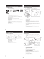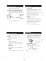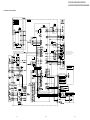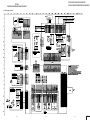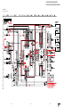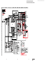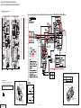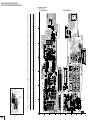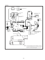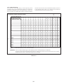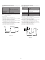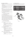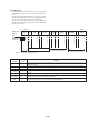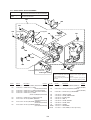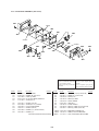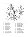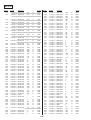
1
CCD-TR315/TR416/TR416PK/TR516/TR516PK/TR716 CCD-TRV16/TRV16PK/TRV36/TRV36PK/TRV43/ TRV46/TRV46PK RMT-708 SERVICE MANUAL US Model Canadian Model CCD-TR416/TR516/TR716 CCD-TRV16/TRV36/TRV43/TRV46 E Model Ver 1.0 1999.01 CCD-TR315/TR416PK/TR516PK CCD-TRV16/TRV16PK/TRV36PK/ TRV46/TRV46PK Photo : CCD-TR516 Hong Kong Model CCD-TRV16/TRV46 Taiwan Model CCD-TRV16 Brazilian Model CCD-TR315/TR416 CCD-TRV16 For MECHANISM ADJUSTMENTS, refer to the “8mm Video MECHANICAL ADJUSTMENT MANUAL VII” (9-973-801-11). SPECIFICATIONS Video camera recorder System Video recording system 2 Rotary heads Helical scanning FM system Audio recording system Rotary heads, FM system Video signal NTSC color, EIA standards Usable cassette 8mm video format cassette CCD-TR315/TR416/TR416PK CCD-TRV16/TRV16PK : standard 8 CCD-TR516/TR516PK/TR716 CCD-TRV36/TRV36PK/TRV43/TRV46/ TRV46PK : Hi8 Recording / Playback time (using 120 min. cassette) SP mode: 2 hours LP mode: 4 hours Fastforward/rewind time (using 120 min. cassette) Approx. 5 min. Image device 1/4 inch CCD (Charge Coupled Device) CCD-TR315/TR416/TR416PK/TR516/ TR516PK CCD-TRV16/TRV16PK/TRV36/ TRV36PK : Approx. 270,000 pixels (Effective : approx 250,000 pixels) MICROFILM NTSC Photo : CCD-TRV46 B MECHANISM Color temperature Auto CCD-TR716 CCD-TRV34/TRV46/TRV46PK : Approx. 320,000 pixels (Effective : approx 200,000 pixels) Minimum illumination 0.4 lux at F 1.4 0 lux (in NightShot mode)* Viewfinder Electronic viewfinder CCD-TR315/TRV series : Monochrome CCD-TR416/TR416PK/TR516/ TR516PK/TR716 : Color Illumination range 0.4 lux to 100,000 lux Lens Combined power zoom lens Filter diameter 1 7/16 in. (37 mm) CCD-TR315/TR416:US,CND CCD-TRV16/TRV16PK : 18 x (Optical), 180 x (Digital) CCD-TR416:BR/TR416PK : 18 x (Optical), 220 x (Digital) CCD-TR516/TR516PK/TR716 CCD-TRV36/TRV36PK/TRV43/TRV46/ TRV46PK : 18 x (Optical), 330 x (Digital) Focal distance 3/16 - 8 in. (4.1 - 37.8 mm) When converted to a 35 mm still camera CCD-TR315/TR416/TR416PK/TR516/ TR516PK CCD-TRV16/TRV16PK/TRV36/ TRV36PK : 1 9/16 - 28 in. (39.4 - 709 mm) CCD-TR715 CCD-TRV43/TRV46/TRV46PK : 1 7/8 - 33 1/2 in. (47.2 - 850 mm) Recommended illumination More than 100 lux * Object invisible for the dark can be shot with infrared lighting. LCD screen (TRV series only) Picture 2.5 inches measured diagonally 2 x 1 1/2 in.(50.3 x 37.4 mm) On-screen display TN LCD/TFT active matrix method Total dot number 61,380 (279 x 220) — Continued on next page — hVIDEO CAMERA RECORDER CCD-TR315/TR416/TR416PK CCD-TRV16/TRV16PK HVIDEO CAMERA RECORDER CCD-TR516/TR516PK/TR716 CCD-TRV36/TRV36PK/TRV43/TRV46/TRV46PK Input and output connectors Video output Phono jack, 1 Vp-p, 75 ohms, unbalanced Audio output Monaural, Phone jack, 327 mV (at output impedance 47 kilohms) impedance less than 2.2 kilohms RFU DC OUT Special minijack, DC 5V Earphone jack (TRV series only) Monaural minijack (ø 3.5 mm) LANC control jack Stereo mini-minijack (ø 2.5 mm) MIC jack Mini jack, 0.388mV low impedance with 2.5 to 3.0 V DC, output impedance 6.8 kilohms (ø 3.5 mm) : Monaural type Speaker (TRV series only) Dynamic speaker General Averege power consumption(when using the battery pack) During camera recording CCD-TR416/TR416PK/TR516/ TR516PK : 2.4 W CCD-TR315/TR716 : 2.5 W During camera recording using LCD CCD-TRV16/TRV16PK/TRV36/ TRV36PK : 3.1 W CCD-TRV43/TRV46/TRV46PK : 3.2 W Viewfinder CCD-TRV16/TRV16PK/TRV36/ TRV36PK : 2.5 W CCD-TRV43/TRV46/TRV46PK : 2.6 W Operating temperature 32°FC to 104°F (C0°C to 40°C) Storage temperature -4°FC to 140°F (-20°C to +60°C) Mass (Approx.) CCD-TR315/TR716 : 1 lb 11 oz (790 g) CCD-TR416/TR416PK/TR516/ TR516PK : 1 lb 11 oz (780 g) CCD-TRV16/TRV16PK/TRV36/ TRV36PK : 1 lb 14 oz (870 g) CCD-TRV43/TRV46/TRV46PK : 1 lb 15 oz (880 g) excluding the battery pack, lithium battery, cassette and shoulder strap 2 lb 3 oz (1 kg) including the battery pack NP-F330, lithium battery CR2025, cassette and shoulder strap AC power adaptor Power requirements 100 -240 V AC, 50/60 Hz Power consumption 23 W Output voltage DC OUT: 8.4 V, 1.5 A in operating mode Operating temperature 32°F to 104°F(0°C to 40°C) Storage temperature -4°F to +140°F(-20°C to +60°C) Microphone Monaural type Dimentions (Approx.) 5 x 1 9/16 x 2 1/2 in. (125 x 39 x 62 mm)(w/h/d) excluding projecting parts Supplied accessories See page 4. Mass (Approx.) 9.8 oz (280 g) excluding power cord Design and specifications are subject to change without notice. Dimentions (Approx.) 4 1/4 x 4 1/4 x 7 5/8 in. 107 x 107 x 193 mm)(w/h/d) • Abbreviation Canadian model is abbreviated as CND. Brazilian model is abbreviated as BR. Power requirements 7.2 V (battery pack) 8.4 V (AC power adaptor) SAFETY CHECK-OUT After correcting the original service problem, perform the following safety checks before releasing the set to the customer: 1. Check the area of your repair for unsoldered or poorly-soldered connections. Check the entire board surface for solder splashes and bridges. 2. Check the interboard wiring to ensure that no wires are “pinched” or contact high-wattage resistors. 3. Look for unauthorized replacement parts, particularly transistors, that were installed during a previous repair. Point them out to the customer and recommend their replacement. 4. Look for parts which, though functioning, show obvious signs of deterioration. Point them out to the customer and recommend their replacement. 5. Check the B+ voltage to see it is at the values specified. 6. Flexible Circuit board Repairing • Keep the temperature of the soldering iron around 270°C during repairing. • Do not touch the soldering iron on the same conductor of the circuit board (within 3 times). • Be careful not to apply force on the conductor when soldering or unsoldering. SAFETY-RELATED COMPONENT WARNING !! ATTENTION AU COMPOSANT AYANT RAPPORT À LA SÉCURITÉ!! COMPONENTS IDENTIFIED BY MARK ! OR DOTTED LINE WITH MARK ! ON THE SCHEMATIC DIAGRAMS AND IN THE PARTS LIST ARE CRITICAL TO SAFE OPERATION. REPLACE THESE COMPONENTS WITH SONY PARTS WHOSE PART NUMBERS APPEAR AS SHOWN IN THIS MANUAL OR IN SUPPLEMENTS PUBLISHED BY SONY. LES COMPOSANTS IDENTIFIÉS PAR UNE MARQUE ! SUR LES DIAGRAMMES SCHÉMATIQUES ET LA LISTE DES PIÉCES SONT CRITIQUES POUR LA SÉCURITÉ DE FONCTIONNEMENT. NE REMPLACER CES COMPOSANTS QUE PAR DES PIÉCES SONY DONT LES NUMÉROS SONT DONNÉS DANS CE MANUEL OU DANS LES SUPPLÉMENTS PUBLIÉS PAR SONY. –2– Table for difference of function CCDTR416PK CCDTR516 CCDTR516PK CCDTR716 CCDTRV16 BR E US,CND E US,CND Color G G ¬ 180X G 510 G G G TYPE G Color G G ¬ 220X G 510 G G G Color G G ¬ 220X G 510 G G G Color ¬ ¬ G 330X ¬ 510 G G G US,CND,E, E HK,BR,TW TYPE F B/W B/W G G G G ¬ ¬ 180X 180X G G 510 510 G G G G 2.5 inch 2.5 inch CCDTRV43 CCDTRV46 CCDTRV46PK Destination US,CND E Classification View finder Remote commander (RMT-708) Hi8 Standard 8 Lens (Digital ZOOM) Video light CCD Steadyshot Laser Link LCD panel B/W ¬ ¬ G 330x ¬ 510P ¬ ¬ 2.5 inch US,CND,E, HK TYPE B B/W ¬ ¬ G 330x ¬ 510P ¬ ¬ 2.5 inch CCDTR315 CCDTR416 Destination E,BR US,CND Classification View finder Remote commander (RMT-708) Hi8 Standard 8 Lens (Digital ZOOM) Video light CCD Steadyshot Laser Link LCD panel TYPE E B/W G G ¬ 180X G 510 G G G Model TYPE C Color ¬ ¬ G 330X ¬ 510 G G G –3– Model B/W ¬ ¬ G 330x ¬ 510P ¬ ¬ 2.5 inch Remark ¬ : with SE-80/81board SE451,452,IC451 ¬ : with VC-215board IC751 2.5 inch : TRV series only TYPE D Color ¬ ¬ G 330X ¬ 510P ¬ G G CCDTRV16PK CCDTRV36 CCDTRV36PK US,CND E B/W ¬ ¬ G 330X ¬ 510 G G 2.5 inch TYPE A B/W ¬ ¬ G 330X ¬ 510 G G 2.5 inch Remark ¬ : with SE-80/81board SE451,452,IC451 ¬ : with VC-215board IC751 2.5 inch : TRV series only • Abbreviation Canadian model is abbreviated as CND. Brazilian model is abbreviated as BR. Hong Kong model is abbreviated as HK. Taiwan model is abbreviated as TW. Supplied accessories 1 2 3 4 5 7 8 9 1 RMT-708 Wireless Remote Commander (1) 6 7 Shoulder strap (1) CCD-TR516/TR516PK/TR716 CCD-TRV36/TRV36PK/TRV43/TRV46/TRV46PK 8 Video P6-15P HB tape CCD-TR416: US/TR516: US/TR716:US CCD-TRV16:US/TRV36:US/TRV43:US/TRV46:US 2 AC-L10A/L10B/L10C AC power adaptor 3 NP-F330 Battery pack (1) 9 2 pin conversion adaptor (1) CCD- TR315//TR416PK/TR516PK CCD- TRV16:E,BR,HK,TW/TRV16PK/TRV36PK/ TRV46:E,HK/TRV46PK 4 CR2025 Lithium Battery (1) The lithium battery is already installed in your camcorder. 5 Size AA (R6) battery for Remote Commander (2) CCD-TR516/TR516PK/TR716 CCD-TRV36/TRV36PK/TRV43/TRV46/TRV46PK 6 A / V connecting cable (1) • Abbreviation Brazilian model is abbreviated as BR. Hong Kong model is abbreviated as HK. Taiwan model is abbreviated as TW. –4– SERVICE NOTE 1. POWER SUPPLY DURING REPAIRS In this unit, about 10 seconds after power is supplied (8.4V) to the battery terminal using the service power cord (J-6082-223-A), the power is shut off so that the unit cannot operate. This following three methods are available to prevent this. Take note of which to use during repairs. Battery switch Method 1. Connect the servicing remote commander RM-95 (J-6082-053-B) to the LANC jack, and set the remote commander switch to the “ADJ” side. Method 2. Press the battery switch of the battery terminal using adhesive tape, etc. Battery terminal ‘ Method 3. Use the DC IN terminal. (Use the AC power adaptor.) DC IN terminal Battery terminal ’ Battery SIG terminal 2. TO TAKE OUT A CASSETTE WHEN NOT EJECT (FORCE EJECT) 1 Refer to 2-1. to remove the front panel block. 2 Refer to 2-4. to remove the cabinet (R) assembly. 3 Refer to 2-6. to remove the battery panel block. 4 Refer to 2-7. to remove the cabinet (L) block. 5 Add +5V from the DC POWER SUPPLY and unload with a pressing the cassette lid. 6 Pull the timing belt in the direction of arrow A with a pinsette while pressing the cassette lid (take care not to damage) to adjust the bending of a tape. A Pinsette Press the cassette lid not to rise the cassette compartment [DC power supply] (+5V) Timing belt 7 Let go your hold the cassette lid and rise the cassette compartment to take out a cassette. + – Loading motor Adjust the bending of a tape Timing belt –5– SELF-DIAGNOSIS FUNCTION 1. Self-diagnosis Function 2. Self-diagnosis display When problems occur while the unit is operating, the self-diagnosis function starts working, and displays on the viewfinder or Display window what to do. This function consists of two display; selfdiagnosis display and service mode display. Details of the self-diagnosis functions are provided in the Instruction manual. When problems occur while the unit is operating, the counter of the viewfinder or Display window shows a 4-digit display consisting of an alphabet and numbers, which blinks at 3.2 Hz. This 5-character display indicates the “repaired by:”, “block” in which the problem occurred, and “detailed code” of the problem. Viewfinder Display window C:31:11 C:31:11 Blinks at 3.2 Hz C 31 11 Display window Repairede by : Block C : Corrected by customer H : Corrected by dealer E : Corrected by service engineer Detailed Code Refer to page7 Self-diagnosis Code table Indicates the appropriate step to be taken E. g. 31 ... Reload the tape. 32 ... Turn on power again. 3. Service Mode Display The service mode display shows up to six self-diagnosis codes shown in the past. 3-1. Display Method While pressing the “STOP” key, set the switch from OFF to “VTR or PLAYER”, and continue pressing the “STOP” key for 5 seconds continuously. The service mode will be displayed, and the counter will show the backup No. and the 5-character self-diagnosis codes. Viewfinder Display window 3C:31:11 [3] C : 3 1 : 1 1 Lights up [3] Backup No. C:31:11 Self-diagnosis codes Control dial Order of previous errors 3-2. Switching of Backup No. By rotating the control dial, past self-diagnosis codes will be shown in order. The backup No. in the [] indicates the order in which the problem occurred. (If the number of problems which occurred is less than 6, only the number of problems which occurred will be shown.) [1] : Occurred first time [4] : Occurred fourth time [2] : Occurred second time [5] : Occurred fifth time [3] : Occurred third time [6] : Occurred the last time 3-3. End of Display Turning OFF the power supply will end the service mode display. Note: The self-diagnosis display data will be backed up by the coin-type lithium battery. When this coin-type lithium battery is disconnected, the self-diagnosis data will be lost by initialization. –6– 4. Self-diagnosis Code Table Repaired by: Self-diagnosis Code Block Detailed Function Code C 2 C 2 C 2 1 0 2 0 3 0 C 3 1 1 C 3 1 1 C C C C C C C C C C C 3 3 3 3 3 3 3 3 3 3 3 1 1 1 1 1 1 1 1 1 1 1 2 2 2 2 3 3 4 4 4 4 4 C 3 2 1 C 3 2 1 C 3 2 2 C 3 2 2 C 3 2 2 C 3 2 2 C 3 2 3 C 3 2 3 C 3 2 4 C 3 2 4 C 3 2 4 C 3 2 4 C 3 2 4 E 6 1 0 E 6 1 1 E 6 2 0 E 6 2 0 Symptom/State Correction 0 Condensation. 0 Video head is dirty. 0 Non-standard battery is used. LOAD direction. Loading does not 0 complete within specified time UNLOAD direction. Loading does not 1 complete within specified time 0 T reel side tape slacking when unloading. 1 S reel side tape slacking when unloading. 2 T reel fault 3 S reel fault 0 FG fault when starting capstan 1 FG fault during normal capstan operations 0 FG fault when starting drum 1 PG fault when starting drum 2 FG fault during normal drum operations 3 PG fault during normal drum operations 4 Phase fault during normal drum operations Remove the cassette, and insert it again after one hour. Clean with the optional cleaning cassette. Use the InfoLITHIUM battery. Load the tape again, and perform operations from the beginning. Load the tape again, and perform operations from the beginning. Load the tape again, and perform operations from the beginning. Load the tape again, and perform operations from the beginning. Load the tape again, and perform operations from the beginning. Load the tape again, and perform operations from the beginning. Load the tape again, and perform operations from the beginning. Load the tape again, and perform operations from the beginning. Load the tape again, and perform operations from the beginning. Load the tape again, and perform operations from the beginning. Load the tape again, and perform operations from the beginning. Load the tape again, and perform operations from the beginning. Load the tape again, and perform operations from the beginning. Remove the battery or power cable, connect, and perform operations 0 LOAD direction loading motor time-out from the beginning. UNLOAD direction loading motor time- Remove the battery or power cable, connect, and perform operations 1 from the beginning. out Remove the battery or power cable, connect, and perform operations 0 T reel side tape slacking when unloading. from the beginning. Remove the battery or power cable, connect, and perform operations 1 S reel side tape slacking when unloading. from the beginning. Remove the battery or power cable, connect, and perform operations 2 T reel fault from the beginning. Remove the battery or power cable, connect, and perform operations 3 S reel fault from the beginning. Remove the battery or power cable, connect, and perform operations 0 FG fault when starting capstan from the beginning. Remove the battery or power cable, connect, and perform operations 1 FG fault during normal capstan operations from the beginning. Remove the battery or power cable, connect, and perform operations 0 FG fault when starting drum from the beginning. Remove the battery or power cable, connect, and perform operations 1 PG fault when starting drum from the beginning. Remove the battery or power cable, connect, and perform operations 2 FG fault during normal drum operations from the beginning. Remove the battery or power cable, connect, and perform operations 3 PG fault during normal drum operations from the beginning. Remove the battery or power cable, connect, and perform operations 4 Phase fault during normal drum operations from the beginning. Inspect the lens block focus reset sensor (Pin !ª of CN551 of VC-215 board) when focusing is performed when the focus dial is rotated in the focus manual mode and the focus motor drive circuit (IC552 of VC-215 Difficult to adjust focus 0 board) when the focusing is not performed. (Cannot initialize focus.) Note : Use the remote commander RM-95 only for the model without the focus dial. Inspect the lens block zoom reset sensor (Pin @¡ of CN551 of VC-215 board) when zooming is performed when the zoom lens is operated and Zoom operations fault 0 the zoom motor drive circuit (IC552 of VC215 board) when zooming is (Cannot initialize zoom lens.) not performed. Handshake correction function does not Inspect yaw angular velocity sensor (SE451 of SE-80/81 board) 0 work well.(With pitch angular velocity peripheral circuits. sensor output stopped) Handshake correction function does not Inspect pitch angular velocity sensor (SE452 of SE-80/81 board) 1 work well.(With yaw angular velocity peripheral circuits. sensor output stopped) –7– TABLE OF CONTENTS SERVICE NOTE 2. DISASSEMBLY 1. Power Supply During Repairs ................................................ 5 2. To Take out a Cassette when not Eject (Force Eject) .............. 5 2-1. Removal of Front Panel Block and Video Light Block .... 2-1 2-2. Removal of LB-54, VF-119 and VF-120 Boards (Color View Finder Models) .................. 2-2 2-3. Removal of VF-99 Board and CRT Assembly (B/W View Finder Models) ..................... 2-2 2-4. Removal of Cabinet (R) Block ......................................... 2-3 2-5. Removal of Cassette Lid Assembly ................................. 2-3 2-6. Removal of Battery Panel Block .......................................... 2-3 2-7. Removal of Cabinet (L) Block ......................................... 2-4 2-8. Removal of Control Switch Block (FK-8500) ................. 2-4 2-9. Removal of Zoom Lens Block and VL-20/21 Board ....... 2-4 2-10. Removal of DD-117 and PJ-90/91 Boards ....................... 2-4 2-11. Removal of VC-215 abd SE-80/81 Boards ...................... 2-5 2-12. Removal of View Finder Block ........................................ 2-5 2-13. Removal of TR Cover, CF-60 Board and Display Panel (TR series) ................................................ 2-6 2-14. Removal of IR Cover, CF-61 Board and LCD Panel (TRV series) ............................................ 2-6 2-15. Service Position ............................................................... 2-7 2-16. Circuit Boards Location ................................................... 2-8 2-17. Flexible Boards and Flat Cables Location ....................... 2-8 Self-Diagnosis Function 1. Self-diagnosis function ............................................................ 6 2. Self-diagnosis Display ............................................................. 6 3. Service Mode Display ............................................................. 6 3-1. Display Method ................................................................ 6 3-2. Switching of Backup No. ................................................. 6 3-3. End of Display ................................................................. 6 4. Self-diagnosis Code Table ....................................................... 7 1. GENERAL This section is extacked from instruction manual of CCD-TRV36/TRV43/TRV46. Using this manual ...................................................................... 1-1 Checking supplied accessories .................................................. 1-1 Installing and Charging the battery pack ................................... 1-1 Inserting a cassette ..................................................................... 1-2 Camera recording ...................................................................... 1-2 Hints for better Shooting ........................................................... 1-4 Checking the recorded picture ................................................... 1-4 Playing back a tape .................................................................... 1-5 Searching for the end of the picture .......................................... 1-5 Using alternative power sources ................................................ 1-6 Changing the mode settings ...................................................... 1-6 Shooting with backlighting ....................................................... 1-7 Using the FADER function ....................................................... 1-7 Shooting in the dark (NightShot) .............................................. 1-8 Using the wide mode function ................................................... 1-8 Using the PROGRAM AE function ........................................... 1-9 Focusing manually ..................................................................... 1-9 Enjoying picture effect ............................................................ 1-10 Adjusting the exposure ............................................................ 1-10 Superimposing a title ............................................................... 1-11 Making your own titles ............................................................ 1-11 Recording with the date/time ................................................... 1-11 Optimizing the recording condition ......................................... 1-12 Using the built-in light ............................................................. 1-12 Releasing the STEADYSHOT function .................................. 1-12 Watching on a TV screen ......................................................... 1-13 Editing onto another tape ......................................................... 1-13 Changing the lithium battery in the camcoder ........................ 1-13 Resetting the date and time ...................................................... 1-14 Simple setting of clock by time difference .............................. 1-14 Usable cassettes and playback modes ..................................... 1-14 Tips for using the battery pack ................................................ 1-15 Maintenance information and precautions .............................. 1-15 Using your camcorder abroad ................................................. 1-17 Truoble check .......................................................................... 1-17 Self-diagnosis display .............................................................. 1-18 Identifying the parts ................................................................. 1-18 Warning Indicators .................................................................. 1-20 3. BLOCK DIAGRAMS 3-1. Overall Block Diagram .................................................... 3-1 3-2. Camera/Video 1 Block Diagram ...................................... 3-5 3-3. VTR/Camera Control Block Diagram ............................. 3-9 3-4. Servo Block Diagram ..................................................... 3-12 3-5. Mode Control Block Diagram ........................................ 3-15 3-6. Audio Block Diagram .................................................... 3-19 3-7. LCD Block Diagram (TRV model) .................................... 3-23 3-8. Color EVF Block Diagram (Color EVF model) ............ 3-26 3-9. B/W EVF Block Diagram (B/W EVF model) ............... 3-29 3-10. Power Block Diagram .................................................... 3-33 –8– 4. PRINTED WIRING BOARDS AND SCHEMATIC DIAGRAMS 5. ADJUSTMENTS 4-1. Frame Schematic Diagram (1) ........................................... 4-1 • Frame Schematic Diagram (2) ........................................ 4-4 4-2. Printed Wiring Boards and Schematic Diagrams ............... 4-7 • CD-210/211 (CCD Imager) Board .................................. 4-8 • VC-215 (Camera, Y/C Processor, IN/OUT, REC/PB Head Amp, Servo/System Control, Servo, Audio, IR Transmitter, Mode Control) Board ............... 4-10 • VC-215 (Camera 1) Board ............................................ 4-17 • VC-215 (Camera 2) Board ............................................ 4-19 • VC-215 (Y/C Processor) Board .................................... 4-23 • VC-215 (IN/OUT) Board .............................................. 4-27 • VC-215 (REC/PB Head Amp) Board ............................ 4-31 • VC-215 (Servo/System Control) Board ........................ 4-35 • VC-215 (Servo) Board .................................................. 4-38 • VC-215 (Audio) Board .................................................. 4-41 • VL-20/21 (Video Light) Board (Video Light model) .... 4-45 • VC-215 (IR Transmitter) Board .................................... 4-46 • VC-215 (Mode Control) Board ..................................... 4-49 • SE-80/81 (Steady Shot) Board ...................................... 4-52 • PJ-90/91 (AV OUT) Board ............................................ 4-55 • MA-345/346 (Mic, Laser Link) Board .......................... 4-59 • CF-60 (Control (TR Series)) Board ............................... 4-65 • CF-61 (Control (TRV Series)) Board ............................ 4-72 • Control Switch Block (FK-8500/SS-8500) ................... 4-79 • PD-107 (RGB Decorder, LCD Drive, Back Light, LCD (TRV Series)) Board ......................... 4-81 • PD-107 (RGB Decorder (TRV Series)) Board .............. 4-83 • PD-107 (LCD Drive (TRV Series)) Board .................... 4-86 • PD-107 (Back Light (TRV Series)) Board .................... 4-89 • PD-107 (LCD (TRV Series)) Board .............................. 4-90 • VF-99 (B/W EVF (B/W EVF Model)) Board ............... 4-92 • VF-119 (COLOR EVF (COLOR EVF Model)) Board ...... 4-95 • VF-120 (COLOR EVF (COLOR EVF Model)) Board .... 4-100 • LB-54 (Back Light (Color EVF model)) Board .......... 4-102 • DD-117 (Power) Board ............................................... 4-109 5-1. CAMERA SECTION ADJUSTMENTS .......................... 5-1 1-1. Preparations before Adjustment (Camera Section) .......... 5-1 1-1-1. List of Service Tools ................................................. 5-1 1-1-2. Preparations ............................................................... 5-2 1-1-3. Precautions ................................................................ 5-5 1. Setting the Switch ..................................................... 5-5 2. Adjusting Procedure .................................................. 5-5 3. Subject ....................................................................... 5-5 1-1-4. Adjusting Remote Commander ................................. 5-6 1. Using the adjusting remote commander .................... 5-6 2. Precautions upon using the adjusting remote commander .................................................... 5-6 1-1-5. Data Processing ......................................................... 5-7 1-2. Initialization of D, E, F Page Data .................................... 5-8 1. Initialization the D, E, F Page Data ........................... 5-8 2. Modification of D, E, F Page Data ........................... 5-8 3. D Page Table ............................................................. 5-9 4. F Page Table ............................................................ 5-10 5. E Page Table ............................................................ 5-12 1-3. Camera System Adjustments .......................................... 5-14 1. G-CAM flip Adjustment ......................................... 5-14 2. Hall Adjustment ...................................................... 5-15 3. Flange Back Adjustment ......................................... 5-16 3-1. Flange Back Adjustment (1) ................................... 5-16 3-2. Flange Back Adjustment (2) ................................... 5-16 4. Flange Back Check ................................................. 5-17 5. Picture Frame Setting .............................................. 5-17 6. Color Reproduction Adjustment ............................. 5-18 7. IRIS IN/OUT Adjustment ....................................... 5-19 8. MAX GAIN Adjustment ......................................... 5-19 9. Auto White Balance Standard Data Input ............... 5-20 10. Auto White Balance Adjustment ............................. 5-20 11. White Balance Check .............................................. 5-21 12. Angular Velocity Sensor Sensitivity Check ............ 5-22 1-4. Color Electronic Viewfinder System Adjustments (CCD-TR416/TR416PK/TR516/TR516PK/TR716) ...... 5-23 1. EVF Initial Data Input ............................................. 5-23 2. VCO Adjustment (VF-119 board) ........................... 5-24 3. Bright Adjustment (VF-119 board) ......................... 5-24 4. Contrast Adjustment (VF-119 board) ..................... 5-25 5. Backlight Consumption Current Adjustment (VF-120 board) ....................................................... 5-25 1-5. Monochrome Electronic Viewfinder System Adjustments ....................................................... 5-26 1-5-1. Horizontal Slant Check ........................................... 5-26 1-5-2. Centering Adjustment ............................................. 5-26 1-5-3. Focus Adjustment .................................................... 5-26 1-5-4. Aberration Adjustment ............................................ 5-27 1-5-5. Horizontal Amplitude Adjustment (VF-99 board) .. 5-27 1-5-6. Vertical Amplitude Adjustment (VF-99 board) ....... 5-28 1-5-7. Brightness Adjustments (VF-99 board) .................. 5-28 1-5-8. Horizontal Amplitude, Vertical Amplitude, Focus Check ............................................................ 5-28 1-6. LCD System Adjustment (TRV Series) .......................... 5-29 1. LCD initial data input ............................................. 5-29 2. VCO adjustment (PD-107 board) ........................... 5-30 3. D range adjustment (PD-107 board) ....................... 5-30 4. Bright adjustment (PD-107 board) .......................... 5-31 5. Contrast adjustment (PD-107 board) ...................... 5-31 6. V-COM adjustment (PD-107 board) ....................... 5-32 7. Color adjustment (PD-107 board) ........................... 5-32 8. V-COM adjustment (PD-107 board) ....................... 5-33 9. White balance adjustment (PD-107 board) ............. 5-33 –9– 5-2. MECHANICAL SECTION ADJUSTMENT ................. 5-34 2-1. Operating without a Cassette .......................................... 5-34 2-2. Tape path Adjustment ..................................................... 5-34 1. Preparations for adjustments ................................... 5-34 5-3. VIDEO SECTION ADJUSTMENTS ............................. 5-35 3-1. Preparations before Adjustment ...................................... 5-35 3-1-1. Equipments to be Used ........................................... 5-35 3-1-2. Precautions on Adjusting ........................................ 5-36 3-1-3. Adjusting Connectors .............................................. 5-36 3-1-4. Connecting the Equipments .................................... 5-37 3-1-5. Alignment Tape ....................................................... 5-37 3-1-6. Output Level and Impedance .................................. 5-39 3-1-7. Recording Mode (Standard 8/Hi8) switching (Hi8 model) ............................................................. 5-39 3-1-8. Service Mode .......................................................... 5-39 1. Test mode setting ..................................................... 5-39 2. Emergency memory address ................................... 5-40 2-1. EMG CODE (Emergency Code) ............................. 5-40 2-2. MSW Codes ............................................................ 5-41 3. Bit value discrimination .......................................... 5-42 4. Switch check (1) ...................................................... 5-42 5. Switch check (2) ...................................................... 5-43 6. Headphone jack check ............................................ 5-43 7. Input/output selection check ................................... 5-43 8. LED, LCD (display window) check ........................ 5-44 9. Record of use check ................................................ 5-44 3-2. System Control System Adjustment ............................... 5-45 1. Initialization of D, E, F Page Data .......................... 5-45 2. Battery End Adjustment (VC-215 board) ............... 5-45 3-3. Servo System Adjustments ............................................. 5-46 1. CAP FG Offset Adjustment (VC-215 board) .......... 5-46 2. Switching Position Adjustment (VC-215 board) .... 5-46 3-4. Video System Adjustments .............................................. 5-47 1. 28 MHz Origin Oscillation Adjustment (VC-215 board) ....................................................... 5-47 2. AFC f0 Adjustment (VC-215 board) ...................... 5-48 3. Filter f0 Adjustment (VC-215 board) ...................... 5-48 4. Y OUT Level Adjustment (VC-215 board) ............. 5-49 5. C OUT Level Adjustment (VC-215 board) ............. 5-49 6. RP Filter f0 Adjustment (VC-215 board) ................ 5-50 7. Hi8 REC Y Current Adjustment (VC-215 board) (CCD-TR516/TR516PK/TR716 CCD-TRV36/ TRV36PK/TRV43/TRV46/TRV46PK) ................... 5-51 8. Standerd8 REC Y Current Adjustment (VC-215 board) (CCD-TR315/TR416/TR416PK CCD-TRV16/TRV16PK) ........................................ 5-52 9. Hi8 REC L Level Adjustment (VC-215 board) (CCD-TR516/TR516PK/TR716 CCD-TRV36/ TRV36PK/TRV43/TRV46/TRV46PK) ................... 5-53 10. Standerd8 REC L Level Adjustment (VC-215 board) (CCD-TR315/TR416/TR416PK CCD-TRV16/TRV16PK) ........................................ 5-54 11. REC C Current Adjustment (VC-215 board) .......... 5-55 3-5. IR Transmitter Adjustments (CCD-TRV43/TRV46/TRV46PK) .......................... 5-56 1. IR Video Carrier Frequency Adjustment (VC-215 board) ....................................................... 5-56 2. IR Video Deviation Adjustment (VC-215 board) .... 5-56 3. IR Audio Deviation Adjustment (VC-215 board) ... 5-57 3-6. Monaural Audio System Adjustment ............................... 5-58 1. 1.5 MHz Deviation Adjustment (VC-215 board) .... 5-59 2. BPF Adjustment (VC-215 board) ........................... 5-59 3-7. Arrangement Diagram for Adjustment Parts ................... 5-60 6. REPAIR PARTS LIST 6-1. Exploded Views ................................................................. 6-1 6-1-1. Remote Commander and Cassette Lid Assembly .... 6-1 6-1-2. Cabinet (L) and Battery Panel Assembly ................. 6-2 6-1-3. Front Panel Block Assembly .................................... 6-3 6-1-4. Cabinet (R) Block Assembly (TR series) ................ 6-4 6-1-5. Cabinet (R) Block Assembly (TRV series) .............. 6-5 6-1-6. Main Boards Block Assembly ................................. 6-6 6-1-7. Clolor EVF Block Assembly (CCD-TR416/TR416PK/TR516/TR516PK/TR716) ..... 6-7 6-1-8. B/W EVF Block Assembly (CCD-TR315 and TRV series) ................................. 6-8 6-1-9. LCD Block Assembly (TRV series) ......................... 6-9 6-1-10. Zoom Lens Block Assembly .................................. 6-10 6-1-11. Cassette Compartment Assembly .......................... 6-11 6-1-12. LS Chassis Assembly ............................................. 6-12 6-1-13. Mechanism Chassis Assembly ............................... 6-13 6-2. Electrical Parts List .......................................................... 6-14 – 10 – CCD-TR315/TR416/TR416PK/TR516/TR516PK/TR716 CCD-TRV16/TRV16PK/TRV36/TRV36PK/TRV43/TRV46/TRV46PK SECTION 1 GENERAL 1-1 This section is extracted from instruction manual of CCD-TRV36/TRV43/TRV46. 1-2 1-3 1-4 1-5 1-6 1-7 1-8 1-9 1-10 1-11 1-12 1-13 1-14 1-15 1-16 1-17 1-18 1-19 1-20E CCD-TR315/TR416/TR416PK/TR516/TR516PK/TR716 CCD-TRV16/TRV16PK/TRV36/TRV36PK/TRV43/TRV46/TRV46PK SECTION 2 DISASSEMBLY The equipment can be removed using the following procedure. VIDEO CAMERA RECORDER 2-2. LB-54/VF-119 & 120 BOARDS (Color view finder models only) 2-3. CRT/VF-99 BOARD (B/W view finder models only) 2-1. FRONT PANEL BLOCK VIDEO LIGHT BLOCK (Video light models only) 2-5. CASSETTE LID ASSEMBLY 2-4. CABINET (R) BLOCK 2-13. CONTROL SWITCH BLOCK (MF-8500) TR COVER (TR series) CF-60 BOARD (TR series) LCD BLOCK (TR series) 2-14. IR COVER (TRV series) CF-61 BOARD (TRV series) LCD PANEL (TRV series) 2-12. VIEW FINDER BLOCK 2-5. CASSETTE LID ASSEMBLY 2-6. BATTERY PANEL BLOCK 2-7. CABINET (L) BLOCK 2-9. ZOOM LENS BLOCK VL-21/22 BOARD 2-8. CONTROL SWITCH BLOCK (FK-8500) 2-10. DD-117 & PJ-90/91 BOARDS 2-11. VC-215 & SE-80/81 BOARDS NOTE : Follow the disassembly procedure in the numerical order given. 2-1. REMOVAL OF FRONT PANEL BLOCK AND VIDEO LIGHT BLOCK —Video light models— —No video light models— CCD-TR516/TR516PK/TR716 CCD-TRV36/TRV36PK/TRV43/TRV46/TRV46PK CCD-TR315/TR416/TR416PK CCD-TRV16/TRV16PK 2Cabinet (LT) 1Two screws (M2 x 4) 1Two screws (M2x4) 2Cabinet (N) 3Screw (M2x4) 6Front panel block 3Screw (M2 x 4) 6Front panel block 8Video light block Claw Claw 4Screw (M 2x 4) Two claws 5Two screws (M2 x 4) 4Screw (M2x4) 7FP-56 flexible board 5Two screws (M2 x 4) CN303, 18P 7FP-56 flexible board CN303, 18P 2-1 2-2. REMOVAL OF LB-54, VF-119 AND VF-120 BOARDS (Color view finder model CCD-TR416/TR416PK/TR516/TR516PK/TR716) 1 Tilt-up the EVF block to the direction of arrow A. 5 FP-57 flexible board CN5401,20P 3 Remove the EVF rear cabinet assembly 4 Flexible retainer sheet to the direction of arrow B. !£ VF-119 board !º Back light cushion Four claws ( Turn the cushion (Sponge rubber) face to the LB-54 board side for installation. ) 6 FP-57 flexible board CN5301,8P 2 Two screws (M2 x 3) !™ LCD cushion (1) B !¡ LCX024AK-5 CN5402, 16P Three claws A 9 LB-54 board 8 VF-120 board 7 VF light interception sheet 2-3. REMOVAL OF VF-99 AND CRT ASSEMBLY (B/W view finder model CCD-TR315 and TRV series) 1 Tilt-up the EVF block to the direction of arrow A. 7 CRT assembly 6 CRT holder assmebly 3 Remove the EVF rear cabinet assembly to the direction of arrow B. 4 VF electrostatic sheet 2 Three screws (M2 x 3) B A 8 VF-99 board 5 Flexible flat cable(FFC-235) CN5803,4P 2-2 2-4. REMOVAL OF CABINET (R) BLOCK Note : Be sure to that the pin of the Lens assembly is put into the hole of the IR knob when attaching. (TR series) (TRV series) 5Flat cable (FFC-257F) 5Flat cable (FFC-257F) CN911, 45P CN911, 45P 2Two screws 2Two screws (M2 x 4) Pin 3Three screws (M2 x 4) Pin 3Three screws (M2 x 4) (M2 x 4) 6Harness (PD-108) 1Two screws 4Cabinet (R) block 1Two screws 4Cabinet (R) block (M2 x 4) (M2 x 4) IR knob IR knob 2-5. REMOVAL OF CASSETTE LID ASSEMBLY 2-6. REMOVAL OF BATTERY PANEL BLOCK 1Two screws (M2x4) 2Cassette lid assembly 3Connector CN801, 7P 2Battery panel block 1Two screws (M2 x 4) 2-3 2-7. REMOVAL OF CABINET (L) BLOCK 2-8. REMOVAL OF CONTROL SWITCH BLOCK Function Key Switch (FK-8500) 2Cabinet (L) block 1 Remove the Function key switch in Screwdriver(-) 2Flexible connector the direction of arrow with pushing the claw. Two claws CN935, 10P 3Flexible connector CN934,12P 1Screw (M2 x 3) Two claws 2-9. REMOVAL OF ZOOM LENS BLOCK AND VL-21/22 BOARD 2-10. REMOVAL OF DD-117 AND PJ-90/91 BOARDS 1Three screws (M2 x 3) —Video light models— CCD-TR516/TR516PK/TR716 CCD-TRV36/TRV36PK/TRV43/TRV46/TRV46PK —No video light models— CCD-TR315/TR416/TR416PK CCD-TRV16/TRV16PK CN931, 70P CN101, 12P 7Two screws (M2 x 3) 8Shoe bracket No video light models 2DD-117 board 3Screw (M2 x 3) 5FP-623 flexible board CN501, 16P 4Zoom lens block 5PJ-90/91 board 6Lens flexible board CN551, 23P CN909 4Two screws (M2 x 4) 2Screw (M2 x 3) 1Screw (M2 x 3) !¡FP-58 flexible board 0VL-21/22 board 9Screw (M2 x 3) 3FP-621 flexible board (VC side)CN909, 4P (VL side)CN151, 4P Video light models 2-4 2-11. REMOVAL OF VC-215 AND SE-80/81 BOARDS 2 Flexible board 6 FP-56 flexible board 1 FP-220 flexible board CN916, 18P CN901, 8P from loading motor 0 Screw (M2x3) CN001, 16P from video head 7 FP-621 flexible board CN902, 12P 3 Flexible board CN905, 10P from drum motor 8 FP-620 flexible board 4 FP-248 flexible board (VC side) CN904, 10P (SE side) CN650, 10P !™ Four screws (M2x3) 9 Two screws (M2 x 3) CN905, 12P !¡ VC-215 board 5 FP-221 flexible board CN908, 15P !£ SE-80/81 board CCD-TR716 & TRV series 2-12. REMOVAL OF VIEW FINDER BLOCK —Color view finder— —B/W view finder— CCD-TR315 and TRV series CCD-TR416/TR416PK/TR516/TR516PK/TR716 2VF flexible retainer sheet 2VF flexible retainer sheet 3Tapping screw 3Tapping screw 4Tapping screw 4Tapping screw 5VF base assembly 5VF base assembly 7Three tapping 7Three tapping screws screws 1FP-57 flexible board 1Flat cable (FFC-235) CN007, 20P CN008, 4P 6Tilt-up the EVF block to 6Tilt-up the EVF block to the direction of arrow. the direction of arrow. 2-5 2-13. REMOVAL OF TR COVER, CF-60 BOARD AND DISPLAY PANEL ...(TR series) !∞ Liquid crystal display panel Phase adjustment S024 !¢ LCD holder S015 4FP-57 flexible board...(Color EVF type only) CN007, 20P Flat cable (FFC-235)...(B/W EVF type only) CN008, 4P Claw !™ CF-60 board !¡Two tapping screws 6Two tapping screws Hole 5Flat cable (FFC-257S) !£ CN009 !§ IR knob CN001, 50P 9TR cover assembly !¶ Link plate spring 0 Two tapping screws 8 Tapping screw 1Flexible connector CN002, 8P 7Three tapping screws 2 Two tapping screws 3Control switch block (MF-8500) 2-14. REMOVAL OF IR COVER, CF-61 BOARD AND LCD PANEL...(TRV series) Claw !¶LCD panel 4Flat cable (FFC-235) CN008, 4P !§Four tapping screws Phase adjustment S024 Hole 5Flat cable (FFC-257S) CN001, 45P !¢ IR knob !™Two tapping screws !£IR cover assembly CN008 !∞ Link plate spring 0CF-61 board 6Harness 9Five tapping screws !¡Three tapping screws 1Flexible connector CN002, 8P 2 Two tapping screws 7Harness (PD-108) 8Three tapping screws 3Control switch block (MF-8500) 2-6 2-15. SERVICE POSITION Preparation : Refer to previous section “DISASSEMBLY”, and connect as shown in the figure after each parts has been removed. —TR series— CPC-7 jig (J-6082-382-A) VC-215 board : CN910, 16P Extension cord 70P (J-6082-439-A) DD-117 board : CN931 — VC-215 board : CN915 VC-215 board Screw (M2x3) Control switch block (FK-8500) Cabinet (R) block Battry panel block DD-117 board PJ-90 board Cabinet (L) block Front panel block —TRV series— CPC-7 jig (J-6082-382-A) VC-215 board : CN910, 16P Extension cord 70P (J-6082-439-A) DD-117 board : CN931 — VC-215 board : CN915 VC-215 board Screw (M2 x 3) Control switch block (FK-8500) Cabinet (R) block Battry panel block LCD panel block DD-117 board PJ-91 board Cabinet (L) block Front panel block 2-7 2-16. CIRCUIT BOARDS LOCATION VF-119...Color EVF models only (Color EVF) LB-54...Color EVF models only (Back light) VF-120...Color EVF models only (Color EVF) CF-60...TR series only (Control) VL-21... TR516/TR516PK/TR716 VL-22... TRV36/TRV36PK/TRV43/ DD-117 (Power) TRV46/TRV46PK VF-99...B/W EVF models only (B/W EVF) (Video light) CD-210...TR series only CD-211...TRV series only (CCD imager) PJ-90...TR series PJ-91...TRV series (AV Out) VC-215 Camera, Y/C prosessor, IN/OUT, REC.PB head amp, Servo/System control, Servo, Audio, IR transmitter, Mode control PD-107...TRV series only RGB decoder, LCD, LCD drive, Back light MA-345...TR series MA-346...TRV series (Mic, Laser link) CF-61...TRV series only (Control) SE-80...TR716 only SE-81...TRV series only (Steady shot) 2-17. FLEXIBLE BOARDS AND FLAT CABLES LOCATION FP-57...Color EVF models only Stand-by, Start/Stop Back light...Color EVF models only (SS-8500) Zoom lens Flat cable (FFC-235)...B/W EVF models only FP-623 FP-58...Video light models only FP-355 FP-356 FP-680 Function key (FK-8500) FP-249 Flat cable (FFC-257F) FP-621 FP-56 FP-248 FP-642...TRV series only FP-221 Manual forcus Capstan motor Video head Drum motor 2-8E (MF-8500) FP-620...TR716 & TRV series only FP-220 CCD-TR315/TR416/TR416PK/TR516/TR516PK/TR716 CCD-TRV16/TRV16PK/TRV36/TRV36PK/TRV43/TRV46/TRV46PK SECTION 3 BLOCK DIAGRAMS 3-1. OVERALL BLOCK DIAGRAM (VIDEO LIGHT MODEL) ( TR716 only ) (TR MODEL TR516/TR516PK/TR716) (TRV MODEL TRV36/TRV36PK/TRV43/TRV46/TRV46PK) VIDEO LIGHT 4-69 SELECT I/O L I/O R ( TRV MODEL ) TR MODEL : CCD-TR315/TR416/TR416PK/TR516/TR516PK/TR716 TRV MODEL : CCD-TRV16/TRV16PK/TRV36/TRV36PK/TRV43/TRV46/TRV46PK COLOR EVF MODEL : CCD-TR416/TR416PK/TR516/TR516PK/TR716 B/W EVF MODEL : CCD-TR315 CCD-TRV16/TRV16PK/TRV36/TRV36PK/TRV43/TRV46/TRV46PK STEADY SHOT MODEL : CCD-TRV43/TRV46/TRV46PK IR TRANSMITTER MODEL : CCD-TRV43/TRV46/TRV46PK REMOTE COMMANDER MODEL : CCD-TR516/TR516PK/TR716 CCD-TRV36/TRV36PK/TRV43/TRV46/TRV46PK VIDEO LIGHT MODEL : CCD-TR516/TR516PK/TR716 CCD-TRV36/TRV36PK/TRV43/TRV46/TRV46PK 3.1V 3.1V 3-1 3-2 3-3 3-4 CCD-TR315/TR416/TR416PK/TR516/TR516PK/TR716 CCD-TRV16/TRV16PK/TRV36/TRV36PK/TRV43/TRV46/TRV46PK 3-2. CAMERA/VIDEO 1 BLOCK DIAGRAM CAMERA REC 0.3Vp-p 2V CAMERA REC IC001 H IC401 CAMERA REC 2V CAMERA REC 0.3Vp-p IC202 16 CAMERA REC 1.3Vp-p H CAMERA REC 5 TRIG : IC001 21 3Vp-p 0.4Vp-p 0.5Vp-p 1.3Vp-p 7 IC001 44 , 48 H IC001 H 3 IC202 13 H IC502 26 3.1 CAMERA REC PB 3.2Vp-p PB 0.4Vp-p 0.14usec 3.1 7Vp-p 0.4Vp-p IC502 2 — 10 V V IC202 40 IC001 17 H IC401 3 4 PB 0.4Vp-p H PB IC502 36 0.4Vp-p 7Vp-p V IC001 11 H IC401 PB 1 , 2 0.4Vp-p CAMERA REC TR MODEL : CCD-TR315/TR416/TR416PK/TR516/TR516PK/TR716 TRV MODEL : CCD-TRV16/TRV16PK/TRV36/TRV36PK/TRV43/TRV46/TRV46PK COLOR EVF MODEL : CCD-TR416/TR416PK/TR516/TR516PK/TR716 B/W EVF MODEL : CCD-TR315 CCD-TRV16/TRV16PK/TRV36/TRV36PK/TRV43/TRV46/TRV46PK H CAMERA REC 14.32 MHz IC501 IC001 2.3Vp-p CAMERA REC 7 7Vp-p 2.3Vp-p 28.636 MHz IC501 3.1 4.12 MHz 5 Q001 11 , 12 CAMERA REC CAMERA REC 2.9Vp-p 2V 3Vp-p IC001 21 H IC501 44 CAMERA REC 3Vp-p V CAMERA REC IC501 45 3.1Vp-p H IC151 62 3.58 MHz 1.6Vp-p CAMERA REC IC202 66 3Vp-p H IC201 20 0.46Vp-p CAMERA REC CAMERA REC CAMERA REC CAMERA REC H IC151 0.9Vp-p H H IC202 3Vp-p 0.34Vp-p 0.84Vp-p 3 IC202 6 H 3 V IC201 19 IC202 33 0.32Vp-p H IC151 CAMERA REC 5 H IC151 29 3.2Vp-p 2.1Vp-p 7.16 MHz CAMERA REC IC201 8 0.18Vp-p H IC202 26 CAMERA REC 0.18Vp-p CAMERA REC 3Vp-p H IC202 23 V 3.1 IC202 81 PB 3Vp-p H IC202 80 3-5 3-6 3-7 3-8 C CCD-TR315/TR416/TR416PK/TR516/TR516PK/TR716 CCD-TRV16/TRV16PK/TRV36/TRV36PK/TRV43/TRV46/TRV46PK 3-3. VTR/CAMERA CONTROL BLOCK DIAGRAM 710 only 3.1V 3.1V 1.7Vp-p 20 MHz IC402 1 3.1V 3Vp-p 13usec 3.1V IC402 70 TR MODEL : CCD-TR315/TR416/TR416PK/TR516/TR516PK/TR716 TRV MODEL : CCD-TRV16/TRV16PK/TRV36/TRV36PK/TRV43/TRV46/TRV46PK COLOR EVF MODEL : CCD-TR416/TR416PK/TR516/TR516PK/TR716 STEADY SHOT MODEL : CCD-TRV43/TRV46/TRV46PK 3.1V 3Vp-p 4V IC402 48 3Vp-p 2V IC402 47 3.1V 3.1V 3.1V 3.1V 3-9 3-10 3-11 CCD-TR315/TR416/TR416PK/TR516/TR516PK/TR716 CCD-TRV16/TRV16PK/TRV36/TRV36PK/TRV43/TRV46/TRV46PK 3-4. SERVO BLOCK DIAGRAM 3Vp-p 13usec IC402 69 3Vp-p 0.76Vp-p 2.8msec 506 kHz IC402 116 IC801 64 3.1V 1.2Vp-p 5.6msec IC451 3.1V 1 , 2 , 29 3Vp-p 3Vp-p 2V 1.2msec 0.76Vp-p IC402 115 507 kHz IC402 117 IC801 4 3Vp-p 13usec IC402 68 3-12 3-13 3-14 CCD-TR315/TR416/TR416PK/TR516/TR516PK/TR716 CCD-TRV16/TRV16PK/TRV36/TRV36PK/TRV43/TRV46/TRV46PK CCD-TR315/TR416/TR416PK/TR516/TR516PK/TR716 CCD-TRV16/TRV16PK/TRV36/TRV36PK/TRV43/TRV46/TRV46PK 3-5. MODE CONTROL BLOCK DIAGRAM SELECT (TRV MODEL) 1.5Vp-p 20 MHz IC604 41 2.6Vp-p 32 kHz IC604 52 TRV TR MODEL : CCD-TR315/TR416/TR416PK/TR516/TR516PK/TR716 TRV MODEL : CCD-TRV16/TRV16PK/TRV36/TRV36PK/TRV43/TRV46/TRV46PK REMOTE COMMANDER MODEL : CCD-TR516/TR516PK/TR716 CCD-TRV36/TRV36PK/TRV43/TRV46/TRV46PK VIDEO LIGHT MODEL : CCD-TR516/TR516PK/TR716 CCD-TRV36/TRV36PK/TRV43/TRV46/TRV46PK (VIDEO LIGHT MODEL) (TR MODEL TR516/TR516PK/TR716) (VIDEO LIGHT MODEL) (TRV MODEL TRV36/TRV36PK/TRV43/TRV46/TRV46PK) VIDEO LIGHT 3.1V 3-15 3-16 3-17 3-18 CCD-TR315/TR416/TR416PK/TR516/TR516PK/TR716 CCD-TRV16/TRV16PK/TRV36/TRV36PK/TRV43/TRV46/TRV46PK 3-6. AUDIO BLOCK DIAGRAM 0.7Vp-p 0.5Vp-p H 0.09usec IC751 22 IC751 41 PB 0.4Vp-p 0.34Vp-p V 0.09usec IC301 24 IC751 16 3.1V 0.5Vp-p 2usec IC751 15 0.25Vp-p 3.58 MHz IC751 7 CAMERA REC 0.36Vp-p V IC301 29 CAMERA REC TR716 only 0.26Vp-p 3.58 MHz IC301 32 3.1V TR MODEL : CCD-TR315/TR416/TR416PK/TR516/TR516PK/TR716 TRV MODEL : CCD-TRV16/TRV16PK/TRV36/TRV36PK/TRV43/TRV46/TRV46PK IR TRANSMITTER MODEL : CCD-TRV43/TRV46/TRV46PK CAMERA REC 2.9Vp-p 2V IC301 21 3-19 3-20 3-21 3-22 CCD-TR315/TR416/TR416PK/TR516/TR516PK/TR716 CCD-TRV16/TRV16PK/TRV36/TRV36PK/TRV43/TRV46/TRV46PK 3-7. LCD BLOCK DIAGRAM (TRV MODEL) H IC5502 16 4.7Vp-p 2H IC5502 20 4.2Vp-p 0.7Vp-p 3.1V 3.1V H IC5502 13 2H IC5502 22 4.2Vp-p 2H IC5502 24 0.44Vp-p 4.2Vp-p 0.2Vp-p 15 IC5502 9 0.2Vp-p FRPV IC5502 8 H FRPT H 3.1V H IC5502 10 VGL COM 11 H 5601 4 IC5601 26 4.7Vp-p Approx.5.8MHz : 4.1Vp-p IC5602 DAC AMP 3 IN+ 1 FRPT OUT1 12 IC5601 24 FRPV 4.7Vp-p Approx.2.9 MHz H IC5601 37 4.7Vp-p TRV MODEL : CCD-TRV16/TRV16PK/TRV36/TRV36PK/TRV43/TRV46/TRV46PK 3.1V 20msec IC4601/5601 34 3-23 4.7Vp-p 3-24 3-25 CCD-TR315/TR416/TR416PK/TR516/TR516PK/TR716 CCD-TRV16/TRV16PK/TRV36/TRV36PK/TRV43/TRV46/TRV46PK 3-8. COLOR EVF BLOCK DIAGRAM (COLOR EVF MODEL) FP-57 (FLEXIBLE 7.5Vp-p 2H IC5401 22 7.2Vp-p 2H IC5401 20 3.1V LCD902 7.6Vp-p 2H 3.1V IC5401 24 3.1V 3.1V 3.1V 3Vp-p 3.1V H IC5401 14 3Vp-p 12Vp-p V H IC5404 45 IC5301 15 3Vp-p H IC5404 22 3.4Vp-p 1.84 MHz IC5404 23 , 24 3.1V 3Vp-p 7.852 kHz IC5404 20 , 21 3Vp-p 2.7Vp-p COLOR EVF MODEL : CCD-TR416/TR416PK/TR516/TR516PK/TR716 V 11.06 MHz IC5404 18 IC5404 41 2.4Vp-p H IC5301 4 3-26 3-27 3-28 CCD-TR315/TR416/TR416PK/TR516/TR516PK/TR716 CCD-TRV16/TRV16PK/TRV36/TRV36PK/TRV43/TRV46/TRV46PK CCD-TR315/TR416/TR416PK/TR516/TR516PK/TR716 CCD-TRV16/TRV16PK/TRV36/TRV36PK/TRV43/TRV46/TRV46PK 3-9. B/W EVF BLOCK DIAGRAM B/W EVF MODEL T901/T902 2.2Vp-p H IC901 13 1Vp-p H IC901 11 B/W EVF MODEL : CCD-TR315 CCD-TRV16/TRV16PK/TRV36/TRV36PK/TRV43/TRV46/TRV46PK 3-29 3-30 3-31 3-32 CCD-TR315/TR416/TR416PK/TR516/TR516PK/TR716 CCD-TRV16/TRV16PK/TRV36/TRV36PK/TRV43/TRV46/TRV46PK (VIDEO LIGHT MODEL) (TR MODEL TR516/TR516PK/TR716) 3-10. POWER BLOCK DIAGRAM (TRV MODEL TRV36/TRV36PK/TRV43/TRV46/TRV46PK) VIDEO 3.1V TR MODEL : CCD-TR315/TR416/TR416PK/TR516/TR516PK/TR716 TRV MODEL : CCD-TRV16/TRV16PK/TRV36/TRV36PK/TRV43/TRV46/TRV46PK COLOR EVF MODEL : CCD-TR416/TR416PK/TR516/TR516PK/TR716 B/W EVF MODEL : CCD-TR315 CCD-TRV16/TRV16PK/TRV36/TRV36PK/TRV43/TRV46/TRV46PK STEADY SHOT MODEL : CCD-TRV43/TRV46/TRV46PK IR TRANSMITTER MODEL : CCD-TRV43/TRV46/TRV46PK J 3.1V 20 3.1V 3.1V 3.1V 3.1V 3.1V 3.1V 20 3.1V 3.1V 3.1V 3.1V 3.1V 3.1V 3.1V MT 4. 75V 3.1V 3.1V 3.1V 3.1V TR716 only 3-33 3-34 3-35 3-36 E CCD-TR315/TR416/TR416PK/TR516/TR516PK/TR716 CCD-TRV16/TRV16PK/TRV36/TRV36PK/TRV43/TRV46/TRV46PK SECTION 4 PRINTED WIRING BOARDS AND SCHEMATIC DIAGRAMS 4-1. FRAME SCHEMATIC DIAGRAM (1) (COLOR EVF MODEL) (B/W EVF MODEL) (TR MODEL) (TR710 ONLY) 4-1 4-2 4-3 FRAME CCD-TR315/TR416/TR416PK/TR516/TR516PK/TR716 CCD-TRV16/TRV16PK/TRV36/TRV36PK/TRV43/TRV46/TRV46PK FRAME SCHEMATIC DIAGRAM (2) FRAME 4-4 4-5 4-6 CCD-TR315/TR416/TR416PK/TR516/TR516PK/TR716 CCD-TRV16/TRV16PK/TRV36/TRV36PK/TRV43/TRV46/TRV46PK 4-2. PRINTED WIRING BOARDS AND SCHEMATIC DIAGRAMS CD-210/211 (CCD IMAGER) PRINTED WIRING BOARD – Ref No. CD-210 BOARD: 4,000 series, CD-211 BOARD: 9,000 series – THIS NOTE IS COMMON FOR PRINTED WIRING BOARDS AND SCHEMATIC DIAGRAMS. (In addition to this, the necessary note is printed in each block.) CD-210/211 BOARD (SIDE B) CD-210/211 BOARD (SIDE A) • For printed wiring boards. • Measuring conditions voltage value and waveform. • b : Pattern from the side which enable seeing. (The other layer's patterns are not indicated.) • Circled numbers refer to waveforms. • Through hole is omitted. • There are few cases that the part printed on diagram isn’t mounted in this model. • Chip parts. • The object is color bar chart of pattern box. • Voltages and dc between ground and measurement points. Readings are taken with a digital multimeter (DC 10MΩ). • Voltages variations may be noted due to normal production tolerances. 1.Connection Transistor B Diode C 6 5 4 4 5 6 Q Q Q Q Q B E 1 2 3 3 2 1 3 2 1 5 4 3 4 5 1 3 3 3 2 1 2 1 2 1 2 C Pattern box 3 2 1 1.5m • For schematic diagrams. • All capacitors are in µF unless otherwise noted. pF: µµF. 50 V or less are not indicated except for electrolytics and tantalums. • Chip resistor are 1/16W unless otherwise noted. kΩ : 1000Ω, MΩ : 1000kΩ. • Caution when replacing chip parts. New parts must be attached after removal of chip. Be careful not to heat the minus side of tantalum capacitor, because it is damaged by the heat. • Some chip part will be indicated as follows. Example C541 L452 22U 10UH TA A 2520 2.Adjust the distance so that the output waveform of Fig. a and the Fig. b can be obtain.  External dimensions (mm) • Constants of resistors, capasitors, ICs and etc with XX indicate tha they are not used. In such cases, the unused circuits may be indicated. differ according to the model/destination. Refer to • Parts with the mount table for each function. • All variable and adjustable resistors have characteristic curve B, unless otherwise noted. • Signal name XEDIT n EDIT PB/XREC n PB/REC • 2 : non flammable resistor. • 1 : fusible resistor. • H : panel designation. • A : B+ Line • B : B– Line • J : IN/OUT direction of (+, –) B LINE. • C : adjustment for repair. • Circled numbers refer to waveforms. The components identified by mark !or dotted line with mark ! are critical for safety. Replace only with part number specified. 1 09 Yellow A B H A=B B A Fig. a (Video output terminal output waveform) CD-210/ CD-211 BOARD C401 C403 C405 C406 C407 CN401 A-3 B-3 A-3 A-3 B-3 B-4 IC401 A-1 L401 B-1 Q402 B-3 R401 R404 R405 R406 A-3 B-3 A-3 B-4 2 3 There are few cases that the part isn't mounted in this model is printed on this diagram. • Chip transistor C Q B E VF-99...B/W EVF models only (B/W EVF) CD-210...TR series only CD-211...TRV series only (CCD imager) Yellow Cyan Green White Magenta Red 4 • For Printed Wiring Boards. Electron beam scanned frame Blue Kinds of capacitor  Temperature chracteristics 1-672-458- 11 1-672-464- 11 21 Cyan Green White Magenta Red Blue ( A Lens reference plane surface lmaging surface of CCD imager (IC401 on CD-197/198 board) CD-210/211 BOARD CAMERA REC 1 PD-107...TRV series only RGB decoder, LCD, LCD drive, Back light CRT picture frame 7Vp-p H IC401 Les composants identifiés par une marque ! sont critiques pour la sécurité. Ne les remplacer que par une piéce portant le numéro spécifié. 1 , 2 2 Fig. b (Picture on monitor TV) Note on the CCD imager replacement • The CCD imager is not mounted for the already mounted CD-210/211 board supplied as the repair parts. When replacing the CD-210/211 board, remove the CCD imager from the old board and install on the new board. • Perform all adjustments of the camera block when the CCD imager has been replaced. • Handle the CCD imager with attention such as MOS IC as it may be broken by static electricity in the structure. Also, prevent the receiving light section from dust attached and strong light. 7Vp-p H CF-61...TRV series only (Control) When indicating parts by reference number, please include the board name. SE-80...TR716 only SE-81...TRV series only (Steady shot) IC401 3 , 4 3 1.3Vp-p Refer to page 3 as for “Table for difference of functions” of models and classification. H IC401 4-7 4-8 7 4-9 CCD IMAGER CD-210/211 CCD-TR315/TR416/TR416PK/TR516/TR516PK/TR716 CCD-TRV16/TRV16PK/TRV36/TRV36PK/TRV43/TRV46/TRV46PK CCD-TR315/TR416/TR416PK/TR516/TR516PK/TR716 CCD-TRV16/TRV16PK/TRV36/TRV36PK/TRV43/TRV46/TRV46PK VC-215 (CAMERA, Y/C PROCESSOR, IN/OUT, REC/PB HEAD AMP, SERVO/SYSTEM CONTROL, SERVO, AUDIO, IR TRANSMITTER, MODE CONTROL) PRINTED WIRING BOARD VC-215 BOARD (SIDE B) C002 C003 C008 C011 C012 C013 C014 C015 C016 C017 C019 C020 C022 C025 C038 C040 C042 C043 C048 C050 C051 C054 C056 C058 C060 C066 C067 C068 C069 C070 C072 C074 C076 C080 C083 C086 C087 C090 C152 C157 C158 C159 C174 C175 C176 C182 C183 C190 C191 C192 C202 C203 C205 C206 C207 C208 C209 C210 C211 C212 C213 C217 C218 – Ref No. VC-215 BOARD: 1,000 series – A-5 A-5 A-4 B-5 B-5 B-6 B-6 B-5 B-5 B-5 B-5 B-6 B-5 B-6 B-6 B-6 B-5 B-5 B-6 C-6 B-5 B-5 B-5 B-6 C-5 B-6 C-6 C-6 C-5 C-6 C-6 C-6 C-5 C-5 C-5 C-4 C-4 C-6 D-8 E-8 E-8 C-8 D-8 D-8 D-8 D-8 D-8 D-8 C-7 C-7 D-3 D-3 E-4 D-4 D-3 D-3 D-6 D-6 E-3 D-3 D-5 D-4 D-4 C227 C229 C232 C233 C234 C235 C236 C239 C241 C243 C244 C246 C247 C249 C252 C301 C302 C348 C371 C372 C378 C380 C381 C382 C383 C384 C385 C386 C387 C388 C402 C451 C452 C453 C454 C455 C456 C457 C458 C459 C460 C461 C462 C463 C464 C465 C466 C467 C468 C469 C470 C471 C473 C474 C475 C476 C477 C478 C479 C479 C480 C481 C483 D-5 E-5 D-3 D-5 D-5 D-3 D-3 E-4 E-3 F-3 F-3 D-4 D-4 E-4 F-3 B-9 C-9 F-7 E-8 E-7 F-7 E-7 E-7 F-8 E-8 E-8 E-8 F-8 F-8 E-8 C-1 A-3 A-3 A-3 A-3 A-3 A-4 A-3 A-4 A-4 A-4 A-3 A-4 A-3 B-3 B-4 B-3 B-3 B-3 B-4 B-4 B-4 A-1 A-2 A-2 A-2 A-2 A-2 A-2 A-2 A-2 A-1 A-2 C484 C485 C504 C505 C506 C507 C508 C509 C510 C514 C515 C553 C554 C556 C557 C558 C559 C563 C564 C566 C569 C572 C607 C610 C611 C613 C625 C626 C627 C630 C634 C636 C704 C714 C715 C751 C752 C753 C754 C755 C756 C758 C759 C760 C761 C762 C763 C764 C765 C766 C767 C768 C769 C770 C771 C772 C773 C774 C775 C776 C777 C778 C781 A-2 A-1 E-6 E-6 E-7 E-6 F-5 E-6 E-6 E-5 E-5 G-6 G-7 G-7 G-5 G-5 F-7 F-6 F-6 G-7 G-6 F-6 E-2 F-2 F-2 E-1 E-2 E-2 F-2 F-3 F-3 F-2 F-7 F-8 F-8 B-7 A-7 A-7 A-7 A-7 A-7 A-8 B-7 B-7 B-8 B-8 B-8 B-8 A-8 A-8 B-8 B-8 A-8 A-8 B-8 A-8 B-8 A-8 A-8 B-9 A-9 B-9 B-8 CN904 CN910 A-9 D-1 D001 D201 D202 D371 D502 D604 D608 D609 D610 D611 D612 C-4 D-3 D-3 E-8 F-5 F-2 F-1 F-2 E-2 E-2 E-2 FB204 FB205 FB503 FB504 F-3 F-3 E-5 E-5 IC152 IC201 IC204 IC371 IC401 IC451 IC452 IC501 IC552 IC602 IC603 IC751 C-8 E-4 F-4 E-7 C-2 A-4 A-2 E-6 G-6 E-2 F-1 B-8 L002 L003 L007 L008 L010 L011 L015 L019 L152 L204 L205 L206 L552 L602 L701 L702 L704 L751 L752 L753 B-4 B-4 C-6 C-6 C-6 C-6 C-5 B-6 D-8 D-4 D-6 D-3 F-7 E-3 F-7 F-7 F-8 B-8 B-8 B-8 Q003 Q004 Q005 Q006 Q007 Q008 Q009 Q010 Q011 A-5 A-6 A-5 A-5 A-6 B-6 B-6 B-5 B-5 Q012 Q016 Q017 Q018 Q019 Q021 Q023 Q025 Q026 Q030 Q031 Q032 Q038 Q039 Q041 Q042 Q151 Q204 Q205 Q208 Q217 Q303 Q306 Q307 Q451 Q454 Q455 Q551 Q607 Q619 Q705 Q901 B-5 B-5 B-6 C-5 C-6 B-6 C-6 C-6 C-6 C-5 C-5 C-7 C-5 C-5 B-5 C-4 D-8 D-5 E-5 D-6 D-4 C-9 B-9 C-9 B-3 A-1 A-1 G-7 F-2 E-3 F-7 D-2 R001 R002 R008 R009 R010 R011 R012 R013 R014 R015 R016 R017 R018 R019 R020 R021 R022 R023 R025 R029 R031 R040 R041 R042 R047 R048 R049 R050 R051 R056 A-6 A-6 A-4 A-5 B-6 B-5 B-5 B-6 B-4 B-5 B-6 B-6 B-5 B-5 B-4 B-5 C-5 B-6 B-6 B-5 B-5 B-5 B-5 B-5 B-5 B-5 B-6 B-6 B-6 B-6 R058 R066 R067 R068 R069 R070 R076 R077 R078 R079 R080 R083 R084 R087 R088 R089 R090 R094 R095 R105 R106 R109 R110 R112 R152 R154 R157 R179 R180 R183 R184 R185 R186 R188 R189 R190 R202 R203 R204 R205 R206 R208 R210 R211 R212 R214 R215 R216 R217 R223 R224 R226 R240 R244 R245 R246 R247 R248 R249 R250 R254 R255 R257 B-6 B-6 C-6 C-6 C-6 C-6 C-6 C-6 C-6 C-6 C-6 C-5 C-5 C-5 C-5 C-5 C-5 C-5 D-7 C-6 C-6 B-4 B-4 C-7 D-8 D-8 D-8 D-8 D-8 E-8 E-7 D-7 D-7 D-8 C-7 C-8 D-3 D-4 D-3 D-3 D-4 D-3 D-3 D-3 D-5 E-5 D-5 D-5 E-4 D-3 D-3 D-4 D-4 D-3 D-4 D-3 D-3 E-3 E-3 F-3 D-2 E-5 D-4 R260 R261 R262 R263 R264 R265 R266 R267 R304 R305 R306 R307 R312 R324 R326 R327 R371 R372 R373 R374 R376 R377 R378 R379 R382 R383 R384 R385 R386 R388 R389 R403 R404 R415 R416 R417 R418 R426 R427 R428 R429 R430 R432 R433 R434 R435 R442 R443 R452 R453 R454 R455 R456 R457 R459 R460 R461 R462 R463 R467 R468 R469 R470 D-3 E-4 D-4 E-6 E-4 E-4 E-4 D-4 B-9 C-9 B-9 C-9 C-9 B-9 C-9 C-9 E-8 E-8 D-9 E-8 E-8 E-8 E-8 E-7 E-8 E-8 E-7 F-8 F-8 E-8 E-8 C-2 C-3 B-2 B-2 B-2 B-2 C-2 B-2 B-2 B-2 B-2 C-2 C-2 C-2 B-2 B-2 C-2 A-3 A-3 A-3 A-3 A-3 A-3 A-3 A-3 A-3 A-3 A-3 A-2 A-2 A-2 A-2 R471 R472 R473 R475 R477 R479 R480 R481 R482 R483 R484 R485 R486 R487 R504 R508 R510 R511 R512 R527 R530 R535 R536 R537 R552 R555 R563 R564 R566 R567 R570 R579 R582 R584 R603 R604 R608 R612 R618 R619 R620 R621 R622 R624 R625 R627 R628 R629 R630 R631 R632 R633 R634 R635 R636 R637 R638 R639 R640 R641 R642 R643 R644 A-2 A-2 A-1 A-1 A-2 A-2 A-2 A-2 A-2 A-1 A-1 A-1 B-1 A-1 E-6 E-5 E-5 E-5 F-5 E-5 F-7 E-5 E-5 E-6 G-6 G-7 G-5 G-6 G-5 G-6 F-5 G-6 G-6 G-7 F-2 F-2 F-2 E-1 F-1 F-1 F-1 F-1 F-2 F-1 F-2 F-2 F-2 F-1 F-2 G-2 G-1 E-2 E-2 E-2 E-2 G-2 G-2 G-2 F-2 F-3 G-2 F-2 G-2 R645 R646 R647 R648 R649 R651 R652 R653 R654 R655 R662 R663 R664 R665 R678 R686 R687 R689 R691 R692 R704 R705 R716 R717 R718 R719 R723 R752 R753 R754 R755 R756 R757 R758 R759 R760 R761 R762 R763 R764 R765 R766 R767 R768 R770 R771 R772 R773 R774 R775 R922 R923 R924 R925 R926 R927 R933 E-2 F-2 F-2 F-2 F-2 F-2 F-3 F-3 F-3 F-2 E-3 F-3 F-2 F-3 F-3 E-2 E-2 F-3 F-2 F-1 G-8 G-7 G-8 F-8 F-7 F-8 F-7 A-7 A-7 B-7 B-7 B-7 A-7 A-7 A-7 B-8 A-8 A-8 A-8 B-8 B-8 A-8 B-8 A-8 A-8 A-8 A-8 B-8 B-9 A-8 D-1 C-1 D-1 D-1 D-1 D-2 D-2 TH401 C-4 X151 X401 X501 D-7 C-3 F-5 VC-215 BOARD (SIDE B) G 6 F 5 4 1 3 2 27 E 26 25 D • For Printed Wiring Boards. • This board is four-layer print board. However, the patterns of layers 2 to 3 have not been included in the diagram. There are few cases that the part isn't mounted in this model is printed on this diagram. • Chip transistor 6 5 4 C Q Q B E 1 2 3 Chip diode 3 3 VF-119...Color EVF models only (Color EVF) DD-117 (Power) 2 1 2 1 C 3 2 1 LB-54...Color EVF models only (Back light) B VF-120...Color EVF models only (Color EVF) CF-60...TR series only (Control) VL-21... VL-22... 60 TR516/TR516PK/TR716 TRV36/TRV36PK/TRV43/ TRV46/TRV46PK 61 52 51 57 58 (Video light) PJ-90...TR series PJ-91...TRV series (AV Out) VC-215 Camera, Y/C prosessor, IN/OUT, REC.PB head amp, Servo/System control, Servo, Audio, IR transmitter, Mode control MA-345...TR series MA-346...TRV series (Mic, Laser link) 59 50 A 11 21 1-672-45609 1 2 3 4 5 6 4-11 4-10 7 4-12 CAMERA, Y/C PROCESSOR, IN/OUT, REC/PB HEAD AMP, SERVO/SYSTEM CONTROL, SERVO, AUDIO, IR TRANSMITTER, MODE CONTROL VC-215 (SIDE B) 8 9 CCD-TR315/TR416/TR416PK/TR516/TR516PK/TR716 CCD-TRV16/TRV16PK/TRV36/TRV36PK/TRV43/TRV46/TRV46PK VC-215 BOARD (SIDE A) VC-215 BOARD (SIDE A) G 62 63 F 24 23 22 21 E 20 19 8 18 12 7 9 10 11 13 15 14 16 17 30 D 28 29 30 C 47 33 34 31 41 35 48 32 36 56 49 39 38 B 46 45 37 55 44 54 42 43 53 40 A 11 21 1-672-45609 10 CCD-TR315/TR416/TR416PK/TR516/TR516PK/TR716 CCD-TRV16/TRV16PK/TRV36/TRV36PK/TRV43/TRV46/TRV46PK 11 12 13 14 15 16 4-13 17 18 C001 C004 C005 C006 C007 C010 C018 C021 C023 C024 C026 C027 C028 C029 C030 C031 C032 C033 C034 C035 C036 C037 C039 C041 C044 C045 C046 C047 C049 C052 C053 C055 C057 C059 C061 C062 C065 C071 C073 C078 C079 C081 C082 C084 C085 C088 C089 C156 C160 C161 C162 C163 C164 C166 C168 C169 C170 C171 C172 C173 C177 C178 C179 C180 C181 C184 C185 C186 C187 C188 C189 C201 C219 C224 C225 C226 C230 C237 C245 C248 C250 C275 C304 C306 C307 C308 C309 C310 C312 C313 C314 C315 C316 C317 C319 C320 C321 C322 C323 C324 C325 C326 C327 C328 C329 C330 C331 C332 C333 C334 C335 A-13 A-14 B-14 B-14 A-13 B-13 B-14 A-14 A-13 A-13 B-13 B-13 B-12 B-13 B-14 B-13 B-13 B-14 B-14 C-14 B-13 B-14 B-14 B-14 B-13 B-14 C-14 B-14 C-14 C-13 C-14 C-13 C-13 C-12 C-13 C-14 C-14 C-15 C-13 C-14 C-13 C-14 C-14 D-14 C-14 C-14 C-13 E-12 D-12 E-12 E-11 E-11 D-11 D-12 D-11 D-12 D-11 D-12 D-12 D-12 D-12 D-12 D-12 D-12 C-11 D-11 C-12 E-11 C-11 C-12 C-12 E-16 D-15 D-15 D-15 E-16 D-15 D-16 D-15 E-16 D-15 C-13 B-12 B-10 A-10 B-10 B-10 B-10 A-10 B-10 A-11 B-10 B-10 A-11 B-11 A-10 A-10 C-11 A-11 A-11 C-11 C-11 A-11 C-11 A-11 C-11 C-11 A-11 A-11 C-12 A-11 C336 C337 C338 C339 C340 C341 C342 C343 C344 C345 C346 C347 C349 C404 C405 C406 C410 C411 C412 C414 C415 C416 C417 C418 C419 C420 C472 C486 C487 C488 C490 C501 C502 C503 C511 C512 C513 C516 C517 C519 C520 C521 C522 C523 C524 C525 C526 C527 C528 C529 C530 C531 C532 C533 C534 C535 C551 C552 C555 C560 C561 C562 C565 C567 C568 C570 C571 C605 C612 C615 C616 C617 C618 C619 C620 C621 C622 C623 C624 C628 C629 C637 C702 C703 C705 C706 C707 C708 C709 C710 C711 C712 C713 C716 C717 C849 C918 C-11 A-11 C-12 A-11 C-12 A-11 B-12 C-11 B-12 A-12 B-12 B-12 B-12 C-16 B-16 B-16 C-17 B-17 B-17 C-17 C-17 C-17 C-16 A-16 B-17 C-17 A-17 A-12 A-18 A-18 B-18 F-13 E-13 E-13 E-13 D-13 E-13 E-13 E-13 E-13 E-13 E-13 D-13 D-13 D-13 D-13 D-13 D-13 D-14 D-14 D-14 D-13 D-13 D-13 E-13 E-13 G-12 G-13 G-15 F-14 G-14 G-14 F-15 G-14 G-13 G-14 G-14 G-16 E-16 E-16 E-17 E-17 E-17 E-17 E-17 E-17 E-17 E-17 E-16 F-16 G-16 F-16 F-11 F-11 F-12 F-12 F-12 F-12 F-11 E-12 E-12 E-12 E-12 F-12 F-12 A-15 B-11 CN001 CN501 CN551 CN901 CN902 CN903 CN905 CN906 CN908 CN909 CN911 CN915 A-13 F-13 G-12 A-11 D-10 B-10 A-15 A-16 A-17 G-11 D-16 C-18 D002 D501 D551 D610 FB001 FB002 FB003 FB004 FB201 FB401 FB502 FB701 C-13 F-13 G-13 E-17 A-13 A-13 A-13 A-14 E-16 B-17 E-13 F-12 IC001 IC151 IC202 IC301 IC402 IC502 IC551 IC604 IC701 B-13 D-11 E-15 B-11 B-16 E-13 G-15 F-17 E-11 L001 L004 L006 L009 L012 L013 L016 L018 L502 B-13 B-12 C-15 C-12 C-13 C-14 D-14 C-14 D-12 Q001 Q002 Q003 Q020 Q022 Q024 Q027 Q028 Q029 Q036 Q040 Q043 Q044 Q153 Q154 Q156 Q213 Q214 Q215 Q216 Q301 Q302 Q305 Q308 Q309 Q310 Q371 Q372 Q456 Q501 Q552 Q553 Q608 Q609 Q610 Q611 Q701 Q702 Q703 Q704 Q902 A-14 B-14 C-14 C-12 C-14 C-13 C-13 C-13 C-13 D-14 C-14 C-13 C-13 D-11 D-11 D-10 C-15 C-15 C-15 C-15 C-10 B-10 A-10 C-10 C-10 A-11 A-10 A-10 A-18 D-13 G-15 G-15 G-16 G-16 G-16 G-15 G-11 G-12 F-12 F-11 E-16 R003 R004 R005 R006 R007 R026 R027 R032 R033 R034 R035 R037 R038 R039 R043 R045 R046 R052 R055 R057 R059 R060 R061 R062 R063 R064 R065 R072 R073 R074 R075 R081 R082 R085 R092 B-14 A-14 B-14 B-14 B-14 B-13 B-13 B-13 B-14 B-13 B-14 B-14 B-14 B-14 C-13 B-14 C-14 C-14 C-14 C-14 C-13 C-13 C-12 B-12 C-14 C-14 C-14 C-13 C-13 C-12 C-13 D-13 D-13 C-13 C-14 R093 R096 R098 R099 R101 R102 R107 R113 R161 R162 R165 R166 R167 R170 R175 R176 R177 R178 R187 R207 R209 R213 R218 R219 R220 R221 R222 R225 R227 R228 R229 R230 R231 R232 R233 R234 R235 R235 R236 R237 R238 R239 R241 R242 R243 R251 R252 R253 R256 R258 R259 R302 R303 R308 R309 R310 R311 R313 R314 R315 R316 R317 R318 R318 R319 R321 R322 R323 R325 R331 R343 R350 R402 R405 R406 R407 R409 R410 R411 R412 R413 R414 R420 R421 R424 R425 R431 R440 R441 R464 R465 R466 R474 R476 R485 R488 R490 R501 R502 R503 R506 R507 R509 R513 R514 R515 R521 R522 R523 R524 R525 C-13 C-14 D-14 C-14 C-14 C-14 C-14 C-14 D-11 C-11 D-10 D-10 D-10 D-10 D-12 D-12 D-10 D-10 C-12 D-14 D-14 D-14 D-15 D-15 D-15 D-14 C-15 C-15 D-14 D-14 D-14 D-15 D-15 C-15 D-15 D-15 D-15 D-15 D-14 D-14 D-15 D-15 D-14 D-16 E-16 E-16 E-16 F-16 F-14 D-15 D-15 C-10 B-10 B-11 G-15 B-11 B-10 A-10 B-10 A-10 A-10 A-11 C-12 B-12 A-11 A-10 A-12 B-12 B-12 B-12 A-12 A-12 B-16 A-16 A-16 A-16 A-17 A-17 C-16 C-17 C-17 C-17 B-17 B-17 B-17 A-17 C-17 B-17 C-17 A-16 A-16 A-16 A-17 A-17 A-15 A-18 A-18 F-13 F-13 F-13 E-13 E-13 E-13 D-13 D-12 E-13 D-13 D-13 D-13 D-13 D-13 R529 R531 R532 R533 R534 R551 R553 R554 R556 R557 R558 R559 R560 R561 R562 R565 R568 R569 R571 R572 R573 R575 R576 R577 R583 R605 R606 R610 R611 R613 R614 R650 R666 R667 R668 R669 R670 R671 R672 R673 R675 R676 R677 R679 R680 R681 R682 R683 R684 R685 R693 R695 R696 R697 R701 R702 R703 R705 R706 R707 R708 R709 R710 R711 R712 R713 R714 R715 R720 R721 R722 R724 R725 R726 R916 R917 R918 R919 R920 R921 R928 R929 R930 R931 E-12 F-12 E-12 E-12 F-12 G-12 G-13 G-12 G-13 G-12 F-15 G-15 G-15 G-15 G-15 F-15 G-13 F-14 F-15 B-17 G-15 G-13 G-13 G-13 G-12 G-16 G-16 G-16 G-16 G-16 G-16 F-16 E-17 E-17 E-17 E-17 E-17 E-17 E-17 E-16 F-16 F-16 F-16 G-17 G-17 F-17 F-17 F-17 F-17 F-17 F-18 G-16 G-16 G-17 F-11 F-11 F-11 G-11 F-11 G-12 F-12 F-12 F-12 F-11 E-12 E-12 E-12 E-12 E-12 E-12 E-12 E-11 F-11 F-11 E-16 C-17 C-17 C-17 C-17 E-16 E-17 E-17 E-16 E-16 X601 X602 G-17 F-15 4-14 CAMERA, Y/C PROCESSOR, IN/OUT, REC/PB HEAD AMP, SERVO/SYSTEM CONTROL, SERVO, AUDIO, IR TRANSMITTER, MODE CONTROL VC-215 (SIDE A) 4-15 CCD-TR315/TR416/TR416PK/TR516/TR516PK/TR716 CCD-TRV16/TRV16PK/TRV36/TRV36PK/TRV43/TRV46/TRV46PK CCD-TR315/TR416/TR416PK/TR516/TR516PK/TR716 CCD-TRV16/TRV16PK/TRV36/TRV36PK/TRV43/TRV46/TRV46PK • For schematic diagrams. • Refer to page 4–11 for Printed Wiring Board. VC-215 BOARD (1/10) 1 CAMERA REC 2.3Vp-p NTSC : 28.636 MHz IC501 2 5 CAMERA REC 2.3Vp-p NTSC : 14.32 MHz IC501 3 11 , 12 CAMERA REC 7Vp-p H IC501 25 , 26 4 CAMERA REC 7Vp-p H IC501 28 , 31 5 CAMERA REC 3Vp-p H IC501 44 6 CAMERA REC 3Vp-p V IC501 45 7 CAMERA REC 3.2Vp-p 0.14usec IC502 8 2 — 10 CAMERA REC 1.3Vp-p H IC502 26 9 PB 0.4Vp-p H IC502 36 4-16 CAMERA (1) VC-215 (1/10) 4-17 4-18 CCD-TR315/TR416/TR416PK/TR516/TR516PK/TR716 CCD-TRV16/TRV16PK/TRV36/TRV36PK/TRV43/TRV46/TRV46PK CCD-TR315/TR416/TR416PK/TR516/TR516PK/TR716 CCD-TRV16/TRV16PK/TRV36/TRV36PK/TRV43/TRV46/TRV46PK • For schematic diagrams. • Refer to page 4–11 for Printed Wiring Board. 4-19 4-20 CAMERA (2) VC-215 (2/10) 4-21 4-22 CCD-TR315/TR416/TR416PK/TR516/TR516PK/TR716 CCD-TRV16/TRV16PK/TRV36/TRV36PK/TRV43/TRV46/TRV46PK • For schematic diagrams. • Refer to page 4–11 for Printed Wiring Board. VC-215 BOARD (3/10) 10 19 CAMERA REC CAMERA REC 3Vp-p 0.34Vp-p H H IC202 11 IC202 61 3 20 CAMERA REC CAMERA REC 3.1Vp-p 0.84Vp-p H 3.58 MHz IC202 12 IC202 66 6 21 CAMERA REC CAMERA REC 3Vp-p 0.5Vp-p 4V H IC202 71 IC202 13 13 22 CAMERA REC CAMERA REC 3Vp-p 0.4Vp-p 2V H IC202 72 IC202 16 14 23 CAMERA REC PB 3Vp-p 0.18Vp-p H H IC202 80 IC202 23 15 24 CAMERA REC CAMERA REC 3Vp-p 0.18Vp-p V H IC202 81 IC202 26 16 25 CAMERA REC CAMERA REC 3.2Vp-p 0.9Vp-p H 7.16 MHz IC201 IC202 33 17 26 PB 8 CAMERA REC 3Vp-p 0.4Vp-p V V IC201 19 IC202 40 18 27 CAMERA REC CAMERA REC 3Vp-p 3Vp-p V IC202 60 Y/C PROCESSOR VC-215 (3/10) H IC201 20 4-23 4-24 4-25 4-26 CCD-TR315/TR416/TR416PK/TR516/TR516PK/TR716 CCD-TRV16/TRV16PK/TRV36/TRV36PK/TRV43/TRV46/TRV46PK CCD-TR315/TR416/TR416PK/TR516/TR516PK/TR716 CCD-TRV16/TRV16PK/TRV36/TRV36PK/TRV43/TRV46/TRV46PK • For schematic diagrams. • Refer to page 4–11 for Printed Wiring Board. VC-215 BOARD (4/10) CAMERA REC 28 0.46Vp-p H IC151 3 29 0.32Vp-p H IC151 5 30 H IC151 29 IC151 62 (2.1Vp-p) (1.6Vp-p) REC PB 4-27 4-28 4-29 IN/OUT VC-215 (4/10) 4-30 CCD-TR315/TR416/TR416PK/TR516/TR516PK/TR716 CCD-TRV16/TRV16PK/TRV36/TRV36PK/TRV43/TRV46/TRV46PK • For schematic diagrams. • Refer to page 4–11 for Printed Wiring Board. VC-215 BOARD (5/10) 31 40 CAMERA REC CAMERA REC 0.3Vp-p H 4.12 MHz IC001 32 7Vp-p 3 Q001 C CAMERA REC 0.3Vp-p 2V IC001 33 5 TRIG : IC001 21 PB 0.4Vp-p H IC001 34 7 PB 0.4Vp-p V IC001 11 35 PB 0.4Vp-p V IC001 17 36 CAMERA REC 2.9Vp-p 2V IC001 21 37 CAMERA REC 3Vp-p 2V IC001 44 , 48 38 CAMERA REC 0.18Vp-p V IC001 61 39 CAMERA REC 3Vp-p V IC001 62 REC/PB HEAD AMP VC-215 (5/10) 4-31 4-32 4-33 4-34 CCD-TR315/TR416/TR416PK/TR516/TR516PK/TR716 CCD-TRV16/TRV16PK/TRV36/TRV36PK/TRV43/TRV46/TRV46PK • For schematic diagrams. • Refer to page 4–11 for Printed Wiring Board. VC-215 BOARD (6/10) CAMERA REC 41 1.7Vp-p 20 MHz IC402 1 42 3Vp-p 2V IC402 47 43 3Vp-p 4V IC402 48 44 3Vp-p 13usec IC402 68 45 3Vp-p 13usec IC402 69 46 3Vp-p 13usec IC402 70 47 3Vp-p 1.2msec IC402 115 48 3Vp-p 2.8msec IC402 116 49 3Vp-p 2V IC402 117 4-35 4-36 4-37 SERVO/SYSTEM CONTROL VC-215 (6/10) CCD-TR315/TR416/TR416PK/TR516/TR516PK/TR716 CCD-TRV16/TRV16PK/TRV36/TRV36PK/TRV43/TRV46/TRV46PK • For schematic diagrams. • Refer to page 4–11 for Printed Wiring Board. 50 51 52 VC-215 BOARD (7/10) CAMERA REC 50 1.2Vp-p 5.6msec IC451 1 , 2 , 29 51 3Vp-p 2V IC451 11 52 3Vp-p 2.8msec IC451 18 SERVO VC-215 (7/10) 4-38 4-39 4-40 CCD-TR315/TR416/TR416PK/TR516/TR516PK/TR716 CCD-TRV16/TRV16PK/TRV36/TRV36PK/TRV43/TRV46/TRV46PK CCD-TR315/TR416/TR416PK/TR516/TR516PK/TR716 CCD-TRV16/TRV16PK/TRV36/TRV36PK/TRV43/TRV46/TRV46PK • For schematic diagrams. • Refer to page 4–11 for Printed Wiring Board. VC-215 BOARD (8/10) 53 CAMERA REC 2.9Vp-p 2V IC301 21 54 PB 0.4Vp-p V IC301 24 55 CAMERA REC 0.36Vp-p V IC301 29 56 CAMERA REC 0.26Vp-p 3.58 MHz IC301 32 56 55 54 53 4-41 4-42 4-43 AUDIO VC-215 (8/10) 4-44 CCD-TR315/TR416/TR416PK/TR516/TR516PK/TR716 CCD-TRV16/TRV16PK/TRV36/TRV36PK/TRV43/TRV46/TRV46PK VL-21/22 (VIDEO LIGHT (VIDEO LIGHT MODEL)) PRINTED WIRING BOARD • For schematic diagrams. • Refer to page 4–11 for Printed Wiring Board. – Ref No. VL-21 BOARD: 1,000 series – VL-21/22 BOARD (SIDE B) VC-215 BOARD (9/10) PB VL-21/22 BOARD (SIDE A) 57 C 0.25Vp-p 3.58 MHz IC751 7 58 B 0.5Vp-p 2usec IC751 15 A K A A 59 K K 0.34Vp-p A CN151 0.09usec IC751 16 1-672-461- 11 60 1-672-467- 11 21 1 09 2 3 4 5 0.7Vp-p 60 0.09usec VL-21/22 BOARD C151 C152 C153 A-4 A-1 A-1 CN151 A-1 D151 D152 D153 A-2 A-4 A-4 L151 A-4 Q151 Q152 A-4 A-2 IC751 22 • For Printed Wiring Boards. 61 61 There are few cases that the part isn't mounted in this model is printed on this diagram. 59 58 0.5Vp-p • Chip transistor 57 H C IC751 41 Note: The components identified by mark ! or dotted line with mark ! are critical for safety. Replace only with part number specified. Q B E Note: Les composants identifiés par une marque ! sont critiques pour la sécurité. Ne les remplacer que par une piéce portant le numéro spécifié. (VIDEO LIGHT MODEL) VF-119...Color EVF models only (Color EVF) VL901 VIDEO LIGHT DD-117 (Power) LB-54...Color EVF models only (Back light) VF-120...Color EVF models only (Color EVF) CF-60...TR series only (Control) VL-21... VL-22... TR516/TR516PK/TR716 TRV36/TRV36PK/TRV43/ TRV46/TRV46PK (Video light) PJ-90...TR series PJ-91...TRV series (AV Out) VC-215 Camera, Y/C prosessor, IN/OUT, REC.PB head amp, Servo/System control, Servo, Audio, IR transmitter, Mode control IR TRANSMITTER, VIDEO LIGHT VC-215 (9/10) VL-21/22 4-45 MA-345...TR series MA-346...TRV series (Mic, Laser link) 4-46 4-47 4-48 CCD-TR315/TR416/TR416PK/TR516/TR516PK/TR716 CCD-TRV16/TRV16PK/TRV36/TRV36PK/TRV43/TRV46/TRV46PK • For schematic diagrams. • Refer to page 4–11 for Printed Wiring Board. VC-215 BOARD (10/10) 62 1.5Vp-p 20 MHz IC604 41 63 2.6Vp-p (VIDEO LIGHT MODEL) TO VL-21/22 BOARD CN151 32 kHz IC604 52 (SEE PAGE 4–45) 62 4-49 63 4-50 4-51 MODE CONTROL VC-215 (10/10) CCD-TR315/TR416/TR416PK/TR516/TR516PK/TR716 CCD-TRV16/TRV16PK/TRV36/TRV36PK/TRV43/TRV46/TRV46PK SE-80/81 (STEADY SHOT (STEADY SHOT MODEL)) PRINTED WIRING BOARD – Ref No. SE-80 BOARD: 4,000 series, SE-81 BOARD: 9,000 series – SE-80 SE-81BOARD SE-80/81 BOARD (SIDE B) SE-80/81 BOARD (SIDE A) F E D C C451 C452 C453 C454 C455 C456 C457 C458 C459 C460 C461 C462 C463 C464 C465 C466 C467 C468 C469 C470 C471 C-7 D-3 B-7 E-6 C-3 C-3 C-2 C-3 C-7 E-6 C-6 C-6 C-3 C-6 C-3 C-6 A-2 A-6 A-2 A-6 B-3 CN451 A-3 D451 D452 A-6 A-6 IC451 C-6 J451 A-8 L451 L452 L453 L454 B-3 B-2 A-3 A-2 R451 R452 R453 R454 R455 R456 R457 R458 R459 R460 R461 R462 R463 C-6 D-3 D-3 C-6 D-7 C-3 C-3 C-6 C-6 C-3 C-6 B-3 B-3 SE451 SE452 B-3 E-3 (TR716 ONLY) B 3 2 1 A 3 2 1 09 2 3 4 5 1 6 7 1-672-459- 11 1-672-465- 11 21 VF-99...B/W EVF models only (B/W EVF) CD-210...TR series only CD-211...TRV series only (CCD imager) 8 PD-107...TRV series only RGB decoder, LCD, LCD drive, Back light • For Printed Wiring Boards. There are few cases that the part isn't mounted in this model is printed on this diagram. • Chip diode 3 STEADY SHOT SE-80/81 4-52 2 1 CF-61...TRV series only (Control) 4-53 SE-80...TR716 only SE-81...TRV series only (Steady shot) 4-54 CCD-TR315/TR416/TR416PK/TR516/TR516PK/TR716 CCD-TRV16/TRV16PK/TRV36/TRV36PK/TRV43/TRV46/TRV46PK PJ-90/91 (AV OUT) PRINTED WIRING BOARD – Ref No. PJ-90 BOARD: 4,000 series, PJ-91 BOARD: 9,000 series – PJ-90/91 BOARD (SIDE B) PJ-90/91 BOARD D C PJ-90/91 BOARD (SIDE A) B S VIDEO R A AUDIO 1 09 L 2 RFU DC OUT 3 C101 C102 C103 C104 C105 C106 C107 C108 C109 C110 C111 D-4 D-3 C-3 C-3 D-1 D-2 C-1 D-1 D-5 C-5 C-1 CN101 D-2 D101 D102 D103 D104 D105 D106 D-1 C-3 C-3 C-5 C-5 D-5 J101 B-3 L101 L102 L103 L104 D-3 C-3 D-2 C-2 Q101 Q102 D-5 D-4 R101 R102 R103 R104 R105 R106 R107 R108 R109 R110 C-4 D-4 C-4 D-4 D-4 C-5 D-5 C-5 C-3 C-2 VIDEO 4 5 1-672-460- 11 1-672-466- 11 21 6 • For Printed Wiring Boards. There are few cases that the part isn't mounted in this model is printed on this diagram. • Chip diode 3 2 1 VF-119...Color EVF models only (Color EVF) DD-117 (Power) LB-54...Color EVF models only (Back light) VF-120...Color EVF models only (Color EVF) CF-60...TR series only (Control) VL-21... VL-22... TR516/TR516PK/TR716 TRV36/TRV36PK/TRV43/ TRV46/TRV46PK (Video light) PJ-90...TR series PJ-91...TRV series (AV Out) VC-215 Camera, Y/C prosessor, IN/OUT, REC.PB head amp, Servo/System control, Servo, Audio, IR transmitter, Mode control MA-345...TR series MA-346...TRV series (Mic, Laser link) 4-55 4-56 4-57 AV OUT PJ-90/91 CCD-TR315/TR416/TR416PK/TR516/TR516PK/TR716 CCD-TRV16/TRV16PK/TRV36/TRV36PK/TRV43/TRV46/TRV46PK CCD-TR315/TR416/TR416PK/TR516/TR516PK/TR716 CCD-TRV16/TRV16PK/TRV36/TRV36PK/TRV43/TRV46/TRV46PK MA-345, 346 (MIC, LASER LINK) PRINTED WIRING BOARD – Ref No. MA-345, 346 BOARD: 9,000 series – MA-345/346 BOARD (SIDE B) MA-345/346 BOARD (SIDE A) E VTR D POWER CAMERA LIGHT ON/OFF C B MIC (PLUG IN POWER) A 1-672-462- 11 1-672-468- 11 21 1 09 2 3 4 5 6 7 MA-345/346 BOARD • For Printed Wiring Boards. VF-119...Color EVF models only (Color EVF) There are few cases that the part isn't mounted in this model is printed on this diagram. DD-117 (Power) • Chip transistor LB-54...Color EVF models only (Back light) VF-120...Color EVF models only (Color EVF) CF-60...TR series only (Control) VL-21... VL-22... C TR516/TR516PK/TR716 TRV36/TRV36PK/TRV43/ TRV46/TRV46PK (Video light) Q PJ-90...TR series PJ-91...TRV series (AV Out) B E VC-215 Camera, Y/C prosessor, IN/OUT, REC.PB head amp, Servo/System control, Servo, Audio, IR transmitter, Mode control 4-58 MIC, LASER LINK MA-345/346 4-59 MA-345...TR series MA-346...TRV series (Mic, Laser link) C801 C301 C302 C303 C304 C305 C306 C318 C331 C332 C333 C334 C335 C336 C337 C338 C339 C340 C341 C342 C343 C344 C345 C346 C347 C349 C350 C351 C352 C353 E-3 B-2 B-2 A-1 A-1 A-2 A-1 B-7 C-6 C-4 B-5 B-5 B-6 D-5 B-6 B-2 C-3 C-3 B-5 B-6 C-3 D-3 C-3 D-3 B-7 B-7 B-6 D-5 C-3 C-5 C354 C355 C356 C357 C358 C359 C360 C361 C362 C363 C364 C365 C366 C367 C368 C369 C370 C371 D-3 B-6 C-3 D-5 D-5 D-5 D-6 D-3 D-3 C-3 D-3 C-3 C-3 D-2 C-5 B-6 C-6 C-6 CN301 CN302 CN303 B-2 B-3 B-1 D301 D302 D303 D305 D307 D308 D309 A-6 A-6 B-5 B-7 D-6 B-1 A-6 4-60 D331 D332 D333 B-5 C-4 B-5 F301 B-2 IC301 IC331 IC332 A-7 D-3 B-6 J301 B-4 L301 B-1 Q301 Q302 Q303 Q304 Q305 Q331 Q332 A-5 A-1 A-2 A-3 A-1 B-2 B-5 R301 R302 R303 R304 R305 R306 R307 R308 A-5 B-1 A-1 A-2 A-2 B-1 B-1 D-5 R309 R310 R311 R312 R313 R314 R315 R316 R331 R332 R333 R334 R335 R336 R337 R338 R339 R340 R341 R342 R343 R344 R345 R346 R347 R348 R349 R350 R351 R352 D-5 A-3 A-1 A-5 B-5 A-1 A-1 B-5 C-5 C-5 C-4 B-5 B-3 C-3 C-5 C-5 C-4 C-3 B-5 B-2 C-4 B-6 B-6 D-5 D-5 D-5 D-5 D-5 C-5 D-5 R353 R354 R355 R356 R357 R358 R359 R360 R361 R362 R363 R364 R365 R366 R367 R368 R369 C-5 D-5 D-3 C-3 D-3 D-3 C-3 D-3 C-2 C-5 D-5 C-3 D-6 D-6 B-5 C-6 B-6 S301 S302 S303 D-4 D-2 C-1 CCD-TR315/TR416/TR416PK/TR516/TR516PK/TR716 CCD-TRV16/TRV16PK/TRV36/TRV36PK/TRV43/TRV46/TRV46PK 1.3 0.1 1.3 3.1 CCD-TR315/TR416/TR416PK/TR516/TR516PK/TR716 CCD-TRV16/TRV16PK/TRV36/TRV36PK/TRV43/TRV46/TRV46PK 2.3 1.1 0.6 1.1 1.7 1.3 0.6 2.3 4-61 4-62 4-63 MIC, LASER LINK MA-345/346 4-64 CCD-TR315/TR416/TR416PK/TR516/TR516PK/TR716 CCD-TRV16/TRV16PK/TRV36/TRV36PK/TRV43/TRV46/TRV46PK CF-60 (CONTROL (TR Series)) PRINTED WIRING BOARD – Ref No. CF-60 BOARD: 4,000 series – CF-60 BOARD (SIDE B) CF-61 BOARD BH001 B-9 C001 C002 B-6 A-6 CN001 CN002 CN005 CN006 CN007 CN009 CN010 C-4 A-5 C-7 B-7 C-5 B-6 A-3 D004 D005 D006 D007 D008 D009 D010 D012 A-13 B-7 A-7 A-14 A-6 B-1 C-3 A-4 Q002 C-1 R001 R002 R005 R007 R013 R022 R023 R029 R031 R032 R036 R038 R039 R041 R051 R052 R053 R054 B-1 B-6 A-13 C-1 A-13 B-13 B-14 C-2 B-4 C-11 C-2 B-4 C-2 A-4 C-5 C-5 A-4 A-12 S006 S010 S015 S022 A-13 B-14 A-15 C-11 CF-60 BOARD (SIDE A) BACK LIGHT TITLE PICTURE EFECT D EXPOSUE C COUNTER RESET MENU DATE B TIME (LITHIUM BATTERY HOLDER) AE-DIAL REC MODE NOR PUSH 5SEC SELECT-DIAL A 1-672-463- 11 09 1 2 3 VF-119...Color EVF models only (Color EVF) • For Printed Wiring Boards. There are few cases that the part isn't mounted in this model is printed on this diagram. DD-117 (Power) 4 5 6 7 8 9 10 11 12 13 14 15 16 17 LB-54...Color EVF models only (Back light) VF-120...Color EVF models only (Color EVF) CF-60...TR series only (Control) VL-21... TR516/TR516PK/TR716 VL-22... TRV36/TRV36PK/TRV43/ TRV46/TRV46PK • Chip transistor C (Video light) Chip diode PJ-90...TR series PJ-91...TRV series (AV Out) 3 Q B E 2 1 VC-215 Camera, Y/C prosessor, IN/OUT, REC.PB head amp, Servo/System control, Servo, Audio, IR transmitter, Mode control CONTROL CF-60 (TR Series) 4-65 MA-345...TR series MA-346...TRV series (Mic, Laser link) 4-66 4-67 4-68 18 CCD-TR315/TR416/TR416PK/TR516/TR516PK/TR716 CCD-TRV16/TRV16PK/TRV36/TRV36PK/TRV43/TRV46/TRV46PK 1.4 1.4 1.4 1.4 CAMERA REC MODE 1.4 : 1.4 NO MARK 1.6 1.4 1.4 1.4 1.9 1.4 1.4 3 1.4 3 1.4 3 1.4 2.9 4-69 1.4 1.4 1.4 1.4 1.4 1.4 0.1 2.9 2.9 4-70 4-71 CONTROL CF-60 (TR Series) CCD-TR315/TR416/TR416PK/TR516/TR516PK/TR716 CCD-TRV16/TRV16PK/TRV36/TRV36PK/TRV43/TRV46/TRV46PK CONTROL CF-61 (TRV Series) 4-72 4-73 4-74 CCD-TR315/TR416/TR416PK/TR516/TR516PK/TR716 CCD-TRV16/TRV16PK/TRV36/TRV36PK/TRV43/TRV46/TRV46PK CCD-TR315/TR416/TR416PK/TR516/TR516PK/TR716 CCD-TRV16/TRV16PK/TRV36/TRV36PK/TRV43/TRV46/TRV46PK CF-61 (CONTROL (TRV Series) PRINTED WIRING BOARD – Ref No. CF-61 BOARD: 9,000 series – CF-61 BOARD (SIDE B) CF-61 BOARD (SIDE A) E CF-61 BOARD COUNTER RESET BACK LIGHT REC MODE D NOR TIME 5SEC PUSH DATE PROGRAM AE C DISPLAY TITLE END SEARCH EXPOSUE MENU B PICTURE EFECT (LITHIUM BATTERY HOLDER) BH001 B-9 C001 C002 B-6 A-6 CN001 CN002 CN005 CN006 CN007 CN009 CN010 C-4 A-5 C-7 B-7 C-5 B-6 A-3 D004 D005 D006 D007 D008 D009 D010 D012 A-13 B-7 A-7 A-14 A-6 B-1 C-3 A-4 Q002 C-1 R001 R002 R005 R007 R013 R022 R023 R029 R031 R032 R036 R038 R039 R041 R051 R052 R053 R054 B-1 B-6 A-13 C-1 A-13 B-13 B-14 C-2 B-4 C-11 C-2 B-4 C-2 A-4 C-5 C-5 A-4 A-12 S006 S010 S015 S022 A-13 B-14 A-15 C-11 SELECT-DIAL A • For Printed Wiring Boards. 09 1 2 3 4 5 6 7 8 9 10 11 12 13 14 There are few cases that the part isn't mounted in this model is printed on this diagram. 11 21 1-672-469- 15 • Chip transistor C Chip diode 3 Q VF-99...B/W EVF models only (B/W EVF) B E 2 1 CD-210...TR series only CD-211...TRV series only (CCD imager) PD-107...TRV series only RGB decoder, LCD, LCD drive, Back light CF-61...TRV series only (Control) SE-80...TR716 only SE-81...TRV series only (Steady shot) 4-75 4-76 4-77 CONTROL CF-61 (TRV Series) 4-78 CCD-TR315/TR416/TR416PK/TR516/TR516PK/TR716 CCD-TRV16/TRV16PK/TRV36/TRV36PK/TRV43/TRV46/TRV46PK PD-107 (RGB DECODER, LCD DRIVE, BACK LIGHT, LCD (TRV Series)) PRINTED WIRING BOARD – Ref No. PD-107 BOARD: 10,000 series – PD-107 BOARD C5501 C5502 C5503 C5504 C5505 C5506 C5507 C5508 C5509 C5511 C5512 C5513 C5514 C5515 C5516 C5517 C5518 C5519 C5520 C5601 C5602 C5603 C5604 C5605 C5607 C5608 C5609 C5610 C5612 C5616 C5618 C5619 C5620 C5621 C5622 C5623 C5624 C5625 C5633 C5701 C5702 C5703 C5704 C5705 C5706 C5801 B-10 B-10 C-2 A-10 A-10 B-2 A-3 B-2 C-3 C-2 C-2 C-1 C-2 C-2 C-2 C-1 C-3 B-2 C-3 A-2 A-2 B-10 C-9 B-9 B-9 C-9 B-10 C-9 C-10 B-9 D-9 D-2 D-10 C-2 C-11 C-2 B-3 B-2 C-9 C-8 C-8 C-3 C-4 C-6 C-4 A-4 CN5501 CN5601 CN5701 CN5801 CN5802 CN5803 CN5804 CN5805 D-9 D-10 D-6 A-8 A-7 A-8 A-10 A-6 D5601 D5603 D5604 D5605 D5701 D5702 D5703 D5704 B-10 B-10 C-10 C-9 A-5 A-5 D-5 D-4 FB5502 FB5503 FB5504 FB5603 A-2 A-2 A-2 A-9 IC5501 IC5502 IC5601 IC5602 IC5701 IC5801 B-10 C-2 C-9 C-8 C-4 A-4 L5501 L5601 L5605 L5701 A-3 A-2 C-9 C-7 Q5501 Q5601 Q5602 Q5605 Q5606 Q5607 Q5608 Q5701 Q5702 C-2 B-9 B-9 C-8 C-9 C-9 C-8 C-3 D-4 R5501 R5502 R5503 R5504 R5505 R5506 R5507 R5508 R5509 R5510 R5511 R5512 R5513 R5516 R5517 R5518 R5519 R5520 R5521 R5522 R5526 R5527 R5528 R5531 R5532 R5537 R5541 R5542 R5544 R5545 R5602 R5603 R5604 R5605 R5606 R5607 R5608 B-2 B-2 B-2 B-2 B-2 B-2 B-2 B-1 B-1 B-3 B-3 B-1 B-2 B-2 B-1 B-1 C-3 C-3 B-2 B-2 C-1 B-1 C-3 C-2 C-3 D-8 D-2 D-3 C-2 B-3 C-2 D-8 D-3 C-1 C-10 A-2 B-9 R5608 R5610 R5612 R5613 R5615 R5616 R5617 R5619 R5620 R5621 R5622 R5623 R5624 R5625 R5626 R5627 R5628 R5629 R5630 R5631 R5632 R5637 R5640 R5641 R5643 R5644 R5646 R5647 R5648 R5651 R5652 R5653 R5654 R5657 R5658 R5659 R5660 R5661 R5663 R5664 R5665 R5666 R5667 R5668 R5669 R5670 R5671 R5672 R5673 R5674 R5676 R5678 R5679 R5680 R5681 R5682 R5683 R5684 R5685 R5686 R5688 R5692 R5693 R5694 C-10 B-10 B-9 B-9 B-9 B-10 B-10 B-10 B-9 C-9 B-8 B-8 B-9 C-10 C-9 C-10 C-10 B-8 C-9 B-9 B-10 C-10 C-9 C-3 C-9 C-9 C-10 D-2 D-10 D-2 D-2 D-9 D-9 D-9 D-9 D-10 D-10 D-10 C-9 D-10 D-10 D-1 D-1 D-1 D-1 D-1 D-9 D-9 D-1 D-1 D-1 D-9 D-2 D-2 D-2 D-1 D-2 D-2 D-3 D-3 C-9 C-9 C-9 C-9 R5695 R5696 R5697 R5698 R5701 R5702 R5703 R5704 R5705 R5706 R5707 R5708 R5709 R5710 R5801 R5802 R5803 R5804 R5805 R5806 R5807 R5809 R5810 R5811 R5812 C-9 D-10 C-11 D-9 A-5 A-5 C-4 D-4 D-4 C-4 C-4 D-4 C-4 D-4 C-1 C-1 A-1 A-1 A-7 A-1 B-7 B-7 B-9 A-4 A-4 S5801 S5802 S5803 S5804 D-1 C-1 B-1 A-1 T5701 B-7 PD-107 BOARD (SIDE B) PD-107 BOARD (SIDE A) D LCD BRIGHT (+) LCD BRIGHT (–) 8 C 7 5 6 12 3 2 14 1 B VOLUME (+) A 15 VOLUME (–) 1 2 3 4 5 6 7 8 9 • For Printed Wiring Boards. • This board is four-layer print board. However, the patterns of layers 2 to 3 have not been included in the diagram. CD-210...TR series only CD-211...TRV series only (CCD imager) There are few cases that the part isn't mounted in this model is printed on this diagram. PD-107...TRV series only RGB decoder, LCD, LCD drive, Back light • Chip transistor C Q B E CF-61...TRV series only (Control) SE-80...TR716 only SE-81...TRV series only (Steady shot) 4-79 PD-107 (TRV Series) 4-80 11 1-672-470- VF-99...B/W EVF models only (B/W EVF) FK-8500, SS-8500 9 10 13 09 CONTROL SWITCH BLOCK, RGB DECODER, LCD DRIVE, BACK LIGHT, LCD 11 4 4-81 4-82 10 11 CCD-TR315/TR416/TR416PK/TR516/TR516PK/TR716 CCD-TRV16/TRV16PK/TRV36/TRV36PK/TRV43/TRV46/TRV46PK PD-107 BOARD (1/4) CAMERA REC 1 0.44Vp-p H IC5502 8 2 0.2Vp-p H IC5502 9 3 0.2Vp-p H IC5502 10 4 0.7Vp-p H IC5502 13 5 4.7Vp-p H IC5502 16 6 4.2Vp-p 2H IC5502 20 7 4.2Vp-p 2H IC5502 22 8 4.2Vp-p 2H IC5502 24 4-83 4-84 4-85 RGB DECODER PD-107 (1/4) (TRV Series) CCD-TR315/TR416/TR416PK/TR516/TR516PK/TR716 CCD-TRV16/TRV16PK/TRV36/TRV36PK/TRV43/TRV46/TRV46PK • For schematic diagrams. • Refer to page 4–79 for Printed Wiring Board. PD-107 BOARD (2/4) CAMERA REC 9 4.7Vp-p H IC5601 4 10 4.7Vp-p 20msec IC5601 5 11 4.7Vp-p IC5601 24 12 4.1Vp-p IC5601 26 13 4.7Vp-p 20msec IC5601 34 14 4.7Vp-p H IC5601 37 LCD DRIVE PD-107 (2/4) (TRV Sereis) 4-86 4-87 4-88 CCD-TR315/TR416/TR416PK/TR516/TR516PK/TR716 CCD-TRV16/TRV16PK/TRV36/TRV36PK/TRV43/TRV46/TRV46PK • For schematic diagrams. • Refer to page 4–79 for Printed Wiring Board. • For schematic diagrams. • Refer to page 4–79 for Printed Wiring Board. 3KV PD-107 BOARD (4/4) CAMERA REC 15 2.9Vp-p 24.17 kHz IC5801 2 4-89 4-90 4-91 BACK LIGHT, LCD PD-107 (3/4, 4/4) (TRV Sereis) CCD-TR315/TR416/TR416PK/TR516/TR516PK/TR716 CCD-TRV16/TRV16PK/TRV36/TRV36PK/TRV43/TRV46/TRV46PK VF-99 (B/W EVF) PRINTED WIRING BOARD – Ref No. VF-99 BOARD: 10,000 series – VF-99 BOARD (SIDE B) VF-99 BOARD (SIDE A) VF-99 BOARD (TYPE 2/TYPE 3) (TYPE 2) D 1 2 C B C901 C902 C903 C904 C905 C906 C907 C908 C909 C910 C911 C912 C913 C914 C915 C916 D-1 C-1 C-3 C-3 D-1 D-3 D-3 C-2 B-3 B-1 B-1 B-1 D-3 A-1 A-2 B-2 CN901 CN902 D-2 C-3 D901 D903 D-3 A-2 IC901 D-3 L901 L902 L903 C-3 C-2 A-3 Q901 Q902 Q903 Q904 C-1 C-1 C-2 C-2 R901 R902 R903 R904 R905 R906 R907 R908 R909 R910 R911 R912 R913 R914 R916 R917 R918 C-1 C-1 D-3 C-1 C-1 C-1 C-3 C-3 C-3 C-3 D-1 D-3 C-3 C-3 D-3 D-3 C-2 R919 R920 R921 R922 R923 R924 R925 R926 R927 R928 R929 R930 R931 R932 B-2 C-2 A-2 A-3 A-1 B-2 B-2 A-2 C-3 C-3 D-3 B-3 B-3 B-3 RV903 RV904 A-3 A-3 T901 T902 B-3 B-3 TH901 C-3 W901 B-3 (TYPE 3) A 11 1-670-163- 1 09 2 3 BOARD TYPE TYPE 2 Ref. No. C910 R906 R921 T901 T902 XX 1.5k 18 XX TYPE 3 4700pF 1.5k 6.8 XX There are three types by combining RV904 and the fly-back transformer. RV904 type Chip type • For Printed Wiring Boards. • This board is four-layer print board. However, the patterns of layers 2 to 3 have not been included in the diagram. VF-99...B/W EVF models only (B/W EVF) CD-210...TR series only CD-211...TRV series only (CCD imager) There are few cases that the part isn't mounted in this model is printed on this diagram. VF-99 BOARD CAMERA REC Position to attach flyTYPE back transformer label TYPE 2 Top (T902) TYPE 3 Side (T901) Fly-back transformer (T901, T902) 1 RV904 PD-107...TRV series only RGB decoder, LCD, LCD drive, Back light 1Vp-p • Chip transistor C H IC901 11 Q 2 B E 2.2Vp-p CF-61...TRV series only (Control) B/W EVF VF-99 (B/W EVF MODEL) 4-92 Top Side H SE-80...TR716 only SE-81...TRV series only (Steady shot) IC901 13 4-93 4-94 Label position CCD-TR315/TR416/TR416PK/TR516/TR516PK/TR716 CCD-TRV16/TRV16PK/TRV36/TRV36PK/TRV43/TRV46/TRV46PK VF-119 (COLOR EVF (COLOR EVF MODEL)) PRINTED WIRING BOARD VF-119 BOARD CAMERA REC – Ref No. VF-119 BOARD: 10,000 series – VF-119 BOARD (SIDE B) VF-119 BOARD (SIDE A) 1 3Vp-p H IC5401 14 2 C 7.2Vp-p 2H IC5401 20 4 K 3 3 A 2 7.5Vp-p 2H 1 B 4 2 1 3 IC5401 22 7.6Vp-p 10 9 2H IC5401 24 7 A 5 8 5 6 3Vp-p 1-668-942V 13 1 09 2 3 IC5404 18 4 6 • For Printed Wiring Boards. • This board is four-layer print board. However, the patterns of layers 2 to 3 have not been included in the diagram. VF-119 BOARD There are few cases that the part isn't mounted in this model is printed on this diagram. • Chip transistor C Q B E VF-119...Color EVF models only (Color EVF) DD-117 (Power) LB-54...Color EVF models only (Back light) VF-120...Color EVF models only (Color EVF) CF-60...TR series only (Control) VL-21... TR516/TR516PK/TR716 VL-22... TRV36/TRV36PK/TRV43/ TRV46/TRV46PK (Video light) PJ-90...TR series PJ-91...TRV series (AV Out) VC-215 Camera, Y/C prosessor, IN/OUT, REC.PB head amp, Servo/System control, Servo, Audio, IR transmitter, Mode control MA-345...TR series MA-346...TRV series (Mic, Laser link) 4-95 C5401 C5402 C5403 C5404 C5405 C5406 C5407 C5408 C5409 C5410 C5411 C5413 C5414 C5415 C5416 C5417 C5418 C5419 C5420 C5421 C5422 C5423 C5424 C5427 C5428 C5429 C5430 C5431 C5432 C5433 C5434 C5435 C5436 C-2 B-2 A-3 B-3 B-3 B-3 C-3 C-3 B-4 C-4 C-4 C-3 C-2 C-3 B-4 B-1 B-2 B-1 B-1 B-1 A-2 A-2 A-1 A-4 A-1 A-1 C-3 C-1 B-3 B-2 B-2 C-1 C-1 CN5401 CN5402 B-1 A-4 D5401 D5402 B-1 B-3 FB5405 B-4 IC5401 IC5402 IC5404 B-3 C-4 A-1 L5401 L5402 L5403 L5404 C-2 C-3 A-2 B-1 Q5401 C-1 R5401 R5402 R5403 R5405 R5406 R5407 R5408 R5409 R5410 R5411 R5412 R5413 R5414 R5415 R5416 R5417 R5420 R5421 R5422 R5423 R5424 R5425 R5426 R5427 R5428 R5429 R5431 R5432 R5433 R5434 R5435 R5437 R5439 R5440 R5441 R5444 R5445 R5446 R5447 R5448 R5449 R5452 R5454 R5456 R5457 R5458 R5460 R5471 R5472 R5473 R5476 R5477 C-2 C-1 C-1 C-2 A-2 A-2 C-1 C-2 C-1 A-2 B-2 C-2 C-2 B-2 C-1 B-3 C-1 C-1 C-1 A-3 C-1 C-1 C-1 C-2 C-2 C-1 B-2 B-2 C-2 C-2 B-2 B-2 B-2 C-2 C-2 B-1 B-1 B-1 B-1 B-1 B-2 B-2 A-1 A-4 A-4 A-4 A-1 B-4 C-2 A-2 A-4 A-4 3Vp-p 7.852 kHz IC5404 20 , 21 7 3Vp-p H IC5404 22 8 3.4Vp-p 1.84 MHz IC5404 23 , 24 9 2.7Vp-p 11.06 MHz IC5404 41 10 3Vp-p V IC5404 45 4-96 4-97 4-98 COLOR EVF VF-119 (COLOR EVF MODEL) CCD-TR315/TR416/TR416PK/TR516/TR516PK/TR716 CCD-TRV16/TRV16PK/TRV36/TRV36PK/TRV43/TRV46/TRV46PK CCD-TR315/TR416/TR416PK/TR516/TR516PK/TR716 CCD-TRV16/TRV16PK/TRV36/TRV36PK/TRV43/TRV46/TRV46PK VF-120 BOARD CAMERA REC 1 2.4Vp-p H IC5301 4 2 12Vp-p H IC5301 15 4-99 COLOR EVF, BACK LIGHT VF-120 (COLOR EVF MODEL), LB-54 4-100 4-101 4-102 CCD-TR315/TR416/TR416PK/TR516/TR516PK/TR716 CCD-TRV16/TRV16PK/TRV36/TRV36PK/TRV43/TRV46/TRV46PK CCD-TR315/TR416/TR416PK/TR516/TR516PK/TR716 CCD-TRV16/TRV16PK/TRV36/TRV36PK/TRV43/TRV46/TRV46PK VF-120 (COLOR EVF), LB-54 (BACK LIGHT) (COLOR EVF MODEL) PRINTED WIRING BOARDS – Ref No. VF-120 BOARD: 10,000 series, LB-54 BOARD: 10,000 series – VF-120 BOARD (SIDE B) VF-120 BOARD (SIDE A) LB-54 BOARD (SIDE B) LB-54 BOARD (SIDE A) B B 1 1-668-944- 13 2 A 4 3 6 1 A 3 1-668-943- 13 09 1 2 3 There are few cases that the part isn't mounted in this model is printed on this diagram. 3 2 1 • Chip transistor 6 5 4 C D Q VF-119...Color EVF models only (Color EVF) DD-117 (Power) B E 1 2 3 LB-54...Color EVF models only (Back light) C5301 C5302 C5303 C5304 C5305 C5306 C5307 C5308 C5309 C5310 C5311 C5312 C5313 C5314 C5315 B-3 A-4 A-3 A-3 A-4 B-3 B-3 B-3 A-3 B-4 A-4 A-3 B-3 A-4 A-4 CN5301 CN5302 B-4 A-1 D5301 D5302 A-3 A-4 IC5301 A-4 L5301 A-4 Q5301 Q5302 Q5303 Q5304 Q5305 B-3 A-2 A-2 A-4 B-4 2 1 09 4 2 3 4 LB-54 BOARD VF-120 BOARD • For Printed Wiring Boards. • This board is four-layer print board. However, the patterns of layers 2 to 3 have not been included in the diagram. • Chip diode 1 R5301 R5302 R5303 R5304 R5305 R5306 R5307 R5308 R5309 R5310 R5311 R5312 R5313 R5314 R5315 R5316 R5317 R5318 R5319 R5320 R5321 R5322 R5323 R5324 R5325 A-4 A-2 A-1 A-3 A-4 A-3 A-3 A-3 A-3 A-3 A-3 B-3 B-3 B-3 A-3 A-3 B-3 B-4 A-4 A-2 A-3 A-3 A-4 A-4 B-4 C5351 C5352 C5353 C5354 C5355 C5356 A-3 A-3 A-3 B-3 B-3 A-3 CN5351 A-4 D5351 A-1 L5351 L5352 A-3 A-3 ND5351 B-1 Q5351 B-3 R5351 A-3 T5351 B-4 VF-120...Color EVF models only (Color EVF) CF-60...TR series only (Control) VL-21... VL-22... TR516/TR516PK/TR716 TRV36/TRV36PK/TRV43/ TRV46/TRV46PK (Video light) PJ-90...TR series PJ-91...TRV series (AV Out) VC-215 Camera, Y/C prosessor, IN/OUT, REC.PB head amp, Servo/System control, Servo, Audio, IR transmitter, Mode control MA-345...TR series MA-346...TRV series (Mic, Laser link) 4-103 4-104 COLOR EVF, BACK LIGHT VF-120 (COLOR EVF MODEL), LB-54 4-105 CCD-TR315/TR416/TR416PK/TR516/TR516PK/TR716 CCD-TRV16/TRV16PK/TRV36/TRV36PK/TRV43/TRV46/TRV46PK DD-117 (POWER) PRINTED WIRING BOARD – Ref No. DD-117 BOARD: 2,000 series – DD-117 BOARD (SIDE B) DD-117 BOARD (SIDE A) DD-117 BOARD VF-119...Color EVF models only (Color EVF) LB-54...Color EVF models only (Back light) VF-120...Color EVF models only (Color EVF) CF-60...TR series only (Control) DD-117 (Power) VL-21... TR516/TR516PK/TR716 VL-22... TRV36/TRV36PK/TRV43/ TRV46/TRV46PK (Video light) PJ-90...TR series PJ-91...TRV series (AV Out) VC-215 Camera, Y/C prosessor, IN/OUT, REC.PB head amp, Servo/System control, Servo, Audio, IR transmitter, Mode control C801 C802 C803 C804 C805 C806 C807 C808 C809 C810 C811 C812 C813 C814 C815 C816 C817 C818 C819 C820 C821 C822 C823 C824 C825 C826 C827 C828 C829 C830 C831 C832 C833 C834 C836 C837 C838 C840 C841 C842 C843 C844 C846 C847 C848 C849 C850 C851 C852 C853 C854 C855 C856 C857 C860 C861 C862 C863 C864 C865 C866 C867 C868 C869 C870 C871 C872 C873 C874 C875 C876 C877 C878 CN801 CN931 CN933 CN934 CN935 CN936 E-3 E-3 D-3 E-3 E-2 E-2 D-2 E-3 D-2 D-3 D-2 D-3 D-2 E-8 C-3 E-8 E-8 F-3 C-3 C-3 C-2 E-8 C-3 C-2 B-2 D-8 E-2 E-1 E-1 D-2 E-2 B-3 B-2 C-3 B-2 C-2 C-3 D-8 B-3 A-5 B-3 A-3 B-3 B-7 B-7 A-2 A-3 B-4 B-7 B-7 B-3 A-3 E-3 A-2 A-6 A-7 A-2 B-5 B-6 A-5 A-5 A-6 A-6 A-5 E-2 B-2 F-3 A-2 A-7 A-2 D-6 D-6 B-2 C-5 C-4 A-4 D-9 G-7 F-6 D806 D809 D810 D812 D813 D814 D815 D816 D817 D818 D819 D820 D821 D822 D932 D933 D934 D935 D936 D938 B-2 B-7 B-2 B-2 C-4 F-4 F-3 E-3 C-4 D-1 E-2 B-7 B-7 F-3 G-2 F-3 G-3 F-3 G-2 E-9 FB931 FB932 FB933 D-9 E-8 D-9 IC802 IC802 D-3 E-2 L801 L802 L803 L804 L805 L806 L807 L808 L809 L810 L811 L812 L813 L814 L815 L816 L817 L818 L819 L820 L821 L822 D-7 D-7 D-7 E-9 B-7 C-8 C-6 B-8 C-7 B-4 B-3 B-3 B-3 A-2 A-3 B-3 A-3 A-2 A-3 D-8 A-6 A-2 LF801 D-6 PS801 PS802 PS803 PS804 PS805 PS806 PS807 F-3 F-2 F-2 F-2 F-2 F-3 F-3 Q801 Q803 Q804 Q805 Q806 Q807 Q808 Q809 Q810 Q812 Q813 Q814 Q815 Q817 Q819 Q820 Q823 Q824 Q826 Q827 Q828 Q829 Q830 Q831 Q832 Q833 Q834 Q835 Q836 Q837 Q838 Q839 Q840 Q841 Q842 Q843 Q844 Q845 Q846 Q847 Q848 Q849 Q850 Q851 Q852 Q853 Q854 Q855 Q856 Q932 Q933 Q934 F-3 E-3 F-3 F-3 C-2 C-3 C-3 B-2 C-2 C-3 C-2 C-2 C-2 C-2 D-8 E-2 B-2 E-2 A-7 A-2 B-6 A-6 B-6 A-7 B-5 A-2 B-6 A-8 A-8 A-7 A-8 A-8 A-8 A-7 A-6 A-6 A-8 A-8 A-7 A-6 A-8 A-7 A-8 E-3 B-2 B-2 B-2 B-2 A-6 G-3 G-3 G-3 R801 R802 R803 R804 R805 R806 R807 R808 R809 R810 R811 R812 R813 R814 R815 R816 R817 R818 R819 R820 R821 E-2 E-3 E-3 D-3 D-2 E-2 E-3 D-3 E-3 D-2 D-2 D-2 F-3 D-3 D-3 D-3 D-3 D-2 D-2 D-3 D-2 R822 R824 R825 R826 R827 R828 R829 R829 R830 R831 R832 R833 R834 R835 R836 R837 R838 R840 R841 R842 R843 R844 R845 R846 R847 R849 R850 R852 R853 R854 R859 R864 R865 R866 R867 R868 R870 R871 R876 R877 R878 R879 R880 R881 R882 R883 R884 R885 R887 R888 R889 R890 R891 R892 R893 R894 R895 R896 R897 R898 R899 R900 R901 R902 R903 R904 R905 R906 R907 R908 R910 R911 R912 R913 R914 R915 R916 R917 R918 R919 R920 R921 R922 R923 R924 R925 R926 R932 R933 R934 R935 R936 R937 R938 R939 R940 R941 R942 R943 R944 R945 E-3 D-2 D-3 D-3 E-3 E-3 C-2 D-2 D-2 F-3 D-3 D-2 D-2 D-3 D-3 D-2 D-3 C-3 C-3 E-2 C-2 D-6 D-2 D-6 E-2 E-2 E-1 D-2 D-1 D-2 E-3 E-3 B-2 B-2 E-2 A-1 A-7 A-7 B-6 A-7 A-2 B-6 B-6 B-6 B-6 B-8 B-8 A-7 B-8 B-8 A-7 A-7 A-8 A-8 A-8 A-7 A-6 A-8 A-8 A-6 A-7 A-6 A-6 A-6 A-7 A-8 A-7 A-8 A-8 B-2 B-2 B-2 B-2 F-4 D-2 E-1 A-7 A-7 A-1 A-7 A-7 D-7 D-7 D-7 B-6 A-8 C-4 G-3 F-6 F-6 F-6 F-6 F-6 F-6 F-6 F-3 G-3 E-8 G-3 B-5 B-5 T801 B-6 G F E D 1 A DD-117 4-106 2 A K A K C B A MA-345...TR series MA-346...TRV series (Mic, Laser link) 1-672-457- 11 21 09 POWER K 1 2 4-107 3 4 5 6 7 4-108 8 9 CCD-TR315/TR416/TR416PK/TR516/TR516PK/TR716 CCD-TRV16/TRV16PK/TRV36/TRV36PK/TRV43/TRV46/TRV46PK DD-117 BOARD CAMERA REC 1 0.76Vp-p 507 kHz IC801 4 2 0.76Vp-p 506 kHz IC801 64 7.7 7.9 1.9 7.9 3.1 3.1 7.8 4-109 4-110 4-111 4-112E POWER DD-117 CCD-TR315/TR416/TR416PK/TR516/TR516PK/TR716 CCD-TRV16/TRV16PK/TRV36/TRV36PK/TRV43/TRV46/TRV46PK SECTION 5 ADJUSTMENTS 5-1. Refer to page 3 as Table for distinction functions of models and classification CAMERA SECTION ADJUSTMENTS 1-1. PREPARATIONS BEFORE ADJUSTMENT (CAMERA SECTION) 1-1-1. List of Service Tools • Oscilloscope • Color monitor • Adjusting driver • Regulated power supply Ref. No. J-1 • Vectorscope • Digital voltmeter Parts Code J-6080-058-A J-6 J-7 J-8 J-9 J-10 J-11 J-12 Name Filter for color temperature correction (C14) ND filter 1.0 ND filter 0.3 Pattern box PTB-450 Color bar chart for pattern box Adjusting remote commander (RM-95-remodeled partly) (Note 1) Siemens star Multi CPC jig CPC-7 jig Power code (Note 2) AFM DEV jig Clear chart Extension cable (16P, 0.5 mm) J-13 J-14 IR receiver jig Extension cable (70P, 0.8 mm) J-6082-383-A J-6082-439-A J-2 J-3 J-4 J-5 Usage Auto white balance adjustment/check White balance adjustment/check White balance check White balance check J-6080-808-A J-6080-818-A J-6082-200-A J-6020-250-A J-6082-053-B For checking the flange back For adjusting LCD block For adjusting the video section and color viewfinder adjustment For connecting the battery terminal and DC power supply For adjusting the deviation J-6080-875-A J-6082-311-A J-6082-382-A J-6082-223-A J-6082-312-A J-6080-621-A J-6082-357-A Note 1: If the micro processor IC in the adjusting remote commander is not the new micro processor (UPD7503GC56-12), the pages cannot be switched. In this case, replace with the new micro processor (8-759-148-35). For extension between the CD-210/211 board (CN401) and VC-215 board (CN501) For adjusting the IR transmitter For extension between the DD-107 board (CN931) and VC-215 board (CN915) Note 2: Connect the adjusting remote commander to the LANC jack, and set the HOLD switch to the “ADJ” side, or press the battery switch of the battery terminal using adhesive tape, etc. J-1 J-2 J-3 J-4 J-5 J-6 J-7 J-8 J-9 J-10 J-11 J-12 J-13 J-14 Fig. 5-1-1. 5-1 1-1-2. Preparations Note 1: For details of how remove the cabinet and boards, refer to “2. DISASSEMBLY”. Note 2: When performing only the adjustments, the lens block and boards need not be disassembled. 1) Connect the equipment for adjustments according to Fig. 5-1-3, 4. 2) By setting the “Forced Camera Power ON mode”, the camera power can be turned ON even if the front panel block (MA-345/ 346 board, power switch, microphone unit) has been removed. When removing the front panel block disconnect the following connector. 1. VC-215 board CN916 (18P 0.5mm) 3) The video light model need not be assembled. If removing it. disconnect the following connector. 1. VC-215 board CN909 (4P 0.8mm) Pattern box 1.5m Front of lens Note 3: As removing the cabinet (R) (removing the VC-215 board CN911) means removing the lithium 3V power supply (CF-60/61 board) , data such as date, time, user-set menus will be lost. After completing adjustments, reset these data. If the cabinet (R) has been removed, the self-diagnosis data, data on history of use (total drum rotation time etc. ) will be lost. Before removing, note down the self-diagnosis data and data on the history use. (Refer to the “Service Mode” of “VIDEO SECTION ADJUSTMENT” for the data on the history use.) Fig. 5-1-2. Note 4: Setting the “Forced Camera Power ON” Mode 1) Select page: 0, address: 01, and set data: 01. 2) Select page: D, address: 10, set data: 01, and press the PAUSE button of the adjusting remote commander. The above procedure will enable the camera power to be turned on with the front panel block removed. After completing adjustments, be sure to exit the “Forced Camera Power ON Mode”. Note 5: Exiting the “Forced Camera Power ON” Mode 1) Select page: 0, address: 01, and set data: 01. 2) Select page: D, address: 10, set data: 00, and press the PAUSE button of the adjusting remote commander. 3) Select page: 0, address: 01, and set data: 00. 5-2 TR MODEL Color monitor Vector scope Terminated at 75 Ω Lens block CD-210 board CN401 Regulaterd power supply (8.4 ± 0.1 Vdc) Battery terminal (Note 1) Extension cable(16P) (J-6082-357-A) VL-21 board CN151 Adjusting remote commander Battery switch VIDEO terminal LANC terminal CN935 CN909 CN551 CN501 CN934 CN911 CN902 VC-215 board CN910 CN801 CN915 CN916 CN901 CN001 MA-345 board CN303 CN931 CN905 CN906 CN908 Extension cable(70P) (J-6082-439-A) DD-117 board Must be connected when performing the VIDEO system or color EVF system adjustments. CPC-7 jig (J-6082-382-A) CF-60 board CN001 Note 1: Connect the adjusting remote commander to the LANC jack, and set the HOLD switch to the “ADJ” side, or press the battery switch of the battery terminal using adhesive tape, etc. or use the AC power adaptor. Fig. 5-1-3. 5-3 TRV MODEL Color monitor Vector scope Terminated at 75 Ω Lens block CD-211 board CN401 Regulaterd power supply (8.4 ± 0.1 Vdc) Battery terminal (Note 2) Extension cable(16P) (J-6082-357-A) Adjusting remote commander VL-22 board CN151 Battery switch VIDEO terminal LANC jack CN935 CN909 CN551 CN501 CN934 CN911 CN902 VC-215 board CN910 CN801 CN915 CN916 CN901 CN001 CN931 CN905 CN906 CN908 MA-346 board CN303 DD-117 board CN933 Must be connected when performing the VIDEO system. Extension cable(70P) (J-6082-439-A) CPC-7 jig (J-6082-382-A) CF-61 board CN001 CN5701 CN5501 CN5601 Must be connected when performing the LCD system adjustments. PD-107 board Multi CPC jig (J-6082-311-A) CN5805 CN5802 CN5803 CN5804 Note 2 : Connect the adjusting remote commander to the LANC jack, and set the HOLD switch to the “ADJ” side, or press the battery switch of the battery terminal using adhesive tape, etc. or use the AC power adaptor. Fig. 5-1-4. 5-4 1-1-3.Precaution 1. Setting the Switch Unless otherwise specified, set the switches as follows and perform adjustments without loading cassette. 1. POWER switch (MA-345/346 board) .................... CAMERA 2. NIGHT SHOT switch (Lens Block) ................................ OFF (Night shot model) 3. DEMO MODE (Menu display) ....................................... OFF 4. DIGITAL ZOOM (Menu display) ................................... OFF 5. STEADY SHOT (Menu display) .................................... OFF 6. DISPLAY (Menu display) ................................. V-OUT/LCD 7. 8. 9. 10. 11. FOCUS switch (MF-8500) .................................... MANUAL PROGRAM AE (CF-60/61 board) .................................. Auto BACK LIGHT (CF-60/61 board) .................................... OFF PICTURE EFECT (CF-60/61 board) .............................. OFF 16 : 9 WIDE (Menu display) ........................................... OFF 2. Adjusting Procedure Adjust in the given order. Electronic beam scanning frame Color bar chart standard picture trame A=B Red Blue White Magenta Cyan Yellow Green 0 ± 0.1 msec Blue Magenta Red Green White Yellow A B Cyan H CRT picture frame V B A Fig. b. (TV monitor picture) Enlargement Fig. a. (Video output terminal output wavefom) Difference in level A B Adjust the camera zoom and direction to obtain the output wavefom shown in Fig. a and the TV monitor display shown in Fig. b. Fig. 5-1-5. 3. Subject 1) Color bar chart (Standard picture frame) Adjust the picture frame as shown in Fig. 5-1-5. if adjustments are performed using the color bar chart. (Standard picture frame) 2) White pattern (Standard picture frame) Remove the color bar chart from the pattern box, and insert a clear chart in its place. (Do not perform zoom operations during this time.) 3) Chart for flange back adjustment Combine a white A0 size (1189 mm x 841 mm) paper to a black one, and make the chart shown in Fig. 5-1-6. White 841 mm Black 1189 mm Fig. 5-1-6. Note : Use the non-reflecting and non-glazing vellum paper whose size is more than A0, and make the boundary between white and black to be smoothly flat. 5-5 1-1-4. Adjusting Remote Commander The adjusting remote commander is used for changing the calculation coefficient in signal processing, EVR data, etc. The adjusting remote commander performs bi-directional communication with the unit using the remote commander signal line (LANC). The resultant data of this bi-directional communication is written in the nonvolatile memory. • Changing the address The address increases when the FF ()) button is pressed, and decreases when the REW (0) button is pressed. There are altogether 256 addresses, from 00 to FF. • Changing the data (Data setting) The data increases when the PLAY (() button is pressed, and decreases when the STOP (p) button is pressed. There are altogether 256 data, from 00 to FF. • Writing the adjustment data The PAUSE button must be pressed to write the adjustment data (D, E, F page) in the nonvolatile memory. (The new adjustment data will not be recorded in the nonvolatile memory if this step is not performed.) 4) Select page: 0, address: 01, and set the data to 01, and enables Page D and E, F to be adjusted. 5) After completing all adjustments, set data: 00 to page: 0, address: 01 and turn off the main power supply (8.4V) once. 1. Using the adjusting remote commander 1) Connect the adjusting remote commander to the LANC terminal. 2) Adjust the HOLD switch of the adjusting remote commander to “HOLD” (SERVICE position). If it has been properly connected, the LCD on the adjusting remote commander will display as shown in Fig. 5-1-7. Page Data 2. Precautions upon using the adjusting remote commander Mishandling of the adjusting remote commander may erase the correct adjustment data at times. To prevent this, it is recommended that all adjustment data be noted down before beginning adjustments and new adjustment data after each adjustment. Address Fig. 5-1-7. 3) Operate the adjusting remote commander as follows. • Changing the page The page increases when the EDIT SEARCH+ button is pressed, and decreases when the EDIT SEARCH– button is pressed. There are altogether 16 pages, from 0 to F. Hexadecimal 0 1 2 3 4 5 6 7 8 9 A B C D E F notation LCD Display 0 1 2 3 4 5 6 7 8 9 A b c d E F Decimal notation conversion value 0 1 2 3 4 5 6 7 8 9 10 11 12 13 14 15 Table 5-1-1. 5-6 1-1-5. Data Processing The calculation of the DDS display and the adjusting remote commander display data (hexadecimal notation) are required for obtaining the adjustment data of some adjustment items. In this case, after converting the hexadecimal notation to decimal notation, calculate and convert the result to hexadecimal notation, and use it as the adjustment data. Table 5-1-2. indicates the hexadecimal notation-the decimal notation calculation table. 2 Hexadecimal notation-Decimal notation n The lower digits of the hexadecimal notation The upper digits of the hexadecimal notation 1n 0 1 2 3 4 5 6 7 8 9 A B C D E F (A) (b) (c) (d) (E) (F) 15 0 0 1 2 3 4 5 6 7 8 9 10 11 12 13 14 1 16 17 18 19 20 21 22 23 24 25 26 27 28 29 30 31 2 32 33 34 35 36 37 38 39 40 41 42 43 44 45 46 47 3 48 49 50 51 52 53 54 55 56 57 58 59 60 61 62 63 4 64 65 66 67 68 69 70 71 72 73 74 75 76 77 78 79 5 80 81 82 83 84 85 86 87 88 89 90 91 92 93 94 95 6 96 97 98 99 100 101 102 103 104 105 106 107 108 109 110 111 7 112 113 114 115 116 117 118 119 120 121 122 123 124 125 126 127 8 128 129 130 131 132 133 134 135 136 137 138 139 140 141 142 143 9 144 145 146 147 148 149 150 151 152 153 154 155 156 157 158 159 A (A ) 160 161 162 163 164 165 166 167 168 169 170 171 172 173 174 175 B (b ) 176 177 178 179 180 181 182 183 184 185 186 187 188 189 190 191 C (c ) 192 193 194 195 196 197 198 199 200 201 202 203 204 205 206 207 D (d ) 208 209 210 211 212 213 214 215 216 217 218 219 220 221 222 223 E (E ) 224 225 226 227 228 229 230 231 232 233 234 235 236 237 238 239 F (F ) 240 241 242 243 244 245 246 247 248 249 250 251 252 253 254 255 Note: ( ) indicate the adjusting remote commander display. (Example) In the case that the DDS display and the adjusting remote commander display are BD (bd). As the upper digit of the hexadecimal notation is B (b), and the lower digit is D (d), the intersection “189" of the 1 and 2 in the above table is the decimal notation to be calculated. Table 5-1-2. 5-7 2. Modification of D, E, F Page Data If the D, E, F page data has been initialized, change the data of the “Fixed data-2” address shown in the following tables by manual input. Modifying Method: 1) Before changing the data, select page: 0, address: 01, and set data: 01. 2) New data for changing are not shown in the tables because they are different in destination. When changing the data, copy the data built in the same model. Note : If copy the data built in the different model, the camcorder may not operate. 3) When changing the data, press the PAUSE button of the adjusting remote commander each time when setting new data to write the data in the non-volatile memory. 4) Check that the data of adjustment addresses is the initial value. If not, change the data to the inital value. 5) After compleating “Modification of D, E, F Paga Data” select page: 0, address: 01, and set data: 00. Also perform all adjustments. 1-2. INITIALIZATION OF D, E, F PAGE DATA 1. Initializing the D,E,F Page Data Note 1: If “Initializing the D, E, F Page Data” is performed, all data of the D page, E page and F page will be initialized. (It is impossible to initialize a single page.) Note 2: If the D,E,F page data has been initialized, “Modification of D, E, F Page Data” and all adjustments need to be performed again. Adjusting page Adjusting Address Adjusting page Adjusting Address Adjusting page Adjusting Address D 00 to 6F F 00 to FF E 00 to FF Initializing Method: 1) Select page: 0, address: 01, and set data: 01. 2) Select page: 2, address: 00, and set data: 55 3) Select page: 2, address: 01, set data: 55 and press the PAUSE button of the adjusting remote commander. 4) Select page: 2, address: 02, and check that the data is 01. 5) Select page: 3, address: 00, and set data: 29. 6) Select page: 3, address: 01, set data: 29, and press the PAUSE button of the adjusting remote commander. 7) Select page: 0, address: 01, and set data: 00. 8) Perform “Modification of D,E,F Page Data”. 5-8 3. D Page Table Note1 : Fixed data-1 : Initialized data. (Refer to “1. Initializing the D,E,F Page Data”.) Fixed data-2 : Modified data. (Refer to “2. Modification of D, E, F Page Data”). Address Initial Remark Value 00 to 0F 10 00 Fixed data-1 11 00 12 00 13 Fixed data-2 14 (Modified data, copy the data 15 built in the same model.) 16 17 18 19 1A 1B 1C 1D 1E 1F 20 21 22 23 24 25 26 27 28 29 2A 00 Fixed data-1 2B 00 2C 00 2D 00 2E Fixed data-2 2F 64 Fixed data-1 30 88 Battery end adj. 31 8D 32 A8 33 BD 34 C8 35 05 Fixed data-1 36 02 37 01 38 05 39 Fixed data-2 3A (Modified data, copy the data 3B built in the same model.) 3C 3D 07 Fixed data-1 3E Fixed data-2 3F (Modified data, copy the data 40 built in the same model.) 41 42 04 Fixed data-1 43 Fixed data-2 44 06 Fixed data-1 45 77 46 Fixed data-2 47 8F Fixed data-1 48 06 49 05 4A 03 Address 4B 4C 4D 4E 4F 50 51 52 53 54 55 56 57 58 59 5A 5B 5C 5D 5E 5F 60 61 62 63 64 65 66 67 68 69 6A 6B 6C 6D 6E 6F 5-9 Initial Value 01 00 00 00 00 0E 2A 47 69 91 BF FB FF E2 B2 7F 4D 11 00 00 00 2D 10 1E 19 00 00 00 00 00 00 00 00 00 00 00 00 Remark Fixed data-1 4. F Page table Note 1: Fixed data-1 : Initialized data. ( Refer to “1. Initializing the D,E,F Page Data”.) Fixed data-2 : Modified data. (Refer to “2. Modification of D, E, F Page Data”). Note 2 : There are three models classified by VTR formats as shown below, and the initial value of adjustment is different according to the model. Hi8 model :CCD-TR516/TR516PK/TR716 CCD-TRV36/TRV36PK/TRV43/TRV46/TRV46PK Standard8 model : CCD-TR315/TR416/TR416PK CCD-TRV16/TRV16PK Address 00 to 0F 10 11 12 13 14 15 16 17 18 19 1A 1B 1C 1D 1E 1F 20 21 22 23 24 25 26 27 28 29 2A 2B 2C 2D 2E 2F 30 31 32 33 34 35 36 37 38 39 Initial Value 00 00 00 00 00 00 00 00 00 00 00 00 Address 3A 3B 3C 3D 3E 3F 40 41 42 43 44 Remark 45 46 47 48 49 4A 4B 4C 4D 4E 4F 50 51 52 53 54 55 56 57 58 59 5A 5B 5C 5D 5E 5F 60 61 62 63 64 65 66 67 68 69 6A 6B 6C 6D 6E 6F 70 71 72 73 74 75 76 77 78 79 7A 7B Emergency memory address Fixed data-2 [52] <50> Fixed data-1:CCD-TR516/TR516PK, TRV36/TRV36PK Fixed data-2:CCD-TR716, TRV43/TRV46/TRV46PK G-CAM flip adj. < > : CCD-TR716, TRV43/TRV46/TRV46PK [ ] : CCD-TR516/TR516PK, TRV36/TRV36PK Fixed data-2 Fixed data-1 Fixed data-2 Fixed data-1 A0 80 80 18 1B 42 Fixed data-2 28MHz origin osc. adj. Fixed data-2 Fixed data-1 Hall adj. Max gain adj. Fixed data-2 Fixed data-1 Color reproduction adj. Fixed data-1 Color reproduction adj. Fixed data-1 5-10 Initial Value 89 59 38 41 25 00 19 00 35 58 5E 8D 7A 6B 40 9A 7B 60 40 40 5F 5F 9A/80 80/80 9A/80 80/80 50 50 43 43 66 66 67 67 7C/80 7C/80 80 41 33 C7 80 3B FF 56 7D Remark Auto white balance adj. IRIS IN/OUT adj. Flange back adj. Angular velocity sensor sensitivity check Address 43, 44 and fixed data address. (CCD-TR716, TRV43/TRV46/TRV46PK) Fixed data-1 1.5MHz deviation adj. BPF f0 adj. Fixed data-1 Y OUT level adj. AFC f0 adj. C OUT level adj. Fixed data-1 Filter f0 adj. RP filter f0 adj. Fixed data-1 REC Y current adj. Addresses 57 to5A are fixed data addresses. ( Note 2 : Hi8 model/ Standard8 model REC L level adj. Addresses 63 to 64 are fixed data addresses. ( ) Note 2 : Hi8 model/ Standard8 model REC C current adj. IR video deviation Adj. IR audio deviation Adj. IR video carrier freq. Adj. CAP FG offset adj. Fixed data-2 Fixed data-1 AWB standard data input adj. Fixed data-1 1B 54 25 80 10 FF ) Flange back adj. Address 7C 7D 7E 7F 80 81 82 83 84 85 86 87 88 89 8A 8B 8C 8D 8E 8F 90 91 92 93 94 95 96 97 98 99 9A 9B 9C 9D 9E 9F A0 A1 A2 A3 A4 A5 A6 A7 A8 A9 AA AB AC AD AE AF B0 B1 B2 B3 B4 B5 B6 B7 B8 B9 BA BB BC BD Initial Value 0A 00 Address Remark BE BF C0 C1 C2 C3 C4 C5 C6 C7 C8 C9 CA CB CC CD CE CF D0 D1 D2 D3 D4 D5 D6 D7 D8 D9 DA DB DC DD DE DF E0 E1 E2 E3 E4 E5 E6 E7 E8 E9 EA EB EC ED EE EF F0 F1 F2 F3 F4 F5 F6 F7 F8 F9 FA FB FC FD FE FF Switching position adj. Fixed data-1 Fixed data-2 Fixed data-1 Fixed data-2 Fixed data-1:CCD-TR516/TR516PK, TRV36/TRV36PK Fixed data-2:CCD-TR716, TRV43/TRV46/TRV46PK Fixed data-2 Fixed data-1 Fixed data-2 Fixed data-1 Fixed data-2 Fixed data-1 Fixed data-2 Fixed data-1 Fixed data-2 Fixed data-1 Fixed data-2 Fixed data-1 Fixed data-2 Fixed data-1 Fixed data-2 Fixed data-1 Fixed data-2 Fixed data-1 Fixed data-2 Fixed data-1 Fixed data-2 Fixed data-1 5-11 Initial Value Remark Fixed data-2 Fixed data-1 Fixed data-2 Fixed data-1 Fixed data-2 Fixed data-1 Fixed data-2 Fixed data-1 Fixed data-2 Fixed data-1 Fixed data-2 Fixed data-1 Fixed data-2 Fixed data-1 Fixed data-2 Fixed data-1 FF F6 Color reproduction adj. Fixed data-1 5. E Page Table Note 1: Fixed data-1 : Initialized data. ( Refer to “1. Initializing the D,E,F Page Data”.) Fixed data-2 : Modified data. (Refer to “2. Modification of D, E, F Page Data”). Note 2: See “1-5. LCD SYSTEM ADJUSTMENT”. Address 00 01 02 03 04 05 06 07 08 09 0A 0B 0C 0D 0E 0F 10 11 12 13 14 15 16 17 18 19 1A 1B 1C 1D 1E 1F 20 21 22 23 24 25 26 27 28 29 2A 2B 2C 2D 2E 2F 30 31 32 33 34 35 36 37 Initial Value Address 38 39 3A 3B 3C 3D 3E 3F 40 41 42 43 44 45 46 47 48 49 4A 4B 4C 4D 4E 4F 50 51 52 53 54 55 56 57 58 59 5A 5B 5C 5D 5E 5F 60 61 62 63 64 65 66 67 68 69 6A 6B 6C 6D 6E 6F 70 71 72 73 74 75 76 to 99 Remark Fixed data-1 Fixed data-2 Fixed data-1 Fixed data-2 Fixed data-1 Fixed data-2 Fixed data-1 5-12 Initial Value Remark Fixed data-1 Fixed data-2 Fixed data-1 Fixed data-2 Fixed data-1 Fixed data-2 Fixed data-1 Fixed data-2 Fixed data-1 Fixed data-2 Fixed data-1 Fixed data-2 Fixed data-1 Fixed data-2 Fixed data-1 Fixed data-2 Fixed data-1 Fixed data-2 Fixed data-1 TR model:Fixed data-1/TRV model:Fixed data-2 Fixed data-1 Fixed data-2 Fixed data-1 Fixed data-2 Fixed data-1 Address 9A 9B 9C 9D 9E 9F A0 A1 A2 A3 A4 A5 A6 A7 A8 A9 AA AB AC AD AE AF B0 B1 B2 B3 B4 B5 B6 B7 B8 B9 BA BB BC BD BE BF C0 C1 C2 C3 C4 C5 C6 C7 C8 C9 CA CB CC CD CE CF D0 D1 D2 D3 D4 D5 D6 D7 D8 Initial Value Address Remark D9 DA DB DC DD DE DF E0 E1 E2 E3 E4 E5 E6 E7 E8 E9 EA EB EC ED EE EF F0 F1 F2 F3 F4 F5 F6 F7 F8 F9 FA FB FC to FF Fixed data-2 Fixed data-1 Fixed data-2 Fixed data-1 Fixed data-2 Fixed data-1 TR model:Fixed data-1/TRV model:Fixed data-2 Fixed data-2 Fixed data-1 Fixed data-2 TR model : Fixed data-1 TRV model : Fixed data-2 VCO adj. (Color EVF) Bright adj. (Color EVF) Contrast adj. (Color EVF) White balance adj. (Color EVF) White balance adj. (Color EVF) Fixed data-2 : Color EVF model Fixed data-1 : B/W EVF model Backlight consumption current adj. (Color EVF) Fixed data-1 Note 2 Note 2 Note 2 Note 2 Note 2 Note 2 Note 2 Note 2 Note 2 Bright adj. (LCD) Color adj. (LCD) White balance adj. (LCD) White balance adj. (LCD) Contrast adj. (LCD) D range adj. (LCD) V-COM level adj. (LCD) VCO adj. (LCD) V-COM adj. (LCD) Fixed data-1 5-13 Initial Value Remark Fixed data-1 TR model:Fixed data-1/TRV model:Fixed data-2 Fixed data-1 Fixed data-2 Fixed data-1 Fixed data-2 Fixed data-1 Fixed data-2 Fixed data-1 1-3. CAMERA SYSTEM ADJUSTMENTS Before perform the camera system adjustments, Check that the specified value of “28MHz Origin Oscillation Adjustment”, “Y OUT level Adjustment” and “C OUT level Adjustment” of “VIDEO SYSTEM ADJUSTMENT” are satisfied. 1. G-CAM flip Adjustment Set the color reproduction conditions to optimum. Subject Measurement Point Color bar chart standard picture frame Display data of page 1 of the adjusting remote commander (Note 1) Measuring Instrument Adjustment Page Adjustment Address F 21 Note 1. Displayed data of page 1 of the adjusting remote commander. 1 : XX : XX n S2 n S1 Note 2. [ ] : CCD-TR516/TR516PK CCD-TRV36/TRV36PK < > : CCD-TR716 CCD-TRV43/TRV46/TRV46PK Adjusting method: 1) Select page: 0, address: 01, and set data: 01. 2) Select page: 0, address: 03, and set data: 16. 3) Select page 1 of the adjusting remote commander, and compare the higher 2 digits (S1) and lower 2 digits (S2) of the 4-degits display data. When S1<S2 Perform steps 4) onwards. When S1 S2 Perform steps “Processing after Completing Adjustments”. 4) Select page: F, address: 21, set data: when the read data is [52] or <50>, change to [D2] or <D0>, and the read data is [D2] or <D0>, change to [52] or <50>, (initial value is 52) and press the PAUSE button of the adjusting remote commander. Processing after Completing Adjustments 1) Select page: 0, address: 03, and set data: 00. 2) Select page: 0, address: 01, and set data: 00. 5-14 2. HALL Adjustment For detecting the position of the lens iris, adjust the hall AMP gain and offset. Subject Measurement Point Not required DDS display data of LCD or TV monitor (Note 3) Measuring Instrument Adjustment Page Adjustment Address Specified Value F 2F, 30 7E to 82 during IRIS OPEN (Note 1) 13 to 17 during IRIS CLOSE (Note 2) Note 1: Select page: 2, address: 01, set data: 01, and press the PAUSE button of the adjusting remote commander. Note 2: Select page: 2, address: 01, set data: 03, and press the PAUSE button of the adjusting remote commander. Note 3: DDS display data of LCD or TV monitor. 00 00XX n Object data Adjusting method: 1) Select page: 0, address: 01, and set data: 01. 2) Select page: 0, address: 03, and set data: 03. 3) Select page: D, address: 11, set data: 02, and press the PAUSE button of the adjusting remote commander. 4) Select page: 2, address: 01, set data: 03, and press the PAUSE button. 5) Select page: F, address: 30, set data: 80, and press the PAUSE button. 6) Select page: F, address: 2F, set data: 40, and press the PAUSE button. 7) Read the DDS display data (the bottom two digits of the display data at the bottom right of the LCD display or the TV monitor), and this data is named K2. 8) Select page: F, address: 2F, set data: 30, and press the PAUSE button. 9) Read the DDS display data, and this data is named K1. 10)Select page: 2, address: 01, set data: 01, and press the PAUSE button. 11)Read the DDS display data, and this data is named W1. 12)Select page: F, address: 2F, set data: 40, and press the PAUSE button. 13)Read the DDS display data, and this data is named W2. 14)Convert W1, W2, K1, K2, to decimal notation, and obtain W1' , W2' , K1' , K2'. (Refer to Table 5-1-2. “Hexadecimal notation decimal notation conversion table”.) 15)Calculate X1' using the following equations (decimal notation calculation). A’= W2'+ K1'– W1'– K2' Equation 1 B’= W1' – K1' Equation 2 X1'=[1696+(48 x A’)–(16 x B’)] / A’ Equation 3 16)Convert X1' to hexadecimal notation, and obtain X1. (Round off to one decimal place) 17)Select page: F, address: 2F, set data: X1, and press the PAUSE button. 18)Select page: 2, address: 01, and set data: 01, and press the PAUSE button. 19)Select page: F, address: 30, change the data and adjust the DDS display data to “80”. 20)Press the PAUSE button of the adjusting remote commander. 21)Select page: 2, address: 01, and set data: 03, and press the PAUSE button. 22)Read the DDS display data, and this data is named K0. If K0 lies within the “13” to “17” range, perform “Processing after completing adjustments”. If it is lies outside the range, perform the following adjustments. 23)Convert K0 to decimal notation, and obtain K0'. 24)Calculate X2' using the following equations (decimal notation calculation). Equation 4 C’= 128 – B’– K0' X2'=[(106 – B’) x ( X1' – 48)+(48 x C’)] / C’ Equation 5 ( X1' and B’ are values obtained from equations 2) and 3) ) 25)Convert X2' to hexadecimal notation, and obtain X2. (Round off to one decimal place) 26)Select page: F, address: 2F, set data: X2, and press the PAUSE button. 27)Select page: 2, address: 01, set data: 03, and press the PAUSE button. 28)Select page: F, address: 30, change the data and adjust the DDS display data to “15”. 29)Press the PAUSE button of the adjusting remote commander. 30)Select page: 2, address: 01, set data: 01, and press the PAUSE button. 31)Check the DDS display data lies within the “7E” to “82” range. Processing after Completing Adjustments 1) Select page: D, address: 11, and set data: 00, and press the PAUSE button. 2) Select page: 0, address: 01, and set data: 00. 3) Select page: 2, address: 01, and set data: 00, and press the PAUSE button. 4) Select page: 0, address: 03, and set data: 00. 5-15 3. Flange Back Adjustment The inner focus lens flange back adjustment is carried out automatically. In whichever case, the focus will be deviated during auto focusing/manual focusing. 3-1. Flange Back Adjustment(1) Subject Measurement Point Measuring Instrument Adjustment Page Adjustment Address 3-2. Flange Back Adjustment (2) Perform this adjustment after performing “Flange Back Adjustment (1)”. Subject Flange back adjustment chart (2.0 m from the front of the lens) (Luminance: 230 ± 30 lux) Check operation on TV monitor Measurement Point Measuring Instrument Adjustment Page Adjustment Address F 3E to 42, 76 to 7B Adjusting method: 1) Set the zoom lens to the TELE end and expose a subject that is more than 500 m away (subject with clear contrast such as building, etc.). (Nearby subjects less than 500 m away should not be in the screen.) 2) Select page: 0, address: 01, and set data: 01. 3) Select page: 2, address: 02, and check that the data is “00”. 4) Select page: 2, address: 01, set data: 13, and press the PAUSE button of the adjusting remote commander. 5) Place a ND filter on the lens so that the optimum image is obtain. 6) Select page: 2, address: 01, set data: 29, and press the PAUSE button of the adjusting remote commander. (The adjustment data will be automatically input to page: F, addresses: 3E to 42, 76 to 7B.) 7) Select page: 2, address: 02, and check that the data is “01”. Adjusting method: 1) Check that at both the zoom lens TELE end and WIDE end, the center of the chart for the flange back adjustment and center of the exposure screen coincide. 2) Select page: 0, address: 01, and set data: 01. 3) Check that the data of page: F, address: 3E to 42, 76 to 7B is the initial value (See table below). Data 25 00 19 00 35 1B Address 77 78 79 7A 7B F 3E to 42, 76 to 7B Switch setting: 1) NIGHT SHOT switch ...................................................... OFF Switch setting: 1) NIGHT SHOT switch ...................................................... OFF Address 3E 3F 40 41 42 76 Subject more than 500m away (Subjects with clear contrast such as buildings, etc.) Check operation on TV monitor Data 54 25 80 10 FF Processing after Completing Adjustments 1) Select page: 0, address: 01, and set data: 00. 2) Turn OFF the main power supply (8.4V). 3) Perform “Flange Back Check”. 4) Select page: 2, address: 02, and check that the data is “00 “. 5) Select page: 2, address: 01, set data: 13, and press the PAUSE button of the adjusting remote commander. 6) Select page: 2, address: 01, set data: 15, and press the PAUSE button of the adjusting remote commander. (The adjustment data will be automatically input to page: F, addresses: 3E to 42, 76 to 7B.) 7) Select page: 2, address: 02, and check that the data is „01“. Processing after Completing Adjustments 1) Turn OFF the main power supply (8.4V). 2) Perform “Flange Adjustment (2)”. 5-16 4. Flange Back Check Subject Measurement Point Measuring Instrument Adjustment Page Adjustment Address 5. Picture Frame Setting Siemens star chart (2.0 m from the front of the lens) (Luminance: approx. 200 lux) Check operation on TV monitor Subject Measurement Point Measuring Instrument Specified Value F 3E to 42, 76 to 7B Color bar chart standard picture frame (1.5m from the front of the lens) Video output terminal Oscilloscope and TV monitor A=B, C=D, t=0 ± 0.1msec Setting method: 1) Adjust the zoom and the camera direction, and set to the specified position. 2) Mark the position of the picture frame on the monitor display, and adjust the picture frame to this position in following adjustments using “Color bar chart standard picture frame”. Switch setting: 1) NIGHT SHOT switch ...................................................... OFF Checking method: 1) Place the Siemens star 2.0m from the front of the lens. 2) To open the IRIS, decrease the luminous intensity to the Siemens star up to a point before noise appear on the image. 3) Select page: 2, address: 40, and set data: 02. 4) Select page: 2, address: 41, and set data: 01. 5) Shoot the Siemens star with the zoom TELE end. 6) Turn on the auto focus. 7) Check that the lens is focused (Note1). 8) Select page: 2, address: 21, and set data: 10. 9) Shoot the Siemens star with the zoom WIDE end. 10) Observe the TV monitor and check that the lens is focused. 1. Horizontal period C=D A=B B C D A Note 1: When the auto focus is ON, the lens can be checked if it is focused or not by observing the data on the page 1 of the adjusting remote commander. 1) Select page: 0, address: 03, and set data: 0F. 2) Page 1 shows the state of the focus. 1 : 00 : XX n Odd: Focused Even: Unfocused Processing after Completing Adjustments 1) Select page: 2, address: 21, and set data: 00. 2) Select page: 0, address: 03, and set data: 00. 3) Select page: 2, address: 40, and set data: 00. 4) Select page: 2, address: 41, and set data: 00. 2. Vertical period t=0 ± 0.1mesc v Fig. 5-1-8. Color bar chart picture frame TV monitor picture frame Fig. 5-1-9. 5-17 6. Color Reproduction Adjustment Adjust the color Separation matrix coefficient so that proper color reproduction is produced. Subject Measurement Point Measuring Instrument Adjustment Page Adjustment Address Specified Value R-Y Color bar chart standard picture frame Video output terminal Vectorscope F 34, 36, F5, F6 All color luminance points should settle within each color reproduction frame. R MG YL B-Y Switch setting: 1) NIGHT SHOT switch ...................................................... OFF B Adjusting method: 1) Select page: 0, address: 01, and set data: 01. 2) Select page: 2, address: 01, set data: 3D, and press the PAUSE button of the adjusting remote commander. 3) Select page: F, address: 25, set data: 3F, and press the PAUSE button of the adjusting remote commander. 4) Adjust the GAIN and PHASE of the vectorscope, and adjust the burst luminance point to the burst position of the color reproduction frame. 5) Change the data of page: F, address: 34, 36, F5 and F6, and settle each color luminance point in each color reproduction frame. Note 1: Be sure to press the PAUSE button of the adjusting remote commander before changing the addresses. If not, the new data will not be written to the memory. 6) Press the PAUSE button of the adjusting remote commander. G Burst positon Fig. 5-1-10. Processing after Completing Adjustments 1) Select page: 2, address: 01, and set data: 00, and press the PAUSE button of the adjusting remote commander. 2) Select page: 0, address: 01, and set data: 00. 5-18 CY 7. IRIS IN/OUT Adjustment For the unit to judge if the white balance is indoors or outdoors in auto white balance operations, measure the light level and write it in the EEPROM. If the level is not correct, the white balance will not be accurate. Subject Measurement Point Measuring Instrument Adjustment Page Adjustment Address 8. MAX GAIN Adjustment Setting the minimum illumination. If it is not consistent, the image level required for taking subjects in low illuminance will not be produced (dark). Subject Clear chart (Color bar standard picture frame) DDS display of LCD or TV monitor (Note 1) F 3C, 3D Measurement Point Measuring Instrument Adjustment Page Adjustment Address Specified Value Clear chart (Color bar standard picture frame) DDS display of LCD or TV monitor (Note 1) F 31 C0 to FF Note 1: The right four digits of the display data at the right bottom side of the LCD and TV monitor is the LIGHT LEVEL data. 00 XX XX n Lower two digits n Upper two digits Switch setting: 1) STEADY SHOT (Menu display) .................................... OFF 2) NIGHT SHOT switch ...................................................... OFF Note 1: The right two digits of the display data at the right bottom side of the LCD and TV monitor is the object data. 00 00 XX n Object data Adjusting method: 1) Select page: 0, address: 01, and set data: 01. 2) Select page: 0, address: 03, and set data: 06. 3) Select page: D, address: 11, and set data: 02, and press the PAUSE button of the adjusting remote commander. 4) Select page: 2, address: 40, and set data: 02. 5) Select page: 2, address: 01, set data: 0B, and press the PAUSE button of the adjusting remote commander. 6) Read the DDS display data (Note 1), and take the upper two digits as D1 and the lower two as D2. 7) Convert D1 to decimal notation, and obtain D1'. (Refer to Table 5-1-2. “Hexadecimal notation - decimal notation conversion table” of “Service mode”.) 8) Calculate D3' using the following equations. (Equations 1 and 2 are for decimal notation calculation). When D2 D0 D3' = D1' - 21 ................................................... Equation 1 When D2 < D0 D3' = D1' - 22 ................................................... Equation 2 9) Convert D3' to hexadecimal notation, and obtain D3. 10) Select page: F, address: 3C, set data: D3, and press the PAUSE button of the adjusting remote commander. 11) Select page: 2, address: 01, set data: 09, and press the PAUSE button of the adjusting remote commander. 12) Read the DDS display data (Note 1), and take the upper two digits as D4 and the lower two as D5. 13) Convert D4 to decimal notation, and obtain D4'. (Refer to Table 5-1-2. “Hexadecimal notation - decimal notation conversion table”.) 14) Calculate D6' using the following equations. (Equations 3 and 4 are for decimal notation calculation). When D5 F0 D6' = D4' - 13 ................................................... Equation 3 When D5 < F0 D6' = D4' - 14 ................................................... Equation 4 15) Convert D6' to hexadecimal notation, and obtain D6. 16) Select page: F, address: 3D, set data: D6, and press the PAUSE button of the adjusting remote commander. Adjusting method: 1) Select page: 0, address: 01, and set data: 01. 2) Select page: D, address: 11, and set data: 02, and press the PAUSE button of the adjusting remote commander. 3) Select of page: 0, address: 03, and set data: 01. 4) Select page: 2, address: 40, and set data: 02. 5) Select page: 2, address: 56, and set data: 40. 6) Select page: 2, address: 01, set data: 19, and press the PAUSE button of the adjusting remote commander. 7) Select page: F, address: 31, set data: 18, and press the PAUSE button of the adjusting remote commander. 8) Check that the DDS display data (Note 1) lies within the specified value. Switch setting: 1) STEADY SHOT (Menu display) ...................................... OFF 2) NIGHT SHOT switch ....................................................... OFF Processing after Completing Adjustments 1) Select page: D, address: 11, and set data: 00, and press the PAUSE button of the adjusting remote commander. 2) Select page: 0, address: 01, and set data: 00. 3) Select page: 2, address: 01, and set data: 00, and press the PAUSE button of the adjusting remote commander. 4) Select page: 2, address: 40, and set data: 00. 5) Select page: 2, address: 56, and set data: 00. 6) Select page: 0, address: 03, and set data: 00. Processing after Completing Adjustments 1) Select page: D, address: 11, and set data: 00, and press the PAUSE button of the adjusting remote commander. 2) Select page: 0, address: 01, and set data: 00. 3) Select page: 2, address: 01, and set data: 00, and press the PAUSE button of the adjusting remote commander. 4) Select page: 2, address: 40, and set data: 00. 5) Select page: 0, address: 03, and set data: 00. 5-19 9. Auto White Balance Standard Data Input Subject Adjustment Page Adjustment Address 10. Auto White Balance Adjustment Adjust to the proper auto white balance output data. If it is not correct, auto white balance and color reproducibility will be poor. Clear chart (Color bar standard picture frame) F 70 to 73 Subject Note 1: Perform “Color Reproduction Adjustment” before this adjustment. Note 2: Check that the data of page: 2, address: 02 is data: 00. If not, turn the power of the unit OFF/ON. Switch setting: 1) NIGHT SHOT switch ...................................................... OFF Filter Measurement Point Measuring Instrument Adjustment Page Adjustment Address Specified Value Adjusting method: 1) Select page: 0, address: 01, and set data: 01. 2) Wait for 2 seconds. 3) Select page: 2, address: 01, and set data: 11, and press the PAUSE button of the adjusting remote commander. 4) Select page: 2, address: 01, and set data: 0D, and press the PAUSE button of the adjusting remote commander. (When the standard data is take in, the data will be automatically input to page: F, address: 70 to 73.) 5) Select page: 2, address: 02, and check that the data is “01”. 6) Perform “Auto White Balance Adjustment”. Clear chart (Color bar standard picture frame) Filter C14 for color temperature correction DDS display of LCD or TV monitor (Note 1) F 3A, 3B R ratio: 2B40 to 2BC0 B ratio: 5E40 to 5EC0 Note 1: Perform “Auto White Balance Standard Data Input” before this adjustment. Note 2: The right four digits of the display data at the right bottom side of the LCD and TV monitor is the object data. 00 XXXX n Object data Switch setting: 1) NIGHT SHOT switch ...................................................... OFF Adjusting method: 1) Place the C14 filter for color temperature correction on the lens. 2) Select page: 0, address: 01, and set data: 01. 3) Select page: D, address: 11, and set data: 02, and press the PAUSE button of the adjusting remote commander. 4) Select page: 2, address: 01, and set data: 3F, and press the PAUSE button of the adjusting remote commander. 5) Select page: 0, address: 03, and set data: 04. 6) Select page: F, address: 3A, and change the data, and adjust the average value of the DDS display data(Note 2) to the R ratio specified value. 7) Press the PAUSE button of the adjusting remote commander. 8) Select page: 0, address: 03, and set data: 05. 9) Select page: F, address: 3B, and change the data, and adjust the average value of the DDS display data(Note 2) to the B ratio specified value. 10) Press the PAUSE button of the adjusting remote commander. Processing after Completing Adjustments 1) Select page: 2, address: 01, and set data: 00, and press the PAUSE button of the adjusting remote commander. 2) Select page: 0, address: 01, and set data: 00. Processing after Completing Adjustments 1) Select page: D, address: 11, and set data: 00, and press the PAUSE button of the adjusting remote commander. 2) Select page: 0, address: 01, and set data: 00. 3) Select page: 2, address: 01, and set data: 00, and press the PAUSE button of the adjusting remote commander. 4) Select page: 0, address: 03, and set data: 00. 5-20 11. White Balance Check Subject Filter Measurement Point Measuring Instrument Specified Value Clear chart (Color bar standard picture frame) Filter C14 for color temperature correction ND filter 1.0 and 0.3 video output terminal Vectorscope Fig. 5-1-11. A to C R-Y 2 mm B-Y Switch setting: 1) NIGHT SHOT switch ...................................................... OFF 2 mm Checking method: 1) Check that the lens is not covered with either filter. 2) Select page: 2, address: 01, set data: 0F, and press the PAUSE button of the adjusting remote commander. 3) Check that the center of the white luminance point is within the circle shown Fig. 5-1-11.A. 4) Select page: 2, address: 01, set data: 00, and press the PAUSE button of the adjusting remote commander. 5) Select page: 2, address: 01, set data: 23, and press the PAUSE button of the adjusting remote commander. 6) Place the C14 filter on the lens. 7) Check that the center of the white luminance point settles in the circle shown Fig. 5-1-11.B. 8) Remove the C14 filter, and place the ND filter 1.3 (1.0 +0.3) on the lens. 9) Check that the white luminance point stopped moving, and then remove the ND filter 1.3. 10) Check that the center of the white luminance point settles within the circle shown Fig. 5-1-11.C. Fig.5-1-11. A R-Y 1.0 mm B-Y 3 mm 1.0 mm 3 mm Fig.5-1-11. B Processing after Completing Adjustments 1) Select page: 2, address: 01, and set data: 00, and press the PAUSE button of the adjusting remote commander. R-Y 3 mm 2.0 mm 3 mm B-Y 1.0 mm Fig.5-1-11. C 5-21 12. Angular Velocity Sensor Sensitivity Check (CCD-TR716/TRV43/TRV46/TRV46PK) • This adjustment is performed only when replacing the angular velocity sensor. Although this adjustment need not be performed when the circuit is damaged, etc., check the operations. • Note down the sensitivity displayed on the angular velocity sensor of the repair parts. At this time, note down also to which board it was attached to. Be sure to check because if attached incorrectly, the screen will vibrate up and down or left and right during hand-shake correction operations. Precautions on the Parts Replacement There are two types of repair parts. Type A : ENC03EA or ENC 03JA Type B : ENC03EB or ENC 03JB Replace the broken sensor with a same type sensor. If replace with other parts, the image will vibrate up and down or left and right during hand-shake correction operations. After replacing, re-adjust according to the adjusting method after replacement. Precautions on Angular Velocity Sensor The sensor incorporates a precision oscillator. Handle it with care as if it dropped, the balance of the oscillator will be disrupted and operations will not be performed properly. Page F F Address 43 44 Data 58 5E Note: The sensor sensitivity of SE451 and SE452 of the SE-80/ 81 board is written only on the repair parts. 5-22 1. EVF Initial Data Input Mode VTR stop Signal No signal Adjustment Page E Adjusting Address C2 to CD 1-4. COLOR ELECTRONIC VIEWFINDER SYSTEM ADJUSTMENT (CCD-TR416/TR416PK/TR516/TR516PK/TR716) Note 1: The back light (fluorescent tube) is driven by a high voltage AC power supply. Therefore, do not touch the back light holder to avoid electrical shock. Note 2: When replacing the LCD unit, be careful to prevent damages caused by static electricity. Adjusting method: 1) Select page: 0, address: 01, and set data: 01. 2) Select page: E, and input the data in the following table. Note: To write in the non-volatile memory (EEPROM), press the PAUSE button of the adjusting remote commander each time to set the data. 3) Select page: 0, address: 01, and set data: 00. [Adjusting connector] Most of the measuring points for adjusting the viewfinder system are concentrated in CN910 of the VC-215 board. Connect the measuring instruments via the CPC-7 jig (J-6082-382A). The following table shows the Pin No. and signal name of CN910. Pin No. 1 2 3 4 5 6 7 8 Signal Name LANC SIG XCPC IN IR VIDEO AFC F0 BPF MONI PB RF RF AGC IN REG GND Pin No. 9 10 11 12 13 14 15 16 Signal Name RF AGC OUT REC RF RF SWP CAP FG EVF BL EVF BL 4.75V VCO EVF VG Screw driver (–) Cover Fig.5-1-12 5-23 Address C2 C3 C4 C5 C6 C7 C8 C9 CA CB CC Data B0 80 77 80 80 68 50 F8 A8 3C B0 CD 70 Remark VCO adjustment Bright adjustment Contrast adjustment White balance adjustment White balance adjustment Fixed value Fixed value Fixed value Fixed value Fixed value Backlight Consumption Current Adjustment Fixed value 3. Bright Adjustment (VF-119 board) Set the level of the VIDEO signal for driving the LCD to the specified value. If deviated, the screen image will be blackish or saturated (whitish). 2. VCO Adjustment (VF-119 board) Set the VCO free-run frequency. If deviated, the EVF screen will be blurred. Mode Signal Measurement point Measuring instrument Adjustment page Adjustment address Specified value VTR stop No signal Pin !∞ of CN910 (VCO) on VC-215 board Oscilloscope (DC range) E C2 A = 1.8 ± 0.1Vdc Mode Signal Measurement point Measuring instrument Adjustment page Adjustment address Specified value Adjusting method: 1) Select page: 0, address: 01, and set data: 01. 2) Select page: 3, address: 01, set data: 55, and press the PAUSE button of the adjusting remote commander. 3) Check the GND level of the oscilloscope. 5) Select page: E, address: C2, change the data and set the VCO output voltage (A) to the specified value. 4) Press the PAUSE button of the adjusting remote commander. 5) Select page: 3, address: 01, set data: 00, and press the PAUSE button of the adjusting remote commander. 6) Select page: 0, address: 01, and set data: 00. VTR stop No signal Pin !§ of CN910 (EVF VG) on VC-215 board Oscilloscope E C3 A = 7.2 ± 0.1 V Adjusting method: 1) Select page: 0, address: 01, and set data: 01. 2) Select page: 3, address: 01, set data: 55, and press the PAUSE button of the adjusting remote commander. 3) Select page: E, address: C3, change the data and set the voltage (A) between the reversed waveform pedestal and non-reversed waveform pedestal to the specified value. 4) Press the PAUSE button of the adjusting remote commander. 5) Select page: 3, address: 01, set data: 00, and press the PAUSE button of the adjusting remote commander. 6) Select page: 0, address: 01, and set data: 00. H A A GND level (0 Vdc) Fig. 5-1-13. 2H Fig. 5-1-14. 5-24 4. Contrast Adjustment (VF-119 board) Set the level of the VIDEO signal for driving the LCD to the specified value. If deviated, the screen image will be blackish or saturated (whitish). Mode Signal Measurement Point Measuring Instrument Adjustment Page Adjustment Address Specified Value 5. Backlight Consumption Current Adjustment (VF-120 board) Set the backlight luminance and color temperature. If deviated, the image may become dark or bright. Mode Signal Measurement Point VTR stop No signal Pin !§ of CN910 (EVF VG) on VC-215 board Oscilloscope E C4 A = 2.1 ± 0.1V Measuring Instrument Adjustment Page Adjustment Address Specified Value Adjusting method: 1) Select page: 0, address: 01, and set data: 01. 2) Select page: 3, address: 01, set data: 55, and press the PAUSE button of the adjusting remote commander. 3) Select page: E, address: C4, change the data and set the voltage (A) between the 7 step peak and the pedestal to the specified value. 4) Press the PAUSE button of the adjusting remote commander. 5) Select page: 3, address: 01, set data: 00, and press the PAUSE button of the adjusting remote commander. 6) Select page: 0, address: 01, and set data: 00. VTR stop No signal + Probe: Pin !¢ of CN910 (EVF BL 4.75V) on VC-215 board – Probe: Pin !£ of CN910 (EVF BL) on VC-215 board Digital voltmeter E CC A = 21.0 ± 1.0 mVdc Note: Adjust 30 seconds after running on the power supply. Adjusting method: 1) Select page: 0, address: 01, and set data: 01. 2) Select page: 3, address: 01, set data: 55, and press the PAUSE button of the adjusting remote commander. 3) Select page: E, address: CC, change the data and set the voltage difference (A) between Pin !¢ of CN910 (EVF BL 4.75V) and Pin !£ of CN910 (EVF BL) to the specified value. 4) Press the PAUSE button of the adjusting remote commander. 5) Select page: 3, address: 01, set data: 00, and press the PAUSE button of the adjusting remote commander. 6) Select page: 0, address: 01, and set data: 00. 7 step peak 6. White Balance Adjustment (VF-119 board) Correct the white balance. If deviated, the reproduction of the EVF screen may degenerate. Mode Signal Measurement Point Measuring Instrument Adjustment Page Adjustment Address Specified Value A 2H VTR stop No signal Check on EVF screen E C5, C6 The EVF screen should not be colored. Adjusting method: 1) Select page: 0, address: 01, and set data: 01. 2) Select page: 3, address: 01, set data: 51, and press the PAUSE button of the adjusting remote commander. 3) Select page: 2, address: 7D, and set data: 03. 4) Select page: E, address: C5 and C6, set the data to the initial value. Note: To write in the non-volatile memory (EEPROM), press the PAUSE button of the adjusting remote commander each time to set the data. Fig. 5-1-15. Address Data C5 80 C6 80 5) Check that the LCD screen is not colored. If colored, change the data of page: E, address: C5 and C6 so that the EVF screen is not colored. Note: To write in the non-volatile memory (EEPROM), press the PAUSE button of the adjusting remote commander each time to set the data. 6) Select page: 2, address: 7D, and set data: 00. 7) Select page: 3, address: 01, set data: 00, and press the PAUSE button of the adjusting remote commander. 8) Select page: 0, address: 01, and set data: 00. 5-25 1-5. MONOCHROME ELECTRONIC VIEWFINDER SYSTEM ADJUSTMENTS Note: CCD-TR315 CCD-TRV16/TRV16PK/TRV36/TRV36PK/TRV43/ TRV46/TRV46PK 1-5-2. Centering Adjustment 1-5-1. Horizontal Slant Check Mode Signal Specified Value Playback Alighment tape : For checking operations (WR5-5NSP) Monoscope section ± 1.5 ° Mode Signal Specified Value Playback Alighment tape : For checking operations (WR5-5NSP) Monoscope section ± 4% Adjusting method: 1) Use the centering adjustment ring and adjust so that the left, right, top, and bottom sides of the display are uniform. (Refer to Fig. 5-1-17.) Note : As the centering position changes due to earth magnetism, rotate it 360˚ in the horizontal direction, and adjust with the center section of the modifying position. Adjusting method: 1) Adjust RV904 (BRIGHT) (VF-99 board) so that the CRT can be seen easily and clearly. 2) Check that the difference between the horizontal line and the tilt of the black mask satisfies the specified value. Fig. 5-1-16. Fig. 5-1-18. 1-5-3. Focus Adjustment Mode Signal Fig. 5-1-17. Playback Alighment tape : For checking operations (WR5-5NSP) Monoscope section Adjusting method: 1) Adjust the focus ring to obtain the optimum focus. (Refer to Fig. 5-1-17.) VF-99 BOARD (SIDE A) SOL901 RV903 C909 RV904 5-26 1-5-4. Aberration Adjustment Mode Signal Specified Value 1-5-5. Horizontal Amplitude Adjustment (VF-99 board) VTR stop Dot pattern b1 2 • a1 b2 0.8 • a2 Mode Signal Adjusting method: 1) Adjust the aberration adjustment ring so that the tracing of the dot satisfies the specified value. 2) If the centering becomes displaced here, perform the centering adjustment from the beginning again. Adjusting Element Specified Value Playback Alighment tape : For checking operations (WR5-5NSP) Monoscope section C909 (SOL901) ± 1.5 ° Adjusting method: 1) Rotate RV903, and adjust the top and bottom sides of the monoscope image to the top and bottom edges of the display. 2) Rotate RV904 so that the brightness is the normal level. 3) Solder or unsolder SOL901 pattern of the H size adjustment capacitor (C909) to “short” or “open”, so that the horizontal direction over scan becomes 14 ± 6% (Left and right totals). Fig. 5-1-19. SOL901 Open Short Size H Small Big VF-99 BOARD (SIDE A) SOL901 RV903 C909 RV904 Fig. 5-1-20. 5-27 1-5-6. Vertical Amplitude Adjustment (VF-99 board) Mode Signal Adjusting Element Specified Value 1-5-7. Brightness Adjustments (VF-99 board) Playback Alighment tape : For checking operations (WR5-5NSP) Monoscope section RV903 10 ± 3% Mode Signal Specified Value Playback Alighment tape : For checking operations (WR5-5NSP) Monoscope section RV904 Adjusting method: 1) Rotate RV904, and adjust so that the bright/dark sections of the gray scale are displayed correctly. (The bright section should be unsatisfactory till the cross hatch appears vague in the monoscope circle. The dark section should be unsatisfactory till the darkest section and the second darkest section of the gray scale cannot be differentiated.) Adjusting method: 1) Adjust RV903 so that the vertical direction over scan becomes 10 ± 3% (Top and bottom totals). 1-5-8. Horizontal Amplitude, Vertical Amplitude, Focus Check “1-4-5. Horizontal Amplitude Adjustment” and “1-4-6. Vertical Amplitude Adjustment” should both satisfy the specified values. If not, perform the adjustments from the beginning again. In this case, perform “1-4-7. Brightness, Contrast Adjustments” again. Moreover, check the focus, and if it found to be vague, perform “14-3. Focus Adjustment” and “1-4-4. Aberration Adjustment”. Fig. 5-1-21. VF-99 BOARD (SIDE A) SOL901 RV903 C909 RV904 5-28 1-6. LCD SYSTEM ADJUSTMENT (TRV series) 1. LCD Initial Data Input Note1: The back light (fluorescent tube) is driven by a high voltage AC power supply. Therefore, do not touch the back light holder to avoid electrical shock. Note2: When replacing the LCD unit, be careful to prevent damages caused by static electricity. Note3: Set the brightness to the center using the LCD BRIGHT button. Note4: LCD model: PD-107board, Ref. No.5000 series Note5: LCD model : CCD-TRV16/TRV16PK/TRV36/TRV36PK/TRV43/ TRV46/TRV46PK Mode Signal Adjustment Page Adjustment Address Adjusting method: 1) Select page: 0, address: 01, and set data: 01. 2) Select page: E, and input the data in the following table. Note: To write in the non-volatile memory (EEPROM), press the PAUSE button of the adjusting remote commander each time to set the data. 3) Select page: 0, address: 01, and set data: 00. [Adjusting connector] Most of the measuring points for adjusting the LCD display are concentrated in the following connector. CN5501 of the PD-107 board (LCD model) Connect the measuring instruments via the multi CPC jig (J-6082311-A). The following table shows the Pin No. and signal name of the connector. Pin No. 1 3 5 7 9 Signal name VB VG VR SYNC / HD GND Pin No. 2 4 6 8 10 VTR stop Arbitrary E A5 to A7, B0 to B9, BF, C0, C1, CF, D0 to DD Address A5 A6 A7 B0 B1 B2 B3 B4 B5 B6 B7 B8 B9 BF C0 C1 CF D0 D1 D2 D3 D4 D5 D6 D7 D8 D9 DA DB DC DD Signal name VCO VOLTAGE. PANEL COM N.C. H START GND 5-29 Data 53 96 68 3F C8 1F 1F 00 00 B0 4E 08 00 80 A4 C9 69 7A AA 9C B1 B1 94 80 80 80 00 80 52 99 99 Remark Fixed value Fixed value Fixed value Fixed value Fixed value Fixed value Fixed value Fixed value Fixed value Fixed value Fixed value Fixed value Fixed value Fixed value Fixed value Fixed value Bright adjustment Color adjustment White balance adjustment White balance adjustment Contrast adjustment D range adjustment V-COM adjustment VCO adjustment V-COM level adjustment Fixed value Fixed value Fixed value Fixed value Fixed value Fixed value 2. VCO Adjustment (PD-107 board) Set the VCO freerun frequency. If deviated, the LCD screen will be blurred. Mode VTR stop Signal No signal Measurement point Pin 2 of CN5501 (VCO VOLTAGE) of PD-107 board Measuring instrument Oscilloscope Adjustment page E Adjustment address D6 Specified value A = 2.75 ± 0.02V 3. D range Adjustment (PD-107 board) Set the D range of the RGB decoder used to drive the LCD to the specified value. If deviated, the LCD screen will become blackish or saturated (whitish). Mode Signal Measurement point Measuring instrument Adjustment page Adjustment address Specified value Adjusting method: 1) Select page: 0, address: 01, and set data: 01. 2) Select page: 3, address: 01, set data: 55, and press the PAUSE button of the adjusting remote commander. 3) Select page: 2, address: 7D, and set data: 00. 4) Select page: E, address: D6, change the data and set the VCO VOLTAGE (A) to the specified value. 5) Press the PAUSE button of the adjusting remote commander. 6) Select page: 3, address: 01, set data: 00, and press the PAUSE button of the adjusting remote commander. 7) Select page: 0, address: 01, and set data: 00. VTR stop No signal Pin 3 of CN5501 (VG) of PD-107 board External trigger : Pin 4 of CN5501 (PANEL COM) Oscilloscope E D4 A = 3.62 ± 0.05V Note1 : Press the DISPLAY button and erase the screen indictors on the LCD screen. Adjusting method: 1) Select page: 0, address: 01, and set data: 01. 2) Select page: 3, address: 01, set data: 55, and press the PAUSE button of the adjusting remote commander. 3) Select page: 2, address: 7D, and set data: 00. 4) Select page: E, address: D4, change the data and set the voltage (A) between the reversed waveform pedestal and non-reversed waveform pedestal to the specified value. 5) Press the PAUSE button of the adjusting remote commander. 6) Select page: 3, address: 01, set data: 00, and press the PAUSE button of the adjusting remote commander. 7) Select page: 0, address: 01, and set data: 00. H A GND level (0 Vdc) Fig. 5-1-22. A 2H Fig. 5-1-23. 5-30 4. Bright Adjustment (PD-107 board) Set the level of the VIDEO signal for driving the LCD to the specified value. If deviated, the screen image will be blackish or saturated (whitish). Mode Signal Measurement point Measuring instrument Adjustment page Adjustment address Specified value 5. Contrast Adjustment (PD-107 board) Set the level of the VIDEO signal for driving the LCD to the specified value. If deviated, the screen image will be blackish or saturated (whitish). Mode Signal Measurement point VTR stop No signal Pin 3 of CN5501 (VG) of PD-107 board External trigger : Pin 4 of CN5501 (PANEL COM) Oscilloscope E CF A = 1.94 ± 0.05V Measuring instrument Adjustment page Adjustment address Specified value VTR stop No signal Pin 3 of CN5501 (VG) of PD-107 board External trigger : Pin 4 of CN5501 (PANEL COM) Oscilloscope E D3 A = 3.52 ± 0.07V Adjusting method: 1) Select page: 0, address: 01, and set data: 01. 2) Select page: 3, address: 01, set data: 55, and press the PAUSE button of the adjusting remote commander. 3) Select page: 2, address: 7D, and set data: 00. 4) Select page: E, address: D3, change the data and set the voltage (A) between the pedestal (0 IRE) and 100 IRE to the specified value. 5) Press the PAUSE button of the adjusting remote commander. 6) Select page: 3, address: 01, set data: 00, and press the PAUSE button of the adjusting remote commander. 7) Select page: 0, address: 01, and set data: 00. Adjusting method: 1) Select page: 0, address: 01, and set data: 01. 2) Select page: 3, address: 01, set data: 55, and press the PAUSE button of the adjusting remote commander. 3) Select page: 2, address: 7D, and set data: 40. 4) Select page: E, address: CF, change the data and set the voltage (A) between the pedestal and white to the specified value. (The data of address: CF should be “41” to “BF”.) 5) Press the PAUSE button of the adjusting remote commander. 6) Select page: 3, address: 01, set data: 00, and press the PAUSE button of the adjusting remote commander. 7) Select page: 2, address: 7D, and set data: 00. 8) Select page: 0, address: 01, and set data: 00. 100 IRE 0 IRE White Pedestal A A 2H 2H Fig. 5-1-24. Fig. 5-1-25. 5-31 6. V-COM Adjustment (PD-107 board) Set the common electrode drive signal level of LCD to the specified value. Mode Signal Measurement point Measuring instrument Adjustment page Adjustment address Specified value 7. Color Adjustment (PD-107 board) Set the color saturation to the standard value. If deviated, the color will be to dark or light. VTR stop No signal Pin 4 of CN5501 (PANEL COM) of PD-107 board Oscilloscope E D5 A = 6.50 ± 0.05V Mode Signal Measurement point Measuring instrument Adjustment page Adjustment address Specified value Note1 : Perform “Bright Adjustment” and “Contrast Adjustment” before this adjustment. VTR stop No signal Pin 3 of CN5501 (VG) of PD-107 board External trigger : Pin 4 of CN5501 (PANEL COM) Oscilloscope E D0 A = 0.07 ± 0.05V Adjusting method: 1) Select page: 0, address: 01, and set data: 01. 2) Select page: 3, address: 01, set data: 57, and press the PAUSE button of the adjusting remote commander. 3) Select page: 2, address: 7D, and set data: 20. 4) Select page: E, address: D0, change the data and set the voltage (A) between the green and white to the specified value. 5) Press the PAUSE button of the adjusting remote commander. 6) Select page: 3, address: 01, set data: 00, and press the PAUSE button of the adjusting remote commander. 7) Select page: 2, address: 7D, and set data: 00. 8) Select page: 0, address: 01, and set data: 00. Adjusting method: 1) Select page: 0, address: 01, and set data: 01. 2) Select page: 3, address: 01, set data: 55, and press the PAUSE button of the adjusting remote commander. 3) Select page: 2, address: 7D, and set data: 00. 4) Select page: E, address: D5, change the data and set the PANEL COM signal level (A) to the specified value. 5) Press the PAUSE button of the adjusting remote commander. 6) Select page: 3, address: 01, set data: 00, and press the PAUSE button of the adjusting remote commander. 7) Select page: 0, address: 01, and set data: 00. White A Green A 2H 2H Fig. 5-1-26. Fig. 5-1-27. 5-32 9. White Balance Adjustment (PD-107 board) Correct the white balance. If deviated, the LCD screen color cannot be reproduced. 8. V-COM Adjustment (PD-107 board) Set the DC bias of the common electrode drive signal of LCD to the specified value. If deviated, the LCD display will move, producing flicker and conspicuous vertical lines. Mode Signal Measurement point Measuring instrument Adjustment page Adjustment address Specified value Mode Signal Measurement point Measuring instrument Adjustment page Adjustment address Specified value VTR stop No signal Check on LCD display E D7 The brightness difference between the section A and section B is minimum. E D1, D2 The LCD screen should not be colored. Note1: Check the white balance only when replacing the following parts. If necessary, adjust them. 1. LCD panel 2. Light induction plate 3. IC5502 Note1 : Perform “Bright Adjustment" and “Contrast Adjustment” before this adjustment. Adjusting method: 1) Select page: 0, address: 01, and set data: 01. 2) Select page: 3, address: 01, set data: 51, and press the PAUSE button of the adjusting remote commander. 3) Select page: 2, address: 7D, and set data: 02. 4) Select page: E, address: D1 and D2, and set the data to the initial value. Note: To write in the non-volatile memory (EEPROM), press the PAUSE button of the adjusting remote commander each time to set the data. Adjusting method: 1) Select page: 0, address: 01, and set data: 01. 2) Select page: 3, address: 01, set data: 51, and press the PAUSE button of the adjusting remote commander. 3) Select page: 2, address: 7D, and set data: 87. 4) Select page: E, address: D7, change the data so that the brightness of the section A and that of the section B is equal. 5) Press the PAUSE button of the adjusting remote commander. 6) Select page: 3, address: 01, set data: 00, and press the PAUSE button of the adjusting remote commander. 7) Select page: 2, address: 7D, and set data: 00. 8) Select page: 0, address: 01, and set data: 00. B VTR stop No signal Check on LCD display Address D1 D2 Data 94 70 A A B B A A B 5) Check that the LCD screen is not colored. If colored, change the data of page: E, address: D1 and D2 so that the LCD screen is not colored. Note: To write in the non-volatile memory (EEPROM), press the PAUSE button of the adjusting remote commander each time to set the data. 6) Select page: 3, address: 01, set data: 00, and press the PAUSE button of the adjusting remote commander. 7) Select page: 2, address: 7D, and set data: 00. 8) Select page: 0, address: 01, and set data: 00. Fig. 5-1-28. 5-33 5-2. MECHANICAL SECTION ADJUSTMENT 6) Connect the oscilloscope. Channel 1: Pin 6 of CN910 of VC-215 board External trigger: Pin !¡ of CN910 of VC-215 board Connect the oscilloscope via the CPC-7 jig (J-6082-382-A). 7) Playback the alignment tape for tracking. (WR5-1NP) 8) Check that the RF waveform of the oscilloscope is flat at both the entrance and the exit. If not flat, perform necessary adjustment according to the separate “8 mm Video Mechanical Adjustment Manual VII (B Mechanism)”. 9) Perform “Processing after operations”, after completing adjustments. Mechanism Parts Adjustments For details on the adjustments and checks of mechanical section and replacements of mechanism parts, refer to the separate volume“8 mm Video Mechanism Adjustment Manual VII B Mechanism ”. 2-1. OPERATING WITHOUT A CASSETTE 1) Refer to “Section 2 DISASSEMBLY” and supply the power with the cabinet removed. (So that the mechanical deck can be operated.) 2) Connect the adjusting remote commander to the LANC terminal. 3) Turn on the HOLD switch of the adjusting remote commander. 4) Close the cassette compartment without loading a cassette and complete loading. 5) Select page: 0, address: 01, and set data: 01. 6) Select page: F, address: 2A, and set data: 01, and press the PAUSE button of the adjusting remote commander. 7) Select page: D, address: 10, and set data: 10, and press the PAUSE button of the adjusting remote commander. 8) Disconnect the power supply of the unit. By carrying out the above procedure, the unit can be operated without loading a cassette. Be sure to carry out “Processing after Operations” after checking the operations. Set the data of page: D, address: 10 to the following if the sensor ineffective mode, forced PLAYER (VTR) power supply ON mode or forced camera power supply ON mode are to be used together. Forced VTR power supply ON mode ............ 12 Forced camera power supply ON mode ........ 11 CN910 of VC-215 board [Processing after operations] Pin No. 1 2 3 4 5 6 7 8 Signal Name LANC SIG XCPC IN IR VIDEO AFC F0 BPF MONI PB RF RF AGC IN REG GND Pin No. 9 10 11 12 13 14 15 16 1) Connect the adjusting remote commander, and turn on the HOLD switch. 2) Select page: 0, address: 01, and set data: 01. 3) Select page: F, address: 2A, and set data: 00. 4) Press the PAUSE buttonA of the adjusting remote commander. 5) Select page: 0, address: 01, and set data: 00. 6) Remove the power supply from the unit. [Processing after Operations] 1) Select page: 0, address: 01, and set data: 01. 2) Select page: F, address: 2A, and set data: 00, and press the PAUSE button of the adjusting remote commander. 3) Select page: D, address: 10, and set data: 00, and press the PAUSE button of the adjusting remote commander. 4) Select page: 0, address: 01, and set data: 00. 5) Disconnect the power supply of the unit. Must be flat Fig. 5-2-1. 2-2. Signal Name RF AGC OUT REC RF RF SWP CAP FG EVF BL EVF BL 4.75V VCO EVF VG TAPE PATH ADJUSTMENT 1. Preparations for adjustments 1) Clean the tape path face (tape guide, drum, capstan shaft, pinch roller). 2) Connect the adjusting remote commander to the LANC terminal. 3) Turn on the HOLD switch of the adjusting remote commander. 4) Select page: 0, address: 01, and set data: 01. 5) Select page: F, address: 2A, and set data: 04 and press the PAUSE button of the adjusting remote commander. Be sure to perform “Processing after operations” after completing adjustments. 5-34 5-3. VIDEO SECTION ADJUSTMENTS When performing adjustments, refer to the layout diagrams for adjustment related parts beginning from page 5-60. 3-1. PREPARATIONS BEFORE ADJUSTMENT The following adjusting instruments are used for adjusting the video section. 3-1-1. Equipments to be Used 1) TV monitor 2) Oscilloscope: 2 phenomena, band 30 MHz or wider, with delay mode. (Use a 10:1 probe unless specified otherwise.) 3) Frequency counter 4) Pattern generator with video output terminal 5) Digital voltmeter 6) Audio generator 7) Audio level meter 8) Audio distortion meter 9) Audio attenuater 10) Regulated power supply 11) Alignment tape • For tracking adjustment (WR5-1NP) Part Code: 8-967-995-02 • For video frequency characteristics adjustment (WR5-7NE) Part Code: 8-967-995-13 • For checking Standard 8 mode operations For LP (WR5-4NL) Part Code: 8-967-995-51 For SP (WR5-5NSP) Part Code: 8-967-995-42 Note: The following alignment tapes can also be used. WR5-4NSP (8-967-995-41) • For checking Hi8 mode operations For SP (WR5-8NSE) Part Code: 8-967-995-43 For LP (WR5-8NLE) Part Code: 8-967-995-52 • For checking AFM stereo operations (WR5-9NS) Part Code: 8-967-995-23 For checking BPF adjustment (WR5-11NS) Part Code: 8-967-995-71 12) Remote commander for adjustment (J-6082-053-B) 13) CPC-7 jig Part Code: J-6082-382-A Note : Connect the adjusting remote commander to the LANC jack, and set the HOLD switch to the “ADJ” side, or press the battery switch of the battery terminal using adhesive tape, etc. 14) Power code Part Code: J-6082-223-A 15) AFM DEV jig (J-6082-312-A) 16) IR Receiving jig (J-6082-383-A) 17) Extension cable (48P, 0.8mm) (J-6082-188-A) 5-35 3-1-2. Precautions on Adjusting 1) The adjustments of this unit are performed in the VTR mode or camera mode. To set to the VTR mode, set the power switch to “VTR” or set the “Forced VTR Power ON mode” using the adjusting remote commander (Note 1). To set to the Camera mode, set the power switch to “CAMERA” or set the “Forced Camera Power ON mode” using the adjusting remote commander (Note 2). After completing adjustments, be sure to exit the “Forced VTR Power ON Mode” or “Forced Camera Power ON Mode”. (Note 3) 2) By setting the “Forced VTR Power ON mode” or “Forced Camera Power ON mode”, the video section can be operate even if even if the front panel block (MA-345/346 board, power switch, microphone unit) has been removed. When removing the front panel block disconnect the following connector. 1. VC-215 board CN916 (18P 0.5mm) 3) The lens block (CD-210/211 board) need not be connected except during battery end adjustment. To remove, disconnect the following connectors. 1. VC-215 board CN501 (16P, 0.5mm) 2. VC-215 board CN551 (23P, 0.5mm) 4) The video light model need not be assembled.If removing it. disconnect the following connect. 1. VC-215 board CN909 (4P 0.8mm) 5) Cabinet (R) ( Camera function switch (CF-60/61board), LCD block, viewfinder) need not be connected. But removing the cabinet (R) (removing the VC-215 board CN911) means removing the lithium 3V power supply (CF-60/61 board) , data such as date, time, user-set menus will be lost. After completing adjustments, reset these data. If the cabinet (R) has been removed, the self-diagnosis data, data on history of use (total drum rotation time etc. ) will be lost. Before removing, note down the selfdiagnosis data and data on the history use. (Refer to the “Service Mode” for the data on the history use.) To remove the cabinet (R), disconnect the following connectors. 1. VC-215 board CN911 (45P, 0.5mm) 2. DD-117 board CN933 (10P, 1.0mm) 3-1-3. Adjusting Connectors Some of the adjusting points of the video section are concentrated at VC-215 board CN910. Connect the measuring instruments via the CPC-7 jig (J-6082-382-A). The following table lists the pin numbers and signal names of CN910. Pin No. 1 2 3 4 5 6 7 8 Signal Name LANC SIG XCPC IN IR VIDEO AFC F0 BPF MONI PB RF RF AGC IN REG GND Pin No. 9 10 11 12 13 14 15 16 Table 5-3-1. Screw driver (–) Cover Fig. 5-3-1. Note 1: Setting the “Forced VTR Power ON” mode (VTR mode) 1) Select page: 0, address: 01, and set data: 01. 2) Select page: D, address: 10, set data: 02, and press the PAUSE button of the adjusting remote commander. The above procedure will enable the VTR power to be turned on with the front panel block removed. After completing adjustments, be sure to exit the “Forced VTR Power ON mode”. Note 2: Setting the “Forced Camera Power ON” mode (Camera mode) 1) Select page: 0, address: 01, and set data: 01. 2) Select page: D, address: 10, set data: 01, and press the PAUSE button of the adjusting remote commander. The above procedure will enable the camera power to be turned on with the front panel block removed. After completing adjustments, be sure to exit the “Forced Camera Power ON mode”. Note 3: Exiting the “Forced Power ON” mode 1) Select page: 0, address: 01, and set data: 01. 2) Select page: D, address: 10, set data: 00, and press the PAUSE button of the adjusting remote commander. 3) Select page: 0, address: 01, and set data: 00. 5-36 Signal Name RF AGC OUT REC RF RF SWP CAP FG EVF BL EVF BL 4.75V VCO EVF VG 3-1-4. Connecting the Equipments Connect the measuring instruments as shown in Fig. 5-3-2 and perform the adjustments. Connecting the TV Monitor and Regulated Power Supply Battery terminal Main Unit TV monitor Regulated power supply 8.4±0.1Vdc VIDEO Connect when using the camera mode or playing back. VIDEO terminal Fig. 5-3-2. 3-1-5. Alignment Tape The following table lists alignment tapes which are available. Use the tape specified in the signal column for each adjustment. If the type of tape to be used for checking operations is not specified, use whichever type. Record -ing mode Tape type Tape speed Standard8 MP SP Video frequency characteristics WR5-7NE Hi8 ME SP Operation check (SP mode) WR5-5NSP Standard8 MP SP Operation check (SP mode) WR5-8NSE Hi8 ME SP Operation check (LP mode) WR5-4NL Standard8 MP LP Operation check (LP mode) WR5-8NLE Hi8 ME LP AFM stereo Operation check WR5-9NS Standard8 MP SP AFM stereo Checking operations BPF adjustment WR5-11NS Standard8 MP SP BPF adjustment Name Tracking WR5-1NP Tape type MP ..... Particle type metal tape ME ..... Evaporated type metal tape Table 5-3-2. 5-37 Usage Tape path adjustment Switching position adjustment Frequency characteristics adjustment Checking operations Note: Measure using the VIDEO terminal (Terminated at 75 Ω). Fig. 5-3-3. shows the 75% color bar signals recorded on the alignment tape. Fig. 5-3-3. Color Bar Signals of the Alignment Tape 5-38 3-1-6. Output Level and Impedance Video output Phono jack, 1 Vp-p, 75Ω, unbalanced, sync negative Audio output Phono jack, –7.5 dBs, (at load impedance 47 kΩ), impedance less than 2.2 kΩ 3-1-8. Service Mode Additional note on adjustment Note: After the completion of the all adjustments, cancell the service mode by either of the following ways. 1) Unplug the main power supply and remove the lithium battery. (In this case, date and time and menu setting have been set by users are canceled. Perform resetting.) 2) After data on page: D and F is restored, select page: 0, address: 01, and return the data to 00. And when data on page: 3 is changed, return the data to the original condition. 3-1-7. Recording Mode (Standard 8/Hi8) switching (Hi8 model) The record mode (Standard 8/Hi8) of this unit switches as shown in the following table. The playback mode (Standard 8/Hi8) switches automaticaly according to the recording mode of the tape played back. Tape Used ME Hi8 MP MP 1. Test mode setting Set/release each test mode. Select page: 0, address: 01, and set data: 01 before setting the data of page D and F. Page F Data 00 Recording Mode Hi8 Standard 8 01 Page D Data 00 01 02 03 Address 2A Function Normal Test mode Various emergency prohibitions and releases Drum emergency, capstan emergency, loading motor emergency, reel emergency, tape top and end, DEW detection Address 10 Function Normal Camera power ON VTR power ON Camera+VTR power ON * For page D and F, the data set will be recorded in the nonvolatile memory by pressing the PAUSE button on the adjusting remote commander. Take note that, in this case, the test mode will not be released even if the main power has been turned off (8.4 Vdc). * Be sure to return this address data to 00 after completing adjustments/repairs and press the PAUSE button of the adjusting remote commander. And select page: 0, address: 01, and set data: 00. 5-39 2-1. EMG CODE (Emergency Code) The codes shown in the following table which correspond to errors that occur are recorded in addresses 10, 14, and 18. 2. Emergency Memory Address Page F Address 10 to 1B Address Contents 10 1st EMG code Upper: MSW code when the mechanism starts shifting 12 the 1st time Lower: MSW code when the 1st emergency occurs 13 Lower: Target MSW code of the 1st emergency occurs 14 2nd EMG code Upper: MSW code when the mechanism starts shifting 16 the 2nd time Lower: MSW code when the 2nd emergency occurs 17 Lower: Target MSW code of the 2nd emergency occurs 18 Last EMG code Upper: MSW code when the mechanism starts shifting 1A the last time Lower: MSW code when the last emergency occurs 1B Lower: Target MSW code of the last emergency occurs Code 00 10 11 20 21 22 23 30 31 40 41 42 43 44 When there are no emergency, data 00 will be written in the above addresses (10 to 1B). When the first emergency occurs, the data corresponding to the emergency will be written in the address (10 to 13) for this first emergency. In the same way, when the second emergency occurs, the data corresponding to the emergency will be written in the address (14 to 17) for this second emergency. The data corresponding to the emergency occurring the last will be written in the address (18 to 1B) for this last emergency. Therefore the data of addresses 18 to 1B are renewed each time an emergency occurs. Note 1: Be sure to rewrite the data of addresses 10 to 1B to 00 after repairs/adjustments. Note 2: When rewriting the data, be sure to press the PAUSE buttton of the remote commander after setting the data. 5-40 Type of Emergency No error Loading motor time-out during load Loading motor time-out during unload T reel emergency (reel slack) during unloading S reel emergency (reel slack) during unloading T reel emergency S reel emergency FG emergency at the start up of the capstan FG emergency during the normal rotation of the capstan FG emergency at the start up of the drum PG emergency at the start up of the drum FG emergency during the normal rotation of the drum PG emergency during the normal rotation of the drum Phase emergency during the normal rotation of the drum 2-2. MSW Codes • The lower parts of the data of addresses 12, 16 and 1A represent the MSW codes (mode switch, mechanism position) when errors occurs. • The upper parts of the data of addresses 12, 16 and 1A represent, when the mechanism position is to be moved, the MSW codes at the start of movement (when moving the loading motor). • The lower parts of the data of addresses 13, 17 and 1B represent the MSW codes of the desired movement when the mechanism position is to be moved. N Unloading USE BL 7 3 2 STOP 6 TURN 4 RECP/PB 0 REW 5 REW ( 9 0 1 0 1 = 5 BL USE LOAD BL 0 1 1 1 = 7 1 0 0 0 0 = 0 EJECT REC/PB 0 1 1 1 = 7 Release of Pinch Roller Release of Cassette Compartment Lock MSW Code BL 9 ( Mechanism Position TURN 0 1 0 0 = 4 0 1 1 0 = 6 0 1 1 1 = 7 0 1 1 1 = 7 0 0 1 0 = 2 LS Chassis Movement Range 9 BL STOP BL LOAD 0 1 1 1 = 7 ( ( ( ( BL 0 0 1 1 = 3 MSB MODE SW C MODE SW B MODE SW A Loading n 0 1 1 1 = 7 EJECT 0 0 0 1 = 1 Mechanism Position ( Pinch Roller Pressing Contents Position at which the cassette compartment lock is released. The mechanism will not move any further in the unloading direction. BLANC code. Between two codes. The mechanism will not be stopped by this code while it is operating. EJECT completion position. When the cassette is ejected, the mechanism will stop at this position. Code during loading/unloading. Code that is used while the LS chassis is moving. Normal stop position. The pinch roller separates, the tension regulator returns, and the brakes of both reels turn on. Position at which is used when the pendulum gear swings from S to T or from T to S. PB, REC, CUE, REV, PAUSE, FF positions. The pinch roller is pressed and tension regulator is on. REW position. REW are carried at this position. The mechanism will not move any further in the loading direction. 5-41 3. Bit value discrimination Bit values must be discriminated using the display data of the adjusting remote commander for the following items. Use the table below to discriminate if the bit value is “1” or “0”. 4. Switch check (1) Page 3 Bit 0 1 2 3 4 5 6 7 Address 43 Function When bit value=1 When bit value=0 VTR MODE SW OFF ON CAM MODE SW OFF ON START/STOP SW OFF ON EJECT SW OFF ON CC DOWN SW OFF ON Using method: 1) Select page: 3, address: 43. 2) By discriminating the bit value of display data, the state of the switches can be discriminated. An Bn Remote controller display 0 1 2 3 4 5 6 7 8 9 A (A) B (b) C (c) D (d) E (E) F (F) bit 3 or bit 7 0 0 0 0 0 0 0 0 1 1 1 1 1 1 1 1 Bit value bit 2 or bit 1 or bit 6 bit 5 0 0 0 0 1 0 1 0 0 1 0 1 1 1 1 1 0 0 0 0 1 0 1 0 0 1 0 1 1 1 1 1 bit 0 or bit 4 0 1 0 1 0 1 0 1 0 1 0 1 0 1 0 1 (Example) If the remote commander display data is “8E”, bit values from bit7 to bit4 can be discriminated from column A, and those from bit3 to bit0 from column B. 5-42 5. Switch check (2) Page 3 Address 60 to 66 Using method: 1) Select page: 3, address: 60 to66. 2) By discriminating the display data, the pressed key can be discriminated. Address 60 (AD0: IC604 (£) 00 to 0D 0E to 29 2A to 46 Data 47 to 68 69 to 90 91 to BE BF to EA No key input EDIT SEARCH EDIT SEARCH (+) (–) (FK8500 S009) (FK8500 S010) LASER LINK STOP FF (FK-8500 S008) (FK-8500 S001) (FK-8500 S003) EB to FF No key input 61 (AD1: IC604 (¢) PLAY PAUSE REW (FK-8500 S002) (FK-8500 S004) (FK-8500 S006) 62 (AD2: IC604 (∞) PUSHING REC NORMAL REC PICTURE MENU EXECUTE TIME 5sec REC EFFECT (CF-60/61 S010) (CF-60/61 S015) (CF-60/61 S021) (CF-60/61 S024) (CF-60/61 S024) (CF-60/61 S024) (CF-60/61 S006) 63 (AD3: IC604 (§) PROGRAM AE PROGRAM AE PROGRAM AE PROGRAM AE SPOT LIGHT PORTRAIT SPORT BEACH & SKI LESSON (CF-60 S020) (CF-60 S020) (CF-60 S020) (CF-60 S020) PROGRAM AE AUTO (CF-60 S020) PROGRAM AE PROGRAM AE SUNSET & LANDSCAPE MOON (CF-60 S020) (CF-60 S020) FOCUS AUTO FOCUS EXPOSURE BACK LIGHT FADER FOCUS (MF-8500 S001) MANUAL (CF-60/61 S012) (CF-60/61 S017) (MF-8500 S002) INFINITY (MF-8500 S001) (MF-8500 S001) 64 (AD4: IC604 (¶) No key input 65 (AD5: IC604 (•) END SEARCH TITLE DISPLAY DATE COUNTER (CF-60/61 S003) RESET (CF-61 S013) (CF-60/61 S018) (CF-61 S022) (CF-60/61 S008) 66 (AD6: IC604 (ª) BRIGHT(–) VOLUME(–) PANEL VOLUME(+) PROGRAM AE BRIGHT(+) (PD-107 S5801) (PD-107 S5802) (PD-107 S5803) (PD-107 S5804) REVERSE (CF-61 S004) (FP-642) 6. Headphone jack check Page 3 Bit Function 1 Headphone jack PANEL CLOSE PANEL NORMAL (FP-642) (FP-642) 7. Input/output selection check Address 45 Page 3 When bit value=1 When bit value=0 Headphone jack is used Bit Function 1 2 3 4 MIC jack 5 AUDIO terminal 6 VIDEO terminal Using method: 1) Select page: 3, address: 45. 2) By discriminating the bit value of display data, the state of the headphone jack can be discriminated. Address 49 When bit value=1 When bit value=0 MIC jack is used Monaural VIDEO terminal is used Using method: 1) Select page: 3, address: 49. 2) By discriminating the bit value of display data, the state of the input/output selection can be discriminated. 5-43 8. LED, LCD (display window) check Page 3 Address 05 9. Record of Use Check Bit5 Page 3 Address Using method: 1) Select page: 3, address: 05, and set the bit value of Bit5 to “1”. 2) Check that all LED are lit and all segments of LCD (display window) are lit. 3) Select page: 3, address: 05, and set the bit value of Bit5 to “0”. A2 A3 A4 A5 A6 A7 A8 A9 AA Address A2 to AA Function Remarks 1000th place digit and 100th place digit of Hour (H) counted time Drum rotation (decimal digit) counted time 10th place digit and 1st (BCD code) Hour (L) place digit of counted time (decimal digit) Minute User initial power Year After setting the clock, set on date Month the date of power on next (BCD code) Day Final condensation Year occurrence date Month (BCD code) Day Using method: 1) The record of use data is displayed at page 3, addresses: A2 to AA. Note: This data will be erased when the coin lithium battery is removed (reset). 5-44 3-2. SYSTEM CONTROL SYSTEM ADJUSTMENT 1. Initialization of D, E, F Page Data If the D, E, F page data is erased due to some reason, perform “1-2. INITIALIZATION OF D, E, F PAGE DATA”, of “5-1. CAMERA SECTION ADJUSTMENT”. 2. Battery End Adjustment (VC-215 board) Set the battery end voltage. If the voltage is incorrect, the life of the battery will shorten. The image at the battery end will also be rough. Mode Subject Measurement Point Measuring Instrument Adjustment Page Adjustment Address Camera recording Arbitrary LCD display of the adjusting remote commander D 30 to 34 Note 1: The lens block and cabinet (R) must be connected. Fig. 5-3-4. Switch setting 1) AUTO FOCUS ............................. OFF 2) LCD screen ................................... Closed 3) NIGHT SHOT .............................. OFF 4) VIDEO LIGHT ............................. OFF (VIDEO LIGHT model) Connection: 1) Connect the regulated power supply and the digital voltmeter to the battery terminal as shown in Fig. 5-3-4. Adjusting method: 1) Adjust the output voltage of the regulated power supply so that the digital voltmeter display is 6.1±0.1Vdc. 2) Turn off the power supply. 3) Turn on the HOLD switch of the adjusting remote commander. 4) Turn on the power supply. 5) Load a cassette, and set to the camera recording mode. 6) Select page: 0, address: 01, and set data: 01. 7) Decrease the output voltage of the regulated power supply so that the digital voltmeter display is 5.30±0.01Vdc. 8) Select page: 0, address: FF, data: 00 (section 00) 9) Select page: 3, address: 5D, read the data, and this data is named Dref. 10) Select page: D, address: 30, set data: Dref, and then press the PAUSE button of the adjusting remote commander. 11) Convert Dref to decimal notation, and obtain Dref '. (Refer to Table 5-1-2. “Hexadecimal-decimal conversion table”) 12) Calculate D31', D32', D33' and D34' using following equations (decimal calculation), convert it to a hexadecimal number, and input each adjustment address. Address: 31 D31' = Dref ' + 5 Address: 32 D32' = Dref ' + 20 Address: 33 D33' = Dref ' + 35 Address: 34 D34' = Dref ' + 40 Note 3: After setting each data, be sure to press the PAUSE button. 13) Select page: 3, address: FO, “read the data”, and Select page: D, address: 5F, set data: “read data” and the press the PAUSE button of the adjusting remote commander. 14) Select page: 0, address: 01, and set data: 00. 5-45 3-3. 2. RF Switching Position Adjustment (VC-215 Board) If deviated in this case causes switching noise or jitter on the played back screen. SERVO SYSTEM ADJUSTMENTS 1. CAP FG Offset Adjustment (VC-215 board) Improve the capstan servo characteristic. If it is not correct. jitters will increase. Mode Subject Measurement Point Measuring Instrument Adjustment Page Adjustment Address Specified value Mode Signal Camera recording (SP mode) Arbitrary Pin !™ of CN910 (CAP FG) Oscilloscope F 69 Duty = 50±0.5% Measurement Point Measuring Instrument Adjustment Page Adjustment Address Specified Value Adjusting method: 1) Select page: 0, address: 01, and set data: 01. 2) Select page: 2, address: 01, and set data: 81, and press the PAUSE button of the adjustment remote commander. (to start up automatic CAP FG offset adjustment.) 3) Select page: 2, address: 02, and check that the data is “01”. 4) Check that Duty of CAP FG signal satisfies the specified value. If not, select page: 2, address: 01, set data: 00, and press the PAUSE button, and then, repeat steps 2) to 4). 5) Select page: 2, address: 01, and set data: 00, and press the PAUSE button of the adjustment remote commander. 6) Select page: 0, address: 01, and set data: 00. Playback Alignment tape: For tracking adjustment WR5-1NP CH1: Pin !¡ of CN910 (RF SWP) CH2: Pin 6 of CN910 (PB RF) Oscilloscope F 7C (upper digits), 7D (lower digits) t1 = 0±10µsec Adjusting Method: 1) Select page: 0, address: 01, and set data: 01. 2) Select page: F, address: 2A, and set data: 20, and press the PAUSE button of the adjustment remote commander. 3) Select page: F, address: 7C, change the data and minimize “t1”, and then press the PAUSE button of the adjustment remote commander. (Coarse adjustment) 4) Select page: F, address: 7D, change the data and adjust so that the switching position (t1) becomes the specified value. (Fine adjustment) 5) Press the PAUSE button of the adjustment remote commander. 6) Select page: F, address: 2A, and set data: 00, and press the PAUSE button of the adjustment remote commander. 7) Select page: 0, address: 01, and set data: 00. Fig. 5-3-5. Fig. 5-3-6. 5-46 3-4. VIDEO SYSTEM ADJUSTMENTS 1. 28 MHz Origin Oscillation Adjustment (VC-215 board) Set the frequency of the clock for synchronization. If deviated, the synchronization will be disrupted and the color will become inconsistent. Video system adjustments must be performed in the following order. [Adjusting Order] 1. 28MHz origin oscillation adjustment 2. AFC f0 adjustment 3. Filter f0 adjustment 4. Y OUT level adjustment 5. C OUT level adjustment 6. RP filter f0 adjustment 7. Hi8 REC Y current adjustment 8. Standard REC Y current adjustment 9. Hi8 REC L level adjustment 10. Standard8 REC L level adjustment 11. REC C current adjustment Mode Signal Measurement Point Measuring Instrument Adjustment Page Adjustment Address Specified Value VTR stop No signal Pin ^§ of IC202 or pin !™ of IC501 Frequency counter F 2C Pin ^§ of IC202 : f=3579545±17Hz Pin !™ of IC501 : f=14318181±68Hz Adjusting method: 1) Select page: 0, address: 01, and set data: 01. 2) Select page: 2, address: 61, and set data: 30. 3) Select page: 3, address: 01, set data: 41, and press the PAUSE button of the adjusting remote commander. 4) Select page: F, address: 2C, change the data and set the clock frequency(f) to the specified value. 5) Press the PAUSE button of the adjusting remote commander. 6) Select page: 2, address: 61, and set data: 10. 7) Select page: 3, address: 01, set data: 00, and press the PAUSE button of the adjusting remote commander. 6) Select page: 0, address: 01, and set data: 00. 5-47 3. Filter f0 Adjustment (VC-215 board) Minimize the chroma signal residual components during composite video signal input. 2. AFC f0 Adjustment (VC-215 board) Adjust the pull-in range of the A/D converted clock generator during playback. Mode Signal Measurement Point Measuring Instrument Adjustment Page Adjustment Address Specified Value Mode Signal Measurement Point Measuring Instrument Adjustment Page Adjustment Address Specified Value VTR stop No signal Pin 4 of CN910 (AFC f0) Digital voltmeter F 4A A = 2.10±0.05Vdc Adjusting method: 1) Select page: 0, address: 01, and set data: 01. 2) Select page: 3, address: 01, set data: 4D, and press the PAUSE button of the adjusting remote commander. 3) Select page: F, address: 4A, change the data and set the DC voltage (A) to the specified value. 4) Press the PAUSE button of the adjusting remote commander. 5) Select page: 3, address: 01, set data: 00, and press the PAUSE button of the adjusting remote commander. 6) Select page: 0, address: 01, and set data: 00. VTR stop No signal Pin 3 of CN910 (IR VIDEO) Oscilloscope F 4D Minimum residual chroma signal components (A = Bellow 35mV) Switch setting: LASER LINK .................... ON (Red LED is lit) Adjusting method: 1) Select page: 0, address: 01, and set data: 01. 2) Select page: 3, address: 01, set data: 4F, and press the PAUSE button of the adjusting remote commander. 3) Select page: F, address: 4D, change the data and minimize the residual chroma signal components (A). 4) Press the PAUSE button of the adjusting remote commander. 5) Select page: 3, address: 01, set data: 00, and press the PAUSE button of the adjusting remote commander. 6) Select page: 0, address: 01, and set data: 00. A H Fig. 5-3-7. 5-48 4. Y OUT Level Adjustment (VC-215 board) Set the Y signal output level. Mode Signal Measurement Point Measuring Instrument Adjustment Page Adjustment Address Specified Value 5. C OUT Level Adjustment (VC-215 board) Set the chroma signal output level. Mode Signal Measurement Point Measuring Instrument Adjustment Page Adjustment Address Specified Value VTR stop No signal VIDEO terminal (75Ω terminated ) Oscilloscope F 49 A = 286±5mV VTR stop No signal VIDEO terminal (75Ω terminated ) Oscilloscope F 4B A = 286±5mV Note 1 : Hi8 model CCD-TR516/TR516PK/TR716 CCD-TRV36/TRV36PK/TRV43/TRV46/TRV46PK : Standard8 model CCD-TR315/TR416/TR416PK CCD-TRV16/TRV16PK Note 1 : Hi8 model CCD-TR516/TR516PK/TR716 CCD-TRV36/TRV36PK/TRV43/TRV46/TRV46PK : Standard8 model CCD-TR315/TR416/TR416PK CCD-TRV16/TRV16PK Adjusting method: 1) Select page: 0, address: 01, and set data: 01. 2) Select page: 3, address: 01, set data: 41, and press the PAUSE button of the adjusting remote commander. 3) Select page: 2, address: 61, and set data: 30, and press the PAUSE button of the adjusting remote commander. 4) Select page: F, address: 49, change the data and set the SYNC level (A) to the specified value. 5) Press the PAUSE button of the adjusting remote commander. 6) Select page: 2, address: 61, and set data: 10. 7) Select page: 3, address: 01, set data: 00, and press the PAUSE button of the adjusting remote commander. 8) Select page: 0, address: 01, and set data: 00. Adjusting method: 1) Select page: 0, address: 01, and set data: 01. 2) Select page: 3, address: 01, set data: 41, and press the PAUSE button of the adjusting remote commander. 3) Select page: 2, address: 61, and set data: 30, and press the PAUSE button of the adjusting remote commander. 4) Select page: F, address: 4B, change the data and set the burst level (A) to the specified value. 5) Press the PAUSE button of the adjusting remote commander. 6) Select page: 2, address: 61, and set data: 10. 7) Select page: 3, address: 01, set data: 00, and press the PAUSE button of the adjusting remote commander. 8) Select page: 0, address: 01, and set data: 00. Hi8 model Standard 8 model Hi8 model Standard 8 model A A H H Fig. 5-3-8. Fig. 5-3-9. 5-49 6. RP Filter f0 Adjustment (VC-215 board) Adjust the LPF of the playback RF amplifier. Mode Signal Measurement Point Measuring Instrument Adjustment Page Adjustment Address Specified Value VTR stop No signal Pin 9 of CN910 (RF AGC OUT) Oscilloscope F 4E A = Below 10mVp-p Connection: 1) Input a 14.2MHz, 400mVp-p CW signal to Pin 7 of CN910 (RF AGC IN). Signal generator Pin 5 of CN101 of PJ-90/91 board 14.2MHz 400mVp-p 1kΩ 0.01µF 0.01µF Pin 7 of CN910 (RF AGC IN) 47 Ω 15kΩ Pin 8 of CN910 (REG GND) Transistor : General NPN transistor (2SC403. etc) 1-249-401-11 47 Ω resistor : 1-249-417-11 1k Ω resistor : 1-249-431-11 15k Ω resistor : 0.01µF capacitor : 1-101-004-00 Fig. 5-3-10. Adjusting method: 1) Select page: 0, address: 01, and set data: 01. 2) Select page: 3, address: 01, set data: 35, and press the PAUSE button of the adjusting remote commander. 3) Only for Standard8 model, select page: D, address: 15, after memorizing the data , set the bit value of bit0 to “1”. (Refer to “3. Bit value discrimination” of “3-1-8. Service mode”). 4) Select page: F, address: 4E, change the data and minimize the 14.2 MHz signal level (A). 5) Press the PAUSE button of the adjusting remote commander. 6) Select page: D, address: 15, and set the data memorized at step 3), and press the PAUSE button of the adjusting remote commander.. 7) Select page: 3, address: 01, set data: 00, and press the PAUSE button of the adjusting remote commander. 8) Select page: 0, address: 01, and set data: 00. Fig. 5-3-11. 5-50 7. Hi8 REC Y Current Adjustment (VC-215 board) CCD-TR516/TR516PK/TR716 CCD-TRV36/TRV36PK/TRV43/TRV46/TRV46PK Adjust the Y FM signal recording current. Mode Signal Measurement Point Measuring Instrument Adjustment Page Adjustment Address Specified Value 14) Write the following data in page: F, address: 57 to 5A. Address 57 58 59 5A VTR recording (SP mode) No signal Pin !º of CN910 (REC RF) Oscilloscope (20 MHz BW LIMIT: OFF) F 53 to 5A A = 170±5mV Data 9A 80 9A 80 Note: After setting each data, be sure to press the PAUSE button of the adjusting remote commander. 15) Select page: F, address: 5C, set the data noted down at step 3), press the PAUSE button of the adjusting remote commander. 16) Select page: F, address: 65, set the data noted down at step 4), press the PAUSE button of the adjusting remote commander. 17) Select page: 3, address: 01, set data: 00, and press the PAUSE button of the adjusting remote commander. 18) Select page: 0, address: 01, and set data: 00. 19) Select page: 0, address: 01, and set data: 01. 20) Select page: D, address: 14, and set the data memorized at step 2) of “Preparations only for the model without REC switch”. 21) Press the PAUSE button of the adjusting remote commander. 22) Select page: D, address: 15, and set the data memorized. 23) Press the PAUSE button of the adjusting remote commander. 24) Select page: 0, address: 01, and set data: 00. Adjusting method: 1) Select page: 0, address: 01, and set data: 01. 2) Select page: D, address: 14, after memorizing the data, set the bit value of bit1 to “1”. (Refer to “3. Bit value discrimination” of “3-1-8. Service mode”). 3) Select page: D, address: 15, after memorizing the data , set the bit value of bit7 to “0”. 4) Set to recording mode. (Use the wireless remote commander of 8mm VCR, or connect Pin 6 of CN935 of DD-117 board and GND with 4.7kΩ registor for a second.) 4.7kΩ registor : 1-249-425-11 5) Insert a tape, set to recording mode. 6) Select page: 0, address: 01, and set data: 01. 7) Select page: F, address: 5C, after note down the data , set data: FF, and press the PAUSE button of the adjusting remote commander. 8) Select page: F, address: 65, after note down the data , set data: 00, and press the PAUSE button of the adjusting remote commander. 9) Select page: 3, address: 01, set data: 41, and press the PAUSE button of the adjusting remote commander. 10) Select page: F, address: 54, change the data and set the Y signal level (A) to the specified value. 11) Press the PAUSE button of the adjusting remote commander. 12) Select page: F, address: 54, and read the data (D54). 13) Calculate the adjustment data (hexadecimal) from the following equations (hexadecimal calculation), and input each adjustment address. (Refer to Table 5-1-2. Hexadecimal-Decimal conversion Table.) Address: 53 D53 = D54 Address: 55 D55 = D54 Address: 56 D56 = D54 Fig. 5-3-12. Note: After setting each data, be sure to press the PAUSE button of the adjusting remote commander. 5-51 8. Standard8 REC Y Current Adjustment (VC-215 board) CCD-TR315/TR416/TR416PK CCD-TRV16/TRV16PK Adjust the Y FM signal recording current. Mode Signal Measurement Point Measuring Instrument Adjustment Page Adjustment Address Specified Value 14) Write the following data in page: F, address: 57 to 5A. Address 57 58 59 5A VTR recording (SP mode) No signal Pin !º of CN910 (REC RF) Oscilloscope (20 MHz BW LIMIT: OFF) F 53 to 5A A = 170±5mV Data 80 80 80 80 Note: After setting each data, be sure to press the PAUSE button of the adjusting remote commander. 15) Select page: F, address: 5C, set the data noted down at step 3), press the PAUSE button of the adjusting remote commander. 16) Select page: F, address: 65, set the data noted down at step 4), press the PAUSE button of the adjusting remote commander. 17) Select page: 3, address: 01, set data: 00, and press the PAUSE button of the adjusting remote commander. 18) Select page: 0, address: 01, and set data: 00. 19) Select page: 0, address: 01, and set data: 01. 20) Select page: D, address: 14, and set the data memorized. 21) Press the PAUSE button of the adjusting remote commander. 22) Select page: D, address: 15, and set the data memorized. 23) Press the PAUSE button of the adjusting remote commander. 24) Select page: 0, address: 01, and set data: 00. Adjusting method: 1) Select page: 0, address: 01, and set data: 01. 2) Select page: D, address: 14, after memorizing the data, set the bit value of bit1 to “1”. (Refer to “3. Bit value discrimination” of “3-1-8. Service mode”). 3) Select page: D, address: 15, after memorizing the data , set the bit value of bit7 to “0”. 4) Set to recording mode. (Use the wireless remote commander of 8mm VCR, or connect Pin 6 of CN935 of DD-117 board and GND with 4.7kΩ registor for a second.) 4.7kΩ registor : 1-249-425-11 5) Insert a tape, set to recording mode. 6) Select page: 0, address: 01, and set data: 01. 7) Select page: F, address: 5C, after note down the data , set data: FF, and press the PAUSE button of the adjusting remote commander. 8) Select page: F, address: 65, after note down the data , set data: 00, and press the PAUSE button of the adjusting remote commander. 9) Select page: 3, address: 01, set data: 41, and press the PAUSE button of the adjusting remote commander. 10) Select page: F, address: 54, change the data and set the Y signal level (A) to the specified value. 11) Press the PAUSE button of the adjusting remote commander. 12) Select page: F, address: 54, and read the data (D54). 13) Calculate the adjustment data (hexadecimal) from the following equations (hexadecimal calculation), and input each adjustment address. (Refer to Table 5-1-2. Hexadecimal-Decimal conversion Table.) Address: 53 D53 = D54 Address: 55 D55 = D54 Address: 56 D56 = D54 Fig. 5-3-13. Note: After setting each data, be sure to press the PAUSE button of the adjusting remote commander. 5-52 9. Hi8 REC L Level Adjustment (VC-215 board) CCD-TR516/TR516PK/TR716 CCD-TRV36/TRV36PK/TRV43/TRV46/TRV46PK Set the recording levels of the REC AFM signal and REC ATF signal. If the level is too low, the audio S/N will deteriorated, tracking will not be stable, or SP/LP will not be discriminated properly. If too high, color beets will be produced on the self-recording/playback image. Mode Signal Measurement Point Measuring Instrument Adjustment Page Adjustment Address Specified Value 13) Calculate the adjustment data (hexadecimal) from the following equations (hexadecimal calculation), and input each adjustment address. (Refer to Table 5-1-2. Hexadecimal-Decimal conversion Table.) Address: 5B D5B = D5C Address: 5D D5D = D5C Address: 5E D5E = D5C Address: 5F D5F = D5C + 14 Address: 60 D60 = D5C + 14 Address: 61 D61 = D5C + 14 Address: 62 D62 = D5C + 14 VTR recording (SP mode) No signal Pin !º of CN910 (REC RF) Oscilloscope (20MHz BW LIMIT: OFF) F 5B to 64 A = 10.1±0.6mV Note: After setting each data, be sure to press the PAUSE button of the adjusting remote commander. 14) Write the following data in page: F, address: 63 to 64. Address 63 64 Connection: 1) Remove C085 (0.01µF, Pin !§ of IC202). Data 7C 7C Note: After setting each data, be sure to press the PAUSE button of the adjusting remote commander. Note: After completing “REC L Level Adjustment” and “REC C Current Adjustment”, replace C085 with new parts (1-162970-11 CERAMIC CHIP 0.01µF 10% 25V). 15) 16) 17) 18) 19) 20) Select page: 0, address: 01, and set data: 00. Perform “REC C Current Adjustment”. Select page: 0, address: 01, and set data: 01. Select page: D, address: 14, and set the data memorized. Press the PAUSE button of the adjusting remote commander. Select page: D, address: 15, and set the data memorized at step 4) of “Preparations only for the model without REC switch”. 21) Press the PAUSE button of the adjusting remote commander. 22) Select page: 0, address: 01, and set data: 00. Adjusting method: 1) Insert Hi8 ME tape. 2) Select page: 0, address: 01, and set data: 01. 3) Select page: D, address: 14, after memorizing the data, set the bit value of bit1 to “1”. (Refer to “3. Bit value discrimination” of “3-1-8. Service mode”). 4) Select page: D, address: 15, after memorizing the data , set the bit value of bit7 to “0”. 5) Set to recording mode. (Use the wireless remote commander of 8mm VCR, or connect Pin 6 of CN935 of DD-117 board and GND with 4.7kΩ registor for a second.) 4.7kΩ registor : 1-249-425-11 6) Insert Hi8 ME tape, set to recording mode. 7) Select page: 0, address: 01, and set data: 01. 8) Select page: F, address: 5B, set data: FF, and press the PAUSE button of the adjusting remote commander. 9) Select page: F, address: 65, set data: 00, and press the PAUSE button of the adjusting remote commander. 10) Select page: F, address: 5C, change the data and set the REC AFM signal level (A) to the specified value. 11) Press the PAUSE button of the adjusting remote commander. 12) Select page: F, address: 5C, read the data (D5C). Fig. 5-3-14. 5-53 10. Standard8 REC L Level Adjustment (VC-215 board) CCD-TR315/TR416/TR416PK CCD-TRV16/TRV16PK Set the recording levels of the REC AFM signal and REC ATF signal. If the level is too low, the audio S/N will deteriorated, tracking will not be stable, or SP/LP will not be discriminated properly. If too high, color beets will be produced on the self-recording/playback image. Mode Signal Measurement Point Measuring Instrument Adjustment Page Adjustment Address Specified Value 14) Write the following data in page: F, address: 63 to 64. Address 63 64 Data 80 80 Note: After setting each data, be sure to press the PAUSE button of the adjusting remote commander. VTR recording (SP mode) No signal Pin !º of CN910 (REC RF) Oscilloscope (20MHz BW LIMIT: OFF) F 5B to 64 A = 9.3±0.5mV 15) 16) 17) 18) 19) 20) 21) 22) Connection: 1) Remove C085 (0.01µF, Pin !§ of IC202). Select page: 0, address: 01, and set data: 00. Perform “REC C Current Adjustment”. Select page: 0, address: 01, and set data: 01. Select page: D, address: 14, and set the data memorized at step 3) of “Preparations only for the model without REC switch”. Press the PAUSE button of the adjusting remote commander. Select page: D, address: 15, and set the data memorized. Press the PAUSE button of the adjusting remote commander. Select page: 0, address: 01, and set data: 00. Note: After completing “REC L Level Adjustment” and “REC C Current Adjustment”, replace C085 with new parts (1-162970-11 CERAMIC CHIP 0.01µF 10% 25V). Adjusting method: 1) Insert Srandrd8 MP tape. 2) Select page: 0, address: 01, and set data: 01. 3) Select page: D, address: 14, after memorizing the data, set the bit value of bit1 to “1”. (Refer to “3. Bit value discrimination” of “3-1-8. Service mode”). 4) Select page: D, address: 15, after memorizing the data , set the bit value of bit7 to “0”. 5) Set to recording mode. (Use the wireless remote commander of 8mm VCR, or connect Pin 6 of CN935 of DD-117 board and GND with 4.7kΩ registor for a second.) 4.7kΩ registor : 1-249-425-11 6) Insert Srandrd8 MP tape, set to recording mode. 7) Select page: 0, address: 01, and set data: 01. 8) Select page: F, address: 5B, set data: FF, and press the PAUSE button of the adjusting remote commander. 9) Select page: F, address: 65, set data: 00, and press the PAUSE button of the adjusting remote commander. 10) Select page: F, address: 5C, change the data and set the REC AFM signal level (A) to the specified value. 11) Press the PAUSE button of the adjusting remote commander. 12) Select page: F, address: 5C, read the data (D5C). 13) Calculate the adjustment data (hexadecimal) from the following equations (hexadecimal calculation), and input each adjustment address. (Refer to Table 5-1-2. Hexadecimal-Decimal conversion Table.) Address: 5B D5B = D5C Address: 5D D5D = D5C Address: 5E D5E = D5C Address: 5F D5F = D5C Address: 60 D60 = D5C Address: 61 D61 = D5C Address: 62 D62 = D5C Fig. 5-3-15. Note: After setting each data, be sure to press the PAUSE button of the adjusting remote commander. 5-54 11. REC C Current Adjustment (VC-215 board) Set the recording current levels of the REC Chroma signal. If it is too low, chroma signal noise in played back picture will increased. If too high, Y signal noises will increase and white modulation noises will be produced. Mode Signal Measurement Point Measuring Instrument Adjustment Page Adjustment Address Specified Value 14) Select page: 0, address: 01, and set data: 01. 15) Select page: D, address: 14, and set the data memorized at step 2) of “Preparations only for the model without REC switch”. 16) Press the PAUSE button of the adjusting remote commander. 17) Select page: D, address: 15, and set the data memorized. 18) Press the PAUSE button of the adjusting remote commander. 19) Select page: 0, address: 01, and set data: 00. VTR recording (SP mode) No signal Pin !º of CN910 (REC RF) Oscilloscope F 65 Hi8 model : A = 34.6±1.2mV Standard8 model : A = 30.0±1.1mV Center of the luminance line width A Note 1: Hi8 model: CCD- TR516/TR516PK/TR716 CCD- TRV36/TRV36PK/TRV43/TRV46/ TRV46PK Standard8 model: CCD-TR315/TR416/TR416PK CCD-TRV16/TRV16PK 1.35 µsec Fig. 5-3-16. Connection: 1) Remove C085 (0.01µF, Pin !§ of IC202). Note: After completing “REC L Level Adjustment” and “REC C Current Adjustment”, replace C085 with new parts (1-162970-11 CERAMIC CHIP 0.01µF 10% 25V). 2) Connect Pin 1 of IC001 and GND with a 0.01F capacitor. 0.01µF capacitor: 1-101-004-00 Adjusting method: 1) Select page: 0, address: 01, and set data: 01. 2) Select page: D, address: 14, after memorizing the data, set the bit value of bit1 to “1”. (Refer to “3. Bit value discrimination” of “3-1-8. Service mode”). 3) Select page: D, address: 15, after memorizing the data , set the bit value of bit7 to “0”. 4) Set to recording mode. (Use the wireless remote commander of 8mm VCR, or connect Pin 6 of CN935 of DD-117 board and GND with 4.7kΩ registor for a second.) 4.7kΩ registor : 1-249-425-11 5) Insert a tape, set to recording mode. 6) Select page: 0, address: 01, and set data: 01. 7) Select page: 3, address: 01, set data: 41, and press the PAUSE button of the adjusting remote commander. 8) Select page: 2, address: 61, and set data: 30. 9) Select page: F, address: 65, change the data and set the REC chroma signal level (A) to the specified value. 10) Press the PAUSE button of the adjusting remote commander. 11) Select page: 2, address: 61, and set data: 10. 12) Select page: 3, address: 01, set data: 00, and press the PAUSE button of the adjusting remote commander. 13) Select page: 0, address: 01, and set data: 00. 5-55 3-5. 2. IR Video Deviation Adjustment (VC-215 board) IR TRANSMITTER ADJUSTMENTS (CCD-TRV43/TRV46/TRV46PK) Mode Subject Measurement Point Adjust using a IR receiver jig (J-6082-383-A). Switch setting: LASER LINK .................... (Red LED is lit) Measuring Instrument Adjustment Page Adjustment Address Specified Value 1. IR Video Carrier Frequency Adjustment (VC-215 board) Mode Subject Measurement Point Measuring Instrument Adjustment Page Adjustment Address Specified Value Camera standby Arbitrary Pin 5 of CN003 of IR receiver jig (RF) ( Or Pin !§ of IC751 of VC-215 board) Frequency counter F 68 f = 11.85±0.05MHz Connection of Equipment Connect the measuring device as shown in the following figure, and adjust. Oscilloscope Main unit 75 Ω 75 Ω (1-247-804-11) IR receiver jig Pin 5 of CN003 IR receiver jig VIDEO OUT Connection of Equipment Connect the measuring device as shown in the following figure, and adjust. Main unit Camera standby Arbitrary VIDEO OUT terminal of IR receiver jig (Terminated at 75Ω) Oscilloscope F 66 A = 0.87±0.04V Fig. 5-3-18. Frequency counter Adjusting method: 1) Select page: 0, address: 01, and set data: 01. 2) Select page: 3, address: 01, set data: 39, and press the PAUSE button of the adjusting remote commander. 3) Select page: F, address: 66, and change the data, set the video signal amplitude (A) to the specified value. 4) Press the PAUSE button of the adjusting remote commander. 5) Select page: 3, address: 01, set data: 00, and press the PAUSE button of the adjusting remote commander. 6) Select page: 0, address: 01, and set data: 00. Fig. 5-3-17. Adjusting method: 1) Select page: 0, address: 01, and set data: 01. 2) Select page: 3, address: 01, set data: 37, and press the PAUSE button of the adjusting remote commander. 3) Select page: F, address: 68, change the data, and set the video carrier frequency (f) to the specified value. 4) Press the PAUSE button of the adjusting remote commander. 5) Select page: 3, address: 01, set data: 00, and press the PAUSE button of the adjusting remote commander. 6) Select page: 0, address: 01, and set data: 00. A H Fig. 5-3-19. 5-56 3. IR Audio Deviation Adjustment (VC-215 board) Mode Signal Measurement Point Measuring Instrument Adjustment Page Adjustment Address Specified Value VTR recording Audio signal : 400Hz, –7.5dBs : AUDIO terminal Video signal : Color bar signal : VIDEO terminal AUDIO terminal of IR receiver jig ( Terminated at 47kΩ) Audio level meter F 67 Signal level: –7.5±2.0dBs Connection of Equipment Connect the measuring device as shown in the following figure, and adjust. Adjusting method: 1) Select page: 0, address: 01, and set data: 01. 2) Connect the audio level meter to the AUDIO terminal of the IR receiver jig. 3) Select page: F, address: 67, change the data and set the 400Hz audio signal level to the specified value. 4) Press the PAUSE button of the adjusting remote commander. 5) Select page: 0, address: 01, and set data: 00. Pattern generator Main unit IR receiver jig VIDEO OUT (75 Ω) Video Audio Audio oscillator AUDIO OUT 600 Ω Attenuator 600 Ω (270 Ω (1-249-410-11) + 330 Ω (1-249-411-11)) Audio level meter 47kΩ 47kΩ (1-249-437-11) Fig. 5-3-20. 5-57 3-6. AUDIO SYSTEM ADJUSTMENT 1. 1.5 MHz Deviation Adjustment (VC-215 board) Adjust to the optimum audio FM signal distortion. If the adjustment is not correct, its playback level will differ from that of other units. [Connecting the measuring instruments for the audio] Connect the audio system measuring instruments besides the video system measuring instruments as shown Fig. 5-3-25. Mode Signal • Connection of Audio generator and attenuator. Audio generator 600 Ω Measurement Point Measuring Instrument Adjustment Page Adjustment Address Specified Value AUDIO terminal Attenuator Playback Alignment tape: For checking the operation (WR5-5CSP) Audio output terminal Audio level meter F 46 –7.5±0.5dBs Adjusting method : 1) Select page: 0, address: 01, and set data: 01. 2) Select page: F, address: 46, change the data and set the 400Hz signal level to the specified value. 3) Press the PAUSE button of the adjusting remote commander. 4) Select page: 0, address: 01, and set data: 00. Parts cord 600 Ω : 270 (1-249-410-11) + 330 (1-249-411-11) • Connection of Audio level meter or distortion meter 2. BPF Adjustment (VC-215 board) Adjust to the optimum audio BPF characteristics of the IC. If the adjustment is not correct, the distortion rate and S/N ratio will worsen. Audio level meter or distortion meter Mode Signal AUDIO terminal 47kΩ Measurement Point Measuring Instrument Adjustment Page Adjustment Address Specified Value Parts cord 47kΩ : 1-249-437-11 Fig. 5-3-21. Playback Alignment tape: For BPF adjustment (WR5-11CS) Audio output terminal distortion meter F 47 The distortion rate should be and minimum. Adjusting method : 1) Select page: 0, address: 01, and set data: 01. 2) Select page: F, address: 47, change the data and minimize the distortion rate. 3) Press the PAUSE button of the adjusting remote commander. 4) Select page: 0, address: 01, and set data: 00. 5-58 3-7. ARRANGEMENT DIAGRAM FOR ADJUSTMENT PARTS VC-215 BOARD (SIDE A) 4 1 CN909 23 1 CN551 51 50 26 25 CN501 2 IC604 1 132 133 89 88 75 16 1 76 15 100 IC202 176 1 45 44 1 45 CN911 C085 16 1 17 48 49 IC301 64 1 64 33 32 IC001 32 49 33 48 17 16 VC-215 BOARD (SIDE B) IC501 48 37 1 36 12 25 13 24 1 CN910 16 IC751 36 25 37 48 5-59 5-60E 24 1 12 13 CCD-TR315/TR416/TR416PK/TR516/TR516PK/TR716 CCD-TRV16/TRV16PK/TRV36/TRV36PK/TRV43/TRV46/TRV46PK SECTION 6 REPAIR PARTS LIST 6-1. EXPLODED VIEWS NOTE: • Items marked “*” are not stocked since they are seldom required for routine service. Some delay should be anticipated when ordering these items. • The mechanical parts with no reference number in the exploded views are not supplied. The components identified by mark ! or dotted line with mark ! are critical for safety. Replace only with part number specified. • Abbreviation Canadian model is abbreviated as CND. Brazilian model is abbreviated as BR. Hong Kong model is abbreviated as HK. Taiwan model is abbreviated as TW. Les composants identifiés par une marque ! sont critiques pour la sécurité. Ne les remplacer que par une piéce portant le numéro spécifié. 6-1-1. REMOTE COMMANDER AND CASSETTE LID ASSEMBLY Video light model CCD-TR516/TR516PK/TR716 CCD-TRV36/TRV36PK/TRV43/TRV46/TRV46PK No video light CCD-TR315/TR416/TR416PK model CCD-TRV16/TRV16PK 3 See pages 6-4 to 6-5 3 1 8 4 2 CCD-TR516/TR516PK/TR716 CCD-TRV36/TRV36PK/TRV43/ TRV46/TRV46PK 3 3 3 3 3 3 7 3 3 Video light models 6 3 See page 6-2 5 3 3 See page 6-3 Ref. No. 1 2 3 * 4 5 5 5 5 Part No. Description 3 Remark Ref. No. 1-467-574-21 REMOTE COMMANDER (RMT-708) (TR516/TR516PK/TR716/TRV36/TRV36PK/ TRV43/TRV46/TRV46PK) 3-958-131-01 LID, BATTERY CASE (for RMT-708) (TR516/TR516PK/TR716/TRV36/TRV36PK/ TRV43/TRV46/TRV46PK) 3-962-826-01 SCREW (2 x 4) 3-053-276-01 SHEET (M), LENS INSULATING X-3948-219-1 LID ASSY, CASSETTE (TR416:US,CND/TR516/TR716/TRV43/TRV46:US,CND) X-3948-221-1 LID ASSY, CASSETTE (TRV16:US,CND,E,HK/TRV36) X-3948-222-1 LID ASSY, CASSETTE (TR315:BR/TR516PK/TRV46:E,HK/TRV46PK) X-3948-223-1 LID ASSY, CASSETTE (TR315:E/TR416:BR/TR416PK/TRV16:BR,TW/TRV36PK) 6-1 Part No. No Video light models Description Remark 6 7 3-987-645-01 CABINET (N) (for No video light models) 3-987-652-02 CABINET (LT) (for Video light models) 8 8 8 8 8 3-053-274-01 3-053-274-21 3-053-274-91 3-053-275-01 3-053-275-21 8 8 3-053-275-71 WINDOW (910), LCD (TRV43) 3-053-275-81 WINDOW (910), LCD (TRV16:US,CND,E,BR,HK/TRV16PK) 3-054-607-01 WINDOW (900), LCD (TR315) 3-054-642-21 WINDOW (910), LCD (TRV16:TW) 8 8 WINDOW (900), LCD (TR716) WINDOW (900), LCD (TR516/TR516PK) WINDOW (900), LCD (TR416/TR416PK) WINDOW (910), LCD (TRV46/TRV46PK) WINDOW (910), LCD (TRV36/TRV36PK) 6-1-2. CABINET (L) AND BATTERY PANEL ASSEMBLY 55 70 not supplied 71 51 73 56 72 not supplied not supplied not supplied 54 J901 74 See page 6-6 69 53 51 65 64 61 63 52 62 not supplied 68 60 52 52 59 S003 67 66 57 J001 51 58 51 Ref. No. Part No. Description Remark Ref. No. 51 52 53 54 55 3-962-826-01 3-948-339-61 3-679-362-11 3-713-786-21 3-968-729-61 SCREW (2 x 4) TAPPING SCREW SCREW (M2 x 3) SCREW (M2 x 3), LOCK ACE, P2 68 69 70 3-987-717-01 SCREW, TRIPOD 3-987-679-01 SHEET METAL (LOWER), STRAP 3-975-752-01 LID (BT), CPC 71 56 57 58 59 60 3-713-791-51 3-975-522-11 3-052-815-01 3-949-192-01 3-970-854-01 SCREW (M1.7 x 3.5), TAPPING, P2 COVER, JACK BELT (ES), GRIP HOLDER, STAND-BY KNOB SPRING, STAND-BY 71 61 62 63 64 65 3-979-642-01 3-975-966-01 3-969-081-01 3-960-566-01 3-302-492-00 SPRING, COMPRESSION SHEET METAL (2), SS KNOB, STAND-BY BUTTON, S/S SPRING, COMPRESSION X-3948-171-1 PANEL ASSY, BATTERY (Except TR315:BR/TR416:BR/TRV16:BR) X-3948-461-1 PANEL ASSY, BATTERY (TR315:BR/TR416:BR/TRV16:BR) 3-987-656-01 LID, JACK 1-475-617-11 SWITCH BLOCK, CONTROL (FK-8500) (TR series/TRV16/TRV16PK/TRV36/TRV36PK) 1-475-617-21 SWITCH BLOCK, CONTROL (FK-8500) (TRV43/TRV46/TRV46PK) 72 73 73 * 66 67 74 74 J001 J901 S003 3-975-532-01 HOLDER, EL 1-475-619-11 SWITCH BLOCK, CONTROL (SS-8500) 6-2 Part No. X-3948-207-1 X-3948-208-1 1-565-276-31 1-694-384-11 1-572-688-11 Description CABINET (L) ASSY (for TRV series) CABINET (L) ASSY (for TR series) JACK, ULTRA SMALL 1P (LANC) TERMINAL BOARD, BATTERY SWITCH, PUSH (1 KEY) (EJECT) Remark 6-1-3. FRONT PANEL BLOCK ASSEMBLY Video light model CCD-TR516/TR516PK/TR716 CCD-TRV36/TRV36PK/TRV43/TRV46/TRV46PK No video light CCD-TR315/TR416/TR416PK model CCD-TRV16/TRV16PK 110 101 5 -3446 A 3 M 102 110 110 not supplied not supplied 109 110 107 not supplied not supplied 108 106 105 No video light models 104 VL901 LAMP,HALOGEN XB-3D(DC6V/3W) MIC901 103 Video light models Ref. No. 101 101 101 101 101 101 102 102 102 Part No. Description Remark The components identified by mark ! or dotted line with mark ! are critical for safety. Replace only with part number specified. Ref. No. X-3949-168-1 PANEL ASSY, FRONT (TR516/TR516PK/TR716) X-3949-453-1 PANEL ASSY (V), FRONT (TRV43/TRV46/TRV46PK) X-3949-454-1 PANEL ASSY (V), FRONT (TRV36/TRV36PK) X-3949-503-1 PANEL ASSY, FRONT (TR315/TR416/TR416PK) X-3949-514-1 PANEL ASSY (V), FRONT (TRV16:US,CND,E,BR,HK/TRV16PK) X-3949-527-1 PANEL ASSY (V), FRONT (TRV16:TW) A-7073-782-A MA-345 (B) BOARD, COMPLETE (TR516/TR516PK/TR716) A-7073-812-A MA-346 (VIB) BOARD, COMPLETE (TRV43/TRV46/TRV46PK) A-7073-820-A MA-345 (SL) BOARD, COMPLETE (TR315/TR416/TR416PK) 102 102 * 103 Part No. Les composants identifiés par une marque ! sont critiques pour la sécurité. Ne les remplacer que par une piéce portant le numéro spécifié. Description A-7073-823-A MA-346 (VZB) BOARD, COMPLETE (TRV36/TRV36PK) A-7073-873-A MA-346 (VZL) BOARD, COMPLETE (TRV16/TRV16PK) X-3948-493-1 GRILLE ASSY (G), MICROPHONE 104 105 106 107 108 3-987-632-01 3-973-619-01 3-987-633-01 3-987-631-01 3-987-882-01 HOLDER, P KNOB SPRING, COMPRESSION BUTTON, LOCK KNOB, P SPRING, TORSION 109 110 MIC901 ! VL901 3-987-642-01 3-948-339-61 1-542-312-11 1-517-760-11 SPRING, CLICK TAPPING MICROPHONE LIGHT, VIDEO (for Video light models) 6-3 Remark 6-1-4. CABINET (R) BLOCK ASSEMBLY (TR series) 154 161 166 157 161 164 161 161 161 153 161 161 161 155 161 156 165 165 151 not supplied 161 See pages 6-7 to 6-8 161 161 C 0 F-6 160 152 163 158 162 LCD903 B/W view finder model Color view finder model Ref. No. 151 152 152 152 153 * 154 155 156 157 158 CCD- TR315 CCD- TR416/TR416PK/TR516/ TR516PK/TR716 159 Part No. Description 1-475-620-11 X-3949-179-1 X-3949-501-1 X-3949-518-1 3-989-121-01 SWITCH BLOCK, CONTROL (MF-8500) CABINET (R) ASSY (TR516/TR516PK/TR716) CABINET (R) ASSY (TR315/TR416:US,CND) CABINET (R) ASSY (TR416:BR/TR416PK) SPRING, TENSION Remark Ref. No. 3-987-842-01 SHEET, VF FLEXIBLE RETAINER (for B/W View finder models) X-3948-603-1 BASE ASSY, VF 3-987-783-01 LOCK, TILT 1-790-334-11 CABLE, FLEXIBLE FLAT (FFC-257F) A-7073-783-A CF-60 (CN) BOARD, COMPLETE (TR416/TR416PK/TR516/TR516PK/TR716) Part No. Description 158 159 159 160 161 A-7073-821-A X-3949-172-1 X-3949-500-1 3-053-195-01 3-948-339-61 CF-60 (N) BOARD, COMPLETE (TR315) COVER ASSY, TR (TR516/TR516PK/TR716) COVER ASSY, TR (TR315/TR416/TR416PK) HOLDER, LCD TAPPING 162 163 164 165 * 166 3-987-744-01 3-987-739-01 9-987-742-01 3-948-339-01 3-053-202-01 KNOB, IR SPRING, LINK PLATE PLATE (878), GROUND SCREW, TAPPING SHEET METAL, ELECTROSTATIC 6-4 LCD903 A-7093-473-A INDICATION LCD BLOCK ASSY Remark 6-1-5. CABINET (R) BLOCK ASSEMBLY (TRV series) 166 161 157 161 154 161 161 -61 158 CF 161 161 164 161 155 161 161 153 156 165 165 151 See page 6-8 not supplied 161 161 not supplied SP901 160 160 167 163 152 162 See page 6-9 159 Ref. No. 151 152 152 152 153 * 154 155 156 157 158 159 Part No. Description 161 Remark 161 Ref. No. 1-475-620-11 SWITCH BLOCK, CONTROL (MF-8500) X-3949-280-1 CABINET (R) ASSY (TRV36/TRV36PK/TRV43/TRV46/TRV46PK) X-3949-522-1 CABINET (R) ASSY (TRV16:US,CND,E,BR,HK/TRV16PK) X-3949-528-1 CABINET (R) ASSY (TRV16:TW) 3-989-121-01 SPRING, TENSION 3-987-842-01 X-3948-603-1 3-987-783-01 1-790-334-11 A-7073-811-A SHEET, VF FLEXIBLE RETAINER BASE ASSY, VF LOCK, TILT CABLE, FLEXIBLE FLAT (FFC-257F) CF-61 BOARD, COMPLETE X-3949-173-1 COVER ASSY, IR (TRV43/TRV46/TRV46PK) 159 159 159 Description Remark 160 X-3949-321-1 COVER ASSY, IR (TRV36/TRV36PK) X-3949-404-1 COVER ASSY, IR (TRV16:TW) X-3949-530-1 COVER ASSY, IR (TRV16:US,CND,E,BR,HK/TRV16PK) 3-959-978-02 CUSHION, PANEL 161 162 163 164 165 3-948-339-61 3-987-744-01 3-987-739-01 9-987-742-01 3-948-339-01 * 166 167 SP901 6-5 Part No. TAPPING KNOB, IR SPRING, LINK PLATE PLATE (878), GROUND SCREW, TAPPING 3-053-798-01 CLAMP, HARNESS 3-965-367-01 SPACER, SP 1-504-753-41 SPEAKER (2.8 CM) 6-1-6. MAIN BOARDS BLOCK ASSEMBLY Video light model CCD-TR516/TR516PK/TR716 CCD-TRV36/TRV36PK/TRV43/TRV46/TRV46PK No video light CCD-TR315/TR416/TR416PK model CCD-TRV16/TRV16PK See page 6-10 214 214 201 not supplied No video light models 214 215 204 214 DD -11 7 205 VC -21 214 214 5 210 214 207 214 Video light models 211 SE452 208 209 212 206 206 214 See pages 6-11 to 6-13 202 214 SE451 213 203 CCD-TR716 & TRV series Ref. No. 201 201 201 201 201 201 201 202 202 203 203 203 204 204 204 Part No. Description Remark Ref. No. A-7094-110-A VC-215 (ZCB0) BOARD, COMPLETE (TR516/TR516PK) A-7094-111-A VC-215 (MMCB0) BOARD, COMPLETE (TR716) A-7094-112-A VC-215 (ZSL0) BOARD, COMPLETE (TR315) A-7094-117-A VC-215 (VZB0) BOARD, COMPLETE (TRV36/TRV36PK) A-7094-118-A VC-215 (VMMIB0) BOARD, COMPLETE (TRV43/TRV46/TRV46PK) 204 A-7094-179-A VC-215 (ZLC0) BOARD, COMPLETE (TR416/TR416PK) A-7094-204-A VC-215 (VZL0) BOARD, COMPLETE (TRV16/TRV16PK) A-7073-788-A PJ-90 BOARD, COMPLETE (for TR series) A-7073-809-A PJ-91 (V) BOARD, COMPLETE (for TRV series) A-7073-789-A SE-80 (MM) BOARD, COMPLETE (TR716) 207 204 204 205 206 207 * 208 209 210 A-7073-810-A SE-81 (VMM) BOARD, COMPLETE (TRV43/TRV46/TRV46PK) A-7073-825-A SE-81 (V) BOARD, COMPLETE (TRV16/TRV16PK/TRV36/TRV36PK) A-7073-785-A DD-117 (MMCB0) BOARD, COMPLETE (TR516/TR516PK/TR716) A-7073-806-A DD-117 (VMMIB0) BOARD, COMPLETE (TRV43/TRV46/TRV46PK) A-7073-818-A DD-117 (ZL0) BOARD, COMPLETE (TR315) 6-6 Part No. Description Remark A-7073-824-A DD-117 (VZB0) BOARD, COMPLETE (TRV36/TRV36PK) A-7073-858-A DD-117 (ZLC0) BOARD, COMPLETE (TR416/TR416PK) A-7073-874-A DD-117 (VZL0) BOARD, COMPLETE (TRV16/TRV16PK) 3-987-711-11 FRAME (A), MD 3-987-675-01 FRAME (B), MD A-7073-787-A VL-21 BOARD, COMPLETE (TR516/TR516PK/TR716) A-7073-808-A VL-22 BOARD, COMPLETE (TRV36/TRV36PK/TRV43/TRV46/TRV46PK) 3-987-716-01 PROTECTOR, LS FLEXIBLE 1-668-957-11 FP-621 FLEXIBLE BOARD 1-672-454-11 FP-58 FLEXIBLE BOARD (for Video light models) 211 212 213 214 215 1-672-453-11 1-668-956-11 3-962-826-01 3-713-786-21 3-987-719-01 SE451 1-803-041-11 SENSOR, ANGULAR VELOCITY (YAW) (TR716/TRV43/TRV46/TRV46PK) 1-803-041-21 SENSOR, ANGULAR VELOCITY (PITCH) (TR716/TRV43/TRV46/TRV46PK) SE452 FP-56 FLEXIBLE BOARD FP-620 FLEXIBLE BOARD (TR716/TRV series) SCREW (2 x 4) SCREW (M2 x 3) BRACKET, SHOE (for No video light models) 6-1-7. COLOR EVF BLOCK ASSEMBLY (Color View Finder models CCD-TR416/TR416PK/TR516/TR516PK/TR716) Note : As for the model whitch carries a B/W view finder, refer to page 6-8. 253 254 252 251 VF -11 9 262 255 256 LCD902 257 not supplied 261 ND5351 258 259 260 not supplied 262 The components identified by mark ! or dotted line with mark ! are critical for safety. Replace only with part number specified. Ref. No. 251 252 253 254 255 * 256 257 258 Part No. Description X-3948-237-1 A-7073-437-A 3-053-224-01 1-672-455-11 X-3948-229-1 CABINET (REAR) (SC) (N) ASSY, EVF VF-119 BOARD, COMPLETE SHEET ,FLEXIBLE RETAINER FP-57 FLEXIBLE BOARD LENS ASSY (860), VF 3-960-302-11 CUSHION (1), LCD X-3949-174-1 HOLDER ASSY, BL 3-050-905-01 SHEET, VF LIGHT INTERCEPTION Remark Ref. No. 259 260 261 Part No. Les composants identifiés par une marque ! sont critiques pour la sécurité. Ne les remplacer que par une piéce portant le numéro spécifié. Description Remark A-7073-439-A LB-54 BOARD, COMPLETE A-7073-438-A VF-120 BOARD, COMPLETE X-3949-175-1 CABINET (FRONT) ASSY, EVF (TR516/TR516PK/TR716) 261 X-3949-502-1 CABINET (FRONT) ASSY, EVF (TR416/TR416PK) 262 3-968-729-61 SCREW (M2 x 3), LOCK ACE, P2 LCD902 8-753-023-37 LCX024AK-4/5 COMPLE ! ND5351 1-517-315-21 LAMP, FLUORESCENT (0.55 INCH) 6-7 6-1-8. B/W EVF BLOCK ASSEMBLY (B/W View Finder models CCD-TR315 and TRV series) Note : As for the model whitch carries a color view finder, refer to page 6-7. 301 310 303 302 304 306 305 307 VF 312 -99 V901 311 308 309 304 313 304 The components identified by mark ! or dotted line with mark ! are critical for safety. Replace only with part number specified. Ref. No. Part No. Description 301 302 303 304 305 X-3949-273-1 3-963-391-01 X-3948-278-1 3-968-729-61 3-975-898-01 FINDER ASSY EYE CUP CABINET (REAR) (878) B ASSY SCREW (M2 x 3), LOCK ACE, P2 SCREW (T), F LOCK 306 307 308 309 310 3-977-292-01 3-725-130-01 1-783-241-11 A-7066-792-A X-3948-279-1 MASK, CRT COVER, HINGE VOLTAGE CABLE, FLEXIBLE FLAT (FFC-235) VF-99 (VHL4) BOARD, COMPLETE HOLDER (878) ASSY, CRT Remark Les composants identifiés par une marque ! sont critiques pour la sécurité. Ne les remplacer que par une piéce portant le numéro spécifié. Ref. No. Part No. * 311 312 312 * 313 3-989-914-01 SHEET, VF (B/W) ELECTROSTATIC X-3948-364-1 CABINET (FRONT) (845) B ASSY (TR315/TRV16:US,CND,E,BR,HK/TRV16PK) X-3949-176-1 CABINET (FRONT) ASSY, EVF (TRV36/TRV36PK/TRV43/TRV46/TRV46PK) X-3949-403-1 CABINET (FRONT) ASSY, EVF (TRV16:TW) 3-987-843-01 SHEET, VF FLEXIBLE LOCK ! V901 1-452-673-61 CRT ASSY (M01KXX90WB) 312 6-8 Description Remark 6-1-9. LCD BLOCK ASSEMBLY (TRV series) 351 ND801 353 354 359 352 PD -10 7 LCD901 357 LCD903 364 362 362 355 363 356 358 365 366 367 361 The components identified by mark ! or dotted line with mark ! are critical for safety. Replace only with part number specified. Ref. No. Part No. Description Remark Ref. No. 351 352 353 354 355 3-948-339-11 X-3948-162-1 3-053-206-01 A-7073-813-A 3-713-786-21 SCREW, TAPPING CABINET (M) (870) ASSY, P FRAME (S), PANEL PD-107 (S6N) BOARD, COMPLETE SCREW (M2 x 3) 356 357 358 359 360 3-987-584-11 4-981-286-01 1-668-963-21 1-959-271-11 3-053-205-01 HOLDER (870), LCD SCREW (M1.7 x 2) (IB LOCK) FP-642 FLEXIBLE BOARD HARNESS (PD-108) CABINET (U), P (TRV16/TRV16PK) 360 3-053-205-11 CABINET (U), P (TRV36/TRV36PK/TRV43/TRV46/TRV46PK) 360 Les composants identifiés par une marque ! sont critiques pour la sécurité. Ne les remplacer que par une piéce portant le numéro spécifié. Part No. Description 361 361 362 363 3-053-203-01 3-053-203-11 3-962-826-01 3-987-625-01 CABINET (C), P (Except TRV16:TW) CABINET (C), P (TRV16:TW) SCREW (2 x 4) COVER (M), HINGE 364 365 366 367 367 3-948-339-01 X-3948-169-7 3-987-623-01 3-503-204-01 3-503-204-11 SCREW, TAPPING HINGE ASSY CLAMP, HARNESS COVER (C), HINGE (Except TRV16:TW) COVER (C), HINGE (TRV16:TW) LCD903 A-7093-473-A INDICATION LCD BLOCK ASSY LCD901 1-803-355-21 MODULE, CRYSTAL INDICATION ! ND801 1-517-752-11 TUBE, FLUORESCENT, COLD CATHODE 6-9 Remark 6-1-10. ZOOM LENS BLOCK ASSEMBLY 411 414 not supplied 403 409 406 404 405 M906 407 403 412 402 M905 IC401 410 402 408 402 401 415 415 413 Be sure to read “Note on the CCD Imager replacement” on page 4–8 when changing the CCD imager. Ref. No. Part No. Description Remark Ref. No. 401 402 403 404 8-848-722-01 3-713-791-51 3-713-791-41 3-979-029-01 DEVICE, LENS (LSV-600A) SCREW (M1.7 x 3.5), TAPPING, P2 SCREW (M1.7 x 5), TAPPING PS LEVER, IR 405 406 407 408 409 2-327-405-01 2-623-756-21 3-979-037-11 3-978-981-11 1-758-133-21 WASHER SCREW (B1.7 x 5), P SPRING, RETURN ADAPTOR (FK), CCD FITTING FILTER BLOCK, OPTICAL 410 411 411 3-953-817-01 RUBBER (F), SEAL A-7073-786-A CD-210 (NT) BOARD, COMPLETE (for TR series) A-7073-807-A CD-211 (NT) BOARD, COMPLETE (for TRV series) Description Remark 412 413 1-668-959-11 FP-623 FLEXIBLE BOARD 3-987-712-01 FRAME, LENS 414 415 IC401 M905 3-318-203-11 SCREW (B1.7 x 6), TAPPING 3-948-339-61 TAPPING A-7030-960-A CCD BLOCK ASSY (206 Service) (TR315/TR416/TR416PK/TR516/TR516PK/ TRV16/TRV16PK/TRV36/TRV36PK) A-7030-961-A CCD BLOCK ASSY (207 Service) (TR716/TRV43/TRV46/TRV46PK) 1-763-047-11 MOTOR, FOCUS STEPPING M906 1-763-046-11 MOTOR, ZOOM STEPPING IC401 6-10 Part No. 6-1-11. CASSETTE COMPARTMENT ASSEMBLY 704 708 708 711 705 706 703 709 707 708 712 702 See page 6-13 710 701 See page 6-12 Ref. No. Part No. Description 701 702 703 704 705 A-7040-421-A 7-624-102-04 X-3949-153-2 3-965-587-03 3-965-584-08 DAMPER ASSY STOP RING 1.5, TYPE -E CASSETTE COMPARTMENT ASSY SPRING (POWER, TENSION), TENSION RETAINER, GOOSENECK 706 3-976-055-01 SCREW (M1.4X1) Remark Ref. No. 6-11 Part No. Description 707 708 709 710 X-3945-399-1 3-947-503-01 3-331-007-21 3-727-176-01 GEAR ASSY, GOOSENECK SCREW (M1.4X2.5) WASHER WASHER, STOPPER 711 712 3-973-268-01 SPRING (POWER, TENSION), TENSION 3-971-076-01 FASTENER, D Remark 6-1-12. LS CHASSIS ASSEMBLY 762 793 772 771 S002 778 779 S001 773 761 A 760 782 776 765 FP-249 (not supplied) 781 777 774 767 D001 758 780 775 784 769 769 785 766 770 768 778 759 783 758 786 787 758 757 758 789 752 753 788 754 756 751 Ref. No. 755 Part No. Description 751 752 753 754 755 A-7040-419-A A-7040-418-B 3-965-559-01 3-965-557-01 3-965-558-01 BASE (S) BLOCK ASSY, GUIDE BASE (T) BLOCK ASSY, GUIDE STOPPER (T) STOPPER (T), GB STOPPER (S) 756 757 758 759 760 3-965-556-01 3-965-553-01 3-947-503-01 3-965-573-01 1-658-213-11 STOPPER (S), GB RAIL, GUIDE SCREW (M1.4X2.5) RETAINER, TG4 FP-355 FLEXIBLE BOARD 761 762 763 764 765 3-965-552-01 1-657-786-13 3-965-551-01 1-658-214-11 A-7040-417-A HOLDER (T), SENSOR FP-221 FLEXIBLE BOARD HOLDER (S), SENSOR FP-356 FLEXIBLE BOARD ARM BLOCK ASSY, TG4 766 767 768 769 770 3-965-574-01 3-965-575-01 3-965-568-01 3-965-562-01 3-965-581-03 SPRING (RETURN, TG4), TORSION SPRING (PINCH), TORSION GUIDE, LOCK SPRING (RATCHET), TENSION RATCHET, T 771 772 773 774 X-3949-380-1 X-3945-398-2 3-965-648-01 3-965-579-01 ARM ASSY (E), PINCH DECK ASSY, REEL, T SPRING (PINCH), TENSION ROLLER, PINCH PRESS A 791 792 764 790 Remark 763 Ref. No. Part No. Description 775 3-965-563-01 GEAR, T SOFT 776 777 778 779 780 3-965-565-01 X-3945-397-1 X-3945-396-1 3-945-756-01 3-965-583-01 CLAW, T SOFT DECK ASSY, REEL, S BAND ASSY, TENSION REGULATOR SCREW (M1.4X3) ARM, RVS 781 782 783 784 785 3-965-580-01 3-966-384-01 3-965-578-01 3-965-560-01 3-965-561-01 SPRING (ARM, RVS), TENSION SPRING, T SOFT SPRING, TENSION COIL RATCHET, S PLATE, RELEASE, S RATCHET 786 787 788 789 * 790 X-3945-395-1 3-965-576-01 3-965-567-01 3-965-566-01 3-965-577-01 ARM ASSY, TG1 SPRING (TG1), TENSION LID OPEN COVER, LS GUIDE PLATE, CAM, LS 791 792 * 793 D001 S001 3-965-569-01 A-7040-427-A 3-972-838-01 8-719-988-42 1-692-614-11 ARM, EJ CHASSIS (S1) ASSY, LS SPACER, REEL DIODE GL453 SWITCH, PUSH (3 KEY) (Hi8 MP, ME/MP, REC PROOF) S002 6-12 1-572-688-11 SWITCH, PUSH (1 KEY)(C.C. LOCK) Remark 6-1-13. MECHANISM CHASSIS ASSEMBLY M901 817 809 809 810 812 823 805 81 1 806 M903 814 813 808 807 828 830 813 821 803 831 815 837 825 819 816 805 M902 824 815 805 820 826 836 S901 835 804 not supplied 809 829 827 814 822 818 802 832 801 not supplied 808 833 834 Ref. No. Part No. Description Remark 801 802 803 804 805 X-3947-343-1 3-965-550-02 1-657-785-11 3-965-545-01 3-965-549-01 GROUND (IM) ASSY, SHAFT SCREW (M1.7X1.6) FP-248 FLEXIBLE BOARD (DEW SENSOR) SPACER, CAPSTAN SCREW (M1.4 X 6.5) 806 807 808 809 810 3-966-349-01 3-971-644-01 3-971-939-01 3-947-503-01 A-7040-416-A HOLDER, FLEXIBLE SLIDER (2), M SCREW (M1.4) SCREW (M1.4X2.5) BASE BLOCK ASSY, DRUM 811 812 813 814 815 3-965-527-01 3-965-544-01 3-331-007-21 3-965-546-01 3-965-533-01 GEAR, CHANGE GEAR, RELAY WASHER BELT, TIMING ROLLER, LS 816 817 818 819 820 3-965-528-01 1-657-784-11 3-965-529-01 3-965-536-01 X-3945-388-1 GEAR, CAM FP-220 FLEXIBLE BOARD PLATE, REGULATOR, TENSION SPRING (LIMITTER ARM T), COIL SLIDER ASSY, GL 821 3-965-532-11 ARM, LS Ref. No. 6-13 Part No. Description 822 823 824 825 3-965-535-01 3-965-542-01 3-965-539-01 3-965-538-01 SPRING (LIMITTER ARM S), COIL SHIELD, MOTOR GEAR (A) SLEEVE, MOTOR HOLDER 826 827 828 829 830 3-965-540-01 3-965-541-01 3-321-393-01 3-965-724-01 A-7040-423-A HOLDER, MOTOR SHAFT, WORM WASHER, STOPPER SPRING (RETURN, HC), TORSION ROLLER BLOCK ASSY, HC 831 832 833 834 835 X-3945-407-1 3-965-531-01 3-965-530-01 X-3947-915-2 3-965-526-02 ARM ASSY, HC ROLLER ARM, GL PLATE (2), REGULATOR, TENSION CHASSIS ASSY, MECHANICAL ROLLER, LS GUIDE 836 837 M901 M902 M903 3-965-547-01 3-965-534-01 A-7048-870-A 8-835-531-32 X-3945-401-1 ARM, HC DRIVING PLATE, PRESS, PINCH DRUM ASSY (DGH-0E3A-R) CAPSTAN ASSY MOTOR ASSY, DC (LOADING) S901 1-762-436-15 SWITCH, ROTARY (ENCODER) Remark CD-210/211 6-2. CF-60/61 ELECTRICAL PARTS LIST Note: The components identified by mark ! or dotted line with mark ! are critical for safety. Replace only with part number specified. Les composants identifiés par une marque ! sont critiques pour la sécurité. Ne les remplacer que par une piéce portant le numéro spécifié. When indicating parts by reference number, please include the board name. Ref. No. Part No. • Due to standardization, replacements in the parts list may be different from the parts specified in the diagrams or the components used on the set. • -XX, -X mean standardized parts, so they may have some difference from the original one. • Items marked “*” are not stocked since they are seldom required for routine service. Some delay should be anticipated when ordering these items. • RESISTORS All resistors are in ohms METAL: Metal-film resistor METAL OXIDE: Metal Oxide-film resistor F : nonflammable Description Remark Ref. No. A-7073-786-A CD-210(NT) BOARD, COMPLETE ************************** (TR315/TR416/416PK/TR516/TR516PK/TR716) (Ref.No. 4,000 Series) BH001 25V 10V 20V 1-529-104-21 BUZZER, PIEZOELECTRIC (TR315/TR416/TR416PK/TR516/TR516PK/TR716) < CAPACITOR > C003 < CONNECTOR > CN401 1-550-104-11 HOLDER, BATTERY < BUZZER > BZ002 20% 20% Remark < BATTERY HOLDER > < CAPACITOR > 1-164-156-11 CERAMIC CHIP 0.1uF 1-135-210-11 TANTALUM CHIP 4.7uF 1-135-214-21 TANTAL. CHIP 4.7uF Description A-7073-811-A CF-61 BOARD, COMPLETE ********************* (TRV16/TRV16PK/TRV36/TRV36PK/TRV43/TRV46/TRV46PK) (Ref.No. 9,000 Series) A-7073-807-A CD-211(NT) BOARD, COMPLETE ************************** (TRV16/TRV16PK/TRV36/TRV36PK/TRV43/TRV46/TRV46PK) (Ref.No. 9,000 Series) (IC401 is not including to the mounted board) C401 C405 C406 Part No. • SEMICONDUCTORS In each case, u: µ , for example: uA...: µ A..., uPA...: µ PA..., uPB...: µ PB..., uPC...: µ PC..., uPD...: µ PD... • CAPACITORS uF : µ F • COILS uH : µ H • Abbreviation Canadian model is abbreviated as CND. Brazilian model is abbreviated as BR. Hong Kong model is abbreviated as HK. Taiwan model is abbreviated as TW. 1-766-346-21 CONNECTOR, FFC/FPC 16P 1-107-826-91 CERAMIC CHIP 0.1uF 10% 16V (TR315/TR416/TR416PK/TR516/TR516PK/TR716) < CONNECTOR > < IC > IC401 A-7030-960-A CCD BLOCK ASSY (206 Service) (CCD IMAGER) (TR315/TR416/TR416PK/TR516/TR516PK/TRV16/TRV16PK/TRV36/ TRV36PK) IC401 A-7030-961-A CCD BLOCK ASSY (207 Service) (CCD IMAGER) (TR716/TRV43/TRV46/TRV46PK) CN001 CN002 * CN003 CN005 CN006 1-774-054-21 CONNECTOR, FFC/FPC (ZIF) 45P 1-774-765-11 CONNECTOR, FFC/FPC 8P 1-580-055-21 PIN, CONNECTOR 2P (TRV16/TRV16PK/TRV36/TRV36PK/TRV43/TRV46/TRV46PK) 1-778-509-21 PIN, CONNECTOR (PC BOARD) 11P (TRV16/TRV16PK/TRV36/TRV36PK/TRV43/TRV46/TRV46PK) 1-778-508-21 PIN, CONNECTOR (PC BOARD) 6P (TRV16/TRV16PK/TRV36/TRV36PK/TRV43/TRV46/TRV46PK) < COIL > CN007 L401 1-414-757-11 INDUCTOR 1-779-334-11 CONNECTOR, FFC/FPC 20P (TR416/TR416PK/TR516/TR516PK/TR716) * CN008 1-778-283-11 CONNECTOR, FFC/FPC 4P (TR315/TRV16/TRV16PK/TRV36/TRV36PK/TRV43/TRV46/TRV46PK) CN009 1-691-362-11 CONNECTOR, FFC/FPC (ZIF) 24P (TR315/TR416/TR416PK/TR516/TR516PK/TR716) 100uH < TRANSISTOR > Q402 8-729-117-73 TRANSISTOR 2SC4178-F13F14-T1 < RESISTOR > R404 R405 R406 1-216-829-11 METAL CHIP 1-216-809-11 METAL CHIP 1-216-864-11 METAL CHIP < DIODE > 4.7K 100 0 5% 5% 5% 1/16W 1/16W 1/16W D001 D005 D006 D008 D010 A-7073-783-A CF-60(CN) BOARD, COMPLETE ************************* (TR416/TR416PK/TR516/TR516PK/TR716) < IC > IC001 A-7073-821-A CF-60(N) BOARD, COMPLETE (TR315) ************************ (Ref.No. 4,000 Series) Be sure to read “Note on the CCD Imager replacement” on page 4–9 when changing the CCD imager. 6-14 8-719-062-16 DIODE 01ZA8.2(TPL3) (TRV16/TRV16PK/TRV36/TRV36PK/TRV43/TRV46/TRV46PK) 8-719-073-03 DIODE MA8082-(K8).S0 8-719-073-03 DIODE MA8082-(K8).S0 8-719-073-01 DIODE MA111-(K8).S0 8-719-073-03 DIODE MA8082-(K8).S0 8-759-573-02 IC BU9729K-E2 (TR315/TR416/TR416PK/TR516/TR516PK/TR716) CF-60/61 Ref. No. Part No. Description Remark Ref. No. < TRANSISTOR > Q001 S010 8-729-402-42 TRANSISTOR UN5213-TX (TR315/TRV16/TRV16PK/TRV36/TRV36PK/TRV43/TRV46/TRV46PK) S010 S012 Part No. DD-117 Description Remark 1-771-029-21 SWITCH, TACTILE (MENU) (TR315/TR416/TR416PK/TR516/TR516PK/TR716) 1-771-138-61 SWITCH, KEY BOARD (MENU) (TRV16/TRV16PK/TRV36/TRV36PK/TRV43/TRV46/TRV46PK) 1-771-029-21 SWITCH, TACTILE (EXPOSURE) < RESISTOR > S013 R002 R005 R006 R007 1-216-864-11 1-216-833-11 1-216-833-11 1-216-833-11 R008 R009 R011 R013 1-216-833-11 METAL CHIP 10K 5% 1/16W 1-216-833-11 METAL CHIP 10K 5% 1/16W 1-216-855-11 METAL CHIP 680K 5% 1/16W (TR315/TR416/TR416PK/TR516/TR516PK/TR716) 1-216-864-11 METAL CHIP 0 5% 1/16W (TR315/TR416/TR416PK/TR516/TR516PK/TR716) 1-216-822-11 METAL CHIP 1.2K 5% 1/16W R015 R016 R019 R020 R022 1-216-822-11 1-216-822-11 1-216-823-11 1-216-823-11 1-216-823-11 R023 R025 R026 R028 1-216-825-11 1-216-825-11 1-216-825-11 1-216-822-11 R012 R029 R031 R032 METAL CHIP METAL CHIP METAL CHIP METAL CHIP METAL CHIP METAL CHIP METAL CHIP METAL CHIP METAL CHIP 0 10K 10K 10K 1.2K 1.2K 1.5K 1.5K 1.5K 5% 5% 5% 5% 5% 5% 5% 5% 5% 1/16W 1/16W 1/16W 1/16W S015 S017 S017 1/16W 1/16W 1/16W 1/16W 1/16W METAL CHIP 2.2K 5% 1/16W METAL CHIP 2.2K 5% 1/16W METAL CHIP 2.2K 5% 1/16W METAL CHIP 1.2K 5% 1/16W (TR315/TR416/TR416PK/TR516/TR516PK/TR716) 1-216-828-11 METAL CHIP 3.9K 5% 1/16W R036 1-216-828-11 METAL CHIP 3.9K 5% 1/16W 1-216-828-11 METAL CHIP 3.9K 5% 1/16W (TRV16/TRV16PK/TRV36/TRV36PK/TRV43/TRV46/TRV46PK) 1-216-823-11 METAL CHIP 1.5K 5% 1/16W (TR315/TR416/TR416PK/TR516/TR516PK/TR716) 1-216-825-11 METAL CHIP 2.2K 5% 1/16W (TR315/TR416/TR416PK/TR516/TR516PK/TR716) 1-216-832-11 METAL CHIP 8.2K 5% 1/16W R038 R039 R041 R046 1-216-832-11 1-216-838-11 1-216-838-11 1-216-828-11 R034 R035 R047 R048 R051 R052 S017 1-771-138-61 SWITCH, KEY BOARD (END SEARCH) (TRV16/TRV16PK/TRV36/TRV36PK/TRV43/TRV46/TRV46PK) 1-771-025-21 SWITCH, ROTARY (SELECT DIAL)(ENCODER) 1-762-851-21 SWITCH, KEY BOARD (BACK LIGHT)(TR315) 1-771-029-21 SWITCH, TACTILE (BACK LIGHT) (TRV16/TRV16PK/TRV36/TRV36PK/TRV43/TRV46/TRV46PK) 1-771-138-61 SWITCH, KEY BOARD (BACK LIGHT) (TR416/TR416PK/TR516/TR516PK/TR716) S018 S018 1-762-851-21 SWITCH, KEY BOARD (TITLE)(TR315) 1-771-138-61 SWITCH, KEY BOARD (TITLE) (TR416/TR416PK/TR516/TR516PK/TR716/TRV16/TRV16PK/TRV36/ TRV36PK/TRV43/TRV46/TRV46PK) S020 1-762-442-21 SWITCH, ROTARY (AE DIAL) (TR315/TR416/TR416PK/TR516/TR516PK/TR716) S021 1-762-851-21 SWITCH, KEY BOARD (TIME)(TR315) S021 1-771-138-61 SWITCH, KEY BOARD (TIME) (TR416/TR416PK/TR516/TR516PK/TR716/TRV16/TRV16PK/TRV36/ TRV36PK/TRV43/TRV46/TRV46PK) S022 S024 1-771-138-61 SWITCH, KEY BOARD (DISPLAY) (TRV16/TRV16PK/TRV36/TRV36PK/TRV43/TRV46/TRV46PK) 1-762-648-21 SWITCH, SLIDE (START/STOP MODE) A-7073-785-A DD-117(MMCB0) BOARD, COMPLETE ***************************** (TR516/TR516PK/TR716) A-7073-806-A DD-117(VMMIB0) BOARD, COMPLETE ****************************** (TRV43/TRV46/TRV46PK) A-7073-818-A DD-117(ZL0) BOARD, COMPLETE (TR315) *************************** METAL CHIP 8.2K 5% 1/16W METAL CHIP 27K 5% 1/16W METAL CHIP 27K 5% 1/16W METAL CHIP 3.9K 5% 1/16W (TR315/TR416/TR416PK/TR516/TR516PK/TR716) 1-216-832-11 METAL CHIP 8.2K 5% 1/16W (TR315/TR416/TR416PK/TR516/TR516PK/TR716) A-7073-824-A DD-117(VZB0) BOARD, COMPLETE **************************** (TRV36/TRV36PK) A-7073-858-A DD-117(ZLC0) BOARD, COMPLETE **************************** (TR416/TR416PK) 1-216-838-11 METAL CHIP 27K 5% 1/16W (TR315/TR416/TR416PK/TR516/TR516PK/TR716) 1-216-821-11 METAL CHIP 1K 5% 1/16W 1-216-821-11 METAL CHIP 1K 5% 1/16W A-7073-874-A DD-117(VZL0) BOARD, COMPLETE **************************** (TRV16/TRV16PK) (Ref.No. 2,000 Series) < SWITCH > S003 S003 1-762-851-21 SWITCH, KEY BOARD (DATE)(TR315) 1-771-138-61 SWITCH, KEY BOARD (DATE) (TR416/TR416PK/TR516/TR516PK/TR716/TRV16/TRV16PK/TRV36/ TRV36PK/TRV43/TRV46/TRV46PK) S004 1-771-029-21 SWITCH, TACTILE (PROGRAM AE) (TRV16/TRV16PK/TRV36/TRV36PK/TRV43/TRV46/TRV46PK) S006 1-762-851-21 SWITCH, KEY BOARD (PICTURE EFFECT)(TR315) S006 1-771-138-61 SWITCH, KEY BOARD (PICTURE EFFECT) (TR416/TR416PK/TR516/TR516PK/TR716/TRV16/TRV16PK/TRV36/ TRV36PK/TRV43/TRV46/TRV46PK) S008 S008 1-762-851-21 SWITCH, KEY BOARD (COUNTER RESET)(TR315) 1-771-138-61 SWITCH, KEY BOARD (COUNTER RESET) (TR416/TR416PK/TR516/TR516PK/TR716/TRV16/TRV16PK/TRV36/ TRV36PK/TRV43/TRV46/TRV46PK) 6-15 < CAPACITOR > C801 C802 C803 C804 C805 1-162-967-11 1-162-960-11 1-107-826-91 1-107-826-91 1-107-826-91 CERAMIC CHIP CERAMIC CHIP CERAMIC CHIP CERAMIC CHIP CERAMIC CHIP 0.0033uF 220PF 0.1uF 0.1uF 0.1uF 10% 10% 10% 10% 10% 50V 50V 16V 16V 16V C806 C807 C808 C809 C810 1-107-826-91 1-162-970-11 1-164-227-11 1-162-967-11 1-164-227-11 CERAMIC CHIP CERAMIC CHIP CERAMIC CHIP CERAMIC CHIP CERAMIC CHIP 0.1uF 0.01uF 0.022uF 0.0033uF 0.022uF 10% 10% 10% 10% 10% 16V 25V 25V 50V 25V DD-117 Ref. No. Part No. Description C811 C812 C813 C815 C817 1-162-965-11 1-162-964-11 1-162-964-11 1-162-964-11 1-113-991-11 CERAMIC CHIP CERAMIC CHIP CERAMIC CHIP CERAMIC CHIP TANTAL. CHIP 0.0015uF 0.001uF 0.001uF 0.001uF 33uF Remark C818 C819 C820 C821 C823 1-163-038-91 1-162-964-11 1-162-964-11 1-162-964-11 1-115-566-11 CERAMIC CHIP CERAMIC CHIP CERAMIC CHIP CERAMIC CHIP CERAMIC CHIP 0.1uF 0.001uF 0.001uF 0.001uF 4.7uF C824 C825 C826 1-115-566-11 CERAMIC CHIP 4.7uF 10% 10V 1-115-566-11 CERAMIC CHIP 4.7uF 10% 10V 1-115-566-11 CERAMIC CHIP 4.7uF 10% 10V (TRV16/TRV16PK/TRV36/TRV36PK/TRV43/TRV46/TRV46PK) 1-164-227-11 CERAMIC CHIP 0.022uF 10% 25V (TRV16/TRV16PK/TRV36/TRV36PK/TRV43/TRV46/TRV46PK) 1-162-962-11 CERAMIC CHIP 470PF 10% 50V (TRV16/TRV16PK/TRV36/TRV36PK/TRV43/TRV46/TRV46PK) 10% 10% 10% 10% 20% 50V 50V 50V 50V 16V 10% 10% 10% 10% 25V 50V 50V 50V 10V Ref. No. C864 C865 C866 C867 C827 C828 C829 C830 C831 C832 C833 C868 C869 1-162-966-11 CERAMIC CHIP 0.0022uF 10% 50V (TRV16/TRV16PK/TRV36/TRV36PK/TRV43/TRV46/TRV46PK) 1-162-966-11 CERAMIC CHIP 0.0022uF 10% 50V (TRV16/TRV16PK/TRV36/TRV36PK/TRV43/TRV46/TRV46PK) 1-164-489-11 CERAMIC CHIP 0.22uF 10% 16V (TRV16/TRV16PK/TRV36/TRV36PK/TRV43/TRV46/TRV46PK) 1-115-566-11 CERAMIC CHIP 4.7uF 10% 10V 1-162-974-11 CERAMIC CHIP 0.01uF 50V (TRV16/TRV16PK/TRV36/TRV36PK/TRV43/TRV46/TRV46PK) C871 C872 C873 C875 C876 C877 Part No. Description Remark 1-113-985-11 TANTAL. CHIP 10uF 20% 20V 1-117-720-11 CERAMIC CHIP 4.7uF 10V (TRV16/TRV16PK/TRV36/TRV36PK/TRV43/TRV46/TRV46PK) 1-164-505-11 CERAMIC CHIP 2.2uF 16V (TRV16/TRV16PK/TRV36/TRV36PK/TRV43/TRV46/TRV46PK) 1-164-346-11 CERAMIC CHIP 1uF 16V (TR416/TR416PK/TR516/TR516PK/TR716) 1-135-214-21 TANTAL. CHIP 4.7uF 20% 20V 1-164-505-11 CERAMIC CHIP 2.2uF 16V (TRV16/TRV16PK/TRV36/TRV36PK/TRV43/TRV46/TRV46PK) 1-135-157-21 TANTALUM CHIP 10uF 20% 6.3V 1-164-227-11 CERAMIC CHIP 0.022uF 10% 25V 1-164-227-11 CERAMIC CHIP 0.022uF 10% 25V (TRV16/TRV16PK/TRV36/TRV36PK/TRV43/TRV46/TRV46PK) 1-164-489-11 CERAMIC CHIP 0.22uF 10% 16V (TRV16/TRV16PK/TRV36/TRV36PK/TRV43/TRV46/TRV46PK) 1-107-826-91 CERAMIC CHIP 1-107-826-91 CERAMIC CHIP 0.1uF 0.1uF 10% 10% 16V 16V < CONNECTOR > * CN801 CN931 CN933 CN934 CN935 1-580-756-21 PIN, CONNECTOR 7P 1-774-597-41 CONNECTOR, BOARD TO BOARD 70P 1-785-627-21 PIN, CONNECTOR (PC BOARD) 10P (TRV16/TRV16PK/TRV36/TRV36PK/TRV43/TRV46/TRV46PK) 1-766-342-21 CONNECTOR, FFC/FPC 12P 1-764-709-11 CONNECTOR, FFC/FPC (LIF) 10P < DIODE > C834 C836 C837 C838 C840 1-115-566-11 CERAMIC CHIP 4.7uF 10% 10V 1-115-566-11 CERAMIC CHIP 4.7uF 10% 10V 1-115-566-11 CERAMIC CHIP 4.7uF 10% 10V 1-115-566-11 CERAMIC CHIP 4.7uF 10% 10V 1-115-566-11 CERAMIC CHIP 4.7uF 10% 10V (TRV16/TRV16PK/TRV36/TRV36PK/TRV43/TRV46/TRV46PK) C841 C842 1-135-149-21 TANTALUM CHIP 2.2uF 20% 10V 1-135-216-11 TANTALUM CHIP 10uF 20% 10V (TRV16/TRV16PK/TRV36/TRV36PK/TRV43/TRV46/TRV46PK) 1-135-157-21 TANTALUM CHIP 10uF 20% 6.3V 1-135-157-21 TANTALUM CHIP 10uF 20% 6.3V 1-135-149-21 TANTALUM CHIP 2.2uF 20% 10V D806 D809 D810 D812 C843 C844 C846 C847 C848 C849 C850 C851 C852 C853 C854 C855 C857 1-164-506-11 CERAMIC CHIP 4.7uF 16V 1-164-506-11 CERAMIC CHIP 4.7uF 16V 1-135-149-21 TANTALUM CHIP 2.2uF 20% 10V (TRV16/TRV16PK/TRV36/TRV36PK/TRV43/TRV46/TRV46PK) 1-135-149-21 TANTALUM CHIP 2.2uF 20% 10V 1-135-157-21 TANTALUM CHIP 10uF 20% 6.3V 1-164-505-11 CERAMIC CHIP 2.2uF 16V (TRV16/TRV16PK/TRV36/TRV36PK/TRV43/TRV46/TRV46PK) 1-165-319-11 CERAMIC CHIP 0.1uF 50V (TRV16/TRV16PK/TRV36/TRV36PK/TRV43/TRV46/TRV46PK) 1-135-157-21 TANTALUM CHIP 10uF 20% 6.3V (TR416/TR416PK/TR516/TR516PK/TR716) 1-135-149-21 TANTALUM CHIP 2.2uF 20% 10V 1-135-157-21 TANTALUM CHIP 10uF 20% 6.3V D813 8-719-027-76 DIODE 1SS357-TPH3 (TRV16/TRV16PK/TRV36/TRV36PK/TRV43/TRV46/TRV46PK) 8-719-027-77 DIODE MA796-TX 8-719-027-76 DIODE 1SS357-TPH3 (TRV16/TRV16PK/TRV36/TRV36PK/TRV43/TRV46/TRV46PK) 8-719-027-76 DIODE 1SS357-TPH3 (TRV16/TRV16PK/TRV36/TRV36PK/TRV43/TRV46/TRV46PK) 8-719-073-03 DIODE MA8082-(K8).S0 D814 D815 D816 D817 D818 8-719-073-03 DIODE MA8082-(K8).S0 8-719-073-03 DIODE MA8082-(K8).S0 8-719-027-76 DIODE 1SS357-TPH3 8-719-073-02 DIODE MA728-(K8).S0 8-719-027-76 DIODE 1SS357-TPH3 (TRV16/TRV16PK/TRV36/TRV36PK/TRV43/TRV46/TRV46PK) D822 D933 8-719-056-89 DIODE MA8120-TX 8-719-045-87 DIODE MA4Z082WA-(K8).SO (TR516/TR516PK/TR716/TRV43/TRV46/TRV46PK) 8-719-062-16 DIODE 01ZA8.2(TPL3) 8-719-045-87 DIODE MA4Z082WA-(K8).SO (TR516/TR516PK/TR716/TRV43/TRV46/TRV46PK) 8-719-062-16 DIODE 01ZA8.2(TPL3) D933 D934 D934 D936 D936 8-719-045-87 DIODE MA4Z082WA-(K8).SO (TR516/TR516PK/TR716/TRV43/TRV46/TRV46PK) 8-719-062-16 DIODE 01ZA8.2(TPL3) < FERRITE BEAD > C860 C861 C861 C862 C863 1-107-826-91 CERAMIC CHIP 0.1uF 10% 16V 1-162-968-11 CERAMIC CHIP 0.0047uF 10% 50V (TRV16/TRV16PK/TRV36/TRV36PK/TRV43/TRV46/TRV46PK) 1-162-970-11 CERAMIC CHIP 0.01uF 10% 25V (TR416/TR416PK/TR516/TR516PK/TR716) 1-164-227-11 CERAMIC CHIP 0.022uF 10% 25V (TRV16/TRV16PK/TRV36/TRV36PK/TRV43/TRV46/TRV46PK) 1-164-227-11 CERAMIC CHIP 0.022uF 10% 25V (TRV16/TRV16PK/TRV36/TRV36PK/TRV43/TRV46/TRV46PK) 6-16 FB931 FB932 FB933 1-414-760-21 FERRITE 0UH 1-414-760-21 FERRITE 0UH 1-414-760-21 FERRITE 0UH < IC > IC801 IC802 8-759-384-78 IC SN104241PM-TEB 8-759-492-30 IC MB3817PFV-G-BND (TRV16/TRV16PK/TRV36/TRV36PK/TRV43/TRV46/TRV46PK) DD-117 Ref. No. Part No. Description Remark Ref. No. < COIL > Q815 Q819 L804 1-412-056-11 INDUCTOR CHIP 4.7uH (TRV16/TRV16PK/TRV36/TRV36PK/TRV43/TRV46/TRV46PK) L805 1-409-532-41 INDUCTOR 33uH (TR315/TR516/TR516PK/TR716/TRV36/TRV36PK/TRV43/TRV46/TRV46PK) L805 1-424-675-51 INDUCTOR 33uH L806 1-409-532-41 INDUCTOR 33uH (TR315/TR516/TR516PK/TR716/TRV36/TRV36PK/TRV43/TRV46/TRV46PK) L806 1-424-675-51 INDUCTOR 33uH L807 1-424-674-11 INDUCTOR 22uH (TR315/TR516/TR516PK/TR716/TRV36/TRV36PK/TRV43/TRV46/TRV46PK) L807 1-424-674-51 INDUCTOR 22uH L808 1-424-674-11 INDUCTOR 22uH (TR315/TR516/TR516PK/TR716/TRV36/TRV36PK/TRV43/TRV46/TRV46PK) L808 1-424-674-51 INDUCTOR 22uH L809 1-424-674-11 INDUCTOR 22uH (TR315/TR516/TR516PK/TR716/TRV36/TRV36PK/TRV43/TRV46/TRV46PK) 1-424-674-51 1-414-396-21 1-414-396-21 1-414-396-21 1-414-396-21 INDUCTOR INDUCTOR INDUCTOR INDUCTOR INDUCTOR 22uH 4.7uH 4.7uH 4.7uH 4.7uH L814 L815 L816 1-414-396-21 INDUCTOR 4.7uH 1-414-396-21 INDUCTOR 4.7uH 1-414-396-21 INDUCTOR 4.7uH (TR416/TR416PK/TR516/TR516PK/TR716) 1-414-396-21 INDUCTOR 4.7uH 1-414-396-21 INDUCTOR 4.7uH (TRV16/TRV16PK/TRV36/TRV36PK/TRV43/TRV46/TRV46PK) L819 L820 L820 L821 1-414-400-11 INDUCTOR 22uH 1-424-674-11 INDUCTOR 22uH (TRV36/TRV36PK/TRV43/TRV46/TRV46PK) 1-424-674-51 INDUCTOR 22uH (TRV16/TRV16PK/TRV36/TRV36PK/TRV43/TRV46/TRV46PK) 1-412-056-11 INDUCTOR CHIP 4.7uH (TRV16/TRV16PK/TRV36/TRV36PK/TRV43/TRV46/TRV46PK) Q828 Q828 Q833 Q834 Q835 Q836 Q837 Q838 Q839 Q840 < IC LINK > Q841 ! PS801 ! PS803 ! PS804 ! PS805 1-576-286-21 FUSE, MICRO (1.4A) 1-576-286-21 FUSE, MICRO (1.4A) 1-576-286-21 FUSE, MICRO (1.4A) 1-576-286-21 FUSE, MICRO (1.4A) (TRV16/TRV16PK/TRV36/TRV36PK/TRV43/TRV46/TRV46PK) ! PS806 1-576-286-21 FUSE, MICRO (1.4A) (TR516/TR516PK/TR716/TRV36/TRV36PK/TRV43/TRV46/TRV46PK) < TRANSISTOR > 8-729-024-48 8-729-804-41 8-729-037-74 8-729-042-29 8-729-024-48 Q806 8-729-037-74 TRANSISTOR UN9213J-(K8).SO (TRV16/TRV16PK/TRV36/TRV36PK/TRV43/TRV46/TRV46PK) 8-729-042-29 TRANSISTOR RN1104F(TPL3) (TRV16/TRV16PK/TRV36/TRV36PK/TRV43/TRV46/TRV46PK) 8-729-804-41 TRANSISTOR 2SB1122-ST-TD 8-729-046-98 TRANSISTOR CPH6702-TL 8-729-046-98 TRANSISTOR CPH6702-TL Q806 Q807 Q808 Q809 Q810 Q813 Q814 TRANSISTOR TRANSISTOR TRANSISTOR TRANSISTOR TRANSISTOR Q842 Q843 Q844 Q845 Q846 Q801 Q803 Q804 Q804 Q805 2SK1830-TE85L 2SB1122-ST-TD UN9213J-(K8).SO RN1104F(TPL3) 2SK1830-TE85L Q847 Q848 6-17 8-729-037-74 TRANSISTOR UN9213J-(K8).SO (TRV16/TRV16PK/TRV36/TRV36PK/TRV43/TRV46/TRV46PK) 8-729-042-29 TRANSISTOR RN1104F(TPL3) (TRV16/TRV16PK/TRV36/TRV36PK/TRV43/TRV46/TRV46PK) 8-729-037-53 TRANSISTOR 2SA1832F-Y/GR(TPL3) 8-729-037-52 TRANSISTOR 2SC4738F-Y/GR(TPL3) 8-729-041-23 TRANSISTOR NDS356AP (TR416/TR416PK/TR516/TR516PK/TR716/TRV16/TRV16PK/TRV36/ TRV36PK/TRV43/TRV46/TRV46PK) 8-729-041-23 TRANSISTOR NDS356AP (TRV16/TRV16PK/TRV36/TRV36PK/TRV43/TRV46/TRV46PK) 8-729-041-23 TRANSISTOR NDS356AP (TRV16/TRV16PK/TRV36/TRV36PK/TRV43/TRV46/TRV46PK) 8-729-037-53 TRANSISTOR 2SA1832F-Y/GR(TPL3) 8-729-037-52 TRANSISTOR 2SC4738F-Y/GR(TPL3) (TRV16/TRV16PK/TRV36/TRV36PK/TRV43/TRV46/TRV46PK) 8-729-037-53 TRANSISTOR 2SA1832F-Y/GR(TPL3) (TRV16/TRV16PK/TRV36/TRV36PK/TRV43/TRV46/TRV46PK) 8-729-037-52 TRANSISTOR 2SC4738F-Y/GR(TPL3) (TR416/TR416PK/TR516/TR516PK/TR716) 8-729-037-53 TRANSISTOR 2SA1832F-Y/GR(TPL3) (TRV16/TRV16PK/TRV36/TRV36PK/TRV43/TRV46/TRV46PK) 8-729-037-52 TRANSISTOR 2SC4738F-Y/GR(TPL3) (TRV16/TRV16PK/TRV36/TRV36PK/TRV43/TRV46/TRV46PK) 8-729-037-53 TRANSISTOR 2SA1832F-Y/GR(TPL3) (TRV16/TRV16PK/TRV36/TRV36PK/TRV43/TRV46/TRV46PK) 8-729-037-53 TRANSISTOR 2SA1832F-Y/GR(TPL3) (TR416/TR416PK/TR516/TR516PK/TR716) 8-729-037-52 TRANSISTOR 2SC4738F-Y/GR(TPL3) 8-729-037-53 TRANSISTOR 2SA1832F-Y/GR(TPL3) 8-729-037-53 TRANSISTOR 2SA1832F-Y/GR(TPL3) (TRV16/TRV16PK/TRV36/TRV36PK/TRV43/TRV46/TRV46PK) 8-729-037-52 TRANSISTOR 2SC4738F-Y/GR(TPL3) (TRV16/TRV16PK/TRV36/TRV36PK/TRV43/TRV46/TRV46PK) 8-729-037-52 TRANSISTOR 2SC4738F-Y/GR(TPL3) (TR416/TR416PK/TR516/TR516PK/TR716) Q851 8-729-037-52 TRANSISTOR 2SC4738F-Y/GR(TPL3) 8-729-037-52 TRANSISTOR 2SC4738F-Y/GR(TPL3) (TRV16/TRV16PK/TRV36/TRV36PK/TRV43/TRV46/TRV46PK) 8-729-037-53 TRANSISTOR 2SA1832F-Y/GR(TPL3) (TRV16/TRV16PK/TRV36/TRV36PK/TRV43/TRV46/TRV46PK) 8-729-037-52 TRANSISTOR 2SC4738F-Y/GR(TPL3) (TRV16/TRV16PK/TRV36/TRV36PK/TRV43/TRV46/TRV46PK) 8-729-046-77 TRANSISTOR SI4963DY-T1 Q852 Q853 Q854 Q855 8-729-017-61 8-729-037-53 8-729-037-52 8-729-037-52 Q849 8-729-046-98 TRANSISTOR CPH6702-TL 8-729-037-53 TRANSISTOR 2SA1832F-Y/GR(TPL3) (TRV16/TRV16PK/TRV36/TRV36PK/TRV43/TRV46/TRV46PK) 8-729-046-98 TRANSISTOR CPH6702-TL Remark 8-729-037-74 TRANSISTOR UN9213J-(K8).SO 8-729-042-29 TRANSISTOR RN1104F(TPL3) 8-729-037-74 TRANSISTOR UN9213J-(K8).SO (TR416/TR416PK/TR516/TR516PK/TR716/TRV16/TRV16PK/TRV36/ TRV36PK/TRV43/TRV46/TRV46PK) Q826 8-729-042-29 TRANSISTOR RN1104F(TPL3) (TR416/TR416PK/TR516/TR516PK/TR716/TRV16/TRV16PK/TRV36/ TRV36PK/TRV43/TRV46/TRV46PK) Q827 8-729-037-61 TRANSISTOR RN2104F(TPL3) (TRV16/TRV16PK/TRV36/TRV36PK/TRV43/TRV46/TRV46PK) Q832 L817 L818 Description Q823 Q823 Q826 Q829 Q830 Q831 L809 L810 L811 L812 L813 Part No. 8-729-046-98 TRANSISTOR CPH6702-TL 8-729-046-98 TRANSISTOR CPH6702-TL (TRV16/TRV16PK/TRV36/TRV36PK/TRV43/TRV46/TRV46PK) Q850 TRANSISTOR TRANSISTOR TRANSISTOR TRANSISTOR The components identified by mark ! or dotted line with mark ! are critical for safety. Replace only with part number specified. 2SB1581-T1 2SA1832F-Y/GR(TPL3) 2SC4738F-Y/GR(TPL3) 2SC4738F-Y/GR(TPL3) Les composants identifiés par une marque ! sont critiques pour la sécurité. Ne les remplacer que par une piéce portant le numéro spécifié. DD-117 Ref. No. Part No. Description Remark Ref. No. Q856 8-729-037-52 TRANSISTOR 2SC4738F-Y/GR(TPL3) R852 Q932 8-729-037-74 TRANSISTOR UN9213J-(K8).SO (TRV43/TRV46/TRV46PK) 8-729-042-29 TRANSISTOR RN1104F(TPL3) (TRV43/TRV46/TRV46PK) R853 Q932 < RESISTOR > METAL CHIP RES,CHIP METAL CHIP METAL CHIP METAL CHIP 47K 82K 10K 22K 15K 5% 0.50% 5% 5% 5% 1/16W 1/16W 1/16W 1/16W 1/16W R806 R807 R808 R809 R810 1-218-879-11 1-216-839-11 1-218-879-11 1-216-813-11 1-216-837-11 RES,CHIP METAL CHIP RES,CHIP METAL CHIP METAL CHIP 22K 33K 22K 220 22K 0.50% 5% 0.50% 5% 5% 1/16W 1/16W 1/16W 1/16W 1/16W R811 R812 R813 R814 R815 1-218-883-11 1-218-901-11 1-216-853-11 1-218-879-11 1-216-813-11 RES,CHIP RES,CHIP METAL CHIP RES,CHIP METAL CHIP 33K 180K 470K 22K 220 0.50% 0.50% 5% 0.50% 5% 1/16W 1/16W 1/16W 1/16W 1/16W R816 R817 R818 R819 R820 1-218-879-11 1-218-879-11 1-216-813-11 1-218-887-11 1-216-845-11 RES,CHIP RES,CHIP METAL CHIP RES,CHIP METAL CHIP 22K 22K 220 47K 100K 0.50% 0.50% 5% 0.50% 5% 1/16W 1/16W 1/16W 1/16W 1/16W R876 R821 R822 R824 R825 R826 1-218-879-11 1-216-150-91 1-216-837-11 1-218-879-11 1-216-821-11 RES,CHIP RES,CHIP METAL CHIP RES,CHIP METAL CHIP 22K 10 22K 22K 1K 0.50% 5% 5% 0.50% 5% 1/16W 1/8W 1/16W 1/16W 1/16W R879 R827 R828 R829 R830 R831 1-216-821-11 1-216-831-11 1-216-837-11 1-218-883-11 1-216-841-11 METAL CHIP METAL CHIP METAL CHIP RES,CHIP METAL CHIP 1K 6.8K 22K 33K 47K 5% 5% 5% 0.50% 5% 1/16W 1/16W 1/16W 1/16W 1/16W R832 R833 R834 R835 R836 1-218-879-11 1-216-839-11 1-218-883-11 1-218-879-11 1-216-837-11 RES,CHIP METAL CHIP RES,CHIP RES,CHIP METAL CHIP 22K 33K 33K 22K 22K 0.50% 5% 0.50% 0.50% 5% 1/16W 1/16W 1/16W 1/16W 1/16W R887 R837 R838 R839 R840 R841 1-216-825-11 1-216-837-11 1-216-837-11 1-216-839-11 1-216-834-11 METAL CHIP METAL CHIP METAL CHIP METAL CHIP METAL CHIP 2.2K 22K 22K 33K 12K 5% 5% 5% 5% 5% 1/16W 1/16W 1/16W 1/16W 1/16W R890 R842 1-218-903-11 RES,CHIP 220K 0.50% 1/16W (TRV16/TRV16PK/TRV36/TRV36PK/TRV43/TRV46/TRV46PK) 1-218-895-11 RES,CHIP 100K 0.50% 1/16W (TRV16/TRV16PK/TRV36/TRV36PK/TRV43/TRV46/TRV46PK) 1-216-296-91 SHORT 0 1-218-847-11 RES,CHIP 1K 0.50% 1/16W (TRV16/TRV16PK/TRV36/TRV36PK/TRV43/TRV46/TRV46PK) 1-216-296-91 SHORT 0 R870 R846 R871 R872 R873 R874 R875 R877 R878 R880 R881 R882 R883 R884 R885 R888 R889 R891 R892 R893 R894 R895 R896 R897 R847 R849 R850 1-216-296-91 SHORT 0 1-216-837-11 METAL CHIP 22K 5% 1/16W (TRV16/TRV16PK/TRV36/TRV36PK/TRV43/TRV46/TRV46PK) 1-216-857-11 METAL CHIP 1M 5% 1/16W (TRV16/TRV16PK/TRV36/TRV36PK/TRV43/TRV46/TRV46PK) 6-18 Remark 1-218-887-11 RES,CHIP 47K 0.50% 1/16W (TRV16/TRV16PK/TRV36/TRV36PK/TRV43/TRV46/TRV46PK) R865 1-216-841-11 METAL CHIP 47K 5% 1/16W R866 1-216-837-11 METAL CHIP 22K 5% 1/16W R867 1-216-296-91 SHORT 0 (TR516/TR516PK/TR716/TRV36/TRV36PK/TRV43/TRV46/TRV46PK) R868 1-216-849-11 METAL CHIP 220K 5% 1/16W (TRV16/TRV16PK/TRV36/TRV36PK/TRV43/TRV46/TRV46PK) 1-216-841-11 1-218-893-11 1-216-833-11 1-216-837-11 1-216-835-11 R844 R845 Description R854 R801 R802 R803 R804 R805 R843 Part No. 1-218-851-11 RES,CHIP 1.5K 0.50% 1/16W (TRV16/TRV16PK/TRV36/TRV36PK/TRV43/TRV46/TRV46PK) 1-216-849-11 METAL CHIP 220K 5% 1/16W (TRV16/TRV16PK/TRV36/TRV36PK/TRV43/TRV46/TRV46PK) R898 R899 1-216-857-11 METAL CHIP 1M 5% 1/16W (TR416/TR416PK/TR516/TR516PK/TR716/TRV16/TRV16PK/TRV36/ TRV36PK/TRV43/TRV46/TRV46PK) 1-216-857-11 METAL CHIP 1M 5% 1/16W (TR416/TR416PK/TR516/TR516PK/TR716/TRV16/TRV16PK/TRV36/ TRV36PK/TRV43/TRV46/TRV46PK) 1-216-845-11 METAL CHIP 100K 5% 1/16W 1-216-841-11 METAL CHIP 47K 5% 1/16W 1-216-857-11 METAL CHIP 1M 5% 1/16W (TRV16/TRV16PK/TRV36/TRV36PK/TRV43/TRV46/TRV46PK) 1-216-849-11 METAL CHIP 220K 5% 1/16W (TRV16/TRV16PK/TRV36/TRV36PK/TRV43/TRV46/TRV46PK) 1-216-845-11 METAL CHIP 100K 5% 1/16W (TRV16/TRV16PK/TRV36/TRV36PK/TRV43/TRV46/TRV46PK) 1-216-864-11 METAL CHIP 0 5% 1/16W (TR315) 1-216-857-11 METAL CHIP 1M 5% 1/16W (TRV16/TRV16PK/TRV36/TRV36PK/TRV43/TRV46/TRV46PK) 1-216-837-11 METAL CHIP 22K 5% 1/16W 1-218-895-11 RES,CHIP 100K 0.50% 1/16W 1-216-864-11 METAL CHIP 0 5% 1/16W 1-218-903-11 RES,CHIP 220K 0.50% 1/16W 1-216-841-11 METAL CHIP 47K 5% 1/16W (TRV16/TRV16PK/TRV36/TRV36PK/TRV43/TRV46/TRV46PK) 1-216-845-11 METAL CHIP 100K 5% 1/16W (TRV16/TRV16PK/TRV36/TRV36PK/TRV43/TRV46/TRV46PK) 1-216-845-11 METAL CHIP 100K 5% 1/16W (TR416/TR416PK/TR516/TR516PK/TR716) 1-216-849-11 METAL CHIP 220K 5% 1/16W (TRV16/TRV16PK/TRV36/TRV36PK/TRV43/TRV46/TRV46PK) 1-216-845-11 METAL CHIP 100K 5% 1/16W (TRV16/TRV16PK/TRV36/TRV36PK/TRV43/TRV46/TRV46PK) 1-216-837-11 METAL CHIP 22K 5% 1/16W (TR416/TR416PK/TR516/TR516PK/TR716) 1-216-845-11 METAL CHIP 100K 5% 1/16W 1-218-895-11 RES,CHIP 100K 0.50% 1/16W (TRV16/TRV16PK/TRV36/TRV36PK/TRV43/TRV46/TRV46PK) 1-218-903-11 RES,CHIP 220K 0.50% 1/16W (TRV16/TRV16PK/TRV36/TRV36PK/TRV43/TRV46/TRV46PK) 1-216-835-11 METAL CHIP 15K 5% 1/16W (TRV16/TRV16PK/TRV36/TRV36PK/TRV43/TRV46/TRV46PK) 1-216-861-11 METAL CHIP 2.2M 5% 1/16W (TR416/TR416PK/TR516/TR516PK/TR716) 1-216-837-11 METAL CHIP 22K 5% 1/16W 1-218-903-11 RES,CHIP 220K 0.50% 1/16W (TRV16/TRV16PK/TRV36/TRV36PK/TRV43/TRV46/TRV46PK) 1-218-891-11 RES,CHIP 68K 0.50% 1/16W (TRV16/TRV16PK/TRV36/TRV36PK/TRV43/TRV46/TRV46PK) 1-218-895-11 RES,CHIP 100K 0.50% 1/16W (TR416/TR416PK/TR516/TR516PK/TR716) 1-218-883-11 RES,CHIP 33K 0.50% 1/16W (TR416/TR416PK/TR516/TR516PK/TR716) FP-355 FP-249 Ref. No. Part No. Description Remark 1-218-895-11 RES,CHIP R901 R902 R903 1-218-887-11 RES,CHIP 47K 0.50% 1/16W 1-216-864-11 METAL CHIP 0 5% 1/16W 1-216-845-11 METAL CHIP 100K 5% 1/16W (TRV16/TRV16PK/TRV36/TRV36PK/TRV43/TRV46/TRV46PK) 1-216-849-11 METAL CHIP 220K 5% 1/16W (TRV16/TRV16PK/TRV36/TRV36PK/TRV43/TRV46/TRV46PK) 1-218-901-11 RES,CHIP 180K 0.50% 1/16W (TRV16/TRV16PK/TRV36/TRV36PK/TRV43/TRV46/TRV46PK) R904 R905 100K Ref. No. R900 Part No. 0.50% 1/16W LB-54 Description Remark < HALL ELEMENT > H001 H002 8-719-033-37 ELEMENT, HALL HW-105C 8-719-033-37 ELEMENT, HALL HW-105C < TRANSISTOR > Q001 Q002 8-729-907-25 PHOTO TRANSISTOR PT4850F 8-729-907-25 PHOTO TRANSISTOR PT4850F < SWITCH > R906 R907 R908 R910 R911 R912 R913 R914 R915 R917 R918 R921 R922 R923 R924 R925 1-216-833-11 METAL CHIP 10K 5% 1/16W (TRV16/TRV16PK/TRV36/TRV36PK/TRV43/TRV46/TRV46PK) 1-218-903-11 RES,CHIP 220K 0.50% 1/16W (TRV16/TRV16PK/TRV36/TRV36PK/TRV43/TRV46/TRV46PK) 1-216-841-11 METAL CHIP 47K 5% 1/16W 1-216-833-11 METAL CHIP 10K 5% 1/16W 1-218-883-11 RES,CHIP 33K 0.50% 1/16W R936 R937 R938 R939 R941 1-216-821-11 1-216-821-11 1-216-821-11 1-216-821-11 1-216-821-11 R943 R944 1-216-029-00 METAL CHIP 1-216-864-11 METAL CHIP METAL CHIP METAL CHIP METAL CHIP METAL CHIP METAL CHIP 1K 1K 1K 1K 1K 5% 5% 5% 5% 5% 1/16W 1/16W 1/16W 1/16W 1/16W D001 150 0 5% 5% 1/10W 1/16W 8-719-988-42 DIODE GL453 A-7073-439-A LB-54 BOARD, COMPLETE ********************* (TR416/TR416PK/TR516/TR516PK/TR716) < CAPACITOR > C5351 C5352 C5353 C5354 C5355 1-113-642-11 1-115-566-11 1-162-970-11 1-163-020-00 1-163-020-00 TANTAL. CHIP CERAMIC CHIP CERAMIC CHIP CERAMIC CHIP CERAMIC CHIP C5356 1-163-020-00 CERAMIC CHIP 47uF 4.7uF 0.01uF 0.0082uF 0.0082uF 20% 10% 10% 10% 10% 10V 10V 25V 50V 50V 0.0082uF 10% 50V < CONNECTOR > CN5351 1-784-564-11 CONNECTOR, BOARD TO BOARD 12P < COIL > L5351 L5352 1-412-031-11 INDUCTOR CHIP 47uH 1-412-029-11 INDUCTOR CHIP 10uH < FLUORESCENT INDICATOR > < TRANSFORMER > ! T801 1-658-213-11 FP-355 FLEXIBLE BOARD ********************* (Ref.No. 10,000 Series) < DIODE > 1-216-849-11 METAL CHIP 220K 5% 1/16W (TRV16/TRV16PK/TRV36/TRV36PK/TRV43/TRV46/TRV46PK) 1-216-296-91 SHORT 0 1-216-296-91 SHORT 0 1-216-296-91 SHORT 0 1-216-849-11 METAL CHIP 220K 5% 1/16W (TRV16/TRV16PK/TRV36/TRV36PK/TRV43/TRV46/TRV46PK) R926 R933 R934 R935 1-692-614-11 SWITCH, PUSH (3 KEY) (Hi8 MP, ME/MP, REC PROOF) 1-572-688-11 SWITCH, PUSH (1 KEY) (C. C. LOCK) S002 1-218-879-11 RES,CHIP 22K 0.50% 1/16W 1-216-857-11 METAL CHIP 1M 5% 1/16W 1-216-811-11 METAL CHIP 150 5% 1/16W (TRV16/TRV16PK/TRV36/TRV36PK/TRV43/TRV46/TRV46PK) 1-218-911-11 RES,CHIP 470K 0.50% 1/16W (TRV16/TRV16PK/TRV36/TRV36PK/TRV43/TRV46/TRV46PK) 1-216-864-11 METAL CHIP 0 5% 1/16W (TRV16/TRV16PK/TRV36/TRV36PK/TRV43/TRV46/TRV46PK) 1-216-864-11 METAL CHIP 0 5% 1/16W (TRV16/TRV16PK/TRV36/TRV36PK/TRV43/TRV46/TRV46PK) 1-216-821-11 METAL CHIP 1K 5% 1/16W 1-216-821-11 METAL CHIP 1K 5% 1/16W 1-216-821-11 METAL CHIP 1K 5% 1/16W 1-216-821-11 METAL CHIP 1K 5% 1/16W ! T801 S001 ! ND5351 1-517-325-21 LAMP, FLUORESCENT (0.55 INCH) 1-429-565-21 TRANSFORMER, CONVERTER (TRV16/TRV16PK/TRV36/TRV36PK/TRV43/TRV46/TRV46PK) 1-431-749-21 TRANSFORMER, DC/DC CONVERTER (TR315/TR416/TR416PK/TR516/TR516PK/TR716) < TRANSISTOR > Q5351 8-729-039-24 TRANSISTOR FX216-TL1 < RESISTOR > R5351 FP-249 FLEXIBLE BOARD ********************* (Ref.No. 10,000 Series) 1-216-839-11 METAL CHIP 33K 5% 1/16W < TRANSFORMER > ! T5351 1-426-849-41 TRANSFORMER, INVERTER 1-658-214-11 FP-356 FLEXIBLE BOARD 3-965-551-01 HOLDER (S), SENSOR 3-965-552-01 HOLDER (T), SENSOR 6-19 The components identified by mark ! or dotted line with mark ! are critical for safety. Replace only with part number specified. Les composants identifiés par une marque ! sont critiques pour la sécurité. Ne les remplacer que par une piéce portant le numéro spécifié. MA-345/346 Ref. No. Part No. Description Remark Ref. No. A-7073-782-A MA-345(B) BOARD, COMPLETE ************************* (TR516/TR516PK/TR716) D333 A-7073-820-A MA-345(SL) BOARD, COMPLETE ************************** (TR315/TR416/TR416PK) (Ref.No. 9,000 Series) ! F301 A-7073-823-A MA-346(VZB) BOARD, COMPLETE *************************** (TRV36/TRV36PK) A-7073-873-A MA-346(VZL) BOARD, COMPLETE *************************** (TRV16/TRV16PK) (Ref.No. 4,000 Series) < CAPACITOR > 1-107-686-11 TANTAL. CHIP C302 1-107-826-91 CERAMIC CHIP C303 1-107-826-91 CERAMIC CHIP C304 1-107-826-91 CERAMIC CHIP C305 1-107-826-91 CERAMIC CHIP C331 C333 C335 C336 C337 1-165-176-11 1-162-927-11 1-110-563-11 1-162-927-11 1-107-826-91 CERAMIC CHIP CERAMIC CHIP CERAMIC CHIP CERAMIC CHIP CERAMIC CHIP 0.047uF 100PF 0.068uF 100PF 0.1uF 10% 5% 10% 5% 10% 16V 50V 16V 50V 16V C338 C341 C342 C348 C349 1-162-927-11 1-162-970-11 1-119-749-11 1-107-826-91 1-109-982-11 CERAMIC CHIP CERAMIC CHIP TANTAL. CHIP CERAMIC CHIP CERAMIC CHIP 100PF 0.01uF 33uF 0.1uF 1uF 5% 10% 20% 10% 10% 50V 25V 4V 16V 10V C355 C367 C368 C369 C370 1-109-982-11 1-162-970-11 1-162-970-11 1-135-201-11 1-115-467-11 CERAMIC CHIP CERAMIC CHIP CERAMIC CHIP TANTALUM CHIP CERAMIC CHIP 1uF 0.01uF 0.01uF 10uF 0.22uF 10% 10% 10% 20% 10% 10V 25V 25V 4V 10V C371 1-162-927-11 CERAMIC CHIP 100PF 5% 50V Description Remark < FUSE > A-7073-812-A MA-346(VIB) BOARD, COMPLETE *************************** (TRV43/TRV46/TRV46PK) C301 Part No. 8-719-073-01 DIODE MA111-(K8).S0 4.7uF 20% 16V (TRV43/TRV46/TRV46PK) 0.1uF 10% 16V (TRV43/TRV46/TRV46PK) 0.1uF 10% 16V (TRV43/TRV46/TRV46PK) 0.1uF 10% 16V (TRV43/TRV46/TRV46PK) 0.1uF 10% 16V (TRV43/TRV46/TRV46PK) 1-533-874-21 FUSE, MICRO (200mA/24V) < IC > IC301 8-749-012-83 IC RS-180-T (TR516/TR516PK/TR716/TRV36/TRV36PK/TRV43/TRV46/TRV46PK) IC301 8-759-494-30 IC AN2984FH-EB IC332 8-759-339-63 IC NJM2118V-TE2 < JACK > J301 1-568-027-11 JACK, SMALL TYPE (MIC (PLUG IN POWER)) < COIL > L301 1-216-295-91 SHORT 0 (TR315/TR416/TR416PK/TR516/TR516PK/TR716/TRV16/TRV16PK/TRV36/ TRV36PK) L301 1-414-754-11 INDUCTOR 10uH (TRV43/TRV46/TRV46PK) < TRANSISTOR > Q301 8-729-420-24 TRANSISTOR 2SB1218A-QRS-TX (TRV43/TRV46/TRV46PK) Q301 8-729-422-51 TRANSISTOR UN5110-QRS-TX (TR315/TR416/TR416PK/TR516/TR516PK/TR716/TRV16/TRV16PK/TRV36/ TRV36PK) Q302 8-729-122-63 TRANSISTOR 2SA1226-T1E4 (TRV43/TRV46/TRV46PK) Q303 8-729-140-75 TRANSISTOR 2SD999-T1-CLCK Q304 8-729-402-42 TRANSISTOR UN5213-TX Q305 8-729-402-42 TRANSISTOR UN5213-TX (TR315/TR416/TR416PK/TR516/TR516PK/TR716/TRV16/TRV16PK/TRV36/ TRV36PK) Q331 8-729-420-24 TRANSISTOR 2SB1218A-QRS-TX Q332 8-729-230-63 TRANSISTOR 2SD1819A-QRS-TX < RESISTOR > R301 1-216-823-11 METAL CHIP 1.5K 5% 1/16W (TRV43/TRV46/TRV46PK) R302 1-216-810-11 METAL CHIP 120 5% 1/16W (TRV43/TRV46/TRV46PK) R303 1-216-817-11 METAL CHIP 470 5% 1/16W R304 1-216-309-00 METAL CHIP 5.6 5% 1/10W (TR315/TR416/TR416PK/TR516/TR516PK/TR716/TRV16/TRV16PK/TRV36/ TRV36PK) R304 1-216-311-00 METAL CHIP 6.8 5% 1/10W (TRV43/TRV46/TRV46PK) < CONNECTOR > * CN301 CN303 R305 R306 R308 1-695-320-21 PIN, CONNECTOR (1.5MM)(SMD) 2P 1-764-526-11 CONNECTOR, FFC/FPC 18P < DIODE > D301 D302 D303 D305 8-719-061-86 DIODE DCR2810 (TRV43/TRV46/TRV46PK) 8-749-060-65 DIODE DCC3810 8-719-061-82 DIODE TLSU1002(TPX1,SONY) 8-719-073-01 DIODE MA111-(K8).S0 (TR516/TR516PK/TR716/TRV36/TRV36PK/TRV43/TRV46/TRV46PK) D309 8-719-067-44 DIODE CL-310IRS-X-TU (TR315/TR416/TR416PK/TR516/TR516PK/TR716/TRV16/TRV16PK/TRV36/ TRV36PK) D331 8-719-073-03 DIODE MA8082-(K8).S0 6-20 1-216-302-00 METAL CHIP 2.7 5% 1/10W 1-216-864-11 METAL CHIP 0 5% 1/16W 1-216-837-11 METAL CHIP 22K 5% 1/16W (TR516/TR516PK/TR716/TRV36/TRV36PK/TRV43/TRV46/TRV46PK) R308 1-216-864-11 METAL CHIP 0 5% 1/16W R309 1-216-847-11 METAL CHIP 150K 5% 1/16W (TR516/TR516PK/TR716/TRV36/TRV36PK/TRV43/TRV46/TRV46PK) R310 R311 R311 1-216-824-11 METAL CHIP 1.8K 5% 1/16W 1-216-841-11 METAL CHIP 47K 5% 1/16W 1-216-864-11 METAL CHIP 0 5% 1/16W (TR516/TR516PK/TR716/TRV36/TRV36PK/TRV43/TRV46/TRV46PK) The components identified by mark ! or dotted line with mark ! are critical for safety. Replace only with part number specified. Les composants identifiés par une marque ! sont critiques pour la sécurité. Ne les remplacer que par une piéce portant le numéro spécifié. PD-107 MA-345/346 Ref. No. Part No. Description R312 1-216-864-11 METAL CHIP R313 1-216-864-11 METAL CHIP Remark Ref. No. 0 Part No. Description Remark 5% 1/16W (TRV43/TRV46/TRV46PK) 0 5% 1/16W C5616 C5618 C5619 1-107-682-11 CERAMIC CHIP 1-113-994-11 TANTAL. CHIP 1-162-970-11 CERAMIC CHIP 1uF 6.8uF 0.01uF 10% 20% 10% 16V 16V 25V R314 1-216-815-11 METAL CHIP 330 5% 1/16W (TR315/TR416/TR416PK/TR516/TR516PK/TR716/TRV16/TRV16PK/TRV36/ TRV36PK) R315 1-216-864-11 METAL CHIP 0 5% 1/16W (TRV43/TRV46/TRV46PK) R331 1-216-824-11 METAL CHIP 1.8K 5% 1/16W R332 1-216-817-11 METAL CHIP 470 5% 1/16W R334 1-216-864-11 METAL CHIP 0 5% 1/16W C5620 C5621 C5622 C5624 C5625 1-107-826-91 1-135-177-21 1-107-682-11 1-107-688-11 1-107-688-11 CERAMIC CHIP TANTALUM CHIP CERAMIC CHIP TANTAL. CHIP TANTAL. CHIP 0.1uF 1uF 1uF 1.5uF 1.5uF 10% 20% 10% 20% 20% 16V 20V 16V 10V 10V C5633 C5701 C5702 C5703 C5704 1-162-967-11 1-104-911-11 1-109-982-11 1-164-661-11 1-164-004-11 CERAMIC CHIP TANTAL. CHIP CERAMIC CHIP CERAMIC CHIP CERAMIC CHIP 0.0033uF 33uF 1uF 0.018uF 0.1uF 10% 20% 10% 10% 10% 50V 10V 10V 50V 25V 12PF 0.01uF 0.1uF 10% 10% 10% 3KV 25V 16V R335 R338 R341 R342 R344 1-216-864-11 1-216-830-11 1-216-838-11 1-216-838-11 1-216-831-11 METAL CHIP METAL CHIP METAL CHIP METAL CHIP METAL CHIP 0 5.6K 27K 27K 6.8K 5% 5% 5% 5% 5% 1/16W 1/16W 1/16W 1/16W 1/16W R345 R367 R368 R369 1-216-803-11 1-216-841-11 1-216-841-11 1-216-829-11 METAL CHIP METAL CHIP METAL CHIP METAL CHIP 33 47K 47K 4.7K 5% 5% 5% 5% 1/16W 1/16W 1/16W 1/16W ! C5705 C5706 C5801 1-113-521-91 CERAMIC CHIP 1-162-970-11 CERAMIC CHIP 1-107-826-91 CERAMIC CHIP < CONNECTOR > < SWITCH > S301 1-692-605-11 SWITCH, SLIDE (LIGHT ON/OFF) (TR516/TR516PK/TR716/TRV36/TRV36PK/TRV43/TRV46/TRV46PK) S302 1-771-040-21 SWITCH, PUSH (POWER (PLAYER)) S303 1-771-039-11 SWITCH, PUSH (POWER (CAMERA)) * CN5501 CN5601 CN5701 CN5801 CN5802 1-573-984-11 1-691-362-11 1-764-709-11 1-750-360-21 1-785-627-21 CONNECTOR, BOARD TO BOARD 10P CONNECTOR, FFC/FPC (ZIF) 24P CONNECTOR, FFC/FPC (LIF) 10P CONNECTOR, FFC/FPC (ZIF) 24P PIN, CONNECTOR (PC BOARD) 10P CN5803 1-778-508-21 PIN, CONNECTOR (PC BOARD) 6P CN5804 1-778-509-21 PIN, CONNECTOR (PC BOARD) 11P CN5805 1-766-336-21 CONNECTOR, FFC/FPC 6P < DIODE > A-7073-813-A PD-107(S6N) BOARD, COMPLETE *************************** (TRV16/TRV16PK/TRV36/TRV36PK/TRV43/TRV46/TRV46PK) (Ref.No. 10,000 Series) D5604 D5605 D5703 D5704 8-719-976-96 8-713-102-80 8-719-058-86 8-719-073-01 DIODE DIODE DIODE DIODE MA8047-H-TX 1T369-01-T8A PG1101H-TR MA111-(K8).S0 < CAPACITOR > < FERRITE BEAD > C5501 C5502 C5503 C5504 C5505 1-107-826-91 1-107-826-91 1-162-970-11 1-162-970-11 1-162-970-11 CERAMIC CHIP CERAMIC CHIP CERAMIC CHIP CERAMIC CHIP CERAMIC CHIP 0.1uF 0.1uF 0.01uF 0.01uF 0.01uF 10% 10% 10% 10% 10% 16V 16V 25V 25V 25V C5506 C5507 C5508 C5509 C5511 1-164-004-11 1-104-851-11 1-107-826-91 1-135-180-21 1-109-982-11 CERAMIC CHIP TANTAL. CHIP CERAMIC CHIP TANTALUM CHIP CERAMIC CHIP 0.1uF 10uF 0.1uF 3.3uF 1uF 10% 20% 10% 20% 10% 25V 10V 16V 6.3V 10V C5512 C5513 C5514 C5515 C5516 1-104-851-11 1-107-826-91 1-115-339-11 1-115-339-11 1-115-339-11 TANTAL. CHIP CERAMIC CHIP CERAMIC CHIP CERAMIC CHIP CERAMIC CHIP 10uF 0.1uF 0.1uF 0.1uF 0.1uF 20% 10% 10% 10% 10% 10V 16V 50V 50V 50V C5517 C5518 C5519 C5520 C5602 1-107-826-91 1-109-982-11 1-104-851-11 1-107-826-91 1-107-687-11 CERAMIC CHIP CERAMIC CHIP TANTAL. CHIP CERAMIC CHIP TANTAL. CHIP 0.1uF 1uF 10uF 0.1uF 3.3uF 10% 10% 20% 10% 20% 16V 10V 10V 16V 20V L5501 L5605 L5701 C5603 C5604 C5605 C5607 C5608 1-164-004-11 1-107-826-91 1-107-826-91 1-164-004-11 1-164-357-11 CERAMIC CHIP CERAMIC CHIP CERAMIC CHIP CERAMIC CHIP CERAMIC CHIP 0.1uF 0.1uF 0.1uF 0.1uF 1000PF 10% 10% 10% 10% 5% 25V 16V 16V 25V 50V Q5501 Q5601 Q5602 Q5605 C5610 C5612 1-162-926-11 CERAMIC CHIP 1-162-926-11 CERAMIC CHIP 82PF 82PF 5% 5% 50V 50V FB5502 FB5503 FB5603 FB5604 1-500-238-22 1-500-238-22 1-500-238-22 1-500-238-22 FERRITE 0UH FERRITE 0UH FERRITE 0UH FERRITE 0UH < IC > IC5501 IC5502 IC5601 IC5602 IC5701 8-759-530-19 8-759-539-27 8-759-495-00 8-759-327-01 8-759-075-70 IC IC IC IC IC MB40D001PFV-G-BND-ER IR3Y37A4 LZ9GH184 NJM062V(TE2) TA75S393F-TE85R IC5801 8-759-573-02 IC BU9729K-E2 < COIL > 1-414-754-11 INDUCTOR 1-412-956-21 INDUCTOR 1-416-919-21 INDUCTOR 10uH 27uH 150uH < TRANSISTOR > 6-21 8-729-420-24 8-729-402-42 8-729-402-42 8-729-230-63 TRANSISTOR TRANSISTOR TRANSISTOR TRANSISTOR The components identified by mark ! or dotted line with mark ! are critical for safety. Replace only with part number specified. 2SB1218A-QRS-TX UN5213-TX UN5213-TX 2SD1819A-QRS-TX Les composants identifiés par une marque ! sont critiques pour la sécurité. Ne les remplacer que par une piéce portant le numéro spécifié. PD-107 Ref. No. Part No. Description Remark Q5606 8-729-420-24 TRANSISTOR 2SB1218A-QRS-TX Q5607 Q5608 Q5701 Q5702 8-729-230-63 8-729-420-24 8-729-039-43 8-729-015-74 TRANSISTOR TRANSISTOR TRANSISTOR TRANSISTOR Ref. No. 2SD1819A-QRS-TX 2SB1218A-QRS-TX FP216-TL UN5111-TX < RESISTOR > Part No. Description Remark R5674 R5676 1-216-864-11 METAL CHIP 1-216-864-11 METAL CHIP 0 0 5% 5% 1/16W 1/16W R5679 R5680 R5681 R5685 R5686 1-216-805-11 1-216-805-11 1-216-805-11 1-216-845-11 1-216-845-11 METAL CHIP METAL CHIP METAL CHIP METAL CHIP METAL CHIP 47 47 47 100K 100K 5% 5% 5% 5% 5% 1/16W 1/16W 1/16W 1/16W 1/16W R5501 R5505 R5512 R5513 R5516 1-216-840-11 1-216-841-11 1-216-837-11 1-216-834-11 1-216-837-11 METAL CHIP METAL CHIP METAL CHIP METAL CHIP METAL CHIP 39K 47K 22K 12K 22K 5% 5% 5% 5% 5% 1/16W 1/16W 1/16W 1/16W 1/16W R5688 R5692 R5694 R5695 R5696 1-216-864-11 1-216-853-11 1-216-839-11 1-216-833-11 1-216-864-11 METAL CHIP METAL CHIP METAL CHIP METAL CHIP METAL CHIP 0 470K 33K 10K 0 5% 5% 5% 5% 5% 1/16W 1/16W 1/16W 1/16W 1/16W R5517 R5518 R5520 R5521 R5522 1-216-835-11 1-216-839-11 1-216-852-11 1-216-834-11 1-216-840-11 METAL CHIP METAL CHIP METAL CHIP METAL CHIP METAL CHIP 15K 33K 390K 12K 39K 5% 5% 5% 5% 5% 1/16W 1/16W 1/16W 1/16W 1/16W R5703 R5704 R5705 R5706 R5707 1-216-055-00 1-216-055-00 1-216-845-11 1-216-831-11 1-216-837-11 METAL CHIP METAL CHIP METAL CHIP METAL CHIP METAL CHIP 1.8K 1.8K 100K 6.8K 22K 5% 5% 5% 5% 5% 1/10W 1/10W 1/16W 1/16W 1/16W R5528 R5531 R5532 R5537 R5541 1-218-895-11 1-216-821-11 1-216-841-11 1-216-830-11 1-216-825-11 RES,CHIP METAL CHIP METAL CHIP METAL CHIP METAL CHIP 100K 1K 47K 5.6K 2.2K 0.50% 5% 5% 5% 5% 1/16W 1/16W 1/16W 1/16W 1/16W R5708 R5709 R5710 R5801 R5802 1-216-810-11 1-216-817-11 1-216-864-11 1-216-823-11 1-216-825-11 METAL CHIP METAL CHIP METAL CHIP METAL CHIP METAL CHIP 120 470 0 1.5K 2.2K 5% 5% 5% 5% 5% 1/16W 1/16W 1/16W 1/16W 1/16W R5542 R5544 R5545 R5603 R5604 1-216-824-11 1-216-821-11 1-216-864-11 1-216-864-11 1-216-864-11 METAL CHIP METAL CHIP METAL CHIP METAL CHIP METAL CHIP 1.8K 1K 0 0 0 5% 5% 5% 5% 5% 1/16W 1/16W 1/16W 1/16W 1/16W R5803 R5804 R5805 R5806 R5811 1-216-828-11 1-216-832-11 1-216-838-11 1-216-822-11 1-216-864-11 METAL CHIP METAL CHIP METAL CHIP METAL CHIP METAL CHIP 3.9K 8.2K 27K 1.2K 0 5% 5% 5% 5% 5% 1/16W 1/16W 1/16W 1/16W 1/16W R5607 R5608 R5610 R5612 R5613 1-216-864-11 1-216-864-11 1-216-845-11 1-216-833-11 1-216-841-11 METAL CHIP METAL CHIP METAL CHIP METAL CHIP METAL CHIP 0 0 100K 10K 47K 5% 5% 5% 5% 5% 1/16W 1/16W 1/16W 1/16W 1/16W R5812 1-216-855-11 METAL CHIP 680K 5% 1/16W R5615 R5617 R5621 R5622 R5623 1-216-848-11 1-216-833-11 1-216-857-11 1-216-845-11 1-216-845-11 METAL CHIP METAL CHIP METAL CHIP METAL CHIP METAL CHIP 180K 10K 1M 100K 100K 5% 5% 5% 5% 5% 1/16W 1/16W 1/16W 1/16W 1/16W R5624 R5625 R5627 R5628 R5630 1-216-841-11 1-218-895-11 1-218-901-11 1-216-864-11 1-216-821-11 METAL CHIP RES,CHIP RES,CHIP METAL CHIP METAL CHIP 47K 100K 180K 0 1K 5% 0.50% 0.50% 5% 5% 1/16W 1/16W 1/16W 1/16W 1/16W R5632 R5637 R5640 R5641 R5643 1-216-864-11 1-216-864-11 1-216-845-11 1-216-839-11 1-216-845-11 METAL CHIP METAL CHIP METAL CHIP METAL CHIP METAL CHIP 0 0 100K 33K 100K 5% 5% 5% 5% 5% 1/16W 1/16W 1/16W 1/16W 1/16W R5644 R5651 R5652 R5653 R5654 1-216-839-11 1-218-883-11 1-218-879-11 1-218-883-11 1-218-879-11 METAL CHIP RES,CHIP RES,CHIP RES,CHIP RES,CHIP 33K 33K 22K 33K 22K 5% 0.50% 0.50% 0.50% 0.50% 1/16W 1/16W 1/16W 1/16W 1/16W R5657 R5658 R5659 R5660 R5661 1-216-864-11 1-216-864-11 1-216-864-11 1-216-864-11 1-216-864-11 METAL CHIP METAL CHIP METAL CHIP METAL CHIP METAL CHIP 0 0 0 0 0 5% 5% 5% 5% 5% 1/16W 1/16W 1/16W 1/16W 1/16W R5669 R5670 R5671 1-216-864-11 METAL CHIP 1-216-864-11 METAL CHIP 1-216-864-11 METAL CHIP 0 0 0 5% 5% 5% 1/16W 1/16W 1/16W < SWITCH > S5801 S5802 S5803 S5804 1-692-088-41 1-692-088-41 1-692-088-41 1-692-088-41 SWITCH, TACTILE (LCD BRIGHT +) SWITCH, TACTILE (LCD BRIGHT -) SWITCH, TACTILE (VOLUME +) SWITCH, TACTILE (VOLUME -) < TRANSFORMER > ! T5701 1-433-452-11 TRANSFORMER, INVERTER A-7073-788-A PJ-90 BOARD, COMPLETE ********************* (TR315/TR416/TR416PK/TR516/TR516PK/TR716) (Ref.No. 4,000 Series) A-7073-809-A PJ-91(V) BOARD, COMPLETE ************************ (TRV16/TRV16PK/TRV36/TRV36PK/TRV43/TRV46/TRV46PK) (Ref.No. 9,000 Series) < CAPACITOR > C101 1-110-569-11 TANTAL. CHIP 47uF 20% 6.3V < CONNECTOR > * CN101 6-22 1-764-521-11 CONNECTOR, FFC/FPC (ZIF) 12P The components identified by mark ! or dotted line with mark ! are critical for safety. Replace only with part number specified. Les composants identifiés par une marque ! sont critiques pour la sécurité. Ne les remplacer que par une piéce portant le numéro spécifié. PJ-90 Ref. No. Part No. Description Remark Ref. No. C466 < DIODE > D102 D103 8-719-062-16 DIODE 01ZA8.2(TPL3) 8-719-062-16 DIODE 01ZA8.2(TPL3) Description VC-215 Remark 1-162-970-11 CERAMIC CHIP 0.01uF 10% 25V (TR716/TRV43/TRV46/TRV46PK) < CONNECTOR > < JACK > J101 Part No. SE-80/81 CN451 1-766-646-21 CONNECTOR, FFC/FPC 10P (TR716/TRV16/TRV16PK/TRV36/TRV36PK/TRV43/TRV46/TRV46PK) 1-537-747-41 TERMINAL BOARD (VIDEO/AUDIO) < DIODE > < COIL > D451 L101 L102 1-414-072-11 INDUCTOR 1-216-295-91 SHORT 1uH 0 D451 8-719-045-87 DIODE MA4Z082WA-(K8).SO (TRV43/TRV46:US,E,HK/TRV46PK) 8-719-062-16 DIODE 01ZA8.2(TPL3) (TRV16/TRV16PK/TRV36/TRV36PK/TRV43/TRV46/TRV46PK) < TRANSISTOR > < IC > Q101 Q102 8-729-101-07 TRANSISTOR 2SB798-T1-DLDK 8-729-230-63 TRANSISTOR 2SD1819A-QRS-TX IC451 8-759-489-19 IC uPC6756GR-8JG-E2 (TR716/TRV43/TRV46/TRV46PK) < RESISTOR > < JACK > R101 R102 R103 R104 R105 1-216-864-11 1-216-138-00 1-216-830-11 1-216-820-11 1-216-836-11 METAL CHIP METAL CHIP METAL CHIP METAL CHIP METAL CHIP R109 1-216-821-11 METAL CHIP 0 3.3 5.6K 820 18K 5% 5% 5% 5% 5% 1/16W 1/8W 1/16W 1/16W 1/16W 1K 5% 1/16W J451 1-695-514-11 JACK (SMALL TYPE) 1P (HEADPHONE) (TRV16/TRV16PK/TRV36/TRV36PK/TRV43/TRV46/TRV46PK) < COIL > L451 L453 A-7073-789-A SE-80(MM) BOARD, COMPLETE (TR716) ************************* 1-414-754-11 INDUCTOR 10uH (TR716/TRV43/TRV46/TRV46PK) 1-216-295-91 SHORT 0 (TRV16/TRV16PK/TRV36/TRV36PK/TRV43/TRV46/TRV46PK) < RESISTOR > A-7073-810-A SE-81(VMM) BOARD, COMPLETE ************************** (TRV43/TRV46/TRV46PK) A-7073-825-A SE-81(V) BOARD, COMPLETE ************************ (TRV16/TRV16PK/TRV36/TRV36PK) (Ref.No. 9,000 Series) R451 1-216-837-11 METAL CHIP R452 1-216-837-11 METAL CHIP R453 1-216-837-11 METAL CHIP R454 1-216-837-11 METAL CHIP R455 1-216-864-11 METAL CHIP R456 1-216-857-11 METAL CHIP R458 1-216-833-11 METAL CHIP R459 1-216-857-11 METAL CHIP R461 1-216-835-11 METAL CHIP R463 1-216-809-11 METAL CHIP < CAPACITOR > C451 C452 C453 C454 C457 C458 C459 C460 C461 C462 C464 C465 1-164-004-11 CERAMIC CHIP 0.1uF 10% 25V (TR716/TRV43/TRV46/TRV46PK) 1-164-004-11 CERAMIC CHIP 0.1uF 10% 25V (TR716/TRV43/TRV46/TRV46PK) 1-104-847-11 TANTAL. CHIP 22uF 20% 4V (TR716/TRV43/TRV46/TRV46PK) 1-104-847-11 TANTAL. CHIP 22uF 20% 4V (TR716/TRV43/TRV46/TRV46PK) 1-164-343-11 CERAMIC CHIP 0.056uF 10% 25V (TR716/TRV43/TRV46/TRV46PK) 1-164-343-11 CERAMIC CHIP 0.056uF 10% 25V (TR716/TRV43/TRV46/TRV46PK) 1-164-343-11 CERAMIC CHIP 0.056uF 10% 25V (TR716/TRV43/TRV46/TRV46PK) 1-110-666-11 ELECT CHIP 22uF 20% 6.3V (TR716/TRV43/TRV46/TRV46PK) 1-164-343-11 CERAMIC CHIP 0.056uF 10% 25V (TR716/TRV43/TRV46/TRV46PK) 1-110-666-11 ELECT CHIP 22uF 20% 6.3V (TR716/TRV43/TRV46/TRV46PK) 1-110-501-11 CERAMIC CHIP 0.33uF 10% 16V (TR716/TRV43/TRV46/TRV46PK) 1-135-259-11 TANTAL. CHIP 10uF 20% 6.3V (TR716/TRV43/TRV46/TRV46PK) 6-23 22K 5% 1/16W (TR716/TRV43/TRV46/TRV46PK) 22K 5% 1/16W (TR716/TRV43/TRV46/TRV46PK) 22K 5% 1/16W (TR716/TRV43/TRV46/TRV46PK) 22K 5% 1/16W (TR716/TRV43/TRV46/TRV46PK) 0 5% 1/16W (TR716/TRV43/TRV46/TRV46PK) 1M 5% 1/16W (TR716/TRV43/TRV46/TRV46PK) 10K 5% 1/16W (TR716/TRV43/TRV46/TRV46PK) 1M 5% 1/16W (TR716/TRV43/TRV46/TRV46PK) 15K 5% 1/16W (TR716/TRV43/TRV46/TRV46PK) 100 5% 1/16W (TR716/TRV43/TRV46/TRV46PK) < SENSOR > SE451 SE452 1-803-041-11 SENSOR, ANGULAR VELOCITY (PITCH) (TR716/TRV43/TRV46/TRV46PK) 1-803-041-21 SENSOR, ANGULAR VELOCITY (YAW) (TR716/TRV43/TRV46/TRV46PK) A-7094-110-A VC-215(ZCB0) BOARD, COMPLETE **************************** (TR516/TR516PK) A-7094-111-A VC-215(MMCB0) BOARD, COMPLETE (TR716) ***************************** VC-215 Ref. No. Part No. Description Remark Ref. No. A-7094-112-A VC-215(ZSL0) BOARD, COMPLETE (TR315) **************************** A-7094-117-A VC-215(VZB0) BOARD, COMPLETE ***************************** (TRV36/TRV36PK) A-7094-118-A VC-215(VMMIB0) BOARD, COMPLETE ****************************** (TRV43/TRV46/TRV46PK) A-7094-179-A VC-215(ZLCO) BOARD, COMPLETE **************************** (TR416/TR416PK) A-7094-204-A VC-215(VZLO) BOARD, COMPLETE **************************** (TRV16/TRV16PK) (Ref.No. 1,000 Series) < CAPACITOR > Part No. Description Remark C062 C065 C068 1-162-926-11 CERAMIC CHIP 1-162-970-11 CERAMIC CHIP 1-162-921-11 CERAMIC CHIP 82PF 0.01uF 33PF 5% 10% 5% 50V 25V 50V C069 C070 C071 C072 C073 1-162-970-11 1-162-908-11 1-104-752-11 1-162-958-11 1-164-392-11 CERAMIC CHIP CERAMIC CHIP TANTAL. CHIP CERAMIC CHIP CERAMIC CHIP 0.01uF 3PF 33uF 270PF 390PF 10% 0.25PF 20% 5% 5% 25V 50V 6.3V 50V 50V C074 C075 C076 C078 C079 1-162-915-11 1-162-959-11 1-162-921-11 1-162-928-11 1-162-922-11 CERAMIC CHIP CERAMIC CHIP CERAMIC CHIP CERAMIC CHIP CERAMIC CHIP 10PF 330PF 33PF 120PF 39PF 0.5PF 5% 5% 5% 5% 50V 50V 50V 50V 50V C080 C081 C082 C083 C085 1-162-915-11 1-162-916-11 1-162-915-11 1-162-926-11 1-162-970-11 CERAMIC CHIP CERAMIC CHIP CERAMIC CHIP CERAMIC CHIP CERAMIC CHIP 10PF 12PF 10PF 82PF 0.01uF 0.5PF 5% 0.5PF 5% 10% 50V 50V 50V 50V 25V 5% 5% 5% 10% 10V 50V 50V 50V 25V C001 C004 C006 C007 C008 1-162-970-11 1-162-970-11 1-104-752-11 1-104-752-11 1-162-927-11 CERAMIC CHIP CERAMIC CHIP TANTAL. CHIP TANTAL. CHIP CERAMIC CHIP 0.01uF 0.01uF 33uF 33uF 100PF 10% 10% 20% 20% 5% 25V 25V 6.3V 6.3V 50V C086 C088 C089 C090 C152 1-115-156-11 1-162-957-11 1-162-923-11 1-162-958-11 1-162-970-11 CERAMIC CHIP CERAMIC CHIP CERAMIC CHIP CERAMIC CHIP CERAMIC CHIP 1uF 220PF 47PF 270PF 0.01uF C009 C010 C011 C012 C017 1-164-217-11 1-162-970-11 1-162-926-11 1-162-927-11 1-162-964-11 CERAMIC CHIP CERAMIC CHIP CERAMIC CHIP CERAMIC CHIP CERAMIC CHIP 150PF 0.01uF 82PF 100PF 0.001uF 5% 10% 5% 5% 10% 50V 25V 50V 50V 50V C156 C158 C159 C160 C161 1-164-677-11 1-162-970-11 1-164-346-11 1-162-970-11 1-115-467-11 CERAMIC CHIP CERAMIC CHIP CERAMIC CHIP CERAMIC CHIP CERAMIC CHIP 0.033uF 0.01uF 1uF 0.01uF 0.22uF 10% 10% 10% 10% 16V 25V 16V 25V 10V C018 C019 C021 C022 C023 1-162-970-11 1-162-964-11 1-164-156-11 1-162-970-11 1-165-176-11 CERAMIC CHIP CERAMIC CHIP CERAMIC CHIP CERAMIC CHIP CERAMIC CHIP 0.01uF 0.001uF 0.1uF 0.01uF 0.047uF 10% 10% 10% 10% 25V 50V 25V 25V 16V C163 C166 C168 C169 C170 1-135-180-21 1-162-970-11 1-164-489-11 1-109-982-11 1-162-970-11 TANTALUM CHIP CERAMIC CHIP CERAMIC CHIP CERAMIC CHIP CERAMIC CHIP 3.3uF 0.01uF 0.22uF 1uF 0.01uF 20% 10% 10% 10% 10% 6.3V 25V 16V 10V 25V C024 C026 C027 C028 C029 1-165-176-11 1-162-970-11 1-162-970-11 1-135-259-11 1-162-970-11 CERAMIC CHIP CERAMIC CHIP CERAMIC CHIP TANTAL. CHIP CERAMIC CHIP 0.047uF 0.01uF 0.01uF 10uF 0.01uF 10% 10% 10% 20% 10% 16V 25V 25V 6.3V 25V C182 C184 C185 C186 C188 1-135-149-21 1-162-970-11 1-126-246-11 1-135-259-11 1-135-181-21 TANTALUM CHIP CERAMIC CHIP ELECT CHIP TANTAL. CHIP TANTALUM CHIP 2.2uF 0.01uF 220uF 10uF 4.7uF 20% 10% 20% 20% 20% 10V 25V 4V 6.3V 6.3V C030 C031 C032 C033 C034 1-162-970-11 1-162-970-11 1-165-176-11 1-165-176-11 1-107-826-91 CERAMIC CHIP CERAMIC CHIP CERAMIC CHIP CERAMIC CHIP CERAMIC CHIP 0.01uF 0.01uF 0.047uF 0.047uF 0.1uF 10% 10% 10% 10% 10% 25V 25V 16V 16V 16V C190 C191 C192 C202 C204 1-107-826-91 1-162-970-11 1-135-157-21 1-107-682-11 1-162-964-11 CERAMIC CHIP CERAMIC CHIP TANTALUM CHIP CERAMIC CHIP CERAMIC CHIP 0.1uF 0.01uF 10uF 1uF 0.001uF 10% 10% 20% 10% 10% 16V 25V 6.3V 16V 50V C035 C036 C037 C039 C041 1-162-920-11 1-162-970-11 1-162-970-11 1-162-970-11 1-107-826-91 CERAMIC CHIP CERAMIC CHIP CERAMIC CHIP CERAMIC CHIP CERAMIC CHIP 27PF 0.01uF 0.01uF 0.01uF 0.1uF 5% 10% 10% 10% 10% 50V 25V 25V 25V 16V C205 C206 C207 C209 C210 1-115-156-11 1-162-967-11 1-162-965-11 1-162-915-11 1-162-922-11 CERAMIC CHIP CERAMIC CHIP CERAMIC CHIP CERAMIC CHIP CERAMIC CHIP 1uF 0.0033uF 0.0015uF 10PF 39PF 10% 10% 0.5PF 5% 10V 50V 50V 50V 50V C042 C043 C048 C049 C050 1-162-970-11 1-162-970-11 1-162-970-11 1-162-970-11 1-162-970-11 CERAMIC CHIP CERAMIC CHIP CERAMIC CHIP CERAMIC CHIP CERAMIC CHIP 0.01uF 0.01uF 0.01uF 0.01uF 0.01uF 10% 10% 10% 10% 10% 25V 25V 25V 25V 25V C211 C212 C217 C218 C219 1-135-181-21 1-164-392-11 1-162-970-11 1-107-823-11 1-109-982-11 TANTALUM CHIP CERAMIC CHIP CERAMIC CHIP CERAMIC CHIP CERAMIC CHIP 4.7uF 390PF 0.01uF 0.47uF 1uF 20% 5% 10% 10% 10% 6.3V 50V 25V 16V 10V C052 C053 C055 C058 C059 1-162-970-11 1-162-970-11 1-162-970-11 1-162-968-11 1-164-217-11 CERAMIC CHIP CERAMIC CHIP CERAMIC CHIP CERAMIC CHIP CERAMIC CHIP 0.01uF 0.01uF 0.01uF 0.0047uF 150PF 10% 10% 10% 10% 5% 25V 25V 25V 50V 50V C224 C225 C226 C227 C229 1-162-927-11 1-162-970-11 1-109-982-11 1-107-682-11 1-162-970-11 CERAMIC CHIP CERAMIC CHIP CERAMIC CHIP CERAMIC CHIP CERAMIC CHIP 100PF 0.01uF 1uF 1uF 0.01uF 5% 10% 10% 10% 10% 50V 25V 10V 16V 25V C060 C061 1-163-809-11 CERAMIC CHIP 1-162-970-11 CERAMIC CHIP 0.047uF 0.01uF 10% 10% 25V 25V C230 C232 1-115-156-11 CERAMIC CHIP 1-164-156-11 CERAMIC CHIP 6-24 1uF 0.1uF 10V 25V VC-215 Ref. No. Part No. Description Remark Ref. No. C233 C234 C235 1-162-638-11 CERAMIC CHIP 1-162-970-11 CERAMIC CHIP 1-162-970-11 CERAMIC CHIP 1uF 0.01uF 0.01uF C237 C239 C245 C246 C247 1-164-156-11 1-115-156-11 1-162-970-11 1-162-970-11 1-162-638-11 CERAMIC CHIP CERAMIC CHIP CERAMIC CHIP CERAMIC CHIP CERAMIC CHIP 0.1uF 1uF 0.01uF 0.01uF 1uF C250 C301 C304 C307 C308 1-162-970-11 1-135-201-11 1-162-925-11 1-135-151-21 1-162-638-11 CERAMIC CHIP TANTALUM CHIP CERAMIC CHIP TANTALUM CHIP CERAMIC CHIP 0.01uF 10uF 68PF 4.7uF 1uF 10% 20% 5% 20% 25V 4V 50V 4V 16V C309 C312 C316 C318 C319 1-135-202-21 1-107-823-11 1-115-467-11 1-135-201-11 1-115-467-11 TANTAL. CHIP CERAMIC CHIP CERAMIC CHIP TANTALUM CHIP CERAMIC CHIP 22uF 0.47uF 0.22uF 10uF 0.22uF 20% 10% 10% 20% 10% 4V 16V 10V 4V 10V C320 C322 C325 C326 C328 1-107-826-91 1-163-017-00 1-162-970-11 1-109-982-11 1-163-021-91 CERAMIC CHIP CERAMIC CHIP CERAMIC CHIP CERAMIC CHIP CERAMIC CHIP 0.1uF 0.0047uF 0.01uF 1uF 0.01uF 10% 5% 10% 10% 10% 16V 50V 25V 10V 50V C332 C333 C335 C337 C338 1-109-982-11 1-162-968-11 1-115-467-11 1-109-982-11 1-109-982-11 CERAMIC CHIP CERAMIC CHIP CERAMIC CHIP CERAMIC CHIP CERAMIC CHIP 1uF 0.0047uF 0.22uF 1uF 1uF 10% 10% 10% 10% 10% 10V 50V 10V 10V 10V C340 C342 C346 C347 C349 1-109-982-11 1-165-176-11 1-162-970-11 1-162-970-11 1-162-970-11 CERAMIC CHIP CERAMIC CHIP CERAMIC CHIP CERAMIC CHIP CERAMIC CHIP 1uF 0.047uF 0.01uF 0.01uF 0.01uF 10% 10% 10% 10% 10% 10V 16V 25V 25V 25V C371 1-104-908-11 TANTAL. CHIP 47uF 20% 4V (TRV16/TRV16PK/TRV36/TRV36PK/TRV43/TRV46/TRV46PK) 1-104-908-11 TANTAL. CHIP 47uF 20% 4V 1-135-181-21 TANTALUM CHIP 4.7uF 20% 6.3V (TRV16/TRV16PK/TRV36/TRV36PK/TRV43/TRV46/TRV46PK) 1-135-181-21 TANTALUM CHIP 4.7uF 20% 6.3V (TRV16/TRV16PK/TRV36/TRV36PK/TRV43/TRV46/TRV46PK) 1-164-346-11 CERAMIC CHIP 1uF 16V (TRV16/TRV16PK/TRV36/TRV36PK/TRV43/TRV46/TRV46PK) C372 C378 C380 C381 C382 C383 C384 C385 C386 C387 10% 10% 10% 10% 16V 25V 25V 25V 10V 25V 25V 16V 1-164-227-11 CERAMIC CHIP 0.022uF 10% 25V (TRV16/TRV16PK/TRV36/TRV36PK/TRV43/TRV46/TRV46PK) 1-107-826-91 CERAMIC CHIP 0.1uF 10% 16V (TRV16/TRV16PK/TRV36/TRV36PK/TRV43/TRV46/TRV46PK) 1-107-826-91 CERAMIC CHIP 0.1uF 10% 16V (TRV16/TRV16PK/TRV36/TRV36PK/TRV43/TRV46/TRV46PK) 1-107-826-91 CERAMIC CHIP 0.1uF 10% 16V (TRV16/TRV16PK/TRV36/TRV36PK/TRV43/TRV46/TRV46PK) 1-107-826-91 CERAMIC CHIP 0.1uF 10% 16V (TRV16/TRV16PK/TRV36/TRV36PK/TRV43/TRV46/TRV46PK) C402 C404 C405 1-104-847-11 TANTAL. CHIP 22uF 20% 4V (TRV16/TRV16PK/TRV36/TRV36PK/TRV43/TRV46/TRV46PK) 1-162-961-11 CERAMIC CHIP 330PF 10% 50V (TRV16/TRV16PK/TRV36/TRV36PK/TRV43/TRV46/TRV46PK) 1-109-982-11 CERAMIC CHIP 1uF 10% 10V 1-162-915-11 CERAMIC CHIP 10PF 0.5PF 50V 1-162-915-11 CERAMIC CHIP 10PF 0.5PF 50V C406 C410 C411 1-162-970-11 CERAMIC CHIP 1-109-982-11 CERAMIC CHIP 1-162-969-11 CERAMIC CHIP C388 0.01uF 10% 1uF 10% 0.0068uF 10% 25V 10V 25V 6-25 Part No. Description Remark C412 C414 1-162-969-11 CERAMIC CHIP 1-164-156-11 CERAMIC CHIP 0.0068uF 10% 0.1uF 25V 25V C415 C416 C417 C418 C419 1-164-156-11 1-164-156-11 1-164-156-11 1-164-156-11 1-164-156-11 CERAMIC CHIP CERAMIC CHIP CERAMIC CHIP CERAMIC CHIP CERAMIC CHIP 0.1uF 0.1uF 0.1uF 0.1uF 0.1uF 25V 25V 25V 25V 25V C420 C451 C452 C453 C454 1-162-970-11 1-107-826-91 1-107-826-91 1-107-826-91 1-162-968-11 CERAMIC CHIP CERAMIC CHIP CERAMIC CHIP CERAMIC CHIP CERAMIC CHIP 0.01uF 0.1uF 0.1uF 0.1uF 0.0047uF 10% 10% 10% 10% 10% 25V 16V 16V 16V 50V C455 C456 C457 C458 C459 1-162-968-11 1-107-826-91 1-162-968-11 1-107-826-91 1-107-826-91 CERAMIC CHIP CERAMIC CHIP CERAMIC CHIP CERAMIC CHIP CERAMIC CHIP 0.0047uF 0.1uF 0.0047uF 0.1uF 0.1uF 10% 10% 10% 10% 10% 50V 16V 50V 16V 16V C460 C461 C462 C463 C464 1-162-970-11 1-165-176-11 1-162-970-11 1-165-176-11 1-107-826-91 CERAMIC CHIP CERAMIC CHIP CERAMIC CHIP CERAMIC CHIP CERAMIC CHIP 0.01uF 0.047uF 0.01uF 0.047uF 0.1uF 10% 10% 10% 10% 10% 25V 16V 25V 16V 16V C465 C467 C468 C469 C470 1-109-982-11 1-162-968-11 1-165-176-11 1-107-826-91 1-162-970-11 CERAMIC CHIP CERAMIC CHIP CERAMIC CHIP CERAMIC CHIP CERAMIC CHIP 1uF 0.0047uF 0.047uF 0.1uF 0.01uF 10% 10% 10% 10% 10% 10V 50V 16V 16V 25V C471 C472 C473 C474 C475 1-162-970-11 1-164-156-11 1-164-227-11 1-162-964-11 1-162-964-11 CERAMIC CHIP CERAMIC CHIP CERAMIC CHIP CERAMIC CHIP CERAMIC CHIP 0.01uF 0.1uF 0.022uF 0.001uF 0.001uF 10% 25V 25V 25V 50V 50V C476 C478 C480 C483 C484 1-165-176-11 1-165-176-11 1-164-227-11 1-164-156-11 1-164-156-11 CERAMIC CHIP CERAMIC CHIP CERAMIC CHIP CERAMIC CHIP CERAMIC CHIP 0.047uF 0.047uF 0.022uF 0.1uF 0.1uF 10% 10% 10% C485 C486 C487 C488 C489 1-164-505-11 1-164-156-11 1-162-957-11 1-107-826-91 1-162-962-11 CERAMIC CHIP CERAMIC CHIP CERAMIC CHIP CERAMIC CHIP CERAMIC CHIP 2.2uF 0.1uF 220PF 0.1uF 470PF C501 C502 C503 C504 C506 1-162-919-11 1-162-964-11 1-162-919-11 1-162-922-11 1-115-156-11 CERAMIC CHIP CERAMIC CHIP CERAMIC CHIP CERAMIC CHIP CERAMIC CHIP 22PF 0.001uF 22PF 39PF 1uF C507 C509 C511 C512 C513 1-115-156-11 1-107-682-11 1-163-021-91 1-107-826-91 1-115-156-11 CERAMIC CHIP CERAMIC CHIP CERAMIC CHIP CERAMIC CHIP CERAMIC CHIP 1uF 1uF 0.01uF 0.1uF 1uF 10% 10% 10% 10V 16V 50V 16V 10V C514 C515 C516 C517 C518 1-162-964-11 1-162-917-11 1-107-826-91 1-115-467-11 1-162-964-11 CERAMIC CHIP CERAMIC CHIP CERAMIC CHIP CERAMIC CHIP CERAMIC CHIP 0.001uF 15PF 0.1uF 0.22uF 0.001uF 10% 5% 10% 10% 10% 50V 50V 16V 10V 50V C519 C520 C521 1-107-826-91 CERAMIC CHIP 1-162-970-11 CERAMIC CHIP 1-162-970-11 CERAMIC CHIP 0.1uF 0.01uF 0.01uF 10% 10% 10% 16V 25V 25V 10% 10% 10% 5% 10% 10% 5% 10% 5% 5% 16V 16V 25V 25V 25V 16V 25V 50V 16V 50V 50V 50V 50V 50V 10V VC-215 Ref. No. Part No. Description Remark C522 C523 1-107-826-91 CERAMIC CHIP 1-115-467-11 CERAMIC CHIP 0.1uF 0.22uF 10% 10% 16V 10V C524 C525 C526 C527 C528 1-162-962-11 1-162-970-11 1-107-826-91 1-107-826-91 1-109-982-11 CERAMIC CHIP CERAMIC CHIP CERAMIC CHIP CERAMIC CHIP CERAMIC CHIP 470PF 0.01uF 0.1uF 0.1uF 1uF 10% 10% 10% 10% 10% 50V 25V 16V 16V 10V C529 C530 C531 C552 C553 1-107-826-91 1-107-826-91 1-104-752-11 1-162-968-11 1-162-970-11 CERAMIC CHIP CERAMIC CHIP TANTAL. CHIP CERAMIC CHIP CERAMIC CHIP 0.1uF 0.1uF 33uF 0.0047uF 0.01uF 10% 10% 20% 10% 10% 16V 16V 6.3V 50V 25V C554 C555 C556 C557 C558 1-162-970-11 1-107-826-91 1-162-970-11 1-162-962-11 1-115-467-11 CERAMIC CHIP CERAMIC CHIP CERAMIC CHIP CERAMIC CHIP CERAMIC CHIP 0.01uF 0.1uF 0.01uF 470PF 0.22uF 10% 10% 10% 10% 10% 25V 16V 25V 50V 10V C559 C560 C561 C562 C563 1-162-970-11 1-164-156-11 1-162-970-11 1-162-966-11 1-162-970-11 CERAMIC CHIP CERAMIC CHIP CERAMIC CHIP CERAMIC CHIP CERAMIC CHIP 0.01uF 0.1uF 0.01uF 0.0022uF 0.01uF 10% 25V 25V 25V 50V 25V C564 C565 C566 C567 C569 1-104-752-11 1-164-156-11 1-115-156-11 1-162-964-11 1-164-004-11 TANTAL. CHIP CERAMIC CHIP CERAMIC CHIP CERAMIC CHIP CERAMIC CHIP 33uF 0.1uF 1uF 0.001uF 0.1uF 20% C570 C571 C572 C605 C607 1-162-970-11 CERAMIC CHIP 0.01uF 10% 25V 1-135-201-11 TANTALUM CHIP 10uF 20% 4V 1-135-201-11 TANTALUM CHIP 10uF 20% 4V 1-135-177-21 TANTALUM CHIP 1uF 20% 20V (TRV16/TRV16PK/TRV36/TRV36PK/TRV43/TRV46/TRV46PK) 1-164-156-11 CERAMIC CHIP 0.1uF 25V C610 C611 C612 C613 C615 1-164-156-11 1-164-156-11 1-119-749-11 1-162-638-11 1-164-156-11 CERAMIC CHIP CERAMIC CHIP TANTAL. CHIP CERAMIC CHIP CERAMIC CHIP 0.1uF 0.1uF 33uF 1uF 0.1uF C616 C617 C618 C619 C620 1-164-156-11 1-162-970-11 1-162-970-11 1-162-970-11 1-162-970-11 CERAMIC CHIP CERAMIC CHIP CERAMIC CHIP CERAMIC CHIP CERAMIC CHIP 0.1uF 0.01uF 0.01uF 0.01uF 0.01uF C621 C622 C623 C624 C625 1-162-970-11 1-162-970-11 1-162-970-11 1-162-970-11 1-164-156-11 CERAMIC CHIP CERAMIC CHIP CERAMIC CHIP CERAMIC CHIP CERAMIC CHIP 0.01uF 0.01uF 0.01uF 0.01uF 0.1uF C626 C627 C628 C629 C630 1-164-156-11 1-164-227-11 1-162-919-11 1-162-917-11 1-164-156-11 CERAMIC CHIP CERAMIC CHIP CERAMIC CHIP CERAMIC CHIP CERAMIC CHIP 0.1uF 0.022uF 22PF 15PF 0.1uF C636 C637 C751 1-164-156-11 CERAMIC CHIP 0.1uF 25V 1-162-969-11 CERAMIC CHIP 0.0068uF 10% 25V 1-135-201-11 TANTALUM CHIP 10uF 20% 4V (TRV43/TRV46/TRV46PK) 1-135-259-11 TANTAL. CHIP 10uF 20% 6.3V (TRV43/TRV46/TRV46PK) 1-162-970-11 CERAMIC CHIP 0.01uF 10% 25V (TRV43/TRV46/TRV46PK) 10% 10% 10% Ref. No. C755 1-107-823-11 C756 1-162-970-11 C757 1-135-201-11 C758 1-109-982-11 C759 1-162-970-11 CERAMIC CHIP C761 C762 C763 C764 C765 C766 C752 C753 10% 10% 20% 10% 10% 10% 10% 10% 10% 10% 10% 10% 5% 5% Description 1-107-823-11 CERAMIC CHIP C760 6.3V 25V 10V 50V 25V Part No. C754 C767 C768 0.01uF 10% 25V (TRV43/TRV46/TRV46PK) 1-135-181-21 TANTALUM CHIP 4.7uF 20% 6.3V (TRV43/TRV46/TRV46PK) 1-162-970-11 CERAMIC CHIP 0.01uF 10% 25V (TRV43/TRV46/TRV46PK) 1-164-668-11 CERAMIC CHIP 510PF 5% 50V (TRV43/TRV46/TRV46PK) 1-162-970-11 CERAMIC CHIP 0.01uF 10% 25V (TRV43/TRV46/TRV46PK) 1-135-181-21 TANTALUM CHIP 4.7uF 20% 6.3V (TRV43/TRV46/TRV46PK) 1-162-970-11 CERAMIC CHIP 0.01uF 10% 25V (TRV43/TRV46/TRV46PK) 1-109-982-11 CERAMIC CHIP 1uF 10% 10V (TRV43/TRV46/TRV46PK) 1-107-826-91 CERAMIC CHIP 0.1uF 10% 16V (TRV43/TRV46/TRV46PK) 1-162-909-11 CERAMIC CHIP 4PF 0.25PF 50V (TRV43/TRV46/TRV46PK) C769 1-107-823-11 CERAMIC CHIP C770 1-107-823-11 CERAMIC CHIP C771 1-162-921-11 CERAMIC CHIP C772 1-109-982-11 CERAMIC CHIP C773 1-162-922-11 CERAMIC CHIP C774 1-109-982-11 CERAMIC CHIP 25V 25V 25V 25V 25V C775 1-107-826-91 CERAMIC CHIP C776 1-162-970-11 CERAMIC CHIP C777 1-162-970-11 CERAMIC CHIP 25V 25V 25V 25V 25V C778 1-162-970-11 CERAMIC CHIP C781 1-104-847-11 TANTAL. CHIP 25V 25V 4V 16V 25V 25V 25V 50V 50V 25V Remark 0.47uF 10% 16V (TRV43/TRV46/TRV46PK) CERAMIC CHIP 0.47uF 10% 16V (TRV43/TRV46/TRV46PK) CERAMIC CHIP 0.01uF 10% 25V (TRV43/TRV46/TRV46PK) TANTALUM CHIP 10uF 20% 4V (TRV43/TRV46/TRV46PK) CERAMIC CHIP 1uF 10% 10V (TRV43/TRV46/TRV46PK) 0.47uF 10% 16V (TRV43/TRV46/TRV46PK) 0.47uF 10% 16V (TRV43/TRV46/TRV46PK) 33PF 5% 50V (TRV43/TRV46/TRV46PK) 1uF 10% 10V (TRV43/TRV46/TRV46PK) 39PF 5% 50V (TRV43/TRV46/TRV46PK) 1uF 10% 10V (TRV43/TRV46/TRV46PK) 0.1uF 10% 16V (TRV43/TRV46/TRV46PK) 0.01uF 10% 25V (TRV43/TRV46/TRV46PK) 0.01uF 10% 25V (TRV43/TRV46/TRV46PK) 0.01uF 10% 25V (TRV43/TRV46/TRV46PK) 22uF 20% 4V (TRV43/TRV46/TRV46PK) < CONNECTOR > 6-26 CN001 CN501 CN551 CN551 CN901 1-766-346-21 1-779-332-11 1-573-363-21 1-691-361-11 1-766-644-21 CONNECTOR, FFC/FPC 16P CONNECTOR, FFC/FPC 16P CONNECTOR, FFC/FPC 23P CONNECTOR, FFC/FPC (ZIF) 23P CONNECTOR, FFC/FPC 8P CN902 1-766-342-21 CONNECTOR, FFC/FPC 12P CN904 1-691-374-11 CONNECTOR, FFC/FPC 10P (TR716/TRV16/TRV16PK/TRV36/TRV36PK/TRV43/TRV46/TRV46PK) CN905 1-766-646-21 CONNECTOR, FFC/FPC 10P CN906 1-766-342-21 CONNECTOR, FFC/FPC 12P CN908 1-766-345-21 CONNECTOR, FFC/FPC 15P VC-215 Ref. No. Part No. Description Remark Ref. No. CN908 1-774-639-21 CONNECTOR, FFC/FPC 15P CN909 1-764-703-11 CONNECTOR, FFC/FPC (LIF) 4P (TR516/TR516PK/TR716/TRV36/TRV36PK/TRV43/TRV46/TRV46PK) CN910 1-766-346-21 CONNECTOR, FFC/FPC 16P CN911 1-785-760-21 CONNECTOR, FFC/FPC (ZIF) 45P CN915 1-774-600-41 CONNECTOR, BOARD TO BOARD 70P CN916 1-766-348-21 CONNECTOR, FFC/FPC 18P Part No. Description Remark L003 L004 L005 1-414-406-11 INDUCTOR 1-414-754-11 INDUCTOR 1-412-948-11 INDUCTOR 220uH 10uH 5.6uH L006 L008 L009 L010 L011 1-412-963-11 1-412-280-31 1-410-656-11 1-410-657-21 1-412-956-21 INDUCTOR INDUCTOR INDUCTOR CHIP INDUCTOR CHIP INDUCTOR 100uH 330uH 150uH 180uH 27uH L012 L013 L015 L016 L018 1-412-955-11 1-412-944-11 1-412-951-11 1-412-946-11 1-410-656-11 INDUCTOR INDUCTOR INDUCTOR INDUCTOR INDUCTOR CHIP 22uH 2.7uH 10uH 3.9uH 150uH L019 L204 L205 L206 L502 1-412-957-11 1-410-658-31 1-412-955-11 1-412-945-11 1-216-295-91 INDUCTOR INDUCTOR CHIP INDUCTOR INDUCTOR SHORT 33uH 220uH 22uH 3.3uH 0 L552 L602 L751 1-414-398-11 INDUCTOR 1-414-754-11 INDUCTOR 1-412-948-11 INDUCTOR L752 1-412-957-11 INDUCTOR L753 1-412-957-11 INDUCTOR < DIODE > D002 D201 D202 D371 D502 8-719-073-01 DIODE MA111-(K8).S0 8-719-055-86 DIODE KV1470TL1-3 8-719-055-86 DIODE KV1470TL1-3 8-719-073-01 DIODE MA111-(K8).S0 (TRV16/TRV16PK/TRV36/TRV36PK/TRV43/TRV46/TRV46PK) 8-713-103-84 DIODE 1T379-01-T8A D551 D601 D602 D604 D608 8-719-073-01 8-719-073-02 8-719-073-02 8-719-073-01 8-719-073-01 D609 D610 8-719-049-09 DIODE 1SS367-T3SONY 8-719-073-02 DIODE MA728-(K8).S0 DIODE DIODE DIODE DIODE DIODE MA111-(K8).S0 MA728-(K8).S0 MA728-(K8).S0 MA111-(K8).S0 MA111-(K8).S0 10uH 10uH 5.6uH (TRV43/TRV46/TRV46PK) 33uH (TRV43/TRV46/TRV46PK) 33uH (TRV43/TRV46/TRV46PK) < FERRITE BEAD > FB001 FB002 FB003 FB004 FB201 1-216-864-11 1-414-229-11 1-216-864-11 1-414-229-11 1-414-228-11 METAL CHIP 1/16W INDUCTOR CHIP 0UH METAL CHIP 1/16W INDUCTOR CHIP 0UH INDUCTOR CHIP 0UH FB401 FB502 FB503 FB504 FB505 1-414-229-11 1-216-864-11 1-500-284-21 1-500-284-21 1-500-284-21 INDUCTOR CHIP 0UH METAL CHIP 1/16W INDUCTOR CHIP 0UH INDUCTOR CHIP 0UH INDUCTOR CHIP 0UH < TRANSISTOR > < IC > IC001 IC151 IC152 IC152 IC201 8-752-079-46 8-759-357-63 8-759-169-02 8-759-536-93 8-759-494-73 IC IC IC IC IC CXA2084R-T6 AN2220FH-EB MB88344BPFV-G-BND-ER M62371GP-600D MB90097PFV-G-104-ER IC202 IC301 IC371 IC401 IC402 8-759-494-55 IC MB87F126DPFF-G-BND 8-759-494-30 IC AN2984FH-EB 8-759-494-52 IC BA7783FS-E2 (TRV16/TRV16PK/TRV36/TRV36PK/TRV43/TRV46/TRV46PK) 8-759-445-94 IC AK6480AM-E2 8-759-574-45 IC MB91191PFF-G-130-BND-ER IC451 IC452 IC501 IC502 IC551 8-759-327-67 8-759-327-61 8-752-384-70 8-759-534-77 8-759-444-87 IC IC IC IC IC LB1950V-TLM LB8112V-TLM CXD2486R-T4 AD9800JDSTRL NJM324V(TE2) IC552 IC602 IC603 IC604 IC751 8-759-475-79 8-759-424-79 8-759-536-72 8-759-574-83 8-759-498-52 IC IC IC IC IC uPD16833AG3-E2 S-8423YFS-T2 TL1596CPWR S579225PZ-TEB LA9511W-TBM (TRV43/TRV46/TRV46PK) Q001 Q002 Q003 Q012 Q017 8-729-047-19 8-729-037-53 8-729-037-53 8-729-037-52 8-729-037-52 TRANSISTOR TRANSISTOR TRANSISTOR TRANSISTOR TRANSISTOR 2SA1965-S-TL 2SA1832F-Y/GR(TPL3) 2SA1832F-Y/GR(TPL3) 2SC4738F-Y/GR(TPL3) 2SC4738F-Y/GR(TPL3) Q019 Q019 Q020 Q021 Q022 8-729-037-74 8-729-042-29 8-729-037-52 8-729-037-52 8-729-037-52 TRANSISTOR TRANSISTOR TRANSISTOR TRANSISTOR TRANSISTOR UN9213J-(K8).SO RN1104F(TPL3) 2SC4738F-Y/GR(TPL3) 2SC4738F-Y/GR(TPL3) 2SC4738F-Y/GR(TPL3) Q023 Q024 Q025 Q026 Q027 8-729-037-52 8-729-037-52 8-729-037-89 8-729-047-19 8-729-037-53 TRANSISTOR TRANSISTOR TRANSISTOR TRANSISTOR TRANSISTOR 2SC4738F-Y/GR(TPL3) 2SC4738F-Y/GR(TPL3) 2SC4627J-C(K8).S0 2SA1965-S-TL 2SA1832F-Y/GR(TPL3) Q028 Q028 Q029 Q030 Q032 8-729-037-74 8-729-042-29 8-729-037-53 8-729-037-53 8-729-037-53 TRANSISTOR TRANSISTOR TRANSISTOR TRANSISTOR TRANSISTOR UN9213J-(K8).SO RN1104F(TPL3) 2SA1832F-Y/GR(TPL3) 2SA1832F-Y/GR(TPL3) 2SA1832F-Y/GR(TPL3) Q033 Q034 Q036 Q038 Q038 8-729-047-19 8-729-037-53 8-729-037-89 8-729-037-74 8-729-042-29 TRANSISTOR TRANSISTOR TRANSISTOR TRANSISTOR TRANSISTOR 2SA1965-S-TL 2SA1832F-Y/GR(TPL3) 2SC4627J-C(K8).S0 UN9213J-(K8).SO RN1104F(TPL3) Q039 Q040 Q040 Q041 Q042 8-729-037-52 8-729-037-74 8-729-042-29 8-729-230-72 8-729-037-74 TRANSISTOR TRANSISTOR TRANSISTOR TRANSISTOR TRANSISTOR 2SC4738F-Y/GR(TPL3) UN9213J-(K8).SO RN1104F(TPL3) 2SA1362-YG-EL UN9213J-(K8).SO Q042 Q043 Q044 8-729-042-29 TRANSISTOR RN1104F(TPL3) 8-729-047-19 TRANSISTOR 2SA1965-S-TL 8-729-037-74 TRANSISTOR UN9213J-(K8).SO < COIL > L001 L002 1-414-406-11 INDUCTOR 1-412-952-11 INDUCTOR 220uH 12uH 6-27 VC-215 Ref. No. Part No. Description Remark Q044 Q151 8-729-042-29 TRANSISTOR RN1104F(TPL3) 8-729-037-61 TRANSISTOR RN2104F(TPL3) Q153 Q202 Q203 Q204 Q205 8-729-040-77 8-729-037-52 8-729-037-53 8-729-037-52 8-729-037-74 TRANSISTOR TRANSISTOR TRANSISTOR TRANSISTOR TRANSISTOR Ref. No. 2SC5376-B(TE85L) 2SC4738F-Y/GR(TPL3) 2SA1832F-Y/GR(TPL3) 2SC4738F-Y/GR(TPL3) UN9213J-(K8).SO Q205 Q208 Q208 Q213 8-729-042-29 TRANSISTOR RN1104F(TPL3) 8-729-037-74 TRANSISTOR UN9213J-(K8).SO 8-729-042-29 TRANSISTOR RN1104F(TPL3) 8-729-037-52 TRANSISTOR 2SC4738F-Y/GR(TPL3) (TR416/TR416PK/TR516/TR516PK/TR716/TRV16/TRV16PK/TRV36/ TRV36PK/TRV43/TRV46/TRV46PK) Q214 8-729-037-52 TRANSISTOR 2SC4738F-Y/GR(TPL3) (TR416/TR416PK/TR516/TR516PK/TR716/TRV16/TRV16PK/TRV36/ TRV36PK/TRV43/TRV46/TRV46PK) Q215 8-729-037-52 TRANSISTOR 2SC4738F-Y/GR(TPL3) (TR315/TRV16/TRV16PK/TRV36/TRV36PK/TRV43/TRV46/TRV46PK) Q216 8-729-037-52 TRANSISTOR 2SC4738F-Y/GR(TPL3) (TR416/TR416PK/TR516/TR516PK/TR716) Q217 8-729-037-53 TRANSISTOR 2SA1832F-Y/GR(TPL3) Q302 8-729-042-74 TRANSISTOR UN9216J-(K8).SO Q302 8-729-045-78 TRANSISTOR RN1110F(TPL3) (TR315/TR416/TR416PK/TRV16/TRV16PK/TRV36/TRV46) Q305 Q306 Q308 Q309 Q309 8-729-037-63 8-729-037-76 8-729-037-61 8-729-037-74 8-729-042-29 Q371 Q371 Q452 Q452 Q453 8-729-042-74 TRANSISTOR UN9216J-(K8).SO 8-729-045-78 TRANSISTOR RN1110F(TPL3) (TR315/TR416/TR416PK/TRV16/TRV16PK/TRV36/TRV46) 8-729-037-74 TRANSISTOR UN9213J-(K8).SO 8-729-042-29 TRANSISTOR RN1104F(TPL3) 8-729-037-74 TRANSISTOR UN9213J-(K8).SO Q453 Q454 Q455 Q456 Q501 8-729-042-29 8-729-037-53 8-729-037-53 8-729-037-52 8-729-037-53 Q551 Q552 Q553 Q607 Q608 8-729-037-53 TRANSISTOR 2SA1832F-Y/GR(TPL3) 8-729-037-52 TRANSISTOR 2SC4738F-Y/GR(TPL3) 8-729-037-52 TRANSISTOR 2SC4738F-Y/GR(TPL3) 8-729-041-43 TRANSISTOR HN1L02FU(TE85R) 8-729-037-52 TRANSISTOR 2SC4738F-Y/GR(TPL3) (TRV16/TRV16PK/TRV36/TRV36PK/TRV43/TRV46/TRV46PK) Q609 8-729-037-52 TRANSISTOR 2SC4738F-Y/GR(TPL3) (TRV43/TRV46/TRV46PK) 8-729-037-74 TRANSISTOR UN9213J-(K8).SO 8-729-042-29 TRANSISTOR RN1104F(TPL3) 8-729-037-74 TRANSISTOR UN9213J-(K8).SO (TRV43/TRV46/TRV46PK) 8-729-042-29 TRANSISTOR RN1104F(TPL3) (TRV43/TRV46/TRV46PK) Q610 Q610 Q611 Q611 Q620 TRANSISTOR TRANSISTOR TRANSISTOR TRANSISTOR TRANSISTOR TRANSISTOR TRANSISTOR TRANSISTOR TRANSISTOR TRANSISTOR UN9115J-(K8).SO UN9215J-(K8).SO RN2104F(TPL3) UN9213J-(K8).SO RN1104F(TPL3) RN1104F(TPL3) 2SA1832F-Y/GR(TPL3) 2SA1832F-Y/GR(TPL3) 2SC4738F-Y/GR(TPL3) 2SA1832F-Y/GR(TPL3) 8-729-042-58 TRANSISTOR UN9111J-(K8).SO Part No. Description R006 R007 R008 R009 R014 1-216-825-11 1-216-829-11 1-216-814-11 1-216-813-11 1-216-837-11 METAL CHIP METAL CHIP METAL CHIP METAL CHIP METAL CHIP 2.2K 4.7K 270 220 22K 5% 5% 5% 5% 5% 1/16W 1/16W 1/16W 1/16W 1/16W Remark R015 R020 R021 R022 R023 1-216-839-11 1-216-837-11 1-216-837-11 1-216-295-91 1-216-837-11 METAL CHIP METAL CHIP METAL CHIP SHORT METAL CHIP 33K 22K 22K 0 22K 5% 5% 5% 1/16W 1/16W 1/16W 5% 1/16W R025 R026 R027 R029 R031 1-216-837-11 1-216-816-11 1-216-816-11 1-216-837-11 1-216-837-11 METAL CHIP METAL CHIP METAL CHIP METAL CHIP METAL CHIP 22K 390 390 22K 22K 5% 5% 5% 5% 5% 1/16W 1/16W 1/16W 1/16W 1/16W R032 R033 R034 R035 R037 1-216-816-11 1-216-816-11 1-216-864-11 1-216-841-11 1-216-824-11 METAL CHIP METAL CHIP METAL CHIP METAL CHIP METAL CHIP 390 390 0 47K 1.8K 5% 5% 5% 5% 5% 1/16W 1/16W 1/16W 1/16W 1/16W R038 R039 R040 R043 R045 1-216-841-11 1-216-824-11 1-216-864-11 1-216-833-11 1-216-845-11 METAL CHIP METAL CHIP METAL CHIP METAL CHIP METAL CHIP 47K 1.8K 0 10K 100K 5% 5% 5% 5% 5% 1/16W 1/16W 1/16W 1/16W 1/16W R046 R047 R048 R049 R050 1-216-821-11 1-216-864-11 1-216-864-11 1-216-833-11 1-216-837-11 METAL CHIP METAL CHIP METAL CHIP METAL CHIP METAL CHIP 1K 0 0 10K 22K 5% 5% 5% 5% 5% 1/16W 1/16W 1/16W 1/16W 1/16W R051 R052 R055 R056 R057 1-216-825-11 1-216-833-11 1-216-829-11 1-216-855-11 1-216-819-11 METAL CHIP METAL CHIP METAL CHIP METAL CHIP METAL CHIP 2.2K 10K 4.7K 680K 680 5% 5% 5% 5% 5% 1/16W 1/16W 1/16W 1/16W 1/16W R058 R059 R060 R061 R062 1-216-853-11 1-216-821-11 1-216-837-11 1-216-833-11 1-216-818-11 METAL CHIP METAL CHIP METAL CHIP METAL CHIP METAL CHIP 470K 1K 22K 10K 560 5% 5% 5% 5% 5% 1/16W 1/16W 1/16W 1/16W 1/16W R063 R064 R065 R066 R067 1-216-817-11 1-216-828-11 1-216-833-11 1-216-825-11 1-216-817-11 METAL CHIP METAL CHIP METAL CHIP METAL CHIP METAL CHIP 470 3.9K 10K 2.2K 470 5% 5% 5% 5% 5% 1/16W 1/16W 1/16W 1/16W 1/16W R068 R069 R072 R073 R074 1-216-817-11 1-216-864-11 1-216-864-11 1-216-821-11 1-216-816-11 METAL CHIP METAL CHIP METAL CHIP METAL CHIP METAL CHIP 470 0 0 1K 390 5% 5% 5% 5% 5% 1/16W 1/16W 1/16W 1/16W 1/16W R075 R076 R078 R079 R080 1-216-817-11 1-216-816-11 1-216-815-11 1-216-815-11 1-216-813-11 METAL CHIP METAL CHIP METAL CHIP METAL CHIP METAL CHIP 470 390 330 330 220 5% 5% 5% 5% 5% 1/16W 1/16W 1/16W 1/16W 1/16W R081 R082 R083 R084 R085 1-216-826-11 1-216-822-11 1-216-820-11 1-216-833-11 1-216-833-11 METAL CHIP METAL CHIP METAL CHIP METAL CHIP METAL CHIP 2.7K 1.2K 820 10K 10K 5% 5% 5% 5% 5% 1/16W 1/16W 1/16W 1/16W 1/16W < RESISTOR > R001 R002 R003 R004 R005 1-216-864-11 1-216-864-11 1-216-806-11 1-216-818-11 1-216-809-11 METAL CHIP METAL CHIP RES,CHIP METAL CHIP METAL CHIP 0 0 56 560 100 5% 5% 5% 5% 5% 1/16W 1/16W 1/16W 1/16W 1/16W 6-28 VC-215 Ref. No. Part No. Description R087 R088 R092 R093 R094 1-216-821-11 1-216-864-11 1-216-809-11 1-216-833-11 1-216-815-11 METAL CHIP METAL CHIP METAL CHIP METAL CHIP METAL CHIP 1K 0 100 10K 330 5% 5% 5% 5% 5% Remark 1/16W 1/16W 1/16W 1/16W 1/16W R095 R096 R098 R099 R101 1-216-839-11 1-216-813-11 1-216-817-11 1-216-817-11 1-216-837-11 METAL CHIP METAL CHIP METAL CHIP METAL CHIP METAL CHIP 33K 220 470 470 22K 5% 5% 5% 5% 5% 1/16W 1/16W 1/16W 1/16W 1/16W R102 R103 R104 R105 R106 1-216-834-11 1-216-816-11 1-216-828-11 1-216-819-11 1-216-823-11 METAL CHIP METAL CHIP METAL CHIP METAL CHIP METAL CHIP 12K 390 3.9K 680 1.5K 5% 5% 5% 5% 5% 1/16W 1/16W 1/16W 1/16W 1/16W R107 R109 R110 R112 R113 1-216-833-11 1-216-829-11 1-216-829-11 1-216-833-11 1-216-825-11 METAL CHIP METAL CHIP METAL CHIP METAL CHIP METAL CHIP 10K 4.7K 4.7K 10K 2.2K 5% 5% 5% 5% 5% 1/16W 1/16W 1/16W 1/16W 1/16W R152 R167 R170 R175 R177 1-216-822-11 1-216-803-11 1-216-804-11 1-216-837-11 1-216-821-11 METAL CHIP METAL CHIP METAL CHIP METAL CHIP METAL CHIP 1.2K 33 39 22K 1K 5% 5% 5% 5% 5% 1/16W 1/16W 1/16W 1/16W 1/16W R179 R183 R184 R185 R186 1-216-815-11 1-218-876-11 1-218-847-11 1-216-295-91 1-216-295-91 METAL CHIP RES,CHIP RES,CHIP SHORT SHORT 330 16K 1K 0 0 5% 1/16W 0.50% 1/16W 0.50% 1/16W R187 R188 R189 R190 R202 1-216-295-91 1-216-864-11 1-216-295-91 1-216-864-11 1-216-833-11 SHORT METAL CHIP SHORT METAL CHIP METAL CHIP 0 0 0 0 10K 5% 1/16W 5% 5% 1/16W 1/16W R203 R205 R206 R208 R210 1-216-814-11 1-216-835-11 1-216-827-11 1-216-827-11 1-216-809-11 METAL CHIP METAL CHIP METAL CHIP METAL CHIP METAL CHIP 270 15K 3.3K 3.3K 100 5% 5% 5% 5% 5% 1/16W 1/16W 1/16W 1/16W 1/16W R211 R212 R214 R215 R216 1-216-830-11 1-216-825-11 1-216-823-11 1-216-822-11 1-216-811-11 METAL CHIP METAL CHIP METAL CHIP METAL CHIP METAL CHIP 5.6K 2.2K 1.5K 1.2K 150 5% 5% 5% 5% 5% 1/16W 1/16W 1/16W 1/16W 1/16W Ref. No. R227 R228 R229 R230 R231 R232 R217 R218 1-216-864-11 METAL CHIP 0 5% 1/16W 1-216-826-11 METAL CHIP 2.7K 5% 1/16W (TR416/TR416PK/TR516/TR516PK/TR716/TRV16/TRV16PK/TRV36/ TRV36PK/TRV43/TRV46/TRV46PK) R219 1-216-826-11 METAL CHIP 2.7K 5% 1/16W (TR315/TRV16/TRV16PK/TRV36/TRV36PK/TRV43/TRV46/TRV46PK) R220 1-216-815-11 METAL CHIP 330 5% 1/16W (TR416/TR416PK/TR516/TR516PK/TR716/TRV16/TRV16PK/TRV36/ TRV36PK/TRV43/TRV46/TRV46PK) R222 1-216-826-11 METAL CHIP 2.7K 5% 1/16W (TR416/TR416PK/TR516/TR516PK/TR716) R223 R224 R225 1-216-821-11 METAL CHIP 1K 5% 1/16W 1-216-831-11 METAL CHIP 6.8K 5% 1/16W 1-216-826-11 METAL CHIP 2.7K 5% 1/16W (TR416/TR416PK/TR516/TR516PK/TR716/TRV16/TRV16PK/TRV36/ TRV36PK/TRV43/TRV46/TRV46PK) R226 1-216-820-11 METAL CHIP 820 5% 1/16W 6-29 Part No. Description 1-216-811-11 METAL CHIP Remark 150 5% 1/16W 1-216-813-11 METAL CHIP 220 5% 1/16W 1-216-805-11 METAL CHIP 47 5% 1/16W 1-216-812-11 METAL CHIP 180 5% 1/16W 1-216-812-11 METAL CHIP 180 5% 1/16W 1-216-815-11 METAL CHIP 330 5% 1/16W (TR416/TR416PK/TR516/TR516PK/TR716/TRV16/TRV16PK/TRV36/ TRV36PK/TRV43/TRV46/TRV46PK) R233 R234 R235 R236 R237 1-216-824-11 1-216-832-11 1-216-824-11 1-216-825-11 1-216-825-11 METAL CHIP METAL CHIP METAL CHIP METAL CHIP METAL CHIP 1.8K 8.2K 1.8K 2.2K 2.2K 5% 5% 5% 5% 5% 1/16W 1/16W 1/16W 1/16W 1/16W R238 R239 R240 R241 R242 1-216-832-11 1-216-827-11 1-216-857-11 1-216-828-11 1-216-845-11 METAL CHIP METAL CHIP METAL CHIP METAL CHIP METAL CHIP 8.2K 3.3K 1M 3.9K 100K 5% 5% 5% 5% 5% 1/16W 1/16W 1/16W 1/16W 1/16W R243 R244 R245 R246 R247 1-216-845-11 1-216-845-11 1-216-840-11 1-216-835-11 1-216-817-11 METAL CHIP METAL CHIP METAL CHIP METAL CHIP METAL CHIP 100K 100K 39K 15K 470 5% 5% 5% 5% 5% 1/16W 1/16W 1/16W 1/16W 1/16W R248 R249 R251 R252 R253 1-216-822-11 1-216-833-11 1-216-833-11 1-216-821-11 1-216-845-11 METAL CHIP METAL CHIP METAL CHIP METAL CHIP METAL CHIP 1.2K 10K 10K 1K 100K 5% 5% 5% 5% 5% 1/16W 1/16W 1/16W 1/16W 1/16W R254 R255 R257 R258 R259 1-216-864-11 1-216-833-11 1-216-295-91 1-216-832-11 1-216-832-11 METAL CHIP METAL CHIP SHORT METAL CHIP METAL CHIP 0 10K 0 8.2K 8.2K 5% 5% 1/16W 1/16W 5% 5% 1/16W 1/16W R260 R261 R262 R263 R264 1-216-295-91 1-216-295-91 1-216-295-91 1-216-295-91 1-216-295-91 SHORT SHORT SHORT SHORT SHORT 0 0 0 0 0 R265 R266 R267 R303 R304 1-216-864-11 1-216-864-11 1-216-864-11 1-216-817-11 1-216-817-11 METAL CHIP METAL CHIP METAL CHIP METAL CHIP METAL CHIP 0 0 0 470 470 5% 5% 5% 5% 5% 1/16W 1/16W 1/16W 1/16W 1/16W R313 1-216-864-11 METAL CHIP 0 5% 1/16W (TR315/TR416/TR416PK/TR516/TR516PK/TR716/TRV16/TRV16PK/TRV36/ TRV36PK) R314 1-216-823-11 METAL CHIP 1.5K 5% 1/16W R317 1-216-845-11 METAL CHIP 100K 5% 1/16W R318 1-216-845-11 METAL CHIP 100K 5% 1/16W R321 1-216-843-11 METAL CHIP 68K 5% 1/16W R322 R323 R325 R331 R371 1-216-845-11 METAL CHIP 100K 5% 1/16W 1-218-879-11 RES,CHIP 22K 0.50% 1/16W 1-218-903-11 RES,CHIP 220K 0.50% 1/16W 1-216-820-11 METAL CHIP 820 5% 1/16W 1-216-821-11 METAL CHIP 1K 5% 1/16W (TRV16/TRV16PK/TRV36/TRV36PK/TRV43/TRV46/TRV46PK) R374 R375 1-216-809-11 METAL CHIP 100 5% 1/16W 1-216-834-11 METAL CHIP 12K 5% 1/16W (TRV16/TRV16PK/TRV36/TRV36PK/TRV43/TRV46/TRV46PK) 1-216-834-11 METAL CHIP 12K 5% 1/16W (TRV16/TRV16PK/TRV36/TRV36PK/TRV43/TRV46/TRV46PK) R376 VC-215 Ref. No. R377 R378 R379 R382 R383 R384 R385 R386 Part No. Description Remark 1-216-852-11 METAL CHIP 390K 5% 1/16W (TRV16/TRV16PK/TRV36/TRV36PK/TRV43/TRV46/TRV46PK) 1-216-837-11 METAL CHIP 22K 5% 1/16W (TRV16/TRV16PK/TRV36/TRV36PK/TRV43/TRV46/TRV46PK) 1-216-837-11 METAL CHIP 22K 5% 1/16W (TRV16/TRV16PK/TRV36/TRV36PK/TRV43/TRV46/TRV46PK) 1-216-829-11 METAL CHIP 4.7K 5% 1/16W (TRV16/TRV16PK/TRV36/TRV36PK/TRV43/TRV46/TRV46PK) 1-216-826-11 METAL CHIP 2.7K 5% 1/16W (TRV16/TRV16PK/TRV36/TRV36PK/TRV43/TRV46/TRV46PK) R402 R403 1-216-849-11 METAL CHIP 220K 5% 1/16W (TRV16/TRV16PK/TRV36/TRV36PK/TRV43/TRV46/TRV46PK) 1-216-864-11 METAL CHIP 0 5% 1/16W (TR315/TR416/TR416PK/TR516/TR516PK/TR716) 1-216-864-11 METAL CHIP 0 5% 1/16W (TR315/TR416/TR416PK/TR516/TR516PK/TR716) 1-216-821-11 METAL CHIP 1K 5% 1/16W 1-216-845-11 METAL CHIP 100K 5% 1/16W R404 R405 R406 R407 R409 1-216-845-11 1-216-845-11 1-216-845-11 1-216-845-11 1-216-845-11 METAL CHIP METAL CHIP METAL CHIP METAL CHIP METAL CHIP 100K 100K 100K 100K 100K 5% 5% 5% 5% 5% 1/16W 1/16W 1/16W 1/16W 1/16W R410 R412 R414 R415 R417 1-216-829-11 1-216-829-11 1-216-864-11 1-216-821-11 1-216-821-11 METAL CHIP METAL CHIP METAL CHIP METAL CHIP METAL CHIP 4.7K 4.7K 0 1K 1K 5% 5% 5% 5% 5% 1/16W 1/16W 1/16W 1/16W 1/16W R419 R420 R421 R424 R425 1-216-839-11 1-216-833-11 1-216-833-11 1-216-841-11 1-216-853-11 METAL CHIP METAL CHIP METAL CHIP METAL CHIP METAL CHIP 33K 10K 10K 47K 470K 5% 5% 5% 5% 5% 1/16W 1/16W 1/16W 1/16W 1/16W R426 R427 R428 R429 R430 1-216-825-11 1-216-841-11 1-216-841-11 1-216-811-11 1-216-813-11 METAL CHIP METAL CHIP METAL CHIP METAL CHIP METAL CHIP 2.2K 47K 47K 150 220 5% 5% 5% 5% 5% 1/16W 1/16W 1/16W 1/16W 1/16W R431 R432 R433 R434 R435 1-216-825-11 1-216-845-11 1-216-845-11 1-216-853-11 1-216-853-11 METAL CHIP METAL CHIP METAL CHIP METAL CHIP METAL CHIP 2.2K 100K 100K 470K 470K 5% 5% 5% 5% 5% 1/16W 1/16W 1/16W 1/16W 1/16W R440 R441 R442 R443 R452 1-216-841-11 1-216-845-11 1-216-845-11 1-216-295-91 1-217-671-11 METAL CHIP METAL CHIP METAL CHIP SHORT METAL CHIP 47K 100K 100K 0 1 5% 5% 5% 1/16W 1/16W 1/16W 5% 1/10W R453 R454 R455 R456 R457 1-217-671-11 1-217-671-11 1-216-833-11 1-216-833-11 1-216-833-11 METAL CHIP METAL CHIP METAL CHIP METAL CHIP METAL CHIP 1 1 10K 10K 10K 5% 5% 5% 5% 5% 1/10W 1/10W 1/16W 1/16W 1/16W R457 1-216-833-11 METAL CHIP R388 R389 R458 R459 R460 Ref. No. 1-216-834-11 METAL CHIP 12K 5% 1/16W (TRV16/TRV16PK/TRV36/TRV36PK/TRV43/TRV46/TRV46PK) 1-216-825-11 METAL CHIP 2.2K 5% 1/16W (TRV16/TRV16PK/TRV36/TRV36PK/TRV43/TRV46/TRV46PK) 10K 5% 1/16W (TR716/TRV43/TRV46/TRV46PK) 1-216-808-11 METAL CHIP 82 5% 1/16W 1-216-864-11 METAL CHIP 0 5% 1/16W 1-216-864-11 METAL CHIP 0 5% 1/16W 6-30 Part No. Description Remark R461 1-216-853-11 METAL CHIP 470K 5% 1/16W R462 R463 R464 R465 R466 1-216-853-11 1-216-853-11 1-216-851-11 1-216-845-11 1-216-841-11 METAL CHIP METAL CHIP METAL CHIP METAL CHIP METAL CHIP 470K 470K 330K 100K 47K 5% 5% 5% 5% 5% 1/16W 1/16W 1/16W 1/16W 1/16W R467 R468 R469 R470 R471 1-216-833-11 1-216-833-11 1-216-841-11 1-216-829-11 1-216-833-11 METAL CHIP METAL CHIP METAL CHIP METAL CHIP METAL CHIP 10K 10K 47K 4.7K 10K 5% 5% 5% 5% 5% 1/16W 1/16W 1/16W 1/16W 1/16W R472 R473 R474 R475 R476 1-216-833-11 1-216-841-11 1-216-817-11 1-216-838-11 1-216-817-11 METAL CHIP METAL CHIP METAL CHIP METAL CHIP METAL CHIP 10K 47K 470 27K 470 5% 5% 5% 5% 5% 1/16W 1/16W 1/16W 1/16W 1/16W R477 R479 R480 R481 R482 1-216-864-11 1-216-864-11 1-216-864-11 1-216-864-11 1-216-833-11 METAL CHIP METAL CHIP METAL CHIP METAL CHIP METAL CHIP 0 0 0 0 10K 5% 5% 5% 5% 5% 1/16W 1/16W 1/16W 1/16W 1/16W R483 R484 R485 R486 R487 1-216-836-11 1-217-671-11 1-217-671-11 1-216-845-11 1-216-827-11 METAL CHIP METAL CHIP METAL CHIP METAL CHIP METAL CHIP 18K 1 1 100K 3.3K 5% 5% 5% 5% 5% 1/16W 1/10W 1/10W 1/16W 1/16W R488 R490 R502 R503 R504 1-216-829-11 1-216-023-00 1-216-798-11 1-216-798-11 1-216-845-11 METAL CHIP METAL CHIP RES,CHIP RES,CHIP METAL CHIP 4.7K 82 12 12 100K 5% 5% 5% 5% 5% 1/16W 1/10W 1/16W 1/16W 1/16W R506 R508 R509 R510 R511 1-216-857-11 1-216-809-11 1-216-864-11 1-216-809-11 1-216-809-11 METAL CHIP METAL CHIP METAL CHIP METAL CHIP METAL CHIP 1M 100 0 100 100 5% 5% 5% 5% 5% 1/16W 1/16W 1/16W 1/16W 1/16W R512 R513 R514 R515 R522 1-216-853-11 1-216-825-11 1-216-821-11 1-216-864-11 1-216-864-11 METAL CHIP METAL CHIP METAL CHIP METAL CHIP METAL CHIP 470K 2.2K 1K 0 0 5% 5% 5% 5% 5% 1/16W 1/16W 1/16W 1/16W 1/16W R525 R526 R529 R533 R534 1-216-864-11 1-216-864-11 1-216-864-11 1-216-864-11 1-216-864-11 METAL CHIP METAL CHIP METAL CHIP METAL CHIP METAL CHIP 0 0 0 0 0 5% 5% 5% 5% 5% 1/16W 1/16W 1/16W 1/16W 1/16W R535 R536 R537 R551 R554 1-216-864-11 1-216-864-11 1-216-296-91 1-216-841-11 1-216-843-11 METAL CHIP METAL CHIP SHORT METAL CHIP METAL CHIP 0 0 0 47K 68K 5% 5% 1/16W 1/16W 5% 5% 1/16W 1/16W R555 R556 R557 R558 R560 1-216-829-11 1-216-001-00 1-216-843-11 1-216-295-91 1-216-821-11 METAL CHIP METAL CHIP METAL CHIP SHORT METAL CHIP 4.7K 10 68K 0 1K 5% 5% 5% 1/16W 1/10W 1/16W 5% 1/16W R561 R562 R563 R564 1-216-853-11 1-216-849-11 1-216-853-11 1-216-853-11 METAL CHIP METAL CHIP METAL CHIP METAL CHIP 470K 220K 470K 470K 5% 5% 5% 5% 1/16W 1/16W 1/16W 1/16W VC-215 Ref. No. Part No. Description Remark Ref. No. Part No. Description Remark R565 1-216-833-11 METAL CHIP 10K 5% 1/16W R649 1-216-857-11 METAL CHIP 1M 5% 1/16W R566 R567 R569 R570 R571 1-216-835-11 1-216-825-11 1-216-825-11 1-216-841-11 1-216-837-11 METAL CHIP METAL CHIP METAL CHIP METAL CHIP METAL CHIP 15K 2.2K 2.2K 47K 22K 5% 5% 5% 5% 5% 1/16W 1/16W 1/16W 1/16W 1/16W R650 R651 R652 R653 R654 1-219-570-11 1-216-845-11 1-216-853-11 1-216-853-11 1-216-817-11 RES,CHIP METAL CHIP METAL CHIP METAL CHIP METAL CHIP 10M 100K 470K 470K 470 5% 5% 5% 5% 5% 1/16W 1/16W 1/16W 1/16W 1/16W R572 R573 R574 R575 R576 1-216-845-11 1-216-815-11 1-216-821-11 1-216-821-11 1-216-821-11 METAL CHIP METAL CHIP METAL CHIP METAL CHIP METAL CHIP 100K 330 1K 1K 1K 5% 5% 5% 5% 5% 1/16W 1/16W 1/16W 1/16W 1/16W R655 R666 R667 R668 R669 1-216-853-11 1-216-821-11 1-216-821-11 1-216-821-11 1-216-821-11 METAL CHIP METAL CHIP METAL CHIP METAL CHIP METAL CHIP 470K 1K 1K 1K 1K 5% 5% 5% 5% 5% 1/16W 1/16W 1/16W 1/16W 1/16W R577 R579 R582 R583 R584 1-216-833-11 1-216-821-11 1-216-864-11 1-216-295-91 1-216-295-91 METAL CHIP METAL CHIP METAL CHIP SHORT SHORT 10K 1K 0 0 0 5% 5% 5% 1/16W 1/16W 1/16W R670 R671 R672 R673 R675 1-216-821-11 1-216-821-11 1-216-821-11 1-216-821-11 1-216-821-11 METAL CHIP METAL CHIP METAL CHIP METAL CHIP METAL CHIP 1K 1K 1K 1K 1K 5% 5% 5% 5% 5% 1/16W 1/16W 1/16W 1/16W 1/16W R603 R604 R605 1-216-845-11 METAL CHIP 100K 5% 1/16W 1-216-813-11 METAL CHIP 220 5% 1/16W 1-216-841-11 METAL CHIP 47K 5% 1/16W (TRV16/TRV16PK/TRV36/TRV36PK/TRV43/TRV46/TRV46PK) 1-216-829-11 METAL CHIP 4.7K 5% 1/16W (TRV43/TRV46/TRV46PK) 1-216-845-11 METAL CHIP 100K 5% 1/16W R676 R677 R678 R679 R680 1-216-821-11 1-216-821-11 1-216-821-11 1-216-821-11 1-216-845-11 METAL CHIP METAL CHIP METAL CHIP METAL CHIP METAL CHIP 1K 1K 1K 1K 100K 5% 5% 5% 5% 5% 1/16W 1/16W 1/16W 1/16W 1/16W R681 R682 R683 R684 R685 1-216-821-11 1-216-821-11 1-216-821-11 1-216-821-11 1-216-821-11 METAL CHIP METAL CHIP METAL CHIP METAL CHIP METAL CHIP 1K 1K 1K 1K 1K 5% 5% 5% 5% 5% 1/16W 1/16W 1/16W 1/16W 1/16W R686 R687 R689 R691 R692 1-216-821-11 1-216-821-11 1-216-864-11 1-216-845-11 1-216-853-11 METAL CHIP METAL CHIP METAL CHIP METAL CHIP METAL CHIP 1K 1K 0 100K 470K 5% 5% 5% 5% 5% 1/16W 1/16W 1/16W 1/16W 1/16W R693 R695 1-216-821-11 METAL CHIP 1K 5% 1/16W 1-216-827-11 METAL CHIP 3.3K 5% 1/16W (TR315/TR416/TR416PK/TR516/TR516PK/TR716) 1-216-854-11 METAL CHIP 560K 5% 1/16W 1-216-864-11 METAL CHIP 0 5% 1/16W 1-216-841-11 METAL CHIP 47K 5% 1/16W (TRV43/TRV46/TRV46PK) R606 R608 R610 R611 R612 R613 R614 1-216-821-11 METAL CHIP 1K 5% 1/16W (TRV16/TRV16PK/TRV36/TRV36PK/TRV43/TRV46/TRV46PK) 1-216-825-11 METAL CHIP 2.2K 5% 1/16W (TRV43/TRV46/TRV46PK) 1-216-853-11 METAL CHIP 470K 5% 1/16W 1-216-821-11 METAL CHIP 1K 5% 1/16W (TRV16/TRV16PK/TRV36/TRV36PK/TRV43/TRV46/TRV46PK) 1-216-821-11 METAL CHIP 1K 5% 1/16W (TRV43/TRV46/TRV46PK) R618 R619 R620 R621 R622 1-216-853-11 1-216-853-11 1-216-853-11 1-216-853-11 1-216-853-11 METAL CHIP METAL CHIP METAL CHIP METAL CHIP METAL CHIP 470K 470K 470K 470K 470K 5% 5% 5% 5% 5% 1/16W 1/16W 1/16W 1/16W 1/16W R624 R625 R627 R628 R629 1-216-853-11 1-216-845-11 1-216-853-11 1-216-841-11 1-216-833-11 METAL CHIP METAL CHIP METAL CHIP METAL CHIP METAL CHIP 470K 100K 470K 47K 10K 5% 5% 5% 5% 5% 1/16W 1/16W 1/16W 1/16W 1/16W R630 R631 R632 R633 R634 1-216-826-11 1-216-845-11 1-216-857-11 1-216-853-11 1-216-853-11 METAL CHIP METAL CHIP METAL CHIP METAL CHIP METAL CHIP 2.7K 100K 1M 470K 470K 5% 5% 5% 5% 5% 1/16W 1/16W 1/16W 1/16W 1/16W R635 R636 R637 R638 R639 1-216-857-11 1-216-857-11 1-216-845-11 1-216-845-11 1-216-845-11 METAL CHIP METAL CHIP METAL CHIP METAL CHIP METAL CHIP 1M 1M 100K 100K 100K 5% 5% 5% 5% 5% 1/16W 1/16W 1/16W 1/16W 1/16W R640 R641 R642 R643 R644 1-216-845-11 1-216-845-11 1-216-821-11 1-216-857-11 1-216-841-11 METAL CHIP METAL CHIP METAL CHIP METAL CHIP METAL CHIP 100K 100K 1K 1M 47K 5% 5% 5% 5% 5% 1/16W 1/16W 1/16W 1/16W 1/16W R645 R646 R647 R648 1-216-845-11 1-216-853-11 1-216-853-11 1-216-853-11 METAL CHIP METAL CHIP METAL CHIP METAL CHIP 100K 470K 470K 470K 5% 5% 5% 5% 1/16W 1/16W 1/16W 1/16W R697 R726 R752 6-31 R753 1-216-841-11 METAL CHIP R755 1-216-837-11 METAL CHIP R756 1-216-829-11 METAL CHIP R757 1-216-829-11 METAL CHIP R758 1-216-833-11 METAL CHIP R759 1-216-833-11 METAL CHIP R760 1-216-835-11 METAL CHIP R761 1-216-857-11 METAL CHIP R763 1-218-879-11 RES,CHIP R764 1-216-815-11 METAL CHIP R765 1-216-821-11 METAL CHIP R767 1-216-817-11 METAL CHIP 47K 5% 1/16W (TRV43/TRV46/TRV46PK) 22K 5% 1/16W (TRV43/TRV46/TRV46PK) 4.7K 5% 1/16W (TRV43/TRV46/TRV46PK) 4.7K 5% 1/16W (TRV43/TRV46/TRV46PK) 10K 5% 1/16W (TRV43/TRV46/TRV46PK) 10K 5% 1/16W (TRV43/TRV46/TRV46PK) 15K 5% 1/16W (TRV43/TRV46/TRV46PK) 1M 5% 1/16W (TRV43/TRV46/TRV46PK) 22K 0.50% 1/16W (TRV43/TRV46/TRV46PK) 330 5% 1/16W (TRV43/TRV46/TRV46PK) 1K 5% 1/16W (TRV43/TRV46/TRV46PK) 470 5% 1/16W (TRV43/TRV46/TRV46PK) VC-215 Ref. No. VF-99 Part No. Description R768 1-216-847-11 METAL CHIP R770 1-216-847-11 METAL CHIP R771 1-216-818-11 METAL CHIP R772 Remark 6.8K 5% 1/16W (TRV43/TRV46/TRV46PK) R773 1-216-817-11 METAL CHIP 470 5% 1/16W (TRV43/TRV46/TRV46PK) R774 1-216-840-11 METAL CHIP 39K 5% 1/16W (TRV43/TRV46/TRV46PK) R775 1-216-864-11 METAL CHIP 0 5% 1/16W (TR315/TR416/TR416PK/TR516/TR516PK/TR716/TRV16/TRV16PK/TRV36/ TRV36PK) R916 1-216-864-11 METAL CHIP 0 5% 1/16W (TR315/TR416/TR416PK/TR516/TR516PK/TR716) R916 R917 R917 R918 R919 1-216-864-11 METAL CHIP 0 5% 1/16W (TR416/TR416PK/TR516/TR516PK/TR716) 1-216-833-11 METAL CHIP 10K 5% 1/16W (TR315/TR416/TR416PK/TR516/TR516PK/TR716) 1-216-841-11 METAL CHIP 47K 5% 1/16W (TRV16/TRV16PK/TRV36/TRV36PK/TRV43/TRV46/TRV46PK) 1-216-845-11 METAL CHIP 100K 5% 1/16W 1-216-833-11 METAL CHIP 10K 5% 1/16W (TRV36/TRV36PK) 1-216-837-11 METAL CHIP 22K 5% 1/16W (TR416/TR416PK/TRV43/TRV46/TRV46PK) R919 1-216-841-11 METAL CHIP 47K 5% 1/16W (TR516/TR516PK) R919 1-216-842-11 METAL CHIP 56K 5% 1/16W (TR716) R919 1-216-843-11 METAL CHIP 68K 5% 1/16W (TR315/TRV16/TRV16PK/TRV36/TRV36PK/TRV43/TRV46/TRV46PK) R919 1-216-845-11 METAL CHIP 100K 5% 1/16W (TRV16/TRV16PK) R920 R920 R920 R921 1-216-833-11 METAL CHIP 5% 1/16W (TRV16/TRV16PK) 1-216-842-11 METAL CHIP 56K 5% 1/16W (TR315) 1-216-843-11 METAL CHIP 68K 5% 1/16W (TR716) 1-216-845-11 METAL CHIP 100K 5% 1/16W (TR416/TR416PK/TR516/TR516PK/TRV36/TRV36PK/TRV43/TRV46/ TRV46PK) 1-216-800-11 RES,CHIP 18 5% 1/16W (TRV36/TRV36PK/TRV43/TRV46/TRV46PK) R922 R923 R924 R925 R928 1-217-671-11 1-217-671-11 1-216-821-11 1-216-821-11 1-216-821-11 METAL CHIP METAL CHIP METAL CHIP METAL CHIP METAL CHIP R929 1-216-864-11 METAL CHIP 1-107-854-11 1-163-038-91 1-135-145-11 1-162-965-11 1-104-752-11 TANTAL. CHIP CERAMIC CHIP TANTALUM CHIP CERAMIC CHIP TANTAL. CHIP 68uF 0.1uF 0.47uF 0.0015uF 33uF 10% 10% 20% 6.3V 25V 35V 50V 6.3V C906 C907 C908 C909 ! C910 1-162-638-11 1-104-563-11 1-162-920-11 1-163-009-11 1-163-017-91 CERAMIC CHIP FILM CHIP CERAMIC CHIP CERAMIC CHIP CERAMIC CHIP 1uF 0.1uF 27PF 0.001uF 4700PF 5% 5% 10% 5% 16V 16V 50V 50V 50V ! C911 C912 C913 C914 C915 1-163-019-91 1-107-854-11 1-135-145-11 1-113-984-11 1-163-037-11 CERAMIC CHIP TANTAL. CHIP TANTALUM CHIP TANTAL. CHIP CERAMIC CHIP 6800PF 68uF 0.47uF 1.5uF 0.022uF 10% 20% 10% 20% 10% 50V 6.3V 35V 35V 25V 0.001uF 10% 500V C916 1-164-611-11 CERAMIC CHIP 20% < CONNECTOR > CN901 * CN902 1-573-506-41 CONNECTOR, FPC (NON ZIF) 4P 1-580-057-11 PIN, CONNECTOR 4P < DIODE > D901 D903 D905 8-719-951-21 DIODE PR1102W-TR 8-719-404-50 DIODE MA111-TX 8-719-073-03 DIODE MA8082-TX IC901 < IC > 8-759-196-14 IC BA7149F-E2 10K 1 1 1K 1K 1K 5% 5% 5% 5% 5% 1/10W 1/10W 1/16W 1/16W 1/16W 0 5% 1/16W < COIL > L901 L902 ! L903 1-412-031-11 INDUCTOR CHIP 47uH 1-410-387-11 INDUCTOR CHIP 33uH 1-411-697-11 COIL, FERRITE (HLC) < TRANSISTOR > Q901 Q902 Q903 Q904 8-729-230-63 8-729-106-68 8-729-216-31 8-729-230-63 TRANSISTOR TRANSISTOR TRANSISTOR TRANSISTOR 2SD1819A-QRS-TX 2SD1615-T1GLGK 2SA1163G-TE85L 2SD1819A-QRS-TX < RESISTOR > R901 R902 R903 R904 R905 1-431-915-11 TRANSFORMER ASSY, FLYBACK (M) (TRV36/TRV36PK/TRV43/TRV46/TRV46PK) R906 R906 1-760-655-41 1-760-320-11 1-760-458-21 1-760-458-21 Remark C901 C902 C903 C904 C905 < VIBRATOR > X401 X501 X601 X602 Description < CAPACITOR > < TRANSFORMER > T902 Part No. A-7066-792-A VF-99 (YM)(YS)(VHL4) BOARD, COMPLETE ************************************ (TR315/TRV16/TRV16PK/TRV36/TRV36PK/TRV43/TRV46/TRV46PK) (Ref.No. 10,000 Series) 1-216-831-11 METAL CHIP R919 R920 Ref. No. 150K 5% 1/16W (TRV43/TRV46/TRV46PK) 150K 5% 1/16W (TRV43/TRV46/TRV46PK) 560 5% 1/16W (TRV43/TRV46/TRV46PK) R907 R908 R909 VIBRATOR, CRYSTAL (20MHz) VIBRATOR, CRYSTAL (28.6363MHz) VIBRATOR, CERAMIC (20MHz) VIBRATOR, CRYSTAL (32.768kHz) 6-32 1-216-817-11 1-216-817-11 1-216-057-00 1-216-833-11 1-216-822-11 METAL CHIP METAL CHIP METAL CHIP METAL CHIP METAL CHIP 470 470 2.2K 10K 1.2K 5% 5% 5% 5% 5% 1/16W 1/16W 1/10W 1/16W 1/16W 1-216-823-11 METAL CHIP 1.5K 5% 1/16W (TR315/TRV16/TRV16PK/TRV36/TRV43/TRV46/TRV46PK) 1-216-813-11 METAL CHIP 220 5% 1/16W (TR315/TRV16/TRV16PK/TRV36/TRV43/TRV46/TRV46PK) 1-216-845-11 METAL CHIP 100K 5% 1/16W 1-216-852-11 METAL CHIP 390K 5% 1/16W 1-216-833-11 METAL CHIP 10K 5% 1/16W The components identified by Les composants identifiés par une mark ! or dotted line with mark marque ! sont critiques pour la sécurité. ! are critical for safety. Replace only with part number Ne les remplacer que par une specified. piéce portant le numéro spécifié. VF-99 Ref. No. Part No. Description R910 R911 R912 R916 R917 1-216-835-11 1-216-160-00 1-216-857-11 1-218-879-11 1-218-891-11 METAL CHIP RES,CHIP METAL CHIP RES,CHIP RES,CHIP R918 R919 R920 R921 1-216-829-11 METAL CHIP 4.7K 5% 1/16W 1-216-843-11 METAL CHIP 68K 5% 1/16W 1-216-837-11 METAL CHIP 22K 5% 1/16W 1-216-800-11 RES,CHIP 18 5% 1/16W (TR315/TRV16/TRV16PK/TRV36/TRV43/TRV46/TRV46PK) 1-216-795-11 RES,CHIP 6.8 5% 1/16W (TR315/TRV16/TRV16PK/TRV36/TRV43/TRV46/TRV46PK) R921 Remark 15K 27 1M 22K 68K 5% 5% 5% 0.50% 0.50% Ref. No. 1/16W 1/8W 1/16W 1/16W 1/16W Part No. VF-119 Description Remark C5421 1-162-927-11 CERAMIC CHIP 100PF 5% 50V C5422 C5423 C5424 C5427 C5429 1-135-259-11 1-162-970-11 1-165-112-11 1-165-112-11 1-107-682-11 10uF 0.01uF 0.33uF 0.33uF 1uF 20% 10% 10% 6.3V 25V 16V 16V 16V TANTAL. CHIP CERAMIC CHIP CERAMIC CHIP CERAMIC CHIP CERAMIC CHIP < CONNECTOR > CN5401 1-766-350-21 CONNECTOR, FFC/FPC 20P CN5402 1-691-380-21 CONNECTOR, FFC/FPC 16P < DIODE > R922 R923 R924 R925 R926 1-216-847-11 1-216-857-11 1-216-862-11 1-216-862-11 1-216-821-11 METAL CHIP METAL CHIP RES,CHIP RES,CHIP METAL CHIP 150K 1M 2.7M 2.7M 1K 5% 5% 5% 5% 5% 1/16W 1/16W 1/16W 1/16W 1/16W R927 R928 R929 R930 R931 1-216-821-11 1-216-827-11 1-216-818-11 1-216-791-11 1-217-671-11 METAL CHIP METAL CHIP METAL CHIP METAL CHIP METAL CHIP 1K 3.3K 560 3.3 1 5% 5% 5% 5% 5% 1/16W 1/16W 1/16W 1/16W 1/10W R932 1-216-829-11 METAL CHIP 4.7K 5% 1/16W D5401 D5402 8-713-102-80 DIODE 1T369-01-T8A 8-719-062-16 DIODE 01ZA8.2(TPL3) < FERRITE BEAD > FB5405 1-500-238-22 FERRITE 0UH < IC > IC5401 IC5402 IC5404 8-759-498-53 IC CXA8115R-T4 8-759-364-05 IC M62376GP-65AD 8-752-392-33 IC CXD2458AR-T4 < VARIABLE RESISTOR > RV903 RV904 < COIL > 1-238-852-11 RES, ADJ, CERMET 470 1-238-862-11 RES, ADJ, CERMET 1M L5401 L5402 L5403 L5404 < TRANSFORMER > ! T901 ! T902 1-453-124-12 TRANSFORMER ASSY, FLYBACK (TYPE 3) 1-431-915-11 TRANSFORMER ASSY, FLYBACK (M) (TYPE 2) INDUCTOR INDUCTOR INDUCTOR INDUCTOR 10uH 10uH 47uH 6.8uH < RESISTOR > < FLEXIBLE BOARD > ! W901 1-414-754-11 1-414-754-11 1-412-959-11 1-412-949-21 1-540-019-42 SOCKET ASSY, CRT A-7073-437-A VF-119 BOARD, COMPLETE ********************** (TR416/TR416PK/TR516/TR516PK/TR716) R5401 R5403 R5405 R5408 R5409 1-216-864-11 1-216-864-11 1-216-837-11 1-216-837-11 1-216-839-11 METAL CHIP METAL CHIP METAL CHIP METAL CHIP METAL CHIP 0 0 22K 22K 33K 5% 5% 5% 5% 5% 1/16W 1/16W 1/16W 1/16W 1/16W R5415 R5416 R5417 R5420 R5421 1-216-864-11 1-216-864-11 1-216-864-11 1-216-843-11 1-216-839-11 METAL CHIP METAL CHIP METAL CHIP METAL CHIP METAL CHIP 0 0 0 68K 33K 5% 5% 5% 5% 5% 1/16W 1/16W 1/16W 1/16W 1/16W R5422 R5423 R5424 R5425 R5426 1-216-840-11 1-216-853-11 1-216-840-11 1-216-843-11 1-216-839-11 METAL CHIP METAL CHIP METAL CHIP METAL CHIP METAL CHIP 39K 470K 39K 68K 33K 5% 5% 5% 5% 5% 1/16W 1/16W 1/16W 1/16W 1/16W R5427 R5428 R5429 R5431 R5432 1-216-840-11 1-216-839-11 1-216-864-11 1-216-809-11 1-216-809-11 METAL CHIP METAL CHIP METAL CHIP METAL CHIP METAL CHIP 39K 33K 0 100 100 5% 5% 5% 5% 5% 1/16W 1/16W 1/16W 1/16W 1/16W R5435 R5437 R5439 R5440 R5441 1-216-809-11 1-216-864-11 1-216-864-11 1-218-905-11 1-218-873-11 METAL CHIP METAL CHIP METAL CHIP RES,CHIP RES,CHIP 100 0 0 270K 12K 5% 5% 5% 0.50% 0.50% 1/16W 1/16W 1/16W 1/16W 1/16W R5444 1-216-840-11 METAL CHIP 39K 5% 1/16W < CAPACITOR > C5401 C5402 C5403 C5404 C5405 1-135-259-11 1-162-970-11 1-135-179-21 1-162-970-11 1-162-970-11 TANTAL. CHIP CERAMIC CHIP TANTAL. CHIP CERAMIC CHIP CERAMIC CHIP 10uF 0.01uF 2.2uF 0.01uF 0.01uF 20% 10% 20% 10% 10% 6.3V 25V 16V 25V 25V C5406 C5407 C5408 C5409 C5410 1-162-970-11 1-135-181-21 1-135-181-21 1-135-181-21 1-162-970-11 CERAMIC CHIP TANTALUM CHIP TANTALUM CHIP TANTALUM CHIP CERAMIC CHIP 0.01uF 4.7uF 4.7uF 4.7uF 0.01uF 10% 20% 20% 20% 10% 25V 6.3V 6.3V 6.3V 25V C5411 C5413 C5414 C5415 C5416 1-135-181-21 1-107-686-11 1-162-970-11 1-164-505-11 1-115-566-11 TANTALUM CHIP TANTAL. CHIP CERAMIC CHIP CERAMIC CHIP CERAMIC CHIP 4.7uF 4.7uF 0.01uF 2.2uF 4.7uF 20% 20% 10% 10% 6.3V 16V 25V 16V 10V C5417 C5418 C5419 C5420 1-162-970-11 1-115-566-11 1-162-967-11 1-164-357-11 CERAMIC CHIP CERAMIC CHIP CERAMIC CHIP CERAMIC CHIP 0.01uF 4.7uF 0.0033uF 1000PF 10% 10% 10% 5% 25V 10V 50V 50V 6-33 The components identified by mark ! or dotted line with mark ! are critical for safety. Replace only with part number specified. Les composants identifiés par une marque ! sont critiques pour la sécurité. Ne les remplacer que par une piéce portant le numéro spécifié. VF-119 Ref. No. VF-120 VL-21/22 Part No. Description R5446 R5447 R5448 R5449 1-216-837-11 1-216-833-11 1-216-839-11 1-216-864-11 METAL CHIP METAL CHIP METAL CHIP METAL CHIP 22K 10K 33K 0 5% 5% 5% 5% Remark 1/16W 1/16W 1/16W 1/16W R5452 R5458 R5460 R5471 R5473 1-216-821-11 1-216-864-11 1-216-864-11 1-216-837-11 1-216-864-11 METAL CHIP METAL CHIP METAL CHIP METAL CHIP METAL CHIP 1K 0 0 22K 0 5% 5% 5% 5% 5% 1/16W 1/16W 1/16W 1/16W 1/16W R5476 1-216-864-11 METAL CHIP 0 5% 1/16W Ref. No. TANTAL. CHIP CERAMIC CHIP CERAMIC CHIP TANTAL. CHIP CERAMIC CHIP 6.8uF 0.022uF 0.01uF 10uF 2200PF 20% 10% 10% 20% 5% 20V 25V 25V 10V 16V C5307 C5308 C5309 C5310 C5311 1-135-181-21 1-164-227-11 1-162-970-11 1-164-217-11 1-107-826-91 TANTALUM CHIP CERAMIC CHIP CERAMIC CHIP CERAMIC CHIP CERAMIC CHIP 4.7uF 0.022uF 0.01uF 150PF 0.1uF 20% 10% 10% 5% 10% 6.3V 25V 25V 50V 16V C5312 C5313 C5314 1-109-982-11 CERAMIC CHIP 1-115-467-11 CERAMIC CHIP 1-162-970-11 CERAMIC CHIP 1uF 0.22uF 0.01uF 10% 10% 10% 10V 10V 25V 5% 5% 5% 1/16W 1/16W 1/16W R5313 R5314 R5315 R5316 R5317 1-216-842-11 1-216-850-11 1-216-833-11 1-216-851-11 1-216-848-11 METAL CHIP METAL CHIP METAL CHIP METAL CHIP METAL CHIP 56K 270K 10K 330K 180K 5% 5% 5% 5% 5% 1/16W 1/16W 1/16W 1/16W 1/16W R5318 R5321 R5322 R5324 1-216-822-11 1-216-837-11 1-216-853-11 1-216-864-11 METAL CHIP METAL CHIP METAL CHIP METAL CHIP 1.2K 22K 470K 0 5% 5% 5% 5% 1/16W 1/16W 1/16W 1/16W A-7073-787-A VL-21 BOARD, COMPLETE ********************* (TR516/TR516PK/TR716) (Ref.No. 2,000 Series) A-7073-808-A VL-22 BOARD, COMPLETE ********************* (TRV36/TRV36PK/TRV43/TRV46/TRV46PK) (Ref.No. 3,000 Series) < CAPACITOR > C151 1-115-566-11 CERAMIC CHIP 4.7uF 10% 10V (TR516/TR516PK/TR716/TRV36/TRV36PK/TRV43/TRV46/TRV46PK) C153 1-162-964-11 CERAMIC CHIP 0.001uF 10% 50V (TR516/TR516PK/TR716/TRV36/TRV36PK/TRV43/TRV46/TRV46PK) < CONNECTOR > CN151 1-764-703-11 CONNECTOR, FFC/FPC (LIF) 4P (TR516/TR516PK/TR716/TRV36/TRV36PK/TRV43/TRV46/TRV46PK) < CONNECTOR > CN5301 1-691-346-11 CONNECTOR, FFC/FPC (ZIF) 8P CN5302 1-691-513-11 CONNECTOR, BOARD TO BOARD 12P < COIL > L151 < DIODE > D5301 D5302 Remark 56K 270K 68K < CAPACITOR > 1-104-916-11 1-164-227-11 1-162-970-11 1-104-851-11 1-164-676-11 Description 1-216-842-11 METAL CHIP 1-216-850-11 METAL CHIP 1-216-843-11 METAL CHIP A-7073-438-A VF-120 BOARD, COMPLETE ********************** (TR416/TR416PK/TR516/TR516PK/TR716) C5302 C5303 C5304 C5305 C5306 Part No. R5310 R5311 R5312 8-719-043-70 DIODE MA6S121-(TX) 8-719-056-49 DIODE 1SS370(TE85L) 1-416-344-11 INDUCTOR 10uH (TR516/TR516PK/TR716/TRV36/TRV36PK/TRV43/TRV46/TRV46PK) < TRANSISTOR > Q151 8-729-043-94 TRANSISTOR CPH3106-PM-TL (TR516/TR516PK/TR716/TRV36/TRV36PK/TRV43/TRV46/TRV46PK) Q152 8-729-028-26 TRANSISTOR 2SK1829(TE85L) (TR516/TR516PK/TR716/TRV36/TRV36PK/TRV43/TRV46/TRV46PK) < IC > IC5301 8-759-097-75 IC MB3789PFV-G-BND-ER < COIL > L5301 < RESISTOR > 1-412-031-11 INDUCTOR CHIP 47uH R151 1-216-864-11 METAL CHIP 0 5% 1/16W (TR516/TR516PK/TR716/TRV36/TRV36PK/TRV43/TRV46/TRV46PK) R152 1-216-813-11 METAL CHIP 220 5% 1/16W (TR516/TR516PK/TR716/TRV36/TRV36PK/TRV43/TRV46/TRV46PK) R153 1-216-821-11 METAL CHIP 1K 5% 1/16W (TR516/TR516PK/TR716/TRV36/TRV36PK/TRV43/TRV46/TRV46PK) R154 1-216-845-11 METAL CHIP 100K 5% 1/16W (TR516/TR516PK/TR716/TRV36/TRV36PK/TRV43/TRV46/TRV46PK) < TRANSISTOR > Q5301 Q5304 Q5305 8-729-028-81 TRANSISTOR RN2305-TE85L 8-729-403-35 TRANSISTOR UN5113-TX 8-729-402-42 TRANSISTOR UN5213-TX < RESISTOR > R5301 R5304 R5305 R5306 R5307 1-216-809-11 1-218-901-11 1-218-887-11 1-216-843-11 1-216-838-11 METAL CHIP RES,CHIP RES,CHIP METAL CHIP METAL CHIP 100 180K 47K 68K 27K 5% 0.50% 0.50% 5% 5% 1/16W 1/16W 1/16W 1/16W 1/16W R5308 R5309 1-216-847-11 METAL CHIP 1-216-841-11 METAL CHIP 150K 47K 5% 5% 1/16W 1/16W 6-34 Ref. No. Part No. Description Remark Ref. No. MISCELLANEOUS ************* 67 73 151 157 209 210 211 212 254 1-668-957-11 1-672-454-11 1-672-453-11 1-668-956-11 1-672-455-11 308 FP-621 FLEXIBLE BOARD FP-58 FLEXIBLE BOARD (for Video light models) FP-56 FLEXIBLE BOARD FP-620 FLEXIBLE BOARD (TR716/TRV series) FP-57 FLEXIBLE BOARD (for Color view finder models) 358 359 401 409 1-783-241-11 CABLE, FLEXIBLE FLAT (FFC-235) (for B/W view finder models) 1-668-963-21 FP-642 FLEXIBLE BOARD (for TRV series) 1-959-271-11 HARNESS (PD-108) (for TRV series) 8-848-722-01 DEVICE, LENS (LSV-600A) (SOC) 1-758-133-21 FILTER BLOCK, OPTICAL 412 760 762 764 803 1-668-959-11 1-658-213-11 1-657-786-13 1-658-214-11 1-657-785-11 ! FP-623 FLEXIBLE BOARD FP-355 FLEXIBLE BOARD FP-221 FLEXIBLE BOARD FP-356 FLEXIBLE BOARD FP-248 FLEXIBLE BOARD (DEW SENSOR) J901 1-694-384-11 TERMINAL BOARD, BATTERY LCD901 1-803-355-21 MODULE, CRYSTAL INDICATION LCD902 8-753-023-37 LCX024AK-4/5 COMPLE (for Color view finder models) LCD903 A-7093-473-A INDICATION LCD BLOCK ASSY A-7048-870-A 8-835-531-32 X-3945-401-1 1-763-047-11 1-763-046-11 DRUM ASSY (DGH-0E3A-R) CAPSTAN ASSY MOTOR ASSY, DC (LOADING) MOTOR, FOCUS STEPPING MOTOR, ZOOM STEPPING MIC901 1-542-312-11 MICROPHONE ! ND801 1-517-752-11 TUBE, FLUORESCENT, COLD CATHODE (for TRV series) ! ND5351 1-517-325-21 LAMP, FLUORESCENT (0.55 INCH) (for Color view finder models) S001 1-692-614-11 SWITCH, PUSH (3 KEY) (Hi8 MP, ME/MP, REC PROOF) S002 1-572-688-11 SWITCH, PUSH (1 KEY)(C.C. LOCK) S003 S901 SE451 SE452 SP901 ! VL901 ! V901 Remark 1-467-574-21 REMOTE COMMANDER (RMT-708) (TR516/TR516PK/TR716/TRV36/TRV36PK/TRV43/TRV46/TRV46PK) ! 1-475-599-11 ADAPTOR, AC (AC-L10) ! 1-569-008-21 ADAPTOR, CONVERSION 2P (TR315/TR416:BR/TR416PK/TR516PK/TRV16:E,BR,HK,TW/TRV16PK/ TRV36PK/TRV46:E,HK/TRV46PK) 1-696-862-21 CORD, CONNECTION (A/V CONNECTING CABLE (Monaural) 1.5M) ! 1-575-131-11 CORD, POWER (TR315/TR416:BR/TR416PK/TR516PK/TRV16:E,BR,TW/TRV16PK/TRV36PK/ TRV46:E/TRV46PK) ! 1-783-374-11 CORD, POWER (TRV16:HK/TRV36:HK/TRV46:HK) 817 1-657-784-11 FP-220 FLEXIBLE BOARD D001 8-719-988-42 DIODE GL453 IC401 A-7030-960-A CCD BLOCK ASSY (206 Service) (TR315/TR416/TR416PK/TR516/TR516PK/TRV16/TRV16PK/TRV36/TRV36PK) IC401 A-7030-961-A CCD BLOCK ASSY (207 Service) (TR716/TRV43/TRV46/TRV46PK) J001 1-565-276-31 JACK, ULTRA SMALL 1P (LANC) M901 M902 M903 M905 M906 Description ACCESSORIES ************ 1-475-619-11 SWITCH BLOCK, CONTROL (SS-8500) 1-475-617-11 SWITCH BLOCK, CONTROL (FK-8500) (TR series/TRV16/TRV16PK/TRV36/TRV36PK) 1-475-617-21 SWITCH BLOCK, CONTROL (FK-8500) (TRV43/TRV46/TRV46PK) 1-475-620-11 SWITCH BLOCK, CONTROL (MF-8500) 1-790-334-11 CABLE, FLEXIBLE FLAT (FFC-257F) 73 Part No. 1-790-107-22 CORD, POWER (TR416:US,CND/TR516/TR716/TRV16:US,CND/TRV36/TRV43/ TRV46:US,CND) 3-054-045-01 VIDEO, HOW TO TAKE (TR516:US/TR716:US/TRV16:US/TRV36:US/TRV46:US) 3-865-332-11 MANUAL, INSTRUCTION (English) (TR416:US,CND/TR516/TR716) 3-865-332-21 MANUAL, INSTRUCTION (French) (TR416:CND/TR516:CND/TR716:CND) 3-865-332-31 MANUAL, INSTRUCTION (Spanish,Portuguese) (TR315:E/TR416PK/TR516PK) 3-865-332-41 MANUAL, INSTRUCTION (Chinese) (TR315:E/TR416PK/TR516PK) 3-865-332-51 MANUAL, INSTRUCTION (Korean) (TR315:E/TR416PK/TR516PK) 3-865-332-61 MANUAL, INSTRUCTION (English) (TR315:E/TR416PK/TR516PK) 3-865-333-11 MANUAL, INSTRUCTION (English) (TRV16:US,CND/TRV36/TRV43/TRV46:US,CND) 3-865-333-21 MANUAL, INSTRUCTION (French) (TRV16:CND/TRV36:CND/TRV43:CND/TRV46:CND) 3-865-333-31 MANUAL, INSTRUCTION (Spanish,Portuguese) (TRV16:E,HK,TW/TRV16PK/TRV36PK/TRV46:E,HK/TRV46PK) 3-865-333-41 MANUAL, INSTRUCTION (Chinese) (TRV16:E,HK,TW/TRV16PK/TRV36PK/TRV46:E,HK/TRV46PK) 3-865-333-51 MANUAL, INSTRUCTION (Korean) (TRV16:E,TW/TRV16PK/TRV36PK/TRV46:E,HK/TRV46PK) 3-865-333-61 MANUAL, INSTRUCTION (English) (TRV16:E,HK,TW/TRV16PK/TRV36PK/TRV46:E,HK/TRV46PK) 3-987-015-01 BELT (S), SHOULDER 3-988-960-01 BAG (8500), CARRYING (TR416PK/TR516PK/TRV16PK/TRV36PK/TRV46PK) A-7093-731-A NP-F330 BATTERY PACK (US,CND) A-7093-732-A NP-F330 BATTERY PACK (Except US,CND) 1-572-688-11 SWITCH, PUSH (1 KEY) (EJECT) 1-762-436-15 SWITCH, ROTARY (ENCODER) 1-803-041-11 SENSOR, ANGULAR VELOCITY (YAW) (TR716/TRV43/TRV46/TRV46PK) 1-803-041-21 SENSOR, ANGULAR VELOCITY (PITCH) (TR716/TRV43/TRV46/TRV46PK) 1-504-753-41 SPEAKER (2.8 CM) (for TRV series) 1-517-760-11 LIGHT, VIDEO (for Video light models) 1-452-673-61 CRT ASSY (M01KXX90WB) (for B/W view finder models) 6-35 E The components identified by mark ! or dotted line with mark ! are critical for safety. Replace only with part number specified. Les composants identifiés par une marque ! sont critiques pour la sécurité. Ne les remplacer que par une piéce portant le numéro spécifié. Take a copy CAMERA COLOR REPRODUCTION FRAME and Parts reference sheets with a clear sheet for use. FOR CAMERA COLOR REPRODUCTION ADJUSTMENT CCD-TR315/TR416/TR416PK/TR516/TR516PK/TR716 CCD-TRV16/TRV16PK/TRV36/TRV36PK/TRV43/TRV46/TRV46PK < PARTS REFERENCE SHEET > You can find the parts position of mount locations applying to boards of a set. SIDE B 8 7 6 5 4 3 2 1 9 G G CN909 CN551 IC204 F F E E CN910 D VC-215 BOARD D CN914 C B CN904 IC451 IC301 C B IC402 A A 10 11 12 13 14 15 16 17 18 SIDE A CCD-TR315/TR416/TR416PK/TR516/TR516PK/TR716 CCD-TRV16/TRV16PK/TRV36/TRV36PK/TRV43/TRV46/TRV46PK – 289 – CCD-TR315/TR416/TR416PK/TR516/TR516PK/TR716 CCD-TRV16/TRV16PK/TRV36/TRV36PK/TRV43/TRV46/TRV46PK Sony Corporation 9-974-124-11 Personal A&V Products Company – 290 – 98L0931-1 Printed in Japan © 1998. 12 Published by Quality Engineering Dept. (Osaki East)