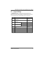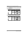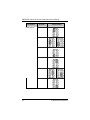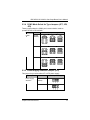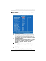
1
SBC84700 Series VIA Eden/C7 All-in-One Capa Board with DualView display User’s Manual Disclaimers This manual has been carefully checked and believed to contain accurate information. AXIOMTEK Co., Ltd. assumes no responsibility for any infringements of patents or any third party’s rights, and any liability arising from such use. AXIOMTEK does not warrant or assume any legal liability or responsibility for the accuracy, completeness or usefulness of any information in this document. AXIOMTEK does not make any commitment to update the information in this manual. AXIOMTEK reserves the right to change or revise this document and/or product at any time without notice. No part of this document may be reproduced, stored in a retrieval system, or transmitted, in any form or by any means, electronic, mechanical, photocopying, recording, or otherwise, without the prior written permission of AXIOMTEK Co., Ltd. CAUTION If you replace wrong batteries, it causes the danger of explosion. It is recommended by the manufacturer that you follow the manufacturer’s instructions to only replace the same or equivalent type of battery, and dispose of used ones. ©Copyright 2007 AXIOMTEK Co., Ltd. All Rights Reserved December 2007, Version A3 Printed in Taiwan ii ESD Precautions Computer boards have integrated circuits sensitive to static electricity. To prevent chipsets from electrostatic discharge damage, please take care of the following jobs with precautions: Do not remove boards or integrated circuits from their anti-static packaging until you are ready to install them. Before holding the board or integrated circuit, touch an unpainted portion of the system unit chassis for a few seconds. It discharges static electricity from your body. Wear a wrist-grounding strap, available from most electronic component stores, when handling boards and components. Trademarks Acknowledgments AXIOMTEK is a trademark of AXIOMTEK Co., Ltd. ® MS-DOS and Windows 95 are trademarks of Microsoft Corporation. VIA is a trademark of VIA Technologies, Inc. AWARD is a trademark of Award Software. Inc. IBM, PC/AT, PS/2, VGA are trademarks of International Business Machines Corporation. Winbond is a trademark of Winbond Electronics Corp. SMI is a trademark of Silicon Motion Inc. Other brand names and trademarks are the properties and registered brands of their respective owners. iii Table of Contents Disclaimers ................................................................................................................ ii ESD Precautions ...................................................................................................... iii Chapter 1 Introdcution ........................................................................ 1 1.1 1.2 Specifications ............................................................................................... 2 Utilities Supported ........................................................................................ 4 Chapter 2 Jumpers and Connectors ................................................. 5 2.1 2.2 2.2 2.3 Board Dimensions and Fixing Holes ............................................................ 5 Board Layout ................................................................................................ 7 Board Layout ................................................................................................ 7 Jumper Settings ........................................................................................... 9 2.3.1 Power Selection of Flat Panel Connector (VCCM of LVDS) (JP1)...... 10 2.3.2 CompactFlash Power Selection Jumper (JP2).................................... 10 2.3.3 COM1~2 Mode Selection Jumpers (JP3, JP4) ................................... 11 2.3.4 COM1 Mode Select for Type Jumpers (JP7, JP8, JP9) ...................... 13 2.3.5 Power Supply Selection Jumper (JP5)................................................ 13 2.3.6 CMOS Clear Jumper (JP6) ................................................................. 14 2.3.7 Audio Output Selection (JP10) ............................................................ 14 2.4 Connectors ................................................................................................. 15 2.4.1 Digital I/O Port (DIO) Connector (CN1) ............................................... 16 2.4.2 IrDA Connector (CN2) ......................................................................... 16 2.4.3 Flat Panel Bezel Connector (CN3) ...................................................... 17 2.4.4 VGA/LCD Connectors (CN4, CN8, CN26) .......................................... 18 2.4.5 Enhanced IDE Interface Connector (CN5) .......................................... 20 2.4.6 SATA Connector (CN6)....................................................................... 20 2.4.7 CPU Fan Connector (CN7) ................................................................. 21 2.4.8 SMBUS Connector (CN9) ................................................................... 21 2.4.9 Mini PCI Connector (CN10)................................................................. 21 2.4.10 Power Input Connector (CN11) ........................................................... 23 2.4.11 Audio Connector (CN15) ..................................................................... 23 2.4.12 USB1~4 Connectors (CN17, CN22).................................................... 24 2.4.13 Serial Port Interface [CN19 (COM2), CN24 (COM1)].......................... 25 2.4.14 Ethernet RJ-45 Connectors (CN20, CN21) ......................................... 26 2.4.15 Keyboard and PS/2 Mouse Connector (CN23) ................................... 27 2.4.16 FDD Connector (CN27)....................................................................... 27 2.4.17 CompactFlash Connector (CN29) ....................................................... 28 2.4.18 DIO Connector (CN1)......................................................................... 29 Chapter 3 Hardware Description...................................................... 31 3.1 3.2 3.3 iv Microprocessors ......................................................................................... 31 BIOS........................................................................................................... 31 System Memory.......................................................................................... 31 3.4 3.5 I/O Port Address Map................................................................................. 32 Interrupt Controller ..................................................................................... 33 Chapter 4 Award BIOS Utility ........................................................... 35 4.1 4.2 4.3 4.4 4.5 4.6 4.7 4.8 4.9 4.10 4.11 4.12 4.13 4.14 4.15 4.16 4.17 Entering Setup............................................................................................ 35 Control Keys ............................................................................................... 36 Getting Help ............................................................................................... 36 The Main Menu .......................................................................................... 37 Standard CMOS Setup Menu..................................................................... 38 Advanced BIOS Features........................................................................... 41 Advanced Chipset Features ....................................................................... 46 Integrated Peripherals ................................................................................ 49 Power Management Setup......................................................................... 55 PnP/PCI Configuration Setup..................................................................... 60 PC Health Status........................................................................................ 61 Frequency/Voltage Control......................................................................... 63 Load Fail-Safe Defaults.............................................................................. 64 Load Optimized Defaults ............................................................................ 65 Set Supervisor/User Password .................................................................. 66 Save & Exit Setup ...................................................................................... 67 Exit Without Saving .................................................................................... 68 Appendix Watchdog Timer ............................................................... 69 v MEMO vi SBC84700 VIA V4 All-in-One Capa Board User’s Manual Chapter 1 Introduction The SBC84700 Series is a VIA V4 Eden/C3/C7 CPU Capa board equipped with graphics, Fast Ethernet and audio interface. The SBC84700 Series can be adapted to VIA V4 processors with its designing for space-limited applications, and the standardized format conforming to the size of a 3.5” Hard Disk drive. To simplify the system integration, super I/Os, UXGA, LCD, Ethernet and solid state disk are provided to make all on one single borad. Four serial ports (3 x RS-232, 1 x RS-232/422/485) with +5V/12V power capability make the unique embedded feature to apply an extensive array of PC peripherals. The industrial-grade construction of SBC84700 Series allows your system to endure the continuous operation in hostile environments where most require stability and reliability. The system dependability of SBC84700 Series can be enhanced by its built-in watchdog timer, a special industrial feature not commonly seen on other motherboards. Designed for the professional embedded VIA developers, embedded board SBC84700 Series is virtually the ultimate one-step solution for embedded system applications. Introduction 1 SBC84700 VIA V4 All-in-One Capa Board User’s Manual 1.1 z Specifications CPU VIA V4 Eden 600M/1GHZ z System Chipset VIA CN700 + VT8237R z Bus Clock 400/533MHz z BIOS Phoenix-Award BIOS, Y2K compliant 4Mbit Flash, DMI, Plug and Play SmartView for multiple LCD type selection, display mode option and application extension features RPL/PXE Ethernet Boot ROM “Load Optimized Default” to backup customized Setting in the BIOS flash chip to prevent from CMOS battery fail z System Memory One 184-Pin DDR-2 SODIMM socket Maximum DDR of up to 1GB DDR2-533 z L2 Cache -- Integrated in CPU z Onboard IDE 1 parallel ATA-100 PATA-100 as PIO Mode 0-4, DMA Mode 0-2 and Ultra DMA/33/66/100 1 SATA-150 z Compact Flash Socke: One Compact Flash Type II Socket z Onboard Multi I/: One floppy port 1 x RS-232 1 x RS-232/422/485 2 Introduction SBC84700 VIA V4 All-in-One Capa Board User’s Manual z USB Interface 4* ports of USB 2.0 with 1* double deck USB connector and 1* 10-pin 2.0 pitch box-header z Real Time Clock -- with battery backup z Watchdog Timer 1~255 seconds; up to 255 levels z Graphics/Streaming Integrate VIA CN700 Single display mode maximum resolutions: DualView display mode CRT -- 2048 x 1536@ 75Hz LVDS LCD -- 1600 x 1200 CRT: 2048 x 1536@ 75Hz LVDS LCD -- 1600 x 1200 LCD backlight control supported z Ethernet Realtek 8100C PCI Bus 10/100M Base-T Wake On LAN (via ATX power supply) Equipped with RJ-45 interface Optional with Realtek RTL8110S for 10/100/1000Base-T z Audio Realtek AC’97 codec audio Amplify for speaker-out with 2.5W for each channel MIC-in, Line-in, Line-out/Speaker-out (jumper selectable) z Power Management -- ACPI (Advanced Configuration and Power Interface) z Form Factor -- 3.5” hard disk drive form factor NOTE All specifications and images are subject to change without notice. Introduction 3 SBC84700 VIA V4 All-in-One Capa Board User’s Manual 1.2 Utilities Supported z z z z 4 Chipset Driver Ethernet Driver VGA Drivers Audio Drivers Introduction SBC84700 VIA V4 All-in-One Capa Board User’s Manual Chapter 2 Jumpers and Connectors 2.1 Board Dimensions and Fixing Holes Component Side Jumpers and Connectors 5 SBC84700 VIA V4 All-in-One Capa Board User’s Manual Solder Side 6 Jumpers and Connectors SBC84700 VIA V4 All-in-One Capa Board User’s Manual 2.2 Board Layout Component Side Jumpers and Connectors 7 SBC84700 VIA V4 All-in-One Capa Board User’s Manual Solder Side 8 Jumpers and Connectors SBC84700 VIA V4 All-in-One Capa Board User’s Manual 2.3 Jumper Settings The SBC84700 Series is configured to meet the needs of your application by proper jumper settings. The table below is a summary of all jumpers and each corresponding function on the board. Jumper JP1 JP2 JP3 JP4 JP5 JP6 JP7 JP8 JP9 JP10 Default Setting Flat Panel Power Selection: Default: 3.3V Compact Flash Voltage Selection Default: 5V CN24 Pin 1: DCD COM1 Mode Select CN24 Pin 9: RI CN19 Pin 1: DCD COM2 Mode Select CN19 Pin 8: RI Power Supply Selection: ATX power supply Clear CMOS Setting: Normal COM1 Mode Select: RS-232 COM1 Mode Select: RS-232 COM1 Mode Select: RS-232 Audio Line Out/Speaker Out: Line Out Jumpers and Connectors Jumper Setting Short 1-2 Short 2-3 Short 7-9 Short 8-10 Short 7-9 Short 8-10 Short 2-3 Short 1-2 Short 3-5, 4-6 Short 3-5, 4-6 Short 1-2 Short 1-3, 2-4 9 SBC84700 VIA V4 All-in-One Capa Board User’s Manual 2.3.1 Power Selection of Flat Panel Connector (VCCM of LVDS) (JP1) SBC84700VEEA supports +3.3V or +5V flat panel displays that you can configure jumper JP1 with appropriate voltage for the flat panel. Description VDDM Function Jumper Setting 3.3V (Default) JP1 5V JP1 2.3.2 CompactFlash Power Selection Jumper (JP2) This jumper is to select the voltage for CompactFlash interface. Description CompactFlash Power Select 10 Function Jumper Setting 5V (Default) JP2 3.3V JP2 Jumpers and Connectors SBC84700 VIA V4 All-in-One Capa Board User’s Manual 2.3.3 COM1~2 Mode Selection Jumpers (JP3, JP4) These jumpers select the COM1, COM2 ports’ DCD and RI mode. Description COM1 (CN24) Function Jumper Setting Pin 1=5V Pin 1=12V JP3 JP3 JP3 *Pin 1=DCD JP3 Pin 9=5V JP3 Pin 9=12V *Pin 9=RI Jumpers and Connectors JP3 JP3 JP3 11 SBC84700 VIA V4 All-in-One Capa Board User’s Manual Description COM2 (CN19) Function Pin 1=5V Pin 1=12V JP4 JP4 JP4 *Pin 1=DCD JP4 Pin 8=5V JP4 Pin 8=12V *Pin 8=RI 12 Jumper Setting JP4 JP4 JP4 Jumpers and Connectors SBC84700 VIA V4 All-in-One Capa Board User’s Manual 2.3.4 COM1 Mode Select for Type Jumpers (JP7, JP8, JP9) These jumpers select the COM1 port’s communication mode to operate RS-232 or RS-422/485. Description Function COM1 Jumper Setting RS-232 (Default) JP9 JP7 JP8 RS-422 JP9 JP7 JP8 RS-485 JP9 JP7 JP8 2.3.5 Power Supply Selection Jumper (JP5) This jumper let you select either AT or ATX power supply. Description Power Supply Selection Function Jumper Setting ATX POWER (Default) JP5 AT POWER JP5 Jumpers and Connectors 13 SBC84700 VIA V4 All-in-One Capa Board User’s Manual 2.3.6 CMOS Clear Jumper (JP6) You may need to use this jumper is to clear the CMOS memory if incorrect settings in the Setup Utility. Description CMOS Clear Function Jumper Setting Normal (Default) JP6 Clear CMOS JP6 2.3.7 Audio Output Selection (JP10) Description Audio Output Selection 14 Function Jumper Setting Line Out (Default) JP10 Speak Out JP10 Jumpers and Connectors SBC84700 VIA V4 All-in-One Capa Board User’s Manual 2.4 Connectors Connectors connect the CPU card with other parts of the system. Loose or improper connection might cause problems. Make sure all connectors are properly and firmly connected. Here is a summary table shows you all connectors on the SBC84700 Series. Connectors DIO Connector IrDA Connector Flat Panel Bezel Connector LVDS Connector IDE Connector SATA Connector FAN Power connector LVDS Inverter Connector SM BUS Connector Mini PCI Connector Power Connector Audio Connector External USB Connector COM2 Connector 2’ST Ethernet Connector 1’ST Ethernet Connector USB Connector Keyboard and Mouse Connector COM1 Connector VGA CRT Connector F.D.D Connector DDRII SODIMM Socket CompactFlash Connector Jumpers and Connectors Label CN1 CN2 CN3 CN4 CN5 CN6 CN7 CN8 CN9 CN10 CN11 CN15 CN17 CN19 CN20 CN21 CN22 CN23 CN24 CN26 CN27 CN28 CN29 15 SBC84700 VIA V4 All-in-One Capa Board User’s Manual 2.4.1 Digital I/O Port (DIO) Connector (CN1) The board is equipped a digital I/O connector CN1 that meets requirements for a system customary automation control. The digital I/O can be configured to control cash drawers, sense warning signals from an Uninterrupted Power System (UPS), or perform store security control. The digital I/O is controlled via software programming. Pin 1 3 5 7 9 Description In-0 In-2 Out-0 Out-2 Out-4 Pin 2 4 6 8 Description In-1 GND Out-1 Out-3 CN1 2.4.2 IrDA Connector (CN2) The board supports the Infrared data port that allows wireless exchange of information between your system and related devices. Infrared sensor can be used to transfer data to and from your computer and similarly equipped devices. 16 Pin Description 1 +5V 2 NC 3 IRRX 4 GND 5 IRTX CN2 Jumpers and Connectors SBC84700 VIA V4 All-in-One Capa Board User’s Manual 2.4.3 Flat Panel Bezel Connector (CN3) Power LED This 3-pin connector named as Pin 1 to Pin 5 connects the system power LED indicator to such a switch on the case. Pin 1 is assigned as +, and Pin 3 and 5 as -. The Power LED lights up when the system is powered ON. External Speaker and Internal Buzzer Connector Pin 2, 4, 6 and 8 can be connected to the case-mounted speaker unit or internal buzzer. While connecting the CPU card to an internal buzzer, you need to short pins 2-4; while connecting to an external speaker, set pins 2-4 to Open and connect the speaker cable to pin 8 (+) and pin 2 (-). ATX Power On/Off Button This 2-pin connector named as Pin 9 and 10 connects the front panel’s ATX power button to the CPU card, which allows users to control ATX power supply to be on/off. System Reset Switch Pin 11 and 12 can be connected to the case-mounted reset switch that reboots your computer instead of turning OFF the power switch. It is a better way to reboot your system for a longer life of the system’s power supply. HDD Activity LED This connection is linked to hard drive activity LED on the control panel. LED flashes when HDD is being accessed. Pin 13 and 14 connect the hard disk drive to the front panel HDD LED, Pin 13 assigned as -, and Pin 14 as +. Jumpers and Connectors 17 SBC84700 VIA V4 All-in-One Capa Board User’s Manual 2.4.4 VGA/LCD Connectors (CN4, CN8, CN26) The SBC84700 has for connectors that support CRT VGA and flat panel displays. On the board, CN26 is a standard 15-pin pin header connector commonly used for the CRT VGA display, CN4 a 40-pin connector for the LVDS. It is strongly recommended to use the matching connector JST SHDR-40V-S-B 40-pin tor for LVDS on the board. The CN8 is a 7-pin connector for inverter on the board that is strongly recommended to use the DF13-7S-1.25C 7-pin connector. CN26: 15-pin CRT/VGA Connector Pin Description Pin Description Pin Description 1 Red 2 Green 3 Blue 4 N/A 5 GND 6 GND 7 GND 8 GND 9 VCC 10 GND 11 N/A 12 DDC DAT 13 Horizontal Sync 14 Vertical Sync 15 DDC CLK CN8: DF13-7S-1.25C 7 pin Connector for Inverter It is strongly recommended to use the DF13-7S-1.25C 7-pin connector for inverter on the board. Pin 18 Description 1 +12V 2 +12V 3 5V 4 ENBA 5 GND 6 GND 7 GND CN8 Jumpers and Connectors SBC84700 VIA V4 All-in-One Capa Board User’s Manual CN4: JST SHDR-40V-S-B 40 pin connector The LVDS connector on the board is a 40-pin connector that we strongly recommend you to use the matching connector JST SHDR40V-S-B. The LVDS interface with this 40-pin connector supports 18/24-bit single/dual channel type of LCD. Pin 1 3 5 7 9 11 13 15 17 19 21 23 25 27 29 31 33 35 37 39 Description VCCM VCCM VCCM N.C. GND Channel B D3Channel B D3+ GND Channel B CLKChannel B CLK+ GND Channel A D0Channel A D0+ GND Channel A D1Channel A D1+ GND Channel A D2Channel A D2+ GND Pin 2 4 6 8 10 12 14 16 18 20 22 24 26 28 30 32 34 36 38 40 Description VCCM VCCM VCCM N.C. GND Channel B D0Channel B D0+ GND Channel B D1Channel B D1+ GND Channel B D2Channel B D2+ GND Channel A D3Channel A D3+ GND Channel A CLKChannel A CLK+ GND CN4 Jumpers and Connectors 19 SBC84700 VIA V4 All-in-One Capa Board User’s Manual 2.4.5 Enhanced IDE Interface Connector (CN5) The SBC84700 has a PCI bus enhanced IDE controller that supports master/slave mode, post write transaction mechanisms with 64-byte buffer and master data transaction. Pin Description Pin Description Pin Description 1 4 7 10 13 16 19 22 25 28 31 34 37 40 43 CN5 Reset # Data 8 Data 5 Data 11 Data 2 Data 14 GND GND IOR # No Connector Interrupt No Connector HDC CS0 # GND GND 2 5 8 11 14 17 20 23 26 29 32 35 38 41 44 GND Data 6 Data 10 Data 3 Data 13 Data 0 No Connector IOW # GND No Connector No Connector SA0 HDC CS1 # VCC N.C. 3 6 9 12 15 18 21 24 27 30 33 36 39 42 Data 7 Data 9 Data 4 Data 12 Data 1 Data 15 No Connector GND IOCHRDY GND-Default SA1 SA2 HDD Active # VCC 2.4.6 SATA Connector (CN6) The SATA connector CNS1 is for high-speed SATA interface port and it can be connected to serial ATA hard disk devices. Pin Description Pin 20 Description 1 GND 2 TX+ 3 TX- 4 GND 5 RX- 6 RX+ 7 GND CN6 Jumpers and Connectors SBC84700 VIA V4 All-in-One Capa Board User’s Manual 2.4.7 CPU Fan Connector (CN7) CN21 is a CPU fan connector. VIA microprocessors require a fan for heat dispensing. The fan connector on SBC84700 provides power to the fan. Pin 2.4.8 Description 1 GND 2 +5V CN7 SMBUS Connector (CN9) Connector CN9 is for SMBUS interface support. 2.4.9 CN9 Pin Description 1 Serial Port (SMB/I2C) Clock 2 Serial Por t(SMB/I2C) Data 3 GND Mini PCI Connector (CN10) Pin 1 3 5 7 9 11 13 15 17 19 21 23 25 27 Description TIP KEY LAN_RD+ LAN_RDRJ45 termination RJ45 termination LAN_LED1+ LAN_LED1CHGND INTB# 3.3V RESERVED GND CLK GND Jumpers and Connectors Pin 2 4 6 8 10 12 14 16 18 20 22 24 26 28 Description RING KEY LAN_TD+ LAN_TDRJ45 termination RJ45 termination LAN_LED2+ LAN_LED2RESERVED 5V INTA# RESERVED 3.3VAUX RST# 3.3V 21 SBC84700 VIA V4 All-in-One Capa Board User’s Manual Pin 29 31 33 35 37 39 41 43 45 47 49 51 53 55 57 59 61 63 65 67 69 71 73 75 77 79 81 83 85 87 89 91 93 95 97 99 101 22 Description REQ# 3.3V AD31 AD29 GND AD27 AD25 RESERVED C/BE3# AD23 GND AD21 AD19 GND AD17 C/BE2# IRDY# 3.3V CLKRUN# SERR# GND PERR# C/BE1# AD14 GND AD12 AD10 GND AD08 AD07 3.3V AD05 RESERVED 5V 5V AD01 GND Pin 30 32 34 36 38 40 42 44 46 48 50 52 54 56 58 60 62 64 66 68 70 72 74 76 78 80 82 84 86 88 90 92 94 96 98 100 102 Description GNT# GND PME# RESERVED AD30 3.3V AD28 AD26 AD24 IDSEL GND AD22 AD20 PAR AD18 AD16 GND FRAME# TRDY# STOP# 3.3V DEVSEL# GND AD15 AD13 AD11 GND AD09 C/BE0# 3.3V AD06 AD04 AD02 AD00 RESERVED RESERVED GND Jumpers and Connectors SBC84700 VIA V4 All-in-One Capa Board User’s Manual Pin Description 103 105 107 109 111 113 115 117 119 121 123 Pin RESERVED RESERVED RESERVED RESERVED RESERVED RESERVED RESERVED RESERVED RESERVED RESERVED RESERVED 104 106 108 110 112 114 116 118 120 122 124 Description RESERVED RESERVED RESERVED RESERVED RESERVED GND RESERVED RESERVED RESERVED RESERVED RESERVED -- End of Mini PCI Connector (CN10) Pin Assignment Table -- 2.4.10 Power Input Connector (CN11) Use this connector to connect standard power supply +12V & +5V inputs. This card runs in full functions only with 5V only input power. 12V input power is required for LCD interface only. Pin 1 2 3 4 5 Signal PS_ON GND GND +12V N.C. Pin 6 7 8 9 10 Signal +5VSB +5V +5V N.C. GND CN11 2.4.11 Audio Connector (CN15) The board supports an audio interface. CN15 is a 10pin-header connector for the audio interface. Pin 1 3 5 7 9 Description MIC-IN Line In L Line In R Audio Out L Audio Out R Jumpers and Connectors Pin 2 4 6 8 10 Description CN15 GND GND GND GND GND 23 SBC84700 VIA V4 All-in-One Capa Board User’s Manual 2.4.12 USB1~4 Connectors (CN17, CN22) There are four Universal Serial Bus (USB) connectors, compliant with USB2.0 (480Mbps), on the board that can be adapted to USB peripherals, such as monitor, keyboard and mouse. CN22 consists of two 4-pin standard USB ports, and CN17 a 10pin-header connector. Pin 24 Description Pin Description 1 VCC 2 VCC 3 D0- 4 D1- 5 D0+ 6 D1+ 7 Ground (GND) 8 Ground (GND) 9 Ground (GND) 10 Ground (GND) Pin Description 1, 5 USB Vcc 2, 6 USB - 3, 7 USB + 4, 8 USB GND CN17 CN22 Jumpers and Connectors SBC84700 VIA V4 All-in-One Capa Board User’s Manual 2.4.13 Serial Port Interface [CN19 (COM2), CN24 (COM1)] COM1 Port Connector (CN24) is a standard DB9 connector. The pin assignment is listed as below: Pin Description 1 DCD, Data carrier detect 2 RXD, Receive data 3 TXD, Transmit data 4 DTR, Data terminal ready 5 GND, ground 6 DSR, Data set ready 7 RTS, Request to send 8 CTS, Clear to send 9 RI, Ring indicator CN24 The COM1 RS-422/485 pin assignment list: Pin 1 2 3 4 Description R2-422 RS-485 TXTX+ RX+ RX- DATADATA+ No connector No connector The RS-422 pin assignment list: Pin 1 3 5 7 9 Description Pin Data Carrier Detect (DCD) Receive Data (RXD) Transmit Data (TXD) Data Terminal Ready (DTR) Ground (GND) Jumpers and Connectors 2 4 Description Data Set Ready (DSR) Request to Send (RTS) 6 Clear to Send (CTS) 8 Ring Indicator (RI) 10 NC CN19 25 SBC84700 VIA V4 All-in-One Capa Board User’s Manual 2.4.14 Ethernet RJ-45 Connectors (CN20, CN21) The board is equipped with a high performance Plug and Play Ethernet interface, fully compliant with the IEEE802.3 standard, consisting of a RJ-45 connector LAN. Pin Description 1 Tx+ (Data transmission positive) 2 Tx- (Data transmission negative) 3 Rx+(Data reception positive) 4 RJ-45 Termination 5 RJ-45 Termination 6 Rx- (Data reception negative) 7 RJ-45 Termination 8 RJ-45 Termination A Active LED B 100/1000 LAN LED CN20, CN21 Feature 10Mb/s and 100Mb/s operations Supports 10Mb/s and 100Mb/s N-Way auto negotiation Full duplex capability Full compliance with PCI Revision 2.1 PCI Bus Master data transfers Drivers Supported Bundled with popular software drivers, the SBC84700 Ethernet interface allows great flexibility to work with all major networking operating systems including Novell NetWare v2.x, v3.x, v4.x, Microsoft LAN Manager, Win3.1, Win NT, Win95, IBM LAN Server, SCO UNIX or other ODI, NDIS and Packet drive compliant operating systems. 26 Jumpers and Connectors SBC84700 VIA V4 All-in-One Capa Board User’s Manual 2.4.15 Keyboard and PS/2 Mouse Connector (CN23) The SBC84700 Series provides a keyboard and Mouse interface. CN25 is a DIN connector for PS/2 keyboard connection via “Y” Cable. Pin 1 2 3 4 5 6 Description CN23 Keyboard Data Mouse Data GND VCC Keyboard Clock Mouse Clock 2.4.16 FDD Connector (CN27) There is one 26-pin FCC Z.I.F. type connector with the general output support for a single floppy drive. The floppy drive could be any one of the following types: 3.5" 720KB or 1.44MB/2.88MB. Pin Description Pin Description 1 3 5 7 9 11 13 15 17 19 21 23 25 +5V +5V +5V No Connector No Connector No Connector No Connector GND GND GND GND GND GND 2 4 6 8 10 12 14 16 18 20 22 24 26 INDEX DRIVE0 DSKCHG No Connector MOTOR ON DIR STEP WDATA WGATE TRK0 WPT RDATA HDSEL Jumpers and Connectors CN27 1 2 3 4 5 6 7 8 9 10 11 12 13 14 15 16 17 18 19 20 21 22 23 24 25 26 27 SBC84700 VIA V4 All-in-One Capa Board User’s Manual 2.4.17 CompactFlash Connector (CN29) The board is equipped with a CompactFlashTM disk type-II socket on the solder side to support an IDE interface CompactFlashTM disk card with DMA mode supported. The socket is especially designed to avoid incorrect installation of the CompactFlashTM disk card. When installing or removing the CompactFlashTM disk card, please make sure the system power is off. The CompactFlashTM disk card is defaulted as the C: or D: disk drive in your PC system. Pin 1 3 5 7 9 11 13 15 17 19 21 23 25 27 29 31 33 35 37 39 41 43 45 47 49 28 Description GND Data 4 Data 6 CS0# ATASEL Address 8 VCC Address 5 Address 3 Address 1 Data 0 Data 2 CD2# Data 11 Data 13 Data 15 VS1# IOWR# INTR CSEL# RESET# DMAREQ DASP# Data 8 Data 10 Pin 2 4 6 8 10 12 14 16 18 20 22 24 26 28 30 32 34 36 38 40 42 44 46 48 50 Description Data 3 Data 5 Data 7 Address 10 Address 9 Address 7 Address 6 Address 4 Address 2 Address 0 Data 1 IOCS16# CD1Data 12 Data 14 CS1# IORD# WE# VCC VS2# IORDY# DMAACKPDIAG# Data 9 GND Jumpers and Connectors SBC84700 VIA V4 All-in-One Capa Board User’s Manual CF1 2.4.18 DIO Connector (CN1) The board is equipped a digital I/O connector CN1 that meets requirements for a system customary automation control. The digital I/O can be configured to control cash drawers, sense warning signals from an Uninterrupted Power System (UPS), or perform store security control. The digital I/O is controlled via software programming. Pin 1 3 5 7 9 Description In-0 In-2 Out-0 Out-2 Out-4 Pin 2 4 6 8 Description In-1 GND Out-1 Out-3 CN1 D/I Address:449H Digital Input Bit7 Bit6 In-2 Bit5 In-1 Bit4 In-0 Bit3 Bit2 Bit1 Bit0 D/O Address:600H Digital Output Bit7 Bit6 Bit5 Bit4 Out -4 Jumpers and Connectors Digital Output Bit3 Bit2 Out -3 Out -2 Bit1 Out-1 Bit0 Out-0 29 SBC84700 VIA V4 All-in-One Capa Board User’s Manual MEMO 30 Jumpers and Connectors SBC84700 VIA V4 All-in-One Capa Board User’s Manual Chapter3 Hardware Description 3.1 Microprocessors The SBC84700 Series supports VIA V4 architecture CPUs. Systems based on these CPUs can be operated under Windows 2000/XP and Linux environments. The system performance depends on the microprocessor installed onboard. Make sure all settings are correct for the installed microprocessor to prevent any damage to the CPU. 3.2 BIOS System BIOS used on the SBC84700 Series is Phoenix-Award Plug and Play BIOS. The SBC84700 Series contains a single 4Mbit Flash. 3.3 System Memory The SBC84700 Series industrial CPU card supports one 200-pin DDR SODIMM socket for a maximum memory of 1GB DDR SDRAMs. The memory module can come in sizes of 64MB, 128MB, 256MB, 512MB and 1GB. Hardware Description 31 SBC84700 VIA V4 All-in-One Capa Board User’s Manual 3.4 I/O Port Address Map The VIA V4 architecture CPUs communicates via I/O ports. It has a total of 1KB port addresses available for assignment to other devices via I/O expansion cards. Address 000-01F 020-03F 040-05F 060-06F 070-07F 080-09F 0A0-0BF 0C0-0DF 0F0 0F1 0F8-0FF 1F0-1F8 250-25F 300-31F 380-38F 3A0-3AF 3B0-3BF 3C0-3CF 3D0-3DF 3F0-3F7 3F8-3FF 3E8-3EF 2F8-2FF 2E8-2EF 3F0-3FF 32 Devices DMA controller #1 Interrupt controller #1 Timer Keyboard controller Real time clock, NMI DMA page register Interrupt controller #2 DMA controller #2 Clear math coprocessor busy signal Reset math coprocessor Math processor Fixed disk controller HR I/O Prototype card SDLC #2 SDLC #1 MDA video card (including LPT1) EGA card CGA card Floppy disk controller Serial port #1 (COM1) Serial port #3 (COM3) Serial port #2 (COM2) Serial port #4 (COM4) Super I/O Hardware Description SBC84700 VIA V4 All-in-One Capa Board User’s Manual 3.5 Interrupt Controller The SBC84700 Series is a 100% PC compatible control board. It consists of 16 interrupt request lines. Four out of the sixteen can either be programmable. The mapping list of the 16 interrupt request lines is shown on the following table. NMI IRQ0 IRQ1 IRQ2 IRQ3 IRQ4 IRQ5 IRQ6 IRQ7 IRQ8 IRQ9 IRQ10 IRQ11 IRQ12 IRQ13 IRQ14 IRQ15 Parity check error System timer output Keyboard Interrupt rerouting from IRQ8 through IRQ15 Serial port #2 Serial port #1 Reserved Floppy disk controller Parallel port #1 Real time clock Reserved Serial port #3 Serial port #4 PS/2 Mouse Math coprocessor Primary IDE channel Secondary IDE Channel Hardware Description 33 SBC84700 VIA V4 All-in-One Capa Board User’s Manual MEMO 34 Hardware Description SBC84700 VIA V4 All-in-One Capa Board User’s Manual Chapter 4 Award BIOS Utility The Phoenix-Award BIOS provides users with a built-in Setup program to modify basic system configuration. All configured parameters are stored in a battery-backed-up RAM (CMOS RAM) to save the Setup information whenever the power is turned off. 4.1 Entering Setup There are two ways to enter the Setup program. You may either turn ON the computer and press <Del> immediately, or press the <Del> and/or <Ctrl>, <Alt>, and <Esc> keys simultaneously when the following message appears at the bottom of the screen during POST (Power on Self Test). TO ENTER SETUP PRESS DEL KEY If the message disappears before you respond and you still want to enter Setup, please restart the system to try it again. Turning the system power OFF and ON, pressing the “RESET” button on the system case or simultaneously pressing <Ctrl>, <Alt>, and <Del> keys can restart the system. If you do not press keys at the right time and the system doesn’t boot, an error message will pop out to prompt you the following information: PRESS <F1> TO CONTINUE, <CTRL-ALT-ESC> OR <DEL> TO ENTER SETUP Award BIOS Utility 35 SBC84700 VIA V4 All-in-One Capa Board User’s Manual 4.2 Control Keys Up arrow Move cursor to the previous item Down arrow Left arrow Right arrow Move cursor to the next item Move cursor to the item on the left hand Move to the item in the right hand Main Menu -- Quit and delete changes into CMOS Status Page Setup Menu and Option Page Setup Menu -- Exit current page and return to Main Menu Increase the numeric value or make changes Decrease the numeric value or make changes Esc key PgUp/“+” key PgDn/“−“ key F1 key (Shift) F2 key F3 key F4 key F5 key F6 key F7 key F8 key F9 key F10 key 4.3 General help, only for Status Page Setup Menu and Option Page Setup Menu Change color from total 16 colors. F2 to select color forward, (Shift) F2 to select color backward Reserved Reserved Restore the previous CMOS value from CMOS, only for Option Page Setup Menu Load the default CMOS value from BIOS default table, only for Option Page Setup Menu Load the Setup default, only for Option Page Setup Menu Reserved Reserved Save all the CMOS changes, only for Main Menu Getting Help z Main Menu The online description of the highlighted setup function is displayed at the bottom of the screen. z Status Page Setup Menu/Option Page Setup Menu Press <F1> to pop out a small Help window that provides the description of using appropriate keys and possible selections for highlighted items. Press <F1> or <Esc> to exit the Help Window. 36 Award BIOS Utility SBC84700 VIA V4 All-in-One Capa Board User’s Manual 4.4 The Main Menu Once you enter the Award BIOS CMOS Setup Utility, the Main Menu appears on the screen. In the Main Menu, there are several Setup functions and a couple of Exit options for your selection. Use arrow keys to select the Setup Page you intend to configure then press <Enter> to accept or enter its sub-menu. NOTE If your computer can not boot after making and saving system changes with Setup, the Award BIOS will reset your system to the CMOS default settings via its built-in override feature. It is strongly recommended that you should avoid changing the chipset’s defaults. Both Award and your system manufacturer have carefully set up these defaults that provide the best performance and reliability. Award BIOS Utility 37 SBC84700 VIA V4 All-in-One Capa Board User’s Manual 4.5 Standard CMOS Setup Menu The items in Standard CMOS Setup Menu are divided into 10 categories. Each category includes no, one or more than one setup items. Use the arrow keys to highlight the item and then use the <PgUp> or <PgDn> keys to select the value you want in each item. z Date day date month year z 38 It is determined by the BIOS and read only, from Sunday to Saturday. It can be keyed with the numerical/ function key, from 1 to 31. It is from January to December. It shows the current year of BIOS. Time This item shows current time of your system with the format <hour> <minute> <second>. The time is calculated based on the 24-hour military-time clock. For example, 1 p.m. is 13:00:00. Award BIOS Utility SBC84700 VIA V4 All-in-One Capa Board User’s Manual z IDE Primary Master/Primary Slave These items identify the types of each IDE channel installed in the computer. There are 45 predefined types (Type 1 to Type 45) and 2 user’s definable types (Type User) for Enhanced IDE BIOS. Press <PgUp>/<+> or <PgDn>/<−> to select a numbered hard disk type, or directly type the number and press <Enter>. Please be noted your drive’s specifications must match the drive table. The hard disk will not work properly if you enter improper information. If your hard disk drive type does not match or is not listed, you can use Type User to manually define your own drive type. If selecting Type User, you will be asked to enter related information in the following items. Directly key in the information and press <Enter>. This information should be provided in the documentation from your hard disk vendor or the system manufacturer. If the HDD interface controller supports ESDI, select “Type 1”. If the HDD interface controller supports SCSI, select “None”. If the HDD interface controller supports CD-ROM, select “None”. CYLS. number of cylinders HEADS number of heads PRECOMP write precom LANDZONE landing zone SECTORS number of sectors MODE HDD access mode If there is no hard disk drive installed, select NONE and press <Enter>. z Dive A type/Drive B type The item identifies the types of floppy disk installed in the computer, as drive A or drive B. None 360K, 3.5 in 1.2M, 3.5 in 720K, 3.5 in 1.44M, 3.5 in 2.88M, 3.5 in No floppy drive installed 3.5 inch PC-type standard drive; 360Kb Mini ITXcity 3.5 inch AT-type high-density drive; 1.2MB Mini ITXcity 3.5 inch double-sided drive; 720Kb Mini ITXcity 3.5 inch double-sided drive; 1.44MB Mini ITXcity 3.5 inch double-sided drive; 2.88MB Mini ITXcity z Video Select the display adapter type for your system. z Halt On This item determines whether the system will halt or not, if an error Award BIOS Utility 39 SBC84700 VIA V4 All-in-One Capa Board User’s Manual is detected while powering up. No errors The system booting will halt on any errors detected. (default) All errors Whenever BIOS detects a non-fatal error, the system will stop and you will be prompted. All, But Keyboard The system booting will not stop for a keyboard error; it will stop for other errors. All, But Diskette The system booting will not stop for a disk error; it will stop for other errors. All, But Disk/Key The system booting will not stop for a keyboard or disk error; it will stop for other errors. Press <Esc> to return to the Main Menu page. 40 Award BIOS Utility SBC84700 VIA V4 All-in-One Capa Board User’s Manual 4.6 Advanced BIOS Features This section allows you to configure and improve your system, to set up some system features according to your preference. z Hard Disk Boot Priority Use this item to select the disk boot priority. z Virus Warning This option flashes on the screen. During and after the system boot up, any attempt to write to the boot sector or partition table of the hard disk drive will halt the system with the following message. You can run an anti-virus program to locate the problem. The Award BIOS Utility 41 SBC84700 VIA V4 All-in-One Capa Board User’s Manual default setting is “Disabled”. ! WARNING ! Disk boot sector is to be modified Type “Y” to accept write or “N” to abort write Award Software, Inc. Enabled Disabled It automatically activates while the system boots up and a warning message appears for an attempt to access the boot sector or hard disk partition table. No warning message will appear for attempts to access the boot sector or hard disk partition table. NOTE This function is only available with DOS and other operating systems that do not trap INT13. z CPU L1 & L2 Cache These two options speed up memory access. However, it depends on the CPU/chipset design. The default setting is “Enabled”. CPUs without built-in internal cache will not provide the “CPU Internal Cache” item on the menu. Enabled Disabled z Enable cache Disable cache Quick Power On Self Test This option speeds up Power on Self Test (POST) after you turn on the system power. If set as Enabled, BIOS will shorten or skip some check items during POST. The default setting is “Enabled”. Enabled Enable Quick POST Disabled Normal POST z First/Second/Third Boot Device These items let you select the 1st, 2nd, and 3rd devices that the system will search for during its boot-up sequence. The wide range of selection includes Floppy, LS120, ZIP100, HDD0~3, SCSI, and CDROM. z Boot Other Device This item allows users to enable or disable the boot device not 42 Award BIOS Utility SBC84700 VIA V4 All-in-One Capa Board User’s Manual listed in the First/Second/Third boot devices option above. The default setting is “Enabled”. z Swap Floppy Drive This item allows you to determine whether to enable Swap Floppy Drive or not. When enabled, the BIOS swap floppy drive assignment makes Drive A become Drive B, and vice versa. The default setting is “Disabled”. z Boot Up Floppy Seek During POST, BIOS will determine the floppy disk drive type, 40 or 80 tracks. The 360Kb type is 40 tracks while 720Kb, 1.2MB and 1.44MB are all 80 tracks. The default value is “Enabled”. Enabled Disabled BIOS searches for floppy disk drive to determine if it is 40 or 80 tracks. Please be noted BIOS can not differentiate 720K, 1.2M or 1.44M drive type as they all are 80 tracks. BIOS will not search for the type of floppy disk drive by track number. There will be no warning message displayed if the installed drive is 360K. z Boot Up NumLock Status Set the the Num Lock status when the system is powered on. The default value is “On”. z Gate A20 Option The default value is “Fast”. Normal Fast z Typematic Rate Setting This item determines the typematic rate of the keyboard. The default value is “Disabled”. Enabled Disabled z The A20 signal is controlled by keyboard controller or chipset hardware. Default: Fast. The A20 signal is controlled by Port 92 or chipset specific method. Enable typematic rate and typematic delay programming. Disable typematic rate and typematic delay programming. The system BIOS will use default value of these 2 items, controlled by keyboard. Typematic Rate (Chars/Sec) This option refers to character numbers typed per second by the Award BIOS Utility 43 SBC84700 VIA V4 All-in-One Capa Board User’s Manual keyboard. The default value is “6”. 6 8 10 12 15 20 24 30 z 6 characters per second 8 characters per second 10 characters per second 12 characters per second 15 characters per second 20 characters per second 24 characters per second 30 characters per second Typematic Delay (Msec) This option defines how many milliseconds must elapse before a held-down key begins generating repeat characters. The default value is “250”. 250 500 750 1000 z 250 msec 500 msec 750 msec 1000 msec Security Option This item allows you to limit access to the system and Setup, or just to Setup. The default value is “Setup”. System Setup If a wrong password is entered at the prompt, the system will not boot, the access to Setup will be denied, either. If a wrong password is entered at the prompt, the system will boot, but the access to Setup will be denied. NOTE: To disable the security, select PASSWORD SETTING at Main Menu and then you will be asked to enter a password. Do not type anything, just press <Enter> and it will disable the security. Once the security is disabled, the system will boot and you can enter Setup freely. z APIC Mode Use this item to enable or disable APIC (Advanced Programmable Interrupt Controller) mode that provides symmetric multiprocessing (SMP) for systems. z PS/2 Mouse Function Control Use this item to set the use of PS/2 mouse or not. If there is a 44 Award BIOS Utility SBC84700 VIA V4 All-in-One Capa Board User’s Manual PS/2 mouse connected to your system, please enable this item. z OS Select for DRAM >64MB This item allows you to access the memory over 64MB in OS/2. z Report No FDD For WIN 95 Select Yes to release an IRQ when the system doesn’t have any floppy drive, for compatibility with Windows 95 logo certification. In the Integrated Peripherals screen, select Disabled for the Onboard FDC Controller field. Press <Esc> to return to the Main Menu page. Award BIOS Utility 45 SBC84700 VIA V4 All-in-One Capa Board User’s Manual 4.7 Advanced Chipset Features This section contains completely optimized chipset’s features on the board that you are strongly recommended to leave all items on this page at their default values unless you are very familiar with the technical specifications of your system hardware. z DRAM Timing Use this item to enable or disable the SDRAM timing, which can be defined by Serial Presence Detect. z CAS Latency Time You can select CAS latency time to HCLKs 2, 3, or Auto. The board designer should have set up these values in accordance with the installed DRAM. Do not change these values unless you have to change the specifications of the installed DRAM or CPU. 46 Award BIOS Utility SBC84700 VIA V4 All-in-One Capa Board User’s Manual z DRAM RAS# to CAS# Delay When DRAM is refreshed, both rows and columns are addressed separately. This field lets you insert a timing delay between the CAS and RAS strobe signals, used when DRAM is written to, read from, or refreshed. z DRAM RAS# Precharge The precharge time is the number of cycles it takes for the RAS to accumulate its charge before DRAM refresh. If insufficient time is allowed, refresh may be incomplete and the DRAM may fail to retain data. z DRAM Data Integrity Mode Use this item to set data integrity mode of the DRAM installed in the system. The default setting is “Non-ECC”. z MGM Core Frequency Use this item to set the clock ratio of CPU and system. z System BIOS Cacheable Selecting Enabled allows caching of the system BIOS ROM at F0000h-FFFFFh, resulting in better system performance. However, if any program writes to this memory area, a system error may result. The default value is “Disabled”. z Video BIOS Cacheable This item allows you to change the Video BIOS location from ROM to RAM. Video Shadow will increase the video speed. z Memory Hole At 15M-16M You can reserve this area of system memory for ISA adapter ROM. When this area is reserved, it cannot be cached. The user information of peripherals that need to use this area of system memory usually discusses their memory requirements. z Delayed Transaction The chipset has an embedded 32-bit posted write buffer to support delay transactions cycles. Select “Enabled” to support PCI specification version 2.1. The options available are “Enabled” and “Disabled”. z AGP Aperture Size (MB) Use this item to set aperture size of the graphics. The aperture is a portion of the PCI memory address range dedicated for graphics memory address space. Host cycles that hit the aperture Award BIOS Utility 47 SBC84700 VIA V4 All-in-One Capa Board User’s Manual range are forwarded to the AGP without any translation. The options available are “4M”,” 8M”, “16M”, “32M”, ”64M”, “128M” and “256M”. z Init Display First This item allows you to decide whether PCI Slot or AGP to be the first primary display card. *** On-Chip VGA Setting *** z On-Chip VGA Use this item to choose the primary display card. z On-Chip Frame Buffer Size Use this item to set the VGA frame buffer size. z Boot Display This item is for Intel define ADD card only. Press <Esc> to return to the Main Menu page. 48 Award BIOS Utility SBC84700 VIA V4 All-in-One Capa Board User’s Manual 4.8 Integrated Peripherals This section allows you to configure your SuperIO Device, IDE Function and Onboard Device. Award BIOS Utility 49 SBC84700 VIA V4 All-in-One Capa Board User’s Manual z OnChip IDE Device Scroll to this item and press <Enter> to view the VIA OnChip IDE Device sub menu. ¾ ¾ IDE DMA transfer access Automatic data transfer between system memory and IDE device with minimum CPU intervention. This improves data throughput and frees CPU to perform other tasks. On-Chip Primary/Secondary PCI IDE The integrated peripheral controller contains an IDE interface with support for two IDE channels. Select Enabled to activate each channel separately. The default value is “Enabled”. NOTE Choosing Disabled for these options will automatically remove the IDE Primary Master/ Slave PIO and/or IDE Secondary Master/Slave PIO items on the menu. 50 Award BIOS Utility SBC84700 VIA V4 All-in-One Capa Board User’s Manual ¾ ¾ IDE Primary/Secondary Master/Slave PIO The four IDE PIO (Programmed Input/Output) fields let you set a PIO mode (0-4) for each of the four IDE devices that the onboard IDE interface supports. Modes 0 to 4 provide successively increased performance. In Auto mode, the system automatically determines the best mode for each device. IDE Primary/Secondary Master/Slave UDMA Select the mode of operation for the IDE drive. Ultra DMA33/66/100/133 implementation is possible only if your IDE hard drive supports it and the operating environment includes a DMA driver. If your hard drive and system software both support Ultra DMA-33/66/100/133, select Auto to enable UDMA mode by BIOS. *** On-Chip Serial ATA Setting *** ¾ SATA Mode There are these options for you to set up SATA mode: IDE, RAID or AHCI. ¾ On-Chip Serial ATA Use this item to enable or disable the built-in on-chip serial ATA. ¾ SATA Port 0/1 If the “PATA IDE Mode“ is Primary, it will show ” P1, P3 is Secondary” which means SATA 2 and SATA 4 are Secondary. If the “PATA IDE Mode “ is Secondary, it will show “ P0, P2 is Primary “ which means SATA 1 and SATA 3 are Primary. Press <Esc> to return to the Integrated Peripherals page. Award BIOS Utility 51 SBC84700 VIA V4 All-in-One Capa Board User’s Manual z Onboard Device Scroll to this item and press <Enter> to view the Onboard Device sub menu. ¾ ¾ ¾ ¾ ¾ USB Controller Enable this item if you are using the USB in the system. You should disable this item if a higher-level controller is added. USB 2.0 Controller Enable this item if you are using the EHCI (USB2.0) controller in the system. USB Keyboard Support Enable this item if the system has a Universal Serial Bus (USB) controller, and you have a USB keyboard. USB Mouse Support Enable this item to boot the hard drive by a USB mouse. AC’97 Audio Select Use this item to enable or disable the onboard AC’97 Audio function. Press <Esc> to return to the Integrated Peripherals page. 52 Award BIOS Utility SBC84700 VIA V4 All-in-One Capa Board User’s Manual z Super I/O Device Scroll to this item and press <Enter> to view the Super I/O Device sub menu. ¾ ¾ ¾ ¾ Onboard FDC Controller Select Enabled, if your system has a floppy disk controller (FDC) installed on the system board and you want to use it. If you install and-in FDC or the system has no floppy drive, select Disabled in this field. Options: Enabled and Disabled. Onboard Serial Port 1/2 Select an address and corresponding interrupt for the serial port. Options are: “3F8/IRQ4”, “2F8/IRQ3”, “3E8/IRQ10”, “2E8/IRQ11”, “338/IRQ5”, “238/IRQ7”, “Auto” and “Disabled”. URAT Mode Select When UART Mode Select is set as ASKIR or IrDA, the options RxD, TxD Active and IR Transmittion delay will appear. RxD, TxD Active When the IR transmission is enabled, you can set up speeds of reception (RxD) and transmission (TxD). Award BIOS Utility 53 SBC84700 VIA V4 All-in-One Capa Board User’s Manual ¾ ¾ IR Transmission Delay Enable or disable this item to decide if the IR transmission delay function will be set or not while transferring to the reception mode. UAR2 Duplex Mode The second serial port offers these infrared interface modes: 1. 2. 3. ¾ ¾ ¾ ¾ ¾ ¾ IrDA ASKIR IrDA-compliant serial infrared port Normalo (default value) NOTE The UART Mode Select will not appear on the menu once you disable the setting of Onboard Serial Port 2. Use IR Pins Use this item to set up IR devices based on the IR pin definitions. Onboard Paralellel Port This item allows you to determine the I/O address for onboard parallel port. Options are: “378H/IRQ7”, “278H/IRQ5”, “3BC/IRQ7” and “Disabled”. Parallel Port Mode Select an operating mode for the onboard parallel (printer) port. Select Normal unless your hardware and software require another mode in this field. Options are: “EPP1.9”, “ECP”, “SPP”, “ECPEPP1.7” and “EPP1.7”. EPP Mode Select Select EPP port type 1.7 or 1.9. ECP Mode Use DMA Select a DMA channel for the parallel port while using the ECP mode. PWRON After PWR-Fail This item enables your computer to automatically restart or return to its operating status. Press <Esc> to return to the Integrated Peripherals page. z 54 Onboard LAN boot ROM Use this item to enable or disable the Boot ROM function of the onboard LAN chip when the system boots up. Award BIOS Utility SBC84700 VIA V4 All-in-One Capa Board User’s Manual Press <Esc> to return to the Main Menu page. 4.9 Power Management Setup The Power Management Setup allows you to save energy of your system effectively. It will shut down the hard disk and turn OFF video display after a period of inactivity. z ACPI Function This item allows you to enable/disable the Advanced Configuration and Power Management (ACPI). The function is always “Enabled”. Award BIOS Utility 55 SBC84700 VIA V4 All-in-One Capa Board User’s Manual z ACPI Suspend Type This item specifies the power saving modes for ACPI function. If your operating system supports ACPI, such as Windows 98SE, Windows ME and Windows 2000, you can choose to enter the Standby mode in S1 (POS) or S3 (STR) fashion through the setting of this field. Options are: [S1 (POS)] The S1 sleep mode is a low power state. In this state, no system context is lost (CPU or chipset) and hardware maintains all system contexts. [S3 (STR)] The S3 sleep mode is a lower power state where the information of system configuration and open applications/files is saved to main memory that remains powered while most other hardware components turn off to save energy. The information stored in memory will be used to restore the system when a “wake up” event occurs. z Power Management This option allows you to select the type (or degree) of power saving for Doze, Standby, and Suspend modes. The table below describes each power management mode: It is maximum power savings, only available for SL CPUs. The inactivity period is 1 minute in each mode. It sets each mode. Select time-out periods in the PM User Define Timers section. It is minimum power savings. The inactivity period is 1 Min Saving hour in each mode (except the hard drive). Disabled Default value Max Saving z PM Control by APM If Advanced Power Management (APM) is installed in your system, the selection of Yes will give better power savings. The default value is “Yes”. No Yes The system BIOS will ignore APM when power is managing the system. The System BIOS will wait for APM’s prompt before it enters any PM mode (i.e., DOZE, STANDBY or SUSPEND). Note: If APM is installed or there is a task running, even when the timer has timed out, the APM will not prompt the BIOS to put the system into any power saving mode! NOTE If APM is not installed, this option doesn’t work. 56 Award BIOS Utility SBC84700 VIA V4 All-in-One Capa Board User’s Manual z Video Off Method This setting determines the manner in which the monitor is blanked. V/H SYNC+Blank DPMS Blank Screen z It turns OFF vertical and horizontal synchronization ports and writes blanks to the video buffer. Select this option if your monitor supports the Display Power Management Signaling (DPMS) standard of the Video Electronics Standards Association (VESA). Use the supplied software for your video subsystem to select video power management values. The System only writes blanks to the video buffer. Video Off After As the system changes from lesser to greater power-saving mode, select the mode in which you want the monitor to blank off. The default value is “Standby”. NA Suspend Standby Doze The System BIOS will never turn off the screen. The screen will be off when the system is in SUSPEND mode. The screen will be off when the system is in STANDBY mode. The screen will be off when the system is in DOZE mode. NOTE: Green monitoring detects the V/H SYNC signals to turn off its electron gun. z Moden Use IRQ If you want an incoming call on a modem to automatically resume the system from a powersaving mode, use this item to specify the interrupt request line (IRQ) used by the modem. You might have to connect the fax/modem to the board Wake On Modem connector for working this feature. z Suspend Mode After a selected period of system inactivity (1 minute to 1 hour), all devices except the CPU shut off. The default value is “Disabled”. Award BIOS Utility 57 SBC84700 VIA V4 All-in-One Capa Board User’s Manual Disabled 1/2/4/6/8/10/2 0/30/40 Min/1 Hr The System will never enter the SUSPEND mode. It defines continuous idle time before the system entering the SUSPEND mode. If any item defined in (J) is enabled and active, the SUSPEND timer will be reloaded. z HDD Power Down If HDD activity is not detected for a specified length of time in this field, the hard disk drive will be powered down while other devices remain active. z Soft-Off by PWR-BTTN This option only works with systems using an ATX power supply. It also allows users to define which type of soft power OFF sequence the system will follow. The default value is “Instant-Off”. Instant-Off Delay 4 Sec. This option follows the conventional manner of system performance when turning the power to OFF. Instant-Off is a software power OFF sequence requiring the power supply button is switched to OFF. Upon the system’s turning OFF through the power switch, this option will delay the complete system power OFF sequence approximately 4 seconds. Within this delay period, the system will temporarily enter into the Suspend Mode enabling you to restart the system at once. z CPU THRM-Throttling This item allows you to set up the CPU thermal throttling rate that you can reduce the CPU speed when it reaches the preset highest temperature. z Wake-Up by PCI card If enable this item, the system can automatically resume when the PCI Modem or PCI LAN card receives an incoming call. z z 58 Power On by Ring This option allows the system to resume or wake up upon detecting any ring signals coming from an installed modem. The default value is “Enabled”. Wake Up On LAN When this option is enabled, a wake up event will awaken the system from the power-down state. Award BIOS Utility SBC84700 VIA V4 All-in-One Capa Board User’s Manual z Resume by Alarm If enable this item, the system can automatically resume after a fixed time in accordance with the system’s RTC (realtime clock). ** Reload Global Timer Events ** Global Timer (power management) events can prevent the system from entering a power saving mode or can awaken the system from such a mode. z Primary/Secondary IDE 0/1 Use this item to configure the IDE devices monitored by the system. z FDD, COM, LPT Port Use this item to configure the FDD, COM and LPT ports monitored by the system. z PCI PIRQ[A-D]# This item can be used to detect PCI device activities; if no activity, the system will enter the sleep mode. Press <Esc> to return to the Main Menu page. Award BIOS Utility 59 SBC84700 VIA V4 All-in-One Capa Board User’s Manual 4.10 PnP/PCI Configuration Setup This section describes the configuration of PCI (Personal Computer Interconnect) bus system, which allows I/O devices to operate at speeds close to the CPU speed while communicating with other important components. This section covers very technical items that only experienced users could change default settings. z Reset Configuration Data Normally, you leave this item Disabled. Select Enabled to reset Extended System Configuration Data (ESCD) when you exit Setup or if installing a new add-on cause the system reconfiguration a serious conflict that the operating system can not boot. Options: Enabled, Disabled. z Resources Controlled By The Award Plug and Play BIOS can automatically configure all boot and Plug and Play-compatible devices. If you select Auto, all interrupt request (IRQ), DMA assignment, and Used DMA fields disappear, as the BIOS automatically assigns them. The default value is “Manual”. z IRQ Resources When resources are controlled manually, assign each system interrupt to one of the following types in accordance with the type of devices using the interrupt: 60 Award BIOS Utility SBC84700 VIA V4 All-in-One Capa Board User’s Manual 1. Legacy ISA Devices compliant with the original PC AT bus specification, requiring a specific interrupt (such as IRQ4 for serial port 1). 2. PCI/ISA PnP Devices compliant with the Plug and Play standard, whether designed for PCI or ISA bus architecture. The default value is “PCI/ISA PnP”. z PCI/VGA Palette Snoop Some non-standard VGA display cards may not show colors properly. This item allows you to set whether MPEG ISA/VESA VGA Cards can work with PCI/VGA or not. When enabled, a PCI/VGA can work with a MPEG ISA/VESA VGA card; when disabled, a PCI/VGA cannot work with a MPEG ISA/VESA Card. Press <Esc> to return to the Main Menu page. 4.11 PC Health Status This section supports hardware monitering that lets you monitor those parameters for critical voltages, temperatures and fan speed of the board. Award BIOS Utility 61 SBC84700 VIA V4 All-in-One Capa Board User’s Manual z Current GMCH Temperature The current GMCH temperature will be automatically detected by the system. z Current CPU Temperature The current system CPU temperature will be automatically detected by the system. z Current SYSTEM Temperature Show you the current system1 temperature. z Current FAN1/FAN2 Speed Show you the current system fan1/fan2 temperature. z Vcore +3.3V/+5V/+12V/-12V/VBAT(V)/5VSB Show you the voltage of +3.3V/+5V/+12V/-12V. Press <Esc> to return to the Main Menu page. 62 Award BIOS Utility SBC84700 VIA V4 All-in-One Capa Board User’s Manual 4.12 Frequency/Voltage Control This section is to control the CPU frequency and Supply Voltage, DIMM OverVoltage and AGP voltage. z Auto Detect PCI Clk The enabled item can automatically disable the clock source for a PCI slot without a module, to reduce EMI (ElectroMagnetic Interference). z Spread Spectrum If spread spectrum is enabled, EMI (ElectroMagnetic Interference) generated by the system can be significantly reduced. Press <Esc> to return to the Main Menu page. Award BIOS Utility 63 SBC84700 VIA V4 All-in-One Capa Board User’s Manual 4.13 Load Fail-Safe Defaults When you press <Enter> on this item, a confirmation dialog box pops out to show you such a message: Please press “Y” to load default values that will be factory settings for accomplishing the optimal performance of system operations. 64 Award BIOS Utility SBC84700 VIA V4 All-in-One Capa Board User’s Manual 4.14 Load Optimized Defaults This option allows you to load your system configuration with default values. These default settings are optimized to enable high performance features. To load CMOS SRAM with SETUP default values, please enter “Y”. If not, please enter “N”. Award BIOS Utility 65 SBC84700 VIA V4 All-in-One Capa Board User’s Manual 4.15 Set Supervisor/User Password You can set a supervisor or user password, or both of them. The differences between them are: 1. Supervisor password: You can enter and change the options on the setup menu. 2. User password: You can just enter, but have no right to change the options on the setup menu. When you select this function, the following message will appear at the center of the screen to assist you in creating a password. ENTER PASSWORD Type a maximum eight-character password, and press <Enter>. This typed password will clear previously entered password from the CMOS memory. You will be asked to confirm this password. Type this password again and press <Enter>. You may also press <Esc> to abort this selection and not enter a password. To disable the password, just press <Enter> when you are prompted to enter a password. A message will confirm the password is getting disabled. Once the password is disabled, the system will boot and you can enter Setup freely. PASSWORD DISABLED When a password is enabled, you have to type it every time you enter the Setup. It prevents any unauthorized persons from changing your system configuration. Additionally, when a password is enabled, you can also require the BIOS to request a password every time the system reboots. This would prevent unauthorized use of your computer. You decide when the password is required for the BIOS Features Setup Menu and its Security option. If the Security option is set to “System”, the password is required during booting up and entry into the Setup; if it is set as “Setup”, a prompt will only appear before entering the Setup. 66 Award BIOS Utility SBC84700 VIA V4 All-in-One Capa Board User’s Manual 4.16 Save & Exit Setup This section allows you to determine whether or not to accept your modifications. Type “Y” to quit the setup utility and save all changes into the CMOS memory. Type “N” to bring you back to the Setup utility. Award BIOS Utility 67 SBC84700 VIA V4 All-in-One Capa Board User’s Manual 4.17 Exit Without Saving Select this option to exit the Setup utility without saving changes you have made in this session. Type “Y”, and it will quit the Setup utility without saving your modifications. Type “N” to return to the Setup utility. 68 Award BIOS Utility SBC84700 VIA V4 All-in-One Capa Board User’s Manual Appendix Watchdog Timer Watchdog Timer Setting The watchdog timer makes the system auto-reset while it stops working for a period. The integrated watchdog timer can be set up as system reset mode by program. Timeout Value Range 1 to 255 Second Program Sample Watchdog timer sets up as system reset with 5 second of timeout. 2E, 87 2E, 87 2E, 07 2F, 00 2E, 29 2F, A0 2E, 07 2F, 08 2E, 30 2F, 01 2E, F3 2F, N 2E, F4 2F, M Watchdog Timer Logical Device 0 Set WDT Funtion Enable Logical Device 8 Activate Set Second N = 0 or 4 Set Value M = 00 ~ FF 69 SBC84700 VIA V4 All-in-One Capa Board User’s Manual Using the Watchdog Function Start ↓ Un-Lock WDT ↓ Select Logic device : O 2E 87 O 2E 87 : O 2E 07 O 2F 00 Set WDT Funtion : O 2E 29 O 2F A0 Select Logic device : O 2E 07 O 2F 08 Set Second or Minute : O 2E F3 O 2F N table) ↓ Set base timer ↓ Activate WDT ↓ WDT counting ↓ re-set timer table) ↓ IF No re-set timer IF to disable WDT 70 ; Un-lock super I/O ; Un-lock super I/O N=00 or 04(See below : O 2E F4 O 2F M=00,01,02,…FF(Hex) ,Value=0 to 255 : O 2E 30 O 2F 01 : O 2E F4 O 2F M ; M=00,01,02,…FF(See below : WDT time-out, generate RESET : O 2E 30 O 2F 00 ; Can be disable at any time Watchdog Timer