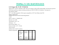
1
SERVICE MANUAL & TROUBLESHOOTING GUIDE FOR
7521 Plus/N
BY: Richard Wang
TESTING TECHNOLOGY DEPARTMENT / TSSC
AUG. 2001
7521Plus / N N/B MAINTENANCE
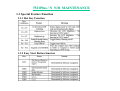
CONTENTS
1. Hardware Engineering Specification ------------------------------------------------------------------------------- 3
1.1
1.2
1.3
1.4
1.5
1.6
Introduction ----------------------------------------------------------------------------------------------------------------------------Hardware System ---------------------------------------------------------------------------------------------------------------------Special Feature Function ------------------------------------------------------------------------------------------------------------SMM And System BIOS -------------------------------------------------------------------------------------------------------------Peripheral Component ---------------------------------------------------------------------------------------------------------------Appendix: GPIO Definitions ---------------------------------------------------------------------------------------------------------
3
4
37
39
42
49
2. System View And Disassembly --------------------------------------------------------------------------------------- 51
2.0 Tools Introduction --------------------------------------------------------------------------------------------------------------------- 51
2.1 System View ----------------------------------------------------------------------------------------------------------------------------- 52
2.2 System Disassembly ------------------------------------------------------------------------------------------------------------------- 55
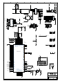
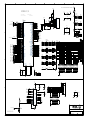
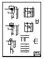
3. Definition & Location Of Connectors / Switches Setting ------------------------------------------------------- 76
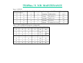
3.1
3.2
3.3
3.4
3.5
3.6
3.7
Mother Board -A ----------------------------------------------------------------------------------------------------------------------Mother Board Switch Table --------------------------------------------------------------------------------------------------------Mother Board -B ----------------------------------------------------------------------------------------------------------------------Daughter Board -----------------------------------------------------------------------------------------------------------------------Charger Board -------------------------------------------------------------------------------------------------------------------------IQSB Board --------------------------------------------------------------------------------------------------------------------------------------------------------------------------------------------------------------------------------------------------------Easy Start Button Board -------------------------------------------------------------------------------------------------------------------------------------------------------------------------------------------------------------------------
76
77
78
79
80
81
81
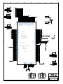
4. Definition & Location Of Major Components -------------------------------------------------------------------- 82
4.1 Main Board ( Side A ) ----------------------------------------------------------------------------------------------------------------- 82
4.2 Main Board ( Side B ) ----------------------------------------------------------------------------------------------------------------- 83
5. Pin Description Of Major Components ---------------------------------------------------------------------------- 84
5.1 Pentium III/Celeron FC-PGA2 CPU ----------------------------------------------------------------------------------------------- 84
5.2 SiS630S Slot 1/Socket 370 2D/3D Ultra-AGP™ Single Chipset -------------------------------------------------------------- 90
1
7521Plus / N N/B MAINTENANCE
CONTENTS
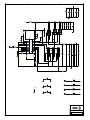
6. System Block Diagram ------------------------------------------------------------------------------------------------- 97
7. Maintenance Diagnostic ----------------------------------------------------------------------------------------------- 98
7.1 Introduction ----------------------------------------------------------------------------------------------------------------------------- 98
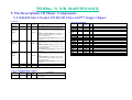
7.2 Error Codes ----------------------------------------------------------------------------------------------------------------------------- 99
7.3 Diagnostic Tools ------------------------------------------------------------------------------------------------------------------------ 101
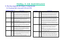
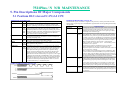
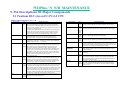
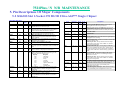
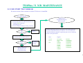
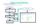
8. Trouble Shooting -------------------------------------------------------------------------------------------------------- 102
8.1 No Power --------------------------------------------------------------------------------------------------------------------------------8.2 No Display ------------------------------------------------------------------------------------------------------------------------------8.3 VGA Controller Failure LCD No Display ---------------------------------------------------------------------------------------8.4 External Monitor No Display -------------------------------------------------------------------------------------------------------8.5 Memory Test Error -------------------------------------------------------------------------------------------------------------------8.6 Keyboard ( K/B ) , Touch-Pad ( T/P ) , ESB Test Error ----------------------------------------------------------------------8.7 CD-ROM Drive Test Error ---------------------------------------------------------------------------------------------------------8.8 Hard Drive Test Error ---------------------------------------------------------------------------------------------------------------8.9 USB Port Test Error -----------------------------------------------------------------------------------------------------------------8.10 Audio Failure -------------------------------------------------------------------------------------------------------------------------8.11 SIO Port Test Error -----------------------------------------------------------------------------------------------------------------8.12 PIO Port Test Error ----------------------------------------------------------------------------------------------------------------8.13 PC CARD Socket Failure -----------------------------------------------------------------------------------------------------------
103
108
111
113
115
117
119
121
123
125
128
130
132
9. Spare Parts List ---------------------------------------------------------------------------------------------------------- 134
10. System Explode View ------------------------------------------------------------------------------------------------- 143
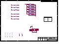
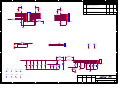
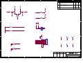
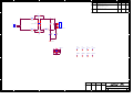
11. 7521 Plus/N Schematics ---------------------------------------------------------------------------------------------- 145
12. Reference ---------------------------------------------------------------------------------------------------------------- 180
2
7521Plus / N N/B MAINTENANCE
1. Hardware Engineering Specification
1.1 Introduction
1.1.1 General Description
This document describes the engineering specification for 7521 plus portable notebook computer system.
1.1.2 System Overview
The 7521 plus model motherboard will accept Intel Pentium III at FSB 133/100MHz and Celeron at FSB 66MHz processor
with FC-PGA packaged. Those are Pentium III 600/650/667/700/733/ 750/800/866 MHz, and Celeron
3/566/600/633/667/700/733/766 MHz.
This system is based on PCI architecture and is fully compatible with IBM PC/AT specification, which has standard
hardware peripheral interface. The power management complies with Advanced Configuration and Power Interface (ACPI)
1.0. It also provides easy configuration through CMOS setup, which is built in system BIOS software and can be pop-up by
pressing F2 key at system start up or warm reset. System also provides icon LEDs to display system status, such as AC
Power indicator, FDD, HDD, NUM LOCK, CAP LOCK, SCROLL LOCK, SUSPEND MODE and battery present,
capacity & charging status. It also equipped with LAN, FIR, USB port, 3D stereo audio and TV-OUT functions.
The memory subsystem supports 64MB on board SDRAM, one 144pin SO-DIMM socket for upgrading up to 320MB.
The SiS630S integrates the north bridge chip, super south bridge and the real 128-bit 3D graphics accelerator all into one
single chip. It provides, 3D Positional Audio, Advance H/W DVD playback and 2D/3D graphics engine.
The TI 1225 cardbus controller supports PCMCIA and CARDBUS. The National Semiconductor PC97338 Super I/O
controller integrates the standard PC I/O functions: floppy interface, two FIFO serial ports, one EPP/ECP capable parallel
port, and support for an IrDA 1.1, 1.0 and sharp ASK compatible infrared interface. To provide for the increasing number
of multimedia applications, a CODEC CS4299 is integrated onto the motherboard that support 16-bit stereo, Sound Blaster
Pro, Windows Sound System compatibility, and full-duplex capabilities to meet the demands of interactive multimedia
applications.
3
7521Plus / N N/B MAINTENANCE
The SiS900 is a single chip 10/100Mbps Fast Ethernet LAN solution, which fully integrates both the Media Access
Controller (MAC) with PCI bus master interface and 802.3u compliant 10/100Mbps physical layer interface into a 128 pins
PQFP, 0.35um process chip. It is targeted at low-cost, low-power, high volume desktop PC motherboards, mobile PC
module, adapter cards, and embedded systems.
The Chrontel’s CH7005 digital PC to TV encoder is a standalone integrated circuit that provides a PC 99 compliant solution
for TV output. It provides a universal digital input port to accept a pixel data stream from a compatible VGA controller (or
equivalent) and converts this directly into NTSC or PAL TV format.
A full set of software drivers and utilities are available to allow advanced operating systems such as Windows 98 or
Windows ME to take full advantage of the hardware capabilities. Features such as bus mastering IDE, Plug and Play,
Advanced Power Management (APM) with application restart, software-controlled power shutdown. Following chapters
will have more detail description for each individual sub-systems and functions.
1.2 Hardware System
1.2.1 System parts
Central Processing Unit : using Intel Pentium III or Celeron microprocessors in FC-PGA packaged.
Synthesizer : ICS9248-102.
SiS630S : CPU/PCI and CPU/AGP Bridge with memory controller/IDE/USB/PMU controller.
Super I/O Controller : NS PC97338VJG.
PCMCIA Interface Controlle : TI 1225.
Keyboard System : Hitachi H8 (3434F) universal keyboard controller.
3D Audio System : CRYSTAL CS4299 CODEC.
FIR port: HP HSDL-3600#007 FIR module.
FAX/MODEM : Software Modem (option).
LAN : SiS900
CH7005 : Digital PC to TV Encoder with Macrovision™
4
7521Plus / N N/B MAINTENANCE
1.2.2 CPU MODULE
Intel Pentium III/Celeron Processors with 370 pins FC-PGA package.
Pentium III 600/650/667/700/733/750/800 MHz, FC-PGA package at FSB 133/100Mhz.
Celeron 600/633/667/700/733 MHz, FC-PGA package at FSB 66Mhz.
1.2.3 Synthesizer
System frequency synthesizer : ICS9248-102
Maximized EMI suppression using Integrated Circuit System spread spectrum technology.
Three copies of CPU output, output to output skew between them within 175ps and seven copies of PCI output, output to
output skew within 500ps, fourteen copies of SDRAM output, output to output skew between them within 250ps.
One 48MHz output for USB and selectable 24/48MHz output (pin 25).
Two buffer copies of 14.318MHz input reference signal.
Supports up to 166MHz CPU or SDRAM operation.
Supports two SDRAM DIMMS.
Ideal for high performance Desktop/Notebook designed using SIS630 chip set.
I²C serial configuration interface.
1.2.4 SiS630S Slot 1/Socket 370 2D/3D Ultra-AGP™
Single Chipset
The single chipset, SiS630S, provides a high performance/low cost Desktop solution for the Intel Slot 1 and socket 370
series CPUs based system by integrating a high performance North Bridge, advanced hardware 2D/3D GUI engine, SuperSouth bridge and an AGP4X Slot. In addition, SiS630S provides system-on-chip solution that complies with Easy PC
Initiative which supports Instantly Available/OnNow PC technology, USB, Legacy Removal and Slotless Design and
FlexATX form factor.
5
7521Plus / N N/B MAINTENANCE
By integrating the UltraAGP TM technology and advanced 64-bit graphic display interface, SiS630S delivers AGP 4x
performance and memory bandwidth of up to 1 GB/s. In addition, SiS also supports an extra AGP Slot that supports 4X
and Fast Write transactions. Furthermore, SiS630S provides powerful hardware decoding DVD accelerator to improve the
DVD playback performance. In addition to providing the standard interface for CRT monitors, SiS630S also provides the
Digital Flat Panel Port (DFP) for a standard interface between a personal computer and a digital flat panel monitor. To
extend functionality and flexibility, SiS also provides the “ Video Bridge ” (SiS301) to support the NTSC/PAL Video
Output, Digital LCD Monitor and Secondary CRT Monitor, which reduces the external Panel Link transmitter and TV-Out
encoder for cost effected solution. SiS630S adopts Share System Memory Architecture which can flexibly utilize the frame
buffer size up to 64MB.
The “ Super-South Bridge “ in SiS630S integrates all peripheral controllers/accelerators /interfaces. SiS630S provides a
total communication solution including 10/100Mb Fast Ethernet for Office requirement and 1Mb HomePNA for Home
Networking. SiS630S offers AC’7 compliant interface that comprises digital audio engine with 3D-hardware accelerator,
on-chip sample rate converter, and professional wavetable along with separate modem DMA controller. SiS630S also
provides interface to Low Pin Count (LPC) operating at 33 MHz clock which is the same as PCI clock on the host, and
dual USB host controllers with six USB ports that deliver better connectivity and 2 x 12Mb bandwidth.
The built-in fast PCI IDE controller supports the ATA PIO/DMA, and the Ultra DMA33/66/100 function that supports the
data transfer rate up to 100 MB/s. It provides the separate data path for two IDE channels that can eminently improve the
performance under the multi-tasking environment.
SiS630S Features
Host Interface Controller
Supports Intel Slot 1/Socket370 Pentium II/!!! CPUs
Synchronous Host/DRAM Clock Scheme
Asynchronous Host/Dram Clock Scheme
6
7521Plus / N N/B MAINTENANCE
Integrated DRAM Controller
3-DIMM/6-Bank of 3.3V SDRAM
Supports Memory Bus up to 133 MHz
System Memory Size up to 1.5 GB
Up to 512MB per Row
Supports 16Mb, 64Mb, 128Mb, 256Mb, 512Mb SDRAM Technology
Suspend-to-RAM (STR)
Relocatable System Management Memory Region
Programmable Buffer Strength for CS#, DQM[7:0], WE#, RAS#, CAS#, CKE, MA[14:0] and MD[63:0]
Shadow RAM Size from 640KB to 1MB in 16KB increments
Two Programmable PCI Hole Areas
Integrated A.G.P. Compliant Target /66Mhz Host-to-PCI Bridge
AGP v2.0 Compliant
Supports Graphic Window Size from 4MBytes to 256MBytes
Supports Pipelined Process in CPU-to Integrated 3D A.G.P. VGA Access
Supports 8 Way, 16 Entries Page Table Cache for GART to Enhance Integrated A.G.P. VGA Controller Read/Write
Performance
Supports PCI-to-PCI Bridge Function for Memory Write from 33MHz PCI Bus to Integrated A.G.P. VGA
Supports Additional AGP slot with 4X and Fast Write Transaction
Meet PC99 Requirements
PCI 2.2 Specification Compliant
High Performance PCI Arbiter
Supports up to 4 PCI Masters
Guaranteed Minimum Access Time for CPU and PCI Masters
7
7521Plus / N N/B MAINTENANCE
Integrated Host-to-PCI Bridge
Zero Wait State Burst Cycles
CPU-to-PCI Pipeline Access
256B to 4KB PCI Burst Length for PCI Masters
PCI Master Initiated Graphical Texture Write Cycles Re-mapping
Reassembles PCI Burst Data Size into Optimized Block Size
Fast PCI IDE Master/Slave Controller
Supports PCI Bus Mastering
Native Mode and Compatibility Mode
PIO Mode 0, 1, 2, 3, 4
Multiword DMA Mode 0, 1, 2
Ultra DMA 33/66/100
Two Independent IDE Channels Each with 16 DW FIFO
Virtual PCI-to-PCI Bridge
Integrated Ultra AGP VGA for Hardware 2D/3D Video/Graphics Accelerators
Supports Tightly Coupled 64 Bits Host Interface to VGA to Speed Up GUI Performance and Video Playback Frame Rate
AGP v. 2.0 Compliant
Zero-Wait-State 128x4 Post-Write Buffer with Write Combine Capability
Zero-Wait-State 128x4 2-Way Read Ahead Cache Capability
Re-locatable Memory-Mapped and I/O Address Decoding
Flexible Design Shared Frame Buffer Architecture for Display Memory
Shared System Memory Area up to 64MB
Built-in 8K Bytes Texture Cache
8
7521Plus / N N/B MAINTENANCE
32-Bit VLIW Floating-Point Primitive Setup Engine
Supports Flat and Gouraud Shading
Supports High Quality Dithering
Supports Bump Mapping
Supports Z-Test, Stencil Test, Alpha Test and Scissors Clipping Test
Supports Z Pre-Test for Reducing Texture Read DRAM Bandwidth
Supports Individual Z-Buffer and Render Buffer at the Same Time
Supports 16/24/32 BPP Z Buffer Integer/Floating Formats
Supports 16/32 BPP Render Buffer Format
Supports 1/2/4/8 Stencil Format
Supports Per-Pixel Texture/Fog Perspective Correction
Supports MIPMAP with Point-Sampled, Linear, Bi-Linear and Tri-Linear Texture Filtering
Supports Single Pass Two MIPMAP Texture, One Texture on Clock
Supports up to 2048x2048 Texture Size
Supports 2’S Power of Width and Height Structure Rectangular Texture
Supports 1/2/4/8 BPP Palletize Texture with 32 Bit ARGB Format
Supports Palette for High Performance Palette Look Up
Supports 1/2/4/8 BPP Luminance Texture
Supports 1/2/4/8 BPP Intensity Texture
Supports 8/16/24/32 BPP RGB/ARGB Texture Format
Supports Video YUV Texture in All Supported Texture Formats
Supports MIP-Mapped Texture Transparency, Blending, Wrapping, Mirror and Clamping
Supports Fogging and Alpha Blending
9
7521Plus / N N/B MAINTENANCE
Internal Full 32 Bits ARGB Format Ultra Pipelined Architecture for Ultra High Performance and High Rendering Quality
128-Bit 2D Engine with a Full Instruction Set
Built-In 64x64x2 Bit-Mapped Hardware Cursor
Built-In 32x32x16, 32x32x32 Bit-Mapped Color Hardware Cursor
Maximum 64 MB Frame Buffer with Linear Addressing
MPEG-2 ISO/IEC 13818-2 MP@ML and MPEG-1 ISO/IEC 11172-2 Standards Compliant
Supports Hardware DVD Accelerator
Direct DVD to TV Playback
Supports Single Frame Buffer Architecture
Supports Two Independent Video Windows with Overlay Function and Scaling Factors
Supports YUV-To-RGB Color Space Conversion
Supports Bi-Linear Video Interpolation with Integer Increments of Pixel Accuracy
Supports Graphic and Video Overlay Function
Supports CD/DVD to TV Playback Mode
Simultaneous Graphic and TV Video Playback Overlay
Supports Current Scan Line of Refresh Red-Back and Interrupt
Supports Tearing Free Double/Triple Buffer Flipping
Supports Input Video Vertical Blank or Line Interrupt
Supports RGB555, RGB565, YUV422 and YUV420 Video Playback Format
Supports Filtered Horizontal Up and Down Scaling Playback
Supports DVD Sub-Picture Playback Overlay
Supports DVD Playback Auto-Flipping
Built-in Two Video Playback Line Buffers
10
7521Plus / N N/B MAINTENANCE
Built-in Programmable 24-bit True-Color RAMDAC up to 270 MHz Pixel Clock RAMDAC Snoop Function
Built-in Reference Voltage Generator and Monitor Sense Circuit
Supports Down-Loadable RAMDAC for Gamma Correction in High Color and True Color Mode
Built-in Dual-Clock Generator
Supports Multiple Adapters and Multiple Monitors
Built-in PCI Multimedia Interface
Supports Digital Flat Panel Port for Digital Monitor (LCD Panel)
Built-in VESA Plug and Display for CH7003, PanelLink TM and LVDS Digital Interface
Built-in Secondary CRT Controller for Independent Secondary CRT, LCD or TV digital output
Supports VESA Standard Super High Resolution Graphic Modes
-640x480 16/256/32K/64K/16M colors 120 Hz NI
-800x600 16/256/32K/64K/16M colors 120 Hz NI
-1024x768 256/32K/64K/16M colors 120 Hz NI
-1280x1024 256/32K/64K/16M colors 85 Hz NI
-1600x1200 256/32K/64K/16M colors 85 Hz NI
-1920x1440 8bbp/16bbp 60NI
Low Resolution Modes
Supports Virtual Screen up to 4096x4096
Fully DirectX 7.0 Compliant
Efficient and Flexible Power Management with ACPI Compliance
Supports DDC1, DDC2B and DDC 3.0 Specifications
Cooperate with “ SiS Video Bridge ” to Support
-NTSC/PAL Video Output
-Digital LCD Monitor
-Secondary CRT Monitor
11
7521Plus / N N/B MAINTENANCE
Low Pin Count Interface
Forwards PCI I/O and Memory Cycles into LPC bus
Translates 8/16 bit DMA cycles into PCI bus cycles
Advanced PCI H/W Audio & Modem
Advanced Power Management
Meets ACPI 1.0 Requirements
Meets APM 1.2 Requirements
ACPI Sleep States Include S1, S3, S4, S5
CPU Power States Include C0, C1, C2 C3
Power Button with Override
RTC Day-of-Month, Month-of-Year Alarm
24-bit Power Management Timer
LED Blinking in S0,S1 and S3 States
System Power-Up Events Include: Power Button, Hot-Key, Keyboard Password/ Hot Key, RTC Alarm, Modem Ring-In,
SMBALY#, LAN, PME#, AC’97 Wake-Up and USB Wake-Up
Software Watchdog Timer
Power Supply’98 Support
PCI Bus Power Management Interface Spec. 1.0
Integrated DMA Controller
Two 8237A Compatible DMA Controller
8/16 bit DMA data transfer
Distributed DMA Support
12
7521Plus / N N/B MAINTENANCE
Integrated Interrupt Controller
Two 8237A Compatible DMA Controller
Two 8259A Compatible Interrupt Controllers
Level or Edge Triggered programmable
Serial IRQ
Interrupt Source Re-routable to Any IRQ channel
Three 8254 Compatible Programmable 16-bits counters
System timer interrupt
Generate refresh request
Speaker output
Integrated Keyboard Controller
Hardwired Logic Provides Instant Response
Supports PS/2 Mouse Interface
Password Security and Password Power-Up
System Sleep and Power-Up by Hot-Key
KBC and PS2 Mouse Can Be Individually Disabled
Integrated Real Time Clock (RTC) with 256B CMOS SRAM
Supports ACPI Day-Month and Month-of-Year- Alarm
256 Bytes of CMOS SRAM
Provides RTC H/W Year 2000 Solution
13
7521Plus / N N/B MAINTENANCE
Universal Serial Bus Host Controller
Open HCI Host Controller with Root Hub
Two USB Host Controllers
Six USB Ports
Supports Legacy Devices
Over Current Detection
I²C Bus/SMBus Series Interface
Integrated Fast Ethernet Controller and MAC Interface
Plug and Play Compatible
High-Performance 32-Bit PCI Bus Master Architecture with Integrated Direct Memory Access (DMA) Controller for Low
CPU and Bus Utilization
Supports an Unlimited PCI Burst Length
Supports Big Endian and Little Endian Byte Alignments
Implements Optional PCI 3.3v Auxiliary Power Source 3.3Vaux Pin And Optional PCI
IEEE 802.3 and 802.3u Standard Compatible
Single 25MHz Clock for 10 and 100 Mbps Operation
Supports Software, Enhanced Software, and Automatic Polling Schemes to Internal PHY Status Monitor and Interrupt
Supports 10base-T, 100base-Tx 1Mb Home Networking
NAND Tree for Ball Connectivity Testing
672-Balls BGA Package
1.8V Core with Mixed 3.3V and 5V I/O CMOS Technology
14
7521Plus / N N/B MAINTENANCE
1.2.5 Super IO: NS PC 97338VJG
High speed PC16550A compatible UART with receive/transmit 16 Bytes FIFO programmable serial baud rate generator
Multi-mode parallel port support including standard port, EPP/ECP (IEEE1284 compliant, 2 interrupt pins)
Plug and Play module
FDC, 100% IBM compatible, S/W & register compatible to 82077 with 16Bytes data FIFO
Support 3-Mode FDD
FIR/MIR/SIR/SHARP ASK for Infrared application.
COM2
IrDA 1.0/ IrDA 1.1/ SHARP ASK
Baud rate: max. 4Mb
Link distance: 0.01 to 1 m
Half angle : ±15°
Bit Error Rate (BER) : 10 -9
Peak wavelength : 0.85 - 0.90 µm
TQFP 100 pins
Standby mode: control by software
Default configuration :
IO address
IRQx
DRQx
COM1
3F8-3FF
4
-
FIR/MIR/SI
278-27F
3
-
R/ SHARP
ASK
(COM2)
PIO
378-37F
7
-
FDD
3F0-3FF
6
2
15
7521Plus / N N/B MAINTENANCE
1.2.6 PC CARD interface controller : TI1225
ACPI 1.0 Compliance
PCI Power Management interface specification 1.0 Compliance
Supports distributed DMA (DDMA) and PC/PCI DMA
Advanced submicron, low-power CMOS technology.
Supports two I/O windows and two memory windows available to each cardbus socket.
Supports five PCI memory windows and two I/O windows available to each PC CARD16 socket.
Supports Burst Transfers To Maximize Data Throughput On Both PCI Buses
Provides Serial Interface To TI TPS2202/TPS2206 Dual Slot PC CARD Power Interface Switch
Supports up to 5 general purpose I/O
Multi-Function PCI Device With Separate Configuration Space For Each Socket
Pipelined architecture allows greater than 130Mbps second throughput from cardbus to PCI and from PCI to cardbus.
Support PCI Bus Lock (/LOCK)
3.3-V core logic with universal PCI interface
PCI Local Bus Specification Revision 2.1 compliant
Fully compatible with the Intel 430TX(Mobile Triton II) chipset
1995 PC Card Standard compliant
Supports two 16-bit PC card or Cardbus card; sockets powered at 3.3V or 5V with hot insertion and removal
Provides a serial EEPROM interface for loading the subsystem ID and subsystem vendor ID.
ExCA compatible registers mapped in memory or I/O space.
Supports ring indicate output, SUSPEND#, and programmable output select for CLKRUN#.
Provides socket activity LED signals.
Provides zoom video support signals.
16
7521Plus / N N/B MAINTENANCE
Provides zoom video port function in socket B.
208-Pin LQFP package
1.2.7 DUAL-SLOT PC CARD POWER INTERFACE SWITCH : TPS2206
Fully Integrated VCC and V pp Switching for Dual-Slot PC Card Interface
I2C 3-Lead Serial Interface Compatible With CardBus Controllers
3.3 V Low-Voltage Mode
Meets PC Card Standards
RESET for System Initialization of PC Cards
12-V Supply Can Be Disabled Except During 12-V Flash Programming
Short Circuit and Thermal Protection
30-Pin SSOP (DB) and 32-Pin TSSOP (DAP)
Compatible With 3.3-V, 5-V and 12-V PC Cards
Break-Before-Make Switching
1.2.8 Keyboard system : H8 (3434F) universal keyboard controller
CPU
Two-way general register configuration
Eight 16-bit registers or Sixteen 8-bit registers
High-speed operation
Maximum clock rate: 16Mhz at 5V
Memory
Include 32KB ROM and 1KB RAM
17
7521Plus / N N/B MAINTENANCE
16-bit free-running timer
One 16-bit free-running counter
Two output-compare lines
Four input capture lines
8-bit timer (2 channels)
Each channel has one 8-bit up-counter, two time constant registers
PWM timer (2 channels)
Resolution: 1/250
Duty cycle can be set from 0 to 100%
I²C bus interface (one channel)
Include single master mode and slave mode
Host interface (HIF)
8-bit host interface port
Three host interrupt requests (HIRQ1, 11,12)
Regular and fast A20 gate output
Keyboard controller
Controls a matrix-scan keyboard by providing a keyboard scan function with wake-up Interrupts and sense ports
A/D converter
10-bit resolution
8 channels: single or scan mode (selectable)
D/A converter
8-bit resolution
2 channels
18
7521Plus / N N/B MAINTENANCE
Interrupts
Nine external interrupt lines: NMI#, IRQ0 to 7#
26 on-chip interrupt sources
Power-down modes
Sleep mode
Software standby mode
Hardware standby mode
A single chip microcomputer
On-chip flash memory
Maximum 64-kbyte address space
Support three PS/2 port for external keyboard, mouse and internal track pad.
Support SMI, SCI trigger input:
Cover switch
Battery charging control
Smart Battery monitoring
Control D/D system on/off
Fan control and LED indicator serial interface
100pin TQFP
19
7521Plus / N N/B MAINTENANCE
1.2.9 System BIOS
See software BIOS specification
1.2.9.1 System BIOS and Software Features Overview
Including System BIOS, VGA BIOS, POST, APM, PnP, ACPI and PXE BIOS
Support Shadow RAM BIOS Feature
Support APM 1.2
Support ACPI V1.0B
Support DMI 2.3
Support SMBIOS 2.2
Support Quite Boot
Support Extended Int14H function 50H (IR type switching)
Support Hot-Plug for PS/2 keyboard and pointing devices.
Support Intel CPU Microcode Update function
Support Power management S0, S1, S3, S4
Parallel Port Support- Standard / Bi-Directional / EPP(1.9) / ECP
PC99A Compliance
The following device can be disabled by BIOS
Serial Port
Parallel Port
Audio
Ethernet
Modem
(When disable the device, the resource of its device are released)
20
7521Plus / N N/B MAINTENANCE
1.2.9.2 BIOS Setup Feature Introduction
Setup Utility allows you to enter the system configuration information. This information is needed by the system to
identify the type of device installed and to setup special features. Typical configuration information includes the data
and time, the type of disk drives, and the amount of memory; special features include Security and Power Saving.
The configuration information is stored in a special kind of memory called CMOS ( Complementary Metal Oxide
Semiconductor) RAM. CMOS RAM data are backed up by a RTC backup battery.
You may need to run Setup Utility when :
You see an error message on the screen requesting you to run Setup Utility.
You change factory default settings for some special features.
You want to modify the configuration information.
During POST, the end user can press <F2> to enter Setup and change the system parameters originally specified in the
BIOS defaults. The purpose of Setup is the following:
Change system hardware
Change system behavior
Optimize system performance
21
7521Plus / N N/B MAINTENANCE
1.2.10 POWER MANAGEMENT
ACPI Introdution
The system BIOS is conform with ACPI1.0B specification.
Concept
ACPI (Advanced Configuration and Power Interface) replaces APM and PnP functionality, it’s a Operating-System
controlled Power Management and a subset of OnNow system.
The general behavior of a PC with OnNow is as follows:
Minimized or eliminated Startup and shutdown delays.
Both hardware and software can be made to trigger wake-up events.
The PC is perceived to be off when not in use but still capable of responding to wake-up events.
ACPI Power States
G0~G3 : Global power states
S0~S5 : System power states
B0~B3 : Bus power states
C0~C3 : Processor power states
D0~D3 : Device power states
Summary of Global Power States
Global System
State
G0 - Working
Software
Runs
Yes
Latency
0
Large
OS restart
required
No
Smaller
No
No
Yes
Very near 0
Yes
No
Yes
RTC battery
Yes
Yes
No
G1 - Sleeping
No
G2/S5-Soft off
No
>0 varies with
sleep state
Long
G3-Mechanical Off
No
Long
Power Consumption
Safe to disassemble
computer
No
Exit state
electronically
Yes
22
7521Plus / N N/B MAINTENANCE
Summary of Device Power Sates
Device State
D0 – Fully On
Power Consumption
Device Context Retained
Driver Restoration
As needed for operation
All
None
D1
D0>D1>D2>D3
>D2
<D2
D2
D0>D1>D2>D3
<D1
>D1
0
None
Full init and load
D3 – Off
System States
1. Working (S0)
System is fully usable. User can enter working state from S4 or S5 by pressing the power button or wake up from sleeping
state.
2.Sleeping State (S3)
The S3 sleeping state is a low wake-up latency sleeping state where all system context is lost except system memory. CPU,
cache, and chip set context is lost in this state.
This state is attained by:
• Set “ Low Battery Alarm Actions ” to “ Standby ”, when the battery discharge to a critical level, unit will enter this state.
• If sets optional action of “ cover switch ”, “ power button ”, “ sleep button ” to “ Standby ”, and presses these buttons, or
sets “ System standby ” timeout.
• Set “ System standby ” in “ Power Schemes ” for system inactivity time out.
• Putting the PC into standby through the Operating System by clicking Start, Shut Down then select Standby item.
23
7521Plus / N N/B MAINTENANCE
Events that can bring the platform back to Working state :
•. Pressing any key on the keyboard.
•. Wake on LAN.
•. Modem answering call.
•. Pressing the power button less than 4 seconds.
3.Hibernation (S4)
The S4 sleeping state is lowest power, longest wake-up latency sleeping state supported by ACPI. The platform context
is maintained. For entering this state, users have to check “ Enable Hibernate ” in “ Power Management “of control panel.
This state is attained by:
• Set “ Low Battery Alarm Actions “ to “ Hibernate “ when the battery discharge to a critical level, unit will enter this
state.
• If user sets optional action of “ cover switch “, “ power button “, “sleep button “ to “ hibernate “, and presses these
buttons, the platform will enter this state.
• Set “System hibernate “ in “ Power Schemes “ for system inactivity time out.
Events that can bring the platform back to Working state:
• Pressing the power button.
4.Soft Off State (S5)
The S5 state is similar to the S4 state except the OS does not save any context nor enable any device to wake the system.
The system is in the “ soft “off state and requires a complete boot when awakened.
This state is attained by:
• Shut down the PC through the Operating System by clicking Start, Shutdown, then Ok.
• Reset the PC by holding the Power button for more than 4 seconds.
Note: (1) This action may cause date loss. (2) This action normally causes the OS to run Scan Disk after reboot.
Events that can bring the platform back to Working state:
• Pressing the Power button.
24
7521Plus / N N/B MAINTENANCE
5.Mechanical Off
No power supplied and consumption, achieved by unplugging the machine and removing the battery. By definition, unit
will return to Soft Off (S5) by restoration of power. If previous mode was Hibernation (S4), then system returns to S4.
Component Level Power Management Matrix
25
7521Plus / N N/B MAINTENANCE
APM
Concept
This platform supports Advanced Power Management (APM1.2) developed by Microsoft and Intel. APM consists of
one or more layers of software that support power management in computers with power manageable hardware.
Power State
1.Full Power
Default mode. System activity detected. This is the normal state of the system. If system power management is disabled,
the system remains in this state until the power is turned off.
2. Idle
An APM driver will notify the APM BIOS about CPU usage but the APM BIOS determines the action to take. Idle is a
state between full system power and standby. Enable/Disable by toggling the setting in Bios Setup Menu.
Idle Mode slows down the CPU during brief periods.
This state is attained by :
• The APM driver acknowledge APM BIOS that the system is idle. The APM BIOS issues “CPU HLT “ instruction.
Events that can bring unit back to full power state :
• CPU idle until the next system event (typically an interrupt) occurs.
3.Standby
System may not be working and in a low power state with some power saving. Most devices are in a low power mode.
The CPU clock is slowed. System returns quickly to full on state. Operational parameters are retained.
This state is attained by:
• Set “Standby Timeout “ in Bios Setup Menu.
• Triggered by the timeout timer of the standby timer.
Events that can bring unit back to full power state:
• Pressing any key on the keyboard.
• Wake on LAN.
• Modem answering call.
26
7521Plus / N N/B MAINTENANCE
4.Suspend
System in not working and in a low power consumption state with maximum power savings . Most power managed
devices are not powered. Includes stopping the CPU clock and shutting down all peripherals. Detection restores full
power state. System takes a relatively long time to return to full on mode. Operational parameters are saved to be restored
later when resuming.
This state is attained by:
• Triggered by the timeout timer of the suspend timer.
• Pressing “ Fn+F12 “ hot key.
• Set “ Save To Disk Timeout ” in Bios Setup Menu.
• Allowing battery discharge to the critical level.
• Events that can bring unit back to full power state:
(1) Suspend to Ram:
• Pressing any key on the internal keyboard.
• Wake on LAN.
• Modem answering call.
• Set RTC wake up timer.
(2) Suspend to Disk:
• Press power button.
27
7521Plus / N N/B MAINTENANCE
5. Off
System is not working, the power supply is off. Operational parameters are not saved. System resets and initializes when
transitioning to the Full on State.
Component Level Power Management Matrix
28
7521Plus / N N/B MAINTENANCE
1.2.11 Memory System
HYUNDAI SDRAM cell on board13
One chip memory size : 4Banksx1Mx16bit SDRAM.
Standard 54-pin TSOP-II package.
Power supply : 3 ±0.3V
Supports One JEDEC 144-pin SO-DIMM sockets on Mother Board for expansion
Supports 3.3V SDRAM
2 banks on one socket.
SDRAM accesses time from clock: 6ns
Memory bus bandwidth: 64 bits
7521 plus Supports 64 MB SDRAM on board and one 144-pin DIMM socket for upgrading up to 320 MB of DRAM.
Here are some main memory system essential characteristics :
One chip 4Banksx1Mx16bit on board 64 MB
144-pin SO-DIMM socket 1
Memory Voltage 3.3V ± 10%
Banks on DIMM Mixed type DRAM Only supports SDRAM
29
7521Plus / N N/B MAINTENANCE
1.2.12 Interface
Power Supply Jack.
One Standard Parallel Port With ECP/EPP Functions
Supports Two USB port for all USB devices.
Supports Macrovision’s TV-OUT connector.
Tunable volume by variable resistor.
Two Serial Ports, One For COM1/COM2, The Other For FIR/MIR/SIR/SHARP ASK.
One External CRT Connector For CRT Display.
One PS/2 Interface For External KB, Mouse Or Other Devices.
Two Cardbus Sockets.
Cable For Connection Between M/B And Panel.
Cable For Connection Between M/B And Backlight BD.
Digital (Optical, 48KHz) / Analog Line-out Jack, Line-In Jack and Microphone Input Jack.
One MODEM RJ-11 phone jack for PSTN line and RJ-45 for LAN.
Battery translation board connection between M/B and battery.
Easy start buttons translation board (ESB) connection between M/B and five Buttons.
Internet quick start button translation board (IQSB) connection between M/B and touch pad, three LEDs, Mail Received
Button Buttons.
FDD-HDD translation board connection between M/B and floppy, hard disk.
One CD-ROM connector on M/B.
30
7521Plus / N N/B MAINTENANCE
1.2.13 Audio System: AC’97 CODEC CS4299
AC’97 CODEC CS4299 provides a complete high quality audio solution, Feature Include :
MPU-401 interface
FM synthesizer
Game Port
MIDI port.
MODEM
CD-ROM
Volume Control: Rotary VR
Stereo BTL 2x1 W amplifiers (TPA0202) with 8-Ohm Load.
CD-ROM IDE interface.
18-bit stereo ADC & 20-bit stereo DAC for record and play back.
Programmable sample rates from 20Hz to 20kHz for record and playback.
Digital (optical, 48KHz)/ analog line-out port * 1 (3.5 mm phone-jack and SCMS support)
Line-in * 1(3.5 mm phone-jack)
Built-in speaker * 2 (1w, 8 ohm)
Built-in microphone * 1
Note: for those input source not using should be set mute in order to reduce noise.
31
7521Plus / N N/B MAINTENANCE
1.2.14 IR MODULE: HSDL-3600#007
Fully Compliant to IrDA 1.1 Specifications
115.2 kb/s to 4 Mb/s operation
Excellent nose-to-nose operation
Compatible with ASK, HP-SIR, and TV Remote
IEC825-Class 1 Eye Safe
Wide Operating Voltage Range
2.7 V to 5.25 V
Small Module Size
4.0 x 12.2 x 5.1 mm (HxWxD)
Complete Shutdown
TXD, RXD, PIN diode
Low Shutdown Current
10 nA typical
Adjustable Optical Power Management
Adjustable LED drive-current to maintain link integrity
Single Rx Data Output
FIR Select pin switch to FIR
Integrated EMI Shield
Excellent noise immunity
Edge Detection Input
Prevents the LED from long turn-on time
Interface to various Super I/O and Controller Devices
Designed to Accommodate Light Loss with Cosmetic Window
Minimum External Components Required
32
7521Plus / N N/B MAINTENANCE
1.2.15 SiS900 Fast Ethernet PCI Bus 10/100Mbps LAN Single Chip with OnNow
Support
SiS900 is a single chip 10/100Mbps Fast Ethernet LAN solution, which fully integrates both the Media Access
Controller (MAC) with PCI bus master interface and 802.3u compliant 10/100Mbps physical layer interface into a 128
pins PQFP, 0.35um process chip. It is targeted at low-cost, low-power, high volume desktop PC motherboards, mobile
PC module, adapter cards, and embedded systems.
SiS900 fully implements the PCI bus version 2.1 interface for host communications. Packet descriptors and data are
transferred via bus-mastering DMA channels, reducing the burden on the host CPU. The buffer management scheme
utilized by SiS900 optimizes the use of memory space and the system bus. Descriptor information, describing the buffer
space in which packet information is held, is symmetrical between transmit and receive operations. SiS900 supports
both half-duplex and full-duplex operations with minimum inter frame gap and IEEE802.3x full-duplex flow control. In
order to meet the PC 98 and the Green PC power saving requirements, SiS900 supports ACPI and Network Device
Class Power Management specification. All the device states of D0, D1, D2, D3hot, and D3cold are implemented.
SiS900 also supports Remote Wake On LAN and OnNow for the Desktop PC management. Additional features include
a serial EEPROM interface for device information access and a Boot ROM interface up to 128K bytes for remote boot
functions support.
SiS900 also integrates analog interface for twisted pair Fast Ethernet applications. SiS900 can be configured for either
100 Mbps (100Base-TX) or 10 Mbps (10Base-T) Ethernet operation. SiS900 consists of 4B5B/Manchester
encoder/decoder, scrambler/descrambler, 100Base-TX/10Base-T twisted pair transmitter with wave shaping and output
driver, 100Base-TX/10Base-T twisted pair receiver with on chip equalizer and baseline wander correction, clock and
data recovery, and Auto Negotiation capability. The addition of internal output wave shaping circuitry and on-chip
filters eliminates the need for external filters normally required in 100Base-TX and 10Base-T applications. SiS900 can
automatically configure itself for 100 or 10 Mbps and Full or Half Duplex operation with the on-chip Auto Negotiation
algorithm. SiS900 PHY can access eleven 16-bit registers through the internal Management Interface (MI) serial port.
These registers contain configuration inputs, status outputs, and device capabilities.
33
7521Plus / N N/B MAINTENANCE
SiS900 Features
Integrated Fast Ethernet controller and 10/100 megabit per second (Mbps) Physical Layer Transceivers for the PCI
local bus
PCI specification revision 2.1 compliant
32-bit glueless PCI host interface
Plug and Play compatible
Supports PCI clock frequency from DC to 33 MHz independent of network clock
Supports network operation with PCI clock from 25Mhz to 33Mhz
Supports both +3.3v and +5v PCI signaling
High-performance 32-bit PCI bus master architecture with integrated Direct Memory
Access (DMA) Controller for low CPU and bus utilization
Supports an unlimited PCI burst length
Supports big endian and little endian byte alignments
Supports PCI Device ID, Vendor ID/Subsystem ID, Subsystem Vendor ID programming through the EEPROM interface
Implements optional PCI 3.3v auxiliary power source 3.3Vaux pin and optional PCI power management event (PME#) pin
IEEE 802.3 and 802.3u standard compatible
IEEE 802.3u Auto Negotiation and Parallel detection for automatic speed selection
Full duplex and half duplex mode for both 10 and 100 Mbps.
Fully compliant ANSI X3.263 TP-PMD physical sub-layer which includes adaptive equalization and Baseline Wander
compensation.
Automatic Jam and IEEE 802.3x Auto-Negotiation for flow control
Single access to complete PHY register set
Built-in waveform shaping requires no external filters
Single 25Mhz clock for 10 and 100 Mbps operation.
34
7521Plus / N N/B MAINTENANCE
Power down of 10Base-T/100Base-TX sections when not in use
Jabber control and auto-polarity correction for 10Base-T.
User programmable LED function mapping
Supports software, enhanced software, and automatic polling schemes to internal PHY status monitor and interrupt
Supports 10BASE-T, 100BASE-TX, and any future
Supports PC97, PC98, and Net PC requirements - Green PC compatible
Supports Advanced Configuration and Power Interface Specification (ACPI) Revision 1.0
Supports PCI Bus Power Management Interface Specification Version 1.0a
Supports Network Device Class Power Management Specification Version 1.0a
Supports PCI Hot-Plug Specification Revision 1.0
Implements full OnNow features including pattern matching and link status wake-up with automatic internal PHY status
polling
Implements optional Magic Packet TM remote wake-up scheme
Implements IEEE 802.3x compliant Flow Control
Additional features
Internal 128-bit Multicast Hash Table address filter
Serial EEPROM support
Boot ROM supports up to 128 Kbytes
Extensive programmable internal/external loop back capabilities
+3.3V power supply with +5V tolerant I/Os
128pin PQFP package. Low-Power CMOS 0.35um Technology
35
7521Plus / N N/B MAINTENANCE
1.2.16 CH7005C Digital PC to TV Encoder
The Chrontel’s CH7005 digital PC to TV encoder is a standalone integrated circuit which provides a PC 99 compliant
solution for TV output. It provides a universal digital input port to accept a pixel data stream from a compatible VGA
controller (or equivalent) and converts this directly into NTSC or PAL TV format.
This circuit integrates a digital NTSC/PAL encoder with 9-bit DAC interface, and new adaptive flicker filter, and high
accuracy low-jitter phase locked loop to create outstanding quality video. Through its TrueScale TM scaling and
deflickering engine, the CH7005 supports full vertical and horizontal underscan capability and operates in 5 different
resolutions including 640x480 and 800x600.
A new universal digital interface along with full programmability make the CH7005 ideal for system-level PC solutions.
All features are software programmable through a standard I 2 C port, to enable a complete PC solution using a TV as the
primary display.
CH7005 Features
Supports MacrovisionTM 7.X anti-copy protection
Function compatible with CH7004
Universal digital interface accepts YCrCb (CCIR601or 656) or RGB (15,16 or 24-bit) video data in both non-interlaced
and interlaced formats
TrueScaleTM rendering engine supports undescam operations for various graphic resolutions
Enhanced text sharpness and adaptive flicker removal with up to 5-lines of filtering
Enhanced dot crawl control and area reduction
Fully programmable through I2C port
Supports NTSC, NTSC-EIA (Japan), and PAL (B, D, G, H, I, M and N) TV formats
Provides Composite, S-Video and SCART outputs
Auto-detection of TV presence
Supports VBI pass-through
Programmable power management
9-bit video DAC outputs
Complete Windows and DOS driver software
Offered in 44-pin PLCC, 44-pin TQFP
36
7521Plus / N N/B MAINTENANCE
1.3 Special Feature Function
1.3.1 Hot Key Function
1.3.2 Easy Start Button function
37
7521Plus / N N/B MAINTENANCE
1.3.3 Flash ROM (BIOS)
7521 plus system utilizes the state-of-the-art Flash EEPROM technology. User can upgrade the system BIOS in the future
just running the program from MiTAC.
1.3.4 LED Indicators
System has ten status LED indicators to display system activity which include above keyboard and below touch pad:
(1) Four LEDs indicators below touch pad :
From left to right that indicates Mail Received status, AC POWER, BATTERY POWER and BATTERY STATUS:
• MAIL RECEIVED STATUS : This LED lights to indicate that User received E-mail status. User can define color of
LED (yellow or green) to indicate relation of transmitter.
• AC POWER : This LED lights green when the notebook is being powered by AC, and flash (on 1 second, off 1 second)
when Suspend to DRAM is active using AC power. The LED is off when the notebook is off or powered by batteries,
or when Suspend to Disk.
• BATTERY POWER : This LED lights green when the notebook is being powered by batteries, and flashes (on 1
second, off 1 second) when Suspend to DRAM is active using battery power. The LED is off when the notebook is off
or powered by AC, or when Suspend to Disk.
• BATTERY STATUS : During normal operation, this LED stays off as long as the battery is charged. When the
battery charge drops to 10% of capacity, the LED lights red, flashes per 1 second and beeps per 2 second. When AC is
connected, this indicator glows green if the battery pack is fully charged, or orange (amber) if the battery is being
charged.
(2) Six LED indicators above keyboard :
From left to right that indicates CD-ROM DRIVE, HARD DISK DRIVE, FLOPPY DISK DRIVE, NUM LOCK,
CAPS LOCK and SCROLL LOCK.
38
7521Plus / N N/B MAINTENANCE
1.3.5 COM port assignment
COM1 : MODEM / RS-232 / Disable
COM2 : IR / RS-232 / Disable
1.4 SMM and System BIOS
System Management Mode
7521 plus system has built in several power saving modes to prolong the battery usage for mobile purpose. User can enable
and configure different degrees of power management modes via ROM CMOS setup (booting by pressing F2 key). Following
are the descriptions of the SMM and power management modes supported.
Full On Mode
In this mode, each device is running with the maximal speed. CPU clock is up to its maximum.
Doze Mode
In this mode, CPU will be toggling between on & stop grant mode either. The technology is clock throttling. This can save
battery power without loosing much computing capability. The CPU power consumption and temperature is lowered in this
mode.
Standby
For more power saving, it turns off the peripheral component. In this mode, the following is the status of each device.
• CPU: Stop grant
• LCD: backlight off
• HDD: spin down
• FDD: standby
Suspend Mode
The most chipset of the system is entering power down mode for more power saving. In this mode, the following is the status
of each device.
39
7521Plus / N N/B MAINTENANCE
Suspend to DRAM:
• CPU : off
• SiS630 : Partial off
• VGA : Suspend
• PCMCIA : Suspend
• Super IO : off
• Audio : off
• SDRAM: Self Refresh.
Suspend to HDD:
• All devices are stopped clock and power-down,
• System status is saved in HDD.
• All system status will be restored when powered on again.
Other power management functions
HDD & Video access
System has the ability to monitor video and hard disk activity. User can enable monitoring function for video and/or hard
disk individually. When there is no video and/or hard disk activity, system will enter next PMU state depending on the
application. When the VGA activity monitoring is enabled, the performance of the system will have some impact.
Battery Warning
System also provides Battery capacity monitoring and gives user a warning so that users have chance to save his data before
battery dead. Also, this function protects system from mal-function while battery capacity is low.
- Battery Warning: Capacity below 10%, Battery Capacity LED flashes per second, system beeps per 2 seconds. (System
beeps only if BIOS setup enable Battery Warning Beeping.) System will suspend to HDD after 2 Minute if BIOS setup
enable this function or system will runs until battery dead without any protection.
40
7521Plus / N N/B MAINTENANCE
Cover Switch
System automatically provides power saving on monitoring Cover Switch. It will save battery power and prolong the usage
time when user closes the notebook cover unintentionally but the system still in power on mode. There are two functions to
be chosen.
1. Switch to CRT
2. Panel Off
3. Suspend to DRAM or Suspend to Disk by CMOS setup
Battery Warning State
7521 plus system provides battery management function and gives warning while battery is in its low power state. When the
battery capacity is below 10% (Battery Warning State), system will generate beep for every 2 seconds. When hearing the
beeping, it is recommended that user should plug in AC adapter to get power from external source, or stop working and save
his data file to prevent disaster results.
Battery Low State
After Battery Warning State, and battery capacity is below 4%, system will generate beep for twice second.
Battery Dead State
When the battery voltage level reaches 9 volts, system will shut down automatically in order to extend the battery packs' life.
Fan power on/off management
FAN is controlled by H8 embedded controller which using LM45 to sense CPU temperature and PWM to control fan speed.
41
7521Plus / N N/B MAINTENANCE
1.5 Peripheral Components
LCD Panel
Hyundai 14X13
1024X768 XGA TFT Panel
Display size (diagonal): 14.1 inch
262,144 colors display
1 channel LVDS Interface (Flat Link, Ti)
Display Mode: Normal White
Back-light unit: CCFL, 1 tube
DC for Panel: 3.3V+-0.3V
Pixel pitch: 0.279(H) X0.279 (V)
Power supply current: 320 mA (Typ)
Lamp start Voltage : 1500Vrms (25 ℃)
Hard Disk Drive
FUJITSU MHK2120AT: 12 GB Capacity
12.0GB Capacity
Number of head: 3
Number of cylinders: 14,784
Bytes per sector: 512
Recording method: 16/17 MTR
Track density: 24,300 TPI
Bit Density: 383 Kbpi
42
7521Plus / N N/B MAINTENANCE
Rotational Speed: 4,200 rpm +-1%
Average Latency: 7.14 ms
Interface: ATA-5 (Max. Cable length: 0.46 m)
Data transfer rate:
To/From Media: 12.5 to 22.3 MB/s
To/From Host: 66.6 MB/s Max (Ultra-DMA mode 4)
Data Buffer Size: 512 KB
Spin up current: 0.9Arms
Max. Power Consumption: 4.5W (During spin up)
Physical Dimensions (H X W X D): 9.5 mm X 100.0 mm X 70.0 mm
15GB, 20GB, 24GB HDD To Be Defined.
Keyboard
External keyboard: Supports IBM 106 key compatible keyboard
Key pitch: 19 mm
Windows95 applied
Internal keyboard: Compatible Japanese keyboard layout (90 keys)
Floppy Disk Drive
Mitsumi D353G
Using High density (2HD) 3.5 inch disk
Data transfer rate: 500k bits/sec
Disk rotational speed: 300 rpm for 2mode, 360rpm for 3mode
Track density: 135 tip
Track to Track time: 3msec
43
7521Plus / N N/B MAINTENANCE
Touch Pad
Logic Tech: 904255-0002
Vcc: 5V +- 0.5
Icc (max): 15 mA
Interface: PS/2
X/Y position resolution: 480+-50 CPI
Dimension: 66mm x 50mm x 5.0mm
Effective area: 55mm x 39 mm
Operating Temp. : 0 - 50 degree C
Storage humidity: 5 - 90 %,
Storage Temp.: -20 - + 60 degree C
ESD: 15KV applied to front surface
24X CD-ROM Drive
System has optional MATSUSHITA UJDA150 24X speed CD-ROM drive, LGS CRN8241B 24X speed CD-ROM
drive, or TEAC CD-224E-A92 24X speed CD-ROM drive.
Hardware interface is compliant with ATAPI IDE specification.
IDE second channel (170h). The default drive is D. User should install the CD-ROM device driver in order to
operate this device. This CD-ROM drive also support audio interface. Co-operate with audio circuit, CD-ROM
drive can work as a CD player.
Ejection: Manual eject using the eject button/Automatically eject using the tray
44
7521Plus / N N/B MAINTENANCE
XM-1802B:
Average data transfer rate of 3,600 KB/s
Average random seek time of 100ms
Random access time of 110ms.
Small size (only 12.7(H) x 128(W) x 129(D) mm)
Extremely low weight of 230g
Low average power consumption of 2.4W (maximum only 3.2W).
DVD-ROM drive
MATSUSHITA: UJDA520L-SH 4X speed
Fast 170 ms Random Access Time (DVD)
Max. 4X (DVD)/Max. 24X (CD)
Max. 5,408 Kbytes/s (DVD)/Max. 3,600 Kbytes/s (CD) Sustained Transfer Rate.
PIO mode-4 ATAPI Drive (16.7 Mbytes/s)
DMA: Multi word DMA transfer mode-2 (Transfer Rate 16.7 Mbytes/s)
Ultra DMA mode-2 (Transfer Rate 33.3 Mbytes/s)
CD-R/RW drive
MATSUSHITA: UJDA310
WRITE 4X-Speed
READ max 20X-Speed (CD-RW max 14X-Speed)
PIOMODE: 16.6MB/s; Mode 4
DMAMODE: 4.2MB/s; Mode 0
Write: 150KB/s (Normal speed), 300KB/s (2X speed), 600KB/s (4X speed)
Buffer memory: 2MB
Access speed 150ms (Typ.)
45
7521Plus / N N/B MAINTENANCE
LED Indicators
Lower ICON LEDs on M/B
Mail Received status (left 1)
AC POWER (left2)
BATTERY POWER (right 2)
BATTERY STATUS (right 1)
Upper ICON LEDs on M/B
CD-ROM/MO (left 1)
HARD DISK DRIVE (left 2)
FLOPPY DISK DRIVE (left 3)
NUM LOCK (right 3)
CAPS LOCK (right 2)
SCROLL LOCK (right 1)
IO port
HP HSDL-3600#007 FIR Module
Meet IrDA Physical Layer Specification
1 cm to 1 Meter Operating Distance
30 degree Viewing Angle
Support Two Channels - 2.4 Kb/s to 115.2Kb/s and 1.15Mb/s to 4.0 Mb/s
CMOS Battery
CR2032 3V 220mAh lithium battery
When AC in or system main battery in, CMOS battery will no power consumption.
AC or main battery not exists, CMOS battery life at less (220mAh/5.8uA) 4 years.
In normal condition, battery life is at less over 4 years. Battery was put in battery holder.
46
7521Plus / N N/B MAINTENANCE
Serial Interface
Using ADM3311ARU chip
ESD rating: ±3KV
Lead TEMP. (Soldering 10sec): +300 ℃
Number of RS-232 drivers: 3
Number of RS-232 receivers: 5
28 pin SSOP package
Support shutdown mode (pin 23).
-40 ℃ - +85 ℃ operating TEMP. range
Operating voltage range : 3V ±0.3V
MAX. data rate: 460 kbps
Shutdown supply current: 15(TYP) uA- 50(MAX) uA
PCMCIA Socket
Operating temperature range: -55 ℃- +85 ℃
Insertion force: 39.2N (MAX)
10000 times insertion and withdrawal at the cycle rate 400- 600cycles/hour and no
evidence of breakage and cracks on the component.
In +85 ℃ 250h life test conditions should be no evidence of breakage and
Cracks on the component.
In -55 ℃ 96h life test conditions should be no evidence of breakage and
Cracks on the component.
47
7521Plus / N N/B MAINTENANCE
FAN
Dimension: (25mmx25mmx10mm)±0.5mm
Made by Sunonwealth Electric Machine Industry Co. Ltd.
Model number: KD0502PEB2-8 DC brushless fan
Operating speed: 8000 rpm.
Input voltage: 5V
Operating temperature: -10 - +70 degree C.
Weight: 7g
Direction of rotation: C.C.W.
Noise level: 27 dB (A)
Rated power: 0.6 W
Static pressure: 0.09 inch-H2O
Air delivery: 2.3 CFM
48
7521Plus / N N/B MAINTENANCE
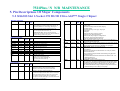
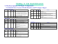
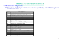
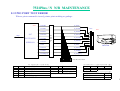
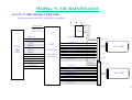
1.6 Appendix 1: GPIO definitions
GPI DEFINITIONS
Signal
Name
Function
S1
S3
S4/S5
GPIO [0]
Panel ID switch1
Panel ID select
In
In
Defined
Off
Off
GPIO [1]
Panel ID switch2
Panel ID select
In
In
Defined
Off
Off
GPIO [2]
Panel ID switch3
Panel ID select
In
In
Defined
Off
Off
GPIO [3]
Panel ID switch4
Panel ID select
In
In
Defined
Off
Off
GPIO [4]
KBD_US/JP#
In
In
Defined
Off
Off
GPIO [5]
Rst_CDROM
Out
Out
Defined
Off
Off
GPIO [6]
EXTSMI#
In
In
Defined
Off
Off
GPIO [7]
SPDIF
SPDIF output
Out
Out
Defined
Off
Off
GPIO [8]
TV_Rset
7005 function
Out
Out
Defined
Off
Off
GPIO [9]
CRT_isolate#
Out
Out
Defined
Off
Off
In
In
Defined
Off
Off
GPIO [11] SPK_OFF#
Out
Out
Defined
Off
Off
GPIO [12] RS232_OFF#
Out
Out
Defined
Off
Off
GPIO [13] CARD_IN#
In
In
Defined
Off
Off
GPIO [14] CRT_IN#
In
In
Defined
Off
Off
GPIO [15] CARD_ACT
In
In
Defined
Off
Off
GPIO [10] FDD_MODE
Description
Reset CD-ROM function
During
After
PCIRST# PCIRST#
Remark
49
7521Plus / N N/B MAINTENANCE
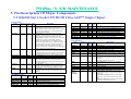
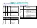
Note 1. LCD ID
LCD_SW4 LCD_SW3 LCD_SW2
LCD_SW1
Vendor
PANEL
Description
0
0
0
0
HannStar
HSD141PX11
14.1”
0
0
0
1
Unipac
UP141X01-2
14.1”
0
0
1
0
Hyundai
14X13-101
14.1”
1
0
0
0
Hyundai
HT15X31
15”
1
0
0
1
Hitachi
TX38D85VC1CAA
15”
Note 3. CPU & SDRAM Frequency setting table:
SW_FS3
SW_FS2
SW_FS1
SW_FS0
CPU
SDRAM
0
0
0
0
66
100
0
0
0
1
100
100
0
0
1
1
133
100
0
1
0
0
66
133
0
1
0
1
100
133
0
1
1
1
133
133
1
0
0
0
66
66
50
7521Plus / N N/B MAINTENANCE
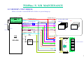
2 System View and Disassembly
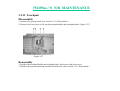
2.0 Tools introduction
1.Minus screw driver with bit size 3mm for CPU assembly & disassembly.
3mm
2. Auto screw driver for system assembly & disassembly.
Bit Size
#0
#1
5mm
Screw Size
Tooling
Tor.
Bit Size
1. M2.0
Auto-Screw driver
2.5-3.0 kg/cm2
#0
2. M2.6
Auto-Screw driver
3.0-3.5kg/cm2
#1
3. M3.0
Auto-Screw driver
3.0-3.5kg/cm2
#1
4. Standoff 4mm
Auto-Screw driver
2.5-3.0 kg/cm2
# 5mm
51
7521Plus / N N/B MAINTENANCE
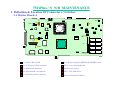
2 System View and Disassembly
2.1 System View
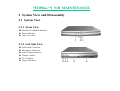
2.1.1 Front View
n Mail-Received Button/Indicator
o Power Indicators
p Top Cover Latch
2.1.2 Left-Side View
n
o
p
q
r
s
Audio Input Connector
Microphone Connector
Audio Output Connector
Volume Control
PC Card Slots
Floppy Disk Drive
52
7521Plus / N N/B MAINTENANCE
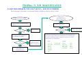
2.1.3 Right-Side View
n Battery Pack
o CD-ROM/DVD-ROM Drive
p IR Port
2.1.4 Rear View
n
o
p
q
r
s
t
u
v
w
Power Connector
PS/2 Port
USB Ports
Parallel Port
Serial Port
RJ-45 Connector
VGA Port
TV-Out Connector
RJ-11 Connector
Kensington Lock
53
7521Plus / N N/B MAINTENANCE
2.1.5 Bottom View
n
o
p
q
CPU Cover
Modem Card Cover
FDD/HDD Module
Battery Pack
2.1.6 Top-Open View
n
o
p
q
r
s
LCD Screen
Power Button
Keyboard
Touchpad
Stereo Speaker Set
Easy Start Buttons
54
7521Plus / N N/B MAINTENANCE
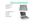
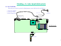
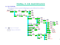
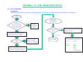
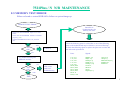
2.2 System Disassembly
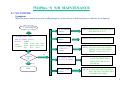
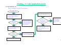
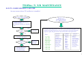
The section discusses at length each major component for disassembly/reassembly and show corresponding
illustrations. Use the chart below to determine the disassembly sequence for removing components from the
notebook.
NOTE: Before you start to install/replace these modules, disconnect all peripheral devices and make sure the
notebook is not turned on or connected to AC power.
2.2.1 Battery Pack
2.2.2 CPU
Modular Components
2.2.3 Modem Card
2.2.4 FDD/HDD Module
2.2.5 CD-ROM Drive
2.2.6 Keyboard
2.2.7 SO-DIMM
NOTEBOOK
2.2.8 LCD Assembly
LCD Assembly Components
2.2.9 LCD Panel
2.2.10 Inverter Board
Base Unit Components
2.2.11 System Board
2.2.12 Touchpad
55
7521Plus / N N/B MAINTENANCE
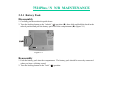
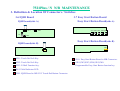
2.2.1 Battery Pack
Disassembly
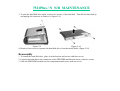
1. Carefully put the notebook upside down.
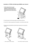
2. Turn the locking button to the "unlock” ( ) position (n), then slide and hold the latch in the
unlock position and pull the battery pack out of the compartment (o).(figure 2-1)
Figure 2-1
Reassembly
1. Push the battery pack into the compartment. The battery pack should be correctly connected
when you hear a clicking sound.
2. Turn the locking button to the "lock” ( ) position.
56
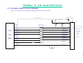
7521Plus / N N/B MAINTENANCE
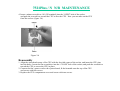
2.2.2 CPU
Disassembly
1. Carefully put the notebook upside down.
2. Remove two screws locking the CPU compartment cover, and then lift the cover up. (figure 2-2)
Figure 2-2
Figure 2-3
3. Remove four screws fastening the heatsink and disconnect the fan’s power cord to free the heatsink
from the CPU module. (figure 2-3)
57
7521Plus / N N/B MAINTENANCE
4. Insert a minus screwdriver 101 (JIS standard) into the “OPEN” hole of the socket,
and push the screwdriver toward the CPU to free the CPU. Now you can take out the CPU
from the socket. (figure 2-4)
Figure 2-4
Reassembly
1. Align the arrowhead corner of the CPU with the beveled corner of the socket, and insert the CPU pins
into the holes. Insert the flat screwdriver into the “CLOSE” hole of the socket, and push the screwdriver
toward the CPU to secure the CPU in place.
2. Connect the fan’s power cord to the system board, fit the heatsink onto the top of the CPU
and secure with four screws.
3. Replace the CPU compartment cover and secure with two screws.
58
7521Plus / N N/B MAINTENANCE
2.2.3 Modem Card
Disassembly
1. Carefully put the notebook upside down.
2. Remove one screw locking the modem card compartment cover, and then lift the cover up. (figure 2-5)
Figure 2-5
Figure 2-6
3. Remove one screw fastening the connector board and the grounding cable. (figure 2-6)
59
7521Plus / N N/B MAINTENANCE
4. Slightly lift up the connector board, and then remove one screw fastening the modem card.
Now you can take out the modem card from the compartment. (figure 2-7)
Figure 2-7
Reassembly
1. Reconnect the modem card into the system board and secure with two screws.
2. Hold the connector board an angle so that the phone line connector is pointed towards the opening
on the notebook. Insert the connector into the opening and secure with a screw which fastening
both the connector board and the grounding cable.
3. Replace the compartment cover and secure with one screw.
60
7521Plus / N N/B MAINTENANCE
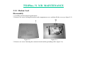
2.2.4 FDD/HDD Module
Disassembly
1. Carefully put the notebook upside down.
2. Remove one screw and slide the FDD/HDD module out of the compartment. (figure 2-8)
Figure 2-8
61
7521Plus / N N/B MAINTENANCE
3. To take the hard disk drive apart, remove two screws of the hard disk. Then lift the hard disk up
and unplug the connector to remove it. (figure 2-9)
Figure 2-9
Figure 2-10
4. Remove four screws to separate the hard disk drive from the metal shield. (figure 2-10)
Reassembly
1. To install the hard disk drive, place it in the bracket and secure with four screws.
2. Connect the hard disk to the connector on the FDD/HDD module and secure with two screws.
3. Slide the FDD/HDD module into the compartment and secure with one screw.
62
7521Plus / N N/B MAINTENANCE
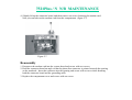
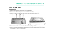
2.2.5 CD-ROM Drive
Disassembly
1. Carefully put the notebook upside down.
2. Remove the battery pack. (See section 2.2.1 Disassembly.)
3. Remove the modem card. (See section 2.2.3 Disassembly.)
4. Remove the FDD/HDD module. (See step 2 in section 2.2.4 Disassembly.)
5. Remove one screw locking the CD-ROM (n), and then the other twelve screws
locking the base unit frame. (figure 2-11) Now you can lift the base unit frame up.
Figure 2-11
63
7521Plus / N N/B MAINTENANCE
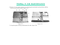
6. Hold the CD-ROM drive and slide it outward carefully. (figure 2-12).
Figure 2-12
Reassembly
1. Push the CD-ROM drive into the compartment.
2. Replace the base unit frame and secure with thirteen screws (includes one locking the CD-ROM drive).
3. Replace the FDD/HDD module. (See section 2.2.4 Reassembly.)
4. Replace the modem card. (See section 2.2.3 Reassembly.)
5. Replace the modem card. (See section 2.2.3 Reassembly.)
6. Replace the battery pack. (See section 2.2.1 Reassembly.)
64
7521Plus / N N/B MAINTENANCE
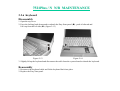
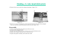
2.2.6 Keyboard
Disassembly
1. Open the top cover.
2. Press the locking latch downward to unlatch the Easy Start panel (n) , push it leftward and
lift it up from the left side (o). (figure 2-13)
Figure 2-13
Figure 2-14
3. Slightly lift up the keyboard and disconnect the cable from the system board to detach the keyboard.
Reassembly
1. Reconnect the keyboard cable and fit the keyboard back into place.
2. Replace the Easy Start panel.
65
7521Plus / N N/B MAINTENANCE
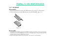
2.2.7 SO-DIMM
Disassembly
1. Remove the keyboard to access the SO-DIMM sockets. (See section 2.2.6 Disassembly.)
2. Pull the retaining clips outwards (n) and remove the SO-DIMM (o). (figure 2-15)
Figure 2-15
Reassembly
1. To install the SO-DIMM, match the SO-DIMM's notched part with the socket's projected part
and firmly insert the SO-DIMM into the socket at 20-degree angle. Then push down until the
retaining clips lock the SO-DIMM into position.
2. Replace the keyboard and the Easy Start panel. (See section 2.2.6 Reassembly.)
66
7521Plus / N N/B MAINTENANCE
2.2.8 LCD Assembly
Disassembly
1. Open the top cover and remove the Easy Start panel. (See steps 1 to 2 in section 2.2.6 Disassembly.)
2. Remove the two hinge covers by inserting a flat screwdriver to the rear of the cover and pry the
cover out. (figure 2-16)
Figure 2-16
Figure 2-17
3. Open the top cover. Unplug the three cable connectors coming from the LCD assembly,
and remove four screws of the hinges. Now you can separate the LCD assembly from the
base unit. (figure 2-17)
67
7521Plus / N N/B MAINTENANCE
Reassembly
1. Attach the LCD assembly to the base unit and secure with four screws on the hinges.
2. Reconnect the LCD cable connectors to the system board.
3. Replace the two hinge covers.
4. Replace the Easy Start panel.
68
7521Plus / N N/B MAINTENANCE
2.2.9 LCD Panel
Disassembly
1. Remove the LCD assembly. (See section 2.2.8 Disassembly.)
2. Remove the two rubber pads and two screws on the lower part of the panel. (figure 2-18)
Figure 2-18
Figure 2-19
3. Insert a flat screwdriver to the lower part of the frame and gently pry the frame out.
Repeat the process until the frame is completely separated from the housing.
4. Remove the four screws on the two sides of the LCD panel, and unplug the cable from
the inverter board. (figure 2-19)
Reassembly
1. Fit the LCD panel back into place and secure with four screws, and reconnect the cable to the inverter board.
2. Fit the LCD frame back into the housing and replace the two screws and two rubber pads.
3. Replace the LCD assembly. (See section 2.2.8 Reassembly.)
69
7521Plus / N N/B MAINTENANCE
2.2.10 Inverter Board
Disassembly
1. Remove the LCD assembly and detach the LCD frame (see instructions in previous two sections).
2. To remove the inverter board at the bottom side of the LCD assembly, unplug the cable and
remove the two screws. (figure 2-20)
Figure 2-20
Reassembly
1. Fit the inverter board back into place and secure with two screws.
2. Reconnect the cables.
3. Replace the LCD frame. (See section 2.2.9 Reassembly.)
4. Replace the LCD assembly. (See section 2.2.8 Reassembly.)
70
7521Plus / N N/B MAINTENANCE
2.2.11 System Board
Disassembly
1. Remove the Keyboard. (See section 2.2.6 Disassembly.)
2. Remove the LCD assembly. (See section 2.2.8 Disassembly.)
3. Remove seven screws, and then take out the Easy Start board. (figure 2-21)
Figure 2-21
Figure 2-22
4. Remove four screws on the rear side of the notebook. (figure 2-22)
5. Remove the battery pack, heatsink, modem card, FDD/HDD module, and CD-ROM drive.
(See section 2.2.1 to 2.2.5 Disassembly.)
71
7521Plus / N N/B MAINTENANCE
6. Remove six screws and two hexnut screws fastening the metal shield, and then lift the shield up
from the system board carefully. (figure 2-23)
Figure 2-23
Figure 2-24
7. Lift up the speaker assembly and disconnect the cable. (figure 2-24)
72
7521Plus / N N/B MAINTENANCE
8. Remove four screws to take the recharge board apart. (figure 2-25)
Figure 2-25
Figure 2-26
9. Remove two screws fastening the system board and disconnect the cable of the touchpad.
Now you can lift the system board up from the base unit. (figure 2-26)
Reassembly
1. Fit the system board into place and secure with two screws.
2. Reconnect the touchpad’s cable.
3. Replace the metal shield and secure with six screws and two hexnut screws.
4. Replace the recharge board and secure with four screws.
5. Replace the speaker assembly and reconnect the cable.
73
7521Plus / N N/B MAINTENANCE
6. Replace the base unit frame and secure with twelve screws.
7. Replace the battery pack, heatsink, modem card, FDD/HDD module, and CD-ROM drive.
8. Secure the four screws on the rear side of the notebook.
9. Put the notebook back to the upright position. Replace the Easy Start board into the housing,
then secure with seven screws.
10. Replace the LCD assembly.
11. Replace the keyboard and Easy Start panel.
74
7521Plus / N N/B MAINTENANCE
2.2.12 Touchpad
Disassembly
1. Remove the system board. (See section 2.2.11 Disassembly.)
2. Remove the four screws to lift up the touchpad holder and touchpad panel. (figure 2-27)
Figure 2-27
Reassembly
1. Replace the touchpad holder and touchpad panel, and secure with four screws.
2. Replace the system board and assemble the notebook. (See section 2.2.11 Reassembly.)
75
7521Plus / N N/B MAINTENANCE
3. Definition & Location Of Connectors / Switches
3.1 Mother Board-A
J2
J4
SW2
J5
SW1
J3
J1
SW3
J6
SW4
J1: Inverter BD CONN.
J6: 144 pins expansion SDRAM SO-DIMM socket.
J2: LCD panel LVDS connector.
SW1: Cover Suspend Switch.
J3: ESB Board connector.
SW2: Power button.
J4: External MIC-in connector.
SW3 : CPU FSB Select.
J5: Internal keyboard connector.
SW4 : LCD Panel ID Select.
76
7521Plus / N N/B MAINTENANCE
3. Definition & Location Of Connectors / Switches
3.2 Mother Board Switch Table
SW3. CPU & SDRAM Frequency setting table:
SW_FS3
SW_FS2
SW_FS1
SW_FS0
CPU
SDRAM
0
0
0
0
66
100
0
0
0
1
100
100
0
0
1
1
133
100
0
1
0
0
66
133
0
1
0
1
100
133
0
1
1
1
133
133
1
0
0
0
66
66
SW1
SW2
SW3
SW4
SW4. LCD Panel ID Select
LCD_SW4 LCD_SW3 LCD_SW2
LCD_SW1
Vendor
PANEL
Description
0
0
0
0
HannStar
HSD141PX11
14.1”
0
0
0
1
Unipac
UP141X01-2
14.1”
0
0
1
0
Hyundai
14X13-101
14.1”
1
0
0
0
Hyundai
HT15X31
15”
1
0
0
1
Hitachi
TX38D85VC1CAA
15”
77
7521Plus / N N/B MAINTENANCE
3. Definition & Location Of Connectors / Switches
3.3 Mother Board-B
PJ501 J502
J508
J505
J507
J506
J504
J501
J503
U501
U502
J509
BT501
J510
J511
U503
VR501
J506
J512
J513
J514
J516
J515
PJ501: Power jack ( AC adapter).
J507: VGA Connector.
J516 :HDD/FDD Connector.
J502 : PS2 Mouse/keyboard.
J508: USB connector.
J512: CD-ROM drive connector.
J503: Line in Jack.
J509: Phone Jack Connector.
J514: Charger & Touch-Pad connector.
J504: RJ45 LAN connect.
J510: Line Out with APDIF.
J515: Touch-Pad button connector.
J505: Parallel Port.
J511: MDC MODEM transfer BD connector.
BT501: CMOS Battery connector.
J506: PCMCIA card socket.
J513: CPU FAN Connector.
VR501: Volume control VR.
U503: FC-PGA Socket 370 CPU Slot.
78
7521Plus / N N/B MAINTENANCE
3. Definition & Location Of Connectors / Switches
3.4 Daughter Board
MDC/LAN transfer board
J23
J1
J1: RJ-11 phone jack for internal
modem.
J23: MDC jump wire connector.
JP1
U2
U1
JP3
JP1: MDC jump wire connector.
JP3: Connector 2 for connected
MDC/LAN transfer board
to M/B.
79
7521Plus / N N/B MAINTENANCE
3. Definition & Location Of Connectors / Switches
3.5 Charger Board
Charge board(side B)
Charge board(side A)
J1
PJ4
J2
SW500
J500
J1:Charger & Touch-Pad connector to M/B.
J500: Touch-Pad button connector.
PJ4:Battery pack connector.
SW500: CMOS Reset
J2: Internal speaker connector.
80
7521Plus / N N/B MAINTENANCE
3. Definition & Location Of Connectors / Switches
3.6 IQSB Board
3.7 Easy Start Button Board
Easy Start Button Board(side A)
IQSB board(side A)
SW1
D8
SW2
SW1 SW2 SW3 SW4 SW5
SW3
Easy Start Button Board(side B)
IQSB board(side B)
J501
J500
SW1: Touch Pad Left Key.
J501: Easy Start Button Board to MB Connector .
SW2: Touch Pad Left Key.
SW1,SW2,SW3,SW4,SW5,SW6:
SW3: E-Mail Function key.
Programmable Easy Start Button function key.
D8: E-Mail Indicator LED.
J500: IQSB Board to MB J515 Touch-Pad Button Connector.
81
7521Plus / N N/B MAINTENANCE
4. Definition & Location Of Major Components
4.1 Main Board ( Side A )
U1
U2
PU2
U3
U6
U5
U33
U7
PU4
PU22
PU10
U9
U11
U16 U17
U15
U13
PU9
PU14
PU19,12,23
U14
PU5
PU18
U24
U21
U31
U27
U28
PU7
U18
U19
U22
U23
U25
U26
U29
U30
U1: ADM3311ARU RS232/SIO.
U13: TPS2206 PCcard Power switch matrix.
U31:W83626F LPC to ISA.
U2: DS90C363MTD VGA LVD controller.
U15: ICS9248-102 Frequency Synthesizer.
U5: CS4299 AC’97 CODE.
U24: SiS630S single chipset.
U18,U22,U25,U29
: On board SDAM.
U6: TPA0202 AUDIO AMP.
U27: Super IO PC97338VJG.
U7: CH7005C TV-Encoder.
U28: System BIOS.
U14: H8(3434F) universal.
82
7521Plus / N N/B MAINTENANCE
4. Definition & Location Of Major Components
4.2 Main Board ( SIDE B )
U502
BT501
U503
U505
U502: PH163112 LAN Controller.
U503: Socket 370 CPU.
U505: PCI1225PDV PC CARD interface controller.
83
7521Plus / N N/B MAINTENANCE
5. Pin Descriptions Of Major Components
5.1 Pentium III/Celeron FC-PGA2 CPU
Alphabetical Signal Reference
Signal Name
A[35:3]#
A20M#
ADS#
AERR#
AP[1:0]#
BCLK
I/O
Signal Description
I/O The A[35:3]# (Address) signals define a 2 36 -byte physical memory
GTL+ address space. When ADS# is active, these signals transmit the
address of a transaction; when ADS# is inactive, these signals
transmit transaction information. These signals must be connected to
the appropriate pins/balls of both agents on the system bus. The
A[35:24]# signals are protected with the AP1# parity signal,
and the A[23:3]# signals are protected with the AP0# parity signal.
On the active-to-inactive transition of RESET#, each processor bus
agent samples A[35:3]# signals to determine its power-on
configuration. See Section 4 of this document and the PentiumII
Processor Developer’s Manual for details.
I
If the A20M# (Address-20 Mask) input signal is asserted, the
1.5V processor masks physical address bit 20 (A20#) before looking up a
Tolerant line in any internal cache and before driving a read/write transaction
on the bus. Asserting A20M# emulates the 8086 processor's address
wrap-around at the 1-Mbyte boundary. Assertion of A20M# is only
supported in Real mode.
I/O The ADS# (Address Strobe) signal is asserted to indicate the validity
GTL+ of a transaction address on the A[35:3]# signals. Both bus agents
observe the ADS# activation to begin parity checking, protocol
checking, address decode, internal snoop or deferred reply ID match
operations associated with the new transaction. This signal must be
connected to the appropriate pins/balls on both agents on the system
bus.
I/O The AERR# (Address Parity Error) signal is observed and driven by
GTL+ both system bus agents, and if used, must be connected to the
appropriate pins/balls of both agents on the system bus. AERR#
observation is optionally enabled during power-on configuration; if
enabled, a valid assertion of AERR# aborts the current transaction.
If AERR# observation is disabled during power-on configuration, a
central agent may handle an assertion of AERR# as appropriate to the
error handling architecture of the system.
I/O The AP[1:0]# (Address Parity) signals are driven by the request
GTL+ initiator along with ADS#, A[35:3]#, REQ[4:0]# and RP#. AP1#
covers A[35:24]#. AP0# covers A[23:3]#. A correct parity signal is
high if an even number of covered signals are low and low if an odd
number of covered signals are low. This allows parity to be high when
all the covered signals are high. AP[1:0]# should be connected to the
appropriate pins/balls on both agents on the system bus.
I
The BCLK (Bus Clock) signal determines the system bus frequency.
2.5V Both system bus agents must receive this signal to drive their outputs
Tolerant and latch their inputs on the BCLK rising edge. All external timing
parameters are specified with respect to the BCLK signal.
Signal Name
BERR#
BINIT#
BNR#
BP[3:2]#
BPM[1:0]#
I/O
Signal Description
I/O The BERR# (Bus Error) signal is asserted to indicate an
GTL+ unrecoverable error without a bus protocol violation. It may be driven
by either system bus agent and must be connected to the appropriate
pins/balls of both agents, if used. However, the mobile Pentium III
processors do not observe assertions of the BERR# signal.
BERR# assertion conditions are defined by the system configuration.
Configuration options enable the BERR# driver as follows:
• Enabled or disabled
• Asserted optionally for internal errors along with IERR#
• Asserted optionally by the request initiator of a bus transaction after
it observes an error
• Asserted by any bus agent when it observes an error in a bus
transaction
I/O- The BINIT# (Bus Initialization) signal may be observed and driven
GTL+ by both system bus agents and must be connected to the appropriate
pins/balls of both agents, if used. If the BINIT# driver is enabled
during the power-on configuration, BINIT# is asserted to signal any
bus condition that prevents reliable future information.
If BINIT# is enabled during power-on configuration, and BINIT# is
sampled asserted, all bus state machines are reset and any data which
was in transit is lost. All agents reset their rotating ID for bus
arbitration to the state after reset, and internal count information is
lost. The L1 and L2 caches are not affected.
If BINIT# is disabled during power-on configuration, a central agent
may handle an assertion of BINIT# as appropriate to the Machine
Check Architecture (MCA) of the system.
I/O- The BNR# (Block Next Request) signal is used to assert a bus stall by
GTL+ any bus agent that is unable to accept new bus transactions. During a
bus stall, the current bus owner cannot issue any new transactions.
Since multiple agents may need to request a bus stall simultaneously,
BNR# is a wired-OR signal that must be connected to the appropriate
pins/balls of both agents on the system bus. In order to avoid wire-OR
glitches associated with simultaneous edge transitions driven by
multiple drivers, BNR# is activated on specific clock edges and
sampled on specific clock edges.
I/O The BP[3:2]# (Breakpoint) signals are the System Support group
GTL+ Breakpoint signals. They are outputs from the processor that indicate
the status of breakpoints.
I/O The BPM[1:0]# (Breakpoint Monitor) signals are breakpoint and
GTL+ performance monitor signals. They are outputs from the processor
that indicate the status of breakpoints and programmable counters
used for monitoring processor performance.
84
7521Plus / N N/B MAINTENANCE
5. Pin Descriptions Of Major Components
5.1 Pentium III/Celeron FC-PGA2 CPU
Alphabetical Signal Reference
Signal Name
BPRI#
BREQ0#
BSEL[1:0]
CLKREF
CMOSREF
D[63:0]#
I/O
Signal Description
I
The BPRI# (Bus Priority Request) signal is used to arbitrate for
GTL+ ownership of the system bus. It must be connected to the appropriate
pins/balls on both agents on the system bus. Observing BPRI# active
(as asserted by the priority agent) causes the processor to stop issuing
new requests, unless such requests are part of an ongoing locked
operation. The priority agent keeps BPRI# asserted until all of its
requests are completed and then releases the bus by deasserting
BPRI#.
I/O The BREQ0# (Bus Request) signal is a processor Arbitration Bus
GTL+ signal. The processor indicates that it wants ownership of the system
bus by asserting the BREQ0# signal.
During power-up configuration, the central agent must assert the
BREQ0# bus signal. The processor samples BREQ0# on the activeto-inactive transition of RESET#.
I
The BSEL[1:0] (Select Processor System Bus Speed) signal is used to
1.5V configure the processor for the system bus frequency. Table 38 shows
Tolerant the encoding scheme for BSEL[1:0]. The only supported system bus
frequency for the mobile Pentium III processor is 100 MHz. If
another frequency is used or if the BSEL[1:0] signals are not driven
with "1" then the processor is not guaranteed to function properly.
BSEL[1:0] Encoding
BSEL[1:0]
System Bus Frequency
00
66 MHz
01
100 MHz
10
Reserved
11
133 MHz
Analog The CLKREF (System Bus Clock Reference) signal provides a
reference voltage to define the trip point for the BCLK signal. This
signal should be connected to a resistor divider to generate 1.25V
from the 2.5-V supply.
Analog The CMOSREF (CMOS Reference Voltage) signal provides a DC
level reference voltage for the CMOS input buffers. A voltage divider
should be used to divide a stable voltage plane (e.g., 2.5V or 3.3V).
This signal must be provided with a DC voltage that meets the
VCMOSREF specification from Table 13.
I/O The D[63:0]# (Data) signals are the data signals. These signals
GTL+ provide a 64-bit data path between both system bus agents, and must
be connected to the appropriate pins/balls on both agents. The data
driver asserts DRDY# to indicate a valid data transfer.
Signal Name
DBSY#
DEFER#
DEP[7:0]#
DRDY#
EDGCTRLP
FERR#
FLUSH#
I/O
Signal Description
I/O- The DBSY# (Data Bus Busy) signal is asserted by the agent
GTL+ responsible for driving data on the system bus to indicate that the data
bus is in use. The data bus is released after DBSY# is deasserted. This
signal must be connected to the appropriate pins/balls on both agents
on the system bus.
I
The DEFER# (Defer) signal is asserted by an agent to indicate that
GTL+ the transaction cannot be guaranteed in-order completion. Assertion
of DEFER# is normally the responsibility of the addressed memory
agent or I/O agent. This signal must be connected to the appropriate
pins/balls on both agents on the system bus.
I/O The DEP[7:0]# (Data Bus ECC Protection) signals provide optional
GTL+ ECC protection for the data bus. They are driven by the agent
responsible for driving D[63:0]#, and must be connected to the
appropriate pins/balls on both agents on the system bus if they are
used. During power-on configuration, DEP[7:0]# signals can be
enabled for ECC checking or disabled for no checking.
I/O The DRDY# (Data Ready) signal is asserted by the data driver on
GTL+ each data transfer, indicating valid data on the data bus. In a multicycle data transfer, DRDY# can be deasserted to insert idle clocks.
This signal must be connected to the appropriate pins/balls on both
agents on the system bus.
Analog The EDGCTRLP (Edge Rate Control) signal is used to configure the
edge rate of the GTL+ output buffers. Connect the signal to VSS with
a 110-Ω, 1% resistor.
O
The FERR# (Floating-point Error) signal is asserted when the
1.5V processor detects an unmasked floating-point error. FERR# is similar
Tolerant to the ERROR# signal on the Intel 387 coprocessor, and it is included
Open- for compatibility with systems using DOS-type floating-point error
drain) reporting.
I
When the FLUSH# (Flush) input signal is asserted, the processor
1.5V writes back all internal cache lines in the Modified state and
Tolerant invalidates all internal cache lines. At the completion of a flush
operation, the processor issues a Flush Acknowledge transaction. The
processor stops caching any new data while the FLUSH# signal
remains asserted.
On the active-to-inactive transition of RESET#, each processor bus
agent samples FLUSH# to determine its power-on configuration.
85
7521Plus / N N/B MAINTENANCE
5. Pin Descriptions Of Major Components
5.1 Pentium III/Celeron FC-PGA2 CPU
Alphabetical Signal Reference
Signal Name
GHI#
HIT#, HITM#
IERR#
IGNNE#
INIT#
I/O
Signal Description
I
The GHI# signal controls which operating mode bus ratio is selected
1.5V in a mobile Pentium III processor featuring Intel SpeedStep
Tolerant technology. On the processor featuring Intel SpeedStep technology,
this signal is latched when BCLK restarts in Deep Sleep state and
determines which of two bus ratios is selected for operation. This
signal is ignored when the processor is not in the Deep Sleep state.
This signal is a "Don't Care" on processors that do not feature Intel
SpeedStep technology. This signal has an on-die pull-up to VccT and
should be driven with an Open-drain driver with no external pull-up.
I/O The HIT# (Snoop Hit) and HITM# (Hit Modified) signals convey
GTL+ transaction snoop operation results, and must be connected to the
appropriate pins/balls on both agents on the system bus.
Either bus agent can assert both HIT# and HITM# together to indicate
that it requires a snoop stall, which can be continued by reasserting
HIT# and HITM# together.
O
The IERR# (Internal Error) signal is asserted by the processor as the
1.5V result of an internal error.Assertion of IERR# is usually accompanied
Tolerant by a SHUTDOWN transaction on the system bus.
Open- This transaction may optionally be converted to an external error
drain signal (e.g., NMI) by system logic. The processor will keep IERR#
asserted until it is handled in software or with the assertion of
RESET#, BINIT, or INIT#.
I
The IGNNE# (Ignore Numeric Error) signal is asserted to force the
1.5V processor to ignore a numeric error and continue to execute nonTolerant control floating-point instructions. If IGNNE# is deasserted, the
processor freezes on a non-control floating-point instruction if a
previous instruction caused an error. IGNNE# has no affect when the
NE bit in control register 0 (CR0) is set.
I
The INIT# (Initialization) signal is asserted to reset integer registers
1.5V inside the processor without affecting the internal (L1 or L2) caches
Tolerant or the floating-point registers. The processor begins execution at the
power-on reset vector configured during power-on configuration. The
processor continues to handle snoop requests during INIT# assertion.
INIT# is an asynchronous input.
If INIT# is sampled active on RESET#'s active-to-inactive transition,
then the processor executes its built-in self test (BIST).
Signal Name
INTR
LINT[1:0]
LOCK#
NMI
I/O
Signal Description
I
The INTR (Interrupt) signal indicates that an external interrupt has
1.5V been generated. INTR becomes the LINT0 signal when the APIC is
Tolerant enabled. The interrupt is maskable using the IF bit in the EFLAGS
register. If the IF bit is set, the processor vectors to the interrupt
handler after completing the current instruction execution. Upon
recognizing the interrupt request, the processor issues a single
Interrupt Acknowledge (INTA) bus transaction. INTR must remain
active until the INTA bus transaction to guarantee its recognition.
The LINT[1:0] (Local APIC Interrupt) signals must be connected to
I
1.5V the appropriate pins/balls of all APIC bus agents, including the
Tolerant processor and the system logic or I/O APIC component. When APIC
is disabled, the LINT0 signal becomes INTR, a maskable interrupt
request signal, and LINT1 becomes NMI, a non-maskable interrupt.
INTR and NMI are backward compatible with the same signals for
the Pentium processor. Both signals are asynchronous inputs.
Both of these signals must be software configured by programming
the APIC register space to be used either as NMI/INTR or LINT[1:0]
in the BIOS. If the APIC is enabled at reset, then LINT[1:0] is the
default configuration.
I/O The LOCK# (Lock) signal indicates to the system that a sequence of
GTL+ transactions must occur atomically. This signal must be connected to
the appropriate pins/balls on both agents on the system bus. For a
locked sequence of transactions, LOCK# is asserted from the
beginning of the first transaction through the end of the last
transaction.
When the priority agent asserts BPRI# to arbitrate for bus ownership,
it waits until it observes LOCK# deasserted. This enables the
processor to retain bus ownership throughout the bus locked operation
and guarantee the atomicity of lock.
The NMI (Non-Maskable Interrupt) indicates that an external
I
1.5V interrupt has been generated. NMI becomes the LINT1 signal when
Tolerant the APIC is disabled. Asserting NMI causes an interrupt with an
internally supplied vector value of 2. An external interruptacknowledge transaction is not generated. If NMI is asserted during
the execution of an NMI service routine, it remains pending and is
recognized after the IRET is executed by the NMI service routine. At
most, one assertion of NMI is held pending. NMI is rising edge
sensitive.
86
7521Plus / N N/B MAINTENANCE
5. Pin Descriptions Of Major Components
5.1 Pentium III/Celeron FC-PGA2 CPU
Alphabetical Signal Reference
Signal Name
PICCLK
PICD[1:0]
PLL1, PLL2
PRDY#
PREQ#
PWRGOOD
I/O
Signal Description
The PICCLK (APIC Clock) signal is an input clock to the processor
and system logic or I/O APIC that is required for operation of the
processor, system logic, and I/O APIC components on the APIC bus.
The PICD[1:0] (APIC Data) signals are used for bi-directional serial
message passing on the APIC bus. They must be connected to the
appropriate pins/balls of all APIC bus agents, including the processor
and the system logic or I/O APIC components. If the PICD0 signal is
sampled low on the active-to-inactive transition of the RESET#
signal, then the APIC is hardware disabled.
Analog The PLL1 and PLL2 signals provide isolated analog decoupling is
required for the internal PLL. See Section 3.2.2 for a description of
the analog decoupling circuit.
O
The PRDY# (Probe Ready) signal is a processor output used by
GTL+ debug tools to determine processor debug readiness.
I
The PREQ# (Probe Request) signal is used by debug tools to request
1.5V debug operation of the processor.
Tolerant
I
PWRGOOD (Power Good) is a 2.5-V tolerant input. The processor
2.5V requires this signal to be a clean indication that clocks and the power
Tolerant supplies (Vcc, VccT, etc.) are stable and within their specifications.
Clean implies that the signal will remain low, (capable of sinking
leakage current) and without glitches, from the time that the power
supplies are turned on, until they come within specification. The
signal will then transition monotonically to a high (2.5V) state. Figure
26 illustrates the relationship of PWRGOOD to other system signals.
PWRGOOD can be driven inactive at any time, but clocks and power
must again be stable before the rising edge of PWRGOOD. It must
also meet the minimum pulse width specified in Table 17 (Section
3.7) and be followed by a 1 ms RESET# pulse.
I
2.5V
Tolerant
I/O
1.5V
Tolerant
Opendrain
PWRGOOD Relationship at Power On
The PWRGOOD signal, which must be supplied to the processor, is used to protect internal circuits
against voltage sequencing issues. The PWRGOOD signal should be driven high throughout boundary
scan operation.
Signal Name
REQ[4:0]#
RESET#
RP#
PWRGOOD Relationship at Power On
RS[2:0]#
I/O
Signal Description
I/O The REQ[4:0]# (Request Command) signals must be connected to the
GTL+ appropriate pins/balls on both agents on the system bus. They are
asserted by the current bus owner when it drives A[35:3]# to define
the currently active transaction type.
I
Asserting the RESET# signal resets the processor to a known state
GTL+ and invalidates the L1 and L2 caches without writing back Modified
(M state) lines. For a power-on type reset, RESET# must stay active
for at least 1 msec after Vcc and BCLK have reached their proper DC
and AC specifications and after PWRGOOD has been asserted. When
observing active RESET#, all bus agents will deassert their outputs
within two clocks. RESET# is the only GTL+ signal that does
not have on-die GTL+ termination. A 56.2Ω1% terminating resistor
connected to VccT is required.
A number of bus signals are sampled at the active-to-inactive
transition of RESET# for the power-on configuration. The
configuration options are described in Section 4 and in the Pentium II
Processor Developer’s Manual.
Unless its outputs are tri-stated during power-on configuration, after
an active-to-inactive transition of RESET#, the processor optionally
executes its built-in self-test (BIST) and begins program execution at
reset-vector 000FFFF0H or FFFFFFF0H. RESET# must be connected
to the appropriate pins/balls on both agents on the system bus.
I/O The RP# (Request Parity) signal is driven by the request initiator and
GTL+ provides parity protection on ADS# and REQ[4:0]#. RP# should be
connected to the appropriate pins/balls on both agents on the system
bus.
A correct parity signal is high if an even number of covered signals
are low and low if an odd number of covered signals are low. This
definition allows parity to be high when all covered signals are high.
I
The RS[2:0]# (Response Status) signals are driven by the response
GTL+ agent (the agent responsible for completion of the current transaction)
and must be connected to the appropriate pins/balls on both agents on
the system bus.
87
7521Plus / N N/B MAINTENANCE
5. Pin Descriptions Of Major Components
5.1 Pentium III/Celeron FC-PGA2 CPU
PWRGOOD Relationship at Power On
Signal Name
RSP#
RSVD
RTTIMPEDP
SLP#
SMI#
STPCLK#
TCK
I/O
Signal Description
I
The RSP# (Response Parity) signal is driven by the response agent
GTL+ (the agent responsible for completion of the current transaction)
during assertion of RS[2:0]#. RSP# provides parity protection for
RS[2:0]#. RSP# should be connected to the appropriate pins/balls on
both agents on the system bus.
A correct parity signal is high if an even number of covered signals
are low, and it is low if an odd number of covered signals are low.
During Idle state of RS[2:0]# (RS[2:0]#=000), RSP# is also high
since it is not driven by any agent guaranteeing correct parity.
TBD The RSVD (Reserved) signal is currently unimplemented but is
reserved for future use. Leave this signal unconnected. Intel
recommends that a routing channel for this signal be allocated.
Analog The RTTIMPEDP (RTT Impedance/PMOS) signal is used to
configure the on-die GTL+ termination. Connect the RTTIMPEDP
signal to VSS with a 56.2-Ω, 1% resistor.
The SLP# (Sleep) signal, when asserted in the Stop Grant state,
I
1.5V causes the processor to enter the Sleep state. During the Sleep state,
Tolerant the processor stops providing internal clock signals to all units,
leaving only the Phase-Locked Loop (PLL) still running. The
processor will not recognize snoop and interrupts in the Sleep state.
The processor will only recognize changes in the SLP#, STPCLK#
and RESET# signals while in the Sleep state. If SLP# is deasserted,
the processor exits Sleep state and returns to the Stop Grant state in
which it restarts its internal clock to the bus and
APIC processor units.
The SMI# (System Management Interrupt) is asserted asynchronously
I
1.5V by system logic. On accepting a System Management Interrupt, the
Tolerant processor saves the current state and enters System Management
Mode (SMM). An SMI Acknowledge transaction is issued, and the
processor begins program execution from the SMM handler.
The STPCLK# (Stop Clock) signal, when asserted, causes the
I
1.5V processor to enter a low-power Stop Grant state. The processor issues
Tolerant a Stop Grant Acknowledge special transaction and stops providing
internal clock signals to all units except the bus and APIC units. The
processor continues to snoop bus transactions and service interrupts
while in the Stop Grant state. When STPCLK# is deasserted, the
processor restarts its internal clock to all units and resumes execution.
The assertion of STPCLK# has no affect on the bus clock.
The TCK (Test Clock) signal provides the clock input for the test bus
I
1.5V (also known as the test access port).
Tolerant
Signal Name
TDI
TDO
TESTHI
TESTLO[2:1]
TESTP
THERMDA,
THERMDC
TMS
TRDY#
TRST#
I/O
I
1.5V
Tolerant
O
1.5V
Tolerant
Opendrain
I
1.5V
Tolerant
I
1.5V
Tolerant
Analog
Signal Description
The TDI (Test Data In) signal transfers serial test data to the
processor. TDI provides the serial input needed for JTAG support.
The TDO (Test Data Out) signal transfers serial test data from the
processor. TDO provides the serial output needed for JTAG support.
The TESTHI (Test input High) is used during processor test and
needs to be pulled high during normal operation.
The TESTLO[2:1] (Test input Low) signals are used during processor
test and needs to be pulled to ground during normal operation.
The TESTP (Test Point) signals are connected to Vcc and Vss at
opposite ends of the die. These signals can be used to monitor the Vcc
level on the die. Route the TESTP signals to test points or leave them
unconnected. Do not short the TESTP signals together.
Analog The THERMDA (Thermal Diode Anode) and THERMDC (Thermal
Diode Cathode) signals connect to the anode and cathode of the ondie thermal diode.
The TMS (Test Mode Select) signal is a JTAG support signal used by
I
1.5V debug tools.
Tolerant
I
The TRDY# (Target Ready) signal is asserted by the target to indicate
GTL+ that the target is ready to receive write or implicit write-back data
transfer. TRDY# must be connected to the appropriate pins/balls on
both agents on the system bus.
The TRST# (Test Reset) signal resets the Test Access Port (TAP)
I
1.5V logic. The mobile Pentium III processors do not self-reset during
Tolerant power on; therefore, it is necessary to drive this signal low during
power-on reset.
88
7521Plus / N N/B MAINTENANCE
5. Pin Descriptions Of Major Components
5.1 Pentium III/Celeron FC-PGA2 CPU
PWRGOOD Relationship at Power On
Signal Name
VID[4:0]
I/O
Signal Description
O - The VID[4:0] (Voltage ID) pins/balls can be used to support
Open- automatic selection of power supply voltages. These pins/balls are not
drain signals, they are either an open circuit or a short to VSS on the
processor substrate. The combination of opens and shorts encodes the
voltage required by the processor. External to pull-ups are required to
sense the encoded VID. For processors that have Intel SpeedStep
technology enabled, VID[4:0] encode the voltage required in the
battery-optimized mode. VID[4:0] are needed to cleanly support
voltage specification changes on mobile Pentium III processors. The
voltage encoded by VID[4:0] is defined in Table 39. A "1" in this
table refers to an open pin/ball and a "0" refers to a short to VSS. The
power supply must provide the requested voltage or disable itself.
Please note that in order to implement VID on the BGA2 package,
some VID[4:0] balls may be depopulated. For the BGA2 package, a
"1" in Table 39 implies that the corresponding VID ball is
depopulated, while a "0" implies that the corresponding VID ball is
not depopulated.
But on the Micro-PGA2 package, VID[4:0] pins are not depopulated.
89
7521Plus / N N/B MAINTENANCE
5. Pin Descriptions Of Major Components
5.2 SiS630S Slot 1/Socket 370 2D/3D Ultra-AGP™ Single Chipset
Host Bus Interface
Name
CPUCLK
ADS#
Tolerance
3.3V/5V
1.5V
HREQ[4:0]#
1.5V
BREQ0#
1.5V
BNR#
1.5V
HLOCK#
1.5V
HIT#
1.5V
HITM#
1.5V
DEFER#
1.5V
RS[2:0]#
1.5V
HTRDY#
1.5V
DRDY#
1.5V
DBSY#
1.5V
Power Type
Description
Plane Attr
MAIN
I Host Clock :
MAIN I/O Address Strobe : Address Strobe is driven by CPU to
GTL+ indicate the start of a CPU bus cycle.
MAIN I/O Request Command: HREQ[4:0]# are used to define
GTL+ each transaction type during the clock when ADS# is
asserted and the clock after ADS# is asserted.
MAIN
O Symmetric Agent Bus Request: BREQ0# is driven
GTL+ by the symmetric agent to request for the bus.
MAIN I/O Block Next Request: This signal can be driven
GTL+ asserted by any bus agent to block further requests
being pipelined.
MAIN
I Host Lock : CPU asserts HLOCK# to indicate the
GTL+ current bus cycle is locked.
MAIN I/O Keeping a Non-Modified Cache Line:
GTL+
MAIN I/O Hits a Modified Cache Line: Hit Modified indicates
GTL+ the snoop cycle hits a modified line in the L1 cache of
CPU.
MAIN
O Defer Transaction Completion: SiS630 will use this
GTL+ signal to indicate a retry response to host bus.
MAIN
O Response Status: RS[2:0]# are driven by the response
GTL+ agent to indicate the transaction response type. The
following shows the response type.
RS[2:0]
Response
000
Idle State
100
Reserved
001
Retry
101
No data
010
Reserved
110
Implicit Write-back
011
Reserved
111
Normal Data
MAIN I/O Target Ready: During write cycles, response agent
GTL+ will drive TRDY# to indicate the agent is ready to
accept data.
MAIN I/O Data Ready: DRDY# is driven by the bus owner
GTL+ whenever the data is valid on the bus.
MAIN I/O Data Bus Busy: Whenever the data is not valid on the
GTL+ bus with DRDY# is deserted, DBSY# is asserted to
hold the bus.
Name
Tolerance
BPRI#
1.5V
CPURST#
1.5V
HA[31:3]#
1.5V
HD[63:0]#
1.5V
FERR#
1.5V~5V
IGNE#
1.5V~5V
NMI
1.5V~5V
INTR
1.5V~5V
CPUSLP#
1.5V~5V
STPCLK#
1.5V~5V
SMI#
1.5V~5V
Power Type
Description
Plane Attr
MAIN
O Priority Agent Bus Request: BPRI# is driven by the
GTL+ priority agent that wants to request the bus.
BPRI# has higher priority than BREQ0# to access a bus.
MAIN
O Host Bus Reset: CPURST# is used to keep all the bus
GTL+ agents in the same initial state before valid cycles issued.
MAIN I/O Host Address Bus :
GTL+
MAIN I/O Host Data Bus :
GTL+
MAIN
I
Floating Point Error : CPU will assert this signal upon a
floating point error occurring.
MAIN OD Ignore Numeric Error : IGNE# is asserted to inform CPU
to ignore a numeric error.
Speed Trap for PII : This pin will be forced to voltage
level according to the input value of MD41 or APC0h.4
during system reset period.
MAIN OD Non-Maskable Interrupt : A rising edge on NMI will
trigger a non-maskable interrupt to CPU. Speed Trap for
PII : This pin will be forced to voltage level according to
the input value of MD44 or APC0h.7 during system reset
period.
MAIN OD Interrupt Request : High-level voltage of this signal
indicates the CPU that there is outstanding interrupt(s)
needed to be serviced.
Speed Trap for PII : This pin will be forced to voltage
level according to the input value of MD43 or APC0h.6
during system reset period.
MAIN OD CPU Sleep : SiS630 can optionally assert CPUSLP# to
force the CPU into deep sleep mode when going to S2 state.
MAIN OD Stop Clock : STPCLK# will be asserted to inhibit or
throttle CPU activities upon a pre-defined power
management event occurs.
MAIN OD System Management Interrupt : SMI# will be asserted
when a pre-defined power management event occurs.
90
7521Plus / N N/B MAINTENANCE
5. Pin Descriptions Of Major Components
5.2 SiS630S Slot 1/Socket 370 2D/3D Ultra-AGP™ Single Chipset
Host Bus Interface
Name
Tolerance
INIT#
1.5V~5V
A20M#
1.5V~5V
Power Type
Description
Plane Attr
MAIN OD Initialization : INIT is used to re-start the CPU
without flushing its internal caches and registers. In
Pentium II platform it is active high. This signal
requires an external pull-up resistor tied to 3.3V.
MAIN OD Address 20 Mask : When A20M# is asserted, the
CPU A20 signal will be forced to "0".
Speed Trap for PII : This pin will be forced to
voltage level according to the input value of MD42 or
APC0h.5 during system reset period.
Name
AD[31:0]
DRAM Controller
Name
Tolerance
SDCLK
MD[63:0]
MA[14:0]
CSA[5:0]#
CSB[5:0]#
3.3V/5V
3.3V
3.3V
3.3V
3.3V
DQM[7:0]#
WE#
SRAS#
SCAS#
CKE
3.3V
3.3V
3.3V
3.3V
3.3V
Power Type
Description
Plane Attr
MAIN
I SDRAM Clock Input
MAIN I/O System Memory Data Bus
MAIN
O System Memory Address Bus
MAIN
O SDRAM Chip Select
MAIN
O SDRAM Chip Select Signals
(Duplicated Copy)
MAIN
O SDRAM Input/Output Data Mask
MAIN
O SDRAM Write Enable
MAIN
O SDRAM Row Address Strobe
MAIN
O SDRAM Column Address Strobe
AUX
O SDRAM Clock Enable
During Suspend-to-DRAM mode
(ACPI S2 or S3 state), SDRAM can
be put into self-refresh mode by
asserting CKE.
PCI Interface
Name
Tolerance
PCICLK
3.3V/5V
C/BE[3:0]#
3.3V/5V
Power Type
Description
Plane Attr
MAIN
I PCI Clock : The PCICLK input provides the
fundamental timing and the internal operating
frequency for the SiS Chip. It runs at the same
frequency and skew of the PCI local bus.
MAIN I/O PCI Bus Command and Byte Enables: PCI Bus
Command and Byte Enables define the PCI command
during the address phase of a PCI cycle, and the PCI
byte enables during the data phases. C/BE[3:0]#
are outputs when the SiS Chip is a PCI bus master and
inputs when it is a PCI slave.
PAR
FRAME#
IRDY#
TRDY#
Tolerance Power Type
Description
Plane Attr
3.3V/5V MAIN I/O PCI Address /Data Bus:
In address phase:
1.When the SiS Chip is a PCI bus master, AD[31:0]
are output signals.
2.When the SiS Chip is a PCI target, AD[31:0] are
input signals.
In data phase:
1.When the SiS Chip is a target of a memory
read/write cycle, AD[31:0] are floating.
2.When the SiS Chip is a target of a configuration or
an I/O cycle, AD[31:0] are output signals in a
read cycle, and input signals in a write cycle.
3.3V/5V MAIN I/O Parity : SiS630 drives out Even Parity covering AD[31:0] and C/BE[3:0]#. It
does not check the input parity signal.
3.3V/5V MAIN I/O Frame#: FRAME# is an output when the SiS Chip is a PCI bus master. The SiS
Chip drives FRAME# to indicate the beginning and duration of an access.
When the SiS Chip is a PCI slave device, FRAME# is an input signal.
3.3V/5V MAIN I/O Initiator Ready : IRDY# is an output when the SiS
Chip is a PCI bus master. The assertion of IRDY# indicates the current PCI bus
master's ability to
complete the current data phase of the transaction. For a read cycle, IRDY#
indicates that the PCI bus
master is prepared to accept the read data on the following rising edge of the
PCI clock. For a write
cycle, IRDY# indicates that the bus master has driven valid data on the PCI
bus. When the SiS Chip is a
PCI slave, IRDY# is an input pin.
3.3V/5V MAIN I/O Target Ready : TRDY# is an output when the SiS
Chip is a PCI slave. The assertion of TRDY# indicates the target agent's ability
to complete the current data phase of the transaction. For a read cycle, TRDY#
indicates that the target has driven valid data onto the PCI bus. For a write
cycle, TRDY# indicates that the target is prepared to accept data from the PCI
bus. When the SiS Chip is a PCI master, it is an input pin.
91
7521Plus / N N/B MAINTENANCE
5. Pin Descriptions Of Major Components
5.2 SiS630S Slot 1/Socket 370 2D/3D Ultra-AGP™ Single Chipset
PCI Interface
Name
Tolerance
STOP#
3.3V/5V
DEVSEL#
3.3V/5V
PLOCK#
3.3V/5V
PREQ[2:0]#
PGNT[2:0]#
INT[A:D]#
3.3V/5V
3.3V
3.3V/5V
PCIRST#
SERR#
3.3V
3.3V/5V
Power Type
Description
Plane Attr
MAIN I/O Stop# : STOP# indicates that the bus master must start
terminating its current PCI bus cycle at the next
clock edge and release control of the PCI bus. STOP#
is used for disconnection, retry, and target-abortion
sequences on the PCI bus.
MAIN I/O Device Select : As a PCI target, SiS Chip asserts
DEVSEL# by doing positive or subtractive decoding.
SiS Chip positively asserts DEVSEL# when the
DRAM address is being accessed by a PCI master, PCI
configuration registers or embedded controllers’
registers are being addressed, or the BIOS memory
space is being accessed. The low 16K I/O space and
low 16M memory space are responded subtractively.
The DEVESEL# is an input pin when SiS Chip is
acting as a PCI master. It is asserted by the addressed
agent to claim the current transaction.
MAIN I/O PCI Lock : When PLOCK# is sampled asserted at the
beginning of a PCI cycle, SiS630 considers itself being
locked and remains in the locked state until PLOCK#
is sampled and negated at the following PCI cycle.
MAIN
I PCI Bus Request : PCI Bus Master Request Signals
MAIN
O PCI Bus Grant : PCI Bus Master Grant Signals
MAIN
I PCI interrupt A,B,C,D : The PCI interrupts will be
connected to the inputs of the internal Interrupt
controller through the rerouting logic associated with
each PCI interrupt.
AUX
O PCI Bus Reset : PCIRST# will be asserted during
the period when PWROK is low, and will be kept on
asserting until about 24ms after PWROK goes high.
MAIN
I System Error : When sampled active low, a nonmaskable interrupt (NMI) can be generated to CPU if
enabled.
PCI IDE Interface
Name
Tolerance
IDA[15:0]
IDB[15:0]
IDECSA[1:0]#
IDECSB[1:0]#
IIOR[A:B]#
3.3V/5V
3.3V/5V
3.3V
3.3V
3.3V
Power Type
Description
Plane Attr
MAIN I/O Primary Channel Data Bus
MAIN I/O Secondary Channel Data Bus
MAIN
O Primary Channel CS[1:0]
MAIN
O Secondary Channel CS[1:0]
MAIN
O Primary/Secondary Channel IOR# Signals
Name
Tolerance
IIOW[A:B]#
ICHRDY[A:B]
IDREQ[A:B]
IDACK[A:B]#
IIRQ[A:B]
IDSAA[2:0]
IDSAB[2:0]
CBLID[A:B]
3.3V
3.3V/5V
3.3V/5V
3.3V
3.3V/5V
3.3V
3.3V
3.3V/5V
Power Type
Description
Plane Attr
MAIN
O Primary/Secondary Channel IOW# Signals
MAIN
I Primary/Secondary Channel ICHRDY# Signals
MAIN
I Primary/Secondary Channel DMA Request Signals
MAIN
O Primary/Secondary Channel DMACK# Signals
MAIN
I Primary/Secondary Channel Interrupt Signals
MAIN
O Primary Channel Address [2:0]
MAIN
O Secondary Channel Address [2:0]
MAIN
I Primary/Secondary Ultra-66 Cable ID
VGA Interface
Name
HSYNC
VSYNC
SSYNC
DDCCLK
DDCDATA
COMP
Tolerance
3.3V
3.3V
3.3V
3.3V/5V
3.3V/5V
RSET
VREF
VCS#
ROUT
GOUT
BOUT
VBA1
VBCLK
PLPWDN#
3.3V
3.3V
Power Type
Description
Plane Attr
MAIN
O Horizontal Sync
MAIN
O Vertical Sync
MAIN
O Stereo Sync
MAIN I/O Display Data Channel Clock Line
MAIN I/O Display Data Channel Data Line
MAIN
AI Compensation Pin: Connect this pin to AVDD via a
0.1uF capacitor
MAIN
AI Reference Resistor: An external resistor is
connected between the RSET pin and AGND to
control the
magnitude of the full-scale current.
MAIN
AI Voltage Reference: Connect 0.1uF Capacitor to
Ground.
MAIN I/O VGA Frame Buffer Cache Chip Select
MAIN AO Red Signal Output
MAIN AO Green Signal Output
MAIN AO Blue Signal Output
MAIN
O Display Memory Bank Select: When 128bits
I/O DRAM interface enable, it represents the Memory
O Bank Select
Digital Video Clock Input: When Video Bridge
connected, it represents the Digital Video Clock
Input
Panel Power Down When external LCD transmitter
connected, it represents power down.
92
7521Plus / N N/B MAINTENANCE
5. Pin Descriptions Of Major Components
5.2 SiS630S Slot 1/Socket 370 2D/3D Ultra-AGP™ Single Chipset
VGA Interface
Name
VMA11
VGCLK
Tolerance
3.3V
VMA10
VBHCLK
3.3V
VMD[63:60]
VMD[59:52]
VBRGB[7:0]
VMD[51:49]
VBRGB[18:16]
VMD[48:44]
VBRGB[19:23]
VMD[43:42]
VBRGB[10:11]
VMD[41:40]
VBRGB[9:8]]
VMD[39:38]
VBRGB[13:12]
VMD[37:36]
VBRGB[14:15]
VMD35
VBBLANKN
VMD[34:33]
TVCTL[0:1]
VMD32
VBCAD
VMD31
VBHSYNC
VMD30
VBVSYNC
VMD29
DDC2CLK
VMD28
DDC2DATA
VMD[27:0]
3.3V
3.3V
3.3V
3.3V
3.3V
3.3V
3.3V
3.3V
3.3V
3.3V
3.3V
3.3V
3.3V
3.3V
3.3V
3.3V
Power Type
Description
Plane Attr
MAIN
O Display Memory Address bit 11 : When 128bits
O DRAM interface enable, it represents the Memory
Address bit 11
Digital Video Clock Output: When Video Bridge
connected, it represents the Digital Video Clock
Output
MAIN
O Display Memory Address bit 10: When 128bits
O DRAM interface enable, it represents the Memory
Address bit 10
Control Clock Output: When Video Bridge
connected, it represents the Control Clock Output
MAIN I/O Display Memory Data Bus bits [63:60]
MAIN I/O Display Memory Data Bus bits [59:52]
O Digital Video Data bits [7:0]
MAIN I/O Display Memory Data Bus bits [51:49]
O Digital Video Data bits [18:16]
MAIN I/O Display Memory Data Bus bits [48:44]
O Digital Video Data bits [19:23]
MAIN I/O Display Memory Data Bus bits [43:42]
O Digital Video Data bits [10:11]
MAIN I/O Display Memory Data Bus bits [41:40]
O Digital Video Data bits [9:8]
MAIN I/O Display Memory Data Bus bits [39:38]
O Digital Video Data bits [13:12]
MAIN I/O Display Memory Data Bus bits [37:36]
O Digital Video Data bits [14:15]
MAIN I/O Display Memory Data Bus bit 35
O Digital Video Display Enable
MAIN I/O Display Memory Data Bus bits [34:33]
O Video Bridge Data Control bits [0:1]
MAIN I/O Display Memory Data Bus bit 32
I/O Video Bridge Programming Control
MAIN I/O Display Memory Data Bus bit 31
I/O Digital Video Horizontal Sync
MAIN I/O Display Memory Data Bus bit 30
I/O Digital Video Vertical Sync
MAIN I/O Display Memory Data Bus bit 29
I/O Second Display data channel clock line
MAIN I/O Display Memory Data Bus bit 28
I/O Second Display data channel data line
MAIN I/O Display Memory Data Bus bits [27:0]
Name
VDQM[7:0]
OSCI
ENTEST
Tolerance Power Type
Description
Plane Attr
3.3V
MAIN O Display Memory SDRAM Input /Output Mask
3.3V/5V MAIN
I External 14.318MHz Clock Input
3.3V/5V MAIN
I Test Mode Enable
Power management Interface
Name
ACPILED
Tolerance Power
Plane
<=5V
AUX
EXTSMI#
3.3V/5V
MAIN
PME#
3.3V/5V
AUX
PSON#
<=5V
AUX
PWRBTN#
3.3V/5V
AUX
RING
3.3V/5V
AUX
Type
Description
Attr
OD ACPILED : ACPILED can be used to control the
blinking of an LED at the frequency of 1 Hz to indicate the system is at power
saving mode.
I
External SMI#: EXTSMI# can be used to generate
wakeup event, sleep event, or SCI/SMI#/GPEIRQ event to the ACPIcompatible power management
unit.
I/O PME# : When the system is in power-down mode, an active low event on
PME# will cause the PSON# to go low and hence turn on the power supply.
When
the system is in suspend mode, an active PME# event will cause the system
wakeup and generate an
SCI/SMI#/GPEIRQ.
OD ATX Power ON/OFF control: PSON# is used to control the on/off state of
the ATX power supply. When the ATX power supply is in the OFF state, an
activated power-on event will force the power supply to ON state.
I
Power Button: This signal is from the power button
switch and will be monitored by the ACPI- mpatible power management unit
to switch the system between working and sleeping states.
I
Ring Indication : An active RING pulse and lasting for more than 4ms will
cause a wakeup event for system to wake from S1~S5.
93
7521Plus / N N/B MAINTENANCE
5. Pin Descriptions Of Major Components
5.2 SiS630S Slot 1/Socket 370 2D/3D Ultra-AGP™ Single Chipset
Power management Interface
Name
THERM#
GPIO[6:4]
Tolerance
3.3V/5V
3.3V/5V
Power
Plane
MAIN
AUX
Type
Description
Attr
I
Thermal Detect : THERM# is connected to the
internal ACPI-compatible power management
unit as an indication of outstanding thermal event.
An active THERM# event can be used to generate
SCI/SMI#/GPEIRQ. If THERM# is activated for
more than 2 second, a thermal override event will
occur and the system will enter CPU thermal
throttling mode automatically.
I/O/OD General Purpose Input/Output [6:4]: Refer to GPIO
description.
Name
PMDAT
GPIO12
Tolerance Power
Plane
3.3V/5V AUX
PMCLK
GPIO13
3.3V/5V
KLOCK#
GPIO14
3.3V/5V
Type
Description
Attr
I/OD PS2 Mouse Data: When the internal keyboard and PS2 mouse controllers are
I/O/OD enabled, this pin is
used as PS2 mouse data signal.
General Purpose Input/Output 12 : Refer to GPIO description.
AUX I/OD PS2 Mouse Clock: When the internal keyboard and PS2 mouse controllers are
I/O/OD enabled, this pin is used as the PS2 mouse clock signal.
General Purpose Input/Output 13 : Refer to GPIO description.
AUX
I
Keyboard Lock: When KLOCK# is tied low, the internal keyboard controller
I/O/OD will not respond to
any key-strikes.
General Purpose Input/Output 14 : Refer to GPIO description.
SMBus Interface
Name
SMBDAT
I2CDAT
SMCLK
I2CCLK
SMBALT#
I2CALT#
GPIO15
Tolerance
3.3V/5V
3.3V/5V
3.3V/5V
Power
Plane
MAIN
Type
Attr
I/OD
I/OD
MAIN I/OD
I/OD
AUX
I/OD
I/OD
I/O/OD
Description
SMBus Data : SMBus data input/output pin.
I2C Data : I2C data input/output pin.
SMBus Clock : SMBus clock input/output pin.
I2C Clock : I2C clock input/output pin.
SMBus Alert : This pin is used for SMBus device to
wake up the system from sleep state or to generate
SCI/SMI#/GPEIRQ.
I2C Alert : This pin is used for I2C device to wake
up the system from sleep state or to generate
SCI/SMI#/GPEIRQ.
General Purpose Input/Output 15 : Refer to GPIO
description.
Keyboard controller Interface
Name
Tolerance
KBDAT
GPIO10
3.3V/5V
Power
Plane
AUX
KBCLK
GPIO11
3.3V/5V
AUX
LPC Interface
Name
LAD[3:0]
Tolerance Power
Plane
3.3V/5V MAIN
LDRQ#
LFRAME#
3.3V/5V
3.3V
MAIN
MAIN
SIRQ
3.3V/5V
MAIN
Type
Description
Attr
I/O LPC Address/Data Bus : LPC controller drives these four pins to transmit LPC
command, address,
and data to LPC device.
I
LPC DMA Request 0: This pin is used by LPC device to request DMA cycle.
O LPC Frame : This pin is used to notify LPC device
that a start or a abort LPC cycle will occur.
I/OD Serial IRQ : This signal is used as the serial IRQ
line signal.
Type
Description
Attr
I/OD Keyboard Dada : When the internal keyboard
I/O/OD controller is enabled, this pin is used as the keyboard
data signal.
General Purpose Input/Output 10 : Refer to GPIO
description.
I/OD Keyboard Clock : When the internal keyboard
I/O/OD controller is enabled, this pin is used as the keyboard
clock signal. General Purpose Input/Output 11 :
Refer to GPIO description.
94
7521Plus / N N/B MAINTENANCE
5. Pin Descriptions Of Major Components
5.2 SiS630S Slot 1/Socket 370 2D/3D Ultra-AGP™ Single Chipset
Fast Ethernet and Homenetworking interface
RTC Interface
Name
AUXOK
Tolerance
1.8V
Power
Plane
RTC
BATOK
1.8V
RTC
OSC32KHI
1.8V
RTC
OSC32KHO
<1.8V
RTC
PWROK
1.8V
RTC
Type
Description
Attr
I
Auxiliary Power OK : This signal is supplied from
the power source of resume well. It is also used to
reset the logic in resume power well. If there is no
auxiliary power source on the system, this pin should
be tied together with PWROK.
I
Battery Power OK: When the internal RTC is
enabled, this signal is used to indicate that the power
of RTC well is stable. It is also used to reset the logic
in RTC well. If the internal RTC is disabled, this pin
should be tied low.
I
RTC 32.768 KHz Input : When internal RTC is
enabled, this pin provides the 32.768 KHz clock
signal from external crystal or oscillator.
O
RTC 32.768 KHz Output : When internal RTC is
enabled, this pin should be connected with the other
end of the 32.768 KHz crystal or left unconnected if
an oscillator is used.
I
Main Power OK : A high-level input to this signal
indicates the power being supplied to the system is in
stable operating state. During the period of PWROK
being low, CPURST and PCIRST# will all be
asserted until after PWROK goes high for 24 ms.
AC’97 interface
Name
Tolerance
AC_BITCLK
3.3V/5V
AC_RESET#
3.3V
AC_SDIN[1:0]
3.3V/5V
AC_SDOUT
3.3V
AC_SYNC
3.3V
SPDIF
GPIO7
3.3V/5V
Power
Plane
MAIN
Type
Description
Attr
I
AC’97Bit Clock : This signal is a 12.288MHz
serial data clock, which is generated by primary
Codec.
AUX
O
AC’97 Reset : Hardware reset signal for external
Codecs.
AUX
I
AC’97 Serial Data input : Serial data input from
primary Codec and secondary Codec.
MAIN
O
AC’97 Serial Data output : Serial data output to
Codecs.
MAIN
O
AC’97 Syncronization : This is a 48KHz signal,
which is used to syncronize the Codecs.
MAIN
O
S/PDIF Transmitter Output
I/O/OD General Purpose Input/Output 7 :
Refer to GPIO description.
Name
EECS
Tolerance Power
Plane
3.3V
AUX
EEDI
3.3V
AUX
EEDO
GPIO3
3.3V/5V
AUX
EESK
OSC25MHI
3.3V
3.3V
AUX
AUX
PLEDO#
OC3#
GPIO8
3.3V
AUX
REXT
AUX
TPIP
TPIN
TPOP
TPON
HRTXRXP
HRTXRXN
AUX
AUX
AUX
AUX
AUX
AUX
Type
Description
Attr
O Serial EEPROM Chip Select : This enables the EEPROM during loading of
the Ethernet configuration data.
O Serial EEPROM Data Input : During serial EEPROM access cycle, the
SiS630 will use this pin to serially write OP codes, addresses and data into the
serial EEPROM.
I
Serial EEPROM Data Output : During serial EEPROM access cycle, the
I/O/OD SiS630 will read the contents of the EEPROM serially through this pin.
Requires external pull-up resistor.
General Purpose Input/Output 3 : Refer to GPIO description.
O Serial EEPROM Clock : This pin provides the clock for the serial EEPROM.
I
PHY 25MHz Clock Input : This pin is supplied the 25MHz clock signal input
from the external crystal or an oscillator.
OD Programmable LED Output :
O (A)Select 10/100Mbps LAN Mode: This pin is used as an LINK/ACTIVITY
I/O/OD indication output.
(B)Select Home Networking Mode: This pin is also an LINK/ACTIVITY
indication output.
OC3# : When this pin is configured as OC3#, it can
detects USB Port 3 over current condition.
General Purpose Input/Output 8 : Refer to GPIO description.
I
Transmit Current Set : An external resistor connected between this pin and
GND will set the output current level for the twisted pair outputs.
I
Twisted Pair Receive Positive Input
I
Twisted Pair Receive Negative Input
O Twisted Pair Transmit Positive Output
O Twisted Pair Transmit Negative Output
I/O Twisted Pair Transmit / Receive Positive Data
I/O Twisted Pair Transmit / Receive Negative Data
95
7521Plus / N N/B MAINTENANCE
5. Pin Descriptions Of Major Components
5.2 SiS630S Slot 1/Socket 370 2D/3D Ultra-AGP™ Single Chipset
USB interface
Name
Tolerance
CLK48M
3.3V/5V
Power
Plane
MAIN
OC0#
PCIREQ3#
GPIO0
3.3V/5V
MAIN
OC1#
PCIGNT3#
GPIO1
3.3V/5V
MAIN
OC3#
LDRQ1#
GPIO2
3.3V/5V
MAIN
3.3V
3.3V
AUX
AUX
USBP[4:0]P
USBP[4:0]N
Type
Attr
I
Description
USB 48 MHz clock input : This signal provides
the fundamental clock for the USB Controller.
I
USB Port 0 Over Current Detection : OC0# is
used to detect the over current condition of USB
I
I/O/OD Port 0.
External PCI Master Request 3: PCIREQ3# is
used for PCI Device on PCI Slot 3 to assert its
request to hold PCI Bus.
General Purpose Input/Output 0 : Refer to GPIO
description.
I
USB Port 1 Over Current Detection : OC1# is
used to detect the over current condition of USB
O
I/O/OD Port 1.
External PCI Master Grant 3 : PCIGNT3# is
used to indicate PCI Device on PCI Slot 3 the PCI
Bus has been granted.
General Purpose Input/Output 1 : Refer to GPIO
description.
I
USB Port 3 Over Current Detection: OC3# is
used to detect the over current condition of USB
I
I/O/OD Port 3.
LPC DMA Request 1 : LDRQ1# is the second
LPC DMA request signal used by LPC Device to
request DMA cycles.
General Purpose Input/Output 2 : Refer to GPIO
description.
I/O
USB Port [4:0] Positive Input/Output
I/O
USB Port [4:0] Negative Input/Output
Power and Ground Signals
Name
VSS
IVDD
IVDD (AUX)
OVDD
(AUX)
USBVDD
RTCVDD
DCLKAVDD
ECLKAVDD
TXAVDD
RXAVDD
DACAVDD
IDEAVDD
SDAVDD
CPUAVDD
VTTB
VSSQ
VTTA
VCC3
Tolerance
Power
Type
Plane
Attr
GROUND
0V
MAIN
1.8V
AUX
1.8V
AUX
3.3V
AUX
RTC
MAIN
MAIN
AUX
AUX
MAIN
MAIN
MAIN
MAIN
MAIN
GROUND
MAIN
MAIN
Description
3.3V
1.8V
3.3V
3.3V
3.3V
3.3V
3.3V
1.8V
3.3V
3.3V
1.5V
0V
1.5V
3.3V
Legacy I/o and Miscellaneous Signals
Name
SPK
Tolerance
3.3V
Power
Plane
MAIN
Type
Description
Attr
O
Speaker output : The SPK is connected to the
system speaker.
96
7521Plus / N N/B MAINTENANCE
6. System Block Diagram
SH5
SH11
TV OUT
S-VIDEO
SH11
U2
J2
LCD PANEL
ON BOARD SDRAM
SH5
TMDS
DS90C363
LVDS
J6
CH7005C
TV-Encoder
J506
CRT
J506
PCMCIA/
CARDBUS
SLOTS
J504
U24
SIS630S
U505 SH14
SH15
PCMCIA /
CARDBUS
CONTROLLER
TI1225
U13
TPS2216
Power Switch
SH12
RJ45
HDD
J516
CDROM
J512
Line In
SH16
Internal
SPK.
U6
U5
AC97 Link
TPA
0202
CS4299
CODEC
Line Out
Phone Jack
SH24
U21 SH12
SIS900
LAN Controller
J511
U31
SH18
SH9
SO-DIMM
SOCKET
SH3
U7 SH7
J501
SH10
U503 SH2
Pentium III
/ Celeron
CPU / FC-PGA
M.D.C
Internal MIC.
RJ-11
Jack
External MIC.
W83626F
LPC to ISA
ISA BUS
PS/2 KBD
FDD
SH22
PS/2 MOUSE
Internal Keyboard
FAN
U14
SH20
SH19
H8/3434F
Micro Controller
U27
PC97338VJG
Super I/O Controller
FIR
U28
SYSTEM
BIOS
PIO
Power Button
Touch PAD
SIO
97
7521Plus / N N/B MAINTENANCE
7. Maintenance Diagnostics
7.1 Introduction
Each time the computer is turned on, the system bios runs a series of internal
checks on the hardware. This power-on self test (post) allows the computer to
detect problems as early as the power-on stage. Error messages of post can alert
you to the problems of your computer.
If an error is detected during these tests, you will see an error message
displayed on the screen. If the error occurs before the display is initialized,then the
screen cannot display the error message. Error codes or system beeps are used to
identify a post error that occurs when the screen is not available.
The value for the diagnostic port (378H) is written at the beginning of the test.
Therefore, if the test failed, the user can determine where the problem occurred by
reading the last value written to port 378H by the 378H port debug board plug at
PIO PORT.
98
7521Plus / N N/B MAINTENANCE
7. Maintenance Diagnostics
7.2 Error Codes : Following is a list of error codes in sequent display on the PIO debug board.
SYSTEM SOFT BIOS:
CODE
01h
02h
03h
04h
05h
06h
07h
08h
09h
0Ah
0Bh
0Ch
0Fh
10h
11h
12h
13h
14h
15h
16h
18h
19h
1Ah
1Bh
1Ch
DESCRIPTION
Start of boot loader sequence.
Initialize chipset.
Memory Sizing.
Perform conventional RAM(1st 640K) test with crossedpattern R/W
Move boot loader to the RAM.
Start point of execution of boot loader in RAM.
Shadow system BIOS.
Initialize clock synthesizer
Initialize audio controller.
Detect internal ISA MODEM
Proceed with normal boot
Proceed with crisis boot
DRAM sizing
Initial L1,L2 cache, make stack and diagnose CMOS.
Turn off fast A20 for post. Reset GDT's, 8259s quickly.
Signal power on reset at COMS.
Initialize the chipset, (SDRAM).
Search for ISA bus VGA adapter
Reset counter/timer 1, exite the RAM.
User register config through CMOS
Dispatch to 1st 64K RAM test
Checksum the ROM
Reset PIC's(8259s)
Initialize video adapter(s)
Initialize video (6845 regs)
CODE
1Dh
1Eh
1Fh
20h
21h
22h
23h
24h
25h
26h
27h
28h
29h
2Ah
2Bh
2Ch
2Dh
2Eh
2Fh
30h
31h
32h
33h
34h
35h
36h
DESCRIPTION
Initialize color adapter
Initialize monochrome adapter
Test 8237A page registers
Perform keyboard self test
Test & initialize keyboard controller
Check if CMOS RAM valid
Test battery fail & CMOS X-SUM
Test the DMA controllers
Initialize 8237A controller
Initialize interrupt vectors table.
RAM quick sizing
Protected mode entered safely
RAM test completed
Protected mode exit successful
Setup shadow
Prepare to initialize video
Search for monochrome adapter
Search for color adapter, VGA initialize.
Signon messages displayed
Special init of keyboard ctlr
Test if keyboard present
Test keyboard interrupt
Test keyboard command Byte
Test, blank and count all RAM
Protected mode entered safely (2).
RAM test complete
99
7521Plus / N N/B MAINTENANCE
7. Maintenance Diagnostics
7.2 Error Codes : Following is a list of error codes in sequent display on the PIO debug board.
SYSTEM SOFT BIOS:
CODE
37h
38h
39h
3Ah
3Bh
3Ch
3Dh
3Eh
3Fh
40h
41h
42h
43h
44h
45h
46h
47h
48h
49h
4Ah
DESCRIPTION
Protected mode exit successful
Update keyboard output port to disable gate of A20
Setup cache controller
Test if 18.2Hz periodic working
Initialize BIOS data area at 40:0.
Initialize the hardware interrupt vector tabl
Search and init the Mouse
Update num lock status
OEM initialization of COMM and LPT ports
Configure the COMM and LPT ports
Initialize the floppies
Initialize the hard disk
OEM's init of PM with USB
Initialize additional ROMs
Update NUMLOCK status
Test for coprocessor installed
OEM's init of power management, (check SMI)
OEM functions before boot (PCMCIA, CardBus)
Dispatch to operation system boot
Jump into bootstrap code
100
7521Plus / N N/B MAINTENANCE
7. Maintenance Diagnostics
7.3.1 Diagnostic Tools :
LED
*
8
PIO CONNECTOR
*
1
P/N:411904800001
DESCRIPTION :PWA;PWA-378PORT DEBUG BD
Note:Order it from MIC/TSSC
7.3.2 CIRCUIT:
PIO
CONNECTOR
LED
25
13
OR
14
1
PIN1 : STROBE
PIN 13 : SLCT
PIN10: ACK#
PIN 16 : INT#
PIN11: BUSY
PIN 17 : SELIN#
PIN12: PTERR
PIN 14 : AUTOFD#
PIN{9:2}: PD{7:0}
101
7521Plus / N N/B MAINTENANCE
8. TROUBLE SHOOTING
8.1 NO POWER
8.2 NO DISPLAY
8.3 VGA CONTROLLER FAILURE LCD NO DISPLAY
8.4 EXTERNAL MONITOR NO DISPLAY
8.5 MEMORY TEST ERROR
8.6 KEYBOARD(K/B) TOUCH-PAD(T/P) , ESB TEST ERROR
8.7 CD-ROM DRIVE TEST ERROR
8.8 HARD DRIVE TEST ERROR
8.9 USB PORT TEST ERROR
8.10 AUDIO FAILURE
8.11 SIO PORT TEST ERROR
8.12 PIO PORT TEST ERROR
8.13 PC-CARD SOCKET FAILURE
102
7521Plus / N N/B MAINTENANCE
8.1 NO POWER:
When the power button is pressed, nothing happens ,power indicator does not light up.
1. Check AC Adaptor.
2. Check OUTLET.
3.Check Charge B’D
22.5V 2.67A
OUTLET
Power Jack
MOTHER BOARD
J514
J1
Charge B’D
103
7521Plus / N N/B MAINTENANCE
8.1 NO POWER:
When the power button is pressed, nothing happens ,power indicator does not light up.
P25
PJ501
PL501, PF501
PD1
POWER IN
PU2
P25
F2, U23
PWR_VDDIN
P26
ADINP
PD3, PD4,
PL3
P23
VDD5
Q22
P23
+S5V
Q21
P23
VDD5S
P29
VMAIN
P25
D/VMAIN
PQ502
PQ503,PU10
PU10,PQ7,PQ9
PL503,PU501
P27
+S3V_P
P27 PQ501
+S12V
PL12,PU18,PU12,PU19,
PU20,PU22,PU23,PL11
Note:
P25
:Page 25 on circuit diagram.
PU14,PU5
PD1, PD2,
PL3
:Through by parts PD1,PD2,PL3.
PU14,PU4
PU10,PQ7
PQ9,PL503
JO3
P28
1.8V
P29
+S3V
PQ10
P29
S1.8V
PQ504
P29
+3V
P29
+S1.8V
JO4
P29
+12V
P30
VCC_CORD
JO11
P29
+1.8V
P29
2.5V
L22
P5
ICVCC
PQ3
P29
+5V
JS11
JS10
J02
P29
+S5V
JS503
L7
P5
LVDSVCC
L527
P5
DACAVDDB
L525,R580
P29
+2.5V
JO5
L19
L526,R577
P28
1.5V
P27
+S5V_P
PQ13
P5
PLLVCC
P5
DCLKAVDD
P5
ECLKAVDD
P13
+5VS_FDD
P13
+5VS_HDD
P13
+5VS_CDROM
104
7521Plus / N N/B MAINTENANCE
8.1 NO POWER:
Symptom:
When the power button is pressed, nothing happens, no fan activity is heard and power indicator is not light up.
PJ501
POWER IN
PU2
SI4835DY
PF501
PL501
120Z/100M 6.5A/32VDC
PC2
0.1U
PR15
470K
PC509
0.1U PD501
RLZ24D
PQ5 D
G
2N7002
PD1
EC10QS041M
PWR_VDDIN
3
2
1 S
8
7
6
5
D
PR9
4.7K
G 4
PR13
1M
R199
VDD5_SW
FROM H8
0
G
Q22
S
X
U32
LP2951-02BM
C247
10U
R195
100K
2
D
ADEN#_P
PQ12
2N7002 D
PR16
226K
+S5V
VDD5_SW#
2
G
3
3
D/VMAIN
1.25V
PR18
100K
PJ4
38
47
BAT_V
RP7
PF3
6.5A/32VDC
PC6
0.1U
PL1
120Z/100M
PL2
120Z/100M
PC1
0.01U
PQ8
PR2
301K
PC5
0.1U
50V
Q509
PU2B
PC18
0.1U
J1
BATT
BATT_ALARM
+
-
BATTERY IN
S
PR7
100K
PR13
10K
PR19
715K
1
6
G
S
PQ6
DTC144WK VDD5S_P
2
1
H8/3434F
D
1
2
1
S
G
Q23
3
DTC144WK
3
R575
C588
U14
VDD5
IN
5VTAP 6
SENSE
OUT 1
F/B
ERR- 5
SHUTDN
GND 4
POWER BUTTON
LEARNING
D
8
2
7
3
D/VMAIN
POWERBTN#
PD4
EC31QS04
PD2
EC10QS041M
F2
PL3
120Z/100M
SW2
PR14
120K
S
ADINP
PD3
EC31QS04
PR23
33K
J514
BATT
BAT_V
8
7
6
5
4
1
2
3
PU9
SI4435DY
PR21
100K
BAT_V
PR1
100K
CHARGE B’D
105
7521Plus / N N/B MAINTENANCE
8.1 NO POWER:
Symptom:
When the power button is pressed, nothing happens, no fan activity is heard and power indicator is not light up.
No power
Is the
notebook
power source O.K?
(Either AC adapter
or battery)
No
Board level
troubleshooting
for no power
Connect
AC adapter
or battery
BATTERY PACK
WHERE
FROM POWER SOURCE
PROBLEM
?
Yes
Try another known good battery,
charger board or AC adapter.
Yes
Power
O.K ?
No
Replace motherboard or go into
board level troubleshooting
1. Check the power source from
battery circuit.
AC-ADAPTOR
Replace the faulty
battery, charger
board or AC adapter.
Next Page
From mother board J514
check the following signal & parts.
SIGNAL:
BATT
BAT_V
PARTS:
PU9
PR20
PR21
PQ12
J514
CHARGE B’D
106
7521Plus / N N/B MAINTENANCE
8.1 NO POWER:
Symptom:
When the power button is pressed, nothing happens, no fan activity is heard and power indicator is not light up.
CONTINUE
2. Check the power source
from AC adapter. (PJ501)
SIGNAL:
ADINP
LEARING
PARTS:
PL501 PC509 PR15 PR16
PF501 PD501 PR14 PD3
PU2
PR13 ……..
PC2
If “D/VMAIN”
failure.
CHECK: PD3,PD4,PL3,PR20,PR21,PQ12,
PU9,PR23,PC58,PC57…….
If “VDD5”
failure.
CHECK : PD1,PD2,F2,U32,C247,Q22....
If “VCC_CORE”
(CPUVCC)
failure.
CHECK: PL12,PU18,PU12,PU19,PU20,
PU22,PU23,PL11,PD21,PR79,
PR80,PC122,PC119,PC123,….
NO
POWER
OK?
If “+S12V, +S5V_P
or +S3V_P” failure.
YES
END
If “1.5V, 1.8V”
Failure.
CHECK : PU10,PQ502,PQ503,PQ7,
PQ9,PL504,PD505,PU501,
PD502,PL503,PR1,PL502,
PR3,PD504…….
CHECK: PU14,PU4,PU5,PD7,PD8,PD10,
PD11,PD15,PL5,PL6,PR32,PR35
,PR46,PR47,PR41,PR42….
107
7521Plus / N N/B MAINTENANCE
8.2 NO DISPLAY
There is no display on both LCD and monitor
NO DISPLAY
Plug PIO debug board to PIO
port and get the 378h error code.
1. Check if power system is O.K .
2. Remove all the I/O device
from system.
Reboot
and display
OK?
YES
NO
Connect the I/O device
& cables to the system
one at a time to find out
the faulty parts then
replace and end.
YES
Refer to the error
code description
and find out the
error.
NO
Check system clock or reset
circuit and major chip for any
cold solder.
Check switch setting or replace
a known good battery.
Reboot
and display
OK?
Is there
any error code
shown on debug
board ?
NO
Replace motherboard or into
board-level Troubleshooting.
YES
Replace the faulty parts then end.
108
7521Plus / N N/B MAINTENANCE
8.2 NO DISPLAY
******System Clock Check ******
SH2
U503
SH3
CPU
FC-PGA
CPUCLK
630PCLK
R93
APICCLK
USB_48MHZ
CLK14_VGA
R84
HCLK_CPU
48
R83
SIS 630S
R124
46
9
17
R91
25
R135
2
R131
32.768KHZ
U18,U22
U25,U29
SDRAMCLK0
J6
AGPCLK
R145
45
20
SH8
21
R126
28
R86
29
R85
U15
Clock
Generator
ICS9248-102
11
R132
PCLKCARD 180
U505 SH14
TI1225
PCMCIA
CONTROLLER
R133
LPC2ISACLK
21
14
48
R96
ISA 14M
26
4
13
R144
C162
X3
SH18
U31
LPC TO ISA
W83626F
5
26
14.318MHz
C161
SO-DIMM
Socket
R125
12
R120
C178
SDRAMCLK3
U19,U23
U26,U30
SDRAMCLK1
U24
X4
W37
J33
630SDCLK
SDRAMCLK2
FS0
C153
SH12
R90
R205
SIS900CLK
U21
SIS900
LAN Controller
IO_48MHZ
5
SH19
U27
Super I/O
PC97338VJG
109
7521Plus / N N/B MAINTENANCE
8.2 NO DISPLAY
******Power Good & Reset System ******
+2.5V
+S12V
+S5V_P
+3V_P
1.5V
1.8V
VCC_CORE
7521
Power
Module
+3V
D5
SH23
U10 RESET#
MAX809
R80
PWROK
CPU_PWRGOOD
VCC
U503
GND
CPU
FC-PGA
H8_PWRON_SIS
+S3V
+3V
D9
CPU_PWR_ON
18
14
CPU_PWR_ON
PWR_ON
U14
H8/
3434F
R78
R77
PWR_ON
SH20
VDD5
U504 RESET#
MAX809
H8_RESET#
VCC
GND
23
Q10
VCC
U24
SIS630S
U12 SH6
RESET#
MAX809
SW2
U31 SH18
LPC 77
TO
ISA
14
SH19
RSTDRY
U27
100
Super I/O
PC97338VJG
R575
C588
1000P
C148
J512
J516
HDD
PCIRST#
SIS PWROK
CD-ROM
RST_CDROM
R97
POWERBTN#
POWER ON BTN
PCIRST#
U16
GND
R576
CPURST#
SIS_PWRBTN#
SH20
SH20
H8_PWRON
SH3
R601
+5V
R79
SH2
JL21
PCIRSTNS#
R98
R57
14
U13 SH15
POWER
SWITCH
MATRIX
ARST
11
SH16
U5
CODEC
CS4299
166
U505
SH14
PCMCIA/CARDBUS
CONTROLLER
TI 1225
SH12
U21
SIS900
J511
FM/D
110
7521Plus / N N/B MAINTENANCE
8.3 VGA CONTROLLER FAILURE LCD NO DISPLAY
There is no display or picture abnormal on LCD.
+5V
+12V
+3V
+3V
+5V
SH5
R7
D
FPVCC
G
U24
SIS 630S
4
G
R5
5678
S
R149
SH11
R150
R18
Q15
S
24
U14
H8
L534
VGCLK
L540
VBCLK
R527
4
SH20
J2
SH5
L4
U2
2
TXCLKOUT+
7
33
TXCLKOUT-
11
40
TXOUT0+
16
41
TXOUT0-
20
38
TXOUT1+
8
25
DS90C363MTD 39
TXOUT1-
12
26
34
TXOUT2+
15
27
35
TXOUT2-
19
B[2~7]_301
VBBLANK#
45 BLADJ
32
G[2~7]_301
L536
2
1
R[2~7]_301
VBVSYNC
Q14
Q4
FA6,FA8,FA10
FA7,FA9,FA11
L537
LID_OPEN#
SH21
3
LCD COVER SW
VBHSYNC
1
SW1
ENABKL_VGA#
RP31,RP33,RP24
RP32,RP26,RP36
J1
L9
ENABKL_VGA
Q2
D
1 2 3
Q3
+5V
+3V
22
23
LVDS
SH5
LCD
111
7521Plus / N N/B MAINTENANCE
8.3 VGA CONTROLLER FAILURE LCD NO DISPLAY
There is no display or picture abnormal on LCD.
VGA CONTROLLER FAILURE
1. Confirm LCD panel or monitor is good
and check the cable are connected
properly.
2. Try another known good monitor or
LCD module.
YES
Replace motherboard
or into board-level
Troubleshooting.
Replace faulty
LCD or monitor.
Display
OK?
Remove all the I/O device & cable from
motherboard except LCD panel or extended
monitor.
YES
NO
Re-soldering.
NO
One of the following parts on the mother-board may be
defective, use an oscilloscope to check the following signal or
replace the parts one at a time and test after each replacement.
NO
Display
OK?
YES
Check if
U24, U2, J1, J2
are cold
solder?
Connect the I/O device & cable
to the M/B one at a time to find
out which part is causing the
problem.
Parts:
U24
J1
Q2
Q4
Q14
SW1
R7
L9
R149
L536
Signals:
U2
J2
Q3
Q15
U14
R5
R150
R18
L537
L534
FA8
FA11
FA6
RP11
RP31
RP24
RP26
L540
FA9
FA10
FA7
RP12
RP33
RP32
RP36
R527
R[2~7]301
G[2~7]301
B[2~7]301
VBHSYNC
VBVSYNC
VBBLANK#
VGCLK
FPVCC
LID_OPEN#
TXCLKOUTTXCLKOUT+
TXOUT0TXOUT0+
TXOUT1TXOUT1+
TXOUT2TXOUT2+
112
7521Plus / N N/B MAINTENANCE
8.4 EXTERNAL MONITOR NO DISPLAY
There is no display or picture abnormal on CRT monitor.
SH5
SH11
L518
RED
GREEN
U24
BLUE
1
L516
2
L515
3
J506
+12V
SIS 630S
+3V
R630
HSYNC
R114
L514
13
VSYNC
R112
L519
14
G
R3
DDDA
S
Q501
R2
DDCK
CRT_IN#
Q502
D
G
S
+3V
R516
R518
D
L512
12
L513
15
CRT MONITOR
10
C505
113
7521Plus / N N/B MAINTENANCE
8.4 EXTERNAL MONITOR NO DISPLAY
There is no display or picture abnormal on CRT monitor.
VGA CONTROLLER FAILURE
Replace motherboard or
into board-level Troubleshooting.
1. Confirm monitor is good and check
the cable are connected properly.
2. Try another known good monitor.
YES
Display
OK?
One of the following parts on the mother-board may be
defective, use an oscilloscope to check the following signal or
replace the parts one at a time and test after each replacement.
NO
Remove all the I/O device & cable from
motherboard except monitor.
YES
NO
Re-soldering.
NO
Replace faulty monitor.
Display
OK?
YES
Check if
U24, J506
are cold
solder?
Parts:
Connect the I/O device &
cable to the M/B one at a
time to find out which part
is causing the problem.
U24
J506
R114
R112
C505
L518
L516
L515
CA501
CA502
Signals:
PR15
L514
L519
L512
L513
Q501
Q502
R2
R3
CRT_IN#
RED
GREEN
BLUE
HYNC
VSYNC
DDCK
DDDA
114
7521Plus / N N/B MAINTENANCE
8.5 MEMORY TEST ERROR
Either on board or extend SDRAM is failure or system hangs up.
SH8
U15
ICS9248-102
Clock Synthesizer
RP20,RP22,RP23,RP25
RP41,RP44,RP54,RP53
MDR[0~63]
R124
SH3
SDRAMCLK[2~3]
SDRAMCLK[0~3]
CKE[2,4]
ON BOARD 64MB
SDRAM
SH10
U18,U22,U25,U29
U19,U23,U26,U30
MD[0~63]
MAB#[0~14]
DQMA#[0~7]
SDCLK
CS#[0~3]
630SDCLK
RP40
CSA#[0~3]
SRASA#,SCASA#
CSA#[2,3]
R162,R154
SMDATA, SMCLK
WEA#
U24
SIS 630S
R163
+S3V
R588
8.2K
SDRAMCLK[0~1]
SH3
J6
U508
CKE
74LVC244
SH9
144 PIN SO-DIMM
CSA#[0,1]
CKE[0,1]
115
7521Plus / N N/B MAINTENANCE
8.5 MEMORY TEST ERROR
Either on board or extend SDRAM is failure or system hangs up.
MEMORY TEST ERROR
Board-level
Troubleshooting for
Memory test error.
1. Check if on board SDRAM chips are no cold
solder.
2. Check the extend SDRAM module is installed
properly. ( J6)
3. Confirm the SDRAM socket is ok, no band
pins.
YES
Test
OK?
Correct it.
NO
Try another known good
SDRAM modules.
NO
Test
OK?
YES
Replace mother
board or into
board level
Troubleshooting.
Check the following parts for cold solder or one of the following
parts on the mother-board may be defective, use an oscilloscope
to check the following signal or replace the parts one at a time and
test after each replacement.
Parts:
Signals:
U24, U15
U18, U22
U25, U29
U19, U23
U26, U30
RP20, RP22
RP23, RP25
RP41, RP44
RP54, RP53
RP40, J6
R588, U508
MDR[0~63]
MD[0~63]
MAB#[0~9]
MAB[10,13]
MAB#[11,12]
SCASA#,
SRASA#
WEA#
DQMA#[0:7]
CSA#[0:3]
CKE[0:3]
SDRAMCLK[0:3]
SMBDATA
SMBCLK
END
116
7521Plus / N N/B MAINTENANCE
8.6 KEYBOARD(K/B) TOUCH-PAD(T/P) , ESB TEST ERROR
Error message of keyboard failure is shown or any key doesn’t work.
+3V
KBD_US/JP#
RP520
SH6
25
KI[0~7]
SH20
U24
SIS 630S
J5
KO[0~15]
SH20
+5V
RP18
SH18
U31
LPC
TO
ISA
W83626F
IOW#
97
IOR#
96
IRQ1
53
IRQ12
54
U14
H8/3434F
KEYBOARD
CONTROLLER
SD[0:7]
J502
K/M CLK
58
M DATA
2
68
K/M DATA
1
11
M CLK
6
57
H8/T_DATA
L54
10
H8/T_ CLK
L53
SW1
X2
16MHz
FA5
20
+5V
SH20
5
L3
4
F1
J515
+5V
SH21
L55
C262
J500
CHARGE
B.D
2
SW2
SW2
3
T/P SWITCH B.D
95
RP7
SH12
U507
KBCS# 74CBTD
3384 H8_KBCS#
PS/2 Mouse
C6
BAT_D
BAT_C
2
J3
TOUCH-PAD MODULE
J501
SH12 16 QSB0#
KI1
15
QSB1#
KI2
14
QSB2#
KI3
W83601R 13
QSB3#
KI4
QSB4#
KI5
1
U11
7
SW3
SW B.D
117
7521Plus / N N/B MAINTENANCE
8.6 KEYBOARD(K/B) TOUCH-PAD(T/P) , ESB TEST ERROR
Error message of keyboard or touch pad failure is shown or any key doesn’t work.
Board-level
Troubleshooting for
K/B or T/P test error.
KEYBOARD TEST ERROR
Check if K/B or T/P cable installed
properly.
Check if U14, J5, J515 and J502
are cold solder or not.
YES
YES
NO
NO
Check the following parts for cold solder or one of the following
parts on the mother-board may be defective, use an oscilloscope
to check the following signal or replace the parts one at a time
and test after each replacement.
Try another known good K/B or
T/P (Internal or external).
YES
Test
OK?
Parts:
Replace the faulty
K/B or T/P then end.
NO
Replace M/B or
into board-level
Troubleshooting
Replace or Re-solder
U14, J5, J515 and J502
Test
OK?
Correct it then
end.
Test
OK?
U14, U31
R520, RP18
FA5, L3
F1, L53
L54, RP7
U11, L55
C262, J3
J501
Signals:
CHARGE BD
SWITCH BD
KI[0:7]
KO[0:15]
H8/T_DATA
H8/T_CLK
H8_KBCS#
IOW#
IOR#
IRQ1
IRQ12
SD[0:7]
118
7521Plus / N N/B MAINTENANCE
8.7 CD-ROM DRIVE TEST ERROR
An error message is shown when reading data from CD-ROM drive.
CD_RST#
RST_CDROM
Q508
+5VS_CDROM
+5V
5
JS503
SH6
U24
SIS
630S
+
RP50, RP51
RP52, RP58
SDD[0~15]
SH13
C672
+
C669
RDDS[0~15]
J512
SDIOW#
RSDIOW
SDA[0:2]
RDAS[0:2]
SDCS[1,3]#
RCS[1,3]S#
SDDREQ
RSDDREQ
22
SDIOR#
RSDIOR#
24
SDDACK#
RSDDACK#
28
RIRQ15
29
SIORDY
27
IRQ15
R193
SIORDY
+5VS_CDROM
25
CD-ROM
R606
119
7521Plus / N N/B MAINTENANCE
8.7 CD-ROM DRIVE TEST ERROR
An error message is shown when reading data from CD-ROM drive.
CD-ROM DRIVE TEST ERROR
Board-level
Troubleshooting for
CD-ROM drive test error.
1. Try another known good transfer board.
2. Try another known good compact disk.
3. Check if CD-ROM is installed
properly( J512 ).
YES
Test
OK?
Correct it
then end.
NO
Try another known good
CD-ROM drive.
YES
Test
OK?
NO
Replace M/B or
into board-level
Troubleshooting.
Replace faulty
parts then end.
Check the following parts for cold solder or one of the following
parts on the mother-board may be defective, use an oscilloscope
to check the following signal or replace the parts one at a time and
test after each replacement.
Parts:
Signals:
U24, Q508
RP50, RP51
RP52, RP58
R193, R106
C672, C669
J512
SDD[0~15]
SDDACK#
SDIOR#
SDIOW#
SDDREQ
SDCS[1,3]#
SDA[0:2]
SIDEACTS#
SIDE_ PU
RDDS[0~15]
RSDDACK#
RSDIOR#
RSDIOW#
RCS[1,3]S#
RDAS[0~2]
CD_RST#
RST_CDROM
120
7521Plus / N N/B MAINTENANCE
8.8 HARD DRIVE TEST ERROR
Either an error message is shown , or the driver motor continues spinning ,
while reading data is from or writing data is to hard drive.
+5V
R210
+5V
+5VS_HDD
Q24
PCIRST#
Q25
JS10
1,3,4
+
SH6
U24
SIS
630S
C250
HDD_RST#
RP46, RP47
RP45, RP58
PDD[0~15]
C253
+
SH13
44
RDDP[0~15]
J516
PDIOW#
RPDIOW#
PDA[0~2]
RDAP[0~2]
PDCS[1,3]#
RCS[1,3]P#
PDDREQ
RPDDREQ
24
PDIOR#
RPDIOR#
20
PDDACK#
RPDDACK#
16
RIRQ14
14
IRQ14
R191
PIORDY
PIORDY
+5VS_HDD
R211
PIDE_UP
22
HARD DRIVE
18
17
R212
121
7521Plus / N N/B MAINTENANCE
8.8 HARD DRIVE TEST ERROR
Either an error message is shown , or the driver motor continues spinning ,
while reading data is from or writing data is to hard drive.
HARD DRIVE TEST ERROR.
Board-level
Troubleshooting for
hard drive test error.
Check if HDD’s cable installed to
HDD and system properly (J516)
YES
Re-boot
OK?
Correct it
then end.
NO
1. Try another known good HDD.
2. Try another known good HDD’s
Transulation cable.
YES
Re-boot
OK?
NO
Replace mother BD
or into board-level
Troubleshooting.
Replace the
faulty parts
then end.
Check the following parts for cold solder or one of the following
parts on the mother-board may be defective, use an oscilloscope
to check the following signal or replace the parts one at a time and
test after each replacement.
Parts:
Signals:
U24, Q24
Q25, R210
RP46, RP47
RP45, RP58
R191, R211
R212, JS10
C253, C250
J516
PDD[0~15]
PDDACK#
PDIOR#
PDIOW#
PDDREQ
PDCS[1,3]#
PDA[0:2]
PIDEACTS#
PIDE_ PU
RDDP[0~15]
RPDDACK#
RPDIOR#
RPDIOW#
RCS[1,3]P#
RDAP[0~2]
122
7521Plus / N N/B MAINTENANCE
8.9 USB PORT TEST ERROR
An error occurs when a USB I/O device is installed.
J508
L2
F502
SH6
+5V
R20
USB_OC0#
USB_B1
SH21
B1
C14
C506
R19
L6
F503
+5V
U24
R22
USB_OC1#
USB_A1
A1
C25
C507
R23
SIS
630S
RP21
USBP0+
USBP0-
L12
D/USBP0+
D/USBP0-
USB_B2
L8
D/USBP1+
USBP1+
D/USBP1-
USBP1-
USB_B3
USB_A3
USB_A2
CP7
R140
B4
A4
B2
GND1
A3
A2
GND2
GND3
GND4
R142
R141
B3
L504
R143
L511
GND
USB_GND
123
7521Plus / N N/B MAINTENANCE
8.9 USB PORT TEST ERROR
An error occurs when a USB I/O device is installed.
USB TEST ERROR
Board-level
Troubleshooting for
USB test error
1. Check if the USB device is
installed properly.
2. Confirm USB driver is installed
ok.
YES
Test
OK?
Correct It.
NO
Try another known
good USB device.
Parts:
YES
Re-test
OK?
NO
Change M/B or go
into board-level
Troubleshooting.
Check the following parts for cold solder or one of the following
parts on the mother-board may be defective, use an oscilloscope
to check the following signal or replace the parts one at a time and
test after each replacement.
Change the
faulty part
then end.
U24, RP21, CP7
F502, R20, R19
C506, L2, C14
F503, R22, R23
C507, L6, C25
R141, R140, R142
R143, , L12
L8, L504, L511
Signals:
USBP1USB_B1
USBP1+ USB_B2
USBP0USB_B3
USBP0+ USB_B4
D/USBP1- USB_A1
D/USBP1+ USB_A2
D/USBP0- USB_A3
D/USBP0+ USB_A4
USB_OC0#
USB_OC1#
124
7521Plus / N N/B MAINTENANCE
8.10 AUDIO FAILURE
No sound from speaker after audio driver is installed.
AUDIO IN
R27
VA
C39
L26
+
C321
R50
D2
+12V
J4
L13
L10
U4
ADP3301AR-5
+
INTERNAL MIC1
SH16
J509
C59
+
C48
R42
+
R41
EXT MIC.
L506
C75
C66
L505
SH6
U24
SIS
630S
ASDIN0
8
ASDOUT
5
ASYNC
10
SH16
SH16 21
C61
23
C56
LINE_IN/L
24
C55
LINE_IN/R
U5
R504
R502
R503
CS4299
20
18
19
L503
J503
L502
LINE IN
L501
R505
J512
CDROM_R
C63
R35
CDROM_RIGHT
CDROM_L
C73
R60
CDROM_ LEFT
CDROM_COMM
C64
R55
SH13
CDROM CONNECTOR
R40
CDROM_GND
R46
2
CODEC XIN
U31
W83626F
R179
L51
R75
24.576MHZ
C221
125
7521Plus / N N/B MAINTENANCE
8.10 AUDIO FAILURE
No sound from speaker after audio driver is installed.
AUDIO OUT
U31 SH18
W83626F
R179
L51
R75
24.576MHZ
29
C221
CODEC XIN
2 SH16
C81
R52
SH24
R64
SH6
AOUT_R
U24
U5
AC97_SDOUT
SIS
630S
AC97_SDIN0
AC97_SYNC
36
35
C80
CS4299
R61
C52
C65
AOUT_L
20 RHP IN
21 RLINE IN
VR501
5
8
R49
U6
TPA0202
Amplifier
C71
SH17
C62
LOUT+
LOUTC11
SH17
R53
DEVICE DECT#
AMP_SHUTDOWN
VA
4
L24
DECT HP#/OPT
2
DEVICE_DECT#
R37
+3V
1
8
7
9
L15
L16
+5V
U16
3
L28
L25
L18
SPDIFOUT
Q6
R43
Q8
Drive
IC
LED
6
L12
R44
AMP_DOWN
Q13
5
L23
+5V
SPK_OFF#
J510
L29
L11
R25
R8
SPDIF
Q7
R29
R38
11
R115
VA
R36
MUTE IN
CODEC
AC’97
CODEC LINK
CHARGE
B.D
R29
14,16 HP/LINE
R33
R31
3
10
J514
+5V
R34
10
ROUT+
ROUT-
C24
4 LLINE IN
5 LHP IN
R45
22
15
+3V
Q5
126
7521Plus / N N/B MAINTENANCE
8.10 AUDIO FAILURE
No sound from speaker after audio driver is installed.
Board-level
Troubleshooting for
audio test error.
AUDIO DRIVE FAILURE
1. Check if speaker cables are connected
properly.
2. Make sure all the drivers are installed
properly.
YES
Test
OK?
NO
1.Try another known good
speaker, CD-ROM.
2. Exchange another known
good charger board.
YES
End.
Test
OK?
NO
Check the following parts for cold solder or one of the following parts on the
motherboard may be defective,use an oscilloscope to check the following signal
or replace the parts one at a time and test after each replacement.
1. If no sound cause of line
out, check the following
parts & signals:
2. If no sound cause of MIC,
check the following
parts & signals:
Parts:
Signals:
Parts:
U5, C52
U6, C65
VR501
C81, C80
C71, C62
R52, R49
R45, R31
R64, R61
R34, R33
Charge BD
AOUT_R
AOUT_L
ROUT+
ROUTLOUT+
LOUTSPK_OFF
MIC1
U5, C61
L506, L505
C75, J509
J4, L13, L10
R41, R42
C39, R50
D2, U4
Signals:
3. If no sound cause of
CD-ROM,check the
following parts & signals:
Parts:
Signals:
U5, C63
C73, C64
J512
CDROM_LEFT
CDROM_RIGHT
CDROM_GND
Replace M/B or go
into board-level
Troubleshooting.
127
7521Plus / N N/B MAINTENANCE
8.11 SIO PORT TEST ERROR
An error occurs when a mouse or other I/O device is installed.
SH19
COM1RTS#
SH19
COM1TXD
U27
SUPER I/O
PC97338VJG
J507
D/TXD
D/DTR#
COM1DTR#
U1
COM1DSR#
ADM3311
D/DSR#
COM1CTS#
D/CTS#
COM1RI#
D/RI#
COM1DCD#
D/DCD#
COM1RXD
D/RXD
+3V
ISA_IRQ4
D/RTS#
LOOPBACK CONNECTOR
FOR SIO TEST
R1
100K
SH18
U31
W83626F
Q1
PIN 1,4,6
SHORT
PIN 2,3
SHORT
PIN 7,8,9
SHORT
PIN DEFINITION OF SIO PORT:
PIN 1: DCD…… DATA CARRIER DETECT PIN 6: DSR….. DATA SET READY
SH6
U24
SIS630S
RS232_OFF#
PIN 2: RD…….. RECEIVED DATA
PIN 7: RTS….. REQUEST TO SEND
PIN 3: TD…….. TRANSMIT
PIN 8: CTS….. CLEAR TO SEND
PIN 4: DTR…… DATA TERMINAL READY PIN9: RI…….. RING INDICATOR
PIN 5: SG…….. SIGNAL GROUND
128
7521Plus / N N/B MAINTENANCE
8.11 SIO PORT TEST ERROR
An error occurs when a mouse or other I/O device is installed.
SIO TEST ERROR
Board-level
Troubleshooting for
SIO test error.
1. Check if the mouse or others I/O device are
installed (J507) properly.
(Including driver)
2. Check if CMOS COM port setting correctly.
YES
Test
OK?
Correct
it and end.
NO
Try another known good I/O device.
YES
Re-test
OK?
NO
Change M/B or go
into board-level
Troubleshooting.
Change the
faulty part
and end.
Check the following parts for cold solder or one of the following
parts on the mother-board may be defective, use an oscilloscope
to check the following signal or replace the parts one at a time and
test after each replacement.
Parts:
Signals:
U27,U1
Q1,R1
ISA_IRQ4
RS232_OFF#
D/RI#
D/DTR#
D/CTS#
D/TXD
D/RTS#
D/RXD
D/DSR#
J507
D/DCD#
COM1DCD#
COM1DSR#
COM1RXD
COM1CTS#
COM1RTS#
COM1TXD
COM1DTR#
129
7521Plus / N N/B MAINTENANCE
8.12 PIO PORT TEST ERROR
When a print command is issued, printer prints nothing or garbage.
SH19
IRQ7
D/STB#
P_STB#
D/AFD#
P_D/AFD#
D/INIT#
P_D/INIT#
U27
D/SLIN#
PC97338VJG
D/ACK#
SUPER I/O
D/BUSY
J505
SH19
P_D/SLIN#
FA1
FA2
FA3
FA4
L1
P_D/ACK#
P_D/BUSY
D/PE
P_D/PE
D/SLCT
P_D/SLCT
D/ERR#
P_D/ERR#
D/LPD[0:7]
P_LPD[0:7]
PRINTER
CA3,CA4,CA5,CA6,C5
PIN D E FIN IT IO N O F PIO PO R T
L O O PB A C K C O N N E C T O R FO R PIO T E ST :
PIN 1
ST B
ST R O B E SIG N A L
PIN 14
A FD
A U T O L IN E FE E D
PIN 1, 13
SH O R T
PIN 1 0,16
SH O R T
PIN 2-9
D0 - D7
PA R A L L E L PO R T D A T A B U S D 0 T O D 7
PIN 15
ERR
E R R O R A T PR IN T E R
PIN 2, 15
SH O R T
PIN 11,17
SH O R T
PIN 10
ACK
A C K N O W L E D G E H A N D SH A N K
PIN 16
IN IT
IN IT IA T E O U T PU T
PIN 12, 14
SH O R T
PIN 11
B U SY
B U SY SIG N A L
PIN 17
SL IN PR IN T E R SE L E C T
PIN 12
PE
PA PE R E N D
PIN 18-25:
PIN 13
SL C T
PR IN T E R SE L E C T E D
SIG N A L G R O U N D
L O O PB A C K C O N N E C T O R FO R E PP T E ST :
PIN 1, 2, 4, 6, 8
SH O R T
PIN 3, 5, 7, 9, 16
SH O R T
PIN 18, 19, 20, 21, 22, 23, 24, 25
SH O R T
130
7521Plus / N N/B MAINTENANCE
8.12 PIO PORT TEST ERROR
When a print command is issued, printer prints nothing or garbage.
PIO TEST ERROR
Board-level
Troubleshooting for
PIO test error.
1. Check the PIO device is installed
properly.(J505)
2. Confirm CMOS LPT port and
extended mode setting properly.
YES
Test
OK?
Correct
it and end.
NO
Try another known good PIO device.
(Such as printer)
YES
Change the
faulty device
then end.
Re-test
OK?
NO
Replace M/B or go
into board-level
Troubleshooting.
Check the following parts for cold solder or one of the following parts
on the mother-board may be defective, use an oscilloscope to check
the following signal or replace the parts one at a time and test after
each replacement.
Parts:
Signals:
J505, C5
U27, L1
FA1, FA2
FA3, FA4
FA5,
CA3~CA6
P_STB#
P_D/AFD#
P_D/ERR#
P_LPD[0:7]
P_D/INIT#
P_D/SLIN#
P_D/ACK#
P_D/BUSY
P_D/PE
P_D/SLCT
131
7521Plus / N N/B MAINTENANCE
8.13 PC-CARD SOCKET FAILURE
An error occurs when a PC card device is installed.
+3V
+12V
PCLKCARD
+5V
SH15
32K_CARD
VPPAOUT
CARD_VCCA
U13
TPS2206
SH14
U24
SIS
630S
AD[0:31]
C/BE[0:3]
PAR
TRDY#
IRDY#
RESET#
SERR#
PERR#
STOP#
DEVSEL#
FRAME#
REQ0#
GNT0#
CLKRUN#
POWER SWITCH MATRIX
SLOT A
U505
PCI1225PDV
PC-CARD
Controller
ACD[0:15]
ACA[0:25]
PC-CARD
AIOWR#/AIORD#
AINPACK#/AREG#
ARDY/AWAIT#
ABVD1/ABVD2
ARESET/AWE#
AVS1/AVS2
ACE1#/ACE2#
A_CD#1/A_CD#2
AOE#/AWP
BCD[0:15]
BCA[0:25]
BIOWR#/BIORD#
BINPACK#/BREG#
BRDY/BWAIT#
BBVD1/BBVD2
BRESET/BWE#
BVS1/BVS2
BCE1#/BCE2#
B_CD#1/B_CD#2
BOE#/BWP
SH15
U506
VPPBOUT
CARD_VCCB
SLOT B
PC-CARD
132
7521Plus / N N/B MAINTENANCE
8.13 PC-CARD SOCKET FAILURE
An error occurs when a PC card device is installed.
PC CARD TEST ERROR
Board-level
Troubleshooting for
PC CARD test error
1. Check if the PC CARD device is
installed properly.
2. Confirm Pc card driver is installed
ok.
YES
Test
OK?
Correct It.
NO
Parts:
Try another known
Good PC card device.
YES
Re-test
OK?
NO
Change M/B or go
into board-level
Troubleshooting.
Check the following parts for cold solder or one of the following parts on the
mother-board may be defective, use an oscilloscope to check the following
signal or replace the parts one at a time and test after each replacement.
Change the
faulty part
then end.
U13, U505
U506, RP11
RP12, RP14
RP508, RP511
C279, C280
R566, R564
C275, C274
L43, L40, L38
C159, C122
C123, C138
C147, C139
C152, C146
SOCKET A
SIGNALS
ACD[0:15]
ACA[0:25]
AIOWR#/AIORD#
AINPACK#/AREG#
ARDY/AWAIT#
ABVD1/ABVD2
ARESET/AWE#
AVS1/AVS2
ACE1#/ACE2#
A_CD#1/A_CD#2
AOE#/AWP
COMMON
SIGNALS
AD[0:31]
C/BE[0:3]
PAR
TRDY#
IRDY#
RESET#
SERR#
PERR#
STOP#
DEVSEL#
FRAME#
REQ0#
GNT0#
CLKRUN#
SOCKET B
SIGNALS
BCD[0:15]
BCA[0:25]
BIOWR#/BIORD#
BINPACK#/BREG#
BRDY/BWAIT#
BBVD1/BBVD2
BRESET/BWE#
BVS1/BVS2
BCE1#/BCE2#
B_CD#1/B_CD#2
BOE#/BWP
133
7521Plus / N N/B MAINTENANCE
9. SPARE PARTS LIST-1
Part Number
Description
Location(s)
Part Number
Description
Location(s)
442051200001 AC ADPT ASSY;19V/3.16A,DELTA
272073104501 CAP;.1U ,25V,+80-20%,0603,Y5V,SMT
C525,C540,C549,C559,C5
541667000031 AK;1-EN,BOX,7521 MTC CTO
272075104701 CAP;.1U ,50V,+80-20%,0603,SMT
C143,C149,C160,C165,C1
541667000001 AK;EN,7521-UTILITY ONLY
272072104402 CAP;.1U ,CR,16V,10%,0603,X7R,SMT
C10,C501,C517,C527,C53
441999900047 BATT ASSY OPTION;LI-ION,7521 ID2C
272002474401 CAP;.47U ,CR,16V ,10%,0805,X7R,SMT
C12
442670040002 BATT ASSY;14.8V,3.6AH,LI,PAN,ID2 C,7521
272030102401 CAP;1000P,2KV,10%,1808,X7R,SMT
C17
272075102701 CAP;1000P,50V ,+/-20%,0603,X7R,SMT
C126,C134,C14,C25,C272
338530010005 BATTERY;LI,3V/220MAH,CR2032
272075102403 CAP;1000P,CR,50V,10%,0603,X7R,SMT
PC51,PC58,PC60,PC63,P
340670020005 BEZEL ASSY;DVD-ROM,PIONEER,7521P
272075101701 CAP;100P ,50V ,+ -10%,0603,NPO,SMT
C100,C101,C133,C5,C503
221670040001 BOX;AK,7521
272075101401 CAP;100P ,50V ,10%,0603,COG,SMT
C505
340669600048 BRACKET ASSY-4;I/O,TV-OUT,RACE
272075100701 CAP;10P ,50V ,+-10%,0603,NPO,SMT
C113,C114,C116,C117,C1
342670000003 BRACKET; LCD,UNIPAC,L,7521
272075100401 CAP;10P ,50V ,10%,0603,COG,SMT
C106,C514,C671
342670000004 BRACKET; LCD,UNIPAC,R,7521
272021106501 CAP;10U ,10V ,20%,1210,X7R,SMT
C506,C507,PC7,PC83,PC
342669600014 BRACKET;CD-ROM,RACE
272011106701 CAP;10U ,10V,+80-20%,1206,Y5V,SMT
C223,C243,C244,C624,C6
342666600002 BRACKET;HDD,TITAN
272012106701 CAP;10U ,16V ,+80-20%,1206,Y5U,SMT
C109,C112,C121,C179,C1
344670000005 BUTTON;TOUCH PAD,7521
272022106701 CAP;10U ,16V,+80-20%,1210,Y5V,SMT
C226,C39
421015560001 CABLE ASSY;PHONE LINE,6P2C,W/Z CORE
272023106501 CAP;10U ,25V ,20%,1210,Y5U,SMT
PC14,PC35,C255,PC108,5
421015560001 CABLE ASSY;PHONE LINE,6P2C,W/Z CORE
272431157504 CAP;150U ,4V ,20%,7343,POSCAP,SMT
PC70,C124,PC119,PC120
332300000115 CABLE;FFC,FDD,6020
272431157505 CAP;150U ,6.3V ,20%7343,POSCAP,SMT
PC10
332669600002 CABLE;FFC,IQSB BD,CHARGER BD,REDSEA
272001105403 CAP;1U ,10%,10V ,0805,X7R,SMT
C518,C519,C520,C526,C5
298000000002 BATTERY HOLDER;FOR CR2032,BH-800.1K
BT501
332669600001 CABLE;FFC,TOUCHPAD,REDSEA
272071105701 CAP;1U ,CR,10V ,80-20%,0603,Y5V
C195,C46,C537,C54,C571
272075103501 CAP;.01U ,50V ,20%,0603,X7R,SMT
PC104,PC98,C290,PC102
272012105702 CAP;1U ,CR,16V ,+80-20%,1206,Y5V
C250,C263,C679
272075103702 CAP;.01U ,50V,+80-20%,0603,SMT
C27,C32,C34,C590,C600,
272013105501 CAP;1U ,CR,25V ,+80-20%,1206,SMT
PC18
272075103401 CAP;.01U ,CR,50V ,10%,0603,X7R,SMT
PC118,PC121,PC124,PC1
272002105701 CAP;1U ,CR,16V ,-20+80%,0805,Y5V,S
C139,C146,PC510,PC97,P
272005103401 CAP;.01U ,CR,50V,10%,0805,X7R
C174
272002225701 CAP;2.2U ,CR,16V ,+80-20%,0805,Y5V
C55,C56
272072104702 CAP;.1U ,16V,+80-20%,0603,SMT
C1,C103,C122,C123,C129
272012225702 CAP;2.2U ,CR,16V ,+80-20%,1206,Y5V
C147,C152,C37
134
7521Plus / N N/B MAINTENANCE
9. SPARE PARTS LIST-2
Part Number
Description
Location(s)
Part Number
Description
Location(s)
272075222701 CAP;2200P,50V ,+/-20%,0603,X7R,SMT
C107
291000010604 CON;HDR,FM,6P*1,1.25MM,ST,SMT
J1
272075221302 CAP;220P ,50V ,5% ,0603,NPO,SMT
C23,C31,PC76,PC77
291000012011 CON;HDR,MA,10P*2,1.0MM,ST,SMT
J2
272075220701 CAP;22P ,50V ,+ -10%,0603,NPO,SMT
C108,C128
331040060003 CON;HDR,MA,20P*3,.8MM,R/A,AMP
J516
272021226701 CAP;22U ,10V,+80-20%,1210,Y5V,SMT
C154,PC519
291000025006 CON;HDR,MA,25P*2,.8MM,R/A,SMT
J512
272041226501 CAP;22U ,CR,10V ,20%,1812,X7R,SMT
C547
291000011410 CON;HDR,MA,7P*2,1.27MM,ST,H3MM,SMT
J3
272011475401 CAP;4.7U ,10%,10V ,1206,X7R,SMT
C175
291000251441 CON;IC CARD,FM,72P*2,.6MM,H3MM,SMT
U506
272001475701 CAP;4.7U ,CR,10V ,+80-20%,0805,Y5V,
C184,C20,C227,C36,C125
331870004005 CON;MINI DIN,4P,R/A,W/GROUNDING,F6S
J501
272012475701 CAP;4.7U ,CR,16V ,+80-20%,1206,Y5V
C521,C522,C523,C528,C5
331870006013 CON;MINI DIN,6P,R/A,W/GROUND,73156
J502
272075471401 CAP;470P ,50V,10%,0603,X7R,SMT
PC116
291000810805 CON;PHONE JACK,8P,H=12.59,R/A,RJ45,C100
J504
272075470401 CAP;47P ,50V ,10%,0603,COG,SMT
C150,C157,C158,C163,C1
331910003020 CON;POWER JACK,3P,D=2.5,MARLIN
PJ501
221670020009 CARTON;NON-BRAND,TW,7521
331840010001 CON;STEREO JACK,10P,W/SPDIF,R/A
J510
431670020003 CASE KIT;ID3C 7521P MTC
331840005007 CON;STEREO JACK,5P,R/A,W9.1,LGY2313
J503,509
342665500008 CFM-SUYIN;S-STANDOFF,#4-40H4.8,NIW
331000008026 CON;USB,FM,H=13.62,R/A,4P*2,72309-6220B
J508
273000111002 CHOKE COIL;120OHM/100MHZ,20%,3216
L12,L15,L544,L545,L8
291000410201 CON;WFR,MA,2P,1.25,ST,SMT/MB
J4
313000020248 CHOKE COIL;15UH,16.5TS,55130,TUBE
PL502
291000410301 CON;WFR,MA,3P,1.25,ST,SMT/MB
J513
273000500023 CHOKE COIL;1UH ,20%,15A,3.5MM,SMT
PL11
345669600065 CONDUCTIVE TAPE;MB,SDRAM,RACE
273000500034 CHOKE;10UH,3.5A,3.65mm,THA02P63,SMT
PL6,PL8
345669600053 CONDUCTIVE TAPE;PCMCIA,RACE
313000020148 CHOKE;15UH,D.7*16T/.2*32,55130,TUBE
PL503
313000150093 CORE;LAN CORE,230OHM/100MHZ,LF-100
331720015023 CON;D,FM,15P,2.29,R/A,3 ROW,TITAN
J506
340670020009 COVER ASSY;CPU,7521P
331720025012 CON;D,FM,25P,2.77,R/A,TITAN
J505
340670000031 COVER ASSY;EASY STAR,ID3,CHAMP,7521
331720009008 CON;D,MA,9P,2.775,R/A,TITAN
J507
340670000015 COVER ASSY;LCD,ID2,CHAMP,7521
291000151204 CON;FPC/FFC,12P,.5MM,R/A,SMT,REDSEA
J515
441670020003 COVER ASSY;M/B,14",ID3C 7521P MTC
291000152604 CON;FPC/FFC,26P,1MM,R/A,ELCO,SMT
J5
344670000051 COVER HINGE;ID2,CHAMP,7521
291000023002 CON;HDR,FM,15P*2,0.8MM.H4.4,R/A,SMT
J511
344670000013 COVER;MODEM,7521
291000023201 CON;HDR,FM,16P*2,1.27MM,R/A,SMT
J514
272625101401 CP;100P*4,8P,50V ,10%,1206,NPO,SMT
CA3,CA4,CA5,CA6
135
7521Plus / N N/B MAINTENANCE
9. SPARE PARTS LIST-3
Part Number
Description
272625470401 CP;47P*4 ,8P,50V ,10%,1206,NPO,SMT
Location(s)
CA501,CA502,CA7,CA8,C
Part Number
Description
Location(s)
227670000002 END CAP;MANUAL,7521
227670000010 END CAP;W/CARRING BAG,7521
345669600062 CUSHION;CPU-1,RACE
291006214411 DIMM SOCKET;144P,.8MM,AMP353870,SMT
J6
481670000002 F/W ASSY;KBD CTRL,7521+
U14
288100032013 DIODE;BAS32L,VRRM75V,MELF,SOD-80
PD10,PD11,PD14,PD15,P
481670000001 F/W ASSY;SYS/VGA BIOS,7521+
U28
288100701002 DIODE;BAV70LT1,70V,225MW,SOT-23
D502
523411442008 FD DRIVE;1.44M,3 MODE,D353G
288100099001 DIODE;BAV99,70V,450MA,SOT-23
D5,D6,D7,D9
523467002001 FDD ASSY;7521P ID3C MTC
288100056003 DIODE;BAW56,70V,215MA,SOT-23
D17
273000610013 FERRITE ARRAY;120OHM100MHZ,3216,MAG
FA1,FA10,FA11,FA2,FA3,
288100212001 DIODE;DAN212K,80V,SWITCH,SOT23
D18
273000610014 FERRITE ARRAY;60OHM/100MHZ,3216,MAG
RP58
288101004024 DIODE;EC10QS04,RECT,40V,1A,CHIP,SMT
PD7,PD8,PD1,PD2,PD20
273000150013 FERRITE CHIP;120OHM/100MHZ,2012,6A
L532,L533,L56,PL1,PL50
288103104001 DIODE;EC31QS04-TE12L,40V,3A,SMT
PD18,PD19,PD3,PD4,PD
273000150031 FERRITE CHIP;120OHM/100MHZ,2012,SMT
L9,L2,L3,L4,L55,L6
288104148001 DIODE;RLS4148,200MA,500MW,MELF,SMT
D1,D14,D16,D19,D501,D
273000130039 FERRITE CHIP;130OHM/100MHZ,1608,SMT
L33,L36,L37,L38,L39,L40
288100020001 DIODE;RLZ20C,ZENER,19.23V,5%,SMT
PD506
273000150036 FERRITE CHIP;32OHM/100MHZ,2012,SMT
C102,C16,L21,R10,R73
288100024002 DIODE;RLZ24D,ZENER,23.63V,5%,SMT
PD501
273000130006 FERRITE CHIP;600OHM/100MHZ,.2A,1608
L504,L511
288100056001 DIODE;RLZ5.6B,ZENER,5.6V,5%,LL34
D505,D15,D20
273000130038 FERRITE CHIP;600OHM/100MHZ,1608,SMT
L10,L11,L13,L16,L18,L23
288100056005 DIODE;UDZ5.6B,ZENER,5.6V,UMD2,SMT
D2,D506
273000150022 FERRITE CHIP;60OHM/100MHZ,2012,SMT
L20,L5
451670000102 DVD ME KIT;8X,DVD-K11,7521
346664900010 FILM;LCD PROTEC,.14.2",235*300,5027
523467000005 DVD ROM ASSY;8X,K11TA,7521
288003600001 FIR;HSDL3600#007,FRONT VIEW,10P,SMT
U501
272601107506 EC;100U ,6.3V,M,9.3*3.6,-55~105'C
C11,C24
295000010008 FUSE;1.1A,POLY SWITCH,1812,SMT
F1
312271006358 EC;100U,25V,RA,M,D6.3*7,SGX,SANYO
PC503,PC508
295000010014 FUSE;1.1A/6V,POLY SWITCH,PTC,SMD
F502,F503
312272205359 EC;22U ,20V,20%,RA,D6.3*5,OS-CON
PC521
295000010105 FUSE;1A,NORMAL,1206,SMT
F2
272603226505 EC;22U ,20V,M,SVP,6.6mm,OS-CON,SMT
PC127
295000010029 FUSE;FAST,.75A,63V,1206,THIN FILM
PF1
272601337502 EC;330u ,6.3V,M,10.1*4.6,-55~105'C
C4
295000010016 FUSE;NORMAL,6.5A/32VDC,3216,SMT
PF501
312270687161 EC;680U,6.3V,20%D10,FUJITSU-FPCAP
PC512,PC513
345669600055 GASCKET;TV-OUT,RACE
227670000003 END CAP;AK BOX,7521
345669600047 GASKET;FDD,LONG,RACE
227670000004 END CAP;BATTERY,7521
345669600048 GASKET;FDD,SHORT,RACE
136
7521Plus / N N/B MAINTENANCE
9. SPARE PARTS LIST-4
Part Number
Description
Location(s)
Part Number
Description
Location(s)
345669600006 GASKET;IO-PS2,RACE
286303301001 IC;ADP3301AR-5,.8%,REG.,SO,8P
U4
345669600013 GASKET;LAN,RACE
284507005001 IC;CH7005C,TV ENCODER,3/5V,PQFP,44P
U7
345669600041 GASKET;LVDS,9X6X10,RACE
324180786043 IC;CPU,P-III,800MHZ,EB,FCPGA,370P
345669600043 GASKET;MIC,5X5X19,RACE
284504299001 IC;CS4299-JQ,AC97 CODEC,TQFP,48P
U5
345669600042 GASKET;USB,10X15X0.3,RACE
284590363001 IC;DS90C363,LVDS,18BIT,SSOP,48P
U2
345669600005 GASKET;USB,RACE
283466570001 IC;EEPROM,9346,64*16 BITS,SO8,SMT
U17
523415780091 HD DRIVE;20GB,2.5",MHM2200AT,9.5,F
283450083001 IC;FLASH,256K*8-70,PLCC32,ST39SF020
451670040004 HDD ME KIT;7521 ID2 C
284583434001 IC;H8/F3434,KBD CTLR,TQFP,100P
523499990051 HDD OPTION;20GB,9.5MM
286317812001 IC;HA178L12UA,VOLT REGULATOR,SC-62
PU501
340670020007 HEATSINK ASSY;CPU,7521P
284509248006 IC;ICS9248-102,CLOCK GEN,SSOP,48P
U15
451670000131 HEATSINK ME KIT;7521
286100393002 IC;LM393A,DUAL,COMPARTOR,SO,8P
U33
340670020012 HOUSING ASSY;LCD,CHIMEI,ID3C,7521P
286100393004 IC;LMV393,DUAL COMPARTOR,SSOP,8P
PU3
340670020002 HOUSING ASSY;TV-OUT;7521P
286302951015 IC;LP2951ACM,VOLTAGE REGULATOR,SO
U20,U32
451670020031 HOUSING KIT+TV-OUT;14",7521P ID3C
286301628001 IC;LTC1628,PWM SWITCH REG.,SSOP,28P
PU14
344670000054 HOUSING;FDD-HDD,ID2,CHAMP,7521
286301632002 IC;MAX1632CAI,PWM CTRL,SSOP,28P
PU10
344600000239 IC CARD CON PART;72P*2,22RRF
286301711001 IC;MAX1711/PWM CTLR,SOP,24P
PU18
331650037002 IC SOCKET;370P,ZIF,ZIFPGA370
U503
286300809002 IC;MAX809S,RESET CIRCUIT,2.9V,SOT23
U10,U12
282574132001 IC;74AHCT1G32,SINGLE OR GAT,SOT23-5
U8
284597338001 IC;PC97338VJG,SUPER I/O,TQFP,100P
U27
282574032006 IC;74AHCT32,QUAD 2-I/P OR,TSSOP,14P
U16
284501225001 IC;PCI1225PDV,PCI/CARDBUS,LQFP,208P
U505
282074338405 IC;74CBT3384,10 BIT BUS SW,TSOP-24
U507
286300431010 IC;SC431CSK-1,1%,ADJ REG,SOT23
Q28
282074244005 IC;74LVC244A,BUFFER,TSSOP,20P
U508
286300431014 IC;SC431LCSK-.5,.5%,ADJ REG,SOT23
PQ11,PQ14,PQ8
282574164002 IC;74VHC164,SIPO REGISTER,TSSOP,14P
U3
283767002002 IC;SDRAM,2M*16*4-133,TSOP,54P,7521P,SIS
U18,U19,U22,U23,U25,U
284501021003 IC;ADM1021A,TEMPERATURE MTR,SSOP16
U9
284500630009 IC;SIS630S,PCI/AGP/LPC,VGA,BGA,672P
U24
286203311001 IC;ADM3311E,RS-232,TSSOP,28P
U1
284500900001 IC;SIS900,LAN CONTROLLER,PQFP,128P
U21
286300809003 IC;ADM809M,RESET CIRCUIT,4.38V,SOT2
U504
286300594001 IC;TL594C,PWM CONTROL,SO,16P
PU17
137
7521Plus / N N/B MAINTENANCE
9. SPARE PARTS LIST-5
Part Number
Description
Location(s)
Part Number
Description
286100202001 IC;TPA0202,AUDIO AMP,2W,TSSOP,24P
U6
242664800013 LABEL;CAUTION,INVERT BD,PITCHING
286302216001 IC;TPS2216,CARDBUS PWM CTRL,SSOP30P
U13
242600000099 LABEL;MODEL,5M,MITAC
284583601001 IC;W83601R,I2C TO GPIO,SSOP 20P
U11
242600000001 LABEL;PAL,20*5MM,COMMON
284583626001 IC;W83626F,LPC/ISA BRIDGE,PQFP,128P
U31
242600000412 LABEL;PENTIUM,PWR SUITE 3 NOTE BIOS
273000114002 INDUCTER;4.7UH,10%,1206,SMT
L522
242668800033 LABEL;WINDOWS ME,CARTON,ORION2
273000990021 INDUCTOR;33uH,CDRH124,SMT
PL506
242668820022 LABEL;WINDOWS ME/2000,ORION-3
346669600056 INSULATOR 4X50X0.5;I/O BRACKET,RACE
441670020032 LCD ASSY;TFT,CHIMEI,14",7521P ID3C
346669600055 INSULATOR 4X8X0.5;I/O BRACKET,RACE
451670020002 LCD ME KIT;TFT,CHIMEI,14",7521P ID3C
346669600054 INSULATOR;DC JACK,RACE
413000020266 LCD;N141X201,TFT,14",LVDS,XGA,CHIMEI
346669600071 INSULATOR;FDD BACK,RACE
561567000001 MANUAL KIT;EN,7521,NON-BRAND
346669600014 INSULATOR;INVERTER,REDSEA
561567000031 MANUAL;USER'S,EN,7521,NON-BRAND
346669600041 INSULATOR;MEMORY,RACE
421670000031 MICROPHONE ASSY;LCD,7521,MSL
346670020001 INSULATOR;PCMCIA,7521P
412999900007 MODEM OPTION;UNIVERSAL,MDC,7521
346669600039 INSULATOR;TP BUTTON,RACE
416267002013 NB PLATFORM;TFT,CHIMEI,14",7521P ID3C M
346670020005 INSULATOR;TV-OUT,7521P
274042500405 OSC;25MHZ,50PPM,3.3V,15PF,H=1,SMALL
531020237254 KBD;87,UI,K982318S1,W/EMI,7521
461670000015 PACKING KIT;N-B,BOX,7521 MTC
451670000058 LABEL KIT;NON-BRAND,7521 MTC
221670050001 PARTITION;AK BOX,7521
242600000380 LABEL;10*8MM,BIOS,HI-TEMP 260
221670050007 PARTITION;STOPER,AK BOX,7521
242600000380 LABEL;10*8MM,BIOS,HI-TEMP 260
412155600048 PCB ASSY;MDM,56K,UNIV,W/O Y-CAP,7521
242662300009 LABEL;25*10MM,3020F
222600020049 PE BAG;50*70MM,W/SEAL,COMMON
242600000385 LABEL;27*10,LAN ID BAR CODE
222600020049 PE BAG;50*70MM,W/SEAL,COMMON
242600000378 LABEL;27*7MM,HI-TEMP 260'C
222667220003 PE BAG;L560XW345,CERES
242670020001 LABEL;AGENCY-GLOBAL,MTC,7521
222670000001 PE BUBBLE BAG;BATTERY,7521
242600000157 LABEL;BAR CODE & S/N,13.5*75,COMMON
340669600004 PLATE ASSY;TOUCHPAD,REDSEA
242600000433 LABEL;BLANK,11*5MM,COMMON
412670050004 PWA;PWA-7521 ID3C,QSB TRANS BD,MTC
Location(s)
OSC1
138
7521Plus / N N/B MAINTENANCE
9. SPARE PARTS LIST-6
Part Number
Description
Location(s)
Part Number
Description
Location(s)
412670000005 PWA;PWA-7521,CHARGER TRANS BD MTC
271071143701 RES;14K ,1/16W,0.1% ,0603,SMT
R30
412670000001 PWA;PWA-7521,HDD/FDD BD,T/U MTC
271072151101 RES;150 ,1/10W,1% ,0603,SMT
R519,R542,R547,R555,R5
412670000004 PWA;PWA-7521,IQSB TRANS BD,T/U MTC
271071153101 RES;15K ,1/16W,1% ,0603,SMT
PR45
412670000002 PWA;PWA-7521,MDC TRANS BD,MTC
271071153301 RES;15K ,1/16W,5% ,0603,SMT
R140,R141,R142,R143,R3
411670020002 PWA;PWA-7521P,MOTHER BD MTC
271071178311 RES;178K ,1/16W,1% ,0603,SMT
R204
411670020004 PWA;PWA-7521P,MOTHER BD,SMT MTC
271071102302 RES;1K ,1/16W,5% ,0603,SMT
PR22,PR39,R211,R29,R50
411670020003 PWA;PWA-7521P,MOTHER BD,T/U MTC
271071105101 RES;1M ,1/16W,1% ,0603,SMT
R568,PR83
412670000006 PWA;PWA-INVERTER BD,7521,T/U,MTC
271071105301 RES;1M ,1/16W,5% ,0603,SMT
PR13,PR64,PR72,PR73,R
332810000033 PWR CORD;125V/7A,2P,BLACK,AMERICA
271071222302 RES;2.2K ,1/16W,5% ,0603,SMT
R2,R3,R63,R169
271045157101 RES;.015 ,1W ,1% ,2512,SMT
PR1,PR3,PR32,PR35
271071272301 RES;2.7K ,1/16W,5% ,0603,SMT
R128,R129,R130,R161,R6
271045207101 RES;.02 ,1W ,1% ,2512,SMT
PR68,PR2
271071200101 RES;20 ,1/16W,1% ,0603,SMT
PR75
271002000301 RES;0
,1/10W,5% ,0805,SMT
L507
271071203101 RES;20K ,1/16W,1% ,0603,SMT
R35,R60,R228
271071000002 RES;0
,1/16W,0603,SMT
L52,L541,PR12,PR30,R11
271071221302 RES;22 ,1/16W,5% ,0603,SMT
R103,R131,R132,R133,R1
R163,R527,R154,R162
271071221301 RES;220 ,1/16W,5% ,0603,SMT
R507,R557,R67
271071101301 RES;100 ,1/16W,5% ,0603,SMT
R599
271071226311 RES;226K ,1/16W,1% ,0603,SMT
PR16
271071104101 RES;100K ,1/16W,1% ,0603,SMT
PR18
271071249811 RES;24.9 ,1/16W,1% ,0603,SMT
R254,R255,R257,R258
271071104302 RES;100K ,1/16W,5% ,0603,SMT
PR21,PR48,PR5,PR501,P
271071249311 RES;249K ,1/16W,1% ,0603,SMT
PR65
271071103101 RES;10K ,1/16W,1% ,0603,SMT
PR26,PR27,PR37,PR38,P
271071202102 RES;2K ,1/16W,1% ,0603,SMT
PR66,PR71
271071103302 RES;10K ,1/16W,5% ,0603,SMT
R127,R149,R150,R152,R1
271071202301 RES;2K ,1/16W,5% ,0603,SMT
PR44
271071106301 RES;10M ,1/16W,5% ,0603,SMT
R120
271071205101 RES;2M ,1/16W,1% ,0603,SMT
R571
271071118271 RES;11.8K,1/16W,0.1%,0603,SMT
PR61
271071316211 RES;31.6K,1/16W,1% ,0603,SMT
PR55,PR81
271071111101 RES;110 ,1/16W,1% ,0603,SMT
R553,R558
271071330302 RES;33 ,1/16W,5% ,0603,SMT
PR4,PR502,PR506,R112,R
271071124102 RES;12.4K ,1/16W,1% ,0603,SMT
PR47
271071331301 RES;330 ,1/16W,5% ,0603,SMT
R27,R508,R517,R548,R56
271071124301 RES;120K ,1/16W,5% ,0603,SMT
PR14
271071333301 RES;33K ,1/16W,5% ,0603,SMT
PR23,PR509,R34,R61
271071141102 RES;140 ,1/16W,1% ,0603,SMT
R581
271071357311 RES;357K ,1/16W,1% ,0603,SMT
PR80
271071100302 RES;10 ,1/16W,5% ,0603,SMT
139
7521Plus / N N/B MAINTENANCE
9. SPARE PARTS LIST-7
Part Number
Description
Location(s)
Part Number
Description
Location(s)
271071361101 RES;360 ,1/16W,1% ,0603,SMT
R56
271071750101 RES;75 ,1/16W,1% ,0603,SMT
R12,R13,R14,R15,R536,R
271071453111 RES;4.53K,1/16W,1% ,0603,SMT
PR25
271071822301 RES;8.2K ,1/16W,5% ,0603,SMT
R177,R588
271013478301 RES;4.7 ,1/4W,5% ,1206,SMT
L31,R21,R24
271071909101 RES;9.09K,1/16W,1% ,0603,SMT
PR41
271002472301 RES;4.7K ,1/10W,5% ,0805,SMT
PR9
271071976111 RES;9.76K,1/16W,1% ,0603,SMT
PR46
271071472302 RES;4.7K ,1/16W,5% ,0603,SMT
PR67,PR7,R106,R111,R14
271071976311 RES;976K ,1/16W,1% ,0603,SMT
R202
271071499171 RES;4.99K,1/16W,0.1%,0603,SMT
PR60
561567009001 REVISED PAGE;GN,7521,NO.1
271071470301 RES;47 ,1/16W,5% ,0603,SMT
PR51,R510,R511,R564,R5
271611000301 RP;0*4 ,8P ,1/16W,5% ,0612,SMT
FA5
271071471302 RES;470 ,1/16W,5% ,0603,SMT
R212,R525,R530,R533,R5
271571000301 RP;0*8 ,16P ,1/16W,5% ,1606,SMT
RP27,RP28,RP29,RP45,R
271071474301 RES;470K ,1/16W,5% ,0603,SMT
PR15,R188,R579,R7
271611100301 RP;10*4 ,8P ,1/16W,5% ,0612,SMT
RP40
271071473101 RES;47K ,1/16W,1% ,0603,SMT
PR508,PR53
271571100301 RP;10*8 ,16P ,1/16W,5% ,1606,SMT
RP20,RP22,RP23,RP25,R
271071473301 RES;47K ,1/16W,5% ,0603,SMT
R105,R65,R77
271611103301 RP;10K*4 ,8P ,1/16W,5% ,0612,SMT
RP10,RP13,RP39,RP61,R
271071499811 RES;49.9 ,1/16W,1% ,0603,SMT
R256,R259
271621103303 RP;10K*8 ,10P,1/16W,5% ,1206,SMT,TF
RP16,RP18,RP38,RP42,R
271071562301 RES;5.6K ,1/16W,5% ,0603,SMT
R189,R616,R98
271621102303 RP;1K*8 ,10P,1/16W,5% ,1206,SMT,TF
RP35
271071565301 RES;5.6M ,1/16W,5% ,0603,SMT
PR52
271621102302 RP;1K*8 ,10P,1/32W,5% ,1206,SMT
RP2
271071510301 RES;51 ,1/16W,5% ,0603,SMT
R6
271611220301 RP;22*4 ,8P ,1/16W,5% ,0612,SMT
RP17,RP21,RP24,RP26,R
271071511102 RES;510 ,1/16W,1% ,0603,SMT
PR77
271611472301 RP;4.7K*4,8P ,1/16W,5% ,0612,SMT
RP1,RP49,RP519,RP6
271071511301 RES;510 ,1/16W,5% ,0603,SMT
R541
271621472303 RP;4.7K*8,10P,1/16W,5% ,1206,SMT,TF
RP43,RP524
271071564301 RES;560K ,1/16W,5% ,0603,SMT
R19,R23
271621433301 RP;43K*8 ,10P,1/16W,5% ,1206,SMT
RP11,RP12,RP14,RP508,
271071576311 RES;576K ,1/16W,1% ,0603,SMT
R203
271621560302 RP;56*4 ,8P ,1/16W,5% ,1206,SMT
RP516
271071619111 RES;6.19K,1/16W,1% ,0603,SMT
PR57
271571560302 RP;56*8 ,16P,1/16W,5% ,1606,SMT
RP3,RP4,RP5,RP501,RP5
271071682101 RES;6.8K ,1/16W,1% ,0603,SMT
R62
271611750301 RP;75*4 ,8P ,1/16W,5% ,0612,SMT
RP15
271071682301 RES;6.8K ,1/16W,5% ,0603,SMT
R502,R503,R504,R505,R5
345666600003 RUBBER;DOWN,LCD,TITAN
271071619811 RES;61.9 ,1/16W,1% ,0603,SMT
R176
345669600054 RUBBER;HDD_PCBA,RACE
271071681301 RES;680 ,1/16W,5% ,0603,SMT
R513,R242,R243,R244,R2
565167000001 S/W;CD ROM SYSTEM DRIVER,7521
271071715311 RES;715K,1/16W,1%,0603,SMT
PR19
565180626001 S/W;CD*1,DVD,WIN-DVD,INTERVIDEO
140
7521Plus / N N/B MAINTENANCE
9. SPARE PARTS LIST-8
Part Number
Description
Location(s)
Part Number
Description
Location(s)
371102030301 SCREW;M2L3,FLT(+),NIB/NLK
370102010604 SPC-SCREW;M2L6,K-HD(+),NIW/NLK,HEAT
371102030303 SCREW;M2L3,K-HEAD(+),NIW/NLK
370103010405 SPC-SCREW;M3L4,NIW,K-HD,T0.3
371102030303 SCREW;M2L3,K-HEAD(+),NIW/NLK
340669600003 SPEAKER ASSY;REDSEA
371102030303 SCREW;M2L3,K-HEAD(+),NIW/NLK
345669600007 SPOGE; CPU,RACE
371102030601 SCREW;M2L6,K-HEAD(+),NIB/NLK
342669600011 STANDOFF;M2DP2H4L5,NIW,RACE
371103030602 SCREW;M3L6,K-HEAD(+),NIB/NLK
344669600037 STOPPER;CUP SOCKET,RACE
340669600019 SHELDING ASSY;HDD,RACE
297120101005 SW;DIP,SPST,8P,50VDC,.1A,SMT,DHS4S
SW3,SW4
340669600016 SHIELDING ASSY;AUDIO,RACE
297030105001 SW;PUSH BUTTON,SPSD,48V/.05A,SMT
SW2
340670020010 SHIELDING ASSY;BOTTOM,7521P
297030102001 SW;TOGGLE,SPST,5V/0.2mA,H10.7MM,SMT
SW1
340669600015 SHIELDING ASSY;CD ROM,RACE
346670000010 THERMAL PAD;HEATSINK,7521
346669600046 SHIELDING; MEMORY,RACE
346669600067 THERMALPAD;M/B,CHOCK,RACE
346669600052 SPACER;HDD/FDD PCB,RACE
346669600006 THERMALPAD;SOCKET,RACE
346669600016 SPACER;SOCKET 370,REDSEA
340666600018 TILT UNIT;L,TITAN
370102611802 SPC-SCREW;M2.6L18,K-HD,NIB/NLK
340666600017 TILT UNIT;R,TITAN
370102610405 SPC-SCREW;M2.6L4,NIW,K-HD,t=0.8,NLK
340670020011 TOP COVER ASSY;ID3C,7521P
370102610405 SPC-SCREW;M2.6L4,NIW,K-HD,t=0.8,NLK
442164900006 TOUCH PAD MODULE;TM41PUM220-2
370102610405 SPC-SCREW;M2.6L4,NIW,K-HD,t=0.8,NLK
288227002001 TRANS;2N7002LT1,N-CHANNEL FET
PQ1,PQ12,PQ15,PQ16,PQ
370102610603 SPC-SCREW;M2.6L6,K-HD,NIB/NLK
288200144002 TRANS;DTA144WK,PNP,SMT
Q505,Q6
370102610603 SPC-SCREW;M2.6L6,K-HD,NIB/NLK
288200144003 TRANS;DTC144TKA,N-MOSFET,SOT-23
Q18,Q5,Q503,Q8,Q9
370102610804 SPC-SCREW;M2.6L8,K-HD,t=0.8,NIB/NLK
288200144001 TRANS;DTC144WK,NPN,SOT-23,SMT
PQ6,Q1,Q10,Q13,Q14,Q1
370102610804 SPC-SCREW;M2.6L8,K-HD,t=0.8,NIB/NLK
288207811002 TRANS;IRF7811ATR,N-MOS,.01OHM,SO8
PU12,PU19,PU20,PU22,P
370102010204 SPC-SCREW;M2L2,NIW/NLK,K-HD
288202222001 TRANS;MMBT2222AL,NPN,TO236AB
PQ19
370102010256 SPC-SCREW;M2L2.5,K-HD(t0.5) NLK,NIW
288203904010 TRANS;MMBT3904L,NPN,Tr35NS,TO236AB
Q509,Q27
370102010253 SPC-SCREW;M2L2.5,NIW/NLK,HD07
288203906018 TRANS;MMBT3906L,PNP,Tr35NS,TO236AB
Q16
370102020301 SPC-SCREW;M2L3,NIW,K-HEAD
288207002001 TRANS;NDC7002N,N-MOSFET,SSOT-6
PQ21
141
7521Plus / N N/B MAINTENANCE
9. SPARE PARTS LIST-9
Part Number
Description
Location(s)
288202301001 TRANS;SI2301DS,P-MOSFET,SOT-23
PQ17,PQ501,Q21,Q22,Q5
288202302001 TRANS;SI2302DS,N-MOSFET,SOT-23
PQ10,PQ13
288204416001 TRANS;Si4416DY,N-MOSFET,.028OHM,SO8
PQ3,PQ502,PQ504,PQ7
288204435001 TRANS;SI4435DY,P-MOSFET,.035OHM,SO8
PQ22,PU2,PU9
288204832001 TRANS;SI4832DY,N-MOSFET,.028OHM,SO8
PQ503,9
288204920001 TRANS;SI4920DY,NCH-DUAL,5.8A30V,SO8
PU4,PU5
288204925001 TRANS;SI4925DY,P-MOSFET,SO-8
PU16
288209410001 TRANS;SI9410DY,N-MOSFET,.04OHM,SO-8
Q2
273001050022 TRANSFORMER;10/100 BASE,PH163112SMT
U502
373201710550 T-SCREW;P,M1.7L5.5,K-HD(+),0,NIW
271911103902 VR;10K ,20%,.05W,XV0102GPH1N-9391
VR501
346669600015 WASHER;INVERTER,REDSEA
421670020002 WIRE ASSY;INVERTER,LCD,7521P
421670020003 WIRE ASSY;LCD,CHIMEI,7521P
274011431408 XTAL;14.318M,50PPM,32PF,7*5,4P,SMT
X3
274011431409 XTAL;14.318MHZ,16PF,50PPM,8*4.5,2P
X1
274011600407 XTAL;16MHZ,30PPM,16PF,7*5,4P,SMT
X2
274013276103 XTAL;32.768KHZ,20PPM,12.5PF,CM200
X4
142
1
2
3
4
5
6
7
REV
8
DESCRIPTION OF CHANGE
ECR
R00
A
7521 plus R02
DATE
APPROVAL
09/29/2000
R0B
1.Add 10K ohm pull high resistor between +3v and DS90363 pin 14.
2.Add frequency select resistor.
3.Add ESD solution on PCMCIA socket.
4.Change test pin resistor of SiS900 form 4.7K to 10K ohm.
5.Correct autoload pin of SiS900 power form +5V to +S5V.
6.Add 0 ohm pull high resistor between +S5V and EEPROM pin 6.
7.Modify Vcc_RTC circuit.
8.Modify Vmain_PWROK circuit.
9.Modify Vcc_CORE circuit.
10.Change SiS900 interrupt from IRQB to IRQC.
12.Add filter circuit for 25Mhz oscillator.
02/01/2001
R01
1.Add RLZ5.6B between VDD5 to GND.
2.Modify GPIO 83601R reset circiut.
3.Modify CH7005 R-set circiut.
4.Add LCD panel ID select DIP switch.
5.Modify CRT_ISOLATE circuit.
6.Modify LM393A circuit for RTC data loss problem.
03/01/2001
1.Add AGPAVDD1 circiut for LCD panel incorrect color.
2.Modify "Enable_VGA AND PCI_RST#" circuit.
04/30/2001
R02
A
B
B
MTG8
MTG1
1
2
3
4
5
6
7
8
9
10
11
12
1
2
3
4
5
6
7
8
9
10
11
12
MTG118_N_RD30X12
MTG6
MTG7
1
2
3
4
5
6
7
8
9
10
11
12
1
2
3
4
5
6
7
8
9
10
11
12
1
2
3
4
5
6
7
8
9
10
11
12
MTG118_N_RD30X12
GND_D
1
1
GND_D
MTG118_N_RD30X12
GND_D
MTG118_N_RD30X12
FD4
FD_DOT040
1
FD1
FD_DOT040
FD504
FD_DOT040
FD503
FD_DOT040
FD501
FD_DOT040
FD3
FD_DOT040
1
FD2
FD_DOT040
1
FD502
FD_DOT040
1
1
2
3
4
5
6
7
8
9
10
11
12
1
MTG11
1
2
3
4
5
6
7
8
9
10
11
12
1
MTG10
1
2
3
4
5
6
7
8
9
10
11
12
GND
MTG13
ID2.1/OD5.0
GND
MTG9
MTG118_N_RD30X12
C
MTG12
ID2.1/OD5.0
1
GND
GND
2
BEAD_120Z/100M
1
MTG118_N_RD30X12
D
L517
1
GND
MTG14
GND
2
BEAD_120Z/100M
MTG118_N_RD30X12
GND
C
L520
1
MTG118_N_RD30X12
D
GND
DRAWN
DESIGN CHECK
ISSUES
MITAC INTERNATIONAL CORP.
Title
7521 plus
1
2
3
4
5
6
7
Size
C
Document Number
SD411670000002
Date:
Tuesday, May 08, 2001
Rev
02
Sheet
1
8
of
30
A
B
C
D
PREQ#
24
PRDY#
PRDY#
2
2
1
R525
470
0603B
1
VTT
AD4
AA3
Z4
AK6
AA1
Y3
AF6
AB4
AB6
AE3
AJ1
AC3
AG3
Z6
AE1
AN7
AL5
AK14
AL7
AN5
AK10
AH6
AL9
AH10
AL15
AN9
AH8
AH12
AK8
A31
A30
A29
A28
A27
A26
A25
A24
A23
A22
A21
A20
A19
A18
A17
A16
A15
A14
A13
A12
A11
A10
A9
A8
A7
A6
A5
A4
A3
R536
75
0603
1%
1
AM4
AK34
AF34
AD32
AB34
Z32
AA37
X34
Y35
P34
V32
T34
R32
R36
M32
K34
H36
K32
H32
V36
B34
B30
B26
B22
B18
B14
B6
B10
F22
F26
F30
F34
E9
E5
E17
E13
D6
D20
D24
D28
D32
D36
C3
F14
K2
N5
J5
F4
F2
W5
S5
T2
P2
AH24
AF2
AE5
AB2
AA5
AH36
AH32
AJ29
AJ25
AJ21
AJ17
AJ13
AJ9
AJ5
AK2
AM32
AM28
AM24
AM20
AM16
AM12
AM8
STPCLK#
THERMTRIP#
THERMDP
THERMDN
ADS#
SLP#
BPRI#
BSEL#
SMI#
BNR#
TRST#
BP[3:2]#
BPM[1:0]#
BPRI#
GTL+
TDI
TDO
INPUT
COMPARISON OF VCC_CMOS PULL HIGH
=======================================
SOCKET_370
MOBILE
- - - - - - - - - - - - - - - - - - - - IFRR#
N.C.
4.7K
FERR#
220
4.7K
FLUSH#
500
4.7K
PREQ#
330
4.7K
STPCLK#
410
4.7K
INIT#
330
1K
NMI
330
4.7K
INTR
330
4.7K
IGNNE#
330
4.7K
A20M#
330
4.7K
SMI#
410
4.7K
THERMTRIP#
220
NO
PWRGOOD
330
NO
SLP#
330
10K
FSB FREQ SELECT PIN
========================
BSEL1
BSEL0
FREQ
0
0
66MHz
0
1
100MHz
1
0
RESERVED
1
1
133MHz
**SLP# IS NOT CONNECTED TO PIIX4E & PULL HIGH
10K OHM FOR QUICK START STATE(ON MOBILE MODULE)
TAP PULL HIGH OR LOW (NO USE)
===================================
SOCKET_370
TDI
TCK
TMS
TRST#
150(UP)
150(UP)
150(UP)
680(DOWN)
MOBILE
1K(DOWN)
1K(DOWN)
1K(DOWN)
1K(DOWN)
R547 150
1
2
R542 150 0603
1
2
3
A
HREQ#[0..4]
B
2
1
2
1
2
1
2
1
2
1
2
1
2
1
1
2
2
VTT
+2.5V
FLUSH#
IGNNE#
A20M#
6
IGNNE#
6
1
AE37
AG37
C37
J37
PREQ#
W37
AK20
HCLK_CPU
HLOCK#
AG35
STPCLK#
AN19
X4
DEFER#
CPURST#
AH28
AL31
AL29
THERMTRIP#
AG1
AK26
AC35
EDGCTRL
CPU_PWRGOOD
CPU_FERR#
C559
0.1U
0603
25V
20%
GND
HCLK_CPU 8
HLOCK# 3
6
DEFER# 3
CPURST# 3
THERMDP 22
THERMDN 22
AN31
AH30
AN17
AJ33
AJ35
AH14
AN33
ADS#
SLP#
BPRI#
BSEL0
SMI#
BNR#
TRST#
AK32
AL33
TMS
TCK
AN35
AN37
TDI
TDO
CPU_PWRGOOD
CPU_FERR# 6
ADS#
SLP#
BPRI#
BSEL0
SMI#
BNR#
R558 1
TESTHI#
23
3
6
3
8
6
3
2 110
1%
R554
1K
0603
0603
GND
TESTHI#
RSP#
VCC_CMOS
R560
NMI
INTR R556
IGNNE#R534
A20M# R543
R553 1
1
1
1
1
2
2
2
2
470
470
470
470
0603B
0603B
0603B
0603B
0603
2 110
1%
GND
VCC_CMOS
DEP#2
DEP#3
DEP#7
VTT
R530
470
0603B
BINIT#
DEP#0
DEP#1
DEP#5
DEP#4
DEP#6
INIT#
R557
1
2
+3V
220
0603
AP#0
VCC_CMOS
AERR#
A#32
BERR#
A#34
R533
470
0603B
A#33
STPCLK#
A#35
1
AP#1
A#32
A#33
A#34
A#35
TP1
VTT
GND
VCC_CORE
2
DEP#1
DEP#2
DEP#4
DEP#0
CPURST#
R11
0/NA
0603B_DFS
RP#
16
15
14
13
12
11
10
9
16
15
14
13
12
11
10
9
16
15
14
13
12
11
10
9
16
15
14
13
12
11
10
9
16
15
14
13
12
11
10
9
16
15
14
13
12
11
10
9
16
15
14
13
12
11
10
9
16
15
14
13
12
11
10
9
16
15
14
13
12
11
10
9
16
15
14
13
12
11
10
9
16
15
14
13
12
11
10
9
16
15
14
13
12
11
10
9
16
15
14
13
12
11
10
9
16
15
14
13
12
11
10
9
RP501
56*8
RPX8
RP5
56*8
RPX8
4
RP4
56*8
RPX8
RP3
56*8
RPX8
RP502
56*8
RPX8
RP503
56*8
RPX8
RP505
56*8
RPX8
VTT
RP507
56*8
RPX8
RP509
56*8
RPX8
RP512
56*8
RPX8
RP513
56*8
RPX8
VID[0..3]
VID0
VID1
VID2
VID3
VID[0..3]
RP515
56*8
RPX8
RP516
56*4
1206
RP517
1
2
3
4
5
10
9
8
7
6
AP#0
AP#1
RP#
BERR#
VTT
BPM0#
BPM1#
BP3#
BP2#
VTT
10
9 DEP#3
8 DEP#6
7 DEP#7
6 DEP#5
VTT
10
9 BINIT#
8 RSP#
7 AERR#
6
VTT
1206
RP510
1
2
3
4
5
10K*8
1206
1
1206
R541
510
0603
EDGCTRL
C
1
1
R6
51
0603
30
FLUSH#
D
2
RP514
56*8
RPX8
8
7
6
5
1
2
3
4
5
10K*8
RP504
10K*8
VCC_CMOS
VCC_CMOS
R508
330
0603
2
R514
4.7K
0603
3
RP506
56*8
RPX8
8
1
R515
4.7K
0603
2
R522
4.7K
0603
1
1
1
1
R526
4.7K
0603
BSEL1
2
HREQ#[0..4]
GND
2
GND
GND
+3V
2
2
GND
C528
4.7U
1206
16V
2
0603
3
3
1
2
3
4
5
6
7
8
1
2
3
4
5
6
7
8
1
2
3
4
5
6
7
8
1
2
3
4
5
6
7
8
1
2
3
4
5
6
7
8
1
2
3
4
5
6
7
8
1
2
3
4
5
6
7
8
1
2
3
4
5
6
7
8
1
2
3
4
5
6
7
8
1
2
3
4
5
6
7
8
1
2
3
4
5
6
7
8
1
2
3
4
5
6
7
8
1
2
3
4
5
6
7
8
1
2
3
4
5
6
7
8
1
2
3
4
1
GND
C525
0.1U
0603
25V
20%
HREQ#4
HREQ#3
HREQ#2
HREQ#1
HREQ#0
1
2
1
2
1
2
1
2
1
C549
0.1U
0603
25V
20%
2
C564
0.1U
0603
25V
20%
1
1
2
1
A20M#
E27
W35
AA33
AA35
AC37
N35
N37
N33
Q33
L33
Q35
Q37
S33
S35
S37
U35
U37
G37
A33
A31
A29
AL21
B36
G35
C33
C31
C29
E31
E29
E21
E23
F10
AL13
AL11
Y1
AK24
X6
X2
R2
V4
W3
AK30
AC1
AK16
AN11
AF4
AH20
AH4
AN15
AN13
AN21
AN23
RSVRD
RSV50
RSV49
RSV48
RSV47
RSV46
RSV45
RSV44
RSV43
RSV42
RSV41
RSV40
RSV39
RSV38
RSV37
RSV36
RSV35
RSV34
RSV33
RSV32
RSV31
RSV30
RSV29
RSV28
RS27V
RSV26
RSV25
RSV24
RSV23
RSV22
RSV21
RSV20
RSV19
RSV18
RSV17
RSV16
RSV15
RSV14
RSV13
RSV12
RSV11
RSV10
RSV9
RSV8
RSV7
RSV6
RSV5
RSV4
RSV3
RSV2
RSV1
RSV0
1
C540
0.1U
0603
25V
20%
6
HITM#
HIT#
C124
+ 150U
7343
4V
20%
VCC_CMOS
AE33
AB36
+2.5V
R555
150
0603
INIT#
C8
0.1U
0603
16V
10%
VCC_CMOS
TMS
TCK
GTL+ PIN NO PULL HIGH IN DEMO SCHEMATICS
HITM#
HIT#
STPCLK#
DEFER#
RESET#
I/O
I/O
2
BPM#1
BPM#0
VCC74
VCC73
VCC72
VCC71
VCC70
VCC69
VCC68
VCC67
VCC66
VCC65
VCC64
VCC63
VCC62
VCC61
VCC60
VCC59
VCC58
VCC57
VCC56
VCC55
VCC54
VCC53
VCC52
VCC51
VCC50
VCC49
VCC48
VCC47
VCC46
VCC45
VCC44
VCC43
VCC42
VCC41
VCC40
VCC39
VCC38
VCC37
VCC36
VCC35
VC34C
VCC33
VCC32
VCC31
VCC30
VCC29
VCC28
VCC27
VCC26
VCC25
VCC24
VCC23
VCC22
VCC21
VCC20
VCC19
VCC18
VCC17
VCC16
VCC15
VCC14
VCC13
VCC12
VCC11
VCC10
VCC9
VCC8
VCC7
VCC6
VCC5
VCC4
VCC3
VCC2
VCC1
VCC0
BCLK
LOCK#
BREAKPOINT SIGNAL
GTL+
GTL+
C527
0.1U
0603
16V
10%
AD36
Z36
EDGCTRL
PWRGOOD
FERR#
BP[3:2]#
BPM[1:0]#
C565
0.1U
0603
16V
10%
GND
PREQ#
OUTPUT
INPUT
INPUT
INPUT
INPUT
INPUT
OUTPUT
TP3
1
AL23
AL25
VCC_1.5
VCC_2.5
=============================
INIT#
AG33
AE35
INIT#
IERR#
IN-TARGET PROBE SIGNAL
GTL+
CMOS
TAP
TAP
TAP
TAP
TAP
C576
0.1U
0603
16V
10%
MENDOCINO
PGA370_ZIFPGAF47
A20M#
VCC_CMOS
PRDY#
PREQ#
TCK
TDI
TMS
TRST#
TDO
1
C517
0.1U
0603
16V
10%
2
GND
VCC_CORE
U503
CELERON PPGA 370-PIN SOCKET
Processor Pin Definition Comparison
=========================================
Pin
Celeron
Cm-128
Cm-256
----------------------------------------A29
RSV
RSV
DEP7#
A31
RSV
RSV
DEP3#
A33
RSV
RSV
DEP2#
AA33
RSV
RSV
VTT
AA35
RSV
RSV
VTT
AC1
RSV
RSV
A33#
AC37
RSV
RSV
RSP#
AF4
RSV
RSV
A35#
AG1
EDGCTRL
EDGCTRL
EDGCTRL
/VRSEL
/VRSEL
AH20
RSV
RSV
VTT
AH4
RSV
RSV
RESET#
AJ31
GND
BSEL1
BSEL1
AK16
RSV
RSV
VTT
AK24
RSV
RSV
AERR#
AL11
RSV
RSV
AP0#
AL13
REV
REV
VTT
AL21
REV
RSV
VTT
AM2
GND
RSV
RSV
AN11
RSV
RSV
VTT
AN13
RSV
RSV
AP1#
AN15
RSV
RSV
VTT
AN21
RSV
RSV
VTT
AN23
RSV
RSV
RP#
B36
REV
REV
BINIT#
C29
RSV
RSV
DEP5#
C31
RSV
RSV
DEP1#
C33
RSV
RSV
DEP0#
E23
RSV
RSV
VTT
E29
RSV
RSV
DEP6#
E31
RSV
RSV
DEP4#
G35
RSV
RSV
VTT
S33
RSV
RSV
VTT
S37
RSV
RSV
VTT
U35
RSV
RSV
VTT
V4
RSV
RSV
BERR#
W3
RSV
RSV
A34#
X4
RESET#
RESET#
RESET2#
X6
RSV
RSV
A32#
Y33
GND
RSV
CLKREF
1
1
2
C519
1U
0805
10V
2
C552
1U
0805
10V
1
1
1
C533
1U
0805
10V
2
1
2
C531
1U
0805
10V
2
1
2
2
2
1
1
2
1
C526
1U
0805
10V
2
1
2
1
2
1
1
2
2
2
1
1
2
1
2
1
2
1
1
1
2
BPM1#
BPM0#
E35
C35
2
BP3#
BP2#
E37
G33
BP#3
BP#2
BR#0
2
BREQ#0
AN29
1
RS#2
RS#1
RS#0
AK28
AH22
AH26
RS#2
RS#1
RS#0
C518
1U
0805
10V
2
1
C558
1U
0805
10V
FLUSH#
IGNNE#
CPUPRES#
AL17 REQ#4
AL19 REQ#3
AH18REQ#2
AH16REQ#1
AK18REQ#0
HA#31
HA#30
HA#29
HA#28
HA#27
HA#26
HA#25
HA#24
HA#23
HA#22
HA#21
HA#20
HA#19
HA#18
HA#17
HA#16
HA#15
HA#14
HA#13
HA#12
HA#11
HA#10
HA#9
HA#8
HA#7
HA#6
HA#5
HA#4
HA#3
VCC_CMOS
SMI#
2
PLL2
PLL1
PLL2
PLL1
C P U
AK22VREF7
AK12VREF6
AD6 VREF5
V6 VREF4
R6 VREF3
K4 VREF2
F18 VREF1
E33 VREF0
HA#[3..31]
C556
1U
0805
10V
HITM#
HIT#
HA#[3..31]
3
C557
1U
0805
10V
2
TRST#
PREQ#
C555
1U
0805
10V
2
TRST#
24
C553
1U
0805
10V
C577
0.1U
0603
16V
10%
1
TDO
24
C530
1U
0805
10V
C575
0.1U
0603
16V
10%
2
24
TDO
C548
1U
0805
10V
C578
0.1U
0603
16V
10%
C535
0.1U
0603
16V
10%
1
TDI
C529
1U
0805
10V
C9
0.1U
0603
16V
10%
C501
0.1U
0603
16V
10%
2
TDI
D63
D62
D61
D60
D59
D58
D57
D56
D55
D54
D53
D52
D51
D50
D49
D48
D47
D46
D45
D44
D43
D42
D41
D40
D39
D38
D37
D36
D35
D34
D33
D32
D31
D30
D29
D28
D27
D26
D25
D24
D23
D22
D21
D20
D19
D18
D17
D16
D15
D14
D13
D12
D11
D10
D9
D8
D7
D6
D5
D4
D3
D2
D1
D0
C566
0.1U
0603
16V
10%
C570
0.1U
0603
16V
10%
ADS#
BREQ#0
RS#2
DRDY#
DBSY#
HTRDY#
HREQ#0
DEFER#
HREQ#3
HLOCK#
RS#1
HITM#
RS#0
HIT#
HA#4
BNR#
HA#14
HA#7
HREQ#1
HREQ#4
BPRI#
HREQ#2
HA#3
HA#13
HA#16
HA#5
HA#9
HA#6
HA#11
HA#8
HA#12
HA#15
HA#28
HA#10
HA#21
HA#25
HA#19
HA#31
HA#22
HA#17
HA#23
HA#20
HA#24
HA#30
HA#27
HA#29
HA#18
HA#26
CPURST#
HD#0
HD#6
HD#15
HD#4
HD#1
HD#5
HD#8
HD#17
HD#10
HD#12
HD#9
HD#18
HD#2
HD#14
HD#3
HD#13
HD#20
HD#11
HD#7
HD#30
HD#24
HD#21
HD#23
HD#16
HD#26
HD#25
HD#19
HD#33
HD#35
HD#29
HD#31
HD#32
HD#28
HD#22
HD#34
HD#38
HD#43
HD#37
HD#36
HD#39
HD#44
HD#45
HD#51
HD#49
HD#42
HD#27
HD#41
HD#40
HD#47
HD#63
HD#52
HD#59
HD#48
HD#55
HD#57
HD#54
HD#46
HD#58
HD#53
HD#62
HD#50
HD#60
HD#56
HD#61
PRDY#
1
TMS
24
F16
E25
A27
A25
C17
C23
A19
C27
C19
C21
A23
D16
A13
C25
C13
A17
A15
A21
C11
A11
A7
D12
D14
C15
D10
D8
A9
C9
B2
C7
C1
F6
C5
J3
A3
A5
F12
E1
E3
K6
G3
F8
G1
L3
H6
P4
R4
H4
U3
N3
L1
Q1
M4
Q3
P6
S1
J1
T6
S3
U1
M6
N1
T4
W1
DBSY#
DRDY#
C534
1U
0805
10V
C567
0.1U
0603
16V
10%
2
TCK
TMS
HD#63
HD#62
HD#61
HD#60
HD#59
HD#58
HD#57
HD#56
HD#55
HD#54
HD#53
HD#52
HD#51
HD#50
HD#49
HD#48
HD#47
HD#46
HD#45
HD#44
HD#43
HD#42
HD#41
HD#40
HD#39
HD#38
HD#37
HD#36
HD#35
HD#34
HD#33
HD#32
HD#31
HD#30
HD#29
HD#28
HD#27
HD#26
HD#25
HD#24
HD#23
HD#22
HD#21
HD#20
HD#19
HD#18
HD#17
HD#16
HD#15
HD#14
HD#13
HD#12
HD#11
HD#10
HD#9
HD#8
HD#7
HD#6
HD#5
HD#4
HD#3
HD#2
HD#1
HD#0
TRDY#
PRDY#
2
2
TCK
24
AL27
AN27
C554
1U
0805
10V
R34 VSS79
X36 VSS78
P32 VSS77
AD34VSS76
X32 VSS75
AB32VSS74
AC33VSS73
Z34 VSS72
Y37 VSS71
Y33 VSS70
M34 VSS69
P36 VSS68
H34 VSS67
K36 VSS66
V34 VSS65
T32 VSS64
T36 VSS63
A37 VSS62
B28 VSS61
B32 VSS60
B20 VSS59
B24 VSS58
B4 VSS57
B8 VSS56
B12 VSS55
AF32 VSS54
B16 VSS53
F20 VSS52
F28 VSS51
F24 VSS50
E7 VSS49
F36 VSS48
F32 VSS47
E11 VSS46
E19 VSS45
E15 VSS44
D2 VSS43
D4 VSS42
AF36 VSS41
D18 VSS40
D22 VSS39
D26 VSS38
D30 VSS37
D34 VSS36
G5 VSS35
L5 VSS34
H2 VSS33
M2 VSS32
Q5 VSS31
U5 VSS30
V2 VSS29
AG5 VSS28
Y5 VSS27
AD2 VSS26
AC5 VSS25
Z2 VSS24
AH34VSS23
AH2 VSS22
AJ31 VSS21
AJ27 VSS20
AJ23 VSS19
AJ19 VSS18
AJ3 VSS17
AJ15 VSS16
AJ11 VSS15
AJ7 VSS14
AK36VSS13
AK4 VSS12
AL3 VSS11
AL1 VSS10
AM34VSS9
AM30VSS8
AM26VSS7
AM22VSS6
AM18VSS5
AM14VSS4
AM10VSS3
AM6 VSS2
AM2 VSS1
AN3 VSS0
24
AN25
A35
AJ37 VID3
AL37 VID2
AM36VID1
AL35 VID0
HD#[0..63]
HTRDY#
PRDY#
DBSY#
DRDY#
L37
M36
J33
3
DBSY#
DRDY#
HD#[0..63]
PICCLK
HTRDY#
3
3
LINT1/NMI
LINT0/INTR
3
PICD1
PICD0
BREQ#0
BREQ#0
3
PICD1
PICD0
APICCLK
U33
W33
8
L35
J35
RS#0
RS#1
RS#2
APICCLK
3
C541
1U
0805
10V
=========================== ==============
RS#[0..2]
4
C520
1U
0805
10V
============= ================
3
INTR
NMI
INTR
NMI
C130
C74
C105
C563
C550
+ 150U/NA + 150U/NA + 150U/NA + 150U/NA 1U
7343
7343
7343
7343
0805
4V
4V
4V
10V
4V
20%
20%
20%
20%
2
C546
4.7U
1206
16V
1
1
1
C521
4.7U
1206
16V
2
1
C561
4.7U
1206
16V
2
1
C562
4.7U
1206
16V
2
1
C538
4.7U
1206
16V
2
1
C536
4.7U
1206
16V
2
1
C523
4.7U
1206
16V
2
1
C522
4.7U
1206
16V
2
1
C560
4.7U
1206
16V
2
C551
4.7U
1206
16V
2
THERMTRIP#
2
PICD1
1
1
2
2
2
PICD0
6
6
RS#[0..2]
C10
0.1U
0603
16V
10%
2
R507
220
0603
1
1
R561
150
0603
2
C539
10U
1206
16V
PLL2
VTT
2
R562
150
0603
1
2
1
2
C547
22U
1812
10V
20%
1
PLL1
2
4.7UH-10%
3225
1
L522
C545
C544
+ 150U/NA + 150U/NA
7343
7343
4V
4V
20%
20%
1
1
VTT
VCC_CORE
1
E
VCC_CMOS
2
VCC_CMOS
1
VCC_CMOS
VCC_CORE
MITAC INTERNATIONAL CORP.
Title
7521 plus
Size
C
Document Number
SD411670000002
Date:
Tuesday, May 08, 2001
Rev
02
SLP#
Sheet
E
2
of
30
1
2
3
4
5
6
7
8
VTT
1
1
VTT
1
CS#0
CS#1
CS#2
CS#3
GTLREFA
MDR[0..63] 9
2
2
C635
0.001U
0603
20%
1
2
3
4
CSA#0
CSA#1
CSA#2
CSA#3
8
7
6
5
CSA#0
CSA#1
CSA#2
CSA#3
9
9
10
10
A
RP40
10*4
1206
MDR63
MDR62
MDR61
MDR60
MDR59
MDR58
MDR57
MDR56
MDR55
MDR54
MDR53
MDR52
MDR51
MDR50
MDR49
MDR48
MDR47
MDR46
MDR45
MDR44
MDR43
MDR42
MDR41
MDR40
MDR39
MDR38
MDR37
MDR36
MDR35
MDR34
MDR33
MDR32
MDR31
MDR30
MDR29
MDR28
MDR27
MDR26
MDR25
MDR24
MDR23
MDR22
MDR21
MDR20
MDR19
MDR18
MDR17
MDR16
MDR15
MDR14
MDR13
MDR12
MDR11
MDR10
MDR9
MDR8
MDR7
MDR6
MDR5
MDR4
MDR3
MDR2
MDR1
MDR0
R604
150
0603
C593
0.001U
0603
20%
1
2
1
C636
0.1U
0603
16V
2
2
R574
150
0603
2
C637
0.01U
0603
1
GTLREFB
1
2
C587
0.1U
0603
16V
1
1
1
C590
0.01U
0603
2
A
2
R605
75
0603
1%
2
R578
75
0603
1%
T25
W28
W27
Y29
Y27
Y26
AA28
AA26
AB28
AB26
AC29
AC27
AC25
AD28
AD27
Y25
AG22
AJ22
AF21
AH21
AF20
AH20
AJ20
AG19
AJ19
AF18
AH18
AF17
AG17
AJ17
AF16
AH16
T24
W29
U25
W26
Y28
V25
AA29
AA27
AB29
AB27
V24
AC28
AC26
AD29
W25
AD26
AF22
AH22
AE23
AG21
AJ21
AG20
AE22
AF19
AH19
AE18
AG18
AJ18
AD20
AH17
AE21
AG16
GND
GTLREFA
GTLREFB
HREQ#4
HREQ#3
HREQ#2
HREQ#1
HREQ#0
R27
T26
T28
R28
P27
HA#31
HA#30
HA#29
HA#28
HA#27
HA#26
HA#25
HA#24
HA#23
HA#22
HA#21
HA#20
HA#19
HA#18
HA#17
HA#16
HA#15
HA#14
HA#13
HA#12
HA#11
HA#10
HA#9
HA#8
HA#7
HA#6
HA#5
HA#4
HA#3
M24
H26
G29
J26
H29
H27
K27
H28
J29
J27
K26
J28
K28
L26
L27
L28
K29
M25
M26
M27
L29
N25
N28
M28
M29
N29
N26
P24
N27
630S-1
RS#[2]
RS#[1]
RS#[0]
MA[14]
MA[13]
MA[12]
MA[11]
MA[10]
MA[9]
MA[8]
MA[7]
MA[6]
MA[5]
MA[4]
MA[3]
MA[2]
MA[1]
MA[0]
ADS#
HITM#
HIT#
DRDY#
DBSY#
BNR#
HREQ#[4]
HREQ#[3]
HREQ#[2]
HREQ#[1]
HREQ#[0]
HA#[31]
HA#[30]
HA#[29]
HA#[28]
HA#[27]
HA#[26]
HA#[25]
HA#[24]
HA#[23]
HA#[22]
HA#[21]
HA#[20]
HA#[19]
HA#[18]
HA#[17]
HA#[16]
HA#[15]
HA#[14]
HA#[13]
HA#[12]
HA#[11]
HA#[10]
HA#[9]
HA#[8]
HA#[7]
HA#[6]
HA#[5]
HA#[4]
HA#[3]
DQM[7]
DQM[6]
DQM[5]
DQM[4]
DQM[3]
DQM[2]
DQM[1]
DQM[0]
SRAS#
SCAS#
SDCLK
MAB14
MAB13
MAB#12
MAB#11
MAB10
MAB#9
MAB#8
MAB#7
MAB#6
MAB#5
MAB#4
MAB#3
MAB#2
MAB#1
MAB#0
Y24
AE28
AF23
AG23
AD25
AE29
AJ24
AD22
1
2
3
4
5
6
7
8
16
15
14
13
12
11
10
9
DQMA#7
DQMA#6
DQMA#5
DQMA#4
DQMA#3
DQMA#2
DQMA#1
DQMA#0
MAB14
MAB13
MAB#12
MAB#11
MAB10
MAB#9
MAB#8
MAB#7
MAB#6
MAB#5
MAB#4
MAB#3
MAB#2
MAB#1
MAB#0
AH23
AH24
AJ23
AJ16
630SDCLK
E9
CKE
R1631 10
2 0603
WEA#
9,10
R1621 10
R1541 10
2 0603
2 0603
SRASA#
SCASA#
9,10
9,10
RP34
10*8
RPX8
B
RP37
10*8
RPX8
630SDCLK 8
R588
8.2K
0603
+S3V
U508
2
4
6
8
11
13
15
17
SIS630S
HD#63
HD#62
HD#61
HD#60
HD#59
HD#58
HD#57
HD#56
HD#55
HD#54
HD#53
HD#52
HD#51
HD#50
HD#49
HD#48
HD#47
HD#46
HD#45
HD#44
HD#43
HD#42
HD#41
HD#40
HD#39
HD#38
HD#37
HD#36
HD#35
HD#34
HD#33
HD#32
HD#31
HD#30
HD#29
HD#28
HD#27
HD#26
HD#25
HD#24
HD#23
HD#22
HD#21
HD#20
HD#19
HD#18
HD#17
HD#16
HD#15
HD#14
HD#13
HD#12
HD#11
HD#10
HD#9
HD#8
HD#7
HD#6
HD#5
HD#4
HD#3
HD#2
HD#1
HD#0
2
C647
10U
1206
16V
1A1
1A2
1A3
1A4
2A1
2A2
2A3
2A4
1Y1
1Y2
1Y3
1Y4
2Y1
2Y2
2Y3
2Y4
1OE
2OE
VCC
GND
18
16
14
12
9
7
5
3
CKE0
CKE1
CKE2
CKE6
CKE4
9
9
10
6
10
C
L531
BEAD_130Z/100M
1
C643
0.1U
0603
16V
2
1
1
2
0603
9,10
9,10
9,10
9,10
9,10
9,10
9,10
9,10
9,10
9,10
9,10
9,10
9,10
9,10
9,10
RP30
10*8
RPX8
BGA516_69_87
R607
2
16
15
14
13
12
11
10
9
16
15
14
13
12
11
10
9
+S3V
CKE
+3V
0
1
2
3
4
5
6
7
8
1
2
3
4
5
6
7
8
DQMA#[0..7] 9,10
WE#
HA#[3..31]
1
AB25
AF27
AF26
AG29
AG28
AG27
AH28
AB24
AH27
AD24
AJ27
AG26
AH26
AJ26
AF25
1
2
C
HREQ#[0..4]
U26
R24
U28
T27
U27
P28
AF28
AF29
AA25
AE25
AE26
AE27
2
2
ADS#
HITM#
HIT#
DRDY#
DBSY#
BNR#
CS#3
CS#2
CS#1
CS#0
1
19
C644
0.001U
0603
20%
HD#[0..63]
2
20
10
1
B
ADS#
HITM#
HIT#
DRDY#
DBSY#
BNR#
CSB#[5]
CSB#[4]
CSB#[3]
CSB#[2]
CSB#[1]
CSB#[0]
AE24
AG24
AF24
AJ25
AH25
AG25
1
2
2
2
2
2
2
V26
R25
U29
CPUCLK
HLOCK#
DEFER#
HTRDY#
CPURST#
BPRI#
BREQ0#
HD#63
HD#62
HD#61
HD#60
HD#59
HD#58
HD#57
HD#56
HD#55
HD#54
HD#53
HD#52
HD#51
HD#50
HD#49
HD#48
HD#47
HD#46
HD#45
HD#44
HD#43
HD#42
HD#41
HD#40
HD#39
HD#38
HD#37
HD#36
HD#35
HD#34
HD#33
HD#32
HD#31
HD#30
HD#29
HD#28
HD#27
HD#26
HD#25
HD#24
HD#23
HD#22
HD#21
HD#20
HD#19
HD#18
HD#17
HD#16
HD#15
HD#14
HD#13
HD#12
HD#11
HD#10
HD#9
HD#8
HD#7
HD#6
HD#5
HD#4
HD#3
HD#2
HD#1
HD#0
RS#[0..2]
RS#2
RS#1
RS#0
CSA#[5]
CSA#[4]
CSA#[3]
CSA#[2]
CSA#[1]
CSA#[0]
E21
A19
C19
B20
B21
B19
A21
A20
D19
E20
D20
B22
C22
C20
A22
D21
A23
C21
B23
C23
A25
E22
D22
D24
D23
C25
B25
C24
E25
F22
D25
E23
B26
E24
C26
A26
A27
D26
B27
C27
B28
F24
C28
D28
H24
C29
E26
D27
J25
E28
D29
E27
H25
K24
F25
F27
E29
F26
L25
K25
F29
F28
G26
G25
2
CPUCLK
HLOCK#
DEFER#
HTRDY#
CPURST#
BPRI#
BREQ#0
VSSQA
VSSQB
V27 CPUAVDD
V28 CPUAVSS
8
2
2
2
2
2
2
V29
T29
R26
P25
G27
R29
G28
74LVC244A_V
1
B24
P26
CPUCLK
HLOCK#
DEFER#
HTRDY#
CPURST#
BPRI#
BREQ#0
2
P29
A24
MD63
MD62
MD61
MD60
MD59
MD58
MD57
MD56
MD55
MD54
MD53
MD52
MD51
MD50
MD49
MD48
MD47
MD46
MD45
MD44
MD43
MD42
MD41
MD40
MD39
MD38
MD37
MD36
MD35
MD34
MD33
MD32
MD31
MD30
MD29
MD28
MD27
MD26
MD25
MD24
MD23
MD22
MD21
MD20
MD19
MD18
MD17
MD16
MD15
MD14
MD13
MD12
MD11
MD10
MD9
MD8
MD7
MD6
MD5
MD4
MD3
MD2
MD1
MD0
U24A
GTLREFA
GTLREFB
AE20SDAVSS
AE19SDVADD
GND
C618
0.01U
0603
TSSOP20
2
GND
2
GND
GND
GND
C613
0.1U
0603
16V
GND
+3V
+3V
L538
1
4.7K
MDR54
R151
1
2 0603
4.7K
MD36: Enable Ext-PLink
MDR36
R613
1
2 0603
4.7K
MD33: Enable Video Bridge
MDR33
R175
1
2 0603
4.7K
MD39:VGA ECLK and MCLK mode
MDR39
R187
1
2 0603
4.7K
C673
0.001U
0603
20%
C676
0.1U
0603
16V
1
4.7K
2 0603
2
2 0603
1
1
R148
2
R123
MDR56
(Default 01)
MD[57..56]: CPU DLL ER[1..0]
2
MDR58
MD[59..58]: SDRAM DLL ER[1..0]
1
1
2
BEAD_130Z/100M
C663
10U
1206
16V
(Default 01)
MD[55..54]: PCI DLL ER[1..0]
GND
(Default 01)
D
D
MITAC INTERNATIONAL CORP
Title
7521 plus
1
2
3
4
5
6
7
Size
C
Document Number
SD411670000002
Date:
Tuesday, May 08, 2001
Rev
02
Sheet
3
8
of
30
1
2
3
4
5
6
7
8
2
C675
10U
1206
10V
AD31
AD30
AD29
AD28
AD27
AD26
AD25
AD24
AD23
AD22
AD21
AD20
AD19
AD18
AD17
AD16
AD15
AD14
AD13
AD12
AD11
AD10
AD9
AD8
AD7
AD6
AD5
AD4
AD3
AD2
AD1
AD0
2
C677
0.1U
0603
50V
2
C678
1000P
0603
1
0 0603
1
1
12,14 AD[0..31]
2
12,14,22 FRAME#
12,14,22 IRDY#
12,14,22 TRDY#
12,14,22 STOP#
12,14,22
12,14
12,14,22
22
B
SERR#
PAR
DEVSEL#
PLOCK#
8
630PCLK
5,12,18,23 PCIRST#
13
PIRQA#
PIRQB#
PIRQC#
PIRQD#
N1
P4
P5
P3
FRAME#
IRDY#
TRDY#
STOP#
H3
H2
H1
J2
SERR#
PAR
DEVSEL#
PLOCK#
B11
M6
J3
L4
630PCLK
PCIRST#
AJ15
C11
D1
E4
J4
E3
K6
E2
E1
F4
F2
K5
F1
G4
G3
G2
G1
L5
K4
K3
M5
K2
K1
L3
N6
L2
M4
N5
M3
M2
M1
N4
P6
N3
IDEAVDD
F3
H4
J1
L1
PGNT#[2]
PGNT#[1]
PGNT#[0]
ICHRDYA
IDREQ[A]
IIRQA
CBLIDA
IIOR#[A]
IIOW#[A]
IDACK#[A]
C/BE#[3]
C/BE#[2]
C/BE#[1]
C/BE#[0]
IDSAA[2]
IDSAA[1]
IDSAA[0]
630S-2
INTA#
INTB#
INTC#
INTD#
IDECSA#[1]
IDECSA#[0]
ICHRDYB
IDREQ[B]
IIRQB
CBLIDB
FRAME#
IRDY#
TRDY#
STOP#
IIOR#[B]
IIOW#[B]
IDACK#[B]
SERR#
PAR
DEVSEL#
PLOCK#
PCICLK
PCIRST#
IDSAB[2]
IDSAB[1]
IDSAB[0]
AE8 IDA0
AE12IDA1
AG7 IDA2
AJ6 IDA3
AD12IDA4
AF6 IDA5
AE11IDA6
AH5 IDA7
AJ5 IDA8
AE6 IDA9
AG6 IDA10
AH6 IDA11
AF7 IDA12
AH7 IDA13
AJ7 IDA14
AD13IDA15
PIRQA#
PIRQB#
PIRQC#
PIRQD#
D2
D3
D4
C/BE3#
C/BE2#
C/BE1#
C/BE0#
PREQ#[2]
PREQ#[1]
PREQ#[0]
PDD0
PDD1
PDD2
PDD3
PDD4
PDD5
PDD6
PDD7
PDD8
PDD9
PDD10
PDD11
PDD12
PDD13
PDD14
PDD15
14,22
22
12,22
22
P_GNT2#
P_GNT1#
P_GNT0#
AE17IDB0
AG12IDB1
AF12 IDB2
AH11IDB3
AE16IDB4
AJ10 IDB5
AD15IDB6
AE15IDB7
AG10IDB8
AH10IDB9
AF11 IDB10
AG11IDB11
AJ11 IDB12
AD16IDB13
AH12IDB14
AJ12 IDB15
12,14 C/BE3#
12,14 C/BE2#
12,14 C/BE1#
12,14 C/BE0#
C1
C2
C3
SDD0
SDD1
SDD2
SDD3
SDD4
SDD5
SDD6
SDD7
SDD8
SDD9
SDD10
SDD11
SDD12
SDD13
SDD14
SDD15
22 P_GNT2#
12,22 P_GNT1#
14,22 P_GNT0#
P_REQ2#
P_REQ1#
P_REQ0#
AD31
AD30
AD29
AD28
AD27
AD26
AD25
AD24
AD23
AD22
AD21
AD20
AD19
AD18
AD17
AD16
AD15
AD14
AD13
AD12
AD11
AD10
AD9
AD8
AD7
AD6
AD5
AD4
AD3
AD2
AD1
AD0
U24B
22 P_REQ2#
12,22 P_REQ1#
14,22 P_REQ0#
AH15
GND
IDECSB#[1]
IDECSB#[0]
AE13
AG8
AF9
AH9
PIORDY
PDDREQ
AH8
AF8
AJ8
PDIOR#
PDIOW#
PDDACK#
AD14
AE14
AG9
PDA2
PDA1
PDA0
AF10
AJ9
PDCS3#
PDCS1#
AH13
AD17
AF15
AG15
SIORDY
SDDREQ
AG13
AF13
AJ13
SDIOR#
SDIOW#
SDDACK#
AG14
AF14
AD18
SDA2
SDA1
SDA0
AJ14
AH14
SDCS3#
SDCS1#
PIORDY
PDDREQ
IRQ14
13
13
13
+3V
PDIOR#
13
PDIOW# 13
PDDACK# 13
PDA2
PDA1
PDA0
13
13
13
PDCS3#
PDCS1#
13
13
SIORDY
SDDREQ
IRQ15
13
13
13
+1.8V
SDIOR#
13
SDIOW# 13
SDDACK# 13
SDA2
SDA1
SDA0
13
13
13
SDCS3#
SDCS1#
13
13
AB10
AB11
AB13
AB18
AB20
H11
H12
H18
J18
L8
M8
N22
T22
Y22
AA10
AA14
AA17
AA21
AB14
AB17
H13
H16
J10
J13
J16
J17
J19
J20
K21
L21
L9
M21
N21
N9
T21
U9
SIS630S
BGA516_69_87
SDD[0..15]
PDD[0..15]
13
OVDD0
OVDD1
OVDD2
OVDD3
OVDD4
OVDD5
OVDD6
OVDD7
OVDD8
OVDD9
OVDD10
OVDD11
OVDD12
OVDD13
OVDD14
OVDD15
OVDD16
OVDD17
OVDD18
OVDD19
OVDD20
OVDD21
OVDD22
OVDD23
OVDD24
OVDD25
GTLVTT0
GTLVTT1
GTLVTT2
GTLVTT3
GTLVTT4
GTLVTT5
GTLVTT6
GTLVTT7
GTLVTT8
1
A
AA11
AA12
AA13
AA18
AA19
AA20
AA22
AB12
AB19
AB21
AB22
H10
H17
J11
J12
J9
K8
K9
M9
U21
U22
V21
V22
W21
W22
Y21
AA8
AA9
AB8
AB9
N8
P8
P9
U8
V8
V9
W8
W9
Y8
Y9
U24E
R612
VDDQ0
VDDQ1
VDDQ2
VDDQ3
VDDQ4
VDDQ5
VDDQ6
VDDQ7
VDDQ8
VDDQ9
VDDQ10
VDDQ11
VDDQ12
VDDQ13
+3V
+1.8V
VTT
H19
H20
H21
H22
J21
J22
K22
L22
M22
+3V
630S-5
PVDD0
PVDD1
PVDD2
PVDD3
PVDD4
PVDD5
PVDD6
PVDD7
PVDD8
PVDD9
PVDD10
PVDD11
PVDD12
PVDD13
VSSD0
VSSD1
VSSD2
VSSD3
VSSD4
VSSD5
VSSD6
VSSD7
VSSD8
VSSD9
VSSD10
VSSD11
VSSD12
VSSD13
VSSD14
VSSD15
VSSD16
VSSD17
VSSD18
IVDD0
IVDD1
IVDD2
IVDD3
IVDD4
IVDD5
IVDD6
IVDD7
IVDD8
IVDD9
IVDD10
IVDD11
IVDD12
IVDD13
IVDD14
IVDD15
IVDD16
IVDD17
IVDD18
IVDD19
IVDD20
IVDD21
VSSQ0
VSSQ1
VSSQ2
VSSQ3
VSSQ4
VSSQ5
VSSQ6
VSSQ7
VSSQ8
VSSQ9
VSSQ10
VSSQ11
VSSQ12
VSSQ13
L532
1
+S3V
2
H9
L533
HDD_RST# 13
2
C
1
C630
0.1U
0603
16V
2
2
C617
0.001U
0603
20%
J8
1
1
1
2
1
C611
0.1U
0603
16V
2
BEAD_120Z/100M
0805C
C623
10U
1206
16V
C629
0.001U
0603
20%
AUX3.3V
AUX1.8V
L13
L14
L15
L16
L17
M12
M13
M14
M15
M16
M17
M18
N11
N12
N13
N14
N15
N16
N17
N18
N19
P14
P15
P18
P19
R14
R15
T14
T15
U14
U15
V14
V15
W13
W14
W15
A
P16
P17
R16
R17
R18
R19
T16
T17
T18
T19
U16
U17
U18
U19
V16
V17
V18
W16
W17
B
P11
P12
P13
R11
R12
R13
T11
T12
T13
U11
U12
U13
V12
V13
SIS630S
BGA516_69_87
GND
3
R210
10K
0603
C619
10U
1206
16V
2
2
1
1
+5V
1
+S1.8V
2
BEAD_120Z/100M
0805C
VSS0
VSS1
VSS2
VSS3
VSS4
VSS5
VSS6
VSS7
VSS8
VSS9
VSS10
VSS11
VSS12
VSS13
VSS14
VSS15
VSS16
VSS17
VSS18
VSS19
VSS20
VSS21
VSS22
VSS23
VSS24
VSS25
VSS26
VSS27
VSS28
VSS29
VSS30
VSS31
VSS32
VSS33
VSS34
VSS35
2
GND
C
GND
Q24
3
+3V
+3V
VTT
1
DTC144WK
PCIRST#
2
Q25
C646
GND
+3V
1
C641
2
1
C645
2
1
C652
2
1
C614
2
1
C615
2
1
2
1
DTC144WK
C141
1
0.1U
16V
0603
C633
2
GND
1U 0805
3
CD_RST# 13
Q508
2
6,22 RST_CDROM
5%
1
C132
1
DTC144WK
1
1
1
0.1U
50V
0603
C616
2
1
1
0.1U
50V
0603
C665
0.01U
0603
2
1
C244
C182
2
1
10V
C658
0.01U
0603
0.1U
50V
0603
C659
1
2
0.1U
50V
0603
2
1
10V
0.1U
50V
0603
C170
1
C655
0.1U
0603
16V
2
1
10U 10V
1206
C654
0.01U
0603
GND
GND
C667
2
1
0.1U
50V
0603
C666
GND
1
D
2
0.1U
50V
0603
2
GND
MITAC INTERNATIONAL CORP
Title
7521 plus
GND
3
GND
2
0.1U
50V
0603
C634
1
10V
1
2
10U
1206
2
2
GND
2
2
0.1U
50V
0603
0.1U
50V
0603
1
0.1U
50V
0603
C627
0.1U
50V
0603
C638
2
1
1
C640
0.1U
0603
16V
2
2
C626
0.01U
0603
2
1
1
C625
0.1U
0603
16V
2
1
C651
10U
1206
10V
2
1
2
1
2
1
2
0.1U
50V
0603
C664
2
0.1U
16V
0603
10U
1206
2
1
C661
1
C243
+1.8V
D
1
2
0.01U
0603
2
10U
1206
2
1
0.1U
50V
0603
C657
GND
1
C624
10U
1206
10V
C656
2
0.1U
16V
0603
C653
5%
GND
C632
10U
1206
10V
0.1U
50V
0603
C650
2
1U 0805
1
C642
10U
1206
10V
0.01U
0603
4
5
6
7
Size
C
Document Number
SD411670000002
Date:
Tuesday, May 08, 2001
Rev
02
Sheet
4
8
of
30
7
1
2
3
4
1
2
3
4
8
7
6
5
8
7
6
5
G1_301
G7_301
G6_301
G5_301
G2_301
R7_301
R6_301
G4_301
8
7
6
5
8
7
6
5
FA7
120OHM/100MHZ
R4_301
R5_301
G0_301
R0_301
B7_301
B4_301
B5_301
R1_301
G1_301
G7_301
G6_301
G5_301
G2_301
R7_301
R6_301
G4_301
7
7
7
7
7
7
7
7
R4_301
R5_301
G0_301
R0_301
B7_301
B4_301
B5_301
R1_301
7
7
7
7
7
7
7
7
ICVCC
C631
10U
1206
16V
FA10
120OHM/100MHZ
C15
0.01U
0603
L22
2
2
GND
L7
BEAD_120Z/100M
0805C
FA9
120OHM/100MHZ
LVDSVCC
A
C36
4.7U
0805
+80-20%
1
1
PLLVCC
C33
0.1U
0603
50V
1
1
2
3
4
1
2
3
4
L19
BEAD_120Z/100M
0805C
C34
0.01U
0603
C27
0.01U
0603
2
RP36
22*4
1206
R_4
R_5
G_0
R_0
B_7
B_4
B_5
R_1
8
7
6
5
8
7
6
5
2
BEAD_120Z/100M
0805C
C26
0.1U
0603
50V
C20
4.7U
0805
+80-20%
11
11
C662
47P
0603
W1
W2
DACAVDDB
DACAVSSB
AGPAVDD1
AGPAVSS1
AA1
R177 8.2K
1
2 0603
AB1
R176 61.9
1
2 0603
AE10
AD10
AGPVADD1
AGPVASS1
AE9
AD8
AGPVADD2
AGPVASS2
1%
C660
47P
0603
+3V
+3V
GND
+12V
2
2
B3
B2
B6
G3
B1
B0
R3
R2
G1
G7
G6
G5
G2
R7
R6
G4
R4
R5
G0
R0
B7
B4
B5
R1
3
3
Q512
2N7002
2 PCIRST#
2
C717
10U
1206
16V
Q511
DTC144WK
Q510
DTC144WK
1
C716
0.1U
0603
25V
20%
AGPVASS2
1
R631
10K
0603
R149
10K
0603
2 PCIRST#
PCIRST#
4,12,18,23
GND
GND
1
3
21 ENABKL_VGA
GND
GND
+3V
2
2
D506
1
DACAVSSC
DACAVSSB
2
4
3
2
1
C
CP13
47PX4
1206
1
2
2
1
1
2
2
1
2
C674
10U
1206
16V
CP9
47PX4
1206
CP11
47PX4
1206
GND
GND
GND
R580
ECLKAVDD
2
DCLKAVSS
0603
D
1
1
C585
10U
1206
16V
C601
0.1U
0603
25V
20%
L525
1
2
BEAD_120Z/100M
0805C
C597
10U
1206
16V
2
C583
10U
1206
16V
1
0
1
0603
+3V
L526
1
2
BEAD_120Z/100M
0805C
1
C589
0.1U
0603
25V
20%
2
C584
10U
1206
16V
2
2
C608
10U
1206
16V
1
1
1
1
C586
10U
1206
16V
C599
0.1U
0603
25V
20%
2
C605
10U
1206
16V
2
1
2
1
2
1
1
2
C149
0.1U
0603
50V
2
R581
140
0603
1%
2
0
C592
0.1U
0603
25V
20%
C668
10U
1206
16V
+3V
R577
1
25V
20%
1
0.1U
0603
2
630VREF
1206
47PX4
CP8
AGPVASS1
GND
DCLKAVDD
1
2
BEAD_130Z/100M
1206
47PX4
CP12
GND
L527
DACAVDDB
1
2
BEAD_130Z/100M
D
RSET
+3V
L528
2
C22
47P
0603
10%
2
C591
1
C21
47P
0603
10%
C512
47P
0603
10%
2
+3V
DACAVDDC
COMP
2
1
C511
47P
0603
10%
GND
GND
1
1
C670
0.1U
0603
25V
20%
1
7
2
TXCLKIN
L539
1
2
BEAD_130Z/100M
AGPVADD1
1
7
7
1
ENABKL_VGA#
TXIN18
TXIN19
2
2
3
2
+3V
TXIN18
TXIN19
TXIN20
TXCLKIN
Q14
DTC144WK
2
11,20 LID_OPEN#
R150
10K
0603
Q15
DTC144WK
3
BAW56
1
1206
47PX4
CP10
1
BEAD_130Z/100M_NA
1
C718
10U/NA
1206
16V
C150
47P
0603
2
1
GND
G
AGPVADD2
2
2
1
R529
4.7K
0603
1
+5V
2
+5V
1
DDDA
DDCK
2
C
S
L543
1
2
GND
C158
47P
0603
+3V
R617
4.7K
0603
D
S
+3V
7,11 DDDA
7,11 DDCK
PLLGND
LVDSGND
GND
AA2
SIS630S
BGA516_69_87
2
GND
8
1
AGPVSSREF
GND
DS90C363MTD
TSSOP48
C671
10P
0603
D
AGPAVDD2
AGPAVSS2
AGPCLK
C715
10U
1206
16V
ECLKAVSS
MITAC INTERNATIONAL CORP
Title
7521 plus
GND
1
GND
GND
2
GND
3
GND
4
B
8
7
6
5
AGPRCOMP
AJ3
TXCLKOUT+
TXCLKOUT-
2 VBCLK
0603
1
2
3
4
AGPVREF
DACAVDDC
DACAVSSC
1
AD2
AD3
R527
10
C513
47P/NA
0603
10%
4
3
2
1
AGPCLK
DCLKAVDD
DCLKAVSS
BEAD_130Z/100M
BEAD_130Z/100M
BEAD_130Z/100M
BEAD_130Z/100M
11
11
11
11
11
11
1
5
6
7
8
DACAVDDB E14
DACAVSSB D14
ECLKAVDD
ECLKAVSS
L537
L536
L534
L540
2
2
2
2
8
7
6
5
DACAVDDC F18
DACAVSSC F20
AD_STB1
AD_STB1#
1
1
1
1
TXOUT0+
TXOUT0TXOUT1+
TXOUT1TXOUT2+
TXOUT2-
1
2
3
4
F15
E15
DCLKAVDD F16
DCLKAVSS E16
AD_STB0
AD_STB0#
VBHSYNC
VBVSYNC
VBBLANK#
VGCLK
PLLVCC
LVDSVCC
TXOUT0+
TXOUT0TXOUT1+
TXOUT1TXOUT2+
TXOUT2-
4
3
2
1
ECLKAVDD
ECLKAVSS
SB_STB
SB_STB#
RSET
VREF
COMP
VBCLK630S
VBVSYNC
VBHSYNC
T2
T3
R619
10K
0603B
ICVCC
5
6
7
8
RSET
E19
630VREF C14
COMP
B15
VOSCI
GND
2
8
21
14
29
37
43
40
41
38
39
34
35
27
42
36
31
28
30
5
11
17
24
46
8
7
6
5
CLK14_VGA
R4
R5
V6
2
8
CLK14_VGA A11
VBCLK/ST2
VBVSYNC/ST1
VBHSYNC/ST0
LVDSGND
P2
P1
U6
VCC
VCC1
VCC2
R-FB
PLLVCC
LVDSVCC
NC
TXOIU0+
TXOUT0TXOUT1+
TXOUT1TXOUT2+
TXOUT2PWRDWN/
LVDSGND
LVDSGND1
LVDSGND2
PLLGND
PLLGND1
GND
GND1
GND2
GND3
GND4
1
2
3
4
630S-3
SSYNC
2
BEAD_60Z/100M
0603
TXIN0
TXIN1
TXIN2
TXIN3
TXIN4
TXIN5
TXIN6
TXIN7
TXIN8
TXIN9
TXIN10
TXIN11
TXIN12
TXIN13
TXIN14
TXIN15
TXIN16
TXIN17
TXIN18
TXIN19
TXIN20
TXCLKIN
TXCLKOUT+
TXCLKOUT-
5
6
7
8
C16
GND
B
VBHCLK/RBF#
VBCTL0/WBF#
VBCTL1/PIPE#
GND
L20
44
45
47
48
1
3
4
6
7
9
10
12
13
15
16
18
19
20
22
23
25
26
32
33
1
DDC1DATA
DDC1CLK
PLLGND
1
PLLGND
U2
R2_301
R3_301
R4_301
R5_301
R6_301
R7_301
G2_301
G3_301
G4_301
G5_301
G6_301
G7_301
B2_301
B3_301
B4_301
B5_301
B6_301
B7_301
TXIN18
TXIN19
TXIN20
TXCLKIN
TXCLKOUT+
TXCLKOUT-
1
C15
B16
VGCLK
B7
B6
LVDSGND
2
BEAD_60Z/100M
0603
1
DDDA
DDCK
C157
47P
0603
HSYNC
VSYNC
R6
T6
AB2
Y6
AB3
AB4
AB6
AA5
AB5
1
2
C603
47P
0603
D15
A16
VBCAD/AREQ#
VGCLK/AGNT#
B7/AFRAME#
B6/AIRDY#
ATRDY#
ADEVSEL
ASERR#
APAR
ASTOP#
L5
1
2
HSYNC
VSYNC
ROUT
GOUT
BOUT
+3V
R0
B4
1
VSYNC
1
HSYNC
11
1
11
B14
A14
A15
U3
AA3
AC1
AG2
2
RED
GREEN
BLUE
RED
GREEN
BLUE
R0/ACBE3#
B4/ACBE2#
ACBE1#
ACBE0#
2
11
11
11
FA11
120OHM/100MHZ
GND
SBA7
SBA6/G4
SBA5/G5
SBA4/G6
SBA3/G7
SBA2/DDC2CLK
SBA1/DDC2DAT
SBA0/VBBLANK#
AAD0
AAD1
AAD2
AAD3
AAD4
AAD5
AAD6
AAD7
AAD8
AAD9
AAD10
AAD11
AAD12
AAD13
AAD14
AAD15
AAD16/B5
AAD17/B2
AAD18/B3
AAD19/B0
AAD20/B1
AAD21/R1
AAD22/R2
AAD23/R3
AAD24/R4
AAD25/R5
AAD26/R6
AAD27/R7
AAD28/G2
AAD29/G0
AAD30/G1
AAD31/G3
U24C
U2
U1
T5
T4
T1
R1
R2
R3
AD6
AG1
AF3
AF2
AF1
AE4
AE3
AE2
AE1
AD5
AD4
AD1
AC4
AC3
AC2
AC5
AA4
Y5
Y4
Y3
Y2
Y1
W4
W3
V5
V4
V3
V2
V1
U5
U4
W5
2
C639
47P/NA
0603
1
2
3
4
1
2
3
4
RP26
22*4
1206
GND
1
R4
R5
G0
R0
B7
B4
B5
R1
11
VBBLANK#
1
RP32
22*4
1206
FA6
120OHM/100MHZ
2
FPVCC
RP24
22*4
1206
C45
0.1U
0603
16V
1
G_1
G_7
G_6
G_5
G_2
R_7
R_6
G_4
8
+3V
FA8
120OHM/100MHZ
2
8
7
6
5
8
7
6
5
7
7
7
7
7
7
7
7
1
1
2
3
4
1
2
3
4
B3_301
B2_301
B6_301
G3_301
B1_301
B0_301
R3_301
R2_301
2
B3_301
B2_301
B6_301
G3_301
B1_301
B0_301
R3_301
R2_301
1
8
7
6
5
8
7
6
5
2
1
2
3
4
1
2
3
4
1
B_3
B_2
B_6
G_3
B_1
B_0
R_3
R_2
2
8
7
6
5
8
7
6
5
1
1
GND
6
1
2
3
4
1
2
3
4
1
G4
G5
G6
G7
FPVCC
ENABKL_VGA#
C649
47P
0603
2
A
RP33
22*4
1206
G1
G7
G6
G5
G2
R7
R6
G4
VBCLK630S
1
2
BEAD_130Z/100M
RP31
22*4
1206
2
L535
VBCLK
5
B3
B2
B6
G3
B1
B0
R3
R2
1
4
B5
B2
B3
B0
B1
R1
R2
R3
R4
R5
R6
R7
G2
G0
G1
G3
2
3
1
2
2
1
5
GND
6
7
Size
C
Document Number
SD411670000002
Date:
Tuesday, May 08, 2001
Rev
02
Sheet
5
8
of
30
1
2
3
4
5
6
7
8
+3V
ASDIN1
ASDIN0
ASDOUT
ASYNC
U24D
SMCLK
SMBDAT
GP15/SMBALT#
GP0/PREQ#3/TXD0#
GP1/PGNT#3/TXD1#
GP2/LDRQ1#/TXD2#
GP3/RXER
GP4/TXCLK
GP5/COL
GP6/CRS
GP7/SPDIF
GP8/MDC
GP9/RXCLK
2
2
AH3
AG3
A8
SMBCLK
SMBDATA
CARD_ACT
F10
D6
USB_OC0#
USB_OC1#
SMBCLK 8,9
SMBDATA 8,9
CARD_ACT 14,22
USB_OC0# 21
USB_OC1# 21
USBP0USBP0+
USBP1USBP1+
USBP2USBP2+
USBP3USBP3+
USBP4USBP4+
USBP5USBP5+
USB_48MHZ
GND
1
C178
10P
0603
LM393A
C285 SO8
4.7U
0805
+80-20%
GND
R587
1
2 0603
4.7K
GND
GND
+S3V
+S3V
+S5V
1
+3V
L46
BEAD_130Z/100M
R573
10K/NA
0603
B2
B3
USBVDD0
USBVDD1
C9
B9
E13
A9
RXD0
RXD1
RXD2
RXD3
D5
LANCLK25M
C162
10P
0603
GND
GND
R169
2.2K
0603
R174
10K
0603
D18
DAN212K/T146
C186
0.1U
0603
16V
2
SPDIF
AUX_OK
R171
SPDIFOUT 17
C187
0.1U
0603
16V
1
1
C183
4.7U
1206
16V
VCC_CMOS
2
USB_48MHZ 8
2
E
Q16
C MMBT3906L
B
10K
0603
C227
4.7U
0805
+80-20%
Q17
2
In
In
In
In
In
In
In
In
In
In
In
In
In
In
In
In
S1
S3
S4/S5
Function
GND
Defined
Defined
Defined
Defined
Defined
Defined
Defined
Defined
Defined
Defined
Defined
Defined
Defined
Defined
Defined
Defined
Off
Off
Off
Off
Off
Off
Off
Off
Off
Off
Off
Off
Off
Off
Off
Off
Off
GPIO0
Off
GPIO1
Off
GPIO2
Off
GPIO3
Off
KBD_US/JP#
Off
RST_CDROM
Off
EXTSMI#
Off
SPDIF
Off
TV_RSET
Off CRT_ISOLATE#
Off
FDD_MODE
Off
SPK_OFF#
Off
RS232_OFF#
Off
CARD_IN#
Off
CRT_IN#
Off
CARD_ACT
1
2
GND
CPU_FERR#
CPU_FERR#
GND
+5V
VCC_CMOS
+S5V
+S5V
1
In
In
In
In
In
In
In
In
In
In
In
In
In
In
In
In
DTC144WK
A20M#
1
GPIO0
GPIO1
GPIO2
GPIO3
GPIO4
GPIO5
GPIO6
GPIO7
GPIO8
GPIO9
GPIO10
GPIO11
GPIO12
GPIO13
GPIO14
GPIO15
After
PCIRST#
R546
4.7K
0603
1
H8_GA20
3
H8_GA20
R232
10K
0603
20
Q503
DTC144TKA
SOT23AN_1
PSON#
3
2
SUSC#
R173
10K
0603
D17
20
Q19
3
CKE6
CKE6
R231
10K
0603
+S3V
1
During
PCIRST#
B
R172
4.7K
0603
R548
330
0603
GND
Signal
Name
AUX_OK
2
4
LANCLK25M
1
GND
7
1
OUTB
V+
4.7K
2
GND
C284
0.1U
0603
16V
2
1
1
2
C
2
C283
0.1U
0603
16V
OUTA
2 0603
R1
8
IN+A
IN-A
IN+B
IN-B
2
0
2
R82
1
1
0603
1
2
GND
4
32.768KHZ
CM200_MC306
R120
1
2
10M
0603
2
H8_PWR_DOWN# 12
R106
2
3
H5
J5
G5
H6
E5
F5
E6
F6
F8
E7
E8
D7
A12
SIS630S
BGA516_69_87
X4
1
SIS_PWROK
1
3
LANCLK25M
U33
1
A
4.7K
0603
2
B4
RXD[0]
RXD[1]
RXD[2]
RXD[3]
D/VMAIN
3
2
5
6
900PME#
2
RTCVSS
4.7K
4.7K/NA
4.7K
R603
2
USBVDD0
USBVDD1
AUXOK
BATOK
PWROK
RTCVDD
2 0603
2 0603
2 0603
1
1
1
LPC PULL-HIGH
PLACE NEAR TO
SUPER I/O
4.7K
4.7K
4.7K
ENTEST
2
+5V
2 0603
2 0603
2 0603
1
1
1
1
AC_SDIN[1]
AC_SDIN[0]
AC_SDOUT
AC_SYNC
AC_RESET#
AC_BIT_CLK
UV0UV0+
UV1UV1+
UV2UV2+
UV3UV3+
UV4UV4+
UV5UV5+
USBCLK48M
GND
+3V
R576
R184
R178
1
A3
R611
R185
R182
8
7
6
5
No Need Near the SiS630
2
2
C156
0.01U
0603
LDRQ#
LFRAME#
SERIRQ
1
2
3
4
4.7K*4
No Need Near the SiS630
RXDV/OC0#
MDIO/OC1#
630S-4
1
1
2
STPCLK#
SLP#
630_THRM#
SMBCLK
SMBDATA
2
A5
C5
C4
A4
C155
0.1U
0603
16V
2
2
2
2
2
2
1
2 AUX_OK
BATOK
SIS_PWROK
VCC_RTC
L41
1
2
BEAD_130Z/100M
GND
NMI
SMI#
INTR
A20M#
INIT#
IGNNE#
0603
2
0603
GND
+S3V
0/NA
1
NMI
SMI#
INTR
A20M#
INIT#
IGNNE#
CPU_FERR#
STPCLK#
SLP#
C18
D16
D18
B17
A17
B18
A18
C17
D17
2
1
R99
SIS_PWROK
C144
10P
0603
B
1
L42 BEAD_130Z/100M
Place Near to AC'97 CODEC
ENTEST
VSSA
VSSB
VSSC
VSSD
2
0603
RP49
3
B10
A10
A13
B13
D11
C13
RESERVE2
RESERVE1
OSC32KHO
22
ASDIN1
ASDIN0
ASDOUT
ASYNC
ARST#
NMI
SMI#
INTR
A20M#
INIT#
IGNNE#
FERR#
STPCLK#
CPUSLP#
F13
F17
N24
U24
R103
1
ABITCLK
16,24 ABITCLK
24
16
16,24
16,24
16,24
18
2
ASDIN1
ASDIN0
ASDOUT
ASYNC
ARST#
2
11 CRT_ISOLATE#
LAD[0..3]
LDRQ#
18
LFRAME# 18
SERIRQ 14,18
1
TV_RSET
C12
D12
E17
F12
C10
F14
C6
E12
D9
D10
LAD0
LAD1
LAD2
LAD3
0603
0603
0603
0603
+3V
KBDAT/GP10
KBCLK/GP11
PMDAT/GP12
PMCLK/GP13
KLOCK#/GP14/TXD
OSC32KHI
7
GPIO0
GPIO1
GPIO2
GPIO3
KBD_US/JP#
RST_CDROM
EXTSMI#
SPDIF
TV_RSET
CRT_ISOLATE#
100K
100K
100K/NA
100K/NA
2
2
2
2
1206
LAD[0..3]
2
20,21,22 KBD_US/JP#
4,22 RST_CDROM
20 EXTSMI#
N2
LDRQ#
LFRAME#
SERIRQ
1
1
1
1
1
AE7
AH2
ENTEST
AF5
AH4
AG5
R107
R101
R102
R108
2
B7
A7
D8
C8
B8
LAD0
LAD1
LAD2
LAD3
1
FDD_MODE
SPK_OFF#
RS232_OFF#
CARD_IN#
CRT_IN#
LDRQ#
LFRAME#
SIRQ
AG4
AF4
AJ4
AE5
1
FDD_MODE
SPK_OFF#
RS232_OFF#
CARD_IN#
CRT_IN#
LAD0
LAD1
LAD2
LAD3
B5
13,22
17,22
19,22
14,22
11
SPK
PSON#
ACPILED
EXTSMI#
PWRBTN#
RING
PME#
THERM#
2
A
WAKEUP#
900PME#
630_THRM#
E18
E11
C7
B12
E10
B6
A6
D13
1
SPKR
PSON#
ACPILED
SCI#
16 SPKR
29 PSON#
21 ACPILED
20
SCI#
20 SIS_PWRBTN#
20 WAKEUP#
12 900PME#
20,22 THRM#
2
DTC144WK
1
C
BAW56
SOT23N
1
+3V
R253
U12
MAX809_SOT23
TV_RSET
1
GND
2
2
10K
GND
+3V
R97
4.7K
0603
RP62
1
2
SW4
8
7
6
5
SIS_PWROK
GPIO0
GPIO1
GPIO2
GPIO3
1
2
3
4
1
1
1
1
680
680
680
680
2
2
2
2
1
0603
0603
0603
0603
+3V
2
10K
0603
1
RP519
HDS404E
R98
5.6K
0603B
C148
0.1U
0603
16V
R242
R243
R244
R245
8
7
6
5
10K*4
1206
RXD0
RXD1
RXD2
RXD3
LCD PANEL SWITCH
GND
2
2
1
GND
CRT_ISOLATE#
1
2
3
4
0603
R629
1
2
3
4
8
7
6
5
+S3V
4.7K*4
1206
+S5V
1
RESET#
1
VCC
GND
2
3
20,23 PWROK
+3V
R168
10K
0603
GND
R105
47K
0603
16V
C596
1
2
D
16V
0.1U
2
C612
1
0603
CKE6
0.01U
2
0.1U
2
C241
1
0603
1
3
Q18
DTC144TKA
SOT23AN_1
0603
0.01U
2
SUSB#
20
1
C240
1
USBP2USBP2+
USBP3USBP3+
USBP4USBP4+
USBP5USBP5+
1
21
21
21
21
C220
0.1U
0603
2
VCC_RTC
D/USBP0+
D/USBP0D/USBP1+
D/USBP1-
4
3
2
1
1206
8
7
6
5
2
R1
RP21 22*4
1
2
3
4
0603
GND
D
C598
1
R596
15K
0603
16V
C648
1
2
R597
15K
0603
2
R592
15K
0603
1
1
1
R598
15K
0603
2
R591
15K
0603
2
R583
15K
0603
1
1
1
R585
15K
0603
2
2
R584
15K
0603
2
1
1
2
5
6
7
8
C154
22U
1210
10V
1
BATOK
CP7
47PX4
1206
2
USBP0+
USBP0USBP1+
USBP1-
GND
16V
GND
GND
GND
GND
GND
GND
GND
GND
0.1U
2
C602
1
0603
0.01U
2
0603
0.1U
2
C600
1
0603
0.01U
2
0603
MITAC INTERNATIONAL CORP
GND
Title
7521 plus
GND
1
2
3
4
5
GND
6
7
Size
C
Document Number
SD411670000002
Date:
Tuesday, May 08, 2001
Rev
02
Sheet
6
8
of
30
1
2
3
4
5
6
7
8
A
A
2
2
+5V
16V
C95
10U
1206
2
0.1U
0603
16V
GND
GND
L30
0805C
7
9
G6_301
G7_301
39
TXCLKIN
2
1
B
TXIN18
TXIN19
40
41
5
5
5
5
5
5
5
5
G5_301
G4_301
G3_301
B7_301
B6_301
B5_301
B4_301
B3_301
6
4
3
2
1
44
43
42
29
ADDR
CVBS
Y
XCLK
C
HS
VS
CSYNC
BCO
P-OUT
D[7]
D[6]
D[5]
D[4]
D[3]
D[2]
D[1]
D[0]
ADDR
XTALO
XTALI
1
C99
0.1U
0603
16V
2
1
C70
0.1U
0603
16V
2
1
2
1
C543
0.1U
0603
16V
2
+3V
BEAD_120Z/100M
C77
10U
1206
10V
38
20
GND
22
TV_LUMA
21
TV_CRMA
TV_LUMA 11
17
35
37
1
R32
33
32
1206
47PX4
CP2
2
0/NA
+3V
0603
XTALO
XTALI
10
11
12
13
14
15
R56 1
24
360
0603
CH7005C/NA
1%
PQFP44A_0.8MM
IRSET
GND
TV_CRMA 11
R3_301
R4_301
R5_301
R6_301
R7_301
2
5
5
5
5
5
Test only.
Never
mount even
TV
function
required.
5
5
5
5
5
5
5
5
5
5
5
5
5
5
5
5
5
5
5
5
5
5
5
5
TV_RSET 6
SIS630S GPIO 8
B3_301
B2_301
B6_301
G3_301
B1_301
B0_301
R3_301
R2_301
G1_301
G7_301
G6_301
G5_301
G2_301
R7_301
R6_301
G4_301
R4_301
R5_301
G0_301
R0_301
B7_301
B4_301
B5_301
R1_301
B3_301
B2_301
B6_301
G3_301
B1_301
B0_301
R3_301
R2_301
G1_301
G7_301
G6_301
G5_301
G2_301
R7_301
R6_301
G4_301
R4_301
R5_301
G0_301
R0_301
B7_301
B4_301
B5_301
R1_301
1206
47PX4
CP5
4
3
2
1
8
18
36
34
19
23
D[10]
D[11]
D[12]
D[13]
D[14]
D[15]
C49
0.1U
0603
16V
2
2
30
5
16
U7
DVDD3
D[8]
D[9]
AGND
GND0
GND1
GND
C286
0.1U/NA
0603
16V
5
5
SD
SC
DVDD0
DVDD1
DVDD2
26
27
DGND
5
TV_DAT
TV_CLK
DGND0
DGND1
DGND2
5
5
2 0603B_DFS
2 0603B_DFS
28
R552 0/NA 1
R551 0/NA 1
5,11 DDDA
5,11 DDCK
AVDD
VDD
31
25
1
1
8
7
6
5
0.1U
0603
1
1206
47PX4
CP3
CP1
47PX4
1206
5
6
7
8
CP6
47PX4
1206
5
6
7
8
CP4
47PX4
1206
5
6
7
8
GND
B
1
2
3
4
C68
C104 10V
1
2
4
3
2
1
1
8
7
6
5
1
2
1
2
3
4
10U
2
4
3
2
1
C69
8
7
6
5
10V
1
2
3
4
1206
L32
BEAD_120Z/100M
0805C
1
1
L523
BEAD_120Z/100M
0805C
GND
GND
GND
C
C
XTALI
+3V
1
XTALO
R47
4.7K
0603
X1
1
2
1
2
GND
GND
ADDR
1
C50
10P
0603
2
C51
10P
0603
R48
10K/NA
0603
2
1
2
14.31818MHZ/NA
GND
Default mount R48 if TV function required.
D
D
MITAC INTERNATIONAL CORP
Title
7521 plus
1
2
3
4
5
6
7
Size
C
Document Number
SD411670000002
Date:
Tuesday, May 08, 2001
Rev
02
Sheet
7
8
of
30
1
2
3
4
5
6
7
8
CLOCK SYNTHESIZER AND DRIVER
L39
2
C172
0.01U
0603
C184
4.7U
0805
+80-20%
2
C126
1000P
0603
2
C174
0.01U
0805
1
1
1
C137
0.1U
0603
16V
2
2
1
1
1
C177
0.1U
0603
16V
2
2
C201
10U
1206
16V
VDDPCI
2
BEAD_130Z/100M
2
1
+3V
1
A
VDDSDR1
2
1
1
L47
BEAD_130Z/100M
C112
10U
1206
16V
2
1
+3V
C173
4.7U
0805
+80-20%
A
SELECT CPU VOLTAGE
(2.5V)
GND
+3V
Near Target Chip
L37
R89
2
0603
1
1
2
C192
10P
0603
C191
10P
0603
2
1
C193
10P
0603
2
C202
10P
0603
2
C203
10P
0603
2
2
C113
10P
0603
2
C114
10P
0603
1
GND
1
1
10K
1
C125
4.7U
0805
+80-20%
1
CPUV
1
C134
1000P
0603
2
C136
0.01U
0603
2
C135
0.1U
0603
16V
1
1
BEAD_130Z/100M
C109
10U
1206
16V
2
1
2
VDDSDR2
2
1
1
+3V
2
GND
GND
CLK14_VGA
0603
0603
ISA14M
APICCLK
22 1
22 1
2
2
0603
0603
USB_48MHZ
IO_48MHZ
0603
630SDCLK
2
2
2
2
0
0
0
0
0603
0603
0603
0603
SDRAMCLK2
SDRAMCLK3
SDRAMCLK0
SDRAMCLK1
C190
10P
0603
C189
10P
0603
C118
10P/NA
0603
C119
10P
0603
C142
10P
0603
C145
10P
0603
C117
10P
0603
ISA14M
APICCLK
18
2
USB_48MHZ 6
IO_48MHZ 19
630SDCLK 3
SDRAMCLK2
SDRAMCLK3
SDRAMCLK0
SDRAMCLK1
10
10
9
9
C199
10P
0603
2
C116
10P
0603
2
C188
10P
0603
CLK14_VGA 5
1
2 0
1
1
1
1
1
1
R125
R126
R86
R85
1
R124
(5 OPTIONS)
5
GND
GND
GND
GND
GND
GND
GND
GND
GND
GND
1:ICS9248-102 (ICS)
2:ICW207 (IC Works)
3:PLL52C72-31 (Phase Link)
4:W83194R-630 (Winbond)
5:RTM540-630 (Realtek)
X3
1
3
2
4
1
1
2
C153
10P
0603
2
C161
10P
0603
TP13
TOUCHPAD_METAL
GND
GND
C
1
14.318M_TXC7X5
C
0603
2
2
X2
SCLK
SDATA
X1
SMBCLK
SMBDATA
24
23
4
6,9
6,9
SMBCLK
SMBDATA
17
18
20
21
28
29
31
32
34
35
37
38
40
41
CPUV R91
FS0 R90
2
2
GNDL
GND
25
26
1
22 1
22 1
1
SDRAM0
SDRAM1
SDRAM2
SDRAM3
SDRAM4
SDRAM5
SDRAM6
SDRAM7
SDRAM8
SDRAM9
SDRAM10
SDRAM11
SDRAM12
SDRAM13
VDDLCPU
C133
100P
0603
44
630PCLK 4
PCLKCARD 14
LPC2ISACLK 18
SIS900CLK 12
AGPCLK 5
2
24_48/CPU2V_3V#
FS0/48MHZ
R96
R93
1
GNDPCI
1
C129
0.1U
0603
16V
0
630PCLK
PCLKCARD
LPC2ISACLK
2
FS3/REF0
REF1
2
1
C121
10U
1206
16V
2
1
2
1
2
BEAD_130Z/100M
C282
0.1U
0603
16V
47
0603
0603
0603
0603
0603
B
GNDSDR
GNDSDR
GNDSDR
GNDSDR
GND
2
2
2
2
2
2
CPUCLK 3
HCLK_CPU 2
GNDREF
L36
1
+2.5V
FS3 R135
1
1
1
1
1
1
10
2
48
22
22
22
22
22
CPUCLK
HCLK_CPU
2
16
22
33
39
GND
0603
0603
1
3
B
VDDPCI
FS1
FS2
R131
R132
R133
R144
R145
2
2
2
6
7
8
9
11
12
13
14
22 1
22 1
1
VDDPCI
FS1/PCICLK0
FS2/PCICLK1
PCICLK2
PCICLK3
PCICLK4
PCICLK5
PCICLK6
R83
R84
2
1
VDDSDR2
C171
0.1U
0603
50V
VDDSDR
VDDSDR
VDDSDR
VDDSDR
VDDSDR
VDDSDR
46
45
43
1
2
C180
10U
1206
16V
2
1
1
C179
10U
1206
16V
15
19
27
30
36
42
CPUCLK0
CPUCLK1
CPUCLK2
2
VDDSDR1
VDDREF
1
1
2
2
BEAD_130Z/100M
2
PLACE THESE RESISTORS
NEAR CLOCK GENERATOR
U15
ICS9248-102
L45
1
+3V
GND
+3V
2
2
2
2
2.7K/NA
2.7K/NA
2.7K/NA
2.7K/NA
0603
0603
0603
0603
R160
10K
0603
9248-102 FREQUENCY SUPPORT
BSEL1
2
BSEL0
2
1
1
1
1
1
1
R109
R110
R238
R122
R156
10K
0603
D
(FS2)
SW3
0
0
0
0
1
1
1
1
0
0
0
0
1
1
1
1
(FS1)
SW2
0
0
1
1
0
0
1
1
0
0
1
1
0
0
1
1
(FS0)
SW1
0
1
0
1
0
1
0
1
0
1
0
1
0
1
0
1
CPU
(MHz)
66.7
100
150
133
66
100
100
133
66.7
83.3
90
95
95
112
166
166
SDRAM
(MHz)
100
100
100
100
133
133
150
133
66.7
83.3
90
95
126.67
112
111
166
PCI
(MHz)
33.33
33.33
37.59
33.33
33.33
33.33
37.59
33.33
33.33
27.78
30
31.67
31.67
37.34
27.67
27.67
REF
(MHz)
14.318
14.318
14.318
14.318
14.318
14.318
14.318
14.318
14.318
14.318
14.318
14.318
14.318
14.318
14.318
14.318
2
(FS3)
SW4
0
0
0
0
0
0
0
0
1
1
1
1
1
1
1
1
0:OFF
1:ON
2
+3V
SW3
R128
R129
R130
R161
1
1
1
1
2
2
2
2
2.7K
2.7K
2.7K
2.7K
0603
0603
0603
0603
1
2
3
4
8
7
6
5
R127
R157
R158
R94
FS0
FS1
FS2
FS3
1
1
1
1
2
2
2
2
10K
10K
10K
10K
0603
0603
0603
0603
HDS404E
GND
D
MITAC INTERNATIONAL CORP
Title
7521 plus
1
2
3
4
5
6
7
Size
C
Document Number
SD411670000002
Date:
Tuesday, May 08, 2001
Rev
02
Sheet
8
8
of
30
1
2
3
4
5
6
7
8
144 PIN SODIMM SOCKET
MD[0..63]
A
A
+S3V
+S3V
J6
CLOSE TO RECEIVER
3
MDR[0..63]
RP20
RP10*8
RP_16P8R_4016
RP22
RP10*8
RP_16P8R_4016
RP23
RP10*8
RP_16P8R_4016
RP25
RP10*8
RP_16P8R_4016
B
RP41
RP10*8
RP_16P8R_4016
RP44
RP10*8
RP_16P8R_4016
RP54
RP10*8
RP_16P8R_4016
RP53
RP10*8
RP_16P8R_4016
MDR[0..63]
MD[0..63]
MDR31
MDR63
MDR30
MDR29
MDR58
MDR62
MDR61
MDR28
MDR60
MDR27
MDR59
MDR56
MDR26
MDR25
MDR57
MDR24
MDR54
MDR23
MDR55
MDR22
MDR21
MDR53
MDR48
MDR20
MDR52
MDR19
MDR51
MDR18
MDR50
MDR17
MDR49
MDR16
MDR15
MDR47
MDR14
MDR13
MDR45
MDR12
MDR44
MDR46
MDR11
MDR43
MDR10
MDR9
MDR41
MDR42
MDR8
MDR7
MDR39
MDR6
MDR40
MDR38
MDR5
MDR37
MDR4
MDR36
MDR34
MDR3
MDR35
MDR2
MDR1
MDR33
MDR0
MDR32
1
2
3
4
5
6
7
8
1
2
3
4
5
6
7
8
1
2
3
4
5
6
7
8
1
2
3
4
5
6
7
8
1
2
3
4
5
6
7
8
1
2
3
4
5
6
7
8
1
2
3
4
5
6
7
8
1
2
3
4
5
6
7
8
MD0
MD1
MD2
MD3
MD[0..63] 10
MD31
MD63
MD30
MD29
MD58
MD62
MD61
MD28
MD60
MD27
MD59
MD56
MD26
MD25
MD57
MD24
MD54
MD23
MD55
MD22
MD21
MD53
MD48
MD20
MD52
MD19
MD51
MD18
MD50
MD17
MD49
MD16
MD15
MD47
MD14
MD13
MD45
MD12
MD44
MD46
MD11
MD43
MD10
MD9
MD41
MD42
MD8
MD7
MD39
MD6
MD40
MD38
MD5
MD37
MD4
MD36
MD34
MD3
MD35
MD2
MD1
MD33
MD0
MD32
16
15
14
13
12
11
10
9
16
15
14
13
12
11
10
9
16
15
14
13
12
11
10
9
16
15
14
13
12
11
10
9
16
15
14
13
12
11
10
9
16
15
14
13
12
11
10
9
16
15
14
13
12
11
10
9
16
15
14
13
12
11
10
9
MD4
MD5
MD6
MD7
3,10
3,10
3,10
3,10
3,10
DQMA#0
DQMA#1
DQMA#0
DQMA#1
MAB#0
MAB#1
MAB#2
MAB#0
MAB#1
MAB#2
MD8
MD9
MD10
MD11
MD12
MD13
MD14
MD15
SDRAMCLK0
3,10
3,10
3
3
SRASA#
WEA#
CSA#0
CSA#1
SRASA#
WEA#
CSA#0
CSA#1
MD16
MD17
MD18
MD19
MD20
MD21
MD22
MD23
3,10
3,10
MAB#6
MAB#8
3,10
3,10
MAB#9
MAB10
3,10
3,10
DQMA#2
DQMA#3
MAB#6
MAB#8
MAB#9
MAB10
DQMA#2
DQMA#3
MD24
MD25
MD26
MD27
MD28
MD29
MD30
MD31
6,8
R138 1
2 0/NA
2
4
6
8
10
12
14
16
18
20
22
24
26
28
30
32
34
36
38
40
42
44
46
48
50
52
54
56
58
60
61
63
65
67
69
71
73
75
77
79
81
83
85
87
89
91
93
95
97
99
101
103
105
107
109
111
113
115
117
119
121
123
125
127
129
131
133
135
137
139
141
143
62
64
66
68
70
72
74
76
78
80
82
84
86
88
90
92
94
96
98
100
102
104
106
108
110
112
114
116
118
120
122
124
126
128
130
132
134
136
138
140
142
144
MD32
MD33
MD34
MD35
MD36
MD37
MD38
MD39
DQMA#4
DQMA#5
MAB#3
MAB#4
MAB#5
DQMA#4
DQMA#5
3,10
3,10
MAB#3
MAB#4
MAB#5
3,10
3,10
3,10
CKE0
3
SCASA#
CKE1
3,10
3
MD40
MD41
MD42
MD43
MD44
MD45
MD46
MD47
B
8
C
MA14
1
3
5
7
9
11
13
15
17
19
21
23
25
27
29
31
33
35
37
39
41
43
45
47
49
51
53
55
57
59
MAB14
SMBDATA
SCASA#
CKE1
MA14
MAB13
SDRAMCLK1 8
MD48
MD49
MD50
MD51
MD52
MD53
MD54
MD55
MAB#7
MAB#11
MAB#12
MAB13
DQMA#6
DQMA#7
MAB#7
MAB#11
3,10
3,10
MAB#12
MAB13
3,10
3,10
DQMA#6
DQMA#7
3,10
3,10
MD56
MD57
MD58
MD59
MD60
MD61
MD62
MD63
C
SMBCLK
6,8
DIMM144P/0.8MM
DIMM144_AMPC316312
GND
3,10
CKE0
GND
0603B_DFS
+S3V
1
C210
0.1U
0603B
D
C195
1U
0603
2
1
C259
0.1U
0603B
2
1
C151
0.1U/NA
0603B
2
1
C261
0.1U/NA
0603B
2
1
C238
0.1U/NA
0603B
2
1
C212
0.1U/NA
0603B
2
D
2
1
+S3V
GND
GND
MITAC INTERNATIONAL CORP.
Title
7521 plus
1
2
3
4
5
6
7
Size
C
Document Number
SD411670000002
Date:
Tuesday, May 08, 2001
Rev
02
Sheet
9
8
of
30
1
2
3
4
5
6
7
8
2M X 16 BITS X 4 BANK X 4 = 64M BYTES
MD[0..63]
MD[0..63] 9
MD[0..63]
U29
3,9
3,9
3,9
3,9
3,9
3,9
3,9
3,9
3,9
3,9
3,9
3,9
3,9
3,9
A
8
3
MAB#0
MAB#1
MAB#2
MAB#3
MAB#4
MAB#5
MAB#6
MAB#7
MAB#8
MAB#9
MAB10
MAB13
MAB#12
MAB#11
SDRAMCLK3
CKE4
3,9
3,9
SRASA#
SCASA#
3,9
WEA#
3
CSA#2
3,9
3,9
DQMA#0
DQMA#1
3,9
MAB14
MAB#0
MAB#1
MAB#2
MAB#3
MAB#4
MAB#5
MAB#6
MAB#7
MAB#8
MAB#9
MAB10
MAB13
MAB#12
MAB#11
23
24
25
26
29
30
31
32
33
34
22
35
21
20
SDRAMCLK3 38
CKE4
37
SRASA#
SCASA#
WEA#
CSA#2
DQMA#0
DQMA#1
MAB14
18
17
16
19
15
39
36
40
A0
A1
A2
A3
A4
A5
A6
A7
A8
A9
A10/AP
A11
A12/BA1
A13/BA0
DQ0
DQ1
DQ2
DQ3
DQ4
DQ5
DQ6
DQ7
DQ8
DQ9
DQ10
DQ11
DQ12
DQ13
DQ14
DQ15
CLK
CKE
VDD0
VDD1
VDD2
RAS
CAS
VSS0
VSS1
VSS2
WE
CS
LDQM
UDQM
N.C
N.C/RFU
MD[0..63]
U22
VDDQ0
VDDQ1
VDDQ2
VDDQ3
VSSQ0
VSSQ1
VSSQ2
VSSQ3
2
4
5
7
8
10
11
13
42
44
45
47
48
50
51
53
MAB#0
MAB#1
MAB#2
MAB#3
MAB#4
MAB#5
MAB#6
MAB#7
MAB#8
MAB#9
MAB10
MAB13
MAB#12
MAB#11
MD0
MD1
MD2
MD3
MD4
MD5
MD6
MD7
MD8
MD9
MD10
MD11
MD12
MD13
MD14
MD15
1
14
27
SDRAMCLK3 38
CKE4
37
+S3V
SRASA#
SCASA#
28
41
54
3
9
43
49
3,9
3,9
6
12
46
52
23
24
25
26
29
30
31
32
33
34
22
35
21
20
WEA#
16
CSA#2
19
DQMA#2
DQMA#3
DQMA#2
DQMA#3
18
17
MAB14
A0
A1
A2
A3
A4
A5
A6
A7
A8
A9
A10/AP
A11
A12/BA1
A13/BA0
DQ0
DQ1
DQ2
DQ3
DQ4
DQ5
DQ6
DQ7
DQ8
DQ9
DQ10
DQ11
DQ12
DQ13
DQ14
DQ15
CLK
CKE
VDD0
VDD1
VDD2
RAS
CAS
VSS0
VSS1
VSS2
WE
VDDQ0
VDDQ1
VDDQ2
VDDQ3
CS
15
39
LDQM
UDQM
36
40
VSSQ0
VSSQ1
VSSQ2
VSSQ3
N.C
N.C/RFU
SDRAM_2M*16*4
TSOP54
MD16
MD17
MD18
MD19
MD20
MD21
MD22
MD23
MD24
MD25
MD26
MD27
MD28
MD29
MD30
MD31
2
4
5
7
8
10
11
13
42
44
45
47
48
50
51
53
1
14
27
U30
MAB#0
MAB#1
MAB#2
MAB#3
MAB#4
MAB#5
MAB#6
MAB#7
MAB#8
MAB#9
MAB10
MAB13
MAB#12
MAB#11
23
24
25
26
29
30
31
32
33
34
22
35
21
20
A0
A1
A2
A3
A4
A5
A6
A7
A8
A9
A10/AP
A11
A12/BA1
A13/BA0
DQ0
DQ1
DQ2
DQ3
DQ4
DQ5
DQ6
DQ7
DQ8
DQ9
DQ10
DQ11
DQ12
DQ13
DQ14
DQ15
CLK
CKE
VDD0
VDD1
VDD2
+S3V
8
3
28
41
54
3
9
43
49
SDRAMCLK2 38
CKE2
37
SDRAMCLK2
CKE2
3
CSA#3
6
12
46
52
SRASA#
SCASA#
18
17
WEA#
16
CSA#3
19
DQMA#0
DQMA#1
15
39
MAB14
36
40
SDRAM_2M*16*4
TSOP54
GND
GND
RAS
CAS
VSS0
VSS1
VSS2
WE
CS
LDQM
UDQM
N.C
N.C/RFU
9
U23
VDDQ0
VDDQ1
VDDQ2
VDDQ3
VSSQ0
VSSQ1
VSSQ2
VSSQ3
MAB#0
MAB#1
MAB#2
MAB#3
MAB#4
MAB#5
MAB#6
MAB#7
MAB#8
MAB#9
MAB10
MAB13
MAB#12
MAB#11
MD0
MD1
MD2
MD3
MD4
MD5
MD6
MD7
MD8
MD9
MD10
MD11
MD12
MD13
MD14
MD15
2
4
5
7
8
10
11
13
42
44
45
47
48
50
51
53
1
14
27
23
24
25
26
29
30
31
32
33
34
22
35
21
20
SDRAMCLK2 38
CKE2
37
+S3V
28
41
54
3
9
43
49
6
12
46
52
SRASA#
SCASA#
18
17
WEA#
16
CSA#3
19
DQMA#2
DQMA#3
15
39
MAB14
36
40
SDRAM_2M*16*4/NA
TSOP54
A0
A1
A2
A3
A4
A5
A6
A7
A8
A9
A10/AP
A11
A12/BA1
A13/BA0
DQ0
DQ1
DQ2
DQ3
DQ4
DQ5
DQ6
DQ7
DQ8
DQ9
DQ10
DQ11
DQ12
DQ13
DQ14
DQ15
CLK
CKE
VDD0
VDD1
VDD2
RAS
CAS
2
4
5
7
8
10
11
13
42
44
45
47
48
50
51
53
1
14
27
VSS0
VSS1
VSS2
N.C
N.C/RFU
+S3V
3
9
43
49
VDDQ0
VDDQ1
VDDQ2
VDDQ3
CS
A
28
41
54
WE
LDQM
UDQM
MD16
MD17
MD18
MD19
MD20
MD21
MD22
MD23
MD24
MD25
MD26
MD27
MD28
MD29
MD30
MD31
6
12
46
52
VSSQ0
VSSQ1
VSSQ2
VSSQ3
SDRAM_2M*16*4/NA
TSOP54
GND
GND
B
B
LDQM
UDQM
R159
220/NA
0603B
MAB14
N.C
N.C/RFU
VSSQ0
VSSQ1
VSSQ2
VSSQ3
3
9
43
49
3,9
3,9
6
12
46
52
R180
220/NA
0603B
WEA#
16
CSA#2
19
DQMA#6
DQMA#7
15
39
RAS
CAS
VSS0
VSS1
VSS2
WE
VDDQ0
VDDQ1
VDDQ2
VDDQ3
CS
LDQM
UDQM
MAB14
36
40
VSSQ0
VSSQ1
VSSQ2
VSSQ3
N.C
N.C/RFU
GND
2
C211
10P/NA
0603B
GND
GND
1
14
27
23
24
25
26
29
30
31
32
33
34
22
35
21
20
SDRAMCLK2 38
CKE2
37
3
9
43
49
6
12
46
52
SRASA#
SCASA#
18
17
WEA#
16
CSA#3
19
DQMA#4
DQMA#5
15
39
R139
220/NA
0603B
MAB14
36
40
GND
C236
10P/NA
0603B
U19
A0
A1
A2
A3
A4
A5
A6
A7
A8
A9
A10/AP
A11
A12/BA1
A13/BA0
DQ0
DQ1
DQ2
DQ3
DQ4
DQ5
DQ6
DQ7
DQ8
DQ9
DQ10
DQ11
DQ12
DQ13
DQ14
DQ15
CLK
CKE
VDD0
VDD1
VDD2
RAS
CAS
VSS0
VSS1
VSS2
+S3V
28
41
54
SDRAM_2M*16*4
TSOP54
2
SDRAM_2M*16*4
TSOP54
2
DQMA#6
DQMA#7
2
1
36
40
VDDQ0
VDDQ1
VDDQ2
VDDQ3
VDD0
VDD1
VDD2
U26
MAB#0
MAB#1
MAB#2
MAB#3
MAB#4
MAB#5
MAB#6
MAB#7
MAB#8
MAB#9
MAB10
MAB13
MAB#12
MAB#11
WE
CS
LDQM
UDQM
N.C
N.C/RFU
VDDQ0
VDDQ1
VDDQ2
VDDQ3
VSSQ0
VSSQ1
VSSQ2
VSSQ3
MD32
MD33
MD34
MD35
MD36
MD37
MD38
MD39
MD40
MD41
MD42
MD43
MD44
MD45
MD46
MD47
2
4
5
7
8
10
11
13
42
44
45
47
48
50
51
53
1
14
27
MAB#0
MAB#1
MAB#2
MAB#3
MAB#4
MAB#5
MAB#6
MAB#7
MAB#8
MAB#9
MAB10
MAB13
MAB#12
MAB#11
SDRAMCLK2 38
CKE2
37
+S3V
28
41
54
3
9
43
49
6
12
46
52
23
24
25
26
29
30
31
32
33
34
22
35
21
20
SRASA#
SCASA#
18
17
WEA#
16
CSA#3
19
DQMA#6
DQMA#7
15
39
MAB14
36
40
A0
A1
A2
A3
A4
A5
A6
A7
A8
A9
A10/AP
A11
A12/BA1
A13/BA0
DQ0
DQ1
DQ2
DQ3
DQ4
DQ5
DQ6
DQ7
DQ8
DQ9
DQ10
DQ11
DQ12
DQ13
DQ14
DQ15
CLK
CKE
VDD0
VDD1
VDD2
RAS
CAS
VSS0
VSS1
VSS2
R181
220/NA
0603B
SDRAM_2M*16*4/NA
TSOP54
GND
C197
10P/NA
0603B
GND
GND
2
4
5
7
8
10
11
13
42
44
45
47
48
50
51
53
N.C
N.C/RFU
+S3V
28
41
54
3
9
43
49
VDDQ0
VDDQ1
VDDQ2
VDDQ3
CS
LDQM
UDQM
MD48
MD49
MD50
MD51
MD52
MD53
MD54
MD55
MD56
MD57
MD58
MD59
MD60
MD61
MD62
MD63
1
14
27
WE
1
CS
18
17
CLK
CKE
MD48
MD49
MD50
MD51
MD52
MD53
MD54
MD55
MD56
MD57
MD58
MD59
MD60
MD61
MD62
MD63
2
4
5
7
8
10
11
13
42
44
45
47
48
50
51
53
C
6
12
46
52
VSSQ0
VSSQ1
VSSQ2
VSSQ3
SDRAM_2M*16*4/NA
TSOP54
2
WE
SRASA#
SCASA#
28
41
54
DQ0
DQ1
DQ2
DQ3
DQ4
DQ5
DQ6
DQ7
DQ8
DQ9
DQ10
DQ11
DQ12
DQ13
DQ14
DQ15
1
15
39
SDRAMCLK3 38
CKE4
37
+S3V
A0
A1
A2
A3
A4
A5
A6
A7
A8
A9
A10/AP
A11
A12/BA1
A13/BA0
2
19
DQMA#4
DQMA#5
VSS0
VSS1
VSS2
1
14
27
23
24
25
26
29
30
31
32
33
34
22
35
21
20
2
16
CSA#2
RAS
CAS
MAB#0
MAB#1
MAB#2
MAB#3
MAB#4
MAB#5
MAB#6
MAB#7
MAB#8
MAB#9
MAB10
MAB13
MAB#12
MAB#11
MD32
MD33
MD34
MD35
MD36
MD37
MD38
MD39
MD40
MD41
MD42
MD43
MD44
MD45
MD46
MD47
1
C
DQMA#4
DQMA#5
WEA#
VDD0
VDD1
VDD2
1
3,9
3,9
18
17
CLK
CKE
2
4
5
7
8
10
11
13
42
44
45
47
48
50
51
53
1
SRASA#
SCASA#
DQ0
DQ1
DQ2
DQ3
DQ4
DQ5
DQ6
DQ7
DQ8
DQ9
DQ10
DQ11
DQ12
DQ13
DQ14
DQ15
2
SDRAMCLK3 38
CKE4
37
U18
A0
A1
A2
A3
A4
A5
A6
A7
A8
A9
A10/AP
A11
A12/BA1
A13/BA0
1
23
24
25
26
29
30
31
32
33
34
22
35
21
20
1
U25
MAB#0
MAB#1
MAB#2
MAB#3
MAB#4
MAB#5
MAB#6
MAB#7
MAB#8
MAB#9
MAB10
MAB13
MAB#12
MAB#11
GND
C239
10P/NA
0603B
1
C235
0.1U
0603B
C208
0.1U/NA
0603B
2
1
C196
0.1U/NA
0603B
2
1
C237
0.1U/NA
0603B
2
1
C234
0.1U
0603B
2
2
C209
0.1U
0603B
1
1
C194
0.1U
0603B
2
1
C260
0.1U/NA
0603B
2
1
C258
0.1U
0603B
2
2
1
+S3V
D
D
GND
MITAC INTERNATIONAL CORP.
Title
7521 plus
1
2
3
4
5
6
7
Size
C
Document Number
SD411670000002
Date:
Tuesday, May 08, 2001
Rev
02
Sheet
10
8
of
30
1
2
3
4
5
6
7
8
+3V
+12V
D
Q3
2N7002
1
A
S
2
3
D
S
G
FPVCC
S
5
5
6
7
8
2
1
1
1
1
2
2
1
R72
75
0603
1%
Q2
NDS9410
SO8
D
G
4
GND
AVGND
L4
GND
GND
GND
BEAD_120Z/100M
0805C
1
1
1
1
R69
75
0603
1%
2
0
0805C
1
C101
100P
0603B
R7
470K
0603
R5
4.7K
0603
2
L507
1
C100
100P
0603B
C504
100P
0603B
TV_LUMA 7
TV_CRMA 7
2
JO543 JO544 JO545 JO546
C503
100P
0603B
2
2
2
2
2
FOXCONN-MH1174-FS6/NA
TV_LUMA
TV_CRMA
2 0603
2
0603
2
R71
0 1
1
0
R70
0603B
0603B
1
2 BEAD_130Z/100M
2 BEAD_130Z/100M
GND1
GND2
2
A
L510 1
L509 1
2
GND1
GND2
+5V
1
2
3
4
1
1
2
3
4
1
J501
GND
1
+3V
C287
0.1U
0603
50V
1
R516
J2
12
PANEL_VDD
2
1K
0603
+3V
C505
100P
0603
10%
1
SW1
2
C502
1000P/NA
0603B
MINISMDC110/NA
BEAD_120Z/100M/NA
POLYSW_MINISMDC110
0805C
LID_OPEN# 5,20
5 TXOUT2+
5 TXOUT2-
Q4
1
2
2
1
3
5
7
9
11
13
15
17
19
2
4
6
8
10
12
14
16
18
20
PANEL_VDD
GND
TXOUT1+ 5
TXOUT1- 5
TXOUT0+ 5
TXOUT0- 5
DTC144WK
HDR/MA/10X2P/1MM
CONN_DF20ADP_20
HIROSE-DF20A-20DP-1V
2
B
3
4
2
2
1
+5V
L508
LID_OPEN#
R18
10K
0603
CRTGND
F501
1
5 TXCLKOUT+
5 TXCLKOUT-
3
2
1
1
6 CRT_IN#
2
R518
100K
0603
MPU-101-6DB
B
1
CRTGND
GND
GND
GND
GND
J506
16
2 BEAD_130Z/100M 0603B
L516 1
2 BEAD_130Z/100M 0603B
L515 1
2 BEAD_130Z/100M 0603B
RED
GREEN
BLUE
5
5
5
5
6
7
8
1
2
3
4
L518 1
4
3
2
1
6
1
11
12
7
8
2
3
13
14
9
10
4
5
15
CA8
47PX4
RPSOA_8C
RP15
RP75X4
RPSOA_8
8
7
6
5
4
3
2
1
5
6
7
8
RPSOA_8C
47PX4
CA502
R118
17
1
CRTGND
GND
GND
0
2
0603
CRTGND
2 BEAD_130Z/100M
0603B
C
Q12
D
S
HSYNC
5
(+5VS)
+5V
+3V
G
2
R112 33 0603B
1
1
D
R113
2
0
0603
Q11
S
FROM VGA CHIP
2N7002/NA
VSYNC
5
R523
2.2K/NA
0603
R524
2.2K/NA
0603
1
0603B
1
2 BEAD_130Z/100M
1
L519 1
JO528 JO529 JO530 JO531 JO532 JO533 JO534 JO535 JO536
1
2
2
2
2
2
2
2
2
2
L514 1
R114 33 0603B
2
1
D
S
15P/2R-FM
D
S
C
CRTGND
R3
2.2K
0603
R2
2.2K
0603
2 BEAD_130Z/100M
2 BEAD_130Z/100M
R520
0603B
0603B
1
2
33/NA 0603
2
2
2N7002/NA
2
R521
1
2
33/NA 0603
DDCK
DDDA
5,7
5,7
Q501
D
D
S
5
6
7
8
L513 1
L512 1
2
1
1
1
1
1
1
1
1
1
G
S
D
D
S
Q502
+12V
S
G
2N7002
G
1
RPSOA_8C
47PX4
CA501
2N7002
R630
10K
0603
2
4
3
2
1
GND
CRTGND
6 CRT_ISOLATE#
+5V
SiS630S GPIO 9
JL503
JP_NET
JP_SMT4_DFS
JL504
D
D
JP_NET
JP_SMT4_DFS
CRTGND
GND
MITAC INTERNATIONAL CORP.
Title
7521 plus
1
2
3
4
5
6
7
Size
C
Document Number
SD411670000002
Date:
Tuesday, May 08, 2001
Rev
02
Sheet
11
8
of
30
1
2
3
4
5
6
7
8
+S3V
1
C281
0.1U
0603
50V
GP17/INT
GP26/INT
IQSB0#
ALARM#
1
2
2
2
24
20
L44
Slave address
00110001
BEAD_120Z/100M
C166 0805C
0.1U
0603
50V
GND
21
21
13
13
+S5V
2
GND
SCROLL_LOCK#
CAP_LOCK#
PIDEACTS#
SIDEACTS#
C160
0.1U
0603
50V
1
2
1
2
3
4
5
6
7
8
GND1
GND2
GND3
GND4
GND1
GND2
GND3
GND4
2
8PX1/1.016MM
JO547 JO548 JO549 JO550 JO551 JO552 JO553 JO554
J3
QSB0#
QSB2#
QSB4#
1
LAN_GND
1
2
4
6
8
10
12
14
1
2
4
6
8
10
12
14
1
1
3
5
7
9
11
13
1
1
3
5
7
9
11
13
2
C17
1000P
1808
2KV
10%
2
R14
75
1%
1
2
3
4
5
6
7
8
2
2
2
R13
75
1%
1
1
R15
75
1%
PJ8
PJ7
PJRXPJ5
PJ4
PJRX+
PJTXPJTX+
1
IQSB0#
ALARM#
18
12
+5V
QSB1#
QSB3#
1
W83601R
SSOP20
R12
75
1%
2
1%
H8_PWR_DOWN# 6
A
GND
1
GP20/A0
GP21/A1
GP22/A2
C143
.1U
J504
3
L545
2
PLP3216S
TPI-
2
2
VDD
3
4
5
8
7
6
5
NM93C46M8
SO8
1
20
IQSB1#
24
VADJ_1_P 26
VADJ_2_P 26
VCC
NC
NC
GND
PJ7
1
VSS
R87
10K
0603
1
24.9
CS
SK
DI
DO
PJ4
2
RST#
10
2
1%
R254
1
2
3
4
LAN_GND
MTR#
20
NUM_LOCK# 21
1
SDAT
19
1
24.9
2
2
RST#
VDD5
R257
1
BAT_D
GPIO_RST#
PJ5
PJ8
4
.01U
1
20
RTC_INT#
QSB4#
QSB3#
QSB2#
QSB1#
QSB0#
IQSB1#
VADJ_1_P
VADJ_2_P
6
7
13
14
15
16
17
8
9
11
12
13
PH163112
SOX16
1
VDD5
GP10
GP11
GP12
GP13
GP14
GP15
GP16
GP23
GP24
GP25
SCLK
2
20,24 BAT_D
1
NC2
NC3
R255
1
2
24.9
1%
C290
1
2
+S3V
U11
BAT_C
R95
0
0603
U17
EECS
EESK
EEDI
EEDO
PJRX-
2
R258
1
2
24.9
1%
NC0
NC1
PJRX+
PJTX-
2
TPI+
RX+
RXC
RX-
PJTX+
16
15
14
2
4
5
RD+
RDC
RD-
11
10
9
2
TPO-
TX+
CMT
TX-
2
TD+
TDC
TD-
1
2
3
1
1
20,24 BAT_C
+S5V
R225
0
0603
U502
6
7
8
3
L544
2
PLP3216S
2
1%
1
1%
C288
10P
0603
4
A
1
1
1
R256
49.9
2
R259
49.9
2
TPO+
R111
4.7K
2
1
1
2
C289
10P
0603
+S5V
1
+S5V
+S3V
GND
MA/7PX2/1.27
G462-D101-146
SPEED-G462-D101-146
GND
GND
VDD5
RP8
+S3V
QSB0#
QSB1#
QSB2#
QSB3#
1
C228
0.1U
0603
50V
PCIRST#
R146
4.7K
0603
2
123
43
21
0/NA
GND
C
1
GND
OSCIN
REXT
1
C169
0.1U
0603
50V
1
C207
0.1U
0603
50V
SIS900CLK 8
2 0603B
900PME#
900RST#
R136 4.7K
1
2
6
+S3V
GND
0603
R237
103
1
10K 1
1%
2 0603
22
LAN_GND
OSC1
2
3
0603
2
C277
47P
0603
GND
R506
0/NA
0805
0805C_DFS
+S3V
EECS
R166
R501
0/NA
0805
0805C_DFS
GND
2
R119 10K 1
1
1
1
C206
0.1U
0603
50V
2
C204
0.1U
0603
50V
2
1
1
C200
0.1U
0603
50V
2
C185
0.1U
0603
50V
2
2
C167
0.1U
0603
50V
1
2
20
104
C168
0.1U
0603
50V
1
TPO+
TPO-
2
0603
+3V
2
TPI+
TPI-
107
108
+5V
C272
2 0603
2 0603
1
1
1000P
111
112
67
68
71
8
7
6
5
GND
D
OUT
VDD
GND
E/D
4
1
1
APS
POENN
EECS
1
2
3
4
+3V
R153 4.7K
R155 4.7K
1
PMENN
PRSTNN
0603
VADJ_2_P
VADJ_1_P
10K*4
1206
114
115
116
117
65
66
2
AUTOLOAD
94
95
97
98
99
100
101
102
61
62
1
VDD5
RP9
R250
RST#
2
DVDD2
DVDD1
DVDD0
128
53
45
35
27
16
8
OVDD6
OVDD5
OVDD4
OVDD3
OVDD2
OVDD1
OVDD0
119
5VDD
5VDD_AUX
63
110
109
AVDD_AUX1
AVDD_AUX0
82
70
10K*4
1206
C213
25MHZ
OSC_TXC30CO
GND
GND
0.01U
0603
2
XPAR
EEDI
EESK
EEDO
1
XIDSEL
72
74
75
76
77
78
79
83
84
85
86
87
88
90
91
92
93
8
7
6
5
R147
4.7K/NA
0603
2
XINTANN
XGNTNN
XREQNN
WAKEUP
TEST
124 DVSS2
44 DVSS1
19 DVSS0
34
PCLK
XFRMNN
XIRDYNN
XTRDYNN
XDVSLNN
XSTOPNN
XPERRNN
XSERRNN
89
73
4,14 PAR
9
TPO+
TPO-
OVSS6
OVSS5
OVSS4
OVSS3
OVSS2
OVSS1
OVSS0
4,14 AD20
TPI+
TPI-
XCBENN0
XCBENN1
XCBENN2
XCBENN3
57
49
39
31
23
12
4
120
121
122
PLED0
PLED1
PLED2
PLED3
DVSS_AUX1
DVSS_AUX0
4,22 PIRQC#
4,22 P_GNT1#
4,22 P_REQ1#
PA0/EEDI
PA1/EESK
PA2/EEDO
PA3
PA4
PA5
PA6/AUTOLOAD_ON
PA7
PA8
PA9
PA10
PA11
PA12
PA13
PA14
PA15
PA16
PD0
PD1
PD2
PD3
PD4
PD5
PD6
PD7
113 AVSS_AUX2
106 AVSS_AUX1
105 AVSS_AUX0
25
26
28
29
30
32
33
DVDD_AUX1
DVDD_AUX0
118
96
80
64
50
36
24
7
FRAME#
IRDY#
TRDY#
DEVSEL#
STOP#
PERR#
SERR#
4,14,22
4,14,22
4,14,22
4,14,22
4,14,22
14,22
4,14,22
D
C/BE0#
C/BE1#
C/BE2#
C/BE3#
IDSEL:AD20
81
69
4,14 C/BE0#
4,14 C/BE1#
4,14 C/BE2#
4,14 C/BE3#
XAD0
XAD1
XAD2
XAD3
XAD4
XAD5
XAD6
XAD7
XAD8
XAD9
XAD10
XAD11
XAD12
XAD13
XAD14
XAD15
XAD16
XAD17
XAD18
XAD19
XAD20
XAD21
XAD22
XAD23
XAD24
XAD25
XAD26
XAD27
XAD28
XAD29
XAD30
XAD31
OVSS_AUX1
OVSS_AUX0
C
60
59
58
56
55
54
52
51
48
47
46
42
41
40
38
37
22
18
17
15
14
13
11
10
6
5
3
2
1
127
126
125
OVDD_AUX3
OVDD_AUX2
OVDD_AUX1
OVDD_AUX0
AD0
AD1
AD2
AD3
AD4
AD5
AD6
AD7
AD8
AD9
AD10
AD11
AD12
AD13
AD14
AD15
AD16
AD17
AD18
AD19
AD20
AD21
AD22
AD23
AD24
AD25
AD26
AD27
AD28
AD29
AD30
AD31
1
2
3
4
1
AUTOLOAD
U21
SIS900
PQFP128M_0.5MM
4,14 AD[0..31]
VDD5
RP10
IQSB1#
RTC_INT#
QSB4#
IQSB0#
2
C223
10U
1206
10V
GND
4,5,18,23
1
GND
1
C198
0.1U
0603
50V
2
1
C165
0.1U
0603
50V
2
1
2
1
2
C205
0.1U
0603
50V
B
10K*4
1206
900RST#
GND
GND
8
7
6
5
+S5V
+3V
+S3V
1
2
3
4
1
C217
0.1U
0603
50V
2
C225
0.1U
0603
50V
2
2
1
+5V
2
B
GND
MITAC INTERNATIONAL CORP
Title
7521 plus
GND
1
2
3
4
5
6
7
Size
C
Document Number
SD411670000002
Date:
Tuesday, May 08, 2001
Rev
02
Sheet
12
8
of
30
1
2
3
4
5
6
7
8
terminating resistors should be place close to SiS630
PDIOR#
PDDACK#
PDD1
PDIOW#
PDD2
PDD13
PDD14
PDD0
PDD1
PDD2
PDD13
PDD14
PDD0
1
2
3
4
5
6
7
8
PRIMARY IDE & FDD CONNECTOR
RP46
RPDIOR#
RPDDACK#
RDDP1
RPDIOW#
RDDP2
RDDP13
RDDP14
RDDP0
16
15
14
13
12
11
10
9
(+5VS)
+5V
2
4
4
4
4
4
4
4
4
JS11
SHORT-SMT4
1
0*8
RP_16P8R_4016
+5VS_FDD
RP45
GND
RDDP7
RDDP6
RDDP5
RDDP4
RDDP3
RDDP2
RDDP1
RDDP0
+5VS_HDD
RP47
PDD15
PDDREQ
1
4
R616
5.6K
0603B
4
4
PDD6
PDD4
PDD6
PDD4
1
2
3
4
5
6
7
8
RCS3P#
RDAP0
RCS1P#
RDAP2
RDDP15
RPDDREQ
RDDP6
RDDP4
16
15
14
13
12
11
10
9
1
PDCS3#
PDA0
PDCS1#
PDA2
PDD15
R211
1K
0603B
RPDDREQ
RPDIOW#
RPDIOR#
PIORDY
RPDDACK#
RIRQ14
RDAP1
RDAP0
RCS1P#
2
4
4
4
4
4
4
PIORDY
2
0*8
RP_16P8R_4016
12 PIDEACTS#
GND
PIDEACT#
1
2
GND
GND
19
DRV0#
19
INDEX#
MTR0#
DIR#
19
19,20
19
1
DSKCHG
2
59
57
55
53
51
49
47
45
43
41
39
37
35
33
31
29
27
25
23
21
19
17
15
13
11
9
7
5
3
1
C264
0.1U
0603B
DIR#
C263
1U
1206
16V
GND
RDDP8
RDDP9
RDDP10
RDDP11
RDDP12
RDDP13
RDDP14
RDDP15
PIDE_PU
PIOCS16#
pd diag
RDAP2
RCS3P#
1
2
10k pull dn
60
58
56
54
52
50
48
46
44
42
40
38
36
34
32
30
28
26
24
22
20
18
16
14
12
10
8
6
4
2
C265
0.1U
0603B
2
GND2
GND1
19
HDSEL#
19
RDATA#
19
WPROT#
19
TRK0#
19
WGATE#
19
WDATA#
19
STEP#
6,22 FDD_MODE
4
HDD_RST#
0*8
RP_16P8R_4016
R183
10K
0603B
L56
BEAD_120Z/100M
0805C
J516
HDSEL#
RDATA#
WPROT#
TRK0#
WGATE#
WDATA#
STEP#
FDD_MODE
HDD_RST#
1
A
RDDP12
RDDP10
RDDP11
RDDP3
RDDP5
RDDP9
RDDP8
RDDP7
16
15
14
13
12
11
10
9
R212
470
0603B
2
PDD7
1
2
3
4
5
6
7
8
1
4
PDD12
PDD10
PDD11
PDD3
PDD5
PDD9
PDD8
PDD7
PDD12
PDD10
PDD11
PDD3
PDD5
PDD9
PDD8
2
4
4
4
4
4
4
4
1
A
GND
B
+5VS_HDD
L52
R193 2
75
0603
RP0X4
R192
10K
0603
2
C250 0 0603
1U
1206
16V
1
C253
0.1U
0603B
1
1
RIRQ14
RDAP1
RDAS1
RIRQ15
2
RP61
+5V
HDD_RST#
PIOCS16#
SIOCS16#
CD_RST#
C254 SHORT-SMT4
0.1U
0603B
GND
GND
1
2
3
4
RP10KX4 RPSOA_8C
8
+5VS_HDD
7
6
5
+5VS_CDROM
1206
GND
273000610014
EMI 60 OHM
2
2
8
7
6
5
(+5VS)
JS10
1
1
2
3
4
2
1
1
1
R194
10K
0603
R191 2
75
0603
2
1
IRQ14
PDA1
SDA1
IRQ15
1
RP58
4
4
4
4
B
GND
CONN_AMP11201-6_60
2
GND
GND GND
RP50
16
15
14
13
12
11
10
9
RDDS2
RDDS11
RDDS3
RDDS10
RDDS12
RDDS8
RDDS9
RDDS5
16 CDROM_LEFT
CDROM_RIGHT 16
16 CDROM_GND
0*8
RP_16P8R_4016
J512
4
RP51
4
4
4
4
4
4
SDD6
SDDACK#
SDD1
SDD14
SDD15
SDIOW#
2
R608
10K
0603B
SDD4
SDD7
SDD6
SDD1
SDD14
SDD15
1
2
3
4
5
6
7
8
16
15
14
13
12
11
10
9
+5VS_CDROM
RDDS4
RDDS7
RDDS6
RSDDACK#
RDDS1
RDDS14
RDDS15
RSDIOW#
1
SDD4
SDD7
1
4
4
10k pull dn
R606
1K
0603B
0*8
RP_16P8R_4016
GND
4
SDDREQ
1
4
SDA2
SDCS1#
SDCS3#
SDA0
4
4
4
SDD0
SDD13
SDIOR#
16
15
14
13
12
11
10
9
SIORDY
RIRQ15
RDAS1
RDAS0
RCS1S#
SIDEACTS#
RDAS2
RCS1S#
RCS3S#
RDAS0
RSDDREQ
RDDS0
RDDS13
RSDIOR#
SIDE_PU
0*8
RP_16P8R_4016
GND
2
R189
5.6K
0603B
SDD0
SDD13
1
2
3
4
5
6
7
8
RSDIOW#
SIORDY
12 SIDEACTS#
RP52
4
4
4
4
CD_RST#
2
C
CDROM_LEFT
CDROM_GND
CD_RST#
RDDS7
RDDS6
RDDS5
RDDS4
RDDS3
RDDS2
RDDS1
RDDS0
1
3
5
7
9
11
13
15
17
19
21
23
25
27
29
31
33
35
37
39
41
43
45
47
49
GND1
GND2
1
3
5
7
9
11
13
15
17
19
21
23
25
27
29
31
33
35
37
39
41
43
45
47
49
GND1
GND2
2
4
6
8
10
12
14
16
18
20
22
24
26
28
30
32
34
36
38
40
42
44
46
48
50
2
4
6
8
10
12
14
16
18
20
22
24
26
28
30
32
34
36
38
40
42
44
46
48
50
GND
CDROM_RIGHT
Add via to GND per inch
RDDS8
RDDS9
RDDS10
RDDS11
RDDS12
RDDS13
RDDS14
RDDS15
RSDDREQ
RSDIOR#
fdd pull high
C
+5VS_FDD
RP524
WPROT#
DSKCHG
RDATA#
TRK0#
SECONDARY IDE CONNECTOR
RSDDACK#
SIOCS16#
1
2
3
4
5
10
9
8
7
6
INDEX#
RP4.7KX8
RPSOE_10
RDAS2
RCS3S#
1
0/NA
R610 2
0603
GND
R/A-25PX2/0.8
SPEED
K211-5X01-050
L541
1
1
2
1
GND
R609
470/NA
0603B
+5VS_CDROM
(+5VS)
JS503
2
1
C669
0.1U
0603B
GND
GND
C672
0.1U
0603B
2
+5V
SHORT-SMT4
2
GND
C679 0 0603
1U
1206
16V
1
1
2
3
4
5
6
7
8
2
SDD2
SDD11
SDD3
SDD10
SDD12
SDD8
SDD9
SDD5
1
SDD2
SDD11
SDD3
SDD10
SDD12
SDD8
SDD9
SDD5
2
4
4
4
4
4
4
4
4
D
D
GND
MITAC INTERNATIONAL CORP.
Title
7521 plus
1
2
3
4
5
6
7
Size
C
Document Number
SD411670000002
Date:
Tuesday, May 08, 2001
Rev
02
Sheet
13
8
of
30
1
2
3
4
5
6
7
8
+3V
1
2
3
4
5
10
9 A_CD1#
8 A_CD2#
7 AVS2
6 AVS1
RP43KX8
RPSOE_10
A
CARD_VCCB
RP511
BCA19
BCA21
BCA23
BCA22
10
9
8
7
6
BCA14
BCA15
BWP
BCA20
A
BCD[0..15]
BCD[0..15] 15
BCA[0..25]
BCA[0..25] 15
A_CD1#
2
A_CD2#
1
RP43KX8
RPSOE_10
D13
3
BCA0
BCA1
BCA2
BCA3
BCA4
BCA5
BCA6
BCA7
BCA8
BCA9
BCA10
BCA11
BCA12
BCA13
BCA14
BCA15
BCA16
BCA17
BCA18
BCA19
BCA20
BCA21
BCA22
BCA23
BCA24
BCA25
1
2
3
4
5
B_CD1#
B_CD2#
BCE1#
BCE2#
BOE#
BIORD#
BIOWR#
BWE#
BWP
BBVD1
BBVD2
BWAIT#
BRDY
BVS1
BVS2
BREG#
BINPACK#
BRESET
BCD0
BCD1
BCD2
BCD3
BCD4
BCD5
BCD6
BCD7
BCD8
BCD9
BCD10
BCD11
BCD12
BCD13
BCD14
BCD15
15
15
15
15
15
15
15
15
15
15
15
15
15
15
15
15
15
15
RP11
B_CD1#
B_CD2#
BVS1
BVS2
BAW56/NA
SOT23N
CARD_IN# 6,22
B
15
ACD[0..15]
15
15
15
15
15
15
15
15
15
15
15
15
15
15
15
15
15
15
AINPACK#
AREG#
ARDY
AWAIT#
ABVD2
ABVD1
AWP
ARESET
AWE#
AIOWR#
AIORD#
AOE#
AVS2
AVS1
ACE2#
ACE1#
A_CD2#
A_CD1#
ACA[0..25]
ACA25
ACA24
ACA23
ACA22
ACA21
ACA20
ACA19
ACA18
ACA17
ACA16
ACA15
ACA14
ACA13
ACA12
ACA11
ACA10
ACA9
ACA8
ACA7
ACA6
ACA5
ACA4
ACA3
ACA2
ACA1
ACA0
121
118
116
114
111
109
107
105
103
112
115
108
106
117
100
95
102
104
119
123
125
126
128
131
132
133
AIOWR#
AIORD#
ACD[0..15]
C
15
ACD15
ACD14
ACD13
ACD12
ACD11
ACD10
ACD9
ACD8
ACD7
ACD6
ACD5
ACD4
ACD3
ACD2
ACD1
ACD0
127
130
135
136
137
138
139
124
110
101
99
98
122
134
97
94
140
82
93
91
89
87
84
147
145
142
92
90
88
85
83
146
144
141
AWAIT#
ACA[0..25]
A_INPACKB/A_CRE
A_REG#/A_CCBE3
A_READY/A_CINT#
A_WAIT#/A_CSERR
A_BVD2/A_CAUDIO
A_BVD1/A_CSTSCH
A_WP/A_CLKRUN#
A_RESET/A_CRST#
A_WE#/A_CGNT#
A_IOWR#/A_CAD15
A_IORD#/A_CAD12
A_OE#/A_CAD11
A_VS2#/A_CVS2
A_VS1#/A_CVS1
A_CE2#/A_CAD10
A_CE1#/A_CCBE0#
A_CD2#/A_CCD2#
A_CD1#/A_CCD1#
A_D15/A_CAD8
A_D14/A_RSVD
A_D13/A_CAD6
A_D12/A_CAD4
A_D11/A_CAD2
A_D10/A_CAD31
A_D9/A_CAD30
A_D8/A_CAD28
A_D7/A_CAD7
A_D6/A_CAD5
A_D5/A_CAD3
A_D4/A_CAD1
A_D3/A_CAD0
A_D2/A_RSVD
A_D1/A_CAD29
A_D0/A_CAD27
MFUNC0:INTA# ; PCI INTERRUPT SIGNAL
MFUNC1:INTB# ; PCI INTERRUPT SIGNAL
MFUNC2:ZV_STAT ; ZOOM VIDEO STATUS OUTPUT
MFUNC3:IRQ AND OPTIONAL PCI ; SERIAL INTERRUPT STREAM
MFUNC4:RI_OUT# ; RING-INDICATE OUTPUT
MFUNC5:CARD_ACT ; SOCKET 0 OR SOCKET 1 ACTIVITY
MFUNC6:CLKRUN# ; PCI CLOCK CONTROL SIGNAL
IDSEL :AD19
SERIAL IRQ/PARALLEL PCI INTERRUPT:
INDEX -- 92h
CONTENTS -- 64H
A_A25/A_CAD19
A_A24/A_CAD17
A_A23/A_CFRAME#
A_A22/A_CTRDY#
A_A21/A_CDEVSEL
A_A20/A_CSTOP#
A_A19/A_CBLOCK#
A_A18A/A_RSVD
A_A17/A_CAD16
A_A16/A_CCLK
A_A15/A_CIRDY#
A_A14/A_CPERR
A_A13/A_CPAR
A_A12/A_CCBE2#
A_A11/A_CAD12
A_A10/A_CAD9
A_A9/A_CAD14
A_A8/A_CCBE1#
A_A7/A_CAD18
A_A6/A_CAD20
A_A5/A_CAD21
A_A4/A_CAD22
A_A3/A_CAD23
A_A2/A_CAD24
A_A1/A_CAD25
A_A0/A_CAD26
PCIREQ#/GNT# : 0
PCIINT# : A,B
1
2
55
53
51
49
47
45
42
40
37
48
50
43
41
52
34
29
36
39
54
57
59
60
62
65
66
67
MULTIFUNCTION PIN:
3
BAW56/NA
SOT23N
C/BE3#
C/BE2#
C/BE1#
C/BE0#
PAR
SERR#
PERR#
STOP#
DEVSEL#
TRDY#
IRDY#
FRAME#
IDSEL
REQ#
GNT#
PRST#
SUSPEND#
RI_OUT#PME#
SPKROUT
LATCH
DATA
PCLK
CLOCK
MFUNC6
MFUNC5
MFUNC4
MFUNC3
MFUNC2
MFUNC1
MFUNC0
AD31
AD30
AD29
AD28
AD27
AD26
AD25
AD24
AD23
AD22
AD21
AD20
AD19
AD18
AD17
AD16
AD15
AD14
AD13
AD12
AD11
AD10
AD9
AD8
AD7
AD6
AD5
AD4
AD3
AD2
AD1
AD0
TI 1225
1
162
192
203
5
202
200
199
198
197
196
195
193
182
169
168
166
156
163
149
150
152
180
151
161
160
159
158
157
155
154
170
171
173
174
176
177
165
179
183
184
185
186
188
189
190
191
204
205
206
208
172
2
3
4
6
8
9
10
11
12
14
15
C/BE3#
C/BE2#
C/BE1#
C/BE0#
PAR
SERR#
PERR#
STOP#
DEVSEL#
TRDY#
IRDY#
FRAME#
C/BE3#
C/BE2#
C/BE1#
C/BE0#
PAR
SERR#
PERR#
STOP#
DEVSEL#
TRDY#
IRDY#
FRAME#
P_REQ0#
P_GNT0#
PCIRSTNS#
CARD_SUS#
4,12
4,12
4,12
4,12
4,12
4,12,22
12,22
4,12,22
4,12,22
4,12,22
4,12,22
4,12,22
R599
C120
0.1U/NA
0603B
GND
B
+3V
0603B AD19
2 100
1
1
RP43KX8
RPSOE_10
B_CD2#
D12
AD19
4,12
R600
10K
0603
P_REQ0# 4,22
P_GNT0# 4,22
PCIRSTNS# 15,23
PME#
CARDSPK#
SER_LATCH
SER_DATA
PCLKCARD
CARDSPK# 16
SER_LATCH 15
SER_DATA 15
PCLKCARD 8
CLKRUN#
32K_CARD
CARD_SUS#
20
2
BRESET
10
BBVD1
9
BRDY
8
BWAIT#
7
6 BBVD2
2
32K_CARD 15
CLKRUN# 22
CARD_ACT 6,22
1
2 SERIRQ
R595 0/NA 0603B_DFS
TP507
1
PIRQA#
AD31
AD30
AD29
AD28
AD27
AD26
AD25
AD24
AD23
AD22
AD21
AD20
AD19
AD18
AD17
AD16
AD15
AD14
AD13
AD12
AD11
AD10
AD9
AD8
AD7
AD6
AD5
AD4
AD3
AD2
AD1
AD0
PIRQA#
SERIRQ
6,18
4,22
1
RP508
1
2
3
4
5
BINPACK#
B_CD1#
R590
100K/NA
0603
2
CARD_VCCB
PCI1225PDV
PQFP208
B_A25/B_CAD19
B_A24/B_CAD17
B_A23/B_CFRAME#
B_A22/B_CTRDY#
B_A21/B_CDEVSEL
B_A20/B_CSTOP#
B_A19/B_CBLOCK#
B_A18/B_RSVD
B_A17/B_CAD16
B_A16/B_CCLK
B_A15/B_CIRDY#
B_A14/B_CPERR3
B_A13/B_CPAR
B_A12/B_CCBE2#
B_A11/B_CAD12
B_A10/B_CAD9
B_A9/B_CAD14
B_A8/B_CCBE1#
B_A7/B_CAD18
B_A6/B_CAD20
B_A5/B_CAD21
B_A4/B_CAD22
B_A3/B_CAD23
B_A2/B_CAD24
B_A1/B_CAD25
B_A0/B_CAD26
B_RESET/B_CRST#
B_INPACK/B_CREQ
B_REG#/B_CCBE3#
B_VS2#/B_CVS2
B_VS1#/B_CVS1
B_READY/B_CINT#
B_WAIT#/B_CSERR
B_BVD2/B_CAUDIO
B_BVD1/B_CSTSCH
B_WP/B_CLKRUN#
B_WE#/B_CGNT#
B_IOWR#/B_CAD15
B_IORD#/B_CAD13
B_OE#/B_CAD11
B_CE2#/B_CAD10
B_CE1#/B_CCBE0#
B_CD2#/B_CCD2#
B_CD1#/B_CCD1#
B_D15/B_CAD8
B_D14/B_RSVD
B_D13/B_CAD6
B_D12/B_CAD4
B_D11/B_CAD2
B_D10/B_CAD31
B_D9/B_CAD30
B_D8/B_CAD28
B_D7/B_CAD7
B_D6/B_CAD5
B_D5/B_CAD3
B_D4/B_CAD1
B_D3/B_CAD0
B_D2/B_RSVD
B_D1/B_CAD29
B_D0/B_CAD27
58
61
63
56
68
69
70
71
72
73
46
35
33
32
30
28
74
16
27
25
23
20
18
81
79
77
26
24
21
19
17
80
78
76
U505
GND
C
CARD_VCCA
RP12
AINPACK#
ARESET
ACA15
ACA22
1
2
3
4
5
10
9
8
7
6
ACA19
ACA14
ACA20
ACA21
RP43KX8
RPSOE_10
CARD_VCCA
178 VCCP1
1
VCCP
VCC9
VCC8
VCC7
VCC6
VCC5
VCC4
VCC3
VCC2
VCC1
VCC
201
187
175
164
143
113
86
64
31
7
148 VCCI
207
194
181
167
153
129
96
75
44
22
13
38 VCCB
120 VCCA
GND11
GND10
GND9
GND8
GND7
GND6
GND5
GND4
GND3
GND2
GND1
RP14
AD[0..31]
AD[0..31]
4,12
1
2
3
4
5
AWP
10
9
8
7
6
ARDY
AWAIT#
ABVD2
ABVD1
RP43KX8
RPSOE_10
C573
0.1U
0603B
2
C574
0.1U
0603B
D
GND
C620
0.1U
0603B
1
C622
0.1U
0603B
2
C572
0.1U
0603B
1
1
1
C604
0.1U
0603B
2
1
C621
0.1U
0603B
2
1
C579
0.1U
0603B
2
C609
0.1U
0603B
2
1
+3V
1
C568
0.1U
0603B
2
1
C569
0.1U
0603B
2
2
1
+3V
2
GND
2
2
D
+3V
1
CARD_VCCA
1
CARD_VCCB
GND
C628
0.1U
0603B
MITAC INTERNATIONAL CORP.
Title
7521 plus
GND
1
2
3
4
GND
5
6
7
Size
C
Document Number
SD411670000002
Date:
Tuesday, May 08, 2001
Rev
02
Sheet
14
8
of
30
1
2
3
4
5
6
CARD_VCCA
7
8
CARD_VCCB
U506
GND
14
14
ACE1#
ACE2#
14
14
14
AVS1
AOE#
AIORD#
14
AIOWR#
14
AWE#
14
ARDY
ACD7
ACD15
ACE1#
ACE2#
ACA10
AVS1
AOE#
AIORD#
ACA11
AIOWR#
ACA9
ACA17
ACA8
ACA18
ACA13
ACA19
ACA14
ACA20
AWE#
ACA21
ARDY
VPPAOUT
VPPAOUT
1
ACA22
2
B
1 R566
2
47
0603
ACA16
C275
0.1U
0603
50V
ACA23
ACA15
ACA24
ACA12
ACA25
ACA7
AVS2
ACA6
ARESET
ACA5
AWAIT#
ACA4
AINPACK#
GND
14
ACA[0..25]
ACA[0..25]
14
AVS2
14
ARESET
14
AWAIT#
14
AINPACK#
14
AREG#
14
ABVD2
14
ABVD1
14
14
A_CD2#
AWP
ACA3
AREG#
ACA2
ABVD2
ACA1
ABVD1
ACA0
ACD8
ACD0
ACD9
ACD1
ACD10
ACD2
A_CD2#
AWP
CARD_VCCA
GND3
GND4
GND1
GND2
GND7
GND8
GND5
GND6
1
B_CD1#
BCD3
BCD11
C280
0.1U
0603
50V
14
2
B_CD1#
BCD4
BCD12
BCD5
BCD13
BCD6
BCD14
BCD7
BCD15
BCE1#
BCE2#
BCA10
A
GND
BVS1
BOE#
BIORD#
BCA11
BIOWR#
BCA9
BCA17
BCA8
BCA18
BCA13
BCA19
BCA14
BCA20
BWE#
BCA21
BRDY
VPPBOUT
VPPBOUT
BCE1#
BCE2#
14
14
BVS1
BOE#
BIORD#
14
14
14
BIOWR#
14
BWE#
14
BRDY
14
BCA22
1
47
BCA23
BCA15
BCA24
BCA12
BCA25
BCA7
BVS2
BCA6
R564 2
0603
BRESET
BCA5
BWAIT#
BCA4
BINPACK#
BCA3
BREG#
BCA2
BBVD2
BCA1
BBVD1
BCA16
BVS2
14
BRESET
14
BWAIT#
14
C274
0.1U
0603
50V
B
GND
BINPACK# 14
BCA0
BCD8
BCD0
BCD9
BCD1
BCD10
BCD2
B_CD2#
BWP
BREG#
14
BBVD2
14
BBVD1
14
B_CD2#
14
BCA[0..25]
BWP
BCA[0..25] 14
14
CARD_VCCB
GND1
GND2
GND5
GND6
R246
0/NA
0805
FM/72P/.6MM/H3MM
73213-001
2
2
14
GND7
GND8
R248
0/NA
0805
B1
B2
B3
B4
B5
B6
B7
B8
B9
B10
B11
B12
B13
B14
B15
B16
B17
B18
B19
B20
B21
B22
B23
B24
B25
B26
B27
B28
B29
B30
B31
B32
B33
B34
B35
B36
B37
B38
B39
B40
B41
B42
B43
B44
B45
B46
B47
B48
B49
B50
B51
B52
B53
B54
B55
B56
B57
B58
B59
B60
B61
B62
B63
B64
B65
B66
B67
B68
B69
B70
B71
B72
2
R249
0/NA
0805
C
1
1
GND3
GND4
A1
A2
A3
A4
A5
A6
A7
A8
A9
A10
A11
A12
A13
A14
A15
A16
A17
A18
A19
A20
A21
A22
A23
A24
A25
A26
A27
A28
A29
A30
A31
A32
A33
A34
A35
A36
A37
A38
A39
A40
A41
A42
A43
A44
A45
A46
A47
A48
A49
A50
A51
A52
A53
A54
A55
A56
A57
A58
A59
A60
A61
A62
A63
A64
A65
A66
A67
A68
A69
A70
A71
A72
1
A_CD1#
ACD3
ACD11
ACD4
ACD12
ACD5
ACD13
ACD6
ACD14
A_CD1#
2
14
1
C279
0.1U
0603
50V
CARD_VCCB
B1
B2
B3
B4
B5
B6
B7
B8
B9
B10
B11
B12
B13
B14
B15
B16
B17
B18
B19
B20
B21
B22
B23
B24
B25
B26
B27
B28
B29
B30
B31
B32
B33
B34
B35
B36
B37
B38
B39
B40
B41
B42
B43
B44
B45
B46
B47
B48
B49
B50
B51
B52
B53
B54
B55
B56
B57
B58
B59
B60
B61
B62
B63
B64
B65
B66
B67
B68
B69
B70
B71
B72
1
2
A
A1
A2
A3
A4
A5
A6
A7
A8
A9
A10
A11
A12
A13
A14
A15
A16
A17
A18
A19
A20
A21
A22
A23
A24
A25
A26
A27
A28
A29
A30
A31
A32
A33
A34
A35
A36
A37
A38
A39
A40
A41
A42
A43
A44
A45
A46
A47
A48
A49
A50
A51
A52
A53
A54
A55
A56
A57
A58
A59
A60
A61
A62
A63
A64
A65
A66
A67
A68
A69
A70
A71
A72
R247
0/NA
0805
C
2
1
CARD_VCCA
BCD[0..15]
BCD[0..15]
14
ACD[0..15]
ACD[0..15]
GND
GND
GND
GND
GND
GND
GND
GND
POWER SWITCH MATRIX
CARD_VCCA
U13
C159
L40
0.1U +12V
0603B
1
2
2
BEAD_130Z/100M
L38 GND
BEAD_130Z/100M
1
C122
0.1U
0603B
2
C123
0.1U
0603B
2
1
BEAD_130Z/100M
1
2
2
D
+5V 1
GND
GND
GND
C138
0.1U
0603B
23
20
21
22
25
6
26
27
28
29
14
C147
2.2U
1206
GND
GND
C152
2.2U
1206
1
1
VPPBOUT
2
3V1
3V2
3V3
12V1
12V2
5V1
5V2
5V3
GND
BVPP
BVCC1
BVCC2
BVCC3
VDD
NC1
NC2
NC3
NC4
NC5
NC6
2
15
16
17
7
24
1
2
30
12
VPPAOUT
8
9
10
11
1
2
1
1
AVPP
AVCC1
AVCC2
AVCC3
2
L43
+3V
DATA
CLOCK
LATCH
APWR_GD
BPWR_GD
OC/
1
3
4
5
13
19
18
SER_DATA
32K_CARD
SER_LATCH
2
14
14
14
GND
GND
C146
1U
0805C
CARD_VCCB
PCCARD SOCKET
C139
1U
0805C
D
PCIRSTNS# 14,23
TPS2216
SSOP30
GND
MITAC INTERNATIONAL CORP.
Title
7521 plus
1
2
3
4
5
6
7
Size
C
Document Number
SD411670000002
Date:
Tuesday, May 08, 2001
Rev
02
Sheet
15
8
of
30
4
5
6
7
8
L503
BEAD_600Z/100M
1
2
J503
1
2
4
5
3
VA
2
R505
6.8K
0603
5%
ADP3301AR-5
SO8
A
1
1
8
7
6
5
C35
0.1U
0603
CAGND
A
GND
1
2
1
2
L13 1
L10 1
4.7K
0603B
C66
1U
0603B
273000130006
2 BEAD_600Z/100M
2 BEAD_600Z/100M
0603B
0603B
1
2
C29
47P/NA
0603B
J4
HIROSE
MA/2P/ST
DF13B-2P-1.25V
2
2
1
4.7K
0603B
1
1
R503
6.8K
0603
5%
2
BEAD_600Z/100M
0603B
IN0
IN1
ERR
SD
OUT0
OUT1
NR
GND
1
K
2
2
1
2
2
LINE_IN/R
R41
1
C48
0.1U
0603B
2
1
1
2
1
2
C59
0.1U
0603B
1
LINE_IN/L
2
0603
2
0603
2
2
2
1
C32 1
D2
UDZ5.6B
R504
1
6.8K
L501
JO555 JO556
0603
1
2
3
4
0.01U
0603
2
1
1
2
C84
0.1U
0603B
BEAD_600Z/100M
U4
R42
C83
0.1U
0603B
2
2
+12V
R51
0/NA
0603B_DFS
L26
BEAD_120Z/100M
0805C
R502
1
6.8K
2
1
2
R27 330
1
R50
0
0603
(+3VS)
+3V
C97
4.7U
1206
1
CONN_SMKLGY2313
C39
10U 16V
1210
A
L34
BEAD_120Z/100M/NA
0805C_DFS
L502
1
3
2
2
1
1
VIDEO/R
AUX/L
C41
2
1 0.1U
31
C40
2
1 0.1U/NA
32
C510 2
1 0.1U/NA
33
C508 2
1 0.1U/NA
34
C509
1000P
0603
U8
C96
1 R54
2
6.8K
0603
1
2
0.1U
0603B
FLTI
LINE/OUT/R
FLTO
PHONE
MONO_OUT
NC1
NC2
NC3
ID0#
ID1#
EAPD
S/PDIF_OUT
ALT_LINE_OUT_L
ALT_LINE_OUT_R
AFLT1
AFLT2
R63
2.2K
0603
REFFLT
VREFOUT
C60
1
2 1U 0603
20
C63
1
2 1U 0603
CDROM_R
18
C73
1
2 1U 0603
CDROM_L
19
C64
1
2 1U 0603
26
42
1
2 0.1U
0603B
17
C72
1
2 0.1U
0603B
14
C82
1
2 0.1U
0603B
15
C78
1
2 0.1U
0603B
36
1
2 1U 0603
37 C46
1
2 1U 0603
39
C67
BEAD_600Z/100M
0603B
AOUT_L
17
AOUT_R
17
2
R62
41
C76
2 0.1U/NA 0603B
1
29
C38
1
2
1000P
0603
30
C42
1
2
1000P
0603
C86
0.01U
0603B
R58
10K
0603B
2
MODEMSPK 24
6.8K 1%
0603B
CDROM_R
1 R35
2
20K
0603
CDROM_RIGHT 13
CDROM_L
2 R60
1
20K
0603
CDROM_LEFT 13
27
28
CS4299
PQFP48_0.5MM
C44
0.1U
0603B
C47
0.1U
0603B
C37
2.2U
1206
GND
R55
R40
100K
0603
100K
0603
C
1
1
GND
C
B
JO557
1
MONO_OUT 24
2 0.1U/NA 0603B
1
CONN_SMKLGY2313
PHONE-JACK-LGY2313_0
CAGND
2
L505
BEAD_600Z/100M
0603B
J509
GND
35
2
4
7
1
C79
13 C85
C75
100P
0603B
2
CDROM_GND
16
1
2
NC7S32
SOT25
5
4
LINE/OUT/L
AVSS1
AVSS2
VCC
Y
1
0.1U
0603
R65
47K
0603
1
2
GND
FLT3D
DVSS1
DVSS2
1
2
3
2
2
C98
1
1
SPKR
CARDSPK#
40
43
44
45
46
47
48
2
6
14
C89
0.1U
0603
50V
1
2
1
VA
AUX/R
BPCFG
22
1
1
PC_BEEP
0603
1
VIDEO/L
2 1U
2
CD/GND
XTL/OUT
1
2
25
38
XTL/IN
3
5
4
2
1
L506
C61
1
GND
CD/L
LINE_IN/R
21
2
3
MIC2
LINE_IN/L
0805
1
2
12
MIC1
CD/R
0805
2 2.2U
2
CODEC_XIN
RESET#
SDATA/OUT
SDATA/IN
SYNC
BIT/CLK
2 2.2U
1
2
2
R59 2
1
0/NA
0603B_DFS
1
C55
1
L33
BEAD_130Z/100M
P/N = 273000130039
C106
10P
0603
10%
B
2
C56
24
2
1
11
5
8
10
6
LINE/IN/R
23
1
0/NA
2
0603B_DFS
LINE/IN/L
2
ARST#
ASDOUT
ASDIN0
ASYNC
ABITCLK
1
1
6,24
6,24
6
6,24
6,24
R57
U5
AVDD1
AVDD2
DVDD1
DVDD2
1
9
GND
CDROM_GND
1
CDROM_GND 13
2
R46
0
0603
C16
1
L21
2
1
273000150036
0805C
BEAD_320Z/100M
2
273000150036
0805C
BEAD_320Z/100M
GND
AGND
GND
R10
1
1
R75
2
2
1
18 CODEC_24M
AGND
GND
2
273000150036
0805C
BEAD_320Z/100M
2
0
1
273000150036
0805C
BEAD_320Z/100M
C102
CODEC_XIN
0603
C110
10P/NA
0603
10%
GND
R73
D
1
GND
D
2
273000150036
0805C
BEAD_320Z/100M
AGND
GND
MITAC INTERNATIONAL CORP.
Title
7521 plus
1
2
3
4
5
6
7
Size
C
Document Number
SD411670000002
Date:
Tuesday, May 08, 2001
Rev
02
Sheet
16
8
of
30
1
2
3
4
5
6
7
8
C93
1
C81
1
R52
2
1
10K
0603B
4.7U
16V
1206
1
AOUT_R
AOUT_R
1
2
15K
0603B
C90
C52
16
2
5P/NA
0603B
R64
2
1
2
2
C80
A
1
4.7U
16V
1206
R49
2
1
5P/NA
0603B
2
0.1U
0603B
10K
0603B
C71
R45
R61
1
A
2
0603
33K
5
VR501
10K
8
7
3
4
2
1
GND
C65
16
AOUT_L
AOUT_L
1
2
4.7U
16V
1206
C58
1
1
2
1
0.1U
0603B
2
5P/NA
0603B
2
10K
0603B
R34
1
2
0603
33K
B
B
C57
1
R31
2
1
10K
0603B
4.7U
16V
1206
(+5VS)
+5V
5P/NA
0603B
R33
2
1
2
2
C62
1
2
15K
0603B
L31
1
4.7
1206
U6
C4
+ 330U
20%
6.3V
R8
1K
0603
1
R29
1K
0603
R25
22
0603
C
R36
22
0603
+5V
VA
3
TPA0202_GND
TSSOP24_TPA0102
1
25
26
27
28
29
2
G1
G2
G3
G4
G5
1
2
G6
G7
G8
G9
G10
2
30
31
32
33
34
AMP_SHUTDOWN
1
2
17
23
SHUTDOWN
1
R53
15K
0603
2
1
1
C53
0.1U
0603B
2
NC0
NC1
NC2
C87
0.1U
0603B
C24
+ 100U
20%
6.3V
1
SE/BTL#
HP/LINE#
MUTE IN
MUTE OUT
1
12
13
24
C11
+ 100U
20%
6.3V
2
GND0
GND1
GND2
GND3
1
24
24
18
7
2
L BYPASS
R BYPASS
24
24
LOUT+
LOUT-
1
RVDD
LVDD
ROUT+
ROUT-
3
10
2
2
8
C
LLINE IN
LHP IN
22
15
2
14
16
11
9
C94
0.1U
0603B
VA
L OUT+
L OUT-
1
2
1
1
C88
1U
0603B
R OUT+
R OUT-
1
6
19
C54
1U
0603B
2
1
4
5
RLINE IN
RHP IN
2
21
20
Q7
R38
4.7K
0603
DTC144WK
R39
10K
0603
+3V
1
R37
0/NA
1
2
0603B_DFS
3
2
+5V
2
+5V
R43
10K
0603
1
AMP_DOWN
R115
4.7K
0603
Q6
DTA144WK
SOT23AN_1
14
R1
2
2
1
1
3
3
AMP_DOWN
AMP_SHUTDOWN
8
7
9
2 L15
1
3
4
6
10
LED
Drive
IC
GP1F562T
2
3 Q8
U16A
5
4
2
3
1
2
1
1
R44
4.7K
0603
GND
J510
BEAD_600Z/100M
DEVICE_DECT#
L29 1
2 0603B
GND_C
BEAD_600Z/100M
L11 1
2 0603B
L24 1
BEAD_600Z/100M
2 0603B
L23 1
BEAD_600Z/100M
2 0603B
DECT_HP#/OPT
BEAD_600Z/100M
L28 1
2 0603B
BEAD_600Z/100M
L25 1
2 0603B
6
SPDIFOUT
L18 1
2 0603B
BEAD_600Z/100M
BEAD_600Z/100M
L16 1
2 0603B
2
+3V
1
+5V
2
2
2
DEVICE_DECT#
JO558 JO559
3 Q5
DTC144TKA
R1
2
PLP3216S
CHOKE_PLP3216S
2 DECT_HP#/OPT
DTC144TKA
74AHCT32_V
TSSOP14
1
2
7
D
SPK_OFF#
1
1
6,22 SPK_OFF#
D
Q13
DTC144WK
GND
1
DEVICE_DECT#
GND
GND
GND
MITAC INTERNATIONAL CORP.
Title
7521 plus
1
2
3
4
5
6
7
Size
C
Document Number
SD411670000002
Date:
Tuesday, May 08, 2001
Rev
02
Sheet
17
8
of
30
1
2
3
4
5
6
7
8
+3V
+5V
A
1
L48
BEAD_120Z/100M
0805C
C226
1
1210
2
1
C246
0.1U
0603
16V
2
1
10U
AEN
19,20,22 IOR#
19,20,22 IOW#
C
TP11
19,22 IOCHRDY
1
RSTDRV
IOCS16#
MEMCS16#
IOCHCK#
ZEROWS#
31
32
33
34
35
41
42
43
44
46
47
48
49
51
52
53
54
56
57
58
SD0
SD1
SD2
SD3
SD4
SD5
SD6
SD7
SD8
SD9
SD10
SD11
SD12
SD13
SD14
SD15
67
68
69
71
72
73
74
75
114
115
116
117
118
119
121
122
AEN
59
IOR#
IOW#
86
84
IOCHRDY
61
92
77
11
12
76
81
RSTDRV
IOCS16#
MEMCS16#
ZEROWS#
25
20
VCC3
AVCC3
5
45
55
70
85
105
120
VCC5A
VCC5B
VCC5C
VCC5D
VCC5E
VCC5F
VCC5G
SERIRQ
LDRQ#
ISOLATE#
REFRESH#
BALE
SBHE#
MEMR#
MEMW#
SA0
SA1
SA2
SA3
SA4
SA5
SA6
SA7
SA8
SA9
SA10
SA11
SA12
SA13
SA14
SA15
SA16
SA17
SA18
SA19
MASTER#
IRQ14
IRQ15
IRQ12
IRQ11
IRQ10
IRQ9
IRQ7
IRQ6
IRQ5
IRQ4
IRQ3
DRQ0
DRQ1
DRQ2
DRQ3
DRQ5
DRQ6
DRQ7
SD0
SD1
SD2
SD3
SD4
SD5
SD6
SD7
SD8
SD9
SD10
SD11
SD12
SD13
SD14
SD15
DACK0#
DACK1#
DACK2#
DACK3#
DACK5#
DACK6#
DACK7#
TC
PME#
ROMCS#
GPIO0/IRQ1
GPIO1/KBCS#
GPIO2/MCCS#
GPIO3/IRQIN2
GPIO4/IRQIN1
GPIO5/KBEN
GPIO6
GPIO7
AEN
IOR#
IOW#
IOCHRDY
SYSCLK
RSTDRV
IOCS16#
MEMCS16#
IOCHCK#
OWS#
14.318M
14MOUT1
14MOUT2
24.576M
82
83
SMEMW# 22
SMEMR# 22
91
101
102
1
TP12
MEMR#
MEMW#
112
113
123
REFRESH# 22
SBHE#
22
MEMR#
MEMW#
22
22
MASTER# 22
6
7
8
9
10
78
93
94
96
97
98
IRQ12
IRQ11
IRQ10
IRQ9
IRQ7
IRQ6
IRQ5
IRQ4
IRQ3
3
90
79
88
1
127
124
DREQ0
DREQ1
DREQ2
DREQ3
DREQ5
DREQ6
DREQ7
4
89
99
87
2
128
126
DACK0#
DACK1#
DACK2#
DACK3#
DACK5#
DACK6#
DACK7#
100
TC
36
37
KBEN#
38
39
40
62
63
64
65
66
IRQ1
KBCS#
MCCS#
L_GPIO3
L_GPIO4
L_GPIO5
IRMD0
IRMD1
B
ISA14M
26
27
28
29 R179 1
W83626F
PQFP128M_0.5MM
IRQ12
IRQ11
IRQ10
IRQ9
IRQ7
IRQ6
IRQ5
IRQ4
IRQ3
20,22
19,22
19,22
19,22
19,22
19,22
19,22
19,22
19,22
DREQ0
DREQ1
DREQ2
DREQ3
DREQ5
DREQ6
DREQ7
19,22
19,22
19,22
19,22
22
22
22
DACK0#
DACK1#
DACK2#
DACK3#
1
19
19
19
19
TP9
TP10
1
TC
19
BIOSCS#
22
IRQ1
KBCS#
MCCS#
L_GPIO3
L_GPIO4
L_GPIO5
IRMD0
IRMD1
20,22
20
20
22
22
22
19
19
ISA14M
8
R186
4.7K
0603
R190
4.7K
0603
+3V
GND
C
GND
2 22
0603
TP7
1
TP8
1
1
2
L51 BEAD_130Z/100M
CODEC_24M 16
R206
10K
0603
IRMD0
IRMD1
R207
10K
0603
C221
10P
0603
2
15
50
60
80
95
110
125
19
22
22
22
19,22
SA0
SA1
SA2
SA3
SA4
SA5
SA6
SA7
SA8
SA9
SA10
SA11
SA12
SA13
SA14
SA15
SA16
SA17
SA18
SA19
SMEMW#
SMEMR#
PCIRST#
1
19
23
22
24
PCICLK
2
19,20,22 SD[0..15]
SERIRQ
LDRQ#
LFRAM#
AVCC3_GND
22
22
22
22
22
22
22
1
B
14
LA23
LA22
LA21
LA20
LA19
LA18
LA17
2
19,20,22 SA[0..19]
21
PCIRST#
103
104
106
107
108
109
111
1
6,14 SERIRQ
6
LDRQ#
13
LPC2ISACLK
0603
2
4,5,12,23 PCIRST#
LFRAME#
LA23
LA22
LA21
LA20
LA19
LA18
LA17
1
LPC2ISACLK
1000P
2
16V
2
LFRAME#
8
LAD3
LAD2
LAD1
LAD0
AGND
6
16
17
18
19
30
LAD[0..3]
LAD3
LAD2
LAD1
LAD0
+5V
C273
1
0603
2
0.1U
GND0
GND1
GND2
GND3
GND4
GND5
GND6
6
U31
+3V
GND
C232
1
GND
C230
0.1U
0603
16V
16V
1
C256
0.1U
0603
16V
2
1
C245
0.1U
0603
16V
2
1
C249
0.1U
0603
16V
2
1
C269
0.1U
0603
16V
2
1
C231
0.1U
0603
16V
2
1
C268
0.1U
0603
16V
2
2
1
2
A
GND
R252
L_GPIO3
1
2
680/NA
GND
0603
R222
AVCC3_GND
L_GPIO4
1
GND
2
680/NA
0603
GND
R223
L_GPIO5
1
680/NA
L49
2
0603
GND
GND
BEAD_DFS
0603B_DFS
AVCC3_GND
D
D
MITAC INTERNATIONAL CORP
Title
7521 plus
1
2
3
4
5
6
7
Size
C
Document Number
SD411670000002
Date:
Tuesday, May 08, 2001
Rev
02
Sheet
18
8
of
30
1
2
3
4
5
6
7
8
+5V
HP FIR MODULE HSDL-3600#007
D1
SUPER I/O
+3V
16 BIT ADDRESS DECODE
11-BIT ADDRESS/COM2
1
2
4.7U
1206
C12
0.47U
0805
2
RPSOA_8
RP4.7KX4
5
6
7
8
JP_NET
JP_SMT4_DFS
JL509
U501
A
+3VS_FIR
3V_FIR
1
2
3
4
5
6
7
8
9
10
FIR_GND
U27
PC97338VJG
PQFP100_0.5MM
13
GND
D/SLCT
1
2
3
4
5
10
9
8
7
6
1K*8
D/LPD3
D/LPD6
D/LPD5
D/LPD4
1206
J505
26
D/STB#
D/AFD#
D/LPD0
D/ERR#
4
3
2
1
D/LPD1
D/INIT#
D/LPD2
D/SLIN#
4
3
2
1
RPSOA_8C
120OHM/100MHZ
5
6
7
8
CA6
P_STB#
P_D/AFD#
P_LPD0
P_D/ERR#
8
7
6
5
P_LPD1
P_D/INIT#
P_LPD2
P_D/SLIN#
8
7
6
5
FA4
P_STB#
P_D/AFD#
P_LPD0
P_D/ERR#
P_LPD1
P_D/INIT#
P_LPD2
P_D/SLIN#
P_LPD3
1
2
3
4
100PX4
RPSOA_8C
RPSOA_8C
120OHM/100MHZ
5
6
7
8
1
14
2
15
3
16
4
17
5
18
6
19
7
20
8
21
9
22
10
23
11
24
12
25
13
CA5
P_LPD4
1
2
3
4
P_LPD5
P_LPD6
FA3
P_D/ACK#
8
7
6
5
1
2
3
4
P_D/BUSY
P_D/PE
100PX4
RPSOA_8C
P_D/SLCT
B
27
CA3
2
2
2
2
2
2
2
2
2
25P/FM
1
2
3
4
2
8
7
6
5
2
P_LPD3
P_LPD4
P_LPD5
P_LPD6
RPSOA_8C
120OHM/100MHZ
P_LPD7
4
5
P_D/ACK#
3
6
P_D/BUSY
2
7
P_D/PE
1
8
D/LPD7
D/ACK#
D/BUSY
D/PE
P_LPD7
CA4
2
4
3
2
1
RPSOA_8C
120OHM/100MHZ
5
6
7
8
2
D/LPD3
D/LPD4
D/LPD5
D/LPD6
100PX4
RPSOA_8C
PIO_GND
PIO_GND
100PX4
RPSOA_8C
C229
0.1U
0603B
1
1
1
1
1
2
100P
0603
1
C5
1
P_D/SLCT
2
BEAD_120Z/100M
0805C
1
1
1
D/SLCT
JO503 JO504 JO505 JO506 JO507 JO508 JO509 JO510 JO511 JO512 JO513 JO514 JO515 JO516 JO517 JO518 JO519
1
FA1
1
48
40
DRV0#
D/LPD0
D/LPD1
D/LPD2
D/LPD7
JP_NET
JP_SMT4_DFS
PIO_GND
L1
1
2
0603
RP2
FA2
PIO_GND
RP39
8
7
6
5
2
1
13
13
13
13
13
13
13
13
13
13
13,20
(+3VS)
+3V
2
C
RDATA#
WDATA#
WGATE#
HDSEL#
DIR#
STEP#
TRK0#
INDEX#
DSKCHG
WPROT#
MTR0#
D/LPD0
D/LPD1
D/LPD2
D/LPD3
D/LPD4
D/LPD5
D/LPD6
D/LPD7
D/SLIN#
D/STB#
D/AFD#
D/INIT#
D/ACK#
D/ERR#
D/SLCT
D/PE
D/BUSY
92
91
90
89
87
86
85
84
79
93
76
78
83
77
80
81
82
(+3VS)
+3V
C242
0.1U
0603B
R4
1
4.7K
JP_NET
JP_SMT4_DFS
1
TC
DACK0#
DACK1#
DACK2#
DREQ0
DREQ1
DREQ2
CS0#/SIRQI2
DRV2#/SIRQI3
TC
DACK0#
DACK1#
DACK2#
DRQ0
DRQ1
DRQ2
D/ERR#
D/ACK#
D/BUSY
D/PE
4.7 1206
2
18
18
18
18
18,22
18,22
18,22
PIO_PNF#
RPSOA_8
RP4.7KX4
5
6
7
8
JL506
33
37
36
32
39
38
35
45
30
34
44
41
42
43
46
50
1
DACK3#
VDDB
VSSB
18
49
47
4
53
52
3
54
31
2
4
3
2
1
A
RP1
2
DREQ3
D/STB#
D/AFD#
D/INIT#
D/SLIN#
JL502
HSDL-3600
FIR_HSDL3600_007
FIR_GND
2
R24
GND
GND1
1
IRMODE
PD0/INDEX#
PD1/TRK0#
PD2/WP#
PD3/RDATA#
PD4/DSKCHG#
PD5/MSEN0
PD6/DRATE0
PD7/MSEN1
SLIN#/STEP#
STB#/WRITE#
AFD#/DSTRB#
INIT#/DIR#
ACK#/DR1#
ERR#/HDSEL#
SLCT/WGATE#
PE/WDATA#
BUSY/WAIT#
RD#
WR#
IOCHRDY
CS1#/ZWS#
IRQ3
IRQ4
IRQ5/ADRATE0
IRQ6
IRQ7
IRQ9
IRQ10
IRQ11
IRQ12/DSR2#
IRQ15/SIRQI1
1
IRRXA
IRTX
11
2
17
16
51
1
99
98
96
95
94
55
56
57
66
58
2
4.7 1206
1
18,20,22
IOR#
18,20,22
IOW#
18,22 IOCHRDY
18,22 ZEROWS#
18,22
IRQ3
18,22
IRQ4
18,22
IRQ5
18,22
IRQ6
18,22
IRQ7
18,22
IRQ9
18,22
IRQ10
18,22
IRQ11
D0
D1
D2
D3
D4
D5
D6
D7
1
R21
FIR_GND
1
15
14
13
12
11
10
9
8
RDATA#
WDATA#
WGATE#
HDSEL#
DIR#
STEP#
TRK0#
INDEX#
DSKCHG#
WP#
MTR0#
MTR1#/IDLE
DR0#
DR1#/PD
DENSEL/ADRATE1
DRATE0/MSEN0
1
0/NA
R17
4
3
2
1
RP6
JP_NET
JP_SMT4_DFS
2
SD0
SD1
SD2
SD3
SD4
SD5
SD6
SD7
SD0[0..7]
18,20,22 SD[0..7]
A0
A1
A2
A3
A4
A5
A6
A7
A8
A9
A10
A11/R12#
A12/DTR2#
A13/CTS2#
A14/RTS2#
A15/DCD2#
IRMD0
IRMD1
VCC
AGND
FIR_SEL
MD0
MD1
NC
GND
RXD
TXD
LEDA
1
28
27
26
25
24
23
22
21
20
19
29
60
61
62
64
67
MR
AEN
COM1RXD
COM1TXD
COM1RTS#
COM1DTR#
COM1CTS#
COM1DSR#
COM1DCD#
COM1RI#
73
71
72
69
70
74
75
68
6
65
63
VSSE
SA0
SA1
SA2
SA3
SA4
SA5
SA6
SA7
SA8
SA9
SA10
SA11
SA12
SA13
SA14
SA15
SIN1
BOUT1/SOUT1
RTS1#/BADDR0
DTR1#
CTS1#
DSR1#
DCD1#
RI1#
IRSL1
SIN2/IRRX1
BOUT2/SOUT2
VSSD
SA[0..15]
18
18
3V_FIR
X1(CLKIN)
IRMODE
IRMD0
IRMD1
2
0603B_DFS
59
18
RSTDRV
18
AEN
18,20,22 SA[0..15]
18,22
5
100
18
88
R205 2
0/NA
0603B_DFS
VDDC
VSSC
1
IO_48MHZ
97
7
8
B
K
JL508
1
CFG1=HIGH (10K PULL-HIGH):
RLS4148
MLL34B
+3VS_FIR
C19
1
CFG0=LOW (DEFAULT):
A
+3VS_FIR
1
2
3
4
PIO_PNF#
COM1RI#
COM1DSR#
C
RP10KX4
RPSOA_8
GND
PIO_GND
+3V
J507
C3+
3
6,22 RS232_OFF#
Q1
DTC144WK
SOT23AN_1
2
1
2
D/RTS#
D/TXD
D/DTR#
C2
0.1U
0603B
C3-
19
18
17
16
15
D/DCD#
D/DSR#
D/RXD
D/CTS#
D/RI#
28
1
JL505
JP_NET
JL501
11
2
2
2
2
D-FM/9P/1.3875MM
GND
JP_NET
JP_SMT4_DFS
JP_SMT4_DFS
SIO_GND
SIO_GND
GND
JO520 JO521 JO522 JO523 JO524 JO525 JO526 JO527
C1
0.1U
0603B
ADM3311ARU
TSSOP_SSOP28
1
2
1
D
26
1
R1IN
R2IN
R3IN
R4IN
R5IN
R1OUT
R2OUT
R3OUT
R4OUT
R5OUT
SD
EN/
22
21
20
2
T1IN
T2IN
T3IN
27
2
23
5
T1OUT
T2OUT
T3OUT
1
1
R1
100K
0603B
D
C2-
2
10
11
12
13
14
GND
25
1
COM1DCD#
COM1DSR#
COM1RXD
COM1CTS#
COM1RI#
+3V
1
2
7
8
9
VC2+
1
COM1RTS#
COM1TXD
COM1DTR#
V+
C1-
2
4
C1+
1
2
5
9
4
8
3
7
2
6
1
D/RI#
D/DTR#
D/CTS#
D/TXD
D/RTS#
D/RXD
D/DSR#
D/DCD#
1
1
1
2
6
24
C18
0.1U
0603B
2
C7
0.1U
0603B
1
U1
2
2
GND
C3
0.1U
0603B
VCC
3
1
10
C13
0.1U
0603B
GND
MITAC INTERNATIONAL CORP.
GND
Title
RS232/SIO
1
1
7521 plus
Size
C
Document Number
SD411670000002
Date:
Tuesday, May 08, 2001
Rev
02
GND
2
3
4
5
6
7
Sheet
19
8
of
30
2
3
4
5
6
7
8
VMAIN
H8_VDDA
D15
RLZ5.6B
LP2951-02BM
SO8
L530
C175
4.7U
1206
10%
GND
C176
0.1U
0603
50V
2
6
1
5
4
5VTAP
OUT
ERRGND
1
BEAD_120Z/100M
0805C
IN
SENSE
F/B
SHUTDN
2
8
2
7
3
2
14
22
22
A
GND
H8AGND
THRM#
KBCS#
MCCS#
H8AGND
PME#
R594
R593
PME#
THRM_CLK
THRM_DATA
1
TP505
0/NA 1
0/NA 1
2
2
0603B_DFS
0603B_DFS
1
TP506
H8AGND
VDD5_SW#
23 VDD5_SW#
H8AGND
14
17
18
21
22
1
2
R251
U504
MAX809
0
0603
GPIO_RST# 12
K
A
+3V
1
K/M_CLK
K/M_DATA
M_CLK
M_DATA
2
8
7
6
5
1
1
2
4
3
2
1
1
18,19,22
IOR#
IOW#
18,19,22
18,19,22
PS2 PORT PULL-HIGH
R575
1
1
6
+12V
1
H8/T_CLK
H8/T_DATA
CA7
47PX4
RPSOA_8C
MINI-DIN/6P
C10801-106XX
331870006013
KBD_GND
1
26
K
ADEN#
23,24
Q509
B
C
pull hi
RLS4148
MLL34B
SUSB#
BATT_ALARM 26
E
MMBT3904L
SOT23
H8/T_CLK 21
6
GND
R81
X2
C128
22P
0603B
2 1M
0603B
16MHZ TXC7X5
3
2
4
RP518
VDD5
H8_PME#
H8_ADEN#
POWERBTN#
LID_OPEN#
C108
22P
0603B
10
9
8
7
6
1
2
3
4
5
ALARM#
BATT_ALARM#
H8_KBCS#
H8_MCCS#
VDD5
RP10KX8
RPSOE_10
GND
GND
H8_RST_OUT
1
2
16
15
14
13
12
11
10
9
16
15
14
13
12
11
10
9
16
15
14
13
12
11
10
9
VDD5
10
9
8
7
6
KI4
KI5
KI6
KI7
RP28
0*8
RPX8
RP29
0*8
RPX8
C
RP27
0*8
RPX8
KI0
KI1
KI2
KI3
1
2
3
4
5
VDD5
RP10KX8
RPSOE_10
+5V
12V+-0.6V
U16B
H8_STBY#
+S3V
FAN_GOOD
4
FAN_SPD
R601
10K
0603B
6
C571
1U
0603B
5
74AHCT32_V
TSSOP14
6 SIS_PWRBTN#
+5V
Q10
DTC144WK
14
+5V
U16D
12
11
12 MTR#
2 H8_PWON_SIS
U16C
9
H8_PWROK
MTR0#
6,23
10
R134
1M
0603
13,19
PWROK
8
D
74AHCT32_V
TSSOP14
GND
13
2
1
KO_0
KO_1
KO_2
KO_3
KO_4
KO_5
KO_6
KO_7
KO_8
KO_9
KO_10
KO_11
KO_12
KO_13
KO_14
KO_15
KI_0
KI_1
KI_2
KI_3
KI_4
KI_5
KI_6
KI_7
1
2
3
4
5
6
7
8
1
2
3
4
5
6
7
8
1
2
3
4
5
6
7
8
RP16
TP6
GND
7
GND
KB / PS2
H8_SUSC#
SUSC#
6
74AHCT32_V
TSSOP14
GND
MITAC INTERNATIONAL CORP.
R116
1M
0603B
JL507
JP_NET
JP_SMT4_DFS
GND
Title
7521 plus
GND
3
Size
C
Document Number
SD411670000002
Date:
Tuesday, May 08, 2001
Rev
02
GND
GND
1
KO0
KO1
KO2
KO3
KO4
KO5
KO6
KO7
KO8
KO9
KO10
KO11
KO12
KO13
KO14
KO15
KI0
KI1
KI2
KI3
KI4
KI5
KI6
KI7
D503
A
14
1
2
3
4
5
6
GND1
GND2
2
CHARGING
H8/T_DATA 21
ALARM# 12
1
GND1
GND2
RP10KX4
RPSOA_8
2
RP0X4
1206
1
2
3
4
5
6
1
2
3
4
LED_CLK 21
LED_DATA 21
GREEN_LIGHT 24
YELLOW_LIGHT 24
K/M_DATA
M_DATA
H8/T_DATA
ALARM#
BATT_ALARM#
H8_PME#
H8_ADEN#
FAN_SPD
K/M_CLK
M_CLK
H8/T_CLK
H8_STBY#
SUSB#
H8_RESET#
Q504
DTC144WK
SOT23AN_1
2
8
7
6
5
SMT-1-01
SW_FJKSMT1_01
2
2
1
1
1
JO560 JO561 JO562 JO563
8
7
6
5
H8_12V
4
3
2
1
2
2
2
2
1
2
3
4
K
BAT_CLK
BAT_DATA
H8_MODE0
H8_MODE1
1
5
GND
5
6
7
8
K/M_DATA
M_DATA
K/M_CLK
M_CLK
1
D
D501
B
GND
GND
J502
KBD_GND
FA5
A
RLS4148
MLL34B
+5V
RP10KX8
RPSOE_10
C6
1000P
0603B
3
2
6
GND
3
1
BEAD_120Z/100M
2
1
2
3
4
5
SW2
2
C588 1K
1000P 0603B
0603B
1
10
9
8
7
6
1
K/M_CLK
K/M_DATA
M_DATA
M_CLK
K H8_WAKEUP#
RLS4148
MLL34B
2
H8_GA20
BAT_DATA
H8_MODE0
H8_MODE1
LED_CLK
LED_DATA
2
+5V
D14
A
WAKEUP#
VDD5
VDD5_SW 23
1
2
1
RP18
GND
24
24
12,24
12,24
RP13
LID_OPEN# 5,11
POWERBTN#
H8_THRM#
VDD5_SW
H8_PWROK
1
R565
10K
0603B
Q505
DTA144WK
SOT23AN_1
H8AGND
6
VDD5
GND
H8AGND
GND
2
47P
0603
21
C595
0.1U
0603B
14
47P
0603
BAT_V
BAT_T
BAT_C
BAT_D
2
H8_MCCS#
BAT_CLK
H8_SUSC#
2
SA2
TP5
H8_KBCS#
7
2 H8_SCI
1
1
1
1
SA2
2
BLADJ
C163
2
1
2
3
4
R589
10K
0603B
25
1
1
RP7
22*4
1206
C607
0.1U
0603B
C610
1U
0603
I-LIMIT
2
3
H8/T_CLK
H8/T_DATA
8
7
6
5
+S5V
C164
SCI#
BAT_TEMP
C606
0.1U
0603B
BAT_VOLT
MD0 MD1 MODE
DESCRIPTION
==================================
0
1
MODE1
expanded mode with
on-chip ROM disable
1
0
MODE2
expanded mode with
on-chip ROM enable
*
1
1
MODE3
single-chip mode
47PX4
RPSOA_8C
BAT_VOLT
BAT_TEMP
BAT_CLK
BAT_DATA
5
6
7
8
70
71
92
15
46
36
VSS1
VSS2
VSS3
VSS4
AVSS
AVREF
VCC1
VCC2
AVCC
VCCB
H8/F3434
PQFP100_0.5MM
H8/3434F-ZTAT
1
2
3
4
R569
10K
0603B
0805C
A
H8AGND
H8/3434F-ZTAT
HD64F3434TF16
100P TQFP(TFP-100B)
RLS4148
MLL34B
CA9
U14
38
39
40
41
42
43
44
45
93
94
95
96
97
98
99
25
24
23
22
19
18
17
16
6
5
91
90
81
80
69
68
58
57
48
47
31
30
21
20
11
10
8
7
1
2
3
100
P70/AN0
P71/AN1
P72/AN2
P73/AN3
P74/AN4
P75/AN5
P76/AN6/DA0
P77/AN7/DA1
P80/HA0
P81/GA20
P82/CS1
P83/IOR
P84/IRQ2/TXD1/I
P85/IRQ4/RXD1/C
P86/IRQ5/SCK1/S
P90/IRQ2/ESC2
P91/IRQ1/EIOW
P92/IRQ0
P93/RD
P94/WR
P95/AS
P96/0
P97/WAIT/SDA
MD0
MD1
PB0/XDB0
PB1/XDB1
PB2/XDB2
PB3/XDB3
PB4/XDB4
PB5/XDB5
PB6/XDB6
PB7/XDB7
PA0/KEYIN8
PA1/KEYIN9
PA2/KEYIN10
PA3/KEYIN11
PA4/KEYIN12
PA5/KEYIN13
PA6/KEYIN14
PA7/KEYIN15
/STBY/FVPP
/NMI
/RES
XTAL
EXTAL
/RESO
FAN_GOOD
GND
1
GND
1
C
2
A
R602
2.7K
0603
32
1
KI_0
KI_1
KI_2
KI_3
KI_4
KI_5
KI_6
KI_7
P10/A0
P11/A1
P12/A2
P13/A3
P14/A4
P15/A5
P16/A6
P17/A7
P20/A8
P21/A9
P22/A10
P23/A11
P24/A12
P25/A13
P26/A14
P27/A15
P30/HDB0/D0
P31/HDB1/D1
P32/HDB2/D2
P33/HDB3/D3
P34/HDB4/D4
P35/HDB5/D5
P36/HDB6/D6
P37/HDB7/D7
P40/TMCI0
P41/TMO0
P42/TMRI0
P43/TMCI1/HIRQ1
P44/TMO1/HIRQ1
P45/TMRI1/HIRQ1
P46/PW0
P47/PW1
P50/TXD0
P51/RXD0
P52/SCK0
P60/KEYIN0/FTCI
P61/KEYIN1/FTOA
P62/KEYIN2/FTIA
P63/KEYIN3/FTIB
P64/KEYIN4/FTIC
P65/KEYIN5/FTID
P66/KEYIN6/IRQ6
P67/KEYIN7/IRQ7
RPSOA_8
RP22X4
RP17
1
D
S
2
2
H8_12V
R152
10K
0603B
D16
2
S
R615
10K
0603B
ST/MA-3
CONN_DF13V_3
33
0603B
1
TP503
RLS4148
1
+5V
GND
1
LEARNING
R614
MINISMDC110-2
POLYSW_MINISMDC110
24
12
D502
BAV70LT1
SOT23N
2
25
H8_PWRON
R5721
0/NA 2
0603B_DFS
1
H8_PWRON
1
23
+5V
D505
A
H8_PWON_SIS
FAN_ON#
1
D
G
1
2
3
IRQ1
IRQ12
79
78
77
76
75
74
73
72
67
66
65
64
63
62
61
60
82
83
84
85
86
87
88
89
49
50
51
52
53
54
55
56
14
13
12
26
27
28
29
32
33
34
35
GND
2
18,22
18,22
R582
2
33
0603B
G
J513
+5V
VCC
GND
3
2
1
H8AGND
9
59
37
4
SD0
SD1
SD2
SD3
SD4
SD5
SD6
SD7
FAN_ON#
H8_WAKEUP#
H8_SMI#
H8_SCI
1
2
R579
470K
0603B
L3
1
D504
K
+5V
H8_PME#
BAT_CLK
BAT_DATA
SN74CBT3384
TSSOP24
282074338405
2
1
2
SD[0..7]
(+5VS)
+5V
F1
TP504
H8_VDDA
+S3V
VCC_CORE
VTT
C580
0.1U
0603B
2
2
1
1
2
C140
0.1U
0603B
KO_0
KO_1
KO_2
KO_3
KO_4
KO_5
KO_6
KO_7
KO_8
KO_9
KO_10
KO_11
KO_12
KO_13
KO_14
KO_15
GND
K
C582
0.1U
0603B
GND
18,19,22 SD[0..7]
Q506
DTC144WK
1
GND
R571
2M1%
0603B
GND
KO15
21
KO14
21
KO13
21
KO12
21
KO11
21
KO10
21
KO9
21
KO8
21
KO7
21
KO6
21
KO5
21
KO4
21
KO3
21
KO2
21
KO1
21
KI7
21
KI6
21
KI5
21
KI4
21
KI3
21
KI2
21
KI1
21
KI0
21
KO0
21
KBD_US/JP# 6,21,22
FPC/FFC/1MM/26P
ELCO-6200-26
6
1OE#
2OE#
15
16
19
20
23
21
1
C581
0.1U
0603B
H8AGND
GND
J5
RLZ5.6B
TP502
H8_THRM#
H8_KBCS#
H8_MCCS#
R568
1M 1%
0603B
C594
0.1U
0603B
2
L524
BEAD_130Z/100M
1608
ensure low status when vdd5 below 1V
GND
Q507
SI2301DS
SOT23_FET
2B1
2B2
2B3
2B4
2B5
1
1
H8_VDDA
VDD5
RESET_SW# 21,24
2
RESET setup time :min 300ns
B
2A1
2A2
2A3
2A4
2A5
H8_SMI#
2
5
6
9
10
H8_RESET# 21,24
R567
100K
0603
1
RESET pulse width : min 10 Tcyc
KO15
KO14
KO13
KO12
KO11
KO10
KO9
KO8
KO7
KO6
KO5
KO4
KO3
KO2
KO1
KI7
KI6
KI5
KI4
KI3
KI2
KI1
KI0
KO0
KBD_US/JP#
1B1
1B2
1B3
1B4
1B5
2
H8_RESET#
2
RESET#
at least 20ms
1
2
3
4
5
6
7
8
9
10
11
12
13
14
15
16
17
18
19
20
21
22
23
24
25
26
1A1
1A2
1A3
1A4
1A5
+S5V
VCC
GND
3
1
VDD5
2
1
A
1
1
13
R586
0/NA
0603B_DFS
7
BEAD_DFS
0603B_DFS
GND
3
4
7
8
11
EXTSMI#
1
1
U20
L529
1
K
VDD5
U507
6
TP501
6,22
18
18
1
1
4
5
6
7
Sheet
20
8
of
30
1
2
3
4
5
6
7
8
USB CONNECTOR
+5V
J508
J1
L9
1
+5V
5
2
BEAD_120Z/100M
0805C
20
BLADJ
2
1
1
C30
1000P
0603B
C28
1000P
0603B
C31
220P
0603B
1
1
1
1
1
L504
C23
220P
0603B
A
DF13-6P-1.25V
2
2
1
JO540 JO541 JO542
1
2
3
4
5
6
2
4PX2/FM
BERG
72309-XX4XX
USB-BERG-72309
JO537 JO538 JO539
1
USB_GND
1
GND
R19
560K
0603
2
GND1
GND2
GND3
GND4
1
2
3
4
5
6
ENABKL_VGA
1
2
2
USB_A1
USB_A2
USB_A3
A1
A2
A3
A4
A1
A2
A3
A4
1
GND1
GND2
GND3
GND4
2
2
6 USB_OC0#
B1
B2
B3
B4
2
B1
B2
B3
B4
2
1
1
USB_B1
USB_B2
USB_B3
C14
1000P
0603
2
A
2
R20
100K
0603
USB_B1
2
BEAD_120Z/100M
C506
10U
1210
10V
2
0805C
1
1
2
2
L2
F502
1
MINISMDC110
1.1A/6V-POLY-SW
BEAD_600Z/100M
0603B
GND
GND
1
6 D/USBP0L12
4
GND
L511
GND
2
BEAD_600Z/100M
0603B
USB_B2
USB_GND
3
GND
PLP3216S
U3
2
1
2
LED_DATA
A
B
GND
VCC
1
1
CLR
QA
QB
QC
QD
QE
QF
QG
QH
R142
15K
0603
20
R143
15K
0603
8
LED_CLK
H8_RESET#
20,24 H8_RESET#
+S3V
CLK
9
2
BATT_LED#
1
2
7
BATT_LED# 24
GND
CLR
CLK
A B
QA
QB
SCROLL_LOCK# 12
NUM_LOCK# 12
CAP_LOCK# 12
AC_POWER#
BATT_POWER#
BATT_R#
BATT_G#
14
AC_POWER# 24
BATT_R# 24
BATT_G# 24
VDD5
74VHC164
TSSOP14
GND
R100
10K
0603
B
SCROLL_LOCK#
NUM_LOCK#
CAP_LOCK#
3
4
5
6
10
11
12
13
1
20
USB_B3
6 D/USBP0+
QC ... QH
C43
0.1U
0603B
B
2
1
2
GND
6
R1
2
ACPILED
L
H
H
H
H
3
Q9
1DTC144TKA
SOT23AN_1
+5V
L6
L
QA
H
L
L
L
QB
QAn
QAn
QAn
L ... L
QC ... QH
QBn...QGn
QBn...QGn
QBn...QGn
USB_A1
2
BEAD_120Z/100M
BATT_POWER#
C25
1000P
0603
2
1
2
C507
10U
1210
10V
X
X
H
X
L
2
R22
100K
0603
X
X
H
L
X
0805C
1
1
2
1
F503
1
MINISMDC110
1.1A/6V-POLY-SW
X
L
^
^
^
6 USB_OC1#
USB_GND
1
GND
R23
560K
0603
USB_A2
2
6 D/USBP14
L8
KO15
20
KO14
20
KO13
20
KO12
20
KO11
20
KO10
20
KO9
20
KO8
20
KO7
20
KO6
20
KO5
20
KO4
20
KO3
20
KO2
20
KO1
20
KI7
20
KI6
20
KI5
20
KI4
20
KI3
20
KI2
20
KI1
20
KI0
20
KO0
20
KBD_US/JP# 6,20,22
3
PLP3216S
2
1
GND
USB_A3
1
1
6 D/USBP1+
2
C
R140
15K
0603
2
R141
15K
0603
GND
C271
47P
0603
10%
1 R201
0/NA
1 R198
0/NA
2
0603B_DFS
2
0603B_DFS
1
C251
47P
0603
10%
2
1
2
D
24 TP_R
C248
47P
0603
10%
GND
12
11
10
9
8
7
6
5
4
3
2
1
2
J515
12
11
10
9
8
7
6
5
4
3
2
1
GND
24 TP_L
2
2
2
2
2
2
2
2
2
2
2
2
2
2
2
2
2
2
2
2
2
2
2
1
1
1
1
1
1
1
1
1
JO30 JO15 JO29 JO14 JO28 JO13 JO27 JO26 JO25 JO17
1
1
1
JO21 JO31 JO8
1
1
1
1
1
1
1
1
1
1
1
JO32 JO24 JO23 JO16 JO22 JO12 JO20 JO11 JO19 JO10 JO18 JO9
1
2
1
BEAD_130Z/100M
2
2
L55
BEAD_120Z/100M
0805C
GND
1
0603
2
C270
47P
0603
10%
1
2
L54
1
20 H8/T_DATA
+5v
1
BEAD_130Z/100M
1
1
20 H8/T_CLK
0603
2
2
L53
C262
0.1U
0603
50V
GND
GND
D
FPC/FFC-12P/0.5MM
6239-012-001-800
291000151204
MITAC INTERNATIONAL CORP.
Title
7521 plus
GND
1
2
C
3
4
5
6
7
Size
C
Document Number
SD411670000002
Date:
Tuesday, May 08, 2001
Rev
02
Sheet
21
8
of
30
1
2
3
4
5
6
7
8
SD[0..7]
18,19,20 SD[0..7]
SYSTEM BIOS
10
9
8
7
6
1
2
3
4
5
P_GNT2#
P_GNT1#
IRDY#
THRM#
audio
IRDY#
SD[0..15]
SA[0..17]
18,19,20
(+3VS)
+3V
+3V
(+3VS)
SD4
SD5
SD7
SD6
10
9
8
7
6
1
2
3
4
5
RP10KX8
RPSOE_10
A
SD0
SD1
SD2
SD3
(+3VS)
+3V
(+5VS)
+5V
RP10KX8
RPSOE_10
13
14
15
17
18
19
20
21
1
1
PIRQA#
PIRQB#
PIRQC#
PIRQD#
(+3VS)
4,14
4
4,12
4
RP56
+3V
+3V
RP10KX8
RPSOE_10
(+3VS)
SD12
SD13
SD14
SD15
10
9
8
7
6
SD8
SD9
SD10
SD11
(+3VS)
1
2
3
4
5
32
1
1
2
3
4
5
2
10
9
8
7
6
GND
VPP
+3V
RP10KX8
RPSOE_10
VCC
C266
0.1U
0603B
2
14
CLKRUN#
4,12,14
SERR#
12,14
PERR#
(+3VS)
CLKRUN#
SERR#
PERR#
A0
A1
A2
A3
A4
A5
A6
A7
A8
A9
A10
A11
A12
A13
A14
A15
A16
A17
CE#
OE#
O0
O1
O2
O3
O4
O5
O6
O7
(+5VS)
+5V
C267
0.1U
0603B
RP521
+3V
SA[0..17]
U28
SD0
SD1
SD2
SD3
SD4
SD5
SD6
SD7
RP42
4
4,12
4,12,14
6,20
16
WE#
VSS
12
11
10
9
8
7
6
5
27
26
23
25
4
28
29
3
2
30
22
24
SA0
SA1
SA2
SA3
SA4
SA5
SA6
SA7
SA8
SA9
SA10
SA11
SA12
SA13
SA14
SA15
SA16
SA17
BIOSCS#
MEMR#
31
MEMW#
18,19,20
A
+3V
1
4,12,14 DEVSEL#
4,12,14
STOP#
4
PLOCK#
4,12,14 TRDY#
(+3VS)
DEVSEL#
STOP#
PLOCK#
TRDY#
R197
4.7K
0603
2
SD[0..15]
RP523
+3V
BIOSCS#
MEMR#
18
MEMW#
18
18
32P/PLCC/SMT
PLCC32
GND
RP522
+3V
4,14
4
P_GNT0#
P_REQ2#
(+3VS)
card bus
modem
10
9
8
7
6
card bus
audio
FRAME#
1
2
3
4
5
P_REQ0# 4,14
P_REQ1# 4,12
FRAME# 4,12,14
(+3VS)
+3V
RP10KX8
RPSOE_10
+3V
RP520
10
9
8
7
6
+3V
6,14
CARD_IN#
6,20,21 KBD_US/JP#
6,13
FDD_MODE
6,17
SPK_OFF#
1
2
3
4
5
3
DXP
VCC
2
B
U9
RST_CDROM 4,6
CARD_ACT 6,14
RS232_OFF# 6,19
2
THERMDN
THERMDN
4
10
6
+3V
RP10KX8
RPSOE_10
7
8
16
13
9
STBY
2
0603
C103
0.1U
0603
25V
20%
1
1
2
R66
4.7K
0603
GND
R74
10K
0603
2
C107
2200P
0603
2
THERMDP
THERMDP
1
2
220
2
1
R67
1
B
15
DXN
ADD0
ADD1
SMBCLK
SMBDATA
GND
GND
ALERT
N.C.
N.C.
N.C.
N.C.
N.C.
14
THRM_CLK 20
12
R76
1
0/NA
11
THRM_DATA 20
2
1
0603
TP4
1
5
ADM1021
QSOP16B
Slave Address 0011000
** NEAR CPU
GND
RP38
+3V
18,19
18,20
IRQ11
IRQ12
(+3VS)
IRQ11
IRQ12
10
9
8
7
6
MEMR#
MEMW#
IOR#
IOW#
(+3VS)
1
2
3
4
5
IOR#
IOW#
18,19,20
18,19,20
RP59
+3V
+3V
18
18
18
18
RP10KX8
RPSOE_10
(+3VS)
LA23
LA22
LA21
LA20
10
9
8
7
6
input pin pull high
1
2
3
4
5
LA17
LA18
LA19
+3V
18
18
18
1
2
3
4
5
SA0
SA1
SA2
SA3
+3V
18,19
18,19
18,19,20
18,19
1
2
3
4
5
SA8
SA9
SA10
SA11
+3V
18,19
18,19
18,19
18,19
1
2
3
4
5
+3V
RP10KX8
RPSOE_10
RP57
+3V
18,19
18,19
18,19
18,19
C
IRQ5
IRQ7
IRQ6
IRQ10
(+3VS)
IRQ5
IRQ7
IRQ6
IRQ10
10
9
8
7
6
IRQ1
IRQ9
IRQ3
IRQ4
(+3VS)
1
2
3
4
5
IRQ1
IRQ9
IRQ3
IRQ4
+3V
18,20
18,19
18,19
18,19
18,19
18,19
18,19
18,19
(+3VS)
C
RP48
+3V
RP10KX8
RPSOE_10
(+3VS)
SA4
SA5
SA6
SA7
10
9
8
7
6
RP10KX8
RPSOE_10
RP43
GND
18
18
18
10
9
8
7
6
DREQ5
DREQ6
DREQ7
DREQ5
DREQ6
DREQ7
1
2
3
4
5
DREQ0
DREQ1
DREQ2
DREQ3
DREQ0
DREQ1
DREQ2
DREQ3
18,19
18,19
18,19
18,19
RP55
RP4.7KX8
RPSOE_10
+3V
GND
18,19
18,19
18,19
18,19
(+3VS)
SA12
SA13
SA14
SA15
10
9
8
7
6
RP35
10
9
8
7
6
+3V
18
18
18
18
SMEMW#
SMEMR#
MASTER#
IOCS16#
IOCS16#
1
2
3
4
5
IOCHRDY
MEMCS16#
REFRESH#
ZEROWS#
RP10KX8
RPSOE_10
IOCHRDY 18,19
MEMCS16# 18
REFRESH# 18
ZEROWS# 18,19
+3V
RP1KX8
RPSOE_10
RP60
+3V
18 L_GPIO3
18 L_GPIO4
18 L_GPIO5
D
TP509
1
18
1
SA18
18
1
SA19
18
2
SA16
SA17
SA18
SA19
18
18
18
18
D
1
2
R209
4.7K
0603
2
R208
4.7K
0603
TP508
10
9
8
7
6
RP10KX8
RPSOE_10
+3V
1
+3V
(+3VS)
IOCHCK#
18
MITAC INTERNATIONAL CORP.
SBHE#
Title
7521 plus
3
4
5
6
7
Size
C
Document Number
SD411670000002
Date:
Tuesday, May 08, 2001
Rev
02
Sheet
22
8
of
30
1
2
3
4
5
6
7
8
pull high at d/d bd
R78
1
4.7K
20 H8_PWRON
2
0603
PWR_ON 24
+5V
A
1
A
R79
100K
0603
D9
2
Q21
VDD5
VDD5S
S
G
D
R77
47K
0603
1
24
1
1
CPU_PWR_ON
G
1
D
S
C115
1U
0603
R188
470K
SI2301DS
SOT23_FET
2
2
BAV99
2
pull low at PQ510
2
3
C233
0.1U/NA
0603
50V
D19
GND
A
K
ADEN#
20,24
RLS4148
MLL34B
3
GND
+S3V
1
Q20
DTC144WK
2 SOT23AN_1
GND
JL21
4,5,12,18 PCIRST#
PCIRSTNS# 14,15
JP_NET
JP_NET15
B
B
VDD5
+3V
R80
4.7K
0603
D5
VCC
RESET#
2
2
3
2
CPU_PWRGOOD
2
C
Q27
E MMBT3904L
B
BAV99
2
GND
3
R228
20K
0603
1%
1
2
U10
MAX809_SOT23
1
1
+2.5V
VCC_RTC
1
Q28
1
3
C276
10U
1206
10V
D6
D7
2
BAV99
D
GND
1
BAV99
2
GND
1
2
GND
3
1
6,20
3
PWROK
SCK431CSK-1
SOT23N
R227
1
D
S
GG
2
Q26
SI2301DS
C
1
470
0603
PWR_VDDIN
1
S
C
F2
2
6
1
5
4
+S5V
G
BT501
D
LP2951-02BM
2
R195
100K
0603B
1
A
2
GND
D20
RLZ5.6B
C247
10U
1206
10V
SI2301DS
SOT23_FET
BH-800.1K
BAT_B098
2
0/NA
0603B_DFS
S
GND
1
5VTAP
OUT
ERRGND
G
2
20 VDD5_SW
IN
SENSE
F/B
SHUTDN
D
S
1
Q22
U32
8
2
7
3
R199
R224
1K
0603
12
VDD5
2
FUSE_1206
3216FF-1
1A-1206
K
1
R226
100K
0603
GND
VDD5_SW# 20
GND
3
GND
Q23
DTC144WK
2 SOT23AN_1
1
VDD5_SW 20
GND
D
D
SUSTAT1#
O
SUSTAT2#
O
SUSA#
SUSB#
SUSC#
O
O
O
FULL ON
VDD5
O
+5V51
O
VDD3
O
+12V
O
+5V
O
+5VS
O
+3V
O
+3VS
CPU_IO
CPU_CORE
O
O
O
X
X
X
O
O
POS
O
O
O
O
O
O
O
O
O
O
X
X
X
X
O
STR
O
O
O
O
O
X
O
X
X
X
X
X
X
X
X
O
O
X
X
X
X
X
X
X
X
X
X
X
X
STD(SOFT OFF)
(ACIN OR BATTERY IN)
MECH OFF
(NO ACIN & NO BATT)
X
X
X
X
X
X
X
X
1
2
X
O / X
ADIN / BAT
X
MITAC INTERNATIONAL CORP.
Title
7521 plus
3
4
5
6
7
Size
C
Document Number
SD411670000002
Date:
Tuesday, May 08, 2001
Rev
02
Sheet
23
8
of
30
A
B
C
VDD5S
D
E
VDD5
4
4
J514
1
3
5
7
9
11
13
15
17
19
21
23
25
27
29
31
21 TP_R
20 GREEN_LIGHT
12 IQSB0#
21 AC_POWER#
21 BATT_R#
17 ROUT+
17 ROUT-
TP_L
21
YELLOW_LIGHT 20
IQSB1#
12
BATT_LED# 21
BATT_G# 21
LOUT+
17
LOUT17
RESET_SW# 20,21
BAT_C
12,20
BAT_V
20
JS2
23
PWR_ON
1
2
D/PWR_ON 27
SHORT-SMT1
1
26 NiMH/Li#
12,20 BAT_D
20 BAT_T
25,26 BATT
2
4
6
8
10
12
14
16
18
20
22
24
26
28
30
32
2
1
HDR/FM/16PX2/1.27MM
S-200-0100-321
2
C252
0.1U
0603
50V
JS3
C680
0.1U
0603
50V
1
23 CPU_PWR_ON
2
D/CPU_PWR_ON
28
SHORT-SMT1
GND1
JS501
1
VDD5S
2
VDD5S_P
SHORT-SMT1
JS502
ADEN#
20,23 ADEN#
1
2
GND
ADEN#_P 25
SHORT-SMT1
3
3
Charger board connector
1
1
VCC_CMOS
R512
1K
0603
R509
1K
0603
+5V
2
2
2
2
J511
1
R511 1
R510 1
MODEMSPK 16
2 47
2 47
0603
0603
2
GND
TCK
TMS
TDI
2
2
2
TDO
TRST#
PRDY#
PREQ#
2
2
2
2
6,16
C514
10P
0603
10%
R563
330
0603
R517
330
0603
1
R519
150
0603
VTT
R513
680
0603
2
R570
120/NA
0603
1
PREQ# PULL UP AT CPU
GND
2
ABITCLK
6,16
6
1
FM/0.8MM/H2.4
AMP C-179373
ASYNC
ASDIN1
1
2 0603
2 0603
2
R544 1
22
R537 1 22/NA
1 R535
2
0/NA 0603B_DFS
1
+3V
2
0.1U
0603
C537
1U
0603
2
ASDOUT
ARST#
1
R550
10K
0603
1
6,16
6,16
1 R549
2
4.7K 0603
2
+S3V
C542
2
4
6
8
10
12
14
16
18
20
22
24
26
28
30
2
1
3
5
7
9
11
13
15
17
19
21
23
25
27
29
1
MONO_OUT
2
16
GND
VCC_CMOS
GND
GND
1
1
MITAC INTERNATIONAL CORP.
Title
7521 plus
A
B
C
D
Size
C
Document Number
SD411670000002
Date:
Tuesday, May 08, 2001
Rev
02
Sheet
E
24
of
30
A
B
C
D
E
4
4
ADINP
PU2
SI4835DY
SO8
PR2
0.02
1
3
2
1
A4
2
PR15
470K
0603
PC9
0.1U_NA
0603B
50V
PR16
226K
0603B
1%
2
PD501
RLZ24D
MLL34B
PR9
4.7K
0805C
1
2012
2
D/VMAIN
BEAD_120Z/100M
1
2
PR21
100K
0603
1
2
3
1
2
PR10
4.7K_NA
0603
A5
K
PD4
EC31QS04
DC2010
1
1
K
PL3
A
2
PC509
0.1U
0603B
50V
A
2
PC2
0.1U
0603B
50V
2512
1%
4
1
1
2
6.5A/32VDC
G
BEAD_120Z/100M
8
7
6
5
PD3
EC31QS04
DC2010
A
K
2
A3
1
1206
2
2
PF501
A2 1
1
2012
1
D
JACK-3P/D2.5/H9.5/W7
IDJ-D21-6T
PL501
2
A1
S
1
2
3
1
PJ501
26
PR14
120K
0603
S
GND
GND
2
D
5
6
7
8
1
3
S
1
PR13
1M
0603
PR23
33K
0603
PQ6
DTC144WK
SOT23AN_1
D2
2
3
PQ12
2N7002
GND
GND
A
PD2
EC10QS04
DC2010
BATT
2
PC58
1000P
25V
10%
0603
1
24,26
1
GND
2
K
PC93
1U_NA
0805
+80-20%
D
S
G
S
GND
PWR_VDDIN
1
PQ5
2N7002
PD1
EC10QS04
DC2010
K
A
I-LIMIT
2
LEARNING
1
2
1
PC3
0.1U_NA
0603B
50V
GND
2
20
2
1
MAX4173FEUT-T_NA
SOT26
PR50
10_NA
0603
3
20
1
GND1
GND0
3
2
OUT
D
S
G
VCC
G
6
RS+
RS-
PU9
SI4835DY
SO8
D
VDD5S
PU1
4
5
4
ADEN#_P 24
PC57
0.01U
50V
10%
0603B
GND
2
2
1
1
Title
7521 plus_ADINP & DISCHARGE
Size
C
Date:
A
B
C
D
Document
Number
Rev
02
SD411670000002
Tuesday, May 08, 2001
E
Sheet
25
of
30
K
2
2
1
A
4
2
1
1
1
4
RLZ20C
MLL34B
2
GND
1
R202
976K
0603
1%
R203
576K
0603
1%
D
PR60
4.99K
0603
0.1%
1
1
1
PR62
23.2K_NA
0603
0.1%
PU3A
LMV393M
SSOP8
6
PD5
2
GND
A
PR508
PQ506 D
S
2N7002
SOT23_FET
NiMH#/Li
G LI_OVP
2
1
CHARGING
20
S
-
2
1
1
2
R30
14K
0603
.1%
PC20
0.1U
0603
50V
LI_OVP
1
2
2
PQ21B
NDC7002N
47K
0603
K
1
4
5
4
3
VADJ_2_P 12
2
1
PR73
1M
0603
PR71
2K_1%
0603
PR64
1M
0603
3
2
PR66
2K_1%
0603
2
2
PR65
249K
0603
1%
1
1
PQ21A
NDC7002N
2
2
2
0603
0603
1
2
PR57
6.19K
0603
1%
D
S
2N7002
SOT23_FET
G
GND
1
2
PR68
0.02
PC101
470P_NA 2512
0603
1%
10%
1
PQ23
2
PC95
0.1U
25V
0603
20%
0.1U
50V
0603B
D/VMAIN
2
D
REF
1
PC99
470P_NA
0603
10%
GND1
S
2
1
PC106
1
2
2
1
PR70
0
0603
PR74
10K
0603B
1%
PR58
10K
0603B
1%
1
PC94
1000P
0603B
10%,X7R
2
PR56
100K
0603B
PC97
1U
0805
16V
1
1
PC98
0.01U
50V
10%
2
2
1
R196
0_NA
3
PQ20A
NDC7002N_NA
1
2
0603
NiMH/Li#
2
2
1
2
PC103
0.1U_NA
0603B
50V
2
100K_NA
1
1
1
PR63
VDD5
24
GND
VADJ_1_P 12
2
8
7
6
5
4
3
2
1
1
1
E1
C1
E2
GND
C2
RT
VCC
CT
OUTPUTCTRL
DTC
REF
FEEDBACK
2IN1IN2IN+
1IN+
PC96
0.01U_NA
0603
50V
10%
TL594C
SO16
1
2
3
PD506
100K
0603B
33K
0603
+
2
GND
D
2
9
10
11
12
13
14
15
16
PC105
0.1U
0603B
50V
2
GND
24,25
GND
PU17
2IN+
GND
3
BAS32L_NA
MLL34B
1
D2
PR52
5.6M
0603
BATT
PR59
PR83
1M
0603
1%
GND
PQ18
2N7002
SOT23_FET
S
D
S
5
6
3
PR509
1.25V
PQ17
SI2301DS
SOT23_FET
S
1
1
2
1
G
47
0603
A
BAS32L
MLL34B
D
S
PR51
2 G
1
VDD5S_P
1
1
PR55
31.6K
0603
1%
PR61
11.8K
0603
0.1%
8
2
K
G
PR53
47K
0603
PD17
2
1A-1206
FUSE_1206
L6
2
PF1
1
10K
0603
PC100
0.1U_NA
0603
50V
2
PR54
PC108
10U
1210
25V
2
A
2
20
PC107
0.1U
0603
50V
2IN+
R204
178K
0603
1%
PQ19
MMBT2222A
GND
22U
20V
ELC01_1
2
2
C
B
PD18
EC31QS04
DC2010
E
CHARGING
2
K
PR69
100K
0603B
1
1
4
R200
4.7K
0603
PU16B
SI4925DY
SO8
PC521
+
1
PR67
4.7K
0603
8
7
L5
2
33UH
IND_CDR127_1
1
PC102
0.01U
0603
50V
10%
2
C255
10U
1210
25V
1
1
1
1
PC109
22U_NA
1812
25V
20%
2
0603
50V
10%
2
4
PC110
0.01U_NA
2
1
2
1
2
PC104
0.01U
0603
50V
10%
L4 1
G
BEAD_120Z/100M
0805C
2
L3
2
PL506
4
1
S
EC31QS04
DC2010
E
PU16A
SI4925DY
SO8
8
7
6
5
1
PL10
L2
K
D
L1 A
ADINP
3
2
1
D
1
PD19
25
C
PQ22
SI4435DY
SO8
2
B
1
A
GND
1
2
GND
+5V
PR72
1M
0603
VDD5S_P
JS9
2
PR19
715K
0603
1%
PR6
100K
0603
8
2
1.25V
+
6
-
PR18
100K
0603
1%
PC16
0.1U
0603
50V
7
BATT_ALARM 20
2
LMV393M
SSOP8
2
2
3
1
1
4
1
5
PU3B
2
2
GND
PQ8
SCK431LCSK-.5
SOT23N
1
1
PC18
1U
1206
25V
2
2
1
1
PR7
4.7K
0603
2
1
SHORT-SMT3
GND
GND
VADJ_2_P
1
VADJ_1_P
16.60V
0
0
16.65V
0
1
16.70V
1
0
16.75V
1
1
1
Title
7521 plus_CHARGER
Size
C
Document
Number
Rev
A
B
C
D
02
SD411670000002
Date: Tuesday, May 08, 2001
Sheet
E
26
of
30
A
B
C
D
E
4
4
24
D/PWR_ON
PL504
1
PC516
10U
1210
25V
PC1
1000P
0603
2
100U
25V
20%
1
PC503
+
2
1
PR20
100K_NA
0603
2
2
1
1
D/VMAIN_1
2
BEAD_120Z/100M
2012
2
1
D/VMAIN
PC511
10U
1210
25V
PU501
HA178L12UA
SOT89N
2
CSH5
CSL5
14
PC513
+ 330U
6.3V
20%
PC10
+ 150U
7343
6.3V
1
2
K
1
PC12
0.1U
0603
50V
PR504
0
0603
PD503
PC7
10U
1210
10V
RLZ5.6B_NA
SEQ
REF
10
RESET
12
PR30
15
9
1
CSH5
2
0
0603
11
MAX1632
SSOP28A
2
FB5
TIME/ON5
1
2
3
RUN/ON3
PC54
1U
0603
10V
CSL5
PC55
1U
0603
10V
2
JS1
2
0
0603
PQ9
SI4832DY
SO8
4
PR31
1
1
+S5V_P
PR503
0_NA
0603
S
CSL3
GND
2
PR1
0.015
2512
1%
13
FB
CSH3
2
D
G
1
7
20
2
28
CSL3
SKIP
3
2
1
1
2
2
PQ503
SI4832DY
SO8
PGND
CSH3
1
2
4 DL3
3
PC6
10U
1206
16V
2
DL5
19
1
A
17
2
G
S
PR12
0
0603
2
K
1
GND
5V_2
PL503
CORE_7*13*4S
CORE_7X13X4SA
1
DL5
2
5V_1
16
2
DL3
GND
1
D
PC8
0.1U
0603
50V
8
1
2
1
2
PC24
10U
1206
10V
+ PC512
330U
6.3V
20%
1
2
A
RLZ3.6B_NA
2
1
2
K
1
PD504
PC19
+ 150U
7343
4V
20%
3
22
6
21
23
LX5
18
2
24
LX3
1
S
PC33
0.1U
0603
1
26
DH5
3
PC510
1U
0805
16V
10%
1
4
5
1
15UH/16.5TS/D0.8
CORE_7X13X2SF
DH3
+S12V
PC507
0.1U
0603
25V
20%
2
27
1
GND
2
2
3V_1
OUT
100U
25V
20%
2
PR11
0_NA
0603
2
BST5
4
1
PR3
0.015
2512
1%
3V_2 1
BST3
+
3
2
2
GND
12OUT
VDD
IN
PC508
4
8
7
6
5
1
1
D
3
EC10QS04
DC2010
PQ7
SI4416DY
SO8
G
DH5
12V_2
5
6
7
8
+S3V_P
1
5
6
7
8
25
PL502
V+
SYNC
VL
PU10
1
2
3
PC515
0.1U
0603
50V
SHDN
1
S
K
2
1
4 DH3
2
PC4
0.1U
0603
50V
PC31
0.1U
0603
50V
2
3
G
PD502
12V_1 A
2
PD6
BAS32L
GND
D
GND
PC514
0.1U
0603
50V
1
GND
1
2
2
K
8
7
6
5
GND
PC30
10U
1206
16V
1
2
1
1
PR27
10K
0603
1%
A
PR28
10K
0603
2
PR29
0_NA
0603
2
PD505
BAS32L
PC25
0.1U
0603
50V
2
PQ502
SI4416DY
SO8
1
A
1
1
1
VL5
PC32
0.1U
0603
50V
1
2
SHORT-SMT1
GND
FB5
FB3
1
1
Title
7521 plus_ S5V_S3V_S12V
Size
C
Date:
A
B
C
D
Document
Number
Rev
02
SD411670000002
Tuesday, May 08, 2001
E
Sheet
27
of
30
A
B
C
D
E
1
7
8
INTVCC
PU4A
SI4920DY
SO8
D
PQ16
2N7002
SOT23_FET
PR48
100K
0603
TG1.5.
2
G
PL6
10UH
20%
THA02P63B
1
2
1
2
PC14
10U
1210
25V
20%
PC21
0.01U
50V
10%
0603B
4
GND
1
S
PC15
10U_NA
1210
25V
20%
2
PC22
1000P
0603
25V
10%
2
4
1
1
D/VMAIN
PD14
BAS32L
MLL34B
1
2
2
1
2
A
1
2
1
1
1
1
K
5
6
3
1
BST1.8
1
2
GND
GND
PC36
10U_NA
1210
25V
20%
3
PC35
10U
1210
25V
20%
D
A
TG1.8
2
G
1
S
PC49
0.1U
50V
0603
PU5A
SI4920DY
SO8
GND
PL8
10UH
20%
THA02P63B
SW1.8
1
2
1
2
1.8V_2
1
2
4
1
1
2
2
2
2
PC61
0.1U
0603
50V
PC79
1000P
0603
2
1
PR46
9.76k
0603
1%
SENSE2+
2
2
SENSE2-
PC78
1000P_NA
0603
2
1
A
3
PC83
10U
1210
10V
EC10QS04
S
PU5B
SI4920DY
SO8
PC68
150U
7343
4V
PR47
12.4K
0603
1%
PD8
G
BG1.8
+
K
D
1
1.8V
PR35
0.015
2512
1%
PL7
10UH/4.7A_NA
CHOKE_ETQP1F
5
6
PC59
0.1U
16V
0603
10%
1
K
30 D/CPU_PWR_ON_P
1000P
25V
0603
10%
PC44
1000P
0603
25V
10%
BAS32L
2
LTC1628CG
SSOP28A
2
D/VMAIN
PD11
1
PC63
1
PC48
10U
1206
16V
1
10%
2
PC77
220P
0603
10%
1
0603
1
2
PC43
0.1U
0603
50V
2
2
1
GND
INTVCC
7
8
1%
50V
2
1
PC76 220P
1
PR45 15K 0603
PC88 33P_NA
0603
K
1
PC90
1000P_NA
0603
2
2
2
PC86
10U
1210
10V
BST1.5
2
2
1
PC89
1000P
0603
BAS32L
28
27
26
25
24
23
22
21
20
19
18
17
16
15
A
1
FLTCPL
TG1
SW1
BOOST1
VIN
BG1
EXTVCC
INTVCC
PGND
BG2
BOOST2
SW2
TG2
RUN/SS2
K
3
2
RUN/SS1
SENSE1+
SENSE1VOSENSE1
FREQSET
STBYMD
FCB
ITH1
SGND
3.3VOUT
ITH2
VOSENSE2
SENSE2SENSE2+
PR41
9.09K
0603
1%
FB1.5V
PR42
10K
0603
1%
SENSE1-
2
PC75
0.01U 0603
PC87 33P_NA
50V
0603
PR44 2K 0603
1
1
2
3
4
5
6
7
8
9
10
11
12
13
14
PC56
0.1U
0603
50V
SENSE1+
PD10
PU14
SENSE1+
SENSE1FB1.5V
PC70
150U
7343
4V
A
VDD5
1
2
2
1
PC60
1000P
25V
0603
10%
1.5V
2
PR32
0.015
2512
1%
EC10QS04
S
1
PR36
0_NA
0603
1
+
4
PU4B
SI4920DY
SO8
1.5V_2
PD7
G
BG1.5.
2
GND
1M
0603
BAS32L
MLL34B
2
PL5
10UH/4.7A_NA
CHOKE_ETQP1F
1
K
2
D
A
R92
2
1
PC47
0.1U
0603
50V
2
1
2
S
PD15
PC74
0.1U
16V
10%
0603
2
1
1
D/CPU_PWR_ON
PQ15
2N7002
SOT23_FET
1
2
2
D
D
S
S
24
SW1.5
2
D
S
G
G
30
D
D/CPU_PWR_ON_P
JP1
1
2
SHORT-SMT
GND
FB1.8V
1
1
Title
7521 plus _1.5V/1.8V
Size
C
Date:
A
B
C
D
Document
Number
Rev
02
SD411670000002
Tuesday, May 08, 2001
E
Sheet
28
of
30
A
B
1
D
2
OPEN-SMT4
1
PQ10
SI2302DS
SOT23_FET
2
+S3V_P
PL1
BEAD_120Z/100M
0805C
S1.8V
S
+5V
3
1
2
G
1
2
1
3
1
2
PC42
1U
0805
10V
PC34
0.1U
0603
50V
PR26
10K
0603
1%
PR17
100K/NA
0603
2
D
2
2
PC39
1U
0805
10V
2
2
PQ11
SCK431LCSK-0
SOT23N
1
1
PR25
4.53K
0603
1%
2
1000P
0603
10%,X7R
2
1
PC37
1U
0805
10V
2
1
PC17
0.1U
0603
50V
1
D
S
OD5
G
S
PQ1
2N7002
PC11
10U
1206
10V
2
2
1
PR4
33
0603
1
+S5V_P
1
100K
0603
2
2
PC29
10U
1206
16V
2
PR22
1K
0603
1
2
PC51
1
2
1
1
PR5
+S5V_P
1
PL2
BEAD_120Z/100M
PC5 0805C
0.1U
0603
50V
S
G
4
PQ3
SI4416DY
SO8
+S12V
1
D
D
S
8
7
6
5
+S5V_P
D
1
E
1
JO1
C
GND
+3V
GND
+S3V
GND
PC134
1
2
PQ13
SI2302DS
SOT23_FET
+3V
2.5V
1U 10V
0805
PC133
1
2
D
D
S
2
PQ504
SI4416DY
SO8
JO502 OPEN-SMT4
S
1
2
2
1U 10V
G
0805
+3V
2
2
1
2
PQ14
SCK431LCSK-0
SOT23N
1
PC66
10U
1206
16V
PC67
0.1U
0603
50V
PR37
10K
0603
1%
1
PC520
0.1U
0603
50V
2
PC519
22U
1210
10V
2
2
1
PR506
33
0603
1
+S5V_P
1
100K
0603
PR38
10K
0603
1%
2
1000P
0603
10%,X7R
2
PC65
1U
0805
10V
1
3
2
PR505
2
PR39
1K
0603
1
1
1
G
4
PL505
BEAD_120Z/100M
PC518 0805C
0.1U
0603
50V
2
1
S
D
2
2
PC80
2
1
1
1
3
+S12V
1
1
+5V
8
7
6
5
+S3V_P
GND
2
D
2
PR507
100K/NA
0603
PQ505 D
2N7002 S
OD3
S
G
+S1.8V
JO4
1
GND
3
+1.8V
JO6
2
S
D
S
G
G
1
SHORT-SMT4
C131
1U
0603
0603B_DFS
6
1
GND
GND
JO7
2
1
+S5V_P
1
1
PC505
1U
0805
10V
2
1
2
VTT
PC506
0.1U
0603
50V
JO5
1
2
1.5V
2
1
R28
1
0/NA
0603B_DFS
2 OD5
0603
R26
1
0/NA
0603B_DFS
2 OD12
0603
2.5V
2
SHORT-SMT4
PR8
100K
0603
2
D
0603
SHORT-SMT4
+2.5V
VMAIN
PQ2 D
2N7002 S
PSON#
GND
PC504
0.1U
0603
50V
2
PR501
100K
0603
PR502
33
0603
2 OD3
R559
1
0/NA
C127
1U
0603
+12V
D
1
+S12V
PL507
BEAD_120Z/100M
0805C
3
1.8V
2
2
C719
1U
0603
OPEN-SMT2
1
2
2
1
PQ501
SI2301DS
SOT23_FET
JO501
2
1
1
1
S1.8V
2
SHORT-SMT4
GND
JO33
1
GND
D/VMAIN
2
SHORT-SMT4
G
+S5V
JO2
1
D
S
4
PQ4 D
2N7002 S
+S5V_P
4
2
SHORT-SMT4
G OD12
JO3
S
+S3V
1
+S3V_P
2
SHORT-SMT4
GND
GND
Title
7521 plus_+5V_+3V_+12V_S1.8V_2.5V
Size
C
Date:
A
B
C
D
Document
Number
Rev
02
SD411670000002
Tuesday, May 08, 2001
E
Sheet
29
of
30
B
C
D
E
VCC_CORE
1
PC546
+ 150U
7343
4V
20%
2
1
PC545
+ 150U
7343
4V
20%
2
1
PC543
+ 150U
7343
4V
20%
2
1
PC125
+ 150U
7343
4V
20%
2
2
PC124
0.01U
50V
10%
0603B
2
4
1
1
A
PC126
+ 150U
7343
4V
20%
4
GND
PL12
120Z/100M
2012
1
PC131
0.01U
50V
10%
0603B
2
1
PC130
10U
1210
25V
20%
2
1
2
PC129
10U
1210
25V
20%
2
1
1210
25V
20%
5
6
7
8
PC128
10U
PC132
1000P
0603
25V
10%
5
6
7
8
5
6
7
8
+S5V_P
1
PC127
+ 22U
EW6.6
20V
2
1
2
2
1
D/VMAIN
CP1
2
1
2
3
1
2
3
K
1
PL11
1UH
IHLP-5050CE
15%
4
D
G
PU23
FDS6690A
SO8
4
PU12
FDS6690A
SO8
D
G
PD21
EC31QS04
DC2010
PR80
357K
0603
1%
S
S
S
PC122
+ 150U
7343
4V
20%
1
PC119
+ 150U
7343
4V
20%
PC120
+ 150U
7343
4V
20%
1
PU19
FDS6690A
SO8
4
D
G
6
3
2
3
4
11
12
21
2
2
DL
2
PC123
+ 150U
7343
4V
20%
PC118
0.01U
50V
10%
0603B
PC121
0.01U
50V
10%
0603B
1
1
1
14
1M
0603
GND
VCC_CORE
CORE_1
1
MAX1711
QSOP24A
ILIM
DH
1
TON
FB
FBS
GNDS
PGOOD
SKIP
13
2
1
D0
D1
D2
D3
D4
DL
PGND
PR76
0
0603
2
SHDN
1
23
2
PR79
GND
24
2
PR78
0_NA
0603
8
LX
1
2
CC
22
2
1
DH
PC114
0.1U
0603
50V
K
2
20
19
18
17
16
BST
REF
GND
A
10
D/VID0
D/VID1
D/VID2
D/VID3
VCC
1
5
6
7
8
1
510
0603
V+
1
2
3
BAS32L
MLL34B
2
VDD
5
6
7
8
PR77
K
5
S
1
2
3
PD22
A
2
PC116
470P
0603
10%
GND
S
S
5
6
7
8
28 D/CPU_PWR_ON_P
1
2
3
PC115
0.1U
16V
0603
9
PU21
si4894_NA
SO8
D
G
4
1
7
GND
2
1
PU20
si4894
SO8
GND
PU18
15
G
4
1
2
3
PC113
1U
0805
16V
PC112
0.1U
0603
50V
D
PU22
si4894
SO8
2
2
1
1
2
1
A
G
4
PC111
10U
1206
10V
1
2
3
1
D
PD20
EC10QS04
2
PR75
20
0603
1%
2
1
2
PR81
31.6K
0603
1%
PC117
1000P_NA
0603
10%
GND
PR82
1
2
0
0603
2
2
JO564
1
2
JS6
OPEN-SMT4
1
2
2
D/VID0
2
D/VID1
2
D/VID2
2
D/VID3
VID0
GND
GND
SHORT-SMT1
JP_SMT1
JS8
JO565
1
1
2
2
VID1
SHORT-SMT1
JP_SMT1
OPEN-SMT4
TP14
TOUCHPAD_METAL
GND
JS5
GND
1
2
VID2
1
JO566
1
SHORT-SMT1
JP_SMT1
2
OPEN-SMT4
JS4
GND
1
GND
GND
2
VID3
SHORT-SMT1
JP_SMT1
1
1
Title
Size
C
Date:
A
B
C
D
7521 plus_CPU PWR
Document
Number
Rev
411670000002
Tuesday, May 08, 2001
E
Sheet
30
of
30
02
7521P
HDD/FDD BD
;<%2
?
8
&
'
7
(
8
&
'
7
(
8
&
'
@3
;<%2
% #3
!
3
4!"3
!63
45 3
4
3
% 3
2"
2!%3
!
!
'
!
!
&
!
8
!
!
!
!
! 9
!
"43
!
"!3
"!
:
!
63
!!9&
!
!
!%3
3
'
7
'
&
&7
&'
&&
&
&
87
8'
8&
8
8
7
'
&
7
'
&
7
'
&
5
5
4
3
45 3
45 3
%65
!<3
@3
!3
!3
!3
!63
!63
=
7
>
4!"3
4!"3
!
3
!
3
% #3
% #3
5
!
7
!
(
!
!
!
!
8
!
&
!
'
#"'8'
5
% #
"%'3
5
!
!%83
!$7
"2@'2'
888'8
5
2"
% 3
4
3
(
8
&(
&
&
&8
&
8(
8
8
88
8
(
8
(
8
(
8
% #3
!
3
4!"3
!63
45 3
4
3
% 3
2"
!3
!3
2"
% 3
!<3
%65
5
5
?
8
=
7
>
8
&
'
7
(
8
&
'
7
(
8
&
'
?8
2!%3
!
!
'
!
!
&
!
8
!
!
!
5
;<%2
8
(
8
(
8
(
8
88
8
8
8(
&
&8
!
! 9
!
"43
!
"!3
"!
:
!
63
!!9&
!
!
!%3
3
=
7
>
5
8
(
8
(
8
(
8
88
8
8
8(
&
&8
&
'
7
&
'
7
&
'
7
8
8
8&
8'
87
&
&
&&
&
'
7
&
'
7
&
'
7
8
8
8&
8'
87
&
&
&&
!
7
!
(
!
!
!
!
8
!
&
!
% #
"%'3
5
!
!%83
$
"2%:%2&&
5
5
5
$"
$
58
$"
&$
5
$"
$
;<%2
5
5
5
&
=
7
>
5
DRAWN
DESIGN
CHECK
ISSUES
)*+
!"#"!$
%),
-.*
%
&''('&
*/
!
%0*
1
REV
DESCRIPTION OF CHANGE
ECR
R00 1.Base on RACE QSB trans bd r01.
/,
34
'
FDD LED
1
'+
/
47
1
991
34
'
1
/ ',--.-,/+
34
':
1
/
%0.-,/+
/
8
/
/
/
47
1
991
-9:5
8
47
1
991
-9:5
NUM_LOCK LED
/
-9:5
SCROLL_LOCK LED
8
DATE
02/15/2000
8
47
1
991
34
'
CAP_LOCK LED
1
/
1.-,/+
-9:5
8
47
1
991
34
'
HDD LED
1
/
21+
5%
-9:5
34
'
CDROM LED
1
/
21+
-9:5
7521
7321
QSB0#
QSB1#
QSB2#
QSB3#
QSB4#
SW_GND
KI1
KI2
KI3
KI4
KI5
KO0
34
5%
60
4
-
21
;
:
0
:
/
/
/
'+
%0.-,/+
/,
7<
76
99
/
/
',--.-,/+
1.-,/+
21+
21+
.,
5%
5
67,6
.,
5%
5%
.,
.,
.,
5
67,6
.,
.,
.,
DRAWN
DESIGN CHECK
ISSUES
)
!"#$
%"#&
'(
!*
REV
8
8
:-*!'
;<
8
)<
A*('
:;<
8
4!
+"*'*:*+:
//<
11
:;<
8
DATE
05/26/2000
R0A 1.Relayout base on R00
2.Correcting J1 shape library.
06/16/2000
R0B 1.Relayout base on R0A
2.Add SW1 for H8_RESET function
3.Add PL3 & PL4 for EMI issue
4.Add capacitors for Power issue
07/04/2000
R01 1.Relayout base on R0b
2.Remove one of VDD5S circuit
3.Change PF2 from 6.5A/32V to 125V/5A
08/15/2000
R02 1.Change PF2 from
10/26/2000
)
&1'
9
<
B
;
9
<
4!
()(0123
("(0123
4"11!()54+
21)),6()54+
57&3
57&3
'(,61"3
&'()13
&'(43
&'("3
)9
A*('
9
<
B
;
9
<
?*??/9*:
;<B/9//
-*!'
;<
4!
125V/5A to 7A/24VDC
>
()(0123
21)),6()54+
57&3
&'()13
&'(43
),-.
),-/
"11(63
&'(
&'(8
)*!+
&'(
&'(
9
;
9
;
9
;
<
<
&'
9
;
9
;
9
;
<
<
("(0123
4"11!()54+
57&3
'(,61"3
&'("3
",-.
",-/
>
<
B
<
B
<
B
<
<
B
<
B
<
B
<
4!
ECR
R00
)
&1'
9
:-*!'
;<
8
)
&1'
8
<
:-*!'
;<
8
DESCRIPTION OF CHANGE
4!
4!
>
"11(63
<
9
;
"
"
"9
"<
",-.
",-/
),-.
),-/
8*'
//'
<
9
4
5<:*,;:*B:
<
9
'*9@*:
+5",1
?</9/:+
4
5<:*,;:*B:
"
;<
6
4!
4!
4!
)
A*
)
?
8*'(!'
A*
?
?(,9
4!
4!
:;<
8
"
0
;<
:=
9
;<
=
<
9
;<
=
9
;<
=
+"*?*;@*4)
-25!
;9/;4
4!
4!
?
?(,9
?<
?(,9
9
;<
=
>9
4!
?<
?(,9
?
?(,9
?
?(,9
?9
?(,9
DESIGN CHECK
ISSUES
DRAWN
?
?(,9
:-*!'
;<
8
=
&'(
"
9:BB0
;<
:=
8
"
0
;<
:=
:;<
8
8
;
:;<
8
8
<
:;<
9
:;<
&'(8
<
:;<
:;<
:;<
B
:;<
"
<0
;<
:=
;
9
<
&'(
)*!+
&'(
&'
?<
'*98
$
"#
!
%
REV
8
8
'
DESCRIPTION OF CHANGE
ECR
DATE
R00
05/26/2000
R0A 1.Relayout base on R00
2.Remove SW3 & SW4 pin 4
3.Remove 74164 blanking circuit
4.Reverse BATT_G# & BATT_R# pin assignment error
5.Change power source from VDD5 to VDD5S for LEDs
6.Remove the reserved circuit
07/04/2000
R01 1.Relayout base on R0A
2.Change Batt LED from BRPG1201W to 19-22SRVGC/TR8
3.Change Batt LED RES to fix orange color
4.Change Mail LED from L-1384AD/1GD and
L-1384AD/1YD to L-59BL/1GYW
5.Remove one of VDD5S circuit
08/15/2000
R02 1.Relayout base on R01
2.Add Q1,Q2 (2N7002) to enhance mail LED brightness
09/20/2000
'
8
6
'
99
9
'9
6
&
/.,,23+,67
9
D
S
9
9
1+23.'0
-
1
,;6
'
:9
8
6&
'
99
9
6&
,;,46/3
1+3'450
'
:9
6'..&+,67 D S
&
'
-
1
,;6
6&
8
3
'
99
9
'9
9
+,+-./0
984:1
;984:1
VG
9
1+60
1+'0
SR
;'864'
3
+'+-./0
984:1
;984:1
6&
8
39
0
;11;
;11+
6&
<6
9:42
:
<6
<64:42
6&
<6
<64:42
5455;4:<<
9;;;
6&
>4&1
9
6&
<6
9:42
:4,
9
9
9
9
9
6&
=
+,+-./0
+'+-./0
6'..&+,67
/.,,23+,67
0
0
1+23.'0
1+3'450
1+60
1+'0
<69
9:42
:4,
<6
9:42
:
,
.1
9
:>
9
8
6&
9
3
6&
6&
6&
0
;11;
;11+
6&
DRAWN
DESIGN CHECK
ISSUES
!
"
#$%&
)
'(
#*
REV
DESCRIPTION OF CHANGE
ECR
DATE
R00
R0A
1.Relayout base on R00
2.Change PF1 from MINISMDC110 to MINISMD0C14-2
3.Change J2 from DF1.3B-2P-1.25v to
DF1.3-2P-1.25H
4.ADD C1,C2 for MDC safety
08/15/2000
1.Relayout base on R0A
09/07/2000
R01
%
.
0$,
7
/0
/1
%
)$
)$
:21
1=
.2
)$
)$
0-=
-4$+1<,51
1
;$;1
%2
0$,
7
9
58
7
/0
/1
:
3-45+16.
<
<
.
9
58
7
)$*+,%-
:2
:*4
:
:*4
:
:*4
:
:*4
)
;
=904=
:2
:*4
:
:*4
:
:*4
:
:*4
)$*+,%
DRAWN
DESIGN CHECK
ISSUES
'
!"#
$
%&
!(
SERVICE
SERVICE MANUAL
MANUAL &
& TROUBLESHOOTING
TROUBLESHOOTING GUIDE
GUIDE FOR
FOR
7521
7521 Plus/N
Plus/N
Sponsoring Editor : Shoestring Tsai
Author : Richard.Wang
Assistant Editor : Kelly Chiang
Publisher : MITAC INTERNATIONAL CORP.
Address : 4F, NO.18, PU-DING ROAD, HSINCHU, TAIWAN, R.O.C.
TEL : 886-3- 5645850
Fax : 886-3- 5781245
First Edition : Aug. 2001
E-mail : Jesse.Jan @ mic.com.tw