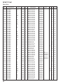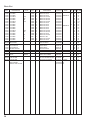
1
VERTEX STANDARD CO., LTD. 4-8-8 Nakameguro, Meguro-Ku, Tokyo 153-8644, Japan VERTEX STANDARD UHF FM Transceiver US Headquarters 10900 Walker Street, Cypress, CA 90630, U.S.A. VX-230 Series Unit 12, Sun Valley Business Park, Winnall Close Winchester, Hampshire, SO23 0LB, U.K. YAESU UK LTD. VERTEX STANDARD HK LTD. Unit 5, 20/F., Seaview Centre, 139-141 Hoi Bun Road, Kwun Tong, Kowloon, Hong Kong Service Manual ©2009 VERTEX STANDARD CO., LTD. VERTEX STANDARD (AUSTRALIA) PTY., LTD. Normanby Business Park, Unit 14/45 Normanby Road Notting Hill 3168, Victoria, Australia EC085U90C Introduction This manual provides technical information necessary for servicing the VX-230 FM Transceiver. Servicing this equipment requires expertise in handling surface-mount chip components. Attempts by non-qualified persons to service this equipment may result in permanent damage not covered by the warranty, and may be illegal in some countries. Two PCB layout diagrams are provided for each double-sided circuit board in the transceiver. Each side of is referred to by the type of the majority of components installed on that side (“leaded” or “chip-only”). In most cases one side has only chip components, and the other has either a mixture of both chip and leaded components (trimmers, coils, electrolytic capacitors, ICs, etc.), or leaded components only. While we believe the technical information in this manual to be correct, VERTEX STANDARD assumes no liability for damage that may occur as a result of typographical or other errors that may be present. Your cooperation in pointing out any inconsistencies in the technical information would be appreciated. Important Note This transceiver was assembled using Pb (lead) free solder, based on the RoHS specification. Only lead-free solder (Alloy Composition: Sn-3.0Ag-0.5Cu) should be used for repairs performed on this apparatus. The solder stated above utilizes the alloy composition required for compliance with the lead-free specification, and any solder with the above alloy composition may be used. Contents Specifications...........................................................2 Exploded View & Miscellaneous Parts .................3 Block Diagram ........................................................ 5 Circuit Description ................................................7 Alignment ............................................................... 9 MAIN Unit (Lot. 1~5) .......................................... 17 MAIN Unit (Lot. 6~) ............................................ 21 MAIN Unit Parts List .......................................... 25 1 Specifications VTX/EXP version General Frequency Range: 450MHz - 512MHz (Version VTX, Type D), 450MHz - 520MHz (Version EXP, Type D), 400MHz - 470MHz (Version VTX/EXP, Type A) Number of Channels: 16 Power Supply Voltage: 7.4 V DC ±10 % Channel Spacing: 12.5 / 20 / 25 kHz Battery Life (5-5-90 duty): 9 hrs (7.3 hrs w/o saver) w/FNB-V103LI (1150 mAh) 16.5 hours (13.5 hrs w/o saver) w/FNB-V104LI (2000 mAh) Operating Temperature Range: +22 °F to +140 °F (–30 °C to +60 °C) Frequency Stability: ±2.5 ppm RF Input-Output Impedance: 50 Ohm Dimension (W x H x D): 2.3” x 4.3” x 1.2” (58 x 110 x 30 mm) Weight (Approx.): 10.1 oz ( 285 g) w/FNB-V103LI, Antenna, Belt Clip Receiver (measured by TIA/EIA-603) Sensitivity (12 dB SINAD): 0.25 μV typical Adjacent Channel Selectivity: 65 / 60 dB (25 kHz / 12.5 kHz) Intermodulation: 65 / 60 dB (25 kHz / 12.5 kHz) Spurious and Image Rejection: 65 dB Audio Output: 500 mW @ 4 ohms 5 % THD Transmitter (measured by TIA/EIA-603) Output Power: Modulation: Conducted Spurious Emission: FM Hum & Noise: Audio Distortion: EU version General Frequency Range: Number of Channels: Power Supply Voltage: Channel Spacing: Battery Life (5-5-90 duty): Temperature Range: Frequency Stability: RF Input-Output Impedance: Battery Pack: Dimension (W x H x D): Weight (Approx.): 5/1W 16K0F3E, 11K0F3E 65 dB below carrier 45 / 40 dB (25 kHz/ 12.5 kHz) < 3 % @1 kHz 400MHz - 470MHz (VX-231-EG6B-5) 16 7.4 V DC ±10 % 12.5 / 20 / 25 kHz 9 hrs (7.3 hrs w/o saver) w/FNB-V103LI (1150 mAh) 16.5 hours (13.5 hrs w/o saver) w/FNB-V104LI (2000 mAh) –20 °C to +55 °C (Operation) –0 °C to +45 °C (Battery Charging) Turn the radio off while charging the battery, and use only the Vertex Standard Co., Ltd. Model PA-42C/U AC Adapter and CD-34 Desktop. ±2.5 ppm 50 Ohm FNB-V103LI / FNB-V104LI Risk of explosion if battery is replaced by an incorrect type. Dispose of used batteries according to the instructions. 58 x 110 x 30 mm 285 g w/FNB-V103LI, Antenna, Belt Clip Receiver (Measurement per EN 300 086) Sensitivity (20 dB SINAD): 0.5 μV Adjacent Channel Selectivity: 70 / 60 dB (25 kHz / 12.5 kHz) Intermodulation: 65 dB Spurious and Image Rejection: 70 dB FM Noise: 45 / 40 dB (25 kHz / 12.5 kHz) Spurious Emission: –36 dBm (<1GHz), –30 dBm (>1GHz) Audio Output: 500 mW @ 4 ohms 5 % THD Transmitter (Measurement per EN 300 08) Output Power: 5/1W Modulation: Variable Reactance Modulation Maximum Frequency Deviation: ±2.5 / ±4.0 / ±5.0 kHz (12.5 kHz / 20 kHz / 25 kHz) FM Hum & Noise: 45 / 40 dB (25 kHz / 12.5 kHz) Audio Distortion: < 5 % @1 kHz Spurious Emission: –36 dBm (<1GHz), –30 dBm (>1GHz) Specification may be changed without notification. 2 Exploded View & Miscellaneous Parts d d RA1096000 COIL SPRING RA0173500 CAP (MIC/SP) CP9350001 FRONT CASE ASSY RA1058900 O RING RA103980A RELEASE KNOB(BATT) RA090600C KNOB(VOL) RA1107500 LATCH PLATE RA091760B KNOB ASSY(CH) RA1041900 FRAME(PTT) RA090490B COVER(PTT) RA1041800 RUBBER(SIDE) RA1041700 RUBBER(PTT) RA0187600 SHEET RA1042100 LOCK PLATE T9318325 WIRE ASSY (YEL 65) RA0557900 SP NET T9318324 WIRE ASSY(BLK 65) M4090192B SPEAKER (14-ohm/1W) RA1085300 TAPE(SP) f RA1124300 (DST: EU) SHIELD CASE COVER f f f f f f h f f f f MAIN Unit RA090590A NUT RA103890B RUBBER PACKING RA090590A NUT RA0248200 GROUND PLATE g RA103910A TERMINAL ASSY RA0248200 GROUND PLATE g RA037690B SHEET CP9349001 REAR CASE ASSY RA1103200 ELEC. COND TAPE RA1039000 PACKING PAD(BATT-C) e RA103880A CASE COVER(REAR) e BATTERY PACK CP9351001 BELT CLIP ASSY c REF VXSTD P/N c U02308020 d U20206007 e U24110002 f U44105002 g U24106002 h U07230302 DESCRIPTION QTY. SEMS SCREW SM3X8SUS 1 BINDING HEAD SCREW M2.6X6B 2 BIND HEAD TAPTITE-B M2X10NI 2 PAN HEAD TAPTITE-B M2X5NI 11 BIND HEAD TAPTITE-B M2X6NI 2 PAN HEAD SCREW M2X3NI #3 1 Non-designated parts are available only as part of a designated assembly. 3 Note 4 Block Diagram 5 Block Diagram Note 6 Circuit Description 1. Circuit Configuration by Frequency The receiver is a Double-conversion Super-heterodyne with a first intermediate frequency (IF) of 67.65MHz and a second IF of 450kHz. Incoming signal from the antenna is mixed with the local signal from the VCO/PLL to produce the first IF of 67.65MHz. This is then mixed with the 67.2MHz second local oscillator output to produce the 450kHz second IF. This is detected to give the demodulated signal. The transmit signal frequency is generated by the PLL VCO, and modulated by the signal from the microphone. It is then amplified and sent to the antenna 2. Receiver System 2-1. Front-end RF amplifier Incoming RF signal from the antenna is delivered to the RF Unit and passes through Low-pass filer, antenna switching diode, high pass filter and removed undesired frequencies by varactor diode (tuned band-pass filer). The passed signal is amplified in Q1013 (MSG33001) and moreover cuts an image frequency with the tuned band pass filter and comes into the 1st mixer. 2-2. First Mixer The 1st mixer consists of the Q1024 (3SK293). Buffered output from the VCO is amplified by Q1027 (2SC5005) to provide a pure first local signal between 382.35 and 444.35 MHz (EXP: 452.35 MHz) for injection to the first mixer. The IF signal then passes through monolithic crystal filters XF1001 (±7.5 kHz BW) to strip away all but the desired signal. 2-3. IF Amplifier The first IF signal is amplified by Q1033 (2SC5226). The amplified first IF signal is applied to FM IF subsystem IC Q1038 (NJM2591V) which contains the second mixer, second local oscillator, limiter amplifier, noise amplifier, and RSSI amplifier. The signal from reference oscillator X1002 becomes 4 times of frequencies in Q1038, it is mixed with the IF signal and becomes 450kHz. The second IF then passes through the ceramic filter CF1001 (LTM450FW) to strip away unwanted mixer products, and is applied to the limiter amplifier in Q1038, which removes amplitude variations in the 450kHz IF, before detection of the speech by the ceramic discriminator CD1001 (JTBM450CX24). 2-4. Audio amplifier Detected signal from Q1038 is inputted to TX/RX switch Q1001-4 (TC74VHC4066AFT). The signal which appeared from Q1001 is in high pass filter Q1050 (NJM12902V). The signal which passed Q1050 goes to AF volume (VR1001). And then the signal goes to audio amplifier Q1005 (NJM2070M). The output signal from Q1005 is in audio speaker. 2-5. Squelch Circuit There are 16 levels of squelch setting from 0 to 15. The level 0 means open the squelch. The level 1 means the threshold setting level and level 14 means tight squelch. From 2 to 13 is established in the middle of threshold and tight. The bigger figure is nearer the tight setting. The level 15 becomes setting of carrier squelch. 2-5-1. Noise Squelch Noise squelch circuit is composed of the band path filter of Q1038, and noise detector D1029 (1SS400G). When a carrier isn't received, the noise ingredient which goes out of the demodulator Q1038 is amplified in Q1038 through the band path filter Q1038, is detected to DC voltage with D1029 and is inputted to 52pin (the A/D port) of the Q1026 (CPU). When a carrier is received, the DC voltage becomes low because the noise is compressed. When the detected voltage to CPU is high, the CPU stops AF output with Q1001-3 “OFF” by making the 41pin (CPU) “L” level. When the detection voltage is low, the CPU makes Q1001 ON with making 41pin “H” and the AF signal is output. 2-5-2. Carrier Squelch The CPU (53pin: A/D port) detect RSSI voltage output from Q1038 12 pin, and controls AF output. The RSSI output voltage changes according to the signal strength of carrier. The stronger signal makes the RSSI voltage to be higher voltage. The process of the AF signal control is same as Noise Squelch The shipping data is adjusted -1dBμ (EMF) higher than squelch tight sensitivity. 3. Transmitter System 3-1. Mic Amplifier The AF signal from internal microphone MC1001 or external microphone J1002 is amplified with microphone amplifier Q1049-3 (NJM12902V). This signal enters high pass filter Q1050 via the mute switch Q1001-1 (TC74VHC4066AFT). Afterwards, the switch circuit is controlled in the gain by way of microphone gain volume Q1012 (M62364FP-CH1). AF signal is passes a pre-emphasis circuit and is input to the limiter amplifier Q1049-2 (NJM12902V). The signal passed splatter filter of Q1049 and adder amplifier Q1046 is adjusted by maximum deviation adjustment volume Q1012 (M62364FP-CH4). The AF signal ingredient is amplified Q1046 (NJM12902V). After that, it is made FM modulation to transmit carrier by the modulator D1014 (HVC383B) of VCO. 7 Circuit Description 3-2. Drive and Final amplifier The modulated signal from the VCO Q1032 (2SC4227) is buffered by Q1027 (2SC5005). Then the signal is buffered by Q1018 (2SC5227) for the final amplifier driver Q1015 (RQA0004PXDQS). The low-level transmit signal is then applied to Q1010 (RQA0011DNS) for final amplification up to 5watts output power. The transmit signal then passes through the antenna switch D1002 (HVU131) and is low pass filtered to suppress away harmonic spurious radiation before delivery to the antenna. 3-3. Automatic Transmit Power Control The current detector Q1052-1(NJM12904R) detects the current of Q1010 and Q1015, and converts the current difference to the voltage difference. The output from the current detector Q1052-1 is compared with the reference voltage and amplified by the power control amplifier Q1052-2. The output from Q1052-2 controls the gate bias of the final amplifiers Q1010 and the final amplifier driver Q1015. The reference voltage changes into four values (Transmit Power High and Low) controlled by Q1012 (M62364FP-CH8). 3-4. PLL Frequency Synthesizer The frequency synthesizer consists of PLL IC, Q1042 (MB15E03SL), VCO, TCXO (X1002) and buffer amplifier. The output frequency from TCXO is 16.8MHz and the tolerance is ±2.5 ppm (in the temperature range -30 to +60 degrees). 3-4-1. VCO While the radio is receiving, the RX oscillator Q1030 (2SK508) in VCO generates a programmed frequency between 382.35 and 444.35 MHz (EXP: 452.35 MHz) as 1st local signal. While the radio is transmitting, the TX oscillator Q1032 (2SC4227) in VCO generates a frequency between 450 and 512 MHz (EXP: 520 MHz) . The output from oscillator is amplified by buffer amplifier Q1027 (2SC5005) and becomes output of VCO. The output from VCO is divided, one is amplified by Q1027 and feed back to the PLL IC 8pin. It is put into the mixer as the 1st local signal through D1012, in transmission, it is buffered Q1018, and more amplified in Q1015 through D1012 and it is put into the final amplifier Q1010. 8 3-4-2. VC0 Tuning Voltage Tuning voltage of VCO is expanding the lock range of VCO by controlling the cathode of varactor diode at the voltage and the control voltage from PLL IC. 3-4-3. PLL The PLL IC consists of reference divider, main divider, phase detector, charge pumps and pulse swallow operation. The reference frequency from TCXO is inputted to 1pin of PLL IC and is divided by reference divider. The other hand, inputted feed back signal to 8pin of PLL IC from VCO is divided with the dividing ratio which becomes same frequency as the output of reference divider. These two signals are compared by phase detector, the phase difference pulse is generated. The phase difference pulse and the pulse from through the charge pumps and LPF. It becomes the DC voltage to control the VCO. The oscillation frequency of VCO is locked by the control of this DC voltage. The PLL serial data from CPU is sent with three lines of SDO (60pin), SCK (58pin) and PSTB (59pin). The lock condition of PLL is output from the UL (14Pin) terminal and UL becomes “H” at the time of the lock condition and becomes “L” at the time of the unlocked condition. The CPU always watches over the UL condition, and when it becomes “L” unlocked condition, the CPU prohibits transmitting and receiving. Alignment Introduction Required Test Equipment The VX-230 series has been aligned at the factory for the specified performance across the entire frequency range specified. Realignment should therefore not be necessary except in the event of a component failure. All component replacement and service should be performed only by an authorized Vertex Standard representative, or the warranty policy may be voided. The following procedures cover the sometimes critical and tedious adjustments that are not normally required once the transceiver has left the factory. However, if damage occurs and some parts are replaced, realignment may be required. If a sudden problem occurs during normal operation, it is likely due to component failure; realignment should not be done until after the faulty component has been replaced. We recommend that servicing be performed only by authorized Vertex Standard service technicians who are experienced with the circuitry and fully equipped for repair and alignment. Therefore, if a fault is suspected, contact the dealer from whom the transceiver was purchased for instructions regarding repair. Authorized Vertex Standard service technicians realign all circuits and make complete performance checks to ensure compliance with factory specifications after replacing any faulty components. Those who do undertake any of the following alignments are cautioned to proceed at their own risk. Problems caused by unauthorized attempts at realignment are not covered by the warranty policy. Also, Vertex Standard must reserve the right to change circuits and alignment procedures in the interest of improved performance, without notifying owners. Under no circumstances should any alignment be attempted unless the normal function and operation of the transceiver are clearly understood, the cause of the malfunction has been clearly pinpointed and any faulty components replaced, and the need for realignment determined to be absolutely necessary. The following test equipment (and thorough familiarity with its correct use) is necessary for complete realignment. Correction of problems caused by misalignment resulting from use of improper test equipment is not covered under the warranty policy. While most steps do not require all of the equipment listed, the interactions of some adjustments may require that more complex adjustments be performed afterwards. Do not attempt to perform only a single step unless it is clearly isolated electrically from all other steps. Have all test equipment ready before beginning, and follow all of the steps in a section in the order presented. Radio Tester with calibrated output level at 500 MHz In-line Wattmeter with 5% accuracy at 500 MHz 50-ohm, 10-W RF Dummy Load Regulated DC Power Supply (standard 7.5 VDC, 2 A) Frequency Counter: ±0.2 ppm accuracy at 500 MHz AF Signal Generator AC Voltmeter DC Voltmeter UHF Sampling Coupler Microsoft® Windows® 2000, XP, or Vista Micorosoft® Net Framework 2.0 or later Vertex Standard CE99 Alignment program and CT-42 Connection Cable or FIF-10A USB Programming Interface and CT-106 PC Programming Cable. Alignment Preparation & Precautions A 50-ohm RF Dummy load and in-line wattmeter must be connected to the main antenna jack in all procedures that call for transmission, except where specified otherwise. Correct alignment is not possible with an antenna. After completing one step, read the following step to determine whether the same test equipment will be required. If not, remove the test equipment (except dummy load and wattmeter, if connected) before proceeding. Correct alignment requires that the ambient temperature be the same as that of the transceiver and test equipment, and that this temperature be held constant between 20 °C and 30 °C (68 °F ~ 86 °F). When the transceiver is brought into the shop from hot or cold air, it should be allowed time to come to room temperature before alignment. Whenever possible, alignments should be made with oscillator shields and circuit boards firmly affixed in place. Also, the test equipment must be thoroughly warmed up before beginning. Note: Signal levels in dB referred to in this procedure are based on 0 dBμ EMF = 1.0 μV. 9 Alignment Test Setup Basic Alignment Mode Setup the test equipment as shown for transceiver alignment, then apply 7.5 V DC power to the transceiver. In the Basic Alignment mode, the aligned data written in the radio will be able to re-align its alignment data. In this mode, there are many items to align with five points (F1, F2, F3, F4, F5) except “Frequency”, “Mic Sense”, “SQL/RSSI”, and “Battery”. The value of each parameter can be changed to desired position by “»” / “¼” arrow key for up/down, direct number input and drag the mouse. 50-ohm Dummy Load RF Signal Generator RF Sampling Coupler Inline Wattmeter ANT Transceiver MIC/SP Deviation Meter BATTERY TERMINAL Power Supply 7.5 VDC CT-42 or FIF10A + CT-106 Frequency Counter COM Port (for CT-42) or USB Port (for FIF10A + CT-106) CLONE SP GND SP MIC MIC CLONE GND The Alignment Tool Outline Installation the tool Install the CE99 (Clone Editor) to your PC. “Basic Alingment” function in the “Radio” menu of CE99. Action of the switches When the transceiver is in alignment mode, the action of PTT and KEY is ignored. All of the action is remote controlled by PC. To enter the Basic Alignment Mode, select “Basic Alignment” in the main menu “Radio”. It will start to “Read” the written personalized data from the radio. Then pressing the button “OK” will start the Basic Alignment Mode. Note: when all items are aligned, it is strongly recommended to align according to following order. The detail information is written in the help of CE99 (Clone Editor). 1. PLL Reference Frequency (Frequency) 2. RX Sensitivity (RX Tune) 3. Squelch (SQL/RSSI) 4. TX Power <High> / <Low> 5. Mic Sense 6. Maximum Deviation <Wide> / <Narrow> 7. Modulation Balance <Wide> / <Narrow> 8. CTCSS Deviation <Wide> / <Narrow> 9. DCS Deviation <Wide> / <Narrow> 10. Battery Unit During alignment, you may select the value among dBμV, μV (EMF or PD), or dBm. ¯ Caution! Please never turn off a power supply while alignment. If the power supply turn off while alignment, the setting data is failed. 10 When perform the RX Tune and SQL alignment, the RF level shows this unit according to this setting. Alignment 1. PLL REFERENCE FREQUENCY (FREQUENCY) This parameter is to align the reference frequency for PLL. 1. Press the “Frequency” button to start the alignment. It will appear the Frequency Alignment window. 2. Click the “PTT” button, then the radio starts to transmit on center frequency channel. 3. Set the value to get desired frequency by drag the slide bar, click the up-down button, press the left or right key, or enter the value on the entry box. 4. After getting the desired frequency then click the “PTT” button to stop the transmit. 5. Click the “OK” button to finish the frequency alignment and save the data. ¯ 2. RX SENSITIVITY (RX TUNE) This parameter is to align the RX BPF (Band Pass Filter) for Receive (RX) sensitivity. It must be done both alignments of the “Frequency” before this alignment is going to start. There are following 2 Way for Alignment. ¯ Manual Alignment 1. Press the “RX Tune” button to start the alignment. It will appear the Frequency Alignment window. 2. Click the left mouse button on the slide bar, then switched to selected channel. 3. Set the Signal Generator according to the indication. 4. Drag the slide bar, click the up-down button, press the left or right key, or enter the value on the entry box to get the best RX sensitivity. 5. Click the “OK” button to finish the RX Sensitivity alignment and save the data. ADJ Type Single : Alignment value change only to selected channel. All Freq : Alignment value change for connecting with other channels. Automatic Alignment 1. Press the “RX Tune” button to start the alignment. It will appear the Frequency Alignment window. 2. Click the left button on the “Auto” button, then the alignment window will appear. 3. Set the Signal Generator according to the indication. 4. Click the left button on the “Start” button, then start the automatic alignment to get the best RX sensitivity. 5. It will show the alignment result in the “New” box. 6. Click the “OK” button to finish the RX Sensitivity alignment and save the data. 11 Alignment 3. SQUELCH (SQL) This parameter is to align the SQL (Squelch) Sensitivity. There are several alignments as follows in the Squelch Sensitivity. Threshold SQL Level The Alignment for the Noise SQL Threshold level at Wide (5k/ 4k). or Narow (2.5k). Tight SQL Level The Alignment for the Noise SQL Tight level at Wide (5k/4k). or Narow (2.5k). Tight SQL RSSI Level The Alignment for the “level 14” of the RSSI SQL level at Wide (5k/4k). or Narow (2.5k). TX Save RSSI Level The Alignment for the TX Save RSSI level at Wide (5k/4k). or Narow (2.5k). ¯ The procedure for all the alignment is as follows. 1. Click the “Start” button to open the alignment window in the SQL/RSSI Alignment menu. 2. It will appear the Alignment windows, Set the Signal Generator according to the indication, then click the “Start” button. 3. Then start the automatic alignment to get the SQL or RSSI level. 4. It will show the alignment result in the “New” box. 5. Click the “OK” button, then the data will be saved and the alignment is accomplished. 4. TX POWER This parameter is to align the “Power High” or “Power Low” for the selected channel. 12 ¯ 1. Click the “PTT” button at desired channel, then the radio starts to transmit on selected channel. 2. Set the value to get desired output power (High: 5W, Low: 1W) on the Power Meter by drag the slide bar, click the updown button, press the left or right key, or enter the value on the entry box. 3. After getting the desired output power then click the “PTT” button to stop the transmit. 4. Click the “OK” button to finish the Power high / low alignment and save the data. ADJ Type Single : Alignment value change only to selected channel. All Freq : Alignment value change for connecting with other channels. Alignment 5. MIC SENSE This parameter is to align the “Microphone Sense” (Gain) and it needs the appropriate JIG (Tuning Interface BOX). Connect the JIG and Test Equipment to the radio before the alignment is going to start. It must be done alignment of the “Max Deviation” before this alignment is going to start. 1. Click the “PTT” button, then the radio starts to transmit on center frequency channel. 2. Set the value to get desired Microphone Sense on the deviation meter by drag the slide bar, click the up-down button, press the left or right key, or enter the value on the entry box. 3. After getting the desired deviation then click “PTT” button to stop the transmit. 4. Click “OK” button to finish the Mic Sense alignment and save the data. ¯ 6. MAXIMUM DEVIATION <WIDE> / <NARROW> This parameter is to align the “Maximum Deviation” (Wide/Narrow) and it needs the appropriate JIG (Tuning Interface BOX). Connect the JIG and Test Equipment to the radio before the alignment is going to start. ¯ 1. Click the “PTT” button, then the radio starts to transmit on selected channel. 2. Set the value to get desired deviation (Wide: 4.2kHz, Narrow: 2.1kHz) on the deviation meter by drag the slide bar, click the up-down button, press the left or right key, or enter the value on the entry box. 3. After getting the desired deviation then click “PTT” button to stop the transmit. 4. Click “OK” button to finish the Max Deviation alignment and save the data. ADJ Type Single : Alignment value change only to selected channel. All Freq : Alignment value change for connecting with other channels. 13 Alignment 7. MODULATION BALANCE <WIDE> / <NARROW> (THIS ALIGNMENT IS DIFFICULT.) This parameter is to align the “Modulation Deviation” (Wide/Narrow) and it needs the appropriate JIG (Tuning Interface BOX). Connect the JIG and Test Equipment to the radio before the alignment is going to start.It must be done alignment of the "Max Deviation" before this alignment is going to start. ¯ 1. Click the “PTT” button, then the radio starts to transmit on selected channel. 2. Set the value to get desired deviation on the deviation meter by drag the slide bar, click the up-down button, press the left or right key, or enter the value on the entry box. 3. After getting the desired deviation then click “PTT” button to stop the transmit. 4. Click the “OK” button to finish the Modulation Balance alignment and save the data. ADJ Type Single : Alignment value change only to selected channel. All Freq : Alignment value change for connecting with other channels. 8. CTCSS DEVIATION <WIDE> / <NARROW> This parameter is to align CTCSS Deviation of the selected channel. 14 ¯ 1. Input the desired CTCSS Frequency on the CTCSS Frequency Box. Default: 151.4Hz, Input Range: 67.0 to 255.9Hz 2. Click the “PTT” button, then the radio starts to transmit on selected channel. 3. Set the value to get desired deviation on the deviation meter by drag the slide bar, click the up-down button, press the left or right key, or enter the value on the entry box. 4. After getting the desired deviation then click “PTT” button to stop the transmit. 5. Click “OK” button to finish the CTCSS Deviation alignment and save the data. ADJ Type Single : Alignment value change only to selected channel. All Freq : Alignment value change for connecting with other channels. Alignment 9. DCS DEVIATION <WIDE> / <NARROW> This parameter is to align “DCS Deviation” of the selected channel. ¯ 1. Input the desired DCS Code on the DCS Code Box. Default: 523 Input Range: 000 to 777 2. Click the “PTT” button, then the radio starts to transmit on selected channel. 3. Set the value to get desired deviation on the deviation meter by drag the slide bar, click the up-down button, press the left or right key, or enter the value on the entry box. 4. After getting the desired deviation then click “PTT” button to stop the transmit. 5. Click “OK” button to finish the DCS Deviation alignment and save the data. ADJ Type Single : Alignment value change only to selected channel. All Freq : Alignment value change for connecting with other channels. 10. BATTERY This parameter is to align the “Alert Reference voltage” and “Write Protect Level” voltage. When the DC source power becomes below the “Write Protect Level” voltage, the radio will stop writing data to the EEPROM due to prevent the erroneous writing. 1. Set the value of DC Power source to 6.5V (according to the indication) and click “Start” button. Then alignment value show in the “New” box. 2. Set the value of DC Power source to 5.5V (according to the indication) and click “Start” button. Then alignment value show in the "New” box. 3. Click the “OK” button, then the data will be saved and the alignment is accomplished. 4. Set the value of DC Power source to 7.5V (according to the indication). ¯ 15 Note 16 MAIN Unit (Lot. 1~5) Circuit Diagram RX: 2.1 V TX: 0 V RX: 0 V TX: 0.8 V RX: 2.9 V TX: 0 V –11 dBμ –1 dBμ +7 dBμ –5 dBμ –8 dBμ RX: 0.8 V TX: 0 V 5.0 V RX: 0 V TX: 4.2 V 4.2 V WIDE: 4.6 V NARROW: 0 V TX 5W: 1.1 V 7.4 V 3.0 V RX: 0.8 V TX: 0.8 V RX: 3.7 V TX: 4.2 V 4.9 V TX 5W: 0.7 V RX: 2.5 V TX: 2.5 V 0.3 V RX: 4.2 V TX: 4.0 V RX: 0 V TX: 0.4 V RX: 1.9 V TX: 1.8 V TX 5W: 1.9 V PTT “ON”: 0 V PTT “OFF”: 3.5 V 7.4 V 0.7 V LOCK: 3.4 V UNLOCK: 0 V SAVE “ON”: 0 V SAVE “OFF”: 3.5 V 5.0 V RX: 5.0 V TX: 0 V RX: 0 V TX: 3.5 V RX: 0 V TX: 5.0 V 1.9 V NORMAL TEMP.: 2.6 V 1.3 V RX: 0 V TX: 5.0 V RX: 5.0 V TX: 0 V BUSY: 3.5 V MUTE: 0 V BUSY: 7.4 V MUTE: 0 V 6.7 V 3.5 V 4.0 Vp-p @500 mW 7.4 V 3.5 V INT.PTT ON:3.5 V OFF:0 V EXT.PTT ON:2.1 V OFF:4.0 V RX: 0 V TX: 2.9 V RX: 2.9 V TX: 0 V 4.3 V RX: 2.4 V TX: 2.9 V RX: 2.9 V TX: 2.5 V 17 MAIN Unit (Lot. 1~5) Note 18 MAIN Unit (Lot. 1~5) Parts Layout (Side A) 5 4 3 2 1 TC74VHC4066AFT (Q1001) NJM12902V (Q1046, 1049, 1050) A 2SC4617 (Q1002, 1007, 1016) 2SC4081 (Q1037) B TAR5S50U (5V0) (Q1003) TAR5S35U (3V5) (Q1020) NJM2070M (Q1005) C MTM231230L (BL) (Q1006, 1008,1011) 2SK3541 (Q1056) DTC144EE (26) (Q1009, 1014,1045) DA221 (K) (D1003, 1028) NJM12904R (Q1047, 1052) NJM12903R-TE1 (Q1048) DTA144EE (16) (Q1028) UPD78F1142GB(S)-GAH-AX (Q1026) M62364FP (Q1012) RQA0011DNS (Q1010) 19 MAIN Unit (Lot. 1~5) Parts Layout (Side B) 5 4 3 2 1 a MSG330010L (5S) (Q1013) 2SC5227 (Q1018) 2SC5005 (73) (Q1022, 1027) 2SC4227-T1 (R32) (Q1032) 2SC5226 (R22) (Q1033) 2SC4617 (BR) (Q1034) b RQA0004PXDQS (PX) (Q1015) c 3SK293 (HF) (Q1024) 2SK508 (K52) (Q1030) DA221(K) (D1019, 1035) 20 DAN222 (N) (D1012) DTC144EE (26) (Q1043, 1044) NJM2591V (Q1038) MB15E03SLPFV1 (Q1042) DTC114TE (04) (Q1023, 1025,1029, 1031) MAIN Unit (Lot. 6~) Circuit Diagram 21 MAIN Unit (Lot. 6~) Note 22 MAIN Unit (Lot. 6~) Parts Layout (Side A) 5 4 3 2 1 TC74VHC4066AFT (Q1001) NJM12902V (Q1046, 1049, 1050) A 2SC4617 (Q1002, 1007, 1016) 2SC4081 (Q1037) B TAR5S50U (5V0) (Q1003) TAR5S35U (3V5) (Q1020) NJM2070M (Q1005) C MTM231230L (BL) (Q1006, 1008,1011) 2SK3541 (Q1056) DTC144EE (26) (Q1009, 1014,1045) DA221 (K) (D1003, 1028) NJM12904R (Q1047, 1052) NJM12903R-TE1 (Q1048) DTA144EE (16) (Q1028) UPD78F1142GB(S)-GAH-AX (Q1026) M62364FP (Q1012) RQA0011DNS (Q1010) 23 MAIN Unit (Lot. 6~) Parts Layout (Side B) 5 4 3 2 1 a MSG330010L (5S) (Q1013) 2SC5227 (Q1018) 2SC5005 (73) (Q1022, 1027) 2SC4227-T1 (R32) (Q1032) 2SC5226 (R22) (Q1033) 2SC4617 (BR) (Q1034) b RQA0004PXDQS (PX) (Q1015) c 3SK293 (HF) (Q1024) 2SK508 (K52) (Q1030) DA221(K) (D1019, 1035) 24 DAN222 (N) (D1012) DTC144EE (26) (Q1043, 1044) NJM2591V (Q1038) MB15E03SLPFV1 (Q1042) DTC114TE (04) (Q1023, 1025,1029, 1031) MAIN Unit Parts List REF. DESCRIPTION VALUE V/W TOL. MFR’S DESIG PCB with Components Printed Circuit Board C 1001 C 1002 C 1003 C 1004 C 1005 C 1006 C 1007 C 1008 C 1009 C 1010 C 1011 C 1012 C 1013 C 1014 C 1014 C 1014 C 1015 C 1016 C 1017 C 1018 C 1018 C 1018 C 1019 C 1020 C 1020 C 1020 C 1021 C 1022 C 1023 C 1024 C 1026 C 1027 C 1028 C 1028 C 1030 C 1031 C 1032 C 1033 C 1034 C 1037 C 1037 C 1037 C 1037 C 1039 C 1040 C 1042 C 1044 C 1045 C 1047 C 1049 C 1050 C 1051 C 1054 C 1055 C 1056 C 1062 C 1064 C 1065 C 1066 C 1066 CHIP CAP. CHIP CAP. CHIP CAP. CHIP CAP. CHIP CAP. CHIP CAP. CHIP TA.CAP. CHIP CAP. CHIP CAP. CHIP CAP. CHIP TA.CAP. CHIP CAP. CHIP CAP. CHIP CAP. CHIP CAP. CHIP CAP. CHIP CAP. CHIP CAP. CHIP CAP. CHIP CAP. CHIP CAP. CHIP CAP. CHIP CAP. CHIP CAP. CHIP CAP. CHIP CAP. CHIP CAP. CHIP TA.CAP. CHIP CAP. CHIP CAP. CHIP CAP. CHIP CAP. CHIP TA.CAP. CHIP TA.CAP. CHIP CAP. AL.ELECTRO.CAP. CHIP CAP. CHIP CAP. CHIP TA.CAP. CHIP CAP. CHIP CAP. CHIP CAP. CHIP CAP. CHIP CAP. CHIP CAP. CHIP CAP. CHIP CAP. CHIP TA.CAP. CHIP CAP. CHIP CAP. CHIP CAP. CHIP CAP. CHIP CAP. CHIP TA.CAP. CHIP TA.CAP. CHIP TA.CAP. CHIP CAP. CHIP CAP. CHIP CAP. CHIP CAP. AC085U000 47pF 0.001uF 150pF 0.01uF 150pF 3pF 10uF 150pF 150pF 0.047uF 4.7uF 150pF 6pF 1pF 1.5pF 1pF 47pF 150pF 150pF 6pF 7pF 6pF 150pF 2pF 2.5pF 2pF 0.01uF 10uF 220pF 0.01uF 5pF 0.022uF 10uF 4.7uF 0.1uF 220uF 2pF 0.1uF 10uF 10pF 15pF 10pF 10pF 7pF 68pF 0.1uF 150pF 10uF 0.01uF 220pF 150pF 0.01uF 100pF 10uF 10uF 2.2uF 9pF 0.01uF 4pF 4pF 50V 50V 50V 25V 50V 50V 10V 50V 50V 10V 10V 50V 50V 50V 50V 50V 50V 50V 50V 50V 50V 50V 50V 50V 50V 50V 25V 10V 50V 25V 50V 16V 16V 16V 10V 10V 50V 10V 10V 50V 50V 50V 50V 50V 50V 10V 50V 16V 25V 50V 50V 25V 50V 16V 10V 6.3V 50V 25V 50V 50V CH B CH B CH CJ CH CH B CH CH CK CK CK CH CH CH CH CH CH CH CK CH CK B B B CH B B CK B CH CH CH CH CH CH B CH B CH CH B CH CH B CH CH GRM1552C1H470JZ01D GRM155B11H102KA01D GRM1552C1H151JA01D GRM155B11E103KA01D GRM1552C1H151JA01D GRP1553C1H3R0CZ01E F931A106MAA GRM1552C1H151JA01D GRM1552C1H151JA01D GRM155B11A473KA01D F931A475MAA GRM1552C1H151JA01D GRM1552C1H6R0DZ01D GRM1554C1H1R0BZ01D GRM1554C1H1R5BZ01D GRM1554C1H1R0BZ01D GRM1552C1H470JZ01D GRM1552C1H151JA01D GRM1552C1H151JA01D GRM1552C1H6R0DZ01D GRM1552C1H7R0DZ01D GRM1552C1H6R0DZ01D GRM1552C1H151JA01D GRM1554C1H2R0BZ01D CM05CH2R5B50AH GRM1554C1H2R0BZ01D GRM155B11E103KA01D F931A106MAA GRM155B11H221KA01D GRM155B11E103KA01D GRM1552C1H5R0CZ01D GRM155B11C223KA01D F931C106MAA F921C475MAA GRM155B11A104KA01D ESMG100ELL221ME11S GRM1554C1H2R0CZ01D GRM155B11A104KA01D F931A106MAA GRM1882C1H100JA01D GRM1882C1H150JA01D GRM1882C1H100JA01D GRM1882C1H100JA01D GRM1882C1H7R0DZ01D GRM1552C1H680JZ01D GRM155B11A104KA01D GRM1552C1H151JA01D F931C106MAA GRM155B11E103KA01D GRM1552C1H221JA01D GRM1552C1H151JA01D GRM155B11E103KA01D GRM1552C1H101JD01D F931C106MBA F931A106MAA F920J225MPA GRM1882C1H9R0DZ01D GRM155B11E103KA01D GRM1552C1H4R0CZ01D GRM1552C1H4R0BZ01D VXSTD P/N VERS. CS2009401 CS2009402 CS2009404 CS2009405 CS2009406 FR018690E FR018690F K22178228 K22178809 K22178240 K22148834 K22178240 K22178205 K78100078 K22178240 K22178240 K22108801 K78100077 K22178240 K22178208 K22178287 K22178288 K22178287 K22178228 K22178240 K22178240 K22178208 K22178209 K22178208 K22178240 K22178289 K22178298 K22178289 K22148834 K78100078 K22178801 K22148834 K22178207 K22128806 K78120095 K78120096 K22108802 K40109027 K22178204 K22108802 K78100078 K22174211 K22174215 K22174211 K22174211 K22174208 K22178232 K22108802 K22178240 K78120095 K22148834 K22179713 K22178240 K22148834 K22178236 K78120087 K78100078 K78080101 K22174210 K22148834 K22178206 K22178291 VTX, TYP: D EXP, TYP: D VTX, TYP: A EXP, TYP: A EU VERSION A VERSION D VERSION A VERSION D VERSION A VERSION D VERSION A VERSION D VERSION A VERSION A LOT. SIDE LAY ADR 1611111111111111-5 661111-6 7711-5 661111111-5 6111111-5 6 6 77111111111111711 2-5 A B B A B B A A A A A A B B B B A A A B B B B B B B B A A A B A A A A B B A A B B B B B A A A A A A A A B B A A B B B B B1 a2 c1 B1 b2 c1 A1 B1 C1 C2 C2 C2 c1 b1 b1 b1 B2 C2 B2 b1 b1 b1 b1 b1 b1 b1 b1 B1 B1 A1 b1 C3 B1 B1 A4 a1 b1 B1 C3 b1 b1 b1 b1 b1 C3 C1 B2 C1 A1 B2 B2 A1 b1 b2 A1 B1 b2 b2 b2 b2 25 MAIN Unit Parts List REF. C 1066 C 1066 C 1066 C 1068 C 1069 C 1069 C 1069 C 1069 C 1070 C 1072 C 1072 C 1072 C 1072 C 1074 C 1075 C 1077 C 1078 C 1080 C 1081 C 1081 C 1082 C 1082 C 1082 C 1082 C 1082 C 1082 C 1082 C 1083 C 1084 C 1084 C 1084 C 1085 C 1086 C 1087 C 1087 C 1087 C 1089 C 1090 C 1090 C 1090 C 1090 C 1091 C 1092 C 1093 C 1094 C 1095 C 1097 C 1098 C 1099 C 1100 C 1100 C 1100 C 1101 C 1103 C 1104 C 1106 C 1106 C 1107 C 1108 C 1109 C 1110 C 1110 C 1110 C 1112 C 1113 C 1114 C 1115 26 DESCRIPTION CHIP CAP. CHIP CAP. CHIP CAP. CHIP CAP. CHIP CAP. CHIP CAP. CHIP CAP. CHIP CAP. CHIP CAP. CHIP CAP. CHIP CAP. CHIP CAP. CHIP CAP. CHIP CAP. CHIP CAP. CHIP CAP. CHIP CAP. CHIP CAP. CHIP TA.CAP. CHIP TA.CAP. CHIP CAP. CHIP CAP. CHIP CAP. CHIP CAP. CHIP CAP. CHIP CAP. CHIP CAP. CHIP CAP. CHIP CAP. CHIP CAP. CHIP CAP. CHIP CAP. CHIP CAP. CHIP CAP. CHIP CAP. CHIP CAP. CHIP CAP. CHIP CAP. CHIP CAP. CHIP CAP. CHIP CAP. CHIP CAP. CHIP CAP. CHIP CAP. CHIP CAP. CHIP CAP. CHIP TA.CAP. CHIP CAP. CHIP CAP. CHIP CAP. CHIP CAP. CHIP CAP. CHIP CAP. CHIP CAP. CHIP CAP. CHIP CAP. CHIP CAP. CHIP CAP. CHIP CAP. CHIP CAP. CHIP CAP. CHIP CAP. CHIP CAP. CHIP CAP. CHIP CAP. CHIP CAP. CHIP CAP. VALUE 8pF 7pF 4pF 150pF 8pF 8pF 12pF 8pF 0.001uF 4pF 4pF 3pF 4pF 0.001uF 0.001uF 150pF 0.001uF 0.01uF 10uF 10uF 4pF 4pF 8pF 6pF 5pF 4pF 6pF 150pF 27pF 39pF 27pF 0.001uF 0.001uF 12pF 15pF 12pF 0.1uF 8pF 8pF 5pF 8pF 150pF 0.01uF 220pF 0.01uF 0.01uF 1uF 0.01uF 150pF 56pF 33pF 56pF 0.001uF 150pF 150pF 10pF 10pF 100pF 0.001uF 0.0047uF 15pF 12pF 15pF 0.01uF 150pF 0.001uF 0.1uF V/W 50V 50V 50V 50V 50V 50V 50V 50V 50V 50V 50V 50V 50V 50V 50V 50V 50V 25V 10V 10V 50V 50V 50V 50V 50V 50V 50V 50V 50V 50V 50V 50V 50V 50V 50V 50V 10V 50V 50V 50V 50V 50V 50V 50V 25V 25V 16V 25V 50V 50V 50V 50V 50V 50V 50V 50V 50V 50V 50V 50V 50V 50V 50V 25V 50V 50V 10V TOL. CH CH CH CH CH CH CH CH B CH CH CJ CH B B CH B B CH CH CH CH CH CH CH CH CH CH CH B B CH CH CH B CH CH CH CH CH B CH B B B CH CH CH CH B CH CH CH CH CH B B CH CH CH B CH B B MFR’S DESIG GRM1552C1H8R0BZ01D GRM1552C1H7R0BZ01D GRM1552C1H4R0BZ01D GRM1552C1H151JA01D GRM1552C1H8R0DZ01D GRM1552C1H8R0BZ01D GRM1552C1H120JZ01D GRM1552C1H8R0BZ01D GRM155B11H102KA01D GRM1552C1H4R0CZ01D GRM1552C1H4R0BZ01D GRM1553C1H3R0BZ01D GRM1552C1H4R0BZ01D GRM155B11H102KA01D GRM155B11H102KA01D GRM1552C1H151JA01D GRM155B11H102KA01D GRM155B11E103KA01D TEESVP1A106M8R F921A106MPA GRM1552C1H4R0CZ01D GRM1552C1H4R0BZ01D GRM1552C1H8R0BZ01D GRM1552C1H6R0BZ01D GRM1552C1H5R0BZ01D GRM1552C1H4R0BZ01D GRM1552C1H6R0BZ01D GRM1552C1H151JA01D GRM1552C1H270JZ01D GRM1552C1H390JZ01D GRM1552C1H270JZ01D GRM155B11H102KA01D GRM155B11H102KA01D GRM1552C1H120JZ01D GRM1552C1H150JZ01D GRM1552C1H120JZ01D GRM155B11A104KA01D GRM1552C1H8R0DZ01D GRM1552C1H8R0BZ01D GRM1552C1H5R0BZ01D GRM1552C1H8R0BZ01D GRM1552C1H151JA01D GRM188B11H103KA01D GRM1552C1H221JA01D GRM155B11E103KA01D GRM155B11E103KA01D F931C105MAA GRM155B11E103KA01D GRM1552C1H151JA01D GRM1552C1H560JD01D GRM1552C1H330JZ01D GRM1552C1H560JD01D GRM155B11H102KA01D GRM1552C1H151JA01D GRM1552C1H151JA01D GRM1552C1H100JZ01D GRM1552C1H100BZ01D GRM1552C1H101JD01D GRM155B11H102KA01D GRM155B11H472KA01D GRM1552C1H150JZ01D GRM1552C1H120JZ01D GRM1552C1H150JZ01D GRM155B11E103KA01D GRM1552C1H151JA01D GRM155B11H102KA01D GRM155B11A104KA01D VXSTD P/N VERS. K22178295 K22178294 K22178291 K22178240 K22178210 K22178295 K22178214 K22178295 K22178809 K22178206 K22178291 K22178290 K22178291 K22178809 K22178809 K22178240 K22178809 K22148834 K78100074 K78100089 K22178206 K22178291 K22178295 K22178293 K22178292 K22178291 K22178293 K22178240 K22178222 K22178226 K22178222 K22178809 K22178809 K22178214 K22178216 K22178214 K22108802 K22178210 K22178295 K22178292 K22178295 K22178240 K22174823 K22179713 K22148834 K22148834 K78120082 K22148834 K22178240 K22178230 K22178224 K22178230 K22178809 K22178240 K22178240 K22178212 K22178297 K22178236 K22178809 K22178838 K22178216 K22178214 K22178216 K22148834 K22178240 K22178809 K22108802 VERSION A VERSION A VERSION D VERSION A VERSION D EU VTX/EXP EU EXP VER. A VERSION A VERSION D VTX VER. A VERSION A VERSION D VERSION A VERSION D VERSION A VERSION D EU VTX / EXP VERSION A VERSION D LOT. SIDE LAY ADR 6 7611 2-6 7711 2-6 77111111-6 71 2-5 776 6711-5 66111-5 6611 2-6 77111111111-6 771111 21111-6 771111- B B B B B B B B A B B B B A A A A B A A B B B B B B B B B B B A A B B B A B B B B B B A A B B A B B B B B B B B B B A A B B B A A A B b2 b2 b2 b2 b2 b2 b2 b2 A5 b2 b2 b2 b2 B3 B2 B3 A5 b2 A3 A3 c2 c2 c2 c2 c2 c2 c2 c2 a3 a3 a3 B3 A3 a3 a3 a3 A2 b2 b2 b2 b2 a3 a2 B2 B4 a3 a2 B4 b2 b2 b2 b2 a3 a3 a3 b2 b2 b2 B4 A4 b2 b2 b2 A4 B2 A5 b2 MAIN Unit Parts List REF. C 1116 C 1117 C 1118 C 1119 C 1119 C 1119 C 1119 C 1119 C 1120 C 1121 C 1122 C 1123 C 1124 C 1125 C 1125 C 1125 C 1125 C 1127 C 1127 C 1128 C 1129 C 1131 C 1133 C 1133 C 1134 C 1135 C 1136 C 1137 C 1138 C 1139 C 1140 C 1141 C 1143 C 1146 C 1147 C 1148 C 1149 C 1152 C 1153 C 1155 C 1159 C 1160 C 1161 C 1162 C 1163 C 1164 C 1167 C 1169 C 1170 C 1171 C 1172 C 1173 C 1174 C 1175 C 1176 C 1177 C 1178 C 1179 C 1180 C 1182 C 1183 C 1184 C 1185 C 1186 C 1187 C 1188 C 1189 DESCRIPTION CHIP TA.CAP. CHIP CAP. CHIP CAP. CHIP CAP. CHIP CAP. CHIP CAP. CHIP CAP. CHIP CAP. CHIP CAP. CHIP CAP. CHIP CAP. CHIP CAP. CHIP CAP. CHIP CAP. CHIP CAP. CHIP CAP. CHIP CAP. CHIP CAP. CHIP CAP. CHIP CAP. CHIP CAP. CHIP CAP. CHIP TA.CAP. CHIP TA.CAP. CHIP CAP. CHIP CAP. CHIP CAP. CHIP CAP. CHIP CAP. CHIP CAP. CHIP CAP. CHIP CAP. CHIP CAP. CHIP CAP. CHIP CAP. CHIP CAP. CHIP CAP. CHIP CAP. CHIP CAP. CHIP CAP. CHIP CAP. CHIP CAP. CHIP CAP. CHIP CAP. CHIP CAP. CHIP CAP. CHIP CAP. CHIP CAP. CHIP CAP. CHIP CAP. CHIP CAP. CHIP CAP. CHIP CAP. CHIP CAP. CHIP CAP. CHIP CAP. CHIP CAP. CHIP CAP. CHIP CAP. CHIP CAP. CHIP CAP. CHIP CAP. CHIP CAP. CHIP CAP. CHIP CAP. CHIP CAP. CHIP CAP. VALUE 1uF 10pF 0.0047uF 4pF 4pF 2pF 3pF 4pF 7pF 0.1uF 0.047uF 0.001uF 2.2uF 8pF 8pF 7pF 8pF 6pF 6pF 150pF 47pF 150pF 4.7uF 4.7uF 0.01uF 150pF 0.001uF 10pF 0.001uF 0.01uF 0.1uF 0.1uF 150pF 1uF 7pF 0.01uF 0.001uF 1uF 56pF 150pF 10pF 10pF 10pF 0.001uF 10pF 0.01uF 0.0047uF 0.0022uF 0.001uF 150pF 3pF 150pF 0.1uF 12pF 7pF 150pF 7pF 1uF 7pF 150pF 0.1uF 150pF 0.1uF 1pF 0.001uF 150pF 8pF V/W 16V 50V 50V 50V 50V 50V 50V 50V 50V 10V 10V 50V 10V 50V 50V 50V 50V 50V 50V 50V 50V 50V 20V 16V 25V 50V 50V 50V 50V 25V 10V 10V 50V 6.3V 50V 25V 50V 6.3V 50V 50V 50V 50V 50V 50V 50V 25V 50V 50V 50V 50V 50V 50V 10V 50V 50V 50V 50V 6.3V 50V 50V 10V 50V 10V 50V 50V 50V 50V TOL. CH B CH CH CK CJ CH CH B B B B CH CH CH CH CH CH CH CH CH B CH B CH B B B B CH B CH B B B CH CH CH CH CH B CH B B B B CH CJ CH B CH CH CH CH B CH CH B CH B CK B CH CH MFR’S DESIG F931C105MAA GRM1552C1H100JZ01D GRM155B11H472KA01D GRM1552C1H4R0CZ01D GRM1552C1H4R0BZ01D GRM1554C1H2R0BZ01D GRM1553C1H3R0BZ01D GRM1552C1H4R0BZ01D GRM1552C1H7R0DZ01D GRM155B11A104KA01D GRM155B11A473KA01D GRM155B11H102KA01D GRM188B31A225KE18D GRM1552C1H8R0DZ01D GRM1552C1H8R0BZ01D GRM1552C1H7R0BZ01D GRM1552C1H8R0BZ01D GRM1552C1H6R0DZ01D GRM1552C1H6R0BZ01D GRM1552C1H151JA01D GRM1552C1H470JZ01D GRM1552C1H151JA01D F931D475MAA F921C475MAA GRM155B11E103KA01D GRM1552C1H151JA01D GRM155B11H102KA01D GRM1552C1H100JZ01D GRM155B11H102KA01D GRM155B11E103KA01D GRM155B11A104KA01D GRM155B11A104KA01D GRM1552C1H151JA01D GRM188B10J105KA01D GRM1552C1H7R0DZ01D GRM155B11E103KA01D GRM155B11H102KA01D GRM188B10J105KA01D GRM1552C1H560JD01D GRM1552C1H151JA01D GRM1552C1H100JZ01D GRM1552C1H100JZ01D GRM1552C1H100JZ01D GRM155B11H102KA01D GRM1552C1H100JZ01D GRM155B11E103KA01D GRM155B11H472KA01D GRM155B11H222KA01D GRM155B11H102KA01D GRM1552C1H151JA01D GRP1553C1H3R0CZ01E GRM1552C1H151JA01D GRM155B11A104KA01D GRM1552C1H120JZ01D GRM1552C1H7R0DZ01D GRM1552C1H151JA01D GRM1552C1H7R0DZ01D GRM188B10J105KA01D GRM1552C1H7R0DZ01D GRM1552C1H151JA01D GRM155B11A104KA01D GRM1552C1H151JA01D GRM155B11A104KA01D GRM1554C1H1R0CZ01D GRM155B11H102KA01D GRM1552C1H151JA01D GRM1552C1H8R0DZ01D VXSTD P/N K78120082 K22178212 K22178838 K22178206 K22178291 K22178289 K22178290 K22178291 K22178209 K22108802 K22108801 K22178809 K22104805 K22178210 K22178295 K22178294 K22178295 K22178208 K22178293 K22178240 K22178228 K22178240 K78130070 K78120096 K22148834 K22178240 K22178809 K22178212 K22178809 K22148834 K22108802 K22108802 K22178240 K22084801 K22178209 K22148834 K22178809 K22084801 K22178230 K22178240 K22178212 K22178212 K22178212 K22178809 K22178212 K22148834 K22178838 K22178813 K22178809 K22178240 K22178205 K22178240 K22108802 K22178214 K22178209 K22178240 K22178209 K22084801 K22178209 K22178240 K22108802 K22178240 K22108802 K22178202 K22178809 K22178240 K22178210 VERS. VERSION A VERSION A VERSION D VERSION A VERSION D LOT. SIDE LAY ADR 1111 2-5 6 76111111 2-5 661 21111-5 61111111111111111111111111111111111111111111- A B A B B B B B B A A A A B B B B B B B A B A A B B A B A B A A B A B A A A A B B B B A B A A A B B B B A A B B B A B B A B A B A B B B2 a3 B4 b2 b2 b2 b2 b2 a3 B4 A4 A5 A4 b3 b3 b3 b3 b3 b3 a3 B3 a3 A1 A1 a3 a3 B4 a3 A2 a3 B4 B2 a3 C4 a4 A2 B2 B2 B3 a4 a3 c5 c5 C3 a4 B4 C3 C3 b3 b3 b5 b3 C3 C3 a4 b3 b3 A5 a4 a4 A5 a4 B4 b3 C3 a4 b3 27 MAIN Unit Parts List REF. C 1190 C 1191 C 1191 C 1192 C 1192 C 1192 C 1192 C 1192 C 1193 C 1194 C 1195 C 1196 C 1197 C 1198 C 1200 C 1201 C 1202 C 1203 C 1203 C 1204 C 1205 C 1206 C 1207 C 1207 C 1207 C 1207 C 1207 C 1208 C 1209 C 1210 C 1211 C 1214 C 1214 C 1214 C 1217 C 1219 C 1221 C 1223 C 1224 C 1224 C 1224 C 1224 C 1225 C 1225 C 1225 C 1225 C 1227 C 1228 C 1230 C 1231 C 1232 C 1233 C 1234 C 1237 C 1241 C 1243 C 1245 C 1246 C 1247 C 1249 C 1250 C 1251 C 1253 C 1256 C 1258 C 1259 C 1262 28 DESCRIPTION CHIP CAP. CHIP CAP. CHIP CAP. CHIP CAP. CHIP CAP. CHIP CAP. CHIP CAP. CHIP CAP. CHIP CAP. CHIP CAP. CHIP CAP. CHIP CAP. CHIP CAP. CHIP CAP. CHIP CAP. CHIP CAP. CHIP CAP. CHIP CAP. CHIP CAP. CHIP CAP. CHIP CAP. CHIP CAP. CHIP CAP. CHIP CAP. CHIP CAP. CHIP CAP. CHIP CAP. CHIP CAP. CHIP CAP. CHIP CAP. CHIP TA.CAP. CHIP CAP. CHIP CAP. CHIP CAP. CHIP CAP. CHIP CAP. CHIP CAP. CHIP TA.CAP. CHIP CAP. CHIP CAP. CHIP CAP. CHIP CAP. CHIP CAP. CHIP CAP. CHIP CAP. CHIP CAP. CHIP CAP. CHIP CAP. CHIP CAP. CHIP CAP. CHIP TA.CAP. CHIP CAP. CHIP CAP. CHIP TA.CAP. CHIP CAP. CHIP CAP. CHIP CAP. CHIP TA.CAP. CHIP TA.CAP. CHIP CAP. CHIP CAP. CHIP CAP. CHIP CAP. CHIP CAP. CHIP CAP. CHIP CAP. CHIP CAP. VALUE 0.001uF 1pF 1pF 180pF 180pF 180pF 180pF 180pF 1pF 0.01uF 0.5pF 0.1uF 0.01uF 4pF 5pF 150pF 0.01uF 5pF 5pF 15pF 12pF 150pF 220pF 220pF 220pF 220pF 220pF 0.0022uF 150pF 150pF 10uF 27pF 33pF 27pF 0.1uF 0.001uF 15pF 10uF 2pF 2pF 1.5pF 2pF 1.5pF 1.5pF 1pF 1.5pF 0.01uF 0.01uF 150pF 150pF 0.22uF 0.1uF 0.001uF 0.22uF 0.01uF 0.047uF 0.1uF 0.1uF 2.2uF 0.01uF 0.01uF 39pF 0.01uF 0.01uF 82pF 0.1uF 270pF V/W 50V 50V 50V 50V 50V 50V 50V 50V 50V 25V 50V 10V 25V 50V 50V 50V 25V 50V 50V 50V 50V 50V 50V 50V 50V 50V 50V 50V 50V 50V 10V 50V 50V 50V 10V 50V 50V 10V 50V 50V 50V 50V 50V 50V 50V 50V 25V 25V 50V 50V 35V 10V 50V 35V 25V 10V 10V 35V 16V 25V 25V 50V 25V 25V 50V 10V 50V TOL. B CK CK CH CH CH CH CH CK B CK B B CH CH CH B CH CH CH CH CH CH CH CH CH CH B CH CH CH CH CH B B CH CK CK CK CK CK CK CK CK B B CH CH B B B B B B B CH B B CH B CH MFR’S DESIG GRM155B11H102KA01D GRM1554C1H1R0CZ01D GRM1554C1H1R0BZ01D GRM1552C1H181JA01D GRM1552C1H181JA01D GRM1552C1H181JA01D GRM1552C1H181JA01D GRM1552C1H181JA01D GRM1554C1H1R0BZ01D GRM155B11E103KA01D GRM1554C1HR50BZ01D GRM155B11A104KA01D GRM155B11E103KA01D GRM1552C1H4R0BZ01D GRM1552C1H5R0BZ01D GRM1552C1H151JA01D GRM155B11E103KA01D GRM1552C1H5R0CZ01D GRM1552C1H5R0BZ01D GRM1552C1H150JZ01D GRM1552C1H120JZ01D GRM1552C1H151JA01D GRM1552C1H221JA01D GRM1552C1H221JA01D GRM1552C1H221JA01D GRM1552C1H221JA01D GRM1552C1H221JA01D GRM155B11H222KA01D GRM1552C1H151JA01D GRM1552C1H151JA01D F931A106MAA GRM1552C1H270JZ01D GRM1552C1H330JZ01D GRM1552C1H270JZ01D GRM155B11A104KA01D GRM155B11H102KA01D GRM1552C1H150JZ01D F931A106MAA GRM1554C1H2R0CZ01D GRM1554C1H2R0BZ01D GRM1554C1H1R5BZ01D GRM1554C1H2R0BZ01D GRM1554C1H1R5CZ01D GRM1554C1H1R5BZ01D GRM1554C1H1R0BZ01D GRM1554C1H1R5BZ01D GRM155B11E103KA01D GRM155B11E103KA01D GRM1552C1H151JA01D GRM1552C1H151JA01D TEESVA1V224M8R GRM155B11A104KA01D GRM155B11H102KA01D TEESVA1V224M8R GRM155B11E103KA01D GRM155B11A473KA01D GRM155B11A104KA01D TEESVA1V104M8R F931C225MAA GRM155B11E103KA01D GRM155B11E103KA01D GRM1552C1H390JZ01D GRM155B11E103KA01D GRM155B11E103KA01D GRM1552C1H820JD01D GRM155B11A104KA01D GRM1552C1H271JA01D VXSTD P/N K22178809 K22178202 K22178287 K22179711 K22179711 K22179711 K22179711 K22179711 K22178287 K22148834 K22178285 K22108802 K22148834 K22178291 K22178292 K22178240 K22148834 K22178207 K22178292 K22178216 K22178214 K22178240 K22179713 K22179713 K22179713 K22179713 K22179713 K22178813 K22178240 K22178240 K78100078 K22178222 K22178224 K22178222 K22108802 K22178809 K22178216 K78100078 K22178204 K22178289 K22178288 K22178289 K22178203 K22178288 K22178287 K22178288 K22148834 K22148834 K22178240 K22178240 K78160027 K22108802 K22178809 K78160027 K22148834 K22108801 K22108802 K78160025 K78120083 K22148834 K22148834 K22178226 K22148834 K22148834 K22178234 K22108802 K22179715 VERS. EU EXP VER. A VERSION D VTX VER. A EU EXP VER. A VERSION D VTX VER. A VERSION A VERSION D VERSION A VERSION D VERSION A VERSION D LOT. SIDE LAY ADR 11 21-5 78681111111111 21111-5 786811111-5 6611111 2-5 661 2-5 66111111111111111111111-6 A B B A A A A A B B B A B B B B B B B B B B A A A A A A B B B B B B A B B B B B B B B B B B A B B B B A A B B B A B B A B B B A B B B B3 a4 a4 C3 C3 C3 C3 C3 a4 a5 a4 C3 a4 a4 a4 a5 b4 a5 a5 a5 a4 a4 B3 B3 B3 B3 B3 B3 a5 a5 b5 a5 a5 a5 B4 b4 a5 a4 a5 a5 a5 a5 a5 a5 a5 a5 B3 b4 b4 a5 b5 B4 A1 b5 b3 b3 C4 b5 b5 C3 c3 c3 b3 C4 b3 c3 b3 MAIN Unit Parts List REF. C 1262 C 1263 C 1263 C 1264 C 1265 C 1266 C 1267 C 1268 C 1270 C 1273 C 1274 C 1276 C 1277 C 1278 C 1279 C 1280 C 1281 C 1281 C 1282 C 1283 C 1285 C 1286 C 1287 C 1288 C 1289 C 1290 C 1291 C 1292 C 1293 C 1294 C 1295 C 1296 C 1297 C 1298 C 1299 C 1300 C 1301 C 1302 C 1303 C 1304 C 1314 C 1315 C 1316 C 1317 C 1317 C 1318 C 1319 C 1322 C 1322 C 1322 C 1324 C 1325 C 1327 C 1327 C 1328 C 1328 C 1328 C 1329 C 1329 C 1329 C 1331 C 1332 C 1333 C 1333 C 1333 C 1333 C 1335 DESCRIPTION CHIP CAP. CHIP CAP. CHIP CAP. CHIP CAP. CHIP CAP. CHIP TA.CAP. CHIP CAP. CHIP CAP. CHIP CAP. CHIP CAP. CHIP TA.CAP. CHIP CAP. CHIP CAP. CHIP CAP. CHIP CAP. CHIP CAP. CHIP CAP. CHIP CAP. CHIP CAP. CHIP CAP. CHIP CAP. CHIP CAP. CHIP CAP. CHIP CAP. CHIP CAP. CHIP CAP. CHIP CAP. CHIP CAP. CHIP CAP. CHIP CAP. CHIP CAP. CHIP CAP. CHIP CAP. CHIP CAP. CHIP CAP. CHIP CAP. CHIP CAP. CHIP CAP. CHIP CAP. CHIP CAP. CHIP CAP. CHIP CAP. CHIP CAP. CHIP TA.CAP. CHIP TA.CAP. CHIP CAP. CHIP CAP. CHIP CAP. CHIP CAP. CHIP CAP. CHIP CAP. CHIP CAP. CHIP CAP. CHIP CAP. CHIP CAP. CHIP CAP. CHIP CAP. CHIP CAP. CHIP CAP. CHIP CAP. CHIP CAP. CHIP CAP. CHIP CAP. CHIP CAP. CHIP CAP. CHIP CAP. CHIP CAP. VALUE 470pF 270pF 470pF 0.01uF 0.001uF 10uF 0.022uF 0.001uF 0.01uF 1uF 10uF 0.0033uF 0.1uF 0.1uF 0.1uF 0.01uF 0.022uF 0.1uF 0.001uF 0.001uF 100pF 0.1uF 33pF 0.01uF 0.01uF 0.1uF 33pF 0.01uF 180pF 0.1uF 0.001uF 100pF 0.0033uF 0.0022uF 0.1uF 0.01uF 0.01uF 0.0033uF 0.022uF 0.01uF 0.001uF 0.001uF 0.001uF 10uF 10uF 0.1uF 1uF 150pF 100pF 150pF 12pF 10pF 9pF 9pF 9pF 9pF 9pF 4pF 5pF 4pF 0.01uF 150pF 9pF 27pF 9pF 9pF 0.01uF V/W 50V 50V 50V 25V 50V 10V 16V 50V 25V 6.3V 10V 50V 10V 10V 10V 25V 16V 10V 50V 50V 50V 10V 50V 25V 25V 10V 50V 25V 50V 10V 50V 50V 50V 50V 10V 25V 25V 50V 16V 25V 50V 50V 50V 10V 10V 10V 6.3V 50V 50V 50V 50V 50V 50V 50V 50V 50V 50V 50V 50V 50V 25V 50V 50V 50V 50V 50V 25V TOL. B CH B B B B B B B B B B B B B B B B CH B CH B B B CH B CH B B CH B B B B B B B B B B B B B CH CH CH CH CH CH CH CH CH CH CH CH CH B CH CH CH CH CH B MFR’S DESIG GRM155B11H471KA01D GRM1552C1H271JA01D GRM155B11H471KA01D GRM155B11E103KA01D GRM155B11H102KA01D F931A106MAA GRM155B11C223KA01D GRM155B11H102KA01D GRM155B11E103KA01D GRM155B30J105KE18D F931A106MAA GRM155B11H332KA01D GRM155B11A104KA01D GRM155B11A104KA01D GRM155B11A104KA01D GRM155B11E103KA01D GRM155B11C223KA01D GRM155B11A104KA01D GRM155B11H102KA01D GRM155B11H102KA01D GRM1552C1H101JD01D GRM155B11A104KA01D GRM1552C1H330JZ01D GRM155B11E103KA01D GRM155B11E103KA01D GRM155B11A104KA01D GRM1552C1H330JZ01D GRM155B11E103KA01D GRM1552C1H181JA01D GRM155B11A104KA01D GRM155B11H102KA01D GRM1552C1H101JD01D GRM155B11H332KA01D GRM155B11H222KA01D GRM155B11A104KA01D GRM155B11E103KA01D GRM155B11E103KA01D GRM155B11H332KA01D GRM155B11C223KA01D GRM155B11E103KA01D GRM155B11H102KA01D GRM155B11H102KA01D GRM155B11H102KA01D TEESVP1A106M8R F921A106MPA GRM155B11A104KA01D GRM188B10J105KA01D GRM1552C1H151JA01D GRM1552C1H101JD01D GRM1552C1H151JA01D GRM1882C1H120JA01D GRM1882C1H100JA01D GRM1882C1H9R0DZ01D GRM1882C1H9R0DZ01D GRM1882C1H9R0DZ01D GRM1882C1H9R0DZ01D GRM1882C1H9R0DZ01D GRM1882C1H4R0CZ01D GRM1882C1H5R0CZ01D GRM1882C1H4R0CZ01D GRM155B11E103KA01D GRM1552C1H151JA01D GRM1882C1H9R0DZ01D GRM1882C1H270JA01D GRM1882C1H9R0DZ01D GRM1882C1H9R0DZ01D GRM155B11E103KA01D VXSTD P/N K22178805 K22179715 K22178805 K22148834 K22178809 K78100078 K22128806 K22178809 K22148834 K22088803 K78100078 K22178815 K22108802 K22108802 K22108802 K22148834 K22128806 K22108802 K22178809 K22178809 K22178236 K22108802 K22178224 K22148834 K22148834 K22108802 K22178224 K22148834 K22179711 K22108802 K22178809 K22178236 K22178815 K22178813 K22108802 K22148834 K22148834 K22178815 K22128806 K22148834 K22178809 K22178809 K22178809 K78100074 K78100089 K22108802 K22084801 K22178240 K22178236 K22178240 K22174213 K22174211 K22174210 K22174210 K22174210 K22174210 K22174210 K22174205 K22174206 K22174205 K22148834 K22178240 K22174210 K22174221 K22174210 K22174210 K22148834 VERS. EU VTX/EXP VERSION A VERSION A VERSION D VERSION D VERSION A VERSION D VERSION A VERSION D LOT. SIDE LAY ADR 71-6 711111111111111-6 711111111111111111111111111-6 7111-6 77771-5 61-5 6 71-5 6 6111-5 6 6 71- B B B B B B A B B A B B B A A B B B B B A B B A B A B A A B B B A A B A A A A B A B B A A A B B B B B B B B B B B B B B B B B B B B B b3 c3 c3 b5 b5 b3 C4 b5 c3 C4 b5 b3 b3 B3 B3 b3 c4 c4 b4 b5 B4 b5 c5 B3 b4 B4 c5 B3 C4 b4 b4 c4 B4 B3 c4 B3 B3 C4 B4 b4 A2 c2 c3 C3 C3 B4 b2 c2 c2 c2 b2 b2 b2 b2 b2 b2 b2 b2 b2 b2 b3 a3 b2 b2 b2 b2 a3 29 MAIN Unit Parts List REF. DESCRIPTION C 1336 C 1337 C 1337 C 1337 C 1337 C 1338 C 1338 C 1340 C 1341 C 1342 C 1343 C 1343 C 1344 C 1345 C 1347 C 1349 C 1350 C 1353 C 1356 C 1357 C 1358 C 1359 C 1360 C 1361 C 1364 C 1365 C 1365 C 1366 CD1001 CF1001 D 1002 D 1003 D 1004 D 1005 D 1007 D 1008 D 1009 D 1010 D 1011 D 1012 D 1013 D 1014 D 1018 D 1019 D 1020 D 1021 D 1022 D 1023 D 1024 D 1025 D 1026 D 1028 D 1029 D 1030 D 1031 D 1035 F 1001 HS1001 J 1001 J 1002 L 1001 L 1002 L 1003 L 1004 L 1005 L 1006 L 1007 CHIP CAP. CHIP CAP. CHIP CAP. CHIP CAP. CHIP CAP. CHIP TA.CAP. CHIP TA.CAP. CHIP TA.CAP. CHIP CAP. CHIP CAP. CHIP TA.CAP. CHIP TA.CAP. CHIP CAP. CHIP CAP. CHIP CAP. CHIP CAP. CHIP CAP. CHIP CAP. CHIP CAP. CHIP CAP. CHIP CAP. CHIP CAP. CHIP CAP. CHIP CAP. CHIP CAP. CHIP CAP. CHIP CAP. CHIP CAP. CERAMIC DISC CERAMIC FILTER DIODE DIODE DIODE DIODE DIODE DIODE DIODE DIODE DIODE DIODE DIODE DIODE DIODE DIODE DIODE DIODE DIODE DIODE DIODE DIODE LED DIODE DIODE DIODE DIODE DIODE CHIP FUSE HEATSINK SPRING CONNECTOR CONNECTOR COIL COIL COIL M.RFC COIL M.RFC COIL 30 VALUE 1uF 10pF 10pF 6pF 10pF 10uF 10uF 10uF 0.1uF 0.001uF 10uF 10uF 150pF 1uF 0.001uF 0.001uF 0.1uF 0.001uF 150pF 150pF 0.001uF 150pF 150pF 0.01uF 1uF 33pF 47pF 150pF V/W 16V 50V 50V 50V 50V 10V 10V 10V 10V 50V 10V 10V 50V 6.3V 50V 50V 10V 50V 50V 50V 50V 50V 50V 25V 6.3V 50V 50V 50V TOL. B CH CH CH CH B B CH B B B B B CH CH B CH CH B B CH CH CH 3.15A 0.014uH 0.014uH 0.014uH 0.39uH 0.017uH 0.015uH 0.0054uH 2% MFR’S DESIG C1608JB1C105KT GRM1552C1H100JZ01D GRM1552C1H100BZ01D GRM1552C1H6R0BZ01D GRM1552C1H100BZ01D TEESVP1A106M8R F921A106MPA F931A106MAA GRM155B11A104KA01D GRM155B11H102KA01D TEESVP1A106M8R F921A106MPA GRM1552C1H151JA01D GRM155B30J105KE18D GRM155B11H102KA01D GRM155B11H102KA01D GRM155B11A104KA01D GRM155B11H102KA01D GRM1552C1H151JA01D GRM1552C1H151JA01D GRM155B11H102KA01D GRM1552C1H151JA01D GRM1552C1H151JA01D GRM155B11E103KA01D GRM155B30J105KE18D GRM1552C1H330JZ01D GRM1552C1H470JZ01D GRM1552C1H151JA01D JTBM450CX24 LTM450FW HVU131 TRF-E DA221 TL RLS135 TE-11 RLS135 TE-11 1SV331(TPH3.F) 1SV331(TPH3.F) 1SS400 TE61 EDZ TE-61 3.9B 1SS400 TE61 DAN222 TL UDZS TE-17 4.3B HVC383B TRF-E 1SS400 TE61 DA221 TL 1SV323(TPH3.F) 1SV323(TPH3.F) 1SV323(TPH3.F) 1SV323(TPH3.F) 1SV323(TPH3.F) 1SV323(TPH3.F) LTST-S326KGJRKT DA221 TL 1SS400G T2R 1SV331(TPH3.F) 1SV331(TPH3.F) DA221 TL FHC16 322ADTP 1.35t-5-6 HSJ1594-010055 AS050425-14NJ AS050425-14NJ AS050425-14NJ C1608CB-R39G-RF AS030616-17NK HK1608 15NJ-T AS050321-5R4NJ VXSTD P/N K22124813 K22178212 K22178297 K22178293 K22178297 K78100074 K78100089 K78100078 K22108802 K22178809 K78100074 K78100089 K22178240 K22088803 K22178809 K22178809 K22108802 K22178809 K22178240 K22178240 K22178809 K22178240 K22178240 K22148834 K22088803 K22178224 K22178228 K22178240 H7901530 H3900572 G2070462 G2070178 G2070128 G2070128 G2071044 G2071044 G2070634 G2071004 G2070634 G2070174 G2070874 G2070922 G2070634 G2070178 G2071006 G2071006 G2071006 G2071006 G2071006 G2071006 G2071172 G2070178 G2070934 G2071044 G2071044 G2070178 Q0000118 RA073610A R0152490 P1090896 L0022827 L0022827 L0022827 L1691107 L0022678 L1690518 L0022581 VERS. VERSION A VERSION D VERSION A VERSION A VERSION A LOT. SIDE LAY ADR 11 2-5 661-6 71111-6 711111111111116 77111111111111111111111111111111111111111- A B B B B B B A B B A A B A A A A A A B B B B A A B3 b3 b3 b3 b3 b4 b4 A2 a4 a4 B3 B3 b2 B4 A5 B1 A3 A5 C2 a3 a3 a3 a3 C4 A4 B A B A B B B B A A A B A B B B B B B B B B A A B B B B A B B B B B B B B B B c3 A2 b1 B2 c1 c1 c2 c2 A2 B2 A1 a4 A2 a4 a4 b3 a5 a5 a5 a5 a5 a5 A1 C4 c3 b2 b3 a3 B1 a2 c1 a2 c1 c1 b1 b1 b1 b1 b2 MAIN Unit Parts List REF. L 1009 L 1010 L 1010 L 1010 L 1011 L 1011 L 1011 L 1014 L 1014 L 1014 L 1015 L 1016 L 1017 L 1017 L 1017 L 1018 L 1018 L 1018 L 1019 L 1021 L 1023 L 1024 L 1025 L 1025 L 1025 L 1026 L 1027 L 1028 L 1029 L 1030 L 1031 L 1032 L 1032 L 1032 L 1033 L 1033 L 1033 L 1036 L 1037 L 1038 L 1039 L 1040 L 1042 L 1049 L 1050 L 1050 L 1050 L 1051 MC1001 Q 1001 Q 1002 Q 1003 Q 1005 Q 1006 Q 1007 Q 1008 Q 1009 Q 1010 Q 1011 Q 1012 Q 1013 Q 1014 Q 1015 Q 1016 Q 1018 Q 1020 Q 1022 DESCRIPTION COIL COIL COIL COIL COIL COIL COIL COIL COIL COIL M.RFC M.RFC COIL COIL COIL COIL COIL COIL M.RFC M.RFC M.RFC CHIP COIL M.RFC M.RFC M.RFC M.RFC M.RFC M.RFC M.RFC M.RFC M.RFC COIL COIL COIL COIL COIL COIL M.RFC M.RFC M.RFC M.RFC M.RFC M.RFC CHIP COIL M.RFC M.RFC M.RFC M.RFC MIC. ELEMENT IC TRANSISTOR IC IC FET TRANSISTOR FET TRANSISTOR FET FET IC TRANSISTOR TRANSISTOR FET TRANSISTOR TRANSISTOR IC TRANSISTOR VALUE 0.047uH 0.013uH 0.017uH 0.013uH 0.013uH 0.017uH 0.013uH 0.0033uH 0.0054uH 0.0033uH 0.068uH 0.01uH 0.013uH 0.017uH 0.013uH 0.013uH 0.017uH 0.013uH 0.015uH 0.015uH 0.047uH 33uH 0.022uH 0.01uH 0.022uH 0.027uH 0.82uH 0.022uH 0.022uH 0.39uH 0.39uH 0.22uH 0.22uH 3.3uH 0.39uH 0.22uH 0.15uH 0.056uH 0.027uH 0.039uH 0.027uH 4.7uH V/W TOL. 5% 2% 2% 2% 2% 2% 2% 2% 2% 2% MFR’S DESIG AS030821-47NK AS030516-13NK AS030616-17NK AS030516-13NK AS030516-13NK AS030616-17NK AS030516-13NK AS050221-3R3NK AS050321-5R4NJ AS050221-3R3NK HK1608 68NJ-T HK1608 10NJ-T AS030516-13NK AS030616-17NK AS030516-13NK AS030516-13NK AS030616-17NK AS030516-13NK HK1608 15NJ-T HK1608 15NJ-T HK1608 47NJ-T NLV-25T-330J-PF C1608CB-22NG-RF C1608CB-10NG-RF C1608CB-22NG-RF HK1608 27NJ-T LK1608 R82K-T HK1608 22NJ-T HK1608 22NJ-T C1608CB-R39G-RF C1608CB-R39G-RF E2 0.35-1.6-4.5T-L E2 0.35-1.6-5.5T-L E2 0.35-1.6-4.5T-L E2 0.35-1.6-4.5T-L E2 0.35-1.6-5.5T-L E2 0.35-1.6-4.5T-L HK1608 R22J-T HK1608 R22J-T LK1608 3R3K-T C1608CB-R39G-RF HK1608 R22J-T HK1608 R15J-T LQW18AN56NJ00D C1608CB-27NG-RF C1608CB-39NG-RF C1608CB-27NG-RF LK1608 4R7K-T PF0-1055P TC74VHC4066AFT 2SC4617 TL R TAR5S50U(TE85L.F) NJM2070M-TE1 MTM231230L 2SC4617 TL R MTM231230L DTC144EE TL RQA0011DNS MTM231230L M62364FP 600D MSG330010L DTC144EE TL RQA0004PXDQS 2SC4617 TL R 2SC5227-4-TB TAR5S35U(TE85L.F) 2SC5005-T1 VXSTD P/N L0022588 L0022762 L0022678 L0022762 L0022762 L0022678 L0022762 L0022635 L0022581 L0022635 L1690526 L1690516 L0022762 L0022678 L0022762 L0022762 L0022678 L0022762 L1690518 L1690518 L1690524 L1691442 L1691036 L1691032 L1691036 L1690521 L1690417 L1690520 L1690520 L1691107 L1691107 L0022577 L0022616 L0022577 L0022577 L0022616 L0022577 L1690940 L1690940 L1690686 L1691107 L1690940 L1690938 L1691264 L1691037 L1691039 L1691037 L1690688 M3290045 G1094640 G3346178R G1094097 G1094509 G3070357 G3346178R G3070357 G3070075 G3070392 G3070357 G1093033 G3070348 G3070075 G3070391 G3346178R G3352278D G1094096 G3350058 VERS. VERSION A VERSION D VERSION A VERSION D VERSION A VERSION D VERSION A VERSION D VERSION A VERSION D VERSION A VERSION D VERSION A VERSION D VERSION A VERSION D VERSION A VERSION D EU LOT. SIDE LAY ADR 11-5 661-5 661-5 66111-5 661-5 6611111-5 661111111-5 661-5 6611111111-5 6671111111111111111111- B B B B B B B B B B B B B B B B B B B B B B B B B B B B B B B B B B B B B B B B B B B B B B B b2 c2 c2 c2 c2 c2 c2 a3 a3 a3 b2 a3 b2 b2 b2 b3 b3 b3 a3 a4 a4 c4 b3 b3 b3 a3 b3 a4 a4 a4 a5 a5 a5 a5 a5 a5 a5 b4 a5 a5 a5 a5 c3 c2 b2 b2 b2 A A A A A A A A A A A A B A B A B A B C2 B3 C2 A1 B1 B1 B1 A1 A2 B2 A1 A3 b2 B3 a3 A4 a3 A2 a4 31 MAIN Unit Parts List REF. Q 1023 Q 1024 Q 1025 Q 1026 Q 1027 Q 1028 Q 1029 Q 1030 Q 1031 Q 1032 Q 1033 Q 1034 Q 1037 Q 1038 Q 1042 Q 1043 Q 1044 Q 1045 Q 1046 Q 1047 Q 1048 Q 1049 Q 1050 Q 1052 Q 1056 R 1001 R 1002 R 1003 R 1004 R 1005 R 1006 R 1007 R 1008 R 1008 R 1009 R 1010 R 1011 R 1012 R 1013 R 1014 R 1015 R 1016 R 1017 R 1018 R 1019 R 1021 R 1022 R 1023 R 1024 R 1025 R 1028 R 1029 R 1030 R 1031 R 1033 R 1035 R 1036 R 1037 R 1038 R 1040 R 1041 R 1042 R 1043 R 1044 R 1045 R 1046 R 1047 32 DESCRIPTION TRANSISTOR FET TRANSISTOR IC TRANSISTOR TRANSISTOR TRANSISTOR FET TRANSISTOR TRANSISTOR TRANSISTOR TRANSISTOR TRANSISTOR IC IC TRANSISTOR TRANSISTOR TRANSISTOR IC IC IC IC IC IC FET CHIP RES. CHIP RES. CHIP RES. CHIP RES. CHIP RES. CHIP RES. CHIP RES. CHIP RES. CHIP RES. CHIP RES. CHIP RES. CHIP RES. CHIP RES. CHIP RES. CHIP RES. CHIP RES. CHIP RES. CHIP RES. CHIP RES. CHIP RES. CHIP RES. CHIP RES. CHIP RES. CHIP RES. CHIP RES. CHIP RES. CHIP RES. CHIP RES. CHIP RES. CHIP RES. CHIP RES. CHIP RES. CHIP RES. CHIP RES. CHIP RES. CHIP RES. CHIP RES. CHIP RES. CHIP RES. CHIP RES. CHIP RES. CHIP RES. VALUE 100 0 4.7k 0 0 2.2k 47k 0 0 0 47k 68 47k 470 2.2k 68 0.33 0.33 0.33 47k 0 0 47k 10 33k 120k 120k 330k 10k 270k 47k 22k 270k 22k 22k 100k 100 5.6k 470 10k 100k 4.7k V/W 1/16W 1/10W 1/16W 1/16W 1/16W 1/16W 1/16W 1/16W 1/16W 1/16W 1/16W 1/16W 1/16W 1/16W 1/16W 1/16W 1/8W 1/8W 1/8W 1/16W 1/16W 1/16W 1/16W 1/16W 1/16W 1/16W 1/16W 1/16W 1/16W 1/16W 1/16W 1/16W 1/16W 1/16W 1/16W 1/16W 1/16W 1/16W 1/16W 1/16W 1/16W 1/16W TOL. 5% 5% 5% 5% 5% 5% 5% 5% 5% 5% 5% 5% 5% 5% 5% 5% 10% 10% 10% 5% 5% 5% 5% 5% 5% 0.5% 0.5% 5% 5% 0.5% 5% 5% 0.5% 5% 5% 5% 5% 5% 5% 5% 5% 5% MFR’S DESIG DTC114TE TL 3SK293(TE85L,F) DTC114TE TL UPD78F1142GB 2SC5005-T1 DTA144EE TL DTC114TE TL 2SK508-T1B-A K52 DTC114TE TL 2SC4227-T1 R34 2SC5226-4/5-TL 2SC4617 TL R 2SC4081 T106 NJM2591V-TE1 MB15E03SLPFV1-G-EF-6E1 DTC144EE TL DTC144EE TL DTC144EE TL NJM12902V-TE1 NJM12904R-TE1 NJM12903R-TE1 NJM12902V-TE1 NJM12902V-TE1 NJM12904R-TE1 2SK3541 T2L RMC1/16 101JATP RMC1/10T 000J RMC1/16S 472JTH RMC1/16S JPTH RMC1/16S JPTH RMC1/16S 222JTH RMC1/16S 473JTH RMC1/16 000JATP RMC1/16 000JATP RMC1/16 000JATP RMC1/16S 473JTH RMC1/16S 680JTH RMC1/16S 473JTH RMC1/16S 471JTH RMC1/16S 222JTH RMC1/16S 680JTH RMC1/8 R33KTP RMC1/8 R33KTP RMC1/8 R33KTP RMC1/16S 473JTH RMC1/16 000JATP RMC1/16 000JATP RMC1/16S 473JTH RMC1/16 100JATP RMC1/16S 333JTH MCR01MZPD1203 MCR01MZPD1203 RMC1/16S 334JTH RMC1/16S 103JTH MCR01MZPD2703 RMC1/16S 473JTH RMC1/16S 223JTH MCR01MZPD2703 RMC1/16S 223JTH RMC1/16S 223JTH RMC1/16S 104JTH RMC1/16S 101JTH RMC1/16S 562JTH RMC1/16S 471JTH RMC1/16S 103JTH RMC1/16S 104JTH RMC1/16S 472JTH VXSTD P/N VERS. G3070225 G4802938 G3070225 Ú G3350058 G3070074 G3070225 G3805088B G3070225 G3342278D G3352268Z G3346178R G3340818 G1094024 G1094623 G3070075 G3070075 G3070075 G1093592 G1093337 G1093336 G1093592 G1093592 G1093337 G3835417 J24185101 J24205000 J24189033 J24189070 J24189070 J24189029 J24189045 J24185000 J24185000 VTX/EXP J24185000 J24189045 J24189011 J24189045 J24189021 J24189029 J24189011 J24219001 J24219001 J24219001 J24189045 J24185000 J24185000 J24189045 J24185100 J24189043 J24189387 J24189387 J24189055 J24189037 J24189329 J24189045 J24189041 J24189329 J24189041 J24189041 J24189049 J24189013 J24189034 J24189021 J24189037 J24189049 J24189033 LOT. SIDE LAY ADR 111111111111111111111111111111111-6 7111111111111111111111111111111111- B B B A B A B B B B B B A B B B B A A A A A A A A A A B A A A A A A A A B A A A B A A A A A A A A A A A A A A A A A A A B A A A A B A c4 b3 a4 A5 a4 B4 a4 a4 a4 a5 b4 b5 A1 b3 b5 b4 b4 B4 B4 B4 C4 C3 B3 B2 C3 C1 C1 b1 C2 C2 C2 C3 C2 C2 B2 C2 b1 C4 C2 C2 b1 B2 B2 B2 C2 B2 B2 B2 B1 C3 B2 B2 C3 C3 B2 B1 B1 B2 A1 A1 c2 B2 B3 B2 B2 c2 B3 Ú: Please contact VERTEX STANDARD. MAIN Unit Parts List REF. R 1048 R 1049 R 1050 R 1051 R 1051 R 1051 R 1052 R 1053 R 1054 R 1055 R 1056 R 1057 R 1058 R 1059 R 1060 R 1061 R 1063 R 1064 R 1064 R 1064 R 1064 R 1064 R 1064 R 1065 R 1066 R 1067 R 1068 R 1069 R 1072 R 1073 R 1074 R 1075 R 1077 R 1081 R 1085 R 1086 R 1088 R 1091 R 1093 R 1095 R 1096 R 1097 R 1097 R 1097 R 1098 R 1099 R 1101 R 1103 R 1104 R 1105 R 1106 R 1107 R 1108 R 1109 R 1110 R 1111 R 1113 R 1114 R 1115 R 1120 R 1122 R 1124 R 1125 R 1126 R 1128 R 1129 R 1130 DESCRIPTION CHIP RES. CHIP RES. CHIP RES. CHIP RES. CHIP RES. CHIP RES. CHIP RES. CHIP RES. CHIP RES. CHIP RES. CHIP RES. CHIP RES. CHIP RES. CHIP RES. CHIP RES. CHIP RES. CHIP RES. CHIP RES. CHIP RES. CHIP RES. CHIP RES. CHIP RES. CHIP RES. CHIP RES. CHIP RES. CHIP RES. CHIP RES. CHIP RES. CHIP RES. CHIP RES. CHIP RES. CHIP RES. CHIP RES. CHIP RES. CHIP RES. CHIP RES. CHIP RES. CHIP RES. CHIP RES. CHIP RES. CHIP RES. CHIP RES. CHIP RES. CHIP RES. CHIP RES. CHIP RES. CHIP RES. CHIP RES. CHIP RES. CHIP RES. CHIP RES. CHIP RES. CHIP RES. CHIP RES. CHIP RES. CHIP RES. CHIP RES. CHIP RES. CHIP RES. CHIP RES. CHIP RES. CHIP RES. CHIP RES. CHIP RES. CHIP RES. CHIP RES. CHIP RES. VALUE 56k 27k 33k 0 15 0 33k 0 10k 22k 1M 100k 220k 2.7k 15k 1.8k 10k 820 330 820 820 820 820 220 470 47 3.3k 2.2k 820k 47 1k 220 68k 0 68k 220k 0 560k 390k 22 22 100 330 100 22 330k 470k 330k 10k 220k 6.8k 330 100k 100k 330 18 0 220k 330 330 390k 27k 0 18k 100k 12k 0 V/W TOL. 1/16W 1/16W 1/16W 1/16W 1/16W 1/16W 1/16W 1/16W 1/16W 1/16W 1/16W 1/16W 1/16W 1/16W 1/16W 1/16W 1/16W 1/16W 1/16W 1/16W 1/16W 1/16W 1/16W 1/16W 1/16W 1/16W 1/16W 1/16W 1/16W 1/16W 1/16W 1/16W 1/16W 1/16W 1/16W 1/16W 1/16W 1/16W 1/16W 1/16W 1/16W 1/16W 1/16W 1/16W 1/16W 1/16W 1/16W 1/16W 1/16W 1/16W 1/16W 1/16W 1/16W 1/16W 1/16W 1/16W 1/16W 1/16W 1/16W 1/16W 1/16W 1/16W 1/16W 1/16W 1/16W 1/16W 1/16W 5% 0.5% 0.5% 5% 5% 5% 5% 5% 5% 5% 5% 5% 5% 5% 5% 5% 5% 5% 5% 5% 5% 0.5% 5% 5% 5% 5% 5% 5% 5% 5% 5% 5% 5% 5% 5% 5% 5% 5% 5% 5% 5% 5% 5% 5% 5% 0.5% 5% 0.5% 5% 0.5% 5% 5% 0.5% 5% 5% 5% 5% 5% 5% 5% 5% 5% 5% 5% 5% 5% 5% MFR’S DESIG RMC1/16S 563JTH MCR01MZPD2702 MCR01MZPD3302 RMC1/16S JPTH RMC1/16S 150JTH RMC1/16S JPTH RMC1/16S 333JTH RMC1/16S JPTH RMC1/16S 103JTH RMC1/16S 223JTH RMC1/16S 105JTH RMC1/16S 104JTH RMC1/16S 224JTH RMC1/16S 272JTH RMC1/16S 153JTH RMC1/16S 182JTH RMC1/16S 103JTH RMC1/16S 821JTH RMC1/16S 331JTH RMC1/16S 821JTH RMC1/16S 821JTH MCR01MZPD8200 RMC1/16S 821JTH RMC1/16S 221JTH RMC1/16S 471JTH RMC1/16S 470JTH RMC1/16S 332JTH RMC1/16S 222JTH RMC1/16S 824JTH RMC1/16S 470JTH RMC1/16S 102JTH RMC1/16S 221JTH RMC1/16S 683JTH RMC1/16S JPTH RMC1/16S 683JTH RMC1/16S 224JTH RMC1/16S JPTH RMC1/16S 564JTH RMC1/16S 394JTH RMC1/16S 220JTH RMC1/16S 220JTH RMC1/16S 101JTH RMC1/16S 331JTH RMC1/16S 101JTH RMC1/16S 220JTH MCR01MZPD3303 RMC1/16S 474JTH MCR01MZPD3303 RMC1/16S 103JTH MCR01MZPD2203 RMC1/16S 682JTH RMC1/16S 331JTH MCR01MZPD1003 RMC1/16S 104JTH RMC1/16S 331JTH RMC1/16S 180JTH RMC1/16S JPTH RMC1/16S 224JTH RMC1/16S 331JTH RMC1/16S 331JTH RMC1/16S 394JTH RMC1/16S 273JTH RMC1/16S JPTH RMC1/16S 183JTH RMC1/16S 104JTH RMC1/16S 123JTH RMC1/16S JPTH VXSTD P/N J24189046 J24189379 J24189380 J24189070 J24189003 J24189070 J24189043 J24189070 J24189037 J24189041 J24189061 J24189049 J24189053 J24189030 J24189039 J24189028 J24189037 J24189024 J24189019 J24189024 J24189024 J24189361 J24189024 J24189017 J24189021 J24189009 J24189031 J24189029 J24189060 J24189009 J24189025 J24189017 J24189047 J24189070 J24189047 J24189053 J24189070 J24189058 J24189056 J24189005 J24189005 J24189013 J24189019 J24189013 J24189005 J24189330 J24189057 J24189330 J24189037 J24189389 J24189035 J24189019 J24189386 J24189049 J24189019 J24189004 J24189070 J24189053 J24189019 J24189019 J24189056 J24189042 J24189070 J24189040 J24189049 J24189038 J24189070 VERS. EU VTX/EXP VERSION A VERSION D VERSION A VERSION D LOT. SIDE LAY ADR 1111-6 77111111111111-5 6 6 7-8 9-12 131111111111111111111-6 7711111111111111111111111- A A A B B B A A A B A A A A A A A B B B B B B B B B A B A B B B A A A A A A A B B B B B B A A A B A B B A A B B A A B B A B B A A A B A1 B3 B3 b2 b2 b2 A2 A3 B3 b2 B2 A2 B4 A4 B4 A4 B5 b2 b2 b2 b2 b2 b2 b2 a3 b2 B2 a3 B4 a3 a3 b2 A4 B4 A4 A4 B4 B3 B3 a3 a3 a3 a3 a3 a3 B1 B3 B1 a3 B1 a3 a3 B2 C4 a3 a3 B3 B3 a4 a4 B3 a4 b3 C3 A4 B4 a3 33 MAIN Unit Parts List REF. R 1131 R 1132 R 1133 R 1135 R 1136 R 1137 R 1138 R 1140 R 1141 R 1142 R 1143 R 1144 R 1145 R 1147 R 1148 R 1149 R 1150 R 1152 R 1154 R 1155 R 1156 R 1157 R 1158 R 1159 R 1161 R 1163 R 1164 R 1165 R 1166 R 1167 R 1168 R 1169 R 1170 R 1171 R 1174 R 1175 R 1175 R 1176 R 1177 R 1178 R 1179 R 1179 R 1179 R 1179 R 1179 R 1181 R 1181 R 1181 R 1182 R 1183 R 1185 R 1186 R 1188 R 1190 R 1191 R 1194 R 1195 R 1195 R 1195 R 1195 R 1196 R 1198 R 1199 R 1201 R 1202 R 1204 R 1205 34 DESCRIPTION CHIP RES. CHIP RES. CHIP RES. CHIP RES. CHIP RES. CHIP RES. CHIP RES. CHIP RES. CHIP RES. CHIP RES. CHIP RES. CHIP RES. CHIP RES. CHIP RES. CHIP RES. CHIP RES. CHIP RES. CHIP RES. CHIP RES. CHIP RES. CHIP RES. CHIP RES. CHIP RES. CHIP RES. CHIP RES. CHIP RES. CHIP RES. CHIP RES. CHIP RES. CHIP RES. CHIP RES. CHIP RES. CHIP RES. CHIP RES. CHIP RES. CHIP RES. CHIP RES. CHIP RES. CHIP RES. CHIP RES. CHIP RES. CHIP RES. CHIP RES. CHIP RES. CHIP RES. CHIP RES. CHIP RES. CHIP RES. CHIP RES. CHIP RES. CHIP RES. CHIP RES. CHIP RES. CHIP RES. CHIP RES. CHIP RES. CHIP RES. CHIP RES. CHIP RES. CHIP RES. CHIP RES. CHIP RES. CHIP RES. CHIP RES. CHIP RES. CHIP RES. CHIP RES. VALUE 100k 120k 22k 18 47k 18 100k 100k 68k 18 15k 1.8M 47 100k 47k 100k 22 15k 680 47 0 68k 220 33k 100 100k 220k 150k 1k 100k 470 220 390 390 100 10k 1k 47 6.8k 56k 56k 56k 56k 56k 56k 5.6k 8.2k 5.6k 47k 0 470 3.3k 2.2k 22k 470 22k 680k 680k 680k 680k 330 1k 470 1.8k 470 10k 0 V/W TOL. 1/16W 1/16W 1/16W 1/16W 1/16W 1/16W 1/16W 1/16W 1/16W 1/16W 1/16W 1/16W 1/16W 1/16W 1/16W 1/16W 1/16W 1/16W 1/16W 1/16W 1/16W 1/16W 1/16W 1/16W 1/16W 1/16W 1/16W 1/16W 1/16W 1/16W 1/16W 1/16W 1/16W 1/16W 1/16W 1/16W 1/16W 1/16W 1/16W 1/16W 1/16W 1/16W 1/16W 1/16W 1/16W 1/16W 1/16W 1/16W 1/16W 1/16W 1/16W 1/16W 1/16W 1/16W 1/16W 1/16W 1/16W 1/16W 1/16W 1/16W 1/16W 1/16W 1/16W 1/16W 1/16W 1/16W 1/16W 5% 5% 5% 5% 5% 5% 5% 5% 5% 5% 5% 5% 5% 5% 5% 5% 5% 5% 5% 5% 5% 5% 5% 5% 5% 5% 5% 5% 5% 5% 5% 0.5% 0.5% 5% 0.5% 5% 5% 0.5% 0.5% 5% 5% 5% 5% 5% 5% 0.5% 0.5% 0.5% 5% 5% 5% 5% 5% 5% 5% 5% 5% 0.5% 0.5% 5% 5% 5% 5% 5% 5% 5% 5% MFR’S DESIG RMC1/16S 104JTH RMC1/16S 124JTH RMC1/16S 223JTH RMC1/16S 180JTH RMC1/16S 473JTH RMC1/16S 180JTH RMC1/16S 104JTH RMC1/16S 104JTH RMC1/16S 683JTH RMC1/16S 180JTH RMC1/16S 153JTH RMC1/16S 185JTH RMC1/16S 470JTH RMC1/16S 104JTH RMC1/16S 473JTH RMC1/16S 104JTH RMC1/16S 220JTH RMC1/16S 153JTH RMC1/16S 681JTH RMC1/16S 470JTH RMC1/16S JPTH RMC1/16S 683JTH RMC1/16S 221JTH RMC1/16S 333JTH RMC1/16S 101JTH RMC1/16S 104JTH RMC1/16S 224JTH RMC1/16S 154JTH RMC1/16S 102JTH RMC1/16S 104JTH RMC1/16S 471JTH RR0510P-221-D RR0510P-391-D RMC1/16S 391JTH RR0510P-101-D RMC1/16S 103JTH RMC1/16S 102JTH RR0510R-470-D RR0510P-682-D RMC1/16S 563JTH RMC1/16S 563JTH RMC1/16S 563JTH RMC1/16S 563JTH RMC1/16S 563JTH RMC1/16S 563JTH RR0510P-562-D RR0510P-822-D RR0510P-562-D RMC1/16S 473JTH RMC1/16S JPTH RMC1/16S 471JTH RMC1/16S 332JTH RMC1/16S 222JTH RMC1/16S 223JTH RMC1/16S 471JTH RMC1/16S 223JTH RMC1/16S 684JTH MCR01MZPD6803 MCR01MZPD6803 RMC1/16S 684JTH RMC1/16S 331JTH RMC1/16S 102JTH RMC1/16S 471JTH RMC1/16S 182JTH RMC1/16S 471JTH RMC1/16S 103JTH RMC1/16S JPTH VXSTD P/N J24189049 J24189050 J24189041 J24189004 J24189045 J24189004 J24189049 J24189049 J24189047 J24189004 J24189039 J24189064 J24189009 J24189049 J24189045 J24189049 J24189005 J24189039 J24189023 J24189009 J24189070 J24189047 J24189017 J24189043 J24189013 J24189049 J24189053 J24189051 J24189025 J24189049 J24189021 J24189103 J24189109 J24189020 J24189095 J24189037 J24189025 J24189087 J24189139 J24189046 J24189046 J24189046 J24189046 J24189046 J24189046 J24189137 J24189141 J24189137 J24189045 J24189070 J24189021 J24189031 J24189029 J24189041 J24189021 J24189041 J24189059 J24189390 J24189390 J24189059 J24189019 J24189025 J24189021 J24189028 J24189021 J24189037 J24189070 VERS. EU EXP VER. A VERSION D VTX VER. A VERSION A VERSION D LOT. SIDE LAY ADR 111111111111111111111111111111111111-6 71111-5 78681-5 66111111111-9 9-11 12-14 151111111- A A A B B B B B B B A A B A A A B A B B B A B B A A B B B A A B B B B A A B B A A A A A A B B B B B B A B A B A A A A A A A B B A A B A4 C3 C3 a4 b3 a4 b3 b3 b3 a4 C3 C3 b3 A5 A5 A4 b3 C3 b3 b3 a4 C3 a4 a4 B4 B3 a4 a4 a4 C3 B4 a4 a4 b4 a5 A5 A5 a5 a5 B3 B3 B3 B3 B3 B3 a5 a5 a5 b4 b4 b3 B3 a4 C4 b5 C4 B4 B4 B4 B4 A1 B1 b5 b5 A1 B4 b5 Parts List REF. R 1206 R 1207 R 1208 R 1210 R 1211 R 1213 R 1214 R 1219 R 1220 R 1223 R 1224 R 1226 R 1228 R 1229 R 1230 R 1231 R 1233 R 1233 R 1233 R 1233 R 1233 R 1234 R 1235 R 1235 R 1236 R 1237 R 1238 R 1239 R 1240 R 1241 R 1242 R 1243 R 1243 R 1243 R 1243 R 1243 R 1244 R 1245 R 1246 R 1247 R 1248 R 1249 R 1251 R 1251 R 1251 R 1252 R 1253 R 1255 R 1256 R 1257 R 1258 R 1259 R 1260 R 1261 R 1262 R 1263 R 1273 R 1274 R 1275 R 1276 R 1277 R 1278 R 1279 R 1280 R 1281 R 1282 R 1283 DESCRIPTION CHIP RES. CHIP RES. CHIP RES. CHIP RES. CHIP RES. CHIP RES. CHIP RES. CHIP RES. CHIP RES. CHIP RES. CHIP RES. CHIP RES. CHIP RES. CHIP RES. CHIP RES. CHIP RES. CHIP RES. CHIP RES. CHIP RES. CHIP RES. CHIP RES. CHIP RES. CHIP RES. CHIP RES. CHIP RES. CHIP RES. CHIP RES. CHIP RES. CHIP RES. CHIP RES. CHIP RES. CHIP RES. CHIP RES. CHIP RES. CHIP RES. CHIP RES. CHIP RES. CHIP RES. CHIP RES. CHIP RES. CHIP RES. CHIP RES. CHIP RES. CHIP RES. CHIP RES. CHIP RES. CHIP RES. CHIP RES. CHIP RES. CHIP RES. CHIP RES. CHIP RES. CHIP RES. CHIP RES. CHIP RES. CHIP RES. CHIP RES. CHIP RES. CHIP RES. CHIP RES. CHIP RES. CHIP RES. CHIP RES. CHIP RES. CHIP RES. CHIP RES. CHIP RES. VALUE 22 33k 33k 4.7k 3.3k 22k 470k 2.2k 1.5k 3.3k 22k 22 56k 47k 6.8k 100k 560 560 560 560 560 100k 1M 220k 22 1k 82k 100k 0 100 1k 470k 470k 470k 470k 470k 4.7k 180k 5.6k 22k 100k 0 10k 10k 10k 100k 18k 100k 27k 33k 82k 10 18k 33k 68k 100k 22k 100k 100k 10k 10k 10k 10k 10k 10k 10k 22k V/W TOL. 1/16W 1/16W 1/16W 1/16W 1/16W 1/16W 1/16W 1/16W 1/16W 1/16W 1/16W 1/16W 1/16W 1/16W 1/16W 1/16W 1/16W 1/16W 1/16W 1/16W 1/16W 1/16W 1/16W 1/16W 1/16W 1/16W 1/16W 1/16W 1/16W 1/16W 1/16W 1/16W 1/16W 1/16W 1/16W 1/16W 1/16W 1/16W 1/16W 1/16W 1/16W 1/16W 1/16W 1/16W 1/16W 1/16W 1/16W 1/16W 1/16W 1/16W 1/16W 1/16W 1/16W 1/16W 1/16W 1/16W 1/16W 1/16W 1/16W 1/16W 1/16W 1/16W 1/16W 1/16W 1/16W 1/16W 1/16W 5% 5% 5% 5% 5% 5% 5% 5% 5% 5% 5% 5% 5% 5% 5% 0.5% 0.5% 0.5% 0.5% 0.5% 0.5% 0.5% 5% 5% 5% 5% 5% 5% 5% 5% 5% 0.5% 0.5% 0.5% 0.5% 0.5% 5% 5% 5% 0.5% 5% 5% 0.5% 0.5% 0.5% 5% 5% 5% 5% 5% 5% 5% 5% 5% 5% 5% 5% 5% 5% 5% 5% 5% 5% 5% 5% 5% 5% MFR’S DESIG RMC1/16S 220JTH RMC1/16S 333JTH RMC1/16S 333JTH RMC1/16S 472JTH RMC1/16S 332JTH RMC1/16S 223JTH RMC1/16S 474JTH RMC1/16S 222JTH RMC1/16S 152JTH RMC1/16S 332JTH RMC1/16S 223JTH RMC1/16S 220JTH RMC1/16S 563JTH RMC1/16S 473JTH RMC1/16S 682JTH MCR01MZPD1003 MCR01MZPD5600 MCR01MZPD5600 MCR01MZPD5600 MCR01MZPD5600 MCR01MZPD5600 MCR01MZPD1003 RMC1/16S 105JTH RMC1/16S 224JTH RMC1/16S 220JTH RMC1/16S 102JTH RMC1/16S 823JTH RMC1/16S 104JTH RMC1/16S JPTH RMC1/16S 101JTH RMC1/16S 102JTH MCR01MZPD4703 MCR01MZPD4703 MCR01MZPD4703 MCR01MZPD4703 MCR01MZPD4703 RMC1/16S 472JTH RMC1/16S 184JTH RMC1/16S 562JTH MCR01MZPD2202 RMC1/16S 104JTH RMC1/16S JPTH MCR01MZPD1002 MCR01MZPD1002 MCR01MZPD1002 RMC1/16S 104JTH RMC1/16S 183JTH RMC1/16S 104JTH RMC1/16S 273JTH RMC1/16S 333JTH RMC1/16S 823JTH RMC1/16S 100JTH RMC1/16S 183JTH RMC1/16S 333JTH RMC1/16S 683JTH RMC1/16S 104JTH RMC1/16S 223JTH RMC1/16S 104JTH RMC1/16S 104JTH RMC1/16S 103JTH RMC1/16S 103JTH RMC1/16S 103JTH RMC1/16S 103JTH RMC1/16S 103JTH RMC1/16S 103JTH RMC1/16S 103JTH RMC1/16S 223JTH VXSTD P/N J24189005 J24189043 J24189043 J24189033 J24189031 J24189041 J24189057 J24189029 J24189027 J24189031 J24189041 J24189005 J24189046 J24189045 J24189035 J24189386 J24189359 J24189359 J24189359 J24189359 J24189359 J24189386 J24189061 J24189053 J24189005 J24189025 J24189048 J24189049 J24189070 J24189013 J24189025 J24189332 J24189332 J24189332 J24189332 J24189332 J24189033 J24189052 J24189034 J24189378 J24189049 J24189070 J24189374 J24189374 J24189374 J24189049 J24189040 J24189049 J24189042 J24189043 J24189048 J24189001 J24189040 J24189043 J24189047 J24189049 J24189041 J24189049 J24189049 J24189037 J24189037 J24189037 J24189037 J24189037 J24189037 J24189037 J24189041 VERS. EU EXP VER. A VERSION D VTX VER. A EU EXP VER. A VERSION D VTX VER. A VERSION D LOT. SIDE LAY ADR 11111111111111111-5 786811-6 711111111-5 78681111111-5 6 71111111111111111111111- B A A A B A B B B B B B A A B A A A A A A A B B B B A A B B B A A A A A B A B A A A A A A A A A A A A B A A A A A B B A A A A A A A A b3 C4 C4 C4 b3 C4 c3 b3 c3 b3 c3 b5 C4 C4 b3 B3 B3 B3 B3 B3 B3 B3 c4 c4 b5 c5 B4 C4 b4 b5 c5 B3 B3 B3 B3 B3 c4 B4 b4 B3 B3 B3 B3 B3 B3 B3 B3 B3 B3 B3 B4 b4 B3 B3 B3 B4 C3 b2 b3 B5 B5 B5 B5 B5 B5 B5 B5 35 Parts List REF. DESCRIPTION R 1284 R 1285 R 1285 R 1287 R 1294 R 1295 R 1296 R 1297 R 1298 R 1298 R 1299 R 1300 R 1301 R 1302 R 1303 R 1304 R 1306 R 1307 R 1308 RB1001 RB1002 S 1001 S 1002 S 1003 S 1004 TH1001 VR1001 X 1001 X 1002 XF1001 XF1001 XF1001 CHIP RES. CHIP RES. CHIP RES. CHIP RES. CHIP RES. CHIP RES. CHIP RES. CHIP RES. CHIP RES. CHIP RES. CHIP RES. CHIP RES. CHIP RES. CHIP RES. CHIP RES. CHIP RES. CHIP RES. CHIP RES. CHIP RES. BLOCK RES. BLOCK RES. TACT SWITCH TACT SWITCH TACT SWITCH ROTARY SWITCH THERMISTOR POT. XTAL U3B TCXO XTAL FILTER XTAL FILTER XTAL FILTER HOLDER RUBBER LEAF SPRING SHIELD CASE COVER 36 VALUE 18 0 0 100k 3.3k 22k 100k 0 0 0 0 0 100k 2.2k 0 10k 18 10k 0 3.6864MHz 16.8MHz V/W 1/8W 1/16W 1/16W 1/16W 1/16W 1/16W 1/16W 1/16W 1/16W 1/16W 1/16W 1/16W 1/16W 1/16W 1/16W 1/16W 1/8W 1/16W 1/16W TOL. 5% 5% 5% 5% 5% 5% 5% 5% 5% 5% 5% 5% 5% 5% 5% 5% 5% 5% 5% MFR’S DESIG VXSTD P/N RMC1/8T 180J RMC1/16S JPTH RMC1/16S JPTH RMC1/16S 104JTH RMC1/16S 332JTH RMC1/16S 223JTH RMC1/16S 104JTH RMC1/16S JPTH RMC1/16S JPTH RMC1/16S JPTH RMC1/16S JPTH RMC1/16S JPTH RMC1/16S 104JTH RMC1/16S 222JTH RMC1/16S JPTH RMC1/16S 103JTH RMC1/8T 180J RMC1/16S 103JTH RMC1/16S JPTH CN1J4TTD223J CN1J4TTD223J SKHLLD SKRTLAE010 SKRTLAE010 EC10SP16-85A0 TH05 4B473FR RK0971111 20KA/SW 3.686400MHz (11p) HKE3149A 16.8MHZ TF4-67EA1 67.65MHZ HF-734A 67.65MHZ-L2YM TF4-67EA1 67.65MHZ (MIC) J24215180 J24189070 J24189070 J24189049 J24189031 J24189041 J24189049 J24189070 J24189070 J24189070 J24189070 J24189070 J24189049 J24189029 J24189070 J24189037 J24215180 J24189037 J24189070 J42900050 J42900050 N5090066 N5090130 N5090130 Q9000764 G9090150 J60800256 H0103307 H9501060 H1102399 H1102456 H1102399 RA0110200 RA1085200 RA1124300 VERS. VERSION D VERSION D EU VTX/EXP EU EU LOT. SIDE LAY ADR 11-6 7111111-5 611111111611111111111-6 77177- B B B B B A A B B B B B A B A A B B A A A B B B B A B B B B B B a2 a2 a2 c5 a3 B3 C4 b2 b2 b2 b2 b3 A4 a5 C3 A3 a2 c5 C1 B5 B5 c1 c2 c3 b1 B4 a1 c4 b4 b3 b3 b3 37 Copyright 2009 VERTEX STANDARD CO., LTD. All rights reserved No portion of this manual may be reproduced without the permission of VERTEX STANDARD CO., LTD. 38