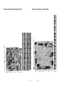
1
SERVICE MANUAL
MODEL: LM-M340A/D/X,LMS-M340, LM-M342A/X,LMS-M342
MINI HI-FI SYSTEM
SERVICE MANUAL
CAUTION
BEFORE SERVICING THE UNIT, READ THE “SAFETY PRECAUTIONS” IN THIS MANUAL.
MODEL: LM-M340A/D/X,LMS-M340
LM-M342A/X,LMS-M342
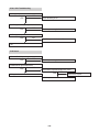
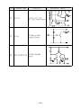
[CONTENTS]
❍ SECTION 1. GENERAL
• SERVICING PRECAUTIONS . . . . . . . . . . . . . . . . . . . . . . . . . . . . . . . . . . . . . . . . . . . . . . . 1-2
• ESD PRECAUTIONS . . . . . . . . . . . . . . . . . . . . . . . . . . . . . . . . . . . . . . . . . . . . . . . . . . . . . 1-4
• SPECIFICATION . . . . . . . . . . . . . . . . . . . . . . . . . . . . . . . . . . . . . . . . . . . . . . . . . . . . . . . . . .1-5
❍ SECTION 2. ELECTRICAL SECTION
• ADJUSTMENTS . . . . . . . . . . . . . . . . . . . . . . . . . . . . . . . . . . . . . . . . . . . . . . . . . . . . . . . . . 2-1
• AUDIO PART ELECTRICAL TROUBLESHOOTING GUIDE . . . . . . . . . . . . . . . . . . . . . . . . . 2-2
• BLOCK DIAGRAM . . . . . . . . . . . . . . . . . . . . . . . . . . . . . . . . . . . . . . . . . . . . . . . . . . . . . . 2-39
• SCHEMATIC DIAGRAMS . . . . . . . . . . . . . . . . . . . . . . . . . . . . . . . . . . . . . . . . . . . . . . . . . 2-41
• WIREING DIAGRAM . . . . . . . . . . . . . . . . . . . . . . . . . . . . . . . . . . . . . . . . . . . . . . . . . . . . . 2-53
• PRINTED CIRCUIT DIAGRAMS . . . . . . . . . . . . . . . . . . . . . . . . . . . . . . . . . . . . . . . . . . . . 2-55
❍ SECTION 3. EXPLODED VIEWS
• CABINET AND MAIN FRAME SECTION . . . . . . . . . . . . . . . . . . . . . . . . . . . . . . . . . . . . . . . .3-1
• TAPE DECK MECHANISM (A/R & A/S : LEFT A/S DECK) . . . . . . . . . . . . . . . . . . . . . . . . . . .3-3
• TAPE DECK MECHANISM (A/R & A/S : RIGHT A/R DECK) . . . . . . . . . . . . . . . . . . . . . . . . . .3-5
• CD MECHANISM . . . . . . . . . . . . . . . . . . . . . . . . . . . . . . . . . . . . . . . . . . . . . . . . . . . . . . . . . 3-7
❍ SECTION 4. SPEAKER PART
• SPEAKER PART . . . . . . . . . . . . . . . . . . . . . . . . . . . . . . . . . . . . . . . . . . . . . . . . . . . . . . . . . .4-1
❍ SECTION 5. REPLACEMENT PARTS LIST
• REPLACEMENT PARTS LIST . . . . . . . . . . . . . . . . . . . . . . . . . . . . . . . . . . . . . . . . . . . . . . . .5-1
- 1-1 -
SECTION 1. GENERAL
❏ SERVICING PRECAUTIONS
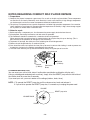
NOTES REGARDING HANDLING OF THE PICK-UP
1. Notes for transport and storage
1) The pick-up should always be left in its conductive bag until immediately prior to use.
2) The pick-up should never be subjected to external pressure or impact.
Storage in conductive bag
Drop impact
2. Repair notes
1) The pick-up incorporates a strong magnet, and so should never be brought close to magnetic materials.
2) The pick-up should always be handled correctly and carefully, taking care to avoid external pressure and
impact. If it is subjected to strong pressure or impact, the result may be an operational malfunction and/or
damage to the printed-circuit board.
3) Each and every pick-up is already individually adjusted to a high degree of precision, and for that reason
the adjustment point and installation screws should absolutely never be touched.
4) Laser beams may damage the eyes!
Absolutely never permit laser beams to enter the eyes!
Also NEVER switch ON the power to the laser output part (lens, etc.) of the pick-up if it is damaged.
NEVER look directly at the laser beam, and don’t let
contact fingers or other exposed skin.
5) Cleaning the lens surface
If there is dust on the lens surface, the dust should be cleaned away by using an air bush (such as used
for camera lens). The lens is held by a delicate spring. When cleaning the lens surface, therefore, a cotton
swab should be used, taking care not to distort this.
Pressure
Magnet
Pressure
How to hold the pick-up
Cotton swab
Conductive Sheet
6) Never attempt to disassemble the pick-up.
Spring by excess pressure. If the lens is extremely dirty, apply isopropyl alcohol to the cotton swab. (Do
not use any other liquid cleaners, because they will damage the lens.) Take care not to use too much of
this alcohol on the swab, and do not allow the alcohol to get inside the pick-up.
- 1-2 -
NOTES REGARDING COMPACT DISC PLAYER REPAIRS
1. Preparations
1) Compact disc players incorporate a great many ICs as well as the pick-up (laser diode). These components
are sensitive to, and easily affected by, static electricity. If such static electricity is high voltage, components
can be damaged, and for that reason components should be handled with care.
2) The pick-up is composed of many optical components and other high-precision components. Care must be
taken, therefore, to avoid repair or storage where the temperature of humidity is high, where strong magnetism is present, or where there is excessive dust.
2. Notes for repair
1) Before replacing a component part, first disconnect the power supply lead wire from the unit
2) All equipment, measuring instruments and tools must be grounded.
3) The workbench should be covered with a conductive sheet and grounded.
When removing the laser pick-up from its conductive bag, do not place the pick-up on the bag. (This is
because there is the possibility of damage by static electricity.)
4) To prevent AC leakage, the metal part of the soldering iron should be grounded.
5) Workers should be grounded by an armband (1M Ω)
6) Care should be taken not to permit the laser pick-up to come in contact with clothing, in order to prevent static electricity changes in the clothing to escape from the armband.
7) The laser beam from the pick-up should NEVER be directly facing the eyes or bare skin.
Armband
Resistor
(1 Mohm)
Resistor
(1 Mohm)
Conductive
Sheet
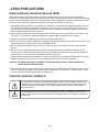
CLEARING MALFUNCTION
You can reset your unit to initial status if malfunction occur(button malfunction, display, etc.).
Using a pointed good conductor(such as driver), simply short the RESET jump wire on the inside of
the volume knob for more than 3 seconds.
If you reset your unit, you must reenter all its settings(stations, clock, timer)
NOTE: 1. To operate the RESET jump wire, pull the volume rotary knob and release it.
2. If you wish to operate the RESET jump wire, it is necessary to unplug the power cord.
VOLUME
UP
RESET jump wire
VOLUME KNOB
DOWN
- 1-3 -
❏ ESD PRECAUTIONS
Electrostatically Sensitive Devices (ESD)
Some semiconductor (solid state) devices can be damaged easily by static electricity. Such components
commonly are called Electrostatically Sensitive Devices (ESD). Examples of typical ESD devices are integrated
circuits and some field-effect transistors and semiconductor chip components. The following techniques should
be used to help reduce the incidence of component damage caused by static electricity.
1. Immediately before handling any semiconductor component or semiconductor-equipped assembly, drain off
any electrostatic charge on your body by touching a known earth ground. Alternatively, obtain and wear a
commercially available discharging wrist strap device, which should be removed for potential shock reasons
prior to applying power to the unit under test.
2. After removing an electrical assembly equipped with ESD devices, place the assembly on a conductive surface such as aluminum foil, to prevent electrostatic charge buildup or exposure of the assembly.
3. Use only a grounded-tip soldering iron to solder or unsolder ESD devices.
4. Use only an anti-static solder removal device. Some solder removal devices not classified as "anti-static" can
generate electrical charges sufficient to damage ESD devices.
5. Do not use freon-propelled chemicals. These can generate electrical charges sufficient to damage ESD
devices.
6. Do not remove a replacement ESD device from its protective package until immediately before you are
ready to install it. (Most replacement ESD devices are packaged with leads electrically shorted together by
conductive foam, aluminum foil or comparable conductive materials).
7. Immediately before removing the protective material from the leads of a replacement ESD device, touch the
protective material to the chassis or circuit assembly into which the device will by installed.
CAUTION : BE SURE NO POWER IS APPLIED TO THE CHASSIS OR CIRCUIT, AND OBSERVE ALL
OTHER SAFETY PRECAUTIONS.
8. Minimize bodily motions when handing unpackaged replacement ESD devices. (Otherwise harmless motion
such as the brushing together of your clothes fabric or the lifting of your foot from a carpeted floor can generate static electricity sufficient to damage an ESD device).
CAUTION. GRAPHIC SYMBOLS
THE LIGHTNING FLASH WITH APROWHEAD SYMBOL. WITHIN AN EQUILATERAL TRIANGLE, IS
INTENDED TO ALERT THE SERVICE PERSONNEL TO THE PRESENCE OF UNINSULATED “DANGEROUS VOLTAGE” THAT MAY BE OF SUFFICIENT MAGNITUDE TO CONSTITUTE A RISK OF
ELECTRIC SHOCK.
THE EXCLAMATION POINT WITHIN AN EQUILATERAL TRIANGLE IS INTENDED TO ALERT THE
SERVICE PERSONNEL TO THE PRESENCE OF IMPORTANT SAFETY INFORMATION IN SERVICE
LITERATURE.
- 1-4 -
❏ SPECIFICATIONS
- 1-5 -
MEMO
- 1-6 -
SECTION 2. ELECTRICAL
❏ ADJUSTMENTS
This set has been aligned at the factory and normally will not require further adjustment. As a result, it is
not recommended that any attempt is made to modificate any circuit. If any parts are replaced or if anyone tampers with the adjustment, realignment may be necessary.
IMPORTANT
1. Check Power-source voltage.
2. Set the function switch to band being aligned.
3. Turn volume control to minimum unless otherwise noted.
4. Connect low side of signal source and output indicator to chassis ground unless otherwise specified.
5. Keep the signal input as low as possible to avoid AGC and AC action.
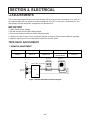
TAPE DECK ADJUSTMENT
1. AZIMUTH ADJUSTMENT
Deck Mode
Test Tape
Test Point
Adjustment
Adjust for
Palyback
MTT-114
Speaker Out
DECK Screw
Azimuth Screw
Maximum
Electronic
Voltmeter
Head
Playback Mode
R ch
Speaker Out
L out
L ch
Test Tape
MTT-114
Dual-trace
synchroscope
CH1 CH2
Unit
GND
R out
Figure 1. Azimuth Adjustment Connection Diagram
- 2-1 -
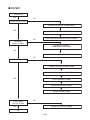
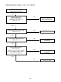
❏ ELECTRICAL TROUBLESHOOTING GUIDE
■ AUDIO PART
P-SENS PART CHECK
ZD 901(5V) Voltage check
YES
NO
Half-wave rectification wave form check
YES
IC301 6PIN PATTERN Check
NO
D713 Replacement
R783 check, then ZD901 replacement
VKK CHECK
CN302 28pin DC -33V check
YES
ZD902 -33V check
YES
IC301 87PIN check
NO
ZD902 replacement
Q903 turn on check
YES
NO
Pattern disconnection check
C916 -33V and less check
YES
NO
D912, D911 replacement
YES
Q903 replacement
normal
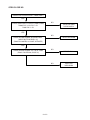
- 2-2 -
NO
Refer to power
supply check
POWER CHECK
Every kinds of Fuse check
YES
NO
Fuse replace
C901(+), C902(-) DC power output check
YES
NO
CN901 1, 5 AC voltage output check
YES
NO
Power supply Ass’y check
and transformer replacent
D901 replacement
C903(+) DC power output check
YES
NO
CN901, 9, 10 pin DC power output check
YES
IC901, IC902 power output check
YES
NO
NO
Power supply Ass’y check
and transformer replacent
D902, D903, D904, D905 (1SR35)
check and replacement
IC901, IC902 check and replacement
IC903 power output check (12V)
YES
NO
IC301 77PIN 5V check
YES
NO
IC301 5V Power output
PN302/CN302 13 PIN check
IC904 replacement
Check
CN513 7PIN 5V check (at CD Function)
YES
NO
Q904(A1273) Base Low check
YES
normal operation
NO
IC501(BU2090) 14PIN HIGH check
YES NO
IC5019BU2090 check & replace
Q905 Base HIGH(C103M)
Check and replace defective
Q904, CD Ass’y check replacement
- 2-3 -
Muting circuit Troubleshooting (if MUTE)
Q702(A102) Base “LOW”
NO
YES
Q702 Base and GND operation
status check
Q701, Q751(IC302) Base “LOW” check
YES
MUTE
No sound
IC 601 12, 27 PIN Output check
YES
NO
Refer to IC601(TDA7468D) IC specification
IC701 input check (14PIN)
YES
NO
Refer Muting troubleshooting
IC701 output check (6PIN)
YES
NO
IC701 12PIN (over 2V) check and power
supply circuit check
RY701 check
NO
YES
Refer SPK replay troubleshooting
normal
- 2-4 -
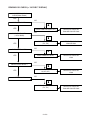
SPK Relay Troubleshooting
D704(+) 12V check
NO
YES
Refer power check
Q704 Collector “Low” check
NO
YES
Q704 Base “High”
YES
Output check
NO
YES
RELAY Replacement
(RY701)
Q704 Replacement
normal operation
Specific FUNCTION MODE has no sound
TAPE
YES
IC601 3,26 PIN signal input check
YES
Refer IC202 Troubleshooting
AUX
YES
IC601 5, 24 PIN signal input check
YES
JK600 signal input check
- 2-5 -
NO
Refer IC501(BU2090) Troubleshooting
CD
YES
IC601 6,23 PIN signal input check
YES
CN513 1,3 PIN signal check and refer to CD Troubleshooting
TUNER
YES
IC601 4, 25 PIN signal input check
YES
Refer TUNERMODULE
MIC
YES
IC602 2PIN check
YES
Refer to IC404 Troubleshooting
IC301 Troubleshooting
C301 31, 32, 51, 88 power applied check
YES
NO
Refer to power supply check
IC301 6PIN 5V applied check
YES
NO
P-SENS terminal check
X301 oscilates or not
YES
NO
X301 replacement
When IC301 92Pin voltage input. High➞Low➞High
YES
NO
RESET circuit check
IC301 replace
- 2-6 -
IC501 Troubleshooting
IC501 16PIN power applied check
NO
YES
Refer to power supply check
IC501 2, 3 PIN CLK Data check
NO
YES
IC301 13, 14 PIN data check
(When switched to CD, TAPE Function)
YES
CONTROL function check
NO
Refer to IC301 Troubleshooting
NO
IC501 replace
YES
Pattern check between IC301 and IC501
normal
IC601(TDA7468D) Troubleshooting
IC601 1PIN power applied check
NO
YES
Refer to power supply check
IC601 15,14 Pulse waveform check
(with tunning VOL DIAL)
NO
YES
IC301 15, 16, 66, 67, 68, 69 Pin check
YES
IC601 7,22 Pin waveform output check
YES
NO
IC601 replace
YES
IC601 12,17Pin waveform output check
NO
IC301 Troubleshooting
MICOM(82,83) - IC401(21,22) Pattern check
IC601 8,21Pin waveform input check
YES
NO
IC601 replacement
normal
- 2-7 -
IC701, IC751 Troubleshooting
3PIN signal input check
YES
NO
Refer to Muting circuit
8, 15Pin(-), 7, 13Pin(+) voltage check
YES
NO
Refer to power supply check
14 Pin signal output check
YES
NO
9, 10PIN power check (over 5V)
OK
PLAY check
IC202 18Pin VCC power applied
YES
NO
Refer to power supply check
IC202 5,20 Pin signal output check
YES
NO
Deck Mecha operation performance check
YES
Muting circuit check
IC202 replacement
- 2-8 -
NO
Deck Mecha replace
Rec check (Q252, Q202 ON : R273, R223 High)
IC202 11,14PIN signal input check
NO
YES
Q253, Q203 Base "Low" check
YES
IC202 9,16 Pin signal input check
NO
NO
Refer to IC203 Troubleshooting
Q253,Q203 replacement
IC202 18Pin VCC voltage check
YES
IC201 6(12V), 4 Pin High check
YES
NO
Power check, IC203 Troubleshooting check
L203 2,3PIN oscilation check
YES
NO
C236(+) power supply check
YES
Deck replacement
NO
Refer to power supply check
Q208 Base 0.6V supplied check
YES
NO
IC203 Troubleshooting check
Q208 Collector Low
YES
NO
Q208 replacement
Q207 replace
YES
NO
normal
Dubbing check ("NORMAL or REC"//"HIGH")
Q252, 202 "OFF"//"ON" : R273,223 "Low"//"HIGH"
YES
Q253,203 "ON"//"OFF"
NO
IC203 Troubleshooting check
YES
Refer to REC Check
- 2-9 -
L203 replacement
■ CD PART
TURN ON CD
YES
NO
OPEN CLOSE CHECK
CONNECTOR CHECK ( PN808,PN807 )
YES
CHECK POWER SUPPLY CIRCUIT( PN808 )
CHECK MICOM INTERFACE CIRCUIT( PN807 )
NO
“ READING ”
DISPLAY CHECK
CONNECTOR CHECK
( PN808,PN807,PN802,PN801 )
YES
CHECK MICOM INTERFACE CIRCUIT( PN807 )
NO
READING OK CHECK
CONNECTOR CHECK(PN801,PN802)
CHECK PICKUP MOVEMENT
YES
CHECK BA5810FP (IC803)
CHECK MN6627933CG (IC801)
CHECK AN22004 (IC802)
IF PLAY, AUDIO
OUTPUT CHECK
NO
CONNECTOR CHECK (PN808)
YES
OK
- 2-10 -
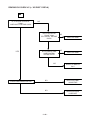
OPEN CLOSE NG
CONNECTOR LOCKING CHECK ( PN808,PN807 )
YES
CHECK POWER SUPPLY CIRCUIT( PN808 ,PN807)
PN808 PIN 5 = 6.2V, PIN 7 = 5V
PN807 PIN 1 = 5V
NO
DEFECTIVE MAIN
POEWR SUPPLY
YES
NO
DEFECTIVE MICOM
CHECK VOLTAGE CHANGE OF OPEN CLOSE ,
AND BTLMUTE VOLTAGE(= 5V)
(PN807 PIN 20:OPEN, 19:CLOSE, 4:BTLMUTE)
YES
CHECK VOLTAGE CHANGE LO+, LO- OF IC803
(PN807, PIN OPEN:20, CLOSE:19)
NO
DEFECTIVE IC803
NO
- 2-11 -
DEFECTIVE
MECHANISM
READING DISPLAY CHECK (= ONLY “CD “DISPLAY)
CONNECTOR LOCKING CHECK
(PN808,PN807,PN802,PN801 )
YES
NO
CHECK POWER SUPPLY
PORT( PN808 ,PN807)
PN808 PIN 5 = 6.2V, PIN 7 = 5V
PN807 PIN 1 = 5V
DEFECTIVE CONNECTOR OR
MAIN POWER SUPPLAY
YES
NO
CHECK VOLTAGE THE PIN 2 OF IC805
IC805 PIN2 : 3.3V
DEFECTIVE IC805
YES
NO
CHECK RESET SIGNAL OF PN807
PN807 PIN12 : 5V
DEFECTIVE MICOM OR
CONNECTOR
YES
CHECK MICOM INTERFACE
CIRCUIT( PN807 )
PN807 PIN 11,13,14,15 SIGNAL CHECK
(11: STAT, 13: MDATA, 14:MCLK, 15:MLD)
CHECK THE WAVE FORM #1
NO
DEFECTIVE MICOM OR
CONNECTOR
YES
NO
DEFECTIVE IC801
- 2-12 -
READING OK CHECK (= “NO DISC” DISPLAY)
CONNECTOR LOCKING
CHECK(PN801,PN802)
YES
NO
DOES SLED MOVE ?
A
YES
DOES LENSE MOVE ?
(= UP & DOWN)
CHECK PN802 PIN 3,4( SL+,SL-)
DEFECTIVE PICKUP OR
IC803 OR IC801 OR IC802
NO
B
CHECK PN801 PIN 13,16
( FA-, FA+)
YES
DEFECTIVE PICKUP OR
IC803 OR IC801
NO
DOES LASER LIGHT ?
C
CHECK PN802 PIN 10( LD )
YES
DOES SPINDLE ROTATE ?
DEFECTIVE PICKUP OR
IC802
NO
D
CHECK PN802 PIN
5,6( SP+,SP-)
YES
DEFECTIVE PICKUP OR
IC803
NO
IS READING OK ?
E
CHECK PN801 PIN 14,15
(TA- ,TA+)
- 2-13 -
DEFECTIVE PICKUP OR
IC803 OR IC801 OR IC802
READING OK CHECK #A (= “NO DISC” DISPLAY)
A
DOES SL+ WAVEFORM APPEAR AT
( IC803 PIN14 AND PN802 PIN3)
WAVEFORM #2
SLED MOTOR WAVE
NO
DOES SLIN WAVEFORM
APPEAR AT
( IC803 PIN 5)
WAVEFORM #2
SLED DRIVE WAVE
NO
DEFECTIVE IC801
YES
NO
DEFECTIVE IC803
NO
CHECK PN802 CONNECTOR LINE
DEFECTIVE PN802
CONNECTOR
YES
NO
- 2-14 -
DEFECTIVE PICKUP
SLED MOTOR
READING OK CHECK #B (= “NO DISC” DISPLAY)
B
DOES FA+ WAVEFORM APPEAR AT
( IC803 PIN15 AND PN801 PIN16)
WAVEFORM #3
FOCUS COIL DRIVE WAVE
NO
DOES FAIN- WAVEFORM
APPEAR AT
( IC803 PIN 26)
WAVEFORM #3
FOCUS DRIVE WAVE
NO
DEFECTIVE IC801
YES
NO
DEFECTIVE IC803
NO
CHECK PN801 CONNECTOR LINE
DEFECTIVE PN801
CONNECTOR
YES
NO
- 2-15 -
DEFECTIVE PICKUP
FOCUS ACTUATOR
READING OK CHECK #C (= “NO DISC” DISPLA)
C
IS ?V APPLIED TO PIN10 OF
PN801
LASER SUPPLY VOLTAGE CHECK
NO
IS 3.3 V APPLIED TO
PIN3 OF IC802
RF IC SUPPLY VOLTAGE
CHECK
YES
IS 2.0 V PIN2 OF IC802
LASER CONTROL
VOLTAGE CHECK
NO
CHECK PN801 CONNECTOR LINE
NO
DEFECTIVE IC805
NO
DEFECTIVE IC802
DEFECTIVE Q801 OR
D811
NO
DEFECTIVE PN801
CONNECTOR
NO
DEFECTIVE PICKUP
LASER PART
- 2-16 -
READING OK CHECK #D (= “NO DISC” DISPLAY)
D
DOES SP+ WAVEFORM APPEAR AT
( IC803 PIN12 AND PN802 PIN6)WAVEFORM #4
SPINDLE MOTOR DRIVE WAVE
NO
DOES SPIN WAVEFORM
APPEAR AT( IC803 PIN 6)
WAVEFORM #4
SPINDLE DRIVE WAVE
NO
DEFECTIVE IC801
YES
NO
DEFECTIVE IC803
NO
CHECK PN802 CONNECTOR LINE
NO
- 2-17 -
DEFECTIVE PN802
CONNECTOR
DEFECTIVE PICKUP
SPINDLE MOTOR
READING OK CHECK #E (= “NO DISC” DISPLAY)
E
DOES TA+ WAVEFORM APPEAR AT
( IC803 PIN17 AND PN801 PIN15)
WAVEFORM #5
TRACKING COIL DRIVE WAVE
NO
DOES TAIN- WAVEFORM
APPEAR AT
( IC803 PIN 23)
WAVEFORM #5
TRACKING DRIVE WAVE
NO
DEFECTIVE IC801
YES
NO
DEFECTIVE IC803
CHECK PN802 CONNECTOR LINE
NO
DEFECTIVE PN802
CONNECTOR
NO
DEFECTIVE PICKUP OR
IC802
NO
DEFECTIVE PICKUP OR
IC802
YES
DOES ARF SIGNAL APPEAR?
(IC802 PORT 8)
WAVEFORM #6
YES
DOES FE, TE SIGNAL APPEAR?
(IC802 PORT FE:23, TE:21)
WAVEFORM #6
NO
- 2-18 -
DEFECTIVE IC801
WAVEFORMS OF MAKOR CHECK POINT
- 2-19 -
#4. SPINDLE DRIVE AND MOTOR WAVEFORM
(IC503 pin6, 1 2) when TOC reading
#5. TRACK DRIVE AND MOTOR WAVEFORM
(TP560, IC503 pin23) during normal play
#6. RF, TRACKING AND FOCUS ERROR WAVEFORM
(IC502 pin8, 2 1 , 23) during normal play
- 2-20 -
❏ INTERNAL BLOCK DIAGRAM of ICs
• NJM2706M (IC1)
BLOCK DIAGRAM
PIN CONFIGURATION
- 2-21 -
• BA3126N (IC201)
BLOCK DIAGRAM
PIN CONFIGURATION
- 2-22 -
• KIA6289N (IC202)
BLOCK DIAGRAM
- 2-23 -
- 2-24 -
- 2-25 -
- 2-26 -
• BU2090F (IC 501)
12-bit, Serial IN, Parallel OUT driver
Vss 1
DATA 2
Control circuit
12-bit shift register
CLOCK 3
16 VDD
15 Q11
14 Q10
Latch
Q0 4
Q1 5
BU2090/F/FS
1
2
3
4
5
6
7
8
9
10
11
12
13
14
15
16
Pin No.
BU2092/F
1
2
3
4
5
6
7
8
9
10
11
12
13
14
15
16
17
18
13 Q9
Output buffer
(open drain)
12 Q8
Q2 6
11 Q7
Q3 7
10 Q6
Q4 8
9 Q5
BU2092/FV
1
2
3
4
5
6
7
8
9
10
11
12
13
14
15
16
17
18
19
20
- 2-27 -
Pin name
Function
Vss
DATA
CLOCK
LCK
Q0
Q1
Q2
Q3
Q4
Q5
Q6
N.C.
N.C.
Q7
Q8
Q9
Q10
Q11
OE
VDD
GND
Serial data input
Data shift clock input
Data latch clock input
parallel data output
parallel data output
parallel data output
parallel data output
parallel data output
parallel data output
parallel data output
Not connected
Not connected
parallel data output
parallel data output
parallel data output
parallel data output
parallel data output
Output Enable
Power supply
• TDA7468D (IC601)
BLOCK DIAGRAM
- 2-28 -
PIN CONFIGURATION
- 2-29 -
• STK403-070 (IC701)
BLOCK DIAGRAM
- 2-30 -
• N6627933CG (IC801)
Pin Assignment
Note) Pins marked with an asterisk can be switched to different signals by using microcontroller
commands.
- 2-31 -
Internal Block Diagram
- 2-32 -
Pin Descriptions
Pin No.
1
2
3
4
5
6
7
8
9
10
11
12
13
14
15
16
17
18
19
20
21
22
23
24
25
26
27
28
29
30
31
32
33
34
35
36
37
38
39
40
41
42
43
44
45
46
47
48
49
50
51
52
53
54
55
Symbol
D11
D10
D9
D8
UDQM
SDRCK
A11
A9
A8
A7
A6
A5
A4
LDQM
NWE
NCAS
NRAS
NCS
A3
A2
A1
A0
DRVDD1
DVSS1
A10
*BA1
*BA0
DVDD1
SPOUT
*SPPOL
TRVP
*TRVM
*TRVP2
*TRVM2
TRP
*TRM
FOP
*FOM
IOVDD1
TBAL
FBAL
FE
TE
ADPVCC
RFENV
LDON
NRFDET
OFT
BDO
AVDD1
IREF
ARF
DSLF
PWMSEL
PLLF
I/O
I/O
I/O
I/O
I/O
O
O
O
O
O
O
O
O
O
O
O
O
O
O
O
O
O
O
I
I
O
O
O
I
O
O
O
O
O
O
O
O
O
O
I
O
O
I
I
I
I
O
I
I
I
I
I
I
O
I
O
Function
DRAM data signal I/O 11
DRAM data signal I/O 10
DRAM data signal I/O 9
DRAM data signal I/O 8
SDRAM upper byte data mask signal output
SDRAM clock signal output
DRAM address signal output 11
DRAM address signal output 9
DRAM address signal output 8
DRAM address signal output 7
DRAM address signal output 6
DRAM address signal output 5
DRAM address signal output 4
SDRAM lower byte data mask signal output
DRAM write enable signal output
DRAM CAS control signal output
DRAM RAS control signal output
SDRAM chip select signal output
DRAM address signal output 3
DRAM address signal output 2
DRAM address signal output 1
DRAM address signal output 0
Power supply 1 for DRAM interface I/O
Ground 1 for digital circuits
DRAM address signal output 10
SDRAM bank selection signal output 1
SDRAM bank selection signal output 0
Power supply 1 for internal digital circuits
Spindle drive signal output (absolute value)
Spindle drive signal output (polarity)
Traverse drive signal output (positive polarity)
Traverse drive signal output (negative polarity)
Traverse drive signal output 2 (positive polarity)
Traverse drive signal output 2 (negative polarity)
Tracking drive signal output (positive polarity)
Tracking drive signal output (negative polarity)
Focus drive signal output (positive polarity)
Focus drive signal output (negative polarity)
Power supply 1 for digital I/O
Tracking balance adjustment signal output
Focus balance adjustment signal output
Focus error signal input
Tracking error signal input
Voltage input for supply voltage monitor
RF envelope signal input
Laser ON signal output
RF detectoion signal input
Off-track signal input
Dropout signal input
Power supply 1 for analog circuits
Analog reference current input
RF signal input
DSL loop filter pin
PWM output mode selection input Low: Direct High: 3-state
PLL loop filter pin (for phase comparison)
- 2-33 -
Pin No.
56
57
58
59
60
61
62
63
64
65
66
67
68
69
70
71
72
73
74
75
76
77
78
79
80
81
82
83
84
85
86
87
88
89
90
91
92
93
94
95
96
97
98
99
100
Symbol
PLLFO
AVSS1
LOOUTL
LOVSS1
LOOUTR
LOVDD1
N.C.
TMON1
N.C.
N.C.
TMON2
DVDD3
DVSS2
*EXT0
*EXT1
*EXT2
MCLK
MDATA
MLD
*STAT
*BLKCK
*SMCK
*PMCK
*TX
*FLAG
NRST
NTEST
DVSS3
X1
X2
IOVDD2
DVDD2
D2
D1
D0
D3
D4
D5
D6
D7
D15
D14
DRVDD2
D13
D12
I/O
O
I
O
I
O
I
O
O
I
I
I/O
I/O
I/O
I
I
I
O
O
O
O
O
O
I
I
I
I
O
I
I
I/O
I/O
I/O
I/O
I/O
I/O
I/O
I/O
I/O
I/O
I
I/O
I/O
Function
PLL loop filter pin (for speed comparison)
Ground 1 for analog circuits
L-ch audio output for line-out output
Ground for line-out output
R-ch audio output for line-out output
Power supply for line-out output
Test monitor output 1
Test monitor output 2
Power supply 3 for digital circuits
Ground 2 for digital circuits
Expansion I/O port 0
Expansion I/O port 1
Expansion I/O port 2
Microcontroller command clock signal input
Microcontroller command data signal input
Microcontroller command load signal input
Status signal output
Subcode block clock signal output
4.2336-/8.4672-MHz clock signal output
88.2-kHz clock signal output
Digital audio interface signal output
Flag signal output
LSI reset signal input
Test mode setting input
Ground 3 for digital circuits
Crystal oscillator circuit input
Crystal oscillator circuit output
Power supply 2 for digital I/O
Power supply 2 for internal digital circuits
DRAM data signal I/O 2
DRAM data signal I/O 1
DRAM data signal I/O 0
DRAM data signal I/O 3
DRAM data signal I/O 4
DRAM data signal I/O 5
DRAM data signal I/O 6
DRAM data signal I/O 7
DRAM data signal I/O 15
DRAM data signal I/O 14
Power supply 2 for DRAM interface I/O
DRAM data signal I/O 13
DRAM data signal I/O 12
- 2-34 -
• BA5810FP (IC803)
• KA3082 (IC 807)
Bi-Directional DC Motor Driver
Description
The KA3082 is a monolithic integrated circuit designed for driving bi-directional DC motor with braking and
speed control, and it is suitable for the loading motor driver of VCR, CDP, and TOY systems. The speed control can be achieved by adjusting the external voltage of the speed control pin. It has two pins of logic inputs
for controlling the forward/ reverse and braking.
- 2-35 -
• KIA7805AP/API (IC 901)
THREE TERMINAL POSITIVE VOLTAGE REGULATORS 5V, 6V, 8V, 9V, 10V, 12, 15V, 18V, 24V.
EQUIVALENT CIRCUIT
- 2-36 -
- 2-37 -
• KIA78R12PI (IC 903)
4 TERMINAL LOW DROP VOLTAGE REGULATOR
The KIA78RXX Series are Low Drop Voltage Regulator suitable for various electronic equipments. It provides
constant voltage power source with TO-220 4 termainal lead full molded PKG. The Regulator has multi function such as over current protection, overheat protection and ON/OFF control.
Block Diagram
- 2-38 -
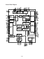
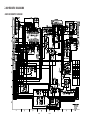
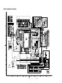
❏ BLOCK DIAGRAM
2-39
2-40
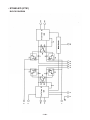
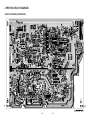
❏ SCHEMATIC DIAGRAMS
• MAIN SCHEMATIC DIAGRAM
2-41
2-42
• MAIN-OAO SCHEMATIC DIAGRAM
2-43
2-44
• DECK SCHEMATIC DIAGRAM
2-45
2-46
• FRONT SCHEMATIC DIAGRAM
2-47
2-48
• CDP SCHEMATIC DIAGRAM
2-49
2-50
• POWER SCHEMATIC DIAGRAM
NOTE: Warning
Parts that are shaded are critical With respect
to risk of fire or electrical shock.
2-51
NOTE:
1. Shaded(■) parts are critical for safety.Replace only
with specified part number.
2. Voltages are DC-measured with a digital voltmefer
during Play mode.
2-52
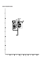
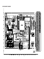
❏ WIRING DIAGRAM
CN901
PN901
PN401
2-53
2-54
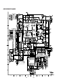
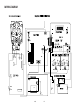
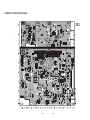
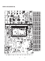
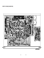
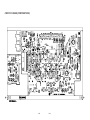
❏ PRINTED CIRCUIT DIAGRAMS
• MAIN P.C. BOARD (SOLDER SIDE)
2-55
2-56
• MAIN P.C. BOARD (COMPONENT SIDE)
2-57
2-58
• POWER P.C. BOARD (SOLDER SIDE)
2-59
2-60
• POWER P.C. BOARD (COMPONENT SIDE)
2-61
2-62
• FRONT P.C. BOARD (SOLDER SIDE)
2-63
2-64
• FRONT P.C. BOARD (COMPONENT SIDE)
2-65
2-66
• CD MAIN P.C. BOARD (COMPONENT SIDE)
• CD MAIN P.C. BOARD (SOLDER SIDE)
2-67
2-68
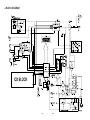
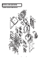
SECTION 3. EXPLODED VIEWS
❏ CABINET AND MAIN FRAME SECTION
A26
270
351
354
355
271
269
454
A41
266
268
267
273
260
272
A46
A47
302
265
305
264
450
286
263
259
262
303
MIC Optio n
306
284
252
254
MIC Optio n
285
454
354
251
257
253
284
287
MIC Optio n
A43
454
258
261
454
250
255
A00
256
287
3-1
3-2
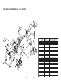
• TAPE DECK MECHANISM (A/R & A/S : LEFT A/S DECK)
021
505
019
020
018
007
008
017
016
003
015
022
401
023
009
401
502
501
026
025
403
504
009
401
030
011
027
401
028
013
029
3-3
3-4
LOCA. NO.
LG PART NO.
DESCRIPTION
A00
6720AG0002C
DECK,AUDIO
SPECIFICATION
CWM42FR47 TOKYO PIGEON L-DOUBL
003
6768R-PP03A
DECK MECHANISM PARTS
33-160-4309 PIGEON PRESS CASSE
007
6768R-GP03B
DECK MECHANISM PARTS
50-222-4578 PIGEON GEAR IDLER
008
6768R-SP01F
DECK MECHANISM PARTS
01-082-4598 PIGEON SPRING CWL4
009
6768R-MP01C
DECK MECHANISM PARTS
50-219-4014 PIGEON MOLD CWL44
011
6768R-SP01A
DECK MECHANISM PARTS
01-081-4601 PIGEON SPRING CWL4
013
6768R-SP03A
DECK MECHANISM PARTS
01-082-4686 PIGEON SPRING CRM4
015
6768R-AP01A
DECK MECHANISM PARTS
50-268-3016 PIGEON ARM CWL44
016
6768R-GP01H
DECK MECHANISM PARTS
50-093-4503 PIGEON GEAR CRL442
017
6768R-AP01C
DECK MECHANISM PARTS
50-239-4072 PIGEON ARM CWL44
018
6768R-GP01J
DECK MECHANISM PARTS
50-222-4428 PIGEON GEAR CRL442
019
6768R-SP01P
DECK MECHANISM PARTS
01-081-4678 PIGEON SPRING CRL4
020
6768R-BP01C
DECK MECHANISM PARTS
02-083-4188 PIGEON BELT/FELT C
021
6768R-LP01C
DECK MECHANISM PARTS
50-223-4429 PIGEON PULLEY/FLYW
022
6768R-VP03A
DECK MECHANISM PARTS
50-093-4748 PIGEON SOLENOID AS
023
6768R-GP03A
DECK MECHANISM PARTS
50-093-4810 PIGEON GEAR ASSY C
025
6768R-JP03B
DECK MECHANISM PARTS
50-093-31009 PIGEON PULLEY/FLY
026
6768R-SP01D
DECK MECHANISM PARTS
01-080-4609 PIGEON SPRING CWL4
027
6768R-DP01A
DECK MECHANISM PARTS
50-259-3342 PIGEON LEVER CWL44
028
6768R-RP01A
DECK MECHANISM PARTS
22-027-41054 PIGEON ROLLER CWL
029
6768R-MP01A
DECK MECHANISM PARTS
50-219-4033 PIGEON MOLD CWL44
030
6768R-EP03C
DECK MECHANISM PARTS
T21V0P PIGEON HEAD CWM42FF30
401
6768R-CP01B
DECK MECHANISM PARTS
GSE20A2005 PIGEON SCREW CWL44
403
6768R-CP01D
DECK MECHANISM PARTS
GSL10A1704 PIGEON SCREW CWL44
501
6768R-WP03A
DECK MECHANISM PARTS
GWN19S035040 PIGEON WASHER CRM
502
6768R-WP03B
DECK MECHANISM PARTS
03-000-4532 PIGEON WASHER CRM4
504
6768R-WP01D
DECK MECHANISM PARTS
GWP21X045020 PIGEON WASHER CWL
505
6768R-WP01E
DECK MECHANISM PARTS
GWP12X030040S PIGEON WASHER CW
• TAPE DECK MECHANISM (A/R & A/S : RIGHT A/R DECK)
006
021
506
001
505
037
020
019
018
007
016
008
017
402
401
002
A01
003
402
015
022
502
507
009
401
023
502
501
026
403
028
032
025
504
038
009
027
401
031
040
406
028
011
039
409
036
029
035
013
3-5
3-6
LOCA. NO.
A00
A01
001
002
003
006
007
008
009
011
013
015
016
017
018
019
020
021
022
023
025
026
027
028
029
031
032
035
036
037
038
039
040
401
402
403
406
409
501
502
504
505
506
507
LG PART NO.
6720AG0002C
6768R-UP03D
6768R-BP03D
6768R-BP03E
6768R-PP03A
6768R-QP03C
6768R-GP03B
6768R-SP01F
6768R-MP01C
6768R-SP01A
6768R-SP03A
6768R-AP01A
6768R-GP01H
6768R-AP01C
6768R-GP01J
6768R-SP01P
6768R-BP01C
6768R-LP01C
6768R-VP03A
6768R-GP03A
6768R-JP03B
6768R-SP01D
6768R-DP01A
6768R-RP01A
6768R-MP01A
6768R-SP04A
6768R-EP04A
6768R-PP04A
6768R-SP04B
6768R-JP03A
6768R-MP01D
6768R-MP02A
6768R-SP01M
6768R-CP01B
6768R-CP01A
6768R-CP01D
6768R-CP01G
6768R-CP02A
6768R-WP03A
6768R-WP03B
6768R-WP01D
6768R-WP01E
6768R-WP01H
6768R-WP01F
DESCRIPTION
DECK,AUDIO
DECK MECHANISM PARTS
DECK MECHANISM PARTS
DECK MECHANISM PARTS
DECK MECHANISM PARTS
DECK MECHANISM PARTS
DECK MECHANISM PARTS
DECK MECHANISM PARTS
DECK MECHANISM PARTS
DECK MECHANISM PARTS
DECK MECHANISM PARTS
DECK MECHANISM PARTS
DECK MECHANISM PARTS
DECK MECHANISM PARTS
DECK MECHANISM PARTS
DECK MECHANISM PARTS
DECK MECHANISM PARTS
DECK MECHANISM PARTS
DECK MECHANISM PARTS
DECK MECHANISM PARTS
DECK MECHANISM PARTS
DECK MECHANISM PARTS
DECK MECHANISM PARTS
DECK MECHANISM PARTS
DECK MECHANISM PARTS
DECK MECHANISM PARTS
DECK MECHANISM PARTS
DECK MECHANISM PARTS
DECK MECHANISM PARTS
DECK MECHANISM PARTS
DECK MECHANISM PARTS
DECK MECHANISM PARTS
DECK MECHANISM PARTS
DECK MECHANISM PARTS
DECK MECHANISM PARTS
DECK MECHANISM PARTS
DECK MECHANISM PARTS
DECK MECHANISM PARTS
DECK MECHANISM PARTS
DECK MECHANISM PARTS
DECK MECHANISM PARTS
DECK MECHANISM PARTS
DECK MECHANISM PARTS
DECK MECHANISM PARTS
SPECIFICATION
CWM42FR47 TOKYO PIGEON L-DOUBL
50-093-4895 PIGEON PWB UNIT CW
02-083-4254 PIGEON BELT/FELT C
02-083-4256 PIGEON BELT/FELT C
33-160-4309 PIGEON PRESS CASSE
50-093-4880 PIGEON MOTOR(ASSY)
50-222-4578 PIGEON GEAR IDLER
01-082-4598 PIGEON SPRING CWL4
50-219-4014 PIGEON MOLD CWL44
01-081-4601 PIGEON SPRING CWL4
01-082-4686 PIGEON SPRING CRM4
50-268-3016 PIGEON ARM CWL44
50-093-4503 PIGEON GEAR CRL442
50-239-4072 PIGEON ARM CWL44
50-222-4428 PIGEON GEAR CRL442
01-081-4678 PIGEON SPRING CRL4
02-083-4188 PIGEON BELT/FELT C
50-223-4429 PIGEON PULLEY/FLYW
50-093-4748 PIGEON SOLENOID AS
50-093-4810 PIGEON GEAR ASSY C
50-093-31009 PIGEON PULLEY/FLY
01-080-4609 PIGEON SPRING CWL4
50-259-3342 PIGEON LEVER CWL44
22-027-41054 PIGEON ROLLER CWL
50-219-4033 PIGEON MOLD CWL44
01-082-4731 PIGEON SPRING
50-093-41007 PIGEON HEAD ASSY
50-119-4915 PIGEON PRESS
01-081-4730 PIGEON SPRING
50-093-4674 PIGEON PULLEY/FLYW
50-219-4034 PIGEON MOLD CWL44
50-219-3900 PIGEON MOLD
01-080-4607 PIGEON SPRING CWL4
GSE20A2005 PIGEON SCREW CWL44
GSE10A2003 PIGEON SCREW CWL44
GSL10A1704 PIGEON SCREW CWL44
GSE20A2004 PIGEON SCREW CWL44
GSD10A2016 PIGEON SCREW
GWN19S035040 PIGEON WASHER CRM
03-000-4532 PIGEON WASHER CRM4
GWP21X045020 PIGEON WASHER CWL
GWP12X030040S PIGEON WASHER CW
GWP23X040020 PIGEON WASHER CWL
GWN21X040040 PIGEON WASHER CWL
• CD MECHANISM
416
151
159
156
422
418
165
419
155
173
164
LOCA.NO.
A26
A30
A35
151
153
155
156
159
162
163
164
165
166
167
168
169
170
171
172
173
175
177
184
185
186
187
416
417
418
419
420
421
422
170
171
153
163
168
162
417
169
166
417
167
416
177
172
175
3-7
3-8
PART NO
4405RCE008C
3041RB0002C
6717RCA001A
3390RB0002A
4470RB0005A
4681RBA001A
6871RF9211A
3390RB0001A
4400SB0001A
4470SB0003A
4470RB0003A
6871RZ7036A
4470RB0006A
4470RB0007A
4470RB0002A
4860SB0001A
3550SB0001A
524-012AAAA
3040RB0005A
4510RB0001A
4680SBP001A
4470RB0001A
4900RB0001A
3040SB0003A
4970RB0001A
4970RB0001B
88H-0004
88H-0002
353-025BAAA
88H-0003
353S353F
6756SBX001A
353-028H
DESCRIPTION
MECHANISM ASSEMBLY
BASE ASSEMBLY
PICK UP ASSY
TRAY
GEAR
MOTOR ASSEMBLY
PWB(PCB) ASSEMBLY,FRONT
TRAY
BELT
GEAR
GEAR
PWB(PCB) ASSEMBLY,OTHERS
GEAR
GEAR
GEAR
CLAMP
COVER
COVER
BASE
LEVER
MOTOR(MECH)
GEAR
DAMPER
BASE
SPRING
SPRING
CD MECHA PARTS
CD MECHA PARTS
SCREW
CD MECHA PARTS
SCREW
CD MECHANISM PARTS
SCREW
SPECIFICATION
CDM-H1503 3 CD CHANGER
PU(SPRING DAMPER)
KSM-213VSCM SONY FRONT LOADING
DISC(CDM-H1503)
TRAY (CDM-H1503)
TRAY (CDM-H1503)
1503 T/D SENSOR
LOADING(CDM-H1503)
MAIN(CDM-H1303)
PULLEY (CDM-H1303)
LOADING (CDM-H1503)
CDM-H1503 UP/DW/OP/CL
PU UP (CDM-H1503)
PU DOWN (CDM-H1503)
CAM (CDM-H1503)
DISC(CDM-H1303)
MAGNET(CDM-H1303)
CLAMP MAGNET (030X018X5T)
MAIN (CDM-H1503)
S/W CLOSE
OTHER . . .
MAIN (CDM-H1503)
RUBBER 3CD CHANGER
PU(CDM-H1303)
COIL 3 CD CHANGER
COIL 50 3CD CHANGER
3X12X12FNM
3X9X12FZMY
#NAME?
3X12X10FZMY
#NAME?
SCREW 2.6X10X10XFZMY CDM-H813
#NAME?
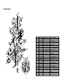
SECTION 4. SPEAKER SECTION
❏ MODEL: LMS-M340, LMS-M342
863
860
859
RIGHT
LFET
858
851
850
865
856
852
861
855
864
853
857
854
- 4-1 -
- 4-2 -