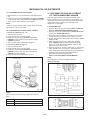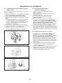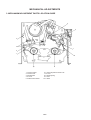
1
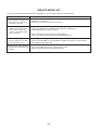
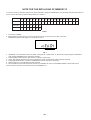
MVR2040A
SERVICE MANUAL
VIDEO CASSETTE RECORDER
ORIGINAL
MFR’S VERSION A
Design and specifications are subject to change without notice.
SERVICING NOTICES ON CHECKING
1. KEEP THE NOTICES
As for the places which need special attentions,
they are indicated with the labels or seals on the
cabinet, chassis and parts. Make sure to keep the
indications and notices in the operation manual.
2. USE THE DESIGNATED PARTS
The parts in this equipment have the specific
characters of incombustibility and withstand
voltage for safety. Therefore, the part which is
replaced should be used the part which has
the same character.
Especially as to the important parts for safety
which is indicated in the circuit diagram or the
table of parts as a
mark, the designated
parts must be used.
3. PUT PARTS AND WIRES IN THE
ORIGINAL POSITION AFTER
ASSEMBLING OR WIRING
There are parts which use the insulation
material such as a tube or tape for safety, or
which are assembled in the condition that
these do not contact with the printed board.
The inside wiring is designed not to get closer
to the pyrogenic parts and high voltage parts.
Therefore, put these parts in the original
positions.
4. PERFORM A SAFETY CHECK AFTER
SERVICING
Confirm that the screws, parts and wiring which
were removed in order to service are put in the
original positions, or whether there are the
portions which are deteriorated around the
serviced places serviced or not. Check the
insulation between the antenna terminal or
external metal and the AC cord plug blades.
And be sure the safety of that.
HOW TO ORDER PARTS
Please include the following informations when you order parts. (Particularly the VERSION LETTER.)
1. MODEL NUMBER and VERSION LETTER
The MODEL NUMBER can be found on the back of each product and the VERSION LETTER can be
found at the end of the SERIAL NUMBER.
2. PART NO. and DESCRIPTION
You can find it in your SERVICE MANUAL.
A1-1
CONTENTS
SERVICING NOTICES ON CHECKING .....................................................................................
HOW TO ORDER PARTS ...........................................................................................................
CONTENTS .................................................................................................................................
GENERAL SPECIFICATIONS ....................................................................................................
DISASSEMBLY INSTRUCTIONS
1. REMOVAL OF MECHANICAL PARTS AND P. C. BOARDS ............................................
2. REMOVAL OF DECK PARTS ............................................................................................
KEY TO ABBREVIATIONS .........................................................................................................
SERVICE MODE LIST .................................................................................................................
PREVENTIVE CHECKS AND SERVICE INTERVALS ..............................................................
NOTE FOR THE REPLACING OF MEMORY IC .......................................................................
SERVICING FIXTURES AND TOOLS ........................................................................................
PREPARATION FOR SERVICING .............................................................................................
MECHANICAL ADJUSTMENTS .................................................................................................
ELECTRICAL ADJUSTMENT ....................................................................................................
BLOCK DIAGRAMS
Y/C/AUDIO/CCD/HEAD AMP ..................................................................................................
SYSTEM CONTROL/SERVO/DECK .......................................................................................
TUNER .....................................................................................................................................
OPERATION/POWER .............................................................................................................
PRINTED CIRCUIT BOARDS
SYSCON/OPERATION/DECK .................................................................................................
SYSCON/OPERATION ............................................................................................................
SCHEMATIC DIAGRAMS
Y/C/AUDIO/CCD/HEAD AMP ..................................................................................................
SYSTEM CONTROL/SERVO ..................................................................................................
TUNER .....................................................................................................................................
POWER ...................................................................................................................................
OPERATION ...........................................................................................................................
DECK .......................................................................................................................................
INTERCONNECTION DIAGRAM ................................................................................................
WAVEFORMS .............................................................................................................................
MECHANICAL EXPLODED VIEW .............................................................................................
CHASSIS EXPLODED VIEWS ...................................................................................................
MECHANICAL REPLACEMENT PARTS LIST ..........................................................................
CHASSIS REPLACEMENT PARTS LIST ..................................................................................
ELECTRICAL REPLACEMENT PARTS LIST ...........................................................................
A2-1
A1-1
A1-1
A2-1
A3-1~A3-6
B1-1
B2-1~B2-5
C1-1, C1-2
C2-1
C3-1, C3-2
C4-1
C5-1
C5-1
D1-1~D1-4
D2-1, D2-2
E-1, E-2
E-3, E-4
E-5, E-6
E-7, E-8
F-1, F-2
F-3, F-4
G-1, G-2
G-3, G-4
G-5, G-6
G-7, G-8
G-9, G-10
G-11, G-12
G-13, G-14
H-1
I-1
I-2, I-3
J1-1
J2-1
J3-1, J3-2
GENERAL SPECIFICATIONS
G-1. Outline of the Product
3
-Speed 1/2" Video Cassette Recorder
G-2. VCR Format
VHS Standard
NTSC
PAL
SECAM
PAL-M
PAL-N
VHS Hi-Fi Audio System
G-3. Video Recording System
: Rotary,slant azimuth two head helical scan system
Luminance Component : FM recording
Chrominance Component: Low frequency converted direct recording
G-4. Broadcasting System
US
System
M
G-5. Color System
NTSC
PAL
G-6. NTSC Playback(PAL60Hz)
Yes
No
SECAM or Monochrome
G-7. MESECAM
Yes
No
G-8. Cassette Tape
VHS type video cassette tape
Width 12.65mm (1/2 Inch)
VHS-C type video cassette tape
Width 12.65mm (1/2 Inch)
G-9. Tape Speed
NTSC or PAL-M
PAL or SECAM
SP
33.35 mm/sec
SP
23.39 mm/sec
LP
16.67 mm/sec
LP
11.69 mm/sec
SLP
11.12 mm/sec
G-10. Recording/Playback Time
NTSC or PAL-M
at SP
Mode Max. 210 min. (with T-210 cassette)
at LP
Mode Max. 420 min. (with T-210 cassette)
at SLP Mode Max. 630 min. (with T-210 cassette)
PAL or SECAM
at SP
Mode Max. 300 min. (with E-300 cassette)
at LP
Mode Max. 600 min. (with E-300 cassette)
G-11.Deck
OVD-5
OVD-6
OVD-6S
G-12.Rewind/Fast Forward Time(Approx.)
FF:1' 48" / Rew:1' 48"
(with T-120 cassette)
(with E-180 cassette)
G-13.Search Speed
SP
LP
SLP
3
7
9
and 5
and 9
and 15
Times
Times
Times
G-14.Slow Speed
SP
LP
SLP
1/5 ~ 1/30
1/5 ~ 1/30
1/5 ~ 1/30
Times
Times
Times
G-15.Frame Advance
SP
LP
SLP
1/10
1/10
1/10
Times
Times
Times
G-16.Antenna Input Impedance
VHF/UHF 75 ohm unbalanced
A3- 1
OVD-6S(Vertical)
GENERAL SPECIFICATIONS
G-17.Tuner and Receiving Channel
Tuner: Contactless Electric Tuner
Oscar(W/O HYPER)
Oscar(W/ HYPER)
Channel coverage
2 ~ 69 ,
4A , A-5 ~ A-1 , A ~ I , J ~ W ,
Tuning System
Frequency syn.
Voltage syn.
G-18.Preset Channel
No
Allocation
G-19.Intermediate Frequency
Picture(FP)
Sound (FS)
FP-FS
--
channels
ch ~
ch ~
ch ~
45.75
41.25
4.50
G-20.RF Converter Output
Channel
Level/Impedance
Sound Selector
G-21.Stereo/Dual TV Sound
Yes( NICAM
GERMAN
Microphone
Line
RCA
Output Level
Line
RCA
S/N Ratio at SP Mode
Harmonic Distortion :
Frequency Response :
at SP
at LP
at SLP
W+1 ~ W+84
Others
MHz
MHz
MHz
~
75
I
MHz
MHz
MHz
ohm
K)
USA
G-22.Video Signal
Input Level
1
Vp-p /
75
ohm
Output Level
1
Vp-p /
75
ohm
S/N Ratio
50
dB (Weighted)
Horizontal Resolution at SP Mode
230
G-23.Audio Signal
Input Level
Others
ch
ch
ch
MHz
MHz
MHz
3 or 4 ch.
66 dBµ /
Yes( G
France CATV
No
JAPAN)
No
Lines
-dB /
-Kohm
-dB /
-Kohm
-8
dB /
50
Kohm
-dB /
-Kohm
-8
dB /
1
Kohm(0dB=0.775
42 dB (Weighted)
1.5 % (1KHz)
Mode
100
Hz ~
10
Mode
100
Hz ~
6
Mode
100
Hz ~
4
Hi-Fi Audio Signal
NONE
Depth Multiplex Recording Rotary, Slant Azimuth Two Head
System
Helical Scan System
Dynamic Range : More than -- dB
Wow And Flutter : Less than
-- % Wrms
Channel Separation : More than
-- dB
Harmonic Distortion : Less than
-- %
G-24.Heads
Video
FM Audio
Audio / Control
Erase
G-25.Motor:
4
1
1
Rotary Heads
Rotary Heads
Stationary Head (
Full Track Erase
3
Motors
Tape/Cassette Loading
Cylinder (Direct Drive)
Capstan (Direct Drive)
A3- 2
Mono
Stereo(L,R) )
Vrms)
KHz
KHz
KHz
GENERAL SPECIFICATIONS
G-26.Power Source
120
V
AC 50Hz
G-27.Power Consumption:
Stand by:
Per Year:
AC 60Hz
11
2.5
--
W at AC
120
W at AC
120
kWh / Year
V
V
60
60
Hz(Approx.)
Hz(Approx.)
G-28.Dimensions(Approx.)
360 mm(W)
240
G-29.Weight(Approx.)
mm(D)
Net
Gross
G-30.Cabinet Material
Cabinet Front:
:
:
95
3.2
4.6
mm(H)
Kg (
Kg (
PS
ABS
7.1 lbs)
10.2 lbs)
94HB
94V2
94V0
DECABROM
NON-DECA
G-31.Cassette Loading System: Front Cassette Loading System
G-32.Tape Counter: Linear Time Tape Counter
G-33.Protector:
Power Fuse
G-34.Regulation
Safety
UL
NEMKO
SEMKO
NOM
Radiation
FCC
SABA
CNS
G-35.Temperature
Operation
Storage
Dew Sensor
CSA
FEMKO
NZ
AS3159
SAA
DEMKO
HOMOLO
DENTORI
SI
IEC65
SABS
UNE
CE
CNS
GOST
NONE
DOC
SI
CISPR13
PTT
NZ
DENTORI
CE
HOMOLO
AS/NZS
SEV
UNE
NONE
5
-20
ºC
ºC
G-36.Operating Humidity : Less than
~
~
40
60
80
%RH
SEV
SISIR
ºC
ºC
G-37.Clock and Timer
Built-in
1
Month
8
Events Programmable Timer
One Touch Recording : Max Time
5
Hours
G-38.Timer back up Time
More than 1/12 Minutes (at Power Off Mode)
G-39.Terminals
VHF/UHF Antenna Input/Output
Din Type
F-Type
France Type
Front Video Input<RCA ø8.3>
Front Audio Input<RCA ø8.3>
Rear Video Input<RCA ø8.3>
Rear Audio Input<RCA ø8.3>
Rear Video Output<RCA ø8.3>
Rear Audio Output<RCA ø8.3>
21 Pin
G-40.Indicator
Power
( Red )
TV/VCR
( Red )
Play
(
REC
( Red )
ATR
)
(
)
T-REC
( Red )
A3- 3
(
Repeat
)
(
Tape In
)
NONE
GENERAL SPECIFICATIONS
G-41.Display
Fluorescent Indicator Yes
No
Clock/Counter,Channel,Timer Rec,OTR,Play,Rec,FF(Cue),Rew(Rev),
Still,Pause,ATR,Eject,Stop
WKL,Y.M.D,Start,End
AFT
Repeat
VCR
Memory
Index
VPS
PDC
SP
LP
SLP
AM
PM
On Screen Display
Menu
Clock Set( Calendar
12H
24H)
Timer Rec Set
Auto Repeat On Off
Sap On Off
CH Set
TV/CATV
Auto CH Memory
Add/Delete
Language
No Noise Back Ground
G-CODE(or SHOWVIEW or PLUSCODE)No. Entry
NICAM M1/2,NICAM Off,Audio Output
Stereo,Audio Output,Bilingual
Stereo,Audio Output,SAP
Stereo,Audio Output
Play/Stop/FF/Rew/Rec/OTR/Pause/T-Rec (Symbol)
CH/AV
Clock
Memory
Tape Counter
Index
Tracking
Hi-Fi
Dirty Head
G-42.OSD Language
Eng
Ger
OSD Language Setting
Eng
Ger
Not Applicable
Pin Code
Tape Speed
Fre
Spa
Ita
Por
Jan
Fre
Spa
Ita
Por
Jan
G-43.Carton
Master Carton: Need
No Need
Content:
---Set
Material:
---/
---Corrugated Carton
Dimensions:
---- mm(W)
---- mm(D)
---- mm(H)
Description of Origin
Yes
No
Gift Box
Need
No Need
Material
Single/Brown
Corrugated Carton ( with Photo Label)
Single/White
Corrugated Carton ( with Photo Label)
Single Full Color Carton W/Photo
Dimensions:
450 mm(W)
345 mm(D)
195 mm(H)
Design: As Per
BUYER 's
Description of Origin:
Yes
No
Drop Test
Natural Dropping At 1 Corner / 3 Edges / 6 Surfaces
Height
25cm
31cm
46cm
62cm
80cm
100cm
Container Stuffing:
1,870 Sets / 40' container
A3- 4
GENERAL SPECIFICATIONS
G-45.Accessories
Owner's Manual ( W/Guarantee Card) [English/Spanish]
Remote Control Unit
Dew Caution Sheet
Video Cassette Tape
Battery (UM- 4 x 2 )
Safety Tip
Toll Free Insert Sheet
Guarantee Card
Audio-Video Cord (RCA)
Warning Sheet Quick Set-Up Sheet
Information Sheet
U/V Mixer
75 ohm Coaxial Cable ( Single Shield
Double Shield)
300 ohm to 75 ohm VHF Antenna Adaptor
Registration Card
Car Cord
Tape Rewinder(Buyer Supply)
G-45.Other Features
Auto Head Cleaning
Index Search
Auto Tracking
CH Auto Set-Up/Auto Clock
ATS
VIDEO PLUS+, SHOWVIEW, G-CODE
PDC
HQ (VHS Standard High Quality)
VPS
Auto Power On, Auto Play, Auto Rewind, Auto Eject,Auto Power Off
Premiere/ Canal+
Full OSD
Forward / Reverse Picture Search
SQPB
One Touch Playback
SAP
CATV
Channel Lock
Auto CH Memory
Anti Theft
Just Clock Function
Hotel Lock
Kurupika Guide
CM Skip(30 sec. x 6 times )
Rental
Game Position
Self Seeking
Dirty Head Warning
Energy Star
G-46.Switch
Front
Power
Play
Pause/Still
System Select
One Touch Playback
Channel Up
F.FWD/Cue
Eject/Stop
Input Select
Channel Down
Rew/Rev
Rec/OTR
Output Select
Rear
RF-Converter Output Channel Selector(
TV/CATV Selector
SIF Selector
A3- 5
1 or 2CH
3 or 4CH)
GENERAL SPECIFICATIONS
G-47.Remote Control
Unit
:RC-DC
Glow in Dark Remocon
Yes
No
Power Source : D.C
3 V Battery UM - 4 x 2
Control Key
:Total
42 Key
0
1
2
3
4
5
6
7
8
9
Menu
Set Up
Set Down
Enter
Cancel
Call
Ch Up
Ch Down
Input Select
Audio Select
TV/VCR
Pause/Still
Slow
Slow Speed Up
Slow Speed Down
Skip Search
Speed
TV Monitor
Index
Program
Video Plus
Program/Video Plus
A3- 6
Power
Eject
Play
Stop
F.FWD
Rew
Timer Rec
REC/OTR
Auto Tracking
Tracking Up
Tracking Down
Counter Reset
Clock/Counter
Zero Return
One Touch Playback
DISASSEMBLY INSTRUCTIONS
1-3: DECK CHASSIS (Refer to Fig. 1-3)
1. REMOVAL OF MECHANICAL PARTS
AND P.C. BOARDS
1. Remove the 3 screws 1.
2. Remove the screw 2.
3. Disconnect the following connectors: (CP1001, CP1002,
CP1003, CP4001, CP4002 and CP4003).
4. Remove the Deck Chassis in the direction of arrow.
1-1: TOP CABINET, FRONT CABINET AND
OPERATION PCB (Refer to Fig. 1-1)
1. Remove the 4 screws 1.
2. Remove the Top Cabinet in the direction of arrow (A).
3. Disconnect the following connector: (CP651).
4. Unlock the 7 supports 2.
5. Remove the Front Cabinet in the direction of arrow (B).
6. Remove the 4 screws 3 and remove the Operation PCB.
1
1
2
1
Deck Chassis
1
Top Cabinet
1
1
(A)
1
Front Cabinet
(B)
2
2
3
2
2
3
Bottom Plate
3
Fig. 1-3
3
2
2
2
1-4: SYSCON PCB AND JACK PLATE (Refer to Fig. 1-4)
Operation PCB
1. Remove the screw 1.
2. Remove the Syscon PCB in the direction of arrow (A).
3. Unlock the 2 supports 2.
4. Remove the Jack Plate in the direction of arrow (B).
Fig. 1-1
1-2: FLAP (Refer to Fig. 1-2)
1. Open Flap to 90˚ and flex in direction of arrow (A), at
the same time slide in direction of arrow (B).
2. Then lift in direction of arrow (C).
2
2
1
(A)
Syscon PCB
(C)
(B)
Jack Plate
(A)
(B)
Flap
Bottom Plate
Fig. 1-4
Fig. 1-2
B1-1
DISASSEMBLY INSTRUCTIONS
2. REMOVAL OF DECK PARTS
NOTE
2-1: TOP BRACKET (Refer to Fig. 2-1)
When you install the Tape Guide L, install as shown in the
circle of Fig. 2-3-B. (Refer to Fig. 2-3-B)
1. Remove the 2 screws 1.
2. Slide the 2 supports 2 and remove the Top Bracket.
NOTE
Tape Guide L
When you install the Top Bracket, install the screw (1)
first, then install the screw (2).
REC Lever
(2)
(1)
1
1
Top Bracket
Top Bracket
• The REC Lever is not installed on the Video Cassette Player.
Fig. 2-3-B
2-4: CASSETTE HOLDER ASS'Y (Refer to Fig. 2-4)
2
2
1. Move the Cassette Holder Ass'y to the front side.
2. Push the Locker R to remove the Cassette Side R.
3. Remove the Cassette Side L.
Main Chassis
Main Chassis
• Screw Torque: 5 ± 0.5kgf•cm
Fig. 2-1
Cassette Side R
Locker R
Main Chassis
2-2: FLAP LEVER/TAPE GUIDE R (Refer to Fig. 2-2)
1. Move the Cassette Holder Ass'y to the back side.
2. Remove the Polyslider Washer 1.
3. Remove the Flap Lever.
4. Unlock the 3 supports 2 and remove the Tape Guide R.
Tape Guide R
Flap Lever
Main Chassis
Cassette Side L
Fig. 2-4
2
2-5: CASSETTE SIDE L/R (Refer to Fig. 2-5)
2 2
1. Unlock the 4 supports 1 and then remove the Cassette
Side L/R.
1
Main Chassis
NOTE
Fig. 2-2
When you install the Cassette Side R, be sure to move the
Locker R after installing.
2-3: TAPE GUIDE L (Refer to Fig. 2-3-A)
1. Move the Cassette Holder Ass'y to the back side.
2. Unlock the 2 supports 1 and remove the Tape Guide L.
3. Remove the REC Lever. (Recorder only)
1
1
REC Lever
Locker R
1
1
Tape Guide L
Cassette Side R
Cassette Side L
1
Fig. 2-5
1
Main Chassis
• The REC Lever is not installed on the Video Cassette Player.
Fig. 2-3-A
B2-1
DISASSEMBLY INSTRUCTIONS
2-6: LINK ASS'Y (Refer to Fig. 2-6)
2-9: TENSION ASS'Y (Refer to Fig. 2-9-A)
1. Set the Link Ass'y to the Eject position.
2. Remove the (A) side of the Link Ass'y first, then remove
the (B) side.
1. Move the Inclined S Ass'y to the back side.
2. Remove the Tension Spring.
3. Unlock the support 1 and remove the Tension Arm
Ass'y.
4. Remove the Tension Adjust.
5. Unlock the 2 supports 2 and remove the Tension Band
Ass'y.
6. Unlock the support 3 and remove the Tension Holder.
7. Remove the SS Brake Spring.
8. Remove the SS Arm Brake.
Link Ass'y
Tension Adjust
(B)
(A)
2
2
Link Ass'y
Tension Band Ass'y
Main Chassis
Main Chassis
Fig. 2-6
Tension Spring
Tension Arm Ass'y
2-7: LOADING MOTOR ASS'Y (Refer to Fig. 2-7)
1
3
1. Remove the Link Lever.
2. Remove the Dumper Spring.
3. Remove the 2 screws 1.
4. Unlock the support 2 and remove the Loading Motor
Ass'y.
5. Unlock the 2 supports 3 and remove the Deck PCB
(BOT).
Tension Holder
SS Brake Spring
SS Arm Brake
Inclined S Ass'y
Fig. 2-9-A
1
NOTE
Loading Motor Ass'y
Dumper Spring
When you install the Tension Adjust, install as shown in
Fig. 2-9-B. (Refer to Fig. 2-9-B)
2
Adjust the direction of the Marker to inside.
3
Main Chassis
1
Fig. 2-9-B
Deck PCB
(BOT)
Link Lever
2-10: T BRAKE ASS'Y (Refer to Fig. 2-10)
1. Remove the T Brake Spring.
2. Remove the T Brake Ass'y.
• Screw Torque: 5 ± 0.5kgf•cm
Fig. 2-7
T Brake Ass'y
2-8: SENSOR COVER L3 (Refer to Fig. 2-8)
1. Unlock the support 1 and remove the Sensor Cover L3.
Main Chassis
T Brake Spring
Sensor Cover L3
1
Fig. 2-10
Fig. 2-8
B2-2
DISASSEMBLY INSTRUCTIONS
2-11: S REEL/T REEL (Refer to Fig. 2-11)
NOTE
1. Remove the S Reel and T Reel.
2. Remove the 2 Polyslider Washers 1.
1. Do not touch the Pinch Roller. (Use gloves.)
2. When you install the Pinch Roller Block, install as shown
in the circle of Fig. 2-12-B. (Refer to Fig. 2-12-B)
NOTE
1. Take care not to damage the gears of the S Reel and T
Reel.
2. The Polyslider Washer may be remained on the back of
the reel.
3. Take care not to damage the shaft.
4. Do not touch the section "A" of S Reel and T Reel. (Use
gloves.) (Refer to Fig. 2-11) Do not adhere the stains
on it.
5. When you install the reel, clean the shaft and oil it (FL
OIL #6115). (If you do not oil, noise may be heard in FF/
REW mode.)
6. After installing the reel, adjust the height of the reel.
(Refer to MECHANICAL ADJUSTMENT)
Fig. 2-12-B
2-13: A/C HEAD (Refer to Fig. 2-13-A)
1. Remove the screw 1.
2. Remove the A/C Head Base.
3. Remove the 3 screws 2.
4. Remove the A/C Head and A/C Head Spring.
S Reel
NOTE
(A)
1. Do not touch the A/C Head. (Use gloves.)
2. When you install the A/C Head Spring, install as shown
in Fig. 2-13-B. (Refer to Fig. 2-13-B)
3. When you install the A/C Head, tighten the screw (1)
first, then tighten the screw (2), finally tighten the screw
(3).
T Reel
1
(A)
1
(1)
2
Fig. 2-11
(3)
2
2
(2)
A/C Head
2-12: PINCH ROLLER BLOCK/P5-3 ARM ASS'Y
(Refer to Fig. 2-12-A)
1. Remove the P5 Spring.
2. Remove the screw 1.
3. Unlock the 2 supports 2 and remove the Cassette
Opener.
4. Remove the Pinch Roller Block, Pinch Roller Arm
Spring, Pinch Roller Lever Ass'y and P5-3 Arm Ass'y.
A/C Head Spring
1
A/C Head Base
• Screw Torque: 4 ± 0.5kgf•cm (Screw 1)
Fig. 2-13-A
Spring Position
Fig. 2-13-B
1
P5 Spring
2
Cassette Opener
2
P5-3 Arm Ass'y
Pinch Roller Block
Pinch Roller Arm Spring
Pinch Roller Lever Ass'y
2-14: FE HEAD (RECORDER ONLY) (Refer to Fig. 2-14)
1. Remove the screw 1.
2. Remove the FE Head.
Main Chassis
1
FE Head
• Screw Torque: 5 ± 0.5kgf•cm
Fig. 2-12-A
• The FE Head is not installed on the Video Cassette Player.
• Screw Torque: 4 ± 0.5kgf•cm
B2-3
Fig. 2-14
DISASSEMBLY INSTRUCTIONS
2-15: AHC ASS'Y/CYLINDER UNIT ASS'Y
(Refer to Fig. 2-15)
1
Middle Gear
1. Unlock the support 1 and remove the AHC Ass'y.
2. Remove the 3 screws 2.
3. Remove the Cylinder Unit Ass'y.
E-Ring
Main Cam
NOTE
Pinch Roller Cam
When you install the Cylinder Unit Ass'y, tighten the
screws from (1) to (3) in order while pulling the Ass'y
toward the left front direction.
2
Joint Gear
P5 Cam
AHC Ass'y
Fig. 2-17-A
1
Cylinder Unit Ass'y
NOTE
When you install the Pinch Roller Cam, P5 Cam and Main
Cam, align each marker. (Refer to Fig. 2-17-B)
Pinch Roller Cam
Check the hole of Main
Chassis can be seen.
P5 Cam
2 (1)
2
(2) 2
(3)
• Screw Torque: 3 ± 0.5kgf•cm
Fig. 2-15
Main Cam
Marker
2-16: CAPSTAN DD UNIT (Refer to Fig. 2-16)
1. Remove the Capstan Belt.
2. Remove the 3 screws 1.
3. Remove the Capstan DD Unit.
Fig. 2-17-B
Capstan Belt
2-18: CLUTCH ASS'Y (Refer to Fig. 2-18)
Capstan DD Unit
1. Remove the Polyslider Washer 1.
2. Remove the Clutch Ass'y, Ring Spring and Coupling
Gear.
3. Unlock the 2 supports 2 and remove the Clutch Lever.
1
1
• Screw Torque: 5 ± 0.5kgf•cm
1
Clutch Ass'y
1
Fig. 2-16
Ring Spring
2-17: MIDDLE GEAR/MAIN CAM (Refer to Fig. 2-17-A)
Coupling Gear
1. Remove the Polyslider Washer 1, then remove the
Middle Gear.
2. Remove the E-Ring, then remove the Main Cam, P5
Cam and Pinch Roller Cam.
3. Remove the Polyslider Washer 2, then remove the
Joint Gear.
2
Clutch Lever
2
Fig. 2-18
B2-4
DISASSEMBLY INSTRUCTIONS
2-19: LOADING GEAR S/T ASS'Y (Refer to Fig. 2-19-A)
2. When you install the Clutch Actuator, install as shown in
the circle of Fig. 2-19-C. (Refer to Fig. 2-19-C)
1. Remove the E-Ring 1 and remove the Main Loading
Gear.
2. Remove the Capstan Brake Spring.
3. Slide the Main Rod and remove the Capstan Brake
Ass'y.
4. Remove the Main Rod, Tension Lever, Clutch Actuator,
Idler Arm Ass'y.
5. Remove the screw 2.
6. Remove the LED Reflecter.
7. Remove the Loading Arm S Ass'y and Loading Arm T
Ass'y.
8. Remove the Loading Gear S and Loading Gear T.
9. Remove the Loading Gear Spring.
Clutch Actuator
Fig. 2-19-C
2-20: INCLINED S/T ASS'Y (Refer to Fig. 2-20)
Capstan Brake Spring
Capstan Brake Ass'y
1. Unlock the support 1 and remove the P4 Cover.
2. Remove the screw 2.
3. Unlock the support 3 and remove the Loading Gear
Holder.
4. Remove the Inclined S.
5. Remove the Inclined T.
6. Remove the 2 screws 4, then remove the Guide Roller.
1
Main Loading Gear
Main Rod
Tension Lever
Loading Gear T
NOTE
Idler Arm Ass'y
LED Reflecter
Do not touch the roller of Guide Roller.
Loading Gear
Spring
2
2
Loading Arm T Ass'y
Loading Gear S
Loading Gear Holder
Loading Gear
Spring
Clutch Actuator
3
Guide Roller
4
Loading Arm S Ass'y
Guide Roller
Inclined S
4
• Screw Torque: 5 ± 0.5kgf•cm
Fig. 2-19-A
Inclined T
P4 Cover
NOTES
1
1. When you install the Loading Arm S Ass'y, Loading Arm
T Ass'y and Main Loading Gear, align each marker.
(Refer to Fig. 2-19-B)
Marker
• Screw Torque: 5 ± 0.2kgf•cm (Screw 2)
• Screw Torque: 0.7 ± 0.2kgf•cm (Screw 4)
Main Loading Gear
Marker
Loading Arm T Ass'y
Loading Arm S Ass'y
Fig. 2-19-B
B2-5
Fig. 2-20
KEY TO ABBREVIATIONS
A A/C
ACC
AE
AFC
AFT
AFT DET
AGC
AMP
ANT
A.PB
APC
ASS'Y
AT
AUTO
A/V
B BGP
BOT
BPF
BRAKE SOL
BUFF
B/W
C C
CASE
CAP
CARR
CH
CLK
CLOCK (SY-SE)
COMB
CONV
CPM
CTL
CYL
CYL-M
CYL SENS
D DATA (SY-CE)
dB
DC
DD Unit
DEMOD
DET
DEV
E E
EF
EMPH
ENC
ENV
EOT
EQ
EXT
F F
FBC
FE
FF
FG
FL SW
FM
FSC
FWD
G GEN
GND
H H.P.F
:
:
:
:
:
:
:
:
:
:
:
:
:
:
:
:
:
:
:
:
:
:
:
:
:
:
:
:
:
:
:
:
:
:
:
:
:
:
:
:
:
:
:
:
:
:
:
:
:
:
:
:
:
:
:
:
:
:
:
:
:
:
Audio/Control
Automatic Color Control
Audio Erase
Automatic Frequency Control
Automatic Fine Tuning
Automatic Fine Tuning Detect
Automatic Gain Control
Amplifier
Antenna
Audio Playback
Automatic Phase Control
Assembly
All Time
Automatic
Audio/Video
Burst Gate Pulse
Beginning of Tape
Bandpass Filter
Brake Solenoid
Buffer
Black and White
Capacitance, Collector
Cassette
Capstan
Carrier
Channel
Clock
Clock (Syscon to Servo)
Combination, Comb Filter
Converter
Capstan Motor
Control
Cylinder
Cylinder-Motor
Cylinder-Sensor
Data (Syscon to Servo)
Decibel
Direct Current
Direct Drive Motor Unit
Demodulator
Detector
Deviation
Emitter
Emitter Follower
Emphasis
Encoder
Envelope
End of Tape
Equalizer
External
Fuse
Feed Back Clamp
Full Erase
Fast Forward, Flipflop
Frequency Generator
Front Loading Switch
Frequency Modulation
Frequency Sub Carrier
Forward
Generator
Ground
High Pass Filter
I
K
L
M
N
O
P
R
S
C1-1
H.SW
Hz
IC
IF
IND
INV
KIL
L
LED
LIMIT AMP
LM, LDM
LP
L.P.F
LUMI.
M
MAX
MINI
MIX
MM
MOD
MPX
MS SW
NC
NR
OSC
OPE
PB
PB CTL
PB-C
PB-Y
PCB
P. CON
PD
PG
P-P
R
REC
REC-C
REC-Y
REEL BRK
REEL S
REF
REG
REW
REV, RVS
RF
RMC
RY
S. CLK
S. COM
S. DATA
SEG
SEL
SENS
SER
SI
SIF
SO
SOL
SP
STB
SW
:
:
:
:
:
:
:
:
:
:
:
:
:
:
:
:
:
:
:
:
:
:
:
:
:
:
:
:
:
:
:
:
:
:
:
:
:
:
:
:
:
:
:
:
:
:
:
:
:
:
:
:
:
:
:
:
:
:
:
:
:
:
Head Switch
Hertz
Integrated Circuit
Intermediate Frequency
Indicator
Inverter
Killer
Left
Light Emitting Diode
Limiter Amplifier
Loading Motor
Long Play
Low Pass Filter
Luminance
Motor
Maximum
Minimum
Mixer, mixing
Monostable Multivibrator
Modulator, Modulation
Multiplexer, Multiplex
Mecha State Switch
Non Connection
Noise Reduction
Oscillator
Operation
Playback
Playback Control
Playback-Chrominance
Playback-Luminance
Printed Circuit Board
Power Control
Phase Detector
Pulse Generator
Peak-to Peak
Right
Recording
Recording-Chrominance
Recording-Luminance
Reel Brake
Reel Sensor
Reference
Regulated, Regulator
Rewind
Reverse
Radio Frequency
Remote Control
Relay
Serial Clock
Sensor Common
Serial Data
Segment
Select, Selector
Sensor
Search Mode
Serial Input
Sound Intermediate Frequency
Serial Output
Solenoid
Standard Play
Serial Strobe
Switch
KEY TO ABBREVIATIONS
S SYNC
SYNC SEP
T TR
TRAC
TRICK PB
TP
U UNREG
V V
VCO
VIF
VP
V.PB
VR
V.REC
VSF
VSR
VSS
V-SYNC
VT
X X'TAL
Y Y/C
:
:
:
:
:
:
:
:
:
:
:
:
:
:
:
:
:
:
:
:
:
Synchronization
Sync Separator, Separation
Transistor
Tracking
Trick Playback
Test Point
Unregulated
Volt
Voltage Controlled Oscillator
Video Intermediate Frequency
Vertical Pulse, Voltage Display
Video Playback
Variable Resistor
Video Recording
Visual Search Fast Forward
Visual Search Rewind
Voltage Super Source
Vertical-Synchronization
Voltage Tuning
Crystal
Luminance/Chrominance
C1-2
SERVICE MODE LIST
This unit provided with the following SERVICE MODES so you can repair, examine and adjust easily.
Method
Press both PLAY button and
CH UP button on the set for
more than 2 seconds.
While pressing the CH UP
key on the set, press the
FF key on the set for more
than 2 seconds.
Press the ATR button on the
remote control for more than
2 seconds during PLAY.
Make the short circuit between
the test point of SERVICE and
the GND.
Operations
Initialization of the factory.
NOTE: Do not use this for the normal servicing.
PLAY/REC total hours are displayed on the FIP.
Refer to the "PREVENTIVE CHECKS AND SERVICE INTERVALS"
(CONFIRMATION OF USING HOURS).
Can be checked of the INITIAL DATA of MEMORY IC.
Refer to the "NOTE FOR THE REPLACING OF MEMORY IC".
Adjusting of the Tracking to the center position.
Refer to the "MECHANICAL ADJUSTMENT" (GUIDE ROLLER) and "ELECTRICAL
ADJUSTMENT" (PG SHIFTER).
The EOT/BOT/Reel sensor do not work at this moment.
Refer to the "PREPARATION FOR SERVICING"
C2-1
PREVENTIVE CHECKS AND SERVICE INTERVALS
The following standard table depends on environmental conditions and usage. Unless maintenance is properly
carried out, the following service intervals may be quite shortened as harmful effects may be had on other parts.
Also, long term storage or misuse may cause transformation and aging of rubber parts.
Time
Parts Name
500
hours
1,000
hours
1,500
hours
2,000
hours
3,000
hours
Notes
Audio Control Head
Clean those parts in
contact with the tape.
Full Erase Head
(Recorder only)
Capstan Belt
Clean the rubber, and parts
which the rubber touches.
Pinch Roller
Capstan DD Unit
Loading Motor
Tension Band
Capstan Shaft
Tape Running
Guide Post
Replace when rolling
becomes abnormal.
Cylinder Unit
Clean the Head
: Clean
: Replace
CONFIRMATION OF USING HOURS
PLAY/REC total hours can be checked on the FIP.
Total hours are displayed in 16 system of notation.
1. Turn on the POWER.
2. While pressing the CH UP button on the set, press the FF button on the set for more than 2 seconds.
3. Adjust the ADDRESS to "7D" by SET +/- button and read the DATA.
(This DATA becomes the thousands digit and hundreds digit value of the following formula.)
4. Adjust the ADDRESS to "7E" by SET +/- button and read the DATA.
(This DATA becomes the tens digit and ones digit value of the following formula.)
5. After the confirmation of using hours, turn off the power.
ADDRESS
DATA
(16 x 16 x 16 x thousands digit value) + (16 x 16 x hundreds digit value) + (16 x tens digit value) + (ones digit value)
C3-1
PREVENTIVE CHECKS AND SERVICE INTERVALS
CLEANING
NOTE
2. TAPE RUNNING SYSTEM
After cleaning the heads with isopropyl alcohol, do not
run a tape until the heads dry completely. If the heads
are not completely dry and alcohol gets on the tape,
damage may occur.
When cleaning the tape transport system, use the
gauze moistened with isopropyl alcohol.
3. CYLINDER
Wrap a piece of chamois around your finger. Dip it in
isopropyl alcohol. Hold it to the cylinder head softly.
Turn the cylinder head counterclockwise to clean it (in
the direction of the arrow). (Refer to the figure below.)
1. AUDIO CONTROL HEAD
Wrap a piece of chamois around your finger. Dip it in
isopropyl alcohol and clean the audio control head by
wiping it horizontally. Clean the full erase head in the
same manner. (Refer to the figure below.)
NOTE
Do not exert force against the cylinder head. Do not move
the chamois upward or downward on the head.
Use the chamois one by one.
Audio Control Head
Cylinder Head
C3-2
NOTE FOR THE REPLACING OF MEMORY IC
If a service repair is undertaken where it has been required to change the MEMORY IC, the following steps should be taken to
ensure correct data settings while making reference to TABLE 1.
INI
INI
INI
INI
INI
INI
INI
INI
INI
INI
INI
INI
INI
INI
INI
INI
INI
INI
INI
00
01
02
03
04
05
06
07
08
09
0A
0B
0C
0D
0E
0F
10
11
12
DATA
0A
02
00
64
64
4A
0A
0B
26
85
53
0C
08
0C
00
8C
68
5C
53
ADDRESS
INI
13
INI
14
INI
15
INI
16
INI
17
INI
18
INI
19
DATA
00
00
00
00
00
00
00
ADDRESS
Table 1
1. Turn on the POWER.
2. While pressing the CH UP key on the set, press the FF key on the set for more than 2 seconds.
ADDRESS and DATA will appear on TV Monitor as FIG 1.
ADDRESS
DATA
Fig. 1
3. ADDRESS is now selected and should "blink". Using the FF or REW button on the remote, step through the ADDRESS
until required ADDRESS to be changed is reached.
4. Press ENTER to select DATA. When DATA is selected, it will "blink".
5. Again, step through the DATA using FF or REW button until required DATA value has been selected.
6. Pressing ENTER will take you back to ADDRESS for further selection if necessary.
7. Repeat steps 3 to 6 until all data has been checked.
8. When satisfied correct DATA has been entered, turn POWER off (return to STANDBY MODE) to finish DATA input.
The unit will now have the correct DATA for the new MEMORY IC.
C4-1
SERVICING FIXTURES AND TOOLS
(For 2 heads model)
VHS Alignment Tape
JG001 (VN 2 S-LI6 3 )
JG001A (VN 2 S-CO13 )
JG001Q (VN 2 S-LI6 3 H)
JG001T (VN 2 S-X6 3 )
(For 4 heads model)
VHS Alignment Tape
JG001B (VN 1 S-LI6 3 )
JG001I (VN 1 S-CO13 )
JG001P (VN 1 S-LI6 3 H)
JG001S (VN 1 S-X6 3 )
JG002B Adapter
JG002E Dial Torque Gauge
(10~90gf•cm)
JG002F (60~600gf•cm)
JG005 Post Adjustment
Screwdriver
Part No. SV-TG0-030-000
(small)
JG153 X Value Adjustment
Screwdriver
JG022 Master Plane
JG024A Reel Disk Height
Adjustment Jig
JG100A Torque Tape
(VHT-063)
JG154 Cable
Tentelometer
Part No.
JG001
JG001A
Remarks
Monoscope, 6KHz (For 2 heads model)
Color Bar, 1KHz (For 2 heads model)
JG001Q
Hi-Fi Audio (For 2 heads Hi-Fi model)
JG001T
X Value Adjustment (For 2 heads model)
JG001B
Monoscope, 6KHz (For 4 heads model)
JG001I
JG001P
Color Bar, 1KHz (For 4 heads model)
Hi-Fi Audio (For 4 heads Hi-Fi model)
JG001S
X Value Adjustment (For 4 heads model)
JG002B
VSR Torque, Brake Torque (S Reel/T Reel Ass'y)
JG002E
Brake Torque (T Reel Ass'y)
JG002F
VSR Torque, Brake Torque (S Reel)
JG005
Guide Roller Adjustment
JG153
X Value Adjustment
JG022/JG024A
JG100A
JG154
Reel Disk Height Adjustment
Playback Torque, Back Tension Torque During Playback
Used to connect the test point of SERVICE and GROUND
PREPARATION FOR SERVICING
1. Short circuit between TP1001 and Ground with the cable JG154.
(Refer to MAJOR COMPONENTS LOCATION GUIDE)
The EOT, BOT and Reel Sensor do not work at this moment.
At that time, the STOP/EJECT button is available to insert and eject the Cassette Tape.
C5-1
MECHANICAL ADJUSTMENTS
1-2: CONFIRMATION AND ADJUSTMENT OF TENSION
POST POSITION
1. CONFIRMATION AND ADJUSTMENT
Read the following NOTES before starting work.
1. Set to the PLAY mode.
2. Adjust the Tension Adjust until the edge of the Tension
Arm is positioning within 0.5mm range from the
standard line center of Main Chassis.
After this adjustment, confirm that the cut position is
located in "A" area as shown in Fig. 1-2-B. If it is
located in "B" area, adjust again.
3. While turning the S Reel clockwise, confirm that the
edge of the Tension Arm is located in the position
described above.
• Place an object which weighs between 450g~500g on
the Cassette Tape to keep it steady when you want to
make the tape run without the Cassette Holder. (Do not
place an object which weighs over 500g.)
• When you activate the deck without the Cassette
Holder, short circuit between TP1001 and GND. (Refer
to ELECTRICAL ADJUSTMENT PARTS LOCATION
GUIDE) In this condition the BOT/EOT/Reel Sensor will
not function.
1-1: CONFIRMATION AND ADJUSTMENT OF REEL
DISK HEIGHT
Standard line of Main Chassis
1. Turn on the power and set to the STOP mode.
2. Set the master plane (JG022) and reel disk height
adjustment jig (JG024A) on the mechanism framework,
taking care not to scratch the drum, as shown in Fig. 11-A.
3. Confirm that "A" of the reel disk is lower than "B" of the
reel disk height adjustment jig (JG024A) , and is higher
than "C". If it is not enough height, adjust to 10(+0.2, -0)
mm with the height adjustment washer.
4. Adjust the other reel in the same way.
Tension Arm
0.5mm (Adjusting range)
Standard line center of Main Chassis
Tension Adjust
Fig. 1-2-A
Master Plane (JG022)
Reel Disk Height Adjustment Jig
(JG024A)
(A)
Cut Position
(B)
Tension Adjust
Fig. 1-2-B
1-3: CONFIRMATION OF PLAYBACK TORQUE AND
BACK TENSION TORQUE DURING PLAYBACK
Fig. 1-1-A
1. Load a video tape (T-120) recorded in standard speed
mode. Set the unit to the PLAY mode.
2. Install the tentelometer as shown in Fig. 1-3. Confirm that
the meter indicates 20 ± 2gf in the beginning of playback.
Reel Disk Height
Adjustment Jig
(JG024A)
Reel Disk
• USING A CASSETTE TYPE TORQUE TAPE (JG100A)
Master Plane (JG022)
(B)
1. After confirmation and adjustment of Tension Post
position (Refer to item 1-2), load the cassette type
torque tape (JG100A) and set to the PLAY mode.
2. Confirm that the right meter of the torque tape indicates
60~110gf•cm during playback in SP mode.
3. Confirm that the left meter of the torque tape indicates
25~40gf•cm during playback in SP mode.
10(+0.2, -0)mm
(C)
(A)
Tentelometer
Height Adjustment
Washer
2.6x4.7xT0.13
2.6X4.7xT0.25
Video Tape
Fig. 1-1-B
P1 Post
Guide Roller
Fig. 1-3
D1-1
MECHANICAL ADJUSTMENTS
1-4: CONFIRMATION OF VSR TORQUE
1. Operate within 4~5 seconds after the reel disk begins to
turn.
2. Install the Torque Gauge (JG002F) and Adapter (JG002B)
on the S Reel. Set to the Rewind mode. (Refer to Fig.1-4)
3. Then, confirm that it indicates 120~180gf•cm.
2. CONFIRMATION AND ADJUSTMENT
OF TAPE RUNNING MECHANISM
NOTE
Tape Running Mechanism is adjusted precisely at the
factory. Adjustment is not necessary as usual. When you
replace the parts of the tape running mechanism because
of long term usage or failure, the confirmation and
adjustment are necessary.
Install the Torque Gauge on the reel disk firmly. Press the
REW button to turn the reel disk.
2-1: GUIDE ROLLER
1. Playback the VHS Alignment Tape (JG001 or JG001B).
(Refer to SERVICING FIXTURE AND TOOLS)
2. Connect CH-1 of the oscilloscope to TP4001 (Envelope)
and CH-2 to TP1002 (SW Pulse).
3. Press and hold the Tracking-Auto button on the remote
control more than 2 seconds to set tracking to center.
4. Trigger with SW Pulse and observe the envelope. (Refer
to Fig. 2-1-A)
5. When observing the envelope, adjust the Adjusting
Driver (JG005) slightly until the envelope will be flat.
Even if you press the Tracking Button, adjust so that
flatness is not moved so much.
6. Adjust so that the A : B ratio is better than 3 : 2 as shown
in Fig. 2-1-B, even if you press the Tracking Button to
move the envelope (The envelope waveform will begin to
decrease when you press the Tracking Button).
7. Adjust the PG shifter during playback.
(Refer to the ELECTRICAL ADJUSTMENTS)
1-5: CONFIRMATION OF REEL BRAKE TORQUE
(S Reel Brake) (Refer to Fig. 1-4)
1. Set to the STOP mode.
2. Move the Idler Ass'y from the S Reel.
3. Install the Torque Gauge (JG002F) and Adapter
(JG002B) on the S Reel. Turn the Torque Gauge
(JG002F) clockwise.
4. Then, confirm that it indicates 60~100gf•cm.
(T Reel Brake) (Refer to Fig. 1-4)
1. Set to the STOP mode.
2. Move the Idler Ass'y from the T Reel.
3. Install the Torque Gauge (JG002E) and Adapter
(JG002B) on the T reel. Turn the Torque Gauge
(JG002E) counterclockwise.
4. Then, confirm that it indicates 45~70gf•cm.
NOTE
Torque Gauge/Adapter
(JG002F/JG002B)
After adjustment, confirm and adjust A/C head.
(Refer to item 2-2)
CH-1
Envelope
(TP4001)
Torque Gauge/Adapter
(JG002E/JG002B)
CH-1
Track
CH-2
Track
CH-2
SW Pulse (TP1002)
S Reel
Envelope
(1)
T Reel
CH-3
Audio
Fig. 1-4
(2)
NOTE
Fig. 2-1-A
If the torque is out of the range, replace the following
parts.
Check item
Replacement Part
1-4
Idler Ass'y/Clutch Ass'y
1-5
T Brake Spring/Tension Spring
Entrance
Max
A
Exit
B
A:B=3:2
D1-2
Max
Fig. 2-1-B
MECHANICAL ADJUSTMENTS
2-2: CONFIRMATION AND ADJUSTMENT OF AUDIO/
CONTROL HEAD
2-3: TAPE RUNNING ADJUSTMENT
(X VALUE ADJUSTMENT)
When the Tape Running Mechanism does not work well,
adjust the following items.
1. Confirm and adjust the height of the Reel Disk.
(Refer to item 1-1)
2. Confirm and adjust the position of the Tension Post.
(Refer to item 1-2)
3. Adjust the Guide Roller. (Refer to item 2-1)
4. Confirm and adjust the Audio/Control Head.
(Refer to item 2-2)
5. Connect CH-1 of the oscilloscope to TP4001, CH-2 to
TP1002 and CH-3 to HOT side of Audio Out Jack.
6. Playback the VHS Alignment Tape (JG001S or JG001T).
(Refer to SERVICING FIXTURE AND TOOLS)
7. Press and hold the Tracking-Auto button on the remote
control more than 2 seconds to set tracking to center.
8. Set the X Value adjustment driver (JG153) to the 4 of
Fig. 2-2-B. Adjust X value so that the envelope waveform
output becomes maximum. Check if the relation between
Audio and Envelope waveform becomes (1) or (2) of Fig.
2-1-A.
1. Playback the VHS Alignment Tape (JG001 or JG001B).
(Refer to SERVICING FIXTURE AND TOOLS)
2. Confirm that the reflected picture of stamp mark is
appeared on the tape prior to P4 Post as shown in Fig.
2-2-A.
a) When the reflected picture is distorted, turn the screw
1 clockwise until the distortion is disappeared.
b) When the reflected picture is not distorted, turn the
screw 1 counterclockwise until little distortion is
appeared, then adjust the a).
3. Turn the screw 2 to set the audio level to maximum.
4. Confirm that the bottom of the Audio/ Control Head and
the bottom of the tape is shown in Fig. 2-2-C.
c) When the height is not correct, turn the screw 3 to
adjust the height. Then, adjust the 1~3 again.
Audio/Control Head
2-4: CONFIRM HI-FI AUDIO (Hi-Fi model only)
Reflected picture of
Stamp Mark
1. Connect CH-1 of the oscilloscope to TP4001, CH-2 to
TP1002 and CH-3 to the Hi-Fi Audio Out Jack.
2. Playback the VHS Alignment Tape (JG001P or JG001Q).
(Refer to SERVICING FIXTURE AND TOOLS)
3. Press and hold the Tracking-Auto button on the remote
control more than 2 seconds to set tracking to center.
4. Press the Tracking Up button and count number of steps
which the audio output is changed from Hi-Fi (10KHz) to
MONO (6KHz).
5. Press the Tracking Down button and count number of
steps which the audio output is changed from Hi-Fi
(10KHz) to MONO (6KHz).
6. Confirm that the difference between these counted steps
number in the above items are within 2 steps. If the
difference are more than 3 steps, do Tape Running
Adjustment again. (Refer to item 2-3)
P4 Post
Stamp Mark
Fig. 2-2-A
Audio/Control Head
3
1
2
4
Fig. 2-2-B
Audio/Control Head
Tape
0.25±0.05mm
Fig. 2-2-C
D1-3
MECHANICAL ADJUSTMENTS
3. MECHANISM ADJUSTMENT PARTS LOCATION GUIDE
5
6
4
3
7
2
1
8
9
10
1. Tension Adjust
2. Tension Arm
3. Guide Roller
4. P1 Post
5. Audio/Control Head
6. X value adjustment driver hole
7. P4 Post
8. T Brake Spring
9. T Reel
10. S Reel
D1-4
ELECTRICAL ADJUSTMENTS
Read and perform this adjustment when repairing the
circuits or replacing electrical parts or PCB assemblies.
1. BASIC ADJUSTMENT
CAUTION
When replacing IC's or transistors, use only specified
silicon grease (YG6260M).
(To prevent the damage to IC's and transistors.)
1-1: PG SHIFTER
CONDITIONS
MODE-PLAYBACK
Input Signal-Alignment Tape (JG001B)
INSTRUCTIONS
1. Connect CH-1on the oscilloscope to TP1002 and CH-2
to TP4201.
2. Playback the alignment tape. (JG001B)
3. Press and hold the Tracking-Auto button on the remote
control more than 2 seconds to set tracking to center.
4. While pressing the CH UP button on the set, press the
STOP button on the set for more than 2 seconds. if the
indicator ATR disappear's, the adjustment is finished.
(Refer to Fig. 1-1-A, B)
CH-2
6.5H
CH-1
Fig. 1-1-A
CH-2
CH-1
6.5H
Fig. 1-1-B
D2-1
ELECTRICAL ADJUSTMENTS
2. ELECTRICAL ADJUSTMENT PARTS LOCATION GUIDE
TP1001
T501
TU6001
TP4001
TP1002
TP4201
J4201
SYSCON PCB
D2-2
Y/C/AUDIO/CCD/HEAD AMP BLOCK DIAGRAM
Q4007
BUFFER
Q4008
X4001
3.579545MHz
BUFFER
Q4009
Y/C/AUDIO/CCD/
HEAD AMP IC
IC4001
LA71077BM-MPB
BUFFER
62
51
61
49
53
47
4FSC
PULL
VX01
TIMMING
L
85
H.SW
REC
FM-EQ
H
84
AGC
AMP
83
CP4001
1
H
H.AMP
SW
L
82
EP/LP_CH2 (L)
2 EP/LP_COM
88
P
CYL
SP-CH2 (L)
5
SP_COM
H
TRICK_PB-H/EE-H
19
DOC_XO_CTL
DETAL
ENH
CLAMP
P
P
R
R
Main
CONV
B-UP
AMP
H.SW
9
VCA
YNR/
COMB
3.58M
BPF2
P
ACC
AMP
P
CLAMP
N.L.
DEEM
3.58M
BPF1
R
KIL
B.D.
NC1
PB
AMP
Y/C MIX
PB
PHASE-EQ
FM
DEM
DOUBLE
LIM
P
SUB
LPF
REC AMP
R
V-AGC
FE HEAD
P
6
2 FE HEAD (GND)
LINE
AMP
AUTO BIAS
EQ
AMP
4
99
3
SYNC
SEP
1
100
98 97
78 76
Y/C R/P
16
AUDIO R/P
17
COMP OUT
94
REC/EE/PB
Q4004
BUFFER
COMP
C.ROTARY
RF SW IN
AUDIO
FBC
MUTE
H.A R/P
H.SW
12
AUDIO_MUTE-H
11
V.REC_ST-H
ENV DET
93
ENV.DET
H.A SW
15
H.AMP_SW
31
DUMMY_V.SYNC
Chara
INS.
35
OSD_V
34
C.SYNC
6
AUDIO PB
T4001
5
AUDIO REC
5
4
CTL+
42 40
3
CTL-
2
AE HEAD(-)
1
AE HEAD(+)
FRONT_V_IN
Q4005
2
TUNER_V
BIAS CTL
TUNER_A
6
3
4
AUDIO PB SW
TUNER
FRONT_A_IN-L
Q4006
P.CON+5V
BIAS OSC
Q4001, Q4002
FROM_NORMAL_A
1
Q4003
SW
CTL+
CTL-
E-1
SYSCON/
SERVO/DECK
FSC
CP4002
HEAD
AUDIO
CONTROL
96
44
14
6dB
MUTE
2
R
46
13
ALC
PB.EE
25
C ROT
1/2
5
1 FE HEAD (HOT)
SYSCON/
SERVO/DECK
28
Y-LPF
PB
FM-EQ
L
7
30
NL
EMPHA
WC
DC
C-LPF
DELAY
91
INPUT_SEL
CLAMP
R
90
8
CCD
KIL
FM
AGC
7
SP/LP/EP-H
55
V/I
CONV
GCA
89
6 SP-CH1 (R)
59
FM
MOD
R
3 EP/LP_CH1 (R)
4
DRIVER
OUT
SYSCON/
SERVO/DECK
E-2
SYSTEM CONTROL/SERVO/DECK BLOCK DIAGRAM
TIMER SYSCON SERVO CONTROLLER IC
IC1001 OEC0089A
80 POWER ON H
POWER_ON-H
POWER
89 POWER FAIL-H
POWER_FAIL
X1001
10MHz
C.SYNC
C.SYNC 54
P_OFF-L 55
4FSC
73 OSC 2
4 FSC OUT
52
72 OSC 1
SP/LP/EP-H
83
SP/LP/EP-H
1
REC/EE/PB
27
DUMMY_V.SYNC
REC/EE/PB
DUMMY V.SYNC
H.SW 24
OPERATION
KEY-B
8
KEY-B
KEY-A
9
KEY-A
REM_IN
DECK BLK
82 REM IN
CP1003
1 VCC
2 BOT
P.CON+5V
3 BOT-H
BOT SENSOR
Q101
12 EOT-H
2
1
2
1
MICRO
MOTOR
CAPSTAN
DD UNIT
CP1001
3 CYL PG
5 CYL FG
7 CYL DRIVE
4
P.CON+5V
4
3
C.ROTARY
C.ROTARY
28
TRICK PB-H
85
TRICK_PB-H/EE-H
A.MUTE
59
AUDIO_MUTE-H
COMP
30
COMP
V.REC ST-H
56
V.REC_ST-H
ENV DET
14
ENV.DET
CV IN
43
OSD_V
CTL-H(+)
31
CTL+
P.CON+5V
CTL-H(-)
32
CTL-
REEL SENSOR
Q1002
DOC_XO_CTL 100
EOT SENSOR
Q1006
REEL SENSOR
Q1001
H.SW
20
INPUT_SEL
H.AMP SW
29
H.AMP_SW
87 REEL-T
AFT S.CURVE
11
AFT-S.CURVE
88 REEL-S
CV OUT
45
VIDEO_OUT
39 DPG
(TV/VCR)VCR-H
84
TV/VCR
38 DFG
FS/IIC CLK
98
IIC_CLK
IIC DATA
99
IIC_DATA
26 DRUM PWM
CP1002
3 I LIMIT
4 CTL
6 FG
7 CAP/M/F/R
DOC_XO_CTL
INPUT SEL
3
IC1003 RE5VS31A
66 CAP LIMIT
RESET
16
3
SYSTEM
RESET IC
40 CFG
MODE VCC
2
1
2
1
MS_SEN B
Q1004
7
MS SEN-A
6
MS SEN-B
MS_SEN A
Q1005
3
4
3
AT+5V
E-3
D1001
Q1007
92
BA6955AN
LOADING MOTOR DRIVER IC
TAB SW
2
4
1
8
7
5
LDM FWD-H
64
CP1003
LDM-
LDM REV-H
63
LDM+
FL_CS
94
FL_CS
FL_S_CLK
95
FL_S_CLK
FL_SD_OUT
97
FL_SD_OUT
M101
LOADING MOTOR
3
M
4
AT+12.6_V
4
18 CENT LED
P.CON+5V
SW1001
TAB SW
SW.
D1009
IC1002
76 SENS LED
Q1003
AT+5V (M-COM)
1
2
60 CAP FWD
POWER
5 DA
25 CAP PWM
TUNER
EEP ROM IC
IC1099
S-24C01BDP
6 CL
21 CAP FULL
Y/C/AUDIO/CCD/
HEAD AMP
OPERATION
CENT SW.
E-4
TUNER BLOCK DIAGRAM
REAR OUT JACK
J4201
3
2
MONO FRONT JACK
J4203
2
4
Q4201
SYSCON/
SERVO/DECK
VIDEO_OUT
BUFFER
RF-SW
SW6001
AT_13T
TU6001
2
FRONT_A_IN-L
FRONT_V_IN
FSC
Y/C/AUDIO/CCD/
HEAD AMP
TUNER_V
15
2
TUNER_A
FROM_NORMAL_A
3
5
TV/VCR
6
11
IIC_CLK
12
IIC_DATA
SYSCON/
SERVO/DECK
16
21
23
AFT-S.CURVE
24
+32V
E-5
E-6
OPERATION BLOCK DIAGRAM
V651 7-MT_201GA
14
11 10
4 23
22 21
1
17
2
25 26
HEATER_DC-
9
6 17
11 31
30 5
HEATER_DC+
1
CP601
CH-UP
KEY-A
4
4
KEY-A
KEY-B
3
3
KEY-B
FL_CS
CH-DOWN
FIP DRIVER IC
IC 651
BU2977FS
23
24
26
FL_SD_OUT
POWER
STOP/EJECT
POWER
CP651
SYSCON/
SERVO/DECK
FL_S_CLK
OS651
REC/OTR
FF/CUE
1
REM_IN
3
AT+5V
PLAY
REW/REV
POWER BLOCK DIAGRAM
T501
6
HEATER_DC-
7
HEATER_DC+
OPERATION
+32V
13
5
10
2
9
12
4
AT+12.6V
11
P.CON+5V
IC501
KIA431
D505, D508
D523, D528
VOLTAGE
CTL IC
Q503
SW.
Q502
CONTROL
Q511
PHOTO
COUPLER
1
2
Q501
Q510
PHOTO
COUPLER
P.CON+5V SW
Q504
P.ON SW
POWER_ON-H
MODE VCC
L501
SYSCON/
SERVO/DECK
POWER_FAIL
AC IN
E-7
E-8
PRINTED CIRCUIT BOARDS
SYSCON/OPERATION (INSERTED PARTS)
DECK
SOLDER SIDE
SOLDER SIDE
L504
T501
D510
Q503
R513
R511
R514
Q511
R505
D528
D505
D506
C1001
R527
L501
1
CP
W019
D1004
W827
2
00
W018
W017
FH501
1.6A250V
C4002
F501
C504
R502
W063
T4001
C4004
W028
D1003
W026
W025
W027
IC1002
FH502
C4071
Q4006
D523
D508
Q510
W021
W059
C4035
D502
B501
W013
W014
W015
W045
R1007
W020
C4034
C4024
L4003
C4010
R4027
Q4002
C523
C502
D514
W003
D504
W053
W054
W050
W060
W821
C4043
W103
W107
C4017
CP4001
J4201_1
TP4201
Q4004
W105
C4022
W106
IC501
C1035
R1054
W064
W104
05
R4078_1
L4007
C4016
C4011
L4001
W108
C5
W023
W061
R4063
R4062
C4057
C4038
C4001
C4201
Q502
D1002
Q4005
R512
C508
W012
W024
W048
W049
W047
W042
W046
C4062
C4061
W101
C4209
W109
B502
C509
C512
W022
C4021
D651
D512
L505
W161
W824
W001
R1021
W036
W051
W052
W043
W044
W041
W169
Q4008
X4001
C4031
C4030
C4066
C4065
L6001
C6008
C4026
R534
D511
C4060
C4044
R508
R501
D1008
W005
R1041
R1046
C4023
W811
W004
R1018
C1018
W056
W057
W055
W089
W098
W090
L4002
W102
C4070 C4050
C4058
003
CP4
W130
Q4007
W803
Q4201
W008
W007
R1053
W097
W091
W088
C4033
C4037
W812
C4039
W135
R4033
C6010
W159
W164
W119
W121
W125
W168
W150
Q4009
C4059
R4201
R6004
C4045
L4008
W132
TP4001
W816
5
R504
D1001
L4005
W134
W131
W160
W037
W092
W152
C6003
D503
D507
W099
C1026
C506
R1015
C1029
C1020
W100
W093
W829
TP1002
Q1
W006
C1022
SW607
W078
D515
W010
00
2
W081
D1009
W079
TU6001
L6003
Q1004
R1003
W813
C518
W011
00
C1012
IC1003
L6002
C519
W162
C1027
W167
W166
S103
S102
C522
Q1
W083
W116
W039
L1001
W832
SW606_1
W807
W808
W084
W144
SW6001
W040
W086
X1001
Q1001
R6010
D519
Q101
C514
C503
D1006
C1013
W145
CP651_1
R529
D1005
W030
W031
W068
W067
W071
W070
W828
R1013
R1010
W073
SW605
CP601_1
IC1099
Q1006
S106
S104
Q1003
W111
VEX905A
S105
D524
C520
Q501
W112
SW608
SW603_1
C657
W035
W034
TP1001
R663
W113
SW604_1
W138
W114
SW1001
W819
W115
D4205
C4212
J4203_1
CP101
D517
OS651
V651
S101
SW659
SW660
C656
CP1003
W062
CP501
Q4001
CP1001
CP4002
F-1
F-2
F-3
R662
C654
R604
R1011
IC1001
1
R1027
81
R601
R1012
Q1007
C6013
R1006
C515
C1036
C6002
R4046
R1004
R4028
R4031
R6009
C6014
R4026
R4019
R4043
R4045
C6001
C4018
R4003
R4002
C4009
VEX905A
R6005
R6006
C4202
R4206
R4202
R4008
R4013
R4012
R4022
R4020
C4025
C4027 C4020
R4032 R4025
R4034 R4023
C4003
R4001
R4011 C4074
R4010
C4005
C4006
R4072
C6009
R4210
R4029
81
R603
51
R1026
R4051
R4048
C4049
C4041
IC4001
R1005
R4059 R4053
R4044 C4032 C4029
C4028
C4048
C4055 R4050
C1024
C4036
R4057
C4053
C4052
51
R1017
R4060
R4065
C4056
31
R1037
R1014
C1008
C1030
R1019
31
C1009
R1034
R1048
C1010
R1033
R1035
R4055
C4054
C4047
R4049
1
R605
R1008
R1039
R1042
C1015
R1045
C1031
R1036
C1033
C1007
R1025
R1024
C1006
R1023
R1049
C1023
C1019 C1025
C1014 R1044
C1016
R1040
R1043
R1055
R4024 C4068
R4021
R4009
R4209
Q504
R4069
R4068
R4004
C655
R1009
R1030_1
R4067
C1021
R1047
R4070
R4047
C660
R507
C1017
R1050
R516
R1052
R509
R506
R510
R4015
Q4003
C663
R661
R518
C501
C507
R1051
C511
C510
PRINTED CIRCUIT BOARDS
SYSCON/OPERATION (CHIP MOUNTED PARTS)
SOLDER SIDE
R4204
R6008
R1038
C1011
R607
R602
IC651
F-4
A
B
C
D
E
F
G
H
Y/C/AUDIO/CCD/HEAD AMP SCHEMATIC DIAGRAM
(SYSCON PCB)
INPUT_SEL
8
SP/LP/EP-H
P.CON+5V
TUNER_A
FRONT_A_IN-L
8
P.CON+5V
C4070
6.3V 47 KA
R4031
6.8K
4.7K
R4019
FROM POWER
7
47K
47K
R4026
R4028
L4002
100uH 0305
L4008
7
0
A
B
C
C4045
6.3V 47 KA
B
50V 1 KA
0.01 B
1K
F
1.9
0 1.6 5.0 1.0 0.2 2.0 3.4 2.8
2.6
1.9
0
BUFFER
Q4009
2SA1015Y
FROM/TO SYSCON/SERVO
46
2.5
220K
C4058
45
44
43
2.8
C4060
220K 1/4W
42
41
2.8
TRICK_PB-H/EE-H
39
3.5
38
37
36
C.ROTARY
3.3M
AUDIO_MUTE-H
TUNER_V
REC/EE/PB
C4052
C4053 0.01 B
OSD_V
R4057 C4062
1.8K
50V 1 KA
2.5
NC
C4057 6.3V 22 KA
1.5
1.0
V.REC_ST-H
C4061 50V 1 KA
R4063
0.1 F
R4055 100K
FRONT_V_IN
CTLCTL+
DOC_XO_CTL
R4078_1
1
100 1/4W
INPUT_SEL
4
H.AMP_SW
OSD_V
COMP
3.0 C4054 0.01 B
35
5
SP/LP/EP-H
25V 4.7 KA
50V 1 KA
2.8
4.9
DUMMY_V.SYNC
R4062
C.SYNC
C4059
3.0 6.3V 22 KA
3.2
4FSC
R4060
2.7
40
29
FROM_NORMAL_A
0
ENV.DET
4.3
34
33
31
32
25
H.SW
C.SYNC
4.4
NC
0
C4056
4.6
0.1 F
DUMMY_V.SYNC
30
0 2.1 1.0 4.8
3
1.5K
C4049
F
0.1
R4070
C4038
6.3V 100 KA
C4035
47K
100uH 18P CH
R4049
200P CH
L4007 C4047
47K
R4068
24
0.022
C4055
R4050 680K
C4050
0.01 F
C4039
23
TUNER_A
0
VSS
VSS
47 48 49 50
19
6
TUNER_V
33K
0 4.9
18
R4051
0
17
4.7K
0 0.8 0.8 0.8
16
50V 1 KA
15
R4059
1.8K
R4053
F
0.1
C4044
1.5K
50V 1 KA
C4048 0.01 B
C4036
0.022
C4037
R4046
1.8K
8.2K 50V 1 KA R4045
X4001
3.579545MHz
C4033
C4032 0.022 B
R4044
C4030
16V 10 KA
C4031 50V 1 KA
0.047 F
0.1 B
C4029
C4028
NOMAL
88
89
6.3V 22 KA
14
Y-GND
26 27 28
R4048
82
83
84
85
86
87
C4020
NOTE: THIS SCHEMATIC DIAGRAM IS THE LATEST AT THE TIME
OF PRINTING AND SUBJECT TO CHANGE WITHOUT NOTICE
1
13
FRONT_V_IN
2
NOTE: THE DC VOLTAGE AT EACH PART WAS
TRICK_PB-H/EE-H
BIAS OSC
Q4006
2SD734
R4015
0.015 B
6.3V 47 KA
C4006
FE HEAD(HOT)
C4004
1
C4002
FE HEAD(GND)
0
12
FSC
4FSC
W821
0
0
2
R4025
R
VIDEO OUT
47uH 0305
10K
11
Y-Vcc
20 21 22
L4005
5
5.0 5.0
NC
10
47K
3
C4025
C4071
4
330K
0.7 R4003
CP4003
TMC-T02X-E1
G-1
2
P
TEST
P.CON+5V
0
5
0 2.4 2.4 1.5
9
DOC_XO_CTL
TO FULL ERASE HEAD
1
8
REC/EE/PB
2
0
10K
6
7
H.AMP_SW
AUDIO
PB SW
Q4002
2SC3331
0.7 R4002
6
AGC
TC2
V-AGC
VHS
CTL
AMP
5
1 2 3
6DB
Chara
INS.
10K
C4022
0
AUDIO
PB SW
Q4001
2SC3331 0
4
2.4 2.4 2.4 2.4
6.8K
AE HEAD(+)
COIL,BIAS OSC
T4001
1626007
3
R4027
AE HEAD(-)
1
5.2
0
CTL-
100uH
2
560
CTL+
2
R4020
3.3K
CTL-
5.2
R4010
CTL+
3
22K
BIAS CTL
Q4005
2SA1318
L4003
4
5.3
R4001
R4011
0.01 B
AUDIO REC
6.3V 47 KA
C4005
AUDIO PB
5
SW
Q4003
DTA124EKA
6.3V 100 KA
6
0
100V 0.022 TF
3
5.2
V.REC_ST-H
C4074
FROM/TO HEAD AUDIO CONTROL
CP4002
IMSA-9604S-06Z13
470P CH
1
SYNC
SEP
FBC
C4041
C4010
R
1/2
R
P
AFC
P
NL
EMPHA
DOUBLE
LIM
SQPB
R4069
10K
P.CON+5V
R
CLAMP
REC
AMP
REC:
EP/LP
PB:EP
EQ
AMP
R-EQ WC
TEST DC
Y/C
PB-C MIX
R
DETAIL
ENH
FM
DEM
PB-Y
390P CH C4043
2.4
MOD
S-EQ
FM-EQ
PB
PHASE-EQ
Vref
PB
/EE
PB/EE
NOMAL FM
P
1K
R4013
SUB
LPF
PB
FM-EQ
AUTO
BIAS
V/I
CONV
SYNC
DET
NC1
R
18K
5.1
12K
DELAY
LINE
AMP
ALC-LEVEL
REC
FM-EQ
P
R4047
0
MUTE
P
Y-LPF
R
50V 1 KA
18K
A.GND
R
FM
AGC
H.SW
18K
R4072
0.001 B
C4068
R4008
2.8
25V 4.7 KA 0.3
COMP OUT
3.58M
BPF2
C.ROTARY
R4012
FROM_NORMAL_A
ENV DET
Sub
CONV
R4067
2.7K
4
C4016
CH1
REC AGC
FILT
P
ACC
AMP
VCP
N.L.
DEEN
YNR/COMB
B-UP
AMP
Main
CONV
BALANCER
AUDIO_MUTE-H
R4009 2.2K
L H.AMP
SW
V.REC_ST-H
R4004
COMP
H
C4027 820P CH
0
0
4.21M
BPF
C4034
47K
AGC
+
AMP
REC SP
OUT
BUFFER
Q4008
2SC1815Y
3.0
FRONT_A_IN-L
CLAMP
R
HA SW
IN
Y/C
R/P
AUDIO
R/P
0
P
FROM/TO TUNER
2.2K
5.2
3.7
3.58M
BPF1
ACC
BGA DET
GCA
H.A
R/P
AUDIO
MUTE
RF SW
IN
C ROT
R4021
0
CH2
8.2K
4
1.0
2
C-LPF
R
R4032 27K
BUFFER
Q4004
2SC1815Y
50V 1 KA
C4009 0.1 F
5.2
R4065
NC
0 1.4 4.0 2.3 2.2 3.0 4.1 3.4 4.9 3.4 5.0 5.0 2.5 5.0 3.7 2.3 0.1
70 69 68 67 66 65 64 63 62 61 60 59 58 57 56 55 54 53 52 51
ALWAYSC-VCC VDD 4Fsc CLOCK
C-GND
KIL
REG
PULL
SLD 5V
VX01 320FH
DET
VCO
TIMMING
OUT
OUT
AUTO-BIAS
DRIVER
KIL
P
R
BEFORE
REC
BGA
CLAMP
APC
CCD
KIL
P
IN
PB REC
AFTER
APC AFC
BGA
R
PB
KIL
AMP
B.D.
P
R
VCA
C.SYNC
25V 4.7 KA
5.1
ENV.DET
3.0
P
C4024
100K
0
2.4
NC
L
HA TEST
C4011
R4024
71
BUFER
Q4007
2SC1815Y
820
1.8
72
H.AMP
H SW
R4034
EP/LP-CH2 (L)
73
ALC
0.0022 B
1.8
75 74
A-Vcc
180 1/4W 16V 10 KA
EP/LP_COM
90
EP/LP-CH1 (R)
1.8
H.A VCC
91
SP-CH2 (L)
H.A GND
92
1
1.8
C4017
2
5.1
2.2
3
L4001
100uH 0305
C4001
4
P.CON+5V
C4018
SP_COM
0.1 F
SP-CH1 (R)
5
6.3V 47
KA
C4003
6
CH3
93
NC
76
Vref
2.3V
H
94
7
0
77
L
R4022
NC
REC EP
OUT
R4023
8
1.8
50V 1 KA
NC
0.0012 B
9
95
1.8
96
CP4001
TOC-C09X-A1
78
CH4
97
1.8
0
98
FROM/TO CYL
79
NC NC NC
0 2.4 5.0 2.3 2.3 2.8 2.3 1.5 2.0
H.A GND
100 99
1.8
81
80
0
3
1K 1/4W
Y/C/AUDIO/CCD/HEAD AMP IC
IC4001
LA71077BM-MPB
NC
2.4 2.4 2.4
NC
R4033
C4066
50V 1 KA
6
5
C4065 50V 1 KA
C4026
TP4001
C4023
6.3V 22 KA
R4029 2.2M
6.3V
C4021
33 KA
W812
GND
R4043 3.3K
100uH 0305
CAUTION: DIGITAL TRANSISTOR
MEASURED WITH THE DIGITAL TESTER
DURING PLAYBACK
D
E
PCB010
VMX181
RECORD COLOR SIGNAL
RECORD LUMINANCE SIGNAL
AUDIO SIGNAL(REC)
AUDIO SIGNAL(PB)
PLAYBACK COLOR SIGNAL
PLAYBACK LUMINANCE SIGNAL
TUNER VIDEO SIGNAL
F
1
G
H
G-2
A
B
C
D
E
F
G
H
SYSTEM CONTROL/SERVO SCHEMATIC DIAGRAM
POWER_FAIL-AC
VIDEO_OUT
TV/VCR
AFT-S.CURVE
R1008
IIC_CLK
FROM/TO POWER
IIC_DATA
(SYSCON PCB)
POWER_FAIL
8
FROM/TO TUNER
8
10K
MODEVCC
POWER_ON-H
33K
1/4W
R1010
AT+5V[M-CON]
P.CON+5V
1SS133
82P CH
10K
C1019
LOADING MOTOR DRIVER IC
IC1002
BA6955AN
D1008
F/R
4FSC
R1051
LDM.F
LDM.R
V.REC_ST-H
(LDM)
CYL_DRIVE
(CAP)
CAP_LIMIT
GND
(S/S)
SENS_LED
GND
POWER_ON-H
GND
C.SYNC
7
AT+5V
AT+12.6_V
AUDIO_MUTE-H
7
CONTROL LOGIC
STD
B
0.1
B
VCC(5V)
15K 1/4W
R1015
OSD_V
37
36
35
34
33
2.6
B
CTL-
0.022
C1030
25V 4.7 KA
7
R1055
R1052
C1015 220P CH
9
6.3V 47 KA
220
DOC_XO_CTL
INPUT_SEL
CYL_PG
6.3V 22 KA
R1048
COMP
8
ENV.DET
H.SW
VIDEO H.SW
TP1002
NC
FROM/TO OPERATION
6
REM_IN
270K
R1045 47K
FL_CS
R1041
560 1/4W R1046
FL_SD_OUT
C1021
FL_S_CLK
KEY-B
R1047
CTL-
CTL+
IIC_CLK
IIC_DATA
3
KEY-A
6.8K
CONTROL_IN
4
H.AMP_SW
CYL_FG
C1026
C1020
R1042
1K 1/4W
1K
CTL+
CAP_FG
1K
R1054
4.5
NOTE: THE DC VOLTAGE AT EACH PART WAS
MEASURED WITH THE DIGITAL TESTER
DURING PLAYBACK
10K
CAUTION: SINCE THESE PARTS MARKED BY
CRITICAL FOR SAFETY,USE ONES
DESCRIBED IN PARTS LIST ONLY
ARE
2
ATTENTION: LES PIECES REPAREES PAR UN
ETANT
DANGEREUSES AN POINT DE VUE SECURITE
N’UTILISER QUE CELLS DECRITES
DANS LA NOMENCLATURE DES PIECES
CAP_FG
F/R
B
C
5.0
1.3
2
5.6K
R1037
4.7K
R1034
OUT
VCC
GND
1
3
0
5.0
D
E
4
3
2
1
0
0
0
EEP ROM IC
S-24C01BDP
IC1099
MS_SEN B
Q1004
RPI-352Q01R
0.4
IN
A0
4
TEST
1
0.1 F
5.0
8
A1
4
7
CL
1
0
6
A2
3
5.0
5
DA
2
5.0
VSS
3
1.6
C1013
2
C1024
180K
0.6
CONTROL_IN
FG
8
18 1/4W
R1053
27P CH
33P CH
C1018 470K
6.3V 47 KA
5.0
REC/EE/PB
0.0047 B
C1031
50
49
48
47
46
45
44
43
42
41
40
39
R1050
C1029
560 1/4W 0.001 B
R1014
VCO(12V)
CAP/M/F/R
C.ROTARY
AUDIO_MUTE-H
C1022 6.3V 22 KA
5.2
32
COMP
V.REC_ST-H
VIDEO_OUT
5.2
6.3V 220 YK
5
CAP_LIMIT
5.0
6.3V 33 KA
0.0039 X
0.6
C1012
CTL
5.0
1.4
1SS133
1.4
D1009
4
7
TRICK_PB-H/EE-H
C1023 0.1 B
3.5
4.5
5
SP/LP/EP-H
4.7K
C1011 0.18
B
C1010
0.022
F
B
R1043 2.7K
R1044
COMP
H.AMP_SW
C.ROTARY
56K
R1035
DUMMY_V.SYNC
CAP PWM
56K
R1033
H.SW
H.SW
CAP FULL
CENT_LED
31
H.AMP SW
C.ROTARY
DUMMY V.SYNC
DRUM PWM
Hi Fi H.SW
VDD (60K=TEST)
INPUT_SEL
3CH/4CH
CENT LED
RESET
GND
ENV DET
ENV.DET
EOT-H
EOT
AFT-S.CURVE
38
D OSC OUT
4 FSC OUT
C.SYNC
4 FSC IN
P.OFF-L
V.REC ST-H
EE-H
A.MUTE
CAP FWD
LDM FWD-H
CYL SPEED UP
LDM REV-H
INPUT SEL
AFT S.CURVE
ST SEL
10K
C1016
C1014
1M
R1039
22K
CAP LIMIT
CTL_MONITER
TEST
X1
VSS
OSC 1
GND
OSC 2
T-REC LED
REC LED
81
82
86
88
89
87
SENS LED
KEY-A
3.3K
3.3K
1.2
33K
I LIMIT
MS_SEN A
Q1005
RPI-352Q01R
5.6
33K
MOTOR_GND
3
A
G-3
1K 1/4W
C1035
SYSTEM RESET IC
IC1003 RE5VS31A
R1024
16V 10 KA
R1018
SW
Q1003
2SC1815Y
GND
2
6
SENS_LED
C1001
CP1002
TMC-J08P-B1
1
C.SYNC
25V 4.7 KA
120P CH
GND
CYL VCC 5V
FROM/TO CAPSTAN DD UNIT
1
DUMMY_V.SYNC
1.3
CYL_DRIVE
R1038
4FSC
C1027
R1049 820
C1025
CYL_PG
100 1/4W
R1023
1
CYL_FG
0.1
CYL PG
R1036
C1009
CYL +B
3
10 11 12 13 14 15 16 17 18 19 20 21 22 23 24 25 26 27 28 29 30
0
0
0
0
0 0.1 4.3 0 4.7 5.0 5.0
0
0 2.6 5.0 5.0 0 5.0 5.0 5.0 4.8
NC
NC
0.01
4
9
C1008
CYL FG
8
5.6K
3.5
0
7
0 5.0 5.0 5.0 5.0 5.0
3.3
2.6
6
R1026
CYL GND
5
2
CYL_DRIVE
R1021
2
EOT
CYL DRIVE
6
0 5.1
2.7
VSS(SV)
5
MODEVCC
7
4
10K
CP1001
IMSA-9604S-07Z14
3
BOT
0
2
2.2K
EOT SENSOR
Q1006
PNA2604M010R
R1006
FROM/TO MICRO MOTOR
1
0.1 F
0
2.8
2.6
FL_SD_OUT
CTL AMP
FROM/TO Y/C/AUDIO/CCD/HEAD AMP
C1017
CTL GAIN SW
CTL AMP(-)
31 CTL-H(+)
6
3.3
2.6
TUNER_L
FS/IIC CLK
15uH
2.6
CTL BIAS
100 DOC_XO_CTL
L1001
2.6
FL_S_CLK
NC
5.2
32 CTL-H(-)
FL_CS
0
SERVICE
TP1001
99 IIC DATA
R1027
4.9
DFG
W832
0
3
R1019
4
R1017
REEL-S
AUDIO OUT MUTE L
KEY-A
47K
DOC_XO_CTL
DPG
W807
4.9
0
13
47K
3
2
1
5.0
IIC_DATA
R1005
0
4
R1009
REEL SENSOR
Q1002
SG-260
3
2
REEL SENSOR
Q1001
SG-260
1.2
1
0
TAB SW
W808
IIC_CLK
12
1.2
CFG
KEY-B
0.1
VCC(SV)
MS SEN-A
FL_SD_OUT
5.0
NC
0.7
SERVICE
KEY-B
3.0
CV IN
VCR-H(TV/VCR)
PG
REEL-T
FL_S_CLK
V.REF
MS SEN-B
R1003
120 1/4W
FL_CS
5.0
NC
0.3
48 AFC OSC
TIMER SYSCON SERVO CONTROLLER IC
IC1001
OEC0089A
HIFI ENV
CENT SW
0.1 Q1007
DTC124EKA CENT_LED
4.9
0
VIDEO MUTE-H
CV OUT
Vcc(OSD)
BOT-H
R1012
270
2.4
84
5.0
POWER FAIL-H
A VSS
47K 1/4W
49 VSS(OS)
83 SP/LP/EP-H
84
CHR BIAS
50 D OSC IN
82 REM IN
REEL-T
90
0
NC
4.9
R1013
JUST CLOCK
REEL-S
91
D1003
4.2
14
POWER_FAIL-AC
81 POWER ON L
92
R1007
REEL-S
TMPG06-12A
D1004
1N4005E
SID1050CM
D1001
3
4
5.0
1
2
SW1001
SPVF130100
4
REEL-T
TRICK PB-H
93
0
NC
5.0
LM+
LDM+
85
5.0
TRICK_PB-H/EE-H
LM-
94
LDM-
82K
1/4W
BOT
3
95
BOT
2
AFC LPF
96
VCC
4
5.0
TV/VCR
10
97
SP/LP/EP-H
98
1
0
100 99
REM_IN
REC/EE/PB
FROM/TO DECK
CP1003 (CP101)
IMSA-9604S-04Z14
83
0
NC
5.0
SUB-RESET(TV/VCR LED)
NC NC NC
5.0 3.8 3.8 3.8
0
80 79 78 77 76
47K
RECORD COLOR SIGNAL
RECORD LUMINANCE SIGNAL
PLAYBACK COLOR SIGNAL
PLAYBACK LUMINANCE SIGNAL
R1025
R1040
1M
NC NC
NC NC
NC
NC
NC
820
0 0 2.4 2.3
0 5.0 5.0 5.0 0 5.0 3.2 4.3 3.2 2.4 3.4
0 5.0
0 5.0 5.0 5.0 5.0 5.0
0
0
75 74 73 72 71 70 69 68 67 66 65 64 63 62 61 60 59 58 57 56 55 54 53 52 51
1N4005E
R1004
5
R1011
X1001
10MHz
D1002
C1036
11
R1030_1 1M
8
11.9
C1033
7
A VDD
0
0.022
6
0
15P CH
5
C1006
0
15P CH
C1007
4
0
POWER ON H
LDM.F
W827
3
REC/EE/PB
0
LM+
2
0
LM-
1
11.9
LDM.R
6
B
POWER
SAVE
NOTE: THIS SCHEMATIC DIAGRAM IS THE LATEST AT THE TIME
OF PRINTING AND SUBJECT TO CHANGE WITHOUT NOTICE
CAUTION: DIGITAL TRANSISTOR
PCB010
VMX181
1
0
F
G
H
G-4
A
B
C
D
E
F
G
H
TUNER SCHEMATIC DIAGRAM
8
8
(SYSCON PCB)
RF-SW
SW6001
SSAB110100
CH4
CH3
4
3
TU6001
TMDH2-A05A
REAR OUT JACK
J4201_1
JPJ9911-010430
1
H1 H2
4
VIDEO OUT
TP4201
L6001
P.CON+5V
V
W811
R4202
R4209
TV/VCR
CONTROL 5
R6004
2
E
H
3
4
A
FROM/TO Y/C/AUDIO/CCD/HEAD AMP
C4212
FRONT_V_IN
75
16V 10 KA
FRONT_A_IN-L
6
6.3V 470 YK
1K 1/4W
6
C4201
C6001
22P CH
8
NC
NC 9
NC
RF AGC
H
V
NC
100uH 0305
V.IN
3
75
3
MB
A
1
MTZJ6.8B
2
RF_CONV_A.OUT
12K
E
D4205
R6006
E
W819
1
2
CH
MONO FRONT JACK
J4203_1
LPR1250-1600
7
6.3V 47 KA
68K
C6008
R6005
26
A.IN
2
NC
7
25
5
TUNER_V
6
TUNER_A
W803
FROM_NORMAL_A
FSC
CE 10
R6009
IIC_CLK
CLOCK 11
1K
DATA 12
1K
22uH
L6003
C6014
15uH
0.001
18
5
FSC
R4206
+32V
390
B
W813
BUFFER
Q4201
2SA1015Y
TUNER_A
3.3
2.6
0.01 B
R6010
C4202
17
RF_CONV_A.OUT
560 1/2W
270 1/4W
IF TP
W816
R4201
AT_13V W824
0305
TU 32V 16
IF OUT
16V 10 KA
R4204
15
6.3V 220 YK
0.01 B
C6010
C6009
PB 5V 14
FSC
L6002
P.CON+5V
BM 13
5
C4209
IIC_DATA
2.2K
R6008
R4210
VIDEO_OUT
100
0
4
4
A.OUT 21
SIF OUT 22
NC
AFT-S.CURVE
AFT 23
W829
C6003
V.OUT 24
TUNER_V
16V 10 KA
F
0.1
C6002
28
0.033 B
C6013
27
NOTE: THE DC VOLTAGE AT EACH PART WAS
1
MEASURED WITH THE DIGITAL TESTER
DURING PLAYBACK
A
G-5
B
NOTE: THIS SCHEMATIC DIAGRAM IS THE LATEST AT THE TIME
OF PRINTING AND SUBJECT TO CHANGE WITHOUT NOTICE
C
CAUTION: SINCE THESE PARTS MARKED BY
CRITICAL FOR SAFETY,USE ONES
DESCRIBED IN PARTS LIST ONLY
D
2
VIDEO_OUT
TV/VCR
AFT-S.CURVE
IIC_DATA
IIC_CLK
FROM/TO SYSCON/SERVO
(TUNER)
GND
P.CON+5V
+32V
2
AT_13V
3
FROM POWER
3
ARE
ATTENTION: LES PIECES REPAREES PAR UN
ETANT
DANGEREUSES AN POINT DE VUE SECURITE
N’UTILISER QUE CELLS DECRITES
DANS LA NOMENCLATURE DES PIECES
E
F
RECORD LUMINANCE SIGNAL
RECORD COLOR SIGNAL
AUDIO SIGNAL(REC)
AUDIO SIGNAL(PB)
TUNER VIDEO SIGNAL
PLAYBACK LUMINANCE SIGNAL
PLAYBACK COLOR SIGNAL
G
PCB010
VMX181
1
H
G-6
A
B
C
D
E
F
G
H
POWER SCHEMATIC DIAGRAM
8
8
(SYSCON PCB)
TO TUNER
7
7
(TUNER)
GND
R529
+32V
330 1/4W
D524
C518
C522
L504
P.CON+5V
R501
330 1/4W
10V 470 YK
C520
C503
D517
MTZJ27D
C514
1SS244
R508
21DQ04N
(S/S)
(CAP)
(LDM)
1SS133
D502
C506
P.CON+5V SW
Q501
2SB926
R507
R509
1K
390
AT+5V
GND
-30V
3
HEATER_DC+
3.3K
PHOTO COUPLER
Q511
TLP621(D4-GR-LF2)
P.ON SW
Q504
DTC143EKA
+-1%
R518
0.0082 B
VOLTAGE CTL IC
KIA431
IC501
TO OPERATION
0
4.3K
C515
0.03
+-1%
0.4
R516
1/4W
POWER_FAIL
4.8
1K
4.1
390
R510
1
5.2
2
1.8K
-0.4
3
B
POWER_ON-H
R506
4
R513
0.0082
3
R505
1.2K 1/4W
C511
C501
10V 100 YK
1SS133
B
5.6
5.0
10ELS2N
0.012
4
AT+5V
5.7
D510
22K 1/4W
D1005
1N4005E
0.0047 B
R504
GND
D1006
6
C507
GND
AT+5V[M-CON]
1 1W
R514
1SS133
GND
MODEVCC
27 1/4W
5
D503
22uH
D507
4
5
D519
10V 100 KA
10V 1000 YK
C523
9
B
4
0.018
NC
68 1W
0
CONTROL
Q502
2SD734
R511
0.1
16V 220 YK
13
12
10
0
3
C510
250V 0.0033 RS
0.4
21DQ04N
11
150
0.1
C505
22uH
1
15
2
R527
120K 1/2W
R502
3.3M 1/2W
1.6A 250V
C519
D512
SWITCHING
Q503
2SC4160-OEC-YAC1
FROM/TO SYSCON/SERVO
AT+12.6_V
UG2D
BL02RN1-R62
1N4005E
5
50V 10 KA
C512
D511
RGP10JE
T501
8122004
16V 470 YK
D528
D504
1N4005E
L505
D514
B501
50V 10 YK
FH502
F501 EYF-52BC
1.6A250V
GND
500V 0.0027 B
8
FH501
EYF-52BC
C504
250V 0.1 ECQUL
C508
1N4005E
1
1
D523
BLACK
P.CON+5V
C502
B502
WHITE
6
TO Y/C/AUDIO/CCD/HEAD AMP
BL01RN1-A63
1N4005E
C509
4
500V 100P B
2
3
R534
1
330K 1/2W
2
2
BLADE
WIDE
CP501
THL-P03P-B1
D505
1N4005E
D508
200V 82 WA
AC120V_60Hz
CD501
0R614902
1SS244
7
L501
0R3A433F20
P.CON+5V
D515
500V 0.01 E
R512
33K 1/2W
6
MTZJ33B
AT_13V
HEATER_DCOUT
1
74.0
3
74.0
2.4
4
2
1
D506
1SS133
2
4.1
5.7
GND
IN
3
2
0
2.5
2
PHOTO COUPLER
Q510
TLP621(D4-GR-LF2)
1.6A 250V
1
A
G-7
PCB010
VMX181
CAUTION: DIGITAL TRANSISTOR
CAUTION: FOR CONTINUED PROTECTION AGAINST FIRE HAZARD,
REPLACE ONLY WITH THE SAME TYPE FUSE 1.6A 250V
(F501).
ATTENTION: POUR UNEPROTECTION CONTINUE LES RISQUES
D’INCEIE N’UTILISER QUE DES FUSIBLE DE MEME
TYPE 1.6A 250V (F501).
B
NOTE: THE DC VOLTAGE AT EACH PART WAS
MEASURED WITH THE DIGITAL TESTER
DURING PLAYBACK
C
NOTE: THIS SCHEMATIC DIAGRAM IS THE LATEST AT THE TIME
OF PRINTING AND SUBJECT TO CHANGE WITHOUT NOTICE
D
ATTENTION: LES PIECES REPAREES PAR UN
ETANT
DANGEREUSES AN POINT DE VUE SECURITE
N’UTILISER QUE CELLS DECRITES
DANS LA NOMENCLATURE DES PIECES
E
CAUTION: SINCE THESE PARTS MARKED BY
CRITICAL FOR SAFETY,USE ONES
DESCRIBED IN PARTS LIST ONLY
F
1
ARE
G
H
G-8
A
B
C
D
E
F
G
H
OPERATION SCHEMATIC DIAGRAM
(SYSCON PCB)
8
V651
8
7-MT-201GA
6G
7G
5G
4G
1G
2G
3G
OTR
VCR
ATR
APM
SLPM
25 26
7
FROM POWER
1G
2G
3G
4G
5G
7G
6G
NC NC
P11
P9
P10
P8
9 10 11 12 13 14 15 16 17 18 19 20 21 22 23
8
P7
7
P6
6
P5
5
P4
4
P3
2
P1
1
P2
7
HEATER_DCR662
HEATER_DC+
MTZJ5.1C
D651
47K
R661
C654
0.01 B
1G
2G
3G
4G
5G
6G
7G
P11
P10
P9
P8
P7
P6
P5
P4
P3
P2
P1
2.2
6
47P SL
C663
-30V
AT+5V
GND
6
G6
G5
G4
VDD
28
2.4
29
0
30
31
32
32.0 32.0
5.2
FIP DRIVER IC
IC651
BU2977FS
G7
G3
G8
VSS
G9
OSC
S16/G11
S15/G12
S14/G13
REW/REV
SW607
S13/G14
VEE
S10
S9
S8
S5
VDD
S6
S4
S3
32.0
32.0 32.0 32.0 32.0 32.0 -29.5 32.0
32.0 32.0 32.0
32.0 32.0 32.0
32.0 32.0
16
15
14
13
12
11
10
2
1
9
8
7
6
5
4
3
0
23
5.2
24
25
5.2
0
26
5.2
SO
SI
22
VSS
21
0
SCK
K1
20
0
CS
K2
0
K3
K4
19
27
NC
0
REM_IN
SKQNAED010
10
C657
6.3V 100 YK
C656
F
0.1
C655
B
C660
6.8K
0.001
R604
3.9K
R663
R603
FF/CUE
SW605
FROM/TO SYSCON/SERVO
1/4W
FL_CS
35V 47 YK
5
17
18
32.0 4.9
13K
PLAY
SW606_1
R605
SKQNAED010
5
FL_SD_OUT
FL_S_CLK
KEY-B
KEY-A
W828
GND
FL_SD_OUT
REC/OTR
SW604_1
4
FL_S_CLK
FL_CS
SKQNAED010
4
SKQNAED010
R602
2.7K
3.3K
STOP/EJECT
SW603_1
R601
POWER
SW608
SKQNAED010
3.3K
3
R607
SKQNAED010
3
OS651
PIC26043LO
Vout
1
GND 2
B+ 3
KEY-A
4
4
KEY-B
3
3
GND
2
2
GND
1
1
FFC
4
4
KEY-A
3
3
KEY-B
2
2
GND
1
1
GND
SKHVBED010
FRONT 1,4
CP651_1 (CP601_1)
IMSA-9604S-04Z14
CD651
2F040702
CH UP
SW659
FRONT 1,4
CP601_1 (CP651_1)
IMSA-9604S-04Z13
SKHVBED010
2
CH DOWN
SW660
2
PCB010
VMX181
1
1
PCB270
VEX905
A
G-9
B
NOTE: THE DC VOLTAGE AT EACH PART WAS
NOTE: THIS SCHEMATIC DIAGRAM IS THE LATEST AT THE TIME
OF PRINTING AND SUBJECT TO CHANGE WITHOUT NOTICE
MEASURED WITH THE DIGITAL TESTER
DURING PLAYBACK
C
D
E
F
G
H
G-10
A
B
C
D
E
F
G
H
DECK SCHEMATIC DIAGRAM
8
8
LOADING MOTOR
M101
7
7
S105
5.1
6
S106
S101
S102
S103
6
0 BOT SENSOR
Q101
RPT-38PB113
S104
5
5
FROM/TO SYSCON/SERVO
CP101
52044-0445
4
LDM+
3
LDM-
2
BOT
1
VCC
4
4
PCB550
VE8851
3
3
2
2
CAUTION: SINCE THESE PARTS MARKED BY
CRITICAL FOR SAFETY,USE ONES
DESCRIBED IN PARTS LIST ONLY
1
A
G-11
B
ARE
ATTENTION: LES PIECES REPAREES PAR UN
ETANT
DANGEREUSES AN POINT DE VUE SECURITE
N’UTILISER QUE CELLS DECRITES
DANS LA NOMENCLATURE DES PIECES
C
D
NOTE: THE DC VOLTAGE AT EACH PART WAS
MEASURED WITH THE DIGITAL TESTER
DURING PLAYBACK
E
NOTE: THIS SCHEMATIC DIAGRAM IS THE LATEST AT THE TIME
OF PRINTING AND SUBJECT TO CHANGE WITHOUT NOTICE
F
1
G
H
G-12
A
B
C
D
E
F
G
H
INTERCONNECTION DIAGRAM
G
1
O
2
GND
CP651
GND
GND
KEY-B
KEY-A
FE HEAD (HOT)
GND
7
1
MOTOR_GND
2
3
I LIMIT
3
4
CTL
4
5
VCO(12V)
5
6
FG
6
7
CAP/M/F/R
7
8
VCC(5V)
8
CAPSTAN DD UNIT ASS’Y
M2001
1
2
3
4
6
CP4002
BLACK
HEAD AUDIO CONTROL ASS’Y
H5001
CD1002
FFC
6
AUDIO PB
6
AUDIO PB
5
AUDIO REC
5
AUDIO REC
4
CTL+
4
CTL+
CTL-
3
3
5
OUT
SWITCH
LOGIC
MR
FG SENSOR
1
2
CP4003
2
2
2
1
1
WHITE
CP1002 1
FE HEAD (HOT)
BLADE
WIDE
CP501
FE HEAD (GND)
AC120V_60Hz
CD501
6
HALL HALL
VCC
IN
ROTOR
MAGNET
1
2
FE HEAD (GND)
7
MAIN
COIL
OPERATION PCB
PCB270
VEX905
CD651
FFC
FULL ERASE HEAD ASS’Y
H5002
HALL
SENSOR
VCC
3
GND
CP601
4
KEY-B
8
KEY-A
8
AUDIO
CONTROL
CTL-
2
AE HEAD(-)
2
AE HEAD(-)
1
AE HEAD(+)
1
AE HEAD(+)
AE
TUNER,DEMODULATOR
AND RF CONVERTER
TU6001
RF-SW
SW6001
RF IN
25
3 CH
26
A.IN
4 CH
5
RF OUT
DECK PCB
PCB550
VE8851
2
CH 3
MB 4
RED
CONTROL 5
CP1003
V.IN
REAR OUT JACK
J4201
4
6
VIDEO OUT
AUDIO OUT
(RF AGC) 8
NC
NC 9
NC
CD1001
FFC
CP101
WHITE
1
VCC
VCC
1
2
BOT
BOT
2
3
LDM-
LDM-
3
4
LDM+
LDM+
4
BOT SENSOR
Q101
4
LM
LOADING MOTOR
M101
CE 10
CLOCK 11
MONO FRONT JACK
J4203
MICRO MOTOR
M2003
DATA 12
CP1001
VIDEO IN
BM 13
3
AUDIO IN
PB 5V 14
FSC
15
CYL DRIVE
CYL DRIVE
7
6
CYL GND
CYL GND
6
5
CYL FG
CYL FG
5
4
CYL +B
CYL +B
4
3
CYL PG
CYL PG
3
GND
2
1
IF TP
17
IF OUT
18
VCC
7
2
TU 32V 16
CD4001
FFC
GND
CYL VCC 5V
CYL VCC 5V
OS651
FROM
TM601
2
TO OS651
Vout 1
GND 2
B+ 3
A.OUT 21
SIF OUT 22
SYSCON PCB
PCB010
VMX181
3
GND
VCC DRV
GND
FG
PG
CYLINDER UNIT ASS’Y
UN4001
CP4001
COMMAND TRANSMITTER
TM601
1
DRIVE CONTROL
NC
9
9
NC
8
8
NC
7
7
NC
6
SP-CH1 (R)
6
5
SP_COM
5
4
SP-CH2 (L)
4
3
EP/LP-CH1 (R)
3
2
EP/LP_COM
2
1
EP/LP-CH2 (L)
1
FG.PG GND
AFT 23
2
SP HEAD
EP/LP HEAD
V.OUT 24
27
28
1
1
CAUTION: SINCE THESE PARTS MARKED BY
CRITICAL FOR SAFETY,USE ONES
DESCRIBED IN PARTS LIST ONLY
A
G-13
B
C
ARE
ATTENTION: LES PIECES REPAREES PAR UN
ETANT
DANGEREUSES AN POINT DE VUE SECURITE
N’UTILISER QUE CELLS DECRITES
DANS LA NOMENCLATURE DES PIECES
D
E
NOTE: THIS INTERCONNECTION DIAGRAM IS THE LATEST AT THE TIME
OF PRINTING AND SUBJECT TO CHANGE WITHOUT NOTICE
F
G
H
G-14
WAVEFORMS
Y/C/AUDIO/CCD/HEAD AMP
SYSCON/SERVO
1 PB
1V 0.2ms/div
6 PB
2V 5ms/div
11 POWER ON
1V 50ns/div
2 POWER ON
100mV 0.1µs/div
7 PB
1V 0.2ms/div
12 PB
1V 0.2s/div
3 PB
200mV 1ms/div
8 PB
1V 0.5ms/div
13 PB
1V 0.2s/div
4 PB
200mV 0.5ms/div
9 PB
0.5V 10ms/div
14 POWER ON
1V 5ms/div
POWER
5 REC
20V 5µs/div
10 POWER ON
0.5V 50ns/div
15 PB
50V 2µs/div
NOTE: The following waveforms were measured at the point of the corresponding
balloon number in the schematic diagram.
H-1
MECHANICAL REPLACEMENT PARTS LIST
REF. NO. PART NO.
DESCRIPTION
601
602
603
604
605
606
607
608
609
A4C8A1B720
701WPJA808
711WPDA266
712WPJA318
743WKAA001
735WPA0358
735WPA0360
800WFA0041
701WPA0342
CABINET,FRONT ASS'Y
CABINET,FRONT
PLATE,DISPLAY
FLAP
SPRING,FLAP
BUTTON,STOPPER
BUTTON,POWER
CUSHION,LEG
HOLDER,DECK (FIP)
610
611
612
613
614
615
616
617
618
619
723000A698
704WPA0007
752WSA0192
800WR00071
753WSA0124
735WPDA181
755WPA0015
85OP700036
702WSB0015
722A08A044
SHEET,DISPLAY
HOLDER,DECK (R)
SHIELD,CASE HEAD AMP ASS'Y
RUBBER,SYSCON
(8x15xT17.5)
SHIELD,COVER HEAD AMP
BUTTON 2
PLATE,COVER POWER
HOLDER,EOT SENSOR
CABINET,TOP
SHEET,RATING
620
621
622
702WSA0059 PLATE,BOTTOM
702WPA0645 PLATE,JACK
735WPDA180 BUTTON 1
701
702
703
704
705
---------------
8110226804
8107240802
8107140B94
8146240644
8110230A02
JA5U0200
J4C8A101
J4C80417
791WHAA022
791WHA0010
792WHAA017
793WCDA664
SCREW,TAP TITE (P)
SCREW,TAP TITE (S)
SCREW,TAP TITE (S)
SCREW,TAP TITE (S)
SCREW,TAP TITE (P)
POLYBAG
INSTRUCTION BOOK
REGISTRATION CARD
SHEET AIRBUBBLE
GIFT SHEET
PACKAGE
GIFT BOX
J1-1
BIND
BIND
PAN
BIND
BIND
2.6x8
4x8
4x29
4x6
3x10
CHASSIS REPLACEMENT PARTS LIST
REF. NO.
300
PART NO.
DESCRIPTION
A4C831B420A DECK ASS'Y
301
302
303
304
305
306
307
308
309
85OA500022
85OP200290
85OP900710
85OP500083
85OP800324
85OA000367
85OA200082
85OA200080
85OP600556
AHC ASS'Y
BELT,CAPSTAN (S)
LEVER,REC
BASE,AC HEAD
SPRING,AC HEAD
MAIN CHASSIS ASS'Y (S-Z)
CLUTCH ASS'Y(S2)
ARM,IDLER ASS'Y (S)
ARM,SS BRAKE (S)
310
311
312
313
314
315
316
317
318
319
85OP200292
85OA300061
85OA300062
85OA400209
85OA400188
85OA400196
85OA400199
85OA400205
85OA400175
85OA400184
REEL,T (S)
LOADING ARM S ASS'Y
LOADING ARM T ASS'Y
GUIDE ROLLER ASS'Y
BASE,INCL S ASS'Y
BASE,INCL T(S) ASS'Y
P5-3 ARM ASS'Y(S)
PINCH ROLLER BLOCK
TENSION ARM ASS'Y
TENSION BAND ASS'Y (S)
320
321
322
323
324
325
326
327
328
329
85OA400178
85OA600188
85OA600191
85OA900213
85OA900216
85OP200284
85OP200285
85OP200298
85OP200291
85OP600541
PINCH ROLLER LEVER ASS'Y
BRAKE T ASS'Y (S)
CAP BRAKE ASS'Y(S)
LINK ASS'Y
LINK LEVER ASS'Y
LEVER,CLUTCH (S)
ACTUATOR,CLUTCH
GEAR,COUPLING(S2)
REEL,S (S)
WORM
330
331
332
333
334
335
336
337
338
339
85OP600563
85OP300178
85OP300179
85OP300180
85OP300186
85OP400472
85OP400492
85OP400490
85OP400475
85OP600543
BRACKET,MOTOR
GEAR,MAIN LOADING
GEAR,LOADING S
GEAR,LOADING T
HOLDER,LOADING GEAR
ADJUST,TENSION
HOLDER,TENSION
LEVER,TENSION
COVER,P4
GEAR,JOINT
340
341
342
343
344
345
346
347
348
349
85OP600544
85OP600554
85OP600546
85OP600565
85OP600561
85OP700035
85OP800318
85OP800334
85OP800335
85OP800322
GEAR,MIDDLE
CAM,MAIN (S)
CAM,P5
CAM,PINCH ROLLER
ROD,MAIN(S)
REFLECTOR,LED
SPRING,LOADING GEAR
SPRING,P5 (S)
SPRING,BRAKE T (S)
SPRING,TENSION
350
351
352
353
354
355
356
357
358
359
85OP800336
85OP800342
85OP800326
85OP800328
85OP800330
85OP800337
85OP900680
85OP900704
85OP900684
85OP900709
SPRING,CAP BRAKE (S)
SPRING,LOCKER (S)
SPRING,LINK
SPRING,DAMPER
SPRING,RING
SPRING,SS BRAKE (S)
OPENER,CASS
CASS,SIDE L
CASS,SIDE R
TAPE GUIDE L (P,R)
360
361
362
363
364
365
366
367
368
369
85OP900686
85OP900714
85OP900688
85OP900690
85OP600540
85OP900713
85OP900694
85OP900695
85OP900696
85OP800341
TAPE GUIDE R
COVER,SENSOR L3
LEVER,FLAP
CASS HOLDER
DRIVER,WORM
LOCKER,R2
SPRING,PACK
BRACKET,TOP
SPRING,CASS EARTH
SPRING,P/R ARM
REF. NO.
A4C831B420A
DESCRIPTION
8107126A04
8107226804
8107226604
8109126604
810A126804
810B126404
8102120604
8102120304
8102130304
SCREW,TAP TITE(S) PAN
SCREW,TAP TITE(S) BIND
SCREW,TAP TITE(S) BIND
SCREW,TAP TITE(B) PAN
SCREW/WASHER(A)
SCREW/WASHER(B)
SCREW,PAN
SCREW,PAN
SCREW,PAN
2.6x10
2.6x8
2.6x6
2.6x6
M2.6x8
M2.6x4
M2x6
M2x3
M3.0x3.0
510
511
512
513
514
515
810A123504
82P266005N
82Q2647C5N
82P184505N
83ETW30000
810A126504
SEMS A
POLYSLIDER WASHER(CUT)
POLYSLIDER WASHER
POLYSLIDER WASHER(CUT)
E-RING
SCREW/WASHER(A)
M2.3x5.0
2.6x6.0xT0.5
2.6x4.7xT0.25
1.8x4.5xT0.5
3.0
M2.6x5
069R740018
1523D91034
1543D02013
1596P78001
1510398030
1589311005
A4C831B550
0000700320
A4C831B500
CONNECTOR PCB SIDE
HEAD (AUDIO CONTROL)
HEAD (FULL ERASE)
MOTOR (LOADING)
CAPSTAN DD UNIT
MICRO MOTOR
DECK PCB ASS'Y
TRANSISTOR,PHOTO
CYLINDER UNIT ASSY
52044-0445
HVMXA1072A
HVFHP0032A
MXN13FB11H
F2QSB02
F2OEL82
VE8851
RPT-38PB113
A4C831B500
CP101
H5001
H5002
! M101
! M2001
M2003
PCB550
Q101
! UN4001
J2-1
PART NO.
501
502
503
504
505
506
507
508
509
ELECTRICAL REPLACEMENT PARTS LIST
REF. NO.
PART NO.
DESCRIPTION
RESISTORS
!
!
!
!
!
!
!
R502
R508
R511
R512
R514
R527
R529
R03102335J
R655U4331J
R3X181680J
R002T2333J
R3X181010J
R0X2X2124J
R655U4331J
!
!
!
!
C504
C505
C506
C508
C512
C514
C518
C519
C520
C522
C523
P2122B104M
CBNLE0ML3M
E02LU1101M
E02AFC820M
C0JFE0514M
E02LT1102M
E50HU5100M
E02LT2471M
E02LU1471M
E02LT2221M
E02LU5100M
CMP
CC
CE
CE
CC
CE
CE
CE
CE
CE
CE
! D502
! D503
D504
! D505
D506
D507
! D508
D510
D511
! D512
! D514
! D515
D517
D519
! D523
D524
! D528
D651
D1001
D1002
D1003
D1004
D1005
D1006
D1008
D1009
D4205
D28TELS2N2
D17T002440
D2LXE65800
D2LXE65800
D1VT001330
D1VT001330
D2LXE65800
D1VT001330
D2LTP10JE0
D28T21DQN4
D23T0UG2D0
D17T002440
D97T02701D
D28T21DQN4
D2LXE65800
D97U03301B
D2LXE65800
D97U05R11C
0010600060
D2LXE65800
D93T11201A
D2LXE65800
D2LXE65800
D1VT001330
D1VT001330
D1VT001330
D97U06R81B
DIODE, RECTIFER
DIODE, SILICON
DIODE, SILICON
DIODE, SILICON
DIODE, SILICON
DIODE, SILICON
DIODE, SILICON
DIODE, SILICON
DIODE, RECTIFIER
DIODE, SCHOTTKY
DIODE, SILICON
DIODE, SILICON
DIODE, ZENER
DIODE, SCHOTTKY
DIODE, SILICON
DIODE, ZENER
DIODE, SILICON
DIODE, ZENER
LED
DIODE, SILICON
DIODE, ZENER
DIODE, SILICON
DIODE, SILICON
DIODE, SILICON
DIODE, SILICON
DIODE, SILICON
DIODE, ZENER
! IC501
IC651
IC1001
! IC1002
IC1003
IC1099
IC4001
I1KJ9A4310
I07F529770
I54F50089A
I07SQ955AN
IE1J0S31AH
A4C8A1B015
I03F31077B
IC
IC
IC
IC
IC
IC
IC
! Q501
! Q502
! Q503
Q504
! Q510
! Q511
Q1001
Q1002
Q1003
Q1004
Q1005
Q1006
Q1007
Q4001
Q4002
Q4003
TBWT009260
TD3T007340
TCWQ4160E0
TNYJA05001
0002500560
0002500560
0002M00570
0002M00570
TC5T018154
0002700530
0002700530
0000100380
TNYJC05001
TC3T033310
TC3T033310
TPYJC05001
TP3TC05001
TC5T018154
TA3T013180
TD3T007340
TC5T018154
TRANSISTOR, SILICON
TRANSISTOR, SILICON
TRANSISTOR, SILICON
COMPOUND TRANSISTOR
PHOTO COUPLER
PHOTO COUPLER
PHOTO COUPLER
PHOTO COUPLER
TRANSISTOR, SILICON
PHOTO COUPLER
PHOTO COUPLER
PHOTO TRANSISTOR
COMPOUND TRANSISTOR
TRANSISTOR, SILICON
TRANSISTOR, SILICON
COMPOUND TRANSISTOR
COMPOUND TRANSISTOR
TRANSISTOR, SILICON
TRANSISTOR, SILICON
TRANSISTOR, SILICON
TRANSISTOR, SILICON
RC
R, FUSE
R, METAL OXIDE
RC
R, METAL OXIDE
RC
R, FUSE
3.3M OHM 1/2W
330 OHM 1/4W
68 OHM 1W
33K OHM 1/2W
1 OHM 1W
120K OHM 1/2W
330 OHM 1/4W
CAPACITORS
!
!
!
!
!
!
0.1 UF 250V ECQUL
0.0033UF 250VAC
100 UF 10V
82 UF 200V
0.01 UF 500V E
1000 UF 10V
10 UF 50 V
470 UF 16V
470 UF 10V
220 UF 16V
100 UF 50V
REF. NO.
PART NO.
Q4008
Q4009
Q4201
TC5T018154
TA5T010154
TA5T010154
! L501
L504
L505
L1001
L4001
L4002
L4003
L4005
L4007
L4008
L6001
L6002
L6003
! T501
T4001
029T000083
021W66220M
021W66220M
021LA6150K
02167F101J
02167F101J
021673101J
02167F470J
021LA6101K
02167F101J
02167F101J
02167F220J
021LA6150K
0481220044
031626007S
TRANSISTOR, SILICON
TRANSISTOR, SILICON
TRANSISTOR, SILICON
2SC1815Y(TPE2)
2SA1015Y(TPE2)
2SA1015Y(TPE2)
COILS &TRANSFORMERS
DIODES
COIL, LINE FILTER
COIL, CHOKE
COIL, CHOKE
COIL
COIL
COIL
COIL
COIL
COIL
COIL
COIL
COIL
COIL
TRANSFORMER, SWITCHING
COIL, BIAS OSC
0R3A433F20
22 UH
22 UH
15 UH
100 UH
100 UH
100 UH
47 UH
100 UH
100 UH
100 UH
22 UH
15 UH
8122004
1626007
JACKS
10ELS2N-TA1B2
1SS244T-77
1N4005E-G23
1N4005E-G23
1SS133T-77
1SS133T-77
1N4005E-G23
1SS133T-77
RGP10JE-G3
21DQ04N-TA2B1
UG2D-G23
1SS244T-77
21DQ04N-TA2B1
1N4005E-G23
MTZJ33B T-77
1N4005E-G23
MTZJ5.1C T-77
SID1050CM
1N4005E-G23
TMPG06-12A-G3
1N4005E-G23
1N4005E-G23
1SS133T-77
1SS133T-77
1SS133T-77
MTZJ6.8B T-77
ICS
J4201
J4203
0602401029
0607401023
RCA, JACK
RCA, JACK
SW603
SW604
SW605
SW606
SW607
SW608
SW659
SW660
SW1001
SW6001
0504201T32
0504201T32
0504201T32
0504201T32
0504201T32
0504201T32
0504201T31
0504201T31
0508221001
0501201010
SWITCH, TACT
SWITCH, TACT
SWITCH, TACT
SWITCH, TACT
SWITCH, TACT
SWITCH, TACT
SWITCH, TACT
SWITCH, TACT
SWITCH (LEAF)
SWITCH, SLIDE
2SB926(S,T)-AA
2SD734(E,F)-AA
2SC4160-OEC-YAC1
DTC143EKAT146
TLP621(D4-GR-LF2)
TLP621(D4-GR-LF2)
SG-260
SG-260
2SC1815Y(TPE2)
RPI-352Q01R
RPI-352Q01R
PNA2604M010R
DTC124EKAT146
2SC3331(S,T,U)-A
2SC3331(S,T,U)-A
DTA124EKAT146
or
2SA1342(CL)-TA
2SC1815Y(TPE2)
2SA1318(S,T)-AA
2SD734(E,F)-AA
2SC1815Y(TPE2)
JPJ9911-010430
LPR1250-1600
PCB010
PCB270
PCB550
A4C8A1B01A PCB ASS'Y
VMX181A
A4C8A1B27A PCB ASS'Y
VEX905A
A4C831B550 SEE CHASSIS REPLACEMENT PARTS LIST
SWITCHES
SKQNAED010
SKQNAED010
SKQNAED010
SKQNAED010
SKQNAED010
SKQNAED010
SKHVBED010
SKHVBED010
SPVF130100
SSAB110100
P.C.BOARD ASSEMBLIES
MISCELLANEOUS
B501
B502
! CD501
CD651
CP501
CP601
CP651
CD1001
CD1002
KIA431
BU2977FS
OEC0089A
BA6955AN
RE5VS31A
S-24C01BDP
LA71077BM-MPB
TRANSISTORS
Q4004
Q4005
Q4006
Q4007
DESCRIPTION
TRANSISTORS
CD4001
CD6002
CP1001
CP1003
CP4001
CP4002
CP4003
! F501
FH501
FH502
OS651
TM601
! TU6001
V651
X1001
X4001
J3-1
024AT03481
024AT03655
120R614902
122F040702
0697320039
069J740019
069J740029
122F040702
122S040703
122F061501
122S061401
122F071701
122S071702
06CQL02006
069J770029
069J740029
0697290620
069J760019
0697120320
080PA1R601
06710T0006
06710T0006
077Q000018
076R0DC050
0162600018
096779R005
100CT01002
100CF3R512
CORE, BEADS
CORE, BEADS
CORD, AC
CORD, JUMPER
CORD, UX CONNECTOR
CONNECTOR PCB SIDE
CONNECTOR PCB SIDE
CORD, JUMPER
CORD, JUMPER
CORD, JUMPER
CORD, JUMPER
CORD, JUMPER
CORD, JUMPER
CABLE
CONNECTOR PCB SIDE
CONNECTOR PCB SIDE
CONNECTOR PCB SIDE
CONNECTOR PCB SIDE
CONNECTOR PCB SIDE
FUSE
HOLDER, FUSE
HOLDER, FUSE
REMOTE RECEIVER
TRANSMITTER
RF UNIT
TUBE FLUORSCENT DISPLAY
CRYSTAL HC-49/U-S
CRYSTAL HC-49/U
BL02RN1-R62T2
BL01RN1-A63T6
U4N 0R614902
2F040702
THL-P03P-B1
IMSA-9604S-04Z13
IMSA-9604S-04Z14
2F040702
or
2S040703
2F061501
or
1.25X6X138XC
2F071701
or
1.25X7X170XC
SI-C108-40
IMSA-9604S-07Z14
IMSA-9604S-04Z14
TOC-C09X-A1
IMSA-9604S-06Z13
TMC-T02X-E1
23301.6-MB000
EYF-52BC
EYF-52BC
PIC26043LO
R25-1376
TMDH2-A05A
7-MT-201GA
3.579545MHz
10MHz
ELECTRICAL REPLACEMENT PARTS LIST
RESISTOR
RC..................... CARBON RESISTOR
CAPACITORS
CC..................... CERAMIC CAPACITOR
CE..................... ALUMI ELECTROLYTIC CAPACITOR
CP..................... POLYESTER CAPACITOR
CPP...................POLYPROPYLENE CAPACITOR
CPL................... PLASTIC CAPACITOR
CMP.................. METAL POLYESTER CAPACITOR
CMPL................ METAL PLASTIC CAPACITOR
CMPP................METAL POLYPROPYLENE CAPACITOR
J3-2
SPEC.NO.
M4C8-A1B
O/R NO.
B034007