1
VERTEX STANDARD CO., LTD.
4-8-8 Nakameguro, Meguro-Ku, Tokyo 153-8644, Japan
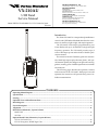
VERTEX STANDARD
VX-210AU
US Headquarters
10900 Walker Street, Cypress, CA 90630, U.S.A.
International Division
8350 N.W. 52nd Terrace, Suite 201, Miami, FL 33166, U.S.A.
UHF Band
Service Manual
YAESU EUROPE B.V.
P.O. Box 75525, 1118 ZN Schiphol, The Netherlands
YAESU UK LTD.
Unit 12, Sun Valley Business Park, Winnall Close
Winchester, Hampshire, SO23 0LB, U.K.
VERTEX STANDARD HK LTD.
©2002 VERTEX STANDARD CO., LTD. Printed in Japan.
Unit 5, 20/F., Seaview Centre, 139-141 Hoi Bun Road,
Kwun Tong, Kowloon, Hong Kong
EC020U90A
Introduction
The Vertex VX-210AU is a compact hand portable transceiver for the UHF land mobile band that offers the convenience of small size, light weight, and simple operation.
The VX-210AU can be simply programmed by your
Vertex Dealer with up to 16 channels for single and split
frequency operation. The VX-210AU provides up to 5
watts of RF output power and includes a flexible quickconnect antenna.
The transceiver and Ni-Cd battery packs are constructed of thick high-impact polycarbonate plastic, with special attention paid by the designers to tight seals and ruggedness, assuring years of reliable operation even in harsh
environments.
The following pages describe the operation, features
and accessories of the VX-210AU. With proper care and
operation, the transceiver will provide many years of reliable communications.
Contents
Operating Manual Reprint ......................................................................................................................................... 2
Specifications ............................................................................................................................................................... 5
Cloning.......................................................................................................................................................................... 6
Exploded View & Miscellaneous Parts ..................................................................................................................... 7
Block Diagram .............................................................................................................................................................. 8
Circuit Description ...................................................................................................................................................... 9
Alignment ................................................................................................................................................................... 11
Board Units (Schematics, Layouts & Parts)
MAIN Unit ............................................................................................................................................................. 13
SW Unit ................................................................................................................................................................... 37
Optional Board Units (Schematics, Layouts & Parts)
VTP-50 VX-Trunk Unit .......................................................................................................................................... 38
FVP-25 Encryption / DTMF Pager Unit ................................................................................................................ 40
1
Operating Manual Reprint
Contorols & Connectors
LED Indicator
Glows Green
Blinking Green
Glows Red
Blinking Red
Blinking Yellow
Antenna
ACC on
Busy Channel (or SQL off)
Transmitting
Battery Voltage is low
Receiving a Selective Call
CH (Channel) Selector
VOL/PWR Knob
Push To Talk
(PTT) Switch
MIC/SP Jack
(External Mic/Earphone)
ACC Button
Speaker
Low Battery Indication
r As the battery discharges during use, the voltage gradually becomes lower. When the battery voltage reaches
6.3 volts, substitute a freshly charged battery and recharge
the depleted pack. The TX/BUSY indicator on the top of
the radio will blink red when the battery voltage is low.
r Avoid recharging Ni-Cd batteries often with little use
between charges, as this can degrade the charge capacity. We recommend that you carry an extra, fullycharged pack with you so the operational battery may
be used until depletion (this “deep cycling” technique
promotes better long-term battery capacity).
Operation
Preliminary Steps
Battery Pack Installation and Removal
Caution!
Do not attempt to open any of the rechargeable NiCd packs, as they could explode if accidentally shortcircuited.
2
11
9
CH
VOL
15
r To remove the battery, turn the radio off and remove
any protective cases. Open the Battery Pack latch on
the bottom of the radio, then slide the battery downward and out from the radio while holding the Belt
Clip.
r Turn the top panel’s VOL/
PWR knob clockwise to
turn on the radio on.
13
r To install the battery, hold the transceiver with your
left hand, so your palm is over the speaker and your
thumb is on the top of the belt clip. Insert the battery
pack into the battery compartment on the back of the
radio while tilting the Belt Clip outward, then close
the Battery Pack Latch until it locks in place with a
“Click.”
Operation Quick Start
7
Before You Begin
3
Battery Pack
Latch
r Install a charged battery pack onto the transceiver, as
described previously.
r Screw the supplied antenna onto the Antenna jack.
Never attempt to operate this transceiver without an
antenna connected.
r If you have a Speaker/Microphone, we recommend that
it not be connected until you are familiar with the basic operation of the VX-210A.
1
Microphone
r Pull and turn the top
panel’s CH selector knob
to choose the desired operating channel.
r Rotate the VOL/PWR knob
to set the volume level. If no
signal is present, press and
hold in the ACC button (the
lower button on the left
side) for more than 1 second
(when “MONITOR” is assigned to the ACC button); background noise will now be heard, and you may use this to set
the VOL/PWR knob for the desired audio level.
r Press and hold in the ACC
button (when “MONITOR” is assigned to the
ACC button) for more
than 1 second (or press the
ACC button twice) to
quiet the noise and resume normal (quiet) monitoring.
Operating Manual Reprint
r To transmit, press and hold
in the PTT switch. Speak
into the microphone area
of the front panel grille
(lower left-hand corner) in
a normal voice level. To return to the Receive mode, release the PTT switch.
r If a Speaker/Microphone is available, remove the plastic cap and its two mounting screws from the right side
of the transceiver, then insert the plug from the Speaker/
Microphone into the MIC/SP jack; secure the plug using the screws supplied with the Speaker/Microphone.
Hold the speaker grille up next to your ear while receiving. To transmit, press the PTT switch on the
Speaker/Microphone, just as you would on the main
transceiver’s body.
Note:
Save the original plastic cap and its mounting screws.
They should be re-installed when not using the
Speaker/Microphone.
Key Functions
The VX-210A provides a programmable “ACC” (Accessory)
button. The ACC button’s functions can be customized (set to
any of a variety of functions), via programming by your VERTEX STANDARD dealer, to meet your communications/network requirements. The particular function to be activated or
disabled may require a simple press of the ACC button, or it
may require that the ACC button be pressed and held in for one
second (or more). See the discussion below.
Some features may require the purchase and installation of
optional internal accessories.
The possible ACC button programming features are illustrated
below, and their functions are explained in the next chapter. For
further details, contact your VERTEX STANDARD dealer.
For future reference, check the box next to the function that
has been assigned to the ACC button on your particular radio,
and keep it handy.
Function
None
Monitor
Squelch OFF
Low Power
Scan
Follow-me Scan
Dual Watch
Talk Around
Call/Reset
Speed Dial
TX Save Off
ACC 1
ACC 2
ACC button
Press Press and Hold
Description of Operating Functions
Monitor
Press the ACC button to override (disable) the Tone Squelch.
Background noise or incoming signals will now be
heard whether or not a matching tone is present on the
signal. Press the ACC button once more to resume normal (quiet) Tone Squelch action.
Squelch OFF
Press the ACC button to override both the Noise and
Tone squelch systems. Again press the ACC button to
resume normal (quiet) Noise and Tone squelch action.
Low Power
Press the ACC button to set the radio's transmitter to
the “Low Power” mode, thus extending battery life.
Press the ACC button again to return to “High Power”
operation when in difficult terrain.
Scan
The Scanning feature is used to monitor multiple channels programmed into the transceiver. While scanning,
the radio will check each channel for the presence of a
signal, and will stop on a channel if a signal is present.
r To activate scanning:
Press the ACC button.
The scanner will search the channels, looking for
“active” ones; it will pause each time it finds a channel on which someone is speaking.
r To stop scanning:
Press the ACC button.
Operation will revert to the channel to which the
CH knob is set.
Follow-Me Scan
“Follow-Me” Scan feature checks a User-assigned Priority Channel regularly as you scan the other channels.
Thus, if only Channels 1, 3, and 5 (of the 8 available channels) are designated for “Scanning,” the user may nonetheless assign Channel as the “User-assigned” Priority
Channel via the “Follow-Me” feature.
Press the ACC button to activate “Follow-Me” scanning,
then pull and turn the CH selector knob to the channel
which you want to designate as the “User-Assigned Priority Channel”. When the scanner stops on an “active”
channel, the User-assigned Priority Channel will automatically be checked every few seconds.
Dual Watch
The Dual Watch feature is similar to the Scan feature,
except that only two channels are monitored: the current operating channel, and the “Priority” channel.
r To activate Dual Watch:
Press the ACC button.
The scanner will search the two channels; it will
pause each time it finds a channel on which someone is speaking.
3
Operating Manual Reprint
r To stop Dual Watch:
Press the ACC button.
Operation will revert to the channel to which the
CH knob is set.
Talk Around
Press the ACC button to activate the Talk Around feature when you are operating on duplex channel systems (separate receive and transmit frequencies, utilizing a “repeater” station). The Talk Around feature
allows you to bypass the repeater station and talk directly to a station that is nearby. This feature has no
effect when you are operating on “Simplex” channels,
where the receive and transmit frequencies are already
the same.
Note that your dealer may have made provision for
“Talk Around” channels by programming “repeater”
and “Talk Around” frequencies on two adjacent channels. If so, the ACC key may be used for one of the
other Pre-Programmed Functions.
Call/Reset
When the 2-tone selective calling unit is installed, press
the ACC button to silence the receiver and reset for
another call, when a communication is finished.
Speed Dial
Your Dealer may have pre-programmed Auto-Dial telephone number memories into your radio.
To dial a number, just press the Dealer-assigned ACC
button for Speed Dialing. The DTMF tones sent during the dialing sequence will be heard in the speaker.
TX Save Off
Press the ACC button to disable the Transmit Battery
Saver, if you are operating in a location where high
power is almost always needed.
The Transmit Battery Saver helps extend battery life
by reducing transmit power when a very strong signal
from an apparently nearby station is being received.
Under some circumstances, though, your hand-held
radio may not be heard well at the other end of the
communication path, and high power may be necessary at all times.
4
ACC 1
Activates an optional Unit (module) while the ACC
button is held depressed.
When you release the ACC button, the optional Unit
will be disabled.
For further details, contact your VERTEX STANDARD
dealer.
ACC 2
Toggles the optional Unit “on” or “off” whenever you
press the ACC button.
For example, when the optional “FVP-25” voice encryption unit is installed, press the ACC button momentarily to disable the voice encryption feature temporarily.
Press the ACC button again to re-enable the voice encryption feature.
Accessories & Options
FNB-V57
FNB-V57IS
FBA-25
NC-76B
NC-76C
VAC-6400
VAC-400B
VAC-400C
VCM-1
MH-45B4B
MH-37A4B
VC-25
FVP-25
VTP-50
CT-42
CT-27
FTT-17
LCC-210
7.2 V 1100 mAh Ni-Cd Battery Pack
7.2 V 1100 mAh Ni-Cd Intrinsically safe Battery
Alkaline Battery Case (6 x AA)
120 VAC Wall Charger
230-240 VAC Wall Charger
6-Unit Multi charger
120 VAC Desktop Rapid Charger
230-240 VAC Desktop Rapid Charger
Mobile Mounting Bracket for VAC-400
Speaker/Microphone
Earpiece/Microphone
VOX Headset
Encryption /DTMF Page Unit
VX-Trunk Unit
PC-Programming Cable (CT-28 + CT-29)
Cloning Cable (Set-to-Set Cloning)
16 keypad for VX-Trunk (VTP-50 required)
Leather Case
Specifications
General
Frequency Range:
Number of Channels:
Channel Spacing:
PLL Steps:
Power Supply Voltage:
Battery Life (5-5-90 duty):
Operating Temperature Range:
Frequency Stability:
Dimensions:
Weight (Approx):
400-430 MHz (AS1), 440-470 MHz (CS), 450-485 MHz (D), 485-512 MHz (F)
16 channels
12.5/25 kHz
5/6.25 kHz
7.5 V DC ±20 %
7.1 hrs. (8.5 hrs. w/saver) @5 W
–22° F to +140° F (–30° C to +60° C)
±2.5 ppm
4.21" (W) × 2.28" (H) × 1.0" (D) (108 × 58 × 26 mm)
0.75 lb. (340 g) w/FNB-V57
Receiver (Measurements made per EIA standard TIA/EIA-603)
Sensitivity:
EIA 12 dB SINAD: 0.25 µV
20 dB Quieting: 0.35 µV
Adjacent Channel Selectivity: 65 dB (25 kHz)/60 dB (12.5 kHz)
Intermodulation:
65 dB
Spurious and Image Rejection: 65 dB
Hum & Noise:
45 dB
Audio Output:
500 mW @4 Ohms, 5% THD
Transmitter (Measurements made per EIA standard TIA/EIA-603)
Power Output:
Modulation:
Conducted Spurious Emission:
FM Hum & Noise:
Audio Distortion (@1 kHz):
5 / 1 W (Selectable) or 3.5 / 1 W (Selectable) w/FBA-25
16K0F3E / 11K0F3E (Direct FM)
60 dB Below Carrier
40 dB (25 kHz) / 35 dB (12.5kHz)
<5%
Specifications subject to change without notice or obligation.
5
Cloning
The VX-210A includes a convenient “Clone” feature,
which allows the programming data from one transceiver to be transferred to another VX-210A. Here is
the procedure for Cloning one radio’s data to another.
Note: When a cloning isn't made, you correct the following part using "CE45."
When a "Set-to-Set Clone" which is in the "Miscellaneous" menu is "Disabled," change this menu to
"Enabled."
1.
2.
3.
4.
Turn both transceivers off.
Remove the plastic cap and its two mounting
screws from the MIC/SP jack on the right side
of the transceiver. Do this for both transceivers.
Connect the optional CT-27 cloning cable between the MIC/SP jacks of the two transceivers.
Press and hold the PTT switch and ACC button
(just below the PTT switch) while turning the
transceiver on. Do this for both transceivers (the
order of the switch-on does not matter).
5.
On the Destination transceiver, press the ACC
button (LED indicator will glow green).
6. Now, on the source transceiver, Press the PTT
switch.Data will now be transferred to the Destination transceiver from the source transceiver (LED indicator will glow red).
7. If there is a problem during the cloning process,
LED indicator will blink red from source the
transceiver.
Check your cable connections and battery voltage, and try again.
8. If cloning is a successful, LED indicator will be
disappeared, turn the Destination transceiver
off. Now turn the source transceiver off.
9. Disconnect the CT-27. Replace the plastic cap
and its two mounting screws.
10. You can then turn the transceivers back on, and
begin normal operation.
Optional Cloning Cable CT-27
Dealer Programming of VTP-50
These procedures are designed to be used by the installing technician after the VTP-50 has been installed in the transceiver. To program a VX-210A's VTP-50 board, you will need the CT-42 programming interface cable, the CE26 Programming diskette, and an IBM PC/AT or PS/2-compatible tyoe
computer.
To enter the Programming mode, use the following procedure:
1. Turn the transceiver off.
2. Turn on the transceiver while holding in the ACC button (just below the PTT switch).
6
Exploded View & Miscellaneous Parts
REF.
À
Á
Â
Ã
Ä
Å
Æ
Ç
VXSTD P/N
U07230107
U20204007
U02206007
U9900051
U9900063
U9900068
U9900086
U9900084
Description
PAN HEAD SCREW M2x3B #1
BINDING HEAD SCREW M2.6x4B
SEMS SCREW SM2.6x6B
TAPTITE SCREW M2x4B #3
TAPTITE SCREW M2x3.3Ni
TAPTITE SCREW M2x4Ni #3
TAPTITE SCREW M1.7x2.5B
BINDING HEAD SCREW M2x7.5B
Qty.
1
2
2
1
5
6
2
1
RA018500A Vertex (USA)
RA018510A (EXP)
FRONT CASE ASS'Y
Non-designated parts are available only
as part of a designated assembly.
RA018520A Vertex (USA)
RA018530A (EXP)
FRONT CASE ASS'Y (16KEY)
Á
Á
RA0173500
CAP
RA0111400
RING NUT
RA008920A
RA008920B (Lot. 7~)
O RING
Ç
RA010300A
RA010300B (Lot. 12~)
KNOB
RA0112300
COIL SPRING
RA0228800
KNOB
RA008890A
O RING
RA0173400
RUBBER KNOB
RA0111500
SPECIAL NUT
R3152420
O RING
M4090128
SPEAKER
Ä
Å
Å
Ä
Å
Ä
RA0173700
RUBBER KNOB (16KEY)
MAIN Unit
Å
Å
SW Unit
RA0123500
LATCH NAIL
Å
RA0107000
TERMINAL PLATE R
Æ
Æ
RA011070A
RUBBER PACKING
RA011720A
MYLAR SHEET
RA010340A
TERMINAL HOLDER
CP7139001
REAR CASE ASS'Y
RA0106900
TERMINAL PLATE L
Ã
Â
À
Ä
Ä
CP7140001
BELT CLIP ASS'Y
Â
7
Block Diagram
8
Circuit Description
1. Receive Signal Path
Incoming RF from the antenna jack is delivered to the
RF Unit and passes through a low-pass filter consisting of
coils L1003, L1006 and L1007, capacitors C1002, C1007,
C1013, C1017, C1022, C1025, and C1169 and antenna
switching diode D1007 (RLS135).
Signals within the frequency range of the transceiver
enter a varactor-tuned band-pass filter consisting of coils
L1014 and L1015, capacitors C1057, C1058, C1064, C1071
and C1073, and diodes D1012 (HVC355B), D1013
(1SV280), D1016 (HVC355B) and D1017 (1SV280). The
signals are then amplified by Q1015 (2SC5006), and enter a varactor-tuned band-pass filter consisting of coils
L1018, L1021 and L1024, capacitors C1084, C1088, C1089,
C1094, and C1096, and diodes D1022, D1024, D1026
(HVC355B) and D1023, D1025 and D1027 (1SV280), before mixing by Q1025 (SGM2016).
Buffered output from the VCO is amplified by Q1009
(2SC5005) to provide a pure first local signal between
406.05 and 441.05 MHz for injection to the first mixer,
Q1025. The 43.95 MHz first mixer product then passes
through monolithic crystal filters XF1001 and XF1002
(43Y12B6, ±6.0 kHz BW) to strip away unwanted mixer
products, and is then amplified by Q1032 (2SC4215Y).
The amplified first IF signal is applied to FM IF subsystem IC Q1036 (BA4116FV), which contains the second
mixer, second local oscillator, limiter amplifier, noise amplifier, and S-meter amplifier.
A second local signal is generated by the PLL reference/
second local oscillator, 14.50 MHz crystal X1001, to produce the 450 kHz second IF when mixed with the first IF
signal within Q1036.
The second IF then passes through the ceramic filter
CF1001 (ALFYM450F) or CF1002 (SFPC450G: only on
“Narrow” channels) to strip away all but the desired signal, and is then applied to the limiter amplifier in Q1036,
which removes amplitude variations in the 450kHz IF,
before detection of the speech by the ceramic discriminator CD1001 (CDBC450CX24).
Detected audio from Q1036 is applied to the audio highpass filter, and then passes via the volume control to the
audio amplifier Q1039 (TDA7233D), which provides up
to 0.5 Watts to the optional headphone jack or a 4-ohm
loudspeaker.
2. Squelch Control
The squelch circuitry consists of a noise amplifier and
band-pass filter within Q1036, and noise detector D1030
(1SS355).
When no carrier is received, noise at the output of the
detector stage in Q1036 is amplified and band-pass filtered by the noise amplifier section of Q1036 and the network between pins 7 and 8, and then is rectified by D1030.
The resulting DC squelch control voltage is passed to
pin 37 of the microprocessor Q1014 (M37515M4-117HP).
If no carrier is received, this signal causes pin 7 of Q1014
to go high and pin 20 to go low. Pin 7 signals Q1037
(IMD10A) to disable the supply voltage to the audio amplifier Q1039, while pin 20 makes Q1023 (IMX1) hold the
green (Busy) half of the LED off, when pin 7 is high and
pin 20 is low.
Thus, the microprocessor blocks output from the audio amplifier, and silences the receiver, while no signal is
being received (and during transmission, as well).
When a carrier appears at the discriminator, noise is
removed from the output, causing pin 37 of Q1014 to go
low and the microprocessor to activate the “Busy” LED
via Q1014.
The microprocessor then checks for CTCSS or CDCSS code
squelch information, if enabled, or for DTMF data on the
optional DTMF Unit. If not transmitting, and CTCSS or
CDCSS is not activated, or if the received tone or code
matches that programmed for that channel, audio is allowed to pass through the audio amplifier Q1039
(TDA7233D) to the loudspeaker because of the enabling
of the supply voltage via Q1037.
3. Transmit Signal Path
Speech input from the microphone is amplified by
Q1017 (NJM2902V); after pre-emphasis by C1059 and
R1045, the audio passes through another section of Q1017.
The processed audio may then be mixed with a CTCSS
tone generated by Q1014 (M37515M4-117HP), and then
delivered to D1005 (HVU350) for frequency modulation
of the PLL carrier (up to ±5kHz from the unmodulated
carrier) at the transmitting frequency.
If a CDCSS code is enabled for transmission, the code
is generated by microprocessor Q1014 and delivered to
D1004 (1SV230) for CDCSS modulating.
If DTMF is enabled for transmission, the tone is generated by the microprocessor Q1014 and applied to the limiter amplifier section in place of the speech audio. Also,
the tone is amplified for monitoring in the loudspeaker.
The modulated signal from the VCO Q1005 (2SK508K52) is buffered by Q1008 (2SC5005) and amplified by
Q1009 (2SC5005). The low-level transmit signal is then
passed through the T/R switching diode D1014
(DAN235U) to the driver amplifiers Q1012 (2SC3357) and
Q1016 (2SK2973). The amplified transmit signal is applied to the final amplifier Q1021, providing up to 5 Watts
9
Circuit Description
of output power.
The transmit signal then passes through the antenna switch
D1007 (RLS135) and is low-pass filtered to suppress harmonic spurious radiation before delivery to the antenna.
3-1 Automatic Transmit Power Control
RF power output from the final amplifier is sampled
by C1099, and is rectified by D1029 (1SS321). The resulting DC is fed back through Q1027 (FMW1) to the drive
amplifier Q1016 and final amplifier Q1021, for control of
the power output.
The microprocessor selects “High” or “Low” power levels.
3-2 Transmit Inhibit
When the transmit PLL is unlocked, pin 7 of PLL chip
Q1004 goes to a logic “low.” The resulting DC unlock control voltage is passed to pin 24 of the microprocessor
Q1014. While the transmit PLL is unlocked, pin 22 of
Q1014 remains high, which then turns off Q1031 and the
Automatic Power Controller Q1027 (FMW1) to disable the
supply voltage to the drive amplifiers Q1012 and Q1016
and final amplifier Q1021, thereby disabling the transmitter.
3-3 Spurious Suppression
Generation of spurious products by the transmitter is minimized by the fundamental carrier frequency being equal
to final transmitting frequency, modulated directly in the
transmit VCO. Additional harmonic suppression is provided by a low-pass filter consisting of L1003, L1006, and
L1007 plus C1002, C1007, C1013, C1017, C1022, and C1169,
resulting in more than 60 dB (High Power) of harmonic
suppression prior to delivery to the antenna.
4. PLL Frequency Synthesizer
The PLL circuitry on the Main Unit consists of VCO
Q1005 (2SK508-K52), VCO buffer Q1008 (2SC5005), and
PLL subsystem IC Q1004 (MB15A01FV1), which contains
a reference divider, serial-to-parallel data latch, programmable divider, phase comparator and charge pump.
Stability is maintained by a regulated 3.5 V supply, via
Q1040 (TK11235BMCL) and R1019/R1020, temperature
compensating thermistors TH1001, TH1002, and TH1003,
and varactor diode D1004 (1SV230), which is associated
with the 14.50 MHz frequency reference crystal X1001.
While receiving, VCO Q1005 oscillates between 406.05
and 441.05 MHz according to the transceiver version and
the programmed receiving frequency. The VCO output is
buffered by Q1008, then applied to the prescaler section
of Q1004. There the VCO signal is divided by 64 or 65,
10
according to a control signal from the data latch section of
Q1004, before being sent to the programmable divider section of Q1004.
The data latch section of Q1004 also receives serial dividing data from the microprocessor Q1014, which causes the pre-divided VCO signal to be further divided in
the programmable divider section, depending upon the
desired receive frequency, so as to produce a 5 kHz or
6.25 kHz derivative of the current VCO frequency.
Meanwhile, the reference divider section of Q1004 divides the 14.5 MHz crystal reference from the reference
oscillator Q1004, by 2900 (or 2320) to produce the 5 kHz
(or 6.25 kHz) loop reference (respectively).
The 5 kHz (or 6.25 kHz) signal from the programmable
divider (derived from the VCO) and that derived from
the reference oscillator are applied to the phase detector
section of Q1004, which produces a pulsed output with
pulse duration depending on the phase difference between
the input signals.
This pulse train is filtered to DC and returned to the
varactor D1001 (HVC355B) and D1002 (HVC355B).
Changes in the level of the DC voltage applied to the varactor affect the reference in the tank circuit of the VCO
according to the phase difference between the signals derived from the VCO and the crystal reference oscillator.
The VCO is thus phase-locked to the crystal reference
oscillator. The output of the VCO Q1005, after buffering
by Q1008 and amplification by Q1009, is applied to the
first mixer as described previously.
For transmission, the VCO Q1005 oscillates between 450
and 485 MHz according to the model version and programmed transmit frequency. The remainder of the PLL
circuitry is shared with the receiver. However, the dividing data from the microprocessor is such that the VCO
frequency is at the actual transmit frequency (rather than
offset for IFs, as in the receiving case). Also, the VCO is
modulated by the speech audio applied to D1005
(HVU350), as described previously.
Receive and transmit buses select which VCO is made
active by Q1002 (RT1N441U).
5. Miscellaneous Circuits
5-1 Push-To-Talk Transmit Activation
The PTT switch on the microphone is connected to pin
35 of microprocessor Q1014, so that when the PTT switch
is closed, pin 23 of Q1014 goes low. This signal disables
the receiver by disabling the 5 V supply bus at Q1035
(DTB123EK) to the front-end, FM IF subsystem IC Q1036,
and the receiver’s VCO circuitry.
At the same time, Q1026 (FMW1) and Q1031 (2SB1122S)
activate the transmit 5V supply line to enable the transmitter.
Alignment
The VX-210A has been carefully aligned at the factory for
the specified performance across the frequency range specified for each version. Re-alignment should therefore not
be necessary except in the event of component failure, or
altering version type. All component replacement and
service should only be performed by an authorized Vertex representative, or the warranty policy may be void.
Required Test Equipment
Before beginning alignment, connect the transceiver and
PC using the CT-42 Programming Cable, and run the CE45
Channel Programming Diskette, then download the EEPROM data from the transceiver to the computer. Then
store this data in a disk file so that it can be uploaded
when alignment is finished.
You should find the corresponding data file on the computer disk for the transceiver version you are aligning, containing channel settings for the high edge, middle and low
edge of the transceiver’s frequency range in channels 1, 2
and 3, respectively. Up-load this file to the transceiver.
Version D
Set up the test equipment as shown for transmitter alignment. Adjust the supply voltage to 7.2 V for all steps where
not specified otherwise.
50-ohm
Dummy Load
RF Signal
Generator
Inline Wattmeter
m CT-42 Programming Cable with CE45 Channel Programming Diskette
m RF Signal Generator with calibrated output level at
1GHz
m Deviation Meter (Linear Detector)
m AC Voltmeter
m SINAD Meter
m In-Line wattmeter with 5 % accuracy at 500 MHz
m Regulated DC Power Supply adjustable from 4 to 10 V,
3A
m 50-ohm Non-reactive Dummy Load: 10 W at 500 MHz
m Frequency Counter: ±0.2 ppm accuracy at 500 MHz
m AF Signal Generator
m DC Voltmeter: high impedance
Channels
PLL & Transmitter
Version CS
Version AS1
Low Band Edge (Channel 1)
450.000 MHz
440.000 MHz
400.000 MHz
Band Center (Channel 2)
470.000 MHz
455.000 MHz
415.000 MHz
High Band Edge (Channel 3) 490.000 MHz
470.000 MHz
430.000 MHz
Deviation Meter
Frequency
Counter
RF Sampling
Coupler
CT-42 connection
Cable
Transceiver
MIC/SP
Power Supply
7.2V DC
PC
COM port
PLL VCV (Varactor Control Voltage)
r Connect the DC voltmeter between TP03 on the chip
side of the Main Unit and ground.
r Set the transceiver to CH 3 (high band edge), and adjust L1004 on the chip side of the Main Unit for 3.6 V
(±0.1 V) on the voltmeter.
r Set the transceiver to CH 1 (low band edge), and confirm the low-end VCV is more than 0.8 V while transmitting, and also while receiving.
L1004
TP03
Note: Signal levels in dB referred to in the alignment procedure are based on 0 dBµ EMF= 0.5µV (closed circuit).
11
Alignment
PLL Reference Frequency
r Set the transceiver to CH 2 (band center). Key the transmitter, and adjust TC1001 on the component side of
the Main Unit, if necessary, so the frequency counter
displays the band center frequency (±100 Hz) (for the
version being aligned) when transmitting.
Transmitter Output Power
r Set the transceiver to CH 2 (band center), and select
high power output.
r Ensure that the supply voltage is precisely 7.2 V, then
adjust VR1004 on the component side of the Main Unit
(while the PTT switch is pressed) for 5.0 W on the wattmeter, and confirm that supply current remains below
2.0 A.
Modulation Level
r Set the transceiver to CH 2 (band center), and adjust
the AF generator for -10 dBm output at 1 kHz to the
EXT MIC jack.
r Press the PTT switch, and adjust VR1002 on the component side of the Main Unit for a deviation of ±4.2
kHz (for 25 kHz steps), or ±2.1 kHz (for 12.5 kHz steps).
DCS Modulation Level
r Set the transceiver to CH 2 (band center), and activate
the DCS with a code number of 627.
r Press the PTT switch, and adjust VR1003 on the component side of the Main Unit for a deviation of ±0.75
kHz (for 25 kHz steps), or ±0.45 kHz (for 12.5 kHz
steps).
Receiver
Sensitivity
r Set the transceiver to CH 3 (high band edge), and
tune the RF signal generator to the same frequency; set the generator for ±3.0 kHz deviation with 1
kHz tone modulation, and set the output level for
40 dBµ at the antenna jack.
r Adjust VR1001 on the component side of the Main Unit
for optimum SINAD, and confirm that signal generator level is better than -6 dBµ for 12 dB SINAD.
RSSI
r Connect the DC voltmeter between TP43 on the component side of the Main Unit and ground.
r Set the transceiver to CH 2 (band center), and tune the
RF signal generator to the same frequency; set the generator for ±3.0 kHz deviation with 1 kHz tone modulation, and set the output level for 15 dBµ at the antenna
jack.
r Adjust VR1005 on the component side of the Main Unit
for 0.7 V (±0.1 V) on the voltmeter.
VR1001
VR1004
TP43
VR1005
VR1003
VR1002
TC1001
12
MAIN Unit
Circuit Diagram
RX: 2.62 (2.62V)
RX: 1.8V (1.8V)
TX: 0V [0V]
RX: 0.75V (0.75V)
RX: 0.72V (0.72V)
TX: 0V [0V]
RX: “3.58V” <0.02V>
RX: (0V)
TX: (3.79V)[4.73V]
TX: (0V) [0V]
RX: 2.2V(2.2V)
TX: 0V
RX: (1.17V)
TX: 1.17V
RX: (4.18V)
TX: 4.21V
RX: (3.74V)
TX: 3.76V
RX: (0.78V)
TX: (0.6V)
RX: (4.06V)
TX: 4.08V
RX: 1.37V(1.37V)
RX: (0.7V)
TX: 1.43V
TX: 0.54V
RX: 0V(0V)
TX: 0.69V
RX: 0V(0V)
TX: 5.01V
TX: (-1.25V)
[-0.9V]
TX HIGH: 2.6V
LOW: 1.23V
TX: (2.44V)
[0.68V]
TX:
(4.81V)
[2.8V]
TX: (1.95V)
[0.38V]
TX: (3.96V)
[0.03V]
RX: (0.02V)
TX: (4.17V)
RX: “0V” <3.57V>
RX: (4.16V)
RX: (0V) TX: 0V
RX: 0.92V (0.92V)
TX: (2.59V)[0.96V]
TX: (2.40V)[0.95V]
RX: 4.86V
(4.86V)
RX: (4.88V)
RX: (0.93V)
RX: (4.81V)
RX: (4.81V)
TX: (0V)
7.58V
RX: 0V(0V)
TX: 2.26V
RX: 0.9V (0.9V)
RX: 3.52V (3.52V)
TX: (3.52V) [3.52V]
RX: 0V (0V)
TX: (3.52V) [3.52V]
RX: (0V)
TX: (0V)
RX: 4.88V (4.88V)
TX: 4.94V
RX: (0.92V)
RX: 1.82V (1.82V)
RX: (0.9V)
RX: 4.85V (4.85V)
TX: (5.00V) [5.00V] {4.92V} <4.92V>
RX: 0V (0V)
TX: 4.82V
RX: (1.53V)
RX: (1.55V)
RX: 0V
(0V)
RX: 2.07V (2.07V)
RX: 4.86V (4.86V)
TX: {2.05V} <2.05V> TX: 0V
RX: 2.19V
(2.19V)
TX: 2.19V
RX: (7.68V)
TX: (6.8V)[7.38V]
RX: 3.20V (3.20V)
TX: 3.20V
RX: (1.53V)
RX: (0.97V)
RX: (0V)
TX: (4.86V)[4.86V]
RX: 3.22V
(3.22V)
TX: 3.22V
RX: (3.51V)
RX: (1.55V)
RX: (1.56V)
RX: (1.55V)
RX: (7.67V)
TX: (6.12V)[6.69V]
7.13V
RX: 3.50V (3.50V)
TX: 3.50V
RX: 4.88V (4.88V)
TX: 4.93V
RX: (4.89V)
TX: 4.91V
RX: (3.52V)
TX: 3.52V
RX: 2.44V (2.44V)
TX: {2.44V} <2.44V>
RX: 3.44V (3.44V)
TX: (3.44V) [3.44V]
{3.44V} <3.44V>
RX: (4.82V)
TX: 0V
RX: 1.23V (0.58V)
RX: 0V (0V)
RX: 0V [7.66V]
RX: (0.04V)
TX: 4.91V
RX: 7.69V
(0.21V)
RX: 0V (1.25V)
RX: (3.51V) TX: 2.93V
RX: 0V (3.59V)
RX: 3.52V (3.52V)
TX: (3.52V) [3.52V]
{3.52V} <3.52V>
RX: (3.52V)
TX: 0V
TX: 7.2V
RX: 0V (0V) [0V] {3.48V}
TX: (0V) [0V] {3.48V} <3.48V>
RX: 7.69V
(6.91V)
RX: 3.12V(2.94V)
TX: (2.83V) [2.84V]
RX: (3.51V)
RX: (0V)
RX: 0V (3.51V)
RX: [0V] {0V}
TX: (0.2V) [0.2V]
{0V} <0V>
RX: [3.0V] {0V}
”3.0V” <0V>
TX: (3.0V) [3.0V]
{0V} <0V>
RX: (3.51V)
RX: (3.57V)
TX: 3.59V
RX: 7.69V (7.69V)
RX: (3.52V)
TX: 3.52V
RX: (0V)
RX: 0V
TX: 0V
TX: 2.2V
TX: 4.86V
RX: [0V] {3.47V}
”0V” <3.47V>
TX: (0V) [0V]
{3.47V}
<3.47V>
RX: (3.51V)
RX: 3.51V
TX: 3.52V (3.52V)
TX: 2.18V
RX: (3.52V)
TX: 2.22V
TX: 2.22V
TX: 2.2V
TX: 2.17V
RX: (0V)
TX: 2.18V
RX: 0V (0V)
TX: (2.17V) [2.17V]
{2.17V} <2.17V>
TX: 2.2V
RX: 0V (0V)
TX: (1.59V) [1.59V]
{1.59V} <1.59V>
RX Squelch Close : xx
RX Squelch Close W :[xx]
RX Squelch Close N :{xx}
RX Squelch Open : (xx)
RX Squelch Open W : “xx”
RX Squelch Open N : <xx>
TX : xx
TX High W : (xx)
TX Low W : [xx]
TX High N : {xx}
TX Low N : <xx>
RX: 0V (0V)
TX: (2.17V) [2.17V]
{2.17V} <2.17V>
Q1036
1
2
3
4
5
6
7
8
9
10
11
12
13
14
15
16
RX SQUELCH
CLOSE OPEN
4.87V 4.87V
3.22V 3.22V
2.07V 2.07V
3.22V 3.22V
2.18V 2.18V
-
TX-W
HIGH LOW
4.9V 4.9V
3.22V 3.22V
2.11V 2.12V
0V
0V
3.22V 3.22V
2.19V 2.19V
-
TX-N
HIGH LOW
4.9V 4.9V
3.22V 3.22V
2.15V 2.15V
3.21V 3.21V
2.2V 2.2V
-
Q1036 (RX SQUELCH OPEN)
1
4.78V
2
4.4V
3
3.57V
4
4.8V
5
4.37V
6
4.5V
7
0.8V
8
0.6V
9
1.06V
10
4.81V
11
3.97V
12
0.47V
13
0.32V
14
1.91V
15
0V
16
0.93V
13
MAIN Unit
Note:
14
MAIN Unit
Parts Layout
A
C
B
D
E
1
2
3
Side A
MB15A01PFV
(Q1004)
NJM2902V
(Q1017)
TDA7233D
(Q1039)
TC4W66FU
(Q1055)
2SK209GR (XG)
(Q1001)
RT1N441U (N3)
(Q1003, 1007,
1018, 1033,
1037, 1046)
2SA1586Y (SY)
(Q1010)
2SC4154 (LE)
(Q1006, 1024, 1051)
2SC4215Y (QY)
(Q1032)
FMW1 (W1)
(Q1027)
2SB1132 (BA)
(Q1031)
CPH6102 (AB)
(Q1050)
UMD3N (D3)
(Q1054)
MC2846 (A4)
(D1031)
15
MAIN Unit
e
d
c
b
a
3
2
1
Side B
BR93LC56F
(Q1011)
M37515M4
(Q1014)
16
TC4W66FU
(Q1019)
NJM12903R
(Q1023)
NJM2902V
(Q1030)
BA4116FV
(Q1036)
2SK508 (K52)
(Q1005)
2SK2973 (K1)
(Q1016)
2SC3357
(Q1012)
RT1P441U (P3)
(Q1013, 1020)
2SK2974
(Q1021)
UMC5N (C5)
(Q1048)
RT1N441U (N3)
(Q1002, 1034,
1041, 1043,
1044, 1052,
1053, 1056)
FMW1 (W1)
(Q1026, 1028)
2SC4154 (LE)
(Q1022, 1047)
2SC5005 (73)
(Q1008, 1009)
2SC5006 (24)
(Q1015)
SGM2016AM (MA)
(Q1025)
TK11235BMCL
(Q1040)
DTC124TE (05)
(Q1049)
DTB123EK (F12)
(Q1035)
S-80735SN (DZ)
(Q1038)
2SB1122S (BE)
(Q1029)
2SA1586Y (SY)
(Q1042)
DAN235U (M)
(D1014)
1SS321 (F9)
(D1029)
MC2848 (A6)
(D1033, 1034)
MC2850 (A7)
(D1015, 1032, 1036)
MAIN Unit (Lot. 12~)
Circuit Diagram
RX: 2.62 (2.62V)
RX: 1.8V (1.8V)
TX: 0V [0V]
RX: 0.75V (0.75V)
RX: 0.72V (0.72V)
TX: 0V [0V]
RX: “3.58V” <0.02V>
RX: (0V)
TX: (3.79V)[4.73V]
TX: (0V) [0V]
RX: 2.2V(2.2V)
TX: 0V
RX: (1.17V)
TX: 1.17V
RX: (4.18V)
TX: 4.21V
RX: (3.74V)
TX: 3.76V
RX: (0.78V)
TX: (0.6V)
RX: (4.06V)
TX: 4.08V
RX: 1.37V(1.37V)
RX: (0.7V)
TX: 1.43V
TX: 0.54V
RX: 0V(0V)
TX: 0.69V
RX: 0V(0V)
TX: 5.01V
TX: (-1.25V)
[-0.9V]
TX HIGH: 2.6V
LOW: 1.23V
TX: (2.44V)
[0.68V]
TX:
(4.81V)
[2.8V]
TX: (1.95V)
[0.38V]
TX: (3.96V)
[0.03V]
RX: (0.02V)
TX: (4.17V)
RX: “0V” <3.57V>
RX: (4.16V)
RX: (0V) TX: 0V
RX: 0.92V (0.92V)
TX: (2.59V)[0.96V]
TX: (2.40V)[0.95V]
RX: 4.86V
(4.86V)
RX: (4.88V)
RX: (0.93V)
RX: (4.81V)
RX: (4.81V)
TX: (0V)
7.58V
RX: 0V(0V)
TX: 2.26V
RX: 0.9V (0.9V)
RX: 3.52V (3.52V)
TX: (3.52V) [3.52V]
RX: 0V (0V)
TX: (3.52V) [3.52V]
RX: (0V)
TX: (0V)
RX: 4.88V (4.88V)
TX: 4.94V
RX: (0.92V)
RX: 1.82V (1.82V)
RX: (0.9V)
RX: 4.85V (4.85V)
TX: (5.00V) [5.00V] {4.92V} <4.92V>
RX: 0V (0V)
TX: 4.82V
RX: (1.53V)
RX: (1.55V)
RX: 0V
(0V)
RX: 2.07V (2.07V)
RX: 4.86V (4.86V)
TX: {2.05V} <2.05V> TX: 0V
RX: 2.19V
(2.19V)
TX: 2.19V
RX: (7.68V)
TX: (6.8V)[7.38V]
RX: 3.20V (3.20V)
TX: 3.20V
RX: (1.53V)
RX: (0.97V)
RX: (0V)
TX: (4.86V)[4.86V]
RX: 3.22V
(3.22V)
TX: 3.22V
RX: (3.51V)
RX: (1.55V)
RX: (1.56V)
RX: (1.55V)
RX: (7.67V)
TX: (6.12V)[6.69V]
7.13V
RX: 3.50V (3.50V)
TX: 3.50V
RX: 4.88V (4.88V)
TX: 4.93V
RX: (4.89V)
TX: 4.91V
RX: (3.52V)
TX: 3.52V
RX: 2.44V (2.44V)
TX: {2.44V} <2.44V>
RX: 3.44V (3.44V)
TX: (3.44V) [3.44V]
{3.44V} <3.44V>
RX: (4.82V)
TX: 0V
RX: 1.23V (0.58V)
RX: 0V (0V)
RX: 0V [7.66V]
RX: (0.04V)
TX: 4.91V
RX: 7.69V
(0.21V)
RX: 0V (1.25V)
RX: (3.51V) TX: 2.93V
RX: 0V (3.59V)
RX: 3.52V (3.52V)
TX: (3.52V) [3.52V]
{3.52V} <3.52V>
RX: (3.52V)
TX: 0V
TX: 7.2V
RX: 0V (0V) [0V] {3.48V}
TX: (0V) [0V] {3.48V} <3.48V>
RX: 3.12V(2.94V)
TX: (2.83V) [2.84V]
RX: 7.69V
(6.91V)
RX: (3.52V)
RX: (3.51V)
RX: (0V)
RX: (0V)
RX: [0V] {0V}
TX: (0.2V) [0.2V]
{0V} <0V>
RX: [3.0V] {0V}
”3.0V” <0V>
TX: (3.0V) [3.0V]
{0V} <0V>
RX: (3.51V)
RX: (3.57V)
TX: 3.59V
RX: 0V (3.51V)
RX: 7.69V (7.69V)
RX: (3.52V)
TX: 3.52V
RX: (0V)
RX: 0V
TX: 0V
TX: 2.2V
TX: 4.86V
RX: [0V] {3.47V}
”0V” <3.47V>
TX: (0V) [0V]
{3.47V}
<3.47V>
RX: (3.51V)
RX: 3.51V
TX: 3.52V (3.52V)
TX: 2.18V
TX: 2.22V
TX: 2.22V
TX: 2.2V
TX: 2.17V
TX: 2.18V
RX: 0V (0V)
TX: (2.17V) [2.17V]
{2.17V} <2.17V>
TX: 2.2V
RX: 0V (0V)
TX: (1.59V) [1.59V]
{1.59V} <1.59V>
RX Squelch Close : xx
RX Squelch Close W :[xx]
RX Squelch Close N :{xx}
RX Squelch Open : (xx)
RX Squelch Open W : “xx”
RX Squelch Open N : <xx>
TX : xx
TX High W : (xx)
TX Low W : [xx]
TX High N : {xx}
TX Low N : <xx>
RX: 0V (0V)
TX: (2.17V) [2.17V]
{2.17V} <2.17V>
Q1036
Q1036 (RX SQUELCH OPEN)
1
4.78V
9
1.06V
2
4.4V
10 4.81V
3
3.57V
11
3.97V
4
4.8V
12 0.47V
5
4.37V
13 0.32V
6
4.5V
14 1.91V
7
0.8V
15
0V
8
0.6V
16 0.93V
1
2
3
4
5
6
7
8
9~16
RX SQUELCH
CLOSE OPEN
4.87V 4.87V
3.22V 3.22V
2.07V 2.07V
3.22V 3.22V
2.18V 2.18V
-
TX-W
HIGH LOW
4.9V 4.9V
3.22V 3.22V
2.11V 2.12V
0V
0V
3.22V 3.22V
2.19V 2.19V
-
TX-N
HIGH LOW
4.9V 4.9V
3.22V 3.22V
2.15V 2.15V
3.21V 3.21V
2.2V 2.2V
-
17
MAIN Unit (Lot. 12~)
Note:
18
MAIN Unit (Lot. 12~)
Parts Layout
A
C
B
D
E
1
2
3
Side A
MB15A01PFV
(Q1004)
NJM2902V
(Q1017)
TDA7233D
(Q1039)
TC4W66FU
(Q1055)
2SK209GR (XG)
(Q1001)
RT1N441U (N3)
(Q1003, 1007,
1018, 1033,
1037, 1046)
2SA1586Y (SY)
(Q1010)
2SC4154 (LE)
(Q1006, 1024, 1051)
2SC4215Y (QY)
(Q1032)
FMW1 (W1)
(Q1027)
2SB1132 (BA)
(Q1031)
CPH6102 (AB)
(Q1050)
UMD3N (D3)
(Q1054)
MC2846 (A4)
(D1031)
19
MAIN Unit (Lot. 12~)
e
d
c
b
a
3
2
1
Side B
BR93LC56F
(Q1011)
M37515M4
(Q1014)
20
TC4W66FU
(Q1019)
NJM12903R
(Q1023)
NJM2902V
(Q1030)
BA4116FV
(Q1036)
2SK508 (K52)
(Q1005)
2SK2973 (K1)
(Q1016)
2SC3357
(Q1012)
RT1P441U (P3)
(Q1013, 1020)
2SK2974
(Q1021)
UMC5N (C5)
(Q1048)
RT1N441U (N3)
(Q1002, 1034,
1041, 1043,
1044, 1052,
1053, 1056)
FMW1 (W1)
(Q1026, 1028)
2SC4154 (LE)
(Q1022, 1047)
2SC5005 (73)
(Q1008, 1009)
2SC5006 (24)
(Q1015)
SGM2016AM (MA)
(Q1025)
TK11235BMCL
(Q1040)
DTC124TE (05)
(Q1049)
DTB123EK (F12)
(Q1035)
S-80735SN (DZ)
(Q1038)
2SB1122S (BE)
(Q1029)
2SA1586Y (SY)
(Q1042)
DAN235U (M)
(D1014)
1SS321 (F9)
(D1029)
MC2848 (A6)
(D1033, 1034)
MC2850 (A7)
(D1015, 1032, 1036)
MAIN Unit (Lot. 20~)
Circuit Diagram
RX: 2.62 (2.62V)
RX: 1.8V (1.8V)
TX: 0V [0V]
RX: 0.75V (0.75V)
RX: 0.72V (0.72V)
TX: 0V [0V]
RX: “3.58V” <0.02V>
RX: (0V)
TX: (3.79V)[4.73V]
TX: (0V) [0V]
RX: 2.2V(2.2V)
TX: 0V
RX: (1.17V)
TX: 1.17V
RX: (4.18V)
TX: 4.21V
RX: (3.74V)
TX: 3.76V
RX: (0.78V)
TX: (0.6V)
RX: (4.06V)
TX: 4.08V
RX: 1.37V(1.37V)
RX: (0.7V)
TX: 1.43V
TX: 0.54V
RX: 0V(0V)
TX: 0.69V
RX: 0V(0V)
TX: 5.01V
TX: (-1.25V)
[-0.9V]
TX HIGH: 2.6V
LOW: 1.23V
TX: (2.44V)
[0.68V]
TX:
(4.81V)
[2.8V]
TX: (1.95V)
[0.38V]
TX: (3.96V)
[0.03V]
RX: (0.02V)
TX: (4.17V)
RX: “0V” <3.57V>
RX: (4.16V)
RX: (0V) TX: 0V
RX: 0.92V (0.92V)
TX: (2.59V)[0.96V]
TX: (2.40V)[0.95V]
RX: 4.86V
(4.86V)
RX: (4.88V)
RX: (0.93V)
RX: (4.81V)
RX: (4.81V)
TX: (0V)
7.58V
RX: 0V(0V)
TX: 2.26V
RX: 0.9V (0.9V)
RX: 3.52V (3.52V)
TX: (3.52V) [3.52V]
RX: 0V (0V)
TX: (3.52V) [3.52V]
RX: (0V)
TX: (0V)
RX: 4.88V (4.88V)
TX: 4.94V
RX: (0.92V)
RX: 1.82V (1.82V)
RX: (0.9V)
RX: 4.85V (4.85V)
TX: (5.00V) [5.00V] {4.92V} <4.92V>
RX: 0V (0V)
TX: 4.82V
RX: (1.55V)
RX: (1.53V)
RX: 0V
(0V)
RX: 2.07V (2.07V)
RX: 4.86V (4.86V)
TX: {2.05V} <2.05V> TX: 0V
RX: 2.19V
(2.19V)
TX: 2.19V
RX: (7.68V)
TX: (6.8V)[7.38V]
RX: 3.20V (3.20V)
TX: 3.20V
RX: (1.53V)
RX: (0.97V)
RX: (0V)
TX: (4.86V)[4.86V]
RX: 3.22V
(3.22V)
TX: 3.22V
RX: (3.51V)
RX: (1.55V)
RX: (1.56V)
RX: (1.55V)
RX: (7.67V)
TX: (6.12V)[6.69V]
7.13V
RX: 3.50V (3.50V)
TX: 3.50V
RX: 4.88V (4.88V)
TX: 4.93V
RX: (4.89V)
TX: 4.91V
RX: (3.52V)
TX: 3.52V
RX: 2.44V (2.44V)
TX: {2.44V} <2.44V>
RX: 3.44V (3.44V)
TX: (3.44V) [3.44V]
{3.44V} <3.44V>
RX: (4.82V)
TX: 0V
RX: 1.23V (0.58V)
RX: 0V (0V)
RX: 0V [7.66V]
RX: (0.04V)
TX: 4.91V
RX: 7.69V
(0.21V)
RX: 0V (1.25V)
RX: (3.51V) TX: 2.93V
RX: 0V (3.59V)
RX: 3.52V (3.52V)
TX: (3.52V) [3.52V]
{3.52V} <3.52V>
RX: (3.52V)
TX: 0V
TX: 7.2V
RX: 0V (0V) [0V] {3.48V}
TX: (0V) [0V] {3.48V} <3.48V>
RX: 3.12V(2.94V)
TX: (2.83V) [2.84V]
RX: 7.69V
(6.91V)
RX: (3.52V)
RX: (3.51V)
RX: (0V)
RX: (0V)
RX: [0V] {0V}
TX: (0.2V) [0.2V]
{0V} <0V>
RX: [3.0V] {0V}
”3.0V” <0V>
TX: (3.0V) [3.0V]
{0V} <0V>
RX: (3.51V)
RX: (3.57V)
TX: 3.59V
RX: 0V (3.51V)
RX: 7.69V (7.69V)
RX: (3.52V)
TX: 3.52V
RX: (0V)
RX: 0V
TX: 0V
TX: 2.2V
TX: 4.86V
RX: [0V] {3.47V}
”0V” <3.47V>
TX: (0V) [0V]
{3.47V}
<3.47V>
RX: (3.51V)
RX: 3.51V
TX: 3.52V (3.52V)
TX: 2.18V
TX: 2.22V
TX: 2.22V
TX: 2.2V
TX: 2.17V
TX: 2.18V
RX: 0V (0V)
TX: (2.17V) [2.17V]
{2.17V} <2.17V>
TX: 2.2V
RX: 0V (0V)
TX: (1.59V) [1.59V]
{1.59V} <1.59V>
RX Squelch Close : xx
RX Squelch Close W :[xx]
RX Squelch Close N :{xx}
RX Squelch Open : (xx)
RX Squelch Open W : “xx”
RX Squelch Open N : <xx>
TX : xx
TX High W : (xx)
TX Low W : [xx]
TX High N : {xx}
TX Low N : <xx>
RX: 0V (0V)
TX: (2.17V) [2.17V]
{2.17V} <2.17V>
Q1036 (RX SQUELCH OPEN)
1
4.78V
9
1.06V
2
4.4V
10 4.81V
3
3.57V
11
3.97V
4
4.8V
12 0.47V
5
4.37V
13 0.32V
6
4.5V
14 1.91V
7
0.8V
15
0V
8
0.6V
16 0.93V
Q1036
1
2
3
4
5
6
7
8
9~16
RX SQUELCH
CLOSE OPEN
4.87V 4.87V
3.22V 3.22V
2.07V 2.07V
3.22V 3.22V
2.18V 2.18V
-
TX-W
HIGH LOW
4.9V 4.9V
3.22V 3.22V
2.11V 2.12V
0V
0V
3.22V 3.22V
2.19V 2.19V
-
TX-N
HIGH LOW
4.9V 4.9V
3.22V 3.22V
2.15V 2.15V
3.21V 3.21V
2.2V 2.2V
-
21
MAIN Unit (Lot. 20~)
Note:
22
MAIN Unit (Lot. 20~)
Parts Layout
A
C
B
D
E
1
2
3
Side A
MB15A01PFV
(Q1004)
NJM2902V
(Q1017)
TDA7233D
(Q1039)
TC4W66FU
(Q1055)
2SK209GR (XG)
(Q1001)
RT1N441U (N3)
(Q1003, 1007,
1018, 1033,
1037, 1046)
2SA1586Y (SY)
(Q1010)
2SC4154 (LE)
(Q1006, 1024, 1051)
2SC4215Y (QY)
(Q1032)
FMW1 (W1)
(Q1027)
2SB1132 (BA)
(Q1031)
CPH6102 (AB)
(Q1050)
UMD3N (D3)
(Q1054)
MC2846 (A4)
(D1031)
23
MAIN Unit (Lot. 20~)
e
d
c
b
a
3
2
1
Side B
BR93LC56F
(Q1011)
M37515M4
(Q1014)
24
TC4W66FU
(Q1019)
NJM12903R
(Q1023)
NJM2902V
(Q1030)
BA4116FV
(Q1036)
2SK508 (K52)
(Q1005)
2SK2973 (K1)
(Q1016)
2SC3357
(Q1012)
RT1P441U (P3)
(Q1013, 1020)
2SK2974
(Q1021)
UMC5N (C5)
(Q1048)
RT1N441U (N3)
(Q1002, 1034,
1041, 1043,
1044, 1052,
1053, 1056)
FMW1 (W1)
(Q1026, 1028)
2SC4154 (LE)
(Q1022, 1047)
2SC5005 (73)
(Q1008, 1009)
2SC5006 (24)
(Q1015)
SGM2016AM (MA)
(Q1025)
TK11235CMCL
(Q1040)
DTC124TE (05)
(Q1049)
DTB123EK (F12)
(Q1035)
S-80835CNMC
(Q1038)
2SB1122S (BE)
(Q1029)
2SA1586Y (SY)
(Q1042)
DAN235U (M)
(D1014)
1SS321 (F9)
(D1029)
MC2848 (A6)
(D1033, 1034)
MC2850 (A7)
(D1015, 1032, 1036)
MAIN Unit
Parts List
REF.
C
C
C
C
C
C
C
C
C
C
C
C
C
C
C
C
C
C
C
C
C
C
C
C
C
C
C
C
C
C
C
C
C
C
C
C
C
C
C
C
C
C
C
C
C
C
C
C
C
C
C
C
C
C
C
C
C
C
C
C
C
1001
1002
1003
1004
1005
1006
1007
1007
1007
1008
1009
1010
1010
1010
1010
1011
1012
1012
1012
1012
1013
1013
1013
1014
1015
1016
1017
1017
1017
1017
1018
1019
1020
1021
1022
1022
1022
1023
1024
1026
1027
1028
1028
1028
1028
1029
1029
1030
1031
1032
1033
1034
1035
1036
1037
1038
1039
1040
1041
1042
1042
DESCRIPTION
PCB with Components
PCB with Components
PCB with Components
Printed Circuit Board
Printed Circuit Board
Printed Circuit Board
CHIP TA.CAP.
CHIP CAP.
CHIP CAP.
CHIP CAP.
CHIP CAP.
CHIP TA.CAP.
CHIP CAP.
CHIP CAP.
CHIP CAP.
CHIP CAP.
CHIP CAP.
CHIP CAP.
CHIP CAP.
CHIP CAP.
CHIP CAP.
CHIP CAP.
CHIP TA.CAP.
CHIP TA.CAP.
CHIP TA.CAP.
CHIP TA.CAP.
CHIP CAP.
CHIP CAP.
CHIP CAP.
CHIP CAP.
CHIP CAP.
CHIP TA.CAP.
CHIP CAP.
CHIP CAP.
CHIP CAP.
CHIP CAP.
CHIP CAP.
CHIP CAP.
CHIP CAP.
CHIP CAP.
CHIP CAP.
CHIP CAP.
CHIP CAP.
CHIP CAP.
CHIP CAP.
CHIP TA.CAP.
CHIP CAP.
CHIP CAP.
CHIP CAP.
CHIP CAP.
CHIP CAP.
CHIP CAP.
CHIP CAP.
CHIP CAP.
CHIP CAP.
CHIP CAP.
CHIP CAP.
CHIP CAP.
CHIP TA.CAP.
CHIP CAP.
CHIP CAP.
CHIP CAP.
CHIP CAP.
CHIP CAP.
CHIP CAP.
CHIP TA.CAP.
CHIP TA.CAP.
VALUE
1uF
15pF
0.001uF
0.001uF
150pF
0.1uF
22pF
22pF
15pF
0.001uF
4pF
15pF
33pF
12pF
22pF
0.0033uF
3.3uF
2.2uF
2.2uF
3.3uF
3pF
4pF
2pF
0.001uF
0.001uF
1uF
3pF
4pF
2pF
3pF
12pF
0.001uF
0.001uF
5pF
2pF
5pF
3pF
0.5pF
220pF
4.7uF
470pF
5pF
5pF
8pF
5pF
2pF
1.5pF
100pF
100pF
100pF
18pF
39pF
4.7uF
680pF
3pF
0.0047uF
0.5pF
0.001uF
0.001uF
10uF
10uF
V/W
16V
50V
50V
50V
50V
20V
50V
50V
50V
50V
50V
50V
50V
50V
50V
50V
6.3V
6.3V
6.3V
6.3V
50V
50V
50V
50V
50V
16V
50V
50V
50V
50V
50V
50V
50V
50V
50V
50V
50V
50V
25V
6.3V
50V
50V
50V
50V
50V
50V
50V
50V
50V
50V
50V
50V
6.3V
50V
50V
25V
50V
50V
50V
6.3V
6.3V
TOL.
CH
B
B
CH
CH
CH
CH
B
CH
CH
CH
CH
CH
B
CJ
CH
CK
B
B
CJ
CH
CK
CJ
CH
B
B
CH
CK
CH
CJ
CK
CH
B
CH
CH
CH
CH
CK
CK
CH
CH
CH
CH
CH
B
CJ
B
CK
B
B
MFR’S DESIG
TESVA1C105M1-8R
GRM36CH150J50PT
GRM36B102K50PT
GRM36B102K50PT
GRM36CH151J50PT
TEMSVA21D104M-8R
GRM36CH220J50PT
GRM36CH220J50PT
GRM36CH150J50PT
GRM36B102K50PT
GRM36CH040C50PT
GRM36CH150J50PT
GRM36CH330J50PT
GRM36CH120J50PT
GRM36CH220J50PT
GRM36B332K50PT
TESVA0J335M1-8R
TESVA0J225M1-8R
TESVA0J225M1-8R
TESVA0J335M1-8R
GRM36CJ030C50PT
GRM36CH040C50PT
GRM36CK020C50PT
GRM36B102K50PT
GRM36B102K50PT
TESVA1C105M1-8R
GRM36CJ030C50PT
GRM36CH040C50PT
GRM36CK020C50PT
GRM36CJ030C50PT
GRM36CH120J50PT
GRM36B102K50PT
GRM36B102K50PT
GRM36CH050C50PT
GRM36CK020C50PT
GRM36CH050C50PT
GRM36CJ030C50PT
GRM36CK0R5B50PT
GRM36CH221J25PT
TEMSVA0J475M-8R
GRM36B471K50PT
GRM36CH050C50PT
GRM36CH050C50PT
GRM36CH080D50PT
GRM36CH050C50PT
GRM36CK020C50PT
GRM36CK1R5C50PT
GRM36CH101J50PT
GRM36CH101J50PT
GRM36CH101J50PT
GRM36CH180J50PT
GRM36CH390J50PT
TEMSVA0J475M-8R
GRM36B681K50PT
GRM36CJ030C50PT
GRM36B472K25PT
GRM36CK0R5B50PT
GRM36B102K50PT
GRM36B102K50PT
TEMSVA0J106M-8R
TEMSVA0J106M-8R
VXSTD P/N
VERS.
CB1824001
CB1824002
CB1824003
FR007700C
FR007700D
FR007700E
K78120009
K22178216
K22178809
K22178809
K22178240
K78130020
K22178220
K22178220
K22178216
K22178809
K22178206
K22178216
K22178224
K22178214
K22178220
K22178815
K78080021
K78080009
K78080009
K78080021
K22178205
K22178206
K22178204
K22178809
K22178809
K78120009
K22178205
K22178206
K22178204
K22178205
K22178214
K22178809
K22178809
K22178207
K22178204
K22178207
K22178205
K22178285
K22148203
K78080017
K22178805
K22178207
K22178207
K22178210
K22178207
K22178204
K22178203
K22178236
K22178236
K22178236
K22178218
K22178226
K78080017
K22178807
K22178205
K22148830
K22178285
K22178809
K22178809
K78080027
K78080027
VERSION D
CS VERSION
VERSION A
LOT. SIDE LAY ADR
11220111111CS VERSION 1VERSION A 12VERSION D 111CS VERSION 1VERSION A 12VERSION D 1VERSION D 1411-7
CS VERSION 8VERSION A 12VERSION D 8CS VERSION 1VERSION A 12VERSION D 1111CS VERSION 1VERSION A 12VERSION D 1VERSION D 161111CS VERSION 1VERSION A 12VERSION D 111111-11
CS VERSION 12VERSION A 12VERSION D 12VERSION A 12VERSION D 11111111111111-15
18-
A
B
B
B
A
A
B
B
B
A
B
B
B
B
B
A
A
A
A
A
B
B
B
B
A
A
B
B
B
B
B
B
A
A
B
B
B
B
B
A
A
B
B
B
B
B
B
A
A
A
A
A
A
A
B
A
B
A
B
A
A
C1
a1
b2
b2
C1
C2
a1
a1
a1
C3
b2
b2
b2
b2
b2
C1
C2
C2
C2
C2
a1
a1
a1
b2
C3
C3
a1
a1
a1
a1
b2
b1
C3
C2
a1
a1
a1
b2
b1
D2
C1
b2
b2
b2
b2
a1
a1
C2
C2
C2
C2
C2
D2
C1
b2
C2
b2
C1
b2
C2
C2
25
MAIN Unit
REF.
C
C
C
C
C
C
C
C
C
C
C
C
C
C
C
C
C
C
C
C
C
C
C
C
C
C
C
C
C
C
C
C
C
C
C
C
C
C
C
C
C
C
C
C
C
C
C
C
C
C
C
C
C
C
C
C
C
C
C
C
C
C
C
C
C
C
C
1043
1044
1046
1047
1048
1049
1050
1051
1052
1053
1055
1056
1057
1057
1057
1058
1058
1058
1058
1059
1060
1061
1062
1063
1064
1064
1064
1064
1064
1065
1066
1066
1066
1066
1067
1068
1068
1068
1069
1070
1071
1071
1071
1071
1072
1073
1073
1073
1073
1074
1075
1076
1077
1078
1079
1080
1081
1082
1082
1082
1082
1082
1083
1084
1085
1086
1087
26
DESCRIPTION
CHIP
CHIP
CHIP
CHIP
CHIP
CHIP
CHIP
CHIP
CHIP
CHIP
CHIP
CHIP
CHIP
CHIP
CHIP
CHIP
CHIP
CHIP
CHIP
CHIP
CHIP
CHIP
CHIP
CHIP
CHIP
CHIP
CHIP
CHIP
CHIP
CHIP
CHIP
CHIP
CHIP
CHIP
CHIP
CHIP
CHIP
CHIP
CHIP
CHIP
CHIP
CHIP
CHIP
CHIP
CHIP
CHIP
CHIP
CHIP
CHIP
CHIP
CHIP
CHIP
CHIP
CHIP
CHIP
CHIP
CHIP
CHIP
CHIP
CHIP
CHIP
CHIP
CHIP
CHIP
CHIP
CHIP
CHIP
TA.CAP.
CAP.
CAP.
TA.CAP.
CAP.
CAP.
CAP.
CAP.
CAP.
CAP.
CAP.
CAP.
CAP.
CAP.
CAP.
CAP.
CAP.
CAP.
CAP.
CAP.
CAP.
CAP.
CAP.
CAP.
CAP.
CAP.
CAP.
CAP.
CAP.
CAP.
CAP.
CAP.
CAP.
CAP.
CAP.
CAP.
CAP.
CAP.
CAP.
CAP.
CAP.
CAP.
CAP.
CAP.
CAP.
CAP.
CAP.
CAP.
CAP.
CAP.
CAP.
CAP.
CAP.
CAP.
CAP.
CAP.
CAP.
CAP.
CAP.
CAP.
CAP.
CAP.
CAP.
CAP.
CAP.
CAP.
CAP.
VALUE
V/W
4.7uF
0.001uF
1uF
10uF
0.1uF
3pF
0.01uF
2pF
10pF
4pF
0.001uF
0.001uF
8pF
12pF
6pF
5pF
5pF
8pF
5pF
0.0018uF
7pF
0.001uF
0.001uF
0.001uF
4pF
4pF
5pF
7pF
6pF
0.1uF
15pF
15pF
27pF
15pF
0.1uF
7pF
7pF
7pF
0.0047uF
0.1uF
4pF
4pF
7pF
4pF
0.015uF
12pF
12pF
15pF
12pF
12pF
0.001uF
0.001uF
0.015uF
18pF
220pF
0.01uF
0.001uF
0.001uF
47pF
0.001uF
0.001uF
47pF
0.001uF
10pF
10pF
15pF
22pF
6.3V
50V
10V
6.3V
10V
50V
16V
50V
50V
50V
50V
50V
50V
50V
50V
50V
50V
50V
50V
50V
50V
50V
50V
50V
50V
50V
50V
50V
50V
10V
50V
50V
50V
50V
10V
50V
50V
50V
25V
10V
50V
50V
50V
50V
16V
50V
50V
50V
50V
50V
50V
50V
16V
50V
25V
16V
50V
50V
50V
50V
50V
50V
50V
50V
50V
50V
50V
TOL.
B
B
B
CJ
B
CK
CH
CH
B
B
CH
CH
CH
CH
CH
CH
CH
B
CH
B
B
B
CH
CH
CH
CH
CH
B
CH
CH
CH
CH
B
CH
CH
CH
B
B
CH
CH
CH
CH
B
CH
CH
CH
CH
CH
B
B
B
CH
CH
B
B
B
CH
B
B
CH
B
CH
CH
CH
CH
MFR’S DESIG
TEMSVA0J475M-8R
GRM36B102K50PT
GRM40B105K10PT
TEMSVA0J106M-8R
GRM36B104K10PT
GRM36CJ030C50PT
GRM36B103K16PT
GRM36CK020C50PT
GRM36CH100D50PT
GRM36CH040C50PT
GRM36B102K50PT
GRM36B102K50PT
GRM36CH080D50PT
GRM36CH120J50PT
GRM36CH060D50PT
GRM36CH050C50PT
GRM36CH050C50PT
GRM36CH080D50PT
GRM36CH050C50PT
GRM36B182K50PT
GRM36CH070D50PT
GRM36B102K50PT
GRM36B102K50PT
GRM36B102K50PT
GRM36CH040C50PT
GRM36CH040C50PT
GRM36CH050C50PT
GRM36CH070D50PT
GRM36CH060D50PT
GRM36B104K10PT
GRM36CH150J50PT
GRM36CH150J50PT
GRM36CH270J50PT
GRM36CH150J50PT
GRM36B104K10PT
GRM36CH070D50PT
GRM36CH070D50PT
GRM36CH070D50PT
GRM36B472K25PT
GRM36B104K10PT
GRM36CH040C50PT
GRM36CH040C50PT
GRM36CH070D50PT
GRM36CH040C50PT
GRM36B153K16PT
GRM36CH120J50PT
GRM36CH120J50PT
GRM36CH150J50PT
GRM36CH120J50PT
GRM36CH120J50PT
GRM36B102K50PT
GRM36B102K50PT
GRM36B153K16PT
GRM36CH180J50PT
GRM36CH221J25PT
GRM36B103K16PT
GRM36B102K50PT
GRM36B102K50PT
GRM36CH470J50PT
GRM36B102K50PT
GRM36B102K50PT
GRM36CH470J50PT
GRM36B102K50PT
GRM36CH100D50PT
GRM36CH100D50PT
GRM36CH150J50PT
GRM36CH220J50PT
VXSTD P/N
K78080017
K22178809
K22100802
K78080027
K22108802
K22178205
K22128804
K22178204
K22178212
K22178206
K22178809
K22178809
K22178210
K22178214
K22178208
K22178207
K22178207
K22178210
K22178207
K22178812
K22178209
K22178809
K22178809
K22178809
K22178206
K22178206
K22178207
K22178209
K22178208
K22108802
K22178216
K22178216
K22178222
K22178216
K22108802
K22178209
K22178209
K22178209
K22148830
K22108802
K22178206
K22178206
K22178209
K22178206
K22128807
K22178214
K22178214
K22178216
K22178214
K22178214
K22178809
K22178809
K22128807
K22178218
K22148203
K22128804
K22178809
K22178809
K22178228
K22178809
K22178809
K22178228
K22178809
K22178212
K22178212
K22178216
K22178220
VERS.
LOT. SIDE LAY ADR
111111111111CS VERSION 1VERSION A 12VERSION D 11-11
CS VERSION 12VERSION A 12VERSION D 12111111-7
CS VERSION 8VERSION A 12VERSION A 20VERSION D 811-11
CS VERSION 12VERSION A 12VERSION D 1211-3
CS VERSION 8VERSION A 12111-11
CS VERSION 12VERSION A 12VERSION D 1211-3
CS VERSION 8VERSION A 12VERSION A 201111111114-7
CS VERSION 8VERSION A 12VERSION D 811111-11
B
B
A
A
A
B
A
B
A
B
B
B
B
B
B
B
B
B
B
B
B
B
B
B
B
B
B
B
B
B
B
B
B
B
B
B
B
B
B
B
B
B
B
B
A
B
B
B
B
B
B
A
A
B
B
A
B
B
B
B
B
B
A
B
B
B
B
e3
b2
C1
C2
C2
a1
C2
b2
C2
b1
b2
c1
a2
a2
a2
a2
a2
a2
a2
c2
b1
a2
e3
c1
a2
a2
a2
a2
a2
d2
c1
c1
c1
c1
d2
b2
b2
b2
c1
d1
a2
a2
a2
a2
C2
a2
a2
a2
a2
c1
c1
C2
C2
c1
a2
C2
c1
a2
a2
a2
a2
a2
E2
a2
c1
b1
b1
MAIN Unit
REF.
C
C
C
C
C
C
C
C
C
C
C
C
C
C
C
C
C
C
C
C
C
C
C
C
C
C
C
C
C
C
C
C
C
C
C
C
C
C
C
C
C
C
C
C
C
C
C
C
C
C
C
C
C
C
C
C
C
C
C
C
C
C
C
C
C
C
C
1087
1087
1087
1088
1088
1088
1088
1089
1089
1089
1089
1091
1092
1093
1094
1094
1094
1094
1096
1096
1096
1096
1097
1098
1099
1101
1102
1103
1104
1105
1106
1107
1108
1109
1110
1111
1112
1113
1114
1115
1116
1117
1118
1119
1120
1120
1121
1122
1123
1124
1125
1126
1127
1128
1129
1130
1131
1132
1133
1134
1135
1136
1137
1138
1139
1139
1140
DESCRIPTION
CHIP
CHIP
CHIP
CHIP
CHIP
CHIP
CHIP
CHIP
CHIP
CHIP
CHIP
CHIP
CHIP
CHIP
CHIP
CHIP
CHIP
CHIP
CHIP
CHIP
CHIP
CHIP
CHIP
CHIP
CHIP
CHIP
CHIP
CHIP
CHIP
CHIP
CHIP
CHIP
CHIP
CHIP
CHIP
CHIP
CHIP
CHIP
CHIP
CHIP
CHIP
CHIP
CHIP
CHIP
CHIP
CHIP
CHIP
CHIP
CHIP
CHIP
CHIP
CHIP
CHIP
CHIP
CHIP
CHIP
CHIP
CHIP
CHIP
CHIP
CHIP
CHIP
CHIP
CHIP
CHIP
CHIP
CHIP
CAP.
CAP.
CAP.
CAP.
CAP.
CAP.
CAP.
CAP.
CAP.
CAP.
CAP.
CAP.
CAP.
CAP.
CAP.
CAP.
CAP.
CAP.
CAP.
CAP.
CAP.
CAP.
CAP.
CAP.
CAP.
CAP.
CAP.
CAP.
CAP.
CAP.
CAP.
TA.CAP.
TA.CAP.
CAP.
CAP.
CAP.
CAP.
CAP.
CAP.
CAP.
TA.CAP.
CAP.
CAP.
CAP.
CAP.
CAP.
CAP.
CAP.
CAP.
CAP.
TA.CAP.
CAP.
CAP.
TA.CAP.
CAP.
CAP.
CAP.
CAP.
CAP.
CAP.
CAP.
CAP.
TA.CAP.
CAP.
CAP.
CAP.
TA.CAP.
VALUE
V/W
22pF
33pF
22pF
3pF
5pF
5pF
3pF
10pF
10pF
10pF
6pF
10pF
0.001uF
10pF
4pF
4pF
9pF
4pF
3pF
3pF
10pF
3pF
100pF
4pF
1pF
3pF
0.001uF
15pF
0.001uF
0.001uF
0.01uF
10uF
10uF
0.001uF
0.001uF
100pF
0.001uF
0.001uF
0.0047uF
0.01uF
4.7uF
0.047uF
0.047uF
0.1uF
0.01uF
0.022uF
0.001uF
0.001uF
12pF
0.01uF
1uF
0.001uF
0.01uF
4.7uF
0.1uF
56pF
0.1uF
0.1uF
0.1uF
470pF
470pF
0.01uF
2.2uF
0.01uF
0.01uF
0.1uF
4.7uF
50V
50V
50V
50V
50V
50V
50V
50V
50V
50V
50V
50V
50V
50V
50V
50V
50V
50V
50V
50V
50V
50V
50V
50V
50V
50V
50V
50V
50V
50V
16V
16V
6.3V
50V
50V
50V
50V
50V
25V
16V
6.3V
10V
10V
10V
16V
16V
50V
50V
50V
16V
16V
50V
16V
6.3V
10V
50V
10V
10V
10V
50V
50V
16V
6.3V
16V
16V
10V
6.3V
TOL.
CH
CH
CH
CJ
CH
CH
CJ
CH
CH
CH
CH
CH
B
CH
CH
CH
CH
CH
CJ
CJ
CH
CJ
CH
CH
CK
CJ
B
CH
B
B
B
B
B
CH
B
B
B
B
B
B
B
B
B
B
B
CH
B
B
B
B
CH
B
B
B
B
B
B
B
B
B
MFR’S DESIG
GRM36CH220J50PT
GRM36CH330J50PT
GRM36CH220J50PT
GRM36CJ030C50PT
GRM36CH050C50PT
GRM36CH050C50PT
GRM36CJ030C50PT
GRM36CH100D50PT
GRM36CH100D50PT
GRM36CH100D50PT
GRM36CH060D50PT
GRM36CH100D50PT
GRM36B102K50PT
GRM36CH100D50PT
GRM36CH040C50PT
GRM36CH040C50PT
GRM36CH090D50PT
GRM36CH040C50PT
GRM36CJ030C50PT
GRM36CJ030C50PT
GRM36CH100D50PT
GRM36CJ030C50PT
GRM36CH101J50PT
GRM36CH040C50PT
GRM36CK010C50PT
GRM36CJ030C50PT
GRM36B102K50PT
GRM36CH150J50PT
GRM36B102K50PT
GRM36B102K50PT
GRM36B103K16PT
TEMSVB21C106M-8R
TEMSVA0J106M-8R
GRM36B102K50PT
GRM36B102K50PT
GRM36CH101J50PT
GRM36B102K50PT
GRM36B102K50PT
GRM36B472K25PT
GRM36B103K16PT
TEMSVA0J475M-8R
GRM36B473K10PT
GRM36B473K10PT
GRM36B104K10PT
GRM36B103K16PT
GRM36B223K16PT
GRM36B102K50PT
GRM36B102K50PT
GRM36CH120J50PT
GRM36B103K16PT
TESVA1C105M1-8R
GRM36B102K50PT
GRM36B103K16PT
TEMSVA0J475M-8R
GRM36B104K10PT
GRM36CH560J50PT
GRM36B104K10PT
GRM36B104K10PT
GRM36B104K10PT
GRM36B471K50PT
GRM36B471K50PT
GRM36B103K16PT
TESVA0J225M1-8R
GRM36B103K16PT
GRM36B103K16PT
GRM36B104K10PT
TEMSVA0J475M-8R
VXSTD P/N
K22178220
K22178224
K22178220
K22178205
K22178207
K22178207
K22178205
K22178212
K22178212
K22178212
K22178208
K22178212
K22178809
K22178212
K22178206
K22178206
K22178211
K22178206
K22178205
K22178205
K22178212
K22178205
K22178236
K22178206
K22178202
K22178205
K22178809
K22178216
K22178809
K22178809
K22128804
K78120025
K78080027
K22178809
K22178809
K22178236
K22178809
K22178809
K22148830
K22128804
K78080017
K22108801
K22108801
K22108802
K22128804
K22128806
K22178809
K22178809
K22178214
K22128804
K78120009
K22178809
K22128804
K78080017
K22108802
K22178230
K22108802
K22108802
K22108802
K22178805
K22178805
K22128804
K78080009
K22128804
K22128804
K22108802
K78080017
VERS.
LOT. SIDE LAY ADR
CS VERSION 12VERSION A 12VERSION D 121-7
CS VERSION 8VERSION A 12VERSION D 81-7
CS VERSION 8VERSION A 12VERSION D 81111-11
CS VERSION 12VERSION A 12VERSION D 121-11
CS VERSION 12VERSION A 12VERSION D 121VERSION A 12111111111111111111111121111111111111111111111-
B
B
B
B
B
B
B
B
B
B
B
B
B
B
B
B
B
B
B
B
B
B
B
B
B
B
B
B
B
B
B
A
A
A
A
A
B
A
B
B
A
A
B
B
B
B
B
B
B
B
B
B
B
B
B
B
B
B
B
B
B
B
A
A
B
B
A
b1
b1
b1
a3
a3
a3
a3
a2
a2
a2
a2
d1
c1
d1
a3
a3
a3
a3
a3
a3
a3
a3
a1
b1
b1
b2
a1
b2
a2
a1
b1
D1
C1
E1
D1
D1
a2
D2
c2
d2
E3
C3
d2
d2
d2
d2
e1
b3
b3
b2
d2
e1
e1
e1
c2
c2
c2
e1
c3
c2
c2
c3
E2
C2
e1
e1
E2
27
MAIN Unit
C
C
C
C
C
C
C
C
C
C
C
C
C
C
C
C
C
C
C
C
C
C
C
C
C
C
C
C
C
C
C
C
C
C
C
C
C
C
C
C
C
C
C
C
C
C
C
C
C
C
C
C
C
C
C
C
C
C
C
C
C
C
C
C
C
C
C
REF.
DESCRIPTION
VALUE
V/W
1141
1141
1142
1143
1144
1145
1145
1146
1147
1148
1149
1150
1151
1151
1151
1151
1152
1153
1154
1155
1156
1157
1157
1158
1159
1160
1160
1161
1162
1163
1164
1165
1166
1167
1168
1169
1170
1171
1172
1173
1173
1174
1176
1177
1178
1180
1180
1180
1181
1181
1181
1182
1182
1182
1182
1182
1183
1184
1185
1186
1189
1189
1189
1189
1190
1191
1191
CHIP CAP.
CHIP CAP.
CHIP CAP.
CHIP CAP.
CHIP CAP.
CHIP CAP.
CHIP CAP.
CHIP CAP.
CHIP TA.CAP.
CHIP CAP.
CHIP CAP.
AL.ELECTRO.CAP.
CHIP CAP.
CHIP CAP.
CHIP CAP.
CHIP CAP.
CHIP TA.CAP.
CHIP CAP.
CHIP CAP.
CHIP CAP.
CHIP CAP.
CHIP CAP.
CHIP CAP.
CHIP CAP.
CHIP TA.CAP.
CHIP CAP.
CHIP CAP.
CHIP CAP.
CHIP CAP.
CHIP CAP.
CHIP CAP.
CHIP CAP.
CHIP CAP.
CHIP CAP.
CHIP CAP.
CHIP CAP.
CHIP CAP.
CHIP CAP.
CHIP CAP.
CHIP CAP.
CHIP CAP.
CHIP CAP.
CHIP CAP.
CHIP CAP.
CHIP TA.CAP.
CHIP CAP.
CHIP CAP.
CHIP CAP.
CHIP CAP.
CHIP CAP.
CHIP CAP.
CHIP CAP.
CHIP CAP.
CHIP CAP.
CHIP CAP.
CHIP CAP.
CHIP TA.CAP.
CHIP CAP.
CHIP CAP.
CHIP CAP.
CHIP CAP.
CHIP CAP.
CHIP CAP.
CHIP CAP.
CHIP CAP.
CHIP CAP.
CHIP CAP.
0.001uF
100pF
0.1uF
0.001uF
0.0047uF
0.022uF
0.1uF
0.0033uF
4.7uF
0.1uF
0.1uF
220uF
220pF
100pF
220pF
100pF
1uF
0.1uF
0.1uF
0.01uF
0.0022uF
0.0047uF
0.0033uF
0.01uF
10uF
0.01uF
0.022uF
0.001uF
0.001uF
0.1uF
0.01uF
100pF
0.1uF
0.0022uF
0.01uF
27pF
0.1uF
0.1uF
0.001uF
0.047uF
0.047uF
0.1uF
0.1uF
15pF
2.2uF
18pF
10pF
10pF
3pF
4pF
2pF
120pF
82pF
56pF
100pF
120pF
0.1uF
0.001uF
0.01uF
0.001uF
3pF
4pF
3pF
4pF
220pF
220pF
220pF
50V
50V
10V
50V
25V
16V
10V
50V
16V
10V
10V
10V
25V
50V
25V
50V
16V
10V
10V
16V
50V
25V
50V
16V
6.3V
16V
16V
50V
50V
10V
16V
50V
10V
50V
16V
50V
10V
10V
50V
10V
10V
10V
10V
50V
6.3V
50V
50V
50V
50V
50V
50V
50V
50V
50V
50V
50V
20V
50V
16V
50V
50V
50V
50V
50V
25V
25V
25V
28
TOL.
B
CH
B
B
B
B
B
B
B
B
CH
CH
CH
CH
B
B
B
B
B
B
B
B
B
B
B
B
B
CH
B
B
B
CH
B
B
B
B
B
B
B
CH
CH
CH
CH
CJ
CH
CK
CH
CH
CH
CH
CH
B
B
B
CJ
CH
CJ
CH
CH
CH
CH
MFR’S DESIG
GRM36B102K50PT
GRM36CH101J50PT
GRM36B104K10PT
GRM36B102K50PT
GRM36B472K25PT
GRM36B223K16PT
GRM36B104K10PT
GRM36B332K50PT
TEMSVA1C475M-8R
GRM36B104K10PT
GRM36B104K10PT
SMG1AVB221M 220UF
GRM36CH221J25PT
GRM36CH101J50PT
GRM36CH221J25PT
GRM36CH101J50PT
TESVA1C105M1-8R
GRM36B104K10PT
GRM36B104K10PT
GRM36B103K16PT
GRM36B222K50PT
GRM36B472K25PT
GRM36B332K50PT
GRM36B103K16PT
TEMSVA0J106M-8R
GRM36B103K16PT
GRM36B223K16PT
GRM36B102K50PT
GRM36B102K50PT
GRM36B104K10PT
GRM36B103K16PT
GRM36CH101J50PT
GRM36B104K10PT
GRM36B222K50PT
GRM36B103K16PT
GRM36CH270J50PT
GRM36B104K10PT
GRM36B104K10PT
GRM36B102K50PT
GRM36B473K10PT
GRM36B473K10PT
GRM36B104K10PT
GRM36B104K10PT
GRM36CH150J50PT
TESVA0J225M1-8R
GRM36CH180J50PT
GRM36CH100D50PT
GRM36CH100D50PT
GRM36CJ030C50PT
GRM36CH040C50PT
GRM36CK020C50PT
GRM36CH121J50PT
GRM36CH820J50PT
GRM36CH560J50PT
GRM36CH101J50PT
GRM36CH121J50PT
TEMSVA21D104M-8R
GRM36B102K50PT
GRM36B103K16PT
GRM36B102K50PT
GRM36CJ030C50PT
GRM36CH040C50PT
GRM36CJ030C50PT
GRM36CH040C50PT
GRM36CH221J25PT
GRM36CH221J25PT
GRM36CH221J25PT
VXSTD P/N
K22178809
K22178236
K22108802
K22178809
K22148830
K22128806
K22108802
K22178815
K78120031
K22108802
K22108802
K40109027
K22148203
K22178236
K22148203
K22178236
K78120009
K22108802
K22108802
K22128804
K22178813
K22148830
K22178815
K22128804
K78080027
K22128804
K22128806
K22178809
K22178809
K22108802
K22128804
K22178236
K22108802
K22178813
K22128804
K22178222
K22108802
K22108802
K22178809
K22108801
K22108801
K22108802
K22108802
K22178216
K78080009
K22178218
K22178212
K22178212
K22178205
K22178206
K22178204
K22178238
K22178234
K22178230
K22178236
K22178238
K78130020
K22178809
K22128804
K22178809
K22178205
K22178206
K22178205
K22178206
K22148203
K22148203
K22148203
VERS.
LOT. SIDE LAY ADR
112111112111111-7
CS VERSION 8-11
VERSION D 8-11
121111111211112111111-11
111111CS VERSION 8VERSION A 121111CS VERSION 1-7
VERSION D 1-7
8CS VERSION 1VERSION A 12VERSION D 11-7
CS VERSION 8VERSION A 12VERSION A 16VERSION D 811111-7
CS VERSION 8-11
VERSION D 8-11
1211-7
VERSION D 8-11
B
B
A
B
B
B
B
B
B
B
A
B
A
A
A
A
B
B
B
B
B
B
B
B
B
B
B
B
B
B
B
A
B
B
B
B
B
B
B
A
A
B
B
A
A
B
B
B
B
B
B
A
A
A
A
A
A
A
B
A
B
B
B
B
A
A
A
d2
d2
E2
e1
c3
d2
d2
d2
e1
c2
E2
a2
D3
D3
D3
D3
c3
c2
c3
c3
c3
c2
c2
c3
c2
d2
d2
c2
c2
c2
c3
E3
d3
d3
d3
a1
d3
d3
b2
C2
C2
d2
c2
D2
C1
b1
b1
b1
b1
b1
b1
D2
D2
D2
D2
D2
C2
C1
c1
E1
b1
b1
b1
b1
D3
D2
D2
MAIN Unit
REF.
C 1192
C 1193
C 1194
C 1196
C 1196
C 1198
C 1199
C 1200
C 1200
C 1201
C 1202
C 1202
C 1202
C 1203
C 1204
C 1205
C 1206
C 1208
C 1208
C 1209
C 1210
CD1001
CF1001
CF1002
D 1001
D 1001
D 1001
D 1002
D 1003
D 1004
D 1005
D 1006
D 1007
D 1008
D 1010
D 1011
D 1012
D 1013
D 1014
D 1015
D 1016
D 1017
D 1018
D 1019
D 1020
D 1021
D 1022
D 1023
D 1024
D 1025
D 1026
D 1027
D 1028
D 1029
D 1030
D 1031
D 1032
D 1033
D 1034
D 1035
D 1036
F 1001
FB1001
FB1002
FB1003
FB1004
FB1005
DESCRIPTION
CHIP CAP.
CHIP CAP.
CHIP CAP.
CHIP CAP.
CHIP CAP.
CHIP CAP.
CHIP CAP.
CHIP CAP.
CHIP CAP.
CHIP CAP.
CHIP CAP.
CHIP CAP.
CHIP CAP.
CHIP CAP.
CHIP CAP.
CHIP CAP.
CHIP CAP.
CHIP CAP.
CHIP CAP.
CHIP CAP.
CHIP CAP.
CERAMIC DISC
CERAMIC FILTER
CERAMIC FILTER
DIODE
DIODE
DIODE
DIODE
DIODE
DIODE
DIODE
DIODE
DIODE
DIODE
DIODE
DIODE
DIODE
DIODE
DIODE
DIODE
DIODE
DIODE
DIODE
DIODE
DIODE
DIODE
DIODE
DIODE
DIODE
DIODE
DIODE
DIODE
LED
DIODE
DIODE
DIODE
DIODE
DIODE
DIODE
DIODE
DIODE
CHIP FUSE
CHIP COI
CHIP COI
CHIP COI
CHIP COI
CHIP COI
VALUE
220pF
220pF
0.047uF
1pF
1pF
0.001uF
220pF
220pF
0.001uF
1uF
10pF
10pF
9pF
0.01uF
0.1uF
0.01uF
0.01uF
22pF
0.1uF
180pF
0.001uF
4A
V/W
25V
25V
10V
50V
50V
50V
25V
25V
50V
10V
50V
50V
50V
16V
10V
16V
16V
50V
10V
25V
50V
TOL.
CH
CH
B
CK
CK
B
CH
CH
B
B
CH
CH
CH
B
B
B
B
CH
B
CH
B
MFR’S DESIG
GRM36CH221J25PT
GRM36CH221J25PT
GRM36B473K10PT
GRM36CK010C50PT
GRM36CK010C50PT
GRM36B102K50PT
GRM36CH221J25PT
GRM36CH221J25PT
GRM36B102K50PT
GRM40B105K10PT
GRM36CH100D50PT
GRM36CH100D50PT
GRM36CH090D50PT
GRM36B103K16PT
GRM36B104K10PT
GRM36B103K16PT
GRM36B103K16PT
GRM39CH220J50PT
GRM36B104K10PT
GRM36CH181J25PT
GRM36B102K50PT
CDBC450CX24-TC
ALFYM450F=K
SFPC450G-TC01
HVC355B(TAPE)
HVC355B(TAPE)
1SV284(TPH3)
HVC355B(TAPE)
HSU277TRF
1SV230 TPH3
HVU350TRF
1SS355 TE-17
RLS135 TE-11
1SS355 TE-17
HSU277TRF
HSU277TRF
HVC355B(TAPE)
1SV280(TPH3)
DAN235U TL
MC2850-T11-1
HVC355B(TAPE)
1SV280(TPH3)
1SS355 TE-17
1SS355 TE-17
1SS355 TE-17
1SS355 TE-17
HVC355B(TAPE)
1SV280(TPH3)
HVC355B(TAPE)
1SV280(TPH3)
HVC355B(TAPE)
1SV280(TPH3)
BRPY1211F-TR
1SS321 TE85R
1SS355 TE-17
MC2846-T11-1
MC2850-T11-1
MC2848-T11-1
MC2848-T11-1
PTZ TE25 15A
MC2850-T11-1
KAB-2402-402NA31
BLM11P600SPT
BLM11P600SPT
BLM11P600SPT
BLM11P600SPT
BLM11P600SPT
VXSTD P/N
K22148203
K22148203
K22108801
K22178202
K22178202
K22178809
K22148203
K22148203
K22178809
K22100802
K22178212
K22178212
K22178211
K22128804
K22108802
K22128804
K22128804
K22174219
K22108802
K22148201
K22178809
H7901340
H3900531
H3900518
G2070588
G2070588
G2070622
G2070588
G2070118
G2070126
G2070380
G2070470
G2070128
G2070470
G2070118
G2070118
G2070588
G2070550
G2070176
G2070704
G2070588
G2070550
G2070470
G2070470
G2070470
G2070470
G2070588
G2070550
G2070588
G2070550
G2070588
G2070550
G2070706
G2070076
G2070470
G2070702
G2070704
G2070694
G2070694
G2070692
G2070704
Q0000086
L1690601
L1690601
L1690601
L1690601
L1690601
VERS.
LOT. SIDE LAY ADR
111CS VERSION 1VERSION A 12111141CS VERSION 8VERSION A 12VERSION D 111114-7
121214111CS VERSION 1VERSION A 12VERSION D 11111111111111111111111111111111111111111-
A
A
A
B
B
A
A
B
B
B
B
B
B
B
B
B
B
D2
D2
C1
a1
a1
E1
E1
b2
b2
c1
b1
b1
b1
d2
d3
d3
d2
B
A
B
B
B
B
B
B
A
B
A
B
A
B
B
B
B
B
B
B
B
B
B
B
B
B
B
B
B
B
B
A
B
B
A
B
B
B
A
B
A
A
A
A
A
A
c2
D3
c3
b2
b2
b2
b2
b2
C2
b1
C2
a1
C2
a1
a1
a2
a2
c1
d2
a2
a2
d2
c1
c1
d2
a2
a2
a2
a3
a2
a3
E1
b1
c2
E2
d2
b3
c3
E3
b2
E3
D3
D3
D2
D2
E3
29
MAIN Unit
REF.
DESCRIPTION
J 1001
J 1002
J 1003
J 1004
J 1005
L 1001
L 1002
L 1003
L 1004
L 1004
L 1004
L 1004
L 1004
L 1005
L 1006
L 1007
L 1008
L 1008
L 1009
L 1010
L 1011
L 1012
L 1012
L 1012
L 1012
L 1013
L 1014
L 1015
L 1016
L 1017
L 1017
L 1017
L 1017
L 1018
L 1018
L 1018
L 1018
L 1019
L 1020
L 1021
L 1022
L 1024
L 1025
L 1026
L 1026
L 1026
L 1027
L 1028
L 1029
L 1029
L 1029
L 1029
L 1029
L 1030
L 1031
L 1031
L 1031
L 1032
MC1001
Q 1001
Q 1002
Q 1003
Q 1004
Q 1005
Q 1006
Q 1007
Q 1008
SPRING CONNECTOR
CONNECTOR
CONNECTOR
SHIELD FINGER
SHIELD FINGER
M.RFC
M.RFC
COIL
COIL
COIL
COIL
COIL
COIL
M.RFC
COIL
COIL
M.RFC
M.RFC
COIL
M.RFC
COIL
M.RFC
M.RFC
M.RFC
M.RFC
M.RFC
COIL
COIL
M.RFC
M.RFC
M.RFC
M.RFC
M.RFC
M.RFC
M.RFC
M.RFC
M.RFC
COIL
COIL
COIL
COIL
COIL
COIL
COIL
COIL
COIL
COIL
CHIP COIL
M.RFC
M.RFC
M.RFC
M.RFC
M.RFC
M.RFC
M.RFC
M.RFC
M.RFC
M.RFC
MIC. ELEMENT
FET
TRANSISTOR
TRANSISTOR
IC
FET
TRANSISTOR
TRANSISTOR
TRANSISTOR
30
VALUE
0.22uH
2.2uH
0.82uH
0.22uH
0.082uH
0.22uH
0.015uH
0.015uH
0.027uH
0.015uH
0.015uH
0.015uH
0.01uH
0.012uH
0.012uH
0.01uH
0.01uH
0.01uH
0.01uH
0.082uH
0.0033uH
0.0033uH
0.22uH
0.068uH
0.033uH
0.068uH
0.082uH
0.033uH
0.82uH
0.039uH
0.039uH
0.033uH
0.012uH
V/W
TOL.
MFR’S DESIG
VXSTD P/N
AXK6S40535P
HSJ1594-010055
2026 3100012
2026 3100012
ELJ-NDR22JF
LK1608 2R2K-T
E2 0.28-1.0-6T-R
E2 0.28-1.0-4.5T-R
E2 0.28-1.0-4.5T-R
E2 0.28-1.0-6T-R
E2 0.28-1.0-6T-R
E2 0.28-1.0-4.5T-R
LK1608 R82K-T
E2 0.5-1.4-2.5T-L
E2 0.45-1.5-4.5T-L
ELJ-NDR22JF
HK1608 82NJ-T
E2 0.35-1.6-4.5T-L
ELJ-NDR22JF
E2 0.35-1.6-4.5T-L
HK1608 15NJ-T
HK1608 15NJ-T
HK1608 27NJ-T
HK1608 15NJ-T
HK1608 15NJ-T
E2 0.28-1.0-4.5T-R
E2 0.28-1.0-4.5T-R
HK1608 15NJ-T
HK1608 10NJ-T
HK1608 12NJ-T
HK1608 12NJ-T
HK1608 10NJ-T
HK1608 10NJ-T
HK1608 10NJ-T
HK1608 10NJ-T
HK1608 82NJ-T
E2 0.45-1.4-4T-L
E2 0.5-1.4-2.5T-L
E2 0.28-1.0-4.5T-R
AS050221-3R3NK
E2 0.28-1.0-4.5T-R
E2 0.45-1.4-4T-L
E2 0.4-1.3-2T-L
E2 0.4-1.3-2T-L
AS050221-3R3NK
E2 0.45-1.5-4.5T-L
LQN21AR22J04
HK1608 68NJ-T
HK1608 33NJ-T
HK1608 68NJ-T
HK1608 82NJ-T
HK1608 33NJ-T
LK1608 R82K-T
HK1608 39NJ-T
HK1608 39NJ-T
HK1608 33NJ-T
HK1005 12NJ-T
EM-100PT
2SK209GR TE85R
RT1N441U-T11-1
RT1N441U-T11-1
MB15A01PFV1-G-BND-EF
2SK508-T2B K52
2SC4154-T11-1E
RT1N441U-T11-1
2SC5005-T1
R0152490
P0091209
P1090896
S5000196
S5000196
L1690628
L1690634
L0022366
L0022395
L0022395
L0022366
L0022366
L0022395
L1690417
L0022613
L0022601
L1690628
L1690527
L0022577
L1690628
L0022577
L1690518
L1690518
L1690521
L1690518
L1690518
L0022395
L0022395
L1690518
L1690516
L1690517
L1690517
L1690516
L1690516
L1690516
L1690516
L1690527
L0022391
L0022613
L0022395
L0022635
L0022395
L0022391
L0022580
L0022580
L0022635
L0022601
L1690600
L1690526
L1690522
L1690526
L1690527
L1690522
L1690417
L1690523
L1690523
L1690522
L1691108
M3290029
G3802097G
G3070247
G3070247
G1092545
G3805087B
G3341548E
G3070247
G3350058
VERS.
LOT. SIDE LAY ADR
111111111-11
CS VERSION 12CS VERSION 14VERSION A 12VERSION D 121111141111-13
CS VERSION 14VERSION A 14VERSION D 141111CS VERSION 1VERSION A 12VERSION D 1VERSION D 111-7
CS VERSION 8VERSION A 12VERSION D 8111111CS VERSION 1VERSION A 12VERSION D 11114-7
CS VERSION 8VERSION A 12VERSION D 81CS VERSION 1VERSION A 12VERSION D 1VERSION D 8111111111-
B
B
B
A
A
B
B
B
B
B
B
B
B
B
B
B
B
B
B
B
B
B
B
B
B
B
B
B
B
B
B
B
B
B
B
B
B
A
B
B
B
B
A
B
B
B
B
B
B
B
B
B
B
B
B
B
B
a1
e2
b3
D2
D1
b2
b2
a1
b2
b2
b2
b2
b2
b3
a1
a1
b2
b2
a1
b2
a1
b2
b2
b2
b2
b1
a2
a2
c1
c1
c1
c1
c1
a2
a2
a2
a2
C1
b1
a3
b1
a3
D1
b1
b1
b1
b1
a1
b2
b2
b2
b2
b2
a2
a2
a2
a2
A
A
B
A
A
B
A
A
B
C2
E2
b2
C1
C2
b2
D2
C3
b2
MAIN Unit
REF.
Q 1009
Q 1010
Q 1011
Q 1012
Q 1013
Q 1014
Q 1015
Q 1016
Q 1017
Q 1018
Q 1019
Q 1020
Q 1021
Q 1022
Q 1023
Q 1024
Q 1025
Q 1026
Q 1027
Q 1028
Q 1029
Q 1030
Q 1031
Q 1032
Q 1033
Q 1034
Q 1035
Q 1036
Q 1037
Q 1038
Q 1038
Q 1039
Q 1040
Q 1040
Q 1041
Q 1042
Q 1043
Q 1044
Q 1046
Q 1047
Q 1048
Q 1050
Q 1051
Q 1052
Q 1053
Q 1054
Q 1055
Q 1056
R 1001
R 1002
R 1003
R 1003
R 1003
R 1003
R 1004
R 1005
R 1005
R 1006
R 1006
R 1006
R 1006
R 1007
R 1008
R 1008
R 1008
R 1008
R 1009
DESCRIPTION
TRANSISTOR
TRANSISTOR
IC
TRANSISTOR
TRANSISTOR
IC
TRANSISTOR
FET
IC
TRANSISTOR
IC
TRANSISTOR
FET
TRANSISTOR
IC
TRANSISTOR
FET
TRANSISTOR
TRANSISTOR
TRANSISTOR
TRANSISTOR
IC
TRANSISTOR
TRANSISTOR
TRANSISTOR
TRANSISTOR
TRANSISTOR
IC
TRANSISTOR
IC
IC
IC
IC
IC
TRANSISTOR
TRANSISTOR
TRANSISTOR
TRANSISTOR
TRANSISTOR
TRANSISTOR
TRANSISTOR
TRANSISTOR
TRANSISTOR
TRANSISTOR
TRANSISTOR
TRANSISTOR
IC
TRANSISTOR
CHIP RES.
CHIP RES.
CHIP RES.
CHIP RES.
CHIP RES.
CHIP RES.
CHIP RES.
CHIP RES.
CHIP RES.
CHIP RES.
CHIP RES.
CHIP RES.
CHIP RES.
CHIP RES.
CHIP RES.
CHIP RES.
CHIP RES.
CHIP RES.
CHIP RES.
VALUE
10k
4.7k
47k
47k
27k
47k
2.2k
82k
82k
2.2k
1k
1k
2.2k
100k
6.8k
6.8k
5.6k
6.8k
1.5k
V/W
1/16W
1/16W
1/16W
1/16W
1/16W
1/16W
1/16W
1/16W
1/16W
1/16W
1/16W
1/16W
1/16W
1/16W
1/16W
1/16W
1/16W
1/16W
1/16W
TOL.
MFR’S DESIG
VXSTD P/N
5%
5%
5%
5%
5%
5%
5%
5%
0.5%
5%
5%
5%
5%
5%
5%
5%
5%
5%
5%
2SC5005-T1
2SA1586Y TE85R
BR93LC56F-E2
2SC3357-T2 RF
RT1P441U-T11-1
M37516E6HP(NO PROG.)
2SC5006-T1
2SK2973-T13
NJM2902V-TE1
RT1N441U-T11-1
TC4W66FU TE12L
RT1P441U-T11-1
2SK2974-T11
2SC4154-T11-1E
NJM12903R(TE1)
2SC4154-T11-1E
SGM2016AM-T7
FMW1 T98
FMW1 T98
FMW1 T98
2SB1132 T100 Q
NJM2902V-TE1
2SB1132 T100 Q
2SC4215Y TE85R
RT1N441U-T11-1
RT1N441U-T11-1
DTB123EK T146
BA4116FV-E2
RT1N441U-T11-1
S-80735SN-DZ-T1
S-80835CNMC-B8U-T2
TDA7233D-TR
TK11235BMCL
TK11235CMCL
RT1N441U-T11-1
2SA1586Y TE85R
RT1N441U-T11-1
RT1N441U-T11-1
RT1N441U-T11-1
2SC4154-T11-1E
UMC5N TR
CPH6102-TL
2SC4154-T11-1E
RT1N441U-T11-1
RT1N441U-T11-1
UMD3N TR
TC4W66FU TE12L
RT1N441U-T11-1
RMC1/16S 103JTH
RMC1/16S 472JTH
RMC1/16S 473JTH
RMC1/16S 473JTH
RMC1/16S 273JTH
RMC1/16S 473JTH
RMC1/16S 222JTH
RMC1/16S 823JTH
RR0510R-823-D
RMC1/16S 222JTH
RMC1/16S 102JTH
RMC1/16S 102JTH
RMC1/16S 222JTH
RMC1/16S 104JTH
RMC1/16S 682JTH
RMC1/16S 682JTH
RMC1/16S 562JTH
RMC1/16S 682JTH
RMC1/16S 152JTH
G3350058
G3115867Y
G1092533
G3333577F
G3070248
G1093148
G3350068
G3829738
G1091679
G3070247
G1091676
G3070248
G3829747
G3341548E
G1093336
G3341548E
G4070012
G3070009
G3070009
G3070009
G3211327Q
G1091679
G3211327Q
G3342157Y
G3070247
G3070247
G3070022
G1092616
G3070247
G1091876
G1093606
G1091112
G1093137
G1093732
G3070247
G3115867Y
G3070247
G3070247
G3070247
G3341548E
G3070137
G3070223
G3341548E
G3070247
G3070247
G3070211
G1091676
G3070247
J24189037
J24189033
J24189045
J24189045
J24189042
J24189045
J24189029
J24189048
J24189165
J24189029
J24189025
J24189025
J24189029
J24189049
J24189035
J24189035
J24189034
J24189035
J24189027
VERS.
LOT. SIDE LAY ADR
11111111111111111111111111111122112211111111111111111-11
CS VERSION 12VERSION A 12VERSION D 1211221-7
CS VERSION 8VERSION A 12VERSION D 811-11
CS VERSION 12VERSION A 12VERSION D 121-7
B
A
B
B
B
B
B
B
A
A
B
B
B
B
B
A
B
B
A
B
B
B
A
A
A
B
B
B
A
B
B
A
B
B
B
B
B
B
A
B
B
A
A
B
B
A
A
B
A
B
A
A
A
A
A
A
A
A
A
A
A
A
A
A
A
A
A
b1
C2
d2
c1
d1
d1
a2
c1
C1
C1
c2
c1
b1
d3
d3
E1
b2
e1
E1
e3
e3
d3
C1
D2
E1
e3
e3
b2
D2
e1
e1
E2
e1
e1
d2
d3
c2
c3
C1
c2
c2
E2
C1
e2
d1
B2
C2
c1
E2
b2
C1
C1
C1
C1
D2
C1
C1
C2
C2
C2
C2
C3
C1
C1
C1
C1
C2
31
MAIN Unit
REF.
R
R
R
R
R
R
R
R
R
R
R
R
R
R
R
R
R
R
R
R
R
R
R
R
R
R
R
R
R
R
R
R
R
R
R
R
R
R
R
R
R
R
R
R
R
R
R
R
R
R
R
R
R
R
R
R
R
R
R
R
R
R
R
R
R
R
R
1009
1009
1009
1010
1010
1011
1012
1013
1014
1015
1016
1016
1016
1016
1017
1018
1018
1019
1020
1021
1021
1021
1021
1022
1023
1023
1024
1024
1025
1026
1026
1027
1028
1029
1030
1031
1033
1033
1033
1033
1033
1033
1033
1034
1034
1035
1036
1036
1037
1037
1038
1039
1040
1041
1042
1042
1043
1043
1044
1045
1046
1046
1047
1048
1050
1051
1052
32
DESCRIPTION
CHIP
CHIP
CHIP
CHIP
CHIP
CHIP
CHIP
CHIP
CHIP
CHIP
CHIP
CHIP
CHIP
CHIP
CHIP
CHIP
CHIP
CHIP
CHIP
CHIP
CHIP
CHIP
CHIP
CHIP
CHIP
CHIP
CHIP
CHIP
CHIP
CHIP
CHIP
CHIP
CHIP
CHIP
CHIP
CHIP
CHIP
CHIP
CHIP
CHIP
CHIP
CHIP
CHIP
CHIP
CHIP
CHIP
CHIP
CHIP
CHIP
CHIP
CHIP
CHIP
CHIP
CHIP
CHIP
CHIP
CHIP
CHIP
CHIP
CHIP
CHIP
CHIP
CHIP
CHIP
CHIP
CHIP
CHIP
RES.
RES.
RES.
RES.
RES.
RES.
RES.
RES.
RES.
RES.
RES.
RES.
RES.
RES.
RES.
RES.
RES.
RES.
RES.
RES.
RES.
RES.
RES.
RES.
RES.
RES.
RES.
RES.
RES.
RES.
RES.
RES.
RES.
RES.
RES.
RES.
RES.
RES.
RES.
RES.
RES.
RES.
RES.
RES.
RES.
RES.
RES.
RES.
RES.
RES.
RES.
RES.
RES.
RES.
RES.
RES.
RES.
RES.
RES.
RES.
RES.
RES.
RES.
RES.
RES.
RES.
RES.
VALUE
2.2k
2.2k
1.5k
82k
82k
100k
100k
47k
100k
47k
27k
47k
27k
47k
1.5k
100k
100k
56k
22k
6.8k
10k
6.8k
6.8k
4.7k
100k
100k
390
150
39k
39k
39k
10k
2.2k
2.2k
2.2k
33k
10k
15k
15k
18k
18k
10k
10k
22k
22k
68k
22k
22k
150
330
68k
1.8M
1k
33k
1.2M
1.8M
1.8k
1.8k
470k
18k
100
330
10k
47k
47k
12k
47k
V/W
TOL.
1/16W
1/16W
1/16W
1/16W
1/16W
1/16W
1/16W
1/16W
1/16W
1/16W
1/16W
1/16W
1/16W
1/16W
1/16W
1/16W
1/16W
1/16W
1/16W
1/16W
1/16W
1/16W
1/16W
1/16W
1/16W
1/16W
1/16W
1/16W
1/16W
1/16W
1/16W
1/16W
1/16W
1/16W
1/16W
1/16W
1/16W
1/16W
1/16W
1/16W
1/16W
1/16W
1/16W
1/16W
1/16W
1/16W
1/16W
1/16W
1/16W
1/16W
1/16W
1/16W
1/16W
1/16W
1/16W
1/16W
1/16W
1/16W
1/16W
1/16W
1/16W
1/16W
1/16W
1/16W
1/16W
1/16W
1/16W
5%
5%
5%
5%
0.5%
5%
5%
5%
5%
5%
5%
5%
5%
5%
5%
5%
0.5%
5%
5%
5%
5%
5%
5%
5%
5%
0.5%
5%
5%
5%
5%
0.5%
5%
5%
5%
5%
5%
5%
5%
0.5%
5%
0.5%
5%
0.5%
5%
0.5%
5%
5%
0.5%
5%
5%
5%
5%
5%
5%
5%
5%
5%
0.5%
5%
5%
5%
5%
5%
5%
5%
5%
5%
MFR’S DESIG
RMC1/16S 222JTH
RMC1/16S 222JTH
RMC1/16S 152JTH
RMC1/16S 823JTH
RR0510R-823-D
RMC1/16S 104JTH
RMC1/16S 104JTH
RMC1/16S 473JTH
RMC1/16S 104JTH
RMC1/16S 473JTH
RMC1/16S 273JTH
RMC1/16S 473JTH
RMC1/16S 273JTH
RMC1/16S 473JTH
RMC1/16S 152JTH
RMC1/16S 104JTH
RR0510R-104-D
RMC1/16S 563JTH
RMC1/16S 223JTH
RMC1/16S 682JTH
RMC1/16S 103JTH
RMC1/16S 682JTH
RMC1/16S 682JTH
RMC1/16S 472JTH
RMC1/16S 104JTH
RR0510R-104-D
RMC1/16S 391JTH
RMC1/16S 151JTH
RMC1/16S 393JTH
RMC1/16S 393JTH
RR0510R-393-D
RMC1/16S 103JTH
RMC1/16S 222JTH
RMC1/16S 222JTH
RMC1/16S 222JTH
RMC1/16S 333JTH
RMC1/16S 103JTH
RMC1/16S 153JTH
RR0510R-153-D
RMC1/16S 183JTH
RR0510R-183-D
RMC1/16S 103JTH
RR0510P-103-D
RMC1/16S 223JTH
RR0510R-223-D
RMC1/16S 683JTH
RMC1/16S 223JTH
RR0510R-223-D
RMC1/16S 151JTH
RMC1/16S 331JTH
RMC1/16S 683JTH
RMC1/16S 185JTH
RMC1/16S 102JTH
RMC1/16S 333JTH
RMC1/16S 125JTH
RMC1/16S 185JTH
RMC1/16S 182JTH
RR0510P-182-D
RMC1/16S 474JTH
RMC1/16S 183JTH
RMC1/16S 101JTH
RMC1/16S 331JTH
RMC1/16S 103JTH
RMC1/16S 473JTH
RMC1/16S 473JTH
RMC1/16S 123JTH
RMC1/16S 473JTH
VXSTD P/N
J24189029
J24189029
J24189027
J24189048
J24189165
J24189049
J24189049
J24189045
J24189049
J24189045
J24189042
J24189045
J24189042
J24189045
J24189027
J24189049
J24189167
J24189046
J24189041
J24189035
J24189037
J24189035
J24189035
J24189033
J24189049
J24189167
J24189020
J24189015
J24189044
J24189044
J24189157
J24189037
J24189029
J24189029
J24189029
J24189043
J24189037
J24189039
J24189147
J24189040
J24189149
J24189037
J24189143
J24189041
J24189151
J24189047
J24189041
J24189151
J24189015
J24189019
J24189047
J24189064
J24189025
J24189043
J24189062
J24189064
J24189028
J24189125
J24189057
J24189040
J24189013
J24189019
J24189037
J24189045
J24189045
J24189038
J24189045
VERS.
LOT. SIDE LAY ADR
CS VERSION 8VERSION A 12VERSION D 8122111111-7
CS VERSION 8-11
VERSION D 8-11
121122111-10
CS VERSION 11VERSION A 11VERSION D 1111221141122111111-7
CS VERSION 8CS VERSION 22VERSION A 12VERSION A 22VERSION D 8VERSION D 2212211221151111141221111511111-
A
A
A
A
A
A
B
B
B
A
A
A
A
A
A
A
A
A
A
A
A
A
A
A
A
A
B
B
A
A
A
B
A
A
A
B
A
A
A
A
A
A
A
A
A
A
A
A
B
B
A
A
A
B
B
B
A
A
A
B
B
B
B
A
B
B
B
C2
C2
C2
C1
C1
C2
b1
b2
b1
C3
C3
C3
C3
C3
C3
C1
C1
C3
C3
C3
C3
C3
C3
C2
C1
C1
b2
b2
C1
C1
C1
d1
B2
B2
B2
b2
C1
C1
C1
C1
C1
C1
C1
C2
C2
C1
C2
C2
b2
b2
C1
C2
C2
b2
c1
c1
C2
C2
C2
c2
b2
b2
d2
B2
e2
d1
d2
MAIN Unit
REF.
R
R
R
R
R
R
R
R
R
R
R
R
R
R
R
R
R
R
R
R
R
R
R
R
R
R
R
R
R
R
R
R
R
R
R
R
R
R
R
R
R
R
R
R
R
R
R
R
R
R
R
R
R
R
R
R
R
R
R
R
R
R
R
R
R
R
R
1053
1054
1055
1056
1057
1058
1059
1060
1061
1062
1063
1063
1063
1063
1064
1065
1066
1067
1068
1069
1070
1070
1070
1071
1072
1073
1074
1074
1075
1076
1077
1078
1079
1080
1081
1082
1083
1084
1085
1086
1086
1086
1087
1088
1090
1091
1091
1091
1091
1092
1093
1095
1097
1098
1099
1102
1103
1104
1105
1106
1107
1108
1109
1110
1111
1111
1112
DESCRIPTION
CHIP
CHIP
CHIP
CHIP
CHIP
CHIP
CHIP
CHIP
CHIP
CHIP
CHIP
CHIP
CHIP
CHIP
CHIP
CHIP
CHIP
CHIP
CHIP
CHIP
CHIP
CHIP
CHIP
CHIP
CHIP
CHIP
CHIP
CHIP
CHIP
CHIP
CHIP
CHIP
CHIP
CHIP
CHIP
CHIP
CHIP
CHIP
CHIP
CHIP
CHIP
CHIP
CHIP
CHIP
CHIP
CHIP
CHIP
CHIP
CHIP
CHIP
CHIP
CHIP
CHIP
CHIP
CHIP
CHIP
CHIP
CHIP
CHIP
CHIP
CHIP
CHIP
CHIP
CHIP
CHIP
CHIP
CHIP
RES.
RES.
RES.
RES.
RES.
RES.
RES.
RES.
RES.
RES.
RES.
RES.
RES.
RES.
RES.
RES.
RES.
RES.
RES.
RES.
RES.
RES.
RES.
RES.
RES.
RES.
RES.
RES.
RES.
RES.
RES.
RES.
RES.
RES.
RES.
RES.
RES.
RES.
RES.
RES.
RES.
RES.
RES.
RES.
RES.
RES.
RES.
RES.
RES.
RES.
RES.
RES.
RES.
RES.
RES.
RES.
RES.
RES.
RES.
RES.
RES.
RES.
RES.
RES.
RES.
RES.
RES.
VALUE
100k
1k
10k
1k
10k
100k
82k
39k
22k
2.2k
5.6k
5.6k
5.6k
4.7k
2.2k
100
27k
330k
82k
820k
4.7
47
47
390
470
27k
4.7k
33k
47k
47k
18k
100
82k
4.7k
39k
8.2k
470
22k
10k
100k
100k
100k
220
100k
0
5.6k
5.6k
5.6k
4.7k
100k
22k
2.2k
100k
100
2.2k
1k
68
220
10k
150
1k
1k
12k
12k
33
100
68
V/W
1/16W
1/16W
1/16W
1/16W
1/16W
1/16W
1/16W
1/16W
1/16W
1/16W
1/16W
1/16W
1/16W
1/16W
1/16W
1/16W
1/16W
1/16W
1/16W
1/16W
1/16W
1/16W
1/16W
1/10W
1/16W
1/16W
1/16W
1/16W
1/16W
1/16W
1/16W
1/16W
1/16W
1/16W
1/16W
1/16W
1/16W
1/16W
1/16W
1/16W
1/16W
1/16W
1W
1/16W
1/16W
1/16W
1/16W
1/16W
1/16W
1/16W
1/16W
1/16W
1/16W
1/16W
1/16W
1/16W
1/16W
1W
1/16W
1/16W
1/16W
1/16W
1/16W
1/16W
1/16W
1/16W
1/10W
TOL.
5%
5%
5%
5%
5%
5%
5%
5%
5%
5%
5%
5%
5%
5%
5%
5%
5%
5%
5%
5%
5%
5%
5%
5%
5%
5%
5%
5%
5%
5%
5%
5%
5%
5%
5%
5%
5%
5%
5%
5%
5%
5%
5%
5%
5%
5%
5%
5%
5%
5%
5%
5%
5%
5%
5%
5%
5%
5%
5%
5%
5%
5%
5%
5%
5%
5%
5%
MFR’S DESIG
RMC1/16S 104JTH
RMC1/16S 102JTH
RMC1/16S 103JTH
RMC1/16S 102JTH
RMC1/16S 103JTH
RMC1/16S 104JTH
RMC1/16S 823JTH
RMC1/16S 393JTH
RMC1/16S 223JTH
RMC1/16S 222JTH
RMC1/16S 562JTH
RMC1/16S 562JTH
RMC1/16S 562JTH
RMC1/16S 472JTH
RMC1/16S 222JTH
RMC1/16S 101JTH
RMC1/16S 273JTH
RMC1/16S 334JTH
RMC1/16S 823JTH
RMC1/16S 824JTH
RMC1/16S 4R7JTH
RMC1/16S 470JTH
RMC1/16S 470JTH
RMC1/10T 391J
RMC1/16S 471JTH
RMC1/16S 273JTH
RMC1/16S 472JTH
RMC1/16S 333JTH
RMC1/16S 473JTH
RMC1/16S 473JTH
RMC1/16S 183JTH
RMC1/16S 101JTH
RMC1/16S 823JTH
RMC1/16S 472JTH
RMC1/16S 393JTH
RMC1/16S 822JTH
RMC1/16S 471JTH
RMC1/16S 223JTH
RMC1/16S 103JTH
RMC1/16S 104JTH
RMC1/16S 104JTH
RMC1/16S 104JTH
RMC1 221JTE
RMC1/16S 104JTH
RMC1/16S JPTH
RMC1/16S 562JTH
RMC1/16S 562JTH
RMC1/16S 562JTH
RMC1/16S 472JTH
RMC1/16S 104JTH
RMC1/16S 223JTH
RMC1/16S 222JTH
RMC1/16S 104JTH
RMC1/16S 101JTH
RMC1/16S 222JTH
RMC1/16S 102JTH
RMC1/16S 680JTH
RMC1 221JTE
RMC1/16S 103JTH
RMC1/16S 151JTH
RMC1/16S 102JTH
RMC1/16S 102JTH
RMC1/16S 123JTH
RMC1/16S 123JTH
RMC1/16S 330JTH
RMC1/16S 101JTH
RMC1/10T 680J
VXSTD P/N
J24189049
J24189025
J24189037
J24189025
J24189037
J24189049
J24189048
J24189044
J24189041
J24189029
J24189034
J24189034
J24189034
J24189033
J24189029
J24189013
J24189042
J24189055
J24189048
J24189060
J24189066
J24189009
J24189009
J24205391
J24189021
J24189042
J24189033
J24189043
J24189045
J24189045
J24189040
J24189013
J24189048
J24189033
J24189044
J24189036
J24189021
J24189041
J24189037
J24189049
J24189049
J24189049
J24305221
J24189049
J24189070
J24189034
J24189034
J24189034
J24189033
J24189049
J24189041
J24189029
J24189049
J24189013
J24189029
J24189025
J24189011
J24305221
J24189037
J24189015
J24189025
J24189025
J24189038
J24189038
J24189007
J24189013
J24205680
VERS.
LOT. SIDE LAY ADR
11111111111-15
CS VERSION 16VERSION A 16VERSION D 16111111CS VERSION 1-7
VERSION D 1-7
8111112111111111111-7
CS VERSION 8VERSION A 121111-15
CS VERSION 16VERSION A 16VERSION D 161111111111111111151-
B
B
B
B
B
B
B
B
B
B
B
B
B
B
A
B
B
B
B
A
B
B
B
B
B
A
B
B
B
B
A
B
B
B
B
B
B
B
B
B
B
B
A
B
A
B
B
B
B
B
B
B
B
B
B
B
B
A
B
B
A
B
B
B
B
B
B
a2
b2
c1
c1
d2
a2
c2
c1
c1
c1
c1
c1
c1
c1
C1
d1
c1
d1
d1
C2
c1
c1
c1
c1
d2
C2
d3
d3
d2
a2
C2
c1
d1
d1
d1
c1
a2
d1
d1
a2
a2
a2
D1
a2
E1
c1
c1
c1
c1
a2
d3
e1
a2
b1
e3
c1
c1
D1
b2
c1
E2
b2
b1
a1
a2
a2
a1
33
MAIN Unit
REF.
R
R
R
R
R
R
R
R
R
R
R
R
R
R
R
R
R
R
R
R
R
R
R
R
R
R
R
R
R
R
R
R
R
R
R
R
R
R
R
R
R
R
R
R
R
R
R
R
R
R
R
R
R
R
R
R
R
R
R
R
R
R
R
R
R
R
R
1113
1114
1115
1116
1117
1118
1119
1120
1121
1122
1123
1124
1125
1126
1127
1128
1129
1131
1132
1133
1134
1135
1136
1137
1138
1139
1140
1141
1142
1143
1144
1145
1146
1147
1147
1148
1149
1149
1149
1149
1150
1151
1152
1152
1153
1154
1155
1155
1155
1155
1155
1156
1157
1158
1159
1160
1160
1161
1161
1162
1163
1163
1164
1165
1165
1166
1167
34
DESCRIPTION
CHIP
CHIP
CHIP
CHIP
CHIP
CHIP
CHIP
CHIP
CHIP
CHIP
CHIP
CHIP
CHIP
CHIP
CHIP
CHIP
CHIP
CHIP
CHIP
CHIP
CHIP
CHIP
CHIP
CHIP
CHIP
CHIP
CHIP
CHIP
CHIP
CHIP
CHIP
CHIP
CHIP
CHIP
CHIP
CHIP
CHIP
CHIP
CHIP
CHIP
CHIP
CHIP
CHIP
CHIP
CHIP
CHIP
CHIP
CHIP
CHIP
CHIP
CHIP
CHIP
CHIP
CHIP
CHIP
CHIP
CHIP
CHIP
CHIP
CHIP
CHIP
CHIP
CHIP
CHIP
CHIP
CHIP
CHIP
RES.
RES.
RES.
RES.
RES.
RES.
RES.
RES.
RES.
RES.
RES.
RES.
RES.
RES.
RES.
RES.
RES.
RES.
RES.
RES.
RES.
RES.
RES.
RES.
RES.
RES.
RES.
RES.
RES.
RES.
RES.
RES.
RES.
RES.
RES.
RES.
RES.
RES.
RES.
RES.
RES.
RES.
RES.
RES.
RES.
RES.
RES.
RES.
RES.
RES.
RES.
RES.
RES.
RES.
RES.
RES.
RES.
RES.
RES.
RES.
RES.
RES.
RES.
RES.
RES.
RES.
RES.
VALUE
560
10k
5.6k
10k
10k
220
390
3.3k
10k
330
3.3k
1k
12k
33k
12k
33k
22
47k
2.2k
10k
47k
1k
18k
470k
100
150k
470
1k
3.3k
47k
470
2.2k
12k
100k
56k
47k
15k
10k
10k
12k
150k
12k
2.7k
2.2k
2.2M
2.2k
2.2k
2.7k
2.7k
2.7k
3.3k
4.7k
12k
1.5k
12k
120k
82k
100k
15k
47k
47k
6.8k
220
150k
180k
10
12k
V/W
1/16W
1/16W
1/16W
1/16W
1/16W
1/16W
1/16W
1/16W
1/16W
1/16W
1/16W
1/16W
1/16W
1/16W
1/16W
1/16W
1/16W
1/16W
1/16W
1/16W
1/16W
1/16W
1/16W
1/16W
1/16W
1/16W
1/16W
1/16W
1/16W
1/16W
1/10W
1/16W
1/16W
1/16W
1/16W
1/16W
1/16W
1/16W
1/16W
1/16W
1/16W
1/16W
1/16W
1/16W
1/16W
1/16W
1/16W
1/16W
1/16W
1/16W
1/16W
1/16W
1/16W
1/16W
1/16W
1/16W
1/16W
1/16W
1/16W
1/16W
1/16W
1/16W
1/16W
1/16W
1/16W
1/16W
1/16W
TOL.
5%
5%
5%
5%
5%
5%
5%
5%
5%
5%
5%
5%
5%
5%
5%
5%
5%
5%
5%
5%
5%
5%
5%
5%
5%
5%
5%
5%
5%
5%
5%
5%
5%
5%
5%
5%
5%
5%
5%
5%
5%
5%
5%
5%
5%
5%
5%
5%
5%
5%
5%
5%
5%
5%
5%
5%
5%
5%
5%
5%
5%
5%
5%
5%
5%
5%
5%
MFR’S DESIG
RMC1/16S 561JTH
RMC1/16S 103JTH
RMC1/16S 562JTH
RMC1/16S 103JTH
RMC1/16S 103JTH
RMC1/16S 221JTH
RMC1/16S 391JTH
RMC1/16S 332JTH
RMC1/16S 103JTH
RMC1/16S 331JTH
RMC1/16S 332JTH
RMC1/16S 102JTH
RMC1/16S 123JTH
RMC1/16S 333JTH
RMC1/16S 123JTH
RMC1/16S 333JTH
RMC1/16S 220JTH
RMC1/16S 473JTH
RMC1/16S 222JTH
RMC1/16S 103JTH
RMC1/16S 473JTH
RMC1/16S 102JTH
RMC1/16S 183JTH
RMC1/16S 474JTH
RMC1/16S 101JTH
RMC1/16S 154JTH
RMC1/16S 471JTH
RMC1/16S 102JTH
RMC1/16S 332JTH
RMC1/16S 473JTH
RMC1/10T 471J
RMC1/16S 222JTH
RMC1/16S 123JTH
RMC1/16S 104JTH
RMC1/16S 563JTH
RMC1/16S 473JTH
RMC1/16S 153JTH
RMC1/16S 103JTH
RMC1/16S 103JTH
RMC1/16S 123JTH
RMC1/16S 154JTH
RMC1/16S 123JTH
RMC1/16S 272JTH
RMC1/16S 222JTH
RMC1/16S 225JTH
RMC1/16S 222JTH
RMC1/16S 222JTH
RMC1/16S 272JTH
RMC1/16S 272JTH
RMC1/16S 272JTH
RMC1/16S 332JTH
RMC1/16S 472JTH
RMC1/16S 123JTH
RMC1/16S 152JTH
RMC1/16S 123JTH
RMC1/16S 124JTH
RMC1/16S 823JTH
RMC1/16S 104JTH
RMC1/16S 153JTH
RMC1/16S 473JTH
RMC1/16S 473JTH
RMC1/16S 682JTH
RMC1/16S 221JTH
RMC1/16S 154JTH
RMC1/16S 184JTH
RMC1/16S 100JTH
RMC1/16S 123JTH
VXSTD P/N
J24189022
J24189037
J24189034
J24189037
J24189037
J24189017
J24189020
J24189031
J24189037
J24189019
J24189031
J24189025
J24189038
J24189043
J24189038
J24189043
J24189005
J24189045
J24189029
J24189037
J24189045
J24189025
J24189040
J24189057
J24189013
J24189051
J24189021
J24189025
J24189031
J24189045
J24205471
J24189029
J24189038
J24189049
J24189046
J24189045
J24189039
J24189037
J24189037
J24189038
J24189051
J24189038
J24189030
J24189029
J24189065
J24189029
J24189029
J24189030
J24189030
J24189030
J24189031
J24189033
J24189038
J24189027
J24189038
J24189050
J24189048
J24189049
J24189039
J24189045
J24189045
J24189035
J24189017
J24189051
J24189052
J24189001
J24189038
VERS.
LOT. SIDE LAY ADR
1111111111111111111111111111111111121CS VERSION 1-7
VERSION D 1-7
8121111211112-24
CS VERSION 25VERSION A 25VERSION D 2511111121111111111211-
B
A
A
B
B
A
A
B
A
A
B
A
A
A
B
B
B
A
A
B
B
A
B
B
A
A
A
A
B
B
A
B
B
B
B
B
B
B
B
B
B
B
B
B
B
A
B
B
B
B
B
B
B
B
B
B
B
B
B
B
B
B
A
B
B
A
B
b2
E1
E1
e1
e2
E1
E1
e2
E1
D2
e1
E1
C1
C1
e3
e3
a2
D2
E1
d3
c1
D2
d2
d2
E2
E2
D3
D3
c3
e1
E2
d2
b3
d2
d2
d2
c2
c2
c2
c2
c2
c3
c2
c2
d3
C2
c2
c2
c2
c2
c2
c2
c3
c2
b3
d2
d2
e1
e1
d3
e1
e1
E2
d2
d2
E2
c3
MAIN Unit
REF.
R
R
R
R
R
R
R
R
R
R
R
R
R
R
R
R
R
R
R
R
R
R
R
R
R
R
R
R
R
R
R
R
R
R
R
R
R
R
R
R
R
R
R
R
R
R
R
R
R
R
R
R
R
R
R
R
R
R
R
R
R
R
R
R
R
R
R
1168
1169
1170
1171
1172
1173
1173
1174
1175
1176
1176
1176
1176
1176
1177
1178
1179
1180
1181
1182
1183
1184
1184
1184
1184
1187
1187
1188
1189
1191
1192
1193
1195
1196
1196
1196
1196
1197
1198
1199
1199
1200
1201
1202
1203
1204
1205
1207
1208
1209
1210
1211
1213
1214
1215
1216
1217
1218
1219
1220
1221
1221
1221
1221
1222
1223
1223
DESCRIPTION
CHIP
CHIP
CHIP
CHIP
CHIP
CHIP
CHIP
CHIP
CHIP
CHIP
CHIP
CHIP
CHIP
CHIP
CHIP
CHIP
CHIP
CHIP
CHIP
CHIP
CHIP
CHIP
CHIP
CHIP
CHIP
CHIP
CHIP
CHIP
CHIP
CHIP
CHIP
CHIP
CHIP
CHIP
CHIP
CHIP
CHIP
CHIP
CHIP
CHIP
CHIP
CHIP
CHIP
CHIP
CHIP
CHIP
CHIP
CHIP
CHIP
CHIP
CHIP
CHIP
CHIP
CHIP
CHIP
CHIP
CHIP
CHIP
CHIP
CHIP
CHIP
CHIP
CHIP
CHIP
CHIP
CHIP
CHIP
RES.
RES.
RES.
RES.
RES.
RES.
RES.
RES.
RES.
RES.
RES.
RES.
RES.
RES.
RES.
RES.
RES.
RES.
RES.
RES.
RES.
RES.
RES.
RES.
RES.
RES.
RES.
RES.
RES.
RES.
RES.
RES.
RES.
RES.
RES.
RES.
RES.
RES.
RES.
RES.
RES.
RES.
RES.
RES.
RES.
RES.
RES.
RES.
RES.
RES.
RES.
RES.
RES.
RES.
RES.
RES.
RES.
RES.
RES.
RES.
RES.
RES.
RES.
RES.
RES.
RES.
RES.
VALUE
470k
33k
68k
47k
22k
100k
82k
2.2k
5.6k
5.6k
10k
10k
10k
8.2k
100k
47k
47k
100k
10k
100k
100k
560
560
560
680
0
0
39k
82k
22k
1M
33
68
470
470
220
470
4.7k
47k
0
0
470
47k
47k
47k
47k
0
6.8k
10k
3.3k
10k
100k
4.7k
820k
220k
22k
22k
10k
10k
4.7k
22k
5.6k
5.6k
22k
0
3.9k
4.7k
V/W
TOL.
1/16W
1/16W
1/16W
1/16W
1/16W
1/16W
1/16W
1/16W
1/16W
1/16W
1/16W
1/16W
1/16W
1/16W
1/16W
1/16W
1/16W
1/16W
1/16W
1/16W
1/16W
1/16W
1/16W
1/16W
1/16W
1/16W
1/16W
1/16W
1/16W
1/16W
1/16W
1/16W
1/10W
1/16W
1/16W
1/16W
1/16W
1/16W
1/16W
1/16W
1/16W
1/16W
1/16W
1/16W
1/16W
1/16W
1/16W
1/16W
1/16W
1/16W
1/16W
1/16W
1/16W
1/16W
1/16W
1/16W
1/16W
1/16W
1/16W
1/16W
1/16W
1/16W
1/16W
1/16W
1/16W
1/16W
1/16W
5%
5%
5%
5%
5%
5%
5%
5%
5%
5%
5%
5%
5%
5%
5%
5%
5%
5%
5%
5%
5%
5%
5%
5%
0.5%
5%
5%
5%
5%
5%
5%
5%
5%
5%
5%
5%
5%
5%
5%
5%
5%
5%
5%
5%
5%
5%
5%
5%
5%
5%
5%
5%
5%
5%
5%
5%
5%
5%
5%
5%
5%
5%
5%
5%
5%
5%
5%
MFR’S DESIG
RMC1/16S 474JTH
RMC1/16S 333JTH
RMC1/16S 683JTH
RMC1/16S 473JTH
RMC1/16S 223JTH
RMC1/16S 104JTH
RMC1/16S 823JTH
RMC1/16S 222JTH
RMC1/16S 562JTH
RMC1/16S 562JTH
RMC1/16S 103JTH
RMC1/16S 103JTH
RMC1/16S 103JTH
RMC1/16S 822JTH
RMC1/16S 104JTH
RMC1/16S 473JTH
RMC1/16S 473JTH
RMC1/16S 104JTH
RMC1/16S 103JTH
RMC1/16S 104JTH
RMC1/16S 104JTH
RMC1/16S 561JTH
RMC1/16S 561JTH
RMC1/16S 561JTH
RR0510P-681-D
RMC1/16S JPTH
RMC1/16S JPTH
RMC1/16S 393JTH
RMC1/16S 823JTH
RMC1/16S 223JTH
RMC1/16S 105JTH
RMC1/16S 330JTH
RMC1/10T 680J
RMC1/16S 471JTH
RMC1/16S 471JTH
RMC1/16S 221JTH
RMC1/16S 471JTH
RMC1/16S 472JTH
RMC1/16S 473JTH
RMC1/16 000JATP
RMC1/16 000JATP
RMC1/16S 471JTH
RMC1/16S 473JTH
RMC1/16S 473JTH
RMC1/16S 473JTH
RMC1/16S 473JTH
RMC1/16S JPTH
RMC1/16S 682JTH
RMC1/16S 103JTH
RMC1/16S 332JTH
RMC1/16S 103JTH
RMC1/16S 104JTH
RMC1/16S 472JTH
RMC1/16S 824JTH
RMC1/16S 224JTH
RMC1/16S 223JTH
RMC1/16S 223JTH
RMC1/16S 103JTH
RMC1/16S 103JTH
RMC1/16S 472JTH
RMC1/16S 223JTH
RMC1/16S 562JTH
RMC1/16S 562JTH
RMC1/16S 223JTH
RMC1/16S JPTH
RMC1/16S 392JTH
RMC1/16S 472JTH
VXSTD P/N
J24189057
J24189043
J24189047
J24189045
J24189041
J24189049
J24189048
J24189029
J24189034
J24189034
J24189037
J24189037
J24189037
J24189036
J24189049
J24189045
J24189045
J24189049
J24189037
J24189049
J24189049
J24189022
J24189022
J24189022
J24189115
J24189070
J24189070
J24189044
J24189048
J24189041
J24189061
J24189007
J24205680
J24189021
J24189021
J24189017
J24189021
J24189033
J24189045
J24185000
J24185000
J24189021
J24189045
J24189045
J24189045
J24189045
J24189070
J24189035
J24189037
J24189031
J24189037
J24189049
J24189033
J24189060
J24189053
J24189041
J24189041
J24189037
J24189037
J24189033
J24189041
J24189034
J24189034
J24189041
J24189070
J24189032
J24189033
VERS.
LOT. SIDE LAY ADR
1111111211112-24
CS VERSION 25VERSION A 25VERSION D 2511111111-24
CS VERSION 25VERSION A 25VERSION D 251-7
VERSION D 81111111-11
CS VERSION 12VERSION A 12VERSION D 12111-3
811111111111111111111-7
CS VERSION 8VERSION A 12VERSION D 811-7
CS VERSION 8-
B
B
B
B
B
B
B
B
B
B
B
B
B
B
B
B
B
A
A
B
B
B
B
B
B
A
A
A
A
B
B
B
B
B
B
B
B
A
B
B
B
B
A
A
B
B
B
B
A
A
B
B
B
B
B
B
B
B
B
B
A
A
A
A
A
A
A
c3
d3
c3
c2
c3
c2
c2
c2
c2
c3
c3
c3
c3
c3
c2
d1
d1
C1
C1
d3
d3
d3
d3
d3
d3
C2
C2
C1
C1
d2
c2
c2
a1
a2
a2
a2
a2
E2
d2
a2
a2
b1
B1
B2
c1
c1
c2
c1
C2
C1
c1
d2
d3
d3
d3
d3
d3
d3
d3
e2
C2
C2
C2
C2
C2
C2
C2
35
MAIN Unit
REF.
R 1223
R 1223
R 1224
R 1225
R 1226
R 1227
R 1228
R 1229
R 1230
R 1232
R 1233
R 1234
S 1002
TC1001
TH1001
TH1002
TH1003
TH1004
TH1005
VR1001
VR1002
VR1003
VR1004
VR1005
VR1006
X 1001
X 1002
XF1001
XF1002
36
DESCRIPTION
CHIP RES.
CHIP RES.
CHIP RES.
CHIP RES.
CHIP RES.
CHIP RES.
CHIP RES.
CHIP RES.
CHIP RES.
CHIP RES.
CHIP RES.
CHIP RES.
ROTARY SWITCH
TRIMMER CAP.
THERMISTOR
THERMISTOR
THERMISTOR
THERMISTOR
THERMISTOR
POT.
POT.
POT.
POT.
POT.
POT.
XTAL TOP-B
XTAL SX-1319
XTAL FILTER
XTAL FILTER
TERMINAL HOLDER
TERMINAL HOLDER
TERMINAL PLATE R
SHIELD CASE VCO
HOLDER RUBBER
O RING
RUBBER SHEET
VALUE
4.7k
3.9k
47k
100k
100k
100k
100k
100k
100k
100k
0
390
6pF
50k
10k
10k
10k
100k
14.5MHz
3.6864MHz
V/W
1/16W
1/16W
1/16W
1/16W
1/16W
1/16W
1/16W
1/16W
1/16W
1/16W
1/16W
1/16W
TOL.
5%
5%
5%
5%
5%
5%
5%
5%
5%
5%
5%
5%
MFR’S DESIG
RMC1/16S 472JTH
RMC1/16S 392JTH
RMC1/16S 473JTH
RMC1/16S 104JTH
RMC1/16S 104JTH
RMC1/16S 104JTH
RMC1/16S 104JTH
RMC1/16S 104JTH
RMC1/16S 104JTH
RMC1/16S 104JTH
RMC1/16S JPTH
RMC1/16S 391JTH
TP70QF4162
TC13C060C-TP03
TBPS1R103K440H5Q
TBPS1R103K440H5Q
TBPS1R473K475H5Q
TBPS1R473K475H5Q
TBPS1R473K475H5Q
EVN-5ESX50B54
EVN-5ESX50B14
EVN-5ESX50B14
EVN-5ESX50B14
EVN-5ESX50B15
TP76N00N 20KA/SW
14.5MHZ
3.6864MHZ
43Y12B6
43Y12B6
(MIC)
(SHAFT)
VXSTD P/N
VERS.
LOT. SIDE LAY ADR
J24189033 VERSION A 12J24189032 VERSION D 8J24189045
1J24189049
1J24189049
1J24189049
1J24189049
1J24189049
1J24189049
1J24189049
12J24189070
12J24189020
14N0190178
1K91000220
1G9090067
1G9090067
1G9090068
1G9090068
1G9090068
1J51811503
1J51811103
1J51811103
1J51811103
1J51811104
1J60800239
1H0103196
1H0103214
1H1102323
1H1102323
1RA010340A
1RA010340B
29RA0107000
1RA0204500
1RA0110200
1RA008890A
1RA0347000
1-
A
A
A
B
B
B
B
B
B
C2
C2
C2
d2
d1
e2
e2
d2
d2
B
A
A
A
A
B
A
A
A
A
A
A
B
A
B
B
B
a2
B2
B3
C3
C3
b1
C1
E2
C1
C3
E1
C3
a3
C2
d1
b2
b2
SW Unit
Parts Layout
Side A
Side B
Parts List
REF.
S 3001
S 3002
DESCRIPTION
PCB with Components
Printed Circuit Board
TACT SWITCH
TACT SWITCH
MYLAR SHEET
VALUE
V/W
TOL.
MFR’S DESIG
SOP-114HST R66-5374
SOP-114HST R66-5374
VXSTD P/N
CB1825001
FR002650B
N5090107
N5090107
RA011720A
VERS.
LOT. SIDE LAY ADR
111-
A
A
37
VTP-50 VX-Trunk Unit
Circuit Diagram
Parts Layout
Side B
Side A
NJM2904V
(Q1001)
38
MC68HSC705C8A502
(Q1002)
TA75S01F (SA)
(Q1003)
BR93LC56FV
(Q1004)
VTP-50 VX-Trunk Unit
Parts List
REF.
C 1002
C 1003
C 1003
C 1004
C 1004
C 1005
C 1005
C 1006
C 1007
C 1008
C 1009
C 1010
C 1011
C 1012
C 1013
C 1014
D 1001
J 1001
Q 1001
Q 1002
Q 1002
Q 1003
Q 1004
R 1001
R 1002
R 1003
R 1004
R 1005
R 1006
R 1007
R 1008
R 1009
R 1010
R 1011
R 1012
R 1013
R 1014
R 1015
R 1016
R 1017
R 1018
R 1019
R 1020
R 1021
R 1022
R 1023
R 1024
R 1025
R 1026
R 1027
R 1028
X 1001
DESCRIPTION
Printed Circuit Board
CHIP CAP.
CHIP CAP.
CHIP CAP.
CHIP CAP.
CHIP CAP.
CHIP CAP.
CHIP CAP.
CHIP CAP.
CHIP CAP.
CHIP CAP.
CHIP TA.CAP.
CHIP CAP.
CHIP CAP.
CHIP CAP.
CHIP CAP.
CHIP CAP.
DIODE
CONNECTOR
IC
IC
IC
IC
IC
CHIP RES.
CHIP RES.
CHIP RES.
CHIP RES.
CHIP RES.
CHIP RES.
CHIP RES.
CHIP RES.
CHIP RES.
CHIP RES.
CHIP RES.
CHIP RES.
CHIP RES.
CHIP RES.
CHIP RES.
CHIP RES.
CHIP RES.
CHIP RES.
CHIP RES.
CHIP RES.
CHIP RES.
CHIP RES.
CHIP RES.
CHIP RES.
CHIP RES.
CHIP RES.
CHIP RES.
CHIP RES.
XTAL SX-1315
BLIND SHEET
VALUE
V/W
TOL.
0.001uF
0.01uF
0.01uF
0.1uF
0.01uF
0.01uF
0.01uF
10pF
10pF
0.001uF
4.7uF
0.0018uF
0.1uF
0.1uF
0.001uF
0.1uF
50V
25V
25V
16V
25V
25V
25V
50V
50V
50V
6.3V
50V
16V
16V
50V
16V
B
B
B
B
B
B
B
CH
CH
B
B
B
B
B
B
0
680k
100k
470k
120k
680k
330k
150k
82k
39k
20k
10k
10k
1M
10k
10k
10k
10k
10k
2.2k
2.2k
100k
560k
18k
68k
470k
68k
33k
3.579545MHz
1/16W
1/16W
1/16W
1/16W
1/16W
1/16W
1/16W
1/16W
1/16W
1/16W
1/16W
1/16W
1/16W
1/16W
1/16W
1/16W
1/16W
1/16W
1/16W
1/16W
1/16W
1/16W
1/16W
1/16W
1/16W
1/16W
1/16W
1/16W
5%
5%
5%
5%
5%
5%
5%
5%
5%
5%
1%
5%
5%
5%
5%
5%
5%
5%
5%
5%
5%
5%
5%
5%
5%
5%
5%
5%
MFR’S DESIG
VXSTD P/N
FR002540C
GRM39B102K50PT
K22174821
GRM39B103M25PT
K22144802
GRM39B103K25PT
K22144803
GRM39B104K16PT
K22124805
GRM39B103K25PT
K22144803
GRM39B103M25PT
K22144802
GRM39B103K25PT
K22144803
GRM39CH100C50PT
K22174248
GRM39CH100C50PT
K22174248
GRM39B102K50PT
K22174821
TEMSVA0J475M-8R
K78080017
GRM39B182M50PT
K22174812
GRM39B104K16PT
K22124805
GRM39B104K16PT
K22124805
GRM39B102K50PT
K22174821
GRM39B104K16PT
K22124805
1SS355 TE-17
G2070470
AXK5S40035P
P1091012
NJM2904V-TE1
G1091677
MC68HSC705C8A502-6030 130 G1092917
MC68HSC705C8A502-6030 131 G1093326
TA75S01F TE85R
G1091593
BR93LC56FV-E2
G1092787
RMC1/16 000JATP
J24185000
RMC1/16 684JATP
J24185684
RMC1/16 104JATP
J24185104
RMC1/16 474JATP
J24185474
RMC1/16 124JATP
J24185124
RMC1/16 684JATP
J24185684
RMC1/16 334JATP
J24185334
RMC1/16 154JATP
J24185154
RMC1/16 823JATP
J24185823
RMC1/16 393JATP
J24185393
RMC1/16 203FTP
J24183203
RMC1/16 103JATP
J24185103
RMC1/16 103JATP
J24185103
RMC1/16 105JATP
J24185105
RMC1/16 103JATP
J24185103
RMC1/16 103JATP
J24185103
RMC1/16 103JATP
J24185103
RMC1/16 103JATP
J24185103
RMC1/16 103JATP
J24185103
RMC1/16 222JATP
J24185222
RMC1/16 222JATP
J24185222
RMC1/16 104JATP
J24185104
RMC1/16 564JATP
J24185564
RMC1/16 183JATP
J24185183
RMC1/16 683JATP
J24185683
RMC1/16 474JATP
J24185474
RMC1/16 683JATP
J24185683
RMC1/16 333JATP
J24185333
3.579545MHZ
H0103185
RA0109300
VERS.
LOT. SIDE LAY ADR
111919191111111111111611111111111111111111111111111111-
A
A
A
A
A
A
A
A
A
A
A
A
A
A
A
A
A
A
A
A
A
A
A
A
A
A
A
A
A
A
A
A
A
A
A
A
A
A
A
A
A
A
A
A
A
A
A
A
A
A
A
A
39
FVP-25 Encryption / DTMF Pager Unit
Circuit Diagram
Parts Layout
Side A
M64026FP
(Q1001)
40
Side B
LC73881
(Q1002)
DTC144EU (26)
(Q1003)
FVP-25 Encryption / DTMF Pager Unit
Parts List
REF.
C 1001
C 1002
C 1003
C 1004
C 1005
C 1007
C 1007
C 1008
C 1009
C 1010
C 1011
C 1012
C 1013
C 1014
D 1001
D 1002
J 1001
Q 1001
Q 1002
Q 1003
R 1001
R 1002
R 1003
R 1004
R 1006
R 1007
R 1008
R 1008
R 1008
X 1001
X 1002
DESCRIPTION
Printed Circuit Board
CHIP CAP.
CHIP CAP.
CHIP CAP.
CHIP CAP.
CHIP CAP.
CHIP CAP.
CHIP CAP.
CHIP CAP.
CHIP CAP.
CHIP CAP.
CHIP CAP.
CHIP TA.CAP.
CHIP CAP.
CHIP CAP.
DIODE
DIODE
CONNECTOR
IC
IC
TRANSISTOR
CHIP RES.
CHIP RES.
CHIP RES.
CHIP RES.
CHIP RES.
CHIP RES.
CHIP RES.
CARBON FILM RES.
CHIP RES.
XTAL SX-1315
XTAL SX-1315
BLIND SHEET
VALUE
V/W
TOL.
0.1uF
0.01uF
10pF
10pF
0.1uF
0.1uF
0.01uF
0.1uF
68pF
390pF
0.001uF
4.7uF
0.022uF
0.1uF
16V
25V
50V
50V
16V
16V
25V
16V
50V
50V
50V
6.3V
25V
16V
B
B
CH
CH
B
B
B
B
CH
CH
B
47k
1M
22k
680k
150k
47k
10k
22k
22k
3.6263MHz
4.194304MHz
1/16W
1/16W
1/16W
1/16W
1/16W
1/16W
1/16W
1/8W
1/16W
5%
5%
5%
5%
5%
5%
5%
5%
5%
B
B
MFR’S DESIG
GRM39B104K16PT
GRM39B103M25PT
GRM39CH100D50PT
GRM39CH100D50PT
GRM39B104K16PT
GRM39B104K16PT
GRM39B103M25PT
GRM39B104K16PT
GRM39CH680J50PT
GRM39CH391J50PT
GRM39B102K50PT
TEMSVA0J475M-8R
GRM39B223K25PT
GRM39B104K16PT
1SS355 TE-17
1SS355 TE-17
AXK5S40035P
M64026FP-650C
LC73881M-TLM
DTC144EU T106
RMC1/16 473JATP
RMC1/16 105JATP
RMC1/16 223JATP
RMC1/16 684JATP
RMC1/16 154JATP
RMC1/16 473JATP
RMC1/16 103JATP
RD18TJ223 22K
RMC1/16 223JATP
3.6263MHZ
4.194304MHZ
VXSTD P/N
FR005010F
K22124805
K22144802
K22174211
K22174211
K22124805
K22124805
K22144802
K22124805
K22174231
K22174255
K22174821
K78080017
K22144807
K22124805
G2070470
G2070470
P1091012
G1092754
G1092755
G3070041
J24185473
J24185105
J24185223
J24185684
J24185154
J24185473
J24185103
J01215223
J24185223
H0103183
H0103184
RA0109300
VERS.
LOT. SIDE LAY ADR
11111132111111111111111111111417111-
A
A
A
A
A
A
A
A
A
A
A
A
A
A
A
A
A
A
A
A
A
A
A
A
A
A
A
A
A
A
A
B1
B1
A1
A1
A1
A1
A1
A2
A1
A1
A2
A2
A1
A1
B1
B1
A2
A1
B1
B1
A1
A1
A1
A1
A1
B1
A1
A1
A1
A1
B1
41
Copyright © 2002
VERTEX STANDARD CO., LTD.
All rights reserved
42
No portion of this manual may be
reproduced without the permission
of VERTEX STANDARD CO., LTD.

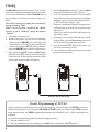
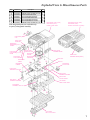
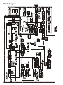


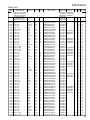
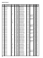

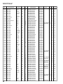

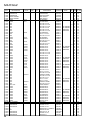


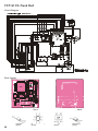
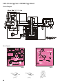


![全国の商品テスト概要[PDF形式]](http://vs1.manualzilla.com/store/data/006553164_2-632c6c5aab952bf844285b6a8ec0211d-150x150.png)