1
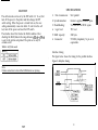
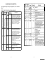
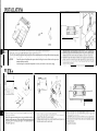
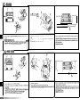
EPSON OVERSEAS MARKETING LOCATIONS
1
EPSON AMERICA. INC.
2780 Lomita Blvd..
EPSON DEUTSCHLAND GmbH
ZUlpicher Stra6e 6. 4000 OUsseldarf 11
Torrance, Calif. 90505. U.S.A
F.R. Germany
Phone: (213) 539-9140
Phone: 10211) 56030
Fax:
Telex:
(213)
534-5654
32KB
6584766
EPSON UK LTD.
Campus 100. Maylands Avenue.
EPSON FRANCE S. A.
Hemel Hempstead. Her,s.
LevallowPerref.
HP2 7EZ. U.K.
Phone: (1) 47-373333
Phone: 442-61144
Telex. 5 162467
Telex. 610657
68 bis. rue Marjohn 9 2 3 0 0 .
Parallel Interface
France
EPSON AUSTRALIA PTY. LTD.
““at 3. 17 Rodborough Road.
EPSON SINGAPORE PTE. LTD.
Frenchr Forest. NSW 2066, Austreha
OUB Centrs.
Phone:
Phone:
12) 452-0666
No. 1 Raffles Place #26-00
Singapore 0104
533-0477
Fax: (2) 975-1409
Fax:
EPSON ELECTRONICS TRADING LTD.
EPSON ELECTRONICS TRADING LTD.
(TAIWAN BRANCH)
25/F. Harbour Centre.
533-6119
25 Harbour Road. Wanchai.
1OF. No. 287 Nankmg E. Road Sec. 3.
Hong Kong
Taipei. Taiwan. R.O.C.
Phone:
Phone: (02) 717-7360
5-6314600
Telex: 65542
Fax: (02) 712-9164
EPSON ITALIA S.D.A.
EPSON-ST1 S.A.
V. le F. 111 Carwaghi. 4 2 7 2 0 0 9 9
SESTO S. GIOVANNI MI. Italy
Phone: 4 1034.00
Phone: 2.26233,
Fax: 2.2440750
Pans. 152. 08036 Barcelona. Span
Fax:
239-95-17
SEIKO EPSON COR PORATION
(Hirooka Office)
80 Harashmden, Hiraoka
Sh,o,m-sh,.
Nagano-ken
399.07 Japan
Phone: (0263) 52.2552
1989 July
Printed in Japan 89.12-.4
FCC COMPLIANCE STATEMENT
FOR AMERICAN USERS
32KB Parallel Interface
This equipment has been tested and found to comply with the limits for a Class B digital device.
Pursuant to Part 15 of the FCC Rules. These limits are designed to provide reasonable protection
against harmful Interference in a residential installation. This equipment generates, uses and can
radiate radio frequency energy and, if not installed and used in accordance with the instructions,
may cause harmful interference to radio communications. However there is no guarantee that
interference W ill not occur in a particular installation. If this equipment does cause harmful
interference to radio or television reception, which can be determined by turning the equipment
off and on, the user is encouraged to try to correct the interference by one or more of the following
measures:
- Reorient or relocate the receiving antenna
- Increase the separation between the equipment and receiver.
- Connect the equipment into an outlet on a circuit different from that to which the receiver
is connected.
- Consult the dealer or an experienced radio/TV technician for help
32-KB-Schnittstellenkarte
This device complies with Part 15 of the FCC Rules. Operation is subject to the following two
conditions:
(1) this device may not cause harmful interference. and
(2) this device must accept any interference received,
including interference that may cause undesired operation.
Interface parallsle 32Ko
FOR CANADIAN USERS
This digital apparatus does not exceed the Class B limits for radio noise emissions from digital
apparatus as set out in the radio interterence regulations of the Canadian Department of
Communications.
Le pr6sent apparelI numerique “‘Pm& pas de bruits radioClectriques depassant les limites
applicables aux appareils numdnques de Class B prescrites dam lr rGglrment SW le brouillage
radi&lectrique edict6 par le Minis&w des Commumcatmns du Canada.
WARNING
Interface en paralelo de 32KB
The connection of a non-shielded printer interface cable to this printer will invalidate the FCC
Certification of this device and may cause interference levels which exceed the limits established
by the FCC for this equipment. If this equipment has more than one intertace connector. do not
leave cables connected to unused interfaces.
Seiko Epson Corporation shall not be liable against any damages or problems arising from the use
of any options or any consumable products other than those designated as Original Epson
Products or Epson Approved Products by Seiko Epson Corporation.
NOTICE
All rights reserved. Reproduction of any part of this manual, in any form whatsoever without Seiko
Epsons express written permission is forbidden.
The contents of this manual are subject to change without notice.
All efforts have been made to ensure the accuracy of this manual. However. should any errors be
detected, Seiko Epson would greatly appreciate being informed of them
The above notwithstanding, Seiko Epson can assume no responsibility for any errors in this
manual or their consequences.
Copyright © 1989 by Seiko Epson Corporation. Nagano. Japan
Interfaccia parallela da 32 KB
i
TABLE OF CONTENTS
INTRODUCTION
About this guide
2
3
SETTING THE CONDITIONS
Board layout
DIP switch settings
Jumpers
Jumper settings
4
4
5
6
7
DATA ENTRY
About data entry
9
9
SELF TEST
10
SPECIFICATIONS
11
HARDWARE DESCRIPTION
12
INSTALLATION
FX, FX+
LX-80/86
LQ-800/1000
About this guide
This guide is designed to give you detailed information on
how to install your C82303* interface board in a variety of
Epson printers. Installation procedures vary slightly depending upon the printer model that you have.
Also included, are instructions on how to adjust the settings of
the C82303* interface board, as well as a general description of
parallel data communication.
The C82303* option package contains the following items:
C82303* parallel I/F board (1)
FG plate
3
SETTING THE CONDITIONS
The C82303* interface board has a set of DIP (Dual In-line
Package) switches, and 6 jumpers. This switch and jumpers
are used for selecting various interface operations.
Board layout
The diagram below shows the layout of the C82303* board,
and the locations of the DIP switch and jumpers.
Figure 1. Board layout
DIP switch settings
Before you install the C82303* interface, you may need to
adjust some of the settings. When making DIP switch setting
changes, it is best to use a pointed device, such as a ball-point
pen or small screwdriver.
Caution
All changes of DIP switch and jumper settings should be made
with the printer power turned off. The printer checks and
recognizes new settings only at the time the power is turned
About DIP switches
A set of DIP switches on the C82303* is labelled SW1. SW1
contains a number of individual toggle type switches that can
be set either on or off. The individual switches are referred to
by set (SW1) and number. Therefore, the switch in set SW1
marked by the small number 3 is called DIP switch 1-3.
5
DIP switch 1
The table below contains information on switch functions, and
the factory setting of each switch. The switches on DIP switch
1 allow you to change interface functions.
Table 1. DIP switch 1
1 SW Ipin No.1
( ON 1 Off ( Factory setting )
Function
J
1-1
I/F board enable/disable
Enable Disable
ON
1-2
Buffer enable/disable
Enable Disable
ON
1-3
Self test enable/disable
I
Enable I Disable
-
OFF
1-4
Jumper settings
The tables below give you information about the interface
conditions that can be selected using jumpers. In all cases, ON
denotes the connection of the jumper (covering both terminals), while OFF denotes the disconnection of the jumper.
I
Not used.
Table 2. Jumper settings
Function
Jumper
ON: SLCT IN signal is enable. (See Note 1.)
J1
Fixed (See Note 2.)
12
OFF
I H
A
Jumpers
The jumper is a small terminal used for connecting or disconnecting a circuit. The jumper is on when the jumper plug
covers both wires of the terminal. Jumper settings can be
changed by either attaching or removing the rectangular
jumper plug. If the jumper is to be turned off, connect it to just
one of the two terminal pins as shown in the figure below. By
doing this, you can avoid losing the unused jumper plug.
Figure 2. lumpers
J4
ON (close)
6
Data latch liming
selection.
See Table 3.
JG 1 ON: Connect Chassis Ground to Signal Ground.
OFF
Note
1. SLCT IN signal can be fixed LOW by setting the printer
DIP switch , jumper or SelecType function. If this signal is
fixed Low, you should not connect J1. When J1 is ON,
SLCT IN signal (pin No. 36 of I/F connector on the I/F
board) is connected to the printer through the I/F board to
enable it to be controlled by a Host computer. Sampling
this signal is always carried out by the printer, therefore
this function depends on the printer specification.
2.
OFF (open)
B
OFF
-
Fixed (See Note 2.)
J3
Factory Setting
J2 and J3 jumpers are connected at the factory, and you
should not change these setting.
I
DIP switch 1
The table below contains information on switch functions, and
the factory setting of each switch. The switches on DIP switch
1 allow you to change interface functions.
Table 1. DIP switch 1
1 SW Ipin No.1
( ON 1 Off ( Factory setting )
Function
J
1-1
I/F board enable/disable
Enable Disable
ON
1-2
Buffer enable/disable
Enable Disable
ON
1-3
Self test enable/disable
I
Enable I Disable
-
OFF
1-4
Jumper settings
The tables below give you information about the interface
conditions that can be selected using jumpers. In all cases, ON
denotes the connection of the jumper (covering both terminals), while OFF denotes the disconnection of the jumper.
I
Not used.
Table 2. Jumper settings
Function
Jumper
ON: SLCT IN signal is enable. (See Note 1.)
J1
Fixed (See Note 2.)
12
OFF
Jumpers
The jumper is a small terminal used for connecting or disconnecting a circuit. The jumper is on when the jumper plug
covers both wires of the terminal. Jumper settings can be
changed by either attaching or removing the rectangular
jumper plug. If the jumper is to be turned off, connect it to just
one of the two terminal pins as shown in the figure below. By
doing this, you can avoid losing the unused jumper plug.
Figure 2. lumpers
I
A
J4
JG
ON (close)
6
Data latch liming
selection.
See Table 3.
ON: Connect Chassis Ground to Signal Ground.
OFF
Note
1. SLCT IN signal can be fixed LOW by setting the printer
DIP switch , jumper or SelecType function. If this signal is
fixed Low, you should not connect J1. When J1 is ON,
SLCT IN signal (pin No. 36 of I/F connector on the I/F
board) is connected to the printer through the I/F board to
enable it to be controlled by a Host computer. Sampling
this signal is always carried out by the printer, therefore
this function depends on the printer specification.
2.
OFF (open)
B
OFF
-
Fixed (See Note 2.)
J3
Factory Setting
J2 and J3 jumpers are connected at the factory, and you
should not change these setting.
I
DATA ENTRY
Table 3. Data latch timing selection
Jumper
J4
Function
* ON Falling edge of
B OFF STROBE
OFF Rising edge of
ON STROBE
Note
Either J4A or J4B jumper must be connected.
Factory Setting
ON
OFF
1
About data entry
To accommodate data entry, the C82303* interface board is
equipped with a buffer that temporarily stores data before
transferring it to the printer. When this buffer becomes full,
any additional transmitted data cannot be accepted and is
discarded.
The buffered data is transferred transparently to the printer
main board every time the printer enters the READY state. A
maximum of 512K bytes of data can be buffered with this
board depending on its setting.
8
9
I
SPECIFICATIONS
SELF TEST
The self test mode can be set by the DIP switch 1-3. To set, first
turn off the power to the printer and then change the DIP
switch setting. When the power is turned back on, the new
setting automatically comes into effect. To exit from the self
test, turn off the power and reset the DIP switch.
The interface board first checks the RAM condition. After
checking the RAM, data in the range between <3&H to <3!bH
is sent to the printer and printed. The print out is only 80
columns wide.
1.
Data transmission:
S-bit parallel
2. Synchronization:
External supplied STROBE pulse
3. Handshaking:
Via ACKNLG or BUSY signals
Logic level:
TTL level
5. RAM capacity:
32K bytes
6. Connector:
57-30360 (Amphenol), 36 pin or its
equivalents .
4.
Table 4. Self test mode
Interface timing
The figure below shows the timing for the parallel interface.
Figure 3. Interface timing
Note
It takes some time to check the RAM before test printing.
I
I
I
STROBE
11
HARDWARE DESCRIPTION
For signal description and pin assignment, refer to the table
below:
Table 5. Signal description and pin assignment
-I
Signal I
Pin
izn
Pin
Signal
19
20
21
22
23
24
25
26
27
12
30
13
-
Ike&on
Description
YimiE
IN
STROBE pulse to read data. Pulse
width must be more than 0.5 microseconds at the receiving terminal.
DATA 1
DATA 2
DATA 3
DATA 4
DATA 5
DATA 6
DATA 7
DATA 8
IN
IN
IN
IN
IN
IN
IN
IN
These signals represent information
of the 1st to 8th bits of parallel data,
respectively. Each signal is at
HIGH level when data is logical 1
and LOW when it is logical 0.
vXNLG
OUT
BUSY
OUT
About a IO-microsecond pulse.
LOW indicates that data has been
received and that the interface
board is ready to accept more data.
This signal is output as a pair
together with BUSY.
A HIGH signal indicates that the
interface board cannot receive data.
The signal goes HIGH in the
following cases:
1) During data entry (ea. car. time)
2) When off line
3) During printer-error state
I
OUT
SLCT
OUT
L
12
A HIGH signal indicates that the
printer is out of paper.
Pulled up to +5 V through 3.3k ohm
resistance.
13
Note
1. The column heading “Direction” refers to the direction of
signal flow as viewed from the printer.
2.
All interface conditions are based on TTL level. Both the
rise and fall of each signal must be less than 0.2 KS.
14
L
+xiI ‘Xii
3:
xda
NOILV-IWLSNI
C
000T/008-iTI
we
98/08-X1