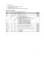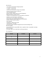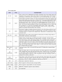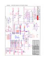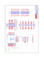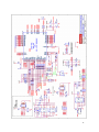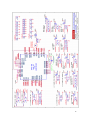
1
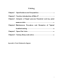
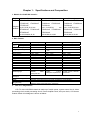
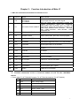
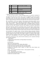
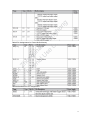
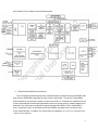
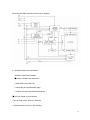
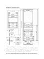
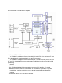
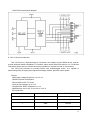
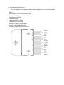
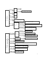
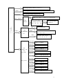
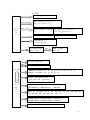
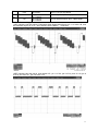
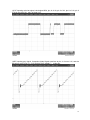
LTA-32N658HCP LTA-32N680HCP LTC-26N680HCP LTC-32N680HCP LCD COLOUR TV SERVICE MANUAL MODEL: LTC-26N680HCP LTC-32N680HCP LTA-32N680HCP LTA-32N658HCP CHASSIS NO.: LS02/PS02 1 Please read this manual carefully before service. 2 Catalog Chapter1 Specifications and Composition ...................................................... 4 Chapter2 Function Introduction of Main IC Chapter3 Analysis of Signal process Flowchart and key point U U U U U .................................................... 7 measure date .................................................................................................... 31 U Chapter4 Maintenance Procedure and Examples of Typical U troubleshooting .............................................................................................. 40 U Chapter5 Spare Part Lists ............................................................................................. 42 Chapter6 Factory Setup and notice ...................................................................... 43 U U U U Appendix: Circuit Schematic diagram 3 Chapter 1: 0B Specifications and Composition 1. Models for LS02/PS02 chassis : Region Europe America Other regions Original Models LT26GHxxE LT37GHxxE LT32GHxxE LT42GHxxE LT47GHxxE xx:01,19,29,30,41 etc. PT32GHxxE PT42GHxxE PT50GHxxE xx:218,528,26,18,36 LT26GHxxU LT37GHxxU LT32GHxxU LT42GHxxU LT47GHxxU xx:01,19,29,30,41 etc. PT32GHxxU PT42GHxxU PT50GHxxU xx:218,528,26,18,36 LT26GHxxA LT37GHxxA LT32GHxxA LT42GHxxA LT47GHxxA xx:01,19,29,30,41 etc. PT32GHxxA T42GHxxA PT50GHxxA xx:218,528,26,18,36 2. Main Feature Region RF Color system signal Sound system Video or Y/C signal Europe PAL、SECAM D/K、B/G、I、L/L’ PAL、NTSC、SECAM Program presetting 100 (0-235) Audio output(THD≤7%) Power source Teletxt CCD VCHIP Sound demodulator SCART VGA YPbPr HDMI Earphone 5W+5W 100V~240V 100 pages X X NICAM、IGR Yes Yes Yes Yes Yes English, French, German, Italian, Portuguese etc. OSD language Auto Off without Signal Reception Program booking Swap Plug and Play 3. America NTSC、PAL M/ N M/N PAL、NTSC、SECAM 181 (AIR:2-69;CABLE: 1-125) 5W+5W 100V~240V X Yes Yes BTSC X Yes Yes Yes Yes Other regions PAL、NTSC、SECAM D/K、B/G、I、M PAL、NTSC、SECAM 5W+5W 100V~240V 100 pages X X NICAM、IGR X Yes Yes Yes Yes English, French, Portuguese, Spanish etc. English, French, German, Spanish etc. 236 (0-235) 5 minutes 5 program booking. Turn to the corresponding program at the booking time. Customer could rearrange the channels according to personal habit LCD TV could be used as computer screen, no need for the installation of software, which is Plug and Play in real sense Unit IC Compositions: LCD TV with LS02/PS02 chassis is made up of switch power, system control circuit, video processing circuit, audio processing circuit, Power Amplifier circuit, AV input circuit, LCD screen module. Block circuit diagram is shown as below: 4 RS232 IR_Key 5V Flash Speaker E2PROM 12V AMP I/O IF LVDS 8Mx16DDR SVP_AX32 TUNER D_Port TV-CVBS,SIF V1,RGB,FS1,FB1,Vout1 Y1Pb1Pr1 PS301 19 HDMI Lin1/Rin1 Lo1/Ro1 Y C,FS2 Lin2/Rin2 Lo2/R02 Y C 1 VGA S-Video Y1Pb1PR1/L3R3 V3 L3 SCART2 SCART1 Headphone R3 S_Video EU Model Y1 V3 Pb1 L3 Pb1 R3 V2 L2 R2 V1 L1 R1 S_Video CHN Model Y1 Pb1 Pb1 Y2 Pb2 Pr2 VO1 LO1 RO1 5 4. Introduction of PCB module LCD TV with LS02/PS02 Chassis is made up of power board, side AV board, remote control reception board, key board, and mainboard. The table below is the introduction of the function of all printed board modules. No. 1 Parts Description Mainboard module is the core of LCD TV signal processing. Under the control of the system control circuit, It undertakes the task of converting the external input signal into the unified digital signal that the LCD screen could identify. Mainboard controls the whole machine through IIC bus, decode VIDEO signal, controls the Video (brightness, contrast, chroma, hue, definition etc), white balance adjusts, generates OSD, de-interlaces signal, converts signal frequency, and finishes signal A/D and D/A conversion, video enhancement, LVDS signal coding and output; it has Scart , S-Video, AV , YPbPr, HDMI and PC interface, Tuner input, sound demodulation, sound processing, sound power amplifier, and online update. Mainboard module The remote reception board module is constituted by an indicator-light and a remote reception. Customer could manipulate the LCD TV by using remote controller very conveniently. By the color of the indicator light, the operation mode of the LCD TV could be judged (red is standby, green is power on). Remote 2 reception module 3 Built-in power Convert the 100V~240V (50/60HZ)AC into DC, output have +12V, +5V, board module +3.3V and the +5V_STB in standby state. 4 Keyboard module Keyboard module has 7 function keys (program +/-, volume +/-, AV/TV, menu ,power), customer could use the key to operate the TV freely. LCD screen has built-in inverter that convert DC into high voltage AC signal to LCD screen 5 turn on the backlight CCFL (Cold Cathode Fluorescent Light); the LCD screen module process the video signal from signal board and reappear. 6 Side board AV Side AV board is used for earphone output. 6 Chapter 2: Function Introduction of Main IC 1. Main ICs and functional modules of LS02/PS02 chassis No. Item no. Model Main function 1 U8 AFT7/W003 AFT7/W103 AFT7/W300 Tuner,output sound IF and video signal 2 U1 SVP-AX32LF/SVP-AX68LF SVP AX family video processors provide the highest performance, target the converging HDTV-ready and PC-ready LCD TV, PDP TV applications where high precession processing of video, which Embed in ADC converter、 3D comb filter 、 HDMI processor 、 video decoder 、 LVDS transmitter etc. 3 U3 AT24C64-SO8-DNS EEPROM 4 U5 W25X80-VSSIG 8M-bit Serial Flash, Store the Control program. 5 U7 HY5DU281622FTP-4 8M×16bits DDR SDRAM 6 U9 TDA9886T 7 U11 74HC4052 Audio signal switch of AV terminal 8 U15 74LVC14A VGA line and field synchronizing signal waveform shaping 9 U16 AT24C64 EEPROM 10 U17 IRF7404/AO4459 Field Effect Transistor 11 U22 MP1411DH DC-DC converter 12 U20、U24 AP1117E33 LDO,5V to 3.3V DC converter 13 U23 AP1122EL LDO,5V to 1.2V DC converter 14 U27 TDA7266SA Audio amplifier (BTL output) 15 U32 PS201 HDMI two-to-one switch Multistandard alignment-free IF-PLL demodulators 2. Function introduction of ICs or functional module of LCD TV with LS02/PS02 chassis 1. Tuner (Asian TV:AFT7/W003;European TV: AFT7/W103;American TV: AFT7/W300) 1B No. Terminal name Description 1 AGC AGC voltage supply 2 NC No Connected 3 SAS Address Selection Line 4 SCL Serial Clock 5 SDA Serial Data 6 NC No Connected Line Line 7 7 BP +B For PLL & Mixer 8 ADC/NC ADC Input/ No Connected 9 NC No Connected 10 NC No Connected 11 IF1 IF 12 ANT VHF/UHF Output Signal Input 2. Video processing IC SVP-AX32LF/SVP-AX68LF The SVPTMCX video processor is a highly integrated system-on-a-chip device, targeting the converging HDTV-ready and PC-ready LCD TV, PDP TV applications where high precision processing of video and data are the requirements. SVPTMCX contains 6th generation dual-purposed triple 10-bit high-precision and high speed video ADCs for both PC and video inputs, the high-performance multi-format 3D digital comb video decoder that supports NTSC, PAL, and SECAM*, a HDTV sync separator, motion adaptive de-interlacing engine, and the video format conversion engine, supporting multi-window display in many different output modes. Trident’s DCReTM – Digital Cinema Reality engine, is integrated inside the SVPTMCX family to provide the most natural cinema-realistic images. The DCReTM technology integrates advanced 3D-comb video decoding, advanced motion adaptive de-interlacing, object-based digital noise reduction, advanced 7th generation scaler, film mode support, average picture level (APL), edge smoothing and dynamic sharpness enhancement. Trident's patented Unified Memory Architecture (UMA) that allows frame rate conversion, 3D comb video decoding, and video enhancement processing to share the same memory buffer that is made up of high-speed and cost-effective PC graphic memory. All these advanced digital processing techniques combined with a true 10-bit video data processing for the most optimal video fidelity to provide the most natural and cinema quality video images. Designed for maximum system design flexibility, SVPTMCX integrates all video interfaces to support converging digital video, analog video, and PC data applications. The users of Trident's single chip SVP™CX series video processor(s) will benefit from many features while maintaining a price competitive advantage over the existing solution(s) Main features: ●Integrated 7th Generation Motion and Edge Adaptive De-interlacing ● Integrated ADC ● PC auto tune ●Built-in 8-bit LVDS Transmitter ●Advanced 7th generation cubic-4 image scaling engine ● Advanced Chroma Processing and Dynamic Contrast Function ● Green color stretch, blue color stretch, skin color enhancement ●Integrated 7th Generation Motion Adaptive 3D Digital Comb Video Decoder with Programmable Filter ●60Hz~100Hz interlaced scanning and 50Hz~75Hz progressive scanning ● frame rate conversion ● 14D: dynamic picture enhancements ● Advanced Film Mode Recovery-3:2/2:2 pull down ● Build-in A/D conversion function 8 ● Teletext function ● Supports 16bits DDR memory interface ● Multi-screen display mode ● OSD and VBI/Closed caption and advanced OSD engine Pin function description: Table1: Pin Assignments for CPU-related and GPIO pins 9 10 11 Table2 Pin Assignments for Analog Support Interface Table3 Pin Assignments for Analog Input Interface Table4 Pin Assignments for Capture Interface (TV&RGB) 12 Table5 Pin Assignments for Frame Buffer Memory Table6 Miscellaneous Pin Assignments 13 Table7 LVDS Output Pin Assignments Table8 HDMI Interface Pin Assignments Table9 Analog Audio Input/Output Interface Pin Assignments 14 Table10 Digital Audio Interface Pin Assignments Table11 Pin Assignments for Power and Ground 15 16 SVP-CX32LF/ SVP-CX68LF internal block diagram: 3.AT24C64-SO8-DNS brief introduction: The AT24C64A provides 65,536 bits of serial electrically erasable and programmable read only memory (EEPROM) organized as 8192 words of 8 bits each. The device’s cascadable feature allows up to 8 devices to share a common two-wire bus. The device is optimized for use in many industrial and commercial applications where low power and low voltage operation are essential. The AT24C64A is available in space saving 8-lead JEDEC PDIP, 8-lead JEDEC SOIC, 8-lead EIAJ SOIC, 8-lead MAP and 8-lead TSSOP packages and is accessed via a 2-wire serial interface. In addition, the entire family is available in 2.7V (2.7V to 5.5V) and 1.8V (1.8V to 5.5V) versions. 17 Main features: • Low-Voltage and Standard-Voltage Operation – 2.7 (VCC = 2.7V to 5.5V) – 1.8 (VCC = 1.8V to 5.5V) • Low-Power Devices (ISB = 6μA @ 5.5V) Available • Internally Organized 4096 x 8, 8192 x 8 • Two-wire Serial Interface • Schmitt Trigger, Filtered Inputs for Noise Suppression • Bidirectional Data Transfer Protocol • 100 kHz (1.8V) and 400 kHz (2.5V) Clock Rate for AT24C32A • 400 kHz (1.8V) Clock Rate for AT24C64A • Write Protect Pin for Hardware Data Protection • 32-byte Page Write Mode (Partial Page Writes Allowed) • Self-timed Write Cycle (5 ms Max) • High Reliability – Endurance: 1 Million Write Cycles – Data Retention: 100 Years • Automotive Grade, Extended Temperature and Lead-free/Halogen-free Devices Available • 8-lead JEDEC PDIP, 8-lead JEDEC SOIC, 8-lead EIAJ SOIC, 8-lead MAP and 8-lead TSSOP Packages • Die Sales: Wafer Form, Waffle Pack, and Bumped Wafers Pin Configuration Pin NO. Pin Name Function 1-3 A0 – A2 Address Inputs 4 GND Ground 5 SDA Serial Data 6 SCL Serial Clock Input 7 WP Write Protect 8 VCC Power Supply 18 AT24C64-SO8-DNS internal functional block diagram: 4.W25X80-VSSIG brief introduction W25X80-VSSIG main features: ■Family of Serial Flash Memories ● 8M-bit/1M-byte(1,048,576) ● 256-bytes per programmable page ● Uniform 4K-byte Sectors/64K-byte Blocks ■ SPI with Single or Dual Outputs ● Clock ,Chip Select, Data I/O, Data Out ● Optional Hold function for SPI flexibility 19 ■ Data Transfer up to 150M-bits/second ● Clock operation to 75MHz ● Fast Read Dual Out instruction ● Auto-increment Read capability ■ Flexible Architecture with 4KB sectors ● Sector Erase(4K-bytes) ● Block Erase(64K-byte) ● Page program up to 256 bytes<2ms ■ Low Power Consumption, Wide Temperature Range ● Single 2.7 to 3.6V supply ● 5mA active current,1uA Power-down (typ) ■ Software and Hardware Write Protection ● White-Protect all or portion of memory ● Enable/Disable protection with /WP pin ● Top or bottom array protection Pin introduction: Pin NO. Pin Name I/O Function 1 /CS I Chip Select Input 2 DO O Data Output 3 /WP I White Protect input 4 GND 5 DIO I/O Data Input/Output 6 CLK I Serial Clock Input 7 /HOLD I Hold input 8 VCC Ground Power Supply 20 W25X80-VSSIG internal block diagram: 5.HY5DU281622FTP-4 brief introduction: The HY5DU281622FT(P) is a 134,217,728-bit CMOS Double Data Rate(DDR) Synchronous DRAM, ideally suited for the main memory applications which requires large memory density and high bandwidth. This Hynix 128Mb DDR SDRAMs offer fully synchronous operations referenced to both rising and falling edges of the clock. While all addresses and control inputs are latched on the rising edges of the CK (falling edges of the /CK), Data, Data strobes and Write data masks inputs are sampled on both rising and falling edges of it. 21 The data paths are internally pipelined and 2-bit prefetched to achieve very high bandwidth. All input and output voltage levels are compatible with SSTL_2. main features: • VDD, VDDQ = 2.3V min ~ 2.7V max (Typical 2.5V Operation +/- 0.2V for DDR266, 333) • VDD, VDDQ = 2.4V min ~ 2.7V max (Typical 2.6V Operation +0.1/- 0.2V for DDR400,400Mbps/pin product and 500Mbps/pin product ) • All inputs and outputs are compatible with SSTL_2 interface • Fully differential clock inputs (CK, /CK) operation • Double data rate interface • Source synchronous - data transaction aligned to bidirectional data strobe (DQS) • x16 device has two bytewide data strobes (UDQS,LDQS) per each x8 I/O • Data outputs on DQS edges when read (edged DQ) Data inputs on DQS centers when write (centered DQ) • On chip DLL align DQ and DQS transition with CK transition • DM mask write data-in at the both rising and falling edges of the data strobe • All addresses and control inputs except data, data strobes and data masks latched on the rising edges of the clock • Programmable CAS latency 2/2.5 (DDR266, 333) and 3/4 (DDR400, 400Mbps/pin product and 500Mbps/pin product) supported • Programmable burst length 2/4/8 with both sequential and interleave mode • Internal four bank operations with single pulsed/RAS • Auto refresh and self refresh supported • tRAS lock out function supported • 4096 refresh cycles/64ms • JEDEC standard 400mil 66pin TSOP-II with 0.65mm pin pitch • Lead free (*ROHS Compliant) 22 Pin introduction: 23 HY5DU281622FTP-4 internal block diagram: 6. TDA9885T/TDA9886T brief introduction: The TDA9885 is an alignment-free multistandard (PAL and NTSC) vision and sound IF signal PLL demodulator for negative modulation only and FM processing. The TDA9886 is an alignment-free multistandard (PAL, SECAM and NTSC) vision and sound IF signal PLL demodulator for positive and negative modulation, including sound AM and FM processing. Features: · 5 V supply voltage · Gain controlled wide-band Vision Intermediate Frequency (VIF) amplifier, AC-coupled · Multistandard true synchronous demodulation with active carrier regeneration: very linear demodulation ,good inter modulation figures, reduced harmonics, and excellent pulse response · Gated phase detector for L and L-accent standard 24 · Fully integrated VIF Voltage Controlled Oscillator (VCO), alignment-free, frequencies switchable for all negative and positive modulated standards via I2C-bus · Digital acquisition help, VIF frequencies of 33.4, 33.9,38.0, 38.9, 45.75, and 58.75 MHz · 4 MHz reference frequency input: signal from Phase-Locked Loop (PLL) tuning system or operating as crystal oscillator · VIF Automatic Gain Control (AGC) detector for gain control, operating as peak sync detector for negative modulated signals and as a peak white detector for positive modulated signals · External AGC setting via pin OP1 · Precise fully digital Automatic Frequency Control (AFC) detector with 4-bit digital-to-analog converter, AFC bits readable via I2C-bus · Take Over Point (TOP) adjustable via I2C-bus or alternatively with potentiometer · Fully integrated sound carrier trap for 4.5, 5.5, 6.0, and 6.5 MHz, controlled by FM-PLL oscillator · Sound IF (SIF) input for single reference Quasi Split Sound (QSS) mode, PLL controlled · SIF-AGC for gain controlled SIF amplifier, single reference QSS mixer able to operate in high performance single reference QSS mode and in intercarrier mode, switchable via I2C-bus · AM demodulator without extra reference circuit · Alignment-free selective FM-PLL demodulator with high linearity and low noise · Four selectable I2C-bus addresses · I2C-bus control for all functions · I2C-bus transceiver with pin programmable Module Address (MAD). Pin function 25 TDA9886T internal block diagram: 26 7. 74HC4052 brief introduction: The M74HCT4052 is a dual four-channel analog MULTIPLEXER/DEMULTIPLEXER fabricated with silicon gate C2MOS technology and it is pin to pin compatible with the equivalent metal gate CMOS4000B series. It contains 8 bidirectional and digitally controlled analog switches. Feature: • Low power dissipation: ICC = 4mA (MAX.) at TA=25°C •Logic level translation to enable TTL logic signal to communicate With ±5V analog signal • Low "ON" resistance: 70W TYP. (VCC - VEE = 4.5V) 50W TYP. (VCC - VEE = 9V) •Wide analog input voltage range: ±6V •Fast switching: tpd = 13ns (TYP.) at TA = 25 °C • Low crosstalk between switches • High ON/OFF output voltage ratio •Wide operating supply voltage range (VCC - VEE) = 2V TO 12V • Low sine wave distortion: 0.02% at VCC - VEE = 9V •Compatible with TLL outputs: VIH = 2V(MIN.) VIL = 0.8V (MAX.) • PIN and function compatible with 74 series 4052 Pin introduction: Pin SYMBOL Function description 1,5,2,4 2Y0 to 2Y3 Independent Input Outputs 6 INH INHIBIT Input 7 VEE Negative Supply Voltage 10,9 A,B Select Inputs 12,14,15,11 1Y0 to 1Y3 Independent Input Outputs 3 2-COM Common X Output/Input 13 1-COM Common Y Output/Input 8 GND Ground 16 VCC Positive Supply Voltage 27 74HCT4052 internal block diagram: 8. 74LVC14A brief introduction: The 74LVC14A is a high-performance, low-power, low-voltage, Si-gate CMOS device, superior to most advanced CMOS compatible TTL families. Inputs can be driven from either 3.3 or 5 V devices. This feature allows the use of these devices as translators in a mixed 3.3 and 5V environment. The 74LVC14A provides six inverting buffers with Schmitt-trigger action. It is capable of transforming slowly changing input signals into sharply defined, jitter-free output signals. Feature: · Wide supply voltage range from 1.2 to 3.6 V · CMOS low power consumption · Direct interface with TTL levels · Inputs accept voltages up to 5.5 V · Complies with JEDEC standard no. 8-1A · Specified from -40 to +85 °C and -40 to +125 °C. Pin introduction: PIN SYMBOM DESCRIPTION 1,3,5,9,11 and 13 1A to 6A Data input 2,4,6,8,10 and 12 1Y to 6Y Data output 7 GND Ground 14 VCC supply voltage 28 14.TDA7266SA brief introduction: The TDA7266SA is a dual bridge amplifier specially designed for TV and Portable Radio applications. Feature: • WIDE SUPPLY VOLTAGE RANGE (3-18V) • MINIMUM EXTERNAL COMPONENTS – NO SWR CAPACITOR – NO BOOTSTRAP – NO BOUCHEROT CELLS – INTERNALLY FIXED GAIN • STAND-BY & MUTE FUNCTIONS • SHORT CIRCUIT PROTECTION • THERMAL OVERLOAD PROTECTION PIN CONNECTION: 29 TDA7266SA internal block diagram: 30 Chapter 3: 2B Analysis of Signal process Flowchart and key point measure date This chapter mainly introduces the receipt and dispose of AV signal the power supply system and system control process of this TV. 1. Video signal flow RF signal is demodulated by tuner, then the obtained video signal and signals inputted from COMPONENT terminal, AV, S-VIDEO, 2-way SCART interface and VGA interface are all sent into video-processing IC SVP-AX32LF/SVP-AX68LF for decoding. The different format input signals are changed into uniform LVDS signals, and are sent to LCD screen. In addition, TV video signal is processed by SVP-AX32LF/SVP-AX68LF to generate 2 CVBS signal, which are used in SCART video output. Signal inputted from HDMI interface is into video decoding IC SVP-AX32LF/SVP-AX68LF for decoding. After procession, the obtained uniform LVDS differential signal is sent into LCD Screen. 2.Sound process flow RF signal is demodulated by tuner, and then the obtained SIF signal (SIF-2 signal) and audio signal inputted from Scart1 interface are are first sent into 74HCT4052D for choosing passages. The output audio signal of 74HC4052 is sent into power amplifier TDA7266DNS, and the amplified signal is finally sent into speaker or earphone. Signals from HDTV terminal, AV terminal, Scart2 interface and PC Audio are first sent into 74HCT4052 for choosing passages, and then sent into SVP-AX32LF/SVP-AX68LF for demodulation and sound process. The output audio signal of SVP-AX32LF/SVP-AX68LF is sent into power amplifier TDA7266DN, and finally the amplified signals are sent into speaker or earphone. After the demodulation and sound effect processing of SVP-AX32LF/SVP-AX68LF, there is an audio output which is used for sound output of Scart1 terminal. 3. Power supply system There are 3 ways of voltage output in the power panel:+12V、+5V and +5V-SB. +12V output is provided for power amplifier TDA7266, and is also changed into +1.2V output by MP1411 to supply SVP-AX IC; +5V output is changed into 3.3V output,2.5Voutput and 1.2V output by DC/DC (such as AX_VD33) to satisfy the needs ICs. +12V and +5V outputs will be cut off in standby state. While +5-SB output is the power supply of MCU, infrared receiver and EEPROM etc, and will be cut off when the AC is turn off. 5V output will be divided into two ways: one way is changed into 5VA power supplies through DC/DC converter for TUNER, 74HCT4052 IC etc and peripheral circuits; the other way of 5V voltage supply power especially for MCU, infrared receiver and EEPROM etc, and will still operating in standby state. (1) The composition and distribution of the TV power supply(Next page) 31 R408(80mA) +12VA 12V shutdown mute circuit * JP3 PIN1 12V power CON11 PIN 8,7,6,5 FB22* JP3 PIN 2 FB22(320mA) 12V ( voltage of line to screen)CON2 PIN31,32,33 FB6(13mA) SVP-AX ANALOG PIN 230 FB26(112mA) U22 AP1513 1.2V FB29(30mA) SVP-AX Power Supply PIN 23,83,100,122, 151,169,233,244 FB28(44.5mA) SVP-AX ADC Power Supply PIN 32,40,47,49 FB16(20mA) FB15(160mA) 5V_ FB17(45.5mA) TUNER FB14(85.5mA) IF amplify circuitry Sound surface filter circuitry TUNER power supply,U8 PIN 7 +5VA R400 262mA Change 33V 5V POWER CON11 PIN 8, 7,6, 5 TUNER power supply,U8 PIN 9 Starting up mute circuit R280(20mA) 74HCT4052 power supply,U11 PIN 9 U11 PIN 1,2,5,4,11,12,14,15 AX_CVBS_OUT1/2 signal amplify L15* Power supply,U26 PIN 9,2,3, 5,6 FB1* Power supply,U4 PIN9 32 Back light switch control CON20 PIN3,4 FB23* 5V(voltage of line to screen)CON2 PIN 31,32,33,34 PWM back light switch control circuitry FB25 FB24(530mA) DDR power supply,U7 PIN 1,3,9,15,18,33,55,61 U19 change into2.5V FB25 MCU power supply, MCU power supply, U1 PIN 94,107,116, FB33 U1 PIN114 128,142,113,114 (187mA) (354) 5V CON11 PIN 8,7 6,5 FB6 FB27* U22 IC stabilivolt 1.2V FB29 FB28 MCU U1 PIN 230 MCU PIN 23,83,100,122,151, 169,233,244 MCU ADC power supply PIN 32,40,47,49 L3(38.5mA) MCU,U1 PIN54 L4(69.5mA) MCU,U1 PIN51 FB2(51mA) U20 MCU,U1 PIN 59 Change into FB5(15mA) 3.3V MCU,U1 PIN 93,162,246 AX_VD33 FB10(34.5mA) MCU,U1 PIN 202,217,228 FB8(7.2mA) MCU,U1 PIN 62 FB7(31mA) MCU,U1 PIN 25 R21(6.9mA) MCU,U1 PIN 71 AX_VCC33 FB13(47.5mA) MCU,U1 PIN 72 FB12,FB11 MCU,U1 PIN 2,3,7,11,15, 33 (13,45mA) Power Amplifier mute circuit FB19(40.8mA) 5V_SB CON11 PIN 2,3 D18,D17 HDMI EEPROM IC,U12 PIN 8 SDA、SCL,U12 PIN 5,6 IC power supply,U15 PIN 14 CON15 SDA,SCL VGA EEPROM IC,U16 PIN 8 SDA、SCL,U16 PIN 5,6 CON16 SDA,SCL 上 CON11 PIN 4 L:ON H:OFF U23 5V_SB change into 1.2V_SB FB3 (27mA) MCU,U1 PIN 192,193 U6 power supply PIN 2 FB4 (62mA) U24 3.3V_SB 5V_SB CON11 PIN 2,3 MCU IC,U1 PIN 180 HDMI IC,U32 PIN 7,17,27,33,56,13,43,50,61,69,75 HDMI IC,U32 PIN 1,20,19,42,21,22 5V SLV、MST change into 3V Q19,Q20,Q21,Q22 PIN 2,3 MCU RESET IC(IMP810-2.63V),U18 PIN 3 MCU RESET IC(IMP810-2.63V),U18 PIN 2 MCU IC,U1 PIN 85,86,87,255,160,161,177,182,182,183,185, 157,92,89,189,190,198,201,153,154 FLASH ROM IC(W25X80-VSSIG),U5 PIN 7,8 FLASH ROM IC(W25X80-VSSIG),U5 PIN 3 LVDS,CON2 PIN 37,38,39,40 34 (2) Position number Component model Pin 1(V) Pin 2(V) Pin 3(V) U19 AP1117D25 GND 2.5V 5V U20 AP1117E33 GND 3.3V 5V U23 AZP1122EL GND 1.2V 5V U24 AP1117E33 GND 3.3V 5V (3) Pin sequence of power cord of power panel Position number CON1 CON23 Pin Pin description 1 12VA 2 12VA 3 GND 4 GND 1 5V-SB 2,3,7,8 GND 4,5 5V 6 5V-SB 9,10 12V 4. Position and definition of the main components and sockets on mainboard(see next page) 35 (1) Socket definition Serial Position number number 1 CON1 Connecting object Power panel 2 CON4 3 CON5 Earphone Board 4 CON8 SCART1 input 5 CON9 SCART2 input 6 HDMI input 7 CON10 CON27 CON13 VGA audio signal input 8 CON12 S terminal input 9 CON14 VGA input 10 CON21 AV Input 11 CON15 Standby 12 CON16 Standby 13 CON18 Keyboard 14 CON19 15 CON17 Remote control receiving board Standby 16 CON20 17 CON23 (2) Speaker Function description +12V,+12V ,GND,GND L+,L-,R+,R- +3.3V、GND、KEY1、KEY2 +3.3V、REMOTE、GND、indicator1、indicator1 Back light control line GND,GND,back light switch control,back light brightness control Power panel 5V-SB,GND,GND,5V,5V,5V-SB,GND,GND,12V,12V Main components descriptions Serial numbe r A Position number component Function description B U7 SVP-AX32LF/SVP-AX Video decoder, image processor, A/D and D/A 68LF conversion HY5DU281622FTP-4 8M×16bits DDR C U3 AT24C64 EEPROM D U5 W25X80-VSSIG E U9 TDA9886T F U11 74HC4052 8M-bit Serial Flash, Store the Control program. Alignment-free multistandard vision,sound AM and FM processing Audio input switch of AV terminal G U12、U16 H U15 74LVC14A I U17 IRF7404 EEPROM VGA line and field synchronizing signal waveform shaping Thermoelectric Cooler Controller J U19 AP1117D25 5V to 2.5V DC-DC Converter K U24 AP1117E33 5V to 3.3V DC conversion U1 AT24C02 36 L U23 M U27 AP1122EL 5V to 1.2V DC conversion TDA7266SA Audio amplifier (BTL output) AFT7/W003 N AFT7/W103 Tuner output sound IF and video signal U8 AFT7/W300 5. Waveforms at key points (1)RF inputting color bar signal, Composite Video Signal waveform at pin 11 of tuner U8, and the waveform at pin 52 of U1(SVP-AX32LF/SVP-AX68LF) is like this: (2)RF inputting color bar signal, clock signal SCL, pin 11 of U9, pin 6 of U3, pin 6 of U12, pin 6 of U16, pin 154 of U1, pin 4 of tuner U15: 37 (3) RF inputting color bar signal, clock signal SDA, pin 10 of U9, pin 5 of U3, pin 5 of U12, pin 5 of U16, pin 153 of U1, pin 5 of tuner U15: (4)RF inputting grey signal, Composite Video Signal waveform at pin 11 of tuner U15, and the waveform at pin 52 of U1(SVP-AX32LF/SVP-AX68LF) is like this: 38 (7)Inputting sound signal with 1KHz frequency, with the processing of U33 and power amplifier TDA7266DNS, waveform at pin 1, 2, 14, 15 of U33, and waveform at CON4 speaker and CON5 earphone output interfaces: 39 Chapter 4: 3B Maintenance Procedure and Examples of Typical troubleshooting 1. Failure phenomenon: The picture is normal, but OSD has line in it. The reason and the processing: Check the pin of U7 and pin 95-150 of U1 for pseudo soldering, and have pseudo soldering touched up. 2. Failure phenomenon: There is no sound but no picture; there is no OSD when start up, and the back light is bright. The reason and processing: Check the connecting line to screen, and have it connect well 3. Failure phenomenon: There are no picture, no sound, and no flower dot in TV mode, but AV is normal. The reason and processing: Check the tuner and its peripheral circuits (including bus and power supply). If the peripheral circuits work well but there is no output from tuner, then the tuner must failure. 4. Failure phenomenon: LCD television cannot be controlled (including no starting up with red light on, remote control and local key having no effect, etc). The reason and processing: LCD television has crash phenomenon, restart after power off. 5. Failure phenomenon: +5V SB voltage has output, but there are no picture, no sound, and back light and indicating light are not on. The reason and processing: Check other groups of voltage; if they have no outputs, then check Flash to find if it is installed well or damaged. When you meet the following common problems, you might diagnose and get the solutions without contacting with the technicians. 40 Symptoms Possible Reason Solutions No picture, no sound, and no indicator light on 1.The power cord is not plugged in 2.The power is off 1.Plug the power cord in 2.Turn the power on 1.Contrast, sharpness, and color are set improperly 2.Color system is set improperly 3.Sound system is set improperly 1.Adjust the value of Contrast, sharpness, and color 2.Set the Color system to the country broadcasting standard 3.Set the Sound system to the country broadcasting standard Picture and abnormity sound with Picture is spotted or with snow No picture, no sound and indicator light is green Blue screen, AV or SVIDEO is displayed Picture is unclear or shaking or with black horizontal strips (in VGA mode) Signal source is low-grade or the signal cord is in a lower quality Contrast, brightness, color and volume are all in the minimum value or TV is in mute mode. The signal cable is not correctly connected. There is no signal input or the video cable is not connected or incorrectly connected VGA picture adjusted. is not correctly VGA picture is not centered There is no audio signal input or audio cable is not connected correctly No sound VGA picture display improper color with HDMI source, with pixel of full screen snow The remote control does not work The color temp incorrectly by user The source standard is generate adjusted is not Batteries are improperly installed or exhausted Use the qualified signal cord Adjust the value of contrast, brightness, color and volume Connect the signal cable correctly Connect the correctly video cable Enter into “SETUP” menu, select “Auto Tracking” item to perform automatic calibration and adjust “Phase” to solve the problem Connect the correctly audio cable Readjust the color temp, or select the original color setting Plug the HDMI cable again 1.Make sure the positive and the negative polarities are correct. 2.Check if there is a loose contact between the batteries and the springs 3.Replace the batteries 41 Chapter 5: Spare Part Lists 4B This listing of maintenance and repair parts are presented for reference only, modification of parameters will not be informed. For accurate models or specifications, please consult the newest data of our company. Proportion of easy damage (‰) 15B Number Name Part number 12B 13B Print plate number 14B 1. Main Board 1 2. Remote receiving board part 0.5 3. Keyboard part 0.5 4. Inner module 5. LCD screen LG.PHILIPS 6. Electronic tuner AFT7/W003 AFT7/W103 AFT7/W300 7. Dynamic speaker YDT613-A9-10W-8Ω Dynamic speaker 8. Dynamic speaker YDG52-A3-10W-8Ω Dynamic speaker 9. Remote emitter Remote control emitter power FSP205-4E03 JSK4200-014 control GK23J6 Inner power module LCD screen (IF:38MHz) (IF:38.9 MHz) Electronic tuner (IF:45.75 MHz) 5 6B 0.1 7B 0.5 8B 2 9B 2 10B 1 11B 42 Chapter 6: Factory Setup and notice 5B 1. Enter factory menu Switch on TV set, and make LCD at operating state: ① Press 【MUTE】 key on remote control; ② Press “MENU” key on remote control, and switch to “SOUND” option with 【V+】,【V-】key; ③ Move cursor to “Balance” option with 【P+】(or【P-】)and【V+】(or【V-】)key to enter setting status; ④ Press number key “3”、 “1”、“3”、 “8”on remote control to enter password. Entering factory mode is finished. If you want to quit facory mode, Pls. press【Power】key to switch off the TV . ⑴ Factory menu display is presented like bellow: chassis:LS02/PS02 SEP 18 10:37:05 Version:ELT-01-Asian-M32-257.25WL IIC off Clear EEPROM Panel Control Factory Setting System Control Min/Max CONTROL White Balance(Hex) Hotel Option Source Select EnterISP ChangHong Channel Table Notes: “chassis:LS02/PS02”is the TV chassis number, “Sep 18 10:37:05”is the latest upgrading time for software, and“Version:ELT-01-Asian-M32-257.25WL”is the version number of current software. (2)The detailed setting items are given bellow: Contents of first page: Remark Setting item Setting content Setting method Stop I²C bus Used for updating IIC Off “OK”or“V+”,“V-”key communication program E²PROM Press “OK”key first,then Only done in first Clear EEPROM initialization press “V-”key setting station Screen back light Press “V+”,“V-”keys to Panel Control brightness control(or enter submenu select the panel type) Press “V+”,“V-”keys to Factory Setting Factory Setting enter submenu Press “V+” key to enter System Control System Control submenu Only set sub Analog datum setting Press “V+” key to enter Min/Max Control brightness of picture and sound submenu Bri Mid White balance Press “V+” key to enter White Balance submenu parameters setting Press “V+” key to enter Used for hotel TV Hotel Option Hotel mode submenu Source Select EnterISP 43 Channel Table ChangHong Exit Menu Use 【P+】and 【P-】keys on remote control to make up or down option, and use【V+】 and【V-】keys to set. Contents of sub pages: Panel Control Setting item LVDS Mapping SSC SSCDELTA Setting value 0x09 Off 00 Remark Polarity of LVDS signal Factory Setting Setting item Model Type Tuner Select Sound system AutoDetsoundSys overmodulation IIR Factory Out Setting value Asian(Europe) Asian Tuner(Eu Tuner) BG(I,,DK,L,M) On(Off) On(Off) Big/Small >> Remark Output the factory settings System Control Setting item Default Lang EQ Enable Aging Mode Logo TV_ANSTEREOSYS TV_DISSTEREOSYS_FM TV_DISSTEREOSYS TV_DIDUALSYS_FM TV_DIDUALSYS TV_FMSYS HDMI_I2CSYS OTHER_LRSYS Setting value English On(Off) On(Off) On(Off) 01 04 01 04 06 02 83 C1 Remark Default OSD language Min/Max Control Setting item Con Min Con Mid Con Max Bri Min Bri Mid Bri Max Col Min Col Mid Col Max Setting value 30H 70H A2H 00H 88H A2H 00H 40H 70H Setting item Vol Min Vol Mid 1 Vol Mid 2 Vol Mid 3 Vol Mid 4 Vol Max Tre Min Tre Mid Tre Max Setting value 00H 01H 14H 28H 4BH 64H 00H 30H 60H 44 Tnt Min Tnt Mid Tnt Max Shp Min Shp Mid Shp Max 20H 80H E0H 00H 60H A0H Bas Min Bas Mid Bas Max 00H 30H 60H Warm R Gain G Gain B Gain R Offset G Offset B Offset 7DH 80H 9AH 84H 80H 74H White Balance Normal R Gain G Gain B Gain R Offset G Offset B Offset Cool R Gain G Gain B Gain R Offset G Offset B Offset 7DH 80H 9AH 80H 80H 74H 7DH 80H 9AH 80H 80H 90H Hotel Option Setting item Setting value Hotel Enable ON Remark Hotel mode presetting(On——users can enter into Hotel mode,Off——users can’t enter into Hotel mode) Source Select TV AV1 AV2 AV3 SCART1 SCART2AV SCART2YC SCARTAV3 SVIDEO ON ON ON ON OFF OFF OFF OFF ON SVIDEO2 SVIDEO3 COMP1 COMP2 COMP3 PC HDMI1 HDMI2 YCBCR OFF OFF ON ON OFF ON ON ON OFF EnterISP Enter software upgrading mode. Channel Table Presetting TV channel ,only for factory test. Exit Menu Notes: A. In“Min/Max CONTROL” setting item, “Bri Mid”item is used to set sub-brightness of picture; 45 B. White balance needs to be set in “Normal”mode; C. Set CLEAR E²PROM will clear the memory data, So do not set it unless it is needed; other setting items do not need setting. 2. Setting method of factory menu ⑴ Choose setting item Operators can choose setting item orderly with【P+】and【P-】key, font having background display represents the item has been chosen. Press【V+】key to enter sub directory. Use 【P+】and 【P-】keys on remote control to make up or down option, and use【V+】and 【V-】keys to set. (2)All the menu functions are opened in factory mode, item checking and effect testing can be done by using menu if it is needed. (3)Switching TV signal in factory mode can be done by directly pressing the number key. Press【MENU】key to back to the parent of working directory, press【DISPLAY】key to quit factory mode. 46 Appendix :LS02/PS02 module Circuit Schematic Diagram 47 48 49 50 51 52 53 54 55 56 57