1
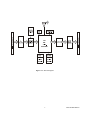
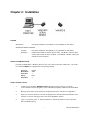
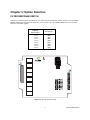
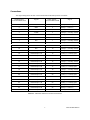
10623 Roselle Street, San Diego, CA 92121 C (858) 550-9559 C Fax (858) 550-7322
[email protected] C www.accesio.com
MODEL WM-IIRO-8
USER MANUAL
1
Notice
The information in this document is provided for reference only. ACCES does not assume any liability arising
out of the application or use of the information or products described herein. This document may contain or
reference inform ation a nd p rodu cts protected by copyrights or patents and does not convey any license under
the patent rights of ACCES, nor the rights of others.
IBM PC, PC /XT, and PC/AT are registered trademarks of the International Business Machines Corporation.
Printed in USA. Copyright 2005 by ACCES I/O Products Inc, 10623 Roselle Street, San Diego, CA 92121.
All rights reserved.
WARNING!!
ALWAYS CONNECT AND DISCONNECT YOUR FIELD CABLING WITH
THE COMPUTER POWER OFF. ALWAYS TURN COMPUTER POWER
OFF BEFORE INSTALLING A CARD. CONNECTING AND
DISCONNECTING CABLES, OR INSTALLING CARDS INTO A SYSTEM
WITH THE COMPUTER OR FIELD POWER ON MAY CAUSE DAMAGE
TO THE I/O CARD AND WILL VOID ALL WARRANTIES, IMPLIED OR
EXPRESSED.
2
Man ual W M-IIRO -8
Warranty
Prior to shipment, ACCES equipment is thoroughly inspected and tested to applicable specifications.
How ever, should equipment failure occur, ACCES assures its customers that prompt service and support
will be available. All equipment originally manufactured by ACCES which is found to be defective will be
repaired or replaced subject to the following considerations.
Terms and Conditions
If a unit is suspected of failure, contact ACCES' Custom er Service de partm ent. Be pre pared to give the unit
model number, serial number, and a description of the failure symptom(s). W e may suggest som e sim ple
tests to confirm the fa ilure. W e will assign a Return Material Authorization (RMA) num ber which must appear
on the outer label of the return package. All units/components should be properly packed for handling and
returned with freight prepaid to the ACCES designated Service Center, and will be returned to the
customer's/user's site freight prepaid and invoiced.
Coverage
First Three Years: Returned unit/part will be repaired and/or replaced at ACCES option with no charge for
labor or pa rts no t exc luded by warranty. W arranty com m enc es w ith equ ipm ent shipm ent.
Following Years: Throughout your equipment's lifetime, ACC ES stands ready to provide on-site or in-plant
servic e at reasonable ra tes sim ilar to those of other m anufacturers in the industry.
Equipment Not Manufactured by ACCES
Equipment pro vided but not m anufactured by ACCES is warrante d and will be repaired according to the
term s and conditions of the re spective equipm ent m anufacturer's w arranty.
General
Under this W arranty, liability of ACCES is limited to replacing, repairing or issuing credit (at ACCES
discretion) for an y products which are proved to be defective during the warranty period. In no case is
ACCES liable for consequential or special damage arriving from use or misuse of our product. The customer
is responsible for all charges caused by m odificatio ns or a dditions to AC CES equipm ent not approved in
writing by ACC ES or, if in ACCE S op inion the eq uipm ent has b een sub jecte d to abno rm al use . "Abnormal
use" for purposes of this warranty is defined as any use to which the equipment is exposed other than that
use specified or intended as evidenced by purchase or sales representation. Other than the above, no other
warranty, expressed or implied, shall apply to any and all such equipment furnished or sold by ACCES.
3
Man ual W M-IIRO -8
Table of Contents
Chapter 1: Introduction . . . . . . . . . . . . . . . . . . . . . . . . . . . . . . . . . . . . . . . . . . . . . . . 5
Functional Description . . . . . . . . . . . . . . . . . . . . . . . . . . . . . . . . . . . . . . . . . . . . . . . . . . . . . 5
Figure 1-1: Block Diagram . . . . . . . . . . . . . . . . . . . . . . . . . . . . . . . . . . . . . . . . . . . . . . . 6
Chapter 2: Installation . . . . . . . . . . . . . . . . . . . . . . . . . . . . . . . . . . . . . . . . . . . . . . . . 7
Chapter 3: Option Selection . . . . . . . . . . . . . . . . . . . . . . . . . . . . . . . . . . . . . . . . . . . 8
Figure 3-1: Option Selection Map . . . . . . . . . . . . . . . . . . . . . . . . . . . . . . . . . . . . . . . . . . . 8
Table 3-1: W M-IIRO-8 Screw Terminal Connections . . . . . . . . . . . . . . . . . . . . . . . . . . . . 9
Chapter 4: Software . . . . . . . . . . . . . . . . . . . . . . . . . . . . . . . . . . . . . . . . . . . . . . . . . 11
General . . . . . . . . . . . . . . . . . . . . . . . . . . . . . . . . . . . . . . . . . . . . . . . . . . . . . . . . . . . . . . . 11
Command List . . . . . . . . . . . . . . . . . . . . . . . . . . . . . . . . . . . . . . . . . . . . . . . . . . . . . . . . . . 12
Command Functions . . . . . . . . . . . . . . . . . . . . . . . . . . . . . . . . . . . . . . . . . . . . . . . . . . . . . 13
Error Codes . . . . . . . . . . . . . . . . . . . . . . . . . . . . . . . . . . . . . . . . . . . . . . . . . . . . . . . . . . . . 18
Chapter 5: Specification . . . . . . . . . . . . . . . . . . . . . . . . . . . . . . . . . . . . . . . . . . . . . . 19
4
Man ual W M-IIRO -8
Chapter 1: Introduction
Features
•
RS2 32 Serial Interface to Host Co m puter.
•
900 MHz W ireless Connection Between Host Computer Modem and W M-IIRO-8.
•
8 Optically-Isolated, Non-Polarized Digital Inputs with Change of State(COS) Detection.
•
8 SPDT Electro-Mechanical Relay Outputs that Switch Up to 1 Amp Each.
•
Digital Outputs May Be Either Level or Pulsed.
•
Type 8031 Microcontroller w ith 8K R AM and 8K E EP ROM. (32K X 8 option al)
•
Ability to Program with Custom Firmware over W ireless Connection
•
NEMA 4 Enclosure for Harsh Atmospheric or Marine Environments.
Functional Description
The W M-IIRO-8 is an intelligent 8-bit parallel digital I/O unit that comm unicates with ACCES’s
W ireless Serial Modem via a 900 MH z wireles s co nne ction. T he W ireless Serial Modem con nec ts
to a host com puter’s standard C OM port using an RS232 (or RS485) serial com m unication s protoc ol.
Both the W M-IIRO -8 and the W ireless Serial Modem are packaged in NEMA4 enc losures for rem ote
installation in harsh environments. ASCII-based comm and/response protocol permits comm unication
with virtually any co m pute r system . It can operate at bau d rate s up to 9600 b aud at distance s up to
7 m iles line-of-sigh t.
Th e 8 iso lated inputs can be driven b y either A C or DC signa ls and are n ot polarity sens itive.
Input signals are rectified by photocoupler diodes. Standard 12/24 AC control transformer
outp uts c an b e ac cep ted as we ll as DC voltages. T he inp ut voltage ra nge is 3 to 28 volts (rm s).
Unused power dissipates through a 1.8KS resistor. Ex terna l resisto rs conn ecte d in se ries w ith
this m ay be used to exten d the input voltag e ra nge. E ach input circuit conta ins a switc hable
slow/fast filter that has a 4.7 ms time constant. (W ithout filtering, the response is 10 :s) The filter
must be selected for AC inputs in order to elim inate response to zero crossings, h ow ever, it is
also valuable for use with slow DC signals in a noisy environment. A filter is individually selected
when a jum per is ins talled onto any of the position s ‘FILT ER 0' thru ‘FILT ER 7'.
The electro-mechanical relay outputs may be programm ed individually or as an 8-bit byte. These
outputs m ay be latched, pulsed, or set to free-run for a prescribed period of time . The relays are
Form C, SPD T, and a re de -ene rgized at power-on.
A type 8031 microcontroller (with 8K x 8 RAM, 8K x 8 non-volatile EEPROM, and a watchdog timer
circu it) gives the W M-IIRO-8 the capability and versatility expected from a m odern distributed control
system. To accom modate special programs, the RAM and EEPR OM can each be expanded to 32K
x 8.
The built-in watchdog timer resets the pod if the microcontroller "hangs up". Data collected by the
pod can be sto red in local R AM and accessed later through the com puter's serial port. This
facilitates stand-alone operation.
The module, or p od, address is pro gram m able from 00 to F F h ex. W hatever address is ass igned to
the pod gets stored in EEPRO M and used as the default address at the next Power-ON. The use of
m odule add ressing allows as m any as 256 W M-IIRO -8 units may be connected to a single host
computer & wireless serial modem .
5
Man ual W M-IIRO -8
Figure 1-1: Block Diagram
6
Man ual W M-IIRO -8
Chapter 2: Installation
POWER
W M-IIRO -8
Plug the provide d AC wall adapto r to any stand ard A C w all outlet.
W IRELESS SERIAL MODEM
Lap tops :
Desktops:
Plug the provide d AC wall adapto r to any stand ard A C w all outlet.
Ins tall th e provided two sectio n pow er cable. The Molex ~ DB 9-F c able
section goes inside the host computer. The DB9-M ~ Modem cable goes
outs ide the hos t com pute r.
SERIAL COMMUNICATION
Plug the provided DB9-F / Modem cable into one of the host computer’s COM Ports. The COM
Port selected MU ST be configured for the following settings:
Pro toc ol:
Baud Rate:
Data Bits:
Parity:
Stop Bits:
RS232
9600
7
Even
1
VERIFY INSTALLATION
1.
Locate and run AC CES ’ WINRISC.EXE application program (easy-to-use serial
com m unication te rm inal pro gram ) on the CD-R OM provided at :\disk s\T ools.win\W IN32\.
2.
Ma tch the pu ll-down m enu setting s to the ap prop riate ‘Po rt’ and a bove co nfiguration.
3.
Click the “Connect” button to connect the application to the Wireless Serial Modem then
click the cursor into the large “data” area of the W INRISC window.
4.
Type “?” and p ress enter. A “M ain Help Screen ” will be returned if the two units have
bee n insta lled pro perly.
7
Man ual W M-IIRO -8
Chapter 3: Option Selection
FILTER RESPONSE SWITCH
Jumpers are used to select input filtering on a channel-by-channel basis. W hen jumper FLT0 is installed,
additional filtering is introduced for input bit 0, FLT1 for bit 1, etc. This additional filtering must be used
whe n AC inputs are a pplied.
JUMPER
SELECTION
Bit Filtered
FLT-0
FLT-1
FLT-2
FLT-3
FLT-4
FLT-5
FLT-6
FLT-7
IN00
IN01
IN02
IN03
IN04
IN05
IN06
IN07
Figure 3-1: Option Selection Map
8
Man ual W M-IIRO -8
Connections
The signal assignment to each of the screw terminal board’s pins are as follows:
‘Isolated Input’
Terminal Block PCB
Signal
‘Relay Outp ut’
Terminal Block PCB
Signal
1
GND
1
Relay 7 - normally closed
2
GND
2
Relay 7 - comm on
3
+PWR*
3
Relay 7 - normally open
4
+PWR*
4
Relay 6 - normally closed
5
N/C
5
Relay 6 - comm on
6
N/C
6
Relay 6 - normally open
7
N/C
7
Relay 5 - normally closed
8
N/C
8
Relay 5 - comm on
9
N/C
9
Relay 5 - normally open
10
N/C
10
Relay 4 - normally closed
11
Isolated Input 7 B
11
Relay 4 - comm on
12
Isolated Input 7 A
12
Relay 4 - normally open
13
Isolated Input 6 B
13
N/C
14
Isolated Input 6 A
14
N/C
15
Isolated Input 5 B
15
Relay 3 - normally closed
16
Isolated Input 5 A
16
Relay 3 - comm on
17
Isolated Input 4 B
17
Relay 3 - normally open
18
Isolated Input 4 A
18
Relay 2 - normally closed
19
Isolated Input 3 B
19
Relay 2 - comm on
20
Isolated Input 3 A
20
Relay 2 - normally open
21
Isolated Input 2 B
21
Relay 1 - normally closed
22
Isolated Input 2 A
22
Relay 1 - comm on
23
Isolated Input 1 B
23
Relay 1 - normally open
24
Isolated Input 1 A
24
Relay 0 - normally closed
25
Isolated Input 0 B
25
Relay 0 - comm on
26
Isolated Input 0 A
26
Relay 0 - normally open
Tab le 3-1: W M-IIRO-8 Screw Terminal Connections
9
Man ual W M-IIRO -8
+PW R*:
Power is power from a local power supply. The voltage can be
anywhere from 7.5 VDC to 16 VDC. Higher local power, 24 VDC
for example, can be used if an external zener diode is used to
reduce the voltage applied to RIOD24. (See Temperature de-rating
com m ents in the Specification sectio n of this manual under "Power
Re quired".)
10
Man ual W M-IIRO -8
Chapter 4: Software
General
You received ASII-based software on CD for use with W M-IIRO-8. ASCII programm ing permits you
to write app lications in any high level language that supp orts A SC II string fu nction s.
The comm unication protocol has two forms: addressed and non-addressed. Non-addressed protocol
can be used when only one W M-IIRO-8 is in use. W hen more than one module (pod) is in use,
addressed protocol must be used. The only difference is that an address com m and is sent to enable
the spe cific po d. The address comm and is only sent once during comm unication between the pod
and the host c om puter. It en ables com m unication with that sp ecific pod and disables all other pods
on the network.
Command Structure
All com m unication mu st be 7 data bits, even parity, 1 stop bit. All numb ers sent to or received from
the pod are in hexa decim al form. Th e factory default baud rate is 9600 Baud. The pod is considered
to be in add ressed m ode any tim e its pod address is not 00. The factory default pod address is 00
(non-addre ssed m ode).
Addressed Mode
The address select comm and must be issued before any other comm and to the addressed pod. The
address comm and is as follows:
"!xx [CR ]" where xx is the pod address from 01 to FF hex, and [CR] is Carriage Re turn, A SC II
character 13.
The pod resp ond s with "xxN [CR ]" or "xx Y[CR]" if an input c han ge o f state has occurred on enabled
bits since the last "Y" or address comm and, or with "xxN[CR]" otherwise.
Once the address select comm and has been issued, all further comm ands (other than a new address
select) will be executed by the selected pod. The addressed mode is required when using more than
one pod.
Non-Addressed Mode
W hen there's only one pod connected, no address select comm and is needed. You can merely issue
comm ands listed in the following table. Terminology used is as follows:
a.
b.
c.
d.
e.
f.
g.
The single lower case letter 'x' designates any valid hex digit (0-F).
The sing le low er case lette r 'b' designa tes eithe r a '1' or '0'.
The sym bol '±' design ates either a '+' or a '-'.
All comm ands are terminated with CR, the ASCII character #13.
W herever xx is used to designate a bit number, only 00-07 are valid.
All comm ands are case insensitive; i.e., upper or lower case letters can be used.
The symb ol '*' mea ns zero or m ore valid characters (total msg length <2 55 decim al).
11
Man ual W M-IIRO -8
Command List
I
Ixx
Oxx0xx
Ox±
Oxx±
Ox±xx
Oxx±xx
Y
Txx
Dx±
Dxx±
Cxx
or
Rxx
Ra ll
V
N
H*
BAUD=xxx
POD=xx
PROG RAM=
D
FASTDATA
Re ad a ll 8 digital bits.
Read a single digital bit. (00<=xx<=0 7)
Ou tput all 8 digital bits.
Output either high or low on bit x
Output either high or low on bit xx
Output either high or low on bit x for time xx
Output either high or low on bit xx for time xx
Re ad d igital input C OS bit and clear bit
Set bit 00-07 Mask for COS bit flag, 1=change will set COS
Set digital input active state high or low on bit x
Set digital input active state high or low on bit xx
Read digital input xx counter (counts ea ch active pulse)
Read pulse/free-run output xx counter and reload value
Reset digital input counter xx to 0000
Reset all digital input counters to 0000
Read the Firmw are version num ber
Resend last response
Gree ting mes sage: cop yright, firm ware version num ber
Set new baud rate. Each x is code number for new baud
Set pod address to xx
Begin process of uploading custom program to pod
Download historical storage of digital input data again
Ac quire bits 0-7 as fas t as possible, the n display
12
xxCR
bCR
CR
CR
CR
CR
CR
Y or N
CR
CR
CR
xxCR
xxCR
CR
CR
x.xxCR
varies
varies
=:Baud:0x
varies
special
varies
varies
Man ual W M-IIRO -8
Command Functions
The following paragraphs give details of the command functions, describe what the comm ands
cause, and give examples. Please note that all comm ands have an acknowledgment response. You
m ust w ait for a resp ons e from a com m and befo re an othe r com m and is sen t.
Read Digital Inputs
I
Ixx
Re ad 8 bits
Read bit number xx
These comm ands read the digital input bits from the pod. All byte or word wide responses are sent
m ost-s ignificant nibb le first.
Exam ples:
Re ad A LL 8 bits.
SEND:
RECEIVE:
Re ad o nly bit 2
SEND:
RECEIVE:
I
FF[CR]
I02
1[CR]
Write Digital Outputs
Oxx
Ox±
Oxx±
Ox±xx
Oxx±xx
bx±xx
bxx±xx
W rite to all 8 digital outpu t bits
Set bit x hi or low
Set bit xx hi or low
Pulse bit x hi or low for time xx
Pulse bit xx hi or low for time xx
Identical to Ox±xx
Identical to Oxx±xx
These comm ands write outputs to digital bits. Any attempt to write to a bit configured as input will fa il.
W riting to a byte or word wherein some bits are input and some are output will cause the output
latches to change to the new value, but the bits which are inputs will not output the value until/unless
they are placed in output mode.
Sin gle bit comm ands will return an error (4) if an attempt is made to write to a bit con figure d as input.
W riting a one to a port asserts the pull-down. W riting a zero de-asserts the pull-down. Therefore,
if the fac tory installed +5V pull-up is installed, writing a one will cause zero volts to be at the
conne ctor, and writing a zero will cause +5 volts to be asserted. If the factory installed pull-up has
been removed, the user supplied pull-up will be asserted.
W rite a zero to bit 2
SEND:
or
SEND :
RECEIVE:
(set output to +5V or user pull-up)
O2O02[CR]
13
Man ual W M-IIRO -8
W rite zeros to every od d bit
SEND:
OAA
RECEIVE:
[CR]
Read Change-of-state
Y
Re ad C OS bit.
The pod can set a change-of-s tate flag for any input th at has been configured to do so. This
comm and will read then reset that bit. Therefore, this comm and will always return "N[CR]" unless the
T c om m and has first been u sed to enable cha nge -of-s tate detec t for an y given b it.
If a chang e-of-state has bee n detected since the last "Y" com m and (see note), the pod will return
"Y[CR]" otherwise "N[CR]" will be returned.
Exam ples:
Read C OS bit
SEND:
RECEIVE:
Note:
Y
N[CR]
The address com m and fo r an y given pod will also return "Y" or "N" and clear the
Change-of-state flag in the pod.
Enable Change-of-State Detection
Txx
Set COS m ask
These com m ands co nfigure the bit-by-bit mask to enable change-of-state to set the COS flag on the
pod for readback by the "Y" or address comm ands. If a one is set for a particular bit, that bit will set
the C OS flag if/wh en the bit ch ang es s tate. A zero w ill disable chan ge-o f-state detection .
Note:
The COS Flag is read via either the "Y" c om m and or a valid address command. The COS
Flag is reset to FALSE by either comm and.
Selecting Which Edge Will Increment Counter
dx±
dxx±
Set Digital input active state on bit x
Set Digital input active state on bit xx
These comm ands allow you to set whether a rising or falling edge will increment the digital input
counter; i.e., if all bits are set to rising edge, the digital input counter for any given bit will increment
each time a rising edge is detected. "+" is rising edge, "-" is falling edge.
Exam ples:
Set bit 1 to rising edge ac tive
SEND:
D1+
or
SEND:
D01+
RECEIVE:
[CR]
Note:
The digital input counters are read with the "cxx" comm and, and reset with the "rxx"
comm and.
14
Man ual W M-IIRO -8
Read Digital Input Counter
cxx
Read digital input counter xx
Tthis comm and will read how m any tim es b it xx ha s ch ang ed to its active state (as c onfigured with
dx± or dx x±) since the last res et com m and (rxx).
Input counters are configured as 16-bit counters. Counter conte nt is provided m ost s ignificant bit first.
Outpu t return values are divided into two eight-bit counte rs. The first byte of the outpu t co unters is
the time-rem aining before the output pulse expires, the second byte is the originally-programm ed
period of free-run o utpu ts. The s eco nd b yte is zero for pu lse ou tputs.
Exam ples:
Read digital input counter for bit #1
SEND:
C01
RECEIVE:
0213[CR];assuming 213hex edges since last reset
Reset Counter
rxx
Reset digital input counter xx
Th is com m and is norm ally used to res et a digital input c oun ter to zero.
Exam ples:
Rese t digital input counter for digital input num ber 3
SEND:
r03
RECEIVE:
[CR]
Read Firmware Revision Number
V
Read the firmware revision number
Th is com m and is use d to read the version of firm ware insta lled in the pod . It returns "X.X X[C R]".
Exam ple:
Read the W M-IIRO-8 version number
SEND:
V
RECEIVE:
1.00[CR]
Note:
The "H" comm and returns the version number along with other information.
Resend Last Response
n
Resend last response
This comm and will cause the pod to return the sam e thing it just sent. Th is com m and works for all
responses less than 255 character in length. No rm ally this com m and is used if the host detected a
parity or other line fault while receiving data, and needs the data to be sent a second time.
The "n" command m ay be repeated.
15
Man ual W M-IIRO -8
Exam ple:
Assum ing that the last comm and was "I", ask pod to resend last response
SEND:
n
RECEIVE:
FF[CR];or whatever the data was
Note:
This comm and may not be used for the FASTDATA comm and, as they exceed the 255
character limit. Use the "D" comm and to perform the sam e task for these three comm ands.
Hello Message
H*
Hello message
Any string of characters sta rting with "H " will be interpreted as this comm and. ("H[CR]" along is also
acc epta ble.) T he re turn from this co m m and take s the form (without the quo tes):
"=Po d aa , W M-IIRO -8 R ev 1.01 F irm ware Ve r:x.xx AC CE S I/O Produc ts, Inc."
aa
rr
x.xx
is the pod address
is the hardware revision, such as "B2"
is the software revision, such as "1.01"
Exam ple:
Read the greeting message
SEND:
Hello?
RECEIVE:
=Pod 00, W M-IIRO-8 Rev B2 Firmware Ver:1.01 ACCES I/O Products,
Inc.[cr]
Programming Pod Address
A=xx
Program the currently selected pod to respond at address xx
This com m and cha nge s the pod 's addres s to xx. If the new a ddre ss is 00, the pod will be plac ed into
non-add ressed mod e. If the new address is not 00, the pod will not respond to further
comm unications until a valid address com m and is issued. Hex num bers 00-FF a re considered valid
addresses. The RS485 specification allows only 32 drops on the line, so many addresses will be
unused.
The new pod address is saved in EEPRO M and will be used even after power-down until the next
"A=xx" com m and is issued. N ote that, it the new address is not 00 (i.e., the pod is configured to be
in addressed mode), it is necessary to issue an address command to the pod at the new address
before it will respond.
The pod returns a message containing the pod number as confirmation.
Exam ple:
Set the pod address to 01
SEND:
A=01
RECEIVE:
=:Pod#01[CR]
Set the pod address to F3
SEND:
A=F3
RECEIVE:
=:Pod#F3[CR]
Take the pod out of addressed mode
SEND:
A=00
RECEIVE:
=:Pod#00[CR]
16
Man ual W M-IIRO -8
Read and Store Digital Input Data
FASTDATA
Read digital bits 0-7 as fas t as possible
These comm ands read the respective byte of d igital input data and store it in SRAM at the fastest
poss ible rate: 21 microseconds between samples. The comm ands will store as much data as the pod
can hold: R A M size -1KB yte. T ypically, th is is 7Kbyte s of da ta, h ow ever, a 32k RA M version is
optionally available, which would provide 31Kbytes of data storage.
Once the d ata has bee n stored, it is du m ped to the s erial po rt. The da ta is form atted into 3-b yte
chunks, followed by a sp ace : xxx xxx xxx ...etc. There are no carriage returns until the last byte has
bee n se nt.
All normal pod activities (parsing comm ands, receiving commands, pulse output countdowns, free-run
generation, CO S dete ct, etc .) STOP until th e serial data is done transmitting. NOTHING else works
until the data has been dumped.
Re-send Data
D
Th is will dum p the last sto red h istorica l data to the serial po rt.
Data can be resent by issuing a "D" comm and. This will dump the las t stored histo rical da ta to the
serial port and can be used, for example, if line noise or similar problems are suspected.
This comm and should only be used after FASTDAT A has been issued, because random data fills the
buffer until one of these comm ands acquire data.
The format of the data is identical to the FASTDA TAx com mands. See the previous description of
the FASTDATA x comm and for more information about the format and length of returned data.
Exam ple:
Resend the data buffer
SEND:
D
RECEIVE:
xxxxx x xxxx xx xxx xxx ... xxxxxx for size of buffer.
Entering a New Program
PROGRAM=
This comm and initiates the transfer of a new program to the W M-IIRO-8.
This comm and should be used carefully. If you accidentally issue a "PROGR AM=" command, ESC
(AS CII 27 ) will restart the pod a s if power had bee n res et.
This feature is designed to allow ACC ES to provide field-upgrades to the W M-IIRO -8 firmware, and,
for advanc ed u sers, the opp ortun ity to custo m ize the firmw are in the pod. Documentation relating to
the use of this comm and is provided with the CD, or is available separately for a small fee.
17
Man ual W M-IIRO -8
Error Codes
The following error codes can be returned from the pod:
1:
3:
4:
9:
Invalid channel number (too large, or n ot a num ber. All channel numbers m ust be between
00 and 17 , in hex. (0-24 decima l))
Im prop er Syntax. (Not enough para m eters is the usua l culprit)
Channel number is invalid for this task (For example, if you try to output to a bit that is set
as an input bit, this error code will occur)
Parity error. (Th is occurs wh en s om e pa rt of the rece ived data conta ins a p arity or framing
error)
Additionally, several full-text error codes are returned. All begin with "Error, ", and are useful when
using a terminal to program the pod.
Error, Unrecognized Command: {command received} [CR]
This occurs if the comm and is not recognized.
Error, Command not fully recognized: {Comm and received} [CR]
Th is occurs if the first letter of the c om m and is valid, bu t the rem aining letters a re no t.
Error, Address command must be CR terminated [CR]
This occurs if the address comm and (!xx[CR]) has extra characters between the pod number and the
[CR ].
18
Man ual W M-IIRO -8
Chapter 5: Specification
General
•
Connectivity:
A serial cable connec ts the host com puter’s CO M po rt
with ACC ES’s W M-D P-232 m odem , which in turn
communicates with the WM-IIRO-8 via a 900 MHz
wireless connection.
•
Intelligence:
Type 8051 microcontroller family provides capability of
•
Protection:
W atch dog Tim er circ uit
•
Mem ory:
Up to 32k RAM & 32k EEPROM.
•
Size of NEMA4 box:
4.53" long by 3.54" wide by 2.17" high
•
W eight:
19.0 oz
local control.
Power Requirements
•
Voltage Range:
7.5 to 15 vo lts
•
Current Range:
130 mA - idle mode
30 mA - increase per relay activation
100 mA - increase during constant transmission
470 m A - m axim um
Idle mode m ay be reduced to 70 mA with cyclic sleep mode
900 MHz Radio
•
Frequency Range:
902 to 928 MHz, Unlicensed ISM Band
•
Type:
Frequency Hopping Spread Spectrum T ransceiver
•
Th roug hpu t:
9600 baud
•
Trans m it Power:
100m W
•
Receiver Sensitivity:
-110dBm
•
Outdoor Range:
7 m iles ( theoretical with line o f sight )
•
Interference Rejection:
70dB at pager and cellular phone frequencies
900 MHz Antenna
•
Frequency Range:
902 to 928 M Hz
•
Impedance:
50 S nominal
•
Gain:
2.1 dBi
•
Length:
7"
•
Polarization:
Vertical
•
W ave:
Half W ave
•
Conn ector:
SMA reverse polarity plug (RPSMA)
19
Man ual W M-IIRO -8
Isolated Inputs
•
Num ber:
Eight
•
Type:
Non-polarized, optically isolated from each other and
from the com puter.
(CMOS compatible)
•
Logic Input Low:
-0.5 V to 0.8 V
•
Logic Input High:
+3.0 V to +33.0 V
•
Isolation:
60V channel-to-ground or channel-to-channel
•
Input Resistance:
1.8K ohms in series with two diodes and an LED.
•
Change of State Detection:
Change-of-state flags can be set on either the rising or
falling edge of a ny enabled input bit a nd can be re ad via
the serial po rt.
Relay Outputs
•
Num ber:
Eight.
•
Contac t Form :
SPDT ( form C )
•
Contact Type:
Single Crossbar
•
Contac t Mate rial:
Silver + Gold-clad
•
Rated Load:
0.5 A at 125 VAC; 1 A at 24 VDC
•
Ma x. Sw itching Current:
1A
•
Max. Switching Voltage:
125 VAC; 60 VDC
•
Max. Sw itch ing Ca pacity:
62.5 VA; 30 W
•
Contact Resistance:
100 m S max.
•
Operate Time:
5 ms
•
Release Time:
5 ms
•
Contac t Life (mech anical):
5 million operations
Environmental
•
Operating Tem perature Range: 0 °C . to 65 °C .
•
Tem perature De-rating:
Based on the power applied, maxim um operating
temperature may have to be de-rated because internal
pow er regulators d issipa te som e he at.
For exam ple, when 7.5VD C is applied, the tempe rature rise inside the enclosure is 7.3 °C. above the
ambient temperature.
Maximum operating temperature can be determined according to the following equation:
V I(TJ = 100) < 19.6 - T A/6.83
W here T A is the ambient temperature in °C. and V I(TJ = 100) is the voltage at which the integral voltage
regu lator jun ction te m pera ture w ill rise to a tem pera ture o f 100 °C.
(No te: The junction tem pera ture is rated to 120 °C . m axim um .)
20
Man ual W M-IIRO -8
For example, at an ambient temperature of 25 °C., the voltage VI can be up to 15.9V .
At an ambient temperature of 100°F (37.8°C), the voltage VI can be up to 14V.
•
Storage Tem perature Range:
-20 °C. to +70 °C.
•
Hum idity:
5% to 95% RH non-condensing.
21
Man ual W M-IIRO -8
Customer Comments
If you experience any problems with this manual or just want to give us som e fe edback , please em ail
us at: m a nu als @ ac ce sio .c om . Please detail any errors you find and include your mailing address
so that we can send you any manual updates.
10623 Roselle Street, San Diego CA 92121
Tel. (858)550-9559 FAX (858)550-7322
www.accesio.com