1
SERVICE MANUAL
■ CONTENTS
SPECIFICATIONS .................................................................................. 3/5
PANEL LAYOUT .......................................................................................7
CIRCUIT BOARD LAYOUT ..................................................................... 9
DISASSEMBLY PROCEDURE ...............................................................10
LSI PIN DESCRIPTION .........................................................................13
IC BLOCK DIAGRAM ............................................................................18
BLOCK DIAGRAM .................................................................................. 19
CIRCUIT BOARDS .................................................................................20
TEST PROGRAM & INITIALIZE ........................................................ 25/33
ERROR MASSAGE ............................................................................ 41/43
CONFIRMATION OF MIDI DATA ....................................................... 42/44
MIDI IMPLEMENTION CHART .............................................................. 45
MIDI DATA FORMAT ......................................................................... 47/53
PARTS LIST
PANEL SWITCH TABLE
OVERALL CIRCUIT DIAGRAM
SY 011446
19981201-99800
HAMAMATSU,JAPAN
1.92K-*** I Printed in Japan’98.12
RM1x
IMPORTANT NOTICE
This manual has been provided for the use of authorized Yamaha Retailers and their service personnel. It has been assumed that
basic service procedures inherent to the industry, and more specifically Yamaha Products, are already known and understood by
the users, and have therefore not been restated.
WARNING:
Failure to follow appropriate service and safety procedures when servicing this product may result in
personal injury, destruction of expensive components and failure of the product to per form as specified.
For these reasons, we advise all Yamaha product owners that all service required should be performed by
an authorized Yamaha Retailer or the appointed service representative.
IMPORTANT:
This presentation or sale of this manual to any individual or firm does not constitute authorization, certification, recognition of any applicable technical capabilities, or establish a principal-agent relationship of any
form.
The data provided is believed to be accurate and applicable to the unit(s) indicated on the cover. The research engineering, and
service departments of Yamaha are continually striving to improve Yamaha products. Modifications are, therefor, inevitable and
changes in specification are subject to change without notice or obligation to retrofit. Should any discrepancy appear to exist,
please contact the distributor's Service Division.
WARNING:
Static discharges can destroy expensive components. Discharge any static electricity you body may have
accumulated by grounding yourself to the ground buss in the unit (heavy gauge black wires connect to this
buss).
IMPORTANT:
Turn the unit OFF during disassembly and parts replacement. Recheck all work before you apply power to
the unit.
WARNING: CHEMICAL CONTENT NOTICE!
The solder used in the production of this product contains LEAD. In addition, other electrical / electronic and / or plastic (where
applicable) components may also contain traces of chemicals found by the California Health and Welfare Agency (and possibly
other entities) to cause cancer and / or birth defects or other reproductive harm.
DO NOT PLACE SOLDER, ELECTRICAL / ELECTRONIC OR PLASTIC COMPONENTS IN YOUR MOUTH FOR ANY REASON
WHAT SO EVER!
Avoid prolonged, unprotected contact between solder and your skin! When soldering, do not inhale solder fumes or expose eyes to
solder / flux vapor!
If you come in contact with solder or components located inside the enclosure of this product, wash your hands before handling
food.
LUTHIUM BATTERY HANDLING
This product uses a lithium battery for memory back-up.
WARNING:
●
●
●
●
●
●
●
●
Lithium batteries are dangerous because they can be exploded by improper handling. Observe the following precautions when handling or replacing lithium batteries.
Leave lithium battery replacement to qualified service personnel.
Always replace with batteries of the same type.
When installing on the PC board by soldering, solder using the connection terminals provided on the battery cells.
Never solder directly to the cells. perform the soldering as quickly as possible.
Never reverse the battery polarities when installing.
Do not short the batteries.
Do not attempt to recharge these batteries.
Do not disassemble the batteries.
Never heat batteries or throw them into fire.
ADVARSEL!
Lithiumbatteri—Eksplosionsfare ved fejlagtig håndtering. Udskiftning må kun ske med batteri af samme fabrikat og type. Levér
det brugte batteri tilbage til leverandoren.
VARNING
Explosionsfara vid felaktigt batteribyte. Använd samma batterityp eller en ekvivalent typ som rekommenderas av
apparattillverkaren. Kassera använt batteri enlight fabrikantens instruktion.
VAROITUS
Paristo voi räjähtää, jos se on virheellisesti asennettu. Vaihda paristo ainoastaan laitevalmistajan suosittelemaan tyyppiin. Hävitä
käytetty paristo valmistajan ohjeiden mukaisesti.
The following information complies with Dutch Official Gazette 1995. 45; ESSENTIALS OF ORDER ON THE COLLECTION OF
BATTERIES.
・Please refer to the diassembly procedure for the removal of Back-up Battery.
・Leest u voor het verwijderen van de backup batterij deze beschrijving.
WARNING
Components having special characteristics are marked
installed.
and must be replaced with parts having specification equal to those originally
RM1x
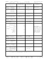
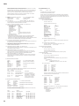
Sequencer block
Data capacity
Note resolution
Polyphony
BPM (Tempo)
Recording method
Tracks
Patterns
Phrases
Pattern Chain
Songs
Edit
Jobs
Split
Groove
Play Fx
MIDI delay
Arpeggio
Sequence file formats
Demo song
approximately 110,000 notes
480 clocks per quarter note
64 notes
25.0 - 300.0
Realtime Recording (Replace)
Realtime Recording (Overdub)
Realtime Recording (Punch In) - only the Song mode
Step Recording
Grid Step Recording
Pattern : 16 tracks
Song : 16 tracks, BPM track
960 preset patterns (60 styles x 16 sections)
800 user patterns (50 styles x 16 sections)
Measures : Up to 256
Over 7,000 preset phrases
256 user phrases/1 user style
20 chains
20 user songs
Phrase edit
Song edit
Pattern jobs
: 36
Pattern chain jobs : 8
Song jobs
: 28
Split song, Split pattern
Grid Groove (Note offset, Clock shift, Gate time offset, Velocity offset)
Harmonize (Unison, Octaver, Harmonize1, 2)
Play Fx
(Beat stretch, Clock shift, Gate time, Velocity offset)
MIDI delay edit, Feedback edit
Type (Up, Down, Alternate1, 2, Random) , Sort, Hold, Octave range
RM1x native sequence format, SMF format 0
4 (Included disk)
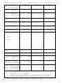
Tone generator block
Type
Maximum polyphony
Multi-timbral capability
Preset voices
Effects
Reverb
Chorus
Variation
Digital low boost
AWM2 tone generator
32 notes
16 timbres (with DVA)
Normal voices 654 (except GM voices)
Drum voices 46 kits (except GM kits)
3 systems (Reverb effect, Chorus effect, Variation effect)
11 types
11 types
43 types
Frequency (50Hz - 2.0kHz), Gain (+/-24dB)
Controls
Standby / On switch (STANDBY / ON)
Volume control (VOLUME)
Assignable knobs (x 8)
Display knobs (x 4)
CONTRAST control
Mode buttons
[PATTERN], [PATT CHAIN], [SONG], [UTILITY]
Submode buttons
[GROOVE], [PLAY FX], [MIDI DELAY], [ARPEGGIO],[VOICE], [VOICE EDIT],
[EFFECT], [SETUP], [DISK], [JOB], [EDIT], [SPLIT]
Function buttons
[F1] - [F4]
Knob A/B button
[KNOB]
3
RM1x
Eject button
Display button
Sequencer buttons
Data entry buttons
Cursor buttons
Shift button
Keyboard mode buttons
Arpeggio on button
Octave button
Keyboard pad
[EXIT]
[DISPLAY←], [DISPLAY→]
,
, , , ,
[NO -1], [YES+1]
[CURSOR↑], [CURSOR↓], [CURSOR←], [CURSOR→]
[SHIFT]
[TRACK], [TRANSPOSE], [NUM], [MUTE], [SECTION]
[ARPEGGIO ON]
[OCT DOWN] , [OCT UP]
E2 - F4, Tap tempo button [TAP]
Display (LCD)
64 x 240 dot graphic LCD
(with CFL backlight, adjustable contrast)
LED indicators
MODE ( x 4) (green)
REC
(red)
PLAY (green)
TRACK (x 16) (red)
KEYBOARD MODE - MUTE (red), SECTION (red),
ARPEGGIO ON (red)
FUNCTION BUTTON (red x 4)
KNOB A/B (red)
MIDI IN (red), MIDI OUT (green)
7 segments LED (x 4)
Connectors
PHONES (stereo phone jack)
OUTPUT (phone jack x 2) (L/MONO, R)
FOOT SW
DC IN
MIDI IN, MIDI OUT
Floppy disk drive
3.5 inch 2HD (MF2HD) and 2DD (MF2DD) types
Power supply
AC adaptor (PA-5C)
Dimensions
420 mm (W) x 282 mm (D) x 98 mm (H)
Weight
4.4kg
Included items
Power adaptor (PA-5C)
Floppy disk (Demo song)
Owner’s manual
* Specifications and appearance are subject to change without notice for
improvement of the product.
4
RM1x
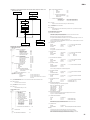
PANEL LAYOUT
●
Front Panel
2
3
16
7
1
4
11
6
12
5
10
13
9
17
16
18
9
8
15
14
19
1. BPM Display
2. MIDI Data Monitors
3. LCD Display
4. Display Knobs
5. Function Buttons and Indicators
6. VOLUME Control
7. Real Time Controller Knobs & [KNOB] Button
8. Cursor Buttons
9. [NO -1] and [YES +1] Buttons
10. DISPLAY [<-] and [->] Buttons
11. MODE and SUBMODE Buttons
12. [EXIT] Button
13. Sequencer Buttons and Indicators
14. Keyboard
15. Keyboard Mode Buttons
16. [OCT DOWN] and [OCT UP] Buttons
17. [SHIFT] Button
18. [ARPEGGIO ON] Button
19. [TAP/ENTER] Button
5
RM1x
● Rear
Panel
4
1.
2.
3.
4.
5.
6.
7.
6
STANDBY/ON Switch
DC IN Jack
CONTRAST Control
MIDI IN & OUT Connectors
L/MONO & R OUTPUT Jacks
PHONES Jack
FOOT SW Jack
3
7
5
6
2
1
RM1x
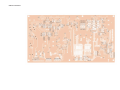
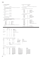
■ CIRCUIT BOARD LAYOUT
7
RM1x
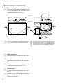
■ DISASSEMBLY PROCEDURE
1.
Bottom Case Assembly
1-1
Remove the eight (8) screws marked [280] and the
four (4) screws marked [281]. The bottom case
assembly can then be removed. (Fig. 1)
Rear View
Bottom view
(Fig.1)
[280]: Bind Head Tapping Screw-B 3.0X6 MFZN2BL (EP600230)
[281]: Bonding Head Screw-B 3.0X10 MFZN2BL (VQ498000)
2.
DM Circuit Board
2-1
Remove the bottom case assembly. (See Procedure 1.)
Remove the two (2) screws marked [310] and the
screw marked [251] on the back of the upper case.
(Fig. 2)
Remove the six (6) screws marked [250]. The DM
circuit board can then be removed. (Fig. 2)
2-2
2-3
3.
FDD Assembly
3-1
Remove the bottom case assembly. (See Procedure 1.)
Remove the three (3) screws marked [230] and
the screw marked [231]. The FDD assembly can
then be removed. (Fig. 2)
3-2
8
(Fig.2)
[230]:
[231]:
[250]:
[251]:
[310]:
Bind Head Tapping Screw-B 3.0X6 MFZN2BL (EP600230)
Bind Head Tapping Screw-B 3.0X8 MFZN2BL (EP600190)
Bind Head Tapping Screw-B 3.0X6 MFZN2BL (EP600230)
Bonding Head Screw-B 3.0X10 MFZN2BL (VQ498000)
Bind Head Tapping Screw-B 3.0X8 MFZN2BL (EP600190)
RM1x
Rear View
Bottom view
(Fig.3)
[210]: Bind Head Tapping Screw-B 3.0X6 MFZN2BL (EP600230)
[211]: Bind Head Tapping Screw-B 3.0X8 MFZN2BL (EP600190)
[212]: Bonding Head Screw-B 3.0X10 MFZN2BL (VQ498000)
4.
PN Circuit Board
4-1
Remove the bottom case assembly. (See Procedure 1.)
Remove the DM circuit board. (See Procedure 2.)
Remove the FDD assembly. (See Procedure 3.)
Remove the four (4) screws marked [210], the two
(2) screws marked [212] and the four (4) screws
marked [211]. The shield cover can then be removed. (Fig. 3)
Remove the four (4) knobs marked [320]. (Fig. 4)
Remove the twelve (12) screws marked [60]. The
PN circuit board can then be removed. (Fig. 5)
4-2
4-3
4-4
4-5
4-6
(Fig. 4)
[330]: Knob (V2887900)
[320]: Knob (V2647700)
(Fig.5)
[60]:
Bind Head Tapping Screw-B 3.0X6 MFZN2BL (EP600230)
9
RM1x
Bottom View
(Fig.6)
[40]:
[80]:
[100]:
5.
Knob Circuit board
5-1
Remove the bottom case assembly. (See Procedure 1.)
Remove the DM circuit board. (See Procedure 2.)
Remove the FDD assembly. (See Procedure 3.)
Remove the shield cover. (See Procedure 4.)
Remove the nine (9) knobs marked [330]. (Fig. 4)
Remove the four (4) screws marked [100]. The
KNOB circuit board can then be removed. (Fig. 6)
5-2
5-3
5-4
5-5
5-6
6.
MVR Circuit Board
6-1
Remove the bottom case assembly. (See Procedure 1.)
Remove the DM circuit board. (See Procedure 2.)
Remove the FDD assembly. (See Procedure 3.)
Remove the shield cover. (See Procedure 4.)
Remove the PN circuit board. (See Procedure 4.)
Remove the volume knob marked [330]. (Fig.4)
Remove the two (2) screws marked [80]. The MVR
circuit board can then be removed. (Fig.6)
6-2
6-3
6-4
6-5
6-6
6-7
7.
LCD
7-1
Remove the bottom case assembly. (See Procedure 1.)
Remove the DM circuit board. (See Procedure 2.)
Remove the FDD assembly. (See Procedure 3.)
Remove the shield cover. (See Procedure 4.)
Remove the four (4) screws marked [40]. The LCD
can then be removed. (Fig. 6)
7-2
7-3
7-4
7-5
10
Bind Head Tapping Screw-B 3.0X8 MFZN2BL (EP600190)
Bind Head Tapping Screw-B 3.0X6 MFZN2BL (EP600230)
Bind Head Tapping Screw-B 3.0X6 MFZN2BL (EP600230)
RM1x
●
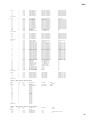
HG73C205FD (XU947A00) SWX000 TONE GENERATOR
PIN
NO.
1
2
3
4
5
6
7
8
9
10
11
12
13
14
15
16
17
18
19
20
21
22
23
24
25
26
27
28
29
30
31
32
33
34
35
36
37
38
39
40
41
42
43
44
45
46
47
48
49
50
51
52
53
54
55
56
57
58
59
60
61
62
63
64
65
66
67
68
69
70
71
72
73
74
75
76
77
78
79
80
81
82
83
84
NAME
I/O
ICN
RFCLKI
TM2
AVDD_PLL
AVSS_PLL
MODE0
VCC7
GND8
XIN
XOUT
MODE1
TEST0
TESTON
AN0-P40
AN1-P41
AN2-P42
AN3-P43
AVDD_AN
AVSS_AN
TXD0
TXD1
EXCLK
SMD11
SMD4
SMD3
SMD12
SMD10
SMD5
SMD2
SMD13
SMD9
SMD6
SMD1
SMD14
VCC35
GND36
SMD8
SMD7
SMD0
SMD15
SOE
SWE
SRAS
SCAS
REFRESH
CS0
SMA0
SMA16
VCC49
GND50
SMA1
SMA15
SMA2
SMA14
SMA3
SMA13
SMA4
SMA12
SMA5
GND60
VCC61
SMA11
SMA6
SMA10
SMA7
SMA9
SMA17
SMA8
SMA18
SMA19
SMA20
SMA21
SMA22
SMA23
CMA20
CMA19
VCC77
GND78
CMA18
CMA17
CMA5
CMA6
CMA4
CMA7
I
I
I
I
I
O
I
I
I
I
I
I
I
O
O
I
I/O
I/O
I/O
I/O
I/O
I/O
I/O
I/O
I/O
I/O
I/O
I/O
I/O
I/O
I/O
I/O
O
O
O
O
O
O
O
O
O
O
O
O
O
O
O
O
O
O
O
O
O
O
O
O
O
O
O
O
O
O
O
O
O
O
O
O
O
O
O
FUNCTION
Initial clear
PLL Clock
PLL Control
Power supply
Ground
SWX dual mode
Power supply
Ground
crystal oscillator
crystal oscillator
SWX separate mode
TEST pin
TEST pin
A/D converter
A/D converter
A/D converter
A/D converter
Power supply
Ground
for MIDI or TO-HOST
for MIDI
Crystal oscillator
Wave memory data bus
Wave memory data bus
Wave memory data bus
Wave memory data bus
Wave memory data bus
Wave memory data bus
Wave memory data bus
Wave memory data bus
Wave memory data bus
Wave memory data bus
Wave memory data bus
Wave memory data bus
Power supply
Ground
Wave memory data bus
Wave memory data bus
Wave memory data bus
Wave memory data bus
read signal
write signal
RAS signal
CAS signal
REFRESH signal
CS signal
Memory address bus
Memory address bus
Power supply
Ground
Memory address bus
Memory address bus
Memory address bus
Memory address bus
Memory address bus
Memory address bus
Memory address bus
Memory address bus
Memory address bus
Ground
Power supply
Memory address bus
Memory address bus
Memory address bus
Memory address bus
Memory address bus
Memory address bus
Memory address bus
Memory address bus
Memory address bus
Memory address bus
Memory address bus
Memory address bus
Memory address bus
Program address bus
Program address bus
Power supply
Ground
Program address bus
Program address bus
Program address bus
Program address bus
Program address bus
Program address bus
PIN
NO.
85
86
87
88
89
90
91
92
93
94
95
96
97
98
99
100
101
102
103
104
105
106
107
108
109
110
111
112
113
114
115
116
117
118
119
120
121
122
123
124
125
126
127
128
129
130
131
132
133
134
135
136
137
138
139
140
141
142
143
144
145
146
147
148
149
150
151
152
153
154
155
156
157
158
159
160
161
162
163
164
165
166
167
168
NAME
I/O
CMA3
CMA8
CMA2
CRD
CMA1
CUB
VCC91
GHND92
CS1
CMA0
CLB
CMA12
CMA11
CMA10
CMA9
GND100
CWE
CMA16
CMA15
CMA14
CMA13
CMD8
CMD7
CMD9
CMD6
CMD10
CMD5
CMD11
CMD4
CMD12
CMD3
CMD13
CMD2
CMD14
VCC119
GND115
CMD1
CMD15
CMD0
CMA21
PDT15
PDT14
PDT13
PDT12
PDT11
PDT10
PDT9
PDT8
VCC133
GND134
PDT7
PDT6
PDT5
PDT4
PDT3
PDT2
PDT1
PDT0
VCA143
GND144
PAD2
PAD1
PAD0
VCC148
GND149
PCS
PWR
PRD
RXD0
RXD1
SCLKI
ADIN
ADLR
DO0
DO1
SYSCLK
VCC161
GND162
WCLK
QCLK
BCLK
SYI
IRQ0
NMI
O
O
O
O
O
O
O
O
O
O
O
O
O
O
O
O
O
O
I/O
I/O
I/O
I/O
I/O
I/O
I/O
I/O
I/O
I/O
I/O
I/O
I/O
I/O
I/O
I/O
O
I/O
I/O
I/O
I/O
I/O
I/O
I/O
I/O
I/O
I/O
I/O
I/O
I/O
I/O
I/O
I/O
I
I
I
I
I
I
I
I
I
I
O
O
O
O
O
O
O
I
I
I
FUNCTION
Program address bus
Program address bus
Program address bus
read signal
Program address bus
high byte effective signal
Power supply
Ground
CS signal
Program address bus
low byte effective signal
Program address bus
Program address bus
Program address bus
Program address bus
Ground
write signal
Program address bus
Program address bus
Program address bus
Program address bus
Program memory Data bus
Program memory Data bus
Program memory Data bus
Program memory Data bus
Program memory Data bus
Program memory Data bus
Program memory Data bus
Program memory Data bus
Program memory Data bus
Program memory Data bus
Program memory Data bus
Program memory Data bus
Program memory Data bus
Power supply
Ground
Program memory Data bus
Program memory Data bus
Program memory Data bus
Program address bus
SWX access data bus
SWX access data bus
SWX access data bus
SWX access data bus
SWX access data bus
SWX access data bus
SWX access data bus
SWX access data bus
Power supply
Ground
SWX access data bus
SWX access data bus
SWX access data bus
SWX access data bus
SWX access data bus
SWX access data bus
SWX access data bus
SWX access data bus
Power supply
Ground
SWX access address bus
SWX access address bus
SWX access address bus
Power supply
Ground
Chip select
write enable
read enable
for MIDI or TO-HOST
for MIDI or Key scan
EXT Clock
A/D converter
A/D converter LR clock
DAC
DAC
1/2 clock
Power supply
Ground
for DAC LR clock
1/12 clock
IIS-DAC clock
Synch signal
Interrupt request
Interrupt request
11
RM1x
●
HG73C201FD (XT890A00) SWX00 TONE GENERATOR
PIN
NO.
1
2
3
4
5
6
7
8
9
10
11
12
13
14
15
16
17
18
19
20
21
22
23
24
25
26
27
28
29
30
31
32
33
34
35
36
37
38
39
40
41
42
43
44
45
46
47
48
49
50
51
52
53
54
55
56
57
58
59
60
61
62
63
64
65
66
67
68
69
70
71
72
73
74
75
76
77
78
79
80
81
82
83
84
12
NAME
I/O
ICN
RFCLKI
TM2
AVDD_PLL
AVSS_PLL
MODE0
VCC7
GND8
XIN
XOUT
MODE1
TEST0
TESTON
AN0-P40
AN1-P41
AN2-P42
AN3-P43
AVDD_AN
AVSS_AN
TXD0
TXD1
EXCLK
SMD11
SMD4
SMD3
SMD12
SMD10
SMD5
SMD2
SMD13
SMD9
SMD6
SMD1
SMD14
VCC35
GND36
SMD8
SMD7
SMD0
SMD15
SOE
SWE
SRAS
SCAS
REFRESH
CS0
SMA0
SMA16
VCC49
GND50
SMA1
SMA15
SMA2
SMA14
SMA3
SMA13
SMA4
SMA12
SMA5
GND60
VCC61
SMA11
SMA6
SMA10
SMA7
SMA9
SMA17
SMA8
SMA18
SMA19
SMA20
SMA21
SMA22
SMA23
CMA20
CMA19
VCC77
GND78
CMA18
CMA17
CMA5
CMA6
CMA4
CMA7
I
I
I
I
I
O
I
I
I
I
I
I
I
O
O
I
I/O
I/O
I/O
I/O
I/O
I/O
I/O
I/O
I/O
I/O
I/O
I/O
FUNCTION
Initial clear
PLL Clock
PLL Control
Power supply
Ground
Mode set
Power supply
Ground
crystal oscillator
crystal oscillator
Mode set
TEST pin
TEST pin
Analog Signal
Power supply
Ground
for MIDI or TO-HOST
for MIDI
1M Clock for to Hast
Wave memory data bus
Power supply
Ground
I/O
I/O
I/O
I/O
O
O
O
O
O
O
O
O
O
O
O
O
O
O
O
O
O
Wave memory data bus
read signal
write signal
RAS signal
CAS signal
REFRESH signal
CS signal
Memory address bus
Memory address bus
Power supply
Ground
Wave Memory address bus
Ground
Power supply
O
O
O
O
O
O
O
O
O
O
O
O
O
O
O
O
O
O
O
O
O
O
Wave Memory address bus
Program address bus
Program address bus
Power supply
Ground
Program address bus
PIN
NO.
85
86
87
88
89
90
91
92
93
94
95
96
97
98
99
100
101
102
103
104
105
106
107
108
109
110
111
112
113
114
115
116
117
118
119
120
121
122
123
124
125
126
127
128
129
130
131
132
133
134
135
136
137
138
139
140
141
142
143
144
145
146
147
148
149
150
151
152
153
154
155
156
157
158
159
160
161
162
163
164
165
166
167
168
NAME
I/O
CMA3
CMA8
CMA2
CRD
CMA1
CUB
VCC91
GHND92
CS1
CMA0
CLB
CMA12
CMA11
CMA10
CMA9
GND100
CWE
CMA16
CMA15
CMA14
CMA13
CMD8
CMD7
CMD9
CMD6
CMD10
CMD5
CMD11
CMD4
CMD12
CMD3
CMD13
CMD2
CMD14
VCC119
GND115
CMD1
CMD15
CMD0
CMA21
PDT15
PDT14
PDT13
PDT12
PDT11
PDT10
PDT9
PDT8
VCC133
GND134
PDT7
PDT6
PDT5
PDT4
PDT3
PDT2
PDT1
PDT0
VCC143
GND144
PAD2
PAD1
PAD0
VCC148
GND149
PCS
PWR
PRD
RXD0
RXD1
SCLKI
ADIN
ADLR
DO0
DO1
SYSCLK
VCC161
GND162
WCLK
QCLK
BCLK
SYI
IRQ0
NMI
O
O
O
O
O
O
O
O
O
O
O
O
O
O
O
O
O
O
I/O
I/O
I/O
I/O
I/O
I/O
I/O
I/O
I/O
I/O
I/O
I/O
I/O
FUNCTION
read signal
Program address bus
high byte effective signal
Power supply
Ground
CS signal
Program address bus
low byte effective signal
Program address bus
Ground
write signal
Program address bus
Program memory Data bus
Power supply
Ground
I/O
I/O
I/O
O
I/O
I/O
I/O
I/O
I/O
I/O
I/O
I/O
Program memory Data bus
Program address bus
SWX access data bus
Power supply
Ground
I/O
I/O
I/O
I/O
I/O
I/O
I/O
I/O
I
I
I
I
I
I
I
I
I
I
O
O
O
O
O
O
O
I
I
I
SWX access data bus
Power supply
Ground
SWX access address bus
SWX access address bus
SWX access address bus
Power supply
Ground
SWX access Chip select
SWX access write enable
SWX access read enable
for MIDI or TO-HOST
for MIDI or Key scan
EXT Sync Clock
For Ext A/D converter
A/D converter LR clock
DAC
DAC
1/2 clock
Power supply
Ground
for DAC LR clock
1/12 clock
IIS-DAC clock
Synch signal
Interrupt request
Interrupt request
RM1x
●
SH7014 (XT437A00) CPU
PIN
NO.
1
2
3
4
5
6
7
8
9
10
11
12
13
14
15
16
17
18
19
20
21
22
23
24
25
26
27
28
29
30
31
32
33
34
35
36
37
38
39
40
41
42
43
44
45
46
47
48
49
50
51
52
53
54
55
56
NAME
I/O
PE14
PE15
VSS
A0
A1
A2
A3
A4
A5
A6
A7
A8
A9
A10
A11
A12
A13
A14
A15
A16
VCC
PB1/A17
VSS
/RAS
/CASL
/CASH
VSS
RDWR
A18
A19
A20
PB9
VSS
/RD
/WDTOVF
/WRH
VCC
/WRL
VSS
/CS1
/CS0
PA9
PA8
O
O
I
O
O
O
O
O
O
O
O
O
O
O
O
O
O
O
O
O
I
O
I
O
O
O
O
O
O
O
O
O
I
O
O
O
I
O
I
O
O
O
I
O
O
O
O
O
I
O
I
I/O
I/O
I/O
I
I/O
/CS3
/CS2
PA5
PA4
PA3
/IRQ0
TXD0
RXD0
D15
D14
D13
VSS
D12
FUNCTION
Port E
Port E
Ground
Address bus
Power supply
Address bus
Ground
Bus control
Ground
Port A
Port B
Ground
Bus control
NC
NC
Power supply
Bus control
Ground
Bus control
Bus control
Port A
Port A
Bus control
Bus control
Port A
Interrupt
SCI
SCI
Data bus
Ground
Data bus
PIN
NO.
57
58
59
60
61
62
63
64
65
66
67
68
69
70
71
72
73
74
75
76
77
78
79
80
81
82
83
84
85
86
87
88
89
90
91
92
93
94
95
96
97
98
99
100
101
102
103
104
105
106
107
108
109
110
111
112
NAME
D11
D10
D9
D8
VSS
D7
D6
D5
VCC
D4
D3
D2
D1
D0
VSS
XTAL
MD3
EXTAL
MD2
NMI
VCC
MD1
MD0
PLLVCC
PLLCAP
PLLVSS
PA15/CK
/RES
PE0
PE1
PE2
PE3
PE4
VSS
AN0
AN1
AN2
AN3
AN4
AN5
AVSS
AN6
AN7
AVCC
VSS
PE5
VCC
PE6
PE7
PE8
PE9
PE10
VSS
PE11
PE12
PE13
I/O
I/O
I/O
I/O
I/O
I
I/O
I/O
I/O
I
I/O
I/O
I/O
I/O
I/O
I
I
I
I
I
I
I
I
I
I
I
I
O
I
I
I
I
I
I
I
I
I
I
I
I
I
I
I
I
I
I
O
I
O
O
O
O
O
I
O
O
O
FUNCTION
Data bus
Ground
Data bus
Power supply
Data bus
Ground
CLK
Mode control
CLK
Mode control
Non-maskable interrupt request
Power supply
Mode control
Mode control
CLK
Port A
Reset
Port E
Ground
A/D
Analog ground
A/D
A/D
Power supply
Ground
Port E
Power supply
Port E
Ground
Port E
μPD63200GS-E1 (XP867A00) DAC (Digital to Analog Converter)
●
PIN
NO.
1
2
3
4
5
6
7
8
NAME
I/O
4/8FS
D. GND
16/8 BIT
D. VDD
A. GND
R. OUT
A. VDD
A. VDD
I
I
O
FUNCTION
4/8 Fs selection
Digital ground
16 bit/8 bit selection
Digital power supply
Analog ground
Channel R output
Analog power supply
PIN
NO.
9
10
11
12
13
14
15
16
NAME
R. REF
L. REF
L. OUT
A. GND
LRCX/W D
LR/RSI
SI/LSI
CLK
I/O
O
I
I
I
I
FUNCTION
Channel R voltage reference
Channel L voltage reference
Channel L output
Analog ground
Left/right check, Word clock
Left/right selection, Channel R series input
Series input/Channel L series input
Clock
13
RM1x
●
HD63266F (XI939A00) FDC (Floppy Disk Controller)
PIN
NO.
1
2
3
4
5
6
7
8
9
10
11
12
13
14
15
16
17
18
19
20
21
22
23
24
25
26
27
28
29
30
31
32
●
I/O
I
I
I
I
I
I
I
I
I
FUNCTION
Data transmission speed
Clock select
Rest
Enable/Read
Read/write/Write
Chip select
DMA acknowledge
Register select
Ground
I/O
I/O
I/O
I/O
I/O
I/O
I/O
I/O
O
O
I
Data bus
DMA request
Interrupt request
Data end
Ground
Power supply
I
I
I
I
I
I
I
Host interface select
Format data
Index pulse
Ready from FDD
Write control signal
PIN
NO.
33
34
35
36
37
38
39
40
41
42
43
44
45
46
47
48
49
50
51
52
53
54
55
56
57
58
59
60
61
62
63
64
NAME
/TRKO
/INDEX
/RDATA
XTAL2
EXTAL2
NC
XTAL1
EXTAL1
VSS4
VSS5
NC
VCC2
VCC3
VCC4
/WGATE
/WDATA
VSS6
/STEP
/HDIR
/HLOAD
/HSEL
VSS7
/DS0
/DS1
/DS2
/DS3
VSS8
/MON0
/MON1
/MON2
/MON3
VSS9
I/O
I
I
I
NAME
XD2
XD1
XD0
XECL
XSCL
VSS
LP
WF
YDIS
YD
YSCL
VD7
VD6
VD5
VD4
VD3
VD2
VD1
VD0
VA15
VA14
VA13
VA12
VA11
VA10
VA9
VA8
VA7
VA6
NC
I/O
O
O
O
O
O
FUNCTION
Track 00 signal
Index signal
Read data input from FDD
Clock
Clock
Ground
Power supply
O
O
O
O
O
O
O
O
O
O
Write control
Write data to FDD
Ground
Step signal to control head of FDD
Direction
Head load
Head select
Ground
Drive select
Ground
O
O
O
O
Motor on
Ground
SED1335F0B (XQ595A00) LCDC (LCD Controller)
PIN
NO.
1
2
3
4
5
6
7
8
9
10
11
12
13
14
15
16
17
18
19
20
21
22
23
24
25
26
27
28
29
30
14
NAME
8"//5"
XTALSET
/RESET
E//RD
RW//WR
/CS
/DACK
RS0
RS1
VSS1
VSS2
D0
D1
D2
D3
D4
D5
D6
D7
/DREQ
/IRQ
/DEND
VSS3
1/2 EX1
VCC1
NUM1
NUM3
IFS
SFORM
/INP
/READY
/WPRT
NAME
VA5
VA4
VA3
VA2
VA1
VA0
VR/W
/VCE
NC
/RES
NC
NC
/RD
/WR
SEL2
SEL1
OSC1
OSC2
/CS
A0
VDD
D0
D1
D2
D3
D4
D5
D6
D7
XD3
I/O
O
O
O
O
O
O
O
O
FUNCTION
VRAM address bus
VRAM write strobe
VRAM chip enable
I
Reset
I
I
I
I
I
O
I
I
80: Read strobe, 68: E clock
80: Write strobe, 68: Read/Write
CPU 80/68 bus select
I/O
I/O
I/O
I/O
I/O
I/O
I/O
I/O
O
Clock
Chip select
Data bus signal discrimination
Power supply
Data bus
X driver data bus
PIN
NO.
31
32
33
34
35
36
37
38
39
40
41
42
43
44
45
46
47
48
49
50
51
52
53
54
55
56
57
58
59
60
O
O
O
O
O
I/O
I/O
I/O
I/O
I/O
I/O
I/O
I/O
O
O
O
O
O
O
O
O
O
O
FUNCTION
X driver data bus
X driver enable chain clock
X driver shift clock
Ground
Latch pulse
Frame signal
LCD power down
Scan start pulse
Scan shift clock
VRAM data bus
VRAM address bus
RM1x
●
SED1335F0B (XQ595A00) LCDC (LCD Controller)
PIN
NO.
1
2
3
4
5
6
7
8
9
10
11
12
13
14
15
16
17
18
19
20
21
22
23
24
25
26
27
28
29
30
●
NAME
I/O
VA5
VA4
VA3
VA2
VA1
VA0
/VWR
/VCE
/VRD
/RES
NC
NC
/RD
/WR
SEL2
SEL1
OSC1
OSC2
/CS
A0
Vdd
D0
D1
D2
D3
D4
D5
D6
D7
XD3
O
O
O
O
O
O
O
O
I
I
I
I
I
I
O
I
I
I/O
I/O
I/O
I/O
I/O
I/O
I/O
I/O
O
FUNCTION
VRAM address bus
VRAM read/write
Memory control
Not used
Initial clear
Not used
Not used
Read strobe
Write strobe
Bus select
Bus select
Clock
Clock
Chip select
Data mode select
Power supply
Data bus
Data bus output for 4 bit dot
PIN
NO.
31
32
33
34
35
36
37
38
39
40
41
42
43
44
45
46
47
48
49
50
51
52
53
54
55
56
57
58
59
60
NAME
I/O
XD2
XD1
XD0
XECL
XSCL
Vss
LP
WF
YDIS
YD
YSCL
VD7
VD6
VD5
VD4
VD3
VD2
VD1
VD0
VA15
VA14
VA13
VA12
VA11
VA10
VA9
VA8
VA7
VA6
NC
O
O
O
O
O
O
O
O
O
O
I/O
I/O
I/O
I/O
I/O
I/O
I/O
I/O
O
O
O
O
O
O
O
O
O
O
-
NAME
I/O
XD2
XD1
XD0
XECL
XSCL
Vss
LP
WF
YDIS
YD
YSCL
VD7
VD6
VD5
VD4
VD3
VD2
VD1
VD0
VA15
VA14
VA13
VA12
VA11
VA10
VA9
VA8
VA7
VA6
NC
O
O
O
O
O
O
O
O
O
O
I/O
I/O
I/O
I/O
I/O
I/O
I/O
I/O
O
O
O
O
O
O
O
O
O
O
-
FUNCTION
Data bus output for 4 bit dot
S driver enable, chain clock
Data bus shift clock
Ground
X driver latch pulse
Frame signal for X/Y driver
Power down signal for displaying off mode
Scan start signal
Scan shift clock
VRAM data bus
VRAM address bus
Not used
SED1335FOB (XQ595A00) LCDC
PIN
NO.
1
2
3
4
5
6
7
8
9
10
11
12
13
14
15
16
17
18
19
20
21
22
23
24
25
26
27
28
29
30
NAME
I/O
VA5
VA4
VA3
VA2
VA1
VA0
/VWR
/VCE
NC
/RES
NC
NC
/RD
/WR
SEL2
SEL1
OSC1
OSC2
/CS
A0
Vdd
D0
D1
D2
D3
D4
D5
D6
D7
XD3
O
O
O
O
O
O
O
O
I
I
I
I
I
I
O
I
I
I/O
I/O
I/O
I/O
I/O
I/O
I/O
I/O
O
FUNCTION
VRAM Address Bus
VRAM Write Signal
VRAM Chip enable
Reset Input Signal
Read Signal
Write Signal
Bus Select
Bus Select
Oscillator1
Oscillator2
Chip Select Input Signal
Data Bus Signal Kind Judgement
Power Supply
Data Bus for System
X Driver Data Bus
PIN
NO.
31
32
33
34
35
36
37
38
39
40
41
42
43
44
45
46
47
48
49
50
51
52
53
54
55
56
57
58
59
60
FUNCTION
X Driver Data Bus
Xdriver Enable Change Clock
Xdriver Shift Clock
Groud
Latch Pulse
Frame Signal
LCD Power Down Output
Scan Start Pulse
Scan Sift Clock
VRAM Data Bus
VRAM Address Bus
15
RM1x
16
RM1x
28CA1-8812706
19
RM1x
• DM Circuit Board
MIDI-IN
CONTRAST
FOOT SW
OUTLET/R OUTLET/L-MONO PHONES
DC IN
STAND BY/ON
to PNCN1
to LCD Back light
to FDD
to PN-CN4
to FDD UNIT
to MVR CN6
MIDI-OUT
to LCD
to PN-CN4
to PN-CN5
Component side
DM:2NA-V260480
20
2
△
RM1x
• DM Circuit Board
Patternside
21
RM1x
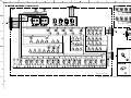
• PN 1/3Circuit Board
Note: See parts list for details of circuit board component parts.
See PANEL SWITCH TABLE on C2 of OVERALL CIRCUIT
DIAGRAM.
to DM-CN5
to DM-CM3
to DM-CN1
22
to DM-CN4
Component side
RM1x
• PN 1/3Circuit Board
Patternside
PN: 2NA-V260490
2
△
23
RM1x
• PN 2/3 Circuit Board
CLOCK SHIFT
GATE TIME
VEROCITY
VOLUME
to DM-CN8
to DM-CN2
TIME STRECH
• PN 3/3 Circuit Board
Component side
CUT OFF
RESONANCE
EG DECAY
PITCH
BEND
Component side
Patternside
Patternside
Note: See parts list for details of circuit board component parts.
See PANEL SWITCH TABLE on C2 of OVERALL CIRCUIT DIAGRAM.
2
△
PN:2NA-V260490
24
RM1x
TEST PROGRAM & INITIALIZE
1.TEST PROGRAM
●PREPARATIONS
Measuring instruments:
Jigs:
low frequency oscillator, frequency counter, oscilloscope,
volt meter (JIS- C curve), keyboard amplifier, etc.
MIDI cable, floppy disk (2HD, form atted), etc.
●TEST PROGRAM
TEST No.
A
B
C
C- 1
C- 2
C- 3
C- 4
C- 5
C- 6
C- 7
C- 8
C- 9
C-10
C-11
C-12
C-13
C-14
C-15
C-16
C-17
C-18
C-19
C-20
C-21
C-22
TEST
How to enter the test program
Proceeding through the tests
Test program
SYSTEM RAM
RAM Battery
LCD
LED light up
Panel switch
Encoder 1
Encoder 2
Encoder 3
Encoder 4
Knob 1
Knob 2
Knob 3
Knob 4
Knob 5
Knob 6
Knob 7
Knob 8
FOOT SW
FDD
MIDI IN / OUT
W AVE ROM
PCM sine wave sound OUTPUT (L)
C-23
PCM sine wave sound OUTPUT (R)
C-24
C-25
Factory Set
EXIT
TEST RESULT
OK / NG
OK
Vertical Stripes (by seconds)
Red, green
ON / OFF
OK, 0-30-0-30
OK, 0-30-0-30
OK, 0-30-0-30
OK, 0-30-0-30
OK, 64-128-0-64
OK, 64-128-0-64
OK, 64-128-0-64
OK, 64-128-0-64
OK, 64-128-0-64
OK, 64-128-0-64
OK, 64-128-0-64
OK, 64-128-0-64
OK, 0-1-0
OK
OK
OK
OUTPUT (L): +2 +/- 2 dBm load 10 kohm
OUTPUT (R ): less than -76 dBm
PHONES (L): -5 +/- 2 dBm load 33 ohm
PHONES (R ): less than -68 dBm
OUTPUT (R ): +2 +/- 2 dBm load 10 kohm
OUTPUT (L): less than -76 dBm
PHONES (R ): -5 +/- 2 dBm load 33 ohm
PHONES (L): less than -68 dBm
* Noise level
OUTPUT (L), OUTPUT (R):
less than -78 dBm
PHONES (L), PHONES (R):
less than -78 dBm
*Note) OUTPUT (L) and OUTPUT (R) are occasionally abbreviated as L and R.
25
RM1x
A. HOW TO ENTER THE TEST PROGRAM
While pressing the [PATTERN], [PATT CHAIN]
and [UTIL] buttons, turn the power switch on.
The following message will appear on the LCD.
When the [+1] switch is pressed, the test is
automatically executed from the test where the
error occurs.
The [F4] switch is pressed, the “C-25 EXIT” is
started.
Manual Mode
**RM1x TEST**
MAIN Ver #.##
SUB Ver #.##
When the manual mode test is enterd, the
following display will appear:
**RM1x TEST**MANUAL
MAIN Ver #.##
SUB Ver #.##
[F1]:AUTO
[F2]:MANUAL
[F3]:Factory Set
[F4]:Exit
Use the [F1], [F2], [F3] and [F4] switches to
select the appropriate test mode.
When the [F1] switch is pressed, the auto mode
test is entered.
When the [F2] switch is pressed, the manual
mode test is entered.
The [F3] switch is pressed, the “C-24 Factory
Set” is started.
The [F4] switch is pressed, the “C-25 EXIT” is
started.
B. PROCEEDING THROUGH THE TESTS
Auto Mode
When the auto mode test is entered, the
following display will appear:
**RM1x TEST** AUTO
MAIN Ver #.##
SUB Ver #.##
01:RAM R/W
[F4]:Exit
01:RAM R/W
[F4]:Exit
Use the [+1] and [-1] switches to select the
appropriate test number.
When the [ENTER] switch is pressed, the test of
the selected number is executed.
The [F4] switch is pressed, the “C-25 EXIT” is
started.
Test Selection When An Error Is Detected
In each test, if “NG” (No Good) error is
detected, pressing [F4] switch will make the
undermentioned.
You can then retry the test or another test.
Auto Mode ---------->error processing state
Manual Mode ------->test number waiting state
However, this method does not correspond at
the test of “C-5 PANEL SWITCH”.
C. TEST PROGRAM
This test program explains the manual mode.
C-1 SYSTEM RAM READ / WRITE TEST
Use the [+1] and [-1] switches to select the
appropriate test number.
When the [ENTER] switch is pressed, the test is
sequentially executed from the selected test number.
When the [ENTER] switch is pressed without
setting anything,
the test is automatically
executed from “C-1 RAM”.
The error message is displayed when an error
occurs and the test stops.
In this case, the error is processed with either
of the [ENTER], [+1] or [F4] switches.
When the [ENTER] switch is pressed, the test is
automatically executed again from the test
where the error occurs.
01: RAM R/W
This is the read/write check for the MAIN CPU
RAM. The test result appears on the LCD.
Display Of Test Results
OK
01: RAM R/W
OK
NG
01: RAM R/W
NG
26
RM1x
Test End
After displaying the test result and the test will
be finished.
All the RAM data will be restored.
Press the [F4] switch to exit the test, press the
[+1] switch to proceed with the next test and
then the [ENTER] switch to execute the next
test.
C-3 LCD ALL ON / OFF TEST
03: LCD Check
Confirm that all LCD dots blink. Each line should
blink in one (1) second intervals.
Confirm that the LCD dots light normally.
Confirm that the LCD contrast changes when
rotating the contrast adjustment volume.
C-2 RAM BATTERY TEST
02: RAM Battery
Display Of Test Results
Not appearing
Test End
This test checks that the voltage of the RAM
backup battery is greater than 2.9V and less
than 3.5V at the A / D input terminal of CPU.
The “OK” will be displayed when the voltage
is within the range.
Press the [F4] switch to end the test.
Press the [+1] switch to proceed with the next
test and then the [ENTER] switch to execute
the next test.
C-4 LED ON / OFF TEST
Display Of Test Results
OK
NG
02: RAM Battery
3.2V
OK
04: LED Check
02: RAM Battery
#.#V Low
NG
02: RAM Battery
#.#V High
NG
Confirm that LED lights on and off sequentially
from the left of Fig. 1 and all LED ’s light on
and off at the same time.
The above-mentioned procedure are repeated
until being interrupted.
Display Of Test Results
Not appearing
Test End
Displays the test result and ends the test.
Press the [+1] switch to proceed with the next
test and then the [ENTER] switch to execute
the next test.
○
Test End
Press the [F4] switch to ends the test.
Press the [+1] switch to proceed with the next
test and then the [ENTER] switch to execute
the next test.
RM1x
LCD
◇
○
○
○
◇
○ ○
○
○
○
◇ ◇ ◇ ◇
○
○ ○ ○ ○ ○ ○ ○ ○ ○ ○ ○ ○ ○ ○ ○ ○
(Fig. 1 )
Notes) ○ mark is red LED, ◇ mark is green LED,
mark is 7- Seg. LED
27
RM1x
When it is normal, a piano tone is generated
while being press on the switch.
NG is displayed when another switch is pressed
and a piano tone does not generate. After this,
the test advances to the next switch test when a
correct switch is pressed.
C-5 PANEL SWITCH TEST
05: Panel Switch
Press the panel switches consecutively from the
[F1] switch to the [ENTER] switch, according to
the order indicated by the LCD. Confirm all
switches are working properly.
Confirm the 32 channel sounds generate.
The test result is displayed if all switches are normal.
Assume that the operation of 32CH was
confirmed when 32 times the sound generates
continuously.
The order of the switch check and the pitches
are shown in the Table 1 and Fig. 2.
05: Panel Switch
Push [MODE ]
Switch
F1
F2
F3
F4
KNOB
REC
TOP
STOP
PLAY
BWD
FWD
SHIFT
TRACK
TRANSPOSE
NUM
MUTE
SECTION
ARPEGGIO ON
DISP LEFT
DISP RIGHT
EXIT
DEC/NO
Pitch Switch
C 3 UP
D 3 INC/YES
E 3 LEFT
F 3 DOWN
G 3 RIGHT
C 3 PATTERN
Pitch
G3
A3
B3
C4
D4
C3
D 3 PATT CHAIN
E 3 SONG
F 3 UTILITY
G 3 GROOVE
A 3 PLAY FX
C 3 MIDI DELAY
D 3 ARPEGGIO
E 3 VOICE
F 3 VOICE EDIT
G 3 EFFECT
A 3 SETUP
B 3 DISK
C 3 JOB
D 3 EDIT
E 3 SPLIT
F 3 OCT DOWN
D3
E3
F3
G3
A3
B3
C4
D4
E4
F4
G4
A4
B4
C5
D5
D2
Switch
OCT UP
E2
F2
Gb2
G2
Ab2
Pitch Switch
Eb2 Db4
E2D4
F 2 Eb4
Gb2 E 4
G2F4
Ab2 TAP
A2
Bb2
B2
C3
Db3
D3
Eb3
E3
F3
Gb3
G3
Ab3
A3
Bb3
B3
C4
A2
Bb2
B2
C3
Db3
D3
Eb3
E3
F3
Gb3
G3
Ab3
A3
Bb3
B3
C4
(Table 1)
RM1x
LCD
■
■
■ ■
■ ■ ■ ■ ■ ■
■ ■ ■ ■ ■ ■ ■
■
■■■
■■■
■■■
■■■■
■■■■
■■■■
■■■■
■■ ■■■ ■■ ■■■ ■■ ■
■■■■■■■■■■■■■■■■
(Fig. 2)
Notes) Make sure all switches marked ■ are working properly.
28
Pitch
Db 4
D4
Eb4
E4
F4
Gb4
RM1x
Display Of Test Results
NG
05: Panel Switch
Push [MODE ]
C-10 KNOB 1 (BEAT STRETCH) TEST
10: Knob 1
xxx 64
NG
Test End
After displaying the test result when the check
to the [TAP] switch end and the test will be
finished.
After Pressing the [F4] to exit the test, press the
[+1] switch to proceed with the next test and
then the [ENTER] switch to execute the next test.
Refer to “B PROCEEDING THROUGH THE
TESTS” if the “NG” occurs while testing.
(where xxx= current KNOB 1 value)
According to the target value displayed on the
LCD, slowly rotate the KNOB 1.
Check that the value changes from 64 to 128
then to 00 and back to 64 (in other words, center
to top then to bottom and back to center). After
that, confirm that the “OK” appears on the LCD.
10: Knob 1
xxx yyy
(where xxx= current KNOB 1 value and
yyy= target value)
C-6 ENCODER 1 [F1 ] TEST
06: Encoder 1
RIGHT 00
Confirm the Encoder corresponding to the [F1]
switch are working properly from the left side.
When you rotate the Encoder clockwise according
to the LCD display, the value at the right of the
LCD simply increases from 0 to 30. When you
rotate the Encoder counterclockwise, the value
at the right of the LCD simply increases from 0
to 30. After that, confirm that the OK appears on
the LCD.
06: Encoder1
RIGHT xx
06: Encoder1
LEFT xx
(where xx= current ENCODER 1 value)
Display Of Test Results
OK
06: Encoder1
LEFT 00 NG
OK
Not appearing
Test End
After displaying the test result and the test will
be finished.
After Pressing the [F4] to exit the test, press the
[+1] switch to proceed with the next test and
then the [ENTER] switch to execute the next test.
Refer to “B PROCEEDING THROUGH THE
TESTS” if the “NG” occurs while testing.
C-7 ENCODER 2 [F2] TEST
C-8 ENCODER 3 [F3] TEST
C-9 ENCODER 4 [F4] TEST
These tests can be performed in the same manner
as the test C-6, “ENCODER 1 [F2] TEST”.
Display Of Test Results
OK
10: Knob1
064 064
OK
NG
Not appearing
When the value of the display passes 64 after
64-128-00 and passes 64 , OK is displayed.
Test End
After displaying the test result and the test will
be finished.
After Pressing the [F4] to exit the test, press the
[+1] switch to proceed with the next test and
then the [ENTER] switch to execute the next test
Refer to “B PROCEEDING THROUGH THE
TESTS ” if the “NG” occurs while testing.
C-11
C-12
C-13
C-14
C-15
C-16
C-17
KNOB 2
KNOB 3
KNOB 4
KNOB 5
KNOB 6
KNOB 7
KNOB 8
(CLOCK SHIFT) TEST
(GATE TIME) TEST
(VELOCITY) TEST
(CUTOFF) TEST
(RESONANCE) TEST
(EG DECAY) TEST
(PITCH BEND) TEST
These tests can be performed in the same
manner as the test C-10,“KNOB 1 (BEAT) TEST”
C-18 FOOT SW TEST
18: FOOT SW
0
Connect a foot switch and press it on and off.
Check that the display on the LCD changes
from off to on then back to off and verify that to
the “OK” result is displayed.
29
RM1x
Display Of Test Results
OK
18: FOOT SW
1
OK
NG
Not appearing
Display Of Test Results
OK
20: MIDI (IN/OUT)
OK
NG
20: MIDI (IN/OUT)
Test End
NG
After displaying the test result the test will be finished.
After pressing the [F4] to exit the test, press the
[+1] switch to proceed with the next test and then
TIME OUT 20: MIDI (IN/OUT)
ERROR
TIMEOUT
the [ENTER] switch to execute the next test.
Refer to “B PROCEEDING THROUGH THE
TESTS” if the “NG” occurs while testing.
C-19 FDD TEST
(When the reception does not end
within the fixed time)
Test End
After displaying the test result the test will be finished.
19:
(WRITE/READ)
FDD
Press the [+1] switch to proceed with the next test and
then the [ENTER] switch to execute the next test.
Refer to “B PROCEEDING THROUGH THE
TESTS” if the “NG” occurs while testing.
Insert the floppy disk (2HD, formatted) which is
set to “protect off” position. Press the [ENTER]
to execute the write/read test by using the test
two pattern.
Confirm that “OK” is displayed.
Display Of Test Results
OK
19:FDD (WRITE/READ)
OK
NG
19:
(WRITE/READ)
FDD
C-21 WAVE ROM TEST
21: WAVE ROM
Confirm that the read test of the “WAVE ROM”
and the display of OK appears.
Display Of Test Results
OK
21: WAVE ROM
OK
NG
21: WAVE ROM
Error Code
RDERR
WRERR
NODSK
UNFORM
WRPRT
:
:
:
:
:
NG
Read error
Write error
No disk (FD is not installed)
Unformat (FD is unformatted)
Write protect
Test End
After displaying the test result the test will be finished.
After pressing the [F4] to exit the test, press the
[+1] switch to proceed with the next test and then
the [ENTER] switch to execute the next test.
Test End
After displaying the test result and the test will
befinished.
After pressing the [F4] to exit the test, press the
[+1] switch to proceed with the next test and
C-22 PCM SOUND OUTPUT (OUTPUT L)
TEST
22: PCM SIN 1kHz L
then the [ENTER] switch to execute the next test.
Refer to “B PROCEEDING THROUGH THE
TESTS” if the “NG” occurs while testing.
C-20 MIDI IN/OUT TEST
20: MIDI (IN/OUT)
After connecting the MIDI IN to the MIDI OUT
via- a MIDI cable, execute the test.
The test result appears on the LCD.
30
The VOLUME control must be set at maximum.
Insert the appropriate phone plugs into each
output jack and check the OUTPUT (L, R),
PHONES (L, R) outputs.
If necessary, verify the frequency, output
waveform and output level of each output using
a frequancy countor, oscilloscope and AC
voltmeter (with JIS-C filter). Listed below are the
specifications and conditions of each output
during this test.
RM1x
OUTPUT (L) : 1 kHz +/- 3.0 Hz, Sine wave
+2 +/- 2 dBm (10 kHz load),
Distortion : less than 0.5%
OUTPUT ( R) : less than -76 dBm
PHONES ( L) : 5 +/- 2 dBm (33 ohm load),
Distortion : less than 0.5%
PHONES ( R) : less than -68 dBm
The LCD display during the sound output.
22: PCM SIN 1kHz L
ON
C-24. FACTORY SETTINGS
24: Factory Set
This test is used to initialize the following data to
the factory settings.
System Data
Song Data
Sequence data
When this test is executed, the following
display will appear.
Display Of Test Results
Not appearing
Test End
Press the [F4] switch to finish the test.
After press the [F4] switch to exit the test, press
the [+1] switch to proceed with the next test and
then the [ENTER] switch to execute the next test.
24: Factory Set
[NO] or [YES] ?
[YES] : execute the factory settings.
[NO] : not execute the factory settings.
Display Of Test Results
When the factory set is set.
C-23 PCM SINE WAVE 1kHz OUTPUT
(R) TEST
24: Factory Set
OK
23: PCM SIN 1kHz R
The VOLUME control must be set at maximum.
Insert the appropriate phone plugs into each
output jack and check the OUTPUT (L, R),
PHONES (L, R) outputs. If necessary, verify the
frequency, output waveform and output level of
each output using a frequancy countor,
oscilloscope and AC voltmeter (with JIS-C filter).
Listed below are the specifications and
conditions of each output during this test.
OUTPUT (R) : 1 kHz +/- 3.0 Hz, Sine wave
+2 +/- 2 dBm (10 kHz load),
Distortion : less than 0.5%
OUTPUT ( L) : less than -76 dBm
PHONES ( R) : 5 +/- 2 dBm (33 ohm load)
Distortion : less than 0.5%
PHONES ( L) : less than -68 dBm
The LCD display during the sound output.
23: PCM SIN 1kHz R
ON
Display Of Test Results
Not appearing
Test End
Press the [F4] switch to finish the test.
After press the [F4] to exit the test, press the
[+1] switch to proceed with the next test and
then the [ENTER] switch to execute the next test.
When the factory set is not set.
24: Factory Set
not set
Test End
After displaying the test result the test will be
finished.
After press the [F4] to exit the test, press the
[+1] switch to proceed with the next test and
then the [ENTER] switch to execute the next
test.
At this time, each data are set as follows.
Master Tune fine =
0
Foot Switch Assign =
Start Stop
Pattern Change quantize = 16’ s note
Memory protect =
OFF
LED Display =
BPM display
LCD Mode =
POSI
MTC Start Offset =
00:00:00:00
Metronome =
Click Beat =
Interval Time =
Edit Event List TG View =
REC
4’ s note
100 ms
ON
MIDI SYNC =
MIDI Control =
Echo Back =
MIDI Filter in =
MIDI Filter out =
TG Parameter =
Voice Setup to TG =
Internal
Out
Thru
All Receive
All Transmit
OFF
ON
31
RM1x
Keyboard Velocity setting = 100
Event Chase =
OFF
Setup Mode =
Song Number =
Rec. track =
Pattern Mode
1
1
Pattern Number =
Section =
REC MODE =
Phrase Rec. Loop =
Rec. Pre. Count =
Preset 001
A
Step Rec. Single
Track Recording
ON
1 Ber
Tempo =
Rhythm =
Transpose =
Jump Type =
120.0 bpm
4/4
0
OFF
C-25 EXIT
25: Exit
2. INITIARIZE
If you wish to reset the RM1x’s settings to the factory condition,
you can perform the Initialization operation.
1
While holding down the [OCT DOWN] and [OCT UP]
buttons and the F#/Gb key [ALL] located at their right, turn on
the STANDBY/ON switch.
2 When “RM1x” appears in the display, release the keys.
3 When initialization has been performed, “Factory Set”
appears briefly in the display.
CAUTION!
When the RM1x exits the test program, the
RM1X becomes the play mode. When this test
is executed, the following display will appear.
25: Exit
[NO] or [YES] ?
[YES] : exit the test program.
[NO] : return the test entry mode.
D. OTHERS
When the power switch is turned ON and
OFF, confirm that the clicking noises of the
OUTPUT and PHONES are less than 0.5V p-p.
When the RM1x exits the test program and
returns to play mode, confirm that the noise
levels of each output are as follows.
(A JIS-C curve filter is required for the measurements.)
OUTPUT (L) ------------> less than -78 dBm
OUTPUT (R) ------------> less than -78 dBm
PHONES (L) ------------> less than -78 dBm
PHONES (R) ------------> less than -78 dBm
Confirm that the RM1x starts on a usual initial
screen when you turn on the power switch
again after the Factory Set is executed in “A
HOW TO ENTER THE TEST PROGRAM”,
the power switch is turned off and three
minutes or more pass.
When the RAM data are destroyed, “Backup
Battey Low” or “Factory Set” is displayed.
32
When initialization is performed, all internal memory will be
erased. If you wish to keep any of your data, you must save
it to floppy disk before initializing.
RM1x
●
Monitor
No Data
Illegal Input
Illegal Track Number
Illegal Phrase Number
Illegal Measure
Illegal Check Box
No F7 (End of Exc.)
Preset Phrase
Preset Pattern
Pattern Length Mismatch
Phrase Number Overflow
●
System
Backup Battery Low
Memory Full
Factory Set
Memory Protect
●
When a job is executed, this will appear if the selected track or area contains no data,
making the job invalid. Re-select the area.
This will appear in response to inappropriate operation or input. Check your input
method.
An unavailable or otherwise improper track number has been specified. Select a
different track.
An unavailable or otherwise improper phrase number has been specified. Select a
different phrase.
An unavailable or otherwise improper measure number has been specified. Select a
different measure number.
This message will appear if no check boxes are checked in any of the corresponding
track jobs. At least one check box must be checked.
This message indicates that no “End of Exclusive” byte (F7) was included with a MIDI
exclusive data entry or edit. Be sure to include F7.
This will appear when you attempt to edit a Preset Phrase. If you wish to edit a preset
phrase, you must first copy it to a User Phrase.
This will appear when you attempt to record to a Preset Pattern. You cannot record to
Preset Patterns.
A job has resulted in a pattern having more than the maximum of 256 measures.
All available user phrases (256 maximum) have been used up when recording,
executing a job, or editing.
This will appear when the internal backup battery of the RM1x has run down. Replace the
battery to a new one.
This will appear when internal memory is full and it is not possible to record, edit, execute
a job, receive MIDI, or load from floppy disk. Delete unneeded songs, patterns, or user
phrases, and try the operation once again.
After the power is switched ON, a system diagnosis is run on the RM1x’s system. If the
diagnosis finds the RAM to be defective, this message will appear and the memory will be
reset to its original factory settings. Data for User Song, User Patterns, and User Phrases
will all be eliminated.
You have attempted to execute a recording, editing, or job function when the UTILITY
mode Memory Protect function is ON.
MIDI
Exc. Adrs Error
Exc. Data Error
MIDI Buffer Full
This appears when the received Exclusive data contains an address error.
This appears when the received Exclusive data contains a data size error.
This will appear when the MIDI reception buffer of the RM1x has filled up, and
processing is not possible. Try decreasing the amount of data or increasing the
interval time and transmit the data once again.
41
RM1x
●
Disk
Disk Full
File Not Found
Bad Disk
(Y/N)
No Disk
Format Now?
Unformat
Format Now?
(Y/N)
Write Protected
Bad File
Illegal Format
Disk Changed
Can’t Change File Name
Illegal File
No Data
●
This will appear if the floppy disk is full and has no room to save the file. Either use a
new floppy disk, or delete unneeded files before trying the operation once again.
When loading, this will appear if the specified file does not exist in the floppy disk.
Insert the disk once again, and try the operation again.
The floppy disk is faulty. Press the [Yes +1] button to format the disk.
This indicates that the floppy disk is not correctly inserted into the RM1x. Insert the
floppy disk correctly.
This will appear if the floppy disk is not formatted. Press the [Yes +1] button to format
the disk.
This will appear if the write-protect slider of the floppy disk is in the write prohibit
position. Remove the floppy disk, close the write-protect slider, and try the operation
once again.
This will appear when you attempt to load a defective file.
This will appear if the floppy disk is of a format which the RM1x is not able to handle.
Check the contents of the disk.
This will appear if you have exchanged disks when you should not have. Try the
operation once again from the beginning.
When renaming, this will appear if the floppy disk already contains a file with a name
identical to the specified filename. Specify a different filename.
When loading, this will appear if the specified file cannot be handled by the RM1x.
Check the contents of the file.
When saving data to floppy disk, this will appear if the selected song or style contains
no data, and the save operation is invalid. Select a different song or style.
Messages other than error messages
Can’t Undo. Ok? (Y/N)
Are you sure? (Y/N)
Completed
Executing...
If executing a job would fill up the internal memory so that Undo will not be available,
this message will appear. If you are sure that you will not need to Undo this job,
press the [YES +1] button. To cancel without executing the job, press the [NO -1]
button, and delete unneeded songs, patterns, or user phrases before trying the
operation once again.
Before an operation is executed, this message will ask you for confirmation. Use the
[YES +1]/[NO -1] button to either cancel or execute.
This will appear when the current process has been completed. Press any button
and the message will disappear.
When loading, saving, or formatting, this message will appear while the job is being
executed. Please wait.
■CONFIRMATION OF MIDI DATA
If you want to confirm the MIDI data, you can see them on the owner’s manual or PDF service manual.
42
YAMAHA
[ Music Sequencer --voice part
Model RMlx
MIDI Implementation Chart
Transmitted
]
Date:08-SEP-1998
Version : 1.0
Recognized
Remarks
Function ...
Basic
Channel
Default
Changed
1 - 16
1 - 16
1 - 16
1 - 16
Mode
Default
Messages
Altered
3
x
**************
1
1 - 4(m=1)
x
Note
0 - 127
Number : True voice **************
0 - 127
0 - 127
Velocity Note ON
Note OFF
o
x
o v=1-127
x
After
Touch
x
x
x
x
x
o 0-24 semi
Key's
Ch's
Pitch Bend
0,32
1,64,66,67,84
5,7,10,11,65
6,38
Control
16
1-31,33-119
Change
71-76
91,93,94
96,97
98,99
100,101
9nH,v=1-127
9nH,v=0
o
x
o
o
x
o
o
o
x
x
o
Memorized
Memorized
*1
*2 o
o
*2 o
*2 o
o
o
x
*2 o
o
o
*2 o
Prog
Change : True #
o 0 - 127
***********
o 0 - 127
0 - 127
System Exclusive
o
o
: Song Pos.
Common : Song Sel.
: Tune
x
x
x
x
x
x
System
:Clock
x
Real Time :Commands x
x
x
Transpose
Bank Select
Data Entry
Assignable Cntrl
Assignable Knob
Sound Controller
Effect SendLevel
Data Inc,Dec
NRPN LSB,MSB
RPN LSB,MSB
: All Sound Off x
o
Aux : Reset All Cntrls x
o
: Local ON/OFF
x
x
Mes- : All Notes OFF x
o(123-127)
sages: Active Sense o
o
: Reset
x
x
Notes:*1 m is always treated as "1" regardless of its value.
*2 transmit if TG parameter out sw is on.
Mode 1 : OMNI ON, POLY
Mode 3 : OMNI OFF, POLY
Mode 2 : OMNI ON, MONO
Mode 4 : OMNI OFF, MONO
o : Yes
x : No 45
YAMAHA
[ Music Sequencer --sequencer part
Model RMlx
MIDI Implementation Chart
Transmitted
]
Recognized
Date:08-SEP-1998
Version : 1.0
Remarks
Function ...
Basic
Channel
Default
Changed
1 - 16
x
1 - 16
x
Mode
Default
Messages
Altered
x
x
**************
x
x
x
Memorized
Note
0 - 127
Number : True voice **************
0 - 127
Velocity Note ON
Note OFF
o
x
o v=1-127
x
After
Touch
o
o
o
o
o
o
o
o
Prog
Change : True #
o 0 - 127
***********
o 0 - 127
System Exclusive
o
o
: Song Pos.
Common : Song Sel.
: Tune
o
o
x
*2
*2
o
o
x
*1
*1
System
:Clock
o
Real Time :Commands o
*2
*2
o
o
*3
*1
Key's
Ch's
Pitch Bend
0-121
9nH,v=1-127
9nH,v=0
Control
Change
o
: All Sound Off o
Aux : Reset All Cntrls o
o
: Local ON/OFF
o
o
Mes- : All Notes OFF x
x
sages: Active Sense x
x
: Reset
x
x
Notes:*1 if MIDI control is in or in/out
*2 if MIDI control is out or in/out
*3 if MIDI sync is external
send MMC (stop,deffered play,locate) if sync mode is MTC.
receive MTC quarter frame message if sync mode is MTC.
46
Mode 1 : OMNI ON, POLY
Mode 3 : OMNI OFF, POLY
Mode 2 : OMNI ON, MONO
Mode 4 : OMNI OFF, MONO
o : Yes
x : No
RM1x
MIDI DATA FORMAT
The RM1x tone generator and sequencer blocks handle different MIDIevents. These are listed seqparately in
the MIDI Data Format as well as in the MIDI Implementation Chart.
n Tone generator block (Voice part)
(1) TRANSMIT FLOW
SW1
MIDI <-[]---+--NOTE ON/OFF
9nH
OUT |
|SW2
|
+[]KNOB 1-8 EnH, BnH,01H-77H(except 20H)
|
|SW3
|
+[]FOOT SW Bn,40H 42H
|
|-----+--- SYSTEM EXCLUSIV MESSAGE
|
|
<PARAMETER CHANGE>
|
|------- MIDI MASTER TUNING
F0H 43H 1nH 27H 30H 00H 00H mmH llH ccH F7H
|
|------- XG SYSTEM
F0H 43H 1nH 4CH aaH aaH aaH ddH.....ddH F7H
|
|------- MULTI EFFECT F0H 43H 1nH 4CH aaH aaH aaH ddH.....ddH F7H
|
|------- MULTI PART
F0H 43H 1nH 4CH aaH aaH aaH ddH.....ddH F7H
|
|-----+--- SYSTEM EXCLUSIV MESSAGE
|
MIDI MASTER VOLUME F0H 7FH 7FH 04H 01H llH mmH F7H
|
IDENTITY REPLY
F0H 7EH 7FH 06H 02H 43H 00H 41H ddH ddH
|
00H 00H 00H 01H F7H
+--- ACTIVE SENSING
FEH
SW1 []
MIDI Transmit Channel
Selected with output MIDI CH.
SW2 []
KNOB 1-8
Selected with the Knob Assign page in the SETUP sub mode.
SW3 []
FOOT SWITCH
Selected with the FOOT SWITCH menu in the UTILITY mode.
(2) RECEIVE FLOW
MIDI ->-+---IN
| |
------ |
| -------| | SW1
| |-[]---+--NOTE OFF
|| |
| | +--NOTE ON/OFF
|| |
| | +--CONTROL CHANGE
|| |
BANK SEL MSB
|| |
BANK SEL LSB
|| |
MODULATION
|| |
PORTAMENTO TIME
|| |
DATA ENTRY MSB
|| |
DATA ENTRY LSB
|| |
MAIN VOLUME
|| |
PANPOT
|| |
EXPRESSION
|| |
AC1 CONTROLLER
|| |
SUSTAIN SWITCH
|| |
PORTAMENTO SWITCH
|| |
SOSTENUTO
|| |
SOFT PEDAL
|| |
HARMONIC CONTENT
|| |
RELEASE TIME
|| |
ATTACK TIME
|| |
BRIGHTNESS
|| |
SOUND CONTROLLER 6
|| |
SOUND CONTROLLER 7
|| |
PORTAMENTO CONTROL
|| |
EFFECT SEND LEVEL 1
|| |
EFFECT SEND LEVEL 3
|| |
EFFECT SEND LEVEL 4
|| |
DATA ENTRY INC
|| |
DATA ENTRY DEC
|| |
NRPN
|| |
VIBRATO RATE
|| |
VIBRATO DEPTH
|| |
VIBRATO DELAY
|| |
FILTER CUTOFF FREQ.
|| |
FILTER RESONANCE
|| |
AEG ATTACK TIME
|| |
AEG DECAY TIME
|| |
AEG RELEASE TIME
|| |
RPN
|| |
PITCH BEND SENS.
|| |
FINE TUNING
|| |
COARSE TUNING
|| |
RPN RESET
|| |
ALL SOUND OFF
|| |
RESET ALL CONTROLLERS
|| |
ALL NOTE OFF
|| |
OMNI MODE OFF
|| |
OMNI MODE ON
|| |
MONO MODE
|| |
POLY MODE
|| |
| | +--- PROGRAM CHANGE
|| |
| | +--PITCH BEND CHANGE
||
| |------+
SYSTEM EXCLUSIV MESSAGE
|| |
<PARAMETER CHANGE>
| | |------- MIDI MASTER TUNING
| | |------- XG SYSTEM ON
| | |------- XG SYSTEM
| | |------- MULTI EFFECT
| | |------- MULTI PART
||
| |------+
SYSTEM EXCLUSIV MESSAGE
|
GM MODE ON
|
MIDI MASTER VOLUME
|
IDENTITY REQUEST
|
|-------+
ACTIVE SENSING
8nH
9nH
BnH,00H
BnH,20H
BnH,01H
BnH,05H
BnH,06H
BnH,26H
BnH,07H
BnH,0AH
BnH,0BH
BnH,10H
BnH,40H
BnH,41H
BnH,42H
BnH,43H
BnH,47H
BnH,48H
BnH,49H
BnH,4AH
BnH,4BH
BnH,4CH
BnH,54H
BnH,5BH
BnH,5DH
BnH,5EH
BnH,60H
BnH,61H
BnH,63H,01H,62H,08H,06H,mmH
BnH,63H,01H,62H,09H,06H,mmH
BnH,63H,01H,62H,0AH,06H,mmH
BnH,63H,01H,62H,20H,06H,mmH
BnH,63H,01H,62H,21H,06H,mmH
BnH,63H,01H,62H,63H,06H,mmH
BnH,63H,01H,62H,64H,06H,mmH
BnH,63H,01H,62H,66H,06H,mmH
BnH,64H,00H,65H,00H,06H,mmH
BnH,64H,01H,65H,00H,06H,mmH,26H,llH
BnH,64H,02H,65H,00H,06H,mmH
BnH,64H,7FH,65H,7FH
BnH,78H,00H
BnH,79H,00H
BnH,7BH
BnH,7CH
BnH,7DH
BnH,7EH
BnH,7FH
(3) TRANSMIT/RECEIVE DATA
(3-1) CHANNEL VOICE MESSAGES
(3-1-1) NOTE OFF
STATUS
1000nnnn(8nH)
NOTE NUMBER
0kkkkkkk
VELOCITY
0vvvvvvv
n = 0 ~ 15 VOICE CHANNEL NUMBER
k = 0 (C-2) ~ 127 (G8)
v is ignored
Received only.
(3-1-2) NOTE ON/OFF
STATUS
NOTE NUMBER
VELOCITY
1001nnnn(9nH)
0kkkkkkk
0vvvvvvv
00000000
n = 0 ~ 15 VOICE CHANNEL NUMBER
k = 0 (C-2) ~ 127 (G8)
(v-0)
NOTE ON
(v=0)
NOTE OFF
(3-1-3) PROGRAM CHANGE
STATUS
PROGRAM NUMBER
1100nnnn(CnH)
0ppppppp
n = 0 ~ 15 VOICE CHANNEL NUMBER
p = 0 ~ 127
(3-1-4) PITCH BEND CHANGE
STATUS
LSB
MSB
1110nnnn(EnH)
0vvvvvvv
0vvvvvvv
n = 0 ~ 15 VOICE CHANNEL NUMBER
PITCH BEND CHANGE LSB
PITCH BEND CHANGE MSB
14 bit resolution
MSB
00000000B ( 00H )
01000000B ( 40H )
01111111B ( 7FH )
minimum value
center value
maximum Value
Transmitted according to the Assignable Knobs 1 - 8 settings.
(3-1-5) CONTROL CHANGE
STATUS 1011nnnn(BnH)
CONTROL
CONTROL
n = 0 ~ 15 VOICE CHANNEL NUMBER
NUMBER
0ccccccc
VALUE
0vvvvvvv
* The CONTROL NUMBER to be transmitted.
c= 0
BANK SEL MSB
; v = 0:GM VOICE
63:RM1x VOICE,
126:RM1x DRUM KIT,
127:GM DRUM
c = 32
BANK SEL LSB
; v = 0 - 127
c= 1
MODULATION
; v = 0 - 127
c= 7
MAIN VOLUME
; v = 0 - 127
c = 11
EXPRESSION
; v = 0 - 127
c = 16
AC1 CONTROLLER
; v = 0 - 127
c = 64
SUSTAIN SWITCH
; v = 0-63:OFF , 64-127:ON
*3
*2
c = 1 - 119 (except 32) are transmitted according to the Assignable Knobs 1 - 8 settings.
c = 64 is transmitted according to the Foot Switch setting.
* The CONTROL NUMBER to be received.
c= 0
BANK SEL MSB
; v = 0:GM VOICE,
63:RM1x VOICE,
126:RM1x DRUM KIT,
127:GM DRUM
c = 32
BANK SEL LSB
; v = 0 - 127
c= 1
MODULATION
; v = 0 - 127
c= 5
PORTAMENTO TIME
; v = 0 - 127
*2
c= 6
DATA ENTRY MSB
; v = 0 - 127
*1
c = 38
DATA ENTRY LSB
; v = 0 - 127
*1
c= 7
MAIN VOLUME
; v = 0 - 127
c = 10
PANPOT
; v = 0 - 127
c = 11
EXPRESSION
; v = 0 - 127
c = 16
AC1 CONTROLLER
; v = 0 - 127
*2
c = 64
SUSTAIN SWITCH
; v = 0-63:OFF , 64-127:ON
c = 65
PORTAMENTO SWITCH ; v = 0-63:OFF , 64-127:ON *2
c = 66
SOSTENUTO
; v = 0-63:OFF , 64-127:ON
c = 67
SOFT PEDAL
; v = 0-63:OFF , 64-127:ON
c = 71
HARMONIC CONTENT
; v = 0:-64 - 64:0 - 127:+63
c = 72
RELEASE TIME
; v = 0:-64 - 64:0 - 127:+63
c = 73
ATTACK TIME
; v = 0:-64 - 64:0 - 127:+63
c = 74
BRIGHTNESS
; v = 0:-64 - 64:0 - 127:+63
c = 75
SOUND CONTROLLER 6 ; v = 0:-64 - 64:0 - 127:+63
c = 76
SOUND CONTROLLER 7 ; v = 0:-64 - 64:0 - 127:+63
c = 84
PORTAMENT CONTROL ; v = 0 - 127 *2
c = 91
EFFECT SEND LEVEL 1 ; v = 0 - 127
c = 93
EFFECT SEND LEVEL 3 ; v = 0 - 127
c = 94
EFFECT SEND LEVEL 4 ; v = 0 - 127
(Only when Variation Connection = System)
c = 96
DATA ENTRY INC
; v = 127
*1
c = 97
DATA ENTRY DEC
; v = 127
*1
*1 Used only to set the parameter specified by RPN
*2 Not valid for rhythm voices.
*3 When MSB is 0,126 or 127, this is 0.
When MSB is 63, this is 0-6.
MODULATION controls the depth of vibrato.
PORTAMENTO TIME adjusts the speed of the pitch change if the Portamento Switch = ON. A setting
of 0 produces the shortest portamento time, and 127 produces the longest portamento time. This value
is valid only for the Portamento Switch (Ctr#65).
CnH
EnH
PANPOT produces change relative to the preset value of the voice, both for melody voices and for
rhythm voices.
For PORTAMENTO CONTROL, the portamento time is always fixed at 0.
F0H 43H 1nH 27H 30H 00H 00H mmH llH ccH F7H
F0H 43H 1nH 4CH 00H 00H 7EH 00H F7H
F0H 43H 1nH 4CH aaH aaH aaH ddH.....ddH F7H
F0H 43H 1nH 4CH aaH aaH aaH ddH.....ddH F7H
F0H 43H 1nH 4CH aaH aaH aaH ddH.....ddH F7H
EFFECT SEND LEVEL 1 controls the Reverb send.
EFFECT SEND LEVEL 3 controls the Chorus send.
EFFECT SEND LEVEL 4 controls the Variation send.
HARMONIC CONTENT adjusts the resonance specified by the Voice. This is a relative parameter, and
specifies an increase or decrease centered at 64. Higher values will produce a more distinctive tone.
For some voices, the effective range maybe less than the range of the setting.
F0H 7EH 7FH 09H 01H F7H
F0H 7FH 7FH 04H 01H llH mmH F7H
F0H 7EH 0nH 06H 01H F7H
RELEASE TIME adjusts the envelope release time specified by the Voice. This is a relative parameter,
and specifies an increase or decrease centered at 64.
FEH
ATTACK TIME adjusts the envelope attack time specified by the Voice. This is a relative parameter,
and specifies an increase or decrease centered at 64.
SW1 [] Data received from MIDI will be sounded by part "n" ("n" being the receive channel).
49
RM1x
SOUND CONTROLLER 6 adjusts the envelope decay time specified by the Voice. This is a relative
parameter, and specifies an increase or decrease centered at 64.
BRIGHTNESS adjusts the cutoff frequency specified by the Voice. This is a relative parameter, and
specifies an increase or decrease centered at 64. Decreasing the value will make the sound more
mellow. For some voices, the effective range may be less than the range of the setting.
SOUND CONTROLLER 7 adjusts the LFO Frequency specified by the Voice. This is a relative
parameter, and specifies an increase or decrease centered at 64.
(3-2) CHANNEL MODE MESSAGES
STATUS
1011nnnn(BnH)
CONTROL NUMBER
0ccccccc
CONTROL VALUE
0vvvvvvv
n = 0 ~ 15 VOICE CHANNEL NUMBER
c = CONTROL NUMBER
v = DATA VALUE
(3-2-1) ALL SOUND OFF
(CONTROL NUMBER = 78H , DATA VALUE = 0)
Turns off the sound of all currently sounding notes on the corresponding channel. The status of
channel messages such as Note On and Hold On is also turned off.
(3-5) SYSTEM REAL TIME MESSAGES
(3-5-1) ACTIVE SENSING
STATUS
11111110
(FEH)
Transmitted at intervals of approximately 200 msec.
Not transmitted during disk read/write operations.
Once this message is received, SENSING will begin. If neither STATUS nor DATA messages are
received for an interval longer than approximately 350 msec, the MIDI RECEIVE BUFFER will be
cleared, and all sounding notes and SUSTAIN SWITCH will be forced off. Also, data for each of the
controls will be reset to specific values.
(3-6) SYSTEM EXCLUSIVE MESSAGE
(3-6-1)UNIVERSAL NON REALTIME MESSAGE
(3-6-1-1)GENERAL MIDI MODE ON
F0H 7EH 7FH 09H 01H F7H
The following controller values will be reset.
(3-2-2) RESET ALL CONTROLLERS (CONTROL NUMBER = 79H , DATA VALUE = 0)
Resets the values of the following controllers.
PITCH BEND CHANGE
0 (center)
MODULATION
0 (off)
AC1 CONTROLLER
0 (minimum)
EXPRESSION
127 (maximum)
SUSTAIN SWITCH
0 (off)
PORTAMENTO SWITCH
0 (of f)
SOSTENUTO SWITCH
0 (off)
SOFT PEDAL
0 (off)
NRPN
Un-set status. Internal data will not change.
RPN
Un-set status. Internal data will not change.
PORTAMENT CONTROL
reset
The following data will not change.
PROGRAM CHANGE, BANK SELECT MSB/LSB, VOLUME, PAN, HARMONIC CONTENT,
RELEASE TIME, ATTACK TIME, BRIGHTNESS, SOUND CONTROLLER 6,SOUND
CONTROLLER 7, DRY SEND LEVEL,EFFECT SEND LEVEL 1, EFFECT SEND LEVEL 3,EFFECT
SEND LEVEL 4,PITCH BEND SENSITIBITY, FINE TUNING, COURSE TUNING
(3-2-3) ALL NOTE OFF (CONTROL NUMBER = 7BH , DATA VALUE = 0)
Turns off all notes of the corresponding channel which are on. However if Sustain or Sostenuto are on,
the sound will continue until these are turned off.
VOLUME
PAN
PROGRAM CHANGE
BANK SELECT MSB
REVERB DEPTH
PITCH BEND CHANGE
MODULATION
EXPRESSION
SUSTAIN SWITCH
SOSTENUTO SWITCH
RPN
PORTAMENT CONTROL
MIDI MASTER VOLUME
PITCH BEND SENSITIBITY
FINE TUNING
COURSE TUNING
100
Center
1 (Grandpno)
0
4
0 (center)
0 (off)
127 (maximum)
0 (off)
0 (off)
Un-set status.
reset
127 (maximum)
02 (2 semitones)
0
0
(3-6-1-2)IDENTITY REQUEST (Received only)
F0H 7EH 0nH 06H 01H F7H ("n" is the device number, but the RM1x receives this in
Omni.)
(3-6-1-3)IDENTITY REPLY (Transmitted only)
(3-2-4) OMNI MODE OFF (CONTROL NUMBER = 7CH , DATA VALUE = 0)
Performs the same processing as when ALL NOTE OFF is received. Sets the VOICE RECEIVE
CHANNEL to OMNI OFF and CHANNEL = 1.
(3-2-5) OMNI MODE ON (CONTROL NUMBER = 7DH , DATA VALUE = 0)
Performs the same processing as when ALL NOTE OFF is received. Does not set OMNI ON. Sets the
VOICE RECEIVE CHANNEL to OMNI ON.
F0H 7EH 7FH 06H 02H 43H 00H 41H ddH ddH 00H 00H 00H 01H F7H
dd;Device Number Code
RM1x = 1DH,03H
(3-6-2)UNIVERSAL REALTIME MESSAGE
(3-6-2-1) MIDI MASTER VOLUME
F0H 7FH 7FH 04H 01H llH mmH F7H
(3-2-6) MONO (CONTROL NUMBER = 7EH , DATA VALUE = 0)
Performs the same processing as when All SOUND OFF is received, and if the 3rd byte (mono
number) is in the range 0 - 16, sets the corresponding channel to Mode 4 (m=1). If in the VOICE
MODE, Mode 2 (m=1) is also possible, according to the VOICE RECEIVE CHANNEL.
(3-2-7) POLY (CONTROL NUMBER = 7FH , DATA VALUE = 0)
Performs the same processing as when ALL SOUND OFF is received, and sets the corresponding
channel to Mode 3. When in the VOICE MODE, Mode 1 is also possible, according to the VOICE
RECEIVE CHANNEL.
(3-3) REGISTERED PARAMETER NUMBER
STATUS
LSB
RPN LSB
MSB
RPN MSB
DATA ENTRY MSB
DATA VALUE
DATA ENTRY LSB
DATA VALUE
1011nnnn(BnH)
01100100(64H)
0ppppppp
01100101(65H)
0qqqqqqq
00000110(06H)
0mmmmmmm
00100110(26H)
0lllllll
n = 0 - 15 VOICE CHANNEL NUMBER
p = RPN LSB (Refer to the table on the following page.)
q = RPN MSB (Refer to the table on the following page.)
m = Data Value
l = Data Value
First transmit an RPN MSB and RPN LSB to specify the parameter that is to be controlled, then use
Data Entry to set the value of the specified parameter.
RPN
LSB MSB
D.ENTRY
MSB LSB
PARAMETER NAME
DATA RANGE
00H 00H
01H 00H
mmH --mmH llH
PITCH BEND SENSITIVITY
MASTER FINE TUNE
02H 00H
7FH 7FH
mmH ----- ---
MASTER COARSE TUNE
RPN RESET
00H - 18H (0 - 24 semitones)
{mmH,llH} = {00H,00H} - {40H,00H} - {7FH,7FH}
(-8192*100/8192) - 0 - (+8192*100/8192)
28H - 40H - 58H (-24 - 0 - +24 semitones)
Set to a condition in which the RPN number is unspecified.
Internal settings will not change.
(3-4) NON-REGISTERED PARAMETER NUMBER
STATUS
LSB
RPN LSB
MSB
RPN MSB
DATA ENTRY MSB
DATA VALUE
1011nnnn(BnH)
01100010(62H)
0ppppppp
01100011(63H)
0qqqqqqq
00000110(06H)
0mmmmmmm
n = 0 - 15 VOICE CHANNEL NUMBER
p = NRPN LSB (Refer to the table on the following page.)
q = NRPN MSB (Refer to the table on the following page.)
m = Data Value
First transmit an NRPN MSB and NRPN LSB to specify the parameter that is to be controlled, then
use Data Entry to set the value of the specified parameter.
50
NRPN
MSB LSB
01H 08H
01H 09H
01H 0AH
01H 20H
01H 21H
01H 63H
01H 64H
01H 66H
MSB LSB
D.ENTRY
PARAMETER NAME
DATA RANGE
mmH --mmH --mmH --mmH --mmH --mmH --mmH --mmH ---
VIBRATO RATE
VIBRATO DEPTH
VIBRATO DELAY
FILTER CUTOFF FREQUENCY
FILTER RESONANCE
EG ATTACK TIME
EG DECAY TIME
EG RELEASE TIME
00H - 40H - 7FH (-64 - 0 - +63)
00H - 40H - 7FH (-64 - 0 - +63)
00H - 40H - 7FH (-64 - 0 - +63)
00H - 40H - 7FH (-64 - 0 - +63)
00H - 40H - 7FH (-64 - 0 - +63)
00H - 40H - 7FH (-64 - 0 - +63)
00H - 40H - 7FH (-64 - 0 - +63)
00H - 40H - 7FH (-64 - 0 - +63)
Modifies the MASTER VOLUME value.
The value of mm is used as the MIDI Master Volume (the ll value is ignored).
(3-6-3)PARAMETER CHANGE
(3-6-3-1) MIDI MASTER TUNING
F0H 43H 1nH 27H 30H 00H 00H mmH llH ccH F7H
Modifies the MASTER TUNE value.
The values of mm and ll are used as the MIDI Master Tuning.(n and cc values are
ignored.)
T = M*200/256-100
Where
T : actual tuning value (-99 - +99)
M: a one-byte value with MSB of "mm" bits 0-3, and LSB of
"ll" bits 0-3.
(3-6-3-2) XG SYSTEM ON
11110000
01000011
0001nnnn
01001100
0aaaaaaa
0aaaaaaa
0aaaaaaa
00000000
11110111
F0
43
1n
4C
00
00
7E
00
F7
Exclusive status
YAMAHA ID
device Number
Model ID
Address High
Address Mid
Address Low
Data
End of Exclusive
When ON is received, controllers will be reset and all Multi Part and Effect data of the
attached table will be reset to the XG default values.
(3-6-3-3) XG PARMETER CHANGE
11110000
01000011
0001nnnn
01001100
0aaaaaaa
0aaaaaaa
0aaaaaaa
0ddddddd
|
11110111
F0
43
1n
4C
aaaaaaa
aaaaaaa
aaaaaaa
ddddddd
F7
Exclusive status
YAMAHA ID
device Number
Model ID
Address High
Address Mid
Address Low
Data
|
End of Exclusive
For parameters with a Data Size of 2 or 4, the corresponding amount of data will be
transmitted.
For Addresses and Byte Counts, refer to the attached tables.
The following 3 types are received.
System Data
Multi Effect Data
Multi Part Data
RM1x
(4) Diagram of connections between the Controller block, Sequencer block, and
Tone Generator block
MIDI IN
KEYBOARD
Selected Track
| SW2
|-[]------ SYSTEM REALTIME MESSAGE
|
|
START
|
|
CONTINUE
|
|
STOPFCH
|
|
|
+---- SYSTEM COMMON MESSAGE
|
SONG POSITION POINTER
|
SONG SELECT
|
+--------- SYSTEM EXCLUSIV MESSAGE
SECTION CONTROL
TEST ENTRY
LCD HARD COPY
FAH
FBH
FCH
F2H
F3H
F0H 43H 7EH 00H ssH ddH F7H
F0H 43H 10H 18H 5AH 00H F7H
F0H 43H 10H 18H 5AH 01H F7H
Filter
SW1 [] Input Filter
Reception can be turned on/off according to the MIDI Filter settings.
SW2 [] MIDI Control In
Reception can be turned On/Off.
REC SEQUENCER
SW3 [] MIDI Sync
Select whether timing will be determined by the Internal clock, or by MIDI Clock messages
received at MIDI IN.
PLAY SEQUENCER
Filter
(3) TRANSMIT/RECEIVE DATA
(3-1) CHANNEL VOICE MESSAGE
Transmitted only during recording and playback.
Transmission channel can be turned On/Off and the transmit channel set for each track.
Received only during recording. All Channel are always received.
During MULTI TRACK RECORD, data of MIDI CH 0-15 will be recorded separately onto tracks 1-16.
Transmit Channel
* In the RECORDING MODE, recording is normally omni on.
However, during MULTI TRACK RECORDING, this will be omni off, and data of MIDI CH 0-15 will be
recorded separately onto tracks 1-16.
(3-1-1) NOTE OFF
TONE GENERATOR
MIDI OUT
STATUS
NOTE NUMBER
VELOCITY
Sequncer block (Sequencer part)
(1) TRANSMIT FLOW
SW1 SW3
MIDI <-[]--[]-- CHANNEL VOICE MESSAGE
OUT |
NOTE ON/OFF
|
KEY'S AFTER T OUCH
|
CONTROL CHANGE
|
PROGRAM CHANGE
|
CHANNEL AFTER T OUCH
|
PITCH BEND CHANGE
| SW3
|----[]-CHANNEL MODE MESSAGE
|
ALL SOUND OFF
|
RESET ALL CONTROLLERS
|
LOCAL CONTROL
|
OMNI MODE OFF
|
OMNI MODE ON
|
MONO MODE ON
|
POLY MODE ON
|SW2
|-[]-+--- SYSTEM REALTIME MESSAGE
|
|
TIMING CLOCK
|
|
START
|
|
CONTINUE
|
|
STOP
|
|
|
+---SYSTEM COMMON MESSAGE
|
SONG POSITION POINTER
|
SONG SELECT
|
SW3
|----[]-- SYSTEM EXCLUSIV MESSAGE F0H ........ F7H
|SW2 SW4
|-[]-[]-- MIDI MACHINE CONTROL
STOP
DEFERRED PLAY
LOCATE
n = 0 ~ 15 TRACK CHANNEL NUMBER
k = 0 (C-2) ~ 127 (G8)
v is ignored
Only recorded.
During playback, converted into 9nH kkH 00H.
9nH
AnH
BnH
CnH
DnH
EnH
BnH 78H
BnH 79H
BnH 7AH
BnH 7CH
BnH 7DH
BnH 7EH
BnH 7FH
(3-1-2) NOTE ON/OFF
STATUS
NOTE NUMBER
VELOCITY
1001nnnn(9nH)
0kkkkkkk
0vvvvvvv
00000000
n = 0 ~ 15 TRACK CHANNEL NUMBER
k = 0 (C-2) ~ 127 (G8)
(v-0)
NOTE ON
(v=0)
NOTE OFF
(3-1-3) POLYPHONIC KEY PRESSURE
STATUS
NOTE NUMBER
VALUE
1010nnnn(AnH)
0kkkkkkk
0vvvvvvv
n = 0 ~ 15 TRACK CHANNEL NUMBER
k = 0 (C-2) ~ 127 (G8)
v = 0 - 127
1011nnnn(BnH)
0ccccccc
0vvvvvvv
n = 0 ~ 15 TRACK CHANNEL NUMBER
(3-1-4) CONTROL CHANGE
F8H
FAH
FBH
FCH
STATUS
CONTROL NUMBER
CONTROL VALUE
All Control Change messages are recorded and played back.
F2H
F3H
(3-1-5) PROGRAM CHANGE
STATUS
PROGRAM NUMBER
F0H 7FH 7FH 06H 01H F7H
F0H 7FH 7FH 06H 03H F7H
F0H 7FH 7FH 06H 44H 06H 01H hrH mnH scH
frH ffH F7H
SW1 [] MIDI Transmit Channel
For each track, transmission can be turned on/off, and the transmit channel can be set.
SW2 [] MIDI Control Out
Transmission can be turned on/off.
1100nnnn(CnH)
0ppppppp
n = 0 ~ 15 TRACK CHANNEL NUMBER
p = 0 - 127
(3-1-6) CHANNEL PRESSURE
STATUS
VALUE
1101nnnn(DnH)
0vvvvvvv
n = 0 ~ 15 TRACK CHANNEL NUMBER
v = 0 - 127
(3-1-7) PITCH BEND CHANGE
STATUS
LSB
MSB
1110nnnn(EnH)
0vvvvvvv
0vvvvvvv
n = 0 ~ 15 TRACK CHANNEL NUMBER
PITCH BEND LSB 0 - 127
PITCH BEND MSB 0 - 127
(3-2) CHANNEL MODE MESSAGE
The following messages are recorded and played back.
SW3 [] MIDI Filter
Transmission can be turned on/off.
SW4 [] MIDI Sync
Transmitted when MIDI Sync = MTC.
(2) RECEIVE FLOW
SW1
MIDI >-[]---+ <CHANNEL VOICE MESSAGE>
IN |
|----- NOTE OFF
8nH
|
|----- NOTE ON/OFF
9nH
|
|----- KEY'S AFTER T OUCH
AnH
|
|----- CONTROL CHANGE
BnH
|
|----- PROGRAM CHANGE
CnH
|
|----- CHANNEL AFTER T OUCH
DnH
|
|----- PITCH BEND CHANGE
EnH
|
|
|
|----- CHANNEL MODE MESSAGE
|
|
ALL SOUND OFF
BnH 78H
|
|
RESET ALL CONTROLLERS
BnH 79H
|
|
LOCAL CONTROL
BnH 7AH
|
|
OMNI MODE OFF
BnH 7CH
|
|
OMNI MODE ON
BnH 7DH
|
|
MONO MODE ON
BnH 7EH
|
|
POLY MODE ON
BnH 7FH
|
|
|
|----- SYSTEM EXCLUSIV MESSAGE F0H ........ F7H
|
| SW3
|-[]-------- TIMING CLOCK
F8H
|
| SW3
|-[]------ MTC QUATER FRAME MESSAGE
1000nnnn(8nH)
0kkkkkkk
0vvvvvvv
F1H
RESET ALL CONTROLLERS BnH 78H
LOCAL CONTROL
BnH 7AH
OMNI MODE OFF
BnH 7CH
OMNI MODE ON
BnH 7DH
MONO MODE ON
BnH 7EH
POLY MODE ON
BnH 7FH
(3-3) SYSTEM COMMON MESSAGE
These are transmitted and received as Control Messages for RM1x functions.
They are not recorded as SEQUENCE DATA.
(3-3-1) SONG POSITION POINTER
STATUS
LSB
MSB
11110010(F2H)
0vvvvvvv
0vvvvvvv
SONG POSITION LSB
SONG POSITION MSB
Transmitted when you move to a different measure in the SONG PLAY Mode.
Received when not playing in the SONG PLAY mode.
(3-3-2) SONG SELECT
STATUS
SONG NUMBER
NUMBER)
11110011(F3H)
0sssssss
SONG NUMBER(PATTERN MODE??PATTERN
In the SONG mode, this will be transmitted when a song number is changed.
In the PATTERN mode, this will be transmitted when a style number is changed.
When in the SONG mode not playing, the PATTERN mode, this message is received.
When received in the PATTERN mode, a STYLE number will change.
51
RM1x
(3-4) SYSTEM REAL TIME MESSAGE
Not recorded as Sequence Data.
(3-7) MIDI TIME CODE(QUARTER FRAME MESSAGE)
STATUS
11110001(F1H)
0nnnxxxx
(3-4-1) TIMING CLOCK
STATUS
11111000(F8H)
If MTC is selected as the Timing Clock, MTC Quarter Frame messages will be received.
You can select whether the internal clock will be used as the Timing Clock, or whether Timing Clock
messages from the MIDI IN will be used.
Transmission/reception can be turned On/Off.
(3-4-2) START
(3-8) MIDI MACHINE CONTROL
These will be transmitted if MTC is selected as the Timing Clock.
(3-8-1) STOP(MCS)
STATUS
11111010(FAH)
11110000
01111111
01111111
00000110
00000001
11110111
Transmission/Reception can be turned On/Off.
(3-4-3) CONTINUE
STATUS
F0
7F
7F
06
01
F7
Exclusive status
RealTime Header
device ID
MMC Command Message
STOP(MCS)
End of Exclusive
11111011(FBH)
Transmitted when the STOP button is pressed.
Transmission/Reception can be turned On/Off.
(3-8-2) DEFERRED PLAY(MCS)
(3-4-4) STOP
STATUS
11110000
01111111
01111111
00000110
00000011
11110111
11111100(FCH)
Transmission/Reception can be turned On/Off.
(3-5) SYSTEM EXCLUSIVE MESSAGE
All System Exclusive Messages are recorded and played back.
Even if time intervals existed within the actual data that was received, the entire message between F0
and F7 will be recorded into one timing location.
For playback, an interval time can be specified for each 1K bytes.
F0
43
7E
00
ss
dd
F7
Exclusive status
RealTime Header
device ID
MMC Command Message
DEFERRED PLAY(MCS)
End of Exclusive
Transmitted when the PLAY button is pressed.
(3-8-3) LOCATE(MCP)
(3-6) SECTION CONTROL
11110000
01000011
01111110
00000000
0sssssss
0ddddddd
11110111
F0
7F
7F
06
03
F7
Exclusive status
YAMAHA ID
Style
Section Control
Section
On/Off
End of Exclusive
ss=08H-0FH, dd=on is received, and the PATTERN will be changed to the RM1x's sections A - P
respectively.
11110000
01111111
01111111
00000110
01000100
00000110
00000001
0tthhhhh
0cmmmmmm
0kssssss
0gifffff
0bbbbbbb
F0
7F
7F
06
44
06
01
hr
mn
sc
fr
ff
Exclusive status
RealTime Header
device ID
MMC Command Message
LOCATE(MCP)
Byte Count
"TERGET" Sub Command
standard time specification with sub-frames
11110111
F7
End of Exclusive
Transmitted when you move between measures in the SONG mode.
<Table 1-1> Parmeter Base Address
Parameter Change
Address
(H)
(M)
00
00
00
00
00
00
(L)
00
7E
7F
Description
System
XG System On
All Parameter Reset
INFORMATION
01
00
00
System Information
EFFECT 1
02
01
00
Effect1(Reverb,Chorus,Variation )
02
:
40
:
00
:
Reserved
:
SYSTEM
MULTI PART
08
00
00
08
0F
00
Multi Part 1
:
Multi Part 16
08
:
10
:
00
:
Reserved
:
<Table 1-2> MIDI Parameter Change table ( SYSTEM )
Address
(H)
00 00 00
01
02
03
04
05
06
7D
7E
7F
Size
(H)
4
Data
(H)
0000
..07FF
1
1
1
00..7F
Master Volume
Not Used
28..58
Transpose
-24..+24[semitones]
Not Used
XG System On
00=XG Sytem on (receive only)
All Parameter Reset
00=on (receive only)
00
00
Parameter Name
Description
Master Tune
-102.4..+102.3[cent]
1st bit3-0→bit15-12
2nd bit3-0→bit11-8
3rd bit3-0→bit7-4
4th bit3-0→bit3-0
0..127
Default
value(H)
00 04 00 00
(0400)
(not reset by XG or GM on)
(not reset by XG or GM on)
7F
40
TOTAL SIZE 06
<Table 1-3> MIDI Parameter Change table ( EFFECT 1)
52
Address
(H)
02 01 00
Size
(H)
2
02
03
04
05
06
07
08
09
0A
0B
0C
0D
TOTAL SIZE 0E
1
1
1
1
1
1
1
1
1
1
1
1
Data
(H)
00..7F
00..7F
00..7F
00..7F
00..7F
00..7F
00..7F
00..7F
00..7F
00..7F
00..7F
00..7F
00..7F
01..7F
Parameter Name
Description
Reverb Type MSB
Reverb Type LSB
Reverb Parameter 1
Reverb Parameter 2
Reverb Parameter 3
Reverb Parameter 4
Reverb Parameter 5
Reverb Parameter 6
Reverb Parameter 7
Reverb Parameter 8
Reverb Parameter 9
Reverb Parameter 10
Reverb Return
Reverb Pan
Refer to Ef. Parameter List
00 : basic type
Refer to Ef. Parameter List
Refer to Ef. Parameter List
Refer to Ef. Parameter List
Refer to Ef. Parameter List
Refer to Ef. Parameter List
Refer to Ef. Parameter List
Refer to Ef. Parameter List
Refer to Ef. Parameter List
Refer to Ef. Parameter List
Refer to Ef. Parameter List
-°..0..+6dB(0..96..127)
L63..C..R63(1..64..127)
Default
value(H)
01(=HALL1)
00
depends on Reverb type
depends on Reverb type
depends on Reverb type
depends on Reverb type
depends on Reverb type
depends on Reverb type
depends on Reverb type
depends on Reverb type
depends on Reverb type
depends on Reverb type
40
40
RM1x
02 01 10
11
12
13
14
15
TOTAL SIZE 6
1
1
1
1
1
1
00..7F
00..7F
00..7F
00..7F
00..7F
00..7F
Reverb Parameter 11
Reverb Parameter 12
Reverb Parameter 13
Reverb Parameter 14
Reverb Parameter 15
Reverb Parameter 16
Refer to Ef. Parameter List
Refer to Ef. Parameter List
Refer to Ef. Parameter List
Refer to Ef. Parameter List
Refer to Ef. Parameter List
Refer to Ef. Parameter List
depends on Reverb type
depends on Reverb type
depends on Reverb type
depends on Reverb type
depends on Reverb type
depends on Reverb type
02 01 20
2
22
23
24
25
26
27
28
29
2A
2B
2C
2D
2E
TOTAL SIZE 0F
1
1
1
1
1
1
1
1
1
1
1
1
1
00..7F
00..7F
00..7F
00..7F
00..7F
00..7F
00..7F
00..7F
00..7F
00..7F
00..7F
00..7F
00..7F
01..7F
00..7F
Chorus Type MSB
Chorus Type LSB
Chorus Parameter 1
Chorus Parameter 2
Chorus Parameter 3
Chorus Parameter 4
Chorus Parameter 5
Chorus Parameter 6
Chorus Parameter 7
Chorus Parameter 8
Chorus Parameter 9
Chorus Parameter 10
Chorus Return
Chorus Pan
Send Chorus To Reverb
Refer to Ef. Parameter List
00 : basic type
Refer to Ef. Parameter List
Refer to Ef. Parameter List
Refer to Ef. Parameter List
Refer to Ef. Parameter List
Refer to Ef. Parameter List
Refer to Ef. Parameter List
Refer to Ef. Parameter List
Refer to Ef. Parameter List
Refer to Ef. Parameter List
Refer to Ef. Parameter List
-°..0..+6dB(0..96..127)
L63..C..R63(1..64..127)
-°..0..+6dB(0..96..127)
41(=Chorus1)
00
depends on Chorus Type
depends on Chorus Type
depends on Chorus Type
depends on Chorus Type
depends on Chorus Type
depends on Chorus Type
depends on Chorus Type
depends on Chorus Type
depends on Chorus Type
depends on Chorus Type
40
40
00
02 01 30
31
32
33
34
35
TOTAL SIZE 6
1
1
1
1
1
1
00..7F
00..7F
00..7F
00..7F
00..7F
00..7F
Chorus Parameter 11
Chorus Parameter 12
Chorus Parameter 13
Chorus Parameter 14
Chorus Parameter 15
Chorus Parameter 16
Refer to Ef. Parameter List
Refer to Ef. Parameter List
Refer to Ef. Parameter List
Refer to Ef. Parameter List
Refer to Ef. Parameter List
Refer to Ef. Parameter List
depends on Chorus Type
depends on Chorus Type
depends on Chorus Type
depends on Chorus Type
depends on Chorus Type
depends on Chorus Type
02 01 40
2
42
2
44
2
46
2
48
2
Variation Type MSB
Variation Type LSB
Variation Param 1 MSB
Variation Param 1 LSB
Variation Param 2 MSB
Variation Param 2 LSB
Variation Param 3 MSB
Variation Param 3 LSB
Variation Param 4 MSB
Variation Param 4 LSB
Variation Param 5 MSB
Variation Param 5 LSB
Variation Param 6 MSB
Variation Param 6 LSB
Variation Param 7 MSB
Variation Param 7 LSB
Variation Param 8 MSB
Variation Param 8 LSB
Variation Param 9 MSB
Variation Param 9 LSB
Variation Param 10 MSB
Variation Param 10 LSB
Variation Return
Variation Pan
Send Variation To Rev.
Send Variation To Cho.
Variation Connection
Variation Part
MW Variation Ctrl Depth
PB Variation Ctrl Depth
AT Variation Ctrl Depth
AC1 Variation CtrlDepth
AC2 Variation CtrlDepth
Refer to Ef. Parameter List
00 : basic type
Refer to Ef. Parameter List
Refer to Ef. Parameter List
Refer to Ef. Parameter List
Refer to Ef. Parameter List
Refer to Ef. Parameter List
Refer to Ef. Parameter List
Refer to Ef. Parameter List
Refer to Ef. Parameter List
Refer to Ef. Parameter List
Refer to Ef. Parameter List
Refer to Ef. Parameter List
Refer to Ef. Parameter List
Refer to Ef. Parameter List
Refer to Ef. Parameter List
Refer to Ef. Parameter List
Refer to Ef. Parameter List
Refer to Ef. Parameter List
Refer to Ef. Parameter List
Refer to Ef. Parameter List
Refer to Ef. Parameter List
-°..0..+6dB(0..96..127)
L63..C..R63(1..64..127)
-°..0..+6dB(0..96..127)
-°..0..+6dB(0..96..127)
0:insertion,1:system
part1..32(0..31),off(127)
-63..+63
-63..+63
-63..+63
-63..+63
-63..+63
"05(=DELAY L,C,R)"
00
depends on vari. type
depends on vari. type
depends on vari. type
depends on vari. type
depends on vari. type
depends on vari. type
depends on vari. type
depends on vari. type
depends on vari. type
depends on vari. type
depends on vari. type
depends on vari. type
depends on vari. type
depends on vari. type
depends on vari. type
depends on vari. type
depends on vari. type
depends on vari. type
depends on vari. type
depends on vari. type
40
40
00
00
00
7F
00
00
00
00
00
Variation Parameter 11
Variation Parameter 12
Variation Parameter 13
Variation Parameter 14
Variation Parameter 15
Variation Parameter 16
option Parameter
option Parameter
option Parameter
option Parameter
option Parameter
option Parameter
depends on vari. type
depends on vari. type
depends on vari. type
depends on vari. type
depends on vari. type
depends on vari. type
56
57
58
59
5A
5B
5C
5D
5E
5F
60
TOTAL SIZE 21
1
1
1
1
1
1
1
1
1
1
1
00..7F
00..7F
00..7F
00..7F
00..7F
00..7F
00..7F
00..7F
00..7F
00..7F
00..7F
00..7F
00..7F
00..7F
00..7F
00..7F
00..7F
00..7F
00..7F
00..7F
00..7F
00..7F
00..7F
01..7F
00..7F
00..7F
00..01
00..1F
01..7F
01..7F
01..7F
01..7F
01..7F
02 01 70
71
72
73
74
75
TOTAL SIZE 6
1
1
1
1
1
1
00..7F
00..7F
00..7F
00..7F
00..7F
00..7F
4A
2
4C
2
4E
2
50
2
52
2
54
2
<Table 1-4> MIDI Parameter table ( MULTI EQ )
Address
(H)
02 40 00
01
02
03
04
05
06
07
08
09
0A
0B
0C
0D
0E
0F
10
11
12
13
14
15
TOTAL SIZE 15
Size
(H)
1
1
1
1
1
1
1
1
1
1
1
1
1
1
1
1
1
1
1
1
1
1
Data
(H)
28..58
04..28
Parameter Name
Not Used
Low Boost Gain
low Boost Frequency
Not Used
Not Used
Not Used
Not Used
Not Used
Not Used
Not Used
Not Used
Not Used
Not Used
Not Used
Not Used
Not Used
Not Used
Not Used
Not Used
Not Used
Not Used
Not Used
Description
Default
value(H)
-24dB..+24dB
50Hz..2.0KHz
40(0dB)
0c(80Hz)
<Table 1-5> MIDI Parameter Change table ( MULTI PART )
Address
(H)
08 nn 00
nn 01
nn 02
nn 03
Size
(H)
1
1
1
1
Data
(H)
00..7F
00..7F
00..7F
Parameter Name
Description
Not Used
Bank Select MSB
Bank Select LSB
Program Number
0..127
0..127
1..128
Default
value(H)
00 (except part 10), 7F(part 10)
00
53
RM1x
nn 04
nn 05
nn 06
00..01
00..02
nn 07
nn 08
nn 09
nn 0A
1
2
28..58
00..FF
Not Used
Note Shift
Detune
nn 0B
nn 0C
nn 0D
nn 0E
1
1
1
1
00..7F
00..7F
00..7F
00..7F
Volume
Velocity Sense Depth
Velocity Sense Offset
Pan
nn 0F
nn 10
nn 11
nn 12
nn 13
nn 14
1
1
1
1
1
1
00..7F
00..7F
00..7F
00..7F
00..7F
00..7F
nn 15
nn 16
nn 17
nn 18
nn 19
nn 1A
nn 1B
nn 1C
1
1
1
1
1
1
1
1
nn 1D
nn 1E
nn 1F
nn 20
nn 21
nn 22
nn 23
nn 24
nn 25
nn 26
nn 27
nn 28
TOTAL SIZE 29
54
Not Used
Mono/Poly Mode
Same Note Number
Key On Assign
1
1
0:mono,1:poly
0:single
1:multi
2:inst (for DRUM)
01
01
40
08 00
(80)
Note Limit Low
Note Limit High
Dry Level
Chorus Send
Reverb Send
Variation Send
-24..+24[semitones]
-12.8..+12.7[Hz]
1st bit3..0→bit7..4
2nd bit3..0→bit3..0
0..127
0..127
0..127
0:random
L63..C..R63(1..64..127)
C-2..G8
C-2..G8
0..127
0..127
0..127
0..127
00..7F
00..7F
00..7F
00..7F
00..7F
00..7F
00..7F
00..7F
Vibrato Rate
Vibrato Depth
Vibrato Delay
Filter Cutoff Frequency
Filter Resonance
EG Attack Time
EG Decay Time
EG Release Time
-64..+63
-64..+63
-64..+63
-64..+63
-64..+63
-64..+63
-64..+63
-64..+63
40
40
40
40
40
40
40
40
1
1
1
1
1
1
28..58
00..7F
00..7F
00..7F
00..7F
00..7F
MW Pitch Control
MW Filter Control
MW Amplitude Control
MW LFO PMod Depth
MW LFO FMod Depth
MW LFO AMod Depth
-24..+24[semitones]
-9600..+9450[cent]
-64..+63
0..127
0..127
0..127
40
40
40
0A
00
00
1
1
1
1
1
1
28..58
00..7F
00..7F
00..7F
00..7F
00..7F
Bend Pitch Control
Bend Filter Control
Bend Amplitude Control
Bend LFO PMod Depth
Bend LFO FMod Depth
Bend LFO AMod Depth
-24..+24[semitones]
-9600..+9450[cent]
-64..+63
0..127
0..127
0..127
42
40
40
00
00
00
0..127
0..127
0..127
00
00
00
64
40
40
40
00
7F
7F
00
28
00
nn 30
nn 31
nn 32
nn 33
nn 34
nn 35
nn 36
nn 37
nn 38
nn 39
nn 3A
nn 3B
nn 3C
nn 3D
nn 3E
nn 3F
nn 40
1
1
1
1
1
1
1
1
1
1
1
1
1
1
1
1
1
Not Used
Not Used
Not Used
Not Used
Not Used
Not Used
Not Used
Not Used
Not Used
Not Used
Not Used
Not Used
Not Used
Not Used
Not Used
Not Used
Not Used
nn 41
nn 42
nn 43
nn 44
nn 45
nn 46
nn 47
nn 48
nn 49
nn 4A
nn 4B
nn 4C
1
1
1
1
1
1
1
1
1
1
1
1
Not Used
Not Used
Not Used
Not Used
Not Used
Not Used
Not Used
Not Used
Not Used
Not Used
Not Used
Not Used
nn 4D
nn 4E
nn 4F
nn 50
nn 51
nn 52
1
1
1
1
1
1
Not Used
Not Used
Not Used
CAT LFO PMod Depth
CAT LFO FMod Depth
CAT LFO AMod Depth
nn 53
nn 54
nn 55
nn 56
nn 57
nn 58
1
1
1
1
1
1
Not Used
Not Used
Not Used
Not Used
Not Used
Not Used
nn 59
nn 5A
nn 5B
nn 5C
nn 5D
nn 5E
nn 5F
1
1
1
1
1
1
1
Not Used
Not Used
Not Used
Not Used
Not Used
Not Used
Not Used
nn 60
nn 61
nn 62
nn 63
1
1
1
1
Not Used
Not Used
Not Used
Not Used
nn 64
nn 65
nn 66
nn 67
nn 68
1
1
1
1
1
00..01
00..7F
Not Used
Not Used
Not Used
Portamento Switch
Portamento Time
off/on
0..127
00
00
nn 69
nn 6A
nn 6B
nn 6C
1
1
1
1
00..7F
00..7F
00..7F
00..7F
Pitch EG Initial Level
Pitch EG Attack Time
Pitch EG Release Level
Pitch EG Release Time
-64..+63
-64..+63
-64..+63
-64..+63
40
40
40
40
00..7F
00..7F
00..7F
RM1x
nn 6D
nn 6E
TOTAL SIZE 3F
1
1
Not Used
Not Used
nn = PartNumber
For the Drum Part, the following parameters have no effect.
¥Bank Select LSB
¥Portamento
¥Soft Pedal
¥Mono/Poly
¥Scale Tuning
¥Pitch EG
<Table 1-6> Effect Type List
REVERB TYPE
TYPE MSB
DEC
000
001
002
003
004
005
:
015
016
017
018
019
020
:
127
HEX
0
1
2
3
4
5
:
F
10
11
12
13
14
:
7F
TYPE LSB
00
No Effect
Rev Hall 1
Rev Room1
Rev Stage 1
Rev Plate
No Effect
:
No Effect
Rev WhiteRm
Rev Tunnel
No Effect
Rev Basement
No Effect
:
No Effect
01
02
Rev Hall 2
Rev Room 2
Rev Stage 2
Rev Room 3
01
02
08
Chorus 2
Celeste 2
Flanger 2
Chorus 3
Celeste 3
Chorus 4
Celeste 4
Flanger 3
CHORUS TYPE
TYPE MSB
DEC
000
001
:
064
065
066
067
068
069
:
:
127
HEX
0
1
:
40
41
42
43
46
45
:
:
7F
TYPE LSB
00
No Effect
No Effect
:
No Effect
Chorus 1
Celeste 1
Flanger 1
No Effect
No Effect
:
:
No Effect
VARIATION TYPE(0~63)
TYPE MSB
DEC
000
001
002
003
004
005
006
007
008
009
010
011
012
:
019
020
021
:
063
HEX
0
1
2
3
4
5
6
7
8
9
A
B
C
:
13
14
15
:
3F
TYPE LSB
00
No Effect
Rev Hall 1
Rev Room 1
Rev Stage1
Rev Plate
DelayL,C,R
Delay L,R
Echo
CrossDelay
EarlyRef.1
GateReverb
ReversGate
No Effect(sys),THRU(ins)
:
No Effect(sys),THRU(ins)
[17]Karaoke1
No Effect(sys),THRU(ins)
:
No Effect(sys),THRU(ins)
01
02
Rev Hall 2
Rev Room 2
Rev Stage2
Rev Room 3
EarlyRef.2
Karaoke2
Karaoke3
VARIATION TYPE(64~127)
TYPE MSB
DEC
064
065
066
067
068
069
070
071
072
073
074
075
076
077
078
079
:
127
HEX
40
41
42
43
44
45
46
47
48
49
4A
4B
4C
4D
4E
4F
:
7F
TYPE LSB
00
THRU
Chorus 1
Celeste 1
Flanger 1
Symphonic
RotarySp.
Tremolo
Auto PAN
Phaser 1
Distortion
Overdrive
G-Amp.Sim.
3 Band EQ
2 Band EQ
Auto Wah
THRU
:
THRU
01
02
08
Chorus 2
Celeste 2
Flanger 2
Chorus 3
Celeste 3
Chorus 4
Celeste 4
Flanger 3
Phaser 2
55
RM1x
PARTS LIST
■CONTENTS
OVERALL ASSEMBLY ......................................... 2
LCD ASSEMBLY .................................................. 4
PN-SW ASSEMBLY ............................................. 5
ELECTRICAL PARTS ............................................ 6
Note) DESTINATION ABBREVIATIONS
J : Japanese model
U: U.S. model
C: Canadian model
X: General model
M: South African model
H: North European model
A: Australian model
E: European model
D: German model
B: British model
I : Indonesian model
WARNING
Components having special characteristics are marked
tions equal to those originally installed.
●
●
and must be replaced with parts having specifica-
The numbers in “QTY” shows quantities for each unit.
The parts with “– –” in “Part No.” are not available as spare parts.
1
RM1x
■ OVERALL ASSEMBLY
2
RM1x
REF NO.
*
*
*
*
*
*
*
*
*
*
*
PART NO.
DESCRIPTION
OVERALL ASSEMBLY
Overall Assembly
Top Cover
LED Cover
LCD Assembly
Bind Head Tapping Screw-B
PN-SW Assembly
Bind Head Tapping Screw-B
Bind Head Tapping Screw-B
Bind Head Tapping Screw-B
Connector Assembly
Connector Assembly
Connector Assembly
Connector Assembly
Connector Assembly
Connector Assembly
Connector Assembly
Connector Assembly
Connector Assembly
Shield Plate
Bind Head Tapping Screw-B
Bind Head Tapping Screw-B
Bonding Head Screw-B
FDD Assembly
Holder, FDD
Floppy Disk Drive
Bind Head Tapping Screw-S
Bind Head Tapping Screw-B
Bind Head Tapping Screw-B
Circuit Board
Bind Head Tapping Screw-B
Bonding Head Screw-B
Lithium Battery
Bottom Assembly
Bottom Cover
Foot
Bind Head Tapping Screw-B
Bonding Head Screw-B
Cord Column
Bonding Head Screw-B
Bonding Head Screw-B
Knob
Knob
10
20
30
40
55
60
80
100
110
120
130
140
150
160
170
180
190
200
210
211
212
220
220a
220b
220c
230
231
240
250
251
260
270
270a
270b
280
281
290
300
310
320
330
-V2645400
V2875900
V2737900
EP600190
-EP600230
EP600230
EP600230
----VK106300
-V2605300
V2605400
--EP600230
EP600190
VQ049800
--VZ046700
EP630210
EP600230
EP600190
V2604800
EP600230
VQ049800
VS246400
-V2645600
VU678800
EP600230
VQ049800
VG016600
VQ049800
VQ049800
V2647700
V2887900
340
350
VA126100 Adhesive Tape
CB825380 Push Button
VU113800
VU113700
VU113600
XV418A00
ACCESSORIES
AC Adapter
AC Adapter
AC Adapter
Floppy Disk
REMARKS
RM1X
J,U,E
QTY
RANK
4
01
12
2
4
01
01
01
(V273750)
3.0X8 MFZN2BL
(V273800)
3.0X6 MFZN2BL
3.0X6 MFZN2BL
3.0X6 MFZN2BL
8P-300
9P-150
10P-250
11P-350
12P-300
16P-200
FLAT
FDD
MVR
(VK10590)
(VK10140)
(VJ98270)
(VK10860)
06
(VK10340)
(V260550)
(V264600)
3.0X6 MFZN2BL
3.0X8 MFZN2BL
3.0X10 MFZN2BL
6
4
2
01
01
01
4
3
16
01
01
01
(V273890)
(V264590)
MF355F-3252MG
3.0X6 MFZN2BL
3.0X6 MFZN2BL
3.0X8 MFZN2BL
DM
3.0X6 MFZN2BL
3.0X10 MFZN2BL
CR2450
6
01
(V273930)
3D45
3.0X6 MFZN2BL
3.0X10 MFZN2BL
4
8
4
3.0X10 MFZN2BL
3.0X10 MFZN2BL
F1 to F4
BEAT STRETCH,CLOCK SHIFT,
GATE TIME,VELOCITY,
CUTOFF,RESONANCE,
EG DECAY,PITCH BEND,
VOLUME
12X50
2
4
9
2
STANDBY/ON
PA-5C J
PA-5C U/C
PA-5C E
03
01
01
01
01
01
03
03
09
J
U
E
RANK : Japan only
3
RM1x
■ LCD ASSEMBLY
REF NO.
*
10
20
30
60
60a
60b
70
80
90
100
PART NO.
V2737900
V2737600
VT282300
VB390800
VT210200
VT210100
VT287000
V2645700
V3203300
EP600230
EP600190
DESCRIPTION
LCD ASSEMBLY
LCD Assembly
LCD Cover
LCD
Connector Base Post
Back-lit Assembly
LED
Connector Assembly
Escutcheon
Angle Bracket, LCD
Bind Head Tapping Screw-B
Bind Head Tapping Screw-B
REMARKS
QTY
16
01
14
EDMMR03Y00
PH-12P TE
YAK-08A-72
B-LIGHT
3.0X6 MFZN2BL
3.0X8 MFZN2BL
2
2
RANK : Japan only
4
RANK
RM1x
06
01
01
RM1x
■ PN-SW ASSEMBLY (PN-SW Ass'y)
100
100
110
120
70
40 70
110
60
40
30
30
20
70
50
60
80
120
60 x 15
90
70
20 x 3
50
90 x 17
10
10c
80 x 10
10b
10a
*
*
*
*
10
10a
10b
10c
20
DESCRIPTION
PN-SW ASSEMBLY
PN-SW Assembly
-NX820310 Circuit Board
NX820320 Circuit Board
NX820330 Circuit Board
V2689300 Button Black
*
30
V2689400 Button White
*
*
*
40
50
60
V2689100 Button Black
V2689200 Button White
V2646500 Button Black
*
*
*
*
*
*
70
80
90
100
110
120
V2689000
V2689500
V2647000
V2738400
V2738500
V2738600
REF NO.
REMARKS
PART NO.
Button White
Keyboard Black
Keyboard White
Switch Knob
Switch Knob
Switch Knob
QTY RANK
RM1x
PN
MVR
KNOB
DISPLAY (<-, ->), EXIT
CURSOR (<-, down, ->)
L1WREC
L3WPLAY
L2WFWD
(V273800)
(V260500)
(V260510)
(V260520)
GROOVE/PLAY FX/MIDI DELAY 3
/ARPEGGIO,SETUP/EFFECT
/VOICE EDIT/VOICE,
DISK/JOB/EDIT/SPLIT
PATTERN,PATT CHAIN,SONG,
UTILITY
3
DISPLAY(<-,->),EXIT
3
CURSOR(<-,down,->)
TRACK,TRANSPOSE,NUM,MUTE, 15
SECTION,ARPEGGIO ON,
F1 to F4,KNOB,OCT UP,
OCT DOWN,NO -1,YES +1
2
SHIFT,CURCOR(up)
ALL,1-8,9-16,+/--,BPM,MUTE MEMORY 10
17
1 to 16,TAP
REC
, ,
,
19
12
12
03
04
04
04
03
03
03
03
04
04
RANK : Japan only
5
RM1x
REF NO.
*
*
*
*
*
20
30
40
50
60
BAT1
C1
-4
C5
C6
C7
C8
C9
-27
C28
-29
C30
C31
-35
C37
C38
C39
C40
C41
C42
C43
C44
C45
C46
C47
C48
C49
-58
C59
C60
C61
C62
C63
C64
C65
C66
C67
-68
C69
C70
C71
-73
C74
C75
C76
-84
C86
C87
C88
C89
C90
C91
C92
C93
C94
C95
C96
C97
NX820310
V2604800
NX820320
NX820330
DESCRIPTION
ELECTRICAL PARTS
Circuit Board
Circuit Board
Circuit Board
Circuit Board
V2604800
-EG330360
-XV161B00
XV162B00
VS246300
UB245100
UB245100
UB051220
UB051220
UB012470
UB245100
UB245100
UB245100
UB051150
UB051150
UG037100
UB245100
UB245100
UB245100
UG037100
UB245100
UG066470
UG037100
UB012680
UB013220
UB245100
UG037100
UB245100
UB245100
UG037100
UB245100
UB245100
UB013220
UB044100
UB013220
UB044100
UB013220
UB044100
UB013220
UB044100
UB245100
UB245100
UB044100
UB044100
UB245100
UB245100
UB051220
UB051220
UB245100
UB245100
UB245100
UG037100
UB245100
UB245100
UG038100
UB245100
UG037470
UB245100
UB245100
UG037470
UG037470
UG037100
Circuit Board
Heat Sink
Bind Head Screw
Jack Angle
IC
IC
Battery Holder
Monolithic Ceramic Cap.
Monolithic Ceramic Cap.
Monolithic Ceramic Cap.
Monolithic Ceramic Cap.
Monolithic Ceramic Cap.
Monolithic Ceramic Cap.
Monolithic Ceramic Cap.
Monolithic Ceramic Cap.
Monolithic Ceramic Cap.
Monolithic Ceramic Cap.
Electrolytic Cap. (chip)
Monolithic Ceramic Cap.
Monolithic Ceramic Cap.
Monolithic Ceramic Cap.
Electrolytic Cap. (chip)
Monolithic Ceramic Cap.
Electrolytic Cap. (chip)
Electrolytic Cap. (chip)
Monolithic Ceramic Cap.
Monolithic Ceramic Cap.
Monolithic Ceramic Cap.
Electrolytic Cap. (chip)
Monolithic Ceramic Cap.
Monolithic Ceramic Cap.
Electrolytic Cap. (chip)
Monolithic Ceramic Cap.
Monolithic Ceramic Cap.
Monolithic Ceramic Cap.
Monolithic Ceramic Cap.
Monolithic Ceramic Cap.
Monolithic Ceramic Cap.
Monolithic Ceramic Cap.
Monolithic Ceramic Cap.
Monolithic Ceramic Cap.
Monolithic Ceramic Cap.
Monolithic Ceramic Cap.
Monolithic Ceramic Cap.
Monolithic Ceramic Cap.
Monolithic Ceramic Cap.
Monolithic Ceramic Cap.
Monolithic Ceramic Cap.
Monolithic Ceramic Cap.
Monolithic Ceramic Cap.
Monolithic Ceramic Cap.
Monolithic Ceramic Cap.
Monolithic Ceramic Cap.
Electrolytic Cap. (chip)
Monolithic Ceramic Cap.
Monolithic Ceramic Cap.
Electrolytic Cap. (chip)
Monolithic Ceramic Cap.
Electrolytic Cap. (chip)
Monolithic Ceramic Cap.
Monolithic Ceramic Cap.
Electrolytic Cap. (chip)
Electrolytic Cap. (chip)
Electrolytic Cap. (chip)
PART NO.
REMARKS
QTY RANK
RM1x
PN
DM
MVR
KNOB
(XU710B0)
(XU709B0)
(XU710B0)
(XU710B0)
DM
T220M 25L
3.0X6 MFZN2BL
(XU709B0)
(BA80852)
01
(V264620)
M27C160-16-F1
M27C160-100F1
CR2450BH
F 0.1 25V Z
F 0.1 25V Z
SL 22P 50V J
SL 22P 50V J
B 470P 50V K
F 0.1 25V Z
F 0.1 25V Z
F 0.1 25V Z
SL 15P 50V J
SL 15P 50V J
10UF 16V
F 0.1 25V Z
F 0.1 25V Z
F 0.1 25V Z
10UF 16V
F 0.1 25V Z
4.7UF 50V
10UF 16V
B 680P 50V K
B 2200P 50V K
F 0.1 25V Z
10UF 16V
F 0.1 25V Z
F 0.1 25V Z
10UF 16V
F 0.1 25V Z
F 0.1 25V Z
B 2200P 50V K
F 0.01 50V Z
B 2200P 50V K
F 0.01 50V Z
B 2200P 50V K
F 0.01 50V Z
B 2200P 50V K
F 0.01 50V Z
F 0.1 25V Z
F 0.1 25V Z
F 0.01 50V Z
F 0.01 50V Z
F 0.1 25V Z
F 0.1 25V Z
SL 22P 50V J
SL 22P 50V J
F 0.1 25V Z
F 0.1 25V Z
F 0.1 25V Z
10UF 16V
F 0.1 25V Z
F 0.1 25V Z
100UF 16V
F 0.1 25V Z
47UF 16V
F 0.1 25V Z
F 0.1 25V Z
47UF 16V
47UF 16V
10UF 16V
MAIN-1 16M EPROM
MAIN-2 16M EPROM
03
01
01
01
01
01
01
01
01
01
01
01
01
01
01
01
01
01
01
01
01
01
01
01
01
01
01
01
01
01
01
01
01
01
01
01
01
01
01
01
01
01
01
01
01
01
01
01
01
01
01
01
01
01
RANK : Japan only
6
RM1x
*
*
*
*
*
*
*
*
*
REF NO.
PART NO.
C98
C99
C100
C101
C102
C103
C104
C105
C106
C107
C108
C109
C110
C111
C112
C113
C114
C115
C116
C117
C118
C119
C120
C121
C122
C123
C124
C125
C126
C127
C128
C129
C130
C131
C132
C133
C134
C135
C136
C137
C138
C139
C140
-142
C143
C144
C145
C146
C150
C151
C152
C153
-155
CL1
CL2
CL3
CL4
CN1
CN2
CN3
CN4
CN5
CN6
CN7
CN8
CN9
CN10
D1
-4
D5
UB013100
UB052100
UB013150
UB052100
UB013470
UG037100
UG037100
UB013100
UB052100
UB013150
UB052100
UB013470
UG037100
UG037100
UB245100
UG037100
UB052100
UB052100
UB013470
UB245100
UB052100
UG037220
UG038100
UG037100
UB052100
UB052100
UB013470
UB245100
UB052100
UG037220
UG038100
UB013100
UB013100
UG038100
UG037100
UB044100
UB044100
UR848470
UR848470
UB245100
UB044100
VJ651000
UB245100
UB245100
UG038100
VJ651000
UB245100
VD989700
UB245100
UB245100
UG038100
UB245100
UB245100
VV762900
VP864900
VV905100
VZ703600
VB390600
VB389600
VB390400
VB390500
VF283400
VB390800
VQ391300
VB390200
VB389800
LB918030
VT332900
VT332900
VU653000
DESCRIPTION
Monolithic Ceramic Cap.
Monolithic Ceramic Cap.
Monolithic Ceramic Cap.
Monolithic Ceramic Cap.
Monolithic Ceramic Cap.
Electrolytic Cap. (chip)
Electrolytic Cap. (chip)
Monolithic Ceramic Cap.
Monolithic Ceramic Cap.
Monolithic Ceramic Cap.
Monolithic Ceramic Cap.
Monolithic Ceramic Cap.
Electrolytic Cap. (chip)
Electrolytic Cap. (chip)
Monolithic Ceramic Cap.
Electrolytic Cap. (chip)
Monolithic Ceramic Cap.
Monolithic Ceramic Cap.
Monolithic Ceramic Cap.
Monolithic Ceramic Cap.
Monolithic Ceramic Cap.
Electrolytic Cap. (chip)
Electrolytic Cap. (chip)
Electrolytic Cap. (chip)
Monolithic Ceramic Cap.
Monolithic Ceramic Cap.
Monolithic Ceramic Cap.
Monolithic Ceramic Cap.
Monolithic Ceramic Cap.
Electrolytic Cap. (chip)
Electrolytic Cap. (chip)
Monolithic Ceramic Cap.
Monolithic Ceramic Cap.
Electrolytic Cap. (chip)
Electrolytic Cap. (chip)
Monolithic Ceramic Cap.
Monolithic Ceramic Cap.
Electrolytic Cap.
Electrolytic Cap.
Monolithic Ceramic Cap.
Monolithic Ceramic Cap.
Electrolytic Cap.
Monolithic Ceramic Cap.
Monolithic Ceramic Cap.
Electrolytic Cap. (chip)
Electrolytic Cap.
Monolithic Ceramic Cap.
Tantalum Capacitor
Monolithic Ceramic Cap.
Monolithic Ceramic Cap.
Electrolytic Cap. (chip)
Monolithic Ceramic Cap.
Monolithic Ceramic Cap.
Quartz Crystal Unit
Quartz Crystal Unit
Ceramic Resonator
Quartz Crystal Unit
Connector Base Post
Connector Base Post
Connector Base Post
Connector Base Post
Connector Base Post
Connector Base Post
Connector
Connector Base Post
Base Post Connector
Base Post Connector
Diode
Diode
Diode
REMARKS
QTY RANK
01
01
01
01
01
01
01
01
01
01
01
01
01
01
01
01
01
01
01
01
01
B 1000P 50V K
SL 100P 50V J
B 1500P 50V K
SL 100P 50V J
B 4700P 50V K
10UF 16V
10UF 16V
B 1000P 50V K
SL 100P 50V J
B 1500P 50V K
SL 100P 50V J
B 4700P 50V K
10UF 16V
10UF 16V
F 0.1 25V Z
10UF 16V
SL 100P 50V J
SL 100P 50V J
B 4700P 50V K
F 0.1 25V Z
SL 100P 50V J
22UF 16V
100UF 16V
10UF 16V
SL 100P 50V J
SL 100P 50V J
B 4700P 50V K
F 0.1 25V Z
SL 100P 50V J
22UF 16V
100UF 16V
B 1000P 50V K
B 1000P 50V K
100UF 16V
10UF 16V
F 0.01 50V Z
F 0.01 50V Z
470.00 25.0V
470.00 25.0V
F 0.1 25V Z
F 0.01 50V Z
1000 16.0V
F 0.1 25V Z
F 0.1 25V Z
100UF 16V
1000 16.0V
F 0.1 25V Z
4.7 16V M
F 0.1 25V Z
F 0.1 25V Z
100UF 16V
F 0.1 25V Z
F 0.1 25V Z
7M SMD-49
16M SMD-49
CSTCC4.00MG0H6-TC
8.4672M SMD-49
PH-10P TE
PH-11P SE
PH- 8P TE
PH- 9P TE
PH-16P TE
PH-12P TE
34P TE
PH- 6P TE
PH
2P TE
XH
3P TE
1SS355 TE-17
1SS355 TE-17
SFPB59
01
01
01
01
01
01
01
01
01
01
01
01
01
01
01
01
01
01
03
01
01
01
01
03
04
01
03
01
01
01
03
01
01
03
01
01
01
01
01
01
RANK : Japan only
7
RM1x
REF NO.
D6
D7
D8
D9
D10
D11
D12
IC1
IC2
IC3
IC4
-7
IC8
IC9
IC10
IC11
IC12
IC13
IC15
IC16
IC17
IC18
IC19
IC20
IC21
IC22
-25
IC26
IC27
IC28
IC29
IC30
IC30
* IC31
* IC32
IC33
* IC34
IC35
IC36
IC37
IC38
IC39
IC40
IC41
IC42
JK1
JK2
-4
JK5
JK6
L1
L2
L3
Q1
Q2
Q3
Q4
Q5
R1
R2
R3
R4
-9
R10
R11
R12
R13
R14
R15
R16
PART NO.
VT332900
VT332900
VQ282500
VS201100
VZ016600
VS201100
VT332900
XT437A00
VK863100
VK863100
XS681A00
XS681A00
XP231A00
XP231A00
XI939A00
XQ595A00
XN279C00
XR682A00
XD657A00
XI686A00
XR858A00
XH225A00
XH225A00
XD833A00
XD838A00
XC726A00
XC726A00
XD838A00
XD657A00
XD657A00
XR682A00
VN686000
VR903700
XV163100
XV164100
XU947A00
XV729A00
XS516A00
XP867A00
XJ598A00
XF291A00
XF291A00
XQ138A00
XT442A00
XT441A00
VJ885500
VB312600
VB312600
VE382300
VJ207400
VG238200
VZ017900
VU577000
VD303700
VD303700
VJ927200
VJ927200
VD303700
RD255100
RD255100
RD250000
RD255100
RD255100
RD255680
RD257100
RD256330
RD255220
RD257100
RD257100
RD255220
DESCRIPTION
Diode
Diode
Diode
Diode
Diode
Diode
Diode
IC
IC Socket
IC Socket
IC
IC
IC
IC
IC
IC
IC
IC
IC
IC
IC
IC
IC
IC
IC
IC
IC
IC
IC
IC
IC
Photo Coupler
Photo Coupler
IC
IC
IC
IC
IC
IC
IC
IC
IC
IC
IC
IC
DIN Connector
Phone Jack
Phone Jack
Phone Jack
DC-IN Connector
LC Filter
Coil
Inductance
Transistor
Transistor
Transistor
Transistor
Transistor
Carbon Resistor (chip)
Carbon Resistor (chip)
Carbon Resistor (chip)
Carbon Resistor (chip)
Carbon Resistor (chip)
Carbon Resistor (chip)
Carbon Resistor (chip)
Carbon Resistor (chip)
Carbon Resistor (chip)
Carbon Resistor (chip)
Carbon Resistor (chip)
Carbon Resistor (chip)
REMARKS
1SS355 TE-17
1SS355 TE-17
MA737
D1F60
D3FP3
D1F60
1SS355 TE-17
SH7014
DICF-42CS-E
DICF-42CS-E
M5M51008BFP-70LLT
M5M51008BFP-70LLT
TC74AC139F
TC74AC139F
HD63266F
SED1335F0B
M5M5256DFP-70LL
TC7S66F
SN74HC14NSR
M62021FP
M5291FP-600C
SN74HC574NSR
SN74HC574NSR
SN74HC32NSR
SN74HC245NSR
SN74HC74NSR
SN74HC74NSR
SN74HC245NSR
SN74HC14NSR
SN74HC14NSR
TC7S66F
PC410T
HCPL-M600
LH5332600AN
LH5332600AN
HG73C205FD
IDT71016S15Y-TR
UPC2933T-E1
UPD63200GS-E1
NJM78L05UA
UPC4570G2
UPC4570G2
NJM4556AMT1
SI-8050S
UPC2909T-E1
3P YKF51-5054
YKB21-5012
YKB21-5012
YKB21-5010
16V DC 3A HEC2305
PLT2003C
HP-022J
180U
ELF1010RR-122K
2SC3326 A,B TE85R
2SC3326 A,B TE85R
2SA1162 O,Y
2SA1162 O,Y
2SC3326 A,B TE85R
100.0 0.1 J
100.0 0.1 J
0.0 0.0 J
100.0 0.1 J
100.0 0.1 J
680.0 0.1 J
10.0K 0.1 J
3.3K 0.1 J
220.0 0.1 J
10.0K 0.1 J
10.0K 0.1 J
220.0 0.1 J
QTY RANK
CPU
SRAM 1M
SRAM 1M
DECODER
DECODER
FDC
LCDC
SRAM 256K
ANALOG SWITCH
INVERTER
RESET
DC/DC CONVERTER
D-FF
D-FF
OR
BUFFER
D-FF
D-FF
BUFFER
INVERTER
INVERTER
ANALOG SWITCH
SUB-1 32M MASK ROM
SUB-2 32M MASK ROM
CPU
SRAM
REGULATOR +3.3V
DAC
REGULATOR +5V
OP AMP
OP AMP
OP AMP
REGULATOR +5V
REGULATOR 9V
MIDI
FOOT SW,OUTPUT R
OUTPUT L/MONO
PHONES
DC IN
09
03
07
02
03
03
03
05
03
04
02
02
01
01
04
05
03
01
01
01
01
01
01
01
01
01
01
01
01
01
01
01
RANK : Japan only
8
01
01
02
01
03
01
01
09
03
03
11
11
02
02
09
08
07
01
02
04
03
03
03
01
04
01
01
04
02
02
01
04
04
RM1x
REF NO.
-25
R26
-33
R34
-37
R38
-41
R42
-45
R46
-50
R51
R52
-59
R60
R61
-67
R68
R69
R70
R71
-78
R79
-86
R87
R88
R89
R90
R91
R92
R93
R94
R95
R96
R97
R98
R99
R100
R101
R102
R103
R104
-106
R107
R108
R109
R110
R111
R113
R114
R115
R116
R117
R118
R119
R120
R121
R122
R123
R124
R125
R126
R127
R128
R129
R130
R131
R134
R135
R136
PART NO.
RD255220
RD256100
RD256100
RD257100
RD257100
RD255100
RD255100
RD257100
RD257100
RD256100
RD256100
RD257100
RD255100
RD255100
RD256220
RD257100
RD257100
RD256100
RD257100
RD153390
RD154470
RD154470
RD256100
RD256100
RD258100
RD258220
RD258100
RD258220
RD258100
RD258220
RD258100
RD258220
RD258100
RD257470
RD258100
RD257470
RD258100
RD257470
RD258100
RD257470
RD257100
RD255220
RD255220
RD256100
RD257100
RD258100
RD257100
RD256100
RD257100
RD255330
RD257100
RD257100
RD257100
RD257220
RD256680
RD256680
RD257100
RD256470
RD256100
RD257220
RD256680
RD256680
RD257100
RD256470
RD256100
RD256680
RD257470
RD257100
VI195700
VI195700
DESCRIPTION
Carbon Resistor (chip)
Carbon Resistor (chip)
Carbon Resistor (chip)
Carbon Resistor (chip)
Carbon Resistor (chip)
Carbon Resistor (chip)
Carbon Resistor (chip)
Carbon Resistor (chip)
Carbon Resistor (chip)
Carbon Resistor (chip)
Carbon Resistor (chip)
Carbon Resistor (chip)
Carbon Resistor (chip)
Carbon Resistor (chip)
Carbon Resistor (chip)
Carbon Resistor (chip)
Carbon Resistor (chip)
Carbon Resistor (chip)
Carbon Resistor (chip)
Carbon Resistor (chip)
Carbon Resistor (chip)
Carbon Resistor (chip)
Carbon Resistor (chip)
Carbon Resistor (chip)
Carbon Resistor (chip)
Carbon Resistor (chip)
Carbon Resistor (chip)
Carbon Resistor (chip)
Carbon Resistor (chip)
Carbon Resistor (chip)
Carbon Resistor (chip)
Carbon Resistor (chip)
Carbon Resistor (chip)
Carbon Resistor (chip)
Carbon Resistor (chip)
Carbon Resistor (chip)
Carbon Resistor (chip)
Carbon Resistor (chip)
Carbon Resistor (chip)
Carbon Resistor (chip)
Carbon Resistor (chip)
Carbon Resistor (chip)
Carbon Resistor (chip)
Carbon Resistor (chip)
Carbon Resistor (chip)
Carbon Resistor (chip)
Carbon Resistor (chip)
Carbon Resistor (chip)
Carbon Resistor (chip)
Carbon Resistor (chip)
Carbon Resistor (chip)
Carbon Resistor (chip)
Carbon Resistor (chip)
Carbon Resistor (chip)
Carbon Resistor (chip)
Carbon Resistor (chip)
Carbon Resistor (chip)
Carbon Resistor (chip)
Carbon Resistor (chip)
Carbon Resistor (chip)
Carbon Resistor (chip)
Carbon Resistor (chip)
Carbon Resistor (chip)
Carbon Resistor (chip)
Carbon Resistor (chip)
Carbon Resistor (chip)
Carbon Resistor (chip)
Carbon Resistor (chip)
Chip Metal Film Resistor
Chip Metal Film Resistor
REMARKS
QTY RANK
01
01
01
01
01
01
01
01
01
01
01
01
01
01
01
01
01
01
01
01
01
01
01
01
01
01
01
01
01
01
01
01
01
01
01
01
01
01
01
01
01
01
01
01
01
01
01
01
01
01
01
01
01
01
01
01
01
01
01
01
01
01
01
01
01
01
01
01
01
01
220.0 0.1 J
1.0K 0.1 J
1.0K 0.1 J
10.0K 0.1 J
10.0K 0.1 J
100.0 0.1 J
100.0 0.1 J
10.0K 0.1 J
10.0K 0.1 J
1.0K 0.1 J
1.0K 0.1 J
10.0K 0.1 J
100.0 0.1 J
100.0 0.1 J
2.2K 0.1 J
10.0K 0.1 J
10.0K 0.1 J
1.0K 0.1 J
10.0K 0.1 J
3.9 1/4 J
47.0 1/4 J
47.0 1/4 J
1.0K 0.1 J
1.0K 0.1 J
100.0K 0.1 J
220.0K 0.1 J
100.0K 0.1 J
220.0K 0.1 J
100.0K 0.1 J
220.0K 0.1 J
100.0K 0.1 J
220.0K 0.1 J
100.0K 0.1 J
47.0K 0.1 J
100.0K 0.1 J
47.0K 0.1 J
100.0K 0.1 J
47.0K 0.1 J
100.0K 0.1 J
47.0K 0.1 J
10.0K 0.1 J
220.0 0.1 J
220.0 0.1 J
1.0K 0.1 J
10.0K 0.1 J
100.0K 0.1 J
10.0K 0.1 J
1.0K 0.1 J
10.0K 0.1 J
330.0 0.1 J
10.0K 0.1 J
10.0K 0.1 J
10.0K 0.1 J
22.0K 0.1 J
6.8K 0.1 J
6.8K 0.1 J
10.0K 0.1 J
4.7K 0.1 J
1.0K 0.1 J
22.0K 0.1 J
6.8K 0.1 J
6.8K 0.1 J
10.0K 0.1 J
4.7K 0.1 J
1.0K 0.1 J
6.8K 0.1 J
47.0K 0.1 J
10.0K 0.1 J
2.2K 0.1 J
2.2K 0.1 J
RANK : Japan only
9
RM1x
R137
R138
R139
R140
R141
R142
R143
R144
R145
R146
R147
R148
R149
R150
R151
R152
R153
R154
R155
R156
R157
R158
R159
R160
R161
R162
R163
R164
R165
R166
R167
R168
-173
R174
R175
RA1
-10
RA11
-19
SW1
TA1
TA2
VR1
ZD1
RD154470
RD257470
RD257120
RD256470
RD256820
RD257180
RD257100
RD256100
RD257470
RD257120
RD256470
RD256820
RD257180
RD257100
RD256100
RD250000
RD258100
RD255100
RD257470
RD255220
RD256100
RD256100
RD257100
RD257100
RD257470
RD257470
RD155470
RD255100
VC741300
RD257100
RD255220
RD255100
RD255100
RD257470
RD256470
RE045100
RE045100
RE047100
RE047100
VP691000
XN153A00
VT943400
VM755200
VU171500
DESCRIPTION
Carbon Resistor (chip)
Carbon Resistor (chip)
Carbon Resistor (chip)
Carbon Resistor (chip)
Carbon Resistor (chip)
Carbon Resistor (chip)
Carbon Resistor (chip)
Carbon Resistor (chip)
Carbon Resistor (chip)
Carbon Resistor (chip)
Carbon Resistor (chip)
Carbon Resistor (chip)
Carbon Resistor (chip)
Carbon Resistor (chip)
Carbon Resistor (chip)
Carbon Resistor (chip)
Carbon Resistor (chip)
Carbon Resistor (chip)
Carbon Resistor (chip)
Carbon Resistor (chip)
Carbon Resistor (chip)
Carbon Resistor (chip)
Carbon Resistor (chip)
Carbon Resistor (chip)
Carbon Resistor (chip)
Carbon Resistor (chip)
Carbon Resistor (chip)
Carbon Resistor (chip)
Metal Oxide Film Resistor
Carbon Resistor (chip)
Carbon Resistor (chip)
Carbon Resistor (chip)
Carbon Resistor (chip)
Carbon Resistor (chip)
Carbon Resistor (chip)
Resistor Array
Resistor Array
Resistor Array
Resistor Array
Push Switch
IC
Transistor Array
Rotary Variable Resistor
Zener Diode
47.0 1/4 J
47.0K 0.1 J
12.0K 0.1 J
4.7K 0.1 J
8.2K 0.1 J
18.0K 0.1 J
10.0K 0.1 J
1.0K 0.1 J
47.0K 0.1 J
12.0K 0.1 J
4.7K 0.1 J
8.2K 0.1 J
18.0K 0.1 J
10.0K 0.1 J
1.0K 0.1 J
0.0 0.0 J
100.0K 0.1 J
100.0 0.1 J
47.0K 0.1 J
220.0 0.1 J
1.0K 0.1 J
1.0K 0.1 J
10.0K 0.1 J
10.0K 0.1 J
47.0K 0.1 J
47.0K 0.1 J
470.0 1/4 J
100.0 0.1 J
3.3 1W J
10.0K 0.1 J
220.0 0.1 J
100.0 0.1 J
100.0 0.1 J
47.0K 0.1 J
4.7K 0.1 J
100X4
100X4
10KX4
10KX4
SDDLB1
TD62083F-TP1
TD62785F(TP1)
B 1.0K RK09K111
UDZ 3.6BTE-17 3.6V
CN1
CN2
CN3
CN4
CN5
CN6
D1
-72
LED1
-20
LED21
LED22
-26
LED27
-30
LED31
LED32
LED33
LED34
R1
-8
RE1
NX820310
NX820320
NX820330
VB390600
VB389600
VB390400
VB390500
VF283400
VB858500
VT332900
VT332900
VT022800
VT022800
VT022900
VT022800
VT022800
VT022900
VT022900
V3280000
V3280000
VT022800
VT022900
RD255220
RD255220
VR101400
Circuit Board
Circuit Board
Circuit Board
Connector Base Post
Connector Base Post
Connector Base Post
Connector Base Post
Connector Base Post
Connector Base Post
Diode
Diode
LED
LED
LED
LED
LED
LED
LED
LED Display
LED Display
LED
LED
Carbon Resistor (chip)
Carbon Resistor (chip)
Encoder
PN
MVR
KNOB
PH-10P TE
PH-11P TE
PH- 8P TE
PH-9P TE
PH-16P TE
PH- 6P SE
1SS355 TE-17
1SS355 TE-17
SEL2210R TP8 RE
SEL2210R TP8 RE
SEL2410G TP8 GR
SEL2210R TP8 RE
SEL2210R TP8 RE
SEL2410G TP8 GR
SEL2410G TP8 GR
HDSP-5521 (G,H)
HDSP-5521 (G,H)
SEL2210R TP8 RE
SEL2410G TP8 GR
220.0 0.1 J
220.0 0.1 J
EC16B24204 L=15
REF NO.
*
*
*
*
PART NO.
REMARKS
QTY RANK
01
01
01
01
01
01
01
01
01
01
01
01
01
01
01
01
01
01
01
01
01
01
01
01
01
01
01
01
01
01
01
01
01
01
01
01
01
01
03
04
04
01
01
STANDBY/ON
DRIVER ARRAY
CONTRAST
(XU710B0)
(XU710B0)
(XU710B0)
01
1 to 9,A,B,C,
D,E,F,0,REC
PLAY
F1 to F4,KNOB
PATTERN,PATT CHAIN,SONG
UTILITY
MIDI IN
MIDI OUT
F1 to F4
RANK : Japan only
10
01
01
01
01
01
01
01
01
01
01
01
01
01
05
05
01
01
01
01
04
RM1x
REF NO.
*
*
*
PART NO.
DESCRIPTION
Encoder
Tact Switch
Tact Switch
Push Switch
Push Switch
Tact Switch
Tact Switch
REMARKS
-4
S1
S2
S3
-29
S30
-72
VR101400
VZ085500
VZ085500
VS180900
VS180900
VZ085500
VZ085500
VR1
-8
VQ032500 Rotary Variable Resistor
VQ032500 Rotary Variable Resistor
B 10.0K RK11K113
B 10.0K RK11K113
VR9
VT683100 Rotary Variable Resistor
A 10.0K RK14K12C
VU113800 AC Adapter
VU113700 AC Adapter
VU113600 AC Adapter
PA-5C J
PA-5C U/C
PA-5C E
V2737900
VT282300
VT210200
VT210100
VS246400
VZ046700
LCD Assembly
LCD
Back-lit Assembly
LED
Lithium Battery
Floppy Disk Drive
EC16B24204 L=15
SKQNAM004A
SKQNAM004A
SKEYAG
SKEYAG
SKQNAM004A
SKQNAM004A
EDMMR03Y00
YAK-08A-72
CR2450
MF355F-3252MG
QTY
RANK
04
01
01
01
01
OCT DOWN
OCT UP
1 to 16,ALL,1-8, 9-16,--,BPM
MUTE MEMORY,TAP
SHIFT,TRACK,TRANSPOSE,
NUM,MUTE,SECTION,FORWARD,
ARPEGGIO ON,PUASE, STOP,
REC,PLAY,REWIND,NO,YES,
CURSOR(<-,->,up,down),
DISPLAY(<-,->),EXIT,DISK,
JOB,EDIT,SPLIT,VOICE,
VOICE EDIT,EFFECT,SETUP,
GROOVE,PLAY FX,
MIDI DELAY,ARPEGGIO,
PATTERN,PATT CHAIN,SONG,
UTILITY,F1 to F4,KNOB
BEAT STRETCH,CLOCK SHIFT,
GATE TIME,VELOCITY,
CUTOFF,RESONANCE,
EG DECAY,PITCH BEND
VOLUME
J
U
E
02
03
09
16
14
16
RANK : Japan only
11
RM1x
28CC1-8812705
2
△
Note: See parts list for details of circuit board component parts.
注:シートの部品詳細はパーツリストをご参照下さい。
C1
RM1x
KNOB: 28CC1-8812707(2/3)
MVR: 28CC1-8812707(2/3)
28CC1-8812707(1/3)
Note: See parts list for details of circuit board component parts.
C2