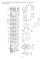
1
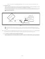
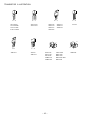
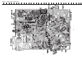
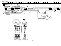
NSX-AJ200 U NSX-AJ205 U NSX-SZ200 EZ,LH NSX-SZ205 EZ SERVICE MANUAL COMPACT DISC STEREO SYSTEM BASIC CD MECHANISM : BZG-2 ZD4NC BASIC TAPE MECHANISM: ZZM-3 YPR2NC SYSTEM CD CASSEIVER SPEAKER NSX–AJ200 (TYPE: U) CX–NAJ200 SX–NAJ202 CX–NAJ205 SX–NAJ205 SX-R145 CX–NSZ200 SX–NSZ202 CX–NSZ205 SX–NSZ205 CX–NSZ200 SX–NSZ205 NSX–AJ205 (TYPE: U) NSX–SZ200 (TYPE: EZ) NSX–SZ205 (TYPE: EZ) NSX–SZ200 (TYPE: LH) REMOTE CONTROLLER RC–AAS11(VS) • This Service Manual is the “Revision Publishing” and replace “Simple Manual” NSX-AJ200/AJ205/SZ200/SZ205<U,EZ,LH>, (S/M Code No. 09-011-440-9T1). • If requiring information about the CD mechanism, see Service Manual of BZG-2 (S/M Code No. 09-00C-353-2N2). S/M Code No. 09-012-440-9R1 N O SI I V TA E R A D SPECIFICATIONS TUNER FM tuning range: 87.5 MHz to 108 MHz FM usable Sensitivity(IHF): 13.2 dBf<U,LH>, 16.8 dBf<EZ> FM antenna terminals: 75 ohms (unbalanced) AM tuning range<U,LH>: 530 kHz to 1710 kHz (10 kHz step) 531 kHz to 1602 kHz (9 kHz step) AM usable sensitivity<U,LH>: 350 mV/m AM antenna<U,LH>: Loop antenna MW tuning range<EZ>: 531 kHz to 1602 kHz (9 kHz step) 530 kHz to 1710 kHz (10 kHz step) MW usable sensitivity<EZ>:350 mV/m LW tuning range<EZ>: 144 kHz to 290 kHz LW usable sensitivity: 1400mV/m MW/LW antenna: Loop antenna AMPLIFIER CX-NAJ200 Power output: Total harmonic distortion: CX-NAJ205 Power output: 20 W + 20 W (50 Hz - 20 kHz, THD less than 1%, 6 ohms) 25 W + 25 W (1 kHz, THD less than 10%, 6 ohms) 0.1% (10 W, 1 kHz, 6 ohms, DIN AUDIO) 40 W + 40 W (50 Hz - 20 kHz, THD less than 1%, 6 ohms) 50 W + 50 W (1 kHz, THD less than 10%, 6 ohms) Total 0.1% (20 W, 1 kHz, 6 ohms, DIN AUDIO) harmonic distortion: CX-NSZ200<EZ> / CX-NSZ205 Power output: 12 W + 12 W (6 ohms, T.H.D. 1%, 1 kHz/DIN 45500) Reference: 15 W + 15 W (6 ohms, T.H.D. 10%, 1 kHz/DIN 45324) DIN MUSIC POWER: 39 W + 39 W Total harmonic distortion: 0.1% (6 W, 1 kHz, 6 ohms, DIN AUDIO) CX-NSZ200<LH> Power output: Rated: 40 W + 40 W (6 ohms, T.H.D. 1%, 1 kHz) Reference: 50 W + 50 W (6 ohms, T.H.D. 10%, 1 kHz) Total 0.1% (20 W, 1 kHz, 6 ohms, DIN AUDIO) harmonic distortion: Input: VIDEO/AUX: 500 mV Output: SPEAKERS: 6 ohms or more SURROUND SPEAKERS (only for CX-NAJ205): 8 ohms to 16 ohms PHONES: 32 ohms or more FRONT SPEAKERS SX-NAJ202 ( only for NSX-AJ200) Speaker system: 2 way, bass reflex (magnetic shielded) Speaker units: Woofer: 120 mm (43/4 in.) cone Tweeter: 20 mm (13/16 in.) cone Impedance: 6 ohms Dimensions (W x H x D): 220 x 324 x 198 mm ( 83/4 x 127/8 x 77/8 in.) Weight: 2.3 kg (5 lbs 1 oz) FRONT SPEAKERS SX-NAJ205 ( only for NSX-AJ205) Speaker system: 3 way, bass reflex (magnetic shielded) Speaker units: Woofer: 120 mm (43/4 in.) cone Tweeter: 60 mm (23/8 in.) cone Super tweeter: 20 mm (13/16 in.) ceramic Impedance: 6 ohms Dimensions (W x H x D): 220 x 324 x 198 mm ( 83/4 x 127/8 x 77/8 in.) Weight: 2.5 kg (5 lbs 8 oz) FRONT SPEAKERS SX-NSZ202 ( only for NSX-SZ200<EZ>) Speaker system: 2 way, bass reflex (magnetic shielded) Speaker units: Woofer: 120 mm cone Tweeter: 20 mm ceramic cone Impedance: 6 ohms Dimensions (W x H x D): 220 x 324 x 198 mm Weight: 2.3 kg (5 lbs 1 oz) FRONT SPEAKERS SX-NSZ205 (for NSX-SZ200<LH>, NSX-SZ205) Speaker system: 3 way, bass reflex (magnetic shielded) Speaker units: Woofer: 120 mm cone Tweeter: 60 mm cone Super tweeter: 20 mm ceramic Impedance: 6 ohms Dimensions (W x H x D): 220 x 324 x 198 mm Weight: 2.5 kg (5 lbs 8 oz) SURROUND SPEAKERS SX-R145 (only for NSX-AJ205) Speaker system: 1 way, bass reflex Speaker units: Full range: 80 mm(31/4 in.) cone Impedance: 8 ohms Dimensions (W x H x D): 100 x 132 x 116 mm (4 x 51/4 x 45/8 in.) Weight: 0.5 kg (1 lbs 2 oz) Accessories: Wall mounting screws (2) GENERAL Powerrequirements: Power consumption: CASSETTE DECK Track format: Frequency response: Recording system: Heads: CD PLAYER Laser: D/A converter: Signal-to-noise ratio: Harmonic distortion: 120 V AC, 60 Hz<U> 230 V AC, 50 Hz<EZ> 120 V/220 - 230 V/240 V AC (Switchable), 50 Hz/60Hz<LH> 60 W<200U>, 67W<205U>, 53 W<EZ> 70 W<200LH>, 4 tracks, 2 channels stereo 50 Hz - 8 kHz AC bias DECK 1: playback x 1 DECK 2: recording/playback x 1, erase x 1 Power consumption in standby mode: Semiconductor laser (l = 780 nm) 1 bit dual 85 dB (1 kHz, 0 dB) 0.05 % (1 kHz, 0 dB) • Design and specifications are subject to change without notice. With ECO mode on: 0.6 W With ECO mode off: 15 W Dimensions ( W x H x D): 260 x 323 x 291 mm (101/4 x 123/4 x 111/2 in.) Weight: 5.9 kg (13 lbs)<U,LH>, 4.9 kg<EZ> –2– PROTECTION OF EYES FROM LASER BEAM DURING SERVICING This set employs laser. Therefore, be sure to follow carefully the instructions below when servicing. WARNING!! WHEN SERVICING, DO NOT APPROACH THE LASER EXIT WITH THE EYE TOO CLOSELY. IN CASE IT IS NECESSARY TO CONFIRM LASER BEAM EMISSION. BE SURE TO OBSERVE FROM A DISTANCE OF MORE THAN 30cm FROM THE SURFACE OF THE OBJECTIVE LENS ON THE OPTICAL PICK-UP BLOCK. CAUTION Use of controls or adjustments or performance of procedures other than those specified herin may result in hazardous radiation exposure. ATTENTION L’utillisation de commandes, réglages ou procédures autres que ceux spécifiés peut entraîner une dangereuse exposition aux radiations. ADVARSEL s Caution: Invisible laser radiation when open and interlocks defeated avoid exposure to beam. Advarsel: Usynlig laserståling ved åbning, når sikkerhedsafbrydere er ude af funktion. Undgå udsættelse for stråling. Usynlig laserståling ved åbning, når sikkerhedsafbrydereer ude af funktion. Undgå udsættelse for stråling. This Compact Disc player is classified as a CLASS 1 LASER product. The CLASS 1 LASER PRODUCT label is located on the rear exterior. VAROITUS! Laiteen Käyttäminen muulla kuin tässä käyttöohjeessa mainitulla tavalla saataa altistaa käyt-täjän turvallisuusluokan 1 ylittävälle näkymättömälle lasersäteilylle. CLASS 1 KLASSE 1 LUOKAN 1 KLASS 1 VARNING! Om apparaten används på annat sätt än vad som specificeras i denna bruksanvising, kan användaren utsättas för osynling laserstrålning, som överskrider gränsen för laserklass 1. LASER PRODUCT LASER PRODUKT LASER LAITE LASER APPARAT Precaution to replace Optical block (KSS-213F) Body or clothes electrostatic potential could ruin laser diode in the optical block. Be sure ground body and workbench, and use care the clothes do not touch the diode. PICK-UP ASSY PWB 1) After the connection, remove solder shown in right figure. Solder –3– NOTE ON BEFORE STARTING REPAIR 1. Forced discharge of electrolytic capacitor of power supply block When repair is going to be attempted in the set that uses relay circuit in the power supply block, electric potential is kept charged across the electrolytic capacitors (C101, 102) even though AC power cord is removed. If repair is attempted in this condition, secondary defect can occur. In order to prevent the secondary trouble, perform the following measures before starting repair work. Discharge procedure MAIN C.B 1 Remove the AC power cord. 2 Connect a discharging resistor at an end of lead wire that has clips at both ends. Connect the other end of the lead wire to metal chassis. 3 Contact the other end of the discharging resistor to the positive (+) side (+VH) of C101. (For two seconds) 4 Contact the same end of the discharging resistor as step 3 to the negative (-) side (-VH) of C102 in the same way. (For two seconds) 5 Check that voltage across C101 and C102 has decreased to 1 V or less using a multimeter or an oscilloscope. D101 3 2 Select a discharging resistor referring to the following table. C102 4 2 Fig-1 Charging voltage (V) Discharging (C101, 102) resistor (Ω) 25-48 100 3 87-A00-247-090 49-140 220 5 87-A00-232-090 Rated power (W) C101 Parts number Note: The reference numbers (C101, C102) of the electrolytic capacitors can change depending on the models. Be sure to check the reference numbers of the charging capacitors on schematic diagram before starting the discharging work. 2. Check items before exchanging the MICROCOMPUTER Be sure to check the following items before exchanging the MICROCOMPUTER. Exchange the MICROCOMPUTER after confirming that the MICROCOMPUTER is surely defective. 2-1. Regarding the HOLD terminal of the MICROCOMPUTER When the HOLD terminal (INPUT) of the MICROCOMPUTER is “H”, the MICROCOMPUTER is judged to be operating correctly. When this terminal is “L”, the main power cannot be turned on. Therefore, be sure to check the terminal voltage of the HOLD terminal before exchange. When the MICROCOMPUTER is not defective, the HOLD terminal can also go “L” when the POWER AMPLIFIER has any abnormalities that triggers the abnormality detection circuit on the MAIN C. B. that sets the HOLD terminal to “L”. • Good or no good judgement of the MICROCOMPUTER 1 Turn on the AC main power. 2 Confirm that the main power is turned on and the HOLD terminal of the MICROCOMPUTER keeps the “H” level or not. 3 When the HOLD terminal is “L” level, the abnormality detection circuit is judged to be working correctly and the MICROCOMPUTER is judged to be good. –4– In such a case, check also if the POWER AMPLIFIER circuit or power supply circuit has any abnormalities or not. 2-2. Regarding reset TE R There are cases that the machine does not work correctly because the MICROCOMPUTER is not reset even though the AC power cord is re-inserted, or the software reset (pressing the STOP key + POWER key) is performed. When the above described phenomenon occurs, it can lead to wrong judgement as if the MICROCOMPUTER is defective and to exchange the MICROCOMPUTER. In such a case, perform the forced-reset by the following procedure and check good or no good of the MICROCOMPUTER. 1 Remove the AC power cord. M IC RO CO M PU FRONT C.B 18 15 C113 % VSS MICROC113 COMPUTER * VDD FRONT C.B Short with tweezers. Fig-2-2 2 Short both ends of the electrolytic capacitor C113 that is connected to VDD of the MICROCOMPUTER with tweezers. 3 Connect the AC power cord again. If the MICROCOMPUTER returns to the normal operation, the MICROCOMPUTER is good. Note: The reference number or MICROCOMPUTER pin number of transistor (Q110) and electrolytic capacitor (C113) can change depending on the models. Be sure to check the reference numbers on schematic diagram before starting the discharging work. 2-3. Confirmation of soldering state of MICROCOMPUTER Check the soldering state of the MICROCOMPUTER in addition to the above described procedures. Be sure to exchange the MICROCOMPUTER after surely confirming that the trouble is not caused by poor soldering but the MICROCOMPUTER itself. –5– ELECTRICAL MAIN PARTS LIST REF. NO. PART NO. KANRI NO. DESCRIPTION REF. NO. IC 87-A21-269-010 87-A21-893-040 87-A21-419-040 8B-NFA-602-030 8B-NFA-603-030 IC,EW732 C-IC,NJM4558V-TE2 C-IC,NJM14558MD-TE2 IC,UPD780226GF-022-3BA<EXCEPT 205EZ> C-IC,UPD780228GF-079-3BA<205EZ> 87-A21-218-110 87-A21-443-040 87-A21-695-010 87-A20-440-040 87-A21-928-010 IC,NJL64H380A C-IC,M62495AFP IC,LA1845L C-IC,BU1920FS<205EZ> IC,LC72131D-N TRANSISTOR PART NO. C20 C21 C21 C22 C22 KANRI NO. 87-A12-431-000 87-A12-442-000 87-A12-440-000 87-A12-381-000 87-A12-441-000 DESCRIPTION CAP,E CAP,E CAP,E CAP,E CAP,E C25 C25 C26 C26 C30 87-010-385-080 87-010-407-080 87-010-247-080 87-010-407-080 87-010-393-080 CAP, CAP, CAP, CAP, CAP, C30 C31 C35 C36 C38 87-010-247-080 87-010-263-080 87-010-406-080 87-010-381-080 87-010-190-080 CAP, ELECT 100-50V<200LH,205U> CAP, ELECT 100-10V CAP, ELECT 22-50 CAP, ELECT 330-16V S CHIP F 0.01 C50 C60 C61 C61 C98 87-010-393-080 87-010-403-080 87-010-380-080 87-010-260-080 87-A12-317-080 CAP, E 100-35V<200EZ,205EZ,200U> CAP, ELECT 3.3-50V CAP, E 47-16V<200EZ,205EZ,200U> CAP, ELECT 47-25V<200LH,205U> C-CAP,U 0.1-50 Z F C123 C124 C125 C126 C127 87-012-269-080 87-012-269-080 87-010-759-080 87-010-759-080 87-010-759-080 C-CAP,U 390P-50 B<200EZ,205EZ> C-CAP,U 390P-50 B<200EZ,205EZ> C-CAP,U, 0.1-25F C-CAP,U, 0.1-25F C-CAP,U, 0.1-25F C128 C129 C130 C131 C132 87-010-759-080 87-010-191-080 87-010-191-080 87-012-286-080 87-012-286-080 C-CAP,U, 0.1-25F C-CAP,S 0.015-50 F<200EZ,205EZ> C-CAP,S 0.015-50 F<200EZ,205EZ> CAP, U 0.01-25 CAP, U 0.01-25 C133 C161 C162 C181 C181 87-A12-317-080 87-010-408-080 87-010-408-080 87-010-235-080 87-010-387-080 C-CAP,U 0.1-50 Z F CAP, ELECT 47-50V<205U> CAP, ELECT 47-50V<205U> CAP,E 470-16 SME<200EZ,205EZ> CAP,E 470-25 SME<200LH,200U,205U> C192 C401 C402 C403 C404 87-010-759-080 87-A12-319-080 87-A12-319-080 87-012-193-080 87-012-193-080 C-CAP,U, 0.1-25F<200EZ,205EZ> C-CAP,U 0.1-25 K B C-CAP,U 0.1-25 K B C-CAP,U 82P-50 CH C-CAP,U 82P-50 CH C405 C406 C407 C408 C409 87-012-286-080 87-012-286-080 87-012-286-080 87-012-286-080 87-012-278-080 CAP, U 0.01-25 CAP, U 0.01-25 CAP, U 0.01-25 CAP, U 0.01-25 C-CAP,U 2200P-50 B 2200-50 3300-25 3300-35 2200-25 2200-35 M M M M M 85<200LH,205U> 85<EXCEPT 200U> 85 IV LELON<200U> 85<EXCEPT 200U> 85 IV LELON<200U> ELECT 220-25V<200LH,205U> E 33-50V<200EZ,205EZ,200U> ELECT 100-50V<200LH,205U> E 33-50V<200EZ,205EZ,200U> E 100-35V<200EZ,205EZ,200U> 87-A30-494-080 89-213-702-010 87-026-610-080 87-A30-076-080 87-A30-075-080 TR,2SA1980G TR,2SB1370 (1.8W) TR,KTC3198GR C-TR,2SC3052F C-TR,2SA1235F 87-A30-484-080 87-A30-190-080 87-A30-255-010 87-A30-306-010 87-A30-528-010 C-TR,KRA102S TR,CC5551 TR,2SB1342<200EZ,205EZ,200U> TR,2SB1677<200LH> TR,2SB1686<205U> 87-A30-256-010 87-A30-307-010 87-A30-529-010 87-A30-107-070 87-A30-106-040 TR,2SD1933<200EZ,205EZ,200U> TR,2SD2619<200LH> TR,2SD2642<205U> C-TR,CMBT5401 C-TR,CMBT5551 87-A30-162-010 87-A30-091-080 87-A30-090-080 87-A30-062-080 87-A30-492-080 FET,2SK2937<200LH,205U> FET,2SJ460 FET,2SK2541 C-TR,KRC104S TR,2SC5343G 87-A30-468-080 87-A30-582-080 87-A30-495-080 89-327-143-080 87-A30-489-080 C-TR,KRC102S-RTK TR,CDA1585BC TR,2SA1981Y TR,2SC2714 (0.1W) C-TR,KRA107S 89-503-602-080 87-A30-086-040 87-A30-234-080 C-FET,2SK360E C-TR,CSD1306E<200EZ,205EZ> TR,CSC4115BC 87-A40-535-080 87-A40-393-090 87-A40-455-080 87-A40-553-080 87-A40-778-080 DIODE,1N5393-GOODARK<200EZ,205EZ> DIODE,1N5402GW(F20)<200LH,205U> DIODE,RL203 GW<200U> DIODE,1N4003 LES ZENER,UZ30BSD C410 C411 C412 C421 C422 87-012-278-080 87-010-405-080 87-010-405-080 87-012-274-080 87-012-274-080 C-CAP,U 2200P-50 B CAP, ELECT 10-50V CAP, ELECT 10-50V C-CAP,U 1000P-50 K B C-CAP,U 1000P-50 K B 87-A40-291-080 87-A40-764-080 87-A40-269-080 87-A40-270-080 87-A40-749-080 DIODE,1N4148 (CPT) ZENER,UZ10BSC C-DIODE,MC2836 C-DIODE,MC2838 ZENER,UZ5.6BSB<200LH,205U> C423 C424 C425 C426 C427 87-012-274-080 87-012-274-080 87-010-263-080 87-010-263-080 87-012-188-080 C-CAP,U 1000P-50 K B C-CAP,U 1000P-50 K B CAP, ELECT 100-10V CAP, ELECT 100-10V C-CAP,U 47P-50 CH 87-A40-748-080 87-A40-739-080 87-017-149-080 ZENER,UZ5.6BSA ZENER,UZ2.7BSA ZENER,HZS6A2L C428 C429 C430 C431 C432 87-012-188-080 87-010-598-080 87-010-598-080 87-012-284-080 87-012-284-080 C-CAP,U 47P-50 CH C-CAP,S 0.068-16VRK C-CAP,S 0.068-16VRK CAP, U 6800P-50 CAP, U 6800P-50 C3 C4 C5 C6 C9 87-010-759-080 87-010-759-080 87-010-759-080 87-010-759-080 87-010-759-080 C-CAP,U, C-CAP,U, C-CAP,U, C-CAP,U, C-CAP,U, C433 C434 C435 C440 C441 87-010-546-080 87-010-546-080 87-010-263-080 87-010-759-080 87-010-787-080 CAP, ELECT 0.33-50V CAP, ELECT 0.33-50V CAP, ELECT 100-10V C-CAP,U, 0.1-25F<200EZ,205EZ> CAP, U 0.022-25 C10 C11 C12 C19 87-010-759-080 87-010-759-080 87-010-759-080 87-A12-431-000 C-CAP,U, 0.1-25F C-CAP,U, 0.1-25F C-CAP,U, 0.1-25F CAP,E 2200-50 M 85<200LH,205U> C442 C443 C445 C446 C447 87-010-759-080 87-010-759-080 87-A10-039-080 87-010-401-080 87-010-787-080 C-CAP,U 0.1-25 Z F C-CAP,U, 0.1-25F C-CAP,U 470P-50 J CH CAP, ELECT 1-50V C-CAP,U 0.022-25<EXCEPT 200U,205U> DIODE MAIN C.B 0.1-25F<200LH,205U> 0.1-25F<200LH,205U> 0.1-25F<200LH,205U> 0.1-25F<200LH,205U> 0.1-25F –6– REF. NO. ! ! ! ! ! ! ! ! ! ! ! ! ! PART NO. C452 C453 C454 C455 C456 KANRI NO. 87-010-382-080 87-012-279-080 87-012-279-080 87-012-279-080 87-012-286-080 DESCRIPTION CAP, ELECT 22-25V C-CAP,U 2700P-50 B C-CAP,U 2700P-50 B C-CAP,U 2700P-50 B CAP, U 0.01-25 C457 C458 C459 C460 C461 87-A12-361-080 87-012-274-080 87-A12-468-080 87-010-759-080 87-A12-466-080 C462 C470 C605 C606 C609 REF. NO. C312 C501 C502 C503 C504 KANRI NO. 87-012-195-080 87-010-759-080 87-010-759-080 87-012-278-080 87-016-460-080 C-CAP,U 100P-50CH C-CAP,U, 0.1-25F C-CAP,U, 0.1-25F C-CAP,U 2200P-50 B C-CAP,S 0.22-16 B CAP,M 5600P-100 J CP CHIP CAP,U 1000P-50B<200EZ,205EZ> C-CAP,U 560P-50 J SL<200EZ,205EZ> C-CAP,U, 0.1-25F C-CAP,U 390P-50 J SL C505 C507 C508 C509 C510 87-010-248-040 87-010-400-040 87-012-172-080 87-A12-462-080 87-012-270-080 CAP,E 220-10 SME CAP,E 0.47-50 CAPACITOR CHIP U 10P CH C-CAP,U 180P-50 J SL CAP, U 470P-50 87-A12-466-080 87-012-270-080 87-012-275-080 87-012-275-080 87-010-785-080 C-CAP,U C-CAP,U C-CAP,U C-CAP,U C-CAP,U C511 C512 C513 C514 C515 87-010-759-080 87-012-268-080 87-010-829-080 87-012-286-080 87-012-274-080 C-CAP,U, 0.1-25F C-CAP,U 330P-50 B CAP, U 0.047-16 CAP, U 0.01-25 CHIP CAP,U 1000P-50B C610 C611 C612 C613 C614 87-010-785-080 87-010-545-080 87-010-545-080 87-010-545-080 87-010-545-080 C-CAP,U0.015-25BK CAP, ELECT 0.22-50V CAP, ELECT 0.22-50V CAP, ELECT 0.22-50V CAP, ELECT 0.22-50V C516 C517 C518 C519 C520 87-010-759-080 87-012-272-080 87-012-272-080 87-010-759-080 87-010-246-040 C-CAP,U, 0.1-25F C-CAP,U 680P-50 B C-CAP,U 680P-50 B C-CAP,U, 0.1-25F CAP,E 47-35 SME C615 C616 C617 C618 C625 87-012-172-080 87-010-248-080 87-010-248-080 87-010-405-080 87-010-598-080 CAPACITOR CHIP U 10P CH CAP, ELECT 220-10V CAP, ELECT 220-10V CAP, ELECT 10-50V C-CAP,S 0.068-16VRK C521 C522 C523 C524 C525 87-A12-317-080 87-010-263-040 87-010-404-040 87-010-404-040 87-010-260-040 C-CAP,U 0.1-50 Z F CAP,E 100-10 CAP,E 4.7-50 SME CAP,E 4.7-50 SME CAP,E 47-25 SME C626 C630 C677 CN102 CN401 87-010-598-080 87-016-669-080 87-012-286-080 87-A61-001-010 87-A60-620-010 C-CAP,S 0.068-16VRK C-CAP,S 0.1-25 K B CAP, U 0.01-25 CONN,17P V BLK TAC-L17X-A3 CONN,3P V 2MM JMT C527 C528 CN502 CN504 FFC502 87-010-759-080 87-010-759-080 87-099-196-010 87-A60-136-010 88-908-201-110 C-CAP,U, 0.1-25F C-CAP,U, 0.1-25F CONN,8P 6216 V CONN,11P V FE FF-CABLE,8P 1.25 CN451 CN602 CNA401 CNA451 FFC602 87-A60-625-010 87-099-194-010 86-ZM3-604-210 8B-NFA-626-010 88-906-251-110 CONN,8P V 2MM JMT CONN,6P 6216V CONN ASSY,3P -PB CONN,ASSY,8P -RPB FF-CABLE,6P 1.25 FFC504 FL501 L501 LED501 S201 88-911-131-110 8B-NFA-601-010 87-A50-655-010 87-A40-317-080 87-A90-164-080 FF-CABLE,11P 1.25 130MM FL,HNA-10SS19T COIL,CLK 4.19MHZ(TOKO) 7KLY LED,SLR-342VCT31 RED SW,TACT SKQAB(N) J101 J205 J602 L101 L102 87-A60-602-010 87-A60-545-010 87-A60-881-010 87-A50-611-010 87-A50-611-010 JACK,DIA6.3 BLK ST W/SW TC JACK,PIN 4P W/R<205U> JACK,PIN 2P MSP<EXCEPT 205U> COIL,1UH K(CS) COIL,1UH K(CS) S202 S203 S204 S205 S206 87-A90-164-080 87-A90-164-080 87-A90-164-080 87-A90-164-080 87-A90-164-080 SW,TACT SW,TACT SW,TACT SW,TACT SW,TACT SKQAB(N) SKQAB(N) SKQAB(N) SKQAB(N) SKQAB(N) L451 L451 PT1 PT1 PT1 87-007-342-010 87-007-342-010 8B-NFA-611-010 8B-NFA-609-010 8B-NFA-607-010 COIL,OSC COIL,OSC PT,BNF-A PT,BNF-A PT,BNF-A S207 S208 S209 S210 S211 87-A90-164-080 87-A90-164-080 87-A90-164-080 87-A90-164-080 87-A90-164-080 SW,TACT SW,TACT SW,TACT SW,TACT SW,TACT SKQAB(N) SKQAB(N) SKQAB(N) SKQAB(N)<205EZ> SKQAB(N)<205EZ> PT1 PT2 PT2 PT2 RY1 8B-NFA-613-010 8B-NF9-665-010 8B-NF9-663-010 8B-NF9-661-010 87-A91-339-010 PT,BNF-A U-HI-SUR<205U> PT,SUB BNF E (TAM)<200EZ,205EZ> PT,SUB BNF H (TAM)<200LH> PT,SUB BNF U (TAM)<200U,205U> RELAY,AC DC12V G5PA-2<200LH> S212 S213 S214 S215 S216 87-A90-164-080 87-A90-164-080 87-A90-164-080 87-A90-164-080 87-A90-164-080 SW,TACT SW,TACT SW,TACT SW,TACT SW,TACT SKQAB(N)<205EZ> SKQAB(N) SKQAB(N) SKQAB(N) SKQAB(N) RY181 RY181 S181 T181 T182 87-A92-072-010 87-A91-418-010 87-A90-165-010 87-A60-317-010 87-A60-317-010 RELAY,AC DC12V HRM3H-S-1POLE<U> RELAY,AC12V G5PA-1-M<200EZ,205EZ> SW,SL 1-2-3 SWS2301<200LH> TERMINAL, 1P MSC TERMINAL, 1P MSC S217 S218 S219 S220 S221 87-A90-164-080 87-A90-164-080 87-A90-164-080 87-A90-164-080 87-A90-164-080 SW,TACT SW,TACT SW,TACT SW,TACT SW,TACT SKQAB(N) SKQAB(N) SKQAB(N) SKQAB(N) SKQAB(N) TM101 87-A61-452-010 TERMINAL,SP 4P(MSC) S222 S223 S230 87-A90-164-080 87-A90-164-080 87-A92-054-010 SW,TACT SKQAB(N) SW,TACT SKQAB(N) SW,RTRY EC12E24504 C301 C303 C304 C305 C306 87-010-759-080 87-012-280-080 87-016-116-080 87-012-184-080 87-012-274-080 C-CAP,U, 0.1-25F CAP, U 3300P-50 C-CAP,U 0.015-25 J B CB C-CAP,U 33P-50 CH CHIP CAP,U 1000P-50B C307 C308 C309 C310 C311 87-012-274-080 87-010-544-040 87-010-404-040 87-012-286-080 87-A12-052-080 CHIP CAP,U 1000P-50B CAP,E 0.1-50 SME CAP,E 4.7-50 SME CAP, U 0.01-25 C-CAP,S 0.033-25 J B C771 C772 C779 C780 C782 87-010-263-080 87-012-286-080 87-010-949-080 87-010-949-080 87-012-286-080 CAP, ELECT 100-10V CAP, U 0.01-25 C-CAP,S 0.01-50 BJ<200EZ,205EZ> C-CAP,S 0.01-50 BJ<200EZ,205EZ> C-CAP,U 0.01-25 K B C783 C784 C785 C786 87-012-286-080 87-012-286-080 87-012-286-080 87-012-286-080 C-CAP,U C-CAP,U C-CAP,U C-CAP,U 390P-50 J SL 470P-50 K B 1200P-50 B 1200P-50 B 0.015-25BK 85K BIAS 85K BIAS EZ-LOW<200EZ,205EZ> LH<200LH> U<200U> FRONT C.B PART NO. DESCRIPTION TUNER C.B –7– 0.01-25 0.01-25 0.01-25 0.01-25 K K K K B B B B REF. NO. PART NO. C788 C789 C789 C790 C790 KANRI NO. 87-012-167-080 87-A12-052-080 87-016-118-080 87-A12-052-080 87-016-118-080 DESCRIPTION C-CAP,U 5P-50 CH C-CAP,S 0.033-25<200LH,200U,205U> C-CAP,U0.022-25BJ<200EZ,205EZ> C-CAP,S 0.033-25<200LH,200U,205U> C-CAP,U0.022-25BJ<200EZ,205EZ> C791 C792 C793 C795 C796 87-010-759-080 87-012-286-080 87-010-404-080 87-012-286-080 87-012-286-080 C797 C798 C799 C800 C801 REF. NO. C942 C947 C948 C952 C957 KANRI NO. 87-012-165-080 87-012-286-080 87-A10-039-080 87-012-286-080 87-012-174-080 CAP 3P<200EZ,205EZ> CAP, U 0.01-25<200EZ,205EZ> C-CAP,U 470P-50 J CH<200EZ,205EZ> CAP, U 0.01-25<200EZ,205EZ> C-CAP, CERA SS 12P CHJ<200EZ,205EZ> C-CAP,U, 0.1-25F C-CAP,U 0.01-25 K B CAP, ELECT 4.7-50V C-CAP,U 0.01-25 K B C-CAP,U 0.01-25 K B C958 C959 C960 C961 C962 87-012-286-080 87-010-831-080 87-010-831-080 87-012-167-080 87-010-401-080 C-CAP,U 0.01-25 K B<200EZ,205EZ> C-CAP,U 0.1-16 Z F<200LH,200U,205U> C-CAP,U 0.1-16 Z F C-CAP,U 5P-50 CH<200LH,200U,205U> CAP, ELECT 1-50V<200EZ,205EZ> 87-010-405-080 87-012-286-080 87-010-265-080 87-012-369-080 87-010-403-080 CAP, ELECT 10-50V C-CAP,U 0.01-25 K B CAP, ELECT 33-16V C-CAP,S 0.047-50F CAP, ELECT 3.3-50V C963 C971 C972 C973 C974 87-015-785-080 87-010-381-080 87-010-404-080 87-012-286-080 87-012-286-080 C-CAP,0.1-25 Z F C3216 CAP, ELECT 330-16V CAP, ELECT 4.7-50V C-CAP,U 0.01-25 K B C-CAP,U 0.01-25 K B C802 C803 C804 C807 C808 87-012-369-080 87-010-787-080 87-010-263-080 87-010-400-080 87-010-401-080 C-CAP,S 0.047-50F CAP, U 0.022-25 CAP, ELECT 100-10V CAP, ELECT 0.47-50V CAP, ELECT 1-50V C979 C981 C982 C983 C984 87-012-195-080 87-010-260-080 87-010-759-080 87-012-286-080 87-012-286-080 C-CAP,U 100P-50 J CH CAP, ELECT 47-25V C-CAP,U, 0.1-25F C-CAP,U 0.01-25 K B C-CAP,U 0.01-25 K B C809 C810 C814 C815 C816 87-010-401-080 87-010-759-080 87-012-286-080 87-010-400-080 87-010-400-080 CAP, ELECT 1-50V C-CAP,U, 0.1-25F CAP, U 0.01-25 CAP, ELECT 0.47-50V CAP, ELECT 0.47-50V C985 C987 C989 C991 C992 87-012-195-080 87-012-286-080 87-012-286-080 87-012-176-080 87-012-176-080 C-CAP,U 100P-50CH<200EZ,205EZ> C-CAP,U 0.01-25 K B C-CAP,U 0.01-25 K B<200EZ,205EZ> CAP 15P CAP 15P C818 C821 C823 C823 C824 87-012-276-080 87-010-405-080 87-012-349-080 87-A10-978-080 87-010-404-080 CAP, CHIP SS 1500 PBK<200EZ,205EZ> CAP, ELECT 10-50V C-CAP,S 1000P-50 CH<200EZ,205EZ> C-CAP,U 820P-25<200LH,200U,205U> CAP, ELECT 4.7-50V C993 C995 C997 C998 C999 87-010-178-080 87-010-178-080 87-010-759-080 87-010-260-080 87-012-286-080 CHIP CAP 1000P CHIP CAP 1000P C-CAP,U, 0.1-25F CAP, ELECT 47-25V C-CAP,U 0.01-25 K B C825 C831 C842 C844 C850 87-010-829-080 87-010-406-080 87-012-286-080 87-012-286-080 87-010-260-080 CAP, U 0.047-16 CAP, ELECT 22-50<200EZ,205EZ> C-CAP,U 0.01-25 K B C-CAP,U 0.01-25 K B CAP, ELECT 47-25V CF831 CF831 CF832 CF832 D902 87-008-423-010 87-008-261-010 82-785-747-010 87-008-261-010 87-A40-128-080 CERAMIC FILTER, SFE10.7<EZ> FILTER, SFE10.7MA5-A<EXCEPT EZ> CF MS2 GHY R<200EZ,205EZ> FILTER, SFE10.7MA5-A<EXCEPT EZ> C-VARI-CAP,HVU202A<EXCEPT EZ> C851 C852 C853 C858 C859 87-012-286-080 87-012-286-080 87-012-286-080 87-010-831-080 87-010-831-080 C-CAP,U C-CAP,U C-CAP,U C-CAP,U C-CAP,U D903 FFE831 J831 J832 L801 87-A40-128-080 A8-6ZA-199-170 87-A60-202-010 87-A60-403-010 87-A50-608-010 C-VARI-CAP,HVU202A<EXCEPT EZ> 6ZA-1 FEENC<200EZ,205EZ> TERMINAL,ANT 4P MSP-154V-02<EXCEPT EZ> TERMINAL,ANT PAL 2P HSP-312V05<EZ> COIL,FM DET-N(TOK) C860 C869 C870 C871 C872 87-012-286-080 87-012-286-080 87-012-274-080 87-012-199-080 87-012-199-080 C-CAP,U 0.01-25 K B<200EZ,205EZ> CAP, U 0.01-25<205EZ> CHIP CAP,U 1000P-50B<205EZ> CAP 220P<205EZ> CAP 220P<205EZ> L802 L811 L832 L861 L902 87-A91-551-010 87-005-847-080 87-005-847-080 87-005-847-080 88-ZA1-602-110 FLTR,PCFJZH-450 L(TOK) COIL,2.2UH(CECS) COIL,2.2UH(CECS) COIL,2.2UH(CECS)<205EZ> COIL,FM-RF-U2 2G<200LH,200U,205U> C873 C874 C875 C876 C877 87-A10-039-080 87-010-405-080 87-010-759-080 87-010-405-080 87-012-286-080 C-CAP,U 470P-50 J CH<205EZ> CAP, ELECT 10-50V<205EZ> C-CAP,U, 0.1-25F<205EZ> CAP, ELECT 10-50V<205EZ> CAP, U 0.01-25<205EZ> L903 L904 L905 L906 L941 88-ZA1-601-010 87-005-847-080 88-ZA1-624-010 88-ZA1-603-010 87-A50-020-010 COIL,FM-RF-U1 2G<200LH,200U,205U> COIL,2.2UH(CECS)<200LH,200U,205U> COIL,FM IFT 7-6.2 (COILS)<EXCEPT EZ> COIL,FM-OSC-U 2G<200LH,200U,205U> COIL,ANT LW(COI)<200EZ,205EZ> C878 C879 C901 C904 C905 87-012-184-080 87-012-180-080 87-018-145-080 87-012-286-080 87-012-286-080 C-CAP,U 33P-50 CH<205EZ> C-CAP,U 22P-50 CH<205EZ> CAP,TC-U 6.8P-50<200LH,200U,205U> CAP, U 0.01-25<200LH,200U,205U> CAP, U 0.01-25<200LH,200U,205U> L942 L951 L951 R790 R991 87-A50-019-010 8A-NF8-668-010 8A-NF8-667-010 87-012-286-080 87-012-195-080 COIL,OSC LW(COI)<200EZ,205EZ> COIL,AM PACK 2(TOK)<200EZ,205EZ> COIL,AM PACK 4(TOK)<200LH,200U,205U> C-CAP,U 0.01-25 K B C-CAP,U 100P-50 J CH C907 C908 C909 C910 C911 87-012-286-080 87-A10-915-080 87-012-286-080 87-012-174-080 87-012-170-080 CAP, U 0.01-25<200LH,200U,205U> C-CAP,U 1000P-25<200LH,200U,205U> CAP, U 0.01-25<200LH,200U,205U> C-CAP, CERA SS 12P<200LH,200U,205U> C-CAP,U 8P-50 CH<200LH,200U,205U> R993 R995 TC942 X862 X992 87-012-195-080 87-012-195-080 87-A91-774-080 87-A70-307-010 87-A70-306-010 C-CAP,U 100P-50 J CH C-CAP,U 100P-50 J CH TRIMMER,PLY 30P 6.8X5.4 CDYL<EZ> VIB,XTAL 4.332MHZ CSA-309ST<205EZ> VIB,XTAL 4.500MHZ CSA-309ST C912 C913 C914 C915 C916 87-012-195-080 87-012-286-080 87-012-166-080 87-012-174-080 87-012-180-080 C-CAP,U 100P-50CH<200LH,200U,205U> CAP, U 0.01-25<200LH,200U,205U> C-CAP,U 4P-50 CH<200LH,200U,205U> C-CAP, CERA SS 12P<200LH,200U,205U> C-CAP,U 22P-50 CH<200LH,200U,205U> C917 C918 C921 C922 C940 87-012-186-080 87-A10-039-080 87-012-195-080 87-012-174-080 87-012-286-080 C-CAP,U 39P-50 CH<200LH,200U,205U> C-CAP,U 470P-50<200LH,200U,205U> C-CAP,U 100P-50CH<200LH,200U,205U> C-CAP, CERA SS 12P<200LH,200U,205U> CAP, U 0.01-25<200EZ,205EZ> C32 C33 C34 C34 C101 87-012-286-080 87-010-263-080 87-010-247-080 87-010-380-080 87-012-279-080 CAP, U 0.01-25 CAP, ELECT 100-10V<200U,205U> CAP, ELECT 100-50V<200LH,205U> CAP, ELECT 47-16V<200EZ,205EZ,200U> C-CAP,U 2700P-50 B<200LH,205U> C101 C102 87-012-281-080 87-012-279-080 C-CAP,U 3900P-50 B<200EZ,205EZ,200U> C-CAP,U 2700P-50 B<200LH,205U> 0.01-25 K B 0.01-25 K B 0.01-25 K B 0.1-16 Z F 0.1-16 Z F<200EZ,205EZ> PART NO. DESCRIPTION AMP C.B –8– REF. NO. PART NO. C102 C103 C104 C105 C105 KANRI NO. 87-012-281-080 87-010-545-080 87-010-545-080 87-012-282-080 87-012-274-080 DESCRIPTION REF. NO. C-CAP,U 3900P-50 B<200EZ,205EZ,200U> CAP, ELECT 0.22-50V CAP, ELECT 0.22-50V CAP, U 4700P-50<200EZ,205EZ,200U> CHIP CAP,U 1000P-50B<200LH,205U> C106 C106 C107 C108 C111 87-012-282-080 87-012-274-080 87-010-403-080 87-010-403-080 87-010-406-080 CAP, CHIP CAP, CAP, CAP, C111 C112 C112 C113 C113 87-010-391-080 87-010-406-080 87-010-391-080 87-A10-946-080 87-012-199-080 CAP,E 10-35 SME<200LH,205U> CAP, ELECT 22-50<200EZ,205EZ,200U> CAP,E 10-35 SME<200LH,205U> C-CAP,S 220P-100 J CH<EXCEPT EZ> CAP 220P<200EZ,205EZ> C114 C114 C119 C120 C121 87-A10-946-080 87-012-199-080 87-012-286-080 87-012-286-080 87-A12-317-080 C-CAP,S 220P-100<200LH,200U,205U> CAP 220P<200EZ,205EZ> CAP, U 0.01-25 CAP, U 0.01-25 C-CAP,U 0.1-50 Z F C122 C133 C140 C186 C187 87-A12-317-080 87-012-282-080 87-012-278-080 87-010-759-080 87-010-405-080 C-CAP,U 0.1-50 Z F C-CAP,U, 4700P-50 K B C-CAP,U 2200P-50 B C-CAP,U, 0.1-25F<200LH,205U> CAP, ELECT 10-50V<200LH,205U> U 4700P-50<200EZ,205EZ,200U> CAP,U 1000P-50B<200LH,205U> ELECT 3.3-50V ELECT 3.3-50V ELECT 22-50<200EZ,205EZ,200U> PART NO. C188 CN101 R129 R130 R131 KANRI NO. 87-010-405-080 87-A61-015-010 87-A00-257-080 87-A00-257-080 87-A00-257-080 DESCRIPTION CAP, ELECT 10-50V<200LH,205U> CONN,17P H BLK TAC-L17P-A3 RES,M/F 0.15-1W J<200LH,205U> RES,M/F 0.15-1W J<200LH,205U> RES,M/F 0.15-1W J<200LH,205U> R131 R132 R132 TH101 TH102 87-A00-258-080 87-A00-257-080 87-A00-258-080 87-A91-042-080 87-A91-042-080 RES,M/F 0.22-1W J<200U> RES,M/F 0.15-1W J<200LH,205U> RES,M/F 0.22-1W J<200U> C-THMS,100K 55001<200LH,200U,205U> C-THMS,100K 55001<200LH,200U,205U> CN1 SFR1 SOL1 SOL2 87-099-753-010 87-024-581-010 82-ZM1-618-410 82-ZM1-618-410 CONN,11P H 9604 SFR,3.3K DIA6V K0A SOL ASSY,27 SOL ASSY,27 SW1 SW2 SW3 SW4 SW5 W1 87-A90-673-010 87-A91-500-010 87-A91-500-010 87-A91-500-010 87-A90-673-010 82-ZM3-601-010 SW,MICRO ESE11SH1C SW,MICRO MPU11470MLB0 SW,MICRO MPU11470MLB0 SW,MICRO MPU11470MLB0 SW,MICRO ESE11SH1C RBN-CORD,4P-75 DECK C.B CHIP RESISTOR PART CODE Chip Resistor Part Coding 8 8 A Figure Resistor Code Value of resistor Chip resistor L W t :A Resistor Code : A 1.0 0.5 0.35 104 1.6 0.8 0.45 108 2 1.25 0.45 118 3.2 1.6 0.55 128 Dimensions (mm) Wattage 1/16W Type 1005 Tolerance 5% Symbol CJ 1/16W 1/10W 1608 2125 5% 5% CJ CJ 1/8W 3216 5% CJ –9– Form L t W TRANSISTOR ILLUSTRATION E C B 2SA1980G CDA1585BC CSC4115BC KTC3198GR B C E B C E 2SA1981Y 2SC5343G 2SB1342 2SB1370 2SB1677 2SB1686 E C B CC5551 2SD1933 2SD2619 2SD2642 D C GDS 2SK2937 B E C B 2SJ460 2SK2541 2SA1235F 2SC2714O 2SC3052F CMBT5551 CMBT5401 – 10 – G E CSD1306E KRA102S KRA107S KRC102S-RTK KRC104S S 2SK360E WIRING 1 (MAIN / FRONT / TUNER)<EZ> 32 31 30 29 28 27 26 25 24 23 22 21 20 19 18 17 16 15 14 13 12 11 10 9 8 7 6 5 4 3 2 1 A B C D E F G H I J K L M N O P Q R S T U 11 SCHEMATIC DIAGRAM – 1 (MAIN 1/2)<EZ> – 12 – SCHEMATIC DIAGRAM – 2 (FRONT / DECK)<EZ> – 13 – SCHEMATIC DIAGRAM – 3 (TUNER)<EZ> – 14 – SCHEMATIC DIAGRAM – 4 (MAIN 2/2: PT SECTION)<EZ> – 15 – WIRING 2 (MAIN / FRONT / TUNER)<U,LH> 32 31 30 29 28 27 26 25 24 23 22 21 20 19 18 17 16 15 14 13 12 11 10 9 8 7 6 5 4 3 2 1 A B C D E F G H I J K L M N O P Q R S T U 16 SCHEMATIC DIAGRAM – 5 (MAIN 1/2)<U,LH> – 17 – SCHEMATIC DIAGRAM – 6 (FRONT / DECK)<U,LH> – 18 – SCHEMATIC DIAGRAM – 7 (TUNER)<U,LH> – 19 – SCHEMATIC DIAGRAM – 8 (MAIN 2/2: PT SECTION)<200U> – 20 – SCHEMATIC DIAGRAM – 9 (MAIN 2/2: PT SECTION)<205U> – 21 – SCHEMATIC DIAGRAM - 10 (MAIN 2/2: PT SECTION)<200LH> – 22 – WIRING 3 (AMP)<EZ> 32 31 30 29 28 27 26 25 24 23 22 21 20 19 18 17 16 15 14 13 12 11 10 9 8 7 6 5 4 3 2 1 A B C D E F G H I J K L M N O P Q R S T U 23 SCHEMATIC DIAGRAM – 11 (AMP)<EZ> – 24 – WIRING 4 (AMP)<200U> 32 31 30 29 28 27 26 25 24 23 22 21 20 19 18 17 16 15 14 13 12 11 10 9 8 7 6 5 4 3 2 1 A B C D E F G H I J K L M N O P Q R S T U 25 SCHEMATIC DIAGRAM – 12 (AMP)<200U> – 26 – WIRING 5 (AMP)<205U,200LH> 32 31 30 29 28 27 26 25 24 23 22 21 20 19 18 17 16 15 14 13 12 11 10 9 8 7 6 5 4 3 2 1 A B C D E F G H I J K L M N O P Q R S T U 27 SCHEMATIC DIAGRAM – 13 (AMP)<200LH,205U> – 28 – WIRING 6 (DECK) 32 31 30 29 28 27 26 25 24 23 22 21 20 19 18 17 16 15 14 13 12 11 10 9 8 7 6 5 4 3 2 A TO FRONT C.B CN504 E DECK C.B SW5 (FFC504) 1 SW4 3 2 5 4 7 6 9 8 11 B SW3 SW1 SW2 L (REA) (CST2) C 10 CN1 (CAM2) 1 H + (CAM1) (CST1) D E 1 IC2 3 SFR1 SOL2 1 R1 SOL1 IC1 F 3 G H W1 + H L M1 TAPE MOTOR I J K L M N O P Q R S T U 29 IC BLOCK DIAGRAM – 30 – FL (HNA-10SS19T) GRID ASSIGNMENT AND ANODE CONNECTION GRID ASSIGNMENT – 31 – ANODE CONNECTION / PIN CONNECTON – 32 – IC DESCRIPTION IC, UPD780226GF-022-3BA<EXCEPT 205EZ> / UPD780228GF-079-3BA<205EZ> Pin No. Pin Name I/O 1 SOL1 O DECK1 solenoid output. 2 SOL2 O DECK2 solenoid output. 3 O-MOTOR O DECK MOTOR ON/OFF output. 4 O-PB2 O DECK2/DECK1 play output. 5 O-BIAS O BIAS ON output. 6 O-RMT O REC mute output. 7 O-CD. ON O CD ON output. 8 O-TU. ON O TUNER ON output. 9 NC - Not connected. 10 O-STBY. LED O STANDBY LED ON/OFF output. 11 O-CLK SFT O Micon clock shift output. 12 ~ 16 NC - Not connected. 17 IC - Internal connection (connected to GND). 18 VSS0 - GND. 19 VDD0 - Power supply. 20 I-VOL A I Volume rotary encoder input A. 21 I-VOL B I Volume rotary encoder input B. 22 O-POWER O System power supply ON/OFF output. 23 O-DISH-R O CD turntable reverse rotation output. 24 CD. CE/O-CD DATA O CD enable output / CD data output. 25 I-TUNE/IFC I Tuner SD detection input / Tuner IF count input. I-RDS. DATA 26 Description Tuner RDS data input (UPD780228GF-079-3BA only). I/O /O-STB. ECHO / Strobe output for shift register. 27 I-WRQ I CD WRQ input. 28 I-RDS. CLK I Tuner RDS clock input (UPD780228GF-079-3BA only). 29 I-SUB. Q I SUB Q data input. 30 RESET - System reset. 31 O-DSC DATA O Function IC control output. 32 I-STEREO I Tuner stereo input. 33 I-DRF I CD DRF input. 34 I-RMC I System remote control input. 35 I-TM. BASE I Base input for clock. 36 I-DISH I CD turntable photo sensor A/D input. 37 VDD1 - Power supply. 38 X2 - 4.19 MHz oscillator circuit. 39 X1 - 4.19 MHz oscillator circuit. 40 VSS1 - GND. 41 AVDD - Power supply. 42 I-HOLD I Power failure detected input. 43 I-CD SW I CD mecha switch input. 44 I-SPEANA1 I A/D 1 input for spectrum analyser level display. – 33 – Pin No. Pin Name I/O Description 45 I-SPEANA2 I A/D 2 input for spectrum analyser level display. 46 I-SPEANA3 I A/D 3 input for spectrum analyser level display. 47 I-KEY1 I Key 1 input. 48 I-KEY2 I Key 2 input. 49 I-TU. SIG I Tuner tuning signal level input (UPD780228GF-079-3BA only). 50 AVSS - GND. 51 O-PLL CLK O PLL clock enable output. 52 O-PLL CE O Chip enable output for tuner PLL. 53 O-CD CLK O CD clock output. 54 O-CD DATA O CD data output. 55 O-CLOSE O CD tray close data output (Not used). 56 O-OPEN O CD tray open data output (Not used)s. 57 O-DISH F O CD turntable forward rotation output (Not used). 58 O-KSCAN O Key scan output. 59 CST1 I DECK 1 cassette detect switch data input. 60 REA I DECK 2 side-A recordable switch data input. “L” = REC. 61 CAM1 I DECK 1 CAM STOP switch data input. 62 AUTO2 I DECK 2 AUTO STOP switch data input. 63 AUTO1 I DECK 1 AUTO STOP switch data input. 64 CAM2 I DECK 2 CAM switch data input. 65 REB I DECK 2 side-B recordable switch data input. “L” = REC. 66 CST2 I DECK 2 cassette detect switch data input. 67 P1/I-AM-10K I/O FL segment P1 output / AM10K data input (U,LH only). 68 P2/I-AM. ST I/O FL segment P2 output / AM ST data input (Not used). 69 P3/I-LW I/O FL segment P3 output / LW mode data input (EZ only). 70 P4/I-SW I/O FL segment P4 output / SW mode data input (Not used). 71 P5/I-OIRT I/O FL segment P5 output / OIRT data input (Not used). 72 P6/I-RDS I/O FL segment P6 output / RDS data input (UPD780228GF-079-3BA only). 73 P7/I-R+1 I/O FL segment P7 output / REV data input (Not used). 74 P8/I-DEMO I/O FL segment P8 output / DEMO data input (Not used). 75 P9/I-C-JACK I/O FL segment P9 output / C-JACK data input (LH only). 76 P10/I-ECO-OFF I/O FL segment P10 output / ECO-OFF data input (LH only). 77 P11/I-FM WIDE I/O FL segment P11 output / FM WIDE data input (Not used). 78 P12 O FL segment P12 output. 79 VDD2 - Power supply. 80 VLOAD - Power supply for FL display. 81 ~ 90 P13 ~ P22 O FL segment P13 ~ P22 output. 91 ~ 100 G1 ~ G10 O FL grid G1 ~ G10 output. – 34 – ADJUSTMENT – 1 <TUNER / FRONT> < TUNER SECTION > 1. Clock Frequency Check Settings : • Test point : TP2 (CLK) Method : U,LH: Set to AM 1710 kHz and check that the test point is 2160 kHz ± 45 Hz. EZ: Set to MW 1602 kHz and check that the test point is 2052 kHz ± 45 Hz. 2. AM VT Check<U,LH> Settings : • Test point : TP1 (VT) Method : Set to AM 1710 kHz and check that the test point is less than 8.0 V. Then set to AM 530 kHz and check that the test point is more than 0.6 V. 3. MW VT Check<EZ> Settings : • Test point : TP1 (VT) Method : Set to MW 1602 kHz and check that the test point is less than 8.0 V. Then set to MW 531 kHz and check that the test point is more than 0.6 V. 4. LW VT Adjustment<EZ> Settings : • Test point : TP1 (VT) • Adjustment location : L942 Method : Set to LW 144 kHz and adjust L942 so that the test point becomes 1.3 V ± 0.05 V. Then set to LW 290 kHz and check that the test point is less than 8.0 V. 5. AM Tracking Adjustment<U,LH> Settings : • Test point : TP8 (Lch), TP9 (Rch) • Adjustment location : L951(1/3) Method : Set to AM 1000 kHz and adjust L951(1/3) so that the test point becomes maximum. 6. MW Tracking Adjustment<EZ> Settings : • Test point : TP8 (Lch), TP9 (Rch) • Adjustment location : L951(1/3) Method : Set to MW 999 kHz and adjust L951(1/3) so that the test point becomes maximum. 7. LW Tracking Adjustment<EZ> Settings : • Test point : TP8 (Lch), TP9 (Rch) • Adjustment location : L941 ................................................... 144 kHz TC942 ................................................. 290 kHz Method : Set up TC942 to center before adjustment. The level at 144 kHz is adjusted to maximum by L941. Then the level at 290 kHz is adjusted to maximum by TC942. 11. FM Tracking adjust<U,LH> Settings : • Test point : TP8 (Lch), TP9 (Rch) • Adjustment location: L903 Method : Set to FM 87.5 MHz and adjust L903 so that the test point is less than 9 dBµV. 12. FM Tracking check<EZ> Settings : • Test point : TP8 (Lch), TP9 (Rch) Method : Set to FM 98.0 MHz and check that the test point is less than 13 dBµV. 13. DC Balance / Mono Distortion Adjustment Settings : • Test point : TP3, TP4 (DC) TP8 (LCH), TP9 (RCH) (MONO DISTORTION) • Adjustment location : L801 • Input level : 60 dBµV Method : Set to FM 98.0 MHz and adjust L801 so that the voltage between TP3 and TP4 becomes 0 V ± 500 mV with minimum distortion. 14. Output Level Check <AM/MW> Settings : • Test point : TP8 (Lch), TP9 (Rch) • Input level : 74 dBµV Method : Set to AM1000 kHz , MW 999 kHz and check that the test point is 50 mV ± 3 dB. <FM> Settings : • Test point : TP8 (Lch), TP9 (Rch) • Input level : 60 dBµV Method : Set to FM 98.0MHz and check that the test point is 150 mV ± 3 dB. 15. FM Separation Check Settings : • Test point : TP8 (Lch), TP9 (Rch) • Input level : 60 dBµV Method : U,LH: Set to FM 98.0 MHz and check that the test point is more than 25 dB. EZ: Set to FM 83.0 MHz and check that the test point is more than 12 dB. < FRONT SECTION > 16. µ-CON OSC Adjustment Settings : • Test point : 8. AM IF Adjustment Settings : • Test point : TP8 (Lch), TP9 (Rch) • Adjustment location : L802 ................................................... 450 kHz 9. FM VT Check<U,LH> Settings : • Test point : TP1 (VT) Method : Set to FM 87.5 MHz check that the test point is more than 0.5 V. Then set to FM 108.0 MHz and check that the test point is 7.0 V ± 0.1 V. 10. FM VT Check<EZ> Settings : • Test point : TP1 (VT) Method : Set to FM 87.5 MHz check that the test point is more than 0.5 V. Then set to FM 108.0 MHz and check that the test point is less than 8.0 V. – 35 – TP5 (KEY-SCAN) TP6 (GND) • Adjustment location : L501 Method : Insert AC plug while pressing of "POWER" key and "TUNER" function key. Connect a frequency counter across TP5 and TP6. Then adjust L501 so that the test point becomes 92.470 Hz ± 0.092 Hz. [ Manual Reset ] Make up for RESET after adjustment. * Reset is to press "POWER" key while pressing of "CLEAR (STOP)" key. ADJUSTMENT – 2 <DECK> < DECK SECTION > 1. Tape Speed Adjustment (DECK 2) Settings : • Test tape : TTA–100 • Test point : TP8 (Lch), TP9 (Rch) • Adjustment location : SFR1 Method : Play back the test tape and adjust SFR1 so that the test point becomes 3000 Hz ± 5 Hz (FWD) and FWD SPEED ± 45Hz (REV) with respect to forward speed. 2. Head Azimuth Adjustment (DECK 1, DECK 2) Settings : • Test tape : TTA–330 • Test point : TP8 (Lch), TP9 (Rch) • Adjustment location : Head azimuth adjustment screw Method : Play back (FWD) the 8 kHz signal of the test tape and adjust screw so that the output becomes maximum. Next, perform on REV PLAY mode. 3. PB Frequency Response Check (DECK 1, DECK 2) Settings : • Test tape : TTA–330 • Test point : TP8 (Lch), TP9 (Rch) Method : Play back the 315 Hz and 10 kHzsignals of the test tape and check that the output ratio of the 10 kHz signal with respect to that of the 315 Hz signal is 0 dB ± 3 dB. 4. REC/PB Frequency Response Check (DECK 2) Settings : • Test tape : TTA–602 • Test point : TP8 (Lch), TP9 (Rch) • Input signal : 8 kHz/1 kHz (-20 VU / 0dB) Method : Apply a 1 kHz signal and REC mode. Then adjust OSC attenuator so that the output level at TP8, TP9 becomes 10 mV. Record and play back the 1 kHz signals and check that the output is 0 dB ± 5 dB. 5. REC/PB Sensitivity Check (DECK 2) Settings : • Test tape : TTA–602 • Test point : TP8 (Lch), TP9 (Rch) • Input signal : 8 kHz (0VU / 0 dB) Method : Apply a 1 kHz signal and REC mode. Then adjust OSC attenuator so that the output level at TP8, TP9 becomes 100 mV. Record and play back the 1 kHz signals and check that the output is –1 dB ± 3.5 dB. 4. PB Sensitivity Check (DECK 1, DECK 2) Settings : • Test tape : TTA–200 • Test point : TP8 (Lch), TP9 (Rch) Method : Play back the test tape and check that the output level of the test point is 110 mV ± 3 dB. – 36 – CD TEST MODE 1. How to Start the CD Test Mode While pressing the FUNCTION button, insert the AC plug to the power outlet. When the test mode is started, the message [CD TEST] is displayed. 2. How to Exit the CD Test Mode Press the POWER button or disconnect the AC plug. * When any key other than PLAY is pressed during play mode, the machine exits the test mode. 3. Function Descriptions and Application of the CD Test Mode No Mode 1 Start mode Operation Display Function All indicators light • All FL indicators light Checking item • FL check • Microprocessor check 2 Search STOP button READING mode • LD illuminates all the time • APC circuit check • Focus search continuous • Laser current measurement operations *1 • Spindle motor continuous kick • Focus search waveform check • Focus error waveform check (DRF in the search mode is ignored) 3 Play mode Play button Normal • Normal playback • Each servo circuit is checked • If TOC cannot be read, focus • DRF check search is continued 4 Traverse PAUSE mode button Normal • Tracking servo OFF/ON • Tracking balance check • Each time PAUSE button is pressed, the tracking servo repeats turning OFF/ON 5 Sled mode FF button RWD button CD TEST CD TEST • Pickup moves to the inner • Sled circuit check circumference *2 • Tracking circuit check At the same time, lens kicks to • Mechanism operation check the inner circumference • Pickup check • Pickup moves to the outer circumference *2 At the same time, lens kicks to the outer circumference 6 Spindle REC/REC mode MUTE button All indicators light • The spindle motor rotates • Spindle circuit forward (rough speed) by • Spindle motor pressing the button and rotates backward by pressing one more time and stops by pressing again *1: The driver IC heats up and the protection circuit starts working when the focus search is continued for 10 minutes or longer. There can be a case that operations can not be performed correctly. In such a case, turn off the main power. After cooling down the machine, restart the machine. *2: Be careful not to damage the gear because the sled motor rotates while the FF or RWD button is being pressed even if the pick-up is located in the innermost track or the outermost track. – 37 – MECHANICAL EXPLODED VIEW 1 / 1 A A A 25 FFC602 d d A A BZG-2 A F 33 C 24 14 15 PWB 26 A A 32 PWB A A FFC502 34 17 a 18 22 10 FL 13 B E 11 16 200U, 200EZ, 205EZ A FFC504 c A 9 A A PT001 12 8 A 19 a 29 b 30 c HLDR, WIRE A c E b A A 7 A PWB 27 D 12 31 F 28 A A HT-SINK 11 6 20 A A ZZM-3 8 HT-SINK, FIN 200LH, 205U 4 5 3 2 1 A CABI, BOTTOM 21 A CUSH, 11-8.5-2 A A – 38 – 23 MECHANICAL PARTS LIST 1 / 1 REF. NO. PART NO. 1 2 3 4 5 KANRI NO. 8A-NF8-282-010 8B-NFA-003-010 8B-NFA-010-010 8B-NFA-009-010 8A-NF8-281-010 DESCRIPTION SPR-T,EJECT BOX,CASS 2 WINDOW,CASS WINDOW,CASS SPR-T,EJECT 6 7 7 7 7 8B-NFA-002-010 8B-NFA-024-010 8B-NFA-032-010 8B-NFA-023-010 8B-NFA-008-010 BOX,CASS 1 WINDOW,DISP WINDOW,DISP WINDOW,DISP WINDOW,DISP 8 9 10 11 12 8Z-NF6-210-010 87-B00-002-010 87-NF4-216-010 86-NF9-224-010 82-NF5-229-010 DMPR,150 N BADGE,AIWA 30 ABS SIL HLDR,LOCK 1 SPR-C,LOCK PLATE,LOCK 13 13 14 15 16 8B-NFA-026-010 8B-NFA-001-010 8B-NFA-015-010 8B-NFA-017-010 8B-NFA-011-010 17 18 19 20 21 22 23 24 25 26 REF. NO. 2 1 1 27 28 28 29 30 KANRI NO. 8B-NFA-206-010 8B-NFA-204-010 8B-NFA-202-010 8B-NFA-218-010 8B-NFA-203-010 HLDR,PT T1 66-55/50<200LH,205U> HLDR,PT S 57-35 /66-30/25<EZ> HLDR,PT S 57-40<200U> HLDR,TR SUS HLDR,AMP H<200LH,200EZ> HI205 U<205U> REZ<205EZ> U<200U> 31 32 32 32 32 8B-NFA-006-010 8B-NFA-054-010 8B-NFA-061-010 8B-NFA-052-010 8B-NFA-058-010 PANEL,RIGHT CABI,REAR EZSC<200EZ> CABI,REAR HI205 USC<205U> CABI,REAR LHSC<200LH> CABI,REAR REZSC<205EZ> 32 33 34 34 34 8B-NFA-051-010 8B-NFA-005-010 87-A80-157-010 87-A80-092-010 87-A80-110-010 CABI,REAR USC<200U> PANEL,LEFT AC CORD ASSY,E BLK CC<200EZ,205EZ> AC CORD ASSY,E BLK SUN FAI<200LH> AC CORD ASSY,U SPT-2W<200U,205U> CABI,FR REZ<205EZ> CABI,FR U<EXCEPT 205EZ> KEY,POWER KEY,FUN RING,OPE A B C D E 87-067-703-010 87-067-975-010 87-NF4-224-010 87-067-584-010 87-721-096-410 TAPPING SCREW, BVT2+3-10 S-SCREW,IT+4-8 S-SCREW,IT3B+3-8 CU SCREW, BVT2+3-6<EXCEPT EZ,200U> QT2+3-10 GLD 8B-NFA-018-010 8B-NFA-016-010 8B-NFA-020-010 87-NF4-217-110 8A-NFA-011-110 KEY,OPE KEY,GEQ KEY,REC HLDR,LOCK 2 KNOB,RTRY VOL F 87-067-641-010 UTT2+3-8(W/O SLOT)BL 8B-NFA-019-010 8B-NFA-222-010 8B-NFA-007-010 8B-NFA-004-010 82-NF7-210-110 KEY,RDS<205EZ> HLDR,HT-SINK PANEL,TRAY PANEL,TOP GUIDE,FL (*) 2 ! ! ! PART NO. DESCRIPTION COLOR NAME TABLE Basic color symbol Color Basic color symbol Color Basic color symbol Color B Black C Cream D Orange G Green H Gray L Blue LT Transparent Blue N Gold P Pink R Red S Silver ST Titan Silver T Brown V Violet W White WT Transparent White Y Yellow YT Transparent Yellow LM Metallic Blue LL Light Blue GT Transparent Green LD Dark Blue DT Transparent Orange GM Metallic Green YM Metallic Yellow DM Metallic Orange PT Transparent Pink LA Aqua Blue GL Light Green HT Transparent Gray – 39 – TAPE MECHANISM EXPLODED VIEW 1 / 1 TERMINAL, LB1 33 A 34 44 55 A 45 43 36 42 31 32 41 46 51 TERMINAL,LB1 33 45 51 35 A 52 44 52 31 32 b a 29 43 47 29 40 39 28 48 50 42 53 46 49 35 41 30 27 37 21 47 B 38 a 48 40 19 27 49 20 26 25 b 24 17 23 18 16 22 28 30 21 26 20 25 24 19 IC, EW732 23 18 22 IC, EW732 54 9 5 6 38 1 14 54 39 2 10 11 c c 5 6 3 37 9 14 15 16 PWB 10 7 11 12 8 4 12 15 13 – 40 – 13 TAPE MECHANISM PARTS LIST 1 / 1 REF. NO. KANRI NO. 8Z-ZM3-227-010 8Z-ZM3-235-010 8Z-ZM1-235-010 87-045-347-010 8Z-ZM1-232-010 31 32 33 34 35 KANRI NO. 8Z-ZM3-233-010 84-ZM2-227-310 87-A90-403-110 87-A90-404-010 8Z-ZM3-239-010 BELT,MAIN M3 BELT,MAIN L PULLEY,MOT MOT,SHU2L 70 GEAR,IDL FF/REW SPR-T,BRG M3 SPR-C,AZIMUTH HEAD,RPH MS15R HEAD,EH LE15B SPR-E,FR 6 7 8 9 10 8Z-ZM3-244-010 8Z-ZM3-256-010 8Z-ZM3-255-010 8Z-ZM3-231-010 8Z-ZM3-213-010 GEAR,CAM TD20 FLY-WHL ASSY,M3 R FLY-WHL ASSY,M3 L SPR-T,TRIG CLR,MG 36 37 38 39 40 8Z-ZM3-211-010 8Z-ZM3-225-010 8Z-ZM3-221-010 8Z-ZM3-234-010 8Z-ZM3-223-010 LEVER,EJECT R LEVER,STOP LEVER,CAS SPR-T,LVR CAS SPR-C,REEL R M3 11 12 13 14 15 82-ZM3-616-010 8Z-ZM3-243-010 8Z-ZM3-238-010 8Z-ZM3-219-010 8Z-ZM3-206-010 RING MAGNET 4 LEVER ASSY,HD UP SPR-T,HD UP GEAR,CAM M3 LEVER,TRIG 41 42 43 44 45 8Z-ZM1-225-110 8Z-ZM3-240-010 8Z-ZM3-237-010 8Z-ZM3-215-010 8Z-ZM1-261-110 GEAR,REEL R SPR-T,T-UP M3 SPR-T,PINCH M3 LEVER,PINCH M3 ROLLER ASSY,PINCH 16 17 18 19 20 8Z-ZM3-209-010 8Z-ZM3-203-010 8Z-ZM1-228-010 8Z-ZM1-265-010 8Z-ZM1-227-010 LEVER,CAM FR CHAS ASSY,M3 GEAR,SLIP T-UP B FELT,T-UP GEAR,SLIP T-UP A 46 47 48 49 50 8Z-ZM1-226-010 8Z-ZM3-222-010 8Z-ZM3-251-010 8Z-ZM3-236-010 82-ZM1-240-110 GEAR,REEL L SPR-C,REEL L M3 GEAR,IDL REW M3 SPR-T,PLAY M3 LVR,REC(*) 21 22 23 24 25 8Z-ZM1-251-110 8Z-ZM1-275-010 8Z-ZM1-257-010 8Z-ZM1-236-010 8Z-ZM3-226-010 SPR-C,T-UP SLIP W-L,1,47-4-0.25 SPR-C,F/R CLR,SLIP FF/REW SPR-C,FR M3 51 52 53 54 55 8Z-ZM3-216-010 87-B10-301-010 8Z-ZM3-212-010 8Z-ZM3-214-010 8B-NFA-626-010 LEVER,T-UP M3 W-L,1.63-3.2-05 SLIT LEVER,EJECT L HLDR,IC CONN ASSY,8P -RPB 26 27 28 29 30 8Z-ZM3-250-010 8Z-ZM1-269-010 8Z-ZM1-238-110 8Z-ZM3-220-010 8Z-ZM3-205-010 GEAR,SLIP F/R A M3 FELT,FF/REW 2 GEAR,SLIP FF/REW B 2 LEVER,FR M3 LEVER,PLAY M3 A B 84-ZM2-242-010 8Z-ZM2-220-110 S-SCREW,AZ1-2-6.4 V+2.6 ZZM-2 1 2 3 4 5 PART NO. DESCRIPTION REF. NO. – 41 – PART NO. DESCRIPTION GENERAL SPEAKER DISASSEMBLY INSTRUCTIONS (FOR REFERENCE) Type.1 Type.4 TOOLS Insert a flat-bladed screwdriver into the position indicated by the arrows and remove the panel. Remove the screws of each speaker unit and then remove the speaker units. 1 Plastic head hammer 2 (() flat head screwdriver 3 Cut chisel 1 2 3 How to Remove the PANEL, FR Type.2 Remove the grill frame and four pieces of rubber caps by pulling out with a flat-bladed screwdriver. Remove the screws from hole where installed rubber caps. Insert a flat-bladed screwdriver into the position indicated by the arrows and remove the panel. Remove the screws of each speaker unit and then remove the speaker units. 1. Insert the (() flat head screwdriver tip into the gap between the PANEL, FR and the PANEL, SPKR. Tap the head of the (() flat head screwdriver with the plastic hammer head, and create the clearance as shown in Fig-1. 2. Insert the cut chisel in the clearance, and tap the head of the cut chisel with plastic hammer as shown in Fig-2, to remove the PANEL, FR. 3. Place the speaker horizontally. Tap head of the cut chisel with plastic hammer as shown in Fig-3, and remove the PANEL, FR completely. Type.3 Insert a flat-bladed screwdriver into the position indicated by the arrows and remove the panel. Turn the speaker unit to counterclockwise direction while inserting a flat-bladed screwdriver into one of the hollows around speaker unit, and then remove the speaker unit. After replacing the speaker unit, install it turning to clockwise direction until "click" sound comes out. Fig-1 Fig-2 Fig-3 How to Attach the PANEL, FR Attach the PANEL, FR to the PANEL, SPKR. Tap the four corners of the PANEL, FR with the plastic hammer to fit the PANEL, FR into the PANEL, SPKR completely. – 42 – SPEAKER PARTS LIST (SX-NAJ202<YUSN> / NSZ202<YSC> / NSZ205<YSC, YLSC> / NAJ205<YUSN>) REF. NO. PART NO. 1 2 2 3 4 KANRI NO. 8B-NSL-001-010 8B-NSL-006-010 8B-NSL-020-010 8A-NSL-603-010 8B-NSL-019-010 DESCRIPTION REF. NO. PANER,FR GRILLE,FRAME ASSY<NSZ205YLSC,SNAJ205YUSN> GRILLE,FRAME ASSY 2WAY<NSZ202YSC,SNAJ202YUSN,NSZ205YSC> SPKR, CERAMIC SPKR, CERAMIC ASSY 5 5 6 8B-NSL-602-010 8B-NSL-608-010 8B-NSL-604-010 SPKR, W 120/25<NSZ205YLSC,SNAJ205YUSN> SPKR, W 120/16<NSZ205YSC,SNAJ202YUSN,NSZ202YSC> SPKR, TW 50<NSZ205YLSC,SNAJ205YUSN> SPEAKER PARTS LIST (SX-R145<YUSN>) REF. NO. 1 2 3 4 5 PART NO. KANRI NO. 81-VSA-010-010 87-010-384-010 8A-YS4-610-010 8A-YS4-601-010 8A-YS4-006-010 DESCRIPTION SPKR, CORD CAP,E 100-25 M SME CORD,SPKR 3.5 SPKR,80 GRILLE, FRAME ASSY ACCESSORIES / PACKAGE LIST REF. NO. ! PART NO. 1 1 1 1 2 KANRI NO. 8B-NFA-902-010 8B-NFA-903-010 8B-NFA-906-010 8B-NFA-916-010 87-043-115-010 DESCRIPTION IB,LH(ESP)S<200LH> IB,U(ESF)S<U> IB,EZ(9L)S-RDS(205)<205EZ> IB,EZ(9L)S<200EZ> FEEDER-ANT,FM<U,LH> 3 4 5 6 87-A90-118-010 87-A92-150-010 87-A91-017-010 8B-NFC-702-010 ANT,WIRE FM(Z)<EZ> ANT,LOOP AM NO-CONT PLUG,CONVERSION JT-0476<LH> RC UNIT,RC-AAS11(VS) – 43 – PART NO. KANRI NO. DESCRIPTION 2–11, IKENOHATA 1–CHOME, TAITO-KU, TOKYO 110, JAPAN TEL:03 (3827) 3111 9820572 0251431 Printed in Singapore