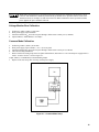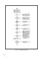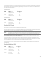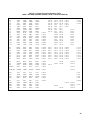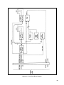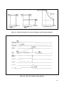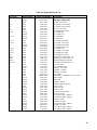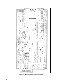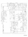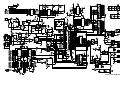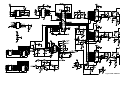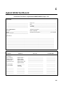
1
SERVICE MANUAL
AUTORANGING
SYSTEM DC POWER SUPPLY
AGILENT MODELS 6033A and 6038A
FOR INSTRUMENTS WITH SERIAL NUMBERS
Agilent Model 6033A; Serials US38320231 and above
Agilent Model 6038A; Serials US38310401 and above
For instruments with higher serial numbers, a change page may be included.
Agilent Part No. 5959-3346
Microfiche Part No. 5959-3347
5
Printed in USA
September, 2000
CERTIFICATION
Agilent Technologies certifies that this product met its published specifications at time of shipment from the factory. Agilent
Technologies further certifies that its calibration measurements are traceable to the United States National Bureau of
Standards, to the extent allowed by the Bureau's calibration facility, and to the calibration facilities of other International
Standards Organization members.
WARRANTY
This Agilent Technologies hardware product is warranted against defects in material and workmanship for a period of three
years from date of delivery. Agilent Technologies software and firmware products, which are designated by Agilent
Technologies for use with a hardware product and when properly installed on that hardware product, are warranted not to
fail to execute their programming instructions due to defects in material and workmanship for a period of 90 days from date
of delivery. During the warranty period Agilent Technologies will, at its option, either repair or replace products which
prove to be defective. Agilent Technologies does not warrant that the operation of the software, firmware, or hardware shall
be uninterrupted or error free.
For warranty service, with the exception of warranty options, this product must be returned to a service facility designated
by Agilent Technologies. Customer shall prepay shipping charges by (and shall pay all duty and taxes) for products returned
to Agilent Technologies for warranty service. Except for products returned to Customer from another country, Agilent
Technologies shall pay for return of products to Customer.
Warranty services outside the country of initial purchase are included in Agilent Technologies product price, only if
Customer pays Agilent Technologies international prices (defined as destination local currency price, or U.S. or Geneva
Export price).
If Agilent Technologies is unable, within a reasonable time to repair or replace any product to condition as warranted, the
Customer shall be entitled to a refund of the purchase price upon return of the product to Agilent.Technologies.
LIMITATION OF WARRANTY
The foregoing warranty shall not apply to defects resulting from improper or inadequate maintenance by the Customer,
Customer-supplied software or interfacing, unauthorized modification or misuse, operation outside of the environmental
specifications for the product, or improper site preparation and maintenance. NO OTHER WARRANTY IS EXPRESSED
OR IMPLIED. AGILENT TECHNOLOGIES. SPECIFICALLY DISCLAIMS THE IMPLIED WARRANTIES OF
MERCHANTABILITY AND FITNESS FOR A PARTICULAR PURPOSE.
EXCLUSIVE REMEDIES
THE REMEDIES PROVIDED HEREIN ARE THE CUSTOMER'S SOLE AND EXCLUSIVE REMEDIES. AGILENT
TECHNOLOGIES SHALL NOT BE LIABLE FOR ANY DIRECT, INDIRECT, SPECIAL, INCIDENTAL, OR
CONSEQUENTIAL DAMAGES, WHETHER BASED ON CONTRACT, TORT, OR ANY OTHER LEGAL THEORY.
ASSISTANCE
The above statements apply only to the standard product warranty. Warranty options, extended support contracts, product
maintenance agreements and customer assistance agreements are also available. Contact your nearest Agilent
Technologies Sales and Service office for further information on Agilent Technologies' full line of Support Programs.
2
SAFETY SUMMARY
The following general safety precautions must be observed during all phases of operation, service and repair of this
instrument. Failure to comply with these precautions or with specific warnings elsewhere in this manual violates safety
standards of design, manufacture, and intended use of the instrument. Agilent Technologies, Inc. assumes no liability for
the customer's failure to comply with these requirements.
BEFORE APPLYING POWER.
Verify that the product is set to match the available line voltage and the correct fuse is installed.
GROUND THE INSTRUMENT.
This product is a Safety Class 1 instrument (provided with a protective earth terminal). To minimize shock hazard, the instrument chassis
and cabinet must be connected to an electrical ground. The instrument must be connected to the ac power supply mains through a threeconductor power cable, with the third wire firmly connected to an electrical ground (safety ground) at the power outlet. For instruments
designed to be hard wired to the ac power lines (supply mains), connect the protective earth terminal to a protective conductor before any
other connection is made. Any interruption of the protective (grounding) conductor or disconnection of the protective earth terminal will
cause a potential shock hazard that could result in personal injury. If the instrument is to be energized via an external autotransformer for
voltage reduction, be certain that the autotransformer common terminal is connected to the neutral (earth pole) of the ac power lines
(supply mains).
FUSES
Only fuses with the required rated current, voltage, and specified type (normal blow, time delay, etc.) should be used. Do not use
repaired fuses or short circuited fuseholders. To do so could cause a shock or fire hazard.
DO NOT OPERATE IN AN EXPLOSIVE ATMOSPHERE.
Do not operate the instrument in the presence of flammable gases or fumes.
KEEP AWAY FROM LIVE CIRCUITS.
Operating personnel must not remove instrument covers. Component replacement and internal adjustments must be made by qualified
service personnel. Do not replace components with power cable connected. Under certain conditions, dangerous voltages may exist even
with the power cable removed. To avoid injuries, always disconnect power, discharge circuits and remove external voltage sources before
touching components.
DO NOT SERVICE OR ADJUST ALONE.
Do not attempt internal service or adjustment unless another person, capable of rendering first aid and resuscitation, is present.
DO NOT EXCEED INPUT RATINGS.
This instrument may be equipped with a line filter to reduce electromagnetic interference and must be connected to a properly grounded
receptacle to minimize electric shock hazard. Operation at the line voltage or frequencies in excess of those stated on the data plate may
cause leakage currents in excess of 5.0mA peak.
SAFETY SYMBOLS.
Instruction manual symbol: the product will be marked with this symbol when it is necessary for the user to refer to the
instruction manual (refer to Table of Contents) .
Indicates hazardous voltages.
Indicate earth (ground) terminal.
The WARNING sign denotes a hazard. It calls attention to a procedure, practice, or the like, which, if not correctly
performed or adhered to, could result in personal injury. Do not proceed beyond a WARNING sign until the
indicated conditions are fully understood and met.
The CAUTION sign denotes a hazard. It calls attention to an operating procedure, or the like, which, if not correctly
performed or adhered to, could result in damage to or destruction of part or all of the product. Do not proceed
beyond a CAUTION sign until the indicated conditions are fully understood and met.
DO NOT SUBSTITUTE PARTS OR MODIFY INSTRUMENT.
Because of the danger of introducing additional hazards, do not install substitute parts or perform any unauthorized modification to the
instrument. Return the instrument to an Agilent Technologies, Inc. Sales and Service Office for service and repair to ensure that safety
features are maintained.
Instruments which appear damaged or defective should be made inoperative and secured against unintended operation until they can be
repaired by qualified service personnel.
3
Safety Symbol Definitions
Symbol
Description
Symbol
Description
Direct current
Terminal for Line conductor on permanently
installed equipment
Alternating current
Caution, risk of electric shock
Both direct and alternating current
Caution, hot surface
Three-phase alternating current
Caution (refer to accompanying documents)
Earth (ground) terminal
In position of a bi-stable push control
Protective earth (ground) terminal
(Intended for connection to external
protective conductor.)
Out position of a bi-stable push control
Frame or chassis terminal
On (supply)
Terminal for Neutral conductor on
permanently installed equipment
Off (supply)
Terminal is at earth potential
(Used for measurement and control
circuits designed to be operated with
one terminal at earth potential.)
Standby (supply)
Units with this symbol are not completely
disconnected from ac mains when this switch is
off. To completely disconnect the unit from ac
mains, either disconnect the power cord or have
a qualified electrician install an external switch.
Printing History
The edition and current revision of this manual are indicated below. Reprints of this manual containing minor corrections
and updates may have the same printing date. Revised editions are identified by a new printing date. A revised edition
incorporates all new or corrected material since the previous printing date. Changes to the manual occurring between
revisions are covered by change sheets shipped with the manual. Also, if the serial number prefix of your power supply is
higher than those listed on the title page of this manual, then it may or may not include a change sheet. That is because even
though the higher serial number prefix indicates a design change, the change may not affect the content of the manual.
Edition 1
Edition2
February, 1991
September, 2000
© Copyright 1991, 2000 Agilent Technologies, Inc.
This document contains proprietary information protected by copyright. All rights are reserved. No part of this document
may be photocopied, reproduced, or translated into another language without the prior consent of Agilent Technologies, Inc.
The information contained in this document is subject to change without notice.
4
TABLE OF CONTENTS
Introduction ............................................................................................................................................................................ 9
Scope .................................................................................................................................................................................... 9
Calibration and Verification ............................................................................................................................................. 9
Troubleshooting................................................................................................................................................................ 9
Principles of Operation ..................................................................................................................................................... 9
Replaceable Parts.............................................................................................................................................................. 9
Circuit Diagrams............................................................................................................................................................... 9
Safety Considerations ........................................................................................................................................................... 9
Manual Revisions................................................................................................................................................................ 10
Firmware Revisions ............................................................................................................................................................ 10
Calibration and Verification................................................................................................................................................ 11
Introduction......................................................................................................................................................................... 11
Test Equipment Required ................................................................................................................................................... 11
Operation Verification Tests............................................................................................................................................... 11
Calibration Procedure ......................................................................................................................................................... 11
Initial Setup..................................................................................................................................................................... 14
Voltage Monitor Zero Calibration .................................................................................................................................. 15
Common Mode Calibration ............................................................................................................................................ 15
Remote Readback Zero Calibration ................................................................................................................................ 16
Constant Voltage Full Scale Calibration......................................................................................................................... 16
Voltage Monitor and Remote Readback Full Scale Calibration ..................................................................................... 17
Constant Voltage Zero Calibration ................................................................................................................................. 17
Current Monitor Zero Calibration................................................................................................................................... 17
Constant Current Zero Calibration.................................................................................................................................. 18
Current Monitor Full Scale Calibration .......................................................................................................................... 18
Constant Current Full Scale Calibration ......................................................................................................................... 19
Power Limit Calibration.................................................................................................................................................. 19
Resistance Programming Full Scale Calibration............................................................................................................. 19
Performance Tests............................................................................................................................................................... 20
Measurement Techniques ............................................................................................................................................... 20
Constant Voltage (CV) Tests .......................................................................................................................................... 21
Constant Current (CC) Tests........................................................................................................................................... 26
Initialization Procedure....................................................................................................................................................... 28
Troubleshooting .................................................................................................................................................................... 29
Introduction......................................................................................................................................................................... 29
Initial Troubleshooting Procedures..................................................................................................................................... 29
Electrostatic Protection ....................................................................................................................................................... 30
Repair and Replacement ..................................................................................................................................................... 30
A2 Control Board Removal ............................................................................................................................................ 31
A4 FET Board Removal ................................................................................................................................................. 31
A8 GPIB Board Removal ............................................................................................................................................... 32
A3 Front-Panel Board Removal...................................................................................................................................... 32
A1 Main Board Removal ................................................................................................................................................ 32
Overall Troubleshooting Procedure.................................................................................................................................... 33
GPIB Section Troubleshooting ........................................................................................................................................... 33
Primary Interface Troubleshooting ..................................................................................................................................... 36
Secondary Interface Troubleshooting ................................................................................................................................. 38
Voltage and Current DAC............................................................................................................................................... 38
Readback DAC Circuits.................................................................................................................................................. 39
Readback Multiplexer (U20): ......................................................................................................................................... 39
5
Signature Analysis .............................................................................................................................................................. 41
Primary SA ..................................................................................................................................................................... 41
Front Panel SA................................................................................................................................................................ 41
Secondary SA ................................................................................................................................................................. 42
Power Section Troubleshooting .......................................................................................................................................... 47
Main Troubleshooting Setup........................................................................................................................................... 48
Troubleshooting No-Output Failures .............................................................................................................................. 49
Power Section Blocks ..................................................................................................................................................... 50
Troubleshooting AC-Turn-On Circuits........................................................................................................................... 53
Troubleshooting DC-To-DC Converter .......................................................................................................................... 53
Troubleshooting Bias Supplies ....................................................................................................................................... 54
Troubleshooting Down Programmer............................................................................................................................... 57
Troubleshooting CV Circuit ........................................................................................................................................... 58
Troubleshooting CC Circuit............................................................................................................................................ 58
Troubleshooting OVP Circuit ......................................................................................................................................... 59
Troubleshooting PWM & Clock..................................................................................................................................... 59
Principles of Operation ........................................................................................................................................................ 61
Introduction......................................................................................................................................................................... 61
GPIB Board ........................................................................................................................................................................ 61
Primary Microprocessor ................................................................................................................................................. 61
Address Switches ........................................................................................................................................................... 61
EEPROM ........................................................................................................................................................................ 63
Isolation .......................................................................................................................................................................... 63
Secondary Microprocessor ............................................................................................................................................. 63
Digital-to-Analog Converters.......................................................................................................................................... 63
Analog Multiplexer......................................................................................................................................................... 63
Status Inputs.................................................................................................................................................................... 63
Front Panel Board ............................................................................................................................................................... 64
Address Latches and Decoders ....................................................................................................................................... 64
Volts and Amps Output Ports and Displays.................................................................................................................... 64
RPG and Latches ............................................................................................................................................................ 64
Front-Panel Switches and Input Port............................................................................................................................... 64
Mode Indicators .............................................................................................................................................................. 66
OVP Adjust Control........................................................................................................................................................ 66
Power Clear .................................................................................................................................................................... 66
Power Mesh and Control Board.......................................................................................................................................... 66
Overview......................................................................................................................................................................... 66
AC Turn-On Circuits ...................................................................................................................................................... 68
DC-to-DC Converter....................................................................................................................................................... 68
Down Programmer.......................................................................................................................................................... 68
Bleeder Circuit (6038A only) ......................................................................................................................................... 69
Constant-Voltage (CV) Circuit ....................................................................................................................................... 69
Constant-Current (CC) Circuit........................................................................................................................................ 69
Overvoltage Protection (OVP) Circuit............................................................................................................................ 70
Power-Limit Comparator ................................................................................................................................................ 70
Control-Voltage Comparator .......................................................................................................................................... 70
Initial-Ramp Circuit ........................................................................................................................................................ 70
Pulse-Width Modulator (PWM) ..................................................................................................................................... 71
Bias Voltage Detector..................................................................................................................................................... 71
AC-Surge-&-Dropout Detector....................................................................................................................................... 71
1-Second-Delay Circuit................................................................................................................................................... 71
6
Replaceable Parts.................................................................................................................................................................. 73
Introduction......................................................................................................................................................................... 73
Ordering Information .......................................................................................................................................................... 74
Component Location and Circuit Diagrams ...................................................................................................................... 89
l00 Vac Input Power Option 100 ....................................................................................................................................... 101
General Information.......................................................................................................................................................... 101
Description.................................................................................................................................................................... 101
Scope of Appendix A.................................................................................................................................................... 101
Suggestions for Using Appendix A............................................................................................................................... 101
Chapter 1 Manual Changes ........................................................................................................................................... 101
Chapter 2 Manual Changes ........................................................................................................................................... 101
Chapter 3 Manual Changes:.......................................................................................................................................... 103
Chapter 4 Manual Changes:.......................................................................................................................................... 103
Chapter 5 and 6 Manual Changes ................................................................................................................................. 104
Blank Front Panel Option 001........................................................................................................................................... 105
Introduction....................................................................................................................................................................... 105
Troubleshooting............................................................................................................................................................ 105
Chapter 2 Manual Changes:.......................................................................................................................................... 105
Chapter 3 Manual Changes:.......................................................................................................................................... 106
Chapter 5 and 6 Manual Changes: ................................................................................................................................ 106
7
1
Introduction
Scope
This manual contains information for troubleshooting the Agilent 6033A/6038A 200W Autoranging Power Supply to the
component level. Wherever applicable, the service instructions given in this manual refer to pertinent information provided
in the Operation Manual. Both manuals cover Agilent Models 6033A/6038A; differences between models are described as
required.
The following information is contained in this manual.
Calibration and Verification
Contains calibration procedures for Agilent Models 6033A/6038A. Also contains verification procedures that check the
operation of the supplies to ensure they meet the specifications of Chapter 1 in the Operating Manual.
Troubleshooting
Contains troubleshooting procedures to isolate a malfunction to a defective component on the main circuit board or to a
defective assembly (front panel, power transformer, or cable assembly). Board and assembly level removal and replacement
procedures are also given in this section.
Principles of Operation
Provides block diagram level descriptions of the supply's circuits. The primary interface, secondary interface, and the power
mesh and control circuits are described. These descriptions are intended as an aid in troubleshooting.
Replaceable Parts
Provides a listing of replaceable parts for all electronic components and mechanical assemblies for Agilent Models
6033A/6038A.
Circuit Diagrams
Contains functional schematics and component location diagrams for all Agilent 6033A/6038A circuits. The names that
appear on the functional schematics also appear on the block diagrams in Chapter 2. Thus, the descriptions in Chapter 2 can
be correlated with both the block diagrams and the schematics.
Safety Considerations
This product is a Safety Class 1 instrument, which means that it is provided with a protective earth terminal. Refer to the
Safety Summary page at the beginning of this manual for a summary of general safety information. Safety information for
specific procedures is located at appropriate places in the manual.
9
Manual Revisions
Agilent Technologies instruments are identified by a 10-digit serial number. The format is described as follows: first two
letters indicate the country of manufacture. The next four digits are a code that identify either the date of manufacture or of a
significant design change. The last four digits are a sequential number assigned to each instrument.
Item
Description
US
The first two letters indicates the country of manufacture, where US = USA.
3648
This is a code that identifies either the date of manufacture or the date of a significant design change.
0101
The last four digits are a unique number assigned to each power supply.
If the serial number prefix on your unit differs from that shown on the title page of this manual, a yellow Manual Change
sheet may be supplied with the manual. It defines the differences between your unit and the unit described in this manual.
The yellow change sheet may also contain information for correcting errors in the manual.
Note that because not all changes to the product require changes to the manual, there may be no update information required
for your version of the supply.
Older serial number formats used with these instruments had a two-part serial number, i.e. 2701A-00101. This manual also
applies to instruments with these older serial number formats. Refer to Appendix E for backdating information.
Firmware Revisions
The primary and secondary interface microcomputer chips inside of your supply are identified with labels that specify the
revision of the supply's firmware. This manual applies to firmware revisions A.00.00, A.00.01, and A.00.02.
10
2
Calibration and Verification
Introduction
This section provides test and calibration procedures. The operation-verification tests comprise a short procedure to verify
that the unit is performing properly, without testing all specified parameters. After troubleshooting and repair of a defective
power supply you can usually verify proper operation with the turn-on checkout procedure in the Operating Manual. Repairs
to the A1 main board, the A2 control board and the A8 GPIB board can involve circuits which, although functional, may
prevent the unit from performing within specified limits. So, after A1, A2 or A8 board repair, decide if recalibration and
operation verification tests are needed according to the faults you discover. Use the calibration procedure both to check
repairs and for regular maintenance.
Test Equipment Required
Table 2-1 lists the equipment required to perform the tests of this section. You can separately identify the equipment for
performance tests, calibration and troubleshooting using the USE column of the table.
Operation Verification Tests
To assure that the unit is performing properly, without testing all specified parameters, first perform the turn-on checkout
procedure in the Operating Manual. Then perform the following performance tests, in this section.
Voltage Programming And Readback Accuracy
Current Programming And Readback Accuracy
CV Load Effect
CC Load Effect
Calibration Procedure
Calibrate the unit twice per year and when required during repair. The following calibration procedures should be
performed in the sequence given.
Note:
Some of the calibration procedures for this instrument can be performed independently, and some
procedures must be performed together and/or in a prescribed order. If a procedure contains no references
to other procedures, you may assume that it can be performed independently.
To return a serviced unit to specifications as quickly as possible with minimal calibration, the technician
need only perform calibration procedures that affect the repaired circuit. Table 2-2 lists various power
supply circuits with calibration procedures that should be performed after those circuits are serviced.
If the GPIB board (A8) has been replaced, you must first initialize the board before you can calibrate the
unit. Refer to Page 28.
11
Table 2-1. Test Equipment Required
TYPE
Oscilloscope
RMS Voltmeter
Logic Pulser
Multimeter
Signature Analyzer
GPIB Controller
Current Probe
Electronic Load
Power Resistor*
Current-Monitoring
Shunts
Calibration and Test
Resistors
Terminating
Resistors (2)
Blocking
Capacitors (2)
Common-mode
Toroidal Core
Switch*
DC Power Supply
REQUIRED CHARACTERISTICS
Sensitivity: 1 mV
Bandwidth: 20MHz & 100MHz
Input: differential, 50 Ω & 10MΩ
True rms, 10MHz bandwidth
Sensitivity: 1 mV Accuracy: 5%
4.5 to 5.5Vdc @ 35mA
Resolution: 100nV
Accuracy: 0.0035%, 6½ digit
-Full GPIB capabilities
No saturation at 30Adc
Bandwidth: 20Hz to 20MHz
Voltage range: 60Vdc
Current range: 30Adc
Power range: 250W
Open and short switched
Value: 0.25Ω >200W (6033A)
Value: 2.3Ω >200W (6038A)
Value: 10mΩ ± 0.04% @ 100W (6033A)
PC: 0.0004%/W
Value: 100mΩ ± 0.04% @ 25W (6038A)
PC: 0.0004%/W
Value: 100Ω, 5%, 1W
1Ω, 5%, ½W
1KΩ, 5%, ¼W
2KΩ, 0.01%, ¼W
Value: 50Ω ±5%, noninductive
USE
P,T
RECOMMENDED MODEL
Agilent 54504A
P
Agilent 3400A
T
P,C,T
Agilent 546A
Agilent 3458A
T
C,T,P
P
Agilent 5004A
HP Series, 200/300
Tektronix P6303 Probe/
AM503 Amp/
TM500 Power Module
Agilent 6060A
P,C
P,C
P,C**
Guildline 9230/15
C,T
P
Value: 0.01µF, 100Vdc
P
≥3.7µH/turn2
≅23mm I.D.
P
SPST, 30A @60V
Voltage range: 0-60Vdc
Current range: 0-3Adc
P = performance testing C = calibration adjustments
Guildline 9230/100
P
C,T
Ferrox-Cube
500T600-3C8,
Agilent 9170-0061
Agilent 6024A
T = troubleshooting
* Not required if using electronic load.
** Less accurate, and less expensive, current-monitor resistors can be used, but the accuracy to which current programming
and readback can be checked must be reduced accordingly.
12
Table 2-2. Guide to Recalibration After Repair
Printed Circuit
Board
Block Name
Ref.
Desig.
Perform These Procedures
A1 Main Board
R3
Current Monitor Full Scale Calibration
Constant Current Full Scale Calibration
A1 Main Board
T1
Power Limit Calibration
A4 Power Mesh Board
T3
Power Limit Calibration
A4 Power Mesh Board
CR7
Power Limit Calibration
A2 Control Board
Constant Voltage Circuit
(All Except Current Source)
All
Voltage Monitor Zero Calibration
Common Mode Calibration
Remote Readback Zero Calibration
Constant Voltage Full Scale Calibration
Voltage Monitor and Remote Readback Full
Scale Calibration
Constant Voltage Zero Calibration
A2 Control Board
Constant Voltage Circuit
(Current Source)
All
Resistance Programming Full Scale Calibration
A2 Control Board
Constant Current Circuit
All
Current Monitor Zero Calibration
Constant Current Zero Calibration
Current Monitor Full Scale Calibration
Constant Current Full Scale Calibration
A2 Control Board
Power Limit Comparator
All
Power Limit Calibration
A2 Control Board
Bias Power Supplies
( + & -15V Supplies)
All
All Calibration Procedures
A8 GPIB Board
Voltage Monitor Buffer
All
Voltage Monitor Zero Calibration
Remote Readback Zero Calibration
Constant Voltage Full Scale Calibration
Voltage Monitor and Remote Readback Full
Scale Calibration
Constant Voltage Zero Calibration
A8 GPIB Board
Analog Multiplexer
All
Remote Readback Zero Calibration
Constant Voltage Full Scale Calibration
Voltage Monitor and Remote Readback Full
Scale Calibration
Constant Voltage Zero Calibration
A8 GPIB Board
Readback DAC
All
Remote Readback Zero Calibration
Constant Voltage Full Scale Calibration
Voltage Monitor and Remote Readback Full
Scale Calibration
Constant Voltage Zero Calibration
13
Table 2-2. Guide to Recalibration After Repair (continued)
Printed Circuit
Board
Block Name
Ref.
Desig.
Perform These Procedures
A8 GPIB Board
Voltage DAC
All
Remote Readback Zero Calibration
Constant Voltage Full Scale Calibration
Voltage Monitor and Remote Readback Full
Scale Calibration
Constant Voltage Zero Calibration
A8 GPIB Board
Current DAC
All
Constant Current Zero Calibration
Constant Current Full Scale Calibration
U5
Remote Readback Zero Calibration
Constant Voltage Full Scale Calibration
Voltage Monitor and Remote Readback Full
Scale Calibration
Constant Voltage Zero Calibration
Constant Current Full Scale Calibration
A8 GPIB Board
Initial Setup
a.
b.
c.
d.
e.
f.
g.
h.
i.
j.
Unplug the line cable and remove the top cover by removing the three screws; the rear handle screw and the two toprear-corner screws. Do not remove the front handle screw as the retaining nut will fall into the unit.
Slide the cover to the rear.
Plug a control board test connector A2J3 onto the A2J3 card-edge fingers.
Turn OVERVOLTAGE ADJUST control A3R59 fully clockwise.
Disconnect all loads from output terminals.
Connect power supply for local sensing, and ensure that MODE switches are set as shown below.
Connect a GPIB controller to the power supply.
Reconnect line cable and turn on ac power.
Allow unit to warm up for 30 minutes.
When attaching the DVM, the minus lead of the DVM should be connected to the first node listed, and the plus lead
should be connected to the second node listed.
k. At the beginning of each calibration procedure, the power supply should be in its power-on state (turn ac power off and
back on), with no external circuitry connected except as instructed.
l. The POWER LIMIT adjustment (A2R25) must be adjusted at least coarsely before many of the calibration procedures
can be performed. If you have no reason to suspect that the Power Limit circuit is out of adjustment, do not change its
setting. Otherwise, center A2R25 before you begin to calibrate the power supply.
m. Turn off ac power when making or removing connections to the power supply.
14
Maintenance described herein is performed with power supplied to the instrument, and protective covers
removed. Such maintenance should be performed only by trained service personnel who are aware of the
hazards involved (for example, fire and electrical shock). Where maintenance can be performed without
power applied, the power should be removed.
Voltage Monitor Zero Calibration
a.
b.
c.
d.
Send string "VSET 0; ISET 0; OUT OFF".
Short power supply output terminals.
Attach the DVM from M on the rear panel through a 1kΩ resistor to A2P3 pin 3 (V-MON1).
Adjust A2R22 (V-MON ZERO) to 0V ±20µV.
Common Mode Calibration
a.
b.
c.
d.
e.
Send string ''VSET 0; ISET 0; OUT OFF".
Short power supply sense terminals ( + S to - S) at rear panel.
Attach the DVM from M on the rear panel through a 1kΩ resistor to A2J3 pin 3 (V-MON).
Take initial reading from DVM.
Remove both local sensing straps from rear-panel terminal block, and connect a 1-volt external power supply with its +
lead to - S and its--lead to - Out. See Figure 2-1.
Adjust A2R21 (CV LOAD REG) to Initial Reading ±20µV.
f. Replace local sense straps after removing external power supply.
Figure 2-1. Common Mode Setup
15
Remote Readback Zero Calibration
Note:
a.
b.
c.
d.
e.
f.
g.
h.
This procedure and the following three procedures must be done as a set, without omitting any of the four
procedures. Also, the following four procedures require that V-MON ZERO (A2R22) be adjusted within
specifications. If it is not, perform the Voltage Monitor Zero Calibration before proceeding.
Connect an external supply to the power supply as shown in Figure 2-2.
Send string "VSET 0; ISET 5; OUT ON''.
Attach the DVM from M on the rear panel through a 1KΩ resistor to A2J3 pin 3 (V-MON).
Adjust A8R40 (CV PROG ZERO) to 625µV ± 30µV.
Remove the DVM.
Enter and run the following program and begin noting the controller's display:
10 OUTPUT 705; "VOUT''
20 ENTER 705; A
30 DISP A
40 GOTO 10
50 END
Adjust A8R51 (READBACK ZERO) until the value displayed on the controller toggles between:
0 and 5mV (6033A).
0 and 15mV (6038A).
After adjusting A8R51 you must continue the calibration procedure through to the completion of Constant Voltage
Zero Calibration. Remember to disconnect the external power supply and resistor.
Figure 2-2. Remote Readback Zero And CV Zero Calibration Setup
Constant Voltage Full Scale Calibration
Note:
a.
b.
16
Perform this procedure only after completing Remote Readback Zero Calibration.
Remove all external test circuits.
Send string:
"VSET 200; ISET 5; OUT ON" (6033A).
"VSET 60; ISET 5; OUT ON" (6038A).
c.
d.
e.
Attach the DVM from - S to + S terminals on rear panel.
Adjust A8R58 (CV PROG F.S.) to:
20.0025 ±600µV (6033A).
60.0075 ±1.82mV (6038A).
After adjusting A8R58 you must continue the calibration procedure through to the completion of Constant Voltage
Zero Calibration.
Voltage Monitor and Remote Readback Full Scale Calibration
Note:
a.
b.
c.
d.
e.
f.
g.
Perform this procedure only after completing Constant Voltage Full Scale Calibration.
Attach the DVM from M on the rear panel to A2J3 pin 3 (V-MON). See DVM connection in Figure 2-1.
Send string:
''VSET 20; ISET 5; OUT ON'' (6033A).
''VSET 60; ISET 5; OUT ON'' (6038A).
Adjust A8R75 (V-MON F.S.) to 5.000625V ±100µV.
Disconnect the DVM.
Enter and run the following program and begin noting the controller's display.
10 OUTPUT 705; ''VOUT?''
20 ENTER 705; A
30 DISP A
40 GOTO 10
50 END
Adjust A8R61 (READBACK F.S.) until the value displayed on the controller toggles between:
20V and 20.005V (6033A).
60V and 60.015V (6038A).
After adjusting A8R61 you must continue the calibration procedure through to the completion of Constant Voltage
Zero Calibration.
Constant Voltage Zero Calibration
Note:
a.
b.
c.
d.
Perform this procedure only after completing Voltage Monitor and Remote Readback Full Scale
Calibration.
Send string "VSET 0; ISET 5; OUT ON".
Connect an external supply to the power supply as shown in Figure 2-2.
Attach the DVM from - S to + S on the rear panel.
Adjust A8R40 (CV PROG ZERO) to 0 ±120µV.
Current Monitor Zero Calibration
a.
b.
c.
d.
e.
Send string "VSET 0; ISET 0; OUT OFF''.
Connect a short across power supply output terminals.
Attach the DVM from M to IM on the rear panel.
Allow several minutes (3 or more) to ensure thermal settling.
Adjust A2R8 (I-MON ZERO) to:
0V ±100µV (6033A).
0V ±25µV (6038A).
17
Constant Current Zero Calibration
a.
b.
c.
d.
Connect the test setup shown in Figure 2-3.
Send string ''VSET 5; ISET 0; OUT ON''.
Allow several minutes (3 or more) to ensure thermal settling.
Adjust A8R29 (CC PROG ZERO) to:
0V ±1mV (6033A).
0V ±350µV (6038A).
Figure 2-3. CC Zero Calibration Setup
Current Monitor Full Scale Calibration
Note:
a.
b.
c.
d.
e.
f.
18
This procedure requires that I-MON ZERO (A2R8) be adjusted within specifications. If it is not, perform
the Current Monitor Zero Calibration before proceeding.
Connect Rm current-monitoring shunt:
(10 milliohm, 6033A)
(100 milliohm, 6038A)
0.05% or better across power supply output terminals.
Send string:
"VSET 5; ISET 30; OUT ON" (6033A).
"VSET 5; ISET 10; OUT ON" (6038A).
Attach DVM from M to IM on the rear panel. Use six-digit display on Agilent 3458A DVM.
Take initial reading from DVM.
Attach DVM across Rm. Allow several minutes (3 or more) to ensure thermal settling. This can be noted as a stable
reading on the DVM.
Adjust A2R9 (I-MON F.S.) to:
0.060 x initial reading ±0.4mV (6033A).
0.200 x initial reading ±1.0mV (6038A).
Constant Current Full Scale Calibration
Note:
a.
b.
c.
d.
This procedure requires that CC PROG ZERO (A8R29) and I-MON F. S. (A2R9) be adjusted within
specifications. If they are not, perform Constant Current Zero and/or Current Monitor Full Scale
Calibration before proceeding.
Connect Rm current-monitoring shunt:
(10 milliohm, 6033A)
(100 milliohm, 6038A)
0.05% or better across power supply output terminals.
Send string:
"VSET 5; ISET 30; OUT ON" (6033A).
"VSET 5, ISET 10; OUT ON'' (6038A).
Attach DVM across Rm. Allow several minutes (3 or more) to ensure thermal settling.
Adjust A8R55 (CC PROG F.S.) to:
300mV ±30µV (6033A).
100mV ±100µV (6038A).
Power Limit Calibration
Note:
a.
b.
c.
d.
e.
f.
This procedure requires that CC PROG F. S. (A8R55) be adjusted within specifications. If it is not,
perform Constant Current Full Scale Calibration before proceeding.
Connect the power supply to the ac power line through a variable autotransformer which is set to the minimum for your
line voltage (e.g. 104V for nominal 120V line).
Turn A2R25 (POWER LIMIT) fully counterclockwise.
Connect a electronic load across the output terminals, or use a:
0.25Ω 200W resistor (6033A).
2.3Ω 200W resistor (6038A).
Set the electronic load for:
30 amperes (6033A).
10 amperes (6038A).
in the constant Current mode.
Turn on power supply and send string:
"VSET 9; ISET 30.5; OUT ON" (6033A).
''VSET 23; ISET 10.2; OUT ON'' (6038A).
Adjust A2R25 (POWER LIMIT) clockwise until CV LED on front panel turns on.
Resistance Programming Full Scale Calibration
a.
b.
c.
Send string ''OUT OFF".
Connect a 2-kilohm calibration resistor from P to VP on rear panel.
Set rear-panel MODE switches for resistance programming:
19
d.
e.
f.
Attach the DVM from P to VP on the rear panel.
Adjust A2R23 (R-PROG F.S.) to 2.5V ±4mV.
Remember to reset MODE switches to original settings.
Performance Tests
The following paragraphs provide test procedures for verifying the unit's compliance with the specifications of Table 1-1 in
the Operating Manual. Please refer to CALIBRATION PROCEDURE or TROUBLESHOOTING if you observe
out-of-specification performance. The performance test specifications are listed in the Performance Test Record in
Appendix C and D. You can record the actual measured values in the columns provided.
Measurement Techniques
Setup For All Tests. Measure the output voltage directly at the + S and - S terminals. Connect unit for local sensing, and
ensure that MODE switches are set as shown below. Select an adequate wire gauge for load leads using the procedures
given in the Operating Manual for connecting the load.
Electronic Load. The test and calibration procedures use an electronic load to test the unit quickly and accurately. If an
electronic load is not available, you may substitute:
2Ω 200W load resistor (6033A).
18Ω 200W load resistor (6038A).
for the electronic load in these tests:
CV Source Effect (Line Regulation).
CC Load Effect (Load Regulation).
You may substitute:
0.25Ω 200W load resistor (6033A).
2.3Ω 200W load resistor (6038A).
in these tests:
CV Load Effect (Load Regulation)
CV PARD (Ripple and Noise)
CC Source Effect (Line Regulation)
CC PARD (Ripple and Noise)
The substitution of the load resistor requires adding a load switch and making minor changes to the procedures. The load
transient recovery time test procedure is not amenable to modification for use with load resistors.
An electronic load is considerably easier to use than a load resistor. It eliminates the need for connecting resistors or
rheostats in parallel to handle the power, it is much more stable than a carbon-pile load, and it makes easy work of switching
between load conditions as is required for the load regulation and load transient-response tests.
Current-Monitoring Resistor. To eliminate output current measurement error caused by voltage drops in the leads and
connections, connect the current-monitoring resistor between -OUT and the load as a four-terminal device. Figure 2-4
shows correct connections. Connect the current-monitoring test leads inside the load-lead connections directly at the
monitoring resistor element.
Note:
20
A current-monitoring resistor with 1% accuracy is suitable for all tests except current programming
accuracy and current readback accuracy. For these tests, use the shunt listed in Table 2-1.
Figure 2-4. Current-Monitoring Resistor Setup
GPIB Controller. Most performance tests can be performed using only front-panel controls. However, a GPIB controller is
required to perform the voltage and current programming accuracy tests and the voltage and current readback accuracy tests.
Constant Voltage (CV) Tests
CV Setup. If more than one meter or a meter and an oscilloscope are used, connect each to the + S and - S terminals by a
separate pair of leads to avoid mutual coupling effects. Connect only to + S and -S because the unit regulates the output
voltage between + S and - S, not between + OUT and -OUT. Use coaxial cable or shielded 2-wire cable to avoid pickup on
test leads. For all CV tests set the output current at full output to assure CV operation.
Voltage Programming And Readback Accuracy. This procedure verifies that the voltage programming and readback
functions are within specifications. A GPIB controller must be used for this test.
a. Connect digital voltmeter between + S and - S.
b. Turn on ac power to the power supply.
c. Send string:
''VSET 0.1; ISET 30'' (6033A).
''VSET 0.09; ISET 10" (6038A).
d. The DVM reading should be in the range:
0.090 to 0.109Vdc (6033A).
0.050 to 0.130Vdc (6038A).
Note the reading.
e. Enter and run the following program:
10 OUTPUT 705; "VOUT?"
20 ENTER 705;A
30 DISP A
40 GOTO 10
50 END
f. The value displayed by the controller should be the value noted in step d:
± 0.006Vdc (6033A).
± 0.015Vdc (6038A).
g. Send string:
"VSET 20; ISET 30" (6033A).
''VSET 60; ISET 10" (6038A).
h. The DVM reading should be in the range:
19.984 to 20.016Vdc (6033A).
59.939 to 60.061Vdc (6038A).
Note the reading.
i. Run the program listed in step e. The value displayed by the controller should be the value noted in step h:
± 0.02Vdc (6033A).
± 0.092Vdc (6038A).
21
Load Effect (Load Regulation). Constant-voltage load effect is the change in dc output voltage (Eo) resulting from a
load-resistance change from open-circuit to full-load. Full-load is the resistance which draws the maximum rated output
current at voltage Eo. Proceed as follows:
a. Connect the test equipment as shown in Figure 2-5. Operate the load in constant resistance mode (Amps/Volt) and set
resistance to maximum.
b. Turn the unit's power on, and, using DISPLAY SETTINGS pushbutton switch, turn up current setting to full output.
c. Turn up output voltage to:
7.0Vdc (6033A).
20.0Vdc (6038A).
as read on the digital voltmeter.
Figure 2-5. Basic Test Setup
d.
e.
f.
g.
h.
Reduce the resistance of the load to draw an output current of:
29Adc (6033A).
10 Adc (6038A).
Check that the unit's CV LED remains lighted.
Open-circuit the load.
Record the output voltage at the digital voltmeter.
Reconnect the load.
When the reading settles, record the output voltage again. Check that the two recorded readings differ no more than:
± 0.0027Vdc (6033A).
± 0.005Vdc (6038A).
Source Effect (Line Regulation). Source effect is the change in dc output voltage resulting from a change in ac input
voltage from the minimum to the maximum value as specified in Input Power Requirements in the Specifications Table, in
the Operating Manual. Proceed as follows:
a. Connect the test equipment as shown in Figure 2-5. Operate the load in constant resistance mode (Amps/Volt) and set
resistance to maximum.
b. Connect the unit to the ac power line through a variable autotransformer which is set for nominal line voltage.
c. Turn the unit's power on, and, using DISPLAY SETTINGS pushbutton switch, turn up current setting to full output.
22
d.
e.
f.
g.
h.
i.
Turn up output voltage to:
20.0Vdc (6033A).
60.0Vdc (6038A).
as read on the digital voltmeter.
Reduce the resistance of the load to draw an output current of:
10Adc (6033A).
3.3Adc (6038A).
Check that the unit's CV LED remains lighted.
Adjust autotransformer to the minimum for your line voltage.
Record the output voltage at the digital voltmeter.
Adjust autotransformer to the maximum for your line voltage.
When the reading settles record the output voltage again. Check that the two recorded readings differ no more than:
± 0.003Vdc (6033A).
± 0.008Vdc (6038A).
PARD (Ripple And Noise). Periodic and random deviations (PARD) in the unit's output-ripple and noise-combine to
produce a residual ac voltage superimposed on the dc output voltage. Constant-voltage PARD is specified as the
root-mean-square (rms) or peak-to-peak (pp) output voltage in a frequency range of 20Hz to 20MHz.
RMS Measurement Procedure. Figure 2-6 shows the interconnections of equipment to measure PARD in Vrms. To ensure
that there is no voltage difference between the voltmeter's case and the unit's case, connect both to the same ac power outlet
or check that the two ac power outlets used have the same earth-ground connection.
Use the common-mode choke as shown to reduce ground-loop currents from interfering with measurement. Reduce noise
pickup on the test leads by using 50Ω coaxial cable, and wind it five turns through the magnetic core to form the
common-mode choke. Proceed as follows:
a. Connect the test equipment as shown in Figure 2-6. Operate the load in constant resistance mode (Amps/Volt) and set
resistance to maximum.
b. Turn the unit's power on, and, using DISPLAY SETTINGS pushbutton switch, turn up current setting to full output.
c. Turn up output voltage to:
7Vdc (6033A).
20Vdc (6038A).
d. Reduce the resistance of the load to draw an output current of:
29Adc (6033A).
10Adc (6038A).
Check that the unit's CV LED remains lighted.
e. Check that the rms noise voltage at the true rms voltmeter is no more than 30mV rms.
Peak-To-Peak Measurement Procedure. Figure 2-7 shows the interconnections of equipment to measure PARD in Vpp.
The equipment grounding and power connection instructions on Page 23 apply to this setup also. Connect the oscilloscope
to the + S and - S terminals through 0.01µF blocking capacitors to protect the oscilloscope's input from the unit's output
voltage. To reduce common-mode noise pickup, set up the oscilloscope for a differential, two-channel voltage measurement.
To reduce normal-mode noise pickup, use matched-length, 1 meter or shorter, 50Ω coaxial cables with shields connected to
the oscilloscope case and to each other at the other ends. Proceed as follows:
23
Figure 2-6. RMS Measurement Test Setup, CV PARD Test
Figure 2-7. Peak-To-Peak Measurement Test Setup, CV PARD Test
24
a.
b.
c.
d.
e.
Connect the test equipment as shown in Figure 2-7. Operate the load in constant resistance mode (Amps/Volt) and set
resistance to maximum.
Turn the unit's power on, and, using DISPLAY SETTINGS pushbutton switch, turn up current setting to full output.
Turn up output voltage to:
7Vdc (6033A).
20Vdc (6038A).
Turn up output current setting to full output and reduce the resistance of the load to draw an output current of:
29Adc (6033A).
10Adc (6038A).
Check that the unit's CV LED remains lighted.
Set the oscilloscope's input impedance to 50Ω and bandwidth to 20MHz. Check that the peak-to-peak is no more than
30mV.
Load Transient Recovery Time. Specified for CV operation only; load transient recovery time is the time for the output
voltage to return to within a specified band around its set voltage following a step change in load.
Use the equipment setup of Figure 2-5 to display output voltage transients while switching the load between 10% with the
output set at:
6.7Vdc (6033A).
20Vdc (6038A).
Proceed as follows:
a.
b.
c.
P
d.
e.
f.
g.
Connect the test equipment as shown in Figure 2-5. Operate the load in constant-current mode and set for minimum
current.
Turn the unit's power on, and, using DISPLAY SETTINGS pushbutton switch, turn up current setting to full output.
Turn up output voltage to:
6.7Vdc (6033A).
20.0Vdc (6038A).
as read on the digital voltmeter.
Set the load to vary the load current between:
27Adc and 30Adc (6033A).
9Adc and 10 Adc (6038A).
at a 30Hz rate for the 10% RECOVERY TEST.
Set the oscilloscope for ac coupling, internal sync and lock on either the positive or negative load transient.
Adjust the oscilloscope to display transients as in Figure 2-8.
Check that the amplitude of the transient pulse at 1 ms is no more than:
50mV (6033A).
75mV (6038A).
25
.
Figure 2-8. Load Transient Recovery Waveform
Constant Current (CC) Tests
CC Setup. Constant-current tests are analogous to constant-voltage tests, with the unit's output short circuited and the
voltage set to full output to assure CC operation. Follow the general setup instructions of Page 20.
Current Programming And Readback Accuracy. This procedure verifies that the current programming and readback
functions are within specifications. A GPIB controller must be used for this test. The accuracy of the current shunt resistor
(Rm) must be 0.02% or better. Proceed as follows:
a.
b.
c.
d.
e.
f.
g.
h.
i.
j.
26
Connect test setup shown in Figure 2-5, except replace the load with a short circuit.
Turn on ac power to the power supply.
Send string:
"VSET 20; ISET 1.0" (6033A).
''VSET 60; ISET 0.5" (6038A).
Check that the voltage across Rm is in the range:
9.79mV to 10.22mV (6033A).
48.9mV to 51.0mV (6038A).
Note the reading.
Enter and run the following program:
10 OUTPUT 705; "IOUT?''
20 ENTER 705; A
30 DISP A
40 GOTO 10
50 END
The value displayed by the controller should be the actual output current ± 0.025Adc.
Send string:
''VSET 20; ISET 30" (6033A).
''VSET 60; ISET 10" (6038A).
Check that the voltage across Rm is in the range:
0.29935 to 0.30065Vdc (6033A).
1.0019 to 0.9982Vdc (6038A).
Note the reading.
Run the program listed in step e.
The value displayed by the controller should be the actual output current:
± 0.115Adc (6033A).
± 0.031Adc (6038A).
Load Effect (Load Regulation). Constant current load effect is the change in dc output current (Io) resulting from a
load-resistance change from short-circuit to full-load, or full-load to short-circuit. Full-load is the resistance which develops
the maximum rated output voltage at current Io. Proceed as follows:
a. Connect the test equipment as shown in Figure 2-5. Operate the load in constant resistance mode (Amps/Volt) and set
resistance to minimum.
b. Turn the unit's power on, and, using DISPLAY SETTINGS pushbutton switch, turn up voltage setting to full output.
c. Turn up output current to:
10Adc (6033A).
3Adc (6038A).
d. Increase the load resistance until the output voltage at +S and -S decreases to:
20Vdc (6033A).
60Vdc (6038A).
Check that the CC LED is lighted and AMPS display still reads ≈ 10 amps.
e. Short-circuit the load and allow the voltage across Rm to stabilize.
f. Record voltage across Rm.
g. Disconnect short across load.
h. When the reading settles (≈ 10s), record the voltage across Rm again. Check that the two recorded readings differ no
more than:
± 100µVdc (6033A).
± 530µVdc (6038A).
Source Effect (Line Regulation). Constant current source effect is the change in dc output current resulting from a change
in ac input voltage from the minimum to the maximum values listed in the Specifications Table in the Operating Manual.
Proceed as follows:
a. Connect the test equipment as shown in Figure 2-5. Operate the load in constant resistance mode (Amps/Volt) and set
resistance to minimum.
b. Connect the unit to the ac power line through a variable autotransformer set for nominal line voltage.
c. Switch the unit's power on and turn up output voltage setting to full output.
d. Turn up output current to:
30Adc (6033A).
10Adc (6038A).
e. Increase the load resistance until the output voltage between + S and - S decreases to:
7.0Vdc (6033A).
20.0Vdc (6038A).
Check that the CC LED is still on.
f. Adjust autotransformer to the minimum for your line voltage.
g. Record the voltage across Rm.
h. Adjust autotransformer to the maximum for your line voltage.
i. When the reading settles record the voltage across Rm again. Check that the two recorded readings differ no more than:
90µVdc (6033A).
300µVdc (6038A).
PARD Ripple And Noise. Periodic and random deviations (PARD) in the unit's output (ripple and noise) combine to
produce a residual ac current as well as an ac voltage super-imposed on the dc output. The ac voltage is measured as
constant-voltage PARD, Page 23. Constant-current PARD is specified as the root-mean-square (rms) output current in a
frequency range 20Hz to 20MHz with the unit in CC operation. To avoid incorrect measurements, with the unit in CC
operation, caused by the impedance of the electronic load at noise frequencies, use a:
0.25Ω (6033A)
2.3Ω (6038A)
load resistor that is capable of safely dissipating 200 watts. Proceed as follows:
a. Connect the test equipment as shown in Figure 2-9.
b. Switch the unit's power on and turn the output voltage all the way up.
c. Turn up output current to:
27
29Adc (6033A).
10Adc (6038A).
Check that the unit's CC LED remains lighted.
d. Check that the rms noise current measured by the current probe and rms voltmeter is no more than:
15mA rms (6033A).
5mA rms (6038A).
Initialization Procedure
Follow the procedure if either the GPIB assembly has been replaced, or the EEPROM (U70) has been replaced:
1. Install the GPIB assembly in the unit.
2. Turn the power on and depending on your unit's model number, send string:
"EEINIT 6033"
or
"EEINIT 6038''.
3. Turn the power off, wait 5 seconds, then turn the power back on.
4. If the GPIB assembly has been replaced, calibrate the unit.
Figure 2-9. CC PARD Test Setup
28
3
Troubleshooting
Maintenance described herein is performed with power supplied to the instrument, and protective covers
removed. Such maintenance should be performed only by service-trained personnel who are aware of the
hazards involved (for example, fire and electrical shock). Where maintenance can be performed without
power applied, the power should be removed.
Introduction
Before attempting to troubleshoot this instrument, ensure that the fault is with the instrument itself and not with an
associated circuit. The performance test enables this to be determined without having to remove the covers from the supply.
The most important aspect of troubleshooting is the formulation of a logical approach to locating the source of trouble. A
good understanding of the principles of operation is particularly helpful, and it is recommended that Chapter 4 of this
manual be reviewed before attempting to troubleshoot the unit. Often the user will then be able to isolate a problem simply
by using the operating controls and indicators. Once the principles of operation are understood, refer to the following
paragraphs.
Table 2-1 lists the test equipment for troubleshooting. Chapter 6 contains schematic diagrams and information concerning
the voltage levels and waveforms at many of the important test points. Most of the test points used for troubleshooting the
supply are located on the control board test "fingers", which are accessible close to the top of the board. See Table 3-9.
If a component is found to be defective, replace it and re-conduct the performance test. When a component is replaced, refer
to Calibration Procedure (Chapter 2). It may be necessary to perform one or more of the adjustment procedures after a
component is replaced.
Initial Troubleshooting Procedures
If a problem occurs, follow the steps below in sequence:
a.
b.
c.
d.
e.
Check that input power is available, and check the power cord and rear-panel line fuse.
Check that the settings of mode switch A2S1 are correct for the desired mode of operation. (See Operating Manual).
Check that all connections to the power supply are secure and that circuits between the supply and external devices are
not interrupted.
Check that the rear-panel GPIB address switch A8S1 is properly set. (See Operating Manual).
If the power supply fails turn-on self-test or gives any other indication of malfunction, remove the unit from the
operating system before proceeding with further testing.
Some circuits on the power mesh are connected directly to the ac power line. Exercise extreme caution
when working on energized circuits. Energize the supply through an isolation transformer to avoid
shorting ac energized circuits through the test instrument's input leads. The isolation transformer must
have a power rating of at least 4KVA. During work on energized circuits, the safest practice is to
disconnect power, make or change the test connections, and then re-apply power.
Make certain that the supply's ground terminal (┴) is securely connected to an earth ground before applying
power. Failure to do so will cause a potential shock hazard that could result in personal injury.
29
Electrostatic Protection
The following caution outlines important precautions which should be observed when working with static sensitive
components in the power supply.
This instrument uses components which can be damaged by static charge. Most semiconductors can
suffer serious performance degradation as a result of static charges, even though complete failure may
not occur. The following precautions should be observed when handling static-sensitive devices.
a.
b.
c.
d.
e.
f.
Always turn power off before removing or installing printed-circuit boards.
Always store or transport static-sensitive devices (all semiconductors and thin-film devices) in conductive material.
Attach warning labels to the container or bag enclosing the device.
Handle static-sensitive devices only at static-free work stations. These work stations should include special conductive
work surfaces (such as Agilent Part No. 9300-0797) grounded through a one-megohm resistor. Note that metal table
tops and highly conductive carbon-impregnated plastic surfaces are too conductive; they can act as large capacitors and
shunt charges too quickly. The work surfaces should have distributed resistance of between 106 and 10l2 Ω per square.
Ground all conductive equipment or devices that may come in contact with static-sensitive devices or sub-assemblies
containing same.
Where direct grounding of objects in the work area is impractical, a static neutralizer should be used (ionized air blower
directed at work). Note that this method is considerably less effective than direct grounding and provides less protection
for static-sensitive devices.
While working with equipment on which no point exceeds 500 volts, use a conductive wrist strap in contact with skin.
The wrist strap should be connected to ground through a one-megohm resistor. A wrist strap with insulated cord and
built-in resistor is recommended, such as 3M Co. No. 1066 (Agilent Part No. 9300-0969 (small) and 9300-0970
[large]).
Do not wear a conductive wrist strap when working with potentials in excess of 500 volts; the one-megohm
resistor will provide insufficient current limiting for personal safety.
g.
All grounding (device being repaired, test equipment, soldering iron, work surface, wrist strap, etc.) should be done to
the same point.
h. Do not wear nylon clothing. Keep clothing of any kind from coming within 12 inches of static-sensitive devices.
i. Low-impedance test equipment (signal generators, logic pulsers, etc.) should be connected to static-sensitive inputs
only while the components are powered.
j. Use a mildly activated rosin core solder (such as Alpha Metal Reliacor No. 1, Agilent Part No. 8090-0098) for repair.
The flux residue of this type of solder can be left on the printed circuit board. Generally, it is safer not to clean the
printed-circuit board after repair. Do not use Freon or other types of spray cleaners. If necessary, the printed-circuit
board can be brushed using a natural-bristle brush only. Do not use nylon-bristle or other synthetic-bristle brushes. Do
not use high-velocity air blowers (unless ionized).
k. Keep the work area free of non-conductive objects such as Styrofoam-type cups, polystyrene foam, polyethylene bags,
and plastic wrappers. Non-conductive devices that are necessary in the area can be kept from building up a static charge
by spraying them with an anti-static chemical (Agilent Part No. 8500-3397).
l. Do not allow long hair to come in contact with static-sensitive assemblies.
m. Do not exceed the maximum rated voltages specified for the device.
Repair and Replacement
Repair and replacement of most components in the power supply require only standard techniques that should be apparent to
the technician. The following paragraphs provide instructions for removing certain assemblies and components for which
the procedure may not be obvious upon inspection.
To avoid the possibility of personal injury, remove the power supply from operation before opening the
cabinet. Turn off ac power and disconnect the line cord, GPIB plug, load, and remote sense leads before
attempting any repair or replacement.
30
When replacing any heatsink-mounted components except thermostat, smear a thin coating of heatsink
compound between the component and heatsink. If a mica insulator is used, smear a thin coating of
heatsink compound on both sides of the mica insulator.
Do not use any heatsink compound containing silicone, which can migrate and foul electrical contacts
elsewhere in the system. An organic zinc oxide cream, such as American Oil and Supply Company
Heatsink Compound #100, is recommended.
Most of the attaching hardware in this unit is metric. The only non-metric (sometimes called English or
inch) fittings are listed below. Be careful when both types of screws are removed not to get them mixed
up.
a.
b.
Rear-panel fuseholders.
Rear-panel ground binding post.
Top Outside Cover Removal. Remove one screw - the rear handle screw using a Size 2, Pozidriv screwdriver. A Phillips
head screwdriver does not fully seat into Pozidriv screws and risks stripping the heads. (Do not remove the front handle
screw, as the retaining nut will fall into the unit.) Remove the top cover by sliding it to the rear and lifting at the front.
Bottom Cover Removal. Remove only for repair of main board. Remove two bottom-rear-corner screws (Pozidriv,
M4x.7), and remove the bottom cover by sliding it to the rear. You do not need to remove the unit's feet.
Inside Top Cover Removal. The unit includes an inside cover which secures the vertical board assemblies. Remove the
inside cover for repair but not for calibration.
Remove the six mounting screws (Pozidriv, M4x.7) - three on each side - and the five board-fastening screws (Pozidriv,
M4x.17) - all on top. Remove the inside cover by lifting at the front edge.
When installing the inside cover, insert it first at the right side. While holding it tilted up at the left, reach through the
cutouts in the cover and fit the top tabs of the A8 GPIB board into the mating slots in the cover. Then repeat the process for
the A2 control board tabs and slots. With the top cover in place reach through the cutout above the A3 power mesh board,
align the board-fastening screw holes, and replace the rear-most screw to secure the A3 board. Press the inside cover down
firmly while tightening screws that secure cover to chassis. Complete the installation by replacing the remaining ten screws.
A2 Control Board Removal
After removing the inside cover, unplug the W5 and W6 ribbon cables at the top edge of the A2 control board. Remove the
A2 board by lifting first at the front edge and than pulling it up and out of the unit. Two connectors hold the A2 board at its
bottom edge.
When installing the A2 board, insert it first at the rear of the unit. While holding it tilted up at the front, fit the A2TB1
terminal strip into the mating cutout in the rear panel. Then lower the A2 board's bottom connectors into the mating
connectors on the main board. Press the A2 board into the connectors, and reinstall the W5 and W6 ribbon cables.
A4 FET Board Removal
After removing the inside cover, remove the A4 mesh board by lifting, using the large aluminum heatsink as a handle. Two
connectors hold the A4 board at its bottom edge.
When installing the A4 power mesh board, lower it into its connectors and press in place.
31
A8 GPIB Board Removal
Remove the A8 board as follows:
a. Remove the two screws (Pozidriv, M3x.5) which attach the A8 GPIB board to the rear panel. Remove the single screw
(Pozidriv, M4x.7) that secures the GPIB board to the side frame near the front corner.
b. After removing the inside cover, unplug the W5 and W6 ribbon cables at the top edge of the A8 board, the W2 3-wire
cable from connector A8J10 and the W1 ribbon cable from connector A8J9.
c. Remove the A8 board lifting it straight up.
Install the A8 board by reversing the above steps. Lower the rear side of the board into the unit first and fit the bottom tabs
into their mating slots.
A3 Front-Panel Board Removal
Remove the A3 front-panel board by first removing the entire front panel assembly. You do not need to remove the top
cover. Follow this procedure:
a. Remove the top plastic insert by prying up with a flat-blade screwdriver.
b. Remove the four front-panel assembly mounting screws on the top and bottom at the corners.
c. Gently pull the front-panel assembly away from the unit as far as permitted by the connecting cables.
d. Remove the ground-wire screw (Pozidriv, M4x.7) holding the green-yellow ground wire.
e. Note the locations of the four power-wire connections to the power switch and then unplug the quick-connect plugs.
f. Unplug the W3 3-wire cable from connector A1J3 to the A1 main board, and unplug the W1 ribbon cable from
connector A8J1 on the A8 GPIB board.
g. Remove the A3 board from the front-panel assembly by removing the five mounting screws (Pozidriv, M4x.7).
Install the A3 Board by reversing the above steps. Connect the power switch wires in the exact locations from which they
were removed.
A1 Main Board Removal
Removing the A1 main board requires removing the rear-panel, all boards except the A3 front-panel board, and 17 A1
board mounting screws, two standoffs, and interface bracket. Component-access cutouts in the bottom inside cover allow
unsoldering most A1-board components for repair without removing the A1 board.
Proceed as follows:
a.
b.
Remove the A2, A4, and A8 boards according to the above instructions.
Detach the rear panel by removing the four mounting screws (Pozidriv, M4x.7)-two on each side. Gently pull the rear
panel away from the unit as far as permitted by the four wires connected to the A1 board.
c. Remove the A8 bracket by removing three screws (Pozidriv, M4x.7) - two on bracket, one on side of the unit.
d. Unplug the W2 3-wire ribbon cable from connector A1J2, and unplug the W3 3-wire cable from connector A1J3.
e. Remove the A1 board by removing the 17 mounting screws (Pozidriv, M4x.7).
f. Note locations and then unplug the two ac power wires and the two fan wires to the A1 board.
Install the A1 board by reversing the above steps. Plug the two ac-power wires onto the two spade terminals in the left-rear
corner of the A1 board. Use the table below to choose the correct terminal for each wire.
32
AC POWER WIRE
from
color
F1 fuse
wht/brn/gry
FL1 line module
white/gry
PLUG ONTO TERMINAL
desig.
located
L
left-rear corner
N
right of above
Plug the fan wires, ignoring color codes if any, onto the remaining pair of terminals.
Overall Troubleshooting Procedure
The overall troubleshooting procedure for the unit involves isolating the problem to one of several circuit blocks and
troubleshooting the block individually. The GPIB / microprocessor related circuit blocks are located on the A3 (front panel)
and the A8 (GPIB) boards. They are referred to collectively as the GPIB section. The power supply circuit blocks are on the
A1 (main), the A2 (control), the A4 (FET), and the A5 (diode) boards. They are referred to collectively as the power
section.
The flowchart of Figure 3-1 provides troubleshooting isolation procedures to guide you either to the appropriate circuit or to
one of the detailed troubleshooting procedures in this section. The purpose of the flowchart is only to isolate the problem to
a specific area of the power supply. If you have already isolated the problem, proceed directly to the applicable
troubleshooting section.
Table 3-1 lists the error codes that may appear on the front panel when the unit performs its internal selftest. Along with the
error codes, the table also identifies various circuits or components that may have caused that error code to appear.
In the Power Section Troubleshooting, Tables 3-10 and 3-11 give various power supply symptoms that identify the
corresponding board, circuit or components that may have caused that symptom. The symptoms in Table 3-10 may become
apparent when running the Performance Tests in Section 2.
GPIB Section Troubleshooting
The GPIB section troubleshooting consists of primary and secondary interface troubleshooting. Signature analysis is
required to troubleshoot the primary and secondary processor as well as the front panel board. Other circuits on the GPIB
board, such as the voltage and current DACs, can be checked using either signature analysis or the front panel controls. The
readback circuits cannot be checked using signature analysis. Figure 3-2 illustrates the test setup that allows access to the
GPIB board components for troubleshooting.
To remove the GPIB board, perform the GPIB board removal procedure discussed earlier in this section. Lay out the board
as shown in Figure 3-2 with a piece of insulating material under the board. Reconnect connectors W1, W2, W5, and W6
after the board is on the insulating material.
Note:
The GPIB board can be placed alongside the unit for troubleshooting by using extender cables provided in
service kit Agilent P/N 06033-60005.
33
Figure 3-1. Troubleshooting Isolation
34
Figure 3-1. Troubleshooting Isolation (continued)
35
Table 3-1. Selftest Error Code Troubleshooting
Error Code
ERROR 4
ERROR 5
ERROR 6
ERROR 7
ERROR 8
ERROR 10
ERROR 12
ERROR 13
ERROR 14
ERROR 15
ERROR 16
ERROR 17
ERROR 18
ERROR 19
ERROR 20
Description
External RAM Test
Internal RAM Test
External ROM Test
GPIB Test
GPIB address set to 31
Internal ROM Test
ADC Zero Too High
Voltage DAC Full Scale Low
Voltage DAC Full Scale High
Voltage DAC Zero Low
Voltage DAC Zero High
Current DAC Full Scale Low
Current DAC Full Scale High
Current DAC Zero Low
Current DAC Zero High
Check Functional Circuit
Replace A8U8
Replace A8U14
Replace A8U6
Replace A8U17
Replace A8U4
Check U11,20,24,66,67; go to Readback DAC Troubleshooting
┐
Check U2,7,64,69
│
Check U2,7,64,69
│
Check U2,7,64,69
│
Go to Secondary SA
Check U2,7,64,69
├─
Troubleshooting
Check U9,65,68
│
Check U9,65,68
│
Check U9,65,68
│
Check U9,65,68
┘
Primary Interface Troubleshooting
Primary interface troubleshooting checks for the presence of bias voltages, clock signals (See Figure 3-3), and activity on
the data lines. Primary signature analysis may be used to further troubleshoot these circuits, but since the address and data
lines go to so many IC's, it may not be cost-effective to narrow an incorrect signature to a specific chip. GPIB board
replacement may be the most cost-effective solution.
Note:
The initialization procedure in Page 28 must be performed when the GPIB board is replaced.
Figure 3-2. GPIB Board Test Setup
36
Figure 3-3. Clock and Primary SA Waveforms
37
+5V and PCLR Circuits:
Node
U1-8
U1-2
U1-3
U1-4
U1-6
Measurement
≈ 3.5Vdc
= 4Vdc
= 4.2Vdc
= 4.2Vdc
≈50mVdc
Clock Signals (See clock waveforms in Figure 3-3)
Node
C7+,C8+
J5-8
U35-12
Measurement
= 12MHz (See waveform)
= 6MHz (See waveform)
≈ 50mVdc (See waveform)
Source
Y2
U14
U35
Data Lines Check that all data and address lines are toggling. Address and data lines go to the following IC's:
Address Lines
U6: A0 to A15
U8: A0 to A15
U12: A0 to A4
U14: A8 to A15
U16: A0 to A7
U17: A0 to A2
U36: A7 to A15
Note:
Node
A0 to A15
D0 to D7
Data Lines
U6: D0 to D7
U8: D0 to D7
U12: D0 to D7
U14: D0 to D7
U16: D0 to D7
U17: D0 to D7
Data and address lines may not toggle if one line is shorted either high or low. If no short is found, replace
all socketed IC's. If the data lines still do not toggle, replace the GPIB (A8) assembly.
Measurement
Toggling
Toggling
Secondary Interface Troubleshooting
Secondary interface troubleshooting checks the operation of the voltage, current, and readback DACs as well as analog
multiplexer and secondary microprocessor. The analog multiplexer is checked in the Readback DAC troubleshooting
procedure. The secondary microprocessor can only be checked using secondary SA (refer to Signature Analysis).
Voltage and Current DAC
The voltage and current DACs can be checked either from the front panel or by secondary SA. Refer to Signature Analysis
to troubleshoot the voltage and current DACs in this manner.
Note:
38
To troubleshoot the voltage and current DACs from the front panel if the unit has failed selftest, place
jumper A8J5 in the skip selftest position (See Table 3-2). This lets you operate the unit even though it
fails the internal selftest.
Use the front panel controls to vary the output voltage and current from zero to full-scale output. Remember to turn off the
unit and connect a short across the output before programming the current from zero to full scale. Use a DMM and check
the voltages at the following nodes:
CV DAC Circuits
Node
U69-6
Setup
Voltage set to 0.
Voltage set to max.
Measurement
0V
+ 5V
U64-6
Voltage set to 0.
Voltage set to max.
0V
-10V
CC DAC Circuits
Node
U68-6
Setup
Current set to 0.
Current set to max.
Measurement
0V
+ 5V
U65-6
Current set to 0.
Current set to max.
0V
-10V
Readback DAC Circuits
Refer to Figure 3-4 for the waveforms to troubleshoot the readback circuits.
The turn-on selftest waveform at U24-7 is obtained by toggling the on/off switch repeatedly to perform the selftest routine.
If this waveform is not correct, isolate the problem either to the readback DAC or the multiplexer.
Note:
To troubleshoot the readback DAC from the front panel if the unit has failed selftest, place jumper A8J5 in the
skip selftest position (See Table 3-2). This lets you operate the unit even though it fails the internal selftest.
Use the front panel controls to vary the output voltage from zero to full-scale output to obtain the waveforms at U67-6.
These waveforms check the operation of the readback DAC.
To check the multiplexer, use the front panel controls to obtain the waveforms at the output of the multiplexer (U24-2).
Remember to turn off the unit and connect a short across the output before programming the current from zero to full scale.
Press "OVP DISPLAY'' on the front panel to display the OV_MON portion of the waveforms.
If the waveforms are not correct, use the front panel controls and a DMM to check the multiplexer input voltages at the
following nodes:
Readback Multiplexer (U20):
Node
U20-9
Setup
Voltage set to 0.
Voltage set to max.
Measurement
0V
+ 5V
U20-10
Current set to 0.
Current set to max.
0V
+ 5V
U20-11
OV set to 0.
OV set to max.
0V
+2.2V
39
Figure 3-4. Readback and Secondary SA Waveforms
40
Signature Analysis
Perform the signature analysis only after you have completed the Primary Processor Troubleshooting.
The easiest and most efficient method of troubleshooting microprocessor-based instruments is signature analysis. Signature
analysis is similar to signal tracing with an oscilloscope in linear circuits. Part of the microcomputer memory is dedicated to
signature analysis and a known bit stream is generated to stimulate as many nodes as possible within the circuit. However,
because it is virtually impossible to analyze a bit stream with an oscilloscope, a signature analyzer is used to compress the
bit stream into a four-character signature that is unique for each node. By comparing signatures of the unit under test to the
correct signatures for each node, faults can usually be isolated to one or two components. Note that signature analysis
provides only go/no-go information; the signature provides absolutely no diagnostic information.
The following general notes apply to signature analysis of the power supply.
1.
2.
3.
4.
5.
6.
Be certain to use the correct setup for the signature being examined.
Most signatures are taken on the GPIB, and front panel assemblies.
Note the signatures for Vcc and ground on the I.C. being examined. If an incorrect signature is the same as that of Vcc
or ground, that point is probably shorted to Vcc or ground.
If two pins have identical signatures, they are probably shorted together. If two signatures are similar, it is only
coincidence. For example, if the signature at a certain point should be 65C4, a signature of 65C3 is not "almost right".
No diagnostic information can be inferred from an incorrect signature.
If a signature is incorrect at an input pin, but is correct at its source (output of previous I.C.), check for printed circuit
and soldering discontinuity.
An incorrect signature at an output could be caused by a faulty component producing that output; or, a short circuit in
another component or on the board could be loading down that node.
Tables 3-2 and 3-3 show the primary, front panel, and secondary signature analyzer connections that are required to perform
the SA tests in Tables 3-4 through 3-8. Remember that the primary and secondary circuits each reference a different circuit
common.
Primary SA
Place the unit in primary SA mode by moving the J5 jumper as shown in Table 3-2. Connect the signature analyzer as
shown in the table. The front panel display should indicate: ''SA SA", and all LED's will be on. If the display is different,
replace U14.
Note:
The power supply will not go into SA mode if one of the data and address lines is shorted either high or
low. Refer to Data Lines troubleshooting.
When the unit is in SA mode, check for the waveforms shown in Figure 3-3. Refer to Table 3-4 for the primary SA
signatures. Return the J5 jumper to its normal position when the primary signature analysis is complete.
Front Panel SA
To place the unit in SA mode for Front Panel SA troubleshooting, follow the procedure for Primary SA troubleshooting.
When the unit is in SA mode, check the signatures in Tables 3-5 through 3-7.
The signatures in Table 3-5 check the registers that drive the 7-segment LED displays. Most problems will involve only one
display or LED indicator. Table 3-6 checks the address latches and decoders. Address latch U15 forwards address data to
the address decoders, which enable the shift registers. Table 3-7 checks flip-flop U12, shift register U11, and gate U18. U12
decodes the output of the RPG. U11 and U18 are used by the microprocessor to read the status of the RPG and front panel
switches.
41
Return the J5 jumper to its normal position when the front panel signature analysis is complete.
Secondary SA
For secondary SA troubleshooting, connect the signature analyzer as shown in Table 3-3. Use a jumper wire and short U4
pin 21 to common (U4 pin 20). Check for the waveforms in Figure 3-4 and the signatures in Table 3-8 for the secondary
SA. When the secondary signature analysis is complete, disconnect the jumper on U4 pin 21.
Table 3-2. Primary and Front Panel Signature Analyzer Test Setups
SIGNATURE
EDGE
ANALYZER INPUT
SETTING
CLOCK
START
STOP
GROUND
A8J5 (in SA mode)
PRIMARY SA
CONNECTIONS
A8J5 pin 8
A8U37 pin 16
A8U37 pin 16
A8J5 pin 5
A8J5 JUMPER POSITIONS
Jumpering pins 1 and 2 skips the internal
selftest when the unit is turned on.
Jumpering pins 3 and 4 places U37 in SA mode.
Jumpering pins 5 and 6 is the normal/operating
position of the jumper.
Table 3-3. Secondary Signature Analyzer Test Setups
SIGNATURE
ANALYZER INPUT
CLOCK
START
STOP
GROUND
EDGE
SETTING
SECONDARY SA
CONNECTIONS
A8U4 pin 23
A8U4 pin 22
A8U4 pin 22
A8U4 pin 20
A8U4 JUMPER POSITIONS
Use a jumper wire and connect A8U4 pin 21 to pin 20 (ground).
Use a 40-pin test clip (Pomona Model 5240 or eq.) to facilitate test
connections to A8U4.
42
Table 3-4. Primary Processor Signature Table
(A8U6 = P/N 5080-2160 REV A.00.00, A.00.01, A.00.02 and A.00.04)
A(0)
A(1)
A(2)
A(3)
A(4)
A(5)
A(6)
A(7)
A(8)
A(9)
A(10)
A(11)
A(12)
A(13)
A(14)
A(15)
A.00.04
A46A
4148
72F5
PAU8
A4A7
45OP
C3UU
HOU4
4U39
45A8
278A
6OA3
7826
5850
F93H
79UA
A.00.02
A46A
UH8O
82H5
9899
3088
48H5
UF3H
HOU4
4U39
45A8
278A
6OA3
7826
5850
F93H
79UA
A.00.01
A46A
UH8O
UO39
HOPF
O7FA
5823
2682
F6OP
17AF
62H1
OOU3
6OA3
7826
5850
F93H
79UA
A.00.00
A46A
UH8O
4FU1
86C2
5A37
PHHO
3F6U
HFP3
17AF
62H1
OOU3
6OA3
7826
585O
F93H
79UA
U14-52
U14-51
U14-50
U14-49
U14-48
U14-47
U14-46
U14-45
D(0)
D(1)
D(2)
D(3)
D(4)
D(5)
D(6)
D(7)
PH2F
HU9O
U665
53PP
C9C2
C27C
HO18
P97H
48P2
6O84
74UH
16A9
196F
132C
4387
4FC3
48P2
6O84
96C5
UH79
AA13
8A9F
497F
33AO
48P2
6O84
HA6P
8OC2
U64C
89AP
2C5F
U44P
U14-60
U14-59
U14-58
U14-57
U14-56
U14-55
U14-54
U14-53
WR*
RD*
ALE
READY
FP65
unstable
U665
26C3
FP65
3PPH
4OAP
26C3
FP65
3PPH
4OAP
26C3
FP65
3PPH
4OAP
26C3
U14-40
U14-61
U14-62
U14-43
BANK_SEL
unstable
5AHH
unstable
unstable
U14-27
EE(0)
EE(1)
EE(2)
EE(3)
7CF1
AH32
HCCH
9P5F
7CF1
AH32
HCCH
9P5F
7CF1
AH32
HCCH
9P5F
7CF1
AH32
HCCH
9P5F
U14-19
U14-20
U14-21
U14-22
APC
UART
GPIB
ROM
RAM
9361
CHU5
2688
C95F
9UPU
9361
CHU5
2688
C95F
9UPU
9361
CHU5
2688
C95F
9UPU
9361
CHU5
2688
C95F
9UPU
U14-23
U16-12
U16-13
U16-14
U16-15
U16-16
U16-17
U16-18
U16-19
U6-12
U6-11
U6-10
U6-9
U6-8
U6-7
U6-6
U6-5
U6-27
U6-26
U6-23
U6-25
U6-4
U6-28
U6-29
U6-3
U8-12
U8-11
U8-10
U8-9
U8-8
U8-7
U8-6
U8-5
U8-27
U8-26
U8-23
U8-25
U8-4
U8-28
U8-3
U8-31
U12-11
U12-13
U12-9
U12-10
U12-8
U16-9
U16-8
U16-7
U16-6
U16-5
U16-4
U16-3
U16-2
U6-13
U6-14
U6-15
U6-17
U6-18
U6-19
U6-20
U6-21
U8-13
U8-14
U8-15
U8-17
U8-18
U8-19
U8-20
U8-21
U12-22
U12-21
U12-20
U12-19
U12-18
U12-17
U12-16
U12-15
U6-24
U8-29
U8-24
U17-21
U17-22
U17-23
U36-11
U36-9
U36-8
U36-7
U36-6
U36-5
U36-4
U36-3
U36-2
U36-1
U17-12
U17-13
U17-14
U17-15
U17-16
U17-17
U17-18
U17-19
U36-12
U36-13
U16-11
U36-15
U36-14
U70-1
U70-2
U70-3
U704
U15-22
U12-14
U6-22
U8-22
U36-16
U36-17
U36-19
U36-18
U17-8
43
Table 3-5. Front Panel LED Display and Indicator Drivers
(A8U6 = P/N 5080-2160 REV A.00.00, A.00.01, A.00.02 and A00.04 Inputs)
Inputs:
Node
U1 to U10-1
U1 to U10-9
U1 to U10-2,14
U1 to U10-7
U1-8
U2-8
U3-8
U4-8
U5-8
U6-8
U7-8
U8-8
U9-8
U10-8
Measurement
6H15
Cycle power to unit--Lo to Hi after approx. 160 ms
+5V
common
F05U
50A9
6F42
AH52
51U7
PHFF
5730
8U73
HU9C
5AHH
Outputs:
Current Display
Voltage Display
$KKKKKKK%KKKKKKKKK&
pin 3
pin 4
pin 5
pin 6
pin 10
pin 11
pin 12
pin 13
44
U1
5AHH
5AHH
5AHH
5AHH
5AHH
5AHH
5AHH
5AHH
U2
102A
92FF
4FUC
94F0
102A
92FF
4FUC
94F0
U3
4A3F
C665
5526
C4A9
A73P
PFP6
163C
lAP8
U4
5AHH
5AHH
5AHH
5AHH
5AHH
5AHH
5AHH
5AHH
$KKKKKKK%KKKKKKKKK&
U5
5AHH
5AHH
5AHH
5AHH
5AHH
5AHH
5AHH
5AHH
U6
4U91
31U5
739H
5724
4U91
31U5
739H
5724
U7
7499
4475
P7AH
OUC4
1467
U810
HA84
C4HC
U8
5AHH
5AHH
5AHH
5AHH
5AHH
5AHH
5AHH
5AHH
U9
CHP5
P3PP
H8HC
84PU
5UAU
U7A8
A60U
56PA
U10
0000
0000
0000
0000
0000
0000
0000
0000
Table 3-6. Front Panel Address Latches and Decoders
(A8U6 = P/N 5080-2160 REV A.00.00, A.00.01, A.00.02 and A.00.04 Inputs)
Inputs:
Node
U14-26
U14-35
U14-38
Measurements
Toggling (unstable)
37F8
1ABC
U15-9, U17-3,6
U17-4,5
Cycle power to unit--Lo to Hi after approx. 160 rms
Cycle power to unit--Hi to Lo after approx. 160 rms
Outputs:
U13-1, U14-1, U15-3
U13-2, U14-2, U15-4
U13-3, U14-3, U15-5
U13-4, U14-4, U17-11
U13-5, U16-3
U13-6, U14-6, U17-9
U13-7
U13-9
U13-10
U13-11
U13-12
U13-13
U13-14
U13-15
969U
C7AA
A372
Toggling
5C91
1ABC
8U73
5730
PHFF
51U7
AH52
6F42
50A9
F05U
U14-5, U16-6
U14-13
U14-14
U14-15
U15-1, U17-2
U15-2
U15-3
U15-6, U16-2, U17-3
U15-8, U16-11
U15-10, U16-1,4,10
F615
Toggling
5AHH
HU9C
6H15
+5V
U16-5, U17-12
U16-12, U17-8
U16-13, U17-10
U17-1
U17-2
9C3C
4056
Toggling
37F8
FlP6
P62F
9H84
45
Table 3-7. Front Panel RPG Latches and Input Port
(A8U6 = P/N 5080-2160 REV A.00.00, A.00.01 A.00.02, and A.00.04)
Inputs:
Node
U11-1
U11-2 U12-4,10
U16-10
Measurement
1ABC
Toggling (unstable)
9H84
Procedure:
Node
S1 LCL
S1 LCL
released
depressed
U11-13 Lo
U11-13 Hi
U11-7, U16-9
U11-7, U16-8,9
Lo
Toggling
U16-8 Hi
S2 OUTPUT ADJUST
S2 OUTPUT ADJUST
released
depressed
U11-14 Lo
U11-14 Hi
U11-7, U16-9
U11-7, U16-8,9
Lo
Toggling
U16-8 Hi
S3 DISPLAY OVP
S3 DISPLAY OVP
released
depressed
U11-3 Lo
U11-3 Hi
U11-7, U16-9
U11-7, U16-8,9
Lo
Toggling
U16-8 Hi
S4 DISPLAY SETTINGS
S4 DISPLAY SETTINGS
released
depressed
U11-4 Lo
U11-4 Hi
U11-7, U16-9
U11-7, U16-8,9
Lo
Toggling
U16-8 Hi
S5 FOLDBACK
S5 FOLDBACK
released
depressed
U11-5 Lo
U11-5 Hi
U11-7, U16-9
U11-7, U16-8,9
Lo
Toggling
U16-8 Hi
U12-5
Node toggles when RPG is rotated clockwise
U12-9
Node toggles when RPG is rotated in either direction
Set scope for dual trace operation, 2V/div, 10 ms/div, normal triggering, and positive edge on channel A.
Connect channel A to U12-3 and channel B to U12-2.
U12-3
Rotate RPG CW
U12-2
Rotate RPG CW
U12-3
Rotate RPG CCW
U12-2
Rotate RPG CCW
46
Table 3-8. Secondary Processor Signature Table
DS(0)
DS(1)
DS(2)
DS(3)
DS(4)
DS(5)
DS(6)
DS(7)
DS(8)
DS(9)
DS(10)
DS(11)
P36U
2280
4277
720F
6A31
662U
6020
6327
1377
FF99
236P
H495
U4-1
U4-2
U4-3
U4-4
U4-5
U4-6
U4-7
U4-8
U4-39
U4-38
U4-37
U4-36
U7-15
U7-14
U7-13
U7-12
U7-11
U7-10
U7-9
U7-8
U7-7
U7-6
U7-5
U7-4
WR*
WR*
WR*
9FU7
9FF7
9FHU
F817
36U7
0562
9F97
9FH6
9FH5
0000
AU68
9FA8
U4-12
U4-13
U4-14
U4-26
U4-27
U4-28
U4-11
U4-17
U4-16
U4-30
U4-35
U4-33,34
U7-17
ISTX
ALE
+ 5V
U9-15
U9-14
U9-13
U9-12
U9-11
U9-10
U9-9
U9-8
U9-7
U9-6
U9-5
U9-4
U11-15
U11-14
U11-13
U11-12
U11-11
U11-10
U11-9
U11-8
U11-7
U11-6
U11-5
U11-4
U2-16
U2-17
U2-18
U2-19
U9-17
U11-17
U20-1
U20-16
U20-15
U2-4, 14
U2-2
U2-11
U2-1
Power Section Troubleshooting
Table 3-9 describes the signals at each of the control board test points. The test connector provided in service kit P/N
5060-2865 allows easy connection to each test point. The measurements given here include bias and reference voltages as
well as power supply status signals. It provides conditions for these measurements and gives the components which are the
sources of the signals. Tables 3-10 and 3-11 describe possible symptoms in the power section. Both give lists of circuit
blocks or components which can cause the symptoms shown. The appropriate assembly is also given.
If the supply exhibits a symptom given in Table 3-10 or 3-11, go to the block which pertains to that symptom. If the exact
symptom seen is not in the tables, start with the symptom that seems to be closest to the one observed. The blocks are given
in the Power Section Blocks section starting on Page 50. Troubleshooting information for each block will include a brief
description of the circuit. The columns provided are as follows:
NODE:
This column lists the nodes where the measurements should be taken. In some cases this will be
stated as NODE( + ) and NODE(-) where the first is the test node and the second is the reference.
SETUP:
If a certain setup is required for the measurement, it will be given in this column.
MEASUREMENT:
This column indicates what the expected measurement is for the given node.
SOURCE:
If applicable, the components which generate the signal will be provided in this column.
47
To troubleshoot the power supply the A4 power FET board and A2 control board can be raised out of the unit using
extender boards and cables provided in service kit P/N 5060-2865.
Main Troubleshooting Setup
Figure 3-5 shows the troubleshooting setup for troubleshooting all of the unit except the front panel and initial no-output
failures (See Page 49). The external power supply provides the unit's internal bus voltage. The ac mains connects directly to
the unit's A1T3 bias transformer via the isolation transformer, thereby energizing the bias supplies, but it does not connect
to the input rectifier and filter to create the bus voltage. With the external supply the unit operates as a dc-to-dc converter.
The supply biases A4Q3, and A4Q4 PFETs with a low voltage rather than the 320Vdc bus voltage. This protects the PFETs
from failure from excess power dissipation if the power-limit comparator or the off-pulse circuitry are defective. It also
reduces the possibility of electrical shock to the troubleshooter.
Figure 3 5. Main Troubleshooting Setup
48
An isolation transformer provides ac voltage that is not referenced to earth ground, thereby reducing the
possibility of accidentally touching two points having high ac potential between them. Failure to use an
isolation transformer as shown in Figure 3-5 will cause the ac mains voltage to be connected directly to
many components and circuits within the power supply, including the FET heatsinks, as well as to the
terminals of the external dc power supply. Failure to use an isolation transformer is a definite personalinjury hazard.
The troubleshooting setup of Figure 3-5 connects high ac voltage to A1F1, A1S2, the fan, and
other components and circuits along the left edge of the A1 main board.
As a convenience in implementing the troubleshooting setup, modify a spare mains cord set as shown in Figure 3-6. This
facilitates connecting the unit's power receptacle to the external supply and connecting the bias transformer to the ac mains.
With the mains cord unplugged proceed as follows:
a.
Remove the top cover and the inside cover per Page 31. Set switch S4 (front-left corner of the A1 main board) in the
TEST position.
Failure to set switch S4 in the TEST position will result in damage to the power supply, damage to the
external dc supply, and is an electrical shock hazard to you.
a.
b.
c.
d.
Install control board test connector onto the A2J3 card-edge fingers.
Connect a 50Ω 10-W load resistor to the unit's output terminals.
With the LINE switch off, connect an external dc power supply to the outside prongs of the unit's power receptacle.
Ignore polarity as the unit's input rectifying diodes steer the dc power to the correct nodes.
Complete the setup of Figure 3-5 by attaching an ac mains cord to test points TP1 (L, black wire) and TP2 (N, white
wire) and connect the green ground wire to the unit's case ground terminal or a suitably grounded cabinet screw. TP1
and TP2 are accessible through the cutout on the left side of the unit and are at the left edge of the A1 main board.
Troubleshooting No-Output Failures
No-output failures often include failure of the A4Q4 PFETs and their fuses A4F1 and A4F2. When either the off-pulses or
the power-limit comparator fails, the PFETs can fail from excessive power dissipation. The strategy for localizing no-output
failures is to check the voltages and waveforms at the control board test connector to predict if that circuit failure would
cause the FETs to fail. This makes it possible to develop your troubleshooting approach without an extensive equipment
setup. Proceed as follows:
a.
b.
c.
d.
With the mains cord disconnected remove the A4 FET board per Page 32. Connect the mains cord and switch on
power.
Using Table 3-9 check the bias voltages, the PWM-OFF and PWM-ON Control signals and other signals of interest at
the A2 control board test fingers, A2J3.
Check for the presence of program voltages, VP and IP, at the rear panel.
Check for presence of the 320Vdc rail voltage between the cathodes of diodes A1CR1 and A1CR2 and the anode of the
diodes A1CR3 and A1CR4. If there is no rail voltage, check diodes A1CR1 through A1CR4.
Diodes AlCR1 through A1CR4 connect to the ac mains voltage. Use a voltmeter with both input terminals
floating to measure the rail voltage.
a.
Select the functional circuit for troubleshooting based on your measurements and Table 3-11, which provides direction
based on the status of the PWM OFF and PWM ON signals.
49
Figure 3-6. Modified Mains Cord Set For Troubleshooting
Power Section Blocks
This section contains the blocks referenced in Tables 3-10 and 3-11.
50
Table 3-9. Control Board Test Connector, A2J7
PIN NO.
SIGNAL NAME
Digital-Circuits Bias & Reference Voltages
1
+5V
22
+ 20V(5V UNREG)
14
2.5V ref
6
0.5V ref
Analog-Circuits Bias Voltages
2
+15V
21
-15V
Status Signals
17
CV
16
CC
13
OV
11
DROPOUT
12
OT
Vdc
5.0
20.0
2.50
0.50
INHIBIT
DOWN PROGRAM
7
OVP PROGRAM
5
OV CLEAR
with 120Hz & 45KHz ripple
15.0
-15.0
SOURCE
A2Q3 (emitter)
AlCR6, AlCR7
A2U9 (OUT)
A2R79,A2R80
A2U12 (OUT)
A2U4 (OUT )
TTL Lo
TTL Lo
TTL Hi
TTL Hi
TTL Hi
if in CV operation
if in CC operation
if not OVP shutdown
if ac mains okay
if not overtemp shutdown
A2Q6C-7 (collector)
A2Q6F-14 (collector)
A2U11D-11
A2U17D-11
A2U11B-6
U1A-5
U2B-6
A2CR26 (cathode)
TTL Hi
1.2-3.0
1.7µs TTL pulses, 20KHz
1.7µs TTL pulses, 20KHz
1V pk, ½ sawtooth, 20KHz
(at full power only)
if not remotely inhibited
while not down programming
1/10 OVP (6033A)
1/30 OVP (6038A)
+5V
e.g.: 2Vdc if OVP set to full
voltage output
inverted OV reset line
A3R6 (wiper)
A8U4-35
Control Signals
25
PWM OFF
26
PWM ON
18
Ip MONITOR
8
15
WAVEFORM/CONDITIONS
A2R185C, U19A-2
A2CR21, A2CR27
19
PCLR2
Commons & Current-Monitor
4
COMMON
+5V
if +5V bias OK
A2Q60-9
0.0
A2C20(-), A2R50
9
COMMON
0.0
10
I-TEST
common return for all bias
voltages, status and control
signals
common return for 2.5V ref and
0.5V ref
inboard-side monitoring res
3
V-MON-BUF
trimmed V-MON for readback
A8U25-6
≈0.005 (6033A).
≈0.055 (6038A)
V-OUT/12
A2R83, A21-20
A1R27 &A1R28, A1T2
51
Table 3-10. Performance Failure Symptoms
SYMPTOMS
unexplained OVP shutdowns
no current limit
max current < 10Adc (6038A)
< 30Adc (6033A)
max power < specified
max voltage < 60Vdc (6038A)
< 20Vdc (6033A)
cycles on & off randomly
DEFECTIVE
BOARD
A2
A2
A2
CHECK FUNCTIONAL CIRCUITS
OVP circuit, CV circuit
CC circuit
CC Clamp, CC circuit
A2, A1
A2, A1
Power Limit, 20KHz clock, transformer AlT1
CV Circuit, diodes A1CR1-CR4
A2, A1
AC-Surge-&-Dropout Detector, Mains Voltage
Select switch A1S2
A2U10A, A2CR20, A2R94
CV circuit, input filter
transformer AlT1, Output Filter, snubbers
A4R7/R8/C5/CR5/, A4R13/
R14/C6/CR6, A4R33/C13
wrong sensing
low ac mains voltage, CV circuit
low ac mains voltage, CC circuit
A2R10, A2C51, A2R95, A2R96, A2R86,
A2C47, A2R71, A2C36
A2U10, A2R86, A2C47, A2C43, A2R77, A2U3D
A2U3D, A2R30, A2C44, A2R76, A2R75,
A2C42, A2C41, A2R1
CV overshoots
output noise (<1KHz)
output noise (>1KHz)
A2
A2,A1
A1, A4
CV regulation, transient
response, programming time
CC regulation
CV oscillates with capacitive
loads
CC oscillates with inductive
loads
A2, A1
A2
A2
A2
Table 3-11. No-Output Failures
(Bias supplies and AC turn-on circuit functioning)
Status of FET On/Off-Pulses
PWM-ON
A2J3-26
Lo
Lo
Hi
Hi
Lo
N
Hi
PWM-OFF
A2J3-25
Lo
Hi
Lo
Hi
N
Lo
N
DEFECTIVE
BOARD
A2
A2&A4
A2&A4
A2&A4
A2
A2&A4
A2&A4
CHECK FUNCTIONAL CIRCUITS
Control ckts: CV & CC thru On- & Off-Pulse Oneshots *
PWM and DC-to-DC Converter: A4Q3 and A4Q4 probably failed
PWM and DC-to-DC Converter: A4Q3 and A4Q4 probably failed
PWM and DC-to-DC Converter: A4Q3 and A4Q4 probably failed
A2U17B, On-Pulse Oneshot and A2Q6A
Off-Pulse Oneshot and DC-to-DC: A4Q3 and A4Q4 probably failed
A2U17B, On-Pulse Oneshot & DC-to-DC: A4Q3 and A4Q4 probably
failed
N
Hi
A2&A4
Off-Pulse Oneshot and DC-to-DC: A4Q3 and A4Q4 probably failed
N
N
A2&A4
Power-Limit Comparator and DC-to-DC: A4Q3 and A4Q4 probably
failed
Lo= TTL low
Hi= TTL high
N= normal 20KHz pulse train, TTL levels
* Decide which to troubleshoot--the CV circuit, the CC circuit, or the PWM and Off-Pulse & On-Pulse Oneshots-- by
measuring the CV CONTROL (A2CR24, cathode) and the CC CONTROL (A2CR19 cathode) voltages. Troubleshoot
whichever is negative, and if neither is negative, troubleshoot the PWM. Make these voltage measurements after you
have implemented the Main Troubleshooting Setup.
52
Troubleshooting AC-Turn-On Circuits
Relay AlK1 closes at 1.0 seconds and DROPOUT goes high at 1.1 seconds after 20V (5V UNREG) reaches about 11Vdc.
DROPOUT high enables the PWM if OVERVOLTAGE , INHIBIT , and OVERTEMP are also high.
Circuits Included. AC-Surge-&-Dropout Detector, Bias Voltage Detector, U11A, 1-Second Delay and Relay Driver--all on
A2 control board.
Setup. The Main Troubleshooting Setup, Page 48. Apply the ac mains voltage to the bias transformer, and set the external
supply to 0Vdc.
Inputs:
NODE (+) *
A2J3-1
A2J3-22
A2U20-8, 10
A2U22-13
SETUP
wait 2s
20Vdc
MEASUREMENT
5.0Vdc
A1CR6, A1CR7
f.w. rect, 1-2V pk
TTL sq wave, 20KHz
SOURCE
A2Q3 (emit.)
A1CR8,A1CR9
A2U22-6
Outputs:
NODE
A2U20-5
A2U20-2
A2Q6-1
A2Q6-9
A2U20-6
A2U20-1, 14
A2U11-3
A2U18-10
A2U18-13
A2U18-12
A2U18-15
A2U17-8
A2U17-11
( DROPOUT )
A2Q5 (col.)
(RELAY ENABLE)
SETUP
cycle power
cycle power
cycle power
cycle power
wait 2s
wait 2s
cycle power
cycle power
cycle power
cycle power
cycle power
cycle power
cycle power
MEASUREMENT
transition 0 to 13.5Vdc
transition 0 to 1.4Vdc
transition 0 to 5.0 to 0.3Vdc
transition 0 to 0.3 to 5.0Vdc
< 0.25Vdc
Hi (5Vdc)
transition Lo to Hi to Lo
burst 1.25khz sq. wave, 1.1s
five 100ms pulses then Hi
two 200ms pulses then Hi
transition Lo to Hi at 800ms
transition Lo to Hi at 1.0s
transition Lo to Hi at 1.1s
cycle power
transition 5.0 to 0.3Vdc at 1.0s
Troubleshooting DC-To-DC Converter
Parallel NOR gates A4U2A, A4U2B and A4U1A act as drivers and switch on PFETs A4Q3 and A4Q4 through pulse
transformer A4T1. NOR gate A4U1B turns off the PFETs through pulse transformer A4T2 and transistors A4Q1 and
A4Q2.
Circuits Included. On-Pulse Driver, Off-Pulse Driver, PFET Switches and Drivers on A4 power mesh board.
Setup. The Main Troubleshooting Setup, Page 48. Apply the ac mains voltage to the bias transformer, set the external
supply to 40Vdc, and switch on the LINE switch. Set the unit's output voltage to 20Vdc and current to above 1Adc. Verify
that the OVERRANGE LED lights. See Figure 3-7 for waveforms.
53
Inputs:
NODE (+)
A2J3-26(PWM-ON)
A2J3-25(PWM-OFF)
A4Q3-D
NODE (-)
VM
VM
A4Q4-S
MEASUREMENT
waveform #1
waveform #2
39Vdc
NODE (-)
A4Q3-S
A4Q4-S
A4Q3-S
A4Q4-S
A2J3-4
MEASUREMENT
waveform #3
waveform #3
waveform #4
waveform #4
waveform #5
SOURCE
A2Ul7-6,A2P1-7, A4P1-24,C
A2U13-5,A2P1-13,A4P1-26,A
A1C4 ( + ),A4P1-10,A,C
A1C4 ( - ),A4P1-4,A,C
Outputs:
NODE (+)
A4Q3-G
A4Q4-G
A4Q3-D
A4Q4-D
A2J3-18
Note:
The Gate (G) and Source (S) leads of PFETs A4Q3 and A4Q4 can be accessed from the circuit side of the
board and used as test points. The Drain (D) of A4Q3 can be picked up at its case or from the cathode of
A4CR13. The Drain of A4Q4 can be picked up at its case or from the anode of A4CR14.
If all the INPUT measurements are correct but the OUTPUT Vgs waveform (3) is incorrect, the problem may be caused by
weak PFETs. Two 6800pF capacitors (P\N 0160-0159) can be substituted for the PFETs (G to S) to check waveform 3. If
the waveform is still incorrect, the problem may be located in the drive components. If you replace the PFETs, replace both
the PFETs and associated drive components as furnished in PFET Service Kit. Agilent Part No. 5060-2860.
The PFETs are static sensitive and can be destroyed by relatively low levels of electrostatic voltage.
Handle the A4 power mesh board and the PFETs only after you, your work surface and your equipment
are properly grounded with appropriate resistive grounding straps. Avoid touching the PFET's gate and
source pins.
Troubleshooting Bias Supplies
+5V On A2 Control Board. The PWM A2U6 includes a clock generator (45KHz set by A2R53 and A2C26), and a
current limit (2Adc set by 0.15Vdc across A2R50). It turns off each output pulse using the difference between the voltage
at voltage divider A2R46-A2R47 and the 2.5Vdc set by voltage regulator A2U5.
Circuit Included. +5Vdc bias supply circuitry from connector pins A2P1-15 through jumper A2W3 on A2 control board.
Setup. The Main Troubleshooting Setup, Page 48. Apply the ac mains voltage to the bias transformer, and set the external
supply to 0Vdc.
Input:
NODE
A2J3-22
54
MEASUREMENT
≈ 20Vdc
SOURCE
A1CR6,A1CR7
Outputs:
NODE
A2U6-6
A2U6-12,13
A2Q3 (emit)
A2U5 (OUT)
A2R50, A2CR11 (anode)
A2R46, A2R47
MEASUREMENT
≈2 to 4Vdc sawtooth, 45KHz
≈ 19V pk, 15µs pulses, 45KHz
≈ 20V pk, 5µs pulses, 45KHz
2.5 Vdc
≈ 0 >V > 0.007Vdc
2.5 Vdc
To check if load on + 5V is shorted, remove jumper A2W3
+15V On A2 Control Board. Voltage regulator A2U12 regulates the voltage across resistor A2R29 to be 1.25Vdc. That
sets the current through zener diode A2VR1 at 7.5mAdc. The output voltage is 1.25Vdc plus 11.7Vdc across A2VR1 plus
the voltage across A2R34.
Circuit Included. +15Vdc bias supply circuitry from connector pin A2P1-27 through test point A2J3-2 on A2 control
board.
Setup. The Main Troubleshooting Setup, Page 48. Apply the ac mains voltage to the isolation transformer, and set the
external supply to 0Vdc.
Input:
NODE
A2U12(IN)
A2C17 (+)
MEASUREMENT
≈ 24Vdc
SOURCE
A1U1, A1C1 (+)
Outputs:
NODE ( + )
A2U12 (OUT)
A2U12 (cath.)
A2VR1 (anode)
A2LR3 (cath.)
NODE (-)
A2U12 (ADJ)
A2U12 (anode)
A2R34, A2R33
A2VR3 (anode)
MEASUREMENT
l.25Vdc
11.7Vdc
2.05Vdc
6.2Vdc
To check if load on +15V is shorted, remove jumper A2W1.
55
Figure 3-7. Waveforms
56
-15 V On A2 Control Board. Voltage regulator A2U4 regulates the voltage across resistor A2R32 to be 1.25Vdc.
Circuit Included. -15 Vdc bias supply circuitry from connector pin A2P1-30 through test point A2J3-21 on A2 control
board.
Setup. The Main Troubleshooting Setup, Page 48. Apply the ac mains voltage to the bias transformer, and set the external
supply to 0Vdc.
Input:
NODE (+)
A2U4(IN), A2C16 (-)
MEASUREMENT
≈ - 24Vdc
SOURCE
A1U1, A1C1(+)
NODE (-)
A2U24 (OUT)
A2VR2 (anode)
A2VR2 (cath.)
MEASUREMENT
l.25Vdc
11.7Vdc
2.05Vdc
Outputs:
NODE ( + )
A2U4 (ADJ)
A2VR2 (cath.)
A2R33, A2R34
To check if load on -15V is shorted, remove jumper A2W3.
Refer to Down Programmer, for the + 8.9Vdc bias supply, and refer to OVP Circuit, for the + 2.5V bias supply.
Troubleshooting Down Programmer
The down programmer loads the output when either MASTER ENABLE is low or CV ERROR is more negative than about
- 6Vdc. Comparator A4U3B triggers down programming when the voltage at A4U3B-5 is less than about 3Vdc. The
collector-emitter current through transistor A4Q6 increases as the output voltage decreases because of feedback from
voltage divider A4R24-A4R27 at A4U3A-2
Circuit Included. Down programmer and 8.9V bias supply on A4 power mesh board.
Setup. The Main Troubleshooting Setup, Page 48, except connect the external supply to the unit's + OUT ( + ) and - OUT
( - ) terminals. Apply the ac mains voltage to the bias transformer. Set the external supply (EXTERNAL) and adjust the
unit's voltage setting (INTERNAL) as instructed below.
Outputs:
NODE
A4U4 (OUT)
A4U3B-7
A4U3B-7
A4U3B-7
A4U3A-2
A4R26
A4Q6 (base)
A4U3A-1
A4R26
Set Voltage (Vdc)
External Internal
0
2
10
0
0
2
0
2
0
2
20
20
20
2
2
2
Setup
unplug TS1
reconnect TS1
unplug TS1
Measurement
8.9Vdc
0Vdc
0Vdc
7.8Vdc
0.43Vdc
≈0.41Vdc (6038A)
0.2Vdc (6033A)
1.0Vdc
4.0Vdc
≈0.34Vdc (6038A)
≈0.11Vdc (6033A)
57
Troubleshooting CV Circuit
V-MON, the output of CV Monitor Amp A2U7 is the voltage between + S and - S. CV Error Amp A2U8 compares
V-MON to CV PROGRAM. Innerloop Amp A2U10A stabilizes the CV loop with IVS input from A2U10C. The
measurements below verify that the operational amplifier circuits provide expected positive and negative dc voltage
excursion when the CV loop is open and the power mesh shut down.
Circuits Included. Constant Voltage (CV) Circuit and buffer amplifier A2U10C.
Setup. The Main Troubleshooting Setup, Page 48. Apply the ac mains voltage to the bias transformer, and disconnect the
external supply. Remove the + S jumper and connect A2J3-2 ( +15V) to + S. Set MODE switch settings B4, B5 and B6 all
to 0. Set VP to 0Vdc by connecting to P or set VP to + 5Vdc by connecting to A2J3-1 according to SETUP below.
Outputs:
NODE
VM
A2U10C-8
A2U8-6
A2U10A-1
A2U8-6
A2U10A-1
SETUP
VP = 0
VP = 0
VP = 5
VP = 5
MEASUREMENT
3.75Vdc
4.7Vdc
-14Vdc
-14Vdc
4.7Vdc
5.1Vdc
If the failure symptoms include output voltage oscillation, check if the CV Error Amp circuit is at fault by shorting A2U8-6
to A2U8-2. If oscillations stop, the CV Error Amp circuit is probably at fault.
Troubleshooting CC Circuit
I-MON, the output of CC Monitor Amp A2U1, in volts is 1/6 the output current in amperes. CC Error Amp A2U2B
compares I-MON to CC PROGRAM. Differentiator circuit A2U3D and A2U3C, stabilizes the CC loop. It differentiates
IVS and has a voltage gain of 16. Its output is summed with CC PROGRAM at CC Error Amp A2U2B.
The measurements below verify that the operational amplifier circuits provide expected positive and negative dc voltage
gain when the CC loop is open and the power mesh shut down.
Circuits Included. Constant Current (CC) Circuit on A2 control board.
Setup. The Main Troubleshooting Setup, Page 48, except connect the external supply with polarity reversed to the unit's +
OUT ( - ) and - OUT ( + ) terminals. Apply the ac mains voltage to the bias transformer. Set the external supply to 3.0Adc
constant current with a voltage limit in the range 5 to 20Vdc. Set IP to 0Vdc by connecting to P or set IP to +5Vdc by
connecting to A2J3-1 according to the following SETUP.
Outputs:
NODE
IM
A2U2B-7
A2U2B-7
A2U3D-13
A2U3C-9
A2U3C-8
58
SETUP
0.50Vdc
IP=0
IP=5
+0.015Vdc
+0.015Vdc
+0.25Vdc
MEASUREMENT
-14Vdc
6.0Vdc
If the failure symptoms include output current oscillation, check if the differentiator circuit is at fault by removing resistor
A2R16. If oscillations stop, the differentiator is probably at fault.
Troubleshooting OVP Circuit
Comparator A2U14D sets, and gate A2U17A resets flipflop A2U14B-A2U14C. TTL low at A2U14-1,8,13 inhibits the
PWM.
Circuit included. OVP Circuit and 2.5V bias supply on A2 control board.
Setup. The Main Troubleshooting Setup, Page 48, except connect the external supply to the unit's + OUT ( + ) and - OUT
(-) terminals. Apply the ac mains voltage to the bias transformer. Adjust the unit's OVP limit to 15Vdc. Set the external
supply (EXTERNAL) as instructed below.
Outputs:
NODE
A2U9 (OUT)
A2U14-10
A2U14-11
A2J3-13
A2J3-13
A2J3-13
A2J3-13
Note:
SET VOLTAGE
EXTERNAL (Vdc)
10
10
20
10
10
SETUP
cycle power
MEASUREMENT
2.5Vdc
1.0Vdc
1.5Vdc
Hi
Lo
Lo
Hi
Connecting a test probe to either input of either comparator in the OV Flipflop (pins A2U14-1, 6, 7, 8, 9,
14 or A2U11-13) may cause the flipflop to change states and cause the probed input to be low.
Troubleshooting PWM & Clock
The inputs to Inhibit Gate A2U19A and PWM gate A2U19B are the keys to PWM troubleshooting. The 20KHz Clock
starts each PWM output pulse, and the pulse stops when any of the inputs to A2U19A or A2U19B goes low. The PWM is
inhibited and prevented from initiating output pulses as long as any of the eight inputs are low.
Circuit Included. Pulse Width Modulator (PWM), Inhibit Gate A2U19A, Off-Pulse Oneshot, On-Pulse Oneshot, A2U17B,
20KHz Clock.
Setup. The Main Troubleshooting Setup, Page 48. Apply the ac mains voltage to the bias transformer and switch on the
LINE switch. Adjust the unit's current setting above 1.0 Adc. Set the external supply (EXTERNAL) and adjust the unit's
voltage setting (INTERNAL) as instructed below.
59
Inputs:
NODE
A2J3-1
A2U19-1
A2U19-2
A2U19-4
A2U19-5
A2U19-10
A2U19-12
A2U19-12
SETUP
POWER LIMIT fully
CCW
POWER LIMIT fully
CCW
MEASUREMENT
5.0Vdc
Hi
Hi
Hi
Hi
Hi
Lo
SOURCE
A2Q3 (emitter)
A2U17D-11
remote inhibit
A2U14-1,8
A2U11B-6
A2U16-7
A2U14-2
Hi
A2U14-2
Outputs:
NODE
A2U21-7
A2U22-3
A2U22-6
A2U13-5
A2U13-9
A2U14-2
SET VOLTAGE (Vdc)
EXT.
INT.
0
0
0
0
0
0
0
0
0
0
40
0
A2U19-8
A2U13-9
A2U17-6
A2U13-13
A2U13-5
A2U17-6
40
40
40
40
40
40
0
0
0
0
0
0
A2U13-5
+OUT
40
40
0
15
+OUT
+OUT
40
40
2
2
60
SETUP
POWER LIMIT fully
CCW
POWER LIMIT fully
CCW
short A2J3-4 to A2J3-8
MEASUREMENT
TTL sq wave, 320KHz
TTL sq wave, 160KHz
TTL sq wave, 20KHz
23.5µs TTL pulses, 20KHz
23.5µs TTL pulses, 20KHz
Lo
Lo
Lo
Lo
Lo
Lo
groups of 4 pulses, 1.7µs, TTL, 20KHz
1.7µs, TTL, 20KHz
≈ 12.2Vdc (OVERRANGE); 6038A
3.8Vdc (OVERRANGE); 6033A
2.0Vdc (CV)
0.0Vdc
4
Principles of Operation
Introduction
This chapter contains block diagrams, simplified schematics, and related descriptions of the power supply. The instrument
can be thought of as comprising two major sections: the GPIB, microcomputer, and interface circuitry; and the power mesh
and control circuits. Block diagrams represent the GPIB board, the front panel board, and the power mesh and control
board. The descriptions associated with these block diagrams explain the function of each block without describing how
individual components within the circuit accomplish that function. Detailed descriptions are provided only for those
individual circuits whose operation may not be obvious to the user.
The circuit names and layouts of the block diagrams are the same as used on the complete schematics; however, some items,
such as bias supplies, are left off the block diagrams for clarity. In general, circuits are described as they appear on the
diagrams from left to right. Signal names that appear on the drawings are printed in capitals in the descriptions, as are
front-panel labels for indicators and controls. Signal names that describe an operating mode or condition are active when
that condition exists. For example, OT is high and OT is low if an overtemperature condition exists. Signal flow is from left
to right and top to bottom, unless arrows indicate otherwise.`
The following paragraphs describe the GPIB and the front-panel board. These circuits provide the interface between the
power mesh circuits and the controller and/or operator. The GPIB and front-panel boards are referenced to earth common.
Isolation is achieved by optical isolators on the GPIB board. Data is sent between boards serially.
GPIB Board
Circuits on the GPIB board, see Figure 4-1, provide the interface between the power supply and the user, generate the
fault/inhibit and relay controls signals (DFI/RI), and supply the analog control and reference signals for the power mesh and
readback circuit. Two microprocessors (primary and secondary) control all data communication between the power supply
and the user. Additional circuits on the GPIB board include the serial interface ports, address switches, an EEPROM, and
status registers.
Primary Microprocessor
The primary microprocessor controls the GPIB /serial link interface, the front panel data communication, and the DFI/RI
interface. It communicates with the secondary microprocessor through two serial link data lines that are optically coupled to
provide the proper isolation of the user interface from the power mesh. The GPIB board also has a ROM, which contains
the operating firmware, and a RAM, which stores variables such as programmed voltage and current and readback values.
Address Switches
The primary microprocessor determines the GPIB address by reading the address switch settings. Two of the address
switches determine the power-on SRQ state and the DFI/RI port setting.
61
Figure 4-1. GPIB Block Diagram
62
EEPROM
The primary microprocessor determines the power supply ID, start-up parameters, calibration constants and scale factors by
reading the factory-initialized EEPROM.
Isolation
Two optical isolators transmit serial data between the primary and secondary microprocessors while maintaining electrical
isolation between the controller/user-interface and the power mesh.
Secondary Microprocessor
The secondary microprocessor translates the serial data from the primary microprocessor into a parallel data bus and other
control signals. Values are loaded into the voltage, current, and readback DAC via the data bus. The secondary
microprocessor also controls the analog multiplexer, which is used when reading back the actual output.
Digital-to-Analog Converters
Output voltage and current are controlled by two 12-bit DACs whose digital inputs are directly connected to the secondary
microprocessor. The microprocessor programs the DACs according to data received over the GPIB or from the front panel
rotary pulse generator. The DAC circuits also include buffers and compensation amplifiers.
The 12-bit readback DAC is connected to the input of a comparator where it's output is compared to the unknown voltage
output of the analog multiplexer. The secondary microprocessor programs the output of the readback DAC starting with the
MSB and continuing down to the LSB. Each bit is programmed either on or off until the output of the DAC is closest to the
unknown voltage output of the multiplexer. At this point, the microprocessor returns the programmed value of the readback
DAC.
Analog Multiplexer
The analog multiplexer selects one of five input voltages to be compared to the readback DAC. This comparison allows the
microprocessor to determine the value of the input voltage. The five inputs of the multiplexer are: CV_PROG and
CC_PROG, which are only used during selftest, at power-on, or in response to the TEST? query when the supply is
disabled; OV_MON, which represents the overvoltage trip setting; and I_MON and V_MON, which represent the measured
values of output current and voltage.
Status Inputs
The status inputs from the main board provide the following status information to the secondary microprocessor. They are:
CC, which is set when the supply is operating in constant current mode; CV, which is set when the supply is in constant
voltage mode; AC_FAULT, which signals that ac power has dropped below the minimum operating voltage of the supply;
OT, which indicates an overtemperature condition has occurred on the supply; and OV, which indicates an overvoltage has
occurred on the supply.
63
Front Panel Board
The front-panel board, see Figure 4-2, contains the VOLTS and AMPS display circuits, the rotary pulse generator (RPG)
and RPG decoders, five pushbutton switches, mode indicators, and the OVP ADJUST potentiometer. Data from the
microprocessor is shifted to the display circuits via DATA DOWN , and data from the front-panel controls circuits is
shifted to the microprocessor via DATA UP. Circuits on the front-panel board operate from bias voltages supplied from the
GPIB board, and are referenced to the same common as the GPIB board (earth ground). The OVP ADJUST potentiometer
is part of the power mesh control circuitry (referenced to power supply negative output), and is not connected to any circuits
on the front-panel board.
Address Latches and Decoders
DATA DOWN bits received while D / A is low are latched and decoded in this circuit, which then steers clock pulses to
the addressed circuit when D / A goes high.
Volts and Amps Output Ports and Displays
These circuits display values sent by the microprocessor via DATA DOWN. Normally, these are the actual output voltage
and current readings. Pressing the DISPLAY SETTINGS switch causes the microprocessor to send the voltage and current
values that have been sent by the controller (remote) or RPG (local). If the unit is in CV mode, the voltage display should
show the same reading for actual and set values; the current display will switch from the actual value to the current limit. In
CC mode, the current readings will be the same and the voltage display will switch from actual value to the voltage limit.
Pressing the DISPLAY OVP switch causes the voltage display to show the OVP trip voltage that has been set.
The microprocessor also uses the readout to display the GPIB address switch settings, self-test error messages, and readback
overrange conditions.
RPG and Latches
When rotated, the RPG products two pulse trains that are 90 degrees phase shifted from each other, with the phase
relationship determined by the direction of rotation. This circuit contains two flip-flops that monitor the RPG outputs. The
output of one flip-flop goes low to indicate that the RPG has been rotated, and the output of the other goes low to indicate
CW rotation or high to indicate CCW rotation. This data is loaded into an input port when D / A is low, and the flip-flops
are set back to their quiescent state by clock pulses from the address decoder when the input port is addressed.
Because the microprocessor reads the input approximately every millisecond, it can determine if the RPG is being turned
rapidly (for a large change) or slowly (for fine adjustment), and the microprocessor varies the rate it changes the DAC
inputs accordingly.
Front-Panel Switches and Input Port
Five front-panel pushbutton switches plus the two RPG flip-flop outputs are connected to this input port. Data is loaded
when D / A is low, and is shifted out by clock pulses from the address decoders. The microprocessor reads data in via
DATA UP approximately every millisecond, and checks the switches every 10ms, thereby ensuring that even rapid switch
operations will be captured.
64
Figure 4-2. Front Panel Block Diagram
65
Mode Indicators
The front-panel mode indicators are controlled by the microprocessor via DATA DOWN and the mode indicator output
ports and latches. DATA DOWN signals are shifted in by clock pulses from the address decoders.
OVP Adjust Control
The OVP ADJUST potentiometer sets the voltage level at which the overvoltage protection (OVP) circuit trips.
Power Clear
The power clear signal ( PCLR ) from the GPIB board goes low when the unit is turned on, and remains low until the bias
power supplies have stabilized. This low level resets the display-circuit latches on the front panel board, causing all
indicators and display segments to turn on and remain on until the microprocessor updates the display (approximately one
second).
Power Mesh and Control Board
The basic operating concepts of the power mesh and control circuits are described in the following paragraphs. The
beginning paragraphs describe the basic difference between an autoranging power supply and a conventional CV/CC power
supply in terms of the available output, and provide an overview of the basic theory of operation. Later paragraphs describe
the functions of the individual circuits on the power mesh and control board.
Overview
The basic difference between an autoranging power supply and conventional types of Constant Voltage/Constant Current
(CV/CC) power supplies can be seen by comparing the maximum-output-power characteristics of each. A conventional
CV/CC power supply can provide maximum output power at only one combination of output voltage and current, as shown
in Figure 4-3a. The range of a power supply can be extended by designing an instrument with two or more switch-selectable
voltage/current ranges within the maximum power-output capability, as shown in Figure 4-3b. An autoranging power supply
provides maximum output power over a wide and continuous range of voltage and current combinations, as shown in Figure
4-3c, without the operator having to select the proper output range.
The unit is a flyback-type switching power supply, so-called from the flyback technique of generating high voltage in
television receivers. Energy is stored in the magnetic field within a transformer while current flows in the primary, and is
transferred to the secondary circuit when current flow in the primary is turned off. Current flow in the primary is controlled
by FET switches which are turned on and off at a 20KHz rate by a pulse width modulator. Regulation is accomplished by
controlling the on time of the FET switches. On pulses are initiated by a clock circuit. Off pulses are initiated when current
flow in the primary has stored enough energy for the output circuit, which is determined as follows.
Sense voltages representing the actual output voltage and current are compared to reference voltages set either by
front-panel controls or remote programming signals. These comparisons produce a control voltage, which represents the
amount of power required by the output circuit. Current flow in the primary circuit produces a ramp voltage that represents
the amount of energy being stored for transfer to the output circuit. An off pulse is generated when the ramp voltage exceeds
the control voltage. It can be seen that the power available in the output circuit corresponds to the duty cycle of the FET
switches.
Figure 4-4 shows the relationship of various signals associated with the FET on/off cycle.
Figure 4-5 is a block diagram of the power mesh. These circuits convert the ac input power to approximately 300Vdc, and
convert this dc voltage to the proper dc output voltage.
66
Figure 4-3. Output Characteristics; Typical, Dual Range, and Autoranging Supplies
Figure 4-4. FET Control Signals Timing Diagram
67
AC Turn-On Circuits
Primary power comes to the input rectifier through a resistor which limits turn-on inrush current to the input filter. Jumper
A1W5 connects the input rectifier and filter as a voltage doubler for 100/120Vac power lines. This jumper is not used for
220/240Vac; thus the input filter develops a dc bus voltage of about 300Vdc for either 100/120 or 220/240Vac power line
voltages. Primary power also comes through line-voltage select switches to the bias power supplies, which provide the
internal operating voltage for the power supply. The line-voltage select switches connect the primary winds of the
bias-supplies transformer for operation at 100, 120, 220, or 240Vac.
The unit checks that the + 5Vdc bias voltage and the ac power line voltage are within acceptable limits as part of its turn-on
sequence. When + 5Vdc comes up, the bias voltage detector resets the overvoltage protection circuit, enables the on-pulse
driver for the PFET switches, and with the ac-surge-&-dropout detector starts the 1-second-delay circuit. After one second,
relay A1K1 bypasses the inrush current-limiting resistor. After 0.1 seconds more, the 1-Second-Delay circuit enables the
PWM through the DROPOUT signal. The power supply can then provide output power.
When the ac-surge-&-dropout detector detects high or low line voltage, the unit shuts down until an acceptable power-line
voltage returns. Then it repeats the above turn-on sequence. This protects the unit from damage from power-line surges and
brownouts.
DC-to-DC Converter
PFET switches A4Q3 and A4Q4 control current flow from the Input Filter through power transformer T1. The PWM
creates on- and off-pulses for the PFETs. A train of on pulses comes through diodes A4CR4 and A4CR3 to the PFETs' gates
to turn on the PFETs. The PFETs' input capacitances hold the PFETs on between on pulses. Off pulses turn on transistors
A4Q1 and A4Q2 which then short the PFETs' input capacitances and turn off the PFETs.
The on-pulse one-short A2U15B and off-pulse one-shot A2U15A generate the on and off pulses. A2U15A produces a train
of 160 KHz on pulses during the PWM output pulse. Off pulse one-short A2U15A triggers an off pulse at each trailing edge
of the PWM output pulses. Figure 4-5 shows the timing. Driver circuits increase the current drive capability before applying
the pulses to pulse transformers A4T1 and A4T2.
When the PFETs turn on, current flows through the primary of power transformer AlT1 and primary-current monitor
transformer A4T3. The output rectifier A4CR7 is reverse biased and blocks current flow in the AlT1 secondary.
Consequently, the AlT1 transformer stores energy. When the PFETs apply the dc bus voltage to the primary, the primary
current ramps up, storing more and more energy. The A4T3 transformer senses the AlT1 primary current, and the secondary
of A4T3 develops the Ip-RAMP VOLTAGE across resistor A2R108. This linearity increasing voltage predicts the
correction in the supply's output voltage or current which will occur when the PFETs are turned off. Comparators
monitoring the Ip-RAMP VOLTAGE signal the PWM to turn off the PFETs when Ip-RAMP VOLTAGE exceeds either the
CP CONTROL-PORT voltage or the POWER-LIMIT reference voltage.
When the PFETs turn off, the collapsing magnetic field reverses the polarity of the voltages across the AlT1 primary and
secondary, and current flows from the A1T2 secondary through output rectifier A4CR7 to charge output capacitor A1C8,
A1C9 and A1C10. When the PFETs turn off, the leakage inductance of T1 forces the current to continue to flow in the
primary. Flyback Diodes A4CR13 and A4CR14 protect the PFETs from excess reverse voltage by conducting this current
around the PFETs and back to the input filter.
Down Programmer
This circuit allows the output voltage to be lowered rapidly when required. In order to lower the output voltage it is
necessary to discharge the output filter capacitors (typically, through the load). In situations that require the output voltage
to drop more rapidly than can be accomplished through the load, the Down Programmer discharges the capacitors and pulls
68
the output line low. Five conditions can conditions can trigger down programming: programming of a lower output voltage,
overvoltage, overtemperature, remote disable, or primary power failure. The Down Programmer turns on when either
MASTER ENABLE is low or the CV ERROR VOLTAGE is more negative than about -6Vdc.
The + 8.9Vdc bias supply for the Down Programmer stores enough energy in its input capacitor to operate the Down
Programmer after loss of primary power. This ensures that the Down Programmer will be able to discharge the output
circuit completely when primary power is turned off.
Bleeder Circuit (6038A only)
This circuit enables the output capacitor to discharge faster by providing ample bleed current at various output levels,
(thereby improving Down Programming times). The path for the bleed current is provided by one of two transistors, A1Q1
or A1Q2. At output voltages below 13 to 15.5Vdc, transistor A1Q2 is turned on to supply milliamperes of bleed current.
When the output voltage is above 13 to 15.5Vdc, transistor A1Q1 is turned on, turning off A1Q2.
Fuse A1F3 provides protection to internal components should A1Q2 short and draw excessive current. Down programming
response time at no load will be considerably longer if components malfunction in the bleeder circuit or if fuse A1F3 is
blown.
Constant-Voltage (CV) Circuit
The constant-voltage circuit compares the output voltage to the user-set CV PROGRAM VOLTAGE to produce CV
CONTROL VOLTAGE. Two comparison amplifier loops accomplish the comparison. In the outerloop, CV error amplifier
A2U8 compares V-MON, a buffered fraction of the sensed output voltage OVS, to the programming voltage from the GPIB
board, to create the CV ERROR VOLTAGE. Then in the innerloop, amplifier A2U10A compares this error voltage to IVS,
a buffered fraction of the innerloop output voltage, to produce the CV CONTROL VOLTAGE. The CV ERROR
VOLTAGE is also diode-OR connected through diode A2CR21 as an input to the down programmer.
V-MON also connects through protective circuitry to rear-panel terminal VM for remote monitoring of the output voltage.
As output varies from zero to full scale, V-MON varies from 0 to + 5 volts.
Settings of the CV programming switches--the B6, B5 and B4 MODE switch settings--allow the CV PROGRAM
VOLTAGE to come from the GPIB board, from an external voltage applied between rear-panel terminals VP and P, or
from an external resistor between VP and P. When using an external resistor, current from the CV constant-current source
flows through the applicable resistance to develop the CV PROGRAM VOLTAGE.
In CV mode the CV CONTROL VOLTAGE varies between about - 0.5Vdc and about + 1.0Vdc. It is most negative when
the load is drawing no power. As the load draws more power, the voltage becomes more positive. The CV CONTROL
VOLTAGE is at the cathode of diode A2CR24, part of the diode-OR input to the control-voltage comparator. Diode
A2CR20 prevents voltage overshoots during transient load changes and program changes.
Constant-Current (CC) Circuit
The constant-current circuit compares the output current user-set CC PROGRAM VOLTAGE to produce CC CONTROL
VOLTAGE. As with the CV Circuit, two comparison amplifier loops accomplish the comparison. OCS is the voltage across
current-monitoring resistors A1R27 and A1R28, and it senses the output current for the outerloop. To compensate for the
fraction of the output current which flows through the unit's output-voltage sensing resistors, CC monitor amplifier A2U1
adds a fraction of VMON to OCS. It amplifies both to produce the outerloop current-sense voltage, I-MON.
I-MON also connects through protective circuitry to rear-panel terminal IM for remote monitoring of the output current. As
output varies from zero to full scale, I-MON varies from 0 to + 5 volts.
69
Differentiation of IVS develops a current proportional voltage which senses the interloop current flowing into the capacitive
output filter. CC error amplifier A2U2B sums this differentiated innerloop voltage with I-MON and compares the sum to the
CC PROGRAM VOLTAGE to produce CC CONTROL VOLTAGE. In CC mode the CC CONTROL VOLTAGE varies
between about -0.5 Vdc and about +1.0Vdc at the cathode of diode A2CR19. CC clamp A2U2A limits CC PROGRAM
VOLTAGE to about 5.6 peak volts.
Settings of the rear-panel CC programming switches--the B3, B2 and B1 MODE switch settings--allow the CC PROGRAM
VOLTAGE to come from the GPIB board, from an external voltage applied between terminals IP and P, or from an
external resistor between IP and P. When using an external resistor, current from the CC constant-current source flows
through the resistance to develop CC PROGRAM VOLTAGE.
Overvoltage Protection (OVP) Circuit
The OVP circuit monitors the power supply output voltage and compares it to a preset limit determined by a front-panel
OVP ADJUST potentiometer. If the output voltage exceeds the limit, the OVP Circuit initiates a PWM OFF pulse, which
also triggers the Down Programmer. The OVP Circuit latches itself until it receives OV CLEAR or ac power is turned off.
The bias voltage detector resets the OVP at turn-on of the unit.
Power-Limit Comparator
Two comparisons with Ip-RAMP VOLTAGE provide POWER LIMIT and CONTROL V LIMIT, two of the four inputs for
the PWM. Power Limit is the output of the Power Limit Comparator A2U14A. The comparator compares Ip-RAMP
VOLTAGE with the power-limit reference voltage of about 1.0Vdc. The reference is adjustable with the POWER LIMIT
calibration trim pot A2R25. POWER LIMIT sets the maximum primary current in power transformer AlT1 by going low
and turning off the PWM when Ip-RAMP VOLTAGE exceeds the reference.
Primary current is approximately proportional to output power, and POWER LIMIT turns off the PWM when the
CONTROL V LIMIT would otherwise allow the unit to deliver more than about 200 watts. This occurs during transient
load increases, step increases in CV PROGRAM VOLTAGE and when the combination of the CV PROGRAM VOLTAGE
and the CC PROGRAM VOLTAGE calls for more than 200 watts. The power-limit comparator produces the power-limited
portion of the unit's output characteristic curve in Figure 4-3 and is the essence of the unit's autoranging characteristic.
Control-Voltage Comparator
The control-voltage comparator A2U16 produces the CONTROL V LIMIT input to the PWM by comparing Ip-RAMP
VOLTAGE to CP CONTROL-VOLTAGE. In CV or CC operation CP is one diode-drop more than the lower of the CV and
CC CONTROL VOLTAGE. CONTROL V LIMIT goes low and turns off the PWM when Ip-RAMP VOLTAGE exceeds
CP. The A2R113-A2R114 voltage divider steers control of CP by its connection at the anodes of series diodes A2CR19 and
A2CR24. The A2R113-A2R114 voltage divider sets the maximum CP voltage to + 1.5Vdc. As an illustration of CV-CC
selection, suppose the unit is in CV operation and diode A2CR24 is forward biased by a low CV CONTROL VOLTAGE:
then CV sets CP to less than + 1.5Vdc. CV keeps diodes A2CR19 reverse biased and prevents CC control until the CC
CONTROL VOLTAGE is even lower.
The lower of the control voltages varies between about - 0.5Vdc and + 1.0Vdc regulating the unit's output. The higher
control voltage has no effect on the output and increases in response to the error voltage in its circuit. When higher, the CC
CONTROL VOLTAGE limits at about 6Vdc. When higher, the CV CONTROL VOLTAGE increases only slightly. In CV
or CC mode CP remains one diode drop more than the lower control voltage and varies from about 0.0 to + 1.5Vdc. In
UNREGULATED mode CP is + 1.0Vdc.
Initial-Ramp Circuit
The control voltage and ramp voltage waveforms in Figure 4-4 show that there is a time delay between when the control
voltage is exceeded and when the PFETS turn off. This cumulative circuit delay causes the PFETS to deliver power even
70
when no power is requested by the control circuits. To eliminate the delay, the initial-ramp circuit adds a ramp voltage to
Ip-RAM VOLTAGE at the input to the control voltage comparator. The added ramp voltage starts with the 20KHz clock
pulse and causes the combined-ramp voltage to exceed the control voltage earlier, thereby essentially eliminated the PFET
turn-off delay. A two-state RC integrating network consisting of resistors A2R116 and A2R117 and capacitors A2C59 and
A2C61 creates the initial ramp by shaping the 20KHz clock pulses.
Pulse-Width Modulator (PWM)
The PWM generates 20 KHz repetition-rate pulses which vary in length according to the unit's output requirements. The
pulses start 1.5µs after each 20KHz clock pulse and turn off when any of these four inputs go low: The output of the
control-voltage comparator (CONTROL V LIMIT ), the output of the power-limit comparator (POWER LIMIT), the 20
KHz clock pulse (50% duty cycle limit), or the output of the inhibit gate A2U19A (MASTER ENABLE). As discussed on
Page 68, the PFETs turn on during and turn off at the trailing edges, respectively, of PWM output pulses.
The PWM generates pulses as follows: a 20KHz dock pulse holds the 1.5µs-delay flip-flop A2U13B reset; 1.5µs after the
trailing edge of the 20KHz pulse, the next pulse from the 320 KHz clock oscillator clocks the output of A2U13B high, and
this initiates the PWM pulse from PWM flip-flop A2U13A. When one of the above four inputs to AND-gate A2U19B goes
low, A2U19B resets A2U13A, and the PWM pulse turns off.
Bias Voltage Detector
The bias voltage detector prevents spurious operation, which might occur at turn-on, of the unit if circuits tried to operate
before the + 5Vdc bias voltage is at the clock, PWM, and logic circuits. After turn-on, as the output of the + 5Vdc bias
supply rises from 0Vdc through 1Vdc, three transistor switches in the Bias Voltage Detector turn on. They inhibit the Relay
Driver and the On-Pulse Driver, and they create the power clear signal, PCLR2 . The transistors inhibit the circuits and hold
PCLR2 low until the unregulated input to the + 5Vdc bias supply is greater than about 11Vdc, an input voltage sufficient to
assure + 5Vdc bias output. PCLR2 resets the OVP at turn-on.
AC-Surge-&-Dropout Detector
The ac-surge-&-dropout detector protects the unit from damage from power line voltage surges and dropouts by shutting
down the unit when there is either a 40% overvoltage or a 20ms voltage interruption in the ac power line voltage. The
detector shuts down the unit by inhibiting the PWM through the DROPOUT signal from the 1-Second Delay circuit. Line
Detect signal, which is fullwave-rectified ac from the + 5Vdc secondary of the bias-supplies transformer, senses the power
line voltage.
The dropout detector, including comparators A2U20A and A2U20D, operates by enabling a capacitor timing ramp when
UNE DETECT ceases. Comparator A2U20C monitors the amplitude of UNE DETECT to provide highline voltage
detection.
1-Second-Delay Circuit
The 1-second-delay circuit is the heart of the unit's controlled turn on. It causes relay A1K1 to bypass inrush
current-limiting resistor A1R1 one second after turn on, and it enables the PWM 0.1 second later. When either the output of
the ac-surge-&-dropout detector or PCLR2 is low NAND gate A2U11A holds the circuit reset. The circuit starts counting
at 1/16 the clock frequency (1.25 KHz) when both inputs to A2U11A are high and causes RELAY ENABLE to go high in
1.0 seconds and DROPOUT to go high in 1.1 seconds. When DROPOUT goes high, it stops the count, and it enables the
PWM.
71
72
5
Replaceable Parts
Introduction
This chapter contains information for ordering replacement parts. Table 5-3 lists parts in alpha-numeric order by reference
designators and provides the following information:
a.
b.
c.
d.
Reference Designators. Refer to Table 5-1.
Agilent Technologies model in which the particular part is used.
Agilent Technologies Part Number.
Description. Refer to Table 5-2 for abbreviations.
Parts not identified by reference designator are listed at the end of Table 5-4 under Mechanical and/or Miscellaneous.
Table 5-1. Reference Designators
A
B
C
CR
DS
F
FL
G
J
K
L
Q
RT
S
T
TB
TS
U
VR
W
X
Y
Assembly
Blower
Capacitor
Diode
Signaling Device (light)
Fuse
Filter
Pulse Generator
Jack
Relay
Inductor
Transistor
Thermistor Disc
Switch
Transformer
Terminal Block
Thermal Switch
Integrated Circuit
Voltage Regulator (Zener diode)
Wire (Jumper)
Socket*
Oscillator
* Reference designator following "X" (e.g. XA2) indicates assembly or device mounted in socket.
73
Ordering Information
To order a replacement part, address order or inquiry to your local Agilent Technologies sales office. Specify the following
information for each part: Model, complete serial number, and any Option or special modification (J) numbers of the
instrument; Agilent Technologies part number; circuit reference designator; and description. To order a part not listed in
Table 5-3, give a complete description of the part, its function, and its location.
Table 5-2. Description Abbreviations
ADDR
ASSY
AWG
BUFF
CER
COMP
CONV
DECODER/DEMULTI
ELECT
EPROM
FET
FF
FXD
IC
INP
LED
MET
MOS
OP AMP
OPTO
OVP
PCB
PORC
POS
PRIOR
ROM
RAM
RECT
REGIS
RES
TBAX
TRlG
UNI
VAR
VLTG REG
WW
74
Addressable
Assembly
American Wire Gauge
Buffer
Ceramic
Carbon Film Composition
Converter
Decoder/Demultiplexer
Electrolytic
Erasable Programmable Read-Only Memory
Field Effect Transistor
Flip-Flop
Fixed
Integrated Circuit
Input
Light Emitting Diode
Metalized
Metal-Oxide Silicon
Operational Amplifier
Optical
Over Voltage Protection
Printed Circuit Board
Porcelain
Positive
Priority
Read-Only Memory
Random Access Memory
Rectifier
Register
Resistor
Tube Axial
Triggered
Universal
Variable
Voltage Regulator
Wire Wound
Table 5-3. Replaceable Parts List
Ref. Desig.
A1
C1
C2,3
C4
C5
C6,7
C8-10
C11,12
C13,14
C15,16
C17
C20,21
C22,23
C24,25
C26
CR1-4
CR6,7
CR8,9
CR13-15
F2
F3
J1
J2
J3
K1
L1
L3
Q1
Q2
R1
R2
R3
R4
R5
R6
R7
R8
R9
Agilent Model
6033A
6038A
both
both
both
both
both
6033A
6038A
6033A
6038A
both
both
6033A
6038A
both
both
both
both
both
both
both
both
both
6038A
both
both
both
both
both
6033A
6038A
6038A
6038A
both
6033A
6038A
6033A
both
6033A
6038A
both
6038A
6033A
6038A
6033A
6038A
Agilent Part Number
06023-60021
06038-60021
0160-7606
0180-3426
0180-3427
0160-7606
0160-5933
0180-3425
0180-3548
0160-5377
0160-6167
0160-7731
0160-4355
0160-5422
0160-4834
0180-3428
0160-4439
0160-4281
0160-4323
1901-1199
1901-0731
1901-0050
1901-0731
2110-0007
2110-0763
1251-5927
1251-5384
1251-8676
0490-1417
06024-80094
5080-1981
9140-0987
1854-0087
1854-0799
0811-3667
0811-1856
0811-1865
5080-2007
0683-1025
8151-0013
7175-0057
0683-1025
0699-1210
8151-0013
0699-0118
8151-0013
7175-0057
Description
Main Board Assembly
Main Board Assembly
cap 1µF +10% 50Vac
cap 590µF +50-10% 400V
cap 300µF +50-10% 200V
cap 1µF +20% 250V
cap 0.022µF 10% 1500V
cap 5500µF l0V
cap 1700µF 75V
cap 2.2µF l00V
cap 2.2µF 63V
cap 0.22µF 10% 1500V
cap 0.01µF +10% 250V
cap 0.047µF +20% l00V
cap 0.047µF +20% 50V
cap 1000µF 50V
cap 4700pF +20% 250V
cap 2200pF 20% 250V
cap 0.047µF 20% 250V
diode-power rectifier 600V 3A
diode-power rectifier 400V 1A
diode-switching 80V 200rnA
diode-power rectifier 400V 1A
fuse 1AT, 250V
fuse, 250mAM, 125V
connector, 26-contact
connector, 3-contact
connector, 5-contact
relay, DPST
choke, RFI, 3A (magnetic core 9170-0721)
choke 0.5µH
choke 3µH
transistor, NPN SI
transistor, NPN SI TIP41C
res 20 5% 7W
res 250 1% 5W
res 2K 1% 5W
res 0.0005 (current sense)
res 1K 5% 1/4W
wire, tinned copper, AWG 22
wire, tinned copper, AWG 22
res 1K 5% 1/4W
res 80K 0.1% 0.lW
wire, tinned copper, AWG 22
res 20K 0.1% 0.lW
wire, tinned copper, AWG 22
wire, tinned copper, AWG 22
75
Table 5-3. Replaceable Parts List (continued)
Ref. Desig.
R10
T2
Agilent Model
6033A
6038A
both
both
6033A
6033A
6038A
both
both
both
both
both
both
6038A
both
6038A
6038A
6038A
6038A
6038A
both
both
6033A
6038A
both
T3
T4
TP1,2
U1
VR1,2
W1,2
XA2P1
XA2P2
XA4P1,2
both
both
both
both
6038A
both
both
both
both
9100-4864
5080-1984
1251-5613
1906 0006
1902-1377
06023-80003
1251-8665
1251-8667
1251-8806
both
both
both
both
6038A
6033A
6033A
6033A
A1 Mechanical
1480-0552
0380-1489
2110-0726
0360-2190
0360-1833
0360-2192
06023 00007
06023-00008
R11
R12
R14
R15
R17,18
R19
R20,21
R22,23
R24,25
R26
R27A,28B
R29
R30
R31
R32
R33
R34
S2
S4
T1
76
Agilent Part Number
8151-0013
0698-6359
0698-6322
0698-8695
0698-3572
8151-0013
0757-0270
0683-1005
0683-1055
0811-1867
0686-1065
0686-1035
0683-3315
0811-3823
0686-3335
0811-1865
0812-0098
0683-1035
0683-4745
0683-2035
3101-1914
3101-2046
5080-1978
06038-80090
9170-1264
Description
wire, tinned copper, AWG 22
res 80K 0.1% 1/8W
res 4K 0.1% 1/8W
res 36K 0.1% 1/8W
res 60.4 1% 1/8W
wire, tinned copper, AWG 22
res 249K 1% 1/4W
res 10 5% 1/4W
res 1M 5% 1/4W
res 15K 5% 5W
res 10M 5% 1/2W
res 10K 5% 1/2W
res 330 5% 1/4W
res 0.1 5% 20W (current sense)
res 33K 5% 1/2W
res 2K 1% 5W
res 135 5% 5W
res 10K 5% 1/4W
res 470 5% 1/4W
res 20K 5% 1/4W
switch 2-DPDT, slide
switch DPDT, slide
transformer, power
transformer, power
core, magnetic (used with primary wire 0602380004)
transformer, bias
choke, line 2mH
connector, single contact
rectifier bridge 400V 1A
diode-zener 6.19V 2%
jumper, output 10 AWG
connector, 30-contact
connector, 20-contact
connector, DIN 32-contact
pin, escutcheon (L1)
snap-in spacer
fuseholder, clip type (F2)
jumper, local sensing (2)
barrier block, 6-position
barrier block, 2-position
bus bar, negative
bus bar, positive
Table 5-3. Replaceable Parts List (continued)
Ref. Desig.
A2
C1
C2
C3
C7
C8
C9
C10,11
C12,13
C14
C15
C16,17
C18,19
C20
C21
C22
C23
C24
C25
C26
C27,28
C29
C30
C31
C32
C33-35
C36
C37
C38
C39,40
C41
C42
C43
C44
C45
C46
C47
C48
C49
C50
C51
Agilent Model
6033A
6038A
both
both
6033A
6038A
both
both
both
both
both
both
both
both
both
both
both
both
both
both
both
both
both
6033A
6038A
both
6033A
6038A
both
both
6033A
6038A
both
6033A
6038A
both
both
both
both
both
6033A
6038A
both
both
both
6033A
6038A
6033A
6038A
both
Agilent Part Number
06023-60023
06038 60023
0160-5469
0160-5422
0160-4801
0160-4812
0160-5422
0160-4812
0160-5377
0160-5469
0160-5422
0180-0291
0180-1731
0180-0230
0180-0291
0180-2624
0160-5098
0160-4832
0180-3407
0160-5098
0160-4833
0160-0154
0160-5422
0160-4808
0160-4812
0160-4830
0160-4808
0160-4801
0160-4801
0160-5422
0160-5422
0160-4833
0160-5422
0160-4801
0160-4803
0160-5422
0160-4835
0160-4805
0160-5422
0160-4805
0160-4808
0160-4810
0160-4807
0160-4822
0160-5422
0160-5644
0160-4833
0160-0167
0160-0168
0160-4801
Description
Control Board Assembly
Control Board Assembly
cap 1µF 10% 50V
cap 0.047µF 20% 50V
cap 100pF 5% 100V
cap 220pF 5%
cap 0.047µF 20% 50V
cap 220pF 5% 100V
cap 2.2µF 10% 63V
cap 1µF 10% 50V
cap 0.047µF 20% 50V
cap 1µF 10% 35V
cap 4.7µF 10% 50V
cap 1µF 20% 50V
cap lµF 10% 35V
cap 2000µF +75-25% 10V
cap 0.22µF 10% 50V
cap 0.01µF 10% 100V
cap 2200µF +50-10% 35V
cap 0.22µF 10% 50V
cap 0.022µF 10% 100V
cap 2200pF 10% 200V
cap 0.047µF 20% 50V
cap 470pF 5% 100V
cap 220pF 5% 100V
cap 2200pF 10% 100V
cap 470pF 5% 100V
cap 100pF 5% 100V
cap 100pF 5% 100V
cap 0.047µF 20% 50V
cap 0.047µF 20% 50V
cap 0.022µF 10% 100V
cap 0.047µF 20% 50V
cap 100pF 5% 100V
cap 68pF 5% 100V
cap 0.047µF 20% 50V
cap 0.1µF 10% 50V
cap 47pF 5% 100V
cap 0.047µF 20% 50V
cap 47pF 5% 100V
cap 470pF 5% 100V
cap 330pF 5% 100V
cap 33pF 5% 100V
cap 1000pF 5% 100V
cap 0.047µF 20% 50V
cap 0.033µF 10% 100V
cap 0.022µF 10% 100V
cap 0.082µF 10% 200V
cap 0.1µF 10% 200V
cap 100pF 5% 100V
77
Table 5-3. Replaceable Parts List (continued)
Ref. Desig.
C52,53
C54
C55,56
C57,58
C59
C60
C61
C62
C63
C64,65
C66
C67,68
C69
C70
C71
C72
CR1,2
CR3
CR5-7
CR8-10
CR11
CR12-16
CR18
CR19
CR20
CR21-30
J1,2
L1
P1
P2
Q1,2
Q3
Q4
Q5
Q6
Q7
R1
R2
R3
R4
R5
R6
R7
R8
R9
R10
78
Agilent Model
both
both
both
both
both
both
both
both
both
both
both
both
both
both
both
6038A
both
both
both
both
both
both
both
both
both
both
both
both
both
both
both
both
both
both
both
6038A
both
6033A
6038A
6033A
6038A
both
6033A
6038A
both
both
both
6033A
6038A
6033A
6038A
Agilent Part Number
0160-4831
0160-5422
0160-4801
0160-5422
0160-4812
0160-5422
0160-4812
0160-5422
0180-0116
0160-5422
0180-0376
0160-4812
0160-4832
0180-1980
0160-5422
0160-5422
1901-0033
1901-0050
1901-0033
1901-0050
1901-0992
1901-0033
1901-0033
1901-0050
1901-0033
1901-0050
1251-8417
06023-80090
1251-8664
1251-8666
1855-0413
1854-0635
1853-0012
1854-0823
1858-0023
1854-0087
0683-5125
0757-4715
0757-0419
0698-6329
0698-6393
0683-1035
0699-7880
0699-0774
0683-5125
0683-4745
2100-3353
2100-3350
2100-3993
0757-5625
0757-0427
Description
cap 4700pF 10% 100V
cap 0.047µF 20% 50V
cap 100pF 5% 100V
cap 0.047µF 20% 50V
cap 220pF 5% 100V
cap 0.047pF 20% 50V
cap 220pF 5% 100V
cap 0.047pF 20% 50V
cap 6.8µF 10% 35V
cap 0.047µF 20% 50V
cap 0.47µF 10% 35V
cap 220pF 5% 100V
cap 0.01µF 10% 100V
cap 1µF 5% 35V
cap 0.047pF 20% 50V
cap 0.047pF 20% 50V
diode-gen purp 180V 200mA
diode-switching 80V 200mA
diode-gen purp 180V 200mA
diode-switching 80V 200mA
diode-power rectifier 40V 3A
diode-gen purp 180V 200mA
diode-gen purp 180V 200mA
diode-switching 80V 200mA
diode-gen purp 180V 200mA
diode-switching 80V 200mA
connector, 16-contact
choke, bias, 820µH
connector, 30-contact
connector, 20-contact
transistor, J-FET P-chan 2N5116
transistor, NPN SI D44H5
transistor, PNP SI 2N2904A
transistor, NPN SI
transistor array CA3081E
transistor, NPN SI
res 5.1K 1/2W
res 470 1% 1/8W
res 681 1% 1/8W
res 845 1% 1/8W
res 585 1% 1/8W
res 10K 5% 1/4W
res 28.7K 1% 1/8W
res 6.65K 1% 1/8W
res 5.1k 5% 1/4W
res 470K 5% 1/4W
trimmer 20K side adjust
trimmer 200 side adjust
trimmer 200 side adjust
res 5.6K 1% 1/8W
res 1.5K 1% 1/8W
Table 5-3. Replaceable Parts List (continued)
Ref. Desig.
R11
R12
R13
R14
R15
R16
R17
R18
R19
R20
R21
R22
R23
R24
R25
R26
R27
R28
R29
R30
R31
R32
R33
R34
R35
R36
R37,38
R39
R40
R41,42
R43
R44
R45
R46,47
R48,49
R50
R51
R52
R53
R54
R55
R56
Agilent Model
6033A
6038A
both
both
both
both
6033A
6038A
6033A
6038A
6033A
6038A
6033A
6038A
both
6033A
6038A
both
both
both
both
both
both
both
both
both
both
both
both
both
both
both
both
both
both
both
both
both
both
both
both
both
both
both
both
both
6033A
6038A
6033A
6038A
Agilent Part Number
0698-3136
0683-1025
0683-1025
0683-2735
0686-5125
0683-2015
0683-3355
0683-2255
0683-6835
0757-0289
0683-3035
0757-0449
0683-4735
0757-0449
0683-1035
2100-3350
2100-3273
2100-3353
2100-3273
2100-3350
2100-3207
0683-1045
0698-6322
0683-1045
0698-4416
0683-7545
0698-6322
0698-4416
0698-4447
0757-0404
0698-4608
0757-0438
0683-1035
0686-2005
0683-1005
0686-6215
0683-1515
0757-0434
0757-0442
0757-0283
0686-1315
0811-3174
0698-6076
0757-0280
0698-4121
0683-2015
0683-5655
0683-1055
0757-0408
0757-0269
Description
res 17.8K 1%
res 1K 5% 1/4W
res 1K 5% 1/4W
res 27K 5% 1/4W
res 5.1K 1/2W
res 200 5% 1/4W
res 3.3M 5% 1/4W
res 2.2M 5% 1/4W
res 68k 5% 1/8W
res 13.3K 1% 1/8W
res 30K 5% 1/4W
res 20K 1% 1/8W
res 47K 5% 1/4W
res 20K 1% 1/8W
res 10K 5% 1/4W
trimmer 200 side adjust
trimmer 2K side adjust
trimmer 20k side adjust
trimmer 2K side adjust
trimmer 200 side adjust
trimmer 5K side adjust
res 100K 5% 1/4W
res 4K 0.1% 1/8W
res 100K 5% 1/4W
res 169 1% 1/8W
res 750K 5% 1/4W
res 4K 0.1% 1/8W
res 169 1% 1/8W
res 280 1% 1/8W
res 130 1% 1/8W
res 806 1% 1/8W
res 5.11K 1% 1/8W
res 10K 5% 1/4W
res 20 5% 1/2W
res 10 5% 1/4W
res 620 5% 1/2W
res 150 5% 1/4W
res 3.65K 1% 1/8W
res 10k 1% 1/8W
res 2K 1% 1/8W
res 130 5% 1/2W
res 0.07 5% 5W
res 39K 1% 1/8W
res 1K 1% 1/8W
res 11.3K 1% 1/8W
res 200 5% 1/4W
res 5.6M 5% 1/4W
res 1M 5% 1/4W
res 243 1/4W
res 270 1/4W
79
Table 5-3. Replaceable Parts List (continued)
Ref. Desig.
R57
R58
R59
R60
R61
R62
R63
R64
R65
R66
R67,68
R69
R70
R71
R72
R73,74
R75
R76
R77
R78
R79
R80
R81
R82
R83
R84
R85
R86
R87
R88,89
R90
R91
R92
R93
R94
R95
R96
80
Agilent Model
6033A
6038A
both
both
both
6033A
6038A
6033A
6038A
6033A
6038A
both
6033A
6038A
6033A
6038A
both
both
both
6033A
6038A
6033A
6038A
6033A
6038A
both
6033A
6038A
6033A
6038A
6033A
6038A
both
both
both
both
both
6033A
6038A
both
both
both
both
both
both
both
both
both
both
6033A
6038A
Agilent Part Number
0683-1325
0683-2015
0683-1045
0698-8816
0757-0199
0699-0059
0698-6360
0698-3432
8159-0005
0699-0059
0698-6360
0683-5125
0699-0118
0699-1210
0699-0118
0699-1211
0686-5125
0683-2225
0683-2015
0683-2735
0698-5089
0757-0465
0757-0470
0683-2035
0757-0452
0683-7545
0683-4735
0757-0446
0683-7545
0757-0469
0757-0415
0698-4014
0698-6983
0698-6320
0757-0459
0683-3325
0757-0270
0683-5125
0757-0442
0698-3450
0757-0452
0683-2715
0683-2225
0683-2715
0683-2225
0683-2015
0683-5125
0683-1035
0757-0472
0698-3572
0757-0455
Description
res 1.3K 5% 1/4W
res 200 5% 1/4W
res 100K 5% 1/4W
res 2.15 1% 1/8W
res 21.5K 1% 1/8W
res 5K 0.1% 1/8W
res 10K 0.1% 1/8W
res 26.1 1% 1/8 W
wire, tinned copper, AWG 22
res 5K 0.1% 1/8W
res 10K 0.1% 1/8W
res 5.1K 5% 1/4W
res 20K 0.1% 0.1W
res 80K 0.1% 0.1W
res 20K 0.1% 0.1W
res 95K 0.1% 0.1W
res 5.1K 5% 1/2W
res 2.2K 5% 1/4W
res 200 5% 1/4W
res 27K 1% 1/8W
res 33K 1% 1/8W
res 100K 1% 1/8W
res 162K 1% 1/8W
res 20K 1% 1/8W
res 27.4K 1% 1/8W
res 750K 5% 1/4W
res 47K 1% 1/8W
res 15K 1% 1/8W
res 750K 1% 1/8W
res 150K 1% 1/8W
res 475 1% 1/8W
res 787 1% 1/8W
res 20.4K 0.1% 1/8W
res 5K 0.1% 1/8W
res 56.2K 1% 1/8W
res 3.3K 5% 1/4W
res 249K 1% 1/8W
res 5.1K 1% 1/8W
res 10K 1% 1/8W
res 42.2K 1% 1/8W
res 27.4K 1% 1/8W
res 270 5% 1/8W
res 2.2K 5% 1/4W
res 270 5% 1/4W
res 2.2K 5% 1/4W
res 200 5% 1/4W
res 5.1K 5% 1/4W
res 10K 5% 1/4W
res 200K 1% 1/8W
res 60.4K 1% 1/8W
res 36.5K 1% 1/8W
Table 5-3. Replaceable Parts List (continued)
Ref. Desig.
R97
R98
R99
R100,101
R102,103
R104
R105
R106
R107
R108
R109
R110
R111
R112
R113
R114
R115
R116
R117
R118
R119
R120
R121
R122
R123-126
R127
R128
R129
R130
R131
R132
R133
R134
R135,136
R137
R138
R139
R140
R141
R142
R143
R144
R145
R146,147
R148
R149
R150,151
R152
R153
R155
Agilent Model
both
both
both
both
both
both
both
both
both
both
both
both
both
both
both
both
both
both
both
both
both
both
both
both
both
both
both
both
both
both
both
both
both
both
both
both
both
both
both
both
both
both
both
both
both
both
both
both
6038A
6038A
Agilent Part Number
0683-5125
0683-2735
0683-1035
1810-0365
0757-0449
0757-0280
0698-3430
0698-3449
0698-3153
0683-2035
0683-2225
0683-4725
0683-2025
0683-1125
0757-0442
0757-0424
0683-1015
0698-3498
0757-0438
1810-0365
0757-0288
0683-1005
0757-0442
0683-5135
0683-4725
0683-1855
0683-6835
0757-0439
0683-1055
0683-3335
0683-2225
0683-2735
0757-0466
0757-0442
0698-3455
0683-2045
0757-0442
0698-3160
0683-1025
0683-2225
0683-1045
0683-4725
0683-4715
0683-1125
0683-3925
1810-0365
0683-1815
0683-1025
0683-1035
0683-1005
Description
res 5.1K 5% 1/4W
res 27K 5% 1/4W
res 10K 5% 1/4W
network sip 2.2K X5
res 20K 1% 1/8W
res 1K 1% 1/8W
res 21.5K 1% 1/8W
res 28.7K 1% 1/8W
res 3.38K 1% 1/8W
res 20K 5% 1/4W
res 2.2K 5% 1/4W
res 4.7K 5% 1/4W
res 2K 5% 1/4W
res 1.1K 5% 1/4W
res 10K 1% 1/8W
res 1.1K 1% 1/8W
res 100 5% 1/4W
res 8.66K 1% 1/8W
res 5.11K 1% 1/8W
network sip 2.2K X5
res 9.09 1% 1/8W
res 10 5% 1/4W
res 10K 1% 1/8W
res 51K 5% 1/4W
res 4.7K 5% 1/4W
res 1.8M 5% 1/4W
res 68K 5% 1/4W
res 6.8K 1% 1/8W
res 1M 5% 1/4W
res 33K 5% 1/4W
res 2.2K 5% 1/4W
res 27K 5% 1/4W
res 110K 1% 1/8W
res 10K 1% 1/8W
res 261K 1% 1/8W
res 200K 5% 1/8W
res 10K 1% 1/8W
res 31.6K 1% 1/8W
res 1K 5% 1/4W
res 2.2K 5% 1/4W
res 100K 5% 1/4W
res 4.7K 5% 1/4W
res 470 5% 1/4W
res 1.1K 5% 1/4W
res 3.9K 5% 1/4W
network sip 2.2K X5
res 180 5% 1/4W
res 1K 5% 1/4W
res 10K 5% 1/4W
res 10 5% 1/4W
81
Table 5-3. Replaceable Parts List (continued)
Ref. Desig.
R156-158
S1
U1
U2
U3
U4
U5
U6
U7,8
U9
U10
U11
U12
U13
U14
U15
U16
U17
U18
U19
U20
U21
U22
VR1,2
VR3
VR4
VR5
W1-3
Y1
A3
C1,2
C3-14
DS1-8
DS9, 10
DS11-16
DS17-23
G1
J1
J2,3
L1
R1-58
R59
R60
82
Agilent Model
6038A
both
both
both
both
both
both
both
both
both
both
both
both
both
both
both
both
both
both
both
both
both
both
both
both
both
both
both
both
Agilent Part Number
0683-1005
3101-2097
1826-0493
1826-0346
1826-0161
1826-0527
1826-0544
1826-0428
1826-0493
1826-0544
1826-0161
1820-1209
1826-0393
1820-1112
1826-0138
1820-1437
1826-0065
1820-1246
1820-0935
1820-1205
1826-0138
1826-0065
1820-2096
1902-0018
1902-0777
1902-3110
1902-0575
7175-0057
0960-0586
both
both
both
both
both
A2 Mechanical
5060-2942
1200-0181
1200-0485
0360-2195
1531-0309
both
both
both
both
both
both
both
both
both
both
both
both
both
both
06033-60020
0180-0374
0160-5422
1990-0985
1990-0835
1990-0831
1990-0835
06033-60008
1251-8417
1251-8675
9100-1618
0683-4715
2100-1775
0683-1015
Description
res 10 5% 1/4W
switch 6-lA slide
IC op amp Lo-bias Hi-impedance
IC op amp dual general purpose
IC op amp quad general purpose
IC voltage regulator 1.2/37V
IC voltage reference 2.5V
IC voltage regulator 1/40V
IC op amp Lo-bias Hi-impedance
IC voltage reference 2.5V
IC op amp quad
IC buffer quad NAND
IC voltage regulator 1.2/37V
IC flip-flop D-type
IC comparator quad
IC multivibrator monostable dual
IC comparator precision
IC gate quad AND
IC counter binary CMOS
IC gate dual AND
IC comparator quad
IC comparator precision
IC counter binary dual
diode-zener 11.7V 5%
diode-zener 6.2V 5%
diode-zener 5.9V 2%
diode-zener 6.5V 2%
jumper wire, AWG 22
resonator 320KHz
heatsink (Q2, U15,16)
insulator (Q4)
socket (S1)
terminal block, 6-position
clevis, tapped
Front Panel Board
cap 10µF 10% 20V
cap 0.047µF 20% 50V
numeric display, 8-character
LED
LED
LED
pulse generator
connector, 16-contact
connector, 5-contact
inductor 5.6µH 10%
res 470 5% 1/4W
trimmer 5K top adjust
res 100 5% 1/4W
Table 5-3. Replaceable Parts List (continued)
Ref. Desig.
R61,62
R63
S2-5
U1-10
U11
U12
U13,14
U15
U16
U17
Agilent Model
both
both
both
both
both
both
both
both
both
both
both
A4
C1
C2
C5,6
C7
C8
C9
C10
C11,12
C13
CR1-4
CR5,6
CR7
CR10,11
CR13,14
F1,2
F3
L3
L4
P1,2
Q1,2
Q3,4
Q6
Q7
R1,2
R3
R4
R5
R6
R7
R8
R9
6033A
6038A
both
both
both
both
both
both
both
both
6033A
6038A
both
both
6033A
6038A
both
both
both
6033A
6038A
both
6033A
6038A
both
both
both
6033A
6038A
both
both
both
both
both
both
both
both
both
Agilent Part Number
1810-0272
1810-1231
5060-9436
1820-1433
1820-1975
1820-1112
1820-1216
1820-1433
1820-1197
1820-1199
A3 Mechanical
4040-1615
06023-60022
06038-60022
0160-5891
0160-5422
0160-4960
0180-0155
0160-0127
0180-2780
0160-4834
0160-4835
0160-0161
0160-5022
1901-0050
1901-1065
1901-1127
1901-0887
1901-0050
1901-1087
2110-0671
2110-0546
2110-0688
06024-80096
06023-80005
06024-80097
1251-8807
1854-0477
1855-0916
1854-0264
1854-1017
1855-0549
0686-0275
0683-3915
0683-1015
0683-4705
0683-1045
0811-1857
0698-3601
0683-3915
Description
network sip 330 X9
network smd 100 X8
switch, pushbutton
IC shift register, 8-bit
IC shift register, 8-bit
IC flip flop, D-type
IC decoder, 3-to-8 line
IC shift register, 8-bit
IC gate quad NAND
IC inverter, HEX
standoff, LED (DS9-23)
Power Mesh Board
Power Mesh Board
cap 0.47µF 10% 800Vdc
cap 0.047µF 20% 50Vdc
cap 2200pF 10% 1.6KV
cap 2.2µF 20% 20V
cap 1µF 20% 25V
cap 470µF 10% 16V
cap 0.047µF 10% 100V
cap 0.1µF 10% 50V
cap 0.01µF 10% 200V
cap 2200pF 10% 600Vac
diode-switching 80V 200mA
diode-power rectifier 400V 1A
diode-power rectifier 150V 70A
diode-power rectifier 300V 50A
diode-switching 80V 200mA
diode-power rectifier 600V 3A
fuse, 125mAM, 125V
fuse, 5AM, 125V
fuse, 3AM, 125V
inductor, 3A
core, ferrite 5µH
inductor, 12A
connector DIN 32-contact
transistor, NPN SI 2N222A
transistor, MOSFET N-channel
transistor, NPN SI
transistor, NPN SI
transistor, PFET
res 2.7 5% 1/2W
res 390 5% 1/4W
res 100 5% 1/4W
res 47 5% 1/4W
res 100K 5% 1/4W
res 400 5% 5W
res 10 5% 2W
res 390 5% 1/4W
83
Table 5-3. Replaceable Parts List (continued)
Ref. Desig.
R10
R11
R12
R13
R14
R15
R16
R17
R18
R19
R20
R21,22
R23
R24
R25
R26
R27
R28
R29
R30
R31
R32
R33
R34
R35,36
R37
R38
R39
T1,2
T3
TS1
TP14
U1,2
U3
U4
VR2
VR3
VR4
Agilent Model
both
both
both
both
both
both
both
both
both
both
both
both
both
6033A
6038A
6033A
6038A
6033A
6038A
both
both
both
both
both
both
6033A
6038A
both
both
both
6038A
both
both
both
both
both
both
both
both
both
both
both
both
both
both
both
84
Agilent Part Number
0683-1015
0683-4705
0683-1045
0811-1857
0698-3601
0757-0403
0683-3305
0683-1025
0683-0475
0683-2025
0683-0275
0683-0475
0683-2725
0757-0464
0757-0476
0686-1005
0686-3005
0811-2490
0811-2994
0698-3225
0757-0279
0698-3159
0698-3202
0698-4046
0757-0442
0698-3601
0698-3628
0698-4484
0683-3305
0683-3325
0757-0465
0683-1055
5080-1983
1900-4350
3103-0116
1251-0646
1820-1050
1826-0346
1826-0393
1902-3002
1902-0057
1902-0575
A4 Mechanical
1205-0919
5060-2942
06023-20001
1531-0309
Description
res 100 5% 1/4W
res 47 5% 1/4W
res 100K 5% 1/4W
res 400 5% 5W
res 10 5% 2W
res 121 1% 1/8W
res 33 5% 1/4W
res lK 5% 1/4W
res 4.7 5% 1/4W
res 2K 5% 1/4W
res 2.7 5% 1/4W
res 4.7 5% 1/4W
res 2.7K 5% 1/4W
res 90.9K 1% 1/8W
res 301K 1% 1/8W
res 10 5% 1/2W
res 30 5% 1/2W
res 0.1 3% 5W
res 0.27 3% 5W
res 1.43K 1% 1/8W
res 3.16K 1% 1/8W
res 26.1K 1%1/8W
res 1.74K 1% 1/8W
res 732 1%
res 10K 1% 1/8W
res 10 5% 2W
res 220 5% 2W
res 19.1K 1% 1/8W
res 33 5% 1/4W
res 3.3K 5% 1/4W
res 100K 1% 1/8W
res lM 5% 1/4W
transformer, FET driver
transformer, current
thermal switch +100 C
connector, contact
IC driver dual NOR
IC op amp dual general purpose
IC voltage regulator 1.2/37V
diode-zener 2.37V 5%
diode-zener 6.49V 5%
diode-zener 6.50V 2%
heatsink (Q3,4)
heatsink (Q7)
heatsink (CR7)
clevis, tapped
Ref. Desig.
A8
C1,4
C2,3
C5
C6
C7,8
C9
C10
C11,12
C13
C14
C15
C16
C22
C23
C24
C25,26
C27
C28-31
C32-37
C38
C39,40
C41,42
C43-47
C48
C49-51
C52
C53-58
C59,60
C61
C62,63
C64
C65
C66
C67-70
C71,73
C142
C143,144
D8,9
D13-17
D20,21
D22
F1,2
J1,2
J3
J4
J5
J6
J7,8
J9
J10
Table 5-3. Replaceable Parts List (continued)
Agilent Model
Agilent Part Number Description
both
5063-3463
GPIB /PSI Board
both
0160-5422
cap 0.047µF 20% 50V
both
0160-4807
cap 33pF 5% 100V
both
0160-4822
cap 1000pF 100V
both
0180-0197
cap 2.2µF 10% 20V
both
0160-4807
cap 33pF 5% 100V
both
0160-5422
cap 0.047µF 20% 50V
both
0160-4801
cap 100pF 5% 100V
both
0160-5422
cap 0 047µF 20% 50V
both
0160-4801
cap 100pF 5% 100V
both
0160-4832
cap 0.01µF 10% 50V
both
0160-5422
cap 0.047µF 20% 50V
both
0160-4801
cap 100pF 5% 100V
both
0180-3798
cap 4700µF 25V
both
0180-4136
cap 10µF 10% 20V
both
0180-0393
cap 39µF 10% 10V
both
0160-5422
cap 0.047µF 20% 50V
both
0180-0374
cap 10µ.F 10% 20V
both
0160-5469
cap 1µF 10% 50V
both
0160-5422
cap 0.047µF 20% 50V
both
0180-0116
cap 6.8µF 10% 35V
both
0160-5422
cap 0.047µF 20% 50V
both
0160-4820
cap 1800pF 5% 100V
both
0160-5422
cap 0.047µF 20% 50V
both
0180-0116
cap 6.8µF 10% 35V
both
0160-5422
cap 0.047µF 20% 50V
both
0160-4822
cap 1000pF 100V
both
0160-5422
cap 0.047µF 20% 50V
both
0160-4822
cap 1000pF 100V
both
0160-4830
cap 2200pF 10% 250V
both
0160-4807
cap 33pF 5% 100V
both
0160-5422
cap 0.047µF 20% 50V
both
0180-0393
cap 39µF 10% 10V
both
0160-5422
cap 0.047µF 20% 50V
both
0160-4832
cap 0.01µF 10% 50V
both
0160-4830
cap 2200pF 10% 250V
both
0160-4801
cap 100pF 5% 100V
both
0160-5422
cap 0.047µF 20% 50V
both
1901-0731
diode-power rectifier
both
1901-1098
diode-switching
both
1901-1080
diode-1N5817
both
1901-1098
diode-switching
both
2110-0712
fuse, 4AM, 125V
both
1251-7330
telephone jacks
both
1200-0485
right angle socket
both
1252-0268
GPIB connector
both
1251-4926
connector 8-contact
both
1251-4927
connector 16-contact
both
1251-8417
connector 16-contact
both
12514927
connector 16-contact
both
1251-5384
connector 3-contact
85
Ref. Desig.
L1
L2-4
Q1, 4
R1
R2
R3
R4
R5
R6
R7
R8-11
R12
R14
R15-17
R18
R19
R20-22
R23
R24,26
R28
R29
R30
R32
R33
R34
R35
R36
R37
R39
R40
R41
R42
R43
R44
R45
R46
R48
R49
R50
R51
R52
R55,58
R59,60
R61
R62-64
R65
R66
R67
R68
R69
R70
R71
86
Table 5-3. Replaceable Parts List (continued)
Agilent Model
Agilent Part Number Description
both
9170-1680
choke
both
9170-1454
core-shield bead
both
1853-0089
transistor 2N4917
both
0757-0457
res 47.5 1% 1/8W
both
0698-3155
res 4.64K 1% 1/8W
both
0757-0442
res 10K 1% 1/8W
both
0698-3155
res 4.64K 1% 1/8W
both
0683-1065
res 10M 5% 1/4W
both
0698-4037
res 46.4 1% 1/8W
both
0698-3155
res 4.64K 1% 1/8W
both
0757-0401
res 100 1% 1/8W
both
0698-3155
res 4.64K 1% 1/8W
both
0698-0082
res 464 1% 1/8W
both
0698-4037
res 46.4 1% 1/8W
both
0757-0280
res 1K 1% 1/8W
both
0698-8827
res 1M 1% 1/8W
both
0698-3155
res 4.64K 1% 1/8W
both
0698-0082
res 464 1% 1/8W
both
0698-3156
res 14.7K 1% 1/8W
both
0699-0059
res 5K 0.1% 1/10W
both
2100-3353
trimmer 20K, side adjust
both
0699-0642
res 10K 0.1% 1/10W
both
0757-0457
res 47.5K 1% 1/8W
both
0698-6360
res 10K 0.1% 1/8W
both
0757-0401
res 100 1% 1/8W
both
0699-0059
res 5K 0.1% 1/10W
both
0757-0316
res 42.2 1% 1/8W
both
0699-0642
res 10K 0.1% 1/10W
both
0757-0270
res 249K 1% 1/8W
both
2100-3353
trimmer 20K, side adjust
both
0757-0401
res 100 1% 1/8W
both
0757-0411
res 332 1% 1/8W
both
0699-0059
res 5K 0.1% 1/l0W
both
0757-0316
res 42.2 1% 1/8W
both
0699-0642
res 10K 0.1% 1/10W
both
0757-0411
res 332 1% 1/8W
both
0757-0457
res 47.5K 1% 1/8W
both
0698-6360
res 10K 0.1% 1/8W
both
0757-0401
res 100 1% 1/8
both
2100-3353
trimmer 20K, side adjust
both
0698-3156
res 14.7K 1% 1/8W
both
2100-3732
trimmer 500, top adjust
both
0698-3558
res 4.02K 1% 1/8W
both
2100-3732
trimmer 500, top adjust
both
0698-3558
res 4.02K 1% 1/8W
both
0757-0280
res 1K 1% 1/8W
both
0698-3558
res 4.02K 1% 1/8W
both
0698-6320
res 5K 0.1% 1/8W
both
0757-0400
res 90.9 1% 1/8W
both
0698-6320
res 5K 0.1% 1/8W
both
0757-0400
res 90.9 1% 1/8W
both
0698-6320
res 5K 0.1% 1/8W
Ref. Desig.
R72
R73
R74
R75
R76
R78
R79,80
R82
R83-88
R89
R90,98,99
R101
R102
R103
R106
R109,110
R111
R112
S1
TB1
U1
U2
U4
U5
U6
U7
U8
U9,11
U12
U13
U14
U16
U19
U20
U24
U25
U28
U31
U32
U33
U35
U36
U37
U64-69
U70
U115
U116
U117
VR2
VR3,4
VR6,7,8
Y1,2
Table 5-3. Replaceable Parts List (continued)
Agilent Model
Agilent Part Number Description
both
0757-0400
res 90.9 1% 1/8W
both
0757-0451
res 24.3k 1% 1/8W
both
0757-0199
res 21.5K 1% 1/8W
both
2100-3273
trimmer 2K, side adjust
both
0698-3455
res 261K 1% 1/8W
both
0698-3156
res 14.7K 1% 1/8W
both
8159-0005
res 0 ohm
both
0698-0082
res 464 1% 1/8W
both
0698-3155
res 4.64K 1% 1/8W
both
0757-0280
res 1K 1% 1/8W
both
0698-3155
res 4.64K 1% 1/8W
both
0698-6360
res 10K 0.1% 1/8W
both
0698-3558
res 4.02K 1% 1/8W
both
0698-3455
res 261K 1% 1/8W
both
1810-0206
network, sip 10K X7
both
0698-3155
res 4.64K 1% 1/8W
both
0757-0316
res 42.2 1% 1/8W
both
1810-0305
network, sip
both
3101-1973
GPIB switch
both
0360-2312
terminal block 4-contact
both
1826-0468
IC MC3423P1 0V-level detect
both
5080-2157
IC GAL programmed
both
1820-8773
IC 80C51 microprocessor
both
1826-1369
IC LT1021 voltage regulator 10V
both
5080-2624
IC EPROM AM27512
both
1826-2187
IC converter PM-7545
both
1818-4134
IC RAM MCM6164C55
both
1826-2187
IC converter PM-7545
both
1820-3210
IC UART MC68B50P
both
1990-1074
IC opto-isolator
both
1821-1479
IC 80C196 microprocessor
both
1820-2724
IC latch 74ALS573
both
1826-0161
IC LM324N quad op amp
both
1826-0609
IC 8-input multiplexer
both
1826-1475
IC LT1011 comparator
both
1826-1896
IC LT1001 op amp
both
1990-1387
IC opto-isolator
both
1820-6789
IC 75176B RS485 driver
both
1990-1387
IC opto-isolator
both
1826-0536
IC LM340AK-5 voltage regulator 5V
both
5080-2625
IC GAL programmed
both
5080-2158
IC GAL programmed
both
1820-4185
IC DS3658N interface
both
1826-1896
IC LT1001 op amp
both
1818-4932
IC EEPROM NMC9346
both
1820-6045
IC SN75ALS61610
both
1820-6170
IC SN75ALS6160
all
1821-1740
IC 9914 talker/listener
both
1902-3172
diode-zener 11V
both
1902-0049
diode-zener 6.19V
both
1902-0766
diode-zener 18.2V
both
0410-2109
oscillator 12MHz
87
Table 5-3. Replaceable Parts List (continued)
Ref. Desig.
B1
S1
FL1
F1
W1
W2
W3
W5,6
Agilent Model
both
both
A8 Mechanical
1205-0564
5001-6732
both
both
both
both
both
both
both
both
Chassis Electrical
3160-0343
3101-0402
9135-0223
2110-0383
8120-4355
8120-4352
8120-4351
8120-4356
both
both
both
6033A
6038A
both
both
both
both
both
both
both
both
both
both
both
both
both
both
both
both
both
both
both
6033A
6038A
both
both
both
both
88
Agilent Part Number
Chassis Mechanical
06023-00016
5021-8417
06033-00010
06033-00013
06038-00015
06023-00024
1510-0044
2110-0564
2110-0565
2110-0569
3160-0309
06023-00023
0403-0282
06033-00002
5041-8803
5001-0540
01650-47401
5041-0309
5041-2089
7120-1254
4040-1954
06023-00020
06023-00022
06023-00009
0360-2191
1540-1626
5062-3703
5041-8819
5041-8820
5041-8801
Description
heat sink (U33)
GPIB mounting plate
fan
switch, DPST (on/off)
ac line filter
fuse, 8AT, 250V
cable, ribbon (A3 to A8)
cable, 3-pin (A1 to A8)
cable, 5-pin (A1 to A3)
cable, ribbon (A2 to A8)
chassis
front frame casting
front sub-panel
front panel, screened
front panel, screened
rear panel
binding post (rear panel ground)
fuseholder body
fuseholder cap
fuseholder nut
finger guard (fan)
bracket, upper (lettered)
bumper feet (on upper bracket)
bracket, lower (A8 board)
top trim strip
side trim strip (2)
knob (RPG adjust)
plain key cap (4)
lettered key cap (LCL)
LOGO
display window
cover, top
cover, bottom
cover, terminal block
cover, dc output
cover, dc output
strap handle
handle retainer, front
handle retainer, back
foot (4)
6
Component Location and Circuit Diagrams
This chapter contains component location diagrams, schematics, and other drawings useful for maintenance of the power
supply. Included in this section are:
a.
b.
c.
Component location illustrations (Figures 6-1 through 6-6), showing the physical location and reference designators of
almost all electrical parts. (Components located on the rear panel are easily identified.)
Notes (Table 6-1) that apply to all schematic diagrams.
Schematic diagrams (Figures 6-7 through 6-9).
AC line voltage is present on the A1 Main Board Assembly whenever the power cord is connected to an ac
power source.
Table 6-1. Schematic Diagram Notes
1.
denotes front-panel marking.
2.
denotes rear-panel marking.
3.
Complete reference designator consists of component reference designator prefixed with assembly number (e.g.:
A2R14).
4.
Resistor values are in ohms. Unless otherwise noted, resistors are either 1/4W, 5% or 1/8W, 1%. Parts list provides
power rating and tolerance for all resistors.
5.
Unless otherwise noted, capacitor values are in microfarads.
6.
Square p.c. pads indicate one of the following:
a. pin 1 of an integrated circuit.
b. the cathode of a diode or emitter of a transistor.
c. the positive end of a polarized capacitor.
7.
Schematic components marked with an asterisk (*) indicate that different values are used in each model. Refer to the
parts list for the applicable values.
8.
9.
indicates multiple paths represented by only one line. Reference designators with pin
numbers indicate destination, or signal names identify individual paths. Numbers
indicate number of paths represented by the line.
Inter-board commons have letter identifications (e.g.:
identifications (e.g.:
).
); commons existing on a single assembly have number
89
Table 6-1. Schematic Diagram Notes (continued)
10. For single in-line resistor packages, pin 1 is marked with a dot. For integrated circuit packages, pin 1 is either marked
with a dot, or pin 1 is to the left (as viewed from top) of indentation on the integrated circuit package (except for A8U6
and A8U8).
90
Figure 6-1. Top View, Top Covers Removed
91
Figure 6-2. Main Board (A1) Component Location
92
Figure 6-3. Control Board (A2) Component Location
93
Figure 6-4. Front Panel Board (A3) Component Location
94
Figure 6-5. Power Mesh Board (A4) Component Location
95
Figure 6-6. GPIB Board (A8) Component Location
96
Figure 6-9A. GPIB Board Schematic Diagram
Figure 6-9B. GPIB Board Schematic Diagram
A
l00 Vac Input Power Option 100
General Information
Description
Option 100 is a modification of Agilent 6033A/6038A power supplies that involves changing a resistor in the A2 OVP
circuit, recalibrating the supply, and changing the Front Panel. These changes allow the units to operate at a lower line
voltage of 87 to 106 Vac, while operating on the same line frequency of 48 to 63 Hz. The reduced input voltage limits the
output power to 150W and the output voltage from 0 to 17V for the Agilent 6033A, and from 0 to 50V for the Agilent
6038A, while retaining the standard's unit output current rating. Other specifications that change due to Option 100 include
Programming Response Time, Overvoltage Protection and Remote Analog Programming.
Scope of Appendix A
This appendix contains all the information necessary to support Agilent 6033A/6038A power supplies that are equipped
with Option 100. The appendix describes only the changes pertaining to Option 100 and how they affect the other portions
of this manual. Unless otherwise specified in Appendix A, all other portions of the manual apply to both the standard unit
and the Option 100 unit.
Suggestions for Using Appendix A
The Option 100 changes are listed sequentially, starting with Chapter 1 in the main body of the manual and working back
through Chapter 6. It is recommended that the user mark all the necessary changes directly into his manual. This will update
the manual for Option 100 and eliminate the need for constant referrals back to Appendix A.
Chapter 1 Manual Changes
On Page 9, in Scope change the output power from 200 to 150 watts.
Chapter 2 Manual Changes
On Page 16, in Constant Voltage Full Scale Calibration, step b, change VSET 20 to VSET (6033A).
On Page 17, in Constant Voltage Full Scale Calibration, step d,
change 20.0025V to 17.0025V ±600µV (6033A).
change 60.0075 to 50.0175V ± 1.52mV (6038A).
On Page 17, in Voltage Monitor and Remote Readback Full Scale Calibration step b, change VSET 60 to VSET 50
(6038A).
101
On Page 17, in Voltage Monitor and Remote Readback Full Scale Calibration step c,
change 5.000625V to 4.250625V ±100µV (6033A).
change 5.000625V to 4.168125V ±80µV (6038A).
On Page 17, in Voltage Monitor and Remote Readback Full Scale Calibration step f,
change 20V and 20.005V to 17.000 and 17.005V (6033A).
change 60V and 60.015V to 50.025V and 50.01V (6038A).
On Page 19, in Power Limit Calibration step d, change 10A to 9.2A (6033A)
On Page 19, in Power Limit Calibration step e,
change ISET 30.5 to ISET 27.5 (6033A).
change VSET 23 to VSET 21 (6038A).
On Page 21 in Voltage Programming and Readback Accuracy step g,
change VSET 20 to VSET17 (6033A).
change VSET 60 to VSET 50 (6038A).
On Page 22, in Voltage Programming and Readback Accuracy step h,
change 19.984 and 20.016 to 16.988 and 17.012 (6033A).
change 59.939 and 60.061 to 49.9375 and 50.0525 (6038A).
On Page 22 in Voltage Programming and Readback Accuracy step I,
change 0.02 to 0.018V (6033A).
On Page 22, in Load Effect (Load Regulation) step c,
change 7.0V to 6.25V (6033A).
change 20.0V to 15.0V (6038A).
On Page 22 in Load Effect (Load Regulation) step d,
change 29A to 25A (6033A).
On Page 22 in Load Effect (Load Regulation) step h,
change 0.0027V to 0.0026V (6033A).
On Page 23, in Source Effect (Line Regulation) step d,
change 20V to 17V (6033A).
change 60V to 50V (6038A).
On Page 23, in Source Effect (Line Regulation) step e,
change 10A to 9A (6033A).
On Page 23, in Source Effect (Line Regulation) step i,
change 0.003 to 0.0027 (6033A).
change 0.08 to 0.007 (6038A).
`
On Pages 23, 25, in RMS Measurement Procedure and Peak Measurement step c,
change 7.0 to 6.25V (6033A).
On Pages 23, 25, in RMS Measurement Procedure and Peak Measurement step d,
change 29A to 25A (6033A).
On Page 25, in Load Transient Recovery Time and step c
change 6.7V to 5.0V (6033A).
102
On Page 26, in Current Programming and Readback Accuracy steps c and g,
change 20V to 17V (6033A).
change 60V to 50V (6038A).
On Page 27 in Load Effect (Load Regulation) steps c,
change 10A to 9A (6033A).
On Page 27 in Load Effect (Load Regulation) steps d,
change 20V to 17V (6033A).
change 60V to 50V (6038A).
On Page 27, in Source Effect (Line Regulation) step d,
change 30A to 25A (6033A).
On Page 27, in Source Effect (Line Regulation) step e,
change 7.0 to 6.25V (6033A).
change 20.0 to 15.0V (6038A).
On Page 27, in Source Effect (Line Regulation) step i,
change 90µV to 85µV (6033A).
On Page 28, in PARD Ripple and Noise step c,
change 29A to 25A (6033A).
On Page 28, Initialization, change step 2 as follows:
2. Turn the power on, and depending on your unit's model number, send the following strings:
"EEINIT 6033
"EEPROM 10,4,17.500"
or
''EEINIT 6038
"EEPROM 10,4,51.495"
Chapter 3 Manual Changes:
On Page 41, in Readback Multiplexer (U20), change Node U20-9,
from + 5V to + 4.25V (6033A).
from + 5V to + 4.167V (6038A).
On Page 48 in Main Troubleshooting and on Page 49 in Troubleshooting No-Out Failures step d, change 320Vdc to
250Vdc.
In Table 3-10 (page 52) under Symptoms,
change max voltage <20 to max voltage <17 (6033A).
change max voltage <60 to max voltage <50 (6038A).
On Page 54 in Troubleshooting AC-Turn-On Circuits, setup,
change 20V to 17V (6033A).
Chapter 4 Manual Changes:
On Page 65, change 5V to 4.25V (6033A); change 5V to 4.167V (6038A).
103
On page 68, change 200W to 150W.
Chapter 5 and 6 Manual Changes
On Page 76,
change A2 board from 06023-60023 to 06023-60123 (6033A).
change A2 board from 06038-60023 to 06038-60024 (6038A).
On Page 80,
change R78 from 475 to 1.43K, Agilent P/N 0698-3225 (6033A).
change R78 from 787 to 1.96K, Agilent P/N 0698-0083 (6038A).
Make these same changes on the schematic diagram, Figure 6-7.
On Page 82, add Option 100 label (A2 board) 9320-5540.
On Page 88,
change front panel from 06033-00013 to 06033-00012 (6033A).
change front panel from 06038-00015 to 06038-00014 (6038A).
On Page 89,
add line voltage label (rear panel) 06033-81004 (6033A).
add line voltage label (rear panel) 06023-81004 (6038A).
104
B
Blank Front Panel Option 001
Introduction
This appendix describes the blank front panel option (Option 001) for the power supply. Option 001 is designed for
applications in which front panel operation and monitoring are unnecessary. It has no front-panel controls and indicators
except for the LINE switch and OVP ADJUST control found on the standard unit, and a pilot light to indicate when ac input
power is turned on. All other characteristics of the standard are retained.
Except for references to front-panel controls and indicators, most of the information in the manual applies to Option 001
units. No attempt has been made in this appendix to change every reference to front-panel controls and indicators. In
general, information in this appendix replaces only those procedures whose modification may not be obvious to the user.
When reading the manual, the user can usually skip over references to front-panel controls and indicators other than the
LINE switch and OVP ADJUST control.
Troubleshooting
The major difference between troubleshooting an Option 001 unit and a standard power supply is that the front panel is not
available to help you isolate the problem to a specific section in the power supply. If you know which section of the supply
is defective, simply go to that section in the troubleshooting procedure and troubleshoot as described in Chapter 3.
To help you isolate the problem to a specific area of the supply, use the flowchart provided in this section.
If you cannot isolate the problem using the flowchart, you could replace the blank front panel of your supply with a standard
front panel and then troubleshoot the unit. Part numbers for front panel assemblies are provided in Chapter 5.
Chapter 2 Manual Changes:
On Page 19, Power Limit Calibration, change step f to read: Connect a DVM to control board test connector A2J3 pin 16
(CC). Observe the DVM while adjusting A2R25 (POWER LIMIT) clockwise. Stop adjusting as soon as test point A2J3-16
goes from high to low.
Note:
You can also send an STS? query (or SCPI equivalent) in a looping program and monitor when the power
supply status changes to CC mode.
Under the Performance Tests section, any references to front panel control will have to be accomplished using GPIB
commands. Use the following guidelines:
1.
To set the voltage and current to specific values, use the VSET and ISET (or SCPI equivalent) commands.
2.
If the procedure says to check the CC or CV LED's, use an STS? query (or SCPI equivalent). A returned value of 1
indicates CV mode; a value of 2 indicates CC mode.
105
Chapter 3 Manual Changes:
Replace Figure 3-1 with the figure on the next page. SA Tables 3-5 through 3-7 do not apply to Option 001 units.
Chapter 5 and 6 Manual Changes:
On Page 83 under A3 Front Panel Board, the only part that applies to the Option 001 unit is R59, the OVP-adjust
potentiometer. Change R59 from 2100-1775 to 2100-4060.
On Page 86 under Chassis Electrical, add Neon Pilot Light, P/N 1450-0647. Also add OVP Cable (R59), P/N 06032-60004.
Under Chassis Mechanical, change screened front panel to:
06033-00011 (6033A)
06038-00013 (6038A)
On Figure 6-7, add the neon pilot light in series with R29, 33K, across pins 4 and 5 of transformer T3.
On Figure 6-9, the only part that applies to the Option 001 unit is R59, the OVP-adjust potentiometer.
106
Figure 3-1. Troubleshooting Isolation (option 001)
107
C
Agilent 6033A Test Record
Performance Test Record - Agilent 6033A POWER SUPPLY (Page 1 of 2)
Test Facility:
__________________________________________
__________________________________________
__________________________________________
__________________________________________
Report No.__________________________________________
Date_______________________________________________
Customer___________________________________________
Tested By___________________________________________
Model Agilent 6033A
Serial No.__________________________________
Options ____________________________________
Firmware Revision ___________________________
Ambient Temperature _______________________________°C
Relative Humidity ___________________________________%
Nominal Line Frequency ____________________Hz (nominal)
Special Notes:
____________________________________________________________________________________________
____________________________________________________________________________________________
____________________________________________________________________________________________
____________________________________________________________________________________________
____________________________________________________________________________________________
____________________________________________________________________________________________
____________________________________________________________________________________________
____________________________________________________________________________________________
Test Equipment Used
Description
1. AC Source
2. DC Voltmeter
3. RMS Voltmeter
4. Oscilloscope
5. Electronic Load
6. Current Probe
7. Current Shunt
_______________
_______________
_______________
_______________
_______________
Model No.
_______________
Agilent 3458A
Agilent 3400A
Agilent 54504A
Agilent 6060A and
Agilent 60502A
_______________
Guildline
9230/100
_______________
_______________
_______________
_______________
_______________
Trace No.
Cal. Due Date
_____________________________
_____________________________
_____________________________
_____________________________
_____________________________
_________________
_________________
_________________
_________________
_________________
_____________________________
_____________________________
_________________
_________________
_____________________________
_____________________________
_____________________________
_____________________________
_____________________________
_________________
_________________
_________________
_________________
_________________
109
Performance Test Record - Agilent 6033A POWER SUPPLY (Page 2 of 2)
MODEL Agilent 6033A
Page
No.
21
Test Description
Report No.______________
Minimum Spec.
Results
*
Constant Voltage Tests
Date_____________________
Maximum
Spec.
Measurement
Uncertainty
Voltage Programming
and Readback
Low Voltage (0.100V)
Front Panel Display
GPIB Readback
0.091
VOUT - 0.011
VOUT - 0.006
________V
________V
________V
0.109
VOUT + 0.011
VOUT + 0.006
3µV
3µV
3µV
High Voltage (20.00V)
Front Panel Display
GPIB Readback
19.984
VOUT - 0.025
VOUT - 0.020
________V
________V
________V
20.016
VOUT + 0.025
VOUT + 0.020
300µV
300µV
300µV
22
Load Effect (7.0V)
VOUT - 0.0027
_______mV
VOUT + 0.0027
20µV
22
Source Effect (20.00V)
VOUT - 0.003
_______mV
VOUT + 0.003
20µV
23
23
PARD (Ripple and Noise)
RMS
Peak-to-Peak
0
0
0
_______mV
_______mV
_______mV
0.003
0.030
0.050
450µV
900µV
6mV
25
Transient Recovery
(90% to 100% Full Load)
Constant Current Tests
26
Current Programming
and Readback
Low Current (1.000A)
Front Panel Display
GPIB Readback
________A
________A
________A
________A
________A
________A
________mA
1.0210
IOUT + 0.023
IOUT + 0.028
30.065
IOUT + 0.155
IOUT + 0.115
IOUT + 0.010
400µA
400µA
400µA
12mA
12mA
12mA
19µA
27
Load Effect (10.0A)
0.9785
IOUT - 0.023
IOUT - 0.028
29.935
IOUT - 0.155
IOUT - 0.115
IOUT - 0.010
27
Source Effect (30.0A)
IOUT - 0.009
________mA
IOUT + 0.009
19µA
27
PARD (Ripple and Noise)
0
________mA
0.015
2µA
High Current (30.00A)
Front Panel Display
GPIB Readback
110
D
Agilent 6038A Test Record
Performance Test Record - Agilent 6038A POWER SUPPLY (Page 1 of 2)
Test Facility:
__________________________________________
__________________________________________
__________________________________________
__________________________________________
Report No.__________________________________________
Date_______________________________________________
Customer___________________________________________
Tested By___________________________________________
Model Agilent 6038A
Serial No.__________________________________
Options ____________________________________
Firmware Revision ___________________________
Ambient Temperature _______________________________°C
Relative Humidity ___________________________________%
Nominal Line Frequency ____________________Hz (nominal)
Special Notes:
____________________________________________________________________________________________
____________________________________________________________________________________________
____________________________________________________________________________________________
____________________________________________________________________________________________
____________________________________________________________________________________________
____________________________________________________________________________________________
____________________________________________________________________________________________
____________________________________________________________________________________________
Test Equipment Used
Description
1. AC Source
2. DC Voltmeter
3. RMS Voltmeter
4. Oscilloscope
5. Electronic Load
6. Current Probe
7. Current Shunt
_______________
_______________
_______________
_______________
_______________
Model No.
_______________
Agilent 3458A
Agilent 3400A
Agilent 54504A
Agilent 6060A and
Agilent 60502A
_______________
Guildline
9230/15
_______________
_______________
_______________
_______________
_______________
Trace No.
Cal. Due Date
_____________________________
_____________________________
_____________________________
_____________________________
_____________________________
_________________
_________________
_________________
_________________
_________________
_____________________________
_____________________________
_________________
_________________
_____________________________
_____________________________
_____________________________
_____________________________
_____________________________
_________________
_________________
_________________
_________________
_________________
111
Performance Test Record - Agilent 6038A POWER SUPPLY (Page 2 of 2)
MODEL Agilent 6038A
Page
No.
21
Test Description
Report No.______________
Minimum Spec.
Results
*
Constant Voltage Tests
Date_____________________
Maximum
Spec.
Measurement
Uncertainty
Voltage Programming
and Readback
Low Voltage (0.090V)
Front Panel Display
GPIB Readback
0.050
VOUT - 0.050
VOUT - 0.050
________V
________V
________V
0.130
VOUT + 0.050
VOUT + 0.050
3µV
3µV
3µV
High Voltage (60.0V)
Front Panel Display
GPIB Readback
59.939
VOUT - 0.092
VOUT - 0.092
________V
________V
________V
60.061
VOUT + 0.092
VOUT + 0.092
845µV
845µV
845µV
22
Load Effect (20.00V)
VOUT - 0.005
_______mV
VOUT + 0.005
20µV
22
Source Effect (60.0V)
VOUT - 0.008
_______mV
VOUT + 0.008
40µV
23
23
PARD (Ripple and Noise)
RMS
Peak-to-Peak
0
0
0
_______mV
_______mV
_______mV
0.003
0.030
0.075
450µV
900µV
9mV
25
Transient Recovery
(90% to 100% Full Load)
26
Current Programming
and Readback
Constant Current Tests
Low Current (0.500A)
Front Panel Display
GPIB Readback
________A
________A
________A
________A
________A
________A
________mA
0.5104
IOUT + 0.012
IOUT + 0.012
10.0185
IOUT + 0.031
IOUT + 0.031
IOUT + 0.0053
221µA
221µA
221µA
4.1mA
4.1mA
4.1mA
2µA
27
Load Effect (3.30A)
0.4896
IOUT - 0.012
IOUT - 0.012
9.9815
IOUT - 0.031
IOUT - 0.031
IOUT - 0.0053
27
Source Effect (10.0A)
IOUT - 0.003
________mA
IOUT + 0.003
4µA
27
PARD (Ripple and Noise)
0
________mA
0.005
750µA
High Current (10.00A)
Front Panel Display
GPIB Readback
112
E
Manual Backdating
This section describes changes that must be made to the manual so that it applies to instruments with serial numbers lower
than those listed on the title page. Look in the following table for the serial number of your instrument, and make only those
changes listed for your instrument. Note that for some changes you may be instructed to update the instrument if certain
components are being replaced during repair.
_____________________________________
CHANGE 1 (continued)
| Prefix | Serial Number | Make Changes |
Delete: R2,12 4.64K 1%, p/n 0698-3155, qty 2.
|
6033A
|
R79,80 0 ohm, p/n 8159-0005, qty 2.
| 3004A | 05092-05096 | 1-10
|
U117 IC-9914 talker/listener, p/n 1821-1740.
| 3024A | 05272-06111 | 1-10
|
Change: A8, GPIB board to p/n 5060-3551.
| 3124A | 06112-06591 | 1-10
|
C14 to 0.047uF, p/n 0160-5422.
| 3211A | 06592-06691 | 1-10
|
C23 to 39uF, p/n 0180-0393.
| 3223A | 06692-07051 | 1-9
|
C61 to p/n 0160-4281.
| 3251A | 07052-07091 | 1-8
|
U6 to p/n 5080-2160.
| 3303A | 07092-07171 | 1-7
|
U36 to p/n 5080-2158.
| 3313A | 07172-07251 | 1-6
|
| 3329A | 07252-07691 | 1-5
|
CHANGE 2:
| 3430A | 07692-07831 | 1-4
|
Under A4 Power Mesh board, change Q3,4 to transistor
| 3442A | 07832-07951 | 1-3
|
PFET, p/n 1855-0547.
| 3506A | 07952-08561 | 1, 2
|
CHANGE 3:
| 3649A | 08562-08881 | 1
|
Under A8 GPIB Board, change U33 to p/n 1820-0430.
| US3649 | 0101-0230 | 1
|
|
|
|
|
CHANGE 4:
|
6038A
|
Under A8 GPIB Board, change U14 to p/n 1820-6721.
| 2933A | 08856-08860 | 1-10
|
CHANGE 5:
| 3025A | 09316-11135 | 1-10
|
Under A8 GPIB Board:
| 3122A | 10396-06591 | 1-10
|
Add:
U15, p/n 1LH4-0001.
| 3212A | 11136-11255 | 1-10
|
Delete: U115, SN75ALS61610, p/n 1820-6045.
| 3221A | 11256-11655 | 1-9
|
U116, SN75ALS6160, p/n 1820-6170.
| 3250A | 11656-11695 | 1-8
|
C142 100pF, p/n 0160-4801.
| 3304A | 11696-11815 | 1-7
|
C143-144 .047uF, p/n 0160-5422.
| 3309A | 11816-12075 | 1-6
|
Change: A8, GPIB board to p/n 5060-3305.
| 3329A | 12076-12545 | 1-5
|
| 3431A | 12546-12655 | 1-4
|
CHANGE 6:
| 3440A | 12656-12855 | 1-3
|
Under A1 Main Board Assembly, Change CR1,3 to p/n
| 3511A | 12856-13825 | 1, 2
|
1901-1087. Change CR2,4 to p/n 0901-0759.
| 3651A | 13826-14195 | 1
|
CHANGE 7:
| US3831 | 0101-0400 | 1
|
Under A3 Front Panel, change G1 to p/n 06033-60007.
CHANGE 1:
Under Chassis Mechanical, change Knob to p/n 0370Under A8 GPIB Board.
1303.
Add:
R100 p/n 0698-4037.
CHANGE 8:
U17 p/n 1820-2549
Under A1 Main Board Assembly, change C13, 14 to
Delete: C67-70 0.01uF 10%, p/n 0160-4832, qty 4.
0.022uF, p/n 0160-5933.
C71,73 2200pF 10%, p/n 0160-4830, qty 2.
CHANGE 9:
L1 choke, p/n 9170-1680.
Under A8 GPIB Board, change U8 to p/n 1818-4111.
L2-4 core-shield bead, p/n 9170-1454, qty 3.
Q1 transistor 2N4917, p/n 1853-0089.
CHANGE 10:
R1 47.5K 1%, p/n 0757-0457.
Under A8 GPIB Board, delete D22.
113