1
Elecraft K2 Schematics
Compiled by Sverre Holm, LA3ZA, from manual pages of www.elecraft.com
Rev 1.0 - 18 February 2005
Contents:
1.
2.
3.
4.
5.
6.
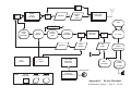
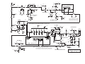
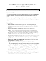
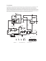
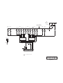
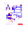
K2 Block Diagram Rev D
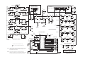
K2 Schematic Key Rev D
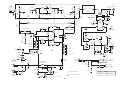
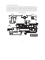
K2 Front Panel Board Rev C
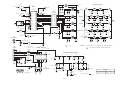
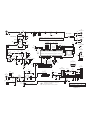
K2 Control Board Rev F
K2 RF Board Rev F
K2 Manual Errata Rev F-2
3
4
5
6
7
11
7.
8.
KPA100 Schematics Rev G
KPA100 Errata Rev C-3
12
14
9.
10.
KSB2 Schematics Rev F
SSB Bandwidth Modification Rev A
15
16
11.
K160RX Schematics Rev A
18
12.
KNB2 Schematics Rev D
19
13.
KBT2 Schematics
20
14.
KAT2 Schematics Rev F
21
15.
KAT100 Schematics Rev B
23
16.
KIO2 Schematics Rev E
26
17.
KDSP2 Schematics Rev C2
27
18.
KAF2 Schematics Rev A
29
19.
20.
K60XV Schematics Rev B
K60XV Errata Rev A-3
30
31
These schematics may be used for personal non-commercial use only.
(c) 1999-2005 Elecraft, Inc
T-R
BANDPASS
FILTERS
T-R
T-R
POWER
AMP
(15W)
DRIVER
LOW-PASS
FILTERS
AGC
4.915MHz
ATTEN.
AND
PREAMP
POSTMIXER
AMP
RCV
MIXER
NOISE
BLANKER
BUFFER
PLL
SYNTH.
VCO
6 - 24MHz
T-R
CRYSTAL
FILTERS
XMIT
MIXER
T-R
BAL.
MOD.
MCU AND
SUPPORT
CIRCUITS
BFO
4.915MHz
I.F. AMP
PROD.
DETECTOR
AUDIO
FILTER,
AF AMP
Shaft Encoder
KEY
Common
Transmit
Receive
DISPLAY
AND CONTROLS
Appendix C
BLOCK DIAGRAM
W. Burdick/E. Swartz
Rev. D 1-9-04
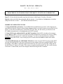
Relay Table
Diodes
SET Relays
MV209, 1SV149
Band
BPF
LPF
VCO
160m
80m
+60m
*40m ALT
40m
30m
20m
17m
15m
12m
10m
K2
K2, K3
K1, 60m-K1
K1
K1
K3, K4
K4
K5
K5, K6
K6, K7
K7
160m-K1
K8
K12
K12
K12
K9
K9
K11
K11
K10
K10
K13
K13,
K13,
K14
K14,
K13,
K13,
K15
K13,
K13,
1Nxxxx
K14
K14
K15
K14, K15
K15
K14, K15
K15
Transistors
2N7000
2N3906
PN2222A
ZVN4424
MPS5179
S
E
2SC2166
2SC1969
2N5109
C
J310
+ 60 meters is available only if the K60XV option is installed.
*40m ALT applies if D19-D20 are not installed.
NOTE: All relays are single-coil latching type and are
G
D
B
C
D
S
G
C
shown in the RESET position in schematics.
Relay pins 5 and 6 are not connected internally.
E
B
B C E
Integrated Circuits
VCO Table
Band
160m
80m
60m
***40m ALT
40m
30m
20m
17m
15m
12m
10m
PLASTIC DIP
VOLTAGE REGULATORS
(DUAL-INLINE PACKAGE)
Fixed Cap., pF
Total Cap., pF*
VCO Freq.
at band edge**
C75 (470)
C72 (270)
C71+C73 (129)
C71+C73 (129)
C71 (120)
C73+C74 (67)
C74 (20)
none (0)
C73 (47)
C74 (20)
none (0)
525-629
325-429
215-259
163-209
154-203
102-131
55-84
35-64
82-111
55-84
35-64
6715 (subtract)
8415 (subtract)
10165 (subtract)
11915 (subtract)
11915 (subtract)
14915 (subtract)
18915 (subtract)
22915 (subtract)
16085 (add)
19975 (add)
23085 (add)
* This includes capacitance of varactor diodes D23-D26 on all bands, D21-D22
on 80 -160 m, and D19-D20 on 40 and 60 meters (if applicable). Only a
portion of the indicated capacitance range is actually used to cover
each Amateur band segment. VCO frequency can be calculated based on
a total inductance of 0.95 µH (T5 in parallel with L30).
** Based on an I.F. of 4915 kHz (e.g., 6715 - 4915 = 1800).
5250 kHz used as 60-meter lower band edge (pending U.S. FCC ruling).
2930T-8, 78XX
78L05, -06
1
2
3
4
8
7
6
5
GND
OUT GND IN
COUNT PINS STARTING AT
PIN 1 AND GOING COUNTER-
OUT
IN
CLOCKWISE (8-PIN DIP SHOWN)
GND
Special Symbols
= On bottom of PC board.
Jumper
Elecraft
K2 Schematic Key
By W. Burdick
E.Swartz
Rev.
Date
D
10/23/02
***40m ALT applies if D19-D20 are not installed.
Appendix B
Sht.
1 of 1
15
35
BANDSTORE
ANT1/2
TUNE
S4
D1
MENU
S5
S3
S2
S1
S0
15
S4
S5
S6
S7
BP2
BP3
BP0
BP1
S10
VLCD
NB
S6
EDIT
D7
RATE
LOCK
#0
S7
LEVEL
D3
D0
6
5
8
9 10
4
3
100K
S0
C9
1
R16
/MIC RD
/BANK2
9 10
6
5
G
H
3
14
4
F
E
13
D
12
C
74HC165
GND
VCC
R1 5K
Keyer Speed
/SPD RD
cw
ccw
8
16
/QH
7
QH
9
SER
CLK
2
10
11
CLK INH
SH/LD
1
5A
U2
15
1
ENC A
ENC B
11
B
A
18
17
/Q7
SOUT
GND
GND
2
5A
10
16
15
/Q4
/Q5
/Q6
GND
SIN
SRCK
3
19
14
6
5
7
8
13
/SRCLR /Q3
/Q2
RCK
12
4
/Q0
/Q1
/G
VCC
2
9
17
16
15
14
7
6
5
18
SOUT
10
GND
/Q7
GND
11
/Q6
GND
19
/Q5
SIN
3
/Q4
SRCK
13
/SRCLR /Q3
8
/Q2
RCK
12
4
/Q0
/Q1
/G
VCC
V+
B
A
3
Shaft Encoder
1
Z1
V-
9
First switch label corresponds to switch TAP,
Second label corresponds to switch HOLD.
S7 - S16 can also be used as a numeric keypad.
(spare)
4
C3
D4
.047
R2
/SR RD SR CK SR DIN 5A
SR CK
SR DOUT
U3
5A
C2
.01
SR WRT
U4
6B595
/BANK1
To RF Board, P1
D5
J1
7
GND
8
8
V POTS
2N3906
C4 C5 C6 C7
.01 .01 .01 .01
P1
Mic Config.
4
16
17
18
19
R5
R4
20
/BANK2
cw
5A
ccw
D6
1N5817
V POTS
R13
68.1K, 1%
5K
RIT/XIT Offset
ccw
cw
R7
4.7K
V POTS
RP3
10K
5A
R14 100K
R3
5A
AF Gain
1
R6
RP3
cw
ccw
3
/MIC RD
5K (audio taper)
These components are supplied with SSB adapter.
14 15
2
.01
GND
13
5K
Q3
RP3
10K
12
R.F. Gain
/DOT-PTT
5
11
MIC AF
6
C8
10
4.7K
IDAT
5V
7
9
ICLK
6
6
8
/SR RD
FUNC
7
ENC A
5
5
6
SR CK
4
UP
5
SR DIN
DN
4
SR WRT
3
3
4
3
SR DOUT
PTT
RP3
10K
7
2
AUXBUS (NC)
2
2
8
1
ENC B
1
AF
cw
ccw
5A
1
5K
Power Out
6B595
J2
Mic
MSG
REC
#9
D0
D7
8
/BANK1
5A
/ENC RD
2
S16
7
11 12 13 14 15 16 17 18 19 20
R15
10K
15K
XIT
PF2
#8
S15
6
DS2
/SPD RD
.01
LED Array
RIT
PF1
#7
S14
Pushbutton Switches
RP1
D0 D1 D2 D3 D4 D5 D6 D7
2V
R12
120
2
XFIL
AFIL
#6
D6
5
7
7
S13
D2
D1
4
8
6
AGC
CW REV
#5
20
3
9
5
D3
S12
D5
2
10
4
PRE/ATTN
SPOT
#4
S11
21
S8
S11
10
S9
S12
A2
VSS
A1
S13
S15
A0
SA0
S16
5
IDAT ICLK
3
D4
D4
6
1
2
A=B
SPLIT
#3
/BANK2
D6
25
S14
S17
CLK
VDD
1
OSC
S20
SCL
/SYNC
4.0V DAY (18mA/LED)
2.7V NIGHT (6mA/LED)
(based on LED Vf=1.9V)
120
S18
S21
SDA
RP2
30
S19
S22
S23
PN2222A
C1
.047
S10
REV
#2
(S0 through S23 connected to DS1; only S0 and S23 shown)
40
Q2
Q1
S9
/BANK1
U1
PCF8566
LCD Driver
S23
/NIGHT
A/B
MODE
VOX
#1
S8
D5
R10
33
R11
470
DISPLAY
RF/ALC
S2
D2
S3
R9
220
/BANK2
COM1
COM2
5
BAND+
RECALL
S1
1B,C,DP
COM3
4
1A,G,D
1F,E,AN
2B,C,DP
2A,G,D
2F,E,AN
3B,C,DP
3A,G,D
3F,E,AN
4B,C,DP
4A,G,D
4F,E,AN
5B,C,DP
5A,G,D
5F,E,AN
6B,C,DP
6A,G,D
3
/BANK1
7
10
VIM-838-DP 8-DIGIT LCD
S23
S22
S21
S20
S19
S18
S17
S16
S15
S14
S13
S12
S11
S10
S9
S8
S7
S6
S4
S3
S5
20
6F,E,AN
7A,G,D
7F,E,AN
2
COM3
COM2
1
8B,C,DP
COM1
D3
8A,G,D
D2
Bargraph
Brightness
Control
25
8F,E,AN
DS1
5A
S1
30
7B,C,DP
Backlight
LEDs
S2
S0
5A
Elecraft
By W. Burdick
E. Swartz
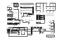
K2 Front Panel Board
Rev.
C
Date
10/6/02
Appendix B
Sht.
1 of 1
1
-
8
V SMTR
RA1
RB5
IDAT
I SENSE
RA2
RB4
/SR RD
V SENSE
RA3
RB3
/SLOW AGC
RA4
V POTS
RA5
RB1
SR WRT
RP2
ENC A
RE0
RB0
SR DIN
5
1
RP3 47K
82K
R12 820
RE1
VDD
RE2
VSS
/AGC OFF
10
EXT ALC
RP4
82K
RP5
470
RP4
82K
3
X2
C21
33
6
5A
15
3
C38
680
C22
8-50
2
P6
Q9
Q10
MPS5179
MPS5179
RD6
/DASH
OSC1
RD5
RX
OSC2
RD4
TX
RC7
RC6
/MUTE
RC2
RC5
SCK
RC3
RC4
COUNT
100kHz-40MHz
VSS
RC1
/DAC2CS
20
/PLLCS
RD0
RD3
RD1
RD2
/DOT-PTT
25
P7
3
0-25.5V
(0.1V res.)
IN
3
4
/CS
VCC
SDO
/HOLD
/WP
SCK
VSS
VOL2
8
C27
Q4
AF Amp
/DAC2CS
AF OUT
PD2
V ALC
AUXBUS
V BIAS-XFIL
8T
EXT ALC
8R
12V IN
V POTS
IDAT
14 16
18
20
22
24
26
28
30 32
34 36
VOL2
2
4
3
5
7
9
11
13 15
17
19
21
23
25
27
29
31
33
35
1
3
.022
8R
4
5
6
P1
P2
8T
To RF Board, J7
PD1
8R
V BFO
12V 5A 8A
ENC B
R4
5.6K
V AGC
VOL1
6
8
10
5
7
9
P3
12
14 16
18
U9
5A
11
13 15
17
8
+
22µF
R20
2.7Ω
6
RP4
82K
19
8
C32
LM380N-8
RP4
82K
5
20
7
RP5
470
C29
220µF
9
L1
82 mH
RP5
470
10
R16
10
12V
C28
220µF
7
C41
.01
To RF Board, J8
Elecraft
To RF Board, J6
K2 Control Board
By W. Burdick
E. Swartz
NOTE 1: Jumpers are used at R18 and R19. They must be removed if the Audio Filter option is installed.
VOL1
VOL3
RX
+
12
C26
0.1
AF OUT
R.F. GAIN
3
7
Q7
J310
D
C23
.01
C25
0.1
10
2N7000
6
G
D
C30
.047
1
RP6
5.1K
2
5
G
8
6
RP6 5.1K
1
8R
S
Q6
J310
RP1
3.9K
U2A
LM833
7
8
S
TX
Q2
2N3906
3.3M
/MUTE
7
5
C3
.01
50K
AGC THR.
Mute
V RFDET
10
3
NC BYPASS
8A
3
8
2
1
cw
.047
6
1
+
R2
8R 3.3M
5.1K
4
R1
1
2
4
4
0Ω
R17
3
5A
.047
12V 5A 8A
2
R19
J1
2
2
C8
39
4
Q3
C19
9
1
5
J2
9
OUT
GND
.001
4
6
RP6
ccw
I.F. OUT
8
3
R18
-
C2
.001
U2B
nc
C7
330
+
2
5
3
+
5
5
1
PD1
12V
v+
7
AUXBUS
OUT
4
RP6
5.1K
47K
Audio
Filter
SDO
IN1
V+
SDI
GND
6
RP3
Q1
2N3906
.047
10
8A
U10C
10
9
GND
R3
10K
8
8T
C14
C11
Q12
PN2222A
D1
1N4148
R5 33K
C9
.01
7
PD2
SCK
5
8V Switching
RP1
3.9K
1
RP2
5A
6
V SMTR
2
V BIAS-XFIL
+
IN2
8A
47K
-
3
+
/SLOW AGC
7
U7
25LC320
C4
0.47µF
RP6
5.1K
RP3
4
C6
.047
X1
5.068MHz
2
U10D
7
8
U5
ICLK
AGC
C10
.01
/EECS
/DAC1CS
78M05
C44
Not Used
/AGC OFF
82K
RP1
3.9K
R7 1.78k, 1%
8
6
9
5V Reg.
PN2222A
0.00-5.10A
(.02 A resolution)
RP2
9
0Ω
C15
100µF
U3A
4
Q11
C1
2.2µF
10
8
LMC6482AIN
V SENSE
-
U3B
7
/CS
5
EEPROM
C16
ENC A
7
1
+
SR WRT
+
-
I SENSE
6
SCLK
DOUT
11
11
82K
8A
SR DIN
5
196K, 1%
V-
/CLR
14
-
5A
12
DIN
V BFO
+
13
13
10
RP7
33K
OUT
GND
SR DOUT
C17
.01
6
3
7
14
RXD
+
1%
2
DGND
8A
4
12
(NOTE 1)
IN
C13
22µF
R10
1
PDE
.01
C40
15
U4
8
2
+
R9
8
VDD
/LDAC
8
21
2.2µF
U10B
5A
16
8V Low-Dropout Reg.
R8
100
Voltage Sense
U1
NE602
AGND
UPO
1
LM2930T-8
C42
0.1
D2
1N4148
REF
12V
3
806K, 1%
OUTD
5A
SR CK
2
Note: Current sense resistor
is R115 on the RF board.
/SR RD
1
OUTA
2
12V IN
1
OUTC
MCU
Current Sense
P5
2
6
C20
TXD
+
7
-
C36
.0027
C35
.01
U8
MAX534
18C452
EXT INT
6
.001
U6
Voltmeter Input
- +
5
4
1
Voltmeter Source
4
RP7
33K
RD7
RC0
3
5A
30
2
3
VDD
ENC B
4
1
Freq. Ctr
Input
2
1
C37
.01
SR CK
OUTB
SCK
RP5
470
4.000MHz
1
/DOT-PTT
V RFDET
5
C39
.01
4
5V FCTR
RB2
C33
+
7
V PWR
5A
LMC660
5
6
5
8
Quad, 8-bit DAC
SR DOUT
35
4
RP7
33K
Q5
2N7000
RP3
47K
3
.0027
SDO
10
9
Part of CW key shaping
mod; solder on back (see text)
2
C12
.0027
ICLK
VOL3
7
3
4
40
RB7
RB6
V ALC
C34 .001
12V
*
MCLR
RA0
ALC
.01
1
5A
6
5
RP3
47K
C24
SIDETONE
2
U10A LMC660
*
6
5
C5
C31
.01
+
R6
100
/DASH
8T
R21 270K
82K
C45
22µF
4
3
8R
+
2
1
RXD
C43
.001
R22
AUXBUS
Q8
PN2222A
AUXBUS
AF OUT
P4
TXD
3
R11
47K
RP7
33K
.01
C46 .01
/PLLCS
Aux I/O
C18
8A
*
("D3" on PCB)
TONEVOL
V PWR
Rev.
F
Date
1/27/04
= on bottom of PC board
Appendix B
Sht.
1 of 1
PLL Reference
Oscillator
PLL Synthesizer
RFC15
12.090-12.100 MHz
12.096MHz
X1
Q19
8B
TP3
100 µH
D
1
G
X2
12µH
S
(NOTE 1)
C84
120
2
4
4
RP2
D16
MV209
7
SCK
8
3
RFC14
18µH
D17
10K
REFOUT
PH R
PDOUT
DIN
6
/PLLCS
PH V
FIN
5
SDO
C87
.01
C85
120
10K
1
3
R22
3.3M
OSCOUT
VSS
/ENB
LD
CLK
FV
DOUT
FR
C91
.001
(NOTE 3)
1
2
SDO
27K
15
R24
13
12
C88
68
10
-
5
2.7K
2.7K
11
6
4
R30
7
+
C92
.022
(NOTE 3)
10µF
4V
R29
10K
K15
VOUT
LD /CS
REF
DOUT
GND
7
3
6
2
+
-
5
1
8B
IN
U6A
(Vout = 0 to 4.096V)
LMC662
2, 3
8
C175
.01
C63
.01
nc
D21
Q17
D22
~2Vpp
2N7000
1SV149
R9
100K
D
VFO ALC
G
C60
100µF
OUT
D11
S
3
4
C58
R10
470
1N4148
.01
2
VFO Range Selection
Relays are shown in RESET
position. See relay table (key).
9
7
C90
.047
C103
220µF
8
C73
47
RC
2.2K
Rt 10K
Thermistor
RE 10K
6, 7
RD 1.8K
RB 12K
9
R11
560
R12
560
8B
.001
8B
RF
10K
nc
C74
20
1
RX VFO
4
R14
10K
1N4148
C61
.01
R33
15K
8
K13
6
-
D8
2
7
C89
+
2
T5
1.2µH
3
+
12-Bit DAC
7
3
3
U3
LT1252
C64
.001
8B
5B
78L05
Buffer
TP1
9
U8
RFC16
47µH
4
10K
TX VFO
4
1
2
K14
D20
D19
MV209
R13
3
4
4
8A
RA 33K
D26
8
8
D13
1N4148
2
R32
10K
(NOTE 2)
DIN
R17
100K
D25
C93
9
7
5B
Q18
J310
S
10K
120
8B
8
D
G
R31
LMC662
2.7K
VCC
MV209
D23
U6B
R25
C65
0.1
33
D24
14
R19
CLK
R15
C68
10pF
+
3
/DAC2CS
RFC10
1mH
16
MC145170
U5
LTC1451
C67
0.1
VFO
R28
R20
270
SCK
4.7µH
U4
1SV149
C100
.001
C96
1µF
.01
8B
C94
.047
+
R21
100K
RP2
C86
0.1
VDD
OSCIN
2
L31
C95
5B
J310
D18
1N4148
L30
(NOTE 3)
C75
(NOTE 2)
PN2222A
470
C71 C72
82 270
R16
C59
0.1
C62
100K
Q16
.01
R18
1M
4V
4, 5
Thermistor Board
(replaces RP3 on PC board)
J6
R2
R1
220
220
1
2
3
4
2
5
4
6
8
10
12
18
20
22
24
26
28
30
32
34
2
36
4
6
8
12
14 16
18
C196
SCK
/DAC2CS
10
/DOT-PTT
VOL2
J7
6
AF OUT
PD2
V ALC
AUXBUS
8T
EXT ALC
8R
12V IN
V POTS
SR DOUT
14 16
12V DC
.047
P3
Aux. 12V
20
+
-
J8
5
7
9
11
13 15
17
19
21
23
25
27
29
31
33
1
35
3
5
7
9
11
13 15
17
2
F1
19
RGE300
SDO
/DASH
/PLLCS
VOL3
VOL1
AF OUT
PD1
V BFO
ENC B
8T
SR DIN
8R
SR WRT
SR CK
ICLK
12V 5A 8A
/SR RD
V AGC
3
12V
R.F. GAIN
I.F. OUT
.001
8R
/DASH
1
0.05Ω, 1%, 3W
R36
82
C106 2.2µF
SB530
17
18
19
5A
16
S1
Power
20
R.F. GAIN
14 15
IDAT
13
ICLK
12
V POTS
11
/SR RD
10
ENC A
9
SR CK
8
SR WRT
7
SR DIN
6
ENC B
5
AUXBUS
4
SR DOUT
P5
3
MIC AF
VOL1
2
2
Q23
2N7000
8T
Elecraft
By W. Burdick
E. Swartz
Phones
Speaker
D12
OFF
+
J2
Board
R113
82
1
1
Panel
P1
VOL3
+
8R
Front
/DOT-PTT
+
ON
Current Sense
VOL2
R35
82
12V IN
R115
AF OUT
C105
2.2µF
D10
95SQ015
1
C1
/DOT-PTT
C2
.001
12V 5A 8A
ENC A
Key/Keyer/Paddle
Control
Board
IDAT
J1
V RFDET
J3
V BIAS-XFIL
NOTE 1: X2 is not used.
NOTE 2: D19-D20 are supplied with the K60XV option. They must not be installed unless the K60XV option is
also installed (60 m band and transverter I/O). C71 must be changed to 120 pF if D19-D20 are installed.
NOTE 3: These components improve PLL stability; they must be soldered on the back of the board (see text).
C111
2.2µF
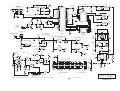
K2 RF Board
Rev.
F
Date
1/27/04
Appendix B
Sht.
1 of 4
C165
8R
12V
C52
.01
R72
470
R73
2.7K
K16
C142 .01
.01
R82
C160
.01
C143
.01
9
2
C141
.01
9
2
C53
.01
RFC12
100µH
R78
22
RX VFO
18
Noise Blanker
C158
+7dBm
R74
47
7
4
7
4
J12
8
3
8
3
.01
K17
R81
1.8K
C159
.01
4
RFC11
100µH
C163
.01
1
2
3
4
5
6
7
R7
68
R6
100
1
Z6
C145
.01
T6
R8
4
100
1
12V
2
C161
.01
3
TUF-1
R75
680
-10dB
2.7K
R80
Buffer
680
R83
4.7Ω
R79
1.8K
W5
NB Bypass
R84
18
100
R88
470
R90
470
+14dB
C162
C164
.01
C146
.01
R77
220
1N4007
R89
2N5109
RF Preamp
R76
10
D7
.047
8R
Q22
Rcv. Mixer
Attenuator
(Sh. 3)
R5
C170
3
Q21
2N5109
BPF
AUXBUS
12V
2
D6
1N4007
8
R85
150
.047
8R
Post-Mixer Amp.
R97
33
-5dB, Z= 150Ω
HI IP
Q12
2N7000
NOTE: If Noise Blanker is installed,
R88 and R90 must be removed,
and R89 replaced with a jumper.
12V
U9
7
4.9136 MHz Variable-Bandwidth Crystal Filter
3
+
6
2
-
R92
33
IF Amp
V BIAS-XFIL
4
R95
R93
820
R101
10K
2.7K
RFC13
100µH
V XFIL2
(NOTE 2)
Q20
RP4
R94
82
C55
.01
8T
D29
6
4
2
2N7000
RP4
1
RP4
1
3
RP5
3
5
6
4
2
2
X8
X9
X10
W3
X11
D31
2
1
AGC
D41
5
6
7
8
D29-D34: 1SV149
V AGC
SSB Control
J11
3
3
J9
2
3
4
5
6
7
8
9
10
11
4
MIC AF
V RFDET
8T
D39
MV209
BFO
Q24
J310
C168
.01
41µH
D
V7
C144
100pF
3
C155
.01
D36
270
5082-3081
2
TP2
BFO Buffer/Attenuator
7
RP6
100K
D38
1SV149
4
G
5
R99
RP6
100K
C173
220
8
(NOTE 1)
NOTE 2: D40 and D41 were added to improve handling of extremely
strong signals (from nearby transmitters). These diodes
must be soldered on the back of the PC board (see text).
V BFO
82
X4
270
NOTE 1: Remove C167 when SSB Adapter is installed.
PD1
7
C174
D37
1SV149
C169
2
PD2
C177
.022
6
4.917MHz
R98
Adapter
1
5
X3
Q25
PN2222A
1
6
3
2
V+
2
C176
0.1
S
U10
NE602
3
1
C186
.01
8A
.001
Aux. AF
U11
NE602
V-
2nd Xtal Filter
C183
.01
EXT ALC
C167
5
C154
100
1
.01
I.F. OUT
C179
100
V+
C153
68
TX VFO
/DOT-PTT
8R
SSB
8
0.1
8
R110
5.6K
C181
V ALC
8T
820
X5
1
XFIL Out
AUXBUS
C156
.047
R91
820
X6
12
XFIL In
Xmit Mixer
2
J10
1
C178
R107
100K
C184
.01
3.9K
2
R100
8A
L34
4.7uH
C182
180
R114
1
J5
V XFIL2
4
D33
D32
Product Det.
MC1350
3
4
330
D30
3
D40
T7
D34
.047
X7
22
U12
4
1
W2
0.1
RP5
C157
C150
R112
1N4148
5 .047
RP5
C185
8R
C166
RP4, RP5: 100K
5.6K
C54
.01
R96
2.7K
LT1252
L33
0.1
R111
C151
3
RP6
100K
C172
.01
390
6
RP6
100K
Elecraft
K2 RF Board
By W. Burdick
E.Swartz
Rev.
F
Date
1/27/04
Appendix B
Sht.
2 of 4
J15
60m
4
C5
100
3
C4
820
2
2
L2
40/60m
L5
C12
560
K2A
20m/
160m
4
30m/80m
5
G
6
7
8
X
8T
K3
1
C108
.01
2
3
4
5
6
7
8
9
10
11
12
13
14
15
R65
10K
16
RXRY RY COM
P6
Aux. RF
160RY
2
1
C224
.047
8T
RFC2
100µH
9
C114
1N4007
D3
K2B
L4
4.7µH
A n t.
8R
6V
8
.01
D4
4
W1
D2
C110
.01
1N4007
W6
R39
1K
R37
100K
D5
RFC3
47µH
RX Ant.
Bypass
80m
L16
K8A
7
3
L3
4.7µH
7
C16
1800
80/160m
4
8R
C15
560
C14
2
2
K1B
1200
C11
1800
3
9
3
C13
2
9
33µH
8
4
160m/
RX
J13
1
J4
Ant.
6V
J14
8
C8
820
4.7µH
K1A
7
C7
100
4.7pF
C6
L1
4.7µH
Xverter
Interface
3
3
2
7
L17
K8B
8
C191 C192
1800 1200
C190
1200
9
8R
C24
47
4.7µH
20/30m
R38
1K
XVTR
Bypass
L9
4
R34
1N4007
D
2.7K
7
L22
8
2
C211
10
K10A
9
C213
33
C210
82
4
U2
78L06
K7B
15/17m
C214
68
C212
150
L23
K10B
7
L24
10/12m
L13
1µH
C48
330
12V
IN
AUXBUS
OUT
9
160RY
VCO Relays
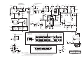
Band-Pass Filters
1
RXRY
K13
1
10
5
/CLASS AB
Z5
4.0MHz
ALL RELAY BYPASS CAPACITORS ARE .001µF
C17, C27, C195, C204, C207, C216, C223
10
C82
.001
Pre/Attn.
Relays
NOTE1: When the K60XV (transverter and 60 m) option is installed,
C6 must be removed and J15 installed in its place, on
the top side of the PC board.
K16
1
14
RB7
BPF Relays
28
10
RA0
RB6
RA1
RB5
RA2
K14
K15
MCLR
RB3
RB2
RB1
VSS
RB0
OSC1
VDD
C39
OSC2
VSS
.001
RC0
RC7
RC1
RC6
C225
390
RC2
RC5
RC3
RC4
K6
330
680
RF Output Detector
10
15
R67
1.5K
D9
R66
V RFDET
2.7K
1
9
C227
C226
20
K10
RF
K11
G
1%
1N5711
C77
.001
R69
100K
R68
226Ω
1%
K12
10
K8
K17
K9
C207
C216
C223
RY COM
C195
C57
.001
8
K7
HI IP
7
L26
C229
220
C228
56
K5
RA4
K11B
3
2
K4
RA5
40/60m
L25
K1
RB4
RA3
4
K2
K3
25
C204
NOTE2: Pins 5 and 6 of relays are not connected internally.
However, these pins may be connected to other relay pins
or to other components on either side of the PC board.
1
C222
100
C220
220
C140
.001
or 16F872
9
C221
39
C218
150
K11A
PIC16C72
C139
0.1
8
C219
12
R64
100
U1
6V
C47
33
1
8
3
2
6V
K12A
5-30pF
C9
C46
C27
BPF
(Sh. 2)
1µH
C203
47
3
10/12m
Low-Pass Filters
C79
C42
330
8
C45
L12
(Sh. 4)
C104
68
7
C43
33
L21
9
K9B
C201
220
C199
220
(Sh. 4)
K6
7
7
3
4
PRE-DRIVER
I/O Controller
5-30pF
C44
K7A
C202
120
LPF
9
K5B
4
12m/15m
2
C36
470
L11
1µH
C200
150
C197
100
T-R
Switch
RFC7
15µH
8
10m/17m
K5A
3
C35
56
5-30pF
C198
27
4
C107
.01
7
C37
L10
1µH
Q2
ZVN4424A
K4B
C34
L20
K9A
C109
.01
8T
15/17m
2
C30
470
2
5-30pF
D1
1N4007
9
L19
8
2
C113
.01
C49
C31
56
3
100µH
C38
C32
4
C23
50pF
12
C33
2.2
8
C25
330
C81
C21
50pF
K4A
9
330
2
C29
C80
C28
12
C19
L18
3
G
S
3
20/30m
8R
RFC1
7
C17
47
4
C22
3.3 pF
L8
4.7µH
C26
C20
LPF
Relays
Elecraft
C208
.001
By W. Burdick
E. Swartz
K2 RF Board
Rev.
F
Date
1/27/04
Appendix B
Sht.
3 of 4
K12B
1
AUXBUS
(NOTE 1)
12V
RFC4
10µH
+
C119
.01
C126
47µF
C133
0.1
R45
47
C135
.01
Z1
C127
T2
RFC5
12:8, FT37-43
10µH
Q7
3
LPF
C122
C115
.01
680
2SC1969
2
56
R53
4.7Ω
4
1
RFC8
10µH
R55
33
(Sh. 3)
C129
.01
5
C
A
6
1
3
R58
2
4
1/2W
T3
3
C116
33
8T
C120
.01
C121
.01
2
R49
120
1
RFC6
RFC9
10µH
D
C130
0.1
B
180
8
0.68µH
4
Q8
7
T4
2:3:1:1
2SC1969
T1
9:3, FT37-43
R44
2.7K
C128
680
Q6
2SC2166
R40
C118
470
.01
R48
120
Z2
R47
47
R50
+
(Sh. 3)
Power Amplifier (PA)
NOTE: WIND T4 2:2:1:1 FOR
BETTER EFFICIENCY AT 5W
(SEE "MODIFICATIONS" SECTION)
C124
C125
0.1
22µF
R42
4.7Ω
C131
0.1
1.5Ω
1/2 W
Q5
2N5109
PRE-DRIVER
R41
560
R54
4.7Ω
R56
33
Driver
S
C117
R43
22Ω
0.047
Q10
2N7000
8T
PA Bias
G
D
8T
R46
270
R59
R61
120
4.7K
Pre-Driver
Q13
PN2222A
V BIAS-XFIL
Q11
PN2222A
+
C137
100µF
C138
.047
R60
100
/CLASS AB
R63
220
Elecraft
R62
2.7K
K2 RF Board
By W. Burdick
E.Swartz
Rev.
F
Date
1/27/04
Appendix B
Sht.
4 of 4
K2 KI T CHAN GES AN D MANU AL ERR ATA
R e v . F - 2, F e b . 26 , 2 0 0 4
PL EAS E READ TH IS INF ORM ATI ON
BEFOR E YOU BEG IN ASS EMBLY
Your K2 kit includes a number of recent upgrades to both hardware and firmware. These include:
Modified CW keying envelope to significantly reduce transmit bandwidth
Limiting diodes on the receive I.F. amplifier input to cleanly handle nearby transmitters
operating on your exact frequency (characteristic of "HF Pack" style operation)
Two new scanning modes, including "channel hopping" (among in-band frequency memories)
and "live scan" (unmuted scanning for use in locating very weak signals)
Up to six transverter band displays
Transverter address control to allow more than one transverter band to select a given XVseries transverter
Full support for the forthcoming K60XV option, which will provide 60 meter capability and
low-level transverter I/O (due in March, 2004)
Errata Items:
1. Page 47, right column, 2nd assembly step: This step was supposed to be on page 64, right column,
just before "Assembly, Part III". Make a note on page 64 referring to the step on page 47.
2. Page 57, right column, 2nd assembly step: Change L31 from 12 µH to 10 µH.
3. Page 82, rear panel drawing: The illustration shows a new lower rear panel that includes holes for
two additional transverter in/out jacks (RCA connectors). Your kit may not have this new rear panel
because it was being phased into production at the time the manual was written. You can obtain the
new rear panel later if you plan to purchase the K60XV option (60 meters and low-level transverter
I/O). Availability of this option will be announced.
4. Appendix A, RF board parts list, page 5: Change L31 from 12 µH to 10 µH. Also make this change
on the schematic (Appendix B, RF board sheet 1, upper left corner).
TP2
N:111
12PA
J1
R14
180K
RF IN
5R
1W
K1
C76
RFC5
100µH
.015
5T
200V
C72
.01
1
GND
RFC11
100µH
.01
RFC3
100µH
D12
1N4007
C73
.01
C71
.0018
200V
C31
.033
200V
C75
0.1
100µH
5µH
C59
C67
R39
T44-2
L15
.033
C81
4700
22
0.1
3W
5µH
C82 (not used)
T4-6
C1
30pF
GND
RFC1
T4
FT50-43
C79
.039
200V
L16
200V
T4-5
D14
1N4007
RFC4
RFC10
100µH
LPF OUT
100µH
T-R Switch
1N4007
LPF IN
K2
(SHEET 2)
D11
C86
.047
Antenna
*
R13
100
3W
ZVN4424
C77
J2
Low-Pass Filters
Q7
ZVN4424
470
2
12PA
R12
510K
Q6
("AUX RF")
90-150V
R11
K2 RF
1
3
2
4
SWR Bridge
D13
1N5404
C95
100
R29
R28
200
1W
D16
1N5711
3.3K
D17
1N5711
C87
.001
C64
1800
200V
C88
.001
R26
R27
E1
C70
.001
T44-2
FWD
100K
REFL
High-pass Filter
GND Post
T1
R21
10
2W
C83
Z = 9:1
R23
5
0 ohms
2
(jumper)
R22
R19
180
C63
L18
0 uH
(jumper)
.047
C61
.047
R9
1.6
1
T2
2
Q1
6
0.6-0.9 V
1
TP4
-
+
22 3W
0.1
PA
Q4
7
MJE182
C57
.047
C56
.047
C55
.047
C54
.047
C53
.047
C52
.047
U7B
LMC6482
+
C51
470µF 25V
C89
.01
1%
5
8
+
7
6
4
4
VRFEN
RP1
3.9K
VFWD
R38
5
T SENSE
+
2
C58
C80 4700
+
Bias Set
3
5V
R25
8.45K
U5A
5
3
10
-
VREFL
Z = 1:16
R34
10
2W
5B
R6
1K
C69
.001
4
12CTRL
C60 100µF
R5
15K
1000
s.m.
Q2
2W
.047
C62
R35
10
2W
2SC2879
3
4
C66
300
2W
R20 1.6
2W
1
R24
8.45K
U6
EL5146C
3
7
3
1%
1
+
2
VRFDET
8
6
EN
-
C68
.01
4
RP1
U5B
3.9K
SCALE
2
LM358
C65
.01
Q10
R16
3.3K
Q11
2N7000
R15
3.3K
Q3
MJE182
Z1
J3
12V, 20A
(Ext. Fuse)
+
-
D10
1N5404
AF
FB110-43
J5
1
(2 beads)
AF In
2
Current Sense
12PA
R7 .005 ohms
1
K2 12V
("AUX 12V")
C48
GND
.047
R32
100
1%
D9
SB530
C33
0.1
C34
0.1
C49
.047
C30
0.1
2
3
+
3.09k, 1%
Q5
Int. Spkr
GND
R3
2.7 ohms
8
4
SP1
C11
0.1
1
* Not on the PC board.
U7A
Elecraft
By W. Burdick
LMC6482
R30
Ext. Spkr
SPKR
2.7 ohms
12K2
J4
3
R2
C85
.047
2
2
J6
C10
0.1
1
3W
1
+
-
GND
2
= on bottom of PC board
2N3904
I SENSE (0-5 V = approx. 0-32 A)
64
E. Swartz
KPA100
Rev.
G
Date
2/5/04
Sht.
1 of 2
K1
U3
78L05
IN
12CTRL
5V
OUT
MCU
C23
0.1
1
C25
.001
VFWD
RA0
RB6
TP1
VREFL
RA1
RB5
5
nc
C26
33
10
X2
4 MHz
C27
30pF
RP1
5
RA3
RB3
RA4
RB2
RA5
RB1
VSS
RB0
OSC1
VDD
or ULN2803
7
1
2
3
4
5
6
20
RC7
SCALE
RC1
RC6
5R
RC2
RC5
RC3
RC4
12PA SENSE
6
RB4
VSS
14
TD62083
3.9K
C29 C22
.01 .01
7
5V
8
9
IN0
/OUT0
IN1
/OUT1
IN2
/OUT2
IN3
/OUT3
IN4
/OUT4
IN5
/OUT5
IN6
/OUT6
IN7
/OUT7
GND
COM
C12
.01
18
C13
.01
C2A
S.M.
C24
.01
L2
C2B
C2D
K4
K5
L4
K5
L5
15
K6
C3E
C3D C3F
C3B
C3A
14
C3C
13
C14 C15
.01 .01
12
LPF IN
K7
L7
K7
11
FAN+
M
C3H
L8
D
Q12
12PA
2N7000
C16 C17
.01 .01
C4B
C4D
C4E
C4C
K9
L10
K9
L11
L12
Ext. PA Key
K10
FAN-
C5A
C18 C19
.01 .01
K11
C5B
C5D
C5F
K12
K12
C6A
C28
.01
C6C
C6B C6D
S.M.
C6E
C6G
C6F
C20 C21
.01 .01
G
C90
.01
R1
3.3K
S
C13-C21
RFC6-8: 100 µH
NOTES:
All relays are shown in the RESET (de-energized) condition.
RS232 Interface
C7-C9, C32: .01 µF
Aux I/O
L14
80m
Q9
J8
C5G
C5E
L13
K11
IRF830 or IRL620
D
K10
10/12/15m
C74
.01
12CTRL
R8
10K
LPF OUT
K8
C5C
J7
C3J
C3G
K8
FAN
G
K6
17/20m
10
R31
S
L6
30/40m
16
C4A
5B
C2E
S.M.
C2C
S.M.
TP3
15
L1
17
200
1/2W
3.9K
K3
K4
8R
RA2
RC0
5T
U2
RP1
8
K3
160m
25
OSC2
VRFEN
28
RB7
MCLR
BIAS SET TEST POINT
I SENSE
K2
AUXBUS
U1
PIC16C72
T SENSE
Low-Pass Filters
12CTRL
= on bottom of PC board (nearest the heatsink).
1
-5 TO -25V
2
RXD
12CTRL
High-Voltage Bias Supply
6
U4
9
D7
MAX1406
VCC
T1IN
R1OUT
7
VDD
R1IN
T1OUT
T2IN
R2OUT
8
1
2
3
4
R2IN
R3OUT
GND
RFC9
15µH
T3IN
VRFDET
12CTRL
T2OUT
R3IN
C32
5
VSS
T3OUT
RFC8
C9
6
C7
7
C8
8
nc
RFC7
5
4
3
RFC6
TXD
.01
D8
C35
0.1uF
.01
/K2 RX
/K2 TX
8R
7
5
3
1
C97
.01
1
2
3
4
6
4
2
AUXBUS
(BACK VIEW)
8T (NC)
9
12CTRL
8
VRFDET
J8
7
3
R4
100K
4
C37
.01
D3
D2
18.432MHz
To Ctrl Board
10 8
6
80V
P1
5
C42
.015
200V
5V
X1
9
C44
.01
D6
D4
16
15
14
13
12
11
9
10
.001
C98 C99
.01 .01
30V
12CTRL
AUXBUS
C84
D5
C39
C38
1
C41
100
Q8
2N3904
2
C40
0.1
65
T3
7T bifilar
FT37-61
C46
.01
C43
.015
200V
90-150V
C36
D1
.015
R10
47
200V
12CTRL
D1-D8 = 1N4148
Elecraft
By W. Burdick
E. Swartz
KPA100
Rev.
G
Date
2/5/04
Sht.
2 of 2
K2/100 MANUAL (Appendix G) ERRATA
Rev. C-3, December 14, 2004
PLEASE READ BEFORE YOU BEGIN ASSEMBLY
Important Notice
Your KPA100 kit includes recent circuit changes that allow the K2/100 to handle higher
mismatch conditions, allowing power reduction to start at an SWR of 2:1 rather than
1.5:1.
Since your kit is one of the first shipped with these enhancements, it may include an
unused toroid core, a few extra resistors, and an extra capacitor (the previous component
values).
Errata Items
1. Page 7, parts list: Change R4 from 100 k to 39 k. (Your kit may include an
unneeded 100 k resistor.) Add resistor R33 to the parts list (1 k, 5%, 1/4 W, BRNBLK-RED).
2. Page 13, left column, 2nd assembly step: Change R4 from 100 k to 39 k.
3. Page 13: Cut out and tape this assembly step at the bottom of the right column:
__ Locate a 1 k, 1/4-watt resistor (R33). Trim R33’s leads to approx. 1/4” (6 mm)
long. Place the resistor across the leads of RFC3 (RFC3 is near the fan and the large
black RF choked marked “101”). Solder the resistor to RFC3’s leads.
4. Page 24, left column, first paragraph: The second sentence in this paragraph should
be replaced with: "Each toroid is wound on a specific type of core. One example is
type T44-2."
5. Page 24, right column, first assembly step: The reference to a T50-2 core in this
paragraph should be changed to T50-10.
6. Page 47: Cut out and tape this test step at the bottom of the left column:
__ Set your DMM for 200 or 300 VDC full-scale. Connect the (-) lead of the DMM to
ground (one of the KPA100 standoffs). Be ready to touch the (+) lead to the left side
of 180-k resistor R12 (the lead closest to RFC5). Turn on the K2 and select CW
mode. Set the power knob above 11 W. Hold the MODE button down 1-2 seconds to
enter CW TEST mode. Press the TUNE button and verify that the DC voltage at the
left side of R12 is 100-110 VDC or more. Exit TUNE by tapping any button. Exit
CW TEST mode by holding down the MODE button.
7. Schematic: On page 64, add R33 (1 k) across RFC3, in the T-R switch. On page 65,
change R4 from 100 k to 39 k in the High Voltage Bias Supply.
P2
P3
PLASTIC DIP
(DUAL-INLINE PACKAGE)
1
2
PN2222A
3
D10-D14
1
2
3
4
1N4007
E
C1
78L06
OUT GND I N
C
B
3
= On bottom of PC board.
D6-D9
C7
100µH
CLOCKWISE (8-PIN DIP SHOWN)
100µH
C17
.01
6
D10
RXS
RP1
7
4
2.7K
2
C3
8
D11
C4
0.1
5
3
D6
8
C2
.01
1
C13
0.1
C6
.01
C10
.01
7
RP2
5
2
2.7K
4
C9
100
R11
150
CD
(short)
CA
39
SSB
CJ
CF
100
CL
100
CP
39
(short)
T2
3
2
C35
X2
X1
3
1
.01
D8
C11
.01
4
C5
.01
3
.01
SSB Crystal Filter
D14
R10
RXS
D9
1
.01
D12
6
C8
.01
D7
R5
470
D13
1
.01
COUNT PINS STARTING AT
PIN 1 AND GOING COUNTER-
RXC
2
1N4007
RFC2
RFC1
.01
8
7
6
5
CB
0
X3
CC
27
X4
CE
39
X5
CG
39
X6
CK
39
CH
39
X7
CM
27
1
4
CN
0
DSB
2
T1
TXS
C12
.01
R6
2.7K
U1
16F872
R12 470
MCU
6V
1
ALC
COMP OUT
5
Z1
/PTT
4.0 MHz
MCLR
RB7
RA1
RB5
RA2
RB4
RA3
RB3
/COMP1
RB2
/COMP2
RA5
RB1
RXC
VSS
RB0
RXS
OSC1
VDD
OSC2
VSS
/ATTEN
RC0
RC7
TXC
RC1
RC6
10
MOD EN
14
/COMP0
25
RC2
RC5
RC3
RC4
/VOX DET
C30
820
U4
LM393
PTT DET
RXS
2
-
4
R16
10K
3
+
1
RB6
RA4
8
AUXBUS
28
RA0
U6
78L06
+
7
-
5
6
6V
1
2
3
TXS
15
4
/CS
SCLK
OUTB
GND
OUTA
COMP OUT
7
REF
VDD
6
PWR CTRL
5
ALC THR
C15
0.1
MAX522
DAC
/ATTEN
U3
SSM2165
GND
VDD
Balanced
Modulator
C16
.01
C20
1
+
C31
2.2µF
C32
3
4
VCA IN
BUF OUT
AF IN
OUT
8
0.33µF
7
+
6
COMP
5
AVG
+
+
2
1
MIC AF
C34
2.2µF
C18
0.1
0.1
Speech
Compressor
C33
.01
1
3
1
4
22µF
C21
.01
C24
8
1
/COMP1
/COMP2
DSB
D4
1N4148
1M
2
CARRIER
BALANCE
5
V3
C22
TXC
+
8T
6
.01
7
C41
D5
RP3
2K
1N4148
D1
1N4007
D2
R8
100
1N4007
C40
.01
SSB
PN2222A
6V
R7
33K
.01
R9
10K
C38
+
.01
R4
56K
47µF
.01
3
D3
1N4148
0.33µF
6
22µH
RP3
2K
C39
.01
C25
22pF
2
C42
.01
ALC
Q1
PN2222A
ALC THR
4.915MHZ
RP3
2K
5
ALC
PWR CTRL
C26
.01
L1
PN2222A
1
U5
NE602
C23
4
Q3
Q2
C43
C44
.01
4
V+
R1
RP5
47K
C14
MOD EN
R2
5.6K
/COMP0
5
1
6
R14
1K
6V
C46
0.1
8
DIN
U2
R15
180
OUT
GND
C27
0.1
6V
20
IN
8V
/PTT
C19
.01
C36
820
MIC AF
8V
8T
AUXBUS
VRFDET
1
2
3
/PTT
4
5
6
7
8
9
10
11
C37
.001
12
P1
Elecraft K2
B y W. Burdick
E. Swartz
24
SSB Adapter
Rev.
Date
F
7-20-04
Sht.
1 of 1
Elecraft SSB B/W Modification
(SSBCAPKT)
Installation Instructions
Revision A, November 9, 2004. Copyright © 2004, Elecraft; All Rights Reserved
Parts Inventory
P/N
E530016
E530049
E530141
E530144
E530152
Description
100 pF, 100V,5%,NPO,0.1LS, CAP
150 pF,100V,5%,NPO,0.2LS, CAP
27 pF, 200V,5%,NPO, 0.1LS, CAP
33 pF, 50V, 5%, NPO, .1LS, CAP
39 pF, 50V, 5%, NPO, .1LS, CAP
QTY
2 EA
2 EA
2 EA
4 EA
6 EA
Introduction
The Crystal Filter Bandwidth Modification capacitor kit provides two options to change the original 2.1 kHz
6 dB bandwidth of the KSB2 SSB filter to either 2.4 kHz or 2.6 kHz. (Note: KSB2s shipped after July 12, 2004
now include the 2.4 kHz bandwidth components.) These modifications are not required for the K2 to function
well in the SSB mode. Instead, they are intended for those who wish to optimize its performance to their personal
preferences.
The 2.4 and 2.6 kHz bandwidth filters also require better matching of crystal motional inductance to minimize
pass-band ripple. We have worked with our supplier to obtain crystals with better control of the motional
inductance. The latest ones now make it possible to increase the SSB filter bandwidth up to 2.6 kHz. The latest
crystals (shipping with all KSB2s since May 2002) are marked with “ECS 4.9136-S” on each crystal. Older
crystals shipped before May 2002 marked with “ECS 4.91-20” or “ECS 4.91-0195” should be replaced when
performing this modification.
The older crystals work fine at a 2.1 kHz bandwidth, but are not optimum for wider bandwidths. If you want to
add a wider SSB bandwidth enhancement to your KSB2, we suggest you order a new set of crystals from Elecraft.
They are Elecraft Part #E850006 (7 matched crystals for the KSB2) or #K2KSB2XTLS (14 crystals for the KSB2
and the K2 CW filters.) See our spare parts order page at http://www.elecraft.com/order_form_parts.htm
Removing parts from the KSB2
The KSB2 is designed with much smaller pad sizes than the other boards in the K2 transceiver. For this reason
it can be more difficult to remove parts without damaging the board. If you don’t have a desoldering tool, cut the
leads off the part and then pull out each piece of wire individually. You will lift pads on the KSB2 if you try to
remove capacitors in one piece. Sacrifice the part and save the board. Crystals may be removed by desoldering
the grounding lead on the top and then wiggling the crystal out by alternately heating each pad on the board.
The best way to remove parts from a KSB2 is to use a Hakko 808 (or equivalent) de-soldering tool. If you are
interested, the Hakko 808 and tips for it are available at http://kiesub.com/hakko808.htm .
Crystal Filter Bandwidth Modification
The KSB2 filter as designed has a 2.1 kHz bandwidth. The response of a crystal ladder filter can be adjusted by
changing the capacitors in the filter. The most critical capacitors are the ones that connect to ground between
each pair of crystals. These capacitors set the coupling between the filter sections. The capacitors in series with a
crystal modify the resonant frequency of each section, but are not nearly as critical in value.
Elecraft
www.elecraft.com
831-662-8345
The wider bandwidth filters require that the BFO be tuned to a higher frequency for receiving USB on
the lower bands. For the 2.4 kHz bandwidth, the BFO must be able to reach approximately 4916.5 kHz and for
the 2.6 kHz bandwidth it must reach approximately 4916.8 kHz. Be sure and check your maximum BFO
frequency before attempting to use a wider filter bandwidth. To measure BFO frequency, attach your K2
frequency probe to TP2 and use CAL FCTR to read the BFO frequency. While in this mode, press BAND UP to
set the BFO to its max frequency and BAND DOWN to set it to its minimum frequency. It may be possible to
increase the maximum BFO frequency in a K2 by removing turns off of L33 or changing capacitor sizes without
raising the minimum frequency too high. Contact [email protected] if you have questions regarding changing
the maximum BFO frequency.
The following table shows the new capacitors for each reference designator (CA, CP etc.) on the KSB2 board.
Remove the old capacitors and install the new ones as indicated for your chosen bandwidth in the table. If
necessary (as noted above) also remove and replace the crystals.
After installation you will need to re-optimize your USB and LSB transmit BFO settings (BF1t) in CAL FIL.
See ‘Transmit BFO Optimization’ on page 22 of the latest KSB2 manual. (Available on our manual download
web page at http://www.elecraft.com )
Nominal
BW
(kHz)
Original
2.4
2.6
Predicted
6 dB BW
(kHz)
2.1
2.4
2.65
Predicted
Loss
(dB)
8.3
7.5
7.3
Predicted
Ripple
(dB)
3.2
1.5
1.9
CA,CP
(pF)
CB,CN
(pF)
CC,CM
(pF)
CD,CL
(pF)
CE,CK
(pF)
CF,CJ
(pF)
CG,CH
(pF)
100
39
39
10
Open
Open
33
27
27
Short
Short
Short
47
39
33
56
100
150
47
39
33
App. Note: Using Spectrogram to make filter measurements
Spectrogram ( http://www.visualizationsoftware.com/gram.html ) may be used to measure the response of the
K2 filters with your PC sound card. To make a measurement of a K2’s filter, use the following procedure:
1. Connect a noise generator to the antenna input of the K2 (Elecraft N-gen etc.). Using antenna noise for
this purpose will be much less accurate.
2. Connect the audio output of the K2 to the sound card input on a PC. If you use the headphone output of
the K2 for this purpose, be sure to place a 10 ohm resistor to ground to avoid rolling off the high
frequencies due to C105/C106.
3. If your K2 has a KAF2 or KDSP2 installed in it, be sure to put it in bypass mode. If left in line, the
higher audio frequencies will be attenuated and will decrease your amplitude measurement accuracy.
4. Set Spectrogram at Scan Input to 22k Sample Rate, 16 bit Resolution, Line Plot, 90 dB Scale, 1024
FFT, and Average Count to 32. Then press OK. Move the slider at the right to the top of its range.
The displayed spectrum should not exceed –30 dB or you risk overloading the sound card input.
5. Set the K2 to 7100 kHz. Turn AGC Off. Set the AF Gain to about its mid-point. Select the filter for
which you wish to measure its frequency response. Adjust the RF Gain so that the maximum level
displayed is –30 dB or less.
6. If you wish to see the KSB2 SSB filter response without it being modified by the K2’s 2nd Xtal Filter,
place 0.1uF caps across X5 and X6 on the RF Board.
7. When you have completed the measurements, return the KAF2 or KDSP2 , if present, to its normal
mode.
8. Spectrogram provides an easy way to look at the filter responses of all of the K2’s filters. You are
limited to a dynamic range of less than 60 dB. The noise fluctuations will be several dB, but you can
reduce this by increasing Average Count to 128. Additional reductions can be accomplished by
averaging several sets of readings.
Elecraft
www.elecraft.com
831-662-8345
K160RX Schematic
160m Low-pass Filter
Receive Antenna Relay
L1
2
9
K2
3
8
4
L2
C1
C2
C3
1500
2700
1500
7
2
9
3
8
RX
4
K1
7
GND
RX ANT.
K2
K1
(Note 1)
1
10
1
10
C4
C5
RY COMMON
1
2
3
4
.001
160 RY
RX RY
C6
.001
.001
5
6
7
8
9
10
11
12
13
14
15
16
J1
To RF Board, P12
NOTES:
1. Remove RF board jumper W1 before using
a separate receive antenna. Refer to manual for
Elecraft
operating instructions.
By W. Burdick
2. K1 and K2 are latching relays, and are shown in the
E. Swartz
RESET position.
11
160m/RX ANT. Module
Rev.
Date
A
8-17-99
Sht.
1 of 1
Circuit Details
U1 amplifies the I.F. signal, which is then detected by D2 (1N34A). Q1 reduces the gain of U1 in proportion to overall
signal strength, keeping the signal at D2 relatively constant. Negative-going pulses that are above the threshold
established by D3 and R3 turn Q2 on, triggering the one-shot (Q3/Q4). Q6 can be used to switch in a larger-value
capacitor, increasing the blanking time. The pulse output of the one-shot (GATE) saturates Q5, attenuating the signal at
the output of the band-pass filter. The band-pass filter creates a small delay between input and output, so that the GATE
signal arrives just ahead of the noise pulses. The controller, U3, decodes auxBus commands from the main processor. It
then controls power to the blanker (via Q7), pulse width (via Q6), and blanking threshold (via R3).
6NB
ALC
RP1
3.9K
6NB
Q1
2N3906
4
6
+
3
D3
1N34A
RP1
3.9K
R1
C15
22µF
100K
4
RP2
3.9K
5
Q2
2N3906
6NB
2
R3
1.8K
C14
RP2
3.9K
Q3
PN2222A
1
One-shot
.01
R4
220
7
3
2
L3
1
3.9K
4
U1
1
MC1350
RF Amp
2
5
6
7
RP1
3.9K
40 µH
GATE
5
6
7
1M
Pulse Amp
D2
8
S
G
THRESHOLD
0V = HIGH
C16
Noise Gate
39
Band-Pass Filter
RP2
D
Q6
2N7000
1N34A
C13
.001
C17
.01
3.9K
8
C12
.0068
PULSE WIDTH
0V = NARROW
6V = WIDE
6V = LOW
Q5
PN2222A
(-6 dB)
C8
.01
GATE
R5
220
C6
C4 1 0 0
1500
R8
C3
120
820
C7
1800
U2
78L06
6V Switch
6V
R9
L1
1.2 µH
1
RF OUT
300
RP2
3.9K
C11
.001
8
R10
RP1
AGC
Q4
2N3906
3
L2
1.2 µH
IN
OUT
2
C10
0.1
3
4
2
3
4
5
6
7
GP5
GP0
GP4
GP1
GP3
GP2
Q7
7
2N3906
6
5
R7
2.7K
6V = OFF
U3
12C509A
AUXBUS
1
VSS
0V = ON
R6
220
12V
6NB
8
VDD
6V
Controller
C9
.001
8
P1
To RF Board, J12
= On bottom of PC board.
2N3906,
PN2222A
2N7000
S
G
Elecraft
D
E
•
B
C
MC1350, 12C509A
78L06
OUT GND IN
1
2
3
4
www.elecraft.com
8
7
6
5
Elecraft KNB2
B y W. Burdick
Rev.
E. Swartz
•
831-662-8345
Noise Blanker
Date
D
8-19-02
Sht.
1 of 1
7.5" Red
3" Red
(-)
(+)
12"
Red
7"
Black
Detail B
Figure 3
7
Circuit Details, KAT2 L-C Board
The L-C board provides eight series inductors and eight parallel capacitors, configured as an L-network. The
capacitance can be placed at the transmitter or antenna end of the network via a relay on the Control board (see next
page). Each inductor and capacitor has its own DPDT relay, with the individual sections of each relay placed in parallel
for reliability. The relays are selected under control of the ATU's microcontroller. Latching relays are used so that they
will not consume any power except when the operator is actually tuning. The relays are switched one at a time to keep
switching current low and to provide acoustically and electrically quiet operation. This results in somewhat longer tune
times.
For additional reliability, the connectors used between the L-C and control boards have gold-plated contacts, and
redundant pins are used for RF signals. Bypass capacitors are used on relay control lines to prevent RF signals from
reaching the microcontroller.
L-C Board Schematic
* L8 is wound on T50-1 core (blue). All others are wound on T50-2 core (red).
L1
L2
L3
.08µH
.16µH
.32µH
X
L4
L5
.64 µH
1.3 µH
Y
*
L6
L7
2.6 µH
5.2 µH
L8
10.4 µH
L-NET IN
L-NET OUT
K1
K2
3
K4
K3
3
3
K6
K5
3
3
K8
K7
3
3
3
2
4
4
2
2
4
4
2
2
4
4
2
2
4
4
2
9
7
7
9
9
7
7
9
9
7
7
9
9
7
7
9
8
8
8
8
8
C3_4
C1_2
C1
10
3
3
3
C5
C6
150
300
K13
K12
C8
1200
C7
620
K15
K14
3
3
8
C7_8
C4
82
K11
K10
8
C5_6
C3
39
C2
22
K9
8
K16
3
3
3
4
2
4
2
4
2
4
2
4
2
4
2
4
2
4
7
9
7
9
7
9
7
9
7
9
7
9
7
9
7
8
8
8
8
P4
4
5
6
7
8
9
10
11
12
13
14
X
15
16
1
.001
.001
C20
C23
C25
C22
C26
C21
C27
1
K1
10
10
1
K13
10
1
K2
1
K4
10
10
1
K14
10
1
K9
1
K3
3
4
5
6
C42
8
9
10
11
12
13
14 15
16
Y
.001
.001
C31
C35
C32
C36
C33
C37
C34
C38
10
10
1
1
K10
7
.001
C24
10
2
C3_4
3
8
P5
C1_2
2
C5_6
1
9
8
8
C7_8
8
2
RELAY COMMON
K11
NOTE: K1-K18 are single-coil latching relays, shown in the RESET position.
10
1
K5
10
10
1
1
K12
K15
10
1
K6
10
10
1
1
K16
10
K7
1
K8
Elecraft
Pins 5 and 6 of each relay are used as tie points but are not internally connected.
B y W. Burdick
= On bottom of PC board. All relays on the L-C board are on the bottom.
E. Swartz
23
KAT2 ATU L-C Board
Rev.
Date
F
11/27/00
Sht.
1 of 2
Circuit Details, KAT2 Control Board
T1, D1, D2 (etc.) form a directional coupler for SWR and power measurements. This type of bridge is much more
accurate than the K2's standard RF detector (D9) in the presence of non-50-ohm loads. The bridge output is buffered by
op-amp U4 and routed to the K2 control board, overriding the signal from D9. The bridge outputs are also connected to
A-to-D inputs on the microcontroller, U1. U1 measures these voltages and converts them to SWR or power readings,
using averaging and linearization techniques to improve accuracy. The EEPROM (U2) stores network and SWR data
for each band and antenna. K17 selects either a capacitor-in or capacitor-out network configuration, while K18 controls
the antenna switch. U1 "sleeps" at all times except during actually antenna tune-up, so it generates no receiver noise.
Control Board Schematic
SWR Bridge
(Sheet 1)
L-NET IN
Antenna Switch
L-NET OUT
J1
Antenna 1
RF
K18
6
C55
5-30pF
4
3
C54
100
GND POST
R3
200
D1
1N5711
4
9
7
3.3K
D2
1N5711
C45
.001
R1
K18
1
10
C51
.001
C47
R2
CAP COMMON
REFL
100K
10
C53
.001
C52
.001
1
2
3
4
5
6
7
8
L-NET IN
J5
J4
U4B
.001
K17
1
FWD
9
10
11
12
13
14
15
RELAY
COMMON
C46
.001
16
1
2
3
4
5
6
7
nc
6
J2
Antenna 2
8
K17
C TX/ANT Select
C50
.001
5
9
2
2
3
R4
8
E1
2
4
1
7
T1
GND
3
5
8
9
10
11
12
13
14
15
16
nc
L-NET OUT
+
7
-
NOT USED
J3
Aux I/O
U4A
LM358
21
RD2
RD3
RC4
RC5
RC6
RC7
RD4
RD5
25
30
RD6
RD7
VSS
VDD
RB0
RB3
RB1
RB2
RB4
RD1
RD0
20
RC3
RC2
RC1
OSC2
OSC1
RC0
15
VSS
VDD
RE1
RE2
RE0
RA5
RA3
RA2
RA1
RA4
10
1
IN
47
5
C60
.001
4
5
6V
RB5
40
6V
U3
R6
1
2
3
MCLR
3
12V
RB6
RB7
G
2
1
C57
.001
6V
RA0
R5
470
35
A
AUXBUS
4
/CS
VCC
SDO
/HOLD
/WP
SCK
VSS
U2
SDI
8
6V
7
6
5
25LC320
OUT
U1
1
8
+
-
4
16C77
3
B
2
LM78L06
C58
0.1
C59
0.1
MCU
Z1
REFL
4.0MHz
FWD
Elecraft KAT2 ATU Control Board
= On bottom of PC board.
24
B y W. Burdick
E. Swartz
Rev.
F
Date
11/27/00
Sht.
2 of 2
L1
.08µH
L2
.16µH
L3
L4
.64 µH
.32µH
L5
1.3 µH
L6
2.6 µH
4
4
L7
5.2 µH
L8
10.4 µH
L OUT
L IN
4
4
1
4
1
4
1
3
1
3
K1
1
3
1
3
K3
K2
1
3
K5
4
1
3
K4
4
3
K6
3
K7
K8
C
3
4
3
4
1
K3
K2
K4
4
3
K11
1
K1
3
K10
K9
C4
82
C3
39
C2
22
4
K6
K7
3
K12
4
3
1
K18
(Sheet 2)
C30
0.1
C14
C15
3
C11
C16
C10
C17
K10
K9
3
4
K16
1
K11
K13
K12
K15
K14
C29
0.1
K16
2
C9
0.1
2
5
C18
0.1
C22
C23
C21
C24
C20
C25
C26
C19
0.1
C54
0.1
0.1
0.1
/FSCL
(Sheet 2)
/RSCL
0.1
4
1
5
C28
0.1
C8
1200
C7D
150
K15
K17
(Sheet 2)
C27
0.1
2
5
C12
C7C
150
4
* R15
C13
C7B
150
1
5
2
C7A
150
C6B
150
K14
1
K8
C6A
150
K13
1
K5
C5
150
12VRY
C1
12
/EOT
/Q4
18
SOUT
GND
GND
U2
6B595
10
7
14
6
5
15
/Q5
GND
19
11
/Q3
3
SIN
/Q2
SRCK
13
4
RCK
VCC
/SRCLR / Q 1
/Q0
16
9
2
C53
0.1
12
47 uH
/G
12V
C52
0.1
8
17
/Q7
/Q6
18
/Q1
SOUT
GND
RFC2
10
GND
5
/Q0
11
GND
4
7
/Q3
SIN
3
19
17
16
6
/Q2
SRCK
13
/SRCLR / Q 7
8
15
/Q6
RCK
7
14
/Q4
/Q5
/G
VCC
2
9
U3
6B595
12
SOUT
5
18
GND
/Q3
GND
11
U4
6B595
10
16
15
6
/Q2
/Q1
GND
SIN
3
19
/Q7
SRCK
/SRCLR / Q 6
/Q5
RCK
17
13
8
12
4
/Q0
/Q4
/G
VCC
2
9
C59
0.1
14
SRTEST
(Sheet 2)
5V
C48
0.1
C55
0.1
RYCK
RYDATA
RYLOAD
*
= Components not supplied; for future use.
= On bottom of PC board.
Note: All relays are shown in the N.C. position.
Elecraft
KAT100 RF Board
B y W. Burdick Rev.
E. Swartz
B
Date
1/4/03
Appendix A
Sht.
1 of 2
J5
Antenna 1
RFIN
T1
FT50-43
SWR Bridge
4
P1
ANT1
L OUT
(Sheet 1)
K17
1
Ant. Switch
P7
R1
3.3K
R2
GND
4
1
C (Sheet 1)
C32
100
4
3
2
L IN
2
3
1
*
1
2
(Sheet 1)
*
J4
RF IN
1
C31
30pF
J6
Antenna 2
3
W1-W2: Both open = Auto. LED control; W1 = DOT; W2 = BAR
JUMPERS
K18
W3-W7: Leave open except as required (see manual).
200
1W
W1
W2
FPDATA
21
RD3
2
RD1
RD0
RC3
20
RC2
RC1
RC0
OSC2
15
OSC1
VDD
10
RE2
RE1
RE0
RA5
4
3
4
R8
3.3K
5
6
7
* U7
1
ICLK
1
4
5
6
D
2N7000
C43
0.1
C42
10 µF
R12
10K
2
C41
0.1
R11
680
*
G
1/2 watt
S
Q2
2N7000
12CTRL
7
8
J3
Control
9
1
AUXBUS
2
C47
.001
3
4
6
W7
VRFDET
RFC1
15µ H
/EOT
8
RP1
3.9K
7
/ON
D
5
8
S
.01
C46
R16
10K
7805
U8
4
9
G
* J7
3
7
3
10 8
2
5
/CD
CT
AD2
1
1
D3
1
P3
6
OUT
+
D4
1N5817
+
-
Q3
5V
IN
Aux. 12V
/8R
Q1
ZTX789A
C44
.047
2
P4
7
5
P6
Aux RF Out
9 10 11 12
9
2
AD1
RP1
3.9K
C49
.047
J3
VPS
1%
1
5
25LC320
6
R13
8.45K
J1
6
(BACK VIEW)
Aux Control
12V DC
SDI
Z1
4.0MHz
P5
Front Panel
12V
* P2
VSS
7
** Test output -- n/c
IDAT
RYDATA
RYCK
RYLOAD
VRFEN
SRTEST
FPDATA
AD2
CT
8
SCK
2
2
/HOLD
/WP
3
1
SDO
8
5
C60
0.1
VCC
6
R9
3.3K
FPCK
C38
.01
/RSCL
/CS
2
RC4
RC5
25
RC6
RC7
RD4
RD5
RD2
FPLOAD
30
RD6
RD7
VSS
VDD
RB0
RB1
35
RB2
RA4
RA3
RA2
RA1
5
C39
.01
4
/FSCL
RB3
RB4
RB5
40
RB6
MCLR
VRFDET
6
4
FPLOAD
EN
-
/SW
U5A
LM358
+
VSW
RP1
3.9K
2
C50
.01
8
AD1
3
1%
4
U6
EL5146C
7
3
2
2
VFWD
R6
8.45K
1
1
5V
VREFL
8
+
VRFEN
RP1
3.9K
IDAT
3
VFWD
MCU
1
12V
C51
.01
1
J2
Aux RF In
* *
3
VPS
1%
R18 1 0 K
U1
16F877
-
5V
ICLK
TP4
7
C40
0.1
RA0
U5B
+
5V
VREFL
R5
120
RB7
C37
.01
/CD
/SW
/8R
FPCK
C36
.001
REFL
R7
8.45K
E1
Ground Post
R17 1 0 K
FWD
AUXBUS
6
GND
R4
100K
5
ANT2
5V
VSS
R3
C35
.001
W3
C34
.001
W4
C33
.001
W5
D2
1N5711
W6
D1
1N5711
4
GND
= Components not supplied; for future use.
= On bottom of PC board.
Note: All relays are shown in the N.C. position.
C45
.01
C56
.047
C58
0.1
KAT100 RF Board
Elecraft
B y W. Burdick
E. Swartz
C57
0.1
Rev.
B
Date
1/4/03
Appendix A
Sht.
2 of 2
LED
5A
Brightness
R115
220
Control
4.0V DAY (18mA/LED)
PN2222A
2.7V NIGHT (6mA/LED)
(based on LED Vf=1.9V)
D113
R113
120
D114
Q102
R116
470
C102
.047
R114
120
/NIGHT
18
16
HP
SOUT
/Q6
R112
120
YELLOW
LP
GND
GND
11
R111
120
D112
GREEN
10
4
17
/Q7
19
14
15
5
3
SIN
GND
/Q0
/Q1
SRCK
/SRCLR / Q 4
8
7
5.0
D111
R110
120
13
/Q5
RCK
6
VCC
/G
9
2
4.0
D110
R109
120
12
/Q3
/Q2
SOUT
GND
5
18
/Q5
GND
3.0
D109
R108
120
10
6
15
/Q1
/Q2
GND
SIN
3
19
11
17
16
/Q6
4
2.5
D108
R107
120
Q101
RED
2.0
D107
R106
120
SRCK
13
/Q4
/Q3
VCC
/G
1.7
D106
R105
120
/SRCLR / Q 7
R104
120
2
D101-D114
1.5
D105
7
R103
120
D104
/Q0
R102
120
D103
YELLOW
1.3
14
R101
120
D102
1.2
RCK
D101
GREEN
1.0
8
Ant. 2
9
YELLOW
Ant. 1
12
GREEN
CATHODE
U102
6B595
DATA
C101
.047
CLOCK
U101
6B595
LOAD
ANODE
5A
1
2
3
4
5
6
7
8
9 10 11 12
J101
RF Board
= On bottom of PC board.
Elecraft KAT100 Front Panel Board
B y W. Burdick
E. Swartz
Rev.
B
Date
1/4/03
Appendix A
Sht.
1 of 1
L2-L4: 100 µH
C3-C6: .01 µF
-6 TO -12 V
L2
1
C8
D1
10 µF
1N4148
D2
1N4148
+
J1
To PC
D1-D4
D3
2
TXD
5
VCC
6
VDD
R1OUT
T1IN
R1IN
T1OUT
R2OUT
T2IN
R3OUT
R2IN
T2OUT
R3IN
7
1
2
3
4
5
12V
C9
Q1
D4
1N4148
MAX1406
.001
J310
C10
120
D
D
S
G
U1
C1
Q1
.01
16
15
14
13
12
11
9
AUX
10
15µH
T3IN
L1
T3OUT
RF
12V
GND
C4
VSS
L4
C5 C6
6
C3
7
L3
8
4
3
RXD
8
C
1N4148
ALC
9
A
S
X1
L5
16.289 MHz
8R
C11
.01
FT23-43
C14
R1
56
3.9K
J1, BACK VIEW
1
2
3
4
To CTRL Board
6
8
10
AUX2 BOARD
4
8R
2
ALC
9
/K2 RX
7
9
5
8
3
7
1
/K2 TX
6
C2
.001
C7 C13
.01 .01
ALL PINS OF P1, J1, AND J2 ARE CONNECTED IN PARALLEL
P1
J1
J2
To CTRL-P4
To KIO2-J2
5V
2
4
3
4
5
6
5
6
8
7
8
7
9
10
9
10
9
2
1
3
6
7
1
4
5
2
3
0.1
1
C12
8
12V
OUT
IN
GND
C15
U2
0.1
10
C1
0.1
RF
OUT GND IN
= On bottom of PC board.
L1
12V
AUX
U2
78L05
EXCEPT FOR PIN 8, WHICH IS CONNECTED AS SHOWN.
To ATU-J8
R2
47
J2
5
15µH
C2
Elecraft
.01
By W. Burdick
E. Swartz
24
KIO2 Aux I/O Adapter
Rev.
Date
E
6-13-01
Sht.
1 of 1
G
49
50
R17
6V Reg.
U4
OUT
GND
Z1
4 MHz
+
GND
R14
2.7K
IN
OUT
1N5711
BT1
3V
-
Note 2
10µF
12V
C11
.01
W2
C10
IN
D2
1N5711
+
78L06
78L06
D1
5.5V
220
W1
6
7
5
CE
CLK
8
VDD
GND
U3
4
/XT
3
XT
2
1
I/O
RB3
RB2
9
RB1
NJU6355ED
8
7
6
RB0
VSS
5
DATA
11
12
13
14
15
10
RB4
RB5
RB6
RB7
VDD
16
RA4
3
RA3
RA2
2
1
J309
MCLR
16C621A
U2
R16
AUXBUS
OSC2
18
0.22
4
C
RA1
A
C17
OSC1
220
RA0
12A
1N5711
17
R15
220
C9
470
D
S
Controller
G
6V
S1
Filter Bypass
C19
33 pF
G
Q1
Q3
5
4
1
2
3
Q2
D
S
D
S
Real-Time Clock
D
LPF1
Low-Pass Filter
IN
OUT
C3
.01
LPF2
LPF1
5
4
3
6V
2
2
13
14
-
L1
82 mH
1
C1
.068
1
R9
10K
5%
R11
220
U1D
12
+
3
R10
P2
To Ctrl Board, J2
P1
To Ctrl Board, J1
X1
32.768 kHz
G
J309
S
6
G
5%
10K
C16
C4
220
LPF2
5%
8
AF2
RP1
AF1
C6 .022, 5%
C8
.01, 5%
7
3.9K
RP1
1
OFF
2
R5
12A
3.9K
0.22
U1A
3
C14
+
.01
-
C12
3
0.22
R13
910
.01
6V
C13
5%
82 mH
R12
470
C2
.068
L2
RP1
3.9K
U1: LM837N
2
4
6
RP1
C15
4
1
R4
47K
C5
.022, 5%
11
5
3.9K
470
100K
6
5
R1
5K
AF1
SET
R3
470
R8
R6
180K
+
C7
.01, 5%
510K
9
7
10
U1B
+
R2
8
U1C
5K
R7
AF2
SET
470
6V
Band-Pass Filter
NOTES:
C18
0.22
= On bottom of PC board.
1. R18 and R19 on the Control board (which may be jumpers)
must be removed when the KAF2 is installed.
2. Install W1 to skip the first-stage band-pass filter output (AF1).
Install W2 to select DD-MM-YY date format.
Elecraft
KAF2 Audio Filter/RTC
By W. Burdick
Rev.
E. Swartz
16
A
Date
8-16-01
Sht.
1 of 1
K60XV Schematic
OUT
P2
1
(J15)
2
R9
10K
C6
4.7
K1A
RFC2
15µH
K1B
7
8
9
470
K2A
4
C2
8-50
*
R8
2
C7
.01
XVTR T-R
C11
.01
7
6
8-50
C4
47
C3
47
4
D2
D1
5082-3081
5082-3081
7
C1
4
3
BPF
5
2.2
3
C8
.01
TX IN
3
C5
2
6T
8R
1
4
2
3
1
TX RF
2N3906
P1
To XVTR I/O
(J13)
2
Q1
3
IN
J1
XVTR RF
6V
To 40/60m BPF
8
8
60 m
6V
K2B
C9
.01
9
R7
470
K1 and K2 are DPDT latching relays shown in RESET position.
Pins 5 and 6 of the relays are not connected internally.
C14
.01
/LP
*
PIN 6 of J13 on K2 RF board is normally 8T (8V TX) and
must be reconfigured for use as VRFDET (see text).
R1
Z1
100
4 MHz
C12
VRFDET
AUXBUS
3.6 VDC = 1.0 mW
.001
TX RF
LMC662
K2
10
1
U2B
K1
5
10
11
12
13
14
16
17
15
R2
2
RB3
RB2
4
R5
R6
1M
91K
6T
C15
.01
J2
* * Not
4
5
C16
.01
* * XVTR
1
-
9
RB1
8
3
8
+
2
R3
470K
XVTR ALC
Q3
2N7000
1
U2A
3
100K
/LP
C13
.01
PN2222A
.001
R4
Q2
D4
1N5711
1M
MCU
7
RB0
6
MCLR
VSS
5
RA4
4
3
RA2
RA3
2
C10
U1
16C621A
7
-
6LP
6LP
RB4
RB5
RB6
RB7
VDD
OSC2
OSC1
RA0
RA1
18
15µH
1
6
D3
1N5711
RFC1
6V
+
Control
J2 PIN
FUNCTION
1
2
3
4
5
GROUND
XVTR KEYLINE
XVTR SELECT 0
XVTR SELECT 1
XVTR SELECT 2
R10
10K
Binary encoding of ADR parameter
in TRN menu entries (See text)
required with Elecraft XV Series Transverters.
Note: All components are located on the bottom of PC board
except resistors, diodes, J1, and J2.
20
Elecraft
K60XV 60m/XVTR IO
B y W. Burdick
E. Swartz
Rev.
Date
B
3/8/04
Sht.
1 of 1
K60XV MANUAL ERRATA
Rev. A-3, June 8, 2004
PLEASE MAKE THE FOLLO WING CHANGES TO TH E MANUAL BEF ORE
PRO CEDING TO ENSURE THAT TH E K60XV FUNCTIONS CORRECTLY
Page 13: Delete the third assembly step from the bottom, which begins “Switch to 40 meters….”
Page 16: At the end of the first paragraph, add the sentence: “Leave D 1 9 set for PA 6 0 =4 0 , even when
using KPA100 kit revision C.” (See detailed information below.)
IMPORTANT OPERATING NOTES:
1. Using the KPA100 on 60 meters: Recent KPA100 kit modifications (revision C) allow high-power
operation on 60 meters. However, these changes do not include a revised 80-meter low-pass filter. For 60
meters, you’ll still use the KPA100’s 30/40-meter low-pass filter. For this reason, you must leave the
K2’s D 1 9 menu parameter set for PA 6 0 =4 0 (see K60XV manual).
2. Using TUNE mode with the K60XV and KAT2 installed: If the KAT2 is in either of its autotune
modes (A U T O or A LT ), and you’re on a transverter band configured for LP mode (Low Power, 0 dBm),
holding TUNE drops power to 0.2 milliwatts maximum. You can override this behavior by holding
D I S P L A Y along with TUNE, or by selecting any KAT2 mode other than A U T O or A LT in the menu.
3. KAT2 modification for use with K60XV LP mode: In some cases the LM358 op-amp on the KAT2
can load down the K60XV's low-power RF detector (at the emitter of Q2), preventing the K60XV from
developing a full 0 dBm (1 milliwatt) signal at the transverter OUT jack. To correct this, change R6 on
the KAT2 from 47 ohms to 470 ohms. This resistor is supplied with the K60XV kit. R6 is on the bottom
of the KAT2 control board, and can be changed without removing the KAT2 module.