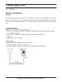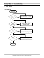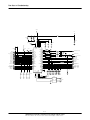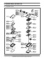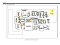
1
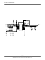
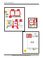
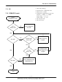
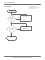
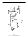
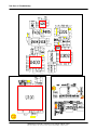
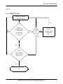
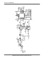
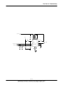
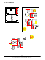
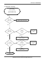
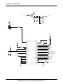
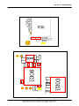
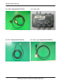
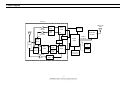
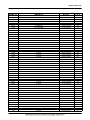
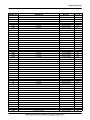
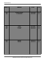
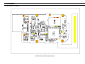
CDMA TELEPHONE
SPH-A940
CONTENTS
CDMA TELEPHONE
1.
General Introduction
2.
Circuit Description
3.
Installation
4.
NAM Programming
5.
Product Support Tools
6.
Test Procedure
7.
Flow Chart of Troubleshooting
8.
Exploded Views and Parts List
9.
Block Diagram
10.
Electrical Parts List
11.
PCB Diagrams
ⓒ Samsung Electronics Co.,Ltd. November. 2005
Printed in Korea.
This Service Manual is a property of Samsung Electronics Co.,Ltd.
Any unauthorized use of Manual can be punished under applicable
International and/or domestic law.
Code No.: GH68-08774A
BASIC.
1. General Introduction
1-1. General Instruction
The SPH-A940 enables mobile users to communicate 3G CDMA2000 1X service into a single handset.
For CDMA/PCS mode, The SPH-A940 supports Release A of the CDMA2000 1X standard.
The SPH-A940 is the first 2 mega pixel camera phone with 2x optical zoom and auto focus of Samsung
for North America that works on North American CDMA networks.
This stylish clamshell phone supports dual color displays, Bluetooth, MMS, voice dialing, airplane mode
and EV-DO services.
1-1
SAMSUNG Proprietary-Contents may change without notice
This Document can not be used without Samsung's authorization
General Introduction
1-2
SAMSUNG Proprietary-Contents may change without notice
This Document can not be used without Samsung's authorization
2. Circuit Description
2-1. Logic Section
2-1-1. Power Supply
Press "END" key to turn on the phone and then the VBATT and ON_SW signals will be connected. This
turns on the inner regulators(V_MSMCORE, V_MSMC, VPD, VPA) of U203(MAX1526).
The VBATT applied to ON_SW will change ON_SW_SENSE signal from HIGH to LOW.
MSM6500(U101) sends out PS_HOLD(logical HIGH) to keep the inner regulators on even after the "END"
key is released.
V_RFRX can be turned on/off by the RX_CTRL signal. V_TCXO can be turned on/off
by the TCXO_CTRL signal. The other regulators(2.85VDD, V_SYNTH, V_RFTX, V_MOTOR, V_LED) will
be in the ON/OFF state by I2C-compatible 2 wire serial interface.
The regulated Voltage(U203, V_MSMCORE) are used in the core of MSM.
The regulated Voltage(U203, V_MSMC) are used in the digital part of MSM.
The regulated Voltage(U203, VPD) are used in the digital part MSM.
The regulated Voltage(U203, VPA) is used in the analog part of MSM.
The regulated Voltage(U203, V_RFTX) is used in the Tx RF part.
The regulated Voltage(U203, V_RFRX) is used in the Rx RF part.
The regulated Voltage(U203, V_TCXO) is used in the TCXO.
The regulated Voltage(U203, V_SYNTH) is used in the PLL part.
The regulated Voltage(U203, 2.85VDD) is used in the Camera Display part and the T-Flash.
The regulated Voltage(U203, V_MOTOR) is used in the MOTOR.
The regulated Voltage(U203, V_LED) is used in the KEYPAD LED.
2-1-2. Inner Charging Circuit Part
The most important function of the charger shall be done in the PMIC(Power Management Circuit U203).
When the phone with a battery is connected with a travel charging adapter, the inner charging circuit of
the PMIC(U203) will charge the battery by constant fast charge mode.
When battery reaches regulation voltage of 4.2V (default charging voltage for Li+mode), the charge
current drops quickly to 0mA
-
Input voltage range : 4.25∼6.5V
- Charging Temperature : 0°C∼40°C
- Charging Method : Constant Voltage/Current -Charging Current : Normal 550mA
- Charging Time : Standard (1100mAh) 2.5 ~ 3 Hrs , Extended (1700mAh) 3.5 ~ 4 Hrs
- Charging Mode : ① Charging ② Completion
2-1
SAMSUNG Proprietary-Contents may change without notice
This Document can not be used without Samsung's authorization
Circuit Description
- Charging Battery Regulation Voltage
① Min 4.158V, Typical 4.2V, Max 4.242V(at TA : 0°C to +85°C)
② Min 4.137V, Typical 4.2V, Max 4.263V(at TA : -40°C to +85°C)
Universal Serial Bus Interface
SPH-A940 supports a Universal Serial Bus(USB) interface by the MSM6500, to provide an efficient
interconnection between the mobile phone and a Personal Computer(PC).
The MSM6500's USB interface is designed to comply with the Universal Serial Bus Specification,
Revision 2.0. An external USB transceiver(U203) is required to implement the USB interface.
2-1-3. Logic Part
The logic part consists of MSM, MEMORY, LCD, CAMERA, CCP, external MEMORY and other input and
output peripherals.
MOBILE SYSTEM MODEM(U101:MSM6500)
Industry standard ARM926EJ-S microprocessor is embedded. The MSM6500 chipset integrates
CDMA2000 1x and 1xEVDO service. The 1xEVDO solution can support High-speed peak data rates of
2.4Mbps on forward link and 153kbps on reverse link.
The MSM6500 device is offered in a 409 ball, 0.5mm pitch, CSP production package. Subsystems within
the MSM6500 device include a CDMA processor, a QDSP for voice compression, an ARM9TDMI
microprocessor. Also integrated in the MSM6500 device are analog functions such as an audio voice
codec, PLL, transmit DACS, ADCS, memories, USB controller, peripheral interfaces, and an enhanced
clock. It is one of the most important components of the CDMA cellular phone.
The interface circuitry consists of reset circuit, dual address/data bus and memory controls. The TCXO
clock of 19.2Mhz is used as the main clock of SPH-A940 model.
MCP : NAND FLASH and SDRAM (U102(KBE00F003M))
MCP is consist of two 512Mbit(64M*8) NAND FLASH and two 256Mbit(4M*16*4Banks) Mobile SDRAM.
NAND FLASH is used to store the Font data and program. EFS area is used to store ESN, NAM
information, telephone directory, SMS messages and other important information of the phone, and also
to store application programs and downloaded stuffs such as BREW applications and MP3. MCP is also
used to excute the DMSS(Dual Mode Subscriber system) software.
Using the down-loading program, the program can be changed even after the terminal is fully assembled.
2-2
SAMSUNG Proprietary-Contents may change without notice
This Document can not be used without Samsung's authorization
Circuit Description
Keypad
For key recognition, key matrix is operated by using SCAN(0:7) and KEYSENCE(0:3) of the input ports
of MSM. 23 backlight LEDs and back-light circuitry are included in the keypad for easy operation in the
dark.
LCD Module
LCD is composed of a Transmissive with Micro Reflective(TMR) type Main TFT-LCD Panel,
Transflective
type Sub TFT-LCD Panel, a driver circuit and a back-light unit.
The resolution of a 2.0" Main LCD(TMR) contains 176 * 220 pixels, the resolution of a 1.17" Sub
LCD(Transflective) contains 96 * 96 pixels.
Clock
CPU clock
: 19.2MHz. Clock signal from the TCXO
Sleep clock : 32.768KHz. Clock signal for sleep.
TCXO/N
: 19.2/N MHz. This clock source is used by various blocks of the MSM6500 device, such
as the ARM9CORE, UARTs, general-purpose PDMs and TCXO is also used by the
MSM6500 device to produce CHIPX8.
USB clock
: 48MHz. Clock signal for the USB interface
CAMERA
The camera module consists of 1/3 type 2 Mega (2140K) Pixels CCD sensor, Digital signal processor,
and MPU. The camera module provides Auto Focus, 2x Optical Zoom, Auto Exposure, and Auto WhiteBalance functionality.
CCP (Camera Control Processor)
CCP can support sensors up to 2M pixels. CCP directly transmits and previews the RGB data to the
LCD graphic memory by processing the sensor output data according to the MSM's command and
provides hardware based real-time JPEG compression and decompression.
CCP can save the raw RGB
data up to SVGA resolution into its image buffer and allows the host processor to download with
scalable sized compressed data. In addition, CCP can download the compressed image to either store
the original RGB data or transfer the image to the LCD.
2-3
SAMSUNG Proprietary-Contents may change without notice
This Document can not be used without Samsung's authorization
Circuit Description
Bluetooth module
Bluetooth module is a BluetoothTM 1.1 and 1.2 compliant, stand-alone baseband processor with an
integrated 2.4GHz transceiver. Bluetooth module supports any voice and/or data application that requires
the Bluetooth SIG standard Host Controller Interface (HCI) via UART and PCM audio interfaces.
Operation Clock: 19.2MHz
Low-Power Clock: 32.768KHz
2-1-4. RF Interface Part
CDMA Data Interface
- TX_Q_P, TX_Q_N, TX_I_P, TX_I_N (U400) : Tx analog signal used during CDMA
- RX_I_P, RX_Q_P, RX_I_N, RX_Q_N (U302) : RX analog signal used during CDMA
RF Interface
- TX : TX_AGC_ADJ(U101) is used to control the TX power,
PA_ON_PCS(U101) is used to control the PCS power amplifier and
PA_ON_CELL(U101) is used to control the CDMA power amplifier.
- RX : TRK_LO_ADJ(U101) is used to compensate the TCXO module.
2-1-5. Audio Part
The MSM6500 device integrates a stereo wideband voice/audio CODEC into the Mobile Station Modem.
The integrated CODEC contains all of the required conversion and amplification stages for the
audio front end.
The CODEC operates as a 13bit linear CODEC with the transmit(TX) and receive(RX) filters designed
to meet ITU-T G.712 requirements. The CODEC contains the software controlled amplifier for both the
receiving and transmitting sections. Also, the vocoding schemes used will be 13kbps QCELP and 8Kbps
EVRC. The QCELP vocoder is based in the MSM internally.
2-1-6. Tx Audio Path
The voice signal from the microphone is filtered and amplified by the internal OP-AMP and is converted
to PCM data by the internal CODEC in the MSM. And then these signals are applied to the the
MSM(U101)'s internal vocoder.
2-4
SAMSUNG Proprietary-Contents may change without notice
This Document can not be used without Samsung's authorization
Circuit Description
2-1-7. Rx Audio Path
The PCM data from the MSM(U101) is inputted to the internal CODEC and the data will be decoded by
the internal DAC. Audio levels are adjusted by the amplifier. And then audio is sent to the receiver.
2-1-8. Speaker Path
When the MSM(U101) receives the data, its internal CMX generates bell and melody. The CMX bell and
melody generated in MSM6500 are sent to SAPA1D2.
The SAPA1D2 (stereo class - D audio power amplifier) is a high quality audio power conversion chip
generating 2.5W RMS output directly from the VBATT supply. It is a high efficiency audio amplifier for
mobile applications. The gain of amplifier in SPH-A940 set to 4(V/V) . The output generated in SAPA1D2
is intended to drive two speakers.
2-1-9. Key Tone Generator
The CODEC data out from the MSM6500 is converted to DTMF signal by TONE generator of internal
CODEC, which is then amplified by the internal audio amplifier to be sent to the receiver unit.
2-2. PCS Section
2-2-1. Receiver
LOW NOISE AMPLIFIER (U301)
The low noise amplifier(It is included in FC7510 : U301) amplifies a weak signal received from the base
station to obtain the optimum signal level.
RF BAND PASS FILTER (F302)
The RF BPF(F302) passes only a specific frequency(1960±30 MHz) from the signal received from the
mobile station. The bandwidth is 60 MHz.
VOLTAGE CONTROLLED OSCILLATOR(OSC301)
The VCO(OSC301) generates the signal having 1715 ~ 1788MHz frequency range.
The VCO's output frequency is changed by control voltage. The PLL in S1M8690X generates this control
signal and this signal is changed into DC control voltage by R-C Loop filter.
2-5
SAMSUNG Proprietary-Contents may change without notice
This Document can not be used without Samsung's authorization
Circuit Description
Frequency Synthesizer Circuit
The PLL(Phased Locked Loop) block consists of VC-TCXO(OSC302), PLL in S1M8690X and
VCO(OSC301). Input reference frequency is generated at VC-TCXO(OSC302) and the RF local signal is
generated at VCO. PLL compares the two signals and generates the desired signal with a
preprogrammed counter which controls voltage.
VOLTAGE CONTROLLED TEMPERATURE COMPENSATED CRYSTAL OSCILLATOR (OSC302)
The VC-TCXO (OSC302) is a reference source of the frequency synthesizer. It provides 19.2MHz
reference frequency to PLL-IC. It is a voltage controlled temperature compensated crystal
oscillator having 19.2MHz ±2.5ppm frequency stability over all useful temperature range.
A correct frequency tuning is made by the control voltage.
2-2-2. Transmitter
Intenna
Intenna sends signal to the base station and receives the signal from the base station.
It is a tri-band Intenna and covers PCS band, CDMA band and GPS band.
RF Switch
It(U405) is used to switch the PCS path, the CDMA path and the GPS path, The RF signal passes
through PCS & CDMA path when GPS_MODE is low.
GPS_MODE is a digital signal from MSM6500 GPIO.
Duplexer
Duplexer(F402) allows to transmit only the signals within acceptable Tx frequency range
(1880 ± 30 MHz) through the Intenna.
It provides the appropriate attenuation of transmitted signal at the receiver input and the appropriate
rejection of the transmit-generated noise in the Receiver band.
Power Amp
Power amplifier module(U404:ACPM-7833-DC1) amplifiers signal to be sent to the base station
through the antenna.
2-6
SAMSUNG Proprietary-Contents may change without notice
This Document can not be used without Samsung's authorization
Circuit Description
Driver Amp
The driver amp(U400 ; included in S1M8690X) allows the signal to be inputted to the power amp(U404)
as a specified level.
Up-converter(Mixer)
The up-converter(U402 ; also included in S1M8690X) receives the local signal FTx * 0.7999
and signal controlled by TX AGC amp(in S1M8690X) to generate Tx RF signal 1880±30MHz
which signal comes out from the mixer output by adding FTx * 0.7999 local signal.
FTx means TX RF signal Frequency.
Automatic Gain Control Amp
The TX IF AGC amp (in S1M8690X) controls gain of AGC to deliver power level needed at
driver amp. Its control voltage varies from 0.2V to 2.5V.
2-3. CDMA Section
2-3-1. Receiver
Low Noise Amplifier(LNA)
The low noise amplifier(It is included FC7510 : U301) amplifies a weak signal received from
the base station to obtain the optimum signal level.
RF Band Pass Filter(Rx RF SAW Filter)
The RF BPF in F301 passes only a specific frequency(881.49±12.5 MHz) from the signal
received from the mobile station. The bandwidth is 25 MHz.
Voltage Controlled Oscillator
The VCO(OSC301) generates the signal having 1715 ~ 1788MHz frequency range.
The VCO's output frequency is changed by control voltage. The PLL in S1M8690X generates this control
signal and this signal is changed into DC control voltage by R-C Loop filter.
2-7
SAMSUNG Proprietary-Contents may change without notice
This Document can not be used without Samsung's authorization
Circuit Description
Frequency Synthesizer Circuit
The PLL(Phased Locked Loop) block consists of VC-TCXO(OSC302), PLL in S1M8690X and
VCO(OSC301). Input reference frequency is generated at VC-TCXO(OSC302) and the RF
local signal is generated at VCO. PLL compares the two signals and generates the desired
signal with a preprogrammed counter which controls voltage.
VC-TCXO
The VC-TCXO (OSC302) is a reference source of the frequency synthesizer. It provides 19.2MHz
reference frequency to PLL-IC. It is a voltage controlled temperature compensated crystal
oscillator having 19.2MHz ±2.5ppm frequency stability over all useful temperature range.
A correct frequency tuning is made by the control voltage.
2-3-2. Transmitter
Intenna
Intenna sends signal to the base station and receives the signal from the base station.
It is a tri-band Intenna and covers PCS band, CDMA band and GPS band.
RF Switch
It(U405) is used to switch the PCS path, the CDMA path and the GPS path, The RF signal
passes through PCS & CDMA path when GPS_MODE is low.
GPS_MODE is a digital signal from MSM6500 GPIO.
Duplexer
Duplexer(F405) passes the RF signal of Rx frequency range(881.49 ±12.5 MHz) and Tx frequency range
(836.49 ±12.5 MHz). It provides appropriate attenuation of transmitted signal at the receiver input and
appropriate rejection of the transmit-generated noise in the Receiver band.
It also matches LNA input in receiving part and PAM(U403:ACPM-7813) output in transmitting part with
the Intenna.
2-8
SAMSUNG Proprietary-Contents may change without notice
This Document can not be used without Samsung's authorization
Circuit Description
Power Amp
Power amplifier module(U403:ACPM-7813-DC1) amplifiers signal to be sent to the base station
through the antenna.
RF Band Pass Filter(Tx RF SAW Filter)
The RF BPF(F404) passes only specific frequency(836.49 ±12.5MHz) to send it to power
amp(U403:ACPM-7813-DC1).
Driver Amp
The driver amp(U402 ; It is included in S1M8690X) allows the signal to be inputted to the
power amp(U403) as a specified level.
Up-Converter(Mixer)
The up-converter(U402 ; It is also included in S1M8690X) receives the local signal FTx * 1.6666
and the signal controlled by TX AGC amp(in S1M8690X) to generate Tx RF signal
836.49±12.5MHz signal comes out from the mixer output by adding FTx * 1.6666 local signal.
FTx means TX RF signal Frequency.
Automatic Gain Control Amp
The TX IF AGC amp in S1M8690X controls gain of AGC to deliver power level to be needed
at Driver amp. Its control voltage varies from 0.2V to 2.5V.
2-9
SAMSUNG Proprietary-Contents may change without notice
This Document can not be used without Samsung's authorization
Circuit Description
2-4. GPS Section
Intenna
Intenna receives a signal from GPS satellites.
It is a tri-band Intenna and covers PCS band, CDMA band and GPS band.
RF Switch
It(U405:TQP4M3018) is used to switch the PCS path and CDMA path and the GPS
path.
The RF signal passes through PCS path when PCS_MODE is high(2.6V). The RF signal
passes through CDMA path when CELL_MODE is high(2.6V).
The RF signal passes through
GPS path when GPS_MODE is high(2.6V). PCS_MODE, CELL_MODE and GPS_MODE are
digital signals from MSM6500 GPIO.
Low Noise Amplifier(LNA)
The low noise amplifier(Q302:ATF55143) amplifies a weak signal received from the base station to
obtain the optimum signal level.
RF Band Pass Filter(Rx RF SAW Filter)
The RF BPF(F303:DG75BS1)
passes only a specific frequency(1575.42±1MHz) from the signal received
from the satellite. The bandwidth is 2 MHz.
2-10
SAMSUNG Proprietary-Contents may change without notice
This Document can not be used without Samsung's authorization
3. Installation
3-1 Installing and Removing the Battery
To remove, make sure the power is off. Push the
To install, insert the battery into the opening on
the back of the phone making sure the plastic tabs battery release latch up completely. Pull and lift the
on the back are inserted into the matching slots in battery away from the phone.
the phone. Press down until the latchsnaps into
place.
3-2 Using the Desktop Charger
◇ A red light on the charger lets you know the
1. Plug the AC cord from the charger into the
electrical outlet.
battery is charging.
◇ A green light lets you know that the battery is
2. Insert the phone into the slot.
at least 90 percent charged.
◇ A orange light indicates that the battery is
operating at a temperature that is too high or
low, or that the charger is not plugged in
correctly. Please check the charger and the
battery.
Specifications using DTC (Desktop Charger)
Standard Battery
Extended Battery
(Li-ion, 1000mAh)
(Li-ion, 1700mAh)
Charging
< 5 hours
< 5 hours
SEC Code
GH43-02160A
GH43-02161A
Battery Type
3-1
SAMSUNG Proprietary-Contents may change without notice
This Document can not be used without Samsung's authorization
Installation
3-2
SAMSUNG Proprietary-Contents may change without notice
This Document can not be used without Samsung's authorization
4. NAM Programming
NAM features can be programmed as follows:
Notes:
For example, press 'menu' and cursor to 'settings & tools' and '*' , then press ' 000000' (000000:
SPC code), you can see
'Service' Mode.
NAM SETTING FLOW:
LCD Display
Key in
Function
Service Mode
1. ESN
***
********(Decimal number)
Enter (↓)
-Electronic Serial Number of the phone is
displayed
number
Enter
AKEY Setup.
- To input AKEY, enter AKEY #.
- Stores it
Enter (OK), and
then enter the
number
The phone number screen enables you to
edit the phone number
********(Hexa Number)
2. AKEY
AKEY
3. Network Setting
-1 Phone Number
Phone Number(MDN)
0000006034
3. Network Setting
-2 MCC
Enter the number
MCC
310
The MCC screen allows you to view and
modify the mobile country code.
3. Network Setting
-3 NMSID
NMSID(NATIONAL
MOBILE STATION ID)
000000006034
Enter the number
3. Network Setting
-4 True IMSI MCC
Enter the number
True IMSI MCC
000
IMSI_S screen allows you to view and
modify the international mobile station
identity
3. Network Setting
-5 True IMSI NMSID
Enter the number
True IMSI NMSID
000000006034
4-1
SAMSUNG Proprietary-Contents may change without notice
This Document can not be used without Samsung's authorization
NAM Programming
3. Network Setting
-6 PRL Enabled
The PRL screen shows if the preferred
roaming list (PRL) is enabled.
PRL Enabled
Yes
No
3. Network Setting
-7 Home SID/NID
This screen allows you to view and modify
Enter the number
Enter SID
2004
Enter NID
65535
network ID
(NID) settings.
3. Network Setting
-8 CDMA Pri Chn A
Enter the number
CDMA Pri Chn A
283
3. Network Setting
-9 CDMA Sec Chn A
Enter the number
CDMA Sec Chn A
691
3. Network Setting
10 CDMA Pri Chn B
Enter the number
CDMA Pri Chn B
384
3. Network Setting
-11 CDMA Sec ChnB
Enter the number
CDMA Sec Chn B
777
the various home system ID (SID) and
The primary channel A screen allows you to
view and modify primary channel A.
The secondary channel A screen allows you
to view and modify secondary channel A.
The primary channel B screen allows you to
view and modify primary channel B
The secondary channel B screen allows you
to view and modify secondary channel B.
3. Network Setting
12 Home Sys Reg
Home Sys Reg
Yes
No
Home SID Reg – home system ID
3. Network Setting
-13 Forgn SID Reg
Forgn SID Reg
Yes
No
Foreign SID Reg – foreign system ID
4-2
SAMSUNG Proprietary-Contents may change without notice
This Document can not be used without Samsung's authorization
NAM Programming
3. Network Setting
-14 Forgn NID Reg
Foreign NID Reg – foreign network ID
Forgn NID Reg
Yes
No
3. Network Setting
-15 Access Overload
Class
Enter the number
The overload class screen allows you to view
and modify the overload class.
Access Overload Class
4
3. Network Setting
-16 Origination Voice
Orgination Voice SO
EVRC
13k
4. SMS Settngs
SMS UTC time
Yes
No
Selecting the SMS settings option allows you
to view and edit the short message services
(SMS).
This option allows you to view and modify
5. Slot Cycle Index
Slot Cycle Index
1
Enter the number
6. Service Programming
Code
Service Programming
Code
000000
Enter the number
the slot cycle index. To modify the index,
select Edit
4-3
SAMSUNG Proprietary-Contents may change without notice
This Document can not be used without Samsung's authorization
NAM Programming
4-4
SAMSUNG Proprietary-Contents may change without notice
This Document can not be used without Samsung's authorization
5. Product Support Tools
5-1. General
IMPORTANT INFORMATION
Purpose
The Product Support Tool (PST) offers you the ability to interface with the SAMSUNG mobile phone
using a PC. With this tool you can program the phones network system requirements and functionality,
data, and download software upgrades. This document supports SamsungPST(Samsung Product Support
Tool).
EQUIPMENT REQUIRED
Make sure you have the following equipment setup:
1. Minimum PC configuration: 586 CPU, 64MB RAM, Windows2000/XP and abolve, 5MB of disk space
free for software upgrade.
2. PST Software with appropriate cable (USB Cable for SAMSUNG mobile phone).
3. USB Port.
4. Power Supply (3.8 V) or Battery.
INSTALLATION
1. Insert the SPH-A940 CDROM into your CD-Rom drive.
2. Run the file explorer and run the Setup.exe file.
3. After SamsungPST is installed on a computer, connect the phone, cable, and PC .
5-1
SAMSUNG Proprietary-Contents may change without notice
This Document can not be used without Samsung's authorization
Product Support Tools
5-2. PST (Product Support Tool)
5-2-1 Getting Started
MAIN MENU SCREEN
1. Double Click on your "Samsung PST for Verizon (SE)"
2. Select SPH-A940
The Main Menu Screen shows the basic tasks that are available.
CAUTION: DO NOT attempt to program phone with a low battery.
5-2-2 Operation Procedure
Information
Click "Read general Information" icon.
Software Download
If the phone works normally, you must proceed below procedures.
Normal Download.
1. Connect PC and SPH-A940 with usb cable
2. Check com port of SAMSUNG CDMA Modem. To check on Com port, first you go to my
computer->property->Hardware->Device Manager ->Modem->Samsung USB Modem. Then go to property
of Samsung USB Modem, and then click on Modem tab. You may see the port number, which is
assigned for Samsung USB Modem.
3. Run Samsung PST.
4. Change PST's comport setting ( Setup
COM Setting ) same as com port of 'SAMSUNG cdma
modem'
5. Select SPH-A940 and then click SW(Software Download) tab.
6. Select 'Normal' in software download option.
7. Click 'openfile' icon and select the bin file.
8. Click 'Start Software Download' icon.
10. When the downloading process is finished, the A970 power on automatically and the PST shows
"Downloading completed!!".
If the phone doesn't works normally, you must proceed below procedures.
Emergency Download.
1. SPH-A940 enters the emergency mode(press simultaneously '9' and 'PWR')
2. Connect PC and SPH-A940 with usb cable
3. Check com port of SAMSUNG CDMA Modem. To check on Com port, first you go to my
computer->property->Hardware->Device Manager ->Modem->Samsung USB Modem. Then go to property
of Samsung USB Modem, and then click on Modem tab. You may see the port number, which is
assigned for Samsung USB Modem.
5-2
SAMSUNG Proprietary-Contents may change without notice
This Document can not be used without Samsung's authorization
Product Support Tools
4. Run Samsung PST.
5. Change PST's comport setting ( Setup COM Setting ) same as com port of 'SAMSUNG cdma
modem'
6. Select SPH-A940 and then click SW(Software Download) tab.
7. Select 'Emergency" in software download option.
8. Click 'openfile' icon and select the bin file.
9. Click 'Start Software Download' icon.
10. When the downloading process is finished, the A970 power on automatically and the PST shows
"Downloading completed!!".
PRL Download
1.Click "Open PRL1 file" icon and select the PRL file.
2.Click "Start PRL Download" icon.
3. When the downloading process is finished, the A970 will reboot automatically and the PST shows
"Completed PRL Programming"
ERI Download
1.Click "Open ERI1 file" icon and select the PRL file.
2.Click "Start ERI Download" icon.
3. When the downloading process is finished, the A970 will reboot automatically and the PST shows
"Completed ERI Programming"
Setting
Read Data from File
Click "Open mmc" icon to select the name of a file whose extension is "mmc". The values will be read
from the named file, and will initialize the parameter values seen on the Settings screen
Read Data from Phone
Click Read from the Phone icon to upload the current programmable parameters of the phone. The
values are read from the phone, so the phone must have the power ON and be properly connected
to the PST.
NOTE: To actually view the data you need to go to the Edit Items screens.
Edit Items
Click this icon to edit Number Assignment Module (NAM) items or UI items.
1. GeneralNAM : Slot Cycle Index, Service Code
2. NAM1
5-3
SAMSUNG Proprietary-Contents may change without notice
This Document can not be used without Samsung's authorization
Product Support Tools
Save Data to File
Click this icon to save the current parameters to a file. Once you enter a filename, Click <OK> button to
write all current parameters to that file. This way the same information can be downloaded into multiple
phones.
Write to Phone
Click this icon to write the selected parameter values to the phone. Writing the selected values to the
phone may take up to a minute. If there are dependencies in a field you can make all the changes in
the proper fields and download the information all together.
If you intend to use this write to Phone? feature, it is recommended that you do a "Read Data from
Phone" first, and then make the changes, so that nothing gets inadvertently overwritten.
NOTE: DO NOT TOUCH THE PHONE WHILE WRITING IS IN PROGRESS.
Transfer
Backup Items
1. Select Item to backup in 'Item option' list.
2. Select 'backup' in 'Backup or Restore' list.
3. Click "Start Backup of Restore" icon.
5-4
SAMSUNG Proprietary-Contents may change without notice
This Document can not be used without Samsung's authorization
6. Test Procedure
6-1 List of Equipment
● DC Power Supply
● Test Jig
● Test Cable
● CDMA Mobile Station Test Set HP8285A, HP8960, CMD-80, etc
● Spectrum Analyzer(include CDMA Test Mode) HP8596E,
6-2 Configuration of Test
6-1
SAMSUNG Proprietary-Contents may change without notice
This Document can not be used without Samsung's authorization
Test Procedure
6-3 TEST CABLE CONNECTIONS
6-3-1 TEST CABLE
6-3-2 TEST CABLE CONNECTIONS
1
MHC 172
2
RF CABLE (1.4dB Loss for CDMA, 2.1dB Loss for PCS, 1.8dB Loss for GPS)
3
BNC CONNECTOR (RF)
4
DATA CABLE
5
Plug Connect to SPH-A940
6
Dsub 25PIN CONNECTOR (DATA)
6-2
SAMSUNG Proprietary-Contents may change without notice
This Document can not be used without Samsung's authorization
Test Procedure
6-3-3 Dsub 25 PIN CONNECTOR PIN DESCRIPTION (TEST CABLE 1, BACK SIDE)
DATA DESCRIPTION
Dsub CONN.
PIN NO.
DATA DESCRIPTION
Dsub CONN.
PIN NO.
GND
13
GND
24,25 (SHORT)
VBATT
4
VBATT
5,6 (SHORT)
HP_PWR
7
DP_RX_DATA
21
RX_AUDIO
12
DP_TX_DATA
22
TX_AUDIO
10
6-3
SAMSUNG Proprietary-Contents may change without notice
This Document can not be used without Samsung's authorization
Test Procedure
6-3-4 CONVERSION TABLE OF FREQUENCY vs CHANNEL
- CDMA/PCS
T Y P E
CHANNEL
CONVERSION EQUATION
TX
FREQUENCY
990 ≤N≤1023
1 ≤N≤779
F=0.03 × (N-1023) + 825.00
F=0.03 × N + 825.00
RX
FREQUENCY
990 ≤N≤1023
1 ≤N≤779
F=0.03 × (N-1023) + 875.00
F=0.03 × N + 875.00
TX
FREQUENCY
0 ≤N≤ 1199
RX
FREQUENCY
0 ≤N≤ 1199
F=0.05 × N + 1850.00
REMARK
N ; CH NUMBER
F ; FREQUENCY
(CDMA)
N ; CH NUMBER
F ; FREQUENCY
F=0.05 × N + 1930.00
(PCS)
6-4
SAMSUNG Proprietary-Contents may change without notice
This Document can not be used without Samsung's authorization
Test Procedure
6-4 Test Procedure
6-4-1 CDMA/PCS mode
- Change the test mode
A. To change the phone's state from Normal Mode to Test Mode, You should enter the following keys.
: Press [ 4 7 * 6 8 # 1 3 5 8 0 ]
B. The command "0 0 1" is Suspend.
C. The command "0 2 2" is mode and channel change.
"2 0 3 6 3"
Channel number
Mode:CDMA
"3 0 6 0 0"
Channel number
Mode:PCS
and press enter key from the soft key board to save mode/channel value..
D. The command "0 0 1" is Suspend.
E. To finish the Test Mode, You should enter the command "0 0 2".
6-4-2 Channel selection and Tx power output level control
CDMA
A. Enter to Test Mode [ 4 7 * 6 8 # 1 3 5 8 0 ]
B. "0 0 1" : Suspend.
C. The command "0 2 2" is mode and channel change
"2 0 3 6 3"
Channel number
Mode:CDMA
Push the [OK] key to save.
6-5
SAMSUNG Proprietary-Contents may change without notice
This Document can not be used without Samsung's authorization
Test Procedure
D. To finish the Test Mode, You should enter the command "0 0 2".
E. Enter to Test Mode [ 4 7 * 6 8 # 1 3 5 8 0 ]
F. "0 0 1" : Suspend.
G. "0 1 1" : Carrier_On.
H. "0 1 4" : CDATA.
I. "0 9 2" : PA_RANGE_1.
J. "0 1 9" : Adjust RF power level.
PCS
A. Enter to Test Mode [ 4 7 * 6 8 # 1 3 5 8 0 ]
B. "0 0 1" : Suspend.
C. The command "022" is mode and channel change
"3 0 6 0 0"
Channel number
Mode:PCS
Push the [enter] key to save.
D. To finish the Test Mode, You should enter the command "0 0 2".
E. Enter to Test Mode [ 4 7 * 6 8 # 1 3 5 8 0 ]
F. "0 0 1" : Suspend.
G. "0 1 1" : Carrier_On.
H. "0 1 4" : CDATA.
I. "0 9 2" : PA_RANGE_1.
J. "0 1 9" : Adjust RF power level.
6-6
SAMSUNG Proprietary-Contents may change without notice
This Document can not be used without Samsung's authorization
Test Procedure
- CDMA Test items
TEST ITEMS
1. PREPARANCE
PROCEDURE
Set test equipments up.
[ 4 7 * 6 8 # 1 3 5 8 0 ] : Enter the Test Mode
"0 0 1" : Suspend
Confirm that the phone is in the "CDMA Mode".
(If not CDMA Mode, Use Test Command "022""2XXXX" and Push
the "
" Key to "OK", and enter "0 0 2" to restart)
If you select a wrong key, press " # ", then enter new command.
To exit the Test Mode at any time, just press [0 0 2].
2. FREQUENCY
ACCURACY
3. OCCUPIED CDMA
BANDWIDTH
4. LIMITATIONS ON
EMISSIONS
5. GATED POWER &
TIME
"0 0 1" : Suspend.
"0 1 3 0 3 6 3 * " : Set channel to 363.
"0 1 1" : Carrier On.
"0 1 4" : Spread spectrum.
"0 1 9 X X X ' END[Push and Hold] ' " : Set AGC Code(XXX) level.
Measure the TX frequency : 835.89MHz±300Hz.
"0
"0
"0
"0
"0
0
1
1
1
1
1" : Suspend.
3 0 3 6 3 * " : Set channel to 363.
1" : Carrier On.
4" : Spread spectrum.
9 X X X ' END[Push and Hold] ' " : Enter AGC Code(XXX) to adjust
RF Output Power.
Measure the bandwidth (spec: 1.23MHz).
"0
"0
"0
"0
"0
"0
0
1
1
1
9
1
1" : Suspend.
3 0 3 6 3 * " : Set channel to 363.
1" : Carrier On.
4" : Spread spectrum.
2" : PA_RANGE_1.
9 X X X ' END[Push and Hold] ' " : Enter AGC Code(XXX) to adjust
RF Output Power.
Measure the spurious at FC±900kHz, FC±1.98MHz, 2FC, 3FC, 1/2FC.
spec: FC±900kHz below 42dBc/30kHz
FC±1.98MHz below 54dBc/30kHz
Outside Receive Band 43+10log (PY)
PY: Mean Output Power in watts
Set the service option 2.
Set the data rate Eighth (1200bps).
Registering: HHP → HP8924C.
Call
: HP8924C → HHP.
Measure the Gated Power & Time.
spec : Gated Power - at least 20dB
Gated Time - Rising Time : below 6㎲
Falling Time : below 6㎲
Burst Time : below 1.25㎳
6-7
SAMSUNG Proprietary-Contents may change without notice
This Document can not be used without Samsung's authorization
Test Procedure
- PCS Test items
TEST ITEMS
1. PREPARANCE
PROCEDURE
Set test equipments up.
[ 4 7 * 6 8 # 1 3 5 8 0 ] : Enter the Test Mode
"0 0 1" : Suspend
Confirm that the phone is in the "PCS Mode".
(If not PCS Mode, Use Test Command "022""3XXXX" and Push
the [OK] Key, and enter "0 0 2" to restart)
If you select a wrong key, press " # ", then enter new command.
To exit the Test Mode at any time, just press [0 0 2].
2. FREQUENCY
ACCURACY
3. OCCUPIED CDMA
BANDWIDTH
4. LIMITATIONS ON
EMISSIONS
"0 0 1" : Suspend.
"0 1 3 0 6 0 0 * " : Set channel to 600.
"0 1 1" : Carrier On.
"0 1 4" : Spread spectrum.
"0 1 9 X X X ' END[Push and Hold] ' " : Set AGC Code(XXX) level.
Measure the TX frequency : 1880.00MHz±300Hz.
"0
"0
"0
"0
"0
0 1" : Suspend.
1 3 0 6 0 0 * " : Set channel to 600.
1 1" : Carrier On.
1 4" : Spread spectrum.
1 9 X X X ' END[Push and Hold] ' " : Enter AGC Code(XXX) to adjust
RF Output Power.
Measure the bandwidth (spec: 1.23MHz).
"0
"0
"0
"0
0
1
1
1
1" : Suspend.
3 0 6 0 0 * " : Set channel to 600.
1" : Carrier On.
4" : Spread spectrum.
"0 9 2" : PA_RANGE_1.
"0 1 9 X X X ' END[Push and Hold] ' " : Enter AGC Code(XXX) to adjust
RF Output Power.
Measure the spurious at FC±1.25MHz
spec: FC±1.25MHz below 42dBc/30kHz
5. GATED POWER &
TIME
Set the service option 2.
Set the data rate Eighth (1200bps).
Registering: HHP → HP8924C.
Call
: HP8924C → HHP.
Measure the Gated Power & Time.
spec : Gated Power - at least 20dB
Gated Time
- Rising Time : below 6㎲
Falling Time : below 6㎲
Burst Time
: below 1.247㎳
6-8
SAMSUNG Proprietary-Contents may change without notice
This Document can not be used without Samsung's authorization
7. Flow Chart of TroubleShooting
7-1 Logic Section
7-1-1 Power On
Insert Power
power on
properly?
Check Phone power on section
NO
YES
U203
pin41=high?
Check CON203 and it's
neighboring circuits
NO
YES
Check
C219 =
2.7V?
NO
C220,C222,C223,C224,C225,C226
and U203's neighboring circuits
YES
C172
Check OSC302,U107 and it's
19.2MHz?
neighboring circuits
NO
YES
END
7-1
SAMSUNG Proprietary-Contents may change without notice
This Document can not be used without Samsung's authorization
Flow Chart of Troubleshooting
VBATT
S3.6
C202
C201
C203
C207
DC_VOLT
VPD
C208
BATT
REFBP
VL
2
_ONO
46
PWR_ON
26
HP_PWR
41
PWR_HOLD
11
INV1
12
COMP1
15
INV2
14
COMP2
C231
C232
R210
VPD (2.7V)
RESETIN_N
VPD (2.7V)
VPA (2.6V)
V_RFRX (2.85V)
RX_CTRL
2.85VDD
R215
1
OUT5
39
TCXO_EN
V_TCXO (2.85V)
TCXO_CTRL
47
OUT6
3
OUT7
5
OUT8
6
OUT9
V_SYNTH
V_RFTX
V_MOTOR
V_LED
49
GND
50
NC
51
NC
C228
C226
C227
C218
C225
23 24 19 18
C229
V_MSMC (1.8V)
R213
C224
44
C230
C217
C216
13
OUT3
43
RX_EN
7
OUT4
_OE
SUSPEND
RCV
VP
VM
GND
USB_OE_N
USB_SUSPEND
USB_DATA
USB_VPO
USB_VMO
L202
R212
C223
16
17
20
21
22
C215
48
_RESET
10
OUT1
8
OUT2
DD+
VTRM
VUSB
EAR_REF
EAR_DET
EAR_MIC
SEND_END
V_MSMCORE (1.375V)
C214
R209
29
LX2
28
PGND2
27
FB2
42
_HRESET
25
DATA
40
CLK
HRESET
SDA_PM
SCL_PM
L201
R208
C222
R211
C212
C220
VICHG
DC_SENS
45
31
LX1
32
PGND1
33
FB1
37
VICHG
38
_AC_OK
C219
C213
30 94
IN1
IN2
IN3
34
CHG_IN
R206
36
ON_SW_SENSE
ON_SW
HP_PWR
PS_HOLD
C276
U203
35
D201
C277
D202
V_BUS
VPULL
C240
U204
1
2
34
DXIN
DXOUT
GND
VBUS
DYIN
DYOUT
6
5
D+
VPULL
D-
7-2
SAMSUNG Proprietary-Contents may change without notice
This Document can not be used without Samsung's authorization
(2.85V)
(2.85V)
(3.1V)
(3.3V)
Flow Chart of Troubleshooting
7-3
SAMSUNG Proprietary-Contents may change without notice
This Document can not be used without Samsung's authorization
Flow Chart of Troubleshooting
7-4
SAMSUNG Proprietary-Contents may change without notice
This Document can not be used without Samsung's authorization
Flow Chart of Troubleshooting
7-1-2 LCD Working
Insert Power
Main LCD Back
Check pulse
-light On?
No
of V503's pin6
Check HEA501 and it's
neighboring circuits
No
Yes
Yes
Change LCD
Check HEA501,
LCD Display
OK?
No
F500, F501
Yes
Replace HEA501,
F502,F503,and
F500, F501 F502,F503 and
it's Short=?
it's neighboring circuits
Yes
No
Change LCD
END
7-5
SAMSUNG Proprietary-Contents may change without notice
This Document can not be used without Samsung's authorization
Flow Chart of Troubleshooting
D_L(0:7)
D_L(0)
D_L(1)
D_L(2)
D_L(3)
D_L(4)
D_L(5)
D_L(6)
D_L(7)
LED_B
SPK_R+
SPK_R-
HALL_SW_L
RCVRCV+
MAIN_LCD_CS
LCD_WR
LRS
12
3 4
8 7 6 5
F500
IN1 1
V500
*
IN2 2
OUT1
IN2 2
IN1 1
IN4 4
IN3 3
OUT1
OUT3
OUT2
6
8
GND
7
5
OUT4
GND
10
8
OUT2
IN3 3
9
F501
7
OUT3
IN4 4
6
GND
OUT4
GND
0
5
91
C515
C500
U516
C516
5 678
4 3 2 1
C511
V501
*
S3.6
HEA501
G G
51 52
1
1
3
3
5
5
78
7
9
9
11
13
15
17
19
21
23
25
27
29
31
33
35
37
39
41
43
45
47
49
11
13
15
17
19
21
23
25
27
29
31
33
35
37
39
41
43
45
47
49
2
4
6
8
10
12
14
16
18
20
22
24
26
28
30
32
34
36
38
40
42
44
46
48
50
2
4
6
10
12
14
16
18
20
22
24
26
28
30
32
34
36
38
40
42
44
46
48
50
C512
VPD (2.7V)
F503
V503
*
6
7
8
OUT4
GND
OUT3
OUT2
OUT1
IN2 2
IN1 1
IN2 2
IN1 1
F502
5
OUT1
IN3 3
IN4 4
IN4 4
IN3 3
8
OUT2
1 234
8 7 6 5
10
GND
0
7
OUT3
9
V504
*
GND
6
OUT4
GND
91
5
8 7 6 5
1234
C513
C514
D_L(8)
D_L(9)
D_L(10)
D_L(11)
D_L(12)
D_L(13)
D_L(14)
D_L(15)
D_L(8:15)
HALL_SW_R
RESOUT_N
LED_R
KEYSENSE1
KEYSENSE2
MAIN_LCD_BL
LED_G
SCAN5
SCAN6
SPK_L+
SPK_L-
7-6
This Document can not be used without Samsung's authorization
SAMSUNG Proprietary-Contents may change without notice
Flow Chart of Troubleshooting
7-7
SAMSUNG Proprietary-Contents may change without notice
This Document can not be used without Samsung's authorization
Flow Chart of Troubleshooting
7-1-3 Speaker, Receiver and Mic Checking
Insert Power
YES
Check HEA501
OK?
Check U205
pin45,46(Spk_R),
Speaker is
NO
pin47,48(Spk_L)
and Speaker
NO
signal OK?
YES
Check SPK1, SPK2 pin1,2 on
LCD signal OK?
YES
Check LCD
FPCB
NO
YES
Replace Speaker
Check HEA501
Receiver is
OK?
Check HEA501
pin 5, 7
NO
NO
signal OK?
and Receiver
YES
YES
Replace receiver
MIC is OK?
NO
Check CN201
Check mic path from
pin20, 22
CN201 to U101 and it's
signal on?
NO
neighboring circuits.
YES
YES
Check KEY FPCB
END
7-8
SAMSUNG Proprietary-Contents may change without notice
This Document can not be used without Samsung's authorization
Flow Chart of Troubleshooting
VPD (2.7V)
V_LED
VBATT
L203
CN201
HALL_FOLDER
ON_SW
SCAN7
SCAN0
V205
4
3
2
3
2
1
3
2
1
1
C239
C233
C234
4
5
5
4
5
24
11
13
15
17
19
21
23
KEYSENSE0
KEYSENSE1
KEYSENSE2
KEYSENSE3
C237
MICM_MIC
14
16
18
20
22
1
3
5
7
9
11
13
15
17
19
21
23
C238
16
18
20
22
24
1
3
5
7
9
C236
4 2
6 4
8 6
8
10
12 10
14 12
C235
2
SCAN6
SCAN5
SCAN4
SCAN3
SCAN2
SCAN1
V207
V206
7-9
SAMSUNG Proprietary-Contents may change without notice
This Document can not be used without Samsung's authorization
V208
Flow Chart of Troubleshooting
C246
C245
C247
C244
U205
R233
AUDIO_EN
HPH_L
R230
1
C248
24
C252
22
C273
R238
SPK_L+
23
18
16
3
SPK_L-
L207
7
L208
15
C268
C269
C271
C272
9
19
21
S3.6
EN_L
EN_R
VIPL
VIPR
VIML
VIMR
VREFL
VREFR
VOPL
VOPR
VOML
VOMR
VDD
VSS
VDD
VSS
VDD
VSS
VDD
VSS
VDD
VSS
VDD
VSS
GND
NC
NC
R240
13
12
C249
C274
11
6
L204
SPK_R+
SPK_R-
4
2
L205
5
8
C255
C256
14
17
20
25
26
27
C258
C257
C259
HPH_R
C250
10
C260
7-10
SAMSUNG Proprietary-Contents may change without notice
This Document can not be used without Samsung's authorization
C253
C254
Flow Chart of Troubleshooting
D_L(0:7)
D_L(0)
D_L(1)
D_L(2)
D_L(3)
D_L(4)
D_L(5)
D_L(6)
D_L(7)
LED_B
SPK_R+
SPK_R-
HALL_SW_L
RCVRCV+
MAIN_LCD_CS
LCD_WR
LRS
12
3 4
8 7 6 5
F500
IN1 1
V500
*
IN2 2
OUT1
IN2 2
IN1 1
IN4 4
IN3 3
OUT1
OUT3
OUT2
6
8
GND
7
5
OUT4
GND
10
8
OUT2
IN3 3
9
F501
7
OUT3
IN4 4
6
GND
OUT4
GND
0
5
91
C515
C500
U516
C516
5 678
4 3 2 1
C511
V501
*
S3.6
HEA501
G G
51 52
1
1
3
3
5
5
78
7
9
9
11
13
15
17
19
21
23
25
27
29
31
33
35
37
39
41
43
45
47
49
11
13
15
17
19
21
23
25
27
29
31
33
35
37
39
41
43
45
47
49
2
4
6
8
10
12
14
16
18
20
22
24
26
28
30
32
34
36
38
40
42
44
46
48
50
2
4
6
10
12
14
16
18
20
22
24
26
28
30
32
34
36
38
40
42
44
46
48
50
C512
VPD (2.7V)
F503
V503
*
6
7
8
OUT4
GND
OUT3
OUT2
OUT1
IN2 2
IN1 1
IN2 2
IN1 1
F502
5
OUT1
IN3 3
IN4 4
IN4 4
IN3 3
8
OUT2
1 234
8 7 6 5
10
GND
0
7
OUT3
9
V504
*
GND
6
OUT4
GND
91
5
8 7 6 5
1234
C513
C514
D_L(8)
D_L(9)
D_L(10)
D_L(11)
D_L(12)
D_L(13)
D_L(14)
D_L(15)
D_L(8:15)
HALL_SW_R
RESOUT_N
LED_R
KEYSENSE1
KEYSENSE2
MAIN_LCD_BL
LED_G
SCAN5
SCAN6
SPK_L+
SPK_L-
7-11
This Document can not be used without Samsung's authorization
SAMSUNG Proprietary-Contents may change without notice
Flow Chart of Troubleshooting
7-12
SAMSUNG Proprietary-Contents may change without notice
This Document can not be used without Samsung's authorization
Flow Chart of Troubleshooting
1. visual check! (soldering)
7-2. RX
2. S/W Mode Check : CDMA Mode Check
3. OSC302 Check : 19.2MHz
7-2-1 CDMA/PCS mode
4. VCO(OSC301) voltage/frequence level check
Frequence : 1715MHz < f < 1788MHz
START
CDMA/PCS mode
Supply Voltage:
2.75 ± 0.1V
Control Voltage:
0.4 ~ 2.3V
5. U301 LNA gain check
6. U403, U404 Check
SVC &
NO
Check CDMA/PCS
Rx Path
ROAM OK?
YES
NO
Call OK?
DVGA value
NO
Check OK?
Adjust DVGA by
program
YES
S1M8690X(U400)
Tx Path
YES
Check OK?
NO
Check Adjust TX by
program
YES
FER OK?
NO
Check RFR6000(U302),
MSM6500(U101)
YES
End
7-13
SAMSUNG Proprietary-Contents may change without notice
This Document can not be used without Samsung's authorization
Flow Chart of Troubleshooting
1. visual check! (soldering)
7-2-2 GPS Mode
2. S/W Test Mode Check : GPS Mode
3. OSC302 Check : 19.2MHz
START GPS
U405 Logic Check
pin1 pin6 pin9
GPS RF
Path Check
NO
GPS
L
L
H
F303 Check
OK?
YES
GPS_NV_ITEM
NO
Adjust by program
Check OK?
YES
End
7-14
SAMSUNG Proprietary-Contents may change without notice
This Document can not be used without Samsung's authorization
C317
19
NC
NC
GND
PLNA_IN
PLNA_INBIAS
CLNA_INBIAS
CLNA_IN
17
5
18
4
16
3
15
2
1
GND
GND
VDDA
SPI_DT
RBIAS
VDDM
L321
G
4
2
D
10
SBI_DT
9
SPI_EN
8
SPI_CLK
7
FM_STEP
6
SBI_ST
SBI_CK
C355
R345
7-15
This Document can not be used without Samsung's authorization
SAMSUNG Proprietary-Contents may change without notice
3
2
C344
Q301
C345
VCON GND
1
2
4
3
VCC OUT
OSC303
50V
C341
TCXO_BT
C324
11
10
C325
GND6
12
GPS_INM
13
38
U302
C338
16
17
RFR6000
15
C323
14
39
LO_INP
1
L322
2.7DV_BT
R343
C362
F303
L314
GND5
PCS_INM
GND4
PCS_INP
GND3
VDDA11
GND2
GPS_INP
Q302
ATF-55143
OUT 4
IN
GGG
2 35
9
8
7
6
5
4
3
CELL_INP
GND1
40
18
36
37
R302
19
35
34
33
GND8
VDDM
SBST
SBCK
SBDT
VDDA3
TCXO
VDDA14
RX_IM
RX_IP
32
21
22
23
24
25
26
27
28
29
30
31
C332
OSC301
R310
R308
V_TCXO
R305
R303
2 4 6 8
VC 5
7
1 OUT
VCC
GG G G
3 SW
C334
C327
SBI_ST
SBI_CK
SBI_DT
TCXO
C302
L301
V_RFRX
C326
C322
R307
C314
C303
UHF_LO_BUFF
C336
V_TCXO
R309
GVCO_TUNE
20
C333
LO_OUT
S1S2
13
C358
1
L312
L309
2
1
46 45 44 43 42 41
VDDA21
L323
C318
C315
L306
L305
LO_INM
C361
3
V_RFRX
OUT
G
OUT 4
F302
G
C311
C310
C309
C307
CELL_INM
R344
IN
5
3
4
2
OUT
OUT
5
VDDA4
BT_CLK_EN
C354
1
GG
2
F301
IN
VDDA22
L324
VPD
C313
L307
1
RX_QM
C356
R346
C321
R306
C308
C306
L304
C305
RX_QP
GPS_RX
C320
11
12
13
14
L303
GND10
GPS_MODE
PLNA_OUT
GND
CLNA_OUT
L302
R301
GND11
GND12
GND13
GND14
NC3
NC4
L313
C316
L310
U301
FC7510
R304
C304
R300
R_BIAS
L311
C301
NC2
L308
C300
NC1
C319
C312
L300
GND9
PCS_RX
CELL_RX
C363
V_RFRX
VPD
RX_I_N
RX_I_P
RX_Q_N
RX_Q_P
C340
1 : GPS_DISABLE
0 : GPS_ENABLE
R312
CP_RX
EXT_VCO_EN
Flow Chart of Troubleshooting
VDDA13
VDDA12
GND7
Flow Chart of Troubleshooting
7-16
SAMSUNG Proprietary-Contents may change without notice
This Document can not be used without Samsung's authorization
Flow Chart of Troubleshooting
7-3 Tx
7-3-1 CDMA/PCS mode
CDMA/PCS Abnormal
Transmitter section
NO
NO
NO
Check
S1M8690X(U400)
P_OUTB(C414)
C_OUT(C430)
RF OUT Level
OK?
NO
Check
PLL
Check
NO
S1M8690X(U400)
pin30(R403)
OK?
OK?
YES
YES
NO
Check
PCS:PA(U404)
CDMA:PA(U403)
Output Level
YES
End
7-17
SAMSUNG Proprietary-Contents may change without notice
This Document can not be used without Samsung's authorization
Flow Chart of Troubleshooting
VPD
R404
TX_Q_P
TX_I_P
TX_Q_N
TX_I_N
C408
C409
C400
C403
C410
R406
39
R400
40
38
BIAS
IREF
I_IP
I_QN
34
I_QP
33
20
35
19
36
18
37
U400
32
31
30
29
28
13
4
GND2
OUT
F401
GND1
IN
2
L401
C421
C404
C407
C420 C415 C416
C441
C417 C418
VDD2 10
U404
1 VDD1
GND 9
GND 6
GND 7
2 RFIN
RFOUT 8
1112 131415 16
C405
PA_ON_CELL
C412
3 GND
4 VCNTL
5 VBIAS
C419
C422
L400
R401
C413
L403
F405
1
8
ANT
TX
4
GND
5
2
C423
PCS_MODE
C437
CELL_RX
L402
C411
RX
ANT
3
F402
RX
1 2 34 67 9 1012 13
11 TX
PA_ON_PCS
C406
C433
C448
C434
PCS_RX
C447
4
15 14 13
1 V3
GND
NC
NC
12
11
6
10
V1
RF1
NC
8
9
7
L404
C425
C435
C438
4
5
U405
ANT
2 RF3
3 NC
KMS-512
U401
VDDA40
VDDA39
GPS_RX
GPS_MODE
1
C432
CDMA_MODE
G
GND 10
U403
RFOUT 8
1 VBIAS
GND 7
GND 9
3 GND
VDD2 6
2 VCNTL
4 RFIN
1112 131415 16
5 VDD1
GND
GND
GND
GND
GND
GND
R409
2
OUT
3 C431
TX_AGC_ADJ
4
GND2
F404
IN
2
GND1
C445
R405
C427
ANT402
C428
ANT401
ANT
SAMSUNG Proprietary-Contents may change without notice
(2.85V)
C402
C426
R403
PAM_VDD
C430
1
C446
This Document can not be used without Samsung's authorization
V_RFTX
C401
C414
C436
CP_RX
C
26
27
24
25
23
22
21
C444
NC
NC
R408
C443
A
C_OUT
VDDA22
C442
R411
G
VDDA26
P_OUTB
VDDA28
GND
VCNTL
VDDA31
VDDA32
16
17
I_IN
15
VDDA14
VDDA13
RX_LO
VDDA16
VDDA17
NC
RX_CP
NC
VDDA24
14
P_OUTA
13
TCXO
TX_CP
NC
NC
12
C449
VDDA7
LOCK
SBST
SBDT
SBCK
PA_ON
VDDM
43 42 41
1
11
10
9
8
7
6
5
4
3
2
GND
GND
GND
C429
AUX_SBI_ST
AUX_SBI_DT
AUX_SBI_CK
TX_ON
V_SYNTH
DAC_REF
TCXO
C440
V_SYNTH
R410
C450
GND
GND
GND
GND
GND
GND
R402
C424
C439
R407
C451
7-18
VDDA12
UHF_LO_BUFF
G10
G9
G8
G7
G6
G5
G4
G3
G2
G1
NC
NC
RF2
V2
3
Flow Chart of Troubleshooting
7-19
SAMSUNG Proprietary-Contents may change without notice
This Document can not be used without Samsung's authorization
Flow Chart of Troubleshooting
7-20
SAMSUNG Proprietary-Contents may change without notice
This Document can not be used without Samsung's authorization
Flow Chart of Troubleshooting
7-4 Camera checking
Insert Power
YES
Check HEA502,
Camera
Preview is
OK?
HIOVDD(R522),
NO
15V(C562) and
Check U500,
U501, and U502
NO
-8V(C563) OK?
YES
YES
Replace Camera module
Check
Auto Focus
& Optical
Zoom is OK?
Check U504
M_DRV(C564),
NO
YES
HIOVDD(R522),
NO
and U502
YES
Replace Camera module
Check
Camera
Flash is OK?
YES
V_FLASH_5V
NO
(C210)
NO
Check U211
YES
Replace Flash FPCB
END
7-21
SAMSUNG Proprietary-Contents may change without notice
This Document can not be used without Samsung's authorization
Flow Chart of Troubleshooting
S3.6
CAMERA & FLASH
U511
3
CE
GND GND
VOUT NC
6
1.8V_ON
HEA503
AXK8L10125SJ
5
4
11
33
55
77
99
NC
V_FLASH_5V
C519
50V
56PF
V505
VC040205X150R
C520
22
4
6
8
10
NC
FLASHV_MOTOR (3.1V)
12
C530
11
4
6
8
10
D502
RB520S-30
C528
10UF
10V
V508
VC040205X150R
2
1.8V
VDD
V507
VC040205X150R
1
C531
33PF
50V
C532
56PF
50V
S3.6
U512
1
2
3
3.0AV
VDD
CE
GND GND
VOUT NC
6
3.0AV_ON
5
4
C518
C517
VIO
(3.1V)
HIOVDD (3.1V)
L505
ACZ1005M-152-T
C501
S3.6
R502
U502
4
C506
17
R503
16
15
S3.6
14
U504
2
3
CAM_MOT_ON
C534
C535
5
EN
23 24
25 26 27
INP
INP
VREF
PGND
U500
FBN
PGND
VNEG
VIN
OUTN
INN
M_DRV (3.1V)
GND
22
ENP
VOUT
21
BSW
VIN
20
13 OUTN
D504
CUS02
C507
19
CN
GND
NC
NC
18
R504
VPOS
C523
CP
C522
FBP
BP
C525
1
D503
CUS02
PSP
EN
C505
C524
NC
3
VIO (3.1V)
ENN
GND
U515
C504
AGND
2
5
VOUT
PSN
CAM_VIO_EN
VIN
NC
1
12
11
10
9
8
7
INN
4
2
L509
S3.6
3
4
5
6
C502
R508
BP
1
PS
U501
-8V_ON
C508
R510
C529
C533
1 VOUT
L510
R511
15V_ON
NC
2 GND
GND
3 EN
VIN
6
5
4
HIOVDD
HIOVDD
HIOVDD M_DRV
HIOVDD
R521
R522
HEA502
2
4
6
8
10
12
14
16
18
20
22
24
26
28
30
C541
CAM_DINT2
D_CAM(0)
D_CAM(2)
D_CAM(4)
D_CAM(6)
MV_CAM_SDA
11
3 3
55
7 7
99
11 11
13 13
15 15
17 17
19 19
21 21
23 23
25 25
27 27
29 29
CAM_HSYNC
CAM_PCLK
CAM_MCLK
CAM_VSYNC
CAM_RESETB
D_CAM(1)
D_CAM(3)
D_CAM(5)
D_CAM(7)
MV_CAM_SCL
R542
R543
R544
HREF
PCLK
VSYNC
C561
C560
C559
C557
C558
C556
C555
C554
C553
C552
C551
C563
C562
C564
C548
C547
C549
C546
R540
C545
M_CAM_SDA
2
4
6
8
10
12
14
16
18
20
22
24
26
28
30
NC
32
NC
31
C540
7-22
SAMSUNG Proprietary-Contents may change without notice
This Document can not be used without Samsung's authorization
R541
M_CAM_SCL
Flow Chart of Troubleshooting
V_FLASH_5V
C211
C210
9
C1M
CPO
L200
12
1
C2+
3
U211
R202
R203
C200
ISET1
8 EN2
FLASH_PULSE
C275
ILED 5
ISET2
CAM_FLASH_ON
2
C1+
VIN
7 EN1
10
C2M
S3.6
6
4
GND 11
GND 13
C209
R205
R204
7-23
SAMSUNG Proprietary-Contents may change without notice
This Document can not be used without Samsung's authorization
FLASH-
Flow Chart of Troubleshooting
7-24
SAMSUNG Proprietary-Contents may change without notice
This Document can not be used without Samsung's authorization
Flow Chart of Troubleshooting
7-5 Bluetooth checking
Insert Power
Enter Test Mode
(4,7,*8,6,9,#,1,2,3,5)
BT RF On (001→027)
YES
Sleep Xtal
(R324) OK?
NO
Replace Sleep Xtal OSC101
YES
Check
TCXO_BT
(C341) OK?
Check PMIC
2.7DV_BT
NO
(L319)
U203
NO
YES
YES
Replace OSC303
Check
BT module
(pin 25) OK?
2.7DV_BT,
NO
1.8DV_BT(L316)
Check PMIC
NO
U203
YES
YES
Replace U306
END
7-25
SAMSUNG Proprietary-Contents may change without notice
This Document can not be used without Samsung's authorization
Flow Chart of Troubleshooting
2.7DV_BT
2
1
BT_CLK_EN
Q301
C341
3
TCXO_BT
C345
C344
4
3
VCC OUT
VCON GND
1
2
13
2
OSC303
AN300
R311
2.7DV_BT
U306
2.7DV_BT
25 ANT_MATCH
3
4
8
1.8DV_BT
R314
18
19
20
34
7
C366
C350
TCXO_BT
16
15
BT_CLK_EN
BTRF_REG
NC
NC
NC
V_I_O
21
C342
C343
C364
2
10
NC
TM0
TM1_2
TM3
BTL_REG
EEPROM_CLK
XTAL_IN
XTAL_OUT
13 BLUE_CLK_EN
1 GND
BLUE_TX 5
BT_TXD
BLUE_RX 33
BT_RXD
BLUE_CTS 29
BT_RTS
BLUE_RTS 31
BT_CTS
ASAP_CLK 27
AUX_PCM_CLK_BT
ASAP_FS 28
AUX_PCM_SYNC_BT
ASAP_TX 32
AUX_PCM_DOUT_BT
ASAP_RX 30
AUX_PCM_DIN_BT
RESET_N
22
BT_RESET
BLUE_HOST_WAKE 9
14 GND
HOST_WAKE
BLUE_WAKE 11
17 GND
REG_CTRL
24 GND
26 GND
LPO_IN
35 GND
TX_PU_TDD_N
BT_WAKE
6
R324
12
23
R325
7-26
SAMSUNG Proprietary-Contents may change without notice
This Document can not be used without Samsung's authorization
SLEEP_XTAL_OUT
Flow Chart of Troubleshooting
7-27
SAMSUNG Proprietary-Contents may change without notice
This Document can not be used without Samsung's authorization
Flow Chart of Troubleshooting
7-28
SAMSUNG Proprietary-Contents may change without notice
This Document can not be used without Samsung's authorization
8. Exploded Views and Parts List
8-1. Exploded Views
QCK08
QME03
QCW01
QCK07
QCK01
QCK04
QCA01
QCR06
QCK02
QFR01
QFU01
QCH08
QCW02
QKP01
QWD02
QWD03
QME01
QME04
QKP02
QCR05
QFR02
QLB01
QMP01
QMP02
QSP01
QAU01
QSP02
QSC14
QRE02
QCR43
QFU03
QCW08
QCR12
QSC11
QAN02
QSC12
QCW03
QRH01
QCR08
QRF03
QFL01
QRE01
QCW04
QVO01
QCR16
QSC04
QSC08
QIF01
QRF01
QCR53
QMW02
QBA01
8-1
SAMSUNG Proprietary-Contents may change without notice
This Document can not be used without Samsung's authorization
Exploded views and Parts List
8-2. Parts List
Location No
Description
Sec Code
QAN02
INTENNA-SPHA940
QAU01
AUDIO-RECEIVER
GH42-00659A
3009-001104
QBA01
BATTERY-1000MAH,SIL,ENG,M
GH43-02160A
QCA01
UNIT-CAMERA
GH59-01626A
QCH08
RMO-RUBBER KEY CAMERA
GH73-04179A
QCK01
MEC-CAMERA KEY DUMMY
GH75-06362A
QCK02
PMO-KEY CAMERA
GH72-19429A
QCK04
MEC-CAMERA BRACKET
GH75-07532A
QCK07
MEC-CAMERA KEY FIX
GH75-07513A
QCK08
MEC-CAMERA DUMMY
GH75-07979A
QCR05
SCREW-MACHINE
6001-001478
QCR06
SCREW-MACHINE
6001-001155
QCR12
SCREW-MACHINE
6001-001530
QCR16
SCREW-MACHINE
6001-001878
QCR43
SCREW-MACHINE
6001-001413
QCR53
SCREW-MACHINE
6001-001639
QCW01
PCT-CAMERA LENS
GH72-19798A
QCW02
PMO-CAMERA KEY DECO
GH72-23056A
QCW03
PMO-ROTARY RING
GH72-19156A
QCW08
ICT-ROTARY HINGE WASHER
GH70-00364A
QFR02
MEC-SHIELD CAN FRONT
GH75-06708A
QFU01
MEC-FOLDER UPPER
GH75-06350A
QFU03
MEC-FOLDER DUMMY
GH75-06353A
QKP01
MEC-KEYPAD MAIN
GH75-06355A
QKP02
MEC-KEY FOLD
GH75-06354A
QLB00
MEC-LCD BRACKET
GH75-06352A
QME01
UNIT-KEY FPCB
GH59-02401A
QME03
UNIT-FLASH FPCB
GH59-02399A
QME04
UNIT-MOD KEY
GH59-02400A
QMP01
PBA MAIN-SPHA940
GH92-02289A
QMP02
PBA ETC-LCD MODULE
GH92-02306A
QMW02
PCT-MAIN WINDOW
GH72-19431A
QRE02
MEC-SHIELD CAN REAR
GH75-06709A
QRF01
MPR-SHEET RF COVER
GH74-16885A
QSC04
RMO-F/LOWER SCREW CAP
GH73-04955A
QSC08
RMO-RUBBER R/SCREW CAP
GH73-05004A
QSC11
MPR-FOLDER DUMMY COVER R
GH74-16044A
QSC12
MPR-FOLDER DUMMY COVER L
GH74-16045A
QSC14
PMO-F/D HOLE COVER
GH72-19099A
QSP01
SPEAKER
3001-001817
QSP02
SPEAKER
3001-001816
QVO01
PMO-SIDE KEY
GH72-23246A
QWD02
PCT-SUB WINDOW
GH72-19432A
QWD03
PMO-DUAL WINDOW DECO
GH72-23251A
QRE01
MEC-REAR COVER
GH75-06349A
QIF01
QFL01
PMO-IF COVER
GH72-23249A
MEC-FOLDER LOWER
GH75-07830A
QCR08
SCREW-MACHINE
6001-001456
QRH01
MEC-ROTARY HINGE
GH75-06361A
QCW08
QFR01
ICT-ROTARY HINGE WASHER
GH70-00364A
MEC-FRONT COVER
GH75-06351A
QRF03
PMO-EAR COVER
GH72-23362A
QCW04
PMO-TFR COVER
GH72-19109A
8-2
SAMSUNG Proprietary-Contents may change without notice
This Document can not be used without Samsung's authorization
Exploded views and Parts List
Description
Sec Code
IC-MEMORY CARD
1109-001313
CONNECTOR-ADAPTOR
3719-001319
BAG PE
6902-000297
BAG PE
6902-000643
BAG ZIPPER
6902-000683
CBF SIGNAL-SPHA940 DANPLA
GH39-00466A
CHARGER-SCHA970 DTC
GH44-00909A
UNIT-EARPHONE
GH59-02008A
LABEL(P)-GUIDE(SPRINT)
GH68-02023A
LABEL(P)-WATER SOAK
GH68-02026A
LABEL(R)-MAIN(SPRINT)
GH68-06665A
MANUAL-SPRINT ACTIVATION
GH68-07877A
MANUAL-TERMS AND COMDITION
GH68-07930A
MANUAL-POWER VISION CARD
GH68-08092A
CUSHION-CASE
GH69-02740A
BOX(P)-UNIT(SPRINT)
GH69-02741A
PMO-SERVICE LED
GH72-19427A
RMO-RUBBER HOLDER VIBRAT
GH73-04231A
MPR-CONTACT VINYL
GH74-07554A
MPR-TAPE SUB WINDOW
GH74-12874A
MPR-TAPE LCD C
GH74-13240A
MPR-TAPE LCD A
GH74-15767A
MPR-GASKET CAM BRK
GH74-15982A
MPR-GASKET LCD CON
GH74-15983A
MPR-TAPE ROTARY SHAFT
GH74-15984A
MPR-TAPE MAIN PCB IF
GH74-15988A
MPR-TAPE MAIN KEY PCB TO
GH74-15989A
MPR-TAPE CAM FPCB
GH74-15990A
MPR-TAPE LCD CON 2
GH74-15991A
MPR-TAPE LCD CON 3
GH74-15992A
MPR-GASKET KEY FPCB
GH74-15995A
MPR-BOHO VINYL C/LENS A
GH74-16082A
MPR-BOHO VINYL C/LENS B
GH74-16083A
MPR-BOHO VINYL C/LENS C
GH74-16084A
MPR-BOHO VINYL F/UPPER A
GH74-16085A
MPR-BOHO VINYL F/UPPER B
GH74-16086A
MPR-BOHO VINYL F/LOWER A
GH74-16087A
MPR-BOHO VINYL F/LOWER B
GH74-16088A
MPR-BOHO VINYL F/U C
GH74-17102A
MPR-BOHO VINYL F/L C
GH74-17104A
MPR-TAPE MAIN SHIELD
GH74-17105A
MPR-TAPE KEY MOD FPCB
GH74-17168A
MPR-TAPE ZIP TYPE CON
GH74-17178A
MPR-BOHO VINYL CAM LENSD
GH74-17472A
PAA ETC-SPH A940(XAR)
GH99-11282A
8-3
SAMSUNG Proprietary-Contents may change without notice
This Document can not be used without Samsung's authorization
Exploded views and Parts List
8-3 DM Cable(GH39-00129A)
8-5 RF Cable(GH39-00397A)
8-4 Test JIG
8-6 Test Jig Cable(GH39-00399A)
8-4
SAMSUNG Proprietary-Contents may change without notice
This Document can not be used without Samsung's authorization
9. Block Diagram
RF part
Cell PA
Cell
BPF
PCS
BPF
ANT
Bluetooth
ANT
RFT
6100
Power IC
Bluetooth
Module
PLL
PCS PA
Tx
VC-TCXO
PCS
DUP
S/W
Tx
VCO
Rx
Cell Rx
DUP
MSM
6500
Cell
BPF
RFL
6000
GPS LNA
PCS
BPF
UART,
PCM I/F
LCD
RFR
6000
Memory
1024MB NAND
+ 512MB SDRAM
GPS
BPF
9-1
SAMSUNG Proprietary-Contents may change without notice
This Document can not be used without Samsung's authorization
Camera
10. Electrical Parts List
Design LOC
AN300
C100
C101
C102
C103
C104
C105
C106
C107
C108
C109
C110
C111
C112
C113
C114
C116
C117
C118
C119
C12
C120
C121
C123
C124
C125
C126
C127
C13
C131
C132
C133
C134
C135
C136
C137
C138
C139
C14
C140
C141
C142
C143
C144
C145
C146
C147
C149
C15
C150
Description
ANTENNA-CHIP
C-CER,CHIP
C-CER,CHIP
C-CER,CHIP
C-CER,CHIP
C-CER,CHIP
C-CER,CHIP
C-CER,CHIP
C-CER,CHIP
C-CER,CHIP
C-CER,CHIP
C-CER,CHIP
C-CER,CHIP
C-CER,CHIP
C-CER,CHIP
C-CER,CHIP
C-CER,CHIP
C-CER,CHIP
C-CER,CHIP
C-CER,CHIP
C-CER,CHIP
C-CER,CHIP
C-CER,CHIP
C-CER,CHIP
C-CER,CHIP
C-CER,CHIP
C-CER,CHIP
C-CER,CHIP
C-CER,CHIP
C-CER,CHIP
C-CER,CHIP
C-CER,CHIP
C-CER,CHIP
C-CER,CHIP
C-CER,CHIP
C-CER,CHIP
C-CER,CHIP
C-CER,CHIP
C-CER,CHIP
C-CER,CHIP
C-CER,CHIP
C-CER,CHIP
C-CER,CHIP
C-CER,CHIP
C-CER,CHIP
C-CER,CHIP
C-CER,CHIP
C-CER,CHIP
C-CER,CHIP
C-CER,CHIP
10-1
SEC CODE
STATUS
4202-001065
2203-005393
2203-005393
2203-000812
2203-000812
2203-005061
2203-006093
2203-005061
2203-000254
2203-005061
2203-000254
2203-005061
2203-000254
2203-005061
2203-000254
2203-005061
2203-001072
2203-000254
2203-005061
2203-000254
2203-006399
2203-005061
2203-000233
2203-000254
2203-000254
2203-000254
2203-000254
2203-005061
2203-006399
2203-000679
2203-000679
2203-006093
2203-006053
2203-005482
2203-001405
2203-001405
2203-001405
2203-001405
2203-006399
2203-005061
2203-005061
2203-006091
2203-000812
2203-000812
2203-000812
2203-006091
2203-005061
2203-005061
2203-005065
2203-005061
SA
SA
SA
SA
SA
SA
SA
SA
SA
SA
SA
SA
SA
SA
SA
SA
SA
SA
SA
SA
SA
SA
SA
SA
SA
SA
SA
SA
SA
SA
SA
SA
SA
SA
SA
SA
SA
SA
SA
SA
SA
SA
SA
SA
SA
SA
SA
SA
SA
SA
SAMSUNG Proprietary-Contents may change without notice
This Document can not be used without Samsung's authorization
Electrical Parts List
Design LOC
Description
SEC CODE
STATUS
C152
C153
C154
C155
C157
C159
C16
C160
C161
C162
C163
C164
C165
C166
C167
C168
C169
C17
C170
C171
C172
C173
C174
C175
C18
C19
C20
C200
C201
C202
C203
C204
C205
C206
C207
C208
C209
C21
C210
C211
C212
C213
C214
C215
C216
C217
C218
C219
C22
C220
C-CER,CHIP
C-CER,CHIP
C-CER,CHIP
C-CER,CHIP
C-CER,CHIP
C-CER,CHIP
C-CER,CHIP
C-CER,CHIP
C-CER,CHIP
C-CER,CHIP
C-CER,CHIP
C-CER,CHIP
C-CER,CHIP
C-CER,CHIP
C-CER,CHIP
C-CER,CHIP
C-CER,CHIP
C-CER,CHIP
C-CER,CHIP
C-CER,CHIP
C-CER,CHIP
C-CER,CHIP
C-CER,CHIP
C-CER,CHIP
C-CER,CHIP
C-CER,CHIP
C-CER,CHIP
C-CER,CHIP
C-CER,CHIP
C-TA,CHIP
C-CER,CHIP
C-CER,CHIP
C-CER,CHIP
C-TA,CHIP
C-TA,CHIP
C-CER,CHIP
C-CER,CHIP
C-CER,CHIP
C-CER,CHIP
C-CER,CHIP
C-CER,CHIP
C-CER,CHIP
C-CER,CHIP
C-CER,CHIP
C-CER,CHIP
C-CER,CHIP
C-CER,CHIP
C-CER,CHIP
C-CER,CHIP
C-CER,CHIP
2203-005061
2203-005061
2203-005061
2203-005061
2203-000233
2203-000254
2203-005061
2203-000254
2203-005509
2203-000254
2203-001432
2203-001432
2203-001432
2203-005482
2203-005509
2203-000885
2203-000254
2203-005061
2203-005061
2203-005061
2203-000995
2203-000254
2203-006093
2203-006093
2203-005061
2203-005061
2203-000995
2203-005482
2203-006329
2404-001274
2203-000254
2203-006348
2203-005061
2404-001381
2404-001274
2203-006324
2203-006201
2203-000995
2203-006329
2203-006324
2203-000254
2203-001652
2203-000585
2203-006201
2203-000585
2203-006201
2203-000438
2203-005664
2203-000995
2203-005664
SA
SA
SA
SA
SA
SA
SA
SA
SA
SA
SA
SA
SA
SA
SA
SA
SA
SA
SA
SA
SA
SA
SA
SA
SA
SA
SA
SA
SA
SA
SA
SA
SA
SA
SA
SA
SA
SA
SA
SA
SA
SA
SA
SA
SA
SA
SA
SA
SA
SA
10-2
SAMSUNG Proprietary-Contents may change without notice
This Document can not be used without Samsung's authorization
Electrical Parts List
Design LOC
Description
SEC CODE
STATUS
C221
C222
C223
C224
C225
C226
C227
C228
C229
C23
C230
C231
C233
C234
C235
C236
C237
C238
C239
C240
C241
C242
C243
C244
C245
C246
C247
C248
C249
C250
C251
C252
C253
C254
C255
C256
C257
C258
C259
C260
C261
C262
C263
C264
C265
C266
C267
C268
C269
C270
C-TA,CHIP
C-CER,CHIP
C-CER,CHIP
C-CER,CHIP
C-CER,CHIP
C-CER,CHIP
C-CER,CHIP
C-CER,CHIP
C-CER,CHIP
C-TA,CHIP
C-CER,CHIP
C-CER,CHIP
C-CER,CHIP
C-CER,CHIP
VARISTOR
VARISTOR
VARISTOR
VARISTOR
C-CER,CHIP
C-CER,CHIP
C-TA,CHIP
C-TA,CHIP
C-CER,CHIP
C-CER,CHIP
C-CER,CHIP
C-CER,CHIP
C-CER,CHIP
C-CER,CHIP
C-CER,CHIP
C-CER,CHIP
C-CER,CHIP
C-CER,CHIP
C-CER,CHIP
C-CER,CHIP
C-CER,CHIP
C-CER,CHIP
C-CER,CHIP
C-TA,CHIP
C-CER,CHIP
C-CER,CHIP
C-CER,CHIP
C-CER,CHIP
C-CER,CHIP
C-CER,CHIP
C-CER,CHIP
C-CER,CHIP
C-CER,CHIP
C-CER,CHIP
C-CER,CHIP
C-TA,CHIP
2404-001105
2203-006201
2203-006201
2203-006053
2203-006053
2203-006201
2203-006324
2203-006324
2203-005061
2404-001225
2203-005061
2203-005061
2203-005482
2203-005482
1405-001110
1405-001138
1405-001138
1405-001138
2203-005482
2203-006053
2404-001305
2404-001305
2203-000812
2203-000233
2203-000233
2203-000233
2203-000233
2203-005480
2203-005480
2203-005480
2203-005482
2203-005480
2203-000812
2203-000812
2203-000438
2203-000438
2203-005482
2404-001347
2203-005061
2203-005061
2203-005482
2203-000940
2203-000233
2203-000438
2203-005061
2203-000254
2203-000812
2203-000438
2203-000438
2404-001381
SA
SA
SA
SA
SA
SA
SA
SA
SA
SA
SA
SA
SA
SA
SA
SA
SA
SA
SA
SA
SA
SA
SA
SA
SA
SA
SA
SA
SA
SA
SA
SA
SA
SA
SA
SA
SA
SA
SA
SA
SA
SA
SA
SA
SA
SA
SA
SA
SA
SA
10-3
SAMSUNG Proprietary-Contents may change without notice
This Document can not be used without Samsung's authorization
Electrical Parts List
Design LOC
Description
SEC CODE
STATUS
C271
C272
C273
C274
C275
C276
C277
C300
C301
C302
C303
C306
C307
C308
C309
C310
C311
C312
C313
C314
C315
C318
C319
C320
C321
C322
C323
C324
C325
C326
C327
C332
C333
C334
C336
C338
C340
C341
C342
C343
C344
C345
C346
C347
C348
C349
C350
C354
C355
C356
C-CER,CHIP
C-CER,CHIP
C-CER,CHIP
C-CER,CHIP
C-CER,CHIP
C-CER,CHIP
C-CER,CHIP
C-CER,CHIP
C-CER,CHIP
C-CER,CHIP
C-CER,CHIP
C-CER,CHIP
C-CER,CHIP
C-CER,CHIP
C-CER,CHIP
C-CER,CHIP
C-CER,CHIP
C-CER,CHIP
C-CER,CHIP
C-CER,CHIP
C-CER,CHIP
C-CER,CHIP
C-CER,CHIP
C-CER,CHIP
C-CER,CHIP
C-CER,CHIP
C-CER,CHIP
C-CER,CHIP
C-CER,CHIP
C-CER,CHIP
C-CER,CHIP
C-TA,CHIP
C-CER,CHIP
C-CER,CHIP
C-CER,CHIP
C-CER,CHIP
C-CER,CHIP
C-CER,CHIP
C-CER,CHIP
C-CER,CHIP
C-CER,CHIP
C-CER,CHIP
C-CER,CHIP
C-CER,CHIP
C-CER,CHIP
C-CER,CHIP
C-CER,CHIP
C-CER,CHIP
C-CER,CHIP
C-CER,CHIP
2203-000812
2203-000812
2203-006093
2203-006093
2203-006324
2203-006090
2203-006090
2203-006201
2203-000233
2203-006201
2203-000995
2203-000233
2203-001017
2203-000438
2203-005061
2203-001017
2203-005446
2203-000438
2203-000438
2203-000438
2203-005061
2203-005446
2203-000438
2203-005482
2203-000233
2203-005061
2203-000995
2203-006093
2203-000233
2203-005061
2203-000995
2404-001381
2203-005061
2203-005482
2203-000995
2203-000995
2203-005061
2203-000438
2203-006201
2203-006053
2203-005065
2203-000438
2203-006093
2203-005482
2203-000233
2203-000254
2203-006201
2203-000438
2203-005050
2203-000233
SA
SA
SA
SA
SA
SA
SA
SA
SA
SA
SA
SA
SA
SA
SA
SA
SA
SA
SA
SA
SA
SA
SA
SA
SA
SA
SA
SA
SA
SA
SA
SA
SA
SA
SA
SA
SA
SA
SA
SA
SA
SA
SA
SA
SA
SA
SA
SA
SA
SA
10-4
SAMSUNG Proprietary-Contents may change without notice
This Document can not be used without Samsung's authorization
Electrical Parts List
Design LOC
Description
SEC CODE
STATUS
C358
C361
C363
C364
C366
C400
C401
C402
C403
C404
C406
C407
C408
C409
C410
C411
C412
C413
C414
C415
C416
C417
C418
C419
C420
C421
C422
C423
C424
C425
C426
C429
C430
C431
C432
C434
C435
C436
C437
C438
C439
C440
C441
C442
C443
C445
C446
C447
C448
C449
C-CER,CHIP
C-CER,CHIP
C-CER,CHIP
C-CER,CHIP
C-CER,CHIP
C-CER,CHIP
C-CER,CHIP
C-CER,CHIP
C-CER,CHIP
C-CER,CHIP
C-CER,CHIP
C-CER,CHIP
C-CER,CHIP
C-CER,CHIP
C-CER,CHIP
C-CER,CHIP
C-CER,CHIP
C-CER,CHIP
C-CER,CHIP
C-CER,CHIP
C-CER,CHIP
C-CER,CHIP
C-CER,CHIP
C-CER,CHIP
C-CER,CHIP
C-CER,CHIP
C-TA,CHIP
C-CER,CHIP
C-CER,CHIP
C-CER,CHIP
C-CER,CHIP
C-CER,CHIP
C-CER,CHIP
C-CER,CHIP
C-CER,CHIP
C-CER,CHIP
C-CER,CHIP
C-CER,CHIP
C-CER,CHIP
C-CER,CHIP
C-CER,CHIP
C-CER,CHIP
C-CER,CHIP
C-CER,CHIP
C-CER,CHIP
C-CER,CHIP
C-CER,CHIP
C-CER,CHIP
C-CER,CHIP
C-CER,CHIP
2203-000870
2203-000233
2203-006093
2203-006208
2203-006208
2203-000585
2203-000995
2203-005482
2203-000585
2203-000233
2203-002677
2203-000885
2203-000995
2203-005061
2203-006201
2203-000233
2203-000885
2203-001072
2203-001178
2203-000885
2203-006201
2203-000885
2203-000940
2203-000885
2203-000885
2203-000940
2404-001352
2203-000233
2203-005061
2203-000233
2203-000885
2203-000438
2203-001259
2203-000438
2203-005234
2203-000254
2203-000254
2203-000233
2203-000679
2203-000679
2203-002687
2203-000254
2203-000885
2203-005480
2203-006190
2203-001072
2203-000940
2203-000254
2203-000679
2203-005061
SA
SA
SA
SA
SA
SA
SA
SA
SA
SA
SA
SA
SA
SA
SA
SA
SA
SA
SA
SA
SA
SA
SA
SA
SA
SA
SA
SA
SA
SA
SA
SA
SA
SA
SA
SA
SA
SA
SA
SA
SA
SA
SA
SA
SA
SA
SA
SA
SA
SA
10-5
SAMSUNG Proprietary-Contents may change without notice
This Document can not be used without Samsung's authorization
Electrical Parts List
Design LOC
Description
SEC CODE
STATUS
C450
C451
C452
C453
C454
C455
C500
C501
C502
C503
C504
C505
C506
C507
C508
C511
C512
C513
C514
C515
C516
C517
C518
C519
C520
C522
C523
C524
C525
C526
C527
C528
C529
C530
C531
C532
C533
C534
C535
C536
C537
C538
C539
C540
C541
C542
C543
C544
C545
C546
C-CER,CHIP
C-CER,CHIP
C-CER,CHIP
C-CER,CHIP
C-CER,CHIP
C-CER,CHIP
C-CER,CHIP
C-CER,CHIP
C-CER,CHIP
C-CER,CHIP
C-CER,CHIP
C-CER,CHIP
C-CER,CHIP
C-TA,CHIP
C-CER,CHIP
C-CER,CHIP
C-CER,CHIP
C-CER,CHIP
C-CER,CHIP
C-CER,CHIP
C-CER,CHIP
C-CER,CHIP
C-CER,CHIP
C-CER,CHIP
C-CER,CHIP
C-CER,CHIP
C-CER,CHIP
R-CHIP
C-CER,CHIP
C-CER,CHIP
C-TA,CHIP
C-TA,CHIP
C-CER,CHIP
C-CER,CHIP
C-CER,CHIP
C-CER,CHIP
C-CER,CHIP
R-CHIP
C-CER,CHIP
C-CER,CHIP
C-TA,CHIP
C-CER,CHIP
C-TA,CHIP
C-CER,CHIP
C-CER,CHIP
C-CER,CHIP
C-TA,CHIP
C-CER,CHIP
C-CER,CHIP
C-CER,CHIP
2203-006201
2203-005482
2203-006324
2203-006208
2203-006190
2203-000138
2203-001072
2203-006427
2203-006427
2203-005061
2203-000254
2203-006190
2203-000885
2404-001374
2203-006427
2203-006093
2203-006093
2203-001072
2203-001072
2203-001072
2203-001072
2203-006093
2203-006093
2203-006093
2203-006093
2203-006137
2203-006201
2007-000162
2203-006093
2203-005061
2404-001105
2404-001381
2203-006137
2203-001072
2203-000812
2203-001072
2203-006201
2007-000162
2203-006093
2203-005061
2404-001105
2203-005061
2404-001105
2203-006093
2203-006093
2203-005061
2404-001105
2203-000254
2203-000628
2203-000386
SA
SA
SA
SA
SA
SA
SA
SA
SA
SA
SA
SA
SA
SA
SA
SA
SA
SA
SA
SA
SA
SA
SA
SA
SA
SA
SA
SA
SA
SA
SA
SA
SA
SA
SA
SA
SA
SA
SA
SA
SA
SA
SA
SA
SA
SA
SA
SA
SA
SA
10-6
SAMSUNG Proprietary-Contents may change without notice
This Document can not be used without Samsung's authorization
Electrical Parts List
Design LOC
Description
SEC CODE
STATUS
C547
C548
C549
C551
C552
C554
C555
C556
C557
C558
C559
C560
C561
C562
C563
C564
C565
CN1
CN201
CN204
CN205
CON10
CON20
D201
D202
D203
D204
D205
D502
D503
D504
EAR20
F12
F301
F302
F303
F401
F402
F404
F405
F500
F501
F502
F503
HEA50
HEA50
HEA50
J3
J4
L100
C-CER,CHIP
C-CER,CHIP
C-CER,CHIP
C-CER,CHIP
C-CER,CHIP
C-CER,CHIP
C-CER,CHIP
C-CER,CHIP
C-CER,CHIP
C-CER,CHIP
C-CER,CHIP
C-CER,CHIP
C-CER,CHIP
C-CER,CHIP
C-CER,CHIP
C-CER,CHIP
C-CER,CHIP
CONNECTOR-FPC/FFC/PIC
HEADER-BOARD TO BOARD
CONNECTOR-BATTERY
JACK-DC POWER
CONNECTOR-CARD EDGE
CONNECTOR-INTERFACE
DIODE-SWITCHING
DIODE-SWITCHING
DIODE-ARRAY
DIODE-TVS
DIODE-TVS
DIODE-SCHOTTKY
DIODE-SCHOTTKY
DIODE-SCHOTTKY
JACK-EAR PHONE
BEAD-SMD
FILTER-SAW
FILTER-SAW
FILTER-SAW
FILTER-SAW
DUPLEXER-FBAR
FILTER-SAW
DUPLEXER-SAW
FILTER-EMI/ESD
FILTER-EMI/ESD
FILTER-EMI/ESD
FILTER-EMI/ESD
HEADER-BOARD TO BOARD
HEADER-BOARD TO BOARD
HEADER-BOARD TO BOARD
CONNECTOR-FPC/FFC/PIC
SOCKET-BOARD TO BOARD
BEAD-SMD
10-7
2203-000386
2203-000386
2203-000386
2203-000628
2203-000628
2203-000386
2203-000628
2203-000628
2203-000386
2203-000386
2203-000386
2203-000386
2203-000628
2203-006348
2203-006053
2203-006093
2203-000438
3708-001912
3711-005210
3711-005732
3722-002119
3709-001344
3710-001611
0401-001110
0401-001110
0407-001002
0406-001178
0406-001150
0404-001172
0404-001245
0404-001245
3722-002315
3301-001342
2904-001521
2904-001519
2904-001498
2904-001499
2910-000009
2904-001474
2910-000007
2901-001337
2901-001337
2901-001337
2901-001337
3711-005550
3711-005618
3711-005728
3708-001880
3710-002042
3301-001342
SA
SA
SA
SA
SA
SA
SA
SA
SA
SA
SA
SA
SA
SA
SA
SA
SA
SA
SA
SA
SA
SA
SA
SA
SA
SA
SA
SA
SA
SA
SA
SA
SA
SA
SA
SA
SA
SA
SA
SA
SA
SA
SA
SA
SA
SA
SA
SA
SA
SA
SAMSUNG Proprietary-Contents may change without notice
This Document can not be used without Samsung's authorization
Electrical Parts List
Design LOC
Description
SEC CODE
STATUS
L101
L103
L200
L201
L202
L203
L204
L205
L206
L207
L208
L300
L301
L302
L303
L304
L305
L306
L307
L308
L309
L310
L311
L312
L313
L314
L316
L319
L321
L322
L323
L324
L400
L401
L402
L403
L404
L405
L502
L503
L504
L505
L507
L508
L509
L510
OSC10
OSC10
OSC30
OSC30
BEAD-SMD
BEAD-SMD
INDUCTOR-SMD
INDUCTOR-SMD
INDUCTOR-SMD
BEAD-SMD
BEAD-SMD
BEAD-SMD
BEAD-SMD
BEAD-SMD
BEAD-SMD
BEAD-SMD
BEAD-SMD
INDUCTOR-SMD
INDUCTOR-SMD
INDUCTOR-SMD
INDUCTOR-SMD
INDUCTOR-SMD
INDUCTOR-SMD
INDUCTOR-SMD
INDUCTOR-SMD
INDUCTOR-SMD
INDUCTOR-SMD
INDUCTOR-SMD
INDUCTOR-SMD
INDUCTOR-SMD
BEAD-SMD
BEAD-SMD
INDUCTOR-SMD
INDUCTOR-SMD
INDUCTOR-SMD
INDUCTOR-SMD
INDUCTOR-SMD
BEAD-SMD
INDUCTOR-SMD
INDUCTOR-SMD
INDUCTOR-SMD
INDUCTOR-SMD
BEAD-SMD
BEAD-SMD
BEAD-SMD
BEAD-SMD
BEAD-SMD
BEAD-SMD
INDUCTOR-SMD
INDUCTOR-SMD
CRYSTAL-SMD
RESONATOR-CERAMIC
OSCILLATOR-VCO
OSCILLATOR-VCTCXO
10-8
3301-001362
3301-001659
2703-001786
2703-002775
2703-002775
3301-001342
3301-001120
3301-001120
3301-001729
3301-001120
3301-001120
3301-001342
3301-001729
2703-001733
2703-001990
2703-001734
2703-001734
2703-001734
2703-001749
2703-001751
2703-002208
2703-001938
2703-002198
2703-002208
2703-001724
2703-002281
3301-001342
3301-001342
2703-001748
2703-001786
2703-001734
2703-001734
2703-001749
3301-001120
2703-002308
2703-001751
2703-001868
2703-002833
3301-001342
3301-001342
3301-001342
3301-001342
3301-001342
3301-001342
2703-002768
2703-002768
2801-004353
2802-001182
2806-001348
2809-001277
SA
SA
SA
SA
SA
SA
SA
SA
SA
SA
SA
SA
SA
SA
SA
SA
SA
SA
SA
SA
SA
SA
SA
SA
SA
SA
SA
SA
SA
SA
SA
SA
SA
SA
SA
SA
SA
SA
SA
SA
SA
SA
SA
SA
SA
SA
SA
SA
SA
SA
SAMSUNG Proprietary-Contents may change without notice
This Document can not be used without Samsung's authorization
Electrical Parts List
Design LOC
Description
SEC CODE
STATUS
OSC30
OSC50
Q1
Q2
Q3
Q301
Q302
R100
R105
R106
R107
R109
R110
R111
R113
R120
R121
R124
R125
R126
R128
R130
R132
R134
R135
R136
R137
R138
R140
R141
R142
R145
R146
R147
R155
R156
R157
R162
R163
R167
R168
R170
R173
R174
R175
R179
R18
R180
R19
R20
OSCILLATOR-VCTCXO
OSCILLATOR-CLOCK
TR-DIGITAL
TR-DIGITAL
TR-DIGITAL
TR-DIGITAL
FET-SILICON
R-CHIP
R-CHIP
R-CHIP
R-CHIP
R-CHIP
R-CHIP
R-CHIP
R-CHIP
R-CHIP
R-CHIP
R-CHIP
R-CHIP
R-CHIP
R-CHIP
R-CHIP
R-CHIP
R-CHIP
R-CHIP
R-CHIP
R-CHIP
R-CHIP
R-CHIP
R-CHIP
R-CHIP
R-CHIP
R-CHIP
R-CHIP
R-CHIP
R-CHIP
R-CHIP
R-CHIP
R-CHIP
R-CHIP
R-CHIP
R-CHIP
R-CHIP
R-CHIP
R-CHIP
R-CHIP
R-CHIP
R-CHIP
R-CHIP
R-CHIP
10-9
2809-001277
2804-001492
0504-001012
0504-001012
0504-001012
0504-001140
0505-001670
2007-001313
2007-000171
2007-000171
2007-000171
2007-000143
2007-000172
2007-000171
2007-000171
2007-000140
2007-000140
2007-000148
2007-000148
2007-000141
2007-000140
2007-001339
2007-000148
2007-000169
2007-000171
2007-000171
2007-000148
2007-001339
2007-000140
2007-000156
2007-000148
2007-000140
2007-007529
2007-007107
2007-000775
2007-007313
2007-000143
2007-000140
2007-001308
2007-007306
2007-000171
2007-000140
2007-000141
2007-001341
2007-000171
2007-000162
2007-007131
2007-000171
2007-000171
2007-000151
SA
SA
SA
SA
SA
SA
SA
SA
SA
SA
SA
SA
SA
SA
SA
SA
SA
SA
SA
SA
SA
SA
SA
SA
SA
SA
SA
SA
SA
SA
SA
SA
SA
SA
SA
SA
SA
SA
SA
SA
SA
SA
SA
SA
SA
SA
SA
SA
SA
SA
SAMSUNG Proprietary-Contents may change without notice
This Document can not be used without Samsung's authorization
Electrical Parts List
Design LOC
Description
SEC CODE
STATUS
R202
R203
R204
R205
R206
R208
R209
R21
R210
R211
R212
R213
R215
R218
R22
R220
R222
R224
R225
R226
R229
R23
R230
R231
R232
R233
R234
R238
R240
R243
R244
R245
R300
R301
R302
R303
R304
R305
R306
R307
R308
R309
R310
R311
R312
R313
R314
R318
R324
R325
R-CHIP
R-CHIP
R-CHIP
R-CHIP
R-CHIP
R-CHIP
R-CHIP
R-CHIP
R-CHIP
R-CHIP
R-CHIP
R-CHIP
R-CHIP
R-CHIP
R-CHIP
R-CHIP
R-CHIP
R-CHIP
R-CHIP
R-CHIP
R-CHIP
R-CHIP
R-CHIP
R-CHIP
R-CHIP
R-CHIP
R-CHIP
R-CHIP
R-CHIP
R-CHIP
R-CHIP
R-CHIP
R-CHIP
R-CHIP
R-CHIP
R-CHIP
R-CHIP
R-CHIP
R-CHIP
R-CHIP
R-CHIP
R-CHIP
R-CHIP
R-CHIP
R-CHIP
R-CHIP
R-CHIP
R-CHIP
R-CHIP
R-CHIP
2007-007142
2007-007142
2007-007134
2007-007138
2007-000148
2007-007107
2007-009118
2007-000151
2007-000162
2007-000148
2007-007107
2007-009117
2007-000171
2007-000140
2007-000151
2007-000242
2007-000148
2007-003006
2007-003006
2007-000758
2007-003010
2007-000171
2007-007134
2007-000140
2007-003010
2007-007134
2007-000140
2007-007134
2007-007134
2007-003010
2007-003010
2007-007107
2007-001290
2007-001290
2007-007491
2007-007314
2007-000155
2007-007314
2007-000138
2007-000138
2007-000172
2007-000171
2007-000172
2007-000171
2007-000140
2007-001298
2007-000171
2007-000138
2007-000165
2007-000169
SA
SA
SA
SA
SA
SA
SA
SA
SA
SA
SA
SA
SA
SA
SA
SA
SA
SA
SA
SA
SA
SA
SA
SA
SA
SA
SA
SA
SA
SA
SA
SA
SA
SA
SA
SA
SA
SA
SA
SA
SA
SA
SA
SA
SA
SA
SA
SA
SA
SA
10-10
SAMSUNG Proprietary-Contents may change without notice
This Document can not be used without Samsung's authorization
Electrical Parts List
Design LOC
Description
SEC CODE
STATUS
R343
R344
R345
R346
R400
R401
R402
R403
R404
R405
R406
R407
R408
R409
R410
R411
R412
R413
R414
R502
R503
R504
R508
R511
R521
R522
R524
R539
R540
R541
R542
R543
R544
R545
R8
R9
TH101
U10
U101
U102
U104
U106
U107
U108
U201
U202
U203
U204
U205
U208
R-CHIP
R-CHIP
R-CHIP
R-CHIP
R-CHIP
R-CHIP
R-CHIP
R-CHIP
R-CHIP
R-CHIP
R-CHIP
R-CHIP
R-CHIP
R-CHIP
R-CHIP
R-CHIP
R-CHIP
R-CHIP
R-CHIP
R-CHIP
R-CHIP
R-CHIP
R-CHIP
R-CHIP
R-CHIP
R-CHIP
R-CHIP
R-CHIP
R-CHIP
R-CHIP
R-CHIP
R-CHIP
R-CHIP
R-CHIP
R-CHIP
R-CHIP
THERMISTOR-NTC
IC-SENSOR
IC-MODEM
IC-MCP
IC-SENSOR
IC-CMOS LOGIC
IC-CMOS LOGIC
IC-POSI.FIXED REG.
IC-VOL. DETECTOR
FET-SILICON
IC-POWER SUPERVISOR
DIODE-ARRAY
IC-AUDIO AMP
IC-CMOS LOGIC
10-11
2007-002970
2007-003112
2007-007092
2007-000143
2007-007309
2007-000172
2007-000172
2007-000140
2007-000148
2007-000171
2007-000140
2007-000242
2007-000171
2007-000172
2007-000172
2007-002797
2007-000171
2007-000171
2007-000148
2007-007589
2007-007943
2007-007590
2007-000171
2007-000171
2007-000143
2007-000143
2007-000171
2007-000171
2007-000171
2007-000171
2007-000171
2007-000171
2007-000171
2007-000172
2007-000170
2007-000171
1404-001165
1209-001603
1205-002521
1109-001307
1209-001626
0801-002529
0801-000306
1203-003787
1203-003408
0505-001889
1203-003495
0407-001038
1201-002241
0801-002661
SA
SA
SA
SA
SA
SA
SA
SA
SA
SA
SA
SA
SA
SA
SA
SA
SA
SA
SA
SA
SA
SA
SA
SA
SA
SA
SA
SA
SA
SA
SA
SA
SA
SA
SA
SA
SA
SA
SA
SA
SA
SA
SA
SA
SA
SA
SA
SA
SA
SA
SAMSUNG Proprietary-Contents may change without notice
This Document can not be used without Samsung's authorization
Electrical Parts List
Design LOC
Description
SEC CODE
STATUS
U209
U210
U211
U301
U302
U306
U400
U401
U402
U403
U404
U405
U500
U501
U502
U503
U504
U511
U512
U515
U516
U517
U7
U9
V1
V2
V201
V202
V203
V204
V205
V206
V207
V208
V209
V210
V3
V4
V5
V500
V501
V503
V504
V505
V507
V508
V6
ZD201
IC-ANALOG SWITCH
IC-ANALOG SWITCH
IC-DC/DC CONVERTER
IC-RECEIVER
IC-RECEIVER
BLUETOOTH MODULE
IC-TRANSMITTER
CONNECTOR-COAXIAL
IC-DC/DC CONVERTER
IC-POWER AMP
IC-POWER AMP
IC-ANALOG SWITCH
IC-DC/DC CONVERTER
IC-SWITCH
IC-POSI.FIXED REG.
IC ASIC-SPHA800
IC-POSI.FIXED REG.
IC-POSI.FIXED REG.
IC-POSI.FIXED REG.
R-CHIP
C-CER,CHIP
C-TA,CHIP
IC-SWITCH REG.
IC-SENSOR
VARISTOR
VARISTOR
VARISTOR
VARISTOR
VARISTOR
VARISTOR
DIODE-TVS
DIODE-TVS
DIODE-TVS
DIODE-TVS
VARISTOR
VARISTOR
VARISTOR
VARISTOR
VARISTOR
VARISTOR
VARISTOR
VARISTOR
VARISTOR
VARISTOR
VARISTOR
VARISTOR
VARISTOR
DIODE-ZENER
1001-001265
1001-001265
1203-003670
1205-002721
1205-002265
4709-001368
1205-002497
3705-001358
1203-003366
1201-002229
1201-002230
1001-001303
1203-003433
1205-002568
1203-003734
GH13-00030A
1203-003734
1203-003688
1203-003815
2007-008401
2203-001072
2404-001105
1203-003309
1209-001613
1405-001082
1405-001082
1405-001093
1405-001093
1405-001093
1405-001093
0406-001178
0406-001178
0406-001178
0406-001178
1405-001110
1405-001110
1405-001082
1405-001082
1405-001082
1405-001119
1405-001119
1405-001119
1405-001119
1405-001082
1405-001082
1405-001082
1405-001082
0403-001547
SA
SA
SA
SA
SA
SA
SA
SA
SA
SA
SA
SA
SA
SA
SA
SA
SA
SA
SA
SA
SA
SA
SA
SA
SA
SA
SA
SA
SA
SA
SA
SA
SA
SA
SA
SA
SA
SA
SA
SA
SA
SA
SA
SA
SA
SA
SA
SA
10-12
SAMSUNG Proprietary-Contents may change without notice
This Document can not be used without Samsung's authorization
11. PCB Diagrams
11-1. Main PCB Top Diagram
11-1
SAMSUNG Proprietary-Contents may change without notice
This Document can not be used without Samsung's authorization
PCB Diagrams
11-2. Main PCB Bottom Diagram
11-2
SAMSUNG Proprietary-Contents may change without notice
This Document can not be used without Samsung's authorization