1
VX-F20DV1
U
SERVICE MANUAL
DVD COLOR TELEVISION
BASIC DVD MECHANISM : AZG-D ZDADM
• This Service Manual is the “Revision Publishing” and replaces “Simple
Manual” (S/M Code No. 09-008-437-0T1).
S/M Code No. 09-009-437-0R1
RE
VI
SIO
DA
N
TA
• If requiring information about DVD mechanism, see Service Manual of
AZG-D, (S/M Code No. 09-00A-350-6N4)
TABLE OF CONTENT
SPECIFICATIONS ................................................................................................................................................................ 3
ACCESSORIES / PACKAGE LIST ...................................................................................................................................... 3
PROTECTION OF EYES FROM LASER BEAM DURING SERVICING ........................................................................ 4
NOTICES BEFORE REPAIRING .................................................................................................................................... 5, 6
DISASSEMBLY INSTRUCTIONS ................................................................................................................................ 7 ~ 20
SERVICE POSITION ......................................................................................................................................................... 21
WIRE ARRANGEMENT ............................................................................................................................................. 22 ~ 27
ELECTRICAL MAIN PARTS LIST ........................................................................................................................... 28 ~ 34
TRANSISTOR ILLUSTRATION ......................................................................................................................................... 35
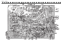
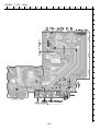
WIRING – 1 (MAIN) ........................................................................................................................................................... 36
SCHEMATIC DIAGRAM – 1 (MAIN) ................................................................................................................................. 37
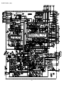
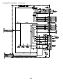
WIRING – 2 (AUDIO) ......................................................................................................................................................... 38
SCHEMATIC DIAGRAM – 2 (AUDIO) .............................................................................................................................. 39
WIRING – 3 (NK) ............................................................................................................................................................... 40
SCHEMATIC DIAGRAM – 3 (NK) ..................................................................................................................................... 41
WIRING – 4 (S-JACK) ........................................................................................................................................................ 42
SCHEMATIC DIAGRAM – 4 (S-JACK) ............................................................................................................................. 43
WIRING – 5 (JOINT) .......................................................................................................................................................... 44
SCHEMATIC DIAGRAM – 5 (JOINT) ............................................................................................................................... 45
WIRING – 6 (SYSTEM) ...................................................................................................................................................... 46
SCHEMATIC DIAGRAM – 6 (SYSTEM) ........................................................................................................................... 47
WIRING – 7 (FR-JACK) ..................................................................................................................................................... 48
SCHEMATIC DIAGRAM – 7 (FR-JACK) ........................................................................................................................... 49
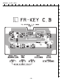
WIRING – 8 (FR-KEY) ....................................................................................................................................................... 50
SCHEMATIC DIAGRAM – 8 (FR-KEY) ............................................................................................................................. 51
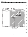
WIRING – 9 (OPT) ............................................................................................................................................................. 52
SCHEMATIC DIAGRAM – 9 (OPT) .................................................................................................................................. 53
WIRING – 10 (PS-2) .......................................................................................................................................................... 54
SCHEMATIC DIAGRAM –10 (PS-2) ................................................................................................................................. 55
WIRING – 11 (PS-SW) ....................................................................................................................................................... 56
SCHEMATIC DIAGRAM –11 (PS-SW) ............................................................................................................................. 57
WIRING – 12 (FR-FL) ........................................................................................................................................................ 58
SCHEMATIC DIAGRAM –12 (FR-FL) ............................................................................................................................... 59
IC BLOCK DIAGRAM ................................................................................................................................................ 60 ~ 61
FL (10-BT-207GK) GRID ASSIGNMENT AND ANODE CONNECTION .............................................................. 62 ~ 63
IC DESCRIPTION ...................................................................................................................................................... 64 ~ 67
VOLTAGE CHART ...................................................................................................................................................... 68 ~ 75
WAVEFORM ............................................................................................................................................................... 76 ~ 81
ELECTRICAL ADJUSTMENT .................................................................................................................................... 82 ~ 96
ON THE DEFAULT MODE WHEN SHIPPED FROM THE FACTORY ....................................................................... 97
DVD TEST MODE ............................................................................................................................................................. 98
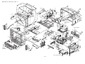
MECHANICAL EXPLODED VIEW 1 / 1 ........................................................................................................................... 99
MECHANICAL PARTS LIST 1 / 1 .................................................................................................................................. 100
–2–
SPECIFICATIONS
TV SECTION
Tuner System
TV System
Channel Coverage
Program Memory
Antenna Input
Picture Tube
Screen Size
Video Input
Audio Input
Video output
Audio output
Digital Audio output
Speaker
GENERAL
Frequency synthesized tuner
NTSC-M
VHF: 2 to 13
UHF: 14 to 69
CATV: 5A, A-1 to A-5, A to W,
W+1 to W+84
181
75 ohms, unbalanced
20 in.
406 (W) x 305 (H) mm
(16 x 121/8 in.)
508 mm (diagonal) (20 in.)
1 Vp-p, 75 ohms
0.5 Vrms., more than 33 k ohms
1 Vp-p, 75 ohms (sync negative)
0.5 Vrms., 2.2 k ohms
Optical
160 x 40 mm (63/8 x 15/8 in.)
DISC PLAYER SECTION
Laser
D/A converter
Signal format
Supported discs
Semiconductor laser
(λ =650 /780 nm)
1 bit dual
NTSC
DVD video discs
12 cm (single-sided single-layer,
single-sided double-layer,
double-sided single-layer,
double-sided double layer)
8 cm (single-sided single-layer,
single-sided double-layer,
double-sided single-layer,
double-sided double layer)
Compact discs (CD-DA, video CD)
12 cm and 8 cm discs
Operating Voltage
Power Consumption
Phones Jack
Operating Temperature
Operating Humidity
Dimensions
Weight
120 V AC, 60 Hz
125 W
Stereo-mini jack
5 °C – 35 °C
35 % – 80 %
575 (W) x 504 (H) x 493(D) mm
(223/4 x 197/8 x 191/2 in.)
30.0 kg (66 lbs.)
• Design and specifications are subject to change without
notice.
• Manufactured under license from Dolby Laboratories Licensing
Corporation.
“DOLBY”, the double-D symbol
and "PRO LOGIC" are
trademarks of Dolby Laboratories Licensing Corporation.
• Manufactured under license from Digital Theater System, Inc. US
Pat. No. 5,451,942 and other worldwide patents issued and pending.
"DTS" and "DTS Digital Surround" are trademarks of Digital Theater
System Inc. C1996 Digital Theater system, Inc. All rights reserved.
ACCESSORIES / PACKAGE LIST
REF. NO. PART NO.
KANRI
DESCRIPTION
NO.
1 8A-JD1-670-010
RC UNIT,RC-AVC01
2 8A-JD1-901-010
IB,U (3L)
3 8A-JD1-904-010
IB,U QUICK (E/S/F)
4 87-B30-311-010
ADAPTOR,300 75 TSN-02
–3–
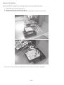
PROTECTION OF EYES FROM LASER BEAM DURING SERVICING
This set employs laser. Therefore, be sure to follow carefully the
CAUTION
instructions below when servicing.
Use of controls or adjustments or performance of procedures other than those specified herin may result in
hazardous radiation exposure.
WARNING!!
WHEN SERVICING, DO NOT APPROACH THE LASER
EXIT WITH THE EYE TOO CLOSELY. IN CASE IT IS
NECESSARY TO CONFIRM LASER BEAM EMISSION.
BE SURE TO OBSERVE FROM A DISTANCE OF MORE
THAN 30cm FROM THE SURFACE OF THE OBJECTIVE
LENS ON THE OPTICAL PICK-UP BLOCK.
ATTENTION
L’utillisation de commandes, réglages ou procédures
autres que ceux spécifiés peut entraîner une dangereuse
exposition aux radiations.
ADVARSEL
Usynlig laserståling ved åbning, når sikkerhedsafbrydereer
ude af funktion. Undgå udsættelse for stråling.
Caution: Invisible laser radiation when
open and interlocks defeated avoid
exposure to beam.
Advarsel: Usynlig laserståling ved åbning,
når sikkerhedsafbrydere er ude af funktion.
Undgå udsættelse for stråling.
This Compact Disc player is classified as a CLASS 1
LASER product.
The CLASS 1 LASER PRODUCT label is located on the
rear exterior.
VAROITUS!
Laiteen Käyttäminen muulla kuin tässä käyttöohjeessa
mainitulla tavalla saataa altistaa käyt-täjän
turvallisuusluokan 1 ylittävälle näkymättömälle
lasersäteilylle.
CLASS 1
KLASSE 1
LUOKAN 1
KLASS 1
VARNING!
Om apparaten används på annat sätt än vad som
specificeras i denna bruksanvising, kan användaren
utsättas för osynling laserstrålning, som överskrider
gränsen för laserklass 1.
LASER PRODUCT
LASER PRODUKT
LASER LAITE
LASER APPARAT
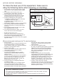
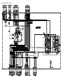
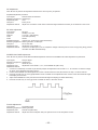
PICKUP ASSY PWB
Solder short land for
DVD laser diode
Precaution to replace Optical block
(SF – HD3AV)
Body or clothes electrostatic potential could
ruin laser diode in the optical block. Be sure
ground body and workbench, and use care
the clothes do not touch the diode.
1) After the connection, remove solder
shown in the right figure.
–4–
Solder short land for
CD laser diode
NOTICES BEFORE REPAIRING
To make the best use of this equipment, make sure to
obey the following items when repairing (or mending).
1. Do not damage or melt the tunicate of the leading
wire on the AC1 side, including the power supply
cord.
2. Do not soil or stain the letters on the spec.
inscription plates, notice labels, fuse labels, etc.
3. When repairing the part extracted from the
conducted side of the board pattern, fix it firmly
with applying bond to the pattern and the part.
4. Restore the following items after repairing.
1) Conditions of soldering of the wires (especially,
the distance on the AC1 side).
2) Conditions of wiring, bundling of wires, etc.
3) Types of the wries.
4) Attachment conditions of all types of the insulation.
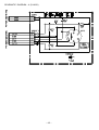
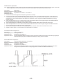
5. After repairing, always measure the insulation
resistance and perform the voltage-withstand test
(See Fig-1).
1) The insulation resistance must be 3.5 to 6.0 MΩ
when applying 500V per second.
2) In the voltage withstand test, apply 1.0 KV for 1
minute and check that the GO lamp lights.
*
*
*
*
Insulation resistance: 3.5 to 6.0 MΩ (500 V/s)
Voltage-withstand: 1.0 KV for 1 minute
Safety checker (Model 7110, etc.)
Earth cable
AC cable
Connect the earth cable
to the outside metal part
terminal.
Fig-1
Breaking current set to 10 mA.
Connect the safety checker as shown in Fig-1,
then measure the resistance and perform the test.
Do not touch the equipment during testing.
For details of the safety checker, refer to the supplied
Operation manual.
When servicing and checking on the TV, note the followings.
1. Keep the notices.
As for the places which need special attentions, they
are indicated with labels or seals on the cabinet,
chassis and parts. Make sure to keep the indications
and notices in the operation manual.
2. Avoid an electric shock.
There is a high voltage part inside. Avoid an electric
shock while the electric current is flowing.
3. Use the designated parts.
The parts in this equipment have the specific
characteristics of incombustibility and withstand
voltage for safety.
Therefore, use a part which has the same character
as the replaced part. Especially as to the important
parts for safety which is indicated in the circuit
diagram or the table of parts with a ! mark, the
designated parts must be used.
4. Put parts and wires in the original position after
assembling or wiring.
There are parts which use the insulation material
such as a tube or tape for safety, or which are
assembled so that these parts do not make contact
with the printed board. The inside wiring is designed
!
not to get close to the pyrogenic parts and high
voltage parts. Therefore, put these parts in the
original positions.
5. Take care of the cathode-ray tube.
By setting an explosion-proof cathode-ray tube in this
equipment, safety is secured against implosion.
However, when removing it or servicing from the
back, it gives out shock that is dangerous. Take
enough care to deal with it.
6. Avoid an X-ray.
Safety is secured against an X-ray by giving
considerations to the cathode-ray tube and the high
voltage peripheral circuit, etc. Therefore, when
repairing the high voltage peripheral circuit, use the
designated parts and do not change the circuit.
Repairing, except indicates, causes rising of high
voltage, and the cathode-ray tube emits an X-ray.
7. Perform a safety check after servicing.
Confirm that the screws, parts and wiring which were
removed in order to service are put in the original
positions, or whether there are deteriorated portions
around the places serviced.
Safety Components Symbol
This symbol is given to important parts which serve to maintain the safety of the product, and which
are made to confirm to special Safety Specifications.
Therefore, when replacing a component with this symbol make absolutely sure that you use a
designated part.
–5–
When repairing the Flat TV, never switch ON the main POWER with the degauss coil removed.
If the degauss coil must inevitably removed due to some reason, connect a dummy using either Method 1 or
Method 2 as described below.
Method 1: Prepare a replacement degauss coil and connect it during repair.
Method 2: Prepare a resistor of 2.8 ohm, 20 W. Manufacture a repair jig by connecting it to the degauss side
connector. Connect the jig during repair.
Waning
If the main POWER is switched ON without connecting degauss coil or dummy resistor, the cement resistor
R801 that is connected in parallel with the degauss coil burns to open.
–6–
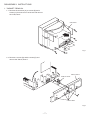
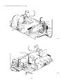
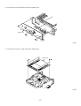
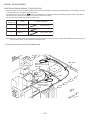
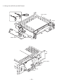
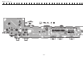
DISASSEMBLY INSTRUCTIONS
1. "CABINET" REMOVAL
1-1. Remove the 9 screws (A), 2 screws (B) and 4
screws (C) from the rear of of the set and remove
the "Cabi, Rear".
Cabi, Rear
Fig-1
1-2. Remove 2 screws (D) and the screw (E) and
remove the "Panel, Rear 2".
Panel, Rear 2
PWB, S-JACK
Four claws
Fig-2
–7–
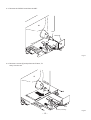
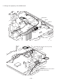
2. "TV. UNIT" REMOVAL
2-1. Anode cap disassembly
2-1-1. Notice Before Disassembly
Discharge the anode.
1)
Anode cap
The cathode-ray tube of this equipment has the structure
that the anode potential is automatically discharged
when the power is off. But immediately after the POWER
is turned off, there might be the case that the anode
potential has not been discharged completely. When
removing the Anode Cap, make sure to discharge the
anode potential.
Do not use a plier.
2)
When using a plier to catch or loose the hook, the spring
is deteriorated depending on the gripping power of the
plier. Therefore, do not use a plier because the hook
may easily slip off from the CRT anode button and it will
be cause of accidents.
Do not rotate the Anode cap.
3)
Do not rotate the Anode Cap. If the Anode Cap is
rotated, the hook may easily slip off.
2-1-2. Disassembly
Discharge the anode (See Fig-3).
1) Connect a flat-head screwdriver to the CRT GND using
a cable with clips.
2) Confirm that the electric current is conducted using the
tester at the tip of the screwdriver and the GND on the
TV side.
3) Put the tip of the screwdriver to the shutter hook.
Note) Take care not to scratch the Anode Cap.
Shutter Hook
CRT
Grip
(Grip must be insulated)
CRT GND
Fig-3
Anode Cap
4) Turn over the Anode Cap (See Fig-4).
Note) Take care not to damage the Anode Cap.
5)
While pushing the Anode Cap in the direction of arrow
with the thumb as the left figure, lift it up in the direction
and remove one side of the hook (See Figof arrow
5).
6) After the side is removed from the Anode Button, turn
over the edge of the Anode Cap, and pull it to remove in
the direction of the arrow (See Fig-6).
Note) Do not remove the Anode Cap in the direction of 90°
degrees (vertical).
Anode Button
CRT
Shutter Hook
Fig-4
Anode Cap
Note) Do not pull it forcefully. Check that the hook has not
changed the shape after removing.
CRT
CRT
Shutter Hook
Shutter Hook
Fig-5
Anode Cap
Pull
Anode Button
Shutter Hook
–8–
Fig-6
2-2. Anode cap assembly
Make sure to keep the notices not to make troubles when
assembling or disassembling the Anode Cap.
Left
Right
2-2-1. Notice Before Assembly
Strictly forbidden to rotate Anode
Cap after assembling.
Anode Cap
Do not use a deformed hook.
If the Anode Cap is rotated after assembling, the Anode
Cap may slip off. Route the high voltage cable before
fixing the Anode Cap (See Fig-7).
2) If the Anode Cap is fixed before routing the high voltage
cable by mistake, route the cable without rotating the
Anode Cap at all.
1)
Fig-7
2-2-2. Anode Cap Assembly
1)
Wipe the assembling position with a clean cloth
moistened with a little alcohol (See Fig-8).
Note) Confirm that there is no dirt, dust, etc in the
assembling position.
2)
Apply a proper quantity of the designated silicon grease
(use KS-650N) in the direction of circumference
(See Fig-8).
Note) Take care that the silicon grease dose not get
into the Anode button.
Anode Button
Assembling position
Fig-8
3)
Straighten the high voltage cable and arrange the wire
not to twist (See Fig-9).
Note) If the wire is not correctly arranged, the Anode Cap
rotates and it causes a failure.
Anode Cap
High Voltage Lead Wire
Fig-9
–9–
4)
Turn over the edge of the Anode Cap as the left figure
(See Fig-10).
Note) The right and left sides of the Anode Cap should be
turned over equally.
Note) Take enough care not to scratch the Anobe Cap.
Fig-10
5)
Hold the Anode Cap with the thumb and middle fingers
while supporting the middle projection with the forefinger
as the left figure. (See Fig-11-1)
6) Insert the one side of the hook to the anode button. (See
Fig-11-2)
Note) Confirm that the hook is surely hitched.
7)
Hook the claw at the other end of the shutter hook on the
anode button as Fig-11-3.
Note) Hook the claw at the other end in the manner of sliding into the Anode Button as shown.
Note) When the shutter hook is inserted into the Anode Button completely, the clicking sound can be heard.
Fig-11-1
Anode Button
Shutter Hook
30°
Shutter Hook
Anode Button
Shutter Hook
Anode Button
Fig-11-2
Fig-11-3
– 10 –
8)
Pull it lightly while keeping the edge of the Anode Cap
turned over. Visually confirm that the both hooks are
inserted and check the condition of hitching of the
shutter hook.
9) Remove hand from the rubber cap of the Anode Cap.
Note) Put on the edge of the Anode Cap without clearance.
Anode cap
10) Push the part of the skirt of the edge of the Anode Cap
lightly and set the rubber cap and CRT to be adhered.
11) Furthermore, reconfirm that the Anode cap adheres
closely to the CRT (See Fig-12).
*
Refer to the "Wire Process method" for details of wire
process.
Part of the skirt
Fig-12
*
1.
2.
3.
4.
5.
6.
7.
When either FBT or anode cap is going to be replaced, be sure to replace both FBT and anode cap at the same time as
follows. (Because the anode cap cannot be removed any more if it is locked into the connector-type FBT.)
Remove the rubber cap at the tip end of the anode cap
assy.
Insert the terminal at the tip end of the high tension lead of the anode cap assy as far as it can go until you feel the clicking
feeling.
Pull the anode cap assy gently upward (with 2 to 3 kg) in order to confirm that the connector is firmly connected. Then move it
down again. (The reason of pulling gently is to confirm that the connector is firmly connected. If it is pulled too strongly, the
connector can be broken.)
Press the rubber cap that is attached to the terminal side
of the anode cap assy, down to the flange. Note that the
rubber cap is not turned over. (See Fig-13.)
Remove the rubber cap of the focus wire.
Anode Cap Assy
Insert the top tip of the cable firmly and push down the
rubber cap so that the rubber cap cover the terminal
completely.
Insert the top tip of the screen wire firmly and secure it
by attaching it to the groove. (See Fig-14)
(White)
Focus Wire
Rubber Cap
(White)
Focus Wire
Rubber Cap
Rubber Cap
Terminal
(Red)
Screen Wire
Rubber Cap
(Red)
Screen Wire
Fig-14
– 11 –
Fig-13
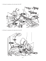
2-3. Remove the connectors from the "TV, UNIT".
CN952
CN406
CN2
CN951
CN404
CN117
CN601
CN9
CN108
Fig-15
Degauss Coil
CN807
CN807
CN202
CN203
CN211
CN204
Fig-16
– 12 –
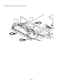
2-4. Remove the "NECK" board from the CRT.
CRT
PWB, NK
Fig-17
2-5. Remove 2 screws (F) and pull out the "Frame, TV
Assy" from the set.
Frame, TV Assy
– 13 –
Fig-18
3. HOW TO REMOVE "MAIN" BOARD AND "AUDIO" BOARD
3-1. Remove the connector that connects the "PWB, MAIN" and "PWB, AUDIO".
CN701
CN706
CN705
CN702
CN409
CN707
Fig-19
3-2. Remove "PWB, AUDIO" and "PWB, MAIN" from "FRAME, TV".
PWB, MAIN
PWB, AUDIO
Five claws
Fig-20
– 14 –
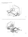
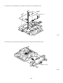
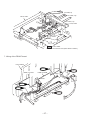
4. HOW TO REMOVE "MECH, ASSY" BOARD
4-1. Remove the connector.
CN110
CN216
Panel, Rear Assy
CN107
Fig-21
4-2. Remove 2 screws (G) and the screw (H). Then pull out the "Mech, Assy" and "PWB, PS-SW" at the same time.
Mech, Assy
PWB, PS-SW
Fig-22
– 15 –
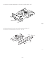
5. HOW TO REMOVE "PS-2" BOARD (WITH "PS-SW" BOARD), "JOINT" BOARD AND "AZG-D".
5-1. Remove 5 screws and remove the "Panel, Rear 1".
Panel, Rear1
Fig-23
5-2. Remove 6 screws (J) and the connector. Then remove the "PWB, JOINT".
CN101
CN103
CN102
PWB, JOINT
CN105
Fig-24
– 16 –
5-3. Remove 6 screws (K) and remove the "PWB, PS-2".
PWB, PS-2
Fig-25
5-4. Remove 6 screws (L) and remove the "Shild, Assy".
Shild, Assy
Fig-26
– 17 –
5-5. Remove 4 screws (M) and 3 screw (N). Then remove the "Shld-Plate, Low".
Shld-Plate, Low
Fig-27
5-6. Remove 2 screws (O) and the screw (P). Then remove the "Hldr, Mech R Assy".
Hldr, Mech R Assy
Fig-28
– 18 –
5-7. Remove 2 screws (Q) and the screw (R). Then remove the "Hldr, Mech L Assy".
Hldr, Mech L Assy
Fig-29
5-8. Remove the screw (S) and the connector. Then remove the "PWB, OPT".
5-9. Remove 2 screws (T) and remove the "Frame, Mech BK".
CN650
PWB, OPT
Frame, Mech BK
Fig-30
– 19 –
6. HOW TO REMOVE "FRONT" BOARD
6-1. Remove 15 screws (V) and remove the "PWB, SYSTEM" and "PWB, FR-JACK" .
PWB, SYSTEM
Fig-31
PWB, FR-JACK
6-2. Remove the connector and separate the 4 boards.
PWB, FR-FL
PWB, FR-KEY
CN13
PWB, SYSTEM
CN304
CN303
CN302
CN301
PWB, FR-JACK
– 20 –
CN8
Fig-32
SERVICE POSITION
When the AZG-D is going to be repaired, take the service position as follows.
1. Disassemble the set and take the AZG-D out.
2. Reassemble the set without installing the AZG-D.
3. Pull out 4 connectors that come from the AZG-D from the left side of the set and connect them.
Note) Picture shows removal of the shield (SHLD-PLATE, LOW) from the bottom of the AZG-D.
– 21 –
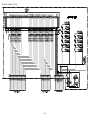
WIRING ARRANGEMENT
WIRE PROCESSING (WIRING, TYING) METHOD
*
*
*
Be sure to follow the instructions described as follows when processing the wires during disassembling and reassembling, in order
to secure safety upon completion of the repair work.
mark in the illustrations, are the parts that are specifically designed as the safety related
The parts that are shown with the
important parts by the safety regulations. Pay utmost care for these marks.
For tying the wires, the following parts are mainly used.
SAFETY
Number in
illustrations
Name
A
Coating lead pin
Soldered to P.Cs.
B
Wire binder
Fixed by Screws.
C
Cable,tie
Cannot be re-used.
Outside appearance
Note) Be sure to follow the instructions described as follows when processing the wires during disassembling and reassembling, in
order to secure safety upon completion of the repair work.
1. Routing of the wires on top of the MAIN board.
SAFETY
PWB, MAIN
(RED WIRE)
Must not touch to SH1
and IC804.
SH1
HT602
IC804
R629
SAFETY
R626
(BROWN WIRE)
Must not touch to
HT602, R629 and
R626.
– 22 –
2. Wiring in the periphery of the MAIN board.
PWB, MAIN
SAFETY
CN707
CNA414
CN702
CN705
CN706
CNA403
CN409
CN405
CN401
CN402
CN701
PWB, AUDIO
CAUTION: Must not touch to tuner (TU101).
SAFETY
CN771
CNA771
TU101
CN701
SAFETY
HT801
To CN409
From CNA603
CAUTION:
CNA603 GND wire must not touch
to heat sink (HT801).
– 23 –
3. Wiring in the periphery of the left side of the CRT.
1cm
SAFETY
CN952
CN901
SAFETY
CN903
SAFETY
CN951
CNA704
SAFETY
CN409
CN404
CNA408
4. Wiring in the periphery of the right side of the CRT.
14~16cm
SAFETY
DGC WIRE
Around the twice.
CN904
SAFETY
CN901
CAUTION:
DGC Wire must not touch
to heat sink.
HEAT SINK
CN902
CN807
1~3cm
SAFETY
CN601
CNA602
– 24 –
5. Wiring in the periphery of the PS-2 board.
PWB, MAIN
PWB, PS-2
CNA305
SAFETY
CN201
SAFETY
CN203
PWB, PS-SW
SAFETY
– 25 –
CN216
6. Wiring of the AZG-D and JOINT board.
Mech, ASSY
SAFETY
CN106
W205
W203
W204
PWB, PS-SW
PWB, PS-2
CNA214
Mech, ASSY
CN101
RED
CN105
CN103
CN102
– 26 –
FF-Cable, 5p
FF-Cable, 13p
Mech, ASSY
RED
FF-Cable, 11p
CN401
Core,Ferrite
CN702
CN551
CN800
CLOTH TAPE
PART NO. SV-T00-067-010 (Size:180mm x 90mm)
7. Wiring of the FRONT board.
Front Cabinet
SAFETY
CNA305
SAFETY
PWB, FR-JACK
PWB, SYSTEM
CN307
CNA306
SAFETY
SAFETY
CN301
CN8
SAFETY
– 27 –
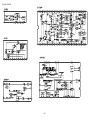
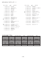
ELECTRICAL MAIN PARTS LIST
REF. NO. PART NO.
KANRI
NO.
DESCRIPTION
REF. NO.
PART NO.
KANRI
NO.
87-070-092-080
87-A40-735-090
87-A40-001-080
87-017-593-090
87-017-654-060
DIODE,S5566B
DIODE,ERC06-15
ZENER,MTZJ12C
DIODE,RGP15J
DIODE,GBU6J
87-A40-450-090
87-A40-828-080
87-A40-911-090
87-A40-734-010
87-A40-354-090
DIODE,RU 1P
DIODE,AK 04
DIODE,RN 2Z
DIODE,FML-G12S
DIODE,UF3GL-6251
87-A40-337-080
87-A40-553-080
87-017-650-080
87-A40-503-080
87-070-173-010
ZENER,MTZJ 6.8B
DIODE,1N4003 LES
DIODE,1SS119
ZENER,MTZJ39B
DIODE,S1WBA60
87-A40-368-080
87-A40-853-080
87-A40-852-090
87-070-274-080
87-A40-367-080
DIODE,EG01C
DIODE,10ELS2
DIODE,30DF2(F)
DIODE,1N4003 SEM
DIODE,EU01
87-A40-851-090
87-A40-353-080
87-017-079-080
87-A40-003-080
87-A40-002-080
DIODE,31DQ04(F)
ZENER,HZS33-3
ZENER,HZS4A3
ZENER,MTZJ4.3A
ZENER,MTZJ5.1C
87-020-125-080
C-DIODE,1SS181
C2
C3
C4
C5
C6
87-018-209-080
87-018-134-080
87-018-127-080
87-010-401-080
87-018-209-080
CAP, CER 0.1-50V
CAPACITOR,TC-U 0.01-16
CAP, CER 470P-50V
CAP, ELECT 1-50V
CAP, CER 0.1-50V
C7
C8
C9
C10
C11
87-010-248-080
87-018-123-080
87-010-401-080
87-018-131-080
87-018-134-080
CAP, ELECT 220-10V
CAP, CER 220P-50V
CAP, ELECT 1-50V
CAP, CER 1000P-50V
CAPACITOR,TC-U 0.01-16
C12
C13
C14
C15
C16
87-018-119-080
87-018-119-080
87-010-263-080
87-018-119-080
87-018-131-080
CAP,
CAP,
CAP,
CAP,
CAP,
CER 100P-50V
CER 100P-50V
ELECT 100-10V
CER 100P-50V
CER 1000P-50V
C17
C18
C19
C20
C21
87-018-128-080
87-018-109-080
87-018-109-080
87-018-119-080
87-018-109-080
CAP,
CAP,
CAP,
CAP,
CAP,
CERA-SOL SS 560P
CER 22P-50V
CER 22P-50V
CER 100P-50
CER 22P-50V
C22
C23
C24
C25
C101
87-018-109-080
87-018-123-080
87-018-209-080
87-018-119-080
87-010-404-080
CAP,
CAP,
CAP,
CAP,
CAP,
CER 22P-50V
CER 220P-50V
CER 0.1-50V
CER 100P-50V
ELECT 4.7-50V
C104
C105
C106
C112
C113
87-010-248-080
87-018-134-080
87-A10-207-080
87-018-109-080
87-018-109-080
CAP, ELECT 220-10V
CAPACITOR,TC-U 0.01-16
CAP,TCS 0.01-50KBUP050
CAP, CER 22P-50V
CAP, CER 22P-50V
C201
C202
C203
C204
C205
87-018-134-080
87-018-134-080
87-010-400-080
87-018-134-080
87-010-237-080
CAPACITOR,TC-U 0.01-16
CAPACITOR,TC-U 0.01-16
CAP, ELECT 0.47-50V
CAPACITOR,TC-U 0.01-16
CAP, ELECT 1000-16V
C206
C207
C208
C209
C210
87-A10-287-080
87-010-400-080
87-018-134-080
87-010-385-080
87-A11-080-080
CAP,M 2200P-50 J
CAP, ELECT 0.47-50V
CAPACITOR,TC-U 0.01-16
CAP, ELECT 220-25V
CAP,TC U 47P-50 J CH
IC
8A-JD1-653-010
87-A21-378-010
87-A20-611-080
87-001-536-010
8Z-JBJ-605-010
IC,M37272EFSP-AJD1UOTP
IC,S-24C04BDP-1A
IC,M51943BSL-700A
IC,NJM78M05FA
IC,TA1268N
87-A21-103-040
87-A21-022-040
87-A21-554-010
87-A21-283-010
87-A21-220-010
C-IC,MM1454XFBE
C-IC,BA3880FS
IC,TA1216AN
IC,AN5277
IC,MM1311AD
87-A21-219-010
87-070-237-010
87-070-417-010
8Z-JBH-605-010
87-A21-468-010
IC,TC90A45P
IC,LA7832
IC,NJM4558 DD
IC,CXA2104S
IC,STR-F6626
87-A21-457-010
87-020-969-010
87-A20-389-010
87-A21-585-010
87-017-889-010
IC,SE120N
IC,NJM78M09FA
IC,NJM7809FA
IC,MM1232XD
IC,NJM4558LD
87-A21-186-010
87-A20-649-080
87-001-576-010
8A-JD1-650-030
8A-JD1-656-030
IC,STR-F6552
IC,HA17431VP
IC,MJM7812FA
C-IC,M38B59EFFP-AJD1UOTP
C-IC,UPD78F0034AYGC-AJD1UFLASH
87-017-825-010
87-070-083-010
IC,GP1F32T
IC,GP1U281X
TRANSISTOR
87-A30-065-080
87-026-269-080
87-A30-066-080
87-026-219-080
87-026-218-080
TR,2SC2785FE
TR,DTA114ES
TR,2SA1175FE
TR,DTA144ES
TR,DTC144ES
89-324-122-080
89-110-372-080
87-A30-062-080
89-324-820-080
87-A30-364-010
TR,2SC2412KR
TR,2SA1037K
C-TR,KRC104S
TR,2SC2482
TR,2SD2578-CA
87-A30-363-010
89-110-154-080
89-318-155-080
87-026-463-080
89-110-913-080
TR,2SD2531
TR,2SA1015Y
TR,2SC1815GR
TR,2SA933SRS
TR,2SA1091-0
87-A30-344-010
87-026-462-080
89-407-742-080
89-118-370-010
89-347-930-010
TR,2SC5147D
TR,2SC1740SRS
TR,2SD774
TR,2SA1837
TR,2SC4793
87-A30-217-010
87-026-235-080
87-A30-218-080
87-026-227-080
87-A30-220-080
TR,2SB1436(R)
CHIP-TR,DTC114EK
TR,2SB1237(Q)
CHIP-TR,DTA114EK
TR,2SC1741AS(R)
87-A30-063-080
CHIP-TR,KRA104S
DIODE
!
87-017-932-080
87-020-465-080
87-002-743-080
87-A40-235-080
87-A40-690-080
ZENER,MTJ6.2B
DIODE,1SS133
ZENER,MTZJ 33B
ZENER,MTZJ9.1C
ZENER,MTZJ11B
87-A40-286-080
87-A40-348-080
87-A40-234-080
87-A40-318-080
DIODE,RGP10JE-5025
ZENER,MTZJ3.3A
ZENER,MTZJ5.6A
ZENER,RM26 V1
DESCRIPTION
MAIN C.B
– 28 –
REF. NO. PART NO.
!
C211
C212
C213
C214
C229
KANRI
NO.
87-A11-080-080
87-A11-080-080
87-A11-082-080
87-018-134-080
87-018-149-080
DESCRIPTION
CAP,TC U 47P-50 J CH
CAP,TC U 47P-50 J CH
CAP,TC U 56P-50 J CH
CAPACITOR,TC-U 0.01-16
CAP,TC-U 15P-50 CH
C301
C302
C305
C306
C307
87-010-403-080
87-018-134-080
87-018-126-080
87-010-405-080
87-A10-299-080
C308
C309
C311
C312
C313
REF. NO.
C626
C627
C629
C630
C631
KANRI
NO.
87-010-401-080
87-A11-984-080
87-A10-469-080
87-010-405-080
87-010-263-080
CAP, ELECT 1-50V
CAP,CER 270P-500 K B DD10
CAP,CER 2200P-500 K B DD10
CAP, ELECT 10-50V
CAP, ELECT 100-10V
CAP, ELECT 3.3-50V
CAPACITOR,TC-U 0.01-16
CAP,TC-U 390P-50 B
CAP, ELECT 10-50V
CAP,M 0.022-50 J
C655
C714
C720
C721
C722
87-A11-354-090
87-010-221-080
87-015-464-080
87-A10-292-080
87-A10-296-080
CAP,E 100-160 M SMG
CAP, ELECT 470-10V
CAP,E 4.7-16 BP
CAP,M 5600P-50 J
CAP,M 0.012-50 J
87-010-401-080
87-018-147-080
87-018-209-080
87-018-209-080
87-018-209-080
CAP, ELECT 1-50V
CAP,TC-U 10P-50 CH
CAP, CER 0.1-50V
CAP, CER 0.1-50V
CAP, CER 0.1-50V
C723
C724
C725
C726
C727
87-010-401-080
87-010-404-080
87-010-405-080
87-010-404-080
87-010-112-080
CAP,
CAP,
CAP,
CAP,
CAP,
C314
C315
C316
C317
C318
87-018-134-080
87-018-123-080
87-A10-378-080
87-010-402-080
87-018-134-080
CAPACITOR,TC-U 0.01-16
CAP, CER 220P-50V
CAP,E 2.2-50 K SH
CAP, ELECT 2.2-50V
CAPACITOR,TC-U 0.01-16
C728
C729
C730
C731
C733
87-015-464-080
87-010-404-080
87-015-464-080
87-A10-288-080
87-016-301-080
CAP,E 4.7-16 BP
CAP, ELECT 4.7-50V
CAP,E 4.7-16 BP
CAP,M 2700P-50 J
CAP,TN 3.3-16K DN
C319
C321
C322
C323
C324
87-010-237-080
87-010-404-080
87-A10-295-080
87-016-280-080
87-018-134-080
CAP, ELECT 1000-16V
CAP, ELECT 4.7-50V
CAP,M 0.01-50 J
CAP,E 3.3-50 M BP SME
CAPACITOR,TC-U 0.01-16
C734
C735
C736
C737
C801
87-015-464-080
87-016-302-080
87-010-401-080
87-018-134-080
87-010-384-080
CAP,E 4.7-16 BP
CAP,TN 10-16K DN
CAP, ELECT 1-50V
CAPACITOR,TC-U 0.01-16
CAP, ELECT 100-25V
C325
C326
C327
C328
C329
87-018-134-080
87-A10-307-080
87-018-134-080
87-010-405-080
87-018-134-080
CAPACITOR,TC-U 0.01-16
CAP,M 0.1-50 J
CAPACITOR,TC-U 0.01-16
CAP, ELECT 10-50V
CAPACITOR,TC-U 0.01-16
C802
C804
C805
C806
C807
87-018-131-080
87-A10-474-090
87-016-515-080
87-A12-169-090
87-A10-568-010
CAP, CER 1000P-50V
CAP,PP 0.01-1.25K J PHS
CAP,CER 1000P-1K B
CAP,E 470-200 M SMH
CAP,PP 1000P-630 J APH
C330
C331
C332
C333
C334
87-010-401-080
87-010-544-080
87-018-134-080
87-018-134-080
87-018-209-080
CAP, ELECT 1-50V
CAP, ELECT 0.1-50V
CAPACITOR,TC-U 0.01-16
CAPACITOR,TC-U 0.01-16
CAP, CER 0.1-50V
C808
C809
C810
C811
C813
87-010-384-080
87-018-131-080
87-018-129-080
87-018-131-080
87-018-131-080
CAP,
CAP,
CAP,
CAP,
CAP,
C335
C336
C337
C338
C339
87-015-997-010
87-018-134-080
87-018-130-080
87-010-405-080
87-018-134-080
CAP, ELECT 2200UF-16V
CAPACITOR,TC-U 0.01-16
CAP,TC-U 820P-50 B
CAP, ELECT 10-50V
CAPACITOR,TC-U 0.01-16
C814
C816
C817
C818
C820
87-010-260-080
87-010-405-080
87-A10-627-090
87-018-209-080
87-010-405-080
CAP, ELECT 47-25V
CAP, ELECT 10-50V
CAP,E 2200-50V
CAP, CER 0.1-50V
CAP, ELECT 10-50V
C340
C341
C342
C343
C344
87-018-118-080
87-018-118-080
87-018-150-080
87-A10-307-080
87-A10-307-080
CAP,TC-U 82P-50 B
CAP,TC-U 82P-50 B
CAP,TC-U 18P-50 CH
CAP,M 0.1-50 J
CAP,M 0.1-50 J
C821
C822
C824
C829
C831
87-010-405-080
87-018-209-080
87-010-237-080
87-010-384-080
87-010-405-080
CAP,
CAP,
CAP,
CAP,
CAP,
C501
C504
C505
C508
C509
87-010-404-080
87-010-393-080
87-018-131-080
87-010-398-090
87-A11-245-080
CAP, ELECT 4.7-50V
CAP, ELECT 100-35V
CAP, CER 1000P-50V
CAP,E 2200-35V
CAP,M/P 0.1-100 J TF-ECQV
C834
C835
C836
C838
C842
87-A10-733-090
87-016-037-060
87-010-260-080
87-A12-302-090
87-012-370-010
CAP,E 220-160 SK
CAP,CER 1000P-2KB
CAP, ELECT 47-25V
CAP,E 1000-50 M SMG
CAP,CER 3300P-250
C510
C605
C607
C608
C609
87-010-405-080
87-A11-336-090
87-A12-050-090
87-A10-859-010
87-A11-278-090
CAP, ELECT 10-50V
CAP,M/P 0.01-1.6K H ECWH(VB)
CAP,M/P 0.013-800 H ECWH(VB)
CAP,CER 390P-2K K R LONG
CAP,M/P 0.47-250 J ECWF(SR)
C843
C844
C845
C846
CF201
87-012-370-010
87-012-370-010
87-012-370-010
87-A10-207-080
84-LB3-626-080
CAP,CER 3300P-250
CAP,CER 3300P-250
CAP,CER 3300P-250
CAP,TC U 0.01-50 KB
FLTR,TPS4.5MB2
C610
C611
C612
C613
C614
87-A10-867-090
87-010-963-080
87-010-976-080
87-016-373-080
87-010-976-080
CAP,CER 2200P-2K K R
CAP,E 2.2-160 SME
CAP,CER 1000P-500 B
CAP,E 10-250
CAP,CER 1000P-500 B
CF202
CN1
CN2
CN601
CN701
84-LB3-627-080
87-009-195-010
87-009-261-010
87-099-762-010
87-A60-628-010
FLTR,SFSH 4.5MDB SIF
CONN,5P B5BEH
CONN,7P V 52147
CONN,5P TBL-P V BOSS
CONN,11P V 2MM JMT
C615
C616
C617
C618
C619
87-A10-843-080
87-A10-843-080
87-A12-082-090
87-A10-301-080
87-A11-987-080
CAP,CER 680P-1K K R
CAP,CER 680P-1K K R
CAP,E 1000-35 SMG
CAP,M 0.033-50 J
CAP,CER 6800P-250 K R HR
CN705
CN706
CN707
CN807
CNA101
87-009-262-010
87-099-186-010
87-A61-126-080
82-481-649-010
8A-JD1-657-010
CONN,8P 52147 MXJ
CONN,6P EH V WHT
MALE,1P TP42097
CONN,2P V VT-50P
CONN ASSY,1P TV-TU TO PS-SW
C620
C621
C622
C623
C624
87-010-395-080
87-018-131-080
87-A11-124-080
87-A12-171-080
87-010-976-080
CAP,E 330-35 SME
CAP, CER 1000P-50V
CAP,TC U 2200P-50 K B
CAP,E 4.7-50 K SH
CAP,CER 1000P-500 B
CNA103
CNA602
CNA603
CNA704
CNA801
8A-JE7-627-010
8Z-JE7-661-110
8A-JD1-658-010
8A-JE7-617-010
8A-JD1-668-010
CONN
CONN
CONN
CONN
CONN
!
!
!
!
!
!
– 29 –
PART NO.
DESCRIPTION
ELECT
ELECT
ELECT
ELECT
ELECT
1-50V
4.7-50V
10-50V
4.7-50V
100-16V
ELECT 100-25V
CER 1000P-50V
CER 680P-50V
CER 1000P-50V
CER 1000P-50V
ELECT 10-50V
CER 0.1-50V
ELECT 1000-16V
ELECT 100-25V
ELECT 10-50V
ASSY,2P
ASSY,5P
ASSY,1P
ASSY,6P
ASSY,2P
MAIN-S
V WHT TV-NK
TV-FBT TO PS-SW
V WHT TV-NK-2
TV TO PS-SW
REF. NO. PART NO.
CNA803
D1
FB301
FB601
FB801
KANRI
NO.
8A-JD1-669-010
87-070-110-010
87-003-320-080
87-003-223-080
87-003-320-080
CONN ASSY,2P TV TO PS
LED,SLP-181B-51 RED
F-BEAD,-9.0FBR07HA121NB
FERRITE BEAD BL02RN2
F-BEAD,FBR07HA121NB
FB802
FB803
FB804
FB805
FB806
87-003-320-080
87-003-320-080
87-003-320-080
87-003-320-080
87-003-320-080
F-BEAD,FBR07HA121NB
F-BEAD,FBR07HA121NB
F-BEAD,FBR07HA121NB
F-BEAD,FBR07HA121NB
F-BEAD,FBR07HA121NB
FB807
FR607
FR608
FR610
J702
87-003-320-080
87-A00-652-090
87-A00-628-090
87-A00-628-090
87-A60-324-110
F-BEAD,FBR07HA121NB
RES,FUSE 0.33-1W J RF 1SL12.5
RES,FUSE 0.68-1W J RF 1SL12.5
RES,FUSE 0.68-1W J RF 1SL12.5
JACK,PIN 6P Y-W-R W/SW
L2
L101
L201
L203
L204
87-005-614-080
87-005-614-080
8Z-JBR-612-010
87-005-612-080
87-003-282-080
COIL 100UH LAV35 J
COIL 100UH LAV35 J
COIL,SIF 4.5MHZ 504BN
COIL,68UH J LAV35
COIL,12UH
L205
L206
L207
L208
L301
8Z-JBH-610-010
87-005-614-080
87-003-147-080
87-003-143-080
87-003-097-080
COIL,PIF-SQ57EL349A 45.75MHZ
COIL 100UH LAV35 J
COIL, 22UH
COIL 4.7 UH
COIL,1UH
L302
L303
L304
L603
L604
87-005-614-080
87-005-614-080
87-003-282-080
87-005-757-010
87-A50-616-080
COIL 100UH LAV35 J
COIL 100UH LAV35 J
COIL,12UH
COIL,3.3MH
COIL,2.2MH J LHL10
!
L605
L701
L801
L803
PR601
8Z-JE7-608-010
87-005-614-080
87-A50-170-010
87-A50-176-080
87-A90-429-080
COIL,HLC ZJE-7
COIL 100UH LAV35 J
COIL,390UH RCH106
COIL,33UH-PJ87
FUSE,1.25A 125V A 251
!
!
!
!
!
PR801
PR802
PR803
PS801
PT801
87-A90-409-080
87-A90-210-080
87-A90-070-080
87-A90-717-010
8A-JD1-654-010
FUSE,1.5A 125V A 251
FUSE,7A 125V 251
FUSE,3.5A 125V 251
P-COUPLER,PC123FY2
PT,U SW AJD-1-TV
R315
R316
R508
R604
R612
87-025-380-080
87-025-427-080
87-A00-541-090
87-A00-565-090
87-A00-629-090
RES,M/F
RES,M/F
RES,M/F
RES,M/F
RES,M/F
15K-1/6W F
27K-1/6W F
390-1W J RSF(S)
1.2K-7W J RSU7
5.6-1W J RSF(S)
R626
R723
R801
R802
R803
87-A00-676-090
87-A00-130-080
87-A00-665-010
87-A00-160-090
87-A00-356-090
RES,M/F
RES,M/F
RES,CEM
RES,M/F
RES,M/F
100-7W J RSV7
62K-1/6W F
56-2W J BGR2U
33-2W J RSF(S)
22-2W J RSS2X
R804
R805
R806
R811
R824
87-A00-633-090
87-A00-170-090
87-A00-380-090
87-A00-646-090
87-A00-718-090
RES,CEM
RES,M/F
RES,M/F
RES,CEM
RES,M/F
0.47-10W
82K-3W J
39K-3W J
0.1-5W K
680-1W J
R833
R834
R844
RY801
SFR501
87-A00-199-090
87-A00-223-090
87-A00-254-090
87-A91-390-010
87-024-430-080
RES,M/F 12K-3W J RSF(S)
RES,M/F 47K-2W J RSF(S)
RES,M/F 0.68-2W J
RELAY,AC12V G5PA-1-8
SFR,2.2K RH063EC
SFR601
SFR602
SFR603
SWF201
T601
87-024-434-080
87-024-429-080
87-A91-856-080
8Z-JBH-633-010
8Z-JE7-606-010
SFR,22K RH063EC
SFR,1K RH063EC
SFR,K 22K H EVM EAS
FLTR,SAW M1969-M
FBT,D ZJE-7
T602
TH801
TU101
X1
X301
85-JT2-653-010
87-A90-254-010
8Z-JBE-610-010
87-A70-124-080
87-A70-007-080
PT,HDT-TV141-2
POS-THMS,PTH451BG5R0M140
TU UNIT,USA ENV56D74G3
VIB,CER 8.0MHZ
VIB,XTAL 3.58MHZ AQC-1001
!
!
!
DESCRIPTION
REF. NO.
J RGC
RSF(S)
RSS H2
RGC5
RSF (S)
PART NO.
KANRI
NO.
87-030-327-010
VIB,CER CSB503F30
C400
C401
C402
C403
C404
87-010-402-080
87-010-404-080
87-A10-295-080
87-A10-295-080
87-A10-307-080
CAP, E 2.2-50 M 11L SME
CAP, ELECT 4.7-50V
CAP,M 0.01-50 J
CAP,M 0.01-50 J
CAP,M 0.1-50 J
C405
C406
C407
C408
C409
87-010-404-080
87-010-260-080
87-010-197-080
87-010-405-080
87-010-404-080
CAP,
CAP,
CAP,
CAP,
CAP,
C410
C411
C413
C414
C415
87-010-404-080
87-010-404-080
87-A10-295-080
87-A10-305-080
87-A10-293-080
CAP, ELECT 4.7-50V
CAP, ELECT 4.7-50V
CAP,M 0.01-50 J
CAP,M 0.068-50 J
CAP,M 6800P-50 J
C416
C417
C418
C419
C420
87-010-260-080
87-010-404-080
87-010-197-080
87-010-404-080
87-010-404-080
CAP,
CAP,
CAP,
CAP,
CAP,
C421
C422
C424
C425
C426
87-010-404-080
87-A10-293-080
87-010-260-080
87-A10-305-080
87-A10-295-080
CAP, ELECT 4.7-50V
CAP,M 6800P-50 J
CAP, ELECT 47-25V
CAP,M 0.068-50 J
CAP,M 0.01-50 J
C427
C428
C429
C430
C431
87-010-404-080
87-010-189-080
87-012-365-080
87-010-401-080
87-010-189-080
CAP, ELECT 4.7-50V
C-CAP,S 8200P-50 B
C-CAP,S 0.027-25VBK
CAP, ELECT 1-50V
C-CAP,S 8200P-50 B
C432
C433
C434
C435
C436
87-010-197-080
87-010-260-080
87-012-365-080
87-010-401-080
87-010-401-080
CAP, CHIP 0.01 DM
CAP, ELECT 47-25V
C-CAP,S 0.027-25VBK
CAP, ELECT 1-50V
CAP, ELECT 1-50V
C437
C438
C439
C440
C441
87-010-401-080
87-010-178-080
87-A10-307-080
87-A10-307-080
87-A10-307-080
CAP, ELECT 1-50V
CHIP CAP 1000P
CAP,M 0.1-50 J
CAP,M 0.1-50 J
CAP,M 0.1-50 J
C442
C443
C444
C445
C446
87-010-401-080
87-010-405-080
87-010-405-080
87-010-405-080
87-010-405-080
CAP,
CAP,
CAP,
CAP,
CAP,
C447
C448
C449
C450
C451
87-010-405-080
87-010-197-080
87-010-402-080
87-010-247-080
87-010-388-080
CAP, ELECT 10-50V
CAP, CHIP 0.01 DM
CAP, ELECT 2.2-50V
CAP, ELECT 100-50V
CAP ELECT 1000-25V SME
C452
C453
C454
C455
C460
87-010-388-080
87-010-178-080
87-010-917-090
87-010-247-080
87-010-197-080
CAP ELECT 1000-25V SME
C-CAP,S 1000P-50 KB
CAP,E 3300-50 M SMG
CAP, ELECT 100-50 M SME
CAP, CHIP 0.01 DM
C464
C465
C466
C467
C468
87-010-260-080
87-010-198-080
87-A10-295-080
87-010-401-080
87-A10-295-080
CAP, ELECT 47-25V
CAP, CHIP 1000P-50 KB
CAP,M 0.01-50 J
CAP, ELECT 1-50V
CAP,M 0.01-50 J
C469
C470
C471
C472
C473
87-A10-295-080
87-010-154-080
87-012-155-080
87-A10-295-080
87-A10-295-080
CAP,M 0.01-50 J
CAP CHIP 10P
C-CAP 180P-50CH
CAP,M 0.01-50 J
CAP,M 0.01-50 J
X302
DESCRIPTION
AUDIO C.B
– 30 –
ELECT 4.7-50V
ELECT 47-25V
CHIP 0.01 DM
ELECT 10-50V
ELECT 4.7-50V
ELECT 47-25V
ELECT 4.7-50V
CHIP 0.01 DM
ELECT 4.7-50V
ELECT 4.7-50V
ELECT
ELECT
ELECT
ELECT
ELECT
1-50V
10-50V
10-50V
10-50V
10-50V
REF. NO. PART NO.
C474
KANRI
NO.
87-A10-295-080
DESCRIPTION
CAP,M 0.01-50 J
C475
C476
C477
C478
87-010-198-080
87-010-260-080
87-010-316-080
87-010-316-080
CAP, CHIP 1000P-50 KB
CAP, ELECT 47-25V
C-CAP,S 33P-50 CH
C-CAP,S 33P-50 CH
C479
C480
C481
C482
C483
87-010-318-080
87-010-316-080
87-010-316-080
87-010-196-080
87-010-260-080
C-CAP,S 47P-50 CH
C-CAP,S 33P-50 CH
C-CAP,S 33P-50 CH
CHIP CAPACITOR,0.1-25
CAP, ELECT 47-25V
C484
C486
C487
C488
C489
87-010-197-080
87-010-197-080
87-010-196-080
87-010-384-080
87-010-197-080
CAP,
CAP,
CHIP
CAP,
CAP,
C493
C494
C495
C496
C497
87-A10-307-080
87-A10-307-080
87-010-400-080
87-010-400-080
87-010-405-080
CAP,M 0.1-50 J
CAP,M 0.1-50 J
CAP, ELECT 0.47-50V
CAP, ELECT 0.47-50V
CAP, ELECT 10-50V
C498
C751
C752
C753
C754
87-010-402-080
87-010-545-080
87-010-402-080
87-010-545-080
87-010-402-080
CAP,
CAP,
CAP,
CAP,
CAP,
E 2.2-50 M 11L SME
ELECT 0.22-50V
ELECT 2.2-50V
ELECT 0.22-50V
ELECT 2.2-50V
C755
C756
C757
C758
C759
87-010-197-080
87-010-545-080
87-010-402-080
87-010-545-080
87-010-402-080
CAP,
CAP,
CAP,
CAP,
CAP,
CHIP 0.01 DM
ELECT 0.22-50V
ELECT 2.2-50V
ELECT 0.22-50V
ELECT 2.2-50V
C760
C761
C762
C763
C764
87-010-197-080
87-010-314-080
87-010-314-080
87-010-405-080
87-010-401-080
CAP, CHIP 0.01 DM
C-CAP,S 22P-50V
C-CAP,S 22P-50V
CAP, ELECT 10-50V
CAP, ELECT 1-50V
C765
C766
C767
C768
C769
87-010-382-080
87-010-402-080
87-010-401-080
87-010-402-080
87-010-405-080
CAP,
CAP,
CAP,
CAP,
CAP,
C770
C780
C781
CN401
CN404
87-010-405-080
87-010-405-080
87-010-405-080
87-009-314-010
87-049-469-010
CAP, ELECT 10-50V
CAP, ELECT 10-50V
CAP, ELECT 10-50V
CONN 8P 51048
CONN,4P V
CN405
CN406
CN407
CN409
CNA401
87-009-317-010
87-099-407-010
8A-JD1-675-010
87-009-033-010
8A-JD1-659-010
CONN,11P 51048
CONN,7P V WHT EH
CONN ASSY,8P V AUDIO TO JOINT
CONNECTOR, 5P
CONN ASSY,1P AUDIO TO FR-JACK
CNA402
CNA403
CNA404
CNA408
CNA414
8A-JE7-610-010
8A-JE7-611-010
8A-JD1-648-010
8Z-JE7-663-010
8A-JE7-626-010
CONN
CONN
CONN
CONN
CONN
CNA416
DL401
FR401
FR402
L401
8A-JD1-659-010
87-A91-598-010
87-A00-478-090
87-A00-478-090
87-005-614-080
CONN ASSY,1P AUDIO TO FR-JACK
DELAY LINE,350NS EQFK5-MT
RES,FUSE 2.2-1W J
RES,FUSE 2.2-1W J
COIL 100UH LAV35 J
L403
L404
L405
L406
L407
87-005-614-080
87-005-614-080
87-003-284-080
87-003-284-080
87-A50-555-010
COIL 100UH LAV35 J
COIL 100UH LAV35 J
COIL,27UH LAL02
COIL,27UH LAL02
COIL,100UH K 7212M-101K
R432
W401
W405
87-A00-753-090
8A-JE7-612-010
8A-JE7-613-010
RES,M/F 1.6—7W K RSV7
F-CABLE,8P 2.0 70MM
F-CABLE,11P 2.0 70MM
CHIP 0.01 DM
CHIP 0.01 DM
CAPACITOR,0.1-25
ELECT 100-25V
CHIP 0.01 DM
ELECT
ELECT
ELECT
ELECT
ELECT
22-25V
2.2-50V
1-50V
2.2-50V
10-50V
ASSY,6P V WHT AU-MAIN
ASSY,11P V WHT AU-VD
ASSY,4P SPEAKER
ASSY,2P COMB-NK
ASSY,1P AU-MAIN
REF. NO.
PART NO.
KANRI
NO.
DESCRIPTION
NK C.B
C901
C902
C903
C906
C907
87-010-405-080
87-010-968-080
87-010-405-080
87-010-400-080
87-010-235-080
CAP, ELECT 10-50V
CAP,CER 680P-2K K B
CAP, ELECT 10-50V
CAP, ELECT 0.47-50V
CAP,E 470-16 SME
C908
C909
C910
C911
C912
87-018-129-080
87-018-129-080
87-018-129-080
87-018-127-080
87-018-127-080
CAP,
CAP,
CAP,
CAP,
CAP,
C913
C914
C915
C916
C917
87-018-127-080
87-A10-052-080
87-010-260-080
87-018-134-080
87-010-970-090
CAP, CER 470P-50V
CAP,E 2.2-250
CAP, ELECT 47-25V
CAPACITOR,TC-U 0.01-16
CAP,CER 4700P-2K B F
C951
C954
C955
C956
C959
87-010-381-080
87-010-405-080
87-010-405-080
87-010-405-080
87-A10-050-010
CAP, ELECT 330-16V
CAP, ELECT 10-50V
CAP, ELECT 10-50V
CAP, ELECT 10-50V
CAP,CER 4700P-500
C960
C961
C962
C963
C964
87-010-221-080
87-A12-168-080
87-A12-010-080
87-A10-283-080
87-A10-283-080
CAP, ELECT 470-10V
CAP,E 33-160 M SMG
CAP,M/P 0.047-250 J ECQE2
CAP,M 1000P-50 J
CAP,M 1000P-50 J
C965
C966
C967
C968
CN901
87-010-963-080
87-A12-014-080
87-A10-303-080
87-010-221-080
87-009-034-010
CAP,E 2.2-160 SME
CAP,M/P 0.1-250 J ECQE2
CAP,M 0.047-50 J
CAP, ELECT 470-10V
CONN,6P PH V
CN902
CN903
CN904
CN951
CN952
87-009-195-010
87-A61-126-080
87-A61-060-080
87-009-030-010
87-099-043-010
CONN,5P B5BEH
MALE, 1P TP42097
CONN,1P V RED TP00706
CONNECTOR 2P PH M
CONN 2P EH
CNA952
L901
L902
L903
L951
8A-JE7-620-010
87-005-614-080
87-005-614-080
87-005-614-080
87-005-482-080
CONN ASSY,2P VM-NK
COIL 100UH LAV35 J
COIL 100UH LAV35 J
COIL 100UH LAV35 J
COIL,56UH FLR50 J
L952
R901
R902
R903
R968
87-005-481-080
87-A00-242-090
87-A00-242-090
87-A00-242-090
87-022-382-090
COIL,47UH J FLR50
RES,M/F 8.2K-3W J RS
RES,M/F 8.2K-3W J RS
RES,M/F 8.2K-3W J RS
RES,M/O 120-2W J
R969
R970
R971
R973
R974
87-A00-638-080
87-A00-634-080
87-A00-636-080
87-A00-637-080
87-022-556-090
RES,M/F
RES,M/F
RES,M/F
RES,M/F
RES,M/O
R976
R977
R978
SO901
87-A00-636-080
87-A00-634-080
87-A00-635-080
8A-JE7-670-010
RES,M/F 560-1/4W J SPR
RES,M/F 2.7-1/4W J SPR
RES,M/F 47-1/4W J SPR
SOCKET,CRT 11P HPS1521-013411
87-010-322-080
87-010-197-080
87-009-345-010
8Z-JE5-631-010
87-A61-174-010
C-CAP,S 100P-50 CH
CAP, CHIP 0.01 DM
CONN 2P H WHT PH
CONN ASSY,5P S-JK
JACK,Y/CYKF51-5558
87-010-260-080
87-010-405-080
87-010-405-080
87-012-286-080
CAP,
CAP,
CAP,
CAP,
CER
CER
CER
CER
CER
680P-50V
680P-50V
680P-50V
470P-50V
470P-50V
47-1/2W J SPR
2.7-1/4W J SPR
560-1/4W J SPR
1K-1/4W J SPR
180-3W J
S-JACK C.B
C771
C772
CN771
CNA771
J771
JOINT C.B
C102
C103
C104
C105
– 31 –
ELECT 47-25V
ELECT 10-50V
ELECT 10-50V
U 0.01-25
REF. NO. PART NO.
C106
C107
C108
C109
C110
KANRI
NO.
87-010-405-080
87-010-405-080
87-010-405-080
87-010-405-080
87-012-286-080
DESCRIPTION
CAP,
CAP,
CAP,
CAP,
CAP,
ELECT 10-50V
ELECT 10-50V
ELECT 10-50V
ELECT 10-50V
U 0.01-25
C111
C112
C113
C114
C115
87-012-286-080
87-012-286-080
87-010-405-080
87-010-405-080
87-012-286-080
CAP,
CAP,
CAP,
CAP,
CAP,
U 0.01-25
U 0.01-25
ELECT 10-50V
ELECT 10-50V
U 0.01-25
C119
C120
C126
C127
C128
87-012-286-080
87-012-286-080
87-012-286-080
87-010-382-080
87-010-382-080
CAP,
CAP,
CAP,
CAP,
CAP,
U 0.01-25
U 0.01-25
U 0.01-25
ELECT 22-25V
ELECT 22-25V
C129
C131
C132
C133
C135
87-010-382-080
87-010-382-080
87-018-119-080
87-018-119-080
87-012-286-080
CAP,
CAP,
CAP,
CAP,
CAP,
ELECT 22-25V
ELECT 22-25V
CER 100P-50V
CER 100P-50V
U 0.01-25
C136
C137
C138
C139
C140
87-012-286-080
87-010-401-080
87-012-172-080
87-010-401-080
87-012-172-080
CAP, U 0.01-25
CAP, ELECT 1-50V
CAPACITOR CHIP U 10P CH
CAP, ELECT 1-50V
CAPACITOR CHIP U 10P CH
C141
C142
C143
C144
C145
87-012-172-080
87-012-172-080
87-010-831-080
87-010-831-080
87-010-260-080
CAPACITOR CHIP U 10P CH
CAPACITOR CHIP U 10P CH
C-CAP,U,0.1-16F
C-CAP,U,0.1-16F
CAP, ELECT 47-25V
C146
C147
C148
CN101
CN102
87-012-286-080
87-010-260-080
87-010-235-080
87-A61-272-010
87-A61-273-010
CAP, U 0.01-25
CAP, ELECT 47-25V
CAP, ELECT 470-16 M SME
CONN,11P V BLK FMN-BTRK
CONN,5P V BLK FMN-BTRK
CN103
CN105
CN106
CN107
CN108
87-A61-274-010
87-A60-629-010
87-A60-632-010
87-A60-631-010
87-A60-625-010
CONN,13P V BLK FMN-BTRK
CONN,12P V 2MM JMT
CONN,15P V 2MM JMT
CONN,14P V 2MM JMT
CONN,8P 2MM JMT
CN110
CN117
FB101
FB102
FB104
87-A60-625-010
87-A61-126-080
87-A50-208-080
87-A50-208-080
87-A50-208-080
CONN,8P 2MM JMT
MALE,1P TP42097
C-COIL,BLM11A601SPT
C-COIL,BLM11A601SPT
C-COIL,BLM11A601SPT
FB105
FB106
FB107
FB108
FB109
87-A50-208-080
87-A50-208-080
87-A50-208-080
87-A50-208-080
87-A50-208-080
C-COIL,BLM11A601SPT
C-COIL,BLM11A601SPT
C-COIL,BLM11A601SPT
C-COIL,BLM11A601SPT
C-COIL,BLM11A601SPT
FB110
FB111
FB112
FB113
FB115
87-A50-208-080
87-A50-208-080
87-008-372-080
87-003-223-080
87-008-372-080
C-COIL,BLM11A601SPT
C-COIL,BLM11A601SPT
FILTER, EMI BL OIRNI
FERRITE BEAD BL02RN2
FILTER, EMI BL OIRNI
FB117
FB120
FB122
FB124
FB125
87-008-372-080
87-008-372-080
87-008-372-080
87-A50-208-080
87-A50-208-080
FILTER, EMI BL OIRNI
FILTER, EMI BL OIRNI
FILTER, EMI BL OIRNI
C-COIL,BLM11A601SPT
C-COIL,BLM11A601SPT
FB126
FB127
FB128
FB129
FB130
87-A50-208-080
87-A50-208-080
87-A50-208-080
87-003-223-080
87-003-223-080
C-COIL,BLM11A601SPT
C-COIL,BLM11A601SPT
C-COIL,BLM11A601SPT
FERRITE BEAD BL02RN2
FERRITE BEAD BL02RN2
FB131
FB132
FB134
L101
L102
87-003-223-080
87-003-223-080
87-A50-208-080
87-005-440-080
87-005-440-080
FERRITE BEAD BL02RN2
FERRITE BEAD BL02RN2
C-COIL,BLM11A601SPT
COIL,47UH FLR50
COIL,47UH FLR50
REF. NO.
PART NO.
KANRI
NO.
87-005-444-080
8A-JD1-666-010
8A-JD1-664-010
8A-JD1-667-010
8A-JD1-661-010
COIL,100UH K FLR50
FF-CABLE,11P 1.0 380MM 30V
FF-CABLE,5P 1.0 430MM 30V
FF-CABLE,13P 1.0 370MM 30V
CONN ASSY,12P V JOINT TO UNIT
C301
C303
C304
C305
C306
87-012-274-080
87-012-286-080
87-010-831-080
87-010-263-080
87-012-286-080
CHIP CAP,U 1000P-50B
CAP, U 0.01-25
C-CAP,U,0.1-16F
CAP, ELECT 100-10V
CAP, U 0.01-25
C307
C308
C309
C315
C316
87-010-831-080
87-010-263-080
87-012-274-080
87-010-263-080
87-010-831-080
C-CAP,U,0.1-16F
CAP, ELECT 100-10V
CHIP CAP,U 1000P-50B
CAP, ELECT 100-10V
C-CAP,U,0.1-16F
C320
C325
C326
C327
C328
87-012-286-080
87-010-408-080
87-010-408-080
87-010-787-080
87-010-263-080
CAP,
CAP,
CAP,
CAP,
CAP,
C329
C330
CN301
CN302
CN303
87-010-405-080
87-012-286-080
87-009-258-010
87-099-574-010
87-099-568-010
CAP, ELECT 10-50V
CAP, U 0.01-25
CONN,4P V 52147 MXJ
CONN,20P TUC-P20P-B1
CONN,11P TUC-P11P-B1
CN304
CN307
CN308
CNA305
CNA306
87-099-567-010
87-009-313-010
87-009-309-010
8A-JD1-663-010
8A-JD1-642-010
CONN,10P TUC-P10P-B1
CONN 7P 51048
CONN 3P 51048
CONN ASSY,15P V PS TO SYSTEM
CONN ASSY,14P V SYSTEM TO JOIN
CNA310
FB301
FB302
FB303
FB304
8A-JD1-652-010
87-A50-208-080
87-A50-208-080
87-A50-208-080
87-A50-208-080
CONN ASSY,1P SYSTEM TO FR-JACK
C-COIL,BLM11A601SPT
C-COIL,BLM11A601SPT
C-COIL,BLM11A601SPT
C-COIL,BLM11A601SPT
FB305
L301
L302
L303
W307
87-A50-208-080
87-005-436-080
87-005-436-080
87-005-436-080
8A-JD1-641-010
C-COIL,BLM11A601SPT
COIL,22UH FLR50,K
COIL,22UH FLR50,K
COIL,22UH FLR50,K
F-CABLE,7P 2.0 440MM SYSTEM
W308
X301
X302
8A-JD1-643-010
87-008-394-080
87-008-394-080
F-CABLE,3P 2.0 220MM SYSTEM
CERAMIC FILTER,
CERAMIC FILTER,
C212
C213
C215
C217
C218
87-012-370-010
87-012-370-010
87-010-386-080
87-A11-196-080
87-A12-408-080
CAP,CER 3300P-250NS
CAP,CER 3300P-250NS
CAP,E 330-25 M SME
CAP,M/P 0.022-400 K MMC
CAP,E 100-35 KMF
C219
C220
C222
C224
C225
87-010-190-080
87-A11-794-080
87-010-190-080
87-A10-493-080
87-A10-011-090
C-CAP,S 0.01-50 ZF
CAP,CER 100P-2K K B
C-CAP,S 0.01-50 ZF
CAP,E 1000-25 KMF
CAP, E 2200-25 SMG
C226
C227
C228
C229
C230
87-010-247-080
87-010-401-080
87-A10-646-090
87-010-247-080
87-010-247-080
CAP, ELECT 100-50V
CAP, ELECT 1-50V
CAP,E 220-400 SMH25.4*40
CAP, ELECT 100-50V
CAP, ELECT 100-50V
C231
C232
C233
C234
C237
87-A10-492-090
87-010-381-080
87-010-247-080
87-010-221-080
87-010-247-080
CAP,E 3300-10 KMF
CAP, ELECT 330-16V
CAP, ELECT 100-50V
CAP, ELECT 470-10V
CAP, ELECT 100-50V
C241
87-012-370-010
CAP,CER 3300P-250NS
L103
W101
W102
W103
W105
DESCRIPTION
SYSTEM C.B
U 0.01-25
ELECT 47-50V
ELECT 47-50V
U 0.022-25
ELECT 100-10V
PS-2 C.B
!
!
!
– 32 –
REF. NO. PART NO.
!
!
!
!
!
!
!
!
!
!
!
C242
C244
C245
CN211
CN216
KANRI
NO.
87-012-370-010
87-A10-831-080
87-A10-374-010
87-A60-937-010
87-A60-632-010
DESCRIPTION
CAP,CER 3300P-250NS
CAP,E 1000-25 M SMG
CAP,M/P 0.1-275 K RMR
CONN,2P V VH
CONN,15P V 2MM JMT
CNA214
FB211
ICF211
ICF212
ICF213
8A-JD1-660-010
87-003-223-080
87-A91-337-080
87-001-132-080
87-A91-337-080
ICF214
ICF215
ICF216
L211
L212
REF. NO.
C715
C716
CN701
CN702
CN703
KANRI
NO.
87-010-550-040
87-010-831-080
87-099-556-010
87-099-557-010
87-099-563-010
CAP,E 100-6.3 M 5L MA
C-CAP,U,0.1-16F
CONN,10P TUC-P10X-B1
CONN,11P TUC-P11X-B1
CONN,20P TUC-P20X-B1
CONN ASSY,15P V PS TO JOINT
FERRITE BEAD BL02RN2
PROTECTOR,IC ICP-N75
ICP-N38
PROTECTOR,IC ICP-N75
D701
FL701
L701
S701
S702
87-002-738-080
88-NF9-630-010
87-003-147-080
87-A90-164-080
87-A90-164-080
LED,SEL2210R TP6
FL,10-BT-207GK
COIL, 22UH
SW,TACT SKQAB(N)
SW,TACT SKQAB(N)
87-001-132-080
87-001-132-080
87-001-486-080
87-A50-193-080
87-A50-193-080
ICP-N38
ICP-N38
PROTECTOR,IC ICP-N15
COIL,10UH K LHL10
COIL,10UH K LHL10
S703
S704
S705
S711
S712
87-A90-164-080
87-A90-164-080
87-A90-164-080
87-A90-164-080
87-A90-164-080
SW,TACT
SW,TACT
SW,TACT
SW,TACT
SW,TACT
SKQAB(N)
SKQAB(N)
SKQAB(N)
SKQAB(N)
SKQAB(N)
L213
LF211
PS211
PT211
R213
87-A50-444-080
87-A90-492-010
87-A90-717-010
8A-JD1-651-010
87-A00-558-090
COIL,22UH K LHL08
FLTR,18MH SS10V-05180
P-COUPLER,PC123FY2
PT, AJD-1 SWT
RES,M/F 56K-2W J
S713
S714
S715
S716
S717
87-A90-164-080
87-A90-164-080
87-A90-164-080
87-A90-164-080
87-A90-164-080
SW,TACT
SW,TACT
SW,TACT
SW,TACT
SW,TACT
SKQAB(N)
SKQAB(N)
SKQAB(N)
SKQAB(N)
SKQAB(N)
R216
R217
R224
R228
R229
87-022-565-090
87-022-565-090
87-A00-765-090
87-A00-279-080
87-025-365-080
RES,M/O
RES,M/O
RES,M/F
RES,M/F
RES,M/F
R230
R245
R250
R258
87-025-365-080
87-029-132-090
87-029-374-010
87-A00-149-090
RES,M/F 680-1/6WJ F
RESTOR FUSE 4.7-1/4W
RES,FUSE 47-1/4W
RES,M/F 100-1W RSF(S)
87-012-286-080
87-010-382-080
87-099-416-010
8A-JD1-665-010
C-CAP,U 0.01-25
CAP, ELECT 22-25V
CONN,3P H WHT EH
CONN ASSY,3P V UNIT TO OPT
47K-1W J
47K-1W J
0.30-2W J
75-1/6W F
680-1/6WJ F
PS-SW C.B
!
!
!
!
!
C201
C202
C203
C204
C205
87-A10-688-090
87-A10-688-090
87-A10-479-080
87-A10-479-080
87-A10-479-080
CAP,M/P
CAP,M/P
CAP,CER
CAP,CER
CAP,CER
!
!
!
!
C206
CN201
CN202
CN203
CN204
87-A10-479-080
87-099-674-010
87-A61-126-080
87-A60-003-010
87-A61-126-080
CAP,CER 2200-250 M E KH
CONN,2P VA V
MALE, 1P TP42097
CONN,2P V TBL-P BOSS
MALE, 1P TP42097
!
!
!
!
!
D201
F201
FC201
FC202
LF201
8Z-JBH-606-010
87-A91-106-010
87-033-213-080
87-033-213-080
87-A91-453-010
VRIS,TNR15G271K
FUSE,5A 125V T SER233
CLAMP, FUSE
CLAMP, FUSE
FLTR,LINE PLH10A7003R6P02B1
!
!
!
LF202
R202
S201
87-A91-449-010
87-023-102-080
87-A91-410-010
FLTR,LINE ELF18D450D
RES,SD 4.7M 1/2W SF
SW,AC PUSH 1-1-1 ESB92SH1B
0.22-275
0.22-275
2200-250
2200-250
2200-250
K
K
M
M
M
(B81133)
(B81133)
E KH
E KH
E KH
87-010-178-080
87-010-178-080
87-012-286-080
8A-JD1-676-010
87-009-257-010
CHIP
CHIP
CAP,
CONN
CONN
CN9
CN13
CNA1
J1
J3
87-A61-126-080
87-A61-126-080
8A-JD1-662-010
87-A61-296-010
87-A60-420-010
MALE, 1P TP42097
MALE, 1P TP42097
CONN ASSY,7P V FR-JACK TO TV
JACK,PIN 3P +S ALL GOLD YKC22JACK,3.5 ST (MSC)
R70
R71
87-A00-667-090
87-A00-667-090
RES,M/F 680-2W J RSF(S)
RES,M/F 680-2W J RSF(S)
C654
C655
CN650
W650
FR-KEY C.B
CN801
D801
S801
S802
S803
87-009-310-010
87-001-161-080
87-A90-164-080
87-A90-164-080
87-A90-164-080
CONNECTOR, 4P
LED SEL2410E
SW,TACT SKQAB(N)
SW,TACT SKQAB(N)
SW,TACT SKQAB(N)
S804
S805
S806
S807
S808
87-A90-164-080
87-A90-164-080
87-A90-164-080
87-A90-164-080
87-A90-164-080
SW,TACT
SW,TACT
SW,TACT
SW,TACT
SW,TACT
W801
8A-JD1-640-010
F-CABLE,4P 2.0 150MM FR-KEY
CAP 1000P
CAP 1000P
U 0.01-25
ASSY,8P V FR-J TO JIONT
3P 52147 MXJ
87-010-560-040
87-010-560-040
CAP,E 10-50 M 5L MA
CAP,E 10-50 M 5L MA
FR-FL C.B
C712
C713
DESCRIPTION
OPT C.B
FR-JACK C.B
C68
C69
C70
CN2
CN8
PART NO.
– 33 –
SKQAB(N)
SKQAB(N)
SKQAB(N)
SKQAB(N)
SKQAB(N)
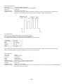
CHIP RESISTOR PART CODE
Chip Resistor Part Coding
8 8
A
Figure
Resistor Code
Value of resistor
Chip resistor
L
W
t
:A
Resistor Code : A
1.0
0.5
0.35
104
1.6
0.8
0.45
108
2
1.25
0.45
118
3.2
1.6
0.55
128
Dimensions (mm)
Wattage
1/16W
Type
1005
Tolerance
5%
Symbol
CJ
1/16W
1/10W
1608
2125
5%
5%
CJ
CJ
1/8W
3216
5%
CJ
Form
L
t
W
– 34 –
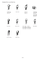
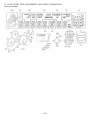
TRANSISTOR ILLUSTRATION
C
B
E
E C B
2SA1091-0
2SC1815GR
2SC2482
B C E
B C E
2SC5147D
2SA1837
2SC4793
2SD2531
E C B
B C E
2SA1015Y
2SD2578-CA
B C E
2SC1741AS(R)
E C B
2SA933SRS
2SA1175FE
2SC1740SRS
2SC2785FE
B C E
2SB1237(Q)
– 35 –
2SA1037K
2SC2412KR
KRC104S
DTA114EK
DTC114EK
KRA104S
E C B
2SD774
DTA114ES
DTA144ES
DTC144ES
2SB1436(R)
WIRING 1 (MAIN)
32
31
30
29
28
27
26
25
24
23
22
21
20
19
18
17
16
15
14
13
12
11
10
9
8
7
6
5
4
3
2
1
A
B
C
D
E
F
G
H
I
J
K
L
M
N
O
P
Q
R
S
T
U
36
SCHEMATIC DIAGRAM – 1 (MAIN)
– 37 –
WIRING – 2 (AUDIO)
32
31
30
29
28
27
26
25
24
23
22
21
20
19
18
17
16
15
14
13
12
11
10
9
8
7
6
5
4
3
2
1
A
B
C
D
E
F
G
H
I
J
K
L
M
N
O
P
Q
R
S
T
U
– 38 –
SCHEMATIC DIAGRAM – 2 (AUDIO)
+
_
_
+
– 39 –
WIRING 3 (NK)
15
14
13
12
11
10
9
8
7
6
5
4
3
2
1
A
B
C
D
E
F
G
H
I
J
K
L
M
N
O
P
Q
R
S
T
U
40
SCHEMATIC DIAGRAM – 3 (NK)
– 41 –
WIRING – 4 (S – JACK)
15
14
13
12
11
10
9
8
7
6
5
4
3
2
1
A
B
C
D
E
F
G
H
I
J
K
L
M
N
O
P
Q
R
S
T
U
– 42 –
SCHEMATIC DIAGRAM – 4 (S-JACK)
– 43 –
WIRING – 5 (JOINT)
32
31
30
29
28
27
26
25
24
23
22
21
20
19
18
17
16
15
14
13
12
11
10
9
8
7
6
5
4
3
2
1
A
B
C
D
E
F
G
H
I
J
K
L
M
N
O
P
Q
R
S
T
U
– 44 –
SCHEMATIC DIAGRAM – 5 (JOINT)
– 45 –
WIRING – 6 (SYSTEM)
32
31
30
29
28
27
26
25
24
23
22
21
20
19
18
17
16
15
14
13
12
11
10
9
8
7
6
5
4
3
2
1
A
B
C
D
E
F
G
H
I
J
K
L
M
N
O
P
Q
R
S
T
U
– 46 –
SCHEMATIC DIAGRAM – 6 (SYSTEM)
– 47 –
WIRING 7 (FR JACK)
15
14
13
12
11
10
9
8
7
6
5
4
3
2
1
A
B
C
D
E
F
G
H
I
J
K
L
M
N
O
P
Q
R
S
T
U
48
SCHEMATIC DIAGRAM – 7 (FR-JACK)
– 49 –
WIRING – 8 (FR – KEY)
15
14
13
12
11
10
9
8
7
6
5
4
3
2
1
A
B
C
D
E
F
G
H
I
J
K
L
M
N
O
P
Q
R
S
T
U
– 50 –
SCHEMATIC DIAGRAM – 8 (FR-KEY)
– 51 –
WIRING – 9 (OPT)
15
14
13
12
11
10
9
8
7
6
5
4
3
2
1
A
B
C
D
E
F
G
H
I
J
K
L
M
N
O
P
Q
R
S
T
U
– 52 –
SCHEMATIC DIAGRAM – 9 (OPT)
– 53 –
WIRING – 10 (PS – 2)
32
31
30
29
28
27
26
25
24
23
22
21
20
19
18
17
16
15
14
13
12
11
10
9
8
7
6
5
4
3
2
1
A
B
C
D
E
F
G
H
I
J
K
L
M
N
O
P
Q
R
S
T
U
– 54 –
SCHEMATIC DIAGRAM – 10 (PS-2)
– 55 –
WIRING – 11 (PS – SW)
32
31
30
29
28
27
26
25
24
23
22
21
20
19
18
17
16
15
14
13
12
11
10
9
8
7
6
5
4
3
2
1
A
B
C
D
E
F
G
H
I
J
K
L
M
N
O
P
Q
R
S
T
U
– 56 –
SCHEMATIC DIAGRAM – 11 (PS-SW)
– 57 –
WIRING – 12 (FR – FL)
32
31
30
29
28
27
26
25
24
23
22
21
20
19
18
17
16
15
14
13
12
11
10
9
8
7
6
5
4
3
2
1
A
B
C
D
E
F
G
H
I
J
K
L
M
N
O
P
Q
R
S
T
U
– 58 –
SCHEMATIC DIAGRAM – 12 (FR-FL)
– 59 –
IC BLOCK DIAGRAM
– 60 –
– 61 –
FL (10-BT-207GK) GRID ASSIGNMENT AND ANODE CONNECTION
GRID ASSIGNMENT
– 62 –
ANODE CONNECTION
– 63 –
IC DESCRIPTION
IC, M37272EFSP-AJD1UOTP
Pin No.
Pin Name
I/O
Description
1
BLK H
I
Blanking H sync input.
2
BLK V
I
Blanking V sync input.
3
A MUTE
O
Audio Amp mute.
4
L MUTE
O
Audio mute.
5
Q SUR
O
Q surround switch.
6
WP
O
EEPROM Write protect.
7
V MUTE
O
Video mute.
8
SEL
O
BPF switch.
9
MAIN SW
–
Connected to GND throuhg a resistor.
10
REMOCON
I
Remote control signal input.
11
SD
I
Pluse check.
12
EXT
I
I2C switch.
13
PON
O
Power switch.
14
AVCC
–
VCC.
15
HLF
–
Filter connection terminal.
16
VHOLD
–
Condenser connection terminal.
17
CV IN
I
Complex video signal input
18
VSS
–
GND.
19
XIN
I
Main Clock (8 MHz).
20
XO
O
Main Clock (8 MHz).
21
VSS
–
GND.
22
VCC
–
VCC.
23
OSC2
–
Not used.
24
OSC1
–
Not used.
25
RST
I
Reset input.
26
SDOUT
O
Not used.
27
FBT DET
O
FBT detection (over 2.5V).
28
REG DET
I
REG detection (over 2.5V).
29
AFTV
I
AFT voltage input.
30
KEY
I
Key input.
31
SDA2
I
I2C bus CH2 data (Reg IC).
32
SDA1
I
I2C bus CH1 data (EEPROM).
33
SCL2
I
I2C bus CH2 data (Reg IC).
34
SCL1
I
I2C bus CH1 data (EEPROM).
35
BBE
O
BBE switch.
36
VM MUTE
O
VM mute.
37
LED
O
Power LED switch.
38
NC
–
Not connected.
39
FAST BLK
O
OSD Blanking.
40
B
O
OSD B output.
41
G
O
OSD G output.
42
R
O
OSD R output.
– 64 –
IC, M38B59EFFP-AJD1UOTP
Pin No.
Pin Name
I/O
Description
1
KEY3
I
Key input 3.
2
S–DET
I
S input monitor. (“L”=DETECTION)
3
SW–CD
I
Pick up/down and tray open/close detection signal input.
4
DISH–SENS
I
Turntable position detection signal input.
5
KEY1
I
Key input 1.
6
KEY2
I
Key input 2.
7
FR–DISC
O
Front input/DVD input switching signal. (“H”=FRONT, "L"=DVD)
8
SETSEL
I
Destination switching input. (Connected to GND through a resistor)
9
RMC
I
Remote control signal input.
10
RESET
I
Reset input.
11
MIC–DET
I
Not used. (Connected to GND through a resistor)
12
POWER–IN
I
TV power on/off detection input.
13
VSS
–
GND.
14
XIN
–
4.19 MHz ceramic oscillator connection.
15
XOUT
–
4.19 MHz ceramic oscillator connection.
16
VCC
–
Power supply (5V).
17
SW2
O
“L” when S is detected. However, this is always “L” when DVD is selected.
18
P–ON2
O
FL power supply on/off signal. (“L”=ON)
19
NC
–
Not used. (Connected to GND through a resistor)
20
PRT1
I
FL power supply monitor input.
21
PRT2
I
VM power supply monitor input.
22
12C–CE
I
CE : 12C-SYS.
23
SCRN–OFF
O
Screen off display. LED on signal. (“H”=ON)
24
DISH–F
O
CD tray rotation control signal.
25
DISH–R
O
CD tray rotation control signal.
26
CLOSE
O
CD tray rotation control signal.
27
OPEN
O
CD tray rotation control signal.
28
VEE
–
(-) power supply for FL display.
29~31
NC
–
Not used. (Connected to GND through a resistor)
32~52
P1~P21
O
FL display tube drive signal.
53
NC
–
Not connected.
54
MIC–MUTE
–
Not used.
55~64
G1~G10
O
FL display tube drive signal.
65
C–CLK
O
CLK : HOST–CD.
66
S–CLK1
O
CLK : SYS–12C.
67
S–SDO
O
DATA : SYS–12C.
68
C–SDO
O
DATA : HOST–CD.
69
SS–CE
O
CE : SYS–12C.
70
S–CLK2
O
CLK : 12C–SYS.
71
NC
–
Not used. (Connected to GND through a resistor)
72
S–RD1
I
DATA : 12C–SYS.
– 65 –
Pin No.
Pin Name
I/O
Description
73
AVSS
–
GND.
74
VREF
–
A/D reference power supply.
75
C–RD1
I
DATA : CD–HOST.
76
STB
–
Not used. (Connected to GND through a resistor)
77
CLK
–
Not used. (Connected to GND through a resistor)
78
CD–CE
O
BUSY : HOST–CD.
79
DATA
–
Not used. (Connected to GND through a resistor)
80
CD–ON
O
CD block power supply on/off signal.
– 66 –
IC, UPD78F0034AYGC-AJD1UFLASH
Pin No.
Pin Name
I/O
Description
1~8
NC
–
Not used. (Connected to GND through a resistor)
9
VSS
–
GND.
10
VDD
–
Power supply.
11~12
NC
–
Not used. (Connected to GND through a resistor)
13
SDA
I
Connect to the TV microprocessor’s 12C bus line.
14
SCL
I
Connect to the TV microprocessor’s 12C bus line.
15
12C–CE
O
CE : 12C–SYS.
16
S–RD1
O
DATA : 12C–SYS.
17
S–CLK2
O
CLK : 12C–SYS.
18
S–SDO
I
DATA : SYS–12C.
19
NC
–
Not used. (Connected to GND through a resistor)
20
S–CLK1
I
CLK : SYS–12C.
21~23
NC
–
Not used. (Connected to GND through a resistor)
24
VDD
–
Supply.
25
AVSS
–
GND.
26~33
NC
–
Not used. (Connected to GND through a resistor)
34
AVREF
–
GND.
35
AVDD
–
Supply.
36
RESET
I
Rest input.
37
NC
–
Not connected.
38
NC
–
Not used. (Connected to VDD)
39
NC
–
Not used. (Connected to GND)
40
X2
–
4.19MHz ceramic oscillator.
41
X1
–
4.19MHz ceramic oscillator.
42
VSS
–
GND.
43
POWER–IN
I
Enter low power consumption mode (HALT) when both TV and SYS are “P-OFF.”
Cancel when either one is turned “ON”.
Enter low power consumption mode (HALT) when both TV and SYS are “P-OFF.”
44
P–ON2–IN
I
Cancel when either one is turned “ON”.
45
MAIN–SW
I
“H” for low power consumption mode (STOP). “L” for cancel. *L fixed.
46
SS–CE
I
CE : SYS–12C.
47
TV–RMC
O
Control signal to TV microprocessor.
48~64
NC
–
Not used. (Connected to GND through a resistor)
– 67 –
VOLTAGE CHART
Test condition for TV mode : COLOR BAR, VOLUME 10
MAIN C.B
PIN NO.
1
2
3
4
5
6
7
8
9
10
11
12
13
14
15
16
17
18
19
20
21
22
23
24
25
26
27
28
29
30
31
32
33
34
35
36
37
38
39
40
41
42
1
2
3
4
5
6
7
8
1
2
3
1
2
3
MODE
DVD
TV
IC1
4.29
4.28
4.91
4.91
0.01
0.01
0.01
0.01
0.02
0.02
5.10
5.10
0
0
0
2.99
5.08
5.08
5.21
5.24
4.62
4.62
5.08
5.08
5.00
5.00
5.05
5.05
2.20
2.18
0.18
0.20
2.33
2.24
0
0
2.26
2.25
2.29
2.29
0
0
5.05
5.05
5.03
5.03
5.04
5.05
5.02
5.03
5.04
5.05
0
0
0
0
2.42
1.89
5.09
5.10
3.68
3.69
5.04
5.05
3.85
3.85
5.05
5.05
0
0
0
0
5.04
5.05
5.04
5.05
0
0
0
0
0
0
0
0
IC3
0
0
0
0
0
0
0
0
5.04
5.05
5.04
5.05
5.09
5.10
5.04
5.05
IC4
5.04
5.05
0
0
5.02
5.03
IC102
5.08
5.06
0
0
8.88
8.90
PIN NO.
STANDBY
5.11
5.11
3.52
1.20
0.02
5.10
0
3.04
5.04
0.47
5.11
5.08
0
5.08
0.75
0
0
0
2.33
2.31
0
5.08
5.06
5.08
5.06
0
5.10
5.06
0.12
5.10
5.08
5.10
5.08
5.10
0
0
0.03
5.08
0
0
0
0
0
0
0
0
5.10
5.10
5.10
5.08
5.08
0
5.06
1
2
3
4
5
6
7
8
9
10
11
12
13
14
15
16
17
18
19
20
21
22
23
24
25
26
27
28
29
30
31
32
33
34
35
36
37
38
39
40
41
42
43
44
45
46
47
48
49
50
51
52
53
54
55
56
0
0
0.43
– 68 –
MODE
TV
IC301
0
0
3.87
3.85
0
3.71
3.25
3.25
0.69
4.43
0
0
1.98
1.96
1.98
1.97
8.83
8.82
4.39
4.38
6.25
6.25
4.77
4.77
0
0
0
0
4.80
4.79
4.77
4.76
4.71
4.70
3.18
3.17
2.85
2.75
2.71
2.67
2.73
2.75
0.77
0.77
5.05
5.05
5.13
5.13
6.43
6.52
8.95
8.96
3.85
3.85
3.70
3.70
2.33
2.40
1.27
1.27
1.12
1.13
1.25
1.25
7.50
7.47
6.01
6.04
0
0
3.17
3.16
3.28
3.24
2.98
2.93
1.86
1.84
5.18
5.18
3.88
3.90
4.71
4.69
4.65
4.64
2.43
1.88
3.92
3.91
8.96
8.93
5.02
3.70
8.79
8.78
7.79
7.77
7.79
7.77
0
0
0
0
2.78
2.77
3.52
4.50
2.77
2.75
0
0
DVD
STANDBY
0
0.21
0
0
0.22
0
0
0
0.44
0.34
0
0
0
0
0.13
0.20
0.18
0.44
0
0
0
0
0.26
0
0.24
0.46
5.09
5.09
0
0
0.24
0
0
0.32
0
0.20
0
0.20
0.27
0.44
0.17
0.50
0.37
0.12
0.43
0.44
0
0.44
0.44
0.44
0
0
0.20
0
0.30
0
PIN NO.
1
2
3
4
5
6
7
1
2
3
4
5
6
7
8
1
2
3
4
5
6
7
8
9
10
11
12
13
14
15
16
17
18
19
20
21
22
23
24
25
26
27
28
29
30
1
2
3
1
2
3
1
2
3
1
2
3
MODE
DVD
TV
IC501
0
0
13.8
13.8
26.0
26.0
0.81
0.77
0.75
0.77
25.9
25.8
1.60
1.65
IC601
25.9
25.3
0
0
0
0
0
0
6.44
6.42
6.44
6.42
2.66
2.70
25.9
25.8
IC701
4.06
4.06
4.06
4.05
3.73
3.70
3.88
3.88
0
0
4.04
4.03
3.96
3.95
4.06
4.05
3.93
3.91
5.22
5.20
4.04
4.03
1.25
1.24
1.28
1.24
0
0
3.97
4.56
8.83
8.82
4.04
4.03
4.05
4.05
3.95
3.12
3.87
4.00
4.05
4.05
3.99
3.97
4.04
4.03
1.76
1.73
4.04
4.03
4.05
4.04
1.71
1.69
3.92
3.92
0
0
4.02
4.01
IC802
120
120
86.3
88.0
0
0
IC803
5.10
5.10
0
0
14.0
12.0
IC804
8.93
8.92
0
0
12.7
12.8
IC805
9.10
9.09
0
0
12.7
12.8
STANDBY
PIN NAME
DVD
0
0.92
1.34
0
0
0.73
0
E
C
B
0
4.62
0.30
E
C
B
5.10
0
5.04
0.60
0
0
0
0
0.18
0.14
0.73
E
C
B
0
4.27
0.02
E
C
B
0
4.90
0.08
E
C
B
5.04
0
5.04
E
C
B
4.38
8.82
5.04
E
C
B
3.10
8.83
3.69
E
C
B
0.25
3.03
0
E
C
B
2.65
4.89
3.28
E
C
B
1.80
6.66
2.41
E
C
B
6.05
8.89
6.66
E
C
B
8.89
0.96
8.81
0.41
0.92
0
E
C
B
0
8.83
0
5.11
0
11.5
E
C
B
3.63
0
2.97
0.46
0
0.46
E
C
B
0
0.95
0
0.44
0
0.46
E
C
B
3.93
0
3.30
MODE
TV
STANDBY
Q1
0
4.62
0.30
0
5.10
0.07
5.10
0
5.04
5.10
5.00
0.02
0
4.26
0.02
0
5.10
0
0
4.90
0.08
0
5.10
0
5.05
0
5.03
5.08
5.06
4.42
3.06
8.80
3.71
0
0.44
0
3.72
8.81
4.36
0
0.44
0
-0.32
2.89
0
-0.08
0.31
0
2.65
4.88
3.28
0
0.44
0.16
1.79
6.66
2.40
0
0.44
0.12
6.03
8.87
6.65
0
0.44
0.44
8.89
0.95
8.81
0.44
0
0.43
0
8.81
0
0
0.43
0
2.74
0
2.08
0.43
0
0
0
0
2.55
0
0.22
0
3.93
0
3.30
0.47
0
0.16
Q2
Q3
Q4
Q5
0.27
0.25
5.09
5.10
0
0.23
0.18
0.10
0.05
0.12
0.15
0.35
0
0
0
0.46
0
0
0
0
0
0
0
0.55
0
0
0.68
0.30
0
0
Q201
Q202
Q301
Q303
Q304
Q305
Q306
Q307
Q309
Q310
Q311
– 69 –
PIN NAME
E
C
B
E
C
B
E
C
B
E
C
B
E
C
B
E
C
B
E
C
B
E
C
B
E
C
B
MODE
TV
Q601
0
0
96.4
96.0
0.33
0.33
Q602
0
0
132
131
-0.06
-0.06
Q603
0
0
20.6
21.6
0.56
0.57
Q604
0
0
5.10
5.10
0
0
Q605
5.10
5.10
0
0
5.10
5.10
Q706
3.80
3.70
8.93
8.94
4.47
4.37
Q801
0
0
0.06
0.05
0.73
0.73
Q806
5.08
5.08
-0.72
-0.88
5.05
5.05
Q811
119
119
0
0
119
119
DVD
STANDBY
PIN NO.
0
0.02
0
1
2
3
4
5
6
7
8
9
10
11
12
13
14
15
16
17
18
19
20
21
22
23
24
0
0.06
0
0
0
0.05
0
5.10
0
5.10
5.10
4.39
0
0.46
0
0
11.2
0
1
2
3
4
5
6
7
8
9
10
11
12
13
14
15
16
17
18
19
20
21
22
23
24
25
26
27
28
29
30
5.11
5.10
4.38
0.40
0
0.29
AUDIO C.B
PIN NO.
1
2
3
4
5
6
7
8
9
10
11
12
13
14
15
16
MODE
TV
IC401
4.00
4.00
4.00
4.00
0.02
0.02
0
0
4.01
4.01
4.01
4.01
4.01
4.01
0
0
4.01
4.01
4.00
4.01
4.01
4.01
4.01
4.01
4.01
4.01
4.65
4.65
4.00
4.00
8.68
8.67
DVD
STANDBY
0.57
0.57
0
0.34
0.55
0.55
0.55
0
0.54
0.54
0.53
0.52
0.52
0.75
0.54
0.46
– 70 –
MODE
TV
IC402
0
0
4.31
0.05
6.27
6.28
8.67
8.69
4.45
4.45
4.45
4.45
4.45
4.45
4.45
4.45
4.44
4.42
4.44
4.45
4.44
4.44
4.44
4.44
4.44
4.44
4.43
4.41
4.43
4.44
0
0
4.44
4.44
4.46
4.45
4.45
4.45
4.45
4.45
8.70
8.68
6.26
6.25
0
0
4.32
0.05
IC403
4.86
4.83
5.43
5.87
5.45
5.72
5.38
5.82
0.13
0.24
5.60
5.60
0
0
3.95
3.95
0
0
0
0
4.70
5.11
0.07
0.06
0.27
0.25
0.25
0.25
5.10
5.10
3.73
3.72
3.88
3.88
4.77
4.77
1.80
1.81
5.64
5.63
4.22
4.21
4.22
4.22
4.89
4.89
8.69
8.69
4.88
4.88
4.88
4.88
4.82
4.82
4.88
4.88
4.88
4.88
4.88
4.88
DVD
STANDBY
0
0.80
0.79
0.46
0
0.57
0.53
0.53
0.51
0.50
0.46
0.23
0.55
0.54
0.52
0
0.50
0.49
0.46
0
0.46
0.76
0
0.75
0.87
0.40
0.22
0.30
0.36
0.45
0
0
0
0
0.50
0.45
0.21
0.21
0.11
5.08
5.08
0.33
0.70
0
0
0
0
0.46
0
0
0
0
0
0
PIN NO.
1
2
3
4
5
6
7
8
9
10
11
12
1
2
3
1
2
3
4
5
6
7
8
9
10
11
12
13
14
15
16
17
18
19
20
21
22
23
24
25
26
27
28
29
30
31
32
MODE
TV
IC404
0
0
0
0
30.1
30.1
0
0
0
0
0
0
15.1
15.1
0.66
0.66
0
0
31.4
31.5
19.9
19.9
15.1
15.1
IC405
5.12
5.12
0
0
8.94
8.94
IC406
4.25
4.25
4.89
4.90
4.24
4.24
4.89
4.90
4.22
4.23
8.12
8.11
4.66
4.24
4.89
4.90
4.65
4.25
4.89
4.90
4.22
4.22
0.84
8.12
4.32
4.32
4.89
4.90
4.89
4.90
0
0
3.72
3.71
3.88
3.88
0
0
4.22
4.22
0
0
5.19
5.08
4.11
4.10
4.11
4.10
5.15
5.05
4.26
4.25
4.19
4.15
8.92
8.92
3.47
3.47
4.89
4.89
4.25
4.60
4.89
4.88
DVD
STANDBY
PIN NO.
0
0
0.53
0
0
0
0.21
2.91
0
3.39
3.34
0.18
1
2
3
4
5
6
7
8
9
10
11
12
13
14
15
16
0
0
0.46
0
0
0
0
0
0.41
0.18
0
0.17
0
0
0.04
0.22
0
0
0
5.08
5.08
1.16
0
0
0.74
0
0
0
0.21
0
0.46
0.22
0
0.69
0
MODE
TV
IC407
0
0
2.25
2.25
2.81
2.81
2.44
2.40
1.31
1.32
0
0
0
0
5.08
5.08
0
0
2.24
2.24
2.07
2.05
3.43
3.43
3.12
3.13
1.75
1.75
2.97
2.90
5.00
5.00
DVD
PIN NAME
DVD
E
C
B
0
5.03
0
E
C
B
31.5
0
31.5
E
C
B
26.0
0.05
25.9
E
C
B
0
3.98
0
E
C
B
0
0
0
E
C
B
0
0
0
E
C
B
0
8.67
0
E
C
B
1.44
8.29
2.00
E
C
B
1.69
8.92
2.31
E
C
B
4.50
8.92
5.15
E
C
B
2.47
0
1.86
– 71 –
MODE
TV
Q402
0
5.04
0
Q403
31.6
0
31.6
Q404
25.8
0.05
25.8
Q405
0
4.07
0
Q406
0
0
0
Q407
0
0
0
Q408
0
8.68
0
Q409
1.44
8.28
2.00
Q410
1.67
8.92
2.29
Q411
4.40
8.92
5.05
Q412
2.42
0
1.81
STANDBY
0
0
0
0
0
0
0
0
0
0
0
0
0
0
0
0
STANDBY
0
4.42
0
2.95
0
2.95
1.12
0.14
0.72
0
-0.12
0
0
0
0
0
0
0
0
0.46
0
0
0.46
0
0
0.46
0
0
0.46
0
0.45
0
0
PIN NAME
DVD
E
C
B
4.49
8.92
5.15
E
C
B
8.93
2.94
8.29
E
C
B
1.35
8.29
1.91
E
C
B
8.92
3.15
8.29
E
C
B
2.22
0
1.58
E
C
B
3.55
8.92
4.19
E
C
B
3.46
8.69
4.10
E
C
B
3.46
8.69
4.10
E
C
B
3.23
8.69
3.88
MODE
TV
Q413
4.39
8.94
5.05
Q414
8.93
2.83
8.29
Q415
1.30
8.29
1.87
Q416
8.93
3.14
8.29
Q417
2.23
0
1.58
Q418
3.52
8.93
4.16
Q751
3.46
8.70
4.11
Q752
3.46
8.69
4.10
Q756
3.23
8.69
3.87
STANDBY
PIN NAME
DVD
0
0.46
0
E
C
B
0.18
8.44
0
0.46
0
0.46
E
C
B
1.66
0
0.97
0
0.46
0
E
C
B
1.58
8.87
2.22
0.46
0
0.46
E
C
B
8.19
3.20
7.55
0.46
0
0.08
E
C
B
0.60
5.59
1.25
0
0.46
0
E
C
B
2.00
5.89
2.65
0
0.46
0
E
C
B
5.28
8.88
5.88
0
0.46
0
E
C
B
119
59.0
118
0
0.46
0.21
E
C
B
0.23
59.0
0.66
MODE
TV
Q907
0.20
8.45
0
Q908
1.66
0
0.96
Q951
1.58
8.86
2.22
Q952
8.18
3.20
7.55
Q953
0.60
5.59
1.24
Q954
2.00
5.89
2.66
Q955
5.27
8.87
5.88
Q956
118
59.2
118
Q957
0.13
59.2
0.68
STANDBY
0
1.21
0
0.17
0
0
0
0.44
0
0.44
0
0
0
0.44
0.06
0
0.44
0.13
0
0.44
0.44
0
0.19
0
0
0.13
0
NK C.B
PIN NAME
DVD
E
C
B
8.40
136
8.88
E
C
B
8.42
143
8.88
E
C
B
8.42
141
8.88
E
C
B
2.55
8.42
2.93
E
C
B
2.42
8.42
2.80
E
C
B
2.44
8.42
2.82
MODE
TV
Q901
8.42
143
8.88
Q902
8.41
146
8.88
Q903
8.41
142
8.88
Q904
2.47
8.42
2.85
Q905
2.40
8.41
2.77
Q906
2.47
8.40
2.85
STANDBY
0.43
1.39
0.43
OPT C.B
PIN NO.
0.43
1.39
0.43
1
2
3
0.44
1.39
0.44
0.15
0.44
0
0.15
0.44
0
0.15
0.44
0
– 72 –
MODE
TV
IC651
1.60
0.33
4.93
0.98
0
0
DVD
STANDBY
0
0
0
JOINT C.B
PIN NO.
1
2
3
4
5
6
7
8
9
10
11
12
13
14
15
16
1
2
3
4
5
6
7
8
9
10
11
12
13
14
15
16
1
2
3
4
5
6
7
8
SYSTEM C.B
MODE
TV
IC101
6.19
5.40
0
3.83
5.45
4.67
0
0
5.46
4.67
2.68
1.88
0
3.83
3.40
2.62
2.98
2.61
0
0
6.18
5.41
0
3.83
11.1
9.66
6.19
5.39
0
0
6.17
5.40
IC102
6.17
5.37
0
3.83
5.43
4.64
0
0
5.43
4.65
2.68
1.83
0
3.83
3.40
2.62
2.99
2.61
0
0
6.15
5.40
0
3.83
11.1
9.66
6.16
5.38
0
0
6.15
5.38
IC103
5.53
4.83
5.53
4.83
5.53
4.83
0
0
5.53
4.83
5.53
4.83
5.53
4.83
11.1
9.69
DVD
STANDBY
PIN NO.
0.37
0
0.55
0
0.38
0.23
0
0
0
0
-0.06
0
0
0.32
0
-0.08
1
2
3
4
5
6
7
8
9
10
11
12
13
14
15
16
17
18
19
20
21
22
23
24
25
26
27
28
29
30
31
32
33
34
35
36
37
38
39
40
41
42
43
44
45
46
47
48
49
50
51
52
53
54
55
56
57
58
59
60
61
62
0
0
0.63
0
0
0.52
0
0
0
0
0
0
0
0
0
0
0.25
0.20
0
0
0
0.24
0.20
0
FR-FL C.B
PIN NO.
1
2
3
MODE
TV
IC701
5.19
5.22
5.21
5.24
0
0
DVD
STANDBY
5.22
5.24
0
– 73 –
MODE
TV
IC301
5.21
5.24
5.19
5.20
4.87
4.88
5.73
5.75
5.21
5.24
5.21
5.24
0
5.09
0
0
5.16
5.22
5.14
5.16
0
0
5.00
5.00
0
0
2.24
2.25
2.52
2.53
5.19
5.21
0.03
8.11
0
0
0
0
4.66
4.66
4.35
4.59
1.64
1.65
3.75
3.78
0
0
0
0
0
0
0
0
-35.0
-30.2
0
0
0
0
0
0
-27.5
-27.2
-32.5
-27.2
-27.5
-24.3
-32.5
-24.3
-32.5
-24.3
-27.5
-21.3
-34.9
-27.2
-34.9
-27.2
-30.0
-24.3
-30.0
-21.3
-32.4
-24.3
-30.0
-24.3
-34.9
-27.2
-27.5
-24.3
-32.4
-27.2
-32.4
-27.2
-34.9
-30.1
-34.9
-30.1
-34.9
-27.2
-34.9
-27.2
-34.9
-30.1
-34.7
-29.9
-34.7
-29.9
-32.5
-27.2
-32.5
-27.2
-32.4
-27.2
-32.4
-27.2
-32.4
-27.2
-32.4
-27.2
-32.4
-27.2
-32.4
-27.2
DVD
STANDBY
5.24
5.23
4.88
5.79
5.24
5.24
0
0
5.22
5.19
0
0
0
2.27
2.54
5.24
0
5.23
0
0
0
5.24
3.76
0
0
0
0
0.58
0
0
0
0.58
0.58
0.58
0.58
0.58
0.58
0.58
0.58
0.58
0.58
0.58
0.58
0.58
0.58
0.58
0.58
0.58
0.58
0.58
0.58
0.58
0.57
0.57
0.63
0.63
0.63
0.63
0.63
0.63
0.63
0.63
PIN NO.
63
64
65
66
67
68
69
70
71
72
73
74
75
76
77
78
79
80
PIN NO.
1
2
3
4
5
6
7
8
9
10
11
12
13
14
15
16
17
18
19
20
21
22
23
24
25
26
27
28
29
30
31
32
33
34
35
36
37
38
39
40
41
MODE
TV
IC301
-32.4
-27.2
-32.4
-27.2
5.03
4.59
5.18
5.16
0.02
0.02
5.12
4.91
5.18
5.16
5.20
5.22
0.43
0.42
5.09
5.12
0
0
5.19
5.21
4.98
0.99
0
0
0
0
1.66
0.99
0
0
5.11
0
DVD
MODE
TV
IC302
0
0
0
0
0
0
0
0
0
0
0
0
0
0
0
0
0
0
5.22
5.24
0
0
0
0
3.72
3.72
3.87
3.88
1.65
1.67
5.10
5.12
5.20
5.22
0.02
0.02
0
0
5.18
5.22
0
0
0
0
0
0
5.21
5.24
0
0
0
0
0
0
0
0
0
0
0
0
0
0
0
0
0
0
0
0
5.22
5.24
5.14
5.17
0.03
0.03
5.22
5.24
0
0
3.08
3.11
2.85
2.78
DVD
STANDBY
PIN NO.
0.63
0.63
0
5.23
0.02
0
5.23
5.24
0
5.24
0
5.23
0
0
0
0
0
0
42
43
44
45
46
47
48
49
50
51
52
53
54
55
56
57
58
59
60
61
62
63
64
STANDBY
0
0
0
0
0
0
0
0
0
5.25
5.19
5.19
5.08
5.08
5.24
5.24
5.24
0.02
0
5.23
0
0
0
5.25
0
0
0
0
0
0
0
0
0
0
5.25
5.19
0.03
5.25
0
3.11
2.83
PIN NAME
E
C
B
MODE
TV
IC302
0
0
5.00
5.00
0
0
0
0
5.18
5.22
5.21
5.24
0
0
0
0
0
0
0
0
0
0
0
0
0
0
0
0
0
0
0
0
0
0
0
0
0
0
0
0
0
0
0
0
0
0
DVD
MODE
TV
Q301
5.19
5.22
5.14
5.17
4.53
4.55
DVD
STANDBY
0
0
5.24
0
5.23
1.27
0
0
0
0
0
0
0
0
0
5.20
5.20
5.20
5.20
5.20
5.20
5.20
5.20
STANDBY
5.23
5.19
4.57
PS-2 C.B
PIN NO.
1
2
3
1
2
3
1
2
3
– 74 –
MODE
TV
IC212
2.49
2.49
0
0
3.76
3.73
IC213
9.16
9.16
0
0
17.6
15.3
IC214
12.0
12.0
0
0
017.6
15.3
DVD
STANDBY
2.49
0
3.72
0
0
0.47
12.0
0
15.2
PIN NAME
E
C
B
E
C
B
E
C
B
E
C
B
E
C
B
E
C
B
E
C
B
E
C
B
E
C
B
E
C
B
E
C
B
E
C
B
E
C
B
E
C
B
MODE
TV
Q211
17.6
15.3
17.6
15.3
16.9
14.6
Q212
0
0
0.06
0.06
5.20
5.23
Q213
11.2
9.78
11.2
9.76
10.5
9.07
Q214
0
0
0
0.02
5.20
5.22
Q217
5.23
5.25
5.17
5.19
1.27
1.30
Q218
5.22
5.25
5.10
5.14
1.27
1.30
Q219
5.22
5.25
5.20
5.22
1.27
1.30
Q220
-36.4
-31.1
-36.3
-31.0
-35.6
-30.3
Q221
-30.1
-25.1
-30.0
-25.0
-29.3
-24.3
Q222
5.22
5.25
5.12
0.99
4.47
5.25
Q223
0
0
0.05
5.25
5.12
0
Q224
1.28
1.30
0
0
0
0
Q225
4.34
4.59
4.34
-1.57
0
4.55
Q226
0
0
0
4.55
5.11
0
DVD
STANDBY
15.2
0.44
15.2
0
15.2
0
10.3
0
10.3
0
10.3
0
5.25
-32.2
5.25
5.25
-5.47
5.25
5.25
0
5.25
-32.2
0.64
-32.2
-5.48
2.53
-5.48
5.25
0
5.25
0
5.25
0
5.25
0
5.24
0
-1.29
0
0
0
0
– 75 –
WAVEFORM
1 IC1 PIN 1 (BLK H)
5 Q202 EMITTER
1
5
0.1 V/div
0.2 ms/div
1 V/div
20 µs/div
2 IC1 PIN 2 (BLK V)
6 IC301 PIN 19 (R OUT)
2
6
1 V/div
20 µs/div
1 V/div
5 ms/div
3 IC1 PIN 11 (SD)
7 IC301 PIN 20 (G OUT)
3
7
1 V/div
20 µs/div
1 V/div
20 µs/div
4 IC701 PIN 2 (TVOUT-L)
8 IC301 PIN 21 (B OUT)
4
8
1 V/div
20 µs/div
0.1 V/div
0.2 ms/div
– 76 –
9 IC301 PIN 45 (CHROMA IN)
# IC407 PIN 10 (FSC-IN)
9
#
0.2 V/div
0.1 µs/div
0.1 V/div
20 µs/div
$ IC407 PIN 13 (C-OUT)
% IC407 PIN 15 (Y-OUT)
0 IC301 PIN 43 (Y IN)
%
0.5 V/div
10 µs/div
0
$
0.2 V/div
10 µs/div
0.2 V/div
10 µs/div
! IC301 PIN 47 (TV DET OUT)
^ Q309 EMITTER
!
^
0.2 V/div
10 µs/div
0.5 V/div
10 µs/div
@ IC407 PIN 4 (V-IN)
& CN601 PIN 1 (H+)
@
&
0.2 V/div
10 µs/div
200 V/div
20 µs/div
– 77 –
* CN601 PIN 2 (H-)
= T602 PIN 3
*
=
20 V/div
20 µs/div
50 V/div
20 µs/div
[ Q751 (EMITTER)
] Q752 (EMITTER)
( CN601 PIN 4 (V-)
[
(
]
5 V/div
5 ms/div
0.2 V/div
0.5 ms/div
) CN601 PIN 5 (V+)
\ J702 (VIDEO OUTPUT)
)
\
0.5 V/div
10 µs/div
10 V/div
5 ms/div
- Q601 COLLECTOR
; D823 ANODE (at POWER ON)
-
;
50 V/div
20 µs/div
10 V/div
5 µs/div
– 78 –
27
_ Q903 COLLECTOR (B-DRIVE)
D827 ANODE (at POWER ON)
_
27
50 V/div
5 µs/div
50 V/div
20 µs/div
, D822 ANODE (at POWER ON)
DVD PLAY (TDV-540
+ CN108 PIN 1 (S-CIN) TITTLE 2 CHAPTER 1)
,
+
2 V/div
10 µs/div
5 V/div
5 µs/div
. Q901 COLLECTOR (R-DRIVE)
{ CN108 PIN 3 (S-YIN)
.
{
50 V/div
20 µs/div
DVD PLAY (TDV-540
TITTLE 2 CHAPTER 1)
2 V/div
10 µs/div
} CN108 PIN 5 (V2-RIN) DVD PLAY (TDV-540
| CN108 PIN 6 (V2-LIN) TITTLE 2 CHAPTER 1)
/ Q902 COLLECTOR (G-DRIVE)
}
/
50 V/div
20 µs/div
|
– 79 –
5 V/div
2 ms/div
: CN108 PIN 8 (V2-VIN)
< IC211 PIN 2 (S)
:
<
MODE : P-STBY
2 V/div
10 µs/div
37
&
IC211 PIN 1 (OCP / FB)
MODE : P-STBY
5 V/div
5 µs/div
< IC211 PIN 2 (S)
MODE : TV
<
37
5 V/div
5 µs/div
1 V/div
5 µs/div
37
.
IC211 PIN 1 (OCP / FB)
< IC211 PIN 2 (S)
MODE : TV
MODE : DISC
<
37
1 V/div
5 µs/div
37
/
IC211 PIN 1 (OCP / FB)
MODE : DISC
5 V/div
5 µs/div
> IC211 PIN 3 (D)
MODE : P-STBY
>
37
1 V/div
5 µs/div
200 V/div
5 µs/div
– 80 –
> IC211 PIN 3 (D)
? PT211 PIN 11
MODE : TV
>
?
200 V/div
5 µs/div
> IC211 PIN 3 (D)
5 V/div
5 µs/div
MODE : DISC
>
200 V/div
5 µs/div
? PT211 PIN 11
MODE : P-STBY
?
5 V/div
5 µs/div
? PT211 PIN 11
MODE : DISC
MODE : TV
?
5 V/div
5 µs/div
– 81 –
ELECTRICAL ADJUSTMENT
Method of Using the Jig Remote Controller
Most of the video circuit and the deflection circuit of this set can be adjusted by using the jig remote controller.
Jig remote controller: RC-AVC01
The jig remote controller RC-AVC01 has the two operating modes. One is the NORMAL mode and the other is the TEST mode.
Either the NORMAL mode or the TEST mode can be selected by short-circuiting or opening the shorting land of the printed foil
pattern.
The TEST mode of the jig remote controller is used for adjusting this set.
The NORMAL mode and the TEST mode are selected as described below.
NORMAL/TEST mode selection method:
Disassemble the jig remote controller and locate the shorting land J1 and J2 on the foil pattern of the printed circuit board.
NORMAL mode:
J1 Shorted
J2 Open
TEST mode:
J1 Open
J2 Shorted
When the remote controller enters the TEST mode, its REPEAT key becomes the TEST key and the CAPTION key becomes the
FINISH key. All keys other than the above two keys are disabled so that the remote controller will not operate even if any key other
than those two keys is pressed.
When the word the TEST key or the FINISH key is written in this Service Manual, it means that the REPEAT key must be
pressed instead of the TEST key, and the CAPTION key must be pressed instead of the FINISH key respectively on the
actual jig remote controller.
– 82 –
Aging Mode
How to enter the aging mode and the contents that are displayed in the aging mode
To enter the aging mode, press the TEST key.
When this set enters the aging mode, the Auto Power Off function that turns off the main power when the input signal is
disconnected, is disabled.
The aging mode is used for aging (such as warming up) of this set before starting the CRT adjustment.
When this set enters the aging mode, the following display appears on CRT screen.
AGING : AFT
OK : 0000H : US21
Destination of the
distinction switch
AFT S-curve status
CRT operating
hours
Contents that are displayed on screen in the aging mode
AFT S-curve display (AFT UP, AFT OK, AFT DN)
The message of either UP or OK or DN (DOWN) is displayed in accordance with the status that the AFT S-curve is high
or optimum or low.
Accumulative operating hours of CRT ON, are displayed
The operating hours of CRT ON are accumulated in units of hour and are displayed in hexadecimal notation.
Example: 1234H=(1 16 16 16)+(2 16 16)+(3 16)+4= 4660 hours
When the accumulative operating hours exceed 7FFFH (32768 hours), the display returns to 0000H.
Distinction switch destination setting
The destination and picture size setups that are set in this set are displayed.
The method of how to set the distinction switch is described in the next section.
– 83 –
How to check and set the distinction switch
When the EEP ROM is going to be replaced, be sure to check and change the distinction switch before starting the EEP
ROM replacement as follows.
1.
2.
3.
4.
5.
6.
Press the TEST key to enter the aging mode.
Press the DISPLAY key to let the DISTINCTION switch appear on screen.
Check that "1: US21" is shown in red among 1: US21 to 6: TW25. If "1: US21" is not shown in red, press the numeric ten key
"1" on the keyboard so that "1: US21" is shown in red.
Check the data contents of the addresses from 0 to F. Confirm that the data contents of the addresses from 0 to F are identical
what are shown in the illustration. If the contents are different from what are shown in the illustration, select the data that you
want to correct using the CHANNEL UP/DOWN key and change the value (0 or 1) of the selected data using the VOLUME UP/
DOWN key.
When data input is complete, press the FINISH key.
If you press the FINISH key, the message INITIALIZING appears on the screen. This set enters the standby state in eight
seconds. (When does this operation, channel presetting etc. are initialized.)
If you press the TEST key, without the initialize being done the AGING mode ends.
– 84 –
This section described the 16 types of distinction switch and the contents that are set by these distinction switches.
SW
0
1
2
3
4
5
6
7
Contents
CLOCK
OSD
PON
RFAGC
MUTE
MTS
QSUR
WEAK
Setup value
0
1
0
1
0
1
1
1
SW
8
9
A
B
C
D
E
F
Contents
BBE
VMUTE
VOL
VCHIP
CCAP
SBASS
SWOOFER
CHILD
Setup value
1
1
1
1
1
1
0
0
SW_0 "CLOCK" [Selection of the OSD reference clock]
External clock. Pins 12 and 24 are used as the
CLOCK=1
external clock ports OSC1 and OSC2
During when the normal OSD is displayed ->
HSYNC is the reference.
CLOCK=2
During when the closed caption is ON and
during asynchronous mode -> HSYNC is the
reference.
SW_5 "MTS" [Use or not use of MTS]
MTS=0
Used
MTS=1
Not used
When MTS is used, only the remote controller is selected.
When MTS = 0 is selected, the remote controller is disabled and
discrimination of audio multiplexing is not implemented.
SW_6 "QSUR" [Use or not use of QSURROUND]
QSUR=0
Used
QSUR=1
Not used
During when the closed caption is ON and
during synchronous mode -> VIDEO signal is
the reference.
During when the closed caption is OFF ->
HSYNC is the reference.
SW_1 "OSD" [Selection of the number corresponding to the
OSD language]
When QSUR = 0 is selected, the remote controller is disabled.
At the same time, the SSURROUND items of the SOUND menu
are not displayed.
Then the blank columns are justified for data display.
[VOL]=0, [QSUR]=0, [BBE]=0, [SBASS]=0, [SWOOFER]=0.
In such cases, the SOUND menu is not displayed.
SW_7 "WEAK" [Use or not use of the sound mute under the
weak electric field]
OSD=0
Eng + Spa
WEAK=0
Used
CSD=1
Eng + Spa + French
WEAK=1
Not used
SW_2 "PON" [Term of the video mute during Power ON]
SW_8 " BBE" [Selection of BBE]
PON=0
MUTE=2.7sec
BBE=0
Used
PON=1
MUTE=5.4sec
BBE=1
Not used
*This setup is not required depending on the production date.
In such a case, hyphen "-" is displayed.
SW_3 "RFAGC" [Selection of measure when RFAGC = 0]
REAGC=0
REAGC=0 & wait 200 ms is used
REAGC=1
REAGC=0 & wait 200 ms is not used
When "wait 200 ms is used" is set, 200 ms delay is given after
the tuner is switched from external input to tuner and then
selection of stations starts.
In the case of BBE = 0, pin-35 (BBE) outputs the CMOS "H"
signal.
When BBE = 0 is selected, the remote controller is disabled.
At the same time, the BBE items of the SOUND menu are not
displayed.
Then the blank columns are justified for data display.
[VOL]=0, [QSUR]=0, [BBE]=0, [SBASS]=0, [SWOOFER]=0.
In such cases, the SOUND menu is not displayed.
SW_4 "MUTE" [Selection of audio mute methods]
MUTE=0
LMUTE & VOL=0
MUTE=1
LMUTE
– 85 –
SW_E "SWOOFER" [Selection of SUBWOOFER]
SW_9 "VMUTE" [Use or not use of the video mute during
channel selection]
VMUTE=0
Used
VMUTE=1
Not used
TA1268 is used
VOL=1
TA1216 is used
[VOL]=0, [QSUR]=0, [BBE]=0, [SBASS]=0, [SWOOFER]=0.
In such cases, the SOUND menu is not displayed.
Used
VCHP=1
Not used
Used
CCAP=1
Not used
SW_D "SBASS" [Selection of SUPER BASS]
SBASS=0
SUPER BASS is not used
SBASS=1
SUPER BASS is used
SUBWOOFER is used
SW_F "CHILD" [Use or not use of the CHILD LOCK function]
SW_C "CCAP" [Use or not use of CHANNEL CAPTION
function]
CCAP=0
SWOOFER=1
[VOL]=0, [QSUR]=0, [BBE]=0, [SBASS]=0, [SWOOFER]=0.
In such cases, the SOUND menu is not displayed.
SW_B "VCHP" [Use or not use of V CHIP function]
VCHP=0
SUBWOOFER is not used
When SUBWOOFER = 0 is selected, the remote controller is
disabled.
In such cases, the SUBWOOFER item of the SOUND menu is
not displayed.
Then the blank columns are justified for data display.
In the case of SW_E [SBASS] = 1, SW_F [SWOOFER] is not set
to SWOOFER = 1.
SW_A "VOL" [Selection of VOL IC]
VOL=0
SWOOFER=0
When SBASS = 0 is selected, the remote controller is disabled.
In such cases, the SUPER BASS item of the SOUND menu is
not displayed.
Then the blank columns are justified for data display.
In the case of SW_F [SUBWOOFER] = 1, SW_E [SBASS] is not
set to SBASS = 1.
[VOL]=0, [QSUR]=0, [BBE]=0, [SBASS]=0, [SWOOFER]=0.
In such cases, the SOUND menu is not displayed.
– 86 –
CHILD=0
CHILD LOCK is not used
CHILD=1
CHILD LOCK is used
How to enter, adjust and terminate the adjustment mode
1.
2.
3.
4.
5.
6.
7.
Press the TEST key while the machine is in the aging mode. The adjustment menu display appears on the screen showing the
machine is in the adjustment mode.
The adjustment pages can be selected by pressing the CHANNEL UP/DOWN key.
Press the numeric ten key to select the desired adjustment item.
Example: When you want to select the adjustment item "1. H POS", select the PAGE1 and press the key 1 on page 1.
When you want to change the adjustment value, press the VOLUME UP/DOWN key.
When you want to move to the next adjustment item or return to the previous adjustment item, press the CHANNEL UP/DOWN
key.
When you want to return to the PAGE screen, press the SOUND EFFECT key.
When you want to terminate the adjustment mode, press the TEST key.
*
*
When you want to change the adjustment value, press the VOLUME UP/DOWN key.
If you press the MUTE key or other keys while you are operating the menu screen, data of the
menu contents disappears. In such a case, press the number of setup item to show the setup
screen, and then press the SOUND EFFECT key to show the menu contents again on screen.
– 87 –
Setting the IIC bus data
Initial value
When the EEP ROM is replaced, enter the following initial value before starting adjustment.
When this set is brought in for normal repair other than the EEP ROM replacement, confirm status of the corresponding item
only before starting adjustment.
Horizontal Picture Position Adjustment
Input signal:
Measuring equipment:
Adjustment point:
Adjustment method:
Monoscope signal
SHIBASOKU TP20A1
Adjustment menu PAGE 1-1
Adjust the horizontal position of picture so that the horizontal position scales at the rightmost end and at the
leftmost end of a monoscope picture are of equal amount, using the VOLUME UP/DOWN key.
Simplified adjustment procedure
If a monoscope signal is not available, connect the playback video signal of VTR that plays back TTV-N6T (test tape), to the
external video input connector and perform the horizontal picture position adjustment in the same manner as shown above.
Alternately, connect the cross-hatch output signal of the pattern generator to the external video input connector. Adjust the
horizontal picture position so that the dot mark in the center of the cross-hatch signal is positioned at the center of the screen
and the number of scales in the right and left on screen are of equal amount as shown in the illustration, using the VOLUME
UP/DOWN key.
Horizontal Picture Size Adjustment
Input signal:
Measuring equipment:
Adjustment point:
Adjustment method:
Monoscope signal
SHIBASOKU TP20A1
SFR601
Adjust the horizontal picture size so that the horizontal position scales at the rightmost end and at the
leftmost end of a monoscope picture are 5.5±0.5 scales using SFR601.
Simplified adjustment procedure
If a monoscope signal is not available, connect the playback video signal of VTR that plays back TTV-N6T (test tape), to the
external video input connector and perform the horizontal picture size adjustment in the same manner as shown above.
Alternately, connect the cross-hatch output signal of the pattern generator to the external video input connector. Adjust the
horizontal picture size so that the number of scales from the center of the screen to the rightmost end and the number scales
from the center to the leftmost end on screen are of equal amount (8 to 9 scales) using the VOLUME UP/DOWN key.
– 88 –
Pin and Barrel Adjustment
Input signal:
Measuring equipment:
Adjustment point:
Adjustment method:
Cross-hatch signal
Pattern generator
Pin-SFR602, Barrel-SFR603
Adjust the pin and barrel distortion of picture so that the areas A and B in the following illustration become
minimum at both the rightmost end and leftmost end of the cross-hatch display, using SFR602 and SFR603.
Vertical Picture Position Adjustment
Input signal:
Measuring equipment:
Adjustment point:
Adjustment method:
Monoscope signal
SHIBASOKU TP20A1
Adjustment menu PAGE 1-2
Adjust the vertical position of picture so that the V-CENTER line at the center of the monoscope picture is
positioned at the center mark using the VOLUME UP/DOWN key of the jig remote controller. The vertical
picture position adjustment and the V LINEARITY adjustment must be performed together alternately.
Repeat the vertical picture position adjustment and the V LINEARITY adjustment each other a few times so
that the number of scales in the topmost end and the bottommost end are of equal amount when the center
line is positioned at the center mark.
Simplified adjustment procedure
If a monoscope signal is not available, connect the playback video signal of VTR that plays back TTV-N6T (test tape), to the
external video input connector and perform the horizontal picture position adjustment in the same manner as shown above.
Alternately, connect the cross-hatch output signal of the pattern generator to the external video input connector. Adjust the
horizontal picture position so that the V-CENTER line at the center of the monoscope picture is positioned at the center mark
using the VOLUME UP/DOWN key of the jig remote controller.
– 89 –
Vertical Linearity Adjustment
Input signal:
Measuring equipment:
Adjustment point:
Adjustment method:
Monoscope signal
SHIBASOKU TP20A1
SFR501
Adjust the vertical linearity so that the number of vertical position scales at the topmost end and at the
bottommost end are of equal amount using SFR501. The vertical linearity adjustment and the vertical
picture position adjustment must be performed together alternately. Repeat the vertical picture position
adjustment and the vertical linearity adjustment each other a few times so that the number of scales in the
topmost end and the bottommost end are of equal amount when the center line is positioned at the center
mark.
Simplified adjustment procedure
If a monoscope signal is not available, connect the playback video signal of VTR that plays back TTV-N6T (test tape), to the
external video input connector and perform the horizontal picture position adjustment in the same manner as shown above.
Alternately, connect the cross-hatch output signal of the pattern generator to the external video input connector. Adjust the
vertical linearity so that the number of vertical position scales at the topmost end and at the bottommost end are of equal
amount using SFR501.
Vertical Picture Size Adjustment
Input signal:
Measuring equipment:
Adjustment point:
Adjustment method:
Monoscope signal
SHIBASOKU TP20A1
Adjustment menu PAGE 1 "3. V. SIZE"
Adjust the vertical picture size so that the vertical position scales at the topmost end and at the bottommost
end of a monoscope picture are 4.5±0.5 scales using the VOLUME UP/DOWN key of the jig remote
controller.
Simplified adjustment procedure
If a monoscope signal is not available, connect the playback video signal of VTR that plays back TTV-N6T (test tape), to the
external video input connector and perform the horizontal picture size adjustment in the same manner as shown above.
Alternately, connect the cross-hatch output signal of the pattern generator to the external video input connector. Adjust the
vertical picture size so that the pattern of the cross-hatch screen becomes complete square using the VOLUME UP/DOWN key
of the jig remote controller.
OSD Position Adjustment
Input signal:
Adjustment point:
Adjustment method:
No input signal is required
Adjustment menu PAGE 1-4
Adjust the OSD position so that the crossing (+) mark on both sides of the OSD are positioned in the same
distance from the both ends of screen, using the VOLUME UP/DOWN key of the jig remote controller.
– 90 –
PIF VCO Adjustment
Note: Be sure to perform the PIF VCO adjustment whenever the VCO coil (L205) is replaced.
Measuring equipment: Spectrum analyzer, search coil
The method how to manufacture the search coil
Setting the spectrum analyzer
Center frequency:
Reference:
Span:
Marker:
45.75 MHz
60 dBµV/ Should be determined by the amplitude of waveform
10 MHz
Set the markers so that the peak marker function can be used.
Adjustment method
1.
2.
3.
4.
5.
Allow 30 minutes or more of aging time of this set.
When an antenna is connected to the antenna terminal, remove an antenna.
Connect pin-5 of IC301 to ground using a wire.
Connect the search coil that is locally manufactured to a spectrum analyzer. Move the tip of the spectrum analyzer to L205.
Adjust L205 so that the peak is positioned at 45.75 MHz±50 kHz on a spectrum analyzer.
Note 1: Be careful that the search coil does not touch the VCO coil or its leads.
Note 2: Take reading of the spectrum analyzer value when the adjustment screwdriver is removed from the VCO coil.
Note 3: Press the marker peak key of a spectrum analyzer. Read the value when the marker peak key is pressed and adjust the
value for 45.75 MHz. The value cannot be read again even if the marker peak key is pressed until the cursor completes a
full scan of tracing over the waveform on a spectrum analyzer display.
(The value can be read only once during one scan. The value remains the same even if the marker peak key is pressed
before the scan is completed.)
Simplified adjustment procedure
Input signal:
Measuring equipment:
Adjustment point:
Adjustment method:
Color bars (RF)
Pattern generator
Adjustment menu PAGE 1-5, L205
Select the adjustment menu PAGE 1-5 "RF VCO". Set the RF VCO value to 58. Adjust L205 so that the
normal color bar picture and the message AFT OK appear on display. When doing this, adjust L205 for the
center of AFT OK lock-in range as close to the center as possible.
– 91 –
SIF Adjustment
Note: Be sure to perform this adjustment whenever the SIF coil (L201) is replaced.
Simplified adjustment procedure
Input signal:
Measuring equipment:
Adjustment point:
Test point:
Adjustment method:
Normal off-the-air broadcast
Oscilloscope
L201
IC301 pin-54
Adjust L201 so that the center value of the audio signal waveform at IC301 pin-54 becomes 4.5±0.2 Vdc.
RF AGC Adjustment
Input signal:
Input level:
Channel:
Video:
Audio:
Modulation degree:
Measuring equipment:
Test point:
Adjustment point:
Adjustment method:
RF input
60 dBµV, P/S 7 dB
11 CH (fp = 199.25 MHz)
Color bars (full field)
400 Hz
Video 87.5%, audio 100% (±25 kHz deviation)
Pattern generator, oscilloscope
TP101, RF AGC
Adjustment menu PAGE 1-6
Connect an oscilloscope to TP 101. Adjust the voltage at the test point for 4.0±0.5 Vp-p using the jig remote
controller VOLUME UP/DOWN keys.
SCREEN VOLTAGE Adjustment
Note: Be sure to perform the WHITE BALANCE Adjustment whenever the SCREEN VOLTAGE Adjustment is performed.
Input signal:
No input signal
Measuring equipment: Oscilloscope
Test point:
SO901 R, G, B
Adjustment point:
Adjustment menu PAGE 2-1, 2-2, 2-3 SCREEN VR (FBT: T601)
Adjustment method:
1. Connect an oscilloscope to SO901 R (R cathode). Adjust the adjustment menu PAGE 2-1 "1. R CUTOFF" so that the voltage
as shown in the illustration becomes 175±2 V.
2. Perform the SCREEN VOLTAGE adjustment for the G and B channels in the same manner as step 1 for the R channel.
3. Press the numeric key "0" of the jig adjustment remote controller on the adjustment menu screen so that the horizontal single
line display on the screen.
4. Adjust the SCREEN VR to the point where the horizontal single line display just starts illuminating.
5. Press the numeric key "0" of the jig remote controller to return to the menu screen.
FOCUS Adjustment
Input signal:
Measuring equipment:
Adjustment point:
Adjustment method:
Dot-pattern signal
Pattern generator
FOCUS VR (FBT:T601)
Adjust the FOCUS VR (FBT:T601) for optimum focus on the dot pattern screen.
– 92 –
White Balance Adjustment
Note: Allow 20 minutes or longer of warm-up time before starting the white balance adjustment. Repeat the entire steps of the white
balance adjustment several times until all three channels of red, green and blue are balanced each other.
Input signal:
White raster
Measuring equipment: Pattern generator
Adjustment point:
Adjustment menu PAGE 2-1 to PAGE 2-5
Adjustment method:
1. Connect the white raster signal from the pattern generator to the input.
2. Find out which color is most strongly illuminating among the three colors of red, green and blue. Set the cut-off value of the
color that you have selected as the most strongly illuminating color, to 127 as the fixed value. Adjust the cut-off values of the
remaining two colors until the optimum white balance is obtained on screen using the VOLUME UP/DOWN keys of the jig
remote controller.
3. Select the adjustment menu 2-4 G. DRIVE and increase the G DRIVE value to 200 or higher using the VOLUME UP/DOWN
keys of the jig remote controller. The screen will get greenish.
4. Then start decreasing the G DRIVE value using the jig remote controller until the green color looks as if it is lost.
5. Select the adjustment menu 2-5 B. DRIVE and increase the B DRIVE value to 200 or higher using the VOLUME UP/DOWN
keys of the jig remote controller. The screen will get bluish.
6. Then start decreasing the G DRIVE value using the jig remote controller until the blue color looks as if it is lost.
7. Repeat the above steps 1 to 6 several times until white balance is obtained.
SUB BRIGHTNESS Adjustment
Input signal:
Measuring equipment:
Adjustment point:
Adjustment method:
Color bars (stair step)
Pattern generator
Adjustment menu PAGE 3-2
Adjust SUB BRIGHTNESS so that the second scale (second step) from the right of the stair step signal just
starts illuminating using the VOLUME UP/DOWN keys of the jig remote controller.
SUB CONTRAST Adjustment
Input signal:
Measuring equipment:
Test point:
Adjustment point:
Adjustment method:
Color bars (Q/W, white/100%, chroma/OFF)
Oscilloscope, pattern generator
SO901 R (R cathode)
Adjustment menu PAGE 3-1
Connect an oscilloscope to SO901 R (R cathode). Adjust the SUB CONTRAST so that the 100% white
voltage from the pedestal is 90±2 V using the jig remote controller VOLUME UP/DOWN keys.
– 93 –
SUB COLOR Adjustment
Input signal:
Measuring equipment:
Test point:
Adjustment point:
Adjustment method:
Color bars (full field, white/100%)
Oscilloscope, pattern generator (Leader 408NPS)
CN901 pin-3
Adjustment menu PAGE 3-4
Connect an oscilloscope to CN901. Adjust the SUB COLOR so that the white (75%) line and the blue line
are aligned to a single straight line using the jig remote controller VOLUME UP/DOWN keys. The white
(75%) line and the blue line must be aligned to a single straight line within 0.3±0.1 V difference.
Simplified adjustment procedure
Input the blue raster signal instead of the color bar signal. Adjust the voltage between the pedestal level to the blue peak for 2.0
V±0.1 V using the jig remote controller VOLUME UP/DOWN keys as shown.
– 94 –
SUB TINT Adjustment
Input signal:
Measuring equipment:
Test point:
Adjustment point:
Adjustment method:
Color bars (full field, white/75%)
Oscilloscope, pattern generator (Leader 408NPS)
CN901 pin-3
Adjustment menu PAGE 3-3
Connect an oscilloscope to CN901. Adjust the SUB TINT so that the magenta line and the blue line are
aligned to a single straight line using the jig remote controller VOLUME UP/DOWN keys.
TV Setting Data
Contents of the TV setting data are fixed to the respective models.
Do not make any settings other than what are specified below.
Confirm that the contents of the adjustment menu are identical to the following table.
If the contents of the adjustment menu are not the same as what are shown in the above table, return the contents to what are
shown in the table using the VOLUME UP/DOWN keys of the jig remote controller.
ATT Adjustment
Input signal:
RF input
Input level:
60 dBµ, P/S 7 dB
Channel:
Not specified
Video:
Not specified
Audio:
100 Hz (Monaural)
Modulation degree:
Video 87.5%, audio 100% (±25 kHz deviation)
Measuring equipment: Pattern generator, NTSC US MPX, VTVM
Test point:
IC701 pin-2
Adjustment point:
Adjustment menu PAGE 5-1
Adjustment method: Adjust ATT so that the voltage at IC701 pin-2 beomces 490 mV±20 mV rms using the VOLUME UP/DOWN
keys of the jig remote controller.
– 95 –
STEREO SEPARATION Adjustment
Input signal:
Stereo test signal from audio generators-1 and -2
Input level:
60 dBµ, P/S 7 dB
Channel:
11 CH (fp = 199.25 MHz)
Video:
Color bars (1 Vp-p, modulation degree 87.5%)
Audio:
400 Hz±25 kHz deviation
Setting the audio generator-1
L-CH only
300 Hz, ±7.5 kHz deviation
STEREO, NR: ON
Setting the audio generator-2
L-CH only
3 kHz, ±7.5 kHz deviation
PRE-EMP: ON
Other setups are the same as those of audio generator-1.
Measuring equipment:Pattern generator, NTSC US MPX, VTVM
Test point:
IC701 pin-1
Adjustment point:
Adjustment menu PAGE 5-2 (WIDEBAND), 5-3 (SPECTRAL)
Adjustment method:
1. Establish the "Setting the audio generator-1". Adjust the voltage at IC701 pin-1 so that the voltage is minimized by changing the
WIDEBAND value on PAGE 5-2 using the VOLUME UP/DOWN keys of the jig remote controller.
2. Establish the "Setting the audio generator-2". Adjust the voltage at IC701 pin-1 so that the voltage is minimized by changing the
SPECTRAL value on PAGE 5-3 using the VOLUME UP/DOWN keys of the jig remote controller.
– 96 –
ON THE DEFAULT MODE WHEN SHIPPED FROM THE FACTORY
Various settings can be returned to the default mode when shipped from the factory by performing the
following procedure.
1)
2)
3)
Turn ON the main power and enter the DVD mode.
Eject all discs to establish the NO DISC state and wait until the DISC READING is completed.
Keep pressing the DISC button and the BACK SKIP buttons at the same time until the aiwa wall paper disappears on the
display. When the aiwa wall paper disappears, remove the hands pressing the buttons. (It takes about 4 to 5 seconds.)
4) The aiwa wall paper appears again and the message "AL CLEAR" appears on the FL display.
5) Turn OFF the main power. This is the end of the procedure.
– 97 –
DVD TEST MODE
1. How to Start Up Test Mode
While pressing the DISC button of the main unit, turn ON the power switch (main switch). At this time, keep pressing the DISC
button until all the indicators on the FL display tube light. (Refer to the following figure.)
After all the indicators on the FL display tube light for three minutes or longer, the display changes to the status display or the media
display.
2. How to Quit Test Mode
Turn OFF the power switch of the main unit or that of the remote control unit.
3. Functions
Status display and media display
After the DVD test mode starts up, the display of the FL tube changes to "SxxMxx".
"Sxx" shows the status.
Status
Contents
S41
STOP status of pickup at inner circumference
S42
STOP status of pickup at inner circumference with resume data
S43
PLAY status
S44
PAUSE status
S45
SKIP status
S46
The status in which TOC reading is in progress
S47
The signal that shows the end of the EEPROM write (This is not displayed in this model.)
S48
Indication that status has not been determined yet
S49
Indication of DISC END
"Mxx" shows the type of media.
Media type
Contents
M21
NO DISC
M22
CD-DA
M23
VCD (Ver1.0 or Ver1.1)
M24
VCD (Ver2.0)
M25
DVD
When any status (any number) other than what are shown in the above tables is displayed, the data is the illegal data.
Display example:
The following display has the following meaning.
S41 STOP
M21 NO DISC
– 98 –
MECHANICAL EXPLODED VIEW 1 / 1
43
44
E
PWB
J
27
L
47
c
L
E
22
K
E
23
28
J
O
c
47
23
25
N
24
J PWB
PWB
B
26
D
b
35
G
A
h
a
d
O PLATE, E-FJ
e
PWB
A
A
PLATE, REAR 1
PWB
30
A
33
B
f
D
SHLD, TOP
29
19
A
8
PWB
B
18
A
g
E
31
46
A
32
A
A
PWB
PWB
A
e
A
d
7
SHLD-PLATE,
TOP2
D
PLATE, BT UL
17
PLATE, REAR 2
E
b
C
16
H
G
O
h
21
PWB
27
O
E
M
F
PWB
34
41
5
6
10
9
D
AZG-D
11
4
12
13
3
2
1
15
36
PWB
D
16
PLATE,
WINDOW
A
14
40
a
45
20
C
39
g
f
A
42
PWB
38
37
D
D
SHLD-PLATE, LOW
– 99 –
A
D
B
I
I
MECHANICAL PARTS LIST 1 / 1
REF. NO. PART NO.
!
!
1
2
3
4
5
8A-JD1-215-010
8A-JD1-013-010
8A-JD1-011-010
8A-JD1-006-010
8A-JD1-002-010
KANRI
DESCRIPTION
NO.
SPR-C,POWER
BTN,POWER
COVER, PLAY KEY
WINDOW,DISPLAY DVD
PANEL,MAIN
6
7
8
9
10
8A-JD1-014-010
8A-JD1-007-010
8A-JD1-001-010
8Z-JE7-008-010
8A-JD1-010-010
LENS,SCREEN
KEY,SCREEN
CABI,FR
BADGE,AIWA ST 52.5
KEY,STOP
11
12
13
14
15
8A-JD1-008-010
8A-JD1-201-010
8A-JD1-012-010
8A-JD1-009-010
8A-JD1-015-010
KEY,MAIN
KEY,PLAY
BTN,PLAY
KEY,VOL
LENS,LED
16
17
18
19
20
8A-JD1-681-010
8A-JD1-648-010
8A-JD1-208-010
8A-JE5-616-010
8A-JD1-203-010
21
22
23
24
25
REF. NO. PART NO.
36
37
38
39
40
8A-JD1-211-010
8A-JD1-207-010
8A-JD1-666-010
8A-JD1-667-010
8A-JD1-003-010
KANRI
DESCRIPTION
NO.
FRAME,MECH R
HLDR,MECH R
FF-CABLE,11P 1.0 400MM 30V
FF-CABLE,13P 1.0 400MM 30V
PANEL,TRAY
41
42
43
44
45
8A-JD1-206-010
8Z-HU1-033-010
8Z-JE7-607-110
86-LBN-625-010
87-A91-981-010
HLDR,MECH L
BADGE,DVD
CONN ASSY,1P CRT GND
COTL,DGC21 6LB-22
F-BEAD,18.8/1.1/7 HF7OSH
46
47
A
B
C
8A-JD1-226-010
87-A90-332-010
87-067-680-010
8Z-AV1-215-010
87-078-070-010
PLATE,FRAME BK
HLDR,SF-2001 HV CABLE
BVI T3+3-10
S-SCREW,IT3B+3-8 ZN
BVIT3B+4-12
SPKR,F4*1680HM
CONN ASSY,4P SPEAKER
FRAME,MECH FR
AC CORD ASSY,USA LK
FRAME,POWER
D
E
F
G
H
87-067-689-010
87-067-690-010
87-761-096-410
8Z-JS1-210-010
87-067-844-010
BVTT+3-8
TAPPING SCREW, BVIT3+3-12
VFT2+3-10 W/O SLOT
BVT2+4-20
BVT2+4-16 BLK
8A-JD1-202-110
8Z-JE7-610-010
8Z-JE7-609-010
8A-JD1-005-010
8A-JD1-017-010
FRAME,TV
HV-CABLE, 2P ZJE-7FOC-SCR
ANODE-CAP,ZJE-7
PANEL,REAR 2
CABI,REAR U
I
J
K
L
M
87-067-703-010
87-067-641-010
87-067-688-010
87-067-579-010
87-067-619-010
TAPPING SCREW, BVT2+3-10
UTT2+3-8(W/O SLOT)BL
BVTT+3-6
TAPPING SCREW, BVT2+3-8
BVT1+3-12
26
27
28
29
30
8A-JE7-607-010
83-JT1-217-010
8A-JE7-620-010
8A-JD1-664-010
8A-JD1-661-110
CRT,A51LTH196X-YOKE FLAT
SPR-E,EARTH
CONN ASSY,2P VM-NK
FF-CABLE,5P 1.0 400MM 30V
CONN ASSY,12P V JOINT TO UNIT
N
O
87-067-758-010
8Z-JBS-205-010
BVT2+3-12 W/O SLOT
W-G,10-20-2
31
32
33
34
35
8A-JD1-665-110
8A-JD1-210-010
8A-JD1-004-010
8A-JD1-209-010
8A-JD1-204-010
CONN ASSY,3P V UNIT TO OPT
FRAME,MECH L
PANEL,REAR 1
FRAME,MECH BK
HLDR,PWB
!
COLOR NAME TABLE
Basic color symbol
Color
Basic color symbol
Color
Basic color symbol
Color
B
Black
C
Cream
D
Orange
G
Green
H
Gray
L
Blue
LT
Transparent Blue
N
Gold
P
Pink
R
Red
S
Silver
ST
Titan Silver
T
Brown
V
Violet
W
White
WT
Transparent White
Y
Yellow
YT
Transparent Yellow
LM
Metallic Blue
LL
Light Blue
GT
Transparent Green
LD
Dark Blue
DT
Transparent Orange
GM
Metallic Green
YM
Metallic Yellow
DM
Metallic Orange
PT
Transparent Pink
LA
Aqua Blue
– 100 –
2–11, IKENOHATA 1–CHOME, TAITO-KU, TOKYO 110, JAPAN TEL:03 (3827) 3111
9301978 0251431
Printed in Singapore