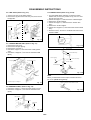
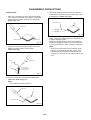
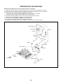
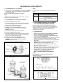
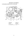
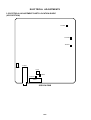
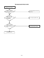
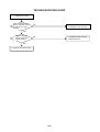
1
VX-S207
U
SERVICE MANUAL
INTEGRATED COLOR TV / STEREO VIDEO
CASSETTE RECORDER
BASIC TAPE MECHANISM : OVD-6
REVISION PUBLISHING 1
VERSION
CRT
PWB070
PWB010
A
A51KSV43X07(M0)
TM9437A
TC9296A
B
A51KST93X31(VM0)
TM9433A
TC9293A
There are 2 types for this model. Because, PCB and Parts are different each other.
VERSION
SERIAL
S/M PARTS No.
A
672-0226001 ~ 672-0628960
09-003-341-4N1
B
672-0712001 ~
09-003-341-4S1
This manual is for VERSION “B” in the above List.
S/M Code No.09-003-341-4S1
DA
TA
NT
E
EM
L
PP
U
S
TABLE OF CONTENTS
TABLE OF CONTENTS ......................................................................................................................................................
SERVICING NOTICES ON CHECKING .............................................................................................................................
DISASSEMBLY INSTRUCTIONS
REMOVAL OF MECHANICAL PARTS AND P.C. BOARDS ...........................................................................................
REMOVAL OF DECK PARTS .........................................................................................................................................
REMOVAL OF ANODE CAP ...........................................................................................................................................
REMOVAL AND INSTALLATION OF FLAT PACKAGE IC .............................................................................................
KEY TO ABBREVIATIONS .................................................................................................................................................
SERVICE MODE LIST ........................................................................................................................................................
PREVENTIVE CHECKS AND SERVICE INTERVALS .......................................................................................................
NOTE FOR THE REPLACING OF MEMORY IC ................................................................................................................
SERVICING FIXTURES AND TOOLS ................................................................................................................................
PREPARATION FOR SERVICING .....................................................................................................................................
VCR TEST TAPE INTERCHANGEABILITY TABLE ...........................................................................................................
MECHANICAL ADJUSTMENTS
CONFIRMATION AND ADJUSTMENT ...........................................................................................................................
CONFIRMATION AND ADJUSTMENT OF TAPE RUNNING MECHANISM ..................................................................
MECHANISM ADJUSTMENT PARTS LOCATION GUIDE .............................................................................................
ELECTRICAL ADJUSTMENTS
ADJUSTMENT PROCEDURE .........................................................................................................................................
BASIC ADJUSTMENTS ..................................................................................................................................................
ELECTRICAL ADJUSTMENT PARTS LOCATION GUIDE .............................................................................................
PURITY AND CONVERGENCE ADJUSTMENTS ..........................................................................................................
TROUBLESHOOTING GUIDES .........................................................................................................................................
IC DESCRIPTIONS ............................................................................................................................................................
SERVO TIMING CHART ....................................................................................................................................................
SYSTEM SWITCH MODE ..................................................................................................................................................
SEMICONDUCTOR BASE CONNECTIONS ......................................................................................................................
BLOCK DIAGRAMS
TV ....................................................................................................................................................................................
Y/C/AUDIO/HEAD AMP/IN/OUT .....................................................................................................................................
MICON/POWER/OPERATION ........................................................................................................................................
HIFI ..................................................................................................................................................................................
PRINTED WIRING BOARDS (OPERATION/FRONT JACK/DECK) ..................................................................................
OPERATION SCHEMATIC DIAGRAM ...............................................................................................................................
FRONT JACK SCHEMATIC DIAGRAM .............................................................................................................................
DECK SCHEMATIC DIAGRAM ..........................................................................................................................................
PRINTED WIRING BOARDS (SYSCON) ...........................................................................................................................
Y/C/AUDIO/HEAD AMP SCHEMATIC DIAGRAM ..............................................................................................................
MICON SCHEMATIC DIAGRAM ........................................................................................................................................
CHROMA/IF SCHEMATIC DIAGRAM ................................................................................................................................
HIFI SCHEMATIC DIAGRAM .............................................................................................................................................
IN/OUT SCHEMATIC DIAGRAM ........................................................................................................................................
POWER SCHEMATIC DIAGRAM ......................................................................................................................................
SOUND AMP SCHEMATIC DIAGRAM ..............................................................................................................................
PRINTED WIRING BOARDS (MAIN/CRT) .........................................................................................................................
DEFLECTION SCHEMATIC DIAGRAM .............................................................................................................................
TV POWER SCHEMATIC DIAGRAM .................................................................................................................................
CRT SCHEMATIC DIAGRAM .............................................................................................................................................
INTERCONNECTION DIAGRAM .......................................................................................................................................
WAVEFORMS ....................................................................................................................................................................
MECHANICAL EXPLODED VIEW ......................................................................................................................................
MECHANICAL REPLACEMENT PARTS LIST ...................................................................................................................
ACCESSORY REPLACEMENT PARTS LIST ....................................................................................................................
CHASSIS EXPLODED VIEW (TOP VIEW) ........................................................................................................................
CHASSIS EXPLODED VIEW (BOTTOM VIEW) ................................................................................................................
CHASSIS REPLACEMENT PARTS LIST ...........................................................................................................................
ELECTRICAL REPLACEMENT PARTS LIST ....................................................................................................................
A1-1
A1-1
A2-1
B1-1, B1-2
B2-1~B2-5
B3-1
B4-1, B4-2
C1-1, C1-2
C2-1
C3-1, C3-2
C4-1
C5-1
C5-2, C5-3
C6-1
D1-1, D1-2
D1-2, D1-3
D1-4
D2-1
D2-1~D2-4
D2-5, D2-6
D2-7
E-1~E-27
F1-1~F1-3
F2-1
F2-2
G-1, G-2
H-1
H-2
H-3
H-4
I-1
I-2
I-3
I-4
I-5~I-7
I-8
I-9
I-10
I-11
I-12
I-13
I-14
I-15
I-16
I-17
I-18
I-19
J-1, J-2
K1-1, K1-2
K1-3
K1-3
K2-1
K2-2
K2-3
K3-1~K3-4
SERVICING NOTICES ON CHECKING
1. KEEP THE NOTICES
6. AVOID AN X-RAY
As for the places which need special attentions, they are
indicated with the labels or seals on the cabinet, chassis
and parts. Make sure to keep the indications and notices
in the operation manual.
Safety is secured against an X-ray by considering about
the cathode-ray tube and the high voltage
peripheral circuit, etc.
Therefore, when repairing the high voltage peripheral
circuit, use the designated parts and make sure not
modify the circuit.
Repairing except indicates causes rising of high
voltage, and it emits an X-ray from the cathode-ray tube.
2. AVOID AN ELECTRIC SHOCK
There is a high voltage part inside. Avoid an electric
shock while the electric current is flowing.
7. PERFORM A SAFETY CHECK AFTER
SERVICING
3. USE THE DESIGNATED PARTS
The parts in this equipment have the specific
characters of incombustibility and withstand voltage for
safety. Therefore, the part which is replaced should be
used the part which has the same character.
Especially as to the important parts for safety which is
indicated in the circuit diagram or the table of parts as
a
mark, the designated parts must be used.
Confirm that the screws, parts and wiring which were
removed in order to service are put in the original
positions, or whether there are the
portions which are deteriorated around the serviced
places serviced or not. Check the insulation between the
antenna terminal or external metal and the AC cord plug
blades. And be sure the safety of that.
4. PUT PARTS AND WIRES IN THE ORIGINAL
POSITION AFTER ASSEMBLING OR WIRING
(INSULATION CHECK PROCEDURE)
1. Unplug the plug from the AC outlet.
2. Remove the antenna terminal on TV and turn on the
TV.
3. Insulation resistance between the cord plug terminals
and the eternal exposure metal [Note 2] should be
more than 1M ohm by using the 500V insulation resistance meter [Note 1].
4. If the insulation resistance is less than 1M ohm, the
inspection repair should be required.
There are parts which use the insulation material such
as a tube or tape for safety, or which are assembled in
the condition that these do not contact with the printed
board. The inside wiring is designed not to get closer to
the pyrogenic parts and high voltage parts. Therefore,
put these parts in the original positions.
5. TAKE CARE TO DEAL WITH THE
CATHODE-RAY TUBE
[Note 1]
In the condition that an explosion-proof cathode-ray
tube is set in this equipment, safety is secured against
implosion. However, when removing it or serving from
backward, it is dangerous to give a shock. Take
enough care to deal with it.
If you have not the 500V insulation resistance meter,
use a Tester.
[Note 2]
External exposure metal: Antenna terminal
Earphone jack
A2-1
DISASSEMBLY INSTRUCTIONS
1-3: TV/VCR BLOCK (Refer to Fig. 1-3)
1. REMOVAL OF MECHANICAL PARTS
AND P.W. BOARDS
1. Remove the 2 screws 1.
2. Disconnect the following connectors:
(CP303, CP401, CP502, CP4201 and CP4202).
3. Unlock the support 2.
4. Remove the TV/VCR Block in the direction of arrow.
1-1: BACK CABINET (Refer to Fig. 1-1)
1. Remove the 2 screws 1.
2. Remove the 4 screws 2.
3. Remove the 2 screws 3 which are used for holding the
Back Cabinet.
4. Remove the AC cord from the AC cord hook 4.
5. Remove the Back Cabinet in the direction of arrow.
1
Front Cabinet
Front Cabinet
1
1
2
UP TO
RELEASE
1
TV/VCR Block
2
Fig. 1-3
2
2
1-4: MAIN PWB (Refer to Fig. 1-4)
3
3
2
4
1. Remove the screw 1.
2. Remove the Main PWB Holder.
3. Remove the 2 screws 2.
4. Remove the 3 screws 3.
5. Disconnect the following connectors:
(CP810, CP820, CP811, CP804 and CD401).
6. Remove the Main PWB in the direction of arrow.
Back Cabinet
Fig. 1-1
1-2: CRT PWB (Refer to Fig. 1-2)
CAUTION: BEFORE REMOVING THE ANODE CAP,
DISCHARGE ELECTRICITY BECAUSE IT
CONTAINS HIGH VOLTAGE.
BEFORE ATTEMPTING TO REMOVE OR
REPAIR ANY PWB, UNPLUG THE POWER
CORD FROM THE AC SOURCE.
2
2
Main PWB
3
3
3
Main PWB Holder
1. Remove the Anode Cap.
(Refer to REMOVAL OF ANODE CAP)
2. Disconnect the following connectors:
(CP801, CP802 and CP850).
3. Remove the CRT PWB in the direction of arrow.
Front Cabinet
1
CRT PWB
VCR Block
Fig. 1-4
Fig. 1-2
B1-1
DISASSEMBLY INSTRUCTIONS
1-5: DECK SHIELD PLATE (Refer to Fig. 1-5)
1-7: JACK PLATE AND SYSCON PWB (Refer to Fig. 1-7)
1. Remove the 2 screws 1.
2. Remove the screw 2.
3. Remove the 2 screws 3.
4. Remove the Deck Shield Plate in the direction of arrow.
1. Remove the screw 1.
2. Remove the Syscon PWB in the direction of arrow (A).
3. Remove the 2 screws 2.
4. Remove the nut 3.
5. Remove the washer 4.
6. Unlock the 2 supports 5.
7. Remove the Jack Plate in the direction of arrow (B).
3
Deck Shield Plate
2
1
Jack Plate
2 2
3
1
3
4
5
Syscon PWB
(B)
5
1
(A)
VCR Block
Fig. 1-5
1-6: DECK CHASSIS (Refer to Fig. 1-6)
1. Remove the 3 screws 1.
2. Disconnect the following connectors:
(CP1002, CP1005, CP1006, CP4001, CP4004 and
CP4005).
3. Remove the Deck Chassis in the direction of arrow.
1
Deck Holder
Fig. 1-7
1
1
Deck Chassis
Syscon PWB
Fig. 1-6
B1-2
DISASSEMBLY INSTRUCTIONS
2. REMOVAL OF DECK PARTS
NOTE
2-1: TOP BRACKET (Refer to Fig. 2-1)
When you install the Tape Guide L, install as shown in the
circle of Fig. 2-3-B. (Refer to Fig. 2-3-B)
1. Remove the 2 screws 1.
2. Slide the 2 supports 2 and remove the Top Bracket.
NOTE
Tape Guide L
When you install the Top Bracket, install the screw (1)
first, then install the screw (2).
REC Lever
(2)
(1)
1
1
Top Bracket
Top Bracket
• The REC Lever is not installed on the Video Cassette Player.
Fig. 2-3-B
2-4: CASSETTE HOLDER ASS'Y (Refer to Fig. 2-4)
2
2
1. Move the Cassette Holder Ass'y to the front side so that
the Link Ass'y doesn't slip out.
2. Push the Locker R to remove the Cassette Side R.
3. Remove the Cassette Side L.
Main Chassis
Main Chassis
• Screw Torque: 5 ± 0.5kgf•cm
Fig. 2-1
Cassette Side R
2-2: FLAP LEVER/TAPE GUIDE R (Refer to Fig. 2-2)
Locker R
Main Chassis
1. Move the Cassette Holder Ass'y to the back side.
2. Remove the Polyslider Washer 1.
3. Remove the Flap Lever.
4. Unlock the 3 supports 2 and remove the Tape Guide R.
Tape Guide R
Link Ass'y
Flap Lever
Main Chassis
Cassette Side L
Fig. 2-4
2
2-5: CASSETTE SIDE L/R (Refer to Fig. 2-5)
2 2
1. Remove the Locker Spring.
2. Unlock the 4 supports 1 and then remove the Cassette
Side L/R.
3. Remove the Cassette Earth Spring.
1
Main Chassis
Fig. 2-2
NOTE
2-3: TAPE GUIDE L (Refer to Fig. 2-3-A)
1. When you install the Cassette Side R, be sure to move
the Locker R after installing.
2. After the installation of the Cassette Holder, then install
the Cassette Earth Spring.
1. Move the Cassette Holder Ass'y to the back side.
2. Unlock the 2 supports 1 and remove the Tape Guide L.
3. Remove the REC Lever. (Recorder only)
1
REC Lever
1
Locker Spring
Tape Guide L
Locker R
1
Cassette Side R
1
1
Locker L
Cassette Side L
1
Main Chassis
• The REC Lever is not installed on the Video Cassette Player.
Cassette Earth Spring
Fig. 2-3-A
Fig. 2-5
B2-1
DISASSEMBLY INSTRUCTIONS
2-6: LINK ASS'Y (Refer to Fig. 2-6)
2-9: TENSION ASS'Y (Refer to Fig. 2-9-B)
1. Set the Link Ass'y to the Eject position.
2. Remove the (A) side of the Link Ass'y first, then remove
the (B) side.
1. Turn the Middle Gear clockwise so that the Tension
Holder hook, is set to the position of Fig. 2-9-A to more
the Tension Arm Ass'y.
2. Unlock the support 1 and remove the S Reel Stopper.
3. Remove the Tension Spring.
4. Unlock the support 2 and remove the Tension Arm
Ass'y.
5. Remove the Tension Adjust.
6. Unlock the 2 supports 3 and remove the Tension Band
Ass'y.
7. Float the hook 4 and turn it clockwise then remove the
Tension Holder.
Link Ass'y
(B)
(A)
Link Ass'y
Tension Arm Ass'y
Main Chassis
Main Chassis
Fig. 2-6
2-7: LOADING MOTOR ASS'Y (Refer to Fig. 2-7)
1. Remove the Link Lever.
2. Remove the Dumper Spring.
3. Remove the 2 screws 1.
4. Unlock the support 2 and remove the Loading Motor
Ass'y.
5. Unlock the 2 supports 3 and remove the Deck PWB
(BOT).
Fig. 2-9-A
Tension Adjust
3
3
1
Tension Band Ass'y
Tension Spring
Tension Arm Ass'y
Loading Motor Ass'y
Dumper Spring
2
4
2
Tension Holder
S Reel Stopper
1
3
Inclined S Ass'y
Main Chassis
1
Fig. 2-9-B
Deck PWB
(BOT)
NOTE
Link Lever
When you install the Tension Adjust, install as shown in
Fig. 2-9-C. (Refer to Fig. 2-9-C)
• Screw Torque: 5 ± 0.5kgf•cm
Adjust the direction of the Marker to inside.
Fig. 2-7
2-8: SENSOR COVER L (Refer to Fig. 2-8)
1. Unlock the support 1 and remove the Sensor Cover L.
2. Unlock the 2 supports 2 and remove the Deck PCB
(EOT).
Fig. 2-9-C
Main Chassis
Sensor Cover L
Deck PCB
(EOT)
2
1
2
Fig. 2-8
B2-2
DISASSEMBLY INSTRUCTIONS
2-10: T BRAKE ASS'Y (Refer to Fig. 2-10)
1
1. Remove the T Brake Spring.
2. Remove the T Brake Ass'y.
P5 Spring
2
Cassette Opener
2
T Brake Ass'y
Pinch Roller Ass'y
P5 Arm Ass'y
T Brake Spring
Pinch Roller Lever
Main Chassis
• Screw Torque: 5 ± 0.5kgf•cm
Fig. 2-10
Fig. 2-12-A
2-11: S REEL/T REEL ASS'Y (Refer to Fig. 2-11)
NOTE
1. Remove the Idler Ass'y.
2. Remove the S Reel and T Reel Ass'y.
3. Remove the 2 Polyslider Washers 1.
1. Do not touch the Pinch Roller. (Use gloves.)
2. When you install the Pinch Roller Ass'y, install as
shown in the circle. (Refer to Fig. 2-12-B)
NOTE
1. Take care not to damage the gears of the S Reel, T
Reel Ass'y and Idler Ass'y.
2. The Polyslider Washer may be remained on the back of
the reel.
3. Take care not to damage the shaft.
4. Do not touch the section "A" of S Reel and T Reel Ass'y.
(Use gloves.) (Refer to Fig. 2-11) Do not adhere the
stains on it.
5. When you install the reel, clean the shaft and oil it
(KYODO OIL SLIDAS #150). (If you do not oil, noise
may be heard in FF/REW mode.)
6. After installing the reel, adjust the height of the reel.
(Refer to MECHANICAL ADJUSTMENT)
Fig. 2-12-B
2-13: A/C HEAD (Refer to Fig. 2-13-A)
1. Remove the screw 1.
2. Remove the A/C Head Base.
3. Remove the 3 screws 2.
4. Remove the A/C Head and A/C Head Spring.
S Reel
NOTE
Idler Ass'y
1. Do not touch the A/C Head. (Use gloves.)
2. When you install the A/C Head Spring, install as shown
in Fig. 2-13-B. (Refer to Fig. 2-13-B)
3. When you install the A/C Head, tighten the screw (1)
first, then tighten the screw (2), finally tighten the screw
(3).
T Reel Ass'y
(A)
1
(A)
1
(1)
2
(3)
2
2
Fig. 2-11
(2)
A/C Head
2-12: PINCH ROLLER ASS'Y/P5 ARM ASS'Y
(Refer to Fig. 2-12-A)
A/C Head Spring
1. Remove the P5 Spring.
2. Remove the screw 1.
3. Unlock the 2 supports 2 and remove the Cassette
Opener.
4. Remove the Pinch Roller Ass'y, Pinch Roller Lever and
P5 Arm Ass'y.
1
A/C Head Base
• Screw Torque: 4 ± 0.5kgf•cm (Screw 1)
B2-3
Fig. 2-13-A
DISASSEMBLY INSTRUCTIONS
Capstan Belt
Capstan DD Unit
Spring Position
Fig. 2-13-B
2-14: FE HEAD (RECORDER ONLY) (Refer to Fig. 2-14)
1. Remove the screw 1.
2. Remove the FE Head.
1
1
1
• Screw Torque: 4 ± 0.5kgf•cm
1
Fig. 2-16
FE Head
2-17: MIDDLE GEAR/MAIN CAM (Refer to Fig. 2-17-A)
• The FE Head is not installed on the Video Cassette Player.
• Screw Torque: 4 ± 0.5kgf•cm
1. Remove the Polyslider Washer 1, then remove the
Middle Gear.
2. Remove the E-Ring, then remove the Main Cam, Link
Lever Spacer and P5 Cam.
3. Remove the Polyslider Washer 2, then remove the
Pinch Roller Cam.
4. Remove the Polyslider Washer 3, then remove the
Joint Gear.
Fig. 2-14
2-15: AHC ASS'Y/CYLINDER UNIT ASS'Y
(Refer to Fig. 2-15)
1. Unlock the support 1 and remove the AHC Ass'y.
2. Remove the 3 screws 2.
3. Remove the Cylinder Unit Ass'y.
1
Middle Gear
E-Ring
NOTE
Main Cam
When you install the Cylinder Unit Ass'y, tighten the
screws from (1) to (3) in order while pulling the Ass'y
toward the left front direction.
2
Pinch Roller Cam
3
Joint Gear
Link Lever Spacer
2
P5 Cam
(3)
Cylinder Unit Ass'y
AHC Ass'y
2
1
(1)
Fig. 2-17-A
2
(2)
NOTE
When you install the Pinch Roller Cam, P5 Cam and Main
Cam, align each marker. (Refer to Fig. 2-17-B)
Pinch Roller Cam
• Screw Torque: 3 ± 0.5kgf•cm
Check the hole of Main
Chassis can be seen.
Fig. 2-15
P5 Cam
2-16: CAPSTAN DD UNIT (Refer to Fig. 2-16)
Marker
1. Remove the Capstan Belt.
2. Remove the 3 screws 1.
3. Remove the Capstan DD Unit.
Main Cam
Fig. 2-17-B
B2-4
DISASSEMBLY INSTRUCTIONS
2-18: CLUTCH ASS'Y (Refer to Fig. 2-18)
NOTE
1. Remove the Capstan Brake Spring.
2. Remove the Polyslider Washer 1.
3. Remove the Clutch Ass'y, Ring Spring, Ring Clutch,
Gear Clutch and Polyslider Washer 2.
When you install the Loading Arm S Ass'y, Loading Arm T
Ass'y and Main Loading Gear, align each marker. (Refer
to Fig. 2-19-B)
Marker
NOTE
When you install the Clutch Ass'y, oil the shaft (KYODO
OIL SLIDAS #150).
Main Loading Gear
Marker
1
Clutch Ass'y
Ring Spring
Ring Clutch
Capstan Brake Spring
Gear Clutch
Loading Arm T Ass'y
Loading Arm S Ass'y
2
Fig. 2-19-B
App. 5mm
Fig. 2-18
2-20: INCLINED S/T ASS'Y (Refer to Fig. 2-20)
1. Unlock the support 1 and remove the P4 Cover.
2. Remove the S-S Brake Spring.
3. Unlock the support 2 and remove the Loading Gear
Holder.
4. Remove the S-S Brake Arm.
5. Remove the Inclined S.
6. Remove the Inclined T.
7. Remove the 2 screws 3, then remove the Guide Roller.
2-19: LOADING GEAR S/T ASS'Y (Refer to Fig. 2-19-A)
1. Remove the E-Ring 1 and remove the Main Loading
Gear.
2. Slide the Main Rod and remove the Capstan Brake
Arm Ass'y.
3. Remove the Main Rod.
4. Remove the Tension Lever.
5. Unlock the 2 supports 2 and remove the Clutch Lever.
6. Remove the screw 3.
7. Remove the LED Reflector.
8. Remove the Loading Arm S Ass'y and Loading Arm T
Ass'y.
9. Remove the Loading Gear S and Loading Gear T.
10. Remove the Loading Gear Spring.
NOTE
Do not touch the roller of Guide Roller.
Loading Gear Holder
2
Guide Roller
S-S Brake Spring
Capstan Brake Arm Ass'y
S-S Brake Arm
1
3
Guide Roller
Inclined S
Main Loading Gear
Main Rod
3
Inclined T
Tension Lever
Clutch Lever
1
Loading Gear T
2
2
3
P4 Cover
Loading Gear
Spring
Loading Arm T Ass'y
LED Reflector
Loading Gear S
Loading Gear
Spring
• Screw Torque: 0.7 ± 0.2kgf•cm
Loading Arm S Ass'y
• Screw Torque: 5 ± 0.5kgf•cm
Fig. 2-19-A
B2-5
Fig. 2-20
DISASSEMBLY INSTRUCTIONS
3. After one side is removed, pull in the opposite direction to
remove the other.
3. REMOVAL OF ANODE CAP
Read the following NOTED items before starting work.
NOTE
* After turning the power off there might still be a potential
voltage that is very dangerous. When removing the
Anode Cap, make sure to discharge the Anode Cap's
potential voltage.
* Do not use pliers to loosen or tighten the Anode Cap
terminal, this may cause the spring to be damaged.
Take care not to damage the Rubber Cap.
INSTALLATION
1. Clean the spot where the cap was located with a small
amount of alcohol. (Refer to Fig. 3-3.)
REMOVAL
Location of Anode Cap
1. Follow the steps as follows to discharge the Anode Cap.
(Refer to Fig. 3-1.)
Connect one end of an Alligator Clip to the metal part of a
flat-blade screwdriver and the other end to ground.
While holding the plastic part of the insulated Screwdriver,
touch the support of the Anode with the tip of the
Screwdriver.
A cracking noise will be heard as the voltage is discharged.
Fig. 3-3
GND on the CRT
NOTE
Confirm that there is no dirt, dust, etc. at the spot where
the cap was located.
2. Arrange the wire of the Anode Cap and make sure the
wire is not twisted.
3. Turn over the Rubber Cap. (Refer to Fig. 3-4.)
CRT
Screwdriver
Support
Alligator Clip
GND on the CRT
Fig. 3-4
Fig. 3-1
4. Insert one end of the Anode Support into the anode button,
then the other as shown in Fig. 3-5.
2. Flip up the sides of the Rubber Cap in the direction of the
arrow and remove one side of the support.
(Refer to Fig. 3-2.)
Rubber Cap
CRT
CRT
Support
Support
Fig. 3-5
Fig. 3-2
5. Confirm that the Support is securely connected.
6. Put on the Rubber Cap without moving any parts.
B3-1
DISASSEMBLY INSTRUCTIONS
3. When IC starts moving back and forth easily after
desoldering completely, pickup the corner of the IC using
a tweezers and remove the IC by moving with the IC
desoldering machine. (Refer to Fig. 4-3.)
4. REMOVAL AND INSTALLATION OF
FLAT PACKAGE IC
REMOVAL
NOTE
1. Put the Masking Tape (cotton tape) around the Flat
Package IC to protect other parts from any damage.
(Refer to Fig. 4-1.)
Some ICs on the PWB are affixed with glue, so be
careful not to break or damage the foil of each IC
leads or solder lands under the IC when removing it.
NOTE
Masking is carried out on all the parts located within
10 mm distance from IC leads.
Masking Tape
(Cotton Tape)
Blower type IC
desoldering
machine
IC
Tweezers
Fig. 4-1
IC
Fig. 4-3
2. Heat the IC leads using a blower type IC desoldering
machine. (Refer to Fig. 4-2.)
4. Peel off the Masking Tape.
NOTE
5. Absorb the solder left on the pattern using the Braided
Shield Wire. (Refer to Fig. 4-4.)
Do not add the rotating and the back and forth
directions force on the IC, until IC can move back and
forth easily after desoldering the IC leads completely.
NOTE
Do not move the Braided Shield Wire in the vertical
direction towards the IC pattern.
Blower type IC
desoldering machine
Braided Shield Wire
Soldering Iron
IC
IC pattern
Fig. 4-2
B4-1
Fig. 4-4
DISASSEMBLY INSTRUCTIONS
INSTALLATION
4. When bridge-soldering between terminals and/or the
soldering amount are not enough, resolder using a Thintip Soldering Iron. (Refer to Fig. 4-8.)
1. Take care of the polarity of new IC and then install the
new IC fitting on the printed circuit pattern. Then solder
each lead on the diagonal positions of IC temporarily.
(Refer to Fig. 4-5.)
Thin-tip Soldering Iron
IC
Soldering Iron
Fig. 4-8
5. Finally, confirm the soldering status on four sides of the
IC using a magnifying glass.
Confirm that no abnormality is found on the soldering
position and installation position of the parts around the
IC. If some abnormality is found, correct by resoldering.
Solder temporarily
Solder temporarily
Fig. 4-5
2. Supply the solder from the upper position of IC leads
sliding to the lower position of the IC leads.
(Refer to Fig. 4-6.)
Solder
IC
NOTE
When the IC leads are bent during soldering and/or
repairing, do not repair the bending of leads. If the
bending of leads are repaired, the pattern may be
damaged. So, be always sure to replace the IC in this
case.
Soldering Iron
Supply soldering
from upper position
to lower position
Fig. 4-6
3. Absorb the solder left on the lead using the Braided
Shield Wire. (Refer to Fig. 4-7.)
NOTE
Do not absorb the solder to excess.
Soldering Iron
IC
Braided Shield Wire
Fig. 4-7
B4-2
KEY TO ABBREVIATIONS
A A/C
ACC
AE
AFC
AFT
AFT DET
AGC
AMP
ANT
A.PB
APC
ASS'Y
AT
AUTO
A/V
B BGP
BOT
BPF
BRAKE SOL
BUFF
B/W
C C
CASE
CAP
CARR
CH
CLK
CLOCK (SY-SE)
COMB
CONV
CPM
CTL
CYL
CYL-M
CYL SENS
D DATA (SY-CE)
dB
DC
DD Unit
DEMOD
DET
DEV
E E
EF
EMPH
ENC
ENV
EOT
EQ
EXT
F F
FBC
FE
FF
FG
FL SW
FM
FSC
FWD
G GEN
GND
H H.P.F
:
:
:
:
:
:
:
:
:
:
:
:
:
:
:
:
:
:
:
:
:
:
:
:
:
:
:
:
:
:
:
:
:
:
:
:
:
:
:
:
:
:
:
:
:
:
:
:
:
:
:
:
:
:
:
:
:
:
:
:
:
:
Audio/Control
Automatic Color Control
Audio Erase
Automatic Frequency Control
Automatic Fine Tuning
Automatic Fine Tuning Detect
Automatic Gain Control
Amplifier
Antenna
Audio Playback
Automatic Phase Control
Assembly
All Time
Automatic
Audio/Video
Burst Gate Pulse
Beginning of Tape
Bandpass Filter
Brake Solenoid
Buffer
Black and White
Capacitance, Collector
Cassette
Capstan
Carrier
Channel
Clock
Clock (Syscon to Servo)
Combination, Comb Filter
Converter
Capstan Motor
Control
Cylinder
Cylinder-Motor
Cylinder-Sensor
Data (Syscon to Servo)
Decibel
Direct Current
Direct Drive Motor Unit
Demodulator
Detector
Deviation
Emitter
Emitter Follower
Emphasis
Encoder
Envelope
End of Tape
Equalizer
External
Fuse
Feed Back Clamp
Full Erase
Fast Forward, Flipflop
Frequency Generator
Front Loading Switch
Frequency Modulation
Frequency Sub Carrier
Forward
Generator
Ground
High Pass Filter
I
K
L
M
N
O
P
R
S
C1-1
H.SW
Hz
IC
IF
IND
INV
KIL
L
LED
LIMIT AMP
LM, LDM
LP
L.P.F
LUMI.
M
MAX
MINI
MIX
MM
MOD
MPX
MS SW
NC
NR
OSC
OPE
PB
PB CTL
PB-C
PB-Y
P. CON
PD
PG
P-P
PWB
R
REC
REC-C
REC-Y
REEL BRK
REEL S
REF
REG
REW
REV, RVS
RF
RMC
RY
S. CLK
S. COM
S. DATA
SEG
SEL
SENS
SER
SI
SIF
SO
SOL
SP
STB
SW
:
:
:
:
:
:
:
:
:
:
:
:
:
:
:
:
:
:
:
:
:
:
:
:
:
:
:
:
:
:
:
:
:
:
:
:
:
:
:
:
:
:
:
:
:
:
:
:
:
:
:
:
:
:
:
:
:
:
:
:
:
:
Head Switch
Hertz
Integrated Circuit
Intermediate Frequency
Indicator
Inverter
Killer
Left
Light Emitting Diode
Limiter Amplifier
Loading Motor
Long Play
Low Pass Filter
Luminance
Motor
Maximum
Minimum
Mixer, mixing
Monostable Multivibrator
Modulator, Modulation
Multiplexer, Multiplex
Mecha State Switch
Non Connection
Noise Reduction
Oscillator
Operation
Playback
Playback Control
Playback-Chrominance
Playback-Luminance
Power Control
Phase Detector
Pulse Generator
Peak-to Peak
Printed Wiring Board
Right
Recording
Recording-Chrominance
Recording-Luminance
Reel Brake
Reel Sensor
Reference
Regulated, Regulator
Rewind
Reverse
Radio Frequency
Remote Control
Relay
Serial Clock
Sensor Common
Serial Data
Segment
Select, Selector
Sensor
Search Mode
Serial Input
Sound Intermediate Frequency
Serial Output
Solenoid
Standard Play
Serial Strobe
Switch
KEY TO ABBREVIATIONS
S SYNC
SYNC SEP
T TR
TRAC
TRICK PB
TP
U UNREG
V V
VCO
VIF
VP
V.PB
VR
V.REC
VSF
VSR
VSS
V-SYNC
VT
X X'TAL
Y Y/C
:
:
:
:
:
:
:
:
:
:
:
:
:
:
:
:
:
:
:
:
:
Synchronization
Sync Separator, Separation
Transistor
Tracking
Trick Playback
Test Point
Unregulated
Volt
Voltage Controlled Oscillator
Video Intermediate Frequency
Vertical Pulse, Voltage Display
Video Playback
Variable Resistor
Video Recording
Visual Search Fast Forward
Visual Search Rewind
Voltage Super Source
Vertical-Synchronization
Voltage Tuning
Crystal
Luminance/Chrominance
C1-2
SERVICE MODE LIST
This unit provided with the following SERVICE MODES so you can repair, examine and adjust easily.
To enter SERVICE MODE, Unplug AC cord till lost actual clock time. Then press and hold Vol (-) button of main unit and
remocon key simultaneously.
The both pressing of set key and remote control key will not be possible if clock has been set. To reset clock, either unplug
AC cord and allow at least 5 seconds before Power On.
Set Key
Remocon Key
VOL. (-) MIN
0
Releasing of V-CHIP PASSWORD.
VOL. (-) MIN
1
Initialization of the factory.
NOTE: Do not use this for the normal servicing.
VOL. (-) MIN
2
Horizontal position adjustment of OSD.
NOTE: Also can be adjusted by using the Adjustment MENU.
Refer to the "ELECTRICAL ADJUSTMENT" (OSD HORIZONTAL).
VOL. (-) MIN
3
Adjust the PG SHIFTER automatically.
Refer to the "ELECTRICAL ADJUSTMENT" (PG SHIFTER).
VOL. (-) MIN
4
Adjust the PG SHIFTER manually.
Refer to the "ELECTRICAL ADJUSTMENT" (PG SHIFTER).
VOL. (-) MIN
5
Adjusting of the Tracking to the center position.
NOTE: Also can be adjusted by pressing the ATR button for more tan 2 seconds
during PLAY.
VOL. (-) MIN
6
Operations
POWER ON total hours and PLAY/REC total hours are displayed on the screen.
Refer to the "PREVENTIVE CHECKS AND SERVICE INTERVALS" (CONFIRMATION
OF USING HOURS).
Can be checked of the INITIAL DATA of MEMORY IC.
Refer to the "NOTE FOR THE REPLACING OF MEMORY IC".
VOL. (-) MIN
8
Writing of EEPROM initial data.
NOTE: Do not use this for the normal servicing.
VOL. (-) MIN
9
Display of the Adjustment MENU on the screen.
Refer to the "ELECTRICAL ADJUSTMENT" (On-Screen Display Adjustment).
Method
Press the ATR button on the
remote control for more than
2 seconds during PLAY.
Make the short circuit between
the test point of SERVICE and
the GND.
Operations
Adjusting of the Tracking to the center position.
Refer to the "MECHANICAL ADJUSTMENT" (GUIDE ROLLER) and "ELECTRICAL
ADJUSTMENT" (PG SHIFTER).
The EOT/BOT/Reel sensor do not work at this moment.
Refer to the "PREPARATION FOR SERVICING"
C2-1
PREVENTIVE CHECKS AND SERVICE INTERVALS
The following standard table depends on environmental conditions and usage. Unless maintenance is properly
carried out, the following service intervals may be quite shortened as harmful effects may be had on other parts.
Also, long term storage or misuse may cause transformation and aging of rubber parts.
Time
Parts Name
500
hours
1,000
hours
1,500
hours
2,000
hours
3,000
hours
Notes
Audio Control Head
Clean those parts in
contact with the tape.
Full Erase Head
(Recorder only)
Capstan Belt
Clean the rubber, and parts
which the rubber touches.
Pinch Roller
Capstan DD Unit
Loading Motor
Tension Band
Capstan Shaft
Tape Running
Guide Post
Replace when rolling
becomes abnormal.
Cylinder Unit
Clean the Head
: Clean
: Replace
CONFIRMATION OF USING HOURS
POWER ON total hours and PLAY/REC total hours can be checked on the screen.
Total hours are displayed in 16 system of notation.
NOTE: The confirmation of using hours will not be possible if clock has been set. To reset clock, either unplug
AC cord and allow at least 5 seconds before Power On.
1. Set the VOLUME to minimum.
2. While holding down VOLUME button on front cabinet, press key 6 on remote control simultaneously.
3. After the confirmation of using hours, turn off the power.
INIT
00
83
POWER ON 0010
PLAY/REC 0003
Initial setting content of MEMORY IC.
POWER ON total hours.
PLAY/REC total hours.
(16 x 16 x 16 x thousands digit value) + (16 x 16 x hundreds digit value) + (16 x tens digit value) + (ones digit value)
C3-1
PREVENTIVE CHECKS AND SERVICE INTERVALS
CLEANING
2. TAPE RUNNING SYSTEM
NOTE
When cleaning the tape transport system, use the
gauze moistened with isopropyl alcohol.
After cleaning the heads with isopropyl alcohol, do not
run a tape until the heads dry completely. If the heads
are not completely dry and alcohol gets on the tape,
damage may occur.
3. CYLINDER
Wrap a piece of chamois around your finger. Dip it in
isopropyl alcohol. Hold it to the cylinder head softly.
Turn the cylinder head counterclockwise to clean it (in
the direction of the arrow). (Refer to the figure below.)
1. AUDIO CONTROL HEAD
Clean the Audio Control Head with the cotton stick
soaked by alcohol. Clean the full erase head in the
same manner. (Refer to the figure below.)
NOTE
Do not exert force against the cylinder head. Do not move
the chamois upward or downward on the head.
Use the chamois one by one.
Audio Control Head
Cylinder Head
C3-2
NOTE FOR THE REPLACING OF MEMORY IC
If a service repair is undertaken where it has been required to change the MEMORY IC, the following steps should be taken to
ensure correct data settings while making reference to TABLE 1.
NOTE: Initial Data setting will not be possible if clock has been set. To reset clock, either unplug AC cord and allow
at least 5 seconds before Power On.
ADDRESS
DATA
ADDRESS
DATA
ADDRESS
DATA
ADDRESS
DATA
ADDRESS
DATA
00
80
0A
1B
14
90
1E
42
28
39
01
6D
0B
B7
15
A0
1F
13
29
00
02
21
0C
CB
16
7F
20
8D
03
00
0D
01
17
66
21
05
04
00
0E
04
18
98
22
11
05
00
0F
06
19
0C
23
00
06
A4
10
6C
1A
44
24
39
07
EB
11
2B
1B
86
25
04
08
39
12
21
1C
8F
26
00
09
90
13
15
1D
FC
27
3A
Table 1
1. Enter DATA SET mode by setting VOLUME to minimum.
2. While holding down VOLUME button on front cabinet, press key 6 on remote control simultaneously.
3. ADDRESS and DATA should appear as FIG 1.
ADDRESS
INIT
00
DATA
83
POWER ON 0010
PLAY/REC 0003
Fig. 1
4. ADDRESS is now selected and should "blink". Using the SET + or - keys on the remote, step through the ADDRESS until
required ADDRESS to be changed is reached.
5. Press ENTER to select DATA. When DATA is selected, it will "blink".
6. Again, step through the DATA using SET + or - until required DATA value has been selected.
7. Pressing ENTER will take you back to ADDRESS for further selection if necessary.
8. Repeat steps 4 to 7 until all data has been checked.
9. When satisfied correct DATA has been entered, turn POWER off (return to STANDBY MODE) to finish DATA input.
The unit will now have the correct DATA for the new MEMORY IC.
C4-1
SERVICING FIXTURES AND TOOLS
(For 2 heads model)
VHS Alignment Tape
JG001 (TTV-N2)
JG001A (TTV-N12)
JG001T (VN 2 S-X6 3 )
(For 4 heads model)
VHS Alignment Tape
JG001B (TTV-N2)
JG001I (TTV-N12)
JG001S (VN 1 S-X6 3 )
JG002B Adapter
JG002E Dial Torque Gauge
(10~90gf•cm)
JG002F (60~600gf•cm)
JG005 Post Adjustment
Screwdriver
Part No. SV-TG0-030-000
(small)
JG153 X Value Adjustment
Screwdriver
JG022 Master Plane
JG024A Reel Disk Height
Adjustment Jig
JG100A Torque Tape
(VHT-063)
JG154 Cable
Parts No. SJ-G15-400-000
JG162C Cable (10 Pins)
Parts No. SJ-G16-2C0-000
JG162D Cable (11 Pins)
Parts No. SJ-G16-2D0-000
JG162Y Cable (5 Pins)
Parts No. SJ-G16-2Y0-000
Tentelometer
Part No.
JG001
JG001A
Remarks
Stair Steps, 7KHz (For 2 heads model)
JG001T
Color Bar, 1KHz (For 2 heads model)
X Value Adjustment (For 2 heads model)
JG001B
Stair Steps, 7KHz (For 4 heads model)
JG001I
Color Bar, 1KHz (For 4 heads model)
JG001S
X Value Adjustment (For 4 heads model)
JG002B
VSR Torque, Brake Torque (S Reel/T Reel Ass'y)
JG002E
Brake Torque (T Reel Ass'y)
JG002F
VSR Torque, Brake Torque (S Reel)
JG005
Guide Roller Adjustment
JG153
X Value Adjustment
JG022/JG024A
JG100A
JG154
Reel Disk Height Adjustment
Playback Torque, Back Tension Torque During Playback
Used to connect the test point of SERVICE and GROUND
JG162C/JG162D
Used to connect the Syscon PWB and Main PWB
JG162Y
Used to connect the Syscon PWB and CRT PWB
C5-1
PREPARATION FOR SERVICING
Basic Servicing Position (In case of needing to check on all blocks)
1. Unplug the connector CP4201, CP4202 and CP303, then remove the TV/VCR Block from the set.
2. Unplug the connector CP810, CP820 and CP850, then remove the Main PWB from the VCR Block.
3. Connect as shown in the below figure using the Service Fixture.
• Connect the Syscon PWB to the Main PWB with the cable JG162C and JG162D.
• Connect the Syscon PWB to the CRT PWB with the cable JG162Y.
4. Remove the Operation PWB from the set, then connect it with the Syscon PWB.
If necessary, connect CP4202. (Front A/V Jack Input Terminal)
5. Short circuit between TP1001 and GND with the cable JG154.
(The EOT, BOT and Reel Sensor do not work at this moment.)
6. At that time, the STOP/EJECT button is available to insert and eject the Cassette Tape.
Front Cabinet
CRT PWB
CP820
CP850
Main PWB
JG162Y
CP810
JG162D
CP602
JG162C
CP601
Syscon PWB
CP1003
TP1001
CP4201
JG154
To Ground
Operation PWB
C5-2
CD751
PREPARATION FOR SERVICING
Servicing Position for Main PWB (In case of needing to check on Main PWB)
• It's possible to get the Servicing Position without the extension Jig if you arrange the unit as shown below.
(But L503 connection can not be done, Degauss circuit will not operate.)
L503 (2 Pin)
• Be careful for the short circuit.
Main PWB
VHS Tape
(Put the Tape under the FBT.)
C5-3
VCR TEST TAPE INTERCHANGEABILITY TABLE
There are two types of the new alignment tape CH-1B (for NTSC) and CH-2 (for PAL). On each tape four signals (1) - (4) are
recorded for the times and in the order shown below.
(1) : 8min. ---> (2) : 2min. ---> (3) : 5min. ---> (4) : 5min.
The TTV-MP1 (for M-PAL), TTV-MS1 (for MESECAM) and TTV-S1 (for SECAM) alignment tapes have the same contents as
the previous tapes.
Now in use TYPE
New TYPE
Application
Method
Model
Contents*1
TTV-N1
NTSC, Color,
1kHz, SP
CH-1B(2) NTSC, Stairsteps,
1kHz, SP
TTV-N1E
NTSC, Color,
1kHz, EP
CH-1B(4)
*2
Model
Contents*1
NTSC, Color,
1kHz, EP
PB-Y Level/General electrical ADJ.
Head ACE Height/Tilt ADJ.
Switching position ADJ.
NTSC
TTV-N2
TTV-N12
(SCV-1998)
TTV-N7A
NTSC, Stairsteps,
NTSC, Stairsteps,
Head ACE Azimuth ADJ.
CH-1B(1)
7kHz, SP
7kHz, SP
NTSC, Color,
1kHz, SP
CH-1B(4)
NTSC, Color,
1kHz, EP
NTSC, Stairsteps,
NTSC, Color, No
1kHz, SP, HiFi
CH-1B(3) sound SP, HiFi
400Hz
400Hz
TTV-P1
PAL, Color,
1kHz, SP
CH-2(2)
*3
TTV-P1L
PAL, Color,
1kHz, LP
CH-2(4)
PAL, Stairsteps,
1kHz, SP
PAL, Color,
1kHz, LP
FM envelope ADJ.
X-Value ADJ.
HiFi Audio PB Level ADJ.
Switching position ADJ.
PB-Y Level/General electrical ADJ.
Head ACE Height/Tilt ADJ.
Switching position. (LP Model)
FM Envelope ADJ. (LP Model)
X-Value ADJ. (LP Model)
PAL
TTV-P2
PAL, Stairsteps,
6kHz, SP
CH-2(1)
PAL, Stairsteps,
6kHz, SP
Head ACE Azimuth ADJ.
FM Envelope ADJ. (SP Model)
X-Value ADJ. (SP Model)
TTV-P7
PAL, Stairsteps,
1kHZ, SP, HiFi,
1kHz
CH-2(3)
PAL, Color, No
sound SP, HiFi
400Hz
HiFi Audio PB Level ADJ.
TTV-P16
PAL, Color, 400Hz,
SP, HiFi 1kHz
No Changed.
FM Filter ADJ.
*1. Described in the order of color format. Video signal. Linear audio. Tape speed and Hi-Fi audio.
*2. Use CH-1B (1) - (3) with models used exclusively in the SP mode.
*3. Use CH-2 (3) and (4) when it is necessary to observe the chroma signal.
C6-1
MECHANICAL ADJUSTMENTS
1-2: CONFIRMATION AND ADJUSTMENT OF TENSION
POST POSITION
1. CONFIRMATION AND ADJUSTMENT
Read the following NOTES before starting work.
1. Set to the PLAY mode.
2. Adjust the Tension Adjust until the edge of the Tension
Arm is positioning within 0.5mm range from the
standard line center of Main Chassis.
After this adjustment, confirm that the cut position is
located in "A" area as shown in Fig. 1-2-B. If it is
located in "B" area, adjust again.
3. While turning the S Reel clockwise, confirm that the
edge of the Tension Arm is located in the position
described above.
• Place an object which weighs between 450g~500g on
the Cassette Tape to keep it steady when you want to
make the tape run without the Cassette Holder. (Do not
place an object which weighs over 500g.)
• When you activate the deck without the Cassette
Holder, short circuit between TP1001 and GND. (Refer
to ELECTRICAL ADJUSTMENT PARTS LOCATION
GUIDE) In this condition the BOT/EOT/Reel Sensor will
not function.
1-1: CONFIRMATION AND ADJUSTMENT OF REEL
DISK HEIGHT
Standard line of Main Chassis
1. Turn on the power and set to the STOP mode.
2. Set the master plane (JG022) and reel disk height
adjustment jig (JG024A) on the mechanism framework,
taking care not to scratch the drum, as shown in Fig. 11-A.
3. While turning the reel and confirm the following points.
Check if the surface "A" of reel disk is lower than the
surface "B" of reel disk height adjustment jig (JG024A)
and is higher than the surface "C". If it is not passed,
place the height adjustment washers and adjust to
10(+2, -0)mm.
4. Adjust the other reel in the same way.
Tension Arm
0.5mm (Adjusting range)
Standard line center of Main Chassis
Tension Adjust
Fig. 1-2-A
Master Plane (JG022)
(A)
Cut Position
Reel Disk Height Adjustment Jig
(JG024A)
(B)
Tension Adjust
Fig. 1-2-B
1-3: CONFIRMATION OF PLAYBACK TORQUE AND
BACK TENSION TORQUE DURING PLAYBACK
1. Load a video tape (T-120) recorded in standard speed
mode. Set the unit to the PLAY mode.
2. Install the tentelometer as shown in Fig. 1-3. Confirm that
the meter indicates 20 ± 2gf in the beginning of playback.
Fig. 1-1-A
Reel Disk
Master Plane (JG022)
• USING A CASSETTE TYPE TORQUE TAPE (JG100A)
Reel Disk Height
Adjustment Jig
(JG024A)
1. After confirmation and adjustment of Tension Post
position (Refer to item 1-2), load the cassette type
torque tape (JG100A) and set to the PLAY mode.
2. Confirm that the right meter of the torque tape indicates
70~110gf•cm during playback in SP mode.
3. Confirm that the left meter of the torque tape indicates
25~40gf•cm during playback in SP mode.
(B)
10(+0.2, -0)mm
(C)
Tentelometer
Video Tape
(A)
Height Adjustment
Washer
2.6x4.7xT0.13
2.6X4.7xT0.25
Fig. 1-1-B
P1 Post
Guide Roller
Fig. 1-3
D1-1
MECHANICAL ADJUSTMENTS
1-4: CONFIRMATION OF VSR TORQUE
NOTE
1. Install the Torque Gauge (JG002F) and Adapter (JG002B)
on the S Reel. Set to the Picture Search (Rewind) mode.
(Refer to Fig.1-4-B)
2. Then, confirm that it indicates 120~180gf•cm.
If the torque is out of the range, replace the following
parts.
NOTE
Install the Torque Gauge on the reel disk firmly. Press the
REW button to turn the reel disk.
Check item
Replacement Part
1-4
Idler Ass'y/Clutch Ass'y
1-5
S Reel side: S Reel/Tension Band Ass'y/
Tension Arm Ass'y
T Reel side: T Reel/T Brake Spring/T Brake
Ass'y
1-5: CONFIRMATION OF REEL BRAKE TORQUE
(S Reel Brake) (Refer to Fig. 1-4-B)
2. CONFIRMATION AND ADJUSTMENT
OF TAPE RUNNING MECHANISM
1. Once set to the Fast Forward mode then set to the Stop
mode. While, unplug the AC cord when the Pinch Roller
Block is on the position of Fig. 1-4-A.
2. Move the Idler Ass'y from the S Reel.
3. Install the Torque Gauge (JG002F) and Adapter
(JG002B) on the S Reel. Turn the Torque Gauge
(JG002F) clockwise.
4. Then, confirm that it indicates 70~100gf•cm.
Tape Running Mechanism is adjusted precisely at the
factory. Adjustment is not necessary as usual. When you
replace the parts of the tape running mechanism because
of long term usage or failure, the confirmation and
adjustment are necessary.
(T Reel Brake) (Refer to Fig. 1-4-B)
2-1: GUIDE ROLLER
1. Once set to the Fast Forward mode then set to the Stop
mode. While, unplug the AC cord when the Pinch Roller
Block is on the position of Fig. 1-4-A.
2. Move the Idler Ass'y from the T Reel Ass'y.
3. Install the Torque Gauge (JG002E) and Adapter
(JG002B) on the T reel. Turn the Torque Gauge
(JG002E) counterclockwise.
4. Then, confirm that it indicates 35~60gf•cm.
1. Playback the VHS Alignment Tape (JG001 or JG001B).
(Refer to SERVICING FIXTURE AND TOOLS)
2. Connect CH-1 of the oscilloscope to TP4001 (Envelope)
and CH-2 to TP1002 (SW Pulse).
3. Press and hold the TRACKING-AUTO button on the remote
control more than 2 seconds to set tracking to center.
4. Trigger with SW Pulse and observe the envelope. (Refer to
Fig. 2-1-A)
5. When observing the envelope, adjust the Adjusting Driver
(JG005) slightly until the envelope will be flat.
Even if you press the Tracking Button, adjust so that
flatness is not moved so much.
6. Adjust so that the A : B ratio is better than 3 : 2 as shown in
Fig. 2-1-B, even if you press the Tracking Button to move
the envelope (The envelope waveform will begins to
decrease when you press the Tracking Button).
7. Adjust the PG shifter during playback.
(Refer to the ELECTRICAL ADJUSTMENTS)
The position at FF mode.
Pinch Roller Block
Stop at this position.
Cassette
Opener
The position at
STOP mode.
Capstan DD Unit
Cassette Holder Ass'y
NOTE
Fig. 1-4-A
After adjustment, confirm and adjust A/C head.
(Refer to item 2-2)
Torque Gauge/Adapter
(JG002F/JG002B)
CH-1
Envelope
(TP4001)
CH-1
Track
Torque Gauge/Adapter
(JG002E/JG002B)
CH-2
Track
CH-2
SW Pulse (TP1002)
Fig. 2-1-A
Entrance
Max
S Reel
A
Exit
B
A:B≥3:2
T Reel Ass'y
Fig. 1-4-B
D1-2
Max
Fig. 2-1-B
MECHANICAL ADJUSTMENTS
2-2: CONFIRMATION AND ADJUSTMENT OF AUDIO/
CONTROL HEAD
2-3: TAPE RUNNING ADJUSTMENT
(X VALUE ADJUSTMENT)
When the Tape Running Mechanism does not work well,
adjust the following items.
1. Confirm and adjust the height of the Reel Disk.
(Refer to item 1-1)
2. Confirm and adjust the position of the Tension Post.
(Refer to item 1-2)
3. Adjust the Guide Roller. (Refer to item 2-1)
4. Confirm and adjust the Audio/Control Head.
(Refer to item 2-2)
5. Connect CH-1 of the oscilloscope to TP4001, CH-2 to
TP1002 and CH-3 to HOT side of Audio Out Jack.
6. Playback the VHS Alignment Tape (JG001S or JG001T).
(Refer to SERVICING FIXTURE AND TOOLS)
7. Press and hold the TRACKING-AUTO button on the
remote control more than 2 seconds to set tracking to
center.
8. Set the X Value adjustment driver (JG153) to the 4 of
Fig. 2-2-B. Adjust X value so that the envelope waveform
output becomes maximum. Check if the relation between
Audio and Envelope waveform becomes (1) or (2) of Fig.
2-3.
1. Playback the VHS Alignment Tape (JG001 or JG001B).
(Refer to SERVICING FIXTURE AND TOOLS)
2. Confirm that the reflected picture of stamp mark is
appeared on the tape prior to P4 Post as shown in Fig.
2-2-A.
a) When the reflected picture is distorted, turn the screw
1 clockwise until the distortion is disappeared.
b) When the reflected picture is not distorted, turn the
screw 1 counterclockwise until little distortion is
appeared, then adjust the a).
3. Turn the screw 2 to set the audio level to maximum.
4. Confirm that the bottom of the Audio/ Control Head and
the bottom of the tape is shown in Fig. 2-2-C.
c) When the height is not correct, turn the screw 3 to
adjust the height. Then, adjust the 1~3 again.
Audio/Control Head
Reflected picture of
Stamp Mark
Envelope
P4 Post
(1)
CH-3
Audio
(2)
Fig. 2-3
Stamp Mark
Fig. 2-2-A
Audio/Control Head
3
1
2
4
Fig. 2-2-B
Audio/Control Head
Tape
0.25±0.05mm
Fig. 2-2-C
D1-3
MECHANICAL ADJUSTMENTS
3. MECHANISM ADJUSTMENT PARTS LOCATION GUIDE
5
6
4
3
7
2
1
8
12
11
10
9
1. Tension Adjust
7. P4 Post
2. Tension Arm
8. T Brake Spring
3. Guide Roller
9. T Reel Ass'y
4. P1 Post
10. Idler Ass'y
5. Audio/Control Head
11. S-S Brake Spring
6. X value adjustment driver hole 12. S Reel
D1-4
ELECTRICAL ADJUSTMENTS
1. ADJUSTMENT PROCEDURE
Read and perform these adjustments when repairing the
circuits or replacing electrical parts or PWB assemblies.
CH-2
CAUTION
When replacing IC's or transistors, use only specified
silicon grease (G746).
(To prevent the damage to IC's and transistors.)
6.5H
CH-1
Fig. 2-1-A
On-Screen Display Adjustment
1. Unplug the AC plug for more than 5 seconds to set the
clock to the non-setting state. Then, set the volume
level to minimum.
2. Press the VOL. DOWN button on the set and the
channel button (9) on the remote control
simultaneously to display adjustment mode on the
screen as shown in Fig. 1-1.
CH-2
CH-1
6.5H
NOTE
Fig. 2-1-B
Use the channel buttons (1-8) on the remote control to
select the options shown in Fig. 1-1.
Press the channel button (0) on the remote control to
end the adjustments.
2-2: VCO FREERUN
1. Place the set with Aging Test for more than 15 minutes.
2. Receive the VHF HIGH.
3. Disconnect the Antenna while receiving the VHF HIGH
and set to the Noise screen.
4. Once turn off the Power and turn on the Power again.
5. Approxi. 3 seconds later, input the Antenna again.
6. Connect the digital voltmeter to TP601.
7. Adjust the L610 until the digital voltmeter is 3.1 ± 0.05V.
1. H/V
2. AKB
3. COLOR TEMP
4. PICTURE
5. OTHERS
6. TEST PATTERN
7. STEREO/SAP
8. (VOL TEST)
0. END
2-3: RF AGC
1. Receive the VHF HIGH (70dB).
2. Connect the digital voltmeter between the pin 5 of
CP603 and the pin 1 (GND) of CP603.
3. Activate the adjustment mode display of Fig. 1-1 and
press the channel button (5) on the remote control.
The Fig. 2-2 appears on the display.
4. Press the channel button (1) on the remote control.
5. Press the VOL. UP/DOWN button on the remote
control until the digital voltmeter is 2.25 ± 0.05V.
"The adjustment items 3, 6, 7 and 8 are not used for
this model."
Fig. 1-1
2. BASIC ADJUSTMENTS
(VCR SECTION)
2-1: PG SHIFTER
1. Connect CH-1 on the oscilloscope to TP1002 and CH-2
to TP4201.
2. Playback the alignment tape. (JG001I)
3. Press and hold the Tracking-Auto button on the remote
control more than 2 seconds to set tracking to center.
4. Press the VOL. DOWN button on the set and the
channel button (3) on the remote control simultaneously
until the indicator REC disappears. If the indicator REC
disappears, adjustment is completed.
1. RF AGC DELAY
2. VIDEO LEVEL
3. FM LEVEL
4. OSD H
5. CUT OFF
6.
7.
8.
0. RETURN
(If the above adjustments doesn't work well:)
"The adjustment item 2 is not used for this model."
Fig. 2-2
5. Press the VOL. DOWN button on the set and the
channel button (3) on the remote control simultaneously
until the indicator REC disappears.
6. When the REC indicator is blinking, press both VOL.
DOWN button on the set and the channel button (4) on
the remote control simultaneously and adjust the
Tracking +/- button until the arising to the down of Head
Switching Pulse becomes 6.5 ± 0.5H.
(Refer to Fig. 2-1-A, B)
7. Stop the alignment tape.
2-4: TUNER AUDIO LEVEL
1. Receive the VHF HIGH (70dB).
2. Connect the AC voltmeter to AUDIO OUT L/R.
3. Activate the adjustment mode display of Fig. 1-1 and
press the channel button (5) on the remote control.
The Fig. 2-2 appears on the display.
4. Press the channel button (3) on the remote control.
5. Press the VOL. UP/DOWN button on the remote
control until the AC voltmeter is 310 ± 10mVrms.
D2-1
ELECTRICAL ADJUSTMENTS
2-5: STEREO SEPARATION
2-9: VERTICAL SIZE
NOTE: Adjust after performing adjustments in section 2-4.
NOTE: Adjust after performing adjustments in section 2-8.
1. Receive the stereo signal. (L=2KHz, R=400Hz)
2. Connect the AC voltmeter to AUDIO OUT L/R through
stereo filter (L=400Hz, R=2KHz).
3. Check if the difference between with the stereo filter
and without the stereo filter is more than 23dB.
1. Connect the digital voltmeter to TP401.
2. Set condition is AV MODE without signal.
3. Adjust the VR502 until the DC voltage is 122 ± 0.5V.
1. Receive the cross hatch signal from the Pattern
Generator.
2. Using the remote control, set the brightness and
contrast to normal position.
3. Activate the adjustment mode display of Fig. 1-1 and
press the channel button (1) on the remote control.
The Fig. 2-4 appears on the display.
4. Press the channel button (3) on the remote control.
5. Press the VOL. UP/DOWN button on the remote
control until the rectangle on the center of the screen
becomes square.
6. Receive a broadcast and check if the picture is normal.
2-7: OSD HORIZONTAL
2-10: VERTICAL LINEARITY
1. Using the remote control, set the brightness and
contrast to normal position.
2. Activate the adjustment mode display of Fig. 1-1 and
press the channel button (5) on the remote control.
The Fig. 2-2 appears on the display.
3. Press the channel button (4) on the remote control.
4. Press the VOL. UP/DOWN button on the remote
control until the difference of A and B becomes
minimum. (Refer to Fig. 2-3)
NOTE: Adjust after performing adjustments in section 2-9.
(TV SECTION)
2-6: CONSTANT VOLTAGE
1. Receive the cross hatch signal from the Pattern
Generator.
2. Using the remote control, set the brightness and
contrast to normal position.
3. Activate the adjustment mode display of Fig. 1-1 and
press the channel button (1) on the remote control.
The Fig. 2-4 appears on the display.
4. Press the channel button (5) on the remote control.
5. Press the VOL. UP/DOWN button on the remote
control until the SHIFT quantity of the OVER SCAN on
upside and downside becomes minimum.
[ TV ]
2-11: VERTICAL POSITION
NOTE: Adjust after performing adjustments in section 2-10.
1. Receive the center cross signal from the Pattern
Generator.
2. Using the remote control, set the brightness and
contrast to normal position.
3. Activate the adjustment mode display of Fig. 1-1 and
press the channel button (1) on the remote control.
The Fig. 2-4 appears on the display.
4. Press the channel button (4) on the remote control.
5. Press the VOL. UP/DOWN button on the remote
control until the horizontal line becomes fit to the notch
of the shadow mask.
OSD H
B
A
Fig. 2-3
2-8: HORIZONTAL PHASE
1. Receive the center cross signal from the Pattern
Generator.
2. Using the remote control, set the brightness and
contrast to normal position.
3. Activate the adjustment mode display of Fig. 1-1 and
press the channel button (1) on the remote control.
The Fig. 2-4 appears on the display.
4. Press the channel button (1) on the remote control.
5. Press the VOL. UP/DOWN button on the remote
control until the right and left screen size of the vertical
line becomes the same.
1. H. PHASE
2. H. BLK
3. V. SIZE
4. V. POSI
5. V. LIN
6. V. SC
7. V. COMP
8. (H FREQ)
2-12: FOCUS
1. Receive a broadcast.
2. Turn the Focus Volume fully counterclockwise once.
3. Adjust the Focus Volume until picture is distinct.
2-13: CUT OFF
1. Place the set with Aging Test for more than 15 minutes.
2. Set condition is AV MODE without signal.
3. Using the remote control, set the brightness and
contrast to normal position.
4. Activate the adjustment mode display of Fig. 1-1 and
press the channel button (5) on the remote control.
The Fig. 2-2 appears on the display.
5. Press the channel button (5) on the remote control.
6. Adjust the Screen Volume until a dim raster is obtained.
0. RETURN
"The adjustment item 8 is not used for this model."
Fig. 2-4
D2-2
ELECTRICAL ADJUSTMENTS
2-14: SUB BRIGHTNESS
2-16: SUB TINT
1. Receive the black pattern*. (RF Input)
2. Using the remote control, set the brightness and
contrast to normal position.
3. Activate the adjustment mode display of Fig. 1-1 and
press the channel button (4) on the remote control.
The Fig. 2-5 appears on the display.
4. Press the channel button (1) on the remote control.
5. Press the VOL. UP/DOWN button on the remote
control until the screen begin to shine.
6. Receive the black pattern*. (Audio Video Input)
7. Press the TV/VCR button on the remote control to set
to the AV mode. Then perform the above adjustments
2~5.
1. Receive the color bar pattern. (RF Input)
2. Using the remote control, set the brightness, contrast,
color and tint to normal position.
3. Connect the synchro scope to TP803.
4. Activate the adjustment mode display of Fig. 1-1 and
press the channel button (4) on the remote control.
The Fig. 2-5 appears on the display.
5. Press the channel button (4) on the remote control.
6. Press the VOL. UP/DOWN button on the remote
control until the section "A" becomes a straight line.
(Refer to Fig. 2-7)
7. Receive the color bar pattern. (Audio Video Input)
8. Press the TV/VCR button on the remote control to set
to the AV mode. Then perform the above adjustments
2~6.
*The Black Pattern means the whole black raster signal.
Select the "RASTER" of the pattern generator, set to
the OFF position for each R, G and B.
1. BRIGHT
2. CONTRAST
3. COLOR
4. TINT
5. SHARPNESS
6. OSD CONT
7.
8.
"A"
0. RETURN
Fig. 2-5
Fig. 2-7
2-15: SUB COLOR
2-17: SUB CONTRAST
1. Receive the color bar pattern. (RF Input)
2. Using the remote control, set the brightness, contrast,
color and tint to normal position.
3. Connect the oscilloscope to TP801.
4. Activate the adjustment mode display of Fig. 1-1 and
press the channel button (4) on the remote control.
The Fig. 2-5 appears on the display.
5. Press the channel button (3) on the remote control.
6. Adjust the VOLTS RANGE VARIABLE knob of the
oscilloscope until the range between white 100% and
0% is set to 4 scales on the screen of the oscilloscope.
7. Press the VOL. UP/DOWN button on the remote
control until the red color level is adjusted to 100 ± 5%
of the white level. (Refer to Fig. 2-6)
8. Receive the color bar pattern. (Audio Video Input)
9. Press the TV/VCR button on the remote control to set
to the AV mode. Then perform the above adjustments
2~7.
1. Activate the adjustment mode display of Fig. 1-1 and
press the channel button (4) on the remote control.
The Fig. 2-5 appears on the display.
2. Press the channel button (2) on the remote control.
3. Press the VOL. UP/DOWN button on the remote
control until the contrast step No. becomes "67"
4. Press the TV/VCR button on the remote control to set
to the AV mode. Then perform the above adjustments
1~3.
2-18: SUB SHARPNESS
1. Activate the adjustment mode display of Fig. 1-1 and
press the channel button (4) on the remote control.
The Fig. 2-5 appears on the display.
2. Press the channel button (5) on the remote control.
3. Check if the step No. of SHARPNESS is "27".
4. Press the TV/VCR button on the remote control to set
to the AV mode. Then perform the above adjustments
1~3.
White 0%
2-19: OSD CONTRAST
0%
1. Using the remote control, set the brightness and
contrast to normal position.
2. Activate the adjustment mode display of Fig. 1-1 and
press the channel button (4) on the remote control.
The Fig. 2-5 appears on the display.
3. Press the channel button (6) on the remote control.
4. Check if the step No. of OSD CONT. is "0".
100%
Red Level
White 100%
Fig. 2-6
D2-3
ELECTRICAL ADJUSTMENTS
2-20: WHITE BALANCE
NOTE: Adjust after performing CUT OFF adjustment.
1. Place the set with Aging Test for more than 15 minutes.
2. Receive the white 100% signal from the Pattern
Generator.
3. Using the remote control, set the brightness and
contrast to normal position.
4. Activate the adjustment mode display of Fig. 1-1 and
press the channel button (2) on the remote control.
The Fig. 2-8 appears on the display.
5. Perform channel button 2 through 7 on the remote
control until the screen becomes white.
1. AKB AUTO
2. R.BIAS
3. G.BIAS
4. B.BIAS
5. R.DRIVE
6. G.DRIVE
7. B.DRIVE
8. AGC AUTO
0. RETURN
"The adjustment items 1 and 8 are not used for this
model."
Fig. 2-8
2-21: H. BLK
1. Activate the adjustment mode display of Fig. 1-1 and
press the channel button (1) on the remote control.
The Fig. 2-4 appears on the display.
2. Press the channel button (2) on the remote control.
3. Switch the R/L by using the ENTER button on the
remote control and check if the H. BLK step No.
becomes "R0, L4".
2-22: V. S-CORRECTION (V. SC)
1. Activate the adjustment mode display of Fig. 1-1 and
press the channel button (1) on the remote control.
The Fig. 2-4 appears on the display.
2. Press the channel button (6) on the remote control.
3. Check if the step No. of V. SC is "0".
2-23: V. COMP
1. Activate the adjustment mode display of Fig. 1-1 and
press the channel button (1) on the remote control.
The Fig. 2-4 appears on the display.
2. Press the channel button (7) on the remote control.
3. Check if the step No. of V. COMP is "7".
2-24: E-E LEVEL
1. Receive the color bar pattern. (Audio Video Input)
2. Connect the oscilloscope to TP4201.
3. Check if the VIDEO OUT LEVEL is 1Vp-p ± 3dB.
2-25: COLOR LEVEL
1. Receive the color bar pattern.
2. Connect the oscilloscope to TP4201.
3. When setting to the Y-LEVEL 100%, check if the
MAGENTA is 45 ± 10%.
D2-4
ELECTRICAL ADJUSTMENTS
3. ELECTRICAL ADJUSTMENT PARTS LOCATION GUIDE
(VCR SECTION)
TP1001
TP1002
TP4001
TU601
CP603
L610
TP601
TP4201
J4201
SYSCON PWB
D2-5
ELECTRICAL ADJUSTMENTS
(TV SECTION)
TP803
J801
TP801
CRT PWB
VR502
TP401
T501
FOCUS VOLUME
SCREEN VOLUME
FB401
MAIN PWB
D2-6
ELECTRICAL ADJUSTMENTS
4-3: STATIC CONVERGENCE
4. PURITY AND CONVERGENCE
ADJUSTMENTS
NOTE
Adjust after performing adjustments in section 4-2.
NOTE
1. Receive the crosshatch pattern from the color bar
generator.
2. Combine red and blue of the 3 color crosshatch pattern
on the center of the screen by adjusting the pair of 4
pole magnets.
3. Combine red/blue (magenta) and green by adjusting the
pair of 6 pole magnets.
1. Turn the unit on and let it warm up for at least 30
minutes before performing the following adjustments.
2. Place the CRT surface facing east or west to reduce the
terrestrial magnetism.
3. Turn ON the unit and demagnetize with a Degauss Coil.
4-1: STATIC CONVERGENCE (ROUGH ADJUSTMENT)
1. Tighten the screw for the magnet. Refer to the adjusted
CRT for the position. (Refer to Fig. 4-1)
If the deflection yoke and magnet are in one body,
untighten the screw for the body.
2. Receive the green raster pattern from the color bar
generator.
3. Slide the deflection yoke until it touches the funnel side
of the CRT.
4. Adjust center of screen to green, with red and blue on
the sides, using the pair of purity magnets.
5. Switch the color bar generator from the green raster
pattern to the crosshatch pattern.
6. Combine red and blue of the 3 color crosshatch pattern
on the center of the screen by adjusting the pair of 4
pole magnets.
7. Combine red/blue (magenta) and green by adjusting the
pair of 6 pole magnets.
8. Adjust the crosshatch pattern to change to white by
repeating steps 6 and 7.
4-4: DYNAMIC CONVERGENCE
NOTE
Adjust after performing adjustments in section 4-3.
1. Adjust the differences around the screen by moving the
deflection yoke upward/downward and right/left.
(Refer to Fig. 4-2-a)
2. Insert three wedges between the deflection yoke and
CRT funnel to fix the deflection yoke.
(Refer to Fig. 4-2-b)
RGB
R
G
B
4-2: PURITY
RGB
R
G
B
UPWARD/DOWNWARD SLANT
NOTE
RIGHT/LEFT SLANT
Fig. 4-2-a
Adjust after performing adjustments in section 4-1.
1. Receive the green raster pattern from color bar
generator.
2. Adjust the pair of purity magnets to center the color on
the screen.
Adjust the pair of purity magnets so the color at the
ends are equally wide.
3. Move the deflection yoke backward (to neck side)
slowly, and stop it at the position when the whole screen
is green.
4. Confirm red and blue colors.
5. Adjust the slant of the deflection yoke while watching
the screen, then tighten the fixing screw.
WEDGE
WEDGE
WEDGE
DEFLECTION YOKE
DEFLECTION YOKE SCREW
MAGNET SCREW
6 POLE MAGNETS
4 POLE MAGNETS
PURITY MAGNETS
Fig. 4-1
D2-7
WEDGE POSITION
Fig. 4-2-b
TROUBLESHOOTING GUIDE
(Television division)
(In case that there isn't a normal tension for time to do
standby CD810 every terminal)
( 1 ) that a power supply doesn't
enter
Is there output on the
secondary of T501
dimensions or not?
NO
Voltage of C507 is
it normal?
NO
Investigate R501 and F501.
YES
YES
Whether there is output
for IC501 3rd pin or not?
NO
Investigate IC506 and IC501.
YES
Investigate T501.
Whether is POWER
FAIL normal?
NO
Investigate T502.
YES
AT6V is it normal?
NO
Investigate IC505.
YES
P.CON 9V is it normal?
NO
Investigate IC503 and ICP503.
YES
AT 12V is it normal?
NO
Investigate IC504 and ICP503.
YES
Is there 100V in the
collector of Q503?
NO
Investigate F502, D510 and
D538.
E-1
TROUBLESHOOTING GUIDE
( 2 ) that a power supply doesn't
enter
Is the voltage 5V for
IC1001 99th pin or not?
(in case that there is a normal tension for time to do
standby CD810 every terminal)
NO
Investigate D1006 and D1011.
YES
Is the voltage of IC1001
85th pin 5V or not?
NO
Investigate D1015 and Q1023.
YES
Is there 12MHz OSC for
IC1001 38th pin and 39th
pin or not?
NO
Investigate X1001.
YES
Is there 100V in the
emitter of Q503?
NO
Investigate TV Power H.
Investigate Q503 with Q501.
YES
Is there horizontal out
for Q405 base or not?
NO
Is the 5V for IC604
6th pin or not?
NO
Investigate Q1006 and Q1019.
YES
YES
Investigate IC604.
Is there a heater
voltage or not?
NO
Investigate Q406, R449 and
R450.
YES
Investigate CRT.
E-2
TROUBLESHOOTING GUIDE
A voice isn't though an image
appears
Whether does a signal
come to IC351 3rd pin
and 6th pin or not?
NO
Whether does a signal
come to IC301 2nd pin
and 19th pin or not?
NO
Investigate IC701 first pin and
11th pin. Then investigate
IC6602 8, 9th pin and 12th pin
or a peripheral circuit.
YES
YES
Investigate IC301 peripheral
circui.
Does a signal change at
a volume upgrade/knock
down or not?
NO
Investigate IC301.
YES
Is the voltage of IC351
12th pin DC 6V or not?
NO
Investigate ICP505, D505 and
D509.
NO
Investigate headphone jack
(J351) or a peripheral circuit.
YES
Does a signal come to
CP702 6th pin and 11th
pin or not?
YES
Investigate a speaker.
E-3
TROUBLESHOOTING GUIDE
A color doesn't adhere to it
Whether is wave form of
IC604 47th pin normal or
not?
NO
Investigate X604.
YES
Whether is wave form of
IC604 54th pin normal or
not?
NO
Investigate IC604.
YES
IC604 17th pin, 18th pin,
and whether is wave form
of 19th pin normal or not?
NO
Investigate IC604.
YES
Investigate Q810, Q811, Q812
and a peripheral circuit.
E-4
TROUBLESHOOTING GUIDE
An image doesn't appear
Whether does video signal
appear for IC701 17th pin
or not?
NO
Investigate IC701 and a
peripheral circuit.
YES
Is the voltage DC 5V for
IC604 6th pin or not?
NO
Investigate P.CON 5V line.
YES
Whether is a luminance
signal early in IC604
52nd pin or not?
NO
Investigate IC604.
YES
R, G, B signal out from
the 17th pin, the 18th
pin and 19th pin?
NO
Investigate IC604 and a
peripheral circuit.
YES
Investigate a transistor of CRT
PWB.
E-5
TROUBLESHOOTING GUIDE
An only horizontal line appears
Is the voltage DC 25V for
IC401 6th pin or not?
NO
Investigate R452.
YES
Is the voltage DC 14V for
IC401 2nd pin or not?
NO
Investigate CRT, IC401 and a
peripheral circuit.
YES
Whether does a vertical
signal appear for IC604
26th pin or not?
NO
Investigate IC604.
Screen display doesn't appear
The wave form of the 62nd
pin, the 63rd pin, the 64th
pin, and also the 60th pin
of IC1001 normal?
The wave form of the 58th pin,
the 59th pin, and also the 56th
pin of IC1001 is investigated.
Q1016 and also Q1015 are
investigated.
NO
YES
The wave form of the 17th
pin, 18th pin and 19th pin
of IC604 normal?
NO
Investigate the circuit of IC604
from IC1001.
E-6
TROUBLESHOOTING GUIDE
(Video division)
Release playback
Insert a cassette, push a PLAY
button.
Is the playback released
approximately 3 seconds
later?
Investigate a tape roading,
roading belt, mode sensor, DD
motor, and cylinder motor.
YES
NO
Is the playback released
approximately 6 seconds
later?
YES
Investigate a reel sensor and
reel belt.
YES
Investigate reel sensor, IC1001,
looseness of a reel belt.
NO
Is the playback released
intermittently?
E-7
TROUBLESHOOTING GUIDE
When playback, a screen
doesn't appear
Whether does a screen
of E-E appear or not?
NO
Whether it takes 5V for
IC4001 16, 25, 40, 55,
58, 75, 87th pin or not?
YES
Whether there are PB
Y/C signal for TP4001
or not?
NO
Investigate a power supply
circuit.
YES
NO
Investigate a connection of
IC4001 and cylinder.
YES
Whether there is FM
signal for IC4001
46th pin or not?
NO
Exchange IC4001.
YES
Whether there is FM
signal for IC4001
41st pin or not?
NO
Investigate Q4012 and the
peripheral circuit.
YES
Whether there is a video
signal for IC4001 29th
pin or not?
NO
Exchange IC4001.
YES
Investigate TV circuit.
E-8
TROUBLESHOOTING GUIDE
When playback, a color
doesn't adhere to it
Whether does FM
envelope appear for
TP4001 or not?
NO
Investigate CP4001 and the
peripheral circuit.
NO
Investigate Q4008 and the
peripheral circuit.
YES
Whether does CHROMA
signal appear for IC4001
71st pin or not?
YES
Whether does composite
signal appear for IC4001
29th pin or not?
NO
Exchange IC4001.
YES
Investigate a television block.
E-9
TROUBLESHOOTING GUIDE
Noise (it is really back to have
cleaned a head) for a picture
when playback
Whether does
TP4001 FM signal
appear or not?
NO
Exchange cylinder unit and
CP4001.
NO
Investigate a peripheral
circuit of IC4001 46th pin.
YES
There is FM signal for
IC4001 41st pin, and
doesn't a noise
appear again?
YES
Video waveform of IC4001
29th pin is 2V, and doesn't
a noise appear again?
NO
Exchange IC4001.
YES
Exchange IC701.
E-10
TROUBLESHOOTING GUIDE
No color during self recording
and playback
Whether there is a
video signal for IC4001
29th pin or not?
Investigate a video input
circuit. (FRONT, and REAR
VIDEO IN)
NO
YES
Whether there is
CHROMA signal for
IC4001 61st pin or not?
NO
Investigate Q4010 peripheral
circuit.
NO
Investigate CP4001 peripheral
circuit.
YES
Whether there is FM
signal for CP4001 4,
6th pin or not?
YES
Exchange a cylinder unit.
E-11
TROUBLESHOOTING GUIDE
When playback, a sound
doesn't appear
Whether does a
sound appear
with E-E or not?
NO
It refers to a clause of " E-E
doesn't appear".
YES
Whether there is an
audio signal for IC4001
4th pin or not?
Investigates wound, whether a
connector with an audio head
is complete and inserted into
CP4005 to investigate whether
there isn't becoming dirty or not
or not for an audio head to
investigate a circuit of IC4001
5~8th pin.
NO
YES
Whether there is an
audio signal for IC5501
61st pin or not?
NO
Investigate L4001 peripheral
circuit. (FH TRAP)
YES
Whether there is an
audio signal for IC5501
57, 53rd pin or not?
NO
Exchange IC5501.
YES
Investigate a peripheral circuit of
IC701 14, 21st pin.
E-12
TROUBLESHOOTING GUIDE
Capstan DD motor doesn't rotate
When playback, is a
tension of 8th pin of
CP1004 5V?
NO
Investigate a power supply
circuit.
YES
When playback, voltage of
4th pin of CP1004 2.5V or
whether is IC1001 12th pin
2.5V or not?
NO
Exchange IC1001.
YES
When being reborn, is
a tension of 4th pin of
CP1004 2.5V?
NO
Exchange IC1001.
YES
Whether do you exchange DD
motor in case that DD motor
doesn't rotate or not?
E-13
TROUBLESHOOTING GUIDE
A audio can't record it
A bias level with L4003
is OK (approximately
40Vp-p)
NO
Investigate Q4005 and
Q4006 peripheral circuit.
NO
Investigate a circuit to IC4001
76th pin with IC5501 61st pin.
NO
Investigate IC4001 and the
peripheral circuit.
NO
Investigate IC4001 and the
peripheral circuit.
YES
Whether there is an
audio signal for IC4001
76th pin or not?
YES
Whether there is an
audio signal for IC4001
96th pin or not?
YES
Whether there is a
signal for IC4001
98th pin or not?
YES
Whether there is a
signal for IC4001
7th pin or not?
NO
Exchange IC4001.
YES
Investigate a lead line and
connector of A/C head.
E-14
TROUBLESHOOTING GUIDE
Though a cassette can insert it,
a tape doesn't move
Does mode indicator
appear in Display?
Investigate a portion related to
roading motor and a mode
sensor.
YES
NO
Does VCR operate with
the remote control?
NO
Investigate IC1001 and CP1005.
YES
Investigate a tact SW.
E-15
TROUBLESHOOTING GUIDE
Recording mechanism works,
but no video recorded from
input jack or tuner
Whether there is a
video signal for IC4001
36, 38th pin or not?
Investigate video input jack and
IC4001, tuner and IC4001
circuit.
NO
YES
Whether there is a video
signal for IC4001 41st
pin or not?
NO
Whether there is a
video signal for IC4001
46th pin or not?
NO
Exchange IC4001.
YES
YES
Investigate Q4012 peripheral
circuit.
Whether there is FM
signal for IC4001 82,
85th pin or not?
NO
Exchange IC4001.
YES
Investigate a cylinder unit.
E-16
TROUBLESHOOTING GUIDE
No E-E (no video and audio
from tuner)
Whether TU601 7th pin
is 5V or not, whether is
9th pin 30V or not?
NO
Investigate a power supply
circuit.
YES
Whether is IC604 6 and
28th pin 5V or not?
NO
Investigate 5V and 9V lines.
YES
Whether there is a
video signal for IC4001
38th pin or not?
NO
Investigate a line of IC4001
38th pin with IC604 56th pin.
NO
Investigate a line of IC604 54,
52nd pin with CP604 4, 5th pin.
YES
Whether there is Y signal
for C signal 52nd pin for
IC604 54th pin or not?
YES
Exchange IC604.
E-17
TROUBLESHOOTING GUIDE
Cylinder not rotating during
playback and recording
Whether is a voltage of
CP1005 2nd pin DC 12V
approximately or not?
NO
Investigate UNREG 12V line of a
MAIN PCB.
YES
When playback, is a
voltage of 5th pin of
CP1005 DC 1.2V
approximately?
YES
Exchange a cylinder motor.
NO
When playback, is a
voltage of 77th pin of
IC1001 square wave of
5Vp-p?
NO
Investigate a circuit to CP1005
5th pin and IC1001 77th pin.
YES
Exchange IC1001.
E-18
TROUBLESHOOTING GUIDE
A sound shakes
Whether is an audio
head wounded or not?
YES
Exchange an audio head.
NO
Whether is an input
level of IC1001 87th
pin a sine wave of
2.5Vp-p or not?
NO
Exchange capstan DD unit.
YES
When playback, is a
tension of 3rd pin of
CP1004 DC 2.2V
approximately?
YES
NO
When playback, is a
tension of 65th pin of
IC1001 square wave
of 5Vp-p?
YES
Investigate a audio block.
E-19
NO
Exchange IC1001.
TROUBLESHOOTING GUIDE
A cassette tape can't insert it
Whether does WORM
gear of a cassette roading
block move or not?
NO
Investigate a front roading gear
and LOCKER.
YES
When not inserting
a cassette more, is
a tension of 3, 4th
pin of IC1001 0V?
Investigate IC1001 to
investigate LED and
photosensor of a MAIN PCB
and the peripheral circuit.
NO
YES
Around a cassette
insertion, is a voltage
for 3, 4th pin of
CP1006 9V?
YES
Exchange roading motor.
NO
Around a cassette
insertion, is a
voltage of 21st pin
of IC 1001 5V?
NO
Whether does 12MHz
clock oscillate or not?
YES
YES
Investigate a circuit of roading
motor.
Exchange IC1001.
E-20
NO
Exchange X1001.
TROUBLESHOOTING GUIDE
When inserting cassette,
it ejects immediately
Whether don't you
enter it with an other
cassette or not?
For whether it is a cassette
defective product or not,
cassette roading block
defective product.
NO
YES
If you cover an infrared
rays sensor, 3rd of IC1001,
is a tension of 4th pin 0V?
NO
Exchange EOT/BOT photo
transister.
YES
Whether is an ejection
position of a front roading
gear correct or not?
NO
Investigate a front roading gear.
YES
Investigate IC1001.
E-21
TROUBLESHOOTING GUIDE
FF/REW do not work
When pushing FF/REW
button, does the voltage
of 65th pin of IC1001
change?
NO
Exchange IC1001.
Investigate IC1001 72nd pin.
NO
Investigate Q1001 and the
peripheral circuit.
YES
Whether does the
voltage of CP1004
4th pin change?
YES
Investigate deck mechanism.
E-22
TROUBLESHOOTING GUIDE
Tape loading is OK, but unloads
immediately
Whether does a
cylinder rotate or not?
NO
Whether it takes UNREG
12V for CP1005 2nd pin
or not?
When playback, it
takes 1.3V for 5th
pin of CP1005?
YES
Exchange a cylinder unit.
NO
NO
30 Hz
YES
Whether is PG pulse
signal inputed by IC1001
90th pin or not?
YES
Exchange IC1001.
Whether is a reel
sensor pulse signal
by IC1001 79th pin
and 80th pin or not?
Investigate a power supply
circuit.
YES
YES
Whether does a head
switching pulse appear
for TP1002 or not?
NO
YES
NO
Investigate a reel sensor.
E-23
NO
Whether is a voltage of a
whether DC 5V pulse depends
on IC1001 65th pin or not
IC1001 76th pin 1.4V or not?
YES
Investigate R1049, R1052,
R1056 and D1009.
NO
TROUBLESHOOTING GUIDE
When playback, a picture
vertically finely shakes
NO
Whether does a
noise appear for
a screen or not?
YES
For tracking UP/DOWN
make, does a noise of a
screen get with no?
NO
Investigate P/B envelope.
YES
Whether is a height
of a guide post
correct or not?
NO
Adjust guide post height.
YES
Whether is PG SIFTER
6.5 H or not?
NO
Adjust PG SHIFTER.
YES
Investigate a circuit of PB-Y.
E-24
TROUBLESHOOTING GUIDE
Auto tracking doesn't work
Whether does DC level
of IC4001 93rd pin
change with manual
tracking or not?
NO
Investigate IC4001 and cylinder
unit.
YES
Whether is VIDEO
SYNC in IC1001 59th
pin or not?
YES
Exchange IC1001.
NO
Investigate Y/C circuit.
E-25
TROUBLESHOOTING GUIDE
When playback, fast forward or
rewind mode is activated, unit
stops immediately
Whether does
capstan DD motor
rotate or not?
NO
It refers to a clause of "Capstan
DD motor doesn't rotate"
YES
Whether is capstan
belt normal or not?
NO
Exchange capstan belt.
YES
Whether there is a reel
sensor pulse signal for
IC1001 79th pin or not?
NO
Investigate Q1001 and R1006.
YES
Whether there is a reel
sensor pulse signal for
IC1001 80th pin or not?
NO
Investigate Q1005 and R1019.
YES
Exchange IC1001.
E-26
TROUBLESHOOTING GUIDE
When playback, a picture
horizontally shakes
Whether is FG output
level of CP1005 3rd
pin approximately
4.5Vp-p or not?
NO
Exchange a cylinder motor.
YES
Do you hang a load, become
approximately 4V for 1.3V or
cylinders voltage of CP1005
5th pin?
NO
Exchange IC1001.
YES
Exchange a cylinder motor.
When playback, a picture
shakes
Whether is FG output
level of CP1005 3rd pin
approximately 4.5Vp-p
or not?
NO
Exchange a cylinder motor .
YES
Whether does a sine wave
of 4.4Vp-p appear for
IC1001 89th pin or not?
NO
Exchange IC1001.
YES
When playback, is it
3.8V as hanging a load
for an approximately
2.2V or cylinders voltage
of 5th pin of CP1005?
NO
YES
Exchange a cylinder motor.
E-27
IC DESCRIPTION
OEC7041A (IC1001)
Pin No.
Pin Name
I/O
DESCRIPTION
1
MSSEN-A
I
2
MSSEN-B
I
3
EOT
I
Tape end sensor input signal.
4
BOT
I
Tape start sensor input signal.
5
HI-FI-ENV
I
Input terminal of HiFi RF envelope.
6
VIDEO-ENV
I
Input terminal of video RF envelope.
7
AFT(MONI)
I
Input terminal of AFT.
8
AFT(REC)
I
Not used.
Main unit key input.
Input terminal of mecha state sensor.
9
KEY A
I
10
KEY B
I
11
CAP-FWD
O Capstan forward and backward command.(forward "L" output)
12
CAP-LIMIT
O Switch the maximum output current of the Capstan Motor.
13
DUMMY-V.SYNC
14
REMOCON-IN
15
COLOR ROTARY
16
17
18
HEAD.AMP.SW
ENV-CMP-IN
VIDEO-H.SW
19
HI-FI-H.SW
O Virtual V Pulse output.
I
Receive the remote control signal.
O Color Rotary Control output.
O Switching output of Head Amp SW on 4 heads.
I Comparison results input of Playback Envelope level ON SP/LP heads(4heads).
O Output terminal of Head SW to Y/C/A and Head Amp.
O Output terminal of audio Head SW to Y/C/A and Head Amp.
20
LDM-RVS
O Output signal to control the rotation direction of the loading motor.
21
LDM-FWD
O
22
TRICK-PB-H
23
MSSENS-CTL
O Special effect playback.(CUE/REVIEW/STILL/SLOW etc)
O MSSEN sensor LED.
24
CAP-HI H
O Power of Capstan Motor select.
25
PLAY LED
O PLAY indication LED output.
26
EXT-MUTE
O Mute signal of external video mute.
27
VCR-POWER
28
TV-POWER
O TV power output.
29
T-REC LED
O T-REC indication LED output.
30
REC LED
31
ON-TIMER LED
32
OTPB LED
33
AKB CTL
O "H" is output at the time of AKB white adjustment.
34
RESET-L
I
RESET will be done when the voltage goes to HIGH after the reset signal.
Subclock pulse.(32kHz)
O VCR power output.
O REC indication LED output.
O ON-TIMER indication LED output.
O OTPB indication LED output.
35
XC_IN(32kHz)
I
36
XC_OUT(32kHz)
O
37
VCC
-
5V
Connect the main crystal.(10MHz)
38
X-IN(12MHz)
I
39
X-OUT(12MHz)
O
40
VSS
-
41
AV1
O Not used.
42
AV2
O Not used.
43
CLKSEL
I
5V
44
OSC-IN2
I
Condenser connection for OSC-IN2.
Ground.
F1-1
IC DESCRIPTION
OEC7041A (IC1001)
Pin No.
Pin Name
45
OSC-OUT2
I/O
DESCRIPTION
O Condenser connection for OSC-OUT2.
46
NUB
47
CM_ADV_VIDEO
-
48
CM_ADV_AUDIO
I
Not used.
49
OSD-VSS
-
Ground.
Ground.
I/O Not used.
50
TAB SW
I
Input terminal for judge the tape if it has TAB or not.
51
SERVICE
I
Input terminal for Service Mode.
52
SD-IN(MONI)
I
Not used.
53
OSD-VCC
-
5V
54
HLF
-
Condenser connection for HLF.
55
VHOLD
-
Condenser connection for VHOLD.
56
CVIN
I
Composite Video input terminal.
57
NUA
-
Ground.
58
H/C-SYNC
I
Input terminal for H-SYNC.
59
V-SYNC
I
Input terminal for V-SYNC.
60
OSD OUT1
61
CENTER LED
O Blanking output terminal of OSD.
62
B
O Color signal blue output.
63
G
O Color signal green output.
64
65
66
R
CAP FULL
V-REC-ST-H
67
IIC-CLK3
O Not used.
68
IIC-DATA3
I/O Not used.
69
SP-H
70
IIC-DATA2
71
IIC-CLK1
72
IIC-DATA1
73
IIC-OFF
I
When input "L" the I2CBUS communication is stopped.
74
JUST CLOCK
I
Not used.
75
AGC(REC)
O Not used.
76
CAP-PWM
O PWM putput of Capstan control.
77
DRUM-PWM
O PWM putput of Cylinder control.
78
E/V_MASK
I
Not used.
79
REEL-S
I
Input terminal of reel sensor supply.
80
REEL-T
I
Input terminal of reel sensor take up.
81
VCR_A_MUTE
82
TV_A_MUTE
83
FF/REW-L
84
CA/MA_SEL
85
POWER_FAIL_L
I
86
CFG AMP-OUT
O Not used.
87
CAP-FG
O Tape end sensor LED.
O Color signal red output.
O Output the HIGH during the acceleration force of capstan motor at SLOW mode.
O On control of A/V recording (Whole width erase) circuit.
O Output "H" terminal of Playback/Recording SP mode.
I/O Terminal for I2C BUS communication.
O CLOCK terminal for I2C BUS communication.
I/O DATA terminal for I2C BUS communication.
O Mute signal of audio mute.(VCR)
O Mute signal of audio mute.(TV)
The output terminal of to that switches the frequency characteristic of CTL by the circuit bill
O
outside.
O Not used.
I
Input for the detection of power interruption.
Input terminal for capstan rotation signal detection.
F1-2
IC DESCRIPTION
OEC7041A (IC1001)
Pin No.
Pin Name
I/O
DESCRIPTION
88
AMP-VSS
-
Ground.
89
DRUM-FG
I
Input terminal for drum rotation signal detection.
90
DRUM-PG
I
Input terminal for DRUM PG signal detection.
91
AMP-VREFOUT
92
AMP-VREFIN
O Condenser connection for AMP-VREFOUT.
I
Condenser connection for AMP-VREFIN.
I
Condenser connection for C.
93
C
94
CTL-
I/O Input and output terminal of Control Head.
95
CTL+
I/O Input terminal of Control Head.
96
AMP C
97
CTL AMP-OUT
-
98
AMP-VCC
-
5V
99
ANALOG VCC
-
5V
Condenser connection for AMP C.
O Output terminal for amp out.
100
DEW(mono)
I
Input terminal for the detection with the dew of the cylinder.
100
STEREO SEL(HiFi)
I
Input terminal for the judgement of voice reception condition.
* The assignment for Pin 100 is varies according to the SET which is MONO or Hi-Fi.
It is used for DEW terminal in MONO and STEREO SEL terminal in Hi-Fi.
F1-3
SERVO TIMING CHART
IC1001 (OEC7041A)
DPG (0 PIN
DFG *9 PIN
H. SW. P
!8 PIN
CH 1
CH 2
V-SYNC (E-E)
%9 PIN
REC CTL (REC)
(7 PIN
V-SYNC (TRICK PB)
!3 PIN
• WAVEFORM CHANGES DEPENDED ON THE TAPE SPEED
F2-1
SYSTEM SWITCH MODE
PB
FWD : CAPSTAN FWD ROTATING
DIRECTION
RVS : CAPSTAN RVS ROTATING
DIRECTION
LOADING DIRECTION
(FWD)
EJECTION
UNLOADING
SLOW
: SETTING SPEED TO SERVO
: MECHANICAL MOVEMENT AND CAPSTAN ROTATING
: MECHANICAL MOVEMENT (NO CAPSTAN ROTATING)
STP3
VSR
F. SLOW
PB/STP
STP2
FF/REW
LIGHT
RECEIVING
EOT
BOT
MSSEN A
MSSEN B
LIGHT
GUARD
LIGHT
RECEIVING
LIGHT
GUARD
LIGHT
RECEIVING(H)
LIGHT
GUARD (L)
LIGHT
RECEIVING
LIGHT
GUARD
LOADING ARM
HEAD CLEANING
CLUTCH
DIRECT
CONNECTION
PINCH ROLLER
T BRAKE
S BRAKE
CASSETTE DOWN
TAPE IN
FWD
FWD
TAPE LOADING
(WHEN MSSEN A IS CHANGED FROM LIGHT GUARD TO
LIGHT RECEIVING, CASSETTE IN WILL BE DETECTED)
RVS
PB/STP
STP3
(VCP)
POWER OFF
(VCR)
FWD
STP
FF/REW
FF/FWD
FF/REW
FF/REW
PB/STP
STP
POWER ON
PB
STP3
PB
FWD
PB
F2-2
SEMICONDUCTOR BASE CONNECTIONS
DIODE
CATHODE
CATHODE
ANODE
ANODE
1SS133T-77
HZ11B3L TD
HZ27-1L TD
HZ30-1L TD
HZ6A3L TD
MTZJ30B T-77
MTZJ5.1B T-77
MTZJ5.6B T-77
MTZJ6.2B T-77
MTZJ6.8B T-77
MTZJ9.1B T-77
SB10-03A3
11E1N-TA1B2
11EQS04N-TA1B2
11EQS04N-TA2B5
11ES1N-TA1B2
1N4005E-6580-G23
RD12FB-T7
21DQ09N-FC4
21DQ09N-TA2B1
RM11C
RM11C-LF-B1
RMPG06J-G3
RU2AM V1
SID1050CM
EM-553-F1T
EQ-552-F1T
IC
1
1
2
1
1
1
3
1
2
3
20PIN
64PIN
8PIN
3PIN
7PIN
3PIN
M62420SP
AN3662FBP
100PIN
LA71170M-MPB
S-24C04BDP-LA
PST600H
LA7840
KIA7806API
KIA7812API
1
1
1
8PIN
BA6955N
4
5PIN
PQ09RD08
1
2
1
3
3PIN
UPC2406AHF
1
5
5PIN
STR-F6624
1
12PIN
AN7522
G-1
12PIN
TLP621(D4-GR-LF2)
8PIN
LA76814BM-MPB
OEC7041A
SEMICONDUCTOR BASE CONNECTIONS
TRANSISTOR
E
C
B
CE
B
2SA1318(S,T)-AA
2SA1371(D,E)-AE
2SA733(C)-T_Q
2SB892(S,T)-AE
2SC1317(Q,R,S)-T
2SC1815Y(TPE2)
2SC2909(S,T)-AA
2SC3331(S,T,U)-A
2SC945(C)-T(P,Q)
E
CB
DTC114ESTP
DTC114TSTP
E
C
2SD2396(J,K)
A
C
E
A
2SA1037AKT146
RPI-352Q01R
2SC2412KT146 R,S
DTA124EKAT146
DTC114EKAT146
DTC114TKAT146
DTC124EKAT146
DTC143EKAT146
B
CE
2SD2499
B
2SC4160-OEC-YAC1 2SC2621(D,E)-RAC
K
B
E
C
B
CE
E
K
C
SG-260
G-2
E
C
B
2SC4217(D,E)-RAC
TV BLOCK DIAGRAM
V. OUTPUT IC401 LA7840
THERMAL
PROTECTION
R. SIGNAL
G. SIGNAL
PUMP
UP
B. SIGNAL
AMP
COLOR SIGNAL
LUMINANCE SIGNAL
TUNER VIDEO SIGNAL
AUDIO SIGNAL
VCC
2
5
6
7
Q405
DEFLECTION SIGNAL
Q406
H. DRIVE
H. OUTPUT
DY
X604
3.579545MHz
CHROMA/IF
IC604 LA76814BM
TU.A.OUT_1
8
VCO
Q603
BUFFER
Y/C/AUDIO/
HEAD AMP/
IN/OUT
54
VIDEO
SW
DC
VOL
SW
SDA
9
SCL
TU601
10
1
SAW FILTER
CF601
1
4
5
VIDEO
DET
DELAY
LINE
5
79
L503
DEGAUSS COIL
VER
RANP
RGB
MATRIX
6
1
59
4
3
60
OSD
SW
FEED BACK SW.
Q806
BLUE AMP
CUT OFF
17
RED AMP
18
GREEN AMP
PLL
P2C
PEAKING
CORING
VD
BLACK
STRETCH
HD
15
OSD_BLK
14
OSD_B
13
OSD_G
12
OSD_R
8
AFT_M
9
RY501
F502
T501
8
IC506 TLP621
1
3
14
4
6V POWER REG.
IC505 KIA7806API
Q503
+B 100V DRIVE
3
AT 30V
AT 10V
Q502
1
Q506
5V SW.
Q513
5V SW.
12
SW. REG.
IC501
STR-F6624
1
3
AT 5.6V
Q501
14
19
AUDIO_OUT_L
7
2
AUDIO_OUT_R
SOUND AMP.
IC352 AN7522
8
Q504
RELAY DRIVE
16
9
1
3
10
12V REG.
IC504 KIA7812API
1
2
1
5
12
6
4
2
4
9V REG.
IC503 PQ09RD08
SP302
SPEAKER
5
4
AT +12V
Y/C/AUDIO/
HEAD AMP/
IN/OUT
SP301
SPEAKER
100V DRIVE
100V SW.
5V POWER REG.
IC502 UPC2406AHF
MICON/
POWER/
OPERATION
DIGITAL SOUND
CONTROL
IC301 M62420SP
I2C BUS
INTERFACE
1
VR502
P.CON+9V
Q804
10
FEED BACK
V801
CRT
Q605
BLACK
STRETCH
AFT
RECTIFIER
Q507
7
11
6
19
COLOP
CLAMP
D501~D504
AC IN
G2
26
RELAY
F501
9
F
8
VER
SEP
TH501
DEGAUSS ELEMENT
2
EF
Q805
L610
+B ADJ.
DEMO
CONTRAST
BRIGHT
78
1
2
X_RAY
11
3
33
30
PFC1
SYNC
SEP
77 RF AGC IFVIF
AGC
4
4
1
HOR
OUT
VER
C/D
BPF
VIDEO
PMP
J801
11
PHASE
AHIFTER
HOR
C/D
ACC
SPLL
56
HV
1/256
SW
BUS
MICON/
POWER/
OPERATION
BPF
67
BUFFER
PMP
LIM
DET
FM
69
PFC2
HOR
VCO
75
Q602
TINT
CLMP
NC 73
TU.V.OUT_1
PPC1
FBP
OSD
FIX GAIN
MONITOR-V
CLMP
DRIVE/CUT-OFF
52
ABL
66
CLAMP
HIFI
FB401
47
3
J351
HEAD PHONE
2
6
7
P.CON +9V
TV_POWER-H
VCR_POWER-H
H-1
POWER FAIL(DC)
MICON/
POWER/
OPERATION
Y/C/AUDIO/HEAD AMP/IN/OUT BLOCK DIAGRAM
RECORD LUMINANCE SIGNAL
PLAYBACK LUMINANCE SIGNAL
RECORD COLOR SIGNAL
PLAYBACK COLOR SIGNAL
TUNER VIDEO SIGNAL
AUDIO SIGNAL(REC)
AUDIO SIGNAL (PB)
HF2
HIFI
HF COM
CP4001
9 HF1 (R)
71
7 HF2 (L)
64
72
82
R
P
KIL
DET
ENV
DET
5 SP COM
84
R
KIL
94
P.CON+5V
320FH
VXO VCO
PB_FM XO
Sub
AGC
CONV
88
Q4004
PB BGA
BEFORE
AFTER
PB BGA
AFTER
COMP
OUT
BUFFER
P
R
P
REC
BGA
R
24
REC
FM-AGC
30 CTL
PB EQ
100
H.SW
CTL-
1
CTL+
P
3
SW
LINE
AMP
AMP
EQ
R CLAMP
REC:
PB/EE
11
43
NL DE
EMP
Y.N.R
P
99
5
6
7
MUTE
P
R
P
ALC
DAT
41
PIC_CTL
ANR
38
36
34
Y/C
MIX
1/2
R
35
FBC
32
SYNC
EE
SEP
AGC
96
97 76 78 80
R
18
17
Y-VCC
19
21
20
5
AUDIO REC
5
2
4
CTL+
4
3
3
CTL-
2
AE HEAD(-)
1
AE HEAD(+)
6
BIAS OSD
L4003
BUFFER
MONITOR_V
SYNC
DET
16 37
Q4212
BUFFER
P.CON 5V
Q4005
AUDIO PB
TV
Q4011
NC NC
6
TU.V.OUT_1
31
29
6DB
CLAMP
P
98
BUFFER
N.C.1
TH
N
CP4005
FE HEAD
P
H-PLL
AUDIO PB SW
HEAD
AUDIO
CONTROL
FRONT_VIDEO_IN
ALC
AUTO PB/EP REC
BIAS
AMP
HIFI
Q4012
BPF1
W/D DOUBLE NL
DETAIL
CLIP LIM
EMPHA ENH
S
PB_FM
EQ
PB/EE
4
Q4001, Q4002
R
NORMAL_A
Y/C_AUDIO
R
ACC
FM FM
DEM DEM
S-EQ
2
Q4003
COMB
AMP
R
SDA
B_UP
AMP
BPF2
DECODER
SERIAL
FSC
45
P
23
BUFFER
P
Main
CONV
91
CLK 49
-IN
46
Y_DELAY
R
REC FM
AGC2
SCL
C COMB
C-LPF
90
52 51
Q4008
VXO
P
BEFORE
85
1 EP/LP-CH2 (L)
54
APC APC
PB
REC
3 EP/LP-CH1 (R)
2 EP/LP COM
57
P
4 SP CH2 (L)
59
63 61
R
6 SP CH1 (R)
MICON/
POWER/
OPERATION
BUFFER
Y/C/A/H.AMP
IC4001
LA71170M-MPB
8 HF COM
CYL
Q4010
X4001
3.579545MHz
HF1
Q4007
DRIVER
Q4013
Q4009
AMP
BUFFER
Y/C_VIDEO_1
Q4210
MUTE SW
EXT_MUTE
SW
Q4006
MICON/
POWER/
OPERATION
V.REC_ST_H
BIAS OSC
CP4004
2 FE HEAD (GND)
AUDIO_OUT_L
1 FE HEAD (HOT)
TV
AUDIO_OUT_R
H_AUDIO_OUT_L
REAR_A_IN_R
HIFI
H_AUDIO_OUT_R
Q4203
NC
REAR_A_IN_L
MUTE SW
1
3
2
4
6
5
7 11 9 10 8
J4201
VIDEO
AUDIO
L
AUDIO
R
H-2
Q4211
CH MUTE
MICON/
VCR_A_MUTE POWER/
OPERATION
MICON/POWER/OPERATION BLOCK DIAGRAM
SW1001
2
3
1
4
SYSCON_TIMER_SERVO
IC1001 OEC7041A
X1001
12MHz
AT+5.6V
50
TAB SW
39
X-OUT(12MHz)
38
X-IN(12MHz)
POWER_FAIL_L
HI-FI-ENV.
1
P. CON 5V
1
4
2
MS_SEN A
Q1009
3
1
2
4
2
MSSEN-A
3
85
5
HIFI_ENV.
HIFI-H.SW
19
HIFI_H.SW
ST SELECT
STEREO SEL
100
VCR_A_MUTE
81
RESET-L
34
MSSEN-B
MS_SEN B
Q1003
3 OUT
VCR_A_MUTE
V.REC_ST_H
SYSTEM RESET
IC1002
PST600H
SENSOR SW
23
MSSENS-CTL
P. CON 5V
Q1019
P.CON 5V
DRIVER
1
3
2
4
1
3
79
REEL-S
REEL SENS.
Q1001
Q1006
P.CON SW
2
80
REEL-T
SCL
Q1010
Q1008
DRIVER
SW.
CTL+
CTL-
94
CTL-
V-REC-ST-H
66
V.REC_ST_H
CVIN
56
Y/C_VIDEO_1
VIDEO-H.SW
18
Q1014
Q1018
VCR POWER
SW.
VCR_POWER_H
CP1005
1 CYL PG
3 CYL FG
5 CYL DRIVE
D1003
24
CAP-MID H
IIC-DATA1
72
IIC-CLK1
71
LED DRIVER
X1002
32.768KHz
LOADING MOTOR DRIVER
IC1003 BA6955N
6 SCL
Q1023
Q1004
X_RAY
97
FF/REW-L
83
SCL
R
64
OSD_R
G
63
OSD_G
X_RAY_SW
SDA
27
VCR-POWER
76
CAP-PWM
87
CAP-FG
11
CAP-FWD
90
DRUM-PG
89
DRUM-FG
77
DRUM-PWM
61
CENTER LED
36
XC-OUT(32MHz)
35
XC-IN(32MHz)
B
62
OSD_B
AFT(MONI)
7
AFT_M
OSD OUT1
60
V-SYNC
59
H/C-SYNC
58
3
BUFFER
VD
Q1016
BUFFER
HD
TV_POWER_H
KEY A
9
TV-POWER
28
KEY B
10
Q1017
TV POWER
SW.
POWER
ON/OFF
Q4204
TV POWER
LED SW.
EOT
TSD
TV
OSD_BLK
Q1015
CONTROL LOGIC
POWER
SAVE
VCR_A_MUTE
EEP ROM
IC1099
S-24C04BDP-LA
5 SDA
CTL AMP-OUT
Q1022
P. CON 5V
Y/C/AUDIO/
HEAD AMP/
IN/OUT
H.SW
VIDEO_H SW
FF/REW_SW
CP1004
4 CTL
CAPSTAN 5 VCO
DD UNIT
6 FG
7 CAP.M F/R
MICRO
MOTOR
EXT_MUTE
95
SDA
CAP VCC ADJ
TV
26
CTL+
SCL
AT+21V
Q1011
CAP MID
VCC DRIVER
Q1012
EXT-MUTE
REEL SENS.
Q1005
4
HIFI
SDA
Q1002
AT 5.6V
TV
POWER FAIL(DC)
REMOCON-IN
14
REC LED
30
REC/OTR
STOP/EJECT
PLAY
FF/CUE
REW
OS753
1
2
CH DOWN
3
CH UP
VOL. UP
VOL. DOWN
PLAY BACK
Q4205
4
2
DECK
CP1006
2 BOT
3 LDM4 LDM+
5
7
4
REC LED SW.
Q4201
ON TIMER LED
20
21
CP1002
1 EOT
BOT
LDM-RVS
LDM-FWD
ON TIMER
LED SW.
31
Q4206
T-REC LED
T-REC
LED SW.
29
Q4202
OTPB LED
OTPB
LED SW.
32
H-3
AT 5V
D791
D793
D792
D794
D795
R. SIGNAL
G.SIGNAL
B. SIGNAL
CAPSTAN AFC SIGNAL
CYLINDER AFC SIGNAL
CYLINDER AFP SIGNAL
DEFLECTION SIGNAL
TUNER VIDEO SIGNAL
HIFI BLOCK DIAGRAM
J702
1
2
3
4
5
6
7
HIFI AUDIO/H.AMP/DEM
IC5501
AN3662FBP
FRONT_VIDEO_IN
HF2
22
AMP
AGC
2
REAR_A_IN_R
10
INPUT SW
Y/C/AUDIO/
H.AMP/IN/OUT
HF1
24
HF_COM
21
4
15
REAR_A_IN_L
AMP
53
H.AUDIO_OUT_R
AMP
57
H.AUDIO_OUT_L
BPF
48
TU.A.OUT_1
FM LIM
30
AMP
OUTPUT
SW
Y/C/AUDIO/
H.AMP/IN/OUT
PNR
FSC
45
Y/C_AUDIO
62
NORMAL_A
61
VCO-FO
ADJ
LOGIC
29
V. REC_ST-H
28
HIFI_ENV.
TV
DEM
BLOCK
P.CON 5V
19
51
P.CON 9V
58
LOGIC
27
HIFI_H.SW
36
VCR_A_MUTE
42
SCL
43
SDA
56
ST_SELECT
TUNER VIDEO SIGNAL
AUDIO SIGNAL(REC)
AUDIO SIGNAL (PB)
H-4
MICON/POWER/
OPERATION
PRINTED WIRING BOARDS
OPERATION/FRONT JACK
SOLDER SIDE
E
D
SW794
R754
A
CD751
W001
SW793
R778
D793
R780
R758 D795
R773
R771
R774
SW792
SW791
R751
W816
W803
W810
W003
CD353
W802
C382
SW751
D751
J702
C781
W811
J351
R381
B351
W819
C384
2
R380
E
1
R772
R794
R761
W814
2
SW798
W002
OS753
R775
C755
SW795
W004
R753
SW799
C752
D791
1
SW796
C779
R752
D792
D794
SW797
B
SW750
R777 R776
C751
W805
W807
C
D
C
B
DECK
SOLDER SIDE
CP101
CP102
Q101
I-1
Q102
A
A
B
C
D
E
F
G
H
OPERATION SCHEMATIC DIAGRAM
8
8
(OPERATION PWB)
7
7
6
6
3
POWER ON L
5
OTPB LED
1 Vout
ON TIMER/ST-BY
2 B+
D792
EQ-552-F1T
5.1
3 GND
W805
270
270
D751
EM-553-F1T
4
D794
EQ-552-F1T
PLAY LED
R751
R794
270
R761
EQ-552-F1T
REC/OTR
D793
5.1
POWER
C752
0.1 F
C755
6.3V 220 KA
SKHVBED010
REW
SW794
SKHVBED010
FF/CUE
SW793
SKHVBED010
PLAY
SW792
SKHVBED010
PLAY BACK
SW750
SKHVBED010
0
SKHVBED010
REC/OTR
SW795
2.7K
VOL DOWN
SW797
R780
1.5K
SKHVBED010
R777
1K
VOL UP
SW796
R776
820
SKHVBED010
R775
CH UP
SW798
SKHVBED010
STOP/EJECT
SW791
5.6K
SKHVBED010
R774
2.7K
SKHVBED010
R773
1.5K
OS753
PIC-28143TH5
KEY A
7
T-REC LED
8
REC LED
9
KEY B
10
ON TIMER LED
W807
3
NC
11
12
R772
1K
AT 5V
4
6
R771
820
C751
3
REMOCON OUT
GND
R778
5
100P B
2
POWER ON/OFF
SW751
CH DOWN
SW799
CD751(CP4201)
CH2C070A
1
0.001 B
C781
FROM/TO I/O
0.001 B
4
C779
5
EQ-552-F1T
T-REC
D791
270
R754
270
R758
R753
270
D795
EM-553-F1T
100 1/2W
R752
PLAY BACK
PLAY LED
2
2
PWB030
TEXA17
NOTE: THE DC VOLTAGE AT EACH PART WAS MEASURED
WITH THE DIGITAL TESTER WHEN THE COLOR BROADCAST
WAS RECEIVED IN GOOD CONDITION AND PICTURE IS NORMAL.
1
A
B
C
NOTE: THIS SCHEMATIC DIAGRAM IS THE LATEST AT THE TIME
OF PRINTING AND SUBJECT TO CHANGE WITHOUT NOTICE
D
1
E
I-2
F
G
H
A
B
C
D
E
F
G
H
FRONT JACK SCHEMATIC DIAGRAM
8
8
(FRONT JACK PWB)
7
7
6
6
J351
HSJ2630-010070
1
5
C384
C382
W819
16V 47 KA
R381
16V 47
KA
4
R380
3
220 1/2W
2
220 1/2W
6
5
5
7
B351
W803
BL01RN1-A63
4
4
W810
W811
W816
TO I/O
W802
1
2
3
FRONT VIDEO IN
GND
FRONT A IN L
4
SOUND GND
5
SOUND OUT L
6
SP OUT L
7
8
3
W814
CD353(CP4202) CH2B027A
3
J702
JPJ3656-01-432
H
GND
2
H
4
H
6
7
NC
FRONT A IN R
NC
9
10
SOUND OUT R
11
SP OUT R
E
1
E
3
E
5
FRONT 2
VIDEO AUDIO L
AUDIO R
2
2
NOTE: THE DC VOLTAGE AT EACH PART WAS MEASURED
WITH THE DIGITAL TESTER WHEN THE COLOR BROADCAST
WAS RECEIVED IN GOOD CONDITION AND PICTURE IS NORMAL.
1
A
B
NOTE: THIS SCHEMATIC DIAGRAM IS THE LATEST AT THE TIME
OF PRINTING AND SUBJECT TO CHANGE WITHOUT NOTICE
C
CAUTION: SINCE THESE PARTS MARKED BY
CRITICAL FOR SAFETY,USE ONES
DESCRIBED IN PARTS LIST ONLY
D
ARE
ATTENTION: LES PIECES REPAREES PAR UN
ETANT
DANGEREUSES AN POINT DE VUE SECURITE
N’UTILISER QUE CELLS DECRITES
DANS LA NOMENCLATURE DES PIECES
E
I-3
TUNER VIDEO SIGNAL
AUDIO SIGNAL(REC)
F
PWB250
TEXA18
G
1
H
A
B
C
D
E
F
G
H
DECK SCHEMATIC DIAGRAM
8
8
LOADING MOTOR
M101
7
7
(DECK PWB)
S105
6
6
5.1
0 BOT SENSOR
Q101
RPT-38PB113
S106
S101
S102
S103
S104
5
5
FROM/TO MICON
CP101
52044-0445
4
LDM+
3
LDM-
2
BOT
1
VCC
FROM/TO MICON
CP102
173979-2
4
2
1
5.1
VCC
EOT
4
0 EOT SENSOR
Q102
RPT-38PB113
PWB550
VE8851
3
3
2
2
CAUTION: SINCE THESE PARTS MARKED BY
CRITICAL FOR SAFETY,USE ONES
DESCRIBED IN PARTS LIST ONLY
1
A
B
C
ARE
ATTENTION: LES PIECES REPAREES PAR UN
ETANT
DANGEREUSES AN POINT DE VUE SECURITE
N’UTILISER QUE CELLS DECRITES
DANS LA NOMENCLATURE DES PIECES
D
NOTE: THE DC VOLTAGE AT EACH PART WAS
MEASURED WITH THE DIGITAL TESTER
DURING PLAYBACK
E
I-4
1
NOTE: THIS SCHEMATIC DIAGRAM IS THE LATEST AT THE TIME
OF PRINTING AND SUBJECT TO CHANGE WITHOUT NOTICE
F
G
H
A
B
C5522
1
C1005
R1011
R350
C5502
R5518
C5514
C5506
C5508
C
I-5
D
C5524R5508
R5516
W944
S816X
E
W244
C4030
W176
1
W915
R305
R4010
C302
C316
C307
W884
C630
R637 R648
W835
R668
R4213
Q603
W255
R655
C674
Q602
W240
R670
W845
R306
R307
R318
Q350
W829
F
R4224 C4213
R611
C647
R4233
Q4211
R625
C4208
C687
C616
R4231
R4203
Q4210
C613 C667
R4232
C4209
R1061
R672
R656
R612
R4212
R1008
C4218
C4217
C646
R633
C614
R605
R606
C604
C692
C608
C673
R662
R663
Q1008
R618
R619
64
Q604
1
C609
W927
R1035
R1065
W266
C1075
R647 R626
C676
41
R621
C678
W834
C4205
E
C675
R651
R629
R4001
C671
C620
W259
R620
C615
R623
R636
C644
R642
R641
C655_1
C657
R317
Q4004
R654
C648
R634
C631
C689
C641
C4009
C642
25
IC
60
4
R653
R635
R673_1
R646
R603
C304
C306
R4006
W917
C682
R639
C1002
5
C310
W899
Q1006
R301 C308
C313 R311
17
R4005
R645
R4016
R4070
R649
C1007
W805
R359
R5511
C5542
C622
R1062
Q1010
C303
C5540
R4011
C4005
R4058
R671_2
R303
R308
R4059
R617
R304
49
33
R1037
R302
C305
C5519
W214
R627
Q1012
R312
C320
R5510
R316
C4011
R4004 R4003
R4031
R4026
Q4003
S825Y
W804
R4080
C4002
W849
W916
81
C4013
W946
R4021 R4023
R4022
R4060
R1003
C4001
1
C666
R1083
C5546
Q4012
W203
R4039
C4049
R4051 C4045
R4035
Q4007
R4008
C4091
C5549
C661
W846
C690
W869
W870
C5544
C4095
W942
S825X
D
R353
R4029
Q4013
C4008
R4015
C1066
Q1014
C5545
R4040
C4043
Q4009
R4043
C4036
C679
C4037
W144
C5543
31
R4018
C4018
C4017
R4009
C4022R4030
W902 R4012
C4031
C4104
W145
R1028
W898
Q4010
C4077
C5551
R4057
R4053
C4057
C5541
R4063
R4062
IC
55
01
Q4011
R4046 R4049
R4050
C4052
R4045
R4042
C4044 R4038
C4055
C4075 W918
C680
W859
SYSCON
W285
R5521
R5520
51
W938 R5505
C5528_1
C5556
W940
R5502
C5535_1 C5513
C5515
C4081 C4032 C4109
W128
W881
C5530
C4069
C4072
Q1015
R5519
Q4008
R4077
C4064
R1084 R1085
R659
R660
R661
C681
R631
R5504 R5517
R4028
C4059
C1070
C4079
R4055
C1028
C1051
C1062 R1029
C1068
W879 W880
C
C5521
C4038
W913
R1053
C4074
R1032
C1073
C1071 C1029
C1069
C1072
C1013
C4047
W817 C4034
R4056
C4033
C4054 C4061
C4042
C4056 C4060
Q1016
R4027
81
R1020
1
R4052
C1017
R1017
R1019
C4093
Q1022
W873 C1039
C1041
C1019
W107
R1012
W108
C1022
Q1004
C1076
C1027
R4048
R4064
51
R1034 R1058
C1055
R1059
R1055
R1001
R1056
C1044
R1057
4
R1033
C1038 C1053
Q1017 Q1018
R4044
R4076
R4204
Q1023
R4002
R4074
R4047
C1079 R1073
B
C4204
C5507
R5503
C4106
C1067
C1034_1
R1036
31
C1035
C1031
Q4206
C1056
C1078 R1078
R1046
Q4201
IC
10
01
C1077
Q4205
C4065
R1031
C1047
R1049
C1049
C1050
Q4209
Q4202
C4066
C1060
C1030
C1061
3
R1045
C1046
R1044
R1006
C1040
C1048
R1041
R1066
Q1002
W847
R1050
R1087
A
01
40
IC
2
R1002
C1026
R1040
R1051
C1014
PRINTED WIRING BOARDS
F
Q4204
5
R1038
Q4203
C4216
C4214
4
C4210
3
R4205
Q4212
C4202
W921
2
S816Y
1
R4201
SW1001
L5501
C5501
W072
L4009
W287
L4014
C4078
W065
C4039
W130
W885
W131
Q1001
L4010
C4046
L4017
C4041
D4005
L4012
IC1099
W021
W093
W090
W086
W087
C4071
3
W084
C4067
C4073
W088
W089
W014 L1001
W016
W017
W013
W011
D1012
C1008
W815
W081
W018
W082
W083
W012
W010
W009
W079
W080
W076
W077
W871
W037
IC1002
X1002
W036
D1011
D1016
W034
5
00
W936
Q1
C1059
W035
W109
W162
W163
W164
W158
W157
W161
C1003_1
W078
W137
W135
W138
X1001
C1021
W033
W031
W030
W029
C1058
R1047
W028
W097
W098
W099
W100
W095
R1010
W101
W102
W103
W106
W105
W104
W149
W146
W027
W026
C1032
W025
W096
W094
W024
R1079
W023
Q1003
R1063
R1076
W114
E
W113
W112
W822
C4201
CP4201
F
W111
D4201
D4202
W166
W262
W267
D608
CP1007
L4205
D4203
W232
CP603
W167
C1037
R1069
R1068
D4204
W268
W269
D1014
W265
IC1003
C1004
W806
CC4201
D
C
I-6
D1015
5
W233
Q1019
R1064
R1077
W286
C1010
D1006
W038
C1015
W039
W043
R4036
R4037
R4032
W169
R1048
W044
W115
C1020
04
C1018
10
C1016
CP
W040
R1024
W901
4
W032
R1013
9
C4068
R1016
D1003
C4063
C4062
C4111
W842
C4050
C4053
C4080
W062
W168
W234
R1018
W003
TP1001
W057
W054
W055
W059
W061
C4108
C4027
X4001
L4011
W151
W148
W215
CP1006
D1009
2
W068
W066
W150
W147
D1005
C1001
C1042
L605
W271
L5503
W951
W851
D1007
W069
R1009
D1001
CP1005_1
D1004
W237
Q1011
W272
C1043
C4029
W133
C5511
W159
W156
R676
W210
W236
W235
W073
B4001
D4001
W139
W136
W165
C1045
W274
W049
W116
C5523
C5516
C4007
W129
W155
W154
W153
R1005
C601
W258
D1010
W802
C5552
W052
W119
W117
C5534
C5536
CP4005
W222
W219
R624
W224
W225
W227
W229
W228
R677
W209
TU601
CP1003
W140
C4076
W134
Q4006
W047
R4054_1
R4041
1
W048
S823X
W143
W212 W211
L604
C656
CF601
W216
W217
W218
W226
C605
L603
W160
R628_1
R632
W231
C638
R644
C623
L4007
C4003
C652
TP4201
J4201
C4245
W860
D605
C4212
C4207
L4004
C4006
R640
C617
C624
C640
C621_1
W260
C4035
W230
W284
C4070
L4008
C650
C4058
C4040
W202
W201
C633
L610
R613
C4220
B602
L4003
W254
C643
S824Y
CD601
C4051
C4048
C4028
W206
R638
C634
W823
D602
TP601
C4206
Q4005
Q4001
Q4002
W067
S823Y
C4025
C651
C659_1
CD4203
L4002
C660
W887
CP602
X604
W818
W142
R650
W890
W050
S824X
L4006
W208
D604
R669
C4023
C4016
C4012
R630
R4007
W183
C611
L601
C4015
W904
TP1002
W075
L5504
W126
L4001
D5501
W256
R4239
L4005
S821X
CP4001
D4008
C654
C645_2
L5505
C5538
R4014
A
TP5502
C5512
C5531
S827Y
D4007
W188
L611
D601
C5509
C5525
C5550
S827X
W184
C626_1
5
C5529
W190
R616
L602
4
C5526
W192
D603
W253
W896
C5547
CP601
C5548
W193
R5514_1
Q605
3
C5533
C5537
R5507_1
W821
W825
C669
C4211
W275
C5558
W195
W248
W250
W249
W247
W836
W246
D606
L302
L612
C5527
C5559
W191
W242
W257
D607
W252
C5560
W197
R4238
L1002
W903
W281
C315_1
C312
C688
C5557
R309
R310
IC4002
W855
W889
C4092
W893
W243
W170
W282
IC301
R5501
W178
C309
C317
L301
2
W200
S821Y
C4084
C5532
C5539
C301_1
W251
C314
W174
W175
W172
B301
C311
C355
W177
C5518_1
W118
C352
C350
W283
W841
W279
C351
004
W120
W179
HS352
L5506
W121
R5513_1
TP5501
C354
R5506_1
W181
W892
CP4
CP1002
TP4001
W276
W277
S818Y
CP4202
CP303
W278
W819
B
CC4202
C5510
W180
IC352
1
C
W125
W280
S818X
D
00
E
Q1
F
PRINTED WIRING BOARDS
SYSCON
CD4201_3
B
A
CC4202
W181
W892
C354
TP5501
R5513_1
W121
R5506_1
W117
W047
C5521
W116
W049
C5501
W285
C5523
R312
C320
R353
W805
R359
C5529
W896
C310
C317
C5557
W916
C4001
C5558
C303
C4027
C5550
C5551
W836
W249
W921
F
C1060
C1061
R4044
R4076
D4005
W089
W131
D1003
C4063
W086
W873
C1039
W084
C4068
C4055
C4067 W918
C4075
C4073
C4074
C4072
W087W913
C4064
W946
C4218
C4217
L611
R630
R649
R623
R642
R618
R647 R626
C676
C654
R645
D4008
L4002
R4046 R4049
R4050
C4052
R4045
R4042
L4007
C4044 R4038
W206
C660
R629
C682
C675
L4003
R4060
C4006
W203
R639
W254
R638
C643
R672
R625
C4208
R656
Q604
C671
R635
C634
W887
R1031
W847
IC
10
01
R4063
W815
C4003
C4008
R4015
R4233
C687
R632
C624
W231
R1020
IC
60
4
R620
C609
W927
C638
W226
C605
R1010
Q4210
C601
W258
R4232
1
CP
00
4
C1016
W237
Q1011
R605
R606
C604
C692
CP1006
R4032
C1001
C1002
D1004
D1005
R4036
R4037
W859
R4204
W043
W039
W038
D1006
W286
C1010
R1077
W169
C1066
C1018
C1020
W879 W880
C1079 R1073
C1056
C1078 R1078
R1046
W115
R1063
R1048
W044
C1077
R1005
L604
R4231
R4203
W040
W023
R1066
Q1003
W095
C656
C678
C4209
J4201
R4212
C614
W105
W149
C622
C620
W259
W099
W098
W101
W104
W216
W217
W218
W224
W225
W227
W222
W214
W219
R627
R624
C666 W153
W155
W148
R1050
R1087
W097
W102
W145
W215
C1032
W100
W103
C1019
W107
R1012
W108
W106
W154
W229
W228
TP4201
R619
R4224 C4213
W159
W156
W158
W162
C1058
C1022
W109
C1051
C1062 R1029
C1068
W157
W161
R628_1
W035
C1071 C1029
C1069
C1072
W163
W164
C5549
CP4005
W160
R621
C617
C641
W165
C4104
C652
R634
C642
R640
R646
R1017
C680
W135
W138
W137
W081
R1058
R1034
C1055
W079
R1059 W080
R1055
R1001
W076
R1056
W077
C1044
R1057
W078
R1033
C1038 C1053
C1003_1
C1014
R1049
W009
C1049
C1050
X1002
C1040
C1048
R1041
R4213
W244
R654
L4001
C4002
C1047
W082
C1035
R1036
W083 C1031
R4018
W126
C4018
L4005
C5541
C4017
C4012
C4036
R4009
C4022R4030
C4037
W902 R4012
C4031
CP4001
C4028
L4004
R4008
R4035
C4015
W129
C4007
C4080
W088
W017
C1026
R1040
W018
R1051
C1008
C613 C667
W889
W855
IC4002
L302
D606
W246
W128
C5544
W804
W247
W248
W250
C4065
C4079 W885
C5543
C5546
C5545
W195
R310
R317
R309
C304
C306
R303
R308
C5536
C5534
L5505
C4066
W065
R1045
R1044
Q1001
Q602
W240
R670
W845
L301
IC
55
01
R4074
R4047
W068
C4041
R4048
R4002
W842
C4046
W287
R4064
C4050
L4014
C4093
R4052 C4062
C4053
C4047
C4078
W817 C4034
C4039
C4111
R4056
C4033
C4054 C4061
C4042
C4056 C4060
W130
R4028
X4001
C5547
C5537
W942
R301 C308 C309
C313 R311
W283
C350
R302
C305
R316
R304
W170
W172
B301
W178
W133
C4108
L4009
R1002
R5504 R5517
C5511
C5516
R5519
C5530
C5533
C5525
W898
W903
C5526
C4029
W072
C4106
W073
R4027
W938 R5505
C5528_1
C5556
C5509
W940
R5502
C5535_1 C5513
C5515
R5501
C352
W120
W118
W119
W052
C5507
W802
R5503
C5552
L5501
Q350
W280
R350
L5506
C5518_1
TP5502
W125
C5510
W061
W055
W059
W054
W057
W890
004
CP4
CP1002
CP4202
CP303
TP1001
W174
TP4001
C4204
W276
W278
W819
W180
W177
TP1002
W277
S818Y
W179
W050
L4010
D1011
D1016
R1018
W003
C351
C5532
C355
R4201
IC352
SW1001
W255
R655
C674
S818X
W279
HS352
W048
C5527
C5539
C4023
L5503
W067
L4006
S827Y
D4007
C5512
R318
W841
D5501
W069
R5507_1
L4012
R4007
W075
W200
S821Y
C5559
W281
C315_1
W175
C311
W884
Q603
W251
D603
Q4005
D604
C5548
W197
C312
C651
S824X
R1016
R650
W192
L4017
S823Y
W012
S824Y
C5531
W193
W062
C4051
L4011
C669
L612
R5514_1
W066
L5504
C5538
R4014
W821
W825
R4238
C5560
W282
IC301
C4084
W184
S821X
W188
CP601
W242
W190
W818
R616
C301_1
R306
R307
C314
C307
C4202
W893
W243
C316
W835
L1002
C302
C688
W904
D601
S827X
C4016
S823X
W021
W142
C4071
W823
CP602
Q4001
Q4002
W256
W016
R4054_1
IC1099
W208
Q605
W183
R637 R648
W257
D607
C611
C645_2
W191
C4048
C4058
W093
C646
R633
C4211
R305
C630
C4092
C4070
W090
C4025
R651
L602
C644
R668
C626_1
E
L601
B4001
D4001
W140
L4008
D602
C659_1
C4040
IC1002
C1059
C1021
00
Q1
W013
W011
W014 L1001
W201
C633
W202
W010
W034
5
W031
W033
W951
W871
W037
41
R611
C647
R4239
S816X
R669
W032
W151
D1012
C4076
R4041
C4035
R1047
W030
W029
R1013
W150
W147
W025
W027
W026
W143
R1079
W024
W094
X1001
W230
W139
W136
C650
W028
W146
W096
R1064
R1076
R1024
W936
R677
C1015
R1009
R676
W134
Q4006
W860
C648
Q4211
W253
W176
W915
C616
W252
R5516
W944
X604
Q4004
1
TP601
W168
W036
W284
D
C5524R5508
64
L610
R5511
R4005
R1035 C1042
C608
C673
R662
R663
W272
Q1008
CD4203
W899
D605
1
17
C5542
C640
C5540
R4011
C4005
R4058
R4006
W917
R636
C615
CD601
R4059
R644
I-7
49
33
R4001
C621_1
C5519
R4010
R641
R612
W260
C
R5510
R673_1
C623
W829
C4011
C4013
25
C655_1
C657
C4212
C4030
L603
81
R4016
R4070
R671_2
R653
C689
C4207
R5518
C5514
1
W210
C5506
C5508
S825X
R4021 R4023
R4022
W212 W211
Q4012
R4004 R4003
R4031
R4026
Q4003
S825Y
CF601
C5522
C4095
R1061
C4245
C1005
R1011
R4029
W209
R5521
R5520
R4080
D1001
CP1005_1
Q4008
31
C631
R603
C4206
R4040
C4043
Q4009
R4043
D1010
C4038
R4057
R4053
C4057
TU601
C4081 C4032 C4109
51
R4039
C4049
R4051 C4045
R617
Q1010
R613
C4220
B602
Q4010
Q4011
L605
W167
W166
W112
W111
W114
W113
W233
W822
W269
D1014
W268
CP1007
D608
W267
W262
R1068
W834
W266
R1065
C4201
C4205
E
W275
C4059
W851
C4069
Q4007
C1045
C5502
R4077
Q4013
C1075
W274
R4055
C4077
W236
W235
R1032
W901
Q1022
R4062
C4009
D1007
W881
C4091
C1043
Q1015
C679
W234
B
R1084 R1085
R659
R660
R661
C681
R631
D1009
C1067
C1034_1
C1070
C661
W846
C690
W869
W870
R1037
W271
C1030
Q1016
C1073
W849
R1038
CP1003
51
R1053
IC1003
81
W144
C1004
31
C1013
R1062
R1069
3
1
C1028
R1003
W806
C1046
C1041
R1028
Q1012
Q1006
Q1019
C1017
Q1004
C1076
C1027
D4203
R1083
R1008
W232
9
C1007
Q4204
D4204
A
00
Q4201
D
W265
2
Q1017 Q1018
D4201
R1006
Q1
Q4206
Q1014
01
40
IC
1
Q1023
D4202
5
SYSCON
CP603
Q1002
Q4205
C
C1037
R1019
Q4209
Q4202
CC4201
CP4201
4
B
L4205
A
CD4201_3
D1015
PRINTED WIRING BOARDS
F
5
Q4203
C4216
C4214
4
C4210
3
R4205
Q4212
2
S816Y
1
A
B
C
D
E
F
G
H
Y/C/AUDIO/HEAD AMP SCHEMATIC DIAGRAM
(SYSCON PWB)
FSC
NC
NOTE: THE DC VOLTAGE AT EACH PART WAS
MEASURED WITH THE DIGITAL TESTER
DURING PLAYBACK
A
C
100uH
L4010
100uH
18
19
20
21
22
23
L4012
50
42
43
CHARA
CLAMP INS
24
25
26
27
1.5
28
16
FROM/TO MICON
2.3
5.2
2.0
3.2
C4063 50V 1 KA
4.9
1.8
3.3
C4111
S823X S823Y
R4056 1K
16V 47 KA
C4074
0.01 B
R4077
2.2M
H.AMP_SW
BL01RN1-A63
SCL
SDA
15
C4069
0.1 B
C4064 0.01 B
R4055
H.SW
B4001
6.3V 47 KA
C4073
C4071
50V 1 KA
D4005
MTZJ5.6B
1.4
16V33 KA
2.2
C4068
3.0
50V3.3 KA
FRONT_VIDEO_IN
0.1 B
C4072 0.01 B
C4067
R4076
100
C4065
1.8K
1.8
0 0.4 0.4 2.0 1.0
NC NC
COL_ROTA
50V 1 KA
C4062 16V 10 KA
2.1
5
VCR_A_MUTE
NC
C4058
40
36
35
33
34
PB EQ
CTL
29 30
GND_1
BUFFER
0
Q4012
2SA1037AK
2.2
1.5
39
38
6DB
AGC
TEC2
32
EE
AGC
0 5.1 5.1 5.1
50V3.3 KA
C4048
0.01 B
C4044
C4040 50V 1 KA
50V2.2 KA
C4037 0.033 B
47
46
45
44
Y-GND
17
TC2
TC1
P.CON+5.6V[A]
C4061 0.01 B
9.8
41
R
DET
R4053
16
SERIAL
DECODER
AGC
31
H-PLL
W815
15
2.2
D.V_SYNC
V.REC_ST_H
ENV_DET
4
CTL+
REAR_VIDEO_IN
C4066
0.1 B
CTLCOMP
Y/C_VIDEO_1
P.CON+5V
D4001
560P B
R P
SYNC
SEP
SYNC
DET
37
DET
FBC
C4060 0.01 B
ALWAY 3.0
5V
5.1
REG
4.1
SYNC
TO CHROMA/IF
C4059 0.01 B
0.8
V.REC_ST_H
1SS133
C4076
3
6.3V 100 KA
C4077
0.1 B
L4011
14
W913
Y/C_VIDEO
C4075
0.1 B
PLAYBACK LUMINANCE SIGNAL
PLAYBACK COLOR SIGNAL
TUNER VIDEO SIGNAL
AUDIO SIGNAL(REC)
W918
D.V_SYNC
2
RECORD COLOR SIGNAL
0.1 B
0
6.3V 100 KA
C4070
BUFFER
Q4011
2SA1037AK
RECORD LUMINANCE SIGNAL
C4091
33P CH
C4055
R4063
SDA
SCL
E
I-8
330
R4057
270
270
ATTENTION: LES PIECES REPAREES PAR UN
ETANT
DANGEREUSES AN POINT DE VUE SECURITE
N’UTILISER QUE CELLS DECRITES
DANS LA NOMENCLATURE DES PIECES
D
3.0
2.4
R4062
180P CH 1.5K
C4052 R4050
470
120uH
L4008
390P CH
560
R4046
C4045
V.REC_ST_H
270
AMP
SW
1.3 1.3
Q4007
Q4013
2SC2412K
DTC114TKA
R4051
1.9
1mH
W873
2.2
C4049 120P CH R4049 4.7K
680
220
R4045
5P CH
1.6
5.1
C4043
BUFFER
Q4009
2SC2412K
68 1/4W
2.7K
R4054_1
R4043
R4042 390
R4038
0
18K
10K
R4036
10K
49
CCD GND
CCD Vcc
R
R P
P
0 0.6 3.4 2.6 1.7 1.5 2.3 5.1 0.2 2.5 2.5 3.1 2.2
NC
R4037
ARE
Y/C
MIX
1/2
CLAMP
P
0
560K
C4057
SUB
LPF
C4095
270P CH
Y-Vcc
14
R4041 56uH 20P CH
11
13
C4031
27K
820P CH
TH
12
PIC_CTL
ANR
R
DOUBLE NL
DETAIL
LIM
EMPHA
ENH
BAL/TC1
11
W/D
CLIP
P
6
2.7K
R4052
C4054
NTSC:H
FM
DEM
ACC DET
10
48
270
P
R
ID DET
AFC APC APC
REC PB REC
FM
DEM
R
N.C.2
N.C.1
P
P
2.2K L4007 C4036
0
9
VCA
DET
NL DE
EMP
Y.N.R
Y-LPF
R
P
100uH
L4009
R4064
2.2M R4047
C4047
0.022 B
X4001
0.022 B
3.579545MHz
100CT3R504
C4046
50V 1 KA R4048 1K
6.8K
R4040
C4050 0.01 F
6.3V 100 KA
C4038
0.1 B
C4041
50V 1 KA
C4042
C4093 10P CH
C4039
0.01 B
C4034
C4053 0.01 F
C4108
6.3V 100 KA
W885
C4033 0.047 B
470
56uH
0.01 B C4032 18P CH
L4014
C4109
C4029 1 F
R4030
COL_ROTA
R
R
R4039
B
C4051 50V 1 KA
68uH
W842
C4079
0.1 B
6.3V 47
W817
R4080
C4027
C4030
C4028
16V 10 KA
C4025
CAUTION: SINCE THESE PARTS MARKED BY
CRITICAL FOR SAFETY,USE ONES
DESCRIBED IN PARTS LIST ONLY
NOTE: THIS SCHEMATIC DIAGRAM IS THE LATEST AT THE TIME
OF PRINTING AND SUBJECT TO CHANGE WITHOUT NOTICE
CLAMP
N
FM AGC DET
81
82
83
84
85
86
R4021
S825Y
PB BGA
AFTER
ACC
DET
ACC
B-UP
AMP
4.8 3.0
S824Y S824X
1
8
H.AMP_SW
FE HEAD(HOT)
7
H.SW
1
0
BIAS OSC
Q4006
2SC1317
VCR_A_MUTE
FE HEAD(GND)
330K
C4022
R4035
CP4004
TMC-T02X-E1
2
5.3
R4026
4.7K
6
5
R4023
0.01 B
0.6
4
150
C4008
L4003
1626007
3
2.6 2.6 2.6 2.7 0.2 2.6 2.6
R4022
3
C4018
4
47
2
REC
AMP
REC:
EP/LP
PB:EP
EQ
AMP
S
PB_FM
EQ
Vref
PB
/EE
15K
0.2
1K
2
L4004
1
5
0.033 B
R4004
6
C4006
TO F/E HEAD
AUDIO
PB SW
15.1
Q4002
20.8
2SC3331
0
R4003
4.7K
C4003
100V0.022 PP
AUDIO 2.7
PB SW
21.2
Q4001
2SC3331 15.1
R4060
PB BGA
BEFORE
R P
REAR_VIDEO_IN
Y/C_VIDEO
Y_DELAY
P
R4018
5.3
0.01 B
R4015
SW
Q4003
21.1 DTA124EKA
5.3 22K
1.9
REC_TU.V.OUT
CCD
LPF
P
REC
FM-AGC
R
S-EQ
REC/EE
PB/EE
P
LINE
AMP
ALC
DET
AUTO
BIAS
1
100uH
0607
5.2
5.1
C4017
4.7K
DRIVER
Q4005
2SA1318
820
2.6
MUTE
Vref
13
R4070
C4084
5.3
A.GND
W860
AUDIO PB
R4001
16V 47 KA
R4016
16V100 KA
C4009
6
CTL+
R4010
AUDIO REC
R4006
CTL+
5
100uH
0607
CTL-
4
2.6
C4015
V.REC_ST_H
CTL-
L4002
AE HEAD(-)
0
C4013
0.1 B
Y/C/A/H.AMP 12
IC4001
LA71170M-MPB
2.2K
AE HEAD(+)
2
2
50V 4.7 KA
R4009
1.8K
P.CON+5.6V[A]
2.5
220
3
5.1
0
REC
FM_AGC1
FRONT_VIDEO_IN
5.2
C-LPF
BPF2
ENV
DET
0.1 B
R4008
6.8K
52045-0645
1
3
2
0
W855
C4092
16V330 YK
FROM/TO A/C HEAD
CP4005
OUT
10V220 YK
GND
1
8.9
3
17
C4012
COMP
OUT
R
680P CH
4
REC FM
AGC2 DET
REC
BGA
Main
CONV
BALANCER
GND_1
0.1 B
BUFFER
Q4010
2SC2412K1.3
R
C4035
4.8
BEFORE
P
REC EQ OUT
0.1
1K
P
320FH
VCO
Sub
CONV
VXO
XO
REC FM
AGC2
R4031
0
PB_FM
AGC
1.2K +-1%
R4059 50V1 KA
R4044
BPF1
10K
R4058
22K
C4080
6.3V 47 KA
C4056
1.8K
COMB
AMP
H.A VCC
12K
C4005
0.33 B
W917
100uH
12K
0
C4016
ENV_DET
L4006
R4027
1.2
BUFFER
Q4008
2SC2412K
R4074
1.8K 2.1
AFTER
0.001 B
0
IN
16V 22 KA
2.2M
R4028
18
0
+5V REG
IC4002 KIA7806API
16V33 KA
C4023
5.2
W902
87
W904
R
H.A GND
88
0
89
2.0
90
EP/LP-CH2 (L)
KIL
ALC
91
1
2.0
92
EP/LP COM
93
EP/LP-CH1 (R)
2
1.2K
94
3
0
95
SP-CH2 (L)
96
SP COM
4
97
5
0
2.0
5.2
NC NC
NC
NC
NC
NC
2.6 2.6 2.6
0 2.6 5.3 1.9 2.2 3.3 2.6 1.9
0
0
0
0 2.1 2.8 4.0 3.3 3.4 3.3 3.4 5.2 3.4 5.2 5.2 2.6
0 2.6 1.9
80 79 78 77 76 75 74 73 72 71 70 69 68 67 66 65 64 63 62 61 60 59 58 57 56 55 54 53 52 51
A-Vcc
C-GND
REC
C-Vcc
4fsc
APC
S-DET
-OUT
H.A GND
OUT
VXO
CLK
SLD
-IN
C COMB
R P
KIL
320FH
Vref
DET
VCO
2.3V
98
SP-CH1 (R)
0.1 B
6
0.01 B
C4011
HF2 (L)
2.7K
HF COM
7
R4011
8
R4007
820
HF1 (R)
0
0
C4002
2.7K
NC
R4012
4
CP4001
TOC-C09X-A1
6
FROM/TO CYL MOTOR
100 99
5
5.0
100uH
L4005
HF1
9
BUFFER
Q4004
2SC2412K
1
3
HF_COM
6
2
NC
R4002
7
FROM/TO I/O
2.8
50V3.3 KA
HF2
C4007
15.6KHZ TRAP
L4001
2623003
P.CON+5V
D4007
GND[HIFI]
MTZJ5.6B
FSC
6.3V 100 KA
0.056 B
Y/C_AUDIO
1
R4014
NORMAL_A
18K
1.5K
C4001
FROM/TO HIFI
R4032
R4005
Y/C_AUDIO
0.1 B
C4106
P.CON+10V
C4078
KA
W818
GND
C4104
0.01 B
P.CON+5V
L4017
S825X
11EQS04N
C4081
D4008
FROM POWER
15P CH
P.CON+5V
7
8
ENV
TP4001
TO SOUND AMP
COMP
P.CON+5V
15K
0.01 B
R4029
8
Y/C_VIDEO_1
AUDIO SIGNAL(PB)
CAUTION: DIGITAL TRANSISTOR
CAUTION: DIGITAL TRANSISTOR
1
PWB010
VMX177
F
G
H
A
B
C
D
F
MICON SCHEMATIC DIAGRAM
D1011
(SYSCON PWB)
C1067
R1032
10K
R1040
5.2
NC
0
NC
0
33K
FROM/TO CHROMA/IF
C1040 18P CH
R1041
1M
D1012
MTZJ6.2B
C1050 22P CH
RESET
5.2
NC
0
0
OSD_B
OSD_BLK
TV_POWER_H
VCR_POWER_H
OTPB_LED
0
30
IIC_OFF
AFT_M
SCL
SDA
OSD_R
OSD_G
X_RAY
C1026
0.1 B
C1049 22P CH
X1002
32.768KHz
1.6
0
ON_TIM_LED
C1061
SDA
68P CH
C1060
0 0.1 B 5.1
7
8
TEST
6
SCL
5.1
5
SDA
5.1
FROM/TO I/O
5.1
5.1
TV POWER SW
Q1017
2SC2412K
A2
A1
A0
4.4
VSS
EEP ROM
IC1099 S-24C04BDP-LA
4
SCL
C1030
4
3
2
1
0
0
0
TV_POWER_H
5.1
0
5.1
R1062
1K
C1079
0.1 B
C1078
0.001 B
C1056
REC_LED
T-REC_LED
EXT_MUTE
PLAYLED
CAP_MID_H
SEN_LED
VCR
POWER SW
Q1018
4.4 2SC2412K
VCR_POWER_H
R1073
1K
RESET
LDM_F
LDM_R
HIFI_H.SW
COMP
REMOCON_IN
D.V_SYNC
REEL_T
REEL_S
0.01 B
KEY_B
C1077
C1076
0.01 B
KEY_A
AFT_M
R1078
ENV_DET
5
C1048 18P CH
5.2
1.4
VD
HD
X1001
12MHz
4.3
W936
W859
W849
HIFI_ENV
MS_SEN-B
SEN_LED
CYL_FG
10K
C1047 18P CH
24
0
5.4
V.REC_ST_H
ST_SELECT
HIFI_ENV
HIFI_H.SW
VCR_A_MUTE
SDA
SCL
1.3
R1024
C1053
0.001 B
C1044
1M
R1034
2.4
6
FROM/TO HIFI
C1046 20P CH
L1001
2.2uH
2.4
68P CH
0
1K
4.7K
0
19
CYL_DRIVE
R1056
27
34
32
33
29
0
31
28
REC LED
27
T-REC LED
26
0.1 5.2 5.2
NC
EXT_MUTE
VCR_A_MUTE
ON_TIM_LED
PLAYLED
OTPB_LED
REC_LED
T-REC_LED
KEY_A
KEY_B
REMOCON_IN
TV_POWER_H
3
1K
25
0
0
NC
0.1 B
24
0
TV-POWER
23
PLAY LED
22
0 NC 0
COL_ROTA
D.V_SYNC
V.REC_ST_H
H.AMP_SW
ENV_DET
1K
35
RESET-L
330K
TAB_SW
R1061
36
XC_IN(32KHz)
EXT-MUTE
21
0
0.1 B
R1036
VCC
XC_OUT(32KHz)
VCR-POWER
20
0
CAP-HI H
19
MSSENS-CTL
18
0 1.3 3.5
TRICK-PB-H
17
LDM-FWD
16
LDM-RVS
15
HI-FI-H.SW
14
VIDEO-H.SW
13
0 4.3 3.8 5.2
10K
R1055
C1038
46
45
44
43
42
X-IN(12MHz)
37
39
VSS
X-OUT(12MHz)
38
AV 1
41
AV 2
40
CLKSEL
VCC
560P CH
50
49
47
48
SERVICE
OSD-VCC
SD-IN(MONI)
HLF
VHOLD
OSC-IN2
48 CM_ADV_AUDIO
ENV-CMP-IN
HEAD.AMP.SW
12
COLOR ROTARY
11
0 2.2
REMOCOM-IN
10
DUMMY-V.SYNC
9
100P CH
R1058
0.1 B
0.001 B
1K
R1031
C1034_1
C1035
200P CH
C1031
NUA
CVIN
H/C-SYNC
V-SYNC
OSD OUT1
CENTER_LED
B
G
R
CAP FULL
IIC-CLK3
SP-H
IIC-DATA3
IIC-CLK1
IIC DATA2
IIC-DATA1
IIC-OFF
AGC(REC)
JUST CLOCK
8
W881
OSD_BLK
OSD_B
560
R1085 100
R1084 100
22K
CAP-PWM
DRUM-PWM
REEL-S
E/V_MASK
81
REEL-T
82
83
84
7
CAP-LIMIT
4.7K
3
2
6
MS_SEN-A
CYL PG
5
BOT
1
4
EOT
CYL +B
3
MS_SEN-B
2
2
MS_SEN-A
CYL GND
1
W851
CYL DRIVE
CYL FG
CTL AMP-OUT
H.SW
P.CON+5V
SCL
SDA
Y/C_VIDEO_1
COMP
VCR_A_MUTE
CTL+
CTL-
0
0
7
FROM/TO Y/C/A/H.AMP
28
5.5
W880
VIDEO-H SW
Q1014
DTC124EKA
CAP_F/R
0
49 OSD-VSS
31 ON-TIMER LED
1.5 1.5 0.1 0.1 3.9 4.0 2.4 2.1 5.2 5.2
NC
W879
NUB
OSC-OUT2
32 OTPB LED
2.6
CP1005_1 52045-0545
3
5.2
0
H.SW
5.1
4
2.6
AMP C
99 ANALOG VCC
100 STEREO SEL
H.SW
TP1002
C1039
1K
50 TAB SW
33 AKB CTL
CAP-FWD
68K
47K
R1003
R1011
LED DRIVER
Q1022
DTC143EKA
COL_ROTA
H.AMP_SW
CENT_LED
FROM/TO MICRO MOTOR
C1022
0.1 B
CTL+
0
47K
1K
C1055
330P CH
0
R1057
0.6
R1033
98 AMP-VCC
CTL-
ST_SELECT
TAB_SW
1
4
SW1001
SPVF130100
0.1
0
2.5
16V10 KA 2.6
1.8
R1018
R1016
4
0.001 B
C1027
0.0039 B
2.5
5.1
270
VCC
C1020
FF/REW_SW
Q1004
DTC124EKA
5.1
C1041
0.1 B
0.001 B
C1005
D1003
SID1050CM
EOT
2
560
C1002
CH22076A
1
R1013
23
LDM+
C1019
0.001 CH
1K
LDM-
4
R1048
3
R1012
10K
C
KEY B
CTL+
560
0.2
AMP-VREFIN
KEY A
BOT
R1009
2.5
AMP-VREFOUT
AFT(REC)
50V4.7 KA
DRUM-PG
AFT(MONI)
C1018
2.5
DRUM-FG
SYSCON_TIMER_SERVO
IC1001
OEC7041A
VIDEO-ENV
16V22 KA
83 FF/REW-L
HI-FI-ENV
VCC
2
R1020
33K
C1016
AMP-VSS
BOT
1
CP1002
3
10V47 KA
52045-0445
CTL-
5
0.6
C1015
82 TV_A_MUTE
EOT
BOT
FROM/TO DECK
CP1006
0.4
22
CAP-FG
MSSEN-B
21
CYL_PG
EOT
LDM_F
LDM_R
1N4005E
85
0
86
2.6
81 VCR_A_MUTE
87
1K
CYL_FG
CFG AMP-OUT
88
1F
C1013
0.0056 B
D1001
5
R1017
W847
15K
R1064
R1077
D1015
18K
20
R1008
POWER_FAIL_L
BUFFER
Q1016
2SC2412K
4.3
0.6
4.9
BUFFER
Q1015
2SC2412K
CS_REC_LED/CM_ADV_VIDEO
89
CAP_FG
C1007
5.9
NC
1.4
CA/MA_SEL
90
RD12FB 11E1N
5.2
NC
5.2
91
R1005
5.2
C1001
D1005 D1004
2.7 1W
TV_A_MUTE
11.9
92
1.6
0
93
6
0
8
94
1.6
7
95
0
6
96
0
5
97
0
4
98
11.9
C1073 100P CH
VCR_A_MUTE
3
100 99
2
R1059
NC
NC NC NC NC
NC
4.9 4.3 0
5.2 5.2 0
1.8 2.6 0
0
5.2 5.1 5.1 0
5.2 2.4 0
0
0
0
2.2 2.0 2.1 5.1 1.7 5.2
2.6 0
5.1 0
80 79 78 77 76 75 74 73 72 71 70 69 68 67 66 65 64 63 62 61 60 59 58 57 56 55 54 53 52 51
25V 100 YK
1
330
3.3K
MSSEN-A
POWER
SAVE
1K
MTZJ5.1B
C1010
STD
50V 3.3 KA
CONTROL LOGIC
R1063
CENT_LED
3.3K
R1044
4.7K
R1076
LOADING MOTOR DRIVER
IC1003
BA6955N
OSD_G
3.3K
R1045
R1053
4.7K
R1028
OSD_R
V.REC_ST_H
100P CH
C1069
C1070
100P CH
100P CH
SCL
SDA
100P CH
IIC_OFF
B
REEL_S
REEL_T
0.1
C1062
C1068
R1001
V-REC-ST-H
0
25
26
C1071
P.CON+5V[A]
R1029
X-RAY SW
Q1023
2SC2412K
0.1
100P CH
5.9
X_RAY
C1029 0.01 B
GND
MOTOR_GND
C1028
CAP_VCO
C1072 100P CH
CAP_MID_H
0.1 B
VCR_POWER_H
C1051
CAP_CTL
CYL_DRIVE
P.CON+12V
POWER_FAIL[DC]
7
H
8
0.1 B
C1008
SB10-03A3
AT+5.6V
10V470 YK
8
G
SERVICE
TP1001
NC
D1006
SB10-03A3
FROM/TO POWER
E
SDA
SCL
7
CAP.M F/R
8
VCC(5V)
CAUTION: DIGITAL TRANSISTOR
CAP_F/R
C1059
1/4W
0
2
0
OUT
3
D1016
5.2
1SS133
3
5.2
REEL SENS
Q1005
SG-260
0.1 F
5.2
REEL SENS
Q1001
SG-260
6.3V 1000YK
0
4
C1014
1.5
3
C1003_1
R1019
C1058
R1047
4.7K
47K
120
47K 6.3V 100 KA
5.6K
GND
1
R1051
IN
2
PWB010
VMX177
1
NOTE: THE DC VOLTAGE AT EACH PART WAS
MEASURED WITH THE DIGITAL TESTER
DURING PLAYBACK
A
0.4
4
R.SIGNAL
G.SIGNAL
B.SIGNAL
DEFLECTION SIGNAL
CAPSTAN AFC SIGNAL
CYLINDER APC SIGNAL
CYLINDER AFC SIGNAL
TUNER VIDEO SIGNAL
6.3V 220 KA
R1010
3.3K
1.5
4
TV_POWER_H
TV_A_MUTE
0.1 B
FG
6
0.4
CAP_FG
2
5.1
1
4.7K
0
1
C1017
VCO
5
1
1.2
2
1
3
16V33 KA
CAP_VCO
1.2
TO SOUND AMP
R1049
SYSTEM RESET
IC1002 PST600H
C1021
CTL
MS_SEN B
Q1003
4
RPI-352Q01R
2.4
5.1
2
R1006
R1046
CAP_CTL
0.8
5.1
3
100
R1087
I LIMIT
4
1
W871
1.3
2
33K
MOTOR GND
R1083
3
1.3
1.3
W901
C1032
2
0.1 B
TMC-J08P-B1
GND
1
6.3V 220 KA
CP1004
MS_SEN A
Q1009
RPI-352Q01R
R1050
FROM/TO CAPSTAN DD UNIT
33K
SENSOR SW
Q1002
2SC2412K
5.0
C1066
R1002
1K
R1079
22 1/4W
R1066
2
4.7K
P.CON+5V
CYL_PG
B
NOTE: THIS SCHEMATIC DIAGRAM IS THE LATEST AT THE TIME
OF PRINTING AND SUBJECT TO CHANGE WITHOUT NOTICE
C
NOTE: THE RESISTOR MARKED F IS FUSE RESISTOR.
THE ALUMI ELECTROLYTIC CAPACITOR MARKED NP
IS NON POLAR ONE.
D
E
I-9
CAUTION: SINCE THESE PARTS MARKED BY
CRITICAL FOR SAFETY,USE ONES
DESCRIBED IN PARTS LIST ONLY
ARE
F
ATTENTION: LES PIECES REPAREES PAR UN
ETANT
DANGEREUSES AN POINT DE VUE SECURITE
N’UTILISER QUE CELLS DECRITES
DANS LA NOMENCLATURE DES PIECES
G
H
A
B
C
D
E
F
G
H
CHROMA/IF SCHEMATIC DIAGRAM
(SYSCON PWB)
R655
47uH
R670 10K
R618 2.2K
0
SCL
IIC_OFF
R629
FROM/TO Y/C/A/H.AMP
0
24K
24K
R636
X604
3.579545MHz
100CT3R505
C643
50V0.47 KA R635
10P CH
C659_1
50V 2.2 KA
C634 50V3.3 KA
C660
0.01 B
C630
10V 1000 YK
Y/C GND
C671
C641 R634
18P CH 22K
6
TU.V.OUT_1
C642 0.001 B
0
42
0
W893
41
GND_1
30
H_GND
BLACK
STRETCH
BLACK
STRETCH
OSD
SW
VER
C/D
VER
RAMP
2.3
19
2.3
25
26
2.3
18
AKB
20
0
21
0
22
0
23
5.6K
R646
4.3K
50V1 KA
4.7K
C651
R639
5
0
R640
1.7
R637
1.1
REF
4.7K +-1%
5.6K
CD601(CP804)
CH01006A
GND
R645
D601
MTZJ9.1B
AFC
10K
0
L002
HF57T18.5*10*10
TO HIFI
TO SOUND AMP
0
R642
0.4
R641 3K
100
C650
SOUND+B
0.47 KA
C654
50V 1 KA
2.5
SOUND_GND
C652
50V
5.1
H_OUT
50V 0.22 KA
V_OUT
2.2
VCR_POWER_H
C682
NC
0.1
TV_POWER_H
D607
0.001 B
1SS133
H_OUT
0
VD
AFC
150 1/2W
C646
C645_2
16V 47 YK
V_OUT
X_RAY
R.OUT
B.OUT
WITH THE DIGITAL TESTER WHEN THE COLOR BROADCAST
WAS RECEIVED IN GOOD CONDITION AND PICTURE IS NORMAL.
A
B
CAUTION: SINCE THESE PARTS MARKED BY
CRITICAL FOR SAFETY,USE ONES
DESCRIBED IN PARTS LIST ONLY
NOTE: THIS SCHEMATIC DIAGRAM IS THE LATEST AT THE TIME
OF PRINTING AND SUBJECT TO CHANGE WITHOUT NOTICE
C
D
E
I-10
SOUND GND
1
SOUND+B
2
VCR POWER H
3
TV POWER H
4
GND
5
H.OUT
6
V.PULSE
V.OUT
ARE
ACL
9
AFC
10
X.RAY
11
3
5
CUT OFF
4
G.OUT
3
R.OUT
2
B.OUT
1
1K 1/4W
1SS133
1SS133
CUT OFF
Q605
2SA733_Q 1.2
0.5
0
TUNER VIDEO SIGNAL
AUDIO SIGNAL
DEFLECTION SIGNAL
R.SIGNAL
G.SIGNAL
B.SIGNAL
1K
D604
50V10 KA
R651
D603
ATTENTION: LES PIECES REPAREES PAR UN
ETANT
DANGEREUSES AN POINT DE VUE SECURITE
N’UTILISER QUE CELLS DECRITES
DANS LA NOMENCLATURE DES PIECES
F
L001
7 KR16TT281807D
8
2
1
NOTE: THE DC VOLTAGE AT EACH PART WAS MEASURED
CP601(CP820) CH2B025A
R650
C611
D602
R649
330
R673_1
B.OUT
G.OUT
R.OUT
R631
OSD_BLK
4.7K 1/4W
11ES1N
1SS133
R630
D605
82K
+-1%
C633
R628_1
1K
R661 100
OSD_B
R660 100
OSD_G
R659 100
OSD_R
1K
R627
SCL
1K
R624
SDA
AFT_M
0.1 B
25V 10 NP
100K
C622
2
4
TO CRT
G.OUT
12K
+-1%
R617
C680 33P CH
R6762.2K
C681 33P CH
C679 33P CH
100uH
L603
P.CON+5V[A]
FROM/TO DEFLECTION
CP602 (CP805)
CH25086A
GND
AT+30V
GND
P.CON+9V
1
TU.A.OUT_1
24
0
8.2K +-1%
GND
FROM POWER
8.0
17
R671_2
C621_1
6.3V 1000 YK
16
C640 0.01 F
100K
0
W870
0.01 B
15
16V 47 YK
6
7
8
9
10
11
12
13
14
0 5.2
2.7 2.4
5.0 5.1 4.0 4.0 1.5 1.5
C620
R620
C690 10P CH
0
5
C638
GND
CH01812A
0
DRIVE/CUT-OFF
4.7K
0
4
CLAMP
W869
3
2
AEL
R644 120 1/2W
R632 100 1/2W
BUS
2.4
0.01 B
R638
OSD
FIX GAIN
HOR
VOC
28
AFT
VER
SEP
FROM/TO TV POWER
R648
0
2.6
RF AGC
HOR GND
0
C669
50V 10 YK
32
31
HOR
OUT
RGB
MATRIX
29
CONTRAST
BRIGHT
0
X_RAY
R633
18K
34
33
PHASE
SHIFTER
PFC1
COLOR
CLAMP
27
74
75
VIF
PFC2
10V220 YK
C648
HOR
C/D
DEMO
DELAY
LINE
FBP
35
1/256
SYNC
SEP
0
0.015
B
40
36
HOR
VCO
ACC
73
72
38
37
TINT
71
TRPP
PEAKING
CORING
76
X-RAY
FILTER
ADJ
SW
FM
DET
IF AGC
CW
KIL
39
65
66
67
68
69
SW
LIM
PMP
70
BPF
C666 10P CH
2.9
PPC1
W846
2.9
VC0
R677
1
MONITOR_V
3.0 2.8 0.5 3.4 0.4
0
48
47
46
45
44
43
BPF
C623
1
CD4203
2.4
49
VIDEO
SW
VIDEO
DET
BPF
DC
VOL
CHROMA/IF
IC604
LA76814BM-MPB
CD4201_3 CH01388A(S144)
NC
0
50
CLMP
SPLL
77
2.0
CLMP
VIDEO
PMP
TRPP
0
3
2.0 2.0 2.5 4.9 2.8
0
56
55
54
53
52
51
P2C
PLL
1
FROM/TO CHASSIS
4.6 4.6 2.6
0
60
59
58
57
78
2.6
0
0.022 B
0
61
FROM/TO I/O
C644
0.033 B
79
0.1 F
C689
L604
0.47uH
C615
SAW FILTER
CF601
M1958M
IN IN G OUTOUT
1 2 3 4 5
C678
0
1.7
0.047 B
R603
75
31
R613
0
62
80
0.1 B
0
NC
0
D608
11E1N
100
C655_1
0
35V47 YK
14
0
P.CON+5.6V[A]
TU.A.OUT_1
C601
IF 11
2.3
3.3
C616
R605
4.7K
L605
100uH
29.0
10
C613
10P CH
0
NC
+30V 9
1K
0.01 B
C609
4.9
8
C614
1.5
0.01 B
+5V 7
R612
W927
C692
0.1 B
NC
6
2.2
0.01 B
R611 3.3K
0
63
68uH
GND_1
C688
2.4
C657
C656 10V220 YK
50V2.2 KA
22K
R606
C604 0.01 B
C605
220
150
0.001 B
0.001 B
1.5
NC
TECC1040PG32D
220
1.6
SDA 5
TU601
R663
1.1
SCL 4
15
50V 1 KA
NC
3
4
R619
64
C667
BL01RN1-A63
2.0
2
5
B602
C624
15P CH
AGC 1
R662
12
C608 100P CH
13
C673 100P CH
C647
L601
C661 10P CH
GND
C631 0.047 B
1
35
SCL
50V1 KA R653
7.5K
SDA
2
3
33
4
34
2
AGC M
3
1
R625 2.2M
6
2.2K
NC
TP601
JWF-50K-1
NC
6
R668
7
VCO
L610
3602038
C626_1 16V 10 KA
NC
50V0.47 KA
C617
8
IIC OFF
P.CON+5.6V[A]
0.1 B
1K
CP603
8283_0812_00_000
4
7
0
C687
R669
5
1K
BUFFER
Q603
2SC2412K
0
82P CH
TEST POINT
6
4.9
W887
15uH
C674
C675
SDA
BUFFER
4.3
Q604
2SC2412K
0.1 B
X_RAY
R623 1.5K
AFT_M
6.8K
L602
2.0
R621 1K
OSD_BLK
5.0
22K
BUFFER
Q602
1K
2SA1037AK
1.6
L611
1.0
R656
R616
OSD_B
7
1K
R647
W845
OSD_G
22K
L612
22uH
C676
D606
11E1N
R672
P.CON+5.6V[A]
OSD_R
47P CH
AFC
100K
R626
R654
HD
VD
1.8K
VCR_POWER_H
TV_POWER_H
8
TU.V.OUT_1
FROM/TO MICON
8
G
1
PWB010
VMX177
H
A
B
C
D
E
F
G
H
HIFI SCHEMATIC DIAGRAM
8
8
VCR_A_MUTE
C5531
6.3V 47 KA
0.1 B
16V 10 KA
L5504
SCL
P.CON+5V
C5530
C5511
100uH
16V 10 KA
16V 10 KA
C5536
C5538
1K
16V 33 KA
R5517
C5534
32
31
30
29
28
27
26
25
23
22
18
L
2.6
0.1
5
2.2
17
6
2.6
7
8
9
0
10
0.1
11
0
12
2.2
13
2.6
14
0
15
0.4
0.1
2.0
V.REC_ST_H
1SS133
HIFI_ENV
C5549
3.9
0.01 B
HIFI_H.SW
3.5
FROM CHROMA/IF
TU.A.OUT_1
5
C5542 0.1 B
TP5502
HIFI_H.SW
0
5.3
C5543 0.01
FROM/TO
Y/C/A/H.AMP
B
HF1
0
FSC
Y/C_AUDIO
0
C5544
0.7
0
2.7
2.6
2.6
C5545 0.1
HF2
0.01 B
HF_COM
C5551
B
NORMAL_A
0.01 B
GND[HIFI]
C5546 0.015 B
C5550
C5547 16V 10 KA
L5505
4
P.CON+5V
100uH
6.3V 47 KA
C5548 16V 10 KA
0.7
2.6
FROM POWER
W898
P.CON+9V
GND
FROM/TO MICON
W899
0.1 B
C5524
B
1
C5535_1
B
1
H_AUDIO_OUT_L
D5501
2.0
NC
C5528_1
H_AUDIO_OUT_R
2.6
16
2.0
REAR_A_IN_L
HIFI ENV
TP5501
C5541 0.22 B
W896
0.1
4
3
21
20
SW13
SW11
C5540 0.015 B
2.6
NC
2
24
HA1
HA2
NORMAL
LCH VCO
19
100
R5521
33K
100
R5510
AGC
INPUT_SW(L)
R
VREF1
16V 3.3 TT
+-10%
C5518_1
SW15
H
INPUT_SW(R)
NC
C5515
DET
REC LPF
L
MATRIX
1
0.022 B
R5520
S/N
MIX
2.6
3
+
PNR LCH
DBX
NOISE REDUCTION
5.6K
C5556
0.0022 B
50V 4.7
YK
49
50
51
52
SW2
SW4
SW NOISE
6.3V 33 KA
0.4
SW14
SW22R
C5539
0.7
R5502
CURR
AMP
-
AUDIO
LIMIT
50V 1 KA
1.1
0.1 B
MIX
C5537
18K 1/4W
PB LPF
50V 1 KA
2.6
C5513
PC
C5533
4
16V10 KA
HOLD
TIMING
BS
25V4.7KA
R5501
Y/C_AUDIO
NC
0.2
DET
LINER
SW
SW10
LCH BPF
C5532
C5512
NORMAL_A
NC
4.6
L
NOISE
DET
RCH BPF
FM UM
MIX
HIFI
FROM 3PIN
L
SAP
59
16V47 KA
RFC
SW17
R
HIFI
MIX
SW16
L
AMP
60
9.0
100uH C5510
MUTE
HPF
50V1 KA
4.5
16V10 KA
L5506
P.CON+9V W890
L
PB LPF
C5529
H_AUDIO_OUT_L
SW19
R
PC
16V10 TT +-10%
1.8
C5552
AMP
REC LPF
C5527
ST_SELECT
AUDIO
LIMIT
25V4.7 KA
0
RCH
VCO
SW9
MUTE FROM 1PIN
R SW18 BS
REC
C5526
2.0
50V 2.2 KA
53
4.6
SW21
16V10 KA
16V10 KA
C5509
PB
SW NOISE
(L.R)/SAP
SWITCH
61
2.2M
SAP
DEMOD
SW12
PNR RCH
62
C5516
S/N
LPF
6
REAR_A_IN_R
0 2.6 0.7 2.6
36
35
34
33
ZZ-PROM
L.R
DEMOD
63
R5503
2.9
STEREO
FILTER
54
0.1 B
55
5.4
C5508
SL
PLL
0 1.8
38
37
MUTE VCO-F0
ADJ
CTL
LOGIC
75uS
DE-EMPH
56
3.8
INPUT
VCA
57
0.1 B
FRONT_A_IN_L
0 5.2
0 NC
41
40
39
LOGIC
PILOT
DET
FROM/TO I/O
FRONT_A_IN_R
0 2.4 1.8 0.3
45
44
43
42
64
C5507
DEM_BLK
58
0.1 B
3.9
5
SDA
FSC
F
1
2.1 NC3.9
47
46
48
C5506
7
C5525
6
C5523
6.8K
3.3K
R5504
C5519
R5519
HIFI AUDIO/H.AMP/DEM
IC5501
AN3662FBP
2.2
H_AUDIO_OUT_R
82uH
0.1 B
0.1 B
C5502
C5501
6.3V 47 KA
7
L5503
2.7K
C5514
24P CH
R5518
0.22 B
C5522
C5521
W802 TU.A.OUT_1
100uH
L5501
P.CON+5V
(SYSCON PWB)
3
V.REC_ST_H
HIFI_ENV
6.8K
SCL
SDA
ST_SELECT
47K
VCR_A_MUTE
2
REAR_A_IN_L
REAR_A_IN_R
680P B
R5514_1 W944 R5516
C5557
6.8K
47K 1/4W
680P B
R5507_1 W942 R5508
C5558
820P B
C5559
R5511
6.8K
FRONT_A_IN_L
2
W946
47K
R5513_1 W940
6.8K
47K
FRONT_A_IN_R
C5560
S821Y S821X
820P B
R5506_1 W938 R5505
HIFI_H.SW
PWB010
VMX177
1
A
B
C
D
MEASURED WITH THE DIGITAL TESTER
DURING PLAYBACK
E
I-11
1
AUDIO SIGNAL(REC)
NOTE: THE DC VOLTAGE AT EACH PART WAS
NOTE: THIS SCHEMATIC DIAGRAM IS THE LATEST AT THE TIME
OF PRINTING AND SUBJECT TO CHANGE WITHOUT NOTICE
AUDIO SIGNAL(PB)
F
G
H
A
B
C
D
E
F
G
H
7
6
5
4
3
2
1
OTPB LED
POWER ON LED
AT+5V
GND
REMOCON OUT
8
KEY A
9
REC LED
T-REC LED
10
11
KEY B
12
PLAY LED
ON TIMER LED
FROM/TO OPERATION
3
CP4201 (CD751)
8283_1212_00_000
4
FRONT A IN L
1
5
SOUND GND
2
6
SOUND OUT L
GND
7
SP OUT L
(SYSCON PWB)
FRONT VIDEO IN
8
GND
9
10
FRONT A IN R
11
SP OUT R
SOUND OUT R
CP4202 (CD353)
8283_1112_00_000
FROM/TO FRONT JACK
IN/OUT SCHEMATIC DIAGRAM
8
8
NC
NC
W804
ON TIMER
LED SW
Q4201
DTC114EKA
3.3
0
W915
7
7
REC
LED SW
Q4205
DTC114EKA
0
3.5
W916
W821
0
3.6
AUDIO_OUT_R
D4203
MTZJ6.8B
SB10-03A3
6
REMOCON_IN
W822
D4202
AT+5.6V
F
KEY_A
OTPB_LED
T-REC_LED
0.1
C4205
C4201 0.1 F
REC_LED
KEY_B
ON_TIM_LED
PLAYLED
REC_TU.V.OUT
SDA
SCL
SDA_A
TV POWER 0
LED SW
Q4204
DTC114EKA
0
W829
SCL_A
H_AUDIO_OUT_L
H_AUDIO_OUT_R
REAR_A_IN_R
REAR_A_IN_L
MONITOR_V
TU.V.OUT_1
Y/C_VIDEO
0
FROM/TO MICON
VCR_A_MUTE
SDA
SCL
W836
AUDIO_OUT_L
5
0
TV_POWER_H
0
W823
FRONT_VIDEO_IN
SOUND_L+
SOUND_GND
FRONT_A_IN_L
FRONT_A_IN_R
SP_OUT_L
0
4.4
SP_OUT_R
SOUND_R+
T-REC
LED SW
Q4206
DTC114EKA
0
0
W825
0.0033 B
C4217
0.0033 B
C4218
75
R4201
C4204
FROM/TO SOUND AMP
470P CH
6
PLAY LED SW
Q4209
DTC114EKA 3.5
OTPB
LED SW
Q4202
DTC114EKA
3.4
0
SDA_A
TO PLATE DECK SHIELD
CC4201
5
ON_TIM_LED
REC_LED
T-REC_LED
KEY_A
KEY_B
OTPB_LED
PLAYLED
REMOCON_IN
TV_POWER_H
EXT_MUTE
SCL_A
CC4202
W903
FROM/TO HIFI
H_AUDIO_OUT_L
H_AUDIO_OUT_R
FRONT_A_IN_L
4
4
FRONT_A_IN_R
FROM/TO Y/C/A/H.AMP
REAR_A_IN_L
FRONT_VIDEO_IN
REAR_A_IN_R
P.CON+9V
8.9
C4211
75
16V470 YK
8.8
R4239
220 1/2W
R4204
MTZJ5.6B
1K
EXT_MUTE
GND_1
3
FROM/TO CHROMA/IF
MONITOR_V
TU.V.OUT_1
MONITOR_V
33
BUFFER
Q4212
2SA1037AK
GND_1
C4220
C4202
0
MUTE SW
Q4210
2SA1037AK
GND_1
D4201
R4238
2.5
27P CH
470P CH
C4209
470P CH
C4214
C4213
C4210
470P CH
1.9
8.1
2
16V100 YK
R4213
MUTE SW
Q4203
2SC2412K
R4224
100uH
L4205
REAR_A_IN_R
REAR_A_IN_L
29
470P CH
0
CH MUTE
Q4211
2SC2412K
10K
V.OUT
TP4201
16V10 KA
50V 4.7 KA
0
0
C4207
50V 4.7 KA
C4245
0
2.2K
2.2K
R4231
R4203
REC_TU.V.OUT
R4232
C4212
0
0
REAR_VIDEO_IN
16V10 KA
100
C4206
0.1 B
R4233
C4208
1K
Y/C_VIDEO
30
1K
R4205
75
C4216
1SS133
D4204
3
W835
0.1 B
R4212
VCR_A_MUTE
REAR_VIDEO_IN
FROM POWER
W889
AT+5.6V
W892
P.CON+9V
GND
2
8
9
10
11
7
5
6
4
2
3
1
NC
J4201
JPJ2689-010550
VIDEO
MEASURED WITH THE DIGITAL TESTER
DURING PLAYBACK
A
R
AUDIO
CAUTION: DIGITAL TRANSISTOR
NOTE: THIS SCHEMATIC DIAGRAM IS THE LATEST AT THE TIME
OF PRINTING AND SUBJECT TO CHANGE WITHOUT NOTICE
NOTE: THE DC VOLTAGE AT EACH PART WAS
1
L
AUDIO
B
C
D
E
I-12
F
1
PWB010
VMX177
TUNER VIDEO SIGNAL
AUDIO SIGNAL
G
H
A
B
C
D
E
F
G
H
POWER SCHEMATIC DIAGRAM
8
8
(SYSCON PWB)
6
6
0
GND
2
AT+12V
3
AT+12V
4
P.CON+9V
5
AT+5.6V
6
SW
Q1008
DTC124EKA
50V10 KA
P.CON+5V[A]
5.2
1N4005E
5.3
D1007
GND
FROM/TO MICON
4.5
P.CON+5V[A]
AT+5.6V
10K
CAP_VCO
POWER_FAIL[DC]
4.5
P.CON SW
Q1006
2SC2412K 0
0.7
CAP_MID_H
R1069
VCR_POWER_H
1.5K
MOTOR_GND
MOTOR GND
AT+21V
AT+10V
AT+5.6V
C1037
9
10
POWER_FAIL[DC]
100
POWER FAIL(DC)
R1068
AT+30V
8
D1014
11EQS04N
6.3V 1000YK
GND
AT+30V
7
5
P.CON+12V
R1065
W834
4
C1075
1
0
CH2A014A
W806
0.01 B
CP1003 (CP810)
C1042
CAP_MID_H
P.CON+10V
P.CON 5V DRIVER
Q1019
2SB892
2.2K
2.9
R1038
5
D1009
0.2
0
CAP VCC ADJ
Q1012
0.4
2SC2412K
1.8K
P.CON+5V[A]
25V 220 YK
1N4005E
R1037
0.2
R1035
0.2
FROM TV POWER
0
1.2K
C1043
29.0
1SS133
2.9
DRIVER
Q1010
DTA124EKA
50V 1 KA
29.0
C1004
D1010
TO Y/C/A/H.AMP
P.CON+12V
CAP MID
VCC DRIVER
Q1011
2SD2396
MOTOR_GND
7
CAP_VCO
7
4
GND
TO CHROMA/IF
AT+30V
C1045
P.CON+10V
16V100 YK
L1002
W921
27uH0607
L006
HF57T18.5*10*10
P.CON+9V
P.CON+5V[A]
GND
P.CON+9V
FROM TV POWER
TO I/O
3
CP1007(CP811)
1
P.CON+10V
2
GND
CH22077A
3
AT+5.6V
P.CON+9V
GND
L005
HF57T18.5*10*10
TO SOUND AMP
P.CON+9V
GND
2
2
TO HIFI
P.CON+9V
GND
CAUTION: DIGITAL TRANSISTOR
1
NOTE: THE DC VOLTAGE AT EACH PART WAS
MEASURED WITH THE DIGITAL TESTER
DURING PLAYBACK
A
CAUTION: SINCE THESE PARTS MARKED BY
CRITICAL FOR SAFETY,USE ONES
DESCRIBED IN PARTS LIST ONLY
NOTE: THIS SCHEMATIC DIAGRAM IS THE LATEST AT THE TIME
OF PRINTING AND SUBJECT TO CHANGE WITHOUT NOTICE
B
C
ARE
CAUTION: DIGITAL TRANSISTOR
ATTENTION: LES PIECES REPAREES PAR UN
ETANT
DANGEREUSES AN POINT DE VUE SECURITE
N’UTILISER QUE CELLS DECRITES
DANS LA NOMENCLATURE DES PIECES
D
E
I-13
F
G
PWB010
VMX177
H
1
A
B
C
D
E
F
G
H
SOUND AMP SCHEMATIC DIAGRAM
8
(SYSCON PWB)
SOUND_AMP
IC352
AN7522
+
1
-
2
6.6
3
3.5
L
4
0
5
3.5
6
3.9
-
R
7
8
1.3
0
9
1.3
8
+
10
6.6
11
3.5
12
0
3.5
HS352
763WAA0027
7
7
W819
FROM/TO I/O
SOUND_L+
C350
R350
100K
SOUND_R+
50V 0.1 KA
SP_OUT_R
SP_OUT_L
6
6
B301
FROM MICON
R353
TV_POWER_H
R359
68K
TV_A_MUTE
KA
5
C351
C352
5
50V 1
SOUND_GND
16V 33 YK
BL01RN1-A63
C354
SOUND+B
25V1000 YK
FROM CHROMA/IF
6.3
0
47K
MUTE
Q350
2SC2412K
W805
SDA_A
R308
4.7K
50V2.2 KA
4.7K
4.7K
R316
AUDIO_OUT_L
C304
R317
AUDIO_OUT_R
C306
C313
0.0033 B
220
1.8K
C312
4
R312
C320
0.0033 B
220
100
R303
1.5K
R301
R306
1K
R310
SOUND_GND
C314
C302
0.033 B
FROM/TO I/O
R309
50V2.2 KA
SCL_A
S816X S816Y
4
36
4.4
4.3
C305
C307
4.3
S7
W884
6.5K
+
CONTROL
LOGIC
TONE
VR6 AMP2
15
14
13
4.4
R318
0
12
5.2
R307
0.033 B
1.8K
3
4
4
SPEAKER
SP302_2
S0410J05A
4_OHM
C308
C317
0.1
MMTS
0.001 B
C309
NOTE: THE DC VOLTAGE AT EACH PART WAS MEASURED
WITH THE DIGITAL TESTER WHEN THE COLOR BROADCAST
WAS RECEIVED IN GOOD CONDITION AND PICTURE IS NORMAL.
16V47 YK
C310
0.1 B
L301
C316
C315_1
16V 47 KA
2
3
3
2
ATTENTION: LES PIECES REPAREES PAR UN
ETANT
DANGEREUSES AN POINT DE VUE SECURITE
N’UTILISER QUE CELLS DECRITES
DANS LA NOMENCLATURE DES PIECES
0.022 B
L302
2
SOUND R-
100
2
FROM POWER
SOUND LSP OUT R+
SP301_2
S0410J05A
4_OHM
1
11
0.022 B 0.47 B
C303
1
5.2
100K
4.4
6.5K
C355
+
+
-
R311
4.7K
R304
R305
VR5
0 10.5
1.6
7
8
9
10
TONE
AMP1
I2C BUS
INTERFACE
+
-
SP OUT L+
SPEAKER
50V2.2 KA
SIMAMP1
VOLAMP16.5K
VOLAMP2
SIMAMP26.5K
VR2
+
136K 1.8K
VR4
20
19
18
17
16
4.4
4.4
6
S3
S5
VR3
S1
1.8K
+
-
4.3
5
4.7K
C301_1
50V10 KA
R302
4.7K
4.3
4
S8
VR1
REF
REF
50V2.2 KA
P.CON+5V
4.4
3
136K
REF
8.9
C311
4.4
2
S2
DIGITAL SOUND CONTROL
IC301
M62420SP
3
4.4
1
S4
S6
4.4
SCL_A
CD303
CH14400A
CP303
TID-X04P-Z1BK
0.022 B 0.47 B
SDA_A
FROM Y/C/A/H.AMP
0
P.CON+5V
100uH 0607
P.CON+9V
100uH
0607
GND
CAUTION: SINCE THESE PARTS MARKED BY
CRITICAL FOR SAFETY,USE ONES
DESCRIBED IN PARTS LIST ONLY
W841
AUDIO SIGNAL
ARE
S818XS818Y
NOTE: THIS SCHEMATIC DIAGRAM IS THE LATEST AT THE TIME
OF PRINTING AND SUBJECT TO CHANGE WITHOUT NOTICE
1
A
B
C
D
E
I-14
F
G
1
PWB010
VMX177
H
E
D
I-15
C
CP820
B
W827
W028
CP810
HS503
FB401
R447
HS402
D532
R456
D509
W018
W017
C541
1
W843
C450
D531
T401
08
ICP502
D5
ICP504
S810X
CP811
C432
R450_2
D502
D503
T501
B505
D413
D409
R442
C407_2
W037
C403_1
R419
W036
D403
W034
W033
C431_1
R421
C405
CC004
R411
R413
R416
R414
R402
C402
R514
R553
D529
TH501
CP502
R542
D401 C409
D516
D534
R503
R506
C510_3
C512
B502
R543
W007
W046
R404
C509
IC501
D518
RY501
R403
W846
R523
VR502
R439
R502
C529
C502
R501
R441
R549
T502
C514_1
HS501
D504
C503
D535
D521
R530
Q504
Q521
R409_1
D506
C430_1
TP403
D501
D411
C561
C429_1
W850
R452_2
Q405
R449
2
2
7_
50
C
L402
W022
C406_1
R515
R410
D402
3
IC506
C515
R80
R802
5
C549
R552
R820
W016
Q520
R801
Q507
R807
C554
W025
D523
W810
L502_1
W804
W039
W038
Q506
C505
R513 R516_1
CP802
C801
W041
W045
W043
F501
FH501
4
C810
C809
R814
R813
R811
R816
R533
W040
C811
RISK OF FIRE
- REPLACE
AS MARKED .
W015
D528
C805
R532
W042
C819
J801
L501_1
FH502
C530
CP501
C821_1
C812_1
R815
D512
C418_1
C560
FH504 Q503
C523_2
18
C5
C519
ICP503
C527
C531_2
W031
D537
W023
C411
C413
W024
IC401
R529_1
Q513
W814
S801
C506
Q806
R812
1
80
CP
CP850
W001
R521
TP402
C423
W826
Q406
R554
F502
Q502
Q501
R518
R535
C526
S810Y
D519
C521
C517
D510_1
FH503
W813
R509
10
R5
R528
IC504
HS502
C524_1
R512 C540_2
C425
C424
W020
S803X
IC503
S803Y
ICP505
W818
R520
W006
C511_1
W010
D515
C538_1
CP804
C537
C532_1
C528
C520_2
S802Y W012
D536
R519
S802X
D505
W842
W822
HS505
C536_1
W021 C516
D527
A
W837
W047
R423
B402
IC505
R531
W027 B403
C438
C822_1
B504
D524
D530
C416
R490
R453
CP401
TP401
R417
D408
W852
R407_1
R444
R408_1
R418_2
TP404
HS401
C401_1
C412
CP803B
Q804
W808
W803
Q805
4
IC502
1
B401
W825
R460
C422_1
L401
C417
8_3
R44
2
W048
R454
W845
D412
R443_1
3
W812
C421_1
CD803
C433_1
CP803A
R808
C820
TP8
TP8
TP8
03
01
02
0
R81
05
R5
00
R5
CC005
CC001
E
D
C
B
A
SOLDER SIDE
MAIN/CRT
PRINTED WIRING BOARDS
A
B
C
D
E
F
G
H
DEFLECTION SCHEMATIC DIAGRAM
(MAIN PWB)
8
8
V.OUTPUT
IC401
LA7840
THERMAL
PROTECTION
AMP
+
23.5
0.9
7
5
1.1
6
D401
C413
100V0.1 TF
1/2W
22.3
1.3
B401
EXCELSA35T
1.3
100 1/4W
C438
160V1 MHE
6
500V 680P B
R460
0
HS402
763WSA0004
500V0.001 B
D413
RMPG06J
C430_1
5
R448_3
1K 1W
C450
2KV0.001 BP
FB401
043221012F
2
262.0
W850
262.0
H.OUTPUT
Q406
2SD2499
22.3
680P BP
4
2
0
R
G
B
5 7 1
127.0
0
10
5
9
COL
0
2.2
1
1W
22.3
2KV470P B
1.5
+180
+B
4
FOCUS
EF
SCREEN
G2
3
7
8
GND
GND 0
11
+14
ABL
+12
4
0.7
TO CRT
D411
RMPG06J
C421_1
R449
TP401
15K 1/4W
+-1%
RMPG06J
HEATER
R450_2
5.6
TP403
1W
W845
R423
SOUND_GND
2.7K 1/4W
P.CON+9V
R453
100V0.47 TF
HZ11B3L
R490
D412
SOUND+B
NC
GND
68K 1/4W
C432
R442
TP404
180V
GND
D409
VCR.POWER_H
35V1000 MHE
3
4.7K 7W
C433_1
R444
D408
HZ27-1L
100K 1/4W
+-1%
15K 1/4W
+-1%
R441
100V22 MHE
3
5
180V
4
3
2
1
CP803A
51052-0500
GND
GND
HEATER
CD803
2E054402
R454
DEFLECTION SIGNAL
P.CON+125V
2
120K 1/4W
GND
NOTE: THE DC VOLTAGE AT EACH PART WAS MEASURED
WITH THE DIGITAL TESTER WHEN THE COLOR BROADCAST
WAS RECEIVED IN GOOD CONDITION AND PICTURE IS NORMAL.
1
A
B
TO CRT
CD802
CH01010A
6 NC
R452_2
C429_1
1
CD801
8M82025A
HV
AFC
2
HEA
2.0 TER
1
3.3K 1/4W +-1%
R443_1
R439
27K 1/4W
+-1%
W852
TV.POWER_H
3
NC 2
0.2
1
C418_1
0
R456
W812
0.5
H.DRIVE
Q405
2SC2621
31.0
4.7K 1/2W
500V 22P SL
C417
500V560P B
4
31.0
B403
EXCELSA35T
T401
305Y002
C416
FROM/TO TV POWER
1K 1/2W
R408_1
R407_1
1.8K
100V 0.47 TF
25V 1200 HR
C403_1
1 YK
50V
C405
4
9
10
8
6
11
2KV
X.RAY
W827
11
TP402
JWF-50K-1
250V0.39 ECWF
AFC
C431_1
250V 4.7 YK
C425_1
ACL
L402
ELH5L4112
W825
9
10
L401
4.7mH0909
C423
V.OUT
W826
8
1.6KV 0.0068 ECWH
V.PULSE
V801
A51KST93X31(VMO)
C422_1
H.OUT
7
CC004
TP-1S-05
68 1/2W
6
6
250V 1 MHE
GND
2
1
B402
EXCELSA35T
C424
TV POWER_H
5
NC
50V 10 YK
4
HS401
763WSA0004
TO DY
3
1.5 1/2W
VCR POWER_H
R418_2
SOUND+B
3
C407_2
R411
22K
D402
D403
150K
5.1K
47K
R414
13K
+-1%
1/4W
5.6K
R403
MTZJ-30BMTZJ-30B
R416
SOUND GND
2
CP401
B05B-DVS
4
R447
5
1/4W 18K1/4W
R410
1
R409_1
CP820 (CD820)
8283_1112_00_000
R413
22K
FROM/TO CHROMA/IF
3
R404
330 1/2W
C411
R417
C409
0.022 M
6
7
8
330 1/2W
R419
C402
4.9
5
0.001 M
50V 4.7 YK
500V390P B
C401_1
18K
W846
C412
R402
7
22.8
R421
14.2
VCC
4
1.5K 1/2W
3
C406_1
2
35V100 MHE
1
11E1N
GND
0
PUMP UP
NOTE: THE RESISTOR MARKED F IS FUSE RESISTOR.
THE ALUMI ELECTROLYTIC CAPACITOR MARKED NP
IS NON POLAR ONE.
C
ATTENTION: LES PIECES REPAREES PAR UN
ETANT
DANGEREUSES AN POINT DE VUE SECURITE
N’UTILISER QUE CELLS DECRITES
DANS LA NOMENCLATURE DES PIECES
NOTE: THIS SCHEMATIC DIAGRAM IS THE LATEST AT THE TIME
OF PRINTING AND SUBJECT TO CHANGE WITHOUT NOTICE
D
E
I-16
27K 1/4W
F
CAUTION: SINCE THESE PARTS MARKED BY
CRITICAL FOR SAFETY,USE ONES
DESCRIBED IN PARTS LIST ONLY
G
2
ARE
PWB070
TM9433
H
1
A
B
C
D
E
F
G
H
TV POWER SCHEMATIC DIAGRAM
(MAIN PWB)
8
8
TV.POWER_H
P.CON+125V
251004
4A125V
21DQ09N
D509
C518
15
STR-F6624
CONT
4
18.5
5
B505
0
LFP3A-M3R2TA
0
0
5A 125V
2KV470P BP
ICP504
D508
251005
5A125V
21DQ09N
1.8K
1/2W
1SS133
1.2
5A 125V
ICP503
251005
5A125V
FH504
EYF-52BC
HZ30-1L
C528
3
0
IS THE LIVE CONNECTION
D534
11E1N
ATTENTION: LES PIECES REPAREES PAR UN
ETANT
DANGEREUSES AN POINT DE VUE SECURITE
N’UTILISER QUE CELLS DECRITES
DANS LA NOMENCLATURE DES PIECES
CAUTION: SINCE THESE PARTS MARKED BY
CRITICAL FOR SAFETY,USE ONES
DESCRIBED IN PARTS LIST ONLY
D
E
I-17
CP804 (CD604) 003P-2100
GND
1
4
CP810 (CD810)
8283_1012_00_000
AT+5.6V
IN
GND
OUT
1
2
3
R528
0
3
TO POWER
GND
1
AT+12V
2
AT+12V
3
P.CON+9V
4
AT+5.6V
5
MOTOR GND
AT+30V
POWER_FAIL
12.3
AT+30V
6
2
7
POWER FAIL(DC) 8
AT+10V
AT+21V
9
AT+10V
10
HS503
763WAA0113
PCB070
TM9433
S803X S803Y
1
ARE
F
4
4.6
16V 470 MHE
D535
11ES1N
C
STOP
12V REG.
IC504
KIA7812API
W818
AT+125V
TV.POWER_H
B
160V220 PR
500V470P B
D519
CAUTION: DIGITAL TRANSISTOR
A
3W
100
NOTE: THIS SCHEMATIC DIAGRAM IS THE LATEST AT THE TIME
OF PRINTING AND SUBJECT TO CHANGE WITHOUT NOTICE
GND
2
9.0
C519
C524_1
C529
CAUTION:
1
WITH THE DIGITAL TESTER WHEN THE COLOR BROADCAST
WAS RECEIVED IN GOOD CONDITION AND PICTURE IS NORMAL.
OUT
1
0
NOTE: THE DC VOLTAGE AT EACH PART WAS MEASURED
2
FROM/TO CHROMA/IF
IN
14.0
R510
GND1
1
GND
9V REG
IC503
PQ09RD08
-3.2
HS501
763WAA0082
P.CON+10V
FROM/TO
PLATE,DECK SHIELD
16.0
R530
3.3K 1/2W
TO POWER
C527
0
R532
330
HZ6A3L
39K 1/2W
0
D521
R506
1SS133
D518
2KV0.0027 BP
C514_1
BL02RN2-R62T4
22 1/2W
AT+5.6V
CP811 (CP601)
8283_0212_00_000
C532_1
5.2
9
HS502
763WAA0046
125V0.0022 MX
5V
SWITCHING 0
Q513
DTC114ES
D528
100
1
W842
21DQ09N
R554
22K 1/2W
R529_1
R513
10
3
5.2
0.6
0
0.2
RMPG06J
0
R553
R516_1
390 1/4W
2
OUT
(W004)
0
11
R502
680 1/2W
C515
R533
390
0
12
10.2
0
104.0
D506
C510_3
1.7
FEED BACK
SWITCHING
Q507
2SC945
5V SWITCHING
Q506
6.8
DTC114TS
R543
0.001 M
0.15 1W
6.3
5.4
D529
1SS133
1SS133
D523
VR502
330
390
R514
0.0022 M
6.0
6.3
16V47 YK
C509
0.001 M
R542
2
0.033 M 10K
C554
B502
1
7.3
3.3K
R503
R552
C512
0.001 M
C549
SWITCHING
Q521
0 DTC114TS
4
0
0
4
2
16V 470 MHE
100.5
10
FEED BACK
IC506
TLP621(D4-GR-LF2)
10.1
13
21DQ09N
GND
C511_1
0.2
3
10K
R549
0
5
251005
5A125V
IN
1
MHE
1.7
VCC
D
3
1
SWITCHING
Q520
DTC114TS
14
D512
100V 22 MHE
S
2
GND
FB/
OCP
1
5.0
6
0
22K 3W
R505
4
-0.8
ICP502
470 35V
143.8
DRIVER
2.7K +-1%
16
C531_2
25V 2200
YK
WHITE
S810X S810Y
5A 125V
25V470 MHE
1
8140047W
5
W813
8.4
10V1000MHE
5
W837
4
5V POWER REG
IC502
UPC2406AHF
(W014)
52.5
GND
8.4
C526
3
6
SW REG
IC501
C521
P.CON+9V
W843
52.5
W810
CP501
THL-P03P-B1
R509
2KV820P BP
7 NC
8
3
FH503
EYF-52BC
BP
8.4
C517
C523_2
D503
8
2
AT+30V
27K 1W
100K 1/2W
52.7
RM11C
D504
9
8.4
BL01RN1-A63
C560
2KV0.0022 B 2KV 0.0022 B
R512
B504
0136001
1
T501
C561
F502
2.5A250V
23302.5
C537
RU2AM
T502
52.7
BLACK
5.0
TV.POWER_H
VCR.POWER_H
0.022 F
D515
200V470 MXR
C503
RM11C
C506
250V 0.22 ECQUL
C505
C507_2
2
D502
4
1
RM11C
3
2
D501
4
1
500V470P B
2
1
SOUND+B
6
233005
FH502
FH501
EYF-52BC
EYF-52BC
1SS133
P.CON+125V
SOUND+B
21DQ09N
RM11C
3
5
2
2.5A 250V
500V470PB
D505
7W
C502
F501
5A125V
BLADE
WIDE
C538_1
ICP505
L502_1
HWA-T9021
250V 0.22 ECQUL
5A 125V
2
9
SOUND_GND
1
D537
7
AT+125V
D510_1
TH501
PTH451C3R0Q11
WHITE
AT+10V
FROM/TO DEFLECTION
H
NC
BLACK
D536
11E1N
C516
4A 125V
1.2
AC120V 60Hz
CD501
0R614918
3
C520_2
C530
4
L501_1
HWA-T9021
3
HS505
763WAA0110
OUT
POWER_FAIL
6
2
2
S802X S802Y
R501
P
GND
1
10V470
MHE
11E1N
IN
W822
11E1N
C536_1
D531
35V 470
MHE
D524
50V4.7 MHE
R518
10K 1/4W
10K
R520
100K
1/2W
4.7K
C540_2
11E1N
6V POWER REG
IC505
KIA7806API
2KV 0.0022
2
2
11E1N
1K
125V 0.001 MX
1
1
D530
R531
1
3
CP502
TV-50P-02-A1
0.6
D527
D532
11E1N
25V1000YK
RY501
2
SDT-S-109LMR
DEGAUSS
COIL
L503
8R140023
10K
MANUFACTURED BY
R500
CAUTION: ICP502,ICP503,ICP504,AND ICP505 ARE
LITTELFUSE INC.,TYPE 251.
2.7M 1/2W
+-10%
7
R523
0
0
100V SWITCHING
Q501
2SC2909
0
R535
0.7
126.8
127.0
160V 10 MHE
0.1
C541
1SS133
RELAY DRIVE
Q504
2SC1815Y
100V DRIVE
Q502
2SA1371
R519
R521
D516
127.0 +B 100V DRIVE
Q503
2SC4160 127.5
-OEC-YAC1
160V47 BXA
CAUTION: FOR CONTINUED PROTECTION AGAINST FIRE HAZARD,
REPLACE ONLY WITH THE SAME TYPE FUSE 5A 125V
(F501,ICP503,ICP504),2.5A 250V(F502),
4A 125V(ICP502).
ATTENTION: POUR UNE PROTECTION CONTINUE LES RISQUES D’INCEIE
N’UTILISER QUE DES FUSIBLE DE MEME TYPE
5A 125V(F501,ICP503,ICP504),2.5A 250V(F502),
4A 125V(ICP502).
127.5
127.0
10K
4A 125V
10K
2.5A 250V
R515
5A 125V
G
H
A
B
C
D
E
F
G
H
CRT SCHEMATIC DIAGRAM
(MAIN PWB)
8
8
0
0
5
6.0
132.9
6
7
104.1
8
4
132.8
3
9
132.5
TP801
7
5
FROM CHROMA/IF
CP850 (CD850)
8283_0512_00_000
CUT OFF
3
G.OUT
R.OUT
1
B.OUT
J801
HPS3200-010501
12K 2W
R807
132.5
2.8
2.5
R814
2
7
F
W803
6
C809
4
0
2.7K 1/4W
RED AMP
Q804
2SC4217
270P B
GND
180
5
1
R802
6
R811
4.7K
TP802
6
R805
12K 2W
132.1
5
2.9
2.5
W804
GREEN AMP
Q805
2SC4217
5
R808
2.7K 1/4W
56P CH
C812_1
C810
56P CH
470P B
180
R815
C822_1
R812
4.7K
C821_1
56P
CH
4
4
TP803
R810
12K 2W
7
2KV0.0022 BP
2.7K 1/4W
R801
BLUE AMP
Q806
2SC4217
1M 1/4W
2.5
C819
R820
132.3
2.8
W808
3
C811
470P B
180
R816
3
C801
2KV
0.0022 BP
C820
250V 1 YK
W814
R813
4.7K
CC001 CC005
TP-1S-05 TP-1S-05
ACCESSORY
C805
HEATER
GND
HEATER
2
1
CP803B
51052-0500
GND
GND
3
180V
NC
4
NC
GND
180V
5
SCREEN
ANT001
T4-216BNK-BK
TM101
S801
FROM DEFLECTION
GND
GND
GND
1
CP801(CD801)
TS-80P-02-V1
1
GND
FROM DEFLECTION
(CD802)
CP802 003P-2100
PWB110
TC9293
GND
2
100P B
2
2
R.SIGNAL
G.SIGNAL
BT101
UM-4/R03
B.SIGNAL
1
1
CAUTION: SINCE THESE PARTS MARKED BY
CRITICAL FOR SAFETY,USE ONES
DESCRIBED IN PARTS LIST ONLY
A
ATTENTION: LES PIECES REPAREES PAR UN
ETANT
DANGEREUSES AN POINT DE VUE SECURITE
N’UTILISER QUE CELLS DECRITES
DANS LA NOMENCLATURE DES PIECES
ARE
B
C
NOTE: THIS SCHEMATIC DIAGRAM IS THE LATEST AT THE TIME
OF PRINTING AND SUBJECT TO CHANGE WITHOUT NOTICE
NOTE: THE DC VOLTAGE AT EACH PART WAS MEASURED
WITH THE DIGITAL TESTER WHEN THE COLOR BROADCAST
WAS RECEIVED IN GOOD CONDITION AND PICTURE IS NORMAL.
D
E
I-18
F
G
H
A
B
C
D
E
F
G
H
SP302
4_OHM
SPEAKER
3
POWER ON LED 4
4
1 Vout
5
OTPB LED
5
OPERATION
6
KEY A
6
PWB030
TEXA17
7
T-REC LED
7
8
REC LED
8
9
KEY B
9
10
ON TIMER LED
10
11
6
2
3
4
2
3
4
1
1
11
PLAY LED
12
J351
CP1004 1
12
5
4
3
2
6
4
7
5
SOUND OUT L
5
6
6
SP OUT L
6
GND
7
E
H
5
NC
SOUND GND
7
3
1
PWB250
TEXA18
OUT
SWITCH
LOGIC
MR
FG SENSOR
6
2
MOTOR GND
3
I LIMIT
3
4
CTL
4
5
VCO
5
6
FG
6
7
CAP.M F/R
7
8
VCC(5V)
8
CP4005
8
FRONT A IN R
9
FRONT JACK
E
H
2
E
H
4
8
HALL HALL
VCC
IN
ROTOR
MAGNET
CAPSTAN DD UNIT
DECK MECHA ASS’Y
M2001
3
FRONT A IN L
4
5
PWB010
VMX177
2
GND
3
J702
1
FRONT VIDEO IN
2
7
SYSCON
CP4202
1
MAIN
COIL
1
GND
2
1
CD353
HALL
SENSOR
G
2
AT 5V
O
GND
3
7
SP OUT R+
2
CP4201
VCC
2 B+
1
SOUND R-
3 GND
REMOCON OUT
SOUND L-
CD751 1
TM101
SP OUT L+
REMOCON SENSOR
OS753
NOTE: THIS INTERCONNECTION DIAGRAM IS THE LATEST AT THE TIME
OF PRINTING AND SUBJECT TO CHANGE WITHOUT NOTICE
ATTENTION: LES PIECES REPAREES PAR UN
ETANT
DANGEREUSES AN POINT DE VUE SECURITE
N’UTILISER QUE CELLS DECRITES
DANS LA NOMENCLATURE DES PIECES
CP303
7
ARE
CD303
CAUTION: SINCE THESE PARTS MARKED BY
CRITICAL FOR SAFETY,USE ONES
DESCRIBED IN PARTS LIST ONLY
8
SPEAKER
SP301
4_OHM
INTERCONNECTION DIAGRAM
8
9
10
SOUND OUT R
10
11
SP OUT R
11
A/C HEAD
H5001
FFC
6
AUDIO PB
6
AUDIO PB
5
AUDIO REC
5
AUDIO REC
4
CTL+
4
CTL+
CTL-
3
3
AUDIO
5
CONTROL
CTL-
2
AE HEAD(-)
2
AE HEAD(-)
1
AE HEAD(+)
1
AE HEAD(+)
AE
CP1007
P.CON+10V
1
GND
2
2
1
RED
CP1002
WHITE
CP102
2
2
VCC
1
1
EOT
DECK
Q102
PWB550
VE8851
CD602
GND
1
GND
1
EOT SENSOR
CP4004
CD601
4
FE HEAD (GND)
2
2
FE HEAD (GND)
FE HEAD (HOT)
1
1
FE HEAD (HOT)
4
1
VCC
VCC
4
GND
5
2
BOT
BOT
3
H.OUT
6
3
LDM-
LDM-
2
V.PULSE
7
4
LDM+
LDM+
1
V.OUT
8
ACL
9
AFC
10
X.RAY
11
NC
3
4
9
10
PWB070
TM9433
2
2
BLADE
WIDE
A
AC120V 60Hz
CD501
B
DRIVE CONTROL
4
CYL GND
CYL GND
4
GND
3
CYL FG
CYL FG
3
2
CYL +B
CYL +B
2
1
CYL PG
CYL PG
1
FG
PG
FG.PG GND
AT+12V
3
P.CON+9V
4
AT+5.6V
5
TU601
GND
GND
2
GND
3
4
GND
NC
NC
4
5
180V
180V
5
11 IF
NC
7
AT+21V
9
AT+10V
10
1
R.OUT
2
2
GND
G.OUT
3
CP850
1
R.OUT
2
G.OUT
3
CUT OFF
4
GND
5
CUT OFF
4
GND
5
8
7 +5V
NC
B.OUT
GND
B.OUT
10
9 +30V
CP602
1
15
6
5 SDA
SCREEN
S801
C
CYLINDER UNIT ASS’Y
UN4001
CP4001
9
HF1 (R)
9
8
HF COM
8
7
HF2 (L)
7
6
SP-CH1 (R)
6
5
SP COM
5
4
SP-CH2 (L)
4
3
EP/LP-CH1 (R)
3
2
EP/LP COM
2
1
EP/LP-CH2 (L)
1
HI-FI HEAD
2
SP HEAD
4 SCL
EP/LP HEAD
J4201
3
2
1 AGC
12
FOCUS
FFC
8
1
6
AT+30V
9
HEATER
MOTOR GND
10
3
5
1
2
CP803B
SCREEN
CP501
MAIN
WHITE
HEATER
FOCUS
2
1
1
1
BLACK
1
2
1
DEGAUSS
COIL
L503
CP502
1
CYL DRIVE
NC
GND
CP801
CD803
CYL DRIVE
7
1
F
VCC
5
5
1
CD2001
2
POWER FAIL(DC) 8
CP802
2
CP803A
CP1005
1
11
5
3
GND
NC
11
CRT SOCKET
J801
BOT SENSOR
MICRO MOTOR
M2003
14
6
WHITE
LM
6
2
8
7
5
FBT
FB401
1
FFC
Q101
LOADING MOTOR
M101
4
CP811
RED
CP101
AT+12V
2
1
GND
TV POWER H
CP1006
CP1003
1
2
P.CON+10V
3
3
AT+21V
1
CP804
GND
VCR POWER H
AT+10V
9
CP401
CD802
GND
2
V801
H.V
F/E HEAD
H5002
1
SOUND+B
ANODE
CP810
CD401
4
SOUND GND
CRT
10
AT+30V
POWER FAIL(DC)
8
7
AT+5.6V
MOTOR GND
6
5
AT+12V
P.CON+9V
4
3
AT+12V
GND
CP820
3
2
1
AFC
ACL
V.OUT
V.PULSE
X.RAY
11
10
9
8
7
GND
5
H.OUT
TV POWER H
4
6
VCR POWER H
3
SOUND+B
2
1
SOUND GND
CP601
CRT
PWB110
TC9293
VIDEO
L
AUDIO
D
E
I-19
1
13
R
AUDIO
F
G
H
WAVEFORMS
TV POWER
1 5.0V 0.1ms/div
Y/C/AUDIO/HEAD AMP
6
50V. 10µs/div
DEFLECTION
2 2.0V 20µs/div
7 50V. 10µs/div
DEFLECTION
3 200mV. 10ms/div
8 10V. 10ms/div
TV POWER
4 200mV. 20µs/div
9
2V. 10µs/div
21 PB
1V. 0.5ms/div
26 REC
1V. 5ms/div
17 REC
0.5V. 0.5ms/div
22 PB
2V. 5ms/div
27 REC
5V. 20µs/div
18 REC
20mV. 5µs/div
23 PB
1V. 10ms/div
28 REC
200mV. 5ms/div
11 REC
0.5V. 0.2ms/div
16
12 REC
100mV. 0.2ms/div
13 REC
200mV. 0.2ms/div
PB
100mV. 10µs/div
MICON
14 PB
0.5V 20µs/div
19
15 REC
200mV. 10µs/div
20 PB
0.5V. 0.5ms/div
PB
2V. 5ms/div
IN/OUT
24 REC
1V. 2ms/div
29 REC
0.5V. 10µs/div
25 REC
1V. 20µs/div
30 POWER ON
200mV 20µs/div
CRT
5 50V. 10µs/div
10 0.5V 5µs/div
NOTE: The following waveforms were measured at the point of the corresponding
balloon number in the schematic diagram.
J-1
WAVEFORMS
CHROMA/IF
31 200mV. 1ms/div
33 200mV. 10µs/div
34 50mV. 10µs/div
35 200mV. 10µs/div
SOUND AMP
36 100mV. 1ms/div
NOTE: The following waveforms were measured at the point of the corresponding
balloon number in the schematic diagram.
J-2
MECHANICAL EXPLODED VIEW
130
138
201
201
203
203
203
130
206
J801
211
206
129
203
143
130
211
132
114
211
115
139
143
L503
143
128
PWB110
(CRT PWB)
112
217
213
110
144
218
111
217
141
217
112
214
112
107
211
V801
145
108
121
205
143
109
215
PWB070
(MAIN PWB)
213
115
114
205
SP302
FB401
113
213
206
PWB250
(AV PWB)
136
A
207
PWB030
(OPERATION PWB)
206
118 127
207
131
SP301
B
117
123
207
208
119 120
124
104
142
122
126
125
116
101
K1-1
MECHANICAL EXPLODED VIEW
115
216
134
216
216
115
212
204
204
A
206
204
115
206
133
115
216
102
106
209
213
202
115
213
137
140
105
TU601
114 210
103
114
202
PWB010
(SYSCON PWB)
B
135
K1-2
MECHANICAL REPLACEMENT PARTS LIST
REF. NO.
PART NO.
DESCRIPTION
Q'TY
REF. NO.
PART NO.
DESCRIPTION
101
102
103
104
105
106
107
108
109
S5-610-1B7-200
------S3-5WP-D06-830
---S7-1WP-A02-310
----------
CABI ASSY,FRONT
SHIELD,CASE HEAD AMP ASS'Y
PLATE,EARTH-SYSCON
BUTTON,REC
HEAT SINK
PLATE,JACK
HEAT SINK
HEAT SINK
HEAT SINK
1
1
1
1
1
1
1
1
1
140
141
142
143
144
145
S2-A97-A40-770
S9-9HV-3T0-000
---S6-9WS-A00-110
-------
W,9.7-14-T0.7
HOLDER,ANODE WIRE
LABEL,ENEGY STAR
WASHER CRT T=0.5
SH,PWB(B)
SH,PWB(A)
1
1
1
4
1
1
110
111
112
113
114
115
116
117
118
119
---------------------S1-2WP-J06-720
S1-2WP-J06-730
S1-3WP-A01-060
HEAT SINK
HEAT SINK
METAL SPACER
RUBBER,SILCON
COATING CLIP
CORD CLIP UL CO.
CABI,FRONT
PLATE,FRONT
FLAP
GLASS,LED
1
1
4
2
5
7
1
1
1
1
201
202
203
204
205
206
207
208
209
S1-172-40C-540
S1-175-40B-040
S1-175-40A-640
S1-171-40A-240
S1-0A1-30A-040
S1-106-30A-240
S1-106-30A-440
S1-106-308-040
S1-102-30A-020
SCREW,TAP(B0)BIND 4-35
SCREW,TAP(B0)TRUSS 4-20
TAP(B0)4-16
TAP(B0)V+4-12
SCREW/WASHER(B)M3-10
SCREW,TAP(P)3-12
UIT+3-14
TAP(P)3-8
VT2+3-10
2
2
4
3
2
12
11
2
2
120
121
122
123
124
125
126
127
128
129
S1-3WP-A01-070
------S2-344-901-010
S3-5WP-D06-820
S3-5WP-J01-310
S3-5WP-D06-840
S4-3WK-A00-320
S5-610-1B7-400
----
GUIDE,REMOCON
HEAT SINK
SHEET,LED
BADGE,BRAND
BUTTON,OTPB
BUTTON,FRAME
BUTTON,PLAY
SPR,FLAP
CABI ASSY,REAR
CABI,BACK
1
1
1
1
1
1
1
1
1
1
210
211
212
213
214
215
216
217
218
87-741-095-410
S1-11J-50D-040
87-743-073-010
87-753-095-410
S1-0A1-30B-040
S1-0B1-308-040
S1-076-308-040
S1-0A1-308-040
S1-0A1-306-040
SCREW,TAP TITE(P) FLAT 3-8
SCREW TAP(A)5-40
VT2+2.6-6
SCREW,TAP 3-8
SCREW,WASHER(A) M3x20
SCREW/WASHER(B)M3-8
SCREW,TAP
WASHER(A)M3-8
SCREW,WASHER(A)M3-6
1
4
1
11
3
1
4
4
2
130
131
132
133
134
135
136
137
138
139
------S4-1WU-A00-010
---S6-1WP-A01-510
S6-1WP-A01-570
S6-1WP-A01-450
S3-004-952-070
-------
FELT SHEET
SH,CRT SERVICEMAN
SPR,EARTH
PLATE,DECK SHIELD ASS'Y
HOLDER,M/PCB
HOLDER,DECK
HOLDER,FBT
NUT,(VOLUME NUT 3/8 INCH)
SHEET,RATING
LABEL,POP
3
1
1
1
1
1
1
1
1
1
ACCESSORY REPLACEMENT PARTS LIST
REF. NO.
1
2
3
PART NO.
DESCRIPTION
S2-3C0-002-2A0 COIL,BALUN HPN-1
S7-660-DB0-100 TRANSMITTER(VXF207UL)
S5-610-101-000 INSTRUCTION BOOK(VXF207UL)
Q'TY
1
1
1
K1-3
Q'TY
CHASSIS EXPLODED VIEW (TOP VIEW)
503
367
503
300
515
505
505
M2003
505
335
UN4001
319
507
313
334
318
AA
H5001
502
508
H5002
355
314
349
321
501
506
348
305
328
356
309
336
310
347
313
512
301
304
508
A
512
361
303
AB
329
315
338
316
AA
317
AB
AA
320
AA
AB
353
366
359
M101
AA
502
357
A
371
368
351
364
308
358
BA
366
306
369
370
509
365
AB
AA
AB
502
AB
AB
363
PWB550
(DECK PWB ASS'Y)
AB
351
362
323
360
324
AB
AB
511
352
CLASS
PART NO.
MARK
GREASE
G-555G
AA
OIL
MG-33
AB
FL-721
AC
KYODO OIL SLIDAS No. 150
BA
NOTE: Applying positions AA, AB, AC and BA for the
grease or oil are displayed for this section.
Check if the correct grease or oil is applied for
each position.
K2-1
CHASSIS EXPLODED VIEW (BOTTOM VIEW)
302
300
M2001
511
AA
340
AA
514
AA
341
AA
AA
343
AA
511
322
330
AA
307
AB
332
346
514
AA
342
AA
333
345
339
350
513
344
503
510
346
331
311
AA
AA
AB
AC
312
AB
354
326
AA
327
325
BA
AA
512
AB
337
504
CLASS
PART NO.
GREASE
G-555G
AA
MG-33
AB
OIL
NOTE: Applying positions AA, AB, AC and BA for the
grease or oil are displayed for this section.
Check if the correct grease or oil is applied for
each position.
MARK
FL-721
AC
KYODO OIL SLIDAS No. 150
BA
K2-2
CHASSIS REPLACEMENT PARTS LIST
REF. NO.
PART.NO.
300
----
DESCRIPTION
DECK ASSY A55901B420A
Q'TY
REF. NO.
PART.NO.
1
360
361
362
363
364
365
366
367
368
369
S5-OP9-007-290
S5-OP9-007-070
S5-OP9-006-880
S5-OP9-006-900
S5-OP9-006-910
S5-OP9-006-920
S5-OP9-006-940
S5-OP9-006-950
---S5-OP6-005-400
TAPE GUIDE, R
COVER,SENSOR L
LEVER,FLAP
CASS HOLDER
LOCKER,L
LOCKER,R
SPR,PACK
BRACKET,TOP
SPR,CASS EARTH
DRIVER,WORM
1
1
1
1
1
1
2
1
1
1
370
371
S5-OP6-005-630 BRACKET,MOTOR
S5-OP6-005-410 WORM
1
1
501
502
503
504
505
506
507
508
509
87-654-075-410
S1-072-268-040
87-743-073-010
87-743-073-410
S1-0A1-268-040
S1-0B1-264-040
87-261-035-410
87-261-032-410
87-258-091-010
SCREW,TAP 2.6-10
VT2+2.6-8
VT2+2.6-6
SCREW,TAP 2.6-6
SCREW,WASHER(A)M2.6-8
SCREW,WASHER(B)M2.6-4
SCREW,PAN M2-6
SCREW,PAN M2-3
U+M3-3
1
3
3
3
3
1
3
2
2
510
511
512
513
514
515
S2-Q31-54C-5N0
S2-P26-600-5N0
S2-Q26-471-3N0
S2-P18-450-5N0
S3-ETW-300-000
S1-0A1-235-040
PW,3.1-5.4-0.25
PW(CUT)2.6-6-0.5
PW 2.6-4.7-0.13
PW(CUT)1.8-4.5-0.5
E-RING 3
SEMS A M2.3-5
1
3
3
1
2
2
CP101
CP102
H5001
H5002
M101
M2001
M2003
PCB550
Q101
Q102
UN4001
------S5-23D-910-340
S5-43D-020-130
S5-96P-780-010
S5-94J-980-080
S5-89V-110-070
---S0-007-003-200
S0-007-003-200
S5-590-1B5-000
CONN,PWB SIDE
CONN,PWB SIDE 173979-2
HEAD,AC
HEAD,FE
MOTOR(LOADING)
CAPSTAN DD UNIT EP15BC
MICRO MOTOR
PWB ASSY,DECK VE8851
PHOTO,TR RPT-38PB113
PHOTO,TR RPT-38PB113
CYLINDER UNIT ASS'Y A55901B500
1
1
1
1
1
1
1
1
1
1
1
301
302
303
304
305
306
307
308
309
S5-OA5-000-220 AHC ASS'Y
S5-OP2-002-700 BELT,CAPSTAN
S5-OP9-007-100 LEVER,REC
S5-OP5-000-830 BASE,AC HEAD
S5-OP8-003-240 SPR,AC HEAD
---CHAS ASSY,MAIN
S5-OA2-000-810 CLUTCH ASS'Y X
S5-OA2-000-730 ARM,IDLER ASS'Y
S5-OP6-005-530 ARM,S-S BRAKE
1
1
1
1
1
1
1
1
1
310
311
312
313
314
315
316
317
318
319
S5-OA2-000-760 T REEL ASS'Y
S5-OA3-000-610 LOAD ARM S ASS'Y
S5-OA3-000-620 LOAD ARM T ASS'Y
S5-OA4-002-100 GUIDE ROLLER ASSY
S5-OA4-001-880 BASE,INCL S ASS'Y
S5-OA4-001-960 BASE,INCL T(S) ASS'Y
S5-OA4-001-970 P5-3 ARM ASS'Y
S5-OA4-002-050 PINCH ROLLER BLOCK
S5-OA4-001-750 TENSION ARM ASS'Y
S5-OA4-001-760 TENSION BAND ASS'Y
1
1
1
2
1
1
1
1
1
1
320
321
322
323
324
325
326
327
328
329
S5-OA4-001-780 PINCH ROLLER LEVER ASS'Y
S5-OA6-001-820 BRAKE T ASS'Y
S5-OA6-001-830 CAP BRAKE ARM ASS'Y
S5-OA9-002-130 LINK ASS'Y
S5-OA9-002-160 LINK LEVER ASS'Y
S5-OP2-002-610 LEVER,CLUTCH
S5-OP2-002-620 RING,CLUTCH
S5-OP2-002-630 GEAR,CLUTCH
S5-OP2-002-710 REEL,S
S5-OP2-002-730 STOPPER,REEL S
1
1
1
1
1
1
1
1
1
1
330
331
332
333
334
335
336
337
338
339
S5-OP2-002-740 SPACER,LINK LEVER
S5-OP3-001-780 GEAR,MAIN LOADING
S5-OP3-001-790 GEAR,LOADING S
S5-OP3-001-800 GEAR,LOADING T
S5-OP3-001-860 HOLDER,LOADING GEAR
S5-OP4-004-720 ADJUST,TENSION
S5-OP4-004-920 HOLDER,TENSION
S5-OP4-004-900 LEVER,TENSION
S5-OP4-004-750 COVER,P4
S5-OP6-005-430 GEAR,JOINT
1
1
1
1
1
1
1
1
1
1
340
341
342
343
344
345
346
347
348
349
S5-OP6-005-440 GEAR,MIDDLE
S5-OP6-005-450 CAM,MAIN
S5-OP6-005-460 CAM,P5
S5-OP6-005-650 CAM,PINCH ROLLER
S5-OP6-005-480 ROD,MAIN
S5-OP7-000-350 REFLECTOR,LED
S5-OP8-003-180 SPR,LOADING GEAR
S5-OP8-003-190 SPR,P5
S5-OP8-003-210 SPR,BRAKE T
S5-OP8-003-220 SPR,TENSION
1
1
1
1
1
1
2
1
1
1
350
351
352
353
354
355
356
357
358
359
S5-OP8-003-230 SPR,CAP BRAKE
S5-OP8-003-420 SPRING,LOCKER (S)
S5-OP8-003-260 SPR,LINK
S5-OP8-003-280 SPR,DAMPER
S5-OP8-003-300 SPR,RING
S5-OP8-003-320 SPR,S-S BRAKE
S5-OP9-006-800 OPENER,CASS
S5-OP9-007-300 CASS SIDE L
S5-OP9-007-320 CASS SIDE R
S5-OP9-007-280 TAPE GUIDE, L(P,R)
1
2
1
1
1
1
1
1
1
1
!
!
!
K2-3
DESCRIPTION
Q'TY
ELECTRICAL REPLACEMENT PARTS LIST
REF.NO.
PART NO.
DESCRIPTION
REF.NO.
PART NO.
SYSCON PWB ASS'Y
*** RESISTORS ***
R628
R640
! R1005
S4-X5T-682-3F0
S4-X5T-647-2F0
S6-150-12R-7J0
RES,MF 82K-1/6W
RES,M 4.7K-1/6W
RES,FUSE 2.7-1W
*** CAPACITORS ***
C301
C309
C311
C312
C314
C315
C350
C351
C352
C354
C355
C601
C605
C611
C617
C621
C623
C624
C626
C633
C634
C638
C643
C645
C650
! C651
C652
C654
C656
C659
C660
C669
C688
! C1001
C1003
C1004
C1008
C1010
C1015
C1016
C1018
C1020
C1021
C1032
C1037
C1042
C1043
C1045
C1058
C1059
C4006
C4007
C4012
C4015
C4016
C4023
C4025
C4027
C4028
C4035
C4039
C4040
C4041
C4046
C4048
C4051
C4058
87-010-560-080
87-010-553-040
87-010-402-080
87-010-402-080
87-010-402-080
87-010-380-080
87-010-067-010
87-015-695-080
87-016-245-090
87-010-388-090
87-010-402-080
S0-2LT-447-0M0
87-010-402-080
87-010-560-080
87-010-400-080
87-010-550-080
87-015-695-080
87-015-695-080
87-015-075-040
S0-2ET-310-0M0
87-010-236-080
87-010-553-040
87-010-400-080
S0-2LT-247-0M0
87-015-695-080
87-015-695-080
87-010-400-080
87-010-545-040
87-A10-189-040
87-010-402-080
87-010-403-080
87-010-560-080
87-A10-189-040
87-010-135-010
87-010-550-080
87-016-584-080
87-010-221-080
87-010-403-080
87-015-680-010
87-016-053-080
87-010-404-080
87-015-075-040
87-015-683-080
87-016-088-040
S0-2LT-010-2M0
87-010-071-080
87-010-560-080
87-010-112-080
87-010-079-080
87-016-088-040
87-010-112-080
87-015-677-010
87-010-404-080
87-010-380-080
87-015-695-080
87-015-683-080
87-015-075-040
87-016-053-080
87-015-697-080
87-010-402-080
87-015-695-080
87-015-695-080
87-015-677-010
87-015-695-080
87-010-403-080
87-015-695-080
87-015-695-080
CAP,E 10-50V
CAP,E 47-16V
CAP,E 2.2-50V
CAP,E 2.2-50V
CAP,E 2.2-50V
CAP,E 47-16V
CAP,E 0.1-50V
CAP,E 1-50V
CAP,E 33-16V
CAP,E 1000-25V
CAP,E 2.2-50V
CAP,E 47-35V
CAP,E 2.2-50V
CAP,E 10-50V
CAP,E 0.47-50V
CAP,E 1000-6.3V
CAP,E 1-50V
CAP,E 1-50V
CAP,E 10-16V
CAP,E 10-25V
CAP,E 1000-10V
CAP,E 47-16V
CAP,E 0.47-50V
CAP,E 47-16V
CAP,E 1-50V
CAP,E 1-50V
CAP,E 0.47-50V
CAP,E 0.22-50 V
CAP,E 220-10V
CAP,E 2.2-50V
CAP,E 3.3-50V
CAP,E 10-50V
CAP,E 220-10V
CAP,E 100-25V
CAP,E 1000-6.3V
CAP,E 220-25V
CAP,E 470-10V
CAP,E 3.3-50V
CAP,E 47-10V
CAP,E 22-16V
CAP,E 4.7-50V
CAP,E 10-16V
CAP,E 33-16V
CAP,E 220-6.3V
CAP,E 1000-6.3V
CAP,E 1-50V
CAP,E 10-50V
CAP,E 100-16V
CAP,E 100-6.3V
CAP,E 220-6.3V
CAP,E 100-16V
CAP,E 100-6.3V
CAP,E 4.7-50V
CAP,E 47-16V
CAP,E 1-50V
CAP,E 33-16V
CAP,E 10-16V
CAP,E 22-16V
CAP,E 3.3-50V
CAP,E 2.2-50V
CAP,E 1-50V
CAP,E 1-50V
CAP,E 100-6.3V
CAP,E 1-50V
CAP,E 3.3-50V
CAP,E 1-50V
CAP,E 1-50V
DESCRIPTION
*** CAPACITORS ***
C4062
C4063
C4067
C4068
C4070
C4071
C4073
C4076
C4078
C4080
C4084
C4092
C4108
C4111
C4206
C4207
C4211
C4212
C4220
C4245
C5501
C5509
C5510
C5511
C5512
C5516
C5518
C5523
C5525
C5526
C5527
C5529
C5531
C5532
C5533
C5534
C5536
C5537
C5538
C5539
C5547
C5548
C5550
C5552
87-015-075-040
87-015-695-080
87-015-683-080
87-010-403-080
87-015-677-010
87-015-695-080
87-010-380-080
87-015-677-010
87-010-549-010
87-010-549-010
87-A10-189-040
87-010-685-080
87-015-677-010
S5-0HU-047-0M0
87-015-075-040
87-010-404-080
87-010-235-080
87-015-075-040
87-010-112-080
87-010-404-080
87-010-549-010
87-010-402-080
87-010-380-080
87-015-075-040
87-015-075-040
87-015-075-040
87-016-301-080
87-016-636-080
87-015-075-040
87-016-334-080
87-016-302-080
87-015-695-080
87-010-549-010
87-016-334-080
87-015-695-080
87-015-683-080
87-015-075-040
87-015-695-080
87-015-075-040
S0-E7T-033-0M0
87-015-075-040
87-015-075-040
87-010-549-010
87-015-075-040
CAP,E 10-16V
CAP,E 1-50V
CAP,E 33-16V
CAP,E 3.3-50V
CAP,E 100-6.3V
CAP,E 1-50V
CAP,E 47-16V
CAP,E 100-6.3V
CAP,E 47-6.3V
CAP,E 47-6.3V
CAP,E 220-10V
CAP,E 330-16V
CAP,E 100-6.3V
CAP,E 47-6.3V
CAP,E 10-16V
CAP,E 4.7-50V
CAP,E 470-16V
CAP,E 10-16V
CAP,E 100-16V
CAP,E 4.7-50V
CAP,E 47-6.3V
CAP,E 2.2-50V
CAP,E 47-16V
CAP,E 10-16V
CAP,E 10-16V
CAP,E 10-16V
CAP,TAN 3.3-16V
CAP,E 4.7-50V
CAP,E 10-16V
CAP,E 4.7-25V
CAP,TAN 10-16V
CAP,E 1-50V
CAP,E 47-6.3V
CAP,E 4.7-25V
CAP,E 1-50V
CAP,E 33-16V
CAP,E 10-16V
CAP,E 1-50V
CAP,E 10-16V
CAP,E 33-6.3V
CAP,E 10-16V
CAP,E 10-16V
CAP,E 47-6.3V
CAP,E 10-16V
*** DIODES ***
D601
D602
D603
D604
D605
D606
D607
D608
D1001
D1003
D1004
D1005
D1006
D1007
D1009
D1010
D1011
D1012
D1014
D1015
D1016
D4001
D4005
D4007
D4008
D4201
D4202
D4203
D4204
K3-1
S9-7U0-9R1-1B0
87-020-465-010
87-020-465-010
87-020-465-010
S2-8T1-1ES-N10
S2-8T1-1E1-N10
87-020-465-010
S2-8T1-1E1-N10
S2-LXE-658-000
S0-106-000-600
S2-8T1-1E1-N10
S9-2T1-120-B00
S2-3U1-003-A30
S2-LXE-658-000
87-020-465-010
S2-LXE-658-000
S2-3U1-003-A30
S9-7U0-6R2-1B0
S2-8TQ-S04-N00
S9-7U0-5R1-1B0
87-020-465-010
87-020-465-010
87-017-931-010
S9-7U0-5R6-1B0
S2-8XQ-S04-N00
87-017-931-010
S2-3U1-003-A30
S3-Z68-V10-000
87-020-465-010
ZENER,MTZJ9.1B
DIODE,1SS133T
DIODE,1SS133T
DIODE,1SS133T
DIODE,11ES1N-TA1B2
DIODE,11E1N-TA1B2
DIODE,1SS133T
DIODE,11E1N-TA1B2
DIODE,1N4005E-G23
LED,SID1050CM
DIODE,11E1N-TA1B2
ZENER,RD12FB-T7
DIODE,SB10-03A3
DIODE,1N4005E-G23
DIODE,1SS133T
DIODE,1N4005E-G23
DIODE,SB10-03A3
ZENER,MTZJ6.2B
DIODE,11EQS04N-TA1B2
ZENER,MTZJ5.1B
DIODE,1SS133T
DIODE,1SS133T
ZENER,MTZJ5.6B
ZENER,MTZJ5.6B T-77
DIODE,11EQS04N-TA2B5
ZENER,MTZJ5.6B
DIODE,SB10-03A3
ZENER,MTZJ6.8B
DIODE,1SS133T
ELECTRICAL REPLACEMENT PARTS LIST
REF.NO.
PART NO.
DESCRIPTION
D5501
87-020-465-010
REF.NO.
PART NO.
DIODE,1SS133T
DESCRIPTION
*** ICS ***
*** COILS ***
IC301
! IC352
! IC604
IC1001
IC1002
! IC1003
IC1099
IC4001
IC4002
IC5501
87-A20-312-010
S0-FSP-752-200
S0-3FE-814-B00
S5-6F5-704-1A0
S9-UJ0-T60-0H0
S0-7SQ-695-500
S5-610-1B0-150
S0-3F3-711-700
S1-KA9-780-6A0
S0-1F6-2FB-P00
IC,M62420SP
IC,AN7522
IC,LA76814BM-MPB
IC,OEC7041A
IC,PST600H
IC,BA6955N
IC,M24C04-BN6
IC,LA71170M-MPB
IC,KIA7806API
IC,AN3662FBP
L604
L605
L610
L611
L612
L1001
L1002
L4001
L4002
L4003
L4004
L4005
L4006
L4007
L4008
L4009
L4010
L4011
L4012
L4014
L4017
L4205
L5501
L5503
L5504
L5505
L5506
*** TRANSISTORS ***
Q350
Q602
Q603
Q604
Q605
Q1001
Q1002
Q1003
Q1004
Q1005
Q1006
Q1008
Q1009
Q1010
! Q1011
Q1012
Q1014
Q1015
Q1016
Q1017
Q1018
! Q1019
Q1022
Q1023
Q4001
Q4002
Q4003
Q4004
Q4005
Q4006
Q4007
Q4008
Q4009
Q4010
Q4011
Q4012
Q4013
Q4201
Q4202
Q4203
Q4204
Q4205
Q4206
Q4209
Q4210
Q4211
Q4212
89-324-122-080
89-110-372-080
89-324-122-080
S8-YJ2-412-K00
84-LB2-698-080
S0-02M-005-700
89-324-122-080
S0-027-005-300
87-026-236-080
S0-02M-005-700
89-324-122-080
87-026-236-080
S0-027-005-300
87-026-228-080
SD-70D-239-600
89-324-122-080
87-026-236-080
89-324-122-080
89-324-122-080
89-324-122-080
89-324-122-080
SB-3T0-089-200
87-026-287-080
89-324-122-080
SC-3T0-333-100
SC-3T0-333-100
87-026-228-080
89-324-122-080
89-113-187-080
89-313-172-010
89-324-122-080
89-324-122-080
89-324-122-080
89-324-122-080
89-110-372-080
89-110-372-080
87-026-239-080
87-026-235-010
87-026-235-010
89-324-122-080
87-026-235-010
87-026-235-010
87-026-235-010
87-026-235-010
89-110-372-080
89-324-122-080
89-110-372-080
TR,2SC2412KT
TR,2SA1037AK
TR,2SC2412KT
TR,2SC2412KT146 S,R
TR,2SA733(C)-T
PHOTO COUPLER SG-260
TR,2SC2412KT
PHOTO COUPLER RPI-352Q01
TR,DTC124EK
PHOTO COUPLER SG-260
TR,2SC2412KT
TR,DTC124EK
PHOTO COUPLER RPI-352Q01
TR,DTA124EK
TR,2SD2396(J,K)
TR,2SC2412KT
TR,DTC124EK
TR,2SC2412KT
TR,2SC2412KT
TR,2SC2412KT
TR,2SC2412KT
TR,2SB892
TR,DTC143EKAT146
TR,2SC2412KT
TR,2SC3331(S,T,U)
TR,2SC3331(S,T,U)
TR,DTA124EK
TR,2SC2412KT
TR,2SA1318(S,T)
TR,2SC1317
TR,2SC2412KT
TR,2SC2412KT
TR,2SC2412KT
TR,2SC2412KT
TR,2SA1037AK
TR,2SA1037AK
DTC114TKAT14
TR,DTC114EK
TR,DTC114EK
TR,2SC2412KT
TR,DTC114EK
TR,DTC114EK
TR,DTC114EK
TR,DTC114EK
TR,2SA1037AK
TR,2SC2412KT
TR,2SA1037AK
87-005-165-010
87-003-152-010
S3-360-203-880
87-003-149-080
87-005-688-080
87-A50-040-010
S2-167-D27-0K0
S3-262-300-380
S2-167-D10-1K0
S3-162-600-7S0
S2-167-D10-1K0
87-005-096-010
87-005-096-010
87-003-286-010
S2-1LA-612-1K0
87-005-096-010
87-005-096-010
87-003-112-010
87-003-152-010
87-003-286-010
87-003-150-010
87-003-152-010
87-003-152-010
87-003-151-010
87-003-152-010
87-003-152-010
87-003-152-010
COIL,0.47UH
COIL,100UH
COIL,V IFT
COIL,47UH
COIL,22UH
COIL,2.2UH
COIL,27UH
COIL,TRAP 2623003
COIL,100UH
COIL,BIAS OSC
COIL,100UH
COIL,100UH
COIL,100UH
COIL,56UH
COIL,120UH
COIL,100UH
COIL,100UH
COIL,1MH
COIL,100UH
COIL,56UH
COIL,68UH
COIL,100UH
COIL,100UH
COIL,82UH
COIL,100UH
COIL,100UH
COIL,100UH
*** SWITCHES ***
SW1001 S5-082-210-010
SW,LEAF
*** CONNECTORS ***
CD601
CP303
CP1004
CP1005
CP1006
CP4001
CP4004
CP4201
CP4202
S6-CH0-100-6A0
S6-9W1-4T2-900
S6-972-805-900
S6-9R7-500-280
S6-9R7-400-280
S6-972-906-200
S6-971-203-200
S6-9E2-C01-290
S6-9E2-B01-290
CORD CONN,CH01006A
CONN,PWB SIDE TID-X04P-Z1B
CONN PWB SIDE
CONN,PWB SIDE 52045-0545
CONN,52045-0445
CONN PWB SIDE
CONN
CONN,PCB SIDE
CONN,PWB SIDE
*** FILTERS ***
CF601
S0-2E2-45R-710
FLTR,SAW M1958M
*** CRYSTAL & CERAMIC OSCILLATORS ***
X604
X1001
X1002
X4001
S0-0CT-3R5-050
S0-0CT-012-070
S0-0D3-2R8-010
S0-0CT-3R5-040
X'TAL,HC-49/C
X'TAL,HC-49/U-S
X'TAL,32.768K
X'TAL,HC-49/C
*** TUNER ***
! TU601
S1-45K-000-550
TUNER,VHF-UHF TECC1040PG32D
*** OTHERS ***
*** COILS ***
B301
B602
B4001
S2-4AT-036-550
S2-4AT-036-550
S2-4AT-036-550
CORE,BEADS BL01RN1-A63T6
CORE,BEADS BL01RN1-A63T6
CORE,BEADS BL01RN1-A63T6
L002
L005
L006
L301
L302
L601
L602
L603
S2-A6A-8A0-A10
S2-A6A-8A0-A10
S2-A6A-8A0-A10
S2-167-D10-1K0
S2-167-D10-1K0
87-003-150-010
87-003-146-010
87-005-096-010
CORE,FERRITE HF57T18.5*10*10
CORE,FERRITE HF57T18.5*10*10
CORE,FERRITE HF57T18.5*10*10
COIL,100UH
COIL,100UH
COIL,68UH
COIL,15UH
COIL,100UH
CP601
CP602
CD4201
CD4203
CP1002
CP1003
CP1007
S6-CH2-B02-5A0
S6-CH2-508-6A0
S6-CH0-138-8A0
S6-CH0-181-2A0
S6-CH2-207-6A0
S6-CH2-A01-4A0
S6-CH2-207-7A0
CORD CONN CH2B025A
CORD CONN CH25086A
CORD CONN CH01388A
CORD,CONN CH01812A
CORD CONN CH22076A
CORD CONN CH2A014A
CORD CONN CH22077A
OPERATION PWB ASS'Y
*** CAPACITORS ***
C755
K3-2
87-016-088-040
CAP,E 220-6.3V
ELECTRICAL REPLACEMENT PARTS LIST
REF.NO.
PART NO.
DESCRIPTION
REF.NO.
PART NO.
DESCRIPTION
*** DIODES ***
*** CAPACITORS ***
D751
D791
D792
D793
D794
D795
S0-21M-5Q1-500
S0-21M-2Q1-200
S0-21M-2Q1-200
S0-21M-2Q1-200
S0-21M-2Q1-200
S0-21M-5Q1-500
LED,EM-553-F1T
LED,EQ-552-F1T
LED,EQ-552-F1T
LED,EQ-552-F1T
LED,EQ-552-F1T
LED,EM-553-F1T
*** SWITCHES ***
!
SW750
SW751
SW791
SW792
SW793
SW794
SW795
SW796
SW797
SW798
SW799
S5-042-01T-310
S5-042-01T-310
S5-042-01T-310
S5-042-01T-310
S5-042-01T-310
S5-042-01T-310
S5-042-01T-310
S5-042-01T-310
S5-042-01T-310
S5-042-01T-310
S5-042-01T-310
SW,TACT SKHVBED010
SW,TACT SKHVBED010
SW,TACT SKHVBED010
SW,TACT SKHVBED010
SW,TACT SKHVBED010
SW,TACT SKHVBED010
SW,TACT SKHVBED010
SW,TACT SKHVBED010
SW,TACT SKHVBED010
SW,TACT SKHVBED010
SW,TACT SKHVBED010
!
!
!
!
!
*** OTHERS ***
CD751
S6-CH2-C07-0A0 CORD CONN CH2C070A
OS753
S7-7Q0-000-170
REMOTE RECEIV
!
!
!
!
!
!
!
!
!
!
!
!
!
!
RES,MF 22K-1/6W
RES,M 27K-1/4W
RES,M 100K-1/4W
RES,M 15K-1/4W
RES,MF 3.3K-1/4W
RES,M 15K-1/4W
RES,FUSE 68-1/2W
RES,M 1K-1W
RES,CEMENT 4.7K-7W
RES,M 5.6-1W
RES,M/O 2.2-1W
RES,CEMENT 1.2-7W
RES,M/O 22K-3W
RES,M 1.2-3W
RES,M 27K
RES,M 2.7K-1/6
RES,M 0.15-1W
DIODE,11E1N-TA1B2
ZENER,MTZJ30B T-77
ZENER,MTZJ30B T-77
ZENER,HZ27-1L TD
ZENER,HZ11B3L TD
DIODE,RMPG06J
DIODE,RMPG06J
DIODE,RMPG06J
DIODE,RM11C
DIODE,RECTIFIER RM11C-LF-B1
DIODE,RECTIFIER RM11C-LF-B1
DIODE,RECTIFIER RM11C-LF-B1
DIODE,21DQ09N-FC4
DIODE,RMPG06J
DIODE,21DQ09N-TA2B
DIODE,21DQ09N-FC4
DIODE,RU2AM V1
DIODE,21DQ09N-TA2B
ZENER,HZ30-1L TD
DIODE,1SS133T
DIODE,1SS133T
DIODE,21DQ09N-TA2B
DIODE,1SS133T
DIODE,1SS133T
DIODE,11E1N-TA1B2
DIODE,11E1N-TA1B2
ZENER,HZ6A3L TD
DIODE,1SS133T
DIODE,11E1N-TA1B2
DIODE,11E1N-TA1B2
DIODE,11E1N-TA1B2
DIODE,11E1N-TA1B2
DIODE,11ES1N-TA1B2
DIODE,11E1N-TA1B2
DIODE,1SS133T-77
! IC506
S0-025-004-800
PHOTO,COUPLER TLP621
! TH501
SF-20C-3R0-Q00
DEGAUSS ELEMENT PTH451C3R0Q11
!
!
!
!
!
!
!
!
!
!
!
!
!
*** CAPACITORS ***
!
!
!
!
!
!
!
C401
C403
C405
C406
C407
C411
C412
C417
C418
C421
C422
C423
C424
C425
C429
C431
C432
C433
C438
C450
C505
C506
C507
C510
87-016-636-080
87-010-560-080
87-015-695-080
S5-EZT-410-1M0
S6-2I0-312-2M0
S6-13T-147-4J0
S0-JTB-05N-2K0
S0-JTB-05S-2K0
S5-EZT-B01-0M0
S5-EZ0-410-2M0
S5-EZT-D01-0M0
S4-11F-339-4J0
S4-14F-968-2H0
S0-1BB-P7U-2K0
87-012-386-080
87-016-545-080
S6-13T-147-4J0
S5-EZT-822-0M0
87-010-977-010
S0-34B-N71-3K0
S2-122-B22-4M0
S2-122-B22-4M0
S5-2SF-C47-1M0
S5-EZT-822-0M0
CAP,E 4.7-50V
CAP,E 10-50V
CAP,E 1-50V
CAP,E 100-35V
CAP,E 1200-25V
CAP,MPL 0.47-100V
CAP,390P-500V B
CAP,CER 560PF-500V
CAP,E 1-160V
CAP,E 1000-35V
CAP,E 1-250V
CAP,MPP 0.39-250V
CAP,M 0.0068UF 1.6KV ECWH
CAP,CER 680PF-2KV BP
CAP,CER 470PF-2K
CAP,E 33-250V
CAP,MPL 0.47-100V
CAP,E 22-100V
CAP,CER 680PF-500V
CAP,CER 0.001-2KV
CAP,0.22-250V E
CAP,0.22-250V E
CAP,E 470-200V
CAP,E 22-100V
CAP,E 470-16V
CAP,0.0027-2KV
CAP,CER 470PF-500V
CAP,CER 820P-2KV BP
CAP,CER 470PF-500V
CAP,CER 470PF-500V
CAP,E 1000-25V
CAP,E 220-160V
CAP,E 470-35V
CAP,E 470-25V
CAP,E 1000-10V
CAP,CER 470P-2KV BP
CAP,E 2200-25V
CAP,E 470-16V
CAP,E 470-35V
CAP,E 4.7-50V
CAP,E 470-10V
CAP,E 10-160V
CAP,E 47-160V
CAP,CER 0.0022-2KV
CAP,E 47-16V
S2-8T1-1E1-N10
S9-7U0-300-1B0
S9-7U0-300-1B0
87-020-407-010
87-027-556-080
S2-LTP-G06-J00
S2-LTP-G06-J00
S2-LTP-G06-J00
S2-BTR-M11-C00
S2-BFR-M11-C00
S2-BFR-M11-C00
S2-BFR-M11-C00
S2-8F2-1DQ-N90
S2-LTP-G06-J00
S2-8T2-1DQ-N90
S2-8F2-1DQ-N90
S2-BTR-U2A-M00
S2-8T2-1DQ-N90
87-027-661-010
87-020-465-010
87-020-465-010
S2-8T2-1DQ-N90
87-020-465-010
87-020-465-010
S2-8T1-1E1-N10
S2-8T1-1E1-N10
S9-4TA-6RA-130
87-020-465-010
S2-8T1-1E1-N10
S2-8T1-1E1-N10
S2-8T1-1E1-N10
S2-8T1-1E1-N10
S2-8T1-1ES-N10
S2-8T1-1E1-N10
S1-VT0-013-300
*** RESISTORS ***
S4-X5T-622-3F0
87-025-525-080
87-025-571-080
87-025-459-080
S4-X5T-433-2F0
87-025-459-080
87-A00-100-060
SF-F01-02J-B10
S5-X2C-E47-2J0
S3-X18-15R-6J0
S3-X18-12R-2J0
S5-X2C-E1R-2J0
87-022-448-090
S3-U28-B1R-2J0
S3-X18-127-3J0
S4-X5T-627-2F0
87-A00-091-080
S5-EZT-247-1M0
S0-1BB-P7K-3K0
87-012-376-010
S0-34B-N7W-2K0
87-012-376-010
87-012-376-010
87-016-587-090
S5-3J0-B22-1M0
S5-EZT-447-1M0
S5-EZT-347-1M0
S5-EZT-110-2M0
S0-34B-N7Q-2K0
87-016-588-080
S5-EZT-247-1M0
S5-EZT-447-1M0
S5-EZT-54R-7M0
S5-EZT-147-1M0
S5-EZT-B10-0M0
S6-2DF-B47-0M0
S0-JBB-07H-3K0
S0-2LT-247-0M0
*** DIODES ***
MAIN PWB ASS'Y
R411
R439
R441
R442
R443
R444
R447
R448
R449
R450
R452
R501
R505
R510
R512
R529
R542
C511
C514
C516
C517
C518
C519
C520
C521
C523
C524
C526
C527
C531
C532
C536
C537
C538
C540
C541
C560
C561
D401
D402
D403
D408
D409
D411
D412
D413
D501
D502
D503
D504
D505
D506
D508
D509
D510
D512
D515
D516
D518
D519
D521
D523
D524
D527
D528
D529
D530
D531
D532
D534
D535
D536
D537
*** ICS ***
!
!
!
!
!
!
IC401
IC501
IC502
IC503
IC504
IC505
87-A20-128-010
S2-BT0-662-400
S0-2K9-240-600
S0-GA9-09R-D00
S1-KA9-781-2A0
S1-KA9-780-6A0
IC,LA7840
IC,STR-F6624
IC,UPC2406AHF
IC,PQ09RD08
IC,KIA7812API
IC,KIA7806API
*** TRANSISTORS ***
K3-3
ELECTRICAL REPLACEMENT PARTS LIST
REF.NO.
PART NO.
DESCRIPTION
! Q405
! Q406
S2-SC2-621-D00
SD-UQ0-259-900
TR,2SC2621(D,E)
TR,2SD2599
*** TRANSISTORS ***
REF.NO.
!
!
!
!
Q501
Q502
Q503
Q504
Q506
Q507
Q513
Q520
Q521
SC-3T0-290-900
SA-3T1-371-A00
SC-300-416-000
89-318-154-080
87-026-464-080
89-309-458-010
SN-YTB-030-010
87-026-464-080
87-026-464-080
TR,2SC2909
TR,2SA1371
TR,2SC4160-OEC
TR,2SC1815Y
TR,DTC114TS
TR,2SC945(C)
TR,DTC114E
TR,DTC114TS
TR,DTC114TS
*** COILS ***
B502
B504
B505
S2-4AT-034-820
S2-4AT-036-550
S2-4DT-035-810
CORE,BEADS
CORE,BEADS BL01RN1-A63T6
CORE,BEADS LFP3A-M3R2TA
L401
L402
! L501
! L502
87-003-143-010
S2-210-000-130
S2-9F0-000-650
S2-9F0-000-650
COIL,4.7MH
COIL,LINEA ELH5L4112
COIL,LINE FILTER HWA-T9021
COIL,LINE FILTER HWA-T9021
T401
S3-305-Y00-2S0
TRANS,H DRIVE 305Y002S
FB401
! T501
T502
C801
C819
C820
CAP,CER 0.0022-2KV
CAP,CER 0.0022-2KV
CAP,E 1-250V
*** TRANSISTORS ***
! Q804
! Q805
! Q806
SC-3F0-421-700
SC-3F0-421-700
SC-3F0-421-700
TR,2SC4217(D,E)
TR,2SC4217(D,E)
TR,2SC4217(D,E)
*** CONNECTORS ***
S6-9E2-501-290
CONN,PWB SIDE
*** FUSES ***
CP803B S6-7R1-050-190
HOLDER,WIRE 51052-0500
*** CRT SOCKET ***
! J801
S6-6X1-200-140
SOCKET,CRT HPS3200-010501
TRANS,FLYBACK 3221012F
AV PWB ASS'Y
S4-814-004-7W0
S4-013-600-160
TRANS,SWITCHING 8140047W
TRANS,POWER AC 0136001
*** CAPACITORS ***
S1-263-L2B-TC0
S2-2E0-544-020
S6-9X4-500-290
S6-973-200-390
S6-9E2-A01-290
S6-9E2-B01-290
C382
C384
87-010-380-080
87-010-380-080
SFR,RH063MCN2R07
*** CONNECTORS ***
CD803
CP401
CP501
CP810
CP820
S0-JBB-07H-3K0
S0-JBB-07H-3K0
87-016-322-080
S4-322-101-2F0
*** VARIABLE RESISTORS ***
VR502
DESCRIPTION
*** CAPACITORS ***
CP850
*** TRANSFORMERS ***
PART NO.
CORD JUMPER 2E054402
CONN PWB SIDE B05B-DVS
CORD UX CONNECTOR
CONN,PWB SIDE
CONN,PWB SIDE
CAP,E 47-16V
CAP,E 47-16V
*** COILS ***
B351
S2-4AT-036-550
CORE,BEADS BL01RN1-A63T6
*** JACKS ***
J351
J702
S6-021-310-120
S6-0X4-310-100
JACK,RCA 3.5 HSJ2630-0100
JACK,RCA
*** OTHERS ***
*** FUSES ***
CD353
CP803A S6-7R1-050-190
S6-CH2-B02-7A0
CORD CONN CH2B027A
HOLDER,WIRE 51052-0500
AND OTHERS
! F501
! F502
FH501
FH502
FH503
FH504
S8-1PA-050-030
S8-0PA-2R5-010
S6-710-T00-060
S6-710-T00-060
S6-710-T00-060
S6-710-T00-060
FUSE,233005-MB000
FUSE,23302.5-MB00
HOLDER,FUSE EYF-52B
HOLDER,FUSE EYF-52B
HOLDER,FUSE EYF-52B
HOLDER,FUSE EYF-52B
*** OTHERS ***
CD801
CD802
S6-CP8-203-5A0
S6-CH0-180-5A0
CORD CONN CP82035A
CORD,CONN CH01805A
*** COILS ***
*** RELAYS ***
! RY501
S5-60Q-102-010
RELAY SDT-S-109LMR
L001
! L503
S2-A12-818-720
S2-8R2-000-260
*** OTHERS ***
!
!
!
!
EL002
S2-412-030-1A0
EYE LET XRY20X30BD
ICP502
ICP503
ICP504
ICP505
S8-3PC-050-020
S8-3PC-050-020
S8-3PC-050-020
S8-3PC-040-020
MICRO FUSE,251005
MICRO FUSE,251005
MICRO FUSE,251005
MICRO FUSE 251004
! R802
! R805
! R810
87-A00-164-090
87-A00-164-090
87-A00-164-090
CORE,TRIDAL KR16TT281807
COIL,DEGAUSS 8R200026
*** AC CORD ***
! CD501
S2-0R6-149-180
CORD AC 0R614918
*** OTHERS ***
CD303
S6-CH1-440-0A0
CORD CONN CH14400A
CRT PWB ASS'Y
! SP301
! SP302
S7-0V0-420-010
S7-0V0-420-010
SPKR S0410J05A
SPKR S0410J05A
*** RESISTORS ***
! V801
S9-8W2-104-230
CRT, W/DY A51KST93X31(VMO)
RES,M 12K-2W
RES,M 12K-2W
RES,M 12K-2W
K3-4
2–11, IKENOHATA 1–CHOME, TAITO-KU, TOKYO 110, JAPAN TEL:03 (3827) 3111
0251431
Printed in Singapore