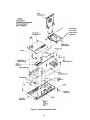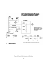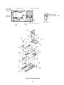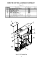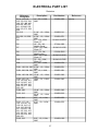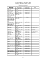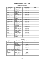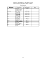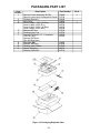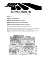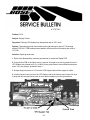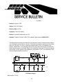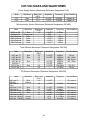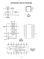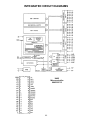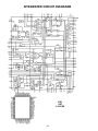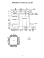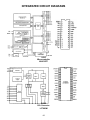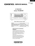
1
Bose® Lifestyle®
Model CD5 Series I Music Center
Note: The first series CD5 can be distinguished from the later CD5V and CD5VII by the serial
number label located on the bottom of the unit. The CD5 will not have a V on the serial number
label, the CD5V will have a V, and the CD5V2 will have a V with the number 2 above the V.
©
1998 Bose Corporation
Service Manual
Part Number 174798 REV 01
Contents
Safety Information ............................................................................................................................ 2
Electrostatic Discharge Sensitive (ESDS) Device Handling ........................................................ 2
Specifications ................................................................................................................................ 3-4
Figure 1. CD5 Block Diagram Sheet 1 of 2 ...................................................................................... 5
Figure 2. CD5 Block Diagram Sheet 2 of 2 ...................................................................................... 6
CD Terms ..................................................................................................................................... 7-11
Theory of Operation .................................................................................................................. 12-17
Figure 3. Labelled Exploded View .................................................................................................. 18
Disassembly/Assembly Procedures ....................................................................................... 19-21
Figure 4. APC PCB ........................................................................................................................ 19
Figure 5. Back Panel with Tab Locations ....................................................................................... 22
Figure 6. Right Cover Assembly (side view) .................................................................................. 22
Figure 7. Base Assembly (top view with covers removed) ............................................................. 22
RC5 Disassembly/Assembly Procedures .................................................................................... 23
Figure 8. Remote Control Assembly Exploded View...................................................................... 23
Test Procedures ........................................................................................................................ 24-26
Figure 9. AM Test Setup ................................................................................................................. 26
Figure 10. Audio PCB Test Section ................................................................................................ 26
CD Test Procedures .................................................................................................................. 27-31
Figure 11. CD Alignment Fixture and Test Setup ........................................................................... 28
Figure 12. Passive Filter Network and Test Setup ......................................................................... 29
Figure 13. Digital PCB Adjustment Locations ................................................................................ 32
Parts List Notes .............................................................................................................................. 33
Console Assembly Parts List ........................................................................................................ 34
Figure 14. Exploded View .............................................................................................................. 35
Remote Control Assembly Parts List ........................................................................................... 36
Figure 15. RC5 Exploded View ...................................................................................................... 36
Electrical Part List ..................................................................................................................... 37-46
RC5 Electrical Part List ............................................................................................................. 47-49
Packaging Part List ........................................................................................................................ 50
Figure 16. Packaging Exploded View ............................................................................................ 50
Service Bulletin ......................................................................................................................... 51-53
CD5 Troubleshooting Guide .......................................................................................................... 54
CD5 Voltages and Waveforms.................................................................................................. 55-58
Integrated Circuit Diagrams ..................................................................................................... 59-66
Figure 17. RC5 PCB Layout ........................................................................................................... 67
Figure 18. RC5 Schematic ............................................................................................................. 68
CAUTION: THE LIFESTYLE ® MODEL 5 MUSIC CENTER CONTAINS NO
USER SERVICEABLE PARTS. TO PREVENT WARRANTY INFRACTIONS,
REFER SERVICING TO WARRANTY SERVICE STATIONS OR FACTORY
SERVICE.
PROPRIETARY INFORMATION
THIS DOCUMENT CONTAINS PROPRIETARY INFORMATION OF
BOSE® CORPORATION WHICH IS BEING FURNISHED ONLY FOR
THE PURPOSE OF SERVICING THE IDENTIFIED BOSE PRODUCT
BY AN AUTHORIZED BOSE SERVICE CENTER OR OWNER OF THE
BOSE PRODUCT, AND SHALL NOT BE REPRODUCED OR USED
FOR ANY OTHER PURPOSE.
1
SAFETY INFORMATION
1. Parts that have special safety characteristics are identified by the
symbol on
schematics or by special notes in the part lists. Use only replacement parts that
have critical characteristics recommended by the manufacturer.
2. Make leakage current or resistance measurements to determine that exposed
parts are acceptably insulated from the supply circuit before returning the unit
to the customer. Use the following checks to perform these measurements:
A. Leakage Current Hot Check: With the unit completely assembled, plug the AC line cord
directly into a 120V AC outlet. (Do not use an isolation transformer during this test.) Use a
leakage current tester or a metering system that complies with American National Standards
Institute (ANSI) C101.1 "Leakage Current for Appliances" and Underwriters Laboratories (UL)
1492 (71). With the unit's AC switch first in the ON position and then in the OFF position,
measure from a known earth ground (metal water pipe, conduit, etc.) to all exposed metal
parts of the unit (antennas, handle bracket, metal cabinet, screw-heads, metallic overlays,
control shafts, etc.), especially any exposed metal parts that offer an electrical return path to
the chassis. Any current measured must not exceed 0.5 milliamp. Reverse the unit's power
cord plug in the outlet and repeat the test. ANY MEASUREMENTS NOT WITHIN THE LIMITS
SPECIFIED HEREIN INDICATE A POTENTIAL SHOCK HAZARD THAT MUST BE ELIMINATED BEFORE RETURNING THE UNIT TO THE CUSTOMER.
B. Insulation Resistance Test Cold Check: (1) Unplug the power supply and connect a
jumper wire between the two prongs of the plug. (2) Turn on the power switch of the unit. (3)
Measure the resistance with an ohmmeter between the jumpered AC plug and each exposed
metallic cabinet part on the unit. When the exposed metallic part has a return path to the
chassis, the reading should be between 1 and 5.2M Ω. When there is no return path to the
chassis, the reading must be "infinite". If it is not within the limits specified, there is the possibility of a shock hazard, and the unit must be repaired and rechecked before it is returned to the
customer.
ELECTROSTATIC DISCHARGE SENSITIVE (ESDS)
DEVICE HANDLING
This unit contains ESDS devices. We recommend the following precautions when repairing,
replacing or transporting ESDS devices:
• Perform work at an electrically grounded work station.
• Wear wrist straps that connect to the station or heel straps that connect to conductive floor
mats.
• Avoid touching the leads or contacts of ESDS devices or PC boards even if properly
grounded. Handle boards by the edges only.
• Transport or store ESDS devices in ESD protective bags, bins, or totes. Do not insert
unprotected devices into materials such as plastic, polystyrene foam, clear plastic bags,
bubble wrap or plastic trays.
2
SPECIFICATIONS
General
Dimensions:
2.5"H x 15"W x 9"D (6 x 38 x 23cm)
Weight:
3.7lb. (1.7kg)
Finish:
Plastic, in-mold brushed aluminum finish
Power Input:
Detachable power pack, 12VAC compatible with
each country's power requirements
Serial Data Output:
2-3.5mm stereo jacks, Tip: Serial data output,
Ring: +12Vdc turn on output.
Power:
14 Watts max.
Input Impedance (@ 1kHz, max. volume):
5kΩ @ aux./video input, 100kΩ @ tape input
Output Impedance:
600Ω @ Speaker A, B output, 1kΩ @ tape output
Distortion:
≤ 0.02% THD @ 1kHz, 2Vrms
S/N Ratio:
≥ 105dB (A-weighted, max. volume)
Headphone Output (32Ω):
45mW (max. output)
Channel Separation:
70dB
Muting (A, B outputs):
-80dB
Max. Output Level:
5Vrms (@ 1kHz, THD < .12%)
FM Electrical
Antenna Input:
US: 75Ω F connector, Europe: 75Ω PAL
Usable Sensitivity:
US: 12dBf, Europe: 17dBf
50dB quieting sensitivity:
Mono: US: 15dBf, Europe: 20dBf
Stereo: US: 37dBf, Europe: 42dBf
S/N ratio (65dBf input):
Mono: 75dB, Stereo: 70dB
THD (65dBf, 1kHz input):
Mono: ≤ 0.2%, Stereo: ≤ 0.3%
Capture Ratio:
1.5dB
AM Rejection (45 dBf input):
60dB
Alternate Channel Selectivity (45 dBf input):
US: 70dB, Europe: 75dB
Image Rejection:
70dB
Frequency Response:
± 0.5dB (30Hz-15kHz)
Stereo Channel Separation:
40dB @ 1kHz
3
SPECIFICATIONS
(Continued)
AM Electrical
Antenna Input:
Binding posts
Usable Sensitivity:
55dBuV/m (IHF standard test loop antenna)
Alternate Channel Selectivity:
60dB
Adjacent Channel Selectivity:
45dB
Image Rejection Ratio:
40dB
S/N Ratio:
50dB (@ 100dBuV/m)
THD:
≤ 1.0% (@ 100dBuV/m)
Frequency Response (@ 100dBuV/m):
100Hz: -8dB
3kHz: -8dB
CD Electrical
D/A Process:
8x over sampling dual 16-bit D/A conversion
Maximum Output Level:
4V
THD+N:
0.05% (@ 1kHz, 0dB)
S/N Ratio:
100dB (A-weighted)
Channel Separation:
≥ 50dB (@ 1kHz)
Frequency Response:
± 0.5dB (20Hz-20kHz)
Dynamic Range:
≥ 90dB
Defect Tracking (Void):
1.5mm (Pierre Verany Test Disc #2)
Defect Tracking (Black Dot):
1mm (ABEX Test Disc TCD-725R)
Defect Tracking (Scratch):
1.6mm (ABEX Test Disc TCD-721R)
Defect Tracking (Fingerprint):
75um (ABEX Test Disc TCD-725R)
Defect Tracking (Warped disc):
1mm (ABEX Test Disc TCD-732RA)
Defect Tracking (Eccentric Disc):
280um (ABEX Test Disc TCD-741R)
4
Figure 1. CD5 Block Diagram Sheet 1 of 2
5
Figure 2. CD5 Block Diagram Sheet 2 of 2
6
CD TERMS
Basic Terms
Access: See track access.
Access Time: The length of time required to change tracks.
CD Mechanism: The mechanical assembly of components used to read information off of the
CD. It contains the optical pickup, sled assembly, disc motor, sled motor, and spindle.
Disc Motor: The motor which spins the disc.
Focus Actuator: The magnet and coil assembly that moves the optical pickup’s lens up and
down.
Laser: A semiconductor light source similar to an LED that is used to read the data off of a CD.
When the laser is turned on it can be seen as a red glow inside the lens.
Laser Pickup: The portion of the CD mechanism that contains the laser diode, lens, focus and
tracking actuators, and photodetector diodes.
Mechanism: see CD Mechanism.
Optical Pickup: See Laser Pickup.
Playability: The extent to which a player can successfully play less than perfect discs. Playability is measured with special test discs (playability discs) that contain certain types of defects and problems.
Playability Disc: A disc which contains a calibrated defect or problem. These include eccentricity, warp, scratch, void, black dot, and fingerprints.
Parking: When the sled is moved to the innermost position on the disc. This is done before (if
necessary) and after playing a disc.
Sled: The portion of the CD mechanism that moves inside to outside to position the optical
pickup near the desired track.
Sled Motor: The motor which moves the sled back and forth.
Spindle: The hub that the disc sits on.
Track Access: The process of moving from one track on a disc to a different track.
Tracking Actuator: The magnet and coil assembly that moves the optical pickup’s lens inside
and out.
Playability Terms
Dropout: A momentary loss of the audio signal, usually caused by a large scratch or other
optical defect.
7
CD TERMS
Eccentricity: The extent to which the hole in the middle of the disc is not located in the geometric center. In other words, the amount that the disc moves in and out as it rotates. Eccentricity is measured as the distance between the center of the hole and the center of the disc (as
determined by the spiral tracks).
Mistracking: When a CD player fails to play the disc in a continuous manner. This may be
caused by a large enough optical defect (scratch, etc.) or by vibration.
Optical Defect: A defect on the surface of the disc which adversely affects the reading of
information by the laser pickup. There are four basic types of optical defects: voids, black dots,
fingerprints, and scratches.
Skipping: When a CD mistracks backwards and gets caught in an “endless loop”. This is
usually caused by a large scratch or other optical defect.
Warp: The extent to which the surface of the disc is not parallel to the seating plane of the disc
(at the center). In other words, the amount that the disc wobbles up and down. Warp is measured as the vertical deviation between the seating plane and the particular point on the disc.
Alignment Terms
CD Alignment: The process of adjusting a CD player for optimum performance, particularly
with respect to its playability.
Free Run Frequency: The VCO frequency in the absence of any signal from the disc. Accurate frequency adjustment is required for the player to be able to read data off the disc. VCO
misalignment results in poor track access and longer access times.
Tracking Offset: The DC offset voltage present at the output of the tracking servo in the
absence of any input signal. For best results, the offset should be adjusted near 0 to keep the
laser positioned in the center of the track. Negative offset causes the laser to be positioned
towards the inside of the track. Misalignment of this parameter can cause the player to skip or
mistrack when playing a dirty or “black dot” disc, especially if the disc is also eccentric.
Scratches and voids may also cause the problem.
Focus Offset: The DC offset voltage present at the output of the focus servo in the absence of
any input signal. For best results, the offset should be adjusted near 0 to keep the laser exactly
in focus. Misalignment of this parameter usually causes dropouts when playing a dirty or “black
dot” disc, especially if the disc is also warped. Scratches may also cause problems. Note that
on the CD5, the focus offset is preset and the adjustment pot is not loaded, however, there is a
spot on the PCB for it.
E-F Balance: The DC offset that results from driving both the E and the F elements of the
photodetector with equal signals. For best results, the offset should be adjusted near 0 to keep
the laser positioned in the center of the track. As with track offset, negative offset causes the
laser to be positioned towards the inside of the track. Misalignment of this parameter can
cause any number of problems including: 1. Poor or slow track access even when playing a
good disc, and 2. Skipping or mistracking when playing a scratched or void disc, especially if
the disc is also eccentric.
8
CD TERMS
Tracking Gain: The overall loop gain of the tracking servo. This controls how tightly the laser
is held in the center of the track. If the gain is too low, the player will have trouble with vibration
and eccentric discs, especially during track access. If the gain is too high the player will have
skips or mistracking with voids and scratches. Proper alignment is a compromise between
these two performance parameters.
Focus Gain: The overall loop gain of the focus servo. This controls how tightly the laser is held
in focus. If the gain is too low, the player will have trouble with vibration and warped discs,
especially during track access. If the gain is too high the player will have skips or mistracking
with black dots and scratches. Proper alignment is a compromise between these two performance parameters.
Technical Terms
RFSM: RF SUM. The amplified A+B+C+D signal from the laser pickup.
Eye Pattern: The pattern displayed on an oscilloscope when monitoring the RFSM test point.
Jitter: The extent to which the zero crossings of the eye pattern occur at other than their ideal
times.
Focusing: Before a disc can be played, the player must focus the CD mechanism by changing
the distance between the lens and the surface of the disc. This must occur before the disc can
start rotating. If the player fails to achieve focus, it will retry. This occurs four times in the CD5
before it “gives up” and indicates “no disc” by lighting up the disc icon in the display.
TOC: Table Of Contents. The innermost area on the disc where track and time information is
stored. When a new disc is inserted into a player (i.e. when the door switch is opened), it must
read the TOC before the first track can be played.
CIRC: Cross Interleave Reed-Solomon Coding: The error detection and correction scheme
used on CDs to provide immunity to small scratches, etc.
CLV: Constant Linear Velocity. CD players rotate the disc at a constant linear velocity of 1.25
M/S. The angular velocity changes from about 500 RPM down to 200 RPM as the disc plays
from beginning (inside) to end (outside).
EFM: Eight-to-Fourteen-Modulation. The format in which the digital data is recorded on the
CD.
Photo Diode: The receiving element that translates the modulated light beam into electrical
signals.
Subcode Q data: The track and time information read off the CD.
Three Beam System: The most common system for providing focus and tracking error signals
for the respective servos. A three beam system uses a six element photo diode array, with the
elements designated A through F. The A, B, C, and D elements are located in the center and
read the information as well as supply the focus error signal. The E and F elements are located
on either side and provide the tracking error signal.
9
CD TERMS
Major Components of the System
ASP: Analog Signal Processor. The component in the CD circuitry that contains the RF amplifier, VCO, and the tracking, focus, and sled servos.
DSP: Digital Signal Processor. The component in the CD circuitry that performs slicing, EFM
demodulation, CIRC decoding, error correction and concealment, track access, CLV regulation, and drives the D/A.
Digital to Analog Converter (D/A, DAC): A device that converts digital information (usually a
serial data stream) into an analog signal.
µC: Micro Controller. The component of the CD circuitry that performs track access, sequences all events (such as focus, disc start, stop, etc.), monitors for servo errors, and processes user information (commands, door open, etc.).
CLV Servo: The circuit that keeps the disc rotating at a constant linear velocity.
Focus Servo: The circuit that keeps the optical pickup’s lens the proper distance away from
the surface of the disc.
Sled Servo: The circuit that keeps the sled positioned within the linear range of the tracking
actuator.
Tracking Servo: The circuit that keeps the optical pickup’s lens positioned within a single track
as the disc rotates.
VCO: Voltage Controlled Oscillator. Part of the phased locked loop circuit that generates an
output frequency dependent on its input voltage.
Signal Names
ATSC: Anti-Shock Circuit.
SLEQ: Sled Equalizer
FDO: Focus Drive Output
FEAO: Focus Error Amplifier Output.
HFL: High Frequency Level
PDO: Phase Detector Output
PH: Peak Hold
SLDO: Sled Drive Output.
SPDO: Spindle Drive Output.
10
CD TERMS
Signal Names
(continued)
TAP: Test Access Port. A 3 pin test interface used by automated test to control and observe
the board under test.
TDO: Tracking Drive Output.
TEAO: Tracking Error Amplifier Output.
TGL: Tracking Gain Low.
THLD: Tracking Hold.
TOFF: Tracking Off
TPA+: Tracking Pre-Amplifier (+ input).
TPA-: Tracking Pre-Amplifier (- input).
TPAO: Tracking Pre-Amplifier Output.
VCOO: VCO Output
Vref1: The reference voltage used by the RF amplifier in the ASP.
Vref2: The unbuffered reference voltage used by the servos in the ASP.
Vref3: The buffered reference voltage used by servos in the ASP.
List of Abbreviations
ASP
CE
CIRC
CLV
D/A
DSP
EEPROM
EFM
IC
IR
kHz
MHz
PLL
RF
µC
VCO
VFD
Analog Signal Processor
Control Expander™
Cross Interleave Reed-Solomon Code
Constant Linear Velocity
Digital to Analog
Digital Signal Processor
Electrically Erasable Program Read Only Memory
Eight-to-Fourteen Modulation
Integrated Circuit
Infrared
Kilohertz
Megahertz
Phase Locked Loop
Radio Frequency
Microcontroller
Voltage Controlled Oscillator
Vacuum Fluorescent Display
11
THEORY OF OPERATION
Overview
The Lifestyle® Model 5 music center is a self-contained CD player, AM/FM tuner, preamplifier,
and control center for use with Bose® powered speaker systems. In addition to the two internal
sources (CD and tuner), it also allows for up to three external devices to be connected (i.e.
AUX, VIDEO, and TAPE). It uses a Radio Frequency (RF) remote control that allows the unit to
be operated from different rooms within a house without the need for a line-of-sight path back
to the console. The remote control commands for the external sources are translated and
passed to the serial data output jack. With the CE-I accessory device this data can be converted to Infrared (IR) for use with many conventional audio devices.
Power Supply
The unit is powered by an external 12VAC power supply capable of delivering 1.2 amps rms.
Dl, C2, D2, and C6 form positive and negative half-wave rectifiers respectively. Q1, Q2, Q3,
and their respective components make up a discrete low dropout regulator with a nominal
output voltage of 10. 2V. VR1 is the corresponding negative voltage regulator with an output of
-12V. These two regulators create the bipolar supply used by all of the audio circuits. The
supply is turned on and off with the unit by the control signal on J7-10.
R5, D3, C9, and VR2 create an +8V regulated supply that is used by the CD servo circuits and
the remote RF receiver. R6, D4, C11, and VR3 create a +5V regulated supply that is used by
the main and CD microcontrollers (U402 and U505), and the CD control circuits (U501, U502,
etc.). Both supplies are live at all times. R5 and R6 limit the power dissipation of their respective regulators. VR2 and VR3 normally run quite hot to the touch.
R8, D6, and C13 form an unregulated supply (M+) that is used by the CD drive electronics.
C14, D7, D8, and C15 form a charge pump that creates a negative high voltage. This voltage
is regulated down to -24V by R9, D9, and C16. The vacuum fluorescent display (VFD) driver
U403 uses this -24V to shut off segments in the display. C19 and C18 reduce the 12VAC to
approximately 3Vrms. This voltage powers the display’s (VFD401) heater. C16, D10, C17, and
R10 provide a DC bias of -15V for the VFD heater (cathode).
Control Electronics
Main microcontroller (µC) U402 controls the audio circuits, tuner, display, and push buttons.
The µC runs at a nominal frequency of 4.0MHz that is supplied by ceramic resonator X401.
The µC is reset by a rising edge on pin 1 caused by R409 and C404. This occurs automatically
on power-up but may be forced manually by depressing S416 (if installed).
U402 communicates with U403 over a four wire serial data bus (U403, pins 15, 16, 18 and
19). The bus is updated once per millisecond. U403 latches the serial data into its outputs,
driving the VFD. The VFD is a four grid multiplexed display with 16 anodes at each grid. The
grids are turned on sequentially, one each millisecond. As each grid is turned on, the corresponding anodes for that grid are also turned on. This lights the desired segments. When the
next grid is turned on, the anodes are changed to correspond to the desired segments under
this next grid. In this way, the entire display is scanned, 1/4 at a time. The display is blanked for
a brief interval in-between when one grid is turned off and the next is turned on. In this blanking interval, the push buttons are scanned to determine what keys are being pressed. This
data is read in on U402, pins 12 through 15.
12
THEORY OF OPERATION
There is one main serial data bus that controls source selection IC U101, volume control IC
U103, PLL frequency synthesizer U302, and EEPROM U401. The clock and data information
for all of these devices is sent out on U402, pins 5 and 7. However, U401, U302, U101 and
U103 each have their own chip select line. Data is sent to U302 whenever the tuner frequency
is changed. During the serial data transmission, U302, pin 3 is driven high. Data is sent to
U101 or U103 whenever a new source is selected or the volume is changed. At the completion
of this transmission, the STRB line (J9-5) is driven high briefly.
U401 is a nonvolatile EEPROM which is used for storing certain data such as tuner presets
and house codes. This data is protected from loss during a power outage. U401 communicates
with U402 over the main serial data bus. During communication to this chip, the chip select line
(U401, pin 1) is driven high.
There is another serial data bus between U402 and U505. These lines are labeled
CD_READY, CD_CLK, CD_ CMD, and CD_DATA on the schematic. The bus sends commands (play, stop, etc.) to U505 and also sends track and time information to U402 so that it
may be displayed. This bus is constantly in use any time “CD” is selected as the source.
RR101 receives and demodulates commands from the RF remote control. R138, C130, C129,
R139, and D109 remove noise and shape the pulse. U106 squares up the pulse edges and
converts them to 5V logic levels. This signal is then fed to U402, pin 37. C401 prevents any
glitches at this pin.
In addition to the major functions mentioned above, U402 also performs several miscellaneous
tasks. The bipolar power supply for the audio circuits (+1OV/-12V) is turned on and off by
U402, pin 19 (power). Both supplies are turned on when this line is high (+5V), and off when it
is low. The unregulated supply is monitored by C414, R407, and R408. In the event of a power
failure, U402 will shut down the system gracefully. There are three independent muting circuits: Mute A, Mute B, and Power-on Mute. Mute A and Mute B are controllable from the
remote, and allows the A and B outputs to be controlled independently. The Power-on Mute is
used only during power-up (when the bipolar supply is turned on) to prevent pops and clicks.
When an external source is selected (AUX, VIDEO, or TAPE), the transport commands (FF,
FR, etc.) are passed through the serial data jack via Q401 and its associated circuitry.
Audio Circuits
There are two internal audio sources (CD and Tuner) and three external sources (AUX,
VIDEO, and TAPE). All of the sources are routed to U101. R101-106 and R201-206 provide
level matching for the different input sources. D101-106, D201-206, C101-103, and C201-203
provide static protection on the inputs. U101 selects 1 of the 5 input sources, and routes it to
its output on pins 5 and 9 (left), and pins 20 and 24 (right).
One half of U102 (pins 1-3 and 12-14) provides gain and buffering for the input signal. The
buffered output is routed to U103 and to the FIXED output on J103. U103 consists of two
sections. The first section attenuates the signal from 0 to 70dB in 10dB steps. The output of
the first section is buffered by the other half of U102 (pins 5-7 and 8-10) and is fed to the
second section. The second section attenuates the signal in 1dB steps. The two sections
together provide smooth attenuation from 0 to 80dB in 1dB steps.
13
THEORY OF OPERATION
U103’s output signal is buffered by U105, and is fed to the A and B outputs. These outputs are
independently mutable through transistors Q103-106 and Q203-206. Each pair of transistors
provides approximately 80dB of attenuation when muted. These mute transistors are controlled by the signals on J9-7 and J9-8. U103’s output signal is also routed to headphone
amplifier U104. This provides gain and buffers the signal in order to drive a low impedance
load. When the headphones are inserted into J104, the control signal on J105-3 causes the A
speaker output to be muted.
The TAPE output jack functions like the FIXED output does. There is one exception. The TAPE
output is shut off whenever “TAPE” is selected as the source. This prevents feedback through
the TAPE deck if it was placed in “Record” while “TAPE” was selected as the source. This is
accomplished by feeding the FIXED level output signal from U102, pins 1 and 14 back into
U101. A control signal from U402 allows U101 to pass this signal to its outputs on pins 5 and
17, except when “TAPE” is selected as a source.
The FIXED, TAPE, and headphone outputs all have a single mute transistor which is used to
prevent pops and clicks during power-up and power-down. These transistors are all controlled
by the signal on J9-6. Each transistor provides about 40dB of attenuation when the muting is
switched on.
CD Player
The CD circuitry consists of six major sections: Analog signal processor (ASP) U501, digital
signal processor (DSP) U502, digital to analog converter (D/A) U506, CD microcontroller (µC)
U505, power drivers U503 and U504, and the CD mechanism. U501 contains the RF amplifier
and servo control circuits. U502 performs EFM demodulation, CIRC decoding, and outputs the
digital audio to U506. It also extracts the subcode Q information (track #, time, etc.) and controls U501 during track access. U505 receives and interprets the subcode Q data from U502
and sends it along to U402. It also issues commands to U502 for track access, and controls all
operations of the CD circuitry.
U501 receives its input signal (through P501) from the mechanism’s photo diode pickup. The
A, B, C, and D inputs are added together and amplified. The RF amplifier output appears on
RFSM (U501, pin 72 ). This signal is the familiar “eye pattern.” This signal is sent to EFMIN on
U502, Pin 8 where it is sliced for EFM demodulation. The inverted and non-inverted sliced
outputs appear on the EFMO and EFMO~ lines (U502, pins 6 and 7) . These signals are lowpassed and subtracted and the output appears on SLCO (U501, pin 53). This signal supplies
the DC bias for the RFSM signal. This signal is then sent to the slicer for slice level control.
The RFSM signal is peak-detected and compared to a reference to determine if there is a
signal being received back from the disc. The output appears on DRF (U501, pin 40 ). This
signal is used by U505 to determine if the lens is in focus. The envelope of the RFSM signal is
also used in determining when the laser crosses a track boundary during track access. The
HFL signal (U501, pin 48) conveys this information to U502.
The A+C signal is subtracted from the B+D signal. This produces the focus error signal FEAO
(U501, pin 26 ). The focus gain is adjusted by R527. This signal is amplified and filtered by the
focus servo amplifier (inside U501). It then appears as an output at FDO (U501, pin 22). The
FDO signal is fed to U503. U503 generates the complementary outputs (pins 11 and 14) that
are used to actuate the focus coil (P502, pins 5 and 8).
14
THEORY OF OPERATION
The E and F signals are amplified and subtracted. This produces the tracking error signal
TEAO (U501, pin 7 ). The F channel’s gain is adjusted by E-F balance potentiometer R506.
The TEAO signal is used by the anti-shock circuit, the track jump detection circuit, and the
tracking servo. The track jump detection output is sent to U502 on the TES line (U501, pin 47).
R510, which is connected to TPA+ (U501, pin 13 ), adjusts the tracking gain. This signal is
amplified and filtered. It then appears as an output on TPAO (U501, pin 15). R511 adjusts the
tracking offset . The TPAO signal is further amplified and filtered. It then appears as an output
on TDO (U501, pin 21). This signal is fed to U503. U503 generates the complementary outputs (U503) that are used to actuate the tracking coil (P502, pins 6 and 7).
The TDO signal is also used as the input for the sled servo. This signal is filtered and fed to the
sled servo amplifier on SLEQ (U501, pin 20). This signal is amplified and is then added to the
FEED signals from U505. The result appears on SLDO (U501, pin 33). This signal is fed to
U504. U504 generates the complementary outputs (pins 11 and 14) that are used to drive the
sled motor (P503, pins 5 and 6).
The Constant Linear Velocity (CLV) servo is regulated by comparing the playback speed to a
FIXED reference frequency in U502. The error signal appears at U502, pins 10 and 11 (CLV+
and CLV-). These signals are subtracted and the difference appears on SPD (U501, pin 29).
The SPD signal is filtered and amplified. It then appears at the output on SPDO (U501, pin
31). This signal is fed to U504. U504 generates the complementary outputs (pins 3 and 6) that
are used to drive the disc motor (P503, pins 1 and 2).
U501 regulates the laser power by monitoring the MD input (P502-3). This signal is compared
to a reference to generate the proper drive signal on LDD (U501, pin 74). This signal biases
Q501. Q501 drives the laser diode output LD (P502-1). U501’s main DC reference voltage is
Vref3 which appears on pin 9. This voltage is nominally 4V.
The VCO is the final function contained in U501. The VCO is used by U502 for EFM demodulation. The PDO output signal (U502, pin 4) is filtered and amplified by U501. In turn, this
output appears on VCOC (U501, pin 59) This is the VCO control voltage input. The nominal
VCO free-run frequency is 8.64MHz and is set by R558. The VCO also requires a 16.9344MHz
clock input from U502. This input appears on CLK (U501, pin 62). The VCO output appears at
VCOO (U501, pin 60). This signal is buffered by U502. The buffered output appears on AO
(U502, pin 2). The VCO output is divided by 2 in U502. In turn, its output appears on PCK
(U502, pin 18), which is 4.32MHz.
The DSP clock is derived from a 16.9344MHz crystal oscillator (X501). However, this oscillator
is normally turned off by U505. It is only switched on during focusing and when a disc is playing. U502 receives its EFM input from U501 on EFMIN (pin 8). This signal is sliced, EFM
demodulated, and CIRC decoded. The digital audio output signal is sent serially to U506 on
the LRCLK, DFOUT and DACLK lines (U502, pins 33, 35, and 36).
U502 receives servo control commands from U505 on the serial bus (U502, pins 51, 53 and
54). These commands are translated to appropriate control signals for U501 for focusing, disc
start, disc stop, disc braking, and track jumps. The focus servo is controlled by the FOCS and
FST outputs. The CLV servo is controlled through the CLV+ and CLV- lines. The tracking
servo is controlled by the TOFF, TGL, and THLD outputs. Track jumps are created by signals
on the JP+ and JP- lines. Track jump detection is based on signals from U501 on the HFL and
TES inputs.
15
THEORY OF OPERATION
U505’s oscillator is obtained from a 4MHz ceramic resonator (X502). U505 is reset by a rising
edge on pin 1 that is caused by R573 and C574. This occurs automatically on power-up, but
may be forced manually by depressing S502 (if installed). U505 communicates with U502 on a
serial bus (U502, pins 50 through 54). U505 sends servo commands for focusing and track
access to U502. U502 sends subcode Q data to U505 which extracts track, time and table of
contents information from it. The time and track data is formatted, and is sent to U402 on a
serial bus (U505, pins 11-13).
During track access, U505 controls the sled motor directly using the FEED+ and FEED- lines
(U505, pins 21 and 22). It also directly controls the laser U503 and VCO using the LASER~
line (U505, pin 9). When the laser is turned on, the VCO and U503 are enabled, otherwise
they are turned off. U505 can also enable and disable U504 with the MOTOR_EN line (U505,
pin 20).
U506 (D/A converter) performs 8x oversampling and digital filtering. It then converts the digital
audio into left and right stereo outputs. D/A reference voltages are obtained from zener diode
D504. U506’s analog outputs are buffered by one-half of U507 (pins 5-7 and 8-10). The
buffered signal is lowpass filtered by the other half of U507. This removes any residual out-ofband digital noise. The recovered audio is then routed to U101.
Tuner
The FM antenna signal is routed through F connector J301 and enters the FM front end module. This contains a tuned RF amplifier, FM local oscillator, and a mixer. The IF output signal
appears on pin 4 (front end) and passes through 10.7MHz ceramic filter CF302. The filter’s
output is amplified by the IF gain stage. This stage consists of Q307, Q308 and their associated components. The signal is then passed through a second ceramic filter, CF303, a second
gain stage (Q309, Q310, etc.) and a third ceramic filter, CF304.
CF304’s output signal is sent to the main tuner IC, U301. This device contains the FM detector, FM stereo MPX decoder, stop level detection, as well as most of the AM circuitry (see
below). U301 further amplifies the IF signal, and then performs FM detection. This detection
uses a double tuned quadrature detector formed by T304 and T305. T305 is adjusted for FM
center frequency by adjusting it for 0VDC between the AFC terminal (U301, pin 4) and the
Vreg terminal (U301, pin 28). T304 is adjusted for minimum distortion (A few iterations may be
required because these two adjustments are dependent on one another). The recovered audio
appears on U301, pin 8.
C313 and its associated components filter the recovered audio and feed it back into U301, pin
9. U301 performs the FM stereo MPX decoding. When you select FM, the decoded L/R channel signals are sent out on pins 14 and 15. The resistance between pin 12 and ground
controls the separation. 456kHz ceramic resonator CF301 controls the PLL decoder. The PLL
loop filter components are connected to pin 11. Potentiometer R334, which is connected to pin
30, sets the FM stop level to 33dBf (nominal).
C304, R304, C307, and R309 perform FM de-emphasis. Q301, Q302 and their associated
components buffer the signals. MPX filters T301 and T302 remove any unwanted out-of-band
signals before sending them to U101.
The AM loop antenna signal enters the unit through J301’s screw terminals. The signal is then
fed to AM front end module, T303. This device contains an RF tuned section and the AM local
16
THEORY OF OPERATION
oscillator tuned circuit. The tuned output appears on pin 12 and is fed to AM buffer FET Q300.
The buffered output is sent to U301, pin 27. U301 contains the AM RF amplifier, mixer, IF
amplifier, AM detector and AM stop level detection. Potentiometer R339, which is connected to
pin 16, sets the AM stop level to 70dB uV/M (nominal). The IF output signal appears on pin 26
and is filtered by IF filter T307. The signal is then fed back into U301, pin 24 for AM detection.
The AM detected output (pin 5) is filtered by C315, R316, and C314. The filtered output is fed
back into U301, pin 6. Finally, it is sent to the L/R outputs (pins 14 and 15) when “AM” is
selected.
U302 controls the AM and FM local oscillators. U402 sets U302 so that it can select the AM or
FM band and can tune to a particular frequency. The PLL reference oscillator originates from
7.2MHz crystal X301. This frequency is divided down to 400KHz (U302, pin 7). U302 divides
down the local oscillator frequencies and compares them to an internal reference frequency.
The error signal resulting from this comparison appears at pin 18. This error signal is integrated and filtered by Q304, Q305, and their associated components. This produces the tuning
voltage which appears at Q304’s collector.
The tuning voltage is further filtered by R323, C326, R322, and C319. This signal is then sent
to AM front end module T303, pin 14. It is used to vary the capacitance of two varactor diodes.
This first diode varies the frequency of the AM local oscillator. The second tunes the AM RF
input section to the desired frequency. Similarly, the tuning voltage is filtered by R330 and
C333. Then it is fed to the FM front end module. The front end uses this voltage to vary the
local oscillator frequency and to tune the RF input sections.
17
See Figure
6 for a side
view of this
assembly.
Figure 3. Labelled Exploded View
18
DISASSEMBLY/ ASSEMBLY PROCEDURES
1. Left Cover Assembly Removal
Note: Refer to Figures 3 and 5 for Procedures 1 and 2.
front of the base assembly (19). Lower the
cover into position.
4.3 There are two black tabs on the bottom
of the right cover. Push them in slightly and
snap the cover into place.
1.1 Remove the two screws (18A) that
secure the left cover (7) to the base (19).
1.2 Press in the three recessed gray tabs
located on the connector panel and lift up
on the rear of the cover.
4.4 Replace the two screws (18B) that
secure the right cover to the base.
4.5 Replace the left cover assembly (Procedure 2).
2. Left Cover Assembly Replacement
2.1 Align the five hooks on the left cover (7)
with the five catches on the front of the
base (19).
5. CD Mechanism Removal
Note: Refer to Figures 3, 4 and 7 for
Procedures 5 and 6.
2.2 Lower the left cover and snap it into
place. The cover should be flush with the
closed door assembly (1).
5.1 Remove the left cover assembly (Procedure 1) and the door/right cover assembly (Procedure 3).
2.3 Replace the two screws (18A) that
secure the left cover to the base (19).
5.2 Lift the CD mechanism (11) straight up
from the four metal posts in the base (19).
Later models have 4 nylon washers (23)
mounted on the posts. Do not remove
them.
3. Door Assembly and Right Cover Removal
Note: Refer to Figures 3, 5 and 6 for
Procedures 3 and 4.
5.3 To prevent electrostatic damage to the
mechanism, solder together the two points
indicated in Figure 4.
3.1 Remove the left cover assembly (Procedure 1).
3.2 Remove the two screws (18B) that
secure the right cover (6) to the base (19).
3.3 Press in the two recessed black tabs
located on the connector panel. Lift up on
the rear of the door assembly (1) and right
cover assembly (6).
Shorting point
3.4 Remove the console latch (16).
Figure 4. APC PCB
4. Door Assembly and Right Cover Replacement
5.4 Disconnect the 6 pin connector from the
PCB that is attached to the motors and the
5 pin and 8 pin connectors from the APC
PCB.
Note: The support grommets (14, 15) and
CD cover (12) are not supplied as part of
the mechanism. Remove and reuse them if
complete replacement of the mechanism is
required.
4.1 Position the console latch (16) in the
base (19).
4.2 Align the two hooks on the right cover
assembly (6) with the two catches on the
19
DISASSEMBLY/ ASSEMBLY PROCEDURES
5.5 Slide the violet (14) and gray (15)
grommets away from the slots in each
corner of the mechanism.
7.1 Remove the left cover assembly (Procedure 1) and the right cover/door assembly (Procedure 3).
5.6 Remove the two screws (13) that
secure the cover (12) to the mechanism.
Unsnap the cover from the mechanism.
7.2 Lift up the CD mechanism (11) and
move it aside. Keep the mechanism connected to the PCB unless removal is
required. See Procedure 5 for removal
procedure.
6. CD Mechanism Replacement
6.1 Snap the cover (12) into position. Align
the screw holes and replace the two screws
(13) that secure the cover to the mechanism (11).
7.3 There are four black plastic tabs that
hold the PCB (10) in position. See Figure 3.
Flex them carefully outward and pull the
PCB up and out.
6.2 Slide the violet (14) and gray (15)
grommets into their respective slots on
each corner of the mechanism. See Figure
3 for their proper locations.
7.4 Remove any connections required to
troubleshoot the PCB.
8. Digital PCB Replacement
6.3 Connect the 6 pin connector to the PCB
that is connected to the motors and the 5
pin (with black cable) and 8 pin
connectors to the APC PCB.
8.1 Replace any connections that were
disconnected during troubleshooting.
8.2 Slide the PCB (10) into position. There
are notches in the PCB which mate with
notches in the base (19). See Figure 7.
6.4 Remove the solder from the shorted
points shown in Figure 4.
Note: Make sure that four nylon washers
(23) are mounted on the posts before
installing the mechanism (later models
only).
8.3 Snap the PCB carefully down under the
four locking tabs.
8.4 Push the CD mechanism (11) down
onto the four metal posts.
Note: The CD mechanism wires must be
routed correctly (see Figure 7) for proper
CD operation. A sign of improper routing is
a clicking noise when playing tracks at the
outermost edge of the CD. Perform the CD
Final Verification tests on page 31 to
ensure proper operation.
8.5 Replace the right cover/door assembly
(Procedure 4) and the left cover assembly
(Procedure 2).
9. Audio PCB Removal
Note: Refer to Figures 3 and 7 for Procedures 9 and 10.
6.5 Place the mechanism on the four metal
posts located in the base (19). Position as
shown in Figure 3.
9.1 Remove the left cover assembly (Procedure 1), the door/right cover assembly
(Procedure 3), and the Digital PCB (Procedure 7).
6.6 Replace the door/right cover assembly
(Procedure 4) and left cover assembly
(Procedure 2).
9.2 There are four locking tabs (three on
the PCB edges and one in the middle of the
PCB) that secure the PCB (10) to the base
(19). Flex the tabs carefully away from the
PCB and disengage the PCB.
7. Digital PCB Removal
Note: Refer to Figures 3 and 7 for Procedures 7 and 8.
20
DISASSEMBLY/ASSEMBLY PROCEDURES
9.3 Slide the PCB clear of the connector
panel, and pull it away from the base.
12. Headphone Jack PCB Replacement
12.1 Snap the PCB (10) into place by
engaging the two locking tabs.
Note: Make sure that the connector wires
are routed through the guiding notch on the
side of the base (19).
9.4 Remove any connections required to
troubleshoot the PCB.
10. Audio PCB Replacement
Note: Make sure that the connections to
the Headphone Jack PCB (10) are routed
through the guiding notch on the side of the
console (see Figure 7).
12.2 Replace the door/right cover assembly
(Procedure 4) and the left cover assembly
(Procedure 2).
10.1 Restore any connections that were
disconnected during troubleshooting.
10.2 Slide the PCB's connectors through
the holes in the rear of the base (19).
10.3 Snap the PCB (10) carefully down
under the four locking tabs. Make sure that
the CD mechanism connections are routed
properly. See Figure 7 and procedure 6
note.
10.4 Replace the Digital PCB (Procedure
8), the door/right cover assembly (Procedure 4), and the left cover assembly (Procedure 2).
11. Headphone Jack PCB Removal
Note: Refer to Figures 3 and 7 for Procedures 11 and 12.
11.1 Remove the left cover assembly
(Procedure 1) and door/right cover assembly (Procedure 3).
11.2 There are two black plastic snaps that
secure the PCB (10). Flex the snaps
outward and carefully pull the PCB away
from the unit.
21
Figure 5. Back Panel with Tab Locations
Hooks onto front
of console.
Tab that fits into cutouts
on back panel
Figure 6. Right Cover Assembly (side view)
Figure 7. Base Assembly (top view with covers removed)
22
RC5 DISASSEMBLY/ASSEMBLY PROCEDURES
1. Enclosure Disassembly
2.2 Press the top cover and the bottom
cover together until they snap into place.
1.1 Slide off the battery compartment door
(5) and remove the batteries.
3. PCB Removal
1.2 While holding the top cover (4) with one
hand, place your fingers from your other
hand in the battery compartment and grasp
the lower part of the bottom cover (3) with
your fingers.
3.1 Lift the PCB (1) straight up. The springs
will come up with the PCB.
4. PCB Replacement
4.1 Lower the PCB (1) into the top cover (4)
so that the springs are in the battery compartment.
1.3 With your finger tips in the battery
compartment, first pull parallel to the unit
and then pull perpendicular.
5. Pad Removal
1.4 With the catches released at the bottom,
work your fingers up the sides to release
the rest of the catches.
2. Enclosure Assembly
5.1 The pad (2) is not secured. Grasp a
corner of the pad and lift it out.
6. Pad Replacement
2.1 Lower the bottom cover (3) onto the top
cover (4) so that the bottom cover's lip fits
over the top cover.
6.1 Lower the pad (2) into the top cover (4)
so that the buttons line up with the holes in
the top cover.
5
3
10
1
6
2
7
9
8
4
Figure 8. Remote Control Assembly Exploded View
23
TEST PROCEDURES
GENERAL TEST SETUP
2.4 Measure the outputs according to the
following table.
Load the outputs as follows:
Headphone output-33Ω, 1% load.
Audio (A, B, Fixed) outputs-10kΩ load.
Output
Speaker A (L,R)
Speaker B (L,R)
Tape (L,R)
Fixed (L,R)
Headphone (L,R)
Note: The remote control or console
buttons can be used to select sources in
these procedures.
Separation (dB)
≥50
≥50
≥50
≥50
≥50
2.5 Repeat this test for the right channel.
Note: This test is the same for the VIDEO
input. Apply a 500mVrms, 1kHz signal to
the left (right) VIDEO input and repeat this
test.
1. AUX Gain Test
1.1 Select AUX.
1.2 Apply a 500mVrms, 1kHz signal to the
left (right) AUX input. Adjust the volume to
maximum. Reference a dB meter to the
applied signal.
3. TAPE Gain Test
3.1 Select TAPE.
1.3 Ground the TAPE, VIDEO and the right
AUX inputs.
3.2 Apply a 500mVrms, 1kHz signal to the
left (right) TAPE input. Adjust the volume to
maximum. Reference a dB meter to the
applied signal.
1.4 Measure the outputs according to the
following table.
Output
Speaker A (L,R)
Speaker B (L,R)
Tape (L,R)
Fixed (L,R)
Headphone (L,R)
Min
(dB)
4.2
4.2
3.3
4.2
5.4
3.3 Ground the AUX, VIDEO and the right
TAPE inputs.
Max
(dB)
5.4
5.4
4.5
5.4
7.4
3.4 Measure the FIXED level output. It
should be 8.9 to 9.9dB.
3.5 Repeat this test for the right channel.
4. Volume Control Mute
1.5 Repeat this test for the right channel.
Note: This test is the same for the VIDEO
input. Apply a 500mVrms, 1kHz signal to
the left (right) VIDEO input and repeat this
test.
4.1 Select the AUX input.
4.2 Apply a 500mVrms, 1kHz signal to the
left (right) AUX input.
2. AUX Separation Test
4.3 Set the volume to minimum at the
speaker A output.
2.1 Select AUX.
4.4 Measure the gain at the A output
(relative to maximum volume). It should be
≥ -75dB.
2.2 Apply a 500mVrms, 1kHz signal to the
left (right) AUX input. Adjust the volume to
maximum. Reference a dB meter to the
applied signal.
2.3 Ground the TAPE, VIDEO, and right
AUX inputs.
24
TEST PROCEDURES
5. Headphone Mute
3.3 Adjust the generator's output to 35dBf.
Verify that U301 pin 21 is < 2.5Vdc.
5.1 Select the AUX input.
4. Stereo Separation
5.2 Apply a 500mVrms, 1kHz signal to the
L/R AUX input.
4.1 Set the RF generator to 65 dBf, pilot on,
left modulation, 1kHz, 100% (75kHz deviation).
5.3 Insert a mini-jack into the headphone
output. The A output should mute.
4.2 Reference a dB meter to left FIXED
output.
FM ALIGNMENT TESTS AND
ADJUSTMENTS
4.3 Measure the right FIXED output. It
should be ≤ -25dB.
Note: If the unit fails this test, perform the
following procedure.
1. Change R354 to a 560Ω, 5%, 1/10.
2. Remove W302.
3. Add R355 (a 1kΩ, 10%, 1/2 W potentiometer). Adjust R355 for maximum separation. This option is listed on note 9 of the
schematic.
Unless otherwise noted, set an RF generator to 98.1MHz, 40dBf, 1kHz, mono modulation, pilot off, 100% (75kHz deviation).
1. Front End Mixer Coil Adjustment
1.1 Adjust the FM front end (TUNER) mixer
coil until a maximum DC voltage is measured at U301 pin 25. Adjust the coil until
the voltage comes within +0, -20mV of the
peak voltage.
5. FM Sensitivity
5.1 Set the RF generator to 42dBf, L= -R
modulation, pilot on.
2. FM Detector Zero Adjust and Distortion
Adjustment
5.2 Reference a dB meter to the left FIXED
output.
2.1 Set the RF generator to 65dBf.
2.2 Adjust T305 until the voltage reads
0Vdc ± 110mVdc across C317+ (AFC test
point) and C322+ (VREG test point).
5.3 Measure the noise (with modulation off
and pilot on) at the right FIXED output. The
SNR should be > 50dB for the 120V version and > 45dB for the 220V version.
Note: If the unit fails this test, the FM front
end should be replaced.
2.3 Adjust T304 for minimum distortion. The
distortion should be < 0.4%.
2.4 Repeat this procedure until optimal
results are obtained.
3. FM Stop Level Adjustment
3.1 Set the RF generator to 31dBf.
3.2 Rotate R334 counterclockwise until the
voltage at U301 pin 21 drops below 2.5Vdc.
Then rotate R334 clockwise until the
voltage goes above 2.5Vdc.
Note: The correct adjustment is at the point
just after the voltage switches high.
25
TEST PROCEDURES
AM ALIGNMENT PROCEDURES
1.2 Reference a dB meter to the Fixed level
output.
Test setup: Connect the generator to a
standard radiating loop. Unless otherwise
noted, set an RF generator to 70dBu field
strength, 400Hz, 30% modulation.
See Figure 9.
STANDARD
SIGNAL
GENERATOR
1.3 Shut off the modulation and measure
the noise. The SNR should be > 30dB.
2. AM Stop Level Adjustment
2.1 Set the RF generator so that the field
strength at the unit's antenna is 59dBµ
(59dBµ V/M).
(PLAN VIEW)
60cm
TEST
LOOP
2.2 Rotate R339 counterclockwise until the
voltage measured at U301 pin 21 goes
below 2.5Vdc. Then, rotate R339 clockwise
until the voltage goes above 2.5Vdc.
Note: The correct adjustment is at the point
just after the voltage switches high.
(SIDE VIEW)
STANDARD
SIGNAL
GENERATOR
Figure 9. AM Test Setup
The equivalent field intensity is 26dB less
than the generator output level or 1/20th of
the output voltage.
2.3 Adjust the field strength to 64 dBµ
(64 dBµ V/M). Verify that the voltage at
U301 pin 21 is < 2.5Vdc.
1. AM Sensitivity Alignment
1.1 Set the RF generator so that the field
strength at the unit's antenna is 70dBµ
(70dBµ V/M).
Figure 10. Audio PCB Test Section
26
CD TEST PROCEDURES
CD ALIGNMENT PROCEDURES
(WITH FIXTURE)
button until TO lights up). The meter should
read approximately 90mVdc.
2.4 Simulate a closed CD door by placing
an object between S501's two black posts
(the CD door latch can be used). Select CD
(S413).
Note: Some of these procedures require
the use of a CD alignment fixture (P/N
176318). Alternate procedures that do not
require a fixture begin on page 30. Refer to
Figure 11, CD Alignment Fixture Test
Setup. The fixture is required unless otherwise specified. Refer to Figure 13 for
adjustment locations.
2.5 After the focusing operation is completed, press ERASE (S403). The meter
should change from its previous reading in
step 2.3 (it will drop). If not, remove power
and repeat the test.
Test Equipment Needed
Digital Voltmeter
Frequency Counter
Sony Disc YEDS-18
Bose® CD Alignment Fixture (176318)
2.6 Adjust R511 until the meter reads
between -7 to 17mVdc.
3. E/F Balance (E/F)
1. PLL Free Run Frequency (VCO)
Note: This test does not require a test disk
or the alignment fixture.
3.1 Advance the alignment fixture (ADV
button) to the E/F setting and set the
voltmeter to read DC voltage.
1.1 Connect the frequency counter to PCK
and ground.
3.2 Simulate a closed CD door by placing
an object between S501's two black posts
(the CD door latch can be used). Load the
YEDS-18 test disc, select CD (S413), and
play track 2.
1.2 Simulate a closed CD door by placing
an object between S501's two black posts
(the CD door latch can be used). Select CD
(S413).
3.3 Press STORE (S411). This puts the unit
in the E/F balance mode. The time display
will stop.
1.3 Adjust R558 until the frequency counter
reads 4.320MHz ± 20kHz. (If the adjustment is not done within 4 seconds, then CD
must be selected again).
3.4 Adjust R506 until the meter reads
between - 10 to + 50mVdc.
2. Tracking Offset (TO)
4. Tracking Gain (TG)
Note: Remove any previously loaded test
disc. This test will not work with a disc
loaded.
4.1 Shut the unit off.
4.2 Advance the fixture to the TG setting
and set the voltmeter to read AC voltage.
2.1 Connect the cable from the test fixture
to connector P504 on the unit.
4.3 Simulate a closed CD door by placing
an object between S501's two black posts
(the CD door latch can be used). Load the
YEDS-18 test disc, select CD (S413), and
play track 2.
2.2 Connect a DC voltmeter to the positive
(+) and negative (-) terminals on the test
fixture.
2.3 Select TO on the fixture (press the ADV
4.4 Adjust R510 until the meter reads
between 440 to 500mVrms.
27
CD TEST PROCEDURES
5. Focus Gain (FG)
5.1 Advance the fixture to FG and set the
voltmeter to read AC voltage.
5.2 Simulate a closed CD door by placing
an object between S501's two black posts
(the CD door latch can be used). Load the
test disc, select CD (S413), and play track
2.
5.3 Adjust R527 until the meter reads
between 380 to 420mVrms.
6. Tracking Offset Readjustment
6.1 Refer to procedure 2 and readjust if
necessary.
Front Panel
ADV.
TO
E/F
TG
FG
Back Panel
To
DVM
+
-
P504
This RJ-45
connection only fits
one way. The other
end plugs directly into
P504 on the Digital PCB.
T o 12 VAC
CD5
IN
2' cable connects to
“12 VAC ~ IN" on CD5
back panel. Both ends
of the cable are terminated
exactly the same way as
the power pack.
Figure 11. CD Alignment Fixture and Test Setup
28
Power
Pack
Figure 12. Passive Filter Network and Test Setup
29
CD TEST PROCEDURES
CD ALIGNMENT PROCEDURES
3. E/F Balance
Note: The test disc is required for this test.
Construct the filter indicated in Figure 12
and connect it to P504 pin 4 (TEAO).
(Without Fixture)
Note: Refer to Figure 12 throughout this
procedure.
3.1 Connect a DC voltmeter between the
filter output and P504 pin 1 (Vref3).
Test Equipment Needed
Voltmeter (input impedance > 10MΩ)
Frequency Counter
Sony Disc YEDS-18
Audio Oscillator
3.2 Load the test disc, select CD (S413),
and play track 2. Skip forward using S408.
3.3 Press STORE (S411). This puts the
unit in the E/F balance mode. The time
display will stop.
1. PLL Free Run Frequency (VCO)
1.1 Connect the frequency counter to PCK
and ground.
3.4 Adjust R506 until the meter reads
between - 10 to + 50mVdc.
1.2 Simulate a closed CD door by placing
an object between S501's two black posts
(the CD door latch can be used). Select CD
(S413).
4. Tracking Gain
Note: Shut the unit off. Construct the filter
indicated in Figure 12 and connect it (FLT
IN) to P504 pin 6 (TPA+).
1.3 Adjust R558 until the frequency counter
reads 4.320MHz ± 20kHz. (If the adjustment is not done within four seconds, then
CD must be selected again).
4.1 Connect an AC voltmeter between the
filter output (FLT OUT) and P504 pin 1
(Vref3).
4.2 Connect a 100kΩ resistor to P504 pin 7
(TPA-). Connect an oscillator to the
resistor's other end and apply a .5Vrms,
1.7kHz signal to it.
2. Tracking Offset
Note: Remove any previously loaded test
discs. This test will not work with a disc
loaded.
4.3 Insert the test disc and select CD
(S413) and play track 2.
2.1 Connect a DC voltmeter between P504
pins 2 (TDO) and 1 (Vref3). The meter
should read approximately 90mVdc.
4.4 Adjust R510 until the meter reads
between 26.3 ± 1.5mVrms.
2.2 Simulate a closed CD door by placing
an object between S501's two black posts
(the CD door latch can be used). Select CD
(S413).
5. Focus Gain
Note: Construct the filter indicated in
Figure 12 and connect it (FLT IN) to P504
pin 5 (FEAO).
2.3 After the focusing operation is completed, press ERASE (S403). The meter
should change from its previous reading in
step 2.1 (it will drop). If not, remove power
and repeat the test.
5.1 Connect an AC voltmeter between the
filter output (FLT OUT) and P504 pin 1
(Vref3).
5.2 Connect a 300kΩ resistor to P504 pin 8
(FSW). Connect an oscillator to the
resistor's other end and apply a .5Vrms,
1.7kHz signal to it.
2.4 Adjust R511 until the meter reads
between -7 to +17mVdc.
30
CD TEST PROCEDURES
5.3 Skip back to the beginning of track 2.
3.4 Fingerprint: Play track 15 (75µm).
Listen for at least 10 seconds.
5.4 Adjust R527 until the meter reads
between 23.2 ± 1.5mVrms.
6. Tracking Offset Readjustment
6.1 Refer to procedure 2 and readjust if
necessary.
Final CD Verification Tests
Note: Audible defects are defined as CD
dropouts or skipping during play. All units
must be able to pass these tests without
any audible defects.
1. Warp
1.1 Insert Abex test disc TCD-732RA (or
equivalent). Play track 16 (.7 mm).
1.2 Pause the CD and confirm that there
are no mechanical scraping sounds.
1.3 Access track 16 again and confirm that
it plays properly.
2. Eccentricity
2.1 Insert Abex test disc TCD-714R
(equivalent test disc must be eccentric by
210µm).
2.2 Play track 1 (210µm). Listen for at least
4 seconds.
2.3 Access track 15 ( or furthest track on
equivalent disc) and confirm that the unit
plays properly.
3. Optical Defects
3.1 Insert Abex test disc TCD-725 (or
equivalent).
3.2 Void: Play track 6 (1mm). Listen for at
least 6 seconds.
3.3 Black dot: Play track 9 (.8mm). Listen
for at least 8 seconds.
31
Figure 13. Digital PCB Adjustment Locations
32
PARTS LIST NOTES
1. This part is not normally available from Customer Service. Approval from the Field Service
Manager is required before ordering.
2. The individual parts located on the PCBs are listed in the Electrical Parts List.
3.
This part is critical for safety purposes. Failure to use a substitute replacement with the
same safety characteristics as the recommended replacement part might create shock, fire
and/or other hazards.
4. This PCB is part of a pallet. The pallet contains the Display PCB, Audio PCB, and Headphone PCB. This PCB assembly is manufactured and sold as a pallet.
33
CONSOLE ASSEMBLY PARTS LIST
(Figure 14)
Item
Number
1
2
3
4
5
6
7
8
9
10
11
12
13
14
15
16
17
18
19
20
21
22
Description
Part Number
Door Assembly
Spring-Torsion, LH
Spring-Torsion, RH
Pin-Hinge, 5.3"
Gear-Damper, Blue
Cover Assembly, Right
Cover Assembly, Left
Nameplate, Flat Black
Spring, Ground
PCB Assembly, 120V
PCB Assembly, 220V
PCB Assembly, 120V/220V
CD Mechanism, CD90V1, W/APC
Cover, CD Mechanism
Screw-Tapp, 2 x 6 mm, PAN, XREC
Grommet, CD Support, Violet
Grommet, CD Support, Gray
Latch, Console
Spacer, Foam, Rectangular, .25
Screw-Tapp, 6-20 x .375, PAN, XRC/S
Base Assembly
Cable, 5 conductor, 8"
Cable, 8 conductor, 8"
Pad, Foam, Adhesive Backed
34
187743-001
176083
176082
173210
146816-05
149956
190819
180213
173449
146075-101A
146075-201A
146075-601A
146074
148787
149954-04
146822-02
146822-01
146081
172332-04
172779-06
149955-01
172599
172673
174231
Note
1, 2, 4
Figure 14. Exploded View
35
REMOTE CONTROL ASSEMBLY PARTS LIST
(Figure 15)
Item
Number
1
2
3
4
5
6
7
8
9
10
Description
Part Number
Note
194387
146088
146089
146090
146226
174001
174000
174002-01
174002-02
173605
1, 2
PCB ASSY RMT CNTRL, RC-5A
MAT, SWITCH, CD-5
COVER, BOTTOM, CD-5
COVER, TOP, CD-5
DOOR, BATTERY, CD-5
CONTACT, BATTERY, CONE
CONTACT, BATTERY, FLAT
CONTACT, BATTERY, CONE/FLAT
CONTACT, BATTERY, FLAT/CONE
SPACER, PAD, FOAM
5
3
10
1
6
2
7
9
8
4
Figure 15. RC5 Exploded View
36
ELECTRICAL PART LIST
Resistors
Reference
Designator
R1, 4, 113, 213,
330, 333, 336, 342,
348, 353, 145, 406,
420-423, 426, 427,
431, 433-442, 502,
503, 553, 572, 598,
600
R2, 315
Description
Part Number
1kΩ, 5%, 1/10W,
0805
133626-1025
5.11kΩ, 1%, 1/10W,
0805
R3, 109, 111, 209,
4.75kΩ, 1%, 1/10W,
211
0805
R5
2.7Ω, 5%, 1/2W,
52mm, CF
R6
10Ω, 5%, 1W,
Metallic Oxide
R7
1.5kΩ, 5%, 1/4W,
52mm, CF
R8
1.5Ω, 5%, 1W,
Metallic oxide
R9
220Ω, 5%, 1/4W,
52mm, CF
R10
75Ω, 5%, 1/4W,
52mm, CF
R12
27Ω, 5%, 1/10W,
0805
R101, 102, 201, 202 9.76kΩ, 1%, 1/10W,
0805
R103, 203, 588, 592 1kΩ, 1%, 1/10W,
0805
R104, 105, 204, 205 15.4kΩ, 1%, 1/10W,
0805
R106, 107, 110,
100kΩ, 5%, 1/10W,
114, 139, 206, 207, 0805
210, 214, 407, 415,
424, 425, 545, 566,
568, 575, 577, 589,
593, 595
R108, 208
12.4kΩ, 1%, 1/10W,
0805
R112, 212
22.1kΩ, 1%, 1/10W,
0805
R115, 215
825Ω, 1%, 1/10W,
0805
R116, 117, 119,
4.7kΩ, 5%, 1/10W,
120, 123-125, 127,
0805
130-133, 216, 217,
219, 220, 223-225,
227, 230-233, 318,
331, 337, 323, 327,
335, 356, 357, 410,
414, 509, 524, 560,
580, 603
R118, 218
619Ω, 1%, 1/10W,
0805
37
133625-5111
133625-4751
121243-1512R75
173314-1005
121243-1211525
171259-1R55
121243-1212215
121243-1217505
133626-2705
133625-9761
133625-1001
133625-1542
133626-1045
133625-1242
133625-2212
133625-8250
133626-4725
133625-6190
Reference
US/Can.
ELECTRICAL PART LIST
Resistors (Continued)
Reference
Description
Designator
R121, 128, 221, 228 432Ω, 1%, 1/10W,
0805
R122, 129, 222, 229 182Ω, 1%, 1/10W,
0805
R126, 226
150Ω, 1%, 1/10W,
0805
R134-136, 142, 599, 1MΩ, 5%, 1/10W,
601
0805
R138, 304, 309,
10kΩ, 5%, 1/10W,
325, 338, 341, 358
0805
R140, 303, 308, 552 330kΩ, 5%, 1/10W,
0805
R141, 522, 557, 578 33kΩ, 5%, 1/10W,
0805
R143
30kΩ, 5%, 1/10W,
0805
R144, 569
1.8kΩ, 5%, 1/10W,
0805
R145
3.3kΩ, 5%, 1/10W,
0805
R145, 302, 307,
2.2kΩ, 5%, 1/10W,
504, 565
0805
R300, 525, 540
1.2kΩ, 5%, 1/10W,
0805
R301
220Ω, 5%, 1/10W,
0805
R305, 310, 313, 507 2.7kΩ, 5%, 1/10W,
0805
R306, 311, 516
5.6kΩ, 5%, 1/10W,
0805
R314, W302, W401 Jumper, Chip, 0805
R316
12kΩ, 5%, 1/10W,
0805
R317
8.2kΩ, 5%, 1/10W,
0805
R319
22Ω, 5%, 1/10W,
0805
R320
9.10kΩ, 5%, 1/10W,
0805
R322, 345, 350,
22kΩ, 5%, 1/10W,
530-533, 548-551,
0805
555
R324
43Ω, 5%, 1/4W,
52mm, CF
R326
100Ω, 5%, 1/10W,
0805
R328
1.6kΩ, 5%, 1/10W,
0805
R329
620Ω, 5%, 1/10W,
0805
R332, 535
6.8kΩ, 5%, 1/10W,
0805
R334
Potentiometer, 10kΩ,
10%, 1/2W
Part Number
Note
133625-4320
133625-1820
133625-1500
133626-1055
133626-1035
133626-3345
133626-3335
133626-3035
133626-1825
133626-3325
Military (120/230V)
133626-2225
Eur./UK/Sing./Aus.
133626-1225
133626-2215
133626-2725
133626-5625
133627
133626-1235
133626-8225
133626-2205
133626-9125
133626-2235
121243-1214305
133626-1015
133626-1625
133626-6215
133626-6825
170042-103
38
ELECTRICAL PART LIST
Resistors (Continued)
Reference
Designator
R339, 558
R340
R343, 501
R344, 346, 349,
351, 429, 430, 561,
582
R347, 352
Description
Part Number
Potentiometer, 20kΩ,
10%, 1/2W
120Ω, 5%, 1/10W,
0805
10Ω, 5%, 1/10W,
0805
330Ω, 5%, 1/10W,
0805
170042-203
18kΩ, 5%, 1/10W,
0805
R354
1.05kΩ, 5%, 1/10W,
0805
R354
1.5kΩ, 5%, 1/10W,
0805
R401-405, 411, 413, 10kΩ, 5%, 1/10W,
416-419, 432, 505,
0805
521, 526, 554, 562,
576, 594
R408, 538
120kΩ, 5%, 1/10W,
0805
R409, 514, 517
390kΩ, 5%, 1/10W,
0805
R412, 543, 544,
27kΩ, 5%, 1/10W,
546, 547
0805
R428, 556, 563,
470Ω, 5%, 1/10W,
581, 583-585, 596,
0805
597
R506, 527
Potentiometer, Trim,
5kΩ, 10%, 1/2W
R508, 542
220kΩ, 5%, 1/10W,
0805
R510
Potentiometer, Trim,
2kΩ, 10%, 1/2W
R511
Potentiometer, Trim,
100kΩ, 10%, 1/2W
R512, 528, 574
4.7MΩ, 5%, 1/10W,
0805
R513
15kΩ, 5%, 1/10W,
0805
R515, 559
3.9kΩ, 5%, 1/10W,
0805
R518
150kΩ, 5%, 1/10W,
0805
R519
62kΩ, 5%, 1/10W,
0805
R520
1.5MΩ, 5%, 1/10W,
0805
R523, 539, 571
56kΩ, 5%, 1/10W,
0805
R534
3.3kΩ, 5%, 1/10W,
0805
R536
82kΩ, 5%, 1/10W,
0805
39
Note
133626-1215
133626-1005
133626-3315
133626-1835
133625-1051
US/Can./Mil.
133626-1525
Eur./UK/Sing./Aus.
133626-1035
133626-1245
133626-3945
133626-2735
133626-4715
170042-502
133626-2245
170042-202
170042-104
133626-4755
133626-1535
133626-3925
133626-1545
133626-6235
133626-1555
133626-5635
133626-3325
133626-8235
ELECTRICAL PART LIST
Resistors (Continued)
Reference
Designator
R537
Description
Part Number
160kΩ, 5%, 1/10W,
0805
R541
91kΩ, 5%, 1/10W,
0805
R567
200kΩ, 5%, 1/10W,
0805
R570
68kΩ, 5%, 1/10W,
0805
R573, 579
270kΩ, 5%, 1/10W,
0805
R586, 587, 590, 591 2.21kΩ, 1%, 1/10W,
0805
R602
3.9MΩ, 5%, 1/10W,
0805
R604
56Ω, 5%, 1/2W, CF
Note
133626-1645
133626-9135
133626-2045
133626-6835
133626-2745
133625-2211
133626-3955
121243-1515605
Capacitors
Reference
Designator
C1
C2, C13
C3, 4, 7, 8, 10, 12,
20, 114, 214, 310,
345
C5, 100, 107, 112,
207, 212, 313, 336
412, 413, 523
C6
C9, 11
C14, 17, 18, 116,
216, 330
C15, 16
C19
C101, 102, 201,
202, 354, 533
C103, 104, 117120, 203, 204, 217220, 337, 349, 401,
411, 502, 539
C105, 109, 111,
129, 205, 209, 211,
308, 311, 333, 414
C106, 206
C108, 208, 328
Description
Part Number
.01µF, 20%, 100V,
Z5U, Disc
2200µF, 20%, 25V,
85, EL
10µF, 20%, 50V, 85,
EL
146821-103
100pF, 5%, 50V,
COG, 0805
149948-222E
149948-100H
133622-101
470µF, 20%, 25V,
85, EL
1000µF, 20%, 16V,
85, EL
100µF, 20%, 25V,
85, EL
100µF, 20%, 50V,
85, EL
33µF, 20%, 25V,
85, EL
180pF, 5%, 50V,
COG, 0805
1000pF, 5%, 50V,
COG, 0805
149948-471E
149948-102C
149948-101E
149948-101H
149948-330E
133622-181
133622-102
1µF, 20%, 50V,
85, EL
149948-1R0H
47pF, 5%, 50V,
COG, 0805
2.2µF, 20%, 50V,
85, EL
133622-470
149948-2R2H
40
Note
US/Can./Mil.
ELECTRICAL PART LIST
Capacitors (continued)
Reference
Designator
C110, 210, 302,
305, 342
C113, 213, 301,
324, 331, 346
C115, 215
C121, 130, 133,
134, 221, 314, 326,
327, 335, 403, 534,
535, 574
C122-127, 132,
135, 332, 402, 407,
408, 518, 520, 528,
537, 545, 546, 553,
555, 568, 570-573,
575
C300, 316, 319,
321, 323, 325, 329,
334, 341, 343, 347,
348, 350-353
C303, 306, 317
Description
Part Number
4.7µF, 20%, 50V,
85, EL
47µF, 20%, 25V,
85, EL
22µF, 20%, 25V,
85, EL
.01µF, 10%, 50V,
X7R, 0805
149948-4R7H
.10µF, 80%, 25V,
Y5V, 0805
133624
.047µF, 20%, 50V,
Z5U, 0805
148779-473
Note
149948-470E
149948-220E
133623-103
3.3µF, 20%, 50V,
85, EL
C304, 307
.0056µF, 5%, 100V,
85, Box
C304, 307
.0082µF, 5%, 100V,
85, Box
C309, 313
470pF, 5%, 50V,
COG, 0805
C309, 405, 406,
39pF, 5%, 50V,
548, 549
COG, 0805
C312, 524
.33µF, 5%, 50V,
85, Box
C315
6800pF, 10%, 50V,
X7R, 0805
C318, 556, 557
16pF, 5%, 50V,
COG, 0805
C322
220µF, 20%, 25V,
85, EL
C339
33pF, 5%, 50V,
COG, 0805
C340
27pF, 5%, 50V,
COG, 0805
C344, 505, 516, 540 .1µF, 5%, 50V,
85, Box
C404
.22µF, 20%, 50V,
85, EL
C415
.47µF, 20%, 50V,
85, EL
C501, 512, 529,
47µF, 20%, 16V,
538, 554, 559, 561
85, EL
C503, 506, 513, 527 10µF, 20%, 25V,
85, EL
C504
.01µF, 5%, 100V,
85, BOX
41
149948-3R3H
137127-562
Eur./UK/Sing./Aus.
137127-822
US/Can./Mil.
133622-471
Eur./UK/Sing./Aus.
133622-390
US/Can./Mil
137127-334
133623-682
133622-160
149948-221E
133622-330
133622-270
137127-104
149948-R22H
149948-R47H
149947-470C
149947-100E
137127-103
ELECTRICAL PART LIST
Capacitors (continued)
Reference
Designator
C507
Description
Part Number
560pF, 5%, 50V,
COG, 0805
C508
1µF, 20%, 50V,
EL, 85, BP
C509
.018µF, 5%, 100V,
85, Box
C510
.47µF, 20%, 50V,
EL, 85, BP
C511, 514, 525,
.033µF, 5%, 63V,
542, 543
85, Box
C515
.068µF, 5%, 63V,
85, Box
C519, 521, 526
100µF, 20%, 16V,
EL, 85
C522, 562, 565
.0033µF, 5%, 100V,
85, Box
C530
12pF, 5%, 50V,
COG, 0805
C531
2.7pF, 5%, 50V,
COG, 0805
C532
.47µF, 20%, 50V,
85, EL
C536
.033µF, 10%, 50V,
X7R, 0805
C541
220pF, 5%, 50V,
COG, 0805
C544
390pF, 5%, 50V,
COG, 0805
C547, 558, 564, 567 1µF, 20%, 50V,
85, EL
C563, 566
.0015µF, 5%, 100V,
85, Box
Note
133622-561
147522-1R0
137127-183
147522-R47
137127-333
137127-683
149947-101C
137127-332
133622-120
133622-2R7
149947-R47H
133623-333
133622-221
133622-391
149947-1R0H
137127-152
Diodes
Reference
Designator
D1-4, 6-8, 301
Description
Part Number
Rectifier, 1N4004,
400V, 1A
D5
LED, Green,
Rt. Angle Mount
D9
Zener, 1N5252,
24V, .5W, 5%
D10
Zener, 1N5239,
9.1V, .5W, 5%
D101-109, 201-206, 1N4148, 75V,
302, 303, 401, 502, 300mA, Switching
503
D402-405
Switch, 75V,
200mA, SOT-23
D406
Zener, 1N5246,
16V, .5W, 5%
116996-4
147551
136758-5252
136758-5239
121501
148582
136758-5246
42
Note
ELECTRICAL PART LIST
Diodes (continued)
Reference
Designator
D407
D504
D505
Description
Part Number
Zener, 1N5232,
5.6V, .5W, 5%
Zener, 1N5231,
5.1V, .5W, 5%
Zener, 1N4742A,
12V, 1W, 5%
136758-5232
Note
136758-5231
116995-4742A
Transistors
Reference
Designator
Q1
Q101-107, 201-207
Q2, 3, 5, 301, 302,
401, 502
Q300
Q304
Q305
Q307-310
Q312, 405, 500
Q4, 311, 501
Q402-404
Description
Part Number
Bipolar, P, 60V,
5A, TO-126
Bipolar, N, 50V,
800mA, SOT23
Bipolar, N, 40V,
200mA, SOT23
JFET, N, 20V,
20mA, TO-92
Bipolar, N, 60V,
200mA, TO-92
JFET, N, 40V,
10mA, TO-92
Bipolar, N, 30V,
30mA, TO-92
Bipolar, N, 50V,
100mA, SOT23
Bipolar, P, 40V,
200mA, SOT23
Bipolar, P, 50V,
100mA, SOT23
Note
147529-S
148770
146819
148590-F
146812-T
147561-3
147565
146817
148596
146818
Integrated Circuits
Reference
Designator
U101
U102, 507
U103
U104
U105
U106
U301
U302
Description
Part Number
Analog Switch,
TC9163N, DIP28
Op-Amp, Quad,
NJM074, DIP14
Volume Control,
TC9213P, DIP16
Op-Amp, Dual,
NJM4556, SO-8
Op-Amp, Dual,
NJM2082M, SO-8
Comparator, Dual,
LM393, SO-8
Digital Tuner,
LA1851, DIP30
Frequency
Synthesizer, PLL,
LM7000, DIP20
146814
146078
147622
148598
146820
148584
146815
147527
43
Note
ELECTRICAL PART LIST
Integrated Circuits (continued)
Reference
Designator
U401
U402
U403
U501
U502
U503, 504
U505
U506
VR1
VR2
VR3
Description
Part Number
EEPROM,
59C11, 1 KB, SO-8
Microcontroller,
68HC05C12,
Programmed
VFD Driver,
MM58342, DIP28
ASP, LA9210M,
DIP80
DSP, LC7867,
DIP64
Motor Driver,
LA6531, DIP16
Microcontroller,
68HC05P7, SO-28,
Programmed
DAC, LC7883M,
16 bit, SO-28
Regulator, 12V,
Neg., LM320LZ,
TO-92
Regulator-Voltage,
Pos., 8V, TO-92
Regulator-Voltage,
Pos., 5V, TO-92
147536
Note
178324
146813
146809
146810
146808
146806
146811
147530-12
171406-08
171406-05
Inductors
Reference
Designator
L1, 400, 501, 504,
506
L101, 505
L301
L302-304
L502, 503
L507
Description
Part Number
10µH, 160A,
7.96Hz
1µH, 270A, 25.2Hz
1000µH, 40A,
.796Hz
100µH, 90A,
2.52Hz
Inductor, 4.7µH,
10%
Inductor, 2.2µH,
SMD
147563-100
Note
147563-1R0
147563-102
147563-101
147563-4R7
173273-2R2
Ceramic Filter
Reference
Designator
CF301
CF302-304
CF302-304
Description
Part Number
Resonator,
Ceramic, 456kHz
Filter, Ceramic,
10.7MHz, 230kHz
Filter, Ceramic,
10.7MHz, 280kHz
Note
147233
44
147559
Eur./UK/Sing./Aus.
173107
US/Can./Mil.
ELECTRICAL PART LIST
Crystals
Reference
Designator
X301
X401, 502
X501
Description
Part Number
Crystal, Quartz,
7.2MHz, 50 PPM
Resonator,
Ceramic, 4MHz
Crystal,
16.93444MHz, 100
PPM
Note
147223
147534
147533
Tuning Coils
Reference
Designator
T301, 302
T303
T304
T305
T306
T307
TUNER
TUNER
Description
Part Number
Filter, Stereo MPX,
Single-tuned
Module, Tuning,
AM, Front End
Inductor, FM
Detector, Distortion
Adj., 10.7MHz
Inductor, FM
Detector, Center
Adj., 10.7MHz
Filter, FTZ, 114kHz
Inductor, AM IF,
High Selectivity,
450kHz
Tuner, Front, FM,
4-gang
Tuner, Front, FM,
4-gang
Note
147236
172972
147557
147564
147558
148581
Eur./UK/Sing./Aus.
140088
US/Can./Mil.
140089
Eur./UK/Sing./Aus.
Miscellaneous
Reference
Designator
RR101
J6A
J7A
J7B
J9A
J9B
Description
Part Number
Receiver, RF
Remote, 27.145MHz
Connector,
Header, 5 pos.
Cable, 24 AWG,
5 conductor,
2.5 mm, 3"
Connector,
Header, 12 pos.
Cable, 24 AWG,
12 conductor,
2.5 mm, 3"
Connector,
Header, 9 pos.
Cable, 24 AWG,
9 conductor,
2.5 mm, 3"
148588
45
148591-05
148772-0503
148591-12
148772-1203
148591-09
148772-0903
Note
ELECTRICAL PART LIST
Miscellaneous (continued)
Reference
Designator
J101, 102
J103
J104
J105A-B, 105B-A
J301
J301
J401
P1
P401
P501
P502
P503
P504
S501
S401-415
VFD401
Description
Part Number
Connector, Jack,
Quad Phono
Connector, Jack,
Phono, 6 pos.
Connector, Jack,
Headphone,
3.5mm
Cable, 26 AWG,
5 conductor,
2 mm, 13"
Connector,
Antenna, F/SCR
Terminal
Connector,
Antenna, PAL
Connector, Dual
Stereo, Mini
Connector, Jack,
DC Power
Connector,
Header, 3 pin
Connector,
Header, 6 pin, Male
Connector,
Header, 8 pin, Male
Cable, 6
conductor, 3",
28AWG
Connector,
Header, 8 pos.
Switch, Optical
Switch, Tactile
Dome, 160 gf
Display, Vacuum
Fluorescent
149959
46
Note
148766
148583
148771-0513
148586
US/Can./Mil.
171623
Eur./UK/Sing./Aus.
145310
147540
148595-03
134740-06
134740-08
172162-0603
148591-08
171258
172999-02
146077
RC5 ELECTRICAL PART LIST
Resistors
Reference
Designator
R2-5,13, 21-23
R6, 9
R7
R8
R10
R11
R12
R14
R15
R16
R17
R18
R19
R20
Description
Part Number
200kΩ, 5%, 1/10W,
0805
100kΩ, 5%, 1/10W,
0805
470kΩ, 5%, 1/10W,
0805
4.7kΩ, 5%, 1/10W,
0805
2.7kΩ, 5%, 1/10W,
0805
1kΩ, 5%, 1/10W,
0805
680Ω, 5%, 1/10W,
0805
130kΩ, 5%, 1/10W,
0805
180kΩ, 5%, 1/10W,
0805
560Ω, 5%, 1/10W,
0805
220kΩ, 5%, 1/10W,
0805
150kΩ, 5%, 1/10W,
0805
10kΩ, 5%, 1/10W,
0805
4.3kΩ, 5%, 1/10W,
0805
133626-2045
Note
133626-1045
133626-4745
133626-4725
133626-2725
133626-1025
133626-6815
133626-1345
133626-1845
133626-5615
133626-2245
133626-1545
133626-1035
133626-4325
Capacitors
Reference
Designator
C1
C2
C3, 4, 6
C5
C7
C8
C10
C12
C13, 18, 25
C14
Description
Part Number
330pF, 5%, 50V,
COG, 0805
0.033µF, 10%, 50V,
X7R, 0805
100pF, 5%, 50V,
COG, 0805
.10µF, 80%, 25V,
Y5V, 0805
10µF, 20%, 25V,
85, EL
.047µF, 20%, 50V,
0805, Z5V
120pF, 5%, 50V,
COG, 0805
270pF, 5%, 50V,
COG, 0805
.022µF, 10%, 50V,
X7R, 0805
10pF, 5%, 50V,
COG, 0805
133622-331
47
133623-333
133622-101
133624
148769-100E
148779-473
133622-121
133622-271
133623-223
133622-100
Note
RC5 ELECTRICAL PARTS LIST
Capacitors (continued)
Reference
Designator
C16
C17
C19
C20
C21
C22
C23
C24
C26
TC1
Description
Part Number
33pF, 5%, 50V,
COG, 0805
27pF, 5%, 50V,
COG, 0805
56pF, 5%, 50V,
COG, 0805
22pF, 5%, 50V,
COG, 0805
39pF, 5%, 50V,
COG, 0805
68pF, 5%, 50V,
COG, 0805
560pF, 5%, 50V,
COG, 0805
27pF, 5%, 100V,
T2H, 0805
1000pF, 5%, 50V,
COG, 0805
2-7pF, 100V, NPO,
Trim Capacitor
133622-330
Note
133622-270
133622-560
133622-220
133622-390
133622-680
133622-561
147531-270
133622-102
148768-Z070
Diodes
Reference
Designator
D2, 4, 5
D3, 6, 7
Description
Part Number
Switch, 75V,
200mA, SOT23
Dual, 75V, 300mA,
SOT23
Note
148582
148774
Transistors
Reference
Designator
Q1, 3
Q2
Q4, 5
Q6
Description
Part Number
Bipolar, 40V,
200mA, P, SOT23
Bipolar, 40V,
200mA, N, SOT23
Bipolar, 30V,
30mA, N, SOT23
Bipolar, 20V,
1.5A, N, SOT23
Note
148596
146819
148781-4
148780-7
Integrated Circuit
Reference
Designator
U1
U2
Description
Part Number
RC Transmitter,
SO-24
Monostable
Multivibrator,
CD4538, SO-16
148784
148785
48
Note
RC5 ELECTRICAL PARTS LIST
Miscellaneous
Reference
Designator
L2, 5, 6, 9
L3
L4
L7
L8
SW1
T1
X1
X2
Description
Part Number
Connector
receptacle, Battery
contact (2 in qty.)
10µH, 160A,
7.96Hz, Axial
6.8µH, 175A,
7.96Hz, Axial
1.2µH, 260A,
7.96Hz, Axial
.47µH, 330A,
25.2Hz, Axial
Bar antenna,
1.15µH, 5%
Switch, DIP, SPST,
16 DIP, 8 position
Inductor, 27.145MHz
Resonator,
Ceramic, 455kHz
9.04833MHZ,
35PPM
171982
49
147563-100
147563-6R8
147563-1R2
147563-R47
148786
148777
148778
148782
148783
Note
PACKAGING PART LIST
Item
Number
1
2
3
4
5
6
7
8
9
10
11
-
Description
Part Number
Remote Control Assembly (RC5A)
Remote Control Assy Packaged for Resale
Polybag (Remote)
Wire Cover
Power Supply, 120V (US/Can.)
Power Supply, 220V (Eur.)
Power Supply, 230V (UK/Sing.)
Power Supply, 240V (Aus.)
Batteries-AA size
Packing-Insert, Top
Antenna-FM Dipole, 75Ω, F connector
(US/Can., Mil.)
Antenna-FM Dipole
(Eur./UK/Sing./Aus.)
Microfoam Bag
Antenna, AM Loop
Packing, Insert, Bottom
Carton, Shipping
Shipping Carton Kit
179980
172724
144348
173201
146225
146798
146799
146800
147538
147539
148589
143185
174591
147544
147543
148767
179730
Figure 16. Packaging Exploded View
50
Note
2
3
# 181473
Product: CD5
Subject: Micro Reset Modification
Symptom: Customer complains of CD not working.
Reason: CD micro is not resetting under certain conditions.
Solution: Perform reset modification listed below to display PCB.
1) Remove: R408 (120k), C414 (1uf), R573 (270k), C547 (1uf), D502.
2) Add a jumper wire from the hot side of S416 to hot side of S502. This wire should not be
excessively long, and should lay flat on the board. (See diagrams below)
Note: Latter production units used an improved reset circuit (U404). U404 is located on the
display PCB under the BOSE ® logo. This modification is not needed on these units.
51
# 177871-B1
Product: CD-5
Subject: Display Failure
Symptom: Flashing VFD displays are being observed on CD-5 units.
Reason: The existing ground trace breaks at the pad leaving no ground. This change
affects PCB P/N 177400 and has been added to all production units starting the week of
12/17/95.
Solution: Repair ground trace.
1. Refer to the disassembly/ assembly procedures to access the Digital PCB.
2. Compare the PCB to the figure below. If a piece of jumper buss wire is present from the
VFD Support tab (closest to pin 21 of U402) to the ground trace, the modification has been
done. If it is not present, proceed to step 3.
3. Scrape the ground trace a 1/4" from the VFD Support tab until the copper is visible.
4. Install a jumper buss wire from the VFD Support tab to the broken ground trace. Be sure
to wrap the wire around the tab once or twice before soldering it to the ground trace.
52
174798-B1
Product: Lifestyle® CD5
Subject: Dim VFD Display
Effective Date: 8/27/96
Symptom: Dim VFD Display.
Reason: Improper voltage rating on C19.
Solution: Replace C19 with a 33uF, 63V capacitor, part number 149948-3301J.
The display dims on some units, after the unit has been in use for a period of time. When a
unit is returned from the field for service, C19 should be checked to ensure that the voltage
rating on C19 is 63V. If it is not, it should be replaced with a 33uF, 63V capacitor, part
number 149948-3301J. This should be done to all units returned for service to ensure this
failure does not occur in the future. Refer to the schematic below, the CD5 service manual,
part number 174798, and the CD5 supplement, part number 177871, for schematics, PCB
layouts and disassembly procedures.
+5V
NOTE 24
R19
J7-12
220,1W
R6
LM78M05CT
D4
229
+5V
1
3
VR3
10,1W
1N4004
C11
NOTE 24
558
D
J7-2
-24V
C14
231
100/25V
D8
C12
10/50V
220
1/4W
M
8
M
233
100/50V
D9
C16
M
M
2
R10
-15V
120,1/4W
9.1V
24V
1N5252
C15
1N4004
1N5239
D10
100/50V
D7
D
D
R9
232
1N4004
C19
538
2
1000/16V
214
+5V
1
F
M
100/25V
100/25V
C17
C18
TO VFD
SHT 2
M
4.5VAC
33/63V
CD5 Power Supply
Date issued: 6/17/97
53
CD5 TROUBLESHOOTING GUIDE
Symptom
Hum
Intermittent or no operation
No operation
Display Dim
Probable Cause
C2, physical damage
P1, fractured solder joint or
lifted pad
Q2, 3, 4, 5 failed
C19 voltage under rated
Display Flashes
Ground break at VFD
support tab
Will not track or focus. CD
mechanism not the problem
U503 or U501
No laser output
Solder short across C502
One or more of the unit's
functions do not operate
using controls on center but
work with remote
No remote control operation
Defective switch
No FM
No audio output
Distorted output, CD only
Customer complains that
CD does not operate. CD
operates after unit is
unplugged and plugged in
again.
CD will not operate.
Remote control receiver not
properly soldered
X301 defective
U101 (multiplex IC)
defective
Defective U506 (D/A
converter) or poor solder
connection
CD micro is not resetting
under certain conditions
C13, located in the power
supply, has a bad
connection causing low
voltage on pin 1 (≈ 14V)
and pin 16 (≈ 4V) of U503
or U504.
54
Solution
Replace C2
Repair fractured solder joint
or lifted pad.
Replace Q2, 3, 4, 5.
Replace C19 with a 33uF,
63V cap part number
149948-3301J.
Repair ground break at VFD
support tab located near
U402, pin 21.
Ensure U501 and 503 is
properly soldered. Check
U501 and 503 for proper
operation.
Remove solder short from
C502 and check Q501.
Replace switch.
Service
Bulletin
174798-B1
177871-B1
Remove solder from legs of
remote receiver and scrape
legs and then solder
Replace X301
Replace U101
Ensure U506 is properly
soldered or replace U506
See service bulletin 181473
for reset modification
procedures.
Repair fractured solder joint
or damaged track.
181473
CD5 VOLTAGES AND WAVEFORMS
Remote Control Voltages
Node
Min.
Q1 C
Q1 C
Q3 C
Q4 B
Q4 E
Voltages
Typical
4.50
0.00
0.00
1.25
.62
Units
Test Condition
VDC
VDC
VDC
VDC
VDC
Button pressed
Remote off
Remote off
Button pressed
Button pressed
Max.
Power Supply Section Voltages (Reference Designators 0-99)
Node
Min.
P1 pin 1 (AC power
in)
D1 Cathode
C3+ (+10V supply)
C3+ (+10V supply)
D2 Anode
C8- (-12V supply)
C8- (-12V supply)
C4+
D6 Cathode (M+
supply)
D3 Cathode
C10+ (+8V supply)
D4 Cathode
C12+ (+5V supply)
D9 Anode (-24V
supply)
C18- (VFD heater)
C19- (VFD heater)
Across VFD heater
Voltages
Typical
13.0
9.4
-12.8
11.5
7.5
9.2
4.7
-26.5
14.5
10.3
0.0
-17.9
-12.0
0.0
0.0
14.25
13.6
8.0
10.4
5.0
-24.5
Units
Test Condition
VRMS
FM on
VDC
VDC
VDC
VDC
VDC
VDC
VDC
VDC
FM on
FM on
Unit off
FM on
FM on
FM on
Unit off
FM on
14.8
8.5
12.4
5.3
-22.3
VDC
VDC
VDC
VDC
VDC
FM on
FM on
FM on
FM on
FM on
4.3
VDC
VDC
VRMS
FM on
FM on
FM on
Max.
11
-11.2
-15.3
-15.3
2.6
Audio Section Voltages (Reference Designators 100-299)
Node
Min.
J8 pin 8
J8 pin 8
J8 pin 6
J8 pin 6
J8 pin 7
J8 pin 7
Voltages
Typical
-10.7
+4.9
-10.7
+4.9
-10.7
+4.9
Units
Test Condition
VDC
VDC
VDC
VDC
VDC
VDC
FM on
Unit off
A unmuted
A muted
B unmuted
B muted
Max.
55
CD5 VOLTAGES AND WAVEFORMS
Microcontroller Section Voltages (Reference Designators 400-499)
Node
Min.
U402 Pin 40 (Vdd)
U402 Pin 35
(reset)
U402 Pin 36
Voltages
Typical
5.0
4.8
Units
Test Condition
Max.
VDC
VDC
4.9
VDC
Tuner Section Voltages (Reference Designators 300-399)
Node
Min.
Q301 E
Q301 C
Q302 E
Q302 C
C346+
Q311 C (FM B+)
Q308 E
Q308 C
Q310 E
Q310 C
Q300 S
U301 Pin 28 (Vreg)
U301 Pin 5 (AM det out)
U301 Pin 7 (FM Disc)
U301 Pin 8 (FM det out)
U301 Pin 14 (Lout)
U301 Pin 15 (Rout)
Q305 S
2.1
Voltages
Typical
4.3
6.9
4.3
6.9
9.5
10.2
3.3
8.6
3.3
8.6
.55
2.3
0.83
8.30
3.15
4.8
4.8
2.1
56
Units
Test Condition
VDC
VDC
VDC
VDC
VDC
VDC
VDC
VDC
VDC
VDC
VDC
VDC
VDC
VDC
VDC
VDC
VDC
VDC
FM on
FM on
FM on
FM on
FM on
FM on
FM on
FM on
FM on
FM on
FM on
FM on
FM on
FM on
FM on
FM on
FM on
FM on
Max.
2.6
CD5 VOLTAGES AND WAVEFORMS
CD Section Voltages (Reference Designators 500-699)
Node
Min.
U501 pin 80 (Vref1)
U501 pin 8 (Vref2)
U501 pin 9 (Vref3)
U501 pin 7 (TEAO)
U501 pin 15 (TPAO)
U501 pin 21 (TDO)
U501 pin 22 (FDO)
U501 pin 26 (FEAO)
U501 pin 31 (SPDO)
U501 pin 33 (SLDO)
P501 pin 4 (A+C)
P501 pin 5 (B+D)
P501 pin 2 (E)
P501 pin 1 (F)
P502 Pin 1 (LD)
U505 pin 1 (reset)
U505 pin 23 (door sw)
U505 pin 23 (door sw)
U502 pin 56 (reset)
D504 Cathode
U506 VrefH
U507 pin 1
U507 pin 14
3.6
3.6
4.75
4.0
Voltages
Typical
1.6
4.0
4.0
4.0
4.0
4.0
4.0
4.0
4.0
4.0
1.6
1.6
4.0
4.0
1.9
4.8
4.8
0.2
4.9
5.0
4.4
2.2
2.2
Units
Test Condition
VDC
VDC
VDC
VDC
VDC
VDC
VDC
VDC
VDC
VDC
VDC
VDC
VDC
VDC
VDC
VDC
VDC
VDC
VDC
VDC
VDC
VDC
VDC
CD on
CD on
CD on
CD on
CD on
CD on
CD on
CD on
CD on
CD on
CD on
CD on
CD on
CD on
CD on
CD on
CD door closed
CD door open
Max.
4.4
4.4
5.4
4.75
Remote Control Waveforms
Node
Waveform
U1 pin 10
Q3 C
Q4 B
Q4 E
Q4 C
Q5 B
Q5 C
(sine)
Data
Sine
Sine
Sine
Sine+Data
Modulated
Sine
Modulated
Sine
Modulated
Sine
Q6 C
L7/C23
(TP27)
Bias Level
(VDC)
2.2
-1.1
0.7
4.3
0.3
Amplitude
57
4.5VPP
4.2VPP
3.2VPP
2.8VPP
2.1VPP
1.3VPP
4.3VPP
Frequency
(MHz)
.455
-9.048
9.048
27.145
27.145
27.145
Test Condition
Button pressed
Button pressed
Button pressed
Button pressed
Button pressed
Button pressed
Button pressed
3.0VPP
27.145
Button pressed
3.0VPP
27.145
Button pressed
CD5 VOLTAGES AND WAVEFORMS
Power Supply Section Waveforms (Reference Designators 0-99)
Node
Waveform
C18C19-
Sine
Sine
Bias Level
(VDC)
-15.3
-15.3
Amplitude
Frequency
Test Condition
4.3 VPP
1.3 VPP
50/60HZ
50/60HZ
Display off
Display off
Microcontroller Section Waveforms (Reference Designators 400-499)
Node
Waveform
U402 pin 38
U402 pin 33
D402 Cathode
D403 Cathode
D404 Cathode
D405 Cathode
Sine
Clock pulse
Pulse
Pulse
Pulse
Pulse
Bias Level
(VDC)
2.2
------
Amplitude
Frequency
6.0 VPP
0/5V
-.5/4.5 V
-.5/4.5 V
-.5/4.5 V
-.5/4.5 V
4.0MHz
-1.0KHz
1.0KHz
1.0KHz
1.0KHz
Test Condition
Tuner Section Waveforms (Reference Designators 300-399)
Node
Waveform
U301 pin 13
U301 pin 29
U301 pin 26
U301 pin 30
U302 pin 7
FM F.E pin 1
FM F.E pin 4
Sine
Sine
Sine
Sine
Bias Level
(VDC)
6.5
2.3
8.3
0.7
-0.0
0.0
Amplitude
Frequency
Test Condition
2.4 VPP
0.9 VPP
-0.8 VPP
3.8 VPP
0.4 VPP
--
456KHz
1450KHz
450KHz
1450KHz
400KHz
108.8MHz
10.7MHz
FM on
AM, 1 MHz
AM, Sig. in
AM, 1 MHz
FM, 98.1
FM on
CD Section Waveforms (Reference Designators 500-699)
Node
Waveform
U501 pin 72
(RFSM)
U501 pin 60
VCO
U502 pin 2 AO
U505 pin 26
U502 pin 59 4M
U502 pin 64 Xo
U502 pin 58 16M
U506 pin 5 BCLK
U506 pin 7 LRCK
(Eye
Pattern)
Sine
Sine
Square
Sine
Square
Square
Bias Level
(VDC)
1.45
Amplitude
Frequency
Test Condition
2.4 VPP
--
CD playing
3.8
1.9 VPP
8.64MHz
CD playing
2.2
2.2
-2.2
2.1
---
4.1 VPP
6.0 VPP
0/5 V
4.8 VPP
5.3 VPP
0/5 V
0/5 V
8.64MHz
4.0MHz
4.234MHz
16.93MHz
16.93MHz
2.117MHz
44.1MHz
CD playing
58
CD
CD
CD
CD
CD
playing
playing
playing
playing
playing
INTEGRATED CIRCUIT DIAGRAMS
U1
Remote Transmitter
U101
Analog Switch
TC9163N
U103
Volume Control
TC9213P
59
INTEGRATED CIRCUIT DIAGRAMS
U2
Monostable Multivibrator
CD4538
U301
AM/FM Tuner
LA1851N
U302
PLL Frequency
Synthesizer
LM7000
60
INTEGRATED CIRCUIT DIAGRAMS
T303
AM Front End
Tuning Module
TUNER
FM Front End Module
61
INTEGRATED CIRCUIT DIAGRAMS
U401
EEPROM
59C11
U403
VFD Driver
MM58342
U503, U504
Motor Driver
LA6531
62
INTEGRATED CIRCUIT DIAGRAMS
U402
Microcontroller
68HC05C12
63
INTEGRATED CIRCUIT DIAGRAMS
U501
ASP
LA9210M
64
INTEGRATED CIRCUIT DIAGRAMS
U502
DSP
LC7867
65
INTEGRATED CIRCUIT DIAGRAMS
U505
Microcontroller
68HC05P7
U506
D/A Converter
LC7883M
66
L8
TP27
TP25
R20
C21
C23
C10
Q5
C24
C14
C20
Q6
T1
R14
C12
R18
C19
Q4
C16
C22
R19
C25
X2
R16
C17
L3
R17
R15
C18
C13
TC1
L2
L4 L6
L5
L7
L9
TP26
TAPE
VIDEO
AUX
TP8
TUN
PP
2
CD
X1
TP9
C3
D7
SKIPF
C4
13
TP14
12
SKIPR
D6
TP15
TP16
D4
D5
FF
TP2
TP3
FR
TP7
24
TP18
1
TP1
U1
TP6
D3
VOLUP
TP4
Q2
C7
TP12
D2
TP22
Q1
VOLDN
U2
1
TP10
TP5
SLEEP
OFF
MUTE
TP23
TP17
C26
C1
C2
R6
R7
C6
R8
R10
C5
Q3
R4
R23
R13
R3
R2
R21
R5
R9
1
TP21
TP11
C8
R11
R22
TP20
TP24
TP19
BAT-
R12
TP13
Figure 17. RC5 PCB Layout
67
BAT+
Figure 18. RC5 Schematic
68
SPECIFICATIONS AND FEATURES SUBJECT TO CHANGE WITHOUT NOTICE
Bose Corporation
The Mountain
Framingham Massachusetts USA 01701
P/N 174798 REV. 01 02/98 FOR TECHNICAL ASSISTANCE OR PART ORDERS, CALL 1-800-367-4008