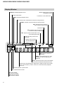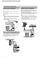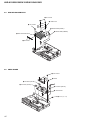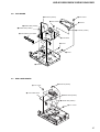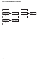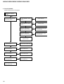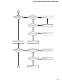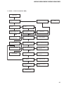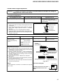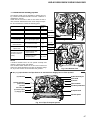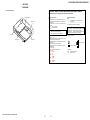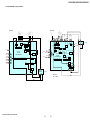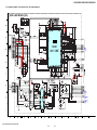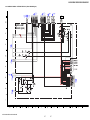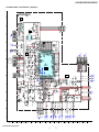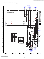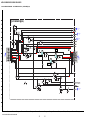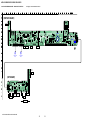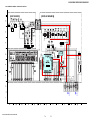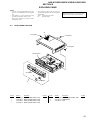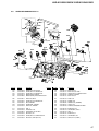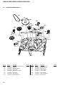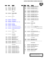
1
AVD-K150B/K150E/K150G/ K150N/K150R SERVICE MANUAL AEP Model AVD-K150B/K150E/K150N/K150R UK Model Ver 1.0 2004.06 AVD-K150G AVD-K150B/K150E/K150G/K150N/K150R is the Amplifier, DVD/VIDEO player and tuner section in DAV-D150B/D150E/D150G/D150N/D150R. • Manufactured under license from Dolby Laboratories. "Dolby", "Pro Logic", and the double-D symbol are trademarks of Dolby Laboratories. Confidential unpublished works. Copyright 1992 -1997 Dolby Laboratories. All rights reserved. • DTS and DTS Digital Surround are registered trademarks of Digital Theater Systems, Inc. Model Name Using Similar Mechanism NEW DVD VCR Mechanism Type DP-7C Optical Pick-up Name PVR-502W Mechanism Type D35 (N) SPECIFICATIONS General Maximum recording time Power requirements AC 230 V , 50/60 Hz Power consumption 74W Dimensions (approx.) 430 x 98 x 386 mm (17 x 3 7/8 x 15 1/4 inches) (W x H x D) Mass (approx.) 6.5 kg (14 lb 6 oz) 5 °C to 35 °C (41 °F to 95 °F) Operating temperature Operating humidity Rewind time Input level SP: 4 hour (E-240 tape), LP: 8 hour (E-240 tape) About 180 seconds (E-180 tape) VIDEO: 1.0 V(p-p), 75 ohms, unbalanced AUDIO: -6.0 dBm, more than 10 kohms (SCART) -6.0 dBm, more than 47 kohms (RCA) DIGITAL AUDIO IN: Optical connector x 1 Output level 5 % to 90 % VIDEO: 1.0 V(p-p), 75 ohms, unbalanced FM Tuner DVD Section Laser Signal system Frequency response DVD (PCM 48 kHz): 10 Hz to 22 kHz CD: 10 Hz to 20 kHz Signal-to-noise ratio More than 80 dB (ANALOG OUT connectors only) Less than 0.05% Harmonic distortion Tuning Range Semiconductor laser (Wavelength DVD: 650nm, CD: 780nm) PAL Intermediate Frequency 65 - 74 MHz (150R) 87.5 - 108.0 MHz (ALL MODEL) 10.7 MHz AM Tuner Tuning Range Intermediate Frequency 522 - 1,611 kHz 450 kHz Amplifier Section VIDEO Section Stereo mode Head system Television system Recording format Tape speed 4 heads helical scan azimuth system Surround mode PAL B/G colour system (150E) PAL B/G, SECAM L colour system (150B) PAL I colour system (150G) PAL B/G, SECAM D/K colour system (150N) PAL (B/G, I/I), SECAM D/K colour system (150R) PAL PAL/MESECAM; 23.39 mm/s (SP), 16.69 mm/s (LP) 70W + 70W (6 Ω at 1 kHz, THD 10 %) Front: 70W/ch (6 Ω at 1 kHz, THD 10 %) Center*: 70W (6 Ω at 1 kHz, THD 10 %) Surround*: 70W/ch (6 Ω at 1 kHz, THD 10 %) Subwoofer*: 100W (4 Ω at 30 Hz, THD 10 %) * Depending on the sound mode settings and the source, there may be no sound output. Inputs AV 2, AV 3, OPTICAL IN (AV3 OPT) • Design and specifications are subject to change without notice. DVD/VCR RECEIVER 9-877-959-01 2004F1678-1 © 2004.06 Sony Corporation Home Audio Company Published by Sony Engineering Corporation AVD-K150B/K150E/K150G/K150N/K150R Laser component in this product is capable of emitting radiation exceeding the limit for Class 1. This appliance is classified as a CLASS 1 LASER product. The CLASS 1 LASER PRODUCT MARKING is located on the rear exterior. CAUTION Use of controls or adjustments or performance of procedures other than those specified herein may result in hazardous radiation exposure. Notes on chip component replacement • Never reuse a disconnected chip component. • Notice that the minus side of a tantalum capacitor may be damaged by heat. Flexible Circuit Board Repairing • Keep the temperature of the soldering iron around 270 °C during repairing. • Do not touch the soldering iron on the same conductor of the circuit board (within 3 times). • Be careful not to apply force on the conductor when soldering or unsoldering. UNLEADED SOLDER Boards requiring use of unleaded solder are printed with the leadfree mark (LF) indicating the solder contains no lead. (Caution: Some printed circuit boards may not come printed with the lead free mark due to their particular size) : LEAD FREE MARK Unleaded solder has the following characteristics. • Unleaded solder melts at a temperature about 40 °C higher than ordinary solder. Ordinary soldering irons can be used but the iron tip has to be applied to the solder joint for a slightly longer time. Soldering irons using a temperature regulator should be set to about 350 °C. Caution: The printed pattern (copper foil) may peel away if the heated tip is applied for too long, so be careful! • Strong viscosity Unleaded solder is more viscou-s (sticky, less prone to flow) than ordinary solder so use caution not to let solder bridges occur such as on IC pins, etc. • Usable with ordinary solder It is best to use only unleaded solder but unleaded solder may also be added to ordinary solder. SAFETY-RELATED COMPONENT WARNING!! COMPONENTS IDENTIFIED BY MARK 0 OR DOTTED LINE WITH MARK 0 ON THE SCHEMATIC DIAGRAMS AND IN THE PARTS LIST ARE CRITICAL TO SAFE OPERATION. REPLACE THESE COMPONENTS WITH SONY PARTS WHOSE PART NUMBERS APPEAR AS SHOWN IN THIS MANUAL OR IN SUPPLEMENTS PUBLISHED BY SONY. 2 NOTES ON HANDLING THE OPTICAL PICK-UP BLOCK OR BASE UNIT The laser diode in the optical pick-up block may suffer electrostatic break-down because of the potential difference generated by the charged electrostatic load, etc. on clothing and the human body. During repair, pay attention to electrostatic break-down and also use the procedure in the printed matter which is included in the repair parts. The flexible board is easily damaged and should be handled with care. NOTES ON LASER DIODE EMISSION CHECK The laser beam on this model is concentrated so as to be focused on the disc reflective surface by the objective lens in the optical pickup block. Therefore, when checking the laser diode emission, observe from more than 30 cm away from the objective lens. LASER DIODE AND FOCUS SEARCH OPERATION CHECK Carry out the “S curve check” in “CD section adjustment” and check that the S curve waveform is output several times. AVD-K150B/K150E/K150G/K150N/K150R • SERVICE POSITION-1 (DVD Mechanism Deck) Extension cable (J-2501-242-A, J-2501-245-A) is required to inspect the DVD mechanism deck. DVD mechanism deck J-2501-245-A (1mm/23P/L300) J-2501-242-A (1mm/11P/L300) • SERVICE POSITION-2 (VIDEO Mechanism Deck) Perform the operation check of the VIDEO mechanism deck after the VCR board and the VIDEO mechanism deck are turned upside down. SMPS board VCR board VIDEO mechanism deck 3 AVD-K150B/K150E/K150G/K150N/K150R TABLE OF CONTENTS 1. GENERAL ................................................................... 5 2. DISASSEMBLY 2-1. 2-2. 2-3. 2-4. 2-5. 2-6. 2-7. Cover, Front Panel Assembly .......................................... DISPLAY/KEY Board .................................................... Video Mechanism Deck .................................................. DVD Mechanism Deck ................................................... SMPS Board .................................................................... VCR Board ...................................................................... DVD & AMP Board ........................................................ 3. 12 13 13 14 14 15 15 ELECTRICAL ADJUSTMENTS 3-1. VCR Section Electrical Adjustment ................................ 16 3-2. Electrical Troubleshooting Guide .................................... 17 3-3. DVD & AMP Section Electrical Troubleshooting Guide .................................................... 32 4. MECHANICAL ADJUSTMENTS ......................... 40 5. DIAGRAMS 5-1. 5-2. 5-3. 5-4. 5-5. 5-6. 5-7. 5-8. 5-9. Block Diagram – DVD (OVERALL) Section – .............. Block Diagram – DVD (AMP) Section – ........................ Block Diagram – VCR/PANEL Section – ....................... Block Diagram – VCR (Y/C) Section – .......................... Block Diagram – VCR (TU-VPS) Section – ................... Block Diagram – VCR (HI-FI) Section – ........................ Block Diagram – VCR POWER Section – ...................... Block Diagram – POWER Section – ............................... Printed Wiring Board – DVD & AMP Section (Component Side) – ................. 5-10. Printed Wiring Board – DVD & AMP Section (Conductor Side) – ................... 5-11. Schematic Diagram – MPEG Section – [DVD & AMP Board] (1/6) .............. 5-12. Schematic Diagram – RF & SERVO Section – [DVD & AMP Board] (2/6) ............................................. 4 52 53 54 55 56 57 58 59 60 61 62 63 5-13. Schematic Diagram – AUDIO, µ_COM Section – [DVD & AMP Board] (3/6) ............................................. 5-14. Schematic Diagram – DIGITAL AMP Section – [DVD & AMP Board] (4/6) ............................................. 5-15. Schematic Diagram – PWM & CODEIC Section – [DVD & AMP Board] (5/6) ............................................. 5-16. Schematic Diagram – INTERFACE Section – [DVD & AMP Board] (6/6) ............................................. 5-17. Printed Wiring Board – VCR Section – ........................... 5-18. Schematic Diagram – VCR SYSTEM Section – [VCR Board] (1/6) ........................................................... 5-19. Schematic Diagram – AVCP/SECAM Section – [VCR Board] (2/6) ........................................................... 5-20. Schematic Diagram – HI-FI/SWITCH Section– [VCR Board] (3/6) ........................................................... 5-21. Schematic Diagram – TUIF/NICAM/VPS Section – [VCR Board] (4/6) ........................................................... 5-22. Schematic Diagram – SCART/SWITCH Section– [VCR Board] (5/6) ........................................................... 5-23. Schematic Diagram – VCR POWER Section – [VCR Board] (6/6) ........................................................... 5-24. Printed Wiring Board – DISPLAY/KEY Section – ......... 5-25. Schematic Diagram – DISPLAY/KEY Section – ........... 5-26. Printed Wiring Board – SMPS Section – ........................ 5-27. Schematic Diagram – SMPS Section – .......................... 64 65 66 67 70 71 72 73 74 75 76 78 79 80 81 6. EXPLODED VIEWS 6-1. 6-2. 6-3. 6-4. 6-5. 6-6. Front Panel Section ......................................................... Overall Section ................................................................ DVD Mechanism Deck ................................................... Video Mechanism Deck -1 .............................................. Video Mechanism Deck -2 .............................................. Video Mechanism Deck -3 .............................................. 7. ELECTRICAL PARTS LIST .................................. 89 83 84 85 86 87 88 AVD-K150B/K150E/K150G/K150N/K150R SECTION 1 This section is extracted GENERAL from instruction manual. Front Panel A VIDEO Ejects the tape in the VIDEO deck. @/1 Switches the DVD/VCR Receiver ON and OFF. VOLUME Adjusts sound level of speakers. AV 3 IN (VIDEO/AUDIO (Left/Right)) Connect the audio/video output of an external source (Audio system, TV/ Monitor, another VCR). Disc Tray (DVD deck) Insert a disc here. INPUT SELECT Selects the VIDEO deck's source (Tuner, AV1, AV2, AV3 OPT or AV3). x (STOP) Stops playback or recording. X (PAUSE) Pause playback or recording temporarily. H (PLAY) To play back a disc or a recorded tape. Video Cassette Compartment (VIDEO deck) Insert a video cassette here. TUNER FM/AM Selects Radio operation mode. CH/PRESET (+/-) Scans up or down through memorized channels or radio frequencies (stations). Remote Sensor Point the DVD/VCR Receiver remote control here. Display window Shows the current status of the DVD/VCR Receiver. A DVD Opens or closes the disc tray. DVD/VIDEO Toggles control between the DVD deck and the VIDEO deck. lm DVD: Go to beginning of current chapter/track or to previous chapter/track. Press and hold for a fast reverse search. VIDEO: Rewinds the tape from STOP mode or for fast reverse picture search. ML DVD: Go to NEXT chapter/track. Press and hold for a fast forward search. VIDEO: Advances the tape from STOP mode or for fast forward picture search. z REC/ITR To record normally or to activate Instant Timer Recording. 5 AVD-K150B/K150E/K150G/K150N/K150R Display Window SHUFFLE RANDOM playback active SP LP Displays the recording and playback speed. Indicates repeat mode A cassette is in the VIDEO deck. PGM Programmed playback active. BIL Indicates when a BILINGUAL broadcast is being received. STEREO Indicates a stereo broadcast is being received. HI-FI Indicates the unit is playing back a tape recorded in Hi-Fi. ANGLE active OPT Indicates source of DVD/VCR Receiver is DIGITAL AUDIO IN. RDS Lights up when the FM station tuned is transmitting RDS data. Indicates encoding format of the current disc. Indicates sound mode is DOLBY PROLOGIC II. SHUFFLE PGM REPEAT 1 A B BIL STEREO CHAP TRK PCM D PL VIDEO TIMER RDS ANGLE HI-FI REC OPT SP LP MP3 DVD VCDPBC REC DVD/VCR Receiver is Recording. TIMER DVD/VCR Receiver is in timer recording or a timer recording is programmed. VIDEO DVD/VCR Receiver functions are available and channels are selected at DVD/VCR Receiver. Indicates clock, total playing time, elapsed time, chapter number, track number, channel, radio frequency, volume, channel or current deck status (Playback, Pause, etc). Indicates playback or pause mode. PBC Indicates PBC On mode DVD DVD inserted. CD Audio CD inserted. VCD Video CD inserted MP3 MP3 disc inserted 6 AVD-K150B/K150E/K150G/K150N/K150R Remote Control VIDEO Select the output source to VIDEO. DVD Sets the output source to DVD. INPUT SELECT Selects the VIDEO deck's source (AV1, AV2, AV3 OPT, AV3, or Tuner). TUNER FM/AM Selects the DVD/VCR Receiver's tuner as the listening choice. (FM and AM bands) 0-9 numerical buttons Selects numbered options in a menu. TUNING (+/-) To tune in the desired station. MEMORY Memorize a radio station frequency into the tuner. RDS Start a search for a specific PS type. SHUFFLE Plays tracks in random order. PROGRAM Enters to the program edit mode or exits from that. z REC/ITR Records normally or activates Instant Timer Recording. TV/VIDEO To view channels selected by the VIDEO tuner or by the TV tuner. SP/LP Selects recording speed. CM SKIP Fast forwards picture search through 30 seconds of recording. SHOWVIEW To display the programme menu for SHOWVIEW System programming. TV @ / 1 Switches TV ON and OFF. @/1 Switches DVD/VCR Receiver ON and OFF. TV Control Buttons (see page 41) • VOL +/- : Adjusts TV's volume. • CH +/- : Selects TV's channel. • TV/VIDEO: Selects the TV's source. CLEAR Removes a track number on the program menu. To clear preset stations from the tuner memory. Playback Control Buttons • H (PLAY) Starts playback. • x (STOP) Stops playback. • . (PREV) (DVD mode only) Go to beginning of current chapter or track or go to previous chapter or track. • > (NEXT) (DVD mode only) Go to next chapter or track. • m/M (SLOW t/T) DVD: For picture search or slow playback backward or forward. VIDEO: Rewinds or advances the tape in STOP mode or for picture search. • X (PAUSE) zPause playback or recording temporarily. ANGLE Selects a DVD camera angle if available. SUBTITLE Selects a subtitle language. AUDIO Selects an audio language (DVD) or an audio channel (CD). REPEAT Repeat chapter, track, title, all. A-B DVD TOP MENU Repeats sequence. Displays the disc's Title menu, if available. SETUP/MENU (i) DVD MENU Accesses menu on a DVD disc. B/b/V/v (left/right/up/down) Selects an option in the menu. CH/PRESET(+/-): Selects a program of VIDEO or Tuner. Adjusts manually the tape's picture onscreen. ENTER/OK Acknowledges menu selection. DVD DISPLAY, CLK/CNT Accesses On-Screen display. Switches among the clock and tape counter. Accesses or returns DVD setup menu and VIDEO setup menu. SOUND FIELD Selects sound mode between BYPASS, PRO LOGIC, PRO LOGIC II (MOVIE, MUSIC, MATRIX) and 3D SURROUND. VOL (+/-) Adjusts speaker volume. MUTING Momentarily silence the speaker of the DVD/VCR Receiver. RETURN Returns the setup menu. Note This remote control uses the same buttons for VIDEO and DVD functions (ex. PLAY). To use the VIDEO, first press the VIDEO button. To use the DVD, first press the DVD button. 7 AVD-K150B/K150E/K150G/K150N/K150R Rear Panel FM ANTENNA Connectors Connect the FM antenna to this terminal. SPEAKERS Connectors Connect the six supplied speakers to these terminals. EURO AV2 DECODER/EXTERNAL (VIDEO IN) Connect to Pay-TV decoder, Set Top Box or another video recorder. AC Power Cord Plug into the power source. ANTENNA IN Connect the VHF/UHF/CATV antenna to this terminal. AV3 (OPTICAL IN) (DIGITAL AUDIO IN) Connect to a digital audio output on a digital device. ANTENNA OUT (DVD/VIDEO OUT) Connect to a TV with RF coaxial inputs. AM ANTENNA Connectors Connect the AM antenna to this terminal. EURO AV1 (TO TV) (VIDEO IN+OUT/DVD OUT) Connect to your TV set or another video recorder. AA Remote control battery installation AA Dust Protection Cap Remove the dust protection cap from the OPTICAL IN jack and connect the optical digital cable (not supplied) securely so that the configurations of both the cable and the connector match. Keep the dust protection cap and always reattach the cap when not using the connector to protect against dust intrusion. Detach the battery cover on the rear of the remote control, and insert two R6 (size AA) batteries with and aligned correctly. When using the remote control, point it at the remote sensor on the unit. Caution Do not mix old and new batteries. Never mix different types of batteries (standard, alkaline, etc.). Do not touch the inner pins of the jacks on the rear panel. Electrostatic discharge may cause permanent damage to the unit. 8 AVD-K150B/K150E/K150G/K150N/K150R Connections TV and Decoder (or Set Top Box) Connections Make one of the following connections, depending on the capabilities of your existing equipment. SCART INPUT AERIAL Rear of TV Tips • Depending on your TV and other equipment you wish to connect, there are various ways you could connect the DVD/VCR Receiver. Use one of the connections described below. • Please refer to the manuals of your TV, VIDEO, Stereo System or other devices as necessary to make the best connections. Caution − Make sure the DVD/VCR Receiver is connected directly to the TV. Select the correct AV input on your TV. − Do not connect your DVD/VCR Receiver to TV via your VIDEO. The DVD image could be distorted by the copy protection system. Basic connection (RF) 1 Connect the aerial cable (A) from your indoor/ outdoor aerial to ANTENA IN jack on the rear panel of DVD/VCR Receiver. the supplied RF cable (R) from the 2 Connect ANTENA OUT jack on the rear panel of DVD/VCR Receiver to your television's Aerial Input. Notes When you connect the DVD/VCR Receiver to your TV, be sure to turn off the power and unplug both units from the wall outlet before making any connections. Basic connections (AV) 1 Connect the EURO AV1 (TO TV) on the rear panel of the DVD/VCR Receiver to the scart input socket on the TV using a SCART lead (E). TV broadcasters transmit encoded television 2 Some signals which you can only see with a purchased or rented decoder.You can connect such a decoder (descrambler) to the DVD/VCR Receiver (D). 9 AVD-K150B/K150E/K150G/K150N/K150R Connections (Continued) Radio Aerial Connections Digital Device Connections Connect the supplied FM/AM antennas for radio listening. the AM loop antenna to the AM antenna 1 Connect connectors. the FM wire antenna to the FM antenna 2 Connect connectors. Connect the OPTICAL IN jacks on the DVD/VCR Receiver to the digital audio out (optical) jacks on your digital device (Game device, Digital Set Top Box, etc.), using optional optical audio cable. To select source of DVD/VCR Receiver to OPTICAL IN, press INPUT SELECT repeatedly on the remote control until "AV3 OPT" appears in the display window. Notes • To prevent noise pickup, keep the AM loop antenna away from the DVD/VCR Receiver and other components. • Be sure to fully extend the FM wire antenna. • After connecting the FM wire antenna, keep it as horizontal as possible. Notes • If the audio format of the digital output does not match the capabilities of your DVD/VCR Receiver, the DVD/VCR Receiver will produce a strong, distorted sound or no sound at all. • The Optical input function is available only when the other unit's Sampling Frequency is 32 - 48kHz. Accessory Audio/Video (A/V) Connections to DVD/VCR Receiver Connect the AV3 IN jacks on the DVD/VCR Receiver to the audio/video out jacks on your accessory component, using optional audio/video cables. 10 AVD-K150B/K150E/K150G/K150N/K150R Connections (Continued) Speaker System Connections Speaker Positioning Connect the speakers using the supplied speaker cords by matching the colors of the terminals and those of the cords. To obtain the best possible surround sound, adjust the speaker parameters (distance, level, etc.). For a normal setup use 6 speakers (2 front speakers, center speaker, 2 rear speakers and subwoofer). Notes • Be sure to match the speaker cord to the appropriate terminal on the components: 3 to 3 and # to #. If the cords are reversed, the sound will be distorted and lack bass. • If you use front speakers with low maximum input rating, adjust the volume carefully to avoid excessive volume output to the speakers. • Do not disassemble the front covers of supplied speakers. Front Speaker (Right) Center Speaker • Front Speakers Based on your listening position, set up the speakers at equal distance. And by hearing position, set up an interval between speakers of 45 degree. • Center Speaker It is ideal that the center speakers and front speakers are same height. But normally place it above or below the television as shown below. • Rear Speakers Place the rear surround speakers to the left and right behind the primary listening area. These speakers recreate sound motion and atmosphere required for surround playback. For best results, do not install the rear speakers too far behind the listening position, install them at or above the level of the listenerês ears. It is also effective to direct the rear speakers towards a wall or ceiling to further disperse the sound. In the case of a smaller room size, if the audience is near to the rear wall set the rear speakers opposite each other, and set the rear speakers 60 - 90 cm above the listener's ears. • Subwoofer This can be placed in any front position. Front Speaker (Left) Subwoofer Center Speaker Front Speaker (Left) Front Speaker (Right) Rear Speaker (Left) Rear speaker (Right surround) Subwoofer Rear speaker (Left surround) About Ferrite Core 1 2 Be sure to attach the ferrite core to the speaker cables (for connecting to this unit). This ferrite core can reduce noises. How to attach the ferrite core. 1 Push the stopper [a] of the ferrite core 3 Rear Speaker (Right) Speaker Positioning Example Note Speaker stand is optional. Attaching the foot pads To prevent speaker vibration or movement while listening, attach the supplied foot pads to the speaker, as shown. Foot pads to open. 2 Wind the Center and Subwoofer 3 Speaker cables once on the ferrite core. Pass the others straight on the ferrite core. Close the ferrite core until it clicks. Attaching the color labels Attach the color labels onto the rear panel of the speakers before connecting the speakers. FRONT L Color labels 11 AVD-K150B/K150E/K150G/K150N/K150R SECTION 2 DISASSEMBLY • This set can be disassembled in the order shown below. • The dotted square with arrow ( ) prompts you to move to the next job when all of the works within the dotted square ( ) are completed. SET 2-1.COVER, FRONT PANEL ASSEMBLY (Page 12) 2-2.DISPLAY/ KEY BOARD (Page 13) 2-3.VIDEO MECHANISM DECK (Page 13) 2-5.SMPS BOARD (Page 14) 2-6.VCR BOARD (Page 15) 2-4.DVD MECHANISM DECK (Page 14) 2-7.DVD & AMP BOARD (Page 15) Note: Follow the disassembly procedure in the numerical order given. 2-1. COVER, FRONT PANEL ASSEMBLY 1 two screws 4 cover 2 three screws 3 two screws 7 three hooks 6 three hooks 8 front panel assembly 5 volume knob 12 AVD-K150B/K150E/K150G/K150N/K150R 2-2. DISPLAY/KEY BOARD 1 three claws 4 DISPLAY/ KEY board 2 four claws 3 connector (PM602,PM601) 2-3. VIDEO MECHANISM DECK 1 six screws 4 VIDEO mechanism deck 2 flexible cable 3 connector (PMCO1) 13 AVD-K150B/K150E/K150G/K150N/K150R 2-4. DVD MECHANISM DECK 2 two screws 3 shield cover 1 two screws 5 flexible cable (PMD01) 4 flexible cable (PMD03) 7 DVD mechanism deck 6 door case 2-5. SMPS BOARD 1 four screws 2 shield 4 connector (PSW01) 5 connector (PSV01) 3 connector (PW101) 7 SMPS board 6 screw (3 × 10) 14 AVD-K150B/K150E/K150G/K150N/K150R 2-6. VCR BOARD 6 connector (PDV01) 1 four screws q; three screws 4 bracket 7 flexible cable (PVD02) 8 flexible cable (PVD03) 2 connector (PVS01) 5 VCR-DISPLAY pwb holder qs VCR board 9 screw 3 screw qa two claws 2-7. DVD & AMP BOARD 4 four screws 1 connector (PDV01) 6 DVD & AMP board 2 flexible cable (PDV02) 3 flexible cable (PDV03) 5 four screws 15 AVD-K150B/K150E/K150G/K150N/K150R SECTION 3 ELECTRICAL ADJUSTMENTS 3-1. VCR SECTION ELECTRICAL ADJUSTMENT 1. Servo Adjustment 1) PG Adjustment • Test Equipment a) OSCILLOSCOPE b) NTSC MODEL : NTSC SP TEST TAPE • Adjustment And Specification MODE MEASUREMENT POINT ADJUSTMENT POINT SPECIFICATION PLAY V.Out H/SW(W373, W374) R/C TRK JIG KEY 6.5 ± 0.5H • Adjustment Procedure a) Insert the SP Test Tape and play. b) Connect the CH1 of the oscilloscope to the H/SW(W373, W374) and CH2 to the Video Out for the VCR. c) Trigger the mixed Combo Video Signal of CH2 to the CH1 H/SW(W373, W374), and then check the distance (time difference), which is from the selected A(B) Head point of the H/SW(W373, W374) signal to the starting point of the vertical synchronized signal, to 6.5H ± 0.5H (412µs, 1H=63µs). Note - Press FRONT CH UP KEY and FRONT PLAY KEY on Deck playback, and it goes in to ATR PRESET. after the SP Test Tape is inserted. • PG Adjustment Method a-1) Payback the SP standard tape b-2) Press the “O” key on the Remote controller and the “PLAY” key on the Front Panel the same time, then it goes in to Tracking initial mode. c-3) Repeat the above step(No.b-2), then it finishes the PG adjusting automatically. d-4) Stop the playback, then it goes out to PG adjusting mode after mony the PG data. • CONNECTION V.Out OSCILLOSCOPE H/SW(W373, W374) CH1 CH2 R/C KEY H/SW V.out (W373, W374) • WAVEFORM H/SW 6.5H(412µs) Composite VIDEO 16 AVD-K150B/K150E/K150G/K150N/K150R 3-2. ELECTRICAL TROUBLESHOOTING GUIDE 1. Power (SMPS) CIRCUIT (1) No 5.3VA (SYS/Hi-Fi/TUNER) (2) No 12VA (TO CAP, DRUM MOTOR) NO 5.3VA. NO 12VA. YES Is the F101 normal? YES NO Replace the F101. (Use the same Fuse) YES Is the BD101 normal? Check or Replace the D110. YES NO Replace the BD101. YES Is the R101 normal? Is the Vcc(13V) supplied NO to (+) terminal in D115? Is the Vcc(12V) supplied NO to (-) terminal in D115? Replace the D115. YES NO Replace the R101. Check or Replace the Motor Vcc. YES Is Vcc(8.5~21V) supplied to IC101 Pin7? NO YES Is the D102 normal? NO Check or Replace the D102. (3) No 5.0V (SYS/Hi-Fi/TUNER) Is the D112 normal? NO NO 5.0VA. Replace the D112. YES YES Is there about 2.5V NO at the IC103 Vref? Replace the IC103. NO Is 5.3VA put into the Q160 Emitter? 5.3VA Line Check. YES YES Check the Main PCB 5.3VA/5.0V Line short? Is the Q162 Base “H”? NO Check the Power Control. YES Is about 5V put into NO the Q160 Base? Check or Replace the Q162, R157, R158, R159. YES Check or Replace the Q162/Q160. 17 AVD-K150B/K150E/K150G/K150N/K150R (4) No 5V (TO DVD) (5) No 33V (TUNER) NO 5V. No 33V. YES YES NO Is 5.3VA put into the Q160 Emitter? 5.3VA Line Check. YES Is the Q162 Base “H”? YES NO Check the Power Control. YES Is about 5V put into NO the Q160 Base? YES Check or Replace the Q162/Q160 18 Is Q163 Base “H”? Check or Replace the Q162, R157, R158, R159. Check or Replace Q161, R154, R155. NO Check the Power Control. AVD-K150B/K150E/K150G/K150N/K150R 2. SYSTEM/KEY CIRCUIT (1) AUTO STOP Auto Stop YES Does the SW25 waveform appear at the IC501 Pin105? NO Check the Drum Motor signal. YES NO Do the T-UP Reel Pulses appear at the IC501 Pin49? YES Do T/UP Reel Pulses appear at the Q514 Base terminal ? YES NO Replace the T/UP Reel Sensor (RS501). Replace the IC501. Does 5.2V appear at the RS501? YES NO Check the Power Circuit. (2) The unstable loading of a Cassette tape The unstable loading of a Cassette tape YES Is 12V applied to the PMC01 Pin8? NO Check the Power. YES Does the “H” signal appear at the IC501 Pin30 during inserting the CST ? NO Is 5.3V applied to the R544 ? YES YES Does the “L” signal appear at the IC501 Pin72 during inserting the CST? Check the CST SW and the peripheral circuitry. NO Refer to SMPS 5.3VA troubleshooting. NO YES Check the Deck Mechanism. Check the IC501 Pins68, 69, 70, 71. Caution : Auto stop can occur because Grease or Oil is dried up 19 AVD-K150B/K150E/K150G/K150N/K150R 3. SERVO CIRCUIT (1) Unstable Video in PB MODE Unstable Video in PB Mode. YES Does the Noise level of the screen change periodically? YES Do the CTL pulses appear at the IC501 Pin8? NO Is adjusting the height of the CTL Head accurate? NO YES Does the CFG waveform appear at the IC501 Pin9? YES On tracking do the CTL pulses move? Readjust the height of the CTL Head. NO Replace the IC501. YES Does the Video Envelope waveform appear at the IC501 Pin24? YES NO Refer to “(2) No 12VA of Power section” Replace the IC501. (2) When the Drum Motor (2) doesn’t run. Do the Drum PWM Pulses appear at the IC501 Pin107? YES When the Drum Motor doesn’t run, Does 12V appear at the PMC01 Pin8? YES Check the connector (PMC01) and the Drum Motor Ass’y. NO YES Aren’t the foil patterns and the Components between IC501 Pin107 and PMC01 Pin12 short? Do the DFG Pulses appear at the PMC01 Pin11? NO Replace the Cap M. NO YES Does 2.8V appear at the PMC01 Pin12? Refer to “When the Y signal doesn’t appear on the screen in PB Mode”. Do the DFG Pulses appear at the IC501 Pin104? NO NO YES Do the Drum PWM Pulses appear at the IC501 Pin107? NO Aren’t the foil patterns and the Components between IC501 Pin104 and PMC01 Pin11 short? Replace the IC501. YES Aren’t the connecting patterns and the Components between IC501 Pin107 and PMC01 Pin12 short? 20 AVD-K150B/K150E/K150G/K150N/K150R (3) When the Capstan Motor doesn’t run, When the Capstan Motor doesn’t run, Does 12VA appear at the PMC01? NO Refer to “SMPS(CAPSTAN/12Volt) Trouble Shooting”. YES Does 2.8V appear at the PMC01? NO YES Check the PMC01 and the Capstan Motor Ass’y. Does the PWM signal appear at the IC501 Pin108? YES NO Aren’t the foil patterns and Components between IC501 Pin108 and PMC01 Pin9 short? Does the CFG signal appear at the PMC01 Pin1? YES NO Does the CFG signal come into the IC501 Pin9? Check the Capstan Motor Ass’y. NO YES Aren’t the foil patterns and component between IC501 Pin9 and PMC01 Pin1 short? Does the Capstan PWM signal appear at the IC501 Pin108? NO YES Aren’t the foil patterns and Components between IC501 Pin108 and PMC01 Pin9 short? Replace the IC501. 21 AVD-K150B/K150E/K150G/K150N/K150R (4) KEY doesn’t working KEY doesn’t working. Is 5V applied to the IC501 Pin36? NO Refer to “SMPS 5.3VA Trouble Shooting”. NO Replace the defective switches. YES Does LED or FLD change when a function button is pressed? 22 AVD-K150B/K150E/K150G/K150N/K150R 4. Y/C CIRCUIT (1) No Video in EE Mode, No Video in EE Mode Does the Video signal appear at the IC301 Pin48? NO Check the 24Pin of Tuner. YES Is 5V applied to the IC301 Pins18, 24, 42, 55, 72, 91? NO Check the 5.2VT, 5.3VA Line. (Power Circuit) YES Does the Video signal appear at the IC301 Pin65? NO YES Does the Video signal appear at the IC501 Pin19? Is I2C BUS signal applied to the IC301 Pins68, 69? NO YES NO Chck the path of the signal between the IC301 Pin65 and IC501 Pin17. YES Does the Video signal appear at the Emitter terminal of the Q307, Q308? Check the System Circuit. (Refer to ‘SYSTEM I2C BUS CHECK Trouble Shooting’) Check C316. (AGC) YES NO Does the 12VT, 5.3VA NO appear at the Emitter terminal of the Q804, Q308. Replace the IC301. YES Replace the Q804, Q308. Check the 12VT, 5.3VA Line. (Power Circuit) 23 AVD-K150B/K150E/K150G/K150N/K150R 3. Y/C CIRCUIT (2) When the Y(Luminance) signal doesn’t appear on the screen in PB Mode, Is 5.2VT, 5.3VA applied to the IC301 Pins24, 42, 55, 72, 91? NO Check the line of the 5.2VT, 5.3VA Line. (Power Circuit) YES Is the I2C Bus siganl applied NO to the IC301 Pins68, 69 ? Refer to ‘SYSTEM I2C BUS CHECK Trouble Shooting’. YES Does the normal RF signal appear at the IC301 Pin78? NO Is the V.H.S/W signal applied to the IC301 Pin70? NO Check the System Circuit. (IC501 Pin105) NO Check the V.H.S/W level. (Check R303, R304) YES Is V.H.S/W “H” about 3.4V at the IC301 Pin70? YES YES Clean the Drum. Does the Y(Luminance) RF NO signal appear at the IC301 Pin76? NO Check the path of the Y(Luminance) RF signal. (Check the C312) YES Check the path of the Y(Luminance) RF signal. (Check C327) YES YES Is the Y(Luminance) Video waveform showed up at theIC301 Pin43? YES Replace the IC301. 24 NO Replace the IC301. AVD-K150B/K150E/K150G/K150N/K150R 3. Y/C CIRCUIT (3) When the C(Color) signal doesn’t appear on the screen in PB Mode, Is 5.2VT/5.3VA applied to the IC301 Pins24, 42, 55, 72, 91. NO Check the line of the 5.2VT/ 5.3VA Line. (Power Circuit) NO Check the Color Rotary Circuit. (IC501 Pin99 ) NO Check the Color Rotary level. (Check the R303) YES Is the Color Rotary signal applied to the IC301 Pin70? YES Is Color Rotary “H” about 3.4V? YES Does the Color signal appear at the IC301 Pin25 ? NO Does the X301(4.43MHZ) oscillate? NO Does the Color signal appear at the IC301 Pin21? NO Replace the X301. YES Check the Color Pass. YES Replace the IC301. Replace the IC301. 25 AVD-K150B/K150E/K150G/K150N/K150R 3. Y/C CIRCUIT (4) When the Video signal doesn’t appear on the screen in REC Mode, Is the EE signal normal? NO Check EE Mode. YES Is 5.2VT/5.3VA applied to the IC301 Pins24,42,55,72,91? NO Check the line of the 5.2VT/ 5.3VA Line.(Power Circuit) YES Does PB Mdoe operate normally? NO Check PB Mode. YES Does the RF signal appear at the IC301 Pin78? NO YES Does the REC RF signal appear at the IC301 Pins88,89,94,95? YES Check the Drum & Drum Connector 26 Is the REC ‘H’ signal (about 4V) applied to the IC301 Pin80? NO Check the System of REC ‘H’. (the IC501 Pin47 / the D301) YES NO Check REC Luminance Pass & Color Pass. YES Check the circuit of the IC301 Pins85, 86. YES Replace the IC301. AVD-K150B/K150E/K150G/K150N/K150R 5. Hi-Fi CIRCUIT (A) No Sound(EE Mode) No Sound. YES Check the TU Audio of IC801 Pins1, 3. NO Check the DVD Audio of IC801 Pins4, 5. NO Check the DVD MODULE. (P8D01 Pins3, 5). Check the AV1 Audio of IC801 Pins6, 7. NO Check the Scart1 Jack. (SC901 Scart1 Audio in Pins2, 6). Check the AV2 Audio of IC801 Pins8, 9. NO Check the AV3 Audio of IC801 Pins10, 11. NO Check the IC751 Pins30, 31. Check the Scart2 Jack. (SC901 Scart2 Audio in Pins2, 6). Check the front Jack. (PM602 Pins3, 5). YES Check the Vcc of IC801 Pins34, 40, IC802 Pin4. NO Check the Power 5.2V, 12VT. YES Check the IIC Clock and DATA at IC801 Pins42, 43, IC802 Pins32, 33. NO Check the IC501 Pins59, 60. YES NO Replace IC801. Check the Audio of IC801 Pins16, 17. YES NO Check the Audio of IC802 Pins22, 26. Replace IC802. YES Check the JK801. 27 AVD-K150B/K150E/K150G/K150N/K150R 3. Y/C CIRCUIT (B) Hi-Fi Playback PB mode YES No Sound. YES Check the Vcc of IC801 (Pins34, 40) YES NO NO Check the Hi-Fi Selection switch. (IC801 Pin41) and the Tape quality. YES Is the RF Envelope at IC801 Pin44 over 2Vp-p? YES NO Check IC801 Pin42(Data), Pin43(Clock) YES NO Check Power 5.2V, 12VT. Check IC501 Pin25 (A.H/SW) Check the parts of µ-COM (IC501 Pins59, 60) NO Do Audio Signals appear at IC801 Pin16(L-CH), 17(R-CH)? YES Check the Connection at P3D01 Pins7, 9. NO Do Audio Signals appear at IC802 Pin10(L-CH), 16(R-CH)? YES Check the A.IN line of IC802(C808, C809) Do Audio Signals appear at NO IC802 Pins22, 26? YES Check the Vcc of IC802 Pin4. YES Replace IC802. Do Audio Signals appear at JK801? 28 NO Check the Jack(JK801) NO Check Power. AVD-K150B/K150E/K150G/K150N/K150R (C) Hi-Fi REC. YES It is impossible to record Hi-Fi Audio signal. YES Check Vcc of IC801.(Pins34, 40) NO Check Power 5V, 12VT. YES Check IC801 Pin42(Data), Pin43(CLOCK). NO Check ports of µ-COM. YES Do Audio signals appear at IC801 Pins16, 17? NO Check Audio input signal of IC801 Pins2, 3(TU.A.), 4, 5(DVD.A.), 6, 7(AVI.A.), 8, 9(AV2.A.), 10, 11(AV3.A.). YES Do FM Audio signals appear at IC801 Pin36? NO Replace IC801. YES Check the Contact Point of Drum Connector if good then Replace the Drum. 29 AVD-K150B/K150E/K150G/K150N/K150R 6. Tuner/IF CIRCUIT (A) No Picture on the TV screen No picture on the TV screen YES Does the Video signal at the TU701 Pin24. NO YES Is +33V applied to TU701 Pin16? NO Check 33V line. YES Is +5V applied to TU701 Pin13? NO Check 5V line. YES Does the Clock signal appear at TU701 Pin11? NO Check the lIC Clock Signal of µ-COM Pin59. NO Check the lIC Data Signal of µ-COM Pin60. YES Does the data signal appear at TU701 Pin12? YES Replace Tuner. Does Sync appear at IC501 Pin111. NO Check the signal flow from TU701 Pin24 to IC301 Pin48. NO Check the signal from IC301 Pin65 to IC501 Pin17. NO Check the signal from IC501 Pin19 to IC301 Pin56. NO Check the signal from IC501 Pin61 to IC802 Pin1. YES Does the Video signal at the IC501 Pin19. YES Does the Video signal at the IC301 Pin61. YES Does the Video signal at the IC802 Pin30. Check the signal flow from IC802 Pin30 to SC901 Pin19. 30 AVD-K150B/K150E/K150G/K150N/K150R (B) No Sound No Sound. YES Check the Vcc of IC751 Pins1, 11, 19, 22, 33. NO Check 5.2V Line. YES Check the Tuner SiF signal at IC751 Pin2. NO Check the Tuner SIF of TU701 Pin22. YES Check the oscillator of IC751 Pins5, 6. NO Replace X751 YES Check the Audio of IC751 Pins30, 31. NO Check the IIC Clock and Data at IC751 Pins12, 13. NO Check the signal flow from IC751 Pins30, 31 to IC801 Pins2, 3. NO Check the IIC Clock and Data at IC801 Pins42, 43. NO Check the signal flow from IC801 Pins16, 17 to IC802 Pins10, 16. YES Check the Audio of IC801 Pins2, 3. YES Check the Audio of IC801 Pins16, 17. YES Check the Audio of IC802 Pins22, 26. YES Check the Signal flow from IC802 Pins22, 26, SC901 Pins1, 3. 31 AVD-K150B/K150E/K150G/K150N/K150R 3-3. DVD & AMP SECTION ELECTRICAL TROUBLESHOOTING GUIDE 1. System operation flow Power On 1. 8032 initializes SERVO, DSP & RISC registers 2. Write RISC code to SDRAM 3. Reset RISC Show LOGO Yes Tray Closed? No Tray Close to Closed position SLED at Inner Side? Yes No SLED Moves to Inner Position 1. Judge whether have disc and disc type 2. Jump to related disc reading procedure Recieve OPEN/ CLOSE Key? No 1. Execute Pressed Key & IR Key 2. Systemoperati on Routi ne Loop 1. Stop Playback & Open Tray 2. Display tray open message & LOGO No 32 Receive CLOSE Key? Yes AVD-K150B/K150E/K150G/K150N/K150R 2. T est & debug flow TEST Check the AC Voltage Power PCBA (110V or 220V) No Check the POWER PART Yes Switch on the Power PCBA Is the DC Voltage outputs OK? (5V, 3.3V, 8V, 12V) No Check the POWER PART Yes Is 3.3V and 2.5V DC outputs normal on main PCBA? No Check the regulators or diode(D501). Yes Communication between VCR & DVD is normally? No Check the cable connection. (PDV03) Yes Connect to PC RS232 Cable and update the FLASH memory code. Update FLASH(IC5A1) successfully? No 1. Check 27MHz system clock. 2. Check systemreset circuit. 3. Check FLASH R/Wenable signal PRD, RWR. 4. Check RS232 SIGNALS. 5. Check FLASH Memory related circuit. Yes Replace FLASH( IC5A1) A 33 AVD-K150B/K150E/K150G/K150N/K150R A RESET or Power On. Show LOGO? NO Flash Memory operates properly? NO Check connection lines between FLASH & MT1379 and the FLASH access time whether is sui table or not. NO Check connection lines between SDRAM(IC502,IC503) & MT1379 and the SDRAM is damaged. YES YES SDRAM works properly? YES MT1379 VIDEO outputs properly? NO Check the related circuit of MT1379. (IC501 PIN 161,166, 168 check) YES Have TV signal output? NO Check the filtering and amp circuit of TV signal .(IC507) YES Check AV cable connection to TV set . Does Tray move inside when it is not at closed position? YES NO Normal TROUT & TRIN signals? NO Check the load OPEN & CLOSE switch NO Check the Tray control IO pins on MT1376 & MT1379. NO Check the Tray control amplifying circuit on Motor driver.(IC402) YES Normal TRCLOSE & TROPEN signal? YES Normal LOAD+ & LOADsignal ? YES B 34 Check the cable connection between main PCBA and loader. (MECHA) AVD-K150B/K150E/K150G/K150N/K150R B Does the SLED move No to inner side when it is at outer position? Motor Driver STBY Pin is High? No Yes Yes Motor Driver STBY Pin is High? Check the connection line of STBY signal . OK No Check the related circuit of FMSO. No Check the amp circuit on motor driver. Yes SL+ and SL- output properly? Yes Do not put in disc and tray close. Optical Lens has movements for searching Focus? Yes Check the cable connection with MECHA. No Proper FOSO outputs to motor driver? No Check FOSO connection on MT1379 and motor driver. No Check the amp circuit on motor driver. Yes Proper F+ & F- outputs? Yes C Check cable connect of the pick-up head. 35 AVD-K150B/K150E/K150G/K150N/K150R C Laser turns on when reading disc? No Yes LD01 or LD02 output properly? No Check the laser power circuit on MT1336 and connecting to power transistor. (Q404, Q405) No Check the related circuit on laser power transi stor Yes Collector voltage of power transistor is OK? (Q404, Q405) Yes Check cable connection between transistor output and pick-up head. Disc ID is correct? No Proper RFL signal on MT1336? No Check the related circuit on MT1336 RFL signal . Yes Yes Check the RFL connection between MT1336 and MT1379. Does spindle rotate? Yes No Proper DMSO signal on MT1379 No Check DMSO related circuit on MT1379. No Check the spindle control amp circuit of motor driver. Yes SP+ & SP- output properly? Yes Check the cable connection between spindle and main PCBA. D 36 AVD-K150B/K150E/K150G/K150N/K150R D Yes Focus ON OK? No Proper signals on A, B, C, D of MT1336 No Check connections between MT1336 and pick-up head. No Check the related circuit on MT1336 FEO sugnal . Yes Yes Proper FEO signal on MT1336? Yes Check FEO connection between MT1336 and MT1379 Track On OK? No Proper FEO signal on MT1336? No Check the related circuit on MT1336 Yes Yes Properly TRSO signal on MT1379? No Check the TRSO connection on MT1379 and motor dirver. Yes T+ & T- output properly? No Check the tracking control amp circuit on motor driver. Yes Check cable connection on pick-up head. Disc is play? No Check RF signal waveform. Yes E 37 AVD-K150B/K150E/K150G/K150N/K150R E Normal Audio output when disc playback? YES NO Audio DAC received correct data stream? NO Check connection between MT1379 & Audio DAC. (Check ARCK, ALRCK ACKL, ASDAT3) NO Check the related circuit of Audio DAC. (Check Audio out Pins 8, 5) YES Normal Audio DAC out? (IC206) YES Check Audio filter, amplify, mute circuit. (IC205 Application circuit)? TEST END 38 AVD-K150B/K150E/K150G/K150N/K150R 3. AUDIO µ -COM Circuit(DVD & AMP) POWER ON Does CD/DVD appear at FLT? NO Does CD/DVD appear at FLT? YES Does Loading appear at FLD? NO Does it appear DVD Error at FLD? NO Check Connector (DVV01) if is normally. Check power part of Main B/D. YES Reconnet it. NO Refer to SMPS. YES NO Check DVD Module. NO YES Check if DVD an Audio Micom Insert is OK. YES NO YES YES Check Power. OK YES YES Does no Dise or Time appear at FLD? NO NO Check oscillator of X101. Refer to oscillator Circuit. YES NO Check DVD Reset Waveform. NO Check IC101 Reset Waveform. Check if PN102 is high. YES Check SMPS. Check if IC101 Pin53 is high. YES Check if IC101 Pin9, 36, 59 is high(5V). NO Check 3.3V line. YES Check if IC101 Pin49 is high. NO Check Power dection Circuit. YES Replace IC101. 39 AVD-K150B/K150E/K150G/K150N/K150R SECTION 4 MECHANICAL ADJUSTMENTS • Tools and Fixfures for Service SR K 1. Cassette Torque meter SRK-VHT-303(Not SVC part) -V HT -S 2. Alignment tape (See figure below) 3. Torque gauge 600g.Cm ATG 300 250 200 150 0 50 SR VID K CAS EO S TOR ETTE Q MET UE E VHT R -303 -T K- V HT0 SR 50 100 150 200 300 250 4. Torque gauge adaptor 5. Post height adjusting driver 6. + Type driver (φ 5) Parts No. : SV-TGO-030-000(SMALL) : SV-TGO-030-000(LARGE) • Alignment Tapes for Adjustment Derivation No. Mechanism Adjustment Items FM Envelope Height Azimuth X-value BC D A BC D SP/LP 2/4 Head SP 2 Head SP/LP/EP 2/4 Head SP 2 Head TTV-P2L TTV-P2 TTV-N1 (TTV-N12) TTV-N2 A commecially available tape Slantness A/C Head A TTV-P1 (TTV-P1L) TTV-P1 TTV-N1 (TTV-N12) (TTV-N1E) TTV-N1 (TTV-N12) TTV-P1 TTV -P2 TTV-N2 TTV-N2 TTV-P2 (TTV-P2L) TTV-P2 TTV-N2 TTV-N2E TTV-N12 TTV-N2 RG Post Inclination A commecially available tape Tape Back Tension SRK-VHT-303 The numbers in ( ) parenthesis can be used as the substiture. 40 AVD-K150B/K150E/K150G/K150N/K150R 1. Mechanism Alignment Position Check Purpose:To determine if the Mechanism is in the correct position, when a Tape is ejected. Test Equipment/ Fixture Test Conditions (Mechanism Condition) • Blank tape • Eject Mode (with Cassette ejected) 1) Turn the Power S/W on and eject the Cassette by pressing the Eject Button. 2) Remove the Top Cover and Plate Assembly Top, visually check if the Gear Cam Hole is aligned with the Chassis Hole as below Fig. C-2. 3) IF not, rotate the Shaft of the Loading Motor to either clockwise or counterclockwise until the alignment is as below Fig. C-2. Check Point • Mechanism and Mode Switch Position 4) Remove the Screw which fixes the Deck Mechanism and Main Frame and confirm if the Gear Cam is aligned with the Gear Drive as below Fig. C-1(A). 5) Confirm if the Mode S/W on the Main P.C.Board is aligned as below Fig. C-1(B). 6) Remount the Deck Mechanism on the Main P.C.Board and check each operation. CHECK DIAGRAM Gear Cam (A) Mode S/W (B) Gear Drive Gear Cam (o) and Gear Drive (o) groove alignment BOTTOM VIEW Fig. C-1 L/D Motor Assembly Gear Cam (B) (A') (A) (B') Chassis Hole Gear Cam Hole Gear Drive Hole TOP VIEW Fig. C-2 41 AVD-K150B/K150E/K150G/K150N/K150R cassette without tape. Cover the holes of the End Sensors at the both sides of the Chassis to prevent a light leak. Then the Deck Mechanism drives to the Stop Mode. In this case, the Deck Mechanism can accept inputs of each mode, however the Rewind and Review operation can not be performed for more than a few seconds because the Take-up Reel Table is in the Stop State and can not be detected the Reel Pulses. 2. Preparation for Adjustment (To set the Deck Mechanism of the loading state without inserting a cassette tape). 1) 2) 3) 4) Unplug the power cord from the AC outlet. Disassemble the Top Cover and Plate Assembly Top. Plug the power cord into the AC outlet. Turn the power S/W on and push the Lever Stopper of the Holder Assembly CST to the back for loading the 3. Checking Torque Purpose: To insure smooth transport of the tape during each mode of operation. If the tape transport is abnormal, then check the torque as indicated by the chart below. Test Conditions (Mechanism Condition) Test Equipment/ Fixture • Torque Gauge(600g/cm ATG) • Torque Gauge Adaptor • Cassette Torque Meter SRK-VHT-303 • Play (FF) or Review (REW) Mode • Perform each Deck Mechanism mode without inserting a cassette tape(Refer to above No.2 Preparation for Adjustment). • Read the measurement of the Take-up or Supply Reels on the Cassette Torque Meter(Fig. C-3-2). • Attach the Torque Gauge Adaptor to the Torque Gauge and then read the value of it(Fig. C-3-1). Mode Item Checking Method Test Equipment Measurement Reel Measurement Values Fast Forward Torque Fast Forward Cassette Torque Gauge Rewind Torque Rewind Cassette Torque Gauge Supply Reel More than 400g/cm Play Take-Up Torque Play Cassette Torque Meter Take-Up Reel 40~100g/cm Review Torque Review Cassette Torque Meter Supply Reel 120~210g/cm Take-Up Reel More than 400g/cm NOTE: NOTE: The values are measured by using a Torque Gauge and Torque Gauge Adaptor with the Torque Gauge affixed. The torque reading to measure occurs when the tape abruptly changes direction from Fast Forward to Rewind Mode, when quick braking is applied to both Reels. • Torque Gauge (600g.cm ATG) • Cassette Torque Meter (SRK-VHT-303) SR K Torque Gauge Torque Gauge Adaptor -V HT -S 300 250 200 150 0 50 SR VID K CAS EO S TOR ETTE QUE MET VHT ER -303 -T K- V HT0 SR 50 100 150 200 300 Reel Table Fig. C-3-1 42 Fig. C-3-2 250 AVD-K150B/K150E/K150G/K150N/K150R 4.Guide Roller Height Adjustment Purpose: To regulate the height of the tape so that the bottom of the tape runs along the tape guide line on the Lower Drum. 4-1. Preliminary Adjustment Test Equipment/ Fixture • Post Height Adjusting Driver Test Conditions (Mechanism Condition) • Play or Review Mode Adjustment Procedure Adjustment Point • Guide Roller Height Adjustment screws on the Supply and Take-Up Guide Rollers. ADJUSTMENT DIAGRAM 1) Confirm if the tape runs along the tape guide line of the Lower Drum. 2) If the tape runs the bottom of the guide line, turn the Guide Roller Height Adjustment Screw to clockwise direction. 3) If it runs the top, turn to counterclockwise direction. 4) Adjust the height of the Guide Roller to be guided to the guide line of the Lower Drum from the starting and ending point of the Drum. Guide Roller Height Adjustment screw Upper Flange Guide Roller Retaining Screw Fig. C-4-1 4-2. Precise Adjustment Test Equipment/Fixture • Oscilloscope • Alignment Tape • Post Height Adjusting Driver Adjustment Point Test Equipment Connection Points Test Conditions VCR(VCP) State • CH-1:PB RF Envelope • CH-2:NTSC: SW 30Hz PAL: SW 25Hz • Head Switching Output Point • RF Envelope Output Point • Guide Roller Height Adjustment Screws • Play an Alignment Tape Waveform Diagrams P2 POST ADJUSTMENT Adjustment Procedure 1) Play an Alignment Tape after connecting the probe of the Oscilloscope to the RF Envelope Output Test Point and Head Switching Output Test Point. 2) Tracking Control(in PB Mode) : Center Position(When this adjustment is performed after the Drum Assembly has been replaced, set the Tracking Control so that the RF Output is Maximum). 3) Height Adjustment Screw : Flatten the RF waveform. (Fig. C-4-2) 4) Turn(Move) the Tracking Control(in PB Mode) clockwise and counterclockwise.(Fig. C-4-3) 5) Check that any drop of RF Output is uniform at the start and end of the waveform. NOTE Turn the Roller Guide Height Adjustment Screw slightly to flatten the waveform. P3 POST ADJUSTMENT Fig. C-4-2 Tracking Control at center Turn(Move) the Tracking Control to both directions Fig. C-4-3 Connection Diagram OSCILLOSCOPE If the adjustment is excessive or insufficient the tape will jam or fold. RF ENVELOPE OUTPUT TEST POINT HEAD SWITCHING OUTPUT TEST POINT 43 AVD-K150B/K150E/K150G/K150N/K150R 5. Audio/Control (A/C) Head Adjustment Purpose: To insure that the tape passes accurately over the Audio and Control Tracks in exact alignment of the both Record and Playback Modes. 5-1. Preliminary Adjustment (Height and Tilt Adjustment) Perform the Preliminary Adjustment, when there is no Audio Output Signal with the Alignment Tape. Test Equipment/ Fixture • Blank Tape • Screw Driver(+) Type 5mm Test Conditions (Mechanism Condition) Adjustment Point • Tilt Adjustment Screw(C) • Height Adjustment Screw(B) • Azimuth Adjustment Screw(A) • Play the blank tape Adjustment Procedure/Diagrams 1) Initially adjust the Base Assembly A/C Head as shown Fig. C-5-1 by using the Height Adjustment Screw(B). 2) Play a blank tape and observe if the tape passes accurately over the A/C Head without tape curling or folding. 3) If folding or curling is occured then adjust the Tilt Adjustment Screw(C) while the tape is running to resemble Fig. C-5-3. 4) Reconfirm the tape path after Playback about 4~5 seconds. NOTE Ideal A/C head height occurs when the tape runs between 0.2~0.25mm above the bottom edge of the A/C Head core. Tape A/C Head P4 10.9 Tape 0.2~0.25mm A/C Head Base Fig. C-5-3 Fig. C-5-1 X-Value Adjustment Hole Fixed Screw Azimuth Adjustment Screw(A) Tilt Adjustment Screw(C) Height Adjustment Screw(B) A/C Head Assembly Fig. C-5-2 44 AVD-K150B/K150E/K150G/K150N/K150R 5-2. Confirm that the tape passes smoothly between the Take-up Guide and Pinch Roller(using a mirror or the naked eye). 1) After completing Step 5-1.(Preliminary Adjustment), check that the tape passes around the Take-up Guide and Pinch Roller without folding or curling at the top or bottom. (1) If folding or curling is observed at the bottom of the Take-up Guide then slowly turn the Tilt Adjustment Screw(C) in the clockwise direction. (2) If folding or curling is observed at the top of it then slowly turn the Tilt Adjustment Screw(C) in the counterclockwise direction. NOTE: Check the RF envelope after adjusting the A/C Head, if the RF waveform differs from Fig. C-5-4, performs Precise Adjustment to flat the RF waveform. 5-3. Precise Adjustment (Azimuth adjustment) Connection Point Test Equipment/ Fixture • Oscilloscope • Alignment Tape(SP) • Screw Driver(+) Type 5mm • Audio output jack Test Conditions (Mechanism Condition) • Play an Alignment Tape 1kHz, 7kHz Sections Adjustment Procedure Adjustment Point • Azimuth Adjustment Screw(A) • Height Adjustment Screw(B) 1kHz 1) Connect the probe of the oscilloscope to Audio Output Jack. 2) Alternately adjust the Azimuth Adjustment Screw(A) and the Tilt Adjustment Screw(C) for maximum output of the 1kHz and 7kHz segments, while maintaining the flattest envelope differential between the two frequencies. 7kHz A:Maximum B:Maximum Fig. C-5-4 6. X-Value Adjustment Purpose: To obtain compatibility with the other VCR(VCP) Models. Test Equipment/ Fixture • Oscilloscope • Alignment Tape(SP only) • Screw Driver(+) Type 5mm Connection Point • CH-1: PB RF Envelope • CH-2: NTSC: SW 30Hz PAL: SW 25Hz • Head Switching Output Test Point • RF Envelope Output Test Point Adjustment Procedure 1) Release the Automatic Tracking to run long enough for tracking to complete it’s cycle. 2) Loosen the Fixed Mounting Screw and move the Base Assembly A/C Head in the direction as shown in the diagram to find the center of the peak that allows for the maximum waveform envelope. This method should allow the 31µm Head to be centrally located over the 58µm tape track. 3) Tighten the Base Assembly A/C Head mounting Screw. Test Conditions (Mechanism Condition) Adjustment Point • Play an Alignment Tape Left Groove at the Base A/C Right Adjustment Diagram X-Value Adjustment Hole Fixed Screw Azimuth Adjustment Screw(A) Tilt Adjustment Screw(C) Height Adjustment Screw(B) OSCILLOSCOPE Connection Diagram RF ENVELOPE OUTPUT TEST POINT CH-1 CH-2 HEAD SWITCHING OUTPUT TEST POINT 45 AVD-K150B/K150E/K150G/K150N/K150R 7. Adjustment after Replacing Drum Assembly (Video Heads) Purpose: To correct for shift in the Roller Guide and X value after replacing the Drum. Test Equipment/ Fixture Connection Point Test Conditions (Mechanism Condition) • CH-1: PB RF Envelope • Oscilloscope • Play the Blank Tape • CH-2: NTSC: SW 30Hz • Alignment Tapes • Play an Alignment Tape PAL: SW 25Hz • Blank Tape • Post Height Adjusting Driver • Head Switching Output Test Point • Screw Driver(+) Type 5mm • RF Envelope Output Test Point Checking/Adjustment Procedure Adjustment Points • Guide Roller Precise Adjustment • Switching Point • Tracking Preset • X-Value Connection Diagram OSCILLOSCOPE Play a blank tape and check for tape curling or creasing around the Roller Guide. If there is a problem then follow the procedure RF ENVELOPE OUTPUT TEST POINT 4. "Guide Roller Height" and 5. "Audio Control(A/C) Head HEAD SWITCHING OUTPUT TEST Adjustment". CH1 CH2 POINT Waveform V1/V MAX ≤ 0.7 V2/V MAX ≤ 0.8 RF ENVELOPE OUTPUT V1 V V2 Fig. C-7 8. Check the Tape Travel after Reassembling Deck Assembly. 8-1. Checking Audio and RF Locking Time during playback and after CUE or REV (FF/REW) • Oscilloscope • Alignment Tapes(with 6H 3KHz Color Bar Signal) • Stop Watch Test Equipment Connection Connection Points Points Specification Test Equipment/ Fixture • RF Locking Time: Less than 5 sec. • Audio Locking Time:Less than 10sec • CH-1: PB RF Envelope • CH-2: Audio Output • RF Envelope Output Point • Audio Output Jack Test Conditions (Mechanism Condition) • Play an Alignment Tape (with 6H 3kHz Color Bar Signal) Checking Procedure NOTES: Play an Alignment Tape then change the operating mode to CUE or REV and confirm if the unit meets the above listed specifications. 1) CUE is the forward search mode (FF) 2) REV is the backward search mode (REW) 3) Refer to the Play mede 8-2. Checking for tape curling or jamming Test Equipment/ Fixture • T-160 Tape • T-120 Tape Specification Test Conditions VCR(VCP) (Mechanism State Condition) • Be sure there is no tape jamming or curling at • Run the CUE, REV, Play mode at the the begining, middle or end of the tape. beginning and the end of the tape. Checking Procedure 1) Confirm that the tape runs smoothly around the roller guides, Drum and A/C Head Assemblies while abruptly changing operating modes from Play to CUE or REV. This is to be checked at the begining, middle and end sections of the tape. 46 2) Confirm that the tape passes over the A/C Head Assembly as indicated by proper audio reproduction and proper tape counter performance. AVD-K150B/K150E/K150G/K150N/K150R 1. Check before starting repairs The following faults can be remedied by cleaning and oiling. Check the needed lubrication and the conditions of cleanliness in the unit. Check with the customer to find out how often the unit is used, and then determine that the unit is ready for inspection and maintenance. Check the following parts. Phenomenon Replacement Inspection Color beats Dirt on Full-Erase Head Poor S/N, no color a F/E Head Dirt on Video Head a Vertical or Horizontal jitter Dirt on Video Head Dirt on tape transport system a Low volume, Sound distorted Dirt on Audio/Control Head a Dirt on Pinch Roller a Belt Capston Clutch Assembly D35 torque reduced a Clutch Assembly D35 Tape does not run. Tape is slack In Review and Unloading (off mode), the tape is rolled up loosely. Video Head Fig. C-9-1 Top View A/C Head Pinch Roller Cleaning Drum and transport system Fig. C-9-3 NOTE If locations marked with a do not operate normally after cleaning, check for wear and replace. See the EXPLODED VIEWS at the end of this manual as well as the above illustrations and see the Greasing (Page 45, 46) for the sections to be lubricated and greased. Fig. C-9-2 Bottom View * No. (1)~(12) Indicates the Tape Path to be traveled from Supply Reel to Take-up Reel. (6) Base Assembly P3 (3) F/E Head (7) A/C Head (8) P4 Post (5) Drum Assembly (Video Head) (10) Pinch Roller (11) Take-up Guide Post (4) Base Assembly P2 (2) Tension Post (9) Capstan Shaft (1) Supply Reel (12) Take-up Reel Fig. C-9-3 Tape Transport System 47 AVD-K150B/K150E/K150G/K150N/K150R 2. Required Maintenance The recording density of a VCR(VCP) is much higher than that of an audio tape recorder. VCR(VCP) components must be very precise, at tolerances of 1/1000mm, to ensure compatibility with the other VCRs. If any of these components are worn or dirty, the symptoms will be the same as if the part is defective. To ensure a good picture, periodic inspection and maintenance, including replacement of worn out parts and lubrication, is necessary. Schedules for maintenance and inspection are not fixed because they vary greatly according to the way in which the customer uses the VCR(VCP), and the environment in which the VCR(VCP) is used. But, in general home use, a good picture will be maintained if inspection and maintenance is made every 1,000 hours. The table below shows the relation between time used and inspection period. Table 1 About 1 year About 18 months (1) (2) (3) (4) Grease : Kanto G-311G (Blue) or equivalent Isopropyl Alcohol or equivalent Cleaning Patches Grease : Kanto G-381(Yellow) 5. Maintenance Procedure 5-1) Cleaning 3. Scheduled Maintenance When inspection is necessary 4. Supplies Required for Inspection and Maintence About 3 years Average hours used per day One hour (1) Cleaning video head First use a cleaning tape. If the dirt on the head is too stubborn to remove by tape, use the cleaning patch. Coat the cleaning patch with Isopropyl Alcohol. Touch the cleaning patch to the head tip and gently turn the head(rotating cylinder) right and left. (Do not move the cleaning patch vertically. Make sure that only the buckskin on the cleaning patch comes into contact with the head. Otherwise, the head may be damaged.) Thoroughly dry the head. Then run the test tape. If lsopropyl Alcohol remains on the video head, the tape may be damaged when it comes into contact with the head surface. (2) Clean the tape transport system and drive system, etc, by wiping with a cleaning patch wetted with Isopropyl Alcohol. NOTES: 1 It is the tape transport system which comes into contact with the running tape. The drive system consists of those parts which moves the tape. 2 Make sure that during cleaning you do not touch the tape transport system with excessive force that would cause deformation or damage to the system. Two hours Three hours Drum (Rotating Cylinder) Cleaning Patch Head Tip Coat With Isopropyl Alcohol Touch this section of cleaning patch to the head tip and gently turn the Drum (Rotating Cylinder) Fig. C-9-4 48 AVD-K150B/K150E/K150G/K150N/K150R 5-2) Greasing (1) Greasing guidelines Apply grease, with a cleaning patch. Do not use excessive grease. It may come into contact with the tape transport or drive system. Wipe excessive grease and clean with cleaning patch wetted in Isopropyl Alcohol. (2) Periodic greasing Grease specified locations every 5,000 hours. 1) 2) 3) 4) 5) Loading Path Inside & Top side Base Assembly P2,P3 stopper Shaft Shaft Clutch Assembly D35 Shaft NOTE:Greasing Points 1) Loading Path Inside & Top side 2) Base Assembly P2, P3 stopper 3) Shaft 4) L/D Motor Gear Wheel Part 6) Plate Slider Guide Sections 7) Plate Slider Guide Sections 8) Gear Assembly P2, P2 Rubbing Sections 2 5) Arm Take-up Rubbing Sections 6)Reel S,T shaft(G381:Yellow) 7) Arm Assembly F/L Rotating Sections 1 2 3 4 1 8 3 4 5 7 6 Slider Guide 5 Slider Guide Chassis (Bottom) 7 7 6 Chassis (Top) Gear Part Gear Cam Gear Sector Gear Rack F/L Gear Drive Base Loading Guide Rail Chassis (Left Side) Chassis (Right Side) Plate Slider 49 AVD-K150B/K150E/K150G/K150N/K150R Lever, F/R, Base, Tension GEAR AY, P2 & P3 Lever, F/R Base, Tension Clutch (G-754. Yellow) Arm Tension Guide Hole 50 Boss Cam AVD-K150B/K150E/K150G/K150N/K150R SECTION 5 DIAGRAMS • Circuit Boards Location THIS NOTE IS COMMON FOR PRINTED WIRING BOARDS AND SCHEMATIC DIAGRAMS. (In addition to this, the necessary note is printed in each block.) DVD & AMP board For schematic diagrams. Note: • All capacitors are in µF unless otherwise noted. (p: pF) 50 WV or less are not indicated except for electrolytics and tantalums. • All resistors are in Ω and 1/4 W or less unless otherwise specified. • f : internal component. • C : panel designation. SMPS board Note: The components identified by mark 0 or dotted line with mark 0 are critical for safety. Replace only with part number specified. KEY board DISPLAY board • A : B+ Line. • B : B– Line. • Voltages and waveforms are dc with respect to ground under no-signal (detuned) conditions. • Voltages and waveforms are dc with respect to ground in service mode. • Waveforms are taken with a oscilloscope. Voltage variations may be noted due to normal production tolerances. no mark : STOP • Circled numbers refer to waveforms. • Signal path. F : AUDIO J : CD c : DVD d : TUNER L : VIDEO E :Y a : CHROMA q : R, G, B VCR board AVD-K150B/K150E/K150G/K150N/K150R 51 51 For printed wiring boards. Note: • X : parts extracted from the component side. a • : Through hole. • b : Pattern from the side which enables seeing. (The other layers' patterns are not indicated.) Caution: Pattern face side: (Conductor Side) Parts face side: (Component Side) Parts on the pattern face side seen from the pattern face are indicated. Parts on the parts face side seen from the parts face are indicated. • Indication of transistor. C Q BC E These are omitted B E • Abbreviation AED : North European model RU : Russian model These are omitted AVD-K150B/K150E/K150G/K150N/K150R 5-1. BLOCK DIAGRAM – DVD (OVERALL) SECTION – DISC DV33 SPINDLE MOTOR PICK UP M IC5A1 SDRAM DVD:RF0,A,B,C,D CD:RF0,A,B,C,D,E,F MDI1 LD01,LD02, IOA, V2.0 SD33 SD33 IC502 HY57V161610DTC-7 SDRAM IC503 HY57V161610DTC-7 SDRAM APC SLED LOADING (FEEDING) MOTOR MOTOR DQM[2:3] DQ[16:31] MA[00:10] BA0 DCLK DCKE CS# RAS# CAS# WE# DQM[0:1] M M A[00:19] PCE# AD[0:7] PRD# PWR# DQ[00:15] Jc DECK MECHANISM Signal Path K : AUDIO J : CD c : DVD E :Y a : CHROMA AV33/DV33/V25 TXD F+,F-,T+,T- SP+,SP- SL+,SL- LOAD+,LOAD- RXD RVCC DV33 SCL RFON,RFOP,FEO,RFL,CSO TEO,BDO,RFRP,HTRC,V2P8 LIMIT TROUT,TRIN IC401 MT1336E RF & SERVO STBY,TRCLOSE V1P4 IC402 LA6560 MOTOR CONT ‹ DV33 J501 RS232 SDA Jc IC501 (1/2) MT1379DEC MPEG & VIDEO SCLK,SDEN,SDATA PWMOUT2 IC505 S524A40X21-SCTO DAC ACLK ABCLK ALRCK REG_5VA VCC/+8V TROPEN,TRSO,FOSO,DMSO,FMSO IC206 CS4334 DAC ADIN AC 90V~240V 50HZ/60Hz RVCC VCR AVCC 12V DV33 +12V RC601 REMOCON RECEIVER AV33 +9V IC507 MM1623XFBE BUFFER Pr/R Y/G Pb/B KEY Input SYS AVD-K150B/K150E/K150G/K150N/K150R 52 52 Y C L/R K V25 +P8V IC205 4560M AMP Ea E E E 3V3M VCC CVBS POWER BOARD VCC L/R K 5V ASDAT3 Ea IC505 RESET IC 5V2A Y[1:6] VCC -27VA 27MHz X-TAL ASPECT VF- DVD_ESET VF+ DVD_DATA_OUT PWRCTL DVD_ENA DVD_CLK DVD_DATA_IN AVD-K150B/K150E/K150G/K150N/K150R 5-2. BLOCK DIAGRAM – DVD (AMP) SECTION – 12.288MHz 31/32 FRONT R K K 2,3/8,9 REAR R IC710 29/30 STA505 DIGITAL AMP FRONT L REAR L CENTER K K 53/54 80 70/71 92 SDA SCL RESET 505_PDN 505_TH_WAR 63/64 S/WOOFER IC301 PS9702B PWM CONT 60/61 26 22 60 IC101 LC875747B-52AS SYSTEM CONTROLLER 25 2,3/8,9 IC730 31/32 STA505 29/30 DIGITAL AMP SURROUND R+- K 10,11/16,17 IC102 KIA703IP +5V REG K SURROUND L+- 79 K K FRONT R+- FRONT L+- 56/57 5V 67/68 10,11/16,17 Speaker jack 3.3V 33 1231_CTRL RESET AMCLK 42 41 23 52 2.5V 19 181 IC770 STA505 DIGITAL AMP AMCLK ALRCK ABCK ADATA 3 18 17 16 14 15 44 SPDIF 43 7 8 41 9 10 IC202 AK4586VQ CODEC 31 Analog_L 32 IC204 NJM4580M AMP 2 1 Analog_R 33 30 5 7 11 8 . Signal Path K d : AUDIO : TUNER IC104 NJM4560M AMP 7 1 6 2 d 4.5~5.5V d 12.288MHz d d 7 IC203 MM1231XFBE SELECTOR L R Tuner or radio tuner AVD-K150B/K150E/K150G/K150N/K150R 53 53 9 14 K 180 183 184 31,32/ 29.30 INT0 INT1 DO 19 K 2,3,8,9/ 10,11, 16,17 IC501 (2/2) MT1379DEC MPEG & VIDEO RST DI K 7 36 20 32V 34 CS 32 43 CLK ABCK ALRCK ADATA 0, 1, 2 IC750 STA505 31/32 DIGITAL AMP 2,3/8,9 PWRSNS K K K IC103 KIA703IP +5V REG 3 K K WOOFER K K CENTER Analog_L Analog_R AVD-K150B/K150E/K150G/K150N/K150R VCR DATA OUT DVD CLK DVD VCR DATA IN 5-3. BLOCK DIAGRAM – VCR/PANEL SECTION – DAV LD(+) LD(-) OTPB LED 'H' L/M CONTROL R525, R526 IC501 HD6432197SA SYSTEM CONTROLLER CANAL DET 'H' R/C IN(2W) NC FLDRIVER BUFFER IC601 uPD16315 IC506 MM74HCT244 A.ENV CST SW 2fsc R524, R514, R518, R516, R589, C577, C576, L501, Q504 AVD-K150B/K150E/K150G/K150N/K150R 54 54 AVD-K150B/K150E/K150G/K150N/K150R 79 78 76 75 70 68 67 65 V.IN4 FRONT V.IN3 DEC 69 V.OUT MICOM 80 C SYNC 61 CLOCK 63 DATA 65 V.H.SW REC'H' 67 S1 V.OUT 68 S2 V.OUT 69 70 V.OUT (MICOM) C.SYNC 78 CLOCK 79 C.ROTARY DATA (REC MODE) V.H.SW (PB MODE) C.ROTARY 5-4. BLOCK DIAGRAM – VCR (Y/C) SECTION – 59 58 54 52 29 SUB LPF MAIN DE EMP Y/C MIX NL EMPHA W/D CLIP DETAIL ENH SW AGC Y-LPF PB FM EQ W/D CLIP FM OEM Y-LPF 84 L 87 L 90 88 46 YNR IC301 (1/2) LA71750M VIDEO PROCESSOR (To Drum) Y-Delay YNR SP REC C LPF L 93 L 96 ACC MAIN CONV C-Delay (1H/2H) BPF L (To Drum) 95 Killer ACC DET C-LPF 1H/2H DELAY Main Conv ACC Main Conv COMP AMP KILL DEC 33 REC APC 32 VX02 SYNC IN VX02 31 29 IC201(1/2) LA70100M 21 V.IN1 TUNER BPF CCD LPF CNC 48 43 Y-DELAY IC301 (2/2) LA71750M VIDEO PROCESSOR 94 V.IN2 S1 46 89 43 50 FBC REC FM EQ UP REC L V.ENV 18 25 14 21 27 28 29 CLK-IN SECAM CHROMA . Signal Path 12 L L AVD-K150B/K150E/K150G/K150N/K150R 55 55 : VIDEO 4.43MHz L PB FM AGC 16 IC201(2/2) LA70100M 60dB AMP 2 12 14 SECAM CHROMA AVD-K150B/K150E/K150G/K150N/K150R 5-5. BLOCK DIAGRAM – VCR (TU-VPS) SECTION – 5.4VA VPS V.out 141 875 144 5.2VT S.V.W 94 146 93 59 E d 60 396 (From Power) VPS BLOCK 143 TUIF,NICAM&A2 BLOCK 5.2VA K MSP3417 9 DATA/SYNV SLICER CLOCK PLL IC7V1 SDA5650 VPS DECODER 8 PD1 11 10 PD2/ VC02 12 VC01 VSUP 13 Iref 14 L CVBS NICAM/A2 DEMODULATOR T1 DATA AQUISITION IIC BUS INTERFACE TIMING 1 2 3 VCS CSO SDA SCL GND DA VIN EHB 4 5 6 159 CLK d d E 27 E 731 DATA DAV . Signal Path d E K L AVD-K150B/K150E/K150G/K150N/K150R 56 56 : TUNER :Y : AUDIO : VIDEO 7 AVD-K150B/K150E/K150G/K150N/K150R 5-6. BLOCK DIAGRAM – VCR (HI-FI) SECTION – 3 6 AV1 A.IN 'R' K 7 AV2 A.IN 'L' K 10 AV2 A.IN 'R' K 11 IC801 TU V. IN 6 21 NORMAL AUDIO OUT(To AVCP) K NORMAL AUDIO IN(From AVCP) K A.OUT To JACK AV SWITCH VHS HI-FI AUDIO PROCESSOR 22 12 20 24 K K K 26 K IC802 TU A.IN 'L' AV1 A.IN 'L' 16 K 5 A.OUT 'R' K 17 22 TU A.IN 'R' K 10 K DVD A.IN 'R' 4 DVD A.IN 'R' K 29 K DVD A.IN 'L' A.OUT 'L' K 16 28 K d 1 DVD A.IN 'L' Tu A.IN 'R' Hi-Fi PB 'A' 2 35 Hi-Fi REC 1 36 Hi-Fi PB 'B' d 37 E Tu A.IN 'L' K K AUDIO INPUT BLOCK OSD V. IN B Hi-Fi/ REC K A DVD/R V. IN VIDEO INPUT BLOCK MODULATOR A.OUT (To Tu) . Signal Path AUDIO INPUT BLOCK AVD-K150B/K150E/K150G/K150N/K150R 57 57 K d E : AUDIO : TUNER :Y AVD-K150B/K150E/K150G/K150N/K150R 5-7. BLOCK DIAGRAM – VCR POWER SECTION – TO SYS FD(+) TO SYS FD(-) TO SYS -29VA Q163 SWITCH FD(+) 15 FD(-) TO TU 33VT PVD01 IC160 8V REG 1 5.3VA 14 2 8V -29VA 13 3 GND GND 12 4 GND 33VA 11 5 3.3V GND 10 6 3.3V 7 5V 8 5V 9 GND 10 3.3V 11 GND 12 GND 13VA IC161 3.3V REG 9 GND 8 3.8VA 7 3.8VA 6 GND 5 5.3VA 4 5.3VA 3 GND 2 GND 1 Q168 SWITCH IC162 3.3V REG Q167 SWITCH TO SYS 5.3VA TO TU/SYS/ Hi-Fi 5.2VA PVS01 Q169 SWITCH Q166 5V REG FROM -COM PWR CTL 'H' TO AVCP REG 5V AVD-K150B/K150E/K150G/K150N/K150R 58 58 AVD-K150B/K150E/K150G/K150N/K150R 5-8. BLOCK DIAGRAM – POWER SECTION – PSW01 T101 BD101 32VA BD101 5VA RECTIFER & SMOOTHING BLOCK C103 1 12VA PWR SENSE ( D122, C131, R131, C132, C133, C135, L122 ) 5 2 IC101 DEFECTOR FEED-BACK BLOCK 4 PWR SENSE BLOCK ( R122, R121, C136, R123, R124, R125, R126 ) IC102 PHOTO COUPLER ( R184, R185 ) 1 IC103 FIXED VOLTAGE 3 2 PSV01 LINE FILTER BLOCK 2 T102 1 ( C101, C102, L101, L102 ) SNUBBER BLOCK F102 PROTECTOR (D123, C130, ZD121, R127) ( R110, C115, D104, C117 ) 1 DRAIN 2 GND IC104 DEFECTOR V101 FD(+) RECTIFIER & SMOOTHING BLOCK FD(-) RECTIFIER & SMOOTHING BLOCK -29VA ( D124, C137, R128 ) 33VA RECTIFIER & SMOOTHING BLOCK Vcc 3 13VA 3.8VA ( D125, R129, C138 ) RECTIFIER & SMOOTHING BLOCK 5.3VA ( D126, C140, L122, C141 ) F101 SOFT-START 5 C114 RECTIFIER & SMOOTHING BLOCK FEED-BACK 4 ( D127, C142, L123, C146 ) C113 RECTIFIER & SMOOTHING BLOCK ( D129, C144, L124, C147 ) PW101 C122 IC105 PHOTO COUPLER FEED-BACK BLOCK 2 ( R132, R133, C148, R134, R135, R136, R137 ) 1 1 3 BR BL (BK) (WH) IC106 2 FIXED VOLTAGE AVD-K150B/K150E/K150G/K150N/K150R 59 59 IC152 5V REG 3 AVD-K150B/K150E/K150G/K150N/K150R 5-9. PRINTED WIRING BOARD – DVD & AMP SECTION (COMPONENT SIDE) – 1 • See page 51 for Circuit Boards Location. 3 2 4 5 6 7 [DVD& BOARD](COMPONENT SIDE) A 25 36 1 19 18 IC5A1 1 24 IC505 4 36 1 IC401 22 8 IC501 2 8 5 1 4 1 IC402 5 8 IC205 C 1 4 1 1 4 18 36 1 IC206 8 IC204 5 IC503 10 11 36 IC507 IC502 18 IC770 IC710 1 IC203 2 25 1 19 19 50 IC730 IC750 23 IC202 5 5 • Semiconductor Location IC301 B 8 IC104 IC101 48 1 4 1 19 26 D OPTICAL PICK-UP DVD MECHANISM DECK AVD-K150B/K150E/K150G/K150N/K150R 60 60 18 Ref. No. D501 D603 D604 Location C-3 C-4 C-4 IC101 IC104 IC202 IC203 IC204 IC205 IC206 IC301 IC401 IC402 IC501 IC502 IC503 IC505 IC507 IC5A1 IC710 IC730 IC750 IC770 A-2 A-6 C-4 D-4 C-5 C-4 C-5 B-4 B-3 C-3 C-2 C-1 C-2 B-1 C-3 B-1 C-5 B-5 B-5 C-5 Q401 Q402 Q403 Q404 Q405 Q406 Q407 Q408 Q410 Q411 Q501 Q605 Q606 Q607 Q608 Q615 D-3 C-4 C-4 C-3 C-3 C-4 D-2 D-3 D-3 D-2 D-2 C-4 C-4 C-4 C-4 D-4 AVD-K150B/K150E/K150G/K150N/K150R 5-10. PRINTED WIRING BOARD – DVD & AMP SECTION (CONDUCTOR SIDE) – 1 • See page 51 for Circuit Boards Location. 3 2 4 5 6 7 for DownLoad [DVD& BOARD](CONDUCTOR SIDE) A 3 1 PN101 TUNER 1 IC103 12 IC102 3 1 JK602 AV3(OPT) DIGITAL AUDIO IN B JKS01 SPEA KERS for DownLoad C D 1 12 1 10 1 11 1 11 2 121 2 12 F C D E SMPS BOARD PSW01 VCR BOARD PVD03 VCR BOARD PMD02 VCR BOARD PMD01 AVD-K150B/K150E/K150G/K150N/K150R 61 61 • Semiconductor Location Ref. No. IC102 IC103 Location A-5 A-5 AVD-K150B/K150E/K150G/K150N/K150R 5-11. SCHEMATIC DIAGRAM – MPEG SECTION – [DVD & AMP BOARD] (1/6) DVD & AMP BOARD (1/6) IC503 SD RAM HY57V16160DTC-7 1 DVD& BOARD (5/6) IC501 MT1379DEC IC501 MPEG & VIDEO IC502 SD RAM IC507 2 DVD& BOARD (2/6) HY57V16160DTC-7 BUFFER 3 DVD& BOARD (2/6) 6 DVD& BOARD (6/6) 4 DVD& BOARD (2/6) IC5A1 SD RAM IC505 DAC * * IC5A1 SWITCH 150B/150E: DTS60913S DVD 150G: DTS60913I DVD 150N: DTS60913Y DVD 150R: DTS60911X DVD 5 S524A440X21 SECTION DVD& BOARD (6/6) for Down Load AVD-K150B/K150E/K150G/K150N/K150R 62 62 AVD-K150B/K150E/K150G/K150N/K150R 5-12. SCHEMATIC DIAGRAM – RF & SERVO SECTION – [DVD & AMP BOARD] (2/6) DVD & AMP BOARD (2/6) SWITCH SWITCH SWITCH IC401 RF & SERVO 2 (PVR-502W) DVD& BOARD (1/6) SWITCH SECTION SWITCH SWITCH DVD MECHANISM DECK SWITCH SWITCH 3 DVD& BOARD (1/6) SWITCH 4 7 SWITCH IC402 MOTOR CONT AVD-K150B/K150E/K150G/K150N/K150R 63 63 DVD& BOARD (1/6) DVD& BOARD (6/6) AVD-K150B/K150E/K150G/K150N/K150R 5-13. SCHEMATIC DIAGRAM – AUDIO, µ_COM SECTION – [DVD & AMP BOARD] (3/6) 18 DVD& BOARD (6/6) DVD& BOARD (5/6) 14 DVD & AMP BOARD DVD& BOARD (5/6) DVD& BOARD (4/6) DVD& BOARD (5/6) 15 12 13 (3/6) OPEN 10 DVD& BOARD (6/6) for Down Load PN101 TUNER LC875747B-52A5 IC101 SYSTEM CONTROLLER IC102 +5V REG (2/2) IC103 +5V REG IC104 AMP F SMPS BOARD PSW01 8 DVD& BOARD (5/6) (1/2) INTERFACE SECTION L AVD-K150B/K150E/K150G/K150N/K150R 64 64 AVD-K150B/K150E/K150G/K150N/K150R 5-14. SCHEMATIC DIAGRAM – DIGITAL AMP SECTION – [DVD & AMP BOARD] (4/6) 11 DVD & AMP BOARD DVD& BOARD (5/6) 12 DVD& BOARD (3/6) SECTION (4/6) IC770 DIGITAL AMP IC710 DIGITAL AMP IC730 IC750 DIGITAL AMP DIGITAL AMP SPEAKERS AVD-K150B/K150E/K150G/K150N/K150R 65 65 AVD-K150B/K150E/K150G/K150N/K150R 5-15. SCHEMATIC DIAGRAM – PWM & CODEIC SECTION – [DVD & AMP BOARD] (5/6) DVD & AMP BOARD (5/6) 8 9 16 XFBE DVD& BOARD (3/6) DVD& BOARD (6/6) DVD& BOARD (6/6) 14 DVD& BOARD (3/6) 13 DVD& BOARD (3/6) 19 DVD& BOARD (6/6) 15 DVD& BOARD (3/6) 1 DVD& BOARD (1/6) IC203 SELECTOR IC204 AMP PS9702B 11 DVD& BOARD (4/6) IC301 PWM CONT IC205 AMP (1/2) SECTION VQ IC202 CODEC (2/2) 17 IC206 DAC AVD-K150B/K150E/K150G/K150N/K150R 66 66 DVD& BOARD (6/6) AVD-K150B/K150E/K150G/K150N/K150R 5-16. SCHEMATIC DIAGRAM – INTERFACE SECTION – [DVD & AMP BOARD] (6/6) D DVD& BOARD (5/6) 19 9 VCR BOARD (3/6) PMD02 E VCR BOARD (1/6) PMD01 10 DVD& BOARD (3/6) 5 DVD& BOARD (1/6) AV3(OPT) DIGITAL AUDIO IN DVD& BOARD (5/6) DVD & AMP BOARD (6/6) 6 DVD& BOARD (1/6) 7 DVD& BOARD (2/6) 16 17 DVD& BOARD (5/6) SWITCH C SWITCH DVD& BOARD (5/6) VCR BOARD (6/6) PMD03 SWITCH SWITCH SWITCH 18 DVD& BOARD (3/6) AVD-K150B/K150E/K150G/K150N/K150R 67 67 AVD-K150B/K150E/K150G/K150N/K150R • VOLTAGE CHART (DVD & AMP BOARD) –1/2 MODE PIN NO. STOP PLAY IC101 1 5.23 MODE PIN NO. STOP PLAY MODE PIN NO. STOP PLAY MODE PIN NO. STOP PLAY MODE PIN NO. STOP PLAY MODE PIN NO. STOP PLAY MODE PIN NO. STOP PLAY MODE PIN NO. STOP PLAY MODE PIN NO. STOP PLAY MODE PIN NO. STOP PLAY 55 2.04 1.96 28 2.47 2.47 38 1.6 1.59 93 0 0 47 0 0 103 2.07 2.18 29 5.15 5.11 47 0.8 1.84 102 0 0 5.22 56 0 0 29 2.47 2.47 39 NC NC 94 0 0 48 5.12 5.09 104 2.08 0 30 1.45 1.43 48 3.3 2.63 103 1.56 1.55 1.25 2 0 0 57 2.36 2.36 30 2.47 2.47 40 3.21 3.18 95 0 0 49 5.12 0 105 0.13 0.15 31 1.45 1.43 49 0 0.13 104 0.94 3 1.75 1.99 58 2.42 2.42 31 2.47 2.47 41 0 0 96 0 0 50 5.08 5.06 106 0.14 0.16 32 1.45 1.43 50 0 0.07 105 0.41 0 4 0 0 59 4.9 4.91 32 2.47 2.46 42 NC NC 97 NC NC 51 5.09 5.07 107 0 0 33 1.46 1.45 51 0 0 106 0.05 0.06 5 4.91 4.91 60 2.4 2.4 33 2.47 2.46 43 0 0 98 0 0 52 5.1 0 108 1.28 1.28 34 5.08 5.06 52 0 0 107 0 0.06 6 NC NC 61 1.8 1.9 34 4.93 4.92 44 NC NC 99 3.21 3.18 53 0 0 109 5.18 5.05 35 5.15 5.11 53 0 0 108 3.27 3.26 7 0.54 1.88 62 4.9 4.9 35 1.2 1.2 45 NC NC 100 0 0 54 5.13 0 110 0.14 0.16 36 0 0 54 0 0 109 0 0 8 0.54 1.88 63 0 0 36 0 0.01 46 3.21 3.18 IC401(MT1336E) 56 1.61 0 111 0.15 0.15 IC501(MT1379) 55 3.25 3.27 110 0.19 1.74 64 5.23 5.22 37 2.44 2.45 47 0 0 1 1.03 2.99 57 0 0 112 0.13 0.16 1 1.22 1.22 56 1.2 1.18 111 3.3 3.29 38 0 0.01 48 NC NC 2 5.11 5.08 58 0 0 113 0.14 0.15 2 0 0 57 0 0 112 0.18 1.62 9 4.91 4.91 10 0 0 11 4.77 4.77 1 4.93 4.93 39 2.44 2.45 49 NC NC 3 0 0 59 0 0 114 5.1 5.05 3 0.96 0.9 58 3.29 3.29 113 2.98 2.38 12 0.12 0.12 2 0 0 40 0 0.02 50 0 0 4 0 0 60 0 0 115 2.07 2.06 4 2 2.06 59 0 0 114 3.02 1.48 13 4.72 4.72 3 4.93 4.93 41 2.44 2.45 51 3.21 318 5 5.11 5.07 61 3.28 0 116 2.06 2.09 5 0 1.51 60 0 0 115 0 0 14 0 0 42 0 0.01 52 0 0 6 0 1.95 62 0 0 117 0 0 6 1.48 1.47 61 2.59 2.57 116 2.86 3.01 15 0 0 1 3.72 3.71 43 4.24 4.23 53 1.59 1.58 7 0 0 63 0 0 118 0 0 7 0 1.56 62 2.58 2.58 117 2.86 2.54 16 0 0 2 0 0 44 4.93 4.93 54 1.59 1.58 8 0 0 64 0 0 119 0 0 8 3.2 1.52 63 0 0 118 0 0 17 0 0 3 4.93 4.93 55 0 0 9 5.11 0 65 0 0 120 5.1 5.05 9 0.12 0.06 64 2.59 2.56 119 0 2.5 18 0 0 1 0 0 56 1.59 1.58 10 5.11 5.08 66 0.026 0 121 0.13 0.15 10 0.12 0.06 65 3.29 3.29 120 2.55 2.51 19 0 0 1 6.04 6.04 2 0 0 57 1.59 1.58 11 5.11 5.08 67 5.12 5.08 122 0.14 0.15 11 3.25 3.25 66 3.3 3.29 121 3.03 1.4 20 0 0 2 6.04 6.04 3 3.21 3.18 58 3.21 3.18 12 0 0 68 0 0 123 0 0.18 12 1.41 1.49 67 3.29 3.29 122 3.03 1.4 21 0 0 3 6.04 6.04 4 4.91 4.91 59 0 0 13 5.11 0 69 5.12 0 124 0 0.18 13 1.41 1.41 68 2.57 2.56 123 0.22 1.39 22 3.24 3.22 4 0 0 5 3.21 3.18 60 1.59 1.58 14 5.11 5.08 70 3.21 2.03 125 5.08 5.03 14 0 0 69 5.19 5.18 124 0.22 0.34 23 0.91 0.91 5 6.04 6.04 6 2.95 2.92 61 1.59 1.58 15 2.84 2.81 71 3.46 2.2 126 5.08 3.16 15 1.42 1.42 70 2.59 2.57 125 0 0 24 1.65 1.65 6 6.04 6.04 7 1.72 1.7 62 0 0 16 1.45 1.43 72 2.81 0 127 0.06 2.08 16 3.3 0 71 0.12 0.08 126 3.31 0.98 25 0 0 7 6.04 6.04 8 0 0 63 1.59 1.58 17 2.08 2.07 73 0 0 128 0 0 26 0 0 8 12.09 12.08 9 0 0 64 1.59 1.59 18 1.37 1.42 74 0.21 0.09 27 1.99 1.93 IC202(AK4586) 10 0 0 65 3.21 3.18 19 0.69 2.3 75 0.22 28 3.12 3.12 1 2.41 2.39 11 0 0 66 0 0 20 2.4 0 76 29 3.26 3.25 2 2.04 2.07 12 0 0 67 1.59 1.58 21 2.35 0 30 3.12 3.12 3 4.85 4.84 13 0 0 68 1.59 1.58 22 5.11 31 4.65 4.65 4 0 0.01 14 0 0 69 0 0 23 32 NC NC 5 3.28 3.28 15 3.21 3.18 70 1.59 1.58 33 NC NC 6 4.85 0.01 16 0 0 71 1.59 34 NC NC 7 1.18 1.15 17 0 0.9 72 3.21 IC102 IC103 IC104 IC301 17 2.53 2.53 72 2.53 2.52 127 0.26 1.64 IC402 (LA6560) 18 1.42 2.27 73 2.59 2.57 128 3.31 1.53 0 1 0 0 19 1.42 1.39 74 3.29 3.29 129 3.3 1.15 0 0.1 2 0 0 20 0 0 75 2.61 2.61 130 3.3 3.29 77 0.21 0.09 3 8.04 8.01 21 2.61 2.58 76 3.27 3.24 131 3.31 1.49 5.08 78 0.23 0.09 4 0.12 0.06 22 0.75 1.46 77 0 0 132 0.16 0.89 0 0 79 0.21 0.08 5 0 0.06 23 2.83 1 78 0.94 1.04 133 3.3 0 24 2.59 3.2 80 0.23 0.08 6 3.64 3.69 24 1.9 0.89 79 0.78 1.06 134 3.3 1.07 1.58 25 0.19 1.88 81 0.22 0 7 3.62 3.61 25 1.72 0.39 80 0.89 1.15 135 0 0 3.18 26 1.58 0 82 0 0 8 3.64 3.53 26 0.68 0.31 81 0.99 1.34 136 2.86 2.53 35 0 0 8 1.65 1.65 18 0 0 73 0 0 27 2.56 3.13 83 0 0 9 3.6 3.76 27 2.84 3.16 82 2.52 2.52 137 2.86 2.53 36 4.91 4.91 9 1.63 1.62 19 0 0 74 0 0 28 2 2.01 84 0.07 0 10 3.62 2.43 28 0 0 83 3.09 1.33 138 0.07 0.86 37 3.25 3.24 10 1.3 1.25 20 0 0 75 0 0 29 2 2.06 85 0.07 2.27 11 3.63 4.85 29 2.85 0.66 84 0.37 1.16 139 0.09 0.99 38 4.91 4.91 11 0 1.63 21 0 0.9 76 3.1 3.09 30 2.96 1.52 86 1.97 0 12 3.62 3.72 30 1.83 0.49 85 3.08 1.1 140 0.07 2.51 39 0 0 12 0 1.63 22 1.59 1.6 77 3.21 3.18 31 0 0 87 1.96 1.9 13 3.64 3.57 31 0.91 1.39 86 3.07 1.08 141 0.07 0.94 40 3.22 3.2 13 0 0.58 23 1.63 1.62 78 0 0 32 0.06 2.07 88 1.54 1.71 14 8.04 8.01 32 1.43 1.2 87 0.59 1.04 142 0.09 1.13 41 NC NC 14 0 0.03 24 3.22 3.18 79 3.22 3.2 33 0.07 2.07 89 0.19 2.22 15 1.45 1.48 33 1.51 1.57 88 1.57 2.53 143 0.07 1.19 42 NC NC 15 0 0.03 25 0 0 80 0 0 34 0 0 90 0.21 0 16 0.27 1.39 34 1.51 1.43 89 3.2 3.13 144 0.09 1.07 43 NC NC 16 0.45 0.2 26 0 0.9 81 3.21 3.18 35 0 0 91 0.22 0.06 17 0.29 1.32 35 3.3 3.29 90 2.77 2.53 145 0.09 0 44 NC NC 17 0 0.01 27 0 0 82 3.21 3.18 36 0 0 92 0.22 0 18 1.45 1.43 36 0.81 1.26 91 0.22 1.68 146 0 1.51 45 NC NC 18 0 0.02 28 0 0 83 0 0 37 5.13 0 93 0.23 0.06 19 1.45 1.43 37 1.45 1.02 92 0 0 147 0.09 1.25 46 4.91 4.9 19 4.93 4.92 29 0 0 84 3.21 3.18 38 0 0 94 0.23 0.06 20 1.45 0.82 38 1.82 1.6 93 3.32 1 148 0.07 1.64 47 2.08 2.03 20 0 0.02 30 NC NC 85 0 0 39 0 0 95 2.28 0 21 1.45 1.43 39 1.2 1.5 94 0.16 1.58 149 0.06 0 48 2.07 2.07 21 0 0.01 31 NC NC 86 1.67 1.67 40 0 0 96 2.28 2.25 22 1.45 1.43 40 2 2.06 95 3.31 1.62 150 0 1.65 49 4.91 4.9 22 4.94 4.93 32 3.21 3.18 87 NC NC 41 0 0 97 2.27 1.23 23 1.47 1.37 41 2.17 1.95 96 3.3 1.08 151 0.07 3.29 50 NC NC 23 4.93 4.93 33 0 0 88 NC NC 42 5.12 5.09 98 2.27 2.23 24 1.45 1.43 42 2.53 2.52 97 3.3 3.29 152 0 1.6 51 5.09 5.08 24 2.46 2.46 34 NC NC 89 0 0 43 5.12 5.09 99 2.27 2.23 25 1.45 1.43 43 1.96 1.9 98 3.32 1.62 153 0 1.64 52 0 0 25 0 0.02 35 NC NC 90 3.21 3.18 44 5.12 5.09 100 2.16 2.23 26 0.95 0.9 44 1.79 1.9 99 0.16 1.09 154 0 1.44 53 4.91 4.91 26 2.47 2.47 36 NC NC 91 0 0 45 5.12 5.09 101 2.08 2.17 27 0 0 45 0.8 1.72 100 3.32 1.27 155 0 0 54 2.16 2.1 27 2.47 2.47 37 0 0 92 3.25 3.24 46 5.12 5.09 102 2.07 2.17 28 1.45 1.43 46 0.8 1.96 101 3.3 1.32 156 0 0 AVD-K150B/K150E/K150G/K150N/K150R 68 68 AVD-K150B/K150E/K150G/K150N/K150R • VOLTAGE CHART (DVD & AMP BOARD) –2/2 MODE PIN NO. STOP MODE PIN NO. STOP MODE PIN NO. STOP MODE PIN NO. STOP 157 0 1.63 212 0 0 22 5.02 5.02 3 15.6 15.6 158 0 3.29 213 0 0 23 3.25 3.24 4 31.59 31.58 159 0 3.27 160 0 1.27 18 0 0.87 24 19 1.98 2.64 25 0 0 5 0 0 3.15 3.15 6 0 161 0 1.27 0 20 2.28 2.18 26 0 3.15 3.15 7 31.59 31.58 162 0 2.35 IC502(SDRAM) 4 163 0 0 1 3.27 3.28 5 0 0 21 2.13 1.96 3.28 3.29 22 1.67 2.01 27 3.15 3.15 8 15.62 15.62 28 3.24 3.23 9 15.62 164 0 0.73 2 1.18 1.26 6 3.28 3.29 23 1.99 15.62 1.72 29 1.58 1.57 10 15.61 165 0 3.27 3 1.1 1.52 7 0 0 24 15.61 1.93 2.19 30 1.58 1.57 11 15.61 166 0 0.5 4 0 0 8 3.28 3.29 15.61 25 2.05 1.94 31 1.58 1.57 12 31.59 167 0 0 5 0.66 1.07 31.59 IC507(MM1623) 26 0 0 32 1.58 1.57 13 0 168 0 0.53 6 0.85 0 1.12 1 5.09 5.08 27 0 0 33 26.32 26.31 14 0 169 0 3.27 7 0 3.27 3.28 2 2.43 2.42 28 0 0 34 26.32 26.31 15 31.59 31.59 170 0 171 0 0.59 0 8 0.51 0.97 3 5.09 5.08 29 1.49 2.03 35 31.58 31.57 16 15.61 15.61 9 3.06 0 4 1.45 0 30 0.16 1.07 36 31.58 31.57 17 15.61 172 3.01 15.61 0.72 10 0 0 5 0 0 31 1.96 1.25 18 NC 173 NC 0 0.72 11 0.06 0.98 6 1.45 1.69 32 0.16 1.1 1 0 0 19 0 0 174 0 0 12 3.18 0.87 7 0 0 33 0.99 2.2 2 15.6 15.6 20 0.03 0.03 175 0 2.73 13 3.27 3.28 8 2.47 2.46 34 1.17 1.07 3 15.6 15.6 21 5.06 5.06 176 0 3.13 14 2.94 2.56 9 0 0 35 0.79 1.82 4 31.59 31.58 22 5.06 5.06 177 0 3.13 15 0.47 0.42 10 1.14 1.76 36 0.15 1.07 5 0 0 23 3.24 3.23 178 0 3.25 16 2.93 3.01 11 0 0 37 3.29 3.3 6 0 0 24 0 0 179 0 0 17 3.21 3.22 12 2.42 2.42 38 1.93 3.09 7 31.59 31.58 25 3.15 3.15 PLAY MODE PIN NO. STOP 3.28 50 0 0 0.12 IC505(EEPROM) 214 0 0.12 1 0 0 215 1.02 1.43 2 0 0 216 0 1.43 3 0 PLAY PLAY 0 MODE PIN NO. STOP 16 0 17 PLAY PLAY IC730 PLAY 180 0 0 18 2.87 2.95 13 5.09 5.08 39 0.16 1.07 8 15.62 15.62 26 3.15 3.15 181 2.04 2.64 19 0.15 1.32 14 2.43 2.42 40 1.5 2.2 9 15.62 15.62 27 3.15 3.15 182 0 2.52 20 0 0.05 15 0 0 41 0.16 1.07 10 15.61 15.61 28 3.24 3.23 183 0 0 21 3.09 1.32 16 2.49 2.47 42 1.21 2.64 11 15.61 15.61 29 1.58 1.57 184 0 0.09 22 3.09 1.32 17 0 0 43 0.16 1.08 12 31.59 31.59 30 1.58 1.57 185 0 3.26 23 3.09 1.32 18 2.48 2.47 44 1.64 1.48 13 0 0 31 1.58 1.57 186 _ _ 24 3.09 1.33 19 0 0 45 2.05 2.06 14 0 0 32 1.58 1.57 187 0 0.08 25 3.27 3.29 20 1.18 2.3 46 0 0 15 31.59 31.59 33 26.3 26.3 188 0 0 26 0 0 21 1.76 2.17 47 0 0 16 15.61 15.61 34 26.3 26.3 189 0 0 27 0.15 1.36 22 0 0 48 0.07 0.13 17 15.61 15.61 35 31.58 31.57 190 0 0 28 1.84 2.36 23 1.76 2.24 18 NC NC 36 31.58 31.57 191 0.23 0 29 1 2.32 24 0 0 1 0 0 19 0 0 192 0 3.29 30 0.54 1.75 25 0 0 2 15.6 15.6 20 0.02 0.02 193 0 0 31 0.06 0.06 26 0 0 3 15.6 15.6 21 5.02 5.02 194 0 0 32 0.05 0.06 27 0.06 0.05 4 3.59 31.58 22 5.02 5.02 195 0 0 33 0 0 28 5.09 0 5 0 0 23 3.24 3.23 196 0 0 34 0.73 1.26 IC5A1(FLASH) 6 0 0 24 0 0 197 0 1.63 35 1.48 1.55 1 7 31.59 31.58 25 3.15 3.15 198 0 0 36 2.91 2.53 199 0 0 37 0.07 0 200 0 2.15 38 3.27 201 0 1.44 39 1.06 202 0 1.44 40 203 0 1.43 204 0 205 IC710 0.08 0.16 2 1.82 0.45 8 15.62 15.62 26 3.15 3.15 3 2.84 0 9 15.62 15.62 27 3.15 3.15 3.28 4 2.83 3.12 10 15.61 15.61 28 3.24 3.23 1.05 5 0.69 0.26 11 15.61 15.61 29 1.58 1.57 0.47 0.98 6 1.72 0.25 12 31.59 31.59 30 1.58 1.57 41 0 0 7 1.92 0.9 13 0 0 31 1.58 1.57 1.43 42 0 0.6 8 1.7 1.45 14 0 0 32 1.58 1.57 0 1.42 43 1.12 1.24 9 0 0 15 31.59 31.59 33 26.3 26.3 206 0 2.1 44 3.27 3.28 10 0 0 16 15.61 15.61 34 26.3 26.3 207 0 2.07 45 1.21 0.99 11 3.27 3.29 17 15.61 15.61 35 31.58 31.57 208 0 1.41 46 1.31 1.34 12 3.56 3.55 18 NC NC 36 31.58 31.57 209 0 1.52 47 0 0 13 3.29 3.29 19 0 0 210 0 1.43 48 1.43 1.44 14 0 0 20 0.02 0.02 1 0 0 211 0 2.81 49 0.88 1.01 15 0.23 0.06 21 5.02 5.02 2 15.6 15.6 IC750 AVD-K150B/K150E/K150G/K150N/K150R 69 69 SECTION NO DVD& Q401 Q402 Q403 Q404 Q405 Q407 Q408 Q410 Q411 STOP PLAY B E C B E C 5.2 0 5.08 5.01 5.01 0 2.85 5.2 0 5.19 0 0 5.08 5.08 0 0 5.2 0 0 0 0 0 0.44 5.2 0 0 5.2 5.2 0 4.93 4.96 3.32 0 2.83 0 0 5.19 0 0 5.02 4.01 0 0 5.2 0 0 0.22 0 0 1.9 0 0 0 5.19 AVD-K150B/K150E/K150G/K150N/K150R • See page 51 for Circuit Boards Location. 5-17. PRINTED WIRING BOARD – VCR SECTION – D DVD& BOARD PDV02 E DVD& BOARD PDV03 [VCR BOARD] VIDEO MECHANISM DECK SC901 EURO AV1 (TO TV) 2 21 21 20 1 20 20 IC802 11 1 10 EURO AV2 (DECODER/ EXTERNAL) IC506 2 1 2 1 • Semiconductor Location EXCEPT TU-701 150E(AED)/ TUNER 150G/150R IC301 IC501 IC801 IC504 3 1 7 8 E E 1 IC751 IC505 IC160 4 1 E 1 IC7V1 3 4 C150B IC162 30 E 1 E 16 IC201 4 1 15 B IC161 5 8 DISPLAY BOARD P6V02 IC503 E 4 E 1 A DISPLAY BOARD P6V01 VIDEO MECHANISM DECK G SMPS BOARD PSV01 C DVD& BOARD PDV01 for CHECK AVD-K150B/K150E/K150G/K150N/K150R 70 70 Ref. No. D161 D163 D509 Location K-6 J-5 F-16 IC160 IC161 IC162 IC201 IC301 IC501 IC503 IC504 IC505 IC506 IC751 IC7V1 IC801 IC802 J-6 K-6 J-6 J-9 F-10 F-15 K-15 H-16 I-14 C-13 J-3 I-16 F-7 C-4 Q161 Q162 Q163 Q164 Q166 Q167 Q168 Q169 Q301 Q302 Q303 Q304 Q305 Q306 Q308 Q309 Q310 Q501 Q502 Q503 Q504 Q514 Q515 Q5S1 Q804 Q904 Q905 Q906 J-4 J-4 K-4 K-3 L-6 K-6 J-5 L-6 G-8 G-8 G-8 G-9 E-11 H-8 C-7 E-12 G-11 J-14 H-13 J-14 F-13 I-14 E-14 D-14 D-5 D-4 D-4 C-3 AVD-K150B/K150E/K150G/K150N/K150R 5-18. SCHEMATIC DIAGRAM – VCR SYSTEM SECTION – [VCR BOARD] (1/6) VCR BOARD (1/6) IC506 BUFFER MN SJ for CHECK IC503 12P EEPROM AMP AT24C16 E DVD & AMP BOARD (6/6) PDV03 VCR BOARD (2/6) 1 2 VCR BOARD (2/6) IC504 A RESET 12P DISPLAY BOARD P6V01 B DISPLAY BOARD P6V01 VIDEO MECHANISM DECK S 14 8 9 10 5P IC501 SYSTEM CONTROLLER 13 IC505 15 POWER FAIL 14 11 (MODE SWITCH) 12 13 VCR BOARD (6/6) VCR BOARD (6/6) VCR BOARD (6/6) AMP KIA7042P 12 SG-260 SWITCH T-UP REEL SWITCH SWITCH SG-260 SUP. REEL 3 VCR BOARD (2/6) 16 17 4 VCR BOARD (4/6) VCR VCR BOARD BOARD (2/6) (2/6) 5 VCR BOARD (4/6) 6 VCR BOARD (3/6) 7 18 8 9 10 VCR BOARD (3/6) VCR BOARD (2/6,3/6,4/6) VCR BOARD (3/6) VCR BOARD (3/6) VCR BOARD (5/6) 11 VCR BOARD (3/6) R AVD-K150B/K150E/K150G/K150N/K150R 71 71 VCR BOARD (6/6) AVD-K150B/K150E/K150G/K150N/K150R 5-19. SCHEMATIC DIAGRAM – AVCP/SECAM SECTION – [VCR BOARD] (2/6) VCR BOARD (2/6) 150B 2 VCR BOARD (1/6) AMP AMP AMP 1 3 1 2 VIDEO MECHANISM DECK 9PIN IC201 7 SECAM CHROMA B IC301 VCR BOARD (3/6) 19 VCR BOARD (4/6) 18 1 6 VCR BOARD (1/6) VCR BOARD (1/6) VIDEO PROCESSOR Q301-Q304 BIAS CONTROL 3 INVERTER 4 5 VCR BOARD (3/6) VCR BOARD (4/6) VCR BOARD (5/6) VCR BOARD (5/6) VCR BOARD (3/6) VCR BOARD (1/6) VCR BOARD (3/6) VCR BOARD (3/6) VCR BOARD (1/6) VCR BOARD (4/6) 20 21 22 23 24 17 25 26 16 27 (PB) Q306 BIAS OSC AVD-K150B/K150E/K150G/K150N/K150R 72 72 (REC) AVD-K150B/K150E/K150G/K150N/K150R 5-20. SCHEMATIC DIAGRAM – HI-FI/SWITCH SECTION– [VCR BOARD] (3/6) VCR BOARD (3/6) NM1443XJBE VCR BOARD (2/6) 19 18 43 VCR BOARD (1/6,2/6,4/6) VCR BOARD (1/6) VCR BOARD (5/6) 9 8 VCR BOARD (1/6) VCR BOARD (5/6) 42 28 VCR BOARD (4/6) 11 VCR BOARD (1/6) VCR BOARD (5/6) VCR BOARD (5/6) VCR BOARD (5/6) VCR BOARD (5/6) VCR BOARD (1/6) VCR BOARD (1/6) 30 25 37 VCR BOARD (2/6) IC802 24 AV SWITCH 34 29 7 33 6 41 AMP 40 IC801 VHS HI-FI AUDIO PROCESSOR VCR BOARD (2/6) VCR BOARD (4/6) VCR BOARD (5/6) VCR BOARD (5/6) BOARD 39 VCR(5/6) BOARD 38 VCR(5/6) 12P 36 VCR BOARD (5/6) 35 VCR BOARD (5/6) D DVD & AMP BOARD (6/6) PDV02 VCR BOARD (5/6) 31 MUTE * * MUTE * CANAL:150B/150E(AEP)/150N * 2SCART:150E(AED)/150G/150R VCR 32 BOARD VCR 20 BOARD (4/6) (2/6) AVD-K150B/K150E/K150G/K150N/K150R 73 73 VCR 26 BOARD (2/6) AVD-K150B/K150E/K150G/K150N/K150R 5-21. SCHEMATIC DIAGRAM – TUIF/NICAM/VPS SECTION – [VCR BOARD] (4/6) VCR BOARD (4/6) IC7V1 VPS DECODER 27 VCR BOARD (2/6) VCR BOARD (1/6,,2/6,3/6) 18 VCR BOARD (3/6) VCR BOARD (3/6) VCR BOARD (1/6) 32 33 AGC 5 VCR BOARD (2/6) 21 VCR BOARD (3/6) 28 VCR BOARD (1/6) 4 IC751 DEMODULATOR AVD-K150B/K150E/K150G/K150N/K150R 74 74 AVD-K150B/K150E/K150G/K150N/K150R 5-22. SCHEMATIC DIAGRAM – SCART/SWITCH SECTION – [VCR BOARD] (5/6) VCR BOARD (3/6) VCR 43 BOARD (3/6) VCR BOARD VCR VCR BOARD BOARD (3/6) (3/6) 38 37 39 30 VCR BOARD (3/6) VCR BOARD (3/6) VCR 41 22 BOARD (2/6) (5/6) BUFFER VCR BOARD (3/6) 31 EURO AV1 (TO TV) BOARD 42 VCR(3/6) EURO AV2 (DECODER/EXTERNAL) * * EXCEPT 150E(AED) 150G 150R * CANAL:150B/150E(AEP)/150N * 2S-CART:150E(AED)/150G/150R 29 36 10 VCR BOARD (1/6) AVD-K150B/K150E/K150G/K150N/K150R 75 75 VCR BOARD (2/6) 23 40 VCR BOARD (3/6) 34 35 VCR VCR BOARD (3/6) BOARD (33/6) VCR VCR BOARD BOARD (3/6) (3/6) AVD-K150B/K150E/K150G/K150N/K150R 5-23. SCHEMATIC DIAGRAM – VCR POWER SECTION – [VCR BOARD] (6/6) VCR BOARD (6/6) SWITCH BOARD 12 VCR(1/6) SWITCH BOARD 15 VCR(1/6) SWITCH BOARD 14 VCR(1/6) SWITCH +12V REG IC161 B +3.3V REG +9V REG 12P 2 1 3 G IC160 SMPS BOARD PSV01 4 2 1 3 +8V REG C 4 DVD & AMP BOARD PDV01 2 1 3 4 IC162 +3.3V REG SWITCH SWITCH +5V REG 5.6B SWITCH BOARD 13 VCR(1/6) AVD-K150B/K150E/K150G/K150N/K150R 76 76 AVD-K150B/K150E/K150G/K150N/K150R • VOLTAGE CHART (VCR BOARD) Pin No. Voltage IC160 1 12.3 2 8 3 0 4 0 IC161 1 3.8 2 3.3 3 0 4 0 IC162 1 3.8 2 3.3 3 0 4 0 IC201 1 2 2.4 3 3.6 4 5 6 3.7 7 0 8 0 9 10 11 12 1 13 4 14 2.6 15 2 16 3.6 17 4 18 2.2 19 3.6 20 21 0 22 23 4.9 24 4.9 25 2.9 26 2.9 27 3.1 28 0 29 0.7 30 IC301 1 5 2 0 3 2.2 4 0 5 0 6 2.2 Pin No. 7 8 9 10 11 12 13 14 15 16 17 18 19 20 21 22 23 24 25 26 27 28 29 30 31 32 33 34 35 36 37 38 39 40 41 42 43 44 45 46 47 48 49 50 51 52 53 54 55 56 57 58 59 Voltage 0 2.2 2.1 0 2.3 0 0 0 0 5 0 0 1.9 0 0 5 3.3 2.4 2 0 2.6 0 4.9 4.9 2.4 1.5 2.3 2 1.8 2 9.2 0 0 5 2.5 4 2 2.7 4 3.8 2.9 2.3 3.1 2.2 0 5.2 5.2 3.5 0 0 Pin No. Voltage 60 1.5 61 1.5 62 0 63 0 64 0 65 1.7 66 0 67 0 68 4.8 69 4.7 70 2.5 71 1.8 72 5 73 1.7 74 2.8 75 0.6 76 0.7 77 0 78 3.3 79 1.9 80 1.9 81 1.3 82 0 83 2.1 84 0.5 85 0 86 0.4 87 1.9 88 1.9 89 1.9 90 0 91 5 92 0 93 0.7 94 0 95 0 96 0 97 0 98 99 100 2.2 IC501 1 0 2 0.3 3 2 4 2.5 5 2.5 6 2.5 7 2.7 8 2.4 9 0.4 10 5.2 11 1.8 Pin No. 12 13 14 15 16 17 18 19 20 21 22 23 24 25 26 27 28 29 30 31 32 33 34 35 36 37 38 39 40 41 42 43 44 45 46 47 48 49 50 51 52 53 54 55 56 57 58 59 60 61 62 63 64 Voltage 1.8 2.4 4.1 0 3.3 5 2.3 0 2.4 2.5 0 0.8 0 5.2 4.1 2.5 0 1.9 0 0 0 5.1 5.1 0 3 0 0 0 4.9 0 0 5 0 0 4.9 0 0 4.2 5.1 2 0 5.2 5.1 0 0 5.1 5.1 5.1 5.1 5.1 Pin No. Voltage 65 5.1 66 67 0 68 0 69 0 70 5.1 71 5.1 72 0 73 5.1 74 0 75 2.4 76 2.5 77 4.9 78 2.5 79 0 80 2.5 81 3.3 82 5.1 83 2.4 84 0 85 0 86 87 88 5.1 89 5.1 90 5.1 91 2.7 92 5 93 0 94 0 95 0 96 0 97 98 99 0 100 0 101 0 102 103 2.4 104 2.4 105 0 106 0 107 0 108 0 109 0 110 0 111 4 112 5.1 IC503 1 0 2 0 3 0 4 0 Pin No. Voltage 5 5.1 6 5.1 7 0 8 5.2 IC504 1 5.1 2 0 3 5.1 IC505 1 5.1 2 0 3 4.8 IC506 1 0 2 3 2.2 4 5 5.1 6 7 5.1 8 9 10 0 11 12 13 0 14 15 3.8 16 17 1.3 18 19 0 20 5.1 IC751 1 5.1 2 1.5 3 1.5 4 5 2.5 6 2.5 7 8 9 10 0 11 5.1 12 4.8 13 4.8 14 15 16 17 18 19 5.1 Pin No. Voltage 20 0 21 22 5.1 23 24 25 0 26 27 28 29 0 30 2.8 31 2.7 32 33 5.1 34 35 0 36 2.8 37 38 39 40 41 42 2.6 43 2.3 44 0 IC7V1 1 0 2 4.8 3 4.7 4 0 5 6 5.1 7 8 0 9 0 10 0.4 11 0 12 1.5 13 1.7 14 5.1 IC801 1 3.8 2 3.8 3 3.8 4 3.8 5 3.8 6 5.2 7 5.5 8 5.2 9 5.2 10 5.2 11 5.2 12 0 AVD-K150B/K150E/K150G/K150N/K150R 77 77 Pin No. Voltage 13 14 15 0 16 6.1 17 8.1 18 0 19 8.1 20 8.1 21 4.6 22 3.8 23 3.8 24 3.8 25 3.8 26 0.8 27 0 28 3.8 29 2.8 30 0.8 31 3.8 32 3.8 33 3.8 34 11.8 35 0.3 36 2.8 37 0.3 38 0 39 0 40 5.1 41 0 42 5.1 43 5.1 44 0 IC802 1 3.3 2 11.9 3 2.7 4 11.9 5 3 6 5.5 7 5.6 8 9 0 10 5.4 11 11.4 12 5.5 13 14 15 0 16 5.4 17 18 19 0 20 5.4 Pin No. 21 22 23 24 25 26 27 28 29 30 31 32 33 34 Voltage 5.7 5.5 5.7 0 1.4 2.4 5.1 0 0 Location No. Q161 Q162 Q163 Q164 Q166 Q167 Q168 Q169 Q301 Q302 Q303 Q304 Q305 Q306 Q308 Q309 Q310 Q501 Q502 Q503 Q504 Q5S1 Q514 Q515 Q7S1 Q804 Q904 Q905 Q906 Base 13 10 32.6 0.6 5.6 5 5 0.6 0 4.3 0 0.7 A2.1 5 2.5 0 4 0 0.7 4.5 -2.1 0 0 4.8 0 1.8 0 0 0 VOLTAGE : FM MODE Emitter 12 9 33 0 5.2 5.3 5.3 0 0 5 0 0 2.8 5 3.2 3.6 0 0 0 5.2 0 3.8 0 0 0 0 0 0 0 Collector 13 13 33 0 5.3 5.2 5 0 5 5 0 0 0 5 0 0 0 0 0 5.1 3.3 1.5 5 0 0 2.8 0 0 5.2 AVD-K150B/K150E/K150G/K150N/K150R • See page 51 for Circuit Boards Location. 5-24. PRINTED WIRING BOARD – DISPLAY/KEY SECTION – [DISPLAY BOARD] A VIDEO A DVD IC601 x X G RC601 VOLUME DVD 2 1 3 VIDEO REC A B VCR BOARD PV601 VCR BOARD PV602 ML lm RC601 DVD/VIDEO LED601 SW631 ^/1 [KEY BOARD] + – TUNER FM/AM INPUT SELECT CH/PRESET R L VIDEO AUDIO VIDEO-2 IN AVD-K150B/K150E/K150G/K150N/K150R 78 78 AVD-K150B/K150E/K150G/K150N/K150R 5-25. SCHEMATIC DIAGRAM – DISPLAY/KEY SECTION – KEY BOARD + / I TR VIDEO CH/PRESET DVD TUNER FM/AM - VIDEO INPUT SELECT DISPLAY BOARD RC601 R AUDIO L VIDEO VIDEO REMOTE CONTROL RECIVER DVD VIDEO2 IN (40kHz:12MM) VR601 VOLUME IC601 DISPLAY CONT A AVD-K150B/K150E/K150G/K150N/K150R 79 79 VCR BOARD (1/6) PM601 B VCR BOARD (1/6) PM602 AVD-K150B/K150E/K150G/K150N/K150R • See page 51 for Circuit Boards Location. 5-26. PRINTED WIRING BOARD – SMPS SECTION – [SMPS BOARD] 5 1 4 2 IC101 F IC102 3 2 4 1 3 2 4 1 1 3 DVD& BOARD PWS01 IC103 3 1 IC106 IC152 1 4 IC105 5 4 2 1 G IC104 F102 VCR BOARD PVS01 1 2 • Semiconductor Location AVD-K150B/K150E/K150G/K150N/K150R 80 80 Ref. No. BD101 Location F-3 D102 D103 D104 D105 B-5 B-4 F-5 E-5 Ref. No. D108 D122 D123 D124 D125 D126 Location B-5 B-8 F-8 F-7 F-7 F-7 Ref. No. D127 D129 Location E-7 D-7 F102 F-8 IC101 C-4 Ref. No. IC102 IC103 IC104 IC105 IC106 IC152 Location D-6 D-7 E-4 D-6 D-8 E-10 AVD-K150B/K150E/K150G/K150N/K150R 5-27. SCHEMATIC DIAGRAM – SMPS SECTION – 330u/450V SMPS BOARD F IC101 DVD& BOARD (3/6) PWS01 1 DEFECTOR 3 30mH KIA431 2 IC102 IC103 PHOTO COUPLER F102 FIXED VOLTAGE ICP-N20 1 PROTECTOR 2 (SD,NK TYPE) 30mH G VCR BOARD (6/6) PVS01 IC104 FS6M07652RTC DEFECTOR T3.15L/250V IC105 PHOTO COUPLER AC IN 1 3 IC152 KIA431 2 +5V REG IC106 FIXED VOLTAGE AVD-K150B/K150E/K150G/K150N/K150R 81 81 AVD-K150B/K150E/K150G/K150N/K150R • Waveforms – VCR Board – 1 2 IC301 rk, t;, ts, tf, th EE (VIDEO IN) 200 mV/10 msec DIV 5 6 IC301 wa PB (PB RF OUT) IC501 <z/b REC/PB (V.HSW) 280 Acqs Tek Stop : 10.0KS/s 7 IC301 of, og SP REC (REC RF) IC501 <z/. QUE/REV (DV.SYNC) 299 Acqs T Tek Stop : 250KS/s T IC301 wk PB/REC (4.43MHz X-TAL IN) 500 mV/10 msec DIV 100 mV/200 nsec DIV IC301 ik, il LP REC (REC RF) 500 mV/2 msec DIV 9 4 IC301 ya, yd EE (VIDEO OUT) 1.0 V/20 msec DIV 100 mV/5 msec DIV 8 3 IC301 yj PB/REC (C-SYNC OUT) 500 mV/2 msec DIV q; IC501 <z/. QUE/REV (DV.SYNC) UPPER WAVEFORM 18 Acqs Tek Stop : 10.0KS/s Trigger Position: 12% qa IC501 3 (CTL +) 27 Acqs Tek Stop : 10.0KS/s T T T T T 1 T 1 1 Ch1 1.00 V M5.00ms Ch1 3.04 V Ch1 1.00 V qd IC501 4 (CTL –) 35 Acqs Tek Stop : 10.0KS/s Ch1 Ch1 IC501 9 REC/PB (CFG) M 5.00ms Ch1 1 3.04 V Ch1 1.00 V M5.00ms 0.2 V/40 µsec DIV qf Ch1 3.04 V 1 V/5 msec DIV IC501 <z/c, <z/v REC/PB (DPG/DFG) 120 Acqs Tek Stop : 50.0KS/s T 1.00 V 3.04 V 1 V/200 µsec DIV 1.0 V/5 msec DIV qs M 200 s T (DPG) T T (DFG) 1 1 Ch1 1.00 V M5.00ms Ch1 3.04 V 1 V/5 msec DIV Ch1 1.00 V M1.00ms Ch1 3.04 V 1 V/10 msec DIV 1 V/10 msec DIV AVD-K150B/K150E/K150G/K150N/K150R 82 82 AVD-K150B/K150E/K150G/K150N/K150R SECTION 6 EXPLODED VIEWS NOTE: • -XX and -X mean standardized parts, so they may have some difference from the original one. • Items marked “*” are not stocked since they are seldom required for routine service. Some delay should be anticipated when ordering these items. 6-1. • • The mechanical parts with no reference number in the exploded views are not supplied. Abbreviation AED : North European model RU : Russian model The components identified by mark 0 or dotted line with mark 0 are critical for safety. Replace only with part number specified. FRONT PANEL SECTION 3 not supplied not supplied not supplied overall section not supplied 2 1 Ref. No. 1 1 1 1 not supplied Part No. Description 9-885-062-72 9-885-062-84 9-885-062-64 9-885-062-79 PANEL ASSEMBLY,FRONT (150E) PANEL ASSEMBLY,FRONT (150N) PANEL ASSEMBLY,FRONT (150B) PANEL ASSEMBLY,FRONT (150G) Remark Ref. No. 1 2 3 Part No. Description Remark 9-885-062-89 PANEL ASSEMBLY,FRONT (150R) 9-885-055-34 KNOB,VOLUME 9-885-055-32 CASE 83 AVD-K150B/K150E/K150G/K150N/K150R 6-2. OVERALL SECTION DVD mechanism deck 56 56 56 55 video mechanism deck not supplied not supplied 58 b c not supplied 57 not supplied 54 59 53 not supplied 56 not supplied not supplied 61 b 52 60 c not supplied not supplied 51 Ref. No. Part No. Description 51 52 53 54 54 9-885-055-38 9-885-055-48 9-885-055-49 9-885-062-74 9-885-062-86 54 54 54 55 56 9-885-062-68 9-885-062-82 9-885-062-91 9-885-062-62 9-885-034-51 57 9-885-055-44 FFC,12CORE 1.25 60mm SHIELD 51 Remark Ref. No. Part No. Description RUBBER,FOOT DISPLAY BOARD, COMPLETE KEY BOARD, COMPLETE DVD & AMP BOARD, COMPLETE (150E) DVD & AMP BOARD, COMPLETE (150N) 0 58 0 58 59 60 61 9-885-062-81 9-885-062-66 9-885-062-67 9-885-039-85 9-885-062-75 CORD, POWER (150G) CORD, POWER (EXCEPT 150G) SMPS BOARD, COMPLETE SCREW SPECIAL (3X10) VCR BOARD, COMPLETE (150E(AEP)) DVD & AMP BOARD, COMPLETE (150B) DVD & AMP BOARD, COMPLETE (150G) DVD & AMP BOARD, COMPLETE (150R) DOOR,CASE (DVD) SCREW SPECIAL (3X12) 61 61 61 61 61 9-885-062-77 9-885-062-87 9-885-062-69 9-885-062-83 9-885-062-87 VCR BOARD, COMPLETE (150E(AED)) VCR BOARD, COMPLETE (150N) VCR BOARD, COMPLETE (150B) VCR BOARD, COMPLETE (150G) VCR BOARD, COMPLETE (150N) 61 9-885-062-92 VCR BOARD, COMPLETE (150R) Remark The components identified by mark 0 or dotted line with mark 0 are critical for safety. Replace only with part number specified. 84 AVD-K150B/K150E/K150G/K150N/K150R 6-3. DVD MECHANISM DECK 101 116 113 111 115 101 117 101 109 102 110 117 101 112 101 118 103 117 119 101 117 114 104 not supplied 105 106 not supplied 107 120 108 Ref. No. Part No. Description Remark 101 102 103 104 105 9-885-039-79 9-885-041-44 9-885-040-08 9-885-039-99 9-885-056-19 SCREW, B-TITE BASE ASSY, MAIN (DP-7C) GUIDE, UP/DOWN GEAR, LOADING GEAR, PULLEY 106 107 108 109 110 9-885-056-18 9-885-040-26 9-885-039-77 9-885-039-78 9-885-039-95 BELT PWB (PCB) ASSY, OTHERS SCREW, DRAWING (SWERCH16A/ZNBK) SCREW, MACHINE GEAR ASSY Ref. No. Part No. Description 111 112 113 114 115 9-885-041-45 9-885-039-97 9-885-039-96 9-885-056-05 9-885-056-01 BASE ASSY, SLED (DP-7C) GEAR, MIDDLE (DP-7C) GEAR, PINION (DP-7C) TRAY, DISC HOLDER, CLAMP 116 117 118 119 120 9-885-056-07 9-885-056-04 9-885-056-06 9-885-056-02 9-885-056-03 CLAMP ASSY RUBBER, DAMPER (DP-7C) CABLE, FLAT (23 CORE) CABLE, FLAT (11 CORE) FRAME, UP/DOWN DP7C Remark 85 AVD-K150B/K150E/K150G/K150N/K150R 6-4. VIDEO MECHANISM DECK -1 not supplied 159 159 not supplied not supplied 158 157 not supplied not supplied not supplied 156 not supplied 154 not supplied 152 155 not supplied 151 153 Ref. No. 151 152 153 154 155 86 Part No. Description 9-885-034-28 9-885-034-71 9-885-056-15 9-885-034-34 9-885-034-73 OPENER, DOOR GEAR ASSY, RACK (F/L) SPRING, COIL (D35) SPRING, COIL (D35 SWITCH) LEVER ASSY, SWITCH Remark Ref. No. 156 157 158 159 Part No. Description 9-885-034-72 9-885-056-14 9-885-034-70 9-885-056-16 ARM ASSY, F/L PLATE, TOP HOLDER ASSY, CST PLATE, SPRING CST Remark AVD-K150B/K150E/K150G/K150N/K150R 6-5. VIDEO MECHANISM DECK -2 202 203 231 204 201 203 205 223 not supplied not supplied 219 222 not supplied 216 not supplied 212 210 218 214 215 224 220 221 225 217 213 211 209 226 227 228 208 229 230 not supplied Ref. No. 206 Part No. Description 201 202 203 204 205 9-885-034-65 9-885-034-44 9-885-034-45 9-885-033-74 9-885-040-03 DRUM ASSY, D35-6CH PAL SCREW, D2.6 L4.5 MSWR3/FZY SCREW, D2.6 L4.0 MSWR3/FZY MOTOR, DRUM 120AL05 MOTOR (MECH), DRUM MDVC-035AA 206 207 208 209 210 9-885-056-11 9-885-034-47 9-885-034-21 9-885-034-02 9-885-033-82 211 212 212 213 214 9-885-033-88 9-885-033-93 9-885-040-18 9-885-033-83 9-885-034-46 215 9-885-039-82 BASE ASSY, SLED (DP-5-4V) 207 Remark Ref. No. Part No. Description 216 217 218 219 220 9-885-033-84 9-885-033-87 9-885-034-48 9-885-034-66 9-885-033-85 BASE ASSY, P3 BASE ASSY, A/C HEAD SCREW, D2.6 L5.0 SWRCH18A/FZY ARM ASSY, CLEANER BASE ASSY, P4 ARM ASSY, IDLER SCREW, D3.0 L6.0 MSWR3/FZY BASE, TENSION SPRING COIL, TENSION ARM ASSY, TENSION 221 222 223 224 225 9-885-033-80 9-885-033-86 9-885-040-06 9-885-034-01 9-885-034-00 ARM, T/UP OPENER, LID MOTOR ASSY (LOADING) LEVER, T/UP ARM ASSY, DECK/MECHA PINCH REEL, S HEAD, D35 FE ST HEAD (CIRC), D35 FE TDK 6 BASE ASSY, P2 SCREW, D2.6 L5.8 SWRCH16A/FZY 226 227 228 229 230 9-885-033-90 9-885-033-89 9-885-033-99 9-885-033-92 9-885-033-91 BRAKE ASSY, RS SPRING COIL, RS D35 REEL, T BRAKE ASSY, T SPRING COIL, D35 231 9-885-056-10 CABLE, FLAT (7 CORE) Remark 87 AVD-K150B/K150E/K150G/K150N/K150R 6-6. VIDEO MECHANISM DECK -3 257 258 261 259 260 265 256 255 263 262 266 253 254 264 not supplied 252 251 Ref. No. Part No. Description 251 252 253 254 255 9-885-034-49 9-885-034-10 9-885-034-54 9-885-034-07 9-885-034-09 SCREW, D2.6 L6.8 MSWR3/FZY LEVER, F/R WASHER, STOPPER GEAR, DRIVE BRAKE ASSY, CAPSTAN 256 257 258 9-885-034-08 GEAR, CAM 9-885-034-04 BELT, CAPSTAN 9-885-056-12 MOTOR, CAPSTAN 88 Remark Ref. No. Part No. Description 259 260 261 262 263 9-885-034-53 9-885-056-13 9-885-034-68 9-885-034-20 9-885-034-19 WASHER, STOPPER CLUTCH ASSY, D35 GEAR ASSY, P3 LEVER, TENSION PLATE, SLIDER 264 265 266 9-885-034-18 LEVER, SPRING 9-885-034-12 GEAR, SECTOR (D35) 9-885-034-69 GEAR ASSY, P2 Remark AVD-K150B/K150E/K150G/K150N/K150R SECTION 7 ELECTRICAL PARTS LIST DISPLAY DVD & AMP NOTE: • Due to standardization, replacements in the parts list may be different from the parts specified in the diagrams or the components used on the set. • -XX and -X mean standardized parts, so they may have some difference from the original one. • Items marked “*” are not stocked since they are seldom required for routine service. Some delay should be anticipated when ordering these items. • RESISTORS All resistors are in ohms. METAL: Metal-film resistor. METAL OXIDE: Metal oxide-film resistor. F: nonflammable Ref. No. Part No. • • • • CAPACITORS uF: µF COILS uH: µH SEMICONDUCTORS In each case, u: µ, for example: uA. . : µA. . uPA. . : µPA. . uPB. . : µPB. . uPC. . : µPC. . uPD. . : µPD. . Abbreviation AED : North European model RU : Russian model Description Remark Ref. No. When indicating parts by reference number, please include the board name. The components identified by mark 0 or dotted line with mark 0 are critical for safety. Replace only with part number specified. Part No. D501 D603 D604 < INDICATOR TUBE > DG601 Description Remark < DIODE > 9-885-055-48 DISPLAY BOARD,COMPLETE *********************** 6-500-323-01 DIODE RL104 R 8-719-991-34 DIODE 1SS133 8-719-991-34 DIODE 1SS133 9-885-055-97 INDICATOR TUBE, FLUORESCENT <IC > < IC > IC601 8-759-643-83 IC UPD16315GB-3BS < DIODE > LED602 9-885-055-98 DIODE, LED DL-11S2GNS (DVD) LED603 9-885-055-98 DIODE, LED DL-11S2GNS (VIDEO) < CONNECTOR > P6V01 P6V02 PS602 9-885-056-99 CONNECTOR,BOARD TO BOARD 12PIN 9-885-056-00 CONNECTOR,BOARD TO BOARD 7PIN 1-816-678-11 CONNECTOR,BOARD TO BOARD 8PIN < IC > RC601 1-478-247-11 REMOTE CONTROLLER RECEIVER ( ) < SWITCH > SW601 SW602 SW603 SW604 SW605 1-572-184-21 1-572-184-21 1-572-184-21 1-572-184-21 1-572-184-21 SWITCH,TACT (A VIDEO) SWITCH,TACT (X) SWITCH,TACT (x) SWITCH,TACT (ML) SWITCH,TACT (H) SW606 SW607 SW608 SW609 1-572-184-21 1-572-184-21 1-572-184-21 1-572-184-21 SWITCH,TACT (lm) SWITCH,TACT (REC) SWITCH,TACT (DVD/VIDEO) SWITCH,TACT (A DVD) IC101 IC102 IC103 IC104 IC202 9-885-055-65 9-885-032-96 9-885-032-96 8-759-745-64 9-885-055-66 IC IC IC IC IC LC875747B-52A5 KIA7031P KIA7031P NJM4560M-TE1 AK4586VQ IC203 IC204 IC205 IC206 IC301 8-759-297-77 8-759-656-83 8-759-745-64 9-885-055-67 9-885-054-83 IC IC IC IC IC MM1231XFBE NJM4580M NJM4560M-TE1 CS4334-KS PS9702B IC401 IC402 IC501 IC502 IC503 9-885-041-57 6-705-366-01 9-885-055-68 6-700-173-01 6-700-173-01 IC IC IC IC IC MT1336E LA6560-A-TE MT1379DEC HY57V161610DTC-7 HY57V161610DTC-7 IC505 IC507 IC5A1 IC5A1 IC5A1 6-702-399-01 9-885-041-64 9-885-062-95 9-885-062-96 9-885-062-97 IC IC IC IC IC S524A40X21-SCT0 MM1623XFBE PROGRAM, DTS60913S DVD (150B/150E) PROGRAM, DTS60913I DVD (150G) PROGRAM, DTS60913Y DVD (150N) IC5A1 IC710 IC730 IC750 IC770 9-885-062-99 9-885-054-79 9-885-054-79 9-885-054-79 9-885-054-79 IC IC IC IC IC PROGRAM, DTS60911X DVD (150R) STA505 STA505 STA505 STA505 < JACK/TERMINAL > < ENCODER > VR601 9-885-055-02 ENCODER,VOLUME (VOLUME) ************************************************************ JK602 JKS01 8-749-923-05 JACK, TORX178 (VIDEO 1) 1-694-998-11 TERMINAL BLOCK, 6P (SPEAKERS) < CONNECTOR > 9-885-062-68 9-885-062-74 9-885-062-82 9-885-062-86 9-885-062-91 DVD & AMP BOARD,COMPLETE (150B) DVD & AMP BOARD,COMPLETE (150E) DVD & AMP BOARD,COMPLETE (150G) DVD & AMP BOARD,COMPLETE (150N) DVD & AMP BOARD,COMPLETE (150R) ******************************** PDV01 PDV02 PDV03 PDM03 PDM01 9-885-055-74 9-885-054-96 9-885-054-96 9-885-055-75 9-885-055-76 CONNECTOR,MA 12PIN WH CONNECTOR,12PIN 1.25mm CONNECTOR,12PIN 1.25mm CONNECTOR,11P 1.0mm CONNECTOR,23P 1.0mm 89 AVD-K150B/K150E/K150G/K150N/K150R DVD & AMP Ref. No. Part No. KEY SMPS VCR Description Remark Ref. No. Part No. Description < TUNER > PN101 PN101 Remark < DIODE > 9-885-062-94 TUNER,KST-MJ104MMV1-60L (EXCEPT 150R) 9-885-062-98 TUNER,KST-MJ001MV0-60L (150R) < WIRE ASSEMBLY > 0 BD101 0 D102 0 D103 0 D104 0 D105 9-885-055-54 8-719-085-16 8-719-991-34 6-500-366-01 8-719-085-16 DIODE DIODE DIODE DIODE DIODE GBU6J EU01W 1SS133 ERA22-10 EU01W 0 D108 D122 D123 D124 D125 8-719-085-16 9-885-055-56 8-719-085-16 8-719-085-16 8-719-085-16 DIODE DIODE DIODE DIODE DIODE EU01W F20U20STU EU01W EU01W EU01W PWS01 9-885-055-72 WIRE ASSEMBLY, 10PIN 70mm < TRANSISTOR > Q401 Q402 Q403 Q404 Q405 8-729-902-07 8-729-048-50 8-729-048-50 8-729-902-07 8-729-902-07 TRANSISTOR TRANSISTOR TRANSISTOR TRANSISTOR TRANSISTOR 2SA1037K-Q 2SK3018 2SK3018 2SA1037K-Q 2SA1037K-Q Q406 Q407 Q408 Q410 Q411 8-729-034-51 8-729-038-68 8-729-038-68 8-729-902-07 8-729-038-68 TRANSISTOR TRANSISTOR TRANSISTOR TRANSISTOR TRANSISTOR KTC3875S-GR-T1 KRC103S-T1 KRC103S-T1 2SA1037K-Q KRC103S-T1 Q501 Q605 Q606 Q607 Q608 8-729-034-51 8-729-038-55 8-729-038-55 8-729-034-51 8-729-034-51 TRANSISTOR TRANSISTOR TRANSISTOR TRANSISTOR TRANSISTOR KTC3875S-GR-T1 KRA103S-T1 KRA103S-T1 KTC3875S-GR-T1 KTC3875S-GR-T1 Q615 9-885-039-69 TRANSISTOR 2SA1037K-Q D126 D127 D129 9-885-055-56 DIODE F20U20STU 8-719-068-69 DIODE FMB-G24H 8-719-068-69 DIODE FMB-G24H < FUSE > 0 F101 1-533-470-12 FUSE SLOW BLOW 3150mA 250V <IC > < VIBRATOR > X101 X201 X501 0 F102 0 IC101 0 IC102 IC103 0 IC104 1-532-685-91 9-885-055-57 8-749-018-95 6-700-522-01 9-885-055-58 0 IC105 IC106 IC152 8-749-018-95 SENSOR, LTV-817B 6-700-522-01 IC KIA431 8-759-457-44 IC KA78R05TSTU 9-885-054-89 VIBRATOR CRYSTAL 9.8304MHz 9-885-055-90 VIBRATOR CRYSTAL 12.288MHz 9-885-040-11 VIBRATOR CRYSTAL 27MHz < ZENER DIODE > ZD635 9-885-055-73 DIODE ZENER BZX84-C3V3 ZD636 9-885-055-73 DIODE ZENER BZX84-C3V3 ZD637 9-885-055-73 DIODE ZENER BZX84-C3V3 ZD638 9-885-055-73 DIODE ZENER BZX84-C3V3 ************************************************************ 9-885-055-49 KEY BOARD,COMPLETE ******************* IC ICP-N20 IC KA5Q1565RF SENSOR, LTV-817B IC KIA431 IC FS6M07652RTC <TRANSFORMER > 0 T101 0 T102 9-885-055-59 TRANSFORMER EER424220 9-885-055-60 TRANSFORMER EER3530 < THERMISTOR > 0 TH01 9-885-055-61 THERMISTOR, 4.0OHM < VARISTOR > 0 V101 9-885-035-07 VARISTOR, SVC681D < ZENER DIODE > < CONNECTOR > PS603 1-816-677-11 CONNECTOR,BOARD TO BOARD 8PIN < SWITCH > 0 ZD101 9-885-055-62 DIODE ZENER UZ-4.7BSB 0 ZD102 9-885-055-63 DIODE ZENER UZ-10BSB 0 ZD103 9-885-055-63 DIODE ZENER UZ-10BSB ZD121 9-885-055-64 DIODE ZENER UZ-3.3BSB ************************************************************ SW631 1-572-184-21 SWITCH,TACT (?/1) SW632 1-572-184-21 SWITCH,TACT (TUNER FM/AM) SW633 1-572-184-21 SWITCH,TACT (INPUT SELECT ) SW636 1-572-184-21 SWITCH,TACT (CH/PRESET - ) SW637 1-572-184-21 SWITCH,TACT (CH/PRESET + ) ************************************************************ 9-885-062-69 9-885-062-75 9-885-062-77 9-885-062-83 9-885-062-87 9-885-062-67 SMPS BOARD,COMPLETE ********************* 9-885-062-92 VCR BOARD,COMPLETE (150R) ************************************** < CAPACITOR > 0 C103 9-885-062-93 CAP, ELECT 330UF 450V VCR BOARD,COMPLETE (150B) VCR BOARD,COMPLETE (150E(AEP)) VCR BOARD,COMPLETE (150E(AED)) VCR BOARD,COMPLETE (150G) VCR BOARD,COMPLETE (150N) < SWITCH > CS501 9-885-055-77 SWITCH,PUSH The components identified by mark 0 or dotted line with mark 0 are critical for safety. Replace only with part number specified. 90 AVD-K150B/K150E/K150G/K150N/K150R VCR Ref. No. Part No. Description Remark < DIODE > D161 D163 D165 D509 D802 6-500-323-01 6-500-323-01 8-719-991-34 8-719-991-34 8-719-991-34 DIODE, RL104 R DIODE, RL104 R DIODE, 1SS133 DIODE, 1SS133 DIODE, 1SS133 < HOLDER > ES501 ES502 9-885-055-78 HOLDER ASSEMBLY 9-885-055-78 HOLDER ASSEMBLY < COIL > FL301 9-885-055-79 COIL, 75M Ref. No. Part No. Description Q303 Q304 Q305 Q306 Q308 8-729-034-51 8-729-034-51 8-729-034-50 9-885-033-28 8-729-034-50 TRANSISTOR, KTC3875S-GR-T1 TRANSISTOR, KTC3875S-GR-T1 TRANSISTOR, KTA1504-GR-T1 TRANSISTOR, 2SC5344Y TRANSISTOR, KTA1504-GR-T1 Q309 Q310 Q501 Q502 Q503 8-729-034-50 8-729-038-68 8-729-034-51 8-729-034-51 8-729-040-76 TRANSISTOR, KTA1504-GR-T1 TRANSISTOR, KRC103S-T1 TRANSISTOR, KTC3875S-GR-T1 TRANSISTOR, KTC3875S-GR-T1 TRANSISTOR, KTA1273-TP-Y Q504 Q514 Q515 Q5S1 Q804 8-729-034-51 8-729-038-68 8-729-038-68 8-729-034-51 8-729-034-50 TRANSISTOR, KTC3875S-GR-T1 TRANSISTOR, KRC103S-T1 TRANSISTOR, KRC103S-T1 TRANSISTOR, KTC3875S-GR-T1 TRANSISTOR, KTA1504-GR-T1 Q904 Q905 Q906 8-729-034-51 TRANSISTOR, KTC3875S-GR-T1 8-729-034-51 TRANSISTOR, KTC3875S-GR-T1 8-729-034-51 TRANSISTOR, KTC3875S-GR-T1 Remark < IC > IC160 IC161 IC162 IC301 IC501 8-759-544-12 8-759-544-11 8-759-544-11 9-885-063-07 9-885-063-00 IC, KA78R08TSTU IC, KA78R33TSTU IC, KA78R33TSTU IC, LA71750BM IC, HD6432197SA HITACHI 112QFP IC503 IC504 IC505 IC506 IC751 9-885-035-06 9-885-032-96 8-759-059-14 8-759-674-43 9-885-063-08 IC, AT24C16 IC, KIA7031P IC, KIA7042P IC, MM74HCT244SJ IC, MSP3417G-QG-B8-V3 NICAM+A2 IC801 IC802 9-885-033-01 IC, TDA9605H QFP44 BK HIFI AMP+HIF 9-885-063-09 IC, MM1443XJBE CANAL SWITCH < SENSOR > RS501 RS502 9-885-033-37 SENSOR, SG-260 9-885-033-37 SENSOR, SG-260 < JACK > SC901 SC901 9-885-063-03 JACK,SCART(EURO AV1/AV2) (EXCEPT 150E(AED)/150G/150R) 9-885-063-05 JACK,SCART (EURO AV1) (150E(AED)/150G/150R) < HOLDER > LD501 9-885-035-43 HOLDER ASSEMBLY < TUNER > TU701 TU701 9-885-063-02 TUNER,TADC-M401D (150B) 9-885-063-04 TUNER,TADC-M401D (EXCEPT 150B) < SWITCH > < VIBRATOR > MS501 9-885-040-19 SWITCH,MODE < CONNECTOR > P3D01 P3D02 P3D03 PM601 PM602 9-885-055-92 9-885-055-93 9-885-055-94 9-885-055-95 9-885-055-96 CONNECTOR,9PIN 1.25mm CONNECTOR,6PIN 2mm CONNECTOR,2PIN CONNECTOR,12PIN 2.0mm CONNECTOR,7PIN 2.0mm PMC01 PMD01 PMD02 PMD03 9-885-055-91 9-885-054-96 9-885-054-96 9-885-055-90 CONNECTOR,BOARD TO BOARD 12PIN CONNECTOR,12P CONNECTOR,12P CONNECTOR ASSEMBLY,12PIN 200mm <TRANSISTOR > Q161 Q162 Q163 Q164 Q166 8-729-043-89 8-729-043-89 8-729-034-50 8-729-034-51 8-729-043-89 TRANSISTOR, KTC3205-TP-Y TRANSISTOR, KTC3205-TP-Y TRANSISTOR, KTA1504-GR-T1 TRANSISTOR, KTC3875S-GR-T1 TRANSISTOR, KTC3205-TP-Y Q167 Q168 Q169 Q301 Q302 8-729-040-76 8-729-040-76 8-729-034-51 8-729-034-51 8-729-034-50 TRANSISTOR, KTA1273-TP-Y TRANSISTOR, KTA1273-TP-Y TRANSISTOR, KTC3875S-GR-T1 TRANSISTOR, KTC3875S-GR-T1 TRANSISTOR, KTA1504-GR-T1 X301 X501 X502 9-885-033-42 VIBRATOR,CRYSTAL4.433709MHz 9-885-033-43 VIBRATOR,CRYSTAL 10.0MHz 9-885-063-01 VIBRATOR,CRYSTAL 32.768kHz < ZENER DIODE > ZD161 8-719-921-47 DIODE,ZENER MTZJ-5.6B ZD162 8-719-921-88 DIODE,ZENER MTZJ-13B ZD163 8-719-921-75 DIODE,ZENER MTZJ-10B ************************************************************ MISCELLANEOUS ************** 57 0 58 0 58 201 212 9-885-055-44 9-885-062-81 9-885-062-66 9-885-034-65 9-885-033-93 FFC,12CORE 1.25 60mm SHIELD CORD, POWER (150G) CORD, POWER (EXCEPT 150G) DRUM ASSY, D35-6CH PAL HEAD, D35 FE ST 212 223 231 258 9-885-040-18 9-885-040-06 9-885-056-10 9-885-056-12 HEAD (CIRC), D35 FE TDK 6 MOTOR ASSY (LOADING) CABLE, FLAT (7 CORE) MOTOR, CAPSTAN The components identified by mark 0 or dotted line with mark 0 are critical for safety. Replace only with part number specified. 91 AVD-K150B/K150E/K150G/K150N/K150R REVISION HISTORY Clicking the version allows you to jump to the revised page. Also, clicking the version at the upper right on the revised page allows you to jump to the next revised page. Ver. Date 1.0 2004.06 Description of Revision New